Physical properties of high pressure reactively sputtered TiO2
8
Physical properties of high pressure reactively sputtered TiO 2 E. San Andrés, a M. Toledano-Luque, A. del Prado, M. A. Navacerrada, I. Mártil, and G. González-Díaz Departamento Física Aplicada III, Fac. Ciencias Físicas, Universidad Complutense, E-28040 Madrid, Spain W. Bohne, J. Röhrich, and E. Strub Hahn-Meitner-Institut Berlin, Glienicker Str. 100, D-14109 Berlin, Germany Received 12 April 2005; accepted 8 August 2005; published 17 October 2005 We present a study of the physical properties of TiO 2 thin films deposited at 200 °C on Si by high pressure reactive sputtering, a nonconventional deposition method. Just after deposition, the TiO 2 films were in situ annealed in the deposition chamber at temperatures between 600 and 900 ° C in O 2 atmosphere. Morphological, compositional, structural and electrical characterization of the samples was performed by means of several techniques, including transmission electron microscopy, heavy-ion elastic recoil detection analysis, infrared spectroscopy, x-ray and electron diffraction and capacitance-voltage measurements. Microscopy images show that the TiO 2 films are polycrystalline, and that a SiO 2 film spontaneously grows at the TiO 2 / Si interface. The unannealed TiO 2 films are oxygen rich, as shown by compositional measurements. By annealing this oxygen excess is released. For temperatures above 600 ° C the TiO 2 films are stoichiometric. Infrared spectroscopy and diffraction measurements show that as-deposited films are a mixture of anatase and rutile grains. During annealing there is a phase transformation, and at 900 ° C the anatase phase disappears and only the rutile phase is found. The relative dielectric permittivity of the TiO 2 film is calculated from capacitance-voltage measurements, and very high values in the 88–102 range are obtained. © 2005 American Vacuum Society. DOI: 10.1116/1.2056554 I. INTRODUCTION Titanium dioxide TiO 2 is a very interesting material that is extensively studied because of its broad range of applica- tions in many different fields; for instance, buried contact solar cells have been fabricated using TiO 2 as an optical coating, 1 it can be used as gas sensor, 2 it has interesting applications in chemistry due to its behavior as a reaction catalyst 3 and photocatalyst, 4 it has been studied as a bio- coating material 5 due to its corrosion resistance and good bio-compatibility, more than 3 MTon/year are used as pigments, 6 transparent self-cleaning surfaces have been fab- ricated using TiO 2 -coated glass, 7 in microelectronics it has attracted much attention due to its very high k, with a bulk value of 170, 8 which makes TiO 2 an interesting candidate for high-k gate dielectric, and, finally, TiO 2 films have been used in the fabrication of TiO 2 /TiN/TiO 2 / glass heat mirrors structures with a high transmittance in the visible region and high reflectance in the infrared. 9 Depending on the deposition method and sample tempera- ture, TiO 2 grows amorphous, 10 in the anatase phase, 11 in rutile phase, 12 or as a mixture of both phases. 13 Upon anneal- ing, TiO 2 films usually crystallize, appearing in the amor- phous to anatase phase transition at a typical temperature of about 400–500 °C, 14 and the anatase to rutile transition at a temperature range of 600–800 °C. 13 A common method of depositing thin insulator films is standard reactive sputtering, conducted at low gas pressures in the range of 10 -2 -10 -3 mbar. At these pressures the mean free path of the atomic species is moderately high at a typi- cal sputtering pressure of 5 . 10 -3 mbar the mean free path of electrons is around 108 mm and the mean free path of ions is around 1 mm, which is in the order the mean free path of neutrals 15,16 . Thus the dimensions of a conventional system must be large to avoid causing damage to the substrate sur- face by electron bombardment or negatively ionized species bombardment it is well known that oxygen is easily ionized into O 2 - , which may lead to re-sputtering of the film or to the generation of defects at the dielectric/substrate interface. To prevent this effect we have used in this work a noncon- ventional sputtering system to deposit the TiO 2 films. The working pressure of our system 0.5–5 mbar is several or- ders of magnitude higher than the gas pressure of conven- tional sputtering systems. As a result the mean free path of the plasma species is reduced by almost three orders of mag- nitude at a typical pressure of 1 mbar the mean free path for electrons is around 0.54 mm and for ions is only 0.05 mm 15 . This calculated mean path for electrons is in accordance with the observed width of the dark sheath of the target, which is less than 1 mm. The typical target to substrate distance is 1.5 cm. Consequently, with the mean free path calculations, it can be assured that, with a very compact system the cham- ber volume is only 10 dm 3 , all the species that reach the substrate have suffered many collisions and thus they have been thermalized. The other difference in conventional reac- tive sputtering systems is that only one gas O 2 is used as sputtering and reactive gas. When depositing TiO 2 , conven- tional sputtering systems need to use a mixture of O 2 and a Author to whom correspondence should be addressed; electronic mail: esas@fis.ucm.es 1523 1523 J. Vac. Sci. Technol. A 23„6…, Nov/Dec 2005 0734-2101/2005/23„6…/1523/8/$22.00 ©2005 American Vacuum Society
Transcript of Physical properties of high pressure reactively sputtered TiO2

Physical properties of high pressure reactively sputtered TiO2
E. San Andrés,a� M. Toledano-Luque, A. del Prado, M. A. Navacerrada,I. Mártil, and G. González-DíazDepartamento Física Aplicada III, Fac. Ciencias Físicas, Universidad Complutense,E-28040 Madrid, Spain
W. Bohne, J. Röhrich, and E. StrubHahn-Meitner-Institut Berlin, Glienicker Str. 100, D-14109 Berlin, Germany
�Received 12 April 2005; accepted 8 August 2005; published 17 October 2005�
We present a study of the physical properties of TiO2 thin films deposited at 200 °C on Si by highpressure reactive sputtering, a nonconventional deposition method. Just after deposition, the TiO2
films were in situ annealed in the deposition chamber at temperatures between 600 and 900 °C inO2 atmosphere. Morphological, compositional, structural and electrical characterization of thesamples was performed by means of several techniques, including transmission electronmicroscopy, heavy-ion elastic recoil detection analysis, infrared spectroscopy, x-ray and electrondiffraction and capacitance-voltage measurements. Microscopy images show that the TiO2 films arepolycrystalline, and that a SiO2 film spontaneously grows at the TiO2/Si interface. The unannealedTiO2 films are oxygen rich, as shown by compositional measurements. By annealing this oxygenexcess is released. For temperatures above 600 °C the TiO2 films are stoichiometric. Infraredspectroscopy and diffraction measurements show that as-deposited films are a mixture of anataseand rutile grains. During annealing there is a phase transformation, and at 900 °C the anatase phasedisappears and only the rutile phase is found. The relative dielectric permittivity of the TiO2 film iscalculated from capacitance-voltage measurements, and very high values in the 88–102 range are
obtained. © 2005 American Vacuum Society. �DOI: 10.1116/1.2056554�I. INTRODUCTION
Titanium dioxide �TiO2� is a very interesting material thatis extensively studied because of its broad range of applica-tions in many different fields; for instance, buried contactsolar cells have been fabricated using TiO2 as an opticalcoating,1 it can be used as gas sensor,2 it has interestingapplications in chemistry due to its behavior as a reactioncatalyst3 and photocatalyst,4 it has been studied as a bio-coating material5 due to its corrosion resistance and goodbio-compatibility, more than 3 MTon/year are used aspigments,6 transparent self-cleaning surfaces have been fab-ricated using TiO2-coated glass,7 in microelectronics it hasattracted much attention due to its very high k, with a bulkvalue of 170,8 which makes TiO2 an interesting candidate forhigh-k gate dielectric, and, finally, TiO2 films have been usedin the fabrication of TiO2/TiN/TiO2/glass heat mirrors�structures with a high transmittance in the visible region andhigh reflectance in the infrared�.9
Depending on the deposition method and sample tempera-ture, TiO2 grows amorphous,10 in the anatase phase,11 inrutile phase,12 or as a mixture of both phases.13 Upon anneal-ing, TiO2 films usually crystallize, appearing in the amor-phous to anatase phase transition at a typical temperature ofabout 400–500 °C,14 and the anatase to rutile transition at atemperature range of 600–800 °C.13
A common method of depositing thin insulator films isstandard reactive sputtering, conducted at low gas pressures
a�Author to whom correspondence should be addressed; electronic mail:
[email protected]1523 J. Vac. Sci. Technol. A 23„6…, Nov/Dec 2005 0734-2101/2005
in the range of 10−2−10−3 mbar. At these pressures the meanfree path of the atomic species is moderately high �at a typi-cal sputtering pressure of 5 .10−3 mbar the mean free path ofelectrons is around 108 mm and the mean free path of ions isaround 1 mm, which is in the order the mean free path ofneutrals15,16�. Thus the dimensions of a conventional systemmust be large to avoid causing damage to the substrate sur-face by electron bombardment or negatively ionized speciesbombardment �it is well known that oxygen is easily ionizedinto O2
−�, which may lead to re-sputtering of the film or tothe generation of defects at the dielectric/substrate interface.To prevent this effect we have used in this work a noncon-ventional sputtering system to deposit the TiO2 films. Theworking pressure of our system �0.5–5 mbar� is several or-ders of magnitude higher than the gas pressure of conven-tional sputtering systems. As a result the mean free path ofthe plasma species is reduced by almost three orders of mag-nitude �at a typical pressure of 1 mbar the mean free path forelectrons is around 0.54 mm and for ions is only 0.05 mm15�.This calculated mean path for electrons is in accordance withthe observed width of the dark sheath of the target, which isless than 1 mm. The typical target to substrate distance is1.5 cm. Consequently, with the mean free path calculations,it can be assured that, with a very compact system �the cham-ber volume is only 10 dm3�, all the species that reach thesubstrate have suffered many collisions and thus they havebeen thermalized. The other difference in conventional reac-tive sputtering systems is that only one gas �O2� is used assputtering and reactive gas. When depositing TiO2, conven-
tional sputtering systems need to use a mixture of O2 and1523/23„6…/1523/8/$22.00 ©2005 American Vacuum Society

1524 San Andres et al.: Physical properties of high pressure reactively sputtered TiO2 1524
Ar.17,18 Several studies have shown that if the oxygen partialpressure is above 5% –10% the sputtering yield decreasessignificantly, with unacceptably low TiO2 growth rates.19,20
In our high pressure system we have been able to depositTiO2 without the need of Ar, thus avoiding the incorporationof other elements different from Ti and O that could comefrom Ar gas contamination. We will refer to this method ashigh pressure reactive sputtering �HPRS�. This technique hasbeen used successfully to grow high-Tc superconductors,21,22
but this time it has been used to deposit metallic oxides otherthan high-Tc compounds.
In this work we present a study of the physical propertiesof TiO2 thin films deposited on Si by means of HPRS. Justafter deposition the samples have been in situ annealed inO2. The influence of this annealing temperature on the TiO2
properties has also been studied.
II. EXPERIMENT
The HPRS system consists of a homemade small cylindri-cal chamber in which the TiO2 target and the sample holderare located in a parallel-plate configuration. The target tosubstrate holder distance can be varied with a micrometricscrew. The minimum distance is 1 cm �limited by the pres-ence of a shutter� and the maximum is 10 cm. The substrateholder temperature can be controlled from room temperatureto 975 °C. The TiO2 target has a nominal purity of 99.995%and its diameter is 4.5 cm. The system ensures film thicknessuniformity in an area of 1 cm2. The system is pumped by anAlcatel Drytel 31 turbo-molecular pump. During depositionthe pumping speed is reduced to avoid the need for very highgas flows.
Before deposition an initial sputtering �10 min� of theTiO2 target is performed to remove possible target surfacecontamination, which might be formed during substrate in-troduction into the chamber. During this cleaning process,the substrates are covered by a shutter. After this preparationthe substrate holder is placed tangential to the limits of theplasma �at 1 mbar this distance is about 1.5 cm�. Due to thehigh pressure the plasma excited species �ions and electrons�lose a large fraction of their energy by many collisions be-fore reaching the substrate, thus the electron bombardmentand any re-sputtering problems are reduced.
In this work all the depositions were performed at a highpressure of 1 mbar, and the gas used was O2 �purity99.9990%�. The gas flow was controlled by a needle valve.The plasma was excited by a rf power supply working at afrequency of 13.56 MHz. The incident power used in thiswork was 60 W. To avoid power reflection the impedance ofthe rf supply was adjusted to the impedance of the plasma bya matchbox. With this matchbox no reflected power was de-tected at any deposition condition.
The following substrates were used: p-Si �111� substrates,both sides polished, 300 �m thick with a resistivity of80 � cm for Fourier transform infrared spectroscopy �in thefollowing, FTIR�, x-ray diffraction �XRD� and heavy-ionelastic-recoil detection analysis �HI-ERDA�; n-Si �100�,
500 �m thick, one side polished, with a resistivity of 5 � cmJ. Vac. Sci. Technol. A, Vol. 23, No. 6, Nov/Dec 2005
for transmission electron microscopy �TEM�, electron dif-fraction �ED� and capacitance-voltage �C-V� measurements.All substrates had dimensions of 1 cm�1 cm and were pre-pared by the standard Radio Corporation of America �RCA�cleaning method23 before being transferred into the deposi-tion chamber. Just before introduction into the chamber, thenative oxide was removed by immersion in diluted HF �50:1�for 30 s. All TiO2 films were deposited during 3 h at a lowsubstrate holder temperature of 200 °C �lower temperaturesdid not yield film growth�. To study the evolution of thephysical properties of the films with annealing temperature,the samples were subjected to an in situ annealing at tem-peratures in the 600–900 °C range for 1 h in an O2 atmo-sphere at a pressure of 2 mbar just after deposition. To avoidoxygen loss or the incorporation of different elements, thisannealing was performed without breaking the vacuum ofthe chamber. Several unannealed samples were saved to beused as reference.
TEM cross-section images were obtained with a JEOLJEM-2000FX microscope, which produces electrons with anenergy of 200 keV. From the micrographs the thickness ofthe TiO2 film can be measured. Also, the thickness of theinterfacial SiO2 layer that grows at the TiO2/Si interface wasdetermined. The microscope is equipped with an energy dis-persive x-ray �EDX� spectrometer, which gives informationabout the chemical elements present at any particular spot ofthe image. Simultaneously with the TEM measurements,electron diffraction patterns were obtained, which providedinformation on the morphology of the films.
FTIR was used to determine the bonding structure of thefilms. The FTIR spectra were measured in the350–4000 cm−1 range with a Nicolet Magna-IR 750 series IIspectrometer working in the transmission mode at normalincidence. The spectrum of the insulator was obtained bysubtracting the spectrum of a bare Si sample from the totalsignal �substrate � deposited film�.
X-ray diffraction �-2� diagrams were obtained with aPhilips XPERT diffractometer, which works with a Cu K�
source.The HI-ERDA measurements were carried out with a
mass and energy dispersive time-of-flight �ToF� setup.24 Theions used as projectiles were 350 MeV 197Au ions providedby the ion beam facility �ISL� of the Hahn-Meitner-Institut inBerlin. The detection system with a solid angle of 0.4 msrand the use of a large detection angle of 60� provided rea-sonable measuring statistics, even at ion fluences as low as1012 ions cm−2. The number of incident particles was mea-sured with an accuracy of 2% using a “transmission Faradaycup.”25 HI-ERDA is a very powerful technique, since it pro-vides the absolute atomic concentrations of every speciespresent in the samples, and there is no need for calibrationstandards which may lead to ambiguities.
To measure the dielectric permittivity of the TiO2 films,metal-insulator-semiconductor �MIS� devices were fabri-cated. After film deposition and in situ annealing, an Al elec-trode was e-beam evaporated onto the backside of the sub-
2
strate, and Al squares with an average area of 0.124 mm
1525 San Andres et al.: Physical properties of high pressure reactively sputtered TiO2 1525
were evaporated onto the top of the TiO2 film. To ensureoptimum metallic contact, a postmetallization annealing wasperformed at 300 °C in Ar atmosphere during 20 min. Thequasistatic �Cq� and high-frequency capacitance �Ch, 1 MHz�of the MIS devices were simultaneously measured as a func-tion of the gate voltage with a Keithley model 82 system�C-V�. These measurements were performed to obtain theTiO2 dielectric permittivity �via the capacitance/cm2 of thefilms� and the trap distribution at the insulator/Si interface �inthe following, Dit� by the high-low frequency capacitancemethod.26
III. RESULTS AND DISCUSSION
Typical cross-sectional TEM images of the TiO2 films arepresented in Fig. 1. In these micrographs the dual-layeredstructure of the samples can be observed: all samples consistof a polycrystalline layer �dark� on top of an amorphousthinner film �bright�. The Si substrate is visible underneaththis amorphous layer. EDX measurements showed that thetop layer contains titanium and oxygen �in the following,TiOx layer�, while the amorphous layer between the Si sub-strate and the TiOx layer only contains silicon and oxygen.The thickness of the TiOx layer was roughly constant afterin situ oxidation, with a measured thicknesses between 55and 62 nm. The mean TiOx thickness for each temperature isincluded in Table I. The relative constancy of the TiOx thick-ness suggests that there are no substantial changes in theatomic density of the TiOx layer after annealing. Further-more, the increase in grain size with in situ annealing tem-perature is remarkable, as also seen in Fig. 1. Figure 2 pre-sents this evolution of mean grain size as a function of in situannealing temperature, as obtained from the TEM images.As-deposited samples have small grains, with a mean grainsize of about 6.8 nm. With increasing annealing temperaturethese grains grow. At 900 °C the grains have dimensionscomparable to the TiOx film thickness, occupying all the
FIG. 1. Cross-sectional TEM images of the TiO2 films as deposited andin situ annealed at 600, 800, and 900 °C.
space from the top surface to the SiO2 interface layer. Con-
JVST A - Vacuum, Surfaces, and Films
sequently, the first observed effect of in situ annealing in O2
atmosphere is the reduction of the polycrystalline characterof the TiOx film. The crystalline structure and evolution ofthe grains will be discussed later on.
As mentioned above, in addition to the TiOx layer, anamorphous layer located at the TiOx /Si interface is observed,containing only silicon and oxygen as seen by EDX. Thisamorphous film is likely to be SiO2, because it is well knownthat it grows spontaneously when depositing metallic oxidesonto Si27–29. The growth of this layer can have two maincauses: the oxidation of the Si substrate by oxygen radicalsdiffusing from the plasma through the metal oxide, and thereaction of the metal oxide with the Si substrate with theinterchange of O atoms from the oxide to the substrate. TEMimages showed that in situ annealing did not produce anyappreciable crystallization effect in the SiO2 film. Besides,the thickness of the SiO2 film increases with increasing an-nealing temperature, as can be seen in Fig. 1. Figure 2 alsodepicts the thickness of the SiO2 sample measured by theTEM images. The SiO2 film thickness slightly increases from7 nm �unannealed sample� to about 8.5 nm when annealingat temperatures between 600 and 800 °C. In situ annealing athigher temperatures �900 °C� results in a further growth ofthe SiO2 film up to a thickness of 10.5 nm. The reason forthis increase is the diffusion of oxygen molecules throughthe TiOx and SiO2 films towards the Si substrate. Once amolecule reaches the Si/SiO2 interface, it can react with theSi substrate to form Si–O bonds. As it is deduced by Fig. 2,
TABLE I. Measured TiO2 thickness and compositional results of the sput-tered TiO2 films.
Annealingtemperature
TiO2
thickness Ti% O% H% B% C% N%
Unannealed 55 nm 31.1 68 0.57 0.2 �0.1 0.2600 °C 53 nm 31.1 68.5 0.11 0.1 0.1 0.1700 °C 53 nm 31.6 68 0.1 0.1 0.1 0.1800 °C 62 nm 31.2 68.2 0.12 0.1 0.1 0.3900 °C 61 nm 31.8 67.6 0.06 0.1 0.1 0.3
FIG. 2. TiO2 mean grain size �right� and SiO2 film thickness �left�, measuredby TEM, as a function of in situ annealing temperature. The line are drawn
as a guide to the eye.
1526 San Andres et al.: Physical properties of high pressure reactively sputtered TiO2 1526
the O2 diffusion process is enhanced by in situ annealingtemperature. If TiO2 is to be used in gate dielectric applica-tions this SiO2 layer should be much thinner, since in theInternational Technology Roadmap for Semiconductors30 itis stated that in the near future gate dielectrics with anequivalent oxide thickness of 0.5–1.0 nm will be needed,and this value is limited by the interfacial SiO2 thickness.With this application in mind, the SiO2 thickness should besignificantly reduced, and the introduction of O2 diffusionbarriers would be needed, since, as it is known31 and wehave checked in this study, TiO2 does not effectively blockO2 molecules.
Another key parameter of the TiOx films is the accuratecomposition, which in this study has been measured by HI-ERDA. In Fig. 3 a typical scatterplot of an unannealed TiOx
film obtained by HI-ERDA is presented. In this figure it canbe observed that, apart from Ti and O, the films containsmall amounts of B, N, and H. The simultaneous fitting ofthe HI-ERDA mass spectra with the simulation codeSIMNRA
32 gives the concentration of each species in the film.These quantitative results are listed in Table I. Hydrogen andnitrogen may have been incorporated into the film during thedeposition �due to residual gas� or in the time between depo-sition and HI-ERDA characterization. Boron is more likelyto stem from impurities of the TiO2 target.
The values of the oxygen to titanium ratio �in the follow-ing, x� as a function of annealing temperature is the mainobjective of the HI-ERDA analysis. Unfortunately, due to thelimited depth resolution of the ERDA setup and the smallthickness of the interface layer, it was not possible to distin-guish directly between the O atoms originating from theSiO2 and TiOx layer, respectively. Therefore, interface layersof pure SiO2 with a thickness obtained from the TEM mea-surements �Fig. 2� and with the density of amorphous SiO2
FIG. 3. Scatterplot �to-TOF� as a function of energy of an unannealed TiO2
film deposited on Si �111�.
were used in the SIMNRA simulation calculations. The values
J. Vac. Sci. Technol. A, Vol. 23, No. 6, Nov/Dec 2005
obtained for x including these corrections are presented inFig. 4 as a function of the annealing temperature. The sto-ichiometric level �x=2� is indicted by a dashed line. Theerrors bars include the uncertainties due to the counting sta-tistics and due to very small corrections for decomposition ofthe samples caused by the beam exposure.33
It is obvious that the as-deposited sample exhibits a con-siderable excess of oxygen, whereas all annealed TiOx filmsare stoichiometric within the experimental uncertainties. Inany case, since all films present an x value close to stoichi-ometry, they will be referred to as TiO2 films, without mak-ing further distinctions.
The FTIR spectra of the TiO2 samples are shown inFig. 5. Although the spectra were measured in the spectralregion between 350 and 4000 cm−1, the significant spectralfeatures were found only in the 350–1350 cm−1 range.Therefore, Fig. 5 only displays this section. The FTIR spec-tra of the samples exhibit characteristic TiO2 features in therange between 375 and 600 cm−1. 34–36 Also the Si–O–Sistretching mode37 is observed between 1000 and 1100 cm−1.Finally, the peak at 670 cm−1 is due to the Si substratecorrection, and will not be taken into consideration in thefollowing.
First of all, the evolution of the Si–O–Si stretching peakwith in situ annealing temperature will be analyzed. The ap-pearance of this peak indicates the presence of Si–O–Sigroups. These groups must be related to the interfacial SiO2
film that is formed during sputtering, as it has been seen inthe TEM images. From the spectra of Fig. 5 it can be ob-served that the Si–O–Si stretching peak characteristics sig-nificantly change with annealing temperature. In Fig. 6 thepeak wave number of the Si–O–Si stretching vibration andthe full width at half maximum �FWHM� of this peak isdepicted. For the as-deposited samples the peak maximum islocated at 1058 cm−1, characteristic of strained SiO2.38 Afterin situ annealing the maximum of the peak shifted to higherwave numbers, towards the fully relaxed, thermally grown
−1 39
FIG. 4. Oxygen to titanium ratio �x� as a function of in situ annealingtemperature after correction of the SiO2 contribution ���. The stoichiometriclevel is highlighted with a dashed line.
SiO2 value �1078.5 cm �. According to the central force

1527 San Andres et al.: Physical properties of high pressure reactively sputtered TiO2 1527
model, proposed by Fitch, Kim, and Lucovsky,38 the wavenumber of the Si–O–Si stretching vibration ��st� is given by�st=�osin �, where � is the half of the Si–O–Si bond angleand �o is empirically determined to be 1134 cm−1 assuming�=72° for fully relaxed thermally grown SiO2 with �st
=1078.5 cm−1. Consequently, according to this model, theshift of the �st value towards the thermal SiO2 value indicatesa relaxation in the SiO2 network, i.e., a relaxation of strain.The tendency of the FWHM values with annealing tempera-ture confirms this relaxation, as Fig. 6 shows. This parameteris related to the statistical distribution of different bondingenvironments, so that a lower value of the FWHM indicatesa lower dispersion of local environments and a higher struc-tural order of the films.40,41 In Fig. 6 it can be observed thatthis parameter remains almost constant for annealing tem-peratures up to 700 °C. As the temperature is above thisvalue, the FWHM decreases to a value of 69 cm−1 at 900 °C.This behavior reveals an improvement in the structural orderof the film with increasing in situ annealing temperature. It isimportant to point out the tight correlation between theFWHM and the frequency of the Si–O stretching band. Thestructural ordering evidenced by the shift in the Si–O–Sistretching wave number takes place in the same temperaturerange �700–900 °C� as the decrease in FWHM. In the lastpart of the article we will see how this stress relaxationinfluences the interface trap density at the insulator/Siinterface.
The TiO2 peaks do not show a tendency as clear as theSiO2 peak. Moreover, also in the literature no clear consen-sus about the FTIR TiO2 peak assignations can be found. For
FIG. 5. FTIR spectra of the TiO2 films in the 350–1350 cm−1 region: �a�unannealed, �b� in situ annealed at 700 °C, �c� 800 °C and �d� 900 °C. Thetypical wave number of the main vibrations is highlighted with dashed lines:Si–O–Si stretching mode �marked by SiO2�, the Si substrate main vibration�Si�, the TiO2 rutile vibration �R� and the TiO2 anatase vibration �A�.
instance, different works propose that the TiO2 stretching
JVST A - Vacuum, Surfaces, and Films
peak is located at 595,42 540,43 440,44 and 460 cm−1.34 Wehave found that our results are completely consistent with theprevious work of Gracia et al.14 They proved that amorphousTiO2 films do not present any FTIR absorption peaks,whereas several absorption peaks are observable after crys-tallization of the films. Also, these peaks depend on the crys-talline phase of the films, so FTIR can be used to obtaininformation about the crystalline structure of the films. Gra-cia et al. also proved that FTIR is more sensitive to crystal-line phases than conventional XRD. In the spectra of Fig. 5 itcan be observed that several TiO2 peaks appear superim-posed in the 350–600 cm−1 region. In the figure the typicalposition of the TiO2 peak associated with the anatasestructure35 has been marked with a dashed line at 435 cm−1.Also, the typical position of the peak due to the TiO2 rutilestructure36 is marked by a line at 505 cm−1. Figure 5 suggeststhat the TiO2 peaks of as-deposited TiO2 films are a mixtureof anatase and rutile peaks. Annealing temperatures up to800 °C do not produce relevant changes in the FTIR spectra.On the contrary, when the in situ annealing step is done at900 °C, the anatase peak disappears and only the rutile modeis left. This result indicates that as-deposited samples are amixture of anatase and rutile grains. The samples in situannealed at temperatures up to 800 °C are also a mixture ofanatase and rutile grains �but the grain size increases, asTEM images show�. Finally, at 900 °C the anatase phasedisappears and only rutile grains are left �with sizes compa-rable to the TiO2 film thickness�. This result is in agreementwith previous works,12,45 which found that low annealingtemperatures �500 °C� produce the crystallization of theTiO2 film in the anatase structure, while at annealing tem-peratures above 600–700 °C the crystalline structure ofrutile is preferred.
In order to confirm the FTIR results on the crystallinestructure, XRD and electron diffraction experiments wereperformed. In Fig. 7 the XRD diagrams of the TiO2 samplesare presented. Although the signal to noise ratio of thesespectra is poor due to the low thickness of the TiO2 films, the
FIG. 6. Wave number of the Si–O–Si stretching band ��� and FWHM ofthe band ��� as a function of in situ annealing temperature. The lines aredrawn as a guide to the eye.
XRD results qualitatively confirm the findings of FTIR. In

1528 San Andres et al.: Physical properties of high pressure reactively sputtered TiO2 1528
the XRD diagram of the unannealed sample �Fig. 7�a�� the101 anatase peak, located at 25.6°, is present. This is themost pronounced peak of an anatase structure, and since theremaining anatase peaks are less intense, they are covered bythe noise of the measurement. In this diagram no evidence ofrutile peaks is found �the main rutile peak should be locatedat 27.4°�. This peak might be below the detection limit of theXRD technique, or more probably might be shadowed by theSi 111 peak arising from the Si substrate, located at 28.5°.This same sensitivity problem was found by Gracia et al.,14
and they concluded that the FTIR technique is far more sen-sitive to TiO2 crystalline structure than XRD. When anneal-ing at temperatures up to 700 °C �Fig. 7�b�� there are norelevant changes in the diffraction diagram, only the anatasepeak is present. In the diagram of the sample annealed at800 °C �Fig. 7�c�� the anatase peak decreases in intensityand, simultaneously, its width increases. This reduction ofintensity indicates a decrease in the anatase content of theTiO2 film, while the increase in width indicates a decrease inthe anatase grain size. At this temperature a weak indicationof the main rutile peak at 27.4° can also be observed, eventhough it is still superimposed by the substrate Si 111 peak,it is hardly detected. To observe this peak more clearly, theXRD spectra of the TiO2 film annealed at 900 °C was mea-sured at a film deposited on a Si 100 substrate. With thesesubstrates the Si 111 diffraction peak is not present, so therutile peaks can be observed more clearly. The diagram ofthis sample is depicted in Fig. 7�d� and it can be seen that theanatase peaks have vanished completely, while several rutilepeaks have shown up. The main one is located at 27.4°,which corresponds to the 110 reflections, but also two more
FIG. 7. XRD diffraction spectra of several TiO2 films: deposited on Si �111��a� unannealed, �b� in situ annealed at 600 °C and �c� 800 °C; �d� depositedon Si �100� annealed at 900 °C. Peaks of anatase �A�, rutile �R� and sub-strate �Si� are indicated in the figure.
faint peaks appear at 54.2° and 56.5°, corresponding to the
J. Vac. Sci. Technol. A, Vol. 23, No. 6, Nov/Dec 2005
211 and 220 rutile reflections, respectively. In any case, it hasbeen found that the TiOx films are too thin to obtain definiteinformation on the crystalline evolution of the films withannealing temperature by conventional XRD.
The final confirmation of the crystalline phase transforma-tion stems from electron diffraction measurements. Thischaracterization was performed simultaneously with theTEM measurements. The diffraction images obtained for themain in situ annealing temperatures are shown in Fig. 8.From the first image it can be concluded that, as observed byTEM, unannealed films are polycrystalline with small grains.This is indicated by the diffraction dots, which are not veryintense and are grouped on concentric rings. The radii �R� ofthese rings depend on the interplanar spacing �dhkl�, on theelectron wavelength �e� and on the chamber length �L� fol-lowing Bragg’s law for transmitted electrons46
Rdhkl = eL . �1�
Thus, the crystalline structure of the TiO2 films can be de-duced from these diffraction rings. From the known featuresof the microscope used �the chamber length was 80 cm, andthe acceleration voltage of the electrons was 200 keV, whichcorresponds to a e of 0.025 08 nm� the radii of the diffrac-tion rings of anatase and rutile structures were calculatedfollowing Eq. �1�. It was found that, as is highlighted in Fig.8, the rings observed correspond to the anatase 200 �d200
=0.1892 nm�47 and 215 �d215=0.1265 nm�47 diffractions andto the rutile 002 �d002=0.1479 nm�47 and 312 �d312
=0.1036 nm�47 diffractions. This result confirms that as-deposited TiO2 samples are a mixture of anatase and rutilegrains. For the samples deposited at 600–700 °C this situa-tion does not change, as is shown in the 600 °C image of
FIG. 8. Electron diffraction images of several TiO2 films of the TiO2 films asdeposited and in situ annealed at 600, 800, and 900 °C. The main reflectionrings due to anatase �A� and rutile �R� phases have been highlighted.
Fig. 8. In this case the diffraction rings correspond to the
1529 San Andres et al.: Physical properties of high pressure reactively sputtered TiO2 1529
same indices as in the unannealed case. The situationchanges in the diffraction image for the sample annealed at800 °C. In this image the more intense and continuous ringthat can be clearly distinguished is due to the anatase 200diffraction, and the 002 and 312 rutile rings are not as clear.On the other hand, several more intense dots appear, many ofthem superimposed to the expected rutile rings. At 900 °Cthe diffraction rings have vanished, and only very intensedots are found. The explanation of this behavior might be thefollowing: at 800 °C the rutile grains grow in size, being thedominant crystalline phase, and the anatase grains that areleft are very small in size. As a consequence, the anatasediffraction ring is very clear and almost continuous, whilethe diffraction ring of the rutile structure is substituted byvery intense dots. At 900 °C, as FTIR shows and ED con-firms, the anatase phase has been transformed completelyinto rutile. Since rutile grains are quite big, as the TEM im-ages prove, they do not give rise to diffraction rings but veryintense dots, which correspond to a rutile pattern.
Finally, the dielectric permittivity of the high-pressure re-actively sputtered TiO2 films was determined by fabricationof MIS capacitors. The TiO2 permittivity was obtained bymodeling the capacitance of the insulator as two series ca-pacitances, one due to the TiO2 layer, and the other due tothe SiO2 interface layer. Following this model, the permittiv-ity of the TiO2 film �kTiO2
� is
kTiO2=
tTiO2
�o . Aelec/Cac� − tSiO2/SiO2
, �2�
where tTiO2and tSiO2
are the TiO2 and SiO2 mean film thick-nesses measured by TEM, o and SiO2
are the vacuum di-electric permittivity and the SiO2 relative dielectric permit-tivity �3.8�,48 respectively, Aelec is the Al electrode area, andCac is the capacitance value of the MIS device measured inaccumulation.
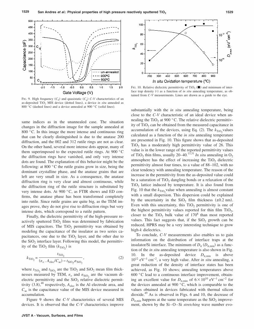
Figure 9 shows the C-V characteristics of several MIS
FIG. 9. High frequency �Ch� and quasistatic �Cq� C-V characteristics of anas-deposited TiO2 MIS device �dotted lines�, a device in situ annealed as800 °C �dashed lines� and a device annealed at 900 °C �solid lines�.
devices. It is observed that the C-V characteristics improve
JVST A - Vacuum, Surfaces, and Films
substantially with the in situ annealing temperature, beingclose to the C-V characteristic of an ideal device when an-nealing the TiO2 at 900 °C. The relative dielectric permittiv-ity of TiO2 can be obtained from the measured capacitance inaccumulation of the devices, using Eq. �2�. The kTiO2
valuescalculated as a function of the in situ annealing temperatureare presented in Fig. 10. This figure shows that as-depositedTiO2 has a moderately high permittivity value of 26. Thisvalue is in the lower range of the reported permittivity valuesof TiO2 thin films, usually 20–40.13,31 In situ annealing in O2
atmosphere has the effect of increasing the TiO2 dielectricpermittivity almost four times, to a value of 88–102, with noclear tendency with annealing temperature. The reason of theincrease in the permittivity from the as-deposited value couldbe a saturation of TiO2 dangling bonds or a relaxation of theTiO2 lattice induced by temperature. It is also found fromFig. 10 that the kTiO2
value when annealing is almost constantwith a small dispersion. This dispersion could be explainedby the uncertainty in the SiO2 film thickness �±0.2 nm�.Even with this uncertainty, this TiO2 permittivity is one ofthe highest permittivity values reported for thin film TiO2,closer to the TiO2 bulk value of 1708 than most reportedvalues. This fact suggests that, if the SiO2 growth can bereduced, HPRS may be a very interesting technique to growhigh-k dielectrics.
To conclude, C-V measurements also enables us to gaininformation on the distribution of interface traps at theinsulator/Si interface. The minimum of Dit �Dit,min� as a func-tion of the in situ annealing temperature is also shown in Fig.10. In the as-deposited device Dit,min is above1012 eV−1 cm−2, a very high value. After in situ annealing, agreat reduction of the density of interface states has beenachieved, as Fig. 10 shows; annealing temperatures above600 °C lead to a continuous interface improvement, obtain-ing an excellent value for Dit,min of 6�1010 eV−1 cm−2 forthe devices annealed at 900 °C, which is comparable to thevalues obtained in devices fabricated with thermal silicondioxide.49 As is observed in Figs. 6 and 10, the decrease ofDit,min happens at the same temperature as the SiO2 improve-
FIG. 10. Relative dielectric permittivity of TiO2 ��� and minimum of inter-face trap density ��� as a function of in situ annealing temperature, as ob-tained from C-V measurements. Lines are drawn as a guide to the eye.
ment, shown by the Si–O–Si stretching wave number evo-
1530 San Andres et al.: Physical properties of high pressure reactively sputtered TiO2 1530
lution towards the fully relaxed value, and the FWHM de-crease. As a consequence, it can be concluded that thereduction of the density of interface states with annealingtemperature is due to the improvement of the SiO2 film prop-erties, i.e., the reduction of SiO2 strain.
IV. CONCLUSION
The physical properties of TiO2 films deposited on Si bythe technique of high pressure reactive sputtering were stud-ied. The influence of in situ O2 annealing temperature onthese properties was also studied. TEM measurements showthat the TiO2 films deposited during 3 h are polycrystallinewith a mean thickness of about 58 nm, and that the grain sizeincreases with increasing annealing temperature. At theTiO2/Si interface a SiO2 layer grows spontaneously with athickness of 7–10.5 nm, depending on the annealing tem-perature. Compositional measurements prove that as-deposited TiO2 films have an oxygen excess, which is re-leased when increasing annealing temperature, until the TiO2
films reach the stoichiometric value when annealing at tem-peratures above 600 °C. FTIR, XRD, and ED measurementsprove that unannealed films are a mixture of anatase andrutile grains, and that by annealing a phase transformationoccurs, the rutile grains grow in size, whereas the anatasephase disappears when annealing at 900 °C. The relative di-electric permittivity of the annealed TiO2 films is extremelyhigh, with values of 88–102, comparable to the TiO2 bulkvalue.
ACKNOWLEDGMENTS
The authors acknowledge C.A.I. de Implantación Iónica�U.C.M.� for technical support, C.A.I. de espectroscopía forFTIR measurements and C.A.I. de difracción de rayos X forx-ray characterization. This work was partially supported bythe Spanish M.E.C., under Contract Nos. T.I.C. 01-1253 andTEC 2004-1237/MIC.
1S. Bryce, S. Richards, R. Richards, M. B. Boreland, and D. N. Jamieson,J. Vac. Sci. Technol. A 22, 339 �2004�.
2A. Rothschild, Y. Komem, A. Levakov, N. Ashkenasy, and Yoram Sha-pira, Appl. Phys. Lett. 82, 574 �2003�.
3B. Mguig, M. Calatayud, and C. Minot, Surf. Rev. Lett. 10, 175 �2003�.4A. Fujishima, K. Hashimoto, and T. Watanabe, TiO2 Photocatalysis: Fun-daments and Applications �BKC, Tokio, 1999�.
5J. Pan, C. Leygraf, D. Thierry, and A. M. Ektessabi, J. Biomed. Mater.Res. 35, 309 �1997�.
6The Economics of Titanium Minerals and Pigments �London, 2003�.7V. Romeas, P. Pichat, and C. Guillard, Ind. Eng. Chem. Res. 38, 3878�1999�.
8B. H. Lee, Y. Jeon, K. Zawadzki, W. -J. Qi, and J. Lee, Appl. Phys. Lett.74, 3143 �1999�.
9M. Tazawa, M. Okada, K. Yoshimura, and S. Ikezawa, Sol. Energy Mater.Sol. Cells 84, 159 �2004�.
10M. D. Stamate, Appl. Surf. Sci. 218, 317 �2003�.11B. S. Richards, J. E. Cotter, and C. B. Honsberg, Appl. Phys. Lett. 80,
1123 �2002�.12L. Miao, P. Jin, K. Kaneko, A. Terai, N. Nabatova-Gabain, and S. Tane-
mura, Appl. Surf. Sci. 212, 213, 255 �2003�.13M. Kadoshima, M. Hiratani, Y. Shimamoto, K. Torii, H. Miki, S. Kimura,
J. Vac. Sci. Technol. A, Vol. 23, No. 6, Nov/Dec 2005
and T. Nabatame, Thin Solid Films 424, 224 �2003�.14F. Gracia, J. P. Holgado, L. Contreras, T. Girardeau, and A. R. González-
Elipe, Thin Solid Films 429, 84 �2003�.15W. Westwood and D. Mattox, Sputtering �AVS, New York, 1977�.16B. Chapman, Glow Discharge Processes �Wiley, New York, 1980�.17N. Martin, C. Rousselot, D. Rondot, F. Palmino, and R. Mercier, Thin
Solid Films 300, 113 �1999�.18B. H. Lee, Y. Jeon, K. Zawadzki, W. -J. Qi, and J. Lee, Appl. Phys. Lett.
74, 3143 �1999�.19H. Ohsaki, Y. Tachibana, A. Mitsui, T. Kamiyama, and Y. Hayashi, Thin
Solid Films 392, 169 �2001�.20H. Tomaszewski, H. Poelman, D. Depla, D. Poelman, R. De gryse,
L. Fiermans, M.-F. Reyniers, G. Heynderickx, and G. B. Marin, Vacuum68, 31 �2003�.
21M. A. Navacerrada, M. L. Lucía, and F. Sánchez Quesada, Phys. Rev. B61, 6422 �2000�.
22M. A. Navacerrada, M. L. Lucía, and F. Sánchez-Quesada, Europhys.Lett. 54, 387 �2001�.
23W. Kern, RCA Rev. 31, 187 �1970�.24W. Bohne, J. Röhrich, and G. Röschert, Nucl. Instrum. Methods Phys.
Res. B 136–138, 633 �1998�.25W. Bohne, S. Hessler, and G. Röschert, Nucl. Instrum. Methods Phys.
Res. B 113, 78 �1996�.26E. H. Nicollian and J. R. Brews, MOS (Metal-Oxide-Semiconductor)
Physics and Technology �Wiley, New York, 1982�.27T. Ma, S. A. Campbell, R. Smith, N. Hoilien, B. He, W. L. Gladfelter,
C. Hobbs, D. Buchanan, C. Taylor, M. Gribelyuk, M. Tiner, M. Coppel,and J. J. Lee, IEEE Trans. Electron Devices 48, 2348 �2001�.
28T. Dimitrova and E. Atanassova, Solid-State Electron. 42, 307 �1998�.29B. -Y. Tsui and H. -W. Chang, J. Appl. Phys. 93, 10119 �2003�.30International Technology Roadmap for Semiconductors �Industry Asso-
ciation, 2002�; http://public.itrs.net.31Y. H. Lee, K. K. Chan, and M. J. Bracy, J. Vac. Sci. Technol. A 13, 596
�1995�.32M. Mayer, SIMNRA users guide, Report No. IPP 9/113, Max-Planck-
Institut für Plasmaphysik, Garching, Germany, 1997.33W. Bohne, W. Fuhs, J. Röhrich, B. Selle, I. Sieber, A. del Prado, E. San
Andrés, I. Mártil, and G. González-Díaz, Surf. Interface Anal. 34, 749�2002�.
34V. G. Erkov, S. F. Devyatova, E. L. Molodstova, T. B. Malsteva, andU. A. Yanovskii, Appl. Surf. Sci. 166, 51 �2000�.
35C. Pecharroman, F. Gracia, J. P. Holgado, M. Ocaña, A. R. González-Elipe, J. Bassas, J. Santiso, and A. Figueras, J. Appl. Phys. 93, 1 �2003�.
36M. Ocaña, V. Fornes, J. V. García Ramos, and C. J. Serna, J. Solid StateChem. 75, 364 �1988�.
37E. San Andrés, A. del Prado, I. Mártil, G. González-Díaz, D. Bravo, F. J.López, M. Fernández, W. Bohne, J. Röhrich, B. Selle, and I. Sieber,J. Appl. Phys. 94, 7462 �2003�.
38J. T. Fitch, S. S. Kim, and G. Lucovsky, J. Vac. Sci. Technol. A 8, 1871�1990�.
39D. V. Tsu, J. Vac. Sci. Technol. B 18, 1796 �2000�.40A. Sasella, A. Borghesi, F. Corni, A. Monelli, G. Ottaviani, R. Tonini, B.
Pivac, M. Bachetta, and L. Zanotti, J. Vac. Sci. Technol. A 15, 377�1997�.
41E. San Andrés, A. del Prado, I. Mártil, G. González-Díaz, and F. L.Martínez, J. Vac. Sci. Technol. B 21, 1306 �2003�.
42C. B. Samantaray, A. Dhar, D. Bhattacharya, M. L. Mukherjee, and S. K.Ray J. Mater. Res. 12, 365 �2001�.
43J. T. Last, Phys. Rev. 105, 1740 �1957�.44K. Guan, B. Lu, and Y. Yin, Surf. Coat. Technol. 173, 219 �2003�.45D. -J. Won, C. -H. Wang, H. -K. Jang, and D. -J. Choi, Appl. Phys. A:
Mater. Sci. Process. 73, 595 �2001�.46B. D. Cullity, Elements of X-Ray Diffraction, 2nd ed. �Addison–Wesley,
Reading, MA, 1978�.47P. A. Doyle and P. S. Turner, Acta Crystallogr., Sect. A: Cryst. Phys.,
Diffr., Theor. Gen. Crystallogr. 24, 390 �1968�.48M. L. Green, E. P. Gusev, R. Degraeve, and E. L. Garfunkel, J. Appl.
Phys. 90, 2057 �2001�.49D. R. Lee, G. Lucovsky, S. Denker, and C. Magee, J. Vac. Sci. Technol.
A 13, 1671 �1995�.