Nanomechanical resonant structures in single-crystal diamond

Photovoltaic absorption enhancement in thin-film solar cells by non-resonant beam collimation by submicron dielectric particlesConstantin R. Simovski, Alexander S. Shalin, Pavel M. Voroshilov, and Pavel A. Belov Citation: J. Appl. Phys. 114, 103104 (2013); doi: 10.1063/1.4820573 View online: http://dx.doi.org/10.1063/1.4820573 View Table of Contents: http://jap.aip.org/resource/1/JAPIAU/v114/i10 Published by the AIP Publishing LLC. Additional information on J. Appl. Phys.Journal Homepage: http://jap.aip.org/ Journal Information: http://jap.aip.org/about/about_the_journal Top downloads: http://jap.aip.org/features/most_downloaded Information for Authors: http://jap.aip.org/authors
Downloaded 11 Sep 2013 to 77.234.203.179. This article is copyrighted as indicated in the abstract. Reuse of AIP content is subject to the terms at: http://jap.aip.org/about/rights_and_permissions

Photovoltaic absorption enhancement in thin-film solar cellsby non-resonant beam collimation by submicron dielectric particles
Constantin R. Simovski,1 Alexander S. Shalin,2,3 Pavel M. Voroshilov,3 and Pavel A. Belov3
1School of Electrical Engineering, Department of Radio Science and Engineering, Aalto University,P.O. Box 13000, 00076 Aalto, Finland2Ulyanovsk Branch of Kotel’nikov Institute of Radio Engineering and Electronics, Goncharov Str. 48,432011 Ulyanovsk, Russia3National Research University of Information Technologies, Mechanics and Optics (ITMO),St. Petersburg 197101, Russia
(Received 11 June 2013; accepted 22 August 2013; published online 11 September 2013)
We propose the enhancement of the photovoltaic absorption in thin-film solar cells using densely
packed arrays (not obviously regular) of non-absorbing submicron or micron-sized dielectric spheres
located on top of the cell. The spheres can decrease reflection forming an effective blooming layer.
Simultaneously, they can suppress the transmission through the photovoltaic layer transforming the
incident radiation into a set of collimated beams. The focusing of the light inside the photovoltaic layer
allows enhanced absorption in it leading to the increase of the photovoltaic current. Every sphere
focuses the incident wave separately—this mechanism does not require collective effects or resonances
and therefore takes place in a wide spectral range. Since the fabrication of such the coating is easy, our
light-trapping structure may be cheaper than previously known light-trapping ones and perhaps even
than flat anti-reflecting coatings. VC 2013 AIP Publishing LLC. [http://dx.doi.org/10.1063/1.4820573]
I. INTRODUCTION
Photovoltaics (PV) is one of the most promising trends in
the modern energy industry. A large amount of toxic waste
generated by the high-purity semiconductor production forces
to pay attention to thin-film solar cells (TFSCs).1–4 The main
advantage of TFSCs is a very small amount of purified semi-
conductor required. The thickness of the PV layer can be as
small as 150-300 nm.1–4 The second important advantage is
the possibility of roll-to-roll processing on flexible substrates.4
The disadvantage of TFSCs is parasitic optical losses due to a
small thickness of the PV layer: the solar radiation transmit-
ting through the PV layer is then absorbed in the substrate. As
a result, the conventional anti-reflecting coating (ARC) can be
less efficient than so-called light-trapping structures (LTSs)
(see, e.g., in Refs. 5–19). LTSs reduce both the reflection
from a solar cell and the transmission through its PV layer.
They localize the incident electric field in the volume of the
PV semiconductor. Here, the transformation of the incident
wave field into near field is usually implied. Some authors
offer LTS performed as combinations of the PV medium with
photonic crystals;5–7 in some works, LTS are performed as
arrays of dielectric resonators,8,9 but most of the authors
develop plasmonic LTS.11–19 The common disadvantage of
plasmonic LTS and LTS based on dielectric resonators is their
resonant behavior that implies a rather narrow frequency
range of the light trapping effect poorly compatible with the
idea of so broadband structure as a solar cell. As to LTS per-
formed as photonic crystals, their stop-bands can be engi-
neered very broadband, however they are rather challenging
in fabrication and expensive.11–19
In this paper, we substantiate the possibility of non-
resonant, i.e., fundamentally broadband light trapping in the
PV layer of thickness 300–400 nm using analytical estimates
and accurate numerical simulations. The decrease of the
reflection of light and the suppression of the transmission
through the PV layer are carried out through two different
mechanisms. Our suggested LTS is so simple that can be even
cheaper for the mass production than the standard ARC.
II. THE MAIN MECHANISMS OF THE NON-RESONANTPHOTOVOLTAIC ABSORPTION ENHANCEMENT
A schematic view of our photovoltaic structure is shown
in Fig. 1. A layer of closely packed micron or submicron
dielectric (e.g., polystyrene, silica, etc.,) spheroidal particles is
placed on the surface of a PV layer of thickness d � 1000 nm.
The PV film is deposited on the aluminum-doped zinc oxide
(AZO) substrate. This system can be either obtained using the
atomic layer deposition (ALD), grown using the self-
organization of colloidal nanoparticles or simply mechanically
applied using the centrifuge (micron-sized silica and polysty-
rene particles are available on the market). It is necessary to
mention that the self-organization is much cheaper than
ALD-methods. In our simulations, the PV layer was doped
crystalline silicon with density of minor carriers in both
p-doped (150 nm-thick) and n-doped (150-nm thick) parts
equal to 3 � 1018 cm�3. Polystyrene spheres were chosen from
the reasons of low cost, absence of dispersion of the optical
constant in the visible range, and simplicity of the fabrication
process of both ALD and colloid self-assembly. The optical
constants of materials were taken from Refs. 20 and 21.
Obviously, two conditions must be satisfied to achieve
high values of the PV absorption using the LTS of spheres.
The first condition is minimization of the reflection from the
structure. For that, a layer of nanoparticles should operate as
an ARC. The second one is a concentration of electromag-
netic energy in the volume of the semiconductor. For this,
0021-8979/2013/114(10)/103104/6/$30.00 VC 2013 AIP Publishing LLC114, 103104-1
JOURNAL OF APPLIED PHYSICS 114, 103104 (2013)
Downloaded 11 Sep 2013 to 77.234.203.179. This article is copyrighted as indicated in the abstract. Reuse of AIP content is subject to the terms at: http://jap.aip.org/about/rights_and_permissions

the LTS should prevent the transmission through the PV
layer.
The suppression of reflection occurs through the interac-
tion of the incident wave with the nanostructure mostly due
to the dipole component scattered by the nanoparticles.22–24
The localization of the radiation arises due to the high-
intensity decaying harmonics that occur through excitation
of multipole moments of high order.25 The last effect can be
simply described as the collimation of the transmitted light
impinging every sphere. The balance of these two mecha-
nisms should give an optimal effect. Here, we do not use any
of resonance mechanisms as well as no photonic crystal
regime—the strict regularity of the array of closely packed
spheres is not a crucial condition. Thus, we believe that the
total light absorption after the correct design of all parame-
ters should be enhanced significantly compared to the open
interface of the solar cell.
III. FIELD CONCENTRATION
First, let us consider a monolayer of nanospheres
located on the surface of a semi-infinite crystalline silicon.
We use this approach to determine the approximate range
of the nanoparticles radii that allows to achieve the optimal
absorption. The resulting spectra will be calculated further
using numerical methods without these approximations.
Hereinafter, we will assume the normally incident wave,
which is polarized along the x axis.
The transmission of radiation into the substrate plays
an important role due to the small thickness of PV layer in
the structure. Therefore, let us explore the possibility of
light collimation through the excitation of high-order multi-
poles in the nanospheres. The stronger is the focusing of the
incident wave inside the PV layer, the larger is the ratio of
the local field to the incident one jE=Eij, and hence the
absorption of light in the PV layer. Respectively, as the
absorption increases, the parasitic transmittance through the
PV layer decreases. Of course, this focusing is diffraction-
limited, but the question is, how onerous restriction is the dif-
fraction limit for realistic TFSCs? Elementary estimations show
that this restriction has no practical significance for
d > 200–300 nm, although in the literature, it is often stated
otherwise.6,10,19,26,27 For example, in amorphous silicon, the
wavelength is shortened about 4 times as compared with the
wavelength in free space (being averaged over the visible
range). So, the wavelength in the material is as small as
100–200 nm. However, the thickness of the PV layer should not
be smaller than 100 nm, otherwise it will be thinner than the
width of the depletion region and the efficiency of the TFSC
will drop unacceptably. For an a-Si TFSC that does not yield in
its efficiency to a wafer solar cell, the PV layer should have
thickness d � 300 nm, i.e., be larger than the wavelength in the
medium. Therefore, for LTS, there is no any obvious need in
huge local field enhancement and nanometer scaled hot spots.
The concentration of the field by such purely wave process as
the wave beam collimation (achievable with dielectric micro- or
nanospheres) can be sufficient to get an optimal absorption of
the incident wave. Our calculations show that the beam collima-
tion inside the silicon layer of thickness d ¼ 300–400 nm is
enough to substantially reduce the transmission through the PV
layer if the effective beam width is nearly equal to d. The con-
centration of the field in the z-direction (along the wave inci-
dence) is also desirable; but under the condition of the sufficient
collimation, it is not critical.
Let us estimate the dependence of the quadrupole
moment of nanospheres (or spheroid) on wavelength and
size of particles. We used the method proposed in Ref. 28
for qualitative evaluations for the case of isolated sphere tak-
ing into account its reflection in the substrate (a semi-infinite
crystalline silicon). Details of this approach are presented in
the paper.28 Taking into account the field inhomogeneity
inside the particle, its internal polarization can be approxi-
mately represented as follows:28
PpðrÞ ¼ Ppðr0Þ þ ðDrrÞPpjr0: (1)
Here, r0 is the coordinate of the center of the particle, r is
the radius vector of a point inside the particle, Dr ¼ r� r0.
Thus, we consider inhomogeneity of the field that character-
izes the quadrupole moment taking into account the gradient
of polarization,28 which is proportional to the gradient of the
electric field because PpðrÞ ¼ e0ðe� 1ÞEðrÞ. We can write
an expression for the vertical gradient of the field inside a
nanosphere
@Ex
@z� 120apb expð�iak0Þð1þ R̂12 expð2iak0ÞÞz4
3a2apbðapb� 32z3Þ þ 80z5ð�apbþ 8z3Þ ;(2)
where k0 is the wave number in vacuum, a is the radius of a
sphere, and it is denoted
ap ¼ a3 e� 1
eþ 2; b ¼ em � 1
eþ 2:
Here, em is the dielectric permittivity of the substrate (PV
medium), and z is the distance from the point inside the parti-
cle to the substrate. In the further estimations, one uses the
FIG. 1. A schematic view of thin film solar cell with nanosphere coating.
Polystyrene particles (e ¼ 2:53) are packed in a square array on the surface
of the doped crystalline silicon film of thickness d¼ 300 nm. The density of
carriers in the silicon layer is assumed to be 3 � 1018 cm�3. Substrate—AZO
(es ¼ 3:53þ i0:004 at the wavelength of 600 nm).
103104-2 Simovski et al. J. Appl. Phys. 114, 103104 (2013)
Downloaded 11 Sep 2013 to 77.234.203.179. This article is copyrighted as indicated in the abstract. Reuse of AIP content is subject to the terms at: http://jap.aip.org/about/rights_and_permissions

averaged value of the field gradient (averaging is done
over the particle cross section). Then, z in formula (2) is
taken z¼ a. Expression (2) after multiplication by ð3=4pÞðe� 1Þ=ðeþ 2Þ gives the averaged gradient of polarization
of the nanosphere and therefore determines the vertical (zz)
component of the quadrupole moment.28 Fig. 2 shows the
distribution of j@Exða; �=@zj according to which the position
of maxima and minima of the quadrupole moment on the
wavelength axis is practically a linear function of a, and is
significant at a ¼ 400� 500 nm. For such values of a,
according to the results of our numerical calculation, multi-
pole moments of high order play an important role in the
formation of the scattering spectrum. The presence of high-
order multipoles results in the formation of the collimated
beam below the sphere illuminated by the plane wave inci-
dent from top. This effect is known and under the name
of photonic nanojet has been considered in Refs. 29–31.
This effect in our structure is illustrated by Fig. 3.
Here, we depict electric field amplitude, magnetic
field amplitude, and local energy density in a cross section
of the PV structure at a frequency 575 THz for the case
a ¼ 450 nm. Simulations were done using the package
Comsol Multiphysics. It should be noted that the effective
width of the collimated beam in the PV layer at this fre-
quency is about 370 nm. This collimation is sufficient for
effective light absorption in the PV layer. Less than 10% of
the incident power is transmitted into the substrate at this fre-
quency. About 35% of the energy incident on the sphere is
reflected in this case (which is not worse than for the open
surface of the PV layer).
We made analytical estimations of the quadrupole
moment based on formula (2). They are in good agreement
with the results of exact numerical simulations. A difference
is caused by the influence of higher-order multipole
moments (also, notice that the results presented in Fig. 2
were obtained in the approximation of semi-infinite silicon
substrate, whereas the numerical simulations were done for
the case d ¼ 300 nm and the AZO substrate). It should be
noted that larger spheres can further enhance the effect of
collimation but the increase of a also leads to the increase of
the reflection and scattering losses.
IV. SUPPRESSION OF REFLECTION
The next step is the suppression of reflection. It can be
achieved through a dense arrangement of spheres, whereby
the upper surface of the array emulates a textured interface.
Let us consider this system qualitatively in the frame of
dipole approximation. According to our studies,22–24 the
array of nanospheres (even closely packed) under this
approximation can be replaced by a flat reflective surface
(often called metasurface) referred to the plane crossing
centres of spheres. Then, the reflection can be described by
the Airy-like formula for two interfaces24
FIG. 2. The electric field gradient inside the particle along the z-axis
depending on the radius of spheres and frequency. A single spherical particle
is placed on the surface of a semi-infinite substrate of doped crystalline sili-
con with a carrier concentration of 3 � 1018 cm�3. The external wave is nor-
mally incident and x-polarized.
FIG. 3. Electric field amplitude (a), magnetic field amplitude (b), and energy density (c) in the cross section of the PV structure at frequency of 575 THz.
Radius of spheres is equal to 450 nm, the external wave is normally incident, the other parameters are the same as in Fig. 1. A horizontal line at the sphere cen-
ter shows the location of the metasurface modeling the array.
103104-3 Simovski et al. J. Appl. Phys. 114, 103104 (2013)
Downloaded 11 Sep 2013 to 77.234.203.179. This article is copyrighted as indicated in the abstract. Reuse of AIP content is subject to the terms at: http://jap.aip.org/about/rights_and_permissions

r̂ ¼ Eref lð0; tÞEIð0; tÞ
¼ R̂l þ R̂12 expf2iðk0DÞg1� R̂21R̂l expf2iðk0DÞg
;
t̂ ¼ EtransðD; tÞEIð0; tÞ
¼ T̂ l � T̂12 expfiðk0DÞg1� R̂21R̂l expf2iðk0DÞg
;
(3)
where k0 is the wave vector of the incident field in vacuum,
r̂; t̂ are reflection and transmission coefficients, Eref lð0; tÞ is
the strength of the reflected field (on a plane through the
centers of nanoparticles—the locations of point dipoles,
which model spherical particles (i.e., radius-vectors of the
spheres centers). EtransðD; tÞ is the strength of the transmit-
ted field, T̂ and R̂ are tensors of the Fresnel reflection and
transmission coefficients (12—incident wave from the
vacuum to the medium and 21—from the medium to the
vacuum). Tensors T̂ l and R̂l characterize the reflection and
the transmission of light by the metasurface emulating the
layer of nanoparticles. According to Refs. 22–24, they can
be approximately written as
jR̂lðk0Þj ¼ffiffiffiffiffiffiffiffiffiffiffiffiffiffiffiffiffiffiffiffiffiffi
1
Fðk0Þ2 þ 1
s;
Fðk0Þ �k0
4p2n1
�jd1 � d2j
ap� 4:29
jd1 � d2j1=2
�
þ 1
3p
�1:461þ 1:797
ffiffiffiffiL0p
k0
þ 1:776L0
k20
�; (4)
qlðk0Þ � arctg
"� 0:155þ
�0:683� jd1 � d2j3=2
2app
�k0ffiffiffiffiL0p
� 0:191ffiffiffiffiL0p
k0
� 0:188
k20
L0
#þ sign½n� n1�p; (5)
T̂ l ¼ 1þ R̂l; (6)
where n1 is the refractive index of the medium in which par-
ticles are arranged (in our case n1 ¼ 1), R̂l ¼ jR̂ljexpðiqlÞ;L0 ¼ ð2pn1Þ2jd1 � d2j; k0 is the wavelength in vacuum,
and d1; d2 are the lattice constants of the layer. Radiation
damping of nanospheres is taken into account in the expres-
sions (4) and (5). Note that the dipole approximation can not
be used for the quantitative calculation for the particles of
size of a few hundred nanometers. However, it is quite appli-
cable for the qualitative assessment of the frequency aver-
aged effect.
Reflection spectrum of the system depending on fre-
quency � ¼ x=2p and the radius a is depicted in Fig. 4. The
regular arrangement of spheres in the square grid and slightly
aperiodic arrangement give practically the same result. As fol-
lows from Fig. 4, the broadband reflection minimum occurs
within the range a ¼ 400� 600 nm. The structure operates as
an ARC, since the averaged reflectance is lower than that of
the open surface of the doped silicon. For lower values of a,the reflection is rapidly growing. A similar increasing of the
reflection also occurs at larger values of a. Moreover, the scat-
tering maxima arise in the upper half-space and result in sig-
nificant scattering losses for a > 600 nm.
Fig. 5 shows the results of an exact numerical calcula-
tion of the reflection from the structure depicted in Fig. 1 in
the operating frequency range for the open surface of the so-
lar cell (dashed line) and in the presence of the nanospheres
(solid line). The radius of nanospheres is chosen to be
a ¼ 450 nm. The power reflectance averaged over the visible
range was calculated for two cases (open surface and nano-
spheres), and the decrease of the reflection is as follows:
GR ¼
ðRspheres dxðRopen dx
¼ 0:66: (7)
Thus, our structure operates as anti-reflecting coating reduc-
ing the integral reflection by 34%.
V. PHOTOVOLTAIC ABSORPTION
For an accurate calculation of the reflection and PV
absorption spectra for the system (see in Fig. 1), we used the
FIG. 4. The dependence of the reflection coefficient on the radius of spheres
and frequency. The monolayer of mutually touching spheres is placed on a
semi-infinite doped silicon substrate. The external wave is normally incident.
FIG. 5. Reflectance from the PV structure described in Fig. 1 for the pure
surface (dashed line) and at the presence of a coating of nanospheres (solid
line). Radius of spheres is equal to 450 nm. The external wave is normally
incident. Numerical calculations are performed in Comsol Multiphysics and
CST Microwave Studio.
103104-4 Simovski et al. J. Appl. Phys. 114, 103104 (2013)
Downloaded 11 Sep 2013 to 77.234.203.179. This article is copyrighted as indicated in the abstract. Reuse of AIP content is subject to the terms at: http://jap.aip.org/about/rights_and_permissions
Finite Element Method implemented in the commercial
product Comsol Multiphysics and verified these simulations
using another commercial package—CST Microwave Studio
implementing the Finite-Difference-Time-Domain method.
The results obtained using these software packages are
in good agreement with each other and with the fields
calculated analytically for the open surface of the PV layer
(without nanospheres). Mutual agreements prove the reliabil-
ity of our results.
According to preliminary estimates made in the previous
sections of this paper, the best balance of the two mechanisms
for increasing the efficiency of the PV conversion occurs in the
range of a ¼ 400� 550 nm. Further, we optimized the struc-
ture by the brute force method varying the value of the radius
with the step Da ¼ 25 nm. The results show that the greatest
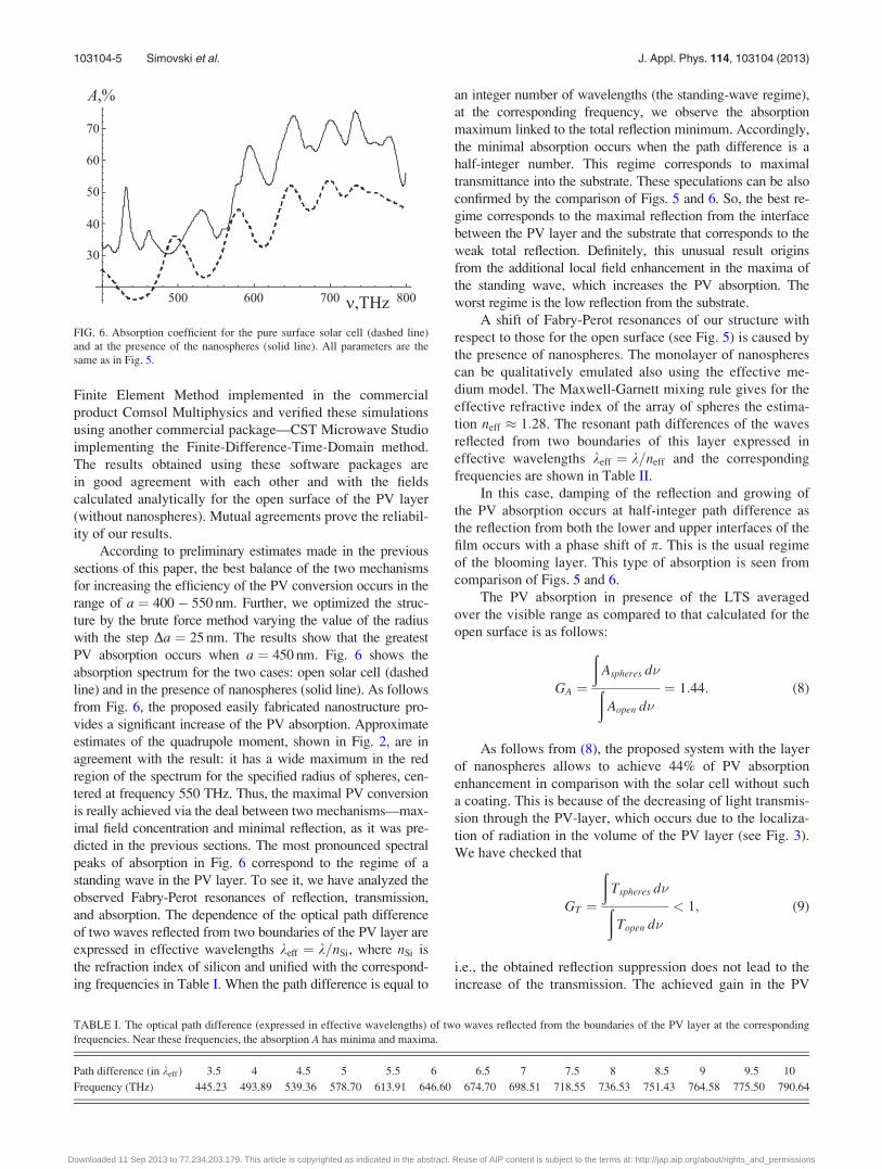
PV absorption occurs when a ¼ 450 nm. Fig. 6 shows the
absorption spectrum for the two cases: open solar cell (dashed
line) and in the presence of nanospheres (solid line). As follows
from Fig. 6, the proposed easily fabricated nanostructure pro-
vides a significant increase of the PV absorption. Approximate
estimates of the quadrupole moment, shown in Fig. 2, are in
agreement with the result: it has a wide maximum in the red
region of the spectrum for the specified radius of spheres, cen-
tered at frequency 550 THz. Thus, the maximal PV conversion
is really achieved via the deal between two mechanisms—max-
imal field concentration and minimal reflection, as it was pre-
dicted in the previous sections. The most pronounced spectral
peaks of absorption in Fig. 6 correspond to the regime of a
standing wave in the PV layer. To see it, we have analyzed the
observed Fabry-Perot resonances of reflection, transmission,
and absorption. The dependence of the optical path difference
of two waves reflected from two boundaries of the PV layer are
expressed in effective wavelengths keff ¼ k=nSi, where nSi is
the refraction index of silicon and unified with the correspond-
ing frequencies in Table I. When the path difference is equal to
an integer number of wavelengths (the standing-wave regime),
at the corresponding frequency, we observe the absorption
maximum linked to the total reflection minimum. Accordingly,
the minimal absorption occurs when the path difference is a
half-integer number. This regime corresponds to maximal
transmittance into the substrate. These speculations can be also
confirmed by the comparison of Figs. 5 and 6. So, the best re-
gime corresponds to the maximal reflection from the interface
between the PV layer and the substrate that corresponds to the
weak total reflection. Definitely, this unusual result origins
from the additional local field enhancement in the maxima of
the standing wave, which increases the PV absorption. The
worst regime is the low reflection from the substrate.
A shift of Fabry-Perot resonances of our structure with
respect to those for the open surface (see Fig. 5) is caused by
the presence of nanospheres. The monolayer of nanospheres
can be qualitatively emulated also using the effective me-
dium model. The Maxwell-Garnett mixing rule gives for the
effective refractive index of the array of spheres the estima-
tion neff � 1:28. The resonant path differences of the waves
reflected from two boundaries of this layer expressed in
effective wavelengths keff ¼ k=neff and the corresponding
frequencies are shown in Table II.
In this case, damping of the reflection and growing of
the PV absorption occurs at half-integer path difference as
the reflection from both the lower and upper interfaces of the
film occurs with a phase shift of p. This is the usual regime
of the blooming layer. This type of absorption is seen from
comparison of Figs. 5 and 6.
The PV absorption in presence of the LTS averaged
over the visible range as compared to that calculated for the
open surface is as follows:
GA ¼
ðAspheres d�ðAopen d�
¼ 1:44: (8)
As follows from (8), the proposed system with the layer
of nanospheres allows to achieve 44% of PV absorption
enhancement in comparison with the solar cell without such
a coating. This is because of the decreasing of light transmis-
sion through the PV-layer, which occurs due to the localiza-
tion of radiation in the volume of the PV layer (see Fig. 3).
We have checked that
GT ¼
ðTspheres d�ðTopen d�
< 1; (9)
i.e., the obtained reflection suppression does not lead to the
increase of the transmission. The achieved gain in the PV
FIG. 6. Absorption coefficient for the pure surface solar cell (dashed line)
and at the presence of the nanospheres (solid line). All parameters are the
same as in Fig. 5.
TABLE I. The optical path difference (expressed in effective wavelengths) of two waves reflected from the boundaries of the PV layer at the corresponding
frequencies. Near these frequencies, the absorption A has minima and maxima.
Path difference (in keff ) 3.5 4 4.5 5 5.5 6 6.5 7 7.5 8 8.5 9 9.5 10
Frequency (THz) 445.23 493.89 539.36 578.70 613.91 646.60 674.70 698.51 718.55 736.53 751.43 764.58 775.50 790.64
103104-5 Simovski et al. J. Appl. Phys. 114, 103104 (2013)
Downloaded 11 Sep 2013 to 77.234.203.179. This article is copyrighted as indicated in the abstract. Reuse of AIP content is subject to the terms at: http://jap.aip.org/about/rights_and_permissions

absorption is not huge (the total PV absorption would corre-
spond to the twice higher gain), however this result is only
the first step in the direction we pointed out and we hope to
improve it.
VI. CONCLUSION
In this paper, we proposed an array of non-resonant sub-
micron dielectric particles (e.g., polystyrene spheres) with
negligible optical losses for a significant increase of the PV
absorption in thin-film solar cells. Instead of the utilization
of a resonator regime of light-trapping, we suggest a broad-
band regime, which is the deal between the reduction of the
transmittance through the thin PV layer and the reduction of
the overall reflectance. Each sphere (or spheroid) transforms
the incident light into a collimated light beam propagating in
the lossy PV layer with a strong attenuation. Stronger colli-
mation of the beam leads to its greater attenuation. Thus, it is
possible to prevent an increase of the light transmission into
the substrate even for the silicon layer as thin as d ¼ 300 nm.
The decrease of the reflection is the collective effect. It can
be described as the effect of an effective layer formed by
closely packed spheres. For larger spheres, the collimation of
the beam in the PV layer is higher but the reflection also
increases, so that there is an optimal radius of the spheres.
The best balance has been achieved in our numerical exam-
ple. This example corresponds to the gain in the PV absorp-
tion GA ¼ 1:44. We believe that a design of the TFSC can be
found for which this gain will be higher than we have
obtained in the present paper.
It should be noted that the use of the array of polysty-
rene or silica spheres instead of a flat anti-reflecting coating
will hardly increase the cost of the fabrication. Really, in
Ref. 32, it was especially proposed to use arrays of polysty-
rene spheres with a diameter d¼ 1 micron in order to reduce
the cost of production of an ARC for the solar cells of the
wafer-type based on gallium arsenide. In that paper, authors
analyzed only the possibility of reducing the reflection of
light from the PV layer by the use of a structured surface.
The problem of preventing the transmission of light into the
substrate in Ref. 32 was not studied because it was not rele-
vant for the GaAs PV layer (which is more absorptive than
the silicon one) with the thickness larger than d¼ 5 microns
Respectively, in Ref. 32, the field distribution inside the
spheres and under them was not considered. The message of
Ref. 32 that the application of the densely packed array of
microspheres, which are produced commercially on the sur-
face of the semiconductor, is simpler and cheaper than grow-
ing textured or planar blooming layer, whereas the
suppression of the reflection is nearly the same.
We hope that physical mechanisms of the interaction of
light with dielectric particles we have revealed in this paper
will help to realize a significant increase of the PV absorp-
tion in thin-film solar cells in a way more attractive for
industrial adaptation than LTS based on photonic crystals,
arrays of plasmonic or dielectric nanoantennas, and other
resonant nanostructures.
ACKNOWLEDGMENTS
This work has been partially supported by the grants of
Russian Fund for Basic Research (number 12-02-31423-mol a,
number 13-02-90765-mol rf nr, 14-08-31730-mol a), of the
Ministry of Education and Science of Russian Federation (num-
bers 14.B37.21.1634, 14.B37.21.0307, and 11.G34.31.0020)
and of the Dynasty Foundation.
1A. Marti and A. Luque, Next-Generation Photovoltaics (Institute of
Physics Publishing, Bristole, Philadelphia, 2004).2J. Nelson, The Physics of Solar Cells (Imperial College Press, London, 2003).3M. A. Green, Solar Cells: Operating Principles, Technology and SystemApplications (University of South Wales, Sydney, 1998).
4“Ultra-low-cost solar electricity cells,” An Overview of Nanosolar’sCell Technology Platform, White Paper (Nanosolar, Inc., 2009),
available at www.catharinafonds.nl/wp-content/uploads/2010/03/
NanosolarCellWhitePaper.pdf.5A. Mihi and H. Myguez, J. Phys. Chem. B 109, 15968 (2005).6P. Bermel, C. Luo, L. Zeng, L. C. Kimerling, and J. D. Joannopoulos, Opt.
Express 15, 16986 (2007).7S. B. Mallick, M. Agrawal, and P. Peumans, Opt. Express 18, 5691 (2010).8J. Grandidier, D. M. Callahan, J. N. Munday, and H. A. Atwater, Adv.
Mater. 23, 1272 (2011).9Y. Yu, V. E. Ferry, A. P. Alivisatos, and L. Cao, Nano Lett. 12, 3674 (2012).
10S. Pillai, K. R. Catchpole, T. Trupke, and M. A. Green, J. Appl. Phys. 101,
093105 (2007).11N. C. Panoiu and R. M. Osgood, Opt. Lett. 32, 2825 (2007).12K. R. Catchpole and A. Polman, Appl. Phys. Lett. 93, 191113 (2008).13Yu. A. Akimov, K. Ostrikov, and E. P. Li, Plasmonics 4, 107 (2009).14C. Rockstuhl and F. Lederer, Appl. Phys. lett. 94, 213102 (2009).15M. E. Ferry, L. A. Sweatlock, D. Pacifici, and H. A. Atwater, Nano Lett. 8,
4391 (2008).16R. A. Pala, J. White, E. Barnard, J. Liu, and M. L. Brongersma, Adv.
Mater. 21, 3504 (2009).17P. A. Spinelli, V. E. Ferry, J. van de Groep, M. van Lare, M. A.
Verschuuren, R. E. I. Schropp, H. A. Atwater, and A. Polman, J. Opt. 14,
024002 (2012).18Y. Wang, T. Sun, T. Paudel, Y. Zhang, Zh. Ren, and K. Kempa, Nano
Lett. 12, 440 (2012).19H. A. Atwater and A. Polman, Nature Mater. 9, 205 (2010).20A. S. Ferlauto, G. M. Ferreira, J. M. Pearce, C. R. Wronski, R. W. Collins,
X. Deng, and G. Ganguly, J. Appl. Phys. 92, 2424 (2002).21G. V. Naik, J. Kim, and A. Boltasseva, Opt. Mater. Express 1, 1090 (2011).22A. S. Shalin, JETP Lett. 91, 636 (2010).23A. S. Shalin, Quantum Electron. 41, 163 (2011).24A. S. Shalin, Prog. Electromagn. Res. B 31, 45 (2011).25M. I. Mishchenko, L. D. Travis, and A. A. Lacis, Scattering, Absorption
and Emission of Light by Small Particles (Cambridge University Press,
Cambridge, 2002).26D. M. Callahan, J. N. Munday, and H. A. Atwater, Nano Lett. 12, 214 (2012).27Z. Yu, A. Raman, and S. Fan, Opt. Express 18, A366 (2010).28S. V. Sukhov, Opt. Spectrosc. 98, 301 (2005).29Z. Chen, A. Taflove, and V. Backman, Opt. Express 12, 1214 (2004).30A. V. Itagi and W. A. Challener, J. Opt. Soc. Am. A 22, 2847 (2005).31S. Lecler, Y. Takakura, and P. Meyrueis, Opt. Lett. 30, 2641 (2005).32T. H. Chang, P. H. Wu, S. H. Chen, C. H. Chan, C. C. Lee, C. C. Chen,
and Ya. K. Su, Opt. Express 17, 6519 (2009).
TABLE II. The dependence of the optical path difference (in effective
wavelengths) of two waves reflected from the effective boundaries of the
layer emulating the array of nanospheres at the corresponding frequency.
Path difference 3.5 4 4.5 5 5.5 6
Frequency (THz) 459.00 524.57 590.14 655.71 721.29 786.86
103104-6 Simovski et al. J. Appl. Phys. 114, 103104 (2013)
Downloaded 11 Sep 2013 to 77.234.203.179. This article is copyrighted as indicated in the abstract. Reuse of AIP content is subject to the terms at: http://jap.aip.org/about/rights_and_permissions
Copyright © 2022 FDOKUMEN


![Resonant Raman effect enhanced by surface plasmon excitation of CdSe nanocrystals embedded in thin SiO[sub 2] films](https://static.fdokumen.com/doc/165x107/634518516cfb3d40640985a1/resonant-raman-effect-enhanced-by-surface-plasmon-excitation-of-cdse-nanocrystals.jpg)