Phonon nanocapacitor for storage and lasing of terahertz lattice waves
11
arXiv:1411.5491v1 [cond-mat.mes-hall] 20 Nov 2014 Phonon nanocapacitor for storage and lasing of terahertz lattice waves Haoxue Han, 1, 2 Baowen Li, 3, 4, 5 Sebastian Volz, 1, 2 and Yuriy A. Kosevich 1, 2, 6 1 CNRS, UPR 288 Laboratoire d’Energ´ etique Mol´ eculaire et Macroscopique, Combustion (EM2C), Grande Voie des Vignes, 92295 Chˆ atenay-Malabry, France 2 Ecole Centrale Paris, Grande Voie des Vignes, 92295 Chˆ atenay-Malabry, France 3 Department of Physics, Centre for Computational Science and Engineering, and Graphene Research Center, National University of Singapore, 117546 Singapore 4 NUS Graduate School for Integrative Sciences and Engineering, National University of Singapore, 117542 Singapore 5 Center for Phononics and Thermal Energy Science, School of Physics Science and Engineering, Tongji University, 200092 Shanghai, P. R. China 6 Semenov Institute of Chemical Physics, Russian Academy of Sciences, Kosygin str. 4, Moscow 119991, Russia (Dated: November 21, 2014) Abstract We introduce a novel ultra-compact nanocapacitor of coherent phonons formed by high-finesse interference mirrors based on atomic-scale semiconductor metamaterials. Our molecular dynamics simulations show that the nanocapacitor stores THz monochromatic lattice waves, which can be used for phonon lasing - the emission of coherent phonons. Either one- or two-color phonon lasing can be realized depending on the geometry of the nanodevice. The two color regimes of the capacitor originates from the distinct transmittance dependance on the phonon wave packet incident angle for the two phonon polarizations at their respective resonances. Phonon nanocapacitor can be charged by cooling the sample equilibrated at room temperature or by the pump-probe technique. The nanocapacitor can be discharged by applying tunable reversible strain, resulting in the emission of coherent THz acoustic beams. 1
-
Upload
independent -
Category
Documents
-
view
2 -
download
0
Transcript of Phonon nanocapacitor for storage and lasing of terahertz lattice waves
arX
iv:1
411.
5491
v1 [
cond
-mat
.mes
-hal
l] 2
0 N
ov 2
014
Phonon nanocapacitor for storage and lasing of terahertz lattice
waves
Haoxue Han,1, 2 Baowen Li,3, 4, 5 Sebastian Volz,1, 2 and Yuriy A. Kosevich1, 2, 6
1CNRS, UPR 288 Laboratoire d’Energetique Moleculaire et Macroscopique,
Combustion (EM2C), Grande Voie des Vignes, 92295 Chatenay-Malabry, France
2Ecole Centrale Paris, Grande Voie des Vignes, 92295 Chatenay-Malabry, France
3Department of Physics, Centre for Computational Science and Engineering,
and Graphene Research Center, National University of Singapore, 117546 Singapore
4NUS Graduate School for Integrative Sciences and Engineering,
National University of Singapore, 117542 Singapore
5Center for Phononics and Thermal Energy Science,
School of Physics Science and Engineering,
Tongji University, 200092 Shanghai, P. R. China
6Semenov Institute of Chemical Physics,
Russian Academy of Sciences, Kosygin str. 4, Moscow 119991, Russia
(Dated: November 21, 2014)
Abstract
We introduce a novel ultra-compact nanocapacitor of coherent phonons formed by high-finesse
interference mirrors based on atomic-scale semiconductor metamaterials. Our molecular dynamics
simulations show that the nanocapacitor stores THz monochromatic lattice waves, which can be
used for phonon lasing - the emission of coherent phonons. Either one- or two-color phonon lasing
can be realized depending on the geometry of the nanodevice. The two color regimes of the capacitor
originates from the distinct transmittance dependance on the phonon wave packet incident angle for
the two phonon polarizations at their respective resonances. Phonon nanocapacitor can be charged
by cooling the sample equilibrated at room temperature or by the pump-probe technique. The
nanocapacitor can be discharged by applying tunable reversible strain, resulting in the emission of
coherent THz acoustic beams.
1
Phonons, quanta of lattice waves, having significantly shorter wavelengths than photons
at the same frequency, may enable us to pursue improved resolution in tomographic, ultra-
sonic and other imaging techniques using focused sound waves. In particular, the terahertz
(THz) phonons that have wavelengths comparable to the lattice constants would allow us
to detect microscopic structure of the material up to the atomic scale with high precision.
To this end, coherent phonons are urgently desired. Coherent lattice waves have been stud-
ied in semiconductor superlattices[1–4], optomechanical systems[5–7] and electromechani-
cal resonators[8–10]. Coherent phonon manipulations for energy transport in dynamical
nanosystems has been an emerging focus of research[12]. The development of nanophononic
devices which enable controllabe generation and coherent emission of phonons has recently
emerged as the subject of intense interest[1–3, 5–7, 10, 13, 14]. Conventional sources of
sound waves, such as piezoelectric transducers, fail to operate efficiently above a few tens of
gigahertz (GHz). The highest emitted-phonon frequency was achieved in a semiconductor
superlattice under electrical bias in which half-THz coherent phonons were released during
electrons tunneling through the quantum wells[3]. Similar coherent phonon emission was
also observed in hybrid optomechanical schemes in which optically pumped microcavities
produce stimulated acoustic emission in the range of MHz[6] and GHz[13]. An entirely me-
chanical phonon laser at sub-MHz was achieved in an electromechanical resonator[8, 9] in
analogy with a three-level laser scheme[10]. For these systems, the need for strong optical
pumping or complex actuator tuning may limit the development of phonon lasers because
unavoidable compromises have to be made in the design scheme.
In this Letter, we introduce a three-dimensional (3D) phonon nanocapacitor based on
atomic-scale semiconductor metamaterials. The nanocapacitor allows for generation of THz
coherent phonons with an ultra-high monochromatic quality by an adiabatic cooling of the
nanodevice or by the pump-probe optical technique [1, 2]. We show that the nanocavity
structure formed by high-finesse phonon interference mirrors (PIMs) can efficiently store a
large number of coherent out-of-equilibrium phonons. The nanocapacitor can emit coherent
THz phonon beams upon application of tunable reversible strain. Such emission can be
considered as “phonon lasing”. Either one- or two-color phonon lasing can be realized
depending on the geometry of the nanodevice, in contrast to the usual one-color photon
lasing. The achievement of generation and emission of coherent THz lattice waves will
provide an essential step towards active hypersound devices and nanophononic applications
2

FIG. 1. Silicon phonon capacitor composed of two phonon interference mirrors (PIMs)
separated by a spacer. a, The atomistic view of the phonon capacitor and mirrors. The atoms in
brown are Ge impurity atoms and the green ones are the Si atoms of the host lattice. b, Two heat
sinks coupled to the phonon capacitor. The dimensions of the capacitor are chosen as Lcx = Lc
y = 8
nm and Lcz = 35 nm.
FIG. 2. Power spectral density of atomic kinetic energy as a function of time delay t
after the cooling onset in different geometries. a,b, Nanocapacitor with Lcx = Lc
y = 8 nm
and Lcz = 35 nm (a) and Lc
x = Lcy = 33 nm and Lc
z = 35 nm (b). c,d, Gaussian fit of the capacitor
phonon peak to measure the full width at half maximum (FWHM) ∆ω for the peaks in (a) and
(b), shown by (c) and (d), respectively. The lines and symbols are Gaussian functions and MD
results.
of THz acoustics, including surgery with focused ultra- and hyper-sound in medicine[11].
A detailed atomistic presentation of the phonon capacitor is depicted in Fig. 1(a). The
capacitor consists of two PIMs separated by a spacer made of bulk silicon (Si). The PIM
is composed of an atomic-scale metafilm: an internal atomic plane in Si lattice embedded
with segregated Germanium (Ge) impurities atoms, as shown in Fig. 1(a). The assisted
3
laser Molecular Beam Epitaxy (MBE) have achieved atomically sharp interfaces in a super-
lattice [18] and can hence provide a possible experimental implementation for our proposed
nanocapacitor structure since this technique can reach the resolution of a single unit cell in
the lattice. In the molecular dynamics (MD) simulations, the covalent Si:Si/Ge:Ge/Si:Ge
interactions are modeled by the Stillinger-Weber (SW) potential[24], which includes both
two- and three-body potential terms. The SW potential has been widely used to study
the thermal[25, 26] and mechanical[27] properties of Si and Ge materials for its best fit for
experimental results. All the MD simulations were performed with LAMMPS [28].
We first implement the charging of a phonon capacitor by cooling a sample equilibrated
at room temperature by MD simulations. Two heat sinks are coupled to the capacitor on
the two facets of the mirrors, as shown in Fig. 1(b). The phonons in the capacitor are
dissipated once entering the sinks, which are modeled by a Langevin heat bath[31], yielding
the effects of inelastic scattering on phonon transport. The capacitor was first thermalized
homogeneously to T = 300K to ensure that the material approaches the state of energy
equipartition. The classical approximation remains relevant for Si at T = 300K ≈ 1/2ΘD,
where ΘD = 645K is the Debye temperature of Si. In Fig. 2(a) and (b), the power spectral
density of atomic kinetic energy in the capacitor is shown which was calculated from the
windowed Fourier transform to demonstrate that all phonon modes were excited. Then
the temperature of the heat sinks was set to 0K to cool down the capacitor. Note that
the switch-on of the heat sinks took only a few picoseconds, during which the phonons
present in the capacitor had no time to escape, which corresponds to an “adiabatic cooling”
process[19]. The idealized assumption of absolute zero temperature is considered to clarify
the physical mechanisms. In practice, liquid helium can be used for the heat sinks and Dewar
flasks can be considered to prevent heat conduction and radiation from the free surfaces in
experimental implementations of the phonon capacitor.
We have found that the nanocapacitor can function in two regimes: in a dual-mode regime
and in a single-mode regime, depending on the aspect ratio of the capacitor p defined as
p = Lx/Lz = Ly/Lz. For a quasi-one-dimensional capacitor with small aspect ratio p ≈ 1/4,
after t = 5ns of cooling we notice a concentration of phonon energy at the frequencies
ω1 = 3.5THz and ω2 = 6.31THz, which corresponds to the dual-mode regime with the
storage of both transverse and longitudinal coherent lattice waves. The spectral energy for
all phonon modes in the capacitor has decayed by over two orders of magnitude except for
4

the two modes, as shown in Fig. 2(a) and (c). By a cooling duration of t = 100ns, which is
very long for an atomic system, the coherent phonon peak intensity at ω1,2 shows a decrease
of only 10% as t = 5ns while all the other phonon modes have practically escaped the
capacitor. This high monochromatic quality makes the capacitor an ideal candidate for a
coherent phonon source - phonon laser[3, 4, 6, 13].
The single-mode regime was achieved in a three-dimensional capacitor with p ≈ 1: after
the same cooling process, only the longitudinal mode at ω2 = 6.31THz is stored, as shown
in Fig. 2(b) and (d). The equivalent temperature Tc of the non-equilibrium phonons in the
capacitor can be estimated as Tc = ~ω2/kB = 303K ≫ Te, where ~ is the reduced Planck
constant, kB is the Boltzmann constant and Te is the surrounding temperature. Since the
capacitor phonons are in a single-mode state, the phonon number nC and the total elastic
lattice energy Eel satisfies Eel = ~ω2(nC+12). We thus obtain a phonon number nC ≈ 57, 000
with Eel = 77.8eV stored in the present capacitor. In the limit of nC ≫ 1, nC and ω2 play,
respectively, the role of the effective charge and potential of the phonon nanocapacitor. For
a sufficient large phonon number nC , the classical equations of motion are valid for ensemble
averaging in the semiclassical limit[20, 21].
The confinement of the phonon modes at ω1,2, stored in the capacitor, results from the
two-path phonon destructive interference in the mirrors[15–17]. Ge atoms in the planar
defect in the PIM force phonons to propagate through two paths: through unperturbed
(matrix) and perturbed (defect) interatomic bonds. The resulting phonon interference yields
transmission antiresonance (zero-transmission dip) in the spectrum of THz phonons. By
MD-based phonon wave-packet (WP) method[17], we calculated the energy transmission
coefficient α(ω,k) for the Si:Ge interference mirror, for transverse and longitudinal waves.
To compute α(ω,k), we excited a 3D Gaussian wave packet centered at the wave vector k
in the reciprocal space and at r0 in the real space. The WP generation was performed by
assigning the displacement for the atom i:
ui = Aǫ(k)ei[k·(ri−r0)−ωt]e−|ri−r0|2/ξ2 (1)
where A is the wave amplitude, ǫ(k) the phonon polarization vector, ξ the spatial extent
(coherence length) of the wave packet, and ω the eigenfrequency for the wave-vector k of a
single branch of the phonon dispersion curve. The phonon transmission coefficient α(ω,k)
is defined as the ratio between the energy carried by the transmitted and initial wave packet
5
for a given phonon mode (ω,k). The transmission αwp(ω) of a WP with a short ξ ∼ λc
(∆ω ∼ ωc) is given by the convolution:
αwp(ω) =
∫ ωmax
0
αpw(ω′)e−
(ω−ω′)2
2∆ω2dω′
∆ω√2π
(2)
where e−ω2/2∆ω2is a Gaussian WP with ∆ω FWHM, and αpw is the transmission coefficient
for plane waves. We have confirmed that the capacitor phonon modes correspond to the
antiresonance modes of the PIM, as shown in Fig. 3(a) and (b). Therefore, the phonons
in the capacitor initially excited by external thermal or optical pumping will experience
spectral narrowing and concentrate to the transverse and longitudinal modes, at ω1 and ω2
respectively, since the interference mirrors totally reflect the antiresonance-mode phonons
but allow the other phonons to transmit. The two-color regime of the capacitor originates
from the distinct dependance of the transmission coefficient α(ω, θ,k) on the WP incident
angle θ for the two phonon polarizations k, at their respective resonances ω = ω1, ω2, as
shown in Fig. 3(c). By modeling the oblique incidence of the WP (with θ < π2), we found
that, for the same θ, αT (ω2, θ) > αL(ω1, θ), indicating that the resonant transverse phonon
has a higher transmittance than the longitudinal counterpart through the mirror. Therefore,
for a large aspect ratio (p ≈ 1), the transverse modes with relatively large incident angles
are more susceptible to transmit through the mirrors. Hence after the cooling process, only
the longitudinal modes remain in the capacitor. While for a small aspect ratio, both the
transverse and longitudinal resonance modes can be confined.
The confining effect of an acoustic mode could also be found in a sub-THz acoustic
nanocavity[1, 14] composed from a spacer held between two Bragg reflectors (BRs). The
defect mode in the nanocavity corresponds to a Fabry-Perot (FP) resonance in an inhib-
ited background of the BR’s acoustic bandgap[2]. This FP mode can give rise to a total
transmission peak lying inside the wide phonon bandgap[14], which can be identified as
“resonance tunneling”. While the frequency of the FP mode inside the bandgap is well
defined, its wavevector k is a complex number, making it difficult to define the wavelength
λ of the evanescent cavity mode. The nanocapacitor phonons are, in contrast, well defined
with the wavevector in the phonon passband thus enabling coherent phonon emission from
the capacitor. The BRs are composed of superlattices while interference mirrors in the
phonon capacitor require only single atomic planes, which enables potential realization of
the ultra-compact nanophononic devices.
6

4 5 6 7 8 9 10 11
ω/2π [THz]
0.0
0.2
0.4
0.6
0.8
1.0
α(ω
)
ω2
(a)
2.5 3.0 3.5 4.00.0
0.2
0.4
0.6
0.8
1.0
(b)ω1
0 35 70
θ [ ◦ ]
0.0
0.2
0.4
0.6
0.8
1.0
(c)
k θ
L
T
FIG. 3. Spectra of the energy transmission coefficient through interference mirror
obtained by MD simulations for phonon WPs with different coherence lengths ξ in
Eq. (1) and incident angles θ. a,b, Transmission of normally incident WP (θ = π2 ) with
long coherence length ξ = 100λc (plane-wave approximation, red circles) and with short coherence
length ξ = 8λc (yellow circles) in comparison with the convolution (green curve) given by equation
(2) for longitudinal (a) and transverse (b) WP polarization with respect to the mirror plane. Under
the plane-wave approximation ξ ≫ λc (∆ω ≪ ωc), the transmission spectrum αpw(ω) displays the
antiresonance profile marked by a sharp dip of zero transmission at ω = ω1,2 due to the two-
path phonon destructive interference. In the transmission of a narrow WP with ξ = 8λc and
∆ω = 0.06ωc, the interference effect is weakened, with α(ω1,2) > 0, by the presence of a large
number of frequency components, but strong reflection at the antiresonance remains pronounced.
c, Transmission of oblique incident WP (θ < π2 ) at the resonances ω = ω1,2 for the longitudinal
and transverse polarizations.
To understand better the generation mechanism of the phonon capacitor, we investigated
the vibrational dynamics in the nanocapacitor under a local excitation in the form of a
phonon WP (see Supplementary Material). We demonstrate through the mapping of the
atomic kinetic energy Ek in the capacitor, shown in Fig. 4(b) and (d), that an initial phonon
WP centered at (k, ω) finally transforms to a standing wave composed of two quasi plane
waves defined by opposite wave-vectors ±k and the same frequency ω in the normal to
the mirrors direction. Between the open boundaries of the capacitor, a standing wave
with the envelope wavelength of λ = 1/2Lcx comes into existence. All the other frequency
components leak out from the cavity and are absorbed by viscous material at the two ends
of the capacitor. In practice, the pump-probe optical technique [1, 2] can be used to charge
7
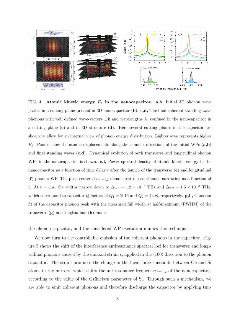
FIG. 4. Atomic kinetic energy Ek in the nanocapacitor. a,b, Initial 3D phonon wave
packet in a cutting plane (a) and in 3D nanocapacitor (b). c,d, The final coherent standing-wave
phonons with well defined wave-vectors ±k and wavelengths λc confined in the nanocapacitor in
a cutting plane (c) and in 3D structure (d). Here several cutting planes in the capacitor are
shown to allow for an internal view of phonon energy distribution. Lighter area represents higher
Ek. Panels show the atomic displacements along the x and z directions of the initial WPs (a,b)
and final standing waves (c,d). Dynamical evolution of both transverse and longitudinal phonon
WPs in the nanocapacitor is shown. e,f, Power spectral density of atomic kinetic energy in the
nanocapacitor as a function of time delay t after the launch of the transverse (e) and longitudinal
(f) phonon WP. The peak centered at ω1,2 demonstrates a continuous narrowing as a function of
t. At t = 5ns, the widths narrow down to ∆ω1 = 1.2 × 10⁻³ THz and ∆ω2 = 1.5 × 10⁻³ THz,
which correspond to capacitor Q factors of Q1 = 2916 and Q2 = 4208, respectively. g,h, Gaussian
fit of the capacitor phonon peak with the measured full width at half-maximum (FWHM) of the
transverse (g) and longitudinal (h) modes.
the phonon capacitor, and the considered WP excitation mimics this technique.
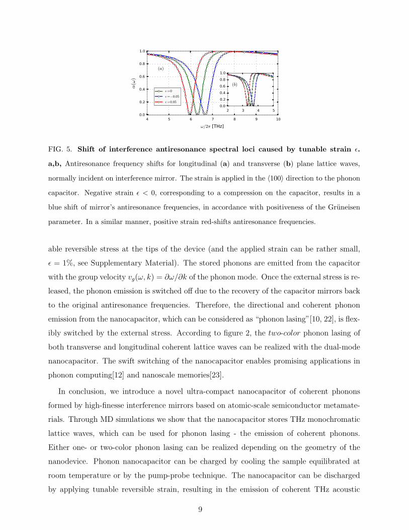
We now turn to the controllable emission of the coherent phonons in the capacitor. Fig-
ure 5 shows the shift of the interference antiresonance spectral loci for transverse and longi-
tudinal phonons caused by the uniaxial strain ǫ, applied in the 〈100〉 direction to the phonon
capacitor. The strain produces the change in the local force constants between Ge and Si
atoms in the mirrors, which shifts the antiresonance frequencies ω1,2 of the nanocapacitor,
according to the value of the Gruneisen parameter of Si. Through such a mechanism, we
are able to emit coherent phonons and therefore discharge the capacitor by applying tun-
8
4 5 6 7 8 9 10
ω/2π [THz]
0.0
0.2
0.4
0.6
0.8
1.0
α(ω)
(a)
ǫ=0
ǫ=−0.05ǫ=0.05
2 3 4 50.0
0.2
0.4
0.6
0.8
1.0
(b)
FIG. 5. Shift of interference antiresonance spectral loci caused by tunable strain ǫ.
a,b, Antiresonance frequency shifts for longitudinal (a) and transverse (b) plane lattice waves,
normally incident on interference mirror. The strain is applied in the 〈100〉 direction to the phonon
capacitor. Negative strain ǫ < 0, corresponding to a compression on the capacitor, results in a
blue shift of mirror’s antiresonance frequencies, in accordance with positiveness of the Gruneisen
parameter. In a similar manner, positive strain red-shifts antiresonance frequencies.
able reversible stress at the tips of the device (and the applied strain can be rather small,
ǫ = 1%, see Supplementary Material). The stored phonons are emitted from the capacitor
with the group velocity vg(ω, k) = ∂ω/∂k of the phonon mode. Once the external stress is re-
leased, the phonon emission is switched off due to the recovery of the capacitor mirrors back
to the original antiresonance frequencies. Therefore, the directional and coherent phonon
emission from the nanocapacitor, which can be considered as “phonon lasing”[10, 22], is flex-
ibly switched by the external stress. According to figure 2, the two-color phonon lasing of
both transverse and longitudinal coherent lattice waves can be realized with the dual-mode
nanocapacitor. The swift switching of the nanocapacitor enables promising applications in
phonon computing[12] and nanoscale memories[23].
In conclusion, we introduce a novel ultra-compact nanocapacitor of coherent phonons
formed by high-finesse interference mirrors based on atomic-scale semiconductor metamate-
rials. Through MD simulations we show that the nanocapacitor stores THz monochromatic
lattice waves, which can be used for phonon lasing - the emission of coherent phonons.
Either one- or two-color phonon lasing can be realized depending on the geometry of the
nanodevice. Phonon nanocapacitor can be charged by cooling the sample equilibrated at
room temperature or by the pump-probe technique. The nanocapacitor can be discharged
by applying tunable reversible strain, resulting in the emission of coherent THz acoustic
9
beams.
[1] A. Huynh, et al. Phys. Rev. Lett. 97, 115502 (2006).
[2] N. D. Lanzillotti-Kimura, B. Perrin, A. Fainstein, B. Jusserand and A. Lemaıtre, Appl. Phys.
Lett. 96, 053101 (2010).
[3] R. P. Beardsley, A. V. Akimov, M. Henini and A.J. Kent, Phys. Rev. Lett. 104, 085501 (2010).
[4] W. Maryam, A.V. Akimov, R.P. Campion and A.J. Kent, Nature Commun. 4, 2184 (2013).
[5] T. J. Kippenberg and K. J. Vahala, Science 321, 1172 (2008).
[6] I.S. Grudinin, H. Lee, O. Painter and K. J. Vahala, Phys. Rev. Lett. 104, 083901 (2010).
[7] J. B. Khurgin, M. W. Pruessner, T. H. Stievater and W. S. Rabinovich, Phys. Rev. Lett. 108,
223904 (2012).
[8] I. Mahboob, K. Nishiguchi,H. Okamoto and H. Yamaguchi, Nat. Phys. 8, 387 (2012).
[9] H. Okamoto et al. Nat. Phys. 9, 480 (2013)
[10] I. Mahboob, K. Nishiguchi, A. Fujiwara and H. Yamaguchi, Phys. Rev. Lett. 110, 127202
(2013).
[11] T. D. Khokhlova et al. Proc. Nat. Acad. Sci. 111, 8161 (2014).
[12] N. Li, J. Ren, L. Wang, G. Zhang, P. Hanggi and B. Li, Rev. Mod. Phys. 84, 1045 (2012).
[13] A. Fainstein, N. D. Lanzillotti-Kimua, B. Jusserand and B. Perrin, Phys. Rev. Lett. 110,
037403 (2013).
[14] M. Trigo, A. Bruchhausen, A. Fainstein, B. Jusserand and V. Thierry-Mieg, Phys. Rev. Lett.
89, 227402 (2002).
[15] Yu. A. Kosevich, Prog. Surf. Sci. 55, 1 (1997).
[16] Yu. A. Kosevich, Physics-Uspekhi 51, 848 (2008).
[17] H. Han, L. G. Potyomina, A. A. Darinskii, S. Volz and Yu. A. Kosevich, Phys. Rev. B 89,
180301(R) (2014).
[18] J. Ravichandran et al. Nat. Mater. 13, 168 (2014).
[19] R. E. Sonntag, C. Borgnakke, G. J. Van Wylen and S. Van Wyk, Fundamentals of Thermo-
dynamics (Wiley, New York, 1998).
[20] C.W. Gardiner and P. Zoller, Quantum Noise (Springer, Berlin, 2004).
[21] M. Aspelmeyer, T. J. Kippenberg and F. Marquardt, arXiv:1303.0733 (2013).
10
[22] K. Vahala, M. Herrmann, S. Knunz, V. Batteiger, G. Saathoff, T. W. Hansch and Th. Udem
Nat. Phys. 5, 682 (2009)
[23] J. E. Jang et al. Nat. Nanotechnol. 3, 26 (2008)
[24] F. H. Stillinger and T.A. Weber, Phys. Rev. B 31, 5262 (1985).
[25] S. Volz, Phys. Rev. Lett. 87, 074301 (2001).
[26] N. Mingo and D. A. Broido, Phys. Rev. Lett. 93, 246106 (2004).
[27] F. Atrash, A. Hashibon, P. Gumbsch and D. Sherman, Phys. Rev. Lett. 106, 085502 (2011).
[28] S. J. Plimpton, Comput. Phys. 117, 1 (1995).
[29] S. J. Nose, Chem. Phys. 81, 511 (1984).
[30] N. G. Hoover, Phys. Rev. A 31, 1695 (1985).
[31] F. Bonetto, J. L. Lebowitz and L. Ray Bellet, Mathematical Physics 2000 (Imperial College
Press, London, 2000).
11