Philips: pm2420
82
PHILIPS
-
Upload
khangminh22 -
Category
Documents
-
view
4 -
download
0
Transcript of Philips: pm2420

PHILIPS
2
Contents
GENERAL fI. INTRODUCTION 5
n. TECHNICAL DATA 5
IE. ACCESSORIES 8
IV. WORKING 9
A. Principle 9
B. Description of the block diagram 10
DIRECTIONS FOR USE
V. INSTALLATION 19
A. Adjustment to the mains voltage 19
B. Fuse 19
C. Earthing 19
VI. OPERATION 21
A. Switching-on 21
B. Calibration 21
C. Measuring 21
SERVICE DATA
VII. CIRCUIT DESCRIPTION 23
A. General 23
B. Power supply 23
C. Input circuit 24
D. Analogue-to- digital converter 30
E. Logic circuit 33
F. Gate 33
G. Clock oscillator 34
H. Polarity indication 34
J. Scaler of four 35
K. Counter 35
L. A stable multivibrator 37
M. ”1000” indication 38
CS19577
3
VIII. DISASSEMBLING 39
A. Housing 39
B . Bottom panel 39
C . Text plate 39
IX. REPLACING PARTS 39
A. Front frame 39
B. Rear frame 40
C. Monoknob 41
D. Selector switch 42
E . Printed wiring boards 42
F. Electrical components 44
X. MAINTENANCE 45
XI. SURVEY OF ADJUSTMENTS 46
XII. CHECKING AND ADJUSTING 48
A. Power supply 48
B. Clock oscillator frequency 49
C. Zero adjustment 49
D. Full scale adjustment 49
E. Adjusting the DC voltage ranges 49
F. Adjusting the ft ranges 50
G. Adjusting the AC voltage ranges 51
H. Checking the current ranges 51
XIII. TROUBLE SHOOTING 53
XIV. LIST OF PARTS 61
A. Mechanical 61
B. Electrical 62
XV. FUNCTIONAL BLOCKS 70
Important
In correspondence regarding this instrument quote the complete type
number and serial number, as stated on the type plate at the rear of
the instrument.
4
I
IList of figures
1. Simplified block diagram2. Voltage-to-time conversion3. Block diagram4a. Pulse diagram of the ADC, with the input socket connected to "0"
b. Pulse diagram of the ADC, with the input voltage positive withrespect to "0"
c. Pulse diagram of the ADC, with the input voltage negative withrespect to ”0”
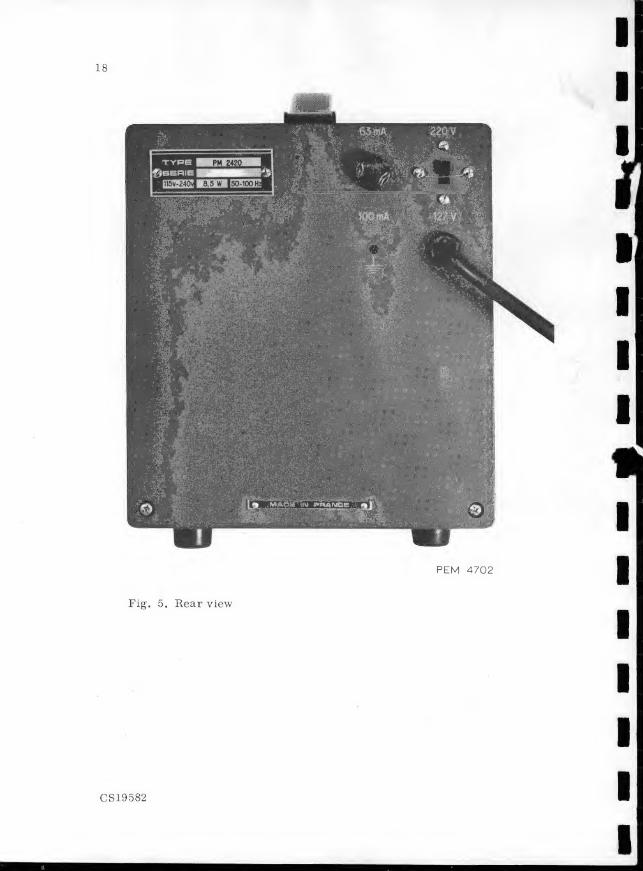
5. Rearview6. Front view7. DC voltage circuits
8. DC current circuit
9. Circuit for resistance measurements10. AC voltage circuit
11. AC current circuit
12. Operational amplifier circuit
13 . Operational amplifier and rectifier circuit
14. Monostable multivibrator15. Logic circuit
16. Polarity indication circuit
17. Nand gate18. ”1000” indication circuit
19. Bottom view20. Right-hand side view21. Left-hand side view22. Measuring set-up for checking the DC current ranges23. Table with measuring results24. Front view with item numbers25. Rear view with item numbers26 . Operational amplifier block27. Polarity indication flip-flop (FF1)28. Decade flip-flop (FF2. . . FF16)29. A stable multivibrator AMI30. Decoder circuit (Dl. . .D3)31. Bottom view (bottom panel removed)32. Instrument opened for servicing purposes33. Printed wiring board Ul; power supply34. Printed wiring board U2; stabilizing circuit
35. Circuit diagram power supply and stabilizing circuit36. Printed wiring board U3; analogue-to- digital converter37. Oscillator coil
38. Printed wiring board U4; amplifier39. Printed wiring board U5; counter40. Printed wiring board U6; DC attenuator41. Printed wiring board U7; AC attenuator42. Printed wiring board U8; interconnection board43. Circuit diagram
9
11
13
14
14
15
18
20
25
26
27
28
28
29
30
31
32
3437
37
38
404151
5860
607171
72
72
737373
75
77
80
81
81
82
84
85
85
86
I
I
I
I
5
GENERAL
I. INTRODUCTION
Instrument PM 2420 is a compact multi-range DVM of the so-called
RAMP type. Characteristic of the RAMP principle is the simplicity of
operation, which makes this DVM ideally suitable for use as a general
purpose instrument.
Operation is facilitated by the possibility of selecting all measuring
ranges by means of a single knob. It is obvious that the combination of
digital read-out system and monoknob range selection ensures fast and
simple, yet accurate reading.
II. TECHNICAL DATA
Values with specified tolerances are guaranteed by the factory. Numeri-
cal values without tolerances represent the properties of an average
instrument and serve only as a guide.
A. VOLTAGE MEASUREMENTS
1. Direct voltages
Measuring range
5 ranges
Accuracy
Resolution
Input resistance
Measuring time
Permissible overranging
0.1 mV. .
.
1000 V
100 mV, 1000 mV, 10 V, 100 V, 1000 V
(full scale)
Ranges 100 mV and 1 V: _+ 0.5 % of full scale
+ 1 digit
Ranges 10 V, 100 V and 1000 V: +0.2 % of
full scale + 1 digit
0.001 of full scale
1 MR: 100 mV, 1000 mV range
5 MR: 100 V range
> 10 MR: 10 V range
10 MR: 1000 V
< 2 s.
5 % of full scale
6
2. Alternating voltages
Measuring range
4 ranges
Accuracy
Frequency range
He solution
Input impedance
Measuring time
Permissible overranging
1 mV™ o ..-3°0 Vmarms rms300 mV, 3 V, 30 V, 300 V (full scale)
+ 1 % of full scale + 1 digit
40 Hz... 10 kHz
1/3 x 0.01 of full scale
5 MK2//100 pF: ranges 300 mV and 3 V10 MS2//50 pF: ranges 30 V and 300 V< 3 s.
10 %. .
.
30 % of full scale, depending on the
frequency applied (40 Hz. . .400 Hz = 30 %)
4
B. CURRENT MEASUREMENTS
1. Direct currents
Measuring range
5 ranges
Accuracy
Re solution
Voltage drop
Measuring time
Permissible overranging
2. Alternating currents
Measuring range
4 ranges
Accuracy
Frequency range
Re solution
Voltage drop
Measuring time
Permissible overranging
0.1 juA. . . 1 A
100 /liA, 1000 mA, 10 mA, 100 mA, 1000 mA(full scale)
+ 1% of full scale + 1 digit
0.001 of full scale
< 100 mV< 2 s.
5 % of full scale
iMrms --- 300 ^rms300 pA, 3 mA, 30 mA, 300 mA (full scale)
+ 1. 5 % of full scale + 1 digit
40 Hz. . .10 kHz
1/3 x 0.01 of full scale
< 300 mV< 3 s.
10 %. .
.
30 % of full scale, depending on the
frequency applied
7
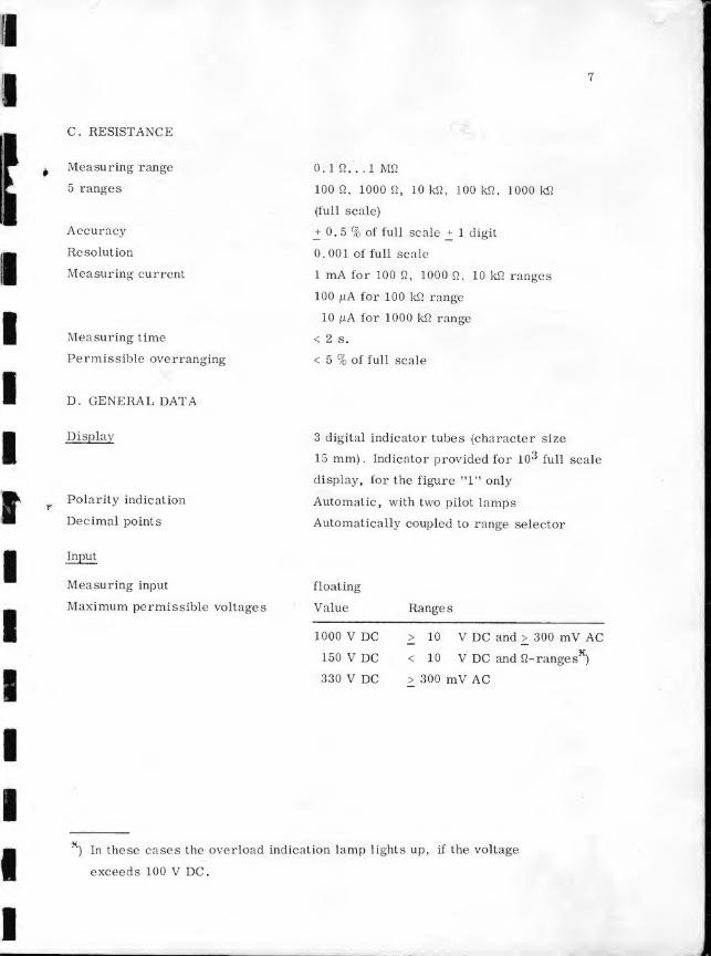
C. RESISTANCE
^Measuring range
5 ranges
Accuracy
Re solution
Measuring current
Measuring time
Permissible overranging
0.18...1 MB
100 8, 1000 8, 10 kft, 100 kft, 1000 kft
(full scale)
+ 0. 5 % of full scale _+ 1 digit
0.001 of full scale
1 mA for 100 ft, 1000 ft, 10 kft ranges
100 pA for 100 kft range
10 piA for 1000 kft range
< 2 s.
< 5 % of full scale
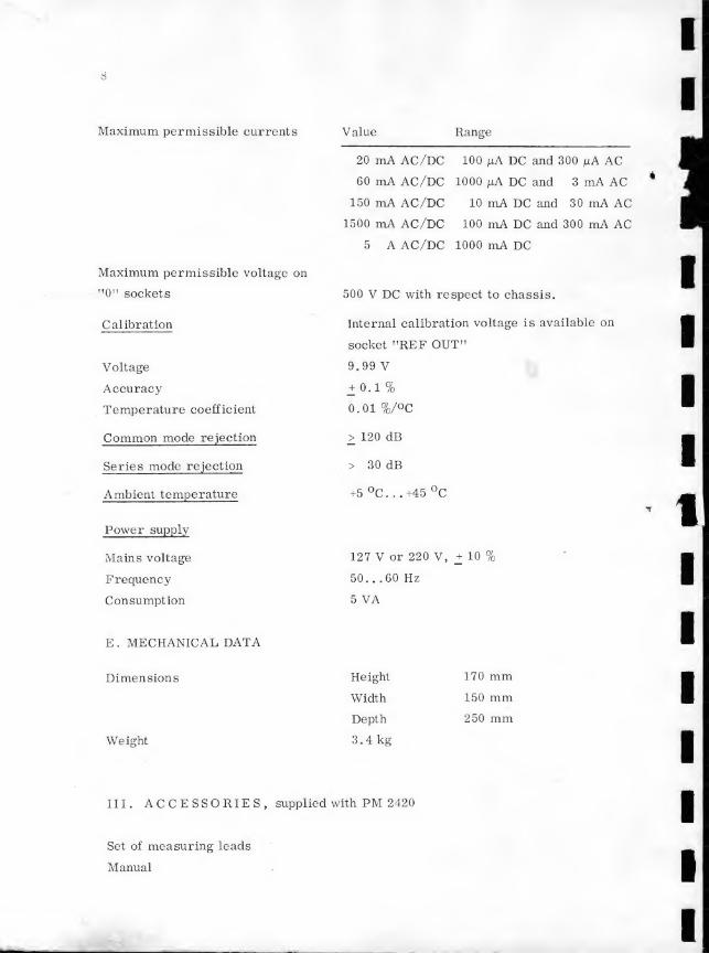
D. GENERAL DATA
Display
Polarity indication
Decimal points
Measuring input
Maximum permissible voltages
3 digital indicator tubes (character size
15 mm) . Indicator provided for 103 full scale
display, for the figure "1" only
Automatic, with two pilot lamps
Automatically coupled to range selector
floating
Value Ranges
1000 V DC
150 V DC
330 V DC
>10 V DC and > 300 mV AC
<10 V DC and ft-range sK
)
> 300 mV AC
x)
In these cases the overload indication lamp lights up, if the voltage
exceeds 100 V DC.
8
Maximum permissible currents Value Range
20 mA AC/DC 100 [iA DC and 300 piA AC
60 mA AC/DC 1000 pA DC and 3 mA AC
150 mA AC/DC 10 mA DC and 30 mA AC
1500 mA AC/DC 100 mA DC and 300 mA AC
5 A AC/DC 1000 mA DC
Maximum permissible voltage on
"0” sockets 500 V DC with respect to chassis.
Calibration Internal calibration voltage is available on
socket nREF OUT”
Voltage 9.99 V
Accuracy + 0.1 %
Temperature coefficient 0.01 %/°c
Common mode rejection > 120 dB
Series mode rejection > 30 dB
Ambient temperature +5 °C . . . +45 °C
Power supply
Mains voltage 127 V or 220 V, + 10 %
Frequency 50. . .60 Hz
Consumption 5 VA
E. MECHANICAL DATA
Dimensions Height 170 mmWidth 150 mmDepth 250 mm
Weight 3.4 kg
III. ACCESSORIES, supplied with PM 2420
Set of measuring leads
Manual
9
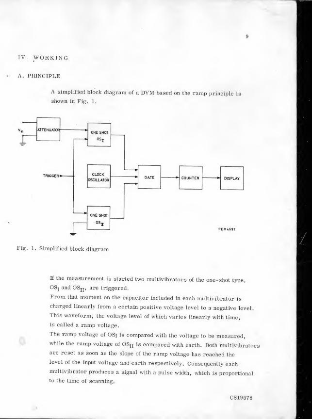
IV. WORKING«
A. PRINCIPLE
A simplified block diagram of a DVM based on the ramp principle is
shown in Fig. 1.
Fig. 1. Simplified block diagram
If the measurement is started two multivibrators of the one-shot type,
OSj and OSjj, are triggered.
From that moment on the capacitor included in each multivibrator is
charged linearly from a certain positive voltage level to a negative level.
This waveform, the voltage level of which varies linearly with time,
is called a ramp voltage.
The ramp voltage of OSj is compared with the voltage to be measured,
while the ramp voltage of OSjj is compared with earth. Both multivibrators
are reset as soon as the slope of the ramp voltage has reached the
level of the input voltage and earth respectively. Consequently each
multivibrator produces a signal with a pulse width, which is proportional
to the time of scanning.
CS19578
10
If the voltage to be measured is called ex and earth eQ the pulse width
of OSj may be written as tx = c. (e
x - V) and the pulse width of OSn as
t2= c ' (eo
“ V> •
The difference between both pulse widths is then determined by
*3= “ t^ = c. (e
x - eQ),
which is proportional to the input voltage level.
This pulse is used to control the gate through which pulses of an internal
clock oscillator have to pass. Consequently, t^ determines the number
of pulses which can pass the open gate. The number of pulses is esta-
blished by a counter which controls the display circuit.
The choice of the ramp slope and the frequency of the clock oscillator
enables the read-out circuit to directly display the measured value. In
this respect reference is made to the following example.
Ramp slope : 1 V/ms
Frequency of clock oscillator : 390 kHz
If the counter is allowed to count for 10 ms, 1000 pulses of the clock
oscillator will pass the gate and the number "1000” is displayed accor-
dingly.
This figure will actually correspond to 10 V, since the ramp slope
chosen is 1 V/ms. Consequently, 500 pulses will correspond to 5 V and
one pulse to 10 mV.
Fig. 2 shows a pulse diagram of the voltage-to-time conversion in a
ramp type DVM.
B. DESCRIPTION OF THE BLOCK DIAGRAM (Fig. 3)
Input circuit
Dependent on the selected DC voltage range, the direct voltage will be:
A. Attenuated, if the 1000 V and 100 V ranges have been selected
(DC attenuator)
B. Amplified, if the 1000 mV and 100 mV ranges have been selected
C . Applied direct to the ADC in the 10 V range.
Consequently, the direct voltage will always reach the ADC at a level
of 10 V full scale.
I
I
f
11
If direct currents have to be measured, switch I$c is closed and the
current is converted into a direct voltage by shunting the input (R g).
This direct voltage is amplified as a DC signal in the 100 mV range.
If alternating voltage have to be measured, the signal has to be converted
into a direct voltage
.
After passing the AC attenuator and the impedance transformer, the
signal is applied to the operational amplifier which also functions as a
rectifier. The direct voltage obtained, will be proportional to the
r.m. s. value of the alternating voltage originally applied to the instrument
(for pure sinewave signals).
CS19579
INPUT
CIRCUIT
ANALOG
DIGITAL
CONVERTER
Fig. 4c
Fig. 4a. Pulse diagram of the ADC, with the input socket connected to ”0”
b. Pulse diagram of the ADC, with the input voltage positive with respect to nO
c. Pulse diagram of the ADC, with the input voltage negative with respect to mO
If alternating currents have to be measured, switch Iac is closed £
current is first converted into an alternating voltage by shunting tl
with the same resistors (Rg) used for direct currents.
Afterwards, this alternating voltage is converted into a direct volt
as indicated in the previous paragraph.
If resistance measurements have to be carried out switch R is c
and a constant current is fed into the relevant resistor. It is obvio
that the direct voltage available across this resistor is measured i
described for direct voltage measurements.
Analogue-to-Digital Converter (ADC)
The direct voltage from the input circuit is applied to the ADC, wb
consists of two one-shot multivibrators, OS I and OS n in Fig. 3.
As soon as OS I and OS II are triggered by pulses from an internal
multivibrator (AM), they will switch over to another position. Mul
brator OS II, locked to zero, will again switch over if the slope ha
reached zero.
Consequently, OS II supplies a squarewave pulse with a constant pi
width, kultivibrator OS I, locked to the direct voltage level from t
input circuit, will again switch over, if the slope has reached the
direct voltage level of the input. Consequently, OS I supplies a squ
wave pulse with a pulse width varying according to the level of the
input voltage
.
The squarewave pulses of both multivibrators are fed into a logic
circuit, which detects the difference in pulse width of the two signs
Consequently, the squarewave pulse leaving the logic circuit will b
proportional to the value of the voltage, current or resistance, apf
to the input of the instrument, see Figs. 4a, b and c.
The capacitors of both multivibrators are linearly charged by gene
which supply a constant current. These generators can be adjusted
means of potentiometers "ZERO" and "FULL SCALE".
When short-circuiting the input, the ramp of both multivibrators whave the same slope (adjustable with "ZERO"), and there will be n<
difference in pulse width (see Fig. 4a).

17
When calibrating (with ’’FULL SCALE”) the difference of the pulse-
widths will be such that the signal from the logic circuit corresponds
to full-scale display (see Fig. 4c). The required voltage (-9.99 V) is
available on socket ”REF. OUT”.
The logic circuit has two functions:
1. To open or to close the oscillator gate , dependent on the presence of
a logic output signal.
2. To determine the polarity
The output signals of OS I and OS II are inverted by the logic circuit.
The last trailing edge of one of the inverted signals determines the
polarity. Should the OS II signal be last, the polarity will be positive.
It will be negative, if the OS I signal is last (see Figs. 4b and c)
.
If the oscillator gate is open, the clock pulses originating from the clock
oscillator, will be passed on to a four- scaler. The pulses from this
network are applied to the counter.
A stable multivibrator AM has three functions:
1. To trigger OS I and OS II, to ensure synchronous operation.
2. To reset all flip-flops of the counter to position zero.
3. To reset the flip-flops of the scaler-of-four to position zero.
Counter
The counter consists of a three-decade counting unit, based on the
1 - 2 - 4 - 8 code.
The digits of each decade are determined by the position of the flip-flops.
Decoding is effected by ten NAND gates for each decade. After 999 pulses
the hundreds decade supplies a carry-pulse to the flip-flop controlling
the one thousand indicator.
See the information on over-ranging, maximum permissible voltages
etc., in the TECHNICAL DATA
.
CS19581
17
When calibrating (with "FULL SCALE") the difference of the pulse-
widths will be such that the signal from the logic circuit corresponds
to full-scale display (see Fig. 4c). The required voltage (-9.99 V) is
available on socket "REF. OUT".
The logic circuit has two functions:
1. To open or to close the oscillator gate , dependent on the presence of
a logic output signal.
2. To determine the polarity
The output signals of OS I and OS II are inverted by the logic circuit.
The last trailing edge of one of the inverted signals determines the
polarity. Should the OS II signal be last, the polarity will be positive.
It will be negative, if the OS I signal is last (see Figs. 4b and c).
If the oscillator gate is open, the clock pulses originating from the clock
oscillator, will be passed on to a four- scaler. The pulses from this
network are applied to the counter.
A stable multivibrator AM has three functions:
1. To trigger OS I and OS II, to ensure synchronous operation.
2. To reset all flip-flops of the counter to position zero.
3. To reset the flip-flops of the scaler-of-four to position zero.
Counter
The counter consists of a three-decade counting unit, based on the
1 - 2 - 4 - 8 code.
The digits of each decade are determined by the position of the flip-flops.
Decoding is effected by ten NAND gates for each decade. After 999 pulses
the hundreds decade supplies a carry-pulse to the flip-flop controlling
the one thousand indicator.
See the information on over-ranging, maximum permissible voltages
etc., in the TECHNICAL DATA
.
CS19581
19
DIRECTIONS FOR USE
V. INSTALLATION
A. ADJUSTMENT TO THE MAINS VOLTAGE
Check that the voltage adapter on the rear panel has been set to the
local mains voltage.
The instrument is suitable for use at a mains voltage
of 127 V AC (115. . . 140 V AC)
or 220 V AC (200. . . 240 V AC)
.
B. FUSE
The rating of the fuse at the rear should be 100 mA, delayed action, for
the voltage range 115 V. . .140 V and 63 mA, delayed action, for mains
voltages from 200 V. . .240 V.
C. EARTHING
The instrument should be earthed in accordance with local safety regu-
lations. This instrument offers the following possibilities:
a. Earthing via the 3-core mains cable, which should be connected to
a wall socket with rim-earthing contacts.
b. Earthing via the earthing socket marked " ± ", on the rear.
Avoid double earthing, which may cause hum.
21
VI. OPERATION
A. SWITCHING ON
The instrument is switched on with the monoknob. The digital indicator
tubes should light up.
B. CALIBRATION
Note: By allowing the instrument to warm up for a few minutes the necessi-
ty of recalibration after a short period is avoided.
- Set the monoknob to position M 10 V DC".
- Short-circuit sockets "VflA" and "0".
- Adjust the digital display to "000" with potentiometer "ZERO"
(screwdriver adjustment on the front, see Fig. 6). If the pilot lamps
light up alternately, this is an indication that the zero setting
has been effected most accurately.
- Connect socket "VftA" to socket "REF OUT".
- Adjust the digital display to "999" with potentiometer "FULL SCALE"
(screwdriver adjustment on the front, see Fig. 6)
.
C. MEASURING
- Calibrate the instrument (see VLB).
- The following measurements can be carried out, if the measuring leads
are connected to sockets "VfiA" and "0", and the appropriate ranges
have been selected with the monoknob:
direct voltages up to 100 V
alternating voltages up to 300 V
direct currents up to 100 mAalternating currents up to 300 mA and
resistance up to 1 MS2.
Notes
- Direct voltages exceeding 100 V, with a maximum of 1000 V, can be
measured via a separate socket "DC- 1000 V", if the monoknob has
been set to position "1000 V DC".
Direct currents exceeding 100 mA, with a maximum of 1 A, can be
measured via a separate socket ”DC-1 A” if the monoknob has been
set to position ”1000 mA DC”.
For DC measurements the polarity of the voltage on socket ”V£2A”
with respect to socket ”0”, is indicated by two pilot lamps, displaying
U_|_M qj. TT_!T
If floating measurements are carried out, the voltage between sockets
”0” and earth (= chassis) should not exceed 500 V DC
.
Theoretically, a maximum indication of ”1500” is possible. However,
the slope linearity decreases so that the indicated value is no longer
reliable. The accuracy is not affected by over-ranging to:
5 % of full scale for DC measurements (no overloading allowed in
1000 V range)
10 %. . .30 % of full scale for AC measurements (dependent on the
frequency applied)
5 % of full scale for resistance measurements.
In range s < 10 V DC and£ 1000 £2 the ’’OVERLOAD” pilot lamp will
light up, if the applied voltage exceeds 100 V DC.
In ranges ”1000 mV” and ”100 mV” an incorrect indication may occur
as a result of the offset current (about 100 nA) of the operational
amplifier. This offset current passes the output impedance of the
circuit under test and causes a voltage: IQffse^
x R across this circuit.
If possible, choose the output impedance of the circuit under test as
low as possible (< 1 k£2).
23
SERVICE DATA
VII. CIRCUIT DESCRIPTION
A. GENERAL
This chapter describes the function of a certain circuit during the mea-
suring process. At the end of this manual illustrations are given of the
corresponding printed wiring boards and the circuit diagram (Fig. 43).
If any switches are involved, these items are drawn in the TTOFFn
position. Reference to a certain contact of a switch is made as follows:
switch/wafer, front (f) or rear (a) /contact; e.g. SK1/Ila/12 means:
switch 1 (= monoknob), wafer 2 rear side, contact 12.
B. POWER SUPPLY (Fig. 35)
1. Transformer
Primary
Windings SI + S2 can be connected for 220 V mains voltages and winding
S2 for 115 V mains with slide switch SK2. Permissible voltage deviation
is + 10 %.
Secondary
The secondary windings S3, S4 + S5, S6 and S7 supply the AC voltages
to the 4 separate rectifying circuits.
These circuits deliver a non- stabilized voltage of +280 V and 4 stabilized
voltages of +15 V, -15 V, -26. 5 V and +10 V, with respect to the common
zero of the circuitry ( l )
.
2. Voltage source +280 V
The +280-V-voltage is used for the digital indicator tubes, the polarity
neon lamps, the decimal-point neon lamp, the n1000 n indicator tube.
This voltage is obtained from a half-wave voltage doubler consisting of
C13, GR1, GR2 and C14.
24
3. Voltage sources +15 V and -15 V
The secondary voltage of windings S4 and S5 is approx. 25 Vrmsiwhich
is rectified with bridge- rectifier GR8 and smoothed by capacitors Cl
and C4. After the rectifier the circuit is divided into a positive and a
negative circuit with common zero. Since the stabilisation circuits for
positive and negative voltages are symmetrical with respect to common
zero, only the positive circuit will be described in detail. The parts
stated between brackets refer to the negative stabilisation circuit.
The voltage across R6 and PI (R12 and P2) is compared with the refe-
rence voltage across Zener-diode GR2 (GR4) . Transistors TS2 (TS4)
operates as a difference-amplifier and controls series regulator TS1
(TS3) . The output voltage is adjusted by potentiometer PI (P2) . Fast
output voltage variations are applied to the base of TS2 (TS4) via C2
(C5).
4. Voltage source -26.5 V
This control circuit is, in principle, similar to the circuitry of the
+15 V or -15 V source. The reference voltage is derived from Zener
diode GR4 (-15 V source). The series regulator consists of TS5 and
TS6 in a Darlington circuit. The output voltage is adjusted by potentio-
meter P3.
5. Voltage source +10 V
This source is only stabilised as regards mains voltage variations by
Zener-diodes GR8, GR9 and transistor TS8. Output voltage variations
are compensated for to some extent by a large capacitor, C12.
C . INPUT CIRCUIT
The input circuit brings the input signal at a DC voltage level of 10 V f. s.d.
for DC measurements and resistance measurements, and at a level of
3 V f. s.d. for AC measurements.
1. DC voltage circuits (Fig. 7)
Dependent on the position of the range selector the input voltage on
socket "VGA" will be:
25
SKI /la
SKI/I;‘ID V"
B.
SKl/3ZHa>ADC
Fig. 7. DC voltage circuits
A. attenuated in the range ”100 V”. The attenuation factor is adjusted
to 10 by potentiometer P409.
B. applied direct to the ADC (range ”10 V”)
C. amplified in the ranges 1 V (amplification factor 10) and 100 mV(amplification factor 100)
.
Voltages exceeding 100 V should be connected to socket ”DC-1000 V”.
They are applied to the ADC via an attenuator, having an attenuation
factor of 100. The attenuation factor can be adjusted by potentiometer
P408.
CS19583
26
2. DC current circuit (Fig. 8)
Shunts are connected in parallel to the input with selector switch SKl/la
if DC currents are applied. These currents produce a voltage across
the shunt-resistor, which is 100 mV for every current range at full
scale (e.g. 100 mA x 1 12 = 100 mV). After this, the voltage is applied
to the amplifier via SKl/Va. The amplification factor amounts to 100.
The output voltage (100 x 100 mV = 10 V) is applied to the ADC via SKI/
Vllf.
Fig. 8. DC current circuit
3. Circuit for resistance measurements (Fig. 9)
Resistance measurements are, in fact, translated into DC voltage mea-
surements. A DC current of 1 mA is applied to the unknown resistor Rx
if the range selector has been set to position 100 12, 1000 12 or 10 M2.
A voltage of 0. 1 V, IV and 10 V respectively will occur across Rx at'
a maximum. This voltage is fed into the ADC as already described for
CS19584
27
DC voltage measurements under points Cl, B and C. If position
"100 kft" is selected the direct current is 0. 1 mA and in position "1000 kfi"
it is 10 pA, which corresponds to 10 V full scale. This DC voltage is
applied direct to the ADC
.
Fig. 9. Circuit for resistance measurements
4. AC voltage circuit (Fig. 10)
AC voltages are translated into DC voltages of 3 V fsd. The ranges
"300 mV" and "3 V" are connected direct to the impedance transformer,
while the ranges "30 V" and "300 V" are connected to a frequency- inde-
pendent attenuator, which causes an attenuation of 100 : 1. Afterwards,
the signal is also applied to the impedance transformer.
The output voltage of the impedance transformer is applied to the
operational amplifier via P406 + R432//R439 + C410 for the 300 mV and
30 V AC voltage ranges and all AC current ranges. If the 3 V and 300 Vvoltage positions have been chosen the output signal will leave the trans-
former via P405 + R431//C409. After this both signals are amplified
and rectified by the operational amplifier in question. The full-wave
rectified signal is applied to a filter via SKl/VIa/14 and SKl/VIf/15,
where the signal is smoothed. The output DC voltage, which is propor-
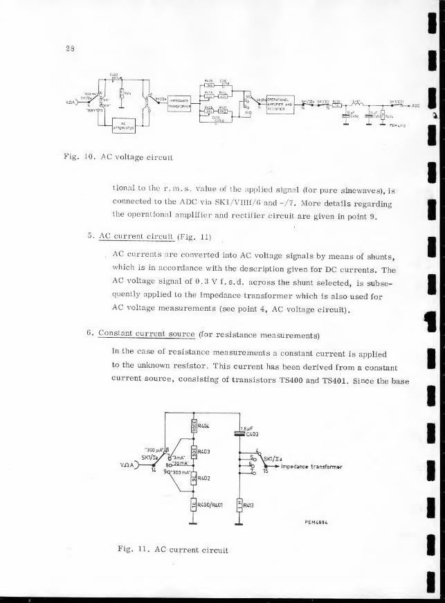
28
Fig. 10. AC voltage circuit
tional to the r.m. s. value of the applied signal (for pure sinewaves), is
connected to the ADC via SKl/VIIIf/6 and -/7. More details regarding
the operational amplifier and rectifier circuit are given in point 9.
5. AC current circuit (Fig. 11)
AC currents are converted into AC voltage signals by means of shunts,
which is in accordance with the description given for DC currents. TheAC voltage signal of 0.3 V f. s.d. across the shunt selected, is subse-
quently applied to the impedance transformer which is also used for
AC voltage measurements (see point 4, AC voltage circuit).
6 * Constant current source (for resistance measurements)
In the case of resistance measurements a constant current is applied
to the unknown resistor . This current has been derived from a constant
current source, consisting of transistors TS400 and TS401. Since the base
Fig. 11. AC current circuit
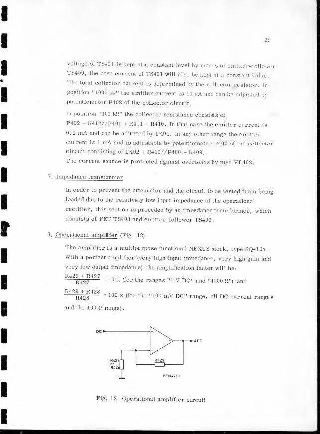
29
voltage of TS401 is kept at a constant level by means of emitter-follower
TS400, the base current of TS401 will also be kept at a constant value.
The total collector current is determined by the collector resistor. In
position u 1000 k£2" the emitter current is 10 juA and can be adjusted by
potentiometer P402 of the collector circuit.
In position n 100 k£2" the collector resistance consists of
P402 + R412//P401 + K411 + R410. In that case the emitter current is
0.1 mA and can be adjusted by P401. In any other range the emitter
current is 1 mA and is adjustable by potentiometer P400 of the collector
circuit consisting of P402 + R412//P400 + R409.
The current source is protected against overloads by fuse VL402.
7. Impedance transformer
In order to prevent the attenuator and the circuit to be tested from being
loaded due to the relatively low input impedance of the operational
rectifier, this section is preceded by an impedance transformer, which
consists of FET TS403 and emitter-follower TS402.
8. Operational amplifier (Fig. 12)
The amplifier is a multipurpose functional NEXUS block, type SQ-lOa.
With a perfect amplifier (very high input impedance, very high gain and
very low output impedance) the amplification factor will be:
R429 + R427R427
= 10 x (for the ranges "1 V DC n and ”1000 £2") and
R429 + R428R428
= 100 x (for the u 100 mV DC” range, all DC current ranges
and the 100 £2 range)
.
Fig. 12. Operational amplifier circuit
30
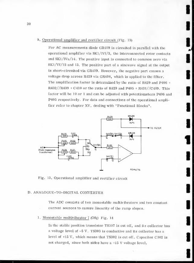
9. Operational amplifier and rectifier circuit (Fig. 13)
For AC measurements diode GR409 is circuited in parallel with the
operational amplifier via SKl/lVf/3, the interconnected rotor contacts
and SKl/lVa/14. The positive input is connected to common zero via
SKl/Vf/12 and 13. The positive part of a sinewave signal at the output
is short-circuited via GR409. However, the negative part causes a
voltage drop across R429 via GR408, which is applied to the filter.
The amplification factor is determined by the ratio of R429 and P406 +
R432//R439 + C410 or the ratio of R429 and P405 + R431//C409. This
factor will be 10 or 1 and can be adjusted with potentiometers P406 and
P405 respectively. For data and connections of the operational ampli-
fier refer to chapter XV, dealing with '’Functional Blocks”.
Fig. 13. Operational amplifier and rectifier circuit
D. ANALOGUE-TO-DIGITAL CONVERTER
The ADC consists of two monostable multivibrators and two constant
current sources to ensure linearity of the ramp slopes.
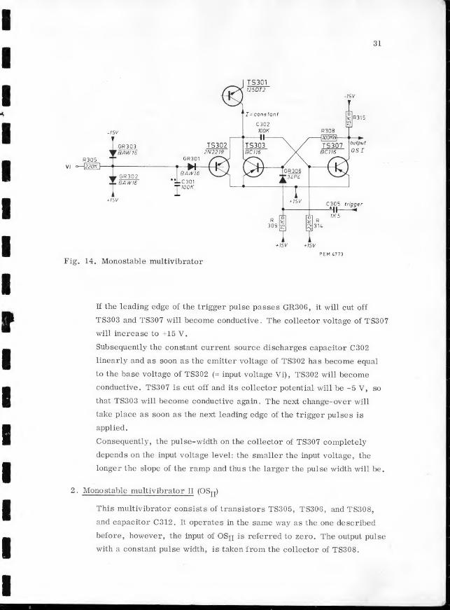
1. Mono stable multivibrator I (OSj) Fig. 14
In the stable position transistor TS307 is cut off, and its collector has
a voltage level of -5 V. TS303 is conductive and its collector has a
level of +15 V, which means that TS302 is cut off. Capacitor C302 is
not charged, since both sides have a +15 V voltage level.
31
Fig. 14. Monostable multivibratorPEM 4.773
If the leading edge of the trigger pulse passes GR306, it will cut off
TS303 and TS307 will become conductive. The collector voltage of TS307
will increase to +15 V.
Subsequently the constant current source discharges capacitor C302
linearly and as soon as the emitter voltage of TS302 has become equal
to the base voltage of TS302 (= input voltage Vi), TS302 will become
conductive. TS307 is cut off and its collector potential will be -5 V, so
that TS303 will become conductive again. The next change-over will
take place as soon as the next leading edge of the trigger pulses is
applied.
Consequently, the pulse-width on the collector of TS307 completely
depends on the input voltage level: the smaller the input voltage, the
longer the slope of the ramp and thus the larger the pulse width will be.
2. Mono stable multivibrator II (OSjj)
This multivibrator consists of transistors TS305, TS306, and TS308,
and capacitor C312. It operates in the same way as the one described
before, however, the input of OSjj is referred to zero. The output pulse
with a constant pulse width, is taken from the collector of TS308.
3. Constant current source
Both monostable multivibrators have their own current source. TS317
ensures the constant base voltage of TS301. Consequently, the base
current of this transistor is constant. The base voltage of TS317 and
TS318 can be adjusted by P301(
MFULL SCALE”). To ensure the symme-
try of the slope of both multivibrators the current of ©Syj can be adjusted
by P304 (ZERO) if the input is short-circuited.
15V
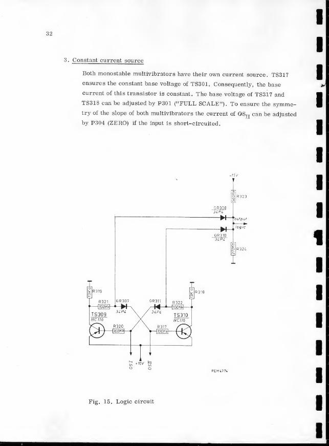
Fig. 15. Logic circuit
33
E. LOGIC CIRCUIT (Fig. 15)
The logic circuit, consisting of difference amplifier TS309 and TS310
with OR gate, compares the output pulses of the two monostable multi-
vibrators. The resultant signal is a pulse, with a width, which is pro-
portional to the difference between both original pulse widths. This
output signal controls a gate.
There are 4 possibilities, viz.
:
1. Output level of both multivibrators (OSj and OSjj) is -5 V (TS307 and
TS308 are cut off).
TS309 and TS310 are conductive. The collector voltages in question
are at a +10 V level. GR307 and GR311 are then conductive. The
relevant anodes are kept at about -5 V, so that diodes GR308 and
GR310 are cut off. The output level will then be approx. -5 V.
2. Output level of both multivibrators is +15 V (TS307 and TS308 are
conductive)
.
TS309 and TS310 are cut off. The collector voltages are at zero level.
GR307 and GR311 are cut off, but GR308 and GR310 are conductive.
Consequently, the output level is approx. 0 V.
3. Output level of multivibrator OSj is - 5 V and the level of OS-q is
+15 V. TS309 is conductive and TS310 is cut off. The collector volt-
age of TS309 is +10 V, while TS310 is at 0 V level. Under these
conditions GR308 will be conductive and the output level will be +10 V.
4. Output level of multivibrator OSjj is - 5 V and the level of OSj is
+15 V, which means that GR310 is conductive and the output level
will be +10 V.
F. GATE
The gate circuit consists of transistors TS312 and TS313 in series. The
gate is open if the base of TS312 is positive (+10 V, see E.3 + E.4). If
the gate is open, pulses of the clock oscillator (see below) are allowed
to pass the gate to the four- scaler.
.
CS19585
34
G. CLOCK OSCILLATOR
The clock signal is produced by an LC-oscillator, consisting of TS314,
T301 and C306. The oscillating frequency is 390 kHz + 1 % and can be
adjusted by T301. Via R326 the signal is applied to the gate.
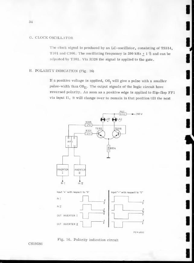
H. POLARITY INDICATION (Fig. 16)
If a positive voltage is applied, OSj will give a pulse with a smaller
pulse-width than OSjj. The output signals of the logic circuit have
reversed polarity. As soon as a positive edge is applied to flip-flop FF1
via input II, it will change over to remain in that position till the next
in i in n
Input V with respect to "0"Input with respect to ”0"
INIn J ]
n
II i
INI-t il
K VOUT INVERTER I
n
1 |
a
a ii
OUT INVERTER Hii
ii
PEM 4.692
CS19586
Fig. 16. Polarity indication circuit
35
positive edge is applied. Output n 0 n will be +10 V and output 0 approx. 0 V.
TS316 is conductive and TS315 will be cut off so that indicator LA
2
lights up. After max. 10 ms. later a positive pulse will be applied via
input 12. FF1 changes over and output ”0" will have become approx. 0 V
and the M0 n output +10 V, so that TS315 and TS316 will be conductive and
blocked respectively and LAI lights up. FF1 will remain in this position
until the next positive pulse arrives via II. This signal is applied approx.
1 sec. later but immediately after this a positive pulse is applied via
12, so that + indicator LAI remains on. If a negative voltage is applied,
OSj will give a pulse with a larger pulse-width than OSn . As a result
the first positive pulse will light the + indicator LAI for a moment,
however, the second positive pulse will light LA2, the negative indicator.
J. FOUR-SCALER
If the gate is open (see F), the clock oscillator pulses are fed to the
four-scaler, consisting of flip-flops FF2 and FF3. The output pulses of
this scaler are applied to the units decade of the counter.
K. COUNTER
The counter has three decades, viz. one for the units, tens and hundreds.
Each decade unit has 4 flip-flops. These 4 flip-flops have a counting
capacity of 16 digits in total, 10 of which are used to control the decimal
display.
The measurement is started, as soon as the astable multivibrator (see
chapter L) initiates a negative pulse. At the same moment a reset pulse
is applied to the flip-flops of the decades via a clamping circuit. These
flip-flops are reset to zero, so that all 0 outputs are +10 V and all
0 outputs are 0 V. The output pulses originating from the four-scaler
are supplied to FF4 and any negative pulse will change the flip-flop
position. Flip-flop FF5 changes over, if FF4 supplies a negative pulse
via GR33. This negative pulse will not influence the position of FF7,
because the negative pulse will keep the transistor cut off. After 9 pulses
the decade will be in position 1 - 0 - 0 - 1 (see table). Since output o" of;
flip-flop FF7 is connected to the input of FF5 via GR34, this FF5 input
36
is blocked. The subsequent negative pulse from FF4 will have no influence
on FF5 so that the signal is applied to FF7 via input II, which cuts off
the transistor so that the flip-flop changes over again. The switch
positions of the flip-flops are given in the table below.
Digit FF7 FF6 FF5 FF4
(23
) (22
) (21) (2°)
0
1
2
3
4
5
6
7
8
9
0
0
0
0
0
0
0
0
1
1
0
0
0
0
1
1
1
1
0
0
0
0
1
1
0
0
1
1
0
0
0
1
0
1
0
1
0
1
0
1
The digits 0 up to 9 are determined by the switching positions of the
flip-flops.
The tens and hundreds decade units operate in the same way and they
are controlled by the carry-pulse made by the preceding decade unit.
The last pulse of a sequence of 1000 will set the flip-flops to zero
(indication 000) and the carry-pulse of the hundreds decade will control
the 1000 indication (see point M).
Decoding is effected with NAND gates.
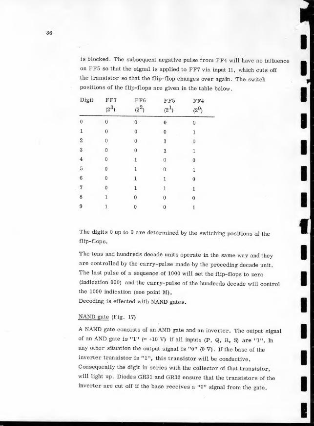
NAND gate (Fig. 17)
A NAND gate consists of an AND gate and an inverter. The output signal
of an AND gate is "1" (= +10 V) if all inputs (P, Q, R, S) are "1". In
any other situation the output signal is "0" (0 V) . If the base of the
inverter transistor is "1", this transistor will be conductive.
Consequently the digit in series with the collector of that transistor,
will light up. Diodes GR31 and GR32 ensure that the transistors of the
inverter are cut off if the base receives a M0" signal from the gate.
37
Fig. 17. Nand gate
INDICATOR INDICATOR
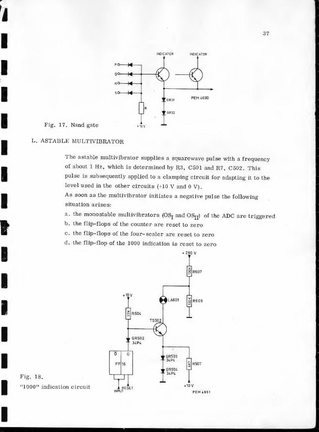
L. ASTABLE MULTIVIBRATOR
The astable multivibrator supplies a squarewave pulse with a frequency
of about 1 Hz, which is determined by R3, C501 and R7, C502. This
pulse is subsequently applied to a clamping circuit for adapting it to the
level used in the other circuits (+10 V and 0 V).
As soon as the multivibrator initiates a negative pulse the following
situation arises:
a. the monostable multivibrators (OSj and OSjj) of the ADC are triggered
b. the flip-flops of the counter are reset to zero
c. the flip-flops of the four- scaler are reset to zero
d. the flip-flop of the 1000 indication is reset to zero
+ 280 V
Fig. 18.
”1000” indication circuit
38
M. ”1000” INDICATION
At the beginning of a measurement flip-flop FF16 is reset to "0" so that
output 0 is in position "0" (0 V). Consequently TS502 is cut off and no
current can pass lamp LA601. As soon as FF16 has changed over due
to a carry-pulse from the hundreds decade unit, output 0 of FF16 will
become "1” (+10 V), and TS502 is conductive, which means that lamp
LA601 lights up and the digit 1 is displayed.
PEM 4704
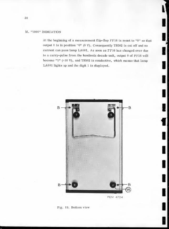
Fig. 19. Bottom view
39
VIII. DISASSEMBLING
A. HOUSING
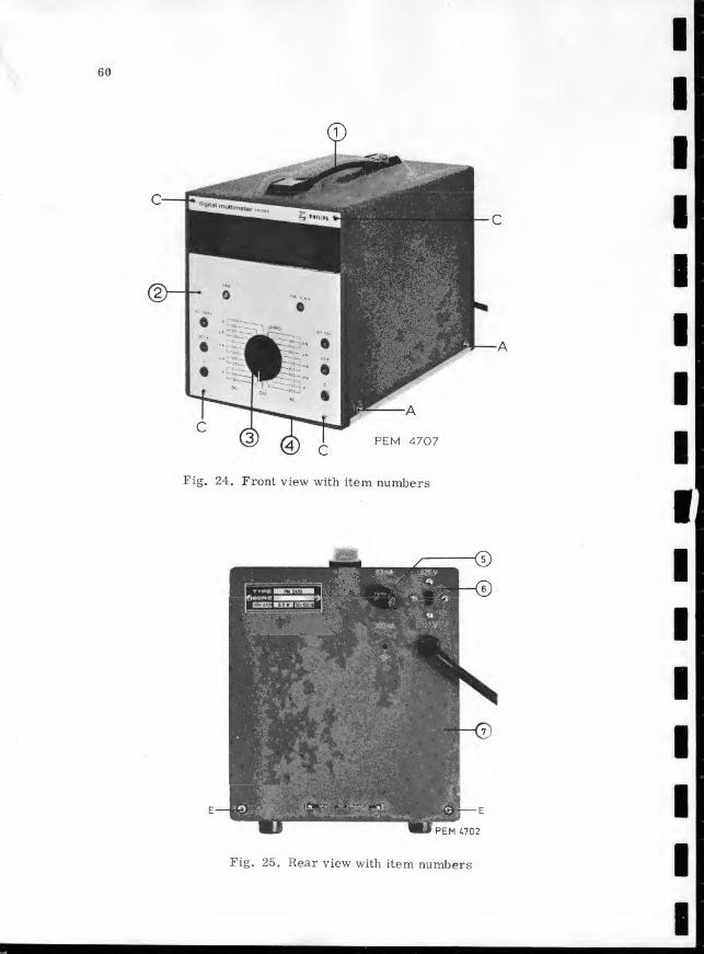
- Remove two screws "A" (Fig. 24) at the right-hand side and two
screws at the left-hand side.
- Lift the housing at the rear side and remove it.
Note: The housing is provided with a cam fitting in the front frame.
B. BOTTOM PANEL
- Remove four screws MBM (Fig. 19).
- Remove the bottom panel.
C. TEXT PLATE
- Remove four screws "C" (Fig. 24).
- Remove the text plate.
IX. REPLACING PARTS
A. FRONT FRAME
- Remove the housing, bottom panel and text plate (see VIII. A, B and
C).
- Unsolder or disconnect the connections of all sockets mounted on, the
front frame.
- Remove the monoknob (see IX. C).
- Loosen the central fixing nut of the selector switch by means of a
12 mm box spanner.
- Remove the 8 screws at the front of the frame,
r Remove the frame.
4ia
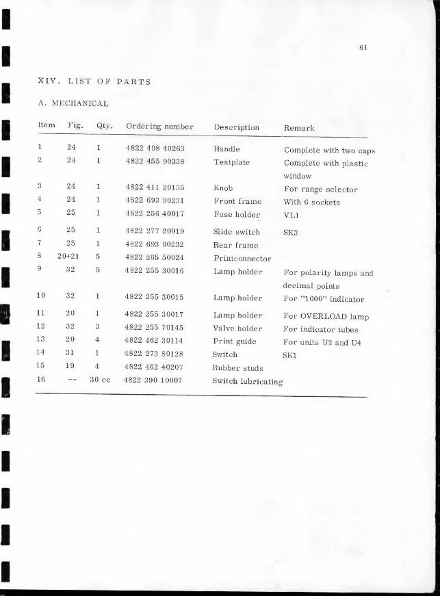
B. REAR FRAME
- Remove the fuse holder.
- Remove the two screws of the voltage selector switch (220 V/127 V)
and the locking spring.
- Remove the type plate (two screws)
.
- Remove the two screws "D" (Figs. 20 and 21) and "E" (Fig. 25).
- Unsolder the mains cable
.
- Remove the two screws with which the mains transformer is fitted in
the rear frame
.
- Remove the rear frame.
Fig. 20. Right-hand side view
C. MONOKNOB
Remove the bottom panel and the text plate (VIII. B+C).
Set the monoknob to position "3 V AC".
Loosen the alien screw some turns.
This screw is accessible from the bottom with a 2 mm alien key
Remove the monoknob.
I
- — '
G il^HPEM 4706
R40'1 R 400
Fig. 21. Left-hand side viewCS19587
42
D. SELECTOR SWITCH
- Remove the housing (see VIII. A).
- Remove the monoknob (see C)
.
- Unsolder the wires (mark them, if necessary’).
- Loosen the central fixing nut of the switch by means of a 12 mm box
spanner.
- Remove the print plate at the back of the switch (two screws)
.
- Remove the switch.
Note: The switch is provided with a cam at the front for correct mounting.
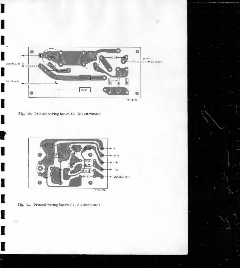
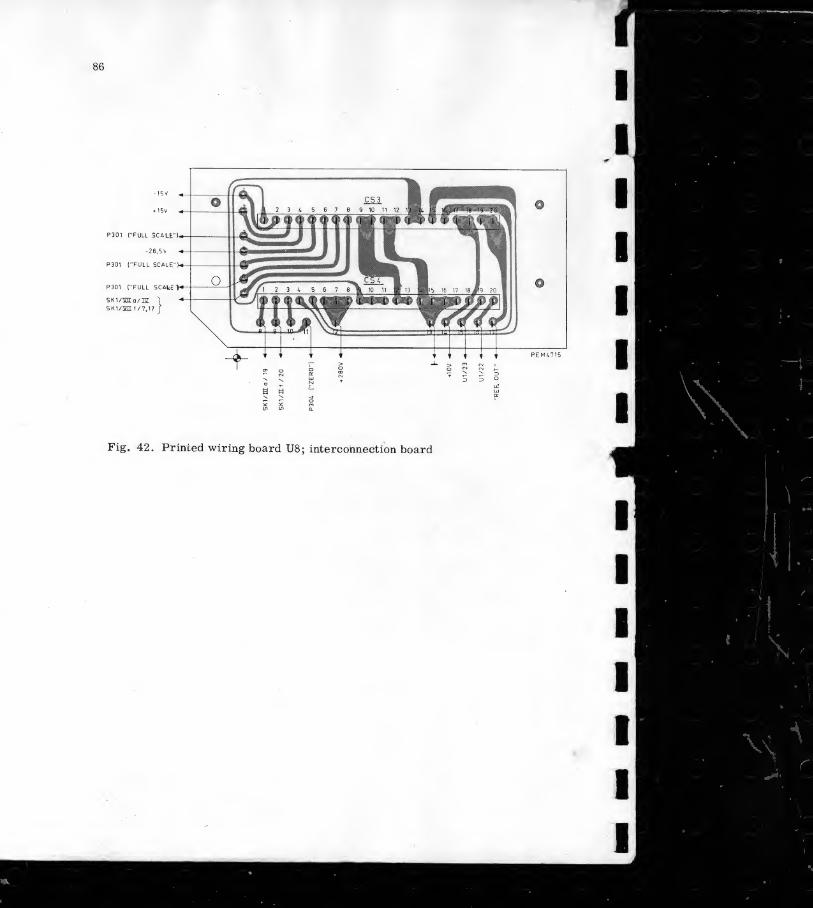
E. PRINTED WIRING BOARDS
1. U2 and U4, stabilisation unit and amplifier unit
- Remove the housing (VIII. A).
- Push the four locking pins ”F” and ”G” (Figs. 20 and 21) forward.
- Slide the prints upwards.
2. Ul, Supply unit
- Remove the housing (VIII. A).
- Remove the bottom panel (VIII. B).
- Remove U2 and U4 (E . 1)
.
- Unsolder all connection wires (component side and wiring side).
- Remove eight screws ”H” (Fig. 31) with which the print-guides are
mounted on print Ul.
- Remove four screws ”J” (Figs. 20 and 21).
- Remove print Ul.
3. U3, ADC unit
- Remove the housing (VIII. A).
- Remove two screws ”K” (Fig. 20).
- Slide print U3 to the front so that the print plate comes out of its
socket
.
- Remove print U3.
CS19588
43
4. U5, Counter unit
- Remove the housing (VIII. A).
- Remove print U3 (E . 3)
.
- Remove two screws "LM (Fig. 20).
- Remove screw "M" (Fig. 21)
.
- Remove two screws "N" (Fig. 32).
- Slide the print backwards, so that it comes clear of the pivot at the
front.
- Lift the print up at the front and slide it out of the socket.
Note: U3 and U5 can be hinged out together (see Fig. 32) after loosening
the screws ML" (Fig. 20).
5. U6, DC attenuator unit
- Remove the housing.
- Remove two screws "R" (Fig. 21).
- Hinge out the box.
- Remove two screws "S” (Fig. 32) and open the box.
- Unsolder the wires.
- Remove the four screws in the corners and remove the print*
6. U7, AC attenuator unit
- Remove the housing (VIII. A).
- Remove the screws "O" (Fig. 20).
- Hinge out the box.
- Remove two screws "P" (Fig. 32) and open the box.
- Remove four screws "Q" (Fig. 32)
.
- Unsolder the wires.
- Remove the mounting plate and print plate U7.
7. U8, Connection print
- Remove the housing.
- Remove print U3 (E . 3)
.
- Remove print U5 (E . 4)
.
- Unsolder all connection wires and remove the print.
44
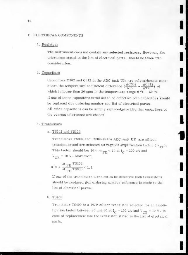
F. ELECTRICAL COMPONENTS
1.
Resistors
The instrument does not contain any selected resistors. However, the
tolerances stated in the list of electrical parts, should be taken into
consideration.
2.
Capacitors
Capacitors C302 and C312 in the ADC (unit U3) are polycarbonate capa-
citors the temperature coefficient difference ("^o°2 - ~'
f'
§o”
)of
which is lower than 20 ppm in the temperature range 0 °C - 50 °C.
If one of these capacitors turns out to be defective both capacitors should
be replaced (for ordering number see list of electrical parts).
All other capacitors can be simply replacedfprovided that capacitors of
the correct tolerances are chosen.
3.
Transistors
a. TS302 and TS305
Transistors TS302 and TS305 in the ADC (unit U3) are silicon
transistors and are selected as regards amplification factor(a ).r L
This factor should be: 20 < a < 40 at = 100 uA andx1 L C
= 10 V. Moreover:
0.9 <ppi TS302—— <11
<* FE TS305* 1,1
If one of the transistors turns out to be defective both transistors
should be replaced (for ordering number reference is made to the
list of electrical parts)
.
b. TS400
Transistor TS400 is a PNP silicon transistor selected for an ampli-
fication factor between 30 and 60 at I = 100 /uA and V„ = 10 V. InC CE
case of replacement use the transistor stated in the list of electrical
parts.
45
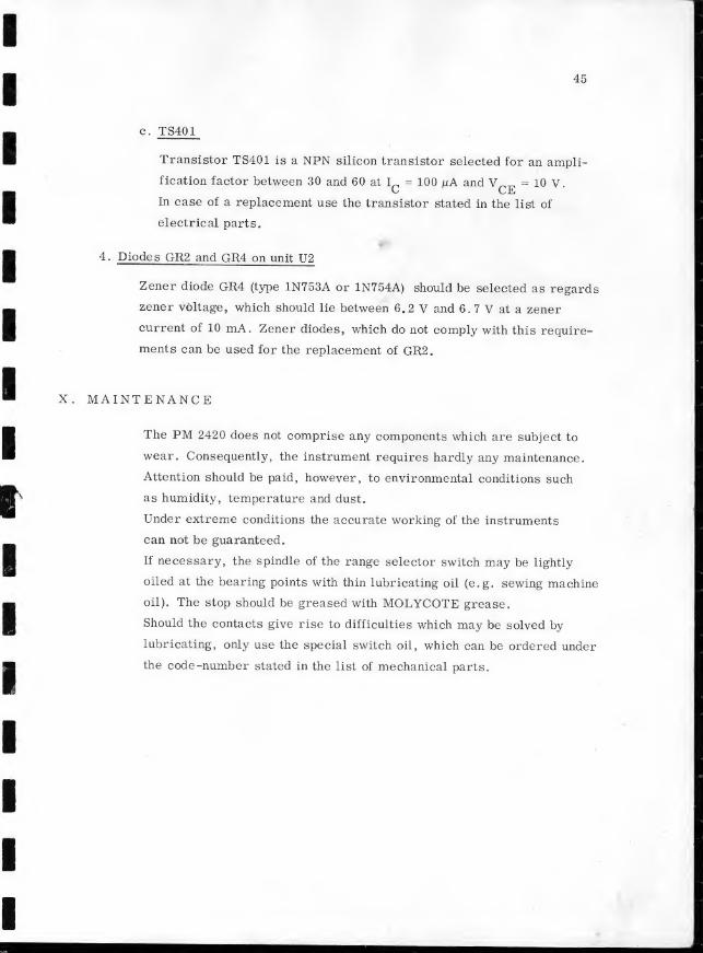
c. TS401
Transistor TS401 is a NPN silicon transistor selected for an ampli-
fication factor between 30 and 60 at I = 100 pA and V„ = 10 V.C CEIn case of a replacement use the transistor stated in the list of
electrical parts.
4. Diodes GR2 and GR4 on unit U2
Zener diode GR4 (type 1N753A or 1N754A) should be selected as regards
zener voltage, which should lie between 6.2 V and 6. 7 V at a zener
current of 10 mA. Zener diodes, which do not comply with this require-
ments can be used for the replacement of GR2.
X. MAINTENANCE
The PM 2420 does not comprise any components which are subject to
wear. Consequently, the instrument requires hardly any maintenance.
Attention should be paid, however, to environmental conditions such
as humidity, temperature and dust.
Under extreme conditions the accurate working of the instruments
can not be guaranteed.
If necessary, the spindle of the range selector switch may be lightly
oiled at the bearing points with thin lubricating oil (e.g. sewing machine
oil). The stop should be greased with MOLYCOTE grease.
Should the contacts give rise to difficulties which may be solved by
lubricating, only use the special switch oil, which can be ordered under
the code-number stated in the list of mechanical parts.
46
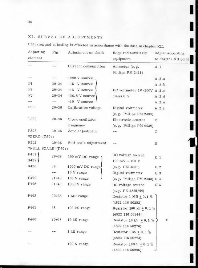
XI. SURVEY OF ADJUSTMENTS
Checking and adjusting is effected in accordance with the data in chapter XII.
Adjusting Fig. Adjustment or check Required auxiliarly Adjust according
element
20+34
20+34
20+34
P303 20+36
,fZEROn(P304)
P302 20+36
"FULL SCALE M(P301)
Adjustment or check
Current consumption
+280 V source
+15 V source I
-15 V source \
-26. 5 V sourcej
+10 V source'
Calibration voltage
Clock oscillator
frequency
Zero adjustment
Full scale adjustment
P407 )
R427j
20+38 100 mV DC range \
R426 38 1000 mV DC range (
— — 10 V range 1
P409 21+40 100 V range /
P408 21+40 1000 V range
P402 20+38 1 Mft range
P401 38 100 kft range
P400 20+38 10 kft range
— — 1 kft range
— — 100 ft range
equipment to chap
Ammeter (e.g. A. 1
Philips PM 2411)
A. 2. a
A. 2. b.
DC voltmeter 1V-300V A.2.c
class 0. 5 A. 2. d
A. 2. e
Digital voltmeter A. 2. f
(e.g. Philips PM 2433)
Electronic counter B
(e.g. Philips PM 6630)
C
DC voltage source,E ^
100 mV - 100 V
(e.g. GM 4561) E.2
Digital voltmeter E.3
(e.g. Philips PM 2433) E.4
DC voltage source E.5
(e.g. PE 4839/00)
Resistor 1 M ft +0.1%
(4822 116 50282)
Resistor 100 kft + 0.1%
(4822 116 50244)
Resistor 10 kft +0.1 % >
(4822 116 50276)
Resistor 1 kft + 0. 1 %
(4822 116 50274)
Resistor 100 ft + 0.1 %
(4822 116 50286)
to chapter XII point
A. 1
47
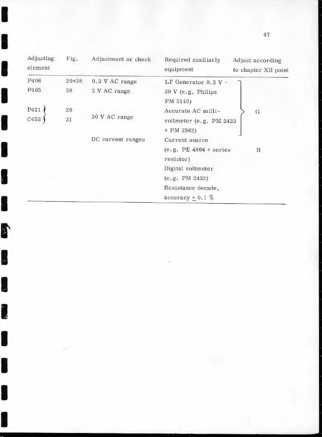
Adjusting
element
Fig. Adjustment or check Required auxiliarly
equipment
Adjust according
to chapter XII point
P406 20+38 0.3 V AC range LF Generator 0.3 V - *1
P405 38 3 V AC range 30 V (e.g. Philips
PM 5140)
P421 ) 20 Accurate AC milli- > GC452
j31
30 V AC rangevoltmeter (e.g. PM 2433
[
+ PM 2562)
DC current ranges Current source
(e.g. PE 4804 + series H
resistor)
Digital voltmeter
(e.g. PM 2433)
Resistance decade,
accuracy + 0. 1 %
48
XII. CHECKING AND ADJUSTING
The tolerances mentioned in this chapter only apply to a completely
readjusted instrument and may therefore deviate from the data given
in chapter II.
In chapter XI a survey is given of the adjustments, adjusting elements
and the required equipment.
Re calibration may only be carried out if measuring instruments and
voltage sources are available that comply with the requirements made.
A. POWER SUPPLY
1. Current consumption
- Connect the instrument to the nominal mains voltage via a variable
transformer and an ammeter (e.g. multimeter PM 2411).
- Current consumption at 110 V : approx. 50 mAat 220 V : approx. 36 mA.
2. DC output voltages
Voltage Measuring point Value Adjusting
source element
a. +280 V test point 19 (Fig.
and socket ”0”
33) +280 V + 14 V none
b. +15 V test point 16 (Fig.
and socket "0"
34) +15 V + 750 mV PI
c. -15 V test point 18 (Fig.
and socket ”0"
34) -15 V + 750 mV P2
d. -26.5 V test point 20 (Fig.
and socket ”0”
34) -26.5 V + 130 mV P3
e. +10 V test point 21 (Fig.
and socket "0"
34) +10 V + 1 V none
f . -9. 995 V sockets "REF. OUT"
and "0"
-9.995 V + 10 mV P300
49
B. CLOCK OSCILLATOR FREQUENCY
- Check the clock oscillator frequency. For this purpose connect an
electronic counter between the emitter of TS314 and_L
- Adjust the counter to 1 second.
- The frequency should be 390 kHz + 1 %- If necessary, adjust T300.
C. ZERO ADJUSTMENT
- Set monoknob to position ”10 V DC”.
- Connect socket ”VftA” to ”0”
- Set potentiometer ”ZERO” (front) to the mid position
- Adjust potentiometer P303 to 0.00 indication (polarity indication
lamps light up alternately).
D. FULL SCALE ADJUSTMENT
- Set monoknob to position ”10 V DC”- Interconnect sockets ”VftA” and ”REF.OUT”- Set potentiometer ”FULL SCALE” (front) to the mid position
- Adjust potentiometer P302 to 9. 99 indication
E. ADJUSTING THE DC VOLTAGE RANGES
1. 100 mV range
- Set the monoknob to position ”10 V DC”- Interconnect sockets ”V£2A” and ”0”
- Adjust the indication to 0. 00 with ”ZERO”- Set the monoknob to position ”100 mV DC”- Adjust potentiometer P407 to obtain 00. 0 indication
- Apply 100 mV + 0.1 % to the instrument. Check this voltage with a
digital voltmeter.
- The indication should be: 99. 6 ... 100.4. If not, the value of R427
should be changed
- Check the linearity by applying successively 0. 1 mV; 0.2 mV;
0.4 mV; 0. 8 mV; 1.6 mV; 3.2 mV; 6.4 mV; 11.1 mV; 22.2 mV;
33.3 mV; 44.4 mV; 55.5 mV; 66.6 mV; 77.7 mV; 88.8 mV and 99.9 mV.CS19589
50
2. 1000 mV range
- Set monoknob to position n1000 mV DC"- Apply IV + 5. 10
4%. Check with a digital voltmeter.
- The indication should be: 996. . . 1004. If not, the value of R426should be changed.
3. 10 V range
- Set monoknob to position "10 V DC"- Apply 10 V + 5.10
4%. Check with a digital voltmeter
- Check the indication: 9. 99 . . . 10. 01.
- Check the linearity by applying successively 0. 01 V; 0. 02 V; 0. 08 V;
0.16 V; 0.32 V; 0.64 V; 1.11 V; 2.22 V; 3.33 V; 4.44 V; 5.55 V;
6. 66 V; 7. 77 V; 8. 88 V and 9. 99 V.
4. 100 V range
- Set monoknob to position "100 V DC".
- Apply 100 V + 5.104%. Check with accurate digital voltmeter.
- Adjust the indication to 99. 9 ... 100. 1 with potentiometer P409.
5. 1000 V range
- Set the monoknob to position "1000 V DC"- Apply 1000 V + 5. 10
4% to sockets "1000 V DC" and "0". Check
with an accurate DC Voltmeter
- Adjust the indication to 999. . . 1001 with potentiometer P408.
F. ADJUSTING THE ft -RANGES
Monoknob in Resistor to be connected Indication Adjust with
position to sockets "VftA" and "0"
1000 kft 1 Mfi + 0.1 % 997 . , . 1003 P402100 kft 100 kft + 0.1 % 997 . , . 1003 P401
10 kft 10 kft + 0.1 % 997 . . 1003 P4001 kft 1 kft + 0.1% 997 . . 1003 —
100 ft 100 ft + 0.1 % 997 . . 1003
CS19590
51
G. ADJUSTING THE AC VOLTAGE RANGES
Monoknob in Apply to sockets Indication Adjusting
position "VftA” and "0" element
0.3 V 0.3 V, 1 kHz 298 .
.
.302 P406
3 V 3 V, 1 kHz 2.98 .. . 3.02 P405
30 V 30 V, 50 kHz 29.8 . 30.2 P421
30 V 30 V, 10 kHz 29. 8 . . . 30.2 C452
Note : Check the applied voltage with an accurate AC millivoltmeter, class 0.2 (e.g
Philips AC to DC Converter PM 2562 + Digital voltmeter PM 2433).
Checking the 300 V AC range
- Set monoknob to position ”30 V AC"- Apply 3 V, 10 kHz, to sockets MVfiA" and ”0”
- Indication 030 + 1 %- Apply 300 V, 50 or 60 Hz, to sockets "VS2A" and ”0”
- Indication 300 + 1 %.
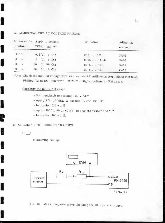
H. CHECKING THE CURRENT RANGES
1.
DC
Measuring set-up:
PEM4710
rangesFig. 22. Measuring set-up for checking the DC current
52
Current source (e.g. PE 4804 + series resistor R ) 100 uA - 1As
Rm = resistance decade box, accuracy 0.1 %.
Digital voltmeter e.g. PM 2433
Measuring procedure:
Measuring Value of Value of Adjust indication Indication
range Rs
Rm on PM 2433 to on PM 2420
100 juA 15 kfi 1 kfi . 1000 (range . 3999) 99.0.
.
.101.0
1000 nA 15 kft 1 k£2 1. 000 (range 3. 999) 99.0.
.
.101.0
10 mA 1 kft 100 fl 1.000 99.0.. .101.0
100 mA 1 kfl 10 1.000 99.0.
.
.101.0
1 A 1 ft 1.000 99.0. . .101.0
(via socket "1 A DC”)
AC
A check of the AC current ranges is not necessary when the DC current
ranges have been checked. The shunts used in the AC current section
are the same as those used in the DC section.
53
XIII. TROUBLE SHOOTING
If the instrument appears to be out of order, it is advisable to check
it systematically. The following instructions may greatly facilitate
the fault finding. Data without tolerances represent the properties of an
average instrument and may serve as a guide only.
1. The voltages mentioned in table 1 of Fig. 35 are the r.m.s. values
of the voltages of the transformer at no-load. The values stated at
the windings in the diagram represent the values valid under normal
conditions.
(Measurement carried out with AC mill ivoltmeter GM 6012).
2. In the circuit diagram of Fig. 43 DC voltages have been indicated
at some points. These voltages have been measured with DC \uCV meter
PM 2440 under the following conditions:
- nominal mains voltage (220 V, 50 Hz)
- calibrated
- monoknob in position "10 V DC M
- socket "VftA" connected to socket MREF. OUT"
3. In table 1 and Fig. 23 below, the most important voltages and
waveforms are given. Conditions:
- nominal mains voltage (220 V, 50 Hz)
- calibrated
- voltages and waveforms with respect to circuit zero (socket "0”)
- monoknob in position "10 V DC" (unless otherwise stated)
- socket "VftA" connected to socket "REF. OUT" (unless otherwise
stated)
It is advised to follow the procedure given hereafter.
Measuring
Fig.
DC
level
Remark
AC
waveform
point
54
f—t i—
i
s—
1
£ >i—
i
>S>B>N—
"
N "
CO CO CO CO CO CO CO COCM CM CM CM CM CM CM CM
bib bi) bi) bn bi) bi) bi) bi)•rH •rH •rH •rH
Pa Pa Pa Pa Pa Pa Pa Ph
© © © © © © © ©© © © © © © © ©CQ CQ CQ CQ CQ CQ CQ CQ
>>>>>>>o rf © o © ©
^ ^ ^ ^ COCO CO CO CO CO CO
© © CO CO ©CO CO CO CO CO
<X> l>- oo © T-I © o Phi-a i-H t-I CM CM i-l CQ Z O CM CO ©
bo d a o o•SP S' S4
bi*5
jd
*a 3 a o oH O O J ^
Oscillator
9
36
See
Fig.
23
(DC)
Oscillator
out
10
36
See
Fig.
23
(X)
(ate
input
II
8
36
See
Fig.
23
(XI)
To
be
measured
Measuring
Fig.
DC
level
Remark
AC
waveform
point
55
W1—
1
1—
1
1—
1
£ >HH
>X X X X x00 00 00 00 COCM CM CM CM CM
bi) bL bi) bi) bi)•H •iH
ptl Pq S Pq Pq
0 0 0 0 00 0 0 0 0GO CO CO CO CO
™ aa qI q 0Cl, ?h
b^ (T) d10 q Oco
^ 0o o
a •rH
0 00 rR
'S q +-»
aq q O
T3o 0a <M£ CD 0o 0 0q bp qo a qc q oR q o0 C2 m
0 q<4H oo +-> +>
Oi 05 Ci 05 00CO 00 00 00 00
CO CM rH CMrH 1“H rH rH CM
0 i
00$H q3 qo CQ
q0 CQ
T5
CD
"§CQ
iH
q0rj
05 0 q q q0CQ m
q*§
03
0$H 0
U3
q0H-»
qq o qq0
0qq"MO o o o Hi CQ
+-» q~q >> >»
q CQ
0Ou q Jh q M q+» q q q qq a q q o qO a O O O o
*tH
-8.
5Vp-p
at
ranges
3V
and
300
VAC
if
an
A.C.
voltage
offfull
scale
value
is
applied.
be > co CO>< CM CM
•rH .
o CO bo beCQ CM •HO Ph P^
CD be CD <DCD •r-i
<D 005 m CO
clCD
CDbe
CD
T3CD
OXCD
aoja
'tfo
OCD cs
CQ §CQ
CD o*
,
o be oi—
i
O a o3 cti T—
1
CD ?H1 T3
8 S gcS Mcq ctf cqCD U <D
CQ <3 CQ
CS19591
aNNNN
59
4. In a short time a large number of clock pulses is applied to the
four- scaler. Moreover, the counter is reset every second. Therefore
it is difficult to display the signals at the measuring points
CS4/9+10, 14, 13, 12, 11 (see table 1) on an oscilloscope.
Should the counter be out of order (unit U5) we may advise to removethe converter unit U3 (see IX. E3). Apply a square wave signal to
point CS4/9 or 10. Unsolder also R502 and C503 on unit U5.
5. In position "10 V DC" the input is connected direct to the ADC.
Therefore, it is suggested to start any repair check in this position,
since under these circumstances the influence of the attenuators,
amplifier, and rectifier will be negligible.
6. If the instrument does not function in the ranges 100 mV, 1000 mV,all DC current ranges and the resistance ranges "100 ft" and
"1000 ft", this may be caused by fuse VL401 being defective.
7. Should all resistance ranges be out of order, this may be caused by
VL402 being blown. In that case no current can pass through the
resistor to be measured and, consequently, there is no voltage across
the unknown resistance.
Remark
Should the instrument appear to be out of order, please apply for advise
to the world -wide PHILIPS Service Organisation. If the repair work is
to be effected at a Philips Service Centre please follow the procedure below:
- Attach a label to the instrument with full name and address of the sender- Indicate as complete as possible the symptom(s) of the fault(s).
- Carefully pack the instrument in the original packing, or, if this is no
longer available, in an other suitable packing.
- Send the instrument to the address mentioned by your local Philips
representative.
100mA
PEM 4707
Fig. 24. Front view with item numbers
PEM 4702
Fig. 25. Rear view with item numbers
61
XIV. LIST OF PARTS
A. MECHANICAL
Item Fig. Qty. Ordering number
1 24 1 4822 498 40263
2 24 1 4822 455 90338
3 24 1 4822 411 20135
4 24 1 4822 693 90231
5 25 1 4822 256 40017
6 25 1 4822 277 20019
7 25 1 4822 693 90232
8 20+21 5 4822 265 50024
9 32 5 4822 255 30016
10 32 1 4822 255 30015
11 20 1 4822 255 30017
12 32 3 4822 255 70145
13 20 4 4822 462 30114
14 31 1 4822 273 80128
15 19 4 4822 462 40207i a O A >4 Ann a A r>>. r\ r\ri
Description
Handle
Textplate
Knob
Front frame
Fuse holder
Slide switch
Rear frame
Printconnector
Lamp holder
Lamp holder
Lamp holder
Valve holder
Print guide
Switch;
Rubber studs
Remark
Complete with two caps
Complete with plastic
window
For range selector
With 6 sockets
VL1
For polarity lamps and
decimal points
For ”1000" indicator
For OVERLOAD lamp
For indicator tubes
For units U2 and U4
SKI
62
B. ELECTRICAL — ELEKTRISCH — ELEKTRISCH — ELECTRIQUE — ELECTRICOS
ma^k^^e'spe^Tficatio^ca^b'e drived ^romtlfrsu^^)fbelow.rtS^ ” "*— '« <h* *»•* di*S™ -» -
^MHlkatl^^kan^aus^adlstere^d^l^b^lcht^g^ele^^werden.^'CSe S'"d Wcha.tblld -it Ka„naeich„U ngen versehen. Die
De^spedfi^t^va^^a^merkt^wns*!*W™"- DKe C0mp0"en“n ** '" het prlndp-ch-n. met een merkteken aangegever.
i^d?,
r
u1erd-d^n
uVCOntie"t|>aS d“ PlSC“ “ niVerSelleS « standard - Cell“-d <•«** reperdes dans le schema de principe. Leurs specifications sont
ma“ at, +S2SZZZS2::e1XTr,^,terSaleS E“OS “mP°"e""S « - «1— d* P^cipm de un.
^h
^h
^lh
^h
Carbon resistor E24 series
Kohleschichtwiderstand, Reihe E24Koolweerstand E24 reeksResistance au carbone, s6rie E24Resistencia de carbon, serie E24
Carbon resistor El 2 series
Kohleschichtwiderstand, Reihe E12Koolweerstand El 2 reeksResistance au carbone, serie El 2Resistencia de carbon, serie El 2
Carbon resistor E24 series
Kohleschichtwiderstand, Reihe E24Koolweerstand E24 reeksResistance au carbone, serie E24Resistencia de carb6n, serie E24
Carbon resistor El 2 series
Kohleschichtwiderstand, Reihe El
2
Koolweerstand El 2 reeksResistance au carbone, serie El 2Resistencia de carbon, serie El
2
HO-
5%
0,25 W <; 1 Mft, 5%> 1 MQ, 10%
0,5 W ^ 5 Mn, 1%> 5 ^10 MQ, 2%
> 10 Ma 5%
r 0,5 W^1,5Mn, 5%>1,5Mft, 10%
Wire-wound resistor
DrahtwiderstandDraadgewonden weerstandResistance bobineeResistencia bobinada
Tubular ceramic capacitorRohrkondensatorKeramische kondensator, buistypeCondensateur ceramique tubulaireCondensador cerdmico tubular
Tubular ceramic capacitor
RohrkondensatorKeramische kondensator, buistypeCondensateur ceramique tubulaireCondensador ceramico tubular
Ceramic capacitor, "pin-up"Keramikkondensator "Pin-up" (Perltyp)Keramische kondensator "Pin-up" typeCondensateur ceramique, type perleCondensador ceramico, version "colgable"
"Microplate" ceramic capacitorMiniatur-Scheibenkondensator"Microplate" keramische kondensatorCondensateur ceramique "microplate"Condensador ceramico "microplaca"
Mica capacitor
GlimmerkondensatorMicakondensatorCondensateur au micaCondensador de mica
500 V
700 V
500 V
30 V
500 V
Carbon resistor El 2 series
Kohleschichtwiderstand, Reihe El
2
Koolweerstand El 2 reeksResistance au carbone, serie El 2Resistencia de carbon, serie El 2
W^2,2MQ, 5%>2,2 MQ, 10%
Carbon resistor El 2 series
Kohleschichtwiderstand, Reihe El
2
Koolweerstand El 2 reeksResistance au carbone, serie El 2Resistencia de carbon, serie El
2
W 5%
Wire-wound resistor
DrahtwiderstandDraadgewonden weerstandResistance bobineeResistencia bobinada
10,4- 1,8 W 0,5%
Wire-wound resistor
DrahtwiderstandDraadgewonden weerstandResistance bobineeResistencia bobinada
1 5,5 W^ 200 a 10%>200 a 5%
10 W 5%
Polyester capacitor
Polyesterkondensator
PolyesterkondensatorCondensateur au polyester
Condensador polyester
Flat-foil polyester capacitor
Miniatur-Polyesterkondensator (flacn)
Platte miniatuur polyesterkondensatorCondensateur au polyester, type plat
Condensador polyester, tipo de placas planas
Paper capacitor
Papierkondensator
Papierkondensator
Condensateur au papier
Condensador de papel
Wire-wound trimmerDrahttrimmerDraadgewonden trimmerTrimmer a fil
Trimmer bobinado
400 V
250 V
1000 V
Tubular ceramic trimmerRohrtrimmerBuisvormige keramische trimmerTrimmer ceramique tubulaire
Trimmer ceramico tubular
For multi-purpose and standard parts, please see PHILIPS’ Service Catalogue.
Fur die Universal- und' Standard-Teile siehe den PHILIPS Service-Katalog.
Voor universele en standaardonderdelen raadplege men de PHILIPS Service Catalogus.
Pour fes pieces universelles et standard veuillez consulter le Catalogue Service PHILIPS.
Para piezas universales y standard consulte el Catalogo de Servicio PHILIPS.
63
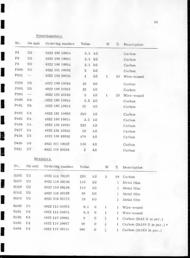
Potentiometer s
Nr. On unit Ordering number Value w % Description
PI U2 4822 100 10014 2.5 k£2 Carbon
P2 U2 4822 100 10014 2.5 k £2 Carbon
P3 U2 4822 100 10014 2.5 k£2 CarbonP300 U3 4822 101 10062 5 k£2 CarbonP301 — 4822 103 20033 1 k£2 l 20 Wire -wound
P302 U3 4822 100 10016 22 k£2 CarbonP303 U3 4822 100 10016 22 k£2 CarbonP304 — 4822 103 20163 5 k£2 l 20 Wire -woundP400 U4 4822 100 10014 2.5 k£2 CarbonP401 U4 4822 100 10016 25 k£2 Carbon
P402 U4 4822 101 10056 250 k £2 CarbonP405 U4 4822 100 10014 2.5 k£2 CarbonP406 U4 4822 100 10011 220 k£2 CarbonP407 U4 4822 101 10053 50 kn CarbonP408 U6 4822 100 10082 470 k£2 Carbon
P409 U6 4822 101 10057 100 k£2 CarbonP421 U7 4822 101 20281 5 k£2 Carbon
Resistors
Nr. On unit Ordering number Value w % Description
R305 U3 4822 111 70107 220 k£2 2 10 CarbonR307 U3 4822 116 50198 110 k£2 1 Metal film
R310 U3 4822 116 50198 110 k£2 1 Metal film
R342 U3 4822 116 50198 68 k£2 1 Metal film
R343 U3 4822 116 50111 39 k£2 1 Metal film
R400 U4 4822 113 50073 0.1 £2 1 1 Wire -woundR401 U4 4822 113 50074 0.9 a 1 1 Wire -woundR402 U4 4822 110 30061 9 £2
1
2 1 Carbon (2x18 £2 in par.
)
R403 U4 4822 110 30087 90 u 1
2 1 Carbon (2x180 £2 in par.)R404 U4 4822 110 30114 900 £2
1
2 1 Carbon (2xlK8 in par.
)
64
Nr. On unit Ordering number Value w % Description
R408 U4 4822 113 80111 2.2 7 5 Wire -woundR409 U4 4822 116 50119 12 k£2
l
4 5 Metal film
R410 U4 4822 116 50049 20 k£214 5 Metal film
R411 U4 4822 116 50136 120 kft14 5 Metal film
R412 U4 4822 110 30189 1.2 MS2 1
4 5 Carbon
R415 U6 4822 116 50488 4.95 Mfi 1 2 Metal film
R416 U6 4822 116 50488 4.95 MS2 1 2 Metal film
R417 U6 4822 116 50488 4.95 Mfl 1 2 Metal film
R418 U6 4822 116 50488 4.95 Mfi 1 2 Metal film
R419 U6 4822 116 50487 10 M ft 2 2 Metal film
R420 U6 4822 116 50487 10 MS2 2 2 Metal film
R421 U6 4822 116 50489 1.06 M Q 2 2 Metal film
R426 U4 4822 113 80111 2.2 kfi 7 5 Wire -woundR427 U4 4822 116 50486 1111 Q i
4 Metal film
R428 U4 4822 116 50485 101 Q 1
4 Metal film
R429 U4 4822 116 50463 10 k fl14 Metal film
R431 U4 4822 116 50102 8.2 k£2l? 5 Metal film
R432 U4 4822 116 50098 820 a i4 5 Metal film
R451 U7 4822 116 50487 10 MS2 2 2 Metal film
R452 U7 4822 116 50462 98.5 kft 1 Metal film
Capacitors
Nr. On unit Ordering number Value V % Description
Cl U2 4822 124 20374 64 MF 40 Electrolytic
C2 U2 4822 124 10004 10 U.F 16 Electrolytic
C4 U2 4822 124 20374 64 MF 40 Electrolytic
C5 U2 4822 124 10004 10 mF 16 Electrolytic
C7 U2 4822 124 20355 10 mf 25 Electrolytic
C8 U2 4822 124 20381 64 mf 64 Electrolytic
CIO U2 4822 124 20411 500 juF 25 Electrolytic
Cll U2 4822 124 10004 10iuF 16 Electrolytic
C12 U2 4822 124 20411 500 MF 25 Electrolytic
C13 U1 4822 124 20434 16 UF 400 Electrolytic
65
On unit Ordering number Value V % Description
C14 U1 4822 124 20434 16
C302* U3 4822 121 50408 0.1
C306 U3 4822 121 50372 2200
C307 U3 4822 124 20384 100
C308 U3 4822 121 40168 4.7
C309 U3 4822 124 10004 10
C310 U3 4822 124 20384 100
C311 U3 4822 121 40055 47000
C312X
U3 4822 121 50408 0.1
C402 — 4822 121 40214 0.1
C403 U4 4822 124 20342 1.6
C408 U4 4822 124 20388 160
C409 U4 4822 121 50038 270
C450 — 4822 120 60081 100
C451 — 4822 120 60058 15
C452 — 4822 125 60033 12
C453 U7 4822 120 60107 2000
C454 U7 4822 124 20342 1.6
C455 U7 4822 120 50143 22000
C456 U4 4822 124 20357 16
C457 U4 4822 120 60107 1000
C458 U4 4822 124 10004 10
C501 U5 4822 124 20346 4
C502 U5 4822 124 20346 4
C503 U5 4822 122 30092 180
400 Electrolytic
mF 160 5 Polycarbonate
pF 63 5 Styroflex
AtF 16 Electrolytic
nF 250 Polyester
mf 16 Electrolytic
[iF 16 Electrolytic
pF Polyester
MF 160 5 Polycarbonate
IxF 1000 Paper
HF 64 Electrolytic
txF 16 Electrolytic
pF 160 Styroflex
pF 5 Mica
pF 5 Mica
pF Trimmer
pF 5 Mica (2xlK in par.
)
HF 64 Electrolytic
pF 1000 Paper
mf 16 Electrolytic
pF 5 Mica
luF 16 Electrolytic
fj,F 64 Electrolytic
HF 64 Electrolytic
pF 10 Ceramic
See DC. F. 2
CS19593
66
Miscellaneous
Nr. Fig. Ordering number Description Remark UU1 25 4822 216 70118 Printed wiring board JU2 26 4822 216 70114 Printed wiring board With components 1U3 26 4822 216 70121 Printed wiring board With components
U4 26 4822 216 70115 Printed wiring board With components
U5 26 4822 466 10151 Printed wiring board Without components 1U6 26 4822 216 70117 Printed wiring board With components
U7 26 4822 216 70116 Printed wiring board With components 1U8 22 4822 216 70119 Printed wiring board
VL1 — 4822 253 30006 Fuse 100 mA (delayed For mains voltages .1action) of 127 V
4822 253 30004 Fuse 63 mA (delayed For mains voltages
action) of 220 V
T1 22 4822 146 40166 Mains -transformer 1T300 21 4822 158 30134 Oscillator coil On unit U3 f
AFF1 21 4822 209 80031 Module Complete bistable
r "
multivibrator on U3 LAMI — 4822 209 80025 Module Complete astable _
multivibrator on U5 1FF2- -- 4822 209 80026 Module Complete bistable
FF16 multivibrator on U5 . iD1-D3 — 4822 209 80027 Module Complete decoder on U5H ft
LA401 — 4822 134 40181 Pilot lamp 6 V, 50 mA Overload indicator
L401 — 4822 158 20249 Choke1— — 4822 209 80028 Operationel amplifier Nexus SQ-10A LI
VL401 — 4822 253 20002 Fuse 31 mA (quick) On unit U4
VL402 — 4822 253 20002 Fuse 31 mA (quick) On unit U4 nB601 — ZMl 000 Indicator tube
B602 — ZM1000 Indicator tube _lB603 — ZM1000 Indicator tube iLA601 — 4822 134 20057 One thousand indicator
i
LA602--LA605 4822 134 20058 Pilot lamp Decimal points and 1polarity indicators
CS19594
D
Transistors
Nr. Ordering number Type Manufacturer
TS1 4822 130 40393 2N2195A Sesco
TS2 4822 130 40394 2N2926 Sesco
TS3 4822 130 40395 BC139 Fairchild
TS4 4822 130 40396 BC116 Fairchild
TS5 4822 130 40396 BC116 Fairchild
TS6 4822 130 40396 BC116 Fairchild
TS7 4822 130 40396 BC116 Fairchild
TS8 4822 130 40393 2N2195A Sesco
TS301 4822 130 40397 125DT2 Sesco
TS302* 4822 130 40401 2N2218 Texas Instruments
TS303 4822 130 40396 BC116 Fairchild
TS304 4822 130 40397 125DT2 Sesco
TS305X
4822 130 40401 2N2218 Texas Instruments
TS306 4822 130 40396 BC116 Fairchild
TS307 4822 130 40396 BC116 Fairchild
TS308 4822 130 40396 BC116 Fairchild
TS309 4822 130 40396 BC116 Fairchild
TS310 4822 130 40396 BC116 Fairchild
TS312 4822 130 40399 2N3605 Sesco
TS313 4822 130 40399 2N3605 Sesco
TS314 4822 130 40399 2N3605 Sesco
TS315 4822 130 40398 BSX21A RTCTS316 4822 130 40398 BSX21A RTCTS317 4822 130 40396 BC116 Fairchild
TS318 4822 130 40396 BC116 Fairchild
)0iTS400 4822 130 40402 BC116 Fairchild
TS401*®*4822130 40403 125DT2 Sesco
TS402 4822 130 40394 2N2926 Sesco
TS403 4822 130 40404 2N3819 Texas Instruments
TS405 4822 130 40394 2N2926 Sesco
x Selected pair, see IX. F. 3a
xx Selected (red point), see IX. F. 3b
xxx Selected (orange point), see IX.F.3c
68
Nr. Ordering number Type Manufacturer
TS406 4822 130 2N4303 Sesco
TS501 4822 130 40396 BC116 Fairchild
TS502 4822 130 40398 BSX21A RTCTS1-10 4822 130 40398 BSX21A RTC (10 pieces on U5)
TS101- 4822 130 40398 BSX21A RTC (10 pieces on U5)
110
TS1001-• 4822 130 40398 BSX21A RTC (10 pieces on U5)
1010
Dioden
Nr. Ordering number Type Manufacturer
GR1 4822 130 30316 TV4F Siemens
GR2 4822 130 30316 TV4F Siemens
GR3 4822 130 30316 TV4F Siemens
GR4 4822 130 30316 TV4F Siemens
GR5 4822 130 30316 TV4F Siemens
GR6 4822 130 30316 TV4F Siemens
GR7 1
GR8 f4822 209 80029 TV4F Siemens (module)
GR1 4822 130 30315 1N752A Inter Rectifier
GR2X
4822 130 30163 1N753A Siemens
GR3 4822 130 30315 1N752A Inter Rectifier
GR4X
4822 130 30163 1N753A Siemens * on unit U2GR5 4822 130 30315 1N752A Inter Rectifier
GR6 4822 130 30314 DZ15A Silec
GR7 4822 130 30314 DZ15A Silec
GR8 4822 130 30315 1N752A Inter Rectifier
xSee IX. F. 4
69
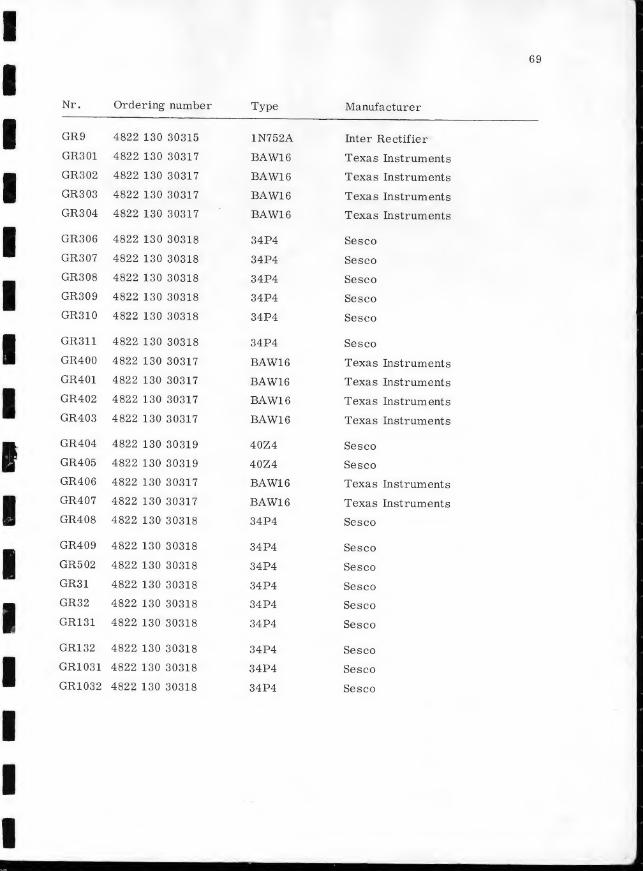
Nr. Ordering number Type Manufacturer
GR9 4822 130 30315 1N752A Inter Rectifier
GR301 4822 130 30317 BAW16 Texas Instruments
GR302 4822 130 30317 BAW16 Texas Instruments
GR303 4822 130 30317 BAW16 Texas Instruments
GR304 4822 130 30317 BAW16 Texas Instruments
GR306 4822 130 30318 34P4 Sesco
GR307 4822 130 30318 34P4 Sesco
GR308 4822 130 30318 34P4 Sesco
GR309 4822 130 30318 34P4 Sesco
GR310 4822 130 30318 34P4 Sesco
GR311 4822 130 30318 34P4 Sesco
GR400 4822 130 30317 BAW16 Texas Instruments
GR401 4822 130 30317 BAW16 Texas Instruments
GR402 4822 130 30317 BAW16 Texas Instruments
GR403 4822 130 30317 BAW16 Texas Instruments
GR404 4822 130 30319 40Z4 Sesco
GR405 4822 130 30319 40Z4 Sesco
GR406 4822 130 30317 BAW16 Texas Instruments
GR407 4822 130 30317 BAW16 Texas Instruments
GR408 4822 130 30318 34P4 Sesco
GR409 4822 130 30318 34P4 Sesco
GR502 4822 130 30318 34P4 Sesco
GR31 4822 130 30318 34P4 Sesco
GR32 4822 130 30318 34P4 Sesco
GR131 4822 130 30318 34P4 Sesco
GR132 4822 130 30318
GR1031 4822 130 30318
GR1032 4822 130 30318
34P4
34P4
34P4
Sesco
Sesco
Sesco
70
XV. FUNCTIONAL BLOCKS
1. General-purpose operational amplifier SQ-lQa (Nexus)
These amplifiers have been designed for use in most analogue and
digital circuits and systems. All units provide high gain, excellent
stability and extremely low offset voltages and currents. Silicon semi-
conductors are used exclusively in all models.
Technical data
The specified data are subject to frequent change, because of continuing
product improvement.
Output range: m in. + 10 V
PPmin. + 5 mA
DC open loop gain: min. 60, 000
typical 100,000
Gain test load: 10 kfi
Input bias current : typical + 30 nA \
max. +100 nA Jat 25 c
temperature coefficient: typical
1.5 nA/°C max. 2 nA/°C
Offset voltage temperature : typical + 5 piV/°C
coefficient max. + 20 juV/°C
Offset/supply voltage
stability coefficient
: typical 200 juV/V
Maximum frequency for full output : typical 25 kHz
Small signal unity -gain cross-over
frequency
: typical 2 MHz
Common mode input voltage : max. + 10 VTypical DC input impedance : differencial 0.3 Mft
common mode 30 MS2
Power: nominal + 15 V
max. + 15 mAExternal voltage offset trim
potentiometer
: 50 k£2
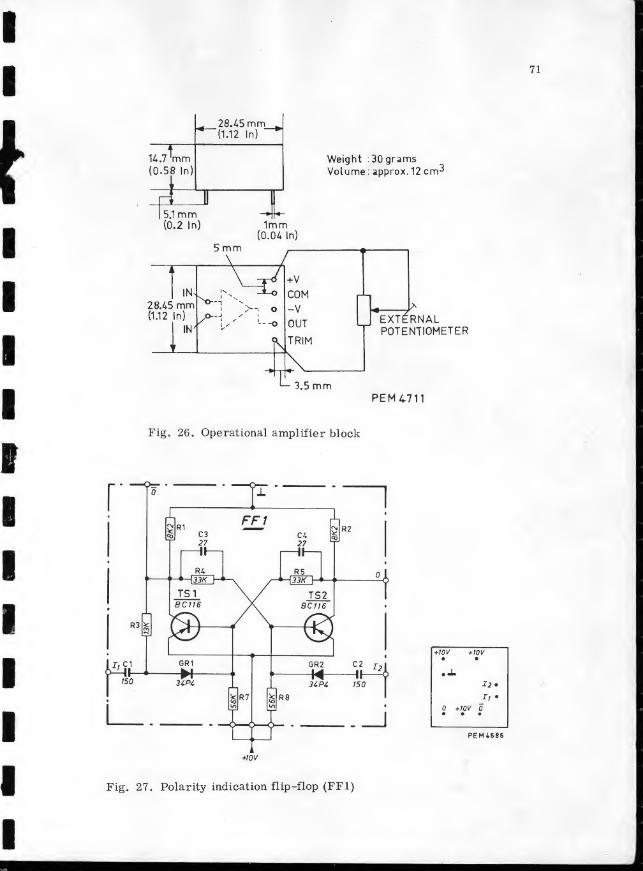
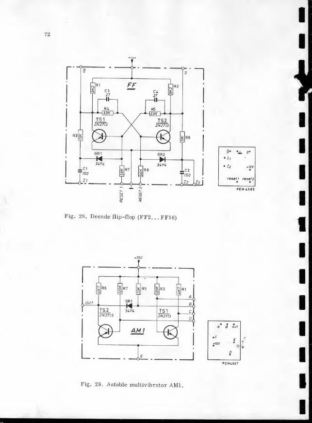
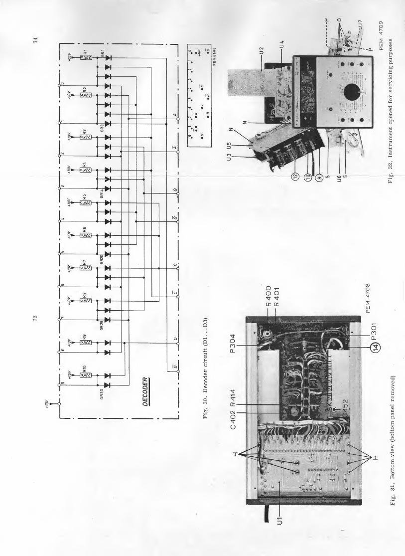
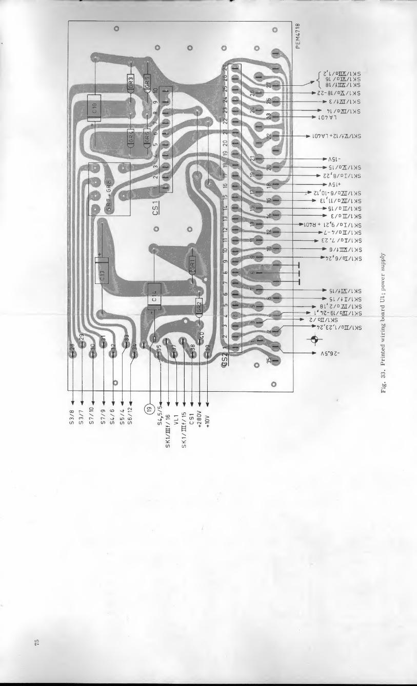
BBHH9H
MMBMuna
r z i/qm/ias9i/Dm/i*s
\ 81/^HZl/INS
22-8l/Di/l>lS
— z/m/i>\s
71/dzi/l^s107 VI
- l07Vl+3l/a/l>1S
ASl“
Sl/DZ/l>lS22'8/DI/l^S
ASI+
2l'0l-9/D3I/l><S— £lr
ll/D5T/L><S
si/dh/i^s£/Dir/i>is
I07d + 13*6 / D I / 1 xsZ,-7/Dir/L>jS
£Z *L / D T/l >\S
9/ym/i>\s73 #
9/PI/l><S
- SW1IK/IXS“ SI /JI/1>1S
8l‘3/DSr/L><Sr 73-6L/qM/l>is
3/pe/i^s~+>VZ'ZZ'[/viL/l>\S
Printed
wiring
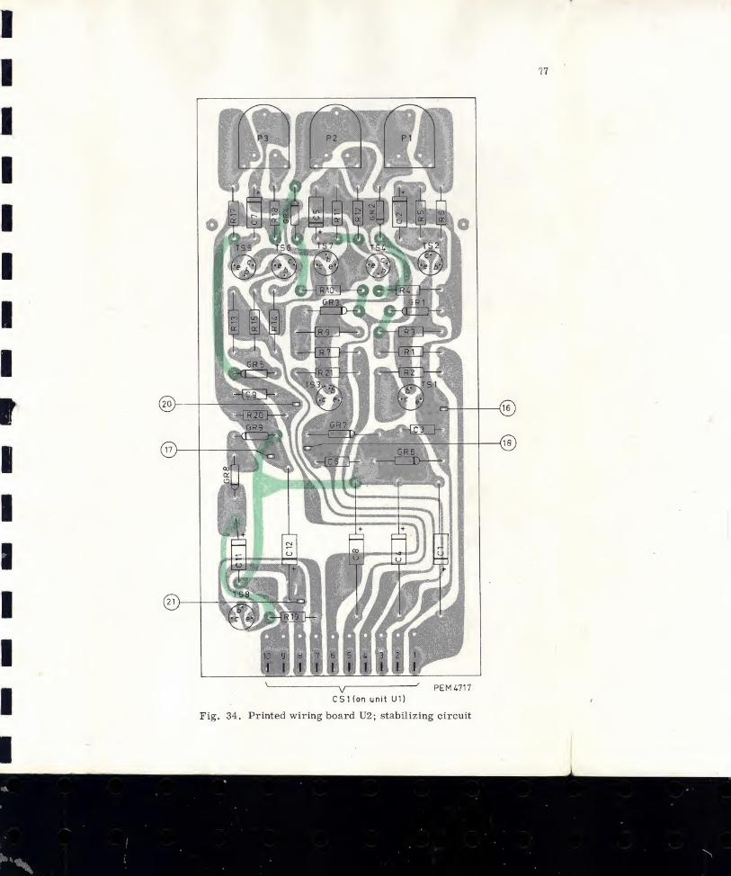
77
vV ' PEM 4717
CS1 (on unit U1)
Fig. 34. Printed wiring board U2; stabilizing circuit
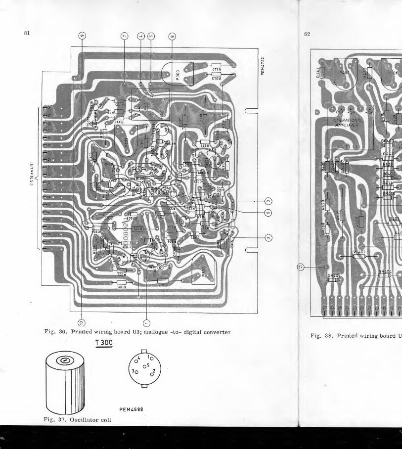
OPERATIONALAMPLIFIER
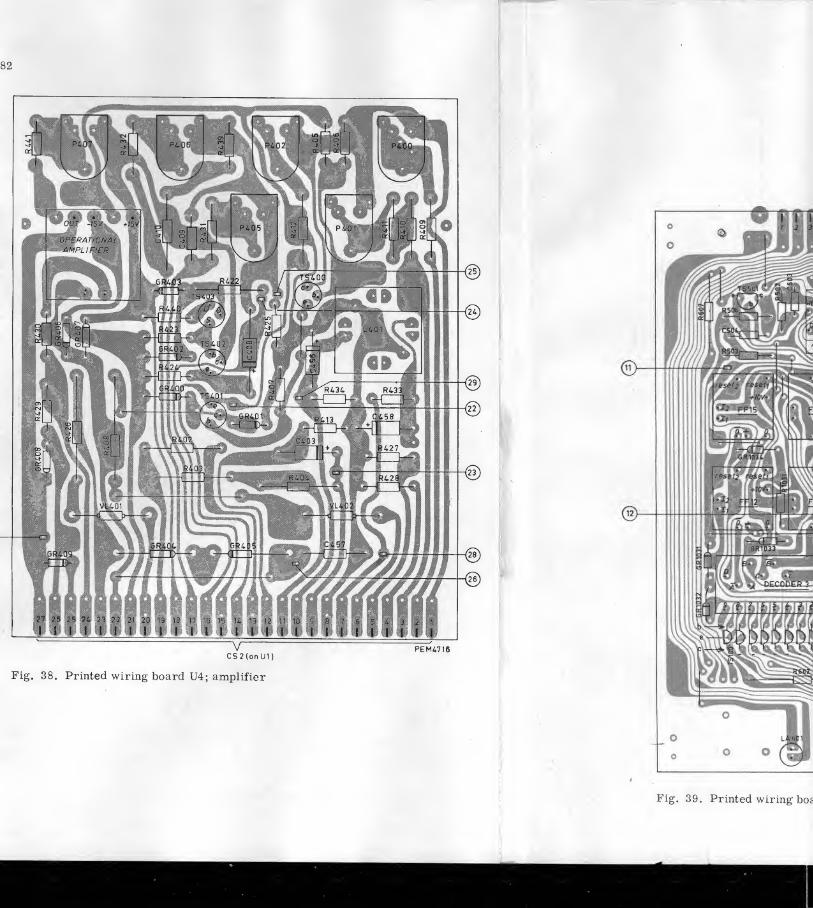
TS401
lint lliiii [to* ! mlI y, 1 1 1 1 1
1
I
i 2 ij W
1 1I il 11 :--® "S’
'' '« :Jfm? "4* •.::+ .Wr |
|I I
' I lf> J1 m EM M
r- ~ ® ^ MSI y/y* 1 • 1 * 1
* W. .
* w *>'T * j « * w * .w • j .
* • j * 1r** § * r * § * »
* ]I * * T*
1
r * 1 * I •
i rlllll l lllllIIII i
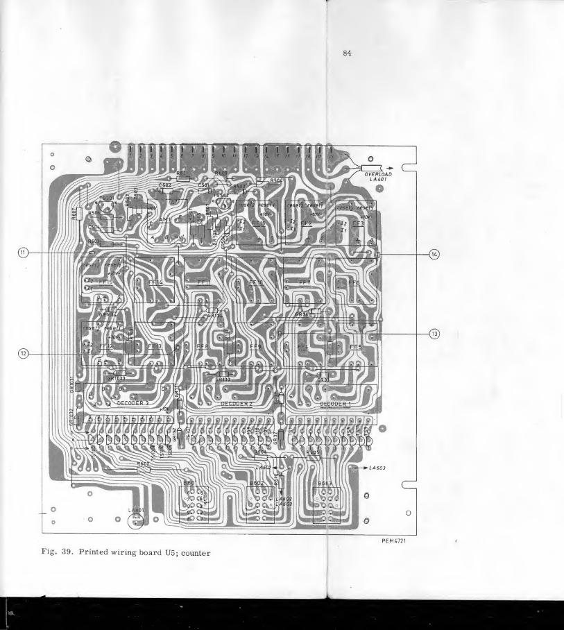
HH