PDF - IPC.org
202
-
Upload
khangminh22 -
Category
Documents
-
view
3 -
download
0
Transcript of PDF - IPC.org


Acknowledgement
Writing the history of IPC and its role in the development and growth of the printed circuit board industry has been an enjoyable, albeit mildly frustrating, project. Mildly frustrating, because it is not possible, in anything less than an encyclopedic work, to cover all of the many significant advances in technology over the decades, nor is it possible to acknowledge everyone who has played a role in the long history of arguably the world’s most remarkable industrial phenomenon, the invention and development of printed circuit technology. Without printed circuits, our world and our lives would be very different from what they are today.
The impact of IPC on this industry has been incalculable, and one of the benefits of researching, writing, and collecting materials for this book has been to foster a great appreciation of IPC and its work, for without its many efforts, ranging from standards to innovative Round Robin test programs to landmark documents, working with government, and tireless efforts to foster education and dissemination of critical knowledge, this industry would not have grown to lead the world in electronics technology for over fifty years. Hopefully the reader will understand, after reading this book, the depth and scope of IPC’s contribution over five decades, and wish it Godspeed for the next fifty.
Of course, it could not have been written and finished without the help of a number of friends who took the time to patiently review, comment, contribute, and steer it. Some of these folks are long-time industry friends who generously donated time to serve as an “ad hoc” committee to review portions of the book as they were created. So please recognize the help of these folks, both within and outside IPC, for their assistance, as I thank them:
Kim Sterling; Jack Crawford; Ray Pritchard; Tony Hilvers; Phil Marcoux; Dieter Bergman; Dr. Ken Gilleo; Terry Jeglum; Jerry Karp; Denny McGuirk, President of IPC; David Bergman; and the many who contributed recollections and historical anecdotes to bring highlights of the history of IPC and the growth of the industry to life.
Michael L. MartelBristol, Rhode IslandJanuary 9, 2007

© Copyright 2007 IPC — Association Connecting Electronics Industries®
3000 Lakeside Drive, 309 SBannockburn, IL 60015
PH 847-615-7100
FAX 847-615-7105
www.IPC.org

�
From Vacuum Tubes to Nanotubes:
An Amazing Half CenturyThe Emergence of Electronic Circuit Technology
1957-2007
Published by IPC — Association Connecting Electronics Industries
Chapter 1: Beginnings
Nature abhors the vacuum tube.— J.R. Pierce, Bell Labs engineer who coined the term “transistor”
The big Philco console radio sits by the workbench, taken apart for repair and rebuilding. It’s large enough to be a piece of furniture. If you plug it in, turn it on, and then turn down the lights in the room, its beautiful, odd-shaped vacuum tubes begin to emit a faint orange glow, like dying embers in the ashes of a fire. Assembled in 1940, its big speaker once boomed the voice of President Franklin Roosevelt; no doubt it broadcasted the news of the attack on Pearl Harbor.
Flip the internal works over, and one can see what makes it tick. There are wires everywhere, filling the metal box; resistors and capacitors as well, old-fashioned cylindrical components coated with hard wax. This is the way that electronic assemblies were built in those days; by hand, one wire connection at a time, with a skilled operator and a bulky soldering iron. Electrical / electronic circuits and systems were assembled using individual wires to connect each component. The components were then mounted on what were known as tag strips and sockets.
Times have certainly changed. For a long time now, highly capable radio receivers have been smaller than a pack of Lucky Strikes. We have even read, of late, of tiny radio receivers, microscopic in size, being built on minuscule Micro-Electro-Mechanical Systems components, or

�
MEMS. Not practical, perhaps, but certainly a sign of how far we have come from radio receivers whose internal works could be no smaller than a commercial four-slice toaster.
The invention of the transistor changed the world of electronics. Wartime advances in technology, particularly of RADAR, spurred advances in the development of semiconductor materials that ultimately led to the transistor. This meant a huge reduction in the size of electronic components, as well as a proportionate increase in their power. Miniaturization occurred on components first; it only stands to reason that more efficient and compact means of interconnecting them had to follow.
Electronic components have advanced in power and complexity; this explosion began during the 1950s. It’s difficult to believe, sometimes, that one of the first on-board computers in a Cold War spy submarine — the most advanced available at the time for its application — had only a fraction of the computing power of a high school student’s hand-held calculator at an open-book math quiz of two decades ago1; and thus the lopsided comparisons go on.
Several major factors drove the remarkable development of the first printed wiring boards, or PWBs. First, there was a need to mass produce interconnect assemblies for standard products. Hand assembly was laborious and time-consuming, and thus costly. Second, components had become smaller, making electronic products more difficult to assemble by hand. Third, circuit assemblies were becoming more complex. Increase the number of connections exponentially, and you increase time to assembly — as well as cost to produce — exponentially as well.
Fourth, there was the need to miniaturize. An orderly and structured interconnect framework could take advantage of shrinking component sizes and produce smaller yet more complex products, and soldering technologies were being developed to make multiple solder connections simultaneously. Last, the integrity of circuits became critical. The more complex the assembly, the greater the number of interconnections, the greater the potential for a single faulty connection when assembled by hand. One faulty connection would mean failure for a complex circuit. The PWB made it possible to quickly assemble a complex circuit with a great many highly reliable connections.

�
The move to more complicated and powerful electronic products quickly outstripped vacuum tube technology and made miniaturization of circuits essential. Why so? The inherent disadvantages and limitations of tubes — high energy use, heat generation, propensity for failure, and size — made them unsuitable to designing and constructing complex circuits. Much of this is described in “The History of the Integrated Circuit,” published on the Web site www.nobelprize.org from which portions of the following are excerpted. The first digital computer, ENIAC, was a veritable monster that weighed more than thirty tons and consumed 200 kilowatts of electrical power. It required approximately 18,000 vacuum tubes, many of which constantly burned out, making the entire machine very unreliable.2
When the transistor was invented, it was recognized as more than a milestone; it was a revolutionary breakthrough. Small, fast, reliable, and effective, it quickly replaced the vacuum tube. Freed from the limitations of the vacuum tube, engineers finally could begin to realize electronic designs and constructions that they had only been able to dream about. The first transistor was invented at Bell Laboratories on December 16, 1947 by William Shockley, John Bardeen, and Walter Brattain. This was perhaps the most important electronics event of the 20th century, as it later made possible the integrated circuit and microprocessor that are the basis of modern electronics. Prior to the transistor, the only alternative to its current regulation and switching functions (transfer resistor) was the vacuum tube, which could only be miniaturized to a certain extent, and wasted much energy in the form of heat.3
With the small and effective transistor available, design engineers of the 1950s began to see the possibilities of constructing far more advanced circuits than ever before. However, as the complexity of circuits increased, problems arose. The first was the above mentioned need for all connections being intact. Another problem was the size of the circuits. A complex circuit, like that of a computer, was dependent upon speed. If the components of the computer were too large or the wires interconnecting them too long, the electric signals couldn’t travel fast enough through the circuit, thus making the computer too slow to be effective. Thus, advanced circuits contained so many components and
The First Transistor

�
connections that they were virtually impossible to build with existing technology and methods. This problem was known as the “tyranny of numbers.”
Much of the following text is excerpted from AmericanHeritage.com, “How Jack Kilby Changed Your Life”:
The transistor quickly replaced the vacuum tube in most circuits. Without having to worry about tubes burning out or melting their equipment, engineers began drawing plans for powerful machines with ridiculously complicated circuitry, machines that could guide a spaceship to Mars or store all the information in the Library of Congress. But the machines could perform their incredible tasks only in their inventors’ imaginations. They were impossible to build. As often happens, removing one constraint revealed another, much larger problem.
In this case, the stumbling block was that three wires branched out from each transistor—as well as from all other circuit components—and they all needed to be hand-soldered to the rest of the circuit. Not only was the process lengthy and expensive—the labor cost on the Navy’s newest aircraft carriers, with 350,000 circuit components, exceeded the price of materials—but inevitable mistakes connecting millions of tiny wires meant unreliable products. Between prohibitive costs, manufacturing time, and unreliability, few of the fantastic appliances that were dreamed of could be achieved. The next great breakthrough in technology came in the summer of 1958, through the efforts of Jack Kilby at Texas Instruments (TI).
Jack Kilby found a solution to the miniaturization problem. That July all the employees of TI took a two-week vacation—except Kilby, who hadn’t been there long enough to accrue time off. Left alone in the quiet of the empty lab, he thought about the tyranny of numbers. He knew that an entirely new approach, rather than an adaptation of existing processes, would be necessary to solve such a pervasive problem. He knew that with the number of minds trained on the unsolved puzzle, the solution must not be obvious. He also realized he didn’t have much time. “I felt it likely that I would be assigned to work on a proposal for the Micro-Module program when vacation was over unless I came up with a good idea very quickly.”
Mindful of the cost problems that employees had been lectured about before vacation, he reasoned that the cheapest avenue for TI, already invested in semiconductors, must involve silicon. So he began to think about what silicon could do. It was used to make transistors, of course. It could also make resistors, although not as well as carbon, and
�
capacitors, although not as well as porcelain. On July 24, all alone in the lab, it dawned on him. If all of the parts of a circuit could be made from the same material, couldn’t they all be made on the same piece of silicon, eliminating the need to wire anything together?
He proposed the idea of forming resistors, capacitors and transistors on the surface of the same piece of semiconductor. In a few weeks he assembled a circuit on a small bar of germanium that included a transistor, a capacitor and three resistors. The circuit worked, and the integrated circuit revolution has changed the world. Kilby’s idea was to make all the components and the chip out of the same block (monolith) of semiconductor material. In September 1958, he had his first integrated circuit ready. Although the first integrated circuit was pretty crude and had some problems, the idea was ground-breaking.
It sounds simple, but it was revolutionary. “Nobody would have made these components out of semiconductor material then,” he recalled. “It didn’t make very good resistors or capacitors, and semiconductor materials were considered incredibly expensive. To make a one-cent carbon resistor from good quality semiconductor seemed foolish.” But as he quickly filled five notebook pages with drawings, numbers, and plans, and the more he thought about it, the more this seemed like the way to make all those imaginary machines finally come to life.4
By making all the parts out of the same block of material and adding the metal needed to connect them as a layer on top of it, there was no more need for individual discrete components. No longer did wires and components need to be assembled manually. The circuits could be made smaller and the manufacturing process could be automated. Jack Kilby is probably most famous for his invention of the integrated circuit, for which he received the Nobel Prize in Physics in 2000. After his success with the integrated circuit Kilby stayed with Texas Instruments and, among other things, he led the team that invented the hand-held calculator.
A few months later, Robert Noyce of Fairchild developed an integrated circuit on a silicon chip. Noyce’s circuit employed a clever interconnection scheme that became the pattern for the integrated circuit industry.
His idea solved several practical problems that Kilby’s circuit had, mainly the problem of interconnecting all the components on the chip. This was done by adding the metal as a final layer and then removing some of it so that the wires needed to connect the components were

�
formed. This made the integrated circuit more suitable for mass production. Besides being one of the early pioneers of the integrated circuit, Robert Noyce, of course, was one of the co-founders of Intel.5
Both Kilby and Noyce applied for patents on the integrated circuit. Following various legal challenges, the U.S. Court of Customs and Patent Appeals ruled that Kilby was the first to invent an integrated circuit while upholding Noyce’s patent claims on interconnecting the individual components formed on the surface of a chip. Kilby was granted some 60 patents during his career. He died in August 2005.
The development of integrated circuits meant greater miniaturization, but also an explosion in the number of circuit connections and the need for greater speed. Simply put, if electronics were going to move to the next level, it would now be up to the interconnect technology. The answer came with the development of the printed wiring board, later almost universally referred to as the printed circuit board (PCB.)
Even today, the terms PCB and PWB are used extensively throughout the electronics industry and in academia. Strictly speaking, a PCB or PWB refers to the bare unpopulated board (i.e., without components). Early PWBs were made from a laminate of an insulating material and were typically about 1.6 mm thick. One side had a layer of copper foil fixed onto it. The foil was then selectively removed to leave a pattern that interconnected the components in the desired manner. Holes were then drilled through the laminate material to enable components to be fixed to the non-copper side. The components had flexible leads as their connection points and these were passed through the laminate. Electrical (and mechanical) connection was achieved by soldering these to the remaining foil. The foil provided the required electrical connection between the components.
The process met the needs of volume manufacture in that it could be automated relatively easily and created a final product that gave repeatable electrical performance and had sound mechanical strength.
Early printed circuit boards were simple designs comprising a small number of components and limited interconnections. Layout level design took place by manually constructing the artworks (or interconnection patterns) for each layer using tape on transparent sheets. Due to only the one layer of connection available to the circuit designer, no connections could be permitted to cross, otherwise a short circuit would occur. These patterns were then photographed to produce
�
the masks for fabrication. As circuit densities began to increase, it was necessary to allow for more and more layers of interconnect to enable the complexity of design. This resulted in a more intricate design problem and it became apparent that some degree of automation would be needed to manage the increasing difficulty inherent in the design process.6
At this time, PWB technology was still being developed, and was far from universally accepted. Electronics giant Zenith opposed the acceptance of PWB technology. The few PWB manufacturers at the time realized that they needed to band together to promote the new technology that they knew held the key to the advancement of electronics technology.
In 1957, a new industry was struggling for identification. Etched printed wiring was emerging as a new technology, but there was confusion regarding the process and its potential. Independent PWB manufacturers held several meetings in 1957 to discuss ideas for promoting the growth of their new industry.
In the fall of 1957, representatives from six of the major independent PWB manufacturers met in Chicago to officially form a trade association they identified as the The Institute of Printed Circuits. At this meeting, they hired Ray Pritchard to serve as executive director and outlined the following objectives:
• To promote an awareness of the attributes of PWBs versus hand wiring.
• To develop standards and specifications to provide believable yardsticks for manufacturers and users to move forward in utilizing products of the new industry.
• To provide a variety of forums where the industry could exchange information on the technology.
• To provide the industry with meaningful statistical data on the market and cost studies.
The 50 years that have passed since 1957 have seen all of these objectives come to fruition and, perhaps, have seen the development of one of the most successful trade associations that exists in America.

�
Sources:
1. Blind Man’s Bluff: The Untold Story of American Submarine Espionage, by Sherry Sontag, Christopher Drew - History - 1999 – p.99
2., 5. “The History of the Integrated Circuit,” published on the Web site www.nobelprize.org, specifically at nobelprize.org/educational_games/physics/integrated_circuit/history/ ©Nobel Web AB 2007. Used with permission.
3. History of the Transistor, www.bellsystemmemorial.com/belllabs_transistor.html
4. From the article on AmericanHeritage.com, “How Jack Kilby Changed Your Life,” located at www.americanheritage.com/people/articles/web/ 20060206-jack-kilby-microchip-integrated-circuit-transistor-vacuum-tube-texas-instruments-robert-noyce-semiconductor-computer-calculator.shtml Article posted February 6, 2006 and authored by Christine Gibson, a former editor at American Heritage magazine. Used with permission.
6. From an online course published by The Department of Computing & Electronic Technology at the University of Bolton (UK), “Concepts of Printed Circuit Design - Unit 1: Introduction to PCB Technology,” URL: www.ami.ac.uk/courses/ami4809_pcd/unit_01/index.asp
Participants in the founding meeting of IPC. Seated (L-R): Al Hughes, Electralab; Robert Swiggett, Photocircuits; William McGinley, Methode. Standing (L-R): Dick Zens, Printed Electronics Corporation; and Carl Clayton, Tingstol. Also in attendance at this initial meeting were Ray Pritchard, thereafter named the Executive Director of IPC; Gene Jones, Printed Electronics Corporation; and George Hart and Stewart Fansteel, Graphik Circuits Division of United Carr.

�
Chapter 2: The Emergence of Printed Circuit Boards
I have not failed. I’ve just found 10,000 ways that won’t work.— Thomas A. Edison
The early history of printed circuit boards is one of starts and stops, of almost-there. The dominant method of connecting components in electronic circuits had been and continued to be point-to-point wiring until, as mentioned in Chapter 1, the “tyranny of numbers” made the assembly of ever-more-complex electronic assemblies impractical and ultimately impossible using this method. We find the use of point-to-point connections in use almost exclusively until the early 1950s 1. Printed circuit technology, however, did not suddenly emerge on the scene; it developed rapidly during the early 1950s due to a number of breakthroughs and improvements in materials, components, and manufacturing techniques. Components consisted primarily of vacuum tubes and sockets, and tubes were often combined with passive components and wired to the circuitry.
In his excellent article, The Circuit Centennial, published in CircuitTree magazine in 2003, Dr. Ken Gilleo describes the profound changes that took place in these early years of technology development; the next few pages draw from his chronology. 2
The idea behind the earliest printed circuit boards, i.e., the concept of using a planar substrate with mounted components and patterned interconnects, dates back to the turn of the 20th Century.3 In 1903, Albert Hanson, a Berliner living in London, filed a ”printed wire” patent based on stamped or cut out brass or copper foil adhesively bonded to waxed paper.
The simple concept was for a double-sided board with crimped interconnections between the top and bottom layers. Although not a true printed circuit, Hanson’s method produced conductive metal patterns on a dielectric by cutting or stamping copper or brass foil patterns and adhesively bonding them to paraffin paper and similar materials. Hanson’s innovations can still be seen in “modern” circuitry. This early inventor had already recognized that high density would be of great importance; therefore, he designed his circuits with conductors on both
Drawing from Hanson’s patent application
�0
sides of the dielectric. Also recognizing that interlayer connections were critical, he added access holes to permit the top and bottom conductors to be selectively connected. Although the connections included only crude crimping and twisting, his 1903 patent clearly describes the concept of double-sided through hole circuitry. Hanson also stated that conductors could be formed in situ by electro-deposition or by applying metal powder in a suitable medium (conductive ink).
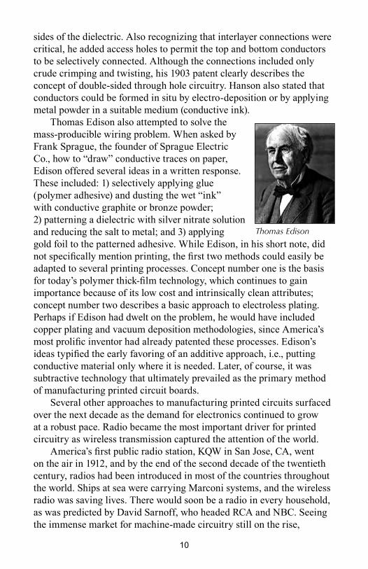
Thomas Edison also attempted to solve the mass-producible wiring problem. When asked by Frank Sprague, the founder of Sprague Electric Co., how to “draw” conductive traces on paper, Edison offered several ideas in a written response. These included: 1) selectively applying glue (polymer adhesive) and dusting the wet “ink” with conductive graphite or bronze powder; 2) patterning a dielectric with silver nitrate solution and reducing the salt to metal; and 3) applying gold foil to the patterned adhesive. While Edison, in his short note, did not specifically mention printing, the first two methods could easily be adapted to several printing processes. Concept number one is the basis for today’s polymer thick-film technology, which continues to gain importance because of its low cost and intrinsically clean attributes; concept number two describes a basic approach to electroless plating. Perhaps if Edison had dwelt on the problem, he would have included copper plating and vacuum deposition methodologies, since America’s most prolific inventor had already patented these processes. Edison’s ideas typified the early favoring of an additive approach, i.e., putting conductive material only where it is needed. Later, of course, it was subtractive technology that ultimately prevailed as the primary method of manufacturing printed circuit boards.
Several other approaches to manufacturing printed circuits surfaced over the next decade as the demand for electronics continued to grow at a robust pace. Radio became the most important driver for printed circuitry as wireless transmission captured the attention of the world.
America’s first public radio station, KQW in San Jose, CA, went on the air in 1912, and by the end of the second decade of the twentieth century, radios had been introduced in most of the countries throughout the world. Ships at sea were carrying Marconi systems, and the wireless radio was saving lives. There would soon be a radio in every household, as was predicted by David Sarnoff, who headed RCA and NBC. Seeing the immense market for machine-made circuitry still on the rise,
Thomas Edison

��
electronics pioneers were strongly motivated to answer the challenge with inventions of their own or those borrowed from other industries.
Subtractive or Additive?
Conductive interconnects today are created almost exclusively through subtractive technology, in which (quite simply described) one covers the entire substrate with copper and then etches or mills away unwanted material. There has been some interest in a return to additive technologies for environmental reasons (less hazardous waste such as acid/etching baths, toxic copper waste, etc.) but there has not been significant movement in this area.
The earliest circuits were based on additive methods; these were quite simply conductors deposited onto a dielectric. The printing industry had long used subtractive methods for making plates. As early as the fifteenth century, wood had been carved away to yield raised letters and graphics. Next, metal was cut to make printing plates, and later plates were made by etching with mineral and organic acids.
In 1913, Arthur Berry filed for a patent which described a method of manufacturing circuits for electric heaters, in which metal was etched away. His patent described the process of coating metal with a resist prior to etching, an improvement over die-cutting, which left stress-concentrating sharp corners. Later, Littlefield described a similar methodology.
Photolithography was well known during the early days of circuitry development, but the subtractive process was largely ignored. Bassist, however, provided specific details of the photoengraving process, including the use of photosensitive chromium salts. Although his patent dealt with making print plates, the process could easily be adapted for circuitry, since Bassist described preparing compliant plates by electrodepositing copper on dielectric laminate. (Bassist, E., “Halftone Plate Process and Process of Producing Same,” U.S. Patent 1,525,531, Feb. 1925).
One successful inventor, Max Schoop, commercialized a metal flame-spraying process in 1918 that was used for many years. Early electronics were power-hungry, with vacuum tubes requiring heated filaments and high voltages. Schoop’s process quelled this hunger for
Marconi with transatlantic transmitter, 1896

��
hefty and robust circuits by depositing thick patterns of flamesprayed metal through a mask. Schoop’s approach had problems with cost and wasted metal, and although some subsequent inventors added improvements, still others labored in corporate laboratories and home
basements in search of a true printed circuit process. The next inventor to achieve notice was Charles Ducas, whose patent described both etching and “plated-up conductors.” One version involved electroplating a copper, silver, or gold pattern onto a low-temperature metal alloy through a contact mask. Heating allowed the conductor, typically a coil, to be
separated from the fusible bus plate and mask. Another Ducas process involved forming grooves in dielectrics such as wax and filling them with conductive paste, which was then electroplated. Both sides of the dielectric could be made into circuits, and Ducas went on to describe multilayer circuits and a means of interconnecting the layers.
Frenchman Cesar Parolini disclosed improvements in additive processing when he patented the printing of patterns with adhesive onto dielectric, followed by applying copper powder to the wet ink. This was Edison’s basic concept and one of Ducas’s methods, but Parolini implemented it fully and added the concept of jumper wires.
Other inventors of the era also employed print and plate methods. Seymour used printed graphite paste to make the platable patterns for the flexible circuit in a 1923 radio tuner. He used waxed paper and gutta-percha dielectrics and lead and copper conductive pastes, with copper plating as the final step. A parade of other inventors followed, most of whom used variations on previously-disclosed inventions, which is typically the case today. In 1933, Franz added conductive carbon particles to polymer ink for printing on cellophane or similar lamina and, perhaps aware of Parolini’s earlier work, added a copper plating step. Since the first mass-producible circuitry was invented, modern circuit developers have made multiple attempts to reinvent the printed wiring concept. While ingenious new circuit inventions will surely emerge, a search of early patents can be a humbling experience for the would-be inventor.
Arthur Berry’s etched foil design

��
Paul Eisler, Father of the Printed Circuit Board
There are quite a number of people in the printed circuit board industry who passionately believe that Paul Eisler indeed deserves the title “Father of the Printed Circuit Board” but has been unfairly passed over by history, and deprived of an honor. Eisler’s autobiography, titled My Life With the Printed Circuit, relates the remarkable life of a happy and widely productive inventor who came within a hair’s breadth of collecting royalties on every circuit board built in the last 50 years.
Born in Austria in 1907, Eisler received an engineering degree from Vienna Technical Institute in 1930. After a few tumultuous years trying to find stable, paying work in pre-war Europe, he enrolled in a doctorate program in Vienna in 1934, eked out a living as a part-time tech at a radio station, and did some writing for a newspaper. At the paper, he became:
...fascinated by the impressive technical achievements of the printing art. I saw this art as a whole: letterpress and gravure, lithography, offset and screen printing, engraving and photomechanical printing. I imbibed all the processes like the wisdom of redemption.
There was no doubt in my mind that everything that could be drawn in black and white could be magnified to poster size or reduced to dimensions smaller than a postage stamp. It could be printed by any of a dozen processes on copper or on other materials that offered a very small or large resistance to electric current. The flat, basically two-dimensional nature of these conductors could then offer new and so far undreamt-of facilities for the whole electrical and electronics industry.
He had already made a little radio set in his room. Now, he took it apart and replaced all the wire-to-wire connections with flat circuitry that he made from strips of copper foil varnished on Bakelite-backed paper. Eisler managed to take his “first printed circuit invention in the form of a complete radio set that worked perfectly” to Plessey, a big radio manufacturer in England. Although the managing director was very impressed with Eisler’s advanced circuitry, his production staff turned it down because “it was pointed out to me that the work my invention would replace was carried out by girls, and ‘girls are cheaper and more flexible.’”
Once war broke out, Eisler was interned as an enemy alien in Britain, emerging from prison in 1941 and turning his talents to the war effort. The ineffectiveness of anti-aircraft fire during the Battle of Britain made him advance his printed circuit ideas to work in contact

��
and proximity fuses. At the end of the war, when its scorekeepers found that proximity fuses had destroyed over 4,000 V-1 rockets, “printed circuits became established as an important branch of the armament industry, and in 1948, the U.S. authorities ruled that all electronic circuits for airborne instruments were to be printed.”
By then, Eisler was fully involved in peacetime work. He and his scientist wife were making electrodeposited copper foil and etching it with ferric chloride in their kitchen sink to make printed heating circuits for everything from wallpaper to airplane wings to canned food. He started a company called Technograph Printed Circuits Ltd. and, always short of funds, applied for a government loan and became mired in years of bureaucracy. While casting about for funding and using all his business contacts, Eisler was granted numerous British patents for printed heating and electrical interconnection patents.
His most important patents dealt with etching. Well before there was a need for circuitry, the printing industry had perfected a copper etching process which initially used etch resist that was mechanically scraped away with a sharp tool. During the 1800s, photosensitive coatings were perfected that enabled the widespread use of photoengraving. The primary difference in the printing industry’s photoengraving process and Eisler’s circuit-making method lies in their end use. The printers used relatively thick copper plates, while Eisler used copper foil laminated to dielectric. The printers’ copper plates were engraved by the etchant to a depth of several mils, leaving the printing pattern elevated and a thinner layer of copper typically remaining at the base. Eisler’s thinner copper was etched all the way through, so the conductor patterns were electrically isolated from one another.
The Eisler patents referenced the print plate technology but instead of actually describing the etching process, Eisler’s applications repeatedly used the phrase “as used in the printing industry” during the 1950s. Eisler’s company filed for U.S. patents. Initially, the U.S. Patent Office rejected all his claims because of prior art but, after four years of meetings and appeals, most of the claims were allowed. A patent’s “file wrapper” normally contains all the written communications between the examiner, the inventor and the patents attorneys as well as the summaries of their meetings. In this case, the patent examiner simply allowed the patents without explaining what had transpired and why he had decided to ignore the substantial prior art that would seem to invalidate Eisler’s claim. Armed with more than 50 British and U.S patents, Eisler commercialized circuit making under the aegis of Technographic Printed Circuits Ltd. All went well for the firm until it
��
sought to cash in with a lawsuit. Its U.S. counterpart, Technographic Printed Circuit Inc. sued Bendix Corp., which was producing printed circuits in the U.S. with an etching process. A very lengthy trial reviewed the entire history of the printed circuit, as was pointed out by the weary judge. Throughout the months of the trial, Eisler was unable to substantiate his claims of earlier work, and couldn’t produce his “book of circuit samples.” The plaintiffs prime exhibit, Eisler’s old three-tube radio, never worked.
Bendix countered with an overwhelming amount of prior patent art and asked that the patents be declared invalid. A key point argued in this phase of the trial was that Eisler had made claims in the U.S. patents that had already been rejected in his earlier British patents, and was, therefore, trying to get U.S. coverage by referencing nonexistent documentation. However, the important defense was that Eisler had simply patented well-understood photolithography that had long been used by the printing industry. Eisler’s own statements in his patents supported this accusation.
On May 27, 1963, the case was decided and any action against Bendix was dismissed. Eisler was defeated and dethroned as the father of printed circuitry. Until the day he died, Eisler felt he had been wronged by the system. But it was clear from the vast amount of prior art that the printed circuit was not invented by a single person, but by many inventors who contributed to the total concept over a number of decades. (The above was excerpted from My Life with the Printed Circuit, Paul Eisler, Lehigh University Press and Associated University Presses, 1989 with permission.)4
��
Interview
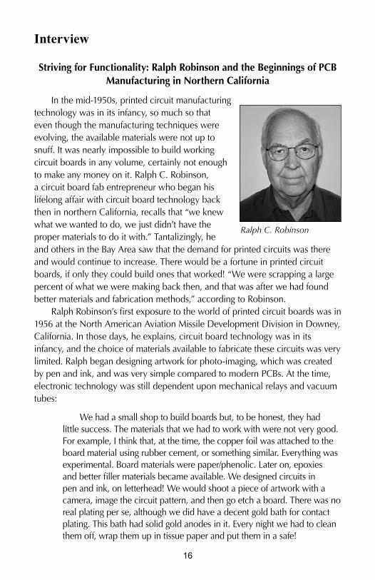
Striving for Functionality: Ralph Robinson and the Beginnings of PCB Manufacturing in Northern California
In the mid-1950s, printed circuit manufacturing technology was in its infancy, so much so that even though the manufacturing techniques were evolving, the available materials were not up to snuff. It was nearly impossible to build working circuit boards in any volume, certainly not enough to make any money on it. Ralph C. Robinson, a circuit board fab entrepreneur who began his lifelong affair with circuit board technology back then in northern California, recalls that “we knew what we wanted to do, we just didn’t have the proper materials to do it with.” Tantalizingly, he and others in the Bay Area saw that the demand for printed circuits was there and would continue to increase. There would be a fortune in printed circuit boards, if only they could build ones that worked! “We were scrapping a large percent of what we were making back then, and that was after we had found better materials and fabrication methods,” according to Robinson.
Ralph Robinson’s first exposure to the world of printed circuit boards was in 1956 at the North American Aviation Missile Development Division in Downey, California. In those days, he explains, circuit board technology was in its infancy, and the choice of materials available to fabricate these circuits was very limited. Ralph began designing artwork for photo-imaging, which was created by pen and ink, and was very simple compared to modern PCBs. At the time, electronic technology was still dependent upon mechanical relays and vacuum tubes:
We had a small shop to build boards but, to be honest, they had little success. The materials that we had to work with were not very good. For example, I think that, at the time, the copper foil was attached to the board material using rubber cement, or something similar. Everything was experimental. Board materials were paper/phenolic. Later on, epoxies and better filler materials became available. We designed circuits in pen and ink, on letterhead! We would shoot a piece of artwork with a camera, image the circuit pattern, and then go etch a board. There was no real plating per se, although we did have a decent gold bath for contact plating. This bath had solid gold anodes in it. Every night we had to clean them off, wrap them up in tissue paper and put them in a safe!
Ralph C. Robinson

��
In those days, Robinson adds, boards were full of sockets, relays, and vacuum tubes. That’s how simple they were. Robinson recalls, “When semiconductors came on board in the late 1950s and early ‘60s, then things started changing. Boards became tighter, more detailed, and designers were trying to pack more and more circuitry into a board. Fortunately, great improvements were also being made concurrently in the laminates.”
In 1957, the division’s missile contract was canceled. A massive layoff followed, and the entire division was eliminated. Ralph subsequently moved north to the San Francisco area where he became employed by the U.S. Army Corps of Engineers until late 1959, when he found an opportunity at an electronic company in what is now Silicon Valley. Although the company ultimately folded, it was, at the time he joined, equipped with a complete in-house etching facility for the fabrication of printed circuit boards. Why did Ralph decide to get involved in printed circuit boards in the first place? It had to do with that little Silicon Valley company that also had a printed circuit shop, Robinson relates, where he was doing design work. The shop could not produce workable circuit boards, and to Ralph’s surprise, the plant manager re-assigned him and two other persons from the engineering division to the circuit board division and gave them a mandate to produce usable, working circuit boards. This was Ralph’s first opportunity to learn fabrication the hard way, by trial and error. In those days there was no pool of experience to draw from, as there was only one other small company fabricating boards in the entire Bay Area. The imminent failure of the company, however, for other reasons, prompted Ralph and his two colleagues to start up their own company dedicated only to printed circuit fabrication. At the time, there was virtually no viable local competition:
We went down there and started working with it, but we were frustrated because there was no information available. It was all new. We persisted, however, and after awhile we began getting results, producing a product that worked and was reasonably reliable. These early boards were basically single-sided. They weren’t plated through, or even plated, they were all hand-drilled using electromechanical drills, hand-held by skilled operators. They were designed for use with sockets, but remember that once they left our shop, we didn’t know what the customer did with them. That has been historically true with most of the fabrication business. We would make boards custom-designed for each individual customer.
We were chemically etching boards, applying a resist, using the old techniques used by lithographers for years. Kodak had a product called KOR, or Kodak Ortho Resist. That worked fairly well; we used that in the early days, then they came out with a KPR, or Kodak Photo Resist, which became very popular. We would apply the resist, expose it, follow

��
through with the developing process, and then it went into an etching bath which was in those days ferric chloride. Once they were etched, we hand-drilled tooling holes, pinned them together, two, three, or four deep, depending on the circuitry, then finished them off with a hot solder dip. We would dip them in a hot solder bath and squeegee off the excess.
In those days, in many cases we used eyelets, especially where you needed extra support, for example, if you thought that you would have to pull a component out. The eyelets were used later as through hole connections, especially when we started doing double-sided boards. This was in the early 1960s.
Robinson eventually founded his own company Exceltronics in 1964. The company served the needs of a niche market, with the motto “Quality and Fast Turnaround.” This concept was novel in that era. The era before CAD (computer aided design) was a good time for a facility specializing in quick turn prototype manufacturing. Board designs were being mostly manually created, and would sometimes require up to five or six revisions before the part would work, which meant that follow-on orders were almost always available.
Robinson describes various innovations that changed the process of creating boards:
We started building boards with plated-through holes in 1962, when we installed our first Shipley electroless copper bath. Shipley was a pioneer in the electroless process. The best thing about the advent of the process is that it eliminated the eyelets, first and foremost. Eyelets were costly and labor intensive; they were essentially like rivets, and had to be installed by a skilled operator. As boards became more densely packed, an operator could spend hours and hours on a single board installing eyelets of varying sizes, and this drove up the cost of each board. Additionally, eyelets needed larger holes, so they absorbed more board real estate and thus stood in the way of miniaturization. With plated-through holes, we were able to condense the circuitry, especially since the science of creating the boards was developing, and materials were getting better.
Once semiconductor materials came along, such as the little three-prong transistors that were very popular, well then everything began to rapidly progress smaller and smaller. Changes followed very rapidly thereafter. The first half of the ‘60s decade was a time of extremely rapid change and advancement in everything from components to materials to fabricating technology. New plating techniques and plating baths were developed.
“Perhaps the biggest advancement was the development of better hole drilling technology, particularly with the advent of CNC machines to automate
��
the drilling process,” Robinson says. Until that time, drilling had been laborious, imprecise, and created a great deal of waste. Imprecision created a lot of scrap, and manual drilling was labor intensive and drove up costs as boards became more complex with a greater number of holes with ever-tighter tolerances. “We would lose sometimes thirty percent or more of our parts just due to hand drilling,” Robinson recalls. With improvements in tooling and automated drilling technology, repeatability improved, and scrap and costs were reduced. High speed steel drills had a short life, especially once fiberglass board materials came into use. “You’d get 150 holes and then your drill would turn into a nail,” he remembers. When carbide drills became available, they were very expensive and brittle as well, and broke often. Automated drilling equipment and better carbide drill manufacturing, resulting in cheaper drills that were also more durable, greatly improved the process.
In Northern California, “quick-turn” became Exceltronics’ niche. The demand for boards by design groups and R&D groups was such that they were demanding parts “tomorrow, not three weeks from tomorrow.” While volume fabrication of boards became entrenched in southern California, many companies in the north focused on design and the technology. Robinson ordered the first multilayer press in the area and delivered the first multilayer boards locally fabricated at that time. He was among the first to use UV cured inks and masks on a regular basis.
Eventually, in the industry, there would be problems between the designers and the producers, where designs were being specified that could not practicably be built. There would also be friction between assemblers and board fab people. The problem was really the fault of both, in Robinson’s opinion. Board fabrication people didn’t really know what happened to the board once it shipped; they weren’t involved in assembly. “Once the board left our shop, we really didn’t have anything to do with it,” he says. Similarly, assembly folks weren’t always cognizant of the manufacturing issues faced by the board fab people, prompting the concept of focusing on “Design for Manufacturability” or DfM. This allowed all three groups to interact with ideas to improve the finished reliability of the PCB.
In the late 1960s — possibly 1967, Robinson was introduced to the DuPont Corporation’s new dry film photo-resist (Riston) at a trade show:
I thought to myself, this is the future. Then I ordered a system right from the show there, and got the first one in the entire western part of the United States. It revolutionized imaging. It was easy to use and generated consistent, excellent results. It was so good, in fact, that we were now under pressure to generate better phototools. Now, we could do very good imaging and, although pen and ink were long gone, we needed to improve our methods. Spaces and traces became smaller, so ultimately
�0
the next step would be scanning and photoplotting, and when that came on board, we were making significant progress. This would have been in the early 1980s. All boards were still through hole for leaded components however. We didn’t start to see much in the way of surface mount boards until the mid-1980s.
After Exceltronics was sold in 1970, Robinson founded Phase II, a company based on the same principles that had proven successful with Exceltronics. Phase II prospered. Robinson became involved in professional organizations and was elected as an officer and then president of the California Circuits Association (CCA).
In his early years at Phase II, Robinson pioneered the use of computers to facilitate order entry, job tracking (real time) and inventory controls. Software had to be created, since none was available for many of these tasks. Robinson introduced foil construction along with vacuum lamination into the fabrication of his multilayer circuit boards while it was still considered a novel concept.
Ralph Robinson retired as President and CEO of Phase II in 1987, returning on a part-time basis to work in engineering and special projects until retiring fully from the company in 1993. He continues consulting today.

��
World War II and Hybrid Circuits
World War II brought circuit developments that took a different turn. Again, we look to Dr. Gilleo’s historical chronology to illuminate the forces driving change during these times.
The need for extremely robust microelectronics for military ordnance spurred development of ceramics. Secret projects developed highly reliable ceramic substrate and conductive inks, called cermets — ceramic-metal. This process, now widely practiced in the ceramic hybrid industry, involved screen printing or stenciling circuit inks, followed by high temperature firing. The process was used to produce tens of thousands of electronic ordnance fuses and is discussed in detail by Cadenhead and DeCoursey4. The war efforts resulted in both the development and optimization of high volume, thick film printed circuit manufacturing.
After the war, the U.S. government under the auspices of the National Bureau of Standards (NBS) disseminated printed circuit technology. Conferences were held and publications described virtually all of the circuit making concepts, including subtractive etching. A Circuit Symposium sponsored by the U.S. Aeronautical Board and the National Bureau of Standards was held in Washington, D.C., in October 1947. Dozens of speakers and hundreds of attendees interacted at the conference. The more than two dozen processes were condensed down to six methods:
Painting (really printing): Metal-filled inks are applied and cured or fired; includes Ceramic Thick Film (CTF) and Polymer Thick Film (PTF) that remain important today.
Spraying: Molten metal or composite conductor material is sprayed through a mask or stencil. The mask can be a resist applied to the substrate. Process is no longer used.
Chemical Deposition: Electroless and electrolytic plating are included. Dozens of early patents described electroless, electrolytic and combination plating. Chemical deposition remains an important process in many circuit-making schemes.
Vacuum Deposition: Sputtering and evaporation through a mask were the key processes mentioned. Thin film circuits are made by vacuum depositing copper, gold and other metals. The method is still used today.
Die Stamping: Many of the early patents claimed cutting and die stamping as the process for patterning conductors. Modern methods simultaneously bonded the weakly adhered metal foil to the substrate

��
during the die cutting process. This was accomplished by using B-staged adhesive and a heated die bed. The method, although low cost and environmentally friendly, has become all but obsolete as tolerances become tighter and density demands increase.
Dusting (conductive powder over tacky ink): Application of graphite or metal powder over wet ink or adhesive is one of the earliest processes reported. Some of the later patents apply solder to the dusted conductors. The process does not appear to be in use today.5

��
Recollection:
A Copper Plating Discovery
By Don Pucci
Frustration, Lab-tinkering, and an odd Russian textbook lead to a breakthrough plating technology in 1969 that is still in use today by
rigid and flex circuit makers today.
I have been in the PCB and Flex circuit industry for nearly 40 years and have been at the forefront for many of those years. My anecdote refers to a day at an IPC meeting in Washington, D.C. in 1969 attended by people from all over the world. I gave a paper at this meeting that stimulated the conversion to the high throw copper sulfate process used by all PCB and Flex suppliers in the world today.
The session I gave my talk at was billed as a great debate between three industry experts on which copper plating process would dominate the future. The combatants were myself (I worked at a small PCB shop called Microfab in Amesbury, Massachusetts as its Chief Engineer) who was preaching the virtue of high throw copper sulfate; Joe Poach from Westinghouse who, believe it or not, believed in copper cyanide; someone else who supported a chemistry called copper pyrophosphate; and another person backing high throw copper fluoborate.
I had actually developed the high throw copper sulfate process in a lab when I worked at Sanders Associates in New Hampshire at their Flexprint Division. At the time I was frustrated with the other three chemistries. They all had fatal problems. One day, on the advice of a friend of mine from Shipley, Gerry Lordi, I went to the MIT library and spent the whole day looking in the physical chemistry section. Near the end of the day, I came across a Russian text book translated to English. In this book there was a chapter on throwing power and the authors described how lowering the metal content and increasing the acid concentration drastically improved the throwing power of a copper sulfate plating solution.
I had experience using copper sulfate plating for a non PCB application, so I knew it did not have many of the problems associated with the others, just poor throwing power.
When I returned to my lab at Sanders, I began experimenting in a prototype tank and the results were astonishing. I used a brightener found in the auto industry that was designed for lower acid content.

��
While it worked great, the high acid of my new formulation degraded the organic brightener too fast and it had to be carbon treated all too often.
At this time, Gus Fletcher was the Sel Rex (chemistry vendor) sales manager in our area. He watched my development and he convinced Sel Rex to develop a brightener that would stand up to my formulation without breakdown. They did and the high throw copper sulfate we all use today was born.
Back to the IPC meeting and the great debate forum; I was young and had never given a presentation in my life — especially to a large international group. I prepared for weeks in front of a mirror and with a tape recorder for days on end leading up to the meeting.
The night before, a few of my supplier friends took me for a night on the town in DC. We hit every joint in the city, I think. It was around 4 or 5 in the morning when I got to bed. My talk was at 9:00 am. I was still somewhat inebriated when I stepped up to the podium for my turn. It was a good thing I had prepared and rehearsed so well. The talk went off perfectly. It finished with a standing ovation from the 500 people in the room. A friend, Charlie Cobb, VP of sales and marketing for MacDermid, said it was the finest presentation he had seen.
Anyway, it did the trick and, from that moment on, the other copper plate chemistries disappeared in favor of high throw copper sulfate.
Don Pucci Director of Strategic Marketing Mflex

��
Recollection:
Ice Cream Days at IPC
By Bernie Kessler
As one may understand, in an organization such as IPC, there are many types of attendees at the semi-annual meetings. While it is a very significant and productive technical forum and people on the design, processing and quality assurance ends made up the bulk of the attendees in the ‘60s and ‘70s, there were, of course, many from sales as well, such as myself. But on one particular night when we were free of meetings, many appointments were made for dinner, especially by salespeople who didn’t attend but were “hawking” the show, i.e., they descended on their prey only after the meeting session and took one or several out to dinner. However, not everyone was available for such appointments and several of us just stayed together to socialize and take our semi-annual walk together. My rule was quickly and readily adopted; we were forbidden to talk business at these get-togethers. This was strictly a relaxing time and we did indeed hop on anyone who may have joined us without knowing the rule. No business. It’s difficult to remember all the names but the core group was Dieter Bergman, George Messner, Gerald Ginsberg, Mark Saverin, Phil Derrough, Vivian Vosberg and me.
In April 1973, the semi-annual meeting was being held in Boston. I was in New Jersey with my wife, visiting with our daughter who was scheduled to give birth any day. With the full understanding of my family, I left that Sunday, April 1, to attend the IPC meeting. When I arrived at the hotel I called N.J. to discover that shortly after I left for the airport the family left for the hospital and on that day my second grand-daughter was born, Jennifer Melissa. It was a pleasant surprise but also a frustration because I had missed the birth of my first granddaughter (same parents) due to an emergency need to go to France and London and I had promised that it would not happen again. I then went downstairs and grabbed the guys I knew very well and told them of my great event and invited one and all to celebrate by having a big dish of ice cream together. This celebration extended to the celebration of all children and grandchildren. The ice cream consumption became the mandatory means of celebration at the end of our traditional walks
Bernie Kessler

��
and so two traditions merged into one. This practice continued and many of the members knew of the ice cream bit and the walks and we’d have a different fringe group join us at each meeting.
On April 1, 1990, seventeen years later to the day, the meeting was again scheduled to start in Boston and I took my granddaughter Jennifer and my wife to this meeting. David Bergman knew the story and their attendance and had invited both of them to our membership luncheon. He also arranged for the hotel to serve ice cream for dessert. I was invited to the podium to introduce the “ice cream” gal to the members present and explain the origin of the tradition, and I did so. I went on to explain that Jennifer and the ice cream were reminders to all of us that while we wildly pursue our goals on our career paths, we can’t help but diminish some of the family events that we must of necessity miss. I asked all to take the time to enjoy the sweetness of the ice cream, a tribute to families and friends whose understanding we need in making our lives meaningful, and everyone had a great time. I’ve been active in IPC for about 45 years, give or take a year. Of all the memories I have, none is as treasured as the human side, this story being just one of many.

��
Recollection:
Developing PCB Manufacturing Techniques During the First Decades
By Gene H. Weiner
As a student technician at MIT Lincoln Laboratories, I tested and validated the first photoplotter during the days of hand taping patterns and photoreducing a picture taken with a large Brown Camera. We converted a Head milling machine, replacing the bit with a hypodermic needle through which we passed light from a Xenon point source. The hypodermic needle served as a collimator. Photosensitive film was vacuum-locked onto the tooling plate while the needle traversed it with the light switching on and off to make the exposure of the circuit pattern.
While at Lincoln Laboratories, we also built the first HDI additive circuit as part of a PWB memory plane in 1957. We punched holes in XXXP substrate, dropped in memory cores, encapsulated with Dow’s Sylguard, metallized with immersion Ag, electroplated Cu to thickness, applied photoresist (KPR by Kodak), contact printed flat surfaces, and simultaneously projection printed patterns through the holes in the ferrite cores. We etched and stripped the resist, and voila, X, Y, Drive, and inhibit circuits were formed through each core as well as the two sides of the structure. Lines and spaces were initially 10 mils through a 50 mil ID core. Later (1958) we printed 6 mil lines and spaces through a 30 mil ID core. E.A. Guditz and I demonstrated additive circuit techniques and projection printing through planar mask on WGBH-TV (educational TV) in 1957.
In 1958, a laboratory error in the cellar of Charles and Lucia Shipley’s elegant home in fashionable Auburndale, Mass., turned into one of the industry’s major inflection points — the development of Catalyst 6F, a colloidal solution containing Pd, which eliminated the need for sanding deposits off of panel surfaces after metallizing drilled holes in laminates. It sounded the death knell for using eyelets to connect circuitry from one side of a panel to the other. I was fortunate enough to become Shipley’s first full-time employee and worked on the development and testing of a wide variety of acidic, organic (albumen), and alkaline catalytic materials for patent applications on materials that would initiate electroless plating.
Gene Weiner

��
In 1960, I introduced the first alkaline etchant in the PWB industry (Etchant M-U [for minimal undercut] by MacDermid). At its peak, it and its descendants became the primary industry etchant. Simple waste treatment provided a variety of marketable salts out of the dissolved copper. M-U was a laboratory curiosity named x-381. It was developed to remove copper from heat treated steel typewriter balls for NCR, but had never been commercialized. I asked if it could be used to etch Cu from Cu-clad PWB laminated and was told “NO!” I tested it in a 3.5 gallon Chemcut etching machine in a laboratory hood. It worked and the alkaline nature (ammonia based with a pH of about 9.8 +/-) eliminated pinholes and reversed the normal undercut caused by acidic etchants (ferric and chromic acids) of the period when etching gold plated boards. I set up a test with Bert Krasnow for a warm summer Friday afternoon at Precision Circuits in New Rochelle, New York. Shortly after we began the test, we heard the sound of feet scrambling down the stairs from the offices located over the production facility. The exhaust from the etcher went to the roof. It was located next to the roof-top air conditioning units, picked up the ammonia and blew it into the office causing the most rapid and complete evacuation in company history. Later, in 1961, Metex Etcant M-U was named product of the year at one of the first major NEPCON shows held at the Coliseum.
In the mid-’60s, as vice president of marketing and sales for Dynachem, I introduced the world’s first totally aqueous developing dry film photo resist, from the now extinct company. The product was one that was developed to a planned goal by Mike Gilano and Irv Martinson, Dynachem founders, and Dr. Mel Lipson. It was one of the few industry products designed from scratch to be what it became. Later iterations of semi-aqueous developing (dilute alkali with a touch of butyl cellusolv) resists also garnered a large segment of the market due to their increased resistance to process chemicals.
It is ironic to note that Dynachem changed the industry but nearly vanished before it conquered. It was technically insolvent when it was rescued by Thiokol. It was growing so fast that it outstripped its resources and suppliers had shut off its credit lines. Thiokol bought the company for less than $12 million. Later years had months with greater than $12 million in sales and pre-tax operating profits in excess of 20%.
There are many stories of the true industry pioneers whose trials and successes may not be noted or remembered, but without whose pioneering spirit and actions we would not have progressed as far as we have.
Gene H. Weiner Weiner & Associates, Inc.

��
Recollection:
Remembering the Beginning of Printed Circuit Board Manufacturing
By Bob Swiggett
Looking back 58 years to 1948, I recall five things that led me to found Photocircuits Corp., which became the first company in the world to manufacture printed wiring boards as its sole line of business. These five things were as follows:
1. I read a short report written by the Signal Corps Engineering Laboratory describing the “autosembly” process for electronic assemblies using plastic boards with etched copper foil patterns where the axial lead components were inserted through holes in the board and dip soldered to the foil pattern;
2. I met Russ Davis, a salesman for the National Vulcanized Fibre Co., at the wedding of a friend. Russ pitched me regarding what he thought was going to be a great new product, copper foil-clad plastic laminate;
3. I worked as a process engineer for Chemco Photoproducts, a company that made plastic film, process cameras, etching, and other equipment for photoengraving printing plates as well as operating three photoengraving plants. We really knew everything about printing and etching processes; and
4. RCA had asked one of our plants to try photoetching coils for a new TV tuner using the new NVF copper clad plastic;
5. My boss at Chemco, A. Jay Powers, enthusiastically supported my request to set up a small laboratory and investigate the potential for what just might become a big business.
After visiting the Signal Corps and the National Bureau of Standards, the lab was put together in the cellar of one of Chemco’s buildings in Glen Cove, New York. In the beginning, there was no market and little interest. After World War II, military electronics was “dead.” Radio manufacturers claimed that they could hand-wire a five-tube AC/DC set for 35 cents. TV was just coming alive. IBM didn’t have a single vacuum tube in any of its punched card equipment. The computer business hardly existed. Nobody had heard of the transistor yet.
However, there were customers for the complex rotary switches that we could make. Etched inductances such as the RCA tuner coils were interesting to
Bob Swiggett
�0
many. We made large quantities of TV antenna filters and couplers, and other products.
Bell Labs came to us for a few small cards that they used to make the first logic circuits with this new “transistor” to be shown at their three-day symposium in 1950, where they introduced it to the world. It seems quite significant in retrospect that the only way that they could mount and interconnect these devices was on a printed wiring board. Amazingly, at the symposium, I sat next to three guys from a small geodesic test equipment firm from Texas — Texas Instruments. They expressed interest in getting a license.
Our antenna filters used two-sided cards where conductors on opposite sides were interconnected by brass eyelets that were soldered. Temperatures on the roof produced open circuits. There was panic! This stimulated violent process development in our lab to produce electroplated holes that would not open. Solving this problem opened the doors to many new applications.
As quantities increased, we developed inks, screen printing machines, etching and electroplating equipment, solder masks, and other products and process tools. Military customers wanted better high-temperature resistance and strength than could be achieved with the early paper-based laminates. We tried many resins, and the best turned out to be a new “epoxy” material in combination with glass cloth. Since the laminators such as NVF had only high-pressure presses, they could not, at the time, use epoxy resins. We acquired a small press and began producing materials ourselves.
My brother Jim, fresh out of Princeton, brought order to our production systems, as well as pricing; still, we lost money operating out of a cellar and a garage. Despair set in, and we almost quit.
Then, in a stroke of good fortune, we convinced the Radiation Laboratory at M.I.T., then in technical control of the computers that were used by the SAGE early system, to use two-sided plated-through hole boards. IBM, the prime contractor, gave us orders, as well as hope for huge long-term business. Since we were the only company capable at the time of producing plated holes, the Air Force forced us to teach IBM what we knew in order to create a second source. In return, we were guaranteed half the business.
Quitting and failure were thus avoided. We built a new 30,000 square foot facility in 1956 and became profitable in the much more efficient layout. By 1957, several small competitors and captive shops had appeared. Inexperience and lack of uniform specifications led to unfortunate pricing. The National Electrical Manufacturers Association (NEMA) proved to be an ineffective answer to the need for a printed wiring board manufacturer’s association. So, we met with Al Hughes of Electralab at our plant in Glen Cove, and then, by phone, set up a meeting in Chicago with a few other competitors. From that meeting came the organization of IPC.

��
Printed Circuit Fabrication Process Pioneer: Charles R. Shipley, Jr. (1917-2004)
When he passed away in June 2004, Shipley left the world a rich legacy of scientific invention. Charles R. Shipley, Jr.’s rise to prominence as an inventor seemed unlikely. He took just one chemistry course at Yale and left the university before graduating. Yet, he would ultimately compile some 20 U.S. patents and more than 70 international ones in the electronics field. His Shipley Company made significant discoveries in specialty chemicals and its involvement in microelectronics and semiconductors resulted in many technological innovations. One example of Shipley’s ingenuity was using a colloidal metal catalyst for electroless chemical plating onto nonconductive plastic substrates. This process became the universally practiced method of manufacture for printed circuit boards and was also used in decorative plating of molded plastic parts, such as grilles for automobiles.
Following World War II, Charles and Lucia Shipley (married in 1941) moved to Massachusetts, where Charles worked for Farrington Manufacturing’s Electralab Division and was in charge of printed circuit board production. The couple founded their company in 1957 to supply the embryonic printed circuit manufacturing industry with products and processes. As the business prospered, the Shipleys moved it to a research facility in Newton Lower Falls.
In 1992, Rohm and Haas Electronic Materials of Marlborough, Mass., merged with the Shipley Company. By then the Shipley work force had grown to 1,000 and its annual sales exceeded $200 million.
“Charlie’s ability to anticipate the unbelievable changes in the electronics marketplace are in large part unsurpassed,” observes Raj L. Gupta, CEO of Rohm and Haas. “In no small measure, his work is the foundation upon which Rohm and Haas’s $1 billion electronics business has been successful.”
The Shipleys won the Winthrop-Sears Medal of the Chemical Industry Association for Entrepreneurial Achievement in 1984 and the Semiconductor Equipment and Materials International Trade Organization Award in 1990.
Edited Text and Photo from Clarkson University Alumni Magazine (online archives), Fall 2004: clarksonalumni.com/stay_connected/magazine/fall_04/shipley.html.
Charles Shipley Jr.

��
Interview
Making a Case for Printed Circuits: Ray Pritchard and the Founding of IPC
The story of every industry is ultimately about people, not machines or infrastructure. In the electronics manufacturing industry, many have made their mark, some very visibly, others behind the scenes. From engineers to entrepreneurial characters, our industry has known its share, certainly within recent memory, certainly since the emergence of SMT. But going back further, to the mid-1950s, the view is dustier, dimmer, more black and white, the image of white shirts and thin ties, horn-rimmed glasses and homburg hats, the era of Truman. The world was a different place then, yet remarkable similarities exist.
The story of the beginning of what is now known as IPC — Association Connecting Electronics Industries is interesting, even a little bit amusing. One day in the autumn of 2005, I sat down in the offices of IPC in Bannockburn, Illinois, just north of Chicago, and listened to Raymond E. Pritchard, IPC’s executive director for 35 years, recall the early days of the organization and of the PWB industry in general. Still spry and energetic for his years, Ray’s sharp memory and engaging manner were a delight. Ray resembles, in a distant way, actor and film director Ron Howard; or perhaps it’s the other way around; but in any case, Ray is a unique guy. At IPC’s organizational meeting in 1957, five companies joined together to form the Institute of Printed Circuits. At that meeting, Ray was appointed executive director. Thus began his long career of involvement with the PWB industry and later the whole of the electronics manufacturing industry.
In 1982, Ray became the third recipient of IPC’s Hall of Fame Award, presented to him in recognition of his first 25 years of service as the executive director of IPC. Ray was on hand at the founding meeting of IPC and provided creative and innovative ideas for programs that have benefited the membership and the industry. In addition to structuring many unique programs, he provided leadership and encouraged an environment of cooperation and trust that has made the organization’s voluntary programs so successful.
Raymond E. Pritchard

��
Ray retired from IPC as executive director emeritus in 1992, on the occasion of IPC’s 35th anniversary and his 35 years of service. He remains occasionally involved and always interested in the organization and the industry that it serves. Here is Ray Pritchard’s personal account of those very beginnings.
I really grew up with Harry Dolan and the Investment Casting Institute. In 1952, I went to work for Harry Dolan, who operated a trade association management company. When I joined him, Harry managed three small industry associations. I went to work for him when he was in the process of signing up a new fourth group: the Investment Casting Institute.
Five years later, in 1957, two fellows walked into our office: Bill McGinley from Methode and Gene Jones from Electralab. Harry was out on an errand at the time, and I happened to be available. They were meeting next door at the Palmer House in Chicago, trying to organize IPC. They realized they needed professional help, so they opened the yellow pages and our firm was in the building right next door. I went next door to meet with their group, and told them and showed them what we were doing for the Investment Casting Institute. It consisted of many programs that fit their needs: industry standards; industry promotion; statistical and market studies; and technical meetings. They recognized these were the kinds of programs they needed, and saw we had the knowledge and experience to make them work. We shook hands and we were their new managers. It was that simple.
Harry and I were not “money” people. We only had three girls working for us in the office, and I think we signed IPC up for a $12,000 per year retainer. It seemed like a reasonable amount of money back then. By working with several associations we could share costs of rent, office equipment and new ideas. We eventually built our association management business to where we managed ten separate trade associations.
Eventually I went out on my own, managing several associations, including IPC. I had gained a great deal of very valuable experience managing multiple trade associations, but eventually IPC was taking practically all of my time. In the late 1980s, I ceased working with any other associations and became an official employee of IPC.
IPC was a joy to work with. They were a joy because they had so many problems to solve, which meant an opportunity to undertake programs to solve those problems. But equally important was that, starting at the beginning, all the presidents were young entrepreneurs who were open to tackling new ideas for programs. I don’t think I ever went to an IPC meeting that I didn’t have a new idea for a program for them. Sometimes these ideas were met with a lukewarm reception, but
��
eventually, by suggesting the new idea at successive meetings, acceptance grew, until it was approved. I learned it takes time to sell a new program, even when your programs have been successful.
In the beginning, the board guys were essentially involved in a new industry. The only markets of any significance were the military and television sets. Zenith, who arguably had the best TVs, used to advertise against printed circuits: “Zenith TV sets have no printed circuits.” Zenith was suggesting that printed circuits were unreliable.
So, we contacted all of the other TV set manufacturers and their marketing managers, and invited them to meet with us in New York. The fact was that consumers had no idea of what a printed circuit might be, and Zenith’s ads were being successful. The reality was that printed circuits were actually more reliable than hand soldering, and ultimately circuit boards were going to be the wave of the future. In fact earlier, we brought the president of the TV Repairmen’s Association to one of our IPC meetings and he presented statistics showing the better reliability of printed circuit boards. So why not capitalize on this fact. We suggested that each TV manufacturer put a little tag on every TV set sold, that stated “YES! We have printed circuit boards,” and include statistics and a brief message with a statement: “Here’s why printed circuits are better.”
It was agreed we would develop such a program, but it never materialized. Apparently news of our planned program reached Zenith and, a few months later, Zenith stopped their anti-printed circuit advertising.
Industry Technical Research — Round Robin Test ProgramsAnother example of this working together involved by the controversy
of plated-through holes versus eyelets that arose in the early years of IPC. IBM and AT&T were the main users of eyelets. Eyelets were being used to interconnect both sides of the circuit. The idea of plating through a drilled hole came along and these big users did not want to take a chance on something with which they did not have experience.
Evaluating the plated-through hole versus eyelet debate was a big issue, with a lot of opinions and controversy. Would the new technology be acceptable? How does one know? Do you pay a million dollars to an independent research laboratory to do a study, when you know when the results are reported, industry members are going to ask: “What do they know about printed circuit boards?”
It was decided we would put together a committee of technical experts to write a specification for producing boards with plated-through holes. Then we invited any interested member to participate by building a

��
plated-through hole circuit board. Each participating company was issued a code number, and then submitted the final product anonymously for testing.
IPC had many OEM members with large and competent research facilities. These facilities were already involved in evaluating various areas of the printed circuit technology for their own company’s information. We invited such OEMs to be a part of our study and do the necessary testing.
Parts produced by the participating companies were then sent to three volunteer testing companies. The testing companies would send their test results back to another committee of experts from both user companies and manufacturers of printed circuit boards for the final evaluation. The final result of this program determined that the plated-through hole was a reliable and cost-effective replacement for eyelet technology. It changed the industry. (Unfortunately, IPC eventually lost all members that were supplying the eyelets.) This was the first Round Robin Test Program, and was the first of many.
In all, there were probably 30 or more testing and evaluation programs sponsored by IPC. These Round Robin studies established facts and knowledge regarding various segments of our technology and refuted any rumors or erroneous reports. What we were really pleased about was that, when we reported the results, we never reported which companies submitted the successful test samples. Participants were anonymous, and it wasn’t commercialized.
One of the biggest benefits of the Round Robin Test Programs was the tremendous amount of money saved by conducting the tests and evaluations through member companies. A singular advantage was the relevance aspect — i.e., testing conducted by companies actively involved in the use and manufacturing of printed circuit boards. The information that came back was respected and of tremendous value to everyone. This was especially important because IPC members needed to keep pace with the overall electronics technology which is constantly advancing.
Cooperation with GovernmentFrom early on at IPC, we learned the value of group cooperation,
whether it meant fighting unfair practices, working with EPA and other government agencies, understanding new technological developments, solving a marketing problem, providing educational material for member companies, or whatever. Get the involved people together: understand your problem; work together to solve it. That has been one of the secrets of IPC’s success over the years. This is an approach that we have taken many times.

��
We began working with government agencies right from the beginning. This was particularly true of those segments of the government that were writing the specifications and standards for products of our industry. Early on, a decision was made to include representatives from government agencies as Allied Members, with no dues required. We wanted to get them involved, encourage them to attend our meetings. Once you talk to people and establish relationships with them, you can solve problems and issues amongst yourselves. Communication is key. We had so many great government people become part of our programs over the years due to this approach, and it has benefited the industry, the organization, and the transfer of knowledge tremendously. For example, it was the valuable input from the folks at Martin Marietta that resulted in a major early success for us, the Acceptability Standards document that has become universally popular, and a benchmark over the years. In terms of military and government agency standards, the evolution of this cooperation was such that, for many years now, it is IPC that writes the standards that are then adopted by the government.
The Importance of Knowing Your MarketThe Technology Marketing Research Council was something we
developed because everyone recognized that market studies, statistics, and marketing information were tremendously valuable. Our members needed more market data, and it was decided that it would be more economical and certainly more effective and convenient to bring this element in-house. Much of the data was based on IPC’s comprehensive statistical programs which had gathered data on our market since our first year of operation. Data included not only information on the U.S. market, but also data on the world market for printed wiring boards.
Assemblers Become a Vital Part of IPCFor many years, IPC was an association of board manufacturers,
users of printed wiring, and suppliers to the industry. It did not include “assemblers.” In fact, there was a big hullabaloo when the idea of bringing in the assemblers was first introduced. Board manufacturers initially didn’t like the idea. Board manufacturers had grown up working with OEMs and had developed good working relationships. They were able to communicate back and forth with changes in drawings that would provide quality circuits at optimum costs. Working with the first group of assemblers seemed more difficult. The presidents saw that the assemblers had two jobs: to assemble, but also to cut costs on components and

��
boards. As time went on, however, the board manufacturers realized that companies doing the assembly in the U.S. would be vital to their future.
They could see that the assemblers were ultimately going to be a big factor in the industry, especially with the advent of surface mounting technology.
A lot of the OEMs did not want to make the investment in surface mounting equipment right away. OEMs felt that surface mounting was something new and there would be many expensive iterations in the equipment used to assemble surface mount components. The assembly people (now identified as companies that provide electronic manufacturing services) were sure that surface mounting was the wave of the future and they were willing to take the risks and make those investments.
So Much MoreOf course, since I retired in 1992, so much more has been done by
IPC. It has become a worldwide leader. The leaders of IPC have expanded significantly on the previous programs and moved forward to many new areas that have provided significant benefit to its many members. What I can say from a long-term perspective … is that it was a challenge and a joy to be part of the early growth of what I felt was a wonderful industry.
An IPC-sponsored Reliability Seminar on Printed Circuit Boards in TV Applications. (L to R) are Bob Swiggett, Photocircuits; John Currier, New England Laminates; and Frank Moch, a representative from NATESA, who reported on the survey results.
��
Sources:
1. The History of the Printed Circuit Board, Opencollector.org, “Local PCB History,” 2/23/06.
2., 5. From Circuitree Magazine (Online), “The Circuit Centennial” by Ken Gilleo, Ph.D., published April 28, 2003; URL: www.circuitree.com/CDA/Articles/Web_Only_Editorial/dc439de37efe7010VgnVCM100000f932a8c0. Used with permission.
3. Cadenhead R. and DeCoursey D., “The History of Microelectronics, Part One, “The International Journal of Microelectronics,” Vol. 8, No. 3, pp. 14-30, Sept., 1985. Used with permission.
4. My Life with the Printed Circuit, by Paul Eisler, Lehigh University Press and Associated University Presses, 1989. URL: www.lehigh.edu/library/lup/BookPages/EislMyLi.htm?SciTech. Used with permission.

��
IPC Chronology: 1958-1970
1958
• Off to a bold start: An announcement was sent to all known PWB manufacturers and suppliers to attend an organizational meeting in New York. Forty-one individuals attended, representing 27 companies. At this session, the speakers outlined their ideas for plans and programs, and signed up all interested companies. IPC was off to a rapid start in 1958, publishing its first landmark document, a book titled How to Design and Specify Printed Circuits, which eventually sold over 25,000 copies. At the same time, IPC developed a bold, innovative new idea, a “round robin” test program to compare plated-through holes with eyelets and grommets. IPC also initiated a monthly statistical program and agreed to open membership to users (OEMs).
The first publication put out by IPC was a book titled How to Design and Specify Printed Circuits. They printed more than 20,000 copies and basically gave it away, distributing it primarily to the member companies’ customers. The focus of the book was how to order printed circuits, how to specify them, and more. This was something critically needed at the time, because up to that point, there were no guidelines and very few people knew how to do it.
— Dieter Bergman
1959• Opposition from Zenith: In IPC’s early days, the development of a
market for “printed circuits” was being hampered by advertising from the powerful Zenith Radio Corporation. Zenith proclaimed that their television sets contained “no printed circuits,” suggesting that printed circuits were less reliable than point-to-point soldered sets. In 1959, IPC cooperated with the National Association of Television Repairmen to undertake a survey, the results of which concluded that printed circuits were indeed reliable. Later in the year, IPC held a meeting in New York with representatives from RCA, Westinghouse, and Sylvania to develop a cooperative program to educate users to the advantages of using printed circuits. As this campaign progressed, Zenith, becoming aware of it and its implications, discontinued their advertising slogan. The cooperative program was also discontinued, since its reason for being had ceased to exist.

�0
• IPC published the first analysis of “costs and profits” in the PWB industry. This program has continued throughout IPC history.
• IPC opened membership on a complimentary basis to representatives of government agencies involved in preparing standards and specifications. This was a bold move, not only strategically sound, but also innovative and proving to be a wise policy in subsequent years.
1960
• By 1960, IPC’s semiannual meetings had become the focal point of the Association’s activity. The rapid advances of new and growing technology exacerbated the need to exchange ideas. IPC was able to encourage the best and the brightest from member companies to present papers at seminars as well as at committee meetings. At that time, more than 100 members were attending to share ideas and to work on the development of new standards and specifications.
• IPC published the initial standard IPC-D-300, Dimensions and Tolerances for Single- and Double-Sided PWBs.
• IPC launched the IPC Technical Review (now the IPC Review), and became involved with the American National Standards Institute (ANSI) and the International Electrotechnical Commission (IEC).
Shown in the photo are speakers at the Fall Meeting in Chicago who presented papers on “Printed Circuit Design Parameters for Data Processing and Communications Equipment.” They are (L –R) Stark Roberts, IBM; Hobie Weaver, Western Electric; Ken Mills, Martin Company; John Hauser, Convair; and Bob Rennie, Bureau of Engraving, Inc.

��
1961
• Technology exchange continued to be important to IPC members and plated-through holes were of major importance in expanding the range of applications for PWBs.
• At the IPC Spring Meeting in New York, a panel of experts participated in a discussion of plated-through holes. Participants included Jack Rausch, Bell Labs; Dick Zens, Electralab; and Oscar Gamble, Burroughs.
• IPC released a movie, The Printed Circuit Story, which was made available to members for promotion.
• IPC completed the first detailed study of the U.S. PCB market, which reported $50 million sales by independent manufacturers and $80 million OEM sales. Independent PCB manufacturers reported operating at 60 percent of capacity with 55 percent of their production for government/military applications.
1962
• The efforts of individual members have made IPC programs successful. In 1962, IPC began presenting awards to those individuals who made outstanding contributions.
• IPC established a committee to write standards for flexible flat cables.
• IPC formed a new committee to develop data on solderability.
President Dick Zens is shown on the left after presenting special awards to (L-R) Dave Radovsky, IBM; Bob Matzinger, Martin Marietta; Lynn Gunsaulus, Photocircuits; and Ed Wright, Bell Labs.

��
• IPC established a joint working group with the National Electrical Manufacturers Association (NEMA) and American Society for Testing Materials (ASTM) to develop data on punching and shearing of laminates.
• IPC formed a new committee to study multilayer boards.
1963
• Many new committees, subcommittees, and working groups were developed and in need of coordination. IPC formed a Technical Planning and Standards Coordinating Committee to oversee committee/group activity and make recommendations to the Board of Directors. The first members of the new Standards Coordinating Committee were Bob Matzinger, Martin-Marietta; Gene Szukalski, RCA; Lynn Gunsaulus, Photocircuits; Hugh Medford, Westinghouse Electric; Stark Roberts, IBM; and Dean Stephenson, Amphenol.
• A comprehensive numbering system was implemented to identify IPC standards.
• IPC published Technical Manual Handbook containing a copy of all standards and specifications published by IPC.
• IPC published the first PCB Wage Rate and Fringe Benefits Survey.
The first members of the new Standards Coordinating Committee.Seated (L-R): Bob Matzinger, Martin-Marietta; Gene Szukalski, RCA. Standing (L-R): Lynn Gunsaulus, Photocircuits; Hugh Medford, Westinghouse Electric; Stark Roberts, IBM; and Dean Stephenson, Amphenol.

��
1964
• Acceptability requirements for PWBs, to some extent, were based on opinions. In 1964, to provide a common set of standards for customers and suppliers, IPC published the first version of IPC-A-600, Acceptability of Printed Boards. To appreciate the significance of this document, it is worth noting that, since 1964, this document has been revised and updated seven times.
• IPC formed a joint IPC/Government Specifications Steering Committee to coordinate IPC specifications with military specifications.
• IPC initiated the Raw Materials Roundtable where members could bring up any problems with raw materials.
1965
• One of the highlights of 1965 was a plant visit to the IBM facility in Endicott, New York. This came about as the result of an IPC seminar on numerically-controlled manufacturing systems sponsored by the Multilayer Committee. There was tremendous interest in the work being done by IBM. Nearly 100 IPC members traveled to Endicott to participate.
• The American Society of Association Executives (ASAE) presented its Grand Award to IPC. This award was the highest honor given by ASAE for association programming.
• IPC completed the first Round Robin Test Program to evaluate the state-of-the-art technology for multilayer boards.
• IPC completed a study of various freight rates being applied to industry products.
1966
• In 1966, the IPC President’s Award was established.
• IPC opened membership to overseas companies.
• IPC published a comprehensive Multilayer Handbook.
• IPC sponsored a marketing seminar to discuss a Five-Year Outlook for Printed Circuit Applications.

��
1967
• Special hands-on workshops had become an important part of IPC semiannual meetings. To expand technology exchange and to provide an additional incentive for participation on working committees, a policy was adopted to encourage chairmen to invite special speakers to committee sessions. Since these were smaller groups, they provided the opportunity for more in-depth discussions of the topics being addressed.
• IPC decided to become more active in the International Electrotechnical Commission (IEC) and named Ken Varker, IBM, to be an official member of IEC TC 52 and also to provide an interface with all committees impacted by IEC activity.
• IPC established a liaison membership for colleges and universities.
1968
• By 1968, IPC committees, subcommittees, and working groups had expanded to the point where certain technologies were of concern to more than one group. As a result, IPC’s technical committee structure was revised.
The Standards Coordinating Committee was expanded to include the chairmen of all general technical committees and the name was changed to the Technical Activities Executive Committee (TAEC). Bernie Kessler, Mica, was named the first Chairman of the TAEC.
In 1968, IPC released Component Mounting Handbook. The core group who made it possible are shown in the photo; (L-R) Hank Koons, Bell Labs; John DeVore, General Electric; Bert Isaacson, Electralab; and Bob Wathen, Fairchild. A co-chairman for the project (not shown in the photo) was Dominick Dellisante, Picatinny Arsenal.

��
In addition, a new group, the Committee Chairmen Council (CCC), was formed to include all general committee, subcommittee, and working group chairmen. This IPC Technical Committee structure still exists today.
• IPC sponsored a meeting in Brighton, England. As a result of that session, European manufacturers decided that, in addition to participating in IPC, they should have an organization in Europe. The following year (1969), the European Institute of Printed Circuits (EIPC) was formed.
• It was agreed that all future IPC documents would contain metric equivalents.
1969
• While standards and technology continued to be the major focus of IPC activity, there was also a continuing interest in the market. In 1969, IPC published its first major study of the marketplace. The data showed the following composition of the market:
Two-sided rigid PWBs 54%One-sided rigid PWBs 23%Multilayer PWBs 20%Flexible circuitry 3%
100%
• IPC initiated a new program to understand potential industry air and water pollution problems.
• IPC held its first “film festival,” at which all movies produced by various members describing details of the technology or market were presented at the annual meeting.
1970
• IPC formed the Environmental Protection Committee with Glenn Affleck, Hewlett Packard, and Jim Rogers, Raytheon, serving as co-chairmen. This committee is now called the Environment, Health and Safety Committee and continues to be very active.
• IPC completed the second Round Robin Test Program to evaluate the state-of-the-art technology for multilayers.

��

��
Chapter 3: Components, Processes, and the rise of Silicon Valley
The half-baked ideas of people are better than the ideas of half-baked people.
— William Shockley
William Shockley, Walter Brattain, and John Bardeen invented the transistor at the Bell Telephone Laboratories. They received the Nobel Prize in Physics in 1956. William Shockley had established Shockley Semiconductor Laboratory in 1955. In turn, Shockley recruited a group of talented physicists and engineers to work with him: Robert Noyce, Gordon Moore, Jay Last, Eugene Kleiner, and Jean Hoerni, among others. The fascinating story of the invention of the transistor is told by Christophe Lécuyer in his article Technology and Entrepreneurship in Silicon Valley, published in late 2001. Lécuyer describes how these men, rebelling against Shockley’s heavy-handed management style, left to start their own company, Fairchild Semiconductor, with financing from Fairchild Camera and Instruments in 1957. These next few pages are excerpted from his article.
In a few years, Fairchild Semiconductor revolutionized the semiconductor industry. Using a new process recently developed at the Bell Telephone Laboratories, Fairchild was the first commercial firm to introduce high frequency silicon transistors to the market. Its research and engineering staff later made major process and design innovations to meet the strict performance and reliability requirements of the U.S. military.
In 1959, Hoerni developed the planar process, a revolutionary innovation which made possible the manufacture of highly reliable silicon components. Capitalizing on this process, Noyce invented a planar integrated circuit. (Jack Kilby had earlier developed a mesa integrated circuit at Texas Instruments.) The integrated circuit idea was put into silicon and developed as a product in the next two years by a
Bardeen, Brattain, and Shockley

��
group directed by Last. Fairchild Semiconductor introduced its first family of digital integrated circuits to the market in 1961.
Responding to a decline in the military demand for electronic components in the early 1960s, Fairchild Semiconductor created new markets for its transistors and integrated circuits in the commercial sector. To meet the price and volume requirements of commercial users, Fairchild’s engineers introduced mass production techniques adapted from the electrical and automotive industries and set up plants in low labor cost areas such as Hong Kong and South Korea. The firm’s application laboratory also developed novel systems such as an all-solid state television set and gave these designs at no cost to its customers, thereby seeding a market for its products. To further convince commercial users of the potential of integrated circuits, Moore published his famous “Moore’s Law” in 1965. Moore predicted that the number of transistors that could be crammed on a silicon circuit would double every year — from 50 individual components in 1965 to 65,000 ten years later. Using these marketing techniques, Fairchild developed a large market for its devices in the consumer electronics and commercial computer industries by the mid-1960s. By 1966, Fairchild had established itself as a mass producer of integrated circuits and controlled 55% of the market for such devices in the United States.
Fairchild Semiconductor also brought venture capital and venture capitalists to the Silicon Valley area. Financiers and engineers involved in the establishment of Fairchild Semiconductor set up a series of venture capital partnerships such as Davis and Rock, and Kleiner Perkins. Fairchild’s success led also to an extraordinary entrepreneurial expansion on the San Francisco Peninsula in the 1960s and early 1970s. Sixty semiconductor companies were established in the area from 1961 to 1972. They were almost all founded by former Fairchild engineers and managers. For example, Noyce and Moore incorporated Intel in 1968. Other Fairchild employees set up Amelco, Signetics, Intersil, National Semiconductor, and Advanced Micro Devices (AMD). These corporations exploited the revolutionary technologies developed by Fairchild Semiconductor and further enlarged the commercial markets for integrated circuits. Intel used a new MOS process developed at Fairchild to manufacture high performance computer memories. A group of Intel engineers around Ted Hoff, Federico Faggin, and Stan Mazor, also designed the microprocessor, a computer-on-a-chip, in 1971. As a result of these and other innovations, the Peninsula’s semiconductor industry grew from 6,000 workers in 1966 to 27,000 in 1977. This rapid expansion deeply reshaped the region’s electronics

��
manufacturing complex. It transformed an industrial district dominated by tube manufacturing into the “Valley of Silicon,” as the area became increasingly referred to in the early and mid-1970s.
Electronic component businesses and the venture capital industry that emerged from them provided the foundation for Silicon Valley’s explosive growth around new system industries such as computing, instrumentation, and telecommunication in the 1970s and 1980s. Fortunes made in components were reinvested in computing, telecommunication, and instrumentation ventures. More importantly, ever more powerful and cheaper integrated circuits made possible the design of totally new systems. Start-ups and established firms exploited these new technological and commercial opportunities. Hewlett-Packard, which until then had concentrated on electronic measurement instruments, expanded their business into calculators, minicomputers, and inkjet printers. New ventures concentrated on fail-safe computers (Tandem), video games (Atari), and telecommunication equipment (Rolm). But it was the personal computer industry which established Silicon Valley as a major center in electronic system manufacturing. This industry, not unlike power grid tube manufacturing forty years earlier, was started by a group of electronics hobbyists.
Early Microprocessors
• First microprocessor, the Intel 4004, released in 1971, designed by Ted Hoff for Japanese calculator company Busicom
• Followed by Intel 8008 and 4040 (1972) and 8080 (1974); entire computer packaged as a single integrated circuit chip, equivalent to having an analytical engine the size of a shirt button
• Motorola 6800 (1974)
• MOS Technology 6502 (1975)
• Zilog Z80 (1976)
Intel 4004
Intel 8080

�0
These enthusiasts congregated around an informal club, the Homebrew Computer Club. The club spawned more than ten personal computer ventures such as Processor Technology, Apple Computer, and Osborne Computer in the mid-1970s. Funded by the Peninsula’s venture capital community and employing experienced managers from Fairchild and Intel, Apple rapidly emerged as the dominant personal computer maker in Silicon Valley. It introduced a series of innovative machines, including the Macintosh in 1984. In turn, Apple’s rapid growth fueled the expansion of the software and disk drive industries on the San Francisco Peninsula.
Startup companies such as Cisco Systems, Sun Microsystems, Silicon Graphics, and MIPS Computer Systems, during the 1980s and much of the 1990s, established themselves as key suppliers of advanced workstations, routers, and other internet devices.1
IPC StandardsIn relating the history of IPC, it is important to remember and
recognize the many standards that have been developed as part of IPC programming. Indeed, the standardization programs of IPC have been the backbone of the association’s success. What is so impressive in realizing the extent of IPC’s standardization activity is the simple realization that not merely hundreds, but thousands of individuals have been involved in the creation and development of IPC standards.
The combined, dedicated work of countless professionals over the years has given the industry IPC’s most notable contribution, IPC Standards.
��
A Silicon Valley Timeline
1955 William Shockley establishes Shockley Semiconductor Laboratories.
1957 Formation of Fairchild Semiconductor
1959 Invention of the planar process by Jean Hoerni at Fairchild Semiconductor. Entry in Robert Noyce’s patent notebook on the integrated circuit
1960-1961 A research and development team under Jay Last develops the integrated circuit idea into a product.
1961 • Formation of Amelco and Signetics• Varian merges with Eima.• Gordon Moore proposes his “Moore’s Law” in
electronics.
1966 Charles Sporck of Fairchild Semiconductor takes over National Semiconductor, an East Coast semiconductor firm, and transforms it into a major Silicon Valley-based integrated circuit manufacturer.
1968 Noyce and Moore incorporate Intel.
1971 Ted Hoff, Federico Faggin, and Stan Mazor develop the microprocessor at Intel.
1975 Formation of the Homebrew Computer Club
1976 Steve Wozniak and Steve Jobs establish Apple Computer.
1981 Andreas Bechtolsheim designs the SUN work station.
1982 • William Yeager develops a router for the Stanford University Network.
• Formation of Sun Microsystems
1984 • Apple Computer introduces the Macintosh computer.• Formation of Cisco Systems

��
Moore’s Law and Other Dire Predictions
By 1965, integrated circuits or “chips” embraced as many as 50 elements. That year a physical chemist named Gordon Moore, co-founder of the Intel Corporation with Robert Noyce, wrote in a magazine article: “The future of integrated electronics is the future of electronics itself.” He predicted that the number of components on a chip would continue to double every year, an estimate that, in the amended form of a doubling every year and a half or so, would become known in the industry as Moore’s Law. While the forecast was regarded as wild-eyed in some quarters, it proved remarkably accurate. The densest chips of 1970 held about 1,000 components. Chips of the mid-1980s contained as many as several hundred thousand. By the mid-1990s some chips the size of a baby’s fingernail embraced 20 million components.2
Author Tim Dean countered in an article in PC Authority3 that “Moore’s Law is not, nor has it ever been, defined as a doubling of transistors on a chip every 18 months.” Dean says that Gordon Moore, then director of Fairchild Semiconductor’s R&D Labs, stated in his infamous article, “Cramming More Components Onto Integrated Circuits” in Electronics Magazine, (April 19, 1965) that “the complexity for minimum component costs has increased at a rate of roughly a factor of two per year ... Certainly over the short term this rate can be expected to continue, if not to increase.”
Dean adds:
Now, this couple of sentences alone is not enough to garner Moore’s Law straight away — it needs a little translation. By “complexity” Moore means the number of transistors, or “components,” on a single integrated circuit. Easy enough. But the key comes from the term “minimum component costs.” Moore noted that the more components you crammed onto a chip, the lower the cost per component. However, there were significant technical challenges to cramming huge numbers (i.e., numbers in the 1000s) of components on a single chip. That meant costs increased rapidly once you started reaching the limits of the manufacturing capabilities.
Gordon Earle Moore is the co-founder of Intel Corporation and the author of Moore’s LawPhoto Source: Fachhochschule Augsburg Fachbereich Elektrotechnik, www.fh-augsburg.de

��
These two forces worked against each other and determined that there was an optimal level of complexity that gave the highest number of components on a chip for the lowest cost per component. Moore’s observation was that the number of components per chip at this optimal complexity level was doubling every 12 months, and that there was “no reason to believe it will not remain nearly constant for at least 10 years.”
However, it only took until the early 1970s before Moore was forced to revise his prediction. As more components were crammed on to the chips, the design of the chips became increasingly more complex, which made manufacturing even more difficult and expensive.
This slowed things down to a 24-month cycle, which became the official formulation of the law in 1975 — the same formulation that remains with us today. In fact, if you chart the number of transistors in all of Intel’s mainstream processors since 1971 you’ll find they fit with uncanny precision to Moore’s 24-month formulation.4
Sources
1. From Technology and Entrepreneurship in Silicon Valley, by Christophe Lécuyer, published December 3, 2001, online at www.nobelprize.org, specifically at: http://nobelprize.org/nobel_prizes/physics/articles/lecuyer/index.html. Used with permission.
Lécuyer is also the author of Making Silicon Valley: Innovation and the Growth of High Tech, 1930–1970.
2. National Academy of Engineering, www.greatachievements.org/?id=3967, “Electronics History 4; Transistors.”
3., 4. Tim Dean, “Moore’s Laws flawed?” PC Authority, May, 2006

��
Spotlight:
IPC Round Robin Test Programs
Perhaps the most popular, and arguably the most valuable programs instituted by IPC, have been the Round Robin Test Programs. A simple statement in the report for 1958 reads “Initiated a new idea: a round robin test program to compare plated-through holes with eyelets and grommets.” At the time, many OEMs did not believe that plated-through holes (PTH) had the same level of reliability as eyelets. Claims and promises meant nothing, the OEMs wanted proof. The IPC Board of Directors came up with a basic idea, which was to develop an appropriate cooperative program that would allow the industry to evaluate the viability of through holes. Thus, a committee developed an appropriate test sample. All manufacturers in the industry were invited to submit samples for testing. Several companies volunteered to do the testing, including Bell Labs.
The results demonstrated without question that PTHs were reliable, and the program proved, from the outset, to be so successful that IPC has continued to use this cooperative approach to constantly reevaluate the state-of-the-art for many critical subjects including multilayers, additive process, hole size capability, surface mounting and many other topics. The significance of this approach is that the final data represents truly what the industry is capable of in any particular area. It is believable data and provides a launching point for the industry to move ahead to even greater accomplishments.
In the case of some of the major studies, such as evaluation of the state-of-the-art for multilayers and for the additive process, the studies were undertaken every two years to monitor progress.
Many of these major studies required significant voluntary investment by participants. This included the time contributed by members to develop the test programs, the time and money to produce the samples, the comprehensive testing itself; and the time spent by individual experts to review and analyze the test data. It has been estimated that the voluntary contributions of participants together amount to many hundreds of thousands of dollars for many individual projects. If these individual projects were to be undertaken by an outside research company, the cost for some studies could easily have reached well over a million dollars, while the sum of all the cost of effort to complete all of the Round Robin Research Programs would amount to many millions of dollars.
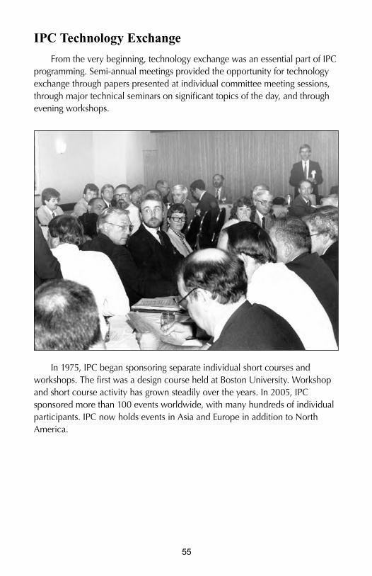
��
IPC Technology Exchange
From the very beginning, technology exchange was an essential part of IPC programming. Semi-annual meetings provided the opportunity for technology exchange through papers presented at individual committee meeting sessions, through major technical seminars on significant topics of the day, and through evening workshops.
In 1975, IPC began sponsoring separate individual short courses and workshops. The first was a design course held at Boston University. Workshop and short course activity has grown steadily over the years. In 2005, IPC sponsored more than 100 events worldwide, with many hundreds of individual participants. IPC now holds events in Asia and Europe in addition to North America.

��
Back East: Chuck Gladstone and “Potted in Timonium”
Over the years, I became the unofficial historian for a company that originated as Electronic Modules Corporation (EMC) in Timonium, Maryland. Founded in 1961, the company produced potted modules that performed the rudimentary operations of early integrated circuits (flip-flops, gates, etc.) These were then populated in different combinations onto printed circuit boards to perform various functions. The company’s early brochures proclaimed “Potted in Timonium.” Everyone would call about this new potting material, only to discover that Timonium is a place instead of a material.
The company’s ownership, name and direction changed numerous times over the years, and I finally established a separate contract manufacturing business with two partners several years ago. But I still have the old images and brochures! Here are a couple that always make me smile.
Regards,Chuck GladstoneVP OperationsChesapeake Manufacturing
Module, Sept. 1978
EMC circa 1970 Hybrid Module Room
EMC circa 1970 Welded Module Room

��
IPC Chronology: 1971-1975
1971
• 1971 was a recession year. The industry had been growing at more than 20% each year and then suddenly dropped to 30% of expectations. At this time, no one was certain where new applications might come from, and the industry was nervous. Nevertheless, it was agreed that IPC would continue to aggressively pursue all existing programs.
• “Measles” on printed circuit boards continued to be an acceptability issue for the industry. Particularly in a down market, measles rejects could cause a serious blow to a struggling company. As a result, IPC technical committees organized a comprehensive campaign to understand and address the measles issue.
• IPC organized all policies and procedures into a single policy manual.
• George Messner, PCK Technology, presented the results of Multilayer Round Robin III.
• IPC established a cooperative program with Underwriters Laboratories (UL) to reduce unnecessary testing of printed circuit board and laminate materials. This activity continues today.
The experts who served on the historic first “measles” committee. Seated: (L-R) Frank Papiano, RCA; Dick Castonguay, Mica; Ed Cuneo, Cinch-Graphik; and Chairman, Jim Swiggett, Photocircuits. Standing: (L-R) Arnie Andrade, Sandia; George Knox, Uniglass; George Smith, NSA; Charles Moser, Bureau of Engraving; and Dick Sarazin, Norplex

��
1972
• A major activity in 1972 was an upgrade of the structure for finalization of IPC standards. Recommendations included the following:
• Developing a standard format for IPC specifications.
• Deciding that IPC would process all of its standards through the American National Standards Institute (ANSI) via the Electronics Industry Association (EIA).
• That a mechanism should be provided to more formally provide test data to substantiate data used in IPC specifications. (This led eventually to the development of the IPC Testing Committee).
• Initiate a program to determine which member companies had test resource facilities and would be willing to undertake cooperative testing programs on subjects in which they had an interest.
• More active participation in the International Electrotechnical Commission (IEC).
• Under the chairmanship of Joe Poch, Westinghouse Electric, IPC published a Flat Cable Handbook.
1973
• Aware of the increasing need for more and better marketing information, a special planning committee was formed to organize a market-oriented seminar.
• IPC published the IPC Test Methods Manual under the chairmanship of George Smith, Department of Defense (DoD).
• IPC issued a significant report on “Measles” which was later included in IPC-A-600, Acceptability of Printed Boards.
• IPC formed a Policy Review Committee to meet periodically with committee chairmen.
• IPC investigated ideas for a format to provide for cooperative technical research. (Aside from the Round Robin Test and Evaluation Programs, additional cooperative research did not materialize).

��
1974IPC joined with the National Association of Metal Finishers
(NAMF) to interface with the U.S. Environmental Protection Agency (EPA) to develop effluent standards impacting all electroplating activity. IPC also participated with NAMF in filing a suit against the EPA, objecting to the initial guidelines. To help underwrite this project, IPC members were asked to make financial contributions and more than $100,000 was collected.
Attendees at the special planning committee for a market seminar. Seated (L-R): Dan McMillan, McGraw-Hill; Marv Larson, Bureau of Engraving; and Bill McGinley, Methode. Standing (L-R): Meridith Suhr, Collins; Ray Pritchard, IPC; Steve Loud, Owens-Corning; George Messner, Photocircuits; Tom Burke, T.M. Associates; Jeff Montgomery and Charles Hill, Quantum Science; Charles Wolff, Western Electric; Ken Varker, IBM; and Wayne Boucher, The Futures Group.
Members of the 1974 Board. Seated (L-R): Henry Kalmus, Sr., Kalmus & Associates; Jim Swiggett, Photocircuits and President of IPC; Marv Larson, Bureau of Engraving; and Dennis Stalzer, Graphic Research. Standing (L-R): Bill McGinley, Methode; Dave Easton, Agard; George Morse, Cinch-Graphik; George Holmes, TRW; Ted Thomas, Ansley; Bill Hangen, Sheldahl; Dick Zens, Electralab; and Bill Guyette, ACD Litton.

�0
1975
• Market research is one of the key membership benefits offered by IPC. IPC created the Technology Marketing Research Council (TMRC), brainchild of Marv Larson, now called the Executive Market and Technology Forum, to provide customized market research and technology trends to TMRC members.
• IPC established a formal program to develop long-range plans for IPC.
• IPC participated as a co-sponsor with the Electrical/Electronics Insulation Conference (E/EIC) holding a joint industry trade show. This program continued for three years.
• IPC published the IPC Process Effects Handbook under co-Chairmen Jim Cost, Raytheon, and Jack Bramel, Honeywell.
• IPC sponsored its first workshop, a design course held at Boston University. Today, IPC conducts hundreds of workshops a year addressing both technical and management topics.
• Don Dinella, Western Electric, presented data from the first Round Robin Test Program to evaluate the state-of-the-art of the additive process.
Members of the original TMRC Steering Committee. Seated (L-R): Ken Malgren, Norplex; Milt Smith, Westinghouse; Marv Larson, Bureau of Engraving; Don Goffredo, Chemcut. Standing (L-R): Steve Hudson, Owens-Corning; Jerry Siegmund and Charles Cobb, McDermid; Shipley representative; Chris Kalmus, Kalmus & Associates; and Jack McFalls, Western Electric.

��
Chapter 4: New Assembly Processes
In all science, error precedes the truth, and it is better it should go first than last.
— Hugh Walpole
Interview
Gert Schouten on Soldering: Focal Point of Circuit Assembly Technology
While advances in circuit assembly technology were moving apace in the United States, European companies were advancing as well. Years before the advent of surface mount technology (SMT), through hole technology peaked as the primary technology for circuit board assembly, and wave soldering was king. On both sides of the Atlantic, increasingly
sophisticated wave soldering machines were finding their way into production assembly facilities.
At early trade shows, the equipment line-ups were certainly far different from those of today. Instead of pick and place machines, there were insertion machines, plus machines for plating, drilling, crimping, cutting, everything
that had nothing to do with surface mount technology. Printing machines were small; they mostly used screens, and did not print solder paste! But even then, soldering was the focal point of the process, the means by which, after board fabrication, all of the connections were made. Soldering became the dominant step in the circuit manufacturing process, and would remain so, especially once SMT stepped out on stage and into the spotlight.
In the meantime, process and equipment engineers were working behind the scenes to develop better ways of soldering and to build more capable industrial machines to accomplish the job. These engineers found guidance in the publications and standards issued by IPC, both in the U.S. and abroad.
Early wave soldering of a through hole demo board, late 1960s

��
One of those engineers was Gert Schouten, who began early on in his career to focus on machine soldering. Schouten, now a senior engineer with Vitronics Soltec in Oosterhout, the Netherlands, recounts a remarkable 40 years of involvement in machine soldering development. He has written numerous papers and studies on the progress of soldering technology; his is a remarkable perspective.
Gert Schouten began working at Philips Telecommunication Industry (PTI) in 1966 as process engineer. “My first major task was to set up the first wave soldering machine in that plant” he writes. “The installation was successful and of course we learned a great deal developing the process to manufacture our products. I investigated areas such as solderability, solderable coatings, fluxes, layout aspects and the effect of machine settings on solder quality.”
During the time Gert worked for Philips, some automatic soldering equipment was developed in the consumer electronics branch. A board with components was dip fluxed, pre-dried and then placed over a solder bath where it was dipped for a few seconds. Then, the board was lifted out and given some time to cool down before the next board was put into the machine. This was the state of the art in the late 1950s and early 1960s, he says. “During the early sixties, the first wave soldering machine generations became mature and were introduced to the shop floor. Although Europe had its own wave soldering machine brands, such as Fry, the main suppliers of wave soldering machines were at that time Hollis and Electrovert.
“I learned something very important early on, that circuit boards would have to be modified or adapted to the wave soldering process, not the other way around. The solder joints on the boards at that time had never been designed for a process like wave soldering. Before machine soldering came about, all joints were soldered by hand using a soldering iron. This, of course, meant that for every solder joint, the assembly worker could choose or create the best soldering conditions for that particular joint. The contact time for the soldering iron could be changed per joint and also the amount of solder that was applied was decided by the person who soldered the joints.
“When such an assembly was transferred to automatic, uniform machine soldering, a lot of problems naturally showed up. Joints
Gert Schouten

��
contained less solder or were not sufficiently soldered due to lack of solderability, or due to a board design that did not match the desired joint layout for automatic soldering. These problems had not been foreseen and as a result, wave soldering initially took the blame for these poor soldering results. With hand soldering, all joints looked perfect, but now after wave soldering a lot of touch-up was necessary. People asked, what could be the benefit of such an automated soldering process?
“That was a question that was often asked in the beginning. Later, when we realized that, in automatic soldering, each joint gets the same treatment, such as soldering time and temperature, we came to the conclusion that we had to design all joints so that they would fit into that time/temperature frame that was directed by the machine.”
Apart from these design aspects, solderability issues became important too. Schouten said that “The soldering machine will never compensate for poor solderability. But what solderability level is necessary for good soldering? Additionally, what surface finishes are solderable, even after longer storage? What fluxes can be used, and will the remaining residues be safe for the equipment? All of these questions/problems required a quick answer and a good solution.”
Horizontal Versus Inclined Wave SolderingThe first wave soldering machine used in PTI was provided with a
horizontal conveyor, Schouten says. One benefit of its design was that the infeed and outfeed were on the same level; “But on the other hand, we found after comparing test results with other soldering lines that had an inclined conveyor that the soldering results, such as bridge formation, flags and spikes could not easily be optimized on machines with the horizontal conveyor. Even when the solder wave nozzle was optimized, the machine settings were rather critical, although good solder quality could be achieved. The critical process window at the machine with a horizontal conveyor was the main reason that, later on, within the Philips organization, only machines with an inclined conveyor system were used for wave soldering.
“Philips Telecommunication Industries was also involved in the early 1970s in European space programs such as ELDO (the European Launcher Development Organisation) and ANS (Astronomical Netherlands Satellite). A totally new philosophy had to be developed, combined with a comprehensive training course, for soldering that type of equipment.”

��
The Impact of IPC-S-815“In the mid-1970s, the European
electronic industry was confronted with IPC directives that required cleaning after soldering (IPC-S-815). In the European telecommunication industry, however, cleaning was not a common practice. Strict solderability requirements were observed for components and boards, so that we were able to solder with mildly activated colophony-based fluxes. The flux residues left on the board after soldering proved in climatic tests to be harmless for the equipment, so there was no direct need for cleaning. In fact, many of the components used on such boards, such as open coils or small transformers, were not designed for immersion in a cleaning solution. It was felt that this would actually increase the risk of problems in the long term, since such a cleaning action could deposit a film of “contaminated” cleaning liquid in all capillaries. After the evaporation of the cleaning liquid, a film of active dirt may be left.
“With this scenario in mind, companies like Philips, Siemens and Ericsson joined in their efforts to bring this subject to the IPC council that was responsible for the content of IPC-815. As a result, IPC-815 adopted this European no-cleaning process as an alternative to standard cleaning, necessary for more activated fluxes, into IPC-S-815.”
Solder-Cut-Solder Lines“A new development in soldering during the mid-1970s was the use
of a double soldering system with a lead cutting unit positioned between the two soldering machines. The idea was that the components could be placed on the board without the extra lead cutting operation that was normally used before soldering.
“This alternative method made use of a drag soldering machine or a high wave soldering machine that was used to create the solder joints, without looking to the side effects such as solder bridges and spikes or flags that were a result of this technique due to long leads. Next, the soldered board passed a unit with horizontal circular cutting blades that trimmed all leads to the desired length. Finally, this board with the trimmed leads that were already soldered was soldered for a second
ANS, Astronomical Netherlands Satellite, 1970s

��
time in a standard wave soldering machine to provide good soldered joints without bridges and spikes. This so-called “SCS” (Solder-Cut-Solder) system turned out to have some serious drawbacks as well. The introduction of automatic component insertion machines by companies such as Universal Instruments finally made the SCS system obsolete.
“Soon after wave soldering systems were introduced in the Philips factories, it became clear that the whole production line in front of such machines were dependent on the wave soldering machine’s reliability. If a wave soldering machine had a problem, it had a great impact on the entire production line.
“At that time, the wave soldering machines from the main suppliers Hollis and Electrovert were new to the European market and the companies had not yet established adequate service resources in Europe to handle customer process problems. Their stocks of spare parts were rather small. As a result, Philips was faced with serious losses when a machine had a problem and went down for several days due to unavailability of service.”
In a move to alleviate the problem, Philips called on a nearby company, the Dutch Zeva Company, already their supplier for other soldering equipment such as solder pots and soldering irons. “At that time, the German branch of Zeva made drag soldering systems, but the people at Philips had already decided that they wanted a wave soldering system with an inclined conveyor.
This created a conflict in the Dutch and German Zeva organizations. Finally they decided to separate the company and each would go their own way. From that moment on, Harry Roepers, who owned the Dutch Zeva Company, changed the company’s name to Soltec and decided to develop a wave soldering machine according to the Philips demands.
“In the mid-eighties, all basic process developments on soldering had been completed and were recorded in Philips standards. At that point, I left Philips to join Soltec.
Horizontal production wave soldering machine, mid-1960s
��
“It was around that time that the development of SMDs for reflow soldering resulted in consumer products that began to use chip components not only in reflow soldering, but also in wave soldering. Since these components were never designed for wave soldering in the first place, we had to find ways in the process to promote good solder joint formation. The obstacle here is often the component body, like the SOT 23, that presses the solder wave away from the joint area. This is due to a combination of the non-wettable epoxy body that in combination with the surface tension of the solder create a “shadow” area where the solder is unable to wet the board. It happens to be in that shadow region that the connection leads are positioned where the solder joint must be made.
“The solution to this problem was use of a dynamic wave that was able to disturb this shadow effect, in combination with a good solder pad design. This dynamic wave, the so-called “chip wave,” was often a thin parabolic wave with a high velocity that resulted in the dynamic behavior when the wave hit the board. In most cases, this dynamic wave was followed by a second wave, the main wave, with a smooth flow. This was necessary to create the optimal drainage conditions for bridge-free soldering. Other solutions were developed, such as the “smart wave,” which created a dynamic area at the front of the solder wave, followed by a smooth wave part to achieve optimal solder drainage conditions.”
Reflow Soldering System DevelopmentGert Schouten has always been a wave soldering guy, but he
remembers when his company jumped into the reflow soldering equipment supplier fray. It happened parallel with the development of special waves for the soldering of chip components that were fixed with a glue dot on the solder side of PCBs that additionally had common leaded components. “More boards began to appear that just contained only SMDs that should be mounted in solder paste and then soldered. The joint formation for such boards required another technique. The process profile was not only depending on the component diversity and the board, but was also directed by the solder paste properties. All these requirements made it necessary to create an oven that could be tuned for the correct reflow profile.”
The Use of Nitrogen in Wave Soldering“New synthetic fluxes for wave soldering were developed that
did not need cleaning after soldering. These “no-clean” fluxes were characterized by very low solids content, often less than 4%. However,
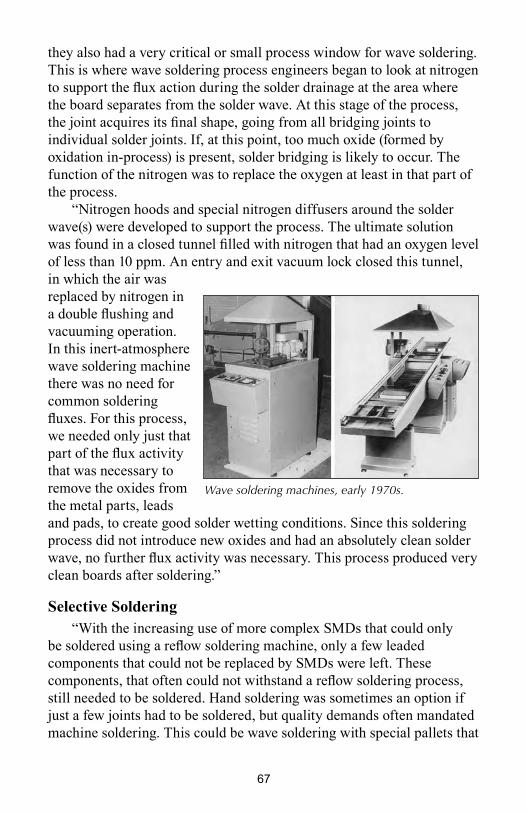
��
they also had a very critical or small process window for wave soldering. This is where wave soldering process engineers began to look at nitrogen to support the flux action during the solder drainage at the area where the board separates from the solder wave. At this stage of the process, the joint acquires its final shape, going from all bridging joints to individual solder joints. If, at this point, too much oxide (formed by oxidation in-process) is present, solder bridging is likely to occur. The function of the nitrogen was to replace the oxygen at least in that part of the process.
“Nitrogen hoods and special nitrogen diffusers around the solder wave(s) were developed to support the process. The ultimate solution was found in a closed tunnel filled with nitrogen that had an oxygen level of less than 10 ppm. An entry and exit vacuum lock closed this tunnel, in which the air was replaced by nitrogen in a double flushing and vacuuming operation. In this inert-atmosphere wave soldering machine there was no need for common soldering fluxes. For this process, we needed only just that part of the flux activity that was necessary to remove the oxides from the metal parts, leads and pads, to create good solder wetting conditions. Since this soldering process did not introduce new oxides and had an absolutely clean solder wave, no further flux activity was necessary. This process produced very clean boards after soldering.”
Selective Soldering“With the increasing use of more complex SMDs that could only
be soldered using a reflow soldering machine, only a few leaded components that could not be replaced by SMDs were left. These components, that often could not withstand a reflow soldering process, still needed to be soldered. Hand soldering was sometimes an option if just a few joints had to be soldered, but quality demands often mandated machine soldering. This could be wave soldering with special pallets that
Wave soldering machines, early 1970s.

��
covered the reflow soldered components, or using components that could withstand the reflow process and using “pin-in-paste” technology.”
Both of these solutions had their drawbacks, Schouten says. “This is where a specific machine for selective soldering could offer a good solution. Today’s selective soldering machine, in essence, contains a fluxing station able to flux only those joints that need to be soldered, has a preheat station, and has a soldering robot that makes it possible to solder single joints, or to drag solder a row of selected joints. The robot manipulates the board with the selected joints over a small solder nozzle at which a spherical solder well is positioned. All separate joints can be given their own specific dwell time. The drag speed and drag angle can be set as required. Even different solder nozzles can be used for such a process. If a board contains many joints with leaded components, there is the possibility to dip-solder all those joints simultaneously in one process.” For this process, a board-specific nozzle plate is used, so that the selective soldering process will not affect surrounding components, while all selected joints are soldered at the same time.
Long-time industry veteran and SMT technology pioneer Phil Marcoux also recalls some of the significant milestones in the development of the wave soldering process, such as the hot air knife. “This device helped remove excess solder collected by the SMT components that were glued onto the wave side of the board. I think that the technology was introduced by Sensbey in the early 1980s since I recall needing to buy one in the 1983-84 timeframe.”
Another issue with wave soldering was the use of special fixturing to accommodate unique soldering applications or board designs. Fixtures tended to be expensive, since they were by nature custom fabricated, and often made of costly metals with low thermal coefficients of expansion. Marcoux remembers “spending a lot of money on special fixtures”; it is likely that many others remember doing the same. Schouten says that “Many of the fixtures that Phil remembers were often used to keep the front of the board flat to create a smooth entrance into the solder wave and to reduce the risk of solder flooding over the top side of the wave. Also, when a board had large slots or cutouts, these openings needed to be covered by fixtures, especially when SMDs had to be soldered with a turbulent wave. Sometimes one could avoid using some fixtures when it was possible to install a wire support in the solder wave.”
Marcoux also remembers the push to develop suitable adhesives for SMDs on the underside of wave soldered boards. “The properties of the adhesive were critical because the adhesive had to hold the component in place through the wave but not form so strong a joint as to damage

��
the board if a component needed to be replaced. Eventually, someone created an adhesive that had strong shear strength but broke easily when twisted with tweezers.” Marcoux recalls that application of the adhesive was also a “sticky” issue. At first, it had to be stenciled, which was a messy process. Then, a Japanese company developed a pin transfer method that neatly applied a consistent dot of adhesive to the board, just the right amount to hold the body of the component in place without interfering with the solder connection areas.
Not only did the SMDs need to be glued, Schouten recalls, but the adhesive required curing, usually by heating. “Indeed, Phil is right that the glue had to be strong enough to hold the SMD, but had to easily break when the component had to be replaced.” Sometimes heating the board softened the adhesive enough so that it would twist off with very little resistance. “In the process of glue application that Phil describes, there was also the alternative to dispense the glue with a syringe. But as Phil said, pin transfer was the most common system.”
It has been a long road for Gert Schouten, but he has few regrets; indeed, he sums up his experience as thus: “In 40 years involved in the development of machine soldering in electronics, I’ve never had a dull moment.”

�0
IPC Chronology: 1976-1977
1976
• In 1976, IPC worked with the U.S. Defense Electronics Supply Center (DESC) to review their approach to developing military specifications. In the past, DESC contracted with outside experts to prepare initial drafts which were then reviewed by a joint government/industry group. DESC agreed to have their future initial drafts prepared by volunteer experts from IPC member companies, thereby providing a better resource for the initial draft and at no cost to the government (and taxpayer).
• IPC formed two special Blue Ribbon Committees, one for the study of Insulation Resistance, and the other for Electromigration.
1977
• 1977 was the year that IPC officially changed its name to the Institute for Interconnecting and Packaging Electronic Circuits. Discussions had started in 1974 on broadening the group’s name to reflect the inclusion of packaging and interconnects other than printed boards. The name change was first approved by a blue ribbon steering committee, the Committee Chairman Council, the Technical Activities Executive Committee and the Board of Directors. It was approved by a vote of the membership with 87% in favor.
IPC members who served on the committee to change IPC’s name. Seated (L-R): Marv Larson, Don Dinella, Bill Hangen, and Ken Varker. Standing (L-R): Arnie Andrade, Jim Swiggett, George Smith, Stan Randall, and Bernie Kessler

��
• The IPC “Hall of Fame” was instituted. The first recipient of the award was Bill McGinley, IPC’s first president.
• A discussion began concerning the possible need for staff access to a computer.
• Ken Hafften, Bureau of Engraving, and Dwayne Poteet, Texas Instruments, led a committee that developed the IPC multi-purpose test board (IPC-B-25).
The new name and logo of IPC were displayed for the first time in 1977. Shown at the presentation are (L-R) Jim Swiggett, IPC President; Bill McGinley, IPC’s first President; and Bernie Kessler, first chairman of the TAEC.

��

��
Chapter 5: The Rise of Surface Mount Technology
Science never solves a problem without creating ten more.— George Bernard Shaw
The emergence of Surface Mount Technology, or SMT, in the early 1980s was the beginning of a seismic change in printed circuit board design and manufacturing technology. SMT meant radical changes “across the board” not only in component types and lead configurations, but also in new types and technologies of assembly equipment. To complicate matters, there were traditional through hole boards, 100% SMT boards, and a bevy of combinations in between, with “percentages” of surface mount content.
SMT changed everything. Some welcomed it; some did not. The effect on the industry was all-transforming, for SMT came on the scene sweeping all before it. It was an enabling technology, allowing much greater miniaturization of circuits, higher complexity of circuits, and increased power and functionality.
The transition to SMT was, of course, neither sudden nor absolute. Through hole products continued to be built, the difference being that more and more boards had an increasingly higher percentage of surface mounted devices (SMDs) comprising them. There were entirely SMT assemblies, and there were “mixed-technology” boards. Eventually, they were given descriptive classifications such as Type I, Type II, and Type III; ultimately, however, the proliferation of diverse board types and styles rendered such classifications inadequate, and thus they are little used today.
Today, virtually all mass-produced electronics circuitry is manufactured using a large percentage of surface mount technology (SMT). Once SMT started to be used in the 1980s, the change from conventional leaded components to SMDs took place quickly in view of the enormous gains that could be made using SMT. Mass produced electronic circuit boards need to be manufactured in a highly mechanized manner. The traditional leaded electronic components do not lend themselves to this approach. Although some mechanization was
Surface mount passive components, large and small (center and adjacent)
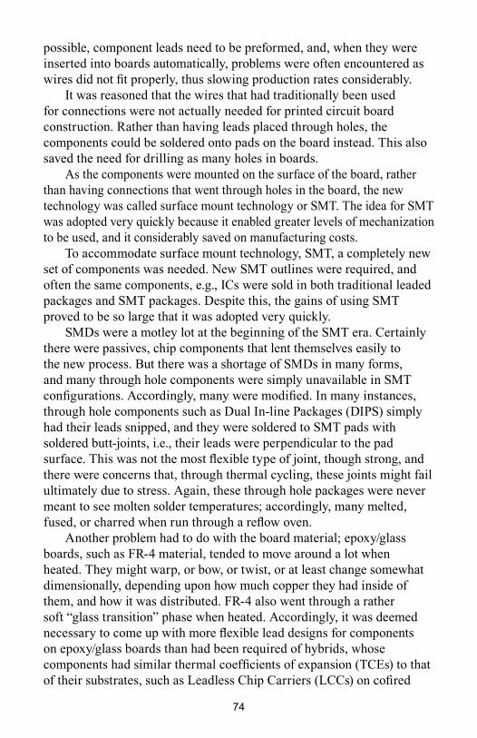
��
possible, component leads need to be preformed, and, when they were inserted into boards automatically, problems were often encountered as wires did not fit properly, thus slowing production rates considerably.
It was reasoned that the wires that had traditionally been used for connections were not actually needed for printed circuit board construction. Rather than having leads placed through holes, the components could be soldered onto pads on the board instead. This also saved the need for drilling as many holes in boards.
As the components were mounted on the surface of the board, rather than having connections that went through holes in the board, the new technology was called surface mount technology or SMT. The idea for SMT was adopted very quickly because it enabled greater levels of mechanization to be used, and it considerably saved on manufacturing costs.
To accommodate surface mount technology, SMT, a completely new set of components was needed. New SMT outlines were required, and often the same components, e.g., ICs were sold in both traditional leaded packages and SMT packages. Despite this, the gains of using SMT proved to be so large that it was adopted very quickly.
SMDs were a motley lot at the beginning of the SMT era. Certainly there were passives, chip components that lent themselves easily to the new process. But there was a shortage of SMDs in many forms, and many through hole components were simply unavailable in SMT configurations. Accordingly, many were modified. In many instances, through hole components such as Dual In-line Packages (DIPS) simply had their leads snipped, and they were soldered to SMT pads with soldered butt-joints, i.e., their leads were perpendicular to the pad surface. This was not the most flexible type of joint, though strong, and there were concerns that, through thermal cycling, these joints might fail ultimately due to stress. Again, these through hole packages were never meant to see molten solder temperatures; accordingly, many melted, fused, or charred when run through a reflow oven.
Another problem had to do with the board material; epoxy/glass boards, such as FR-4 material, tended to move around a lot when heated. They might warp, or bow, or twist, or at least change somewhat dimensionally, depending upon how much copper they had inside of them, and how it was distributed. FR-4 also went through a rather soft “glass transition” phase when heated. Accordingly, it was deemed necessary to come up with more flexible lead designs for components on epoxy/glass boards than had been required of hybrids, whose components had similar thermal coefficients of expansion (TCEs) to that of their substrates, such as Leadless Chip Carriers (LCCs) on cofired
��
ceramic. Thus, the now-familiar gull-wing and J-leads were developed.Some of the following is taken from www.radio-electronics.com.
The various stages in the SMT production processes include adding solder paste to the board, pick and place of the components, soldering, cleaning (sometimes), inspection, and test. All these processes are required, and need to be monitored to ensure that product of the highest quality is produced.
Solder paste: Prior to the addition of the components to a board, solder paste must be added to those areas of the board where solder is required. Typically, these areas are the component pads. This is achieved using a solder screen or stencil.1
Pick and place: The board with the added solder paste is then passed into the pick and place process. Here, a machine loaded with reels of components picks the components from the reels or other dispensers and places them onto the correct position on the board. The components placed onto the board are held in place by the tension of the solder paste. This is usually sufficient to keep them in place. In some processes, automated dispensers add small dots of adhesive to secure the components to the board. This is normally done only if the board is to be wave soldered. The disadvantage of the process is that any repair is made far more difficult by the presence of the adhesive, although some glues are designed to degrade during the soldering process.
Soldering: Once the components have been added to the board, the next stage of the process is to pass it through the reflow soldering machine. Wave soldering is often used for passive components on the bottom of a double-sided board or, for some through hole parts, with the PCB mounted in a custom pallet. Increasingly, selective soldering machines are used for these individual components and connectors.
Wave soldering, the primary means by which through hole connections were made, did not become obsolete with the advent of SMT. In fact, wave soldering continues to enjoy widespread use today in part due to the development of large components, connectors, odd
Rework of gull-wing leaded SMDs: applying liquid flux prior to heating. Components in foreground have “fine pitch” lead spacing.

��
form components, and other applications. As mentioned earlier, as SMT occupied an increasingly larger percentage of circuit assemblies and boards became double-sided, we often saw situations wherein chip components would be attached to the bottom side of a PCB with epoxy dots (and then cured), and then run through a wave soldering machine whereby the through hole components and glued chips were soldered at once. The top side of the board held the other SMDs, plastic parts and those that could not withstand direct contact with the wave, or would not wave solder properly due to their design (entrap solder, etc.). This
side of the board would be printed with solder paste, components placed upon it by hand or (later) by pick and place robotics, and then sent through a reflow soldering oven to reflow the top components. The PCB was usually transported in a boat or fixture to keep the bottom-side components from touching the conveyor
belt. Later, these boards would travel on beltless edge conveyors. Care had to be taken because, regardless of whether the top or bottom side was processed first, one side or the other was going to inescapably see a second reflow. This presented dangers and tradeoffs; for example, many through hole components were not designed to see extended exposure to reflow temperatures as they would be in an SMT reflow oven. Also, with a second reflow, there was once again the concern for solder joint oxidation and dewetting. What if anything on the bottom side needed rework? Now parts of that board would see a total of four exposures to molten solder temperatures; two for manufacture, two for rework (removal of a defective part, and the re-soldering of a new one in its place).
Although most SMT processes use no-clean pastes and fluxes, cleaning is often required for high reliability (Hi-rel) assemblies.
Inspection: After the boards have been passed through the soldering process, they are often inspected. Manual inspection is not an option for surface mount boards employing a hundred or more components. Instead, automatic optical inspection is a far more viable solution. AOI/AXI machines are available that are able to inspect boards and detect poor joints, misplaced components and, some instances, in the wrong component.1
Ball Grid Array (BGA) packages

��
Test: It is necessary to test electronic products before they leave the factory. There are several ways in which they may be tested.
Increasing circuit density, power, and complexity led to a greater number of smaller lead connections; thus “fine pitch” technology was born. This created its own set of manufacturing problems because it required tighter tolerances literally everywhere. Whereas 50-mil spacing between the centers of leads had been common, fine pitch took that spacing down to 10 mils and less. Pick and place machines had to be more accurate.
The ball grid array, or BGA, became the solution to the problem of producing a miniature package for an integrated circuit with many hundreds of pins. Pin grid arrays and dual-in-line surface mount (SOIC) packages were being produced with more and more pins, and with decreasing spacing (pitch) between the pins, but this was causing difficulties for the soldering process. As package pins got closer together, the danger of accidentally bridging adjacent pins with solder grew. BGAs do not have this problem because the solder is factory-applied to the package in exactly the right amount. Also, the connections are beneath the package, utilizing all of that valuable real estate, rather than around the periphery. The BGA package rests on solder spheres, or balls, of higher-temperature solder that does not melt during reflow, but the lower-temperature solder connecting the balls to the package, and then to the pads or footprint on the PCB below, makes a physical and electrical connection to the board.
A further advantage of BGA packages over leaded packages is the lower thermal resistance between the package and the PCB. This allows heat generated by the integrated circuit inside the package to flow more easily to the PCB, preventing the chip from overheating.
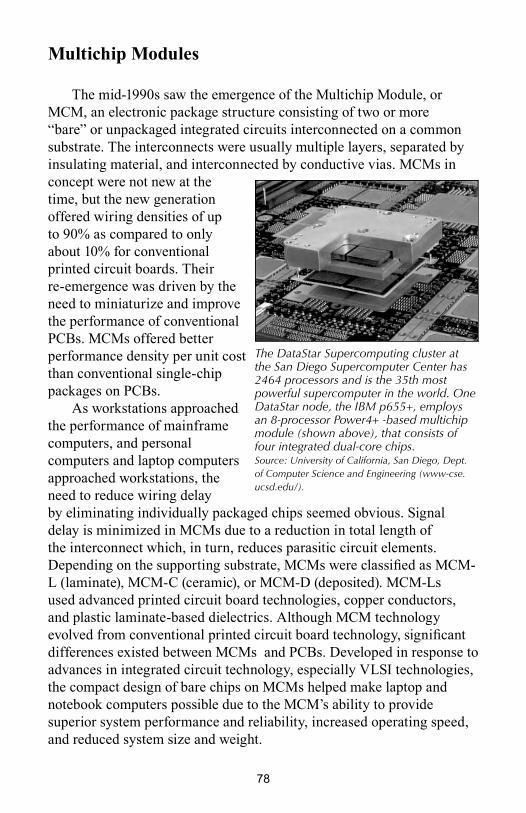
��
Multichip Modules
The mid-1990s saw the emergence of the Multichip Module, or MCM, an electronic package structure consisting of two or more “bare” or unpackaged integrated circuits interconnected on a common substrate. The interconnects were usually multiple layers, separated by insulating material, and interconnected by conductive vias. MCMs in concept were not new at the time, but the new generation offered wiring densities of up to 90% as compared to only about 10% for conventional printed circuit boards. Their re-emergence was driven by the need to miniaturize and improve the performance of conventional PCBs. MCMs offered better performance density per unit cost than conventional single-chip packages on PCBs.
As workstations approached the performance of mainframe computers, and personal computers and laptop computers approached workstations, the need to reduce wiring delay by eliminating individually packaged chips seemed obvious. Signal delay is minimized in MCMs due to a reduction in total length of the interconnect which, in turn, reduces parasitic circuit elements. Depending on the supporting substrate, MCMs were classified as MCM-L (laminate), MCM-C (ceramic), or MCM-D (deposited). MCM-Ls used advanced printed circuit board technologies, copper conductors, and plastic laminate-based dielectrics. Although MCM technology evolved from conventional printed circuit board technology, significant differences existed between MCMs and PCBs. Developed in response to advances in integrated circuit technology, especially VLSI technologies, the compact design of bare chips on MCMs helped make laptop and notebook computers possible due to the MCM’s ability to provide superior system performance and reliability, increased operating speed, and reduced system size and weight.
The DataStar Supercomputing cluster at the San Diego Supercomputer Center has 2464 processors and is the 35th most powerful supercomputer in the world. One DataStar node, the IBM p655+, employs an 8-processor Power4+ -based multichip module (shown above), that consists of four integrated dual-core chips. Source: University of California, San Diego, Dept. of Computer Science and Engineering (www-cse.ucsd.edu/).

��
EMS: The Birth of an Industry and IPC
By Tony Hilvers, IPC
The arc of the Electronics Manufacturing Services Industry can take your breath away. A group of hearty entrepreneurs establish their companies in their basements or small offices, sell their services like crazy and, aided by technology, grow to be a global force in a little more than 20 years.
Yet, very little reflection has been given to the birth and growth of this industry. Maybe the industry has no historical father. Or the culture of the EMS industry doesn’t tolerate companies or individuals who reminisce about past successes: in other words, looking back means you’re not looking ahead. Maybe they believed as Andy Grove did that “success breeds complacency. Complacency breeds failure. Only the paranoid survive.”
The birth of an industry usually has one colorful, strong or eccentric leader that personifies an entire industry: software has Bill Gates, semiconductors have Andy Grove and the personal computer is intimately linked to Steve Jobs. The careers of these industry giants nicely parallel the birth and growth of their respective industry.
Not so for the EMS industry. There were multiple strong, eccentric and colorful leaders: SCI’s Olin King; Manu-Tronics’ Roger Mayer; Roger Main at IEC; Bonnie Fena at Hibbing Electronics; Bruce Ramsey at AVEX; Phil Marcoux at AWI; and Winston Chen at Solectron to name only a few. They came from all parts of the country and all were exceptionally competitive.
These individuals were a study in contrasts. Californian Winston Chen, a Buddhist, was raised in Taiwan, received a doctorate in physics from Harvard and worked for IBM with several patents to his credit. He was reserved and unassuming and yet competitive enough to grow Solectron to become a multi-billion dollar company.
As an example, Solectron was advertising in the late 80s their “surface mount capabilities” although most of the SMT components they placed were by hand. A figurative stone’s throw away, however, his competitor AWI, founded by Phil Marcoux, arguably the father of SMT, featured a complete, functioning SMT line.
Tony Hilvers

�0
Conversely, Olin King, a rocket scientist (which no doubts explains the reason why his company was established in Huntsville, Alabama) was a hard charging, mercurial southerner and the consummate salesman. And like Winston, he too dramatically grew his company. Olin probably has more folklore attached to him than anyone else in the EMS industry.
Tino Gonzalez, who at one time worked for SCI in their Rapid City, S.D. facility, said that Olin would personally approve his travel to IPC meetings. Which meant the founder of what was then a $500 million and growing corporation was approving a process engineer’s travel authorization.
The director of sales at a top tier EMS company, many years ago, was escorting a potential major customer through their facilities in Huntsville. He tried his best to have his president meet with the customers but the president couldn’t find the time. After the tour ended at 4:00 pm, the director of sales thanked his customers for coming and asked them what time they were flying out of Huntsville.
“We’re flying out tomorrow night,” the customers said. “Olin King is cooking dinner for us at his house tonight and then he’s giving us a guided tour of his plants tomorrow.”
California or Alabama; rocket engineer or physicist; the competitive drive of Chen, King and other industry pioneers energized the growth of the EMS industry.
IPC and the EMS IndustryIf the EMS leaders were advocating growth and opportunity for this
new industry, IPC was adding legitimacy.In 1983, an IPC member in Texas questioned why IPC didn’t collect
market research data on contract assembly companies or “board stuffers” as they were also called. Ray Pritchard, IPC’s executive director, asked me to take a look at the potential market.
I started calling companies — first the one in Texas who asked for the market research data. Then I called his competitors and their competitors and over time I collected a list of nearly 50 companies.
When I asked them what they did, they said they assembled printed circuit boards but “don’t tell anyone else because we think we’re the only ones providing this service.”
Using this list of companies and IPC’s database, IPC (Ray Pritchard really did all the number crunching and data analysis) published its first market research report “Survey of the Assembly Market” in 1984. IPC estimated that the “outside service to assemble PWBs” in 1983 was

��
$1 billion in the United States and it was estimated to grow to $1.7 billion in 1984.”
Nearly 100 OEMs and 37 independent assembly companies returned questionnaires. The report especially mentioned that these 37 companies were extremely optimistic about the growth of outside assembly service in the next two to three years. In a harbinger of the things to come, IPC’s sample reported they expected to grow 110 percent the following year.
We were extremely happy about the assembly report. We published a press release on the report commenting on the size of this new independent assembly market. The news, in turn, was reported by industry trade publications.
Almost immediately I received a call from Wayne Moxley, president of Avco Electronics in Huntsville. Avco would later become Avex and still later merge into Benchmark Electronics.
Wayne was upset. “Hey, I read your press release on the independent electronics assembly market. You valued the industry at $1.7 billion. What a bunch of bull —. You have dramatically undervalued the market. Olin King and I have almost $500 million in revenue alone. How do you explain the difference? You put us at real disadvantage with the investment community.”
“Well,” I said, “our market study did not include value add.” “Ah, o.k., never mind,” he said and hung up the phone.
At that time, most companies were still operating a consignment business — they would receive the components and printed circuit boards from their OEMs customers and the independent assembly company would then complete the assembly. During this period, the industry was often called “board stuffers,” a not too flattering term.
Avco and SCI and a handful of companies were transitioning to turnkey assembly or value add — they would buy components and boards for their customers and complete the assembly. As a result, the cost of the components and PWBs would rightly show up in their sales data.
This would be one of the only studies reporting non-value added revenue. The industry quickly transitioned to turnkey assembly and the future IPC market research reports would report sales revenue. Later of course, IPC added a “systems build category” to recognize EMS companies’ persistent march to product design and system or product manufacturing.
IPC continues to conduct market research on the EMS industry. We estimate that in 2006 the EMS market in North America was $53 billion while the global EMS industry had total revenues of $213 billion. For
��
North America alone, the $53 billion represents a 17 percent compound annual growth rate since IPC’s first market research report in 1983.
Without a doubt, IPC’s market research lent credibility to the EMS industry. Companies would trot out the IPC market research study to their banker and say “if you don’t believe how fast we’re growing, take a look at the research of this independent trade association.”
Our market research also received a lot of notice from Wall Street. As a result, analysts began to report on the industry and its growth.
Meetings and NetworkingIPC’s original survey asked the independent assembly companies
(we struggled with this name for several years) on how we, IPC, could be of service to them. Development of standards or guidelines rated high and the lowest rated item was informal meetings.
Yet, by working with the PWB presidents and the technical committees, we knew the power of networking by industry peers. We knew if the senior managers of EMS companies would come together, they would work together for the betterment of the industry. They would also of course become IPC members.
Gathering the EMS executives together for the first few years was a tough go. We created a mini focus group in the late 1980s to determine the direction we could take for EMS programming. Attending the meeting were Joe Sullivan, president of Flextronics, a real up and coming assembly company; Bonnie Fena, president of Hibbing Electronics; Jack Calderon, Interconics; Roger Mayer, Manu-Tronics; and John Endee, president of Photocircuits.
John Endee and Ray Pritchard described some of the programs IPC was conducting for the PWB presidents, including a two hour breakfast meeting in the spring and fall where the presidents would share market data.
Joe Sullivan was brief and to the point in responding to our request for insight into potential programs for EMS companies: “I’m extremely busy growing my company. I don’t want to necessarily talk to my competitors. Give me a reason to attend the meeting. Give me something to learn.”
It was clear to IPC staff that EMS company leaders would attend an IPC meeting but there needed to be a formal program developed and directed specifically at and for EMS companies.
This focus group led to the creation of the IPC EMS management council soon after. The Steering Committee was initially chaired by
��
Roger Mayer, Manu-Tronics, and later by Stan Plzak, Pensar; David Frayden, IEC, and currently by Steve Pudles, Nu Visions.
The steering committee created programming for the bi-annual EMS management meeting as well as a number of groundbreaking programs to help EMS companies. These programs created or advocated by the steering committee included the EMSI-TC2 - IPC Sample Master Ordering Agreement for EMS Companies and OEMs, EMS Program Manager Certification, and the IPC-A-610 Certification Program.
From Board Stuffers to the IPC BoardIn the early 1990s, a trade association based in Detroit began angling
for “contract manufacturers.” The association’s membership included office cleaning services as one of their key membership groups.
Although eminently better than board stuffers, I never liked the name “contract manufacturers.” To me, the term conjured up day labors coming to the job site in yellow school buses. It also reminded me that this new but hotly growing industry would have other groups vying for their attention.
We (Sue Mucha, Brian Throneberry, Leo Reynolds, Steve Pudles, Bonnie Fena and Stan Plzak) had an ad hoc meeting in a hotel lobby. I mentioned I didn’t like the term contract manufacturers. They didn’t either. After lots of brainstorming, the name “Electronics Manufacturing Services Industry” was decided by the group or EMSI for short. They reasoned the name more fully represented the wide range of services their companies were now providing.
The name was proposed to attendees at the EMS management meeting in October, 1991 in Anaheim, Calif. I would like to report it was a unanimous, quick and positive vote by the attendees. That wasn’t the case.
Jack Calderon was in favor of removing the “s” from electronics while Sue Mucha favored keeping the “s.” Each had very persuasive reasons for their position. However, for the life of me, I can’t remember their reasons. I’ll bet though if you asked them, they would both have a reasoned, articulate response to that question.
After an exhausting two hour debate, Plzak called for the question and the majority at the meeting voted to keep the “s.” The industry had a new name. Almost immediately (or so it seems now but it probably took a couple of years), the companies began to refer to themselves as EMS providers. It didn’t hurt that Wall Street analysts loved the name and began calling the companies they followed EMS companies.

��
A compelling business model, charismatic leaders, market research, a new name and attention by Wall Street all conspired to drive the EMS industry to continued double digit growth. What was left? For IPC, it meant a seat on the board of directors for EMS leadership.
Two historic firsts occurred in 1991 for IPC: Bonnie Fena, president of Hibbing Electronics became the first woman and the first EMS company representative to be elected to the IPC Board of Directors. Fena became the chairman of the IPC Board of Directors in 1996. The EMS Industry was fully invested in IPC.
Why EMS?While I certainly believe IPC played a valuable role in the formation
and growth of the EMS industry and I certainly include industry leadership in the equation for success, the growth of the EMS industry was really the result of a “perfect storm” in the electronics industry. This perfect convergence was the drive to strategically outsource electronics assembly and the advent of surface mount technology.
Strategic outsourcing was taking corporate business practices by storm and the electronics industry was not immune to this business model.
In the past, OEMs had used outsourcing tactically when they needed extra capacity. As the need for surface mount technology capability became apparent, OEMs finally saw the EMS as a strategic solution. Rather than invest in the capital demands of SMT and training of their human capital — and take the technology risks — OEMs started to depend on EMS companies. The movement was hastened by the value in time-to-market capabilities.
The computer industry was one of the first industries to fully embrace the outsourcing model, adding legitimacy to outsourcing of electronics assembly. With the technology revolution of the 1990s, new OEM players emerged. These companies found EMS companies to design and build their products. The new startups, as a result, were not burdened by capital equipment and brick and mortar investment in electronics manufacturing facilities. Investors loved this business model.
Andy Rappaport, a speaker at an IPC marketing meeting in 1992, predicted the rapid outsourcing by the computer industry in his award winning Harvard Business Review article “The Computerless Computer Company.”
He said that, by the end of the century, the most successful computer companies would be buying computers rather than building them. Defining how computers are used, not how they are built, would
��
create real value. Three new rules would guide the computer industry’s strategic transformation: 1) compete on utility, not power; 2) monopolize the true sources of added value; and 3) maximize the sophistication of the value delivered, while minimizing the sophistication of the technology consumed.
Some may disagree with Rappaport’s Numbers 1 and 3 but the electronics industry is certainly “monopolizing the true sources of value add.” The massive, vertically integrated company is gone. It has been replaced by companies who embrace an outsourcing strategy that prizes time to market and cost reduction and recognizes the consistent drum beat of globalization.
Source:
1. Source: www.radio-electronics.com, “Electronics Manufacturing.”
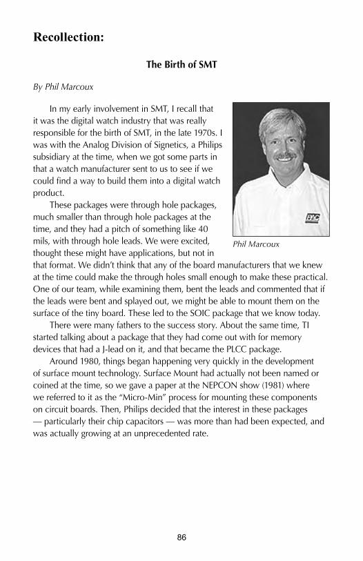
��
Recollection:
The Birth of SMT
By Phil Marcoux
In my early involvement in SMT, I recall that it was the digital watch industry that was really responsible for the birth of SMT, in the late 1970s. I was with the Analog Division of Signetics, a Philips subsidiary at the time, when we got some parts in that a watch manufacturer sent to us to see if we could find a way to build them into a digital watch product.
These packages were through hole packages, much smaller than through hole packages at the time, and they had a pitch of something like 40 mils, with through hole leads. We were excited, thought these might have applications, but not in that format. We didn’t think that any of the board manufacturers that we knew at the time could make the through holes small enough to make these practical. One of our team, while examining them, bent the leads and commented that if the leads were bent and splayed out, we might be able to mount them on the surface of the tiny board. These led to the SOIC package that we know today.
There were many fathers to the success story. About the same time, TI started talking about a package that they had come out with for memory devices that had a J-lead on it, and that became the PLCC package.
Around 1980, things began happening very quickly in the development of surface mount technology. Surface Mount had actually not been named or coined at the time, so we gave a paper at the NEPCON show (1981) where we referred to it as the “Micro-Min” process for mounting these components on circuit boards. Then, Philips decided that the interest in these packages — particularly their chip capacitors — was more than had been expected, and was actually growing at an unprecedented rate.
Phil Marcoux
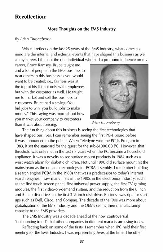
��
Recollection:
More Thoughts on the EMS Industry
By Brian Throneberry
When I reflect on the last 25 years of the EMS industry, what comes to mind are the internal and external events that have shaped this business as well as my career. I think of the one individual who had a profound influence on my career, Bruce Ramsey. Bruce taught me and a lot of people in the EMS business to treat others in this business as you would want to be treated; i.e., fairness was at the top of his list not only with employees but with the customer as well. He taught me to market and sell this business to customers. Bruce had a saying “You bid jobs to win; you build jobs to make money.” This saying was more about how you market your company to customers than it was about pricing.
The fun thing about this business is seeing the first technologies that have shaped our lives. I can remember seeing the first PC-1 board before it was announced to the public. When Teledyne won the PC Jr. Program in 1983, it set the standard for the quest for the sub-$1000.00 PC. However, that threshold was only met in the last six years when the PC became a household appliance. It was a novelty to see surface mount products in 1984 such as a wrist watch alarm for diabetic children. Not until 1990 did surface mount hit the mainstream as the de facto technology for PCBA assembly. I remember building a search engine PCBA in the 1980s that was a predecessor to today’s internet search engines. I saw many firsts in the 1980s in the electronics industry, such as the first touch screen panel, first universal power supply, the first TV gaming modules, the first video-on-demand system, and the reduction from the 8 inch and 5 inch disk drives to the first 3 ½ inch disk drive. Business was ripe for start-ups such as Dell, Cisco, and Compaq. The decade of the ‘90s was more about globalization of the EMS Industry and the OEMs selling their manufacturing capacity to the EMS providers.
The EMS Industry was a decade ahead of the now controversial “outsourcing trend” that other companies in different markets are using today.
Reflecting back on some of the firsts, I remember when IPC held their first meeting for the EMS Industry. I was representing Avex at the time. The other
Brian Throneberry

��
attendees were from Group Technologies, Solectron and SCI, four companies who kept a suspicious eye on each other. From that meeting, IPC has gone on to have a profound effect on the industry in training, standardization, access to investment capital, lobbying for beneficial government laws for the industry, and marketing the EMS Industry for legitimacy. It will be hard to see what other challenges IPC will face in the future, but I have all the confidence that they will be up to it.
The one thing that I miss today in the EMS Industry is the bravado that certain individuals gave to the industry, which created a certain espirit de corps. I miss the persona of Olin King, Roger Main, Bill Morean, Michael Marks, Winston Chen, Bonnie Fena, and Roger Mayer. These individuals shaped this industry into what it has become today. The passion they put into their companies made every company in this industry better because you wanted to beat them at their own game. I am sure employees who were close to these individuals could tell hours of intriguing stories on how they won certain jobs and how they manage their companies. I have my own stories about going up against these individuals in head-to-head marketing. It was always the sweetest pleasure to win business from one of these companies when they personally were involved in the sale.
When I was asked about writing my thoughts on the EMS Industry, I went back through all of my old business cards. I have a large collection of them and would put them up against anyone. Going back through those cards was like going through one’s senior yearbook. You remember a lot of people, and some you don’t, and wonder where some of them are today. You recognize that a lot of them are no longer here with us and those are the ones who are truly missed. They have left a legacy that all of us benefit from today.

��
Recollection:
Thoughts on the Electronics Manufacturing Services (EMS) Industry
By Leo Reynolds
I came into the electronics assembly industry in 1972 through the back door. I had just graduated with a BS degree in electrical engineering and
started working for a major OEM that produced business equipment of all sorts. Since I was an EE and they had just bought a wave solder machine they put us together. It was the job of every good employee of that company to develop what were called “programs for profit,” a methodology for encouraging cost reduction efforts by all associates. The company had installed a wave solder machine in the belief that they could produce their large variety of printed circuit board (PCB) assemblies at lower cost than their vendors could. It was up to me and a small band of “intraprenuers” to make that happen.
We were off and running and writing programs for profit on a weekly and sometimes daily basis, saving this large OEM hundreds of thousands of dollars a year, or so I thought. While doing this I became the company’s main liaison with its many subcontractors, getting to know many of the people who eventually became my competitors. Somewhere along the way on my blissful path of saving bucket loads of money one of the production managers at the plant asked me if I thought we were really saving all the money we were claiming. I assured him the analysis for savings were carefully prepared and the numbers spoke for themselves; we were saving anywhere from 5% to 10% on each assembly we brought in from the outside vendors. He then asked if I’d read the latest annual report from the OEM that we both worked for and pointed out that the corporation was making 23% pre-tax profit. He suggested that actually if I didn’t save at least the 23% I was wasting the corporation’s resources since they were able to do 23% profit and a much higher ROI than our internal assembly facility.
This production manager was not a business school graduate or an accountant but he put his finger on a concept that the rest of the hard goods manufacturing industry would learn to embrace many years later. It was at that point that I decided I wanted to be part of the assembly industry. I stayed at that
Leo Reynolds

�0
OEM and worked for one other, but in 1980 started Electronic Systems, Inc. in Sioux Falls, SD.
I credit that OEM’s production manager and many of my competitors for my enthusiasm for being part of what has become the EMS industry. I’ve always said, and believe to this day, that my competitors are the best and brightest in industry. This is a low margin business with very little tolerance for poor performance or even mediocrity, the waters are fast and deep and only the very strong even survive, let alone prosper. Specifically some of my mentors include Dick LaBorde, former president and founder of Ramsgate and Hibbing Electronics, as well as Bonnie Fena, also a founder and later president of Hibbing Electronics, first female IPC Board Member and first female Chairman of the IPC Board of Directors. Many of the people I’ve had the opportunity to learn from came about due to the EMS Council of IPC.
The EMS Council formed in 1988/1989 and consisted of a small band of industry professionals including, but not limited to, Bonnie Fena, Steve Pudles, Mark Trutna, Dave Fradin, Stan Plzak, Sue Mucha, Brian Throneberrry, Harry Bowers, Mark Wolfe and others. It was immediately agreed that we shared many common issues and concerns and that the value we saw from helping each other far outweighed any potential downsides. This group started enthusiastically and has remained strong through to the present day because there is obvious continuing value for each member of the council. In its simplest and most powerful form, it is a place where EMS industry professionals can go and learn from carefully selected programming and, most importantly, from each other.
In 1996, shortly after I was elected to the IPC Board of Directors we started the Assembly Market Research Council (AMRC) based on the already established and very successful TMRC. These were later combined into one group which is now called the Executive Market & Technology Forum.
EMS has been a great industry to be part of and the friendships developed with other industry people have been a both a personal and professional blessing.

��
IPC Chronology: 1978-1983
1978
• In 1978, IPC sponsored the first Printed Circuit World Convention (PCWC) in London. This was one of the first major IPC international events. PCWC brought together PWB associations from around the world. These included IPC, EIPC (European Institute for Printed Circuits), ICT (Institute of Circuit Technology — UK), JPCA (Japan Printed Circuit Association), and Printed Circuit Group — IMF (Institute of Metal Finishing — UK); all sponsors of the first PCWC.
• The IPC Board created an expanded Long-Range Planning Committee composed of past Presidents. Their recommendations were presented to the TAEC and to the Board of Directors.
• The Board also formed a special Finance Committee to meet for several days each year to develop a proposed budget for presentation to the entire Board.
• IPC cooperated with the Joint Electronic Device Engineering Council (JEDEC) to develop standard packaging for LSI chips.
• A new quarterly statistical program for IPC PWB supplier members began.
• IPC sponsored the first major management meeting at the Fall Meeting in San Diego. Rolly Mettler, Circuit-Wise, chaired the meeting.
1979
• While environmental issues continued to be high on the IPC agenda, IPC also identified emerging problems concerning the availability of energy.
• A policy was established that required all IPC standards and specifications to be reviewed every five years to be reaffirmed, revised, or withdrawn.
• IPC introduced its first videotapes for sale.
• IPC sponsored the first European Technology Market Research Council (TMRC) meeting in Munich, Germany.
• IPC sponsored a statistical marketing meeting in Tokyo.

��
1980
• In 1980, IPC worked with the U.S. Department of Defense (DoD) on a Certification Program for PWB Manufacturers. IPC also formed a Blue Ribbon Committee to review the impact of rising gold prices and developed seminars and documents on the subject.
• IPC received approval of IPC-T-50, Terms and Definitions, from the U.S. Department of Defense, superseding MIL-STD-429C.
• Details regarding the state-of-the-art on additives developed during Round Robin III were presented by Dave Frisch, Photocircuits, and Don Dinella, Western Electric.
• IPC installed its first computer.
• IPC developed a policy to add metric dimensions to IPC standards.
1981
• A highlight of the 1981 IPC meeting in Washington, D.C. was the special evening session where almost 800 members had the opportunity to listen to Dr. W. Edwards Deming.
• IPC’s video department produced 30 new videotapes for members.
• IPC participated as a joint sponsor of Printed Circuit World Convention II (PCWC II) in Germany.
Members of the newly formed Energy Committee. George Messner, PCK Technology, and Jim Rogers, Digital Equipment, were the original co-chairmen.

��
• IPC elected the first member of the IPC Board of Directors from an overseas company: Ralf Gliem, Schoeller & Company, Germany.
• IPC published the Handbook on Safety in Handling Chemicals under Tom Mathias, Digital Equipment Corp.
1982
• The 25th Anniversary Meeting was held in Boston and was attended by 1,040 members.
• IPC and International Society of Hybrid Microelecronics (ISHM) cooperatively published the Hybrid Microcircuit Design Guide.
1983
• IPC appointed a study group to determine how to coordinate implementation of a new technology called surface mounting. The study group estimated that surface mount technology would impact more than 50 IPC technical committees.
• IPC again sued the EPA over the requirements for Total Toxic Organics (TTO). The result of the suit was a revision in the EPA’s requirements for TTO.
• IPC established a new Advanced Packaging Technology Committee under the chairmanship of Foster Gray, Texas Instruments.
Bernie Kessler, Herb Pollack, Dr. Deming, and Jim DiNitto, who as Program Chairman, had arranged for Dr. Deming to address IPC members at the special evening session in Washington, D.C.

��
• IPC released IPC-A-610, Acceptability of Electronic Assemblies. IPC has published more than 200,000 printed copies of this document since 1983, with hundreds of thousands of electronic file users. The IPC-A-610 is the most published and most referenced standard in IPC’s history. Today, the document is also available in many different languages.
Receiving the IPC President’s Award. Front (L-R): Jim Hardman, AMP; Fred Disque, Alpha Metals; John Reust, Beech Aircraft; Foster Gray, Texas Instruments; and Pete Gilmore, Hamilton Standard. Back (L-R): Jim DiNitto, Raytheon; Jack Kerr, USN Electronics; Robert Moore, Sperry; Paul Gould, GTE Sylvania; and Tom Brown, FabriTek.
Presenting at the 1983 Fall Meeting in Denver were (L-R) H. Sakata, Matsushita; I. Hishioka, Sharp; K. Tsukanishi, Hitachi Chemical; Y. Yoshikawa, Daisho Electronics; and Dr. Hayao Nakahara.

��
Chapter 6: Printed Circuit Technology Moves Ahead
The most exciting phrase to hear in science, the one that heralds new discoveries, is not “Eureka!” but “That’s funny...”
— Isaac Asimov
Concurrent with the development of surface mount technology, many exciting new developments were occurring in the world of electronics assembly and manufacture. Components were getting smaller, more powerful, and more complex; circuit boards went from single layer to double-sided to multilayer; flex circuitry was developed.
As more complicated and powerful electronic devices were developed, technology, driven by the need for greater power, complexity, and miniaturization, also changed on the board level and on the component level. We saw the emergence of High Density Interconnect (HDI) technology, and the emergence of chip-scale packaging, such as the famous MicroBGA.1
Design methods changed as well; traditional phototools and Rubylith gave way to faster, more accurate CAD systems. At the same time, looming on the horizon of an increasingly global industry, were regulatory changes that would shake the foundations of the industry. These included the Montreal Protocol and the elimination of CFCs, the resultant development of no-clean fluxes; and the imposition of RoHS and WEEE, and the elimination of lead from the soldering process.
HDI TechnologyThe following description of HDI technology is excerpted from
From “High Density Interconnect Technology,” published online at www.mdatechnology.net.
High Density Interconnect (HDI) is a packaging technology that provides connections between a very complex system of semiconductor chips. HDI is a suite of technologies that allows three-dimensional wafer-scale packaging of integrated circuits. By using a laser to direct-write patterns of interconnect layouts and drill microvia holes, individual chips can be connected to each other using standard semiconductor fabrication methods. To take the packaging to the third dimension, wafer-scale components are stacked like a deck of cards and connected by patterning interconnects at their edges. The result is an electronic assembly that used to be spread out over a large circuit board can now be packaged in a small cube.

��
The technology uses a polyimide overlay as the insulating layer over bare chips on a ceramic substrate. Integrated circuit chips are connected in three dimensions through microvia holes to the individual bonding pads. High-speed via-hole formation and interconnect metallization were accomplished using a laser-assisted direct-write adaptive lithography system. In laser-assisted patterning, a computer-driven laser writes the integrated circuit pattern on the polyimide overlay. Conducting paths are patterned on the edges to electrically interconnect the layers. Once patterned, the wafers are overlaminated with glue and then the microholes are drilled. After the chips are coated with metal, the layers of photoresist and pattern lines are applied.
Direct writing by laser allows selective deposition of metal into patterns, bypassing the traditional photolithography and etching steps that limit the amount of miniaturization possible when forming interconnects on integrated circuits. By also using a laser to drill microvia holes between insulating layers, the process further increases the interconnect density. The higher interconnect density means more electronics in a smaller area.
“The advantage of the technology is in making things smaller, lighter, and cheaper. The technology is on the right path to support that kind of technical evolution into the next century,” said Mike Cristoforo, director of technology programs, Government and Electronic Systems Division, Lockheed Martin. The technology is ideally positioned with one foot in semiconductor technology and one foot in printed circuit board technology. The process essentially builds a microcircuit board on top of the semiconductors, directly writing the interconnect structures that connect one circuit to another. It also eliminates wire bonding, which is a thermomechanical process, with a direct metallurgical connection to the integrated circuit pad.
Small HDI substrates can be made into modules the size of a chip, turning the HDI substrate into its own package that can be put right onto a computer PC board. The efficiency of the packaging technology could be applied to getting energy in and out of computer chips faster to make 1-gigahertz processors. Semiconductor makers looking for advanced packaging could use the chip-scale package version of the plastic process.
There are many other ranges and types of power signals that could benefit from HDI integration. The HDI technology provides

��
miniaturization and improved performance for small environmental and stress monitors, medical imaging, and test equipment. Specialized aerospace and space applications could provide for the development and scale up of the production of this technology. As the cost goes down, it may find second-order applications in consumer products like cellular phones, laptops, and hand-held personal communications devices. For cellular phones, for example, the technology can make the boards and other parts of the assembly simpler.2
HDI History Timeline by Happy Holden
1978: Pactel in Los Angeles produces a sequential-plated post substrate with 10 mil blind holes and fine lines.
1980: IBM and Burroughs use lasers to drill small thru-vias for mainframe boards with buried-vias.
1983: Hewlett-Packard (HP) creates Finstrate using laser blind-via drilling.
1985: HP goes into production of Finstrate for their first 32-bit computer, small enough to fit into a child’s lunch box.
1987: Siemens in Germany begins production of the laser-drilled polyimide film multilayer for their large computer.
1988: Dyconex begins plasma-drilled blind and thru vias.
1989: IBM-Japan introduces the SLC technology using CIBA liquid soldermask as a photo-dielectric.
1992: HP licenses Dyconex plasma drilling for HDI but using RCC and not polyimide.
1994: Laser drills appear on the market.
��
Tape Automated Bonding (TAB)On the component level, packagers had for some time been looking
for an alternative to conventional wire bonding. In the early 1990s, tape automated bonding emerged. TAB is the process of mounting a die on a flexible tape made of polymer material, such as polyimide. The mounting is done such that the bonding sites of the die, usually in the form of bumps or balls made of gold or solder, are connected to fine conductors on the tape, which provide the means of connecting the die to the package or directly to external circuits. Sometimes the tape on which the die is bonded already contains the actual application circuit of the die.3
Tape automated bonding offers the following advantages: 1) it allows the use of smaller bond pads and finer bonding pitch; 2) it allows the use of bond pads all over the die, not just on the die periphery, and, therefore, increases the possible I/O count of a given die size; 3) it reduces the quantity of gold needed for bonding; 4) it limits variations in bonding geometry; 5) it has a shorter production cycle time; 6) it results in better electrical performance (reduced noise and higher frequency); 7) it allows the circuit to be physically flexible; and 8) it facilitates multi-chip module manufacturing.
On the other hand, it has the following disadvantages: 1) time and cost of fabricating the tape; 2) need to “tailor-fit” the tape pattern after each die; and 3) capital expense for TAB equipment since TAB manufacturing requires a set of machines different from those used by conventional processes.
Thus, TAB is a better alternative to conventional wirebonding if very fine bond pitch, reduced die size, and higher chip density are desired. It is also the technique of choice when dealing with circuits that need to be flexible, such as those that experience motion while in operation, e.g., printers, automotive applications, folding gadgets. Tape automated bonding is generally more cost-effective for use in high-volume production, since returns on the time and cost of developing the tape will be maximized under this situation.3
Chip-on-Board (COB)Chip-on-board refers to the semiconductor assembly technology
wherein the microchip or die is directly mounted on and electrically interconnected to its final circuit board, instead of undergoing traditional assembly or packaging as an individual IC. The elimination
��
of conventional device packaging from COB assemblies simplifies the over-all process of designing and manufacturing the final product, and improves its performance as a result of the shorter interconnection paths.
The general term for COB technology is actually direct chip attachment, or DCA. Aside from circuit boards used for COBs, various substrates are available for use in DCA. There are, for instance, ceramic and glass ceramic substrates that exhibit excellent dielectric and thermal properties. Organic substrates that weigh and cost less while providing a low dielectric constant also exist. There are also flex substrates which, being pliable, have the ability to bend. DCA assemblies have received a number of other names aside from COB based on these available substrates, e.g., chip-on-glass (COG), chip-on-flex (COF).
The COB process consists of just three major steps: 1) die attach or die mount; 2) wirebonding; and 3) encapsulation of the die and wires. A variant of COB assembly, the flip-chip on board (FCOB), does not require wirebonding since it employs a chip whose bond pads are bumped, which are the ones that connect directly to designated pads on the board. As such, FCOBs have their chips facing downward on the board (hence the name flipchip). Aside from encapsulation, it is also necessary to underfill a flip chip to protect its active surface and bumps from thermo-mechanical and chemical damage.
Advantages offered by COB technology include: 1) reduced space requirements; 2) reduced cost; 3) better performance due to decreased interconnection lengths and resistances; 4) higher reliability due to better heat distribution and a lower number of solder joints; 5) shorter time-to-market; and 6) better protection against reverse-engineering.4
Chip Scale Packages (CSP)The chip scale package is defined as “a generic terminology for
a package that is slightly larger than the size of the chip.” Although this definition is vague, the CSP is approximately 20 percent larger than existing ICs. It is classified as a derivative item from an existing package. The most widely-known CSP format is Tessera’s µBGA package. Tessera was founded as a multi-chip module (MCM) company to address the Known Good Die (KGD) problem facing the semiconductor industry. To solve this problem, Tessera developed a small and testable chip carrier that also dramatically improved package performance and reliability. This chip carrier, Tessera’s micro ball grid array (µBGA®) package, is still very popular today. In terms of

�00
advantages over traditional package types, BGA/CSP packages offer the advantages of compact size and high-speed.
Flip-Chip AssemblyThe term “flip-chip” refers to an electronic component or
semiconductor device that can be mounted directly onto a substrate, board, or carrier in a “face-down” manner. Electrical connection is achieved through conductive bumps built on the surface of the chips, which is why the mounting process is “face-down” in nature. During mounting, the chip is flipped on the substrate, board, or carrier with the bumps precisely positioned on their target locations. Because flip chips do not require wire bonds, their size is much smaller than their conventional counterparts.5
The flip-chip concept is not new, having been around as early as the 1960s when IBM used them for their mainframes. Since then, various companies have developed the flip-chip for use in thousands of different applications, taking advantage of the size and cost benefits offered by this assembly method. Flip chips have likewise eliminated performance problems related to inductance and capacitance associated with bond wires.
The flip chip is structurally different from traditional semiconductor packages, and therefore requires an assembly process that also differs from conventional semiconductor assembly. Flip chip assembly consists of three major steps: 1) bumping of the chips; 2) “face-down” attachment of the bumped chips to the substrate or board; and 3) under-filling, which is the process of filling the open spaces between the chip and the substrate or board with a non-conductive but mechanically protective material. Given the many different materials and technologies used in the bumping, attachment, and underfilling steps, the flip chip is now available in a vast array of variants.
Changes in Printed Circuit Board DesignAdvances in miniaturization and micro-miniaturization have driven
changes in PCB design since the early printed circuit boards. Surface mount technology made even finer levels of miniaturization possible, but this also created headaches for board designers. Not only did finer features require tighter design tolerances, but also placed burdens on the manufacturing process. As parts have evolved in complexity and density, so have the boards that hold them. Modern computers can contain
underfill die bumps
BGA balls laminate mold
elmBE

�0�
boards with more than 20 layers of tiny conductive traces — fine lines of copper etched down to widths of 0.003 inch. Production of such complex boards has required the development of vastly more sophisticated manufacturing processes and software tools to assist with design and layout. For example, the presence of surface mounted components on the bottom side of wave soldered assemblies, for instance, required board design rule changes to prevent “shadowing” of some components by the solder wave. It placed restrictions on miniaturization; these were (and are still) referred to as design for manufacturability issues.
In the early days of PCB design and fabrication, photographic imaging processes dominated; manufacturers relied on such tools as Rubylith, a red masking film, a separable two-layer acetate film of red or amber emulsion on a clear base. It was invented and trademarked by the Ulano Corporation, and consisted of two films sandwiched together. In printed circuit design, rubylith was used to produce masks when using a photoresist for the etching and plating of individual copper layers of a PCB. In the 1970s, as layout had become onerous with growing circuit complexity, so did the placement of circuit elements and routing of wires. There simply were too many elements to physically place them by hand, making the use of emerging CAD tools essential.
In the early 1970s we saw the emergence of dedicated CAD systems from vendors such as Applicon and Calma for mass production. Automated pattern generation came into vogue as designs grew larger. People realized that it was no longer feasible to do these designs by hand, just by drawing them and cutting the rubylith. It was far preferable to have a database in which one could store the patterns. If it was necessary to make a change, one could just go into the database and change it.
Daisy, along with fellow newcomers Mentor Graphics and Valid, dominated design automation in the early 1980s as full-custom design methodologies took hold. Initially intended for PC board design, these turnkey systems found applications in IC design as well. Daisy and Valid plied the path of proprietary hardware while Mentor went with Apollo workstations. The workstation-based systems represented a unification of design capture, simulation, layout, and verification on one platform in one package.
The Evolution of Flexible CircuitsThe following description is based on the article “Flex Circuits Bend
to Fit More Applications,” by Ann R. Thryft,
Merely a novelty just a few years ago, flexible circuits have moved into mainstream use in many applications. Designers are deploying

�0�
flex circuits for high-volume, surface-mount PCB applications, as well as for array and stacked IC packaging techniques, such as flip-chip, micro-ball grid array (BGA), tape BGA (TBGA), 3D, chip-scale packaging (CSP) and system-in-package (SiP)
Flex circuits are already the technology of choice for small, portable systems that require tiny, thin substrates, such as mobile flip-phones, laptop computers, watches and hearing aids, in addition to medical electronics and MEMS. More recently, flexible electronics are finding their way into RFID tags and photovoltaics, and being considered for lighting and displays.
There are, of course, design constraints when working with flex circuits. Generally, footprint and copper pad sizes must be larger than is the case with rigid PCBs. Unless special pad stacks are made, copper can become detached from the dielectric layer. Delamination can be a problem without sufficient extra clearance to board edges. Interfacing issues between pads and circuit traces can be avoided by using hold-down tabs or fillets at the ends of each pad. Routing traces at right angles to the curve can diminish stress in the copper when flexing occurs.
Several different types of IC package and PCB substrate material are used for flexible circuits, depending on variables such as system size and application. These include polyimide films, liquid crystal polymer (LCP), adhesiveless polyimide laminates, and thermoplastic polyimides.
Thermoplastic materials, such as LCP and thermoplastic polyimides, have become much more common in flex manufacturing, as well as in rigid PCB fabrication. For both, they offer higher frequency and lower moisture. In addition, the newer plastic substrates and manufacturing processes provide increased reliability, greater impedance control, and fewer mechanical connectors. 6

�0�
Flex Circuitry: A Dynamic Breakthrough Technology
Flexible circuit technology has roots deep into the beginnings of the last century; however, beginning in the late 1970s and early 1980s, flex circuit technology took very long strides finding itself used in an ever expanding range of applications. Built on flexible substrates such as polyimide and other heat-resistant materials, circuit patterns were and are now created in many different ways including printing of conductive and dielectric inks or by etching and plating processes. While often used to interconnect electronic assemblies with moving parts such as printers, the three dimensional interconnection aspects of flexible circuit technology, which enable the design and fabrication of ever more feature dense electronics products, has become a major area of application. Industry expert Joe Fjelstad, co-founder, SiliconPipe Inc., has had a long interest in flexible circuits and has a keen understanding of them even as they now evolve into 21st Century applications. “Flex and rigid circuits have diverged significantly in recent years — targeting different markets and occupying unequal amounts of market share....” Fjelstad says. He believes that the opening range of applications, even more so than advances in the circuit technology, will revive and expand the flex-circuit sector. “It’s certainly finding more applications. The technology has a sort of ubiquity, but it does continue to branch out in more areas.” Military and tracking technologies are major R&D drivers, he adds. Fjelstad also finds a lot of variation in the definitions offered to describe flex circuits. As the definition is broadened, the market encompassed by the term grows larger.
RFID tags are an example of flex-circuit technology found in widespread use and dynamic applications — wherein electronic components must be able to bend and move. Fjelstad discusses the evolution of technologies like RFID tags as incremental improvements on flex-circuit design and manufacture. “As features get finer, we are not inventing RFID Tag
Joe Fjelstad

�0�
a new technology, but often improving an existing one,” he says. These improvements could lead to viable and cost effective photoelectric applications, such as solar cells, and printed circuits with conductive nanoparticles comprising the ink.
Another area of interest for flex circuits relates to the environment. Flex circuit technology has the potential to help lead the drive to safer, healthier modes of living. For example, printing circuitry onto flexible, organic substrates like paper or cloth obviates the need for other potentially less environmentally friendly materials both in terms of materials and manufacturing processes of PCBs. “Moreover, solar-powered devices created using flex circuits offer the potential to generate energy without the use of fossil fuels, though cost efficiency is not yet optimum,” he concluded.
Assorted types of flex circuitryPhoto courtesy of Tech-Etch Inc., www.tech-etch.com.

�0�
Printed Circuit Board Technology Evolves
By Dieter Bergman
With the development of printed circuit boards (PCBs), many companies began replacing hard wiring in electronics. The radio work done initially by Marconi and others for the war effort needed more exotic interconnections than just point-to-point. Additionally, computers called for some other method of providing the electronics that could create ones (1) and zeros (0), the language of the computer. To address this dilemma, IBM combined electronic tube technology with that of single-sided printed wiring boards, using the best of both and eliminating many of the errors associated with hand-wired circuits.
Wires were still required to attach tube sockets to the PCBs. The idea of another form of interface was born; i.e., to provide a robust method of interconnection from the single-sided board to other parts of the circuit, using turret terminals on the PCB as the method of attachment. The terminal was swaged on the side of the board with the copper circuitry, and soldered in place. Wires were added to the turrets as needed, mechanically secured and soldered in place. This practice is still used today in NASA’s space shuttle programs where very robust connections are needed.
Although much of the drudgery of hand wiring had been eliminated, a single layer of copper soon proved insufficient to make all the interconnections possible. The IBM tube socket computer module demonstrates that wires were needed to jump over the circuit on the underside of the board. The term jumper wires became a popular term and the use of short wires to realize the total connectivity became part of the assembly operation. The short wires were added at the same time the components were inserted, then swaged over on a copper land. The connection was then wave soldered when the through hole components were attached.
Plug-in assemblies became very popular with computer companies. After the transistor was invented, many companies followed IBM’s lead in taking discrete components and converting them into the logic functions needed in computer technology. AND gates, inverters, flip flops and other logic functions were assembled on single-sided boards out of discrete components. An AND gate was easy to replicate in a two-input
Dieter Bergman

�0�
gate when two inputs were needed to get one signal out. A single-sided board could hold two of these functions. Even these , however, needed extra wiring to make the circuit complete.
It became obvious that a single-sided board made of phenolic material would not serve the long term needs of the industry. To address the need for designers to have at least two opportunities to make conductive interconnections, boards began featuring a conductive pattern on both sides. During this time, frame designers experimented with another modular concept, that of the Cordwood Modules. The idea was very popular with computer specialists. As the term implies, discrete components were stacked like sticks of wood between two single-sided boards. The design became so popular that it was used by the National Security Agency (NSA) in many of their voice coding devices. Known as “Flyball Modules,” the components leads were jammed into notches of two single-sided boards and the leads were soldered in place.
The thirst for a double-sided board continued. As material suppliers provided double-sided phenolic material, designers created circuitry on two sides using a short wire to connect one side to the other. Known as “Z” wires because of their shape in the final configuration, many boards were designed as two-layer printed circuit boards. Installing the “Z” wires was not always easy, e.g., when one side was being soldered, the other side became liquid and partially melted. Many boards had to be retouched to create good connections. If the wire was added before assembly, one side could be soldered when the board went across the solder wave. If everything was hand soldered, it still required a good deal of dexterity. The solution was to use an eyelet to create the connection. The United Shoe Company built a machine that could install an eyelet into a hole, swage it on both sides, and melt the excess solder coated on the eyelet to form a reliable connection.
The U.S. military thought highly of the double-sided board with eyelets as the interfacial connection between the two sides. Many pieces of military hardware were successfully designed using these boards

�0�
and performed exceedingly well in the field. In addition, once swaged and soldered in place, the eyelet was very reliable. The down side of eyelets, however, was that if the board were heated on one side, such as assembling through wave soldering, the bottom eyelet flange melted while the top became soft. The soft side didn’t have sufficient heat to melt and reform and a new defect called a “cold solder joint” appeared. It was characterized by a crystalline appearance instead of a bright and shiny one.
Everyone wanted to improve the process. Some designers put the leads of through hole components into the inside of the eyelet. This only made matters worse, as cold solder joints appeared and now the lead had to be heated or retouched to form a proper joint. In addition, the eyelet machine required that one eyelet at a time be added to the double-sided circuitry. This practice was very time consuming although the board when completed was reliable. If a change had to be made in the field it became difficult to replace a part without disturbing the eyeleted structure. During this time, chemical suppliers were exploring the use of plating techniques to create a structure inside the holes that had been drilled into the board. The practice generated wide differences of opinion. Some independent and captive printed board fabricators installed plating baths that first catalyzed the inside of the drilled hole, and then added a thin electroless copper layer. The thin copper provided electrical continuity between the two sides permitting electroplating to finish the job of plating inside the hole. Thus, plated-through holes were created.
IPC conducted a study to prove that plated-through holes were as reliable as eyeleted holes. By this time, materials had improved dramatically. Paper-based phenolic material had given way to an epoxy resin with a woven glass structure as reinforcement. The newer materials were more robust when subjected to heat, in particular when the material expanded and thickened. The IPC Round Robin Test Program indicated that the plating in the hole would not crack when subjected to stress if it were plated properly. Nevertheless, those who chose eyelets continued on that path. The Sidewinder missile developed for the U.S. Navy had four double-sided boards with eyelets and welded modules and highlighted the missle’s reliability in explaining their adherence to this methodology. To show that more than two layers could be eyeleted, some designs had two double-sided boards with eyelets sandwiched together and eyeleted through the stack. Interconnections existed between layers one and two, three and four, and one and four in the final stack-up.
In the end, the military decided that if the plated-through holes could

�0�
pass their thermal shock test, the concept would be useful for military hardware applications. The thermal shock test (going from -65º to +125º for 400 cycles) was intended to simulate an aircraft on the desert and then in two minutes, at a high altitude where it would be exposed to severely cold temperatures. The time spent at the temperature extremes was 15 minutes and the ramp time up and down was two minutes.
The military during the 1960s was the industry’s largest customer. OEMs who did work for the tri-services (Army, Navy, and Air Force) had the most advanced technology. The contracts they received from the military continued to push the envelope and independent board manufacturers who built products for the military benefited from the technology interchange. Representatives of the military services participated in IPC and were provided a forum where they could speak frankly about their needs and concerns. A strong rapport was built with the services during those years thanks to the help of personnel at the Defense Electronics Supply Center (DESC).
Component technology continued to drive electronic interconnection concepts and conductive mounting patterns. Once the transistor was developed, many companies found ways to use it in the design of electronic equipment. Although the electronics industry could be divided into eight basic markets, the two main market drivers were the military and the evolving computer industry. Different methods of mounting to make electronic interconnections were the subject of debate. Groups in both the military and the computer industry supported organic substrates. Others chose ceramic technology in which conductors were either copper paste (thick film technology) which was fired in order to harden or sputtered copper (thin film technology) following the semiconductor metallization processes. The media loved the controversy and several editorials predicted the demise of printed circuit technology. It was also a time when many things were evolving; semiconductor integration, multilayers, combinations of rigid and flex organic substrates, and using unpackaged semiconductor die.
“Flip chip” solder bump interconnection technology was born during this time of debate. IPC now had many OEM members from both the military and computer camps. To facilitate the debate, the “Next Generation Multilayer” Committee was formed where ideas could be openly discussed but not recorded. The “Hybrid Circuits” Committee also was formed and a cooperative effort with the International Society for Hybrid Microelectronics (ISHM) developed the IPC Hybrid Design Guide. Varying preferences over an unpackaged die versus a packaged equivalent fed the industry debate. In 1960, IBM, as the leader in
�0�
the computer industry, developed Solid Logic Technology (SLT) using hybrid electronic circuitry in IBM’s System 360 computers and introduced it in April 1964. At that time, transistor packaging used hermetically-sealed metal cans with glass-sealed wires emerging from a header upon which the germanium or silicon chip was metallurgically back bonded. Manual thermo-compression wire bonding to the chip was the common technique.
Although transistor technology was much more reliable than the vacuum tube technology that preceded it, the packaging and interconnection technologies were weak. Faulty manual wire bonds, purple plague (gold-aluminum intermetallic formation), and aluminum corrosion of thin film interconnections on the chip, even in hermetic packages, were all reliability concerns. In addition, manufacturability and productivity were deficient. SLT transistors and diodes were glass passivated at the wafer level to protect aluminum wiring from the environment. Glass frits of borosilicate glass were fused on the surface of transistor wafers after the aluminum wiring was formed. The glass film obviated the need for a hermetic enclosure because the transistor was sealed at the chip level. The military required hermetic sealing. Thus, the issue became one of a packaged or unpackaged semiconductor. Additionally, if flip chip technology were to be used inside or outside of a package, the coefficient of thermal expansion needed to match the silicon die. This indicated a need for the ceramic substrate as opposed to an organic PCB.
IPC, to allow all parties involved with the opportunity to present their viewpoint, decided to change its name. No one wanted to give up the initials IPC, so a committee developed the name “The Institute for Interconnecting, and Packaging Electronic Circuits.” Most continued to use the name IPC, though many new committees were formed that went far beyond the concepts of traditional printed circuits. These included connectors, flat cable, hybrid multilayer, and others related to electronic packaging.
Equally important to the elimination of hermetic packaging and manual wire bonding was the profound improvement in manufacturability of circuits. Glass passivated transistors and diode chips were so robust that they could withstand random mechanical handling in vibratory bowl feeders. Testing and chip placement were highly automated, attaining process rates of 3 to 6 chips per second. Chip joining to substrates was done with thousands of solder joints being created simultaneously in reflow furnaces. Low cost and high productivity were closely associated. Those factors, along with the

��0
mechanical ruggedness, made the flip chip attractive to the automotive industry. General Motors (through Delco Electronics) became an early high-volume user of hybrid flip chip technology for voltage regulators and ignition modules.
As the number of circuits grew from three to four to tens of circuits, the number of I/O bumps on logic chips grew as did the demand for pins in the substrate. Interstitial pins were put in the pin grid array to increase the I/O count. Rent’s rule was found to apply to logic chips as well as to logic cards (empirical observations showed that card I/O terminal count is directly related to the number of logic circuits). The packaging concept kept the printed circuit industry vibrant. Several techniques were tried in order to continue to use organic materials to interconnect semiconductors. The initial transistor case identified by the Electronic Industries Association as the TO5 can was expanded to handle more that the three input/output leads needed for the transistor.
Packaging designs in the semiconductor industry were evolving as well. To reduce the cost of the package, the flat pack configuration was developed. Each semiconductor manufacturer chose a slightly different configuration. Some designers called this era “the age of the component packing dilemma.” It seemed that every few months, a new configuration was developed. They were round, square, rectangular, oval, or whatever shape could reduce the cost to the IC manufacturer. Backed against the wall, printed circuit board designers developed ways to interconnect them. Bending the flimsy lead structure required good tooling. Hughes Aircraft developed a soldering process that could attach an entire row of leads to the surface lands known as “hot bar soldering.” It was around 1960 that surface mounting became known as SMT and was known as Planar Technology. Other designs bent the leads into a through hole configuration so as to avoid mixing attachment technologies.
When electronic designers demanded a better solution, the component industry complied. The Joint Devices Electronic Engineering Council (JEDEC) was formed and its participants created a new design for packaging semiconductors. To meet the needs of potential users, the package needed to be hermetically sealed and be available in a cost-effective plastic version. In addition, the package needed to be easy to incorporate into the PCB technology and infrastructure that had developed. Many OEMs began working with independent manufacturers to take advantage of process sharing. They worked with the industry and the chemistry supplier community to develop research and methodology to interconnect the components in the most cost-effective manner. The contractors who built for the National Security Agency found
���
their engineers helping to develop hole cleaning techniques and thus “etchback” was born. However, the most dramatic breakthrough was the registration configuration of the dual in line package (DIP).
Every semiconductor manufacturer in the world saluted the concept of the dual inline package. It could be built in a ceramic configuration (CERDIP) or with a plastic body. The military and computer industry were ecstatic. It was the ideal configuration for design, inspection, automatic insertion, automatic attachment using wave soldering, and testing both in-circuit and functional. A tool called a “ROACH” was developed that could clip onto the DIP and exercise some of the functions inside the component to prove that nothing had been damaged during the assembly. Standard design grids were developed, 0.100; 0.050, 0.025, and 0.005 inch, and adopted worldwide to match this desirable component configuration. The original designs were on double-sided boards with plated-through holes. By the time the DIP was developed, the industry had mastered the double-sided plated-through hole concepts, and enough testing had been completed by the industry and the customer OEM base to prove that plating of the two copper layers provided a highly reliable interconnection method.
Around this time, a new industry debate began. Up to this point, organic boards were produced with subtractive technology. The laminate industry provided glass epoxy copper-clad laminate with different thicknesses of copper as the starting foil. To remove the unwanted copper, the foil was subjected to an acid bath which etched it away; the remaining copper formed the surface topology. This gave rise to an etch factor since, not only did the acid etch down, it also etched laterally. Some felt that the process was a waste of time, since the spent copper had to be reclaimed and could not to be dumped into streams, rivers or sewers. Additive technology developed by independent manufacturers such as Photo Circuits, or OEMs such as AT&T, IBM, and others was to provide a straight wall conductor. IPC once again provided the vehicle to test the concepts and several Additive Technology Round Robin Test Programs were held to prove that this process provided reliable interconnection technology.
Research at the industry level became very important. The OEMs assumed a leadership role. They shared their technology and helped many independent manufacturers hone their conductor-producing skills. The supplier industry was also a big player in order to serve the infrastructure. During the sixties, the ratio of Captive to Independent manufacturers was 60% Captive (owned by an OEM for its own purpose) to 40% Independent (serving a total industry) The ratio, however,

���
gradually shifting. Another reason much of the research became important was that companies were still trying to use double-sided boards to interconnect dual inline packages. The first designs were only with lands on 0.100 inch centers. The land diameter was 0.080 inches and the clearance between lands was 0.020 inches. This practice didn’t last too long in that the logic inside the DIP became more exotic and now required more interconnection wiring. The idea of one conductor between lands seemed the logical answer. This concept expanded to two between and three between. The lands were trimmed across the area where the conductors were routed and additive technology was tested to see if it could handle long thin conductors without a cut or break.
The industry worked closely with the U.S. Tri Services and many joint meetings were held to develop military standards. It was a time of very close cooperation since military customers represented a very large market and many OEMs built product for the military under specific contract requirements that called out military standards and specifications. It was incumbent on industry not only to influence what was written in the standards that impacted their work, but also to understand what was meant by the text or descriptions written in the MIL documents. At this time the single- and double-sided board specification for rigid PCBs was MIL-P-55110. Multilayer board technology was right around the corner and already in use by some of the industry leaders. There was also a flexible single-sided, double-sided MIL specification. In addition, IPC had also run several multilayer Round Robin Test Programs to convince the industry and the two major market users that the technology was robust and reliable.
People shied away from multilayer board technology for three reasons: the need to prove its reliability, the high cost and slow delivery of boards. General multilayer boards took four to six weeks to deliver and their cost was five to ten times the cost per layer of the double-sided version. The military called a joint industry group together to develop a military version of MIL-P-55110. It was identified as MIL-P-55640 and the group met for three days to discuss the differences between the single-sided and double-sided product. The group discussed reliability and how to measure it. As a result the military required that pre-production boards be made for every contract. Any OEM that received a military contract that invoked MIL-P-55640 was required to build six sample boards of the most complex construction from the contract. This required agreement of what constituted the most complex board. Did it have the maximum number of layers, the thinnest conductor, the smallest plated-through hole, or the most exotic material combination?

���
That negotiation took four weeks, so many started producing multilayer boards before they got approval in order to meet the schedule required by the contract.
The new standard also required that heavy copper be used on the inner layers of the multilayer. Two ounce copper (0.0028 inches) was required and every multilayer panel had to have a coupon with six plated-through holes that could be thermally stressed (dropped in hot solder 260º C) and then micro-sectioned to examine the conductive structure. If a contract called for 100 panels it meant 150 micro-sections, since some had the holes cut horizontally and another half of the holes oriented and cut vertically. The coupons were usually positioned near the corners of the panel, since it was felt that this was the least desirable location. The new MIL Specification stated that layer registration could also be measured when looking at the micro-section. The land furthest to the left was examined and its center located. This was compared to the center of the land that was furthest to the right. If the two centers were off no more than 0.014 inches the layer registration was acceptable; if larger than the 0.014 inches the board was scrapped.
In those days, the conductive pattern was produced using polyimide film on which crepe tape was attached to represent the conductive pattern. The pattern was usually scaled larger than full size—sometimes 2:1, 4:1, or 10:1. (Semiconductor die patterns were usually produced at 100:1 using a scribe-coat coordinatograph where the coating was peeled away to leave the represented IC Pattern). For printed circuits, the crepe tape could be bent as it was applied and so smooth conductor images were produced. The tape, however, tended to return to a straight line from its curved position, thus photographic reproductions were made and retained while the taped masters were discarded. The film masters also were not completely stable. They could absorb moisture and stretch in one direction and shrink in the other. Only glass masters were impervious to this condition and, for some complex multilayer boards, the glass material was used to retain registration and accuracy.
Registration, accuracy, time to market, and total cost were driving the industry at every turn. Photocircuits, an independent manufacturing leader, developed many techniques that were useful in meeting the industry’s immediate needs. They had a camera setup that was locked into a fixed position with a copy board that was able to capture an enlarged image at about 20:1. Operators on ladders placed enlarged lands on a grid background and created a “Pad Master.” The pads stayed in-place while the circuit pattern was positioned to arrive at the proper layer interconnection. Once photographed, the enlarged conductors were

���
removed and the next conductive circuit layer was attached. The layer registration was as perfect as possible, since it all came from the same pad master.
Photocircuits also developed an additive process and licensed it to potential users. It was successful in Europe, a few tried it in the U.S. and Japan made it work wonders. Hitachi had both subtractive and additive processes and both groups competed for double-sided work. But only subtractive processes were used for multilayer production. To meet the need for faster turnaround, Photocircuits developed “Multiwire,” a technique that used a double-sided board with a ground and voltage pattern and all circuitry was provided by a wire that was pressed into an adhesive coating. The wire ends went to a plated-through hole where the wire end made contact with the plated-through hole barrel. The wire was insulated and could stand several layers on top of one another. The idea led to a thinner wire known as “Microwire.” There was even a model that had a ground shield around the wire making it a coax wiring concept.
Interconnection was so important that many companies looked at ways to make multiple connections. “Wirewrap” was based on the idea of a pin soldered in a board. The pin could take three gas tight wraps per pin to spread the interconnections. “Termipoint,” developed by Amp Inc., used a clip that made it easier to make a change as the clips could be moved up and down on the pin. Each had an automatic machine that added the wires by routing them through specific channels and then making the attachment. Whether multiwire, wirewrap, or termipoint, these discrete wiring techniques were more cost effective than using 100 multilayer board panels. Thus, many companies chose discrete wiring techniques to prove out their designs in prototype and, when moving to full production, amortized the multilayer setup cost over a larger volume. IPC, at the request of the military, developed IPC-DW-425 Design and End Product Requirements for Discrete Wiring Boards for people handling military contract work.
Multilayer Boards Gain AcceptanceWith military contracts calling for adherence to MIL-P-55640, the
Tri Services promoted their own multilayer products. The National Security Agency also had a multilayer board; their version was a little unusual since it didn’t include layered pairs of copper clad laminate. The NSA board was a seven-layer board which included a center single-sided copper voltage plane, sandwiched between two ground planes. A circuit layer on either side of the voltage and ground distribution system,
���
followed by the outer layers made up the seven-layer construction. The agency was concerned about the reliability of their multilayer product and insisted that all contractors use only a pyrophosphate copper plating bath to produce the conductive copper barrel that made up the plated-through hole. Other manufacturers used various acid baths that were a little easier to control, however NSA insisted that the pyrophosphate chemistry provided a more elastic copper. Copper elasticity was an important characteristic so when the thickness of the board expanded, the copper wall in the barrel could accommodate the strain without creating a “barrel crack.”
It was the late 1960s and everyone wanted a multilayered product and they also wanted reliability. During this timeframe IBM was a clear leader in interconnection design for computer technology. The company continued to use ceramic products due to the coefficient of expansion difference between the silicon die and the mounting substrate, while they experimented with organic material and tested the product for reliability.
The National Security Agency was the leader in the military procurement of multilayer boards. Under the guidance of George Smith, NSA moved to correct some of the deficiencies noted during their procurement activity. There were several discrepancies repeatedly noticed at several plants producing product for the agency throughout the years and corrective action needed to be taken before the fabricators could consistently produce a quality product.
The NSA team indicated that it had been proven time and time again that rigid process controls were essential for fabricating quality multilayer printed wiring boards. To bring the message home to the industry, Smith had NSA join IPC and he personally became involved with many of the committees and various testing programs. His industry colleagues looked to him as an expert in testing and evaluation of product quality. As such Smith recommended that IPC develop a testing methods manual so that the quality assessment characteristics of any product could be clearly understood. He envisioned a manual that also would provide a consistent, repeatable and well founded testing methodology. The IPC-TM-650 Test Methods Manual is still in use today and available for downloading on the IPC Web site.
IPC Multilayer Round Robin Test ProgramsTo validate the IPC standards and database of intellectual
information, the process of round robin testing was developed. The concept was one where an IPC committee developed a test plan, and industry IPC member companies volunteered to produce the test

���
specimen shown in the test plan. Other members volunteered to do the testing, and the committee that developed the test plan usually evaluated the results and wrote the final report. During the years of multilayer development, a total of five Multilayer Round Robin test programs were organized and executed. Each program had a specific purpose and goal. Hundreds of production and testing hours were contributed without charge by the industry experts. It was a way of sharing information without necessarily identifying a particular company or company process. The test plan called for specific control points and a data sheet was required from each manufacturer.
The two driving industries were the military and the computer industries. Into the early 1960s most computer manufacturers made their own logic out of discrete components. These were mounted in single-sided boards. It wasn’t to be long before all of the computer manufacturers started exploring the use of multilayer products.
Although most computers were for commercial use, the Tri Services had a great deal of interest and funded many research programs in order to evaluate the reliability of multilayer printed boards used in a severe military environment. The proof was usually some form of military thermal cycling or thermal stress. In all of these test programs, it was the plated-through hole reliability that was in question. Resin content, copper ductility, copper thickness, hole diameter, and manufacturing quality were the main issues identified by NSA in their survey of manufacturing capability.
The IPC Multilayer Performance Subcommittee organized all of the Round Robin programs. The first three were primarily intended to provide the industry with meaningful data on the performance and reliability of plated-through holes in multilayer boards. Round Robin I, completed in 1969, was only done to sample the industry. The Test plan was largely unstructured, and fabricators were asked to use their best practices and design features in the absence of controlling specifications. There was a wide variation of the design parameters used by the different participants; however, the thermal cycling results provided a good database from which to structure Round Robin II. The second Round Robin followed on the heels of some of the work by IBM and the NSA. Round Robin II had a dual objective; first, to gain additional insight into the effect of hole wall thickness on plated-through hole reliability; second, to evaluate hole wall cleaning comparing the performance of etch-backed holes to non etch-backed holes. It should be understood that the chemistry for etch-back was very severe (sulfuric acid) and not many fabricators wanted to assume the operator risk. On

���
the flip side was the IBM committee leadership who claimed that, if one drilled properly, there wasn’t any resin smear, thus etch-back or any smear removal chemistry was unnecessary. Round Robin II was completed in September 1970.
Round Robin III also had a twofold objective; one was to continue to evaluate etch back compared to non-etch back smear removal; the second objective was to determine if a correlation existed between a lengthy time-consuming thermal cycling test and a relatively short solder shock or hot oil shock test. The idea was to see if a one day test could replace the long thermal cyclic exposure. There were a total of 27 different fabricators who participated in the three round robins; however, only a small percentage submitted boards with etch back hole cleaning. The third round robin was completed in September 1971 and presented orally at the IPC Fall Meeting. Testing for Round Robin I was accomplished by North American Rockwell; testing for Round Robin II and III was done jointly by IBM and the Department of Defense. The participation was in accordance to the following table:
The test specimens were all approximately 0.060 inch thick consisting of five conductive layers (three internal with one a ground plane). The boards were 2.5 x 2.5 inches and consisted of holes in a connected pattern where the diameter was 0.020, 0.030, and 0.040 inches. Each hole-pattern had 80 holes connected in series for a total of 240 holes. The materials for Round Robin I and II were G-10; it was FR-4 material used for Round Robin III. Each test program had failures in a different region of the plated-through holes. The small diameter holes failed first, while the larger diameter holes lasted a longer number of cycles. There was no real coordination between the thermal cycling and solder or hot oil shock tests. There was no attempt to assess what this meant to product in the field; however, the testing teams agreed that the thermal cycling was much more severe than any product would see in normal field use. Rarely do field thermal exposures reach the level of testing done by the round robin programs. In addition, a crack in a plated-through hole would usually be masked by a solder plug in the hole or a lead that was soldered into the hole. Nevertheless, IPC held an open
Participating Fabricators Round Robin
I II III
Total Fabricators 7 16 17
Fabricators submitting Etch back holes 1 5 3

���
forum to let any additional data be presented that related to field failures. The general consensus at the seminar was that field failures were very low and insignificant compared to other hardware failures.
Military Specification UpdatingWith all of the work being done by the industry to define the
reliability of multilayer boards it became important to update the military specifications that governed hardware requirements for the tri-services. In the early 1970s, after the third IPC Multilayer Round Robin, the industry and military representatives met to discuss an update of the requirements for printed boards. Some wanted to have thinner copper on inner layers, others wanted reduced testing requirements. Since military hardware included single sided, double sided, and multilayer boards it was agreed that one specification could define all the requirements. Thus, during the updating of MIL-P-55110, all types of rigid product were defined. The requirement for the thickness of inner layer copper was reduced to one ounce with the conditional requirement that the first layer in from the top and from the bottom would be two ounce copper. The idea was that the heavier copper would help to lock the plated-through hole in place. Another restriction was imposed on the minimum dielectric separation. Because the services were worried about the larger plated profile of electrodeposited copper used to make the foil of double sided copper clad laminate, a spacing limitation was defined as no less than 0.0035 inches with two layers of reinforcement separating the plated side of the foil.
MIL-P-55640 was superseded as the new MIL-P-55110 took effect.
One element still remained, and that was that the contractor had to build six pre-production samples before production could theoretically start. Industry complained that instead of meeting the requirements of the Military contracts they spent more time building pre-production
IPC-I-002023
Metal Cladding
Metal Cladding
(Microsection)
Average of Peakto Valley Thickness(Equivalent to Weight)
DielectricMaximumThicknessTypical ofMechanicalThicknessMeasurements
Peak-to-Peakmin. - 0.09mm[0.0035"]
���
samples that they spent on contractual requirements. The subject was under continuous discussion during any conference that dealt with multilayer or double-sided fabrication for military customers. The Tri Services were too fragmented to provide a solution; However, with the help of the Defense Electronics Supply Agency (DESC), an appointment was arranged with the office of the secretary of Defense. Lester Fox, listened patiently while a group of industry Military hardware suppliers explained the situation. The group suggested that a much better model would be to have a standard certification panel that could be tested and approved by an independent laboratory. Once approved, a fabricator could be qualified for a year to build hardware for any tri service contract.
When Fox asked if there were such a certification panel, the group offered the double sided IPC-B-25 board that was used for industry insulation resistance testing. The board had some very small conductors and comb patterns that were ideal to evaluate a fabricators capability. When it came to the multilayer board the industry only had a four layer board used in IPC Round Robin IV. George Smith suggested that the four layers be duplicated and two surface layers added. This would provide a ten layer certification specimen. Several samples were built and, with the backing of the Tri Services, the director of the Secretary of Defense agreed to try the methodology. DESC was appointed as the auditing agency for the Tri Services and multilayer concepts for MIL hardware moved forward.
Over the next several years, during the 1970s, several revisions were made to the military specifications. It was a time of great cooperative efforts thanks to Ivan Jones, DESC and some of the industry leaders. There were continuous meetings being held in Dayton, Ohio, where the industry and Tri Services discussed and improved the quality of the standards, and the interpretation that could be derived from the text. Many MIL specs were worked on together during this time; MIL-P-13949 on Laminate, MIL-P-28809 on Assembly, and others. It was also a time when IPC specifications were approved for use by DoD such as. Terms and Definitions (IPC-T-50), and Solder Mask (IPC-SM-840). Toward the end of this era, the military needed to increase the severity of solder shock testing. The original concepts were to take a coupon with six plated-through holes and float the specimen on the solder for 10 seconds. The test method called for the solder temperature to be 260ºC, measured one half inch below the surface. In spite of the severity of the test, the services were still experiencing problems when board assemblies were repaired in the field. So, on the next revision of

��0
MIL-P-55110, the solder shock test temperature was raised to 288ºC.The 1970s were also a time for IPC to get its specifications in order.
The Multilayer Performance Specification IPC-ML-950 was originally released in January 1966. The specification was supplemented by the design standard IPC-D-910 and the Documentation Standard IPC-D-975, and was updated in September 1970 with revision A. After the industry had made the request of the DoD to develop a qualification board, the IPC performance standard was updated again. Revision B released in December 1977 paralleled the MIL specs in that there were two multilayer qualification boards. One was a six layer board, Type I, which used the four layer artwork originally developed for the Round Robin IV test program. The four circuit layers were internal and the surface layers were used for testing. The Type II board was a ten layer board that used similar artwork and had the same eight test specimens.
• Interlayer Insulation Resistance Specimen A• Plating Adhesion, Short to Ground Specimen B• Flexure Strength Specimen C• Water absorption Specimen D• Flammability Specimen E• Terminal Pull Strength Specimen F• Continuity Test Specimen G• Intralayer Insulation Test Specimen H
In the IPC specification, qualification testing was agreed to between user and fabricator; in the MIL specifications, it was mandatory if one wanted to be listed on the Qualified Product list (QPL). DESC had many QPLs for electronic parts such as resistors, capacitors, and connectors. However, the QPL for boards was that the fabricator had built the qualification board and was tested to verify that he was qualified to produce a product of a certain number of layers using a particular material. After having built the qualification samples and having passed all the tests, the fabricator was qualified for three years, provided that every year he sent in a summary of his group A and B test results. If the fabricator had provided good product during the year, DESC extended his qualification. So the industry built multilayer boards to a variety of specifications. The military equipment contractors built to MIL-P-55110, while industry built to IPC specifications. Of course, IBM had their own internal specifications as did many of the computer-based companies such as RCA, Sperry Univac, Digital Equipment, Philco, and Texas Instruments. At Philco, rather than re-invent the wheel, the official representative purchased 500 copies of IPC-ML-950 and the industry

���
specification was inserted into every engineering manual with a cover letter from the general manager stating support of the Specification.
It became obvious during the late 70s and early 80s that every industry and every product market had their own views of what constituted a good multilayer product. The concepts could be broken into three basic segments; Commercial, Military, and High-Rel. Each group had their own view of what made sense and how the products should be evaluated. On one issue they all did agree, and that was the issue of cracks in the plated-through hole. Different test methods began to evolve, and there was concern regarding how long some of the testing took, and whether it was representative of product in the field. The test procedures were very different. There was thermal stress (solder float at 260ºC for 10 seconds); there was thermal shock (-55ºC to +125ºC for 100 cycles – 2 minute ramp/15 minutes at the extremes); there was thermal cycling (-55ºC to +125ºC for 400 cycles – 30 minute ramp/30 minutes at the extremes); there was hot oil and fluidized sand stress (ambient to 260ºC for 30 cycles); and there was commercial thermal cycling (0 to 100ºC for 1000 cycles – 30 minute ramp/30 minutes at the extreme). At least the industry agreed on the definition of cracks and so these were added to all the specifications.
As the industry tried to come up with methods of test and techniques for evaluation, product was still being built. The qualification test boards that were developed helped set the stage for some of the concepts. It all instances, the evaluations were based on the value of a four layer board and that of a ten layer board. As IPC embarked on Multilayer Round Robin V, these two types of test specimens were used for the evaluations. The group set the defect limits for the three industry categories which were as follows:
• Commercial: Essentially products sophisticated enough to require multilayer boards such as computers, controllers, etc.
• Military: Essentially military type hardware meeting most but not all requirements of MIL-P-55110.
• High Rel: Equipment in both commercial (pacemakers etc.), or military equipment. Strict interpretation and understanding of the specifications and requirements was necessary to evaluate the products in this category. This category meets essentially all the requirements of MIL-P-55110C.
���
The Round Robin V program consisted of 20 four layer boards and 24 ten layer boards. Many hundreds of hours were donated by IPC member companies to evaluate the products submitted. There were literally thousands of microsections. The committee took all the samples and evaluated them against the criteria of commercial, military or high rel requirements. Approximately 80% of both the four layer and ten layer boards were acceptable for commercial product, but only a little over 40% would meet the requirements for high reliability equipment. It should be remembered that these were the same products that had been tested and only the evaluation decided whether they could be shipped to the customer or put into the trash bin. Independent board fabricators found it a very confusing time, especially if they served different markets from the same facility. The QA personnel also were at odds, since a product that was OK for one group would not serve the requirements of another.
It was stated earlier that the military had changed the thermal stress test temperature in the “C” revision of MIL-P-55110 from a solder float of ten seconds at 260ºC to a new temperature of 288ºC. The solder that wicked into the plated-through holes of the coupon caused such a severe stress on the barrel that, when the microsection was polished, one saw little black voids between the wall of the plating and the drilled hole wall. When asked what that black area represented, an expert at an industry/military coordination meeting said it was a “sulfonation void.” Some of the delegates at the meeting didn’t understand the term, so the expert went on to explain the resin had not been fully cured and the heat of the hot solder caused the resin to shrink further and pull away from the hole. So how much was permitted? The military representatives said none; the industry representatives opted for 100%. After two hours of debate, resin recession was born; Without having any technical data a compromise was reached. Forty percent (40%) recession was permitted after thermal stress; forty-one percent (41%) was scrap. Of course none was permitted in the coupons before stress.
For the next five years, those fabricators who supplied military customers scrapped boards that had 41% or more resin recession. The industry standards didn’t mention the defect (IPC-ML-950); only the MIL-P-55110 revision C where the higher stress temperature was imposed. Nevertheless, the cost impact of resin recession was discussed at every IPC meeting from the end of the ’70s to the early ’80s. For these reasons, Round Robin V was formed to evaluate the long-term effect of having resin recession in the multilayer printed board. Specimen “E” of the test program identified the manner in which this defect would

���
be evaluated. The plan was to take a specimen and subject the product to multiple stress tests. A coupon was developed that contained six specimens which were submitted to multiple stress cycles. After each cycle, one of the six coupon was microsectioned and examined. The testing temperature was set to match the MIL-P-55110C temperature of 288ºC. The results of six solder stress exposures did not do excessive damage to the barrel of the plated-through hole. Those products that were inferior when originally submitted did get worse; however, those that passed many of the other tests, including electrical continuity, stayed good even though some of them exhibited resin recession in the as-received condition. The defect did not get worse.
Thus, five years of pain came to an end for the contractors who provided equipment for the military. It was an experience just to determine how to evaluate the product to see if it was defective or not. By this time, the “A” coupon had been changed to nine holes so that it could be microsectioned in either direction. After cutting and polishing the three holes, the images were examined to determine if there was a greater amount of resin recession than permitted by the specification. The operator would measure all the resin and glass in each wall of the plated-through hole sides and compare the total to the amount of dark dots that represent the voided area. If, when dividing the amount of resin and glass total into the amount of resin recession, image total was less than 40%, it was permissible to ship the boards to the customer. If the loss was more than 40%, the panels were scrapped. Once the Round Robin results were made public in 1984, it didn’t take long for the industry to react. The military contractors asked the military to develop the “Thermal Zone” concept. This would mean that, after thermal stress, laminate imperfections such as resin recession were not evaluated, only the structural integrity of the plated-through hole.
Resin recession was not permitted in the as-received microsection even though the board had seen some stress when submitted to hot air solder leveling. The military made a new revision to MIL-P-55110 and the D rev. spelled out all the requirements in great detail. MIL-P-55110D was published on December 31, 1984, and all the military contractors breathed a sigh of relief.

���
Recollection:
Beginnings of the Flexible Circuit Industry
By Herb Pollack
One of the earliest ideas to manufacture flexible printed wiring had its beginning in the late 1950s at Sanders Associates, a New Hampshire military/aerospace company. The product was meant to replace the bundle of discrete wires that made up a cable harness. The insulating material used was a thermoplastic, Teflon, making the process difficult, with resulting low yields. For this and other reasons, sales were limited to certain military applications, with not very substantial usage. In the late 1960s Dupont introduced a thermoset adhesive on polyimide, which provided more stability for the process. The market was still limited by the primary application of the product as a replacement for a wire harness. I joined Sanders in 1965 to manage several divisions of the company. One of these divisions was the Flexprint Division, and was my first introduction to printed circuits having been recruited out of the microwave test instrumentation industry. I was intrigued by the potential for flexible wiring technology, particularly with the advent of the new material. I left in 1970 to start my own company, Parlex Corporation.
Very early we realized we had to expand the technology to broaden the applications. We developed a process to selectively rigidize the flexible circuit with plated-through holes connecting the flex to the rigid areas so that components as well as connectors could be assembled to the circuit. At the time, it was a complex process since the hole to be plated consisted of varied surfaces made up of the flex and the rigid materials. This 3-dimensional rigid-flex circuit technology that we developed could now be considered an interconnect subsystem for unique packaging and miniaturization of electronic devices. The applications and markets grew. This was followed by the development of production processes for a rigid-flex multilayer, which was initially used by the military and, subsequently, applications in many other commercial markets. Companies in the US, Europe and Asia, particularly Japan, took note of this upcoming flexible circuit technology and the number of
Herb Pollack
���
producers and users expanded. Today, it is probably one of the fastest growing segments of the global printed circuit industry. Amazingly, after some 40-plus years, it is a product whose time has come.
My personal involvement with IPC began about 40 years ago and my company’s membership about 32 years ago. As a member, board member and president, I was privileged to participate in the growth of an industry and IPC. The President’s Breakfast was an event where competitive CEOs and presidents discussed legitimate business issues and became good friends. The TMRC meetings with interesting and informative speakers provided a better understanding of our industry and technology. The many committees wrote standards and design guidelines to better educate our customers and us. The annual board of directors meetings were places where Ray Pritchard made us work for several days in a row and then showed us how to relax and play, usually in the sun. The world meetings were events where the printed circuit was the common denominator between many cultures. These and many more events made IPC a factor for my business and me.
Parlex became a global company and was sold in 2005 to a major, global, Hong Kong based electronics company and I retired. For me, flexible circuits, and my involvement with IPC has been a great adventure with many fond memories.

���
Recollection:
Memories of the PCB Business at PCK Technology Division
By Brewster F. Barclay
I joined the PCK Technology Division in January 1982 as a fresh-faced young MBA with lots of ideas on how to change the world. My first task was to make the coffee every morning which brought me down to earth. Today, I would think that most people do not remember who PCK Technology was. The full name was Photocircuits Kollmorgen Technology Division. When Photocircuits was purchased by Kollmorgen in the early 1970s, every group within Photocircuits was made into a division and the group that had been developing and licensing technology became its own separate division.
What was fantastic about PCK was the wealth of experience of PCB technology distributed among the people. Photocircuits had been at the forefront of PCB technology for 30 years by the time I joined. They had invented a whole range of technologies which by then people took for granted: FR-4 laminates, CNC drilling, solder mask, tin/lead etch resist, ductile electroless copper for PTH, some of the first multilayers, the semi-additive process, the CC-4 fully additive process, NT-1, which was way ahead of its time for plating, hole plugging and etching, and more. The people who had invented these technologies were almost all working at PCK.
John McCormack had been Bob Swiggett’s second or third employee and he had an encyclopaedic knowledge of PCB technology and could immediately point one in the right direction when there was a problem. Rudi Zeblisky had been a key chemist developing ductile copper for PTH and had been there at the inception of fully additive copper. I asked him why they had called it CC-4. Simple, it was the fourth copper chelate that they had tried and it worked. Frank Nuzzi was another great source of information. Page Burr was looked up to as the great inventor of the printed circuit motor and his technology skills were used in all areas of Kollmorgen’s business.
Dr. Karl Egerer was one of the unsung heroes of Photocircuits’ success in developing technology. It was due to his efforts that technologies were patented and then licensed to the world. Through him, almost all the large electronic companies and materials suppliers to the PCB industry were licensees of PCK Technology. I learned all I know about negotiating from Dr. Egerer and his
Brewster Barclay

���
protégé, the inimitable John Dennis-Brown. John was able to go anywhere in the world and negotiate deals of stunning complexity. I worked directly for John for eight years and enjoyed many great times with him throughout the world of PCB manufacturing.
I also had the chance to work with many other remarkable people. George Messner and I shared an office for many years. He was a wonderful, kind and helpful person who was always willing to share his experiences with me. However, I never learned his knack of being able to take a nap of precisely 20 minutes at lunch and wake up completely refreshed. Dr. Hayao Nakahara was another office partner and his worldwide knowledge of PCBs was already phenomenal. His ability to integrate between the east and the west was certainly a vital part in the development of a global PCB industry.
PCK Technology has come and gone but it was a place of great intellectual excitement and a ferment of new ideas which I have never seen since then. There are many people I do not have the space to mention but all of the people who worked there should be remembered for the remarkable impact they had on the PCB industry.
After my 10 years at PCK Technology I spent another 10 years at Orbotech and so have remained with PCB technology for almost my whole business career. I am now running a software company but I still stay in touch with many of my old colleagues and friends.

���
IPC and Trade Shows
For almost three decades after its founding, IPC did not hold an industry trade show. Leaders were stridently opposed to producing a show because they believed that an IPC-produced trade show might cause undue influence on the development of standards through hospitality suites and its commercial focus. In short, the objectivity of the standards process could be seriously compromised.
Industry trade shows produced by for-profit businesses, without serious association competition, flourished in the printed circuit board and electronics assembly industries.
Companies, spurred on by show management, waged pyrrhic battles for the size and location of their booths and the elaborateness of their hospitality suites. Show management offered backroom deals and a staggering breadth of sponsorship opportunities… from name badges to floor mats to hotel key cards.
This competition, as well as the proliferation of trade shows, continued to grow in the 1980s fueled by the advent of Surface Mount Technology (SMT). Electronics assembly, once a sleepy technology backwater, exploded with the advent of SMT.
Surface mount technology took the electronics industry by storm, impacting the entire electronics supply chain from board design to components to reliability. It was also a catalyst for the growth of a new industry: Electronics Manufacturing Services (EMS). OEMs choosing not to invest in this new placement technology instead outsourced their electronic assembly operations to EMS companies.
In 1986, IPC and the then-Electronics Industries Association (EIA) formed the Surface Mount Council. Gathering some of the best technologists from both associations, the Council would look for ways to facilitate SMT implementation.
Part of the work of the two associations and the council was the creation and support of a yearly “Surface Mount and Related Technology” — SMART — Conference. The focus of the conference was the presentation of technical papers and in addition, prompted by EIA, a small exhibition of 20 to 30 companies. With the SMART Conference, IPC dipped its proverbial toe in trade show waters. A few years later, IPC would dive in.
Trade shows took advantage of this almost unquenchable interest in the new technology. It wasn’t a stretch to say that there was not one region of the country that didn’t host a trade show and technical conference for SMT. Predictably, an association, the Surface Mount

���
Technology Association (SMTA), also grew out of this technology.As their influence grew, SMTA joined the Surface Mount Council in
1989. At one of the first Surface Mount Council meetings with SMTA in attendance, SMTA volunteers invited the EIA and IPC to join them and Miller Freeman Exhibitions in a joint SMT event.
This joint event, called Surface Mount International and produced by IPC, SMTA, EIA and Miller Freeman, was first held in San Jose in 1991. It was a resounding success. The event featured more than 400 booths plus an extensive technical program. From a trade show perspective, IPC was getting its feet wet.
PCB Suppliers Demand a Voice and an ExhibitionEarly in IPC’s history, the governance of the association was
concentrated in the hands of the PCB manufacturers. In 1991, printed circuit board (PCB) suppliers met to identify new possibilities for them as a group within IPC. This new IPC PCB Suppliers Council developed a number of initiatives; one of the key points made during their first meeting was “Getting the Most Bang for our Trade Show Buck.”
Faced with the excesses of industry trade shows, members of the IPC PCB Suppliers Council wanted a different kind of event. They wanted an exhibition that was fair, focused and cost effective. They wanted every exhibitor to be treated the same, regardless of booth size. They wanted an event focused on their customers—the printed circuit board industry. And as business leaders, they wanted a cost effective event with reasonable space rates where booth sizes would be capped. Finally, they wanted to reinvest the profits of the event back into the work of their association.
Looking back, this request for an IPC-produced PCB industry trade show should have been widely accepted by IPC governance and the membership. It was not. The IPC board was cautious about the new event; IPC had never produced a trade show on its own.
Some of IPC’s technical committee leadership was resistant to the trade show. They worried the trade show would be a zero sum game; the trade show would take away their resources for standards development.
In the end, the IPC PCB Suppliers Council got their wish and the first IPC Printed Circuits Expo was held at the Hynes Convention Center in Boston in 1994. The event featured 60,000 square feet of exhibit space and 1,700 attendees. Several hundred technologists also participated in standards meetings, mitigating the concern of the technical committees.
IPC had produced its very own conference and exhibition. But another conference and exhibition would soon follow.

��0
Surface Mount Equipment ManufacturersSMT gained acceptance and widespread use by the electronics
assembly industry by the late 1990s. A new technology could support a significant number of trade shows and conferences; a mature technology, which SMT was rapidly becoming, could not.
The four partners of Surface Mount International, facing dwindling exhibitor support and exhibition attendance, cancelled their partnership agreement in 1998.
That same year, several leading assembly equipment presidents reached out to IPC for representation. Through their efforts, the Surface Mount Equipment Manufacturers Association (SMEMA) became an IPC council. They had several goals, including standards for assembly equipment and statistical programs for equipment manufacturers.
With their trust in IPC growing, the SMEMA Council decided in 1999 that an event produced by IPC, under the principles of “IPC Printed Circuits Expo—fair, focused and cost effective,” would be in the best interests of their membership.
This new event, called IPC SMEMA Council APEX® conference and exhibition, was first held in 2000 in Long Beach, Calif. Like IPC Printed Circuits Expo®, APEX® was an instant success, in addition to being one of the largest trade show introductions in the exhibition industry.
At the first APEX, 2000 technologists took advantage of the workshops and technical conference. The exhibit hall in Long Beach sold out with nearly 300,000 square feet of exhibit space; 5,700 attendees visited the show floor. With IPC Printed Circuits Expo moving to southern California, IPC continued to hold separate events for the PCB and electronics assembly industries.
The industry downturn five years later prompted IPC Printed Circuits Expo and the SMEMA Council APEX event to merge. In 2005, IPC created the Designers Summit — a program focused on printed circuit board designers — and added it to the event. Today, the shows rank in the top 200 trade shows in the United States.
International EventIn 2002, IPC partnered with the Hong Kong Printed Circuit
Association to create the International Printed Circuit and Electronics Assembly Fair. The first event was held in Guangzhou, China, and attracted 13,000 visitors to more than 800 exhibit booths. The event continues to grow and has been held in Dongguan, China, since its launch.

���
ConclusionThrough the years, IPC Printed Circuits Expo and APEX have been
produced by IPC. The exhibitor’s space rate (even in the face of sold-out shows for several years) has not changed; it is still $19 a square foot for IPC members, the same as it was in 1994.
What also has not changed is the active involvement in the events by the trade show subcommittees and the PCB Steering Council and SMEMA Council. It is fair to say that the structure of IPC’s trade shows, as well as their operation, is a model which has been copied successfully by others and has saved the industry millions of dollars. They truly are events “by and for the industry.”

���
Sources:
1. Evolution of a Wiring Concept, by Dr. Lars Martin, November 1, 2006, CircuiTree Magazine, www.circuitree.com.
2. “High Density Interconnect Technology,” Spinoff Technology #439, published online at www.mdatechnology.net/techsearch.asp?articleid=439#sec6 , by the General Electric Corporate R&D Center (Hanover, MD); Site sponsored by National Technology Transfer Center — NTTC — Washington Operations.
3. www.siliconfareast.com, www.siliconfareast.com/tab2.htm
4. www.siliconfareast.com, www.siliconfareast.com/cob.htm
5. www.siliconfareast.com,www.siliconfareast.com/flipchipassy.htm
6. Flex Circuits Bend to Fit More Applications, by Ann R. Thryft, (November 2006 Issue, Nikkei Electronics Asia)
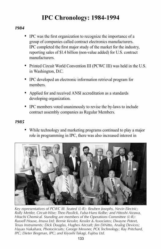
���
IPC Chronology: 1984-1994
1984
• IPC was the first organization to recognize the importance of a group of companies called contract electronics manufacturers. IPC completed the first major study of the market for the industry, reporting sales of $1.4 billion (non-value added) for U.S. contract manufacturers.
• Printed Circuit World Convention III (PCWC III) was held in the U.S. in Washington, D.C.
• IPC developed an electronic information retrieval program for members.
• Applied for and received ANSI accreditation as a standards developing organization.
• IPC members voted unanimously to revise the by-laws to include contract assembly companies as Regular Members.
1985
• While technology and marketing programs continued to play a major role in programming in IPC, there was also increased interest in
Key representatives of PCWC III. Seated (L-R): Reuben Josephs, Nevin Electric; Rolly Mettler, Circuit-Wise; Theo Passlick, Fuba-Hans Kolbe; and Hitoshi Aizawa, Hitachi Chemical. Standing are members of the Operations Committee (L-R): Russell House, Imasa Ltd; Bernie Kessler, Kessler & Associates; Dwayne Poteet, Texas Instruments; Dick Douglas, Hughes Aircraft; Jim DiNitto, Analog Devices; Hayao Nakahara, Photocircuits; George Messner, PCK Technology; Ray Pritchard, IPC; Dieter Bergman, IPC; and Kiyoshi Takagi, Fujitsu Ltd.
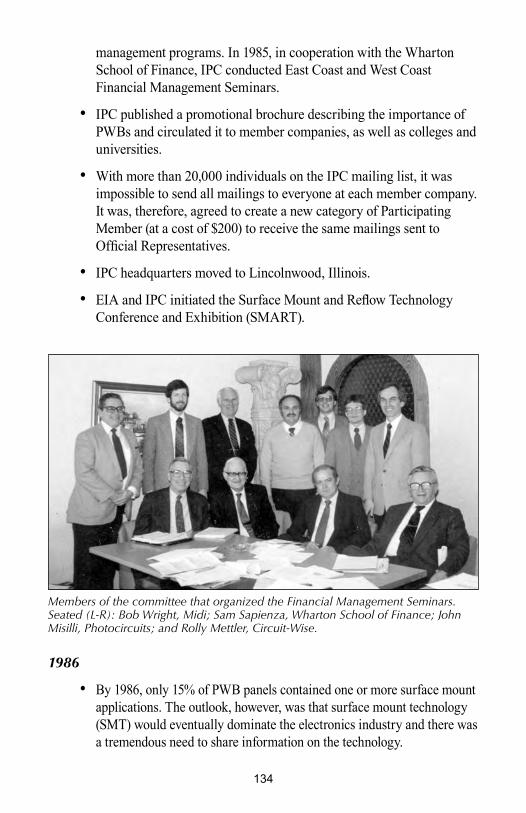
���
management programs. In 1985, in cooperation with the Wharton School of Finance, IPC conducted East Coast and West Coast Financial Management Seminars.
• IPC published a promotional brochure describing the importance of PWBs and circulated it to member companies, as well as colleges and universities.
• With more than 20,000 individuals on the IPC mailing list, it was impossible to send all mailings to everyone at each member company. It was, therefore, agreed to create a new category of Participating Member (at a cost of $200) to receive the same mailings sent to Official Representatives.
• IPC headquarters moved to Lincolnwood, Illinois.
• EIA and IPC initiated the Surface Mount and Reflow Technology Conference and Exhibition (SMART).
1986
• By 1986, only 15% of PWB panels contained one or more surface mount applications. The outlook, however, was that surface mount technology (SMT) would eventually dominate the electronics industry and there was a tremendous need to share information on the technology.
Members of the committee that organized the Financial Management Seminars. Seated (L-R): Bob Wright, Midi; Sam Sapienza, Wharton School of Finance; John Misilli, Photocircuits; and Rolly Mettler, Circuit-Wise.

���
Out of this need, the Surface Mount Council (SMC) was formed in 1986. It was a joint effort between IPC and EIA. The intent of the council was to gather the most knowledgeable experts from EIA and IPC to identify and create programs to overcome the technological barriers to SMT.
• The IPC Long-Range Planning Committee targeted six areas for programming:
• International Standards
• Need to Improve Communications
• U.S. Regional Meetings/Chapters
• International Meetings and Seminars
• Expanding Packaging Activities
• Format for Semiannual Meetings
• For the first time, IPC held meetings in Europe and Asia to review a proposal for a new standard. It was the standard for surface mount land patterns (IPC-SM-782).
• Recognizing that almost 80% of all independent PWB manufacturers had sales of less than $5 million, IPC sponsored management meetings on the East and West coasts aimed directly at the interests and problems of small PWB manufacturers.
• Under the leadership of Maynard Eaves, Hewlett-Packard, IPC published a Quality Evaluation Handbook for PWBs and a comprehensive series of slides.
1987
• Printed Circuit World Convention IV (PCWC IV) was held in Tokyo, Japan.
• IPC surveyed membership interest in Europe and followed up with a meeting in Zurich to discuss how IPC could best serve European members.
• Working with the International Society of Hybrid Microelectronics (now called IMAPS), IPC initiated the Hybrid Marketing Research Council to develop market statistics and technology trends.
• IPC determined that there should be an expanded structure for technical activities to provide a separate section for interconnections and packaging.

���
1988
• Two lawsuits were filed against 20 IPC PWB manufacturing companies contending that materials in the laminate (fiberglass) caused cancer. IPC organized legal counsel from all 20 companies to act in concert to defend these suits. Because of this strong cooperative effort, both suits were dropped.
• DoD 2000 series of soldering standards was a significant step in aligning the multiple standards developed by various government agencies. IPC sponsored workshops throughout the country with representatives from government and industry to reach agreement on the DoD soldering specifications.
1989
• In 1989, EPA undertook research to replace chlorofluorocarbons (CFCs) and sought experts to develop appropriate evaluation and testing programs. IPC volunteered to conduct these studies and developed a benchmark testing program to evaluate alternatives to CFCs for assembly defluxing.
• Cooperated with DoD on future standards using statistical process controls (SPC) rather than end product performance.
The members of the initial group of experts who served on the Surface Mount Council. Seated (L-R): Mike Busby, Interconics; Owen Layden, U.S. Army; Ray Prasad, Intel; Dieter Hauser, KDA Speer; Whit Ackerman, Universal Instruments; Don Mitchell and Max Moore, EIA; and Chairman Dick Rahill, Corning. Standing (L-R): Dean McKee, Naval Oceans Systems Center; Mike Lazar, Burndy; Ken Hafften, Bureau of Engraving; Phil Marcoux, AWI/SCI; Dieter Bergman, IPC; Gerald Fehr, LSI Logic; David Nixen, Aerospace Corporation; Foster Gray, Texas Instruments; Stephen Hinch, Hewlett Packard; Ray Pritchard, IPC.

���
• Published, in cooperation with the EIA and American Society for Testing Materials (ASTM), a joint document on Standardization and Implementation Requirements for Fine Pitch Technology.
• IPC held the second joint U.S./European meeting, in cooperation with the EIPC and the Printed Circuit Interconnection Federation (PCIF), in Denmark.
• Shearson Leahman published a scathing research report on the U.S. PWB industry which set in motion a series of management programs designed to blunt the report.
1990
• Ending an era, Ray Pritchard retired. Thomas Dammrich replaced Pritchard as IPC’s Executive Director.
• Printed Circuit World Convention V (PCWC V) was held in Glasgow, Scotland.
• Work began on the creation of the World Federation of PWB manufacturers. A meeting was held in September in the U.K., attended by representatives from IPC, the JPCA, and the following European organizations: EIPC, PCIF, and Verband Der Deutschen Leiterplattenindustrie BV (VdL).
IPC leadership (L-R): Ray Pritchard,Thom Dammrich, and Larry Velie, President of IPC.

���
• A new program, “Audit for Excellence,” was launched by IPC for PWB manufacturers. This program included a series of audited criteria. Individual companies could then measure how their company compared to others in the industry. Later in the year, this program was renamed “Excellence Through Leadership,” which outlined 14 separate categories for leadership.
• Cooperated with MIT School of Management to study inter-firm relationships between PWB manufacturers, their customers, and PWB suppliers.
1991
• In 1991, IPC began in earnest to develop a presence in Washington, D.C. to represent member interests in legislation and regulatory activities.
• IPC participated with the National Association of Metal Finishers (NAMF) in the first Capitol Hill Day. Members, during the day, met with U.S. senators and congressmen to begin the long journey of making these representatives familiar with the industry.
• In recognition of IPC’s need to play a stronger role in legislation but also environmental issues, R. Wayne Sayer was retained as the official Washington-based Government Relations Consultant. It was further decided that IPC would henceforth hold its own Capitol Hills Days.
Retiring IPC President Bill Miller, Prestwick Circuits (at the podium) presented the 1990 President’s Award to these industry experts. Seated (L-R): Mikel Harry, Motorola; Laura Turbini, Georgia Institute of Technology; Joe Felty, Texas Instruments; Art Mabbett, Mabbett-Capaccio & Associates; and Leslie Guth, AT&T. Standing (L-R): Happy Holden, Hewlett-Packard; Gary Ferrari, Tech Circuits; Walt Custer, Dynachem; William Jacobi, Jacobi & Associates; and Charlie Brooks, AMP. Other receipients not shown were Lutz Treutler, Comargus; Bill Kenyon, DuPont; and Vince Gatto, Tyco Printed Circuit Group.

���
• Approved a $10,000 contribution to the California Circuits Association (CCA) for their efforts to fight unreasonable environmental legislation in California.
• The IPC Board of Directors received approval from the members for a new Mission Statement:
The IPC is a United States based trade association dedicated to furthering the competitive excellence and financial success of its members worldwide, who are participants in the electronic interconnect industry.
In pursuit of these objectives, the IPC will devote resources to management improvement and technology enhancement programs, the creation of relevant standards, protection of the environment, and pertinent government relations.
The IPC encourages the active participation of all its Regular, Allied, and Associate Members in these activities and commits to full cooperation with all related national and international organizations.
• The EMS Management Council determined that a more appropriate identity for contract assembly companies needed to be created. They correctly believed the industry would expand their services from consignment to turnkey and then to system build. They created and popularized the new name: the Electronics Manufacturing Services Industry (EMSI). Wall Street welcomed this new name change, which helped reposition the industry to the investment community.
• The Board reviewed 91 separate ideas for expanding IPC programs. These ideas were organized into nine categories:
• International Program
• Membership Definition
• Management Programs
• The Need for Excellence
• Environmental Issues
• Understanding Members’ Needs and Cooperation with RelatedGroups
• Statistical Process Control (SPC) Programs
• Technology Requirements
• Meeting Structure

��0
• IPC was invited to join the Electronics Roundtable, composed of key representatives of the major electronics industry associations that provide a focus and direction for public policy activities of the U.S. high technology community.
• IPC was named administrator for OZONET by ICOLP (International Cooperative for Ozone Layer Protection) because of our ability to provide electronic information retrieval. This was a joint project to provide a worldwide resource on eliminating the use of CFCs.
• IPC participated as a co-sponsor with EIA, Surface Mount Technology Association (SMTA), and Miller Freeman in presenting the first Surface Mount International (SMI) conference and exhibition in San Jose, California. The initial conference and exhibit was a success with 432 booths and more than 4,000 attendees. The event merged the IPC and EIA Smart Conference with the SMTA and Miller Freeman SMTA conference and exhibition.
1992
• To help members address the growing influence of ISO 9000, IPC published the General Requirement for Implementation of ISO 9000 Quality Systems.
• IPC held third European Joint Technical Conference in Brussels, Belgium.
• IPC published the results of the first comprehensive IPC Benchmarking Study, providing participants with an opportunity to measure their capabilities against the “best” companies in a wide variety of technical and management categories.
• Translated and published a 194-page JPCA report on The Printed Circuit Industry in Japan.
• Officially formed the IPC Designers Council to meet the needs of individual designers and support better design for manufacturability throughout the industry. Today, the IPC Designers Council, with more than 1,000 members and 33 chapters, is an international network of designers. Its mission is to promote printed board and printed board assembly design as a profession and to encourage, facilitate and promote the exchange of information and integration of new design concepts through communications, seminars, workshops and professional certification through a network of local chapters.

���
• Introduced a bi-annual wage and salary study for the EMS members.
• Released an IPC “Book-to-Bill” ratio for U.S. PWB manufacturers. The book-to-bill ratio could be used as one of the predictors for the industry and is still watched closely by financial analysts today.
• Wanting increased influence and programming within IPC, the PWB Suppliers held an organizational meeting in San Jose. Dan Feinberg, Morton Electronic Materials, was selected as the first chairman of the IPC PWB Suppliers Management Council. Initial priorities of the council identified during the meeting were as follows:
1 Getting the most for their “trade show buck”
2 OEM-Technology Interchange
3 Recycling
1993
• IPC, with the support of the PWB Suppliers Council, announced plans for the first IPC Printed Circuits Expo® to be held in 1994 in Boston. A trade show subcommittee of the Council created a revolutionary philosophy for the event: fair, focused and cost effective by and for the industry.
• To serve the electronics assembly industry’s need for market research and technology trends, IPC launched the Assembly Marketing Research Council (AMRC). The Council was patterned after the highly successful TMRC. The first meeting was held jointly with TMRC in New Orleans in December.
Key participants in IPC government relations activity. (L-R): R. Wayne Sayer, IPC Govt. Relations Rep.; Sam Altschuler, Altron; Pat Sweeney, Hadco; Thom Dammrich, IPC; Mary Vessely, aide House Armed Services Com.; Ron Underwood, Circuit Center; and David Lovenheim, Northeast Midwest Institute.

���
• IPC, recognizing the importance of providing the industry with the requirements for future technology, held a workshop in Chicago to begin work on development of the Technology Roadmap. The IPC Technology Roadmap is still published today and made available at no charge to IPC members.
1994
• 1994 marked a major event in the history of IPC — the opening of IPC Printed Circuits Expo in Boston. More than 1,700 people attended IPC Printed Circuits Expo, which featured 275 booths representing 158 companies.
This was not simply an exhibition, however; the event reflected a major effort to provide technology exchange within the industry. IPC Printed Circuits Expo featured more than 60 technical papers, 17 workshops, and nearly 100 committee meetings to develop standards for the industry.
• IPC established the Interconnect Technology Research Institute, (ITRI), to be headed by D. Marshall Andrews. This was a key recommendation of the IPC Technology Roadmap released in 1993. To keep pace with international technology, it was clear that the U.S. PWB manufacturing industry needed a practical forum to undertake cooperative technical research.
• Implemented the first IPC certification and training program based on IPC-A-610B, Acceptability of Electronic Assemblies. Today, IPC-A-610 training is now conducted in many languages around the world, and has a user base of more than 10,000 instructor certifications. These instructors, in turn, have trained nearly 125,000 engineers, operators, inspectors, buyers and members of management teams. In addition, this certification program spawned a number of other IPC certification efforts.
• The IPC Designers Council made plans for a new certification program for designers as a means to improve the education and stature of designers in the electronics industry.
• IPC video expanded into interactive multimedia production on CD-ROM, allowing students to learn at their own pace.
• IPC staff became accessible by e-mail.

���
Chapter 7: The Environment and the Future
If we wish to make a new world we have the material ready. The first one, too, was made out of chaos.
— Robert Quillen
Eliminating CFCs and the Montréal ProtocolThe Montréal Protocol on Substances that Deplete the Ozone Layer
was one of the first international agreements made to restrict human activities that were damaging to the environment. Its goal is to reduce and eventually eliminate the emission of ozone-depleting chemicals. The initial document was signed by twenty-four countries on September 16, 1987. Since then, amendments have been made on two occasions, the London Amendment in 1990 and the Copenhagen Amendment in 1992. There are currently 175 countries that have committed themselves to the goals of the Montréal Protocol.
The Montréal Protocol identifies various halocarbons, the chemicals that hasten the decomposition of stratospheric ozone. They include chlorofluorocarbons (CFCs), tetrachloride, hydrochlorofluorocarbons (HFCFs), and methyl bromide. By limiting the production and use of these chemicals, the goal of the Protocol is the eventual elimination of all emissions of these chemicals. Within the document is a clause that allows developing countries another ten years to comply with the control measures, so long as the per capita use of the halocarbons remains sufficiently low.
Early Research on Stratospheric Ozone
Research on the ozone layer began as early as the 1930s. In the 1970s, concerns arose that stratospheric transport aircraft might damage the ozone layer. It was at this time that the theory was proposed on the role of chlorofluorocarbons (CFCs) in the depletion of the ozone layer. At the time, CFCs were used in refrigeration, aerosol cans, and some industrial processes. Initially greeted with a great deal of skepticism, further research and monitoring began to convince the scientific community the CFC hypothesis might be valid.1
The Road to Montreal
In 1977, the Coordinating Committee on the Ozone Layer was established by the United Nations Environment Programme (UNEP), and UNEP’s Governing Council adopted the World Plan of Action
���
on the Ozone Layer. In the late 1970s and early 1980s, some national governments, including the United States, Canada and Scandinavian countries, imposed bans on CFCs as aerosol propellants in non-essential uses: antiperspirants, hairsprays and deodorants.
The period between the Vienna Convention (March 1985), and the Montreal Protocol (September 1987), was characterized by incredible progress. The global scientific community reached consensus on outstanding matters, while meetings were held in Rome to clarify and quantify the current global emissions of ozone-depleting substances and future trends, and new mechanisms for control were discussed.
By September 1987, the disagreements and lack of understanding had given way to trust. In turn, the trust offered the prospect of consensus on control measures. Thus it was on September 16, 1987 that the Montreal Protocol on Substances that Deplete the Ozone Layer was signed by 24 countries.
On January 1, 1989, the Protocol came into effect. All Parties agreed to meet near-term targets of freezing consumption of key CFCs and halons at 1986 levels, and reducing consumption by 50% within 10 years.
The list of states that have ratified the Protocol has now grown to 175. Since 1992 at the Second Meeting of the Parties in Copenhagen, the Parties have adopted a number of significant amendments, including an expanded list of regulated substances and the introduction and subsequent acceleration of actual phase-outs for regulated substances. For example, at the Ninth Meeting of the Parties in 1997 in Montreal, the Parties decided to accelerate the phase-out of methyl bromide. In 1999, at the Eleventh Meeting of the Parties in Beijing, the Parties decided to add bromochloromethane to the list of controlled substances and to ban its production and consumption by 2002. The use of CFCs and halons has decreased dramatically. Many countries are well ahead on other Montreal Protocol targets, and there is evidence that concentrations of CFCs in the lower atmosphere have begun to drop.2
Impact on the Electronics Manufacturing IndustryThe impending ban on CFCs, HCFCs, and the like created a storm
of controversy within the electronics manufacturing industry that in some ways anticipated the RoHS firestorm that was still in the future. In the late 1980s, working as a process engineer for a small electronics manufacturing company off Massachusetts’ I-495 belt, I [Martel] recall how virtually all of our solder pastes for SMT assembly contained

���
“water-white rosin” based fluxes. I thought this curious, since the flux really was amber-colored and hardly water-white. But it was a natural product, true rosin, and the most effective way of cleaning it at the time was to use a vapor degreaser filled with Freon solvent based on methylene chloride. It was common to have the used cleaning solution reprocessed, as drums of reprocessed material were less costly than new drums of fresh solvent.
With the protocol, vapor degreasers, methylene chloride, Freon, and the like began to be phased out. Other cleaning methods such as saponifier baths with water rises were used, but with far less success than the results that had previously been delivered by Freon solvents. Some applications (non-military, non-hi-rel) allowed fluxes to be left on the board, sometimes referred to as a “poor man’s conformal coating.” Surface Insulation Resistance (SIR) problems, dendrite growth in high-humidity environments, and other factors disallowed this for most electronic assemblies, however. This thinking, however, led to the development of no-clean fluxes. If one could only develop fluxes that became effectively inert after processing, they could be left on most boards, it was reasoned. Water-based cleaning was also tried for some water-soluble fluxes but, in many cases, these proved to be unsuitable for the SMT process and for the formulation of solder pastes. The powerful activity of these fluxes would quickly deteriorate the solder particles, or oxidize them, reducing shelf life dramatically, or would turn them brick-hard while still in the jar.
The solution, ultimately, was the development of no-clean fluxes, now in use today virtually across the industry. Some hi-rel applications such as military electronics still require cleaning, but no-clean fluxes have penetrated virtually every segment of electronics assembly. The development of synthetic rosin technology has further improved the activity of these fluxes as well as product shelf life for solder pastes. Synthetic based fluxes are more tolerant of high heat, especially the higher temperatures required for lead free solders. In the beginning, users found quickly that not all no-clean formulations were compatible. For example, an assembler using Company A’s no-clean solder paste might use Company B’s no-clean cored wire flux for touch-up; when the two fluxes mixed, a highly corrosive residue could sometimes result! These incompatibilities were corrected, and by 2000, virtually every supplier of soldering materials could offer high-performance, superior no-clean products. The era of CFCs in electronics manufacturing was officially over.

���
Going Green: The Emergence of RoHS and WEEEThe European Union (EU) adopted a requirement, going into effect
July 1, 2006, to reduce the use of hazardous materials in consumer electronics products in order to limit the amount of these substances that end up in landfills. “The Restriction of the Use of Certain Hazardous Substances in Electrical and Electronic Equipment Regulations,” abbreviated as RoHS, is one more step in what is likely to be an increasing trend of environmental requirements that will affect all manufacturing worldwide.2
Market drivers for “environmentally friendly” products have been prevalent for some time, but most were not legislated. In the last few years, the need to produce environmentally friendly products has shifted from a consumer-led initiative to a legal requirement. The European Union is spearheading the charge for green products by being the first to adopt legislation. RoHS is based on broader regulations governing the recycling of waste electrical and electronic equipment (WEEE, also used to refer to the legislation itself), but RoHS specifically identifies six key materials whose use is to be strictly limited. Several other countries, including the U.S., Japan, and China are adopting similar environmental regulations.
RoHS impacts any company that: manufactures and sells, resells, imports, or exports electrical or electronic equipment. Products not meeting the criteria of the RoHS directive won’t be allowed on the market in the European Union’s 25 member states, threatening significant revenue loss for those not able to comply. The manufacturer, as the producer of the electronic product, is responsible for ensuring that its products contain controlled concentrations of the six substances restricted by the Directive:
• Lead
• Mercury
• Cadmium
• Hexavalent chromium
• Polybrominated biphenyls (PBB)
• Polybrominated diphenyl ethers (PBDE)
At the time of this writing (end of 2006), however, a vast majority of electronics manufacturers worldwide have not met the deadline, and the implementation of RoHS is causing significant product reliability problems, some of them related to tin whisker growth, especially in all

���
manner of products from wristwatches to avionics. Exemptions to RoHS are multiplying, and RoHS has been referred to by a variety of industry notables, including Indium Corporation’s Dr. Ron Lasky, as “The most disruptive event in the history of electronics.”
The first draft of the RoHS directive appeared in 2000, although there had been rumblings prior to that, such as the 1988 EU Council Resolution to invoke a Community action program to combat cadmium pollution, and the 1996 Review of EU strategy for waste management that identified the need to reduce certain hazardous substances. Electronics manufacturers began exploring alternative alloys and process requirements prior to 2000 and, in the more than six busy years since, volumes have been written, billions have been spent on research and technology, and an incredible amount of effort has been spent to implement the RoHS directive. New alloys and flux systems for soldering have been developed; new processes developed and proven; and the science of lead free soldering has advanced a great deal, but the volume of problems associated with lead free soldering has been staggering.
The higher temperatures required for lead free processing has meant the necessity of replacing nearly all existing soldering machines in manufacturing facilities worldwide. It has required the changing of inventories of parts to lead free finishes, development of synthetic fluxes to survive the higher heat, as well as costly process modifications. In the end, lead free assemblies are still prone to tin whisker growth, poor wetting/soldering results, and other problems. A new family of lead free solders has emerged, led by the popular SnAgCu (“SAC-alloys”) group. There is too much to this story to recount here; however, the last chapter in the global conversion to lead free electronics manufacturing has yet to be written. The controversy surrounding RoHS, as well as the pressure for repeal or added exemptions remains strong; certain types of military, aerospace, and medical products (among others) are exempt from the requirement and the range and scope of these exemptions is likely to increase.
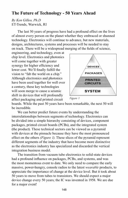
���
The Future of Technology - 50 Years Ahead
By Ken Gilleo, Ph.DET-Trends, Warwick, RI
The last 50 years of progress have had a profound effect on the lives of almost every person on the planet whether they embraced or shunned technology. Electronics will continue to advance, but new materials, designs, architectures, systems and processes will be needed to stay on track. There will be a widespread merging of the fields of science, engineering, and technology, even at chip level. Electronics and photonics will come together with greater synergy for higher efficiency and lower cost. We’ll finally fulfill the vision to “fab the world on a chip.” Although electronics and photonics have been used together for well over a century, these key technologies will soon merge to cause a seismic shift in devices that will profoundly affect packaging and printed circuit boards. While the past 50 years have been remarkable, the next 50 will be incredible.
We can better predict future events by understanding the interrelationships between segments of technology. Electronics can be divided into a simple hierarchy consisting of devices, component packages, printed circuit boards (PCBs), and the integrated system (the product). These technical sectors can be viewed as a pyramid with devices at the pinnacle because they have the most pronounced effect on the others (Figure 1). These slices of the pyramid represent different segments of the industry that have become more distinctive as the electronics industry has specialized and discarded the vertical integration business model.
The transition from vacuum tube electronics to solid-state devices had a profound influence on packages, PCBs, and systems, and was the most momentous event to date. We only need to compare the early massive, power-hungry, console radios to the latest wearable products, to appreciate the importance of change at the device level. But it took about 50 years to move from tubes to transistors. We should expect a major device change every 50 years; the IC was invented in 1958. We are due for a major event!
Figure 1
���
A Century of ProgressSurprising perhaps, the challenges for the next 50 years are more or
less the same as those of the past 50. In fact, the goals and challenges have not really changed since the beginning. Throughout the First Century of Electronics, scientists and technologists were tasked with grand challenges that remain as guideposts as we travel into the future. These key criteria are the following:
Grand Challenges
• Density (smaller)
• Performance (faster)
• Cost - value (cheaper)
• (Addition of other technologies to electronics at the device level)
These fundamental challenges can be applied to our basic segments shown in the pyramid; the device, package, printed circuit, and total system. Density has been at the top of the task list from the beginning - even when the original “high tech” products, like the telegraph and telephone, were based on electricity. High tech began, at least for our purposes, as the Telecom Revolution launched in the late 1800s. This incredible revolution continues today, and telecom has moved to the top as the most important driver for technical advancement. The first printed circuit patent set the stage by defining the first goal, “…it is desirable to have a large number of conductors… within very small compass….” The same statement is equally true today! Expect future advances to replace copper - the king of conductors, eliminate silicon - the incumbent semiconductor, and to even replace the venerable electron as the workhorse messenger. Solder, the 7,000-year old “glue of electronics” will also be retired. Indeed, we are in for serious disruptive changes.3-6
Let’s begin with the device, with its top-of-the-pyramid, high-leverage position. Today’s marvelous semiconductor technology enables hundreds of millions of transistors to be crafted on a single postage stamp-size chip usually made from silicon and its compounds. The semiconductor industry continues to increase density in many ways; however, silicon-based devices will eventually fall short as demands continually increase. Many scientists have high hopes for fundamentally new device technology that will meet needs far into the future. These include Nanoelectronics, quantum devices, molecular electronics, single-electron switches, photonic logic engines, and even bio-centric computational machines.
��0
Beyond SiliconAlthough Nanoelectronics may be the next big technology, there are
other contenders that are fundamentally different. Nanoelectronics, even if it employs non-silicon materials, is following the “silicon blueprint.” They will probably operate using the same principles as today’s silicon-based ICs. The end result will be more dense and powerful chips, but there may not be much change for the other electronic segments. Present packages and PCBs will probably be adequate. We need to include all-photonic and bio-centric computers in our future tech list. Over the next 20 to 30 years, we can expect success for all-photonic computing technology, where photons replace electrons in a fundamentally different system. We’ve become so accustomed to charge-based logic and memory technology, that other viable approaches have been ignored. Consider that the human brain employs principles that are much different from today’s IC mechanisms. But there is an intermediate step to consider, where electrons handle logic and memory functions and photons will deal with data transmission. We must keep in mind that what happens outside of the chip is just as critical as what happens within. The chip must be efficiently connected to the outside world.
Silicon PhotonicsThe chargeless photon is the most important information messenger
for the Internet, telephones, wireless, etc. Photons carry a wealth of information but have not yet succeeded in solid-state logic and memory devices. So it makes sense to develop a hybrid IC where electronics are used for computations and photonics take on the messenger task. Internet and telephone hardware were designed to partition the computation/data transmission tasks allowing the photon to handle medium and long-distance transmissions while electronics were retained for switching and control. The world is connected by “optical wires.” The data-laden photons race along glass optical fiber links that circle the globe as underground and submarine cabling. Photons travel through a single thin glass fiber at the speed of light and can carry about 1-million times more information than electrons using a copper wire. Nothing beats the photon for bandwidth and the reasons are due to the fundamental differences of charged electrons vs. neutral wave-differentiated photons. Remarkably, hundreds, or even thousands, of different wavelengths can independently travel through the same thin (9-micron) fiber. Photonics can send hundreds, or even thousands of different wavelengths through a single fiber using powerful wave division multiplexing (WDM) since photons are relatively non-interactive. Could this mega-bandwidth

���
method eliminate the “copper bottleneck” that limits chip-to-chip data transfer by electrons?
The final breakthrough, in a succession of many, occurred when the team built the world’s first electrically powered Hybrid Silicon Laser using standard silicon manufacturing processes. The Internet uses rather expensive modules built from discrete components. These researchers were able to marry light-emitting Indium Phosphide (InP) to silicon (Si). The InP and Si layers were combined by wafer-level bonding. Since silicon is transparent to the wavelengths used, it can be fabricated with light-manipulating capabilities such as channels, waveguides, prisms, splitters and frequency-separating diffraction gratings. MEMS fabrication methods could also be used to produce optical structures in silicon. Application of voltage to the InP laser structure produces infrared “light” that travels through the silicon waveguide to create a laser beam that can drive other silicon photonic devices. So we can expect hybrid chips, especially the CPU, to move into the mainstream during the next 4 to 10 years (see Figure 2).
But how will the hybrid chip affect packaging and printed circuits? The chip package will need to provide optical pathways. The photonic-capable PCB will also need optical paths, or at least be able to handle optical fiber connections. Assembly could require precision alignment. Silicon Photonics will require much closer interaction and cooperation between semiconductor, package and board designers, something that has already begun and is referred to as “concurrent design.”
Fortunately, many researchers, developers and designers have been working on photonic linkage for many years and a number of concepts have emerged. Concurrently, the photonic Internet in our Net-centric world, will gradually replace copper wire links with wireless and fiber-to-the-home (FTTH). Several large providers now offer fiber connections. The photonic hybrid computer chip will eventually connect directly to the Internet by fiber for incredible speeds making trips even faster and cheaper — and hopefully, friendlier. We can expect Internet bandwidth to surpass the 100 Gigabit/second mark in another decade.
Figure 2

���
Future communications will depend more and more on photons. Copper wire communications will go the way of the telegraph, but never completely disappear. Wireless will continue to play an increasing role for short-range links, but please note that both light waves and radio waves are part of the same electromagnetic spectrum. The basic difference between light waves and radio waves is frequency (inversely proportional to wavelength).
NanoelectronicsAlthough photonically-linked silicon chips will become available
relatively soon, silicon will inevitably run out of gas within the next two decades, even with help from photons. Nanoelectronics is listed on virtually every roadmap and substantial investments in Nanotechnology make it highly probable that efforts will succeed. But first, a clarification of terms for over-hyped and chaotically-described “nano.” Many materials and structures are in the nano-scale range (1 to 100 nm), but this does not necessarily mean that they fit into Nanotechnology.
Our amazing semiconductor lithography, that can craft structures falling right in the middle of the nano-scale range (~50-nm), is still traditional electronics. While our present semiconductor fabrication technology is extraordinary, it is still a clumsy “stone chiseling” process compared to the more optimum device structures of the future. Some believe that the ultimate electronic devices should be built atom-by-atom or “bottom up.” But the more prominent and successful “Top Down” approach, where structures are synthesized or constructed by removing existing material from larger entities, is much closer to success.
Carbon-based chemistry, the same chemistry used to construct the human brain, has taken the lead in Nanoelectronics. The carbon nanotube (CNT) transistor, a semiconductor device made with this pure carbon molecule, is the most likely replacement for silicon. IBM, and others, succeeded in making CNT transistors several years ago, and major efforts are now focused in this area. Researchers are moving closer to building a CNT-based integrated circuit (CNT-IC) that could be ready for production by 2020, but perhaps sooner. But there are hosts
Carbon nanotube (CNT) transistor
���
of other candidates for non-silicon electronics including single-electron devices and others that can be classified as molecular electronics. Whatever the winning technology, we will most certainly move “beyond silicon” in less than two decades.
Beyond ElectronicsSometime within the next 50 years, we can expect a full-photonic
computer, not to be confused with photonically-linked chips, to compete with, and perhaps replace, electronic designs. Concurrently, a more complete understanding of DNA and the brain structure at the molecular-level, can lead to the long-envisioned bio-computer. Even today, considerable research is aimed at connecting electronic chips to the human body, including neural centers. Simple “thought-controlled” computer experiments are succeeding and advancing. But perhaps we’ll merge logic technology with humans to enter the age of bionic enhancement that began many years ago. While bionic beings have been the theme of fiction writers, and the dream of some scientists, brain enhancements may be on the horizon. But do we even need hardware? The ultimate personal technology may be DNA modification that enables the mind to perform most of the functions now provided by our wearable electronics. The choices come down to external hardware, implants, or genetic engineering. In the next 50 years, the bioengineering of humans could provide extreme memory enhancement, a boost in left-brain computational capability (like savants), and the ability to receive and send data by RF. Many life forms can sense external energy forces, including regions of the electromagnetic spectrum, well beyond the range of humans. For better or for worse, we will have the knowledge to re-engineer humanity.
More than Just ElectronsWe tend to think of high tech as electronics only, but most products
incorporate other technologies, especially mechanics and optics. Our favorite gadgets typically use all three. Even the cell phone combines these technologies in the form of video displays, cameras, flash lamps, sound systems, pedometers and digital input means. But what if we could combine them on a single chip? We don’t have to wait for the future — the concept is here today. MEMS (Micro-electro-mechanical systems) combine clusters of technologies into a microchip. The optical version, MOEMS (add opto-), or call it optical MEMS, is a subset that adds light control and other optical features to electronics and mechanics. But while MEMS has been around for years, in simple forms
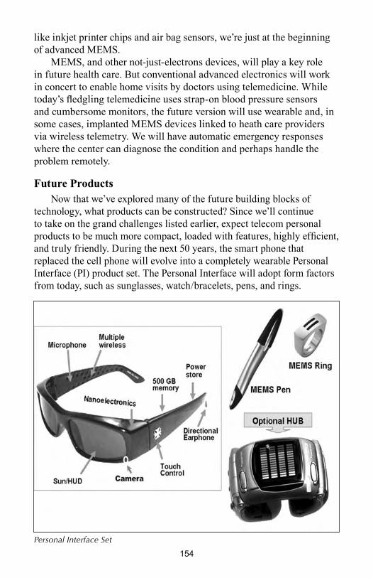
���
like inkjet printer chips and air bag sensors, we’re just at the beginning of advanced MEMS.
MEMS, and other not-just-electrons devices, will play a key role in future health care. But conventional advanced electronics will work in concert to enable home visits by doctors using telemedicine. While today’s fledgling telemedicine uses strap-on blood pressure sensors and cumbersome monitors, the future version will use wearable and, in some cases, implanted MEMS devices linked to heath care providers via wireless telemetry. We will have automatic emergency responses where the center can diagnose the condition and perhaps handle the problem remotely.
Future ProductsNow that we’ve explored many of the future building blocks of
technology, what products can be constructed? Since we’ll continue to take on the grand challenges listed earlier, expect telecom personal products to be much more compact, loaded with features, highly efficient, and truly friendly. During the next 50 years, the smart phone that replaced the cell phone will evolve into a completely wearable Personal Interface (PI) product set. The Personal Interface will adopt form factors from today, such as sunglasses, watch/bracelets, pens, and rings.
Personal Interface Set
���
Health care, or wellness maintenance, is another big area for future technology. Medical electronics will reach high plateaus to help bring a new era to personalized medicine. Although DNA “adjustments” will help reduce hereditary disorders, not all diseases will be eliminated. Efforts will focus on early detection and intervention. Electronics, Optronics, Bio-MEMS, and Nanotechnology will help identify cautionary pre-conditions early, even before they can be called health problems. These technologies will also help contain costs as medicine moves from the hospital, to the clinic, to the doctor’s office, and finally to the home. Telemedicine will be used as the primary method of evaluation so that individuals can have routine check-ups at home or from the near by cyber-office. Within the next 50 years, implants will be able to analyze and treat, with drugs and other means. There will also be wellness agents that can be injected by syringe. A mobile MEMS device team may “swim” through your circulatory system and routinely remove plaque, growths, or anything that could develop into a problem. The mobile MEMS devices will use lasers, mechanical surgical tools, and drugs. In the future, doctors will make house calls without leaving the medical center. And health care micro- and nano-agents will work tirelessly — internally and invisibly, generating self-sustaining energy from body chemistry.
ConclusionsWe have reached a point of no return for technology. The future
world cannot exist without technology and would catastrophically collapse. But, technology must continue to advance to keep pace with problems — some of which are created by technology itself.
The future will be exciting but some will mourn the loss of favorite technologies. Copper will be replaced by organic molecules, solder will make way for reconnectable technologies, including Lego®-like structures and micro-Velcro®, and circuit boards will no longer be etched. For those who embraced emerging technology for the past 50 years, get ready — the next 50 will really be something. Thanks to medical advancements, we might all be here to watch it unfold. Finally, to those who are new to the tech game, you are in for a thrilling half-century of progress, but don’t just be a spectator.

���
Sources
1., 2. The Montreal Protocol: History, www.ec.gc.ca/press/001219_b_e.htm
3. Hanson, A., British Patent 4,681, 1903.
4. Gilleo, K., “First 7000 Years of Soldering - Part 1 - Metallurgy,” Circuits Assembly, pp. 30-34, October 1994. Used with permission from Circuits Assembly/UP Media Group.
5. Gilleo, K., “First 7000 Years of Soldering - Part II- Polymers,” Circuits Assembly, pp. 44 - 45, November 1994. Used with permission from Circuits Assembly/UP Media Group.
6. Gilleo, K., “The 7,000 Year Cycle,” Circuits Assembly, Vol. 16, June 2005. Used with permission from Circuits Assembly/UP Media Group.

���
IPC Chronology: 1995-2006
1995
• With the increasing growth in IPC programming, IPC outgrew its building in Lincolnwood, Ill. In 1995, IPC moved to new headquarters at 2215 Sanders Road, Northbrook, Illinois.
• To enhance the executive director’s ability to work with peers in Washington, D.C., the Board revised the titles of key officers of IPC. The title of the chief elected officer was changed from president to chairman of the Board of Directors. The title of the executive director was changed to president.
• ITRI released its first technical report: Improvements/Alternatives to Mechanical Drilling of PWB Vias.
• Membership in IPC hit an all-time high. Two thousand companies/divisions of companies located in more than 50 countries were members of IPC in 1995.
• Over 100 IPC members participated in the development of a Long Range Strategic Plan approved by the Board in March 1996. The Long Range Plan defined five specific strategies to carry IPC into the new millennium:
• Industry Leadership
• Workforce Development and Training
• Industry Standards/Technical Assistance
With increasing interest in PWB developments in China, IPC sponsored a tour of PWB plants in Beijing and Shanghai. Additionally, tour participants attended the China Printed Circuit Association International Printed Circuit Technological Equipment Exhibition in Shanghai.

���
• Communications, Networking and Participation
• Global Involvement to Benefit Members
• IPC was awarded a grant from the state of Illinois along with Northwestern University to create an Illinois Electronics Manufacturing Extension Center to aid Illinois manufacturers.
• In recognition of the excellence of IPC standards, the Department of Defense adopted IPC-J-STD-001, J-STD-004, J-STD-005 and J-STD-006.
• Due to increasing interest in the growth and development of China, IPC sponsored a tour of PWB plants in Beijing and Shanghai. In addition, participants in the tour attended the China Printed Circuit Association International Printed Circuit Technological Equipment Exhibition in Shanghai.
1996
• Printed Circuit World Convention VII was held in May, so that once again technology and management executives from around the world had an opportunity to exchange ideas and information. In addition to the technical paper sessions and the special management sessions for PWB company presidents, there was a “first time” session for representatives from worldwide organizations to discuss details regarding the size and scope of the PWB markets in all major countries.
• IPC was successful in having HR537 introduced by U.S. Representatives Meeham, Farr and Esho. The bill allowed machinery and equipment used in producing PWBs and electronics assemblies to be depreciated in three years instead of five years.
• IPC established a close working relationship with the California Circuits Association and begain staffing the CCA.
• IPC launched its first Web site (www.ipc.org).
• IPC created seven e-mail forums including: TechNet, ComplianceNet and DesignerCouncil. More than 2,000 technologists participate on these forums.
• Completed the first comprehensive benchmarking study on the market for electronics manufacturing services. This information on financial and operating performance provided an opportunity for EMS members to compare themselves to other industry companies.
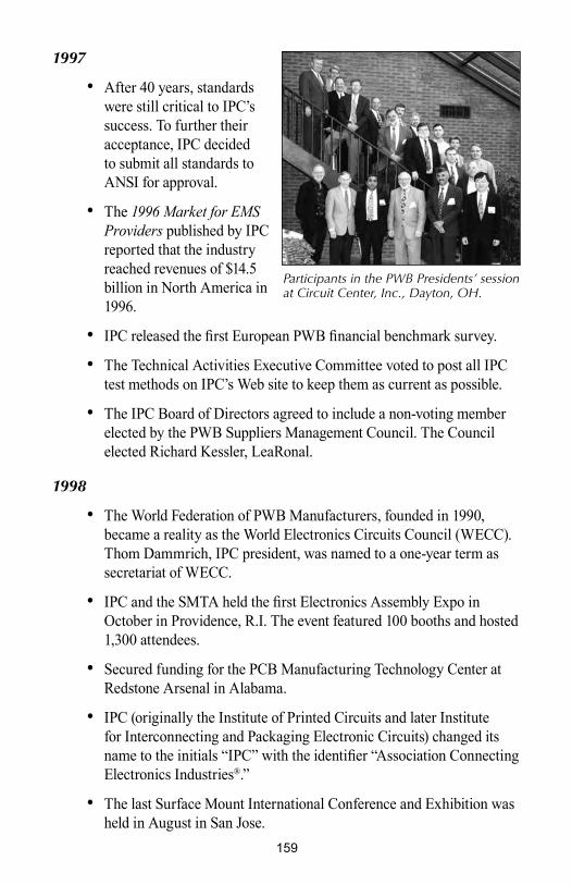
���
1997
• After 40 years, standards were still critical to IPC’s success. To further their acceptance, IPC decided to submit all standards to ANSI for approval.
• The 1996 Market for EMS Providers published by IPC reported that the industry reached revenues of $14.5 billion in North America in 1996.
• IPC released the first European PWB financial benchmark survey.
• The Technical Activities Executive Committee voted to post all IPC test methods on IPC’s Web site to keep them as current as possible.
• The IPC Board of Directors agreed to include a non-voting member elected by the PWB Suppliers Management Council. The Council elected Richard Kessler, LeaRonal.
1998
• The World Federation of PWB Manufacturers, founded in 1990, became a reality as the World Electronics Circuits Council (WECC). Thom Dammrich, IPC president, was named to a one-year term as secretariat of WECC.
• IPC and the SMTA held the first Electronics Assembly Expo in October in Providence, R.I. The event featured 100 booths and hosted 1,300 attendees.
• Secured funding for the PCB Manufacturing Technology Center at Redstone Arsenal in Alabama.
• IPC (originally the Institute of Printed Circuits and later Institute for Interconnecting and Packaging Electronic Circuits) changed its name to the initials “IPC” with the identifier “Association Connecting Electronics Industries®.”
• The last Surface Mount International Conference and Exhibition was held in August in San Jose.
Participants in the PWB Presidents’ session at Circuit Center, Inc., Dayton, OH.

��0
• Driven by IPC, the “Printed Circuit Investment Act of 1998” was introduced in the U.S. House and Senate. Introducing the bill, Florida Senator Connie Mack said: “Printed wiring boards and assemblies are literally central to our economy as they are the nerve centers of nearly every electronics device.” The Act allowed manufacturers to depreciate their equipment in three rather than five years.
1999
• IPC merged with the Surface Mount Equipment Manufacturers Association (SMEMA) to form a new group called the IPC SMEMA Council, an IPC operating division. In addition, IPC amended its by-laws to provide voting representation on the board for both SMEMA and for the IPC PWB Suppliers Council. Gerhard Meese, Universal, joined the Board as the SMEMA Council representative.
• In addition, the Board eliminated IPC membership categories of regular, allied and associate members, resulting in eligibility for the IPC Board of Directors of any individual from any IPC member company.
• TechNet, IPC’s e-mail peer-to-peer forum, surpassed 1,700 subscribers.
• IPC released the GenCam® (Generic Computer Aided Manufacturing) standard, a robust data description format to replace limited Gerber files.
Presidents Meeting at IPC Printed Circuits Expo. (L-R): Rolly Mettler, Circuit-Wise, Dale Blanchfield, Bureau Electronics Group, Stephen Mettler, Circuit-Wise, Joel Yocom, Litchfield, and Ren Sanscrainte, Pentex Schweizer.
���
• Launched a certification program on rework and repair training, based on the IPC-7711 and IPC 7721 assembly rework and repair specifications.
• The Department of Defense cancelled 11 military specifications and authorized their replacement with IPC documents.
• The IPC Board of Directors published a position statement of the growing concern over lead free legislation. The Board’s position: “ … all available scientific evidence and U.S. government reports indicate that the lead used in U.S. printed circuit board (PCB) manufacturing and electronic assembly produces no significant environmental or health hazards. Nonetheless, in the opinion of IPC, the pressure to eliminate lead in electronic interconnections will continue in the future from both the legislative and competitive sides.” A lead free roadmap began at IPC’s fall meeting.
• IPC President Thomas Dammrich resigned to head the National Marine Manufacturers Association.
• 580 designers had, by this time, passed the IPC Designer Certification exam.
2000
• Denny McGuirk, head of the National Fluid Power Association, became IPC’s third president in January.
• IPC launched the SMEMA Council’s Electronics Assembly Process Exhibition and conference (APEX®) at the Long Beach Convention Center in March. 337 exhibitors filled more than 140,000 square feet of floor space and 5,700 attendees visited the exhibition. Retired General H. Norman Schwarzkopf keynoted the event to a standing-room-only crowd.
• U.S. customs officials were trained by IPC to recognize PWBs and substrates, alleviating years of problems with mis-classifications and suspect import data.
• IPC Printed Circuits Expo® attracted 309 exhibitors and 4,200 attendees.
• To keep up with changes, the Technical Activities Executive Committee voted to completely remove test methods from printed standards and post them online instead.

���
• With the rise of the internet, reverse auctions for printed boards appeared, along with internet portals intent on squeezing costs from the supply chain. IPC formed an e-business and Supply Chain Committee to acquaint members with internet supply chain issues. The committee released a white paper, The Myths of E-commerce.
• Published IPC-7095, Design and Assembly Process Implementation for BGAs.
2001
• To avoid millions of dollars in compliance costs for the PWB industry, IPC swiftly organized opposition to the EPA’s Effluent Limitation Guidelines for the Metal Products and Machinery. EPA subsequently abandoned the guidelines.
• PWB shipments for March 2001 decreased 14.6 percent over March 2000 while orders decreased 51.4 percent.
• IPC ended its relationship with its lobbyist in Washington and brought the function in-house with a full time director.
• Due to a need expressed by the EMSI council, IPC launched EMexcess, a searchable database for components.
• The IPC Board voted to close the Interconnection Research Technology Institute, based on a lack of industry support.
Ribbon cutting at the first APEX. (L-R): Bob Balog and Steve DeCollibus, Speedline Technologies; Jim Donaghy, Sheldahl, Inc.; Denny McGuirk, IPC; Bonnie Fena, K-Byte-Hibbing Manufacturing; Gerhard Meese, Universal Instruments; Ron Underwood, Circuit Center; Steve Hall, EKRA America; Stan Plzak, Pensar Corp.; Leo Reynolds, Electronic Systems; and JARA Representative.
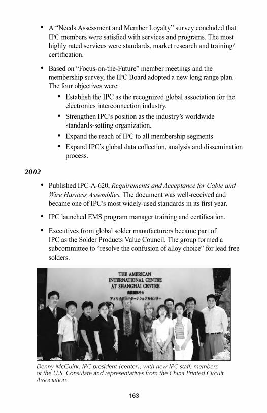
���
• A “Needs Assessment and Member Loyalty” survey concluded that IPC members were satisfied with services and programs. The most highly rated services were standards, market research and training/certification.
• Based on “Focus-on-the-Future” member meetings and the membership survey, the IPC Board adopted a new long range plan. The four objectives were:
•Establish the IPC as the recognized global association for the electronics interconnection industry.
•Strengthen IPC’s position as the industry’s worldwide standards-setting organization.
•Expand the reach of IPC to all membership segments
•Expand IPC’s global data collection, analysis and dissemination process.
2002
• Published IPC-A-620, Requirements and Acceptance for Cable and Wire Harness Assemblies. The document was well-received and became one of IPC’s most widely-used standards in its first year.
• IPC launched EMS program manager training and certification.
• Executives from global solder manufacturers became part of IPC as the Solder Products Value Council. The group formed a subcommittee to “resolve the confusion of alloy choice” for lead free solders.
Denny McGuirk, IPC president (center), with new IPC staff, members of the U.S. Consulate and representatives from the China Printed Circuit Association.

���
• The U.S. Department of Defense adopted IPC-A-610.
• As the industry began to focus on the European Union’s Restriction of Hazardous Substances, IPC and JEDEC jointly organized a conference on lead free technology in San Jose. Nearly 300 technologists attended.
• IPC participated at the third JISSO International Council Meeting in San Jose where technical volunteers from associations from Japan, the U.S. and Europe work to seek agreement on standards adoption and use.
• IPC opened a representative office in Shanghai, China. IPC President Denny McGuirk said “This is the first of many steps IPC plans to take in seeing that our long-range plan comes to fulfillment.”
• Supporting the effort, the U.S. Department of Commerce awarded IPC a grant under its Market Development Cooperator Program. The grant was intended to support IPC’s efforts to promote the adoption and use of IPC standards in China.
• Congress passed realistic depreciation under President Bush’s “Job Creation and Worker Assistance Act of 2002.” The act included a bonus of 30 percent first year depreciation allowance for newly qualified capital investments.
Recipients of Distinguished Committee Service Awards for IPC-2221A, Generic Standard on Printed Board Design (L-R): Lionel Fullwood, WKK Distribution Ltd.; Mike Green, Lockheed Martin Space & Strategic Missiles; Randy Reed, Merix Corp.; Chris Conklin, Lockheed Martin Corp.; Don Dupriest, Lockheed Martin Missiles & Fire Control; and Werner Engelmaier, Engelmaier Associates, L.C.

���
2003
• The Printed Board Process Capability, Quality and Relative Reliability database, a joint effort between IPC and Conductor Analysis Technology, Inc. continued to gain OEM acceptance. The program provided quantitative data to compare the capability, quality, and reliability demonstrated by printed circuit board suppliers on test boards. IPC and CAT, Inc. expect the program to reduce PWB qualification costs for board manufacturers.
• The first project on liquid crystal polymers was launched by the Electronic Interconnection Center for Excellence. The center, a partnership formed by IPC and the Naval Surface Warfare Center — Crane Division, was intended to increase PWB research and development in the United States.
• IPC California Circuits Association held its first “Capitol Hill Day” in Sacramento.
• IPC and the Hong Kong Printed Circuit Association co-produced the first International Printed Circuit and Electronics Assembly Fair in September in Guangzhou, China.
• In spite of the political and economic climate, IPC Printed Circuits Expo® attracted 3,000 visitors to Long Beach in March. Five days later, IPC APEX® attracted 5,000 attendees to Anaheim.
• After 28 long months, the IPC Printed Circuit Board book-to-bill remained above the 1.0 mark for three straight months for the first time since March 2000. However, U.S. rigid PWB production in North America fell to $4.4 billion in 2003.
Showing IPC standards at the HKPCA/IPC show.
���
• More than 100 technologists attended IPC’s first conference on embedded passives.
• IPC and Soldertec, produced their first European lead free technical conference in Brussels.
• IPC urged membership support for “Buy America” provisions contained in the U.S. House of Representatives version of the fiscal year 2004 Defense Authorization Bill. Sixty-seven IPC members contacted the Senate co-authors of the bill in support of its passage.
• 2,000 designers by this time had successfully become certified interconnect designers through IPC’s designer certification program.
• IPC standards became available for download in IPC’s online store.
2004
• Continuing efforts to drive cost from the supply chain, IPC released IPC-2581, Generic Requirements for Printed Board Assembly Products Manufacturing Description Data and Transfer Methodology. This document ended the war over competing data transfer formats and united the industry with a single standard for data interchange.
• IPC and other standards setting organizations filed an amicus (friend of the court) brief in support of Infineon and JEDEC versus Rambus Technologies. The landmark case tested the boundaries of patent disclosure during the standards setting process. Two years later, the court ruled in favor of Infineon and JEDEC.
• To rave reviews from the industry, IPC co-located IPC Printed Circuits Expo®, APEX® and the Designers Summit in Anaheim.
• Hired a European representative to support IPC members and programs in Europe.
• The core of IPC documents describing manufacturing and acceptability for printed wiring boards, revision B of IPC-6012, Qualification and Performance Specification for Rigid Printed Boards, and revision G of IPC-A-600, Acceptability of Printed Boards, were released. In all, 17 new standards or revisions were released throughout the year.
• In response to the growing concern over the lead free implementation dictated by the European Union’s Restriction of Hazardous

���
Substances (RoHS) requirements, IPC launched a new lead free Web site. The high costs of raw materials prompted IPC to begin posting raw materials’ costs including gold, copper, tin, silver, nickel, lead and indium.
• IPC opened a wholly owned foreign enterprise (WOFE) in Shanghai.
• IPC held its first interim standards meeting in China in December during the joint IPC/Hong Kong Printed Circuit Association conference and exhibition. Several IPC standards for both PWBs and assemblies were discussed during the meeting.
2005
• IPC provided the voice of the industry during a National Academies Workshop examining the impact of PWB technology on U.S. military readiness.
• IPC released the blockbuster revision D versions of IPC-A-610 and Requirements for Soldered Electrical and Electronic Assemblies (J-STD-001), introducing lead free criteria.
• The collocated IPC Printed Circuits Expo®, APEX® and Designers Summit took place in February in Anaheim, along with a successful Electronic Circuit World Convention 10.
• Sentry Insurance partnered with IPC to provide insurance for EMS and PWB companies.
• With the significant drive to lead free products, the IPC Board of Directors added a fifth objective to the Long Range Plan: “Position IPC as the Source of Assistance for Compliance Issues for Lead Free and RoHS Regulatory Compliance.” In other action, the board removed the “designated” seats held by the suppliers. The message the board sent was “rather than they (suppliers) are being short-changed, they have arrived and are full partners in the association.”
• IPC Solder Products Value Council issued a final reliability research report on the tin/silver/copper family of lead free solder alloys. The report recommended SAC 305 as the solder paste alloy of choice.
• Nineteen designers at Huawei Technologies in Shenzhen, China became the first Certified Interconnect Designers in China.

���
2006
• Responding to the global need for a streamlined and standardized materials declaration system, IPC released IPC-1752, Materials Declaration Management. One of the fastest documents ever released, it was downloaded by more than 10,000 people in 70 countries.
• With IPC’s site membership becoming problematic in an internet age, IPC created telecommuter memberships for individuals working remotely for member sites.
• The new OEM Critical Components Council released its first IPC standard: IPC-9591, Performance Parameters (Mechanical, Electrical, Quality and Reliability) for Air Moving Devices. With the use of a content expert, the standard was developed in nine months. During 2006, the Council also began work on lithium-ion batteries and power conversion.
• In recognition of the dramatic changes in the industry, the TMRC was reshaped and relaunched as the Executive Market and Technology Forum.
• In addition, in the unrelenting quest for global data, IPC launched a global PCB statistical program partnering with seven other PCB associations under the auspices of the World Electronic Circuits Council (WECC).
IPC Printed Circuits Expo¨, APEX¨ and the Designers Summit leave Anaheim for Los Angeles in 2007 and beyond.

���
• Launched IPC Certification for RoHS Lead Free Electronics Assembly Process Capability Program, an audit program for lead free implementation and validation. Solectron in Charlotte, N.C., was the first site certified.
• During 2006, IPC-A-610D and its certification program were translated into seven languages. Two popular desk reference manuals were translated into Swedish.
• In China, interest in training and certification continued to grow. By mid-2006, more than 200 trainers and 19 designers had been certified in three years. The training materials for IPC-A-610D and IPC-A-600G were translated into Chinese in 2006.

��0
Appendix A
Board chairmen/volunteer presidents
IPC has had 21 volunteer presidents and 4 board chairmen over course of its 50 years. Many volunteered in various capacities for 10 years. Each leader has brought his or her own personal commitment to excellence, striving to ensure that IPC would never be satisfied with past successes, urging constant improvements in standing programs, and welcoming ideas for new programs to benefit the membership.
The status of IPC today reflects the quality of the commitment of time, energy and talent that all of our top leaders have contributed to ensuring the success of the IPC, and welcoming ideas for new programs to benefit the membership.
William J. McGinleyMethode Electronics, Inc.
1957-1960
Richard G. Zens Printed Electronics Corp.
1962-1964
Robert L. Swiggett Photocircuits1960-1962
Robert C. RennieBureau of Engraving, Inc.
1964-1966
George J. Hart Cinch-Graphik Div. TRW
1966-1968
Wally F. Moore The Sibley Comapny
1968-1970
George C. Morse Cinch-Graphik Div. TRW
1970-1972

���
Herbert W. Pollack Parlex Corporation
1984-1986
Norman E. Ronkainen Diceon Electronics
1978-1980
Marvin A. Larson Bureau of Engraving, Inc.
1972-1974
William Miller Prestwick Circuits Ltd.
1988-1990
John Endee Photocircuits1986-1988
Rollin W. MettlerCircuit-Wise, Inc.
1982-1984
William J. Hangen Sheldahl Co.1980-1982
Dennis L. Stalzer Graphic Research Div.
1976-1978
James E. Swigget Photocircuits Corp.
1974-1976
Note: Until 1995, the top volunteer on the IPC Board was referred to as the IPC President and the Chief Staff Officer was the Executive Director. Ultimately, the Board decided that IPC’s Chief Staff Officer would be President; the top Board leader became the Chairman of the Board.

���
C. James Herring Circuit Service, Inc.
2006-2008
Peter MurphyParlex Corporation
2003-2006
Stanley Plzak Pensar Corporation
2002-2003
Bonnie Fena Hibbing Electronics Corp.
1996-1998
Larry N. Velie Velie Circuits1990-1992
Ron Underwood Circuit Center, Inc.
2000-2002
James Donaghy Sheldahl, Inc.1998-2000
Peter Sarmanian Printed Circuit Copr.
1994-1996
Sam Altschuler Altron Incorporated
1992-1994
Note: Until 1995, the top volunteer on the IPC Board was referred to as the IPC President and the Chief Staff Officer was the Executive Director. Ultimately, the Board decided that IPC’s Chief Staff Officer would be President; the top Board leader became the Chairman of the Board.

���
Warren G. Abbott Hollis Engineering 1982Glenn Affleck Hewlett-Packard 1972Raffic Ali Underwriters Labs 1978Bernie Alzua MICA 1966Arnie Andrade Sandia Labs 1970Wilhelm Angele NASA 1968Phil Anthony Autonetics 1970Edward Aoki Hewlett Packard 1997Masamitsu Aoki Toshiba Chemical 1992George Aronen Burroughs 1966Vic Asfour Formica 1970John Balde Interconn Decision 1984Paul Baller Bureau of Engineering 1968Ed Barber Sandia Labs 1970Martin Barton Preferred Designs 1994Tom Basterash Honeywell 1974Jeff Bean IBM 1974Rufus Benton Chemcut 1970Dieter Bergman Philco-Ford 1968Erik Bergum Polyclad Laminates 1998
Appendix B
The President’s Award
The many accomplishments of IPC are a direct result of the tremendous dedication and personal expenditures of volunteer time and effort by many hundreds and even thousands of individual members over the course of IPC’s 50 years. Without the application of their tireless efforts, energy, and talent over the decades, IPC programs and projects could not have achieved the levels of success that they have had, or have even been possible. While it is difficult, if not impossible, to recognize all of these very worthwhile contributions, the Board decided in 1966 to establish a special award, called the President’s Award, to honor those individuals who were deemed to have made the most significant contributions to IPC programs during the term of office of each departing IPC president (the title of president was changed to Chairman of the Board in 1995).
Recipients of the IPC President’s Award
Name Company Year Awarded

���
Name Company Year Awarded
Mark Bird Amkor Technology Inc. 2001Peggi J. Blakley NSWC-Crane 2002Myron Bloom T&B Ansley 1984Dennis Bossi T&B Ansley 1972Jerry Bouska Isola Laminate Systems 2001Jack Bramel Lamination Technology 1976Charles Brien Sibley 1966Charlie Brooks AMP 1990Tom Brown Fabri-Tek 1980Mike Bryant Burlington Glass Fabrics 1986Gordon Buchi Ciba-Geigy 1976Paul Bud Electrovert 1968Tom Burke Venture Strategies 1988Page Burr Photocircuits 1970Mike Busby Unistructure 1988S. Michael Buscher Assembléon America Inc. 2003Frank Cala Church & Dwight 2000Jack Calderon EFTC 2001Joe Cannizzaro IBM 1968Michael Carano Electrochemicals Inc. 2003Karen Carpenter IBM 2001Richard Carpenter IBM/Endicott 1994Walt Cavender Quality Circuits 1988Lou Charles Martin Co. 1968Gene Cody Photocircuits 1970Leon Cohen Formation, Inc. 1994William G. Collings Ciba-Geigy 1982Charles Connor Methode 1966Jim Cost IBM 1966Norm Cotter DuPont 1968Carl Crawford Univac 1968Walt Custer Dynachem 1990Jennifer Day STI 2000Steve DeCollibus Cookson Electronics 2001Dominic DelliSante Picatinny Arsenal 1966Phil Derrough Radiation Corp. 1966John DeVore General Electric 1968Fred Dienst Contraves AG 1988James Dilliplane Berg Electronics 1976
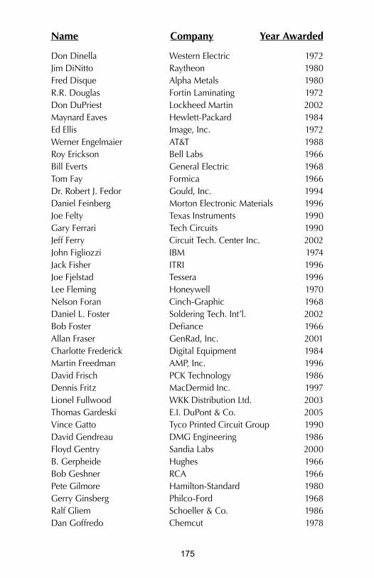
���
Name Company Year Awarded
Don Dinella Western Electric 1972Jim DiNitto Raytheon 1980Fred Disque Alpha Metals 1980R.R. Douglas Fortin Laminating 1972Don DuPriest Lockheed Martin 2002Maynard Eaves Hewlett-Packard 1984Ed Ellis Image, Inc. 1972Werner Engelmaier AT&T 1988Roy Erickson Bell Labs 1966Bill Everts General Electric 1968Tom Fay Formica 1966Dr. Robert J. Fedor Gould, Inc. 1994Daniel Feinberg Morton Electronic Materials 1996Joe Felty Texas Instruments 1990Gary Ferrari Tech Circuits 1990Jeff Ferry Circuit Tech. Center Inc. 2002John Figliozzi IBM 1974Jack Fisher ITRI 1996Joe Fjelstad Tessera 1996Lee Fleming Honeywell 1970Nelson Foran Cinch-Graphic 1968Daniel L. Foster Soldering Tech. Int’l. 2002Bob Foster Defiance 1966Allan Fraser GenRad, Inc. 2001Charlotte Frederick Digital Equipment 1984Martin Freedman AMP, Inc. 1996David Frisch PCK Technology 1986Dennis Fritz MacDermid Inc. 1997Lionel Fullwood WKK Distribution Ltd. 2003Thomas Gardeski E.I. DuPont & Co. 2005Vince Gatto Tyco Printed Circuit Group 1990David Gendreau DMG Engineering 1986Floyd Gentry Sandia Labs 2000B. Gerpheide Hughes 1966Bob Geshner RCA 1966Pete Gilmore Hamilton-Standard 1980Gerry Ginsberg Philco-Ford 1968Ralf Gliem Schoeller & Co. 1986Dan Goffredo Chemcut 1978

���
Name Company Year Awarded
Ozzie Goldman IBM 1968Patricia Goldman Qualitron 1984Ed Golonsbe Methode 1970Charles Gonder Multiwire Division 1984Constantino Gonzalez SCI Mfg. Inc. 1994Paul Gould IBM 1980Foster Gray Texas Instruments 1980Al Green NVF 1968Russell Griffith Dynaco 1992Lynn Gunsaulus Photocircuits 1966Leslie Guth AT&T 1990Steve Hall BTU 2000K.E. Hafften Bureau of Engraving 1978John Hanne Texas Instruments 1968George Hansell W.L. Gore & Associates 1970Dick Hanson Methode 1968Jim Hardman AMP 1980Elise Harmon Autometics 1968Mikel Harry Motorola 1990Robert Hart Digital Equipment 1986Ernie Hausmann Budd Co. 1966Ralph Hersey Lawrence Labs 1974Jim Hickman E.I. DuPont 1996Mike Hill Texas Instruments 1986David Hillman Rockwell Collins 1999Steve Hinch Hewlett-Packard 1988Phil Hinton Hinton “PWB” Engrg. 1992Happy Holden Hewlett-Packard 1990Paul Horbay Honeywell 1978Fred Horn Amphenol 1968Bruce Houghton Celestica 2000Ken Hurley Hughes 1966Les Hymes GE Medical Systems 1988Irv Ireland Shipley 1976Bill Jacobi William Jacobi & Assocs. 1990Martin Jawitz Litton Guidance 1986Charles Jennings Sandia Labs 1978Kathryn Johnson Naval Weapons Center 1986Ivan Jones DESC 1966

���
Name Company Year Awarded
Lea Jones EDX 1992Roger Jones AT&T 1988Chris Kalmus Kalmus & Associates 1974Roger Kauffman W.L. Gore & Associates 1974Russ Keller Goodyear 1968John Kelly Motorola 1992Robert Keltz Westinghouse/Fortin 1992Bill Kenyon DuPont 1990Jack Kerr Naval Electronics Sys. 1980Michael Kerr Circuit Center, Inc. 1994Bernie Kessler Mica 1966Larita Killian EMLC, EMPF 1996Jerry Kirschenbaum Trace Laboratories 1986Bob Klotz McDonnell Douglas 1970Colin Knopton ITT 1978Bob Knowles Winchester Electronics 1966Jeff Koon Raytheon TI Systems 1998H.B. Koons, Jr. AT&T Bell Labs 1966Dana Korf Hadco 1999Jim Kubik Hughes Aircraft 1976Mark Kwoka Harris Corporation 1994Joe La Liberte Trans Circuits 1974Leo Lambert Digital Equipment 1988J.D. Lando Bell Telephone Labs 1978Roger Landolt DuPont 1984Ralph Landreth Western Electric 1974William Lange Lange Associates 1986Marv Larson Bureau of Engraving 1968Dick LaVash Shipley 1968Clarence Leski Methode 1966Al Levy RCA 1966Andy Lietz Hadco Corporation 1994Gerry Lordi Shipley 1970Dr. John Lott E.I. DuPont Electronics 1996Gail Love Martin-Marietta 1966Lincoln Low Hughes 1970Dave Luzadis Bendix 1972Gene Lyman Western Electric 1974Art Mabbett Mabbett & Capaccio 1990

���
Name Company Year Awarded
Andy Mackie Praxair 2001Florian Madina DuPont 1986A. D. Magistro Army Ordnance 1966Jim Maguire Intel Corporation 2001Howard Manko Alpha Metals 1966Susan Mansilla Robison Laboratories 1988Bill March Lawrence Labs 1976Phil Marcoux PPM Associates 1992David Martin Intel Corporation 2001Dick Martz U.S. Navy 1966Bob Matzinger Martin Co. 1966William Dean May NavSea Crane 2005Vivian Mayfield Teradyne Central 1982John McCormack Photocircuits 1968Jack McCreary IBM 1970Brian McCrory Delsen Labs 1996Bill McDaniel Western Electric 1972Garry D. McGuire NASA/Goddard Center 2002John McKay General Electric 1968Michael McLay NIST 1999Paul McNamara Aeroscientific 1988Hugh Medford Riegel Paper 1966Lou Messina RCA 1970George Messner Photocircuits 1966James H. Moffitt Moffitt Consulting Services 2002Bob Moore Sperry Univac 1980Frank Morris RCA 1970Rene Moser General Electric 1976Charles Mosher Bureau of Engraving 1968Sue Mucha Xetel Corporation 1994Leigh Mueller Printed Circuit Builders 1992Joe Mulcahy Philco-Ford 1974George Muller Synthane-Taylor 1968Gabriel Munck Perstorp Electronics 1988Greg Munie Lucent Technologies Inc. 2001Terry Munson CSL 2001Fred Murphy Unisys 1988Tom Murray Bendix 1974Judee Mussehl-Aziz Dept. of Commerce 1994
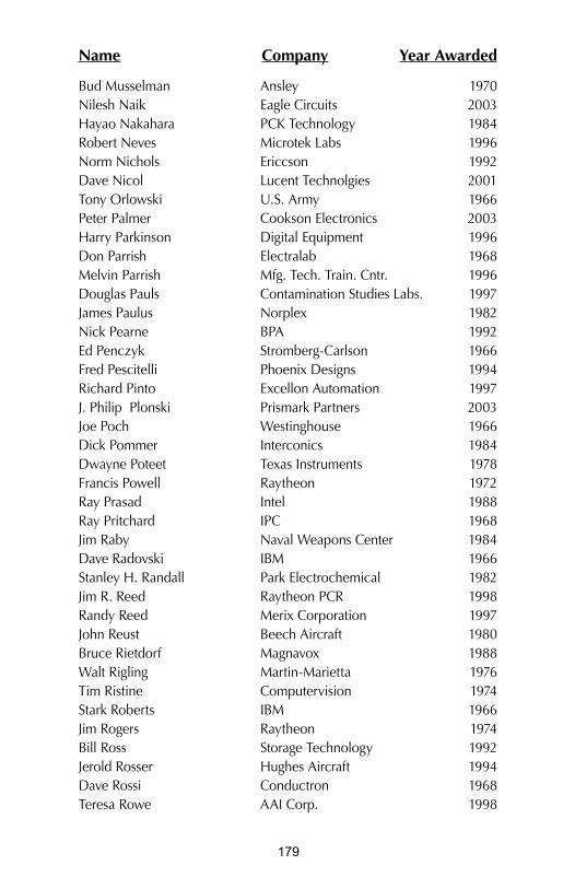
���
Name Company Year Awarded
Bud Musselman Ansley 1970Nilesh Naik Eagle Circuits 2003Hayao Nakahara PCK Technology 1984Robert Neves Microtek Labs 1996Norm Nichols Ericcson 1992Dave Nicol Lucent Technolgies 2001Tony Orlowski U.S. Army 1966Peter Palmer Cookson Electronics 2003Harry Parkinson Digital Equipment 1996Don Parrish Electralab 1968Melvin Parrish Mfg. Tech. Train. Cntr. 1996Douglas Pauls Contamination Studies Labs. 1997James Paulus Norplex 1982Nick Pearne BPA 1992Ed Penczyk Stromberg-Carlson 1966Fred Pescitelli Phoenix Designs 1994Richard Pinto Excellon Automation 1997J. Philip Plonski Prismark Partners 2003Joe Poch Westinghouse 1966Dick Pommer Interconics 1984Dwayne Poteet Texas Instruments 1978Francis Powell Raytheon 1972Ray Prasad Intel 1988Ray Pritchard IPC 1968Jim Raby Naval Weapons Center 1984Dave Radovski IBM 1966Stanley H. Randall Park Electrochemical 1982Jim R. Reed Raytheon PCR 1998Randy Reed Merix Corporation 1997John Reust Beech Aircraft 1980Bruce Rietdorf Magnavox 1988Walt Rigling Martin-Marietta 1976Tim Ristine Computervision 1974Stark Roberts IBM 1966Jim Rogers Raytheon 1974Bill Ross Storage Technology 1992Jerold Rosser Hughes Aircraft 1994Dave Rossi Conductron 1968Teresa Rowe AAI Corp. 1998

��0
Name Company Year Awarded
John Sabo Rockwell/Allen-Bradley 1999Tom Sarnowski PCK Technology 1976Mark Savrin RCA 1974Don Sayrs AMP 1966Herb Schachter Agard 1972Lou Schmidt ITT Canon 1970William Schmid Bell Labs 1970Don Schnorr RCA 1970Dave Schoenthaler AT&T 1984Laura Scholten Optrotech 1992Duane Schroeder Methode 1966Werner Schuele Texas Instruments 1968Alan J. Seabright Computing Devices 1982Karl Seelig AIM 2003Linda Self Litton Interconnect Tech. 2001Robin Sellers Naval Avionics 1992Dr. Dongkai Shangguan Flextronics International 2006Jerry Siegmund MacDermid 1976Steve Simpson E. I. DuPont 1995Rick Smedley Raytheon 1999Barry Smith MCD 1966George Smith DoD 1970Joe Smith Philco-Ford 1970Douglas Sober Essex Technologies 1992John Sohn Lucent Technologies 2001Vern Solberg SCI 1992Al Sorkin Digital Equipment 1982Rick Steiner Gould Electronics 2001Dean Stephenson Amphenol 1966John Stonis Methode 1968Walt Stubbings Methode 1966Mario Suarez-Solis Encore Computer 1994Jorgen Svensson Ericsson Telecom 1992Patrick Sweeney Hadco Corporation 1996Eugene Szukalski AMP, Inc. 1982Bob Tabor Sanders 1966Dr. Karen A. Teelefsen Alpha Metals 2002Max Thorson Compaq Computer Corp. 1997Rainer Thueringer Friedberg University 2003

���
Name Company Year Awarded
Fred Tolley Western Electric 1976Lutz Treutler Comargus 1990Aroon Tungare Motorola 2002Laura Turbini Georgia Tech 1990Tom Turner Nelco 1986Joe Tutchton Martin-Marietta 1994Paul Twigg IBM 1976Henry Utsonomiya Eastern 1996Robert VanNess Army Ordnance 1966Ken Varker IBM 1966David Vaughan E.I. DuPont de Nemours 1997George Voida Sandia Labs 1974Eric Vollmar Methode 1992George Vybiral Thiokol 1966R.T. Walsh General Electric 1968Bernie Wargotz AT&T Bell Labs 1992John Waryold Humiseal 2000Bob Wathen Fairchild-Hiller 1966George Watrous Budd Co. 1970Nick Watts Tektronix 1992R.W. Weaver Martin Company 1966Clark Webster Precision Diversified Industries 1999Gene Weiner Nelco 1968Al Weiss Methode 1966George Wenger Andrew Corporation 2005Tom White Hallmark Circuits 2005Ted Wipple Universal Instruments 1968Roger Wild IBM 1982Charley Wolff Western Electric 1970 James Woodford Department of Defense 1998Bob Wright Bell Labs 1978John Wyatt Naval Electronics 1974Jo Wynschenk Enthone-OMI, Inc. 1996Joel Yocom Allied Signal 1992Lou Zakraysek General Electric 1968Bernie Zimmerman Department of Defense 1970Benson Zinbarg Nelco 1966
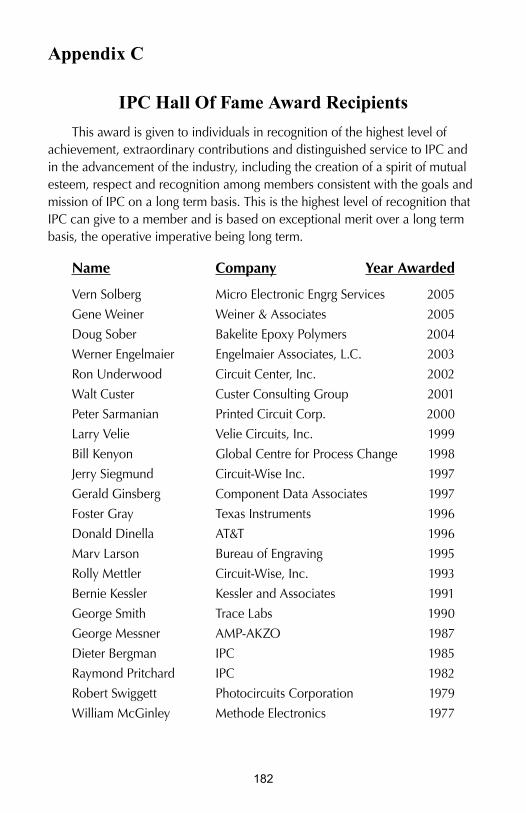
���
Appendix C
IPC Hall Of Fame Award Recipients
This award is given to individuals in recognition of the highest level of achievement, extraordinary contributions and distinguished service to IPC and in the advancement of the industry, including the creation of a spirit of mutual esteem, respect and recognition among members consistent with the goals and mission of IPC on a long term basis. This is the highest level of recognition that IPC can give to a member and is based on exceptional merit over a long term basis, the operative imperative being long term.
Name Company Year Awarded
Vern Solberg Micro Electronic Engrg Services 2005
Gene Weiner Weiner & Associates 2005
Doug Sober Bakelite Epoxy Polymers 2004
Werner Engelmaier Engelmaier Associates, L.C. 2003
Ron Underwood Circuit Center, Inc. 2002
Walt Custer Custer Consulting Group 2001
Peter Sarmanian Printed Circuit Corp. 2000
Larry Velie Velie Circuits, Inc. 1999
Bill Kenyon Global Centre for Process Change 1998
Jerry Siegmund Circuit-Wise Inc. 1997
Gerald Ginsberg Component Data Associates 1997
Foster Gray Texas Instruments 1996
Donald Dinella AT&T 1996
Marv Larson Bureau of Engraving 1995
Rolly Mettler Circuit-Wise, Inc. 1993
Bernie Kessler Kessler and Associates 1991
George Smith Trace Labs 1990
George Messner AMP-AKZO 1987
Dieter Bergman IPC 1985
Raymond Pritchard IPC 1982
Robert Swiggett Photocircuits Corporation 1979
William McGinley Methode Electronics 1977

���
Document Revision Table, updated November 2006Sorted in NUMBER order, ignore all letters
Product ID and Document Status ANSI DoD
Appendix D
J-STD-001, Requirements for Soldered Electrical and Electronic Assemblies
Rev D 2/05 Apr-05 Apr-05Rev. C 3/00Rev. B 10/96Rev. A 1/95Orig. 4/92; Supersedes IPC-S-815
J-STD-001CS, Space Applications Electronic Hardware Addendum for J-STD-001C
CS 1/04
IPC-HDBK-001, Handbook and Guide to the Requirements for Soldered Electrical and Electronic Assemblies
Amend 2 10/05 Jul-01Amend. 1 12/00Orig. 3/98
SMC-TR-001, An Introduction to Tape Automated Bonding Fine Pitch Technology
Orig. 1/89
IT-WP-001, Myths of E-Commerce Orig. 9/00SMC-WP-001, Soldering Capability White Paper Report
Orig. 8/91
SMEMA 1.2, Mechanical Equipment Interface Standard
Update IPC-SMEMA-9851
JP002, Current Tin Whiskers Theory and Mitigation Practices Guideline
Orig. 3/06
J-STD-002, Solderability Tests for Component Leads, Terminations, Lugs, Terminals and Wires
Rev. B 02/03 Y May-95Rev. A 10/98Orig. 4/92; Supersedes IPC-S-805
SMC-WP-002, An Assessment of the Use of Lead in Electronic Assembly
Orig. 8/92
J-STD-003, Solderability Tests for Printed Boards Rev. A 02/03 YOriginal 4/92; Supersedes IPC-S-804
SMC-WP-003, Chip Mounting Technology Orig. 8/93SMEMA 3.1, Fiducial Mark Standard J-STD-004, Requirements for Soldering Fluxes Rev. A 01/04 Y May-95
Orig. 1/95 Supersedes IPC-SF-818
SMC-WP-004, Design for Success Orig. 4/97SMEMA 4, Reflow Terms and Definitions Orig.J-STD-005, Requirements for Soldering Pastes Amend. 1 6/96 Y May-95
Orig. 1/95 Supersedes IPC-SP-819
SMC-WP-005, PWB Surface Finishes Orig. 4/97IPC-HDBK-005, Guide to Solder Paste Assessment Orig. 1/06SMEMA 5, Screen Printing Terms and Definitions Orig.J-STD-006, Requirements for Electronic Grade Solder Alloys and Fluxed and Non-Fluxed Solid Solders for Electronic Soldering Applications
Rev. B 01/06 Y May-95Rev. A 05/01Orig. 1/95
SMEMA 6, Electronics Cleaning Terms and Definitions
Orig.
SMEMA 7, Fluid Dispensing Terms and Definitions Orig.WP-008, Setting up Ion Chromatography Capability Orig. 12/05J-STD-012, Implementation of Flip Chip and Chip Scale Technology
Orig. 1/96 Y
���
Document Revision Table, updated November 2006Sorted in NUMBER order, ignore all letters
Product ID and Document Status ANSI DoD
J-STD-013, Implementation of Ball Grid Array and Other High Density Technology
Orig. 7/96 Y
IPC-DRM-18, Component Identification Desk Reference Manual
Rev. G 9/03Rev. F 8/01Rev. E 8/00Rev. D 7/99Rev. C 7/98Rev. B 2/97Rev. A 4/96Orig. 9/95
J-STD-020, Moisture/Reflow Sensitivity Classification of Plastic Surface Mount Devices
Rev. C 7/04Rev. B 7/02Rev. A 4/99Orig. 10/96
J-STD-026, Semiconductor Design Standard for Flip Chip Applications
Orig. 8/99
J-STD-027, Mechanical Outline Standard for Flip Chip or Chip Scale Configurations
Orig. 02/03
J-STD-028, Performance Standard for Flip Chip Scale Bumps
Orig. 8/99
J-STD-030, Guideline for Selection and Application of Underfill Material for Flip Chip and Other Micropackages
Orig. 9/05
J-STD-032, Performance Standard for Ball Grid Array Bumps and Columns
Orig. 6/02
J-STD-033, Packaging and Handling of Moisture Sensitive Non-Hermetic Solid State Surface Mount Devices
Rev B 10/05Rev. A 7/02Orig. 4/99
J-STD-035, Acoustic Microscopy for Non-Hermetic Encapsulated Electronic Components
Orig. 4/99
IPC-0040, Standards Roadmap for Optoelectronic Assembly and Packaging Technology
Orig. 5/03
IPC-DRM-40, IPC-DRM-PTH, Through Hole Solder Joint Evaluation Desk Reference Manual
Rev D 11/05Renamed to DRM-PTHRev. E 2/02Rev. D 7/00Rev. C 9/99Rev. B 1/99Rev. A 8/97Orig. 5/97
IPC-T-50, Terms and Definitions Interconnecting and Packaging Electronic Circuits
Rev. G 12/03Rev. F 6/96Rev. E 7/92Rev. D 11/88Rev. C 3/85Rev. B 6/80Rev. A 8/76Orig. 8/75
IPC-DRM-53, Introduction to Electronics Assembly Orig. 6/00IPC-DRM-56, Wire Preparation & Crimping Orig. 07/02
���
Document Revision Table, updated November 2006Sorted in NUMBER order, ignore all letters
Product ID and Document Status ANSI DoD
IPC-SC-60, Post Solder Solvent Cleaning Handbook Rev. A 8/99 Oct-99Orig. 4/87
IPC-SA-61, Post-Solder Semi-Aqueous Cleaning Handbook
Rev. A 6/02Orig. 7/95
IPC-AC-62, Post Solder Aqueous Cleaning Handbook
Rev. A 1/96Orig. 12/86
IPC-CH-65, Guidelines for Cleaning of Printed Boards and Assemblies
Rev. A 9/99 Oct-99Orig. 12/90
IPC-CS-70, Guidelines for Chemical Handling Safety in Printed Board Manufacturing
Orig. 8/88 Obsolete without replacement
IPC-CM-78, Guidelines for Surface Mounting and Interconnecting Chip Carriers
Superseded by IPC-SM-780Rev. C 3/88Orig. 11/83
IPC-MP-83, IPC Policy on Metrication Orig. 8/85 Obsolete without replacement
IPC-PC-90, General Requirements for Implementation of Statistical Process Control
Superseded by IPC-9191Orig. 10/90
IPC-QS-95, General Requirements for Implementation of ISO 9000 Quality Systems
Obsolete without replacementOrig. 4/93
IPC-L-108, Specification for Thin Metal Clad Base Materials for Multilayer Printed Boards
Rev. B 6/90 Superseded by IPC-4101Rev. A 10/80Orig. 3/76
IPC-L-109, Specification for Resin Impregnated Fabric (Pregreg) for Multilayer Printed Boards
Superseded by IPC-4101Rev. B 7/92Rev. A 10/80Orig. 3/76
IPC-L-110, Preimpregnated, B-Stage Epoxy-Glass Cloth for Multilayer Printed Circuit Boards
Rev. A Superseded by IPC-L-109 and IPC-4101
IPC-CC-110, Guidelines for Selecting Core Constructions for Multilayer Printed Wiring Board Applications
Superseded by IPC-4121Rev. A 12/97Orig. 1/94
IPC-L-112, Specification for Composite Metal Clad Base materials for Printed Boards
Superseded by IPC-4101Rev. A 6/92Orig. 7/81
IPC-L-115, Specification for Rigid Metal Clad Base Materials for Printed Boards
Superseded by IPC-4101Rev. B 4/90Rev. A 10/80Orig. 3/77
IPC-L-120, Inspection Procedure for Chemical Processing Suitability of Copper-Clad Epoxy-Glass Laminates
Obsolete without replacement

���
Document Revision Table, updated November 2006Sorted in NUMBER order, ignore all letters
Product ID and Document Status ANSI DoD
IPC-L-125, Specifications for Plastic Substrates Clad or Unclad for High Speed/High Frequency Interconnections
Superseded by IPC-4103Rev. A 7/92Orig. 8/83
IPC-L-130, Specifications for Thin Laminates, Metal Clad, Primarily for General-Purpose Multilayer Printed Boards
Superseded by IPC-L-108 and IPC-4101Orig. 1/77
IPC-DD-135, Qualification Testing for Deposited Organic Interlayer Dielectric Materials for Multichip Modules
Orig. 8/95
IPC-EG-140, Specification for Finished Fabric Woven from “E” Glass for Printed Boards
Superseded by IPC-4412Amend. 1 & 2 6/97Orig. 3/88
IPC-SG-141, Specification for Finished Fabric Woven from “S” Glass for Printed Boards
Orig. 2/92
IPC-A-142, Specification for Finished Fabric Woven from Aramid for Printed Boards
Orig. 6/90
IPC-QF-143, General Specification for Finished Fabric Woven from Quartz (Pure Fused Silica) for Printed Boards
Orig. 2/92
IPC-CF-148, Resin Coated Metal for Printed Boards Rev. A 9/98 Oct-98Orig. 6/90
IPC-MF-150, Metal Foil for Printed Wiring Applications
Superseded by IPC-4562Rev. F 10/91 Changed from CF-150 to MF-150Rev. E 5/81Rev. D 3/76Rev. C 8/74Rev. B 2/71Rev. A 9/67Orig. 8/66
IPC-CF-152, Composite Metallic Material Specification for Printed Wiring Boards
Rev. B 12/97Rev. A 1/94Orig. 6/90
IPC-FC-203, Specification for Flat Cable, Round Conductor, Ground Plane
Obsolete 7/96Orig. 7/85
IPC-FC-210, Performance Specification for Flat-Conductor Undercarpet Power Cable (Type FCC)
Obsolete 7/96Orig. 9/85
IPC-FC-213, Performance Specification for Flat Undercarpet Telephone Cable
Obsolete 7/96Orig. 9/84
IPC-FC-217, General Document for Connectors, Electric, Header, Receptacle,Insulation Displacement for Use with Round Conductor Flat Cable
Obsolete 7/96Reaffirmed 4/90Orig. 8/82
IPC-FC-218B/EIA-RS-429, General Specification for Connectors, Electrical Flat Cable Type
Obsolete 7/96Reaffirmed 05/91Reaffirmed 11/81Orig. 7/76
IPC-FC-219, Environment Sealed Flat Cable Connectors for use in Aerospace Applications
Obsolete 7/96Orig. 5/84

���
Document Revision Table, updated November 2006Sorted in NUMBER order, ignore all letters
Product ID and Document Status ANSI DoD
IPC-FC-220, Specification for Flat Cable, Flat Conductor, Unshielded
obsolete 7/96Rev. C 7/85Rev. B 8/75Rev. A 1/74Orig. 5/70
IPC-FC-221, Specification for Flat-Copper Conductors for Flat Cables
Obsolete 7/96Rev. A 5/84Orig. 8/75
IPC-FC-222, Specification of Flat Cable Round Conductor, Unshielded
Obsolete 7/965/91 ReaffirmedOrig. 6/80
IPC-FC-225, Flat Cable Design Guide Obsolete (date)10/85 ReaffirmedOrig. 8/75
IPC-FC-231, Flexible Base Dielectrics for Use in Flexible Printed Wiring
Superseded by IPC-4202Amend. 10/95Rev. C 4/92Rev. B 2/86Rev. A 5/83Orig. 7/74
IPC-FC-232, Adhesive Coated Dielectric Films for Use as Cover Sheets for Flexible Printed Wiring and Flexible Bonding Films
Superseded by 4203Amend. 10/95Rev. C 6/94Rev. B 2/86Rev. A 5/83Orig. 7/74
IPC-FC-233, Flexible Adhesive Bonding Films Incorporated into IPC-FC-232B
IPC-FC-234, PSA Assembly Guidelines for Single- & Double-Sided Flexible Printed Circuits
Orig. 12/97
IPC-FC-240, Single Sided Flex Superseded by IPC-6013Incorporated into FC-250Rev. B 1/74Rev. A 5/69Orig. 12/65
IPC-FC-241, Flexible Metal-Clad Dielectrics for Use in Fabrication of Flexible Printed Wiring
Superseded by IPC-4204Amend. 10/95Rev. C 4/92Rev. B 2/86Rev. A 5/83Orig. 7/74
IPC-RF-245, Performance Specification for Rigid-Flex Printed Boards
Superseded by IPC-6013Orig. 4/87
IPC-D-249, Design Standard for Flexible Single-and Double-Sided Printed Boards
Superseded by IPC-2223Orig. 1/87

���
Document Revision Table, updated November 2006Sorted in NUMBER order, ignore all letters
Product ID and Document Status ANSI DoD
IPC-FC-250A, Specification for Single - and Double-Sided Flexible Printed Wiring
Superseded by IPC-6013Rev. A 9/86Orig. 9/86
IPC-FA-251, Guidelines for Single and Double Sided Flex Circuits
Orig. 2/92
IPC-D-275, Design Standard for Rigid Printed Boards and Rigid Printed Board Assemblies
Superseded by IPC-2221 and 2222Supersedes IPC-D-319 and IPC-D-949Amendment.1 4/96Orig. 9/91
IPC-RB-276, Qualification and Performance Specification for Rigid Printed Boards
Superseded by IPC-6011 and IPC-6012Orig. 3/92 Supersedes IPC-SC-320B and IPC-ML-950C
IPC-D-279, Design Guidelines for Reliable Surface Mount Technology Printed Board Assemblies
Orig. 7/96
IPC-D-300, Printed Board Dimensions and Tolerances
Superseded by IPC-2615Rev. G 1/84Rev. F 11/74Rev. E 10/70Rev. D 1/70Rev. C 10/65Rev. B 1/64Rev. A 7/61Orig. 8/60
IPC-D-310, Guidelines for Phototool Generation and Measurement Techniques
Rev. C 06/91Rev. B 12/85Rev. A 12/77Orig. 9/69
IPC-A-311, Process Control Guidelines for Phototool Generation and Use
Orig. 3/96
IPC-D-316, Design Guide for Microwave Circuit Boards Utilizing Soft Substrates
Superseded by IPC-2252Orig. 5/95
IPC-D-317, Design Guidelines for Electronic Packaging Utilizing High-Speed Techniques
Superseded by IPC-2251Rev. A 1/95Orig. 4/90
IPC-HF-318, Microwave End Product Board Inspection and Test
Superseded by IPC-6018Rev. A 12/91Orig. 6/85
IPC-D-319, Design Standard for Rigid Single-and Double-Sided Printed Boards
Superseded by IPC-D-275, then by IPC-2221/2222Orig. 1/87

���
Document Revision Table, updated November 2006Sorted in NUMBER order, ignore all letters
Product ID and Document Status ANSI DoD
IPC-SD-320, Performance Specification for Rigid Single- and Double-Sided Printed Boards
Superseded by IPC-RB-276Supersedes IPC-TC-500Rev. B 11/86Rev. A 3/81Orig. 1/77
IPC-D-322, Guidelines for Selecting Printed Wiring Board Sizes Using Standard Panel Sizes
Reaffirmed 9/91Orig. 8/84
IPC-MC-324, Performance Specifications for Metal Core Boards
Superseded by IPC-6011 and IPC-6012Orig. 10/88
IPC-D-325, Documentation Requirements for Printed Boards, Assemblies and Support Drawings
Rev. A 5/95Orig. 1/87
IPC-D-326, Information Requirements for Manufacturing Printed Board Assemblies
Rev. A 1/04Orig. 4/91
IPC-D-330, Design Guide Manual Orig. 1972IPC-PD-335, Electronic Packaging Handbook Orig. 12/89IPC-NC-349, Computer Numerical Control Formatting for Drillers and Routers
Orig. 8/85
IPC-D-350, Printed Board Description in Digital Form; Technical Content Identical to IEC-61182-1
Rev. D 7/92Rev. C 10/85Rev. B 8/77Rev. A 2/75Orig. 8/72
IPC-D-351, Printed Board Drawings in Digital Form Orig. 8/85IPC-D-352, Electronic Design Data Description for Printed Boards in Digital Form
Orig. 8/85
IPC-D-354, Library Format Description for Printed Boards in Digital Form
Orig. 2/87
IPC-D-355, Printed Board Assembly Description in Digital Form
Orig. 1/95
IPC-D-356, Bare Board Electrical Test Information in Digital Form
Rev. B 10/02Rev. A 1/98Orig. 3/92
IPC-AM-361, Specification for Rigid Substrates for Additive Process Printed Boards
Superseded by IPC-4101Orig. 1/82
IPC-MB-380, Guidelines for Molded Interconnection Devices
Orig. 10/90
IPC-D-390, Automated Design Guidelines Rev. A 2/88Orig. 7/74
IPC-C-406, Design and Application Guidelines for Surface Mount Connectors
Orig. 1/90
IPC-CI-408, Design and Application Guidelines for the Use of Solderless Surface Mount Connectors
Orig. 1/94
IPC-BP-421, General Specification for Rigid Printed Board Backplanes with Press Fit Contacts
Obsolete without replacementReaffirmed 4/90Orig. 10/80
IPC-D-422, Design Guide for Press Fit Rigid Printed Board Backplanes
Orig. 9/82

��0
Document Revision Table, updated November 2006Sorted in NUMBER order, ignore all letters
Product ID and Document Status ANSI DoD
IPC-DW-424, General Specification for Encapsulated Discrete Wire Interconnection Boards
Orig. 1/95
IPC-DW-425, Design and End Product Requirements for Discrete Wiring Boards
Rev. A 5/90Orig. 9/82
IPC-DW-426, Specifications for Assembly of Discrete Wiring
Orig. 12/87
IPC-TR-460, Trouble-Shooting Checklist for Wave Soldering Printed Wiring Boards
Rev. A 2/84Orig. 1973
IPC-TR-461, Solderability Evaluation of Thick and Thin Fused Coatings
Orig. 3/79
IPC-TR-462, Solderability Evaluation of Printed Boards with Protective Coatings Over Long Term Storage
Orig. 10/87
IPC-TR-464, Accelerated Aging for Solderability Evaluations
Rev. A 12/87Orig. Pub.4/84
IPC-TR-465-1, Round Robin Test on Steam Ager Temperature Control Stability
Orig. 1993
IPC-TR-465-2, The Effect of Steam Aging Time and Temperature on Solderability Test Results
Orig. 1993
IPC-TR-465-3, Evaluation of Steam Aging on Alternative Finishes, Phase IIA
Orig. 7/96
IPC-TR-466, Wetting Balance Standard Weight Comparison Test
Orig. 4/95
IPC-TR-467, Supporting Data and Numerical Examples for ANSI/J-STD-001 Appendix D
Orig. 10/96
IPC-TR-468, Factors Affecting Insulation Resistance Performance of Printed Boards
Orig. 3/79
IPC-TR-470, Thermal Characteristics of Multilayer Interconnection Boards
Orig. 1/74
IPC-TR-474, An Overview of Discrete Wiring Techniques
Obsolete without replacementReprint 1984Orig. 3/79
IPC-TR-476, How to Avoid Metallic Growth Problems on Electronic Hardware, Rev. A Electrochemical Migration Electrically Induced Failures In Printed Assembles
Rev. A 6/84 (new title)Orig. 9/77
IPC-TR-480, Results of Multilayer Test Program Round Robin IV Phase I
Obsolete without replacementOrig. 9/75
IPC-TR-481, Results of Multilayer Test Program Round Robin V
Orig. 4/81
IPC-TR-482, New Developments in Thin Copper Foils
Orig. 1/76
IPC-TR-483, Dimensional Stability Testing of Thin Laminates - Report on Phase I International Round Robin Test Program
Rev. A 3/91Addendums 10/87Orig. 4/84
IPC-TR-484, Results of IPC Cooper Foil Ductility Round Robin Study
Orig. 4/86
IPC-TR-485, Results of Cooper Foil Rupture Strength Test Round Robin Study
Orig. 3/85

���
Document Revision Table, updated November 2006Sorted in NUMBER order, ignore all letters
Product ID and Document Status ANSI DoD
IPC-TR-486, Report on Round Robin Study to Correlate Interconnect Stress Test (IST) with Thermal Stress/Microsectioning Evaluations for Detecting the Presence of Inner-layer Separations
Orig. 07/01
IPC-TR-549, Measles in Printed Wiring Boards Orig. 11/78IPC-TR-551, Quality Assessment of Printed Boards Used for Mounting and Interconnecting Electronic Components
Orig. 7/93
IPC-DR-570, General Specification for 1/8 Inch Diameter Shank Carbide Drills for Printed Boards
Obsolete without replacementRev. A 4/84Orig. 1/79
IPC-DR-572, Drilling Guidelines for Printed Boards Orig. 4/88IPC-TR-576, Additive Process Evaluation Obsolete without
replacementOrig. 9/77
IPC-TR-578, Leading Edge Manufacturing Technology Report - Resulting of a Round Robin Study on Minimum Conductor Width and Plated-Through Holes in Rigid, Bare Copper, Double-Sided Printed Wiring Boards
Orig. 9/84
IPC-TR-579, Round Robin Reliability Evaluation of Small Diameter Plated Through Holes in Printed Wiring Boards
Orig. 9/88
IPC-TR-580, Cleaning and Cleanliness Test Program Phase 1 Test Results
Orig. 10/89
IPC-TR-581, IPC Phase 3 Controlled Atmosphere Soldering Study
Orig. 8/94
IPC-TR-582, IPC Phase 3 No-Clean Flux Study Orig. 11/94IPC-TR-583, An In-Depth Look At Ionic Cleanliness Testing
Orig. 7/02
IPC-WP/TR-584, IPC White Paper and Technical Report on Halogen-Free Materials used for Printed Circuit Boards and Assemblies
Orig. 04/03
IPC-TR-585, Time, Temperature and Humidity Stress of Final Board Finish Solderability
Orig. 05/06
IPC-A-600, Acceptability of Printed Boards Rev. G 07/04Rev. F 11/99Rev. E 8/95Rev. D ‘89Rev. C ‘78Rev. B ‘74Rev. A ‘70Orig. ‘64
IPC-SS-605, Printed Board Quality Evaluation Slide Set
Obsolete without replacement
IPC-QE-605, Printed Board Quality Evaluation Handbook
Rev. A 2/99
IPC-A-610, Acceptability of Electronic Assemblies Rev. D 2/05 Apr-05 Apr-05Rev. C 1/00Rev. B 12/94Rev. A 3/90Orig. 8/83
���
Document Revision Table, updated November 2006Sorted in NUMBER order, ignore all letters
Product ID and Document Status ANSI DoD
IPC-HDBK-610, Handbook and Guide to IPC-A-610 (Includes B-C-D comparison)
Amend 1 10/05Orig. 9/02
IPC-QE-615, Assembly Quality Evaluation Handbook
Obsolete without replacement
IPC/WHMA-A-620, Acceptability of Electronic Wire Harnesses and Cables
Rev A 07/06 Mar-02Orig. 01/02
IPC-AI-640, User’s Guidelines for Automated Inspection of Unpopulated Thick Film Hybrid Substrates
Obsolete without replacementOrig. 1/87
IPC-AI-641, User’s Guidelines for Automated Solder Joint Inspection
Obsolete without replacementOrig. 1/87
IPC-AI-642, User’s Guidelines for Automated Inspection of Artwork, Interlayers, and Unpopulated PWB’s
Obsolete without replacementOrig. 10/88
IPC-OI-645, Standard for Visual Optical Inspection Aids
Orig. 10/93
IPC-TM-650, Test Methods Manual Updated per test method
IPC-ET-652, Guidelines and Requirements for Electrical Testing of Unpopulated Printed Boards
Orig. 10/90 Superseded by IPC-9252
IPC-QL-653, Qualification of Facilities that Inspect/Test Printed Boards, Components, and Material
Rev. A 11/97Orig. 8/88
IPC-MI-660, Incoming Inspection of Raw Materials Manual
Orig. 2/84
IPC-R-700, Suggested Guidelines for Modification, Rework and Repair of Printed Boards and Assemblies
Superseded by IPC-7711A/7721ARev. C 1/88Rev. B 9/77Rev. A 12/71Orig. 9/67
IPC-TA-720, Technology Assessment Handbook on Laminates
Orig. ’86
IPC-TA-721, Technology Assessment Handbook on Multilayer Boards
Orig. ’88
IPC-TA-722, Technology Assessment of Soldering Orig. ’90IPC-TA-723, Technology Assessment Handbook on Surface Mounting
Orig. ’91
IPC-TA-724, Technology Assessment Series on Cleanrooms
Orig. 4/98
IPC-PE-740, Troubleshooting Guide for Printed Board Manufacture and Assembly
Rev. A 12/97Orig. 1/85
IPC-CM-770, Printed Board Component Mounting Rev. E 1/04Rev. D 1/96Rev. C 1/87Rev. B 10/80Rev. A 3/76Orig. 9/68
IPC-SM-780, Component Packaging and Interconnecting with Emphasis on Surface Mounting
Orig. 3/88

���
Document Revision Table, updated November 2006Sorted in NUMBER order, ignore all letters
Product ID and Document Status ANSI DoD
IPC-SM-782, Surface Mount Design and Land Pattern Standard
Superseded by IPC-7351Amend. 2 04/99Amend. 1 10/96Rev. A 8/93Orig. 3/87
IPC-SM-784, Guidelines for Chip-on-Board Technology Implementation
Orig. 11/90
IPC-SM-785, Guidelines for Accelerated Reliability Test of Surface Mount Solder Attachments
Orig. 11/92
IPC-SM-786, Procedures for Characterizing and Handling of Moisture/ Reflow Sensitive ICs
Superseded by J-STD-020 and J-STD-033Rev. A 1/95Orig. 12/90
IPC-MC-790, Guidelines for Multichip Module Technology Utilization
Orig. 8/92
IPC-S-801 Superseded by IPC-804 and J-STD-003
IPC-S-803 Superseded by IPC-804 and J-STD-003
IPC-S-804, Solderability Test Methods for Printed Wiring Boards
Superseded by J-STD-003Rev. A 1/87Orig. 1/82
IPC-S-805, Solderability Tests for Component Leads and Terminations
Superseded byJ-STD-002Orig. 1/85
IPC-MS-810, Guidelines for High Volume Microsection
Orig. 10/93
IPC-S-815, General Requirements for Soldering Electronic Interconnections
Superseded by J-STD-001Rev. B 12/87Rev. A 6/81Orig. 11/77
IPC-S-816, SMT Process Guideline and Checklist Orig. 7/93IPC-SM-817, General Requirements for Dielectric Surface Mounting Adhesives
Orig. 11/89
IPC-SF-818, General Requirement for Electronic Soldering Fluxes
Superseded by J-STD-004Rev. 12/91Orig. 2/88
IPC-SP-819, General Requirements and Test Methods for Electronic Grade Solder Paste
Orig. 10/88 Superseded by J-STD-005
IPC-AJ-820, Assembly and Joining Manual Orig. 8/96IPC-CA-821, General Requirements for Thermally Conductive Adhesives
Orig. 1/95
IPC-CC-830, Qualification and Performance of Electronic Insulating Compound for Printed Board Assemblies
Rev B 08/02 Aug-02Amend. 1 7/99Rev. A 10/98Orig. 1/84
IPC-HDBK-830, Conformal Coating Handbook Orig. 10/02
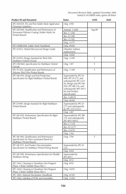
���
Document Revision Table, updated November 2006Sorted in NUMBER order, ignore all letters
Product ID and Document Status ANSI DoD
IPC-SM-839, Pre and Post Solder Mask Application Cleaning Guidelines
Orig. 4/90
IPC-SM-840, Qualification and Performance of Permanent Polymer Coating (Solder Mask) for Printed Boards
Amend. 1 6/00 Aug-00Rev. C 1/96Rev. B 5/88Rev. A 7/83Orig. 11/77
IPC-HDBK-840, Solder Mask Handbook Orig. 09/06IPC-H-855, Hybrid Microcircuit Design Guide Obsolete without
replacementOrig. 10/82
IPC-D-859, Design Standard for Thick Film Multilayer Hybrid Circuits
Orig. 12/89 Y
IPC-HM-860, Specification for Multilayer Hybrid Circuits
Orig. 1/87 Y
IPC-TF-870, Qualification and Performance of Polymer Thick Film Printed Boards
Orig. 11/89 Y
IPC-ML-910, Design and End Production Specification for Rigid Multilayer Printed Boards
Superseded by IPC-D-949, IPC-D-275, and subsequently IPC-2221 for Design and IPC-ML-950, IPC-RB-276, and subsequently IIPC-6011 for End Product SpecificationRev. A 08/76Orig. 06/68
IPC-D-949, Design Standard for Rigid Multilayer Printed Boards
Superseded by IPC-D-275 and subsequently by IPC-2221/2222Orig. 1/87
IPC-ML-950, Performance Specification for Rigid Multilayer Printed Boards
Superseded by IPC-RB-276 and subsequently IPC-6011/6012Rev. C 11/8Rev. B 12/77Rev. A 9/70Orig. 1/66
IPC-ML-960, Qualification and Performance Specification for Mass Laminated Panels for Multilayer Printed Boards
Orig. 7/94 Y
IPC-ML-975, End Product Documentation Specification for Multilayer Printed Wiring Boards
Superseded by IPC-D-325Orig. 9/69
IPC-ML-990, Performance Specification for Flexible Multilayer Wiring
Superseded by IPC-6011Orig. 9/72
IPC-1043, Cleaning & Cleanliness Test Program Phase 3 Water Soluble Fluxes Part 1
Orig. 8/92
IPC-1044, Cleaning & Cleanliness Test Program Phase 3 Water Soluble Fluxes Part 2
Orig. 10/92
IPC-1065, Material Declaration Handbook Orig. 01/05IPC-1066, Labeling of PCBs and Assemblies Orig. 12/04

���
Document Revision Table, updated November 2006Sorted in NUMBER order, ignore all letters
Product ID and Document Status ANSI DoD
IPC-TP-1090, The Layman’s Guide to Qualifying New Fluxes for MIL-STD-2000A or MT-0002
Orig. 7/96
IPC-TP-1103, Manufacturing Concerns When Soldering with Gold Plated Component Leads or Circuit Board Pads
Obsolete without replacement
IPC-TP-1114, The Layman’s Guide to Qualifying a Process to J-STD-001B
Orig. 1/98
IPC-TP-1115, Selection and Implementation Strategy for A Low-Residue No-Clean Process
Orig. 12/98
IPC-1131, IT Guidelines for PWB Manufacturers Orig. 04/00IPC-1331, Voluntary Safety Standard for Electrically Heated Process Equipment
Orig. 3/00
IPC-1710, OEM Standard for Printed Board Manufacturers’ Qualification Profile (MQP)
Rev. A 7/0412/97 updatedOrig. 2/94
IPC-1720, Assembly Qualification Profile (AQP) Rev. A 7/04Orig. 7/96
IPC-1730, Laminator Qualification Profile (LQP) Rev. A 6/00Orig. 1/98
IPC-1731, Strategic Raw Materials Supplier Qualification Profile
Orig. 6/00
IPC-1751, Generic Requirements for Declaration Process Management
Orig. 3/06
IPC-1752, Materials Declaration Management (Includes 2 PDF forms)
Orig. 3/06
IPC-1902, Grid Systems for Printed Circuits (equivalent to IEC 60097)
Orig. 03/99
IPC-2141, Controlled Impedance Circuit Boards and High Speed Logic Design
Rev. A 3/04Orig. 4/96
IPC-2221, Generic Standard on Printed Board Design
Rev. A 5/03Amend. 1 01/00Supersedes IPC-D-275Orig. 2/98
IPC-2222, Sectional Design Standard for Rigid Organic Printed Boards
Supersedes IPC-D-275Orig. 2/98
IPC-2223, Sectional Design Standard for Flexible Printed Boards
Rev. A 06/04Supersedes IPC-D-249Orig. 11/98
IPC-2224, Sectional Standard for Design of PWBs for PC Cards
Orig. 01/98
IPC-2225, Sectional Design Standard for Organic Multichip Modules (MCM-L) and MCM-L Assemblies
Orig. 05/98
IPC-2226, Design Standard for High-Density Array or Peripheral Leaded Component Mounting Structures
Orig. 4/03
IPC-2251, Design Guidelines for Electronic Packaging Utilizing High Speed Techniques
Orig. 12/03
IPC-2252, Design and Manufacturing Guide for RF/Microwave Circuit Boards
Orig. 7/02
IPC/JPCA-2315, Design Guide for High Density Interconnects (HDI) and Microvia
Orig. 6/00
IPC-2501, Definition for Web-based Exchange of XML Data
Orig. 7/03 Y
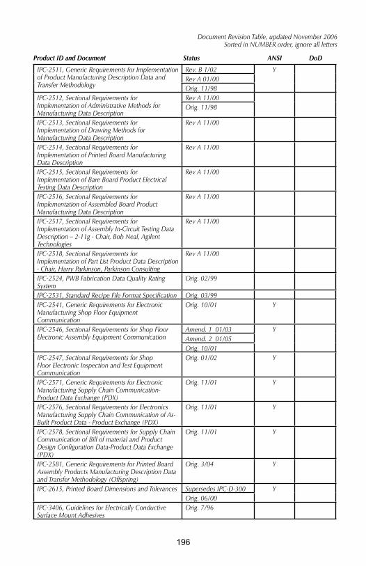
���
Document Revision Table, updated November 2006Sorted in NUMBER order, ignore all letters
Product ID and Document Status ANSI DoD
IPC-2511, Generic Requirements for Implementation of Product Manufacturing Description Data and Transfer Methodology
Rev. B 1/02 YRev A 01/00Orig. 11/98
IPC-2512, Sectional Requirements for Implementation of Administrative Methods for Manufacturing Data Description
Rev A 11/00Orig. 11/98
IPC-2513, Sectional Requirements for Implementation of Drawing Methods for Manufacturing Data Description
Rev A 11/00
IPC-2514, Sectional Requirements for Implementation of Printed Board Manufacturing Data Description
Rev A 11/00
IPC-2515, Sectional Requirements for Implementation of Bare Board Product Electrical Testing Data Description
Rev A 11/00
IPC-2516, Sectional Requirements for Implementation of Assembled Board Product Manufacturing Data Description
Rev A 11/00
IPC-2517, Sectional Requirements for Implementation of Assembly In-Circuit Testing Data Description – 2-11g - Chair, Bob Neal, Agilent Technologies
Rev A 11/00
IPC-2518, Sectional Requirements for Implementation of Part List Product Data Description - Chair, Harry Parkinson, Parkinson Consulting
Rev A 11/00
IPC-2524, PWB Fabrication Data Quality Rating System
Orig. 02/99
IPC-2531, Standard Recipe File Format Specification Orig. 03/99IPC-2541, Generic Requirements for Electronic Manufacturing Shop Floor Equipment Communication
Orig. 10/01 Y
IPC-2546, Sectional Requirements for Shop Floor Electronic Assembly Equipment Communication
Amend. 1 01/03 YAmend. 2 01/05Orig. 10/01
IPC-2547, Sectional Requirements for Shop Floor Electronic Inspection and Test Equipment Communication
Orig. 01/02 Y
IPC-2571, Generic Requirements for Electronic Manufacturing Supply Chain Communication-Product Data Exchange (PDX)
Orig. 11/01 Y
IPC-2576, Sectional Requirements for Electronics Manufacturing Supply Chain Communication of As-Built Product Data - Product Exchange (PDX)
Orig. 11/01 Y
IPC-2578, Sectional Requirements for Supply Chain Communication of Bill of material and Product Design Configuration Data-Product Data Exchange (PDX)
Orig. 11/01 Y
IPC-2581, Generic Requirements for Printed Board Assembly Products Manufacturing Description Data and Transfer Methodology (Offspring)
Orig. 3/04 Y
IPC-2615, Printed Board Dimensions and Tolerances Supersedes IPC-D-300 YOrig. 06/00
IPC-3406, Guidelines for Electrically Conductive Surface Mount Adhesives
Orig. 7/96

���
Document Revision Table, updated November 2006Sorted in NUMBER order, ignore all letters
Product ID and Document Status ANSI DoD
IPC-3408, General Requirements for Anistropically Conductive Adhesive Films
Orig. 11/96
IPC-4101, Specification for Base Materials for Rigid and Multilayer Boards
Rev. B 06/06Rev. A Amend 1 6/02Rev. A 06/02Supersedes IPC-L-108, IPC-L-109, IPC-L-112, IPC-L-115Orig. 12/97
IPC-4103, Specification for Plastic Substrates, Clad or Unclad, for High Speed/High Frequency Interconnection
Supersedes IPC-L-125 YOrig. 01/02
IPC/JPCA-4104, Specification for High Density Interconnect (HDI) and Microvia Materials
Orig. 5/99 May-99
IPC-4110, Specification and Characterization Methods for Nonwoven Cellulose Based Paper for Printed Boards
Orig. 8/98 Oct-98
IPC-4121, Guidelines for Selecting Core Constructions for Multilayer Printed Wiring Board Applications
Supersedes IPC-CC-110AOrig. 1/00
IPC-4130, Specification and Characterization Methods for Nonwoven “E” Glass Mat
Orig. 9/98 Dec-99
IPC-4202, Flexible Base Dielectrics for Use in Flexible Printed Wiring
Supersedes IPC-FC-231C
Jun-02 Feb-03
Orig. 05/02IPC-4203, Adhesive Coated Dielectric Films for Use as Cover Sheets
Supersedes IPC-FC-232C
Jun-02 Feb-03
Orig. 05/02IPC-4204, Flexible Metal-Clad Dielectrics for Use in Fabrication of Flexible Printed Circuitry
Supersedes IPC-FC-241C
Jun-02 Feb-03
Orig. 05/02IPC-4411, Specification and Characterization Methods for Nonwoven Para-Aramid Reinforcement
Rev. A 11/03Orig. 4/99
IPC-4412, Specification for Finished Fabric Woven form “E” Glass for Printed Boards
Supersedes IPC-EG-140A
Jul-02 Feb-03
Orig. 06/02IPC-4552, Specification for Electroless Nickel/Immersion Gold (ENIG) Plating for Printed Circuit Boards
Orig. 10/02 Nov-02
IPC-4553, Specification for Immersion Silver Plating for Printed Circuit Boards
Orig. 06/05 Sep-06
IPC-4562, Metal Foil for Printed Wiring Applications Amend. 1 May-05Supersedes IPC-MF-150F
Sep-00 Feb-03
Orig. 5/00IPC-4761 , Design Guide for Protection of Printed Board Via Structures
Orig. 07/06
IPC-4821, Specification for Embedded Passive Device Capacitor Materials for Rigid and Multilayer Printed Boards
Orig. 05/06
IPC-5701, Users Guide for Cleanliness of Unpopulated Printed Boards
Orig. 7/03
IPC-6011, Generic Performance Specification for Printed Boards
Orig. 7/96

���
Document Revision Table, updated November 2006Sorted in NUMBER order, ignore all letters
Product ID and Document Status ANSI DoD
IPC-6012, Qualification and Performance Specification for Rigid Printed Boards
Rev. B 08/04Amend. 1 07/00Rev. A 10/99Orig. 7/96
IPC-6013, Qualification and Performance Specification for Flexible Printed Boards
Rev. A with Amend. 2 04/06Amend. 1 01/05Rev. A 11/03Supersedes IPC-RF-245 and IPC-FC-250Amend. 1 04/00Orig. 11/98
IPC-6015, Qualification and Performance Specification for Organic Multichip Module (MCM-L) Mounting and Interconnecting Structures
Orig. 2/98
IPC-6016, Qualification and Performance Specification for High Density Interconnect (HDI) Layers or Boards
Orig. 05/99 Aug-99
IPC-6018, Microwave End Product Board Inspection and Test
Rev. A 01/02 YOrig. 1/98
IPC/JPCA-6202, Performance Guide Manual for Single- and Double-Sided Flexible Printed Wiring Boards
Orig. 2/99
IPC/JPCA-6801, Terms & Definitions, Test Methods, and Design Examples for Build-Up/High Density Interconnection
Orig. 1/00
IPC-7095, Design and Assembly Process Implementation for BGAs
Rev. A 11/04 Orig. 8/00
IPC-7351, Generic Requirements for Surface Mount Land Pattern and Design Standard
Orig. 02/05
IPC-7525, Guidelines for Stencil Design Orig. 05/00 Jun-00IPC-7530, Guidelines for Temperature Profiling for Mass Soldering (Wave and Reflow) Processes
Orig. 05/01
IPC-7351, Generic Requirements for Surface Mount Design and Land Pattern Standard
Supersedes IPC-SM-782A with Amendments 1 & 2Orig. 02/05
IPC-7711A/7721A, Rework, Repair and Modification of Electronic Assemblies
Rev A. 10/03Orig. 04/98 Supersedes IPC-R-700C
IPC-7912, Calculation of DPMO and Manufacturing Indices for Printed Wiring Assemblies
Rev. A 01/04 Jan-04Orig. 07/00
IPC-8413-1, Specification for Manufacturing Process Carriers for Handling Optical Fiber
Orig. 04/03
IPC-9151, Printed Board Capability, Quality and Relative Reliability (PCQR2) Benchmark Test Standard and Database
Rev. A 5/03Orig. 06/02
IPC-9191, General Guideline for implementation of Statistical Process Control (SPC)
Supersedes IPC-PC-90Orig. 11/99
IPC-9194, Implementation of Statistical Process Control (SPC) Applied to Printed Board Assembly Manufacture Guideline
Orig. 09/04
IPC-9199, SPC Quality Rating Orig. 09/02

���
Document Revision Table, updated November 2006Sorted in NUMBER order, ignore all letters
Product ID and Document Status ANSI DoD
IPC-9201, Surface Insulation Resistance Handbook Orig. 7/96IPC-9251, Test Vehicles for Evaluating Fine Line Capability
Orig. 7/00
IPC-9252, Guidelines and Requirements for Electrical Testing of Unpopulated Printed Boards
Supersedes IPC-ET-652AOrig. 02/01
IPC-9261, In-Process DPMO and Estimated Yield for PWAs
Rev. A 10/06 Mar-02Orig. 3/02
IPC-9501, PWB Assembly Process Simulation for Evaluation of Electronic Components
Orig. 7/95
IPC-9502, PWB Assembly Soldering Process Guidelines for Non-IC Electronic Components
Orig. 4/99
IPC-9503, Moisture Sensitivity Classification for Non-IC Components
Orig. 4/99
IPC-9504, Assembly Process Simulation for Evaluation of Non-IC Components
Orig. 6/98 Oct-98
IPC-9591, Performance Parameters (Mechanical, Electrical, Environmental and Quality/Reliability) for Air Moving Devices
Orig. 04/06
IPC-9691, User Guide for the IPC-TM-650, Method 2.6.25, Conductive Anodic Filament (CAF) Resistance Test (Electrochemical Migration Testing)
Orig. 10/05
IPC-9701, Qualification and Performance Test Methods for Surface Mount Solder Attachments
Rev. A 02/06 YOrig. 1/02
IPC/JEDEC-9702, Monotonic Bend Characterization of Board-Level Interconnects
Orig. 06/04
IPC-9850, Surface Mount Equipment Performance Characterization
Orig. 7/02 Sep-02
IPC-SMEMA-9851, Equipment Interface Specification
Orig. 11/04
IPC-DRM-SMT, Surface Mount Solder Joint Evaluation Desk Reference Manual
Rev. B 4/00Rev. A 3/99Orig. 7/98
IPC-EMSI-TC, IPC Sample Master Ordering Agreement for EMS Companies and OEMs
Orig. 03/02
Roadmap, National Technology Roadmap for Electronic Interconnections
Updated 2005Updated 2003Updated 2001Updated 9/97Orig. 6/95