Optimizing The Gate Level Area In Digit Serial FIR Filter Design With An MCM Blocks
10
Bayikati Yagneswar Int. Journal of Engineering Research and Applications www.ijera.com ISSN : 2248-9622, Vol. 4, Issue 6( Version 1), June 2014, pp.80-89 www.ijera.com 80 | Page Optimizing The Gate Level Area In Digit Serial FIR Filter Design With An MCM Blocks Bayikati Yagneswar 1 , G. Naresh 2 1 P.G. Student Scholar, M. Tech (VLSI) Department of E.C.E Sree Vidyanikethan Engineering College, Tirupati, A.P 2 M. Tech Assistant Professor Department of E.C.E Sree Vidyanikethan Engineering College, Tirupati, A.P Abstract The last two decades have seen many efficient algorithms and architectures for the design of low -complexity bit-parallel Multiple Constant Multiplications (MCM) operation, which dominates the complexity of Digital Signal Processing (DSP) systems. On the other hand, digit-serial architectures offer alternative low -complexity designs, since digit-serial operators occupy less area and are independent of the data wordlength. This paper introduces the problem of designing a digit-serial MCM operation with minimal area at gate-level and presents the exact formalization of the area optimization problem as a 0-1 Integer Linear Programming (ILP) problem and introduces high level synthesis algorithms, design architectures, and a computer aided design tool. Results and Discussion show the efficiency of the proposed optimization algorithms and of the digit-serial MCM architectures in the design of digit serial MCM operations and finite impulse response filters. Keywords— 0-1 Integer linear programming (ILP), digit-serial arithmetic, finite impulse response (FIR) filters, gate level area optimization, multiple constant multiplications. I. INTRODUCTION Finite impulse response (FIR) filters are of great importance in digital signal processing (DSP) systems since their characteristics in linear-phase and feed-forward implementations make them very useful for building stable high-performance filters. The direct and transposed-form FIR filter implementations are illustrated in Fig. 1(a) and (b), respectively. Although both architectures have similar complexity in hardware, the transposed form is generally preferred because of its higher performance and power efficiency [2]. The multiplier block of the digital FIR filter in its transposed form [Fig. 1(b)], where the multiplication of filter coefficients with the filter input is realized, has significant impact on the complexity and performance of the design because a large number of constant multiplications are required. This is generally known as the multiple constant multiplications (MCM) operation and is also a central operation and performance bottleneck in many other DSP systems such as fast Fourier transforms, discrete cosine transforms (DCTs), and error-correcting codes. Although area-, delay-, and power-efficient multiplier architectures, such as Wallace [3] and modified Booth multipliers, have been proposed, the full flexibility of a multiplier is not necessary for the constant multiplications, since filter coefficients are fixed and determined beforehand by the DSP algorithms. Hence, the multiplication of filter coefficients with the input data is generally implemented under a shift-adds architecture, where Fig. 1.FIR filter implementations. (a) Direct form. (b) Transposed form with generic multipliers. (c) Transposed form with an MCM block. each constant multiplication is realized using addition/subtraction and shift operations in an MCM operation [Fig. 1(c)]. For the shift-adds implementation of constant multiplications, a straightforward method, generally known as digit-based recoding, initially RESEARCH ARTICLE OPEN ACCESS
Transcript of Optimizing The Gate Level Area In Digit Serial FIR Filter Design With An MCM Blocks
Bayikati Yagneswar Int. Journal of Engineering Research and Applications www.ijera.com
ISSN : 2248-9622, Vol. 4, Issue 6( Version 1), June 2014, pp.80-89
www.ijera.com 80 | P a g e
Optimizing The Gate Level Area In Digit Serial FIR Filter Design
With An MCM Blocks
Bayikati Yagneswar1, G. Naresh
2
1P.G. Student Scholar, M. Tech (VLSI) Department of E.C.E Sree Vidyanikethan Engineering College, Tirupati,
A.P 2M. Tech Assistant Professor Department of E.C.E Sree Vidyanikethan Engineering College, Tirupati, A.P
Abstract The last two decades have seen many efficient algorithms and architectures for the design of low -complexity
bit-parallel Multiple Constant Multiplications (MCM) operation, which dominates the complexity of Digital
Signal Processing (DSP) systems. On the other hand, digit-serial architectures offer alternative low -complexity
designs, since digit-serial operators occupy less area and are independent of the data wordlength. This paper
introduces the problem of designing a digit-serial MCM operation with minimal area at gate-level and presents
the exact formalization of the area optimization problem as a 0-1 Integer Linear Programming (ILP) problem
and introduces high level synthesis algorithms, design architectures, and a computer aided design tool. Results
and Discussion show the efficiency of the proposed optimization algorithms and of the digit-serial MCM
architectures in the design of digit serial MCM operations and finite impulse response filters.
Keywords— 0-1 Integer linear programming (ILP), digit-serial arithmetic, finite impulse response (FIR) filters,
gate level area optimization, multiple constant multiplications.
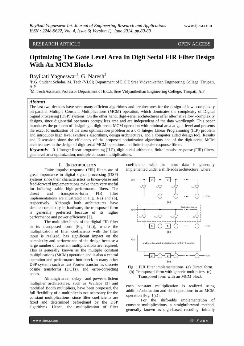
I. INTRODUCTION Finite impulse response (FIR) filters are of
great importance in digital signal processing (DSP)
systems since their characteristics in linear-phase and
feed-forward implementations make them very useful
for building stable high-performance filters. The
direct and transposed-form FIR filter
implementations are illustrated in Fig. 1(a) and (b),
respectively. Although both architectures have
similar complexity in hardware, the transposed form
is generally preferred because of its higher
performance and power efficiency [2].
The multiplier block of the digital FIR filter
in its transposed form [Fig. 1(b)], where the
multiplication of filter coefficients with the filter
input is realized, has significant impact on the
complexity and performance of the design because a
large number of constant multiplications are required.
This is generally known as the multiple constant
multiplications (MCM) operation and is also a central
operation and performance bottleneck in many other
DSP systems such as fast Fourier transforms, discrete
cosine transforms (DCTs), and error-correcting
codes.
Although area-, delay-, and power-efficient
multiplier architectures, such as Wallace [3] and
modified Booth multipliers, have been proposed, the
full flexibility of a multiplier is not necessary for the
constant multiplications, since filter coefficients are
fixed and determined beforehand by the DSP
algorithms. Hence, the multiplication of filter
coefficients with the input data is generally
implemented under a shift-adds architecture, where
Fig. 1.FIR filter implementations. (a) Direct form.
(b) Transposed form with generic multipliers. (c)
Transposed form with an MCM block.
each constant multiplication is realized using
addition/subtraction and shift operations in an MCM
operation [Fig. 1(c)].
For the shift-adds implementation of
constant multiplications, a straightforward method,
generally known as digit-based recoding, initially
RESEARCH ARTICLE OPEN ACCESS
Bayikati Yagneswar Int. Journal of Engineering Research and Applications www.ijera.com
ISSN : 2248-9622, Vol. 4, Issue 6( Version 1), June 2014, pp.80-89
www.ijera.com 81 | P a g e
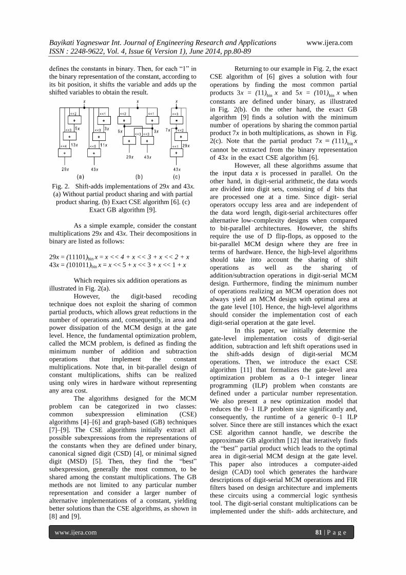
defines the constants in binary. Then, for each ―1‖ in
the binary representation of the constant, according to
its bit position, it shifts the variable and adds up the
shifted variables to obtain the result.
Fig. 2. Shift-adds implementations of 29x and 43x.
(a) Without partial product sharing and with partial
product sharing. (b) Exact CSE algorithm [6]. (c)
Exact GB algorithm [9].
As a simple example, consider the constant
multiplications 29x and 43x. Their decompositions in
binary are listed as follows:
29x = (11101)bin x = x << 4 + x << 3 + x << 2 + x
43x = (101011)bin x = x << 5 + x << 3 + x << 1 + x
Which requires six addition operations as
illustrated in Fig. 2(a).
However, the digit-based recoding
technique does not exploit the sharing of common
partial products, which allows great reductions in the
number of operations and, consequently, in area and
power dissipation of the MCM design at the gate
level. Hence, the fundamental optimization problem,
called the MCM problem, is defined as finding the
minimum number of addition and subtraction
operations that implement the constant
multiplications. Note that, in bit-parallel design of
constant multiplications, shifts can be realized
using only wires in hardware without representing
any area cost.
The algorithms designed for the MCM
problem can be categorized in two classes:
common subexpression elimination (CSE)
algorithms [4]–[6] and graph-based (GB) techniques
[7]–[9]. The CSE algorithms initially extract all
possible subexpressions from the representations of
the constants when they are defined under binary,
canonical signed digit (CSD) [4], or minimal signed
digit (MSD) [5]. Then, they find the ―best‖
subexpression, generally the most common, to be
shared among the constant multiplications. The GB
methods are not limited to any particular number
representation and consider a larger number of
alternative implementations of a constant, yielding
better solutions than the CSE algorithms, as shown in
[8] and [9].
Returning to our example in Fig. 2, the exact
CSE algorithm of [6] gives a solution with four
operations by finding the most common partial
products 3x = (11)bin x and 5x = (101)
bin x when
constants are defined under binary, as illustrated
in Fig. 2(b). On the other hand, the exact GB
algorithm [9] finds a solution with the minimum
number of operations by sharing the common partial
product 7x in both multiplications, as shown in Fig.
2(c). Note that the partial product 7x = (111)bin x
cannot be extracted from the binary representation
of 43x in the exact CSE algorithm [6].
However, all these algorithms assume that
the input data x is processed in parallel. On the
other hand, in digit-serial arithmetic, the data words
are divided into digit sets, consisting of d bits that
are processed one at a time. Since digit- serial
operators occupy less area and are independent of
the data word length, digit-serial architectures offer
alternative low-complexity designs when compared
to bit-parallel architectures. However, the shifts
require the use of D flip-flops, as opposed to the
bit-parallel MCM design where they are free in
terms of hardware. Hence, the high-level algorithms
should take into account the sharing of shift
operations as well as the sharing of
addition/subtraction operations in digit-serial MCM
design. Furthermore, finding the minimum number
of operations realizing an MCM operation does not
always yield an MCM design with optimal area at
the gate level [10]. Hence, the high-level algorithms
should consider the implementation cost of each
digit-serial operation at the gate level.
In this paper, we initially determine the
gate-level implementation costs of digit-serial
addition, subtraction and left shift operations used in
the shift-adds design of digit-serial MCM
operations. Then, we introduce the exact CSE
algorithm [11] that formalizes the gate-level area
optimization problem as a 0–1 integer linear
programming (ILP) problem when constants are
defined under a particular number representation.
We also present a new optimization model that
reduces the 0–1 ILP problem size significantly and,
consequently, the runtime of a generic 0–1 ILP
solver. Since there are still instances which the exact
CSE algorithm cannot handle, we describe the
approximate GB algorithm [12] that iteratively finds
the ―best‖ partial product which leads to the optimal
area in digit-serial MCM design at the gate level.
This paper also introduces a computer-aided
design (CAD) tool which generates the hardware
descriptions of digit-serial MCM operations and FIR
filters based on design architecture and implements
these circuits using a commercial logic synthesis
tool. The digit-serial constant multiplications can be
implemented under the shift- adds architecture, and
Bayikati Yagneswar Int. Journal of Engineering Research and Applications www.ijera.com
ISSN : 2248-9622, Vol. 4, Issue 6( Version 1), June 2014, pp.80-89
www.ijera.com 82 | P a g e
also can be designed using generic digit- serial
constant multipliers.
Results on a comprehensive set of
instances show that the solutions of algorithms
introduced in this paper lead to significant
improvements in area of digit-serial MCM designs
compared to those obtained using the algorithms
designed for the MCM problem. The digit-serial FIR
filter designs obtained by CAD tool also indicate that
the realization of the multiplier block of a digit-serial
FIR filter under the shift- adds architecture
significantly reduces the area of digit-serial FIR
filters with respect to those designed using digit-
serial constant multipliers. Additionally, it is
observed that the optimal tradeoff between area and
delay in digit-serial FIR filter designs can be
explored by changing the digit size d.
II. BACKGROUND This section presents the main concepts
related to the proposed algorithms, introduces the
problem definitions, and gives an overview on
previously proposed algorithms.
A. Number Representation
The binary representation decomposes a
number in a set of additions of powers of 2. The
representation of numbers using a signed digit system
makes use of positive and negative digits, {1, 0, −1}.
The CSD representation is a signed digit system
that has a unique representation for each number and
verifies the following main properties:
1) two nonzero digits are not adjacent
2) the number of nonzero digits is minimum.
Any n digit number in CSD has at most [(n
+1)/2] nonzero digits and, on average, the number
of nonzero digits is reduced by 33% when compared
to binary. The MSD representation [5] is obtained
by dropping the first property of the CSD
representation. Thus, a constant may have several
representations under MSD, including its CSD
representation, but all with a minimum number of
nonzero digits.
Consider the constant 23 defined in six bits.
Its binary representation 010111 includes four
nonzero digits. It is represented as 100110 in CSD,
and both 100110 and 101100 denote 23 in MSD
using three nonzero digits (where 1 stands for −1).
B. Boolean Satisfiability
A Boolean function ϕ: {0, 1}n → {0, 1} can
be denoted by a propositional formula. The
conjunctive normal form (CNF) is a representation
of a propositional formula consisting of a
conjunction of propositional clauses where each
clause is a disjunction of literals and a literal l j
is either a variable x j or its complement x j . Note
that, if a literal of a clause assumes value 1, then
the clause is satisfied. If all literals of a clause
assume the value 0, then the clause is unsatisfied.
The satisfiability (SAT) problem is to find an
assignment on n variables of the Boolean formula in
CNF that evaluates the formula to 1, or to prove that
the formula is equal to the constant 0.
Fig. 3. Combinational circuit and its corresponding
CNF formula.
A combinational circuit is a directed
acyclic graph with nodes corresponding to logic
gates and directed edges corresponding to wires
connecting the gates. Incoming edges of a node are
called fanins and outgoing edges are called fanouts.
The primary inputs of the network are the nodes
without fanins. The primary outputs are the nodes
without fanouts.
The CNF formula of a combinational circuit
is the conjunction of the CNF formulas of each gate,
where the CNF formula of each gate denotes the
valid input–output assignments to the gate. The
derivation of CNF formulas of basic logic gates
can be found in [13]. As a simple example, consider
the combinational circuit and its CNF formula given
in Fig. 3. In this Boolean formula, the first three
clauses represent the CNF formula of a two-input
AND gate, and the last three clauses denote the
CNF formula of a two-input OR gate. Observe from
Fig. 3 that the assignment x1 = x3 = x4 = x5
= 0 and x2 =1 makes the formula ϕ equal to 1,
indicating a valid assignment. However, the
assignment x1 = x3 = x4 = 0 and x2 = x5 = 1
makes the last clause of the formula equal to 0 and,
consequently, the formula ϕ , indicating a conflict
between the values of the inputs and output of the
OR gate.
C. 0-1 ILP
The 0–1 ILP problem is the minimization or
the maximization of a linear cost function subject to a
set of linear constraints and is generally defined as
follows:
Minimize wT ・ x (1)
s.t. A ・ x ≥ b, x ∈ {0, 1}n. (2)
In (1), wj in w is an integer value associated
with each of n variables x j, 1 ≤ j ≤ n, in the cost
function, and in (2), A・ x ≥ b denotes the set of m
linear constraints, where
b ∈ Zm and A ∈ Z
m × Z
n.
A clause l1 + ・ ・ ・ + lk, where k ≤ n, to
be satisfied in a CNF formula can be interpreted as a
linear inequality l1+・ ・ ・+lk ≥ 1, where x j is
Bayikati Yagneswar Int. Journal of Engineering Research and Applications www.ijera.com
ISSN : 2248-9622, Vol. 4, Issue 6( Version 1), June 2014, pp.80-89
www.ijera.com 83 | P a g e
represented by 1−x j, as shown in [14]. These linear
inequalities are commonly referred to as CNF
constraints, where ai j ∈ {−1, 0, 1} and bi is equal to 1
minus the total number of complemented variables in
its CNF formula. For instance, the set of clauses,
(x1 + x2), (x2 + x3), and (x1 + x3), has the equivalent
linear inequalities given as x1 + x2 ≥ 1, −x2 + x3 ≥ 0,
and −x1 − x3 ≥ −1, respectively.
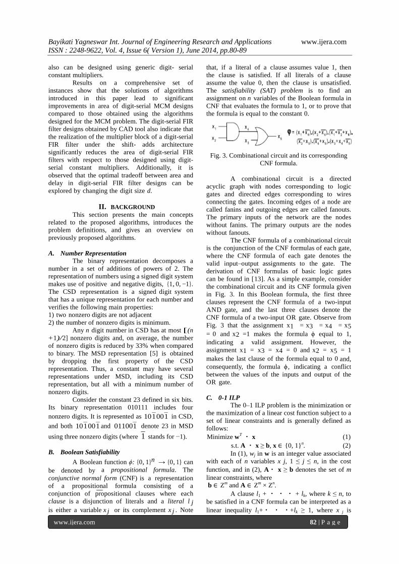
Fig. 4. Digit-serial operations when d is equal to 2.
(a) Addition operation. (b) Subtraction operation.
(c) Left shift by one time. (d) Left shift by two times.
D. Digit – Serial Arithmetic
In digit-serial arithmetic, data words are
divided into digits, with a digit size of d bits, which
are processed in one clock cycle. The special cases of
the digit-serial computation, called bit-serial and bit-
parallel processing, occur when the digit size d is
equal to 1 and input data wordlength, respectively.
The digit-serial computation plays an important role
when the bit-serial implementations cannot meet
delay requirements and the bit-parallel designs
require excessive hardware. Thus, an optimal tradeoff
between area and delay can be obtained by changing
the digit size parameter (d).
The digit-serial addition, subtraction, and
left shift operations are depicted in Figure 4 when d
is equal to 2. Notice from Figure 4(a) that in a digit-
serial addition operation, in general, the number of
required full adders (FAs) is equal to d and the
number of necessary D flip-flops is always 1. The
subtraction operation (Figure 4(b)) is implemented
using 2’s complement, requiring the initialization of
the D flip-flop with 1 and additional d inverter gates
with respect to the digit-serial addition operation. In a
left shift operation (Figure 4(c)-(d)), the number of
required D flip-flops is equal to the amount of shift.
The input-output correspondence and the number of
flip-flops cascaded serially for each input in a digit-
serial left shift operation are given in Eqn. (3) and (4)
respectively, where i ranges from 0 to d−1 and ls
denotes the amount of left shift.
ai => c(i + ls) mod d (3)
.,
)mod(,
Otherwised
ls
dlsdiifd
ls
FFai
(4)
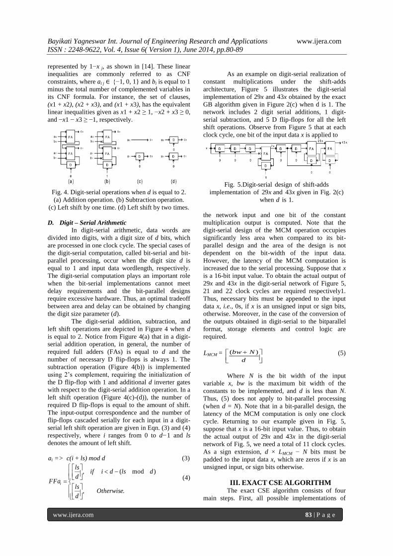
As an example on digit-serial realization of
constant multiplications under the shift-adds
architecture, Figure 5 illustrates the digit-serial
implementation of 29x and 43x obtained by the exact
GB algorithm given in Figure 2(c) when d is 1. The
network includes 2 digit serial additions, 1 digit-
serial subtraction, and 5 D flip-flops for all the left
shift operations. Observe from Figure 5 that at each
clock cycle, one bit of the input data x is applied to
Fig. 5.Digit-serial design of shift-adds
implementation of 29x and 43x given in Fig. 2(c)
when d is 1.
the network input and one bit of the constant
multiplication output is computed. Note that the
digit-serial design of the MCM operation occupies
significantly less area when compared to its bit-
parallel design and the area of the design is not
dependent on the bit-width of the input data.
However, the latency of the MCM computation is
increased due to the serial processing. Suppose that x
is a 16-bit input value. To obtain the actual output of
29x and 43x in the digit-serial network of Figure 5,
21 and 22 clock cycles are required respectively1.
Thus, necessary bits must be appended to the input
data x, i.e., 0s, if x is an unsigned input or sign bits,
otherwise. Moreover, in the case of the conversion of
the outputs obtained in digit-serial to the bitparallel
format, storage elements and control logic are
required.
LMCM =
d
Nbw )( (5)
Where N is the bit width of the input
variable x, bw is the maximum bit width of the
constants to be implemented, and d is less than N.
Thus, (5) does not apply to bit-parallel processing
(when d = N). Note that in a bit-parallel design, the
latency of the MCM computation is only one clock
cycle. Returning to our example given in Fig. 5,
suppose that x is a 16-bit input value. Thus, to obtain
the actual output of 29x and 43x in the digit-serial
network of Fig. 5, we need a total of 11 clock cycles.
As a sign extension, d × LMCM − N bits must be
padded to the input data x, which are zeros if x is an
unsigned input, or sign bits otherwise.
III. EXACT CSE ALGORITHM The exact CSE algorithm consists of four
main steps. First, all possible implementations of
Bayikati Yagneswar Int. Journal of Engineering Research and Applications www.ijera.com
ISSN : 2248-9622, Vol. 4, Issue 6( Version 1), June 2014, pp.80-89
www.ijera.com 84 | P a g e
constants are extracted from the nonzero digits of the
constants defined under a number representation:
binary, CSD, or MSD. Then, the implementations of
constants are represented in terms of a Boolean
network. Third, the gate-level area optimization
problem is formalized as a 0–1 ILP problem with a
cost function to be minimized and a set of constraints
to be satisfied. Finally, a set of operations that yields
the minimum area solution is obtained using a
generic 0–1 ILP solver. These four steps are
described in detail next.
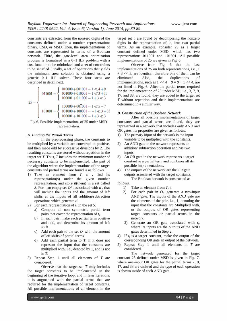
Fig.6. Possible implementations of 25 under MSD
representation.
A. Finding the Partial Terms
In the preprocessing phase, the constants to
be multiplied by a variable are converted to positive,
and then made odd by successive divisions by 2. The
resulting constants are stored without repetition in the
target set T. Thus, T includes the minimum number of
necessary constants to be implemented. The part of
the algorithm where the implementations of the target
constants and partial terms are found is as follows.
1) Take an element from T, ti , find its
representation(s) under the given number
representation, and store it(them) in a set called
S. Form an empty set Oi , associated with ti , that
will include the inputs and the amount of left
shifts at the inputs of all addition/subtraction
operations which generate ti .
2) For each representation of ti in the set S.
a) Compute all non symmetric partial term
pairs that cover the representation of ti.
b) In each pair, make each partial term positive
and odd, and determine its amount of left
shift.
c) Add each pair to the set Oi with the amount
of left shifts of partial terms.
d) Add each partial term to T, if it does not
represent the input that the constants are
multiplied with, i.e., denoted by 1, and is not
in T.
3) Repeat Step 1 until all elements of T are
considered.
Observe that the target set T only includes
the target constants to be implemented in the
beginning of the iterative loop, and in later iterations
it is augmented with the partial terms that are
required for the implementation of target constants.
All possible implementations of an element in the
target set ti are found by decomposing the nonzero
digits in the representation of, ti, into two partial
terms. As an example, consider 25 as a target
constant defined under MSD, which has two
representations 011001 and 101001. All possible
implementations of 25 are given in Fig. 6.
Observe from Fig. 6 that the last
implementations of 25 on both representations, i.e., 1
+ 3 << 3, are identical, therefore one of them can be
eliminated. Also, the duplications of
implementations, such as 1 << 4 + 9 = 9 + 1 << 4, are
not listed in Fig. 6. After the partial terms required
for the implementation of 25 under MSD, i.e., 3, 7, 9,
17, and 33, are found, they are added to the target set
T without repetition and their implementations are
determined in a similar way.
B. Construction of the Boolean Network
After all possible implementations of target
constants and partial terms are found, they are
represented in a network that includes only AND and
OR gates. Its properties are given as follows.
1) The primary input of the network is the input
variable to be multiplied with the constants.
2) An AND gate in the network represents an
addition/ subtraction operation and has two
inputs.
3) An OR gate in the network represents a target
constant or a partial term and combines all its
possible implementations.
4) The outputs of the network are the OR gate
outputs associated with the target constants.
The Boolean network is constructed as
follows.
1) Take an element from T, ti.
2) For each pair in Oi, generate a two-input
AND gate. The inputs of the AND gate are
the elements of the pair, i.e., 1, denoting the
input that the constants are Multiplied with,
or the outputs of OR gates representing
target constants or partial terms in the
network.
3) Generate an OR gate associated with ti,
where its inputs are the outputs of the AND
gates determined in Step 2.
4) If ti is a target constant, make the output of the
corresponding OR gate an output of the network.
5) Repeat Step 1 until all elements in T are
considered.
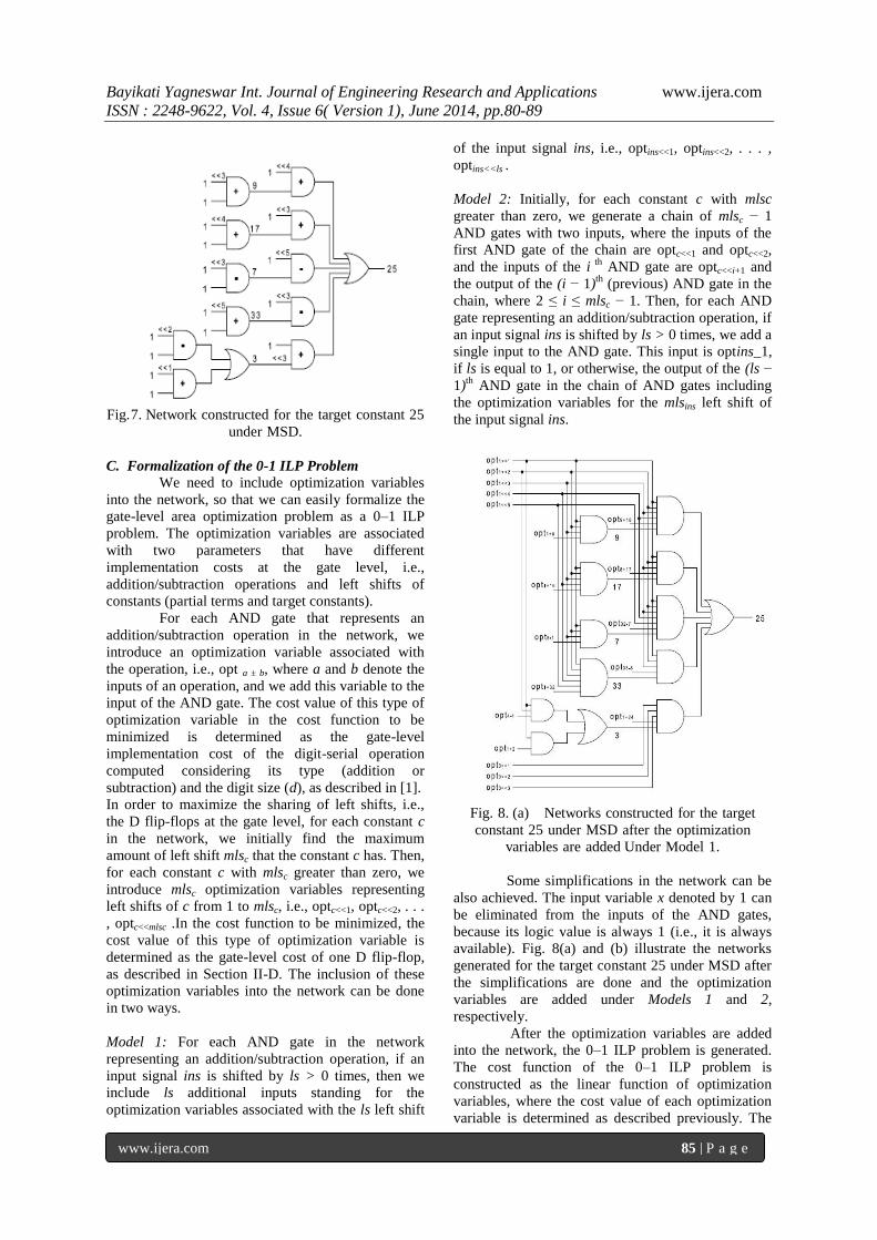
The network generated for the target
constant 25 defined under MSD is given in Fig. 7,
where one-input OR gates for the partial terms 7, 9,
17, and 33 are omitted and the type of each operation
is shown inside of each AND gate.
Bayikati Yagneswar Int. Journal of Engineering Research and Applications www.ijera.com
ISSN : 2248-9622, Vol. 4, Issue 6( Version 1), June 2014, pp.80-89
www.ijera.com 85 | P a g e
Fig.7. Network constructed for the target constant 25
under MSD.
C. Formalization of the 0-1 ILP Problem
We need to include optimization variables
into the network, so that we can easily formalize the
gate-level area optimization problem as a 0–1 ILP
problem. The optimization variables are associated
with two parameters that have different
implementation costs at the gate level, i.e.,
addition/subtraction operations and left shifts of
constants (partial terms and target constants).
For each AND gate that represents an
addition/subtraction operation in the network, we
introduce an optimization variable associated with
the operation, i.e., opt a ± b, where a and b denote the
inputs of an operation, and we add this variable to the
input of the AND gate. The cost value of this type of
optimization variable in the cost function to be
minimized is determined as the gate-level
implementation cost of the digit-serial operation
computed considering its type (addition or
subtraction) and the digit size (d), as described in [1].
In order to maximize the sharing of left shifts, i.e.,
the D flip-flops at the gate level, for each constant c
in the network, we initially find the maximum
amount of left shift mlsc that the constant c has. Then,
for each constant c with mlsc greater than zero, we
introduce mlsc optimization variables representing
left shifts of c from 1 to mlsc, i.e., optc<<1, optc<<2, . . .
, optc<<mlsc .In the cost function to be minimized, the
cost value of this type of optimization variable is
determined as the gate-level cost of one D flip-flop,
as described in Section II-D. The inclusion of these
optimization variables into the network can be done
in two ways.
Model 1: For each AND gate in the network
representing an addition/subtraction operation, if an
input signal ins is shifted by ls > 0 times, then we
include ls additional inputs standing for the
optimization variables associated with the ls left shift
of the input signal ins, i.e., optins<<1, optins<<2, . . . ,
optins<<ls .
Model 2: Initially, for each constant c with mlsc
greater than zero, we generate a chain of mlsc − 1
AND gates with two inputs, where the inputs of the
first AND gate of the chain are optc<<1 and optc<<2,
and the inputs of the i th
AND gate are optc<<i+1 and
the output of the (i − 1)th
(previous) AND gate in the
chain, where 2 ≤ i ≤ mlsc − 1. Then, for each AND
gate representing an addition/subtraction operation, if
an input signal ins is shifted by ls > 0 times, we add a
single input to the AND gate. This input is optins_1,
if ls is equal to 1, or otherwise, the output of the (ls −
1)th
AND gate in the chain of AND gates including
the optimization variables for the mlsins left shift of
the input signal ins.
Fig. 8. (a) Networks constructed for the target
constant 25 under MSD after the optimization
variables are added Under Model 1.
Some simplifications in the network can be
also achieved. The input variable x denoted by 1 can
be eliminated from the inputs of the AND gates,
because its logic value is always 1 (i.e., it is always
available). Fig. 8(a) and (b) illustrate the networks
generated for the target constant 25 under MSD after
the simplifications are done and the optimization
variables are added under Models 1 and 2,
respectively.
After the optimization variables are added
into the network, the 0–1 ILP problem is generated.
The cost function of the 0–1 ILP problem is
constructed as the linear function of optimization
variables, where the cost value of each optimization
variable is determined as described previously. The
Bayikati Yagneswar Int. Journal of Engineering Research and Applications www.ijera.com
ISSN : 2248-9622, Vol. 4, Issue 6( Version 1), June 2014, pp.80-89
www.ijera.com 86 | P a g e
constraints of the 0–1 ILP problem are obtained by
finding the CNF formulas of each gate in the network
and expressing each clause of the CNF formulas as a
linear inequality, as described in Section II-C. The
outputs of the network, i.e., the outputs of OR gates
associated with the target constants, are set to 1, since
the implementation of target constants is aimed.
Observe from Fig. 8(a) and (b) that Model 1
generates a 0-1 ILP problem including slightly less
number of variables than Model 2 due to the chain of
AND gates used in Model 2. However, the 0–1 ILP
problem constructed under Model 2 has significantly
less number of constraints than that of Model 1 since
the number of inputs of an AND gate representing an
addition /subtraction operation is increased only by 1
during the inclusion of the optimization variables
denoting the left shift of a constant in Model 2. Note
that the number of optimization variables under both
models is the same.
Fig. 8. (b) Networks constructed for the target
constant 25 under MSD after the optimization
variables are added Under Model 2.
E. Finding the Minimum Area Solution
A generic 0–1 ILP solver will search for the
minimum value of the cost function on the generated
0–1 ILP problem by satisfying the constraints that
represent how target constants and partial terms are
implemented. The set of operations that yields the
minimum area solution consists of the
addition/subtraction operations whose optimization
variables are set to 1 in the solution obtained by the
0–1 ILP solver.
IV. APPROXIMATE GB ALGORITHM The solution of an exact CSE algorithm
described in Section III is not the global minimum
since all possible implementations of a constant are
found from its representation. Also, the optimization
of gate-level area problem in digit-serial MCM
design is an NP-complete problem due to the NP-
completeness of the MCM problem. Thus, naturally,
there will be always 0–1 ILP problems generated by
the exact CSE algorithm that current 0–1 ILP solvers
find difficult to handle. Hence, the GB heuristic
algorithms, which obtain a good solution using less
computational resources, are indispensable.
In our approximate algorithm called
MINAS-DS[1], as done in algorithms designed for
the MCM problem given in Definition 1[1], we find
the fewest number of intermediate constants such that
all the target and intermediate constants are
synthesized using a single operation. However, while
selecting an intermediate constant for the
implementation of the not yet synthesized target
constants in each iteration, we favor the one among
the possible intermediate constants that can be
synthesized using the least hardware and will enable
us to implement the not-yet synthesized target
constants in a smaller area with the available
constants. After the set of target and intermediate
constants that realizes the MCM operation is found,
each constant is synthesized using an A-operation
that yields the minimum area in the digit-serial MCM
design. In MINAS-DS, the area of the digit-serial
MCM operation is determined as the total gate-level
implementation cost of each digit-serial addition,
subtraction, and shift operation under the digit size
parameter d as described in Section II-D.
V. FIR FILTER DESIGN
This section is divided in two parts: the first
part presents the results of high-level algorithms on
digit-serial MCM blocks design and second part
presents the digit-serial FIR filter design.
A. Digit-Serial MCM Design
The digit-serial realization of multiple
constant multiplications under the shift-adds
architecture is illustrated in Fig. 4 digit-serial
implementation of 29x and 43x obtained by the exact
GB algorithm given in Fig. 2(c) with digit size equal
to 1. As can be easily observed, the network includes
2 digit-serial addition, 1 digit-serial subtractions, and
5 D flip-flops for all the left shift operations. In this
network, at each clock cycle, two bits of input data x
is applied to the network and two bits of the constant
multiplications output is computed at the output of
digit-serial addition/ subtraction operation. While
sharing of addition/ subtraction operation reduces the
complexity of the digit-serial MCM design (since
each addition and subtraction operation requires a
digit-serial operation), the sharing of shift operations
for a constant multiplication also reduces the number
of D flip-flops and, consequently, the area of the
digit-serial MCM design[12][15].
Bayikati Yagneswar Int. Journal of Engineering Research and Applications www.ijera.com
ISSN : 2248-9622, Vol. 4, Issue 6( Version 1), June 2014, pp.80-89
www.ijera.com 87 | P a g e
B. Digit-Serial FIR Filter Design
The realization of Digit-serial FIR filter
using Multiple Constant Multiplication is illustrated
in Fig. 1(c) the multiplier block is replaced by
Multiple Constant Multiplication (MCM) block.
Initially multiplier block is implemented
based on CSE and GB algorithms using digit-serial
addition, subtraction, and shift operations and then
digit-serial FIR filter is implemented by using
multiplier block. Hence these architectures requires
less area, power and delay Compared to bit-parallel
FIR filter. In practical, there should be a tradeoff
between area and delay, it is mainly depends on digit
size d. The digit-serial MCM blocks has been
implemented with the constant coefficients 29, 43
with the digit size 1 by using the graph based
technique through this the digit-serial FIR filter has
been developed like as shown in Fig. 1(c). It can
require a delay elements and adders with an MCM
block.
VI. RESULTS AND DISCUSSIONS This section presents the results of high-
level algorithms on MCM blocks of FIR filters.
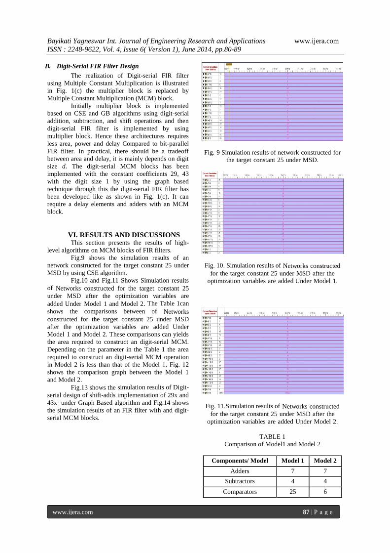
Fig.9 shows the simulation results of an
network constructed for the target constant 25 under
MSD by using CSE algorithm.
Fig.10 and Fig.11 Shows Simulation results
of Networks constructed for the target constant 25
under MSD after the optimization variables are
added Under Model 1 and Model 2. The Table 1can
shows the comparisons between of Networks
constructed for the target constant 25 under MSD
after the optimization variables are added Under
Model 1 and Model 2. These comparisons can yields
the area required to construct an digit-serial MCM.
Depending on the parameter in the Table 1 the area
required to construct an digit-serial MCM operation
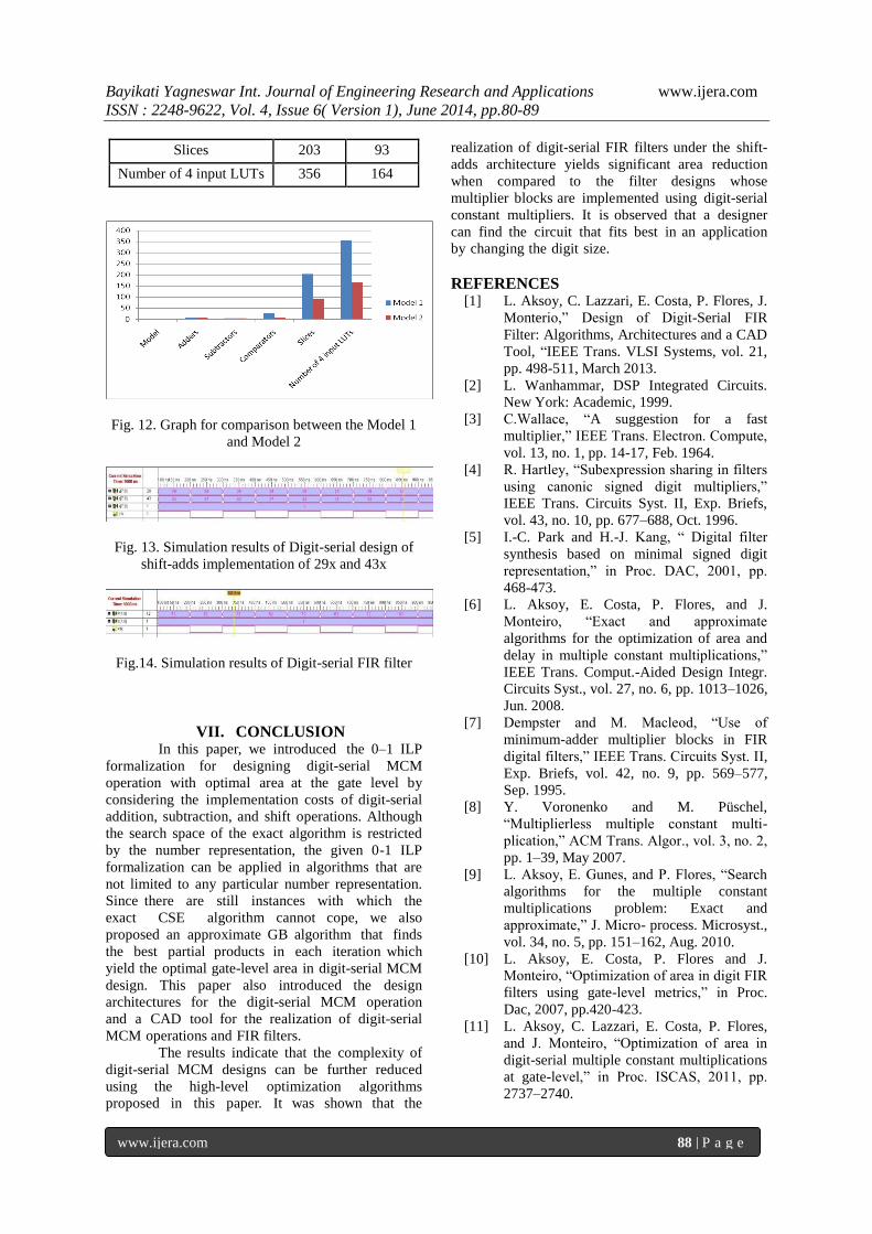
in Model 2 is less than that of the Model 1. Fig. 12
shows the comparison graph between the Model 1
and Model 2.
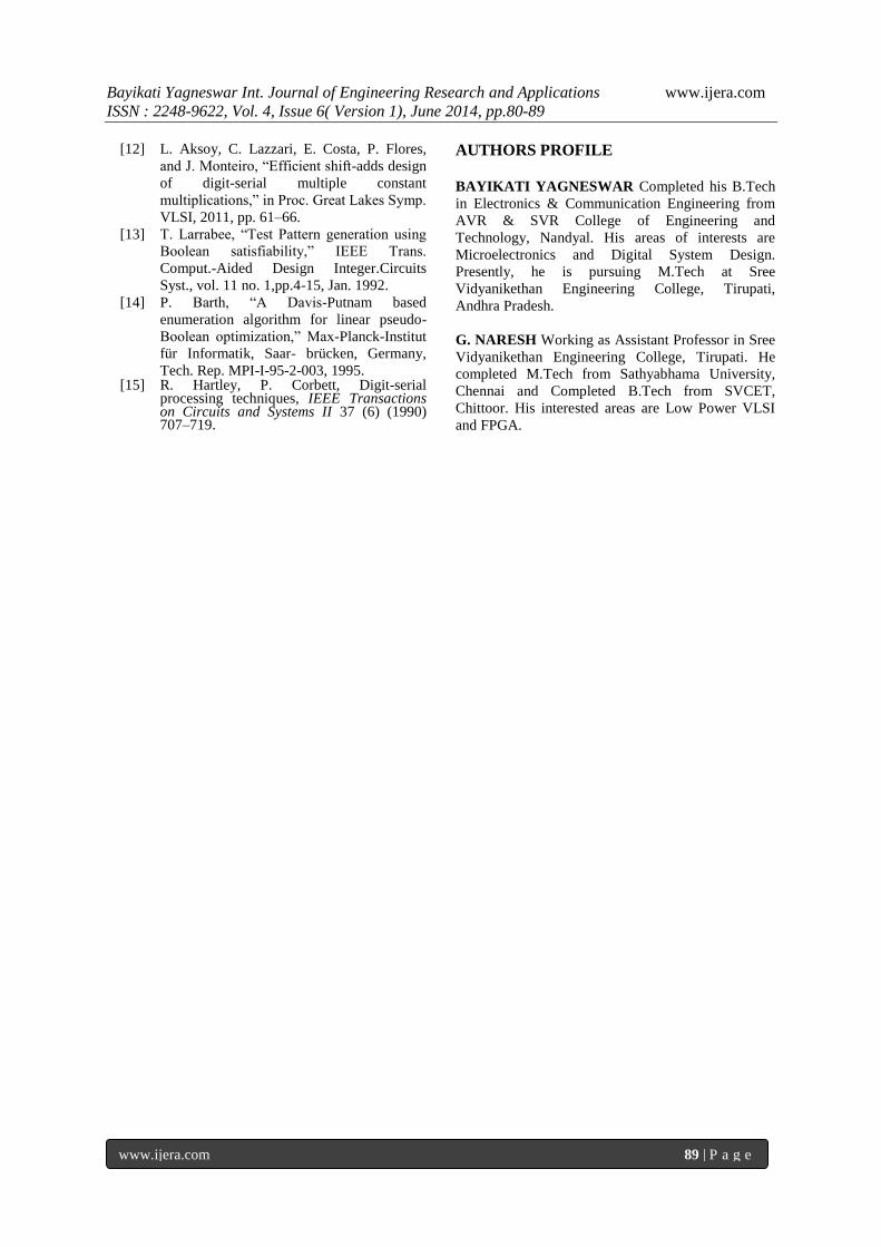
Fig.13 shows the simulation results of Digit-
serial design of shift-adds implementation of 29x and
43x under Graph Based algorithm and Fig.14 shows
the simulation results of an FIR filter with and digit-
serial MCM blocks.
Fig. 9 Simulation results of network constructed for
the target constant 25 under MSD.
Fig. 10. Simulation results of Networks constructed
for the target constant 25 under MSD after the
optimization variables are added Under Model 1.
Fig. 11.Simulation results of Networks constructed
for the target constant 25 under MSD after the
optimization variables are added Under Model 2.
TABLE 1
Comparison of Model1 and Model 2
Components/ Model Model 1 Model 2
Adders 7 7
Subtractors 4 4
Comparators 25 6
Bayikati Yagneswar Int. Journal of Engineering Research and Applications www.ijera.com
ISSN : 2248-9622, Vol. 4, Issue 6( Version 1), June 2014, pp.80-89
www.ijera.com 88 | P a g e
Slices 203 93
Number of 4 input LUTs 356 164
Fig. 12. Graph for comparison between the Model 1
and Model 2
Fig. 13. Simulation results of Digit-serial design of
shift-adds implementation of 29x and 43x
Fig.14. Simulation results of Digit-serial FIR filter
VII. CONCLUSION In this paper, we introduced the 0–1 ILP
formalization for designing digit-serial MCM
operation with optimal area at the gate level by
considering the implementation costs of digit-serial
addition, subtraction, and shift operations. Although
the search space of the exact algorithm is restricted
by the number representation, the given 0-1 ILP
formalization can be applied in algorithms that are
not limited to any particular number representation.
Since there are still instances with which the
exact CSE algorithm cannot cope, we also
proposed an approximate GB algorithm that finds
the best partial products in each iteration which
yield the optimal gate-level area in digit-serial MCM
design. This paper also introduced the design
architectures for the digit-serial MCM operation
and a CAD tool for the realization of digit-serial
MCM operations and FIR filters.
The results indicate that the complexity of
digit-serial MCM designs can be further reduced
using the high-level optimization algorithms
proposed in this paper. It was shown that the
realization of digit-serial FIR filters under the shift-
adds architecture yields significant area reduction
when compared to the filter designs whose
multiplier blocks are implemented using digit-serial
constant multipliers. It is observed that a designer
can find the circuit that fits best in an application
by changing the digit size.
REFERENCES [1] L. Aksoy, C. Lazzari, E. Costa, P. Flores, J.
Monterio,‖ Design of Digit-Serial FIR
Filter: Algorithms, Architectures and a CAD
Tool, ―IEEE Trans. VLSI Systems, vol. 21,
pp. 498-511, March 2013.
[2] L. Wanhammar, DSP Integrated Circuits.
New York: Academic, 1999.
[3] C.Wallace, ―A suggestion for a fast
multiplier,‖ IEEE Trans. Electron. Compute,
vol. 13, no. 1, pp. 14-17, Feb. 1964.
[4] R. Hartley, ―Subexpression sharing in filters
using canonic signed digit multipliers,‖
IEEE Trans. Circuits Syst. II, Exp. Briefs,
vol. 43, no. 10, pp. 677–688, Oct. 1996.
[5] I.-C. Park and H.-J. Kang, ― Digital filter
synthesis based on minimal signed digit
representation,‖ in Proc. DAC, 2001, pp.
468-473.
[6] L. Aksoy, E. Costa, P. Flores, and J.
Monteiro, ―Exact and approximate
algorithms for the optimization of area and
delay in multiple constant multiplications,‖
IEEE Trans. Comput.-Aided Design Integr.
Circuits Syst., vol. 27, no. 6, pp. 1013–1026,
Jun. 2008.
[7] Dempster and M. Macleod, ―Use of
minimum-adder multiplier blocks in FIR
digital filters,‖ IEEE Trans. Circuits Syst. II,
Exp. Briefs, vol. 42, no. 9, pp. 569–577,
Sep. 1995.
[8] Y. Voronenko and M. Püschel,
―Multiplierless multiple constant multi-
plication,‖ ACM Trans. Algor., vol. 3, no. 2,
pp. 1–39, May 2007.
[9] L. Aksoy, E. Gunes, and P. Flores, ―Search
algorithms for the multiple constant
multiplications problem: Exact and
approximate,‖ J. Micro- process. Microsyst.,
vol. 34, no. 5, pp. 151–162, Aug. 2010.
[10] L. Aksoy, E. Costa, P. Flores and J.
Monteiro, ―Optimization of area in digit FIR
filters using gate-level metrics,‖ in Proc.
Dac, 2007, pp.420-423.
[11] L. Aksoy, C. Lazzari, E. Costa, P. Flores,
and J. Monteiro, ―Optimization of area in
digit-serial multiple constant multiplications
at gate-level,‖ in Proc. ISCAS, 2011, pp.
2737–2740.
Bayikati Yagneswar Int. Journal of Engineering Research and Applications www.ijera.com
ISSN : 2248-9622, Vol. 4, Issue 6( Version 1), June 2014, pp.80-89
www.ijera.com 89 | P a g e
[12] L. Aksoy, C. Lazzari, E. Costa, P. Flores,
and J. Monteiro, ―Efficient shift-adds design
of digit-serial multiple constant
multiplications,‖ in Proc. Great Lakes Symp.
VLSI, 2011, pp. 61–66.
[13] T. Larrabee, ―Test Pattern generation using
Boolean satisfiability,‖ IEEE Trans.
Comput.-Aided Design Integer.Circuits
Syst., vol. 11 no. 1,pp.4-15, Jan. 1992.
[14] P. Barth, ―A Davis-Putnam based
enumeration algorithm for linear pseudo-
Boolean optimization,‖ Max-Planck-Institut
für Informatik, Saar- brücken, Germany,
Tech. Rep. MPI-I-95-2-003, 1995. [15] R. Hartley, P. Corbett, Digit-serial
processing techniques, IEEE Transactions on Circuits and Systems II 37 (6) (1990) 707–719.
AUTHORS PROFILE
BAYIKATI YAGNESWAR Completed his B.Tech
in Electronics & Communication Engineering from
AVR & SVR College of Engineering and
Technology, Nandyal. His areas of interests are
Microelectronics and Digital System Design.
Presently, he is pursuing M.Tech at Sree
Vidyanikethan Engineering College, Tirupati,
Andhra Pradesh.
G. NARESH Working as Assistant Professor in Sree
Vidyanikethan Engineering College, Tirupati. He
completed M.Tech from Sathyabhama University,
Chennai and Completed B.Tech from SVCET,
Chittoor. His interested areas are Low Power VLSI
and FPGA.