Compensated CIC-Hybrid Signed Digit Decimation Filter
10
Abstract—In this paper, firstly, we present the mathematical modeling of finite impulse response (FIR) filter and Cascaded Integrator Comb (CIC) filter for sampling rate reduction and then an extension of Canonical signed digit (CSD) based efficient structure is presented in framework using hybrid signed digit (HSD) arithmetic. CSD representation imposed a restriction that two non-zero CSD coefficient bits cannot acquire adjacent bit positions and therefore, represented structure is not economical in terms of speed, area and power consumption. The HSD based structure gives optimum performance in terms of area and speed with 37.02% passband droop compensation. Keywords—Multirate filtering, compensation theory, CIC filter, compensation filter, signed digit arithmetic, canonical signed digit. I. INTRODUCTION ITH the increasing applications of digital techniques in signal processing, the requirement for efficient conversion between various sampling frequencies has become apparent such as in narrow-band filtering where an efficient implementation of a digital filter can be realized by using a sampling rate reduction followed by a sampling rate increase [1], [2]. Multirate digital signal processing deals with the sampling rate conversion of a digital signal, including decimation and interpolation. Crochiere and Rabiner [1] have shown that sampling rate increase and decrease are basically an interpolation process that can be efficiently implemented using FIR digital filters. Bellanger et al. [2] found that efficient implementation of low- pass FIR filters could be obtained by the process of first reducing the sampling rate, filtering, and then increasing the sampling rate back to the original frequency. They proposed a multistage technique of sampling rate reduction by alternately filtering with half-band filters and reducing the sampling rate by factors of two until a desired power of two sampling rate reduction was achieved. In 1981, Hogenauer developed a coefficient less, hardware efficient filter which is referred as CIC filters [3] that are an economical alternative to conventional decimation and interpolation filters. CIC filters are implemented employing a cascade of ideal integrator stages operating at a high sampling rate and an equal number of comb stages operating on a low sampling rate. The integrator section works on a high input data rate ensuing a large chip area and higher power Vishal Awasthi is with the Electronics and Communication Engineering Department, UIET, C.S.J.M. University, Kanpur-24 (U.P.), India (corresponding author; e-mail: [email protected]). Krishna Raj is with the Electronics Engineering Department, H.B.T.I., Kanpur (U.P.), India (e-mail: [email protected]). consumption particularly when the decimation factor is high. Kwentus et al. [4] designed and fabricated a high-throughput programmable CIC decimation filter using carry-save arithmetic through CMOS process whose decimation factor varies in power of two ranges of 2 to 1024. Khoo et al. [5] proposed an efficient architecture utilizing the carry-save integrator stage in a high-speed CIC decimation filter depending on exploiting the carry propagation properties in a carry-save accumulator. Djadi et al. [6] developed a CIC structure based programmable decimation and interpolation digital filter that can be arranged either as a decimation filter or an interpolation filter with conversion ratio from 10 to 256 integer values. Yang and Snelgrove [7] decomposed the decimation ratio ܦinto two factors, for implementing a CIC decimation filter, rather than using one CIC filter to decimate the high-speed digital signal. Another way of implementing the CIC decimation filter was presented by Gao et al. [8] in which the decimation factor ܦwas constrained to ܯ-th power-of-two whereas in Dolecek et al. [9] developed a multiplierless CIC compensation filter based on the 2ܦ-order filter along with the sharpening technique. This method tries to improve the passband characteristic as well as the stop band of a symmetric non- recursive filter using the multiple copies of the same filter. A compensation filter design for the two-stage CIC decimation filter is presented in [10]. The design goal has two-folds: (i) to prevent the integrator section at a high input rate and (ii) to attain least wideband passband droop in the overall filter response. While using the polyphase decomposition of the filter at the first stage all filtering is moved to the reduced rate, which can be ܦtimes less than the input rate. Further, [11] was published on the enhancement of the decimation process through pipelining in recursive CIC filter structure with modified carry look-ahead adder (MCLA). It leads a high- speed CIC filter with maximum throughput of 190 MHz. The sampled RF signal may require a high sampling rate which makes it extremely expensive in terms of processing requirements. Dolecek et al. [12] proposed an efficient modification in the arithmetic of the CIC-Cosine decimation filter. In their method, the coefficients of the compensator filter are presented in a CSD form. The newly designed structure can be implemented using only adders and shifts. A second-order compensator filter is introduced at a low rate in order to improve the passband of interest of overall filter. The resulting filter is a multiplier less filter and exhibits a high attenuation in the stop band, in addition to a low passband droop. This paper presents an extension of the structure proposed Compensated CIC-Hybrid Signed Digit Decimation Filter Vishal Awasthi, Krishna Raj W World Academy of Science, Engineering and Technology International Journal of Electronics and Communication Engineering Vol:10, No:12, 2016 1497 International Scholarly and Scientific Research & Innovation 10(12) 2016 scholar.waset.org/1307-6892/10007308 International Science Index, Electronics and Communication Engineering Vol:10, No:12, 2016 waset.org/Publication/10007308
-
Upload
khangminh22 -
Category
Documents
-
view
0 -
download
0
Transcript of Compensated CIC-Hybrid Signed Digit Decimation Filter

Abstract—In this paper, firstly, we present the mathematical
modeling of finite impulse response (FIR) filter and Cascaded Integrator Comb (CIC) filter for sampling rate reduction and then an extension of Canonical signed digit (CSD) based efficient structure is presented in framework using hybrid signed digit (HSD) arithmetic. CSD representation imposed a restriction that two non-zero CSD coefficient bits cannot acquire adjacent bit positions and therefore, represented structure is not economical in terms of speed, area and power consumption. The HSD based structure gives optimum performance in terms of area and speed with 37.02% passband droop compensation.
Keywords—Multirate filtering, compensation theory, CIC filter,
compensation filter, signed digit arithmetic, canonical signed digit.
I. INTRODUCTION
ITH the increasing applications of digital techniques in signal processing, the requirement for efficient
conversion between various sampling frequencies has become apparent such as in narrow-band filtering where an efficient implementation of a digital filter can be realized by using a sampling rate reduction followed by a sampling rate increase [1], [2]. Multirate digital signal processing deals with the sampling rate conversion of a digital signal, including decimation and interpolation.
Crochiere and Rabiner [1] have shown that sampling rate increase and decrease are basically an interpolation process that can be efficiently implemented using FIR digital filters. Bellanger et al. [2] found that efficient implementation of low-pass FIR filters could be obtained by the process of first reducing the sampling rate, filtering, and then increasing the sampling rate back to the original frequency. They proposed a multistage technique of sampling rate reduction by alternately filtering with half-band filters and reducing the sampling rate by factors of two until a desired power of two sampling rate reduction was achieved.
In 1981, Hogenauer developed a coefficient less, hardware efficient filter which is referred as CIC filters [3] that are an economical alternative to conventional decimation and interpolation filters. CIC filters are implemented employing a cascade of ideal integrator stages operating at a high sampling rate and an equal number of comb stages operating on a low sampling rate. The integrator section works on a high input data rate ensuing a large chip area and higher power
Vishal Awasthi is with the Electronics and Communication Engineering
Department, UIET, C.S.J.M. University, Kanpur-24 (U.P.), India (corresponding author; e-mail: [email protected]).
Krishna Raj is with the Electronics Engineering Department, H.B.T.I., Kanpur (U.P.), India (e-mail: [email protected]).
consumption particularly when the decimation factor is high. Kwentus et al. [4] designed and fabricated a high-throughput programmable CIC decimation filter using carry-save arithmetic through CMOS process whose decimation factor varies in power of two ranges of 2 to 1024. Khoo et al. [5] proposed an efficient architecture utilizing the carry-save integrator stage in a high-speed CIC decimation filter depending on exploiting the carry propagation properties in a carry-save accumulator. Djadi et al. [6] developed a CIC structure based programmable decimation and interpolation digital filter that can be arranged either as a decimation filter or an interpolation filter with conversion ratio from 10 to 256 integer values. Yang and Snelgrove [7] decomposed the decimation ratio into two factors, for implementing a CIC decimation filter, rather than using one CIC filter to decimate the high-speed digital signal.
Another way of implementing the CIC decimation filter was presented by Gao et al. [8] in which the decimation factor was constrained to -th power-of-two whereas in Dolecek et al. [9] developed a multiplierless CIC compensation filter based on the 2 -order filter along with the sharpening technique. This method tries to improve the passband characteristic as well as the stop band of a symmetric non-recursive filter using the multiple copies of the same filter. A compensation filter design for the two-stage CIC decimation filter is presented in [10]. The design goal has two-folds: (i) to prevent the integrator section at a high input rate and (ii) to attain least wideband passband droop in the overall filter response. While using the polyphase decomposition of the filter at the first stage all filtering is moved to the reduced rate, which can be times less than the input rate. Further, [11] was published on the enhancement of the decimation process through pipelining in recursive CIC filter structure with modified carry look-ahead adder (MCLA). It leads a high-speed CIC filter with maximum throughput of 190 MHz.
The sampled RF signal may require a high sampling rate which makes it extremely expensive in terms of processing requirements. Dolecek et al. [12] proposed an efficient modification in the arithmetic of the CIC-Cosine decimation filter. In their method, the coefficients of the compensator filter are presented in a CSD form. The newly designed structure can be implemented using only adders and shifts. A second-order compensator filter is introduced at a low rate in order to improve the passband of interest of overall filter. The resulting filter is a multiplier less filter and exhibits a high attenuation in the stop band, in addition to a low passband droop.
This paper presents an extension of the structure proposed
Compensated CIC-Hybrid Signed Digit Decimation Filter
Vishal Awasthi, Krishna Raj
W
World Academy of Science, Engineering and TechnologyInternational Journal of Electronics and Communication Engineering
Vol:10, No:12, 2016
1497International Scholarly and Scientific Research & Innovation 10(12) 2016 scholar.waset.org/1307-6892/10007308
Inte
rnat
iona
l Sci
ence
Ind
ex, E
lect
roni
cs a
nd C
omm
unic
atio
n E
ngin
eeri
ng V
ol:1
0, N
o:12
, 201
6 w
aset
.org
/Pub
licat
ion/
1000
7308

by Dolecek et al. [12] using HSD number arithmetic along with the mathematical modeling of FIR and CIC decimation filter.
The rest of the paper is organized as follows. In Section II, we review the basic principles of the decimation process with the mathematical modeling of the FIR decimator. In Sections III & IV, we present the general theory of CIC decimation filter and its mathematical modeling respectively. In Section V, we discuss the preliminary work done on the design of compensation filter for efficient performance in various applications. Section VI is the key section of this work which describes the modification and extension of Compensated CIC-Cosine decimation filter [12] structure using HSD arithmetic. Section VII illustrates the efficient filter structure using the HSD number system with its performance. Finally, in Section VIII, an overall conclusion is discussed.
II. PRELIMINARY CONSIDERATIONS OF THE DECIMATION
PROCESSES AND ITS MATHEMATICAL MODELING
Before proceeding towards the design of optimum decimators, it will be convenient to review some of the fundamental concepts of decimation in the context of digital signal processing as discussed in [1].
Altering the sampling rate implies that one discrete signal is changed into another discrete signal with a different sampling rate [3]. The process of decimating a signal is depicted in Fig. 1. The original sampling rate is denoted as and the final
rate is then . The down-sampling or decimation operation
with a down-sampling factor , where is a positive integer, is implemented by discarding 1 consecutive samples and retaining every sample. Applying the down-sampling operation to the discrete signal , produces the down-sampled signal i.e.
(1)
The down-sampling process can be considered as a two-step operation. 1. In the first step, the original signal is multiplied
with the sampling function defined by,
∑ 1 0, , 2 , …0
(2)
where and evidently, equals to 1 for n 0, D, 2D,…and equals to zero otherwise. Multiplying the sequence by the sampling function results in the intermediate signal ,
0, , 2 , …0
(3)
2. In the second step, the zero valued samples in
are omitted, resulting in the down-sampled sequence ,
(4)
Frequency-domain representation of down-sampling is used to investigate the effects of the sampling rate alterations on the spectrum of the signal. Applying the z-transform on both sides of (1), we obtain,
∑ ∑∞ ∞∞
∞
∑∞ ∞ (5)
From (3), the z-transform is expressible by,
∑∞ ∞ (6)
Substituting (2) in (7) we obtain,
∑ ∑∞∞
∑ ∑∞ ∞ ∑ (7)
According to (5) & (7), the desired input-output relation for the down-sampler is given by,
∑ (8)
Substituting in (8), we get,
∑ (9)
Evidently, the spectrum is a sum of uniformly shifted and stretched versions of then scaled by a factor 1/ . Equation (9) explicitly shows that the aliasing will occur when the bandwidth of the original signal exceeds .
Thus, only signals which are band-limited to can be
down-sampled without distortion. For the down-sampling factor , the highest frequency in the spectrum of denoted by should be limited to .
To satisfy the sampling theorem, a low-pass filter is introduced as an anti-aliasing filter to decrease the bandwidth of the signal prior to the downsampling. Down-sampling only changes the sample rate not the bandwidth of the signal. This means to avoid aliasing the factor-of-D decimation has to be implemented in two steps: (1) Band limiting of the original signal to .
(2) Down-sampling by the factor-of-D. Fig. 1 shows the block diagram of a decimator implemented
as a cascade of the decimation filter also called antialiasing filter and the factor-of-D down sampler.
Fig. 1 illustrates the two-step description of the down-sampling operation. The role of the decimation filter is to suppress aliasing to an acceptable range. Since the filter with an ideal frequency response cannot be achieved, some amount of aliasing should be tolerated.
World Academy of Science, Engineering and TechnologyInternational Journal of Electronics and Communication Engineering
Vol:10, No:12, 2016
1498International Scholarly and Scientific Research & Innovation 10(12) 2016 scholar.waset.org/1307-6892/10007308
Inte
rnat
iona
l Sci
ence
Ind
ex, E
lect
roni
cs a
nd C
omm
unic
atio
n E
ngin
eeri
ng V
ol:1
0, N
o:12
, 201
6 w
aset
.org
/Pub
licat
ion/
1000
7308

Fig. 1 Decimation Process
An extremely important consideration in the
implementation of the sampling rate changing system is the choice of the type of low-pass filter [1]. In the conventional implementation, an FIR filter of length is characterized by
coefficients, multiplications and 1 addition per output point. The computational efficiency is determined by the number of multiplications per input sample (MPIS) for the decimator. In the single-rate FIR filter with no-zero coefficients, N multiplications are needed for computing one output sample. A traditional FIR decimator can be implemented efficiently by using a direct form structure or polyphase configuration of the filter length N with a decimation factor D. Assuming the sampling rate of the input signal is then multiplications is executed by every
second and consequently, for decimation ,
multiplication must be carried out. For this type of system, a significant reduction in computation can be obtained as only one multiplication and addition must be performed for every
input point instead of . The direct implementation filter structure can further transform to the computationally efficient structure by exploiting the linear phase coefficients symmetry property of filter coefficients i.e. 1 ,
which reduces the number of MPIS to
. A polyphase structure of the FIR filter can be utilized to
improve the overall system response. In this structure, the system transfer function is decomposed in two lower order transfer functions in the parallel form known as polyphase components, which are finally added together to compose the original transfer function.
Considering the transfer function of FIR filter is and given by,
∑ (10)
0 1 2 ⋯ 2 1 (11)
0 2 4 ⋯ 11 3 5 … 2
or (12)
where
0 2 4 ⋯1 /
and
1 3 5 … 2 /
In general, an -length transfer function can be decomposed into polyphase branches
, , … , in a manner that is expressible in the form-
∑ (13)
where
∑ / ; (14) 0,1, …… 1
The down-sampling-by-D occurs at the inputs of the
polyphase components , , … , and filtering
is performed at sampling rate and thus the overall
computational complexity of the decimator is reduced by .
III. CIC DECIMATION FILTER
The CIC-filter is a multiplierless filter that uses limited storage, which is very good in an economic perspective. It was introduced by Hogenauer [3] for over two decades back and is used for interpolation and decimation. Furthermore, the filter does not require any storage for the filter coefficients and hence can be designed with only two basic building blocks, i.e. comb and integrator section. Unfortunately, the filter has an undesired passband droop due to the boxcar characteristic which often leads to the use of a conventional FIR filter for compensation.
Fig. 2 CIC filter with comb and integrator stages
From Fig. 2, the CIC decimation filter consists of Integrator and comb stages, with a sampling rate change ratio . The input signal is fed to the first integrator stage with
a high sampling frequency and is processed through N integrator stages. A down sampler between the integrator and comb stages select one sample out of samples and fed it into
Stage 1
Integrators
D
StageN StageN+1
Combs
Stage 2N
/
World Academy of Science, Engineering and TechnologyInternational Journal of Electronics and Communication Engineering
Vol:10, No:12, 2016
1499International Scholarly and Scientific Research & Innovation 10(12) 2016 scholar.waset.org/1307-6892/10007308
Inte
rnat
iona
l Sci
ence
Ind
ex, E
lect
roni
cs a
nd C
omm
unic
atio
n E
ngin
eeri
ng V
ol:1
0, N
o:12
, 201
6 w
aset
.org
/Pub
licat
ion/
1000
7308

the first comb stage. This decimation process decreases the sampling rate of CIC decimation filter output / .
Considering the implementation aspects of CIC decimation filters, the integrator section has a unity feedback coefficient which will result to a register overflow in all integrator stages due to finite word length effects. However, the register overflow is of no consequence if following two conditions are met. 1. The filter is implemented with the two’s complement
arithmetic or signed digit arithmetic, which allows “wrap-around”.
2. In the integrator section, the word-length has to be equal to or greater than . bits, where is the word-length in bits of the input signal.
The computational efficiency of an optimal sampling rate conversion system can be further improved by simplifying the arithmetic operation in different filter stage. Signed digit number system allows the parallel arithmetic that enhances the performance in terms of computational speed. In Section VI, we presented a signed digit number system approach to increase the decimation speed along with the compensation of passband droop using polyphase FIR filter structure.
IV. MATHEMATICAL MODELING OF CIC DECIMATION FILTER
As we have already mentioned that CIC decimation filter consists of Integrator and comb stages, with a sampling rate change ratio , the transfer function of integrator stage in
the z-domain is where as for comb section is 1
. Data is processed times slower than the integrator stage, as the clock rate of comb stages is changed of / . Thus, the transfer function of comb stage, normalized to input sample rate, becomes 1 . Hence the overall transfer function of CIC decimation filter is given by-
⋯…
∑ (15)
To implement this structure, 2 adders and 4 2 registers is required, whereas in conventional decimation structure, a total of ∗ adder and ∗ 2 1 registers are required and thus this implementation saves many adders and registers.
Assuming the Fourier transform of signal is and replacing by , then the output of integrator section in frequency domain is given by-
. (16) and the output after down sampler is given by
∑ . ∑ . ..
. . ⋯ (17)
When ∈ , , then 0, and (17) could be
simplified to
. (18)
For 2 / the signal spectrum centered at 2 / or
2 / and does not overlap with region , .
The integrator section emphasizes on the low-frequency content of the input signal and attenuates the high-frequency component. As the number of integrator stages increases, the high-frequency attenuation increases and when the input is a stream of “1”, the integrator output will cause overflow, but the comb stage is a high pass structure that attenuates low frequency components which makes the whole system more stable. The output signal spectrum can be given by
1 . or .
. . (19)
. . .
. . . (20)
For increasing , the amplitude frequency response exhibits
more attenuation in passband edge and (20) can be reduced to
. (21)
and if the rate change ratio is large, then the amplitude response of CIC decimation filter ( ) in (21) can be simplified
. (22)
The error between and is less than 1 dB for 10, 1 7 and 0 255/256.
V. PRELIMINARY WORK DONE ON THE DESIGN OF
COMPENSATION FILTER
In most applications, it is required to have a flat passband else the original signal may be destroyed. Unfortunately, due to the sinc-like characteristic, the CIC filter suffers with a passband droop, which is not acceptable in many cases. Hence, it is of a great interest to get a flat passband using a compensation filter. The compensation filter will take the form of the inverse of the CIC filter frequency response in the passband, and attenuate as much as possible in the stop band.
World Academy of Science, Engineering and TechnologyInternational Journal of Electronics and Communication Engineering
Vol:10, No:12, 2016
1500International Scholarly and Scientific Research & Innovation 10(12) 2016 scholar.waset.org/1307-6892/10007308
Inte
rnat
iona
l Sci
ence
Ind
ex, E
lect
roni
cs a
nd C
omm
unic
atio
n E
ngin
eeri
ng V
ol:1
0, N
o:12
, 201
6 w
aset
.org
/Pub
licat
ion/
1000
7308

Various methods have been proposed by different researchers to compensate the passband droop with optimum performance. In 2009, Dolecek and Harris proposed the compensation
for a wide bandwidth segment of the CIC main lobe [9]. In their method, the spectral response of the multiple CIC stages has been modified by a Taylor series expansion about zero frequencies dominated by its quadratic term. To improve the compensated gain response characteristics, they proposed the use of the sharpening technique using amplitude change function (ACF) between the amplitudes of the overall and the prototype filters which can be used to simultaneously improve the passband and stop band characteristics of a linear-phase FIR digital filter.
Kim et al. [13] proposed the use of a CIC roll-off compensation filter in a W-CDMA digital IF receiver. The performance of the compensation filter relies on the value of compensation filter coefficients, which is attained by minimizing the consequent error function. This filter provides compensation in the wideband.
Recently, in 2012, Pecotic et al. [15] presented a method for the design of finite-impulse-response CIC compensators whose coefficients are expressed as the sums of powers of two (SPT). The proposed technique is based on the minimax error criterion and to obtain the SPT coefficients, a universal optimization technique based on the interval analysis is used.
Dolecek and Torres [12] proposed an altered and efficient interpretation of CIC Cosine decimation filter. A second-order compensator filter was introduced at a low rate to improve the passband of the overall filter. The compensator filter coefficients were represented in a CSD form that could be realized by means of only adders and shifts. Consequently, the resulting filter is a multiplier-free filter and exhibits a high attenuation in the stop band, as well as a low passband droop. The proposed filter in [14], [16]-[18] is the cascade of CIC filter with second order compensator filter which presents a trade-off between the desired compensation of the passband droop, and the complexity of the CSD representation.
In 2011, Yasser et al. [19] proposed that the carry-propagation-free addition of the signed-digit number system can be utilized to implement FIR filters along with Booth-3 algorithm to speedup multipliers in the filter and thereafter a 1D filter is utilized to construct a 2D filter that can be assembled on real hardware in an image-processing application using this algorithm.
In the next section, we introduce the concept of signed digit number arithmetic discussed in [19], [20] in the new scenario to improve the passband characteristics and overall cost of compensation CIC decimation filter [12].
VI. PROPOSED COMPENSATED CIC-HSD DECIMATION FILTER
In this section, we presented an extension of the work done by Dolecek et al. [12] in a new context. To improve the passband of interest in the CIC Cosine decimation filter, Dolecek et al. [12] used CSD number system to represent the
filter coefficient and overall structure that is implemented using only adders and shifts. But in CSD representation, a constraint is imposed that two non-zero CSD coefficient bits cannot acquire adjacent positions. This implies that at most 50% of all CSD bits must have non-zero values. This restriction implies that if the coefficient is partitioned into bits pairs, at the most one bit within each pair can be non-zero. Thus in the designed filter, each bit pair of the coefficient is represented by one data tap value and hence representing the quantized coefficients in the CSD form of compensation filter giving a desired passband compensation but with a higher cost in terms of the number of adder, area and power consumption.
In this work, the modification and extension have been done in three phases: (i) First, we compensate the passband droop by cascading
CIC decimation filter with FIR filter. The selection of the order and the number of stages of cascaded FIR filter should be optimum that gives a desired frequency response in the band of interest.
(ii) Second, in integrator section of CIC decimation filter, a high input data rate signal is added to a feedback signal and thus the resultant signal may overflow as well as carry propagation during the process. So in this phase the conventional adder present in integrator stage has been replaced by HSD adder. This modification speedups the decimation process by a factor of the distance of the signed bit position (shown in Fig. 3). In this design, the important issue is to define the word length of the input signal through which the whole decimation process, quantization process and selection of the position of the signed bit has to be done. Starting with signed bit position from one onward, the value of signed bit distance is increased until it satisfied the fast down sampling speed constraint without overflow at integrator stage. The adopted signed digit and hybrid signed algorithm limit the maximum length of carry propagation chain from fully parallel addition to any desired value.
(iii) Third, we introduce an efficient mechanism to design an efficient compensator which utilizes HSD to represent the quantized coefficient generated during the filtering process.
Signed–digit (SD) number representation enables us to limit carry propagation to a single-digit position, i.e. the carry propagation length is fixed irrespective of the word length by introducing redundancy in the system and has been employed to speedup arithmetic operations [21]. The proposed filter structure using a HSD algorithm (explained in Sections VI A & B) can be given by:
∗ ∗
(23) ∗
(24) From Table IV, introducing the symmetry property of filter
coefficients in (24),
World Academy of Science, Engineering and TechnologyInternational Journal of Electronics and Communication Engineering
Vol:10, No:12, 2016
1501International Scholarly and Scientific Research & Innovation 10(12) 2016 scholar.waset.org/1307-6892/10007308
Inte
rnat
iona
l Sci
ence
Ind
ex, E
lect
roni
cs a
nd C
omm
unic
atio
n E
ngin
eeri
ng V
ol:1
0, N
o:12
, 201
6 w
aset
.org
/Pub
licat
ion/
1000
7308

∗ 1 (25)
∗ | | 1
| | | | (26) This modified structure optimizes the overall performance
in terms of gate delay, hardware complexity and cost in comparison to other efficient structures. In the next section, we present the basic theory of SD number arithmetic used in the designing of the proposed structure along with the rules for implementing the carry-free addition.
A. Redundant SD and HSD Adder Arithmetic
A symmetrical SD number can assume the following values, i.e. [where the maximum value of for radix r must lie within the following range: [(r – 1)/2] r – 1. In the conventional number systems fewer bits, switches and routing are required per digit, although the carry propagates along the entire word length where within the SD number system, more bits, switching devices and routing are essential per digit although the carry propagation is bound with a single-digit position. So a hybrid representation reveals a continuum of possible realizations that reduces the area for speed with the use of the conventional (binary) number system with SD number system arithmetic. In HSD number arithmetic, instead of insisting that every digit be a SD, some of the digits are being signed as well as leaving others unsigned and therefore, this representation limits the maximum length of carry propagation chains to any desired value between one to entire word length. Therefore, the area required in this representation decreases with the increase of the length of carry propagation chain. In addition, HSD representation requires the carry in between all digit positions (unsigned or signed) to assume any value from the set {-1, 0, 1} such as in SD system. The maximum length of a carry propagation chain would be 1 , where is the longest distance between neighboring SDs.
B. Rules for Selecting Intermediate Carry and Sum Based on for Radix 2 for SD and HSD Number System [20]
The signed-digit position bits produce an intermediate sum and a carry out on the bases of two input signed digits (i.e. m andn ) and the two adjacent lower order unsigned digit position bits (i.e. m andn ). (i) When both signed-digit position bits i.e. m andn are 1
then the generated intermediate sum s and carry c are 0 and 1 respectively.
(ii) When both m andn are non-negative, only one input is non-zero and both m andn bits are non-negative, then the intermediate carry c and the intermediate sum s is 1 and 1i. e. b respectively else 0 and 1 i.e. b.
(iii) When the addition of input bits m andn i.e. α mn is 0 then the generated intermediate sum s and carry c is 0.
(iv) When at least one input m orn is negative and zero and
both m andn bits are non-negative, then the generated intermediate sum s and carry c is 0 and 1 for SD algorithm and 1 and b for HSD algorithm else 1 and 1 for SD and 0 and b for HSD algorithm respectively.
(v) When both m andn is non-positive, then the generated intermediate sum s and carry c are 0 and 1respectively.
TABLE I
EXAMPLE OF HSD ADDITION
Notation BSD B B BSD B B BSD B B
* - - * - - * - -
1 0 1 1 0 1 1 0 1 0 1 1 1 1 0 0 1 0
1 1 2 2 1 1 1 1 1 1 0 11 1 0
1 1 1 1 0 1 1 1 1 1
HSD number system is a combination of unsigned binary
(i.e. ) and signed binary (i.e. ) digits to represent a number. As shown in example 1, positions 2nd, 5th & 8th are signed bit binary whereas positions (0th, 1st), (3rd, 4th), & (6th, 7th) are in conventional binary. In binary number addition, when both bits are 1 then a
carry will be produced while in signed digit (SD) number arithmetic, an intermediate sum and carry will be generated in such a way that the concluding addition becomes a parallel addition and the utmost length of a carry propagation chain is confined to the (longest) distance between adjoining signed digits. Therefore, the distance can be set to any desired value from one to the entire word length by choosing the position(s) of the signed digits.
Signed digit number addition is performed through two steps. In the first step, an intermediate sum s and a carry c are generated parallel for all digit positions based on the operand digits mi and n at each digit position i. In the second step, the summation p s c is carried out to produce the final sum digit p . The most important fact is that there is always a possibility to select the intermediate sum s and carry c in such a way that the summation in the second step does not generate a carry [21].
The position selection of the signed binary bits is the controlling factor to terminate the carry propagation chain.
Since the carry is not propagating through LSB to MSB, i.e. the carry propagation length is fixed irrespective of the word length, it will not require a full adder at 3,6,9… etc.... bit position when the distance (d) between the SD number is 2 and so HSD reduces the number of adders in overall design with the reduction in the area and as the second step can be executed in parallel for all those digit positions, it yields a fixed addition time, i.e. increase in computational speed, in addition to the word length.
World Academy of Science, Engineering and TechnologyInternational Journal of Electronics and Communication Engineering
Vol:10, No:12, 2016
1502International Scholarly and Scientific Research & Innovation 10(12) 2016 scholar.waset.org/1307-6892/10007308
Inte
rnat
iona
l Sci
ence
Ind
ex, E
lect
roni
cs a
nd C
omm
unic
atio
n E
ngin
eeri
ng V
ol:1
0, N
o:12
, 201
6 w
aset
.org
/Pub
licat
ion/
1000
7308

VII. FILTER STRUCTURE AND SIMULATION RESULTS
In this section, we presented the block level structure of the algorithm with its performance. Fig. 3 demonstrated the basic setup of CIC decimation filter with the inclusion of fast adder block replacing the adder block in basic CIC Decimator at Integrator stage. This implemented structure enhances the filter performance in terms of down sampling speed and register overflow, but still limiting with its passband droop. To compensate this droop, we implemented a CIC compensator by cascading the CIC Decimator with polyphase FIR filter as demonstrated in Fig. 4. Example 1: Consider the design of a compensator for a
cascaded CIC decimation filter with N 5, N 2 and decimation ratio D 64. The -3 dB passband droop of the CIC filter at normalized frequency is 0.01257. Required passband droop should be minimum and response should be flat in the desired passband.
Fig. 5 & Table II present the overall magnitude response of CIC decimation [9], compensated CIC decimation [9] along with compensated CIC [12] and proposed compensated CIC decimation filter structure with its passband droop compensation respectively of specified parameters. In these figures, we clearly observed that the droop in the passband of the structure is significantly improved compared to [12].
Fig. 3 Block level structure of CIC decimation filter
Fig. 4 Compensated CIC decimation Filter structure with polyphase FIR decimator
TABLE II PASSBAND-DROOP COMPENSATION CHART
Filter with decimation Factor (D) = 64
Magnitude (dB) of Passband droop at Normalized Frequency
0.02 0.1 0.2 0.25 0.3 0.4 0.5 0.6 0.7
CIC decimation Filter -16.310 --- --- ---- ---- --- --- ---- ---
Compensated CIC decimation Filter -0.0036 -4.774 --- ---- ---- --- --- ---- ---
Compensated CIC; Dolecek & Torres [12] -0.0027 -0.3564 -8.277 -19.94 ---- --- --- ---- ---
Proposed Compensated CIC Filter with HSD -0.1585 -0.1035 -0.161 -0.447 -0.915 -2.508 -5.364 -10.254 -19.335
Table III & Fig. 6 illustrated the passband details of
designed filter. It will clearly be observed that passband droop of CIC decimation filter is extremely large (approx. 16.31 dB) and sluggish without compensation, but once introducing the compensation technique, method demonstrates a steady response at higher frequencies (i.e. approx. 37.02% passband improvement at -3 dB) and starts deteriorating after 0.2
frequency though the passband response of Dolecek
& Torres [12] compensated CIC decimation filter carry a large droop i.e. 8.277 dB. For making this compensated model more efficient, we introduce signed & hybrid signed digit algorithm and basic ripple carry adder (RCA) algorithm in two phases: Firstly, in the integrator adder block and then in the quantized
1/D 1/D D
_
CIC Decimator
_
D D
D D
D D
D D h(0)
h(1)
h(N/2-2)
h(N/2-1)
Polyphased FIR decimator
_
Filtered & Down-sampled Output
Integrator Sections
N-stages
1/D
HSD Adder 1/D
HSD Adder D
_
World Academy of Science, Engineering and TechnologyInternational Journal of Electronics and Communication Engineering
Vol:10, No:12, 2016
1503International Scholarly and Scientific Research & Innovation 10(12) 2016 scholar.waset.org/1307-6892/10007308
Inte
rnat
iona
l Sci
ence
Ind
ex, E
lect
roni
cs a
nd C
omm
unic
atio
n E
ngin
eeri
ng V
ol:1
0, N
o:12
, 201
6 w
aset
.org
/Pub
licat
ion/
1000
7308

FIR coefficients of compensated CIC decimator structure with input word length of 18, 20 and 22 bits.
The compensated structure presented in Fig. 4 with the modified concept given in (26) is properly analyzed in terms of gate delay, number of occupied slices and on-chip leakage power as shown in Fig. 7. It is observed that fully SD algorithm is taking the lower gate delay due to its fully parallel carry free addition property as explained in Section VI B by example. HSD algorithm, initially, consumes higher gate delay than RCA and SD but as the number of bits increases, the gate delay of RCA starts increasing rapidly due to carry propagation from LSB to MSB but in HSD, the signed position bits start playing their carry-free addition role and thus the gate delay start reducing in comparison to RCA algorithm as illustrated for 22 bit word length. Hence the compensated filter structure using HSD arithmetic is more efficient in terms of the gate delay by 38.6%, area by 57.5% and on-chip leakage power by 0.1% with SD respectively.
Table V revealed the overall cost in terms of the product of gate delay with the number of used slices and gate delay, number of used slices with on-chip leakage power and it is concluded that as the number of bits (word length) increases, the overall cost of compensated CIC decimation filter (i.e. 752.494) with HSD algorithm provides the most economical outcome in comparison to signed digit algorithm (i.e. 1063.992) and RCA (i.e. 755.921) algorithm. This cost can be further improved with the increase of word length because in the compensated filter with the fully SD algorithm, the chip
area becomes a significant parameter to compensate while in RCA algorithm, the gate delay raises with fast rate and therefore, the compensated CIC decimation filter with HSD algorithm offers a tradeoff between its computational cost and down sampling speed.
Additionally, using the polyphase decomposition, the filters at the first stage can be moved at the lower rate and by increasing the number of stages, the amount of passband aliasing or imaging error can be brought within the required ranges.
TABLE III
PASSBAND-DETAILS CHART
Filter with decimation Factor (D) = 64
Normalized Frequency ) of
Passband at Magnitude (dB) At -1 dB
At -3 dB
At -5 dB
At -50 dB
CIC decimation Filter 0.0093 0.01257 0.0144 0.02490 Compensated CIC decimation Filter
0.04679 0.0801 0.10241 0.2369
Compensated CIC; Dolecek & Torres [12]
0.1224 0.1564 0.17700 0.3046
Proposed Compensated CIC Filter with HSD
0.3083 0.4224 0.49076 0.7828
TABLE IV
POLYPHASE FIR FILTER COEFFICIENTS
0.1148 0.3302 0.2331 0.2331 0.3302 0.1148
Fig. 5 Overall Magnitude Response
0 0.1 0.2 0.3 0.4 0.5 0.6 0.7 0.8 0.9
-100
-80
-60
-40
-20
0
Normalized Frequency ( rad/sample)
Mag
nitu
de (
dB)
CIC Decimation Filter: Quantized
CIC Decimation Filter: -3 dB Bandwidth
Compensated CIC decimation Filter: Quantized
Compensated CIC decimation Filter: -3 dB Bandwidth
Compensated CIC:Deleck & Torres [17]: Quantized
Compensated CIC:Deleck & Torres [17]: -3 dB Bandwidth
Proposed CIC Compensator with HSD: Quantized
Proposed CIC Compensator with HSD: -3 dB Bandwidth
World Academy of Science, Engineering and TechnologyInternational Journal of Electronics and Communication Engineering
Vol:10, No:12, 2016
1504International Scholarly and Scientific Research & Innovation 10(12) 2016 scholar.waset.org/1307-6892/10007308
Inte
rnat
iona
l Sci
ence
Ind
ex, E
lect
roni
cs a
nd C
omm
unic
atio
n E
ngin
eeri
ng V
ol:1
0, N
o:12
, 201
6 w
aset
.org
/Pub
licat
ion/
1000
7308
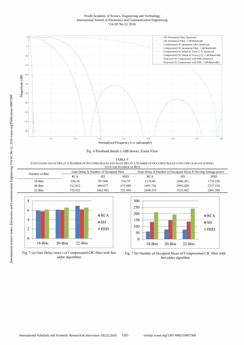
Fig. 6 Passband details (-3dB down): Zoom View
TABLE V COST CHART (GATE DELAY X NUMBER OF OCCUPIED SLICES AND GATE DELAY X NUMBER OF OCCUPIED SLICES X ON-CHIP LEAKAGE POWER)
WITH THE NUMBER OF BITS
Number of Bits Gate Delay X Number of Occupied Slice Gate Delay X Number of Occupied Slices X On-chip leakage power
RCA SD HSD RCA SD HSD
18-Bits 356.34 787.848 536.79 1178.06 2606.201 1776.238
20-Bits 512.012 904.877 675.989 1693.736 2992.428 2237.524
22-Bits 755.921 1063.992 752.494 2498.319 3523.942 2491.508
Fig. 7 (a) Gate Delay (nsec.) of Compensated CIC filter with fast adder algorithms
Fig. 7 (b) Number of Occupied Slices of Compensated CIC filter with fast adder algorithm
0.1 0.2 0.3 0.4 0.5 0.6 0.7 0.8
-50
-45
-40
-35
-30
-25
-20
-15
-10
-5
0
Normalized Frequency ( rad/sample)
Mag
nitu
de (
dB)
CIC Decimation Filter: Quantized
CIC Decimation Filter: -3 dB Bandwidth
Compensated CIC decimation Filter: Quantized
Compensated CIC decimation Filter: -3 dB Bandwidth
Compensated CIC:Deleck & Torres [17]: Quantized
Compensated CIC:Deleck & Torres [17]: -3 dB Bandwidth
Proposed CIC Compensator with HSD: Quantized
Proposed CIC Compensator with HSD: -3 dB Bandwidth
0
2
4
6
8
18-Bits 20-Bits 22-Bits
RCA
SD
HSD
0
50
100
150
200
250
300
18-Bits 20-Bits 22-Bits
RCA
SD
HSD
World Academy of Science, Engineering and TechnologyInternational Journal of Electronics and Communication Engineering
Vol:10, No:12, 2016
1505International Scholarly and Scientific Research & Innovation 10(12) 2016 scholar.waset.org/1307-6892/10007308
Inte
rnat
iona
l Sci
ence
Ind
ex, E
lect
roni
cs a
nd C
omm
unic
atio
n E
ngin
eeri
ng V
ol:1
0, N
o:12
, 201
6 w
aset
.org
/Pub
licat
ion/
1000
7308

Fig. 7 (c) On Chip Power Leakage (W) of Compensated CIC filter with fast adder algorithm
VIII. CONCLUSIONS
We discussed here the issues related to the mathematical modeling of multirate multistage decimator design and also presented a modified view to extend the work proposed by [12] in the new scenario. The proposed implementation of compensated CIC decimation filter with the HSD algorithm, initially compensated the passband droop by 37.02% than compensated CIC filter designed in [12] using the CSD number system, and then it achieves a high throughput in terms of down sampling speed by 65.15% than RCA, area and power by 57.5% and 0.01% than SD algorithms respectively. The inclusion of HSD arithmetic in proposed compensation filter design can control the overall performance in terms of area and speed at the frequencies of interest. This newly designed structure provides an optimum solution for all signal-processing applications which require sampling rate conversion with higher speed and lesser area such as image and speech processing.
REFERENCES [1] R. E. Crochiere and L. R. Rabiner, "Optimum FIR Digital Filter
Implementations for Decimation, Interpolation, and Narrow-Band Filtering," IEEE Transactions on Acoustics, Speech, and Signal Processing, Vol. Assp-23, No. 5, pp. 444-456, Oct. 1975.
[2] M. G. Bellanger, J. L. Daguet, and G. P. Lepagnol,"Interpolation, extrapolation and reduction of computation speed in digital filters," IEEE Trans. Acoustic., Speech, and Signal Processing, vol. ASSP-22, pp. 231-235, Aug. 1974.
[3] E. B. Hogenauer, "An Economical Class of Digital Filters for Decimation and Interpolation", IEEE Transactions on Acoustics, Speech & Signal Processing, Vol. ASSP-29, pp. 155-162, April 1981.
[4] A. Kwentus, O. Lee and A. N. Willson, Jr., "A 250 M sample/sec Programmable Cascaded Integrator-Comb Decimation Filter", in Proceeding of VLSI Signal Processing, IX, pp. 231-240, Oct. 1996.
[5] Kei-Yong Khoo, Zhan Yu, and Alan N. Willson Jr., “Efficient High-Speed CIC Decimation Filter", Proceedings Eleventh Annual IEEE International ASIC Conference, pp. 251-254, June 1998.
[6] Y. Djadi, T. A. Kwasniewski, C. Chan, and V. Szwarc, "A High Throughput Programmable Decimation and Interpolation Filter", Proceeding of the 1994 international Conference on Signal Proc. Applications and Technology, pp. 1743- 1748.
[7] H. K. Yang and W. M. Snelgrove, “High Speed Polyphase CIC Decimation Filters", Proc. of IEEE International Conference On Communications, pp. II.229- II.233, Atlanta, US, May 1996.
[8] Yonghong Gao, Lihong Jia, and Hannu Tenhunen, "An improved Architecture and implementation of Cascaded Integrator-Comb Decimation Filter", IEEE Pacific Rim Conference on Communications, Computers and Signal Processing, pp. 317-320, Victoria, B.C., Canada, August 1999.
[9] G. J. Dolecek and Fred Harris, “Design of wideband CIC compensator filter for a digital IF receiver”, Journal of Digital Signal Processing, Vol. 19, Issue 5, Academic Press, U.S.A., pp. 827–837, Sept. 2009.
[10] G. J. Dolecek and Fred Harris, “On Design of Two- Stage CIC Compensation Filter”, IEEE International Symp. on Industrial Electronics, Seoul, Korea, pp. 903-908, July 5-8, 2009
[11] Rozita Teymourzadeh and Masuri Bin Othman, “An Enhancement of Decimation Process using Fast Cascaded Integrator Comb (CIC) Filter”, IEEE Trans. on Circuits & Systems, 2006.
[12] G. J. Dolecek and Fernando Javier Trejo Torres, “ Compensated CIC-Cosine Decimation Filter “, ECTI Transactions on Computer and Information Technology, Vol.4, No.1 , pp. 8-14, May 2010
[13] S. Kim, W.C. Lee, S. Ahn, and S. Choi, “Design of CIC roll-off compensation filter in a W-CDMA digital receiver”, Journal of Digital Signal Processing, vol. 16, pp. 846–854, 2006
[14] R. Latha and P.T. Vanathi, “Optimized Digital Filter Architectures for Multi-Standard RF Transceivers”, Journal of Theoretical and Applied Information Technology, Vol. 65, No.2, p.p. 544-558, July 2014
[15] Pecotic, M.G., Molnar, G., and Vucic, M. “Design of CIC compensators with SPT coefficients based on interval analysis”, Proceedings of the 35th International Convention, MIPRO, Croatia, pp. 123-128, 21-25 May 2012.
[16] G. J. Dolecek and J. Diaz Carmona, “A new cascaded modified CIC-Cosine decimation filter”, International IEEE Conference ISCAS 2005, Kobe, Japan, pp. 3733-3736, May 2005.
[17] R. K. Dubey, K. P. Pandey and R. K. Singh, “CIC Decimation Filter for Frequency”, International Journal of Science and Research (IJSR), Vol. 4, No.9, p.p. 1401-1405, September 2015.
[18] S. Karthikeyan, Dinesh G. and Binsu J Kailath, “Improved alias rejection using interleaved CIC decimation filter”, proc. of IEEE International conference on New Circuits and Systems Conference (NEWCAS), Canada, 26-29 June 2016.
[19] Y. M. Seddiq and H. Altwaijry,” An Implementation of a 2D FIR Filter Using the Signed-Digit Number System”, proc. of IEEE Inter. conference on Electronics, Communications and Photonics (SIECPC), Saudi, 2011.
[20] Phatak D. S. and I. Koren, “Hybrid Signed-Digit Number Systems: A Unified Framework for Redundant Number Representations with Bounded Carry Propagation Chains” IEEE Trans. on Computers, Vol. 43, No. 8, pp 880-891, Aug. 1994.
[21] A. Avizienis, "Signed-digit number representation for fast parallel arithmetic", IRE Transactions on Electronic Computers, pp. 389, 1961.
Mr. Vishal Awasthi received his B.E. and M. Tech. degree in the field of Electronics & Communication Engineering from Mumbai University and HBTI, Kanpur in 1999 and 2007 respectively. His area of interest is Digital Signal Processing & control system. Presently he is working as head of Electronics & Communication Engg. Department,
UIET, C.S.J.M. University, Kanpur (UP), India.
Dr. Krishna Raj has completed his Ph.D. in the field of computer arithmetics. He is a fellow member of IETE and working as Professor in the department of Electronics Engg., H.B.T.I., Kanpur. His area of interest is digital signal processing & computer arithmetic.
3,302
3,304
3,306
3,308
3,31
3,312
18-Bits 20-Bits 22-Bits
RCA
SD
HSD
World Academy of Science, Engineering and TechnologyInternational Journal of Electronics and Communication Engineering
Vol:10, No:12, 2016
1506International Scholarly and Scientific Research & Innovation 10(12) 2016 scholar.waset.org/1307-6892/10007308
Inte
rnat
iona
l Sci
ence
Ind
ex, E
lect
roni
cs a
nd C
omm
unic
atio
n E
ngin
eeri
ng V
ol:1
0, N
o:12
, 201
6 w
aset
.org
/Pub
licat
ion/
1000
7308