optimal design of switching power supply
40
-
Upload
khangminh22 -
Category
Documents
-
view
3 -
download
0
Transcript of optimal design of switching power supply


OPTIMAL DESIGNOF SWITCHINGPOWER SUPPLY


OPTIMAL DESIGNOF SWITCHINGPOWER SUPPLY
Zhanyou Sha, Xiaojun Wang, Yanpeng Wang,and Hongtao Ma
Hebei University of Science and Technology, China

This edition first published 2015© 2015 China Electric Power Press. All rights reserved.
Published by John Wiley & Sons Singapore Pte. Ltd., 1 Fusionopolis Walk, #07-01 Solaris South Tower,Singapore 138628, under exclusive license granted by China Electric Power Press for all media and languagesexcluding Simplified and Traditional Chinese and throughout the world excluding Mainland China, and withnon-exclusive license for electronic versions in Mainland China.
For details of our global editorial offices, for customer services and for information about how to apply forpermission to reuse the copyright material in this book please see our website at www.wiley.com.
All Rights Reserved. No part of this publication may be reproduced, stored in a retrieval system or transmitted, inany form or by any means, electronic, mechanical, photocopying, recording, scanning, or otherwise, except asexpressly permitted by law, without either the prior written permission of the Publisher, or authorization throughpayment of the appropriate photocopy fee to the Copyright Clearance Center. Requests for permission should beaddressed to the Publisher, John Wiley & Sons Singapore Pte. Ltd., 1 Fusionopolis Walk, #07-01 Solaris SouthTower, Singapore 138628, tel: 65-66438000, fax: 65-66438008, email: [email protected].
Wiley also publishes its books in a variety of electronic formats. Some content that appears in print may not beavailable in electronic books.
Designations used by companies to distinguish their products are often claimed as trademarks. All brand names andproduct names used in this book are trade names, service marks, trademarks or registered trademarks of theirrespective owners. The Publisher is not associated with any product or vendor mentioned in this book. Thispublication is designed to provide accurate and authoritative information in regard to the subject matter covered. It issold on the understanding that the Publisher is not engaged in rendering professional services. If professional adviceor other expert assistance is required, the services of a competent professional should be sought.
Limit of Liability/Disclaimer of Warranty: While the publisher and author have used their best efforts in preparingthis book, they make no representations or warranties with respect to the accuracy or completeness of the contents ofthis book and specifically disclaim any implied warranties of merchantability or fitness for a particular purpose. It issold on the understanding that the publisher is not engaged in rendering professional services and neither thepublisher nor the author shall be liable for damages arising herefrom. If professional advice or other expertassistance is required, the services of a competent professional should be sought.
Library of Congress Cataloging-in-Publication Data applied for.
ISBN: 9781118790908
A catalogue record for this book is available from the British Library.
Cover Image: adventtr/iStockphoto
Typeset in 10/12pt TimesLTStd by SPi Global, Chennai, India
1 2015

Contents
Preface xiii
Introduction xv
1 Overview on Switching-Mode Power Supply (SMPS) 11.1 Classification of Integrated Regulated Power Supply 1
1.1.1 Optimal Design of SMPS 11.2 Characteristics of SMPS 5
1.2.1 Main Characteristics of SMPS 51.2.2 Performance Comparison of SMPS and Linear Regulated
Power Supply 61.3 New Development Trend of SMPS 6
1.3.1 New Development Trend of SMPS 71.3.2 New Technology in the SMPS Field 9
1.4 Basic Principles of SMPS 131.4.1 Working Mode of SMPS 131.4.2 Basic Principles of PWM 141.4.3 Classification of PWM Products 15
1.5 Control Mode Type of SMPS 161.5.1 VMC-Type SMPS 161.5.2 CMC-Type SMPS 18
1.6 Working Mode of SMPS 201.6.1 Setting Methods of CUM and DUM 201.6.2 Power Consumption Comparison between These Two Working Modes 21
1.7 Feedback Type of SMPS 221.7.1 Basic Types of SMPS Feedback Circuit 221.7.2 Feedback Principle of the Single-Chip SMPS 23
1.8 Load Characteristics of SMPS 271.8.1 Constant Load 281.8.2 Transient Load 281.8.3 Constant Current Load 291.8.4 Constant Power Load 291.8.5 Peak Power Load 29
vi Contents
1.8.6 Inertia Load 291.8.7 Low Noise Load 30
2 New Technology and Its Application of SMPS 312.1 Single-Chip Integration of SMPS 312.2 Computer-Based SMPS Design 33
2.2.1 Main Features of SMPS Design Software 342.2.2 Classification of Design and Simulation Software of SMPS 342.2.3 Design Process of SMPS Software 34
2.3 Internal Protection Circuit of SMPS 392.4 Synchronous Rectification (SR) Technology 41
2.4.1 Brief Introduction to the SR Technology 412.4.2 Basic Principle of SR 43
2.5 Active Clamp Technology 432.6 Magnetic Amplifier Regulator Technology 452.7 Programmable Voltage Regulator Technology 49
2.7.1 Basic Work Principle of Digital Potentiometers 492.7.2 Circuit Design of Programmable Switching Regulators 54
2.8 Digital Power Supply System 562.8.1 Main Features of the Digital Power Supply 582.8.2 Basic Constitution of the Digital Power Supply 622.8.3 Circuit Design of Digital Power Supply 63
2.9 Energy-Saving and Environment-Friendly Technology of SMPS 662.9.1 Reduce the Switching Losses with Valley Switching Circuit 662.9.2 Reduce the No-Load Power Consumption with EcoSmart
Energy-Saving Technology 672.9.3 Lead-Free Packaging Technology 68
3 Topologies of the DC/DC Converter 693.1 Topologies of the DC/DC Converter 69
3.1.1 Main Technical Indicators of the Typical Productsof the DC/DC Converter 75
3.2 Basic Principle of Buck Converter 753.2.1 Simplified Circuit of Buck Converter 76
3.3 Basic Principle of Boost Converter 783.3.1 Simplified Circuit of Boost Converter 78
3.4 Basic Principle of Buck-Boost Converter 793.5 Basic Principle of Charge Pump Converter 803.6 Basic Principle of SEPIC 813.7 Basic Principle of Flyback Converter 82
3.7.1 Basic Circuit of Multiple Output Flyback Converter 843.8 Basic Principle of Forward Converter 863.9 Basic Principle of Push-Pull Converter 87
3.9.1 Two Types of Push-Pull Converter 88

Contents vii
3.10 Basic Principle of Half/Full Bridge Converter 893.10.1 Basic Principle of Half-Bridge Converter 893.10.2 Basic Principle of Full-Bridge Converter 89
3.11 Basic Principle of Soft Switching Converter 903.11.1 Basic Principle of Resonant Converter 903.11.2 Basic Principle of Quasi Resonant Converter 913.11.3 Basic Principle of Full-Bridge Zero Voltage Converter 92
3.12 Basic Principle of Half-Bridge LLC Resonant Converter 933.12.1 The Equivalent Circuit and Voltage Gain Characteristic Curve of
Half-Bridge LLC Resonant Converter 953.13 Basic Principle of the 2-Switch Forward Converter 97
4 Method for Selecting Key Peripheral Components of SMPS 994.1 Selection Method for Fixed Resistor 99
4.1.1 Selection Method for Fixed Resistor 994.1.2 Selection Method for Current-Detecting Resistor 102
4.2 Selection Method for Capacitors 1054.2.1 Classification of Common Capacitors for SMPS 1054.2.2 Comparison between Ideal and Actual Capacitors 1064.2.3 Selection Method for Input Filter Capacitor 1074.2.4 Selection Method for Output Filter Capacitor 109
4.3 Inductor Characteristics and Selection Method for Magnetic Beads 1114.3.1 Inductor Characteristics 1114.3.2 Selection Method for Magnetic Beads 112
4.4 Selection Method for EMI Filter 1164.4.1 Structure Principle and Selection Method of EMI Filter 1174.4.2 Selection Method for Capacitors and Inductors in EMI Filter 122
4.5 Selection Method for Input Bridge Rectifier 1284.5.1 Selection Method for Bridge Rectifier 1284.5.2 Conduction Time and Strobing Features of Bridge Rectifier 130
4.6 Selection Method for Output Rectifier 1304.6.1 Selection Method for Fast and Superfast Recovery Diodes 1304.6.2 Selection Method for SBD 133
4.7 Selection Method for Transient Voltage Suppressor (TVS) 1374.7.1 Working Principle of TVS 1374.7.2 Selection Method for TVS and Its Typical Application 140
4.8 Selection Method for Power Switching Tube 1424.8.1 Selection Method for BJT Power Switching Tube 1434.8.2 Selection Method for MOSFET Power Switching Tube 1444.8.3 Selection Method for IGBT Power Switching Tube 146
4.9 Selection Method for Optical Coupler 1494.9.1 Basic Principle of Optical Coupler 1504.9.2 Selection Method for Linear Optical Coupler 151

viii Contents
4.10 Selection Method for Adjustable Precision Shunt Regulator 1524.10.1 TL431 Adjustable Precision Shunt Regulator 1534.10.2 NCP100 Low-Voltage Output Adjustable Precision Shunt Regulator 1554.10.3 LMV431 Low-Voltage Adjustable Precision Shunt Regulator 157
4.11 Selection Method for SMPS Protection Elements 1594.11.1 Selection Method for Fuse 1594.11.2 Selection Method for Fusible Resistor 1614.11.3 Selection Method for Voltage-Sensitive Resistor 162
5 Power Factor Correction Circuit Design of SMPS 1675.1 Brief Introduction to Power Factor Correction (PFC) 167
5.1.1 Power Factor and Total Harmonic Distortion 1675.1.2 Power Factor Correction Method 169
5.2 Basic Principle of Passive PFC Circuit 1705.2.1 Basic Circuit of Passive PFC 1705.2.2 PFC Working Principle Based on Passive Valley Fill Circuit 172
5.3 Design Examples of Passive PFC Circuit 1755.4 Basic Principle of Active PFC Circuit 177
5.4.1 Basic Principle of Active PFC Boost Converter 1775.4.2 Basic Principle of Active PFC 1805.4.3 The Selection of Boost PFC Diode 181
5.5 Design Examples of Active PFC Circuit 1845.5.1 Working Principle of L6561 and L6562 Active PFC Converters 1845.5.2 Typical Application of L6561 and L6562 Active PFC Converters 186
5.6 Principle and Application of High-Power PFC 1885.6.1 Performance Features of HiperPFS Series 1885.6.2 Working Principle of HiperPFS Series Products 1895.6.3 347W High-Efficiency Large-Power Boost PFC Power Supply
Constituted by PFS714EG 1925.6.4 Key Points of Circuit Design 194
5.7 Measures to Suppress PFC Electromagnetic Interference 1975.7.1 Using EMI Filter to Suppress PFC Electromagnetic Interference 1975.7.2 Other Measures to Reduce PFC EMI 198
5.8 PFC Configuration Scheme 2005.8.1 Selection of PFC Type, Number of Stage, and Working Mode 2005.8.2 Four Configuration Schemes of PFC Power Supply 202
6 Design of High-Frequency Transformer 2056.1 Selection Method for Magnetic Cores by the Empirical Formula or Output
Power Table 2056.1.1 Selection Method for Magnetic Cores by the Empirical Formula 2056.1.2 Selection Method for Magnetic Cores by Output Power 209
6.2 Waveform Parameters of the High-Frequency Transformer Circuit 2116.2.1 Analysis of Waveform Coefficient and Waveform Factor 2116.2.2 Parameters of Six Kinds of Common Waveforms in SMPS 212

Contents ix
6.3 Formula Derivation of Selecting High-Frequency Transformer Magnetic CoreBased on AP Method 2126.3.1 The Waveform Factor kf of the Primary Current 2156.3.2 AC Magnetic Flux Density BAC 216
6.4 Design of Flyback High-Frequency Transformer 2176.4.1 Design Method of Flyback High-Frequency Transformer 2176.4.2 Design Examples of Flyback High-Frequency Transformer 2216.4.3 Calculating Air Gap Width 224
6.5 Design of Forward High-Frequency Transformer 2256.5.1 Steps in Designing Forward High-Frequency Transformer 2256.5.2 Three Kinds of Commonly used Magnetic Reset Circuit 226
6.6 Loss of High-Frequency Transformer 2276.6.1 Loss of High-Frequency Transformer 2276.6.2 Skin Effect and Proximity Effect 228
7 Examples of SMPS Optimization Design 2317.1 Multioutput SMPS Design 231
7.1.1 Circuit Design Scheme of Multioutput Single-Chip SMPS 2317.1.2 Design of Multioutput High-Frequency Transformer 234
7.2 Methods to Improve the Cross-Load Regulation of MultioutputSMPS 236
7.3 Design of PC SMPS with Magnetic Amplifier 2387.3.1 Main Circuit Design of 145W Multioutput PC SMPS 2387.3.2 Circuit Design of 3.3-V Magnetic Amplifier 240
7.4 Design of Synchronous Rectification DC/DC Converter 2417.5 Design of SMPS for Peak-Power-Output Audio Power Amplifier 2437.6 Design of Industrial Control Power Supply Based
on Voltage-Doubling Rectifier 2467.7 Design of Industrial Control Power Supply Based on Suspension High-Voltage
Constant Current Source 2487.8 Design of StackFETTM Technology-Based Micro-SMPS 2507.9 Design of Power Supply for the Digital TV Set-Top Box 2527.10 Design of Mobile Phone Charger with USB Interface 254
8 Key Design Points of SMPS 2578.1 SMPS Design Requirements 257
8.1.1 SMPS Design Requirements 2578.1.2 Precautions for SMPS Design 258
8.2 Design of High-Efficiency SMPS 2608.2.1 Power Loss of SMPS 2608.2.2 Design Principles of High-Efficiency SMPS 2618.2.3 Methods to Improve SMPS Efficiency 262
8.3 Methods of Reducing No-Load and Standby Power Consumption of SMPS 2658.3.1 Methods to Eliminate the Power Consumption of Bleeder Resistor
after Start-Up 266

x Contents
8.3.2 Methods to Eliminate the Power Consumption of Thermal Resistorafter Turn-On 270
8.3.3 Methods to Eliminate the Power Consumption of Sense Resistorin Standby Mode 271
8.4 Stability Design of Optocoupler Feedback Control Loop 2748.4.1 Basic Requirements for Optocoupler Feedback Control Loop 2748.4.2 Stability Design of Optocoupler Feedback Control Loop 2768.4.3 Design Examples of Increasing Phase Margin 281
8.5 SMPS Layout and Wiring 2828.5.1 General Principles of SMPS Layout and Wiring 2828.5.2 Notes for SMPS Layout and Wiring 2838.5.3 Notes for PCB Design 287
8.6 Design of Constant Voltage/Current SMPS 2888.6.1 Working Principle of Constant Voltage/Current Output SMPS 2888.6.2 Circuit Design of Constant Voltage/Current Output SMPS 290
8.7 Design of Precision Constant Voltage/Current SMPS 2928.7.1 Working Principle of Precision Constant Voltage/Current
Output SMPS 2938.7.2 Circuit Design of Precision Constant Voltage/Current
Output SMPS 2958.8 Design of Remote Turn-Off Circuit for SMPS 297
8.8.1 Remote Turn-Off Circuit of TOPSwitch-GX 2978.8.2 Remote Turn-Off Circuit of PC SMPS 298
8.9 Typical Application and Printed Circuit Design of New Single-Chip SMPS 2998.9.1 Typical Application and Printed Circuit Design of TOPSwitch-HX
Series Single-Chip SMPS 2998.9.2 Typical Application and Printed Circuit Design of TOPSwitch-JX
Series Single-Chip SMPS 3028.10 Electromagnetic Interference Waveform Analysis and Safety Code Design of
SMPS 3078.10.1 Electromagnetic Interference Waveform Analysis of SMPS 3088.10.2 Safety Code of SMPS 310
8.11 Radiator Design of Single-Chip SMPS 3138.11.1 Working Principles of Radiator 3138.11.2 Radiator Design Methods of Single-Chip SMPS 3168.11.3 Radiator Design Examples of Single-Chip SMPS 317
8.12 Radiator Design of Power Switching Tube (MOSFET) 3218.12.1 Radiator Design Methods of Power Switching Tube 3218.12.2 Radiator Design Example of Power Switching Tube 3228.12.3 Notes for Designing the Radiator of Power Switching Tube 323
8.13 Common Troubleshooting Methods of SMPS 327
9 SMPS Testing Technology 3299.1 Parameter Testing of SMPS 329
9.1.1 Testing Methods of Main SMPS Parameters 3299.1.2 Power Measurement Technology 331

Contents xi
9.2 Performance Testing of SMPS 3339.2.1 Testing Methods of Main SMPS Parameters 3339.2.2 Electrical Performance Testing Methods
of High-Frequency Transformer 3359.3 SMPS Measurement Skills 336
9.3.1 Using the Noncontact Method to Measure the Input Current of SMPS 3369.3.2 Methods to Accurately Measure the Output Ripple Voltage 3379.3.3 Method to Measure the Efficiency of Switching Regulator 3389.3.4 Simple Method to Measure the Input Power of Isolated AC SMPS 3409.3.5 Method to Measure the Load Power of SMPS 341
9.4 Accurate Measurement Method of Duty Ratio 3439.5 Method to Detect the Magnetic Saturation of High-Frequency Transformer
with Oscilloscope 3459.5.1 Magnetic Saturation Characteristic of High-Frequency Transformer
and Its Harmfulness to SMPS 3459.5.2 Method to Detect the Magnetic Saturation of High-Frequency
Transformer with Oscilloscope 3469.6 Digital Online Current/Resistance Meter 348
9.6.1 Principle and Application of Online DC Current Measurement 3499.6.2 Principle and Application of Online Resistance Measurement 352
9.7 Electromagnetic Compatibility Measurement of SMPS 3549.7.1 Research Fields of EMC 3549.7.2 EMC Measurement 357
9.8 Waveform Test and Analysis of SMPS 3599.8.1 Key Waveform Test Method of PWM Controller 3599.8.2 Measuring the Primary Voltage and Current Waveforms 3629.8.3 Measuring the Secondary Voltage and Current Waveforms 365
10 Protection and Monitoring Circuit Design of SMPS 36710.1 Design of Drain Clamp Protection Circuit 367
10.1.1 Potential Distribution of Voltage Parameters on the Drain 36710.1.2 Basic Types of Drain Clamp Protection Circuit 36810.1.3 Design Examples of Drain Clamp Protection Circuit 370
10.2 Overvoltage Protection Circuit Constituted by Discrete Components 37110.2.1 Input/Output Overvoltage Protection Circuit Constituted by Silicon
Controlled Rectifier (SCR) 37110.2.2 Output Overvoltage Protection Circuit Constituted by Bidirectional
Trigger Diode 37410.2.3 Output Overvoltage Protection Circuit Constituted by Regulator Tube 37610.2.4 Overvoltage Protection Circuit Constituted by VSR 377
10.3 Application of Integrated Overvoltage Protector 37710.3.1 Overvoltage Protection Circuit Constituted by NCP345 37710.3.2 Overvoltage Protection Circuit Constituted by MAX4843 37810.3.3 Overvoltage Protection Circuit Constituted by MC3423 379
10.4 Design of Undervoltage Protection Circuit 38110.4.1 Input UVP Circuit Constituted by Optical Coupler 381

xii Contents
10.4.2 Input UVP Circuit Constituted by Bias Winding 38210.4.3 Switching Regulator with Under-Voltage Lockout Function 38210.4.4 External Drive Circuit Realizing Overvoltage
and Undervoltage Control 38310.5 Design of Overcurrent and Overpower Protection Circuit 384
10.5.1 Current Limiting Protection Circuit Constituted by Power Thermistor 38410.5.2 Overcurrent Protection Circuit Constituted by Transistor 38610.5.3 Overcurrent Protection Circuit Constituted by Resettable Fuse 38610.5.4 Application of Integrated Overcurrent Protector 38810.5.5 Application of Integrated Over-Power Protector 388
10.6 Design of Soft-Start Circuit 38910.6.1 Soft-Start Circuit 38910.6.2 + 5/−5 V Power Supply Converter with Soft-Start Function 39110.6.3 Switching Regulator with Delayed Start Function 391
10.7 Mains Voltage Monitor 39210.7.1 Voltage Monitor Constituted by TL431 39210.7.2 Undervoltage and Overvoltage Monitor Constituted by LM3914 39210.7.3 Mains Voltage Monitor Constituted by HYM705/706 39310.7.4 Mains Voltage Monitor Constituted by MCP1316 Series 395
10.8 Transient Interference and Audio Noise Suppression Technology of SMPS 39610.8.1 Transient Interference Suppression Method 39610.8.2 Audio Noise Suppression Method 39810.8.3 Methods to Suppress Other Interferences 399
10.9 Design of Overheating Protection Component and Cooling Control System 40010.9.1 Basic Principles of the Overheating Protection Circuit of SMPS 40010.9.2 Principles and Applications of Two Kinds of Overheating Protection
Component 40110.9.3 Design of Cooling Control System with Multiple Protection Functions 404
References 407
Index 409

Preface
In recent years, the rapid development ofmodern power technology and the huge demand of theglobal market have resulted in higher requirements for the optimal design of switching-modepower supply (SMPS). The so-called optimal design refers to selecting the best design from avariety of design schemes. It should be pointed out that the optimal design is always relative,not absolute. Optimal design is not necessarily the one and only, and there may be severaloptions for designers to choose from. With the development of power technology, the optimaldesign of SMPS is in endless progress. There are many ways to realize the optimal design ofSMPS, which can be approximately grouped into the following aspects: (i) using new devices(e.g., the new single-chip SMPS IC); (ii) using new technologies (e.g., magnetic amplifier, syn-chronous rectification, active clamp, active power factor correction, and digital power supply);and (iii) using new software (the latest version of the computer-aided design software).In recent years, with the development and application of green energy-saving power supply,
the first author of this book gave 15 lectures on “optimal design of SMPS” and “optimal designof LED drive power supply” in the senior seminar held in Beijing, Shanghai, Suzhou, Ningbo,Hangzhou, and Shenzhen at the invitation of several units such as the China Electronics Stan-dardization Institute under theMinistry of Industry and Information Technology and the ChinaElectronics Enterprises Association. Using these lectures as a basis, the authors put many yearsof their teaching and scientific research experience into this book for both new and old readers.The book is scientific, advanced, systematic, and practical and has the following features.First, it describes the optimal design of SMPS in a comprehensive, in-depth, and systematic
manner, including new technologies and applications of SMPS, topology selection of DC/DCconverter, peripheral component selection of SMPS, optimal design examples of SMPS, keydesign points of SMPS, and test technology and protection circuit design.Second, in view that the SMPS current is moving toward single-chip integration, intellectu-
alization, modularization, and the physical features of short, small, light, and thin, it focuseson the optimal design of single-chip SMPS with the most representative single-chip SMPS ICin the world as an example.Third, it is novel in content. It introduces many new technologies and their application
examples such as the half-bridge LLC resonant converter, synchronous rectification, magneticamplifier regulation, StackFETTM (stacked FET), suspended high-voltage constant currentsource, valley fill circuit, active power factor correction, and electromagnetic compatibilitydesign of SMPS.

xiv Preface
Fourth, it is easy to understand, delivering high practical value. It not only gives variousdesign examples of SMPS but also describes in detail the key design points of circuits, testingmethods, selection of key peripheral components, and the design of protection circuit. It hasimportant reference value for readers to research and develop SMPS.Fifth, it is informative with wide range of knowledge, easy for readers to comprehend and
learn by analogy and apply flexibly.Professor Zhanyou Sha contributed Chapters 1, 2, and 6–8, and completed the review and
integration of the whole book. Associate Professor Hongtao Ma, Professor XiaojunWang, andProfessor Yanpeng Wang jointly contributed Chapters 3–5, 9, and 10.We would like to express our sincere thanks to Power Integrations (PI), ON Semiconductor,
STMicroelectronics (ST), Texas Instruments (TI), Fairchild, and Philips for their help andsupport.We would be very glad if the book can be of use for your SMPS design.

Introduction
This book describes the optimal design of switching-mode power supply (SMPS) in a com-prehensive, in-depth, and systematical manner. The book includes 10 chapters. Chapter 1 isthe overview on SMPS. Chapter 2 describes the new technologies and applications of SMPS.Chapters 3 and 4 introduce the topology of DC/DC converter and the method of selecting keyperipheral components of SMPS, respectively. Chapters 5–8 focus on the power factor correc-tion circuit design of SMPS, the design of high-frequency transformer, the examples of SMPSoptimization design, and the key design points of SMPS, respectively. Chapters 9 and 10 intro-duce the SMPS testing technology and the protection circuit design of SMPS, respectively.This book has important reference value for readers to research and develop new-type SMPS.This book is rich in content and easy to understand with numerous illustration, delivering
high practical value. It is suitable for various technicians in the electronic field, universityteachers and students, and fans with a passion for electronics.


1Overview on Switching-ModePower Supply (SMPS)
1.1 Classification of Integrated Regulated Power Supply
There are tens of thousands of integrated voltage regulators in the market, which can be roughlyclassified into linear regulators and switching regulators. See Table 1.1 for the classificationand characteristics of integrated regulated power supply.
1.1.1 Optimal Design of SMPS
The linear regulator, also known as series regulated integrated regulator, is named for its inter-nal regulating tube, which works in the linear working area and is in series connection withload. It has advantages such as sound voltage regulation performance, low-output ripple volt-age, simple circuit, and low cost, while its main disadvantages include relatively bigger voltagedrop and high power consumption of the regulating tube with relatively low efficiency ofthe regulated power supply at about 45%. The linear regulator mainly consists of two types,namely, standard linear regulator using NPN regulating tube, which is also known as NPN lin-ear regulator, and PNP low-dropout (LDO) regulator using PNP regulating tube. Besides, thereare quasi low-dropout (QLDO) regulator and very low-dropout (VLDO) regulator. Accordingto the characteristics of output voltage, linear regulators can be divided into different typessuch as fixed output, adjustable output, positive pressure output, negative pressure output, andmultiplexed-output (including tracking output). The efficiency of traditional standard linearregulators is only around 45%, while that of LDO and VLDO can reach 80−90% under lowvoltage output.
The switching-mode power supply (SMPS) is known as a highly energy-efficient powersupply. It leads the development direction of regulated power supply and now has become theleading product of regulated power supply. With the internal key components working underhigh-frequency switch status, the SMPS consumes quite low energy so that its power efficiencymay reach up to 70−90%, twice as high as that of the standard linear regulated power supply.The SMPS integrated circuit mainly consists of the following four types: pulse width modu-lator (PWM), pulse frequency modulator (PFM), switching regulator, and single-chip SMPS.
According to the circuit principle, regulators can be divided into three types includingseries regulated linear regulator, shunt regulated linear regulator, and switching regulator.
Optimal Design of Switching Power Supply, First Edition. Zhanyou Sha, Xiaojun Wang, Yanpeng Wang, and Hongtao Ma.© 2015 China Electric Power Press. All rights reserved. Published 2015 by John Wiley & Sons Singapore Pte. Ltd.

2 Optimal Design of Switching Power Supply
Table1.1
Cla
ssifi
catio
nan
dC
hara
cter
istic
sof
Inte
grat
edR
egul
ated
Pow
erSu
pply
Inte
grat
edre
gula
ted
pow
ersu
pply
Lin
ear
pow
ersu
pply
Stan
dard
linea
rre
gula
tor
Fixe
dty
peT
hree
-ter
min
alfix
edty
pePo
sitiv
evo
ltage
outp
ut,n
egat
ive
volta
geou
tput
Mul
tiple
-ter
min
alfix
edty
pePo
sitiv
evo
ltage
outp
ut,n
egat
ive
volta
geou
tput
Adj
usta
ble
type
Thr
ee-t
erm
inal
adju
stab
lety
pePo
sitiv
evo
ltage
outp
ut,n
egat
ive
volta
geou
tput
,tra
ckin
gm
ode
Mul
tiple
-ter
min
alad
just
able
type
Posi
tive
volta
geou
tput
,neg
ativ
evo
ltage
outp
ut,t
rack
ing
mod
eL
owdr
opou
tlin
ear
regu
lato
rL
owdr
opou
tre
gula
tor
(LD
O)
Thr
ee-t
erm
inal
orm
ultip
le-t
erm
inal
fixed
/adj
usta
ble
type
Posi
tive
volta
geou
tput
,neg
ativ
evo
ltage
outp
ut,t
rack
ing
mod
e
Qua
silo
wdr
opou
tre
gula
tor
(QL
DO
)V
ery
low
drop
out
regu
lato
r(V
LD
O)
Switc
hing
mod
epo
wer
supp
ly(S
MPS
)
Puls
ew
idth
mod
ulat
or(P
WM
)W
ithre
lativ
ely
low
inte
grat
ion
leve
land
com
plic
ated
peri
pher
alci
rcui
twith
cons
titut
eshi
gh-p
ower
SMPS
Puls
efr
eque
ncy
mod
ulat
or(P
FM)
With
rela
tivel
ylo
win
tegr
atio
nle
vel,
com
plic
ated
peri
pher
alci
rcui
t,sw
itchi
ngfr
eque
ncy
may
reac
hov
er1
MH
z,an
dhi
ghef
ficie
ncy
Switc
hing
regu
lato
rW
ithre
lativ
ely
high
inte
grat
ion
leve
land
pow
ersw
itch
tube
insi
de,w
hich
need
sto
beeq
uipp
edw
ithin
dust
rial
freq
uenc
ytr
ansf
orm
erSi
ngle
-chi
pSM
PSW
ithpr
etty
high
inte
grat
ion
leve
land
sim
ple
peri
pher
alci
rcui
t,w
hich
cons
titut
esSM
PSof
med
ium
and
smal
lpow
er

Overview on Switching-Mode Power Supply (SMPS) 3
Figure 1.1 Equivalent circuits of the three kinds of regulators: (a) series regulated linear regulator; (b)shunt regulated linear regulator; and (c) switching regulator
Their equivalent circuits are respectively shown in Figure 1.1(a)–(c). In this figure, RS refers tothe equivalent resistance of regulating tube and S the power switch tube. As its output voltageis highly stable and output current is very small, shunt regulated linear regulator is generallyused as reference voltage source. The main characteristics of various products are describedin the following sections.
1.1.1.1 Three-Terminal Fixed Regulator
Fairchild Semiconductor Corporation firstly launched μ7800 and μA7900 series three-terminalfixed regulators in the beginning of the 1970s. It is a big revolution for integrated circuitsof power supply, which greatly simplifies the design and application of power supply. Thethree-terminal fixed regulator can be placed in the circuits via the simplest way (such asa transistor) and has relatively complete overcurrent protection (OCP), overvoltage protec-tion (OVP), and overheat protection (OTP) functions. At present, μA7800 and μA7900 seriesthree-terminal fixed regulators have become universal ones in the world, with the widest appli-cation and largest sale volume. Such a three-terminal fixed regulator is easy to operate andneeds no adjustment. It has a simple peripheral circuit and operates reliably and safely, andtherefore is applicable to make general or nominal-output regulated power supply. However,it cannot regulate the output voltage or directly output non-nominal voltage, and its voltage isnot stable enough.
1.1.1.2 Three-Terminal Adjustable Regulator
Three-terminal adjustable regulator was developed in the late 1970s and the early 1980s,which was the second-generation three-terminal regulator initiated by National Semiconductor(NSC). It not only reserves the advantage of simple structure the three-terminal fixed regulatorhas but also overcomes the disadvantage that the voltage could not be regulated. Moreover, itsvoltage stability is increased by one order of magnitude. Therefore, three-terminal adjustableregulator can be used to make laboratory power supply and DC regulated power supply. Inaddition, it can also be designed as fixed type to replace the three-terminal fixed regulator, tofurther improve the voltage regulation performance.

4 Optimal Design of Switching Power Supply
1.1.1.3 Low-Dropout (LDO) Regulator
LDO is a high-efficiency linear integrated regulator, whose input–output dropout voltageis about 500 mV, with power efficiency obviously higher than that of NPN linear regulator.VLDO is a new linear integrated regulator developed based on LDO in the beginning of thetwenty-first century. VLDO uses the field-effect tube with very low specific on-resistanceinstead of the power tube that PNP uses, and its input–output dropout voltage can be as lowas 45–150mV.
1.1.1.4 Multiterminal Integrated Regulator
With plenty of pins, the multiterminal integrated regulator is flexible to use but with compli-cated connections. It can also be classified into fixed type and adjustable type.
1.1.1.5 Tracking Positive–Negative Balanced Output Integrated Regulator
Its characteristic is that when the positive voltage changes for some reasons, the negative volt-age output may track automatically and make corresponding change to keep the absolute valuesof the two equal. The tracking function is particularly important for a precision operationalamplifier powered by two supplies, which can prevent the operational amplifier from zerodrift rising out of the unbalance between positive voltage and negative voltage.
1.1.1.6 Transformer SMPS without Power Frequency
The SMPS is also known as a low-loss power supply. As its internal parts operate underhigh-frequency switch status, the SMPS consumes low energy but with power efficiency twicethat of ordinary linear regulated power supply.
1.1.1.7 Switching Regulator
A switching regulator is a switch integrated voltage regulator developed in the 1980s and1990s. With PWM, power output, and protection circuit integrated on the same chip, theswitching regulator has efficiency of over 90%. In addition, some switching regulators caneven regulate output voltage continuously that can be used to SMPS with dozens to hundredsof wattage.
1.1.1.8 Single-Chip SMPS
With the main circuits (including MOSFET, required analog and digital circuits) of SMPSintegrated on chip, the single-chip SMPS with the highest integration level can realize outputisolation, PWM, and many other protection functions. A single-chip SMPS fits AC current of85–265 V and 47–400 Hz via an input rectifier filter; it is thus an AC/DC power converter.The single-chip SMPS integrated circuit has displayed strong vitality since its appearance

Overview on Switching-Mode Power Supply (SMPS) 5
in the mid-1990s. It has such advantages as high integration level, high cost performance,simplest peripheral circuit, and best performance indicators. Now, single-chip SMPS inte-grated circuit has become an optimal integrated circuit for the development of medium-and small-power SMPS with wattage below 1000 W, precision SMPS, and SMPS modules.Besides, the development of single-chip SMPS has also created favorable conditions for theoptimal design of SMPS.
1.1.1.9 Special SMPS
A special SMPS is characterized by “novelty, uniqueness, and wide application.” It is novelin circuit, unique in function, and advanced in performance, with a great variety and wideapplication. Its varieties include constant voltage/current SMPS, LED driving power for light-ing, constant power SMPS, high-voltage pulse power supply, high-power high voltage powersupply, battery charger, and so on.
1.2 Characteristics of SMPS
1.2.1 Main Characteristics of SMPS
The SMPS is also called low-loss power supply. With its internal components working ina high-frequency switch status, it consumes low energy, and its power supply efficiency istwice that of the ordinary linear regulated power supply. The integrated circuits for SMPSare classified into two types: one is singled-ended or double-ended output PWM and theother is PFM, both of which can constitute the SMPS without power frequency transformer.Because they realize the voltage transformation and grid isolation with high-frequencytransformer of very small volume, they can save power-frequency transformer of cumber-some volume. At present, the work frequency of SMPS has been increased from 20 kHzto hundreds of kilohertz and even above 1 MHz, so has the power efficiency. The outputpower range includes low power (dozens of wattage), medium power (hundreds of wattage),and high power (thousands of wattage). The disadvantage of SMPS is that the outputvoltage is not stable enough, and the output ripple is large and its noise is loud, makingit inappropriate for making precise regulated power supply. However, it can be used as apre-voltage regulator, with the standard linear regulator or low dropout linear regulator as thepost-voltage regulator to constitute a high efficiency and precise regulated power supply oftwo stages. Such compound power supply possesses the advantages of SMPS and linear powersupply.
Compared with the linear power regulator, although the SMPS is of complex design andsome performance indicators are inferior to those of the linear regulator and the noise is loud,the advantages of SMPS mainly lie in the power efficiency, volume, weight, and so on. Espe-cially when it constitutes a high-power regulated power supply, its volume is greatly reducedcompared with that of the linear regulated power supply under the condition of the same outputpower, and the costs also decline significantly.
The efficiency of SMPS generally ranges from 70% to 85% with the maximum of 90%.Equipped with the post-positioned linear regulator and constituting a compound regulated

6 Optimal Design of Switching Power Supply
Table 1.2 Performance comparison of 20 kHz SMPS and linear regulated power supply
Parameter SMPS Linear regulated power supply
Power efficiency (%) 70–85 30–40Output power per unit volume (W∕cm3) 0.12 0.03Output power per unit mass (W/kg) 88 22Voltage regulation rate (%) 0.1–1 0.02–0.1Load regulation rate (%) 1–5 0.5–2Output ripple voltage (mV, peak–peak value) 50 5Output noise voltage (mV, peak–peak value) 50–200 Extremely smallTransient response time (μs) 1000 20Holding time of output voltage after power failure (ms) 20–30 1–2
power supply, it still can achieve a high efficiency ranging from 60% to 65%, while the effi-ciency of most of the linear regulated power supplies (excluding low dropout linear regulators)only ranges from 30% to 40%. Compared with the linear regulator, the overall size of the tra-ditional 20 kHz SMPS is only 1/4 of that of the linear regulator, and the 100–200 kHz SMPSis 1/8, while the size of new 200 kHz–1 MHz SMPS can be much smaller. After the poweroutrage, the SMPS can maintain the output voltage for a longer time than the linear regulator,because the latter is generally equipped with a low-voltage input filter capacitor, while the for-mer is equipped with a high-voltage input filter capacitor with the withstand voltage rangingfrom 200 to 400 V and it saves more charge Q because of the direct proportion between Q andCU1
2 (U1 is DC high voltage).The disadvantage of the SMPS is that it has relatively low-voltage regulation rate and load
regulation rate, which takes a long time to respond to the transient state of load change; theoutput ripple and noise voltage are relatively high so that it is likely to exert electromagneticinterference externally.
1.2.2 Performance Comparison of SMPS and Linear Regulated PowerSupply
See Table 1.2 for the performance comparison of 20 kHz SMPS and linear regulated powersupply. It can be seen from the table that many technical indicators of the SMPS are superiorto those of the linear regulated power supply.
1.3 New Development Trend of SMPS
The SMPS has been developed for decades. The self-excitation push-pull type transistor sin-gle transformer DC converter invented in 1955 took the lead in realizing the high-frequencyconversion control function; and the one invented in 1957 and the SMPS design without powerfrequency transformer plan proposed in 1964 forcefully promoted the technological progressof the SMPS. The emerging of the PWM in 1977 and the single-chip SMPS in 1994 pavedthe way for promotion and popularization of the SMPS. Meanwhile, the frequency of SMPS

Overview on Switching-Mode Power Supply (SMPS) 7
has also increased from 20 kHz at the beginning to hundreds of thousands of hertz, and evena couple of megahertz. The SMPS is developed to be highly efficient, energy-saving, safe,environment-friendly, short, small, light, and thin. A variety of new technologies, processes,and apparatuses spring up like mushrooms and emerge continuously and the application ofSMPS has also been increasingly popular. Next, introduction will be made on the new trendand new technology for the development of SMPS.
1.3.1 New Development Trend of SMPS
1.3.1.1 Green and Energy-Saving SMPS
Many famous integrated circuit manufacturers are making great efforts to develop low-powerconsumption and energy-saving SMPS integrated circuit. For example, Power Integrations (PI)of the United States adopted the energy-saving technology EcoSmart® to develop single-chipSMPS such as TOPSwitch-HX series. PI announced recently that due to the single-chip SMPSIC EcoSmart®, as it would save electric charge of about USD 3.4 billion for consumers all overthe globe. The Green Chip such as TEA1520 series launched by Philips of the Netherlands alsoattaches great importance to high efficiency and energy saving functions. Besides, the interna-tional standards for green and energy-saving power supply have also been widely applied. Forinstance, the United States has established Energy Star Program in 1992 to reduce the no-loadpower consumption of the SMPS. The compulsory energy-saving standards established byCalifornia Energy Commission (CEC) have been implemented from July 1, 2006, requiringthat the standby power consumption and no-load power consumption of electronic productsmust be reduced substantially. These standards cover all electronic products using externalpower adapter or charger, including mobile phone, household appliance, portable music player(MP3), handheld game player, electronic toys, and so on.
According to the fourth edition of power saving standard (Code of Conduct) newly pub-lished by the European Commission, which came into effect since January 1, 2009, specifiedthat the no-load power consumption of ordinary power supply with rated output power of0.3–50 W shall not be more than 0.30 W and that of ordinary power supply with rated powerof 50–250 W shall not be more than 0.50 W. The new standard raised stricter requirements onthe no-load power consumption of mobile phone power supply of 0.3–8.0 W, requiring it notto exceed 0.25 W during January 1, 2009 and December 31, 2010 and 0.15 W from January 1,2011.
1.3.1.2 Intelligent Digital Power Supply and Programmable SMPS
Digital Power SupplyAt present, the SMPS is developed to be intelligent and digitalized. The intelligent digitalpower system, which emerged at the beginning of the twenty-first century, has drawn greatattention of the public for its excellent performance and advanced monitoring functions. Thedigital power supply, being intelligently adaptive and flexible, is able to directly monitor, pro-cess, and adapt to the system condition and meet any complex power requirement. In addition,it also guarantees the reliability of the long-term system operation through remote diagno-sis, including fault management, overcurrent protection, and preventing the system from stop.

8 Optimal Design of Switching Power Supply
The promotion of digital power supply created a favorable condition for the optimal design ofintelligent power system.
The digital power system has the following features:
1. It is an intelligent SMPS system with a digital signal processor (DSP) or micro controllerunit (MCU) as the core and the digital power driver and PWM controller as the controlobject. The traditional SMPS controlled by MCU (including MCU μP and single-chipmachine μC) generally controls only the switch-on and switch-off of the power supply,which is not a digital power supply in real sense.
2. Developed with fusion digital power technology, it realizes the optimal combination ofanalog element and digital element in the SMPS. For example, the analog element usedfor the power stage – MOSFET driver can be conveniently connected to the digital powercontroller and help to manage the power protection and biasing circuit. PWM controlleralso falls into the category of digital control analog chip.
3. With high integration, it realizes power system on chip, integrating a big number of sepa-rated components into a chip or a set of chips.
4. It can make full use of the advantages of DSP and MCU, making the digital powerdesigned reach high technical indicators. For example, the resolution of its PWM canreach 150 ps (or 10−12 s), far exceeding the traditional SMPS. The digital power supplycan also realize many functions such as multiple phase control, nonlinear control, loadshare, and fault prediction providing convenience for the research and manufacturing ofgreen and energy-saving SMPS.
5. It provides convenience for building a distributed digital power system.
In March 2005, Texas Instruments (TI) of the United States announced to launch innovativedigital power products and displayed the solution of Fusion Digital PowerTM that includesthe following three types of chips: UCD7K series digital power drivers, UCD8K series PWMcontrollers, and UCD9K series digital signal processors. Product series have been formed forthe above- mentioned chips, supporting both the AC circuit and load power systems. They canbe widely applied in telecommunication facilities, computer server, data center power system,and UPS.
Programmable SMPSThe adjustable SMPS changes the output voltage of regulator by manually regulating the resis-tance value, which is not only precise enough, but also inconvenient for application. Digitalpotentiometer, which is also called digitally controlled potentiometer (DCP), can replace theadjustable resistance to constitute a programmable SMPS under computer-based control.
The circuit design plan for the programmable SMPS constituted by digital potentiome-ter is shown in Figure 1.2. Figure 1.2(a) shows replacement of adjustable resistance withDCP, which works in the adjustable resistance model. The adjusted resistance value is RDCP,which, together with R1, constitutes a sampling circuit1, which is sent to the feedback terminalFB of the switching regulator. The single-chip microcontroller can set the output voltage ofadjustable switching regulator by changing the value ofRDCP. The second plan is to replace twosampling resistors with RDCP simultaneously, which can save one resistance element, whosesimplified circuit is shown in Figure 1.2(b) with other parts being the same with Figure 1.2(a).The third plan is to connect the DCP between R1 and R2 in series; the simplified circuit is

Overview on Switching-Mode Power Supply (SMPS) 9
Figure 1.2 Circuit design plan for programmable SMPS constituted by DCP (a) Circuit 1; (b) Circuit2 (simplified circuit); and (c) Circuit 3 (simplified circuit)
shown in Figure 1.2(c). This circuit is applicable to the fine regulation of output voltage in asmall range.
1.3.2 New Technology in the SMPS Field
1.3.2.1 Active Clamp Technology
The function of clamp circuit is to clamp down the peak voltage generated by the SMPS atwork time within a certain range in order to protect the power switch tube. The clamp circuitscan be divided into passive clamp circuits and active clamp ones. The general R, C, and VDzclamp circuits belong to passive clamp circuits. The advantage of such passive clamp is thatit has a simple circuit and can absorb the peak voltage generated by leakage inductance ofhigh-frequency transformers. However, the clamp circuit has larger energy consumption itself,thus reducing the power supply efficiency.
The active clamp circuit invented by VICOR of the United States can significantly reducepower loss of the SMPS. The typical active clamp circuit is shown in Figure 1.3. The activeclamp circuit was named for an active power component, MOSFET (V4), which is used asclamper tube in the circuit. In Figure 1.3, Cc is the clamp capacitor and V3 is the power switch

10 Optimal Design of Switching Power Supply
Cc CUP
UI
V4
V1
V2
V3
UGS4
UGS3
US UO
L
T+
–
–
+
+
Figure 1.3 Active clamp circuit
tube of SMPS. It can be seen from this figure that UGS3 is 0 when V4 is on, switching V3off and UGS3 will switch V3 on when V4 is off, thus clamping the peak voltage generated byleakage inductance of high-frequency transformers.
1.3.2.2 Synchronous Rectification (SR) Technology
Synchronous rectification (SR) was developed at the end of the twentieth century. It is a newtechnology of using the special power MOSFET with extremely low on-state resistance insteadof rectifier diode to reduce the rectifier loss, which can significantly improve the efficiencyof SMPS under low voltage and large current output. SR circuit adopts power MOSFET orSchottky Barrier Diode (SBD) as rectifier tube, requiring that the grid voltage should keepsynchronous with the phase of rectified voltage to complete the rectification function. There-fore, it is called SR. For the synchronous rectifier comprising field effect transistor or SBDlaunched by Onsemi recently, the forward on-state voltage drop generally ranges from 0.2 to0.4 V and the reverse recovery time is only 100 ns.
1.3.2.3 Soft Switching Technology
The general PWM-type SMPS adopts a “hard switching” technology, with which the voltageor current on VT is not zero when the power switch tube VT is either on or off. Nevertheless,the VT is forced to be on or off when the voltage or current is not zero, thereby increasing theswitching loss. The switching loss includes the capacitor loss and the switch overlapping lossof the power switch tube. The capacitor loss, which is also called CU2f loss, refers to a losscaused by discharging of the distributed capacitance of power switch tube when each switchingcycle starts. The switch overlapping loss, caused by the switching time of the power switchtube, increases with the rising of switching frequency, which not only limits the developmentof high-frequency SMPS, but also easily generates electromagnetic interference.
Soft switching technology shall be introduced to make up the defects of “hard switching”technology. Soft switching refers to zero voltage switching (ZVS) or zero current switching(ZCS). With ZVS and ZCS, the power switch tube can be switched off when voltage and

Overview on Switching-Mode Power Supply (SMPS) 11
current crossing zero respectively, so as to minimize the switching loss for the purpose ofimproving the power supply efficiency and protecting the power switch tube.
1.3.2.4 Magnetic Amplifier Regulator Technology
A magnetic amplifier is composed of sampling circuit, reference voltage source, magneticreset control circuit, controllable magnetic saturation inductor, and PWM. The controllablemagnetic saturation inductor acts as a controllable magnetic switch in the voltage regulatorcircuit, which can accurately regulate the pulse width only by changing the delay time ofmagnetic reset to achieve accurate voltage regulation. Therefore, the magnetic amplifier isequivalent to an external PWM.
In the positive and negative voltage symmetrical output SMPS, using magnetic amplifiervoltage regulator circuit can not only improve the precision of voltage regulation, but alsoincrease the rate of cross loading regulation.
1.3.2.5 New Technologies for Single-Chip SMPS Application
With the increasing popularization of the single-chip SMPS, new technologies are also appliedin the circuit design. The following examples are given for illustration.
1. StackFETTM (stack field effect transistor) technology. The single-chip SMPS is integratedwith a power field effect transistor MOSFET with a drain-source electrode breakdown volt-age of 700 V. When the maximum AC input voltage UI (max) is 580 V, the maximum primaryvoltage of high-frequency transformer reaches nearly 1050 V (including primary inducedvoltage UOR, which is also called secondary reflected voltage), far above 700 V. To avoidany damage to the internal MOSFET, an MOSFET power field effect tube V can be stackedon its drain electrode as external MOSFET. These are the features of the StackFET circuit.
2. Design of industrial control power supply with ultrawide input range. To ensurethat TinySwitch-III can work normally under ultralow AC input voltage, a floatinghigh-voltage constant-current source shall be added exteriorly for the purpose of continu-ously supplying power to bypass end under low voltage. This technology is applicable fordesigning industrial control power supply with an ultrawide input range of 18–265 V.
3. PFC circuit. To improve the power factor of SMPS and reduce the total harmonic distortion(THD), AC/DC converter shall be provided with a power factor correction (PFC) circuit.Passive “valley fill circuit” (VFC) can be adopted when high-output ripple voltage (such asthe driver composing white light LED lamp) is not required. VFC is used to greatly increasethe conduction angle of rectifier diode, changing the input current from peak pulse into awave form approaching sine wave via filling the valley points. The universal high-powerSMPS is generally equipped with a new special chip with active PFC to simplify the circuitdesign.
4. Single-chip high-power SMPS. In recent years, the maximum output power of single-chiphalf-bridge LLC resonant converter with PFC, single-chip double-switch forward converterand other chips newly developed by chip manufacturers has reached 600–1000 W, creatingfavorable conditions for development of cheap high-power SMPS of high quality.
5. LED lighting driving power supply. LED lighting, also called semi-conductor lightingor solid state lighting, falls into the category of energy-saving and environment-friendly

12 Optimal Design of Switching Power Supply
“green lighting” characterized by low power consumption, high luminance, vibrationresistance, long service life, small overall dimension, quick response, no pollution toenvironment, and other noticeable advantages. LED driving power supply is a power unitexclusive for power supply to LED lamps. At present, using new technologies and newprocesses, chip manufacturers have successively developed a batch of application-specificintegrated circuit (ASIC) with advanced performance and unique characteristics. Thesechips have not only retained the advantages of SMPS chips, such as high efficiencyand energy saving, but also are featured by constant current output, dimmable function,and PFC.
1.3.2.6 Highly Reliable Modular Design
It is well-known that integration technology cannot integrate the high-capacity capacitor,inductor, rectifier bridge, potentiometer, and high-power components of 10 A and above into achip. Therefore, to develop an SMPS, a chip should be selected, the peripheral circuit shouldbe designed, and the printed circuit should be designed as well, which brings inconvenienceto users. However, the problems mentioned earlier can be readily solved if a power supplyblock is used.
The power supply block is a commodity component assembling power supply integratedcircuit and miniature electronic components (such as pellet resistance and subminiature elec-trolytic capacitor) by microelectronic technique to complete a certain specific function. Withthe structural feature that all components are densely installed on a printed board, so thepower supply block is also called secondary integration. The power supply blocks are gen-erally divided into two categories by appearance: totally enclosed and non-removable onesand open ones.
Compared with the traditional whole machine, the whole machine composed of power sup-ply block has the following prominent features: the circuit design can be greatly simplifiedso that the development cycle of new products can be shortened; with advanced technologyand process, the qualified rate and reliability of the whole machine can be improved, and theone-time qualified rate is up to 100%; the volume and weight can be reduced; the machine iseasy to install and maintain; and the use of totally enclosed power supply block can preventforging, so as to protect the rights and interests of manufacturers.
At present, the power supply block is also developed to be intelligent. For example, theintelligent power supply block has achieved higher technical indexes (600 A, 600 V, withvarious protection functions and the failure self-detection and display function). The meantime between failures (MTBF) of single block has reached 107 h with the volume of the blockgradually reduced. With the development of surface mount device (SMD) and surface mounttechnology (SMT), the volume of the power supply block will be further reduced while theperformance indicators will be significantly improved.
1.3.2.7 Realization of SMPS Optimal Design Using Software
In recent years, with the development of power supply technology and the popularization ofcomputer application, it has become a new technology in the international power supply fieldto design the SMPS using computer. At present, software has become the key technology for

Overview on Switching-Mode Power Supply (SMPS) 13
optimal design of the SMPS. The application of software can give full play to the advantagesof high technology and greatly reduce the workload of designers, creating favorable conditionsfor optimal design of the SMPS.
Besides, computer simulation technology has also become a powerful weapon for develop-ing new SMPS products. With the computer simulation technology, the prototype of SMPScan be created, so that the designers can solve potential technical problems when designingthe SMPS before making a model machine, which greatly accelerates the research and devel-opment of new SMPS.
1.3.2.8 Anti-Electromagnetic Interference Capacity and Safety
With the increasing popularization of SMPS, higher requirements are put forward for itsanti-electromagnetic interference capacity and safety, for which corresponding technicalstandards have been formulated. For example, the standards in relation to anti-electromagneticinterference include EN55022B, FCC Class B, CE Mark, and VCCI. The standards in relationto safety include IEC950, UL1950, CSA950, TUV-GS (EN60 950), and so on. China hasimplemented “3C” (China Compulsory Certification), the compulsory product certification,which is also called CCC certification concerning safety, since August 1, 2003.
1.4 Basic Principles of SMPS
1.4.1 Working Mode of SMPS
The SMPS has the following four working modes by control principles:
1. PWM: It is characterized by constant value of switching cycle and achieving voltageregulation by changing duty ratio through pulse width modulation with the core of thePWM.
2. PFM: It is characterized by constant value of pulse width and achieving voltage regulationby changing duty ratio through switching frequency modulation with the core of the PFM.
3. Pulse density modulation (PDM): It is characterized by constant value of pulse width andachieving voltage regulation by changing duty ratio through pulse count modulation. Itadopts zero voltage technology and can significantly reduce the loss of power switch tube.
4. Hybrid modulation: It combines the modes referred to in points (1) and (2). Both the switch-ing cycle and the pulse width are not fixed and adjustable. It includes PWM and PFM.
The four working modes discussed in the preceding text are collectively called as “time ratiocontrol” (TRC), in which PWM is used most widely.
It should be noted that PWM can not only be used as an independent integrated circuit (suchas UC3842 PWM), but also be integrated into a switching regulator (such as L4960 switch-ing regulator integrated circuit) or an SMPS (such as TOP262E single-chip SMPS integratedcircuit), in which the switching regulator belongs to the DC–DC converter and the SMPS isgenerally an AC–DC converter.

14 Optimal Design of Switching Power Supply
Figure 1.4 Basic composition of the SMPS
1.4.2 Basic Principles of PWM
The circuit of SMPS consisting of five components is relatively complex, which is shown inFigure 1.4. These five components refer to input rectifier filter, including the circuit from ACto input rectifier filter; power switch tube (VT) and high-frequency transformer (T); and con-trol circuit (PWM), including oscillator, reference voltage source (UREF), error amplifier, andPWM comparator. The control circuit can produce PWM signal and its duty ratio is controlledby feedback circuit, output rectifier filter, and feedback circuit. In addition, biasing circuit andprotective circuit shall be added. PWM is the core of SMPS.
The operating principle of PWM SMPS is shown in Figure 1.5. u, AC of 220 V, changesinto DC voltage U1 after passing through rectifier filter circuit, then turn into high-frequencysquare-wave voltage after wave chopping by power switch tube and voltage reduction byhigh-frequency transformer T, and finally the required DC output voltage Vo through recti-fier filter. PWM can produce driving signals with fixed frequency and adjustable pulse widthto control the on-off state of power switch tube, so as to adjust the output voltage to achievevoltage regulation.
The sawtooth generator is to provide clock signal, and sampling resistance, error amplifier,and PWM comparator form a closed-ring regulating system. Having been taken as sample byR1 and R2, the output voltage Uo is sent to the inverting input terminal of error amplifier tobe compared with the reference voltage UREF on the non-inverting input terminal to get theerror voltage Ur; then the PWO by PWM comparator is controlled by the amplitude of Ur andfinally Uo can remain unchanged by power amplification and buck output circuit. UJ is theoutput signal of saw-tooth generator.
It should be noted that though the sampling voltage is generally connected to the invertinginput terminal of error amplifier, it may also be connected to the non-inverting input terminal,which is related to the polarity of saw-tooth voltage input at the other end of the error amplifier.Generally, the sampling voltage is connected to the inverting input terminal when the input

Overview on Switching-Mode Power Supply (SMPS) 15
Figure 1.5 Operating principle of PWM SMPS
saw-tooth voltage is of positive polarity and to the non-inverting input terminal when the inputsaw-tooth voltage is of negative polarity (the same follows).
Given that DC input voltage isUI, the efficiency of switching regulator is η and the duty ratiois D, then the impulse amplitude of power switch tube is UP = �UI. The following formulacan be worked out:
Uo = 𝜂DUI (1.1)
This indicates that when 𝜂 and UI are constant, Uo can be modulated automatically only bychanging the duty ratio. When Uo increases because of some reason, Ur ↓→ D ↓→ UO ↓ andwhen Uo decreases, Ur ↑→ D ↑→ UO ↑
This is the principle of automatic voltage regulation. The wave form of automatic voltageregulation process is shown in Figure 1.6(a) and (b), in which UJ refers to the output voltageof sawtooth generator, Ur is the error voltage, and UPWM is the output voltage of PWM com-parator. It can be seen that when Uo decreases, Ur ↑→ D ↑→ UO ↑ and when Uo increases forsome reason, Ur ↓→ D ↓→ UO ↓.
1.4.3 Classification of PWM Products
SMPS usually adopts PWM. There are hundreds of PWM integrated circuits. The classificationof typical products is shown in Table 1.3. It should be noted that PWM can be divided intodoubled-ended output and single-ended output. The former is of push-pull output type that canbe used in high-power SMPS from hundreds to thousands of Watt, and the latter, with a simpleperipheral circuit, that can be used to make SMPS with medium and low power ranging fromdozens to hundreds of wattage. The higher the switching frequency is, the higher the frequencyof SMPS is and the smaller its volume is. Generally, the SMPS with switching frequency upto 1MHz is called high-speed SMPS. The products whose models are listed with slashes inTable 1.3 are series products. Take UC1840/2840/3840 for example. The internal circuits andmain performance indicators of these products are the same and they only vary in the range of

16 Optimal Design of Switching Power Supply
UJ UJ
Ur
UPWM
UOUO
UPWM
Ur
0 0(a) (b)
t t
Figure 1.6 Oscillogram of automatic voltage regulation process. (a) The output voltage increases alongwith the rising of error voltage. (b) The output voltage decreases along with the dropping of error voltage
operating temperature. They respectively fall into Class I Military (−55 to +125 ∘C), Class IIIndustrial (−40 to +85 ∘C), and Class III Civil (0 to +70 ∘C).
1.5 Control Mode Type of SMPS
SMPS has two types of control modes namely voltage mode control (VMC) and current modecontrol (CMC) with respective pros and cons. It is hard to say which one is optimal to allapplications and they shall be chosen according to actual conditions.
1.5.1 VMC-Type SMPS
VMC is the most common control mode of switching power supply. Take step-down switch-ing regulator (or buck converter), for example. The basic principles and working waveformsof VMC-type buck converters are illustrated respectively in Figure 1.7(a) and (b). The charac-teristics of VMC-type SMPS are as follows: Firstly, the output voltage is sampled (a samplingresistance divider can be added if necessary), and the sampling voltage UQ then acts as theinput signal of control loop. After that, the sampling voltage UQ will be compared with thereference voltage UREF, and the comparison result is amplified into the error voltage Ur, whichfinally is sent to PWM comparator for comparison with sawtooth wave voltage UJ so as toobtain the modulating signal whose pulse width is directly proportional to the error voltage.The oscillator in Figure 1.7 has two channels for output signals: clock signal (in square waveor rectangular wave) and sawtooth signal. CT refers to the timing capacitor of sawtooth oscil-lator, T refers to high-frequency transformer, and VT refers to power switch tube. The buckoutput circuit is composed of rectifier tube VD1, freewheel diode VD2, power inductor L, andfilter capacitor Co. R in PWM latch is the reset terminal, S is the set terminal, and Q is theoutput end of the latch. See Figure 1.7(b) for the output waveform.
The pros of VMC-type SMPS are as follows:

Overview on Switching-Mode Power Supply (SMPS) 17
Table 1.3 Classification of typical PWM products
Features Foreign model Maximumswitchingfrequencyfmax (Hz)
Maximumoutput peakcurrentIPM (A)
Domesticmodel
Assemblingform
Double-endedoutput,mediumspeed
MC3520 UC3520 100k 0.1 × 2 CW3520 DIP-16
SG3525A 500k 0.4 × 2 CW3525A DIP-16TL494 UC494A 300k 0.2 × 2 CW494 DIP-16
Single-endedoutput,mediumspeed
UC1840/2840/3840 500k 0.4 CW1840/ DIP-182840/3840
UC1842/2842/3842 500k 1 CW1842/2842/3842 DIP-8UC1841/2841/3841 500k 1 DIP-18TEA2018 500k 0.5 CW2018 DIP-8μPC1094 500k 1.2 DIP-14
Single-endedoutput, highspeed
UC1823/2823/3823 1M 1.5 DIP-16
UC1825/2825/3825 1M 1.5 DIP-16UC1848/2848/3848 1M 2 DIP-16
UC is developed by Unitrode, which has been incorporated into TI. SG and TL are products of TI, andTEA is a product of ST.
1. It is a closed-loop control system with only one voltage feedback loop (or voltage controlloop) and simple circuit design.
2. It can work stably in the process of modulation.3. With low output impedance, it allows power to be supplied through multiple channels to a
load.
The cons of VMC-type SMPS are as follows:
1. Laggard response. Although the current sense resistor RS is used in the VMC-type circuit,RS is not connected to the control loop. As a result, when the input voltage changes, thepulse width can be modulated only after the output voltage changes as well. Owing to lagtime in the filter circuit, the changes of output voltage can only be seen after multiple cycles.Therefore, the response time of VMC-type SMPS is laggard, which by some degree affectsthe stability of output voltage.
2. An overcurrent protection circuit shall be additionally designed.3. Phase compensation of the control loop is quite complex, and closed loop gain will change
with input voltage.
18 Optimal Design of Switching Power Supply
Figure 1.7 (a) Basic principles and (b) working waveforms of VMC-type SMPS
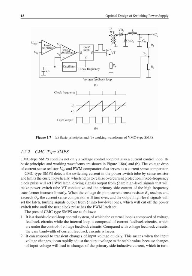
1.5.2 CMC-Type SMPS
CMC-type SMPS contains not only a voltage control loop but also a current control loop. Itsbasic principles and working waveforms are shown in Figure 1.8(a) and (b). The voltage dropof current sense resistor US, and PWM comparator also serves as a current sense comparator.
CMC-type SMPS detects the switching current in the power switch tube by sense resistorand limits the current cyclically, which helps to realize overcurrent protection. Fixed-frequencyclock pulse will set PWM latch, driving signals output from Q are high-level signals that willmake power switch tube VT-conductive and the primary side current of the high-frequencytransformer increase linearly. When the voltage drop on current sense resistor Rs reaches andexceeds Ur, the current sense comparator will turn over, and the output high-level signals willset the latch, turning signals output from Q into low-level ones, which will cut off the powerswitch tube until the next clock pulse has the PWM latch set.
The pros of CMC-type SMPS are as follows:1. It is a double closed-loop control system, of which the external loop is composed of voltage
feedback circuits while the internal loop is composed of current feedback circuits, whichare under the control of voltage feedback circuits. Compared with voltage feedback circuits,the gain bandwidth of current feedback circuits is larger.
2. It can respond to transient changes of input voltage quickly. This means when the inputvoltage changes, it can rapidly adjust the output voltage to the stable value, because changesof input voltage will lead to changes of the primary side inductive current, which in turn,

Overview on Switching-Mode Power Supply (SMPS) 19
Figure 1.8 (a) Basic principles and (b) working waveforms of CMC-type SMPS
results in changes of Us. This means that it can change the output pulse’s duty ratio directlythrough the current sense comparator rather than the error amplifier.
3. The joint control of voltage control loop and current control loop may increase the voltageregulation factor.
4. It can simplify the design of error amplifier compensating network.5. PWM comparator will cut off the power switch tube and maintain output voltage stable as
long as the current pulse reaches the set threshold.6. It is equipped with a limiting current protection circuit. Therefore, the limiting current
threshold can be set precisely and simply by changing the value of Rs.
The cons of CMC-type SMPS are as follows:
1. Two control loops make it difficult to design and analyze circuits.2. A duty ratio of over 50% may lead to instability of the control loops, in which case, a slope
compensation circuit needs to be added.3. It has a poor ability to restrain noises. As the primary side inductor works in the continuous
energy storage mode, the rising slope of switching current signal is small. A relatively lownoise overlaid to the current signal is likely to cause false operation of the PWM controller,for which a noise suppression circuit will be required.

20 Optimal Design of Switching Power Supply
IP IR
KRP<1.0
KRP=1.0
IRIP
(a)
(b)
Figure 1.9 Waveforms of switching currents: (a) CUM and (b) DUM
1.6 Working Mode of SMPS
SMPS has two basic working modes: continuous mode (CUM) and discontinuous mode(DUM). Next, taking the single-chip SMPS of TOPSwitch series for example, we introducethe setting methods of the two working modes and then make comparison on power lossesunder these two working modes so as to derive the conclusion.
1.6.1 Setting Methods of CUM and DUM
1.6.1.1 Characteristics of CUM and DUM
In CUM, the high-frequency transformer starts to work from a non-zero energy storage statein every switching cycle, while in DUM, all energy stored in the high-frequency transformershould be released. Their difference can be seen in Figure 1.9. The switching current in CUMstarts from a certain level, goes up to the peak along the slope, and then back to zero rapidly.At this time, the scale factor KRP between primary winding pulse current IR and peak currentIP is less than 1.0, or
IR = KRPIP < IP (1.2)
The switching current in DUM starts from zero, goes up to the peak, and then back to zerorapidly. At this time,
KRP = 1.0,
orIR = IP (1.3)
1.6.1.2 Working Mode Setting
Using the proportional relationship between IR and IP (or the value ofKRP), the working modesof SMPS can be quantitatively described. The value range of KRP is 0–0.1. When IR = IP andKRP = 1.0, the SMPS is set in DUM. When IR < IP or KRP < 1.0, the SMPS is set in DUM.To be specific, there are two situations: (i) when 0 < IR < IP, or 0 < KRP < 1.0, it is in CUM;and (ii) ideally, when IR = 0 and KRP = 0, it is in absolute CUM, which also can be called

Overview on Switching-Mode Power Supply (SMPS) 21
extreme CUM. Then the primary winding inductance Lp→∞, and the switching current onprimary side appears as a rectangular wave.
As a matter of fact, there is a transition instead of a strict boundary between absolute CUMand DUM. For a given AC input range, a smaller KRP value means a more continuous workingmode, larger primary winding inductance, and smaller primary side IP value and IRMS value.At this time, a lower power TOPSwitch and a larger high-frequency transformer can be used tooptimize the design. Otherwise, a larger KRP value means poor continuity and smaller primarywinding inductance but relatively larger IP and primary side RMS current IRMS. At this time,a large power TOPSwitch and a small high-frequency transformer shall be used.
In conclusion, the working mode of SMPS can be set by selection of KRP value. The settingprocess is Lp ↑→ (IR < IP) → (KRP < 1.0) → CUM.KRP = 0.4–1.0 is the best for 100 V/115 V AC power supplies. KRP = 0.6–1.0 is preferred
for 85–265 V wide-range input or 230 V fixed-input AC power supplies.
1.6.2 Power Consumption Comparison between These Two Working Modes
The following two design cases can illustrate the changes in values of IP and IRMS correspond-ing to KRP = 1.0 (DUM) and KRP = 0.4(CUM) in the wide range input of 85–265 V so thatcomparison can be made on TOPSwitch power consumptions under these two modes.
1.6.2.1 DUM Design Case
The given working parameters are KRP = 1.0, UImin = 90V, Dmax = 60%, PO = 30 W, powerefficiency 𝜂 = 80% and that the primary winding peak current IP can be expressed either as thefunction of IR and KRP or the function of the basic parameters (output power PO, minimum DCinput voltage UImin, maximum duty ratio Dmax, and power efficiency 𝜂) and IR; the equationsare as follows:
IP = IR∕KRP (1.4)
IP =PO
UIminDmax+
IR2
(1.5)
Convert Equation (1.4) to IR = KRPIP, and put it into Equation (1.5), to calculate the valueof IP:
IP =2PO
UIminDmax𝜂(2 − kRP)(1.6)
The final RMS current IRMS of primary winding is
IRMS = IP
√√√√Dmax
(K2
RP
3− KRP + 1
)(1.7)
Put UImin = 90V, Dmax = 60%, 𝜂 = 80%, PO = 30W, and KRP = 1.0 into Equation (1.6)and we will obtain Ip = 1.39 A. Put the result into Equation (1.7) to obtain IRMS = 1.39√
0.6 ×(
13− 1 + 1
)= 0.62 (A)

22 Optimal Design of Switching Power Supply
1.6.2.2 CUM Design Case
The given working parameters are KRP = 0.4, UImin = 90V, Dmax = 60%, PO = 30W, 𝜂 =80%. Different from the first case, KRP here is 0.4, which indicates that the working modeis more continuous. Similarly, it can be worked out that I′P = 0.87 A and I′RMS = 0.54A.
It is easy to work out that the peak current in CUM is only 63% of that in DUM, whereasthe RMS current in CUM is 87% of that in DUM. Therefore, for the given TOPSwitch chip,the power consumption ratio of the two working modes is
P′O
PO=
(I′RMS)2RL
(IRMS)2RL= (87%)2 = 75.7%
This indicates that, 24.3% of power consumption can be reduced in CUM than in DUM.In other words, under the same output power, CUM allows the use of low-power TOPSwitch, orallows TOPSwitch to work with low power consumption. Besides, when an SMPS is designedin CUM, the AC component on primary side circuit is lower than that of DUM. In addition, itcan reduce the skin effect and the power consumption of high-frequency transformers.
1.7 Feedback Type of SMPS
1.7.1 Basic Types of SMPS Feedback Circuit
Consider the Single-Chip SMPS of TOPSwitch series, for example. The SMPS feedback cir-cuits can be grouped into four basic types: (i) basic feedback circuit; (ii) improved basicfeedback circuit; (iii) optical coupling feedback circuit with a voltage-regulator tube; and (iv)optical coupling feedback circuit with TL431, whose simplified circuit diagrams are illustratedin Figure 1.10(a)–(d).
Figure 1.10(a) shows a basic feedback circuit. Its advantages include simple circuit, lowcost, and applicability to small-scale and economic SMPS and disadvantages include poor volt-age regulation performance, voltage regulation SV = ±1.5% to ±2.5%, and load regulationSI≈ ± 5%.
Figure 1.10(b) shows an improved feedback circuit. Equipped with a voltage-regulator tubeVDZ2 and a resistance R1 additionally, the load regulation can reach ±2.5%. The stable voltageof VDZ2 is 22 V generally. The number of turns of the bias winding shall be increased corre-spondingly for a comparatively higher bias voltage UB to satisfy the requirement of circuit.
Figure 1.10(c) shows an optical coupling feedback circuit with a voltage-regulator tube. Thereference voltage UZ is provided by VDZ2. LED inside the optical coupler may get an errorvoltage when the output voltage UO fluctuates. Therefore, this circuit is equivalent to addingan external error amplifier to TOPSwitch. UO, which can be regulated using both external andinternal error amplifiers. This kind of feedback circuit can make the voltage regulation factorlower below ±1%.
Figure 1.10(d) shows an optical coupling feedback circuit with TL431 with a relativelycomplicated circuit but the best voltage regulation performance. Here an adjustable precisionshunt regulator of TL431 type instead of a common regulator is used to form the external erroramplifier so that the precision adjustment to UO can be realized, and the voltage regulation