Optical metamaterials: design, up-scalable fabrication and ...
177
ADVERTIMENT. Lʼaccés als continguts dʼaquesta tesi queda condicionat a lʼacceptació de les condicions dʼús establertes per la següent llicència Creative Commons: http://cat.creativecommons.org/?page_id=184 ADVERTENCIA. El acceso a los contenidos de esta tesis queda condicionado a la aceptación de las condiciones de uso establecidas por la siguiente licencia Creative Commons: http://es.creativecommons.org/blog/licencias/ WARNING. The access to the contents of this doctoral thesis it is limited to the acceptance of the use conditions set by the following Creative Commons license: https://creativecommons.org/licenses/?lang=en
-
Upload
khangminh22 -
Category
Documents
-
view
5 -
download
0
Transcript of Optical metamaterials: design, up-scalable fabrication and ...

ADVERTIMENT. Lʼaccés als continguts dʼaquesta tesi queda condicionat a lʼacceptació de les condicions dʼúsestablertes per la següent llicència Creative Commons: http://cat.creativecommons.org/?page_id=184
ADVERTENCIA. El acceso a los contenidos de esta tesis queda condicionado a la aceptación de las condiciones de usoestablecidas por la siguiente licencia Creative Commons: http://es.creativecommons.org/blog/licencias/
WARNING. The access to the contents of this doctoral thesis it is limited to the acceptance of the use conditions setby the following Creative Commons license: https://creativecommons.org/licenses/?lang=en

Thesis submitted for the degree of Doctor by
L’UNIVERSITÉ DE BORDEAUX AND
LA UNIVERSITAT AUTÒNOMA DE BARCELONA
PhD programs: Physical chemistry of condensed matter and Materials science
Optical metamaterials: design, up-scalable
fabrication and characterization
By Mayte Gómez Castaño
Under the supervision of: Serge Ravaine and Agustín Mihi
Tutor: Jordi Hernando Campos
Centre de Recherche Paul Pascal
Institut de Ciència de Materials de Barcelona
June 2020


“If you only do what you can do,
you’ll never be better than what you are”
Master Shifu, Kung Fu Panda 3


A mi abuela Juanita,


vii
Table of contents
Acknowledgments ..................................................................................................................... xi
Abstract ...................................................................................................................................... xv
Resumen.................................................................................................................................... xvi
Résumé long ............................................................................................................................ xvii
List of abbreviations .............................................................................................................. xxiii
Chapter 1 Introduction ......................................................................................................... 1
1.1 Light-matter interaction ............................................................................................. 1
1.1.1 Electromagnetic wave propagation................................................................ 2
1.1.2 Optical properties of dielectric and metals ................................................... 3
1.1.3 Surface plasmon polaritons ............................................................................. 4
1.2 Metamaterials .............................................................................................................. 7
1.2.1 Tailoring 𝜀 and 𝜇 ............................................................................................... 7
1.2.2 Types of metamaterials .................................................................................... 9
1.3 Negative-index metamaterials ................................................................................ 11
1.3.1 Negative refraction ......................................................................................... 11
1.3.2 Designs for negative-index metamaterials .................................................. 12
1.3.3 Fishnet metamaterials at optical frequencies .............................................. 15
1.4 References .................................................................................................................. 20
Chapter 2 Fabrication, characterization and simulation methods ............................. 27
2.1 Introduction ............................................................................................................... 27
2.2 Colloidal lithography ............................................................................................... 28
2.2.1 Self-assembly of monolayers on the water surface .................................... 29
2.3 Nanoimprint lithography ........................................................................................ 32
2.3.1 Master replication ........................................................................................... 34
2.3.2 Soft nanoimprinting ....................................................................................... 35
2.4 Electrodeposition ...................................................................................................... 37
2.5 Scanning electron microscopy ................................................................................. 39

Table of contents
viii
2.6 Optical characterization methods ........................................................................... 39
2.6.1 Visible-infrared spectroscopy ........................................................................ 40
2.6.2 Angle-resolved spectroscopy ......................................................................... 40
2.6.3 Time-resolved fluorescence microscopy ...................................................... 41
2.7 Finite-difference time-domain simulations ............................................................ 41
2.8 References ................................................................................................................... 43
Chapter 3 Fishnet metamaterials made by colloidal lithography .............................. 49
3.1 Introduction ................................................................................................................ 49
3.2 Tuning the effective refractive index ...................................................................... 51
3.3 Fabrication of double fishnet metamaterials by colloidal lithography .............. 53
3.3.1 Preparation of non-closed-packed monolayers .......................................... 53
3.3.2 Multilayer electrodeposition through a colloidal template ....................... 56
3.3.3 Nickel dissolution and transfer to transparent substrate .......................... 58
3.4 Optical characterization of the fishnet structures ................................................. 59
3.4.1 Colloidal monolayers embedded in a stack of metallic layers .................. 60
3.4.2 Double fishnet metamaterials ........................................................................ 62
3.5 Properties of double fishnet metamaterials ........................................................... 63
3.5.1 Effective parameters ....................................................................................... 63
3.5.2 Verification by Fresnel modelling ................................................................. 67
3.5.3 Negative refraction in a metamaterials prism ............................................. 69
3.5.4 Angle dependence of the operation wavelength ........................................ 69
3.6 Conclusions ................................................................................................................ 70
3.7 References ................................................................................................................... 71
Chapter 4 Fishnet metamaterials by soft nanoimprint lithography .......................... 77
4.1 Introduction ................................................................................................................ 77
4.2 Fabrication of fishnet metamaterials by soft nanoimprinting ............................. 79
4.2.1 Preparation of periodic arrays of pillars ...................................................... 79
4.2.2 Multilayer electrodeposition through two-dimensional templates ......... 82
4.2.3 Nickel dissolution ............................................................................................ 87
4.3 Optical characterization of multilayered fishnet metamaterials......................... 89

Table of contents
ix
4.4 Effective properties of multilayered fishnet metamaterials ................................ 93
4.4.1 Effective parameters ....................................................................................... 93
4.4.2 Change of branch in the refractive index .................................................... 97
4.4.3 Angular dependence of the working wavelength ..................................... 98
4.5 Fishnet metamaterials as refractive index sensors ............................................. 100
4.6 Conclusions .............................................................................................................. 104
4.7 References ................................................................................................................ 106
Chapter 5 Nanostructured metallic surfaces for enhanced molecular emission .. 111
5.1 Introduction ............................................................................................................. 111
5.2 Fluorescent dye ....................................................................................................... 113
5.3 Flat metallic surface ................................................................................................ 114
5.3.1 Fabrication method ....................................................................................... 114
5.3.2 Fluorescent decay in absence of metallic boundary ................................ 116
5.3.3 Collective interference .................................................................................. 117
5.3.4 Theoretical model ......................................................................................... 119
5.4 One-dimensional plasmonic arrays as superradiance platforms ..................... 121
5.4.1 Shallow lines patterning .............................................................................. 121
5.4.2 Corrugated metallic surface ........................................................................ 123
5.4.3 Fluorescent decay evolution with the spacer thickness .......................... 125
5.5 Two-dimensional plasmonic arrays as superradiance platforms .................... 126
5.5.1 Metal-coated colloidal monolayers ............................................................ 127
5.5.2 Fluorescence decay evolution with the distance ...................................... 129
5.6 Conclusions .............................................................................................................. 130
5.7 References ................................................................................................................ 132
Chapter 6 General conclusions and perspectives ....................................................... 137
6.1 Conclusions .............................................................................................................. 137
6.1.1 Negative-index metamaterials .................................................................... 137
6.1.2 Enhanced spontaneous emission ................................................................ 139
6.2 Perspectives.............................................................................................................. 140
6.2.1 Fishnet design ................................................................................................ 140

Table of contents
x
6.2.2 Superradiance platforms .............................................................................. 141
6.2.3 Further photonic and plasmonic systems .................................................. 141
6.3 References ................................................................................................................. 142
Appendix Retrieval of effective parameters ................................................................... 143
Scientific contributions ........................................................................................................... 149

xi
Acknowledgments
This thesis is the result of a great and enriching collaboration between the Centre
de Recherche Paul Pascal (CRPP) and the Institut de Ciència de Materials de Barcelona
(ICMAB), within the frame of an IdEx fellowship and CSIC and ERC projects. This
international teamwork has allowed me to develop my work and grow both
scientifically and personally. I would therefore like to thank the priceless help and
support of the people that have shared with me this adventure.
Firstly, I would like to express my thanks to my supervisors, Serge Ravaine and
Agustín Mihi, for giving me this opportunity, for their incentive, ideas, guidance,
availability for Skype meetings and, of course, help with the infinite paperwork. I want
to thank Serge for his always-open door (even at 7pm on Fridays), for his exhaustive
analysis and discussions, and for providing me all the necessary tools for developing
properly my work: from conferences to countless visits to Placamat within the same
week. To Agustín, I give my thanks for his enthusiasm, for always looking for the best
solution and for pushing further and further until obtaining results at the cutting edge.
His motivation and support during these years have inspired me more than once and I
sincerely appreciate them.
I would like also to thank two very important people (VIP) without whom more
than half of this thesis could not have been accomplished. I am thankful to Renaud
Vallée for teaching me the physics and French terms behind our systems, for his always
positive attitude and for including me in parallel projects that have contributed to the
final development of the thesis. I want to thank as well Juan Luis García Pomar, for his
help with the simulations and for his patience while I was trying to absorb a small piece
of his vast and admirable knowledge. Thanks also for the good moments shared in the
office, always providing unbelievable breaking news all around the world.
La première partie de cette thèse a été effectuée au sein du CRPP, où j’ai eu la
chance de trouver une ambiance de travail et un personnel extraordinaires. Tout d’abord
je voudrais remercier la direction et l’administration pour leur accueil et toute leur aide:
Cécile Zakri, Corinne Amengual, Béatrice Dupin, Elisabeth Hortolland, Evangéline
Lounissi et, plus particulièrement, Caroline Legrand pour son impeccable gestion de la
bourse IdEx.

Acknowledgments
xii
Je remercie les personnes du laboratoire qui m’ont permis de me former sur des
différents instruments et qui ont été toujours disponibles pour mes infatigables et
impatientes demandes. Un grand merci à Isabelle Ly pour m’avoir initiée à la
microscopie électronique, à Xavier Brilland pour les formations sur n’importe quel
spectrophotomètre et à Joanna Giermanska pour son aide avec le spin-coater.
Merci à Sandrine Maillet et Jean-Luc Laborde pour tous les outils informatiques
qu’ils m’ont fournis pour gérer cette cotutelle. Je ne peux pas oublier Nathalie Touzé à
l’accueil pour apporter les meilleurs ingrédients pour bien commencer la journée.
Je remercie également les personnes de Placamat qui ont contribué à l’acquisition
des images de MEB à haute résolution : Sophie Agard, Michel Martineu et, en particulier,
Philippe Legros pour m’apprendre les secrets de la microscopie électronique à balayage.
Merci à Wiljan Smaal et Sokha Khiev de’ElorprintTec pour la formation sur le « plasma
etcher » et les quelques images de MEB faites en pleine crise de microscopie au campus.
At CRPP and Bordeaux in general I had the chance of meeting many people whose
friendship turned these places into my second home. I want to thank specially the Serge
team for the great ambience in and out the lab. I thank Petra for being like a big sister
and great friend (despite it was me who got the molkky). Merci à Hervé pour son
soutien, visites au sous-sol et les bons moments partagés en France et en Espagne. « Tu
vois qui est … ? » Merci également à Pierre-Etienne, Sophie, Eliott, Sharvina, Stéphanie,
Bin, Rawan et Andréa pour leur aide avec les activités quotidiennes au labo.
Je remercie aussi la petite famille française qui m’a accompagnée pendant cet an et
demi au laboratoire, aux soirées jeux ou à la plage. Je pense à ma « co-bureautrice »
Hélène, Artem, Maxime, Rafael, Nathassia, Florian, Romain, Marie-Charlotte, Julien,
Kébo, Antoine et Valentine. Merci à vous tous pour faire partie des très bons moments
qui resteront toujours dans ma mémoire.
I am also grateful to the international family that filled my daily life with lots of
fun and laughs. Special words to Raj for his support and for being the best company ever
for having dinner at Crous restaurants. I also want to thank Laura, Fernando, Teo, Xuan,
Carlotta, Valentina, Marco, Franco, Katerina, Denize, Aurélie, Armand, Said, Ferdinand,
Julia, Marie F., Marie H., Juan, Ricardo, Goce, Rajam, Simone, Etienne, Rémi, Manu,
Lachland, Maëva, Yun, Hongwei, Quentin, Romain, Ale, Flavia, Arantza, Sara, Sarah,
Junjin and all the people that contributed to that amazing environment.

Acknowledgments
xiii
Enfin, merci à l’équipe de running du CRPP sous la direction d’Ahmed Bentaleb
pour leur accueil, la soif de dépassement et pour être une source de déconnexion.
La experiencia en un gran instituto como el ICMAB no iba a ser menos y me ha
permitido conocer y trabajar con personas de la mejor calidad humana y profesional. En
primer lugar, me gustaría agradecer la gran labor de la administración, en especial a
Sonia Roldán y Pietat Sierra por conseguir cerrar mi contrato antes incluso de que
llegara.
Gracias igualmente a Javier Rubio por la gran gestión de mi ordenador portátil
francés, a pesar de todos los dolores de cabeza que le haya podido ocasionar.
También quiero agradecer la ayuda con las medidas de SEM a Anna Esther
Carrillo, del ICMAB, así como al equipo del ICN2. Igualmente, gracias a Luigi Morrone,
de la sala blanca, por los depósitos hechos por ALD.
Gracias también a Anna May por picarme con el gusanillo de la divulgación y por
crear grandes ocasiones para tomar perspectiva del mundo de la ciencia en general.
Millones de gracias al grupo de Enlightment, por todo el conocimiento
intercambiado, por las ideas y por el genial ambiente tanto en el laboratorio como fuera
de él. A Cristiano por enseñarme todo sobre el hard/soft PDMS, for pillars, for holes, for
wait… Era al revés. A Camilla por encontrar siempre una solución buena, rápida y
efectiva. A Pau por ser un gran amigo siempre dispuesto a perder apuestas
(#sestafeiraforever). Al David (Davit), per ser el millor company possible per fer hard
PDMS. A Denise, por su buena onda e inestimable apoyo, wey. A Luis, por siempre
encontrar un hueco para satisfacer mis ansias de medir con ángulo. Y a André, Leo y
Nicolás, por sus buenos consejos y discusiones científicas.
Mis agradecimientos se extienden indudablemente al grupo de Nanopto. A los
bosses, gracias por crear un ambiente de tal envergadura donde crecer y aprender cada
semana. Igualmente, gracias al resto de estudiantes de doctorado y postdocs del grupo.
Moltes graciès al Martí per les seves boges però grans idees per les meves mostres i per
ser el meu professor oficial de català. I also want to thank Adri, Quique, Rana, Minghua,
Osnat, Fatma, José, Valentina, Nadia, Xabi, Albert, Iván, Jinhui, Kai, Alex, Laura,
Bernhard, Miquel, Carmen, Aurélien... for the good moments shared in the lab, during
lunch, playing board games or at the multiple barbecues.

Acknowledgments
xiv
Gracias igualmente a Cris, Sohini, Bego, Edu, Isa, Uri, Juanan, Cristina, Javi, Timo,
Raúl, Juan, Romain, Fendi, Javi P. y todas aquellas personas que me han acompañado
durante esta bonita aventura en Barcelona.
Quiero darles también las gracias a Jose Luis Pau y Eduardo Ruíz por acogerme de
vuelta unos días en el lab de Microelectrónica de la UAM y ayudarme con los depósitos
por CVD.
Aprovecho este momento para agradecerles a mis amigos todo su apoyo e interés
durante estos años a pesar de los cientos de kilómetros que nos separaban. A mis non-
quantum amigas de la uni: Miriam, Irene, Ana y Eva; por supuesto a Mariano (ya en
poco nos dedicamos a nuestra verdadera pasión: la jardinería); a mis amigos del barrio y
derivados: Alba, Diego, Nu, Sandra, Ali, Pablo, Chechu, David y, sobre todo, a Guille y
Álvaro, por ser los mejores amigos que una podría tener.
Mis más sinceras gracias a Andrés, por tus ánimos, tus consejos, por tus ganas de
aprender cada curiosidad que te pueda contar, por los millones de viajes aquí y allá, por
aquella primera tortilla en Burdeos, por creer en mí y, sobre todo, por siempre aportar
luz cuando todo parece oscuridad.
Por último y más importante, me dirijo al gran pilar de mi vida: mi familia. Gracias
a todos vosotros por vuestro cariño, apoyo y por las eternas preguntas de “¿cuánto te
quedas?”, “¿qué tal va la tesis?”, “¿te parece bien si vamos a verte tal finde?”. A la
familia hispano-peruana-boliviana, por vuestras siempre calurosas bienvenidas llenas de
palomitas. A los más viajeros, grupo al que me siento enormemente orgullosa de
pertenecer, por vuestro infalible humor desde allí donde quiera que estéis. A los
Castaños, porque… “esto no es un grupo, es mi familia”, a pesar de lo que diga la policía
turística. A Guillermo y Javi, por traer siempre un contagioso aire fresco y divertido. A
mis abuelos, para mí fuentes de inspiración, superación y cariño.
Y finalmente, gracias a mis padres. Por haber sido siempre un soporte
incondicional y más aún, cuando empezó esta aventura. Porque sólo unos pocos conocen
las maravillosas cazadoras de Burgos, las carreteras del País Vasco o lo que es
verdaderamente importante en nuestras vidas. Gracias por los miles de paquetes
enviados, por las sorpresas a distancia, por aquella traumatizante mudanza y por
llenarme de tappers cada vez que bajaba. Porque sin vosotros, ninguna de estas páginas
habría sido posible. Gracias.

xv
Abstract
Metamaterials are artificially structured materials, thoroughly designed for
achieving electromagnetic properties not observed in nature. In the last years, the field of
metamaterials has exponentially grown due to the exceptional possibilities that they offer
to manipulate light. One of the most attractive phenomena is the negative refractive index,
which may enable resolution imaging beyond the diffraction limit.
Nowadays, one of the main challenges of negative-index metamaterials is the
transition from the laboratory to real applications. However, the vast majority of
metamaterials still rely on low-throughput and expensive techniques that hamper this
progression. Therefore, this thesis is devoted to the development of up-scalable negative-
index metamaterials with the aim of facilitate their implementation in actual devices. We
focus on the fishnet design because of its efficient behavior at optical wavelengths.
Firstly, we develop a bottom-up fishnet design by combining colloidal lithography
and electrodeposition. The system consists of a double-fishnet made of gold layers
separated by air gaps and supported by dielectric particles. We study experimentally and
theoretically the optical dependence on the main structural parameters. Their proper
control gives rise to metamaterials whose refractive index can be easily tailored from
positive to negative values in the near infrared, with a minimum value of -1 at 940 nm.
Secondly, we study fishnet metamaterials made by nanoimprint lithography and
electrodeposition. The infiltration of several metallic layers through templates of pillars
leads to multilayered fishnet structures made of gold and air gaps. The accurate design
leads to strong negative indices, from -1.2 at 700 nm to -2.8 at 910 nm. We thoroughly
analyze their optical response and study their performance as optical sensors when filling
the gaps with different liquids.
Finally, inspired by the cost-effective approaches of colloidal lithography and
nanoimprinting, we investigate the fabrication of nanostructured metallic substrates for
the observation of collective spontaneous emission. We develop large-area plasmonic
crystals whose resonances can boost the emission rate of ensembles of dye molecules.
xvi
Resumen
Los metamateriales son materiales artificialmente estructurados, minuciosamente
diseñados para obtener propiedades electromagnéticas inobservables en la naturaleza. En
los últimos años, el campo de los metamateriales ha crecido exponencialmente debido a
las excepcionales posibilidades que ofrecen para manipular la luz. Uno de los fenómenos
más atractivos es el índice de refracción negativo, con el que se podrían obtener
resoluciones ópticas más allá del límite de difracción.
Hoy en día, uno de los mayores desafíos de los metamateriales es el salto del
laboratorio a las aplicaciones reales, pues la gran mayoría de ellos todavía depende de
técnicas de bajo rendimiento y alto coste que obstaculizan esta transición. Por ello, esta
tesis está dedicada al desarrollo de metamateriales de índice negativo fácilmente
escalables, con el objetivo de facilitar su implementación en dispositivos reales. Nos
centramos en el diseño tipo «fishnet» por su funcionamiento efectivo a frecuencias ópticas.
En primer lugar, desarrollamos un diseño «bottom-up» de metamateriales fishnet
combinando la litografía coloidal y el elecrodepósito. El sistema consiste en una fishnet
doble hecha de capas de oro separadas por cavidades de aire y soportadas por partículas
dieléctricas. Estudiamos la respuesta óptica al variar los principales parámetros
estructurales. Demostramos que un control adecuado da lugar a metamateriales cuyo
índice de refracción puede variar fácilmente desde valores positivos hasta negativos en el
infrarrojo cercano, obteniendo un mínimo de -1 a 940 nm.
En segundo lugar, estudiamos metamateriales fishnet hechos por nanoimpresión y
electrodepósito. La infiltración de múltiples capas metálicas a través de patrones de pilares
da lugar estructuras fishnet multicapas de oro y aire. El riguroso diseño de estas
estructuras da lugar a grandes índices negativos, desde -1.2 a 700 nm hasta -2.8 a 910 nm.
Analizamos en detalle su respuesta óptica y estudiamos su aplicación como sensores
ópticos al infiltrar distintos líquidos entre las cavidades de aire.
Por último, inspirados por la facilidad de procesado de la litografía coloidal y de la
nanoimpresión, investigamos la fabricación de sustratos metálicos nanoestructurados
para la observación de emisión espontánea colectiva. Desarrollamos cristales plasmónicos
cuyas resonancias pueden aumentar el ritmo de emisión de moléculas fluorescentes.
xvii
Résumé long
Les métamatériaux sont des matériaux structurés artificiellement, soigneusement
designés pour obtenir des réponses électromagnétiques inobservables dans la nature.
Leurs propriétés ne proviennent pas seulement des matériaux constitutifs mais sont
surtout déterminées par la géométrie et la disposition des composants.
L’origine des métamatériaux est associé aux travaux pionniers de Veselago (1968)
sur la propagation de la lumière dans un matériau hypothétique de permittivité et
perméabilité négatives.1 Il a montré que dans un tel milieu la lumière obéit toujours aux
lois de Maxwell mais se comporte différemment que dans les matériaux conventionnels,
avec des propriétés exotiques comme un indice de réfraction négatif. Cependant, le sujet
n’a pas attiré l’attention pendant plus de 30 ans2 faute d’un matériau possédant une
permittivité et une perméabilité négatives simultanément. Le fait que cette combinaison
électromagnétique n’existe pas dans les substances naturelles a donné lieu au terme de
métamatériaux.
Au cours de ces dernières années, le domaine des métamatériaux a connu une
croissance exponentielle grâce aux possibilités exceptionnelles qu’ils offrent pour
manipuler la lumière. Entre autres, on peut nommer le magnétisme à fréquences optiques,
la chiralité artificielle ou la réfraction négative. L’indice de réfraction négatif suscite
toujours un grand intérêt en raison de l’obtention potentielle de résolutions optiques au-
delà de la limite de diffraction.
Aujourd’hui, un des principaux défis des métamatériaux à indice de réfraction
négatif est la transition du laboratoire au marché. Ce passage implique quelques prérequis
tels que compatibilité avec de grandes surfaces ou des processus de fabrication à faible
coût, en préservant à tout moment une réponse optique de qualité. A ce jour, la plupart
des métamatériaux dépendent de techniques peu performantes qui empêchent leur
utilisation dans des applications comme la superlentille.3,4
Afin de faciliter leur mise en place dans des dispositifs réels, cette thèse porte sur le
développement de métamatériaux à indice négatif pouvant être réalisés à grandes
échelles. Nous détaillons ci-dessous les principaux sujets et résultats développés au cours
de ces travaux.

Résumé long
xviii
Tout d’abord, le Chapitre 1 présente les notions générales sur l’interaction lumière-
matière qui sont à la base du comportement des métamatériaux. Ceci inclut les propriétés
optiques des métaux et des diélectriques ainsi que le couplage de la lumière avec des
interfaces entre de ces deux types de matériaux. Les ondes électromagnétiques qui se
propagent à ces interfaces sont appelées plasmons-polaritons de surface et sont à l’origine
des propriétés des métamatériaux dans le domaine du visible et l’infrarouge. L’excitation
de ces ondes superficielles et l’ingénierie des résonances plasmoniques donnent lieu à la
possibilité de concentrer et guider la lumière à l’échelle nanométrique. Les métamatériaux
profitent de cette interaction lumière-matière exaltée. En effet, l’excitation et l’hybridation
des plasmons de surface au sein des composites métal-diélectrique est responsable du
caractère extraordinaire des métamatériaux.
Les métamatériaux sont généralement réalisés à partir de l’assemblage de briques
élémentaires complexes, aussi nommées méta-atomes, dont la taille est plus petite que la
longueur d’onde de la lumière. Ainsi, même si les propriétés inhabituelles des
métamatériaux proviennent de l’interaction électromagnétique avec les méta-atomes,
l’ensemble peut être décrit comme un milieu homogène avec des paramètres
macroscopiques effectifs.
On distingue différent types de métamatériaux en fonction de ces paramètres et des
designs proposés pour les réaliser. Parmi les métamatériaux à indice négatif, plusieurs
structures ont été étudiées théoriquement et expérimentalement afin d’obtenir un tel
indice, de la gamme des microondes jusqu’au visible. La condition pour pouvoir observer
un tel comportement est l’existence d’une réponse électrique et magnétique simultanée,
c’est-à-dire à la même longueur d’onde. Etant donnée la réponse électrique des métaux, le
but principal est de designer des architectures qui présentent un magnétisme artificiel.
Les structures de type « fishnet » constituent l’approche la plus prometteuse pour
les gammes du visible et de l’infrarouge,5 ce design permettant un contrôle indépendant
des réponses magnétique et électrique. D’une part, le magnétisme est obtenu à partir de
bandes métalliques parallèles au champ magnétique incident et séparées par une couche
diélectrique. Si les bandes métalliques sont suffisamment proches, les plasmons de surface
excités à chaque interface métal-diélectrique s’hybrident et donnent lieu à des courants
électriques antiparallèles. Ceux-ci induisent à leur tour un moment magnétique artificiel
dans la structure. D’autre part, la réponse électrique est générée grâce à des bandes
métalliques perpendiculaires aux premières et orientées parallèlement au champ

Résumé long
xix
électrique. Elles agissent comme un métal dilué avec une fréquence plasma plus faible qui
confère la réponse électrique aux métamatériaux, notamment une permittivité négative.6
En résumé, le design « fishnet » peut être vu comme une structure multicouche perforée
par des trous périodiques.
Dans les dernières années, plusieurs groupes de recherche ont travaillé sur la
fabrication ce de type de structures en utilisant divers matériaux constitutifs, différentes
épaisseurs de couches ou formes des trous pour obtenir des valeurs d’indice de réfraction
négatives aux fréquences optiques. A la fin du premier chapitre, nous présenterons l’état
de l’art concernant les métamatériaux à indice négatif selon leur taille, la longueur d’onde
de travail et les valeurs d’indice atteintes. Comme précédemment discuté, on constate que
la grande majorité de ces métamatériaux a été fabriquée avec des méthodes difficilement
compatibles avec les grandes surfaces nécessaires pour leur mise en œuvre au sein de
dispositifs opérationnels.
Le Chapitre 2 présente les techniques utilisées au cours de cette thèse pour fabriquer
des matériaux de type fishnet à faible coût, sur des grandes surfaces et avec une réponse
optique comparable à celles atteintes avec les processus « classiques » plus coûteux. A
cette fin, nous avons utilisé la lithographie colloïdale, la lithographie par nanoimpression
et l’électrodéposition.
La lithographie colloïdale permet d’obtenir d’une manière simple et rapide des
monocouches de nanoparticules bien ordonnées dont le diamètre peut être modifié sans
affecter l’ordre du réseau. Dans cette thèse, nous avons utilisé l’assemblage à la surface de
l’eau pour obtenir des monocouches de sphères de polystyrène sur des surfaces de
quelques centimètres. Nous présentons ensuite les avantages de la lithographie par
nanoimpression, notamment la possibilité de répliquer plusieurs motifs nanométriques
avec une grande fiabilité. La fabrication des moules flexibles qui ont été utilisés est
détaillée et le protocole d’électrodéposition est également précisé.
A la fin de ce chapitre, sont présentées les techniques de caractérisation structurale
et optique employées, ainsi que la méthode de différences finies dans le domaine temporel
(FDTD) qui a été utilisée pour simuler les propriétés optiques des métamatériaux
fabriqués.
Le Chapitre 3 est dédié à la conception, à la fabrication et à la caractérisation de
métamatériaux de type « fishnet » par une voie « bottom-up ». Nous avons combiné les

Résumé long
xx
avantages de la lithographie colloïdale et de l’électrodéposition pour réaliser des
matériaux « double fishnet » composés de deux couches d’or séparées par une cavité d’air
et perforées de manière périodique par une monocouche de sphères de polystyrène. En
premier lieu, nous présentons l’influence des paramètres les plus importants dans ces
structures : le diamètre des particules et l’épaisseur de la couche d’air entre les couches
métalliques. Nous montrons qu’en diminuant la taille de ces deux paramètres, on obtient
des indices de réfraction plus négatifs ainsi qu’un décalage vers le rouge de la longueur
d’onde de résonance.
Ces études préliminaires ont servi à la fabrication de métamatériaux avec un indice
de réfraction facilement réglable. Le processus suivi commence par le dépôt d’une
monocouche de particules de polystyrène de 480 nm sur un substrat de nickel. Le diamètre
des particules est réduit à l’aide d’un plasma d’oxygène, ce qui donne lieu à des
monocouches colloïdales non compactes au sein desquelles des couches d’or et de nickel
sont électrodéposées de manière séquentielle. La dissolution sélective ultérieure des
couches sacrificielles de nickel permet d’obtenir des métamatériaux constitués par deux
couches d’or séparées par une cavité d’air et percées par les particules de polystyrène. En
plus, cette étape de dissolution permet de transférer les matériaux obtenus sur des
substrats transparents, permettant leur caractérisation optique.
Nous avons étudié les propriétés optiques de ces structures et avons démontré leur
qualité grâce au bon accord entre les spectres expérimentaux et les simulations. A partir
de ces calculs, on a extrait les propriétés macroscopiques effectives, qui montrent que
l’indice de réfraction des métamatériaux réalisés varie entre valeurs positives, valeurs
proches de zéro et valeurs négatives dans le proche infrarouge. La valeur minimale
d’indice obtenue est de -1 à une longueur d’onde de 940 nm, avec une bande de valeurs
négatives qui s’étale sur 100 nm.
Les simulations de la distribution des champs électromagnétiques montrent que
l’origine de ce comportement est liée à la résonance magnétique excitée dans la cavité
d’air, conformément à la théorie. La validité des paramètres extraits a également été
confirmée en substituant les systèmes par des milieux effectifs qui donnent la même
réponse macroscopique. De la même façon, la modélisation d’un prisme réalisé à partir
du métamatériau d’indice -1 a montré la possibilité d’obtenir une réfraction négative avec
ces structures.

Résumé long
xxi
Le Chapitre 4 est consacré à une autre voie d’élaboration des métamatériaux de type
« fishnets », basée sur la combinaison de la lithographie par nanoimpression et
l’électrodéposition. Dans ce cas, nous avons utilisé différents réseaux de piliers
diélectriques dont la périodicité varie entre 200 et 500 nm. L’infiltration de multicouches
d’or et de nickel autour des piliers puis la dissolution sélective du nickel a permis de
montrer la possibilité de fabriquer des métamatériaux de type « fishnets » constitués de
multicouches d’or et d’air. Ces structures sont préparées sur des substrats conducteurs et
transparents, donc permettant la réalisation directe de dispositifs optiques.
Ce protocole permet d’obtenir une large gamme des métamatériaux en contrôlant
les aspects structuraux tels que la périodicité, le diamètre et la hauteur des piliers,
l’épaisseur des couches d’or, la séparation entre elles ou le nombre de couches métalliques.
Le rigoureux design de ces géométries a conduit à des valeurs d’indice de réfraction
négatives dans le visible et infrarouge, avec des valeurs de -1.2 à 700 nm ou -2.8 à 910 nm.
De même que précédemment, il a été montré que la résonance magnétique a lieu entre les
couches d’or.
On a également montré que pour les structures avec plus de deux couches d’or
l’indice effectif présente une discontinuité prononcée, passant d’une valeur négative à une
valeur positive. Cela est dû au changement du mode électromagnétique dominant dans la
structure. La distribution des champs varie donc entre les branches d’indice négatif et
positif.
La réponse optique des métamatériaux est influencée par le nombre de couches qui
les composent. Par exemple, en augmentant ce nombre, l’absorption diminue et la zone
de travail se décale vers les longueurs d’onde plus petites. Le faible décalage observé pour
les métamatériaux de périodicité plus petite suggère une convergence de leur
comportement avec celui d’un matériau massif, où la réponse optique ne dépend plus du
nombre de couches ou l’angle d’incidence de la lumière.
Enfin nous démontrerons l’accessibilité de la porosité des métamatériaux en
étudiant les changements des propriétés optiques qui se produisent quand on infiltre
différents liquides au sein des couches métalliques. La dépendance linéaire de la longueur
d’onde de résonance avec l’indice de réfraction du milieu infiltré démontre le potentiel
des métamatériaux comme capteur optiques.

Résumé long
xxii
Inspiré par la possibilité d’obtenir des motifs nanométriques par des voies faciles à
mettre en œuvre et reproductibles, le Chapitre 5 aborde la fabrication de substrats
métalliques nanostructurés pour l’étude de l’émission spontanée collective. Dans ce projet,
nous avons développé trois types des plateformes métalliques dont la configuration peut
exalter le taux d’émission d’un ensemble de molécules fluorescentes. Ces plateformes sont
des systèmes où les molécules sont placées à une certaine distance de la surface métallique.
Les trois types correspondent à un film de métal plat, un réseau plasmonique
unidimensionnel et un réseau plasmonique bidimensionnel.
Pour la configuration plate, nous avons démontré théoriquement et
expérimentalement l’existence de deux régimes d’émission (collective et individuelle) et
leur forte dépendance avec la distance entre les molécules et la surface métallique ou avec
le nombre d’émetteurs.
Finalement, nous avons utilisé les techniques de nanoimpression et de lithographie
colloïdale pour fabriquer des cristaux plasmoniques. La superposition spectrale de leurs
résonances avec l’émission des molécules montre la possibilité d’exalter pas seulement le
taux de fluorescence mais aussi le comportement collectif.
Références
1. V. G. Veselago. The electrodynamics of substances with simultaneously negative
values of ε and μ. Sov. Phys. Uspekhi 1968, 10, 509–514.
2. D. R. Smith, W. J. Padilla, D. C. Vier, S. C. Nemat-Nasser and S. Schultz. Composite
medium with simultaneously negative permeability and permittivity. Phys. Rev.
Lett. 2000, 84, 4184–4187.
3. J. B. Pendry. Negative refraction makes a perfect lens. Phys. Rev. Lett. 2000, 85, 3966–
3969.
4. G. Yoon, I. Kim and J. Rho. Challenges in fabrication towards realization of practical
metamaterials. Microelectron. Eng. 2016, 163, 7–20.
5. C. M. Soukoulis and M. Wegener. Past achievements and future challenges in the
development of three-dimensional photonic metamaterials. Nat. Photonics 2011, 5,
523–530.
6. J. Valentine, S. Zhang, T. Zentgraf and X. Zhang. Development of bulk optical
negative index fishnet metamaterials: Achieving a low-loss and broadband
response through coupling. Proc. IEEE 2011, 99, 1682–1690.

xxiii
List of abbreviations
CL Colloidal lithography
EM Electromagnetic
FDTD Finite difference time domain
FOM Figure of merit
FTIR Fourier transform infrared spectroscopy
GSP Gap surface plasmon
ITO Indium-doped tin oxide
MIM Metal-insulator-metal
NIL Nanoimprint lithography
NIM Negative index metamaterial
NA Numerical aperture
NIR Near infrared
PS Polystyrene
PMMA Polymethyl methacrylate
RI Refractive index
RIE Reactive ion etching
RT Room temperature
SEM Scanning electron microscopy
SPP Surface plasmon polariton
SPR Surface plasmon resonance
SRR Split-ring resonator
TE Transverse electric
TM Transverse magnetic
TCO Transparent conducting oxide
UV Ultraviolet
Vis Visible
WE Working electrode


1
Chapter 1
Introduction
1.1 Light-matter interaction
From radio waves to gamma rays, light has inspired scientists for centuries and un-
doubtedly influenced our daily life and progress. The interaction of light with matter has
become an essential tool for research and development in physics, chemistry, biology or
medicine. Yet, the exploration of light propagation, engineering of optical properties and
the innovation in electromagnetic communications make light-matter interaction as one
of the most vibrant areas of science.1,2
The emergence and enormous advances of nanotechnology in the last decades have
led to new perspectives for light manipulation.3 The study of light coupling to nanostruc-
tured materials has rapidly blossomed because of the countless applications in optical
technologies such as imaging,4 sensing,5 energy harvesting,6 or lightning.7 Specifically,
nano- and micro-patterned metal-dielectric interfaces attract great attention for confining
light, upgrading the performance of classical devices or attaining unprecedented electro-
magnetic phenomena.
This is the case of metamaterials, artificially structured materials providing exotic
optical responses. Typically made of periodic composite arrays, metamaterials generate
unique electromagnetic properties mostly governed by the geometry rather than the con-
stituent materials. Therefore, they can be engineered to exhibit electromagnetic behaviors
beyond the natural limits such as optical magnetism or negative refractive index. The ex-
ploitation and practical implementation of these properties could revolutionize the field
of optics with fascinating devices such as super-resolution lenses or invisibility cloaks.8
In this chapter, we will introduce the main theoretical aspects of light-matter inter-
action behind metamaterials. Starting with the fundamentals of light propagation through
a medium, we will later focus on the coupling at metal-dielectric interfaces. This photonic
framework will be the support for introducing the concept of metamaterials, the

Chapter 1 Introduction
2
types so far developed and, more importantly, the key ingredients for realizing negative-
index metamaterials (NIMs). Finally, we will review some of the most relevant works in
this field as well as the main challenges towards the practical implementation of NIMs
working at optical frequencies.
1.1.1 Electromagnetic wave propagation
The spatial and temporal propagation of an electromagnetic (EM) wave within a
material is described by Maxwell’s equations:
∇ · = (1.1)
∇ · = 0 (1.2)
∇ × = − (1.3)
∇ × = + (1.4)
where is the electric displacement, the magnetic induction, the electric field, the
magnetic field, the free charge density and the current density. For a linear and iso-
tropic medium, and are related to and by the constitutive relations:
= + = (1.5)
= + = (1.6)
where is the vacuum electric permittivity, the vacuum magnetic permeability and , the polarization and magnetization induced in the material by the external fields. The
overall response can be expressed in terms of the relative permittivity and permeability
of the medium. These are unitless and complex numbers that depend on the radiation
frequency. The real parts describe the polarization or magnetization strength while the
imaginary parts account for the absorption losses or the gain in the material.
= + ′′ (1.7)
= + ′′ (1.8)
Therefore, the interaction of an EM wave with a medium is determined by these
macroscopic parameters, which significantly vary between dielectrics, semiconductors
and metals. Two related parameters are also used to describe the electromagnetic response
of the medium: the refractive index and the wave impedance . The former is the ratio

Chapter 1 Introduction
3
between the speed of light in vacuum and in the medium, while the latter characterizes
the material resistance to the wave propagation.
= (1.9)
= / (1.10)
Similarly to and , depending on the material and frequency, and might be
complex, the imaginary part being the absorptive component. These values govern the
classical interactions of light and matter such as absorption, reflection or refraction.
1.1.2 Optical properties of dielectric and metals
At optical frequencies, the magnetization of a medium is much weaker than the elec-
tric counterpart and can be neglected. Therefore, the magnetic induction approaches the
free space regime, the relative permeability can be taken as = 1 and the refractive index
is simplified to = √. Contrarily, the permittivity not only differs from the vacuum limit
but acquires remarkable different values for metals and dielectrics.
On one hand, from the blue to the mid-infrared, dielectrics are mostly characterized
by a positive and nearly constant permittivity with a negligible imaginary part. Light is
slowed down but not absorbed within the medium. This is why dielectrics are commonly
used in optical components, since they display high transparency.8
Figure 1.1 Comparison of the permittivity: a real part and b imaginary part of silver and gold at
optical frequencies. Adapted from Johnson and Christy measurements.9
On the other hand, the optical properties of metals are governed by their plasma
frequency , which accounts for the oscillations of the free electrons cloud and typically
falls in the ultraviolet (UV) range. Below this value, the real part of the permittivity is
400 600 800 1000 1200
0
2
4
6
Im (
ε)
Wavelength (nm)
400 600 800 1000 1200
-60
-40
-20
0
Gold Silver
Re
(ε)
Wavelength (nm)
ba

Chapter 1 Introduction
4
characteristically negative. This is one of the most important attributes of metals as far as
optical properties are concerned. It implies that the electrons oscillate out of phase with
the external field, screening the EM wave and leading to a reflectivity close to 1. Besides,
metals present non-negligible losses coming from electronic collisions and band transi-
tions that should be considered when designing optical structures. Figure 1.1 shows the
permittivity of the most commonly used metals in optics: silver and gold, both presenting
negative real parts that substantially decrease with the wavelength.
1.1.3 Surface plasmon polaritons
The sharp contrast between metals and dielectrics is the key for obtaining unusual
electromagnetic properties such as the ones of metamaterials. They typically rely on the
interaction of light with metal-dielectric interfaces. When the impinging light is coupled
to such boundaries, it excites electromagnetic surface waves called surface plasmon polar-
itons. Since most of our research derives from this excitation, we will briefly introduce the
basic properties of such plasmonic waves.
Propagating surface plasmon polaritons or simply called surface plasmon polaritons
(SPPs) are hybrid photon-electron excitations travelling at the interface between a dielec-
tric and a metal. They arise from the coupling of an EM wave with a longitudinal charge
density oscillation at the metallic surface (Figure 1.2). Interestingly, while SPPs can prop-
agate along the interface, they are evanescently confined in the perpendicular direction,
with penetration depths of the order of hundreds of nanometers in the dielectric and tens
of nanometers in the metal.10
Figure 1.2 (Left) Combined electromagnetic and charge density waves of surface plasmon polari-
tons propagating at the metal-dielectric interface. (Right) Decay of the perpendicular electric field
intensity inside the dielectric and the metal.
The nature of surface plasmons lies on the opposite sign of the permittivities in-
volved. As previously discussed, this situation is fulfilled for dielectric and metals above
Chapter 1 Introduction
5
UV wavelengths, where the metal permittivity ! turns negative and rapidly decreases
with the wavelength, whereas the dielectric permittivity " remains constant. From Max-
well’s equations it can be demonstrated that SPPs only exist for the transverse magnetic
(TM) polarization, this is, with the magnetic field perpendicular to the propagation plane.
Under these boundary conditions, the dispersion relation of SPPs results in:
#|| = % & "!" + ! (1.11)
where #|| is the wavenumber parallel to the surface, the wave frequency, % the speed of
light in vacuum and
% = # = 2() (1.12)
being # the vacuum wavenumber and ) the corresponding vacuum wavelength.
In the same dielectric, however, light follows the linear dispersion relation:
#|| = % " (1.13)
which means that the SPP wavenumber is always higher than the wavenumber in
the dielectric or free space. Hence, light impinging at a dielectric-metal interface cannot
directly excite SPPs because of the momentum mismatch and additional in-plane momen-
tum is needed.
There exist several methods for providing the missing momentum and exciting SPPs
through light. These methods include light coupling through a prism by total internal re-
flection, scattering from a surface defect such as protrusions or holes, or diffraction from
gratings.11 The latter is of great interest because of the direct incorporation of the coupling
mechanism into the structure. The absence of external items facilitates the application of
plasmonic behaviors in optical devices.
SPPs are excited on a grating if their wavenumber matches the momentum of the
impinging light plus the reciprocal lattice vectors of the array as follows:12
*#+,,* = *# sin 1 +23! + 34* (1.14)
where #+,, is the wavevector of SPP derived from equation (1.11), # sin1 is the in-plane
wavevector of light, 3!, 34 are the lattice vectors and 2, = 0, ±1, ±2, … In the simplest
case where light impinges normally to the surface (1 = 0), this expression is simplified to

Chapter 1 Introduction
6
the contribution of the reciprocal lattice vectors 3!,4. For the most common periodic ge-
ometries, the module of these lattice vectors, and so of #+,,, is given by the following ex-
pressions, where 6 denotes the lattice constant.
Linear: *#+,,* = *3!* = 2(6 2 (1.15)
Squared: *#+,,* = *3!,4* = 2(6 27 + 7 (1.16)
Hexagonal: *#+,,* = *3!,4* = 4(√3627 + 7 +2 (1.17)
Thus, when this momentum matches the dispersion relation of equation (1.11), light
is coupled to SPPs propagating at the metal-dielectric interface.
Figure 1.3 depicts the excitation of SPPs at normal incidence thanks to the in-plane
momentum provided by a periodic array (3!,4). The frequency at which the momentum
matching is satisfied is known as surface plasmon resonance (SPR). In this situation, the
energy of the incident light is efficiently transferred to the SPP wave, with a drastic effect
on the optical response typically manifested as a fall in the reflection spectra.
Figure 1.3 a Excitation of SPPs on a metal-dielectric grating at normal incidence. b Dispersion rela-
tion of SPP (blue) and light in the same dielectric (black). The red vector represents the momentum
provided by the grating, matching the SPP dispersion at a free space frequency +,:.
The excitation of SPPs and derived plasmonic resonances implies the possibility of
concentrating and channelling light at the nanoscale. Metamaterials are one of the current
fields benefiting from such enhanced light-matter interaction. As we will discuss later, the
excitation and hybridization of SPPs in metal-dielectric composites is responsible for the
extraordinary character of many metamaterials.

Chapter 1 Introduction
7
1.2 Metamaterials
1.2.1 Tailoring ; and <
The origin of metamaterials is associated with the seminal paper of Veselago (1968)
about the behavior of light through a hypothetical material with negative permittivity and
permeability.13 He found that in such medium light would still obey Maxwell’s equations
but would behave inversely to conventional materials, with exotic properties such as neg-
ative refraction. However, the subject was left aside for more than 30 years14,15 due to the
lack of natural materials with simultaneous negative permittivity and permeability for
proving the phenomenon. The fact that such combined electromagnetic response is not
found in naturally occurring substances coined the famous term of metamaterials.
Metamaterials (from the Greek prefix => (meta-), beyond) are artificially engi-
neered structures exhibiting properties not attainable with ordinary media. Made from
the arrangement of subwavelength units, the properties of metamaterials do not derive
from their chemical composition but rather from their physical structure. The basic units,
sometimes called meta-atoms, are composites of conventional materials whose complex
geometry can lead to exotic properties compared to the individual constituents.
Figure 1.4 Principle of the homogenization method. The composite metamaterial can be described
as an effective medium.
The scales of the units, typically their thickness and lattice constant in periodic ar-
rays, are considerably smaller than the wavelength of interest so that the whole system
can be described as a uniform media. Therefore, although the unusual properties of met-
amaterials arise from the intricate EM interaction, light macroscopically sees a homogene-
ous medium. This approximation enables the description of the metamaterial as an effec-
tive medium with macroscopic effective parameters such as permittivity, permeability,
refractive index and impedance (Figure 1.4).8 Properly designing the geometry, size and
media involved in a metamaterial, it is possible to engineer the overall electromagnetic

Chapter 1 Introduction
8
response. For instance, artificial magnetism can be achieved from non-magnetic constitu-
ent materials.16
Figure 1.5 Materials classification as a function of the real parts of the permittivity and permea-
bility . The red dashed line represents natural media at optical frequencies, for which Re () = 1.
Natural and human-made materials can be classified according to the real part of
the parameters and (Figure 1.5).17,18 If both the permittivity and the permeability are
positive numbers, like in most dielectrics and magnetics materials, the media are called
double-positive (DPS). In contrast, if both parameters are negative, materials are referred
as double-negative (DNG). To date, such response has not been observed in nature, and
so this type of materials have become one of the most intriguing metamaterials, particu-
larly since the first experimental realizations.19 When the permittivity becomes negative
but the permeability remains positive, materials are called epsilon-negative (ENG). This
group embraces plasmas, metals below the plasma frequency and some doped semicon-
ductors.20 The opposite situation, this is, materials with positive permittivity and negative
permeability are named mu-negative (MNG). Though unusual, this response has been ob-
served in some ferrites at microwave frequencies.21 In opposition to double-negative ma-
terials, ENG and MNG are often comprised in a single category called single-negative
(SNG). Below the unity values, materials are specifically known as epsilon-near-zero
(ENZ) or mu-near-zero (MNZ). Deeper in this category, materials with both parameters
near-zero have been termed near-zero or just zero-index materials (ZIM) in relation to the
linked refractive index.
Nevertheless, the electromagnetic map is extremely reduced when working with
conventional materials at optical wavelengths due to the lack magnetism. At this range,
from metals to dielectrics, materials present a relative permeability equal to 1 (red dashed

Chapter 1 Introduction
9
line of Figure 1.5). This limitation is indeed the main motivation of metamaterials research:
designing and implementing materials beyond the natural framework.22,23
1.2.2 Types of metamaterials
Theoretical investigations together with the continuous development of nanotech-
nology have led to a feasible tailoring of and from positive to zero and negative values.
As a result, the metamaterials field has rapidly grown and led to different branches of
study according to the sought properties and elementary building blocks.
Figure 1.6 Types of optical metamaterial structures. a Multilayered fishnet negative-index met-
amaterial.24 b Arrangement of split-ring resonators for artificial magnetism.25 c Laminated and d
nanowire hyperbolic metamaterials.26 e Chiral metamaterial made from a helix array.24 f Rasp-
berry-like magnetic nanocluster made from metal-dielectric particles.27 g All-dielectric negative-
index metamaterial from inclusions of high refractive index dielectric spheres.24 h Nanoantenna
array metasurface for negative reflection and refraction.28
Among the different types, we should highlight negative-index metamaterials,8,24
likely the most extended structures for historical reasons and focused on attaining nega-
tive refractive indices through artificial magnetism; hyperbolic metamaterials,26 which
present an anisotropic permittivity; and chiral metamaterials,29 aimed at obtaining strong
optical activity. Other types include colloidal nanoresonators,30,27 displaying also an arti-
ficial magnetic response; or all-dielectric metamaterials,31 similar to the previous classes
but avoiding the common use of plasmonic resonances because of the inherent metallic
losses. In addition, there exists an increasing interest in the so-called metasurfaces,32 pla-
nar metamaterials primarily used in wavefront engineering. Figure 1.6 presents some of
the most studied systems in these fields, largely dominated by plasmonic resonances.

Chapter 1 Introduction
10
The effective electromagnetic design of these structures has made possible the de-
velopment and improvement of optical systems such as invisibility cloaks, super-resolu-
tion lenses, nanoantennas, absorbers, polarizers, sensors, non-linear devices or even anti-
counterfeiting methods.14,28,33–40
Thanks to the academic advances, metamaterials have successfully moved beyond
the laboratory scale to high-volume applications. Companies such as Kymeta or Evolv
Technology already commercialize meta-antennas for high-performance satellite commu-
nications or security scanners, respectively. The start-up Metaboards enables charging
portable electronic devices across large surfaces without the need for alignment, provid-
ing flexible and functional wireless power solutions (Figure 1.7a). Although more chal-
lenging because of the reduced dimensions, the meta-technology has been also extended
to the optical regime. The company Lumotiv has developed a beam steering technology
based on a liquid crystal metasurface for automotive light detection and ranging, LIDAR
(Figure 1.7b). Similarly, Metamaterial Inc. (META) applies nanopatterned composites to
boosted biosensors through impedance matching or to green light anti-reflection glasses.
The latter, patented as MetaAir and co-developed with the aerospace corporation Airbus,
offers a balanced combination of laser protection with high colour transparency (Figure
1.7c).
Figure 1.7 a Photograph of a mobile phone charging on a Metaboards surface.41 b Beam steering
from the liquid crystal metasurface developed by Lumotive.42 c Photograph of the MetaAir aviation
glasses from Metmaterial Inc.43
These companies are just some examples of the promising future of metamaterials
in everyday life devices. For this reason, nowadays a significant part of the research com-
munity works on developing metamaterials that can easily satisfy the requirements
needed for commercialization. Among the types above discussed, negative-index met-
amaterials are still one of them.

Chapter 1 Introduction
11
1.3 Negative-index metamaterials
1.3.1 Negative refraction
The refractive index is one of the most important and used parameters for describ-
ing light propagation through media. Defined as:
= %/? (1.18)
being ? the phase velocity in the medium, it describes how fast light travels through the
material. Most common optical materials present refractive indices ranging from 1 to 2.5
at visible and infrared frequencies.44
When a light ray travels across two different media, it gets bent owing to the change
in refractive index. This phenomenon, refraction, explains why a straw immersed in a
glass of water may appear broken. Thanks to refraction, the light path can be adjusted and
focused in glasses, magnifying lenses or microscopes. Because of this strong influence of
in daily life, the concept of a negative index of refraction is an attractive new domain of
light manipulation with revolutionary impact in current optical technologies.
Figure 1.8 a Positive and b negative refraction, along with the wavevectors and EM fields.
The most intuitive result of negative-index metamaterials is negative refraction. As
expressed by Snell’s law
@ sin1@ = 7 sin17 (1.19)
light passing from a positive index material (@) to a NIM (7) will bend in a negative
angle 17, oppositely to conventional materials (Figure 1.8). Furthermore, in NIMs the
wavevector # will be oriented in the opposite direction to the energy propagation, forming
a left-handed system with the field vectors , . Because of this, NIMs are also known as

Chapter 1 Introduction
12
left-handed materials, unlike natural right-handed materials. Such property implies as
well a negative phase velocity inside the metamaterial with related phenomena such as
reversed Doppler effect or Cerenkov radiation.13
One of the most remarkable applications of NIMs might be the so-called perfect lens
(Figure 1.9).14 Taking advantage of the negative refraction of these materials, it would be
possible to focus light without the need of common curved surfaces. Moreover, the eva-
nescent waves would be amplified through the NIM slab, compensating the decay outside
the material and recovering the original intensity at the focus plane. Since the evanescent
waves carry the subwavelength information of an object, it would be possible to overcome
the diffraction limit of light and reconstruct a super-resolved image. This extraordinary
light bending introduced new prospects for optical space engineering, leading to striking
devices such as invisibility cloaks.33,45
Figure 1.9 Imaging with a a conventional convex lens and b perfect lens with refractive index of -1.
Red and blue lines illustrate the propagating direction and evanescent intensity, respectively.
1.3.2 Designs for negative-index metamaterials
Although Veselago first stated that simultaneous negative and were needed to
achieve NIMs, it was later demonstrated that in dissipative media the strict necessary con-
dition is given by46
+ A 0 (1.20)
Therefore, one could achieve negative indices in a SNG medium, with just ′ or ′ negative.
Yet, this condition implies the existence of an electric and magnetic response at the same
wavelength, this is, and different from passive media.8 The losses in these metamate-
rials are often characterized by the figure of merit (FOM):
FOM = ||′′ (1.21)

Chapter 1 Introduction
13
where ′ and ′′ denote the real and imaginary parts of the refractive index, respectively.
Thus, the higher the FOM, the better the metamaterial performance is.
In the last decades, several approaches have been worldwide developed for the re-
alization of NIMs working from microwave to visible frequencies. Given the electrical re-
sponse of metals, the main motivation has been to design intriguing architectures showing
artificial magnetism. The key point for such goal is the creation of current loops within the
structure components that can induce magnetic dipoles. The combination of the induced
magnetic response with the electrical nature of metals is the most common strategy for
achieving negative refractive index.
Split-ring resonators
The first experimental demonstration of NIMs was provided by a metallic and non-
magnetic array of straight wires combined with split-ring resonators (SRRs).15 In these
meta-atoms, the incident light can excite an oscillating electric current along the metallic
SRRs that in turn induces a local magnetic field perpendicular to the SRR plane (Figure
1.10a). Since the direction of the current loop varies following the EM oscillation, the gen-
erated magnetic field will as well oscillate, leading to an artificial magnetic dipole.
Though efficient at low frequencies, its implementation at optical wavelengths en-
counters several issues such as miniaturization limitations or, more importantly, satura-
tion of the working wavelength and decrease of the magnetic dipole strength.47
Figure 1.10 Examples of meta-atoms for negative-index metamaterials. a Split-ring resonator. b
Cut-wire pair. c Dendritic design. The electrical current loop induces a magnetic dipole 2 from
non-magnetic constituent materials.
Cut-wire pairs
The restrictions found with SRR pushed the design of alternative resonant meta-
atoms such as metallic pairs of rods or plates, known as cut-wire pairs.48,49 The EM reso-
nances in these metamaterials arise from the SPPs excited along the rods. If two rods are

Chapter 1 Introduction
14
brought together, the plasmonic resonance will hybridize into a symmetric and an anti-
symmetric mode. The impinging electric field oriented parallel to the rods will induce
symmetric currents between the rods, whereas the perpendicular magnetic field will gen-
erate antiparallel currents.50 Analogous to the SRRs, the latter will create a magnetic dipole
(Figure 1.10b), responsible for the artificial magnetism. However, an accurate geometrical
design is needed so that both electric and magnetic resonances overlap and lead to a neg-
ative refractive index.
Dendrites
Designs based on dendritic or fractal unit cells present similar operation to the pre-
vious models. In these metallic systems, the magnetic response is induced by current loops
generated in the branches in the same manner as for SRRs (Figure 1.10c).51 Nonetheless,
like for the cut-wire pairs, the electric response appears at a different frequency so that a
fine design is required for obtaining both resonances at the same wavelength. The spectral
difference is the major obstacle that these structures experience.
Fishnet design
The fishnet design breaks this limit thanks to the combination of a magnetic reso-
nance with a non-resonant but rather background electric response (Figure 1.11).
Figure 1.11 Components of the fishnet structure.
The magnetic response is achieved through metallic strips oriented along the inci-
dent magnetic field and separated by a dielectric layer. In the same manner as previous
designs, the metallic wires support antiparallel currents that induce a magnetic moment
in the structure. The origin of these currents lies on the coupling of the SPPs propagating
at both metal-dielectric interfaces. When the metallic layers are close enough, their eva-
nescent fields overlap and lead to the formation of gap surface plasmons (GSPs),52 Figure

Chapter 1 Introduction
15
1.12. Metallic strips parallel to the electric field provide the electric counterpart. They work
effectively as a diluted metal with a lower plasma frequency that gives a background elec-
tric response, namely negative permittivity.
Bringing together both components (Figure 1.11), the fishnet metamaterial can be
viewed as a metal-insulator-metal (MIM) stack drilled with dielectric holes. Since the mag-
netic response is generated in the insulator, the effective permeability will mainly depend
on the thickness and refractive index of this film. On the other hand, the effective permit-
tivity will be governed by the cut-off frequency of the waveguide mode supported by the
holes in the metal layers. Above the cut-off wavelength, the effective permittivity will be-
come negative.53 Therefore, the fishnet design enables an independent control of both re-
sponses while simplifying their operation at the same wavelength.
Figure 1.12 Evanescent waves coupling of SPPs leading to gap-surface plasmons.
1.3.3 Fishnet metamaterials at optical frequencies
In 2011, Soukoulis et al. reported the advances towards optical NIMs, showing the
promising approach of the fishnet design to visible wavelengths (Figure 1.13).24 Compared
to its partners, fishnet metamaterials stand out for the easier overlap of the magnetic and
electric response and for their continuous structure, which is highly compatible with cur-
rent nanopatterning techniques.
Numerous groups have developed fishnet metamaterials with the motivation of get-
ting a strong magnetic resonance, highly negative refractive index, visible operation, po-
larization independency, low losses or large-area implementations. All systems based on
perforated MIM stacks, they have made use of different materials, layers thicknesses, hole
shapes or lattice lengths for obtaining a broad range of NIMs at optical frequencies.

Chapter 1 Introduction
16
Figure 1.13 Advances in metamaterials operating frequency over the first decade.24 Orange: struc-
tures based on double SRRs; green: U-shaped SRRs; blue: cut-wire pairs; red: double-fishnet struc-
tures. The insets show optical or electron micrographs of the four types of designs.
Figure 1.14 summarizes the main fishnet metamaterials developed to date as a func-
tion of the wavelength at which the most negative effective refractive index EFF has been
achieved. The colour bar marks the scale of the systems, showing that the vast majority of
fishnet NIMs working at optical frequencies still rely on low-throughput nanofabrication
(yellow and greenish colours).
1.000E-05
1.000E-04
0.001000
1.000
100.0
500 1000 1500 20000
-1
-2
-3
1000 µm2
10 µm2
1 mm2
Chettiar (2007)Lodewijks (2010)
Xiao (2010)Garcia-Meca (2011)
Liang (2017)
Xiao (2009)
Zhou (2013)
Rottler (2012)
Dolling (2006)
Gao (2014)
Gao (2014)
Re
(nef
f)
Wavelength (nm)
Zhang (2005)
Sharp (2014)
Valentine (2008)
Choi (2013)
1 cm2
Area
Figure 1.14 State of the art at the beginning of this thesis. Main fishnet metamaterials fabricated to
date as a function of the most negative effective refractive index EFF, the operation wavelength
and the area. Data extracted from references 54-67.
Chapter 1 Introduction
17
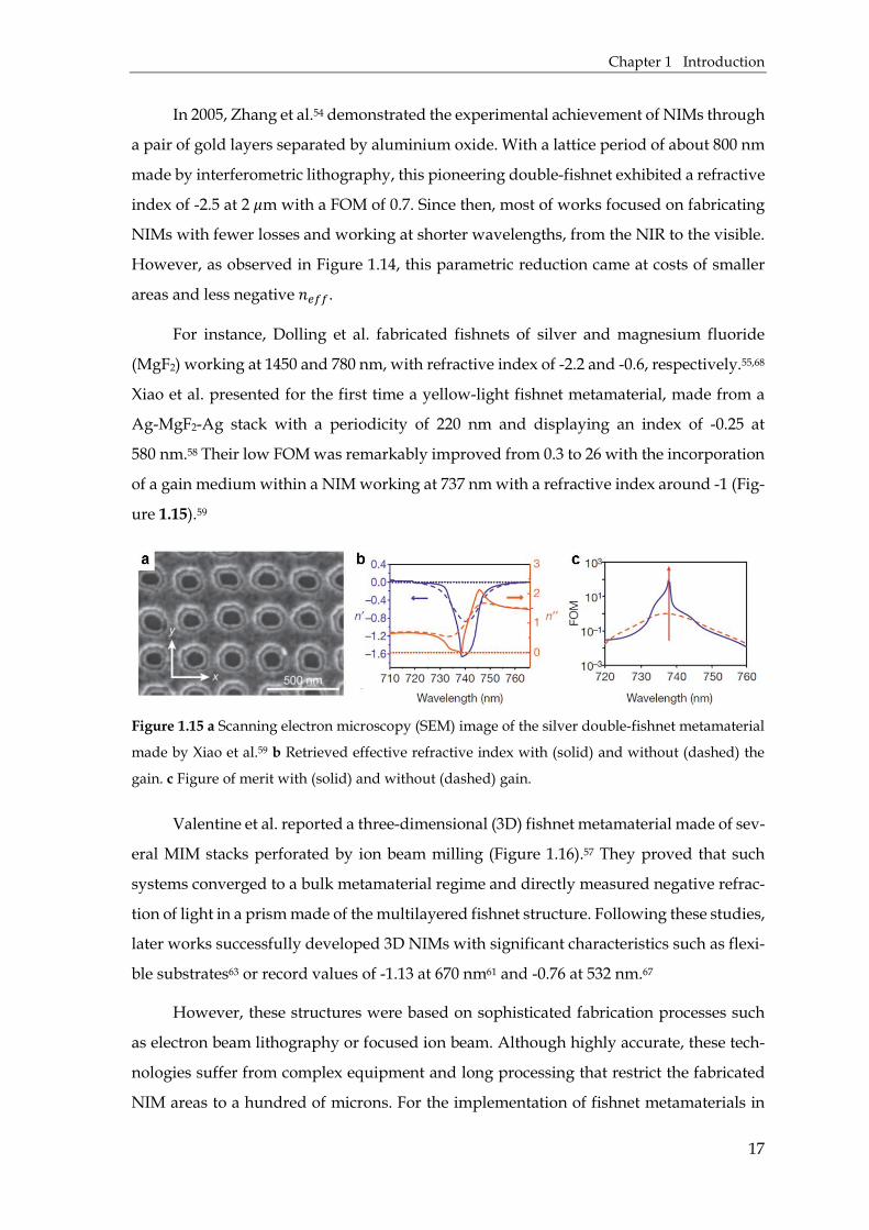
In 2005, Zhang et al.54 demonstrated the experimental achievement of NIMs through
a pair of gold layers separated by aluminium oxide. With a lattice period of about 800 nm
made by interferometric lithography, this pioneering double-fishnet exhibited a refractive
index of -2.5 at 2 m with a FOM of 0.7. Since then, most of works focused on fabricating
NIMs with fewer losses and working at shorter wavelengths, from the NIR to the visible.
However, as observed in Figure 1.14, this parametric reduction came at costs of smaller
areas and less negative EFF.
For instance, Dolling et al. fabricated fishnets of silver and magnesium fluoride
(MgF2) working at 1450 and 780 nm, with refractive index of -2.2 and -0.6, respectively.55,68
Xiao et al. presented for the first time a yellow-light fishnet metamaterial, made from a
Ag-MgF2-Ag stack with a periodicity of 220 nm and displaying an index of -0.25 at
580 nm.58 Their low FOM was remarkably improved from 0.3 to 26 with the incorporation
of a gain medium within a NIM working at 737 nm with a refractive index around -1 (Fig-
ure 1.15).59
Figure 1.15 a Scanning electron microscopy (SEM) image of the silver double-fishnet metamaterial
made by Xiao et al.59 b Retrieved effective refractive index with (solid) and without (dashed) the
gain. c Figure of merit with (solid) and without (dashed) gain.
Valentine et al. reported a three-dimensional (3D) fishnet metamaterial made of sev-
eral MIM stacks perforated by ion beam milling (Figure 1.16).57 They proved that such
systems converged to a bulk metamaterial regime and directly measured negative refrac-
tion of light in a prism made of the multilayered fishnet structure. Following these studies,
later works successfully developed 3D NIMs with significant characteristics such as flexi-
ble substrates63 or record values of -1.13 at 670 nm61 and -0.76 at 532 nm.67
However, these structures were based on sophisticated fabrication processes such
as electron beam lithography or focused ion beam. Although highly accurate, these tech-
nologies suffer from complex equipment and long processing that restrict the fabricated
NIM areas to a hundred of microns. For the implementation of fishnet metamaterials in

Chapter 1 Introduction
18
actual devices like the ones presented in Figure 1.7, requirements such as large-scale, ho-
mogeneous optical response or low-cost production have to be fulfilled.
Figure 1.16 a SEM images of a multilayered fishnet structure made of Ag and MgF2. b Geometry
diagram of the negative angle (>) and beam shift (G) measurement through a NIM prism. c Beam
shift resulting from the bending of light at the prism at various wavelengths.57
Alternatively, Lodewijks et al. proposed an approach based on colloidal lithogra-
phy.60 Instead of engraving through low-throughput techniques, they used a self-assem-
bled colloidal monolayer as mask for creating hexagonal double fishnet structures, made
of gold and silicon dioxide (SiO2). Their method led to NIMs with -1.4 refractive index at
1020 nm (Figure 1.17a,b). Gong et al. used the same concept for developing a low-cost
route based on colloidal lithography and electrodeposition, with a minimum value of -0.5
at 560 nm (Figure 1.17c-e).69
Figure 1.17 Fishnet metamaterials made by colloidal lithography. a,b SEM images of Au-SiO2-Au
sputtered layers drilled following a colloidal mask.60 c Scheme and d,e SEM views of fishnets made
by colloidal lithography and silver electrodeposition, working at visible wavelengths.69

Chapter 1 Introduction
19
In the same line of scalable manufacturing, Chanda et al. proposed the use of
nanoimprint lithography and transfer printing for fabricating metamaterials with a record
index of -7.8 at 2.4 m over centimeter-sized surfaces (Figure 1.18a-c).70 With a similar
method, Gao et al. reduced the size of the unit cell for developing NIMs working at visible.
Their structures displayed negative index over 181 nm, with a minimum value of -0.73 at
710 nm (Figure 1.18d,e).65
Figure 1.18 Fishnet metamaterials based on nanoimprint lithography. a Side and b top SEM views
of a multilayered Ag-MgF2-Ag stack after transfer printing. c Macroscopic optical image of the same
structure.70 d SEM image of a similar MIM stack operating at visible wavelengths. e Photograph of
the sample.65
Thanks to their scalability and low-cost manufacturing, colloidal lithography and
nanoimprinting are promising tools for the achievement of nanostructured metamaterials.
As proved by the latest studies and recent technological advances, these lithographies can
enable the mass production and implementation of metamaterials in real NIM devices.71
In addition, in terms of the absolute values achieved, there is still room for improvement
for large-are NIMs in order to reach the performance obtained by low-throughput ap-
proaches.
Hence, this thesis will make use of colloidal lithography and nanoimprinting for
providing improved fabrication procedures of fishnet metamaterials, with properties
comparable to the ones obtained by the typical short-range methods.

Chapter 1 Introduction
20
1.4 References
1. J. Weiner and F. Nunes. Light-matter interaction: Physics and engineering at the
nanoscale, 2nd ed.; Oxford University Press, New York, USA, 2017.
2. X. Luo. Subwavelength artificial structures: Opening a new era for engineering
optics. Adv. Mater. 2019, 31, 1804680.
3. J. W. Haus. Fundamentals and applications of nanophotonics; Woodhead Publishing,
UK, 2016.
4. S. Lee, Y. Sun, Y. Cao and S. H. Kang. Plasmonic nanostructure-based bioimaging
and detection techniques at the single-cell level. TrAC Trends Anal. Chem. 2019, 117,
58–68.
5. Y. Xu et al. Optical refractive index sensors with plasmonic and photonic structures:
Promising and inconvenient truth. Adv. Opt. Mater. 2019, 7, 1801433.
6. S. Linic, P. Christopher and D. B. Ingram. Plasmonic-metal nanostructures for
efficient conversion of solar to chemical energy. Nat. Mater. 2011, 10, 911–921.
7. Y. Li et al. Tailor-made nanostructures bridging chaos and order for highly efficient
white organic light-emitting diodes. Nat. Commun. 2019, 10, 2972.
8. W. Cai and V. Shalaev. Optical metamaterials: Fundamentals and applications; Springer,
New York, USA, 2010.
9. P. B. Johnson and R. W. Christy. Optical constants of the noble metals. Phys. Rev. B
1972, 6, 4370–4379.
10. W. L. Barnes. Surface plasmon–polariton length scales: A route to sub-wavelength
optics. J. Opt. A Pure Appl. Opt. 2006, 8, S87–S93.
11. A. V Zayats and I. I. Smolyaninov. Near-field photonics: Surface plasmon
polaritons and localized surface plasmons. J. Opt. A Pure Appl. Opt. 2003, 5, S16–
S50.
12. T. W. Ebbesen, H. J. Lezec, H. F. Ghaemi, T. Thio and P. A. Wolff. Extraordinary
optical transmission through sub-wavelength hole arrays. Nature 1998, 391, 667–
669.
13. V. G. Veselago. The electrodynamics of substances with simultaneously negative
values of ε and µ. Sov. Phys. Uspekhi 1968, 10, 509–514.

Chapter 1 Introduction
21
14. J. B. Pendry. Negative refraction makes a perfect lens. Phys. Rev. Lett. 2000, 85, 3966–
3969.
15. D. R. Smith, W. J. Padilla, D. C. Vier, S. C. Nemat-Nasser and S. Schultz. Composite
medium with simultaneously negative permeability and permittivity. Phys. Rev.
Lett. 2000, 84, 4184–4187.
16. J. B. Pendry, A. J. Holden, D. J. Robbins and W. J. Stewart. Magnetism from
conductors and enhanced nonlinear phenomena. IEEE Trans. Microw. Theory Tech.
1999, 47, 2075–2084.
17. A. Alu, N. Engheta, A. Erentok and R. W. Ziolkowski. Single-negative, double-
negative, and low-index metamaterials and their electromagnetic applications.
IEEE Antennas Propag. Mag. 2007, 49, 23–36.
18. Y. Liu and X. Zhang. Metamaterials: A new frontier of science and technology.
Chem. Soc. Rev. 2011, 40, 2494–2507.
19. W. J. Padilla, D. N. Basov and D. R. Smith. Negative refractive index metamaterials.
Mater. Today 2006, 9, 28–35.
20. G. V Naik and A. Boltasseva. A comparative study of semiconductor-based
plasmonic metamaterials. Metamaterials 2011, 5, 1–7.
21. K. Bi et al. Negative and near zero refraction metamaterials based on permanent
magnetic ferrites. Sci. Rep. 2014, 4, 4139.
22. T. Tanaka and A. Ishikawa. Towards three-dimensional optical metamaterials.
Nano Converg. 2017, 4, 34.
23. X. Fu and T. J. Cui. Recent progress on metamaterials: From effective medium
model to real-time information processing system. Prog. Quantum Electron. 2019, 67,
100223.
24. C. M. Soukoulis and M. Wegener. Past achievements and future challenges in the
development of three-dimensional photonic metamaterials. Nat. Photonics 2011, 5,
523–530.
25. M. Kadic, G. W. Milton, M. van Hecke and M. Wegener. 3D metamaterials. Nat. Rev.
Phys. 2019, 1, 198–210.

Chapter 1 Introduction
22
26. P. Huo, S. Zhang, Y. Liang, Y. Lu and T. Xu. Hyperbolic metamaterials and
metasurfaces: Fundamentals and applications. Adv. Opt. Mater. 2019, 7, 1970054.
27. V. Ponsinet et al. Self-assembled nanostructured metamaterials. EPL 2017, 119,
14004.
28. X. Ni, N. K. Emani, A. V Kildishev, A. Boltasseva and V. M. Shalaev. Broadband
light bending with plasmonic nanoantennas. Science 2012, 335, 427.
29. Z. Wang, F. Cheng, T. Winsor and Y. Liu. Optical chiral metamaterials: A review of
the fundamentals, fabrication methods and applications. Nanotechnology 2016, 27,
412001.
30. M. Fruhnert, S. Mühlig, F. Lederer and C. Rockstuhl. Towards negative index self-
assembled metamaterials. Phys. Rev. B 2014, 89, 1–6.
31. S. Jahani and Z. Jacob. All-dielectric metamaterials. Nat. Nanotechnol. 2016, 11, 23–
36.
32. X. Luo. Subwavelength optical engineering with metasurface waves. Adv. Opt.
Mater. 2018, 6, 1701201.
33. D. Schurig et al. Metamaterial electromagnetic cloak at microwave frequencies.
Science 2006, 314, 977–980.
34. A. Martínez, C. García-Meca, R. Ortuño, F. J. Rodríguez-Fortuño and J. Martí.
Metamaterials for optical security. Appl. Phys. Lett. 2009, 94, 251106.
35. T. Chen, S. Li and H. Sun. Metamaterials application in sensing. Sensors 2012, 12,
2742–2765.
36. X. Ni, Z. J. Wong, M. Mrejen, Y. Wang and X. Zhang. An ultrathin invisibility skin
cloak for visible light. Science 2015, 349, 1310–1314.
37. J. Kaschke and M. Wegener. Optical and infrared helical metamaterials.
Nanophotonics 2016, 5, 510–523.
38. S. RoyChoudhury, V. Rawat, A. H. Jalal, S. N. Kale and S. Bhansali. Recent advances
in metamaterial split-ring-resonator circuits as biosensors and therapeutic agents.
Biosens. Bioelectron. 2016, 86, 595–608.
39. P. Yu et al. Broadband metamaterial absorbers. Adv. Opt. Mater. 2019, 7, 1800995.

Chapter 1 Introduction
23
40. J. G. Webster, J. Y. Yin and T. J. Cui. Metamaterial lenses. Wiley Encycl. Electr.
Electron. Eng. 2019, 1–16.
41. Metaboards: Getting rid of the wires, 2018 https://www.alumni.ox.ac.uk/quad/
article/getting-rid-wires.
42. G. M. Askelrod. Optics for automotive lidar: Metasurface beam steering enables
solid-state, high performance lidar, 2019 https://www.laserfocusworld.com/
optics/article/14036818/metasurface-beam-steering-enables-solidstate-
highperformance-lidar.
43. MetaAir laser glare protection eyewear, https://www.meta-air.com.
44. E. Hecht. Optics, 4th ed.; Addison Wesley, San Francisco, USA, 2002.
45. S. Mühlig et al. A self-assembled three-dimensional cloak in the visible. Sci. Rep.
2013, 3, 2328.
46. R. A. Depine and A. Lakhtakia. A new condition to identify isotropic dielectric-
magnetic materials displaying negative phase velocity. Microw. Opt. Technol. Lett.
2004, 41, 315–316.
47. M. W. Klein, C. Enkrich, M. Wegener, C. M. Soukoulis and S. Linden. Single-slit
split-ring resonators at optical frequencies: Limits of size scaling. Opt. Lett. 2006, 31,
1259–1261.
48. V. A. Podolskiy, A. K. Sarychev and V. M. Shalaev. Plasmon modes in metal
nanowires and left-handed materials. J. Nonlinear Opt. Phys. Mater. 2002, 11, 65–74.
49. V. M. Shalaev et al. Negative index of refraction in optical metamaterials. Opt. Lett.
2005, 30, 3356–3358.
50. M. A. Noginov and V. A. Podolskiy. Tutorials in Metamaterials; CRC Press, Taylor &
Francis Group, USA, 2011.
51. X. Zhao. Bottom-up fabrication methods of optical metamaterials. J. Mater. Chem.
2012, 22, 9439–9449.
52. R. Ortuño, C. García-Meca, F. J. Rodríguez-Fortuño, J. Martí and A. Martínez. Role
of surface plasmon polaritons on optical transmission through double layer metallic
hole arrays. Phys. Rev. B 2009, 79, 075425.

Chapter 1 Introduction
24
53. A. Mary, S. G. Rodrigo, F. J. García-Vidal and L. Martín-Moreno. Theory of
negative-refractive index reponse of double-fishnet structures. Phys. Rev. Lett. 2008,
101, 103902.
54. S. Zhang et al. Experimental demonstration of near-infrared negative-index
metamaterials. Phys. Rev. Lett. 2005, 95, 137404.
55. G. Dolling, C. Enkrich, M. Wegener, C. M. Soukoulis and S. Linden. Low-loss
negative-index metamaterial at telecommunication wavelengths. Opt. Lett. 2006, 31,
1800–1802.
56. U. K. Chettiar et al. Dual-band negative index metamaterial: Double negative at 813
nm and single negative at 772 nm. Opt. Lett. 2007, 32, 1671–1673.
57. J. Valentine et al. Three-dimensional optical metamaterial with a negative refractive
index. Nature 2008, 455, 376–380.
58. S. Xiao, U. K. Chettiar, A. V Kildishev, V. P. Drachev and V. M. Shalaev. Yellow-
light negative-index metamaterials. Opt. Lett. 2009, 34, 3478–3480.
59. S. Xiao et al. Loss-free and active optical negative-index metamaterials. Nature 2010,
466, 735–740.
60. K. Lodewijks, N. Verellen, W. Van Roy, G. Borghs and P. Van Dorpe. Self-
assembled hexagonal double fishnets as negative index materials. Appl. Phys. Lett.
2011, 98, 091101.
61. C. García-Meca et al. Low-loss multilayered metamaterial exhibiting a negative
index of refraction at visible wavelengths. Phys. Rev. Lett. 2011, 106, 67402.
62. A. Rottler et al. Rolled-up nanotechnology for the fabrication of three-dimensional
fishnet-type GaAs-metal metamaterials with negative refractive index at near-
infrared frequencies. Appl. Phys. Lett. 2012, 100, 151104.
63. M. Choi, J. H. Choe, B. Kang and C. Choi. A flexible metamaterial with negative
refractive index at visible wavelength. Curr. Appl. Phys. 2013, 13, 1723–1727.
64. Y. Zhou et al. Fabrication of large-area 3D optical fishnet metamaterial by laser
interference lithography. Appl. Phys. Lett. 2013, 103, 123116.

Chapter 1 Introduction
25
65. L. Gao et al. Nanoimprinting techniques for large-area three-dimensional negative
index metamaterials with operation in the visible and telecom bands. ACS Nano
2014, 8, 5535–5542.
66. G. J. Sharp, S. I. Khan, A. Z. Khokhar, R. M. de la Rue and N. P. Johnson. Negative
index fishnet with nanopillars formed by direct nano-imprint lithography. Mater.
Res. Express 2014, 1, 045802.
67. Y. Liang, Z. Yu, N. Ruan, Q. Sun and T. Xu. Freestanding optical negative-index
metamaterials of green light. Opt. Lett. 2017, 42, 3239–3242.
68. G. Dolling, M. Wegener and S. Linden. Negative-index metamaterial at 780 nm
wavelength. Opt. Lett. 2007, 32, 53–55.
69. B. Gong et al. A visible metamaterial fabricated by self-assembly method. Sci. Rep.
2014, 4, 4713.
70. D. Chanda et al. Large-area flexible 3D optical negative index metamaterial formed
by nanotransfer printing. Nat. Nanotechnol. 2011, 6, 402–407.
71. G. Yoon, I. Kim and J. Rho. Challenges in fabrication towards realization of practical
metamaterials. Microelectron. Eng. 2016, 163, 7–20.

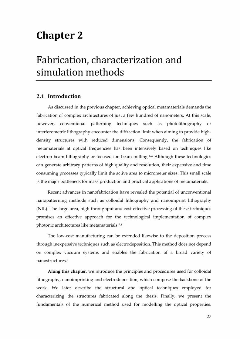
27
Chapter 2
Fabrication, characterization and
simulation methods
2.1 Introduction
As discussed in the previous chapter, achieving optical metamaterials demands the
fabrication of complex architectures of just a few hundred of nanometers. At this scale,
however, conventional patterning techniques such as photolithography or
interferometric lithography encounter the diffraction limit when aiming to provide high-
density structures with reduced dimensions. Consequently, the fabrication of
metamaterials at optical frequencies has been intensively based on techniques like
electron beam lithography or focused ion beam milling.1–6 Although these technologies
can generate arbitrary patterns of high quality and resolution, their expensive and time
consuming processes typically limit the active area to micrometer sizes. This small scale
is the major bottleneck for mass production and practical applications of metamaterials.
Recent advances in nanofabrication have revealed the potential of unconventional
nanopatterning methods such as colloidal lithography and nanoimprint lithography
(NIL). The large-area, high-throughput and cost-effective processing of these techniques
promises an effective approach for the technological implementation of complex
photonic architectures like metamaterials.7,8
The low-cost manufacturing can be extended likewise to the deposition process
through inexpensive techniques such as electrodeposition. This method does not depend
on complex vacuum systems and enables the fabrication of a broad variety of
nanostructures.9
Along this chapter, we introduce the principles and procedures used for colloidal
lithography, nanoimprinting and electrodeposition, which compose the backbone of the
work. We later describe the structural and optical techniques employed for
characterizing the structures fabricated along the thesis. Finally, we present the
fundamentals of the numerical method used for modelling the optical properties,

Chapter 2 Fabrication, characterization and simulation methods
28
providing a better comprehension of the studied systems. The details of additional
techniques used through the manuscript will be briefly explained when mentioned.
2.2 Colloidal lithography
During the past years, colloidal self-assembly has emerged as an attractive bottom-
up route for the fabrication of well-defined micro and nanostructures. At its most
general conception, colloidal self-assembly can lead to single or multilayer colloidal
crystals, hierarchical superstructures or even complex clusters of particles of different
shapes or compositions.10–12
Interestingly, when deposited on a substrate, two-dimensional (2D) colloidal
crystals can work as masks for surface patterning. This is the base of colloidal
lithography (CL), also known as nanosphere lithography. Typically, the particles used
for the formation of these colloidal monolayers are made of silica of polystyrene (PS)
because of their easy synthesis, self-assembly control and compatibility with further
modifications. Besides, since the particle size can vary from microns to hundreds of
nanometers, a broad range of templates can be achieved. Being a low-cost, large-area
and versatile approach, colloidal lithography has become a powerful alternative to the
complex procedures of top-down lithographies.
There exist several techniques for fabricating colloidal crystals, mainly
differentiated by the forces driving the assembly. Typical interactions between
submicron spheres include capillary action, electrostatic repulsion, van der Waals
attraction or external stimuli such as gravity, centrifugation or electromagnetic fields.13,14
The balance of the implied forces generally leads to hexagonal packed colloidal crystals,
where the monodispersity in size and in shape of the particles is of crucial importance
for achieving high quality crystals. Therefore, the use of one particular technique will
depend on the particle material, surface functionalization, dispersion medium and
desired structure. Commonly assembly techniques include drop casting, vertical
deposition, spin-coating, electrophoretic self-assembly or interface self-assembly.14,15
Using the latter method, Gao et al. showed the notable scalability of CL beyond the
laboratory frame.16 Based on the self-assembly at the water-air interface, they developed
a micro-propulsive injection method for the high-throughput fabrication of 1 m2
monolayer of PS spheres (Figure 2.1a,b). Taking a similar monolayer as starting point,
Vogel et al. demonstrated the facile achievement of non-closed packed monolayers of PS

Chapter 2 Fabrication, characterization and simulation methods
29
beads by reducing the particle size with a controlled oxygen plasma step (Figure 2.1c).17
Oppositely, one can also finely reduce the voids between particles by a controlled
annealing of the material (Figure 2.1d).18 More complex structures such as binary
colloidal crystals are also feasible (Figure 2.1e). In this case, colloidal particles of two
different sizes are assembled together in a complementary array, where their relative
amounts determines the final structure.19,20 Furthermore, colloidal self-assembly does not
restrict to spherical beads but has been extended to anisotropic particles with shapes like
ellipsoids,21 cubes22 or red blood cells (Figure 2.1f).23,24
Figure 2.1 Advances in colloidal templates made with polystyrene particles. a,b Photograph and
SEM image of 1 m2 colloidal monolayer.16 c Non-closed packed array obtained after oxygen
plasma etching. Scale bar of the inset: 500 nm.17 d Colloidal monolayer after annealing at 110 ºC.18
e Binary colloidal crystal made of 350 nm and 2µm spheres.19 f Self-assembled anisotropic red
blood cell-like colloidal particles.23
The diverse geometries reachable through CL together with further etching or
deposition steps have drawn the attention of researchers working in the fields of
metamaterials,25,26 light emission devices,27 wettability28 or multiple sensors29,30 where a
large-scale periodic pattern can enhance the targeted performance. In the same way, we
have applied CL to the fabrication of optical metamaterials. The method employed for
the pattern fabrication is now described.
2.2.1 Self-assembly of monolayers on the water surface
We fabricated colloidal monolayers by the well-known method of self-assembly at
the water-air interface.17-31 Based on the controlled spreading of particles and their

Chapter 2 Fabrication, characterization and simulation methods
30
packing on the water surface, this method stands out for its simplicity and rapid
deposition while presenting high quality arrangements.
We made use of submicron polystyrene latex particles previously synthesized in
our laboratory by emulsion polymerization.32 The concentration of the PS suspension in
distilled water was initially adjusted to 12 g/L. Then, an equal volume of ethanol was
added in order to reduce the surface tension of the solution, being 1:1 the final mixture of
water and ethanol.
Substrates of glass, gold or nickel were cleaned by ultrasounds for 20 min in
acetone, 20 min in ethanol and dried by air blowing. They were subsequently treated
with UV ozone in order to render the surface highly hydrophilic.
Figure 2.2 Steps of the self-assembly process on the water surface and transfer onto a substrate: I
immersion of a glass slide into the water, II spreading of the suspension, III deposition of the
monolayer onto a substrate.
Figure 2.2 depicts the formation of a closed-packed monolayer on the water
surface. (I) A cleaned glass is immersed in a crystallizing dish half filled with distilled
water and fixed to the crystallizer wall at approximately 45º using scotch tape. This glass
will be used for spreading the PS suspension, as a bridge to the water surface. Next,
around 30 drops of 2 wt% sodium dodecyl sulfate (SDS, Sigma Aldrich) were added to
the water before spreading the particles in order to promote the ordering. (II) 20 µL of
the colloidal suspension were spread on the inclined glass slide by moving steadily the
pipette so that the particles descended evenly to the water and orderly assembled in the
minimum energy configuration: a hexagonally packed monolayer. The presence of the
surfactant counteracts van der Waals and capillary attractions between particles,
increasing their time available to find the most stable configuration and thus, increasing
the order of the monolayer. A proof of the correct packing on the water surface are the
colourful reflections arising from Bragg diffraction (Figure 2.3a). If the suspension, on
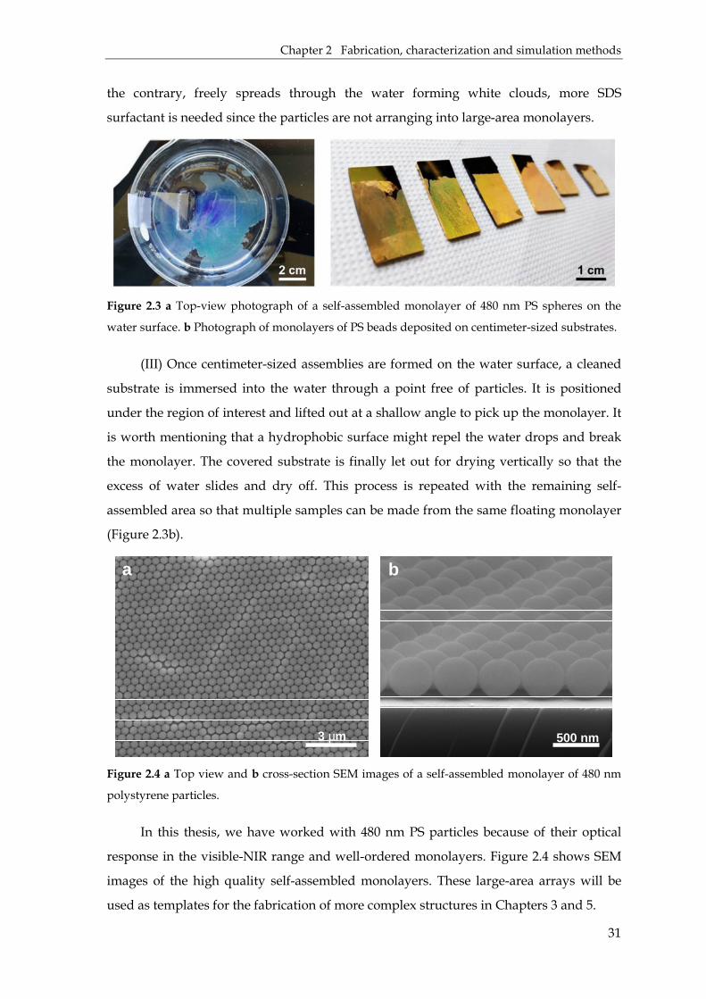
Chapter 2 Fabrication, characterization and simulation methods
31
the contrary, freely spreads through the water forming white clouds, more SDS
surfactant is needed since the particles are not arranging into large-area monolayers.
Figure 2.3 a Top-view photograph of a self-assembled monolayer of 480 nm PS spheres on the
water surface. b Photograph of monolayers of PS beads deposited on centimeter-sized substrates.
(III) Once centimeter-sized assemblies are formed on the water surface, a cleaned
substrate is immersed into the water through a point free of particles. It is positioned
under the region of interest and lifted out at a shallow angle to pick up the monolayer. It
is worth mentioning that a hydrophobic surface might repel the water drops and break
the monolayer. The covered substrate is finally let out for drying vertically so that the
excess of water slides and dry off. This process is repeated with the remaining self-
assembled area so that multiple samples can be made from the same floating monolayer
(Figure 2.3b).
Figure 2.4 a Top view and b cross-section SEM images of a self-assembled monolayer of 480 nm
polystyrene particles.
In this thesis, we have worked with 480 nm PS particles because of their optical
response in the visible-NIR range and well-ordered monolayers. Figure 2.4 shows SEM
images of the high quality self-assembled monolayers. These large-area arrays will be
used as templates for the fabrication of more complex structures in Chapters 3 and 5.
a
3 µm
b
500 nm

Chapter 2 Fabrication, characterization and simulation methods
32
2.3 Nanoimprint lithography
The concept of imprinting for replicating a mold is one of the oldest manufacturing
techniques used by human civilizations. Coins production, leather embossing or
letterpress printing are just some examples. However, the first replica at the nanoscale
only arose in 1995 when Chou et al. proved the high-resolution imprinting of sub-25 nm
features (Figure 2.5a).33
Similar to other lithographies, the principle of nanoimprint lithography (NIL)
consists of transferring an initial pattern to a target substrate. It uses a mold to deform
plastic materials through pressure, creating a negative replica on the target. Although
the fabrication of the initial mold might depend on conventional lithographies, NIL is
considered one of the most promising patterning approaches in future nanotechnology
because of its high-throughput and large-area performance.34,35 Furthermore, the
repeatability of the process from the same mold significantly reduces the costs and times
so far required for producing submicron patterns. These are the reasons why numerous
works investigate its adaptability to materials such as resists, biopolymers or perovskites
(Figure 2.5).36–39 The advances in high resolution and mass production patterns like these
examples have made a breakthrough not only in the metamaterials community7,40–42 but
also in the fabrication of devices such as solar cells,43 nanofluidic chips44 or
supercapacitors.45
Figure 2.5 Versatility of nanoimprint lithography over various materials and shapes. a PMMA
film patterned with 25 nm wide holes.33 b Array of pillars printed on hydroxypropyl cellulose.37 c
Imprinted lines on inorganic halide perovskites. Inset: photogaph of the structure.39
Regarding the process used for nanoimprinting, NIL can be divided in two main
categories: thermal NIL and ultraviolet NIL.
o Thermal NIL, also known as hot-embossing, relies on the compression of a
softened thermoplastic material. Typically, the target material is heated above its

Chapter 2 Fabrication, characterization and simulation methods
33
glass transition temperature () and the mold is pressed against it, so that the
material flows through the pattern reliefs. The system is then cooled down, the
thermoplastic material solidifies with the new negative shape and the mold is
removed. This technique enables patterning a broad variety of polymers at
temperatures around 100 ºC.46
o In UV NIL, a liquid photoresist is used for imprinting a pattern that is later cured
with UV light. For this reason, at least one of the substrates involved in the
imprinting must be transparent at these wavelengths. Compared to thermal NIL,
this method eliminates fracture defects coming from the different thermal
expansion between the mold and the resist.47 However, a photocurable material
is needed.
In addition, NIL is also classified in three different techniques depending on the
stiffness of the stamp used: hard, soft or hybrid molds.48
o Historically, the first nanoimprinted replicas were made from hard molds such as
silicon or quartz because of the high definition of the patterns,33 with Young’s
modulus of the order of GPa.34 The process requires high pressure and
temperature to achieve conformal contact with the target material. Moreover, the
rigidity of the molds presents several drawbacks that can harm the imprinted
structure. These issues include the formation of air bubbles between the stamp
and the resist, the easy damage of the mold or even the breakage when applying
pressure.
o Soft nanoimprinting is characterized by the use of flexible molds such as
polydimethylsiloxane (PDMS) or polyethylene terephthalate (PET). The flexibility
of these materials presents two main advantages. First, a longer working life
thanks to their easy manipulation and re-use. Second, a conformal contact
between the mold and the substrate, which prevents surface defects and enables
imprinting curved surfaces. In fact, soft nanoimprint lithography has been
extended to the mass-production technique of roll-to-roll, facilitating the
fabrication of large and flexible patterned surfaces.49 However, the low Young’s
modulus of soft molds (~2 MPa) often results in the deformation or collapsing of
the features, limiting the patterns to short aspect ratio structures.

Chapter 2 Fabrication, characterization and simulation methods
34
o Hybrid molds merge the advantages of hard and soft stamps. With intermediate
values of the Young’s modulus, they display high-resolution features while
keeping a degree of flexibility that make them a potential tool for fabrication at
the nanoscale. This type include composites of PDMS or photocurable resists
such as Ormostamp.48,50
In this thesis, we have employed hybrid molds for the steady fabrication of
patterns with high definition nanofeatures. Starting from a hard silicon master, we have
transferred the patterns to working molds of PDMS, from which the final imprinted
templates have been created.
2.3.1 Master replication
1 cm2 silicon masters of holes and lines with submicron diameters and periodicities
were fabricated using e-beam lithography by Eulitha (Switzerland) and Naitec (Spain).
Figure 2.6 describes the replication process for obtaining working soft stamps with the
same features as the initial silicon master. As detailed, we made use of the intermediate
photoresist Ormostamp (Micro resist technology).
Figure 2.6 Replication process from the original Si master to obtain working molds of PDMS.
Scale bars: 1 cm.
First, the silicon masters were silanized in order to provide a molecular anti-
sticking layer between the master and the Ormostamp. 5 µL of 1H,1H,2H,2H-
perfluorooctyl-trichlorosilane (PFOTS) (97%, Alfa Aesar) were dropped into a 4 L
desiccator together with the masters and let under vacuum for 30 min. During this time,
the silane molecules evaporated and covalently linked to the silicon surfaces. The
masters were later heated at 150 ºC for 20 min and rinsed with isopropanol to remove
the excess of silane.

Chapter 2 Fabrication, characterization and simulation methods
35
A few drops of Ormostamp photoresist were then poured onto the silicon masters
and covered with previously cleaned and UV ozone activated glass slides. If bubbles are
formed, the glass cover can be gently pressed to facilitate the Ormostamp spreading
while the air is squeezed out. The resist was cured with a commercial UV lamp placed at
10 cm distance for 5 min, adopting the inverse pattern of the initial master. A post-bake
treatment of 130 ºC for 30 min increased the thermal stability of the new stamps and
assisted the physical separation fom the silicon substrates. After carefully demolding to
not damage the patterns, both surfaces were cleaned with acetone and isopropanol.
The new Ormostamp/glass masters of pillars were also silanized prior the
replication into working PDMS stamps. Hybrid molds made of a thin layer of hard-
PDMS and a support layer of soft-PDMS were fabricated following a previous method.51
As explained, this composite would provide simultaneously high-resolution patterns
and conformal contact. For the hard layer, we used a hard PDMS kit purchased from
Gelest (USA). Stirring after each step, we mixed 1.7 g of vinyl prepolymer (VDT-731)
with 9 µL of Pt catalyst (SIP6831.2), 0.05 g of modulator (SIT7530.0) and 0.5 g of
hydrosilane prepolymer (HMS-301). 1.55 g of toluene were lastly added to decrease the
viscosity of the mixture. This was casted on the Ormostamp masters and spread over the
entire surface by air blowing until a homogeneous cover was achieved. The hard-PDMS
was let at room temperature (RT) for 1 hour to ensure it dried and finally cured at 60 ºC
for 1 h.
The soft-PDMS layer was fabricated by thoroughly mixing base and curing agent
(Sylgard184, Dow Corning, USA) in a 10:1 ratio. After degassing for 2 hours, the mixture
was poured onto the hard-PDMS film and cured at 80 ºC for 3 hours. Once cooled down,
the Ormostamp template was released, leading to a PDMS mold with high-resolution
holes (or lines) on a flexible support. These properties enabled the fabrication of a wide
variety of templates, as it is next explained.
2.3.2 Soft nanoimprinting
Cleaned glasses and indium tin oxide coated glasses (Ossila) were used as
substrates. Thin layers of 5-7 wt% SU8 photoresist (MicroChem 2000.5) were spin-coated
(Polos Spin150i) at 2000 rpm for 12s. These conditions led to 150-270 nm thick SU8 layers
for imprinting different patterns.

Chapter 2 Fabrication, characterization and simulation methods
36
Soft nanoimprinting on SU8 was done by combining hot embossing with UV
exposure. Figure 2.7 depicts the main steps of the imprinting process. The previously
fabricated PDMS molds with patterned areas of 1 cm2 were pressed onto the SU8 layers
at 90 ºC ( = 55 ºC) for 10 s. After this time, the SU8 had adopted the negative shape of
the mold and the whole system was let to cool down until 40 ºC for demolding. The
structure was cross-linked by 10 min of UV light and hardened with a post-bake at
160 ºC for 30 min.
Figure 2.7 Hot embossing procedure for imprinting nanostructures from soft molds.
This process was mainly applied to the fabrication of SU8 arrays of pillars, whose
lattice parameter () ranged from 200 nm up to 500 nm. Figure 2.8 presents SEM images
of some of the imprinted patterns, showing the versatility to produce from 100 nm wide
features (Figure 2.8a,b) to 330 nm tall pillars (Figure 2.8c). It is worth noting that pillars
taller than the initial SU8 layer are attainable thanks to the resist filling into the pattern.
These large-area templates will be the base for the structures developed in Chapter
4. Moreover, the process will be applied for the fabrication of shallow lines in Chapter 5.
Figure 2.8 a,b SEM top and cross-section views of periodic arrays of pillars with = 200 nm.
c Cross-section of a similar pattern of = 400 nm.
b
c
a
400 nm2 µm
200 nm

Chapter 2 Fabrication, characterization and simulation methods
37
2.4 Electrodeposition
Metallic electrodeposition, also known as electroplating, consists on the reduction
of metal ions from an electrolyte onto a conductive surface. It is typically performed in a
three-electrode cell that includes the sample to coat, known as cathode or working
electrode (WE), an anode or counter electrode (CE) and a reference electrode (RE)
(Figure 2.9). In potentiostatic mode, a constant potential controlled by the RE is applied
between the WE and CE. The metallic cations of the electrolyte migrate towards the
working electrode and eventually reduce on the conductive parts of the substrate.
Figure 2.9 a Scheme of a three-electrode cell, mainly composed by an electrolyte, a working
electrode (WE), counter electrode (CE) and referene electrode (RE). b Photograph of the
experimental set up used in this thesis.
Electrodeposition presents several attributes that make it stand out over other
deposition methods. Firstly, it can be performed over large areas at RT from water-based
electrolytes. It enables a precise control of the composition, morphology and thickness of
the deposits just by adjusting experimental parameters such as potential, time,
temperature, pH, etc. Furthermore, since electrodeposition starts from the bottom of the
substrate, it is an exceptional technique for plating curved surfaces or creating three-
dimensional architectures.
In industry, electrodeposition is a well-established surface modification tool for
improving properties such as wear resistance, hydrophobicity or passivation against
corrosion.52 Nowadays, with the increasing interest in miniaturized and complex

Chapter 2 Fabrication, characterization and simulation methods
38
devices, electrodeposition offers a unique approach for building nanostructures from
particles to films and hierarchical architectures.9
Of particular interest is the so-called template-assisted electrodeposition, where the
deposit takes place through a micro- or nanopatterned structure. This approach limits
the area for nucleation and growth, enabling a controlled structuring of the material.
Commonly applied for the fabrication of nanowires through alumina membranes,53 in
the last years templated electrodeposition has emerged as an attractive complement for
low-cost patterning techniques such as NIL and CL. Large-area arrays of magnetic
nanodots, nanodendrite sensors or metal-dielectric nanowires for photocatalysis are
some examples of its combination with NIL.54–56 Furthermore, the metallic infiltration
through colloidal crystals have led to intringuing geometries not achievable with top-
down techniques such as metallic inverse opals, dendritic metamaterials or diabolo-like
nanopillars among others.18,57–60
Following these latter results, in this work, we have applied the infiltration of
metallic layers of gold and sacrificial nickel through colloidal and pillar-based templates
for the fabrication of fishnet metamaterials. The technical details of the process are now
described.
Prior to electrodeposition, we delimited the electroactive area with commercial nail
varnish, on top of which no deposition would take place because of its insulating
character. In this way, we avoided electroplating on unpatterned areas, ensuring the
homogeneity of the deposition through the templates.
The electrodeposition step was carried out in a three-electrode cell, using the
samples as working electrodes, a 3 mm thick glassy carbon plate (Alfa Aesar) as counter
electrode and a Ag/AgCl electrode (3 M NaCl, Alvatek) as reference. The surface of the
counter electrode was at least two times bigger than the working electrode to avoid a
current flow limitation by the CE. Both, WE and CE were placed parallel to ensure a
homogeneous growth across the surface. Commercial cyanide-free gold plating bath
(Metalor ECF60) and nickel plating solution (Alfa Aesar, bright finish) were used as
electrolytes. The temperature of the cell was controlled through a water bath set at 25 ºC
unless otherwise stated. The electric current flow was monitored using an Autolab
PGSTAT 20 potentiostat (EcoChemie) working with the GPES 4.9 software.
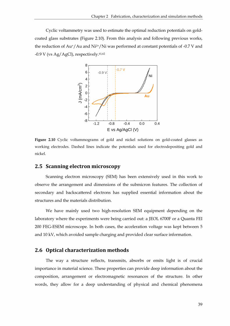
Chapter 2 Fabrication, characterization and simulation methods
39
Cyclic voltammetry was used to estimate the optimal reduction potentials on gold-
coated glass substrates (Figure 2.10). From this analysis and following previous works,
the reduction of Au+/Au and Ni2+/Ni was performed at constant potentials of -0.7 V and
-0.9 V (vs Ag/AgCl), respectively.61,62
-1.2 -0.8 -0.4 0.0 0.4-8
-6
-4
-2
0
2
4
6
8
-0.9 VNi
J (m
A/c
m2 )
E vs Ag/AgCl (V)
-0.7 V
Au
Figure 2.10 Cyclic voltammograms of gold and nickel solutions on gold-coated glasses as
working electrodes. Dashed lines indicate the potentials used for electrodepositing gold and
nickel.
2.5 Scanning electron microscopy
Scanning electron microscopy (SEM) has been extensively used in this work to
observe the arrangement and dimensions of the submicron features. The collection of
secondary and backscattered electrons has supplied essential information about the
structures and the materials distribution.
We have mainly used two high-resolution SEM equipment depending on the
laboratory where the experiments were being carried out: a JEOL 6700F or a Quanta FEI
200 FEG-ESEM microscope. In both cases, the acceleration voltage was kept between 5
and 10 kV, which avoided sample charging and provided clear surface information.
2.6 Optical characterization methods
The way a structure reflects, transmits, absorbs or emits light is of crucial
importance in material science. These properties can provide deep information about the
composition, arrangement or electromagnetic resonances of the structure. In other
words, they allow for a deep understanding of physical and chemical phenomena

Chapter 2 Fabrication, characterization and simulation methods
40
occurring within the material. In this thesis, three main techniques working at vis-NIR
frequencies were used to characterize the optical properties of the samples.
2.6.1 Visible-infrared spectroscopy
The optical properties of the structures were mainly studied by recording vis-NIR
transmittance and reflection spectra under normal incidence. Two commercial
equipment were used depending on the current laboratory where the measurements
were performed. In both cases, silver mirrors (≥ 96% reflectivity) and air were taken as
references for reflectance and transmittance measurements, respectively.
In first place, we employed a CRAIC 2020 microspectrophotometer working with a
10x objective and a spatial aperture of 50 x 50 µm2. Secondly, a Bruker Vertex 70 FTIR
spectrophotometer attached to a Bruker Hyperion optical microscope was used. The
spectra were recorded with a 4x objective, being the spot size 400 x 400 µm2.
2.6.2 Angle-resolved spectroscopy
A home-built setup was used for measuring reflection at oblique angles of
incidence (Figure 2.11). A tungsten halogen lamp (Ocean Optics, HL-2000 HP) was
used as light source. After passing through a linear polarizer, the light was focused on
the sample with a lens of numerical aperture (NA) of 0.125. The sample was mounted on
a goniometer-coupled holder aligned to the rotation axis so that the sample surface was
kept at the same position independently of the rotating angle. The reflected light was
finally collected through a NA = 0.125 lens using a fiber-coupled spectrophotometer
(Ocean Optics, QEPro-FL), placed in specular configuration.
Figure 2.11 Scheme of the setup for angle-resolved reflectance measurements.
This setup was used in Chapter 4 for characterizing the angular response of
multilayered fishnet metamaterials made by NIL and electrodeposition.

Chapter 2 Fabrication, characterization and simulation methods
41
2.6.3 Time-resolved fluorescence microscopy
We used a custom-made setup for measuring the fluorescence decays of the
plasmonic structures developed in Chapter 5 (Figure 2.12). Pulses of 70 ps width from a
laser operating at 654 nm (EPL-Edinburgh Instrument) provided the excitation light.
Keeping the peak power at 120 mW, the repetition rate was varied between 1 kHz and 1
MHz to get a proper signal/noise ratio. The pulses were directed to the sample through
a dichroic mirror and a 100x objective with NA = 0.9 (Zeiss EC Epiplan-Neofluar,
422392-9900). The emitted signal was then collected through the same objective and sent
to the detector (ID Quantique, ID100 single detection module) through two emission
filters (Omega, 710QM80 and Semrock, 664 nm RazorEdge ultrasteep long-pass edge
filter, LP02-664RU-25). The detector was equipped with a Time Correlated Single Photon
Counting (TCSPC) Card (ID Quantique, ID800) registering photons one by one in order
to reconstruct the decay profiles afterwards.
Figure 2.12 Scheme of the experimental setup for fluorescence decay measurements.
2.7 Finite-difference time-domain simulations
The optical response of the structures has been simulated by finite-difference time-
domain (FDTD) calculations. FDTD is a well-extended method for solving Maxwell’s
equations over time in a given volume. Over the last decade, it has become a powerful
tool in computational electromagnetism because of its robust implementation and easy
handling of composite geometries and materials.63,64
The FDTD method discretises Maxwell’s equations on a spatial and temporal grid
using central difference approximations. Firstly, the technique divides three-dimensional

Chapter 2 Fabrication, characterization and simulation methods
42
geometries into a mesh composed by the so-called Yee cells (Figure 2.13). In these
rectangular or cubic units, the location of the electric and magnetic field components
satisfy classical boundary conditions. The fields are then calculated at discrete time steps
with a leapfrog algorithm. This means that the electric field is solved at a given instant,
then the magnetic field at the next time instant, and the process is repeated until
reaching an electromagnetic steady-state.
Figure 2.13 Position of the electric and magnetic field components in a Yee cell.
The spatial mesh size (Δ,Δ,Δ) should be fine enough to well reproduce the
structure, considering both the geometry and the electromagnetic parameters of the
materials. Although the proper mesh depends on the smallest feature size and vary for
each system, when working with plasmonic structures at optical wavelengths a
minimum resolution of 10 nm is typically required. Moreover, the time step (Δ) should
satisfy the Courant condition for numerical stability:
cΔ 1
1Δ
1Δ
1Δ
(2.1)
where is the speed of light in vacuum. One should not forget that high
resolutions come at the costs of large memory requirements and simulation times.
Therefore, if similar results are obtained for different mesh sizes, it is advisable to use the
larger one.
The simulations shown in this manuscript were done using the Lumerical FDTD
solutions software. The structural dimensions were based of the SEM analysis and more
precisely fitted to the optical spectra. Mesh sizes between 2 and 5 nm were used to
resolve the modelled structures, while the program automatically adjusted the time step

Chapter 2 Fabrication, characterization and simulation methods
43
to avoid instabilities. Thanks to the periodicity of the systems, memory and time were
saved through EM (anti)symmetric boundary conditions on the sides of the simulation.
Perfectly matched layers were placed above the structure and on the semi-infinite
substrate to absorb the incoming light with minimal reflections. After illuminating the
system with a linearly polarized planar wave, reflection and transmission coefficients
were collected through power monitors. Similarly, profile monitors were included to
obtain electromagnetic field distributions at a given wavelength. For the angular
dispersion calculations, the broadband fixed angle source technique was used. In
general, the calculations stopped when the energy in the simulation volume dropped to
5x10⁻⁷ of the energy injected.
Regarding the materials modelling, the gold dispersion was taken from Johnson
and Christy,65 nickel from Palik66 and ITO from Sopra SA database (France). The
dielectric materials were considered to have constant refractive indices of 1.46 for silica
glass, 1.59 for polystyrene and 1.65 for SU8.
2.8 References
1. U. K. Chettiar et al. Dual-band negative index metamaterial: Double negative at
813 nm and single negative at 772 nm. Opt. Lett. 2007, 32, 1671–1673.
2. G. Dolling, M. Wegener and S. Linden. Negative-index metamaterial at 780 nm
wavelength. Opt. Lett. 2007, 32, 53–55.
3. S. Xiao, U. K. Chettiar, A. V Kildishev, V. P. Drachev and V. M. Shalaev. Yellow-
light negative-index metamaterials. Opt. Lett. 2009, 34, 3478–3480.
4. C. García-Meca et al. Low-loss multilayered metamaterial exhibiting a negative
index of refraction at visible wavelengths. Phys. Rev. Lett. 2011, 106, 67402.
5. M. Choi, J. H. Choe, B. Kang and C. Choi. A flexible metamaterial with negative
refractive index at visible wavelength. Curr. Appl. Phys. 2013, 13, 1723–1727.
6. Y. Liang, Z. Yu, N. Ruan, Q. Sun and T. Xu. Freestanding optical negative-index
metamaterials of green light. Opt. Lett. 2017, 42, 3239–3242.
7. A. M. Urbas et al. Roadmap on optical metamaterials. J. Opt. 2016, 18, 093005.
8. G. Yoon, I. Kim and J. Rho. Challenges in fabrication towards realization of
practical metamaterials. Microelectron. Eng. 2016, 163, 7–20.

Chapter 2 Fabrication, characterization and simulation methods
44
9. F. Nasirpouri. Electrodeposition of nanostructured materials; Springer, Switzerland,
2017.
10. M. A. Boles, M. Engel and D. V. Talapin. Self-assembly of colloidal nanocrystals:
From intricate structures to functional materials. Chem. Rev. 2016, 116, 11220–
11289.
11. Y. Wang, M. Zhang, Y. Lai and L. Chi. Advanced colloidal lithography: From
patterning to applications. Nano Today 2018, 22, 36–61.
12. X. Liang, R. Dong and J. C. Ho. Self-assembly of colloidal spheres toward
fabrication of hierarchical and periodic nanostructures for technological
applications. Adv. Mater. Technol. 2019, 4, 1800541.
13. Y. S. Lee. Self-assembly and nanotechnology: A force balance approach; John Wiley &
Sons, USA and Canada, 2008.
14. Z. Xu, L. Wang, F. Fang, Y. Fu and Z. Yin. A review on colloidal self-assembly and
their applications. Curr. Nanosci. 2016, 12, 725–746.
15. H. Zheng and S. Ravaine. Bottom-up assembly and applications of photonic
materials. Crystals 2016, 6, 54.
16. P. Gao et al. Large-area nanosphere self-assembly by a micro-propulsive injection
method for high throughput periodic surface nanotexturing. Nano Lett. 2015, 15,
4591–4598.
17. N. Vogel, S. Goerres, K. Landfester and C. K. Weiss. A convenient method to
produce close- and non-close-packed monolayers using direct assembly at the air-
water interface and subsequent plasma-induced size reduction. Macromol. Chem.
Phys. 2011, 212, 1719–1734.
18. H. Zheng et al. Morphological design of gold nanopillar arrays and their optical
properties. J. Phys. Chem. C 2016, 120, 1178–1185.
19. Z. Dai, Y. Li, G. Duan, L. Jia and W. Cai. Phase diagram, design of monolayer
binary colloidal crystals, and their fabrication based on ethanol-assisted self-
assembly at the air/water interface. ACS Nano 2012, 6, 6706–6716.
20. J. L. Russell, G. H. Noel, J. M. Warren, N. L. L. Tran and T. E. Mallouk. Binary
colloidal crystal films grown by vertical evaporation of silica nanoparticle
suspensions. Langmuir 2017, 33, 10366–10373.

Chapter 2 Fabrication, characterization and simulation methods
45
21. T. Ding, K. Song, K. Clays and C.-H. Tung. Fabrication of 3D photonic crystals of
ellipsoids: Convective self-assembly in magnetic field. Adv. Mater. 2009, 21, 1936–
1940.
22. L. Rossi et al. Cubic crystals from cubic colloids. Soft Matter 2011, 7, 4139–4142.
23. L. Song, X. Du, L. Zhong, X. Zhang and Z. Cheng. Self-assembly of anisotropic red
blood cell (RBC)-like colloidal particles. Soft Matter 2018, 14, 7954–7957.
24. L. Song et al. Non-close-packed particle arrays based on anisotropic red blood cell
(RBC) like particles via stretching deformation method. Langmuir 2019, 35, 9044–
9049.
25. K. Lodewijks, N. Verellen, W. Van Roy, G. Borghs and P. Van Dorpe. Self-
assembled hexagonal double fishnets as negative index materials. Appl. Phys. Lett.
2011, 98, 091101.
26. B. Gong et al. A visible metamaterial fabricated by self-assembly method. Sci. Rep.
2014, 4, 4713.
27. S. Mariana et al. Vertical GaN nanowires and nanoscale light-emitting-diode
arrays for lighting and sensing applications. ACS Appl. Nano Mater. 2019, 2, 4133–
4142.
28. P. Xue et al. Ordered micro/nanostructures with geometric gradient: From
integrated wettability “library” to anisotropic wetting surface. Small 2017, 13,
1601807.
29. X. Zhang et al. Ultrasensitive SERS performance in 3D “sunflower-like”
nanoarrays decorated with Ag nanoparticles. Nanoscale 2017, 9, 3114–3120.
30. Y. Zhang et al. Flexible and highly sensitive pressure sensor based on microdome-
patterned PDMS forming with assistance of colloid self-assembly and replica
technique for wearable electronics. ACS Appl. Mater. Interfaces 2017, 9, 35968–
35976.
31. G. D. Moon et al. Assembled monolayers of hydrophilic particles on water
surfaces. ACS Nano 2011, 5, 8600–8612.
32. A. Désert et al. High-yield preparation of polystyrene/silica clusters of controlled
morphology. Polym. Chem. 2012, 3, 1130.
Chapter 2 Fabrication, characterization and simulation methods
46
33. S. Y. Chou, P. R. Krauss and P. J. Renstrom. Imprint of sub-25 nm vias and
trenches in polymers. Appl. Phys. Lett. 1995, 67, 3114.
34. W. Zhou. Nanoimprint lithography: An enabling process for nanofabrication; Springer,
Germany, 2013.
35. D. Wu, N. S. Rajput and X. Luo. Nanoimprint lithography - the past, the present
and the future. Curr. Nanosci. 2016, 12, 712–724.
36. C. Schuster, F. Reuther, A. Kolander and G. Gruetzner. mr-NIL 6000LT-epoxy-
based curing resist for combined thermal and UV nanoimprint lithography below
50 °C. Microelectron. Eng. 2009, 86, 722–725.
37. A. Espinha et al. Hydroxypropyl cellulose photonic architectures by soft
nanoimprinting lithography. Nat. Photonics 2018, 12, 343–348.
38. Y. Jiang, B. Luo and X. Cheng. Enhanced thermal stability of thermoplastic
polymer nanostructures for nanoimprint lithography. Materials. 2019, 12, 545.
39. B. Jeong et al. Polymer-assisted nanoimprinting for environment- and phase-
stable perovskite nanopatterns. ACS Nano 2020, 14, 1645–1655.
40. I. Bergmair et al. Single and multilayer metamaterials fabricated by nanoimprint
lithography. Nanotechnology 2011, 22, 325301.
41. D. Chanda et al. Large-area flexible 3D optical negative index metamaterial
formed by nanotransfer printing. Nat. Nanotechnol. 2011, 6, 402–407.
42. L. Gao et al. Nanoimprinting techniques for large-area three-dimensional negative
index metamaterials with operation in the visible and telecom bands. ACS Nano
2014, 8, 5535–5542.
43. A. Mihi, F. J. Beck, T. Lasanta, A. K. Rath and G. Konstantatos. Imprinted
electrodes for enhanced light trapping in solution processed solar cells. Adv.
Mater. 2014, 26, 443–448.
44. X. Chen and L. Zhang. Review in manufacturing methods of nanochannels of bio-
nanofluidic chips. Sensors Actuators B Chem. 2018, 254, 648–659.
45. S. Lochmann et al. Nanoimprint lithography of nanoporous carbon materials for
micro-supercapacitor architectures. Nanoscale 2018, 10, 10109–10115.

Chapter 2 Fabrication, characterization and simulation methods
47
46. H. Schift. Nanoimprint lithography: An old story in modern times? A review. J.
Vac. Sci. Technol. B Microelectron. Nanom. Struct. Process. Meas. Phenom. 2008, 26,
458–480.
47. M. C. Traub, W. Longsine and V. N. Truskett. Advances in nanoimprint
lithography. Annu. Rev. Chem. Biomol. Eng. 2016, 7, 583–604.
48. B. Kwon and J. H. Kim. Importance of molds for nanoimprint lithography: Hard,
soft, and hybrid molds. J. Nanosci. 2016, 2016, 6571297.
49. N. Kooy, K. Mohamed, L. Pin and O. Guan. A review of roll-to-roll nanoimprint
lithography. Nanoscale Res. Lett. 2014, 9, 320.
50. S. Hosaka. Updates in advanced lithography; IntechOpen, Rijeka, Croatia, 2013.
51. T. W. Odom, J. C. Love, D. B. Wolfe, K. E. Paul and G. M. Whitesides. Improved
pattern transfer in soft lithography using composite stamps. Langmuir 2002, 18,
5314–5320.
52. N. Kanani. Electroplating: Basic principles, processes and practice; Elsevier, Berlin,
Germany, 2004.
53. D. Wang, A. Mukhtar, K. Wu, L. Gu and X. Cao. Multi-segmented nanowires: A
high tech bright future. Materials. 2019, 12, 3908.
54. C. H. Lee et al. Fabrication and characterization of Co-Pt nanodot arrays by
nanoimprint lithography and electrodeposition. Microelectron. Eng. 2010, 87, 2085–
2090.
55. S. Wang et al. Space-confined fabrication of silver nanodendrites and their
enhanced SERS activity. Nanoscale 2013, 5, 4284–4290.
56. H. Eom et al. Strong localized surface plasmon resonance effects of Ag/TiO2 core–
shell nanowire arrays in UV and visible light for photocatalytic activity. Nanoscale
2014, 6, 226–234.
57. N. Sapoletova et al. Controlled growth of metallic inverse opals by
electrodeposition. Phys. Chem. Chem. Phys. 2010, 12, 15414–15422.
58. X. Zhao. Bottom-up fabrication methods of optical metamaterials. J. Mater. Chem.
2012, 22, 9439–9449.

Chapter 2 Fabrication, characterization and simulation methods
48
59. A. Karajić et al. Bottom-up generation of miniaturized coaxial double electrodes
with tunable porosity. Adv. Mater. Interfaces 2015, 2, 1500192.
60. A. Ngamaroonchote, T. Muangnapoh, N. Aroonyadet, P. Kumnorkaew and R.
Laocharoensuk. Plasma-etched nanosphere conductivity-inverted lithography
(PENCIL): A facile fabrication of size-tunable gold disc array on ITO-coated glass.
Adv. Mater. Interfaces 2018, 5, 1800477.
61. A. Karajić. Development of electrode architectures for miniaturized biofuel cells,
University of Bordeaux, 2015.
62. H. Zheng. Design and bottom-up fabrication of nanostructured photonic /
plasmonic materials, University of Bordeaux, 2016.
63. K. Yee. Numerical solution of initial boundary value problems involving
Maxwell’s equations in isotropic media. IEEE Trans. Antennas Propag. 1966, 14,
302–307.
64. A. Z. Elsherbeni and V. Demir. The finite-difference time-domain method for
electromagnetics with matlab simulations, 2nd ed.; SciTech Publishing, United States,
2015.
65. P. B. Johnson and R. W. Christy. Optical constants of the noble metals. Phys. Rev. B
1972, 6, 4370–4379.
66. E. D. Palik. Handbook of optical constants of solids; Academic Press, Boston, 1998.

49
Chapter 3
Fishnet metamaterials made by
colloidal lithography
3.1 Introduction
In the recent years, self-assembly has emerged as a stimulating approach for the
mass production of metamaterials thanks to the easy and low-cost processesing. The
rational organization of subwavelength building blocks can give rise to unconventional
electromagnetic properties at visible and NIR frequencies without the need of expensive
and time consuming top-down lithographic techniques.1–3
Self-assembly enables the synthesis of colloidal nanoresonators, which are
subwavelength elements formed by the controlled organization of metallic nanoparticles
into complex clusters. These systems are commonly studied for achieving phenomena
such as cloaking,4 optical magnetism,5 negative refractive index6 or chirality.7 The
fabrication of self-assembled metamaterials directly on surfaces is also feasible by
approaches such as block copolymer organization. In this case, different patterns are
within reach by adjusting the volume fraction of the polymers involved in the composite.
The resulting templates can be lately employed for the fabrication of chiral,8,9 tunable
refractive index10 or hyperbolic metamaterials.11 In the same way, colloidal lithography
supports the formation of highly ordered and complex architectures such as the ones
needed in periodic metamaterials.
For instance, the spherical particles typically used in CL have attracted great
interest in developing circular SRRs over large surfaces. By using colloidal monolayers
as shadow masks, SRRs operating at the NIR have been achieved when depositing
metals by thermal evaporation12 or electrodeposition.13 Similar approaches have served
for the creation of elliptical shapes14 or even 3D systems by stacking several layers of
split rings.15 Metallic dendritic designs have been also reported as left-handed
metamaterials with an entirely bottom-up route such as CL and electrochemical
deposition.16,17

Chapter 3 Fishnet metamaterials made by colloidal lithography
50
Furthermore, nanosphere lithography has been proposed as an alternative route
for the fabrication of fishnet metamaterials motivated by the large area, inexpensive and
fast character of the approach. Lodewijks et al. showed the feasibility of using
nanosphere lithography for NIMs working at NIR frequencies with refractive indices up
to -1.4 and FOM of the order of 1.18 However, their process still implied subsequent ion
beam milling that hindered the scalability of their method. Less complex procedures
were based on the direct MIM deposition onto the beads, which acted as masks and led
to holey fishnet structures after their removal.19 Gong et al. reported a bottom-up
method based on electroplating silver films through PS monolayers working as
templates.20 The structures showed a minimum refractive index of -0.5 at 560 nm.
Further works included a gain medium within the same metamaterial to compensate the
optical losses coming from the metal absorption at these frequencies.21 However, these
last designs suffered from lateral misalignment of the holes in the metallic layers,
inhibiting the achievement of both strong negative index values and high FOMs.
Figure 3.1 Illustration of the proposed double fishnet structure based on colloidal lithography.
In this chapter, we present a new fishnet design based on such bottom-up
combination of colloidal lithography and electrodeposition, two well-known scalable
and low-cost techniques. The proposed scheme follows the basic geometry of a double
fishnet structure (Figure 3.1). It is composed by two gold layers separated by an air gap
and symmetrically perforated by a monolayer of polystyrene spheres on top of a glass
substrate. We study the dependence of the optical response on structural parameters
such as the diameter of the particles and the air gap width in between the metallic layers.
The possibility of tuning the effective refractive index by properly controlling these
structural dimensions is explored.

Chapter 3 Fishnet metamaterials made by colloidal lithography
51
3.2 Tuning the effective refractive index
As described in Chapter 1, the electric and magnetic responses of a metamaterial
depend on the shape, size and materials of which it is made. The fishnet design allows
and independent control of the permittivity and the permeability at a specific
wavelength.22 In the effective medium approximation, the electric response can be
described from holey metallic layers, where the metal plasma frequency is replaced by
the cut-off frequency of the fundamental mode of a hole waveguide.23 This value
determines the maximum wavelength at which the electric field is guided through the
holes. For wavelengths above the cut-off wavelength , SPP waves dominate the
propagation through the structure and the effective permittivity becomes negative.24,25 In
the case of circular holes, depends on the diameter and the refractive index of the
apertures.26
= 1.841 (3.1)
Two regimes can be found concerning this value:24 as long as is higher than the
lattice parameter of the structure, a decrease of the diameter will involve more
negative and therefore, more negative . However, if becomes smaller than ,
the light will not effectively couple to the periodic structure and less negative values will
be obtained. For this reason, the following studies have focused on the first situation,
this is, on diameters sufficiently large so that > .
The magnetic behavior is induced by the excitation of gap surface plasmons within
the MIM cavity. If the metallic layers are sufficiently close, the SPPs propagating at the
internal faces will interact due to the overlapping of their evanescent fields, creating a
GSP.27 For two non-perforated metallic films of thickness separated by a dielectric
width , the GSP dispersion relation at low frequencies can be described by the linear
approximation28,29
= + 2 coth 2 !"#$/&
(3.2)
where is the vacuum wave vector, the refractive index of the dielectric spacer
and the plasma wavelength of the metal. Even though this equation corresponds to
flat and continuous layers, the dispersion when considering an array of holes perforating
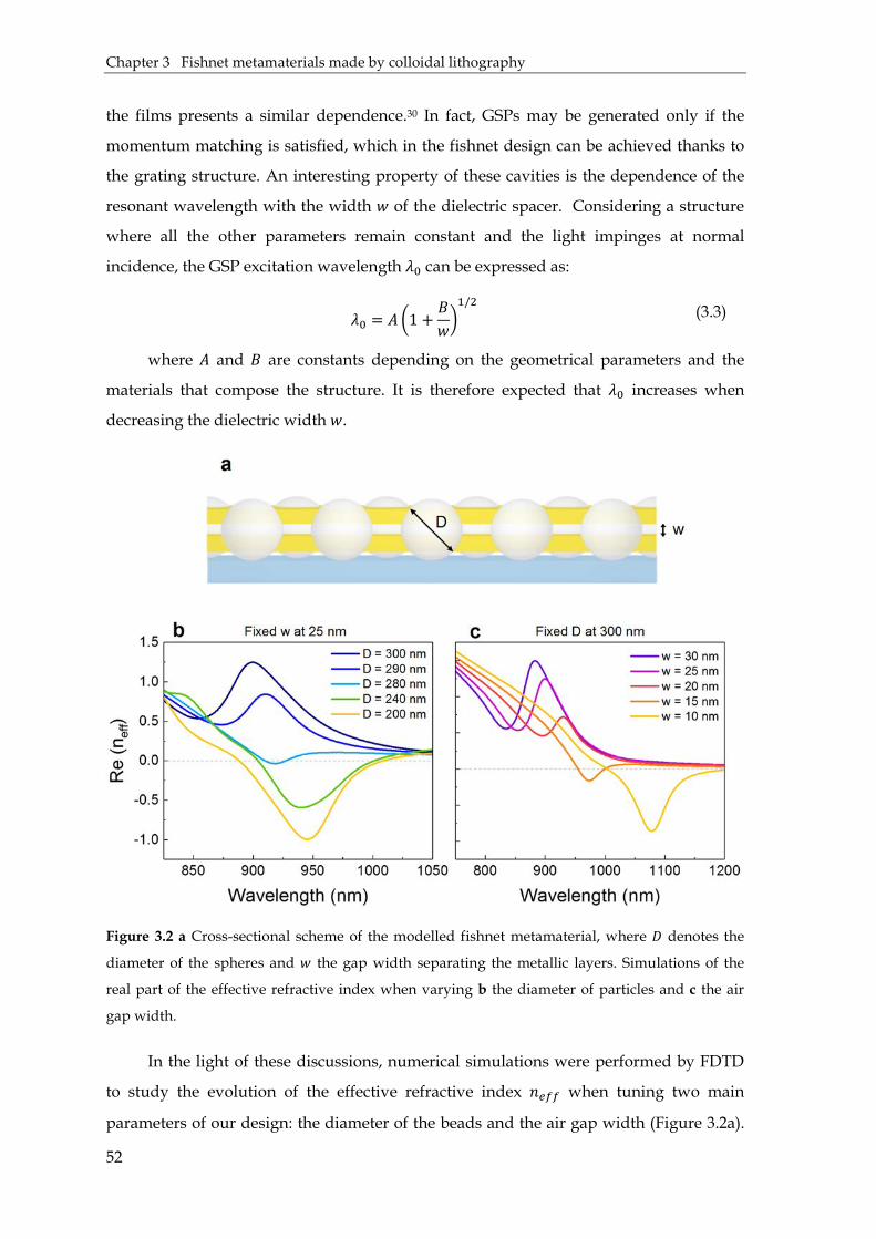
Chapter 3 Fishnet metamaterials made by colloidal lithography
52
the films presents a similar dependence.30 In fact, GSPs may be generated only if the
momentum matching is satisfied, which in the fishnet design can be achieved thanks to
the grating structure. An interesting property of these cavities is the dependence of the
resonant wavelength with the width of the dielectric spacer. Considering a structure
where all the other parameters remain constant and the light impinges at normal
incidence, the GSP excitation wavelength can be expressed as:
= ' 1 + (!$/& (3.3)
where ' and ( are constants depending on the geometrical parameters and the
materials that compose the structure. It is therefore expected that increases when
decreasing the dielectric width .
Figure 3.2 a Cross-sectional scheme of the modelled fishnet metamaterial, where denotes the
diameter of the spheres and the gap width separating the metallic layers. Simulations of the
real part of the effective refractive index when varying b the diameter of particles and c the air
gap width.
In the light of these discussions, numerical simulations were performed by FDTD
to study the evolution of the effective refractive index when tuning two main
parameters of our design: the diameter of the beads and the air gap width (Figure 3.2a).

Chapter 3 Fishnet metamaterials made by colloidal lithography
53
The structure was considered to have a lattice spacing of 480 nm, two 50 nm thick gold
layers and to be placed on top of a semi-infinite glass substrate. The refractive index of
PS was taken as = 1.59. The real parts of for different diameters and gap widths
are plotted in Figure 3.2b and c, respectively. As can be observed, by separately tuning
one of the two parameters, the value of the refractive index changes, moving from
positive to negative and red shifting when decreasing either or . In particular, small
decreases in produce large redshifts of the operating wavelength of the structure, in
accordance with equation (3.3) and previous studies.31 The lowering of when
decreasing can be explained as an enhancement of the GSP coupling as the gold layers
come closer. On the other hand, reductions in primarly result in more negative values
of , in agreement with the above discussion. Therefore, the sizes of and act as
turning knobs that enable the achievement of metamaterials featuring positive, zero and
negative refractive indices.
3.3 Fabrication of double fishnet metamaterials by colloidal
lithography
Double-fishnet structures were fabricated over centimeter-sized areas by a
complete bottom-up route, based on the combination of colloidal lithography and
electrodeposition. Figure 3.3 summarizes the whole fabrication procedure, which will be
explained in detail throughout the following sections.
Figure 3.3 Scheme of the bottom-up fabrication process to obtain double fishnet metamaterials.
PS
airAu
Electrodeposition ofsacrificial Ni
Electrodeposition ofsacrificial Ni
Electrodeposition of AuDissolution of Ni andtransfer to glass substrate
Electrodeposition of Au
Diameter reduction with O2 plasma
Ni/Au coated substrate Self-assembly of PS beads
Ni Au PS

Chapter 3 Fishnet metamaterials made by colloidal lithography
54
3.3.1 Preparation of non-closed-packed templates
Closed-packed monolayers of 480 large PS spheres were prepared on nickel-plated
gold-coated substrates following the self-assembly procedure described in Chapter 2. We
chose such diameter because of the high quality of the formed monolayers and relatively
small size, which would give an optical response in the visible-NIR range. The
conductive surfaces will serve as working electrodes during the electrodeposition step as
will be explained in Section 3.3.2.
Since the fishnet structure is composed by isolated dielectric perforations, the
particles diameter had to be reduced while keeping the original lattice parameter of the
array. Being an organic material, polystyrene can be easily etched by an oxygen plasma
treatment. The oxygen ions and radicals in the plasma react with the polymer leading to
volatile products that are then removed by the vacuum system.32 Therefore, it is possible
and easy to obtain non-closed-packed colloidal templates by varying the diameter of PS
spheres with plasma parameters such as etching time, power or gas flux.
Figure 3.4 Comparison of the particles position after etching when the substrate is placed at a RT
and b -15 ⁰C.
Conserving the periodic order of the array is a crucial aspect when doing colloidal
lithography. If the particles move or detach from the substrate during the plasma
treatment, the final properties coming from the grating will be lost. Thermal annealing
prior to plasma etching can help to increase the contact area with the substrate and well
fix the particles.33 Another important aspect to consider is the substrate temperature
during the process.34 An uncontrolled temperature not only can affect the reliability of
the experiments but also softens and plastically deforms the particles, which combined
with large size reductions leads to a displacement from the original position35 as can be
observed in Figure 3.4a. On the other hand, under a controlled and sufficiently low
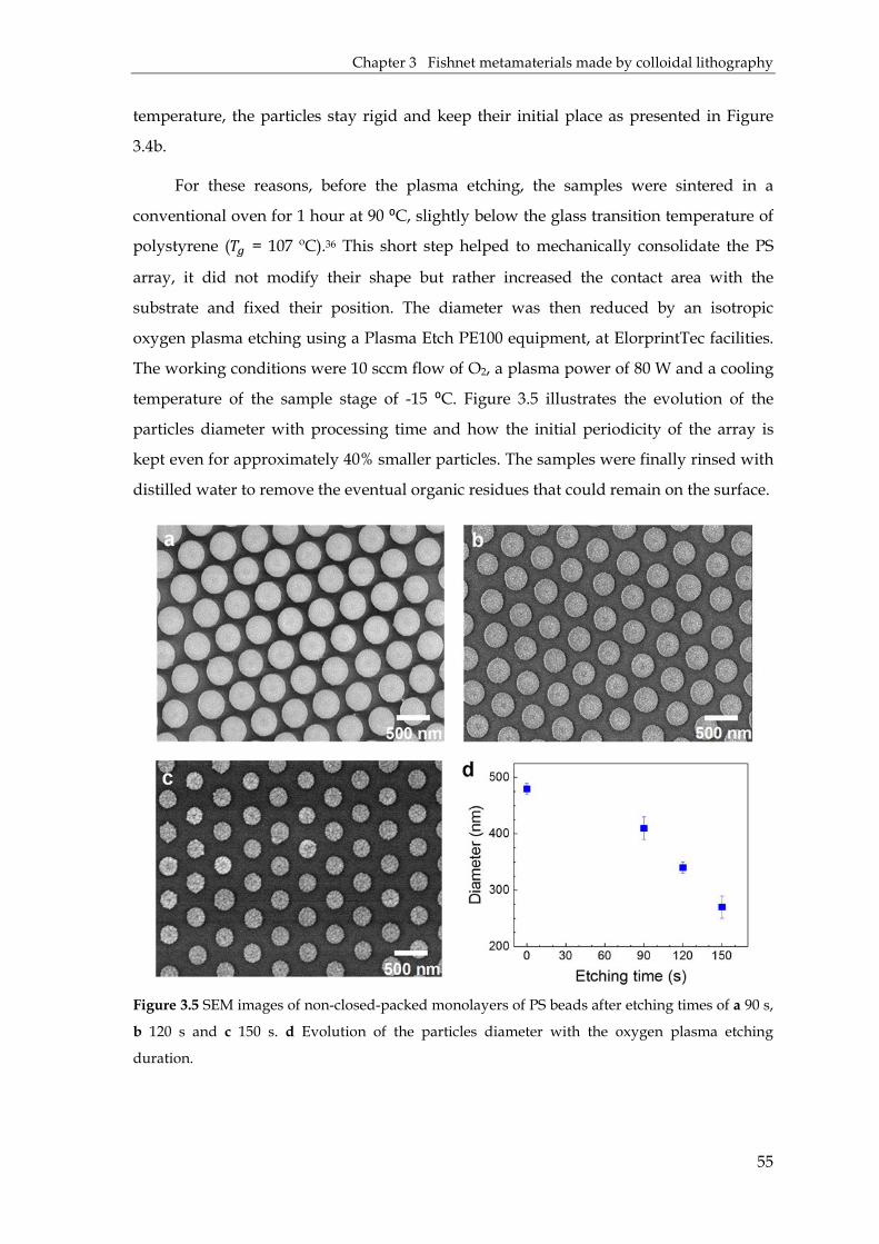
Chapter 3 Fishnet metamaterials made by colloidal lithography
55
temperature, the particles stay rigid and keep their initial place as presented in Figure
3.4b.
For these reasons, before the plasma etching, the samples were sintered in a
conventional oven for 1 hour at 90 ⁰C, slightly below the glass transition temperature of
polystyrene ()* = 107 ºC).36 This short step helped to mechanically consolidate the PS
array, it did not modify their shape but rather increased the contact area with the
substrate and fixed their position. The diameter was then reduced by an isotropic
oxygen plasma etching using a Plasma Etch PE100 equipment, at ElorprintTec facilities.
The working conditions were 10 sccm flow of O2, a plasma power of 80 W and a cooling
temperature of the sample stage of -15 ⁰C. Figure 3.5 illustrates the evolution of the
particles diameter with processing time and how the initial periodicity of the array is
kept even for approximately 40% smaller particles. The samples were finally rinsed with
distilled water to remove the eventual organic residues that could remain on the surface.
Figure 3.5 SEM images of non-closed-packed monolayers of PS beads after etching times of a 90 s,
b 120 s and c 150 s. d Evolution of the particles diameter with the oxygen plasma etching
duration.

Chapter 3 Fishnet metamaterials made by colloidal lithography
56
3.3.2 Multilayer electrodeposition through a colloidal template
The double-fishnet geometry was accomplished by electrodepositing gold layers
through the non-closed-packed monolayer templates. Sacrificial nickel layers were as
well electrodeposited in between serving as supports and spacers for the gold layers.
A very interesting property of combining electrodeposition and CL is the on-time
control of the electrodeposited thickness. Under a constant potential, the electric current
varies accordingly with the electroactive area: larger areas imply higher
electrodeposition currents flowing through the electrolytic cell. Therefore, the deposited
thickness through three-dimensional templates such as ours can be determined by
monitoring the current variations.37,38 Such phenomenon was initially verified by
electrodepositing nickel and gold through closed-packed monolayers of 480 large PS
spheres. As can be observed in Figure 3.6, after some initial fluctuations, the current
reaches a minimum in absolute value. This stage is linked with the smallest electroactive
area where the ions reduction occurs, which corresponds with half the height of the
monolayer. Knowing the time that takes to deposit half a monolayer and assuming a
constant electrodeposition rate, one could calculate the time required for any desired
thickness.
Figure 3.6 Chronoamperometric curves of a nickel and b gold electrodeposition through a closed-
packed monolayer of 480 nm large polystyrene particles.
However, this behavior was not observed for non-closed-packed arrays. The
absence of current variations was attributed to the small difference in cross-sectional
area across the template height. When the diameter is reduced, the particles are no
longer touching each other, the space between them becomes larger and the transversal
area does not change sufficiently so that a current variation is observed. It was then
0 200 400 600 800 1000-0.25
-0.20
-0.15
-0.10
Cur
rent
(m
A)
Time (s)
E = -0.7 V
t1/2 = 730 s
0 50 100 150 200-14
-12
-10
-8
-6
-4
Cur
rent
(m
A)
Time (s)
E = -0.9 V
t1/2 = 90 s
a b

Chapter 3 Fishnet metamaterials made by colloidal lithography
57
considered that the metals grew approximately at the same rate as on an open surface.
The deposition rate for both metals was determined by SEM on gold-coated substrates,
being 0.97 ± 0.09 nm/s for nickel reduced at -0.9 V, and 0.34 ± 0.03 nm/s for gold
reduced at -0.7 V. The slow deposition rates allowed us to finely control the thickness of
each metallic layer.
In order to obtain the targeted symmetric structure (Figure 3.7), the thickness of the
first nickel layer + was adjusted according to the relation between the height ℎ of the
monolayer and the desired thicknesses for the gold layers - and the nickel spacer ..
+ = ℎ − 2- − .2 (3.4)
Figure 3.7 Scheme of the targeted multilayered structure surrounding the colloidal template.
A short sintering step of 102 ⁰C for 15 min was always done before the process in
order to improve the adhesion of the particles and ensure that they stayed fixed at their
positions during the electroplating. Lower temperatures might have implied longer
sintering treatments whereas with higher temperatures we risked to considerably
deform the particles because of the proximity to the polystyrene )*. Without this
mechanical adhesion, while the deposition occurred, the metallic layers could push up
the particles because of their low density.39
Subsequent electrodeposition of nickel, gold, nickel and gold through the PS
templates produced two 50 nm thick gold layers, symmetrically placed regarding the
equatorial axes of the monolayer and separated by a variable sacrificial nickel spacer.
Figure 3.8 presents the multilayered structure after the whole electrodeposition process
over a template of etched spheres with = 340 nm. One can clearly distinguish the PS
particles embedded in a nickel-gold stack, while preserving the high quality of the
periodic array over centimeter-sized areas. These images attest to the successful multi-
h z
x
y
y
Substrate

Chapter 3 Fishnet metamaterials made by colloidal lithography
58
electrodeposition through colloidal templates, without damaging the structure and
accurately controlling the thickness and position of each metallic layer.
Figure 3.8 a SEM image of a multilayered nanostructure composed by 340 nm large PS particles,
two 50 nm thick Au layers symmetrically placed and a 70 nm thick Ni spacer separating them.
b Close-up view of the same structure. c Photograph of the sample, where the iridescent region
corresponds to the multilayered grating.
3.3.3 Nickel dissolution and transfer to transparent substrate
Once we created a multilayered structure through non-closed-packed templates,
the last step was to dissolve the nickel parts. Such removal is needed to achieve the
proper designed fishnet metamaterial, where the MIM structure is composed of gold-air-
gold. To fully characterize, understand and make them suitable for practical
applications, the samples should be placed on a transparent surface. For this purpose,
we planned to detach the fishnet structures from the current substrate, transfer them to
water and recover them with a glass slide as we initially did with just the monolayer.
This is the reason why our substrates were initially plated with a 400 nm thick Ni layer.
When chemically etching the nickel parts, the top layer of the substrate may be also
dissolved and the sample can be detached.
Nickel parts were removed by immersion in 10 wt% nitric acid (HNO3) aqueous
solution for 15 minutes. Although after 3 minutes it could be seen by naked eye that the
top substrate-nickel layer was removed, we let the samples a few minutes more to
ensure a complete removal. Despite the dissolution of such initial layer, the fishnet
structure did not detach, but still presented a strong physical adhesion to the original
substrate by van der Waals forces. The sample was then slowly re-immersed at a grazing
angle so that the fishnet structure separated from the original substrate thanks to the
directional liquid infiltration. While floating on the diluted acid-air interface, the fishnet
structure was scooped on a new glass slide (Figure 3.9d) and allowed to dry in air. The
detachment and transfer steps were always carefully performed so that the layered
Au
AuNiPS
200 nm 1 cm
cba

Chapter 3 Fishnet metamaterials made by colloidal lithography
59
sample did not break into several pieces. Still, some optimizations or alternative ways of
detachment might be studied in order to preserve the structure integrity. Figure 3.9a
presents a close view of a double fishnet metamaterial obtained after nickel removal,
where one can easily recognize the two gold layers, separated by the expected air gap
and supported by the PS particles. Although a slight decrease in the particle size and air
gap is observed, the arranged particles still conserved their high quality order after the
HNO3 treatment (Figure 3.9b). Our approach enables the fabrication of free-standing
membranes (Figure 3.9c), illustrating the flexibility and potential adaptability of the
structures to different kind of substrates over centimeter-sized areas (Figure 3.9d).
Figure 3.9 a SEM tilted and b top views of the hexagonally ordered double fishnet structures after
nickel dissolution. c Close up view of a free-standing metamaterial membrane. d Photographs of
a sample on a glass substrate after the transfer.
3.4 Optical characterization of the fishnet structures
In order to ensure the most reliable reproduction of the optical properties, the
samples were optically characterized and compared to FDTD simulations before and
after nickel dissolution as a quality test of the fabrication procedure. The experimental
curves shown are an average of several measured points on each sample by
microspectrophotometry.
3.4.1 Colloidal monolayers embedded in a stack of metallic layers
Figure 3.10 shows the measured and simulated reflectance spectra of samples with
different diameters after all the electrodeposition steps. For all the cases, the
composition of the metallic stack consisted of two 50 nm thick Au layers separated by a
b
dc
1 µm
1 µm200 nm
a

Chapter 3 Fishnet metamaterials made by colloidal lithography
60
Ni spacer of 70 nm. The thickness of the first nickel layer was adjusted for each particle
size so that the gold films were at the correct height of the monolayer. The modelled
structure also considered the nickel substrate, similarly to the experiment.
Figure 3.10 a Scheme of the simulated unit cell, where 1 denotes the polarization of the electric
field and the direction of the incident wave. Measured (solid) and simulated (dashed lines)
reflectance spectra of Ni-Au-Ni-Au films perforated by PS particles with diameters of b 270 ± 20
nm, c 340 ± 10 nm and d 410 ± 20 nm.
A very good correlation between the experimental and the simulated curves can be
appreciated, which confirms the successful deposition through the colloidal templates.
Nevertheless, some discrepancies exist whose explanation was found with further
simulations. For instance, in Figure 3.10b, the broader experimental dip shown at around
660 nm comes from the slight inhomogeneity of the particles size . When numerically
averaging over the error range of diameters (270 ± 20 nm), the simulated sharp dip
disappears and a smoother curve is obtained like in the measurements (Figure 3.11a). A
small disagreement appears as well in Figure 3.10d at short wavelengths. In particular, at
440 nm, we experimentally obtained a reflectance peak in contrast with a numerical dip.
We ascribe such discrepancy to our experimental set up. On one hand, the simulations
400 600 800 10000
20
40
60
80
100D = 340 ± 10 nm
Ref
lect
ance
(%
)
Wavelength (nm)400 600 800 1000
0
20
40
60
80
100D = 410 ± 20 nm
Wavelength (nm)
Reflectance (%
)
0
20
40
60
80
100
D = 270 ± 20 nm
Reflectance (%
)
dc
E
k
a b

Chapter 3 Fishnet metamaterials made by colloidal lithography
61
were performed with a normally incident wave regarding the structure surface. On the
other hand, the measured reflectivity was acquired by both exciting and collecting the
signal through an objective with NA = 0.2, which implies light impinging with angles in
the range of 0–12⁰. Figure 3.11b illustrates a better agreement between the experimental
spectrum and the average of the simulated curves within this range of incident angles.
Figure 3.11 Measured (solid) and averaged simulations (dashed lines) reflectance spectra of Ni-
Au-Ni-Au films with embedded PS particles. The simulated curves correspond to an average over
a the error range of = 270 nm and b over angles of incidence ranging from 0 to 12⁰ for the
sample with = 410nm.
Close inspection of the spectra of Figure 3.10 points out that the main valley
redshifts as the diameter increases, being located at around 660 nm, 870 nm and 990 nm
for equal to 270, 340 and 410 nm, respectively. This observation confirms the
dependence of the optical response with the diameter.
In order to better understand the resonance, we studied the electromagnetic spatial
profiles of the structure. Figure 3.12 shows the fields distribution at the middle nickel
plane at the resonant wavelength of the structure with = 270 nm. Both the electric and
magnetic fields are confined inside the particles in presence of nickel around them. It is
therefore reasonable that the wavelength of resonance increases with . Larger
diameters imply larger cavities where the radiation is confined hence shifting the
resonant mode towards larger wavelengths.
400 600 800 1000 1200
Wavelength (nm)
Experimental Averaged simulations
D = 410 ± 20 nm
400 600 800 10000
20
40
60
80
100
Experimental Averaged simulations
Wavelength (nm)
Ref
lect
ance
(%
)
D = 270 ± 20 nm
ba

Chapter 3 Fishnet metamaterials made by colloidal lithography
62
Figure 3.12 Normalized a electric and b magnetic field intensities of the multilayered structure at
the nickel middle plane for the minimum reflection ( = 616 nm). The electric field was 2
polarized. The unit cell corresponds to = 480 nm, = 270 nm, 50 nm thick Au layers and 70 nm
thick Ni spacer. White dashed lines indicate the particles edge.
3.4.2 Double fishnet metamaterials
Following the nickel removal and transfer to glass substrates, the samples were
measured in transmission T and reflection R. Figure 3.13 shows the extinction spectra
(Ext=1-T-R) of double fishnet structures featuring different combinations of and .
Closer examination of the spectra enabled us to identify the role played by the particles
diameter and the gap width, revealing a main extinction peak that shifts as a function of
these two parameters. Figure 3.13a and b illustrate how for a fixed gap of 25 nm, the
resonance blue shifts from 920 to 890 nm when increasing the diameter of the particles.
In contrast, when keeping = 300 nm constant (Figure 3.13 b and c), decreasing the gap
from 25 to 15 nm redshifts the feature towards 970 nm. The trend is also confirmed when
keeping = 15 nm fixed and increasing to 350 nm, which blue shifts the resonance to
920 nm (Figure 3.13c and d).
In depth examination of the simulated curves pointed out a slight decrease in
diameter and gap width after immersion in HNO3, as observed by SEM. The broadening
of the measured spectra with respect to the calculations is attributed to some
experimental fluctuations of and over 100 µm length scales, this is, the spot size of
the measurements. Such fluctuations are quantified in the form of error ranges. The
errors of the particles size correspond to the standard deviation of the mean value,
obtained from the SEM image analysis. The errors of the gap widths were obtained from
simulations whose resonance was within the full width at half maximum of the
experimental peak. In spite of this, a fairly good agreement between numerical and
experimental results is observed.
-400 -200 0 200 400
x (nm)
0
1
2
3
|H|2 / |H0|2
-400 -200 0 200 400
200
100
0
-100
-200
y (n
m)
x (nm)
0
1
2
3
4
5
|E|2 / |E0|2
ba

Chapter 3 Fishnet metamaterials made by colloidal lithography
63
D = 300 ± 20 nm, w = 15 ± 8 nmD = 350 ± 30 nm, w = 15 ± 11 nm
D = 300 ± 20 nm, w = 25 ± 12 nmD = 200 ± 20 nm, w = 25 ± 5 nm
400 600 800 1000 1200
Wavelength (nm)
0.0
0.2
0.4
0.6
0.8
1.0
cd
b
Ext
inct
ion
a
400 600 800 10000.0
0.2
0.4
0.6
0.8
1.0
Ext
inct
ion
Wavelength (nm)
Figure 3.13 Experimental (solid lines) and simulated (dashed lines) extinction spectra of double
fishnet structures with a = 200 ± 20 nm and = 25 ± 5 nm, b = 300 ± 20 nm and = 25 ± 12,
c = 300 ± 20 nm and = 15 ± 8 nm, d = 350 nm ± 30 nm and = 15 ± 11 nm.
3.5 Properties of double fishnet metamaterials
3.5.1 Effective parameters
The effective refractive indices of the structures were extracted from the
simulated complex reflection and transmission coefficients. The Appendix describes the
employed retrieval method based on the effective medium approximation40,41 and taking
into account the anisotropy of the system caused by the substrate.42,43 Figure 3.14
summarizes the real parts of the refractive indices for all the fabricated structures. The
values vary from positive to negative as a function of and , both acting as turning
knobs of our design. In particular, the sample with the largest diameter ( = 350 nm)
exhibits a positive over the whole range of interest despite its small of 15 nm. The
refractive index can approach zero values for the double fishnet structure with = 300
nm and = 25 nm ( = 0.50 at 855 nm), and for the one with = 300 nm and = 15
nm ( = -0.16 around 970 nm). Negative refractive indices are also within reach for
fishnets with the appropriate structural parameters. This is the case for the metamaterial

Chapter 3 Fishnet metamaterials made by colloidal lithography
64
with = 200 nm and = 25 nm, which exhibits a minimum value of -1.0 at 945 nm and
is well below zero over a broad spectral range of 100 nm width.
850 900 950 1000 1050
-1.0
-0.5
0.0
0.5
1.0
1.5
2.0 D = 350 nm, w = 15 nm D = 300 nm, w = 25 nm D = 300 nm, w = 15 nm D = 200 nm, w = 25 nm
Re
(nef
f)
Wavelength (nm)
Figure 3.14 Real part of the refractive indices extracted from the numerical reproduction of the
experimental data.
The major effective properties of the sample exhibiting -1 refractive index are
presented in Figure 3.15. The retrieval method is as well explained in the Appendix. The
reasonably high imaginary part of the effective refractive index (Figure 3.15a) likely
originates from the inherent metallic absorption in the gold layers. Consequently, the
FOM gets a maximum value of around 0.3 (Figure 3.15b). The losses could be eventually
compensated by including a gain medium within the gap, which would give a higher
FOM.21,44
The break of symmetry coming from the substrate is revealed by a non-zero
magnetoelectric coupling 3, also known as bianisotropy parameter (Figure 3.15c). As a
consequence, the effective impedance . adopts different values depending on the
propagation direction of the light. Figure 3.15d shows the real and imaginary parts of .
for light impinging from the air (solid curved) and from the substrate (dashed curves).
The real and imaginary parts of the effective permittivity and permeability are shown in
Figure 3.15e and f, respectively. Focusing on the real parts, we can observe that whereas gets negative values over the whole range, 4 remains positive. We have therefore made
a single-NIM working in the near-infrared region.

Chapter 3 Fishnet metamaterials made by colloidal lithography
65
Figure 3.15 Retrieved effective parameters of the double fishnet showing -1 refractive index. a
Refractive index. b Figure of merit of the negative region. c Magnetoelectric coupling parameter.
d Impedance values for light impinging from air (solid lines) and from the substrate (dashed
lines). e Electric permittivity. f Magnetic permeability.
In order to understand the correlation between the retrieved effective parameters
and the extinction resonance at this region (Figure 3.13a), the electromagnetic
distribution was calculated at the extinction maximum ( = 920 nm) for the two planes
depicted in Figure 3.16a. At the air middle plane between the gold layers, the electric
field presents a polarization dependent dipole around the particles (Figure 3.16b), in
contrast with what was found in the presence of nickel, where the field remained
confined in the dielectric spheres. Moreover, a new magnetic resonance is found in both
900 920 940 960 980 10000.0
0.1
0.2
0.3
FO
M
Wavelength (nm)
800 850 900 950 1000 1050-1
0
1
2
3
4 Re (n) Im (n)
Ref
ract
ive
inde
x
Wavelength (nm)
800 850 900 950 1000 1050-0.8
-0.4
0.0
0.4
0.8 Re (ξ) Im (ξ)
Bia
niso
trop
y pa
ram
eter
Wavelength (nm)
800 850 900 950 1000 1050
0.0
0.5
1.0
Re (µ) Im (µ)
Per
mea
bilit
y
Wavelength (nm)800 850 900 950 1000 1050
-20
-10
0
Re (ε) Im (ε)
Per
mitt
ivity
Wavelength (nm)
800 850 900 950 1000 1050
-0.3
-0.2
0.1
Re (z) Im (z)
Impe
danc
e
Wavelength (nm)
c
fe
d
ba

Chapter 3 Fishnet metamaterials made by colloidal lithography
66
+ and - directions at the middle plane between the particles (Figure 3.16c). Such
resonance can be explained when looking at the electrical current flow within the
metamaterial. Antisymmetric currents are created in the metallic layers along the -
direction between the particles as illustrated in red arrows in Figure 3.16e. These current
loops are induced by the GSPs propagation at the air-gold internal interfaces.29 The
electric field pointing at opposite directions generates a magnetic dipole parallel to the +
direction and confined in the dielectric spacer as can be observed in Figure 3.16e.
Consequently, the magnetism of our structures, and therefore the refractive index,
strongly depends on the gap width, in agreement with the theory explained in
Section 3.2.
Figure 3.16 a Unit cell of the simulated system with the mapped planes, where 1 denotes the
polarization of the electric field and the direction of the incident wave. Electromagnetic fields
distribution of the -1 refractive index metamaterial at b,c the sketched horizontal plane, and d,e at
the vertical plane. The simulations were done at the resonant wavelength of 920 nm. Red arrows
represent the direction of the electric field. White dashed lines are a guide for the eyes outlining
the different surfaces.
Considering this dependence, more negative values of the permeability could be
obtained by properly controlling this resonance. For instance, enlarging the gap width
while still exciting GSPs, would increase the overall effective magnetic response of the
structure.45 However, the structure would exhibit shorter resonant wavelengths,
approaching to significant less negative values of the permittivity, what could hamper
0
50
100
150
2001000-100-200
z (n
m)
y (nm)
0
20
40
60
80
100|E|2 / |E0|
2
2001000-100-200
y (nm)
0
2
4
6
8
10
|H|2 / |H0|2
-400 -200 0 200 400
x (nm)
0
2
4
6
8
10
|H|2 / |H0|2
-400 -200 0 200 400
200
100
0
-100
-200
y (n
m)
x (nm)
0
20
40
60|E|2 / |E0|
2
xy
E
k
z ed
b
a
c

Chapter 3 Fishnet metamaterials made by colloidal lithography
67
the achievement of negative . An alternative method would be stacking several MIM
cavities where the individual magnetic resonances couple to each other giving rise to a
stronger magnetic response.46
3.5.2 Verification by Fresnel modelling
According to the effective medium theory, an ideal homogeneous slab
characterized by the retrieved effective parameters would macroscopically behave as the
original complex structure. For such verification, we numerically replaced our structures
by films exhibiting their effective properties (Figure 3.17a) and obtained the extinction
spectra at normal incidence. This calculation was done by making use of the Fresnel
equations, which describe the reflection and transmission of light at the interface
between different media.47 Denoting by 1, 2 and 3 the three media involved (air, effective
medium and glass substrate), the reflectivity 5 and transmissivity ) at normal incidence
can be expressed as:
5 = 6 7$& + 7&89&:;1 + 7$&7&89&:;6& (3.5)
) = <8<$ 6 $&&89:;1 + 7$&7&89&:;6& (3.6)
where the propagation phase > inside the metamaterial depends on its refractive
index and thickness ? as
> = 2 ? (3.7)
Taking into account that in our materials 4 ≠ 1, the Fresnel coefficients 7:A and :A
have to be expressed as a function of the admittance <: and not just as a function of the
refractive index as commonly described.
<: = 1.: = B :4:
(3.8)
7:A = <: − <A<: + <A (3.9)
:A = 2<:<: + <A (3.10)

Chapter 3 Fishnet metamaterials made by colloidal lithography
68
Figure 3.17b-e presents the comparison between the extinction calculated via the
Fresnel equations and the experimental data of each sample. The optical properties are
well reproduced in all the cases, which confirms the validity and success of our retrieval
procedure.
Figure 3.17 a Scheme of the effective system adopted for Fresnel modelling. Experimental (solid
lines) and calculated (dashed lines) extinction spectra of samples with b = 200 nm and = 25
nm, c = 300 nm and = 25 nm, d = 300 nm and = 15 nm, e = 350 nm and = 15 nm.
3.5.3 Negative refraction in a metamaterial prism
To better illustrate the behavior of light through the metamaterial exhibiting = -1, an ideal prism composed of several layers of the basic structure was
numerically modelled. The prism was placed between absorbing walls in a waveguide
configuration so that it would not act as a single scattering structure.48 Figure 3.18a
shows how the light front propagates through the NIM at = 945 nm, this is, where the
more negative value appears. As can be observed, the light front bends oppositely
700 800 900 1000 1100 12000.0
0.2
0.4
0.6
0.8
Ext
inct
ion
Wavelength (nm)
0.0
0.2
0.4
0.6
0.8
Ext
inct
ion
b
3
2
1
Metamaterial
700 800 900 1000 1100 1200
Wavelength (nm)
D = 350 nm, w = 15 nm D = 300 nm, w = 15 nm
D = 300 nm, w = 25 nm
de
a
c
D = 200 nm, w = 25 nm
Air
Glass
Light
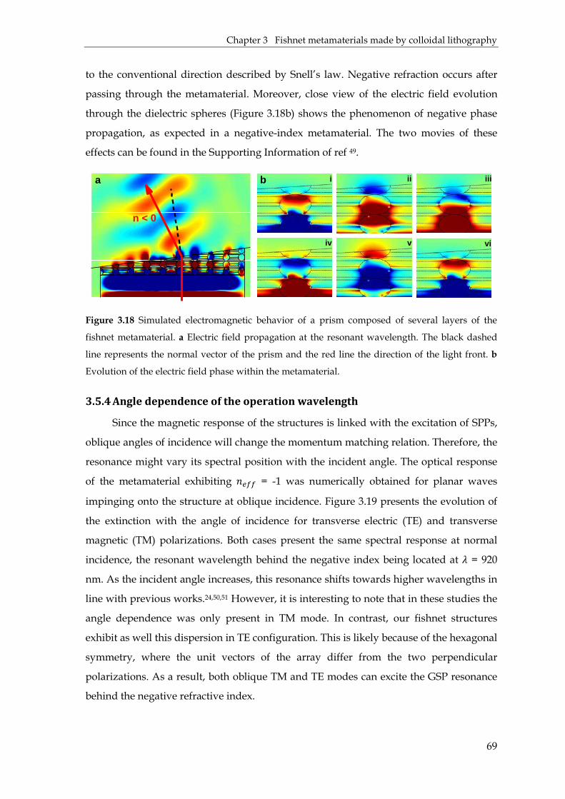
Chapter 3 Fishnet metamaterials made by colloidal lithography
69
to the conventional direction described by Snell’s law. Negative refraction occurs after
passing through the metamaterial. Moreover, close view of the electric field evolution
through the dielectric spheres (Figure 3.18b) shows the phenomenon of negative phase
propagation, as expected in a negative-index metamaterial. The two movies of these
effects can be found in the Supporting Information of ref 49.
Figure 3.18 Simulated electromagnetic behavior of a prism composed of several layers of the
fishnet metamaterial. a Electric field propagation at the resonant wavelength. The black dashed
line represents the normal vector of the prism and the red line the direction of the light front. b
Evolution of the electric field phase within the metamaterial.
3.5.4 Angle dependence of the operation wavelength
Since the magnetic response of the structures is linked with the excitation of SPPs,
oblique angles of incidence will change the momentum matching relation. Therefore, the
resonance might vary its spectral position with the incident angle. The optical response
of the metamaterial exhibiting = -1 was numerically obtained for planar waves
impinging onto the structure at oblique incidence. Figure 3.19 presents the evolution of
the extinction with the angle of incidence for transverse electric (TE) and transverse
magnetic (TM) polarizations. Both cases present the same spectral response at normal
incidence, the resonant wavelength behind the negative index being located at = 920
nm. As the incident angle increases, this resonance shifts towards higher wavelengths in
line with previous works.24,50,51 However, it is interesting to note that in these studies the
angle dependence was only present in TM mode. In contrast, our fishnet structures
exhibit as well this dispersion in TE configuration. This is likely because of the hexagonal
symmetry, where the unit vectors of the array differ from the two perpendicular
polarizations. As a result, both oblique TM and TE modes can excite the GSP resonance
behind the negative refractive index.
viviv
iiiiiba i
n < 0

Chapter 3 Fishnet metamaterials made by colloidal lithography
70
Figure 3.19 Extinction versus wavelength and incident angle of the metamaterial presenting -1
refractive index for a TE and b TM polarizations.
3.6 Conclusions
A new design of double fishnet metamaterials has been fabricated by nanosphere
lithography and electrochemical deposition over large surfaces. The proper control of the
temperature and time during oxygen plasma etching enabled the production of highly
ordered non-closed-packed colloidal templates of different diameters. Such architectures
were successfully employed for the infiltration of sacrificial nickel and gold layers
around the particles. By finely adjusting the electrodeposition time, we fabricated several
colloidal monolayers embedded in nickel-gold-nickel-gold stacks, where the two gold
layers were placed symmetrically with respect to the equatorial axis of the monolayer.
The selective dissolution of the nickel parts led to double-fishnet metamaterials made of
two layers of gold separated by an air cavity and perforated by the dielectric particles.
Besides, the use of a nickel-coated substrate from the beginning enabled transferring the
metamaterial structures to transparent substrates for their detailed optical
characterization. From the experimental point of view, this approach provide a very
good control over the geometrical features so that the final properties of the structures
can be easily tuned.
The fishnet-like samples exhibited extinction resonances in the NIR that varied as a
function of the diameter of the particles and the air gap width between the metallic
layers. The good agreement between the optical measurements and the simulated
spectra throughout the fabrication process attested the successful control over the
structures as well as the reliability of the calculations.
0
10
20
30
40
12001000800600400
Wavelength (nm)
Ang
le o
f inc
iden
ce (
º)
0.0
0.2
0.4
0.6
0.8Extinction
0
10
20
30
40
12001000800600400
Wavelength (nm)
Ang
le o
f inc
iden
ce (
º)
0.0
0.2
0.4
0.6
0.8Extinctionba

Chapter 3 Fishnet metamaterials made by colloidal lithography
71
From the latter, the effective optical properties of the structures were retrieved,
demonstrating that we were experimentally able to tailor the refractive index from
positive to near-zero and even negative values. The minimum achieved corresponded to
a single-NIM with -1 effective refractive index around 940 nm, with negative values over
a 100 nm wide spectral band and a maximum FOM of 0.3. Electromagnetic field
distributions confirmed that the nature of this phenomenon is related with the excitation
a magnetic resonance within the dielectric gap.
The optical spectra of our materials were well reproduced by a simple Fresnel
modelling, ensuring the validity of our calculations. Finally, further simulations
confirmed that the metamaterial can lead to negative refraction and negative phase
propagation, with a dependence on the angle of incidence.
In conclusion, we have developed an effective bottom-up route for the low-cost
and up-scalable fabrication of negative index metamaterials working in the near-infrared
region.
3.7 References
1. A. M. Urbas et al. Roadmap on optical metamaterials. J. Opt. 2016, 18, 093005.
2. V. Ponsinet et al. Self-assembled nanostructured metamaterials. EPL 2017, 119,
14004.
3. M. Mayer, M. J. Schnepf, T. A. F. Konig and A. Fery. Colloidal self-assembly
concepts for plasmonic metasurfaces. Adv. Opt. Mater. 2019, 7, 1800564.
4. S. Mühlig et al. A self-assembled three-dimensional cloak in the visible. Sci. Rep.
2013, 3, 2328.
5. V. Many et al. High optical magnetism of dodecahedral plasmonic meta-atoms.
Nanophotonics 2018, 8, 549–558.
6. R. Paniagua-Domínguez, F. López-Tejeira, R. Marqués and J. A. Sánchez-Gil.
Metallo-dielectric core-shell nanospheres as building blocks for optical three-
dimensional isotropic negative-index metamaterials. New J. Phys. 2011, 13, 123017.
7. J. Cheng et al. GoldHelix: Gold nanoparticles forming 3D helical superstructures
with controlled morphology and strong chiroptical property. ACS Nano 2017, 11,
3806–3818.
Chapter 3 Fishnet metamaterials made by colloidal lithography
72
8. S. Vignolini et al. A 3D optical metamaterial made by self-assembly. Adv. Mater.
2012, 24, 23–27.
9. M. Stefik, S. Guldin, S. Vignolini, U. Wiesner and U. Steiner. Block copolymer self-
assembly for nanophotonics. Chem. Soc. Rev. 2015, 44, 5076–5091.
10. M. Kim, J. Kim and M. Allen. Nanopatterned surfaces based on template-assisted
multilayer electrodeposition. Small 2015, 1912–1918.
11. X. Wang et al. Hyperbolic-by-design self-assembled metamaterial based on block
copolymers lamellar phases. Opt. Laser Technol. 2017, 88, 85–95.
12. M. C. Gwinner et al. Periodic large-area metallic split-ring resonator metamaterial
fabrication based on shadow nanosphere lithography. Small 2009, 5, 400–406.
13. K. Cho, G. Loget and R. M. Corn. Lithographically patterned nanoscale
electrodeposition of plasmonic, bimetallic, semiconductor, magnetic, and polymer
nanoring arrays. J. Phys. Chem. C 2014, 118, 28993–29000.
14. Y. Cai, Y. Cao, P. Nordlander and P. S. Cremer. Fabrication of split-rings via
stretchable colloidal lithography. ACS Photonics 2014, 1, 127–134.
15. K. Tanikawa et al. Fabrication of peelable thin films containing crescent-shaped
split-ring resonators for three-dimensional optical metamaterials. Opt. Mater.
Express 2017, 7, 1.
16. X. Zhou, Q. H. Fu, J. Zhao, Y. Yang and X. P. Zhao. Negative permeability and
subwavelength focusing of quasi-periodic dendritic cell metamaterials. Opt.
Express 2006, 14, 7188.
17. X. Zhao. Bottom-up fabrication methods of optical metamaterials. J. Mater. Chem.
2012, 22, 9439–9449.
18. K. Lodewijks, N. Verellen, W. Van Roy, G. Borghs and P. Van Dorpe. Self-
assembled hexagonal double fishnets as negative index materials. Appl. Phys. Lett.
2011, 98, 091101.
19. Z. Zhou et al. Broad-range electrically tunable plasmonic resonances of a
multilayer coaxial nanohole array with an electroactive polymer wrapper. 2017.
20. B. Gong et al. A visible metamaterial fabricated by self-assembly method. Sci. Rep.
2014, 4, 4713.

Chapter 3 Fishnet metamaterials made by colloidal lithography
73
21. S. Li et al. A green-light gain-assisted metamaterial fabricated by self-assembled
electrochemical deposition. Appl. Phys. Lett. 2013, 103, 181910.
22. J. Valentine, S. Zhang, T. Zentgraf and X. Zhang. Development of bulk optical
negative index fishnet metamaterials: Achieving a low-loss and broadband
response through coupling. Proc. IEEE 2011, 99, 1682–1690.
23. J. B. Pendry, L. Martín-Moreno and F. J. García-Vidal. Mimicking surface
plasmons with structured surfaces. Science 2004, 305, 847–848.
24. A. Mary, S. G. Rodrigo, F. J. García-Vidal and L. Martín-Moreno. Theory of
negative-refractive index reponse of double-fishnet structures. Phys. Rev. Lett.
2008, 101, 103902.
25. S. G. Rodrigo. Optical properties of nanostructured metallic systems: Studied with
the finite-difference time-domain method, University of Zaragoza, 2012.
26. S. Ramo, J. R. Whinnery and T. Van Duzar. Fields and waves in communication
electronics; USA and Canada, 1994.
27. C. L. C. Smith, N. Stenger, A. Kristensen, N. A. Mortensen and S. I. Bozhevolnyi.
Gap and channeled plasmons in tapered grooves: A review. Nanoscale 2015, 7,
9355–9386.
28. E. N. Economou. Surface plasmons in thin films. Phys. Rev. 1969, 182, 539–554.
29. R. Ortuño, C. García-Meca, F. J. Rodríguez-Fortuño, J. Martí and A. Martínez. Role
of surface plasmon polaritons on optical transmission through double layer
metallic hole arrays. Phys. Rev. B 2009, 79, 075425.
30. T. W. H. Oates et al. Oblique incidence ellipsometric characterization and the
substrate dependence of visible frequency fishnet metamaterials. Opt. Express
2012, 20, 11166.
31. J. Yang. Theoretical studies of optical fishnet metamaterials, University of Paris-
Sud, 2012.
32. F. D. Egitto. Plasma etching and modification of organic polymers. Pure Appl.
Chem. 1990, 62, 1699–1708.
33. C. T. Bauer et al. Size and shape evolution of PS particle layers during etching.
Bioinspired, Biomim. Nanobiomaterials 2013, 2, 130–140.

Chapter 3 Fishnet metamaterials made by colloidal lithography
74
34. N. Vogel, S. Goerres, K. Landfester and C. K. Weiss. A convenient method to
produce close- and non-close-packed monolayers using direct assembly at the air-
water interface and subsequent plasma-induced size reduction. Macromol. Chem.
Phys. 2011, 212, 1719–1734.
35. A. Plettl et al. Non-close-packed crystals from self-assembled polystyrene spheres
by isotropic plasma etching: Adding flexibility to colloid lithography. Adv. Funct.
Mater. 2009, 19, 3279–3284.
36. J. Rieger. The glass transition temperature of polystyrene. J. Therm. Anal. 1996, 46,
965–972.
37. M. Heim, S. Reculusa, S. Ravaine and A. Kuhn. Engineering of complex
macroporous materials through controlled electrodeposition in colloidal
superstructures. Adv. Funct. Mater. 2012, 22, 538–545.
38. H. Zheng et al. Morphological design of gold nanopillar arrays and their optical
properties. J. Phys. Chem. C 2016, 120, 1178–1185.
39. H. Zheng. Design and bottom-up fabrication of nanostructured photonic /
plasmonic materials, University of Bordeaux, 2016.
40. X. Chen, T. M. Grzegorczyk, B. I. Wu, J. Pacheco and J. A. Kong. Robust method to
retrieve the constitutive effective parameters of metamaterials. Phys. Rev. E 2004,
70, 016608.
41. D. R. Smith, D. C. Vier, T. Koschny and C. M. Soukoulis. Electromagnetic
parameter retrieval from inhomogeneous metamaterials. Phys. Rev. E 2005, 71,
036617.
42. Z. Li, K. Aydin and E. Ozbay. Determination of the effective constitutive
parameters of bianisotropic metamaterials from reflection and transmission
coefficients. Phys. Rev. E 2009, 79, 026610.
43. S. Yun et al. Experimental verification of substrate-induced bianisotropy in optical
metamaterials. Appl. Phys. Lett. 2013, 103, 233109.
44. S. Xiao et al. Loss-free and active optical negative-index metamaterials. Nature
2010, 466, 735–740.

Chapter 3 Fishnet metamaterials made by colloidal lithography
75
45. P. Ding et al. Numerical simulations of terahertz double-negative metamaterial
with isotropic-like fishnet structure. Photonics Nanostructures - Fundam. Appl. 2009,
7, 92–100.
46. J. Zhou, T. Koschny, M. Kafesaki and C. M. Soukoulis. Negative refractive index
response of weakly and strongly coupled optical metamaterials. Phys. Rev. B 2009,
80, 1–6.
47. M. Born and E. Wolf. Principles of optics. Electromagnetic theory of propagation,
interference and diffraction of light, 7th ed.; Cambridge University Press, UK, 2002.
48. J. L. Garcia-Pomar and M. Nieto-Vesperinas. Transmission study of prisms and
slabs of lossy negative index media. Opt. Express 2004, 12, 2081.
49. M. Gómez-Castaño et al. Tunable index metamaterials made by bottom-up
approaches. Nanoscale Adv. 2019, 1, 1070–1076.
50. A. Minovich et al. Tilted response of fishnet metamaterials at near-infrared optical
wavelengths. Phys. Rev. B 2010, 81, 1–6.
51. S. S. Kruk, D. A. Powell, A. Minovich, D. N. Neshev and Y. S. Kivshar. Spatial
dispersion of multilayer fishnet metamaterials. Opt. Express 2012, 20, 15100–15105.


77
Chapter 4
Fishnet metamaterials by soft
nanoimprint lithography
4.1 Introduction
Soft nanoimprint lithography has been proven as a powerful technique for the
development of plasmonic devices such as structural colour filters,1 directional light
emitters,2 biosensing platforms,3 or metamaterials.4 Thanks to its easy, large-scale and
low-cost operation, NIL technology has led to a broad variety of high performance
metamaterials and metasurfaces, including chiral structures,5 superabsorbers6 and NIMs
made of different geometries and materials.7 Several works can be found in the literature
regarding the fabrication of SRRs by NIL and metal evaporation. The good adaptability
of these techniques to different configurations gave rise to circular,8 U-shaped9 and L-
shaped10 designs working at the NIR region. Tamioka et al.11 developed a different
approach based on the combination of nanoimprint lithography with electrodeposition.
In this way, the metallic parts were directly deposited in between the template following
its shape and avoiding any post-transfer of the structures.
Fishnet structures have been as well accomplished making use of soft
nanoimprinting. Chanda et al.12 showed for the first time the potential application of NIL
to these metamaterials. Their method was based on the deposition of metal-insulator-
metal unit cells over rectangular patterns and subsequent transfer printing to flexible
substrates. The relatively large periodicity of the structures (850 nm) led to NIMs
working over a broad spectral range in the deep near-infrared, with refractive index up
to -7.8 and FOM close to 8. Working at the same spectral region, Bergmair et al. proposed
an approach based on multitransfer printing for piling up several layers.13 Sharp et al.
developed a method where a SiC stamp pressed under high pressure against a
continuous multilayered stack displaced part of the structure and led to the apertures of
the fishnet design.14 The structures exhibited a refractive index of the order of -5
operating in the NIR with FOMs around 3. The first achievement of a fishnet

Chapter 4 Fishnet metamaterials by soft nanoimprint lithography
78
metamaterial made by NIL working in the visible was obtained by Gao et al.4 thanks to
the employ of 300 nm pitch gratings, with a minimum value of -0.73 refractive index at
710 nm and FOM of 4. By optimizing the previous method of Chanda et al.,12 they
carried out a multilayer deposition on top of a pattern followed by lift-off and removal
of the excess material. These examples are summarized in the overview graph of the
main fishnet metamaterials fabricated to date (Figure 1.14 from Chapter 1).
Despite the scalability of these works, they involve several steps and still make use
of top-down deposition methods that can increase the costs and hamper the mass
manufacturing. From the optical point of view, NIMs working in the visible range with
strong negative indices are still lacking for the eventual implementations in optical
devices. Besides, it is worth noting that obtaining NIMs with a negligible angular
dependency remains a daunting challenge but would lead to significant improvement
for light directionality.
Figure 4.1 Illustration of the proposed multilayered fishnet structure combining nanoimprinting
lithography and electrodeposition.
This chapter aims at developing a new approach for the straightforward
fabrication of multilayered fishnet metamaterials. To do so, we will combine the scalable
techniques of soft nanoimprinting and electrodeposition. The targeted geometry is
illustrated in Figure 4.1. A squared array of cylindrical pillars behaves as template for
flat gold layers separated by air gaps, being the whole system placed on top of a
transparent substrate. We engineer constituent dimensions such as lattice spacing, pillars
diameter, gold layers and gaps widths to attain strong refractive indices ranging from
the NIR to the visible. We study experimentally and theoretically the optical properties
of the metamaterials, from the influence of the number of metallic layers to the angular
response. Finally, we demonstrate the accessibility to the air gaps by studying the

Chapter 4 Fishnet metamaterials by soft nanoimprint lithography
79
performance of the metamaterials as optical sensors when infiltrating different liquids
within the metallic layers.
4.2 Fabrication of fishnet metamaterials by soft nanoimprinting
Multilayered fishnet metamaterials were fabricated over centimeter-sized areas by
the versatile combination of soft nanoimprint lithography and metallic electrodeposition.
The procedure followed for the fabrication of the metamaterials is summed up in Figure
4.2. The following sections will describe each fabrication step.
Figure 4.2 Scheme of the fabrication process of fishnet metamaterials based on soft
nanoimprinting and electrodeposition.
4.2.1 Preparation of periodic arrays of pillars
Two-dimensional templates of pillars were prepared by patterning a SU8 thin
layer according to the protocol described in Chapter 2. In brief, a hard-PDMS mold of
holes is pressed against a SU8 layer heated above its glass transition temperature. The
photoresist fills the mold adopting the negative shape and is then cooled down. The
nanopattern is fixed by cross-linking the photoresist with UV light and a post-baking
step. In this project, we made use of squared arrays of cylindrical pillars with lattice
parameters () of 500, 400, 300 and 200 nm in order to obtain structures working over a
broad spectral range.
Substrate choice
Two types of substrates were investigated as WE for the electroplating stage and
the eventual transfer to transparent surfaces. Placing the metamaterials on transparent
SU8 nanopatterning O2 reactive ion etching
Ni-Au electrodepositionNi dissolution

Chapter 4 Fishnet metamaterials by soft nanoimprint lithography
80
substrates will enable the full characterization of their optical properties. Firstly, trying
to optimize the fabrication process followed in Chapter 3, we made use of 100 µm thick
nickel strips (Alfa Aesar). After the electrodeposition step, these bulk pieces would
completely dissolve, leading to transferable membranes onto different substrates.
Thanks to this method, we could simplify the detachment from the original substrate,
avoiding issues like a strong physical adhesion or the possible break of the structures.
As an alternative, we used glass slides coated with a transparent conducting oxide
(TCO). These materials are of great interest in optoelectronics because of their low
electrical resistance and still high transparency.15,16 In our case, it allows us to directly
fabricate the multilayer structure on transparent surfaces without the need of
exchanging the substrate. Hence, the quality of the structures over large surfaces would
be preserved. From the TCOs available, we made use of indium doped tin oxide (ITO,
Ossila) because of its smoother surface and widespread use in optoelectronic devices.17,18
Figure 4.3 presents two samples with a SU8 periodic array of pillars printed on top of the
two substrates.
Figure 4.3 Photographs of patterns of 500 nm periodic pillars printed on SU8 on top of a nickel
strip and b ITO coated glass. Scale bars: 1 cm.
Removal of the residual layer by RIE
The imprinting process is characterized by the formation of a residual layer
between the patterned surface and the substrate. If additional fabrication steps are
planned, it is usually necessary to remove this residual layer to reach the substrate and
isolate the features within the array. In our case, uncovering the conductive substrate
was a crucial step for the correct operation of electrodeposition. The most suitable
etching technique strongly depends on the material to remove and the desired final
shape of the structures. As discussed in Section 3.3.1, the most straightforward approach
a b

Chapter 4 Fishnet metamaterials by soft nanoimprint lithography
81
when working with organic materials is the oxygen plasma treatment. In the case of
spheres, an isotropic plasma cloud was ideal for a homogeneous reduction of the
particles diameter. However, when working with two-dimensional patterns, a controlled
anisotropic treatment is preferred to preserve the aspect ratio of the features. Reactive
ion etching (RIE) enables a high control on the directionality of the generated plasma
species. Ions and radicals are accelerated by an electric field towards the target substrate,
enhancing the etching process in the vertical axis and, therefore, minimizing the
variation of the initial shape. An oxygen RIE treatment was the most appropriate step for
removing the SU8 residual layer under the pillars.
Figure 4.4 a Residual layer thickness as a function of the oxygen RIE time. SEM images of 200 nm
pitch pillars b before and c after the etching process.
We carried out the experiments at the clean room of the Catalan Institute of
Nanoscience and Nanotechnology (ICN2), using a PlasmaPro Cobra 100 equipment from
Oxford Instruments. SU8 residual layers were etched using 25 sccm of O2 under a
pressure of 25 mTorr and a plasma power of 50 W. The sample stage was backside
cooled to maintain a constant temperature during the process. The etching rate
(1.1 nm/s) was previously determined from different etching times over patterns with
= 500 nm with an initial residual layer of 140 nm (Figure 4.4a). The etching time was
adjusted for each batch of samples, whose residual layer was 40-70 nm depending on the
pattern. Although the etching rate can vary with the density of the array because of the
proximity between pillars, such quantity was taken as a valid approximation for very
thin residual layers independently of the pattern features. Figure 4.4b and c show a
periodic array of pillars with = 200 nm before and after the RIE process. Even though
0 30 60 90 1200
20
40
60
80
100
120
140
Res
idua
l lay
er (
nm)
Time (s)
Etching rate = -1.1 nm/s
c
b
200 nm
residual layer
a

Chapter 4 Fishnet metamaterials by soft nanoimprint lithography
82
the pillars are slightly shrunk at the top nanometers, it is proved that the diameter width
is mainly well conserved.
4.2.2 Multilayer electrodeposition through two-dimensional templates
The removal of the residual layer gave rise to periodic arrays of isolated dielectric
pillars on top of conductive substrates. Similarly to Chapter 3, these structures can be
used as templates for the alternating electrodeposition of sacrificial nickel and gold
layers. These multilayer stacks will be the base for the final fishnet structure sustained by
the SU8 pillars. In the case of colloidal templates, a symmetric design regarding the z
axis implied the initial deposition of a supporting nickel layer around the particles. In
the current case, given the lack of symmetry in such direction, the multilayered
geometry could be accomplished by directly electroplating a first gold layer.
Some works have studied the current-time variation when electroplating across
two-dimensional templates. In the case of growing nanowires, a drastic current change is
observed after complete filling the nanoholes, coming from a rapid increase of the
electroactive area.19 However, the deposited thickness is difficult to control when
working with the opposite template: open surfaces patterned with pillars. In such case,
the pillar surface density is not sufficiently large to observe a clear current variation
when exceeding the template high. The layers instead will practically grow like on a flat
surface.
Electrodeposition on nickel strips
Initial tests over unpatterned Ni strips showed that gold deposition did not take
place until applying a reduction potential of -0.9 V, above our usual voltage of -0.7 V.
Such absolute increase manifested a lower chemical affinity between the gold electrolyte
and the nickel foils. Since gold morphology is very sensitive to the deposition conditions,
applying higher potentials could provoke the formation of rough surfaces or even
hierarchical structures.20,21 Instead, we first deposited a 10 nm thick Ni adhesive layer at
the usual conditions (-0.9 V), followed by the deposition of Au at -0.7 V. In this way, the
morphological properties of the gold layers were preserved to be the same as in previous
experiments. However, the same procedure through our templates presented an
inhomogeneous distribution at the microscale. This result was ascribed to the high
roughness of nickel strips, which could increase the hydrophobicity of the substrates.
Considering that our electrolytes were aqueous-based solutions, the low wettability of
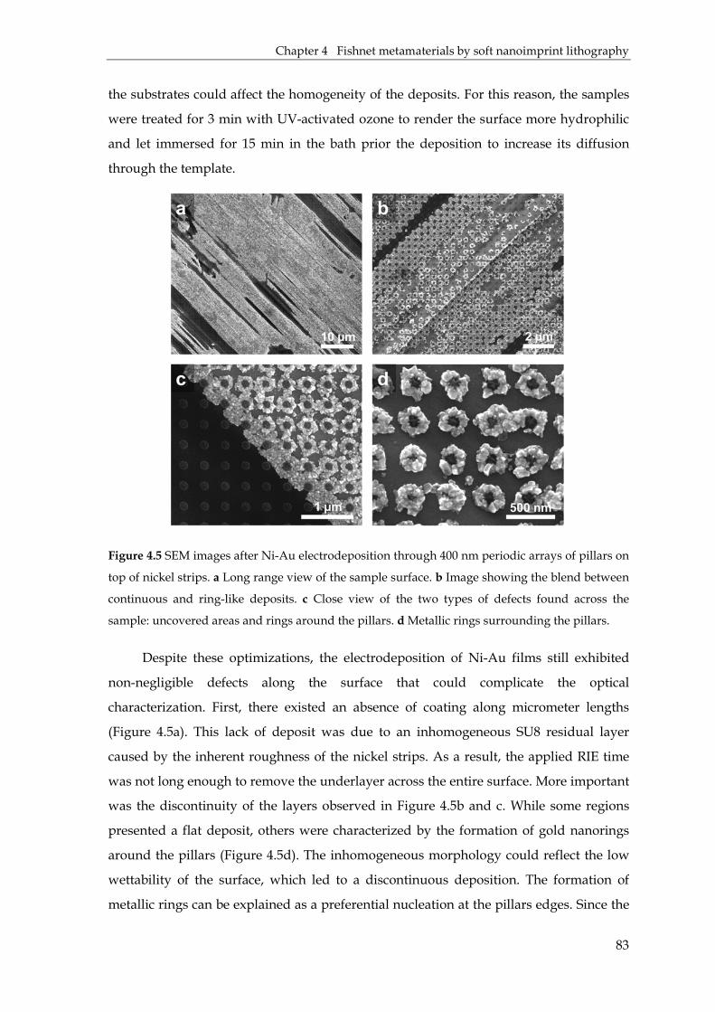
Chapter 4 Fishnet metamaterials by soft nanoimprint lithography
83
the substrates could affect the homogeneity of the deposits. For this reason, the samples
were treated for 3 min with UV-activated ozone to render the surface more hydrophilic
and let immersed for 15 min in the bath prior the deposition to increase its diffusion
through the template.
Figure 4.5 SEM images after Ni-Au electrodeposition through 400 nm periodic arrays of pillars on
top of nickel strips. a Long range view of the sample surface. b Image showing the blend between
continuous and ring-like deposits. c Close view of the two types of defects found across the
sample: uncovered areas and rings around the pillars. d Metallic rings surrounding the pillars.
Despite these optimizations, the electrodeposition of Ni-Au films still exhibited
non-negligible defects along the surface that could complicate the optical
characterization. First, there existed an absence of coating along micrometer lengths
(Figure 4.5a). This lack of deposit was due to an inhomogeneous SU8 residual layer
caused by the inherent roughness of the nickel strips. As a result, the applied RIE time
was not long enough to remove the underlayer across the entire surface. More important
was the discontinuity of the layers observed in Figure 4.5b and c. While some regions
presented a flat deposit, others were characterized by the formation of gold nanorings
around the pillars (Figure 4.5d). The inhomogeneous morphology could reflect the low
wettability of the surface, which led to a discontinuous deposition. The formation of
metallic rings can be explained as a preferential nucleation at the pillars edges. Since the

Chapter 4 Fishnet metamaterials by soft nanoimprint lithography
84
electrodeposition cannot take place under the pillars, the electrical density increases
right at the edges of the features.22,23 This effect along with the hydrophobicity of the
substrate could explain the lack of deposit in between the pillars.
Although interesting for other structures and applications, the formation of
nanorings made unfeasible the proper fabrication of a multilayered structure. We
concluded that if one desires a continuous and homogeneous layer infiltrated through a
template, hydrophilic and flat surfaces are preferentially needed.
Electrodeposition on ITO coated glasses
Alternatively to nickel strips, ITO coated glasses were investigated as WE for the
template-assisted electrodeposition. Despite its conductive properties, ITO presents
higher resistance than metals (15 Ω/sq), what leads to the formation of isolated gold
nanoparticles when electrodepositing at RT.24 Higher electrolyte temperatures can
increase the adatoms diffusion on the working electrode, leading to larger grains and
smoother surfaces.25 Based on previous works,26 denser deposits were obtained when
reducing gold at -0.9 V at 55 ºC. However, they still formed non-continuous coatings for
thickness of about 200 nm. Taking into account that our multilayered structure is based
on 50 nm thick gold layers, these conditions were not suitable for our design. Again, a
sacrificial nickel adhesive layer was first electrodeposited through the templates to
ensure a homogeneous deposit.
The multilayer electrodeposition through pillar arrays placed on ITO substrates
was performed as follows. The sample was let in 55 ºC hot nickel bath for 10 minutes.
This period ensured the electrolyte diffusion through the template. A thin layer of
approximately 10 nm was then electrodeposited at -0.9 V at the same temperature.
Having successfully deposited a homogeneous adhesive film, the rest of layers could be
nicely electrodeposited following our usual experimental conditions. In particular,
alternating layers of gold and nickel were electrodeposited at RT at -0.7 V and -0.9 V,
respectively. It is worth noting that the samples were always let immersed for 10
minutes in the electrolytes before the depositions in order to assure the homogeneity
across the surface. After each step, they were rinsed in water for cleaning. The deposition
rate for each metal was determined by SEM analysis on several pattern samples, being
2.9 ± 0.2 nm/s for nickel deposited at 55 ºC, 1.1 ± 0.1 nm/s for nickel deposited at RT and
0.65 ± 0.06 nm/s for gold. The last two results manifest higher values than growth rates
on unpatterned surfaces. Such effect can be attributed to the higher electrical density at

Chapter 4 Fishnet metamaterials by soft nanoimprint lithography
85
the proximity of the electroactive areas. Given the impossibility of reducing on the
dielectric pillars, the ions migrate towards the closer uncovered surfaces, what increases
the deposition rate. Based on this, the template favors the creation of more compact
layers than an unpatterned surface.
Figure 4.6 SEM images of 500 nm periodic templates after electrodepositing a the first gold layer
and b four gold layers separated by nickel spacers.
Figure 4.6a presents the successful growth of the first nickel-gold layers deposited
on ITO embedding 500 nm periodic pillars. The contrast with the deposition on nickel
strips confirms the importance of the surfaces wettability. The formation of continuous
layers on the ITO substrate enabled the multilayer deposition across the template height.
With a similar grain morphology, the main difference after electrodepositing one and
four gold layers lies on the smaller apertures obtained for the latter (Figure 4.6b). This
observation indicates that the metallic stack has reached the top of the pillars.
Specifically, from close examination of Figure 4.4c, one can notice that the shape of the
pillars is not exactly cylindrical but rather domed at the top. This structural modification
resulted from the RIE step. The metallic films at this location, therefore, present
narrower holes than at the bottom part of the template (Figure 4.7).
Figure 4.7 Scheme of the multilayered metallic stack embedding the dielectric pillars. Red dashed
lines mark the diameter of the pillars at the first and last gold layers as observed by SEM.

Chapter 4 Fishnet metamaterials by soft nanoimprint lithography
86
It is important to note that electrodepositing beyond the pillars height would
eventually close the holes since the growth would not encounter any template limitation.
In order to prevent the fishnet design, the amount of layers deposited through each
template was varied based on the height of the patterns. We used two types of templates
according to their height:
o Arrays with = 200 and 300 nm were 150 nm tall and served for the infiltration of
up to 3 gold layers with 45 nm thickness, always separated by 15 nm thick
sacrificial Ni layers.
o Arrays with = 400 and 500 nm were 330 nm high and enabled the deposition of
even 4 gold layers with a thickness of 50 nm, separated by 30 nm Ni layers.
Figure 4.8 SEM top views of the multilayered metallic stacks with the maximum number of gold
layers for a 200 nm, b 300 nm, c 400 nm and d 500 nm lattice spacing. Scale bars: 1 µm.
In our design, gold layers of around 50 nm thickness were considered as an
appropriate value for, first, achieving homogeneous and continuous deposits and,
second, for providing a good GSP coupling as presented in Chapter 3. The thickness of
the nickel layers was chosen considering that wider gaps led to NIMs working at shorter
a b
c d
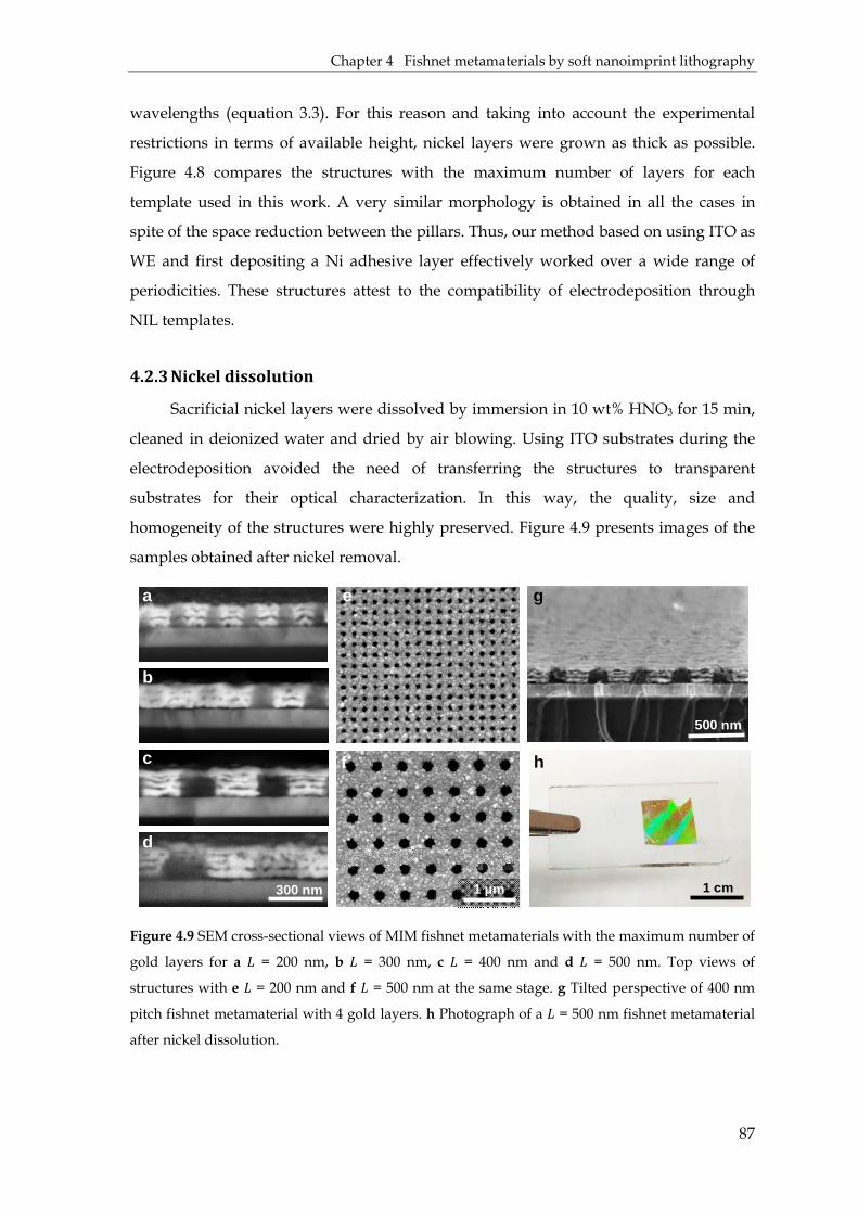
Chapter 4 Fishnet metamaterials by soft nanoimprint lithography
87
wavelengths (equation 3.3). For this reason and taking into account the experimental
restrictions in terms of available height, nickel layers were grown as thick as possible.
Figure 4.8 compares the structures with the maximum number of layers for each
template used in this work. A very similar morphology is obtained in all the cases in
spite of the space reduction between the pillars. Thus, our method based on using ITO as
WE and first depositing a Ni adhesive layer effectively worked over a wide range of
periodicities. These structures attest to the compatibility of electrodeposition through
NIL templates.
4.2.3 Nickel dissolution
Sacrificial nickel layers were dissolved by immersion in 10 wt% HNO3 for 15 min,
cleaned in deionized water and dried by air blowing. Using ITO substrates during the
electrodeposition avoided the need of transferring the structures to transparent
substrates for their optical characterization. In this way, the quality, size and
homogeneity of the structures were highly preserved. Figure 4.9 presents images of the
samples obtained after nickel removal.
Figure 4.9 SEM cross-sectional views of MIM fishnet metamaterials with the maximum number of
gold layers for a = 200 nm, b = 300 nm, c = 400 nm and d = 500 nm. Top views of
structures with e = 200 nm and f = 500 nm at the same stage. g Tilted perspective of 400 nm
pitch fishnet metamaterial with 4 gold layers. h Photograph of a = 500 nm fishnet metamaterial
after nickel dissolution.
500 nm
1 cm1 µm300 nm
a
b
c
d
e
f
g
h

Chapter 4 Fishnet metamaterials by soft nanoimprint lithography
88
Figure 4.9a-d shows the SEM side view from samples with different lattice
parameters. Although sometimes collapsed after cutting the samples, once can easily
identify the gold layers separated by air gaps and supported by the SU8 pillars. The gap
widths were found to be slightly smaller than the nominal Ni thickness. This was
attributed to a thinner deposit that estimated or to a small fall of the gold layers when
removing the nickel supports. Top view SEM images from the structures with = 200
and 500 nm with 3 and 4 gold layers, respectively, are shown in Figure 4.9e and f. The
tilted view of a fishnet structure of = 400 nm with 4 gold layers is presented in Figure
4.9g and illustrates the good quality of the samples. This is indeed perceived just by
naked eye observation of the iridescent large area samples (Figure 4.9h).
We can conclude that we have successfully developed a new straightforward
method for the fabrication of large area multilayered fishnet metamaterials. Our
approach is strongly compatible with different structural dimensions such as the lattice,
the diameter or number of layers. Table 4.1 summarizes the geometrical parameters of
all the fabricated samples according to the scheme presented in Figure 4.10.
Figure 4.10 Scheme of the fabricated samples denoting their composition materials and
geometrical parameters. stands for lattice spacing, for pillars diameter, ℎ for pillars height,
for metal thickness and for gap width.
Table 4.1 Geometrical features of the fabricated structures.
L (nm) D (nm) h (nm) t (nm) w (nm) #Au layers
200 85 150 45 15 2, 3
300 115 150 45 15 2, 3
400 180 330 50 25 2, 3, 4
500 210 330 50 25 2, 3, 4
L D
h
w
t
Glass
ITO
SU8
Au
air

Chapter 4 Fishnet metamaterials by soft nanoimprint lithography
89
4.3 Optical characterization of multilayered fishnet metamaterials
The previous section proved the feasibility of fabricating fishnet structures
featuring several layers over different templates. In order to study their optical
properties and understand the dependence with the features dimensions, the samples
were characterized in transmission T and reflection R. The spectroscopic properties were
measured at normal incidence by FTIR.
Given the anisotropy caused by the substrate, reflectance spectra were compared
for light impinging from the top and bottom sides of samples made of = 500 nm. As
presented in Figure 4.11a, when illuminated from top, the reflectivity of the samples
increases with the number of layers while losing definition of the optical features. Such
observations can be explained when analyzing in detail our samples. First, an increase in
the number of layers could bring about higher reflectance values because of the larger
amount of metal within the structure. Second, since the first light-matter interaction
takes place at the top gold layer, any morphological variation at this point could lead to
noticeable spectral modifications. As previously discussed, the pillars become narrower
at the top part, leading to larger metallic surfaces and thus, higher reflectivity. More
important is the loss of definition with the number of layers, whose explanation can be
found at the scattering caused by the gold layers roughness.
Figure 4.11 Reflectance spectra of multilayered fishnet structures with = 500 nm measured a
from top and b bottom sides.
Analogous results were obtained when measuring from the bottom side (Figure
4.11b). The first observation is the signal attenuation coming from the absorption
400 600 800 1000
2 layers 3 layers 4 layers
Wavelength (nm)400 600 800 1000
0.0
0.2
0.4
0.6
0.8
1.0
Ref
lect
ance
Wavelength (nm)
a b
Chapter 4 Fishnet metamaterials by soft nanoimprint lithography
90
through the ITO layer.27 In contrast with the previous configuration, an increase of the
number of layers does not imply higher reflectance values. This indicates that such
increase was not mainly related with the number of layers but rather with the metal
fraction of the top layer. The similarity of R spectra for all the samples when measuring
from bottom corroborates this statement since all the structures present the same base
diameter and, hence, same metal fraction where the first light-matter interaction occurs.
The main contrast might be the better definition of the curves. Given the lower
roughness of ITO when compared with the electrodeposited layers, the first gold
interface is smoother than the others. As a result, the light is less scattered than in the
former configuration and, therefore, the optical features are better defined.
Considering that we aimed to numerically reproduce as accurately as possible our
experimental results, hereafter we mainly worked with the spectra collected from the
bottom because of the higher resolved curves. Spectra acquired from the top were also
taken as control measurements and compared with the corresponding simulations.
Transmission spectra were as well measured in both configurations and presented
identical curves, in agreement with the reciprocity dictated by Fresnel laws
(Section 3.5.2).
Figure 4.12 presents the transmission and reflection measurements (left) for each
batch of samples with the corresponding simulations (right). The experimental curves
are representative spectra of the homogeneous optical response along the surface. FDTD
simulations based on the parameters specified in Table 4.1 reproduced well both the
position and intensity of the experimental curves, thus corroborating the quality of the
final structures. In the case of = 200, 300 nm, the spectra were fitted to 45 ± 7 nm thick
gold layers and 14 ± 4 wide gaps, where the error ranges correspond to the standard
deviation from the average fitted values. For structures with = 400, 500 nm, the spectra
were fitted to 50 ± 5 nm thick gold layers and gap widths of 27 ± 3 nm. The first
observation from the optical response reveals two main resonances for all the fishnet
structures except for the samples with lattice parameter = 200 nm, whose first
resonance likely falls within the gold absorption band. The resonance redshifts when
increasing the periodicity of the structures. This behavior is ascribed to the excitation of
plasmonic resonances in a metallic grating, where the resonant wavelength scales with .
The disagreement of = 300 nm with this trend indicates that other geometrical
dimensions must be taken into account when analyzing the peaks position.
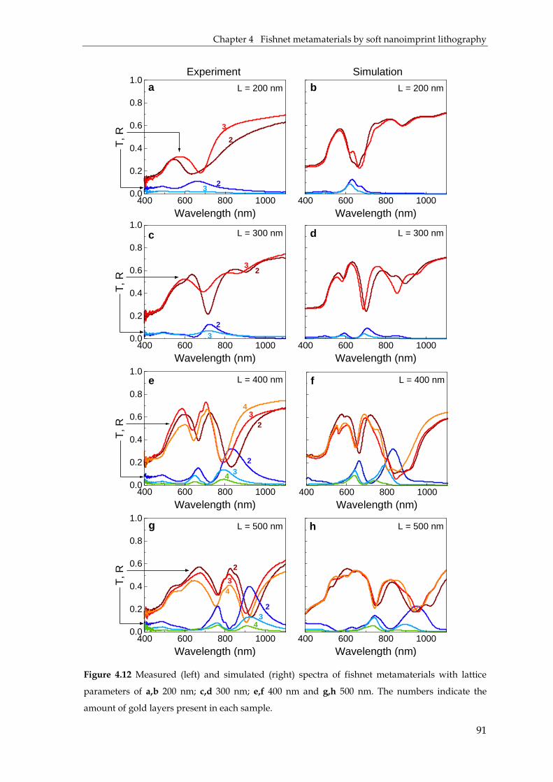
Chapter 4 Fishnet metamaterials by soft nanoimprint lithography
91
Figure 4.12 Measured (left) and simulated (right) spectra of fishnet metamaterials with lattice
parameters of a,b 200 nm; c,d 300 nm; e,f 400 nm and g,h 500 nm. The numbers indicate the
amount of gold layers present in each sample.
400 600 800 10000.0
0.2
0.4
0.6
0.8
1.0
Wavelength (nm)
32
23
T, R
L = 300 nm
400 600 800 10000.0
0.2
0.4
0.6
0.8
1.0
Wavelength (nm)
4
4
3
2
23
L = 500 nm
T, R
400 600 800 10000.0
0.2
0.4
0.6
0.8
1.0
4
Wavelength (nm)
4
32
23
L = 400 nm
T, R
400 600 800 1000
Wavelength (nm)
L = 500 nm
400 600 800 1000
Wavelength (nm)
L = 400 nm
400 600 800 1000
Wavelength (nm)
L = 300 nm
hg
fe
d
400 600 800 10000.0
0.2
0.4
0.6
0.8
1.0
32
2
Wavelength (nm)
3T
, R
L = 200 nm
c
a
400 600 800 1000
Wavelength (nm)
L = 200 nm
SimulationExperiment
b

Chapter 4 Fishnet metamaterials by soft nanoimprint lithography
92
To investigate the physical origin of these resonances, we studied the
electromagnetic fields distribution in a fishnet metamaterial of = 500 nm composed by
4 layers (orange curve in Figure 4.12h). As presented in Figure 4.13, the low wavelength
peak is characterized by an EM confinement within the pillars and the SPP excitation at
the Au-ITO interface. Thus, the substrate material and the cylinders diameter mainly
govern the resonant wavelength.
Figure 4.13 Schemes of the simulated structure at a the middle air gap plane and d the cross-
sectional plane parallel to E polarization. b-f Normalized EM intensities at the low resonant
wavelength ( = 745 nm) at both planes of a fishnet metamaterial made of = 500 nm and 4
layers. White dashed lines delimit the materials surfaces.
On the contrary, the EM profiles found at the second peak (Figure 4.14) highly
resemble the distributions observed for double fishnet metamaterials made with PS
spheres (Figure 3.16 from Chapter 3). The electric field concentrates at the Au-SU8
interfaces in the same direction as the electric field polarization (Figure 4.14b,e). The
magnetic profiles indicate, first, a dependence on the pillars separation (Figure 4.14c)
and second, the existence of a strong magnetic confinement in the dielectric gaps (Figure
4.14f). As previously explained, this EM distribution is responsible of the negative-index
phenomenon in fishnet designs, where magnetic dipoles are induced in the dielectric
layers thanks to the excitation of GSPs. Therefore, from the spectra presented in Figure
4.12, the resonances of interest for NIMs are the high wavelength peaks.

Chapter 4 Fishnet metamaterials by soft nanoimprint lithography
93
The relation with the pillars diameter in both EM distributions explains why
samples with = 300 nm present resonant wavelengths comparable with the ones of
larger periodicities. When analyzing these designs, one should have in mind not only the
lattice parameter of the grating but also the lateral dimension of the features. Calculating
the ratio / from the values given in Table 4.1, it is found that geometries with = 200,
400 and 500 nm present a ratio of the order of 0.43, while the design with = 300 exhibits
a lower ratio of 0.38. Larger diameters would have implied a ratio in line with the other
periodicities and, moreover, shorter resonant wavelengths as demonstrated in
Section 3.2.
Figure 4.14 Schemes of the simulated structure at a the middle air gap plane and d the cross-
sectional plane parallel to E polarization. b-f Normalized EM intensities at the high resonant
wavelength ( = 981 nm) at both planes of a fishnet metamaterial made of = 500 nm and 4
layers. White dashed lines delimit the materials surfaces.
4.4 Effective properties of multilayered fishnet metamaterials
4.4.1 Effective parameters
The effective parameters of the fabricated structures were retrieved from the
simulated complex transmission and reflection coefficients as described in the Appendix.
We made use of the effective medium approximation28,29 and considered the anisotropy
of the structures caused by the substrate.30,31

Chapter 4 Fishnet metamaterials by soft nanoimprint lithography
94
Refractive index
Figure 4.15 presents the real part of the effective refractive index for each
batch of samples along with the FOM of each metamaterial. Negative indices are found
at the high wavelength resonance, confirming that the magnetic confinement found in
the air gaps leads to this extraordinary property. As foreseen in the spectra, the
operation region mainly depends on the lattice parameter of the metamaterial, shifting to
longer as the periodicity increases. In opposition, the negative band blue shifts when
increasing the number of layers. Thanks to our broad range of structures and the proper
relation between and , we successfully obtained metamaterials working from the
visible to the NIR range.
Figure 4.15 Effective refractive indices of all the fabricated samples retrieved from simulations.
The lattice spacing corresponds to a 200 nm, b 300 nm, c 400 nm and d 500 nm.
In the visible, the minimum achieved is = -1.2 ( = 700 nm), arising from the
structure with = 200 nm and 3 gold layers with 15 nm wide gaps (Figure 4.15a). We
should emphasize the fact that large area NIMs working at this region are scarce because
of the complex fabrication process at this scale.4,7 In the NIR, we achieved values up to
900 1000 1100-3
-2
-1
0
1
2
3
FOM = 1.4
2 layers 3 layers 4 layers
FOM = 0.4
Re
(nef
f)
Wavelength (nm)
FOM = 0.9
750 800 850 900 950-3
-2
-1
0
1
2
3
FOM = 1.0
2 layers 3 layers 4 layers
FOM = 0.2Re
(nef
f)
Wavelength (nm)
FOM = 0.8
800 900 1000-3
-2
-1
0
1
2
3 2 layers 3 layers
FOM = 0.4Re
(nef
f)
Wavelength (nm)
FOM = 0.7
650 700 750-1.5
-1.0
-0.5
0.0
0.5
1.0 2 layers 3 layers
FOM = 0.5
Re
(nef
f)
Wavelength (nm)
FOM = 0.5
a
dc
b

Chapter 4 Fishnet metamaterials by soft nanoimprint lithography
95
-2.8 at = 910 nm (Figure 4.15b) or -2.1 at = 870 nm (Figure 4.15c), within the first
telecommunication window. The achievement of such strong values has been rarely
reported in this region, with similar results only at longer wavelengths.12,32,33
Figure of merit
The FOM improvement when increasing the number of layers is known to happen
due to the shift of the minimum real part from the maximum imaginary part of .34,35
Moreover, a gradual increase of the FOM is observed as becomes larger, as plotted in
Figure 4.16. This relation manifests the complex task of designing and fabricating
efficient NIMs working at visible wavelengths, where the metal losses become more
relevant.
200 300 400 5000.0
0.3
0.6
0.9
1.2
1.5 2 layers 3 layers 4 layers
FO
M
Lattice (nm)500 nm
a
b
c
d
Figure 4.16 a Figure of merit of the NIMs as a function of their lattice parameter. SEM images of
fishnet structures with = 500 nm and b four gold layers, c three layers and d two layers.
Permittivity and permeability
Figure 4.17 presents the effective permittivity and permeability obtained from the
retrieval procedure. The positive values of the permeability along with the permittivity
being negative classify our metamaterials as single-NIMs, where < 0 is attained with
just one of these parameters below zero. It is worth noting that in all the cases the
permeability differs from 1 at the operation region, implying a magnetic response at NIR
and visible wavelengths. The permeability is also found to decrease with the number of
layers up to near-zero values like in the cases of the largest with more than two gold
layers (Figure 4.17f and h). The combination of the latter with near-zero permittivities
(Figure 4.17g) leads to the interesting subgroup of near-zero metamaterials. These

Chapter 4 Fishnet metamaterials by soft nanoimprint lithography
96
systems also attract high interest in the community because of the small light phase
variation within the structure, what enables phenomena such as radiation patterning or
spontaneous emission manipulation.36,37
Figure 4.17 Real parts of the effective permittivity (left) and permeability (right) for samples with
periodicities of a,b 200 nm, c,d 300 nm, e,f 400 nm and g,h 500 nm.
700 800 900 1000 1100
-20
-15
-10
-5
0
Re
(εef
f)
Wavelength (nm)
2 layers 3 layers
650 700 750-7
-6
-5
-4
-3
-2
-1
0
Re
(εef
f)
Wavelength (nm)
2 layers 3 layers
900 1000 1100-10
-8
-6
-4
-2
0
2
4 2 layers 3 layers 4 layers
Re
(εef
f)
Wavelength (nm)900 1000 1100
0.0
0.5
1.0
1.5
2.0
Re
(µef
f)
Wavelength (nm)
2 layers 3 layers 4 layers
750 800 850 900 950
0.0
0.5
1.0
1.5
2.0
2.5 2 layers 3 layers 4 layers
Re
(µef
f)
Wavelength (nm)750 800 850 900 950
-6
-4
-2
0
2
4 2 layers 3 layers 4 layers
Re
(εef
f)
Wavelength (nm)
700 800 900 1000 1100
0.5
1.0
1.5
2 layers 3 layers
Re
(µef
f)
Wavelength (nm)
650 700 7500.5
1.0
1.5
2.0
2.5 2 layers 3 layers
Re
(µef
f)
Wavelength (nm)
a b
dc
e f
hg

Chapter 4 Fishnet metamaterials by soft nanoimprint lithography
97
4.4.2 Change of branch in the refractive index
When light propagates in a periodic structure, an infinite number of modes is
excited for a given wavelength. Among them, the mode with the lowest absorption
governs the optical response.38 This is the reason why the refractive index in periodic
structures, does not depend only on the wavelength but also on the propagating mode.
In the case of fishnet metamaterials with more than two metallic layers, the two branches
observed for (Figure 4.15) represent the change on the dominant mode propagating
inside the system. This was studied in a fishnet metamaterial with = 400 nm and 4 gold
layers by analyzing the EM distributions below and above the refractive index
discontinuity found at = 829 nm (Figure 4.18).
Figure 4.18 a Cross-sectional scheme of the simulated structure. b Effective refractive of the
fishnet metamaterial made by = 400 nm and 4 gold layers. Magnetic field profiles at c branch 1,
where < 0, and at d branch 2, where > 0. White arrows show the electric current density.
On one hand, when < 0 (branch 1), the top and middle air gaps exhibit in-
phase contouring current vectors, leading to in-phase magnetic dipoles at these
locations, with a strong enhancement at the top gap. On the other hand, when > 0
(branch 2), the magnetic field is mainly concentrated in the bottom space, with
contouring current loops being in phase for the bottom and middle gaps. Therefore, a
change in propagating mode is perceptible in the magnetic profile as well as in the
direction of the antisymmetric currents generated in the gold-air interfaces.

Chapter 4 Fishnet metamaterials by soft nanoimprint lithography
98
4.4.3 Angular dependence of the working wavelength
Figure 4.15 showed that the position of the negative index band depends on the
number of layers that compose the structure. For a given lattice, a blue shift appeared
when increasing the amount of layers. Former works have discussed the dependence of
the effective properties on the metamaterial thickness, this is, on the number of MIM
cavities composing the structure.35,39,40 It has been shown that by reaching a minimum
number of stacked layers, the multilayered fishnet metamaterial converge to the so-
known bulk metamaterial regime.34,41
Figure 4.19 a Scheme of the TM oblique excitation. Experimental reflectance spectra collected in
this mode for different incident angles in fishnets with b = 200 nm with 3 gold layers and c
= 500 nm with 4 gold layers. Dashed lines are a guide to the eye indicating the evolution of the
GSP resonance. d,e Calculated angular dispersions for the same structures and configuration.
E
0
10
20
30
40
50
400 600 800 1000
Ang
le o
f inc
iden
ce (
º)
Wavelength (nm)
0.2
0.3
0.4
0.5
0.6
0.7
0.8Reflectance
0
10
20
30
40
50
400 600 800 1000
Wavelength (nm)
Ang
le o
f inc
iden
ce (
º)
0.2
0.3
0.4
0.5
0.6
0.7Reflectance
b
d e
a
Ec
400 600 800 1000
Ref
lect
ance
(a.
u.)
Wavelength (nm)
0º
10º
20º
30º
50º
60º
40º
400 600 800 1000
Ref
lect
ance
(a.
u.)
Wavelength (nm)
0º
10º
20º
30º
50º
60º
40º

Chapter 4 Fishnet metamaterials by soft nanoimprint lithography
99
At this limit, metamaterials present unambiguous effective properties
independently of the number of unit cells or the angle of incidence, exhibiting weak
angular dispersion. The small shift of the band observed in Figure 4.15a,b for = 200 nm
and 300 nm suggests that the structures are approaching to the bulk limit with just 3
gold layers, this is, two MIM cavities.
We tested this assumption by measuring reflection from the samples with light
impinging at 0º, 10º, 20º, 30º, 40º, 50º and 60º. Reflectance in TM mode is expected to be
highly sensitive to the angle of incidence because of the change in the E field direction
respect to the surface plane (Figure 4.19a). Figure 4.19b and c show the angle-resolved
reflection measurements taken under TM configuration for the fishnet structures with
= 200 nm and 3 gold layers and = 500 nm and 4 gold layers, respectively. For the
largest periodicity, a clear redshift of the GSP resonance is observed in line with the
results developed in Chapter 3 and in previous works.35,42 Such behavior has been found
to come from the electromagnetic field delocalization across the gaps and interaction
between adjacent cells (Figure 4.20). As a result, the coupling energy of the GSP mode
decreases for higher incident angles and thus, the resonant wavelength redshifts.43
Figure 4.20 a Scheme of the simulated structure in TM configuration, being 30º the incident angle
from air. b Normalized magnetic intensity at the gap resonant wavelength of three adjacent cells,
showing the electromagnetic coupling between them. The lattice corresponds to 500 nm.
In contrast, the sample with the smallest periodicity ( = 200 nm) presents weak
angular dispersion, outlining the robustness of this structure with the angle and,
therefore, its close convergence to a bulk metamaterial. The trends observed for both
structures are supported by the angular dispersion obtained from the simulations, which
present a very good agreement with the measurements (Figure 4.19d,e).

Chapter 4 Fishnet metamaterials by soft nanoimprint lithography
100
Both measurements and simulations for the TE mode (Figure 4.21) show no
significant changes in the GSP resonance since the direction of the E field remains
constant with respect to the structure as the angle increases.
Figure 4.21 a Scheme of the TE oblique excitation. Experimental reflectance spectra collected in
this mode for different angles for fishnet metamaterials with b = 200 nm with 3 gold layers and
c = 500 nm with 4 gold layers. Dashed lines are a guide to the eye indicating the evolution of the
GSP resonance. d,e Calculated angular dispersions for the same structures and configuration.
4.5 Fishnet metamaterials as refractive index sensors
Optical sensors are acquiring great attention in technology for their ability of
transducing refractive index changes into chemical, biological or food modifications.44
Plasmonic structures stand out in this field because of the strong EM enhancement at the
resonant wavelengths, which are highly sensitive to any variation in the surrounding
E
a
0
10
20
30
40
50
400 600 800 1000
Ang
le o
f inc
iden
ce (
º)
Wavelength (nm)
0.2
0.3
0.4
0.5
0.6
0.7Reflectance
0
10
20
30
40
50
400 600 800 1000
Wavelength (nm)
Ang
le o
f inc
iden
ce (
º)
0.2
0.3
0.4
0.5
0.6
0.7
0.8Reflectance
400 600 800 1000
Ref
lect
ance
(a.
u.)
Wavelength (nm)
0º
10º
20º
30º
50º
60º
40º
400 600 800 1000
Ref
lect
ance
(a.
u.)
Wavelength (nm)
0º
10º
20º
30º
50º
60º
40º
b c
d e
E

Chapter 4 Fishnet metamaterials by soft nanoimprint lithography
101
medium. Several works have published in the recent years the fabrication and
characterization of plasmonic structures serving as refractive index sensors. Examples of
diverse geometries include MIM gratings,45 metal dimers,46 graphene-metal hybrid
systems47 or even NIMs made from split-ring resonators.48
In a common fishnet design, the system is composed by a stack of metal and
dielectric layers, drilled with air apertures. Our systems, in contrast, present a different
structure where the apertures are made of a solid material and the dielectric spacers
correspond to air gaps. This unique structure can be understood as a porous material
that allows the infiltration of different media through the gold layers. As a proof of
concept, here we explore the opportunity of tuning the optical response of the
metamaterials when infiltrating liquid media in between the metallic layers. Since the
achievement of negative refractive index relies on the high EM confinement at the air
gaps, the optical properties of the structures are expected to strongly depend on the
medium placed at this location.45,49
Liquids covering a broad range of refractive index were chosen in order to study
the dependence of the GSP resonance with the dielectric medium embedded. In
particular, me made use of water ( = 1.33), isopropanol ( = 1.38), cyclohexane ( =
1.42), toluene ( = 1.49) and chlorobenzene ( = 1.53). For these measurements, a drop of
the liquid of interest was placed on top of a glass slide and covered by the sample facing
down so that the fluid penetrated through the layers (Figure 4.22). The whole system
was then placed in the FTIR setup for reflection measurements. After the spectra
collection, the samples were rinsed with isopropanol and dried with air blowing.
Figure 4.22 Scheme of the liquid infiltration experiment. I Fishnet metamaterials are placed facing
down on a liquid covered glass slide. II After infiltration through the air gaps, reflection spectra
of the whole system are collected.

Chapter 4 Fishnet metamaterials by soft nanoimprint lithography
102
Figure 4.23 presents the wavelength dependence of the limit samples of (a,c) = 200 nm
and (b,d) = 500 nm. A redshift is observed when increasing the refractive index of the dielectric
spacer, implying a redshift as well on the negative operation region. This trend is in good
agreement with equation (3.2), which indicates that in the linear approximation the vacuum
wavevector is inversely proportional to the refractive index of the spacer. Consequently, the
resonant wavelength scales with the index of this layer. It is interesting to note that while this
equation presents a linear relationship, our experiments follow a polynomial curvature. This is
ascribed to a non-linear dependency over broad index ranges such as ours, in line with other
studies about the surface plasmon resonance dependency with bulk solutions.50,51
600 640 680 720 760 800 8400.1
0.2
0.3
0.4
0.5
0.6
c d
b
Ref
lect
ance
Wavelength (nm)
air
isopropanol
water
cyclohexane
cl-benzene
toluene
a
840 880 920 960 1000 10400.0
0.1
0.2
0.3
0.4
0.5
0.6
Ref
lect
ance
Wavelength (nm)
1.0 1.1 1.2 1.3 1.4 1.5 1.6
680
700
720
740
Wav
elen
gth
(nm
)
Refractive index1.0 1.1 1.2 1.3 1.4 1.5 1.6
900
920
940
960
Wav
elen
gth
(nm
)
Refractive index
cc
air
isopropanol
water
cyclohexane
cl-benzene
toluene
Figure 4.23 Reflectance spectra of fishnet metamaterials made of a = 200 nm with 3 gold layers
and b = 500 nm and 4 gold layers separated by air (dark blue) or infiltrated by water (cyan),
isopropanol (green), cyclohexane (orange), toluene (red) and chlorobenzene (brown). c,d
Resonant wavelength as a function of the refractive index of the liquids for the same structures.
Dashed curves describe a second order polynomial fitting.
The wavelength shift observed when infiltrating different optical media suggests
the capability of these structures for refractive index (RI) optical sensing. Three
parameters are commonly used to characterize RI sensors: sensitivity (), figure of merit
( ) and quality factor (Q-factor), defined as:

Chapter 4 Fishnet metamaterials by soft nanoimprint lithography
103
=Δ
Δ (4.1)
=
(4.2)
Q − factor =
(4.3)
The sensitivity is the ratio of the change in resonant wavelength Δ to the bulk RI
variation Δ, usually expressed as a function of refractive index units (RIU). The figure
of merit of a sensor reflects is selectivity, defined as the normalization of the sensitivity
divided by the full width at half maximum (FWHM) of the resonant dip. The Q-factor is
a measurement of the resonance sharpness and, therefore, of its definition. From a linear
fit of the wavelength shift at high index media (Figure 4.24), the sensitivity to
surrounding medium changes was found to be 190 nm/RIU and 180 nm/RIU for
metamaterials with = 200 nm and = 500 nm, respectively. The figure of merit was
calculated at each point, giving an average value of = 2 in both cases. Lastly, Q-factors
of 7 and 11 were obtained for fishnets with = 200 and 500 nm, respectively.
1.30 1.35 1.40 1.45 1.50 1.55
700
720
740
920
940
960
980
180 nm/RIU
Wav
elen
gth
(nm
)
Refractive index
190 nm/RIU
Figure 4.24 Evolution of the resonant wavelength with the refractive index of the infiltrated
solvents for structures with (black) = 200 nm and 3 gold layers and (red) = 500 nm and 4 gold
layers.
These values are in line with those obtained by other plasmonic RI sensors
working at optical wavelengths,52,53 except in our case, the platforms exhibit the
particularity of a negative index of refraction. Our results are of great relevance for the
scalable development of both negative index metamaterials and GSP-optical sensors,

Chapter 4 Fishnet metamaterials by soft nanoimprint lithography
104
being the first fishnet structure applied to this domain. In future experiments, the media
sensitivity combined with the negative index of the structures could lead to tunable flat
lenses.
As preliminary results of the change in the negative band, Figure 4.25 shows the
effective refractive index of the metamaterial with = 200 nm filled with air, water and
chlorobenzene. The values were retrieved by fitting the measurements shown in Figure
4.23. As observed, the negative index decreases and the operation band shifts to longer
wavelengths when infiltrating higher RI media within the metamaterial. Thus, these
systems would enable focusing light at different wavelengths or focal lengths depending
on the embedded liquid.
650 700 750 800 850
-1.5
-1.0
-0.5
0.0
0.5
1.0 air water cl-benzene
Re
(nef
f)
Wavelength (nm)
Figure 4.25 Effective refractive index of the fishnet metamaterial made of = 200 nm with 3 gold
layers when embedded in air, water and chlorobenzene.
4.6 Conclusions
In this chapter, we have developed a novel design of large area fishnet
metamaterials based on nanoimprinting lithography and electrodeposition. The
optimization and appropriate etching of the residual layer enabled the fabrication of two
dimensional arrays of isolated dielectric pillars. Two types of substrates were
investigated as working electrodes for the electrodeposition, demonstrating that high
wettable surfaces are advantageous for obtaining planar layers infiltrated through the
pillars. ITO substrates served as efficient substrates for the homogeneous deposition of
multilayered Ni-Au stacks over patterns with different lattice parameters. The chemical
dissolution of the nickel parts gave rise to the final design of multilayered fishnet
metamaterials over transparent surfaces.

Chapter 4 Fishnet metamaterials by soft nanoimprint lithography
105
Our versatile approach allows tuning different structural parameters such as the
lattice spacing, pillar diameter or number of metallic layers. Furthermore, our fabrication
process involves 4 simple steps and produces metamaterials on a conductive transparent
substrate ready for device implementation.
The fabricated structures displayed optical resonances at wavelengths ranging
from the NIR to the visible, depending on the geometrical parameters of the features and
in good agreement with the simulations. Electromagnetic fields distributions showed
that among the exhibited resonances, the largest wavelengths corresponded to the
expected excitation of gap surface plasmons in between the metallic layers.
Strong negative refractive indices were obtained from the careful fitting of
reflectance and transmittance spectra, achieving a minimum value of -1.2 in the visible
for structures made with 200 nm pitch pillars and -2.8 in the NIR for structures of 300 nm
pitch. The figures of merit were found to increase with the number of layers composing
the metamaterial. Electromagnetic profiles demonstrated that the refractive index
discontinuity obtained for multilayered structures was due to a change on the spatial
mode propagating through the structure. The operation bands shifted to shorter
wavelengths when increasing the number of layers. This behavior was noticeably
weaker in the case of the smallest pitches ( = 200 nm) because of the approach to the
bulk metamaterial regime. Such property was corroborated by the negligible angular
dispersion of their spectroscopic properties, in contrast with the behavior displayed by
the largest lattice structures ( = 500 nm).
Lastly, we studied the accessibility to the porosity of our metamaterials by
infiltrating different optical media in between the metallic layers. The resonant
wavelength exhibited a polynomial dependence with the refractive index of the filling
liquid that could be approximated to a linear relationship at the highest indices. At this
region, the structures presented performance capabilities close to the reported values in
the literature, making our metamaterials potential sensing platforms. Our results report
for the first time the application of large area fishnet metamaterials as optical sensors
and pave the way for the implementation of metamaterials in optoelectronic devices.
In conclusion, we have developed a cost effective and up scalable approach for the
fabrication of multilayered fishnet metamaterials operating at visible and NIR
wavelengths with promising properties as optical sensors.

Chapter 4 Fishnet metamaterials by soft nanoimprint lithography
106
4.7 References
1. Y. K. R. Wu, A. E. Hollowell, C. Zhang and L. Jay Guo. Angle-insensitive
structural colours based on metallic nanocavities and coloured pixels beyond the
diffraction limit. Sci. Rep. 2013, 3, 1–6.
2. G. Lozano, G. Grzela, M. A. Verschuuren, M. Ramezani and J. G. Rivas. Tailor-
made directional emission in nanoimprinted plasmonic-based light-emitting
devices. Nanoscale 2014, 6, 9223–9229.
3. J. Zhu et al. Low-cost flexible plasmonic nanobump metasurfaces for label-free
sensing of serum tumor marker. Biosens. Bioelectron. 2020, 150, 111905.
4. L. Gao et al. Nanoimprinting techniques for large-area three-dimensional negative
index metamaterials with operation in the visible and telecom bands. ACS Nano
2014, 8, 5535–5542.
5. K. Dietrich et al. Elevating optical activity: Efficient on-edge lithography of three-
dimensional starfish metamaterial. Appl. Phys. Lett. 2014, 104.
6. P. Molet et al. Ultrathin semiconductor superabsorbers from the visible to the
near-infrared. Adv. Mater. 2018, 30, 1–6.
7. G. Yoon, I. Kim and J. Rho. Challenges in fabrication towards realization of
practical metamaterials. Microelectron. Eng. 2016, 163, 7–20.
8. C. Fan et al. Wafer-scale fabrication of metal nanoring and nanocrescent arrays
from nanoimprinted nanopillar arrays. J. Micro/Nanolithography, MEMS, MOEMS
2017, 16, 033501.
9. G. J. Sharp, A. Z. Khokhar and N. P. Johnson. Fabrication of 70 nm split ring
resonators by nanoimprint lithography. Metamaterials VII 2012, 8423, 84230H.
10. W. Wu et al. Midinfrared metamaterials fabricated by nanoimprint lithography.
Appl. Phys. Lett. 2007, 90, 1–4.
11. T. Tomioka, S. Kubo, M. Nakagawa, M. Hoga and T. Tanaka. Split-ring resonators
interacting with a magnetic field at visible frequencies. Appl. Phys. Lett. 2013, 103,
1–5.
12. D. Chanda et al. Large-area flexible 3D optical negative index metamaterial
formed by nanotransfer printing. Nat. Nanotechnol. 2011, 6, 402–407.

Chapter 4 Fishnet metamaterials by soft nanoimprint lithography
107
13. I. Bergmair et al. Single and multilayer metamaterials fabricated by nanoimprint
lithography. Nanotechnology 2011, 22, 325301.
14. G. J. Sharp, S. I. Khan, A. Z. Khokhar, R. M. de la Rue and N. P. Johnson. Negative
index fishnet with nanopillars formed by direct nano-imprint lithography. Mater.
Res. Express 2014, 1, 045802.
15. M. Morales-Masis, S. De Wolf, R. Woods-Robinson, J. W. Ager and C. Ballif.
Transparent electrodes for efficient optoelectronics. Adv. Electron. Mater. 2017, 3.
16. R. A. Afre, N. Sharma, M. Sharon and M. Sharon. Transparent conducting oxide
films for various applications: A review. Rev. Adv. Mater. Sci. 2018, 53, 79–89.
17. F. Li et al. Semitransparent inverted polymer solar cells employing a sol-gel-
derived TiO2 electron-selective layer on FTO and MoO3/Ag/MoO3 transparent
electrode. Nanoscale Res. Lett. 2014, 9, 1–5.
18. A. Way et al. Fluorine doped tin oxide as an alternative of indium tin oxide for
bottom electrode of semi-transparent organic photovoltaic devices. AIP Adv. 2019,
9.
19. T. M. Whitney, J. S. Jiang, P. C. Searson and C. L. Chien. Fabrication and magnetic
properties of arrays of metallic nanowires. Science 1993, 261, 1316–1319.
20. W. Ye, J. Yan, Q. Ye and F. Zhou. Template-free and direct electrochemical
deposition of hierarchical dendritic gold microstructures: Growth and their
multiple applications. J. Phys. Chem. C 2010, 114, 15617–15624.
21. H. Zheng, R. M. Almeida, T. Rivera and S. Ravaine. Fabrication of broadband
omnidirectional non-reflective gold surfaces by electrodeposition. Adv. Device
Mater. 2015, 1, 11–16.
22. R. Ji, W. Lee, R. Scholz, U. Gösele and K. Nielsch. Templated fabrication of
nanowire and nanoring arrays based on interference lithography and
electrochemical deposition. Adv. Mater. 2006, 18, 2593–2596.
23. J. García et al. Fabrication and modeling of integrated micro-thermoelectric cooler
by template-assisted electrochemical deposition. ECS J. Solid Sci. Technol. 2017, 6,
N3022–N3028.

Chapter 4 Fishnet metamaterials by soft nanoimprint lithography
108
24. V. Q. Nguyen, D. Schaming, P. Martin and J. C. Lacroix. Large-area plasmonic
electrodes and active plasmonic devices generated by electrochemical processes.
Electrochim. Acta 2015, 179, 282–287.
25. M. Aliofkhazraei. Electroplating of Nanostructures; IntechOpen, Iran, 2015.
26. J. Elias et al. Electrodeposition of gold thin films with controlled morphologies
and their applications in electrocatalysis and SERS. Nanotechnology 2012, 23.
27. D. Zhang and Y. Tang. Enhancing light reflective properties on ITO glass by
plasmonic effect of silver nanoparticles. Results Phys. 2017, 7, 2874–2877.
28. X. Chen, T. M. Grzegorczyk, B. I. Wu, J. Pacheco and J. A. Kong. Robust method to
retrieve the constitutive effective parameters of metamaterials. Phys. Rev. E 2004,
70, 016608.
29. D. R. Smith, D. C. Vier, T. Koschny and C. M. Soukoulis. Electromagnetic
parameter retrieval from inhomogeneous metamaterials. Phys. Rev. E 2005, 71,
036617.
30. Z. Li, K. Aydin and E. Ozbay. Determination of the effective constitutive
parameters of bianisotropic metamaterials from reflection and transmission
coefficients. Phys. Rev. E 2009, 79, 026610.
31. S. Yun et al. Experimental verification of substrate-induced bianisotropy in optical
metamaterials. Appl. Phys. Lett. 2013, 103, 233109.
32. S. Zhang et al. Experimental demonstration of near-infrared negative-index
metamaterials. Phys. Rev. Lett. 2005, 95, 137404.
33. G. Dolling, C. Enkrich, M. Wegener, C. M. Soukoulis and S. Linden. Low-loss
negative-index metamaterial at telecommunication wavelengths. Opt. Lett. 2006,
31, 1800–1802.
34. J. Zhou, T. Koschny, M. Kafesaki and C. M. Soukoulis. Negative refractive index
response of weakly and strongly coupled optical metamaterials. Phys. Rev. B 2009,
80, 1–6.
35. S. S. Kruk, D. A. Powell, A. Minovich, D. N. Neshev and Y. S. Kivshar. Spatial
dispersion of multilayer fishnet metamaterials. Opt. Express 2012, 20, 15100–15105.
Chapter 4 Fishnet metamaterials by soft nanoimprint lithography
109
36. I. Liberal and N. Engheta. Near-zero refractive index photonics. Nat. Photonics
2017, 11, 149–158.
37. I. Liberal and N. Engheta. Zero-index structures as an alternative platform for
quantum optics. Proc. Natl. Acad. Sci. U. S. A. 2017, 114, 822–827.
38. S. Zhang et al. Optical negative-index bulk metamaterials consisting of 2D
perforated metal-dielectric stacks. Opt. Express 2006, 14, 6778–6787.
39. C. García-Meca, R. Ortuño, F. J. Rodríguez-Fortuño, J. Martí and A. Martínez.
Double-negative polarization-independent fishnet metamaterial operating in the
visible spectrum. Opt. Lett. 2009, 34, 1603–1605.
40. Y. Liang, Z. Yu, N. Ruan, Q. Sun and T. Xu. Freestanding optical negative-index
metamaterials of green light. Opt. Lett. 2017, 42, 3239–3242.
41. J. Valentine, S. Zhang, T. Zentgraf and X. Zhang. Development of bulk optical
negative index fishnet metamaterials: Achieving a low-loss and broadband
response through coupling. Proc. IEEE 2011, 99, 1682–1690.
42. A. Minovich et al. Tilted response of fishnet metamaterials at near-infrared optical
wavelengths. Phys. Rev. B 2010, 81, 1–6.
43. J. Marae-Djouda et al. Angular plasmon response of gold nanoparticles arrays:
approaching the Rayleigh limit. Nanophotonics 2017, 6, 279–288.
44. J. A. Jackman, A. R. Ferhan and N. Cho. Nanoplasmonic sensors for biointerfacial
science. Chem. Soc. Rev. 2017, 46, 3615.
45. Z. Liang et al. Plasmonic metamaterial using metal-insulator-metal nanogratings
for high-sensitive refraction index sensor. Results Phys. 2019, 15, 102602.
46. B. Gerislioglu et al. Monolithic metal dimer-on-film structure: New plasmonic
properties introduced by the underlying metal. Nano Lett. 2020.
47. W. Wei et al. Graphene/Au-enhanced plastic clad silica fiber optic surface
plasmon resonance sensor. Plasmonics 2018, 13, 483–491.
48. X. Xu et al. Flexible visible–infrared metamaterials and their applications in highly
sensitive chemical and biological sensing. Nano Lett. 2011, 11, 3232–3238.
49. R. Yahiaoui, A. C. Strikwerda and P. U. Jepsen. Terahertz plasmonic structure
with enhanced sensing capabilities. IEEE Sens. J. 2016, 16, 2484–2488.

Chapter 4 Fishnet metamaterials by soft nanoimprint lithography
110
50. B. Liedberg, I. Lundstrom and E. Stenberg. Principles of biosensing with an
extended coupling matrix and surface plasmon resonance. Sensors Actuators B
1993, 11, 63–72.
51. L. S. Jung, C. T. Campbell, T. M. Chinowsky, M. N. Mar and S. S. Yee.
Quantitative interpretation of the response of surface plasmon resonance sensors
to adsorbed films. Langmuir 1998, 14, 5636–5648.
52. Y. Lee, S. Kim, H. Park and B. Lee. Metamaterials and metasurfaces for sensor
applications. Sensors 2017, 17, 1726.
53. Y. Xu et al. Optical refractive index sensors with plasmonic and photonic
structures: Promising and inconvenient truth. Adv. Opt. Mater. 2019, 7, 1801433.

111
Nanostructured metallic surfaces for
enhanced molecular emission
5.1 Introduction
In the previous chapters, we have shown the feasibility of obtaining large-area and
high quality nanostructured patterns at low-cost processing. Inspired by the accurate
control and reproducibility of these structures, this chapter aims at developing
nanostructured surfaces for exploring the interplay between quantum emitters and the
photonic environment.
An interesting aspect of quantum emitters is the possibility of enhancing their
spontaneous emission rate when placed in a resonant cavity.1 This enhancement of the
light matter interaction will greatly improve the effectiveness of fluorescence-based
technologies such as bioimaging,2 optical communications,3 energy conversion4 or
quantum information.5
A singular phenomenon for enhancing the spontaneous emission rate is the
collective optical response of an ensemble of quantum emitters, first introduced by
Dicke.6,7 When a dense collection of emitters interacts with the same light field, it
responds collectively and coherently to the excitation. This is called superradiance effect.
In this situation, both the emission rate and the field intensity are boosted when
compared with a set of independent emitters.
Since the collective radiation relies on the interaction with a common field, an
electromagnetic resonance would reinforce the cooperativity by promoting long-range
interactions.8 In 2009, Pustovit et al. theoretically demonstrated that this collective
response of emitters could be enhanced by coupling them with plasmons.9 Since then,
several plasmonic systems have been discussed for their potentialities to achieve
collective emission. Examples include metallic nanowaveguides, nanoparticles or
metamaterials.10–14 Experimentally, many works have reported the enhancement of both
the luminescent signal and decay rates when placing quantum emitters in the proximity

Chapter 5 Nanostructured metallic surfaces for enhanced molecular emission
112
of metallic structures. Typically, these systems avoid the direct adsorption of the emitters
to the metallic surface because of the quenching effects, e.g., reduction of both the decay
lifetime and intensity due to ohmic losses in the metals.15
For instance, Fauche et al. studied the decay rate of dye molecules grafted to core-
shell metal-dielectric nanoparticles, showing a clear dependence of the rates on the
dielectric shell thickness and the number of emitters.16 Hoang et al. also found a
significant enhancement of the intensity and emission rates of quantum dots in presence
of metal colloidal nanocubes.17 Shestakov et al. showed that the de-excitation lifetime of
luminescent Ag nanoclusters was influenced by a plasmon energy exchange with other
surrounding Ag nanoparticles.18 Although not referred in these terms, other authors
have as well studied the modification of the spontaneous emission of emitters placed
near plasmonic arrays. Examples include periodic nanopatterns of rods or squares made
by e-beam lithography,19,20 or holey arrays made by the low-cost approach of nanosphere
lithography.21
Figure 5.1 Schemes of the proposed surfaces for studying collective spontaneous emission. a Flat
mirror. b One-dimensional plasmonic array. c Two-dimensional plasmonic array.
Along this chapter, we design three types of metallic substrates for studying the
collective optical response of an ensemble of fluorophores. Our structures consist of flat,
one- and two-dimensional patterned metallic surfaces, covered by a dielectric spacer on
top of which the dye molecules are deposited (Figure 5.1). Starting with the flat
configuration, we study the collective decay rate evolution as a function of the dielectric
layer thickness. Later, we take advantage of nanoimprinting and colloidal lithography
for creating large-area plasmonic arrays serving as superradiance platforms. The proper

Chapter 5 Nanostructured metallic surfaces for enhanced molecular emission
113
design of these structures enables the excitation of plasmonic resonances close to the
emission wavelength of the dyes that can enhance their spontaneous emission.
This work is the product of an on-going collaboration with Dr Renaud Vallée from
CRPP, Dr Maxim Shukarev from the Arizona State University and the Microelectronics
Laboratory from the Autonomous University of Madrid (UAM). I was specifically
involved in the fabrication, optical characterization and fluorescence lifetime
measurements of these structures.
5.2 Fluorescent dye
The effect of metallic boundaries was studied on the emission of Atto 655 organic
fluorophores (Sigma Aldrich, 634 g/mol). These red emitting dyes are commonly used in
fluorescence imaging22,23 because of their high performance characteristics at
wavelengths where the autofluorescence of the samples is drastically reduced. They
present strong absorption (1.25×10⁵ M-1 cm-1), high fluorescence quantum yield (0.3) as
well as high thermal- and photo-stability. Their maximum peaks of absorption and
emission appear around 660 and 680 nm, respectively (Figure 5.2). For this reason, the
molecules will be excited with a pulsed laser operating at 654 nm (see Chaper 2 for
further details). Besides, we will engineer the resonant wavelength of the plasmonic
arrays to occur near the emission maximum in order to induce the plasmonic
superradiance effect.
500 600 700 800
0.0
0.2
0.4
0.6
0.8
1.0 Absorbance Fluorescence
Nor
m. i
nten
sity
Wavelength (nm)
Figure 5.2 Absorbance and fluorescence spectra of Atto 655 molecules diluted in ethanol.

Chapter 5 Nanostructured metallic surfaces for enhanced molecular emission
114
5.3 Flat metallic surface
A pioneering experiment of the spontaneous emission modification of a quantum
emitter was carried out by Drexhage et al.24 They investigated the influence of a planar
metallic surface on the emission lifetime of a single Er3+ ion. It was shown that the decay
rate oscillated with the distance to the metallic surface because of the interference
between the emitted light from the ion and its reflection from the mirror. Since then, the
oscillatory effect has been extensively studied and reproduced in analogous systems
including quantum dots or fluorescent dyes.25–27 This phenomenon is not limited to a
single emitter but is rather expected to happen as well with clusters nearby a metallic
boundary.28 In this section, we study the fluorescence decay rate evolution of ensembles
of dye molecules as a function of their separation from the metal surface.
Fabrication method
The proposed samples were fabricated as shown in Figure 5.3. In summary, a flat
gold surface is covered by a silicon dioxide (SiO2, silica) layer with a well controlled
thickness. Such film works as a thoroughly regulated spacer between the metallic mirror
and a post deposited molecular layer of Atto 655 fluorophores, avoiding quenching
effects. A layer of polymethyl methacrylate (PMMA) is finally deposited on top of the
structure to fix the position of the dyes and provide similar electromagnetic boundary
conditions on both sides of the molecular layer.29
Figure 5.3 Scheme of the fabrication process of ensembles of molecular emitters placed in front of
a flat metallic surface.

Chapter 5 Nanostructured metallic surfaces for enhanced molecular emission
115
Gold substrate
Commercial gold films of 150 nm thickness and 1 cm2 were taken as mirror
substrates because of their high reflectivity at the dyes emission wavelength and because
of the chemical inertness of this material, which made it compatible with the further
fabrication steps.
Chemical vapour deposition of SiO2
The deposition of the well-controlled silica spacer was performed during a
collaboration stay at the Microelectronics Group of UAM. A broad range of SiO2
thicknesses were deposited on top of the gold substrates by chemical vapour deposition
enhanced by electron cyclotron resonance (CVD-ECR). CVD consists in the controlled
chemical reaction of volatile precursors in vacuum, leading to thin and homogeneous
deposits of the reacted species. In the case of CVD-ECR, a plasma of the gases is created
by electron cyclotron resonance for promoting the deposition process. This technique
enables low deposition temperatures and good mechanical and optical properties of the
layers.30
We used a PlasmaQuest 357 equipment. SiO2 layers were deposited by reacting
60 scmm of silane (SiH4) diluted in 5% Ar and 70 sccm of O2. The process was performed
at RT with a microwave power of 1000 W and a working pressure of 10-6 mbar. The
growth rate, determined by ellipsometry from initial trials, corresponded to 17.0 ± 0.3
nm/min. The accurate control over the deposited thickness allowed us to obtain
dielectric spacers ranging from 20 to 680 nm, in steps of 60 ± 2 nm thickness.
Spin-coating of Atto 655 molecules
For the deposition of the Atto 655 molecular layer, the dyes were diluted in ethanol
at concentrations of 10-8 and 10-7 M. They were deposited by spin-coating following a
literature protocol for single molecule detection, avoiding molecular aggregates.31
Aliquots of 20 µL were poured onto the SiO2/Au samples, completely covering the
surface, and spun at 3000 rpm for 20 s. For reference measurements, the same procedure
was carried out on previously cleaned glass substrates.
The density of this molecular layer can be calculated from the amount of molecules
dispersed on a given surface. We estimated this quantity with control experiments over
large area substrates, avoiding any border effect. Specifically, spin-coatings of 20 µL of
ethanol on a Si wafer expanded over areas of about 2.5 cm in radius . Knowing the
Chapter 5 Nanostructured metallic surfaces for enhanced molecular emission
116
number of molecules present in the initial volume and the covered area , one can
determine the molecular surface density. Then, assuming a monolayer distribution of the
molecules, the thickness of the deposit can be considered as the molecule size, which
for organic dyes is typically below 3 nm.32,33 From these values and equation (5.1), we
can estimate molecular densities of 3×10²² m-3 and 3×10²³ m-3 for ensembles of
molecules deposited from 10-8 and 10-7 M solutions.
(5.1)
Spin-coating of the PMMA top layer
A final thin PMMA layer was deposited on top of the fluorescent dyes to fix their
position. PMMA was chosen as material because of its easy deposition and similar
refractive index than the silica layer (=1.46, =1.45), avoiding surface effects on
the molecular dipoles as well as undesirable reflection at the interface.
PMMA powder (Sigma Aldrich, Mw ~ 150000) was diluted in acetone at 1:120
weight ratio and spin-coated on top of the fluorophores at 3000 rpm for 30 s. These
conditions ensured a film of 50 nm thickness.
Fluorescent decay in absence of metallic boundary
The emission properties of the structures were investigated by time-resolved
fluorescence microscopy in close collaboration with Dr Renaud Vallée. As described in
Section 2.6.3, a pulsed laser operating at 654 nm was normally focused on the sample
surface. The emitted fluorescence was then collected through the same objective and sent
to the detector for the following reconstruction of the decay profiles.
Figure 5.4 shows the decay profile of Atto 655 molecules deposited on a reference
glass substrate from a concentration of 10-8 M in ethanol, which corresponds to a
molecular density of 3×10²² m-3. The intensity of the signal presents a clear single
exponential decay in time of the form:
(5.2)
where is the intensity factor, accounts for background noise and corresponds to the
decay rate. This value was found to be 0.27 ± 0.01 ns-1, in good agreement with the
lifetime values reported in absence of a metallic structure.27,34 The monoexponential
decay is characteristic of non-aggregated molecules and reflects an independent
emission of the dyes. Larger concentrations, typically above 3×1024 m-3, lead to non-

Chapter 5 Nanostructured metallic surfaces for enhanced molecular emission
117
exponential decays, evidencing the aggregation of molecules on the glass surface. This
situation was avoided in the following experiments in order to clearly study the
influence of the metallic surface on the collective behavior of emitters, not due to the
properties of aggregates.
0 10 20 301
10
100O
ccur
renc
e
Time (ns) Figure 5.4 (Grey) Semi-logarithmic decay profile of 3 × 10²² m-3 Atto 655 molecules deposited on a
bare glass substrate and covered with 50 nm thick PMMA layer. (Black) Monoexponential fit of
the decay.
Collective interference
Figure 5.5 presents decay profiles of different concentrations of Atto 655 molecules
deposited at various distances (SiO2 thickness) from the gold mirror. A common
deviation from the above mentioned single exponential decay is perceptible. In this case,
a biexponential function of the form
(5.3)
convoluted to the instrumental response of the setup provided a good fitting of the
decay profiles. Such expression represents the two regimes observed in the profiles: the
first decline dominated by a large decay rate and the second slope, dominated by a
small decay rate . The rest of coefficients (, and C) are just fitted for the respective
intensity factors and background noise.
When comparing samples with the same density of molecules such as Figure 5.5a,
b or Figure 5.5c, d, one notices that both decay rates (inserted in the figures) vary with
the thickness of the SiO2 layer. Furthermore, samples with the same silica thickness but
different molecular density present an increase of the large decay rate when going from
lower to higher concentrations (Figure 5.5b and c, respectively). Therefore, the decay
rates depend on both the spacer thickness and the density of fluorophores.
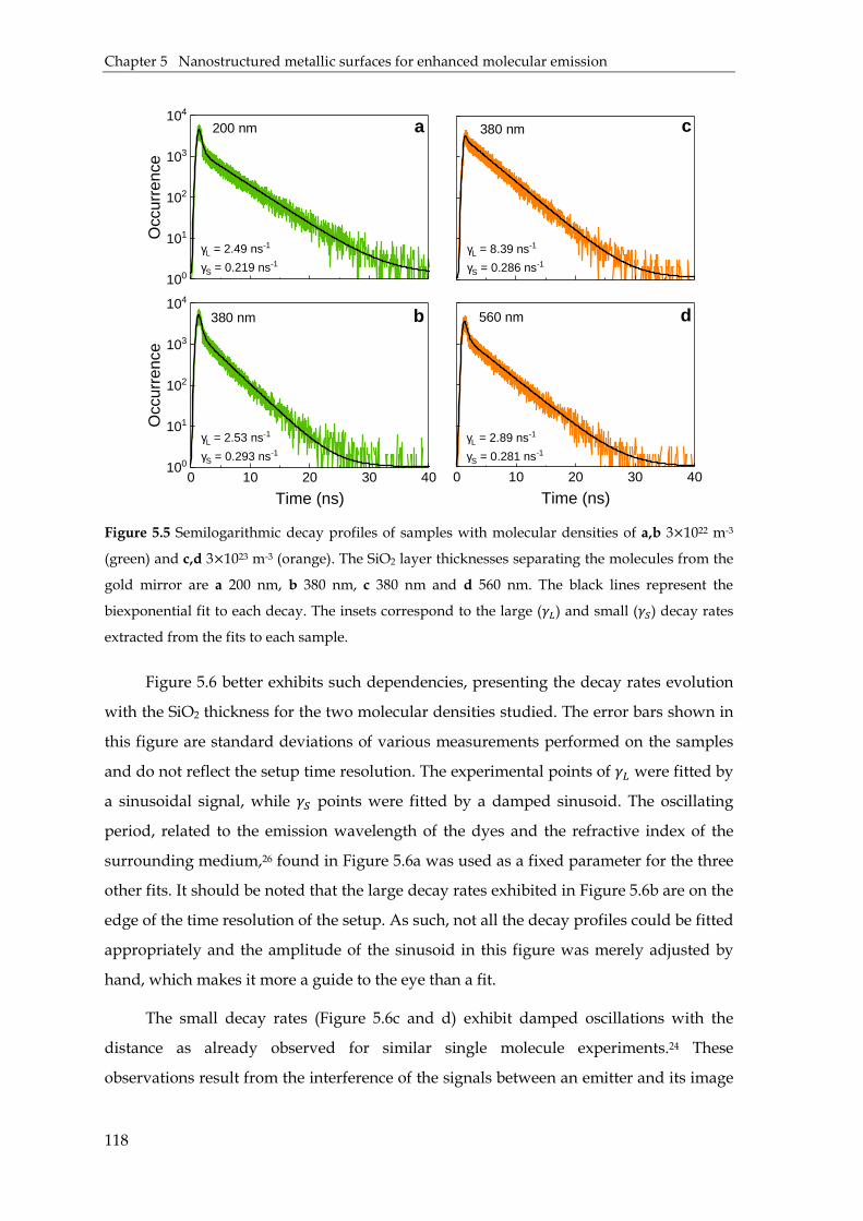
Chapter 5 Nanostructured metallic surfaces for enhanced molecular emission
118
Figure 5.5 Semilogarithmic decay profiles of samples with molecular densities of a,b 3×10²² m-3
(green) and c,d 3×10²³ m-3 (orange). The SiO2 layer thicknesses separating the molecules from the
gold mirror are a 200 nm, b 380 nm, c 380 nm and d 560 nm. The black lines represent the
biexponential fit to each decay. The insets correspond to the large () and small () decay rates
extracted from the fits to each sample.
Figure 5.6 better exhibits such dependencies, presenting the decay rates evolution
with the SiO2 thickness for the two molecular densities studied. The error bars shown in
this figure are standard deviations of various measurements performed on the samples
and do not reflect the setup time resolution. The experimental points of were fitted by
a sinusoidal signal, while points were fitted by a damped sinusoid. The oscillating
period, related to the emission wavelength of the dyes and the refractive index of the
surrounding medium,26 found in Figure 5.6a was used as a fixed parameter for the three
other fits. It should be noted that the large decay rates exhibited in Figure 5.6b are on the
edge of the time resolution of the setup. As such, not all the decay profiles could be fitted
appropriately and the amplitude of the sinusoid in this figure was merely adjusted by
hand, which makes it more a guide to the eye than a fit.
The small decay rates (Figure 5.6c and d) exhibit damped oscillations with the
distance as already observed for similar single molecule experiments.24 These
observations result from the interference of the signals between an emitter and its image
0 10 20 30 40100
101
102
103
104
Time (ns)
Occ
urre
nce
100
101
102
103
104
Occ
urre
nce
0 10 20 30 40
Time (ns)
560 nm
380 nm
380 nm db
ca200 nm
γL = 2.49 ns-1
γS = 0.219 ns-1
γL = 8.39 ns-1
γS = 0.286 ns-1
γL = 2.89 ns-1
γS = 0.281 ns-1
γL = 2.53 ns-1
γS = 0.293 ns-1

Chapter 5 Nanostructured metallic surfaces for enhanced molecular emission
119
from the mirror. As the distance increases, the interference is attenuated and the decay
rate recovers the reference value of 0.27 ns-1 measured on bare glass (Figure 5.4). This
spatial modulation is as well observed for the large decay rates but, remarkably, is not
damped over the observed distance. Furthermore, one notices immediately the increase
of this rate while going from lower to higher concentrations (Figure 5.6a and b,
respectively), a feature not observed for the . This rapid behavior for indicates the
existence of a collective relaxation phenomenon. Thus, the interference behavior is not
limited to individual molecules but is also seen in the collective regime with a notable
absence of damping.
Figure 5.6 Experimental (dots) and fitted (lines) decay rates as a function of SiO2 spacer thickness.
a,b Evolution of the large decay rate for molecular densities of 3 × 10²² m-3 and 3 × 10²³ m-3,
respectively. c,d Evolution of the short decay rate for the same densities.
Theoretical model
The collective response of the systems was theoretically modelled by Dr Sukharev,
from the Arizona State University. The electrodynamics of molecule-to-molecule
interactions were described by the Maxwell-Bloch equations considering the molecules
as two-level emitters.35 The excited state population exhibited an exponential decay
profile with time, from where the decay rates were obtained. It should be noted that in
2
4
6
8
10
0 200 400 600 8000.20
0.25
0.30
0.35
SiO2 thickness (nm)
2.4
2.5
2.6
2.7
γ L (n
s-1)
0 200 400 600 8000.20
0.25
0.30
0.35
γ S (n
s-1)
SiO2 thickness (nm)
dc
ba

Chapter 5 Nanostructured metallic surfaces for enhanced molecular emission
120
these calculations, the emitters are taken to oscillate in phase, leading to a fully coherent
response and, thus, representing the large decay rate of the experiments.
Figure 5.7a shows the dependence of this decay rate with the density of
molecules for three thicknesses of the fluorophore layer. The SiO2 spacer is kept at
300 nm. It is seen that the decay rate linearly scales with the molecular density, as
expected in the collective spontaneous emission regime.7 Figure 5.7b shows the decay
rate as a function of the SiO2 spacer for three thicknesses of the molecular layer, with a
density of molecules of 3 × 10²³ m-3. As can be observed, the spatial oscillations obtained
from the simulations are in excellent agreement with the experimental results for the
large decay rates shown in Figure 5.6a and b. The overestimation of the numerical values
is likely because, in the simulations, all the molecules are perfectly aligned parallel to the
interface and to each other. For an isotropic molecular system, averaging over all
orientations of the dipoles amounts to multiple by 1/3,36 which is remarkably close to
the experiments. In addition, the simulations consider an ideal collective response,
where the intrinsic emission disorder of the experiment is not included. In fact, the
presence of an incoherent component in the measurements may explain why a perfect
destructive interference is not observed. Nevertheless, we can conclude that the lifetime
modulation, long known for individual emitters, is experimentally observed and
theoretically corroborated for ensembles of molecules collectively interacting.
Figure 5.7 a Simulated large decay rate as a function of the molecular density for three different
thicknesses of the molecular layer. The thickness of the spacer layer was kept to 300 nm. b Spatial
dependence of the large decay rate on the thickness of the SiO2 spacer for the same three
thicknesses of the molecular layer. The molecular density is 3×10²³ m-3.
200 400 600 8000
10
20
30
40
50
γ (n
s-1)
SiO2 distance (nm)
0.5 1.0 1.5 2.0 2.5 3.0
10
20
30
40
50 5 nm 10 nm 15 nm
γ (n
s-1)
Molecular density (x1023 m-3)
a b

Chapter 5 Nanostructured metallic surfaces for enhanced molecular emission
121
5.4 One-dimensional plasmonic arrays as superradiance platforms
In the previous section, we have demonstrated the collective response of an
ensemble of molecules placed in front of a flat metallic surface. Here, we design a higher
dimensional metallic structure sustaining plasmon resonances as potential platforms for
the plasmonic superradiance effect.
We designed one-dimensional (1D) plasmonic arrays, this is, metallic gratings of
periodic lines supporting SPPs as depicted in Figure 5.8. NIL enabled the fabrication of
high quality and homogeneous patterns of horizontal lines while working over large-
area surfaces and short time periods. This base structure was then covered with a gold
thin layer and a well-defined thickness of aluminium oxide (Al2O3, alumina) working as
spacer. On top of the metal/dielectric structures, Atto 655 fluorophores and a thin layer
of PMMA were deposited as detailed in Section 5.3.1.
We will now focus on the intricacies of the fabrication of these structures and the
optical properties that derive from them. The proper control over the features will lead
to optimized structures for enhancing the fluorescence of the dyes.
Figure 5.8 Schematic fabrication process of one-dimensional plasmonic arrays serving as
superradiance platforms.
Shallow lines patterning
Taking into account the targeted design of Figure 5.8, a corrugated metallic surface
would be accomplished if the gold deposition is performed onto shallow periodic lines.
Otherwise, using deep patterns as base template, the deposition would create
discontinuous metallic layers, being the metal mainly deposited on the top and bottom
parts of the features. During this work, we developed a simple method for adapting
initial 350 nm deep patterns to shallow templates without passing through complex
SU8 patterned lines
Spin-coating of Atto 655 dyesSpin-coating of PMMA
Evaporation of Au Atomic layer deposition of Al2O3

Chapter 5 Nanostructured metallic surfaces for enhanced molecular emission
122
engraving or etching steps. Unlike a conventional hot embossing process, we imprinted
a SU8 layer below its glass transition temperature !" so that the photoresist did not
completely filled the mold, reducing the height of the obtained features (Figure 5.9).
Figure 5.9 Scheme of the limited infiltration of the SU8 photoresist through the mold when
imprinting below its !".
The detailed procedure for obtaining shallow lines was as follows. First, a SU8
layer of about 200 nm was spin-coated on a Si substrate. A pre-patterned hard-PDMS
mold of lines with 400 nm pitch, 200 nm width and 350 nm height was used as stamp
(Figure 5.10a). For the imprinting process, it was pressed onto the SU8/Si sample at
40 ºC and 5 bar of pressure for 30 minutes. SEM analysis determined that the printed
lines were 62 ± 5 nm high; this is, 5 times shorter than the ones of the initial pattern
(Figure 5.10b, c). Higher temperatures risked to produce taller features because of the
close proximity to the glass transition temperature of the SU8 photoresist (!" = 55 ºC). In
contrast, lower pressures such as 3 bar or shorter times such as 15 min, gave rise to even
shallower lines. These structures were discarded because of the likely loss of definition
of the features with the further deposits.
Figure 5.10 a SEM top view of the initial silicon master of 400 nm periodic lines. b Cross-sectional
view of SU8 lines imprinted by hot embossing. c Cross-sectional view of 60 nm deep periodic
lines imprinted below the SU8 !". Scale bars: 400 nm.
SubstrateSU8 layer
PDMS mould
c
ba

Chapter 5 Nanostructured metallic surfaces for enhanced molecular emission
123
Having checked the success of this controlled imprinting process, we made use of
the great advantage of NIL and replicated this shallow pattern on several stamps of
hard-PDMS as detailed in Chapter 2. The fact of working with numerous stamps
significantly accelerated the fabrication process and enabled the production of a large
number of samples for the subsequent studies. Finally, the PDMS molds were
conventionally printed onto 90 nm thick SU8 layers deposited on glass substrates. This
step led to our final one-dimensional templates of 400 nm pitch and approximately 60
nm deep periodic lines.
Corrugated metallic surface
The 1D plasmonic structure was accomplished by evaporating 50 nm of gold on
top of the patterns. This deposition method uses a resistive heat source to evaporate a
solid material in a vacuum environment. The material vapour traverses the chamber and
finally condenses in form of thin film on the cold substrate. We used a MBraun thermal
evaporator working at 10-6 mbar with a controlled deposition rate of 0.6 Å/s, monitored
by a quartz crystal microbalance. Again, we chose gold as metal because of its good
plasmonic excitation and chemical stability.
Figure 5.11 a SEM cross-sectional view of 400 nm shallow periodic lines covered with 50 nm thick
Au layer. b Photograph of the fabricated samples right after gold evaporation. c Transmittance
(T), reflectance (R) and extinction (Ext) spectra of Au coated-SU8 lines on glass substrates.
Figure 5.11a presents the accomplished plasmonic grating of periodic SU8 lines
covered by a highly continuous gold layer. Figure 5.11b shows the samples after the
metal deposition process, which enhanced the iridescence of the arrays. As can be
observed in Figure 5.11c, the structures follow the spectroscopic properties of a flat gold
500 600 700 800 9000.0
0.2
0.4
0.6
0.8
1.0
T R Ext
Inte
nsity
Wavelength (nm)
670 nm
c
b
1 cm
500 nm
a

Chapter 5 Nanostructured metallic surfaces for enhanced molecular emission
124
thin film with a noticeable extinction peak at 670 nm. Making use of the momentum
matching equation for exciting surface plasmons in linear gratings (eq. 1.15), we can
ascribe this peak to a SPR at the gold-SU8 interface.
Dielectric-coated metal gratings
We made use of the atomic layer deposition (ALD) technique to deposit the
dielectric spacer between the plasmonic grating and the dyes. The principle of ALD
relies on the sequential pulsing of precursor vapours with intermediate purging periods.
In each independent pulse, the vapour molecules react with the surface in a self-limiting
manner, ensuring that the reaction stops once all of the reactive sites on the substrate are
filled. Each reaction then forms about one atomic layer. This technique stands out for
providing highly thickness control and conformal deposits, this is, adapted to the shape
of the features.
We deposited Al2O3 layers of 5, 10, 15, 20 and 25 nm using a Savannah200,
Cambridge Nanotech equipment. Water and trimethylaluminum (TMA) were used as
precursor gases of Al2O3 with open valve times of 0.05 and 0.10 s respectively, followed
by 65 s pump time, which led to 1.1 Å/cycle. The chamber was kept at 150 ºC during the
deposition process, which did not affect the cured SU8 or gold features.
450 600 750 9000.0
0.2
0.4
0.6
0.8
1.0b
T, R
Wavelength (nm)
a
500 600 700 800 9000.0
0.2
0.4
0.6
0.8
1.0 0 nm 5 nm 10 nm 15 nm 20 nm 25 nm
Wavelength (nm)
Ext
Figure 5.12 a Transmittance, reflectance and b extinction spectra of 2D plasmonic lines covered
with different thickness of Al2O3.
Figure 5.12 presents the transmittance, reflectance and extinction (T, R, Ext) spectra
of plasmonic arrays of lines after the deposition of different thicknesses of alumina. For
reference, the spectra of the metallic array without dielectric on top are shown as well in

Chapter 5 Nanostructured metallic surfaces for enhanced molecular emission
125
black. Small redshifts of the resonant extinction peak are observed due to the increase of
the refractive index at the top of the gold layer. It is worth mentioning that although the
SPR is excited at the internal gold surface, the thin thickness of this layer enables the
energy transfer and propagation of the SPP at the Al2O3-Au frontier, too.37,38 The position
of this EM resonance matching the emission peak of the dyes makes it suitable to
enhance the emitters de-excitation.
Fluorescent decay evolution with the spacer thickness
Atto 655 fluorophores were finally spin-casted on top of the Al2O3 coated metallic
gratings as previously described. Similarly, a PMMA cover was deposited on top of the
ensembles of molecules.
Figure 5.13 a Normalized decay profiles of 10-8 M Atto 655 molecules deposited at different
spacer distances from the plasmonic 1D grating, measured in TM polarization. Comparison of the
decay profiles in TM and TE configurations for spacer thicknesses of b 5 nm and c 10 nm.
Figure 5.13 presents preliminary fluorescence decay profiles of structures with
10-8 M concentration of dyes in solution. Polarizing the excitation light perpendicularly
to the grating (TM mode), we observe that the relaxation gets faster as the emitters are
closer to the metal surface (Figure 5.13a). This manifests a decay rate enhancement
arising from the plasmonic structure. The decay profile corresponding to 20 nm of
alumina is not shown because of its similarity with the 25 nm spacer decay. This may
suggest that above 20 nm, the fluorophores do not experience any plasmonic interaction
due to the attenuation at these distances. Moreover, the deviations from a single bi-
10-4
10-3
10-2
10-1
100
TM TE
Nor
m. O
ccur
renc
e
0 5 10 15 20 25 30 3510-4
10-3
10-2
10-1
100
TM TE
Nor
m. O
ccur
renc
e
Time (ns)
0 5 10 15 20 25 30 3510-4
10-3
10-2
10-1
100
5 nm 10 nm 15 nm 25 nm
Nor
m. o
ccur
renc
e
Time (ns) c
b
a

Chapter 5 Nanostructured metallic surfaces for enhanced molecular emission
126
exponential decay, significantly at 5 nm, suggest the existence of several fluorescence
regimes: the single molecule, where the emitters relax independently; the collective de-
excitation, this is, the superradiance phenomenon; and some intermediate behaviors. As
described in previous studies, these rates would be accelerated by a plasmonic
resonance.16,21,39
Interestingly, for the lowest spacer thicknesses (5 and 10 nm), the parallel
polarization (TE) presents larger relaxation times than the TM (Figure 5.13b,c). Such
observation confirms the presence of a plasmon-enhanced fluorescence since in this type
of gratings the SPPs are typically excited in TM mode. Nonetheless, an accurate analysis
of the decay profiles together with a comparison to numerical models should be done in
the future to better understand these observations.
5.5 Two-dimensional plasmonic arrays as superradiance
platforms
The possibility of achieving plasmonic superradiance was also explored with the
design of two-dimensional plasmonic arrays (Figure 5.14). For this purpose, we made
use of colloidal lithography, which enabled a low-cost and fast fabrication process of
hexagonal templates. Similarly to the earlier structures, the patterns were covered with a
gold thin layer and different thicknesses of a dielectric spacer in order to study the
influence of this separation on the fluorescence decays of Atto 655 dyes. The molecules
and the PMMA layer were spin-casted as previously detailed.
Figure 5.14 Schematic fabrication process of two-dimensional plasmonic arrays serving as
superradiance platforms.
Monolayer of PS spheres
Spin-coating of Atto 655 dyesSpin-coating of PMMA
Evaporation of Au Chemical vapor deposition of SiO2

Chapter 5 Nanostructured metallic surfaces for enhanced molecular emission
127
Metal-coated colloidal monolayers
Colloidal monolayers of 480 nm large PS beads were prepared on cleaned glass
substrates following the self-assembly procedure described in Chapter 2. A gold layer of
50 nm thickness was deposited on top of the monolayers by thermal evaporation in a
similar manner as formerly detailed. Figure 5.15a and b show the resulting structure,
which is composed by metallic half-shells covering the top surface of the particles.
Figure 5.15 a Top-view and b cross-section SEM image of a gold-coated colloidal monolayer of PS
particles.
Visible spectra of the metal-coated colloidal monolayers were measured and well
reproduced by FDTD simulations (Figure 5.16a,b). The unit cell of the calculations was
composed of close-packed 480 nm large spheres with a gold half-shell of 50 nm height.
Gold triangular prisms, formed in between the particles during the deposition, were also
included with a side length of 135 nm and 40 nm thickness (Figure 5.16c).
The lower transmittance found for the measurements could be ascribed to the
packing defects of the monolayer. Specifically, the deposition of larger gold areas around
the particles could considerably reduce the overall transmittance while increasing the
reflectance. In spite of this, the experimental optical features are in very good agreement
with the numerical calculations. The small extinction peak at 580 nm is known to be a
hybrid plasmon-photonic mode coming from the waveguided mode in the dielectric
monolayer and the SPP at the metal-PS interface.40 Given the overlapping of the main
extinction peak (# = 730 nm) with the Atto 655 fluorescence, we focused on this
resonance. The Ez field distribution at this wavelength shows periodic lobes along the
metallic half-shells that indicate the excitation of SPPs propagating through the array
(Figure 5.16d).41 Besides, the tapered profile of the shells at the edges of the cover leads
to a strong EM enhancement in between the particles. Thus, the plasmonic nature of this
500 nm
ba
1 µm

Chapter 5 Nanostructured metallic surfaces for enhanced molecular emission
128
resonance together with its wavelength, could reinforce the cooperative emission of the
dyes.
Figure 5.16 a Measured and b simulated transmission, reflection and extinction spectra of gold-
coated colloidal monolayers. c Unit cell scheme of the simulated structure. d Distribution of the z-
component of the electric field at the maximum extinction of 730 nm.
Dielectric-metal-coated colloidal monolayers
Dielectric layers of SiO2 ranging from 5 to 25 nm thickness were deposited by CVD
under the same conditions than for the flat metallic structures. Despite the generation of
a plasma oxygen during the process that could etch the PS spheres, the integrity of the
monolayer was preserved thanks to the instrumental distance from the plasma and the
shield provided by the gold layer. Figure 5.17a, b show two examples of the successful
deposition of SiO2 on top of the metal-coated monolayers. Although for 25 nm of silica
(Figure 5.17b) one can distinguish a reduction of the particles size at the bottom, it is also
manifested that the quality of the monolayer and the gold shells are maintained.
Therefore, combining colloidal self-assembly with thermal evaporation and chemical
0
100
200
300
400
500
-200 -100 0 100 200
x (nm)
z (n
m)
-1
0
1
Ez
400 600 800 10000.0
0.2
0.4
0.6
0.8 T R Ext
Inte
nsity
Wavelength (nm)
600 800 1000
Wavelength (nm)
y
E
x
k
z
d
b
c
a

Chapter 5 Nanostructured metallic surfaces for enhanced molecular emission
129
vapour deposition we fabricated large-area two-dimensional dielectric-metal arrays with
a high structural control.
Figure 5.17 SEM pictures of SiO2/Au coated colloidal monolayers. The thickness of the dielectric
spacer is a 15 nm and b 25 nm. c Photograph of one of the centimeter-sized samples.
The spectra after the SiO2 deposition show a drastic reduction of the overall
transmission and an increase of the reflectance around 550 nm (Figure 5.18). This could
come from the multiple reflections occurring at the SiO2 interfaces because of the
refractive index mismatch. As a result, the main extinction peak is blue-shifted in
average to 720 nm, closer to the maximum emission wavelength of the dyes. It is
interesting to note that the initial extinction peak of 580 nm becomes a dip with the
dielectric coating, decreasing its intensity with the thickness. Such behavior could
indicate the attenuation of the plasmon-photonic hybrid mode. However, further
simulations should be performed to fully understand this effect.
Figure 5.18 a Transmittance, b reflectance and c extinction spectra of SiO2/Au coated colloidal
monolayers, with different thicknesses of the silica layer. For comparison, the spectra of the Au
coated monolayer have been included.
Fluorescence decay evolution with the distance
The dielectric-metal hexagonal arrays were finally coated with Atto 655 dyes and a
thin PMMA layer as detailed for the former structures. Figure 5.19 shows the first results
cba
1 cm
400 600 800 10000.0
0.1
0.2
0.3
0.4
0.5 0 nm 5 nm 10 nm 15 nm 20 nm 25 nm
Tra
nsm
ittan
ce
Wavelength (nm)
400 600 800 10000.4
0.5
0.6
0.7
0.8
0.9
Ext
inct
ion
Wavelength (nm)
400 600 800 10000.0
0.1
0.2
0.3
0.4
0.5
Ref
lect
ance
Wavelength (nm)
cba

Chapter 5 Nanostructured metallic surfaces for enhanced molecular emission
130
of the measured fluorescence decays, from an initial dyes concentration of 10-7 M. A clear
shortening of the lifetime relaxation is observed as decreasing the distance from the
metallic surface, which reflects a plasmonic enhancement of the fluorescence rate.
Moreover, the decays present non-exponential profiles that indicate the presence of both
coherent and decoherent optical responses mediated by the spatial and spectral overlays
with the plasmon resonance. Compared to the modulation observed for the plasmonic
lines (Figure 5.13), the decays are much more monoexponential and shorter for the
design based on colloidal monolayers. This suggests a better coupling between the
fluorophores and the plasmons sustained by the structures, with more intense EM fields
at the dyes location.
Further analysis of these results, comparison to numerical models and studies of
the effect of the emitters concentration will be done in the near future to understand the
effectiveness of the plasmon-mediated superradiance. In addition, an eventual future
project could study the influence of the extinction deep observed at short wavelengths
on the behavior of dyes emitting in this region.
0 5 10 15 20 25 30 35 4010-4
10-3
10-2
10-1
100
5 nm 10 nm 15 nm 25 nm
Nor
m. O
ccur
renc
e
Time (ns)
Figure 5.19 Semi-logarithmic decay profiles of 10-7 M Atto 655 molecules deposited at different
distances (silica thicknesses) from the plasmonic 2D colloidal crystal.
5.6 Conclusions
In this chapter, we have fabricated and characterized different metallic surfaces as
platforms for the observation of collective spontaneous emission of Atto 655 molecules.
Starting with a flat mirror, we have both experimentally and theoretically demonstrated
that the de-excitation of ensembles of molecules strongly depends on the distance from
the metal and the emitters concentration, as a result of interference effects. Two distinct

Chapter 5 Nanostructured metallic surfaces for enhanced molecular emission
131
decay rates have been experimentally and theoretically identified. First, a small decay
rate, exhibiting damped oscillations with the distance from the mirror was ascribed to
single molecule fluorescence. In contrast, the large decay rate presented similar
oscillations but without damping and was strongly dependent of the fluorophores
concentration, which confirmed it collective nature.
With the aim of extending these studies, we have designed two types of
nanostructured metallic substrates for studying the plasmonic superradiance
phenomenon. First, we have fabricated large-area plasmonic gratings of lines by
nanoimprint lithography. We have adapted the conventional protocol to the fabrication
of shallow periodic arrays of lines. The proper choice of the periodicity together with the
deposition of a thin gold layer have enabled the excitation of SPPs at the emission
wavelength of the dyes. After depositing nanometric dielectric spacers, we have
observed that the fluorescence decay rates of the dyes increase in the proximity of the
metal, evidencing the plasmon-enhanced effect. Furthermore, the noticeable non-
exponential profile observed at short distances suggests the achievement of a plasmon-
mediated collective response.
Finally, large-area two-dimensional plasmonic arrays have been successfully
fabricated based on colloidal self-assembly. The optical responses of the metal-coated
monolayers have been very well reproduced by numerical simulations, which also
showed the existence of a strong plasmonic resonance around the gold half-shells. The
electromagnetic enhancement has been used for promoting the fluorescence decay rate
of dyes separated by dielectric spacers from the metal. The decay profiles showed a clear
shortening of the emission lifetime when approaching the metallic surface, confirming
the influence of the plasmonic resonance on the fluorescence. Like in the former case, the
non-exponential profiles might be ascribed, with further analysis, to the phenomenon of
plasmonic superradiance.
In summary, we have developed very efficient metal-based nanostructured
surfaces for investigating the enhancement of collective molecular emission. This work is
on its infancy and detailed analysis and comparison with appropriate numerical models
have to be performed in the future to grasp of the involved phenomena.

Chapter 5 Nanostructured metallic surfaces for enhanced molecular emission
132
5.7 References
1. E. M. Purcell. Spontaneous emission probabilities at radio frequencies. Phys. Rev.
1946, 69, 681.
2. O. S. Wolfbeis. An overview of nanoparticles commonly used in fluorescent
bioimaging. Chem. Soc. Rev. 2015, 44, 4743.
3. E. Desurvire and J. R. Simpson. Amplification of spontaneous emission in erbium-
doped single-mode fibers. J. Light. Technol. 1989, 7, 835–845.
4. F. Sgrignuoli et al. Purcell effect and luminescent downshifting in silicon
nanocrystals coated back-contact solar cells. Sol. Energy Mater. Sol. Cells 2015, 132,
267–274.
5. O. Gazzano and G. S. Solomon. Toward optical quantum information processing
with quantum dots coupled to microstructures. J. Opt. Soc. Am. B 2016, 33, C160–
C175.
6. R. H. Dicke. Coherence in spontaneous radiation processes. Phys. Rev. 1954, 93,
99–110.
7. M. Gross and S. Haroche. Superradiance: An essay on the theory of collective
spontaneous emission. Phys. Rep. 1982, 93, 301–396.
8. P. Lalanne, W. Yan, K. Vynck, C. Sauvan and J. P. Hugonin. Light interaction with
photonic and plasmonic resonances. Laser Photonics Rev. 2018, 12, 1700113.
9. V. N. Pustovit and T. V. Shahbazyan. Cooperative emission of light by an
ensemble of dipoles near a metal nanoparticle: The plasmonic Dicke effect. Phys.
Rev. Lett. 2009, 102, 077401.
10. D. Martín-Cano, L. Martín-Moreno, F. J. García-Vidal and E. Moreno. Resonance
energy transfer and superradiance mediated by plasmonic nanowaveguides.
Nanoletters 2010, 10, 3129–3134.
11. T. Iida. Control of plasmonic superradiance in metallic nanoparticle assembly by
light-induced force and fluctuations. J. Phys. Chem. Lett. 2012, 3, 332–326.
12. R. Fleury and A. Alu. Enhanced superradiance in epsilon-near-zero plasmonic
channels. Phys. Rev. B 2013, 87, 201101.

Chapter 5 Nanostructured metallic surfaces for enhanced molecular emission
133
13. Y. Li and C. Argyropoulos. Controlling collective spontaneous emission with
plasmonic waveguides. Opt. Express 2016, 24, 26696.
14. I. Protsenko, S. Zhang, A. Uskov, X. Chen and H. Xu. Plasmonic superradiance of
two emitters near metal nanorod. Proc. SPIE 10118, Adv. Photonics Quantum
Comput. Mem. Commun. X 2017, 1011811.
15. P. Anger, P. Bharadwaj and L. Novotny. Enhancement and quenching of single-
molecule fluorescence. Phys. Rev. Lett. 2006, 96, 113002.
16. P. Fauche. Plasmonic superradiance in metallo-dielectric nanohybrids, University
of Bordeaux, 2016.
17. T. B. Hoang et al. Ultrafast spontaneous emission source using plasmonic
nanoantennas. Nat. Commun. 2015, 6, 7788.
18. M. V. Shestakov, E. Fron, L. F. Chibotaru and V. V. Moshchalkov. Plasmonic
Dicke effect in Ag-nanoclusters-doped oxyfluoride glasses. J. Phys. Chem. C 2015,
119, 20051–20056.
19. E. Wientjes, J. Renger, A. G. Curto, R. Cogdell and N. F. van Hulst. Nanoantenna
enhanced emission of light-harvesting complex 2: The role of resonance,
polarization, and radiative and non-radiative rates. Phys. Chem. Chem. Phys. 2014,
16, 24739.
20. T. Leisner, O. Kostiucenko, J. R. Brewer, H. Rubahn and J. Fiutowski.
Nanostructure induced changes in lifetime and enhanced second-harmonic
response of organic-plasmonic hybrids. Appl. Phys. Lett. 2015, 107, 251102.
21. N. Michieli, B. Kalinic, C. Scian, T. Cesca and G. Mattei. Emission rate
modification and quantum efficiency enhancement of Er3+ emitters by near-field
coupling with nanohole arrays. ACS Photonics 2018, 5, 2189–2199.
22. S. Van de Linde, R. Kasper, M. Heilemann and M. Sauer. Photoswitching
microscopy with standard fluorophores. Appl. Phys. B 2008, 93, 725–731.
23. H. Kim, M. H. Cho, H. S. Choi, B. Il Lee and Y. Choi. Zwitterionic near-infrared
fluorophore-conjugated epidermal growth factor for fast, real-time, and target-
cell-specific cancer imaging. Theranostics 2019, 9, 1085–1095.
Chapter 5 Nanostructured metallic surfaces for enhanced molecular emission
134
24. K. H. Drexhage, M. Fleck, H. Kuhn, F. P. Schafer and W. Sperling. Beeinflussing
der fluoreszenz eines europium-chelates durch einen spiegel. Ber. Bunsenges. Phys.
Chem 1966, 70, 1179.
25. J.-Y. Zhang, X.-Y. Wang and M. Xiao. Modification of spontaneous emission from
CdSe/CdS quantum dots in the presence of a semiconductor interface. Opt. Lett.
2002, 27, 1253–1255.
26. A. Kwadrin and A. F. Koenderink. Gray-tone lithography implementation of
Drexhage’s method for calibrating radiative and nonradiative decay constants of
fluorophores. J. Phys. Chem. C 2012, 116, 16666–16673.
27. N. Karedla et al. Single-molecule metal-induced energy transfer (smMIET):
Resolving nanometer distances at the single-molecule level. ChemPhysChem 2014,
15, 705–711.
28. R. Brechbühler et al. Two-dimensional Drexhage experiment for electric- and
magnetic-dipole sources on plasmonic interfaces. Phys. Rev. Lett. 2018, 121, 113601.
29. R. Vallée et al. On the role of electromagnetic boundary conditions in single
molecule fluorescence lifetime studies of dyes embedded in thin films. Chem. Phys.
Lett. 2001, 348, 161–167.
30. L. Martinu, O. Zabeida and J. E. Klemberg-Sapieha. Plasma-enhanced chemical
vapor deposition of functional coatings. Handb. Depos. Technol. Film. Coatings 2010,
392–465.
31. Y. Wang, X. Wang, S. K. Ghosh and H. P. Lu. Probing single-molecule interfacial
electron transfer dynamics of porphyrin on TiO2 nanoparticles. J. Am. Chem. Soc.
2009, 131, 1479–1487.
32. O. Schulz et al. Tip induced fluorescence quenching for nanometer optical and
topographical resolution. Opt. Nanoscopy 2013, 2, 1.
33. B. Pedras. Fluorescence in Industry; Springer, Switzerland, 2019.
34. V. Buschmann, K. D. Weston and M. Sauer. Spectroscopic study and evaluation of
red-absorbing fluorescent dyes. Bioconjug. Chem. 2003, 14, 195–204.
35. M. Gómez-Castaño et al. Energy transfer and interference by collective
electromagnetic coupling. Nanoletters 2019, 19, 5790–5795.

Chapter 5 Nanostructured metallic surfaces for enhanced molecular emission
135
36. M. Sukharev and A. Nitzan. Optics of plasmon-exciton nanomaterials. J. Phys.
Condens. Matter 2017, 29, 443003.
37. P. Berini. Long-range surface plasmon polaritons. Adv. Opt. Photonics 2009, 1, 484–
588.
38. B. Xiao, S. K. Pradhan, K. C. Santiago, G. N. Rutherford and A. K. Pradhan.
Topographically engineered large scale nanostructures for plasmonic biosensing.
Sci. Rep. 2016, 6, 24385.
39. H. Yin et al. Plasmon enhanced quantum dots fluorescence and energy conversion
in water splitting using shell-isolated nanoparticles. Nano Energy 2017, 42, 232–
240.
40. C. Farcau, M. Giloan, E. Vinteler and S. Astilean. Understanding plasmon
resonances of metal-coated colloidal crystal monolayers. Appl. Phys. B 2012, 106,
849–856.
41. C. Farcau. Metal-coated microsphere monolayers as surface plasmon resonance
sensors operating in both transmission and reflection modes. Sci. Rep. 2019, 9,
3683.

137
Chapter 6
General conclusions and perspectives
6.1 Conclusions
The works developed during this thesis have been motivated by the design and
large-area fabrication and characterization of plasmonic nanostructures displaying
unusual electromagnetic phenomena. Principally, we have tackled the cost-effective
manufacture and analysis of negative-index metamaterials working at optical
wavelengths; namely, fishnet metamaterials. Secondly, we have addressed the
fabrication of nanostructured metallic platforms for the enhancement of collective
spontaneous emission. The most significant contributions to the fields of metamaterials
and enhanced spontaneous emission are given below.
6.1.1 Negative-index fishnet metamaterials
Along this thesis, we have proposed alternative designs of fishnet metamaterials
where the common metal-insulator-metal stack was composed of gold layers and air
cavities. This approach has been demonstrated to be highly compatible with low-cost
fabrication techniques such as colloidal lithography, soft nanoimprinting and
electrodeposition. Specifically, centimeter-sized arrays of colloidal monolayers and
pillars have served as templates for the electrodeposition of alternating metallic layers.
Fishnet metamaterials based on colloidal lithography
Combining colloidal lithography and electrodeposition, we have first fabricated
metallic stacks of gold and sacrificial nickel layers embedding non-close-packed
monolayers of polystyrene particles. By dissolving the nickel parts, we have
demonstrated the feasibility of obtaining transferable double fishnet metamaterials made
of gold and air, where the particles work as both dielectric perforations and supports of
the layers.
These metamaterials exhibited optical resonances in the near-infrared that were
easily tailored with the diameter of the particles or the air gap width between the two

Chapter 6 General conclusions and perspectives
138
gold layers. The electromagnetic distribution at these wavelengths showed the excitation
of a magnetic resonance within the gap, coming from the coupling of surface plasmons
propagating at the gold-air interfaces. This artificial magnetism together with the electric
response of the metal layers gave rise to tunable effective refractive indices as function of
the geometrical parameters. Specifically, we were able to tune the refractive index from
positive to near-zero and negative values, achieving a record value of -1 at 940 nm with
an entirely bottom-up fabrication process.
Further analysis such as an effective medium modelling or a metamaterial prism
verified the reliability of the metamaterial design and the calculations done for retrieving
the effective parameters.
Fishnet metamaterials based on soft nanoimprinting
These results were extended to metamaterials made from nanoimprinted patterns
and electrodeposition. Based on the previous method, we developed a straightforward
fabrication process of multilayered fishnet metamaterials made of dielectric pillars
supporting several stacks of gold-air-gold layers. Moreover, we demonstrated the
adaptability of the process to transparent conductive substrates, ready for a
metamaterial device implementation.
The multilayered fishnet structures displayed optical resonances ranging from
visible to near-infrared wavelengths. The position of the response was governed by
structural parameters such as the periodicity, diameter of the pillars or number of
metallic layers. Strong negative refractive indices were obtained at these resonances,
with minimum values of -1.2 at 700 nm and -2.8 at 910 nm.
We found that increasing the number of layers brought about significant
improvements for optical metamaterials such as higher figures of merit or shorter
operation wavelengths. This blue shift was noticeably weaker for the smallest pitches
because of its close convergence to the bulk metamaterial regime. The negligible angular
dispersion of this structure corroborated such statement.
Finally, we demonstrated the possibility of tuning the optical response of our
metamaterials when infiltrating different liquids in the air cavities. Increasing the
refractive index of the filling medium, the resonant wavelength was found to move to
larger wavelengths, with attractive capabilities for optical sensing.

Chapter 6 General conclusions and perspectives
139
As proof of the impact of our metamaterials to the current research progress,
Figure 6.1 compares the major results of this thesis with the state of the art at the
beginning of the project. Making use of up-scalable techniques, this work has established
new large-area fabrication procedures of fishnet metamaterials with properties
comparable or even superior than the ones obtained by common short-range methods.
1.000E-05
1.000E-04
0.001000
1.000
100.0
500 1000 1500 20000
-1
-2
-3
1000 µm2
10 µm2
1 mm2
Lodewijks (2010)
Xiao (2010)
Garcia-Meca (2011)
Liang (2017)
Xiao (2009)
Zhou (2013)
Rottler (2012)
Dolling (2006)
Gao (2014)
Gao (2014)
Re
(nef
f)
Wavelength (nm)
Zhang (2005)
Sharp (2014)
Valentine (2008)
Choi (2013)
1 cm2
Area
This thesis
Chettiar (2007)
Figure 6.1 State of the art at the end of this thesis. Main fishnet metamaterials fabricated to date as
a function of the strongest effective refractive index , the operation wavelength and the area.
6.1.2 Enhanced spontaneous emission
We have developed various metallic nanostructured platforms for the observation
of collective molecular emission. In a flat metal-dielectric design, the emission rate of
molecular assemblies depended on the distance to the metallic surface, with spatial
oscillations arising from constructive/destructive interferences. The emission decay
presented two regimes: a small decay rate coming from single molecule fluorescence and
a large decay rate arising from the collective relaxation.
This study inspired the design of one- and two-dimensional plasmonic arrays for
promoting the collective emission phenomenon of superradiance. Nanoimprinting and
colloidal lithography enabled the fabrication of large-area metal-dielectric platforms
displaying plasmonic resonances nearby the emission wavelength of the fluorophores.
Preliminary characterization showed the increase of the decay rates when reducing the

Chapter 6 General conclusions and perspectives
140
distance of the molecules to the metallic surfaces, evidencing the influence of the
plasmonic resonances on the fluorescence rate. The bi-exponential decay profiles found
at short distances suggest the excitation of a plasmon-mediated collective response.
Further analysis will be performed in the near future to understand the nature of such
enhanced behavior.
6.2 Perspectives
The methods and structures engineered along this thesis pave the way for the
device implementation of negative-index metamaterials, experimental study of collective
emission phenomena or the development of further intriguing plasmonic designs by
cost-effective routes. In this section, some interesting continuations of the thesis are
presented.
6.2.1 Fishnet design
The losses of negative-index metamaterials are considerably reduced in
multilayered designs, as proved by the fishnet structures developed by nanoimprint
lithography. This improvement could be applied to the fishnet designs made by colloidal
lithography by depositing several nickel-gold layers around the particles that would
finally lead to multilayered gold-air-gold cavities.
Replacing the gold layers by less lossy metals such as silver would also reduce the
absorption within the metamaterials. A detailed study of the optimum conditions for
electrodepositing silver in homogeneous films would be the basis for the new fishnets.
Special attention should be paid to the roughness of the deposits since the performance
of the final metamaterial strongly depends on the uniform separation between the
metallic layers. Moreover, the dissolution step based on nitric acid might be highly
controlled in order not to dissolve the silver parts.
Considering the negative-index bands achieved with each lattice parameter by
nanoimprinting, we can think about a centimeter-size gradient metamaterial. This would
consist on imprinting side by side various patterns, from the smallest to the largest
periodicity, and following the same electrodeposition protocol. The whole structure
might work as flat lens for different wavelengths.
Inspired by the accessibility to the air gaps, the response of fishnet metamaterials
could be interestingly controlled by filling the cavities with liquid crystals. We could

Chapter 6 General conclusions and perspectives
141
tune the negative-index bands by heating the system or applying a bias through the ITO
and top gold layer. The alignment changes would vary the refractive index of the liquid
crystals, enabling the modulation of the metamaterial response.
6.2.2 Superradiance platforms
As previously discussed, further analysis will be done in the near future regarding
the ensembles of molecules placed near plasmonic arrays. The enhancement of singular
and collective emission will be thoroughly studied when varying the distance to the
metallic surfaces as well as the concentration of molecules.
These works might be extended to other types of emitters such as quantum dots. In
the same way, we could study the dependence of their emission rate with the
distribution on the plasmonic surfaces. These investigations will contribute to the
experimental study of plasmonic superradiance in multiple systems.
6.2.3 Further photonic and plasmonic systems
The methods established along this thesis also broaden the possibilities to explore
in the fields of nanofabrication, photonics and plasmonics.
For instance, we could combine colloidal lithography and nanoimprinting by
replicating a monolayer of polystyrene particles. This would give rise to PDMS large-
area patterns of bowls or domes ranging from microns to a hundreds of nanometers. The
possibility of repeatedly imprinting these low-cost patterns implies a significant progress
for surface nanostructuration, avoiding the use of multiple samples or engraving steps.
Working with hydrophobic substrates such as the nickel strips discussed in
Chapter 4, we could study the achievement of metallic nanorings in pillar-based
templates. These systems have demonstrated potential properties for catalysis, sensing
or enhanced spectroscopies.1,2
Finally, one could take advantage of the flexibility of the PDMS stamps to obtain
asymmetric patterns via elongation of the mold.3 Preliminary results based on stretched
patterns of pillars and electrodeposition have shown the achievement of arrays of
metallic wavy lines (Figure 6.2). These unusual shapes are due to the distinct residual
layers formed in x and y directions when stretching the patterns, preventing the metallic
deposition in one of the axis. Optical characterization will be done in future works in
order to unravel the electromagnetic properties that these structures can provide.

Chapter 6 General conclusions and perspectives
142
Figure 6.2 SEM image of gold wavy lines. The sample was fabricated by imprinting a 60%
stretched PDMS mold onto SU8, removing a few nanometers of residual layer by RIE and
electrodepositing gold through the template.
6.3 References
1. A. Genç et al. Hollow metal nanostructures for enhanced plasmonics: Synthesis,
local plasmonic properties and applications. Nanophotonics 2017, 6, 193–213.
2. X. Liu, W. Liu and B. Yang. Highly ordered 3D-silver nanoring arrays (3D-
AgNRAs) for refractometric sensing. J. Mater. Chem. C 2019, 7, 7681–7691.
3. L. Liu et al. A programmable nanoreplica molding for the fabrication of
nanophotonic devices. Sci. Rep. 2016, 6, 22445.

143
Appendix
Retrieval of effective parameters
The effective properties of the samples were retrieved from FDTD simulations and
making use of the homogenization method, this is, describing the metamaterials as
effective media. One of the most common methods for obtaining the macroscopic
properties relies on the complex transmission and reflection electric fields, known as
scattering parameters or simply S-parameters.1,2
Given the asymmetry of our systems caused by the substrate under the
metamaterial, the S-parameters differ depending on the side of illumination. As a result,
two simulations have to be done for retrieving the effective parameters (Figure A.1): one
where light impinges from the top of the structure and one where light comes from the
bottom, which corresponds to the substrate in our case.
Figure A.1 Scheme of the two simulations performed for the retrieval in a double-fishnet
metamaterial made by colloidal lithography.
The associated four S-parameters can be obtained from the reflected, transmitted
and incident electric fields (, , ) as:
/ (A.1)
/ (A.2)
/ (A.3)
/ (A.4)

Appendix Retrieval of effective parameters
144
Figure A.2b and c show the calculated amplitudes and phases of the S-parameters
for the double-fishnet metamaterial made by colloidal lithography displaying -1
refractive index (Section 3.5). This sample will serve as example for illustrating the
retrieval procedure used along the thesis with fishnet metamaterials. Whereas the
transmission curves present a similar behavior because of the reciprocity of transmitted
light, the reflection amplitudes and phases are different and manifest the substrate-
induced anisotropy.
Figure A.2 a Amplitudes and b phases of the simulated S-parameters for the double-fishnet
metamaterial with -1 refractive index made by colloidal lithography.
The effective properties were calculated according to the procedure reported by Li
et al.3 If the asymmetry of the system is omitted, the effective refractive index can be
obtained from:
cos 1 − +
2 (A.5)
where is the wavenumber of light in free space and is the thickness of the
metamaterial without involving the substrate. However, since the reflection coefficients
and are different, this equation must be corrected to:
cos 1 − +
2 (A.6)
where the averaged term has been included. Isolating + !′′ and expressing
the arccosine function in its logarithmic form we get4
1 #Im &ln ) ± !+1 − ,- + 2./0 (A.7)
−1
Re &ln ) ± !+1 − ,- (A.8)
700 800 900 1000 1100
-160
-140
-100
-50
0
50
100
Pha
se (
deg)
Wavelength (nm)
700 800 900 1000 11000.0
0.2
0.4
0.6
0.8
1.0
S11 (rtop) S21 (ttop)
S22 (rbottom) S12 (tbottom)
Am
plitu
de
Wavelength (nm)
ba

Appendix Retrieval of effective parameters
145
where / is an integer denoting the branch index of ′. From these equations, first, the
signs of the square roots were chosen considering that in a passive medium the
imaginary part must obey ′′ > 0. Second, the branch / was chosen so that it verified the
Kramers-Kronig relations, where ′ is related to ′′, ensuring the validity of the retrieved
effective index.5
Figure A.3 shows the real part of for the top and bottom incidences (equation
(A.5)), as well as the corrected value based on equation (A.6). As observed, the effective
index differs in minimum value and band width from the individual values extracted
from top and bottom illumination. Hence, one should not neglect this correction for
retrieving a valid effective refractive index.
800 850 900 950 1000 1050
-1.0
-0.5
0.0
0.5
1.0 Top Bottom Effective
Re
(n)
Wavelength (nm)
Figure A.3 Real part of the effective refractive index when light impinges from top, from bottom
and after the correction made considering both results.
For comparison, Figure A.4 presents the effective refractive index for the same
structure with and without substrate, showing that a freestanding membrane would
exhibit a larger negative refractive index over a blue-shifted band and a higher FOM.
Previous works have shown that these differences arise from a magnetoelectric coupling
at the resonant wavelength induced by the substrate, namely bianisotropy.6 This implies
that the wave propagation in the metamaterial is described by the permittivity 3, the
permeability 4 and an additional bianisotropy parameter 5, whose value manifests the
magnetoelectric coupling strength. These properties can be derived from the refractive
index and S-parameters as:

Appendix Retrieval of effective parameters
146
5 6 −2sin8 6 −
8 (A.9)
4 6 !
sin8 62 + + 2
− cos8 (A.10)
3 + 5
4 (A.11)
In addition, the existence of a magnetoelectric coupling affects the impedance 9 in
the sense that two values are obtained, depending on the direction of the incoming light.
9± 4 ± !5 (A.12)
Figure A.4 a Real part of the effective refractive index and b figure of merit of the double-fishnet
metamaterial with and without substrate underneath.
References
1. D. R. Smith, D. C. Vier, T. Koschny and C. M. Soukoulis. Electromagnetic
parameter retrieval from inhomogeneous metamaterials. Phys. Rev. E 2005, 71,
036617.
2. E. J. Rothwell, J. L. Frasch, S. M. Ellison, P. Chahal and R. O. Ouedraogo. Analysis
of the Nicolson-Ross-Weir method for characterizing the electromagnetic
properties of engineered materials. Prog. Electromagn. Res. 2016, 157, 31–47.
3. Z. Li, K. Aydin and E. Ozbay. Determination of the effective constitutive
parameters of bianisotropic metamaterials from reflection and transmission
coefficients. Phys. Rev. E 2009, 79, 026610.
850 900 950 10000.0
0.2
0.4
0.6F
OM
Wavelength (nm)
850 900 950 1000 1050
-1.5
-1.0
-0.5
0.0
0.5
Substrate Free-standing
Re
(n)
Wavelength (nm)
ba

Appendix Retrieval of effective parameters
147
4. X. Chen, T. M. Grzegorczyk, B. I. Wu, J. Pacheco and J. A. Kong. Robust method to
retrieve the constitutive effective parameters of metamaterials. Phys. Rev. E 2004,
70, 016608.
5. Z. Szabó, G. Park, R. Hedge and E.-P. Li. A unique extraction of metamaterial
parameters based on Kramers–Kronig relationship. IEE Trans. Microw. Theory
Tech. 2010, 58, 2646–2653.
6. S. Yun et al. Experimental verification of substrate-induced bianisotropy in optical
metamaterials. Appl. Phys. Lett. 2013, 103, 233109.


149
Scientific contributions
Publications derived from this thesis
1. M. Gómez-Castaño, H. Zheng, J.L. García-Pomar, R. Vallée, A. Mihi and S. Ravaine.
Tunable index metamaterials made by bottom-up approaches. Nanoscale Adv. 2019,
1, 1070-1076.
2. M. Gómez-Castaño, A. Redondo-Cubero, L. Buisson, J.L. Pau, A. Mihi, S. Ravaine, R.
Vallée, A. Nitzan and M. Sukharev. Nano Lett. 2019, 19, 5790-5795.
3. M. Gómez-Castaño, J.L. García-Pomar, L.A. Pérez, S. Shanmugathasan, S. Ravaine
and A. Mihi. Electrodeposited negative index metamaterials with visible and near
infrared response. Adv. Opt. Mater. 2020, accepted.
Conference presentations
1. M. Gómez-Castaño, C. Matricardi, R. Vallée, A. Mihi and S. Ravaine. Gold
nanopillar arrays as SERS-active platforms, Surface Enhanced Raman Scattering –
SERS: Faraday Discussions, Glasgow (UK), August 2017, Poster.
2. M. Gómez-Castaño, R. Vallée, A. Mihi and S. Ravaine. Bottom-up fabrication of
double fishnet metamaterials working at visible and near infrared frequencies, 5th
LAPHIA Symposium, Bordeaux (France), December 2017, Poster.
3. M. Gómez-Castaño, R. Vallée, A. Mihi and S. Ravaine. Bottom-up fabrication of
double fishnet metamaterials, 11th International Conference on Nanophotonics, Wroclaw
(Poland), July 2018, Talk.
4. M. Gómez-Castaño. Metamaterials for negative refraction: Making a perfect lens, 7th
Interdisciplinary Meeting of Predoctoral Researchers (JIPI), Barcelona (Spain), February
2019, Talk.
5. M. Gómez-Castaño, J.L. García-Pomar, R. Vallée, A. Mihi and S. Ravaine. Tunable
index metamaterials made by bottom-up approaches, Colloidal Science and
Metamaterials 2019, Paris (France), February 2019, Talk.

Scientific contributions
150
6. M. Gómez-Castaño, H. Zheng. J.L. García-Pomar, R. Vallée, A. Mihi and S. Ravaine.
Tunable index metamaterials made by bottom-up approaches, 8th International
Conference on Spectroscopic Ellipsometry, Barcelona (Spain), May 2019, Poster.
7. M. Gómez-Castaño. Tunable index metamaterials made by bottom-up approaches,
JPhD - 4th Scientific Meeting of BCN-c Students, Barcelona (Spain), June 2019,
Best poster contribution award.
8. M. Gómez-Castaño, J.L. García-Pomar, R. Vallée, A. Mihi and S. Ravaine. Negative-
index metamaterials made by low-cost approaches, 10th META Conference, Lisbon
(Portugal), July 2019, Invited talk.
9. J.L. García-Pomar, M. Gómez-Castaño, C. Matricardi and A. Mihi, Large area and
low cost metasurfaces and metamaterials, Nanophotonics and Micro/Nano Optics
International Conference, Munich (Germany), September 2019, Talk.
10. M. Gómez-Castaño, J.L. García-Pomar, L.A. Pérez, S. Shanmugathasan, S. Ravaine
and A. Mihi, Electrodeposited negative index metamaterials with visible and near
infrared response, Photonics Online Meetup, June 2020, Poster.

Titre : Métamatériaux optiques : conception, fabrication à grande
échelle et caractérisation
Résumé : Les métamatériaux sont des matériaux structurés artificiellement, soigneusement
designés pour obtenir des réponses électromagnétiques inobservables dans la nature, telles
qu’un indice de réfraction négatif. Le but de cette thèse est le développement de
métamatériaux optiques à grandes échelles pouvant être incorporés au sein de dispositifs
réels. En combinant la lithographie colloïdale avec l’électrodéposition, nous avons réalisé par
voie ascendante des métamatériaux de type « fishnet » faits de couches d’or et air, présentant
un indice de réfraction qui varie entre valeurs positives et négatives dans le proche infrarouge.
Des multicouches de type fishnet ont aussi été fabriquées en couplant la lithographie par
nanoimpression et l’électrodéposition. Nous avons analysé en détail les réponses optiques de
ces structures, qui présentent des valeurs négatives d’indice de réfraction du visible au proche
infrarouge. Leur performance comme capteurs optiques a été étudiée via leur infiltration par
différents liquides. Les différentes techniques d’élaboration précitées ont également été
utilisées pour fabriquer des substrats métalliques nanostructurés afin d’étudier l’émission
spontanée collective d’ensembles de molécules fluorescentes.
Mots clés : métamatériaux, indice de réfraction négatif, lithographie colloïdale, lithographie
par nanoimpression, électrodéposition, plasmonique, émission spontanée
Title: Optical metamaterials: design, up-scalable fabrication and
characterization
Abstract: Metamaterials are artificially structured materials, thoroughly designed for
achieving electromagnetic properties not observed in nature such as the negative refractive
index. The purpose of this thesis is the development of up-scalable optical metamaterials that
can be easily incorporated into actual devices. By combining colloidal lithography and
electrodeposition, we report an entirely bottom-up fishnet metamaterial made of gold and air
layers. A proper theoretical and experimental design gives rise to tunable refractive index,
from positive to negative values in the near infrared. This structure is extended to multilayered
fishnet metamaterials made by nanoimprint lithography and electrodeposition. We
thoroughly analyze the optical response of the structures, which lead to strong negative index
from the visible to near infrared. Their performance as optical sensors is studied when
infiltrating different liquids through the air cavities. These techniques are used to fabricate
nanostructured metallic substrates for studying the collective spontaneous emission of
fluorescent molecules.
Keywords: metamaterials, negative refractive index, colloidal lithography, nanoimprint
lithography, electrodeposition, plasmonics, spontaneous emission