Analysis Of Electromagnetic Field Transmitted By A Uniaxial Chiral Lens
Upload
independentCategory
view
0download
0
On the limits of uniaxial magnetic anisotropy tuning by a ripple surface patternMiguel A. Arranz, Jose M. Colino, and Francisco J. Palomares
Citation: Journal of Applied Physics 115, 183906 (2014); doi: 10.1063/1.4876232 View online: http://dx.doi.org/10.1063/1.4876232 View Table of Contents: http://scitation.aip.org/content/aip/journal/jap/115/18?ver=pdfcov Published by the AIP Publishing Articles you may be interested in Superferromagnetism and coercivity in Co-Al2O3 granular films with perpendicular anisotropy J. Appl. Phys. 111, 123915 (2012); 10.1063/1.4730397 Spin-orbit field switching of magnetization in ferromagnetic films with perpendicular anisotropy Appl. Phys. Lett. 100, 212405 (2012); 10.1063/1.4722929 Manipulation of magnetization reversal of Ni81Fe19 nanoellipse arrays by tuning the shape anisotropy and themagnetostatic interactions J. Appl. Phys. 111, 07B909 (2012); 10.1063/1.3676215 Influence of interface-related anisotropy on magnetic properties of Fe - and Co -based thin films and patternedstructures J. Appl. Phys. 96, 6512 (2004); 10.1063/1.1792389 Uniaxial magnetic anisotropy tuned by nanoscale ripple formation: Ion-sculpting of Co/Cu(001) thin films Appl. Phys. Lett. 84, 762 (2004); 10.1063/1.1645317
[This article is copyrighted as indicated in the article. Reuse of AIP content is subject to the terms at: http://scitation.aip.org/termsconditions. Downloaded to ] IP:
81.35.177.87 On: Tue, 13 May 2014 16:32:35

On the limits of uniaxial magnetic anisotropy tuning by a ripple surfacepattern
Miguel A. Arranz,1 Jose M. Colino,2,a) and Francisco J. Palomares3
1Facultad de Ciencias Qu�ımicas, Universidad de Castilla-La Mancha, Avda. Camilo J. Cela 10,13071 Ciudad Real, Spain2Instituto de Nanociencia, Nanotecnolog�ıa y Materiales Moleculares, Universidad de Castilla-La Mancha,Campus de la F�abrica de Armas, 45071 Toledo, Spain3Instituto de Ciencia de Materiales de Madrid, Consejo Superior de Investigaciones Cient�ıficas,c/ Sor Juana In�es de la Cruz 3, 28049 Madrid, Spain
(Received 4 April 2014; accepted 30 April 2014; published online 13 May 2014)
Ion beam patterning of a nanoscale ripple surface has emerged as a versatile method of imprinting
uniaxial magnetic anisotropy (UMA) on a desired in-plane direction in magnetic films. In the case
of ripple patterned thick films, dipolar interactions around the top and/or bottom interfaces are
generally assumed to drive this effect following Schl€omann’s calculations for demagnetizing fields
of an ideally sinusoidal surface [E. Schl€omann, J. Appl. Phys. 41, 1617 (1970)]. We have explored
the validity of his predictions and the limits of ion beam sputtering to induce UMA in a
ferromagnetic system where other relevant sources of magnetic anisotropy are neglected: ripple
films not displaying any evidence of volume uniaxial anisotropy and where magnetocrystalline
contributions average out in a fine grain polycrystal structure. To this purpose, the surface of
100 nm cobalt films grown on flat substrates has been irradiated at fixed ion energy, fixed ion
fluency but different ion densities to make the ripple pattern at the top surface with wavelength Kand selected, large amplitudes (x) up to 20 nm so that stray dipolar fields are enhanced, while the
residual film thickness t¼ 35–50 nm is sufficiently large to preserve the continuous morphology in
most cases. The film-substrate interface has been studied with X-ray photoemission spectroscopy
depth profiles and is found that there is a graded silicon-rich cobalt silicide, presumably formed
during the film growth. This graded interface is of uncertain small thickness but the range of
compositions clearly makes it a magnetically dead layer. On the other hand, the ripple surface rules
both the magnetic coercivity and the uniaxial anisotropy as these are found to correlate with the
pattern dimensions. Remarkably, the saturation fields in the hard axis of uniaxial continuous films
are measured up to values as high as 0.80 kG and obey a linear dependence on the parameter
x2/K/t in quantitative agreement with Schl€omann’s prediction for a surface anisotropy entirely
ruled by dipolar interaction. The limits of UMA tuning by a ripple pattern are discussed in terms
of the surface local angle with respect to the mean surface and of the onset of ripple detachment.VC 2014 AIP Publishing LLC. [http://dx.doi.org/10.1063/1.4876232]
I. INTRODUCTION
Ion beam sputtering (IBS) of solid matter has demon-
strated to be a handy method in many labs to induce self-
organized nanoscale surface patterns. At a broad range of
beam parameters, a ripple pattern forms in the irradiated sur-
face. For decades, experiments and theories have unveiled
that ripple formation originates from the competition of two
counteracting processes: first, the curvature dependent ion
induced surface instability that amplifies the roughness, and
second, the diffusion, which tends to flatten the surface.
Detailed explanations of the overall ripple formation process
have been published elsewhere.1,2 The versatility of this
technique for surface patterning originates from only several
irradiation parameters, like ion energy, angle of incidence,
ion flux, ion fluency, and so forth. Also the initial surface
morphology is known to profoundly determine the
subsequent ripple pattern evolution. Some methods control
the surface morphology of the virgin films by means of dif-
ferent deposition procedures, which result in a variety of
mean grain sizes that affects the lateral periodicity of the rip-
ple pattern,3 alternatively other methods gain control of the
ripple pattern amplitude by means of a prior chemical etch-
ing of the non-irradiated wafer4 or making use of kinetic
roughening in PVD films.5
A number of studies on ripple formation have been car-
ried out on technologically important, polycrystalline metal
films. Ion beam techniques have already been tested to
improve magnetic read–write properties and thermal stability
of CoCrPtB active layers in longitudinal recording media.6
On the fundamental viewpoint, the control of magnetic
anisotropy in low dimensional system has emerged as an
important topic in the nanomagnetism research. Single
polycrystalline films of permalloy, iron, or cobalt deposited
on patterned surfaces exhibit substantial modifications of
their magnetic properties,7–11 most noticeably the appear-
ance of uniaxial magnetic anisotropy (UMA). Such induced
a)Author to whom correspondence should be addressed. Electronic mail:
0021-8979/2014/115(18)/183906/9/$30.00 VC 2014 AIP Publishing LLC115, 183906-1
JOURNAL OF APPLIED PHYSICS 115, 183906 (2014)
[This article is copyrighted as indicated in the article. Reuse of AIP content is subject to the terms at: http://scitation.aip.org/termsconditions. Downloaded to ] IP:
81.35.177.87 On: Tue, 13 May 2014 16:32:35

anisotropy has also been used to control the interlayer
exchange coupling in Fe/Cr/Fe trilayers8 or exchange biased
multilayers.9 In the literature, we basically find two methods
of imprinting UMA in magnetic layers by IBS techniques:
on one hand, ion erosion is applied to a substrate, usually
a silicon wafer, to make ripples in its surface, i.e., to pre-
pattern the surface onto which the magnetic film can be sub-
sequently grown;12–15 on the other hand, the magnetic film is
first deposited on a polished substrate, later an ion beam
erodes directly the film surface to induce a ripple pattern.16,17
Other authors have pursued different strategies, for instance,
Umlor has found UMA to be related to oblique deposition of
a non-magnetic buffer layer;18 similarly Yakovlev et al.have made use of the intrinsic groove morphology of the
CaF2/Si (1 0 0) interface to form a ripple pattern on the
cobalt films grown atop.19
Pioneering research on the UMA induced in ripple films
performed at the G€ottingen and Dresden groups has focused
mainly on the ripple wavelength and thickness dependence
of the anisotropy energy density.7,8,12,16,17 Following their
articles, we have learned that the origin of UMA imprinted
in polycrystalline films can be different from that in epitaxial
films and was interpreted with magnetostatic contributions
of the overall magnetic anisotropy, e.g., shape anisotropy
and dipolar interactions. In either single-crystal or polycrys-
talline films, a relevant feature of the film morphology is
whether the roughness profiles of the top and bottom interfa-
ces are correlated with each other. Films deposited on pre-
patterned substrates usually exhibit correlated interfaces, and
thus the magnetization profile substantially depends upon the
film thickness; Vaz et al. distinguished two thickness
regimes in that scenario:20 (i) A thin film regime, where the
magnetization follows the roughness profile, thus the magne-
tostatic energy is reduced due to “orange-peel” effects. (ii) A
thick film regime, where the linear increase of exchange and
anisotropy energy brings the system to the uniform magnetic
state, e.g., dipolar charges act as a surface anisotropy contri-
bution that is superimposed on the volume contributions.
However, detailed studies have shown a more complicated
magnetization profile underneath the ripple surface; Liedke
et al. performed micromagnetic simulations12 in films with
coherent interfaces indicating a thickness dependent magnet-
ization tilt in the thick film regime. Starting at the surface,
the magnetization tilt decreases with increasing depth until it
reaches its smallest tilt in the middle of the layer. In the case
of films with only one rough interface (top surface), such as
a ripple pattern surface resulting from direct ion erosion, we
expect a smaller effect of dipolar interactions and a more
uniform magnetization profile. This kind of films resembles
closely the ideal scenario of a single, rough interface for
which Schl€omann calculated the demagnetizing fields21—
arising solely from the surface poles. However, in such films,
there is no published experimental work or micromagnetic
simulation, which we are aware of, studying the magnetiza-
tion tilt at and below the top surface layers.
In this paper, we explore the UMA of films with a ripple
pattern at the top surface only, films as thick as possible to
minimize a possible volume contribution (usually associated
with lattice strain and expected to fade away with increasing
thickness), films where the magnetocrystalline energy aver-
ages out because of the fine grain polycrystal structure, thus
where the surface magnetostatic contribution to the anisot-
ropy field can straightforwardly be compared to a prediction.
According to Schl€omann’s calculations,21 the demagnetizing
field of a periodic ripple surface depends on ripple wave-
length K, film thickness t, and ripple amplitude x as x2/K/t.
Since the amplitude enters the formula as squared, our strat-
egy has been to consider it as the leading variable upon
which the law is to be checked, while the thickness and rip-
ple wavelength are as fixed as possible.
II. EXPERIMENTAL METHODS
Nano-undulated surface patterns have been fabricated
on cobalt films in a double-chamber vacuum system. Prior to
insertion into the deposition chamber, the substrates were
cleaned in an ultrasonic acetone bath to eliminate organic
contaminants and rinsed in pure water. Base pressure before
deposition was 4� 10�8 millibars. Polycrystalline cobalt
films were grown on unheated Si(1 0 0), MgO(1 0 0), or
glass (Corning) substrates by dc sputtering from a 1.5 in.
diameter magnetron source in the argon 8� 10�3 millibars
pressure range. The substrate is located at the center above
and parallel to the sputter target to rid the growing film of
any features related with geometrical effects. Most part of
the analysis reported in this paper is relative to films on Si(1
0 0), thus particular interest deserves the study of the Co/Si
interface; nonetheless, the use of a thermally more stable
substrate, such as MgO(1 0 0) or glass, is complementary.
The thickness of as-grown films is determined at �100 nm
by ex situ X-ray reflectivity. This initial thickness was cho-
sen to make polycrystalline films without a texture and with
a rough virgin surface (rms � 2 nm), the latter allowing to
sculpt a deep surface pattern with a subsequent ion erosion.5
Just after deposition, the film is transferred in vacuum to a
separate chamber for ion beam irradiation. This process
chamber is equipped with a wide beam (13 cm) Kauffman
type dc ion source. Irradiation takes a beam of 1.2 keV Arþ
ions at an incidence angle of 80� with respect to the surface
normal of the target film. At a large enough fluency, the
process makes a surface ripple pattern with a wave vector
perpendicular to the ion beam direction.5,22 Within the irradi-
ation stage, the ion energy was fixed while the ion flux was
varied from run to run by tuning the beam current in the
power source. By doing this, we intended to make ripple pat-
terns of greater depth/amplitude, i.e., large surface rough-
ness. Previous evidence of such effect is referred to in a
paper by Chason et al.;23 experiments with an ion flux up to
3 lA/cm2 and fluencies up to 6� 1016 cm�2 have proved that
the surface roughness increases as the square of the flux. In
turn, our ion source works in a range of large ion density
higher than about 100 lA/cm2 (equivalent to a projectile flux
0.63� 1014 ions/s/cm2). In order to probe the effect of differ-
ent ion fluxes, the actual etch rate is determined by meas-
uring the film thickness before and after ion irradiation by
either X-ray reflectivity on a separate set of eroded films or
by atomic force microscopy (AFM) line profiling across
substrate-to-surface steps made with optical lithography.
183906-2 Arranz, Colino, and Palomares J. Appl. Phys. 115, 183906 (2014)
[This article is copyrighted as indicated in the article. Reuse of AIP content is subject to the terms at: http://scitation.aip.org/termsconditions. Downloaded to ] IP:
81.35.177.87 On: Tue, 13 May 2014 16:32:35

On the other hand, since we intended to make ripple films of
about the same residual thickness, the irradiation time has
been adjusted in each run to keep the ion fluency fixed at
around 4� 1018 cm�2. Finally, after the ion erosion, every
sample is in-situ capped with a 2 nm AlOX layer.
X-ray diffraction (XRD) is measured in a conventional
Cu Ka radiation diffractometer including a curved graphite
monochromator in Bragg–Bentano’s geometry at high angles
of incidence (h). h/2h scans show the three lines characteristic
of polycrystalline hcp cobalt in the as-grown film, also in the
patterned films, without any evidence of crystallographic tex-
ture.5 Line width analysis of these lines indicates a crystalline
coherence of 8 6 1 nm, thus proving the fine grain polycrystal
microstructure. The surface topography was investigated exsitu by AFM operating in tapping mode. All measurements
were conducted in air at room temperature using commercial
silicon cantilevers. AFM scan size is typically 2� 2 lm2. At
this image size, the calculated surface roughness has reached
a saturation regime because the sampling window becomes
comparable with or greater than the pattern feature size.
X-ray photoelectron spectroscopy (XPS) depth profiling
experiments allowed us to get information on the chemical
composition along the sample thickness. XPS spectra were
acquired in an ultrahigh vacuum (UHV) chamber with a base
pressure of 10�9 millibar using a hemispherical electron
energy analyzer (SPECS Phoibos 150 spectrometer) and a
monochromatic AlKa (1486.74 eV) X-ray source. XPS spec-
tra were recorded at normal emission take-off angle, using
an energy step of 0.05 eV and a pass-energy of 20 eV for
atomic quantification purposes. High resolution data taken
with energy step and pass energy of 0.025 eV and 7 eV,
which provide an overall instrumental peak broadening of
0.4 eV,24 were used for lineshape and deconvolution analy-
sis. Carbon and hydroxyl (OH) species were also detected as
contaminants on the surface of the samples, and the signal
from adventitious carbon at 284.6 eV was used for energy
calibration. The overall surface composition was determined
from survey spectra and regions of interest (Co2p, O1s, C1s,
and Si2p). The continuous erosion of the sample produced
by the sequence of Arþ ion bombardment (1 KeV,
1.5 lA/cm2, 0.15 nm/min etch rate) cycles interleaved with
XPS measurements provides the means of analyzing the
composition at different depth steps from the film surface to
the Si substrate. The integral peak areas after background
subtraction and normalization using sensitivity factors pro-
vided by electron energy analyzer manufacturer were used to
calculate the atomic concentration of each element. Data
processing was performed using CasaXPS software (Casa
Software Ltd., Cheshire, UK).
The magneto-optical Kerr effect (MOKE) was measured
with our experimental setup for vectorial magnetometry.25,26
The He-Ne laser beam (633 nm, 1mW) was focused on the
sample at an incidence angle of 45� relative to its normal axis.
A high grade Glann-Thompson polarizer was used to align
the radiation polarization plane parallel to the incident plane,
coinciding with the external magnetic field, H (longitudinal
MOKE geometry). As is well known, this configuration
allows one to simultaneously investigate both in plane mag-
netization components, parallel and perpendicular to H,
respectively. In this work, for measuring parallel magnetiza-
tion MPAR, the external H was applied in the range of 61.50
kG at a sweep rate of 15 Hz. The reflected beam from the
sample was recorded with ultrafast photodiodes and an ampli-
fier circuit. The angular dependence of MPAR was studied by
rotating the sample holder around its normal axis, h, being
equivalent to rotate the external field in the sample plane.
Finally, statistical noise in MPAR measurement was further
reduced by averaging many measurements at fixed conditions.
III. RESULTS AND DISCUSSION
A. Film surface morphology
The left column of Figure 1 shows representative AFM
images of films eroded at a fixed ion fluency u� 4
� 1018 cm�2 with different ion fluxes/etch rates, increasing
from the top image (0.013 nm/s) to the bottom image
(0.040 nm/s). All samples have developed a ripple pattern
along the projected direction of the ion beam (see arrows), as
generally observed in the erosive regime. The average ripple
length is around 0.5 lm or greater. K-space 2D-FFT maps
(insets) show elongated spots indicating similar pattern coher-
ence irrespective of the ion flux and a predominant roughening
in the direction perpendicular to the projected beam. In order
to analyze the surface features of every image, we have statisti-
cally performed the ridge-to-valley excursions in a set of line
profiles measured in the direction of the pattern wavevector,
i.e., perpendicular to the ripple crests. The ripple wavelength
histograms for the images on the left column are displayed in
the center column of Figure 1. A wavelength distribution is
found with the mean lying in the range of 60–75 nm; these val-
ues vary without any clear dependence on the ion flux. We
think that those small changes of the mean ripple spacing are
related to uncontrollable small variations (<2�) of angle of
incidence from one run to the next, since in previous experi-
ments at around an angle of incidence of 80�, such small varia-
tions have proved a profound effect on the ripple wavelength
which was explained in accord with the Bradley-Harper
theory.27 More significant is the ripple amplitude histograms
of the same images shown in the right column of Figure 1. The
trend is clear: the mean ripple amplitude increases with a
higher ion flux. Also the amplitude distribution becomes
broader with increasing ion flux, but the greatest amplitudes do
not reach the value corresponding to the average thickness,
hence these films can be considered as continuous.
Figure 2(a) summarizes the effect of the increasing ion
flux/etch rate on the ripple pattern amplitude at fixed ion flu-
ency. The ripple amplitude of films grown on either Si (1 0 0)
or glass increases with the etch rate following the same quali-
tative dependence as reported by Chason et al.23 The same
trend is observed with the rms roughness, although at smaller
values because it accounts for both X and Y directions.
Therefore, from these results, the ion flux seems to be respon-
sible for tuning the ripple amplitude.
B. Film-substrate interface
There has been a considerable interest in the study of
formation of a magnetic dead layer at the interface of
183906-3 Arranz, Colino, and Palomares J. Appl. Phys. 115, 183906 (2014)
[This article is copyrighted as indicated in the article. Reuse of AIP content is subject to the terms at: http://scitation.aip.org/termsconditions. Downloaded to ] IP:
81.35.177.87 On: Tue, 13 May 2014 16:32:35

magnetic and non-magnetic layers, as they can significantly
influence the overall magnetic properties of the film and
multilayered thin film structures.15,28 Either because of some
intermixing or some structural modifications at the interface,
a distinct, magnetically active layer or a dead layer can form
at the interface. In case of ion irradiated films, the ion beam
itself causes sample heating that could enhance intermixing
and other interface modifications. Particularly, in the cobalt-
silicon system, previous works have reported on the rele-
vance of alloying on the magnetic properties: First, single
Co1�X-SiX alloy films are known to retain the magnetic
properties with the saturation magnetization vanishing
only at X higher than 0.25,29 since silicon as an additive is
supposed to change Co alloys as a metalloid element.
Other authors have established the maximum silicon content
at 0.430 or 0.35,31 also with the Si-richer side being
non-magnetic. Second, alloy films in the 0.25<X< 0.35
composition range are amorphous ferromagnets that can
exhibit a well-defined UMA,32 the orientation of the mag-
netic easy axis being correlated with the expected anisotropic
spatial distribution of Si concentration (which presumably
arose from the film co-deposition geometry). All these
evidences have raised our concern on the cobalt-silicon inter-
face, leading us to perform a composition analysis by the
XPS technique. According to the morphology results by
microscopy experiments Figures 1(g)–1(i), the ripple film
patterned at low ion current density is most adequate for
depth profiling because the surface height distribution is not
as broad as others.
A set of high-resolution Co2p3/2 and Si2p XPS spectra
corresponding to stages across the film-substrate interface
are selected and displayed in Figure 3 to show the trend in
the quantification values as a function of etch-time in the
depth profile experiment. The upper Co2p3/2 spectrum (label
A) corresponds to characteristic emission from pure metallic
Co; its evolution and comparison with signals from next
stages readily reveals the line-shape broadening of the
FIG. 1. Left column: Atomic force mi-
croscopy images of 2� 2 lm2 surface
of cobalt films eroded at an ion fluency
u � 4� 1018 cm�2 with different ion
fluxes/etch rates; (a) 0.013 nm/s, (b)
0.025 nm/s, and (c) 0.040 nm/s.
K-space 2D Fourier (2D-FFT) maps
are included as insets for a range of
100 lm�1� 50 lm�1. Center column:
Histograms of surface occupancy ver-
sus ripple spacing for the same films as
previously, with plots (d), (e), and (f)
corresponding to erosion rates 0.013,
0.025, and 0.040 nm/s, respectively.
Right column: Histograms of surface
occupancy versus ripple amplitude,
plots (g)–(i) corresponding to the same
erosion rates as that of the other
columns.
FIG. 2. (a) Ion erosion rate as a function of the ripple pattern amplitude for
films grown on either silicon (solid symbols) or glass (open symbols). Circle
data correspond to rms (image) roughness. Squares are the mean ripple am-
plitude statistically determined in the pattern wavevector direction. (b)
Coercive field as a function of the ripple amplitude for pattern films on sili-
con at different etch rates. The inset shows the coercive field as a function of
residual thickness for a set of films eroded at fixed etch rate (0.013 nm/s)
and varying ion fluency; once some layer is etched out, the surface pattern
developed with an amplitude 5 nm and the coercive fields are irrespective of
the residual thickness.
183906-4 Arranz, Colino, and Palomares J. Appl. Phys. 115, 183906 (2014)
[This article is copyrighted as indicated in the article. Reuse of AIP content is subject to the terms at: http://scitation.aip.org/termsconditions. Downloaded to ] IP:
81.35.177.87 On: Tue, 13 May 2014 16:32:35

spectra, which might be a clear indication of the chemical
reaction of Co taking place with the substrate. Detailed
line-shape analysis, upon normalization and overlapping of
the pure Co and the second from top XPS spectra, from which
Si emission is first observed, there appears a clear asymmetry
on the high binding energy side. This effect is more promi-
nent in consecutive spectra at given depth as profile develops.
This fact is illustrated with the asterisk in the figure, which
resembles the appearance of a chemically shifted component
at þ0.50 eV associated to silicide formation. This observation
is also confirmed by the simultaneous existence of a chemical
shift in its counterpart Si2p core level, which reaches a very
small, but detectable, value (þ0.20 eV) due to the high reso-
lution data obtained in the XPS experiments with monochro-
matic radiation. Both results are in agreement to the previous
values reported in the literature33–35 and suggest the forma-
tion of silicide at the interface. In addition, to unequivocally
determine the formation of silicide at the interface, spectra do
not only reveal line-shape changes but also they are to be
decomposed into chemically shifted components associated
to the Co-silicide phases. Therefore, Co2p3/2 and Si2p spectra
characteristic of regions highlighted in the inset of Figure 3
are normalized to the same height to emphasize line shape
changes and get information on subtle differences and decon-
voluted (Figure 4). Both top Co2p3/2 and Si2p correspond to
the first stage in which Si emission is detected, and silicide
reaction is present. On the one hand, Co2p3/2 is decomposed
into Co-metal and Co-silicide components, after background
subtraction. On the other hand, Si2p is decomposed into the
2p3/2, 1/2 doublet from silicide, Co3s and Si-oxide compo-
nents. One point to notice about is the identification of the
full amount of Si is in the form of silicide. This first stage of
silicide formation resembles to the Co-richest one with com-
position Co1�X-SiX of X� 0.7, which corresponds to a
non-ferromagnetic silicide phase. The subtle Si-oxide compo-
nent present comes from the experimental conditions used for
the growth of the Co films before its nanopatterning by ion
irradiation since Co film is deposited on a clean Si substrate
with a very thin native oxide layer. There also exists a com-
ponent denoted by Co3s emission due to the fact that there is
at this given depth, where silicide reaction starts taking place,
a remaining non-reacted Co metal on top. Similarly, at
slightly higher depth, represented by bottom spectra in
Figure 4, both signals progress simultaneously and show a
decrease/increase of Co-metal/Co-silicide signals with com-
position value of X¼ 0.8, and also the emission of Si2p dou-
blet coming from the Si substrate besides a small contribution
from silicide into the Si2p signal. Next, consecutive deeper
steps of analysis provide a continuous decrease in the amount
Co in the silicide, following the evolution from pure Co layer
through the Si-rich Co-silicide to the Si substrate. This char-
acterization evidences the formation of a very narrow
Co-silicide interface with gradually averaged content X> 0.7
with concentration well above the percentage to be consid-
ered as a magnetically dead layer.31 XPS depth profiles
performed on virgin cobalt films (not shown) have also dem-
onstrated the formation of a graded interface such as that of
ripple films. Because of this, we think that the Co-silicide
forms at the film growth and the ion irradiation is not modify-
ing the film-substrate interface.
C. Magnetostatic properties: Coercivity and uniaxialmagnetic anisotropy
The interplay of an isotropic surface roughness and
coercive force has been studied from the experimental and
theoretical approaches36–39 but, to our knowledge, there is
no published work studying directly the relation between the
coercive field and an anisotropic roughness profile such as a
ripple surface of a magnetic film. The coercive force Hc of
the ripple films has been measured along the ripple crest
direction: Hc data are plotted in Figure 2(b) versus the ripple
FIG. 3. High resolution XPS spectra of the evolution of (a) Co2p3/2 and (b) Si2p core-levels for the ripple film patterned with low ion density (0.013 nm/s).
Residual film thickness is 40 nm. From bottom to top, the spectra displayed correspond to several depth profile stages (labels A-H) with increasing etch time
across the film-substrate interface. The inset in (a) plots the depth profile of photoemission intensities—solid and empty symbols corresponding to cobalt and
silicon, respectively, where the labels denote the profile stages referred to above.
183906-5 Arranz, Colino, and Palomares J. Appl. Phys. 115, 183906 (2014)
[This article is copyrighted as indicated in the article. Reuse of AIP content is subject to the terms at: http://scitation.aip.org/termsconditions. Downloaded to ] IP:
81.35.177.87 On: Tue, 13 May 2014 16:32:35

amplitude. As we shall discuss later, this direction can be
considered the easy axis. Zhao et al.36 have calculated Hc
for both Bloch and N�eel types of domain wall as a function
of (isotropic) roughness amplitude or average surface slope
and quantitatively compared it with experimental studies. In
case of domain wall movement, the coercive field was
predicted to increase linearly with roughness, whereas the
rotational coercivity is either independent or decreases with
increasing roughness, depending upon the wall type.36
Although their predictions apply to self-affine rough surfaces
and were not extended to the case of anisotropic roughness,
we note in Figure 2(b) the same dependence of Hc on the
roughness amplitude as in the isotropic roughness scenario.
This suggests that the coercive force for fields applied along
the ripples is governed by wall movement without a major
effect of the pattern. The inset of Figure 2(b) shows Hc data
for a separate series of films eroded at a fixed ion flux, there-
fore, with fixed ripple amplitude, but with different fluencies
(decreasing residual thickness) starting from 0 ions/cm2
(as-grown film). Clearly, the Hc data for the virgin and ripple
surfaces are very different, although, remarkably the latter
do not depend on the residual thickness. This finding is con-
sistent with the Hc dependence sketched above: the rough-
ness amplitude is the leading factor on the easy axis
coercivity.
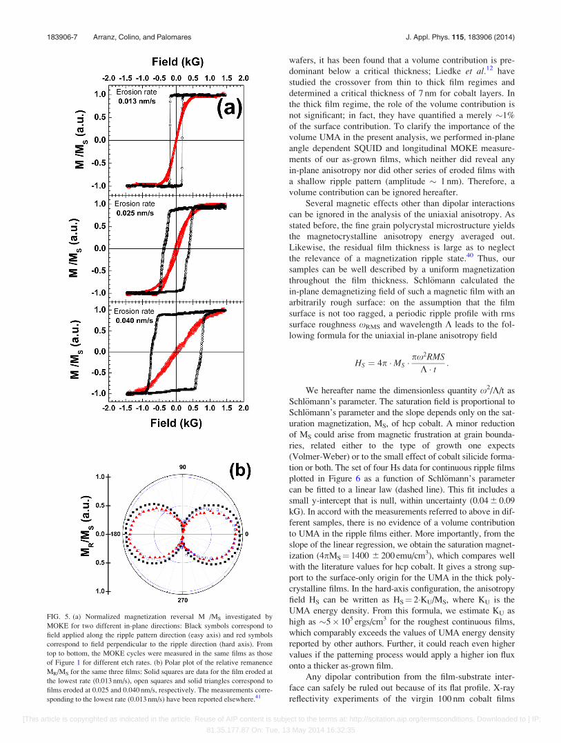
Figure 5(a) displays the in-plane normalized magnetiza-
tion MOKE cycles for the same three films representative of
low, medium, and high ion flux patterning as those used in
the previous morphology analysis. If the field is scanned
along the direction perpendicular to the crests (hard-axis),
the ripple pattern increases drastically the demagnetizing
factor and the uniaxial magnetic anisotropy sets in; the loop
includes a negligible coercive force and saturates at a field
Hs (anisotropy field). We have determined the Hs value by
the field corresponding to the maxima of the field derivatives
of the relative magnetization M/MS in the hard-axis loop. On
the other hand, if the field is applied parallel to the crests
(easy-axis), the experiments have shown loops of high
squareness with coercive fields Hc not quite smaller than Hs
(Hc/Hs � 0.60–0.75). Though the squareness is only perfect
for the lowest ion flux sample, in between the easy and the
hard directions the relative remanence evolves as a function
of in-plane field angle confirming the existence of a
well-defined uniaxial magnetic anisotropy in all cases
(Figure 5(b)).
Some authors consider that HS can be separated into a
volume contribution HSV and the surface contribution HS
S
according to HS¼HSVþHS
S/t. Evidence of the volume con-
tribution has been reported by Sarathlal et al.,15 for example,
with a weak UMA in as-grown Co films on polished Si
wafers if the thickness is higher than 10 nm, which was
attributed to the generation of some long range internal
stresses during the film deposition. A volume contribution
could also be related to ripple dislocations where a broken
symmetry would favour alignment of magnetic moments
parallel to the ripple crests. For ripple films on pre-pattern
FIG. 4. High resolution XPS spectra of
the evolution Co2p3/2 and Si2p core
levels with spectral decomposition (see
text for description of components).
Upper and lower curves correspond to
profile stages B and E, respectively,
referred to in the inset of Figure 3 with
labels and vertical grey stripes.
183906-6 Arranz, Colino, and Palomares J. Appl. Phys. 115, 183906 (2014)
[This article is copyrighted as indicated in the article. Reuse of AIP content is subject to the terms at: http://scitation.aip.org/termsconditions. Downloaded to ] IP:
81.35.177.87 On: Tue, 13 May 2014 16:32:35
wafers, it has been found that a volume contribution is pre-
dominant below a critical thickness; Liedke et al.12 have
studied the crossover from thin to thick film regimes and
determined a critical thickness of 7 nm for cobalt layers. In
the thick film regime, the role of the volume contribution is
not significant; in fact, they have quantified a merely �1%
of the surface contribution. To clarify the importance of the
volume UMA in the present analysis, we performed in-plane
angle dependent SQUID and longitudinal MOKE measure-
ments of our as-grown films, which neither did reveal any
in-plane anisotropy nor did other series of eroded films with
a shallow ripple pattern (amplitude � 1 nm). Therefore, a
volume contribution can be ignored hereafter.
Several magnetic effects other than dipolar interactions
can be ignored in the analysis of the uniaxial anisotropy. As
stated before, the fine grain polycrystal microstructure yields
the magnetocrystalline anisotropy energy averaged out.
Likewise, the residual film thickness is large as to neglect
the relevance of a magnetization ripple state.40 Thus, our
samples can be well described by a uniform magnetization
throughout the film thickness. Schl€omann calculated the
in-plane demagnetizing field of such a magnetic film with an
arbitrarily rough surface: on the assumption that the film
surface is not too ragged, a periodic ripple profile with rms
surface roughness xRMS and wavelength K leads to the fol-
lowing formula for the uniaxial in-plane anisotropy field
HS ¼ 4p �MS �px2RMS
K � t :
We hereafter name the dimensionless quantity x2/K/t as
Schl€omann’s parameter. The saturation field is proportional to
Schl€omann’s parameter and the slope depends only on the sat-
uration magnetization, MS, of hcp cobalt. A minor reduction
of MS could arise from magnetic frustration at grain bounda-
ries, related either to the type of growth one expects
(Volmer-Weber) or to the small effect of cobalt silicide forma-
tion or both. The set of four Hs data for continuous ripple films
plotted in Figure 6 as a function of Schl€omann’s parameter
can be fitted to a linear law (dashed line). This fit includes a
small y-intercept that is null, within uncertainty (0.04 6 0.09
kG). In accord with the measurements referred to above in dif-
ferent samples, there is no evidence of a volume contribution
to UMA in the ripple films either. More importantly, from the
slope of the linear regression, we obtain the saturation magnet-
ization (4pMS¼ 1400 6 200 emu/cm3), which compares well
with the literature values for hcp cobalt. It gives a strong sup-
port to the surface-only origin for the UMA in the thick poly-
crystalline films. In the hard-axis configuration, the anisotropy
field HS can be written as HS¼ 2�KU/MS, where KU is the
UMA energy density. From this formula, we estimate KU as
high as �5� 105 ergs/cm3 for the roughest continuous films,
which comparably exceeds the values of UMA energy density
reported by other authors. Further, it could reach even higher
values if the patterning process would apply a higher ion flux
onto a thicker as-grown film.
Any dipolar contribution from the film-substrate inter-
face can safely be ruled out because of its flat profile. X-ray
reflectivity experiments of the virgin 100 nm cobalt films
FIG. 5. (a) Normalized magnetization reversal M /MS investigated by
MOKE for two different in-plane directions: Black symbols correspond to
field applied along the ripple pattern direction (easy axis) and red symbols
correspond to field perpendicular to the ripple direction (hard axis). From
top to bottom, the MOKE cycles were measured in the same films as those
of Figure 1 for different etch rates. (b) Polar plot of the relative remanence
MR/MS for the same three films: Solid squares are data for the film eroded at
the lowest rate (0.013 nm/s), open squares and solid triangles correspond to
films eroded at 0.025 and 0.040 nm/s, respectively. The measurements corre-
sponding to the lowest rate (0.013 nm/s) have been reported elsewhere.41
183906-7 Arranz, Colino, and Palomares J. Appl. Phys. 115, 183906 (2014)
[This article is copyrighted as indicated in the article. Reuse of AIP content is subject to the terms at: http://scitation.aip.org/termsconditions. Downloaded to ] IP:
81.35.177.87 On: Tue, 13 May 2014 16:32:35

reported in a previous paper5 can be fitted with a structure
model including a flat substrate (rms< 0.2 nm) and a rough
top surface; interface alloying occurred to a probably minor
extent without a significant roughening of the interface pro-
file. Moreover, the use of films grown on different substrates
such as glass and MgO (1 0 0) led to anisotropy fields also in
quantitative agreement with the Schl€omann’s prediction as
that of films on Si (1 0 0)—Figure 6. Thus, the film-substrate
interface is not building surface magnetic charges in the con-
tinuous films.
Three open dots in Figure 6 are data for discontinuous
ripple films. These Hs data for samples of very high ripple
amplitude do not obey the expected linear law; rather, they
remain at about 0.80–1.0 kG. One could try to explain it as
due to intrinsic effects of a very ragged surface; Schl€omann
estimated the second-order corrections to the demagnetizing
field as x4/K3/t, also higher order terms, to be significant
only at surface angles over �45� with respect to the mean
surface.21 However, our films are not so ragged. Although
the mean surface angle of our films goes up with erosion
rate, nonetheless it always stays below �17�. Moreover, his-
tograms of surface angle (not shown) do not reveal any sur-
face parts with values above 30� in the steepest zones. Then
we think that the departure from prediction is related to the
discontinuous morphology. Although those samples are only
discontinuous by about 10%, as estimated from the cutoff of
the amplitude histogram at an amplitude equal to the mean
film thickness, exchange interactions should break up
whereby the ripples are detached and the magnetic energy
balance changes drastically in these zones. Zhang et al.17
applied a direct ion erosion to iron films and reached the sub-
strate to a surface fraction of 43%; the detached ripples were
regarded as spatially separated nanorods and still exhibited
UMA. The study of cobalt planar nanowires made by ripple
detachment will be the aim of a separate paper.
IV. CONCLUSIONS
We have successfully tailored cobalt films as a model
system in which the dipolar-only origin of UMA can be
checked with a ripple patterned top surface. At a first fabrica-
tion stage, the film growth process made up a fine-grain
polycrystalline hcp structure, although it has presumably
delivered enough energy to drive silicide formation at the
surface of the flat silicon substrates. XPS composition analy-
sis has shown that silicide formation gradually occurs at the
interface and leads overall to silicon-rich, non-magnetic
cobalt silicide, Co1�X-SiX with X> 0.7 (magnetically dead
layer). From the composition analysis, the thickness of such
silicide is uncertain. Other evidences suggest that the amount
of cobalt diffused into the whole silicide is small as not to
reduce significantly the film saturation magnetization and
keep the interface flat. At a second fabrication stage, IBS tech-
niques sculpt a ripple pattern of large amplitude on the film
surface using the method of tuning up the roughness by means
of increasing the ion beam flux. This method was previously
used by Chason et al.23 with low ion densities and is hereby
checked with high ion densities. The choice of ion beam pa-
rameters has allowed making ripple patterns of a nearly fixed
wavelength and different amplitudes up to 20 nm, whereas
yielding a nearly fixed residual thickness (35–50 nm).
The top surface is the only magnetically relevant inter-
face as the ion induced pattern drives both the coercivity and
the uniaxial magnetic anisotropy with the easy axis in the
direction of ripple crests. An increasing dependence of the
Hc data on the ripple amplitude suggests that the magnetiza-
tion reversal in the easy axis occurs by wall movement ham-
pered on the ripple crests. A well-defined uniaxial anisotropy
sets in, if the pattern dimensions and film thickness imply a
sufficiently high magnetic anisotropy density. We have stud-
ied the origin of the UMA by considering the ripple ampli-
tude as the leading variable; in this regard, the saturation
field data in the hard-axis direction fit the formula by
Schl€omann21 for the demagnetizing field of a rough surface.
Since any volume contribution can be ruled out, the present
analysis confirms the surface-only origin of UMA for films
of continuous morphology. Other films of slightly discontin-
uous morphology do not obey the prediction. The second
order corrections to Schl€omann formula, arising from a
locally very steep surface, do not explain the departure from
prediction, which is believed to arise from magnetic energy
unbalance associated with the ripple detachment.
ACKNOWLEDGMENTS
We strongly appreciate the assistance of Dr. J. Camarero
to build our setup for vectorial MOKE magnetometry. This
work has been funded on grants from Spanish institutions,
Ministerio de Ciencia e Innovaci�on (No. MAT2006-06242)
and Junta de Comunidades de Castilla-La Mancha (No.
PPII10-0054-1318). F.J.P. acknowledges funding through
Grant Nos. MAT2010-18432 and CSD2008-00023.
1A. Keller and S. Facsko, Materials 3, 4811 (2010).2M. A. Makeev, R. Cuerno, and A.-L. Barabasi, Nucl. Instrum. Methods
Phys. Res., Sect. B 197, 185 (2002).3A. Toma, D. Chiappe, B. Setina Batic, M. Godec, M. Jenko, and F.
Buatier de Mongeot, Phys. Rev. B 78, 153406 (2008).4P. Karmakar and D. Ghose, Surf. Sci. 554, L101 (2004).5J. M. Colino and M. A. Arranz, Appl. Surf. Sci. 257, 4432 (2011).
FIG. 6. Hard axis saturation field Hs as a function of the dimensionless pa-
rameter x2/K/t for continuous films (solid symbols) and discontinuous films
(open symbols). The dashed straight line is a linear fit of the data for the con-
tinuous films in accord with the prediction for the demagnetizing field of a
periodic ripple pattern (see text for details).
183906-8 Arranz, Colino, and Palomares J. Appl. Phys. 115, 183906 (2014)
[This article is copyrighted as indicated in the article. Reuse of AIP content is subject to the terms at: http://scitation.aip.org/termsconditions. Downloaded to ] IP:
81.35.177.87 On: Tue, 13 May 2014 16:32:35

6K. Sato, I. Okamoto, Y. Kitamoto, and S. Ishida, Jpn. J. Appl. Phys., Part
1 46, 5139 (2007).7J. Fassbender, T. Strache, M. O. Liedke, D. Mark�o, S. Wintz, K. Lenz, A.
Keller, S. Facsko, I. M€onch, and J. McCord, New J. Phys. 11, 125002 (2009).8M. K€orner, K. Lenz, M. O. Liedke, T. Strache, A. M€ucklich, A. Keller, S.
Facsko, and J. Fassbender, Phys. Rev. B 80, 214401 (2009).9M. O. Liedke, B. Liedke, A. Keller, B. Hillebrands, A. M€ucklich, S.
Facsko, and J. Fassbender, Phys. Rev. B 75, 220407(R) (2007).10K. V. Sarathlal, D. Kumar, and A. Gupta, Appl. Phys. Lett. 98, 123111
(2011).11E. Paz, F. Cebollada, F. J. Palomares, F. Garc�ıa-S�anchez, and J. M.
Gonz�alez, Nanotechnology 21, 255301 (2010).12M. O. Liedke et al., Phys. Rev. B 87, 024424 (2013).13K. Chen, R. Fr€omter, S. R€ossler, N. Mikuszeit, and H. P. Oepen, Phys.
Rev. B 86, 064432 (2012).14M. K€orner, K. Lenz, R. A. Gallardo, M. Fritzsche, A. M€ucklich, S.
Facsko, J. Lindner, P. Landeros, and J. Fassbender, Phys. Rev. B 88,
054405 (2013).15K. V. Sarathlal, D. Kumar, V. Ganesan, and A. Gupta, Appl. Surf. Sci.
258, 4116 (2012).16K. Zhang, M. Uhrmacher, H. Hofs€ass, and J. Krauser, J. Appl. Phys. 103,
083507 (2008).17K. Zhang, F. Rotter, M. Uhrmacher, C. Ronning, J. Krauser, and H.
Hofs€ass, New J. Phys. 9, 29 (2007).18M. T. Umlor, Appl. Phys. Lett. 87, 082505 (2005).19N. L. Yakovlev, H. Chen, and K. Zhang, J. Nanosci. Nanotechnol. 11,
2575 (2011).20A. F. Vaz, S. J. Steinm€uller, and J. A. C. Bland, Phys. Rev. B 75, 132402
(2007).21E. Schl€omann, J. Appl. Phys. 41, 1617 (1970).22M. A. Arranz and J. M. Colino, J. Phys.: Conf. Ser. 200, 072007 (2010).23E. Chason, T. M. Mayer, and B. K. Kellerman, in Ion-solid interactions
for materials modification and processing, edited by D. B. Poker, D. Ila,
Y. T. Cheng, L. R. Harriott, and T.W. Sigmon (Mater. Res. Soc. Symp.
Proc., 1996), Vol. 396, p. 143.
24A. Redondo-Cubero, R. Gago, F. J. Palomares, A. M€ucklich, M.
Vinnichenko, and L. Vazquez, Phys. Rev. B 86, 085436 (2012).25J. Camarero, J. Sort, A. Hoffmann, J. M. Garc�ıa-Mart�ın, B. Dieny, R.
Miranda, and J. Nogu�es, Phys. Rev. Lett. 95, 057204 (2005).26J. M. Teixeira, R. Lusche, J. Ventura, R. Fermento, F. Carpinteiro, J. P.
Araujo, J. B. Sousa, S. Cardoso, and P. P. Freitas, Rev. Sci. Instrum. 82,
043902 (2011).27W. L. Chan and E. Chason, J. Appl. Phys. 101, 121301 (2007).28J. M. Fallon, C. A. Faunce, P. J. Grundy, and H. J. Blythe, J. Appl. Phys.
87, 6833 (2000).29T. Ishiguro, H. Fujii, Y. Ichinose, J. Endo, and H. Harada, J. Appl. Phys.
61(8), 4284 (1987).30J. M. Fallon, C. A. Faunce, and P. J. Grundy, J. Phys.: Condens. Matter 12,
4075 (2000).31M. V�elez, S. M. Valvidares, J. D�ıaz, R. Morales, and J. M. Alameda, IEEE
Trans. Magn. 38(5), 3078 (2002).32J. D�ıaz, R. Morales, S. M. Valvidares, and J. M. Alameda, Phys. Rev. B
72, 144413 (2005).33P. L. Tam, Y. Cao, and L. Nyborg, Surf. Sci. 606, 329 (2012).34M. Garcia-Mendez, F. F. Castillon, G. A. Hirata, M. H. Farias, and G.
Beamson, Appl. Surf. Sci. 161, 61 (2000).35V. Kinsinger, I. Dezsi, P. Steiner, and G. Langouche, J. Phys.: Condens.
Matter 2, 4955 (1990).36Y.-P. Zhao, R. M. Gamache, G.-C. Wang, and T.-M. Lu, J. Appl. Phys.
89, 1325 (2001).37M. Li, G.-C. Wang, and H.-G. Ming, J. Appl. Phys. 83(10), 5313 (1998).38J. Swerts, S. Vandezande, K. Temst, and C. Van Haesendonck, Solid State
Commun. 131, 359 (2004).39G. Palasantzas, Y.-P. Zhao, J. Th. M. De Hosson, and G.-C. Wang,
Physica B 283, 199 (2000).40K. D. Leaver, Thin Solid Films 2, 149-E (1968).41M. A. Arranz, J. M. Colino, E. Jim�enez, and J. Camarero, “Evidences of
uniaxial magnetic anisotropy in nanopatterned cobalt films,” in
Proceedings of the International Conference on Nanoscale Pattern
Formation at Surfaces, El Escorial, Spain,18–22 September, 2011.
183906-9 Arranz, Colino, and Palomares J. Appl. Phys. 115, 183906 (2014)
[This article is copyrighted as indicated in the article. Reuse of AIP content is subject to the terms at: http://scitation.aip.org/termsconditions. Downloaded to ] IP:
81.35.177.87 On: Tue, 13 May 2014 16:32:35
Copyright © 2022 FDOKUMEN