On-Chip Adaptive Power Management for WPT-Enabled IoT
175
On-Chip Adaptive Power Management for WPT-Enabled IoT Thesis submitted in partial fulfillment of the requirement for the PhD Degree issued by the Universitat Politècnica de Catalunya, in its Electronic Engineering Program by Mohamed Ahmed Saad Abdelhameed Thesis advisor: Dr. Eduard Alarcón-Cot Barcelona, April 2018
-
Upload
khangminh22 -
Category
Documents
-
view
4 -
download
0
Transcript of On-Chip Adaptive Power Management for WPT-Enabled IoT
On-Chip Adaptive Power Management for
WPT-Enabled IoT
Thesis submitted in partial fulfillment of the
requirement for the PhD Degree issued by the
Universitat Politècnica de Catalunya, in its
Electronic Engineering Program
by
Mohamed Ahmed Saad Abdelhameed
Thesis advisor:
Dr. Eduard Alarcón-Cot
Barcelona, April 2018

Page | iii
Abstract
Internet of Things (IoT), as broadband network connecting every physical objects, is becoming
more widely available in various industrial, medical, home and automotive applications. In such
network, the physical devices, vehicles, medical assistance, and home appliances among others
are supposed to be embedded by sensors, actuators, radio frequency (RF) antennas, memory,
and microprocessors, such that these devices are able to exchange data and connect with other
devices in the network. Among other IoT’s pillars, wireless sensor network (WSN) is one of the
main parts comprising massive clusters of spatially distributed sensor nodes dedicated for
sensing and monitoring environmental conditions. The lifetime of a WSN is greatly dependent
on the lifetime of the small sensor nodes, which, in turn, is primarily dependent on energy
availability within every sensor node. Predominantly, the main energy source for a sensor
node is supplied by a small battery attached to it. In a large WSN with massive number of
deployed sensor nodes, it becomes a challenge to replace the batteries of every single sensor
node especially for sensor nodes deployed in harsh environments. Consequently, powering the
sensor nodes becomes a key limiting issue, which poses important challenges for their
practicality and cost.
Therefore, in this thesis we propose enabling WSN, as the main pillar of IoT, by means of
resonant inductive coupling (RIC) wireless power transfer (WPT). In order to enable efficient
energy delivery at higher range, high quality factor RIC-WPT system is required in order to
boost the magnetic flux generated at the transmitting coil. However, an adaptive front-end is
essential for self-tuning the resonant tank against any mismatch in the components values,
distance variation, and interference from close metallic objects. Consequently, the purpose of
the thesis is to develop and design an adaptive efficient switch-mode front-end for self-tuning in
WPT receivers in multiple receiver system.
The thesis start by giving background about the IoT system and the technical bottleneck
followed by the problem statement and thesis scope. Then, Chapter 2 provides detailed
backgrounds about the RIC-WPT system. Specifically, Chapter 2 analyzes the characteristics of
different compensation topologies in RIC-WPT followed by the implications of mistuning on
efficiency and power transfer capability. Chapter 3 discusses the concept of switch-mode
gyrators as a potential candidate for generic variable reactive element synthesis while different
potential applications and design cases are provided. Chapter 4 proposes two different self-
tuning control for WPT receivers that utilize switch-mode gyrators as variable reactive element
synthesis. The performance aspects of control approaches are discussed and evaluated as well in
Chapter 4. The development and exploration of more compact front-end for self-tuned WPT
receiver is investigated in Chapter 5 by proposing a phase-controlled switched inductor
converter. The operation and design details of different switch-mode phase-controlled
topologies are given and evaluated in the same chapter. Lastly, Chapter 6 proposes a novel
approach for real power and reactive power control in phase-controlled converters. Finally,
Chapter 7 provides the conclusions and highlight the contribution of the thesis, in addition to
suggesting the related future research topic.


Page | v
Dedication
To my respected parents, Ahmed Saad and Faten Mahmoud, for their eternal
love and devotion,,,
To my wife, Noha, my son, Ahmed, and my daughter, Fayrouz, for their endless love, support and patience,,,
،،، ستظل دائما مثلي األعليإلي أبي العزيز، أحمد سعد، الذي كان ومازال سندي ومصدر فخري،
،،،إلي أمي الحبيبة، فاتن محمود، معني الحب والحنان في حياتي، أنتي بسمة حياتي وسر وجودي
إلي زوجتي الحبيبة، نهي، لكونك في حياتي، فلوالكي ماكان نجاحي،،،
،،،حياةد، وابنتي الجميلة، فيروز، منكم أستمد قوتي وتعلمت معني جديدا للإلي ابني الحبيب، أحم


Page | vii
“If the doors were to be opened at the first try, with
only one knock, there would probably be nothing
behind them, except for emptiness... the rooms
containing treasures require long and arduous
attempts.”
— Ahmed Khaled Tawfik


Page | ix
Acknowledgment
At this time, as a journey of more than four years is coming to an end, it is time to mention all
the great people who have turned these arduous days of work and study into bright memories.
First of all, I would like to express my deep gratitude and respect to my advisor, Prof.
Eduard Alarcón. It was a real pleasure for me to have such an exceptional scholar and a great
person as an advisor. Although I was one among a long queue of PhD students who are always
asking for his time and support, he led me through the research as if I have been the only PhD
student he is supervising. Strong but supportive, friendly yet firm, he knew perfectly well when
to insist on previously determined plans and when to leave me to follow my own independent
work. His office door was always open, and I will never forget the hours of constructive
discussion we had throughout the past four years. Whenever he felt very busy with a very dense
schedule, he used to share his lunchtime with me, where we discuss, think and plan while we
are having our meals. His enthusiasm and exceptional visionary understanding of various
engineering research areas, and how they relate to our life, is something I would like to inherit
and follow in my future work.
The second blessing I had was to have the opportunity to collaborate with other groups at the
UPC. Among them, I remember the meetings we have with Prof. Francesc Moll Echeto and his
PhD student, David Cavalhiero. As well, I had the pleasure of getting in contact with Prof.
Herminio Martinéz, in which we exchanged the valuable scientific knowledge related to our
research projects.
I have also been exceptionally blessed to cross paths with many other outstanding people at
the Electronics Engineering Department during my PhD journey. At the risk of not mentioning
some of them, I would like to specially thank my colleagues David Cavalheiro, Núria Egidos,
Elisenda Bou-Balust, Mario Iannazzo, Chen Jin, Dídac Vega, Chenna, Mireya Patricia Zapata,
for their friendship, support, and deep intellectual conversations that influenced my ideas and
contributed to my creativity.
In addition, I am thankful to all of my friends for bringing comfort and happiness to my life
and for helping me in overcoming the challenges of adapting to a new country and new culture.
Thank you Ahmed Rabei, Ahmed Elfalah, Mohamed Yousef, Javier Chavarria, Hadeer, without
anyone of you it would never be easy for me.
However, there is someone who always stood by me, who always celebrated my victories
and encouraged me through tough times, someone whose encouragement, love, and sacrifice
were endless. Thank you my wife, Noha, from the bottom of my heart!
Finally, I would like to thank my parents, Ahmed and Faten, for all of their support in the
past years, as well as my dear son Ahmed and my little daughter Fayrouz for bringing many
happy moments into my life and giving a different meaning to my life.


Page | xi
Contents
Abstract ................................................................................................................................. iii
Acknowledgment ................................................................................................................... ix
Contents ................................................................................................................................. xi
List of Figures...................................................................................................................... xiv
List of Tables ....................................................................................................................... xix
1 Introduction .................................................................................................................... 1
1.1 Internet of Things — an Overview .......................................................................... 1
1.1.1 IoT Definition ................................................................................................................. 1
1.1.2 IoT Modeling .................................................................................................................. 2
1.2 Wireless Sensor Networks ...................................................................................... 4
1.2.1 WSNs building blocks (Hardware) ................................................................................. 4
1.3 Powering Wireless Sensor Nodes ............................................................................ 7
1.3.1 Light-Based Energy Harvesting ...................................................................................... 8
1.3.2 Thermal-Based Energy Harvesting ................................................................................. 9
1.3.3 Vibration-Based Energy Harvesting ............................................................................. 10
1.4 Towards Autonomous WSNs ................................................................................ 12
1.5 Problem Statement and Thesis Scope ................................................................... 14
1.5.1 Current Challenges in WPT systems ............................................................................. 14
1.5.2 Scope of the Thesis ....................................................................................................... 15
1.6 Thesis Outline ....................................................................................................... 16
1.7 References ............................................................................................................. 18
2 On the Theory and Modelling of Wireless Power Transfer ..................................... 21
2.1 History of Wireless Power Transfer at a Glance ................................................... 21
2.2 Categories of Wireless power Transfer ................................................................. 22
2.2.1 Far-Field Radiative WPT .............................................................................................. 22
2.2.2 Near-field non-Radiative WPT ..................................................................................... 24
2.3 Resonant Inductive Coupling WPT ....................................................................... 27
2.3.1 Analytical Model of RIC WPT ..................................................................................... 28
2.3.2 Compensation Topologies ............................................................................................. 28
2.4 Analysis of Basic RIC WPT Topologies ............................................................... 29
2.4.1 Series-Series Compensation Scheme ............................................................................ 30
2.4.2 Series-Parallel Compensation Scheme .......................................................................... 37
2.4.3 Compensation Topology Considerations ...................................................................... 43
2.5 Parallel-Compensated WPT Receivers ................................................................. 44
2.5.1 Performance .................................................................................................................. 44

Page | xii
2.5.2 Mistuning Effect on Power Delivery ............................................................................ 44
2.6 Conclusions ........................................................................................................... 47
2.7 References ............................................................................................................. 48
3 Switch-Mode Gyrators as a Potential Candidate for Self-Tuned WPT Receiver .. 51
3.1 Motivation ............................................................................................................. 51
3.2 Revisiting Gyrator ................................................................................................. 52
3.2.1 Gyrator Theory .............................................................................................................. 52
3.2.2 The Gyrator as a Reactive Element Synthesizer ........................................................... 53
3.2.3 Gyrator Implementations .............................................................................................. 54
3.3 Dual Active Bridge Converter as a Natural Gyrator ............................................. 58
3.3.1 Circuit Description and Operation ................................................................................ 58
3.3.2 State-Space Modelling and Simulation ......................................................................... 60
3.3.3 Tunability Range of DAB-based Synthesized Inductance ............................................ 63
3.4 Potential Applications for Switch-Mode DAB-Based Impedance Synthesis ........ 64
3.4.1 Switch-Mode Resonators .............................................................................................. 65
3.4.2 Switch-Mode Alternative to LDO ................................................................................. 66
3.4.3 DAB-Based Resonant Ripple Filter for Power Converters ........................................... 68
3.4.4 Other Possible Applications .......................................................................................... 70
3.5 Gyrator-Based Synthesized Inductance in WPT Receivers .................................. 70
3.5.1 Generalized Model for the Proposed Dynamic Tuning Approach ................................ 71
3.6 Conclusions ........................................................................................................... 72
3.7 References ............................................................................................................. 73
4 Self-Tuning Control for WPT Receivers based on Switch-Mode Gyrators ........... 77
4.1 DAB-Based Variable Inductance Design .............................................................. 77
4.2 A Dual Loop Automatic Tuning Control for WPT Receiver ................................ 80
4.2.1 Coarse-Tuning Loop ..................................................................................................... 81
4.2.2 Fine-Tuning Loop ......................................................................................................... 83
4.2.3 Performance discussion ................................................................................................. 84
4.3 Quadrature Phase-Locked Loop Control ............................................................... 85
4.3.1 PLL-Like Control—Theory and Operation ................................................................... 86
4.3.2 System Integration and Validation Results ................................................................... 87
4.3.3 Chip Implementation for the Proposed DAB-based Inductance Synthesizer ................ 92
4.3.4 System Design Consideration—Performance Discussion............................................. 95
4.4 Conclusions ......................................................................................................... 101
4.5 References ........................................................................................................... 102
5 Phase-Controlled Converters for Active Tuning in WPT Receivers ..................... 105
5.1 State of the art of WPT Receivers for Battery Charging ..................................... 105
5.2 Fundamentals of Variable Phase-controlled Reactance ...................................... 107

Page | xiii
5.2.1 Phase-Controlled Inductive Reactance ........................................................................ 108
5.2.2 Phase-Controlled Series Capacitive Reactance ........................................................... 109
5.3 Phase-Controlled Switched Inductor Converter .................................................. 110
5.3.1 Circuit Operation ......................................................................................................... 111
5.3.2 Circuit Characterization .............................................................................................. 114
5.3.3 Active Tuning in WPT Receivers using Switched-Inductor Topology ....................... 117
5.4 Phase-Controlled Split-Capacitor Converter ....................................................... 122
5.4.1 Circuit Operation ......................................................................................................... 123
5.4.2 Circuit Characterization .............................................................................................. 125
5.4.3 Active Tuning in WPT Receivers ............................................................................... 127
5.5 Self-Tuning Control Design ................................................................................ 131
5.6 Conclusions ......................................................................................................... 134
5.7 References ........................................................................................................... 135
6 Real and Reactive Power Control in WPT Receivers ............................................. 137
6.1 Power Management Topologies in WPT Receivers — an Overview ................. 137
6.2 Real Power Control in Phase-Controlled Converters .......................................... 140
6.3 Characterization and Simulation Results ............................................................ 141
6.4 Insights into Control Design for Simultaneous Real and Reactive Power Control
145
6.5 Conclusions ......................................................................................................... 146
6.6 References ........................................................................................................... 146
7 Conclusions, Contributions and Suggested Future Work ...................................... 147
7.1 Conclusions ......................................................................................................... 147
7.2 Contributions of This Thesis ............................................................................... 151
7.3 Suggested Future Work ....................................................................................... 153

Page | xiv
List of Figures
Figure 1.1 End users and applications of IoT (Reprinted from [3], with permission from
Elsevier). ....................................................................................................................................... 2
Figure 1.2 The IoT tree (Reprint from [5]). ................................................................................. 3
Figure 1.3 The IoT Environment (Reprint from [6]). .................................................................. 3
Figure 1.4 Typical function of a sensor node. .............................................................................. 4
Figure 1.5 Main building blocks of a sensor node. ...................................................................... 5
Figure 1.6 Solar cell model and electrical characteristics. ........................................................... 9
Figure 1.7 Construction of thermoelectric generator. ................................................................ 10
Figure 1.8 Structure of cantilever piezoelectric energy transducer. ........................................... 11
Figure 1.9 Conceptual schematic diagram for WPT-enabled wireless sensor nodes. ................ 13
Figure 1.10 Conceptual block diagram for the main goal of the thesis. ..................................... 16
Figure 2.1 Field regions of a transmitting antenna of dimension D [12]. .................................. 23
Figure 2.2 Flux density B for (a) straight wire, (b) circular current loop [15]. ......................... 24
Figure 2.3 Electromagnetic induction in circular coils. ............................................................. 25
Figure 2.4 A generic systematic model for RIC wireless power transfer system. ..................... 27
Figure 2.5 General block diagram for RIC WPT system. .......................................................... 28
Figure 2.6 Compensation topologies (a) series-series, (b) series-parallel, (c) parallel-series, (d)
parallel-parallel. .......................................................................................................................... 29
Figure 2.7 Equivalent circuit of series-series compensated RIC WPT link. .............................. 29
Figure 2.8 Real part of ZT function of (ω/ωR) at different load quality factors and coupling
coefficients. ................................................................................................................................. 32
Figure 2.9 Power distribution in series-series compensated WPT link. ..................................... 33
Figure 2.10 Efficiency versus normalized frequency, (a) at different k and QL-S; (b) theoretical
versus PSpice simulated. ............................................................................................................. 35
Figure 2.11 Equivalent circuit of series-parallel compensated RIC WPT link. ......................... 37
Figure 2.12 Power distribution in series-parallel compensated WPT link. ................................ 39
Figure 2.13 Real part of ZT as a function of (ω/ωR) at different load quality factors and coupling
coefficients. ................................................................................................................................. 41
Figure 2.14 Link gain and output current in series-parallel compensation topology. ................ 42
Figure 2.15 A model of parallel-compensated WPT receiver. ................................................... 43
Figure 2.16 A simplified model for WPT parallel-compensated receiver with possible
components’ variations modeled. ............................................................................................... 45
Figure 2.17 Mistuning effect on (a) normalized power; (b) receiver resonance frequency. ...... 46
Figure 3.1 A gyrator. (a) Symbolic representation. (b) Behavioral model. ............................... 53
Figure 3.2 Transformation property of a gyrator. (a) C transformation. (b) L transformation. (c)
R transformation. (d) Series resonance transformation. ............................................................. 54

Page | xv
Figure 3.3 Various gyrator realizations (a) Transistor based. (b) Transconductor based. (c)
Current Conveyor II based. ......................................................................................................... 55
Figure 3.4 Block diagram of gyrator realization by means of a POPI circuit. ........................... 56
Figure 3.5 Switch-mode gyrator realizations (a) Inductive-based. (b) Capacitive-based. ......... 57
Figure 3.6 The dual active bridge converter. ............................................................................. 58
Figure 3.7 Waveforms of the input bridge output VAB. .............................................................. 59
Figure 3.8 Four-quadrant switches (a) Two back-to-back MOSFETs. (b) Two anti-series
MOSFET-diode. .......................................................................................................................... 60
Figure 3.9 (a) DAB-based switch-mode inductance synthesis. (b) Operation modes. .............. 62
Figure 3.10 State-space simulation using Simulink. (a) Block diagram. (b) Results. ............... 62
Figure 3.11 DAB-based Lφ, g, and Rφ versus phase-shift φ. ...................................................... 64
Figure 3.12 Synthesized inductance Lφ versus φ at different switching frequency fDAB. ........... 64
Figure 3.13 Tunable switch-mode power resonator. .................................................................. 65
Figure 3.14 Magnitude plot and phase plot of the resonant current in series resonant switch-
mode testbench. ........................................................................................................................... 66
Figure 3.15 Buck converter utilizing DAB-based synthesized inductance. ............................... 67
Figure 3.16 Simulation results of buck converter utilizing DAB-based inductance. ................. 68
Figure 3.17 Buck output ripple versus phase shift φ in a DAB-based inductance. .................... 68
Figure 3.18 Resonant ripple filter for buck converter based on DAB-based inductance. .......... 69
Figure 3.19 Waveforms of buck converter utilizing DAB-based inductance. ........................... 70
Figure 3.20 A model for the proposed approach: (a) Basic concept; (b) DAB-based inductance
dynamic tuning in WPT receiver. ............................................................................................... 71
Figure 4.1 A model of parallel-compensated WPT receiver. ..................................................... 78
Figure 4.2 Validation of DAB-based Inductance synthesis in WPT receiver (a) Waveforms at φ
= 50°; ........................................................................................................................................... 79
Figure 4.3 Block diagram of dual-loop control for DAB-based adaptive tuning of WPT
receiver. ....................................................................................................................................... 80
Figure 4.4 Block diagram for coarse-tuning loop. ..................................................................... 82
Figure 4.5 Waveforms of the coarse-tune loop operation. ......................................................... 82
Figure 4.6 Block diagram for fine-tuning loop. ......................................................................... 83
Figure 4.7 Simulation waveforms of the system with FT operation indicated. ......................... 84
Figure 4.8 False coarse tuning in the dual loop automatic control. ............................................ 85
Figure 4.9 Block diagram of the Q-PLL automatic tuning control for gyrator-based parallel
WPT receiver. ............................................................................................................................. 85
Figure 4.10 Schematic Block diagram of the Q-PLL control for gyrator-based dynamic
frequency tuning system in Figure 4.9. ....................................................................................... 87
Figure 4.11 System operation waveforms: (a) steady-state waveforms of VCtrl, VLPF and Vac; (b)
a zoom-in showing the waveforms of [QRL· Voc], Vac, Vramp, VCtrl, and DAB gating signals PS1
and PS2. ...................................................................................................................................... 89
Page | xvi
Figure 4.12 System response to component variations showing Vac, VLPF and the phase-angle φ:
(a) Case of -11% variation in CR followed by -11% variation in LR; (b) Case of +11% variation
in CR followed by +11% variation in LR. .................................................................................... 90
Figure 4.13 Waveforms of system response to irregular change in CR and LR. ......................... 91
Figure 4.14 Demonstration of system performance versus CR mismatch of ±15%: (a)
Normalized delivered power with dynamic tuning (Po w/ G) and without (Po w/o G); (b) The
synthesized inductance Lφ, the corresponding φ and Vac versus CR mismatch. .......................... 91
Figure 4.15 Schematic diagram for on chip implementation for gyrator-based dynamic tuning.
.................................................................................................................................................... 93
Figure 4.16 Real-time chip design results: (a) tuned point steady-state waveforms of Vac, Voc
and VPD; (b) the corresponding duty-cycle generated and driving signals for DAB circuit; (c)
output power versus variations in CR and LR as well as the WPT receiver efficiency ηR based on
real-time simulated chip implementation. ................................................................................... 94
Figure 4.17 Receiver circuit with parasitic resistances included and the Norton equivalent of
circuit. ......................................................................................................................................... 95
Figure 4.18 Simplified block diagram for the closed-loop control. ........................................... 98
Figure 4.19 System SSI at Kp=1.5 and fz=142.8 kHz. ............................................................... 99
Figure 4.20 System FSI at Kp=5.5 and fz=66.7 kHz. ................................................................. 99
Figure 4.21 Characterization of stability boundaries over the space (Kp, fz). .......................... 100
Figure 5.1 Two phase-controlled inductor WPT receivers in [5] and [7] respectively. ........... 107
Figure 5.2 Elementary phase-controlled inductor and its voltage and current waveforms. ..... 109
Figure 5.3 Elementary phase-controlled series capacitors and its voltage and current
waveforms. ................................................................................................................................ 110
Figure 5.4 Schematic diagram of phase-controlled switched-inductor converter. ................... 111
Figure 5.5 Operation modes of phase-controlled switched-inductor converter. ...................... 113
Figure 5.6 Time-domain waveforms at: (a) α=1.83 rad, and (b) α=2.09 rad. .......................... 114
Figure 5.7 Simplified model for the phase-controlled switched-inductor converter in Figure 5.4.
.................................................................................................................................................. 115
Figure 5.8 Input current’s fundamental component lagging input voltage vac. ........................ 115
Figure 5.9 Effect of time-delay on inductance ratio and resistance ratio: (a) Inductance ratio Lr
at LDC=3μH, 6μH, 9μH and Lr of conventional PCI, and (b) Resistance ratio Rr at LDC= 3μH,
6μH and 9μH. ............................................................................................................................ 116
Figure 5.10 Simple model of a WPT receiver enable by phase-controlled switched-inductor.117
Figure 5.11 Implementation of the proposed phase-controlled switched-inductor tuner and
rectifier in WPT receiver. ......................................................................................................... 118
Figure 5.12 Time-domain simulation for receiver with phase-controlled switched-converter
optimized for tuning and rectification. ...................................................................................... 120
Figure 5.13 Time-domain waveforms of switches current and commutation events at: (a)
positive current cycle, and (b) negative current cycle. ............................................................. 121
Figure 5.14 Simulated WPT receiver performance at different CRx variation percentage (a)
corresponding α and Lα/LDC; and (b) corresponding output power. ......................................... 122
Page | xvii
Figure 5.15 Rectifier-free AC-DC topologies: (a) dual-polarity boost converter [9]; and (b)
direct AC-DC split capacitor [10]. ............................................................................................ 123
Figure 5.16 Operation modes of phase-controlled split-capacitor converter. .......................... 125
Figure 5.17 Time-domain simulation of phase-controlled split-capacitor showing iL1, VC1, VC2,
and VDC. .................................................................................................................................... 126
Figure 5.18 Split-capacitor converter characteristics versus α: (a) Inductance ratio Lr at
L1=2μH, 3μH, 5μH; and (b) Resistance ratio Rr at L1= 2μH, 3μH and 5μH. ........................... 126
Figure 5.19 Implementation of the phase-controlled split-capacitor converter in WPT receiver.
................................................................................................................................................... 127
Figure 5.20 Time-domain waveforms of switches current and commutation of split-capacitor
converter: (a) positive current cycle, and (b) negative current cycle. ....................................... 128
Figure 5.21 Time-domain waveforms of the phase-controlled split-capacitor converter in a
WPT receiver at α = 0.67π. ....................................................................................................... 130
Figure 5.22 Performance of the phase-controlled split-capacitor converter in response to
variation in CR. .......................................................................................................................... 131
Figure 5.23 Block diagram of the self-tuning control for the phase-controlled split capacitor
converter. .................................................................................................................................. 132
Figure 5.24 Time-domain waveforms of the self-tuning control of Figure 5.23. .................... 132
Figure 5.25 Control response to change in system parameters; (a) +10% change in CRx, (b) -
10% change in LRx. ................................................................................................................... 133
Figure 6.1 Block diagram of power conditioning system for parallel WPT receiver. ............. 138
Figure 6.2 Phase-controlled split-capacitor converter, (a) the topology, (b) reactive power
control operation, (c) real and reactive power control operation. ............................................. 139
Figure 6.3 Operation modes for reactive and real power control phase-controlled split-capacitor
converter. .................................................................................................................................. 140
Figure 6.4 Time-domain waveforms of real power and reactive power control in split-capacitor,
(a) at Dα=0.36 and Dc=0.1, (b) at Dα=0.36 and Dc=0.3. ........................................................... 143
Figure 6.5 Characteristic curves versus phase-delay duty cycle Dα at Dc=0.1, 0.2, and 0.3, (a)
synthesized inductance ratio Lα/L1, (b) DC output voltage VDC. .............................................. 144
Figure 6.6 Effective AC resistance of the split-capacitor converter versus Dα and Dc. ........... 144
Figure 6.7 Conceptual block diagram for real power and reactive power control in WPT
receivers. ................................................................................................................................... 145


Page | xix
List of Tables
Table 1.1 Output power of different types of energy harvesters (source [15]). ........................... 7
Table 4.1 DAB circuit parameters. ............................................................................................. 78
Table 4.2 WPT link and DAB gyrator parameters. .................................................................... 88
Table 5.1 WPT receiver and phase-controlled converter. ........................................................ 119
Table 5.2 Parameters of WPT receiver and split-capacitor converter. ..................................... 129
Table 6.1 Parameters of WPT receiver and split-capacitor converter. ..................................... 142

Page | 1
Chapter
1
1 Introduction
Historically, the term of "Internet of Things" has been invented by Kevin Ashton, the co-
founder of the Auto-ID center at Massachusetts Institute of Technology (MIT) in 1998. The
term describes a system where sensor-based physical objects are connected to a huge database
that contains information about each physical object. Since 1998, the Internet of Things (IoT)
term gained a wide interest and become widely recognized and realized in practice.
The motivation of this chapter is to expose an overview about the technical challenges and
the focus of the thesis. A brief revision for the IoT systems and their building blocks will be
discussed. Among the different blocks of IoT system, we will focus more on wireless sensor
network (WSN) as the most effective pillar in IoT. The techniques for enabling autonomous
operation for inaccessible sensor nodes will be also given. The problem statement and the thesis
proposal will be disclosed finally, followed by the thesis outline.
1.1 Internet of Things — an Overview
In last years, IoT has been given various definitions which they are presented here and
discussed in order to raise a clear vision about the concept of IoT.
1.1.1 IoT Definition
The first definition for IoT has been given by the inventor of the term itself. Kevin Ashton
stated that: "Adding radio-frequency identification and other sensors to everyday objects will
create an Internet of Things, and lay the foundations of a new age of machine perception". Out
of this early definition, few other definitions have been assigned in the last years. One important
reference for IoT definitions is the 2009 final report for CASAGRAS (Coordination and
Support Action for Global RFID-related Activities and Standardization) that contains several
definitions combined with analysis for each definition where each definition is discussing
different perspectives [1]. Nonetheless, every definition considers one or more aspects of IoT

Internet of Things — an Overview
Page | 2
unique features. Needless to say, every time a clear and comprehensive definition for IoT is
strongly needed in order to make the open questions more clear and solvable in reality. That's
why IoT is still being defined [2]. Figure 1.1 illustrates a generic diagram for the
interconnection between the application domain and the end users in IoT [3].
Figure 1.1 End users and applications of IoT (Reprinted from [3], with permission from Elsevier).
Accordingly, a more expressive definition has also been derived by SAP as: "A world where
physical objects are seamlessly integrated into the information network and where the physical
objects can become active participants in business processes. Services are available to interact
with these 'smart objects' over the Internet, query and change their state and any information
associated with them, taking into account security and privacy issues" [4].
1.1.2 IoT Modeling
Since a conclusive definition for IoT is always required and new definitions are still being
offered, a comprehensive and evident model is required as well. Up to date, many reference
models have been developed. Among them, a paradigm that represents a general abstract for the
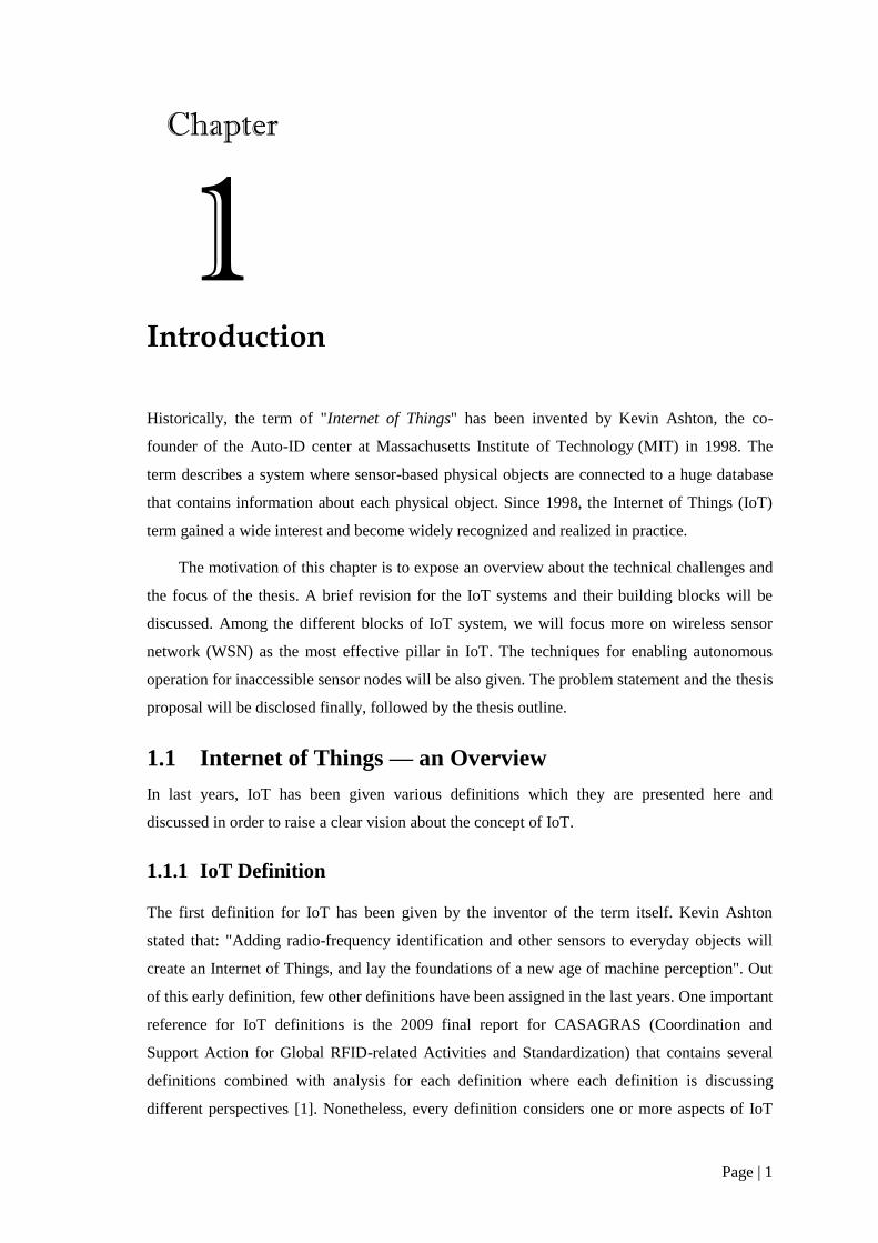
concept of IoT is shown in Figure 1.2 which is mapped as a tree [5]. In the IoT tree, the
technology is represented as the tree’s roots where the technology comprises a group of devices
(including sensors/WSN, tags, actuators...) generating data that are processed by a processing
unit. The connection between the sensors and the application side is carried out through a set of
communication protocols (Zigbee, GPS,..). On the other hand, a wide variety of applications are
enabled through software packages, where the applications represent the leaves of the tree.
Ch. 1 — Introduction
Page | 3
Sensors
Accelerometer
MagnetometerPressure
Temperature
Connectivity
ZigBee
GPS
Wi-Fi
NFC
RFID
Embedded
Processing
MPUMCU
Network
Processor
Technology
Software
Application
Services
Smart
Homes
Smart
Grids Smart
Cars
Smart
HealthSmart
Lightening
Smart
Energy
Supply Chain
automation
Figure 1.2 The IoT tree (Reprint from [5]).
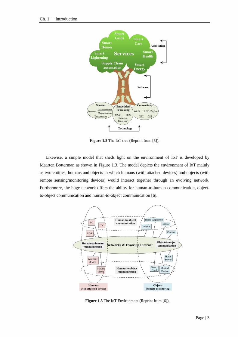
Likewise, a simple model that sheds light on the environment of IoT is developed by
Maarten Botterman as shown in Figure 1.3. The model depicts the environment of IoT mainly
as two entities; humans and objects in which humans (with attached devices) and objects (with
remote sensing/monitoring devices) would interact together through an evolving network.
Furthermore, the huge network offers the ability for human-to-human communication, object-
to-object communication and human-to-object communication [6].
Networks & Evolving Internet
Human-to-object
communication
Mobile
Phone
Wearable
device
PDA
PC
TV
Smart
CardMedical
Device
Home
Server
Vehicle
Home Appliances
Sensor
Camera
Human-to-object
communication
Object-to-object
communication Human-to-human
communication
Humans
with attached devices
Objects
Remote monitoring
Figure 1.3 The IoT Environment (Reprint from [6]).
Wireless Sensor Networks
Page | 4
It is evident that sensors are one of the key elements in the IoT. Noting Figure 1.2 and 1.3,
the sensors are supposed to monitor the physical and environmental conditions and release their
data to the ubiquitous network, where the data could be processed by other objects, devices or
even users. A large number of spatially deployed sensors would form a wireless sensor network
(WSN). A four-pillar paradigm for the IoT has been presented in [7], where WSN is considered
one of the main pillars in the IoT. In order to enable the deployment of very large number of
sensors in one environment, these sensors are mostly connected through a short-range wireless
communication link. Consequently, the mission of enabling fully autonomous WSN becomes
more pressing. The WSN, sometimes called internet of transducers, will be discussed in more
detail in the next section.
1.2 Wireless Sensor Networks
WSN is a network comprising a set of spatially distributed sensors dedicated to sensing and
monitoring environmental conditions such as temperature, pressure, light intensity, humidity,
etc. After that, the collected data is sent to a central server where the data is stored or processed.
Historically, the origin of WSN comes back to the Distributed Sensor Network (DSN)
project at the USA Defense Advanced Research Projects Agency (DARPA) around 1980 [1].
Before that date, research challenges and promising technologies have been addressed in the
Distributed Sensor Networks Workshop that was organized by DARPA in 1978. Since then,
many research projects have been driven by universities and academic institutions followed by
commercial availability offered by many companies.
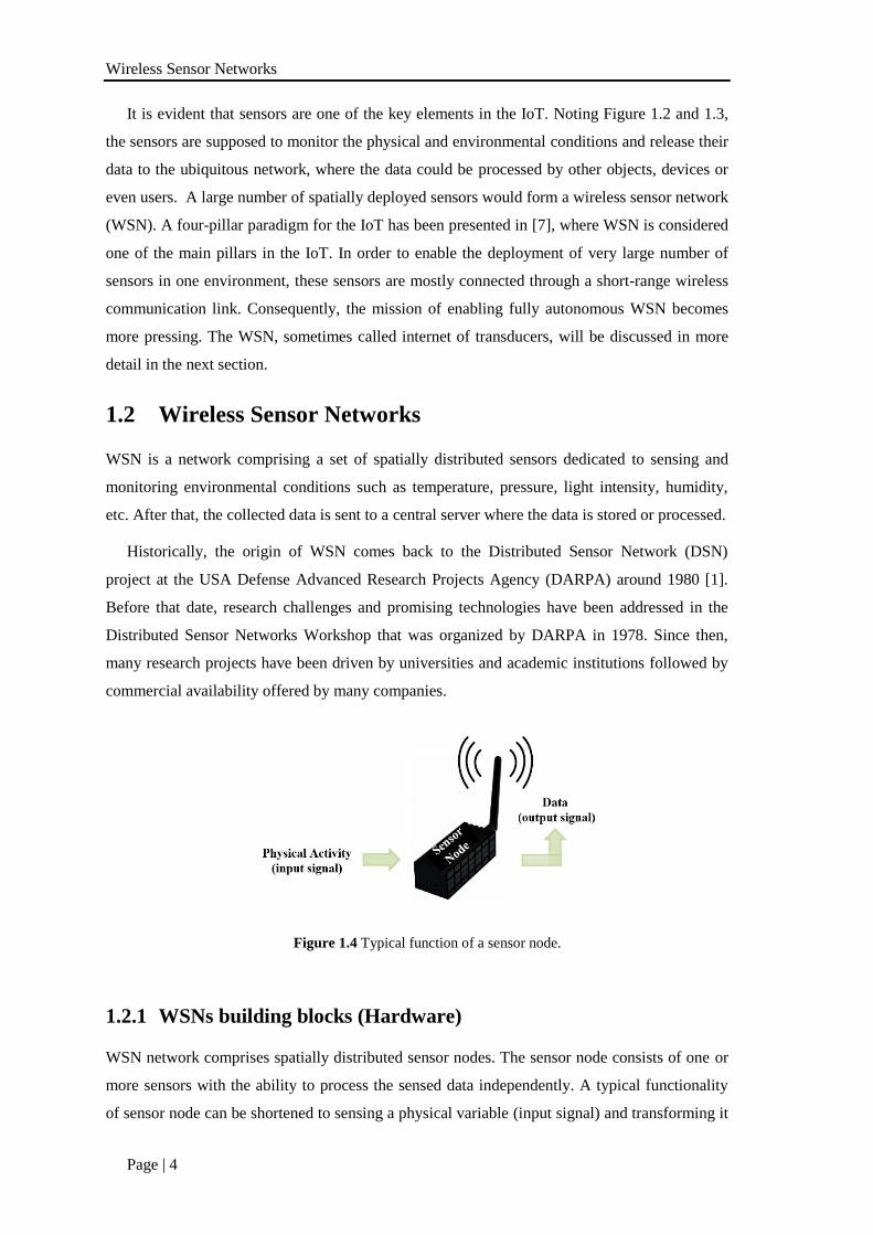
Figure 1.4 Typical function of a sensor node.
1.2.1 WSNs building blocks (Hardware)
WSN network comprises spatially distributed sensor nodes. The sensor node consists of one or
more sensors with the ability to process the sensed data independently. A typical functionality
of sensor node can be shortened to sensing a physical variable (input signal) and transforming it
Ch. 1 — Introduction
Page | 5
to meaningful action or data (output signal). A typical function of a sensor node can be
demystified in Figure 1.4 [8]. The recent trend in sensors is the transition from being a simple
sensing device to be a multifunctional unit. In addition to sensors, modern sensor nodes are
equipped by a processor, a memory, a power supply, a radio and an actuator [9].
It is necessary to have a deeper look on the hardware architecture of a WSN node. The
building blocks of a sensor node, as depicted in Figure 1.5, can be separated as follows:
Sensors/Actuators
μP
Radio
WSN
PowerManagement
Stoarge
EnergySource
Figure 1.5 Main building blocks of a sensor node.
1.2.1.1 Sensors/Actuators
Sensors are the key point in wireless sensor networks where a physical quantity or event is
measured and then transformed to the form of an electrical signal or any other form. Currently,
available sensors are capable of sensing diverse forms of physical quantities such as
temperature, humidity, smoke, light, pressure, vibration, acoustic, motion, etc. Rapid advance in
MEMS technology enabled tiny sensors to be built on a single chip with a significant reduction
in power and cost. It's worth mentioning here that MEMS technology is promising for multi-
sensor realization into a single chip motivated by the increased interest in very small high-
density sensor nodes.
On the other hand, actuators are small mechanical devices that are normally operated to act
to a physical event within the surrounding environments. Similarly, actuators have been
supported by the advance in MEMS technology. Tiny three-dimensional mechanical actuators,
also known as “microactuators”, with a size range from micrometers to few centimeters have
been successfully realized [10].
Wireless Sensor Networks
Page | 6
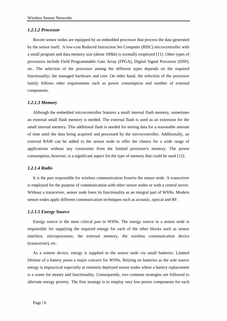
1.2.1.2 Processor
Recent sensor nodes are equipped by an embedded processor that process the data generated
by the sensor itself. A low-cost Reduced Instruction Set Computer (RISC) microcontroller with
a small program and data memory size (about 100kb) is normally employed [11]. Other types of
processors include Field Programmable Gate Array (FPGA), Digital Signal Processor (DSP),
etc. The selection of the processor among the different types depends on the required
functionality; the managed hardware and cost. On other hand, the selection of the processor
family follows other requirements such as power consumption and number of external
components.
1.2.1.3 Memory
Although the embedded microcontroller features a small internal flash memory, sometimes
an external small flash memory is needed. The external flash is used as an extension for the
small internal memory. This additional flash is needed for storing data for a reasonable amount
of time until the data being acquired and processed by the microcontroller. Additionally, an
external RAM can be added to the sensor node to offer the chance for a wide range of
applications without any constraints from the limited processor's memory. The power
consumption, however, is a significant aspect for the type of memory that could be used [12].
1.2.1.4 Radio
It is the part responsible for wireless communication from/to the sensor node. A transceiver
is employed for the purpose of communication with other sensor nodes or with a central server.
Without a transceiver, sensor node loses its functionality as an integral part of WSNs. Modern
sensor nodes apply different communication techniques such as acoustic, optical and RF.
1.2.1.5 Energy Source
Energy source is the most critical part in WSNs. The energy source in a sensor node is
responsible for supplying the required energy for each of the other blocks such as sensor
interface, microprocessor, the external memory, the wireless communication device
(transceiver), etc.
As a remote device, energy is supplied to the sensor node via small batteries. Limited
lifetime of a battery poses a major concern for WSNs. Relying on batteries as the sole source
energy is impractical especially at remotely deployed sensor nodes where a battery replacement
is a waste for money and functionality. Consequently, two common strategies are followed to
alleviate energy poverty. The first strategy is to employ very low-power components for each
Ch. 1 — Introduction
Page | 7
part within the sensor node. Likewise, different hardware architectures are sometimes employed
to minimize the power consumption in a sensor node [13].
The second strategy is to adopt a secondary energy source or multi-sources that are used to
charge the battery whenever needed and whenever these energy sources are available. Energy
harvesting is a promising solution for remote deployed sensor nodes. Energy can be harvested
from ambient environment using sophisticated transducers and be stored in the battery.
Depending on the environment where the sensors are deployed, energy can be available in the
form of solar light, kinetic, wind or electromagnetic energy.
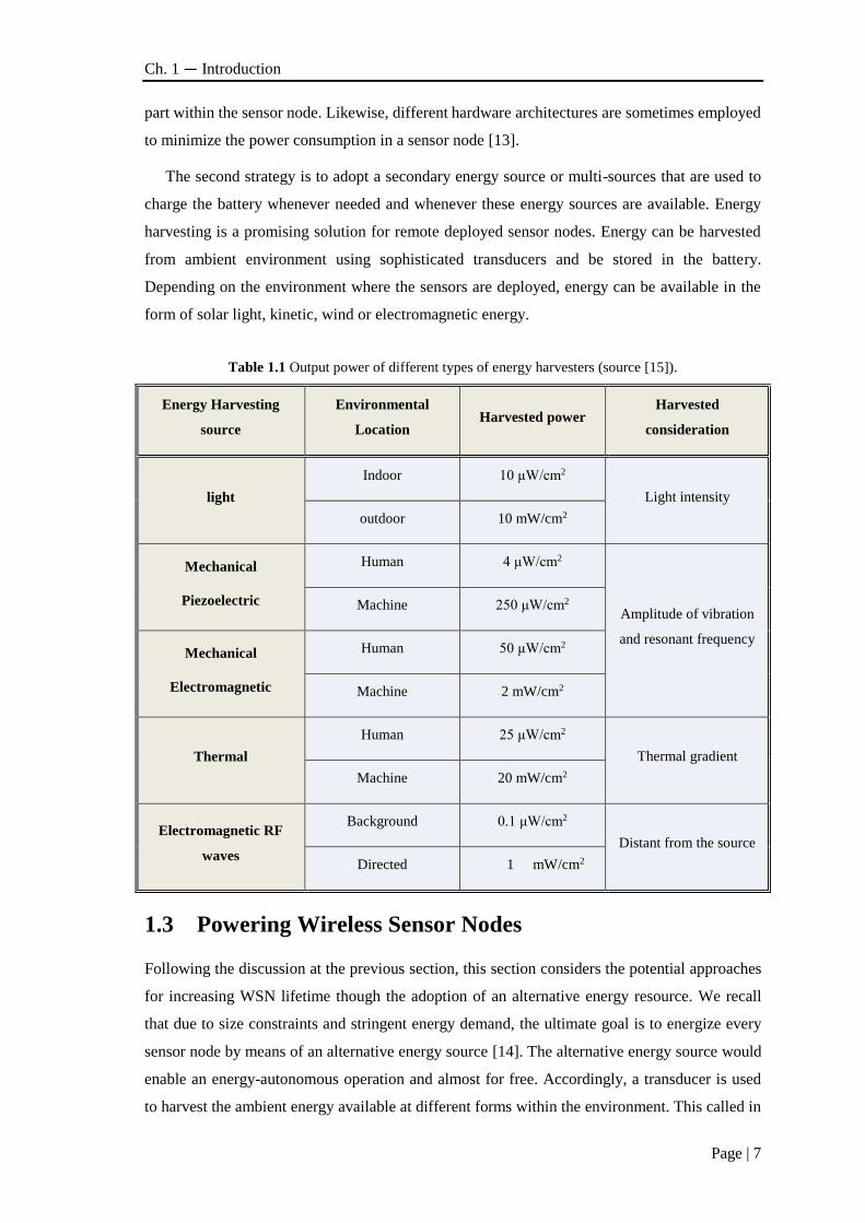
Table 1.1 Output power of different types of energy harvesters (source [15]).
Energy Harvesting
source
Environmental
Location Harvested power
Harvested
consideration
light
Indoor 10 μW/cm2
Light intensity
outdoor 10 mW/cm2
Mechanical
Piezoelectric
Human 4 μW/cm2
Amplitude of vibration
and resonant frequency
Machine 250 μW/cm2
Mechanical
Electromagnetic
Human 50 μW/cm2
Machine 2 mW/cm2
Thermal
Human 25 μW/cm2
Thermal gradient
Machine 20 mW/cm2
Electromagnetic RF
waves
Background 0.1 μW/cm2
Distant from the source
Directed 1 mW/cm2
1.3 Powering Wireless Sensor Nodes
Following the discussion at the previous section, this section considers the potential approaches
for increasing WSN lifetime though the adoption of an alternative energy resource. We recall
that due to size constraints and stringent energy demand, the ultimate goal is to energize every
sensor node by means of an alternative energy source [14]. The alternative energy source would
enable an energy-autonomous operation and almost for free. Accordingly, a transducer is used
to harvest the ambient energy available at different forms within the environment. This called in
Powering Wireless Sensor Nodes
Page | 8
literature as "Energy Harvesting". Usually, the amount of available power is small and strictly
depends on the environmental conditions. The ambient energy sources could be in several forms
such as light, vibration, thermal and electromagnetic waves. Depending on the environmental
conditions, more than one source could be available with a specific application. However, the
energy availability is uncertain as an implication for the irregular, random nature of such
sources [14]. Furthermore, the average power levels, as shown in Table 1.1, available from
different forms are limited to few microwatts, especially for indoor applications.
In Table 1.1., energy harvesting is categorized based on the preliminary form of the
harvested energy. Energy harvesting can be categorized into four basic categories, namely light,
thermal, mechanical vibration and electromagnetic (RF) waves. The fundamentals of each
category will be shortly discussed in the following sections in order to evaluate their feasibility
as potential energy source for wireless sensor nodes.
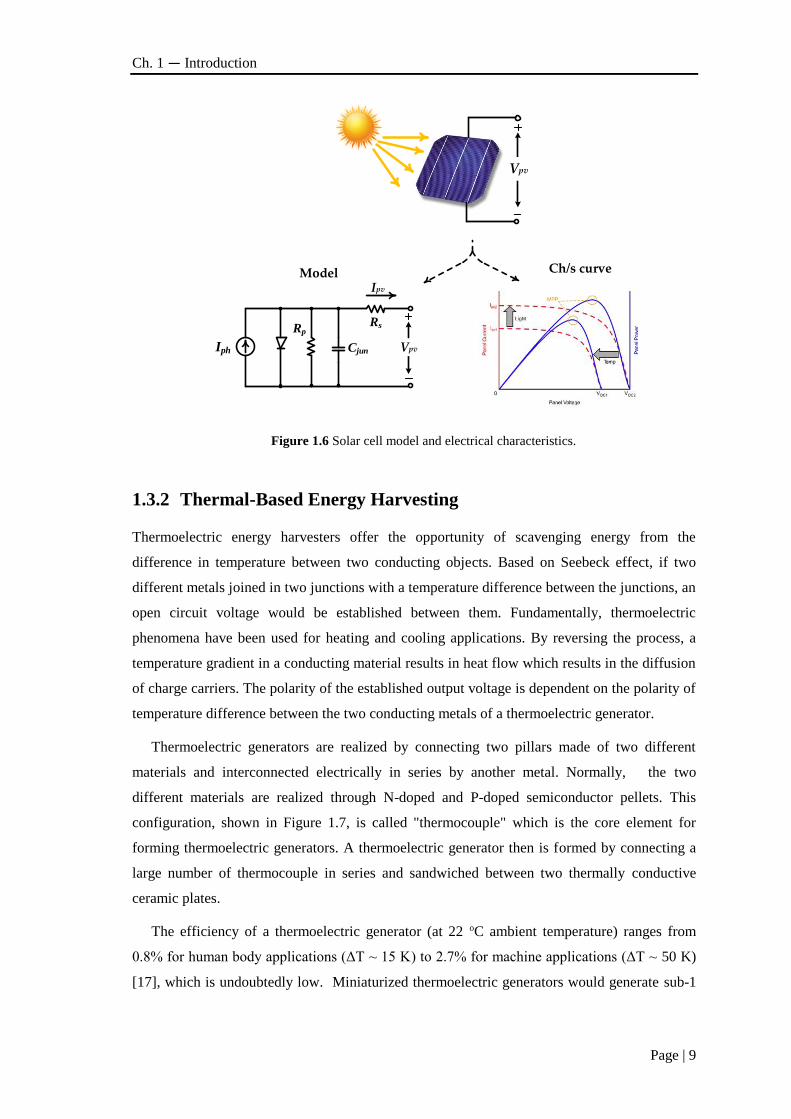
1.3.1 Light-Based Energy Harvesting
Harvesting energy from solar light is the most common alternative energy source. Wherein, a
solar cell is used to convert the solar light into electrical energy by taking advantage of
photovoltaic (PV) effect. A better description for photovoltaic energy harvesters can be
explained by examining a model for solar cell. The circuit model and electrical characteristics
are shown in Figure 1.6. A PV cell is modeled as a current source in parallel with a diode as
well as shunt and series resistances to model non-ideality effects. In the electrical characteristics
curve, the red curve shows the relation between the current and voltage across the solar cell. It
is clear that increasing illumination has a positive effect on the extracted power by increasing
the short-circuit current. While open-circuit voltage of a photovoltaic cell is not affected too
much for illumination variations, it is affected greatly by temperature variations [15]. The
power curve reaches a peak at particular voltage and current. This peak is called maximum
power point (MPP).
Photovoltaic cells can be used as an alternative energy source for autonomous sensor nodes
provided that the environmental conditions are convenient. However, many factors should be
considered while designing solar energy scavengers such as illumination levels, daylight
availability, photovoltaic cell properties, probability of shading on photovoltaic cells and power
supply requirements [16].
Ch. 1 — Introduction
Page | 9
Vpv
Iph
RpRs
Cjun
Ipv
Vpv
Model Ch/s curve
Figure 1.6 Solar cell model and electrical characteristics.
1.3.2 Thermal-Based Energy Harvesting
Thermoelectric energy harvesters offer the opportunity of scavenging energy from the
difference in temperature between two conducting objects. Based on Seebeck effect, if two
different metals joined in two junctions with a temperature difference between the junctions, an
open circuit voltage would be established between them. Fundamentally, thermoelectric
phenomena have been used for heating and cooling applications. By reversing the process, a
temperature gradient in a conducting material results in heat flow which results in the diffusion
of charge carriers. The polarity of the established output voltage is dependent on the polarity of
temperature difference between the two conducting metals of a thermoelectric generator.
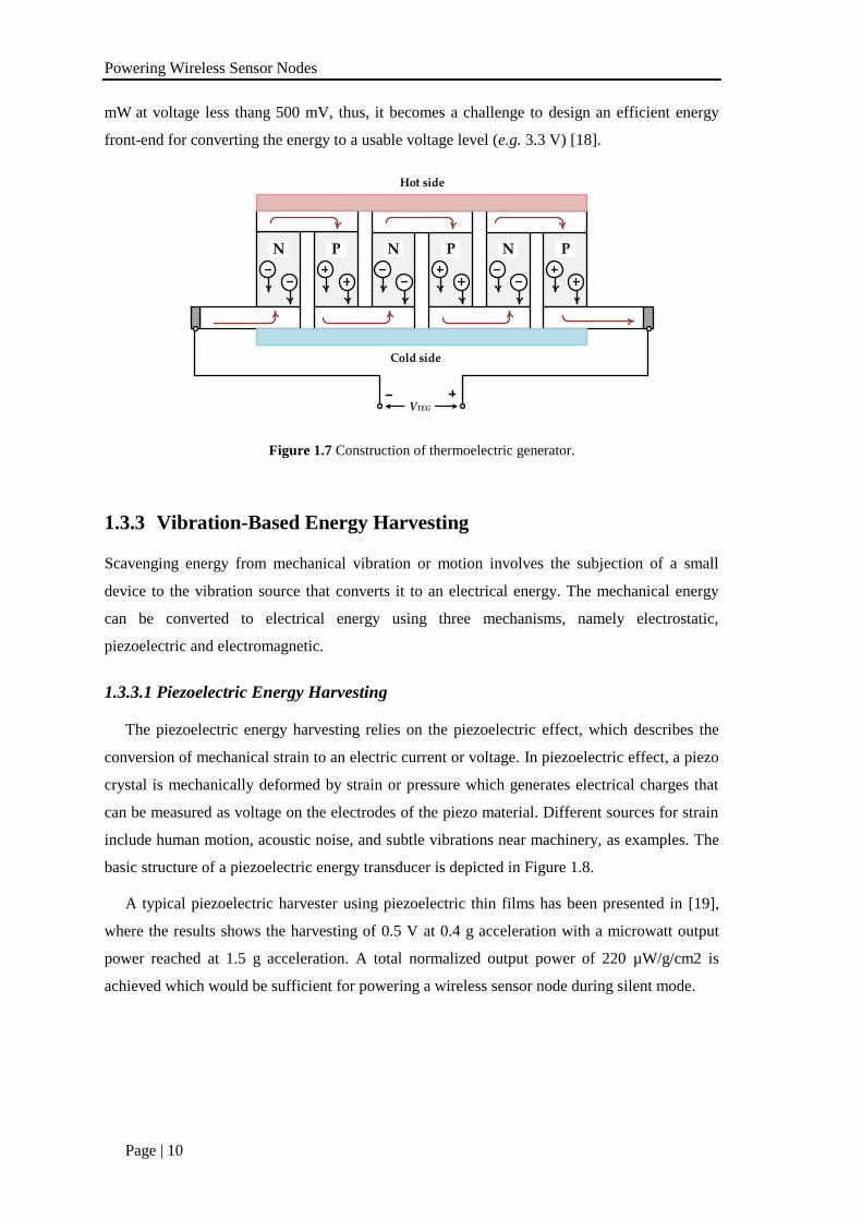
Thermoelectric generators are realized by connecting two pillars made of two different
materials and interconnected electrically in series by another metal. Normally, the two
different materials are realized through N-doped and P-doped semiconductor pellets. This
configuration, shown in Figure 1.7, is called "thermocouple" which is the core element for
forming thermoelectric generators. A thermoelectric generator then is formed by connecting a
large number of thermocouple in series and sandwiched between two thermally conductive
ceramic plates.
The efficiency of a thermoelectric generator (at 22 oC ambient temperature) ranges from
0.8% for human body applications (ΔT ~ 15 K) to 2.7% for machine applications (ΔT ~ 50 K)
[17], which is undoubtedly low. Miniaturized thermoelectric generators would generate sub-1
Powering Wireless Sensor Nodes
Page | 10
mW at voltage less thang 500 mV, thus, it becomes a challenge to design an efficient energy
front-end for converting the energy to a usable voltage level (e.g. 3.3 V) [18].
P N P N PN
Hot side
Cold side
VTEG
Figure 1.7 Construction of thermoelectric generator.
1.3.3 Vibration-Based Energy Harvesting
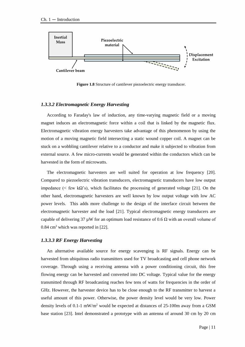
Scavenging energy from mechanical vibration or motion involves the subjection of a small
device to the vibration source that converts it to an electrical energy. The mechanical energy
can be converted to electrical energy using three mechanisms, namely electrostatic,
piezoelectric and electromagnetic.
1.3.3.1 Piezoelectric Energy Harvesting
The piezoelectric energy harvesting relies on the piezoelectric effect, which describes the
conversion of mechanical strain to an electric current or voltage. In piezoelectric effect, a piezo
crystal is mechanically deformed by strain or pressure which generates electrical charges that
can be measured as voltage on the electrodes of the piezo material. Different sources for strain
include human motion, acoustic noise, and subtle vibrations near machinery, as examples. The
basic structure of a piezoelectric energy transducer is depicted in Figure 1.8.
A typical piezoelectric harvester using piezoelectric thin films has been presented in [19],
where the results shows the harvesting of 0.5 V at 0.4 g acceleration with a microwatt output
power reached at 1.5 g acceleration. A total normalized output power of 220 µW/g/cm2 is
achieved which would be sufficient for powering a wireless sensor node during silent mode.
Ch. 1 — Introduction
Page | 11
Piezoelectric material
Inertial Mass
Cantilever beam
DisplacementExcitation
Figure 1.8 Structure of cantilever piezoelectric energy transducer.
1.3.3.2 Electromagnetic Energy Harvesting
According to Faraday's law of induction, any time-varying magnetic field or a moving
magnet induces an electromagnetic force within a coil that is linked by the magnetic flux.
Electromagnetic vibration energy harvesters take advantage of this phenomenon by using the
motion of a moving magnetic field intersecting a static wound copper coil. A magnet can be
stuck on a wobbling cantilever relative to a conductor and make it subjected to vibration from
external source. A few micro-currents would be generated within the conductors which can be
harvested in the form of microwatts.
The electromagnetic harvesters are well suited for operation at low frequency [20].
Compared to piezoelectric vibration transducers, electromagnetic transducers have low output
impedance (< few kΩ’s), which facilitates the processing of generated voltage [21]. On the
other hand, electromagnetic harvesters are well known by low output voltage with low AC
power levels. This adds more challenge to the design of the interface circuit between the
electromagnetic harvester and the load [21]. Typical electromagnetic energy transducers are
capable of delivering 37 µW for an optimum load resistance of 0.6 Ω with an overall volume of
0.84 cm3 which was reported in [22].
1.3.3.3 RF Energy Harvesting
An alternative available source for energy scavenging is RF signals. Energy can be
harvested from ubiquitous radio transmitters used for TV broadcasting and cell phone network
coverage. Through using a receiving antenna with a power conditioning circuit, this free
flowing energy can be harvested and converted into DC voltage. Typical value for the energy
transmitted through RF broadcasting reaches few tens of watts for frequencies in the order of
GHz. However, the harvester device has to be close enough to the RF transmitter to harvest a
useful amount of this power. Otherwise, the power density level would be very low. Power
density levels of 0.1-1 mW/m2 would be expected at distances of 25-100m away from a GSM
base station [23]. Intel demonstrated a prototype with an antenna of around 30 cm by 20 cm
Towards Autonomous WSNs
Page | 12
where 60µW has been harvested from a TV tower station away from the harvester by 4.1km
[24]. While the amount of power would be enough for powering a wireless sensor node, the size
constraints of modern tiny sensor nodes make it impractical solution.
1.3.3.4 Multi-Source Energy Harvesting
The main goal for energy harvesting for sensor nodes is to extend the lifetime of a sensor.
The harvested power should be sufficient and sustained. However, energy cannot be available
all the time from just a single harvesting source which adds many challenges for current WSNs.
This is a little bit far from the main goal of a fully autonomous ubiquitous sensor nodes.
Consequently, a hybrid energy scavenging solution that combines multiple energy harvesters
would be a feasible solution. For instance, a prototype for testing purpose has been developed
that comprises multiplexer module, photovoltaic module, vibration module, supercapacitor
module, battery module, and mains module [25].
Similarly, a platform that combines solar and wind energy transducers has been reported in
[26]. The power output is connected to power an Eco wireless node as well as to charge a Li-
Polymer battery. Likewise, an energy harvesting system presented in [27] to gather the energy
from two energy sources (airflow and sunlight) simultaneously in addition to a fuel cell as silent
energy storage. Unfortunately, the energy-aware analysis for the average amount of power
available for every sensor node is a missing point in most of these research.
1.4 Towards Autonomous WSNs
Lifetime is a key issue that is an important characteristic for evaluating WSNs. A clear
definition for lifetime of WSNs is not clear yet, however we will relate lifetime of WSN to the
lifetime of individual sensor nodes. From that, the lifetime of a sensor node can be defined as
the time period during the sensor node is alive and functioning properly [28]. Due to the nature
of WSNs, lifetime cannot be discussed apart from maintenance. Mostly, WSNs are inaccessible
and been deployed in harsh environments which make it almost impossible or costly to reach
them for maintenance. That's why a WSM with extended lifetime is always a concern.
As a result for the limited resources of remotely deployed WSNs, lifetime mainly depends
upon the power resources of each sensor node. Consequently, a sensor node would be alive and
function normally as long as power is available. On the other hand, sensor nodes are limited in
size and weight and the same constraints apply for battery size in use. Thus, employing an
alternative energy source such as energy harvesting becomes inevitable for extending the
lifetime of the sensor nodes. In general, the lifetime of the sensor node depends basically on two
factors; how much energy it consumes over time, and how much energy is available for its use
[28]. Consequently, it becomes obvious that even energy harvesting would fail to provide the
Ch. 1 — Introduction
Page | 13
sensor node with the required power for autonomous operation. We note in Table 1.1 that the
power density of most of energy harvesting technology is limited. It becomes even worse for
indoor sensor nodes where the available peak power is limited to few micro-watts. Therefore,
two cooperating approaches are normally employed. First, the average power consumption of
the sensor node is managed by applying specific power-aware communication protocols that
keep tracks of the energy availability and data transmission/reception [9]. Second, the power
harvested at each sensor node is increased such that a balance between the energy consumption
and energy harvesting is achieved.
Recently, non-radiative wireless power transfer (WPT) has shown a notable progress as a
potential energy source for a wide variety of applications. Medical implantable devices,
consumer electronics, electric vehicles charging, and robotics are among numerous applications
where WPT has been adopted as a key enabling technology. The feasibility of WPT as a power
source for single input-multiple output (SIMO) WSNs in IoT systems has been investigated and
modeled [29]. As we previously highlighted, it is clear that energy harvesting is a promising
technology, yet the chaotic nature and unpredictability make it a limiting factor toward a fully
autonomous WSNs. Consequently, it becomes more convenient to alleviate the lifetime
bottleneck of WSNs through WPT such that the lifetime is prolonged [30]. It is true that
contactless power transmission has been extensively suggested and validated in WSNs by
means of far-field RF power transmission by harvesting the already-existed electromagnetic RF
power [31], [32]. In these systems, a single antenna or multiple antennas could be utilized to
simultaneously receive data and power. On the other hand, near-field non-radiative WPT
through inductive coupling has become an interesting area for powering indoor and local-area
deployed WSNs. Figure 1.9 shows a conceptual diagram for a WSNs enabled by WPT.
Sensors/Actuators
μP
Radio
WSN
PowerManagement
Stoarge
WPT
RxCoil
Sensors/Actuators
μP
Radio
WSN
PowerManagement
Stoarge
WPT
RxCoil
Sensors/Actuators
μP
Radio
WSN
PowerManagement
Stoarge
WPT
RxCoil
WP
T B
ase
Tx Coil
Power sourceConverter
Circuits
M1M2
Mn
Figure 1.9 Conceptual schematic diagram for WPT-enabled wireless sensor nodes.
Problem Statement and Thesis Scope
Page | 14
1.5 Problem Statement and Thesis Scope
WPT is undoubtedly becoming a promising technology for contactless powering of WSNs
among many other applications. Fundamentally, WPT has been limited for point-to-point
applications where a single receiver is powered from a single receiver over an approximately
fixed distance. Moreover, most of the studied and presented work in WPT work target
stationary transmitter and receiver ends during the power transmission time, which is not a
practical case for many applications in complex dynamic environments. Thus, WPT becomes
less reliable and more vulnerable for power transmission dysfunctionality in a non-stationary
wide-distance environment. In this section, the current challenges in WPT systems are shortly
discussed towards the description of the thesis scope.
1.5.1 Current Challenges in WPT systems
Throughout this chapter we discussed the technical issues related that faces WSN in different
application with a major focusing on technical issues related to powering sensor motes in such
networks. Despite the fact that a considerable amount of literature has been published in energy
harvesting for WSNs, still energy harvesting faces multiple challenges related to the
environmental conditions and the available energy sources. An important potential application
for WSNs is to deploy sensors for indoor operation at hospitals (biomedical implants) or homes
(intelligent appliances) or at any place where energy harvesting is strictly useless due to the
scarceness of energy sources. In that case, wireless power transmission emerges as the relevant
alternative to power WSNs and eliminate the need for replacing batteries. This would greatly
help in reducing the cost of maintenance for such devices and increase the system reliability and
autonomy. However, it is of utmost importance to circumvent the challenges related to WPT
links in order to get all the benefits of wireless powering these sensors; from here emerges the
main scope of the thesis. To enable WSNs, and hence the IoT, by means of WPT, the main
challenges that need to be addressed can be shortly described as follows:
1.5.1.1 Magnetic Coupling Variation
The WPT concept is dependent on the fundamental principle of electromagnetic induction
phenomena, where two coupled coils, mostly loosely coupled, exchange the energy through the
flux linkage from the source/transmitter to the load/receiver coil. Consequently, the coupling
coefficient between the two coils is a key factor that determines how much energy is transferred
and how efficient the system is. From this perspective, if the WPT link is employed in a
dynamic environment where there is a relative movement between the transmitter and the
receiver, the coupling coefficient with evidently becomes variable [33]. Obviously, this would

Ch. 1 — Introduction
Page | 15
lead to a change in the effective impedance at the transmitter side which leads to a change in the
transferred power to the receiver.
1.5.1.2 Components Tolerance
The most common technique in inductive WPT is magnetic resonance, where the reactive
impedance of the coils are compensated to form a resonance circuit at either the transmitter, or
the receiver, or both of them. As we will explain in the next chapters, it is required to design the
resonance circuits both at the transmitter and receiver sides such that they are fully-tuned at the
same natural frequency [34]. The process of components selection assumes fixed components’
values. However, components tolerance after manufacturing and temperature effect make the
system prone for deviation from the optimal operating frequency. Moreover, the sensitivity of
the system increases considerably following the increase of quality factor of the resonant circuit
[35].
1.5.1.3 Proximity Interfering Objects
Conductive interfering objects in close proximity to the transmitter or the receiver have a
great impact on the performance of the WPT system. An interfering objects having a complex
impedance would cause a drift in the resonant frequency of the transmitter or the receiver or
both of them depending on the relative distance of this object and its self-resonant frequency
[36]. Moreover, the loading effect of the conductive object would cause a drop in the
transferred power to the receiver. Whatsoever the effect of an interfering object, the resonant
circuits at the interfered side (transmitter or receiver) has to be adaptively tuned to retain the
proper system functionality.
1.5.1.4 Load Variation
The power transmitted to a receiver, as we will show, is a function of the equivalent load
resistance at the receiver. Consequently, a device whose load varies depending on the operating
condition, such as a system change from idle state to fully awake state, is going to affect the
induced voltage, and the efficiency in essence, or current in the receiver side [37].
Consequently, an adaptive front-end is vital for maintaining a constant voltage/current
operation.
1.5.2 Scope of the Thesis
As a consequence of the shortly aforementioned challenges of WPT systems, it becomes
reasonable to address the challenges and push the boundaries of limiting factors towards an
efficient and sufficient energy transmission for sensors in a dynamic environments. The efforts
Thesis Outline
Page | 16
of mitigating the bottleneck of WPT system performance is fundamentally achievable at the
transmitter side or receiver side. However, it is more practical to focus on having a controllable
receiver side because it is more adequate for single input-multiple output (SIMO) WPT links
such as the case of powering multiple sensor nodes from a single transmitting power source.
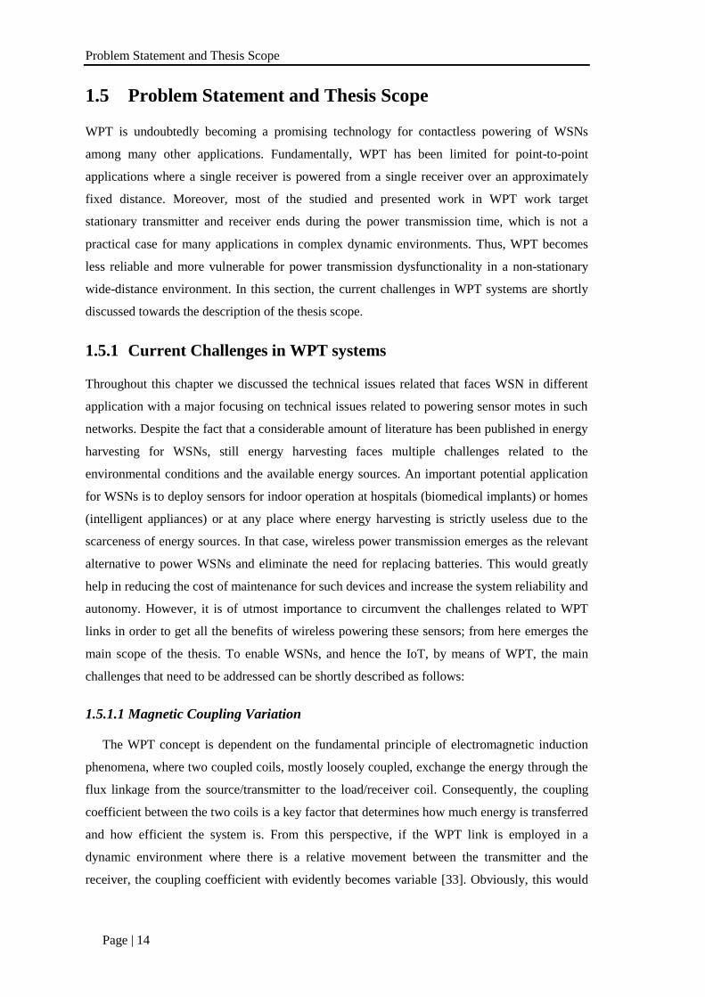
Accordingly, the main scope of the thesis is to study and model the effects of mismatch in
components and coupling variation on the performance of WPT systems including power
transmission capabilities and efficiency. Subsequently, the efforts will be focus on developing
an adaptive power management front-end that would enable the electronic self-tuning of WPT
receivers against any mismatch in components values or system parameters variation. This
would enable the WPT system to be designed at high quality factor without being significantly
sensitive. Consequently, the maximum power delivery to the receiver would be retrieved
automatically. As we will show in the subsequent chapters, the developed front-end should
certainly be efficient in order to achieve the maximum power at the possible maximum
efficiency since it is in the power path. The main scope of the thesis is depicted in Figure 1.10,
where the main efforts will be directed to developing the adaptive front-end at the receiver side
in a WPT system.
RL
Voc
LR
M
IT
TxCompensation
LTVin
Vac
Adaptive Tunable
Front-End
RxCompensation
Controller
VDC
Figure 1.10 Conceptual block diagram for the main goal of the thesis.
1.6 Thesis Outline
After introducing the main scope and objectives of this thesis, the general outline of the thesis
starts by analyzing and modelling WPT systems and then investigates the limiting factors that
affect power transmission in high quality factors resonant WPT. Thereafter, an adaptive power
management front-end has to be proposed in order to ensure a fully-tuned WPT link. The
proposed power management front-end should mainly ensure self-tunability in case of
mismatch or interference in the WPT receiver. The subsequent chapters, then, will have the
following outline:
Ch. 1 — Introduction
Page | 17
Chapter 2 entitled “On the Theory and Modelling of Wireless Power Transfer” gives
background about wireless power transfer kinds followed by a focus on resonant inductive
coupling WPT. It presents, as well, a modelling and analysis of the main compensation
topologies in WPT and the technical issues that limit their performance.
Chapter 3 revisit the gyrator circuit element and its application as a reactive element
synthesizer. The switch-mode implementation of gyrator dedicated for power processing
application is also discussed. The gyrator-based switch-mode reactive element synthesis is then
evaluated in various design cases given as a proof of concept.
Chapter 4 presents a novel dual-loop control for switch-mode gyrator in WPT receivers. The
design details and verification of the control operation is evaluated at design case of parallel-
compensated WPT receiver. In order to mitigate the drawbacks of the dual-loop control, a
further control approach entitled “quadrature phase-locked-loop” is presented and discussed. It
has been shown that the quadrature PLL control is more reliable compared to the dual-loop
control presented so far. Toward a fully integrated system, the chip pre-design of the switch-
mode gyrator circuit and control blocks is also presented and the efficiency of the WPT receiver
at different mismatch cases is also calculated with the help of the accurate models of XFAB
0.18μm HV process.
Chapter 5 discusses the adoption of phase-controlled switched converters for multifunctional
operation by combining the self-tuning functionality with energy rectification functionality. It
has been shown that the presented operation leads to a more compact circuit that tunes the WPT
receiver while the energy is rectified and supplied to the load. The proposed operation has been
verified and applied into two different switch-mode circuits, where the verification results have
given.
Chapter 6 proposes a novel approach which presents a modified operation in the phase-
controlled converter. The proposed novel operation enables active tuning, as a reactive power
control, as well as output voltage regulation, as a real power control. Consequently, the
proposed operation offers extended functionalities of active tuning, rectification and voltage
regulation, altogether by means of a single stage switch-mode front-end.
Chapter 6 concludes the thesis. The main contribution of the thesis is summarized. As well,
the list of publications as a result of the thesis is given. Finally, the suggested future work
derived from the thesis work is given for further research lines that could improve the research
findings in the future.
References
Page | 18
1.7 References
[1] C. Turcu, Ed., Deploying RFID - Challenges, Solutions, and Open Issues. InTech, 2011.
[2] EU FP7 Project CASAGRAS, “CASAGRAS final report: RFID and the inclusive model for the
internet of things,” 2009.
[3] J. Gubbi, R. Buyya, S. Marusic, and M. Palaniswami, “Internet of Things (IoT): A vision,
architectural elements, and future directions,” Futur. Gener. Comput. Syst., vol. 29, no. 7, pp. 1645–
1660, Sep. 2013.
[4] S. Haller, “Internet of Things: An Integral Part of the Future Internet,” SAP presentation.
[5] Ian Chen, “Sensors Are a Primary Source for Big Data,” EECatalog, 2014. [Online]. Available:
http://eecatalog.com/IoT/2014/05/16/sensors-are-a-primary-source-for-big-data/. [Accessed: 26-
Feb-2018].
[6] M. Botterman, “Internet of Things: an early reality of the Future Internet,” Prague, 2009.
[7] H. Zhou, The Internet of Things in the Cloud: A Middleware Perspective. CRC Press, Taylor &
Francis Group, 2012.
[8] V. Kumar, Fundamentals of pervasive information management systems. John Wiley & Sons
Inc, 2013.
[9] J. Yick, B. Mukherjee, and D. Ghosal, “Wireless sensor network survey,” Comput. Networks,
vol. 52, no. 12, pp. 2292–2330, Aug. 2008.
[10] S. (Sergej) Fatikow and U. Rembold, Microsystem Technology and Microrobotics. Springer,
Berlin, Heidelberg, 1997.
[11] P. Baronti, P. Pillai, V. W. C. Chook, S. Chessa, A. Gotta, and Y. F. Hu, “Wireless sensor
networks: A survey on the state of the art and the 802.15.4 and ZigBee standards,” Computer
Communications, vol. 30, no. 7. Elsevier, pp. 1655–1695, 26-May-2007.
[12] J. L. Hill, “System Architecture for Wireless Sensor Networks,” Ph.D Dissertation, Computer
Engineering, University of California, Berkeley USA, 2003.
[13] Á. Asensio, R. Blasco, Á. Marco, and R. Casas, “Hardware architecture design for WSN
runtime extension,” Int. J. Distrib. Sens. Networks, vol. 2013, no. 4, p. 136745, Apr. 2013.
[14] R. G. Cid-Fuentes, A. Cabellos-Aparicio, and E. Alarcon, “Energy buffer dimensioning through
energy-erlangs in spatio-temporal-correlated energy-harvesting-enabled wireless sensor networks,”
IEEE J. Emerg. Sel. Top. Circuits Syst., vol. 4, no. 3, pp. 301–312, Sep. 2014.
[15] J. Carpenter and Y. Ramadass, “Fundamentals of ambient energy transducers in energy
harvesting systems. (Smart Grid & Alternative Energy),” ECN-Electronic Compon. News, vol. 56,
no. 6, p. 20(1), 2012.
[16] V. Raghunathan, A. Kansal, J. Hsu, J. Friedman, and M. Srivastava, “Design considerations for
solar energy harvesting wireless embedded systems,” in 2005 4th International Symposium on
Information Processing in Sensor Networks, IPSN 2005, 2005, vol. 2005, pp. 457–462.
Ch. 1 — Introduction
Page | 19
[17] A. Montecucco, J. Siviter, and A. R. Knox, “The effect of temperature mismatch on
thermoelectric generators electrically connected in series and parallel,” Appl. Energy, vol. 123, pp.
47–54, Jun. 2014.
[18] W. Wang, V. Cionca, N. Wang, M. Hayes, B. O’Flynn, and C. O’Mathuna, “Thermoelectric
energy harvesting for building energy management wireless sensor networks,” Int. J. Distrib. Sens.
Networks, vol. 2013, no. 6, p. 232438, Jun. 2013.
[19] P. Muralt, M. Marzencki, B. Belgacem, F. Calame, and S. Basrour, “Vibration Energy
Harvesting with PZT Micro Device,” in Procedia Chemistry, 2009, vol. 1, no. 1, pp. 1191–1194.
[20] A. Rahimi, Ö. Zorlu, A. Muhtaroǧlu, and H. Külah, “Fully self-powered electromagnetic
energy harvesting system with highly efficient dual rail output,” IEEE Sens. J., vol. 12, no. 6, pp.
2287–2298, Jun. 2012.
[21] H. Ulusan, K. Gharehbaghi, O. Zorlu, A. Muhtaroglu, and H. Kulah, “A fully integrated and
battery-free interface for low-voltage electromagnetic energy harvesters,” IEEE Trans. Power
Electron., vol. 30, no. 7, pp. 3712–3719, Jul. 2015.
[22] P. Glynne-Jones, M. J. Tudor, S. P. Beeby, and N. M. White, “An electromagnetic, vibration-
powered generator for intelligent sensor systems,” in Sensors and Actuators, A: Physical, 2004, vol.
110, no. 1–3, pp. 344–349.
[23] R. Vullers, R. Schaijk, H. Visser, J. Penders, and C. Hoof, “Energy harvesting for autonomous
wireless sensor networks,” IEEE Solid-State Circuits Mag., vol. 2, no. 2, pp. 29–38, 2010.
[24] A. Sample and J. R. Smith, “Experimental results with two wireless power transfer systems,”
2009 IEEE Radio Wirel. Symp., pp. 16–18, Jan. 2009.
[25] A. S. Weddell, N. J. Grabham, N. R. Harris, and N. M. White, “Modular plug-and-play power
resources for energy-aware wireless sensor nodes,” in 2009 6th Annual IEEE Communications
Society Conference on Sensor, Mesh and Ad Hoc Communications and Networks, SECON 2009,
2009, pp. 1–9.
[26] C. Park and P. H. Chou, “AmbiMax: Autonomous energy harvesting platform for multi-supply
wireless sensor nodes,” in 2006 3rd Annual IEEE Communications Society on Sensor and Adhoc
Communications and Networks, Secon 2006, 2007, vol. 1, pp. 168–177.
[27] D. Porcarelli, D. Brunelli, M. Magno, and L. Benini, “A Multi-Harvester architecture with
hybrid storage devices and smart capabilities for low power systems,” in SPEEDAM 2012 - 21st
International Symposium on Power Electronics, Electrical Drives, Automation and Motion, 2012,
pp. 946–951.
[28] Y. Chen and Q. Zhao, “On the lifetime of wireless sensor networks,” IEEE Commun. Lett., vol.
9, no. 11, pp. 976–978, Nov. 2005.
[29] E. Bou-Balust, R. Sedwick, P. Hu, and E. Alarcon, “Advances in non-radiative resonant
inductive coupling wireless Power Transfer: A comparison of alternative circuit and system models
driven by emergent applications,” in Proceedings - IEEE International Symposium on Circuits and
Systems, 2014, pp. 2037–2040.
References
Page | 20
[30] V. V. Mai, W.-Y. Shin, and K. Ishibashi, “Wireless Power Transfer for Distributed Estimation
in Sensor Networks,” IEEE J. Sel. Top. Signal Process., vol. 11, no. 3, pp. 549–562, Apr. 2017.
[31] R. Zhang and C. K. Ho, “MIMO broadcasting for simultaneous wireless information and power
transfer,” IEEE Trans. Wirel. Commun., vol. 12, no. 5, pp. 1989–2001, May 2013.
[32] C. Shen, W. C. Li, and T. H. Chang, “Wireless information and energy transfer in multi-
antenna interference channel,” IEEE Trans. Signal Process., vol. 62, no. 23, pp. 6249–6264, Dec.
2014.
[33] C.-Y. Huang, J. E. James, and G. A. Covic, “Design Considerations for Variable Coupling
Lumped Coil Systems,” IEEE Trans. Power Electron., vol. 30, no. 2, pp. 680–689, Feb. 2015.
[34] J. T. Boys, G. A. Covic, and A. W. Green, “Stability and control of inductively coupled power
transfer systems,” IEE Proc. - Electr. Power Appl., vol. 147, no. 1, p. 37, 2000.
[35] A. Trivino, D. Fernandez, J. A. Aguado, and J. E. Ruiz, “Sensitivity analysis of component’s
tolerance in Inductively Coupled Power Transfer system,” in 2013 International Conference on
Renewable Energy Research and Applications (ICRERA), 2013, no. October, pp. 806–810.
[36] E. Bou, E. Alarcon, R. Sedwick, and P. Fisher, “Interference analysis on Resonant Inductive
Coupled Wireless Power Transfer links,” in Proceedings - IEEE International Symposium on
Circuits and Systems, 2013, pp. 2783–2786.
[37] M. Bojarski, E. Asa, and D. Czarkowski, “Effect of wireless power link load resistance on the
efficiency of the energy transfer,” in 2014 IEEE International Electric Vehicle Conference (IEVC),
2014, pp. 1–7.
Page | 21
Chapter
2
2 On the Theory and Modelling of Wireless
Power Transfer
Wireless power transfer (WPT) is the process of transmitting electrical power from a source to a
load without using conductors or wire. Other times, it is called "contactless power transfer".
While WPT is a wide topic that covers many applications with different techniques and
different ranges, our discussion would be limited to the overall scope that may coincide with
IoT applications.
As it has been discussed in Chapter 1, WPT would be a promising technology for contactless
powering of WSNs since it has more reliable characteristics compared to the random nature of
energy harvesting. In this chapter, an overview of WPT systems and their categories will be
discussed. Then, the resonant-inductive-coupling WPT will be discussed in detail because it
enables energy transmission to wider distances compared to the non-resonant kind. The detailed
analysis of the basic resonator compensation topologies will be also shown. Finally, the
sensitivity and mistuning problem in parallel-compensated WPT receivers will be explained.
2.1 History of Wireless Power Transfer at a Glance
WPT is a field of study under development with many promising applications that could
significantly change the whole society and leave its impact on every aspect of our life. It is
important to go at first through the history of developing WPT before discussing the technical
issues related to such impressive discipline. For the sake of highlighting the most important
milestones in WPT development, the major events in WPT history should be revisited. It all
started in 1891 at a lecture in Columbia College where Nicola Tesla was able to light a bulb
from across a stage. Later in 1899, Tesla found that he could increase the distance by an LC
resonator at the transmitter and receiver sides with both of them tuned to the same frequency
[1]. This way, he was able to light three incandescent lamps by resonant inductive coupling at a
Categories of Wireless power Transfer
Page | 22
distance of about 30 m using high voltages in the order of 20 megavolts, where the findings of
Tesla can be noted in [2], [3]. In the early 1960s, William C. Brown contributed to microwave
power transmission when he invented what is called "rectenna" [4]. A combination of an
antenna and a rectifier had been used to convert microwave power to DC electricity. Later on
1964, Brown was able to wirelessly power a model helicopter using microwaves. During the
1960s, inductive wireless power transmission has been revisited again by Schaldach where
powering artificial hearts has been achieved [5]. Later in 1975, William Brown and Robert
Dickinson were able to transmit high power through a distance of 1.54km using microwaves at
a frequency of 2.388GHz [6].
During the 1990s, several work demonstrated successfully using microwave power
transmission in aerospace applications [7], [8]. Alternatively, in 2007, a team in MIT
transferred successfully a power of 60W over a distance of 2m with efficiency around 40%
using coupled resonant coils of 25cm operating at 10 MHz [9]. The efforts of developing and
promoting wireless power transmission gave rise to the establishment of the "Wireless Power
Consortium" in 2008. The first inductive power transfer "Qi" resulted in 2009 to enable
charging portable devices with a maximum of 5W.
In the last decade, rapid advances in WPT development have been proved by many
commercial products supported by extensive research in most aspects of the technical issues
involved in WPT design. Evidently, it is important here to distinguish between two different
types of wireless power transmission, namely radiative microwave WPT and non-radiative
magnetic coupling WPT. Accordingly, both kinds can be treated as different technologies with
different characteristics and hence different potential applications.
2.2 Categories of Wireless power Transfer
As we have witnessed through the rich history of the development of wireless power
transmission, it is evidently valid to categorize the wireless power transfer, in general, into two
main categories, namely far-field radiative WPT and near-field non-radiative WPT. It
consequently becomes obvious that in order to employ WPT in a specific application, one needs
to understand which type of WPT is possibly more convenient for that application.
2.2.1 Far-Field Radiative WPT
Pioneered by William C. Brown, radiative WPT depends on transmitting energy through space
using electromagnetic radio waves. In such a way, electrical power from a DC source is
converted into radio-frequency (RF) power, then the RF power is transmitted to space toward a
receiving point where the power is received and converted back into DC power [10].
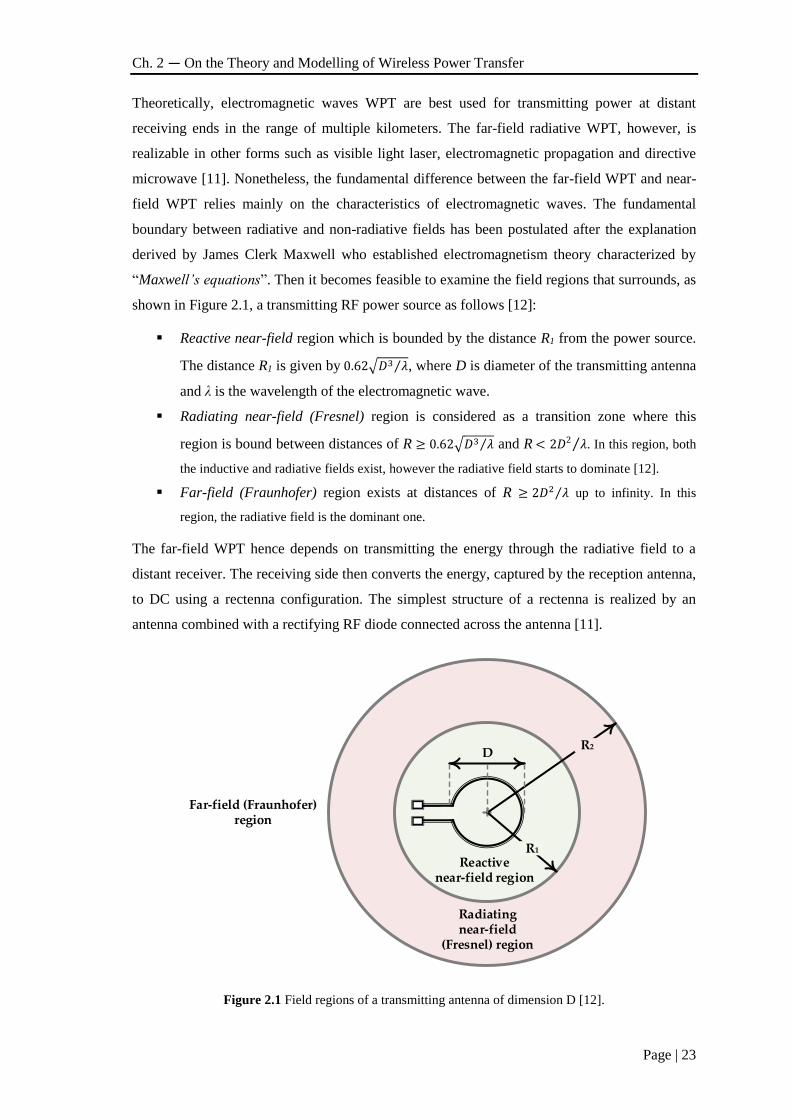
Ch. 2 — On the Theory and Modelling of Wireless Power Transfer
Page | 23
Theoretically, electromagnetic waves WPT are best used for transmitting power at distant
receiving ends in the range of multiple kilometers. The far-field radiative WPT, however, is
realizable in other forms such as visible light laser, electromagnetic propagation and directive
microwave [11]. Nonetheless, the fundamental difference between the far-field WPT and near-
field WPT relies mainly on the characteristics of electromagnetic waves. The fundamental
boundary between radiative and non-radiative fields has been postulated after the explanation
derived by James Clerk Maxwell who established electromagnetism theory characterized by
“Maxwell’s equations”. Then it becomes feasible to examine the field regions that surrounds, as
shown in Figure 2.1, a transmitting RF power source as follows [12]:
Reactive near-field region which is bounded by the distance R1 from the power source.
The distance R1 is given by 0.62√𝐷3 𝜆⁄ , where D is diameter of the transmitting antenna
and λ is the wavelength of the electromagnetic wave.
Radiating near-field (Fresnel) region is considered as a transition zone where this
region is bound between distances of R ≥ 0.62√𝐷3 𝜆⁄ and R < 2𝐷2 𝜆⁄ . In this region, both
the inductive and radiative fields exist, however the radiative field starts to dominate [12].
Far-field (Fraunhofer) region exists at distances of R ≥ 2𝐷2 𝜆⁄ up to infinity. In this
region, the radiative field is the dominant one.
The far-field WPT hence depends on transmitting the energy through the radiative field to a
distant receiver. The receiving side then converts the energy, captured by the reception antenna,
to DC using a rectenna configuration. The simplest structure of a rectenna is realized by an
antenna combined with a rectifying RF diode connected across the antenna [11].
Reactive near-field region
D
R1
R2
Radiating near-field
(Fresnel) region
Far-field (Fraunhofer) region
Figure 2.1 Field regions of a transmitting antenna of dimension D [12].
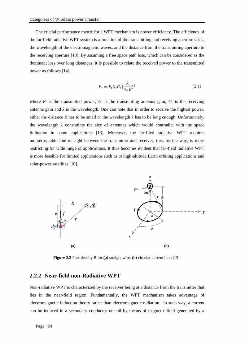
Categories of Wireless power Transfer
Page | 24
The crucial performance metric for a WPT mechanism is power efficiency. The efficiency of
the far-field radiative WPT system is a function of the transmitting and receiving aperture sizes,
the wavelength of the electromagnetic waves, and the distance from the transmitting aperture to
the receiving aperture [13]. By assuming a free space path loss, which can be considered as the
dominant loss over long distances, it is possible to relate the received power to the transmitted
power as follows [14]:
𝑃𝑟 = 𝑃𝑡𝐺𝑡𝐺𝑟(𝜆
4𝜋𝑅)2 (2.1)
where Pt is the transmitted power, Gt is the transmitting antenna gain, Gr is the receiving
antenna gain and λ is the wavelength. One can note that in order to receive the highest power,
either the distance R has to be small or the wavelength λ has to be long enough. Unfortunately,
the wavelength λ constraints the size of antennas which would contradict with the space
limitation in some applications [13]. Moreover, the far-filed radiative WPT requires
uninterruptable line of sight between the transmitter and receiver, this, by the way, is more
restricting for wide range of applications. It thus becomes evident that far-field radiative WPT
is more feasible for limited applications such as to high-altitude Earth orbiting applications and
solar-power satellites [10].
(a)
z
x
ya
φ
I
r
PdBz
Rz
(b)
Figure 2.2 Flux density B for (a) straight wire, (b) circular current loop [15].
2.2.2 Near-field non-Radiative WPT
Non-radiative WPT is characterized by the receiver being at a distance from the transmitter that
lies in the near-field region. Fundamentally, the WPT mechanism takes advantage of
electromagnetic induction theory rather than electromagnetic radiation. In such way, a current
can be induced in a secondary conductor or coil by means of magnetic field generated by a
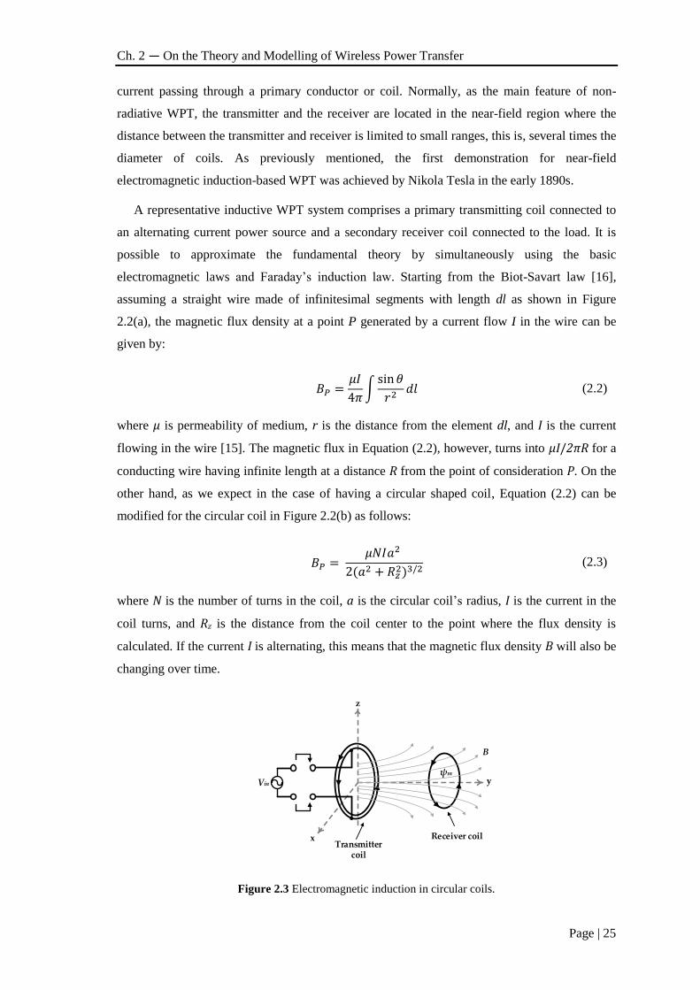
Ch. 2 — On the Theory and Modelling of Wireless Power Transfer
Page | 25
current passing through a primary conductor or coil. Normally, as the main feature of non-
radiative WPT, the transmitter and the receiver are located in the near-field region where the
distance between the transmitter and receiver is limited to small ranges, this is, several times the
diameter of coils. As previously mentioned, the first demonstration for near-field
electromagnetic induction-based WPT was achieved by Nikola Tesla in the early 1890s.
A representative inductive WPT system comprises a primary transmitting coil connected to
an alternating current power source and a secondary receiver coil connected to the load. It is
possible to approximate the fundamental theory by simultaneously using the basic
electromagnetic laws and Faraday’s induction law. Starting from the Biot-Savart law [16],
assuming a straight wire made of infinitesimal segments with length dl as shown in Figure
2.2(a), the magnetic flux density at a point P generated by a current flow I in the wire can be
given by:
𝐵𝑃 =𝜇𝐼
4𝜋∫
sin𝜃
𝑟2𝑑𝑙 (2.2)
where μ is permeability of medium, r is the distance from the element dl, and I is the current
flowing in the wire [15]. The magnetic flux in Equation (2.2), however, turns into μI/2πR for a
conducting wire having infinite length at a distance R from the point of consideration P. On the
other hand, as we expect in the case of having a circular shaped coil, Equation (2.2) can be
modified for the circular coil in Figure 2.2(b) as follows:
𝐵𝑃 = 𝜇𝑁𝐼𝑎2
2(𝑎2 + 𝑅𝑧2)3/2
(2.3)
where N is the number of turns in the coil, a is the circular coil’s radius, I is the current in the
coil turns, and Rz is the distance from the coil center to the point where the flux density is
calculated. If the current I is alternating, this means that the magnetic flux density B will also be
changing over time.
z
x
yψm
B
Vin
Transmitter coil
Receiver coil
Figure 2.3 Electromagnetic induction in circular coils.
Categories of Wireless power Transfer
Page | 26
Assuming that there is a coil connected to an alternating current source, the magnetic flux ψ
will have the direction shown in Figure 2.3. If another coil, let us call it the receiving coil, is
placed close to the first coil such that it becomes linked by the time-varying flux, then the total
magnetic flux ψm that crosses the receiving coil can be expressed as:
𝜓𝑚 = ∫𝐵. 𝑑𝑠
𝑠
(2.4)
where B is the generated magnetic flux by the transmitting coil and s is the receiving coil's
surface. This leads to Faraday's induction law which states that the induced voltage in the
receiving coil can then be expressed by [15]:
𝑉 = −𝑑𝜓𝑚
𝑑𝑡 (2.5)
where V is the open-circuit induced voltage in the receiving coil. If the receiving coil is closed
by a circuitry, a current would pass due to the induced voltage, and hence the power can be
successfully transferred from the transmitting coil to the receiving coil.
The amount of energy received by the receiving coil is dependent on the amount of magnetic
flux that links its surface. This consequently is dependent on the surface of the coil itself, as one
can note in Equation (2.4). On the other hand, as revealed by Equation (2.3), the magnetic flux
density decays rapidly at the rate of R2 from the transmitting coil. Obviously, and similar to
Tesla’s system, it is reasonably better to create resonant coils which would help in
strengthening the magnetic field over a larger distance from the transmitting end so that the
power could be received efficiently at higher distances. In that way, the name “resonant
inductive coupling” WPT emerges to distinguish such system from the non-resonant inductive
WPT. Consequently, resonant inductive coupling (RIC) WPT has attracted many applications
due to its higher efficiency over a wider distance range. Early successful implementations for
RIC-WPT can be noted in [17] where a maximum efficiency of 80% has been achieved at
distance of 10mm. Similarly, an average efficiency of 60% has been achieved at long distances
in the range of 2m [18].
Up to this point, it becomes apparent that RIC-WPT is one of the most convenient type for
transmitting power to WSN in terms of power demand at higher distance with more flexibility
that is not limited to direct line of sight between the power source and the receiving node. Thus,
RIC-WPT is considered as a key enabling technology for a wide number of applications;
however it is of utmost importance to study carefully the different parameters and system
conditions that affect the design. Finding an accurate analysis and model would help in finding
the optimal design parameters such as frequency of operation, transmitter and receiver coil
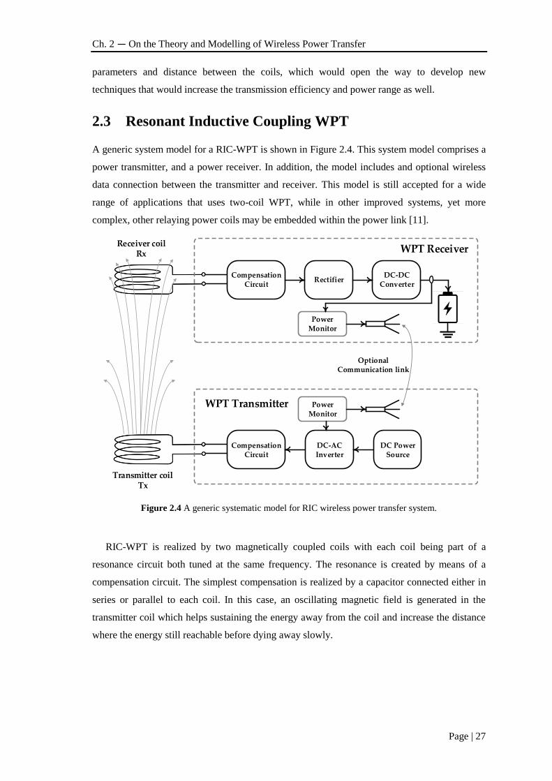
Ch. 2 — On the Theory and Modelling of Wireless Power Transfer
Page | 27
parameters and distance between the coils, which would open the way to develop new
techniques that would increase the transmission efficiency and power range as well.
2.3 Resonant Inductive Coupling WPT
A generic system model for a RIC-WPT is shown in Figure 2.4. This system model comprises a
power transmitter, and a power receiver. In addition, the model includes and optional wireless
data connection between the transmitter and receiver. This model is still accepted for a wide
range of applications that uses two-coil WPT, while in other improved systems, yet more
complex, other relaying power coils may be embedded within the power link [11].
Compensation Circuit
RectifierDC-DC
Converter
Receiver coilRx
Compensation Circuit
DC-ACInverter
DC PowerSource
Transmitter coilTx
Power Monitor
Power Monitor
Optional Communication link
WPT Receiver
WPT Transmitter
Figure 2.4 A generic systematic model for RIC wireless power transfer system.
RIC-WPT is realized by two magnetically coupled coils with each coil being part of a
resonance circuit both tuned at the same frequency. The resonance is created by means of a
compensation circuit. The simplest compensation is realized by a capacitor connected either in
series or parallel to each coil. In this case, an oscillating magnetic field is generated in the
transmitter coil which helps sustaining the energy away from the coil and increase the distance
where the energy still reachable before dying away slowly.
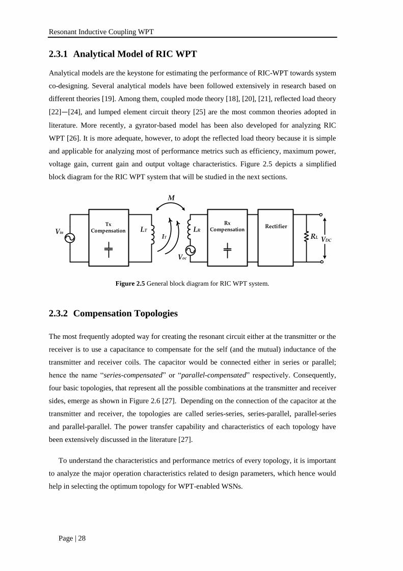
Resonant Inductive Coupling WPT
Page | 28
2.3.1 Analytical Model of RIC WPT
Analytical models are the keystone for estimating the performance of RIC-WPT towards system
co-designing. Several analytical models have been followed extensively in research based on
different theories [19]. Among them, coupled mode theory [18], [20], [21], reflected load theory
[22]—[24], and lumped element circuit theory [25] are the most common theories adopted in
literature. More recently, a gyrator-based model has been also developed for analyzing RIC
WPT [26]. It is more adequate, however, to adopt the reflected load theory because it is simple
and applicable for analyzing most of performance metrics such as efficiency, maximum power,
voltage gain, current gain and output voltage characteristics. Figure 2.5 depicts a simplified
block diagram for the RIC WPT system that will be studied in the next sections.
RL
Voc
LR
M
IT
TxCompensation LTVin
VDC
RxCompensation
Rectifier
Figure 2.5 General block diagram for RIC WPT system.
2.3.2 Compensation Topologies
The most frequently adopted way for creating the resonant circuit either at the transmitter or the
receiver is to use a capacitance to compensate for the self (and the mutual) inductance of the
transmitter and receiver coils. The capacitor would be connected either in series or parallel;
hence the name “series-compensated” or “parallel-compensated” respectively. Consequently,
four basic topologies, that represent all the possible combinations at the transmitter and receiver
sides, emerge as shown in Figure 2.6 [27]. Depending on the connection of the capacitor at the
transmitter and receiver, the topologies are called series-series, series-parallel, parallel-series
and parallel-parallel. The power transfer capability and characteristics of each topology have
been extensively discussed in the literature [27].
To understand the characteristics and performance metrics of every topology, it is important
to analyze the major operation characteristics related to design parameters, which hence would
help in selecting the optimum topology for WPT-enabled WSNs.
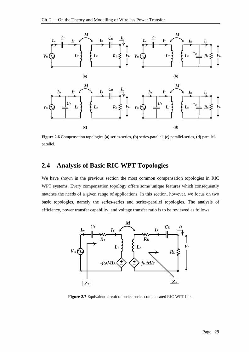
Ch. 2 — On the Theory and Modelling of Wireless Power Transfer
Page | 29
MCT CR
RLLT LR
IT IR
Vin VL
ILIin
MCT
CRRLLT LR
IT IR
Vin VL
ILIin
(a) (b)
M
CT
LT
IT
Vin
IinCR
RLLR
IR
VL
IL
M
CT CRRLLT LR
IT IR
Vin VL
ILIin
(c) (d)
Figure 2.6 Compensation topologies (a) series-series, (b) series-parallel, (c) parallel-series, (d) parallel-
parallel.
2.4 Analysis of Basic RIC WPT Topologies
We have shown in the previous section the most common compensation topologies in RIC
WPT systems. Every compensation topology offers some unique features which consequently
matches the needs of a given range of applications. In this section, however, we focus on two
basic topologies, namely the series-series and series-parallel topologies. The analysis of
efficiency, power transfer capability, and voltage transfer ratio is to be reviewed as follows.
MCT CR
RL
LT LR
IT IR
Vin
VL
ILIin
RRRT
jωMIT
ZRZT
-jωMIR
Figure 2.7 Equivalent circuit of series-series compensated RIC WPT link.

Analysis of Basic RIC WPT Topologies
Page | 30
2.4.1 Series-Series Compensation Scheme
The equivalent circuit of a series-series compensated RIC WPT link is shown in Figure 2.7. In
this circuit, the induced voltage at the transmitter due to the receiver current IR is –jωMIR, while
the induced voltage at the receiver due to the transmitter current IT is jωMIT. With the help of
this equivalent circuit, the reflected load theory will be used to obtain the characteristic
equations.
First, we start by deriving the total receiver impedance, which is given by:
𝑍𝑅𝑠 = 𝑅𝑅 + 𝑅𝐿 + 𝑗𝜔𝐿𝑅 +1
𝑗𝜔𝐶𝑅 (2.6)
where RR is the copper-loss resistance of the receiver coil, LR is the self-inductance of the
receiver coil, CR is the compensating capacitance, and RL is the equivalent load resistance. One
can note that the equivalent circuit is assumed with no capacitors’ ESR nor source resistance,
just for the sake of simplicity. The series resonance circuit at the transmitter and the receiver
results in angular resonance frequencies ωT and ωR respectively, which are given by:
𝜔𝑇 =1
√𝐿𝑇𝐶𝑇 𝜔𝑅 =
1
√𝐿𝑅𝐶𝑅 (2.7)
Moreover, for the series resonant circuit at the transmitter and receiver ends, the intrinsic
quality factors QT and QR respectively, are given by:
𝑄𝑇 =𝜔𝐿𝑇
𝑅𝑇 𝑄𝑅 =
𝜔𝐿𝑅
𝑅𝑅 (2.8)
While otherwise load quality factor at the series-compensated receiver circuit is given by:
𝑄𝐿−𝑆 =𝜔𝐿𝑅
𝑅𝐿 (2.9)
2.4.1.1 Maximum Power Transfer
To calculate the power transfer capability of the series-series compensated WPT link, the
reflected load theory will be used as has been discussed. Thus, the reflected impedance from the
receiver to the transmitter is:
𝑍𝑅𝑠−𝑀 =𝜔2𝑀2
𝑍𝑅𝑠= 𝑅𝑅𝑠−𝑀 + 𝑗𝑋𝑅𝑠−𝑀 (2.10)

Ch. 2 — On the Theory and Modelling of Wireless Power Transfer
Page | 31
where ZRs-M is the reflected impedance from the receiver to the transmitter, ZRs is the series-
compensated receiver impedance as given in Equation (2.6), RRs-M is the real part (resistive part)
and XRs-M is the imaginary part (reactive part). For a while, we assume that the transmitter coils
is lossless, i.e. RT =0, so that the transmitter impedance ZT is calculated as:
𝑍𝑇 = 𝑗𝜔𝐿𝑇 +1
𝑗𝜔𝐶𝑇+ 𝑍𝑅𝑠−𝑀 (2.11)
which is elaborated to:
𝑍𝑇 =𝜔4𝑀2𝐶𝑅
2(𝑅𝑅 + 𝑅𝐿) + 𝑗𝜔3𝑀2𝐶𝑅(1 − 𝜔2𝐿𝑅𝐶𝑅)
𝜔2𝐶𝑅2(𝑅𝑅 + 𝑅𝐿)
2 + (𝜔2𝐿𝑅𝐶𝑅 − 1)2+ 𝑗(𝜔𝐿𝑇 − 1
𝜔𝐶𝑇⁄ ) (2.12)
The power delivered to the receiver PRs is function of the real part ℜ(ZT), written as:
𝑃𝑅𝑠 = |𝐼𝑇|2ℜ(𝑍𝑇) = |𝐼𝑇|2 𝜔4𝑀2𝐶𝑅
2(𝑅𝑅 + 𝑅𝐿)
𝜔2𝐶𝑅2(𝑅𝑅 + 𝑅𝐿)
2 + (𝜔2𝐿𝑅𝐶𝑅 − 1)2 (2.13)
With the help of Equations (2.7)-(2.9), and knowing that M2=k2LTLR, Equation (2.13) can be
simplified as a function of QR, QL-S, ωR as follows:
𝑃𝑅𝑠 = |𝐼𝑇|2𝑘2𝐿𝑇 𝜔3 𝜔𝑅
2⁄ [1 (𝑄𝑅 ∕∕ 𝑄𝐿−𝑆)⁄ ]
1 (𝑄𝑅 ∕∕ 𝑄𝐿−𝑆)2⁄ + (𝜔2 𝜔𝑅
2⁄ − 1)2 (2.14)
The delivered power in Equation (2.14) is a function of the angular frequency; consequently,
the frequency which corresponds to the maximum power can be estimated by taking the
derivative of Equation (2.14) as ∂PRs/∂ω=0, so that the angular frequency ωPm follows:
𝜔𝑃𝑚 =𝜔𝑅
√1 − 1 2(𝑄𝑅 ∕∕ 𝑄𝐿−𝑆)2⁄
(2.15)
The angular frequency at which the maximum power transfer is achieved is a function of ωR,
QR and QL-S. Typical values of QR are around 100 while QL-S is rarely exceeding 40 [28].
Accordingly, the term (1/2(QR // QL-S)2) becomes approximately equal to zero and Equation
(2.14) reduces to:
𝜔𝑃𝑚 ≅ 𝜔𝑅 (2.16)
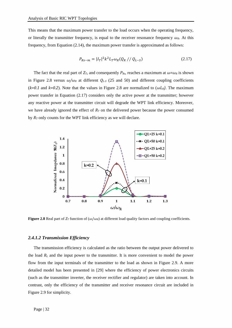
Analysis of Basic RIC WPT Topologies
Page | 32
This means that the maximum power transfer to the load occurs when the operating frequency,
or literally the transmitter frequency, is equal to the receiver resonance frequency ωR. At this
frequency, from Equation (2.14), the maximum power transfer is approximated as follows:
𝑃𝑅𝑠−𝑚 = |𝐼𝑇|2𝑘2𝐿𝑇𝜔𝑅(𝑄𝑅 ∕∕ 𝑄𝐿−𝑆) (2.17)
The fact that the real part of ZT, and consequently PRs, reaches a maximum at ω=ωR is shown
in Figure 2.8 versus ω/ωR at different QL-S (25 and 50) and different coupling coefficients
(k=0.1 and k=0.2). Note that the values in Figure 2.8 are normalized to (ωLR). The maximum
power transfer in Equation (2.17) considers only the active power at the transmitter; however
any reactive power at the transmitter circuit will degrade the WPT link efficiency. Moreover,
we have already ignored the effect of RT on the delivered power because the power consumed
by RT only counts for the WPT link efficiency as we will declare.
Figure 2.8 Real part of ZT function of (ω/ωR) at different load quality factors and coupling coefficients.
2.4.1.2 Transmission Efficiency
The transmission efficiency is calculated as the ratio between the output power delivered to
the load RL and the input power to the transmitter. It is more convenient to model the power
flow from the input terminals of the transmitter to the load as shown in Figure 2.9. A more
detailed model has been presented in [29] where the efficiency of power electronics circuits
(such as the transmitter inverter, the receiver rectifier and regulator) are taken into account. In
contrast, only the efficiency of the transmitter and receiver resonance circuit are included in
Figure 2.9 for simplicity.
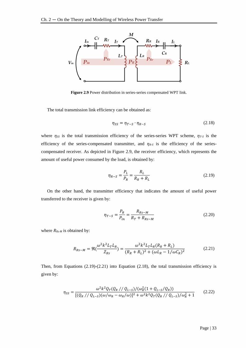
Ch. 2 — On the Theory and Modelling of Wireless Power Transfer
Page | 33
MCT
CR
RL
LT LR
IT IR ILIin RRRT
Pin PLPRr
PRPRt
Vin
Figure 2.9 Power distribution in series-series compensated WPT link.
The total transmission link efficiency can be obtained as:
𝜂𝑆𝑆 = 𝜂𝑇−𝑆 ∙ 𝜂𝑅−𝑆 (2.18)
where ηSS is the total transmission efficiency of the series-series WPT scheme, ηT-S is the
efficiency of the series-compensated transmitter, and ηR-S is the efficiency of the series-
compensated receiver. As depicted in Figure 2.9, the receiver efficiency, which represents the
amount of useful power consumed by the load, is obtained by:
𝜂𝑅−𝑆 =𝑃𝐿
𝑃𝑅=
𝑅𝐿
𝑅𝑅 + 𝑅𝐿 (2.19)
On the other hand, the transmitter efficiency that indicates the amount of useful power
transferred to the receiver is given by:
𝜂𝑇−𝑆 =𝑃𝑅
𝑃𝑖𝑛=
𝑅𝑅𝑠−𝑀
𝑅𝑇 + 𝑅𝑅𝑠−𝑀 (2.20)
where RRs-M is obtained by:
𝑅𝑅𝑠−𝑀 = ℜ(𝜔2𝑘2𝐿𝑇𝐿𝑅
𝑍𝑅𝑠) =
𝜔2𝑘2𝐿𝑇𝐿𝑅(𝑅𝑅 + 𝑅𝐿)
(𝑅𝑅 + 𝑅𝐿)2 + (𝜔𝐿𝑅 − 1 𝜔𝐶𝑅⁄ )2
(2.21)
Then, from Equations (2.19)-(2.21) into Equation (2.18), the total transmission efficiency is
given by:
𝜂𝑆𝑆 =𝜔2𝑘2𝑄𝑇(𝑄𝑅 ∕∕ 𝑄𝐿−𝑆)/(𝜔𝑅
2(1 + 𝑄𝐿−𝑆 𝑄𝑅⁄ ))
[(𝑄𝑅 ∕∕ 𝑄𝐿−𝑆)(𝜔 𝜔𝑅⁄ − 𝜔𝑅 𝜔⁄ )]2 + 𝜔2𝑘2𝑄𝑇(𝑄𝑅 ∕∕ 𝑄𝐿−𝑆) 𝜔𝑅2⁄ + 1
(2.22)
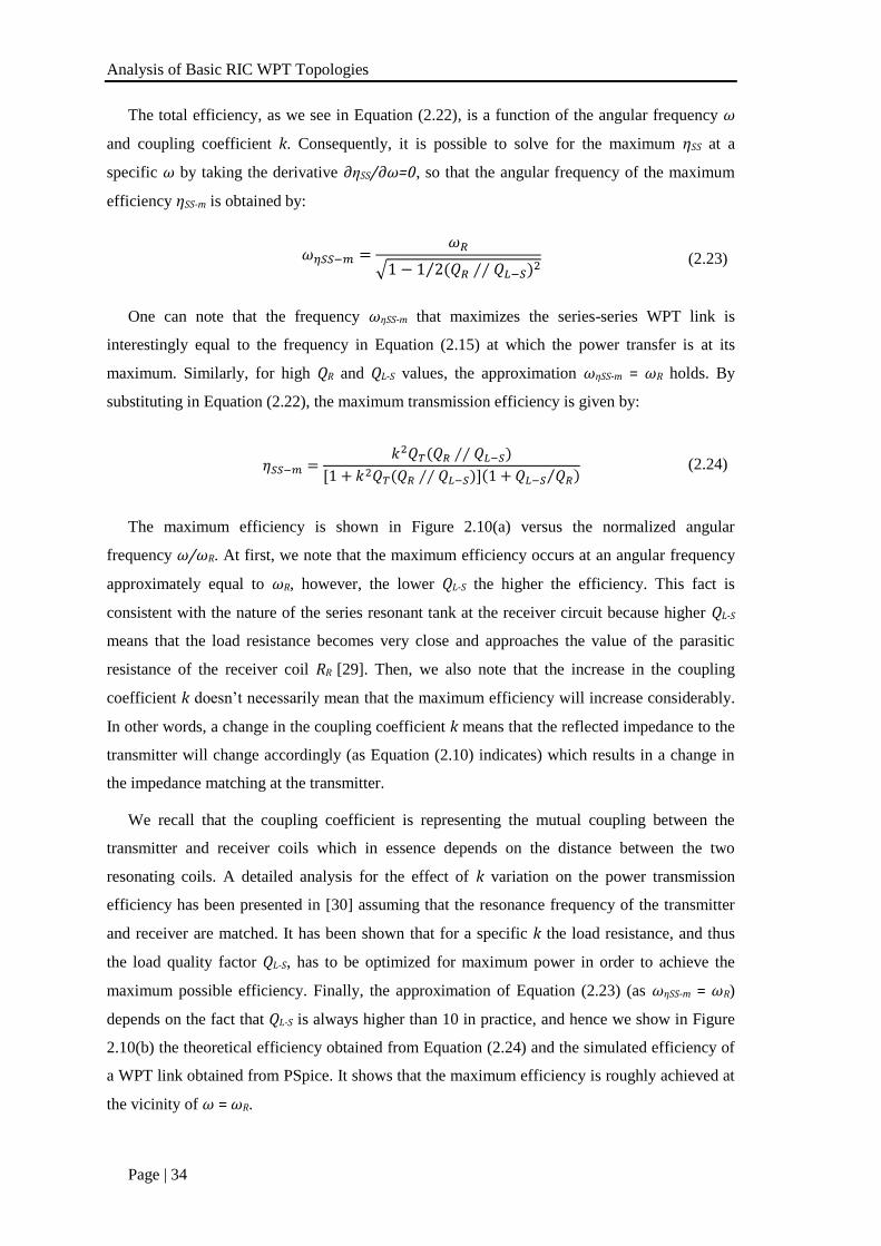
Analysis of Basic RIC WPT Topologies
Page | 34
The total efficiency, as we see in Equation (2.22), is a function of the angular frequency ω
and coupling coefficient k. Consequently, it is possible to solve for the maximum ηSS at a
specific ω by taking the derivative ∂ηSS/∂ω=0, so that the angular frequency of the maximum
efficiency ηSS-m is obtained by:
𝜔𝜂𝑆𝑆−𝑚 =𝜔𝑅
√1 − 1 2(𝑄𝑅 ∕∕ 𝑄𝐿−𝑆)2⁄
(2.23)
One can note that the frequency ωηSS-m that maximizes the series-series WPT link is
interestingly equal to the frequency in Equation (2.15) at which the power transfer is at its
maximum. Similarly, for high QR and QL-S values, the approximation ωηSS-m = ωR holds. By
substituting in Equation (2.22), the maximum transmission efficiency is given by:
𝜂𝑆𝑆−𝑚 =𝑘2𝑄𝑇(𝑄𝑅 ∕∕ 𝑄𝐿−𝑆)
[1 + 𝑘2𝑄𝑇(𝑄𝑅 ∕∕ 𝑄𝐿−𝑆)](1 + 𝑄𝐿−𝑆 𝑄𝑅⁄ ) (2.24)
The maximum efficiency is shown in Figure 2.10(a) versus the normalized angular
frequency ω/ωR. At first, we note that the maximum efficiency occurs at an angular frequency
approximately equal to ωR, however, the lower QL-S the higher the efficiency. This fact is
consistent with the nature of the series resonant tank at the receiver circuit because higher QL-S
means that the load resistance becomes very close and approaches the value of the parasitic
resistance of the receiver coil RR [29]. Then, we also note that the increase in the coupling
coefficient k doesn’t necessarily mean that the maximum efficiency will increase considerably.
In other words, a change in the coupling coefficient k means that the reflected impedance to the
transmitter will change accordingly (as Equation (2.10) indicates) which results in a change in
the impedance matching at the transmitter.
We recall that the coupling coefficient is representing the mutual coupling between the
transmitter and receiver coils which in essence depends on the distance between the two
resonating coils. A detailed analysis for the effect of k variation on the power transmission
efficiency has been presented in [30] assuming that the resonance frequency of the transmitter
and receiver are matched. It has been shown that for a specific k the load resistance, and thus
the load quality factor QL-S, has to be optimized for maximum power in order to achieve the
maximum possible efficiency. Finally, the approximation of Equation (2.23) (as ωηSS-m = ωR)
depends on the fact that QL-S is always higher than 10 in practice, and hence we show in Figure
2.10(b) the theoretical efficiency obtained from Equation (2.24) and the simulated efficiency of
a WPT link obtained from PSpice. It shows that the maximum efficiency is roughly achieved at
the vicinity of ω = ωR.
Ch. 2 — On the Theory and Modelling of Wireless Power Transfer
Page | 35
(a)
(b)
Figure 2.10 Efficiency versus normalized frequency, (a) at different k and QL-S; (b) theoretical versus
PSpice simulated.
2.4.1.3 Link Gain and Transconductance
In this section we will analyze the characteristics of voltage gain ASS and transconductance
GSS of the series-series WPT link modeled by Figure 2.7. The output voltage that appears on the
load can be written as:
𝑉𝐿−𝑆 = 𝑗𝜔𝑀𝐼𝑇𝑅𝐿
𝑍𝑅𝑠 (2.25)
where ZRs is already given in Equation (2.6) and the transmitter current is obtained in terms of
Vin by:
𝐼𝑇 =𝑉𝑖𝑛
𝑍𝑇=
𝑉𝑖𝑛
𝑅𝑇 + 𝑗(𝜔𝐿𝑇 − 1 𝜔𝐶𝑇⁄ ) + 𝜔2𝑀2 𝑍𝑅𝑠⁄ (2.26)
The voltage gain from source-to-load is obtained by substituting Equation (2.26) into Equation
(2.25):
𝐴𝑆𝑆 =𝑉𝐿−𝑆
𝑉𝑖𝑛=
𝑗𝜔𝑀𝑅𝐿
𝑍𝑅𝑠[𝑅𝑇 + 𝑗(𝜔𝐿𝑇 − 1 𝜔𝐶𝑇⁄ )] + 𝜔2𝑀2 (2.27)
As we note in Equation (2.27), the voltage gain ASS is a function of the angular frequency ω,
while it represents a complete transfer function that contains the amplitude and phase
information. However, as we have previously shown, the series-compensated receiver circuit
should be operated at resonance, i.e. (ω = ωR). Consequently, we become more interested in the

Analysis of Basic RIC WPT Topologies
Page | 36
amplitude of ASS at ωR. By knowing that (ZRs= RR+RL) at ωR, the amplitude of Equation (2.27) is
obtained by:
|𝐴𝑆𝑆| = |𝑉𝐿−𝑆
𝑉𝑖𝑛
| =√𝜔𝑅𝑀𝑋𝑇𝑅𝐿(𝑅𝑅 + 𝑅𝐿)
2 + 𝜔𝑅2𝑀2𝑅𝐿
2[𝜔𝑅2𝑀2 + 𝑅𝑇(𝑅𝑅 + 𝑅𝐿)]
2
[𝜔𝑅2𝑀2 + 𝑅𝑇(𝑅𝑅 + 𝑅𝐿)]
2 + 𝑋𝑇2(𝑅𝑅 + 𝑅𝐿)
2 (2.28)
where
𝑋𝑇 = 𝜔𝑅𝐿𝑇 − 1 𝜔𝑅𝐶𝑇⁄ (2.29)
Despite the complexity of Equation (2.28), one can note that the source-to-load voltage gain
is greatly dependent on the compensation at the transmitter side represented by the reactive part
XT. If the transmitter resonance circuit is designed to resonate at ωR, i.e. ωT = ωR, then XT
becomes zero and Equation (2.28) is simplified as follows:
|𝐴𝑆𝑆| =𝜔𝑅𝑀𝑅𝐿
𝜔𝑅2𝑀2 + 𝑅𝑇(𝑅𝑅 + 𝑅𝐿)
(2.30)
As we note, ASS is load-dependent which is certainly undesirable. Moreover, if the
transmitter and receiver circuits are resonating at the same frequency, the losses of transmitter
coil RT will have a considerable effect on the link gain. In contrast, the receiver coil loss RR has
less effect on the link gain because RL ≫ RR in most practical situations.
The transconductance can be determined in a similar way as follows:
𝐼𝐿−𝑆 =𝑗𝜔𝑀𝐼𝑇𝑍𝑅𝑠
=𝑗𝜔𝑀𝑉𝑖𝑛
𝑍𝑅𝑠[𝑅𝑇 + 𝑗(𝜔𝐿𝑇 − 1 𝜔𝐶𝑇⁄ )] + 𝜔2𝑀2 (2.31)
|𝐺𝑆𝑆| = |𝐼𝐿−𝑆
𝑉𝑖𝑛
|𝜔=𝜔𝑅
=√𝜔𝑅𝑀𝑋𝑇(𝑅𝑅 + 𝑅𝐿)
2 + 𝜔𝑅2𝑀2[𝜔𝑅
2𝑀2 + 𝑅𝑇(𝑅𝑅 + 𝑅𝐿)]2
[𝜔𝑅2𝑀2 + 𝑅𝑇(𝑅𝑅 + 𝑅𝐿)]
2 + 𝑋𝑇2(𝑅𝑅 + 𝑅𝐿)
2 (2.32)
Applying the same assumptions of ωT = ωR, XT becomes equal to zero and GSS is simplified
to:
|𝐺𝑆𝑆| =𝜔𝑅𝑀
𝜔𝑅2𝑀2 + 𝑅𝑇(𝑅𝑅 + 𝑅𝐿)
≅1
𝜔𝑅𝑀 (2.33)
The transconductance of a series-series WPT link is nearly RL-independent as we notice in
Equation (2.33). However, it is important to recall that the approximation of GSS =1/MωR
assumes negligible transmitter coil losses which is the case in practical circuits having
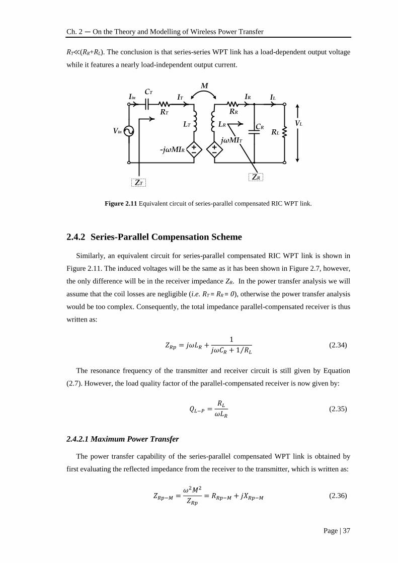
Ch. 2 — On the Theory and Modelling of Wireless Power Transfer
Page | 37
RT≪(RR+RL). The conclusion is that series-series WPT link has a load-dependent output voltage
while it features a nearly load-independent output current.
MCT
CRRL
LT LR
IT IR
Vin
VL
ILIin
RRRT
jωMIT
ZRZT
-jωMIR
Figure 2.11 Equivalent circuit of series-parallel compensated RIC WPT link.
2.4.2 Series-Parallel Compensation Scheme
Similarly, an equivalent circuit for series-parallel compensated RIC WPT link is shown in
Figure 2.11. The induced voltages will be the same as it has been shown in Figure 2.7, however,
the only difference will be in the receiver impedance ZR. In the power transfer analysis we will
assume that the coil losses are negligible (i.e. RT = RR = 0), otherwise the power transfer analysis
would be too complex. Consequently, the total impedance parallel-compensated receiver is thus
written as:
𝑍𝑅𝑝 = 𝑗𝜔𝐿𝑅 +1
𝑗𝜔𝐶𝑅 + 1 𝑅𝐿⁄ (2.34)
The resonance frequency of the transmitter and receiver circuit is still given by Equation
(2.7). However, the load quality factor of the parallel-compensated receiver is now given by:
𝑄𝐿−𝑃 =𝑅𝐿
𝜔𝐿𝑅 (2.35)
2.4.2.1 Maximum Power Transfer
The power transfer capability of the series-parallel compensated WPT link is obtained by
first evaluating the reflected impedance from the receiver to the transmitter, which is written as:
𝑍𝑅𝑝−𝑀 =𝜔2𝑀2
𝑍𝑅𝑝= 𝑅𝑅𝑝−𝑀 + 𝑗𝑋𝑅𝑝−𝑀 (2.36)

Analysis of Basic RIC WPT Topologies
Page | 38
where RRp-M and XRp-M are the real and imaginary parts of the reflected impedance respectively,
which are given by:
𝑅𝑅𝑝−𝑀 = ℜ(𝜔2𝑘2𝐿𝑇𝐿𝑅
𝑍𝑅𝑝) =
𝜔2𝑘2𝐿𝑇𝐿𝑅𝑅𝐿
𝜔2𝐿𝑅2 + (𝜔2𝐿𝑅𝐶𝑅𝑅𝐿 − 𝑅𝐿)
2 (2.37)
𝑋𝑅𝑝−𝑀 = ℑ(𝜔2𝑘2𝐿𝑇𝐿𝑅
𝑍𝑅𝑝) =
−𝜔3𝑘2𝐿𝑇𝐿𝑅[𝐿𝑅 + 𝐶𝑅𝑅𝐿2(𝜔2𝐶𝑅𝐿𝑅 − 1)]
𝜔2𝐿𝑅2 + (𝜔2𝐿𝑅𝐶𝑅𝑅𝐿 − 𝑅𝐿)
2 (2.38)
Using Equations (2.37) and (2.38), the input impedance ZT at the transmitter can be written as:
𝑍𝑇 = 𝑅𝑅𝑝−𝑀 + 𝑗 (𝜔𝐿𝑇 −1
𝜔𝐶𝑇+ 𝑋𝑅𝑝−𝑀) = 𝑅𝑇 + 𝑗𝑋𝑇 (2.39)
where RT and XT are the real part and imaginary part of the transmitter impedance ZT,
respectively. The power delivered to the parallel-compensated receiver PRp is obtained as a
function of the input impedance ZT, written as:
𝑃𝑅𝑝 =|𝑉𝑖𝑛|2
ℜ(𝑍𝑇)= |𝑉𝑖𝑛|2 ∙
𝑅𝑇
𝑅𝑇2 + 𝑋𝑇
2 (2.40)
The maximum power is obtained by taking the derivative of Equation (2.40) as ∂PRp/∂ω=0,
then we find the power transfer is maximized at angular frequency ωPm, where at this frequency
the real part RT is maximized, and given by:
𝜔𝑃𝑚 =𝜔𝑅
√1 + 1/𝑄𝐿−𝑃2
≅ 𝜔𝑅 (2.41)
where QL-P is given in Equation (2.35). From Equation (2.41) into (2.40), the maximum power
transfer is approximated as follows:
𝑃𝑅𝑝−𝑚 = |𝑉𝑖𝑛|2 ∙ 𝑘2𝐿𝑇𝑅𝐿/𝐿𝑅
(𝑘2𝐿𝑇𝑅𝐿/𝐿𝑅)2 + [𝜔𝐿𝑇(1 − 𝑘2) −1
𝜔𝐶𝑇]2
(2.42)
In spite of the fact that the operating frequency of the series-parallel WPT link should be
equal to the receiver resonant frequency ωR, it is important to note in Equation (2.42) that the
transmitter resonance frequency has a different value, given by:
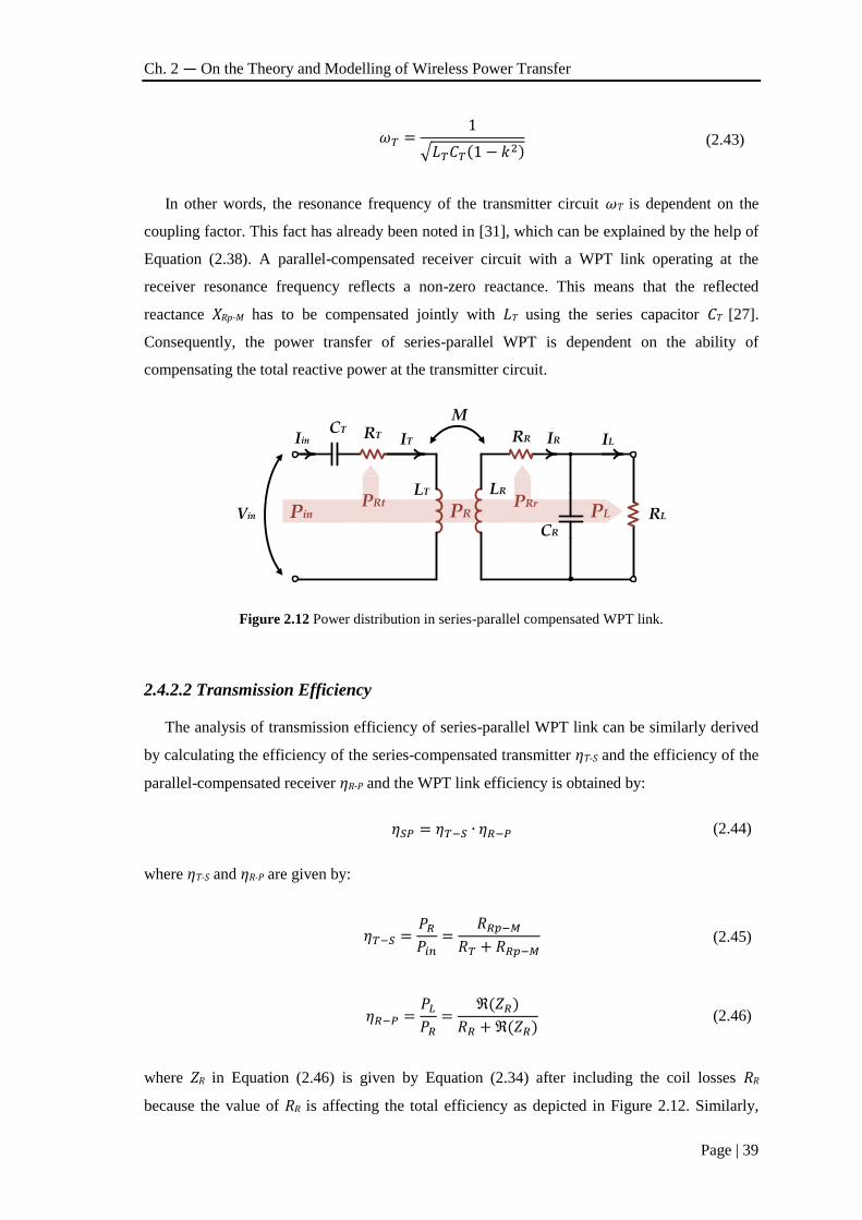
Ch. 2 — On the Theory and Modelling of Wireless Power Transfer
Page | 39
𝜔𝑇 =1
√𝐿𝑇𝐶𝑇(1 − 𝑘2) (2.43)
In other words, the resonance frequency of the transmitter circuit ωT is dependent on the
coupling factor. This fact has already been noted in [31], which can be explained by the help of
Equation (2.38). A parallel-compensated receiver circuit with a WPT link operating at the
receiver resonance frequency reflects a non-zero reactance. This means that the reflected
reactance XRp-M has to be compensated jointly with LT using the series capacitor CT [27].
Consequently, the power transfer of series-parallel WPT is dependent on the ability of
compensating the total reactive power at the transmitter circuit.
MCT
CR
RL
LT LR
IT IR ILIin RRRT
Pin PLPRr
PRPRt
Vin
Figure 2.12 Power distribution in series-parallel compensated WPT link.
2.4.2.2 Transmission Efficiency
The analysis of transmission efficiency of series-parallel WPT link can be similarly derived
by calculating the efficiency of the series-compensated transmitter ηT-S and the efficiency of the
parallel-compensated receiver ηR-P and the WPT link efficiency is obtained by:
𝜂𝑆𝑃 = 𝜂𝑇−𝑆 ∙ 𝜂𝑅−𝑃 (2.44)
where ηT-S and ηR-P are given by:
𝜂𝑇−𝑆 =𝑃𝑅
𝑃𝑖𝑛=
𝑅𝑅𝑝−𝑀
𝑅𝑇 + 𝑅𝑅𝑝−𝑀 (2.45)
𝜂𝑅−𝑃 =𝑃𝐿
𝑃𝑅=
ℜ(𝑍𝑅)
𝑅𝑅 + ℜ(𝑍𝑅) (2.46)
where ZR in Equation (2.46) is given by Equation (2.34) after including the coil losses RR
because the value of RR is affecting the total efficiency as depicted in Figure 2.12. Similarly,

Analysis of Basic RIC WPT Topologies
Page | 40
RRp-M in Equation (2.37) must be updated to include RR. The new expression for RRp-M is now
obtained by:
𝑅𝑅𝑝−𝑀 =𝜔2𝑘2𝐿𝑇𝐿𝑅(𝜔2𝐶𝑅
2𝑅𝐿2𝑅𝑅 + 𝑅𝐿 + 𝑅𝑅)
(𝜔𝐿𝑅 + 𝜔𝐶𝑅𝑅𝐿𝑅𝑅)2 + (𝜔2𝐿𝑅𝐶𝑅𝑅𝐿 − 𝑅𝐿 − 𝑅𝑅)2 (2.47)
Due to the complexity of the derived expression, the total transmission efficiency can be
simplified as [32]:
𝜂𝑆𝑃 =1
(1 + 𝛬𝑇)(1 + 𝛬𝑅) (2.48)
where ΛT and ΛR are respectively given by:
𝛬𝑇 =1 𝑄𝑇⁄ [(1 𝑄𝑅⁄ + 𝑄𝐿−𝑃(1 − 𝜔2 𝜔𝑅
2⁄ ))2+ (1 + 𝑄𝐿−𝑃 𝑄𝑅⁄ )2]
𝜔2𝑘2 𝜔𝑅2⁄ [1 𝑄𝑅⁄ + 𝑄𝐿−𝑃(1 + 𝜔2𝑄𝐿−𝑃
2 𝜔𝑅2𝑄𝑅
2⁄ )] (2.49)
𝛬𝑅 =1
𝑄𝑅𝑄𝐿−𝑃+
𝜔2𝑄𝐿−𝑃
𝜔𝑅2𝑄𝑅
(2.50)
The maximum efficiency ηSP-m can be obtained by solving for ∂ηSP/∂ω=0 to obtain the
frequency ωηSP-m that achieves ηSP-m as follows:
𝜔𝜂𝑆𝑃−𝑚 = 𝜔𝑅
√1 + 1/𝑄𝑅𝑄𝐿−𝑃
(1 + 𝑘2𝑄𝑇 ∕ 𝑄𝑅)1/4 (2.51)
By comparing the frequency ωηSP-m with that in the series-series WPT topology ωηSS-m, we
note that it is dependent on QT in addition to the dependency on the coupling factor k. The
dependency on k is not a desirable property as one can argue. Fortunately, Equation (2.51) can
be approximated once we know that in practice QRQL-P ≫ 1 and k ≪ 1, so that Equation (2.51) is
approximated as follows:
𝜔𝜂𝑆𝑃−𝑚 ≅ 𝜔𝑅 (2.52)
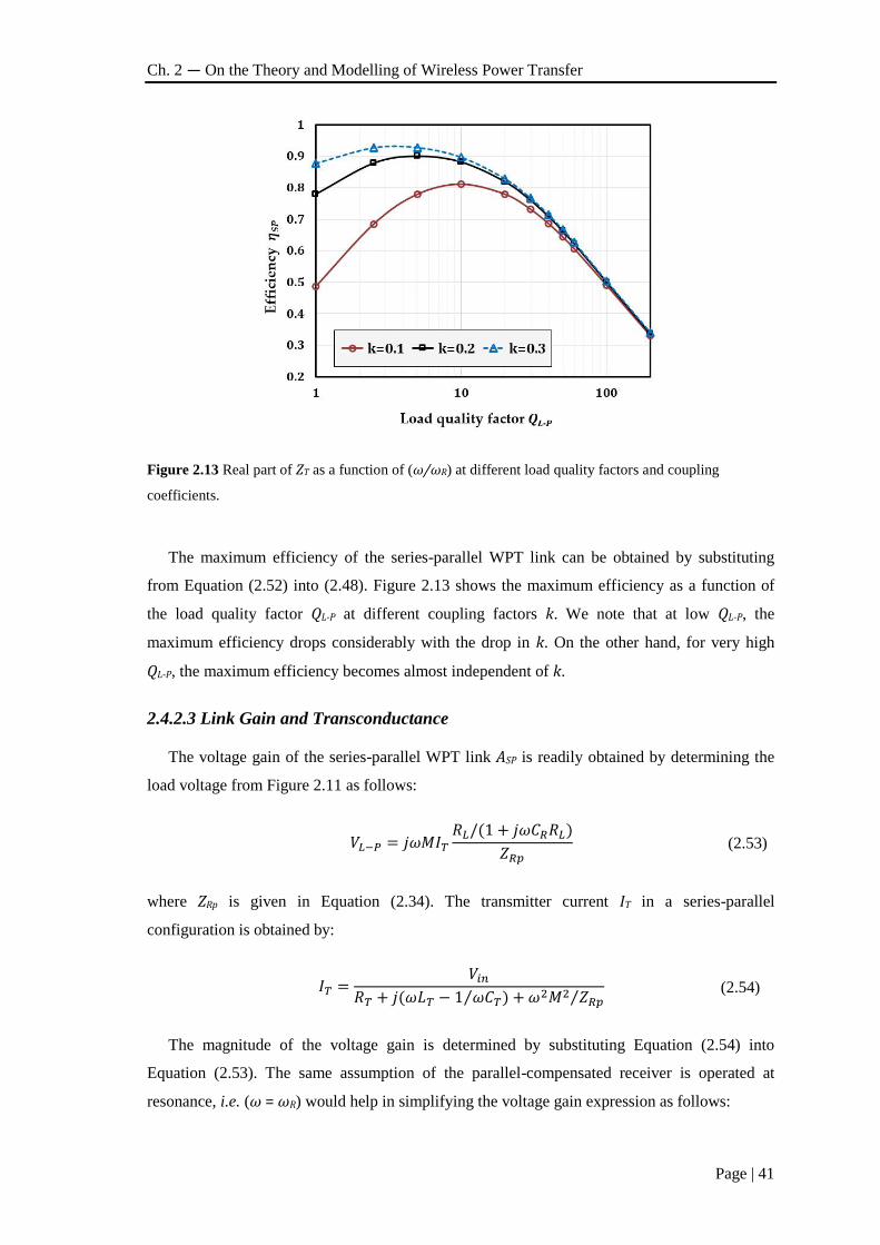
Ch. 2 — On the Theory and Modelling of Wireless Power Transfer
Page | 41
Figure 2.13 Real part of ZT as a function of (ω/ωR) at different load quality factors and coupling
coefficients.
The maximum efficiency of the series-parallel WPT link can be obtained by substituting
from Equation (2.52) into (2.48). Figure 2.13 shows the maximum efficiency as a function of
the load quality factor QL-P at different coupling factors k. We note that at low QL-P, the
maximum efficiency drops considerably with the drop in k. On the other hand, for very high
QL-P, the maximum efficiency becomes almost independent of k.
2.4.2.3 Link Gain and Transconductance
The voltage gain of the series-parallel WPT link ASP is readily obtained by determining the
load voltage from Figure 2.11 as follows:
𝑉𝐿−𝑃 = 𝑗𝜔𝑀𝐼𝑇𝑅𝐿/(1 + 𝑗𝜔𝐶𝑅𝑅𝐿)
𝑍𝑅𝑝 (2.53)
where ZRp is given in Equation (2.34). The transmitter current IT in a series-parallel
configuration is obtained by:
𝐼𝑇 =𝑉𝑖𝑛
𝑅𝑇 + 𝑗(𝜔𝐿𝑇 − 1 𝜔𝐶𝑇⁄ ) + 𝜔2𝑀2 𝑍𝑅𝑝⁄ (2.54)
The magnitude of the voltage gain is determined by substituting Equation (2.54) into
Equation (2.53). The same assumption of the parallel-compensated receiver is operated at
resonance, i.e. (ω = ωR) would help in simplifying the voltage gain expression as follows:
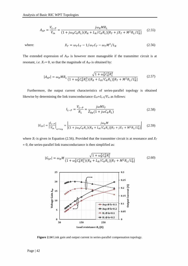
Analysis of Basic RIC WPT Topologies
Page | 42
𝐴𝑆𝑃 =𝑉𝐿−𝑃
𝑉𝑖𝑛=
𝑗𝜔𝑅𝑀𝑅𝐿
(1 + 𝑗𝜔𝑅𝐶𝑅𝑅𝐿)(𝑅𝑅 + 𝐿𝑅 𝐶𝑅𝑅𝐿⁄ )[𝑅𝑇 + 𝑗𝑋𝑇 + 𝑀2𝑅𝐿 𝐿𝑅2⁄ ]
(2.55)
where: 𝑋𝑇 = 𝜔𝑇𝐿𝑇 − 1 𝜔𝑇𝐶𝑇⁄ − 𝜔𝑇𝑀2 𝐿𝑅⁄ (2.56)
The extended expression of ASP is however more manageable if the transmitter circuit is at
resonant, i.e. XT = 0, so that the magnitude of ASP is obtained by:
|𝐴𝑆𝑃| = 𝜔𝑅𝑀𝑅𝐿
√1 + 𝜔𝑅2𝐶𝑅
2𝑅𝐿2
(1 + 𝜔𝑅2𝐶𝑅
2𝑅𝐿2)(𝑅𝑅 + 𝐿𝑅 𝐶𝑅𝑅𝐿⁄ )[𝑅𝑇 + 𝑀2𝑅𝐿 𝐿𝑅
2⁄ ] (2.57)
Furthermore, the output current characteristics of series-parallel topology is obtained
likewise by determining the link transconductance GSP=IL-P/Vin as follows:
𝐼𝐿−𝑃 =𝑉𝐿−𝑃
𝑅𝐿=
𝑗𝜔𝑀𝐼𝑇𝑍𝑅𝑝(1 + 𝑗𝜔𝐶𝑅𝑅𝐿)
(2.58)
|𝐺𝑆𝑃| = |𝐼𝐿−𝑃
𝑉𝑖𝑛
|𝜔=𝜔𝑅
= |𝑗𝜔𝑅𝑀
(1 + 𝑗𝜔𝑅𝐶𝑅𝑅𝐿)(𝑅𝑅 + 𝐿𝑅 𝐶𝑅𝑅𝐿⁄ )[𝑅𝑇 + 𝑗𝑋𝑇 + 𝑀2𝑅𝐿 𝐿𝑅2⁄ ]
| (2.59)
where XT is given in Equation (2.56). Provided that the transmitter circuit is at resonance and XT
= 0, the series-parallel link transconductance is then simplified as:
|𝐺𝑆𝑃| = 𝜔𝑅𝑀√1 + 𝜔𝑅
2𝐶𝑅2𝑅𝐿
2
(1 + 𝜔𝑅2𝐶𝑅
2𝑅𝐿2)(𝑅𝑅 + 𝐿𝑅 𝐶𝑅𝑅𝐿⁄ )[𝑅𝑇 + 𝑀2𝑅𝐿 𝐿𝑅
2⁄ ] (2.60)
Figure 2.14 Link gain and output current in series-parallel compensation topology.
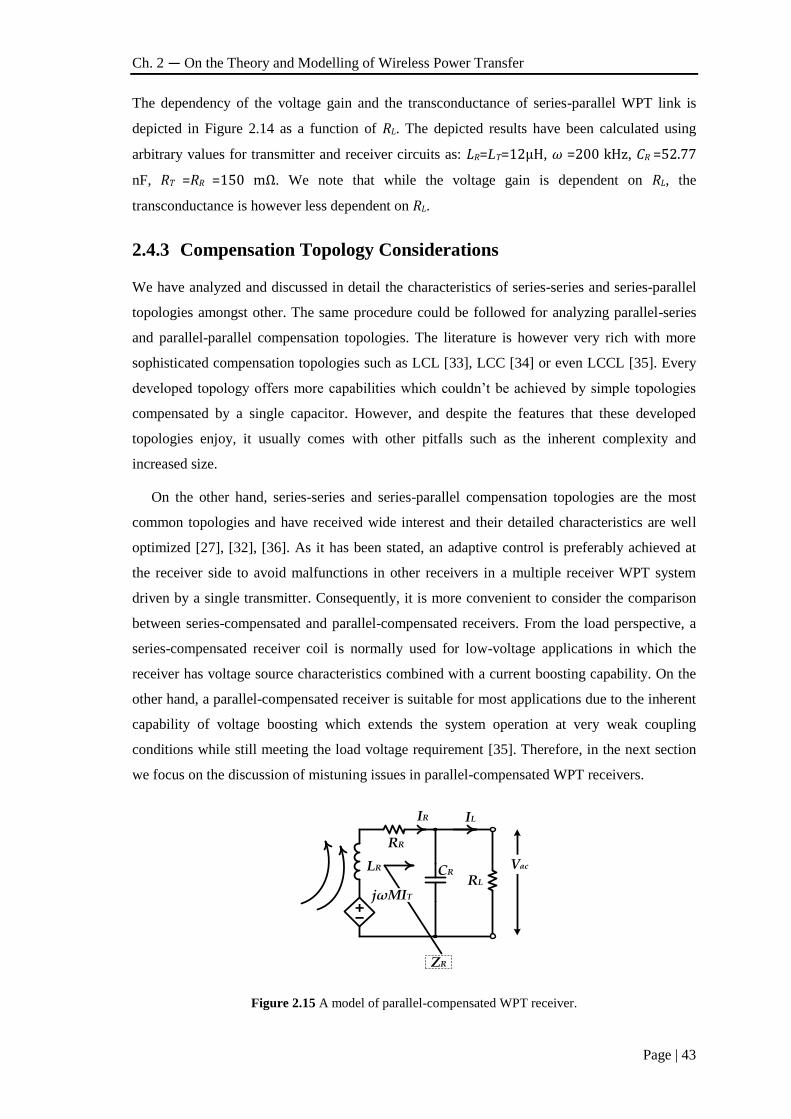
Ch. 2 — On the Theory and Modelling of Wireless Power Transfer
Page | 43
The dependency of the voltage gain and the transconductance of series-parallel WPT link is
depicted in Figure 2.14 as a function of RL. The depicted results have been calculated using
arbitrary values for transmitter and receiver circuits as: LR=LT=12μH, ω =200 kHz, CR =52.77
nF, RT =RR =150 mΩ. We note that while the voltage gain is dependent on RL, the
transconductance is however less dependent on RL.
2.4.3 Compensation Topology Considerations
We have analyzed and discussed in detail the characteristics of series-series and series-parallel
topologies amongst other. The same procedure could be followed for analyzing parallel-series
and parallel-parallel compensation topologies. The literature is however very rich with more
sophisticated compensation topologies such as LCL [33], LCC [34] or even LCCL [35]. Every
developed topology offers more capabilities which couldn’t be achieved by simple topologies
compensated by a single capacitor. However, and despite the features that these developed
topologies enjoy, it usually comes with other pitfalls such as the inherent complexity and
increased size.
On the other hand, series-series and series-parallel compensation topologies are the most
common topologies and have received wide interest and their detailed characteristics are well
optimized [27], [32], [36]. As it has been stated, an adaptive control is preferably achieved at
the receiver side to avoid malfunctions in other receivers in a multiple receiver WPT system
driven by a single transmitter. Consequently, it is more convenient to consider the comparison
between series-compensated and parallel-compensated receivers. From the load perspective, a
series-compensated receiver coil is normally used for low-voltage applications in which the
receiver has voltage source characteristics combined with a current boosting capability. On the
other hand, a parallel-compensated receiver is suitable for most applications due to the inherent
capability of voltage boosting which extends the system operation at very weak coupling
conditions while still meeting the load voltage requirement [35]. Therefore, in the next section
we focus on the discussion of mistuning issues in parallel-compensated WPT receivers.
CRRL
LR
IR
Vac
IL
RR
jωMIT
ZR
Figure 2.15 A model of parallel-compensated WPT receiver.
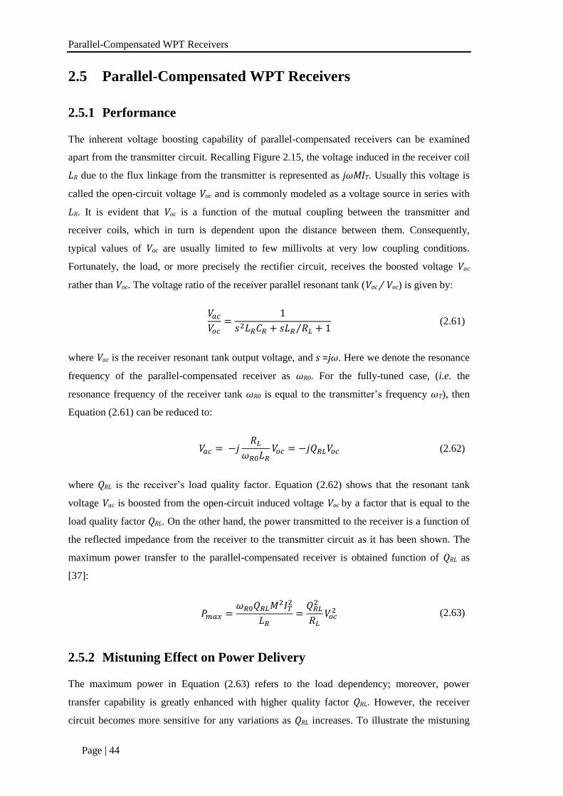
Parallel-Compensated WPT Receivers
Page | 44
2.5 Parallel-Compensated WPT Receivers
2.5.1 Performance
The inherent voltage boosting capability of parallel-compensated receivers can be examined
apart from the transmitter circuit. Recalling Figure 2.15, the voltage induced in the receiver coil
LR due to the flux linkage from the transmitter is represented as jωMIT. Usually this voltage is
called the open-circuit voltage Voc and is commonly modeled as a voltage source in series with
LR. It is evident that Voc is a function of the mutual coupling between the transmitter and
receiver coils, which in turn is dependent upon the distance between them. Consequently,
typical values of Voc are usually limited to few millivolts at very low coupling conditions.
Fortunately, the load, or more precisely the rectifier circuit, receives the boosted voltage Vac
rather than Voc. The voltage ratio of the receiver parallel resonant tank (Vac / Voc) is given by:
𝑉𝑎𝑐
𝑉𝑜𝑐=
1
𝑠2𝐿𝑅𝐶𝑅 + 𝑠𝐿𝑅 𝑅𝐿⁄ + 1 (2.61)
where Vac is the receiver resonant tank output voltage, and s =jω. Here we denote the resonance
frequency of the parallel-compensated receiver as ωR0. For the fully-tuned case, (i.e. the
resonance frequency of the receiver tank ωR0 is equal to the transmitter’s frequency ωT), then
Equation (2.61) can be reduced to:
𝑉𝑎𝑐 = −𝑗𝑅𝐿
𝜔𝑅0𝐿𝑅𝑉𝑜𝑐 = −𝑗𝑄𝑅𝐿𝑉𝑜𝑐 (2.62)
where QRL is the receiver’s load quality factor. Equation (2.62) shows that the resonant tank
voltage Vac is boosted from the open-circuit induced voltage Voc by a factor that is equal to the
load quality factor QRL. On the other hand, the power transmitted to the receiver is a function of
the reflected impedance from the receiver to the transmitter circuit as it has been shown. The
maximum power transfer to the parallel-compensated receiver is obtained function of QRL as
[37]:
𝑃𝑚𝑎𝑥 =𝜔𝑅0𝑄𝑅𝐿𝑀
2𝐼𝑇2
𝐿𝑅=
𝑄𝑅𝐿2
𝑅𝐿𝑉𝑜𝑐
2 (2.63)
2.5.2 Mistuning Effect on Power Delivery
The maximum power in Equation (2.63) refers to the load dependency; moreover, power
transfer capability is greatly enhanced with higher quality factor QRL. However, the receiver
circuit becomes more sensitive for any variations as QRL increases. To illustrate the mistuning
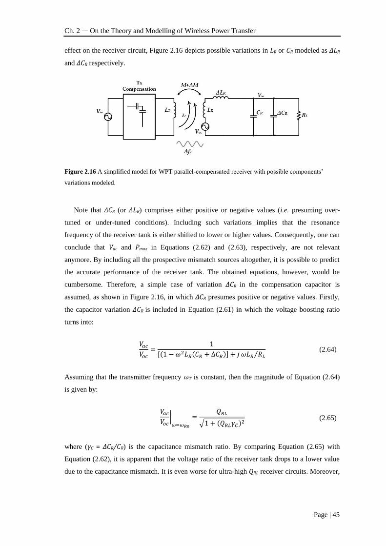
Ch. 2 — On the Theory and Modelling of Wireless Power Transfer
Page | 45
effect on the receiver circuit, Figure 2.16 depicts possible variations in LR or CR modeled as ∆LR
and ∆CR respectively.
Figure 2.16 A simplified model for WPT parallel-compensated receiver with possible components’
variations modeled.
Note that ∆CR (or ∆LR) comprises either positive or negative values (i.e. presuming over-
tuned or under-tuned conditions). Including such variations implies that the resonance
frequency of the receiver tank is either shifted to lower or higher values. Consequently, one can
conclude that Vac and Pmax in Equations (2.62) and (2.63), respectively, are not relevant
anymore. By including all the prospective mismatch sources altogether, it is possible to predict
the accurate performance of the receiver tank. The obtained equations, however, would be
cumbersome. Therefore, a simple case of variation ∆CR in the compensation capacitor is
assumed, as shown in Figure 2.16, in which ∆CR presumes positive or negative values. Firstly,
the capacitor variation ∆CR is included in Equation (2.61) in which the voltage boosting ratio
turns into:
𝑉𝑎𝑐
𝑉𝑜𝑐=
1
[(1 − 𝜔2𝐿𝑅(𝐶𝑅 + ∆𝐶𝑅)] + 𝑗 𝜔𝐿𝑅 𝑅𝐿⁄ (2.64)
Assuming that the transmitter frequency ωT is constant, then the magnitude of Equation (2.64)
is given by:
𝑉𝑎𝑐
𝑉𝑜𝑐|𝜔=𝜔𝑅0
=𝑄𝑅𝐿
√1 + (𝑄𝑅𝐿𝛾𝐶)2 (2.65)
where (γC = ∆CR/CR) is the capacitance mismatch ratio. By comparing Equation (2.65) with
Equation (2.62), it is apparent that the voltage ratio of the receiver tank drops to a lower value
due to the capacitance mismatch. It is even worse for ultra-high QRL receiver circuits. Moreover,
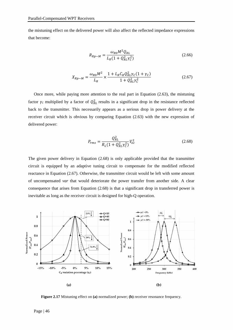
Parallel-Compensated WPT Receivers
Page | 46
the mistuning effect on the delivered power will also affect the reflected impedance expressions
that become:
𝑅𝑅𝑝−𝑀 =𝜔𝑅0𝑀
2𝑄𝑅𝐿
𝐿𝑅(1 + 𝑄𝑅𝐿2 𝛾𝐶
2) (2.66)
𝑋𝑅𝑝−𝑀 =𝜔𝑅0𝑀
2
𝐿𝑅×
1 + 𝐿𝑅𝐶𝑅𝑄𝑅𝐿2 𝛾𝐶(1 + 𝛾𝐶)
1 + 𝑄𝑅𝐿2 𝛾𝐶
2 (2.67)
Once more, while paying more attention to the real part in Equation (2.63), the mistuning
factor γC multiplied by a factor of 𝑄𝑅𝐿2
results in a significant drop in the resistance reflected
back to the transmitter. This necessarily appears as a serious drop in power delivery at the
receiver circuit which is obvious by comparing Equation (2.63) with the new expression of
delivered power:
𝑃𝑟𝑚𝑠 =𝑄𝑅𝐿
2
𝑅𝐿(1 + 𝑄𝑅𝐿2 𝛾𝐶
2)𝑉𝑜𝑐
2 (2.68)
The given power delivery in Equation (2.68) is only applicable provided that the transmitter
circuit is equipped by an adaptive tuning circuit to compensate for the modified reflected
reactance in Equation (2.67). Otherwise, the transmitter circuit would be left with some amount
of uncompensated var that would deteriorate the power transfer from another side. A clear
consequence that arises from Equation (2.68) is that a significant drop in transferred power is
inevitable as long as the receiver circuit is designed for high-Q operation.
(a)
(b)
Figure 2.17 Mistuning effect on (a) normalized power; (b) receiver resonance frequency.
Ch. 2 — On the Theory and Modelling of Wireless Power Transfer
Page | 47
The effect of capacitance variation on the transferred power is shown in Figure 2.17(a),
where the normalized power (Prms/Pmax) is plotted against γC for three different values of QRL. It
is obvious that the drop in power due to a small mismatch percentage of 2% is becoming
noticeable for high-Q values.
As noted in Figure 2.17(a), the high-Q receiver circuit becomes extremely sensitive
irrespective of the enhancement in power transfer capability at the tuned point. The case of QRL
= 80 is an illustrative example in which a 71% drop in Prms is expected for a 2% mismatch in CR.
On the other hand, Figure 2.17(b) depicts the frequency drift by ∆fl as a result of 15% mismatch
while it drifts to a higher frequency by ∆fh amount due to -20% mismatch. As a direct result, in
order to overcome the pitfall of high-Q receivers, the QRL is normally limited to less than 10 in
most systems particularly for high power applications [38]. This, however, is not an adequate
choice for low power applications that would demand energy from a distance that extends up to
a few times the coil diameter. Consequently, to boost the power transfer capabilities by
operating at high QRL, developing an adaptive power management front-end to deal with
sensitivity and detuning issues is demanded.
2.6 Conclusions
In this Chapter we have revisited the history of wireless power transmission and the different
evolving WPT technologies including near-field and far-field. It has been shown that near-field
RIC WPT is the most promising candidate for powering WSNs. The different compensation
topologies in transmitter and receiver have been investigated. Two basic topologies, namely
series-series and series-parallel, are commonly adapted for a wide variety of applications due to
their simplicity over other sophisticated topologies that add more capabilities but increase the
size and complexity.
The detailed analysis of the series-series and series-parallel WPT links has been extended.
From the load perspective, it has been shown that parallel compensation at the receiver side is
more suitable for most applications due to its inherent voltage boosting capabilities which make
it promising for systems that would work at very weak coupling conditions. Accordingly, the
power capability and voltage boosting characteristics of high QRL parallel-compensated WPT
receivers have been investigated. The tradeoff between voltage and power boosting capability,
from one side, and the increased sensitivity of the receiver tank, from the other side, add a
fundamental bottleneck that has been simply alleviated in the literature by designing the system
for low QRL. Designing an adaptive front-end would however help in gaining the advantages of
high QRL WPT receivers while the system is automatically tuned for optimal tuned point.
References
Page | 48
2.7 References
[1] M. A. K. Schwan and P. R. Troyk, “High efficiency driver for transcutaneously coupled coils,”
in Images of the Twenty-First Century. Proceedings of the Annual International Engineering in
Medicine and Biology Society, pp. 1403–1404.
[2] N. Tesla, “Experiments with alternate currents of very high frequency and their application to
methods of artificial illumination,” Trans. Am. Soc. Agric. Eng., vol. 8, no. 1, pp. 267–319, Jan.
1891.
[3] L.P. Wheeler, “Tesla’s contribution to high frequency,” Electr. Eng., vol. 62, no. 8, pp. 355–357,
Aug. 1943.
[4] C. Brown William, “Experimental airborne microwave supported platform,” Rome Air Dev.
Center, NewYork, Tech. Report, RADC-TR-65-188, Contract AF30, vol. 3481, 1965.
[5] M. Schaldach, “Bioelectric energy sources for cardiac pacing.,” Ann. N. Y. Acad. Sci., vol. 167,
no. 2, pp. 1016–24, Oct. 1969.
[6] R. M. M. Dickinson, “Performance of a High-Power, 2.388-GHz Receiving Array in Wireless
Power Transmission Over 1.54 km,” in MTT-S International Microwave Symposium Digest, 1976,
vol. 76, pp. 139–141.
[7] V. S. Dokukin, A. K. Markeev, E. V. Mishin, J. J. Ruzhin, V. V. Fomichev, I. A. Zhulin, V. N.
Ivchenko, G. P. Milinevsky, R. I. Moisya, and R. Z. Sagdeev, “Results of ZARNITZA-2, a rocket
experiment on artificial electron beam injection in the ionosphere,” Adv. Sp. Res., vol. 1, no. 2, pp.
5–15, Jan. 1981.
[8] H. Matsumoto and N. Kaya, “ISY-METS rocket experiment and its preparatory airplane
experiment,” IAF, Int. Astronaut. Congr. 43rd, Washington, Aug. 28-Sept. 5, 1992. 5 p., 1992.
[9] A. Kurs, A. Karalis, R. Moffatt, J. D. Joannopoulos, P. Fisher, and M. Soljačić, “Wireless power
transfer via strongly coupled magnetic resonances,” Science (80-. )., vol. 317, no. 5834, pp. 83–86,
Jul. 2007.
[10] W. C. Brown, “The History of Power Transmission by Radio Waves,” IEEE Trans. Microw.
Theory Tech., vol. 32, no. 9, pp. 1230–1242, Sep. 1984.
[11] T. Sun, X. Xie, and Z. Wang, Wireless Power Transfer for Medical Microsystems. New York,
NY: Springer New York, 2013.
[12] C. A. Balanis, Antenna theory : analysis and design. Wiley Interscience, 2005.
[13] W. C. Brown and E. E. Eves, “Beamed microwave power transmission and its application to
space,” IEEE Trans. Microw. Theory Tech., vol. 40, no. 6, pp. 1239–1250, Jun. 1992.
[14] M. Erol-Kantarci and H. T. Mouftah, “Challenges of wireless power transfer for prolonging
User Equipment (UE) lifetime in wireless networks,” in 2014 IEEE 25th Annual International
Symposium on Personal, Indoor, and Mobile Radio Communication (PIMRC), 2014, pp. 2140–
2144.
[15] J. D. Kraus, Electromagnetics. McGraw-Hill, 1992.
[16] B. Thidé, Electromagnetic field theory. Upsilon Books Uppsala, 2004.
Ch. 2 — On the Theory and Modelling of Wireless Power Transfer
Page | 49
[17] P. Si, A. P. Hu, S. Malpas, and D. Budgett, “A frequency control method for regulating wireless
power to implantable devices,” IEEE Trans. Biomed. Circuits Syst., vol. 2, no. 1, pp. 22–29, Mar.
2008.
[18] A. Kurs, A. Karalis, R. Moffatt, J. D. Joannopoulos, P. Fisher, and M. Soljačić, “Wireless
power transfer via strongly coupled magnetic resonances,” Science (80-. )., vol. 317, no. 5834, pp.
83–86, Jul. 2007.
[19] E. Bou, E. Alarcon, and J. Gutierrez, “A Comparison of Analytical Models for Resonant
Inductive Coupling Wireless Power Transfer,” Prog. Electromagn. Res. Symp., no. 4, pp. 689–693,
2012.
[20] X. Shu and B. Zhang, “Single-Wire Electric-Field Coupling Power Transmission Using
Nonlinear Parity-Time-Symmetric Model with Coupled-Mode Theory,” Energies, vol. 11, no. 3, p.
532, Mar. 2018.
[21] H. Li, K. Wang, L. Huang, W. Chen, and X. Yang, “Dynamic Modeling Based on Coupled
Modes for Wireless Power Transfer Systems,” IEEE Trans. Power Electron., vol. 30, no. 11, pp.
6245–6253, Nov. 2015.
[22] M. Kiani and M. Ghovanloo, “The circuit theory behind coupled-mode magnetic resonance-
based wireless power transmission,” IEEE Trans. Circuits Syst. I Regul. Pap., vol. 59, no. 9, pp.
2065–2074, Sep. 2012.
[23] M. Kiani, U. M. Jow, and M. Ghovanloo, “Design and optimization of a 3-coil inductive link
for efficient wireless power transmission,” in IEEE Transactions on Biomedical Circuits and
Systems, 2011, vol. 5, no. 6, pp. 579–591.
[24] G. A. Kendir, W. Liu, G. Wang, M. Sivaprakasam, R. Bashirullah, M. S. Humayun, and J. D.
Weiland, “An optimal design methodology for inductive power link with Class-E amplifier,” IEEE
Trans. Circuits Syst. I Regul. Pap., vol. 52, no. 5, pp. 857–866, May 2005.
[25] C. C. Kang and M. F. Bin Ain, “Lumped Element Equivalent Circuit for Wireless Power
Transfer,” in 2017 International Conference on Engineering Technology and Technopreneurship
(ICE2T), 2017, pp. 1–4.
[26] Y. H. Sohn, B. H. Choi, G. H. Cho, and C. T. Rim, “Gyrator-Based Analysis of Resonant
Circuits in Inductive Power Transfer Systems,” IEEE Trans. Power Electron., vol. 31, no. 10, pp.
6824–6843, 2016.
[27] C. Wang, G. a Covic, and O. H. Stielau, “Power Transfer Capability and Bifurcation
Phenomena of Loosely Coupled Inductive Power Transfer Systems,” IEEE Trans. Ind. Electron.,
vol. 51, no. 1, pp. 148–157, 2004.
[28] K. van Schuylenbergh and R. Puers, “The concepts of inductive powering,” in Inductive
Powering - Basic Theory and Application to Biomedical Systems, Dordrecht: Springer Netherlands,
2009, pp. 41–76.
[29] K. van. Schuylenbergh and R. Puers, Inductive powering : basic theory and application to
biomedical systems. Springer, 2009.
References
Page | 50
[30] E. Bou Balust, “Wireless power transfer : fueling the dots,” Universitat Politècnica de
Catalunya, 2017.
[31] Y. H. Chao, J. J. Shieh, C. T. Pan, and W. C. Shen, “A closed-form oriented compensator
analysis for series-parallel loosely coupled inductive power transfer systems,” in PESC Record -
IEEE Annual Power Electronics Specialists Conference, 2007, pp. 1215–1220.
[32] W. Zhang, S.-C. Wong, C. K. Tse, and Q. Chen, “Analysis and Comparison of Secondary
Series- and Parallel-Compensated Inductive Power Transfer Systems Operating for Optimal
Efficiency and Load-Independent Voltage-Transfer Ratio,” IEEE Trans. Power Electron., vol. 29,
no. 6, pp. 2979–2990, Jun. 2014.
[33] J.-U. W. Hsu and A. P. Hu, “Determining the variable inductance range for an LCL wireless
power pick-up,” in 2007 IEEE Conference on Electron Devices and Solid-State Circuits, 2007, pp.
489–492.
[34] S. Li, W. Li, J. Deng, T. D. Nguyen, and C. C. Mi, “A Double-Sided LCC Compensation
Network and Its Tuning Method for Wireless Power Transfer,” IEEE Trans. Veh. Technol., vol. 64,
no. 6, pp. 2261–2273, Jun. 2015.
[35] N. a. Keeling, G. a. Covic, and J. T. Boys, “A unity-power-factor IPT pickup for high-power
applications,” IEEE Trans. Ind. Electron., vol. 57, no. 2, pp. 744–751, 2010.
[36] X. Qu, H. Han, S.-C. Wong, C. K. Tse, and W. Chen, “Hybrid IPT Topologies With Constant
Current or Constant Voltage Output for Battery Charging Applications,” IEEE Trans. Power
Electron., vol. 30, no. 11, pp. 6329–6337, Nov. 2015.
[37] M. Zaheer, N. Patel, and A. P. Hu, “Parallel tuned contactless power pickup using saturable
core reactor,” in 2010 IEEE International Conference on Sustainable Energy Technologies (ICSET),
2010, pp. 1–6.
[38] J. T. Boys, G. A. Covic, and A. W. Green, “Stability and control of inductively coupled power
transfer systems,” IEE Proc. - Electr. Power Appl., vol. 147, no. 1, p. 37, 2000.
Page | 51
Chapter
3
3 Switch-Mode Gyrators as a Potential
Candidate for Self-Tuned WPT Receiver
In this chapter, the concept of gyrator as a variable reactive element synthesizer is revisited and
explained. Driven by the goal of developing an adaptive front-end for WPT tuning, the different
implementations of gyrator will be discussed based on their suitability for the WPT application.
Among power processing gyrators, the topology of dual active bridge converter (DAB) will be
selected as a good candidate for a switch-mode natural gyrator topology. Furthermore, the
operation and design details of the candidate topology will be verified by means of state-space
representation on MATLAB as well as on PSIM software. Moreover, the DAB-based reactive
component synthesizer will be validated in different applications such as DAB-based
miniaturized buck converter and DAB-based resonant ripple filter. However, these applications
will be explored as design cases that provide more proof-of-concept for the proposed circuit
operation.
3.1 Motivation
Reactive networks, composed of reactive elements such as inductors and capacitors, have
always been a fundamental component for synthesis of many electrical and electronic systems.
Such elements are key components that can be found in a wide range of applications such as
signal processing and communication applications, as well as power electronics applications.
Despite the fact that reactive elements are used in almost every electrical and electronic
system, they encounter limitations such as value degradation over time and temperature, lack of
tunability and the large physical size of reactive elements with higher values. Furthermore, the
cost increases considerably with the increase of values and electrical ratings [1]. While the
aforementioned challenges are not significant for some applications, they are still critical for
many other applications with stringent demands. To overcome these limitations, various
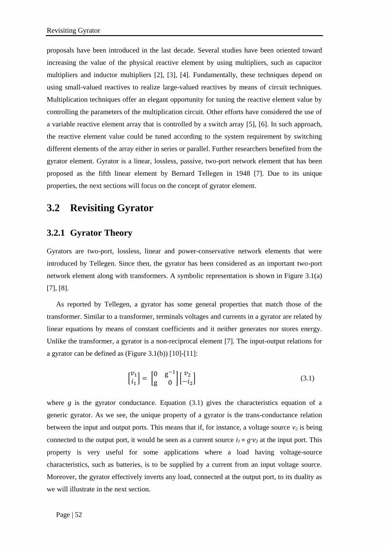
Revisiting Gyrator
Page | 52
proposals have been introduced in the last decade. Several studies have been oriented toward
increasing the value of the physical reactive element by using multipliers, such as capacitor
multipliers and inductor multipliers [2], [3], [4]. Fundamentally, these techniques depend on
using small-valued reactives to realize large-valued reactives by means of circuit techniques.
Multiplication techniques offer an elegant opportunity for tuning the reactive element value by
controlling the parameters of the multiplication circuit. Other efforts have considered the use of
a variable reactive element array that is controlled by a switch array [5], [6]. In such approach,
the reactive element value could be tuned according to the system requirement by switching
different elements of the array either in series or parallel. Further researchers benefited from the
gyrator element. Gyrator is a linear, lossless, passive, two-port network element that has been
proposed as the fifth linear element by Bernard Tellegen in 1948 [7]. Due to its unique
properties, the next sections will focus on the concept of gyrator element.
3.2 Revisiting Gyrator
3.2.1 Gyrator Theory
Gyrators are two-port, lossless, linear and power-conservative network elements that were
introduced by Tellegen. Since then, the gyrator has been considered as an important two-port
network element along with transformers. A symbolic representation is shown in Figure 3.1(a)
[7], [8].
As reported by Tellegen, a gyrator has some general properties that match those of the
transformer. Similar to a transformer, terminals voltages and currents in a gyrator are related by
linear equations by means of constant coefficients and it neither generates nor stores energy.
Unlike the transformer, a gyrator is a non-reciprocal element [7]. The input-output relations for
a gyrator can be defined as (Figure 3.1(b)) [10]-[11]:
[𝑣1
𝑖1] = [
0 g−1
g 0] [
𝑣2
−𝑖2] (3.1)
where g is the gyrator conductance. Equation (3.1) gives the characteristics equation of a
generic gyrator. As we see, the unique property of a gyrator is the trans-conductance relation
between the input and output ports. This means that if, for instance, a voltage source v2 is being
connected to the output port, it would be seen as a current source i1 = g·v2 at the input port. This
property is very useful for some applications where a load having voltage-source
characteristics, such as batteries, is to be supplied by a current from an input voltage source.
Moreover, the gyrator effectively inverts any load, connected at the output port, to its duality as
we will illustrate in the next section.
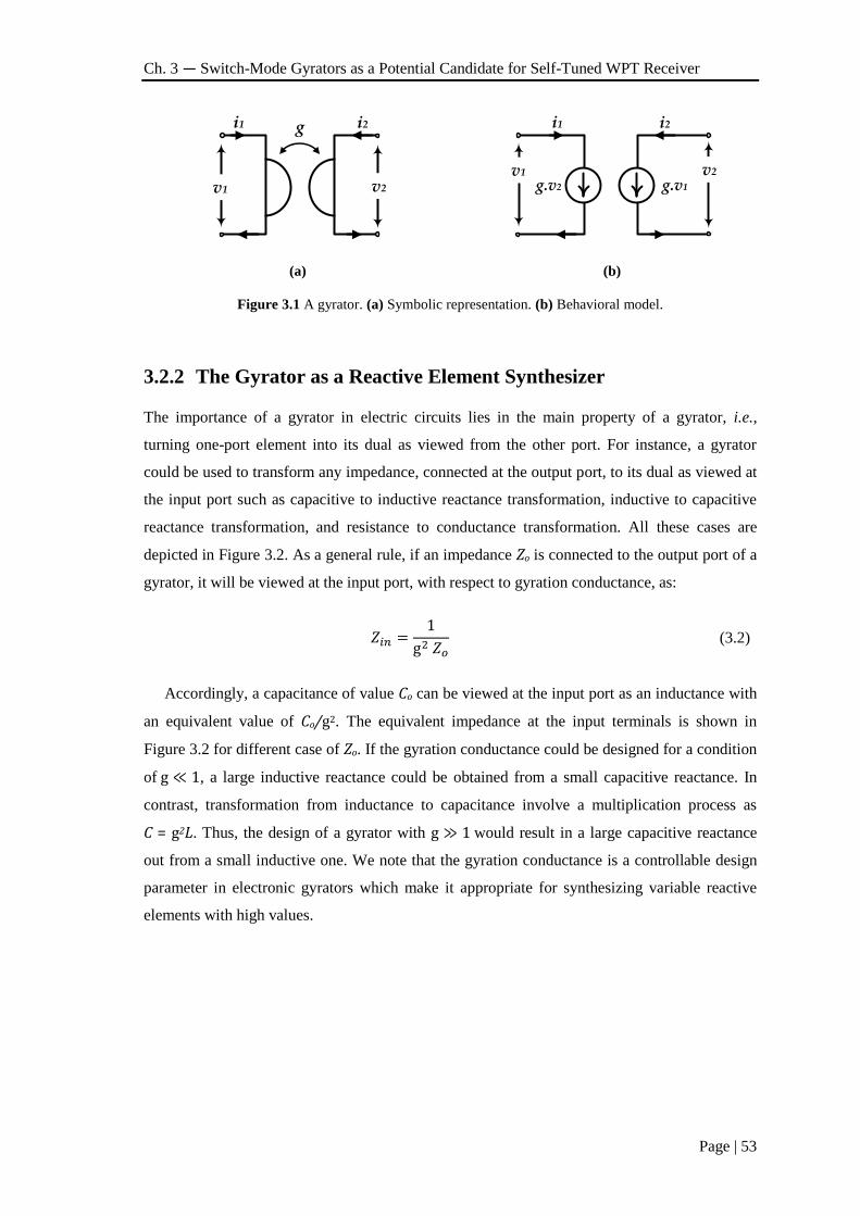
Ch. 3 — Switch-Mode Gyrators as a Potential Candidate for Self-Tuned WPT Receiver
Page | 53
i2i1
v1 v2
g
(a)
i2i1
v1 v2
g.v2 g.v1
(b)
Figure 3.1 A gyrator. (a) Symbolic representation. (b) Behavioral model.
3.2.2 The Gyrator as a Reactive Element Synthesizer
The importance of a gyrator in electric circuits lies in the main property of a gyrator, i.e.,
turning one-port element into its dual as viewed from the other port. For instance, a gyrator
could be used to transform any impedance, connected at the output port, to its dual as viewed at
the input port such as capacitive to inductive reactance transformation, inductive to capacitive
reactance transformation, and resistance to conductance transformation. All these cases are
depicted in Figure 3.2. As a general rule, if an impedance Zo is connected to the output port of a
gyrator, it will be viewed at the input port, with respect to gyration conductance, as:
𝑍𝑖𝑛 =1
g2 𝑍𝑜 (3.2)
Accordingly, a capacitance of value Co can be viewed at the input port as an inductance with
an equivalent value of Co/g2. The equivalent impedance at the input terminals is shown in
Figure 3.2 for different case of Zo. If the gyration conductance could be designed for a condition
of g ≪ 1, a large inductive reactance could be obtained from a small capacitive reactance. In
contrast, transformation from inductance to capacitance involve a multiplication process as
C = g2L. Thus, the design of a gyrator with g ≫ 1 would result in a large capacitive reactance
out from a small inductive one. We note that the gyration conductance is a controllable design
parameter in electronic gyrators which make it appropriate for synthesizing variable reactive
elements with high values.
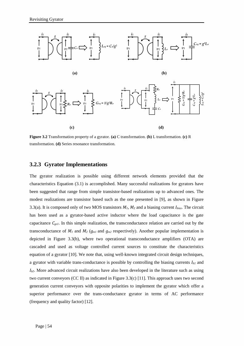
Revisiting Gyrator
Page | 54
i2i1
v1 v2
g i1
v1Leq = Co/g2 Co
(a)
i2i1
v1 v2
g i1
v1
Ceq = g2Lo
Lo
(b)
i2i1
v1 v2
g i1
v1 Geq = 1/g2Ro Ro
(c)
i2i1
v1 v2
g
i1
v1
Geq
= 1
/g2 R
o Ro
Lo
Co
Ceq
= g
2 Lo
Leq
= C
o/g
2
(d)
Figure 3.2 Transformation property of a gyrator. (a) C transformation. (b) L transformation. (c) R
transformation. (d) Series resonance transformation.
3.2.3 Gyrator Implementations
The gyrator realization is possible using different network elements provided that the
characteristics Equation (3.1) is accomplished. Many successful realizations for gyrators have
been suggested that range from simple transistor-based realizations up to advanced ones. The
modest realizations are transistor based such as the one presented in [9], as shown in Figure
3.3(a). It is composed only of two MOS transistors M1, M2 and a biasing current Ibias. The circuit
has been used as a gyrator-based active inductor where the load capacitance is the gate
capacitance Cgs1. In this simple realization, the transconductance relation are carried out by the
transconductance of M1 and M2 (gm1 and gm2 respectively). Another popular implementation is
depicted in Figure 3.3(b), where two operational transconductance amplifiers (OTA) are
cascaded and used as voltage controlled current sources to constitute the characteristics
equation of a gyrator [10]. We note that, using well-known integrated circuit design techniques,
a gyrator with variable trans-conductance is possible by controlling the biasing currents Ib1 and
Ib2. More advanced circuit realizations have also been developed in the literature such as using
two current conveyors (CC II) as indicated in Figure 3.3(c) [11]. This approach uses two second
generation current conveyors with opposite polarities to implement the gyrator which offer a
superior performance over the trans-conductance gyrator in terms of AC performance
(frequency and quality factor) [12].
Ch. 3 — Switch-Mode Gyrators as a Potential Candidate for Self-Tuned WPT Receiver
Page | 55
M1
M2
Vbias
Iin
I1
I2
Ibias
Vin
Cgs1
(a)
gm1
gm2
i2
i1
v2
v1
CoZin=Co/gm.1gm2
Ib1
Ib2
(b)
Y
XZ
CC IIY
X Z
CC IIY
X Z
v1
v2
g
g
Zin
(c)
Figure 3.3 Various gyrator realizations (a) Transistor based. (b) Transconductor based. (c) Current
Conveyor II based.
As we have seen, most of the presented implementations for the gyrator are either based on
small-signal transistors or based on linear amplifiers—current conveyors are even built using
operational amplifiers— which make them inefficient at high power levels. The fact that all
these implementations are always biased by current sources limit their applications to signal
processing where high power delivery is not applicable [13]. For gyrators to be applicable to
WPT application, power efficiency becomes a must.
A first demonstration for switch-mode gyrator realization has been introduced by S. Singer
in [13], [14]. It has been shown that switch-mode power processing circuits enable loss-free
gyrator synthesis. As a power-conservative element, the gyrator can be synthesized by means of
any POPI circuit (output power equal input power) such as buck, buck-boost, cuk, and flyback
converters, with appropriate control. As depicted in Figure 3.4, a closed loop control can be
used to control the output current of a POPI switch-mode circuit such that it related to the input
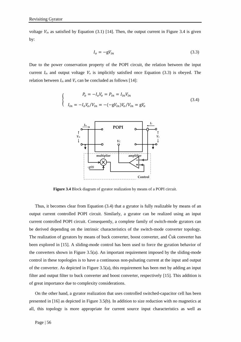
Revisiting Gyrator
Page | 56
voltage Vin as satisfied by Equation (3.1) [14]. Then, the output current in Figure 3.4 is given
by:
𝐼𝑜 = −g𝑉𝑖𝑛 (3.3)
Due to the power conservation property of the POPI circuit, the relation between the input
current Iin and output voltage Vo is implicitly satisfied once Equation (3.3) is obeyed. The
relation between Iin and Vo can be concluded as follows [14]:
𝑃𝑜 = −𝐼𝑜𝑉𝑜 = 𝑃𝑖𝑛 = 𝐼𝑖𝑛𝑉𝑖𝑛
𝐼𝑖𝑛 = −𝐼𝑜𝑉𝑜 𝑉𝑖𝑛⁄ = −(−g𝑉𝑖𝑛)𝑉𝑜 𝑉𝑖𝑛⁄ = g𝑉𝑜
(3.4)
Vin
IinIo
Vo
POPI
-g(t)
multiplier amplifier
VC
Control
Figure 3.4 Block diagram of gyrator realization by means of a POPI circuit.
Thus, it becomes clear from Equation (3.4) that a gyrator is fully realizable by means of an
output current controlled POPI circuit. Similarly, a gyrator can be realized using an input
current controlled POPI circuit. Consequently, a complete family of switch-mode gyrators can
be derived depending on the intrinsic characteristics of the switch-mode converter topology.
The realization of gyrators by means of buck converter, boost converter, and Čuk converter has
been explored in [15]. A sliding-mode control has been used to force the gyration behavior of
the converters shown in Figure 3.5(a). An important requirement imposed by the sliding-mode
control in these topologies is to have a continuous non-pulsating current at the input and output
of the converter. As depicted in Figure 3.5(a), this requirement has been met by adding an input
filter and output filter to buck converter and boost converter, respectively [15]. This addition is
of great importance due to complexity considerations.
On the other hand, a gyrator realization that uses controlled switched-capacitor cell has been
presented in [16] as depicted in Figure 3.5(b). In addition to size reduction with no magnetics at
all, this topology is more appropriate for current source input characteristics as well as
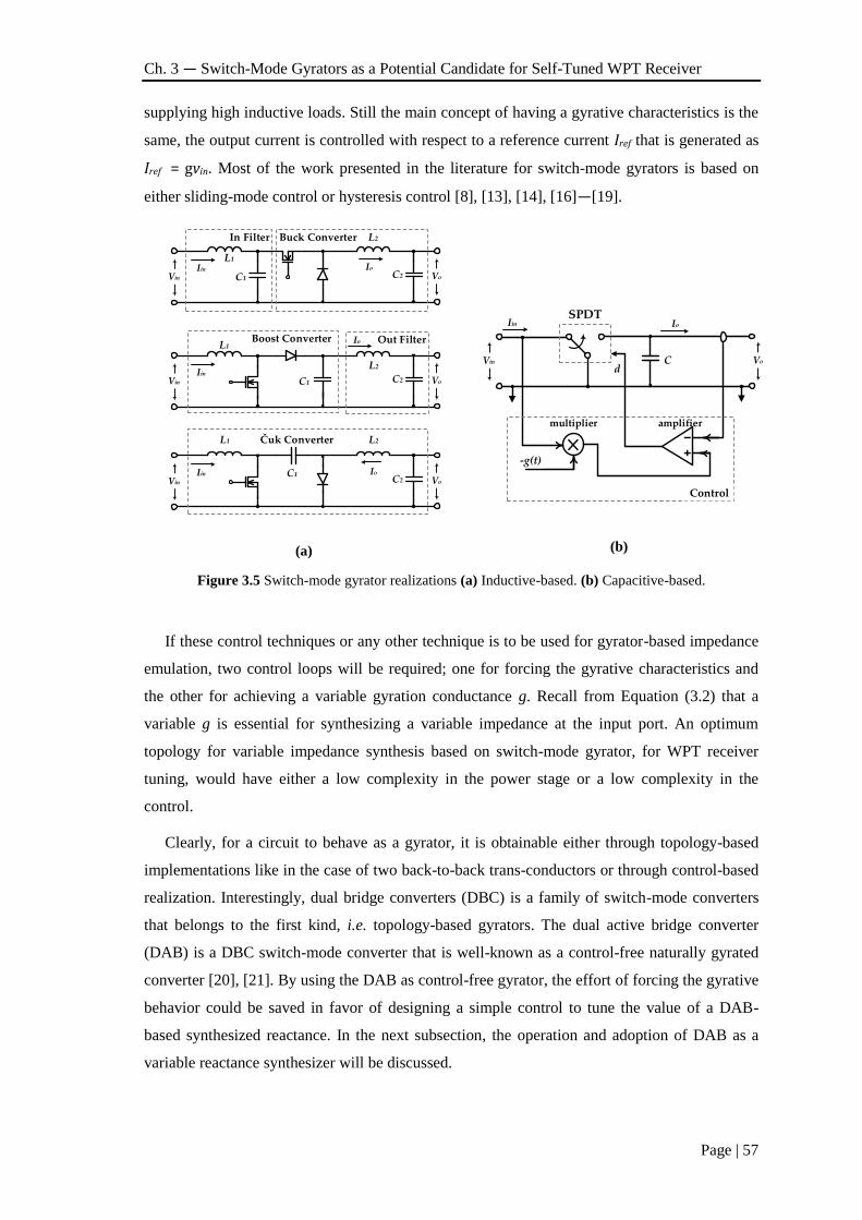
Ch. 3 — Switch-Mode Gyrators as a Potential Candidate for Self-Tuned WPT Receiver
Page | 57
supplying high inductive loads. Still the main concept of having a gyrative characteristics is the
same, the output current is controlled with respect to a reference current Iref that is generated as
Iref = gvin. Most of the work presented in the literature for switch-mode gyrators is based on
either sliding-mode control or hysteresis control [8], [13], [14], [16]—[19].
L1
L2
C2C1Vin Vo
Iin Io
L1
L2
C2C1Vin Vo
Iin
Io
L1 L2
C2C1
Vin Vo
Iin Io
Buck ConverterIn Filter
Out FilterBoost Converter
Čuk Converter
(a)
Vin
Iin Io
Vo
SPDT
-g(t)
multiplier amplifier
Control
Cd
(b)
Figure 3.5 Switch-mode gyrator realizations (a) Inductive-based. (b) Capacitive-based.
If these control techniques or any other technique is to be used for gyrator-based impedance
emulation, two control loops will be required; one for forcing the gyrative characteristics and
the other for achieving a variable gyration conductance g. Recall from Equation (3.2) that a
variable g is essential for synthesizing a variable impedance at the input port. An optimum
topology for variable impedance synthesis based on switch-mode gyrator, for WPT receiver
tuning, would have either a low complexity in the power stage or a low complexity in the
control.
Clearly, for a circuit to behave as a gyrator, it is obtainable either through topology-based
implementations like in the case of two back-to-back trans-conductors or through control-based
realization. Interestingly, dual bridge converters (DBC) is a family of switch-mode converters
that belongs to the first kind, i.e. topology-based gyrators. The dual active bridge converter
(DAB) is a DBC switch-mode converter that is well-known as a control-free naturally gyrated
converter [20], [21]. By using the DAB as control-free gyrator, the effort of forcing the gyrative
behavior could be saved in favor of designing a simple control to tune the value of a DAB-
based synthesized reactance. In the next subsection, the operation and adoption of DAB as a
variable reactance synthesizer will be discussed.
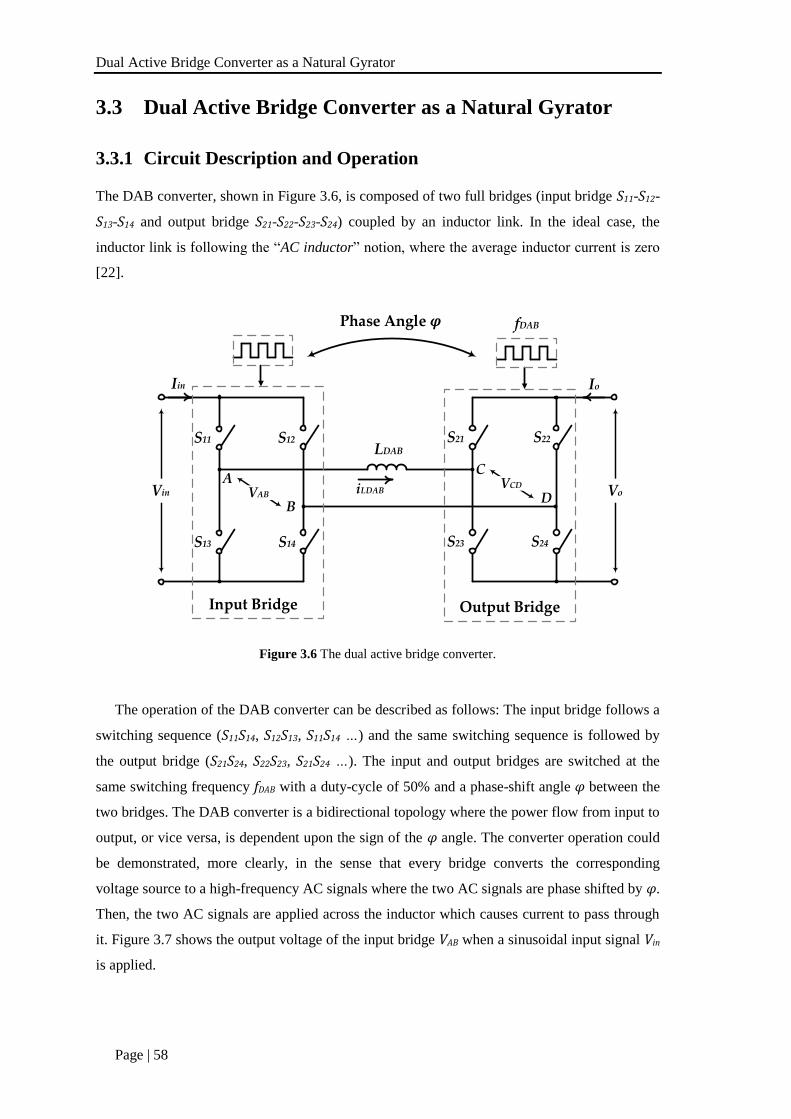
Dual Active Bridge Converter as a Natural Gyrator
Page | 58
3.3 Dual Active Bridge Converter as a Natural Gyrator
3.3.1 Circuit Description and Operation
The DAB converter, shown in Figure 3.6, is composed of two full bridges (input bridge S11-S12-
S13-S14 and output bridge S21-S22-S23-S24) coupled by an inductor link. In the ideal case, the
inductor link is following the “AC inductor” notion, where the average inductor current is zero
[22].
VoVin
IoIin
LDABS11 S12
S13 S14
S21 S22
S23 S24
Input Bridge Output Bridge
fDABPhase Angle φ
iLDABA
B
C
DVABVCD
Figure 3.6 The dual active bridge converter.
The operation of the DAB converter can be described as follows: The input bridge follows a
switching sequence (S11S14, S12S13, S11S14 …) and the same switching sequence is followed by
the output bridge (S21S24, S22S23, S21S24 …). The input and output bridges are switched at the
same switching frequency fDAB with a duty-cycle of 50% and a phase-shift angle φ between the
two bridges. The DAB converter is a bidirectional topology where the power flow from input to
output, or vice versa, is dependent upon the sign of the φ angle. The converter operation could
be demonstrated, more clearly, in the sense that every bridge converts the corresponding
voltage source to a high-frequency AC signals where the two AC signals are phase shifted by φ.
Then, the two AC signals are applied across the inductor which causes current to pass through
it. Figure 3.7 shows the output voltage of the input bridge VAB when a sinusoidal input signal Vin
is applied.
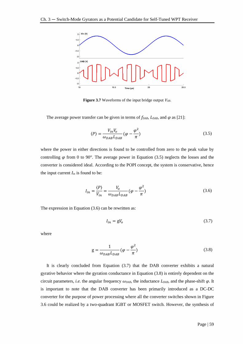
Ch. 3 — Switch-Mode Gyrators as a Potential Candidate for Self-Tuned WPT Receiver
Page | 59
Figure 3.7 Waveforms of the input bridge output VAB.
The average power transfer can be given in terms of fDAB, LDAB, and φ as [21]:
⟨𝑃⟩ =𝑉𝑖𝑛𝑉𝑜
𝜔𝐷𝐴𝐵𝐿𝐷𝐴𝐵(𝜑 −
𝜑2
𝜋) (3.5)
where the power in either directions is found to be controlled from zero to the peak value by
controlling φ from 0 to 90°. The average power in Equation (3.5) neglects the losses and the
converter is considered ideal. According to the POPI concept, the system is conservative, hence
the input current Iin is found to be:
𝐼𝑖𝑛 =⟨𝑃⟩
𝑉𝑖𝑛=
𝑉𝑜𝜔𝐷𝐴𝐵𝐿𝐷𝐴𝐵
(𝜑 −𝜑2
𝜋) (3.6)
The expression in Equation (3.6) can be rewritten as:
𝐼𝑖𝑛 = g𝑉𝑜 (3.7)
where
g =1
𝜔𝐷𝐴𝐵𝐿𝐷𝐴𝐵(𝜑 −
𝜑2
𝜋) (3.8)
It is clearly concluded from Equation (3.7) that the DAB converter exhibits a natural
gyrative behavior where the gyration conductance in Equation (3.8) is entirely dependent on the
circuit parameters, i.e. the angular frequency ωDAB, the inductance LDAB, and the phase-shift φ. It
is important to note that the DAB converter has been primarily introduced as a DC-DC
converter for the purpose of power processing where all the converter switches shown in Figure
3.6 could be realized by a two-quadrant IGBT or MOSFET switch. However, the synthesis of
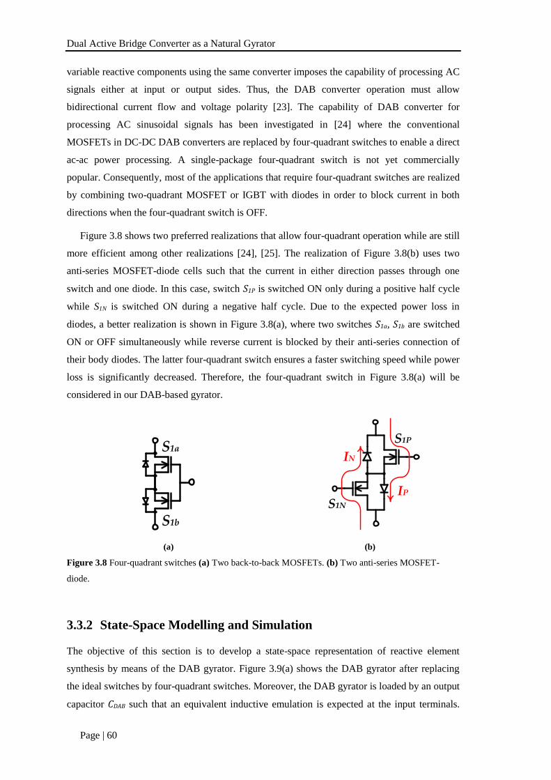
Dual Active Bridge Converter as a Natural Gyrator
Page | 60
variable reactive components using the same converter imposes the capability of processing AC
signals either at input or output sides. Thus, the DAB converter operation must allow
bidirectional current flow and voltage polarity [23]. The capability of DAB converter for
processing AC sinusoidal signals has been investigated in [24] where the conventional
MOSFETs in DC-DC DAB converters are replaced by four-quadrant switches to enable a direct
ac-ac power processing. A single-package four-quadrant switch is not yet commercially
popular. Consequently, most of the applications that require four-quadrant switches are realized
by combining two-quadrant MOSFET or IGBT with diodes in order to block current in both
directions when the four-quadrant switch is OFF.
Figure 3.8 shows two preferred realizations that allow four-quadrant operation while are still
more efficient among other realizations [24], [25]. The realization of Figure 3.8(b) uses two
anti-series MOSFET-diode cells such that the current in either direction passes through one
switch and one diode. In this case, switch S1P is switched ON only during a positive half cycle
while S1N is switched ON during a negative half cycle. Due to the expected power loss in
diodes, a better realization is shown in Figure 3.8(a), where two switches S1a, S1b are switched
ON or OFF simultaneously while reverse current is blocked by their anti-series connection of
their body diodes. The latter four-quadrant switch ensures a faster switching speed while power
loss is significantly decreased. Therefore, the four-quadrant switch in Figure 3.8(a) will be
considered in our DAB-based gyrator.
S1a
S1b
(a)
S1P
S1N
IP
IN
(b)
Figure 3.8 Four-quadrant switches (a) Two back-to-back MOSFETs. (b) Two anti-series MOSFET-
diode.
3.3.2 State-Space Modelling and Simulation
The objective of this section is to develop a state-space representation of reactive element
synthesis by means of the DAB gyrator. Figure 3.9(a) shows the DAB gyrator after replacing
the ideal switches by four-quadrant switches. Moreover, the DAB gyrator is loaded by an output
capacitor CDAB such that an equivalent inductive emulation is expected at the input terminals.

Ch. 3 — Switch-Mode Gyrators as a Potential Candidate for Self-Tuned WPT Receiver
Page | 61
The different operation modes (i.e. Mode1, Mode 2, Mode 3, and Mode 4) of the DAB
converter within one switching cycle is also illustrated in Figure 3.9(b). State-space
representation for the system can be derived after defining the state variables such as the
inductor current iLDAB(t) and the capacitor voltage vo(t). The state-space equations of each
operation mode can be expressed by the full-order state matrices as:
Mode 1: 𝑑
𝑑𝑡[𝑖𝐿𝐷𝐴𝐵(𝑡)𝑣𝑜(𝑡)
] =
[ 0
1
𝐿𝐷𝐴𝐵
−1
𝐶𝐷𝐴𝐵
0]
[𝑖𝐿𝐷𝐴𝐵(𝑡)𝑣𝑜(𝑡)
] + [
1
𝐿𝐷𝐴𝐵
0
] [𝑣𝑖𝑛(𝑡)] (3.9)
Mode 2: 𝑑
𝑑𝑡[𝑖𝐿𝐷𝐴𝐵(𝑡)𝑣𝑜(𝑡)
] =
[ 0
−1
𝐿𝐷𝐴𝐵
1
𝐶𝐷𝐴𝐵
0]
[𝑖𝐿𝐷𝐴𝐵(𝑡)𝑣𝑜(𝑡)
] + [
1
𝐿𝐷𝐴𝐵
0
] [𝑣𝑖𝑛(𝑡)] (3.10)
Mode 3: 𝑑
𝑑𝑡[𝑖𝐿𝐷𝐴𝐵(𝑡)𝑣𝑜(𝑡)
] =
[ 0
−1
𝐿𝐷𝐴𝐵
1
𝐶𝐷𝐴𝐵
0]
[𝑖𝐿𝐷𝐴𝐵(𝑡)𝑣𝑜(𝑡)
] + [
−1
𝐿𝐷𝐴𝐵
0
] [𝑣𝑖𝑛(𝑡)] (3.11)
Mode 4: 𝑑
𝑑𝑡[𝑖𝐿𝐷𝐴𝐵(𝑡)𝑣𝑜(𝑡)
] =
[ 0
1
𝐿𝐷𝐴𝐵
−1
𝐶𝐷𝐴𝐵
0]
[𝑖𝐿𝐷𝐴𝐵(𝑡)𝑣𝑜(𝑡)
] + [
−1
𝐿𝐷𝐴𝐵
0
] [𝑣𝑖𝑛(𝑡)] (3.12)
The state-space model has been implemented using Simulink, as shown in Figure 3.10(a),
where the input voltage and output voltage waveforms are shown in Figure 3.10(b) for the
system conditions of (Vin=5 V, fin= 500 kHz, fDAB=8 MHz, LDAB=25 nH, CDAB=80 nH, φ=40°).
We note that the synthesized inductance Lφ is not purely lossless. This can be concluded from
Figure 3.10(b) as the phase lag between input current and voltage is slightly less than 90° which
denotes a series resistance. The calculated value of the synthesized inductance is 550 nH in
series with Rφ of 265 mΩ. The synthesized inductance is quite large compared to the reactive
components (i.e. LDAB and CDAB) used in the circuit. As the inductor size, and value, is the aspect
of main concern, the synthesized inductance has to be compared to the inductor link of the DAB
converter LDAB. It is clear that Lφ is around 22x of LDAB, which proves the benefits of switch-
mode gyrator circuits for synthesizing large reactive components.
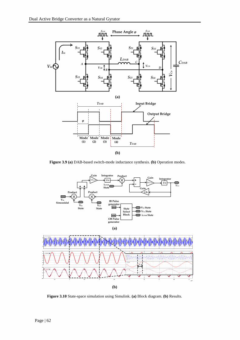
Dual Active Bridge Converter as a Natural Gyrator
Page | 62
Phase Angle φ fDAB fDAB
LDABCDAB
S11 S12
S13 S14
S21 S22
S23 S24
A
BVAB
VCD
C
DVin
Iin
VC
o
(a)
TDAB
φ
Mode(1)
Input Bridge
Output Bridge
Mode(2)
Mode(3)
Mode(4) TDAB
(b)
Figure 3.9 (a) DAB-based switch-mode inductance synthesis. (b) Operation modes.
1/LDAB 1/s
IntegratorGain
1/CDAB
1/Ro
ProductGain Integrator
Gain
ProductProduct
State Select Block
VCo
VCo State
iLDAB State
Vin State
Vin
State
VoC
State
iLDAB
State
IB Pulsegenerator
OB Pulsegenerator
Vin
Sinusoidal
1/s
(a)
Φ = 90o
(b)
Figure 3.10 State-space simulation using Simulink. (a) Block diagram. (b) Results.
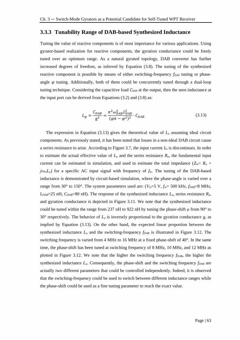
Ch. 3 — Switch-Mode Gyrators as a Potential Candidate for Self-Tuned WPT Receiver
Page | 63
3.3.3 Tunability Range of DAB-based Synthesized Inductance
Tuning the value of reactive components is of most importance for various applications. Using
gyrator-based realization for reactive components, the gyration conductance could be freely
tuned over an optimum range. As a natural gyrated topology, DAB converter has further
increased degrees of freedom, as inferred by Equation (3.8). The tuning of the synthesized
reactive component is possible by means of either switching-frequency fDAB tuning or phase-
angle φ tuning. Additionally, both of them could be concurrently tuned through a dual-loop
tuning technique. Considering the capacitive load CDAB at the output, then the seen inductance at
the input port can be derived from Equations (3.2) and (3.8) as:
𝐿𝜑 =𝐶𝐷𝐴𝐵
g2=
𝜋2𝜔𝐷𝐴𝐵2 𝐿𝐷𝐴𝐵
2
(𝜑𝜋 − 𝜑2)2∙ 𝐶𝐷𝐴𝐵 (3.13)
The expression in Equation (3.13) gives the theoretical value of Lφ assuming ideal circuit
components. As previously stated, it has been noted that losses in a non-ideal DAB circuit cause
a series resistance to arise. According to Figure 3.7, the input current Iin is discontinues. In order
to estimate the actual effective value of Lφ and the series resistance Rφ, the fundamental input
current can be estimated in simulation, and used to estimate the total impedance (Zin= Rφ +
jωinLφ) for a specific AC input signal with frequency of fin. The tuning of the DAB-based
inductance is demonstrated by circuit-based simulation, where the phase-angle is varied over a
range from 30° to 150°. The system parameters used are: (Vin=5 V, fin= 500 kHz, fDAB=8 MHz,
LDAB=25 nH, CDAB=80 nH). The response of the synthesized inductance Lφ, series resistance Rφ,
and gyration conductance is depicted in Figure 3.11. We note that the synthesized inductance
could be tuned within the range from 237 nH to 922 nH by tuning the phase-shift φ from 90° to
30° respectively. The behavior of Lφ is inversely proportional to the gyration conductance g, as
implied by Equation (3.13). On the other hand, the expected linear proportion between the
synthesized inductance Lφ and the switching-frequency fDAB is illustrated in Figure 3.12. The
switching frequency is varied from 4 MHz to 16 MHz at a fixed phase-shift of 40°. In the same
time, the phase-shift has been tuned at switching frequency of 8 MHz, 10 MHz, and 12 MHz as
plotted in Figure 3.12. We note that the higher the switching frequency fDAB, the higher the
synthesized inductance Lφ. Consequently, the phase-shift and the switching frequency fDAB are
actually two different parameters that could be controlled independently. Indeed, it is observed
that the switching-frequency could be used to switch between different inductance ranges while
the phase-shift could be used as a fine tuning parameter to reach the exact value.
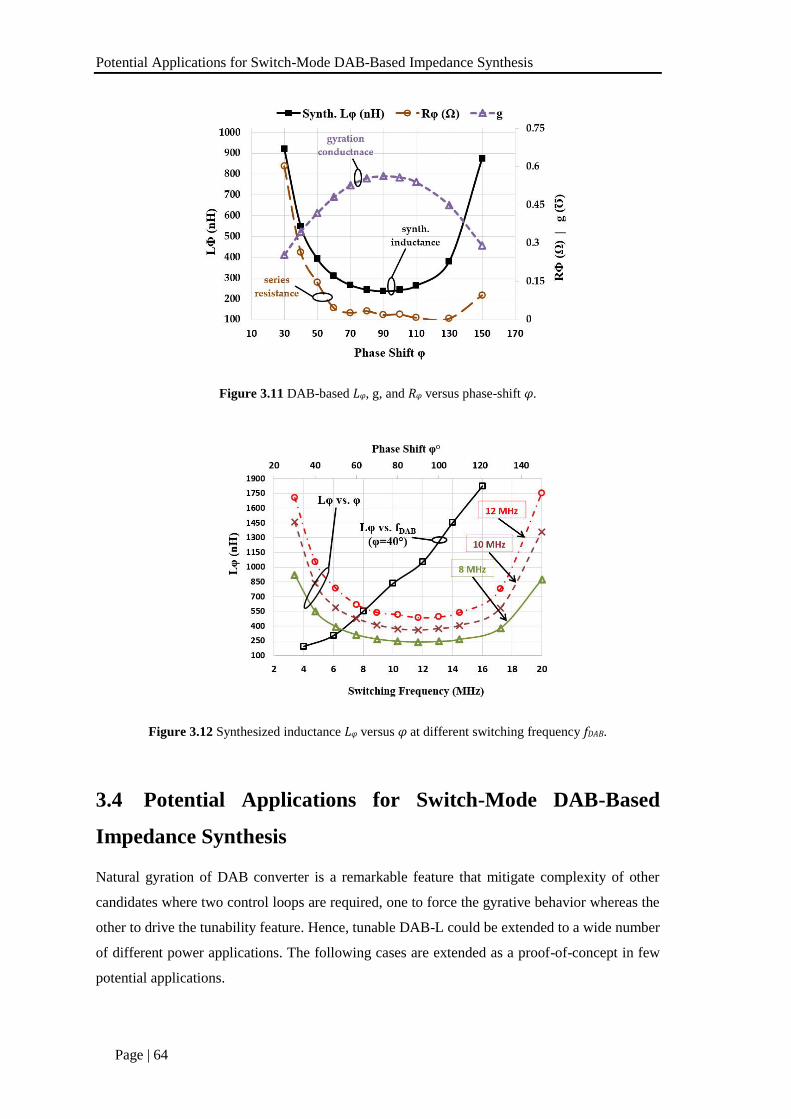
Potential Applications for Switch-Mode DAB-Based Impedance Synthesis
Page | 64
Figure 3.11 DAB-based Lφ, g, and Rφ versus phase-shift φ.
Figure 3.12 Synthesized inductance Lφ versus φ at different switching frequency fDAB.
3.4 Potential Applications for Switch-Mode DAB-Based
Impedance Synthesis
Natural gyration of DAB converter is a remarkable feature that mitigate complexity of other
candidates where two control loops are required, one to force the gyrative behavior whereas the
other to drive the tunability feature. Hence, tunable DAB-L could be extended to a wide number
of different power applications. The following cases are extended as a proof-of-concept in few
potential applications.
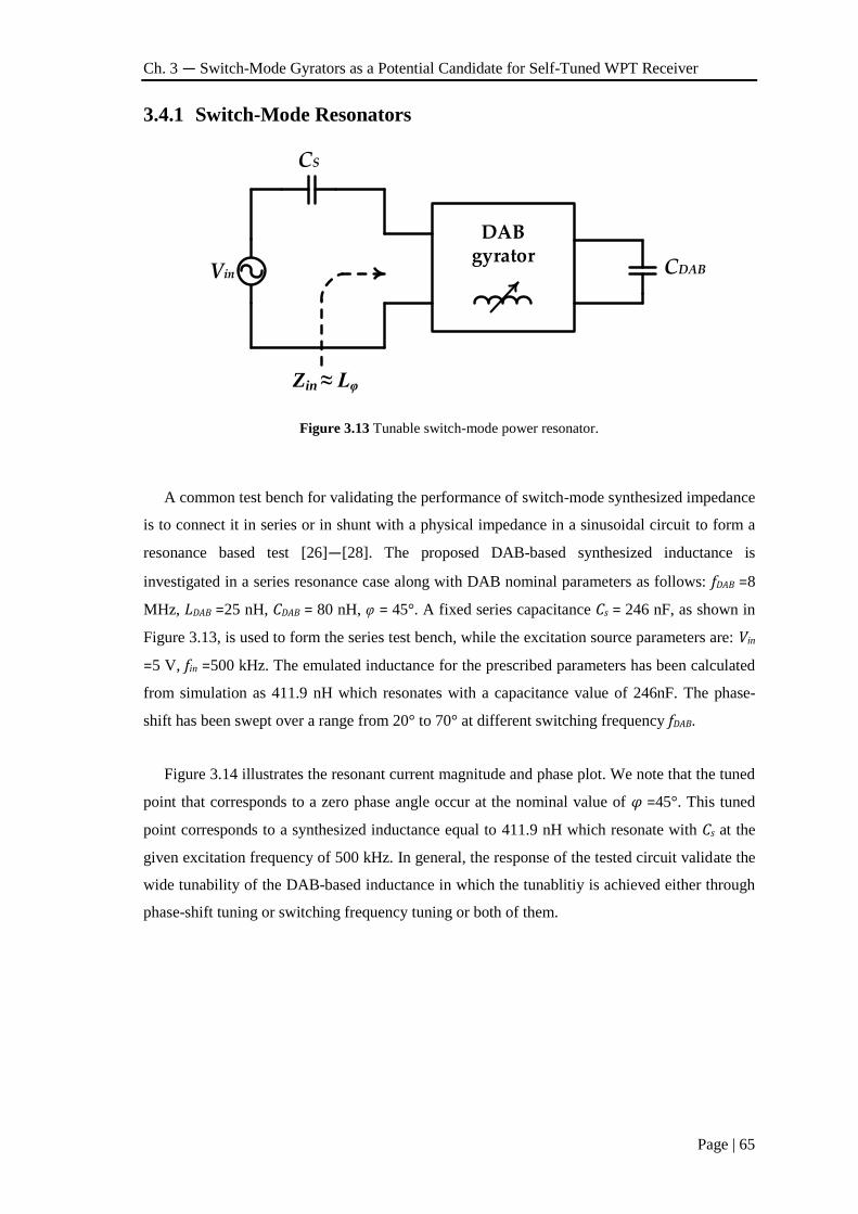
Ch. 3 — Switch-Mode Gyrators as a Potential Candidate for Self-Tuned WPT Receiver
Page | 65
3.4.1 Switch-Mode Resonators
DABgyrator
Vin CDAB
CS
Zin ≈ Lφ
Figure 3.13 Tunable switch-mode power resonator.
A common test bench for validating the performance of switch-mode synthesized impedance
is to connect it in series or in shunt with a physical impedance in a sinusoidal circuit to form a
resonance based test [26]—[28]. The proposed DAB-based synthesized inductance is
investigated in a series resonance case along with DAB nominal parameters as follows: fDAB =8
MHz, LDAB =25 nH, CDAB = 80 nH, φ = 45°. A fixed series capacitance Cs = 246 nF, as shown in
Figure 3.13, is used to form the series test bench, while the excitation source parameters are: Vin
=5 V, fin =500 kHz. The emulated inductance for the prescribed parameters has been calculated
from simulation as 411.9 nH which resonates with a capacitance value of 246nF. The phase-
shift has been swept over a range from 20° to 70° at different switching frequency fDAB.
Figure 3.14 illustrates the resonant current magnitude and phase plot. We note that the tuned
point that corresponds to a zero phase angle occur at the nominal value of φ =45°. This tuned
point corresponds to a synthesized inductance equal to 411.9 nH which resonate with Cs at the
given excitation frequency of 500 kHz. In general, the response of the tested circuit validate the
wide tunability of the DAB-based inductance in which the tunablitiy is achieved either through
phase-shift tuning or switching frequency tuning or both of them.
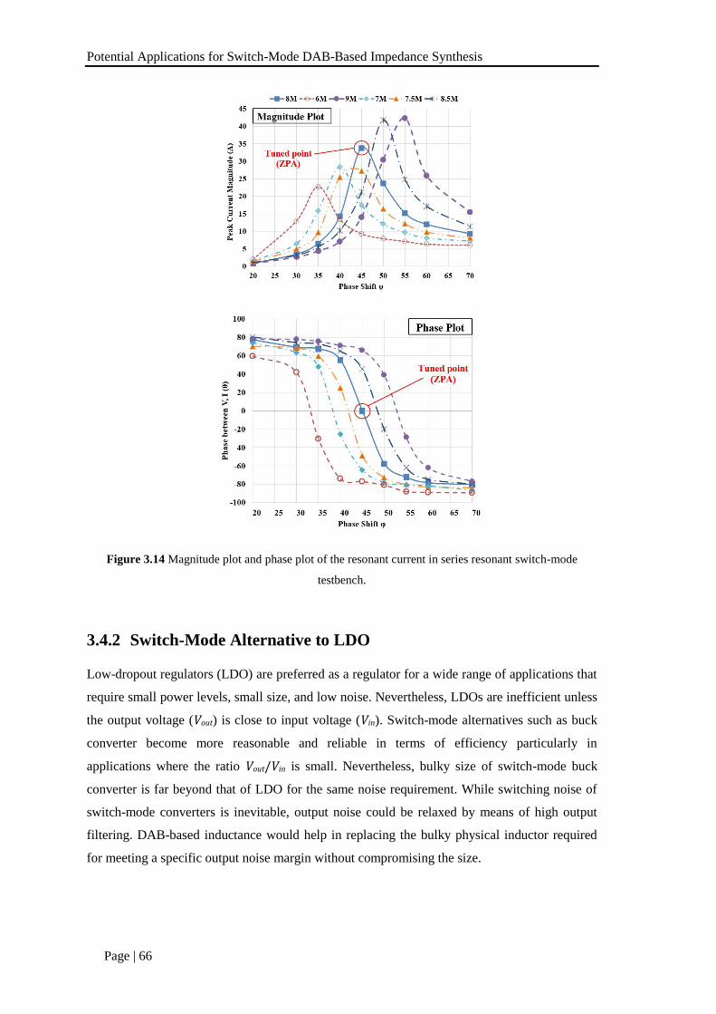
Potential Applications for Switch-Mode DAB-Based Impedance Synthesis
Page | 66
Figure 3.14 Magnitude plot and phase plot of the resonant current in series resonant switch-mode
testbench.
3.4.2 Switch-Mode Alternative to LDO
Low-dropout regulators (LDO) are preferred as a regulator for a wide range of applications that
require small power levels, small size, and low noise. Nevertheless, LDOs are inefficient unless
the output voltage (Vout) is close to input voltage (Vin). Switch-mode alternatives such as buck
converter become more reasonable and reliable in terms of efficiency particularly in
applications where the ratio Vout/Vin is small. Nevertheless, bulky size of switch-mode buck
converter is far beyond that of LDO for the same noise requirement. While switching noise of
switch-mode converters is inevitable, output noise could be relaxed by means of high output
filtering. DAB-based inductance would help in replacing the bulky physical inductor required
for meeting a specific output noise margin without compromising the size.
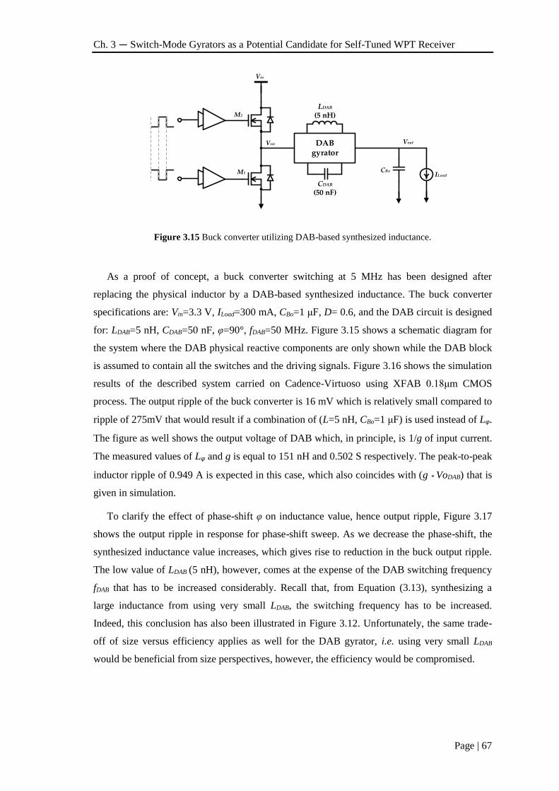
Ch. 3 — Switch-Mode Gyrators as a Potential Candidate for Self-Tuned WPT Receiver
Page | 67
M1
M2
Vin
CDAB
(50 nF)
LDAB
(5 nH)
DABgyrator
ILoadCBo
VoutVsw
Figure 3.15 Buck converter utilizing DAB-based synthesized inductance.
As a proof of concept, a buck converter switching at 5 MHz has been designed after
replacing the physical inductor by a DAB-based synthesized inductance. The buck converter
specifications are: Vin=3.3 V, ILoad=300 mA, CBo=1 μF, D= 0.6, and the DAB circuit is designed
for: LDAB=5 nH, CDAB=50 nF, φ=90°, fDAB=50 MHz. Figure 3.15 shows a schematic diagram for
the system where the DAB physical reactive components are only shown while the DAB block
is assumed to contain all the switches and the driving signals. Figure 3.16 shows the simulation
results of the described system carried on Cadence-Virtuoso using XFAB 0.18μm CMOS
process. The output ripple of the buck converter is 16 mV which is relatively small compared to
ripple of 275mV that would result if a combination of (L=5 nH, CBo=1 μF) is used instead of Lφ.
The figure as well shows the output voltage of DAB which, in principle, is 1/g of input current.
The measured values of Lφ and g is equal to 151 nH and 0.502 S respectively. The peak-to-peak
inductor ripple of 0.949 A is expected in this case, which also coincides with (g * VoDAB) that is
given in simulation.
To clarify the effect of phase-shift φ on inductance value, hence output ripple, Figure 3.17
shows the output ripple in response for phase-shift sweep. As we decrease the phase-shift, the
synthesized inductance value increases, which gives rise to reduction in the buck output ripple.
The low value of LDAB (5 nH), however, comes at the expense of the DAB switching frequency
fDAB that has to be increased considerably. Recall that, from Equation (3.13), synthesizing a
large inductance from using very small LDAB, the switching frequency has to be increased.
Indeed, this conclusion has also been illustrated in Figure 3.12. Unfortunately, the same trade-
off of size versus efficiency applies as well for the DAB gyrator, i.e. using very small LDAB
would be beneficial from size perspectives, however, the efficiency would be compromised.
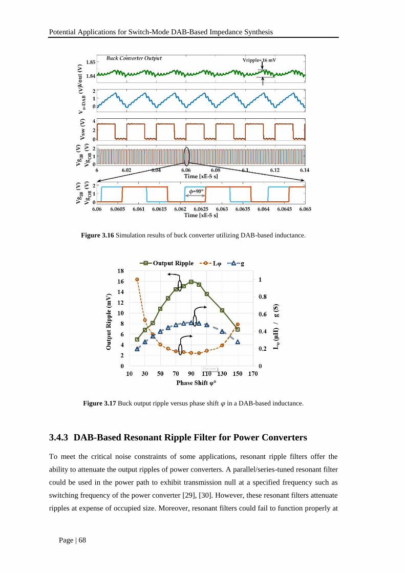
Potential Applications for Switch-Mode DAB-Based Impedance Synthesis
Page | 68
Figure 3.16 Simulation results of buck converter utilizing DAB-based inductance.
Figure 3.17 Buck output ripple versus phase shift φ in a DAB-based inductance.
3.4.3 DAB-Based Resonant Ripple Filter for Power Converters
To meet the critical noise constraints of some applications, resonant ripple filters offer the
ability to attenuate the output ripples of power converters. A parallel/series-tuned resonant filter
could be used in the power path to exhibit transmission null at a specified frequency such as
switching frequency of the power converter [29], [30]. However, these resonant filters attenuate
ripples at expense of occupied size. Moreover, resonant filters could fail to function properly at
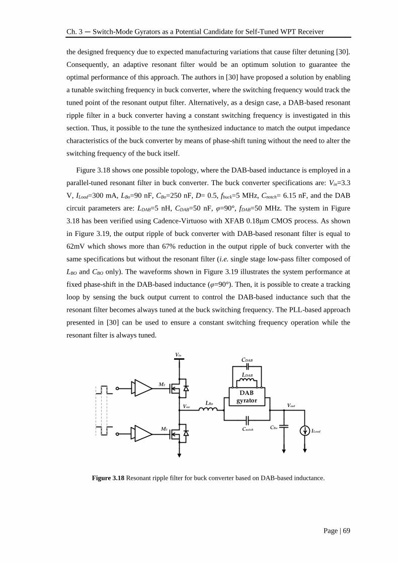
Ch. 3 — Switch-Mode Gyrators as a Potential Candidate for Self-Tuned WPT Receiver
Page | 69
the designed frequency due to expected manufacturing variations that cause filter detuning [30].
Consequently, an adaptive resonant filter would be an optimum solution to guarantee the
optimal performance of this approach. The authors in [30] have proposed a solution by enabling
a tunable switching frequency in buck converter, where the switching frequency would track the
tuned point of the resonant output filter. Alternatively, as a design case, a DAB-based resonant
ripple filter in a buck converter having a constant switching frequency is investigated in this
section. Thus, it possible to the tune the synthesized inductance to match the output impedance
characteristics of the buck converter by means of phase-shift tuning without the need to alter the
switching frequency of the buck itself.
Figure 3.18 shows one possible topology, where the DAB-based inductance is employed in a
parallel-tuned resonant filter in buck converter. The buck converter specifications are: Vin=3.3
V, ILoad=300 mA, LBo=90 nF, CBo=250 nF, D= 0.5, fbuck=5 MHz, Cnotch= 6.15 nF, and the DAB
circuit parameters are: LDAB=5 nH, CDAB=50 nF, φ=90°, fDAB=50 MHz. The system in Figure
3.18 has been verified using Cadence-Virtuoso with XFAB 0.18μm CMOS process. As shown
in Figure 3.19, the output ripple of buck converter with DAB-based resonant filter is equal to
62mV which shows more than 67% reduction in the output ripple of buck converter with the
same specifications but without the resonant filter (i.e. single stage low-pass filter composed of
LBO and CBO only). The waveforms shown in Figure 3.19 illustrates the system performance at
fixed phase-shift in the DAB-based inductance (φ=90°). Then, it is possible to create a tracking
loop by sensing the buck output current to control the DAB-based inductance such that the
resonant filter becomes always tuned at the buck switching frequency. The PLL-based approach
presented in [30] can be used to ensure a constant switching frequency operation while the
resonant filter is always tuned.
M1
M2
Vin
ILoadCBo
VoutVsw
DABgyratorLBo
Cnotch
LDAB
CDAB
Figure 3.18 Resonant ripple filter for buck converter based on DAB-based inductance.
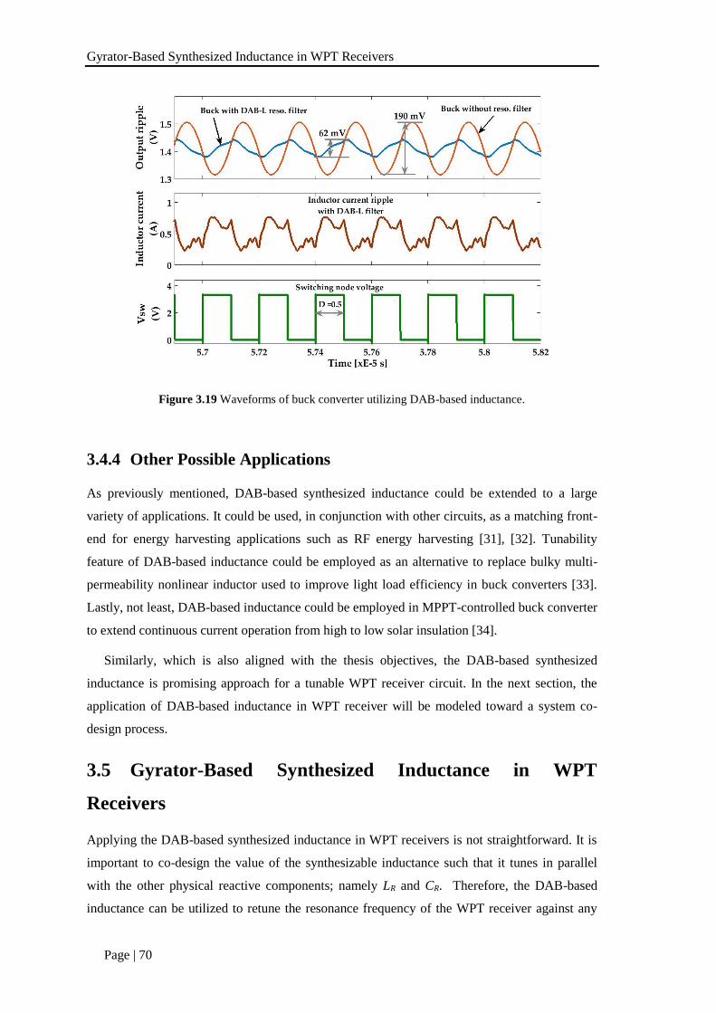
Gyrator-Based Synthesized Inductance in WPT Receivers
Page | 70
Figure 3.19 Waveforms of buck converter utilizing DAB-based inductance.
3.4.4 Other Possible Applications
As previously mentioned, DAB-based synthesized inductance could be extended to a large
variety of applications. It could be used, in conjunction with other circuits, as a matching front-
end for energy harvesting applications such as RF energy harvesting [31], [32]. Tunability
feature of DAB-based inductance could be employed as an alternative to replace bulky multi-
permeability nonlinear inductor used to improve light load efficiency in buck converters [33].
Lastly, not least, DAB-based inductance could be employed in MPPT-controlled buck converter
to extend continuous current operation from high to low solar insulation [34].
Similarly, which is also aligned with the thesis objectives, the DAB-based synthesized
inductance is promising approach for a tunable WPT receiver circuit. In the next section, the
application of DAB-based inductance in WPT receiver will be modeled toward a system co-
design process.
3.5 Gyrator-Based Synthesized Inductance in WPT
Receivers
Applying the DAB-based synthesized inductance in WPT receivers is not straightforward. It is
important to co-design the value of the synthesizable inductance such that it tunes in parallel
with the other physical reactive components; namely LR and CR. Therefore, the DAB-based
inductance can be utilized to retune the resonance frequency of the WPT receiver against any
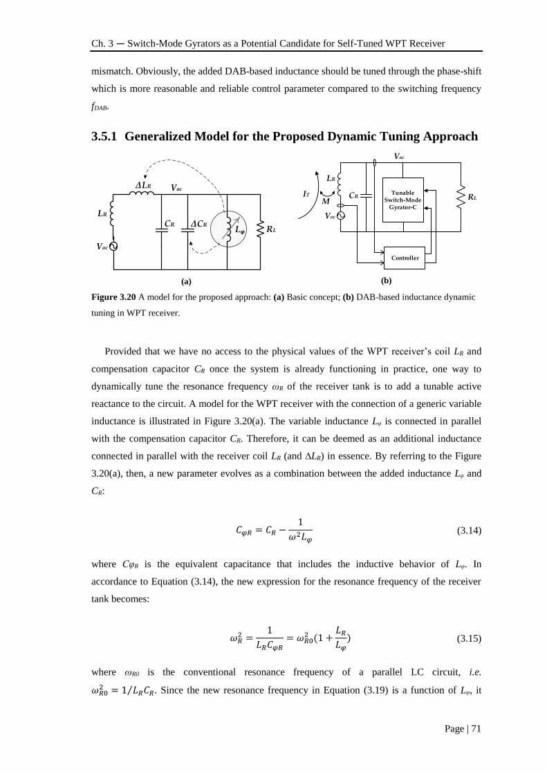
Ch. 3 — Switch-Mode Gyrators as a Potential Candidate for Self-Tuned WPT Receiver
Page | 71
mismatch. Obviously, the added DAB-based inductance should be tuned through the phase-shift
which is more reasonable and reliable control parameter compared to the switching frequency
fDAB.
3.5.1 Generalized Model for the Proposed Dynamic Tuning Approach
CR
Voc
Vac
RL
LR
∆CR
∆LR
Lφ
(a)
TunableSwitch-Mode
Gyrator-C
Controller
MIT
LR
CR RL
Voc
Vac
(b)
Figure 3.20 A model for the proposed approach: (a) Basic concept; (b) DAB-based inductance dynamic
tuning in WPT receiver.
Provided that we have no access to the physical values of the WPT receiver’s coil LR and
compensation capacitor CR once the system is already functioning in practice, one way to
dynamically tune the resonance frequency ωR of the receiver tank is to add a tunable active
reactance to the circuit. A model for the WPT receiver with the connection of a generic variable
inductance is illustrated in Figure 3.20(a). The variable inductance Lφ is connected in parallel
with the compensation capacitor CR. Therefore, it can be deemed as an additional inductance
connected in parallel with the receiver coil LR (and ∆LR) in essence. By referring to the Figure
3.20(a), then, a new parameter evolves as a combination between the added inductance Lφ and
CR:
𝐶𝜑𝑅 = 𝐶𝑅 −1
𝜔2𝐿𝜑 (3.14)
where CφR is the equivalent capacitance that includes the inductive behavior of Lφ. In
accordance to Equation (3.14), the new expression for the resonance frequency of the receiver
tank becomes:
𝜔𝑅2 =
1
𝐿𝑅𝐶𝜑𝑅= 𝜔𝑅0
2 (1 +𝐿𝑅
𝐿𝜑) (3.15)
where ωR0 is the conventional resonance frequency of a parallel LC circuit, i.e.
𝜔𝑅02 = 1 𝐿𝑅𝐶𝑅⁄ . Since the new resonance frequency in Equation (3.19) is a function of Lφ, it
Conclusions
Page | 72
indicates that ωR can be tuned over a wide range that is only limited by the tuning range of Lφ.
With the help of Figure 3.20(a), including all the depicted mismatches (∆LR, ∆CR), the power
transferred to the receiver is calculated as:
𝑃𝑟𝑚𝑠 =𝜔2𝑀2𝐼𝑇
2𝑅𝐿
(𝜔2𝐿𝑅𝐶𝜑𝑅(1 + 𝛾𝐿)(1 + 𝛾𝜑)𝑅𝐿 − 𝑅𝐿)2 + 𝜔2𝐿𝑅
2 (1 + 𝛾𝐿)2 (3.16)
where γL=∆LR/LR and γφ=∆CR/Cφ. Clearly, the transferred power in Equation (3.16) can be
recovered to the maximum, nearly as given by Equation (2.63), by tuning Lφ and thus CφR
subsequently. Thereby, the mistuning effect incurred by γL and γφ could be neutralized.
3.6 Conclusions
The gyrator as a linear power conservative network element has been utilized for synthesizing
variable impedance in wide variety of applications. In this Chapter, we have reviewed the
theoretical basis of the gyrator where the common circuit realizations for the gyrator have also
been revisited. It has been shown that the transistor-based realizations are not adequate for
power processing applications because they are not power-wise efficient. Consequently, the
switch-mode implementations for the gyrator have been revised and discussed. Among these
implementations, the DAB converter has been selected as an optimum candidate topology
because it saves the efforts of forcing the gyration characteristics. The input/output voltage and
currents characteristics of the DAB converter suggest that the converter works as a natural
gyrator.
Accordingly, the DAB converter has been optimized for synthesizing variable inductive
reactance. Different potential applications for DAB-based variable inductance synthesis have
been proposed and tested as a proof-of-concept. The DAB converter switching at very high
frequency, while utilizing small physical reactive components, can be used to synthesize large
variable reactive components. Finally, a general model for DAB-based variable inductance in
parallel-compensated WPT receivers has been discussed. It has been shown accordingly that the
DAB-based inductance can be used as a variable reactive element in WPT receiver to retune the
resonant tank at different mismatch cases.
Ch. 3 — Switch-Mode Gyrators as a Potential Candidate for Self-Tuned WPT Receiver
Page | 73
3.7 References
[1] Q.-C. Zhong, “Active capacitors: Concept and implementation,” in 2012 IEEE International
Symposium on Industrial Electronics, 2012, pp. 149–153.
[2] G. A. Rincon-Mora, “Active capacitor multiplier in Miller-compensated circuits,” IEEE J. Solid-
State Circuits, vol. 35, no. 1, pp. 26–32, 2000.
[3] I.-C. Hwang, “Area-efficient and self-biased capacitor multiplier for on-chip loop filter,”
Electronics Letters, vol. 42, no. 24. p. 1392, 2006.
[4] L. A. Milner and G. A. Rincon-Mora, “A novel predictive inductor multiplier for integrated
circuit DC-DC converters in portable applications,” in ISLPED ’05. Proceedings of the 2005
International Symposium on Low Power Electronics and Design, 2005, pp. 84–89.
[5] Y. Lee and I. C. Park, “Capacitor array structure and switching control scheme to reduce
capacitor mismatch effects for SAR analog-to-digital converters,” in ISCAS 2010 - 2010 IEEE
International Symposium on Circuits and Systems: Nano-Bio Circuit Fabrics and Systems, 2010, pp.
1464–1467.
[6] J. J. Kim, K.-H. Lee, J. Choi, Y. Park, K. Lim, and C.-H. Lee, “Ultra-wideband CMOS voltage-
controlled oscillator with reconfigurable tunable inductors,” Electron. Lett., vol. 47, no. 4, p. 249,
2011.
[7] D. H. Tellegen, “The Gyrator, a New Electric Network Element,” Philips Res. Reports, vol. 3,
no. 2, pp. 81–101.
[8] S. Singer and R. W. Erickson, “Canonical modeling of power processing circuits based on the
POPI concept,” IEEE Trans. Power Electron., vol. 7, no. 1, pp. 37–43, 1992.
[9] M. Ismail and H. Olsson, “A novel CMOS fully differential inductorless RF bandpass filter,”
2000 IEEE Int. Symp. Circuits Syst. Emerg. Technol. 21st Century. Proc., vol. 4, pp. 149–152, 2000.
[10] T. Deliyannis, Y. Sun, and J. K. Fidler, Continuous-time active filter design. CRC Press, 1999.
[11] G. G. A. Black, R. T. Friedmann, and A. S. Sedra, “Gyrator implementation with integrable
current conveyors,” IEEE J. Solid-State Circuits, vol. 6, no. 6, 1971.
[12] G. G. A. Black, R. T. Friedmann, and A. S. Sedra, “Gyrator implementation with integrable
current conveyors,” IEEE Journal of Solid-State Circuits, vol. 6, no. 6. pp. 396–399, 1971.
[13] S. Singer, “Gyrators Application in Power Processing Circuits,” IEEE Trans. Ind. Electron.,
vol. IE-34, no. 3, pp. 313–318, Aug. 1987.
[14] S. Singer, “Loss-free gyrator realization,” IEEE Trans. Circuits Syst., vol. 35, no. 1, pp. 26–34,
1988.
[15] A. Cid-Pastor, L. Martinez-Salamero, C. Alonso, G. Schweitz, J. Calvente, and S. Singer,
“Classification and synthesis of power gyrators,” IEE Proc. - Electr. Power Appl., vol. 153, no. 6, p.
802, Nov. 2006.
[16] D. Shmilovitz, “Gyrator Realization Based on a Capacitive Switched Cell,” IEEE Trans.
Circuits Syst. II Express Briefs, vol. 53, no. 12, pp. 1418–1422, Dec. 2006.
References
Page | 74
[17] A. Cid-Pastor, L. Martinez-Salamero, C. Alonso, R. Leyva, and S. Singer, “Paralleling DC–DC
Switching Converters by Means of Power Gyrators,” IEEE Trans. Power Electron., vol. 22, no. 6,
pp. 2444–2453, Nov. 2007.
[18] A. Cid-Pastor, L. Martinez-Salamero, C. Alonso, B. Estibals, J. Alzieu, G. Schweitz, and D.
Shmilovitz, “Analysis and design of power gyrators in sliding-mode operation,” IEE Proc. - Electr.
Power Appl., vol. 152, no. 4, p. 821, Jul. 2005.
[19] R. Haroun, A. Cid-Pastor, A. El Aroudi, and L. Martinez-Salamero, “Synthesis of Canonical
Elements for Power Processing in DC Distribution Systems Using Cascaded Converters and Sliding-
Mode Control,” IEEE Trans. Power Electron., vol. 29, no. 3, pp. 1366–1381, Mar. 2014.
[20] M. Ehsani, I. Husain, and M. O. BilgiC, “Inverse Dual Converter (IDC) for High-Power DC-
DC Applications,” IEEE Trans. Power Electron., vol. 8, no. 2, pp. 216–223, 1993.
[21] M. Ehsani, I. Husain, and M. O. Bilgic, “Power converters as natural gyrators,” IEEE Trans.
Circuits Syst. I Fundam. Theory Appl., vol. 40, no. 12, pp. 946–949, 1993.
[22] I. Zeltser and S. Ben-Yaakov, “Modeling, analysis and simulation of ‘AC inductor’ based
converters,” in PESC Record - IEEE Annual Power Electronics Specialists Conference, 2007, pp.
2128–2134.
[23] D. Shmilovitz, “Loss-free complex impedance network elements,” IEEE Trans. Circuits Syst. I
Regul. Pap., vol. 53, no. 3, pp. 704–711, Mar. 2006.
[24] Hengsi Qin and J. W. Kimball, “Ac-ac dual active bridge converter for solid state transformer,”
in 2009 IEEE Energy Conversion Congress and Exposition, 2009, pp. 3039–3044.
[25] R. W. (Robert W. Erickson and D. Maksimović, Fundamentals of power electronics. Kluwer
Academic, 2001.
[26] H. Funato, A. Kawamura, and K. Kamiyama, “Realization of negative inductance using
Variable Active-Passive Reactance (VAPAR),” IEEE Trans. Power Electron., vol. 12, no. 4, pp.
589–596, 1997.
[27] M. T. Bina and D. C. Hamill, “Transient response and stability of the bootstrap variable
inductance (BVI),” in 2001 IEEE 32nd Annual Power Electronics Specialists Conference, vol. 2, pp.
510–515.
[28] N. T. Bina and D. C. Hamill, “Average model of the bootstrap variable inductance (BVI),” in
2000 IEEE 31st Annual Power Electronics Specialists Conference. Conference Proceedings, 2000,
vol. 2, no. c, pp. 967–972.
[29] E. Alarcon, G. Villar, S. Ferrandez, F. Guinjoan, and A. Poveda, “Ripple-reduction tuned
filtering switching power converter topology,” in 2004 IEEE 35th Annual Power Electronics
Specialists Conference, pp. 3739–3744.
[30] J. Phinney and D. J. Perreault, “Filters with active tuning for power applications,” IEEE Trans.
Power Electron., vol. 18, no. 2, pp. 636–647, 2003.
Ch. 3 — Switch-Mode Gyrators as a Potential Candidate for Self-Tuned WPT Receiver
Page | 75
[31] S. Agrawal, S. K. Pandey, J. Singh, and M. S. Parihar, “Realization of efficient RF energy
harvesting circuits employing different matching technique,” in Proceedings - International
Symposium on Quality Electronic Design, ISQED, 2014, pp. 754–761.
[32] R. G. Cid-Fuentes, H. Martinez, A. Poveda, and E. Alarcon, “Electronically tunable switch-
mode high-efficiency adaptive band-pass filters for energy harvesting applications,” in ISCAS 2012 -
2012 IEEE International Symposium on Circuits and Systems, 2012, pp. 684–687.
[33] L. Wang, Y. Pei, X. Yang, Y. Qin, and Z. Wang, “Improving light and intermediate load
efficiencies of buck converters with planar nonlinear inductors and variable on time control,” IEEE
Trans. Power Electron., vol. 27, no. 1, pp. 342–353, 2012.
[34] L. Zhang, W. G. Hurley, and W. H. Wölfle, “A New Approach to Achieve Maximum Power
Point Tracking for PV System With a Variable Inductor,” IEEE Trans. Power Electron., vol. 26, no.
4, pp. 1031–1037, Apr. 2011.

Page | 77
Chapter
4
4 Self-Tuning Control for WPT Receivers
based on Switch-Mode Gyrators
In the previous chapters, we have revisited the concept of reactive components emulation by
means of gyrators. We have shown accordingly that the same concept could be applied in power
processing applications where a switch-mode circuit is used for gyrator realization. The DAB
converter has been shown as a good candidate for our application because it is naturally gyrated
without the need for an external control that forces the gyration characteristics.
In order to utilize the DAB gyrator for realization of electronically tunable reactive element
in the framework of self-tuning WPT receivers, a novel control approach is required.
Consequently, the motivation of this chapter is to propose, discuss and evaluate novel control
techniques for self-tuning in WPT receivers. Two different control techniques will be proposed
and evaluated in this chapter, namely, dual-loop cascaded automatic tuning control and
quadrature phase-locked-loop control.
4.1 DAB-Based Variable Inductance Design
Following the proposal of DAB converter as a natural gyrator, a system co-designing is
required in order to apply the DAB converter as a variable inductance synthesizer in parallel-
compensated WPT receivers. Figure 4.1 shows the complete power circuit of the WPT receiver
as has been previously depicted in the block diagram of Chapter 3.
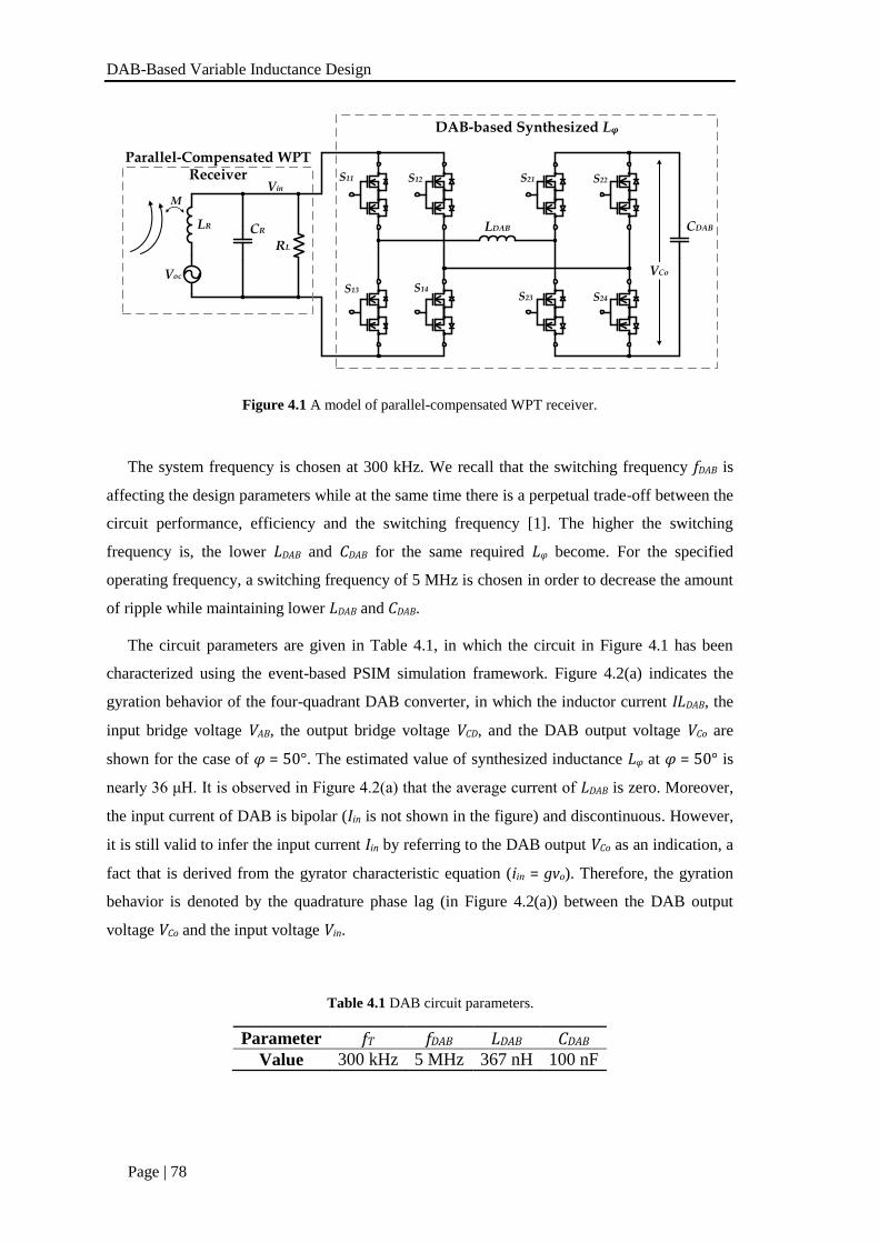
DAB-Based Variable Inductance Design
Page | 78
CDAB
Voc
LDABCR
RL
LR
S11 S12
S13 S14
S21 S22
S23 S24
VCo
M
DAB-based Synthesized Lφ
Parallel-Compensated WPT Receiver
Vin
Figure 4.1 A model of parallel-compensated WPT receiver.
The system frequency is chosen at 300 kHz. We recall that the switching frequency fDAB is
affecting the design parameters while at the same time there is a perpetual trade-off between the
circuit performance, efficiency and the switching frequency [1]. The higher the switching
frequency is, the lower LDAB and CDAB for the same required Lφ become. For the specified
operating frequency, a switching frequency of 5 MHz is chosen in order to decrease the amount
of ripple while maintaining lower LDAB and CDAB.
The circuit parameters are given in Table 4.1, in which the circuit in Figure 4.1 has been
characterized using the event-based PSIM simulation framework. Figure 4.2(a) indicates the
gyration behavior of the four-quadrant DAB converter, in which the inductor current ILDAB, the
input bridge voltage VAB, the output bridge voltage VCD, and the DAB output voltage VCo are
shown for the case of φ = 50°. The estimated value of synthesized inductance Lφ at φ = 50° is
nearly 36 μH. It is observed in Figure 4.2(a) that the average current of LDAB is zero. Moreover,
the input current of DAB is bipolar (Iin is not shown in the figure) and discontinuous. However,
it is still valid to infer the input current Iin by referring to the DAB output VCo as an indication, a
fact that is derived from the gyrator characteristic equation (iin = gvo). Therefore, the gyration
behavior is denoted by the quadrature phase lag (in Figure 4.2(a)) between the DAB output
voltage VCo and the input voltage Vin.
Table 4.1 DAB circuit parameters.
Parameter fT fDAB LDAB CDAB Value 300 kHz 5 MHz 367 nH 100 nF
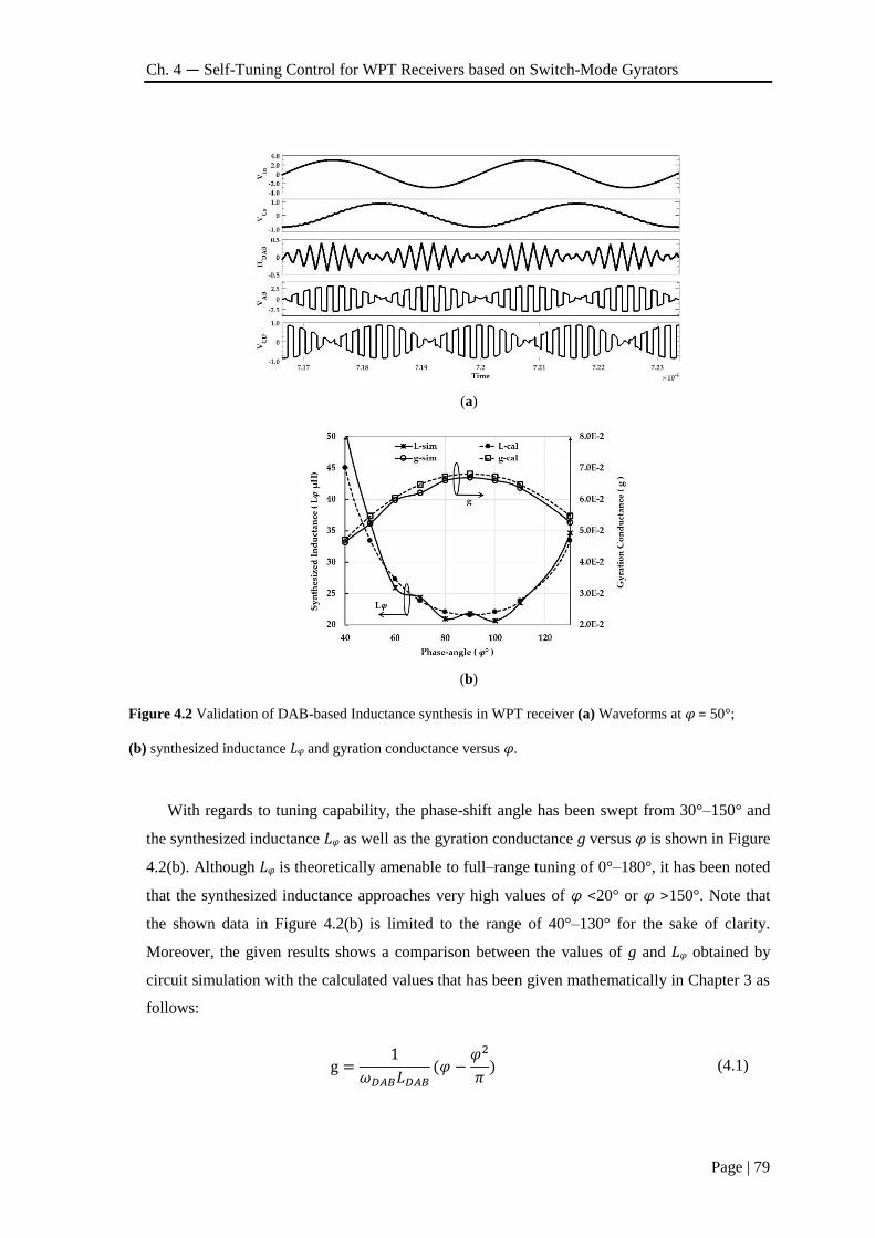
Ch. 4 — Self-Tuning Control for WPT Receivers based on Switch-Mode Gyrators
Page | 79
(a)
(b)
Figure 4.2 Validation of DAB-based Inductance synthesis in WPT receiver (a) Waveforms at φ = 50°;
(b) synthesized inductance Lφ and gyration conductance versus φ.
With regards to tuning capability, the phase-shift angle has been swept from 30°–150° and
the synthesized inductance Lφ as well as the gyration conductance g versus φ is shown in Figure
4.2(b). Although Lφ is theoretically amenable to full–range tuning of 0°–180°, it has been noted
that the synthesized inductance approaches very high values of φ <20° or φ >150°. Note that
the shown data in Figure 4.2(b) is limited to the range of 40°–130° for the sake of clarity.
Moreover, the given results shows a comparison between the values of g and Lφ obtained by
circuit simulation with the calculated values that has been given mathematically in Chapter 3 as
follows:
g =1
𝜔𝐷𝐴𝐵𝐿𝐷𝐴𝐵(𝜑 −
𝜑2
𝜋) (4.1)
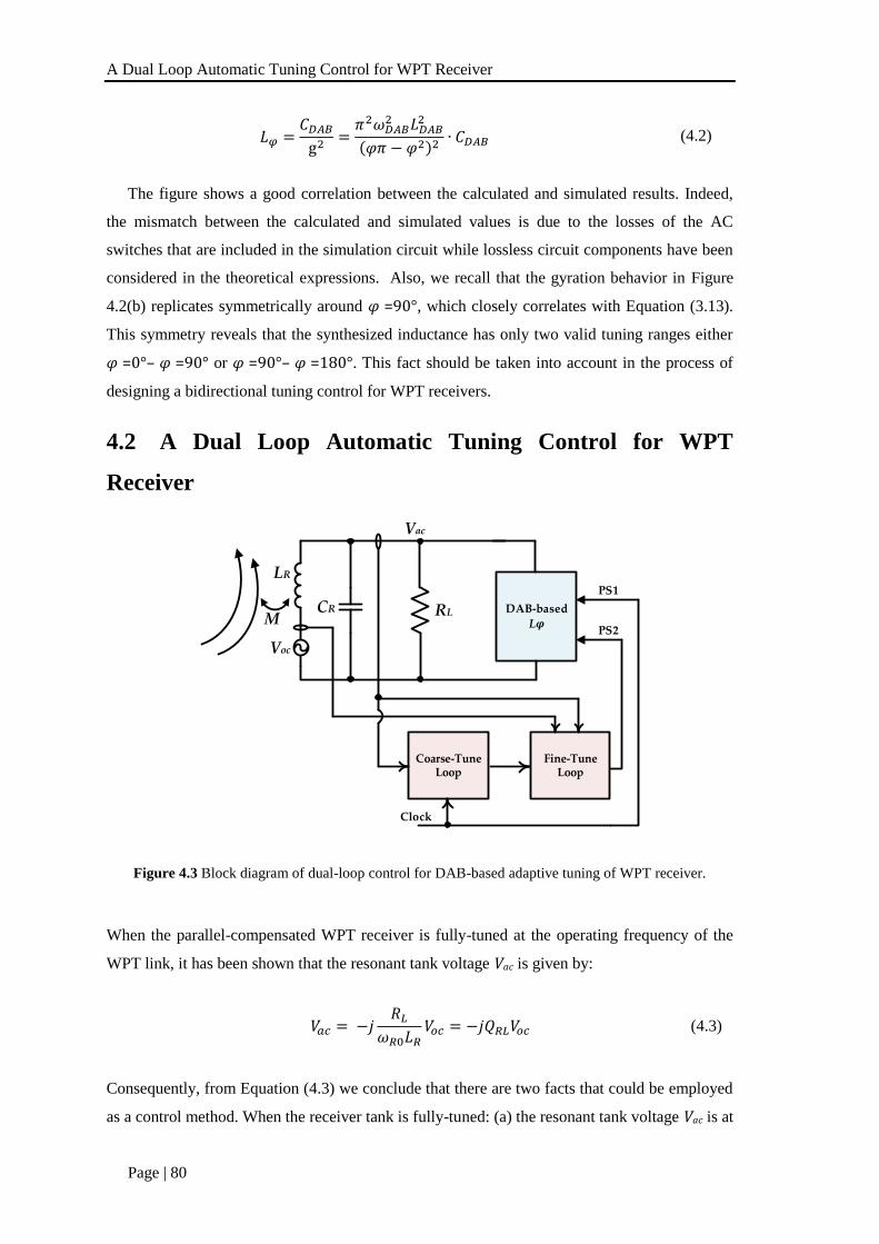
A Dual Loop Automatic Tuning Control for WPT Receiver
Page | 80
𝐿𝜑 =𝐶𝐷𝐴𝐵
g2=
𝜋2𝜔𝐷𝐴𝐵2 𝐿𝐷𝐴𝐵
2
(𝜑𝜋 − 𝜑2)2∙ 𝐶𝐷𝐴𝐵 (4.2)
The figure shows a good correlation between the calculated and simulated results. Indeed,
the mismatch between the calculated and simulated values is due to the losses of the AC
switches that are included in the simulation circuit while lossless circuit components have been
considered in the theoretical expressions. Also, we recall that the gyration behavior in Figure
4.2(b) replicates symmetrically around φ =90°, which closely correlates with Equation (3.13).
This symmetry reveals that the synthesized inductance has only two valid tuning ranges either
φ =0°– φ =90° or φ =90°– φ =180°. This fact should be taken into account in the process of
designing a bidirectional tuning control for WPT receivers.
4.2 A Dual Loop Automatic Tuning Control for WPT
Receiver
DAB-based
Lφ
Coarse-TuneLoop
M
LR
CR RL
Voc
Vac
Clock
Fine-TuneLoop
PS1
PS2
Figure 4.3 Block diagram of dual-loop control for DAB-based adaptive tuning of WPT receiver.
When the parallel-compensated WPT receiver is fully-tuned at the operating frequency of the
WPT link, it has been shown that the resonant tank voltage Vac is given by:
𝑉𝑎𝑐 = −𝑗𝑅𝐿
𝜔𝑅0𝐿𝑅𝑉𝑜𝑐 = −𝑗𝑄𝑅𝐿𝑉𝑜𝑐 (4.3)
Consequently, from Equation (4.3) we conclude that there are two facts that could be employed
as a control method. When the receiver tank is fully-tuned: (a) the resonant tank voltage Vac is at
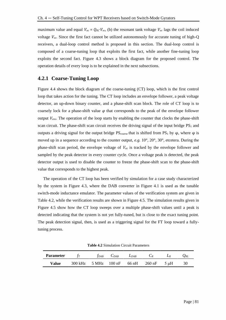
Ch. 4 — Self-Tuning Control for WPT Receivers based on Switch-Mode Gyrators
Page | 81
maximum value and equal Vac = QRL·Voc, (b) the resonant tank voltage Vac lags the coil induced
voltage Voc. Since the first fact cannot be utilized autonomously for accurate tuning of high-Q
receivers, a dual-loop control method is proposed in this section. The dual-loop control is
composed of a coarse-tuning loop that exploits the first fact, while another fine-tuning loop
exploits the second fact. Figure 4.3 shows a block diagram for the proposed control. The
operation details of every loop is to be explained in the next subsections.
4.2.1 Coarse-Tuning Loop
Figure 4.4 shows the block diagram of the coarse-tuning (CT) loop, which is the first control
loop that takes action for the tuning. The CT loop includes an envelope follower, a peak voltage
detector, an up-down binary counter, and a phase-shift scan block. The role of CT loop is to
coarsely lock for a phase-shift value φ that corresponds to the peak of the envelope follower
output Venv. The operation of the loop starts by enabling the counter that clocks the phase-shift
scan circuit. The phase-shift scan circuit receives the driving signal of the input bridge PS1 and
outputs a driving signal for the output bridge PScoarse that is shifted from PS1 by φ, where φ is
moved up in a sequence according to the counter output, e.g. 10°, 20°, 30°, etcetera. During the
phase-shift scan period, the envelope voltage of Vac is tracked by the envelope follower and
sampled by the peak detector in every counter cycle. Once a voltage peak is detected, the peak
detector output is used to disable the counter to freeze the phase-shift scan to the phase-shift
value that corresponds to the highest peak.
The operation of the CT loop has been verified by simulation for a case study characterized
by the system in Figure 4.3, where the DAB converter in Figure 4.1 is used as the tunable
switch-mode inductance emulator. The parameter values of the verification system are given in
Table 4.2, while the verification results are shown in Figure 4.5. The simulation results given in
Figure 4.5 show how the CT loop sweeps over a multiple phase-shift values until a peak is
detected indicating that the system is not yet fully-tuned, but is close to the exact tuning point.
The peak detection signal, then, is used as a triggering signal for the FT loop toward a fully-
tuning process.
Table 4.2 Simulation Circuit Parameters
Parameter fT fDAB CDAB LDAB CR LR QRL
Value 300 kHz 5 MHz 100 nF 66 nH 260 nF 5 μH 30
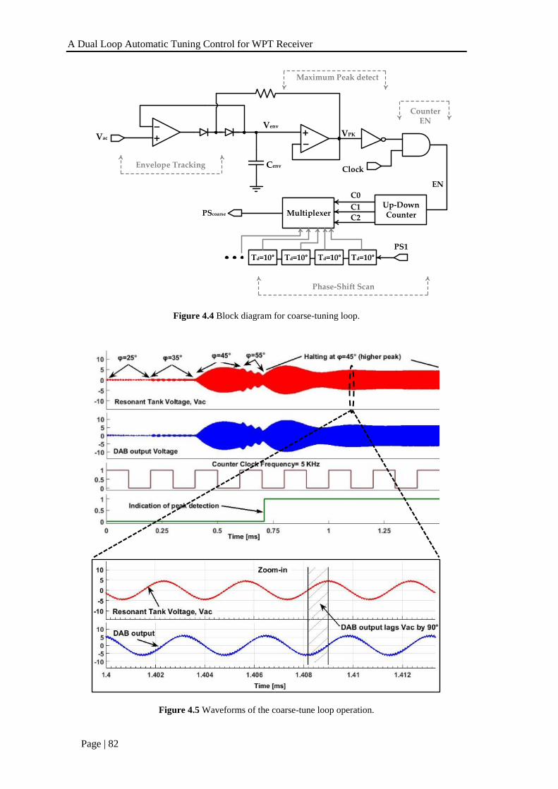
A Dual Loop Automatic Tuning Control for WPT Receiver
Page | 82
Venv
Up-Down Counter
Td=10°
Multiplexer
Td=10° Td=10° Td=10°
Clock
PS1
PScoarse
Vac
C0
C1
C2
EN
VPK
CenvEnvelope Tracking
Maximum Peak detect
Counter EN
Phase-Shift Scan
Figure 4.4 Block diagram for coarse-tuning loop.
Figure 4.5 Waveforms of the coarse-tune loop operation.
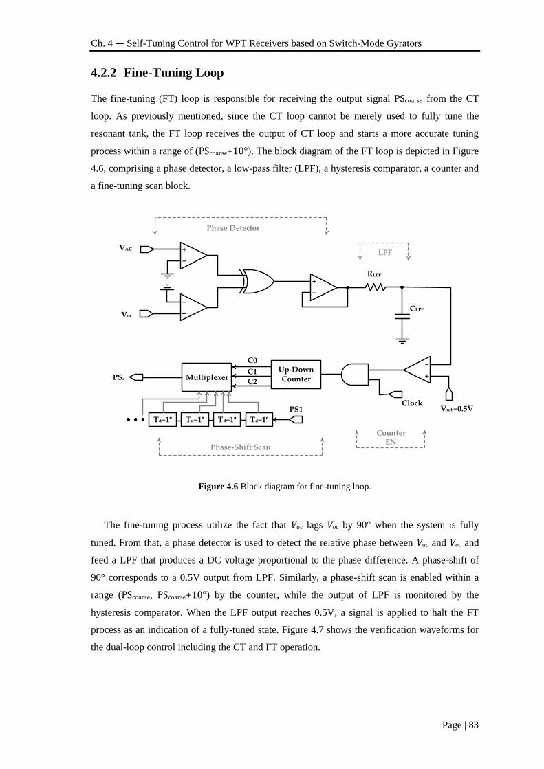
Ch. 4 — Self-Tuning Control for WPT Receivers based on Switch-Mode Gyrators
Page | 83
4.2.2 Fine-Tuning Loop
The fine-tuning (FT) loop is responsible for receiving the output signal PScoarse from the CT
loop. As previously mentioned, since the CT loop cannot be merely used to fully tune the
resonant tank, the FT loop receives the output of CT loop and starts a more accurate tuning
process within a range of (PScoarse+10°). The block diagram of the FT loop is depicted in Figure
4.6, comprising a phase detector, a low-pass filter (LPF), a hysteresis comparator, a counter and
a fine-tuning scan block.
+
−
+
−
+
−
+
−
VAC
Voc
RLPF
CLPF
Vref =0.5VClock
Up-Down Counter
Td=1°
Multiplexer
Td=1° Td=1° Td=1°
PS1
PS2
C0
C1
C2
Phase-Shift Scan
Phase Detector
LPF
Counter EN
Figure 4.6 Block diagram for fine-tuning loop.
The fine-tuning process utilize the fact that Vac lags Voc by 90° when the system is fully
tuned. From that, a phase detector is used to detect the relative phase between Vac and Voc and
feed a LPF that produces a DC voltage proportional to the phase difference. A phase-shift of
90° corresponds to a 0.5V output from LPF. Similarly, a phase-shift scan is enabled within a
range (PScoarse, PScoarse+10°) by the counter, while the output of LPF is monitored by the
hysteresis comparator. When the LPF output reaches 0.5V, a signal is applied to halt the FT
process as an indication of a fully-tuned state. Figure 4.7 shows the verification waveforms for
the dual-loop control including the CT and FT operation.
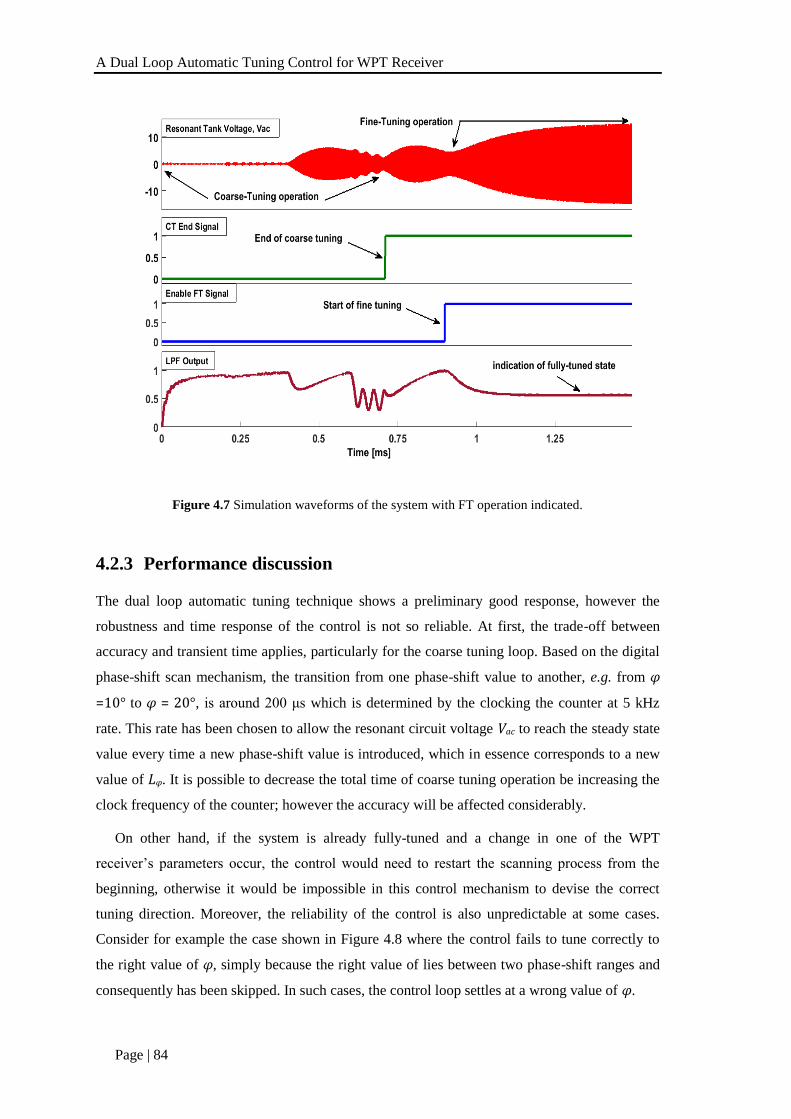
A Dual Loop Automatic Tuning Control for WPT Receiver
Page | 84
Figure 4.7 Simulation waveforms of the system with FT operation indicated.
4.2.3 Performance discussion
The dual loop automatic tuning technique shows a preliminary good response, however the
robustness and time response of the control is not so reliable. At first, the trade-off between
accuracy and transient time applies, particularly for the coarse tuning loop. Based on the digital
phase-shift scan mechanism, the transition from one phase-shift value to another, e.g. from φ
=10° to φ = 20°, is around 200 μs which is determined by the clocking the counter at 5 kHz
rate. This rate has been chosen to allow the resonant circuit voltage Vac to reach the steady state
value every time a new phase-shift value is introduced, which in essence corresponds to a new
value of Lφ. It is possible to decrease the total time of coarse tuning operation be increasing the
clock frequency of the counter; however the accuracy will be affected considerably.
On other hand, if the system is already fully-tuned and a change in one of the WPT
receiver’s parameters occur, the control would need to restart the scanning process from the
beginning, otherwise it would be impossible in this control mechanism to devise the correct
tuning direction. Moreover, the reliability of the control is also unpredictable at some cases.
Consider for example the case shown in Figure 4.8 where the control fails to tune correctly to
the right value of φ, simply because the right value of lies between two phase-shift ranges and
consequently has been skipped. In such cases, the control loop settles at a wrong value of φ.
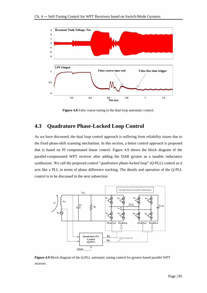
Ch. 4 — Self-Tuning Control for WPT Receivers based on Switch-Mode Gyrators
Page | 85
Figure 4.8 False coarse tuning in the dual loop automatic control.
4.3 Quadrature Phase-Locked Loop Control
As we have discussed, the dual loop control approach is suffering from reliability issues due to
the fixed phase-shift scanning mechanism. In this section, a better control approach is proposed
that is based on PI compensated linear control. Figure 4.9 shows the block diagram of the
parallel-compensated WPT receiver after adding the DAB gyrator as a tunable inductance
synthesizer. We call the proposed control “quadrature phase-locked loop” (Q-PLL) control as it
acts like a PLL in terms of phase difference tracking. The details and operation of the Q-PLL
control is to be discussed in the next subsection.
Figure 4.9 Block diagram of the Q-PLL automatic tuning control for gyrator-based parallel WPT
receiver.
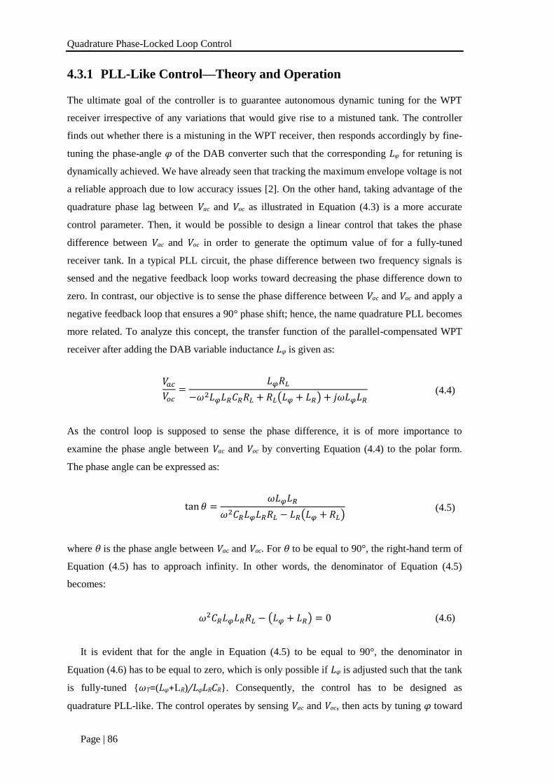
Quadrature Phase-Locked Loop Control
Page | 86
4.3.1 PLL-Like Control—Theory and Operation
The ultimate goal of the controller is to guarantee autonomous dynamic tuning for the WPT
receiver irrespective of any variations that would give rise to a mistuned tank. The controller
finds out whether there is a mistuning in the WPT receiver, then responds accordingly by fine-
tuning the phase-angle φ of the DAB converter such that the corresponding Lφ for retuning is
dynamically achieved. We have already seen that tracking the maximum envelope voltage is not
a reliable approach due to low accuracy issues [2]. On the other hand, taking advantage of the
quadrature phase lag between Vac and Voc as illustrated in Equation (4.3) is a more accurate
control parameter. Then, it would be possible to design a linear control that takes the phase
difference between Vac and Voc in order to generate the optimum value of for a fully-tuned
receiver tank. In a typical PLL circuit, the phase difference between two frequency signals is
sensed and the negative feedback loop works toward decreasing the phase difference down to
zero. In contrast, our objective is to sense the phase difference between Vac and Voc and apply a
negative feedback loop that ensures a 90° phase shift; hence, the name quadrature PLL becomes
more related. To analyze this concept, the transfer function of the parallel-compensated WPT
receiver after adding the DAB variable inductance Lφ is given as:
𝑉𝑎𝑐
𝑉𝑜𝑐=
𝐿𝜑𝑅𝐿
−𝜔2𝐿𝜑𝐿𝑅𝐶𝑅𝑅𝐿 + 𝑅𝐿(𝐿𝜑 + 𝐿𝑅) + 𝑗𝜔𝐿𝜑𝐿𝑅
(4.4)
As the control loop is supposed to sense the phase difference, it is of more importance to
examine the phase angle between Vac and Voc by converting Equation (4.4) to the polar form.
The phase angle can be expressed as:
tan 𝜃 =𝜔𝐿𝜑𝐿𝑅
𝜔2𝐶𝑅𝐿𝜑𝐿𝑅𝑅𝐿 − 𝐿𝑅(𝐿𝜑 + 𝑅𝐿) (4.5)
where θ is the phase angle between Vac and Voc. For θ to be equal to 90°, the right-hand term of
Equation (4.5) has to approach infinity. In other words, the denominator of Equation (4.5)
becomes:
𝜔2𝐶𝑅𝐿𝜑𝐿𝑅𝑅𝐿 − (𝐿𝜑 + 𝐿𝑅) = 0 (4.6)
It is evident that for the angle in Equation (4.5) to be equal to 90°, the denominator in
Equation (4.6) has to be equal to zero, which is only possible if Lφ is adjusted such that the tank
is fully-tuned ωT=(Lφ+LR)/LφLRCR. Consequently, the control has to be designed as
quadrature PLL-like. The control operates by sensing Vac and Voc, then acts by tuning φ toward
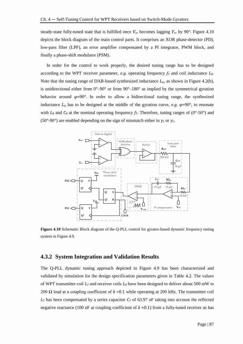
Ch. 4 — Self-Tuning Control for WPT Receivers based on Switch-Mode Gyrators
Page | 87
steady-state fully-tuned state that is fulfilled once Vac becomes lagging Voc by 90°. Figure 4.10
depicts the block diagram of the main control parts. It comprises an XOR phase-detector (PD),
low-pass filter (LPF), an error amplifier compensated by a PI integrator, PWM block, and
finally a phase-shift modulator (PSM).
In order for the control to work properly, the desired tuning range has to be designed
according to the WPT receiver parameter, e.g. operating frequency fT and coil inductance LR.
Note that the tuning range of DAB-based synthesized inductance Lφ, as shown in Figure 4.2(b),
is unidirectional either from 0°–90° or from 90°–180° as implied by the symmetrical gyration
behavior around φ=90°. In order to allow a bidirectional tuning range, the synthesized
inductance Lφ has to be designed at the middle of the gyration curve, e.g. φ=90°, to resonate
with LR and CR at the nominal operating frequency fT. Therefore, tuning ranges of (0°-50°) and
(50°-90°) are enabled depending on the sign of mismatch either in γL or γC.
Figure 4.10 Schematic Block diagram of the Q-PLL control for gyrator-based dynamic frequency tuning
system in Figure 4.9.
4.3.2 System Integration and Validation Results
The Q-PLL dynamic tuning approach depicted in Figure 4.9 has been characterized and
validated by simulation for the design specification parameters given in Table 4.2. The values
of WPT transmitter coil LT and receiver coils LR have been designed to deliver about 500 mW to
200 Ω load at a coupling coefficient of k =0.1 while operating at 200 kHz. The transmitter coil
LT has been compensated by a series capacitor CT of 63.97 nF taking into account the reflected
negative reactance (100 nF at coupling coefficient of k =0.1) from a fully-tuned receiver as has
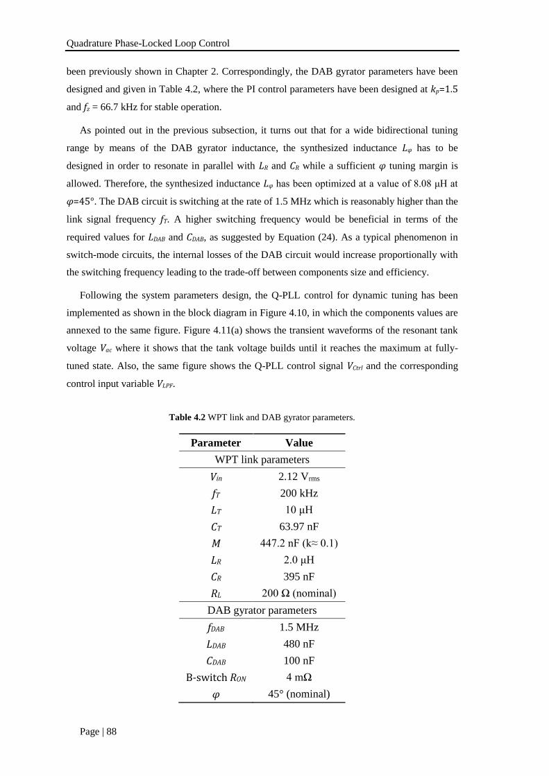
Quadrature Phase-Locked Loop Control
Page | 88
been previously shown in Chapter 2. Correspondingly, the DAB gyrator parameters have been
designed and given in Table 4.2, where the PI control parameters have been designed at kp=1.5
and fz = 66.7 kHz for stable operation.
As pointed out in the previous subsection, it turns out that for a wide bidirectional tuning
range by means of the DAB gyrator inductance, the synthesized inductance Lφ has to be
designed in order to resonate in parallel with LR and CR while a sufficient φ tuning margin is
allowed. Therefore, the synthesized inductance Lφ has been optimized at a value of 8.08 μH at
φ=45°. The DAB circuit is switching at the rate of 1.5 MHz which is reasonably higher than the
link signal frequency fT. A higher switching frequency would be beneficial in terms of the
required values for LDAB and CDAB, as suggested by Equation (24). As a typical phenomenon in
switch-mode circuits, the internal losses of the DAB circuit would increase proportionally with
the switching frequency leading to the trade-off between components size and efficiency.
Following the system parameters design, the Q-PLL control for dynamic tuning has been
implemented as shown in the block diagram in Figure 4.10, in which the components values are
annexed to the same figure. Figure 4.11(a) shows the transient waveforms of the resonant tank
voltage Vac where it shows that the tank voltage builds until it reaches the maximum at fully-
tuned state. Also, the same figure shows the Q-PLL control signal VCtrl and the corresponding
control input variable VLPF.
Table 4.2 WPT link and DAB gyrator parameters.
Parameter Value
WPT link parameters
Vin 2.12 Vrms
fT 200 kHz
LT 10 μH
CT 63.97 nF
M 447.2 nF (k≈ 0.1)
LR 2.0 μH
CR 395 nF
RL 200 Ω (nominal)
DAB gyrator parameters
fDAB 1.5 MHz
LDAB 480 nF
CDAB 100 nF
B-switch RON 4 mΩ
φ 45° (nominal)
Ch. 4 — Self-Tuning Control for WPT Receivers based on Switch-Mode Gyrators
Page | 89
It is evident that VLPF, which represents the phase difference between Vac and Voc, reaches
Vref=0.5 V indicating that Vac lags Voc by 90° as the typical state of a fully-tuned parallel
resonant tank. Moreover, Figure 4.11(b) shows a close-in view for the steady-state waveforms
for which the phase difference between Vac and Voc (scaled by QRL) is highlighted. Figure 4.11(b)
shows, as well, how the duty-cycle generated by the control is translated to the corresponding
phase-angle φ (almost 45° at the specified system parameters in Table 4.2) between the gating
signals PS1 and PS2.
(a)
(b)
Figure 4.11 System operation waveforms: (a) steady-state waveforms of VCtrl, VLPF and Vac; (b) a zoom-in
showing the waveforms of [QRL· Voc], Vac, Vramp, VCtrl, and DAB gating signals PS1 and PS2.
Further, Figure 4.12 shows the performance of the gyrator-based dynamic tuning approach
in response to mismatch in CR and LR. The system operation for -11% mismatch in CR followed
by -11% mismatch in LR is illustrated in Figure 4.12(a), in which the figure shows how φ is
dynamically controlled to retune the resonant tank. To neutralize the under-compensation effect
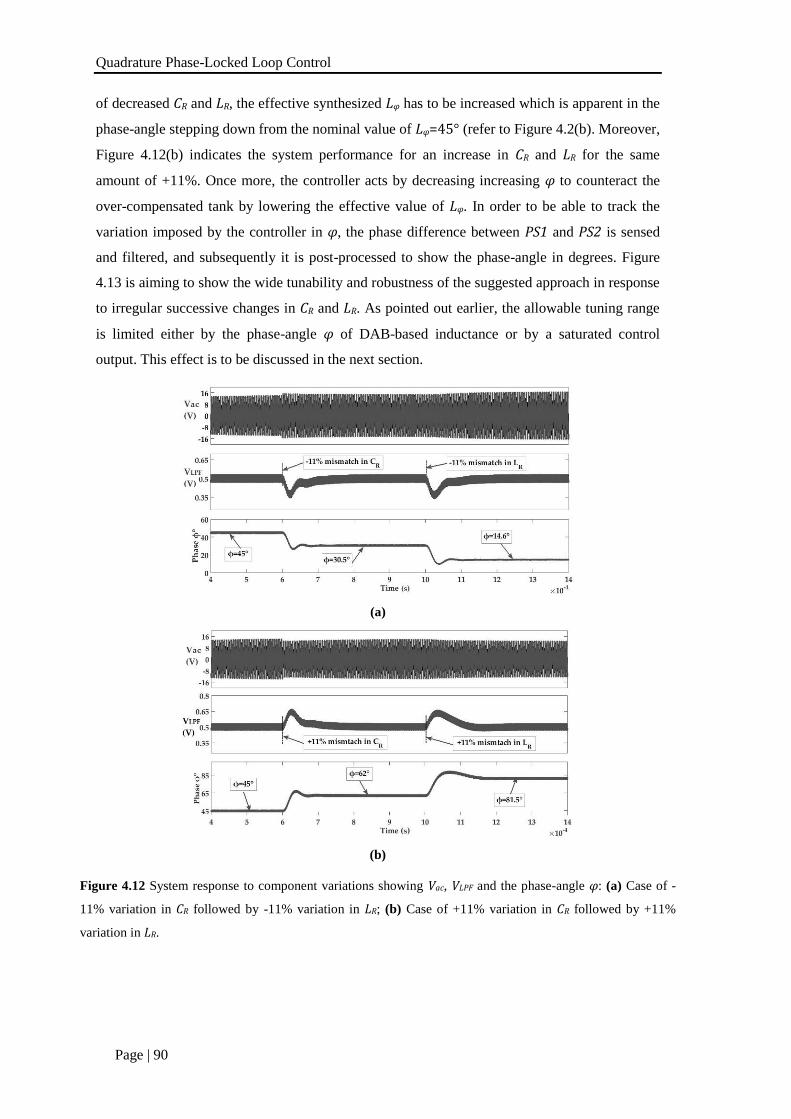
Quadrature Phase-Locked Loop Control
Page | 90
of decreased CR and LR, the effective synthesized Lφ has to be increased which is apparent in the
phase-angle stepping down from the nominal value of Lφ=45° (refer to Figure 4.2(b). Moreover,
Figure 4.12(b) indicates the system performance for an increase in CR and LR for the same
amount of +11%. Once more, the controller acts by decreasing increasing φ to counteract the
over-compensated tank by lowering the effective value of Lφ. In order to be able to track the
variation imposed by the controller in φ, the phase difference between PS1 and PS2 is sensed
and filtered, and subsequently it is post-processed to show the phase-angle in degrees. Figure
4.13 is aiming to show the wide tunability and robustness of the suggested approach in response
to irregular successive changes in CR and LR. As pointed out earlier, the allowable tuning range
is limited either by the phase-angle φ of DAB-based inductance or by a saturated control
output. This effect is to be discussed in the next section.
(a)
(b)
Figure 4.12 System response to component variations showing Vac, VLPF and the phase-angle φ: (a) Case of -
11% variation in CR followed by -11% variation in LR; (b) Case of +11% variation in CR followed by +11%
variation in LR.
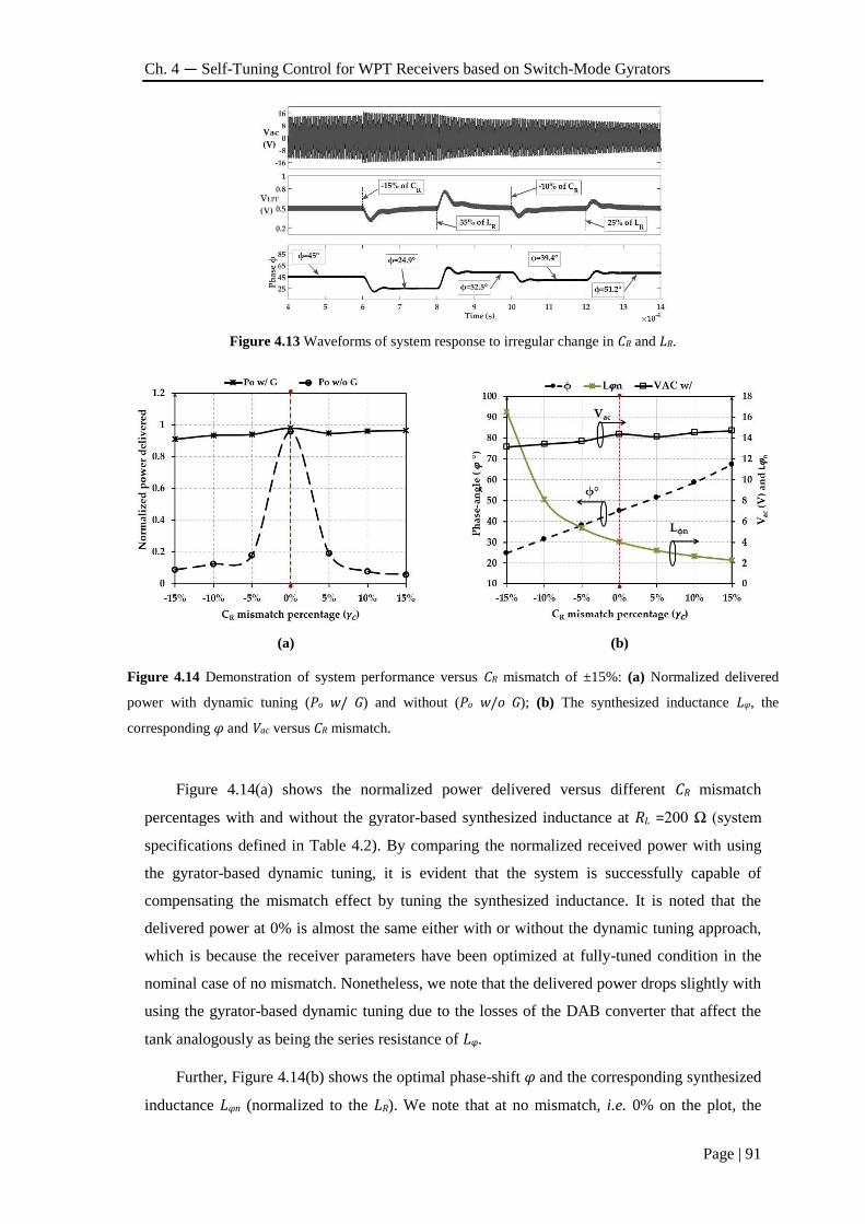
Ch. 4 — Self-Tuning Control for WPT Receivers based on Switch-Mode Gyrators
Page | 91
Figure 4.13 Waveforms of system response to irregular change in CR and LR.
(a)
(b)
Figure 4.14 Demonstration of system performance versus CR mismatch of ±15%: (a) Normalized delivered
power with dynamic tuning (Po w/ G) and without (Po w/o G); (b) The synthesized inductance Lφ, the
corresponding φ and Vac versus CR mismatch.
Figure 4.14(a) shows the normalized power delivered versus different CR mismatch
percentages with and without the gyrator-based synthesized inductance at RL =200 Ω (system
specifications defined in Table 4.2). By comparing the normalized received power with using
the gyrator-based dynamic tuning, it is evident that the system is successfully capable of
compensating the mismatch effect by tuning the synthesized inductance. It is noted that the
delivered power at 0% is almost the same either with or without the dynamic tuning approach,
which is because the receiver parameters have been optimized at fully-tuned condition in the
nominal case of no mismatch. Nonetheless, we note that the delivered power drops slightly with
using the gyrator-based dynamic tuning due to the losses of the DAB converter that affect the
tank analogously as being the series resistance of Lφ.
Further, Figure 4.14(b) shows the optimal phase-shift φ and the corresponding synthesized
inductance Lφn (normalized to the LR). We note that at no mismatch, i.e. 0% on the plot, the
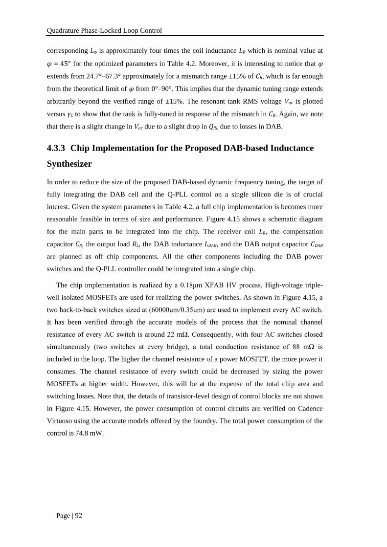
Quadrature Phase-Locked Loop Control
Page | 92
corresponding Lφ is approximately four times the coil inductance LR which is nominal value at
φ = 45° for the optimized parameters in Table 4.2. Moreover, it is interesting to notice that φ
extends from 24.7°–67.3° approximately for a mismatch range ±15% of CR, which is far enough
from the theoretical limit of φ from 0°–90°. This implies that the dynamic tuning range extends
arbitrarily beyond the verified range of ±15%. The resonant tank RMS voltage Vac is plotted
versus γC to show that the tank is fully-tuned in response of the mismatch in CR. Again, we note
that there is a slight change in Vac due to a slight drop in QRL due to losses in DAB.
4.3.3 Chip Implementation for the Proposed DAB-based Inductance
Synthesizer
In order to reduce the size of the proposed DAB-based dynamic frequency tuning, the target of
fully integrating the DAB cell and the Q-PLL control on a single silicon die is of crucial
interest. Given the system parameters in Table 4.2, a full chip implementation is becomes more
reasonable feasible in terms of size and performance. Figure 4.15 shows a schematic diagram
for the main parts to be integrated into the chip. The receiver coil LR, the compensation
capacitor CR, the output load RL, the DAB inductance LDAB, and the DAB output capacitor CDAB
are planned as off chip components. All the other components including the DAB power
switches and the Q-PLL controller could be integrated into a single chip.
The chip implementation is realized by a 0.18μm XFAB HV process. High-voltage triple-
well isolated MOSFETs are used for realizing the power switches. As shown in Figure 4.15, a
two back-to-back switches sized at (60000μm/0.35μm) are used to implement every AC switch.
It has been verified through the accurate models of the process that the nominal channel
resistance of every AC switch is around 22 mΩ. Consequently, with four AC switches closed
simultaneously (two switches at every bridge), a total conduction resistance of 88 mΩ is
included in the loop. The higher the channel resistance of a power MOSFET, the more power it
consumes. The channel resistance of every switch could be decreased by sizing the power
MOSFETs at higher width. However, this will be at the expense of the total chip area and
switching losses. Note that, the details of transistor-level design of control blocks are not shown
in Figure 4.15. However, the power consumption of control circuits are verified on Cadence
Virtuoso using the accurate models offered by the foundry. The total power consumption of the
control is 74.8 mW.
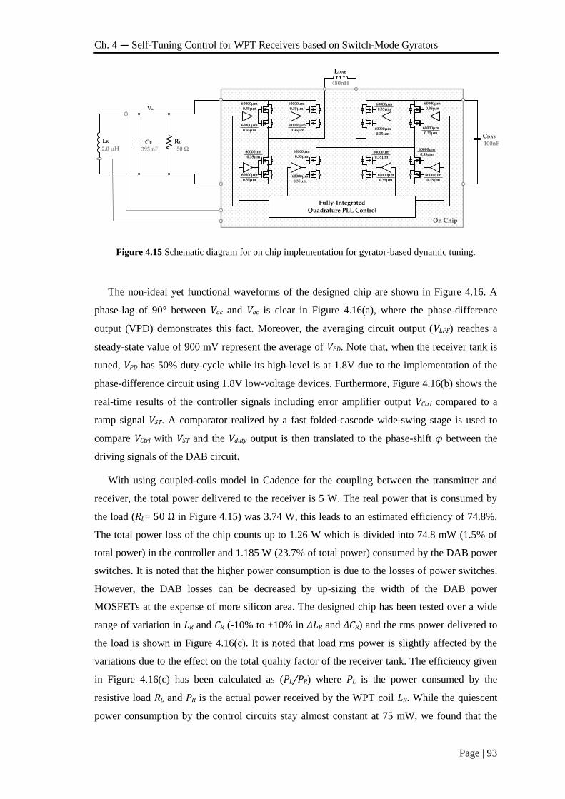
Ch. 4 — Self-Tuning Control for WPT Receivers based on Switch-Mode Gyrators
Page | 93
LDAB
Fully-IntegratedQuadrature PLL Control
CDAB
CR
Vac
LR RL
60000μm0.35μm
60000μm0.35μm
60000μm0.35μm
60000μm0.35μm
60000μm0.35μm
60000μm0.35μm
60000μm0.35μm
60000μm0.35μm
60000μm0.35μm
60000μm0.35μm
60000μm0.35μm
60000μm0.35μm
60000μm0.35μm
60000μm0.35μm
60000μm0.35μm
60000μm0.35μm
480nH
100nF50 Ω 395 nF2.0 μH
On Chip
Figure 4.15 Schematic diagram for on chip implementation for gyrator-based dynamic tuning.
The non-ideal yet functional waveforms of the designed chip are shown in Figure 4.16. A
phase-lag of 90° between Vac and Voc is clear in Figure 4.16(a), where the phase-difference
output (VPD) demonstrates this fact. Moreover, the averaging circuit output (VLPF) reaches a
steady-state value of 900 mV represent the average of VPD. Note that, when the receiver tank is
tuned, VPD has 50% duty-cycle while its high-level is at 1.8V due to the implementation of the
phase-difference circuit using 1.8V low-voltage devices. Furthermore, Figure 4.16(b) shows the
real-time results of the controller signals including error amplifier output VCtrl compared to a
ramp signal VST. A comparator realized by a fast folded-cascode wide-swing stage is used to
compare VCtrl with VST and the Vduty output is then translated to the phase-shift φ between the
driving signals of the DAB circuit.
With using coupled-coils model in Cadence for the coupling between the transmitter and
receiver, the total power delivered to the receiver is 5 W. The real power that is consumed by
the load (RL= 50 Ω in Figure 4.15) was 3.74 W, this leads to an estimated efficiency of 74.8%.
The total power loss of the chip counts up to 1.26 W which is divided into 74.8 mW (1.5% of
total power) in the controller and 1.185 W (23.7% of total power) consumed by the DAB power
switches. It is noted that the higher power consumption is due to the losses of power switches.
However, the DAB losses can be decreased by up-sizing the width of the DAB power
MOSFETs at the expense of more silicon area. The designed chip has been tested over a wide
range of variation in LR and CR (-10% to +10% in ∆LR and ∆CR) and the rms power delivered to
the load is shown in Figure 4.16(c). It is noted that load rms power is slightly affected by the
variations due to the effect on the total quality factor of the receiver tank. The efficiency given
in Figure 4.16(c) has been calculated as (PL/PR) where PL is the power consumed by the
resistive load RL and PR is the actual power received by the WPT coil LR. While the quiescent
power consumption by the control circuits stay almost constant at 75 mW, we found that the
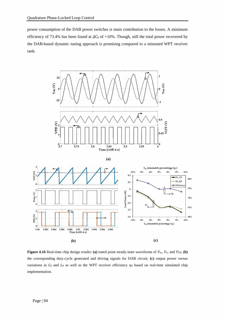
Quadrature Phase-Locked Loop Control
Page | 94
power consumption of the DAB power switches is main contribution to the losses. A minimum
efficiency of 73.4% has been found at ∆CR of +10%. Though, still the total power recovered by
the DAB-based dynamic tuning approach is promising compared to a mistuned WPT receiver
tank.
(a)
(b)
(c)
Figure 4.16 Real-time chip design results: (a) tuned point steady-state waveforms of Vac, Voc and VPD; (b)
the corresponding duty-cycle generated and driving signals for DAB circuit; (c) output power versus
variations in CR and LR as well as the WPT receiver efficiency ηR based on real-time simulated chip
implementation.
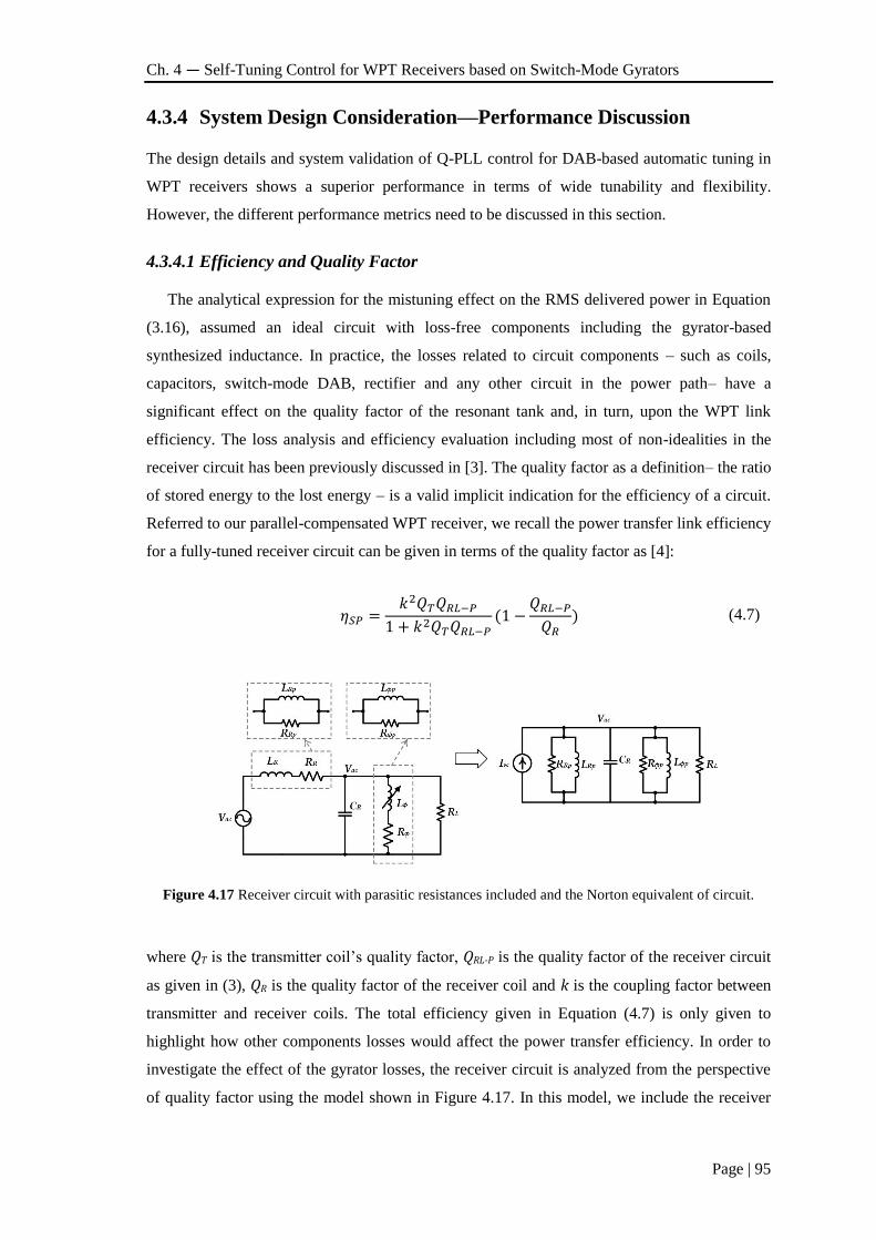
Ch. 4 — Self-Tuning Control for WPT Receivers based on Switch-Mode Gyrators
Page | 95
4.3.4 System Design Consideration—Performance Discussion
The design details and system validation of Q-PLL control for DAB-based automatic tuning in
WPT receivers shows a superior performance in terms of wide tunability and flexibility.
However, the different performance metrics need to be discussed in this section.
4.3.4.1 Efficiency and Quality Factor
The analytical expression for the mistuning effect on the RMS delivered power in Equation
(3.16), assumed an ideal circuit with loss-free components including the gyrator-based
synthesized inductance. In practice, the losses related to circuit components – such as coils,
capacitors, switch-mode DAB, rectifier and any other circuit in the power path– have a
significant effect on the quality factor of the resonant tank and, in turn, upon the WPT link
efficiency. The loss analysis and efficiency evaluation including most of non-idealities in the
receiver circuit has been previously discussed in [3]. The quality factor as a definition– the ratio
of stored energy to the lost energy – is a valid implicit indication for the efficiency of a circuit.
Referred to our parallel-compensated WPT receiver, we recall the power transfer link efficiency
for a fully-tuned receiver circuit can be given in terms of the quality factor as [4]:
𝜂𝑆𝑃 =𝑘2𝑄𝑇𝑄𝑅𝐿−𝑃
1 + 𝑘2𝑄𝑇𝑄𝑅𝐿−𝑃(1 −
𝑄𝑅𝐿−𝑃
𝑄𝑅) (4.7)
Figure 4.17 Receiver circuit with parasitic resistances included and the Norton equivalent of circuit.
where QT is the transmitter coil’s quality factor, QRL-P is the quality factor of the receiver circuit
as given in (3), QR is the quality factor of the receiver coil and k is the coupling factor between
transmitter and receiver coils. The total efficiency given in Equation (4.7) is only given to
highlight how other components losses would affect the power transfer efficiency. In order to
investigate the effect of the gyrator losses, the receiver circuit is analyzed from the perspective
of quality factor using the model shown in Figure 4.17. In this model, we include the receiver
Quadrature Phase-Locked Loop Control
Page | 96
coil series resistance RR, the load resistance RL, and the gyrator losses modeled as a resistance
Rφ in series with the synthesized inductance Lφ. To facilitate the analysis, the circuit can be
converted to the Norton equivalent as shown in Figure 4.17, where Lφp, LRp, RRp and Rφp are
given by:
𝑅𝜑𝑝 = (1 + 𝑄𝜑2)𝑅𝜑 ≅ 𝑄𝜑
2𝑅𝜑 (4.8)
𝐿𝜑𝑝 ≅ 𝐿𝜑 (4.9)
𝑅𝑅𝑝 = (1 + 𝑄𝑅2)𝑅𝑅 ≅ 𝑄𝑅
2𝑅𝑅 (4.10)
𝐿𝑅𝑝 ≅ 𝐿𝑅 (4.11)
where (LRp, RRp) and (Lφp, Rφp) are the equivalent values of (LR, RR) and (Lφ, Rφ) RR and Rφ after
converting the series networks (LR, RR) and (Lφ, Rφ) to parallel networks, while QR and Qφ are
the quality factors of LR and Lφ respectively. At fully-tuned state, the resonant voltage of the
circuit in Figure 4.17 can be given as:
𝑉𝑎𝑐 = −𝑗𝑄𝑅𝐿−𝑃
1
(1 +𝑅𝐿
𝑅𝑅𝑝⁄ +
𝑅𝐿𝑅𝜑𝑝
⁄ )𝑉𝑜𝑐 = −𝑗𝑄𝑅𝑥𝑉𝑜𝑐
(4.12)
Equation (4.12) develops a new term QRx as the total quality factor of the receiver tank,
which contains the losses of LR and Lφ. A similar term could be developed to study the effect of
CR series resistance. It is worth to mention that the losses of the DAB gyrator have been
represented as a series resistance Rφ while indeed it represents the total energy loss due to
switching and conduction loss simultaneously.
In order to maintain a very high QRx, the DAB gyrator circuit has to be optimized for high
efficiency operation. Loss evaluation for AC-AC DAB topology has been already given in [5],
which could be used to accurately optimize the DAB gyrator efficiency. However, deriving
equations for power loss in the DAB circuit is not straightforward as the system is complex in
nature. The power consumed by the DAB gyrator is a function of switching frequency fDAB,
which, in turn, has to be much higher than the operating frequency fT. At the same time, the
losses are closely dependent on the resonant tank output voltage Vac that in turn is a linear
function of QRx. Consequently, a mathematical modelling for the total efficiency has to be
extended while considering the interaction between the DAB parameters and those of the
receiver resonant circuit.
Ch. 4 — Self-Tuning Control for WPT Receivers based on Switch-Mode Gyrators
Page | 97
4.3.4.2 Comparison with Other Solutions in the Literature
In comparison with other proposed ideas in the literature for retuning and impedance
matching, the aim is to discuss how the proposed gyrator-based adaptive tuning is performing.
The main comparison metrics are number of components, tuning mechanism and reliability. A
common solution for tuning is to add a switched matrix of reactive components such as
capacitors. In [6]—[8], a switch-capacitor matrix is proposed for impedance matching either at
the transmitter or receiver side. The proposed work in [6] uses seven capacitors and AC
switches. While the total number of seven capacitors and AC switches has been testeds as one
example, the solution would be extended to M by N capacitor matrix. This technique is
reconfigurable to connect the capacitors in series or parallel with the WPT coil. A digital
algorithm has been suggested to search for the matched point. In comparison, our proposed
gyrator-based uses a fixed number of components, total of eight AC switches, one inductor and
one capacitor. On the other hand, it is not affected by the searching steps for the tuned point. It
is already concluded from [7], [8], that for a higher resolution in the searching algorithm, either
the number of switch-capacitors has to be increased or the searching steps would increase. In
that point, the gyrator-based is more appealing as monotonic wide-range tuner with lower
complexity.
On the other hand, an inductance-capacitance-inductance (LCL) network has been proposed
as a compensation network at the transmitter side [9]. The LCL compensation offers many
advantages such as load independent voltage characteristics and zero-phase-angle which
improves the efficiency and reliability of the transmitter inverter. However, a self-tuning at the
receiver is still inevitable to avoid the incurred reactive power increase at the transmitter side
[6]. Another work in [10] assumes that all the receivers coupled to the transmitter are perfectly
tuned and studies the effect of tuning at the transmitter. On the other hand, employing LCL
compensation at the receiver side as proposed in [11] and [12] has already reported the
sensitivity of the output voltage to variations in the compensation components.
It has been shown that the sensitivity is a function of the quality factor Q, which clearly
needs to be designed at low value in order to avoid the losses in the system due to high-Q
mistuned receiver. Therefore, a saturable-core magnetic amplifier has been proposed for tuning
LCL-compensated receivers which is considered as a bulky solution suitable for high power
applications [13]. Similarly, a double-sided inductance-capacitance-capacitance (LCC)
compensation has been proposed in [14] to achieve a unity power factor at the transmitter and
the receiver. The presented compensation technique has been proposed to offer k-independent
and load-independent constant resonance frequency while achieving a zero-voltage-switching at
the transmitter driver. Still, the proposed technique has not been introduced in the context of
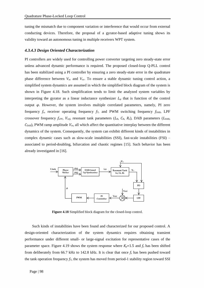
Quadrature Phase-Locked Loop Control
Page | 98
tuning the mismatch due to component variation or interference that would occur from external
conducting devices. Therefore, the proposal of a gyrator-based adaptive tuning shows its
validity toward an autonomous tuning in multiple receivers WPT system.
4.3.4.3 Design Oriented Characterization
PI controllers are widely used for controlling power converter targeting zero steady-state error
unless advanced dynamic performance is required. The proposed closed-loop Q-PLL control
has been stabilized using a PI controller by ensuring a zero steady-state error in the quadrature
phase difference between Vac and Voc. To ensure a stable dynamic tuning control action, a
simplified system dynamics are assumed in which the simplified block diagram of the system is
shown in Figure 4.18. Such simplification tends to limit the analyzed system variables by
interpreting the gyrator as a linear inductance synthesizer Lφ that is function of the control
output φ. However, the system involves multiple correlated parameters, namely, PI zero
frequency fz, receiver operating frequency fT, and PWM switching frequency fDAB, LPF
crossover frequency fLPF, Vref, resonant tank parameters (LR, CR, RL), DAB parameters (LDAB,
CDAB), PWM ramp amplitude Vm, all which affect the quantitative interplay between the different
dynamics of the system. Consequently, the system can exhibit different kinds of instabilities in
complex dynamic cases such as slow-scale instabilities (SSI), fast-scale instabilities (FSI) –
associated to period-doubling, bifurcation and chaotic regimes [15]. Such behavior has been
already investigated in [16].
Figure 4.18 Simplified block diagram for the closed-loop control.
Such kinds of instabilities have been found and characterized for our proposed control. A
design-oriented characterization of the system dynamics requires obtaining transient
performance under different small- or large-signal excitation for representative cases of the
parameter space. Figure 4.19 shows the system response where Kp=1.5 and fz has been shifted
from deliberately from 66.7 kHz to 142.8 kHz. It is clear that once fz has been pushed toward
the tank operation frequency fT, the system has moved from period-1 stability region toward SSI
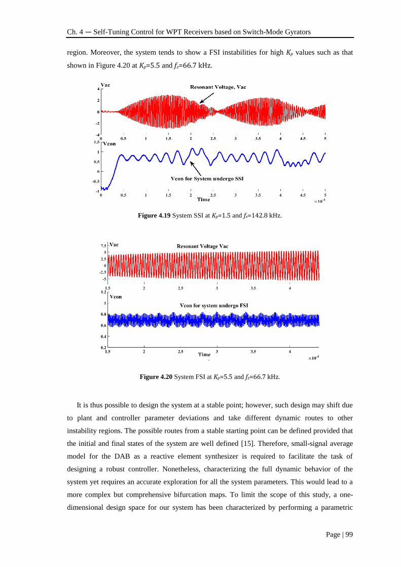
Ch. 4 — Self-Tuning Control for WPT Receivers based on Switch-Mode Gyrators
Page | 99
region. Moreover, the system tends to show a FSI instabilities for high Kp values such as that
shown in Figure 4.20 at Kp=5.5 and fz=66.7 kHz.
Figure 4.19 System SSI at Kp=1.5 and fz=142.8 kHz.
Figure 4.20 System FSI at Kp=5.5 and fz=66.7 kHz.
It is thus possible to design the system at a stable point; however, such design may shift due
to plant and controller parameter deviations and take different dynamic routes to other
instability regions. The possible routes from a stable starting point can be defined provided that
the initial and final states of the system are well defined [15]. Therefore, small-signal average
model for the DAB as a reactive element synthesizer is required to facilitate the task of
designing a robust controller. Nonetheless, characterizing the full dynamic behavior of the
system yet requires an accurate exploration for all the system parameters. This would lead to a
more complex but comprehensive bifurcation maps. To limit the scope of this study, a one-
dimensional design space for our system has been characterized by performing a parametric
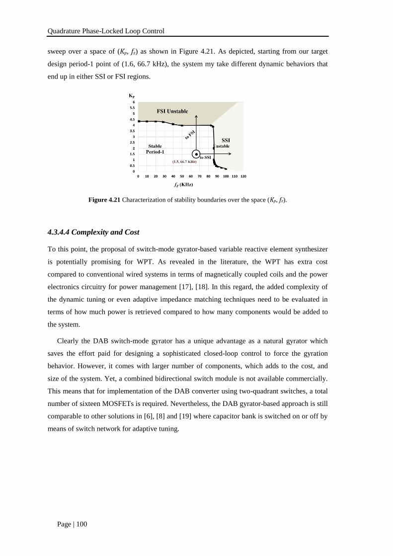
Quadrature Phase-Locked Loop Control
Page | 100
sweep over a space of (Kp, fz) as shown in Figure 4.21. As depicted, starting from our target
design period-1 point of (1.6, 66.7 kHz), the system my take different dynamic behaviors that
end up in either SSI or FSI regions.
Figure 4.21 Characterization of stability boundaries over the space (Kp, fz).
4.3.4.4 Complexity and Cost
To this point, the proposal of switch-mode gyrator-based variable reactive element synthesizer
is potentially promising for WPT. As revealed in the literature, the WPT has extra cost
compared to conventional wired systems in terms of magnetically coupled coils and the power
electronics circuitry for power management [17], [18]. In this regard, the added complexity of
the dynamic tuning or even adaptive impedance matching techniques need to be evaluated in
terms of how much power is retrieved compared to how many components would be added to
the system.
Clearly the DAB switch-mode gyrator has a unique advantage as a natural gyrator which
saves the effort paid for designing a sophisticated closed-loop control to force the gyration
behavior. However, it comes with larger number of components, which adds to the cost, and
size of the system. Yet, a combined bidirectional switch module is not available commercially.
This means that for implementation of the DAB converter using two-quadrant switches, a total
number of sixteen MOSFETs is required. Nevertheless, the DAB gyrator-based approach is still
comparable to other solutions in [6], [8] and [19] where capacitor bank is switched on or off by
means of switch network for adaptive tuning.
Ch. 4 — Self-Tuning Control for WPT Receivers based on Switch-Mode Gyrators
Page | 101
4.4 Conclusions
The DAB converter utilized as switch-mode gyrator has been used for variable inductance
synthesis in WPT receiver. In this chapter we have proposed two control approaches in order to
achieve self-tuning operation in parallel-compensated receivers. The first control technique uses
dual-loop approach where the first coarse-tuning loop tracks the maximum peak voltage of the
resonant tank voltage. On the other hand, the fine-tuning loop tracks the phase difference
relations between the induced voltage in the receiver coil and the resonant tank voltage. The
verification results have shown that there is a trade-off between the accuracy and transient time
of the control. Consequently, an alternative linear control has been proposed, this time it is
based on the quadrature phase difference between the receiver coil’s induced voltage Voc and the
resonant tank voltage Vac. The wide tuning range of the DAB-based self-tuned WPT receiver
has been verified at different mismatch percentages in the coil inductance LR or the
compensation capacitor CR. Moreover, the chip implementation for the DAB converter and the
quadrature PLL control has been discussed carried out by the XFAB 0.18µm technology.
The system performance and design consideration has been discussed as compared to other
solutions in the literature. It has shown that despite the complexity and number of switches used
in the DAB converter, it is still considered as a reasonable solution if we consider the reliability
and wide tuning range of the solution.
References
Page | 102
4.5 References
[1] Hengsi Qin and J. W. Kimball, “Ac-ac dual active bridge converter for solid state transformer,”
in 2009 IEEE Energy Conversion Congress and Exposition, 2009, pp. 3039–3044.
[2] M. Saad, E. Bou-Balust, and E. Alarcon, “Switch-mode gyrator-based emulated inductor
enabling self-tunability in WPT receivers,” in 2017 IEEE International Symposium on Circuits and
Systems (ISCAS), 2017, pp. 1–4.
[3] G. Di Capua, N. Femia, and G. Lisi, “Impact of losses and mismatches on power and efficiency
of Wireless Power Transfer Systems with controlled secondary-side rectifier,” Integr. VLSI J., vol.
55, pp. 384–392, Sep. 2016.
[4] R. F. Xue, K. W. Cheng, and M. Je, “High-efficiency wireless power transfer for biomedical
implants by optimal resonant load transformation,” IEEE Trans. Circuits Syst. I Regul. Pap., vol. 60,
no. 4, pp. 867–874, Apr. 2013.
[5] H. Qin and J. W. Kimball, “A comparative efficiency study of silicon-based solid state
transformers,” in 2010 IEEE Energy Conversion Congress and Exposition, 2010, pp. 1458–1463.
[6] Y. Lim, H. Tang, S. Lim, and J. Park, “An adaptive impedance-matching network based on a
novel capacitor matrix for wireless power transfer,” IEEE Trans. Power Electron., vol. 29, no. 8, pp.
4403–4413, Aug. 2014.
[7] W.-S. Lee, H.-L. Lee, K.-S. Oh, and J.-W. Yu, “Switchable Distance-Based Impedance
Matching Networks For a Tunable HF System,” Prog. Electromagn. Res., vol. 128, no. May, pp.
19–34, 2012.
[8] T. Duong and J.-W. Lee, “A Dynamically Adaptable Impedance-Matching System for Midrange
Wireless Power Transfer with Misalignment,” Energies, vol. 8, no. 8, pp. 7593–7617, Jul. 2015.
[9] C. Y. Huang, J. E. James, and G. A. Covic, “Design considerations for variable coupling lumped
coil systems,” IEEE Trans. Power Electron., vol. 30, no. 2, pp. 680–689, Feb. 2015.
[10] M. Kissin, Chang-Yu Huang, G. A. Covic, and J. T. Boys, “Detection of the tuned point of a
fixed-frequency LCL resonant power supply,” IEEE Trans. Power Electron., vol. 24, no. 4, pp.
1140–1143, Apr. 2009.
[11] N. a. Keeling, G. a. Covic, and J. T. Boys, “A unity-power-factor IPT pickup for high-power
applications,” IEEE Trans. Ind. Electron., vol. 57, no. 2, pp. 744–751, 2010.
[12] J.-U. W. Hsu and A. P. Hu, “Determining the variable inductance range for an LCL wireless
power pick-up,” in 2007 IEEE Conference on Electron Devices and Solid-State Circuits, 2007, pp.
489–492.
[13] J.-U. W. Hsu, A. P. Hu, and A. Swain, “A Wireless Power Pickup Based on Directional Tuning
Control of Magnetic Amplifier,” IEEE Trans. Ind. Electron., vol. 56, no. 7, pp. 2771–2781, Jul.
2009.
[14] S. Li, W. Li, J. Deng, T. D. Nguyen, and C. C. Mi, “A Double-Sided LCC Compensation
Network and Its Tuning Method for Wireless Power Transfer,” IEEE Trans. Veh. Technol., vol. 64,
no. 6, pp. 2261–2273, Jun. 2015.
Ch. 4 — Self-Tuning Control for WPT Receivers based on Switch-Mode Gyrators
Page | 103
[15] E. Rodriguez Vilamitjana, Chaos in switching converters for power management. Springer,
2014.
[16] M. Saad, H. Martinéz-García, P. Alou, and E. Alarcón, “A PLL Control for Self-Tuning of
Parallel Wireless Power Transfer Receivers Utilizing Switch-Mode Gyrator Emulated Inductors,” in
2017 19th European Conference on Power Electronics and Applications, EPE 2017 ECCE Europe,
p. 1-10.
[17] A. Abdolkhani, “Fundamentals of Inductively Coupled Wireless Power Transfer Systems,” in
Wireless Power Transfer - Fundamentals and Technologies, InTech, 2016, pp. 3–26.
[18] S. Li and C. C. Mi, “Wireless power transfer for electric vehicle applications,” IEEE J. Emerg.
Sel. Top. Power Electron., vol. 3, no. 1, pp. 4–17, Mar. 2015.
[19] G. A. Covic, J. T. Boys, A. M. W. Tam, and J. C. H. Peng, “Self tuning pick-ups for inductive
power transfer,” in Power Electronics Specialists Conference, PESC 2008. IEEE, 2008, pp. 3489–
3494.

Page | 105
Chapter
5
5 Phase-Controlled Converters for Active
Tuning in WPT Receivers
In the previous chapters, we have explored and discussed, in detail, the feasibility of gyrator-
based approach for emulating variable reactive elements for the sake of automatic tuning in
WPT receivers. Gyrators have shown a superior performance in which the synthesis of variable
reactive elements is a straightforward transformation between duality of components, i.e.
inductive reactance from capacitive reactance and vice versa. This approach of variable reactive
elements synthesis is based on average behavior where the relation between average voltage
and current constitutes the same for either an inductance or capacitance. In fact, as we shown
previously, the gyrator approach implies a complexity either in the topology structure or control
circuitry.
The motivation of this chapter is to develop novel techniques for active tuning of WPT
receivers by more compact circuit topologies where the same design goals are met while
maintaining simplicity of the topology. In this chapter, a compact adaptive front-end for WPT
receiver that combines dual functionality by reflecting a controlled reactance for tuning purpose
as well as transferring the energy to the output. In other words, the proposed circuit offers an
adaptive tuning while regulates the AC voltage to charge an output energy reservoir.
5.1 State of the art of WPT Receivers for Battery Charging
Developing an automatic frequency tuning for WPT receivers has always been a challenge due
to the trade-off between the size and efficiency of every solution. While the size, and
accordingly the cost, is dependent on circuit and control complexity, the efficiency of the
automatic tuning approach becomes crucial as one of the most important metrics of a WPT
system. The more complexity of the automatic tuning approach, the more size it consumes. On
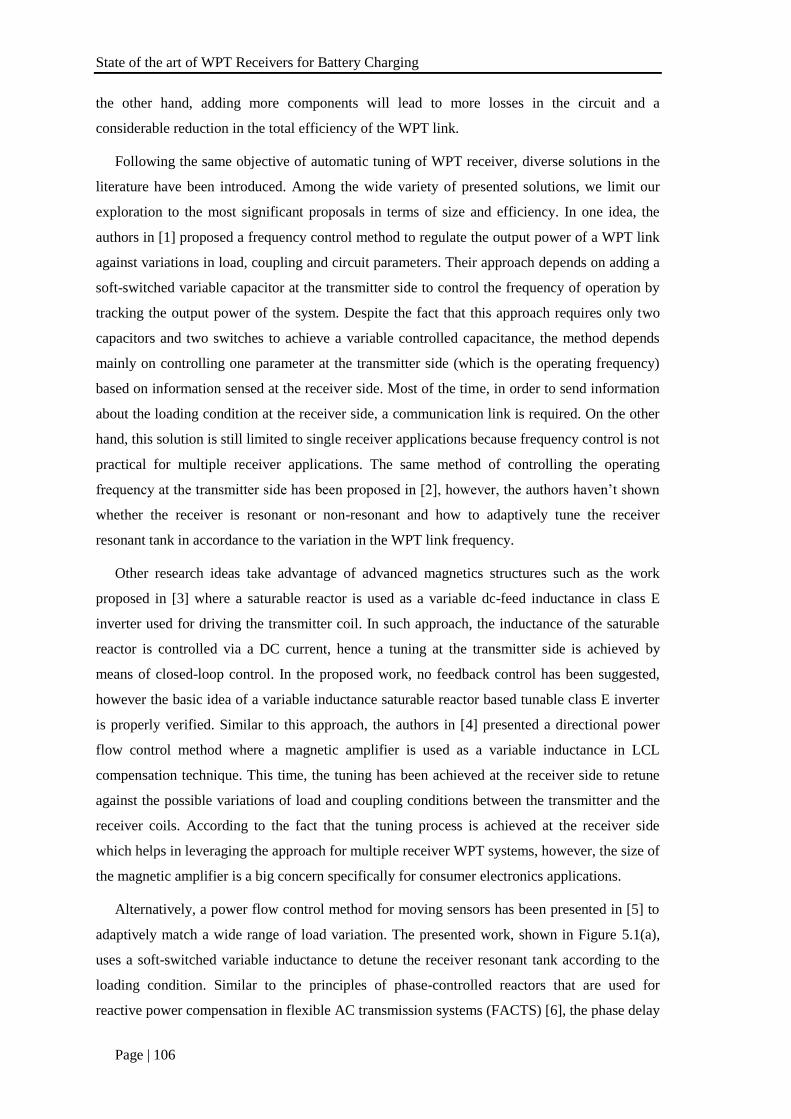
State of the art of WPT Receivers for Battery Charging
Page | 106
the other hand, adding more components will lead to more losses in the circuit and a
considerable reduction in the total efficiency of the WPT link.
Following the same objective of automatic tuning of WPT receiver, diverse solutions in the
literature have been introduced. Among the wide variety of presented solutions, we limit our
exploration to the most significant proposals in terms of size and efficiency. In one idea, the
authors in [1] proposed a frequency control method to regulate the output power of a WPT link
against variations in load, coupling and circuit parameters. Their approach depends on adding a
soft-switched variable capacitor at the transmitter side to control the frequency of operation by
tracking the output power of the system. Despite the fact that this approach requires only two
capacitors and two switches to achieve a variable controlled capacitance, the method depends
mainly on controlling one parameter at the transmitter side (which is the operating frequency)
based on information sensed at the receiver side. Most of the time, in order to send information
about the loading condition at the receiver side, a communication link is required. On the other
hand, this solution is still limited to single receiver applications because frequency control is not
practical for multiple receiver applications. The same method of controlling the operating
frequency at the transmitter side has been proposed in [2], however, the authors haven’t shown
whether the receiver is resonant or non-resonant and how to adaptively tune the receiver
resonant tank in accordance to the variation in the WPT link frequency.
Other research ideas take advantage of advanced magnetics structures such as the work
proposed in [3] where a saturable reactor is used as a variable dc-feed inductance in class E
inverter used for driving the transmitter coil. In such approach, the inductance of the saturable
reactor is controlled via a DC current, hence a tuning at the transmitter side is achieved by
means of closed-loop control. In the proposed work, no feedback control has been suggested,
however the basic idea of a variable inductance saturable reactor based tunable class E inverter
is properly verified. Similar to this approach, the authors in [4] presented a directional power
flow control method where a magnetic amplifier is used as a variable inductance in LCL
compensation technique. This time, the tuning has been achieved at the receiver side to retune
against the possible variations of load and coupling conditions between the transmitter and the
receiver coils. According to the fact that the tuning process is achieved at the receiver side
which helps in leveraging the approach for multiple receiver WPT systems, however, the size of
the magnetic amplifier is a big concern specifically for consumer electronics applications.
Alternatively, a power flow control method for moving sensors has been presented in [5] to
adaptively match a wide range of load variation. The presented work, shown in Figure 5.1(a),
uses a soft-switched variable inductance to detune the receiver resonant tank according to the
loading condition. Similar to the principles of phase-controlled reactors that are used for
reactive power compensation in flexible AC transmission systems (FACTS) [6], the phase delay
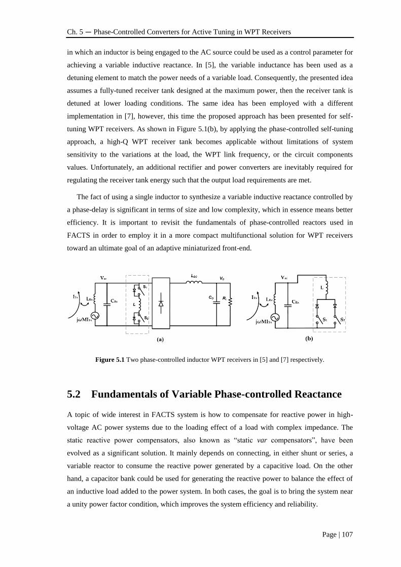
Ch. 5 — Phase-Controlled Converters for Active Tuning in WPT Receivers
Page | 107
in which an inductor is being engaged to the AC source could be used as a control parameter for
achieving a variable inductive reactance. In [5], the variable inductance has been used as a
detuning element to match the power needs of a variable load. Consequently, the presented idea
assumes a fully-tuned receiver tank designed at the maximum power, then the receiver tank is
detuned at lower loading conditions. The same idea has been employed with a different
implementation in [7], however, this time the proposed approach has been presented for self-
tuning WPT receivers. As shown in Figure 5.1(b), by applying the phase-controlled self-tuning
approach, a high-Q WPT receiver tank becomes applicable without limitations of system
sensitivity to the variations at the load, the WPT link frequency, or the circuit components
values. Unfortunately, an additional rectifier and power converters are inevitably required for
regulating the receiver tank energy such that the output load requirements are met.
The fact of using a single inductor to synthesize a variable inductive reactance controlled by
a phase-delay is significant in terms of size and low complexity, which in essence means better
efficiency. It is important to revisit the fundamentals of phase-controlled reactors used in
FACTS in order to employ it in a more compact multifunctional solution for WPT receivers
toward an ultimate goal of an adaptive miniaturized front-end.
Figure 5.1 Two phase-controlled inductor WPT receivers in [5] and [7] respectively.
5.2 Fundamentals of Variable Phase-controlled Reactance
A topic of wide interest in FACTS system is how to compensate for reactive power in high-
voltage AC power systems due to the loading effect of a load with complex impedance. The
static reactive power compensators, also known as “static var compensators”, have been
evolved as a significant solution. It mainly depends on connecting, in either shunt or series, a
variable reactor to consume the reactive power generated by a capacitive load. On the other
hand, a capacitor bank could be used for generating the reactive power to balance the effect of
an inductive load added to the power system. In both cases, the goal is to bring the system near
a unity power factor condition, which improves the system efficiency and reliability.
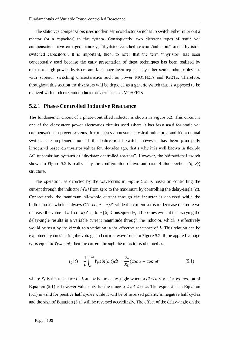
Fundamentals of Variable Phase-controlled Reactance
Page | 108
The static var compensators uses modern semiconductor switches to switch either in or out a
reactor (or a capacitor) to the system. Consequently, two different types of static var
compensators have emerged, namely, “thyristor-switched reactors/inductors” and “thyristor-
switched capacitors”. It is important, then, to refer that the term “thyristor” has been
conceptually used because the early presentation of these techniques has been realized by
means of high power thyristors and later have been replaced by other semiconductor devices
with superior switching characteristics such as power MOSFETs and IGBTs. Therefore,
throughout this section the thyristors will be depicted as a generic switch that is supposed to be
realized with modern semiconductor devices such as MOSFETs.
5.2.1 Phase-Controlled Inductive Reactance
The fundamental circuit of a phase-controlled inductor is shown in Figure 5.2. This circuit is
one of the elementary power electronics circuits used where it has been used for static var
compensation in power systems. It comprises a constant physical inductor L and bidirectional
switch. The implementation of the bidirectional switch, however, has been principally
introduced based on thyristor valves few decades ago, that’s why it is well known in flexible
AC transmission systems as “thyristor controlled reactors”. However, the bidirectional switch
shown in Figure 5.2 is realized by the configuration of two antiparallel diode-switch (S1, S2)
structure.
The operation, as depicted by the waveforms in Figure 5.2, is based on controlling the
current through the inductor iL(α) from zero to the maximum by controlling the delay-angle (α).
Consequently the maximum allowable current through the inductor is achieved while the
bidirectional switch is always ON, i.e. α = π/2, while the current starts to decrease the more we
increase the value of α from π/2 up to π [6]. Consequently, it becomes evident that varying the
delay-angle results in a variable current magnitude through the inductor, which is effectively
would be seen by the circuit as a variation in the effective reactance of L. This relation can be
explained by considering the voltage and current waveforms in Figure 5.2, if the applied voltage
vac is equal to VP sin ωt, then the current through the inductor is obtained as:
𝑖𝐿(𝑡) =1
𝐿∫ 𝑉𝑃𝑠𝑖𝑛(𝜔𝑡)𝑑𝑡
𝜔𝑡
𝛼
=𝑉𝑃
𝑋𝐿(cos 𝛼 − cos𝜔𝑡) (5.1)
where XL is the reactance of L and α is the delay-angle where π/2 ≤ α ≤ π. The expression of
Equation (5.1) is however valid only for the range α ≤ ωt ≤ π−α. The expression in Equation
(5.1) is valid for positive half cycles while it will be of reversed polarity in negative half cycles
and the sign of Equation (5.1) will be reversed accordingly. The effect of the delay-angle on the
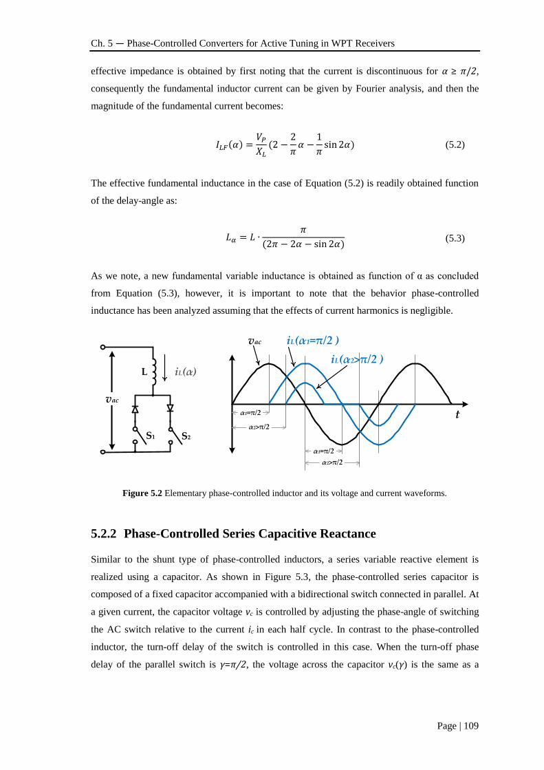
Ch. 5 — Phase-Controlled Converters for Active Tuning in WPT Receivers
Page | 109
effective impedance is obtained by first noting that the current is discontinuous for α ≥ π/2,
consequently the fundamental inductor current can be given by Fourier analysis, and then the
magnitude of the fundamental current becomes:
𝐼𝐿𝐹(𝛼) =𝑉𝑃
𝑋𝐿(2 −
2
𝜋𝛼 −
1
𝜋sin2𝛼) (5.2)
The effective fundamental inductance in the case of Equation (5.2) is readily obtained function
of the delay-angle as:
𝐿𝛼 = 𝐿 ∙𝜋
(2𝜋 − 2𝛼 − sin 2𝛼) (5.3)
As we note, a new fundamental variable inductance is obtained as function of α as concluded
from Equation (5.3), however, it is important to note that the behavior phase-controlled
inductance has been analyzed assuming that the effects of current harmonics is negligible.
S1
L
S2
iL(α)
t
vac
vac iL(α1=π/2 )
iL(α2>π/2 )
α2>π/2
α1=π/2
α1=π/2
α2>π/2
Figure 5.2 Elementary phase-controlled inductor and its voltage and current waveforms.
5.2.2 Phase-Controlled Series Capacitive Reactance
Similar to the shunt type of phase-controlled inductors, a series variable reactive element is
realized using a capacitor. As shown in Figure 5.3, the phase-controlled series capacitor is
composed of a fixed capacitor accompanied with a bidirectional switch connected in parallel. At
a given current, the capacitor voltage vc is controlled by adjusting the phase-angle of switching
the AC switch relative to the current ic in each half cycle. In contrast to the phase-controlled
inductor, the turn-off delay of the switch is controlled in this case. When the turn-off phase
delay of the parallel switch is γ=π/2, the voltage across the capacitor vc(γ) is the same as a
Phase-Controlled Switched Inductor Converter
Page | 110
conventional capacitor. If the turn-off delay of the switch is increased above π/2, the voltage
across the capacitor becomes variable and can be given function of the delay angle as [6]:
𝑣𝐶(𝑡) =1
𝐶∫ 𝐼𝑃𝑠𝑖𝑛(𝜔𝑡)𝑑𝑡
𝜔𝑡
𝛾
= 𝐼𝑃𝑋𝐶(cos 𝛾 − cos𝜔𝑡) (5.4)
where the series current is assumed equal to IP sin(ωt), XC is the capacitor reactance, and γ is the
phase-angle delay (π/2 ≤ γ ≤ π). It is evident from Equation (5.4) that the capacitor’s voltage
magnitude can be controlled by varying the turn-off delay angle γ. In a similar way to the
variable equivalent inductance in Equation (5.3), the equivalent reactance of the phase-
controlled series capacitor is obtained by deriving the fundamental capacitor voltage VCF(γ).
Consequently, the equivalent variable capacitance is obtained by [6]:
𝐶𝛾 = 𝐶 ∙𝜋
(2𝜋 − 2𝛾 − sin 2𝛾) (5.5)
The phase-controlled series capacitor can be used as a variable reactive component or it can
be used alternatively in combination with the phase-controlled inductor to realize a variable
impedance. While different combinations already exist with different characteristics and
features, the main concept of phase-controlled var generation is similarly applied.
iC
S1 S2vC(γ)
C
t
ic vC(γ1=π/2 )
vC(γ2>π/2 )
γ2 >π/2
γ1=π/2
γ1=π/2
γ2 >π/2
Figure 5.3 Elementary phase-controlled series capacitors and its voltage and current waveforms.
5.3 Phase-Controlled Switched Inductor Converter
It is possible to incorporate the concept of variable inductive reactance, based on the concept of
phase-switching explained in the previous section, not only for synthesizing a variable
reactance but also for rectification or even more advanced functionality of rectification and
regulation. The basic idea is to avoid using separate circuits for achieving the multiple
functionalities, by using a single inductor that is switched with a phase-delay with respect to the
ac input. The proposed scheme applies a phase-delay with respect to the AC input during a first
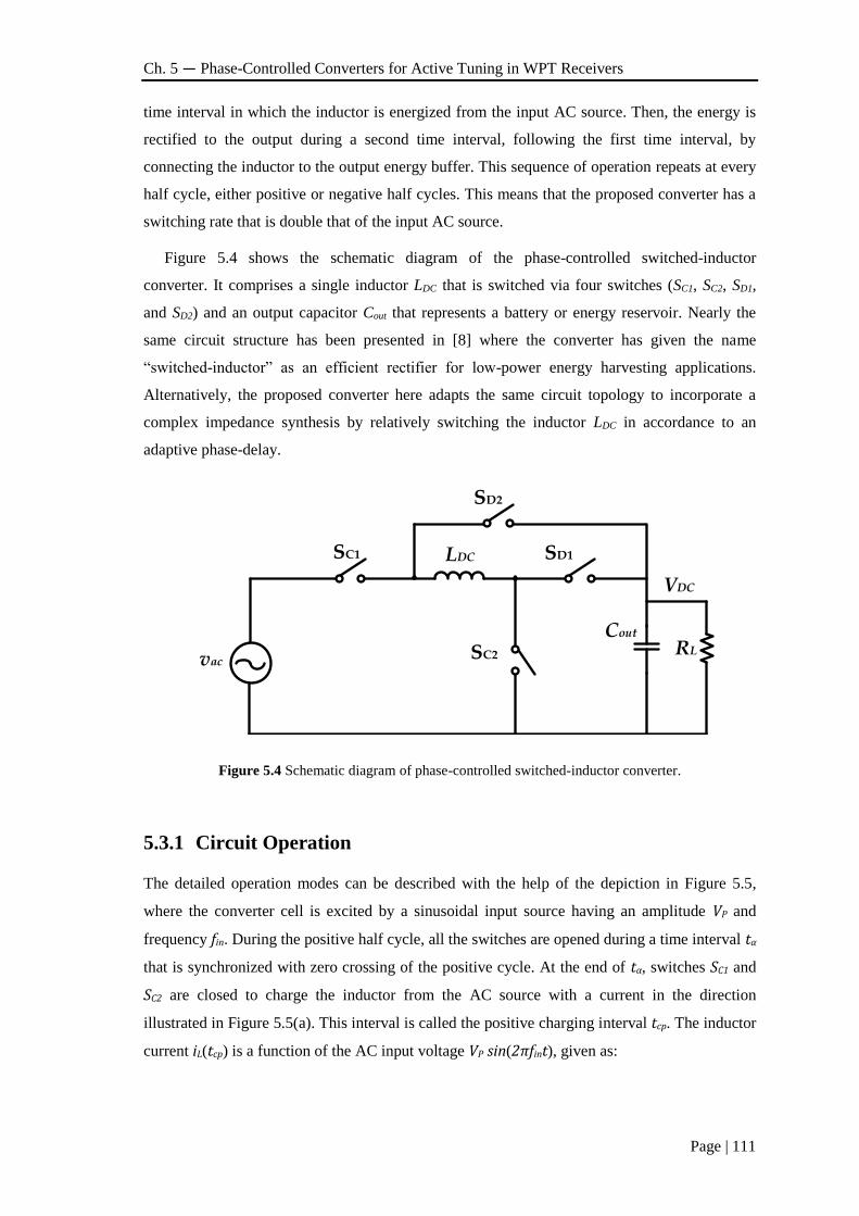
Ch. 5 — Phase-Controlled Converters for Active Tuning in WPT Receivers
Page | 111
time interval in which the inductor is energized from the input AC source. Then, the energy is
rectified to the output during a second time interval, following the first time interval, by
connecting the inductor to the output energy buffer. This sequence of operation repeats at every
half cycle, either positive or negative half cycles. This means that the proposed converter has a
switching rate that is double that of the input AC source.
Figure 5.4 shows the schematic diagram of the phase-controlled switched-inductor
converter. It comprises a single inductor LDC that is switched via four switches (SC1, SC2, SD1,
and SD2) and an output capacitor Cout that represents a battery or energy reservoir. Nearly the
same circuit structure has been presented in [8] where the converter has given the name
“switched-inductor” as an efficient rectifier for low-power energy harvesting applications.
Alternatively, the proposed converter here adapts the same circuit topology to incorporate a
complex impedance synthesis by relatively switching the inductor LDC in accordance to an
adaptive phase-delay.
SC1
vac
LDC
Cout
SC2
SD2
RL
VDC
SD1
Figure 5.4 Schematic diagram of phase-controlled switched-inductor converter.
5.3.1 Circuit Operation
The detailed operation modes can be described with the help of the depiction in Figure 5.5,
where the converter cell is excited by a sinusoidal input source having an amplitude VP and
frequency fin. During the positive half cycle, all the switches are opened during a time interval tα
that is synchronized with zero crossing of the positive cycle. At the end of tα, switches SC1 and
SC2 are closed to charge the inductor from the AC source with a current in the direction
illustrated in Figure 5.5(a). This interval is called the positive charging interval tcp. The inductor
current iL(tcp) is a function of the AC input voltage VP sin(2πfint), given as:
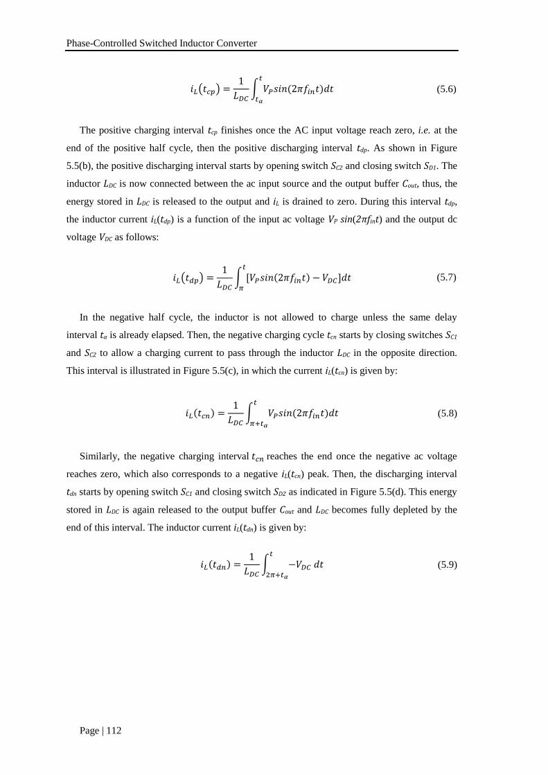
Phase-Controlled Switched Inductor Converter
Page | 112
𝑖𝐿(𝑡𝑐𝑝) =1
𝐿𝐷𝐶∫ 𝑉𝑃𝑠𝑖𝑛(2𝜋𝑓𝑖𝑛𝑡)𝑑𝑡
𝑡
𝑡𝛼
(5.6)
The positive charging interval tcp finishes once the AC input voltage reach zero, i.e. at the
end of the positive half cycle, then the positive discharging interval tdp. As shown in Figure
5.5(b), the positive discharging interval starts by opening switch SC2 and closing switch SD1. The
inductor LDC is now connected between the ac input source and the output buffer Cout, thus, the
energy stored in LDC is released to the output and iL is drained to zero. During this interval tdp,
the inductor current iL(tdp) is a function of the input ac voltage VP sin(2πfint) and the output dc
voltage VDC as follows:
𝑖𝐿(𝑡𝑑𝑝) =1
𝐿𝐷𝐶∫ [𝑉𝑃𝑠𝑖𝑛(2𝜋𝑓𝑖𝑛𝑡) − 𝑉𝐷𝐶]𝑑𝑡
𝑡
𝜋
(5.7)
In the negative half cycle, the inductor is not allowed to charge unless the same delay
interval tα is already elapsed. Then, the negative charging cycle tcn starts by closing switches SC1
and SC2 to allow a charging current to pass through the inductor LDC in the opposite direction.
This interval is illustrated in Figure 5.5(c), in which the current iL(tcn) is given by:
𝑖𝐿(𝑡𝑐𝑛) =1
𝐿𝐷𝐶∫ 𝑉𝑃𝑠𝑖𝑛(2𝜋𝑓𝑖𝑛𝑡)𝑑𝑡
𝑡
𝜋+𝑡𝛼
(5.8)
Similarly, the negative charging interval 𝑡𝑐𝑛 reaches the end once the negative ac voltage
reaches zero, which also corresponds to a negative iL(tcn) peak. Then, the discharging interval
tdn starts by opening switch SC1 and closing switch SD2 as indicated in Figure 5.5(d). This energy
stored in LDC is again released to the output buffer Cout and LDC becomes fully depleted by the
end of this interval. The inductor current iL(tdn) is given by:
𝑖𝐿(𝑡𝑑𝑛) =1
𝐿𝐷𝐶∫ −𝑉𝐷𝐶 𝑑𝑡
𝑡
2𝜋+𝑡𝛼
(5.9)
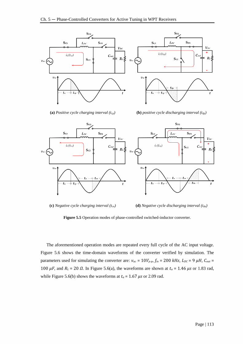
Ch. 5 — Phase-Controlled Converters for Active Tuning in WPT Receivers
Page | 113
(a) Positive cycle charging interval (tcp) (b) positive cycle discharging interval (tdp)
(c) Negative cycle charging interval (tcn) (d) Negative cycle discharging interval (tdn)
Figure 5.5 Operation modes of phase-controlled switched-inductor converter.
The aforementioned operation modes are repeated every full cycle of the AC input voltage.
Figure 5.6 shows the time-domain waveforms of the converter verified by simulation. The
parameters used for simulating the converter are: vac = 10Vp-p, fin = 200 kHz, LDC = 9 µH, Cout =
100 µF, and RL = 20 𝛺. In Figure 5.6(a), the waveforms are shown at tα = 1.46 µs or 1.83 rad,
while Figure 5.6(b) shows the waveforms at tα = 1.67 µs or 2.09 rad.
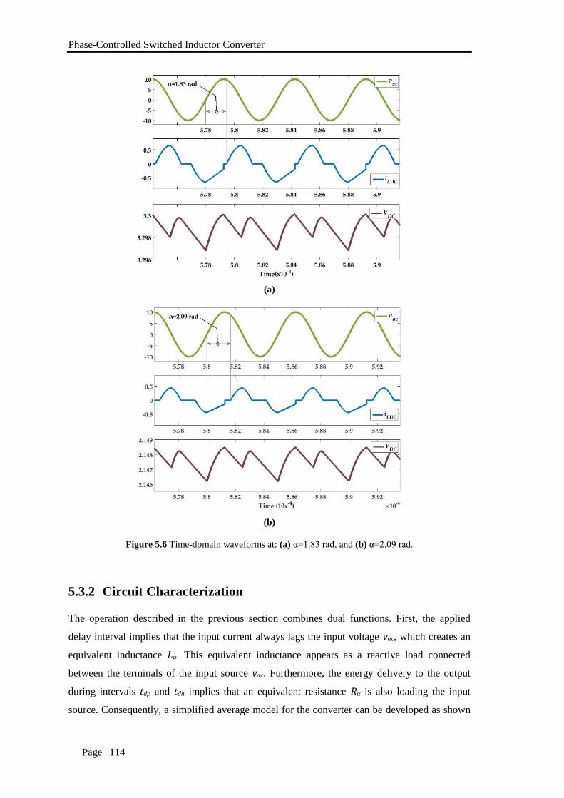
Phase-Controlled Switched Inductor Converter
Page | 114
(a)
(b)
Figure 5.6 Time-domain waveforms at: (a) α=1.83 rad, and (b) α=2.09 rad.
5.3.2 Circuit Characterization
The operation described in the previous section combines dual functions. First, the applied
delay interval implies that the input current always lags the input voltage vac, which creates an
equivalent inductance Lα. This equivalent inductance appears as a reactive load connected
between the terminals of the input source vac. Furthermore, the energy delivery to the output
during intervals tdp and tdn implies that an equivalent resistance Rα is also loading the input
source. Consequently, a simplified average model for the converter can be developed as shown
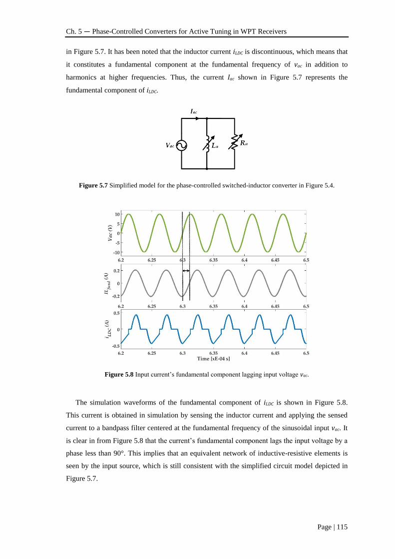
Ch. 5 — Phase-Controlled Converters for Active Tuning in WPT Receivers
Page | 115
in Figure 5.7. It has been noted that the inductor current iLDC is discontinuous, which means that
it constitutes a fundamental component at the fundamental frequency of vac in addition to
harmonics at higher frequencies. Thus, the current Iac shown in Figure 5.7 represents the
fundamental component of iLDC.
Figure 5.7 Simplified model for the phase-controlled switched-inductor converter in Figure 5.4.
Figure 5.8 Input current’s fundamental component lagging input voltage vac.
The simulation waveforms of the fundamental component of iLDC is shown in Figure 5.8.
This current is obtained in simulation by sensing the inductor current and applying the sensed
current to a bandpass filter centered at the fundamental frequency of the sinusoidal input vac. It
is clear in from Figure 5.8 that the current’s fundamental component lags the input voltage by a
phase less than 90°. This implies that an equivalent network of inductive-resistive elements is
seen by the input source, which is still consistent with the simplified circuit model depicted in
Figure 5.7.
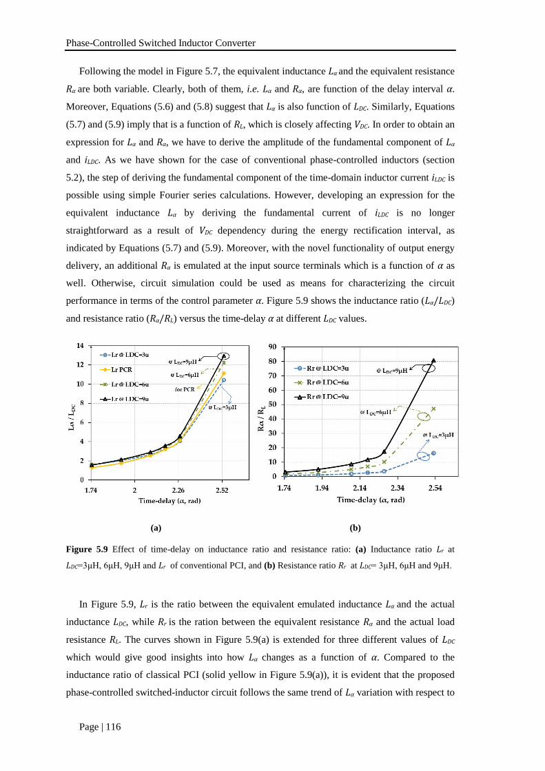
Phase-Controlled Switched Inductor Converter
Page | 116
Following the model in Figure 5.7, the equivalent inductance Lα and the equivalent resistance
Rα are both variable. Clearly, both of them, i.e. Lα and Rα, are function of the delay interval α.
Moreover, Equations (5.6) and (5.8) suggest that Lα is also function of LDC. Similarly, Equations
(5.7) and (5.9) imply that is a function of RL, which is closely affecting VDC. In order to obtain an
expression for Lα and Rα, we have to derive the amplitude of the fundamental component of Lα
and iLDC. As we have shown for the case of conventional phase-controlled inductors (section
5.2), the step of deriving the fundamental component of the time-domain inductor current iLDC is
possible using simple Fourier series calculations. However, developing an expression for the
equivalent inductance Lα by deriving the fundamental current of iLDC is no longer
straightforward as a result of VDC dependency during the energy rectification interval, as
indicated by Equations (5.7) and (5.9). Moreover, with the novel functionality of output energy
delivery, an additional Rα is emulated at the input source terminals which is a function of α as
well. Otherwise, circuit simulation could be used as means for characterizing the circuit
performance in terms of the control parameter α. Figure 5.9 shows the inductance ratio (Lα/LDC)
and resistance ratio (Rα/RL) versus the time-delay α at different LDC values.
(a) (b)
Figure 5.9 Effect of time-delay on inductance ratio and resistance ratio: (a) Inductance ratio Lr at
LDC=3μH, 6μH, 9μH and Lr of conventional PCI, and (b) Resistance ratio Rr at LDC= 3μH, 6μH and 9μH.
In Figure 5.9, Lr is the ratio between the equivalent emulated inductance Lα and the actual
inductance LDC, while Rr is the ration between the equivalent resistance Rα and the actual load
resistance RL. The curves shown in Figure 5.9(a) is extended for three different values of LDC
which would give good insights into how Lα changes as a function of α. Compared to the
inductance ratio of classical PCI (solid yellow in Figure 5.9(a)), it is evident that the proposed
phase-controlled switched-inductor circuit follows the same trend of Lα variation with respect to
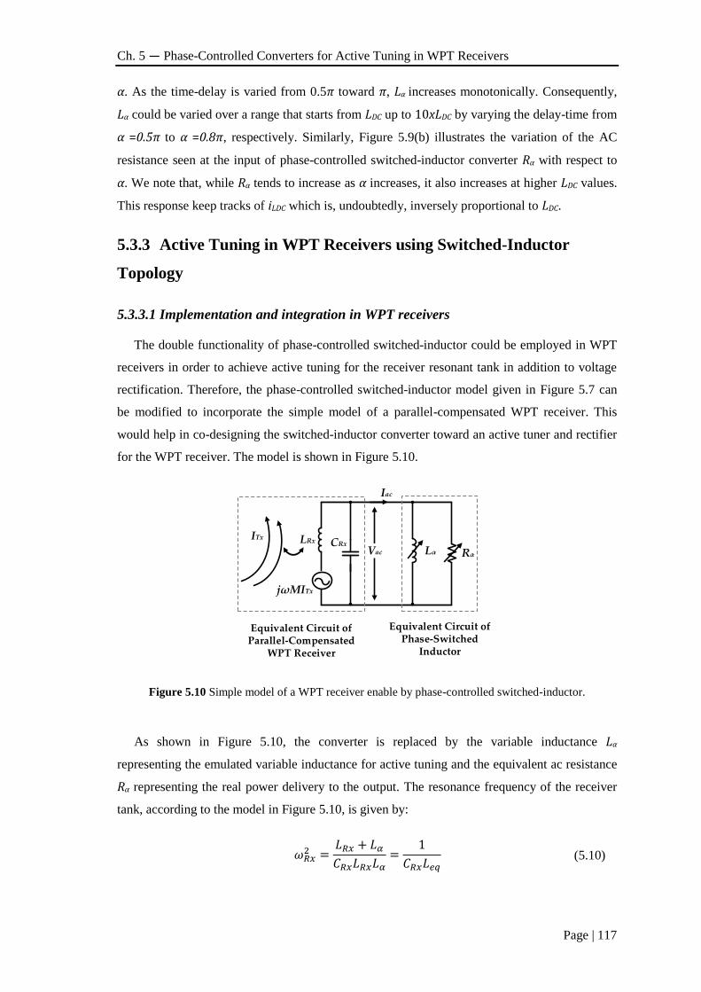
Ch. 5 — Phase-Controlled Converters for Active Tuning in WPT Receivers
Page | 117
α. As the time-delay is varied from 0.5π toward π, Lα increases monotonically. Consequently,
Lα could be varied over a range that starts from LDC up to 10xLDC by varying the delay-time from
α =0.5π to α =0.8π, respectively. Similarly, Figure 5.9(b) illustrates the variation of the AC
resistance seen at the input of phase-controlled switched-inductor converter Rα with respect to
α. We note that, while Rα tends to increase as α increases, it also increases at higher LDC values.
This response keep tracks of iLDC which is, undoubtedly, inversely proportional to LDC.
5.3.3 Active Tuning in WPT Receivers using Switched-Inductor
Topology
5.3.3.1 Implementation and integration in WPT receivers
The double functionality of phase-controlled switched-inductor could be employed in WPT
receivers in order to achieve active tuning for the receiver resonant tank in addition to voltage
rectification. Therefore, the phase-controlled switched-inductor model given in Figure 5.7 can
be modified to incorporate the simple model of a parallel-compensated WPT receiver. This
would help in co-designing the switched-inductor converter toward an active tuner and rectifier
for the WPT receiver. The model is shown in Figure 5.10.
Lα Rα
Iac
CRxLRx
jωMITx
ITx
Vac
Equivalent Circuit of Parallel-Compensated
WPT Receiver
Equivalent Circuit of Phase-Switched
Inductor
Figure 5.10 Simple model of a WPT receiver enable by phase-controlled switched-inductor.
As shown in Figure 5.10, the converter is replaced by the variable inductance Lα
representing the emulated variable inductance for active tuning and the equivalent ac resistance
Rα representing the real power delivery to the output. The resonance frequency of the receiver
tank, according to the model in Figure 5.10, is given by:
𝜔𝑅𝑥2 =
𝐿𝑅𝑥 + 𝐿𝛼
𝐶𝑅𝑥𝐿𝑅𝑥𝐿𝛼=
1
𝐶𝑅𝑥𝐿𝑒𝑞 (5.10)
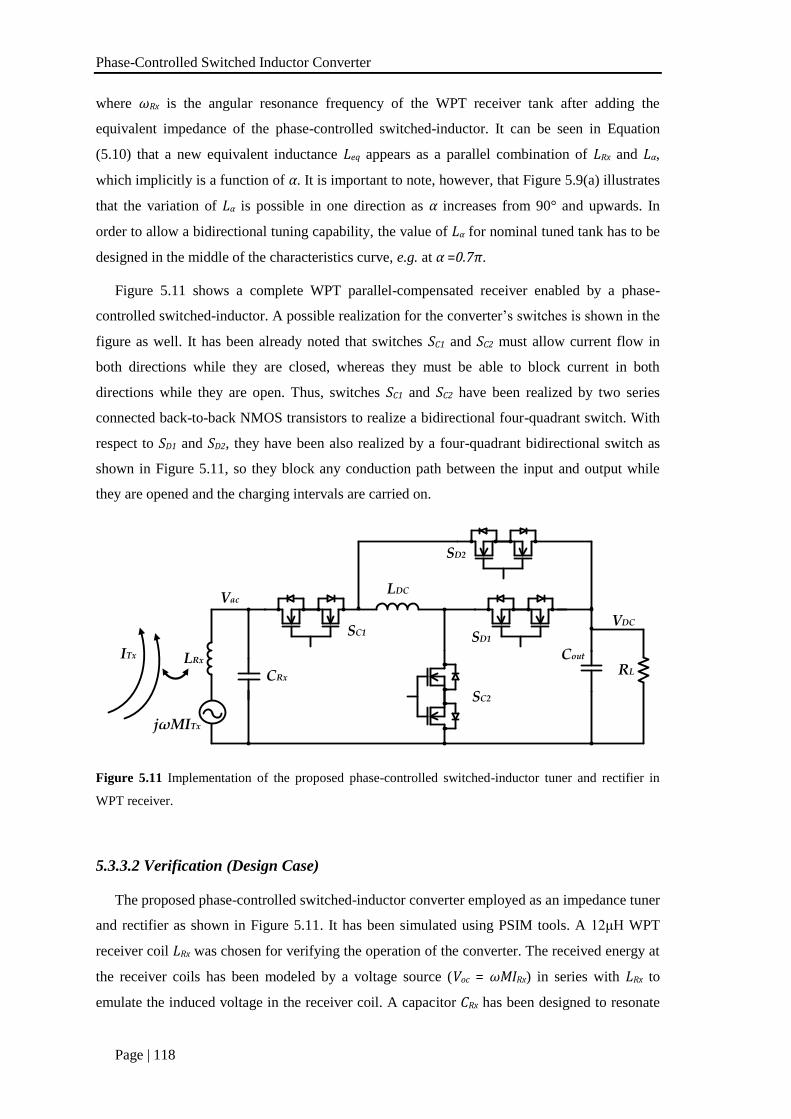
Phase-Controlled Switched Inductor Converter
Page | 118
where ωRx is the angular resonance frequency of the WPT receiver tank after adding the
equivalent impedance of the phase-controlled switched-inductor. It can be seen in Equation
(5.10) that a new equivalent inductance Leq appears as a parallel combination of LRx and Lα,
which implicitly is a function of α. It is important to note, however, that Figure 5.9(a) illustrates
that the variation of Lα is possible in one direction as α increases from 90° and upwards. In
order to allow a bidirectional tuning capability, the value of Lα for nominal tuned tank has to be
designed in the middle of the characteristics curve, e.g. at α =0.7π.
Figure 5.11 shows a complete WPT parallel-compensated receiver enabled by a phase-
controlled switched-inductor. A possible realization for the converter’s switches is shown in the
figure as well. It has been already noted that switches SC1 and SC2 must allow current flow in
both directions while they are closed, whereas they must be able to block current in both
directions while they are open. Thus, switches SC1 and SC2 have been realized by two series
connected back-to-back NMOS transistors to realize a bidirectional four-quadrant switch. With
respect to SD1 and SD2, they have been also realized by a four-quadrant bidirectional switch as
shown in Figure 5.11, so they block any conduction path between the input and output while
they are opened and the charging intervals are carried on.
SC1
CRx
LRx
LDC
Cout
SC2
SD2
RL
VDC
jωMITx
Vac
SD1
ITx
Figure 5.11 Implementation of the proposed phase-controlled switched-inductor tuner and rectifier in
WPT receiver.
5.3.3.2 Verification (Design Case)
The proposed phase-controlled switched-inductor converter employed as an impedance tuner
and rectifier as shown in Figure 5.11. It has been simulated using PSIM tools. A 12μH WPT
receiver coil LRx was chosen for verifying the operation of the converter. The received energy at
the receiver coils has been modeled by a voltage source (Voc = ωMIRx) in series with LRx to
emulate the induced voltage in the receiver coil. A capacitor CRx has been designed to resonate

Ch. 5 — Phase-Controlled Converters for Active Tuning in WPT Receivers
Page | 119
with the parallel combination between LRx and Lα at operating frequency of 200 kHz. Table 5.1
shows all the parameters used for the design case.
Figure 5.12 displays the system functionality at the specified parameters in Table 5.1. It is
noted that there is a 90° phase shift between the coil’s induced voltage Voc and the receiver
resonant tank voltage Vac. This phase shift is considered as an indication for a fully-tuned
parallel resonant tank, a fact that could be used for control design. Moreover, the gating signals
for switches SC1 and SC2 are also shown. It is obvious that the switching sequence of charging
and discharging the inductor LDC is repeated twice within one full cycle of Vac. As well, the
charging intervals tcp and tcn are both engaged after a time delay α = 0.68π with respect to the
starting of a positive cycle and negative cycle respectively.
Table 5.1 WPT receiver and phase-controlled converter.
Parameter Value
WPT receiver
Voc 0.707 Vrms
ITx 1.414 Irms
M 398 nF
fT 200 kHz
LRx 12.0 μH
CRx 77 nF
RL 20 Ω (nominal)
Phase-controlled converter parameters
LDC 9.0 μF
Cout 100 μF
B-switch RON 4 mΩ
α 0.68π (nominal)
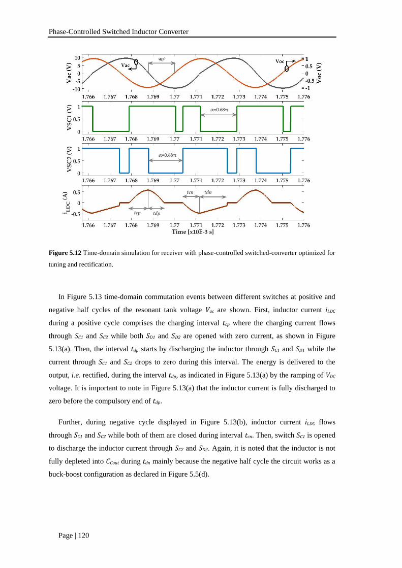
Phase-Controlled Switched Inductor Converter
Page | 120
Figure 5.12 Time-domain simulation for receiver with phase-controlled switched-converter optimized for
tuning and rectification.
In Figure 5.13 time-domain commutation events between different switches at positive and
negative half cycles of the resonant tank voltage Vac are shown. First, inductor current iLDC
during a positive cycle comprises the charging interval tcp where the charging current flows
through SC1 and SC2 while both SD1 and SD2 are opened with zero current, as shown in Figure
5.13(a). Then, the interval tdp starts by discharging the inductor through SC1 and SD1 while the
current through SC1 and SC2 drops to zero during this interval. The energy is delivered to the
output, i.e. rectified, during the interval tdp, as indicated in Figure 5.13(a) by the ramping of VDC
voltage. It is important to note in Figure 5.13(a) that the inductor current is fully discharged to
zero before the compulsory end of tdp.
Further, during negative cycle displayed in Figure 5.13(b), inductor current iLDC flows
through SC1 and SC2 while both of them are closed during interval tcn. Then, switch SC1 is opened
to discharge the inductor current through SC2 and SD2. Again, it is noted that the inductor is not
fully depleted into CCout during tdn mainly because the negative half cycle the circuit works as a
buck-boost configuration as declared in Figure 5.5(d).
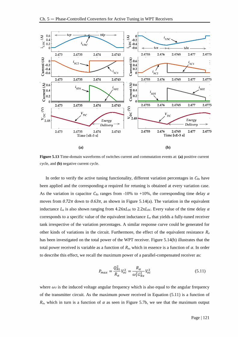
Ch. 5 — Phase-Controlled Converters for Active Tuning in WPT Receivers
Page | 121
(a) (b)
Figure 5.13 Time-domain waveforms of switches current and commutation events at: (a) positive current
cycle, and (b) negative current cycle.
In order to verify the active tuning functionality, different variation percentages in CRx have
been applied and the corresponding 𝛼 required for retuning is obtained at every variation case.
As the variation in capacitor CRx ranges from -10% to +10%, the corresponding time delay α
moves from 0.72π down to 0.63π, as shown in Figure 5.14(a). The variation in the equivalent
inductance Lα is also shown ranging from 4.26xLDC to 2.2xLDC. Every value of the time delay α
corresponds to a specific value of the equivalent inductance Lα that yields a fully-tuned receiver
tank irrespective of the variation percentages. A similar response curve could be generated for
other kinds of variations in the circuit. Furthermore, the effect of the equivalent resistance Rα
has been investigated on the total power of the WPT receiver. Figure 5.14(b) illustrates that the
total power received is variable as a function of Rα, which in essence is a function of α. In order
to describe this effect, we recall the maximum power of a parallel-compensated receiver as:
𝑃𝑚𝑎𝑥 =𝑄𝑅𝐿
2
𝑅𝛼𝑉𝑜𝑐
2 =𝑅𝛼
𝜔𝑇2𝐿𝑅𝑥
2 𝑉𝑜𝑐2 (5.11)
where ωT is the induced voltage angular frequency which is also equal to the angular frequency
of the transmitter circuit. As the maximum power received in Equation (5.11) is a function of
Rα, which in turn is a function of α as seen in Figure 5.7b, we see that the maximum output
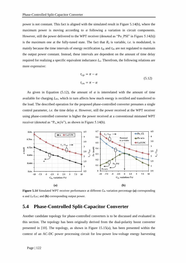
Phase-Controlled Split-Capacitor Converter
Page | 122
power is not constant. This fact is aligned with the simulated result in Figure 5.14(b), where the
maximum power is moving according to α following a variation in circuit components.
However, still the power delivered to the WPT receiver (denoted as “Po_PSI” in Figure 5.14(b))
is the maximum one at the fully-tuned state. The fact that Rα is variable, i.e. is modulated, is
mainly because the time intervals of energy rectification tdp and tdn are not regulated to maintain
the output power constant. Instead, these intervals are dependent on the amount of time delay
required for realizing a specific equivalent inductance Lα. Therefrom, the following relations are
more expressive:
𝑡𝑐𝑝 = 𝜋 − 𝛼
𝑡𝑐𝑛 = 𝜋 − 𝛼 (5.12)
As given in Equation (5.12), the amount of α is interrelated with the amount of time
available for charging LDC, which in turn affects how much energy is rectified and transferred to
the load. The described operation for the proposed phase-controlled converter presumes a single
control parameter, i.e. the time delay α. However, still the power received at the WPT receiver
using phase-controlled converter is higher the power received at a conventional mistuned WPT
receiver (denoted as “Po_w/o”), as shown in Figure 5.14(b).
(a) (b)
Figure 5.14 Simulated WPT receiver performance at different CRx variation percentage (a) corresponding
α and Lα/LDC; and (b) corresponding output power.
5.4 Phase-Controlled Split-Capacitor Converter
Another candidate topology for phase-controlled converters is to be discussed and evaluated in
this section. The topology has been originally derived from the dual-polarity boost converter
presented in [10]. The topology, as shown in Figure 15.15(a), has been presented within the
context of an AC-DC power processing circuit for low-power low-voltage energy harvesting
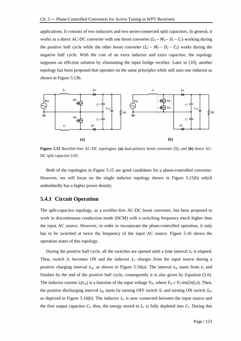
Ch. 5 — Phase-Controlled Converters for Active Tuning in WPT Receivers
Page | 123
applications. It consists of two inductors and two series-connected split capacitors. In general, it
works as a direct AC-DC converter with one boost converter (L1 – MN – D1 – C1) working during
the positive half cycle while the other boost converter (L2 – MP – D2 – C2) works during the
negative half cycle. With the cost of an extra inductor and extra capacitor, the topology
supposes an efficient solution by eliminating the input bridge rectifier. Later in [10], another
topology has been proposed that operates on the same principles while still uses one inductor as
shown in Figure 5.13b.
(a) (b)
Figure 5.15 Rectifier-free AC-DC topologies: (a) dual-polarity boost converter [9]; and (b) direct AC-
DC split capacitor [10].
Both of the topologies in Figure 5.15 are good candidates for a phase-controlled converter.
However, we will focus on the single inductor topology shown in Figure 5.15(b) which
undoubtedly has a higher power density.
5.4.1 Circuit Operation
The split-capacitor topology, as a rectifier-free AC-DC boost converter, has been proposed to
work in discontinuous conduction mode (DCM) with a switching frequency much higher than
the input AC source. However, in order to incorporate the phase-controlled operation, it only
has to be switched at twice the frequency of the input AC source. Figure 5.16 shows the
operation states of this topology.
During the positive half cycle, all the switches are opened until a time interval tα is elapsed.
Then, switch SC becomes ON and the inductor L1 charges from the input source during a
positive charging interval tcp, as shown in Figure 5.16(a). The interval tcp starts from tα and
finishes by the end of the positive half cycle, consequently it is also given by Equation (5.6).
The inductor current iL(tcp) is a function of the input voltage Vin, where Vin = VP sin(2πfint). Then,
the positive discharging interval tdp starts by turning OFF switch SC and turning ON switch SD1
as depicted in Figure 5.16(b). The inductor L1 is now connected between the input source and
the first output capacitor C1, thus, the energy stored in L1 is fully depleted into C1. During this
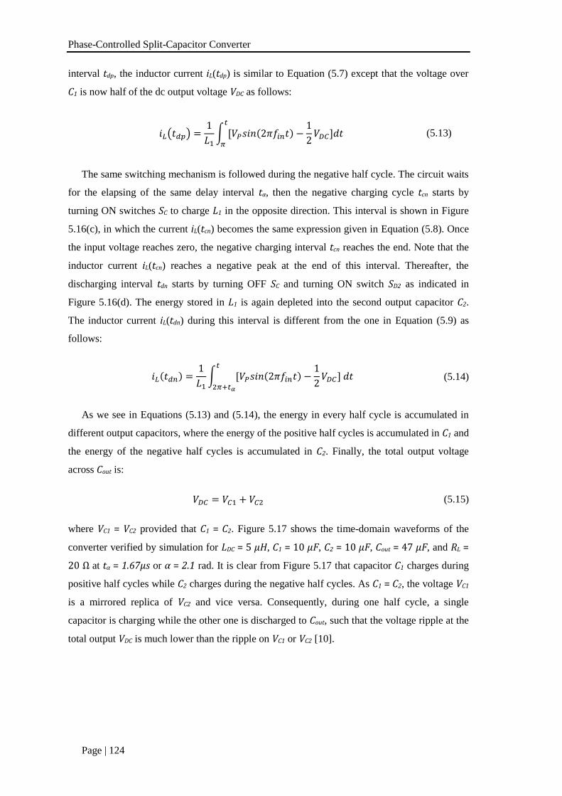
Phase-Controlled Split-Capacitor Converter
Page | 124
interval tdp, the inductor current iL(tdp) is similar to Equation (5.7) except that the voltage over
C1 is now half of the dc output voltage VDC as follows:
𝑖𝐿(𝑡𝑑𝑝) =1
𝐿1∫ [𝑉𝑃𝑠𝑖𝑛(2𝜋𝑓𝑖𝑛𝑡) −
1
2𝑉𝐷𝐶]𝑑𝑡
𝑡
𝜋
(5.13)
The same switching mechanism is followed during the negative half cycle. The circuit waits
for the elapsing of the same delay interval tα, then the negative charging cycle tcn starts by
turning ON switches SC to charge L1 in the opposite direction. This interval is shown in Figure
5.16(c), in which the current iL(tcn) becomes the same expression given in Equation (5.8). Once
the input voltage reaches zero, the negative charging interval tcn reaches the end. Note that the
inductor current iL(tcn) reaches a negative peak at the end of this interval. Thereafter, the
discharging interval tdn starts by turning OFF SC and turning ON switch SD2 as indicated in
Figure 5.16(d). The energy stored in L1 is again depleted into the second output capacitor C2.
The inductor current iL(tdn) during this interval is different from the one in Equation (5.9) as
follows:
𝑖𝐿(𝑡𝑑𝑛) =1
𝐿1∫ [𝑉𝑃𝑠𝑖𝑛(2𝜋𝑓𝑖𝑛𝑡) −
1
2𝑉𝐷𝐶] 𝑑𝑡
𝑡
2𝜋+𝑡𝛼
(5.14)
As we see in Equations (5.13) and (5.14), the energy in every half cycle is accumulated in
different output capacitors, where the energy of the positive half cycles is accumulated in C1 and
the energy of the negative half cycles is accumulated in C2. Finally, the total output voltage
across Cout is:
𝑉𝐷𝐶 = 𝑉𝐶1 + 𝑉𝐶2 (5.15)
where VC1 = VC2 provided that C1 = C2. Figure 5.17 shows the time-domain waveforms of the
converter verified by simulation for LDC = 5 µH, C1 = 10 µF, C2 = 10 µF, Cout = 47 µF, and RL =
20 Ω at tα = 1.67µs or α = 2.1 rad. It is clear from Figure 5.17 that capacitor C1 charges during
positive half cycles while C2 charges during the negative half cycles. As C1 = C2, the voltage VC1
is a mirrored replica of VC2 and vice versa. Consequently, during one half cycle, a single
capacitor is charging while the other one is discharged to Cout, such that the voltage ripple at the
total output VDC is much lower than the ripple on VC1 or VC2 [10].
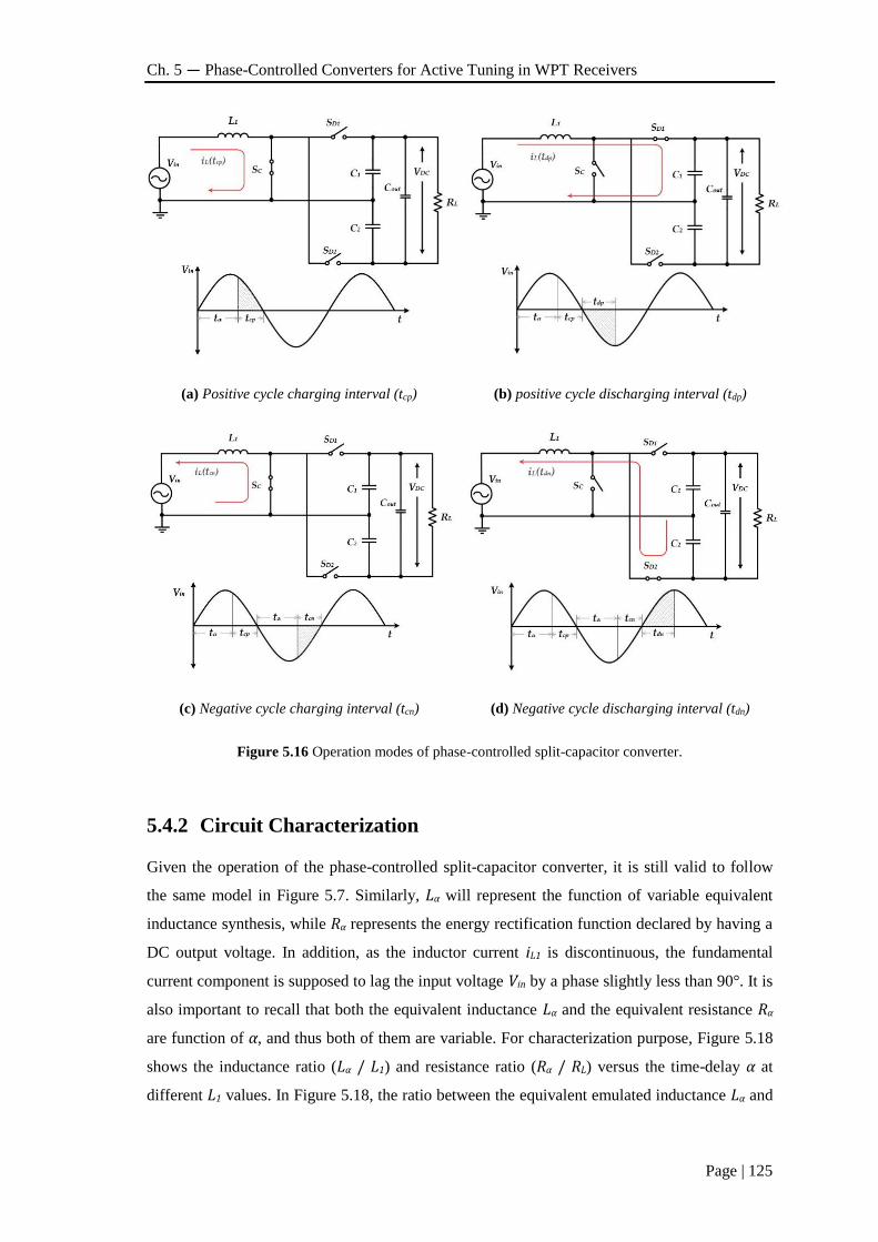
Ch. 5 — Phase-Controlled Converters for Active Tuning in WPT Receivers
Page | 125
(a) Positive cycle charging interval (tcp) (b) positive cycle discharging interval (tdp)
(c) Negative cycle charging interval (tcn) (d) Negative cycle discharging interval (tdn)
Figure 5.16 Operation modes of phase-controlled split-capacitor converter.
5.4.2 Circuit Characterization
Given the operation of the phase-controlled split-capacitor converter, it is still valid to follow
the same model in Figure 5.7. Similarly, Lα will represent the function of variable equivalent
inductance synthesis, while Rα represents the energy rectification function declared by having a
DC output voltage. In addition, as the inductor current iL1 is discontinuous, the fundamental
current component is supposed to lag the input voltage Vin by a phase slightly less than 90°. It is
also important to recall that both the equivalent inductance Lα and the equivalent resistance Rα
are function of α, and thus both of them are variable. For characterization purpose, Figure 5.18
shows the inductance ratio (Lα / L1) and resistance ratio (Rα / RL) versus the time-delay α at
different L1 values. In Figure 5.18, the ratio between the equivalent emulated inductance Lα and
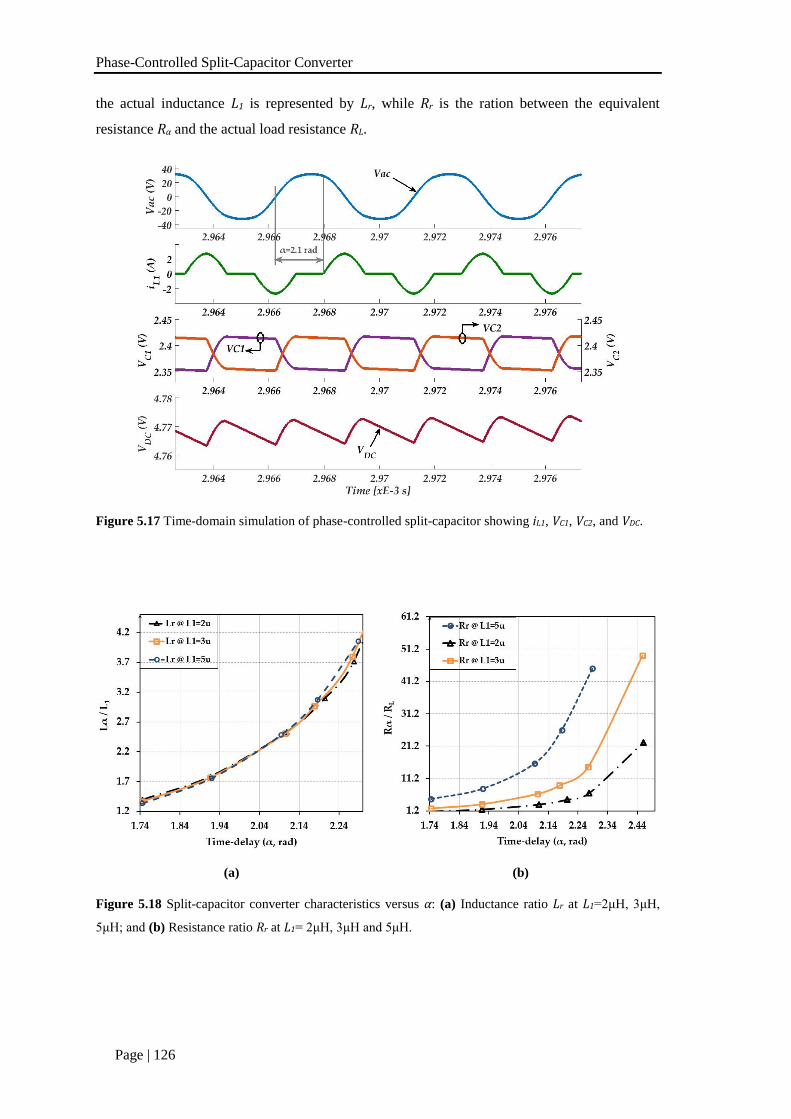
Phase-Controlled Split-Capacitor Converter
Page | 126
the actual inductance L1 is represented by Lr, while Rr is the ration between the equivalent
resistance Rα and the actual load resistance RL.
Figure 5.17 Time-domain simulation of phase-controlled split-capacitor showing iL1, VC1, VC2, and VDC.
(a) (b)
Figure 5.18 Split-capacitor converter characteristics versus α: (a) Inductance ratio Lr at L1=2μH, 3μH,
5μH; and (b) Resistance ratio Rr at L1= 2μH, 3μH and 5μH.
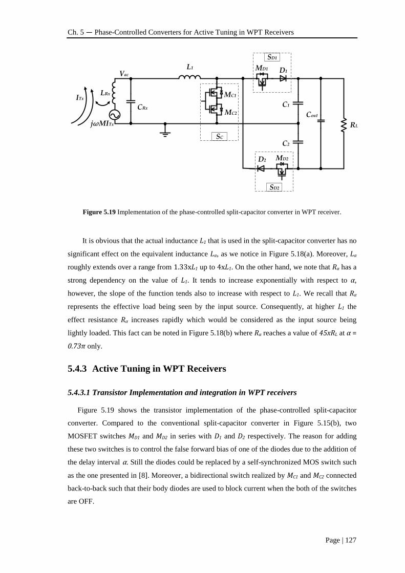
Ch. 5 — Phase-Controlled Converters for Active Tuning in WPT Receivers
Page | 127
L1 D1
MC2
MC1
D2
C1
C2
Cout
RL
MD1
MD2
CRx
LRx
jωMITx
Vac
ITx
SC
SD1
SD2
Figure 5.19 Implementation of the phase-controlled split-capacitor converter in WPT receiver.
It is obvious that the actual inductance L1 that is used in the split-capacitor converter has no
significant effect on the equivalent inductance Lα, as we notice in Figure 5.18(a). Moreover, Lα
roughly extends over a range from 1.33xL1 up to 4xL1. On the other hand, we note that Rα has a
strong dependency on the value of L1. It tends to increase exponentially with respect to α,
however, the slope of the function tends also to increase with respect to L1. We recall that Rα
represents the effective load being seen by the input source. Consequently, at higher L1 the
effect resistance Rα increases rapidly which would be considered as the input source being
lightly loaded. This fact can be noted in Figure 5.18(b) where Rα reaches a value of 45xRL at α =
0.73π only.
5.4.3 Active Tuning in WPT Receivers
5.4.3.1 Transistor Implementation and integration in WPT receivers
Figure 5.19 shows the transistor implementation of the phase-controlled split-capacitor
converter. Compared to the conventional split-capacitor converter in Figure 5.15(b), two
MOSFET switches MD1 and MD2 in series with D1 and D2 respectively. The reason for adding
these two switches is to control the false forward bias of one of the diodes due to the addition of
the delay interval α. Still the diodes could be replaced by a self-synchronized MOS switch such
as the one presented in [8]. Moreover, a bidirectional switch realized by MC1 and MC2 connected
back-to-back such that their body diodes are used to block current when the both of the switches
are OFF.
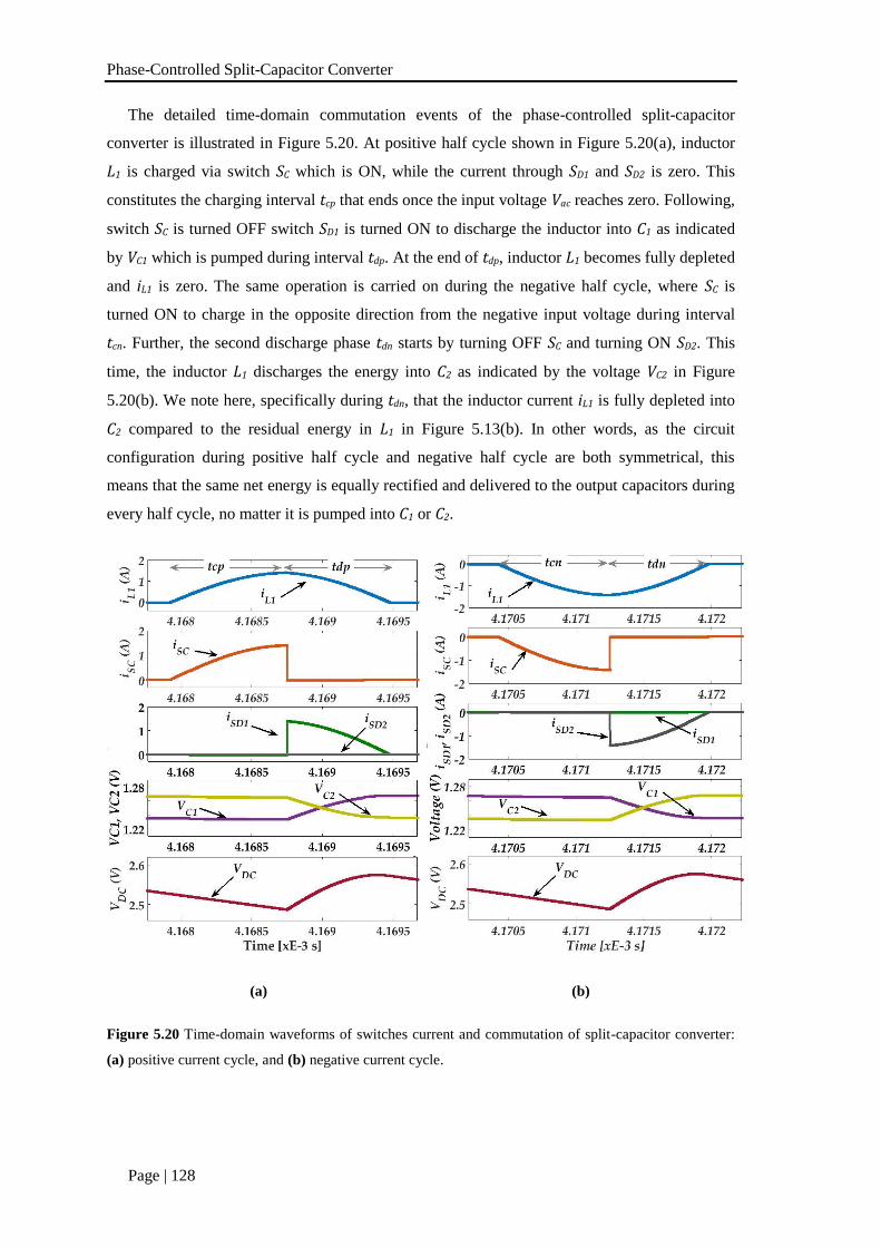
Phase-Controlled Split-Capacitor Converter
Page | 128
The detailed time-domain commutation events of the phase-controlled split-capacitor
converter is illustrated in Figure 5.20. At positive half cycle shown in Figure 5.20(a), inductor
L1 is charged via switch SC which is ON, while the current through SD1 and SD2 is zero. This
constitutes the charging interval tcp that ends once the input voltage Vac reaches zero. Following,
switch SC is turned OFF switch SD1 is turned ON to discharge the inductor into C1 as indicated
by VC1 which is pumped during interval tdp. At the end of tdp, inductor L1 becomes fully depleted
and iL1 is zero. The same operation is carried on during the negative half cycle, where SC is
turned ON to charge in the opposite direction from the negative input voltage during interval
tcn. Further, the second discharge phase tdn starts by turning OFF SC and turning ON SD2. This
time, the inductor L1 discharges the energy into C2 as indicated by the voltage VC2 in Figure
5.20(b). We note here, specifically during tdn, that the inductor current iL1 is fully depleted into
C2 compared to the residual energy in L1 in Figure 5.13(b). In other words, as the circuit
configuration during positive half cycle and negative half cycle are both symmetrical, this
means that the same net energy is equally rectified and delivered to the output capacitors during
every half cycle, no matter it is pumped into C1 or C2.
(a) (b)
Figure 5.20 Time-domain waveforms of switches current and commutation of split-capacitor converter:
(a) positive current cycle, and (b) negative current cycle.
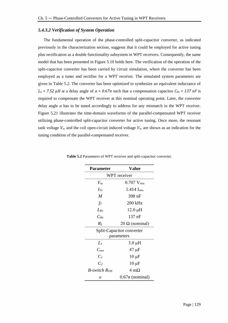
Ch. 5 — Phase-Controlled Converters for Active Tuning in WPT Receivers
Page | 129
5.4.3.2 Verification of System Operation
The fundamental operation of the phase-controlled split-capacitor converter, as indicated
previously in the characterization section, suggests that it could be employed for active tuning
plus rectification as a double functionality subsystem in WPT receivers. Consequently, the same
model that has been presented in Figure 5.10 holds here. The verification of the operation of the
split-capacitor converter has been carried by circuit simulation, where the converter has been
employed as a tuner and rectifier for a WPT receiver. The simulated system parameters are
given in Table 5.2. The converter has been optimized to synthesize an equivalent inductance of
Lα = 7.52 µH at a delay angle of α = 0.67π such that a compensation capacitor CRx = 137 nF is
required to compensate the WPT receiver at this nominal operating point. Later, the converter
delay angle α has to be tuned accordingly to address for any mismatch in the WPT receiver.
Figure 5.21 illustrates the time-domain waveforms of the parallel-compensated WPT receiver
utilizing phase-controlled split-capacitor converter for active tuning. Once more, the resonant
tank voltage Vac and the coil open-circuit induced voltage Voc are shown as an indication for the
tuning condition of the parallel-compensated receiver.
Table 5.2 Parameters of WPT receiver and split-capacitor converter.
Parameter Value
WPT receiver
Voc 0.707 Vrms
ITx 1.414 Irms
M 398 nF
fT 200 kHz
LRx 12.0 μH
CRx 137 nF
RL 20 Ω (nominal)
Split-Capacitor converter
parameters
L1 3.0 μH
Cout 47 μF
C1 10 μF
C2 10 μF
B-switch RON 4 mΩ
α 0.67π (nominal)
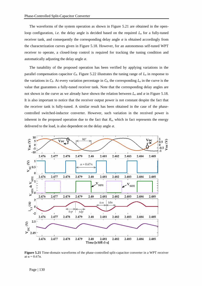
Phase-Controlled Split-Capacitor Converter
Page | 130
The waveforms of the system operation as shown in Figure 5.21 are obtained in the open-
loop configuration, i.e. the delay angle is decided based on the required Lα for a fully-tuned
receiver tank, and consequently the corresponding delay angle α is obtained accordingly from
the characterization curves given in Figure 5.18. However, for an autonomous self-tuned WPT
receiver to operate, a closed-loop control is required for tracking the tuning condition and
automatically adjusting the delay angle α.
The tunability of the proposed operation has been verified by applying variations in the
parallel compensation capacitor CR. Figure 5.22 illustrates the tuning range of Lα in response to
the variations in CR. At every variation percentage in CR, the corresponding Lα in the curve is the
value that guarantees a fully-tuned receiver tank. Note that the corresponding delay angles are
not shown in the curve as we already have shown the relation between Lα and α in Figure 5.18.
It is also important to notice that the receiver output power is not constant despite the fact that
the receiver tank is fully-tuned. A similar result has been obtained in the case of the phase-
controlled switched-inductor converter. However, such variation in the received power is
inherent in the proposed operation due to the fact that Rα, which in fact represents the energy
delivered to the load, is also dependent on the delay angle α.
Figure 5.21 Time-domain waveforms of the phase-controlled split-capacitor converter in a WPT receiver
at α = 0.67π.
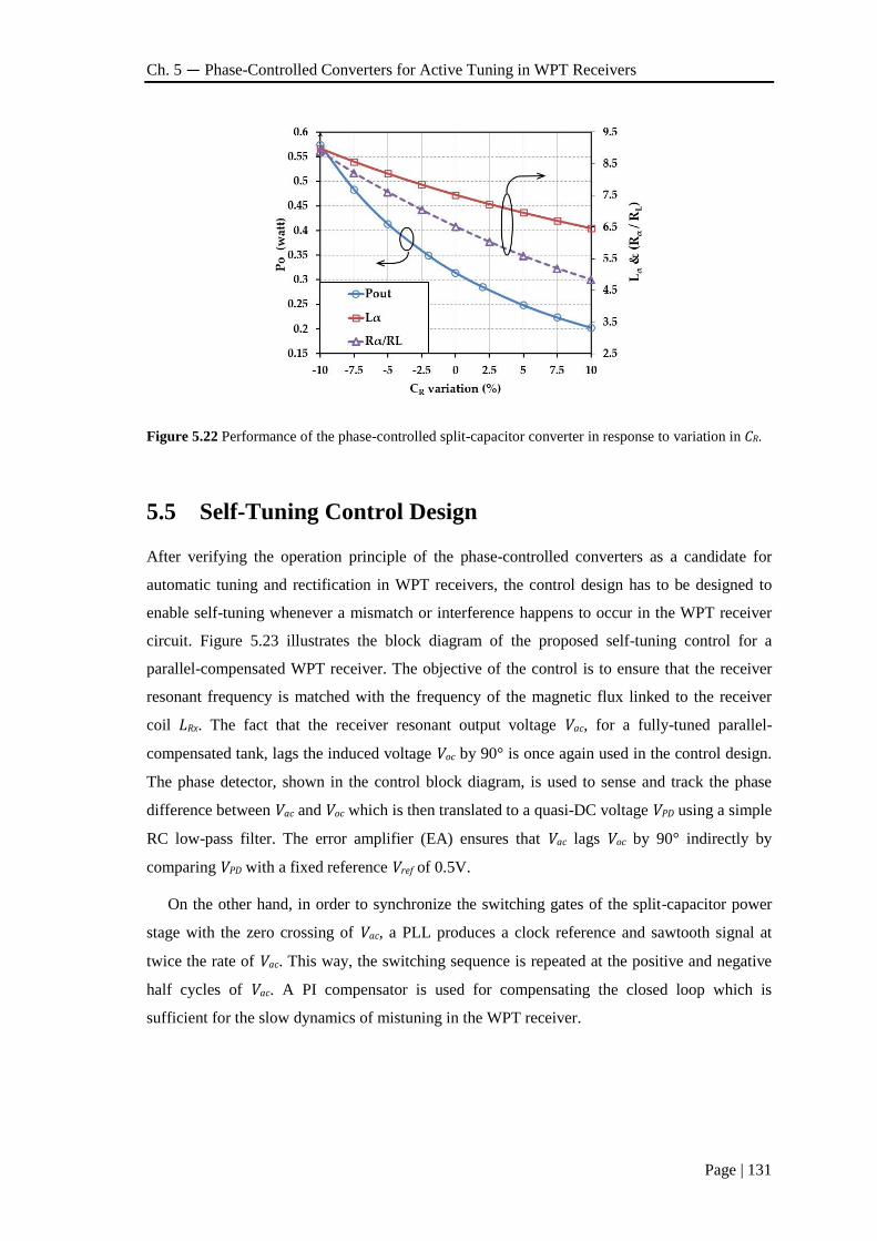
Ch. 5 — Phase-Controlled Converters for Active Tuning in WPT Receivers
Page | 131
Figure 5.22 Performance of the phase-controlled split-capacitor converter in response to variation in CR.
5.5 Self-Tuning Control Design
After verifying the operation principle of the phase-controlled converters as a candidate for
automatic tuning and rectification in WPT receivers, the control design has to be designed to
enable self-tuning whenever a mismatch or interference happens to occur in the WPT receiver
circuit. Figure 5.23 illustrates the block diagram of the proposed self-tuning control for a
parallel-compensated WPT receiver. The objective of the control is to ensure that the receiver
resonant frequency is matched with the frequency of the magnetic flux linked to the receiver
coil LRx. The fact that the receiver resonant output voltage Vac, for a fully-tuned parallel-
compensated tank, lags the induced voltage Voc by 90° is once again used in the control design.
The phase detector, shown in the control block diagram, is used to sense and track the phase
difference between Vac and Voc which is then translated to a quasi-DC voltage VPD using a simple
RC low-pass filter. The error amplifier (EA) ensures that Vac lags Voc by 90° indirectly by
comparing VPD with a fixed reference Vref of 0.5V.
On the other hand, in order to synchronize the switching gates of the split-capacitor power
stage with the zero crossing of Vac, a PLL produces a clock reference and sawtooth signal at
twice the rate of Vac. This way, the switching sequence is repeated at the positive and negative
half cycles of Vac. A PI compensator is used for compensating the closed loop which is
sufficient for the slow dynamics of mistuning in the WPT receiver.
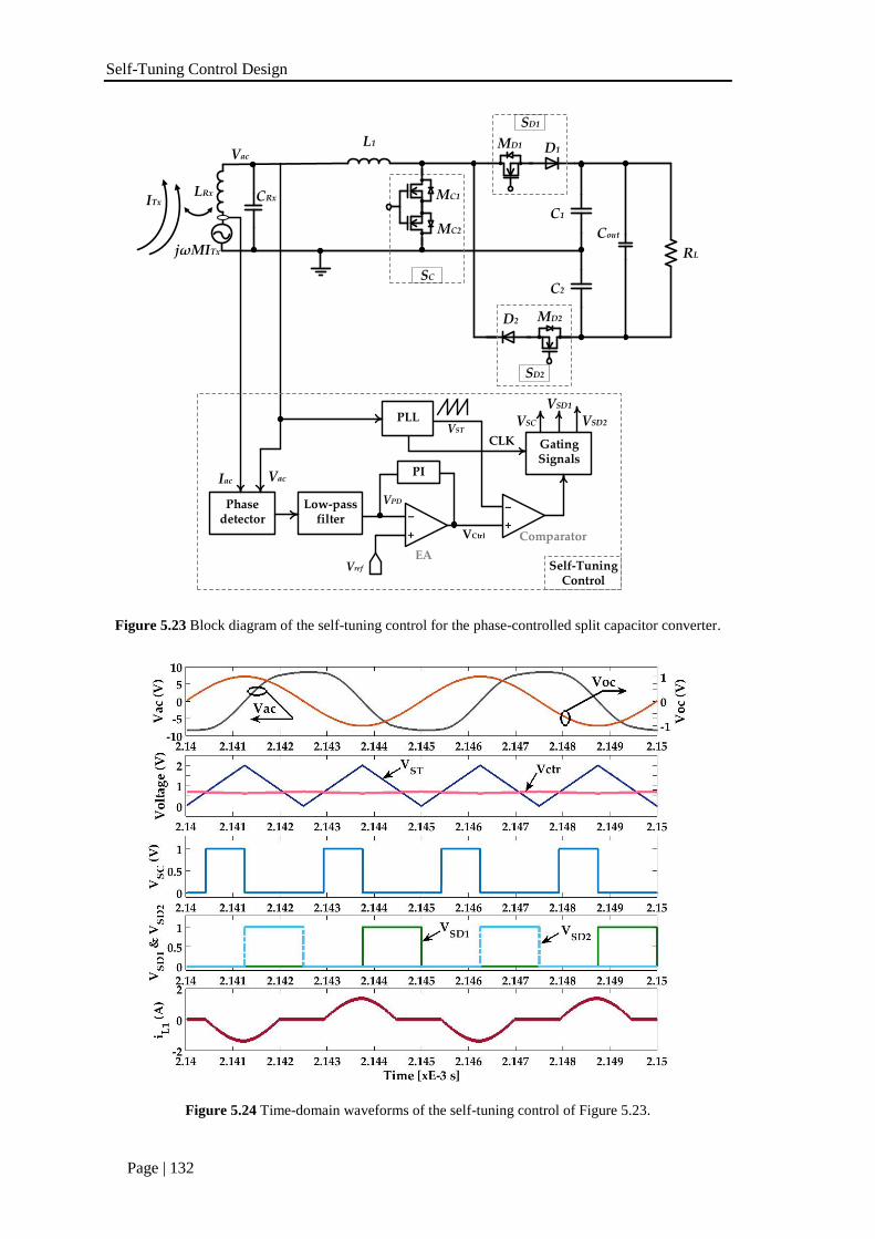
Self-Tuning Control Design
Page | 132
Phasedetector
Low-passfilter
PI
PLL
+
−
Vref
Gating Signals
+
−
CLK
EA
Comparator
VST
VCtrl
Iac Vac
L1 D1
MC2
MC1
D2
C1
C2
Cout
RL
MD1
MD2
CRxLRx
jωMITx
Vac
ITx
SC
SD1
SD2
VSC
VSD1
VSD2
Self-Tuning Control
VPD
Figure 5.23 Block diagram of the self-tuning control for the phase-controlled split capacitor converter.
Figure 5.24 Time-domain waveforms of the self-tuning control of Figure 5.23.
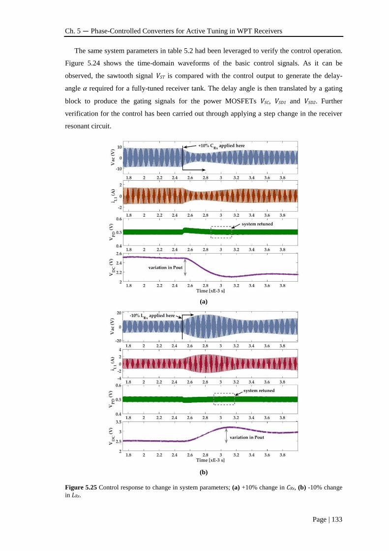
Ch. 5 — Phase-Controlled Converters for Active Tuning in WPT Receivers
Page | 133
The same system parameters in table 5.2 had been leveraged to verify the control operation.
Figure 5.24 shows the time-domain waveforms of the basic control signals. As it can be
observed, the sawtooth signal VST is compared with the control output to generate the delay-
angle α required for a fully-tuned receiver tank. The delay angle is then translated by a gating
block to produce the gating signals for the power MOSFETs VSC, VSD1 and VSD2. Further
verification for the control has been carried out through applying a step change in the receiver
resonant circuit.
(a)
(b)
Figure 5.25 Control response to change in system parameters; (a) +10% change in CRx, (b) -10% change
in LRx.
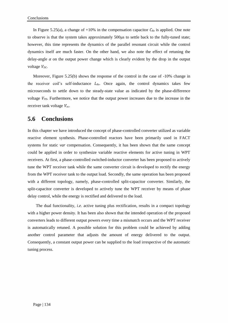
Conclusions
Page | 134
In Figure 5.25(a), a change of +10% in the compensation capacitor CRx is applied. One note
to observe is that the system takes approximately 500μs to settle back to the fully-tuned state;
however, this time represents the dynamics of the parallel resonant circuit while the control
dynamics itself are much faster. On the other hand, we also note the effect of retuning the
delay-angle α on the output power change which is clearly evident by the drop in the output
voltage VDC.
Moreover, Figure 5.25(b) shows the response of the control in the case of -10% change in
the receiver coil’s self-inductance LRx. Once again, the control dynamics takes few
microseconds to settle down to the steady-state value as indicated by the phase-difference
voltage VPD. Furthermore, we notice that the output power increases due to the increase in the
receiver tank voltage Vac.
5.6 Conclusions
In this chapter we have introduced the concept of phase-controlled converter utilized as variable
reactive element synthesis. Phase-controlled reactors have been primarily used in FACT
systems for static var compensation. Consequently, it has been shown that the same concept
could be applied in order to synthesize variable reactive elements for active tuning in WPT
receivers. At first, a phase-controlled switched-inductor converter has been proposed to actively
tune the WPT receiver tank while the same converter circuit is developed to rectify the energy
from the WPT receiver tank to the output load. Secondly, the same operation has been proposed
with a different topology, namely, phase-controlled split-capacitor converter. Similarly, the
split-capacitor converter is developed to actively tune the WPT receiver by means of phase
delay control, while the energy is rectified and delivered to the load.
The dual functionality, i.e. active tuning plus rectification, results in a compact topology
with a higher power density. It has been also shown that the intended operation of the proposed
converters leads to different output powers every time a mismatch occurs and the WPT receiver
is automatically retuned. A possible solution for this problem could be achieved by adding
another control parameter that adjusts the amount of energy delivered to the output.
Consequently, a constant output power can be supplied to the load irrespective of the automatic
tuning process.
Ch. 5 — Phase-Controlled Converters for Active Tuning in WPT Receivers
Page | 135
5.7 References
[1] P. Si, A. P. Hu, S. Malpas, and D. Budgett, “A Frequency Control Method for Regulating
Wireless Power to Implantable Devices,” IEEE Trans. Biomed. Circuits Syst., vol. 2, no. 1, pp. 22–
29, Mar. 2008.
[2] P. P. Nayak, D. P. Kar, S. K. Panda, and S. Bhuyan, “Automatic frequency tuning wireless
charging system for enhancement of efficiency,” Electron. Lett., vol. 50, no. 24, pp. 1868–1870,
Nov. 2014.
[3] S. Aldhaher, P. C.-K. Luk, A. Bati, and J. F. Whidborne, “Wireless Power Transfer Using Class
E Inverter With Saturable DC-Feed Inductor,” IEEE Trans. Ind. Appl., vol. 50, no. 4, pp. 2710–
2718, Jul. 2014.
[4] J.-U. W. Hsu, A. P. Hu, and A. Swain, “A Wireless Power Pickup Based on Directional Tuning
Control of Magnetic Amplifier,” IEEE Trans. Ind. Electron., vol. 56, no. 7, pp. 2771–2781, Jul.
2009.
[5] A. P. Hu and S. Hussmann, “Improved power flow control for contactless moving sensor
applications,” IEEE Power Electron. Lett., vol. 2, no. 4, pp. 135–138, 2004.
[6] N. G. Hingorani and L. Gyugyi, Understanding FACTS : concepts and technology of flexible AC
transmission systems. Wiley-IEEE Press, 2000.
[7] J. James, J. Boys, and G. Covic, “A variable inductor based tuning method for ICPT pickups,” in
7th International Power Engineering Conference, IPEC2005, 2005, vol. 2005.
[8] D. Kwon, G. A. Rincon-Mora, and E. O. Torres, “Harvesting Ambient Kinetic Energy With
Switched-Inductor Converters,” IEEE Trans. Circuits Syst. I Regul. Pap., vol. 58, no. 7, pp. 1551–
1560, Jul. 2011.
[9] P. D. Mitcheson, T. C. Green, and E. M. Yeatman, “Power processing circuits for
electromagnetic, electrostatic and piezoelectric inertial energy scavengers,” in Microsystem
Technologies, 2007, vol. 13, no. 11–12, pp. 1629–1635.
[10] R. Dayal, S. Dwari, and L. Parsa, “Design and Implementation of a Direct AC-DC Boost
Converter for Low-Voltage Energy Harvesting,” IEEE Trans. Ind. Electron., vol. 58, no. 6, pp.
2387–2396, June.

Page | 137
Chapter
6
6 Real and Reactive Power Control in WPT
Receivers
In this chapter, we propose a modified operation in phase-controlled converters in order to
enable real power flow control in addition to the self-tuning of WPT receivers. We have shown
in Chapter 5 that phase-controlled converters are good candidates for variable reactive element
synthesis in the applications of active tuning in WPT receivers. This way, it is possible to
control the reactive power generated in the receiver resonant tank due to mistuning, which
leaves some amount of uncompensated var. We have verified the concept of variable delay-
angle implementation in order to synthesize an average reactive element which is utilized for
compensating the WPT receiver tank automatically towards the fully-tuned condition. However,
it has been shown that, during the energy rectification intervals, the amount of energy delivered
to the load depends upon the amount of delay-angle applied for active tuning.
Accordingly, we explore and propose in this chapter a modified operation that adds an
additional control parameter in order to control the real power flow and supply the load with a
regulated output voltage.
6.1 Power Management Topologies in WPT Receivers — an
Overview
As pointed out before, in a representative RIC-WPT link, a transmitter coil LTx is driven by a
current to produce a magnetic field. At the receiver side, the receiver coil LRx is linked by the
magnetic flux lines which cause an open-circuit voltage Voc to be induced in the coil. Due to the
weak coupling between the transmitter and receiver coil, the induced voltage Voc is usually very
low. Consequently, a compensation circuit is used to form a resonance circuit in order to boost
either the voltage or the current. Compensation topologies have been discussed earlier in
Chapter 2, where we have pointed out that parallel-compensated WPT receiver tank is more
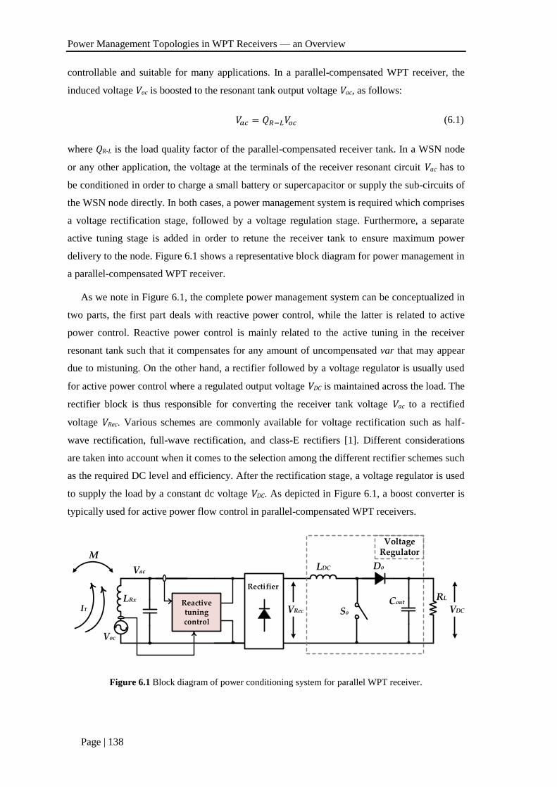
Power Management Topologies in WPT Receivers — an Overview
Page | 138
controllable and suitable for many applications. In a parallel-compensated WPT receiver, the
induced voltage Voc is boosted to the resonant tank output voltage Vac, as follows:
𝑉𝑎𝑐 = 𝑄𝑅−𝐿𝑉𝑜𝑐 (6.1)
where QR-L is the load quality factor of the parallel-compensated receiver tank. In a WSN node
or any other application, the voltage at the terminals of the receiver resonant circuit Vac has to
be conditioned in order to charge a small battery or supercapacitor or supply the sub-circuits of
the WSN node directly. In both cases, a power management system is required which comprises
a voltage rectification stage, followed by a voltage regulation stage. Furthermore, a separate
active tuning stage is added in order to retune the receiver tank to ensure maximum power
delivery to the node. Figure 6.1 shows a representative block diagram for power management in
a parallel-compensated WPT receiver.
As we note in Figure 6.1, the complete power management system can be conceptualized in
two parts, the first part deals with reactive power control, while the latter is related to active
power control. Reactive power control is mainly related to the active tuning in the receiver
resonant tank such that it compensates for any amount of uncompensated var that may appear
due to mistuning. On the other hand, a rectifier followed by a voltage regulator is usually used
for active power control where a regulated output voltage VDC is maintained across the load. The
rectifier block is thus responsible for converting the receiver tank voltage Vac to a rectified
voltage VRec. Various schemes are commonly available for voltage rectification such as half-
wave rectification, full-wave rectification, and class-E rectifiers [1]. Different considerations
are taken into account when it comes to the selection among the different rectifier schemes such
as the required DC level and efficiency. After the rectification stage, a voltage regulator is used
to supply the load by a constant dc voltage VDC. As depicted in Figure 6.1, a boost converter is
typically used for active power flow control in parallel-compensated WPT receivers.
Voc
LRx
M
IT
Vac
RL
Rectifier
Reactive tuning control
LDC
Cout
Do
SoVRec VDC
Voltage Regulator
Figure 6.1 Block diagram of power conditioning system for parallel WPT receiver.
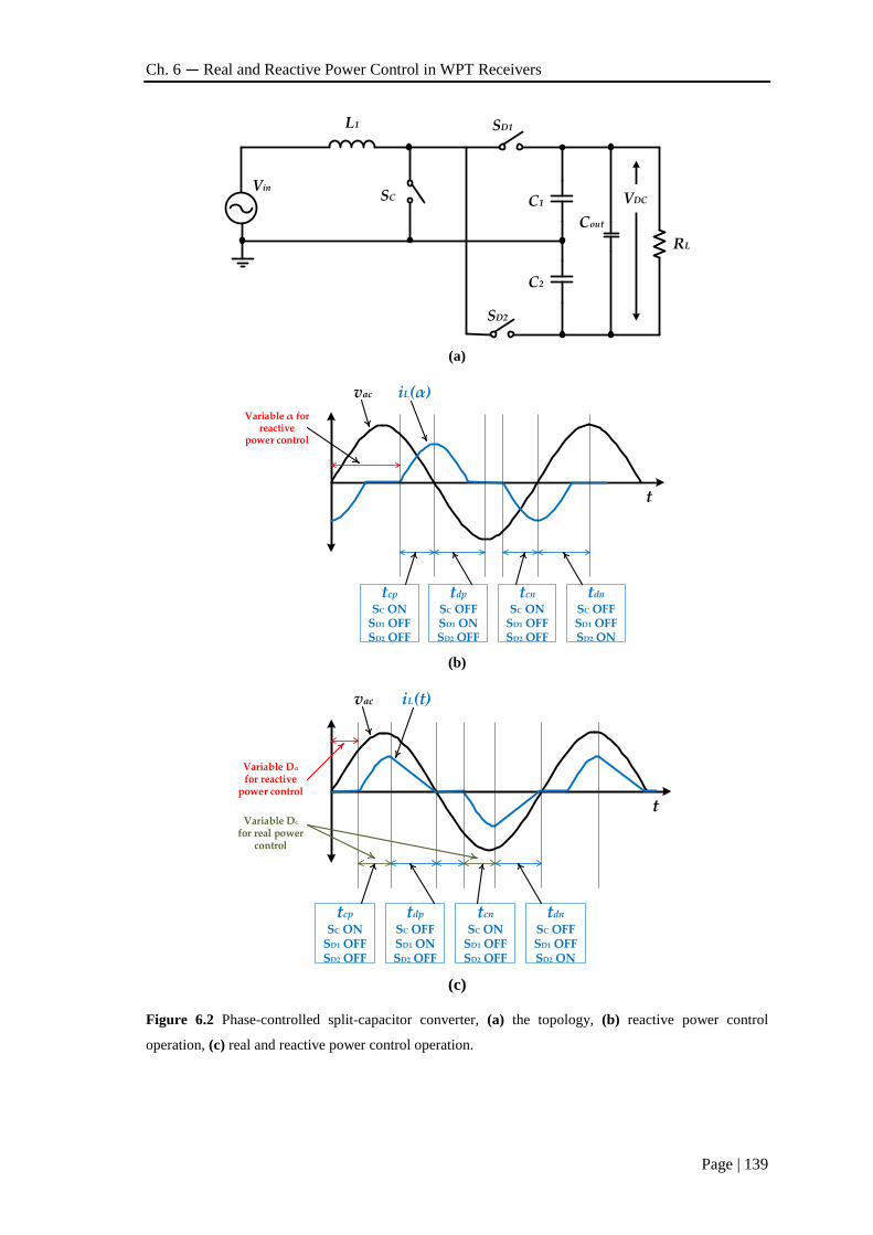
Ch. 6 — Real and Reactive Power Control in WPT Receivers
Page | 139
SC
SD2
L1
Vin
C1
C2
Cout
RL
SD1
VDC
(a)
t
vac iL(α)
Variable α for reactive
power control
tcp SC ON
SD1 OFFSD2 OFF
tdp SC OFFSD1 ONSD2 OFF
tcn SC ON
SD1 OFFSD2 OFF
tdn SC OFFSD1 OFFSD2 ON
(b)
t
vac iL(t)
Variable Dα for reactive
power control
tcp SC ON
SD1 OFFSD2 OFF
tdp SC OFFSD1 ONSD2 OFF
tcn SC ON
SD1 OFFSD2 OFF
tdn SC OFFSD1 OFFSD2 ON
Variable Dc for real power
control
(c)
Figure 6.2 Phase-controlled split-capacitor converter, (a) the topology, (b) reactive power control
operation, (c) real and reactive power control operation.
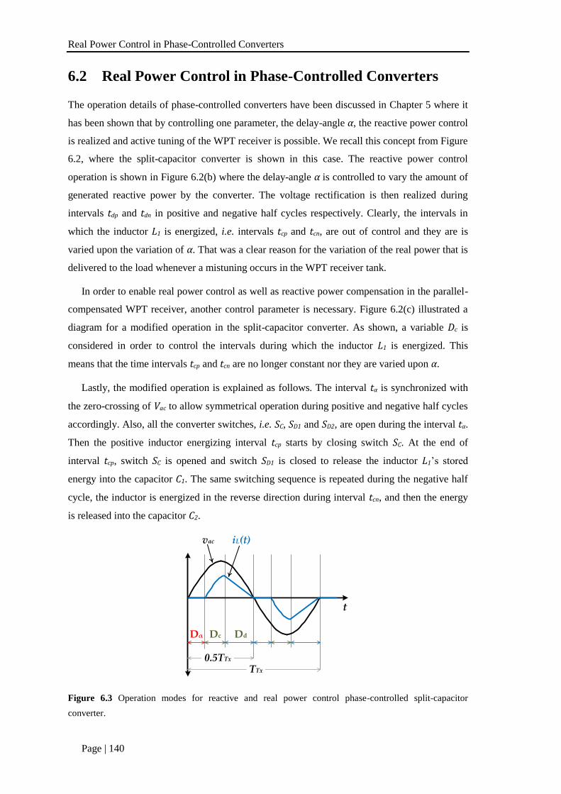
Real Power Control in Phase-Controlled Converters
Page | 140
6.2 Real Power Control in Phase-Controlled Converters
The operation details of phase-controlled converters have been discussed in Chapter 5 where it
has been shown that by controlling one parameter, the delay-angle α, the reactive power control
is realized and active tuning of the WPT receiver is possible. We recall this concept from Figure
6.2, where the split-capacitor converter is shown in this case. The reactive power control
operation is shown in Figure 6.2(b) where the delay-angle α is controlled to vary the amount of
generated reactive power by the converter. The voltage rectification is then realized during
intervals tdp and tdn in positive and negative half cycles respectively. Clearly, the intervals in
which the inductor L1 is energized, i.e. intervals tcp and tcn, are out of control and they are is
varied upon the variation of α. That was a clear reason for the variation of the real power that is
delivered to the load whenever a mistuning occurs in the WPT receiver tank.
In order to enable real power control as well as reactive power compensation in the parallel-
compensated WPT receiver, another control parameter is necessary. Figure 6.2(c) illustrated a
diagram for a modified operation in the split-capacitor converter. As shown, a variable Dc is
considered in order to control the intervals during which the inductor L1 is energized. This
means that the time intervals tcp and tcn are no longer constant nor they are varied upon α.
Lastly, the modified operation is explained as follows. The interval tα is synchronized with
the zero-crossing of Vac to allow symmetrical operation during positive and negative half cycles
accordingly. Also, all the converter switches, i.e. SC, SD1 and SD2, are open during the interval tα.
Then the positive inductor energizing interval tcp starts by closing switch SC. At the end of
interval tcp, switch SC is opened and switch SD1 is closed to release the inductor L1’s stored
energy into the capacitor C1. The same switching sequence is repeated during the negative half
cycle, the inductor is energized in the reverse direction during interval tcn, and then the energy
is released into the capacitor C2.
t
vac iL(t)
Dα Dc Dd
0.5TTx TTx
Figure 6.3 Operation modes for reactive and real power control phase-controlled split-capacitor
converter.
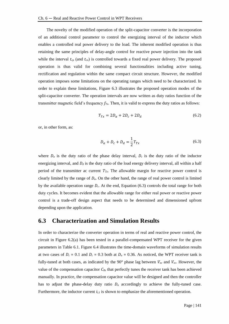
Ch. 6 — Real and Reactive Power Control in WPT Receivers
Page | 141
The novelty of the modified operation of the split-capacitor converter is the incorporation
of an additional control parameter to control the energizing interval of the inductor which
enables a controlled real power delivery to the load. The inherent modified operation is thus
retaining the same principles of delay-angle control for reactive power injection into the tank
while the interval tcp (and tcn) is controlled towards a fixed real power delivery. The proposed
operation is thus valid for combining several functionalities including active tuning,
rectification and regulation within the same compact circuit structure. However, the modified
operation imposes some limitations on the operating ranges which need to be characterized. In
order to explain these limitations, Figure 6.3 illustrates the proposed operation modes of the
split-capacitor converter. The operation intervals are now written as duty ratios function of the
transmitter magnetic field’s frequency fTx. Then, it is valid to express the duty ratios as follows:
𝑇𝑇𝑥 = 2𝐷𝛼 + 2𝐷𝑐 + 2𝐷𝑑 (6.2)
or, in other form, as:
𝐷𝛼 + 𝐷𝑐 + 𝐷𝑑 =1
2𝑇𝑇𝑥 (6.3)
where Dα is the duty ratio of the phase delay interval, Dc is the duty ratio of the inductor
energizing interval, and Dd is the duty ratio of the load energy delivery interval, all within a half
period of the transmitter ac current TTx. The allowable margin for reactive power control is
clearly limited by the range of Dα. On the other hand, the range of real power control is limited
by the available operation range Dc. At the end, Equation (6.3) controls the total range for both
duty cycles. It becomes evident that the allowable range for either real power or reactive power
control is a trade-off design aspect that needs to be determined and dimensioned upfront
depending upon the application.
6.3 Characterization and Simulation Results
In order to characterize the converter operation in terms of real and reactive power control, the
circuit in Figure 6.2(a) has been tested in a parallel-compensated WPT receiver for the given
parameters in Table 6.1. Figure 6.4 illustrates the time-domain waveforms of simulation results
at two cases of Dc = 0.1 and Dc = 0.3 both at Dα = 0.36. As noticed, the WPT receiver tank is
fully-tuned at both cases, as indicated by the 90° phase lag between Vac and Voc. However, the
value of the compensation capacitor CRx that perfectly tunes the receiver tank has been achieved
manually. In practice, the compensation capacitor value will be designed and then the controller
has to adjust the phase-delay duty ratio Dα accordingly to achieve the fully-tuned case.
Furthermore, the inductor current iL1 is shown to emphasize the aforementioned operation.
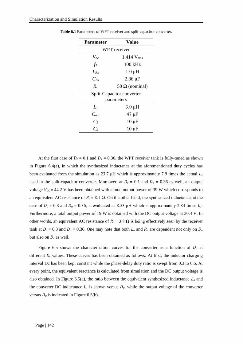
Characterization and Simulation Results
Page | 142
Table 6.1 Parameters of WPT receiver and split-capacitor converter.
Parameter Value
WPT receiver
Voc 1.414 Vrms
fT 100 kHz
LRx 1.0 μH
CRx 2.86 μF
RL 50 Ω (nominal)
Split-Capacitor converter
parameters
L1 3.0 μH
Cout 47 μF
C1 10 μF
C2 10 μF
At the first case of Dc = 0.1 and Dα = 0.36, the WPT receiver tank is fully-tuned as shown
in Figure 6.4(a), in which the synthesized inductance at the aforementioned duty cycles has
been evaluated from the simulation as 23.7 μH which is approximately 7.9 times the actual L1
used in the split-capacitor converter. Moreover, at Dc = 0.1 and Dα = 0.36 as well, an output
voltage VDC = 44.2 V has been obtained with a total output power of 39 W which corresponds to
an equivalent AC resistance of Rα = 8.1 Ω. On the other hand, the synthesized inductance, at the
case of Dc = 0.3 and Dα = 0.36, is evaluated as 8.53 μH which is approximately 2.84 times L1.
Furthermore, a total output power of 19 W is obtained with the DC output voltage at 30.4 V. In
other words, an equivalent AC resistance of Rα = 3.8 Ω is being effectively seen by the receiver
tank at Dc = 0.3 and Dα = 0.36. One may note that both Lα and Rα are dependent not only on Dα
but also on Dc as well.
Figure 6.5 shows the characterization curves for the converter as a function of Dα at
different Dc values. These curves has been obtained as follows: At first, the inductor charging
interval Dc has been kept constant while the phase-delay duty ratio is swept from 0.3 to 0.6. At
every point, the equivalent reactance is calculated from simulation and the DC output voltage is
also obtained. In Figure 6.5(a), the ratio between the equivalent synthesized inductance Lα and
the converter DC inductance L1 is shown versus Dα, while the output voltage of the converter
versus Dα is indicated in Figure 6.5(b).
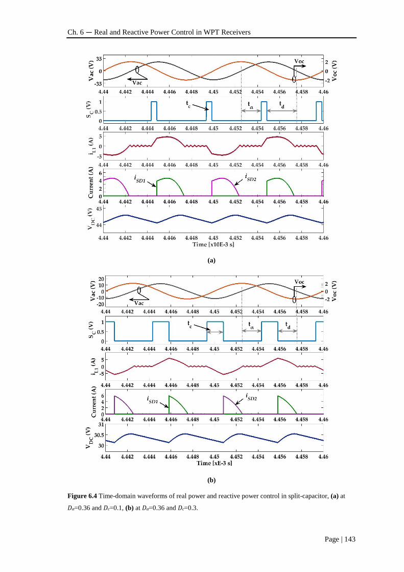
Ch. 6 — Real and Reactive Power Control in WPT Receivers
Page | 143
(a)
(b)
Figure 6.4 Time-domain waveforms of real power and reactive power control in split-capacitor, (a) at
Dα=0.36 and Dc=0.1, (b) at Dα=0.36 and Dc=0.3.
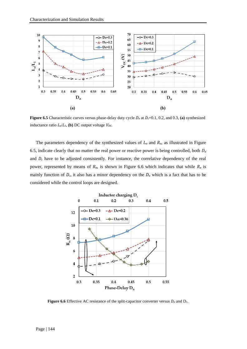
Characterization and Simulation Results
Page | 144
(a) (b)
Figure 6.5 Characteristic curves versus phase-delay duty cycle Dα at Dc=0.1, 0.2, and 0.3, (a) synthesized
inductance ratio Lα/L1, (b) DC output voltage VDC.
The parameters dependency of the synthesized values of Lα and Rα, as illustrated in Figure
6.5, indicate clearly that no matter the real power or reactive power is being controlled, both Dα
and Dc have to be adjusted consistently. For instance, the correlative dependency of the real
power, represented by means of Rα, is shown in Figure 6.6 which indicates that while Rα is
mainly function of Dc, it also has a minor dependency on the Dα which is a fact that has to be
considered while the control loops are designed.
Figure 6.6 Effective AC resistance of the split-capacitor converter versus Dα and Dc.
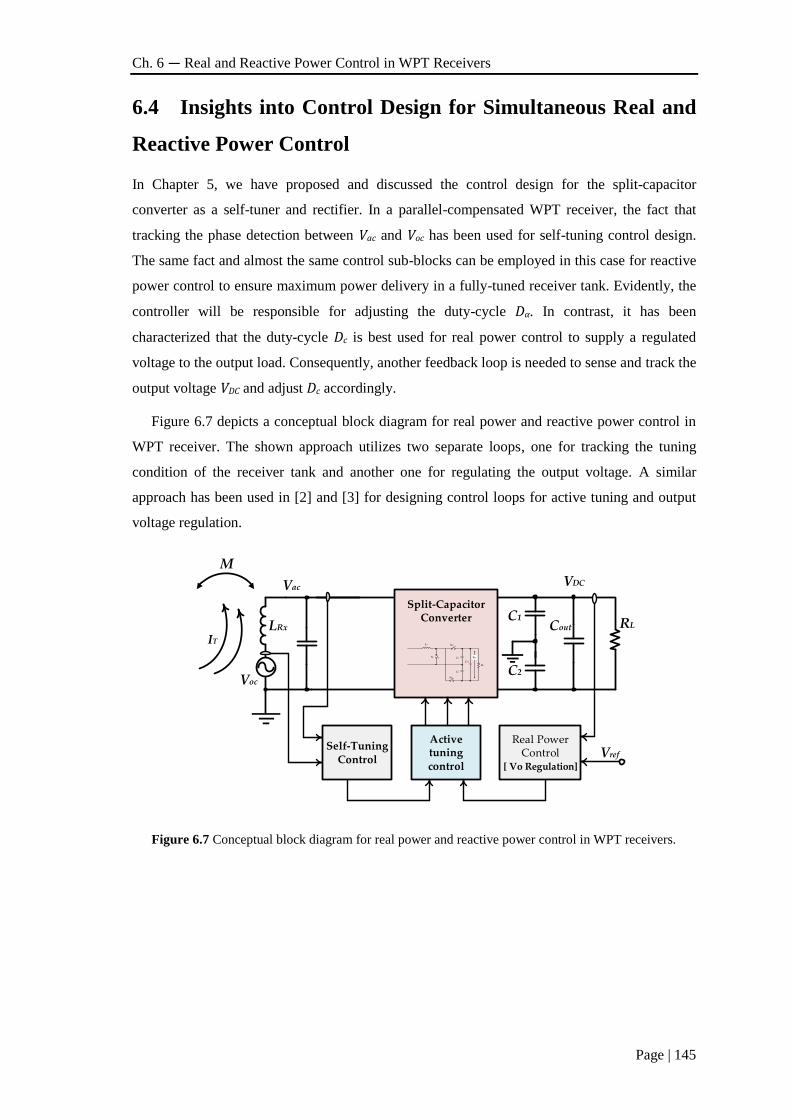
Ch. 6 — Real and Reactive Power Control in WPT Receivers
Page | 145
6.4 Insights into Control Design for Simultaneous Real and
Reactive Power Control
In Chapter 5, we have proposed and discussed the control design for the split-capacitor
converter as a self-tuner and rectifier. In a parallel-compensated WPT receiver, the fact that
tracking the phase detection between Vac and Voc has been used for self-tuning control design.
The same fact and almost the same control sub-blocks can be employed in this case for reactive
power control to ensure maximum power delivery in a fully-tuned receiver tank. Evidently, the
controller will be responsible for adjusting the duty-cycle Dα. In contrast, it has been
characterized that the duty-cycle Dc is best used for real power control to supply a regulated
voltage to the output load. Consequently, another feedback loop is needed to sense and track the
output voltage VDC and adjust Dc accordingly.
Figure 6.7 depicts a conceptual block diagram for real power and reactive power control in
WPT receiver. The shown approach utilizes two separate loops, one for tracking the tuning
condition of the receiver tank and another one for regulating the output voltage. A similar
approach has been used in [2] and [3] for designing control loops for active tuning and output
voltage regulation.
Voc
LRx
M
IT
Vac
RL
Split-Capacitor Converter
Self-Tuning Control
Cout
VDC
SC
SD2
L1
C1
C2
Cout
RL
SD1
VDC
C1
C2
Real Power Control
[ Vo Regulation]
Active tuning control
Vref
Figure 6.7 Conceptual block diagram for real power and reactive power control in WPT receivers.
Conclusions
Page | 146
6.5 Conclusions
In this chapter, a novel technique has been proposed to enable real power control in the
proposed split-capacitor converter that has been discussed in Chapter 5. The same topology and
the same technique for active tuning, or reactive power control, has been followed while a
major modification in the operation has been proposed and designed. The modified operation
adds another control parameter that enables the control of power flow to the output.
Consequently, the novel operation has the following benefits:
It allows reactive power control by adjusting the control parameter Dα, thus the WPT
receiver tank is self-tuned which maximizes the power received.
It allows real power control by adjusting the control parameter Dc, which indeed makes it
possible to obtain a regulated output voltage.
It maintains the same principles of bridgeless operation, as a main feature of the split-
capacitor converter. Thus the AC voltage at the WPT resonant tank is topologically
rectified.
The characterization of the proposed approach has shown that the real power and reactive
power control cannot be achieved separately as they are both dependent on Dα and Dc. Finally,
the control design has been discussed conceptually by showing a block diagram for a potential
two separate control loops WPT self-tuned system.
6.6 References
[1] K. van. Schuylenbergh and R. Puers, Inductive powering : basic theory and application to
biomedical systems. Springer, 2009.
[2] Z. Pantic and S. M. Lukic, “Framework and Topology for Active Tuning of Parallel
Compensated Receivers in Power Transfer Systems,” IEEE Trans. Power Electron., vol. 27, no. 11,
pp. 4503–4513, 2012.
[3] E. Ozalevli, S. Member, N. Femia, S. Member, G. Di Capua, R. Subramonian, D. Du, J.
Sankman, S. Member, and M. El Markhi, “A Cost-Effective Adaptive Rectifier for Low Power
Loosely Coupled Wireless Power Transfer Systems,” IEEE Trans. Circuits Syst. I Regul. Pap., pp.
1–12, 2017.
Page | 147
Chapter
7
7 Conclusions, Contributions and Suggested
Future Work
7.1 Conclusions
The technology advancement and the promising future of a global ubiquitous network, a
network that would connect every object, has opened the door for various research lines to
enable seamless operation of such network. Among the main research lines is the enabling of
autonomous wireless sensor network, which is one of the main pillars of internet of things. The
advanced sensing and communication tasks of wireless sensor nodes increase their power
requirement, which in turn brings a technology bottleneck that conflicts the high performance
with the autonomy of wireless sensor networks. Usually, the main energy source for a sensor
node is a small coin battery which makes the power budget very limited and the lifetime of such
sensing nodes is shortened accordingly.
Therefore, the main objective of the thesis was to propose the enabling of wireless sensor
nodes, as a part of the Internet of Things, by means of wireless power transmission. In contrast
to the common techniques of harvesting RF electromagnetic energy, or any other energy
harvesting resource, we have shown that near-field resonant-inductive-coupling WPT is a more
appealing option for a wide range of applications, more specifically for indoor and industrial
applications. However, resonant-inductive-coupling WPT shows a strong dependency on
quality factors of the resonating transmitter and receiver circuits. On the other hand, pushing the
quality factor while aiming to increase the power transmission range and efficiency is very
challenging due to the increased sensitivity of the WPT system. Consequently, the WPT system
becomes more vulnerable for detuning problems that would degrade the system performance or
even results in a nonfunctional system.
Conclusions
Page | 148
A wide overview and general background about the internet of the things and its main
system building blocks and challenges has been presented in Chapter 1. It has been shown that
the energy source in a sensor node is one of the most key limiting blocks as it puts more
constraints on the performance of the communications and sensing functions according to the
limited power budget. Due to the random nature of energy harvesting, a multi-source energy
harvesting is probably a reasonable solution. Also the limited power budget from energy
harvesting technologies for indoor and industrial applications has been discussed, where WPT
is proposed as key enabling technology for power sensor nodes. Accordingly, the problem
statement has been given where the current challenges in deploying WPT in dynamic
environments has been discussed. It has been shown that a fundamental tradeoff between power
transmission range and system reliability exists which is widely mitigated in the literature by
employing low quality factor resonant WPT systems.
In Chapter 2, the theory and modelling of WPT technologies has been discussed, including
the fundamental and theoretical differences between near-field non-radiative WPT and far-field
electromagnetic WPT. Due to the non-radiative confined field nature of near-field WPT, it is
well known to have higher efficiency, becoming the most adequate power transmission type for
WSNs. On the other hand, resonant-inductive-coupling near-field WPT is a more reliable and
efficient technology for power transmission over a distance that extends across several times
coil diameters, as compared to the non-resonating alternative. The basic simple compensation
topologies for resonant-inductive-coupling WPT have been accordingly discussed. However,
the detailed mathematical and system analysis has been only conducted for series-series and
series-parallel topologies, because these topologies are the most simple, widely adopted ones.
The series-parallel compensation topology has been chosen as the main option for powering
WSNs over large distances due to their voltage-boosting characteristics which would help in
boosting the very low EMF induced voltage up to several volts. Following the topology
selection consideration, the challenges of high-Q sensitivity in parallel-compensated WPT
receivers have been studied.
Following the system-aware discussion and analysis carried out in Chapter 2, the motivation
of developing an adaptive switch-mode power technique for self-tuning in WPT receivers has
been discussed in Chapter 3. The gyrator concept as a variable impedance synthesizer has been
revisited. Different gyrator realization topologies have been explored, so that the DAB
converter has been chosen among others. The DAB converter is generally well-known for its
inherent gyration characteristics, consequently it can be adopted as a natural-gyrator in switch-
mode impedance synthesizers. The characterization of the DAB gyrator shows that the gyration
ratio is a function of two circuit parameters, namely, the switching frequency and the phase-
angle. Consequently, the phase-angle has been considered as a more adequate control
Ch. 7 — Conclusions, Contributions and Suggested Future Work
Page | 149
parameter. The characterization results, verified mathematically and by simulation, have shown
that the gyration ratio is variable over two valid tuning ranges from 0°– 90° and 90°–180°.
Accordingly, a synthesized inductance has been realized by means of DAB converter loaded by
a capacitor. Following the characterization of the DAB as a gyrator-based inductance
synthesizer, the circuit has been tested in several cases as a proof-of-concept as follows:
A switch-mode resonator has been formed by using the DAB as a variable inductance
synthesizer in a series resonance circuit. The tunability of the synthesized inductance is
characterized by varying the phase-angle at different switching frequencies, where the
series current magnitude and phase is obtained at every point. As we one can expect, the
circuit works at resonance at a single phase-angle/switching frequency combination
where the equivalent inductive reactance from the DAB-based synthesizer cancels the
capacitive reactance of the series capacitor.
The potential miniaturization feature of the DAB-based inductance has been integrated
in a buck DC-DC converter, which replaces the physical inductance that is usually used
in buck converters. By switching the DAB circuit at very high switching frequency (of
50 MHz), it is possible to utilize a very small inductance (only 5 nH) to achieve a
synthesized inductance with relatively higher value (150 nH) while a significant
reduction in size is guaranteed. By doing so, it has been shown that a similar approach is
potentially applicable for miniaturization of magnetic components in buck converters.
The DAB converter has been also tested in a resonant ripple filter for buck converter,
where the synthesized inductance is used in a shunt resonant filter while the tuned point
of the filter can be electronically tuned using the DAB’s phase-angle. This would help in
designing a fixed switching frequency buck converters that mitigate the mistuning
problem in resonant ripple filters.
In parallel-compensated WPT receivers, the DAB-based synthesized inductance has been
presented as a variable inductance in parallel with the compensation capacitor. Thus, the
synthesized inductance can be used to automatically tune the receiver resonance frequency
against any mismatch that would cause a resonance frequency drift. To enable self-tuning
operation, a control circuit is required to monitor the tuning state of the WPT receiver and react
by tuning the DAB converter control parameter, i.e. the phase-angle.
In Chapter 4, two control techniques have been presented and evaluated. The first control
approach utilizes a dual-loop approach for maintaining the fully-tuned state; the coarse tuning
loop first scans the full range of phase-angle tuning from 0° to 90°, where the loops determines
how close the tuned point is by tracking the maximum peak voltage of the receiver tank voltage.
Complementarily, the fine tuning loop monitors the phase difference between the open-loop
induced voltage and the receiver tank output voltage and reacts by fine tuning the phase-angle
Conclusions
Page | 150
of the DAB converter. The fully-tuned state is then determined by the receiver phase angle
reaching the steady state value (receiver tank output voltage lagging the induced voltage by
90°). The detailed block description of the proposed dual-loop control has been supported with
simulation results that proves the prescribed operation. The performance limitations of this
proposal, included transient time and accuracy issues, have been discussed showing that there is
a trade-off between the control transient time and accuracy of the tuning process.
In order to improve the accuracy and achieve a faster response, a PLL-like control has been
also proposed. The control is fundamentally based on sensing the phase difference between the
receiver output voltage and the receiver induced voltage (or receiver coil’s current) and
subsequently the phase-difference information is compared with a fixed reference to generate
the correct duty cycle for a phase-shift modulation block. The validation results of the proposed
control shows high accuracy while the control transient time is only limited by the response of
the PI compensator. The proposed control, named as Quadrature-PLL based, has been tested at
different mismatch percentages in the receiver circuit, for which the overall goal of a self-tuned
WPT receiver was promisingly achieved. Furthermore, the transistor-level implementation of
the DAB converter and the proposed control has been designed and validated using XFAB
0.18µm process on Cadence virtuoso. The power stage design and power MOSFETs sizing has
been optimized for high efficiency operation without compromising the total size of the chip.
The tested results based on foundry’s accurate models have shown that an average efficiency of
75% is obtained over a wide range of mistuning cases in circuit components. Higher efficiency
is also achievable by up-sizing the power MOSFETs, however the total size of the chip would
increase considerably. For a general evaluation for the DAB-based self-tuning approach, the
different performance aspects has been discussed, where the main drawback of high number of
components is highlighted and compared with other solutions in the literature.
In the last part of Chapter 4, the discussion of performance aspects of gyrator-based DAB
synthesized inductance approach has illustrated that despite the effectiveness of the control
technique in achieving a self-tuned WPT receiver, the whole DAB circuit and the control
circuits are used as an auxiliary automatic tuning block. This means that, in a complete WPT
receiver circuit, the receiver resonant tank should have a rectifier circuit followed by a voltage
regulator in order to supply the load or the battery by the required voltage. In this case, the
DAB-based self-tuning approach is only used for automatic tuning with no power exchange.
Consequently, in Chapter 5, we have proposed a novel technique that utilizes switch-
inductor converters in order to provide built-in dual functionality: 1) automatic tuning by means
of variable reactive component synthesis; 2) AC/DC voltage regulation. Accordingly, the power
density would be increased by combining dual functions using the same converter circuit. The
fundamental concept depends on switching an inductor between the receiver resonant tank and
Ch. 7 — Conclusions, Contributions and Suggested Future Work
Page | 151
the load according to a variable phase-delay. Thus, the fundamental inductor current constitutes
a variable inductive reactance that is a function of the phase-delay.
The characterization results of the phase-controlled switched-inductor converter indicated
that the proposed converter operation can be modeled by a variable inductance in parallel with a
variable resistance, where the variable inductance represents the tuning effect and the variable
resistance represents the voltage rectification and energy delivery to the load. Integrating the
proposed phase-controlled switched-inductor in a parallel-compensated WPT receiver has been
validated. The results have shown that the phase-delay can be used effectively to tune the WPT
receiver circuit by synthesizing a variable reactance. However, it has been also shown that the
output power delivered to the load is not constant due to the variation that occurs in the
equivalent resistance, which is similarly a function of the phase-delay.
Finally, in Chapter 6 we have proposed a modification to the split-capacitor converter
topology to allow real power control as well as self-tuning reactive power control by means of
the same topology. Typically, two different stages for active tuning and voltage
rectification/regulation are used in power conditioning systems of WPT receivers. The proposed
operation assists in decreasing the size and cost of the power conditioning front-end by enabling
multiple functionalities into the same compact circuit structure. The time-domain results have
shown that the proposed operation offers a reasonable range for self-tuning in the WPT receiver
tank while the output voltage is regulated simultaneously. However, the proposed modification
imposes some limitations over the self-tuning range if a specific output voltage is required
while the limit for output voltage control is reached.
7.2 Contributions of This Thesis
The main contribution of the thesis work can be summarized as follows:
Analyzing the effect of resonant tank high quality factors upon the sensitivity of
parallel-compensated WPT receivers, showing the effect on maximum power
transmission due to mismatch in components.
Proposing and developing the switch-mode gyrator-based variable reactive impedance
synthesis, where the DAB converter has been chosen as switch-mode natural gyrator
topology. The developed circuit has been validated in several switch-mode power
conversion applications. Despite the complexity, the wide tunability and simplicity of
the control are very promising features for other applications.
Proposing a dual-loop control scheme for self-tuning in WPT receivers. The coarse
tuning loop tunes the variable synthesized inductance by coarsely searching for the
phase-angle that corresponds to the maximum envelop peak voltage. The fine tuning
Contributions of This Thesis
Page | 152
loop then proceeds by tuning for the accurate phase-angle for a fully-tuned WPT
receiver tank.
Developing a quadrature-PLL (Q-PLL) control for the gyrator-based synthesized
inductance that outperforms the dual-loop control. The Q-PLL control dynamically
tunes the phase-angle of the DAB converter in accordance to the phase-difference
information sensed at the WPT receiver tank.
Proposing a phase-controlled switched-inductor converter for dual functional approach
that combines active tuning and voltage rectification within the same converter cell. The
developed control dynamically tunes the WPT receiver circuit by switching an inductor
with a relative phase in accordance to the resonant tank voltage. The same inductor is
used to rectify the energy from the WPT receiver tank to the load.
The above contributions have been published in several articles and conference papers as a
result of this thesis. In addition, one patent has been filed based on the gyrator-based self-tuning
approach. The list of already published journals and conference papers are as follows:
Journals and Conferences:
[1] M. Saad and E. Alarcón, “Insights into Dynamic Tuning of Magnetic-Resonant Wireless
Power Transfer Receivers Based on Switch-Mode Gyrators,” Energies 2018, Vol. 11, Page 453,
vol. 11, no. 2, p. 453, Feb. 2018.
[2] M. Saad, H. Martinez-Garcia, P. Alou, and E. Alarcon, “A PLL control for self-tuning of
parallel wireless power transfer receivers utilizing switch-mode gyrator emulated inductors,” in
2017 19th European Conference on Power Electronics and Applications (EPE’17 ECCE
Europe), 2017, p. P.1-P.10.
[3] M. Saad, E. Bou-Balust, and E. Alarcon, “Switch-mode gyrator-based emulated inductor
enabling self-tunability in WPT receivers,” in 2017 IEEE International Symposium on Circuits
and Systems (ISCAS), 2017, pp. 1–4.
[4] M. Saad and E. Alarcon, “Tunable switch-mode emulated inductive elements for enhanced
power converter miniaturization,” in IECON 2016 - 42nd Annual Conference of the IEEE
Industrial Electronics Society, 2016, pp. 1184–1189.
[5] M. Saad, N. Egidos, E. Bou-Balust, and E. Alarcon, “On tunable switch-mode reactive
networks: A gyrator-based resonator emulation,” in 2016 IEEE International Symposium on
Circuits and Systems (ISCAS), 2016, vol. 2016–July, pp. 642–645.
Patents:
[6] M. Saad, E. Bou-Balust, and E. Alarcon, “System and method for tuning wireless power
transfer receivers,” 2017/2 ES. App. Number: P201730148

Ch. 7 — Conclusions, Contributions and Suggested Future Work
Page | 153
7.3 Suggested Future Work
The work carried out in this thesis has focused in investigating the sensitivity and reliability
issues in high quality factor WPT receivers due to mistuning in the resonant compensation
tanks. Consequently, two different techniques have been proposed and verified for self-tuning
of WPT receivers. The suggested future work driven from the two techniques can be listed as
follows:
Switch-mode gyrator-based self-tuning:
o In the presented dual loop control of gyrator-based reactive element synthesis, the
problem of reliability due to fixed phase-shift-based scanning could be mitigated by
designing an improved version. In the modified version, it is possible to add a variable
phase-shift step that is adapted as the system gets closer to the correct fully-tuned point.
o It is also possible to combine the dual loop into one loop by simply applying the variable
phase-shift scanning while the orientation and step size is decreased by monitoring the
phase lagging relation between Voc and Vac.
o The DAB topology has been selected based on the unique feature of natural gyration
without an external control. However, the complexity of the topology in the proposed
function of complex impedance synthesis imposes some limitation on the total
efficiency of the WPT link. The total size also remains debatable unless a chip design
integrating the whole solution is realized. Other topologies with less component count
and gyrators has to be investigated, such that the high efficiency and reduced size
features are combined with unique features of switch-mode gyrators.
o A simple PI controller has been designed for stabilizing the self-tuning control which
has been found sufficient if we consider the slow dynamics nature of mistuning that
would occur in the WPT receiver tank. However, in a very fast dynamic environment,
the controller would fail to retune the receiver tank. Consequently, it is more reasonable
to derive a small-signal model for the DAB-based converter in order to ensure robust
control design that performs fast enough.
Phase-controlled converters for self-tuning:
o As we noted in the phase-controlled converters operation, the output power delivered to
the load, represented by an AC resistance synthesized by the converter Rα, is an
uncontrolled variable every time a mistuning occurs and the control retunes the system
back to fully-tuned condition. However, it is crucial to derive mathematically the exact
formulas of Lα and Rα in terms of the phase-delay angle, such that a quantitative analysis
for the expected output power over the entire tuning range is possible during the design
task.

Suggested Future Work
Page | 154
o The selection of the switch-inductor converter or split-capacitor converter for the
proposed phase-controlled variable reactive element synthesis has been considered due
to their capability of processing AC signals directly without the need of a bridge for AC-
DC rectification. However, the use of bidirectional switches, which are capable of
handling current in both directions, becomes inevitable. It would be more advantageous
to employ simple topologies such as boost converters or buck-boost converters to
achieve the same operation while being preceded by a separate rectifier circuit. Thereby,
the advanced gate drive circuits for bidirectional switches would be avoided at the
expense of lower efficiency and reduced power density.
Real power and reactive power control in phase-controlled converters:
o The proposed real power control and reactive power control operation needs to be
mathematically analyzed in order to obtain accurate expressions for Lα and Rα specially
after adding another control parameter Dc. A robust and reliable control design would
not be feasible unless the interrelated dependency of Dc and Dα is clearly established.
o The novel operation of utilizing a single-stage for rectification, tuning, and voltage
regulation has been already discussed in Chapter 6. However, the control design for self-
tuning and automatic load power control is required.
Page | 155
On-Chip Adaptive Power Management for WPT-Enabled IoT
Abstract: Among other IoT’s pillars, wireless sensor network (WSN) is one of the main
parts comprising massive clusters of spatially distributed sensor nodes dedicated for sensing and
monitoring environmental conditions. The lifetime of a WSN is greatly dependent on the
lifetime of the small sensor nodes, which, in turn, is primarily dependent on energy availability
within every sensor node. Predominantly, the main energy source for a sensor node is supplied
by a small coin battery which has a limited capacity in essence. Consequently, powering the
sensor nodes becomes a key limiting issue, which poses important challenges for their
practicality and cost. Therefore, in this thesis we propose enabling WSN, as the main pillar of
IoT, by means of resonant inductive coupling (RIC) wireless power transfer (WPT). Mainly, the
thesis deals with technical challenges of enabling efficient contactless energy delivery at distant
range by means of high quality factor RIC-WPT system. Therefore, the main thesis objective is
to develop and design an adaptive efficient switch-mode front-end for self-tuning in WPT
receivers in multiple receiver system.
Keywords: Internet of Things; Wireless Sensor Networks; Wireless Power Transfer;
Resonant Inductive Coupling; Active Tuning; Efficient; Switch-Mode