Chemically Modifying Vegetable Oils to Prepare Green ... - MDPI

Observation of negative differential resistance and electrical bi-stability in chemicallysynthesized ZnO nanorodsNandini Roy, Avijit Chowdhury, and Asim Roy
Citation: Journal of Applied Physics 115, 223502 (2014); doi: 10.1063/1.4882017 View online: http://dx.doi.org/10.1063/1.4882017 View Table of Contents: http://scitation.aip.org/content/aip/journal/jap/115/22?ver=pdfcov Published by the AIP Publishing Articles you may be interested in Role of defect states in magnetic and electrical properties of ZnO nanowires AIP Advances 3, 042110 (2013); 10.1063/1.4801937 Green luminescence from Cu-doped ZnO nanorods: Role of Zn vacancies and negative thermal quenching Appl. Phys. Lett. 102, 111106 (2013); 10.1063/1.4798240 Vertically aligned ZnO nanorod grown by hydrothermal based chemical method on glass substrate AIP Conf. Proc. 1447, 421 (2012); 10.1063/1.4710059 Ultraviolet electroluminescence from ordered ZnO nanorod array/p-GaN light emitting diodes Appl. Phys. Lett. 100, 171109 (2012); 10.1063/1.4706259 Effect of annealing on the structural and luminescent properties of ZnO nanorod arrays grown at low temperature J. Appl. Phys. 109, 103508 (2011); 10.1063/1.3586243
[This article is copyrighted as indicated in the article. Reuse of AIP content is subject to the terms at: http://scitation.aip.org/termsconditions. Downloaded to ] IP:
14.139.217.138 On: Tue, 10 Jun 2014 08:03:14

Observation of negative differential resistance and electrical bi-stabilityin chemically synthesized ZnO nanorods
Nandini Roy, Avijit Chowdhury, and Asim Roya)
Department of Physics, National Institute of Technology Silchar, Silchar, Assam 788010, India
(Received 8 April 2014; accepted 25 May 2014; published online 9 June 2014)
Zinc oxide nanorods/p-Si heterostructures have been fabricated by depositing the chemically
synthesized ZnO nanorods on p-type silicon substrate. Heterostructure shows electrical bi-stability
and negative differential resistance (NDR) only at the beginning of the forward bias region, and these
phenomena have been explained with the help of energy band diagram. An explanation is proposed
for the origin of electrical bi-stability in light of the electric field induced charge transfer across the
junction, and the NDR phenomena could be attributed to interfacial traps and defect level that arises
due to oxygen and zinc interstitial vacancies. Room temperature photoluminescence measurement of
ZnO nanorods exhibits the emission peaks at about 466 nm and 566 nm which are attributed to
oxygen vacancies and Zn interstitials. A correlation between NDR and blue emission phenomena in
the ZnO nanorods due to defects states has been established. VC 2014 AIP Publishing LLC.
[http://dx.doi.org/10.1063/1.4882017]
I. INTRODUCTION
Electric-field controlled bi-stable devices have aroused
extensive interests over the past several years due to their
unique advantages such as simple fabrication process, large
memory density, and lower power consumption.1–3 One of the
essential features in the non linear current-voltage (I-V) char-
acteristics is negative differential resistance (NDR), which
would allow further development in information processing
system.4,5 NDR in I-V characteristics of a device shows the
region where current decreases with an increase in applied
voltage and this phenomenon has attracted considerable atten-
tion due to their tremendous potential applications in low-
power memory and logic circuits.6–8 Various possible mecha-
nisms such as the formation of electric filament, electric
charge transfer, and charge trapping in the thin films or nano-
particles have been used to explain the electrical bi-stability
and NDR phenomena.9,10 The NDR effects were observed
recently by various researchers in single layer, multilayer, and
nanocomposites thin films based on organic and inorganic
materials.1,7 Such types of bi-stable devices are a subject of
recent interests and given more attention and further investiga-
tion to achieve practical applications are also necessary.
Zinc oxide is a promising II-VI semiconductor material
with a direct band gap of 3.37 eV.11 Due to its wide band gap
and large excitonic binding energy (60 meV at room tempera-
ture), ZnO has attracted much attention for many device
applications, such as transparent conductors, electro-optical
devices,12,13 gas sensors,14,15 thin film transistors,16 and varis-
tors and solar cells.17–19 Interestingly, ZnO nanostructures
also show a broad photoluminescence (PL) in the visible
region (470–550 nm).20 The visible emissions originate from
defects such as oxygen vacancy which are believed to be
located near the surface region.20–22 The PL emission energy
as well as the intensity not only depend on the size but are
also related to the morphology of the nanostructures.
Recently, studies about fabrication of bi-stable and NDR
hybrid devices based on ZnO nanorods (NRs) on single crys-
talline substrate and organic surface begun to appear in the
literature.23,24 Yang et al.25 reported electrical bi-stability and
NDR in single Sb-doped ZnO nanobelts/SiOx/p-type Si heter-
ostructured devices. Room temperature NDR based on a sin-
gle ZnO nanowire/CuPc nanofilm hybrid heterojunction has
been reported by Guo et al.23
In this work, we have synthesized ZnO nanorods by sim-
ple chemical approach and investigated the electrical bi-
stability and NDR phenomena in the heterostructures based
on ZnO nanorods/p-Si under dark conditions at room temper-
atures. Current–voltage (I–V) measurements were carried out
to study the electrical behavior of the device. A suitable
energy band diagram has been proposed to understand the
electrical bi-stability and NDR phenomena. PL spectrum
shows the blue and the green emission peak which arises due
to the radiative transition from the extended Zni to valence
band and from the conduction band to deep levels, respec-
tively. Such type of devices have potential applications in
the field of bi-stable memory devices for electronic and opto-
electronic applications.
II. EXPERIMENTAL DETAILS
To synthesize ZnO nanorods, Ammonium persulphate
(NH4)2S2O8, sodium hydroxide (NaOH), and zinc metal
powder (Merck chemicals) were used as precursors. A solu-
tion of ammonium persulphate was prepared by dissolving
0.038 mol ammonium persulphate in 20 ml de-ionized water.
This solution was added drop wise to a solution, which was
prepared by dissolving 0.191 mol of NaOH in 20 ml
de-ionized water. Mixture was again added drop wise to
another solution prepared by dissolving 0.9 gm zinc metal
powder in 10 ml de-ionised water with continuous stirring at
room temperature. The solution was stirred by magnetic stir-
rer for 22 h during which the color of the solution changed
a)Author to whom correspondence should be addressed. Electronic mail:
[email protected]. Tel.: þ91 3842 224879.
0021-8979/2014/115(22)/223502/6/$30.00 VC 2014 AIP Publishing LLC115, 223502-1
JOURNAL OF APPLIED PHYSICS 115, 223502 (2014)
[This article is copyrighted as indicated in the article. Reuse of AIP content is subject to the terms at: http://scitation.aip.org/termsconditions. Downloaded to ] IP:
14.139.217.138 On: Tue, 10 Jun 2014 08:03:14
from grey to milky white gradually. The final solution was
filtered, washed many times with de-ionised water, and then
dried at room temperature.
The phase and crystal structure of the sample were
studied by X-ray diffractometer (XRD) (Bruker AXS D8
Advance) using CuKa (40 kV, 40 mA) of wavelength
0.15418 nm in 2h mode. The morphology of the nanostruc-
tures was imaged by using field emission scanning electron
microscopy (Fe-SEM, JSM-6700F, JEOL). The crystalline
structure and lattice fringes of nanostructures were further
examined with a high resolution transmission electron micro-
scope (HRTEM, JEM-2010, JEOL, Japan operating voltage
200 kV). The nanocrystalline powders were dissolved in
methanol solutions for UV-vis spectral studies and PL studies.
An UV-visible scanning spectrophotometer (UV-2401 PC,
Shimazdu, Japan) was used to record the optical absorption
spectra of the sample at room temperature. A spectrofluorom-
eter (Fluoromax-4, Horiba Scientific) was used to record the
PL spectra of the sample.
To make thin films, freshly prepared solution was used
by dissolving synthesized ZnO powder in methanol. Using
this solution, thin films were prepared by precipitation tech-
niques on the single crystalline p-Si substrate for the electri-
cal measurements. To allow the evaporation of solvents from
films, films were kept at room temperature for 24 h and then
dried in oven. On the top of the thin films, circular shaped
aluminum (Al) electrodes (thickness 50 nm, area 0.25 cm2)
were deposited by thermal evaporation (model 12A4DM,
Hind Hivac, Bangalore, India) through shadow mask.
Electrical properties were recorded using semiconductor pa-
rameter analyzer (Keithley 4200 SCS).
III. RESULTS AND DISCUSSION
A. Structural characterization
Figure 1 shows the FE-SEM image of the synthesized
product consists of randomly oriented ZnO nanorods. The
length and the diameter of the nanorods are estimated to be
in the ranges 100–150 nm and 10–20 nm, respectively. Few
nanorods with larger diameter were also observed from the
FESEM image. The inset of Fig. 1 shows the FESEM image
of collection of nanorods at higher magnification. This dem-
onstrates that the simple chemical method can be used for
synthesis of ZnO nanostructures.
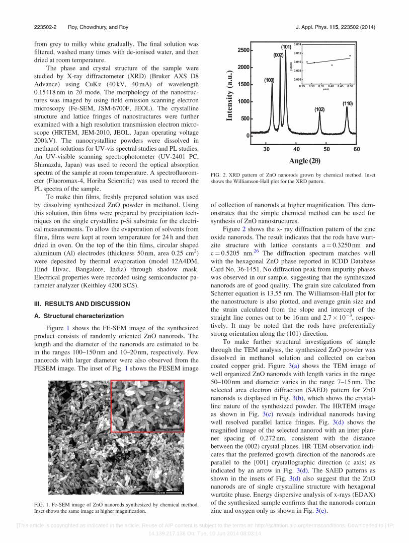
Figure 2 shows the x- ray diffraction pattern of the zinc
oxide nanorods. The result indicates that the rods have wurt-
zite structure with lattice constants a¼ 0.3250 nm and
c¼ 0.5205 nm.26 The diffraction spectrum matches well
with the hexagonal ZnO phase reported in ICDD Database
Card No. 36-1451. No diffraction peak from impurity phases
was observed in our sample, suggesting that the synthesized
nanorods are of good quality. The grain size calculated from
Scherrer equation is 13.55 nm. The Williamson-Hall plot for
the nanostructure is also plotted, and average grain size and
the strain calculated from the slope and intercept of the
straight line comes out to be 16 nm and 2.7� 10�3, respec-
tively. It may be noted that the rods have preferentially
strong orientation along the (101) direction.
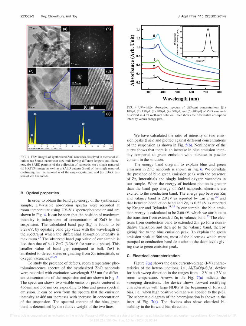
To make further structural investigations of sample
through the TEM analysis, the synthesized ZnO powder was
dissolved in methanol solution and collected on carbon
coated copper grid. Figure 3(a) shows the TEM image of
well organized ZnO nanorods with length varies in the range
50–100 nm and diameter varies in the range 7–15 nm. The
selected area electron diffraction (SAED) pattern for ZnO
nanorods is displayed in Fig. 3(b), which shows the crystal-
line nature of the synthesized powder. The HRTEM image
as shown in Fig. 3(c) reveals individual nanorods having
well resolved parallel lattice fringes. Fig. 3(d) shows the
magnified image of the selected nanorod with an inter plan-
ner spacing of 0.272 nm, consistent with the distance
between the (002) crystal planes. HR-TEM observation indi-
cates that the preferred growth direction of the nanorods are
parallel to the [001] crystallographic direction (c axis) as
indicated by an arrow in Fig. 3(d). The SAED patterns as
shown in the insets of Fig. 3(d) also suggest that the ZnO
nanorods are of single crystalline structure with hexagonal
wurtzite phase. Energy dispersive analysis of x-rays (EDAX)
of the synthesized sample confirms that the nanorods contain
zinc and oxygen only as shown in Fig. 3(e).FIG. 1. Fe-SEM image of ZnO nanorods synthesized by chemical method.
Inset shows the same image at higher magnification.
FIG. 2. XRD pattern of ZnO nanorods grown by chemical method. Inset
shows the Williamson-Hall plot for the XRD pattern.
223502-2 Roy, Chowdhury, and Roy J. Appl. Phys. 115, 223502 (2014)
[This article is copyrighted as indicated in the article. Reuse of AIP content is subject to the terms at: http://scitation.aip.org/termsconditions. Downloaded to ] IP:
14.139.217.138 On: Tue, 10 Jun 2014 08:03:14
B. Optical properties
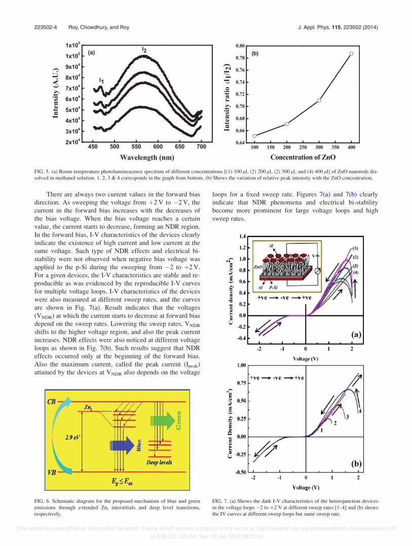
In order to obtain the band gap energy of the synthesized
sample, UV-visible absorption spectra were recorded at
room temperature using UV-Vis spectrophotometer and are
shown in Fig. 4. It can be seen that the position of maximum
intensity is independent of concentration of ZnO in the
suspension. The calculated band gap (Eg) is found to be
3.28 eV, by equating band gap value with the wavelength of
the spectra at which the differential absorption intensity is
maximum.27 The observed band gap value of our sample is
less than that of bulk ZnO (3.36 eV for wurtzite phase). This
smaller value of band gap compared to bulk ZnO is
attributed to defect states originating from Zn interstitials or
oxygen vacancies.28,29
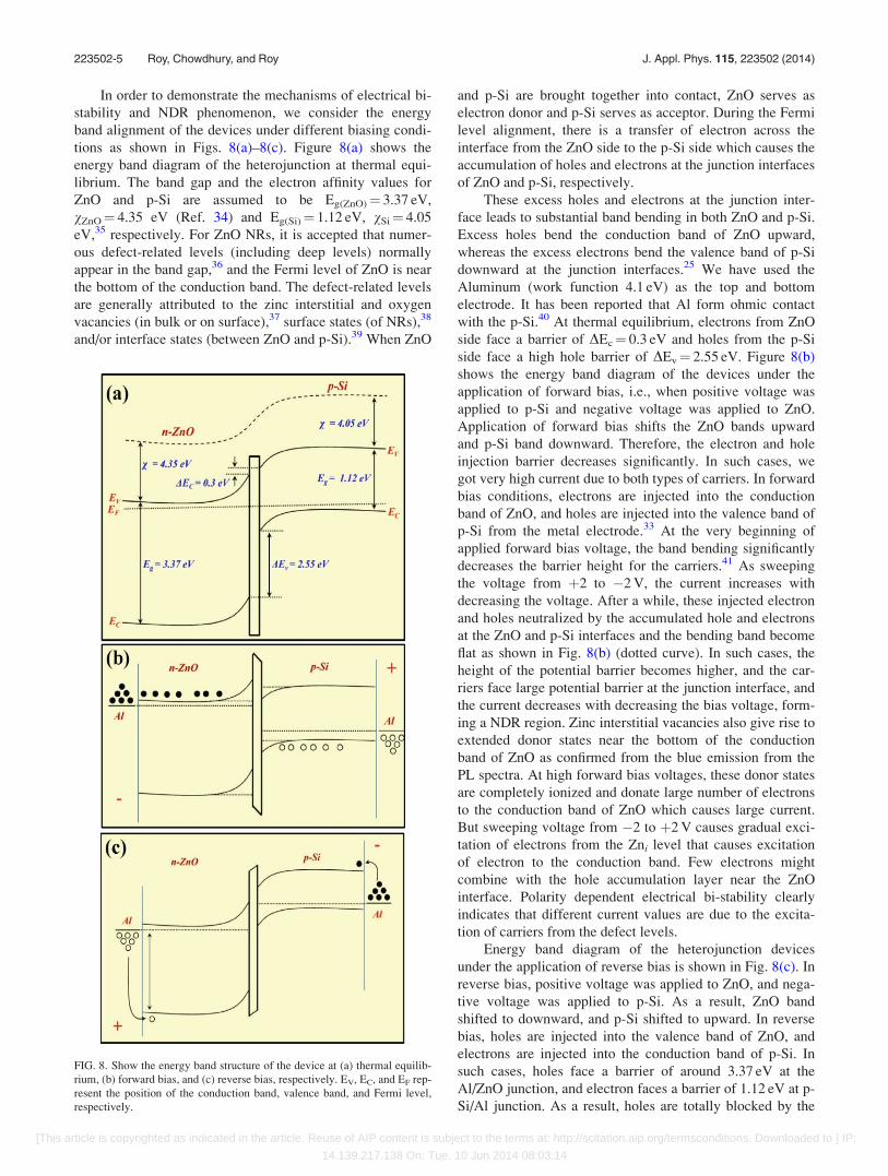
To study the presence of defects, room temperature pho-
toluminescence spectra of the synthesized ZnO nanorods
were recorded with excitation wavelength 325 nm for differ-
ent concentrations of the suspension and are shown in Fig. 5.
The spectrum shows two visible emission peaks centered at
466 nm and 566 nm corresponding to blue and green spectral
emission. It can be seen from the spectra that the emission
intensity at 466 nm increases with increase in concentration
of the suspension. The spectral content of the blue green
band is determined by the relative weight of the two lines.
We have calculated the ratio of intensity of two emis-
sion peaks (I1/I2) and plotted against different concentrations
of the suspension as shown in Fig. 5(b). Nonlinearity of the
curve shows that there is an increase in blue emission inten-
sity compared to green emission with increase in powder
content in the solution.
The energy band diagram to explain blue and green
emission in ZnO nanorods is shown in Fig. 6. We correlate
the presence of blue green emission peak with the presence
of Zni interstitials and singly ionized oxygen vacancies in
our sample. When the energy of incident photon is greater
than the band gap energy of ZnO nanorods, electrons are
excited to the conduction band. The energy gap between Zni
and valance band is 2.9 eV as reported by Lin et al.30 and
that between conduction band and Zni is 0.22 eV as reported
by Kroger and Bylander.31,32 In our sample, the blue emis-
sion energy is calculated to be 2.66 eV, which we attribute to
the transition from extended Zni to valance band.33 The elec-
trons from conduction band to extended Zni go for a nonra-
diative transition and then go to the valance band, thereby
giving rise to the blue emission peak. To explain the green
emission peak at 566 nm, most of the electrons which were
pumped to conduction band de-excite to the deep levels giv-
ing rise to green emission peak.
C. Electrical characterization
Figure 7(a) shows the dark current-voltage (I-V) charac-
teristics of the hetero-junctions, i.e., Al/ZnO/p-Si/Al device
for both sweep direction in the ranges from �2 V to þ2 V at
room temperature. Arrows in the Fig. 7(a) indicate the
sweeping directions. The device shows forward rectifying
characteristics with large NDRs at the beginning of forward
bias, i.e., when high positive voltage was applied to the p-Si.
The schematic diagram of the heterojunction is shown in the
inset of Fig. 7(a). The devices also show electrical bi-
stability in the forward bias direction.
FIG. 3. TEM images of synthesized ZnO nanorods dissolved in methanol so-
lution: (a) Shows nanometer size rods having different lengths and diame-
ters, (b) SAED patterns of the collection of nanorods; (c) a single nanorod;
(d) HRTEM image as well as a SAED pattern (inset) of the single nanorod,
confirming that the nanorod is of the single-crystalline; and (e) EDAX pat-
tern of ZnO nanorods.
FIG. 4. UV-visible absorption spectra of different concentrations [(1)
100 ll, (2) 150 ll, (3) 200 ll, (4) 300 ll, and (5) 400 ll] of ZnO nanorods
dissolved in 4 ml methanol solution. Inset shows the differential absorption
intensity versus energy plot.
223502-3 Roy, Chowdhury, and Roy J. Appl. Phys. 115, 223502 (2014)
[This article is copyrighted as indicated in the article. Reuse of AIP content is subject to the terms at: http://scitation.aip.org/termsconditions. Downloaded to ] IP:
14.139.217.138 On: Tue, 10 Jun 2014 08:03:14
There are always two current values in the forward bias
direction. As sweeping the voltage from þ2 V to �2 V, the
current in the forward bias increases with the decreases of
the bias voltage. When the bias voltage reaches a certain
value, the current starts to decrease, forming an NDR region.
In the forward bias, I-V characteristics of the devices clearly
indicate the existence of high current and low current at the
same voltage. Such type of NDR effects and electrical bi-
stability were not observed when negative bias voltage was
applied to the p-Si during the sweeping from �2 to þ2 V.
For a given devices, the I-V characteristics are stable and re-
producible as was evidenced by the reproducible I-V curves
for multiple voltage loops. I-V characteristics of the devices
were also measured at different sweep rates, and the curves
are shown in Fig. 7(a). Result indicates that the voltages
(VNDR) at which the current starts to decrease at forward bias
depend on the sweep rates. Lowering the sweep rates, VNDR
shifts to the higher voltage region, and also the peak current
increases. NDR effects were also noticed at different voltage
loops as shown in Fig. 7(b). Such results suggest that NDR
effects occurred only at the beginning of the forward bias.
Also the maximum current, called the peak current (Ipeak)
attained by the devices at VNDR also depends on the voltage
loops for a fixed sweep rate. Figures 7(a) and 7(b) clearly
indicate that NDR phenomena and electrical bi-stability
become more prominent for large voltage loops and high
sweep rates.
FIG. 5. (a) Room temperature photoluminescence spectrum of different concentrations [(1) 100 ll, (2) 200 ll, (2) 300 ll, and (4) 400 ll] of ZnO nanorods dis-
solved in methanol solution. 1, 2, 3 & 4 corresponds in the graph from bottom. (b) Shows the variation of relative peak intensity with the ZnO concentration.
FIG. 6. Schematic diagram for the proposed mechanism of blue and green
emissions through extended Zni interstitials and deep level transitions,
respectively.
FIG. 7. (a) Shows the dark I-V characteristics of the heterojunction devices
in the voltage loops �2 to þ2 V at different sweep rates [1–4] and (b) shows
the IV curves at different sweep loops but same sweep rate.
223502-4 Roy, Chowdhury, and Roy J. Appl. Phys. 115, 223502 (2014)
[This article is copyrighted as indicated in the article. Reuse of AIP content is subject to the terms at: http://scitation.aip.org/termsconditions. Downloaded to ] IP:
14.139.217.138 On: Tue, 10 Jun 2014 08:03:14
In order to demonstrate the mechanisms of electrical bi-
stability and NDR phenomenon, we consider the energy
band alignment of the devices under different biasing condi-
tions as shown in Figs. 8(a)–8(c). Figure 8(a) shows the
energy band diagram of the heterojunction at thermal equi-
librium. The band gap and the electron affinity values for
ZnO and p-Si are assumed to be Eg(ZnO)¼ 3.37 eV,
vZnO¼ 4.35 eV (Ref. 34) and Eg(Si)¼ 1.12 eV, vSi¼ 4.05
eV,35 respectively. For ZnO NRs, it is accepted that numer-
ous defect-related levels (including deep levels) normally
appear in the band gap,36 and the Fermi level of ZnO is near
the bottom of the conduction band. The defect-related levels
are generally attributed to the zinc interstitial and oxygen
vacancies (in bulk or on surface),37 surface states (of NRs),38
and/or interface states (between ZnO and p-Si).39 When ZnO
and p-Si are brought together into contact, ZnO serves as
electron donor and p-Si serves as acceptor. During the Fermi
level alignment, there is a transfer of electron across the
interface from the ZnO side to the p-Si side which causes the
accumulation of holes and electrons at the junction interfaces
of ZnO and p-Si, respectively.
These excess holes and electrons at the junction inter-
face leads to substantial band bending in both ZnO and p-Si.
Excess holes bend the conduction band of ZnO upward,
whereas the excess electrons bend the valence band of p-Si
downward at the junction interfaces.25 We have used the
Aluminum (work function 4.1 eV) as the top and bottom
electrode. It has been reported that Al form ohmic contact
with the p-Si.40 At thermal equilibrium, electrons from ZnO
side face a barrier of DEc¼ 0.3 eV and holes from the p-Si
side face a high hole barrier of DEv¼ 2.55 eV. Figure 8(b)
shows the energy band diagram of the devices under the
application of forward bias, i.e., when positive voltage was
applied to p-Si and negative voltage was applied to ZnO.
Application of forward bias shifts the ZnO bands upward
and p-Si band downward. Therefore, the electron and hole
injection barrier decreases significantly. In such cases, we
got very high current due to both types of carriers. In forward
bias conditions, electrons are injected into the conduction
band of ZnO, and holes are injected into the valence band of
p-Si from the metal electrode.33 At the very beginning of
applied forward bias voltage, the band bending significantly
decreases the barrier height for the carriers.41 As sweeping
the voltage from þ2 to �2 V, the current increases with
decreasing the voltage. After a while, these injected electron
and holes neutralized by the accumulated hole and electrons
at the ZnO and p-Si interfaces and the bending band become
flat as shown in Fig. 8(b) (dotted curve). In such cases, the
height of the potential barrier becomes higher, and the car-
riers face large potential barrier at the junction interface, and
the current decreases with decreasing the bias voltage, form-
ing a NDR region. Zinc interstitial vacancies also give rise to
extended donor states near the bottom of the conduction
band of ZnO as confirmed from the blue emission from the
PL spectra. At high forward bias voltages, these donor states
are completely ionized and donate large number of electrons
to the conduction band of ZnO which causes large current.
But sweeping voltage from �2 to þ2 V causes gradual exci-
tation of electrons from the Zni level that causes excitation
of electron to the conduction band. Few electrons might
combine with the hole accumulation layer near the ZnO
interface. Polarity dependent electrical bi-stability clearly
indicates that different current values are due to the excita-
tion of carriers from the defect levels.
Energy band diagram of the heterojunction devices
under the application of reverse bias is shown in Fig. 8(c). In
reverse bias, positive voltage was applied to ZnO, and nega-
tive voltage was applied to p-Si. As a result, ZnO band
shifted to downward, and p-Si shifted to upward. In reverse
bias, holes are injected into the valence band of ZnO, and
electrons are injected into the conduction band of p-Si. In
such cases, holes face a barrier of around 3.37 eV at the
Al/ZnO junction, and electron faces a barrier of 1.12 eV at p-
Si/Al junction. As a result, holes are totally blocked by the
FIG. 8. Show the energy band structure of the device at (a) thermal equilib-
rium, (b) forward bias, and (c) reverse bias, respectively. EV, EC, and EF rep-
resent the position of the conduction band, valence band, and Fermi level,
respectively.
223502-5 Roy, Chowdhury, and Roy J. Appl. Phys. 115, 223502 (2014)
[This article is copyrighted as indicated in the article. Reuse of AIP content is subject to the terms at: http://scitation.aip.org/termsconditions. Downloaded to ] IP:
14.139.217.138 On: Tue, 10 Jun 2014 08:03:14
Al/ZnO junction, but we got current due to electrons as the
electron barrier is around 1.12 eV. The bias polarity depend-
ence demonstrates that the NDR characteristics in our devi-
ces might be due to the interface effects,41,42 directly related
to the interfacial traps,43 leading to the formation of space
charge due to trapping
IV. CONCLUSIONS
In conclusion, large area distributed ZnO nanorods have
been prepared by using simple chemical method, and ZnO/p-
Si heterostructures have also been fabricated. NDR and elec-
trical bi-stability has been observed in ZnO nanorods/p-Si
heterostructures at room temperature. The origin of electrical
bi-stability is attributed to the electric field induced charge
transfer across the junction, and the NDR phenomena could
be ascribed to interfacial traps and defect level that arises
due to oxygen and zinc interstitial vacancies. Room tempera-
ture PL spectra of synthesized nanorods exhibit blue and
broad green emission at about 466 and 566 nm, respectively.
Possible origin of emission peaks has been explained with
help of energy band diagram invoking Zn interstitials and
deep oxygen vacancies level.
1L. P. Ma, J. Liu, and Y. Yang, Appl. Phys. Lett. 80, 2997 (2002).2J. Chen, W. Wang, M. A. Reed, A. M. Rawlett, D. W. Price, and J. M.
Tour, Appl. Phys. Lett. 77, 1224 (2000).3D. I. Son, C. H. You, W. T. Kim, J. H. Jung, and T. W. Kim, Appl. Phys.
Lett. 94, 132103 (2009).4D. Ito, T. Tomita, and T. Hatazawa, Appl. Phys. Lett. 90, 143118 (2007).5H.-K. Lee and M. H.-C. Jin, Appl. Phys. Lett. 97, 013306 (2010).6C. W. Chu, J. Ouyang, J.-H. Tseng, and Y. Yang, Adv. Mater. 17, 1440
(2005).7Y. Yang, J. Ouyang, L. Ma, R. J. Tseng, and C.-W. Chu, Adv. Funct.
Mater. 16, 1001 (2006).8A. Ramesh, P. R. Berger, and R. Loo, Appl. Phys. Lett. 100, 092104
(2012).9J. S. Jung, E. H. Cho, S. Jo, K. H. Kim, D. H. Choi, and J. Joo, Org.
Electron. 14, 2204 (2013).10S. Das, R. K. Singha, A. Dhar, S. K. Ray, A. Anopchenko, N. Daldosso,
and L. Pavesi, J. Appl. Phys. 110, 024310 (2011).11V. Srikant and D. R. Clarke, J. App. Phys. 83, 5447 (1998).12M. H. Huang, S. Mao, H. Feick, H. Yan, Y. Wu, H. Kind, E. Weber, R.
Russo, and P. Yang, Science 292, 1897 (2001).13M. R. Singh, J. Appl. Phys. 106, 063106 (2009).14X. Wang, C. J. Summers, and Z. L. Wang, Nano Lett. 4, 423 (2004).
15S. Tian, F. Yang, D. Zeng, and C. J. Xie, J. Phys. Chem. C 116, 10586
(2012).16S. Y. Cho, Y. H. Kang, J.-Y. Jung, S. Y. Nam, J. Lim, S. C. Yoon, D. H.
Choi, and C. Lee, Chem. Mater. 24, 3517 (2012).17Y. Wang, X. Li, G. Lu, X. Quan, and G. Chen, J. Phys. Chem. C 112,
7332 (2008).18H.-M. Cheng, W.-H. Chiu, C.-H. Lee, S.-T. Tsai, and W.-F. Hsieh,
J. Phys. Chem. C 112, 16359 (2008).19D. C. Olson, S. E. Shaheen, R. T. Collins, and D. S. Ginley, J. Phys.
Chem. C 111, 16670 (2007).20A. van Dijken, E. A. Meulenkamp, D. Vanmaekelbergh, and A. Meijerink,
J. Lumin. 87–89, 454, (2000).21I. Shalish, H. Temkin, and V. Narayananmurti, Phys. Rev. B 69, 245401
(2004).22M. Ghosh, S. C. Gadkari, and S. K. Gupta, J. Appl. Phys. 112, 024314
(2012).23W. Guo, Y. Yang, J. Qi, and Y. Zhang, Appl. Phys. Lett. 97, 263118
(2010).24Z.-L. Tseng, P.-C. Kao, M.-F. Shih, H.-H. Huang, J.-Y. Wang, and S.-Y.
Chu, Appl. Phys. Lett. 97, 212103 (2010).25Y. Yang, J. Qi, W. Guo, Z. Qin, and Y. Zhang, Appl. Phys. Lett. 96,
093107 (2010).26S. Mandal, K. Sambasivarao, A. Dhar, and S. K. Ray, J. Appl. Phys. 106,
024103 (2009).27N. Roy and A. Roy, J. Mater. Sci.: Mater. Electron. 25, 1275 (2014).28R. M. Sheetz, I. Ponomareva, E. Richter, A. N. Andriotis, and M. Menon,
Phys. Rev. B 80, 195314 (2009).29S. A. Ansari, M. M. Khan, S. Kalathil, A. Nisar, J. Lee, and M. H. Cho,
Nanoscale 5, 9238 (2013).30B. Lin, Z. Fu, and Y. Jia, Appl. Phys. Lett. 79, 943 (2001).31F. A. Kr€oger, The Chemistry of Imperfect Crystals, 2nd ed. (North-
Holland, Amsterdam, 1974), Vol. 1.32E. G. Bylander, J. Appl. Phys. 49, 1188 (1978).33H. Zeng, G. Duan, Y. Li, S. Yang, X. Xu, and W. Cai, Adv. Funct. Mater.
20, 561 (2010).34M. Dutta and D. Basak, Appl. Phys. Lett. 92, 212112 (2008).35S. M. Sze, Physics of Semiconductor Devices, 2nd ed. (John Willy and
Sons, USA, 1981).36A. B. Djurisic and Y. H. Leung, Small 2, 944 (2006).37B. J. Jin, S. H. Bae, S. Y. Lee, and S. Imc, Mater. Sci. Eng., B 71, 301
(2000).38A. Layek, B. Manna, and A. Chowdhury, Chem. Phys. Lett. 539, 133
(2012).39F. Yakuphanoglu, Y. Caglar, M. Caglarb, and S. Ilican, Mater. Sci.
Semicond. Process. 13, 137 (2010).40Y. S. Ocak, J. Alloys Compd. 513, 130 (2012).41A. Chowdhury, B. Biswas, and B. Mallik, J. Nanosci. Nanotechnol. 13,
4134 (2013).42P. H. Nguyen, S. Scheinert, S. Berleb, W. Br€utting, and G. Paasch, Org.
Electron. 2, 105 (2001).43A. Sawa, T. Fujii, M. Kawasaki, and Y. Tokura, Appl. Phys. Lett. 85,
4073 (2004).
223502-6 Roy, Chowdhury, and Roy J. Appl. Phys. 115, 223502 (2014)
[This article is copyrighted as indicated in the article. Reuse of AIP content is subject to the terms at: http://scitation.aip.org/termsconditions. Downloaded to ] IP:
14.139.217.138 On: Tue, 10 Jun 2014 08:03:14
Copyright © 2022 FDOKUMEN