NT1065 "Nomada" 4-Channel GPS/GLONASS/Galileo/BeiDou ...
45
NT1065 "Nomada" Ver. 2.04 October 2016 www.ntlab.com 4-Channel GPS/GLONASS/Galileo/BeiDou/IRNSS/QZSS L1/L2/L3/L5 band RF Front End 1. OVERVIEW NT1065 "Nomada" is a four-channel RF front end for a simultaneous reception of GPS, GLONASS, Galileo, BeiDou, IRNSS, QZSS Global Navigation Satellite System (GNSS) and also satellite-based augmentation system (SBAS) including onmiSTAR signals of various frequency bands L1, L2, L3, L5, E1, E5a, E5b, E6, B1, B2, B3. Galileo E5 band as well as BeiDou B1, B2, B3 (phase 3) band can be obtained as entire signal with two channels fed by the same LO and then restored in digital domain to true complex data. As a benefit one can discover wide possibilities of improving the positioning accuracy down to centimeter range without taking RTK technique. Each setting, including output signal frequency bandwidth, AGC options, mirror channel suppression option, etc., can be set for every channel individually. NT1065 includes two fully independent frequency synthesizers. Channel#1 and channel#2 are supplied with LO signal generated in PLL “A” while PLL “B” is assigned for channels #3 and #4. For specific applications there is an option to feed all four channels with single LO source from PLL “A”. This powerful toolkit is accompanied with very simple and easy-to-use register map. All the functionality allows application of NT1065 "Nomada" in high precision GNSS based positioning, goniometric, driverless car systems and related branches. 2. FEATURES − Single conversion super heterodyne receiver − Four independent configurable channels, each includes preamplifier, image rejection mixer, IF filter, IFA, 2-bit ADC − Signal bandwidth up to 31MHz supports GNSS high precision codes such as P-code in GPS or wideband E5 Galileo − Dual adoptable AGC system (RF + IF) or programmable gain − High dynamic range with 1dB compression point more than -30dBm − Analog differential output with two options of voltage swing 0.2/0.47Vp-p and 0.4/0.98Vp-p (sine wave/noise) or 2-bit ADC digital output data − Two independent fully integrated synthesizers with flexible LO and CLK frequencies selection (“A” and “B”) − Embedded temperature sensor − SPI interface with easy-to-use register map − Individual status indicators of main subsystems (available in SPI registers) and cumulative status indicator (AOK, available both as a separate pin and in SPI registers) − 10x10mm QFN88 package 3. APPLICATIONS − GNSS based positioning systems − GNSS based goniometric systems − In-vehicle navigation systems − GNSS based driverless car systems − Professional drones
-
Upload
khangminh22 -
Category
Documents
-
view
1 -
download
0
Transcript of NT1065 "Nomada" 4-Channel GPS/GLONASS/Galileo/BeiDou ...

NT1065 Nomada
Ver 204 October 2016 wwwntlabcom
4-Channel GPSGLONASSGalileoBeiDouIRNSSQZSS L1L2L3L5 band RF Front End
1 OVERVIEW NT1065 Nomada is a four-channel RF front end for a simultaneous reception of GPS GLONASS Galileo BeiDou IRNSS QZSS Global Navigation Satellite System (GNSS) and also satellite-based augmentation system (SBAS) including onmiSTAR signals of various frequency bands L1 L2 L3 L5 E1 E5a E5b E6 B1 B2 B3 Galileo E5 band as well as BeiDou B1 B2 B3 (phase 3) band can be obtained as entire signal with two channels fed by the same LO and then restored in digital domain to true complex data As a benefit one can discover wide possibilities of improving the positioning accuracy down to centimeter range without taking RTK technique Each setting including output signal frequency bandwidth AGC options mirror channel suppression option etc can be set for every channel individually NT1065 includes two fully independent frequency synthesizers Channel1 and channel2 are supplied with LO signal generated in PLL ldquoArdquo while PLL ldquoBrdquo is assigned for channels 3 and 4 For specific applications there is an option to feed all four channels with single LO source from PLL ldquoArdquo This powerful toolkit is accompanied with very simple and easy-to-use register map All the functionality allows application of NT1065 Nomada in high precision GNSS based positioning goniometric driverless car systems and related branches
2 FEATURES minus Single conversion super heterodyne receiver minus Four independent configurable channels each includes preamplifier image rejection
mixer IF filter IFA 2-bit ADC minus Signal bandwidth up to 31MHz supports GNSS high precision codes such as P-code in
GPS or wideband E5 Galileo minus Dual adoptable AGC system (RF + IF) or programmable gain minus High dynamic range with 1dB compression point more than -30dBm minus Analog differential output with two options of voltage swing 02047Vp-p and
04098Vp-p (sine wavenoise) or 2-bit ADC digital output data minus Two independent fully integrated synthesizers with flexible LO and CLK frequencies
selection (ldquoArdquo and ldquoBrdquo) minus Embedded temperature sensor minus SPI interface with easy-to-use register map minus Individual status indicators of main subsystems (available in SPI registers) and
cumulative status indicator (AOK available both as a separate pin and in SPI registers) minus 10x10mm QFN88 package
3 APPLICATIONS minus GNSS based positioning systems minus GNSS based goniometric systems minus In-vehicle navigation systems minus GNSS based driverless car systems minus Professional drones
NT1065 Nomada 4-Channel GPSGLONASSGalileoBeiDouIRNSSQZSS
L1L2L3L5 band RF Front End
Ver 204 page 2 of 45 wwwntlabcom
4 DESCRIPTION 41 STRUCTURE
Figure 41 NT1065 Nomada Block diagram
NT1065 Nomada 4-Channel GPSGLONASSGalileoBeiDouIRNSSQZSS
L1L2L3L5 band RF Front End
Ver 204 page 3 of 45 wwwntlabcom
42 PINS DESCRIPTION
Figure 42 Pin configuration
Table 41 NT1065 Nomada pin description Name Description
1 GND Ground 2 GND Ground 3 RF2_GND 2nd channel RF ground 4 RF2_GND 2nd channel RF ground 5 RF2_IN 2nd channel RF input (DC coupled) 6 RF2_GND 2nd channel RF ground 7 RF2_VCC 2nd channel ldquoRF2rdquo LDO output voltage 27V 8 MIX2_VCC 2nd channel ldquoMIX2rdquo LDO output voltage 27V 9 RS_GND Voltage and current reference source ground 10 PLLA_GND PLL ldquoArdquo ground 11 PLLA_VCC PLL ldquoArdquo LDO output voltage 27V 12 PLLB_VCC PLL ldquoBrdquo LDO output voltage 27V 13 PLLB_GND PLL ldquoBrdquo ground 14 REF_CUR External high-precision resistor connection 15 MIX3_VCC 3rd channel ldquoMIX4rdquo LDO output voltage 27V 16 RF3_VCC 3rd channel ldquoRF3rdquo LDO output voltage 27V 17 RF3_GND 3rd channel RF ground 18 RF3_IN 3rd channel RF input (DC coupled) 19 RF3_GND 3rd channel RF ground 20 RF3_GND 3rd channel RF ground 21 GND Ground 22 GND Ground 23 GND Ground 24 GND Ground 25 RF4_GND 4th channel RF ground 26 RF4_GND 4th channel RF ground 27 RF4_IN 4th channel RF input (DC coupled) 28 RF4_GND 4th channel RF ground
NT1065 Nomada 4-Channel GPSGLONASSGalileoBeiDouIRNSSQZSS
L1L2L3L5 band RF Front End
Ver 204 page 4 of 45 wwwntlabcom
Name Description 29 RF4_VCC 4th channel ldquoRF4rdquo LDO output voltage 27V 30 MIX4_VCC 4th channel ldquoMIX4rdquo LDO output voltage 27V 31 RF4_GND 4th channel RF ground 32 TEST Test output should be opened 33 RO_GND Reference oscillator ground 34 REF_IN Reference frequency (TCXO) input 35 RO_VCC ldquoROrdquo LDO output voltage 27V 36 3V_VCC Supply voltage 3V 37 IFA4_GND 4th channel IFA ground 38 IFA4_VCC 4th channel ldquoIFA4rdquo LDO output voltage 27V 39 IFB4_GND 4th channel IF buffer amp ADC ground
40 IF4_OUTpMAGN 4th channel analog output ndash true 2-bit ADC digital output data ndash MAGN
41 IF4_OUTnSIGN 4th channel analog output ndash complement 2-bit ADC digital output data ndash SIGN
42 IFB4_VCC 4th channel ldquoIFB4rdquo LDO output supply 27V 43 IFB4_GND 4th channel IF buffer amp ADC ground 44 GND Ground 45 GND Ground 46 IFB3_GND 3rd channel IF buffer amp ADC ground 47 IFB3_VCC 3rd channel ldquoIFB3rdquo LDO output supply 27V
48 IF3_OUTnSIGN 3rd channel analog output ndash complement 2-bit ADC digital output data ndash SIGN
49 IF3_OUTpMAGN 3rd channel analog output ndash true 2-bit ADC digital output data ndash MAGN
50 IFB3_GND 3rd channel IF buffer amp ADC ground 51 IFA3_VCC 3rd channel ldquoIFA3rdquo LDO output voltage 27V 52 IFA3_GND 3rd channel IFA ground 53 CLK_GND CLK management unit ground 54 CLK_VCC ldquoCLKrdquo LDO output voltage 17VVCC (Reg12ltD4-D0gt dependent) 55 CLK_OUT1 Clock frequency analog output ndash true CMOS output 56 CLK_OUT2 Clock frequency analog output ndash complement 57 CLK_GND CLK management unit ground 58 CLK_GND CLK management unit ground 59 IFA2_GND 2nd channel IFA ground 60 IFA2_VCC 2nd channel ldquoIFA2rdquo LDO output voltage 27V 61 IFB2_GND 2nd channel IF buffer amp ADC ground
62 IF2_OUTpMAGN 2nd channel analog output ndash true 2-bit ADC digital output data ndash MAGN
63 IF2_OUTnSIGN 2nd channel analog output ndash complement 2-bit ADC digital output data ndash SIGN
64 IFB2_VCC 2nd channel ldquoIFB2rdquo LDO output voltage 27V 65 IFB2_GND 2rd channel IF buffer amp ADC ground 66 GND Ground 67 GND Ground 68 IFB1_GND 1st channel IF buffer amp ADC ground 69 IFB1_VCC 1st channel ldquoIFB1rdquo LDO output voltage 27V
70 IF1_OUTnSIGN 1st channel analog output ndash complement 2-bit ADC digital output data ndash SIGN
NT1065 Nomada 4-Channel GPSGLONASSGalileoBeiDouIRNSSQZSS
L1L2L3L5 band RF Front End
Ver 204 page 5 of 45 wwwntlabcom
Name Description
71 IF1_OUTpMAGN 1st channel analog output ndash true 2-bit ADC digital output data ndash MAGN
72 IFB1_GND 1st channel IF buffer amp ADC ground 73 IFA1_VCC 1st channel ldquoIFA1rdquo LDO output voltage 27V 74 IFA1_GND 1st channel IFA ground 75 CSN SPI chip select (active low) 76 SCLK SPI clock input 77 MOSI SPI data input 78 MISO SPI data output
79 AOK Cumulative status indicator
ldquo1rdquo valid ldquo0rdquo fail
80 RF1_GND 1st channel RF ground 81 MIX1_VCC 1st channel ldquoMIX1rdquo LDO output voltage 27V 82 RF1_VCC 1st channel ldquoRF1rdquo LDO output voltage 27V 83 RF1_GND 1st channel RF ground 84 RF1_IN 1st channel RF input (DC coupled) 85 RF1_GND 1st channel RF ground 86 RF1_GND 1st channel RF ground 87 GND Ground 88 GND Ground
NT1065 Nomada 4-Channel GPSGLONASSGalileoBeiDouIRNSSQZSS
L1L2L3L5 band RF Front End
Ver 204 page 6 of 45 wwwntlabcom
43 APPLICATION SCHEMATIC
Figure 43 NT1065 Nomada Application schematic
Table 42 External component description Component Nominal value Tolerance Notes
С1 15pF plusmn5 Matching network capacitor for L1 band -- pF - Matching network capacitor for L2L3L5 band
С2 1microF plusmn20 Supply voltage filter capacitor С3 1microF plusmn20 Supply voltage filter capacitor С4 1microF plusmn20 Supply voltage filter capacitor С5 1microF plusmn20 Supply voltage filter capacitor С6 1microF plusmn20 Supply voltage filter capacitor С7 1microF plusmn20 Supply voltage filter capacitor
С8 15pF plusmn5 Matching network capacitor for L1 band -- pF - Matching network capacitor for L2L3L5 band
С9 15pF plusmn5 Matching network capacitor for L1 band -- pF - Matching network capacitor for L2L3L5 band
C10 1microF plusmn20 Supply voltage filter capacitor
NT1065 Nomada 4-Channel GPSGLONASSGalileoBeiDouIRNSSQZSS
L1L2L3L5 band RF Front End
Ver 204 page 7 of 45 wwwntlabcom
Component Nominal value Tolerance Notes С11 1microF plusmn20 Supply voltage filter capacitor С12 33pF plusmn20 Blocking capacitor С13 1microF plusmn20 Supply voltage filter capacitor C14 10nF plusmn20 Supply voltage filter capacitor С15 10microF plusmn20 Supply voltage filter capacitor С16 1microF plusmn20 Supply voltage filter capacitor С17 1microF plusmn20 Supply voltage filter capacitor С18 1microF plusmn20 Supply voltage filter capacitor С19 1microF plusmn20 Supply voltage filter capacitor С20 1microF plusmn20 Supply voltage filter capacitor С21 1microF plusmn20 Supply voltage filter capacitor C22 1microF plusmn20 Supply voltage filter capacitor C23 1microF plusmn20 Supply voltage filter capacitor C24 1microF plusmn20 Supply voltage filter capacitor C25 1microF plusmn20 Supply voltage filter capacitor C26 1microF plusmn20 Supply voltage filter capacitor
C27 15pF plusmn5 Matching network capacitor for L1 band -- pF - Matching network capacitor for L2L3L5 band
L1 82nH (Qge40) plusmn2 Matching network inductor for L1 band 10nH (Qge40) Matching network inductor for L2L3L5 band
L2 82nH (Qge40) plusmn2 Matching network inductor for L1 band 10nH (Qge40) Matching network inductor for L2L3L5 band
L3 82nH (Qge40) plusmn2 Matching network inductor for L1 band 10nH (Qge40) Matching network inductor for L2L3L5 band
L4 120Ω 100MHz plusmn20 Supply voltage filter inductor
L5 82nH (Qge40) plusmn2 Matching network inductor for L1 band 10nH (Qge40) Matching network inductor for L2L3L5 band
R1 619kΩ plusmn1 High precision resistor
R2 200Ω plusmn5 Load resistor if analog differential output --Ω - DNP if 2-bit ADC output
R3 200Ω plusmn5 Load resistor if analog differential output --Ω - DNP if 2-bit ADC output
R4 200Ω plusmn5 Load resistor if analog differential output --Ω - DNP if 2-bit ADC output
R5 200Ω plusmn5 Load resistor if analog differential output --Ω - DNP if 2-bit ADC output
Note ndash defined depending on PCB construction and purpose
NT1065 Nomada 4-Channel GPSGLONASSGalileoBeiDouIRNSSQZSS
L1L2L3L5 band RF Front End
Ver 204 page 8 of 45 wwwntlabcom
44 SERIAL INTERFACE DESCRIPTION NT1065 Nomada can be configured with standard 4-wire SPI In addition special pin AOK (cumulative status indicator) for unexpected system failure tracking is available User register map is split up into five parts according to functionality
minus System Info minus General settings and status minus CLK settings minus Channel settings and status (separate for each channel) minus PLL settings and status (separate for each PLL)
Available settings and statuses are listed subsection 446
GENERAL DESCRIPTION 441
Serial interface is used to read and change NT1065 Nomada data register information It is intended for status monitoring mode configuration and parameter adjustment Serial interface requires 4-wires for communication CSN ndash serial interface enable signal input MISO ndash serial interface output data MOSI ndash serial interface input data SCLK ndash data clock signal transmitted through MISO and MOSI outputs
Figure 44 Serial interface structure Standard information packet (command) consists of two bytes The first byte is commandaddress second ndash data byte Data format is always a bit sequence from first MSB to last LSB All data transfers are framed by CSN signal which must be low for any data transfer In idle state when CSN is high SCLK MOSI and MISO pins are blocked and donrsquot respond to external signals At the beginning of any data transfer (falling CSN edge) SCLK must be low
NT1065 Nomada 4-Channel GPSGLONASSGalileoBeiDouIRNSSQZSS
L1L2L3L5 band RF Front End
Ver 204 page 9 of 45 wwwntlabcom
WRITING TO REGISTER 442
Figure 45 Individual register writing Single write reading is shown in Figure 45 Communication is initialized by setting Chip Select (CSN) pin low Bytes are transmitted MSB first Data are clocked into the NT1065 through the MOSI pin on the rising edges of SCLK The first bit of a commandaddress byte is a readwrite attribute read operation is defined by logic 1 and write operation is defined by logic 0 Bits A6hellipA0 represent the address of the register to be read or written Second byte (D7hellipD0 bits) is data written to the given address register After the 16th rising SCLK edge and turn-off CSN hold time CSN goes high disabling the interface
READING FROM REGISTER 443
Figure 46 Single register reading
Single register reading is similar to writing First byte is command byte Read attribute is logic 1 and A6-A0 bits specify address of register to be read Data are clocked out the NT1065 through the MISO pin on the falling edges of SCLK Output data should be clocked on rising SCLK edges of external SPI master Bytes are transmitted MSB first After sending data byte CSN goes high disabling the interface
BURST DATA TRANSFER 444
The NT1065 Nomada has a SPI burst-mode data transfer Unlike single data transfer CSN is continue to be ldquolowrdquo after LSB of data byte Next bit after LSB is a writeread attribute CSN goes high to stop burst data transfer Direction of data transfer can be changed an infinite number of times during burst data transfer See examples below please
NT1065 Nomada 4-Channel GPSGLONASSGalileoBeiDouIRNSSQZSS
L1L2L3L5 band RF Front End
Ver 204 page 10 of 45 wwwntlabcom
Figure 47 Burst data writing
Figure 48 Burst data reading
Figure 49 Burst data writing and reading
NT1065 Nomada 4-Channel GPSGLONASSGalileoBeiDouIRNSSQZSS
L1L2L3L5 band RF Front End
Ver 204 page 11 of 45 wwwntlabcom
TIMING DIAGRAM 445
Figure 410 SPI timing diagram
Table 43 SPI timing
Parameter description Symbol Condition Value Unit min typ max SCLK frequency fclk - - - 40 MHz SCLK high and low time
tch 1fclk = (tch+tcl) 8 - 12 ns tcl Duty cycle D - 40 - 60 CSN setup time before SCLK ts_csn - 8 - - ns
CSN hold time th_csn - 4 - - ns Data set up time tsud - 10 - - ns Data hold time thd - 3 - - ns Switch from Z-state time tswfrZ Load 20 pF - - 10 ns
Output data hold time thdout Load 20 pF 28 - - ns Output data valid time tvdout Load 20 pF - - 10 ns Switch to Z-state time tsw2z Load 20 pF 3 - 8 ns
NT1065 Nomada 4-Channel GPSGLONASSGalileoBeiDouIRNSSQZSS
L1L2L3L5 band RF Front End
Ver 204 page 12 of 45 wwwntlabcom
PROGRAMMABLE REGISTERS 446
4461 SYSTEM INFO minus ID number release
Bit number Name Description Default
Reg0 0x00 D7-D0 IDlt125gt Technical information Chip number (0010000101001)dec = 1065 00100001 Reg1 0x01 D7-D3 IDlt40gt Continue Refer to Reg0ltD7-D0gt 01001 D2-D0 Releaselt20gt Technical information Chip version (010)dec =2 010
4462 GENERAL SETTINGS AND STATUS minus Mode (standby synthesizer only active) minus TCXO frequency setting (10MHz 2484MHz) If other frequency is used please contact
to NTLab for a solution minus LO source (PLL ldquoArdquo for channels1amp2 + PLL ldquoBrdquo for channels3amp4 PLL ldquoArdquo for all
channels) minus LPF auto-calibration system execute and status minus Channel to be monitored for status (ch1 ch2 ch3 ch4) minus Temperature measurement mode (single continuous) minus Temperature measurement system execute minus AOK indicator configuration minus General Status (AOK temperature) minus Selected channel status (RF AGC indicator RF Gain IF Gain)
Bit number Name Description Default
Reg2 0x02 D7-D2 Unused Unused 000000
D1-D0 Modelt10gt
IC mode
11
00 standby 01 PLL A only 10 PLL A only 11 active As register bits are writable in any mode exclude any configuration change in standby mode to return in last configured active mode
Reg3 0x03 D7-D2 Unused Unused 000000
D1 TCXO_sel
TCXO frequency setting If other frequency is used please contact to NTLab for a solution 0 0 100 MHz 1 2484 MHz
D0 LO_Source
LO source
1 0 PLL A for all channels
1 PLL A for channels1amp2 PLL B for channels3amp4
Reg4 0x04 D7-D2 Unused Unused 000000
D1 LPF_ACS_S LPF auto-calibration system status
- 0 error 1 completed successfully
NT1065 Nomada 4-Channel GPSGLONASSGalileoBeiDouIRNSSQZSS
L1L2L3L5 band RF Front End
Ver 204 page 13 of 45 wwwntlabcom
Bit number Name Description Default
D0 LPF_EXE
LPF auto-calibration system execute (duration is about 15 ms and it automatically resets to 0 when finished) 1 0 finished 1 start
Reg5 0x05 D7-D6 Unused Unused 00
D5-D4 Ch_StNumSellt10gt
Channel to be monitored for status
00 00 channel1 01 channel2 10 channel3 11 channel4
D3-D2 Unused Unused 00
D1 TS_MD Temperature measurement mode
0 0 single 1 continuous
D0 TS_EXE
Temperature measurement system execute (duration is up to 17 ms and it automatically resets to 0 when finished) 0 0 finished 1 start
Reg6 0x06 D7-D5 Unused Unused 000
D4 LPF_ACS_AOK LPF auto-calibration system status as AOKs component
1 0 forbidden 1 permitted
D3 PLL_LI_AOK PLL A amp B (if enabled) lock indicator as AOKs components
1 0 forbidden 1 permitted
D2 PLL_VCO_AOK
PLL A amp B (if enabled) VCO input voltage comparator status as AOKs component 1 0 forbidden 1 permitted
D1 RF_AGC_AOK RF AGC indicators (all enabled channels) as AOKs components
0 0 forbidden 1 permitted
D0 StdBy_AOK
IC standby mode as AOKs component (forces AOK to 0 in standby mode) 1 0 forbidden 1 permitted
Reg7 0x07 D7-D5 Unused Unused 000
D4 AOK Cumulative status indicator
- 0 fail 1 valid
D3-D2 Unused Unused 00
D1-D0 TS_codelt98gt
Temperature sensor indicator
-
0000000000 not valid range hellip 0110010100 not valid range 0110010101 +125 degC
hellip deccodeTSTemp )09_(72202417 gtltlowastminus=
1001111001 -40 degC 1001111010 not valid range hellip 1111111111 not valid range
Reg8 0x08
NT1065 Nomada 4-Channel GPSGLONASSGalileoBeiDouIRNSSQZSS
L1L2L3L5 band RF Front End
Ver 204 page 14 of 45 wwwntlabcom
Bit number Name Description Default
D7-D0 TS_codelt70gt Continue Refer to Reg7ltD1-D0gt - Reg9 0x09 D7-D6 Unused Unused 00
D5-D4
RF_AGC_Down RF AGC indicator (refer to Reg5ltD5-D4gt for channel selection)
- 00 input signal power is within regulating range
RF_AGC_Up 01 input signal power is lower than threshold 10 input signal power is higher than regulating range 11 impossible state or RF AGC system is damaged
D3-D0 RF_GainStlt30gt
RF gain value (refer to Reg5ltD5-D4gt for channel selection)
- 0000 11 dB hellip with step of 095 dB 1111 255 dB
Reg10 0x0A D7-D5 Unused Unused 000
D4-D0 IFA_GainStlt40gt
IFA gain value at T = +25 degC (refer to Reg5ltD5-D4gt for channel selection)
-
00000 -05 dB hellip hellip 00011 105 dB hellip hellip 00111 227 dB hellip hellip 01010 315 dB hellip hellip 01110 410 dB hellip hellip 10001 507 dB hellip hellip 10101 610 dB hellip hellip 10111 630 dB 11000 not valid range hellip not valid range 11111 not valid range
4463 CLK SETTINGS minus CLK C divider ratio (8 9 hellip 31) minus CLK frequency source (PLL ldquoArdquo PLL ldquoBrdquo) minus CLK type (LVDS CMOS) minus CLK amplitude (230mV 340mV 460mV 570mV if ldquoLVDSrdquo type 18V 24V 27V
VCC if ldquoCMOSrdquo type) minus CLK output DC level if ldquoLVDSrdquo type (155V 21V 24V 27V)
Bit number Name Description Default
Reg11 0x0B D7-D5 Unused Unused 000
D4-D0 CDIV_Rlt40gt
CLK C divider ratio
01111 01000 8 hellip with step of 1 11111 31
Reg12 0x0C D7-D6 Unused Unused 00
NT1065 Nomada 4-Channel GPSGLONASSGalileoBeiDouIRNSSQZSS
L1L2L3L5 band RF Front End
Ver 204 page 15 of 45 wwwntlabcom
Bit number Name Description Default
D5 CLK_Source CLK frequency source
0 0 from PLL A 1 from PLL B
D4 CLK_TP CLK type
1 0 CMOS 1 LVDS
D3-D2 CLK_CClt10gt
CLK amplitude with Rload without Rload if LVDS type (Vpp)
10 00 023 046V 01 034 069 V 10 045 092 V 11 056 113 V
D1-D0 CLK_OLlt10gt
CLK amplitude if CMOS type (refer to Reg12ltD4gt)
CLK output DC level if LVDS type (refer to Reg12ltD4gt)
00 00 18 V 00 (18 ndash 055Vpp) V 01 24 V 01 (24 ndash 055Vpp) V 10 27 V 10 (27 ndash 055Vpp) V 11 external (VCC) 11 (VCC - 055Vpp) V
4464 CHANNEL SETTINGS minus Channel enable minus Channel GNSS (LSB or USB) minus IF pass band (7bits 150MHz ndash 310MHz) minus Output data interface (analog differential output 2-bit ADC output) minus IFA output DC level (15V 17V 19V 2V) minus RF GC mode (manual auto) minus IFA GC mode (manual auto) minus RF AGC thresholds (3 bits for upper threshold 3 bits for lower threshold) minus IF AGC threshold (200mV 400mV) minus RF gain in manual mode (4 bits) minus IF gain in manual mode (10 bits) minus Channel output load 200 Ohm external resistor (yes no) minus ADC output logic-level high (18V 24V 27V VCC) minus ADC type (asynchronous clocked by rising edge clocked by falling edge)
Bit number Name Description Default
Channel1 Reg13 0x0D Channel2 Reg20 0x14 Channel3 Reg27 0x1B Channel4 Reg34 0x22 D7-D2 Unused Unused 000000
D1 Ch_LSB Channel GNSS Ch1amp4 1
Ch2amp3 0 0 USB (upper side band) 1 LSB (lower side band)
D0 Ch_EN Channel enable
1 0 disabled 1 enabled
Channel1 Reg14 0x0E Channel2 Reg21 0x15 Channel3 Reg28 0x1C Channel4 Reg35 0x23 D7 Unused Unused 0
NT1065 Nomada 4-Channel GPSGLONASSGalileoBeiDouIRNSSQZSS
L1L2L3L5 band RF Front End
Ver 204 page 16 of 45 wwwntlabcom
Bit number Name Description Default
D6-D0 LPF_codelt60gt
IF pass band
Ch1 1010010
Ch2 1001000
Ch3 0111110
Ch4 0100000
0000000 1122 MHz not guaranteed range hellip hellip 0010101 1483 MHz not guaranteed range 0010110 1512 MHz 0011000 1569 MHz hellip hellip 0011011 1659 MHz hellip hellip 0011110 176 MHz hellip hellip 0100001 1833 MHz hellip hellip 0100100 1936 MHz hellip hellip 0100111 2031 MHz hellip hellip 0101010 2113 MHz hellip hellip 0101101 2192 MHz hellip hellip 0110000 2189 MHz hellip hellip 0110011 2382 MHz hellip hellip 0110110 2494 MHz hellip hellip 0111001 2545 MHz hellip hellip 0111100 2650 MHz hellip hellip 0111111 2738 MHz hellip hellip 1000010 2831 MHz hellip hellip 1000101 2902 MHz hellip hellip 1001000 2964 MHz hellip hellip 1001011 3047 MHz hellip hellip 1001101 3119 MHz 1001110 3155 MHz not guaranteed range hellip hellip 1111111 4341 MHz not guaranteed range
Channel1 Reg15 0x0F Channel2 Reg22 0x16 Channel3 Reg29 0x1D Channel4 Reg36 0x24 D7 Unused Unused 0
D6 IFA_AmpLvl IF AGC threshold (wrt sinewave signal)
0 0 200 mV 1 400 mV
D5 IFA_ResLoad Channel output load 200 Ohm external resistor
1 0 not mounted 1 mounted
NT1065 Nomada 4-Channel GPSGLONASSGalileoBeiDouIRNSSQZSS
L1L2L3L5 band RF Front End
Ver 204 page 17 of 45 wwwntlabcom
Bit number Name Description Default
D4 RF_AGC_MD
RF GC mode
0 0 manual gain adjustment (refer to
RF_Gainlt30gt to set gain)
1 automatic gain control (refer to RF_AGC_UBlt20gt and RF_AGC_LBlt20gt to set thresholds)
D3 IFA_AGC_MD
IFA GC mode
1 0 manual gain adjustment (refer to IFA_ManGClt40gt and IFA_Gainlt40gt to set gain)
1 automatic gain control
D2-D1 IFA_OPlt10gt
IFA output DC level
01 00 155 V 01 175 V 10 190 V 11 200 V
D0 IFA_OT Output data interface
0 0 analog differential output 1 2-bit ADC output (CMOS)
Channel1 Reg16 0x10 Channel2 Reg23 0x17 Channel3 Reg30 0x1E Channel4 Reg37 0x25 D7 Unused Unused 0
D6-D4 RF_AGC_UBlt20gt
RF AGC upper threshold (wrt sinewave signal input power)
011
000 -47 dBm 001 -45 dBm 010 -43 dBm 011 -42 dBm 100 -41 dBm 101 -40 dBm 110 not valid range 111 not valid range
D3 Unused Unused 0
D2-D0 RF_AGC_LBlt20gt
RF AGC lower threshold (wrt sinewave signal input power)
100
000 not valid range 001 not valid range 010 not valid range 011 -49 dBm 100 -46 dBm 101 -45 dBm 110 -43 dBm 111 -42 dBm
Channel1 Reg17 0x11 Channel2 Reg24 0x18 Channel3 Reg31 0x1F Channel4 Reg38 0x26
D7-D4 RF_Gainlt30gt
RF gain in manual mode (if RF_AGC_MD = 0)
1111 0000 11 dB hellip with step of 095 dB 1111 255 dB
D3-D2 Unused Unused 00
NT1065 Nomada 4-Channel GPSGLONASSGalileoBeiDouIRNSSQZSS
L1L2L3L5 band RF Front End
Ver 204 page 18 of 45 wwwntlabcom
Bit number Name Description Default
D1-D0 IFA_ManGClt43gt
IFA coarse gain value in manual mode (IFA_AGC_MD = 0)
01
00000 -05 dB 00011 105 dB 00111 227 dB 01010 315 dB 01110 410 dB 10001 507 dB 10101 610 dB 10111 630 dB 11000 not valid range hellip not valid range 11111 not valid range
Channel1 Reg18 0x12 Channel2 Reg25 0x19 Channel3 Reg32 0x20 Channel4 Reg39 0x27 D7-D5 IFA_ManGClt20gt Continue Refer to Reg17ltD1-D0gt 111
D4-D0 IFA_Gainlt40gt
IFA fine gain value in manual mode (if IFA_AGC_MD = 0)
IF AGC digital detector threshold wrt sinewave signal (if IFA_AGC_MD = 1) amp (IFA_OT = 1)
01010
00000 -035 dB 00000 02 hellip hellip hellip hellip 00111 -035 dB 00100 151 01000 -030 dB hellip hellip 01001 -010 dB 01001 278 01010 030 dB 01010 303 01011 090 dB 01011 324 01100 170 dB 01100 345 01101 240 dB 01111 410 01110 300 dB 10000 432 01111 340 dB hellip hellip 10000 380 dB 10011 498 10001 410 dB hellip hellip 10010 440 dB 11000 608 10011 455 dB 11001 not valid range 10100 470 dB hellip not valid range 10101 480 dB 11111 not valid range 10110 490 dB 10111 500 dB 11000 505 dB 11001 510 dB hellip hellip 11111 510 dB
Channel1 Reg19 0x13 Channel2 Reg26 0x1A Channel3 Reg33 0x21 Channel4 Reg40 0x28 D7-D4 Unused Unused 0000
D3-D2 IFA_ADC_Clklt10gt
ADC type
10 00 asynchronous 01 asynchronous 10 clocked by rising edge 11 clocked by falling edge
D1-D0 IFA_ADC_OLlt10gt
ADC output logic-level high (if IFA_OTltD0gt = 1)
10 00 18 V 01 24 V 10 27 V 11 external
NT1065 Nomada 4-Channel GPSGLONASSGalileoBeiDouIRNSSQZSS
L1L2L3L5 band RF Front End
Ver 204 page 19 of 45 wwwntlabcom
4465 PLL SETTINGS AND STATUS minus PLL enable minus Frequency band (L1 or L2L3L5) minus N divider ratio (Nlt80gt) minus R divider ratio (Rlt30gt) minus PLL tuning system execute minus Status (VCO input voltage comparator Lock indicator)
Bit number Name Description Default
PLL A Reg41 0x29 PLL B Reg45 0x2D D7-D2 Unused Unused 000000
D1 PLL__Band PLL frequency band PLL A 1
PLL B 0 0 L2L3L5 1 L1
D0 PLL__EN PLL enable
1 0 disabled 1 enabled
PLL A Reg42 0x2A PLL B Reg46 0x2E
D7-D0 NDiv_R_lt81gt
PLL N divider ratio PLL A 01001111
PLL B 01111011
000110000 48 hellip with step of 1 111111111 511
PLL A Reg43 0x2B PLL B Reg47 0x2F D7 NDiv_R_lt0gt Continue Refer to Reg42ltD7-D0gt Reg46ltD7-D0gt 1
D6-D3 RDiv_R_lt30gt
PLL R divider ratio PLL A 0001
PLL B 0010
0001 1 hellip with step of 1 1111 15
D2-D1 Unused Unused 00
D0 PLL_EXE_ PLL tuning system execute
1 0 finished 1 start (reset to 0 automatically when finished)
PLL A Reg44 0x2C PLL B Reg48 0x30 D7-D3 Unused Unused 00000
D2-D1
Vco_CVL
VCO input voltage indication
-
00 valid
01 upper threshold exceeded (oscillation frequency is too low)
Vco_CVH 10 lower threshold exceeded (oscillation frequency is too high)
11 unused
D0 PLL_LI_ PLL lock indicator
- 0 not locked 1 locked
NT1065 Nomada 4-Channel GPSGLONASSGalileoBeiDouIRNSSQZSS
L1L2L3L5 band RF Front End
Ver 204 page 20 of 45 wwwntlabcom
5 OPERATING CHARACTERISTICS ABSOLUTE MAXIMUM RATINGS Supply voltage______________________________________________________________________-03hellip+ 36 V Maximum input signal level_______________________________________________________________+10 dBm Input pin voltage_____________________________________________________________________-03hellip +36V Storage temperature_________________________________________________________________-55hellip+125 degС Soldering temperature____________________________________________________________________+260 degС Electrostatic discharge rating (JESD78D Class II Level A)
HBM (pins 5 18 27 84) ____________________________________________________________05 kV HBM (pins 14 32 34 40 41 48 49 55 56 62 63 70 71 75-79)____________________________1 kV HBM (except pins 5 14 18 27 32 34 40 41 48 49 55 56 62 63 70 71 75-79 84)___________2 kV
51 DC ELECTRICAL CHARACTERISTICS The values of electrical characteristics are specified for Vcc = 285 V to 33 V TA=-40hellip+85degC Typical values are at Vcc = 30 V TA=+25degC unless otherwise specified
Parameter Symbol Condition Value Unit min typ max Supply voltage Vcc - 285 30 33 V
Current consumption Icc
Mode 11Mode 12 - 360325 -
mA Mode 21Mode 22 - 555490 - Mode 31Mode 32 - 630560 - Mode 41Mode 42 - 950835 - Mode 51Mode 52 - 1020885 - Shutdown mode - 08 35 uA
Input logic-level low VIL - 0 - 03 V Input logic-level high VIH - Vcc-03 - Vcc V Output logic-level low VOL ILOAD = 100uA 0 - 03 V Output logic-level high VOH ILOAD = 100uA Vcc-03 - Vcc V
Output logic-level high (ADC output) VOH_ADC ILOAD = 0mA2mA
Preset 1 - 1817 -
V Preset 2 - 2423 - Preset 3 - 2726 - Preset 4 - Vcc Vcc-02 -
Output logic-level low (ADC output) VOL_ADC ILOAD =2mA 0 - 04 V
IFA output DC level VDC_IFA
Preset 1 - 156 -
V Preset 2 - 175 - Preset 3 - 186 - Preset 4 - 204 -
Clock output DC level VDC_CLK Note 1
Preset 1 - 157 -
V Preset 2 - 217 - Preset 3 - 245 - Preset 4 - 263 -
Die temperature measurement range Tj - -40 25 +125 degC
Die temperature measurement accuracy ∆Tj - - plusmn5 - degC
Modes 1 1 channel (L1 or L2L3L5 band PLL A) 2 2 channels (2 L1 band or 2 L2L3L5 band PLL A) 3 2 channels (1 L1 band PLL A + 1 L2L3L5 band PLL B) 4 4 channels (4 L1 or L2L3L5 band PLL A) 5 4 channels (2 L1 band PLL A + 2 L2L3L5 band PLL B) 1 analog differential output IF AGC threshold = 200mV 2 2-bit ADC output VOH_ADC = 27V CLOAD = 5pF Note 1 Register value Reg12ltD1D0gt
NT1065 Nomada 4-Channel GPSGLONASSGalileoBeiDouIRNSSQZSS
L1L2L3L5 band RF Front End
Ver 204 page 21 of 45 wwwntlabcom
52 AC ELECTRICAL CHARACTERISTICS The values of electrical characteristics are specified for Vcc = 285 V to 33 V TA=-40hellip+85degC Typical values are at Vcc = 30 V TA =+25degC unless otherwise specified
Parameter Symbol Condition Value
Unit min typ max
Overall
Input frequency range FIN L1 band 1530 - 1620
MHz L2L3L5 band 1150 - 1300
Reference frequency (TCXO) range FREF - 5 102484 30 MHz
Noise figure NFRF_IN Note 3 L1 band - 38 -
dB L2L3L5 band - 38 -
1 dB compression point P1dB_RF_IN Note 1 - -28 -
dBm Note 2 - -40 -
Total gain GMAX - - 90 - dB Channel Isolation ChISO - - 40 - dB
Input VSWR VSRWRF_IN 50 Ω L1 band - 15 2
- L2L3L5 band - 18 2
RF AGC range ∆GRF - - 145 - dB IF AGC range ∆GIF - - 64 - dB
PreampampMIX Image rejection IR - - 30 - dB RF (PreampampMixer) max gain GMAX_RF - - 265 - dB RF (PreampampMixer) min gain GMIN_RF - - 12 - dB Preamp gain step GSTEP_MIX - - 095 - dB
LPFampIFA Output frequency range FIF Tunable assurednot guaranteed 3 - 3140 MHz LPF 3dB cut-off frequency Fcut_LPF Tunable assurednot guaranteed
relative to 5 MHz 1511 - 3140 MHz IF (LPFampIFA) max gain GMAX_IF - - 635 - dB IF (LPFampIFA) min gain GMIN_IF - - -05 - dB Sinusoidalnoise signal peak-to-peak voltage at the differential linear outputs
Vm Note 4 Preset 1 - 200470 -
mV Preset 2 - 400980 -
Output resistance Rout Analog differential output - 200 - Ohm
Group time delay ripple ΔTGD FIF = 3 ndash 9MHz Fcut_LPF = 18 MHz - lt20 -
ns FIF = 6 ndash 18MHz Fcut_LPF = 25 MHz - lt15 -
Gain ripple GIR LPF 3dB cut-off frequency excluded - 15 - dB
ADC Resolution RADC - - 2 - bit
ADC output signal level VOH_ADC ILOAD = 0mA2mA
Preset 1 - 1817 -
V Preset 2 - 2423 - Preset 3 - 2726 - Preset 4 - Vcc Vcc-02 -
Synthesizer Reference frequency (TCXO) FREF - 5 102484 30 MHz Reference input level REFIN Sine or triangle wave 06 1 2 Vp-p
LO frequency range FLO L1 band 1450 - 1650
MHz L2L3L5 band 1140 - 1300
VCO frequency range FVCO L1 band 2900 - 3300
MHz L2L3L5 band 2280 - 2600
NT1065 Nomada 4-Channel GPSGLONASSGalileoBeiDouIRNSSQZSS
L1L2L3L5 band RF Front End
Ver 204 page 22 of 45 wwwntlabcom
Parameter Symbol Condition Value
Unit min typ max
VCO to PFD frequency integer-valued division ratio N Multiple of 2 96 - 1024 -
VCO to CLK frequency integer-valued division ratio C Multiple of 4 52 - 64 -
Reference frequency (TCXO) to PFD frequency integer-valued division ratio
R - 1 - 15 -
LO phase noise PNLO
FPFD= 2484 MHz FLO = 158976 MHz
100 kHz - -90 -
dBcHz
1 MHz - -115 - FPFD= 828 MHz FLO = 123372 MHz
100 kHz - -88 - 1 MHz - -117 -
FPFD= 10 MHz FLO = 1590 MHz
100 kHz - -89 - 1 MHz - -116 -
FPFD= 5 MHz FLO = 1235 MHz
100 kHz - -89 - 1 MHz - -118 -
LO RMS jitter JRMS Integrated BW = 25 MHz - 35 - ps
Clock frequency range (tunable) FCLK
FLO = 158976 MHz 25641 - 9936
MHz FLO = 123372 MHz 19899 - 77107 FLO = 1590 MHz 25645 - 99375 FLO = 1235 MHz 19919 - 77187
Peak-to-peak voltage at the differential clock outputs VCLK
RLOAD = 200-- Ohm FCLK lt 50 MHz Cload lt 10pF
Preset 1 - 230460 -
mV Preset 2 - 340690 - Preset 3 - 450920 - Preset 4 - 5601130 -
PFD frequency range FCMP - 1 102484 30 MHz Note 1 RFAGC = min gain IFAGC = min gain Note 2 RFAGC = max gain IFAGC = min gain Note 3 RFAGC = max gain IFAGC gain gt 30 dB Note 4 RMS value measured Vp-p sin = VRMS2radic2 Vp-p noise = VRMS66
NT1065 Nomada 4-Channel GPSGLONASSGalileoBeiDouIRNSSQZSS
L1L2L3L5 band RF Front End
Ver 204 page 23 of 45 wwwntlabcom
6 TYPICAL CHARACTERISTICS
Figure 61 Input VSWR L1 band Figure 62 Input VSWR L2L3L5 band
Figure 63 Noise figure L1 band Figure 64 Noise figure L2L3L5 band
Figure 65 RF gain vs code
Condition IF gain code 40 (13 dB) Figure 66 IF gain vs code
Condition RF gain code 5 (16 dB)
12
13
14
15
16
17
18
1500 1530 1560 1590 1620 1650
VSW
R
Input frequency MHz
25 C 85 C 60 C 0 C -20 C -40 C
15
16
17
18
19
20
21
1150 1165 1180 1195 1210 1225 1240 1255 1270 1285 1300
VSW
R
Input frequency MHz
25 C 85 C 60 C 0 C -20 C -40 C
2
3
4
5
6
7
8
9
0 5 10 15 20 25 30
Noi
se fi
gure
dB
Output frequency MHz
-40 degC -20 degC 0 degC25 degC 60 degC 85 degC
2
3
4
5
6
7
8
9
0 5 10 15 20 25 30
Noi
se fi
gure
dB
Output frequency MHz
-40 degC -20 degC 0 degC25 degC 60 degC 85 degC
15
20
25
30
35
40
45
50
0 1 2 3 4 5 6 7 8 9 10 11 12 13 14 15
Gai
n d
B
RF gain code
85 degC60 degC25 degC0 degC-20 degC-40 degC
0
10
20
30
40
50
60
70
80
90
0 2 4 6 8 10 12 14 16 18 20 22 2331
Gai
n d
B
IF gain code
85 degC60 degC25 degC0 degC-20 degC-40 degC
NT1065 Nomada 4-Channel GPSGLONASSGalileoBeiDouIRNSSQZSS
L1L2L3L5 band RF Front End
Ver 204 page 24 of 45 wwwntlabcom
Figure 67 Noise figure vs IF gain code Figure 68 Noise figure vs IF gain
Figure 69 Pin vs IF gain code
Condition IM3 = 70 dB
Figure 610 Inband noise figure vs input power
Condition RF and IF AGC enabled
Figure 611 Gain vs IF gain code Figure 612 P1dB vs IF gain code
0
5
10
15
20
25
30
35N
oise
figu
re d
B
IF gain code
RF gain code 0
RF gain code 5
RF gain code 10
RF gain code 15
0
5
10
15
20
25
30
35
40
10 20 30 40 50 60 70 80 90
NF
dB
Gain dB
RF gain code 15
RF gain code 10
RF gain code 5
RF gain code 0
-130
-120
-110
-100
-90
-80
-70
-60
-50
Pin
dBm
IM
3 =
70 d
B
IF gain code
RF gain code 15RF gain code 10RF gain code 5RF gain code 0
0
5
10
15
20
25
30
35
40
-100 -90 -80 -70 -60 -50
Noi
se fi
gure
dB
Input power dBm
10
20
30
40
50
60
70
80
90
Gai
n d
B
IF gain code
RF gain code 15
RF gain code 10
RF gain code 5
RF gain code 0-100
-90
-80
-70
-60
-50
-40
-30
-20
P1dB
dBm
IF gain code
RF gain code 0
Rf gain code 15
NT1065 Nomada 4-Channel GPSGLONASSGalileoBeiDouIRNSSQZSS
L1L2L3L5 band RF Front End
Ver 204 page 25 of 45 wwwntlabcom
Figure 613 1dB noise figure desensitization vs jammer frequency
Figure 614 P1dB vs temperature Figure 615 IIP3 vs temperature
Figure 616 Frequency response (normalized typical)
-35
-33
-31
-29
-27
-25
-23
-21
800 900 1000 1100 1200 1300 1400 1500 1600 1700 1800 1900 2000
Jam
mer
pow
er d
Bm
Jammer frequency MHz
L1 band L2 band
-45
-40
-35
-30
-25
-20
-40 -15 10 35 60 85
P1dB
dBm
Temperature degC
RF AGC = min IF AGC = minRF AGC = max IF AGC = min
-35
-30
-25
-20
-15
-10
-5
-40 -15 10 35 60 85
IIP3
dBm
Temperature degC
RF AGC = min IF AGC = min
RF AGC = max IF AGC = min
-65
-60
-55
-50
-45
-40
-35
-30
-25
-20
-15
-10
-5
0
-70 -60 -50 -40 -30 -20 -10 0 10 20 30 40 50 60 70
Ampl
itude
dB
Output frequency MHz
LSB
USB
NT1065 Nomada 4-Channel GPSGLONASSGalileoBeiDouIRNSSQZSS
L1L2L3L5 band RF Front End
Ver 204 page 26 of 45 wwwntlabcom
Figure 617 Frequency response (normalized)
Figure 618 Frequency response (normalized)
Figure 619 Frequency response (normalized)
Condition LPF cut-off control code 57 Fpass band = 2501 MHz
-140
-120
-100
-80
-60
-40
-20
0
-450 -400 -350 -300 -250 -200 -150 -100 -50 0 50 100 150 200 250 300 350 400 450
Ampl
itude
dB
Output frequency MHz
LSB
USB
-30
-25
-20
-15
-10
-5
0
0 5 10 15 20 25 30 35 40 45 50 55 60 65 70
Ampl
itude
dB
Output frequency MHz
Code 0 (not guaranteed)
Code 22 F = 151 MHz
Code 32 F = 181 MHz
Code 55 F = 251 MHz
Code 62 F = 271 MHz
Code 72 F = 296 MHz
Code 76 F = 308 MHz
Code 82 F = 324 MHz
Code 127 (not guaranteed)
-10
-9
-8
-7
-6
-5
-4
-3
-2
-1
0
0 5 10 15 20 25 30 35
Ampl
itude
dB
Output frequency MHz
-40 degC-20 degC0 degC25 degC60 degC85 degC
NT1065 Nomada 4-Channel GPSGLONASSGalileoBeiDouIRNSSQZSS
L1L2L3L5 band RF Front End
Ver 204 page 27 of 45 wwwntlabcom
Figure 620 Typical image rejection characteristic
Figure 621 Typical LO phase noise
Figure 622 LO phase noise
Condition FLO = 1590 MHz Fpfd = 10 MHz Figure 623 LO phase noise
Condition FLO = 1235 MHz Fpfd = 5 MHz
0
10
20
30
40
50
60
-70 -60 -50 -40 -30 -20 -10 0 10 20 30 40 50 60 70
Imag
e re
ject
ion
dB
Output frequency MHz
Channel 1
Channel 2
Channel 3
Channel 4
-140
-130
-120
-110
-100
-90
-80
-70
1E+02 1E+03 1E+04 1E+05 1E+06 1E+07 1E+08
PN d
BcH
z
Frequency Hz
Flo = 1590 MHz Fpfd = 10 MHz
Flo = 1235 MHz Fpfd = 5 MHz
Flo = 158976 MHz Fpfd = 2484 MHz
Flo = 123372 MHz Fpfd = 828 MHz
-140
-130
-120
-110
-100
-90
-80
-70
1E+02 1E+03 1E+04 1E+05 1E+06 1E+07 1E+08
PN d
BcH
z
Frequency Hz
85 degC60 degC25 degC0 degC-20 degC-40 degC
-140
-130
-120
-110
-100
-90
-80
-70
1E+02 1E+03 1E+04 1E+05 1E+06 1E+07 1E+08
PN d
BcH
z
Frequency Hz
85 degC60 degC25 degC0 degC-20 degC-40 degC
NT1065 Nomada 4-Channel GPSGLONASSGalileoBeiDouIRNSSQZSS
L1L2L3L5 band RF Front End
Ver 204 page 28 of 45 wwwntlabcom
Figure 624 LO phase noise
Condition FLO = 158976 MHz Fpfd = 2484 MHz
Figure 625 LO phase noise Condition FLO = 123372 MHz
Fpfd = 828 MHz
Figure 626 Typical clock output
Condition RLOAD = 200 Ohm LVDS output VCLK = 046 V FCLK = 53 MHz
Figure 627 Typical 2-bit ADC output Condition without RLOAD
CMOS output
Figure 628 ADC digital output time diagram
Condition LVDS CLK output type CLK output amplitude 057 V
rising edge ADC clock type
Figure 629 ADC digital output time diagram Condition LVDS CLK output type
CLK output amplitude 057 V falling edge ADC clock type
-140
-130
-120
-110
-100
-90
-80
-70
1E+02 1E+03 1E+04 1E+05 1E+06 1E+07 1E+08
PN d
BcH
z
Frequency Hz
85 degC60 degC25 degC0 degC-20 degC-40 degC
-140
-130
-120
-110
-100
-90
-80
-70
1E+02 1E+03 1E+04 1E+05 1E+06 1E+07 1E+08
PN d
BcH
z
Frequency Hz
85 degC60 degC25 degC0 degC-20 degC-40 degC
Volta
ge 1
00m
Vdi
v
Time 5nsdiv
Volta
ge 1
Vdi
v
Time 20nsdiv
Volta
ge 1
0V
div
Time 2nsdiv
Volta
ge 1
0V
div
Time 2nsdiv
NT1065 Nomada 4-Channel GPSGLONASSGalileoBeiDouIRNSSQZSS
L1L2L3L5 band RF Front End
Ver 204 page 29 of 45 wwwntlabcom
Figure 630 ADC digital output time diagram
Condition CMOS CLK output type CLK output amplitude ext (30 V)
rising edge ADC clock type
Figure 631 ADC digital output time diagram Condition CMOS CLK output type CLK output amplitude ext (30 V)
falling edge ADC clock type
Figure 632 Typical channel histogram (2-bit ADC output) Figure 633 ADC quantization levels
Figure 634 Channel isolation vs temperature
Volta
ge 1
5V
div
Time 2nsdiv
Volta
ge 1
5V
div
Time 2nsdiv
0
5
10
15
20
25
30
35
40
-3 -1 1 3
Code
occ
urre
nce
Output code
402
403
404
405
406
407
408
409
410
-40 -15 10 35 60 85
Isol
atio
n d
B
Temperature degC
NT1065 Nomada 4-Channel GPSGLONASSGalileoBeiDouIRNSSQZSS
L1L2L3L5 band RF Front End
Ver 204 page 30 of 45 wwwntlabcom
7 APPLICATION NOTES Some tricks or not obvious actions as well as configuration examples are described in this section
71 REFERENCE FREQUENCY (TCXO) CONFIGURATION AND START UP PROCEDURE
After power up NT1065 Nomada assumes feeding with 10MHz TCXO signal and wakes up in the active mode PLLs are supposed to be locked after 1 ms and generally chip is ready for operation During next 15 ms LPF calibration procedure is running in background mode and has no influence on channel filters After completion a cut-off frequency correction code is applied to all channels automatically and NT1065 Nomada has following configuration
minus PLL A is set to L1 band and feeds channel1 and channel2 with LO = 1590 MHz minus PLL B is set to L2L3L5 band and feeds channel3 and channel4 with LO = 1235
MHz minus Channel1 down converts low side band (ie L1 GPSGalileoBeidouQZSS) minus Channel2 down converts high side band (ie L1 GLONASS) minus Channel3 down converts high side band (ie L2 GLONASS) minus Channel4 down converts low side band (ie L2 GPSQZSS) minus All channels are set to analog differential output data interface RF GC system in manual
mode max gain IF GC system in auto mode minus PLL A and PLL B tuning systems were executed minus LPF auto-calibration system was executed minus 53 MHz CLK of LVDS type is pushed out
IF non 10MHz TCXO is used some actions should be performed in order to make NT1065 Nomada perform properly Execution sequence is important and described below 2484 MHz TCXO
minus set Reg3 D[1] to 1 minus perform PLL A and PLL B (if intended to use) reconfiguration according to section
72 to get desired LO frequency minus execute LPF auto-calibration system - Reg4 D[0]
Neither 10 MHz nor 2484 MHz TCXO minus contact NTLab in order to get initial configuration minus write this configuration to NT1065 registers minus execute PLL A and PLL B (if intended to use) auto tuning procedure - Reg43 D[0]
and Reg47 D[0] correspondingly minus execute LPF auto-calibration system - Reg4 D[0]
72 PLL A PLL B RECONFIGURATION In order to reconfigure PLL following procedure is recommended
minus set Reg41Reg45 D[1] to desired frequency band minus using the formula 119865119865119871119871119871119871 = Nlowast119865119865119879119879119879119879119879119879119879119879
119877119877 choose N and R
minus write N value to Reg42Reg46 D[7-0] + Reg43Reg47 D[7] minus write R value to Reg43Reg47 D[6-3] minus execute tuning procedure - Reg43Reg47 D[0]
NT1065 Nomada 4-Channel GPSGLONASSGalileoBeiDouIRNSSQZSS
L1L2L3L5 band RF Front End
Ver 204 page 31 of 45 wwwntlabcom
73 SINGLE LO SOURCE CONFIGURATION In order to switch to single LO mode following actions are to perform
minus set Reg3 D[0] to 0 to feed all mixers from PLL A minus turn off PLL B by setting Reg45 D[0] to 0 minus reconfigure PLL A according to desired frequency plan using Reg41-44 if needed
(refer to section 72 for guidance)
74 RF AGC CONFIGURATION RF GC system of NT1065 Nomada starts in the manual operation mode You can change RF gain value manually by setting corresponding value with Reg17 D[7-4] for Channel1 Reg24 D[7-4] for Channel2 Reg31 D[7-4] for Channel3 Reg38 D[7-4] for Channel4 Actual RF power detector status is available at Reg9 D[5-4] in both manual and automatic modes Reg9 D[5] indicates the crossing of upper threshold and Reg9 D[4] indicates the crossing of lower one The thresholds are corresponding to the definite level of output power of input stage thatrsquos why they depend on RF Gain value The thresholdsrsquo values in Reg description table are shown for max RF Gain settings (Reg17 D[7-4] for Channel1 Reg24 D[7-4] for Channel2 Reg31 D[7-4] for Channel3 Reg38 D[7-4] = 1111 for Channel4) To calculate the actual dBm-value of the threshold please use the equation
119879119879119879119879119860119860119860119860119860119860 = 119879119879119879119879119866119866119860119860119866119866119866119866119866119866 + 255119889119889119889119889 minus 119866119866119879119879119878119878119878119878119860119860 where 119879119879119879119879119860119860119860119860119860119860 - actual threshold value dBm 119879119879119879119879119866119866119860119860119866119866119866119866119866119866 - threshold value for max RF Gain (shown in reg description table) dBm 119866119866119879119879119878119878119878119878119860119860 - actual RF Gain chosen by settings dB
Figure 71 RF AGC power detector status operation logic
An upper threshold could be adjusted by Reg16 D[6-4] for Channel1 Reg23 D[6-4] for Channel2 Reg30 D[6-4] for Channel3 Reg37 D[6-4] for Channel4 A lower threshold could be adjusted by Reg16 D[2-0] for Channel1 Reg23 D[2-0] for Channel2 Reg30 D[2-0] for Channel3 Reg37 D[2-0] for Channel4 Power values shown in registers description table are calculated with respect to input signal power The upper threshold should always be higher than lower Also it is strongly recommended to set dBm-value of upper threshold at least 3dB higher than lower threshold to guarantee stability of RF AGC loop The RF AGC thresholds can be changed in order to improve RF channel linearity by decreasing dBm value of both thresholds (IM3 will increase since each block will operate with weaker input signal) or to improve RF channel noise figure by increasing thresholds dBm value (noise of channel blocks will be more suppressed by higher gain of input amplifier and SNR of the receiver will be improved) To enable automatic mode the Reg15 D[4] for Channel1 Reg22 D[4] for Channel2 Reg29 D[4] for Channel3 Reg36 D[4] for Channel4 should be switched to 1 While automatic
NT1065 Nomada 4-Channel GPSGLONASSGalileoBeiDouIRNSSQZSS
L1L2L3L5 band RF Front End
Ver 204 page 32 of 45 wwwntlabcom
mode enabled the RF AGC system will adjust the RF gain to keep its output power between RF AGC thresholds The status of RF gain control register is available at Reg9 D[3-0]
75 IF AGC THRESHOLD CONFIGURATION If 400mV (wrt sine wave signal) option is chosen for output peak-to peak voltage (Reg15 D[6] for Channel1 Reg22 D[6] for Channel2 Reg29 D[6] for Channel3 Reg36 D[6] for Channel4) it is recommended not to solder terminating 200 Ohm resistor and to write appropriate values (0) to D[5] of the same registers It will result in better linearity performance
76 CLK FREQUENCY CONFIGURATION CLK signal is intended for clocking all 2-bit ADCs as well as clocking external correlator engine It is generated from LO frequency either from PLL A or PLL B according to the formula 119865119865119860119860119871119871119862119862 = 119865119865119871119871119879119879
2lowast119860119860 CLK source and frequency can be customized by procedure
minus choose CLK source by setting appropriate value to Reg12 D[5] minus write C value to Reg11 D[4-0]
77 CLK OUTPUT TYPE USAGE Although CMOS output is available for usage it is recommended to select LVDS CLK output It is related to appearing of interferences at the LNA_IN pins and then down converting to IF band These interferences are caused by CLK signal harmonics and allocated frequencies can be calculated as 119865119865119895119895119866119866119866119866 = 119873119873 lowast 119865119865119860119860119871119871119862119862119873119873 = 1234 hellip
78 TEMPERATURE MEASUREMENT PROCEDURE Two modes of temperature modes are available single and continuous (Reg5 D[1]) In single mode the measurement is done once upon request to Reg5 D[0] by setting 1 and result will be stored in Reg7 D[1-0] + Reg8 D[7-0] after procedure is finished (auto reset to 0 in Reg5 D[0] indicates this) until next execution One temperature measurement procedure time is up to 17 ms To enter in continuous mode set Reg5 D[1] to 1 first then execute with Reg5 D[0] In this case embedded temperature sensor periodically runs the measurement procedure and only the latest result is stored in Reg7 D[1-0] + Reg8 D[7-0] In order to stop continuous execution Reg5 D[1] should be set to 0
NT1065 Nomada 4-Channel GPSGLONASSGalileoBeiDouIRNSSQZSS
L1L2L3L5 band RF Front End
Ver 204 page 33 of 45 wwwntlabcom
79 OPERATION EXAMPLES CONFIGURATION SET 1 791
General settings Reference frequency (TCXO) 10MHz LO source PLL laquoAraquo for ch1 ch2
PLL laquoBraquo for ch3 ch4 CLK settings CLK frequency source PLL laquoAraquo CLK frequencyMHz 53 CLK type LVDS CLK amplitude V Preset 4 Channel settings Ch1 GNSS LSB
(GPS L1-O QZSS L1 Galileo E1 BeiDou B1-C GLONASS L1-OC) Ch2 GNSS USB
(GLONASS L1-OF) Ch3 GNSS USB
(GLONASS L2-OF) Ch4 GNSS LSB
(GPS L2-O QZSS L2) Ch1 IF passband MHz 271 Ch2 IF passband MHz 20 Ch3 IF passband MHz 173 Ch4 IF passband MHz 151 Output data interface 2-bit ADC GC mode RF manual + IF auto IF AGC threshold 30 ADC output logic-level high ext (VCC) ADC type Clocked by rising edge PLL settings FLO PLL laquoAraquo MHz 1590 FLO PLL laquoBraquo MHz 1235 Configuration file Please double click here to download -gt ConfigSet01txt configuration file may be also uploaded to NT1065 Nomada under GUI v2018 (or later) if renamed to hex

NT1065 Nomada 4-Channel GPSGLONASSGalileoBeiDouIRNSSQZSS
L1L2L3L5 band RF Front End
Ver 204 page 4 of 45 wwwntlabcom
Name Description 29 RF4_VCC 4th channel ldquoRF4rdquo LDO output voltage 27V 30 MIX4_VCC 4th channel ldquoMIX4rdquo LDO output voltage 27V 31 RF4_GND 4th channel RF ground 32 TEST Test output should be opened 33 RO_GND Reference oscillator ground 34 REF_IN Reference frequency (TCXO) input 35 RO_VCC ldquoROrdquo LDO output voltage 27V 36 3V_VCC Supply voltage 3V 37 IFA4_GND 4th channel IFA ground 38 IFA4_VCC 4th channel ldquoIFA4rdquo LDO output voltage 27V 39 IFB4_GND 4th channel IF buffer amp ADC ground
40 IF4_OUTpMAGN 4th channel analog output ndash true 2-bit ADC digital output data ndash MAGN
41 IF4_OUTnSIGN 4th channel analog output ndash complement 2-bit ADC digital output data ndash SIGN
42 IFB4_VCC 4th channel ldquoIFB4rdquo LDO output supply 27V 43 IFB4_GND 4th channel IF buffer amp ADC ground 44 GND Ground 45 GND Ground 46 IFB3_GND 3rd channel IF buffer amp ADC ground 47 IFB3_VCC 3rd channel ldquoIFB3rdquo LDO output supply 27V
48 IF3_OUTnSIGN 3rd channel analog output ndash complement 2-bit ADC digital output data ndash SIGN
49 IF3_OUTpMAGN 3rd channel analog output ndash true 2-bit ADC digital output data ndash MAGN
50 IFB3_GND 3rd channel IF buffer amp ADC ground 51 IFA3_VCC 3rd channel ldquoIFA3rdquo LDO output voltage 27V 52 IFA3_GND 3rd channel IFA ground 53 CLK_GND CLK management unit ground 54 CLK_VCC ldquoCLKrdquo LDO output voltage 17VVCC (Reg12ltD4-D0gt dependent) 55 CLK_OUT1 Clock frequency analog output ndash true CMOS output 56 CLK_OUT2 Clock frequency analog output ndash complement 57 CLK_GND CLK management unit ground 58 CLK_GND CLK management unit ground 59 IFA2_GND 2nd channel IFA ground 60 IFA2_VCC 2nd channel ldquoIFA2rdquo LDO output voltage 27V 61 IFB2_GND 2nd channel IF buffer amp ADC ground
62 IF2_OUTpMAGN 2nd channel analog output ndash true 2-bit ADC digital output data ndash MAGN
63 IF2_OUTnSIGN 2nd channel analog output ndash complement 2-bit ADC digital output data ndash SIGN
64 IFB2_VCC 2nd channel ldquoIFB2rdquo LDO output voltage 27V 65 IFB2_GND 2rd channel IF buffer amp ADC ground 66 GND Ground 67 GND Ground 68 IFB1_GND 1st channel IF buffer amp ADC ground 69 IFB1_VCC 1st channel ldquoIFB1rdquo LDO output voltage 27V
70 IF1_OUTnSIGN 1st channel analog output ndash complement 2-bit ADC digital output data ndash SIGN
NT1065 Nomada 4-Channel GPSGLONASSGalileoBeiDouIRNSSQZSS
L1L2L3L5 band RF Front End
Ver 204 page 5 of 45 wwwntlabcom
Name Description
71 IF1_OUTpMAGN 1st channel analog output ndash true 2-bit ADC digital output data ndash MAGN
72 IFB1_GND 1st channel IF buffer amp ADC ground 73 IFA1_VCC 1st channel ldquoIFA1rdquo LDO output voltage 27V 74 IFA1_GND 1st channel IFA ground 75 CSN SPI chip select (active low) 76 SCLK SPI clock input 77 MOSI SPI data input 78 MISO SPI data output
79 AOK Cumulative status indicator
ldquo1rdquo valid ldquo0rdquo fail
80 RF1_GND 1st channel RF ground 81 MIX1_VCC 1st channel ldquoMIX1rdquo LDO output voltage 27V 82 RF1_VCC 1st channel ldquoRF1rdquo LDO output voltage 27V 83 RF1_GND 1st channel RF ground 84 RF1_IN 1st channel RF input (DC coupled) 85 RF1_GND 1st channel RF ground 86 RF1_GND 1st channel RF ground 87 GND Ground 88 GND Ground
NT1065 Nomada 4-Channel GPSGLONASSGalileoBeiDouIRNSSQZSS
L1L2L3L5 band RF Front End
Ver 204 page 6 of 45 wwwntlabcom
43 APPLICATION SCHEMATIC
Figure 43 NT1065 Nomada Application schematic
Table 42 External component description Component Nominal value Tolerance Notes
С1 15pF plusmn5 Matching network capacitor for L1 band -- pF - Matching network capacitor for L2L3L5 band
С2 1microF plusmn20 Supply voltage filter capacitor С3 1microF plusmn20 Supply voltage filter capacitor С4 1microF plusmn20 Supply voltage filter capacitor С5 1microF plusmn20 Supply voltage filter capacitor С6 1microF plusmn20 Supply voltage filter capacitor С7 1microF plusmn20 Supply voltage filter capacitor
С8 15pF plusmn5 Matching network capacitor for L1 band -- pF - Matching network capacitor for L2L3L5 band
С9 15pF plusmn5 Matching network capacitor for L1 band -- pF - Matching network capacitor for L2L3L5 band
C10 1microF plusmn20 Supply voltage filter capacitor
NT1065 Nomada 4-Channel GPSGLONASSGalileoBeiDouIRNSSQZSS
L1L2L3L5 band RF Front End
Ver 204 page 7 of 45 wwwntlabcom
Component Nominal value Tolerance Notes С11 1microF plusmn20 Supply voltage filter capacitor С12 33pF plusmn20 Blocking capacitor С13 1microF plusmn20 Supply voltage filter capacitor C14 10nF plusmn20 Supply voltage filter capacitor С15 10microF plusmn20 Supply voltage filter capacitor С16 1microF plusmn20 Supply voltage filter capacitor С17 1microF plusmn20 Supply voltage filter capacitor С18 1microF plusmn20 Supply voltage filter capacitor С19 1microF plusmn20 Supply voltage filter capacitor С20 1microF plusmn20 Supply voltage filter capacitor С21 1microF plusmn20 Supply voltage filter capacitor C22 1microF plusmn20 Supply voltage filter capacitor C23 1microF plusmn20 Supply voltage filter capacitor C24 1microF plusmn20 Supply voltage filter capacitor C25 1microF plusmn20 Supply voltage filter capacitor C26 1microF plusmn20 Supply voltage filter capacitor
C27 15pF plusmn5 Matching network capacitor for L1 band -- pF - Matching network capacitor for L2L3L5 band
L1 82nH (Qge40) plusmn2 Matching network inductor for L1 band 10nH (Qge40) Matching network inductor for L2L3L5 band
L2 82nH (Qge40) plusmn2 Matching network inductor for L1 band 10nH (Qge40) Matching network inductor for L2L3L5 band
L3 82nH (Qge40) plusmn2 Matching network inductor for L1 band 10nH (Qge40) Matching network inductor for L2L3L5 band
L4 120Ω 100MHz plusmn20 Supply voltage filter inductor
L5 82nH (Qge40) plusmn2 Matching network inductor for L1 band 10nH (Qge40) Matching network inductor for L2L3L5 band
R1 619kΩ plusmn1 High precision resistor
R2 200Ω plusmn5 Load resistor if analog differential output --Ω - DNP if 2-bit ADC output
R3 200Ω plusmn5 Load resistor if analog differential output --Ω - DNP if 2-bit ADC output
R4 200Ω plusmn5 Load resistor if analog differential output --Ω - DNP if 2-bit ADC output
R5 200Ω plusmn5 Load resistor if analog differential output --Ω - DNP if 2-bit ADC output
Note ndash defined depending on PCB construction and purpose
NT1065 Nomada 4-Channel GPSGLONASSGalileoBeiDouIRNSSQZSS
L1L2L3L5 band RF Front End
Ver 204 page 8 of 45 wwwntlabcom
44 SERIAL INTERFACE DESCRIPTION NT1065 Nomada can be configured with standard 4-wire SPI In addition special pin AOK (cumulative status indicator) for unexpected system failure tracking is available User register map is split up into five parts according to functionality
minus System Info minus General settings and status minus CLK settings minus Channel settings and status (separate for each channel) minus PLL settings and status (separate for each PLL)
Available settings and statuses are listed subsection 446
GENERAL DESCRIPTION 441
Serial interface is used to read and change NT1065 Nomada data register information It is intended for status monitoring mode configuration and parameter adjustment Serial interface requires 4-wires for communication CSN ndash serial interface enable signal input MISO ndash serial interface output data MOSI ndash serial interface input data SCLK ndash data clock signal transmitted through MISO and MOSI outputs
Figure 44 Serial interface structure Standard information packet (command) consists of two bytes The first byte is commandaddress second ndash data byte Data format is always a bit sequence from first MSB to last LSB All data transfers are framed by CSN signal which must be low for any data transfer In idle state when CSN is high SCLK MOSI and MISO pins are blocked and donrsquot respond to external signals At the beginning of any data transfer (falling CSN edge) SCLK must be low
NT1065 Nomada 4-Channel GPSGLONASSGalileoBeiDouIRNSSQZSS
L1L2L3L5 band RF Front End
Ver 204 page 9 of 45 wwwntlabcom
WRITING TO REGISTER 442
Figure 45 Individual register writing Single write reading is shown in Figure 45 Communication is initialized by setting Chip Select (CSN) pin low Bytes are transmitted MSB first Data are clocked into the NT1065 through the MOSI pin on the rising edges of SCLK The first bit of a commandaddress byte is a readwrite attribute read operation is defined by logic 1 and write operation is defined by logic 0 Bits A6hellipA0 represent the address of the register to be read or written Second byte (D7hellipD0 bits) is data written to the given address register After the 16th rising SCLK edge and turn-off CSN hold time CSN goes high disabling the interface
READING FROM REGISTER 443
Figure 46 Single register reading
Single register reading is similar to writing First byte is command byte Read attribute is logic 1 and A6-A0 bits specify address of register to be read Data are clocked out the NT1065 through the MISO pin on the falling edges of SCLK Output data should be clocked on rising SCLK edges of external SPI master Bytes are transmitted MSB first After sending data byte CSN goes high disabling the interface
BURST DATA TRANSFER 444
The NT1065 Nomada has a SPI burst-mode data transfer Unlike single data transfer CSN is continue to be ldquolowrdquo after LSB of data byte Next bit after LSB is a writeread attribute CSN goes high to stop burst data transfer Direction of data transfer can be changed an infinite number of times during burst data transfer See examples below please
NT1065 Nomada 4-Channel GPSGLONASSGalileoBeiDouIRNSSQZSS
L1L2L3L5 band RF Front End
Ver 204 page 10 of 45 wwwntlabcom
Figure 47 Burst data writing
Figure 48 Burst data reading
Figure 49 Burst data writing and reading
NT1065 Nomada 4-Channel GPSGLONASSGalileoBeiDouIRNSSQZSS
L1L2L3L5 band RF Front End
Ver 204 page 11 of 45 wwwntlabcom
TIMING DIAGRAM 445
Figure 410 SPI timing diagram
Table 43 SPI timing
Parameter description Symbol Condition Value Unit min typ max SCLK frequency fclk - - - 40 MHz SCLK high and low time
tch 1fclk = (tch+tcl) 8 - 12 ns tcl Duty cycle D - 40 - 60 CSN setup time before SCLK ts_csn - 8 - - ns
CSN hold time th_csn - 4 - - ns Data set up time tsud - 10 - - ns Data hold time thd - 3 - - ns Switch from Z-state time tswfrZ Load 20 pF - - 10 ns
Output data hold time thdout Load 20 pF 28 - - ns Output data valid time tvdout Load 20 pF - - 10 ns Switch to Z-state time tsw2z Load 20 pF 3 - 8 ns
NT1065 Nomada 4-Channel GPSGLONASSGalileoBeiDouIRNSSQZSS
L1L2L3L5 band RF Front End
Ver 204 page 12 of 45 wwwntlabcom
PROGRAMMABLE REGISTERS 446
4461 SYSTEM INFO minus ID number release
Bit number Name Description Default
Reg0 0x00 D7-D0 IDlt125gt Technical information Chip number (0010000101001)dec = 1065 00100001 Reg1 0x01 D7-D3 IDlt40gt Continue Refer to Reg0ltD7-D0gt 01001 D2-D0 Releaselt20gt Technical information Chip version (010)dec =2 010
4462 GENERAL SETTINGS AND STATUS minus Mode (standby synthesizer only active) minus TCXO frequency setting (10MHz 2484MHz) If other frequency is used please contact
to NTLab for a solution minus LO source (PLL ldquoArdquo for channels1amp2 + PLL ldquoBrdquo for channels3amp4 PLL ldquoArdquo for all
channels) minus LPF auto-calibration system execute and status minus Channel to be monitored for status (ch1 ch2 ch3 ch4) minus Temperature measurement mode (single continuous) minus Temperature measurement system execute minus AOK indicator configuration minus General Status (AOK temperature) minus Selected channel status (RF AGC indicator RF Gain IF Gain)
Bit number Name Description Default
Reg2 0x02 D7-D2 Unused Unused 000000
D1-D0 Modelt10gt
IC mode
11
00 standby 01 PLL A only 10 PLL A only 11 active As register bits are writable in any mode exclude any configuration change in standby mode to return in last configured active mode
Reg3 0x03 D7-D2 Unused Unused 000000
D1 TCXO_sel
TCXO frequency setting If other frequency is used please contact to NTLab for a solution 0 0 100 MHz 1 2484 MHz
D0 LO_Source
LO source
1 0 PLL A for all channels
1 PLL A for channels1amp2 PLL B for channels3amp4
Reg4 0x04 D7-D2 Unused Unused 000000
D1 LPF_ACS_S LPF auto-calibration system status
- 0 error 1 completed successfully
NT1065 Nomada 4-Channel GPSGLONASSGalileoBeiDouIRNSSQZSS
L1L2L3L5 band RF Front End
Ver 204 page 13 of 45 wwwntlabcom
Bit number Name Description Default
D0 LPF_EXE
LPF auto-calibration system execute (duration is about 15 ms and it automatically resets to 0 when finished) 1 0 finished 1 start
Reg5 0x05 D7-D6 Unused Unused 00
D5-D4 Ch_StNumSellt10gt
Channel to be monitored for status
00 00 channel1 01 channel2 10 channel3 11 channel4
D3-D2 Unused Unused 00
D1 TS_MD Temperature measurement mode
0 0 single 1 continuous
D0 TS_EXE
Temperature measurement system execute (duration is up to 17 ms and it automatically resets to 0 when finished) 0 0 finished 1 start
Reg6 0x06 D7-D5 Unused Unused 000
D4 LPF_ACS_AOK LPF auto-calibration system status as AOKs component
1 0 forbidden 1 permitted
D3 PLL_LI_AOK PLL A amp B (if enabled) lock indicator as AOKs components
1 0 forbidden 1 permitted
D2 PLL_VCO_AOK
PLL A amp B (if enabled) VCO input voltage comparator status as AOKs component 1 0 forbidden 1 permitted
D1 RF_AGC_AOK RF AGC indicators (all enabled channels) as AOKs components
0 0 forbidden 1 permitted
D0 StdBy_AOK
IC standby mode as AOKs component (forces AOK to 0 in standby mode) 1 0 forbidden 1 permitted
Reg7 0x07 D7-D5 Unused Unused 000
D4 AOK Cumulative status indicator
- 0 fail 1 valid
D3-D2 Unused Unused 00
D1-D0 TS_codelt98gt
Temperature sensor indicator
-
0000000000 not valid range hellip 0110010100 not valid range 0110010101 +125 degC
hellip deccodeTSTemp )09_(72202417 gtltlowastminus=
1001111001 -40 degC 1001111010 not valid range hellip 1111111111 not valid range
Reg8 0x08
NT1065 Nomada 4-Channel GPSGLONASSGalileoBeiDouIRNSSQZSS
L1L2L3L5 band RF Front End
Ver 204 page 14 of 45 wwwntlabcom
Bit number Name Description Default
D7-D0 TS_codelt70gt Continue Refer to Reg7ltD1-D0gt - Reg9 0x09 D7-D6 Unused Unused 00
D5-D4
RF_AGC_Down RF AGC indicator (refer to Reg5ltD5-D4gt for channel selection)
- 00 input signal power is within regulating range
RF_AGC_Up 01 input signal power is lower than threshold 10 input signal power is higher than regulating range 11 impossible state or RF AGC system is damaged
D3-D0 RF_GainStlt30gt
RF gain value (refer to Reg5ltD5-D4gt for channel selection)
- 0000 11 dB hellip with step of 095 dB 1111 255 dB
Reg10 0x0A D7-D5 Unused Unused 000
D4-D0 IFA_GainStlt40gt
IFA gain value at T = +25 degC (refer to Reg5ltD5-D4gt for channel selection)
-
00000 -05 dB hellip hellip 00011 105 dB hellip hellip 00111 227 dB hellip hellip 01010 315 dB hellip hellip 01110 410 dB hellip hellip 10001 507 dB hellip hellip 10101 610 dB hellip hellip 10111 630 dB 11000 not valid range hellip not valid range 11111 not valid range
4463 CLK SETTINGS minus CLK C divider ratio (8 9 hellip 31) minus CLK frequency source (PLL ldquoArdquo PLL ldquoBrdquo) minus CLK type (LVDS CMOS) minus CLK amplitude (230mV 340mV 460mV 570mV if ldquoLVDSrdquo type 18V 24V 27V
VCC if ldquoCMOSrdquo type) minus CLK output DC level if ldquoLVDSrdquo type (155V 21V 24V 27V)
Bit number Name Description Default
Reg11 0x0B D7-D5 Unused Unused 000
D4-D0 CDIV_Rlt40gt
CLK C divider ratio
01111 01000 8 hellip with step of 1 11111 31
Reg12 0x0C D7-D6 Unused Unused 00
NT1065 Nomada 4-Channel GPSGLONASSGalileoBeiDouIRNSSQZSS
L1L2L3L5 band RF Front End
Ver 204 page 15 of 45 wwwntlabcom
Bit number Name Description Default
D5 CLK_Source CLK frequency source
0 0 from PLL A 1 from PLL B
D4 CLK_TP CLK type
1 0 CMOS 1 LVDS
D3-D2 CLK_CClt10gt
CLK amplitude with Rload without Rload if LVDS type (Vpp)
10 00 023 046V 01 034 069 V 10 045 092 V 11 056 113 V
D1-D0 CLK_OLlt10gt
CLK amplitude if CMOS type (refer to Reg12ltD4gt)
CLK output DC level if LVDS type (refer to Reg12ltD4gt)
00 00 18 V 00 (18 ndash 055Vpp) V 01 24 V 01 (24 ndash 055Vpp) V 10 27 V 10 (27 ndash 055Vpp) V 11 external (VCC) 11 (VCC - 055Vpp) V
4464 CHANNEL SETTINGS minus Channel enable minus Channel GNSS (LSB or USB) minus IF pass band (7bits 150MHz ndash 310MHz) minus Output data interface (analog differential output 2-bit ADC output) minus IFA output DC level (15V 17V 19V 2V) minus RF GC mode (manual auto) minus IFA GC mode (manual auto) minus RF AGC thresholds (3 bits for upper threshold 3 bits for lower threshold) minus IF AGC threshold (200mV 400mV) minus RF gain in manual mode (4 bits) minus IF gain in manual mode (10 bits) minus Channel output load 200 Ohm external resistor (yes no) minus ADC output logic-level high (18V 24V 27V VCC) minus ADC type (asynchronous clocked by rising edge clocked by falling edge)
Bit number Name Description Default
Channel1 Reg13 0x0D Channel2 Reg20 0x14 Channel3 Reg27 0x1B Channel4 Reg34 0x22 D7-D2 Unused Unused 000000
D1 Ch_LSB Channel GNSS Ch1amp4 1
Ch2amp3 0 0 USB (upper side band) 1 LSB (lower side band)
D0 Ch_EN Channel enable
1 0 disabled 1 enabled
Channel1 Reg14 0x0E Channel2 Reg21 0x15 Channel3 Reg28 0x1C Channel4 Reg35 0x23 D7 Unused Unused 0
NT1065 Nomada 4-Channel GPSGLONASSGalileoBeiDouIRNSSQZSS
L1L2L3L5 band RF Front End
Ver 204 page 16 of 45 wwwntlabcom
Bit number Name Description Default
D6-D0 LPF_codelt60gt
IF pass band
Ch1 1010010
Ch2 1001000
Ch3 0111110
Ch4 0100000
0000000 1122 MHz not guaranteed range hellip hellip 0010101 1483 MHz not guaranteed range 0010110 1512 MHz 0011000 1569 MHz hellip hellip 0011011 1659 MHz hellip hellip 0011110 176 MHz hellip hellip 0100001 1833 MHz hellip hellip 0100100 1936 MHz hellip hellip 0100111 2031 MHz hellip hellip 0101010 2113 MHz hellip hellip 0101101 2192 MHz hellip hellip 0110000 2189 MHz hellip hellip 0110011 2382 MHz hellip hellip 0110110 2494 MHz hellip hellip 0111001 2545 MHz hellip hellip 0111100 2650 MHz hellip hellip 0111111 2738 MHz hellip hellip 1000010 2831 MHz hellip hellip 1000101 2902 MHz hellip hellip 1001000 2964 MHz hellip hellip 1001011 3047 MHz hellip hellip 1001101 3119 MHz 1001110 3155 MHz not guaranteed range hellip hellip 1111111 4341 MHz not guaranteed range
Channel1 Reg15 0x0F Channel2 Reg22 0x16 Channel3 Reg29 0x1D Channel4 Reg36 0x24 D7 Unused Unused 0
D6 IFA_AmpLvl IF AGC threshold (wrt sinewave signal)
0 0 200 mV 1 400 mV
D5 IFA_ResLoad Channel output load 200 Ohm external resistor
1 0 not mounted 1 mounted
NT1065 Nomada 4-Channel GPSGLONASSGalileoBeiDouIRNSSQZSS
L1L2L3L5 band RF Front End
Ver 204 page 17 of 45 wwwntlabcom
Bit number Name Description Default
D4 RF_AGC_MD
RF GC mode
0 0 manual gain adjustment (refer to
RF_Gainlt30gt to set gain)
1 automatic gain control (refer to RF_AGC_UBlt20gt and RF_AGC_LBlt20gt to set thresholds)
D3 IFA_AGC_MD
IFA GC mode
1 0 manual gain adjustment (refer to IFA_ManGClt40gt and IFA_Gainlt40gt to set gain)
1 automatic gain control
D2-D1 IFA_OPlt10gt
IFA output DC level
01 00 155 V 01 175 V 10 190 V 11 200 V
D0 IFA_OT Output data interface
0 0 analog differential output 1 2-bit ADC output (CMOS)
Channel1 Reg16 0x10 Channel2 Reg23 0x17 Channel3 Reg30 0x1E Channel4 Reg37 0x25 D7 Unused Unused 0
D6-D4 RF_AGC_UBlt20gt
RF AGC upper threshold (wrt sinewave signal input power)
011
000 -47 dBm 001 -45 dBm 010 -43 dBm 011 -42 dBm 100 -41 dBm 101 -40 dBm 110 not valid range 111 not valid range
D3 Unused Unused 0
D2-D0 RF_AGC_LBlt20gt
RF AGC lower threshold (wrt sinewave signal input power)
100
000 not valid range 001 not valid range 010 not valid range 011 -49 dBm 100 -46 dBm 101 -45 dBm 110 -43 dBm 111 -42 dBm
Channel1 Reg17 0x11 Channel2 Reg24 0x18 Channel3 Reg31 0x1F Channel4 Reg38 0x26
D7-D4 RF_Gainlt30gt
RF gain in manual mode (if RF_AGC_MD = 0)
1111 0000 11 dB hellip with step of 095 dB 1111 255 dB
D3-D2 Unused Unused 00
NT1065 Nomada 4-Channel GPSGLONASSGalileoBeiDouIRNSSQZSS
L1L2L3L5 band RF Front End
Ver 204 page 18 of 45 wwwntlabcom
Bit number Name Description Default
D1-D0 IFA_ManGClt43gt
IFA coarse gain value in manual mode (IFA_AGC_MD = 0)
01
00000 -05 dB 00011 105 dB 00111 227 dB 01010 315 dB 01110 410 dB 10001 507 dB 10101 610 dB 10111 630 dB 11000 not valid range hellip not valid range 11111 not valid range
Channel1 Reg18 0x12 Channel2 Reg25 0x19 Channel3 Reg32 0x20 Channel4 Reg39 0x27 D7-D5 IFA_ManGClt20gt Continue Refer to Reg17ltD1-D0gt 111
D4-D0 IFA_Gainlt40gt
IFA fine gain value in manual mode (if IFA_AGC_MD = 0)
IF AGC digital detector threshold wrt sinewave signal (if IFA_AGC_MD = 1) amp (IFA_OT = 1)
01010
00000 -035 dB 00000 02 hellip hellip hellip hellip 00111 -035 dB 00100 151 01000 -030 dB hellip hellip 01001 -010 dB 01001 278 01010 030 dB 01010 303 01011 090 dB 01011 324 01100 170 dB 01100 345 01101 240 dB 01111 410 01110 300 dB 10000 432 01111 340 dB hellip hellip 10000 380 dB 10011 498 10001 410 dB hellip hellip 10010 440 dB 11000 608 10011 455 dB 11001 not valid range 10100 470 dB hellip not valid range 10101 480 dB 11111 not valid range 10110 490 dB 10111 500 dB 11000 505 dB 11001 510 dB hellip hellip 11111 510 dB
Channel1 Reg19 0x13 Channel2 Reg26 0x1A Channel3 Reg33 0x21 Channel4 Reg40 0x28 D7-D4 Unused Unused 0000
D3-D2 IFA_ADC_Clklt10gt
ADC type
10 00 asynchronous 01 asynchronous 10 clocked by rising edge 11 clocked by falling edge
D1-D0 IFA_ADC_OLlt10gt
ADC output logic-level high (if IFA_OTltD0gt = 1)
10 00 18 V 01 24 V 10 27 V 11 external
NT1065 Nomada 4-Channel GPSGLONASSGalileoBeiDouIRNSSQZSS
L1L2L3L5 band RF Front End
Ver 204 page 19 of 45 wwwntlabcom
4465 PLL SETTINGS AND STATUS minus PLL enable minus Frequency band (L1 or L2L3L5) minus N divider ratio (Nlt80gt) minus R divider ratio (Rlt30gt) minus PLL tuning system execute minus Status (VCO input voltage comparator Lock indicator)
Bit number Name Description Default
PLL A Reg41 0x29 PLL B Reg45 0x2D D7-D2 Unused Unused 000000
D1 PLL__Band PLL frequency band PLL A 1
PLL B 0 0 L2L3L5 1 L1
D0 PLL__EN PLL enable
1 0 disabled 1 enabled
PLL A Reg42 0x2A PLL B Reg46 0x2E
D7-D0 NDiv_R_lt81gt
PLL N divider ratio PLL A 01001111
PLL B 01111011
000110000 48 hellip with step of 1 111111111 511
PLL A Reg43 0x2B PLL B Reg47 0x2F D7 NDiv_R_lt0gt Continue Refer to Reg42ltD7-D0gt Reg46ltD7-D0gt 1
D6-D3 RDiv_R_lt30gt
PLL R divider ratio PLL A 0001
PLL B 0010
0001 1 hellip with step of 1 1111 15
D2-D1 Unused Unused 00
D0 PLL_EXE_ PLL tuning system execute
1 0 finished 1 start (reset to 0 automatically when finished)
PLL A Reg44 0x2C PLL B Reg48 0x30 D7-D3 Unused Unused 00000
D2-D1
Vco_CVL
VCO input voltage indication
-
00 valid
01 upper threshold exceeded (oscillation frequency is too low)
Vco_CVH 10 lower threshold exceeded (oscillation frequency is too high)
11 unused
D0 PLL_LI_ PLL lock indicator
- 0 not locked 1 locked
NT1065 Nomada 4-Channel GPSGLONASSGalileoBeiDouIRNSSQZSS
L1L2L3L5 band RF Front End
Ver 204 page 20 of 45 wwwntlabcom
5 OPERATING CHARACTERISTICS ABSOLUTE MAXIMUM RATINGS Supply voltage______________________________________________________________________-03hellip+ 36 V Maximum input signal level_______________________________________________________________+10 dBm Input pin voltage_____________________________________________________________________-03hellip +36V Storage temperature_________________________________________________________________-55hellip+125 degС Soldering temperature____________________________________________________________________+260 degС Electrostatic discharge rating (JESD78D Class II Level A)
HBM (pins 5 18 27 84) ____________________________________________________________05 kV HBM (pins 14 32 34 40 41 48 49 55 56 62 63 70 71 75-79)____________________________1 kV HBM (except pins 5 14 18 27 32 34 40 41 48 49 55 56 62 63 70 71 75-79 84)___________2 kV
51 DC ELECTRICAL CHARACTERISTICS The values of electrical characteristics are specified for Vcc = 285 V to 33 V TA=-40hellip+85degC Typical values are at Vcc = 30 V TA=+25degC unless otherwise specified
Parameter Symbol Condition Value Unit min typ max Supply voltage Vcc - 285 30 33 V
Current consumption Icc
Mode 11Mode 12 - 360325 -
mA Mode 21Mode 22 - 555490 - Mode 31Mode 32 - 630560 - Mode 41Mode 42 - 950835 - Mode 51Mode 52 - 1020885 - Shutdown mode - 08 35 uA
Input logic-level low VIL - 0 - 03 V Input logic-level high VIH - Vcc-03 - Vcc V Output logic-level low VOL ILOAD = 100uA 0 - 03 V Output logic-level high VOH ILOAD = 100uA Vcc-03 - Vcc V
Output logic-level high (ADC output) VOH_ADC ILOAD = 0mA2mA
Preset 1 - 1817 -
V Preset 2 - 2423 - Preset 3 - 2726 - Preset 4 - Vcc Vcc-02 -
Output logic-level low (ADC output) VOL_ADC ILOAD =2mA 0 - 04 V
IFA output DC level VDC_IFA
Preset 1 - 156 -
V Preset 2 - 175 - Preset 3 - 186 - Preset 4 - 204 -
Clock output DC level VDC_CLK Note 1
Preset 1 - 157 -
V Preset 2 - 217 - Preset 3 - 245 - Preset 4 - 263 -
Die temperature measurement range Tj - -40 25 +125 degC
Die temperature measurement accuracy ∆Tj - - plusmn5 - degC
Modes 1 1 channel (L1 or L2L3L5 band PLL A) 2 2 channels (2 L1 band or 2 L2L3L5 band PLL A) 3 2 channels (1 L1 band PLL A + 1 L2L3L5 band PLL B) 4 4 channels (4 L1 or L2L3L5 band PLL A) 5 4 channels (2 L1 band PLL A + 2 L2L3L5 band PLL B) 1 analog differential output IF AGC threshold = 200mV 2 2-bit ADC output VOH_ADC = 27V CLOAD = 5pF Note 1 Register value Reg12ltD1D0gt
NT1065 Nomada 4-Channel GPSGLONASSGalileoBeiDouIRNSSQZSS
L1L2L3L5 band RF Front End
Ver 204 page 21 of 45 wwwntlabcom
52 AC ELECTRICAL CHARACTERISTICS The values of electrical characteristics are specified for Vcc = 285 V to 33 V TA=-40hellip+85degC Typical values are at Vcc = 30 V TA =+25degC unless otherwise specified
Parameter Symbol Condition Value
Unit min typ max
Overall
Input frequency range FIN L1 band 1530 - 1620
MHz L2L3L5 band 1150 - 1300
Reference frequency (TCXO) range FREF - 5 102484 30 MHz
Noise figure NFRF_IN Note 3 L1 band - 38 -
dB L2L3L5 band - 38 -
1 dB compression point P1dB_RF_IN Note 1 - -28 -
dBm Note 2 - -40 -
Total gain GMAX - - 90 - dB Channel Isolation ChISO - - 40 - dB
Input VSWR VSRWRF_IN 50 Ω L1 band - 15 2
- L2L3L5 band - 18 2
RF AGC range ∆GRF - - 145 - dB IF AGC range ∆GIF - - 64 - dB
PreampampMIX Image rejection IR - - 30 - dB RF (PreampampMixer) max gain GMAX_RF - - 265 - dB RF (PreampampMixer) min gain GMIN_RF - - 12 - dB Preamp gain step GSTEP_MIX - - 095 - dB
LPFampIFA Output frequency range FIF Tunable assurednot guaranteed 3 - 3140 MHz LPF 3dB cut-off frequency Fcut_LPF Tunable assurednot guaranteed
relative to 5 MHz 1511 - 3140 MHz IF (LPFampIFA) max gain GMAX_IF - - 635 - dB IF (LPFampIFA) min gain GMIN_IF - - -05 - dB Sinusoidalnoise signal peak-to-peak voltage at the differential linear outputs
Vm Note 4 Preset 1 - 200470 -
mV Preset 2 - 400980 -
Output resistance Rout Analog differential output - 200 - Ohm
Group time delay ripple ΔTGD FIF = 3 ndash 9MHz Fcut_LPF = 18 MHz - lt20 -
ns FIF = 6 ndash 18MHz Fcut_LPF = 25 MHz - lt15 -
Gain ripple GIR LPF 3dB cut-off frequency excluded - 15 - dB
ADC Resolution RADC - - 2 - bit
ADC output signal level VOH_ADC ILOAD = 0mA2mA
Preset 1 - 1817 -
V Preset 2 - 2423 - Preset 3 - 2726 - Preset 4 - Vcc Vcc-02 -
Synthesizer Reference frequency (TCXO) FREF - 5 102484 30 MHz Reference input level REFIN Sine or triangle wave 06 1 2 Vp-p
LO frequency range FLO L1 band 1450 - 1650
MHz L2L3L5 band 1140 - 1300
VCO frequency range FVCO L1 band 2900 - 3300
MHz L2L3L5 band 2280 - 2600
NT1065 Nomada 4-Channel GPSGLONASSGalileoBeiDouIRNSSQZSS
L1L2L3L5 band RF Front End
Ver 204 page 22 of 45 wwwntlabcom
Parameter Symbol Condition Value
Unit min typ max
VCO to PFD frequency integer-valued division ratio N Multiple of 2 96 - 1024 -
VCO to CLK frequency integer-valued division ratio C Multiple of 4 52 - 64 -
Reference frequency (TCXO) to PFD frequency integer-valued division ratio
R - 1 - 15 -
LO phase noise PNLO
FPFD= 2484 MHz FLO = 158976 MHz
100 kHz - -90 -
dBcHz
1 MHz - -115 - FPFD= 828 MHz FLO = 123372 MHz
100 kHz - -88 - 1 MHz - -117 -
FPFD= 10 MHz FLO = 1590 MHz
100 kHz - -89 - 1 MHz - -116 -
FPFD= 5 MHz FLO = 1235 MHz
100 kHz - -89 - 1 MHz - -118 -
LO RMS jitter JRMS Integrated BW = 25 MHz - 35 - ps
Clock frequency range (tunable) FCLK
FLO = 158976 MHz 25641 - 9936
MHz FLO = 123372 MHz 19899 - 77107 FLO = 1590 MHz 25645 - 99375 FLO = 1235 MHz 19919 - 77187
Peak-to-peak voltage at the differential clock outputs VCLK
RLOAD = 200-- Ohm FCLK lt 50 MHz Cload lt 10pF
Preset 1 - 230460 -
mV Preset 2 - 340690 - Preset 3 - 450920 - Preset 4 - 5601130 -
PFD frequency range FCMP - 1 102484 30 MHz Note 1 RFAGC = min gain IFAGC = min gain Note 2 RFAGC = max gain IFAGC = min gain Note 3 RFAGC = max gain IFAGC gain gt 30 dB Note 4 RMS value measured Vp-p sin = VRMS2radic2 Vp-p noise = VRMS66
NT1065 Nomada 4-Channel GPSGLONASSGalileoBeiDouIRNSSQZSS
L1L2L3L5 band RF Front End
Ver 204 page 23 of 45 wwwntlabcom
6 TYPICAL CHARACTERISTICS
Figure 61 Input VSWR L1 band Figure 62 Input VSWR L2L3L5 band
Figure 63 Noise figure L1 band Figure 64 Noise figure L2L3L5 band
Figure 65 RF gain vs code
Condition IF gain code 40 (13 dB) Figure 66 IF gain vs code
Condition RF gain code 5 (16 dB)
12
13
14
15
16
17
18
1500 1530 1560 1590 1620 1650
VSW
R
Input frequency MHz
25 C 85 C 60 C 0 C -20 C -40 C
15
16
17
18
19
20
21
1150 1165 1180 1195 1210 1225 1240 1255 1270 1285 1300
VSW
R
Input frequency MHz
25 C 85 C 60 C 0 C -20 C -40 C
2
3
4
5
6
7
8
9
0 5 10 15 20 25 30
Noi
se fi
gure
dB
Output frequency MHz
-40 degC -20 degC 0 degC25 degC 60 degC 85 degC
2
3
4
5
6
7
8
9
0 5 10 15 20 25 30
Noi
se fi
gure
dB
Output frequency MHz
-40 degC -20 degC 0 degC25 degC 60 degC 85 degC
15
20
25
30
35
40
45
50
0 1 2 3 4 5 6 7 8 9 10 11 12 13 14 15
Gai
n d
B
RF gain code
85 degC60 degC25 degC0 degC-20 degC-40 degC
0
10
20
30
40
50
60
70
80
90
0 2 4 6 8 10 12 14 16 18 20 22 2331
Gai
n d
B
IF gain code
85 degC60 degC25 degC0 degC-20 degC-40 degC
NT1065 Nomada 4-Channel GPSGLONASSGalileoBeiDouIRNSSQZSS
L1L2L3L5 band RF Front End
Ver 204 page 24 of 45 wwwntlabcom
Figure 67 Noise figure vs IF gain code Figure 68 Noise figure vs IF gain
Figure 69 Pin vs IF gain code
Condition IM3 = 70 dB
Figure 610 Inband noise figure vs input power
Condition RF and IF AGC enabled
Figure 611 Gain vs IF gain code Figure 612 P1dB vs IF gain code
0
5
10
15
20
25
30
35N
oise
figu
re d
B
IF gain code
RF gain code 0
RF gain code 5
RF gain code 10
RF gain code 15
0
5
10
15
20
25
30
35
40
10 20 30 40 50 60 70 80 90
NF
dB
Gain dB
RF gain code 15
RF gain code 10
RF gain code 5
RF gain code 0
-130
-120
-110
-100
-90
-80
-70
-60
-50
Pin
dBm
IM
3 =
70 d
B
IF gain code
RF gain code 15RF gain code 10RF gain code 5RF gain code 0
0
5
10
15
20
25
30
35
40
-100 -90 -80 -70 -60 -50
Noi
se fi
gure
dB
Input power dBm
10
20
30
40
50
60
70
80
90
Gai
n d
B
IF gain code
RF gain code 15
RF gain code 10
RF gain code 5
RF gain code 0-100
-90
-80
-70
-60
-50
-40
-30
-20
P1dB
dBm
IF gain code
RF gain code 0
Rf gain code 15
NT1065 Nomada 4-Channel GPSGLONASSGalileoBeiDouIRNSSQZSS
L1L2L3L5 band RF Front End
Ver 204 page 25 of 45 wwwntlabcom
Figure 613 1dB noise figure desensitization vs jammer frequency
Figure 614 P1dB vs temperature Figure 615 IIP3 vs temperature
Figure 616 Frequency response (normalized typical)
-35
-33
-31
-29
-27
-25
-23
-21
800 900 1000 1100 1200 1300 1400 1500 1600 1700 1800 1900 2000
Jam
mer
pow
er d
Bm
Jammer frequency MHz
L1 band L2 band
-45
-40
-35
-30
-25
-20
-40 -15 10 35 60 85
P1dB
dBm
Temperature degC
RF AGC = min IF AGC = minRF AGC = max IF AGC = min
-35
-30
-25
-20
-15
-10
-5
-40 -15 10 35 60 85
IIP3
dBm
Temperature degC
RF AGC = min IF AGC = min
RF AGC = max IF AGC = min
-65
-60
-55
-50
-45
-40
-35
-30
-25
-20
-15
-10
-5
0
-70 -60 -50 -40 -30 -20 -10 0 10 20 30 40 50 60 70
Ampl
itude
dB
Output frequency MHz
LSB
USB
NT1065 Nomada 4-Channel GPSGLONASSGalileoBeiDouIRNSSQZSS
L1L2L3L5 band RF Front End
Ver 204 page 26 of 45 wwwntlabcom
Figure 617 Frequency response (normalized)
Figure 618 Frequency response (normalized)
Figure 619 Frequency response (normalized)
Condition LPF cut-off control code 57 Fpass band = 2501 MHz
-140
-120
-100
-80
-60
-40
-20
0
-450 -400 -350 -300 -250 -200 -150 -100 -50 0 50 100 150 200 250 300 350 400 450
Ampl
itude
dB
Output frequency MHz
LSB
USB
-30
-25
-20
-15
-10
-5
0
0 5 10 15 20 25 30 35 40 45 50 55 60 65 70
Ampl
itude
dB
Output frequency MHz
Code 0 (not guaranteed)
Code 22 F = 151 MHz
Code 32 F = 181 MHz
Code 55 F = 251 MHz
Code 62 F = 271 MHz
Code 72 F = 296 MHz
Code 76 F = 308 MHz
Code 82 F = 324 MHz
Code 127 (not guaranteed)
-10
-9
-8
-7
-6
-5
-4
-3
-2
-1
0
0 5 10 15 20 25 30 35
Ampl
itude
dB
Output frequency MHz
-40 degC-20 degC0 degC25 degC60 degC85 degC
NT1065 Nomada 4-Channel GPSGLONASSGalileoBeiDouIRNSSQZSS
L1L2L3L5 band RF Front End
Ver 204 page 27 of 45 wwwntlabcom
Figure 620 Typical image rejection characteristic
Figure 621 Typical LO phase noise
Figure 622 LO phase noise
Condition FLO = 1590 MHz Fpfd = 10 MHz Figure 623 LO phase noise
Condition FLO = 1235 MHz Fpfd = 5 MHz
0
10
20
30
40
50
60
-70 -60 -50 -40 -30 -20 -10 0 10 20 30 40 50 60 70
Imag
e re
ject
ion
dB
Output frequency MHz
Channel 1
Channel 2
Channel 3
Channel 4
-140
-130
-120
-110
-100
-90
-80
-70
1E+02 1E+03 1E+04 1E+05 1E+06 1E+07 1E+08
PN d
BcH
z
Frequency Hz
Flo = 1590 MHz Fpfd = 10 MHz
Flo = 1235 MHz Fpfd = 5 MHz
Flo = 158976 MHz Fpfd = 2484 MHz
Flo = 123372 MHz Fpfd = 828 MHz
-140
-130
-120
-110
-100
-90
-80
-70
1E+02 1E+03 1E+04 1E+05 1E+06 1E+07 1E+08
PN d
BcH
z
Frequency Hz
85 degC60 degC25 degC0 degC-20 degC-40 degC
-140
-130
-120
-110
-100
-90
-80
-70
1E+02 1E+03 1E+04 1E+05 1E+06 1E+07 1E+08
PN d
BcH
z
Frequency Hz
85 degC60 degC25 degC0 degC-20 degC-40 degC
NT1065 Nomada 4-Channel GPSGLONASSGalileoBeiDouIRNSSQZSS
L1L2L3L5 band RF Front End
Ver 204 page 28 of 45 wwwntlabcom
Figure 624 LO phase noise
Condition FLO = 158976 MHz Fpfd = 2484 MHz
Figure 625 LO phase noise Condition FLO = 123372 MHz
Fpfd = 828 MHz
Figure 626 Typical clock output
Condition RLOAD = 200 Ohm LVDS output VCLK = 046 V FCLK = 53 MHz
Figure 627 Typical 2-bit ADC output Condition without RLOAD
CMOS output
Figure 628 ADC digital output time diagram
Condition LVDS CLK output type CLK output amplitude 057 V
rising edge ADC clock type
Figure 629 ADC digital output time diagram Condition LVDS CLK output type
CLK output amplitude 057 V falling edge ADC clock type
-140
-130
-120
-110
-100
-90
-80
-70
1E+02 1E+03 1E+04 1E+05 1E+06 1E+07 1E+08
PN d
BcH
z
Frequency Hz
85 degC60 degC25 degC0 degC-20 degC-40 degC
-140
-130
-120
-110
-100
-90
-80
-70
1E+02 1E+03 1E+04 1E+05 1E+06 1E+07 1E+08
PN d
BcH
z
Frequency Hz
85 degC60 degC25 degC0 degC-20 degC-40 degC
Volta
ge 1
00m
Vdi
v
Time 5nsdiv
Volta
ge 1
Vdi
v
Time 20nsdiv
Volta
ge 1
0V
div
Time 2nsdiv
Volta
ge 1
0V
div
Time 2nsdiv
NT1065 Nomada 4-Channel GPSGLONASSGalileoBeiDouIRNSSQZSS
L1L2L3L5 band RF Front End
Ver 204 page 29 of 45 wwwntlabcom
Figure 630 ADC digital output time diagram
Condition CMOS CLK output type CLK output amplitude ext (30 V)
rising edge ADC clock type
Figure 631 ADC digital output time diagram Condition CMOS CLK output type CLK output amplitude ext (30 V)
falling edge ADC clock type
Figure 632 Typical channel histogram (2-bit ADC output) Figure 633 ADC quantization levels
Figure 634 Channel isolation vs temperature
Volta
ge 1
5V
div
Time 2nsdiv
Volta
ge 1
5V
div
Time 2nsdiv
0
5
10
15
20
25
30
35
40
-3 -1 1 3
Code
occ
urre
nce
Output code
402
403
404
405
406
407
408
409
410
-40 -15 10 35 60 85
Isol
atio
n d
B
Temperature degC
NT1065 Nomada 4-Channel GPSGLONASSGalileoBeiDouIRNSSQZSS
L1L2L3L5 band RF Front End
Ver 204 page 30 of 45 wwwntlabcom
7 APPLICATION NOTES Some tricks or not obvious actions as well as configuration examples are described in this section
71 REFERENCE FREQUENCY (TCXO) CONFIGURATION AND START UP PROCEDURE
After power up NT1065 Nomada assumes feeding with 10MHz TCXO signal and wakes up in the active mode PLLs are supposed to be locked after 1 ms and generally chip is ready for operation During next 15 ms LPF calibration procedure is running in background mode and has no influence on channel filters After completion a cut-off frequency correction code is applied to all channels automatically and NT1065 Nomada has following configuration
minus PLL A is set to L1 band and feeds channel1 and channel2 with LO = 1590 MHz minus PLL B is set to L2L3L5 band and feeds channel3 and channel4 with LO = 1235
MHz minus Channel1 down converts low side band (ie L1 GPSGalileoBeidouQZSS) minus Channel2 down converts high side band (ie L1 GLONASS) minus Channel3 down converts high side band (ie L2 GLONASS) minus Channel4 down converts low side band (ie L2 GPSQZSS) minus All channels are set to analog differential output data interface RF GC system in manual
mode max gain IF GC system in auto mode minus PLL A and PLL B tuning systems were executed minus LPF auto-calibration system was executed minus 53 MHz CLK of LVDS type is pushed out
IF non 10MHz TCXO is used some actions should be performed in order to make NT1065 Nomada perform properly Execution sequence is important and described below 2484 MHz TCXO
minus set Reg3 D[1] to 1 minus perform PLL A and PLL B (if intended to use) reconfiguration according to section
72 to get desired LO frequency minus execute LPF auto-calibration system - Reg4 D[0]
Neither 10 MHz nor 2484 MHz TCXO minus contact NTLab in order to get initial configuration minus write this configuration to NT1065 registers minus execute PLL A and PLL B (if intended to use) auto tuning procedure - Reg43 D[0]
and Reg47 D[0] correspondingly minus execute LPF auto-calibration system - Reg4 D[0]
72 PLL A PLL B RECONFIGURATION In order to reconfigure PLL following procedure is recommended
minus set Reg41Reg45 D[1] to desired frequency band minus using the formula 119865119865119871119871119871119871 = Nlowast119865119865119879119879119879119879119879119879119879119879
119877119877 choose N and R
minus write N value to Reg42Reg46 D[7-0] + Reg43Reg47 D[7] minus write R value to Reg43Reg47 D[6-3] minus execute tuning procedure - Reg43Reg47 D[0]
NT1065 Nomada 4-Channel GPSGLONASSGalileoBeiDouIRNSSQZSS
L1L2L3L5 band RF Front End
Ver 204 page 31 of 45 wwwntlabcom
73 SINGLE LO SOURCE CONFIGURATION In order to switch to single LO mode following actions are to perform
minus set Reg3 D[0] to 0 to feed all mixers from PLL A minus turn off PLL B by setting Reg45 D[0] to 0 minus reconfigure PLL A according to desired frequency plan using Reg41-44 if needed
(refer to section 72 for guidance)
74 RF AGC CONFIGURATION RF GC system of NT1065 Nomada starts in the manual operation mode You can change RF gain value manually by setting corresponding value with Reg17 D[7-4] for Channel1 Reg24 D[7-4] for Channel2 Reg31 D[7-4] for Channel3 Reg38 D[7-4] for Channel4 Actual RF power detector status is available at Reg9 D[5-4] in both manual and automatic modes Reg9 D[5] indicates the crossing of upper threshold and Reg9 D[4] indicates the crossing of lower one The thresholds are corresponding to the definite level of output power of input stage thatrsquos why they depend on RF Gain value The thresholdsrsquo values in Reg description table are shown for max RF Gain settings (Reg17 D[7-4] for Channel1 Reg24 D[7-4] for Channel2 Reg31 D[7-4] for Channel3 Reg38 D[7-4] = 1111 for Channel4) To calculate the actual dBm-value of the threshold please use the equation
119879119879119879119879119860119860119860119860119860119860 = 119879119879119879119879119866119866119860119860119866119866119866119866119866119866 + 255119889119889119889119889 minus 119866119866119879119879119878119878119878119878119860119860 where 119879119879119879119879119860119860119860119860119860119860 - actual threshold value dBm 119879119879119879119879119866119866119860119860119866119866119866119866119866119866 - threshold value for max RF Gain (shown in reg description table) dBm 119866119866119879119879119878119878119878119878119860119860 - actual RF Gain chosen by settings dB
Figure 71 RF AGC power detector status operation logic
An upper threshold could be adjusted by Reg16 D[6-4] for Channel1 Reg23 D[6-4] for Channel2 Reg30 D[6-4] for Channel3 Reg37 D[6-4] for Channel4 A lower threshold could be adjusted by Reg16 D[2-0] for Channel1 Reg23 D[2-0] for Channel2 Reg30 D[2-0] for Channel3 Reg37 D[2-0] for Channel4 Power values shown in registers description table are calculated with respect to input signal power The upper threshold should always be higher than lower Also it is strongly recommended to set dBm-value of upper threshold at least 3dB higher than lower threshold to guarantee stability of RF AGC loop The RF AGC thresholds can be changed in order to improve RF channel linearity by decreasing dBm value of both thresholds (IM3 will increase since each block will operate with weaker input signal) or to improve RF channel noise figure by increasing thresholds dBm value (noise of channel blocks will be more suppressed by higher gain of input amplifier and SNR of the receiver will be improved) To enable automatic mode the Reg15 D[4] for Channel1 Reg22 D[4] for Channel2 Reg29 D[4] for Channel3 Reg36 D[4] for Channel4 should be switched to 1 While automatic
NT1065 Nomada 4-Channel GPSGLONASSGalileoBeiDouIRNSSQZSS
L1L2L3L5 band RF Front End
Ver 204 page 32 of 45 wwwntlabcom
mode enabled the RF AGC system will adjust the RF gain to keep its output power between RF AGC thresholds The status of RF gain control register is available at Reg9 D[3-0]
75 IF AGC THRESHOLD CONFIGURATION If 400mV (wrt sine wave signal) option is chosen for output peak-to peak voltage (Reg15 D[6] for Channel1 Reg22 D[6] for Channel2 Reg29 D[6] for Channel3 Reg36 D[6] for Channel4) it is recommended not to solder terminating 200 Ohm resistor and to write appropriate values (0) to D[5] of the same registers It will result in better linearity performance
76 CLK FREQUENCY CONFIGURATION CLK signal is intended for clocking all 2-bit ADCs as well as clocking external correlator engine It is generated from LO frequency either from PLL A or PLL B according to the formula 119865119865119860119860119871119871119862119862 = 119865119865119871119871119879119879
2lowast119860119860 CLK source and frequency can be customized by procedure
minus choose CLK source by setting appropriate value to Reg12 D[5] minus write C value to Reg11 D[4-0]
77 CLK OUTPUT TYPE USAGE Although CMOS output is available for usage it is recommended to select LVDS CLK output It is related to appearing of interferences at the LNA_IN pins and then down converting to IF band These interferences are caused by CLK signal harmonics and allocated frequencies can be calculated as 119865119865119895119895119866119866119866119866 = 119873119873 lowast 119865119865119860119860119871119871119862119862119873119873 = 1234 hellip
78 TEMPERATURE MEASUREMENT PROCEDURE Two modes of temperature modes are available single and continuous (Reg5 D[1]) In single mode the measurement is done once upon request to Reg5 D[0] by setting 1 and result will be stored in Reg7 D[1-0] + Reg8 D[7-0] after procedure is finished (auto reset to 0 in Reg5 D[0] indicates this) until next execution One temperature measurement procedure time is up to 17 ms To enter in continuous mode set Reg5 D[1] to 1 first then execute with Reg5 D[0] In this case embedded temperature sensor periodically runs the measurement procedure and only the latest result is stored in Reg7 D[1-0] + Reg8 D[7-0] In order to stop continuous execution Reg5 D[1] should be set to 0
NT1065 Nomada 4-Channel GPSGLONASSGalileoBeiDouIRNSSQZSS
L1L2L3L5 band RF Front End
Ver 204 page 33 of 45 wwwntlabcom
79 OPERATION EXAMPLES CONFIGURATION SET 1 791
General settings Reference frequency (TCXO) 10MHz LO source PLL laquoAraquo for ch1 ch2
PLL laquoBraquo for ch3 ch4 CLK settings CLK frequency source PLL laquoAraquo CLK frequencyMHz 53 CLK type LVDS CLK amplitude V Preset 4 Channel settings Ch1 GNSS LSB
(GPS L1-O QZSS L1 Galileo E1 BeiDou B1-C GLONASS L1-OC) Ch2 GNSS USB
(GLONASS L1-OF) Ch3 GNSS USB
(GLONASS L2-OF) Ch4 GNSS LSB
(GPS L2-O QZSS L2) Ch1 IF passband MHz 271 Ch2 IF passband MHz 20 Ch3 IF passband MHz 173 Ch4 IF passband MHz 151 Output data interface 2-bit ADC GC mode RF manual + IF auto IF AGC threshold 30 ADC output logic-level high ext (VCC) ADC type Clocked by rising edge PLL settings FLO PLL laquoAraquo MHz 1590 FLO PLL laquoBraquo MHz 1235 Configuration file Please double click here to download -gt ConfigSet01txt configuration file may be also uploaded to NT1065 Nomada under GUI v2018 (or later) if renamed to hex
NT1065 Nomada 4-Channel GPSGLONASSGalileoBeiDouIRNSSQZSS
L1L2L3L5 band RF Front End
Ver 204 page 5 of 45 wwwntlabcom
Name Description
71 IF1_OUTpMAGN 1st channel analog output ndash true 2-bit ADC digital output data ndash MAGN
72 IFB1_GND 1st channel IF buffer amp ADC ground 73 IFA1_VCC 1st channel ldquoIFA1rdquo LDO output voltage 27V 74 IFA1_GND 1st channel IFA ground 75 CSN SPI chip select (active low) 76 SCLK SPI clock input 77 MOSI SPI data input 78 MISO SPI data output
79 AOK Cumulative status indicator
ldquo1rdquo valid ldquo0rdquo fail
80 RF1_GND 1st channel RF ground 81 MIX1_VCC 1st channel ldquoMIX1rdquo LDO output voltage 27V 82 RF1_VCC 1st channel ldquoRF1rdquo LDO output voltage 27V 83 RF1_GND 1st channel RF ground 84 RF1_IN 1st channel RF input (DC coupled) 85 RF1_GND 1st channel RF ground 86 RF1_GND 1st channel RF ground 87 GND Ground 88 GND Ground
NT1065 Nomada 4-Channel GPSGLONASSGalileoBeiDouIRNSSQZSS
L1L2L3L5 band RF Front End
Ver 204 page 6 of 45 wwwntlabcom
43 APPLICATION SCHEMATIC
Figure 43 NT1065 Nomada Application schematic
Table 42 External component description Component Nominal value Tolerance Notes
С1 15pF plusmn5 Matching network capacitor for L1 band -- pF - Matching network capacitor for L2L3L5 band
С2 1microF plusmn20 Supply voltage filter capacitor С3 1microF plusmn20 Supply voltage filter capacitor С4 1microF plusmn20 Supply voltage filter capacitor С5 1microF plusmn20 Supply voltage filter capacitor С6 1microF plusmn20 Supply voltage filter capacitor С7 1microF plusmn20 Supply voltage filter capacitor
С8 15pF plusmn5 Matching network capacitor for L1 band -- pF - Matching network capacitor for L2L3L5 band
С9 15pF plusmn5 Matching network capacitor for L1 band -- pF - Matching network capacitor for L2L3L5 band
C10 1microF plusmn20 Supply voltage filter capacitor
NT1065 Nomada 4-Channel GPSGLONASSGalileoBeiDouIRNSSQZSS
L1L2L3L5 band RF Front End
Ver 204 page 7 of 45 wwwntlabcom
Component Nominal value Tolerance Notes С11 1microF plusmn20 Supply voltage filter capacitor С12 33pF plusmn20 Blocking capacitor С13 1microF plusmn20 Supply voltage filter capacitor C14 10nF plusmn20 Supply voltage filter capacitor С15 10microF plusmn20 Supply voltage filter capacitor С16 1microF plusmn20 Supply voltage filter capacitor С17 1microF plusmn20 Supply voltage filter capacitor С18 1microF plusmn20 Supply voltage filter capacitor С19 1microF plusmn20 Supply voltage filter capacitor С20 1microF plusmn20 Supply voltage filter capacitor С21 1microF plusmn20 Supply voltage filter capacitor C22 1microF plusmn20 Supply voltage filter capacitor C23 1microF plusmn20 Supply voltage filter capacitor C24 1microF plusmn20 Supply voltage filter capacitor C25 1microF plusmn20 Supply voltage filter capacitor C26 1microF plusmn20 Supply voltage filter capacitor
C27 15pF plusmn5 Matching network capacitor for L1 band -- pF - Matching network capacitor for L2L3L5 band
L1 82nH (Qge40) plusmn2 Matching network inductor for L1 band 10nH (Qge40) Matching network inductor for L2L3L5 band
L2 82nH (Qge40) plusmn2 Matching network inductor for L1 band 10nH (Qge40) Matching network inductor for L2L3L5 band
L3 82nH (Qge40) plusmn2 Matching network inductor for L1 band 10nH (Qge40) Matching network inductor for L2L3L5 band
L4 120Ω 100MHz plusmn20 Supply voltage filter inductor
L5 82nH (Qge40) plusmn2 Matching network inductor for L1 band 10nH (Qge40) Matching network inductor for L2L3L5 band
R1 619kΩ plusmn1 High precision resistor
R2 200Ω plusmn5 Load resistor if analog differential output --Ω - DNP if 2-bit ADC output
R3 200Ω plusmn5 Load resistor if analog differential output --Ω - DNP if 2-bit ADC output
R4 200Ω plusmn5 Load resistor if analog differential output --Ω - DNP if 2-bit ADC output
R5 200Ω plusmn5 Load resistor if analog differential output --Ω - DNP if 2-bit ADC output
Note ndash defined depending on PCB construction and purpose
NT1065 Nomada 4-Channel GPSGLONASSGalileoBeiDouIRNSSQZSS
L1L2L3L5 band RF Front End
Ver 204 page 8 of 45 wwwntlabcom
44 SERIAL INTERFACE DESCRIPTION NT1065 Nomada can be configured with standard 4-wire SPI In addition special pin AOK (cumulative status indicator) for unexpected system failure tracking is available User register map is split up into five parts according to functionality
minus System Info minus General settings and status minus CLK settings minus Channel settings and status (separate for each channel) minus PLL settings and status (separate for each PLL)
Available settings and statuses are listed subsection 446
GENERAL DESCRIPTION 441
Serial interface is used to read and change NT1065 Nomada data register information It is intended for status monitoring mode configuration and parameter adjustment Serial interface requires 4-wires for communication CSN ndash serial interface enable signal input MISO ndash serial interface output data MOSI ndash serial interface input data SCLK ndash data clock signal transmitted through MISO and MOSI outputs
Figure 44 Serial interface structure Standard information packet (command) consists of two bytes The first byte is commandaddress second ndash data byte Data format is always a bit sequence from first MSB to last LSB All data transfers are framed by CSN signal which must be low for any data transfer In idle state when CSN is high SCLK MOSI and MISO pins are blocked and donrsquot respond to external signals At the beginning of any data transfer (falling CSN edge) SCLK must be low
NT1065 Nomada 4-Channel GPSGLONASSGalileoBeiDouIRNSSQZSS
L1L2L3L5 band RF Front End
Ver 204 page 9 of 45 wwwntlabcom
WRITING TO REGISTER 442
Figure 45 Individual register writing Single write reading is shown in Figure 45 Communication is initialized by setting Chip Select (CSN) pin low Bytes are transmitted MSB first Data are clocked into the NT1065 through the MOSI pin on the rising edges of SCLK The first bit of a commandaddress byte is a readwrite attribute read operation is defined by logic 1 and write operation is defined by logic 0 Bits A6hellipA0 represent the address of the register to be read or written Second byte (D7hellipD0 bits) is data written to the given address register After the 16th rising SCLK edge and turn-off CSN hold time CSN goes high disabling the interface
READING FROM REGISTER 443
Figure 46 Single register reading
Single register reading is similar to writing First byte is command byte Read attribute is logic 1 and A6-A0 bits specify address of register to be read Data are clocked out the NT1065 through the MISO pin on the falling edges of SCLK Output data should be clocked on rising SCLK edges of external SPI master Bytes are transmitted MSB first After sending data byte CSN goes high disabling the interface
BURST DATA TRANSFER 444
The NT1065 Nomada has a SPI burst-mode data transfer Unlike single data transfer CSN is continue to be ldquolowrdquo after LSB of data byte Next bit after LSB is a writeread attribute CSN goes high to stop burst data transfer Direction of data transfer can be changed an infinite number of times during burst data transfer See examples below please
NT1065 Nomada 4-Channel GPSGLONASSGalileoBeiDouIRNSSQZSS
L1L2L3L5 band RF Front End
Ver 204 page 10 of 45 wwwntlabcom
Figure 47 Burst data writing
Figure 48 Burst data reading
Figure 49 Burst data writing and reading
NT1065 Nomada 4-Channel GPSGLONASSGalileoBeiDouIRNSSQZSS
L1L2L3L5 band RF Front End
Ver 204 page 11 of 45 wwwntlabcom
TIMING DIAGRAM 445
Figure 410 SPI timing diagram
Table 43 SPI timing
Parameter description Symbol Condition Value Unit min typ max SCLK frequency fclk - - - 40 MHz SCLK high and low time
tch 1fclk = (tch+tcl) 8 - 12 ns tcl Duty cycle D - 40 - 60 CSN setup time before SCLK ts_csn - 8 - - ns
CSN hold time th_csn - 4 - - ns Data set up time tsud - 10 - - ns Data hold time thd - 3 - - ns Switch from Z-state time tswfrZ Load 20 pF - - 10 ns
Output data hold time thdout Load 20 pF 28 - - ns Output data valid time tvdout Load 20 pF - - 10 ns Switch to Z-state time tsw2z Load 20 pF 3 - 8 ns
NT1065 Nomada 4-Channel GPSGLONASSGalileoBeiDouIRNSSQZSS
L1L2L3L5 band RF Front End
Ver 204 page 12 of 45 wwwntlabcom
PROGRAMMABLE REGISTERS 446
4461 SYSTEM INFO minus ID number release
Bit number Name Description Default
Reg0 0x00 D7-D0 IDlt125gt Technical information Chip number (0010000101001)dec = 1065 00100001 Reg1 0x01 D7-D3 IDlt40gt Continue Refer to Reg0ltD7-D0gt 01001 D2-D0 Releaselt20gt Technical information Chip version (010)dec =2 010
4462 GENERAL SETTINGS AND STATUS minus Mode (standby synthesizer only active) minus TCXO frequency setting (10MHz 2484MHz) If other frequency is used please contact
to NTLab for a solution minus LO source (PLL ldquoArdquo for channels1amp2 + PLL ldquoBrdquo for channels3amp4 PLL ldquoArdquo for all
channels) minus LPF auto-calibration system execute and status minus Channel to be monitored for status (ch1 ch2 ch3 ch4) minus Temperature measurement mode (single continuous) minus Temperature measurement system execute minus AOK indicator configuration minus General Status (AOK temperature) minus Selected channel status (RF AGC indicator RF Gain IF Gain)
Bit number Name Description Default
Reg2 0x02 D7-D2 Unused Unused 000000
D1-D0 Modelt10gt
IC mode
11
00 standby 01 PLL A only 10 PLL A only 11 active As register bits are writable in any mode exclude any configuration change in standby mode to return in last configured active mode
Reg3 0x03 D7-D2 Unused Unused 000000
D1 TCXO_sel
TCXO frequency setting If other frequency is used please contact to NTLab for a solution 0 0 100 MHz 1 2484 MHz
D0 LO_Source
LO source
1 0 PLL A for all channels
1 PLL A for channels1amp2 PLL B for channels3amp4
Reg4 0x04 D7-D2 Unused Unused 000000
D1 LPF_ACS_S LPF auto-calibration system status
- 0 error 1 completed successfully
NT1065 Nomada 4-Channel GPSGLONASSGalileoBeiDouIRNSSQZSS
L1L2L3L5 band RF Front End
Ver 204 page 13 of 45 wwwntlabcom
Bit number Name Description Default
D0 LPF_EXE
LPF auto-calibration system execute (duration is about 15 ms and it automatically resets to 0 when finished) 1 0 finished 1 start
Reg5 0x05 D7-D6 Unused Unused 00
D5-D4 Ch_StNumSellt10gt
Channel to be monitored for status
00 00 channel1 01 channel2 10 channel3 11 channel4
D3-D2 Unused Unused 00
D1 TS_MD Temperature measurement mode
0 0 single 1 continuous
D0 TS_EXE
Temperature measurement system execute (duration is up to 17 ms and it automatically resets to 0 when finished) 0 0 finished 1 start
Reg6 0x06 D7-D5 Unused Unused 000
D4 LPF_ACS_AOK LPF auto-calibration system status as AOKs component
1 0 forbidden 1 permitted
D3 PLL_LI_AOK PLL A amp B (if enabled) lock indicator as AOKs components
1 0 forbidden 1 permitted
D2 PLL_VCO_AOK
PLL A amp B (if enabled) VCO input voltage comparator status as AOKs component 1 0 forbidden 1 permitted
D1 RF_AGC_AOK RF AGC indicators (all enabled channels) as AOKs components
0 0 forbidden 1 permitted
D0 StdBy_AOK
IC standby mode as AOKs component (forces AOK to 0 in standby mode) 1 0 forbidden 1 permitted
Reg7 0x07 D7-D5 Unused Unused 000
D4 AOK Cumulative status indicator
- 0 fail 1 valid
D3-D2 Unused Unused 00
D1-D0 TS_codelt98gt
Temperature sensor indicator
-
0000000000 not valid range hellip 0110010100 not valid range 0110010101 +125 degC
hellip deccodeTSTemp )09_(72202417 gtltlowastminus=
1001111001 -40 degC 1001111010 not valid range hellip 1111111111 not valid range
Reg8 0x08
NT1065 Nomada 4-Channel GPSGLONASSGalileoBeiDouIRNSSQZSS
L1L2L3L5 band RF Front End
Ver 204 page 14 of 45 wwwntlabcom
Bit number Name Description Default
D7-D0 TS_codelt70gt Continue Refer to Reg7ltD1-D0gt - Reg9 0x09 D7-D6 Unused Unused 00
D5-D4
RF_AGC_Down RF AGC indicator (refer to Reg5ltD5-D4gt for channel selection)
- 00 input signal power is within regulating range
RF_AGC_Up 01 input signal power is lower than threshold 10 input signal power is higher than regulating range 11 impossible state or RF AGC system is damaged
D3-D0 RF_GainStlt30gt
RF gain value (refer to Reg5ltD5-D4gt for channel selection)
- 0000 11 dB hellip with step of 095 dB 1111 255 dB
Reg10 0x0A D7-D5 Unused Unused 000
D4-D0 IFA_GainStlt40gt
IFA gain value at T = +25 degC (refer to Reg5ltD5-D4gt for channel selection)
-
00000 -05 dB hellip hellip 00011 105 dB hellip hellip 00111 227 dB hellip hellip 01010 315 dB hellip hellip 01110 410 dB hellip hellip 10001 507 dB hellip hellip 10101 610 dB hellip hellip 10111 630 dB 11000 not valid range hellip not valid range 11111 not valid range
4463 CLK SETTINGS minus CLK C divider ratio (8 9 hellip 31) minus CLK frequency source (PLL ldquoArdquo PLL ldquoBrdquo) minus CLK type (LVDS CMOS) minus CLK amplitude (230mV 340mV 460mV 570mV if ldquoLVDSrdquo type 18V 24V 27V
VCC if ldquoCMOSrdquo type) minus CLK output DC level if ldquoLVDSrdquo type (155V 21V 24V 27V)
Bit number Name Description Default
Reg11 0x0B D7-D5 Unused Unused 000
D4-D0 CDIV_Rlt40gt
CLK C divider ratio
01111 01000 8 hellip with step of 1 11111 31
Reg12 0x0C D7-D6 Unused Unused 00
NT1065 Nomada 4-Channel GPSGLONASSGalileoBeiDouIRNSSQZSS
L1L2L3L5 band RF Front End
Ver 204 page 15 of 45 wwwntlabcom
Bit number Name Description Default
D5 CLK_Source CLK frequency source
0 0 from PLL A 1 from PLL B
D4 CLK_TP CLK type
1 0 CMOS 1 LVDS
D3-D2 CLK_CClt10gt
CLK amplitude with Rload without Rload if LVDS type (Vpp)
10 00 023 046V 01 034 069 V 10 045 092 V 11 056 113 V
D1-D0 CLK_OLlt10gt
CLK amplitude if CMOS type (refer to Reg12ltD4gt)
CLK output DC level if LVDS type (refer to Reg12ltD4gt)
00 00 18 V 00 (18 ndash 055Vpp) V 01 24 V 01 (24 ndash 055Vpp) V 10 27 V 10 (27 ndash 055Vpp) V 11 external (VCC) 11 (VCC - 055Vpp) V
4464 CHANNEL SETTINGS minus Channel enable minus Channel GNSS (LSB or USB) minus IF pass band (7bits 150MHz ndash 310MHz) minus Output data interface (analog differential output 2-bit ADC output) minus IFA output DC level (15V 17V 19V 2V) minus RF GC mode (manual auto) minus IFA GC mode (manual auto) minus RF AGC thresholds (3 bits for upper threshold 3 bits for lower threshold) minus IF AGC threshold (200mV 400mV) minus RF gain in manual mode (4 bits) minus IF gain in manual mode (10 bits) minus Channel output load 200 Ohm external resistor (yes no) minus ADC output logic-level high (18V 24V 27V VCC) minus ADC type (asynchronous clocked by rising edge clocked by falling edge)
Bit number Name Description Default
Channel1 Reg13 0x0D Channel2 Reg20 0x14 Channel3 Reg27 0x1B Channel4 Reg34 0x22 D7-D2 Unused Unused 000000
D1 Ch_LSB Channel GNSS Ch1amp4 1
Ch2amp3 0 0 USB (upper side band) 1 LSB (lower side band)
D0 Ch_EN Channel enable
1 0 disabled 1 enabled
Channel1 Reg14 0x0E Channel2 Reg21 0x15 Channel3 Reg28 0x1C Channel4 Reg35 0x23 D7 Unused Unused 0
NT1065 Nomada 4-Channel GPSGLONASSGalileoBeiDouIRNSSQZSS
L1L2L3L5 band RF Front End
Ver 204 page 16 of 45 wwwntlabcom
Bit number Name Description Default
D6-D0 LPF_codelt60gt
IF pass band
Ch1 1010010
Ch2 1001000
Ch3 0111110
Ch4 0100000
0000000 1122 MHz not guaranteed range hellip hellip 0010101 1483 MHz not guaranteed range 0010110 1512 MHz 0011000 1569 MHz hellip hellip 0011011 1659 MHz hellip hellip 0011110 176 MHz hellip hellip 0100001 1833 MHz hellip hellip 0100100 1936 MHz hellip hellip 0100111 2031 MHz hellip hellip 0101010 2113 MHz hellip hellip 0101101 2192 MHz hellip hellip 0110000 2189 MHz hellip hellip 0110011 2382 MHz hellip hellip 0110110 2494 MHz hellip hellip 0111001 2545 MHz hellip hellip 0111100 2650 MHz hellip hellip 0111111 2738 MHz hellip hellip 1000010 2831 MHz hellip hellip 1000101 2902 MHz hellip hellip 1001000 2964 MHz hellip hellip 1001011 3047 MHz hellip hellip 1001101 3119 MHz 1001110 3155 MHz not guaranteed range hellip hellip 1111111 4341 MHz not guaranteed range
Channel1 Reg15 0x0F Channel2 Reg22 0x16 Channel3 Reg29 0x1D Channel4 Reg36 0x24 D7 Unused Unused 0
D6 IFA_AmpLvl IF AGC threshold (wrt sinewave signal)
0 0 200 mV 1 400 mV
D5 IFA_ResLoad Channel output load 200 Ohm external resistor
1 0 not mounted 1 mounted
NT1065 Nomada 4-Channel GPSGLONASSGalileoBeiDouIRNSSQZSS
L1L2L3L5 band RF Front End
Ver 204 page 17 of 45 wwwntlabcom
Bit number Name Description Default
D4 RF_AGC_MD
RF GC mode
0 0 manual gain adjustment (refer to
RF_Gainlt30gt to set gain)
1 automatic gain control (refer to RF_AGC_UBlt20gt and RF_AGC_LBlt20gt to set thresholds)
D3 IFA_AGC_MD
IFA GC mode
1 0 manual gain adjustment (refer to IFA_ManGClt40gt and IFA_Gainlt40gt to set gain)
1 automatic gain control
D2-D1 IFA_OPlt10gt
IFA output DC level
01 00 155 V 01 175 V 10 190 V 11 200 V
D0 IFA_OT Output data interface
0 0 analog differential output 1 2-bit ADC output (CMOS)
Channel1 Reg16 0x10 Channel2 Reg23 0x17 Channel3 Reg30 0x1E Channel4 Reg37 0x25 D7 Unused Unused 0
D6-D4 RF_AGC_UBlt20gt
RF AGC upper threshold (wrt sinewave signal input power)
011
000 -47 dBm 001 -45 dBm 010 -43 dBm 011 -42 dBm 100 -41 dBm 101 -40 dBm 110 not valid range 111 not valid range
D3 Unused Unused 0
D2-D0 RF_AGC_LBlt20gt
RF AGC lower threshold (wrt sinewave signal input power)
100
000 not valid range 001 not valid range 010 not valid range 011 -49 dBm 100 -46 dBm 101 -45 dBm 110 -43 dBm 111 -42 dBm
Channel1 Reg17 0x11 Channel2 Reg24 0x18 Channel3 Reg31 0x1F Channel4 Reg38 0x26
D7-D4 RF_Gainlt30gt
RF gain in manual mode (if RF_AGC_MD = 0)
1111 0000 11 dB hellip with step of 095 dB 1111 255 dB
D3-D2 Unused Unused 00
NT1065 Nomada 4-Channel GPSGLONASSGalileoBeiDouIRNSSQZSS
L1L2L3L5 band RF Front End
Ver 204 page 18 of 45 wwwntlabcom
Bit number Name Description Default
D1-D0 IFA_ManGClt43gt
IFA coarse gain value in manual mode (IFA_AGC_MD = 0)
01
00000 -05 dB 00011 105 dB 00111 227 dB 01010 315 dB 01110 410 dB 10001 507 dB 10101 610 dB 10111 630 dB 11000 not valid range hellip not valid range 11111 not valid range
Channel1 Reg18 0x12 Channel2 Reg25 0x19 Channel3 Reg32 0x20 Channel4 Reg39 0x27 D7-D5 IFA_ManGClt20gt Continue Refer to Reg17ltD1-D0gt 111
D4-D0 IFA_Gainlt40gt
IFA fine gain value in manual mode (if IFA_AGC_MD = 0)
IF AGC digital detector threshold wrt sinewave signal (if IFA_AGC_MD = 1) amp (IFA_OT = 1)
01010
00000 -035 dB 00000 02 hellip hellip hellip hellip 00111 -035 dB 00100 151 01000 -030 dB hellip hellip 01001 -010 dB 01001 278 01010 030 dB 01010 303 01011 090 dB 01011 324 01100 170 dB 01100 345 01101 240 dB 01111 410 01110 300 dB 10000 432 01111 340 dB hellip hellip 10000 380 dB 10011 498 10001 410 dB hellip hellip 10010 440 dB 11000 608 10011 455 dB 11001 not valid range 10100 470 dB hellip not valid range 10101 480 dB 11111 not valid range 10110 490 dB 10111 500 dB 11000 505 dB 11001 510 dB hellip hellip 11111 510 dB
Channel1 Reg19 0x13 Channel2 Reg26 0x1A Channel3 Reg33 0x21 Channel4 Reg40 0x28 D7-D4 Unused Unused 0000
D3-D2 IFA_ADC_Clklt10gt
ADC type
10 00 asynchronous 01 asynchronous 10 clocked by rising edge 11 clocked by falling edge
D1-D0 IFA_ADC_OLlt10gt
ADC output logic-level high (if IFA_OTltD0gt = 1)
10 00 18 V 01 24 V 10 27 V 11 external
NT1065 Nomada 4-Channel GPSGLONASSGalileoBeiDouIRNSSQZSS
L1L2L3L5 band RF Front End
Ver 204 page 19 of 45 wwwntlabcom
4465 PLL SETTINGS AND STATUS minus PLL enable minus Frequency band (L1 or L2L3L5) minus N divider ratio (Nlt80gt) minus R divider ratio (Rlt30gt) minus PLL tuning system execute minus Status (VCO input voltage comparator Lock indicator)
Bit number Name Description Default
PLL A Reg41 0x29 PLL B Reg45 0x2D D7-D2 Unused Unused 000000
D1 PLL__Band PLL frequency band PLL A 1
PLL B 0 0 L2L3L5 1 L1
D0 PLL__EN PLL enable
1 0 disabled 1 enabled
PLL A Reg42 0x2A PLL B Reg46 0x2E
D7-D0 NDiv_R_lt81gt
PLL N divider ratio PLL A 01001111
PLL B 01111011
000110000 48 hellip with step of 1 111111111 511
PLL A Reg43 0x2B PLL B Reg47 0x2F D7 NDiv_R_lt0gt Continue Refer to Reg42ltD7-D0gt Reg46ltD7-D0gt 1
D6-D3 RDiv_R_lt30gt
PLL R divider ratio PLL A 0001
PLL B 0010
0001 1 hellip with step of 1 1111 15
D2-D1 Unused Unused 00
D0 PLL_EXE_ PLL tuning system execute
1 0 finished 1 start (reset to 0 automatically when finished)
PLL A Reg44 0x2C PLL B Reg48 0x30 D7-D3 Unused Unused 00000
D2-D1
Vco_CVL
VCO input voltage indication
-
00 valid
01 upper threshold exceeded (oscillation frequency is too low)
Vco_CVH 10 lower threshold exceeded (oscillation frequency is too high)
11 unused
D0 PLL_LI_ PLL lock indicator
- 0 not locked 1 locked
NT1065 Nomada 4-Channel GPSGLONASSGalileoBeiDouIRNSSQZSS
L1L2L3L5 band RF Front End
Ver 204 page 20 of 45 wwwntlabcom
5 OPERATING CHARACTERISTICS ABSOLUTE MAXIMUM RATINGS Supply voltage______________________________________________________________________-03hellip+ 36 V Maximum input signal level_______________________________________________________________+10 dBm Input pin voltage_____________________________________________________________________-03hellip +36V Storage temperature_________________________________________________________________-55hellip+125 degС Soldering temperature____________________________________________________________________+260 degС Electrostatic discharge rating (JESD78D Class II Level A)
HBM (pins 5 18 27 84) ____________________________________________________________05 kV HBM (pins 14 32 34 40 41 48 49 55 56 62 63 70 71 75-79)____________________________1 kV HBM (except pins 5 14 18 27 32 34 40 41 48 49 55 56 62 63 70 71 75-79 84)___________2 kV
51 DC ELECTRICAL CHARACTERISTICS The values of electrical characteristics are specified for Vcc = 285 V to 33 V TA=-40hellip+85degC Typical values are at Vcc = 30 V TA=+25degC unless otherwise specified
Parameter Symbol Condition Value Unit min typ max Supply voltage Vcc - 285 30 33 V
Current consumption Icc
Mode 11Mode 12 - 360325 -
mA Mode 21Mode 22 - 555490 - Mode 31Mode 32 - 630560 - Mode 41Mode 42 - 950835 - Mode 51Mode 52 - 1020885 - Shutdown mode - 08 35 uA
Input logic-level low VIL - 0 - 03 V Input logic-level high VIH - Vcc-03 - Vcc V Output logic-level low VOL ILOAD = 100uA 0 - 03 V Output logic-level high VOH ILOAD = 100uA Vcc-03 - Vcc V
Output logic-level high (ADC output) VOH_ADC ILOAD = 0mA2mA
Preset 1 - 1817 -
V Preset 2 - 2423 - Preset 3 - 2726 - Preset 4 - Vcc Vcc-02 -
Output logic-level low (ADC output) VOL_ADC ILOAD =2mA 0 - 04 V
IFA output DC level VDC_IFA
Preset 1 - 156 -
V Preset 2 - 175 - Preset 3 - 186 - Preset 4 - 204 -
Clock output DC level VDC_CLK Note 1
Preset 1 - 157 -
V Preset 2 - 217 - Preset 3 - 245 - Preset 4 - 263 -
Die temperature measurement range Tj - -40 25 +125 degC
Die temperature measurement accuracy ∆Tj - - plusmn5 - degC
Modes 1 1 channel (L1 or L2L3L5 band PLL A) 2 2 channels (2 L1 band or 2 L2L3L5 band PLL A) 3 2 channels (1 L1 band PLL A + 1 L2L3L5 band PLL B) 4 4 channels (4 L1 or L2L3L5 band PLL A) 5 4 channels (2 L1 band PLL A + 2 L2L3L5 band PLL B) 1 analog differential output IF AGC threshold = 200mV 2 2-bit ADC output VOH_ADC = 27V CLOAD = 5pF Note 1 Register value Reg12ltD1D0gt
NT1065 Nomada 4-Channel GPSGLONASSGalileoBeiDouIRNSSQZSS
L1L2L3L5 band RF Front End
Ver 204 page 21 of 45 wwwntlabcom
52 AC ELECTRICAL CHARACTERISTICS The values of electrical characteristics are specified for Vcc = 285 V to 33 V TA=-40hellip+85degC Typical values are at Vcc = 30 V TA =+25degC unless otherwise specified
Parameter Symbol Condition Value
Unit min typ max
Overall
Input frequency range FIN L1 band 1530 - 1620
MHz L2L3L5 band 1150 - 1300
Reference frequency (TCXO) range FREF - 5 102484 30 MHz
Noise figure NFRF_IN Note 3 L1 band - 38 -
dB L2L3L5 band - 38 -
1 dB compression point P1dB_RF_IN Note 1 - -28 -
dBm Note 2 - -40 -
Total gain GMAX - - 90 - dB Channel Isolation ChISO - - 40 - dB
Input VSWR VSRWRF_IN 50 Ω L1 band - 15 2
- L2L3L5 band - 18 2
RF AGC range ∆GRF - - 145 - dB IF AGC range ∆GIF - - 64 - dB
PreampampMIX Image rejection IR - - 30 - dB RF (PreampampMixer) max gain GMAX_RF - - 265 - dB RF (PreampampMixer) min gain GMIN_RF - - 12 - dB Preamp gain step GSTEP_MIX - - 095 - dB
LPFampIFA Output frequency range FIF Tunable assurednot guaranteed 3 - 3140 MHz LPF 3dB cut-off frequency Fcut_LPF Tunable assurednot guaranteed
relative to 5 MHz 1511 - 3140 MHz IF (LPFampIFA) max gain GMAX_IF - - 635 - dB IF (LPFampIFA) min gain GMIN_IF - - -05 - dB Sinusoidalnoise signal peak-to-peak voltage at the differential linear outputs
Vm Note 4 Preset 1 - 200470 -
mV Preset 2 - 400980 -
Output resistance Rout Analog differential output - 200 - Ohm
Group time delay ripple ΔTGD FIF = 3 ndash 9MHz Fcut_LPF = 18 MHz - lt20 -
ns FIF = 6 ndash 18MHz Fcut_LPF = 25 MHz - lt15 -
Gain ripple GIR LPF 3dB cut-off frequency excluded - 15 - dB
ADC Resolution RADC - - 2 - bit
ADC output signal level VOH_ADC ILOAD = 0mA2mA
Preset 1 - 1817 -
V Preset 2 - 2423 - Preset 3 - 2726 - Preset 4 - Vcc Vcc-02 -
Synthesizer Reference frequency (TCXO) FREF - 5 102484 30 MHz Reference input level REFIN Sine or triangle wave 06 1 2 Vp-p
LO frequency range FLO L1 band 1450 - 1650
MHz L2L3L5 band 1140 - 1300
VCO frequency range FVCO L1 band 2900 - 3300
MHz L2L3L5 band 2280 - 2600
NT1065 Nomada 4-Channel GPSGLONASSGalileoBeiDouIRNSSQZSS
L1L2L3L5 band RF Front End
Ver 204 page 22 of 45 wwwntlabcom
Parameter Symbol Condition Value
Unit min typ max
VCO to PFD frequency integer-valued division ratio N Multiple of 2 96 - 1024 -
VCO to CLK frequency integer-valued division ratio C Multiple of 4 52 - 64 -
Reference frequency (TCXO) to PFD frequency integer-valued division ratio
R - 1 - 15 -
LO phase noise PNLO
FPFD= 2484 MHz FLO = 158976 MHz
100 kHz - -90 -
dBcHz
1 MHz - -115 - FPFD= 828 MHz FLO = 123372 MHz
100 kHz - -88 - 1 MHz - -117 -
FPFD= 10 MHz FLO = 1590 MHz
100 kHz - -89 - 1 MHz - -116 -
FPFD= 5 MHz FLO = 1235 MHz
100 kHz - -89 - 1 MHz - -118 -
LO RMS jitter JRMS Integrated BW = 25 MHz - 35 - ps
Clock frequency range (tunable) FCLK
FLO = 158976 MHz 25641 - 9936
MHz FLO = 123372 MHz 19899 - 77107 FLO = 1590 MHz 25645 - 99375 FLO = 1235 MHz 19919 - 77187
Peak-to-peak voltage at the differential clock outputs VCLK
RLOAD = 200-- Ohm FCLK lt 50 MHz Cload lt 10pF
Preset 1 - 230460 -
mV Preset 2 - 340690 - Preset 3 - 450920 - Preset 4 - 5601130 -
PFD frequency range FCMP - 1 102484 30 MHz Note 1 RFAGC = min gain IFAGC = min gain Note 2 RFAGC = max gain IFAGC = min gain Note 3 RFAGC = max gain IFAGC gain gt 30 dB Note 4 RMS value measured Vp-p sin = VRMS2radic2 Vp-p noise = VRMS66
NT1065 Nomada 4-Channel GPSGLONASSGalileoBeiDouIRNSSQZSS
L1L2L3L5 band RF Front End
Ver 204 page 23 of 45 wwwntlabcom
6 TYPICAL CHARACTERISTICS
Figure 61 Input VSWR L1 band Figure 62 Input VSWR L2L3L5 band
Figure 63 Noise figure L1 band Figure 64 Noise figure L2L3L5 band
Figure 65 RF gain vs code
Condition IF gain code 40 (13 dB) Figure 66 IF gain vs code
Condition RF gain code 5 (16 dB)
12
13
14
15
16
17
18
1500 1530 1560 1590 1620 1650
VSW
R
Input frequency MHz
25 C 85 C 60 C 0 C -20 C -40 C
15
16
17
18
19
20
21
1150 1165 1180 1195 1210 1225 1240 1255 1270 1285 1300
VSW
R
Input frequency MHz
25 C 85 C 60 C 0 C -20 C -40 C
2
3
4
5
6
7
8
9
0 5 10 15 20 25 30
Noi
se fi
gure
dB
Output frequency MHz
-40 degC -20 degC 0 degC25 degC 60 degC 85 degC
2
3
4
5
6
7
8
9
0 5 10 15 20 25 30
Noi
se fi
gure
dB
Output frequency MHz
-40 degC -20 degC 0 degC25 degC 60 degC 85 degC
15
20
25
30
35
40
45
50
0 1 2 3 4 5 6 7 8 9 10 11 12 13 14 15
Gai
n d
B
RF gain code
85 degC60 degC25 degC0 degC-20 degC-40 degC
0
10
20
30
40
50
60
70
80
90
0 2 4 6 8 10 12 14 16 18 20 22 2331
Gai
n d
B
IF gain code
85 degC60 degC25 degC0 degC-20 degC-40 degC
NT1065 Nomada 4-Channel GPSGLONASSGalileoBeiDouIRNSSQZSS
L1L2L3L5 band RF Front End
Ver 204 page 24 of 45 wwwntlabcom
Figure 67 Noise figure vs IF gain code Figure 68 Noise figure vs IF gain
Figure 69 Pin vs IF gain code
Condition IM3 = 70 dB
Figure 610 Inband noise figure vs input power
Condition RF and IF AGC enabled
Figure 611 Gain vs IF gain code Figure 612 P1dB vs IF gain code
0
5
10
15
20
25
30
35N
oise
figu
re d
B
IF gain code
RF gain code 0
RF gain code 5
RF gain code 10
RF gain code 15
0
5
10
15
20
25
30
35
40
10 20 30 40 50 60 70 80 90
NF
dB
Gain dB
RF gain code 15
RF gain code 10
RF gain code 5
RF gain code 0
-130
-120
-110
-100
-90
-80
-70
-60
-50
Pin
dBm
IM
3 =
70 d
B
IF gain code
RF gain code 15RF gain code 10RF gain code 5RF gain code 0
0
5
10
15
20
25
30
35
40
-100 -90 -80 -70 -60 -50
Noi
se fi
gure
dB
Input power dBm
10
20
30
40
50
60
70
80
90
Gai
n d
B
IF gain code
RF gain code 15
RF gain code 10
RF gain code 5
RF gain code 0-100
-90
-80
-70
-60
-50
-40
-30
-20
P1dB
dBm
IF gain code
RF gain code 0
Rf gain code 15
NT1065 Nomada 4-Channel GPSGLONASSGalileoBeiDouIRNSSQZSS
L1L2L3L5 band RF Front End
Ver 204 page 25 of 45 wwwntlabcom
Figure 613 1dB noise figure desensitization vs jammer frequency
Figure 614 P1dB vs temperature Figure 615 IIP3 vs temperature
Figure 616 Frequency response (normalized typical)
-35
-33
-31
-29
-27
-25
-23
-21
800 900 1000 1100 1200 1300 1400 1500 1600 1700 1800 1900 2000
Jam
mer
pow
er d
Bm
Jammer frequency MHz
L1 band L2 band
-45
-40
-35
-30
-25
-20
-40 -15 10 35 60 85
P1dB
dBm
Temperature degC
RF AGC = min IF AGC = minRF AGC = max IF AGC = min
-35
-30
-25
-20
-15
-10
-5
-40 -15 10 35 60 85
IIP3
dBm
Temperature degC
RF AGC = min IF AGC = min
RF AGC = max IF AGC = min
-65
-60
-55
-50
-45
-40
-35
-30
-25
-20
-15
-10
-5
0
-70 -60 -50 -40 -30 -20 -10 0 10 20 30 40 50 60 70
Ampl
itude
dB
Output frequency MHz
LSB
USB
NT1065 Nomada 4-Channel GPSGLONASSGalileoBeiDouIRNSSQZSS
L1L2L3L5 band RF Front End
Ver 204 page 26 of 45 wwwntlabcom
Figure 617 Frequency response (normalized)
Figure 618 Frequency response (normalized)
Figure 619 Frequency response (normalized)
Condition LPF cut-off control code 57 Fpass band = 2501 MHz
-140
-120
-100
-80
-60
-40
-20
0
-450 -400 -350 -300 -250 -200 -150 -100 -50 0 50 100 150 200 250 300 350 400 450
Ampl
itude
dB
Output frequency MHz
LSB
USB
-30
-25
-20
-15
-10
-5
0
0 5 10 15 20 25 30 35 40 45 50 55 60 65 70
Ampl
itude
dB
Output frequency MHz
Code 0 (not guaranteed)
Code 22 F = 151 MHz
Code 32 F = 181 MHz
Code 55 F = 251 MHz
Code 62 F = 271 MHz
Code 72 F = 296 MHz
Code 76 F = 308 MHz
Code 82 F = 324 MHz
Code 127 (not guaranteed)
-10
-9
-8
-7
-6
-5
-4
-3
-2
-1
0
0 5 10 15 20 25 30 35
Ampl
itude
dB
Output frequency MHz
-40 degC-20 degC0 degC25 degC60 degC85 degC
NT1065 Nomada 4-Channel GPSGLONASSGalileoBeiDouIRNSSQZSS
L1L2L3L5 band RF Front End
Ver 204 page 27 of 45 wwwntlabcom
Figure 620 Typical image rejection characteristic
Figure 621 Typical LO phase noise
Figure 622 LO phase noise
Condition FLO = 1590 MHz Fpfd = 10 MHz Figure 623 LO phase noise
Condition FLO = 1235 MHz Fpfd = 5 MHz
0
10
20
30
40
50
60
-70 -60 -50 -40 -30 -20 -10 0 10 20 30 40 50 60 70
Imag
e re
ject
ion
dB
Output frequency MHz
Channel 1
Channel 2
Channel 3
Channel 4
-140
-130
-120
-110
-100
-90
-80
-70
1E+02 1E+03 1E+04 1E+05 1E+06 1E+07 1E+08
PN d
BcH
z
Frequency Hz
Flo = 1590 MHz Fpfd = 10 MHz
Flo = 1235 MHz Fpfd = 5 MHz
Flo = 158976 MHz Fpfd = 2484 MHz
Flo = 123372 MHz Fpfd = 828 MHz
-140
-130
-120
-110
-100
-90
-80
-70
1E+02 1E+03 1E+04 1E+05 1E+06 1E+07 1E+08
PN d
BcH
z
Frequency Hz
85 degC60 degC25 degC0 degC-20 degC-40 degC
-140
-130
-120
-110
-100
-90
-80
-70
1E+02 1E+03 1E+04 1E+05 1E+06 1E+07 1E+08
PN d
BcH
z
Frequency Hz
85 degC60 degC25 degC0 degC-20 degC-40 degC
NT1065 Nomada 4-Channel GPSGLONASSGalileoBeiDouIRNSSQZSS
L1L2L3L5 band RF Front End
Ver 204 page 28 of 45 wwwntlabcom
Figure 624 LO phase noise
Condition FLO = 158976 MHz Fpfd = 2484 MHz
Figure 625 LO phase noise Condition FLO = 123372 MHz
Fpfd = 828 MHz
Figure 626 Typical clock output
Condition RLOAD = 200 Ohm LVDS output VCLK = 046 V FCLK = 53 MHz
Figure 627 Typical 2-bit ADC output Condition without RLOAD
CMOS output
Figure 628 ADC digital output time diagram
Condition LVDS CLK output type CLK output amplitude 057 V
rising edge ADC clock type
Figure 629 ADC digital output time diagram Condition LVDS CLK output type
CLK output amplitude 057 V falling edge ADC clock type
-140
-130
-120
-110
-100
-90
-80
-70
1E+02 1E+03 1E+04 1E+05 1E+06 1E+07 1E+08
PN d
BcH
z
Frequency Hz
85 degC60 degC25 degC0 degC-20 degC-40 degC
-140
-130
-120
-110
-100
-90
-80
-70
1E+02 1E+03 1E+04 1E+05 1E+06 1E+07 1E+08
PN d
BcH
z
Frequency Hz
85 degC60 degC25 degC0 degC-20 degC-40 degC
Volta
ge 1
00m
Vdi
v
Time 5nsdiv
Volta
ge 1
Vdi
v
Time 20nsdiv
Volta
ge 1
0V
div
Time 2nsdiv
Volta
ge 1
0V
div
Time 2nsdiv
NT1065 Nomada 4-Channel GPSGLONASSGalileoBeiDouIRNSSQZSS
L1L2L3L5 band RF Front End
Ver 204 page 29 of 45 wwwntlabcom
Figure 630 ADC digital output time diagram
Condition CMOS CLK output type CLK output amplitude ext (30 V)
rising edge ADC clock type
Figure 631 ADC digital output time diagram Condition CMOS CLK output type CLK output amplitude ext (30 V)
falling edge ADC clock type
Figure 632 Typical channel histogram (2-bit ADC output) Figure 633 ADC quantization levels
Figure 634 Channel isolation vs temperature
Volta
ge 1
5V
div
Time 2nsdiv
Volta
ge 1
5V
div
Time 2nsdiv
0
5
10
15
20
25
30
35
40
-3 -1 1 3
Code
occ
urre
nce
Output code
402
403
404
405
406
407
408
409
410
-40 -15 10 35 60 85
Isol
atio
n d
B
Temperature degC
NT1065 Nomada 4-Channel GPSGLONASSGalileoBeiDouIRNSSQZSS
L1L2L3L5 band RF Front End
Ver 204 page 30 of 45 wwwntlabcom
7 APPLICATION NOTES Some tricks or not obvious actions as well as configuration examples are described in this section
71 REFERENCE FREQUENCY (TCXO) CONFIGURATION AND START UP PROCEDURE
After power up NT1065 Nomada assumes feeding with 10MHz TCXO signal and wakes up in the active mode PLLs are supposed to be locked after 1 ms and generally chip is ready for operation During next 15 ms LPF calibration procedure is running in background mode and has no influence on channel filters After completion a cut-off frequency correction code is applied to all channels automatically and NT1065 Nomada has following configuration
minus PLL A is set to L1 band and feeds channel1 and channel2 with LO = 1590 MHz minus PLL B is set to L2L3L5 band and feeds channel3 and channel4 with LO = 1235
MHz minus Channel1 down converts low side band (ie L1 GPSGalileoBeidouQZSS) minus Channel2 down converts high side band (ie L1 GLONASS) minus Channel3 down converts high side band (ie L2 GLONASS) minus Channel4 down converts low side band (ie L2 GPSQZSS) minus All channels are set to analog differential output data interface RF GC system in manual
mode max gain IF GC system in auto mode minus PLL A and PLL B tuning systems were executed minus LPF auto-calibration system was executed minus 53 MHz CLK of LVDS type is pushed out
IF non 10MHz TCXO is used some actions should be performed in order to make NT1065 Nomada perform properly Execution sequence is important and described below 2484 MHz TCXO
minus set Reg3 D[1] to 1 minus perform PLL A and PLL B (if intended to use) reconfiguration according to section
72 to get desired LO frequency minus execute LPF auto-calibration system - Reg4 D[0]
Neither 10 MHz nor 2484 MHz TCXO minus contact NTLab in order to get initial configuration minus write this configuration to NT1065 registers minus execute PLL A and PLL B (if intended to use) auto tuning procedure - Reg43 D[0]
and Reg47 D[0] correspondingly minus execute LPF auto-calibration system - Reg4 D[0]
72 PLL A PLL B RECONFIGURATION In order to reconfigure PLL following procedure is recommended
minus set Reg41Reg45 D[1] to desired frequency band minus using the formula 119865119865119871119871119871119871 = Nlowast119865119865119879119879119879119879119879119879119879119879
119877119877 choose N and R
minus write N value to Reg42Reg46 D[7-0] + Reg43Reg47 D[7] minus write R value to Reg43Reg47 D[6-3] minus execute tuning procedure - Reg43Reg47 D[0]
NT1065 Nomada 4-Channel GPSGLONASSGalileoBeiDouIRNSSQZSS
L1L2L3L5 band RF Front End
Ver 204 page 31 of 45 wwwntlabcom
73 SINGLE LO SOURCE CONFIGURATION In order to switch to single LO mode following actions are to perform
minus set Reg3 D[0] to 0 to feed all mixers from PLL A minus turn off PLL B by setting Reg45 D[0] to 0 minus reconfigure PLL A according to desired frequency plan using Reg41-44 if needed
(refer to section 72 for guidance)
74 RF AGC CONFIGURATION RF GC system of NT1065 Nomada starts in the manual operation mode You can change RF gain value manually by setting corresponding value with Reg17 D[7-4] for Channel1 Reg24 D[7-4] for Channel2 Reg31 D[7-4] for Channel3 Reg38 D[7-4] for Channel4 Actual RF power detector status is available at Reg9 D[5-4] in both manual and automatic modes Reg9 D[5] indicates the crossing of upper threshold and Reg9 D[4] indicates the crossing of lower one The thresholds are corresponding to the definite level of output power of input stage thatrsquos why they depend on RF Gain value The thresholdsrsquo values in Reg description table are shown for max RF Gain settings (Reg17 D[7-4] for Channel1 Reg24 D[7-4] for Channel2 Reg31 D[7-4] for Channel3 Reg38 D[7-4] = 1111 for Channel4) To calculate the actual dBm-value of the threshold please use the equation
119879119879119879119879119860119860119860119860119860119860 = 119879119879119879119879119866119866119860119860119866119866119866119866119866119866 + 255119889119889119889119889 minus 119866119866119879119879119878119878119878119878119860119860 where 119879119879119879119879119860119860119860119860119860119860 - actual threshold value dBm 119879119879119879119879119866119866119860119860119866119866119866119866119866119866 - threshold value for max RF Gain (shown in reg description table) dBm 119866119866119879119879119878119878119878119878119860119860 - actual RF Gain chosen by settings dB
Figure 71 RF AGC power detector status operation logic
An upper threshold could be adjusted by Reg16 D[6-4] for Channel1 Reg23 D[6-4] for Channel2 Reg30 D[6-4] for Channel3 Reg37 D[6-4] for Channel4 A lower threshold could be adjusted by Reg16 D[2-0] for Channel1 Reg23 D[2-0] for Channel2 Reg30 D[2-0] for Channel3 Reg37 D[2-0] for Channel4 Power values shown in registers description table are calculated with respect to input signal power The upper threshold should always be higher than lower Also it is strongly recommended to set dBm-value of upper threshold at least 3dB higher than lower threshold to guarantee stability of RF AGC loop The RF AGC thresholds can be changed in order to improve RF channel linearity by decreasing dBm value of both thresholds (IM3 will increase since each block will operate with weaker input signal) or to improve RF channel noise figure by increasing thresholds dBm value (noise of channel blocks will be more suppressed by higher gain of input amplifier and SNR of the receiver will be improved) To enable automatic mode the Reg15 D[4] for Channel1 Reg22 D[4] for Channel2 Reg29 D[4] for Channel3 Reg36 D[4] for Channel4 should be switched to 1 While automatic
NT1065 Nomada 4-Channel GPSGLONASSGalileoBeiDouIRNSSQZSS
L1L2L3L5 band RF Front End
Ver 204 page 32 of 45 wwwntlabcom
mode enabled the RF AGC system will adjust the RF gain to keep its output power between RF AGC thresholds The status of RF gain control register is available at Reg9 D[3-0]
75 IF AGC THRESHOLD CONFIGURATION If 400mV (wrt sine wave signal) option is chosen for output peak-to peak voltage (Reg15 D[6] for Channel1 Reg22 D[6] for Channel2 Reg29 D[6] for Channel3 Reg36 D[6] for Channel4) it is recommended not to solder terminating 200 Ohm resistor and to write appropriate values (0) to D[5] of the same registers It will result in better linearity performance
76 CLK FREQUENCY CONFIGURATION CLK signal is intended for clocking all 2-bit ADCs as well as clocking external correlator engine It is generated from LO frequency either from PLL A or PLL B according to the formula 119865119865119860119860119871119871119862119862 = 119865119865119871119871119879119879
2lowast119860119860 CLK source and frequency can be customized by procedure
minus choose CLK source by setting appropriate value to Reg12 D[5] minus write C value to Reg11 D[4-0]
77 CLK OUTPUT TYPE USAGE Although CMOS output is available for usage it is recommended to select LVDS CLK output It is related to appearing of interferences at the LNA_IN pins and then down converting to IF band These interferences are caused by CLK signal harmonics and allocated frequencies can be calculated as 119865119865119895119895119866119866119866119866 = 119873119873 lowast 119865119865119860119860119871119871119862119862119873119873 = 1234 hellip
78 TEMPERATURE MEASUREMENT PROCEDURE Two modes of temperature modes are available single and continuous (Reg5 D[1]) In single mode the measurement is done once upon request to Reg5 D[0] by setting 1 and result will be stored in Reg7 D[1-0] + Reg8 D[7-0] after procedure is finished (auto reset to 0 in Reg5 D[0] indicates this) until next execution One temperature measurement procedure time is up to 17 ms To enter in continuous mode set Reg5 D[1] to 1 first then execute with Reg5 D[0] In this case embedded temperature sensor periodically runs the measurement procedure and only the latest result is stored in Reg7 D[1-0] + Reg8 D[7-0] In order to stop continuous execution Reg5 D[1] should be set to 0
NT1065 Nomada 4-Channel GPSGLONASSGalileoBeiDouIRNSSQZSS
L1L2L3L5 band RF Front End
Ver 204 page 33 of 45 wwwntlabcom
79 OPERATION EXAMPLES CONFIGURATION SET 1 791
General settings Reference frequency (TCXO) 10MHz LO source PLL laquoAraquo for ch1 ch2
PLL laquoBraquo for ch3 ch4 CLK settings CLK frequency source PLL laquoAraquo CLK frequencyMHz 53 CLK type LVDS CLK amplitude V Preset 4 Channel settings Ch1 GNSS LSB
(GPS L1-O QZSS L1 Galileo E1 BeiDou B1-C GLONASS L1-OC) Ch2 GNSS USB
(GLONASS L1-OF) Ch3 GNSS USB
(GLONASS L2-OF) Ch4 GNSS LSB
(GPS L2-O QZSS L2) Ch1 IF passband MHz 271 Ch2 IF passband MHz 20 Ch3 IF passband MHz 173 Ch4 IF passband MHz 151 Output data interface 2-bit ADC GC mode RF manual + IF auto IF AGC threshold 30 ADC output logic-level high ext (VCC) ADC type Clocked by rising edge PLL settings FLO PLL laquoAraquo MHz 1590 FLO PLL laquoBraquo MHz 1235 Configuration file Please double click here to download -gt ConfigSet01txt configuration file may be also uploaded to NT1065 Nomada under GUI v2018 (or later) if renamed to hex

NT1065 Nomada 4-Channel GPSGLONASSGalileoBeiDouIRNSSQZSS
L1L2L3L5 band RF Front End
Ver 204 page 12 of 45 wwwntlabcom
PROGRAMMABLE REGISTERS 446
4461 SYSTEM INFO minus ID number release
Bit number Name Description Default
Reg0 0x00 D7-D0 IDlt125gt Technical information Chip number (0010000101001)dec = 1065 00100001 Reg1 0x01 D7-D3 IDlt40gt Continue Refer to Reg0ltD7-D0gt 01001 D2-D0 Releaselt20gt Technical information Chip version (010)dec =2 010
4462 GENERAL SETTINGS AND STATUS minus Mode (standby synthesizer only active) minus TCXO frequency setting (10MHz 2484MHz) If other frequency is used please contact
to NTLab for a solution minus LO source (PLL ldquoArdquo for channels1amp2 + PLL ldquoBrdquo for channels3amp4 PLL ldquoArdquo for all
channels) minus LPF auto-calibration system execute and status minus Channel to be monitored for status (ch1 ch2 ch3 ch4) minus Temperature measurement mode (single continuous) minus Temperature measurement system execute minus AOK indicator configuration minus General Status (AOK temperature) minus Selected channel status (RF AGC indicator RF Gain IF Gain)
Bit number Name Description Default
Reg2 0x02 D7-D2 Unused Unused 000000
D1-D0 Modelt10gt
IC mode
11
00 standby 01 PLL A only 10 PLL A only 11 active As register bits are writable in any mode exclude any configuration change in standby mode to return in last configured active mode
Reg3 0x03 D7-D2 Unused Unused 000000
D1 TCXO_sel
TCXO frequency setting If other frequency is used please contact to NTLab for a solution 0 0 100 MHz 1 2484 MHz
D0 LO_Source
LO source
1 0 PLL A for all channels
1 PLL A for channels1amp2 PLL B for channels3amp4
Reg4 0x04 D7-D2 Unused Unused 000000
D1 LPF_ACS_S LPF auto-calibration system status
- 0 error 1 completed successfully
NT1065 Nomada 4-Channel GPSGLONASSGalileoBeiDouIRNSSQZSS
L1L2L3L5 band RF Front End
Ver 204 page 13 of 45 wwwntlabcom
Bit number Name Description Default
D0 LPF_EXE
LPF auto-calibration system execute (duration is about 15 ms and it automatically resets to 0 when finished) 1 0 finished 1 start
Reg5 0x05 D7-D6 Unused Unused 00
D5-D4 Ch_StNumSellt10gt
Channel to be monitored for status
00 00 channel1 01 channel2 10 channel3 11 channel4
D3-D2 Unused Unused 00
D1 TS_MD Temperature measurement mode
0 0 single 1 continuous
D0 TS_EXE
Temperature measurement system execute (duration is up to 17 ms and it automatically resets to 0 when finished) 0 0 finished 1 start
Reg6 0x06 D7-D5 Unused Unused 000
D4 LPF_ACS_AOK LPF auto-calibration system status as AOKs component
1 0 forbidden 1 permitted
D3 PLL_LI_AOK PLL A amp B (if enabled) lock indicator as AOKs components
1 0 forbidden 1 permitted
D2 PLL_VCO_AOK
PLL A amp B (if enabled) VCO input voltage comparator status as AOKs component 1 0 forbidden 1 permitted
D1 RF_AGC_AOK RF AGC indicators (all enabled channels) as AOKs components
0 0 forbidden 1 permitted
D0 StdBy_AOK
IC standby mode as AOKs component (forces AOK to 0 in standby mode) 1 0 forbidden 1 permitted
Reg7 0x07 D7-D5 Unused Unused 000
D4 AOK Cumulative status indicator
- 0 fail 1 valid
D3-D2 Unused Unused 00
D1-D0 TS_codelt98gt
Temperature sensor indicator
-
0000000000 not valid range hellip 0110010100 not valid range 0110010101 +125 degC
hellip deccodeTSTemp )09_(72202417 gtltlowastminus=
1001111001 -40 degC 1001111010 not valid range hellip 1111111111 not valid range
Reg8 0x08
NT1065 Nomada 4-Channel GPSGLONASSGalileoBeiDouIRNSSQZSS
L1L2L3L5 band RF Front End
Ver 204 page 14 of 45 wwwntlabcom
Bit number Name Description Default
D7-D0 TS_codelt70gt Continue Refer to Reg7ltD1-D0gt - Reg9 0x09 D7-D6 Unused Unused 00
D5-D4
RF_AGC_Down RF AGC indicator (refer to Reg5ltD5-D4gt for channel selection)
- 00 input signal power is within regulating range
RF_AGC_Up 01 input signal power is lower than threshold 10 input signal power is higher than regulating range 11 impossible state or RF AGC system is damaged
D3-D0 RF_GainStlt30gt
RF gain value (refer to Reg5ltD5-D4gt for channel selection)
- 0000 11 dB hellip with step of 095 dB 1111 255 dB
Reg10 0x0A D7-D5 Unused Unused 000
D4-D0 IFA_GainStlt40gt
IFA gain value at T = +25 degC (refer to Reg5ltD5-D4gt for channel selection)
-
00000 -05 dB hellip hellip 00011 105 dB hellip hellip 00111 227 dB hellip hellip 01010 315 dB hellip hellip 01110 410 dB hellip hellip 10001 507 dB hellip hellip 10101 610 dB hellip hellip 10111 630 dB 11000 not valid range hellip not valid range 11111 not valid range
4463 CLK SETTINGS minus CLK C divider ratio (8 9 hellip 31) minus CLK frequency source (PLL ldquoArdquo PLL ldquoBrdquo) minus CLK type (LVDS CMOS) minus CLK amplitude (230mV 340mV 460mV 570mV if ldquoLVDSrdquo type 18V 24V 27V
VCC if ldquoCMOSrdquo type) minus CLK output DC level if ldquoLVDSrdquo type (155V 21V 24V 27V)
Bit number Name Description Default
Reg11 0x0B D7-D5 Unused Unused 000
D4-D0 CDIV_Rlt40gt
CLK C divider ratio
01111 01000 8 hellip with step of 1 11111 31
Reg12 0x0C D7-D6 Unused Unused 00
NT1065 Nomada 4-Channel GPSGLONASSGalileoBeiDouIRNSSQZSS
L1L2L3L5 band RF Front End
Ver 204 page 15 of 45 wwwntlabcom
Bit number Name Description Default
D5 CLK_Source CLK frequency source
0 0 from PLL A 1 from PLL B
D4 CLK_TP CLK type
1 0 CMOS 1 LVDS
D3-D2 CLK_CClt10gt
CLK amplitude with Rload without Rload if LVDS type (Vpp)
10 00 023 046V 01 034 069 V 10 045 092 V 11 056 113 V
D1-D0 CLK_OLlt10gt
CLK amplitude if CMOS type (refer to Reg12ltD4gt)
CLK output DC level if LVDS type (refer to Reg12ltD4gt)
00 00 18 V 00 (18 ndash 055Vpp) V 01 24 V 01 (24 ndash 055Vpp) V 10 27 V 10 (27 ndash 055Vpp) V 11 external (VCC) 11 (VCC - 055Vpp) V
4464 CHANNEL SETTINGS minus Channel enable minus Channel GNSS (LSB or USB) minus IF pass band (7bits 150MHz ndash 310MHz) minus Output data interface (analog differential output 2-bit ADC output) minus IFA output DC level (15V 17V 19V 2V) minus RF GC mode (manual auto) minus IFA GC mode (manual auto) minus RF AGC thresholds (3 bits for upper threshold 3 bits for lower threshold) minus IF AGC threshold (200mV 400mV) minus RF gain in manual mode (4 bits) minus IF gain in manual mode (10 bits) minus Channel output load 200 Ohm external resistor (yes no) minus ADC output logic-level high (18V 24V 27V VCC) minus ADC type (asynchronous clocked by rising edge clocked by falling edge)
Bit number Name Description Default
Channel1 Reg13 0x0D Channel2 Reg20 0x14 Channel3 Reg27 0x1B Channel4 Reg34 0x22 D7-D2 Unused Unused 000000
D1 Ch_LSB Channel GNSS Ch1amp4 1
Ch2amp3 0 0 USB (upper side band) 1 LSB (lower side band)
D0 Ch_EN Channel enable
1 0 disabled 1 enabled
Channel1 Reg14 0x0E Channel2 Reg21 0x15 Channel3 Reg28 0x1C Channel4 Reg35 0x23 D7 Unused Unused 0
NT1065 Nomada 4-Channel GPSGLONASSGalileoBeiDouIRNSSQZSS
L1L2L3L5 band RF Front End
Ver 204 page 16 of 45 wwwntlabcom
Bit number Name Description Default
D6-D0 LPF_codelt60gt
IF pass band
Ch1 1010010
Ch2 1001000
Ch3 0111110
Ch4 0100000
0000000 1122 MHz not guaranteed range hellip hellip 0010101 1483 MHz not guaranteed range 0010110 1512 MHz 0011000 1569 MHz hellip hellip 0011011 1659 MHz hellip hellip 0011110 176 MHz hellip hellip 0100001 1833 MHz hellip hellip 0100100 1936 MHz hellip hellip 0100111 2031 MHz hellip hellip 0101010 2113 MHz hellip hellip 0101101 2192 MHz hellip hellip 0110000 2189 MHz hellip hellip 0110011 2382 MHz hellip hellip 0110110 2494 MHz hellip hellip 0111001 2545 MHz hellip hellip 0111100 2650 MHz hellip hellip 0111111 2738 MHz hellip hellip 1000010 2831 MHz hellip hellip 1000101 2902 MHz hellip hellip 1001000 2964 MHz hellip hellip 1001011 3047 MHz hellip hellip 1001101 3119 MHz 1001110 3155 MHz not guaranteed range hellip hellip 1111111 4341 MHz not guaranteed range
Channel1 Reg15 0x0F Channel2 Reg22 0x16 Channel3 Reg29 0x1D Channel4 Reg36 0x24 D7 Unused Unused 0
D6 IFA_AmpLvl IF AGC threshold (wrt sinewave signal)
0 0 200 mV 1 400 mV
D5 IFA_ResLoad Channel output load 200 Ohm external resistor
1 0 not mounted 1 mounted
NT1065 Nomada 4-Channel GPSGLONASSGalileoBeiDouIRNSSQZSS
L1L2L3L5 band RF Front End
Ver 204 page 17 of 45 wwwntlabcom
Bit number Name Description Default
D4 RF_AGC_MD
RF GC mode
0 0 manual gain adjustment (refer to
RF_Gainlt30gt to set gain)
1 automatic gain control (refer to RF_AGC_UBlt20gt and RF_AGC_LBlt20gt to set thresholds)
D3 IFA_AGC_MD
IFA GC mode
1 0 manual gain adjustment (refer to IFA_ManGClt40gt and IFA_Gainlt40gt to set gain)
1 automatic gain control
D2-D1 IFA_OPlt10gt
IFA output DC level
01 00 155 V 01 175 V 10 190 V 11 200 V
D0 IFA_OT Output data interface
0 0 analog differential output 1 2-bit ADC output (CMOS)
Channel1 Reg16 0x10 Channel2 Reg23 0x17 Channel3 Reg30 0x1E Channel4 Reg37 0x25 D7 Unused Unused 0
D6-D4 RF_AGC_UBlt20gt
RF AGC upper threshold (wrt sinewave signal input power)
011
000 -47 dBm 001 -45 dBm 010 -43 dBm 011 -42 dBm 100 -41 dBm 101 -40 dBm 110 not valid range 111 not valid range
D3 Unused Unused 0
D2-D0 RF_AGC_LBlt20gt
RF AGC lower threshold (wrt sinewave signal input power)
100
000 not valid range 001 not valid range 010 not valid range 011 -49 dBm 100 -46 dBm 101 -45 dBm 110 -43 dBm 111 -42 dBm
Channel1 Reg17 0x11 Channel2 Reg24 0x18 Channel3 Reg31 0x1F Channel4 Reg38 0x26
D7-D4 RF_Gainlt30gt
RF gain in manual mode (if RF_AGC_MD = 0)
1111 0000 11 dB hellip with step of 095 dB 1111 255 dB
D3-D2 Unused Unused 00
NT1065 Nomada 4-Channel GPSGLONASSGalileoBeiDouIRNSSQZSS
L1L2L3L5 band RF Front End
Ver 204 page 18 of 45 wwwntlabcom
Bit number Name Description Default
D1-D0 IFA_ManGClt43gt
IFA coarse gain value in manual mode (IFA_AGC_MD = 0)
01
00000 -05 dB 00011 105 dB 00111 227 dB 01010 315 dB 01110 410 dB 10001 507 dB 10101 610 dB 10111 630 dB 11000 not valid range hellip not valid range 11111 not valid range
Channel1 Reg18 0x12 Channel2 Reg25 0x19 Channel3 Reg32 0x20 Channel4 Reg39 0x27 D7-D5 IFA_ManGClt20gt Continue Refer to Reg17ltD1-D0gt 111
D4-D0 IFA_Gainlt40gt
IFA fine gain value in manual mode (if IFA_AGC_MD = 0)
IF AGC digital detector threshold wrt sinewave signal (if IFA_AGC_MD = 1) amp (IFA_OT = 1)
01010
00000 -035 dB 00000 02 hellip hellip hellip hellip 00111 -035 dB 00100 151 01000 -030 dB hellip hellip 01001 -010 dB 01001 278 01010 030 dB 01010 303 01011 090 dB 01011 324 01100 170 dB 01100 345 01101 240 dB 01111 410 01110 300 dB 10000 432 01111 340 dB hellip hellip 10000 380 dB 10011 498 10001 410 dB hellip hellip 10010 440 dB 11000 608 10011 455 dB 11001 not valid range 10100 470 dB hellip not valid range 10101 480 dB 11111 not valid range 10110 490 dB 10111 500 dB 11000 505 dB 11001 510 dB hellip hellip 11111 510 dB
Channel1 Reg19 0x13 Channel2 Reg26 0x1A Channel3 Reg33 0x21 Channel4 Reg40 0x28 D7-D4 Unused Unused 0000
D3-D2 IFA_ADC_Clklt10gt
ADC type
10 00 asynchronous 01 asynchronous 10 clocked by rising edge 11 clocked by falling edge
D1-D0 IFA_ADC_OLlt10gt
ADC output logic-level high (if IFA_OTltD0gt = 1)
10 00 18 V 01 24 V 10 27 V 11 external
NT1065 Nomada 4-Channel GPSGLONASSGalileoBeiDouIRNSSQZSS
L1L2L3L5 band RF Front End
Ver 204 page 19 of 45 wwwntlabcom
4465 PLL SETTINGS AND STATUS minus PLL enable minus Frequency band (L1 or L2L3L5) minus N divider ratio (Nlt80gt) minus R divider ratio (Rlt30gt) minus PLL tuning system execute minus Status (VCO input voltage comparator Lock indicator)
Bit number Name Description Default
PLL A Reg41 0x29 PLL B Reg45 0x2D D7-D2 Unused Unused 000000
D1 PLL__Band PLL frequency band PLL A 1
PLL B 0 0 L2L3L5 1 L1
D0 PLL__EN PLL enable
1 0 disabled 1 enabled
PLL A Reg42 0x2A PLL B Reg46 0x2E
D7-D0 NDiv_R_lt81gt
PLL N divider ratio PLL A 01001111
PLL B 01111011
000110000 48 hellip with step of 1 111111111 511
PLL A Reg43 0x2B PLL B Reg47 0x2F D7 NDiv_R_lt0gt Continue Refer to Reg42ltD7-D0gt Reg46ltD7-D0gt 1
D6-D3 RDiv_R_lt30gt
PLL R divider ratio PLL A 0001
PLL B 0010
0001 1 hellip with step of 1 1111 15
D2-D1 Unused Unused 00
D0 PLL_EXE_ PLL tuning system execute
1 0 finished 1 start (reset to 0 automatically when finished)
PLL A Reg44 0x2C PLL B Reg48 0x30 D7-D3 Unused Unused 00000
D2-D1
Vco_CVL
VCO input voltage indication
-
00 valid
01 upper threshold exceeded (oscillation frequency is too low)
Vco_CVH 10 lower threshold exceeded (oscillation frequency is too high)
11 unused
D0 PLL_LI_ PLL lock indicator
- 0 not locked 1 locked
NT1065 Nomada 4-Channel GPSGLONASSGalileoBeiDouIRNSSQZSS
L1L2L3L5 band RF Front End
Ver 204 page 20 of 45 wwwntlabcom
5 OPERATING CHARACTERISTICS ABSOLUTE MAXIMUM RATINGS Supply voltage______________________________________________________________________-03hellip+ 36 V Maximum input signal level_______________________________________________________________+10 dBm Input pin voltage_____________________________________________________________________-03hellip +36V Storage temperature_________________________________________________________________-55hellip+125 degС Soldering temperature____________________________________________________________________+260 degС Electrostatic discharge rating (JESD78D Class II Level A)
HBM (pins 5 18 27 84) ____________________________________________________________05 kV HBM (pins 14 32 34 40 41 48 49 55 56 62 63 70 71 75-79)____________________________1 kV HBM (except pins 5 14 18 27 32 34 40 41 48 49 55 56 62 63 70 71 75-79 84)___________2 kV
51 DC ELECTRICAL CHARACTERISTICS The values of electrical characteristics are specified for Vcc = 285 V to 33 V TA=-40hellip+85degC Typical values are at Vcc = 30 V TA=+25degC unless otherwise specified
Parameter Symbol Condition Value Unit min typ max Supply voltage Vcc - 285 30 33 V
Current consumption Icc
Mode 11Mode 12 - 360325 -
mA Mode 21Mode 22 - 555490 - Mode 31Mode 32 - 630560 - Mode 41Mode 42 - 950835 - Mode 51Mode 52 - 1020885 - Shutdown mode - 08 35 uA
Input logic-level low VIL - 0 - 03 V Input logic-level high VIH - Vcc-03 - Vcc V Output logic-level low VOL ILOAD = 100uA 0 - 03 V Output logic-level high VOH ILOAD = 100uA Vcc-03 - Vcc V
Output logic-level high (ADC output) VOH_ADC ILOAD = 0mA2mA
Preset 1 - 1817 -
V Preset 2 - 2423 - Preset 3 - 2726 - Preset 4 - Vcc Vcc-02 -
Output logic-level low (ADC output) VOL_ADC ILOAD =2mA 0 - 04 V
IFA output DC level VDC_IFA
Preset 1 - 156 -
V Preset 2 - 175 - Preset 3 - 186 - Preset 4 - 204 -
Clock output DC level VDC_CLK Note 1
Preset 1 - 157 -
V Preset 2 - 217 - Preset 3 - 245 - Preset 4 - 263 -
Die temperature measurement range Tj - -40 25 +125 degC
Die temperature measurement accuracy ∆Tj - - plusmn5 - degC
Modes 1 1 channel (L1 or L2L3L5 band PLL A) 2 2 channels (2 L1 band or 2 L2L3L5 band PLL A) 3 2 channels (1 L1 band PLL A + 1 L2L3L5 band PLL B) 4 4 channels (4 L1 or L2L3L5 band PLL A) 5 4 channels (2 L1 band PLL A + 2 L2L3L5 band PLL B) 1 analog differential output IF AGC threshold = 200mV 2 2-bit ADC output VOH_ADC = 27V CLOAD = 5pF Note 1 Register value Reg12ltD1D0gt
NT1065 Nomada 4-Channel GPSGLONASSGalileoBeiDouIRNSSQZSS
L1L2L3L5 band RF Front End
Ver 204 page 21 of 45 wwwntlabcom
52 AC ELECTRICAL CHARACTERISTICS The values of electrical characteristics are specified for Vcc = 285 V to 33 V TA=-40hellip+85degC Typical values are at Vcc = 30 V TA =+25degC unless otherwise specified
Parameter Symbol Condition Value
Unit min typ max
Overall
Input frequency range FIN L1 band 1530 - 1620
MHz L2L3L5 band 1150 - 1300
Reference frequency (TCXO) range FREF - 5 102484 30 MHz
Noise figure NFRF_IN Note 3 L1 band - 38 -
dB L2L3L5 band - 38 -
1 dB compression point P1dB_RF_IN Note 1 - -28 -
dBm Note 2 - -40 -
Total gain GMAX - - 90 - dB Channel Isolation ChISO - - 40 - dB
Input VSWR VSRWRF_IN 50 Ω L1 band - 15 2
- L2L3L5 band - 18 2
RF AGC range ∆GRF - - 145 - dB IF AGC range ∆GIF - - 64 - dB
PreampampMIX Image rejection IR - - 30 - dB RF (PreampampMixer) max gain GMAX_RF - - 265 - dB RF (PreampampMixer) min gain GMIN_RF - - 12 - dB Preamp gain step GSTEP_MIX - - 095 - dB
LPFampIFA Output frequency range FIF Tunable assurednot guaranteed 3 - 3140 MHz LPF 3dB cut-off frequency Fcut_LPF Tunable assurednot guaranteed
relative to 5 MHz 1511 - 3140 MHz IF (LPFampIFA) max gain GMAX_IF - - 635 - dB IF (LPFampIFA) min gain GMIN_IF - - -05 - dB Sinusoidalnoise signal peak-to-peak voltage at the differential linear outputs
Vm Note 4 Preset 1 - 200470 -
mV Preset 2 - 400980 -
Output resistance Rout Analog differential output - 200 - Ohm
Group time delay ripple ΔTGD FIF = 3 ndash 9MHz Fcut_LPF = 18 MHz - lt20 -
ns FIF = 6 ndash 18MHz Fcut_LPF = 25 MHz - lt15 -
Gain ripple GIR LPF 3dB cut-off frequency excluded - 15 - dB
ADC Resolution RADC - - 2 - bit
ADC output signal level VOH_ADC ILOAD = 0mA2mA
Preset 1 - 1817 -
V Preset 2 - 2423 - Preset 3 - 2726 - Preset 4 - Vcc Vcc-02 -
Synthesizer Reference frequency (TCXO) FREF - 5 102484 30 MHz Reference input level REFIN Sine or triangle wave 06 1 2 Vp-p
LO frequency range FLO L1 band 1450 - 1650
MHz L2L3L5 band 1140 - 1300
VCO frequency range FVCO L1 band 2900 - 3300
MHz L2L3L5 band 2280 - 2600
NT1065 Nomada 4-Channel GPSGLONASSGalileoBeiDouIRNSSQZSS
L1L2L3L5 band RF Front End
Ver 204 page 22 of 45 wwwntlabcom
Parameter Symbol Condition Value
Unit min typ max
VCO to PFD frequency integer-valued division ratio N Multiple of 2 96 - 1024 -
VCO to CLK frequency integer-valued division ratio C Multiple of 4 52 - 64 -
Reference frequency (TCXO) to PFD frequency integer-valued division ratio
R - 1 - 15 -
LO phase noise PNLO
FPFD= 2484 MHz FLO = 158976 MHz
100 kHz - -90 -
dBcHz
1 MHz - -115 - FPFD= 828 MHz FLO = 123372 MHz
100 kHz - -88 - 1 MHz - -117 -
FPFD= 10 MHz FLO = 1590 MHz
100 kHz - -89 - 1 MHz - -116 -
FPFD= 5 MHz FLO = 1235 MHz
100 kHz - -89 - 1 MHz - -118 -
LO RMS jitter JRMS Integrated BW = 25 MHz - 35 - ps
Clock frequency range (tunable) FCLK
FLO = 158976 MHz 25641 - 9936
MHz FLO = 123372 MHz 19899 - 77107 FLO = 1590 MHz 25645 - 99375 FLO = 1235 MHz 19919 - 77187
Peak-to-peak voltage at the differential clock outputs VCLK
RLOAD = 200-- Ohm FCLK lt 50 MHz Cload lt 10pF
Preset 1 - 230460 -
mV Preset 2 - 340690 - Preset 3 - 450920 - Preset 4 - 5601130 -
PFD frequency range FCMP - 1 102484 30 MHz Note 1 RFAGC = min gain IFAGC = min gain Note 2 RFAGC = max gain IFAGC = min gain Note 3 RFAGC = max gain IFAGC gain gt 30 dB Note 4 RMS value measured Vp-p sin = VRMS2radic2 Vp-p noise = VRMS66
NT1065 Nomada 4-Channel GPSGLONASSGalileoBeiDouIRNSSQZSS
L1L2L3L5 band RF Front End
Ver 204 page 23 of 45 wwwntlabcom
6 TYPICAL CHARACTERISTICS
Figure 61 Input VSWR L1 band Figure 62 Input VSWR L2L3L5 band
Figure 63 Noise figure L1 band Figure 64 Noise figure L2L3L5 band
Figure 65 RF gain vs code
Condition IF gain code 40 (13 dB) Figure 66 IF gain vs code
Condition RF gain code 5 (16 dB)
12
13
14
15
16
17
18
1500 1530 1560 1590 1620 1650
VSW
R
Input frequency MHz
25 C 85 C 60 C 0 C -20 C -40 C
15
16
17
18
19
20
21
1150 1165 1180 1195 1210 1225 1240 1255 1270 1285 1300
VSW
R
Input frequency MHz
25 C 85 C 60 C 0 C -20 C -40 C
2
3
4
5
6
7
8
9
0 5 10 15 20 25 30
Noi
se fi
gure
dB
Output frequency MHz
-40 degC -20 degC 0 degC25 degC 60 degC 85 degC
2
3
4
5
6
7
8
9
0 5 10 15 20 25 30
Noi
se fi
gure
dB
Output frequency MHz
-40 degC -20 degC 0 degC25 degC 60 degC 85 degC
15
20
25
30
35
40
45
50
0 1 2 3 4 5 6 7 8 9 10 11 12 13 14 15
Gai
n d
B
RF gain code
85 degC60 degC25 degC0 degC-20 degC-40 degC
0
10
20
30
40
50
60
70
80
90
0 2 4 6 8 10 12 14 16 18 20 22 2331
Gai
n d
B
IF gain code
85 degC60 degC25 degC0 degC-20 degC-40 degC
NT1065 Nomada 4-Channel GPSGLONASSGalileoBeiDouIRNSSQZSS
L1L2L3L5 band RF Front End
Ver 204 page 24 of 45 wwwntlabcom
Figure 67 Noise figure vs IF gain code Figure 68 Noise figure vs IF gain
Figure 69 Pin vs IF gain code
Condition IM3 = 70 dB
Figure 610 Inband noise figure vs input power
Condition RF and IF AGC enabled
Figure 611 Gain vs IF gain code Figure 612 P1dB vs IF gain code
0
5
10
15
20
25
30
35N
oise
figu
re d
B
IF gain code
RF gain code 0
RF gain code 5
RF gain code 10
RF gain code 15
0
5
10
15
20
25
30
35
40
10 20 30 40 50 60 70 80 90
NF
dB
Gain dB
RF gain code 15
RF gain code 10
RF gain code 5
RF gain code 0
-130
-120
-110
-100
-90
-80
-70
-60
-50
Pin
dBm
IM
3 =
70 d
B
IF gain code
RF gain code 15RF gain code 10RF gain code 5RF gain code 0
0
5
10
15
20
25
30
35
40
-100 -90 -80 -70 -60 -50
Noi
se fi
gure
dB
Input power dBm
10
20
30
40
50
60
70
80
90
Gai
n d
B
IF gain code
RF gain code 15
RF gain code 10
RF gain code 5
RF gain code 0-100
-90
-80
-70
-60
-50
-40
-30
-20
P1dB
dBm
IF gain code
RF gain code 0
Rf gain code 15
NT1065 Nomada 4-Channel GPSGLONASSGalileoBeiDouIRNSSQZSS
L1L2L3L5 band RF Front End
Ver 204 page 25 of 45 wwwntlabcom
Figure 613 1dB noise figure desensitization vs jammer frequency
Figure 614 P1dB vs temperature Figure 615 IIP3 vs temperature
Figure 616 Frequency response (normalized typical)
-35
-33
-31
-29
-27
-25
-23
-21
800 900 1000 1100 1200 1300 1400 1500 1600 1700 1800 1900 2000
Jam
mer
pow
er d
Bm
Jammer frequency MHz
L1 band L2 band
-45
-40
-35
-30
-25
-20
-40 -15 10 35 60 85
P1dB
dBm
Temperature degC
RF AGC = min IF AGC = minRF AGC = max IF AGC = min
-35
-30
-25
-20
-15
-10
-5
-40 -15 10 35 60 85
IIP3
dBm
Temperature degC
RF AGC = min IF AGC = min
RF AGC = max IF AGC = min
-65
-60
-55
-50
-45
-40
-35
-30
-25
-20
-15
-10
-5
0
-70 -60 -50 -40 -30 -20 -10 0 10 20 30 40 50 60 70
Ampl
itude
dB
Output frequency MHz
LSB
USB
NT1065 Nomada 4-Channel GPSGLONASSGalileoBeiDouIRNSSQZSS
L1L2L3L5 band RF Front End
Ver 204 page 26 of 45 wwwntlabcom
Figure 617 Frequency response (normalized)
Figure 618 Frequency response (normalized)
Figure 619 Frequency response (normalized)
Condition LPF cut-off control code 57 Fpass band = 2501 MHz
-140
-120
-100
-80
-60
-40
-20
0
-450 -400 -350 -300 -250 -200 -150 -100 -50 0 50 100 150 200 250 300 350 400 450
Ampl
itude
dB
Output frequency MHz
LSB
USB
-30
-25
-20
-15
-10
-5
0
0 5 10 15 20 25 30 35 40 45 50 55 60 65 70
Ampl
itude
dB
Output frequency MHz
Code 0 (not guaranteed)
Code 22 F = 151 MHz
Code 32 F = 181 MHz
Code 55 F = 251 MHz
Code 62 F = 271 MHz
Code 72 F = 296 MHz
Code 76 F = 308 MHz
Code 82 F = 324 MHz
Code 127 (not guaranteed)
-10
-9
-8
-7
-6
-5
-4
-3
-2
-1
0
0 5 10 15 20 25 30 35
Ampl
itude
dB
Output frequency MHz
-40 degC-20 degC0 degC25 degC60 degC85 degC
NT1065 Nomada 4-Channel GPSGLONASSGalileoBeiDouIRNSSQZSS
L1L2L3L5 band RF Front End
Ver 204 page 27 of 45 wwwntlabcom
Figure 620 Typical image rejection characteristic
Figure 621 Typical LO phase noise
Figure 622 LO phase noise
Condition FLO = 1590 MHz Fpfd = 10 MHz Figure 623 LO phase noise
Condition FLO = 1235 MHz Fpfd = 5 MHz
0
10
20
30
40
50
60
-70 -60 -50 -40 -30 -20 -10 0 10 20 30 40 50 60 70
Imag
e re
ject
ion
dB
Output frequency MHz
Channel 1
Channel 2
Channel 3
Channel 4
-140
-130
-120
-110
-100
-90
-80
-70
1E+02 1E+03 1E+04 1E+05 1E+06 1E+07 1E+08
PN d
BcH
z
Frequency Hz
Flo = 1590 MHz Fpfd = 10 MHz
Flo = 1235 MHz Fpfd = 5 MHz
Flo = 158976 MHz Fpfd = 2484 MHz
Flo = 123372 MHz Fpfd = 828 MHz
-140
-130
-120
-110
-100
-90
-80
-70
1E+02 1E+03 1E+04 1E+05 1E+06 1E+07 1E+08
PN d
BcH
z
Frequency Hz
85 degC60 degC25 degC0 degC-20 degC-40 degC
-140
-130
-120
-110
-100
-90
-80
-70
1E+02 1E+03 1E+04 1E+05 1E+06 1E+07 1E+08
PN d
BcH
z
Frequency Hz
85 degC60 degC25 degC0 degC-20 degC-40 degC
NT1065 Nomada 4-Channel GPSGLONASSGalileoBeiDouIRNSSQZSS
L1L2L3L5 band RF Front End
Ver 204 page 28 of 45 wwwntlabcom
Figure 624 LO phase noise
Condition FLO = 158976 MHz Fpfd = 2484 MHz
Figure 625 LO phase noise Condition FLO = 123372 MHz
Fpfd = 828 MHz
Figure 626 Typical clock output
Condition RLOAD = 200 Ohm LVDS output VCLK = 046 V FCLK = 53 MHz
Figure 627 Typical 2-bit ADC output Condition without RLOAD
CMOS output
Figure 628 ADC digital output time diagram
Condition LVDS CLK output type CLK output amplitude 057 V
rising edge ADC clock type
Figure 629 ADC digital output time diagram Condition LVDS CLK output type
CLK output amplitude 057 V falling edge ADC clock type
-140
-130
-120
-110
-100
-90
-80
-70
1E+02 1E+03 1E+04 1E+05 1E+06 1E+07 1E+08
PN d
BcH
z
Frequency Hz
85 degC60 degC25 degC0 degC-20 degC-40 degC
-140
-130
-120
-110
-100
-90
-80
-70
1E+02 1E+03 1E+04 1E+05 1E+06 1E+07 1E+08
PN d
BcH
z
Frequency Hz
85 degC60 degC25 degC0 degC-20 degC-40 degC
Volta
ge 1
00m
Vdi
v
Time 5nsdiv
Volta
ge 1
Vdi
v
Time 20nsdiv
Volta
ge 1
0V
div
Time 2nsdiv
Volta
ge 1
0V
div
Time 2nsdiv
NT1065 Nomada 4-Channel GPSGLONASSGalileoBeiDouIRNSSQZSS
L1L2L3L5 band RF Front End
Ver 204 page 29 of 45 wwwntlabcom
Figure 630 ADC digital output time diagram
Condition CMOS CLK output type CLK output amplitude ext (30 V)
rising edge ADC clock type
Figure 631 ADC digital output time diagram Condition CMOS CLK output type CLK output amplitude ext (30 V)
falling edge ADC clock type
Figure 632 Typical channel histogram (2-bit ADC output) Figure 633 ADC quantization levels
Figure 634 Channel isolation vs temperature
Volta
ge 1
5V
div
Time 2nsdiv
Volta
ge 1
5V
div
Time 2nsdiv
0
5
10
15
20
25
30
35
40
-3 -1 1 3
Code
occ
urre
nce
Output code
402
403
404
405
406
407
408
409
410
-40 -15 10 35 60 85
Isol
atio
n d
B
Temperature degC
NT1065 Nomada 4-Channel GPSGLONASSGalileoBeiDouIRNSSQZSS
L1L2L3L5 band RF Front End
Ver 204 page 30 of 45 wwwntlabcom
7 APPLICATION NOTES Some tricks or not obvious actions as well as configuration examples are described in this section
71 REFERENCE FREQUENCY (TCXO) CONFIGURATION AND START UP PROCEDURE
After power up NT1065 Nomada assumes feeding with 10MHz TCXO signal and wakes up in the active mode PLLs are supposed to be locked after 1 ms and generally chip is ready for operation During next 15 ms LPF calibration procedure is running in background mode and has no influence on channel filters After completion a cut-off frequency correction code is applied to all channels automatically and NT1065 Nomada has following configuration
minus PLL A is set to L1 band and feeds channel1 and channel2 with LO = 1590 MHz minus PLL B is set to L2L3L5 band and feeds channel3 and channel4 with LO = 1235
MHz minus Channel1 down converts low side band (ie L1 GPSGalileoBeidouQZSS) minus Channel2 down converts high side band (ie L1 GLONASS) minus Channel3 down converts high side band (ie L2 GLONASS) minus Channel4 down converts low side band (ie L2 GPSQZSS) minus All channels are set to analog differential output data interface RF GC system in manual
mode max gain IF GC system in auto mode minus PLL A and PLL B tuning systems were executed minus LPF auto-calibration system was executed minus 53 MHz CLK of LVDS type is pushed out
IF non 10MHz TCXO is used some actions should be performed in order to make NT1065 Nomada perform properly Execution sequence is important and described below 2484 MHz TCXO
minus set Reg3 D[1] to 1 minus perform PLL A and PLL B (if intended to use) reconfiguration according to section
72 to get desired LO frequency minus execute LPF auto-calibration system - Reg4 D[0]
Neither 10 MHz nor 2484 MHz TCXO minus contact NTLab in order to get initial configuration minus write this configuration to NT1065 registers minus execute PLL A and PLL B (if intended to use) auto tuning procedure - Reg43 D[0]
and Reg47 D[0] correspondingly minus execute LPF auto-calibration system - Reg4 D[0]
72 PLL A PLL B RECONFIGURATION In order to reconfigure PLL following procedure is recommended
minus set Reg41Reg45 D[1] to desired frequency band minus using the formula 119865119865119871119871119871119871 = Nlowast119865119865119879119879119879119879119879119879119879119879
119877119877 choose N and R
minus write N value to Reg42Reg46 D[7-0] + Reg43Reg47 D[7] minus write R value to Reg43Reg47 D[6-3] minus execute tuning procedure - Reg43Reg47 D[0]
NT1065 Nomada 4-Channel GPSGLONASSGalileoBeiDouIRNSSQZSS
L1L2L3L5 band RF Front End
Ver 204 page 31 of 45 wwwntlabcom
73 SINGLE LO SOURCE CONFIGURATION In order to switch to single LO mode following actions are to perform
minus set Reg3 D[0] to 0 to feed all mixers from PLL A minus turn off PLL B by setting Reg45 D[0] to 0 minus reconfigure PLL A according to desired frequency plan using Reg41-44 if needed
(refer to section 72 for guidance)
74 RF AGC CONFIGURATION RF GC system of NT1065 Nomada starts in the manual operation mode You can change RF gain value manually by setting corresponding value with Reg17 D[7-4] for Channel1 Reg24 D[7-4] for Channel2 Reg31 D[7-4] for Channel3 Reg38 D[7-4] for Channel4 Actual RF power detector status is available at Reg9 D[5-4] in both manual and automatic modes Reg9 D[5] indicates the crossing of upper threshold and Reg9 D[4] indicates the crossing of lower one The thresholds are corresponding to the definite level of output power of input stage thatrsquos why they depend on RF Gain value The thresholdsrsquo values in Reg description table are shown for max RF Gain settings (Reg17 D[7-4] for Channel1 Reg24 D[7-4] for Channel2 Reg31 D[7-4] for Channel3 Reg38 D[7-4] = 1111 for Channel4) To calculate the actual dBm-value of the threshold please use the equation
119879119879119879119879119860119860119860119860119860119860 = 119879119879119879119879119866119866119860119860119866119866119866119866119866119866 + 255119889119889119889119889 minus 119866119866119879119879119878119878119878119878119860119860 where 119879119879119879119879119860119860119860119860119860119860 - actual threshold value dBm 119879119879119879119879119866119866119860119860119866119866119866119866119866119866 - threshold value for max RF Gain (shown in reg description table) dBm 119866119866119879119879119878119878119878119878119860119860 - actual RF Gain chosen by settings dB
Figure 71 RF AGC power detector status operation logic
An upper threshold could be adjusted by Reg16 D[6-4] for Channel1 Reg23 D[6-4] for Channel2 Reg30 D[6-4] for Channel3 Reg37 D[6-4] for Channel4 A lower threshold could be adjusted by Reg16 D[2-0] for Channel1 Reg23 D[2-0] for Channel2 Reg30 D[2-0] for Channel3 Reg37 D[2-0] for Channel4 Power values shown in registers description table are calculated with respect to input signal power The upper threshold should always be higher than lower Also it is strongly recommended to set dBm-value of upper threshold at least 3dB higher than lower threshold to guarantee stability of RF AGC loop The RF AGC thresholds can be changed in order to improve RF channel linearity by decreasing dBm value of both thresholds (IM3 will increase since each block will operate with weaker input signal) or to improve RF channel noise figure by increasing thresholds dBm value (noise of channel blocks will be more suppressed by higher gain of input amplifier and SNR of the receiver will be improved) To enable automatic mode the Reg15 D[4] for Channel1 Reg22 D[4] for Channel2 Reg29 D[4] for Channel3 Reg36 D[4] for Channel4 should be switched to 1 While automatic
NT1065 Nomada 4-Channel GPSGLONASSGalileoBeiDouIRNSSQZSS
L1L2L3L5 band RF Front End
Ver 204 page 32 of 45 wwwntlabcom
mode enabled the RF AGC system will adjust the RF gain to keep its output power between RF AGC thresholds The status of RF gain control register is available at Reg9 D[3-0]
75 IF AGC THRESHOLD CONFIGURATION If 400mV (wrt sine wave signal) option is chosen for output peak-to peak voltage (Reg15 D[6] for Channel1 Reg22 D[6] for Channel2 Reg29 D[6] for Channel3 Reg36 D[6] for Channel4) it is recommended not to solder terminating 200 Ohm resistor and to write appropriate values (0) to D[5] of the same registers It will result in better linearity performance
76 CLK FREQUENCY CONFIGURATION CLK signal is intended for clocking all 2-bit ADCs as well as clocking external correlator engine It is generated from LO frequency either from PLL A or PLL B according to the formula 119865119865119860119860119871119871119862119862 = 119865119865119871119871119879119879
2lowast119860119860 CLK source and frequency can be customized by procedure
minus choose CLK source by setting appropriate value to Reg12 D[5] minus write C value to Reg11 D[4-0]
77 CLK OUTPUT TYPE USAGE Although CMOS output is available for usage it is recommended to select LVDS CLK output It is related to appearing of interferences at the LNA_IN pins and then down converting to IF band These interferences are caused by CLK signal harmonics and allocated frequencies can be calculated as 119865119865119895119895119866119866119866119866 = 119873119873 lowast 119865119865119860119860119871119871119862119862119873119873 = 1234 hellip
78 TEMPERATURE MEASUREMENT PROCEDURE Two modes of temperature modes are available single and continuous (Reg5 D[1]) In single mode the measurement is done once upon request to Reg5 D[0] by setting 1 and result will be stored in Reg7 D[1-0] + Reg8 D[7-0] after procedure is finished (auto reset to 0 in Reg5 D[0] indicates this) until next execution One temperature measurement procedure time is up to 17 ms To enter in continuous mode set Reg5 D[1] to 1 first then execute with Reg5 D[0] In this case embedded temperature sensor periodically runs the measurement procedure and only the latest result is stored in Reg7 D[1-0] + Reg8 D[7-0] In order to stop continuous execution Reg5 D[1] should be set to 0
NT1065 Nomada 4-Channel GPSGLONASSGalileoBeiDouIRNSSQZSS
L1L2L3L5 band RF Front End
Ver 204 page 33 of 45 wwwntlabcom
79 OPERATION EXAMPLES CONFIGURATION SET 1 791
General settings Reference frequency (TCXO) 10MHz LO source PLL laquoAraquo for ch1 ch2
PLL laquoBraquo for ch3 ch4 CLK settings CLK frequency source PLL laquoAraquo CLK frequencyMHz 53 CLK type LVDS CLK amplitude V Preset 4 Channel settings Ch1 GNSS LSB
(GPS L1-O QZSS L1 Galileo E1 BeiDou B1-C GLONASS L1-OC) Ch2 GNSS USB
(GLONASS L1-OF) Ch3 GNSS USB
(GLONASS L2-OF) Ch4 GNSS LSB
(GPS L2-O QZSS L2) Ch1 IF passband MHz 271 Ch2 IF passband MHz 20 Ch3 IF passband MHz 173 Ch4 IF passband MHz 151 Output data interface 2-bit ADC GC mode RF manual + IF auto IF AGC threshold 30 ADC output logic-level high ext (VCC) ADC type Clocked by rising edge PLL settings FLO PLL laquoAraquo MHz 1590 FLO PLL laquoBraquo MHz 1235 Configuration file Please double click here to download -gt ConfigSet01txt configuration file may be also uploaded to NT1065 Nomada under GUI v2018 (or later) if renamed to hex
NT1065 Nomada 4-Channel GPSGLONASSGalileoBeiDouIRNSSQZSS
L1L2L3L5 band RF Front End
Ver 204 page 13 of 45 wwwntlabcom
Bit number Name Description Default
D0 LPF_EXE
LPF auto-calibration system execute (duration is about 15 ms and it automatically resets to 0 when finished) 1 0 finished 1 start
Reg5 0x05 D7-D6 Unused Unused 00
D5-D4 Ch_StNumSellt10gt
Channel to be monitored for status
00 00 channel1 01 channel2 10 channel3 11 channel4
D3-D2 Unused Unused 00
D1 TS_MD Temperature measurement mode
0 0 single 1 continuous
D0 TS_EXE
Temperature measurement system execute (duration is up to 17 ms and it automatically resets to 0 when finished) 0 0 finished 1 start
Reg6 0x06 D7-D5 Unused Unused 000
D4 LPF_ACS_AOK LPF auto-calibration system status as AOKs component
1 0 forbidden 1 permitted
D3 PLL_LI_AOK PLL A amp B (if enabled) lock indicator as AOKs components
1 0 forbidden 1 permitted
D2 PLL_VCO_AOK
PLL A amp B (if enabled) VCO input voltage comparator status as AOKs component 1 0 forbidden 1 permitted
D1 RF_AGC_AOK RF AGC indicators (all enabled channels) as AOKs components
0 0 forbidden 1 permitted
D0 StdBy_AOK
IC standby mode as AOKs component (forces AOK to 0 in standby mode) 1 0 forbidden 1 permitted
Reg7 0x07 D7-D5 Unused Unused 000
D4 AOK Cumulative status indicator
- 0 fail 1 valid
D3-D2 Unused Unused 00
D1-D0 TS_codelt98gt
Temperature sensor indicator
-
0000000000 not valid range hellip 0110010100 not valid range 0110010101 +125 degC
hellip deccodeTSTemp )09_(72202417 gtltlowastminus=
1001111001 -40 degC 1001111010 not valid range hellip 1111111111 not valid range
Reg8 0x08
NT1065 Nomada 4-Channel GPSGLONASSGalileoBeiDouIRNSSQZSS
L1L2L3L5 band RF Front End
Ver 204 page 14 of 45 wwwntlabcom
Bit number Name Description Default
D7-D0 TS_codelt70gt Continue Refer to Reg7ltD1-D0gt - Reg9 0x09 D7-D6 Unused Unused 00
D5-D4
RF_AGC_Down RF AGC indicator (refer to Reg5ltD5-D4gt for channel selection)
- 00 input signal power is within regulating range
RF_AGC_Up 01 input signal power is lower than threshold 10 input signal power is higher than regulating range 11 impossible state or RF AGC system is damaged
D3-D0 RF_GainStlt30gt
RF gain value (refer to Reg5ltD5-D4gt for channel selection)
- 0000 11 dB hellip with step of 095 dB 1111 255 dB
Reg10 0x0A D7-D5 Unused Unused 000
D4-D0 IFA_GainStlt40gt
IFA gain value at T = +25 degC (refer to Reg5ltD5-D4gt for channel selection)
-
00000 -05 dB hellip hellip 00011 105 dB hellip hellip 00111 227 dB hellip hellip 01010 315 dB hellip hellip 01110 410 dB hellip hellip 10001 507 dB hellip hellip 10101 610 dB hellip hellip 10111 630 dB 11000 not valid range hellip not valid range 11111 not valid range
4463 CLK SETTINGS minus CLK C divider ratio (8 9 hellip 31) minus CLK frequency source (PLL ldquoArdquo PLL ldquoBrdquo) minus CLK type (LVDS CMOS) minus CLK amplitude (230mV 340mV 460mV 570mV if ldquoLVDSrdquo type 18V 24V 27V
VCC if ldquoCMOSrdquo type) minus CLK output DC level if ldquoLVDSrdquo type (155V 21V 24V 27V)
Bit number Name Description Default
Reg11 0x0B D7-D5 Unused Unused 000
D4-D0 CDIV_Rlt40gt
CLK C divider ratio
01111 01000 8 hellip with step of 1 11111 31
Reg12 0x0C D7-D6 Unused Unused 00
NT1065 Nomada 4-Channel GPSGLONASSGalileoBeiDouIRNSSQZSS
L1L2L3L5 band RF Front End
Ver 204 page 15 of 45 wwwntlabcom
Bit number Name Description Default
D5 CLK_Source CLK frequency source
0 0 from PLL A 1 from PLL B
D4 CLK_TP CLK type
1 0 CMOS 1 LVDS
D3-D2 CLK_CClt10gt
CLK amplitude with Rload without Rload if LVDS type (Vpp)
10 00 023 046V 01 034 069 V 10 045 092 V 11 056 113 V
D1-D0 CLK_OLlt10gt
CLK amplitude if CMOS type (refer to Reg12ltD4gt)
CLK output DC level if LVDS type (refer to Reg12ltD4gt)
00 00 18 V 00 (18 ndash 055Vpp) V 01 24 V 01 (24 ndash 055Vpp) V 10 27 V 10 (27 ndash 055Vpp) V 11 external (VCC) 11 (VCC - 055Vpp) V
4464 CHANNEL SETTINGS minus Channel enable minus Channel GNSS (LSB or USB) minus IF pass band (7bits 150MHz ndash 310MHz) minus Output data interface (analog differential output 2-bit ADC output) minus IFA output DC level (15V 17V 19V 2V) minus RF GC mode (manual auto) minus IFA GC mode (manual auto) minus RF AGC thresholds (3 bits for upper threshold 3 bits for lower threshold) minus IF AGC threshold (200mV 400mV) minus RF gain in manual mode (4 bits) minus IF gain in manual mode (10 bits) minus Channel output load 200 Ohm external resistor (yes no) minus ADC output logic-level high (18V 24V 27V VCC) minus ADC type (asynchronous clocked by rising edge clocked by falling edge)
Bit number Name Description Default
Channel1 Reg13 0x0D Channel2 Reg20 0x14 Channel3 Reg27 0x1B Channel4 Reg34 0x22 D7-D2 Unused Unused 000000
D1 Ch_LSB Channel GNSS Ch1amp4 1
Ch2amp3 0 0 USB (upper side band) 1 LSB (lower side band)
D0 Ch_EN Channel enable
1 0 disabled 1 enabled
Channel1 Reg14 0x0E Channel2 Reg21 0x15 Channel3 Reg28 0x1C Channel4 Reg35 0x23 D7 Unused Unused 0
NT1065 Nomada 4-Channel GPSGLONASSGalileoBeiDouIRNSSQZSS
L1L2L3L5 band RF Front End
Ver 204 page 16 of 45 wwwntlabcom
Bit number Name Description Default
D6-D0 LPF_codelt60gt
IF pass band
Ch1 1010010
Ch2 1001000
Ch3 0111110
Ch4 0100000
0000000 1122 MHz not guaranteed range hellip hellip 0010101 1483 MHz not guaranteed range 0010110 1512 MHz 0011000 1569 MHz hellip hellip 0011011 1659 MHz hellip hellip 0011110 176 MHz hellip hellip 0100001 1833 MHz hellip hellip 0100100 1936 MHz hellip hellip 0100111 2031 MHz hellip hellip 0101010 2113 MHz hellip hellip 0101101 2192 MHz hellip hellip 0110000 2189 MHz hellip hellip 0110011 2382 MHz hellip hellip 0110110 2494 MHz hellip hellip 0111001 2545 MHz hellip hellip 0111100 2650 MHz hellip hellip 0111111 2738 MHz hellip hellip 1000010 2831 MHz hellip hellip 1000101 2902 MHz hellip hellip 1001000 2964 MHz hellip hellip 1001011 3047 MHz hellip hellip 1001101 3119 MHz 1001110 3155 MHz not guaranteed range hellip hellip 1111111 4341 MHz not guaranteed range
Channel1 Reg15 0x0F Channel2 Reg22 0x16 Channel3 Reg29 0x1D Channel4 Reg36 0x24 D7 Unused Unused 0
D6 IFA_AmpLvl IF AGC threshold (wrt sinewave signal)
0 0 200 mV 1 400 mV
D5 IFA_ResLoad Channel output load 200 Ohm external resistor
1 0 not mounted 1 mounted
NT1065 Nomada 4-Channel GPSGLONASSGalileoBeiDouIRNSSQZSS
L1L2L3L5 band RF Front End
Ver 204 page 17 of 45 wwwntlabcom
Bit number Name Description Default
D4 RF_AGC_MD
RF GC mode
0 0 manual gain adjustment (refer to
RF_Gainlt30gt to set gain)
1 automatic gain control (refer to RF_AGC_UBlt20gt and RF_AGC_LBlt20gt to set thresholds)
D3 IFA_AGC_MD
IFA GC mode
1 0 manual gain adjustment (refer to IFA_ManGClt40gt and IFA_Gainlt40gt to set gain)
1 automatic gain control
D2-D1 IFA_OPlt10gt
IFA output DC level
01 00 155 V 01 175 V 10 190 V 11 200 V
D0 IFA_OT Output data interface
0 0 analog differential output 1 2-bit ADC output (CMOS)
Channel1 Reg16 0x10 Channel2 Reg23 0x17 Channel3 Reg30 0x1E Channel4 Reg37 0x25 D7 Unused Unused 0
D6-D4 RF_AGC_UBlt20gt
RF AGC upper threshold (wrt sinewave signal input power)
011
000 -47 dBm 001 -45 dBm 010 -43 dBm 011 -42 dBm 100 -41 dBm 101 -40 dBm 110 not valid range 111 not valid range
D3 Unused Unused 0
D2-D0 RF_AGC_LBlt20gt
RF AGC lower threshold (wrt sinewave signal input power)
100
000 not valid range 001 not valid range 010 not valid range 011 -49 dBm 100 -46 dBm 101 -45 dBm 110 -43 dBm 111 -42 dBm
Channel1 Reg17 0x11 Channel2 Reg24 0x18 Channel3 Reg31 0x1F Channel4 Reg38 0x26
D7-D4 RF_Gainlt30gt
RF gain in manual mode (if RF_AGC_MD = 0)
1111 0000 11 dB hellip with step of 095 dB 1111 255 dB
D3-D2 Unused Unused 00
NT1065 Nomada 4-Channel GPSGLONASSGalileoBeiDouIRNSSQZSS
L1L2L3L5 band RF Front End
Ver 204 page 18 of 45 wwwntlabcom
Bit number Name Description Default
D1-D0 IFA_ManGClt43gt
IFA coarse gain value in manual mode (IFA_AGC_MD = 0)
01
00000 -05 dB 00011 105 dB 00111 227 dB 01010 315 dB 01110 410 dB 10001 507 dB 10101 610 dB 10111 630 dB 11000 not valid range hellip not valid range 11111 not valid range
Channel1 Reg18 0x12 Channel2 Reg25 0x19 Channel3 Reg32 0x20 Channel4 Reg39 0x27 D7-D5 IFA_ManGClt20gt Continue Refer to Reg17ltD1-D0gt 111
D4-D0 IFA_Gainlt40gt
IFA fine gain value in manual mode (if IFA_AGC_MD = 0)
IF AGC digital detector threshold wrt sinewave signal (if IFA_AGC_MD = 1) amp (IFA_OT = 1)
01010
00000 -035 dB 00000 02 hellip hellip hellip hellip 00111 -035 dB 00100 151 01000 -030 dB hellip hellip 01001 -010 dB 01001 278 01010 030 dB 01010 303 01011 090 dB 01011 324 01100 170 dB 01100 345 01101 240 dB 01111 410 01110 300 dB 10000 432 01111 340 dB hellip hellip 10000 380 dB 10011 498 10001 410 dB hellip hellip 10010 440 dB 11000 608 10011 455 dB 11001 not valid range 10100 470 dB hellip not valid range 10101 480 dB 11111 not valid range 10110 490 dB 10111 500 dB 11000 505 dB 11001 510 dB hellip hellip 11111 510 dB
Channel1 Reg19 0x13 Channel2 Reg26 0x1A Channel3 Reg33 0x21 Channel4 Reg40 0x28 D7-D4 Unused Unused 0000
D3-D2 IFA_ADC_Clklt10gt
ADC type
10 00 asynchronous 01 asynchronous 10 clocked by rising edge 11 clocked by falling edge
D1-D0 IFA_ADC_OLlt10gt
ADC output logic-level high (if IFA_OTltD0gt = 1)
10 00 18 V 01 24 V 10 27 V 11 external
NT1065 Nomada 4-Channel GPSGLONASSGalileoBeiDouIRNSSQZSS
L1L2L3L5 band RF Front End
Ver 204 page 19 of 45 wwwntlabcom
4465 PLL SETTINGS AND STATUS minus PLL enable minus Frequency band (L1 or L2L3L5) minus N divider ratio (Nlt80gt) minus R divider ratio (Rlt30gt) minus PLL tuning system execute minus Status (VCO input voltage comparator Lock indicator)
Bit number Name Description Default
PLL A Reg41 0x29 PLL B Reg45 0x2D D7-D2 Unused Unused 000000
D1 PLL__Band PLL frequency band PLL A 1
PLL B 0 0 L2L3L5 1 L1
D0 PLL__EN PLL enable
1 0 disabled 1 enabled
PLL A Reg42 0x2A PLL B Reg46 0x2E
D7-D0 NDiv_R_lt81gt
PLL N divider ratio PLL A 01001111
PLL B 01111011
000110000 48 hellip with step of 1 111111111 511
PLL A Reg43 0x2B PLL B Reg47 0x2F D7 NDiv_R_lt0gt Continue Refer to Reg42ltD7-D0gt Reg46ltD7-D0gt 1
D6-D3 RDiv_R_lt30gt
PLL R divider ratio PLL A 0001
PLL B 0010
0001 1 hellip with step of 1 1111 15
D2-D1 Unused Unused 00
D0 PLL_EXE_ PLL tuning system execute
1 0 finished 1 start (reset to 0 automatically when finished)
PLL A Reg44 0x2C PLL B Reg48 0x30 D7-D3 Unused Unused 00000
D2-D1
Vco_CVL
VCO input voltage indication
-
00 valid
01 upper threshold exceeded (oscillation frequency is too low)
Vco_CVH 10 lower threshold exceeded (oscillation frequency is too high)
11 unused
D0 PLL_LI_ PLL lock indicator
- 0 not locked 1 locked
NT1065 Nomada 4-Channel GPSGLONASSGalileoBeiDouIRNSSQZSS
L1L2L3L5 band RF Front End
Ver 204 page 20 of 45 wwwntlabcom
5 OPERATING CHARACTERISTICS ABSOLUTE MAXIMUM RATINGS Supply voltage______________________________________________________________________-03hellip+ 36 V Maximum input signal level_______________________________________________________________+10 dBm Input pin voltage_____________________________________________________________________-03hellip +36V Storage temperature_________________________________________________________________-55hellip+125 degС Soldering temperature____________________________________________________________________+260 degС Electrostatic discharge rating (JESD78D Class II Level A)
HBM (pins 5 18 27 84) ____________________________________________________________05 kV HBM (pins 14 32 34 40 41 48 49 55 56 62 63 70 71 75-79)____________________________1 kV HBM (except pins 5 14 18 27 32 34 40 41 48 49 55 56 62 63 70 71 75-79 84)___________2 kV
51 DC ELECTRICAL CHARACTERISTICS The values of electrical characteristics are specified for Vcc = 285 V to 33 V TA=-40hellip+85degC Typical values are at Vcc = 30 V TA=+25degC unless otherwise specified
Parameter Symbol Condition Value Unit min typ max Supply voltage Vcc - 285 30 33 V
Current consumption Icc
Mode 11Mode 12 - 360325 -
mA Mode 21Mode 22 - 555490 - Mode 31Mode 32 - 630560 - Mode 41Mode 42 - 950835 - Mode 51Mode 52 - 1020885 - Shutdown mode - 08 35 uA
Input logic-level low VIL - 0 - 03 V Input logic-level high VIH - Vcc-03 - Vcc V Output logic-level low VOL ILOAD = 100uA 0 - 03 V Output logic-level high VOH ILOAD = 100uA Vcc-03 - Vcc V
Output logic-level high (ADC output) VOH_ADC ILOAD = 0mA2mA
Preset 1 - 1817 -
V Preset 2 - 2423 - Preset 3 - 2726 - Preset 4 - Vcc Vcc-02 -
Output logic-level low (ADC output) VOL_ADC ILOAD =2mA 0 - 04 V
IFA output DC level VDC_IFA
Preset 1 - 156 -
V Preset 2 - 175 - Preset 3 - 186 - Preset 4 - 204 -
Clock output DC level VDC_CLK Note 1
Preset 1 - 157 -
V Preset 2 - 217 - Preset 3 - 245 - Preset 4 - 263 -
Die temperature measurement range Tj - -40 25 +125 degC
Die temperature measurement accuracy ∆Tj - - plusmn5 - degC
Modes 1 1 channel (L1 or L2L3L5 band PLL A) 2 2 channels (2 L1 band or 2 L2L3L5 band PLL A) 3 2 channels (1 L1 band PLL A + 1 L2L3L5 band PLL B) 4 4 channels (4 L1 or L2L3L5 band PLL A) 5 4 channels (2 L1 band PLL A + 2 L2L3L5 band PLL B) 1 analog differential output IF AGC threshold = 200mV 2 2-bit ADC output VOH_ADC = 27V CLOAD = 5pF Note 1 Register value Reg12ltD1D0gt
NT1065 Nomada 4-Channel GPSGLONASSGalileoBeiDouIRNSSQZSS
L1L2L3L5 band RF Front End
Ver 204 page 21 of 45 wwwntlabcom
52 AC ELECTRICAL CHARACTERISTICS The values of electrical characteristics are specified for Vcc = 285 V to 33 V TA=-40hellip+85degC Typical values are at Vcc = 30 V TA =+25degC unless otherwise specified
Parameter Symbol Condition Value
Unit min typ max
Overall
Input frequency range FIN L1 band 1530 - 1620
MHz L2L3L5 band 1150 - 1300
Reference frequency (TCXO) range FREF - 5 102484 30 MHz
Noise figure NFRF_IN Note 3 L1 band - 38 -
dB L2L3L5 band - 38 -
1 dB compression point P1dB_RF_IN Note 1 - -28 -
dBm Note 2 - -40 -
Total gain GMAX - - 90 - dB Channel Isolation ChISO - - 40 - dB
Input VSWR VSRWRF_IN 50 Ω L1 band - 15 2
- L2L3L5 band - 18 2
RF AGC range ∆GRF - - 145 - dB IF AGC range ∆GIF - - 64 - dB
PreampampMIX Image rejection IR - - 30 - dB RF (PreampampMixer) max gain GMAX_RF - - 265 - dB RF (PreampampMixer) min gain GMIN_RF - - 12 - dB Preamp gain step GSTEP_MIX - - 095 - dB
LPFampIFA Output frequency range FIF Tunable assurednot guaranteed 3 - 3140 MHz LPF 3dB cut-off frequency Fcut_LPF Tunable assurednot guaranteed
relative to 5 MHz 1511 - 3140 MHz IF (LPFampIFA) max gain GMAX_IF - - 635 - dB IF (LPFampIFA) min gain GMIN_IF - - -05 - dB Sinusoidalnoise signal peak-to-peak voltage at the differential linear outputs
Vm Note 4 Preset 1 - 200470 -
mV Preset 2 - 400980 -
Output resistance Rout Analog differential output - 200 - Ohm
Group time delay ripple ΔTGD FIF = 3 ndash 9MHz Fcut_LPF = 18 MHz - lt20 -
ns FIF = 6 ndash 18MHz Fcut_LPF = 25 MHz - lt15 -
Gain ripple GIR LPF 3dB cut-off frequency excluded - 15 - dB
ADC Resolution RADC - - 2 - bit
ADC output signal level VOH_ADC ILOAD = 0mA2mA
Preset 1 - 1817 -
V Preset 2 - 2423 - Preset 3 - 2726 - Preset 4 - Vcc Vcc-02 -
Synthesizer Reference frequency (TCXO) FREF - 5 102484 30 MHz Reference input level REFIN Sine or triangle wave 06 1 2 Vp-p
LO frequency range FLO L1 band 1450 - 1650
MHz L2L3L5 band 1140 - 1300
VCO frequency range FVCO L1 band 2900 - 3300
MHz L2L3L5 band 2280 - 2600
NT1065 Nomada 4-Channel GPSGLONASSGalileoBeiDouIRNSSQZSS
L1L2L3L5 band RF Front End
Ver 204 page 22 of 45 wwwntlabcom
Parameter Symbol Condition Value
Unit min typ max
VCO to PFD frequency integer-valued division ratio N Multiple of 2 96 - 1024 -
VCO to CLK frequency integer-valued division ratio C Multiple of 4 52 - 64 -
Reference frequency (TCXO) to PFD frequency integer-valued division ratio
R - 1 - 15 -
LO phase noise PNLO
FPFD= 2484 MHz FLO = 158976 MHz
100 kHz - -90 -
dBcHz
1 MHz - -115 - FPFD= 828 MHz FLO = 123372 MHz
100 kHz - -88 - 1 MHz - -117 -
FPFD= 10 MHz FLO = 1590 MHz
100 kHz - -89 - 1 MHz - -116 -
FPFD= 5 MHz FLO = 1235 MHz
100 kHz - -89 - 1 MHz - -118 -
LO RMS jitter JRMS Integrated BW = 25 MHz - 35 - ps
Clock frequency range (tunable) FCLK
FLO = 158976 MHz 25641 - 9936
MHz FLO = 123372 MHz 19899 - 77107 FLO = 1590 MHz 25645 - 99375 FLO = 1235 MHz 19919 - 77187
Peak-to-peak voltage at the differential clock outputs VCLK
RLOAD = 200-- Ohm FCLK lt 50 MHz Cload lt 10pF
Preset 1 - 230460 -
mV Preset 2 - 340690 - Preset 3 - 450920 - Preset 4 - 5601130 -
PFD frequency range FCMP - 1 102484 30 MHz Note 1 RFAGC = min gain IFAGC = min gain Note 2 RFAGC = max gain IFAGC = min gain Note 3 RFAGC = max gain IFAGC gain gt 30 dB Note 4 RMS value measured Vp-p sin = VRMS2radic2 Vp-p noise = VRMS66
NT1065 Nomada 4-Channel GPSGLONASSGalileoBeiDouIRNSSQZSS
L1L2L3L5 band RF Front End
Ver 204 page 23 of 45 wwwntlabcom
6 TYPICAL CHARACTERISTICS
Figure 61 Input VSWR L1 band Figure 62 Input VSWR L2L3L5 band
Figure 63 Noise figure L1 band Figure 64 Noise figure L2L3L5 band
Figure 65 RF gain vs code
Condition IF gain code 40 (13 dB) Figure 66 IF gain vs code
Condition RF gain code 5 (16 dB)
12
13
14
15
16
17
18
1500 1530 1560 1590 1620 1650
VSW
R
Input frequency MHz
25 C 85 C 60 C 0 C -20 C -40 C
15
16
17
18
19
20
21
1150 1165 1180 1195 1210 1225 1240 1255 1270 1285 1300
VSW
R
Input frequency MHz
25 C 85 C 60 C 0 C -20 C -40 C
2
3
4
5
6
7
8
9
0 5 10 15 20 25 30
Noi
se fi
gure
dB
Output frequency MHz
-40 degC -20 degC 0 degC25 degC 60 degC 85 degC
2
3
4
5
6
7
8
9
0 5 10 15 20 25 30
Noi
se fi
gure
dB
Output frequency MHz
-40 degC -20 degC 0 degC25 degC 60 degC 85 degC
15
20
25
30
35
40
45
50
0 1 2 3 4 5 6 7 8 9 10 11 12 13 14 15
Gai
n d
B
RF gain code
85 degC60 degC25 degC0 degC-20 degC-40 degC
0
10
20
30
40
50
60
70
80
90
0 2 4 6 8 10 12 14 16 18 20 22 2331
Gai
n d
B
IF gain code
85 degC60 degC25 degC0 degC-20 degC-40 degC
NT1065 Nomada 4-Channel GPSGLONASSGalileoBeiDouIRNSSQZSS
L1L2L3L5 band RF Front End
Ver 204 page 24 of 45 wwwntlabcom
Figure 67 Noise figure vs IF gain code Figure 68 Noise figure vs IF gain
Figure 69 Pin vs IF gain code
Condition IM3 = 70 dB
Figure 610 Inband noise figure vs input power
Condition RF and IF AGC enabled
Figure 611 Gain vs IF gain code Figure 612 P1dB vs IF gain code
0
5
10
15
20
25
30
35N
oise
figu
re d
B
IF gain code
RF gain code 0
RF gain code 5
RF gain code 10
RF gain code 15
0
5
10
15
20
25
30
35
40
10 20 30 40 50 60 70 80 90
NF
dB
Gain dB
RF gain code 15
RF gain code 10
RF gain code 5
RF gain code 0
-130
-120
-110
-100
-90
-80
-70
-60
-50
Pin
dBm
IM
3 =
70 d
B
IF gain code
RF gain code 15RF gain code 10RF gain code 5RF gain code 0
0
5
10
15
20
25
30
35
40
-100 -90 -80 -70 -60 -50
Noi
se fi
gure
dB
Input power dBm
10
20
30
40
50
60
70
80
90
Gai
n d
B
IF gain code
RF gain code 15
RF gain code 10
RF gain code 5
RF gain code 0-100
-90
-80
-70
-60
-50
-40
-30
-20
P1dB
dBm
IF gain code
RF gain code 0
Rf gain code 15
NT1065 Nomada 4-Channel GPSGLONASSGalileoBeiDouIRNSSQZSS
L1L2L3L5 band RF Front End
Ver 204 page 25 of 45 wwwntlabcom
Figure 613 1dB noise figure desensitization vs jammer frequency
Figure 614 P1dB vs temperature Figure 615 IIP3 vs temperature
Figure 616 Frequency response (normalized typical)
-35
-33
-31
-29
-27
-25
-23
-21
800 900 1000 1100 1200 1300 1400 1500 1600 1700 1800 1900 2000
Jam
mer
pow
er d
Bm
Jammer frequency MHz
L1 band L2 band
-45
-40
-35
-30
-25
-20
-40 -15 10 35 60 85
P1dB
dBm
Temperature degC
RF AGC = min IF AGC = minRF AGC = max IF AGC = min
-35
-30
-25
-20
-15
-10
-5
-40 -15 10 35 60 85
IIP3
dBm
Temperature degC
RF AGC = min IF AGC = min
RF AGC = max IF AGC = min
-65
-60
-55
-50
-45
-40
-35
-30
-25
-20
-15
-10
-5
0
-70 -60 -50 -40 -30 -20 -10 0 10 20 30 40 50 60 70
Ampl
itude
dB
Output frequency MHz
LSB
USB
NT1065 Nomada 4-Channel GPSGLONASSGalileoBeiDouIRNSSQZSS
L1L2L3L5 band RF Front End
Ver 204 page 26 of 45 wwwntlabcom
Figure 617 Frequency response (normalized)
Figure 618 Frequency response (normalized)
Figure 619 Frequency response (normalized)
Condition LPF cut-off control code 57 Fpass band = 2501 MHz
-140
-120
-100
-80
-60
-40
-20
0
-450 -400 -350 -300 -250 -200 -150 -100 -50 0 50 100 150 200 250 300 350 400 450
Ampl
itude
dB
Output frequency MHz
LSB
USB
-30
-25
-20
-15
-10
-5
0
0 5 10 15 20 25 30 35 40 45 50 55 60 65 70
Ampl
itude
dB
Output frequency MHz
Code 0 (not guaranteed)
Code 22 F = 151 MHz
Code 32 F = 181 MHz
Code 55 F = 251 MHz
Code 62 F = 271 MHz
Code 72 F = 296 MHz
Code 76 F = 308 MHz
Code 82 F = 324 MHz
Code 127 (not guaranteed)
-10
-9
-8
-7
-6
-5
-4
-3
-2
-1
0
0 5 10 15 20 25 30 35
Ampl
itude
dB
Output frequency MHz
-40 degC-20 degC0 degC25 degC60 degC85 degC
NT1065 Nomada 4-Channel GPSGLONASSGalileoBeiDouIRNSSQZSS
L1L2L3L5 band RF Front End
Ver 204 page 27 of 45 wwwntlabcom
Figure 620 Typical image rejection characteristic
Figure 621 Typical LO phase noise
Figure 622 LO phase noise
Condition FLO = 1590 MHz Fpfd = 10 MHz Figure 623 LO phase noise
Condition FLO = 1235 MHz Fpfd = 5 MHz
0
10
20
30
40
50
60
-70 -60 -50 -40 -30 -20 -10 0 10 20 30 40 50 60 70
Imag
e re
ject
ion
dB
Output frequency MHz
Channel 1
Channel 2
Channel 3
Channel 4
-140
-130
-120
-110
-100
-90
-80
-70
1E+02 1E+03 1E+04 1E+05 1E+06 1E+07 1E+08
PN d
BcH
z
Frequency Hz
Flo = 1590 MHz Fpfd = 10 MHz
Flo = 1235 MHz Fpfd = 5 MHz
Flo = 158976 MHz Fpfd = 2484 MHz
Flo = 123372 MHz Fpfd = 828 MHz
-140
-130
-120
-110
-100
-90
-80
-70
1E+02 1E+03 1E+04 1E+05 1E+06 1E+07 1E+08
PN d
BcH
z
Frequency Hz
85 degC60 degC25 degC0 degC-20 degC-40 degC
-140
-130
-120
-110
-100
-90
-80
-70
1E+02 1E+03 1E+04 1E+05 1E+06 1E+07 1E+08
PN d
BcH
z
Frequency Hz
85 degC60 degC25 degC0 degC-20 degC-40 degC
NT1065 Nomada 4-Channel GPSGLONASSGalileoBeiDouIRNSSQZSS
L1L2L3L5 band RF Front End
Ver 204 page 28 of 45 wwwntlabcom
Figure 624 LO phase noise
Condition FLO = 158976 MHz Fpfd = 2484 MHz
Figure 625 LO phase noise Condition FLO = 123372 MHz
Fpfd = 828 MHz
Figure 626 Typical clock output
Condition RLOAD = 200 Ohm LVDS output VCLK = 046 V FCLK = 53 MHz
Figure 627 Typical 2-bit ADC output Condition without RLOAD
CMOS output
Figure 628 ADC digital output time diagram
Condition LVDS CLK output type CLK output amplitude 057 V
rising edge ADC clock type
Figure 629 ADC digital output time diagram Condition LVDS CLK output type
CLK output amplitude 057 V falling edge ADC clock type
-140
-130
-120
-110
-100
-90
-80
-70
1E+02 1E+03 1E+04 1E+05 1E+06 1E+07 1E+08
PN d
BcH
z
Frequency Hz
85 degC60 degC25 degC0 degC-20 degC-40 degC
-140
-130
-120
-110
-100
-90
-80
-70
1E+02 1E+03 1E+04 1E+05 1E+06 1E+07 1E+08
PN d
BcH
z
Frequency Hz
85 degC60 degC25 degC0 degC-20 degC-40 degC
Volta
ge 1
00m
Vdi
v
Time 5nsdiv
Volta
ge 1
Vdi
v
Time 20nsdiv
Volta
ge 1
0V
div
Time 2nsdiv
Volta
ge 1
0V
div
Time 2nsdiv
NT1065 Nomada 4-Channel GPSGLONASSGalileoBeiDouIRNSSQZSS
L1L2L3L5 band RF Front End
Ver 204 page 29 of 45 wwwntlabcom
Figure 630 ADC digital output time diagram
Condition CMOS CLK output type CLK output amplitude ext (30 V)
rising edge ADC clock type
Figure 631 ADC digital output time diagram Condition CMOS CLK output type CLK output amplitude ext (30 V)
falling edge ADC clock type
Figure 632 Typical channel histogram (2-bit ADC output) Figure 633 ADC quantization levels
Figure 634 Channel isolation vs temperature
Volta
ge 1
5V
div
Time 2nsdiv
Volta
ge 1
5V
div
Time 2nsdiv
0
5
10
15
20
25
30
35
40
-3 -1 1 3
Code
occ
urre
nce
Output code
402
403
404
405
406
407
408
409
410
-40 -15 10 35 60 85
Isol
atio
n d
B
Temperature degC
NT1065 Nomada 4-Channel GPSGLONASSGalileoBeiDouIRNSSQZSS
L1L2L3L5 band RF Front End
Ver 204 page 30 of 45 wwwntlabcom
7 APPLICATION NOTES Some tricks or not obvious actions as well as configuration examples are described in this section
71 REFERENCE FREQUENCY (TCXO) CONFIGURATION AND START UP PROCEDURE
After power up NT1065 Nomada assumes feeding with 10MHz TCXO signal and wakes up in the active mode PLLs are supposed to be locked after 1 ms and generally chip is ready for operation During next 15 ms LPF calibration procedure is running in background mode and has no influence on channel filters After completion a cut-off frequency correction code is applied to all channels automatically and NT1065 Nomada has following configuration
minus PLL A is set to L1 band and feeds channel1 and channel2 with LO = 1590 MHz minus PLL B is set to L2L3L5 band and feeds channel3 and channel4 with LO = 1235
MHz minus Channel1 down converts low side band (ie L1 GPSGalileoBeidouQZSS) minus Channel2 down converts high side band (ie L1 GLONASS) minus Channel3 down converts high side band (ie L2 GLONASS) minus Channel4 down converts low side band (ie L2 GPSQZSS) minus All channels are set to analog differential output data interface RF GC system in manual
mode max gain IF GC system in auto mode minus PLL A and PLL B tuning systems were executed minus LPF auto-calibration system was executed minus 53 MHz CLK of LVDS type is pushed out
IF non 10MHz TCXO is used some actions should be performed in order to make NT1065 Nomada perform properly Execution sequence is important and described below 2484 MHz TCXO
minus set Reg3 D[1] to 1 minus perform PLL A and PLL B (if intended to use) reconfiguration according to section
72 to get desired LO frequency minus execute LPF auto-calibration system - Reg4 D[0]
Neither 10 MHz nor 2484 MHz TCXO minus contact NTLab in order to get initial configuration minus write this configuration to NT1065 registers minus execute PLL A and PLL B (if intended to use) auto tuning procedure - Reg43 D[0]
and Reg47 D[0] correspondingly minus execute LPF auto-calibration system - Reg4 D[0]
72 PLL A PLL B RECONFIGURATION In order to reconfigure PLL following procedure is recommended
minus set Reg41Reg45 D[1] to desired frequency band minus using the formula 119865119865119871119871119871119871 = Nlowast119865119865119879119879119879119879119879119879119879119879
119877119877 choose N and R
minus write N value to Reg42Reg46 D[7-0] + Reg43Reg47 D[7] minus write R value to Reg43Reg47 D[6-3] minus execute tuning procedure - Reg43Reg47 D[0]
NT1065 Nomada 4-Channel GPSGLONASSGalileoBeiDouIRNSSQZSS
L1L2L3L5 band RF Front End
Ver 204 page 31 of 45 wwwntlabcom
73 SINGLE LO SOURCE CONFIGURATION In order to switch to single LO mode following actions are to perform
minus set Reg3 D[0] to 0 to feed all mixers from PLL A minus turn off PLL B by setting Reg45 D[0] to 0 minus reconfigure PLL A according to desired frequency plan using Reg41-44 if needed
(refer to section 72 for guidance)
74 RF AGC CONFIGURATION RF GC system of NT1065 Nomada starts in the manual operation mode You can change RF gain value manually by setting corresponding value with Reg17 D[7-4] for Channel1 Reg24 D[7-4] for Channel2 Reg31 D[7-4] for Channel3 Reg38 D[7-4] for Channel4 Actual RF power detector status is available at Reg9 D[5-4] in both manual and automatic modes Reg9 D[5] indicates the crossing of upper threshold and Reg9 D[4] indicates the crossing of lower one The thresholds are corresponding to the definite level of output power of input stage thatrsquos why they depend on RF Gain value The thresholdsrsquo values in Reg description table are shown for max RF Gain settings (Reg17 D[7-4] for Channel1 Reg24 D[7-4] for Channel2 Reg31 D[7-4] for Channel3 Reg38 D[7-4] = 1111 for Channel4) To calculate the actual dBm-value of the threshold please use the equation
119879119879119879119879119860119860119860119860119860119860 = 119879119879119879119879119866119866119860119860119866119866119866119866119866119866 + 255119889119889119889119889 minus 119866119866119879119879119878119878119878119878119860119860 where 119879119879119879119879119860119860119860119860119860119860 - actual threshold value dBm 119879119879119879119879119866119866119860119860119866119866119866119866119866119866 - threshold value for max RF Gain (shown in reg description table) dBm 119866119866119879119879119878119878119878119878119860119860 - actual RF Gain chosen by settings dB
Figure 71 RF AGC power detector status operation logic
An upper threshold could be adjusted by Reg16 D[6-4] for Channel1 Reg23 D[6-4] for Channel2 Reg30 D[6-4] for Channel3 Reg37 D[6-4] for Channel4 A lower threshold could be adjusted by Reg16 D[2-0] for Channel1 Reg23 D[2-0] for Channel2 Reg30 D[2-0] for Channel3 Reg37 D[2-0] for Channel4 Power values shown in registers description table are calculated with respect to input signal power The upper threshold should always be higher than lower Also it is strongly recommended to set dBm-value of upper threshold at least 3dB higher than lower threshold to guarantee stability of RF AGC loop The RF AGC thresholds can be changed in order to improve RF channel linearity by decreasing dBm value of both thresholds (IM3 will increase since each block will operate with weaker input signal) or to improve RF channel noise figure by increasing thresholds dBm value (noise of channel blocks will be more suppressed by higher gain of input amplifier and SNR of the receiver will be improved) To enable automatic mode the Reg15 D[4] for Channel1 Reg22 D[4] for Channel2 Reg29 D[4] for Channel3 Reg36 D[4] for Channel4 should be switched to 1 While automatic
NT1065 Nomada 4-Channel GPSGLONASSGalileoBeiDouIRNSSQZSS
L1L2L3L5 band RF Front End
Ver 204 page 32 of 45 wwwntlabcom
mode enabled the RF AGC system will adjust the RF gain to keep its output power between RF AGC thresholds The status of RF gain control register is available at Reg9 D[3-0]
75 IF AGC THRESHOLD CONFIGURATION If 400mV (wrt sine wave signal) option is chosen for output peak-to peak voltage (Reg15 D[6] for Channel1 Reg22 D[6] for Channel2 Reg29 D[6] for Channel3 Reg36 D[6] for Channel4) it is recommended not to solder terminating 200 Ohm resistor and to write appropriate values (0) to D[5] of the same registers It will result in better linearity performance
76 CLK FREQUENCY CONFIGURATION CLK signal is intended for clocking all 2-bit ADCs as well as clocking external correlator engine It is generated from LO frequency either from PLL A or PLL B according to the formula 119865119865119860119860119871119871119862119862 = 119865119865119871119871119879119879
2lowast119860119860 CLK source and frequency can be customized by procedure
minus choose CLK source by setting appropriate value to Reg12 D[5] minus write C value to Reg11 D[4-0]
77 CLK OUTPUT TYPE USAGE Although CMOS output is available for usage it is recommended to select LVDS CLK output It is related to appearing of interferences at the LNA_IN pins and then down converting to IF band These interferences are caused by CLK signal harmonics and allocated frequencies can be calculated as 119865119865119895119895119866119866119866119866 = 119873119873 lowast 119865119865119860119860119871119871119862119862119873119873 = 1234 hellip
78 TEMPERATURE MEASUREMENT PROCEDURE Two modes of temperature modes are available single and continuous (Reg5 D[1]) In single mode the measurement is done once upon request to Reg5 D[0] by setting 1 and result will be stored in Reg7 D[1-0] + Reg8 D[7-0] after procedure is finished (auto reset to 0 in Reg5 D[0] indicates this) until next execution One temperature measurement procedure time is up to 17 ms To enter in continuous mode set Reg5 D[1] to 1 first then execute with Reg5 D[0] In this case embedded temperature sensor periodically runs the measurement procedure and only the latest result is stored in Reg7 D[1-0] + Reg8 D[7-0] In order to stop continuous execution Reg5 D[1] should be set to 0
NT1065 Nomada 4-Channel GPSGLONASSGalileoBeiDouIRNSSQZSS
L1L2L3L5 band RF Front End
Ver 204 page 33 of 45 wwwntlabcom
79 OPERATION EXAMPLES CONFIGURATION SET 1 791
General settings Reference frequency (TCXO) 10MHz LO source PLL laquoAraquo for ch1 ch2
PLL laquoBraquo for ch3 ch4 CLK settings CLK frequency source PLL laquoAraquo CLK frequencyMHz 53 CLK type LVDS CLK amplitude V Preset 4 Channel settings Ch1 GNSS LSB
(GPS L1-O QZSS L1 Galileo E1 BeiDou B1-C GLONASS L1-OC) Ch2 GNSS USB
(GLONASS L1-OF) Ch3 GNSS USB
(GLONASS L2-OF) Ch4 GNSS LSB
(GPS L2-O QZSS L2) Ch1 IF passband MHz 271 Ch2 IF passband MHz 20 Ch3 IF passband MHz 173 Ch4 IF passband MHz 151 Output data interface 2-bit ADC GC mode RF manual + IF auto IF AGC threshold 30 ADC output logic-level high ext (VCC) ADC type Clocked by rising edge PLL settings FLO PLL laquoAraquo MHz 1590 FLO PLL laquoBraquo MHz 1235 Configuration file Please double click here to download -gt ConfigSet01txt configuration file may be also uploaded to NT1065 Nomada under GUI v2018 (or later) if renamed to hex

NT1065 Nomada 4-Channel GPSGLONASSGalileoBeiDouIRNSSQZSS
L1L2L3L5 band RF Front End
Ver 204 page 19 of 45 wwwntlabcom
4465 PLL SETTINGS AND STATUS minus PLL enable minus Frequency band (L1 or L2L3L5) minus N divider ratio (Nlt80gt) minus R divider ratio (Rlt30gt) minus PLL tuning system execute minus Status (VCO input voltage comparator Lock indicator)
Bit number Name Description Default
PLL A Reg41 0x29 PLL B Reg45 0x2D D7-D2 Unused Unused 000000
D1 PLL__Band PLL frequency band PLL A 1
PLL B 0 0 L2L3L5 1 L1
D0 PLL__EN PLL enable
1 0 disabled 1 enabled
PLL A Reg42 0x2A PLL B Reg46 0x2E
D7-D0 NDiv_R_lt81gt
PLL N divider ratio PLL A 01001111
PLL B 01111011
000110000 48 hellip with step of 1 111111111 511
PLL A Reg43 0x2B PLL B Reg47 0x2F D7 NDiv_R_lt0gt Continue Refer to Reg42ltD7-D0gt Reg46ltD7-D0gt 1
D6-D3 RDiv_R_lt30gt
PLL R divider ratio PLL A 0001
PLL B 0010
0001 1 hellip with step of 1 1111 15
D2-D1 Unused Unused 00
D0 PLL_EXE_ PLL tuning system execute
1 0 finished 1 start (reset to 0 automatically when finished)
PLL A Reg44 0x2C PLL B Reg48 0x30 D7-D3 Unused Unused 00000
D2-D1
Vco_CVL
VCO input voltage indication
-
00 valid
01 upper threshold exceeded (oscillation frequency is too low)
Vco_CVH 10 lower threshold exceeded (oscillation frequency is too high)
11 unused
D0 PLL_LI_ PLL lock indicator
- 0 not locked 1 locked
NT1065 Nomada 4-Channel GPSGLONASSGalileoBeiDouIRNSSQZSS
L1L2L3L5 band RF Front End
Ver 204 page 20 of 45 wwwntlabcom
5 OPERATING CHARACTERISTICS ABSOLUTE MAXIMUM RATINGS Supply voltage______________________________________________________________________-03hellip+ 36 V Maximum input signal level_______________________________________________________________+10 dBm Input pin voltage_____________________________________________________________________-03hellip +36V Storage temperature_________________________________________________________________-55hellip+125 degС Soldering temperature____________________________________________________________________+260 degС Electrostatic discharge rating (JESD78D Class II Level A)
HBM (pins 5 18 27 84) ____________________________________________________________05 kV HBM (pins 14 32 34 40 41 48 49 55 56 62 63 70 71 75-79)____________________________1 kV HBM (except pins 5 14 18 27 32 34 40 41 48 49 55 56 62 63 70 71 75-79 84)___________2 kV
51 DC ELECTRICAL CHARACTERISTICS The values of electrical characteristics are specified for Vcc = 285 V to 33 V TA=-40hellip+85degC Typical values are at Vcc = 30 V TA=+25degC unless otherwise specified
Parameter Symbol Condition Value Unit min typ max Supply voltage Vcc - 285 30 33 V
Current consumption Icc
Mode 11Mode 12 - 360325 -
mA Mode 21Mode 22 - 555490 - Mode 31Mode 32 - 630560 - Mode 41Mode 42 - 950835 - Mode 51Mode 52 - 1020885 - Shutdown mode - 08 35 uA
Input logic-level low VIL - 0 - 03 V Input logic-level high VIH - Vcc-03 - Vcc V Output logic-level low VOL ILOAD = 100uA 0 - 03 V Output logic-level high VOH ILOAD = 100uA Vcc-03 - Vcc V
Output logic-level high (ADC output) VOH_ADC ILOAD = 0mA2mA
Preset 1 - 1817 -
V Preset 2 - 2423 - Preset 3 - 2726 - Preset 4 - Vcc Vcc-02 -
Output logic-level low (ADC output) VOL_ADC ILOAD =2mA 0 - 04 V
IFA output DC level VDC_IFA
Preset 1 - 156 -
V Preset 2 - 175 - Preset 3 - 186 - Preset 4 - 204 -
Clock output DC level VDC_CLK Note 1
Preset 1 - 157 -
V Preset 2 - 217 - Preset 3 - 245 - Preset 4 - 263 -
Die temperature measurement range Tj - -40 25 +125 degC
Die temperature measurement accuracy ∆Tj - - plusmn5 - degC
Modes 1 1 channel (L1 or L2L3L5 band PLL A) 2 2 channels (2 L1 band or 2 L2L3L5 band PLL A) 3 2 channels (1 L1 band PLL A + 1 L2L3L5 band PLL B) 4 4 channels (4 L1 or L2L3L5 band PLL A) 5 4 channels (2 L1 band PLL A + 2 L2L3L5 band PLL B) 1 analog differential output IF AGC threshold = 200mV 2 2-bit ADC output VOH_ADC = 27V CLOAD = 5pF Note 1 Register value Reg12ltD1D0gt
NT1065 Nomada 4-Channel GPSGLONASSGalileoBeiDouIRNSSQZSS
L1L2L3L5 band RF Front End
Ver 204 page 21 of 45 wwwntlabcom
52 AC ELECTRICAL CHARACTERISTICS The values of electrical characteristics are specified for Vcc = 285 V to 33 V TA=-40hellip+85degC Typical values are at Vcc = 30 V TA =+25degC unless otherwise specified
Parameter Symbol Condition Value
Unit min typ max
Overall
Input frequency range FIN L1 band 1530 - 1620
MHz L2L3L5 band 1150 - 1300
Reference frequency (TCXO) range FREF - 5 102484 30 MHz
Noise figure NFRF_IN Note 3 L1 band - 38 -
dB L2L3L5 band - 38 -
1 dB compression point P1dB_RF_IN Note 1 - -28 -
dBm Note 2 - -40 -
Total gain GMAX - - 90 - dB Channel Isolation ChISO - - 40 - dB
Input VSWR VSRWRF_IN 50 Ω L1 band - 15 2
- L2L3L5 band - 18 2
RF AGC range ∆GRF - - 145 - dB IF AGC range ∆GIF - - 64 - dB
PreampampMIX Image rejection IR - - 30 - dB RF (PreampampMixer) max gain GMAX_RF - - 265 - dB RF (PreampampMixer) min gain GMIN_RF - - 12 - dB Preamp gain step GSTEP_MIX - - 095 - dB
LPFampIFA Output frequency range FIF Tunable assurednot guaranteed 3 - 3140 MHz LPF 3dB cut-off frequency Fcut_LPF Tunable assurednot guaranteed
relative to 5 MHz 1511 - 3140 MHz IF (LPFampIFA) max gain GMAX_IF - - 635 - dB IF (LPFampIFA) min gain GMIN_IF - - -05 - dB Sinusoidalnoise signal peak-to-peak voltage at the differential linear outputs
Vm Note 4 Preset 1 - 200470 -
mV Preset 2 - 400980 -
Output resistance Rout Analog differential output - 200 - Ohm
Group time delay ripple ΔTGD FIF = 3 ndash 9MHz Fcut_LPF = 18 MHz - lt20 -
ns FIF = 6 ndash 18MHz Fcut_LPF = 25 MHz - lt15 -
Gain ripple GIR LPF 3dB cut-off frequency excluded - 15 - dB
ADC Resolution RADC - - 2 - bit
ADC output signal level VOH_ADC ILOAD = 0mA2mA
Preset 1 - 1817 -
V Preset 2 - 2423 - Preset 3 - 2726 - Preset 4 - Vcc Vcc-02 -
Synthesizer Reference frequency (TCXO) FREF - 5 102484 30 MHz Reference input level REFIN Sine or triangle wave 06 1 2 Vp-p
LO frequency range FLO L1 band 1450 - 1650
MHz L2L3L5 band 1140 - 1300
VCO frequency range FVCO L1 band 2900 - 3300
MHz L2L3L5 band 2280 - 2600
NT1065 Nomada 4-Channel GPSGLONASSGalileoBeiDouIRNSSQZSS
L1L2L3L5 band RF Front End
Ver 204 page 22 of 45 wwwntlabcom
Parameter Symbol Condition Value
Unit min typ max
VCO to PFD frequency integer-valued division ratio N Multiple of 2 96 - 1024 -
VCO to CLK frequency integer-valued division ratio C Multiple of 4 52 - 64 -
Reference frequency (TCXO) to PFD frequency integer-valued division ratio
R - 1 - 15 -
LO phase noise PNLO
FPFD= 2484 MHz FLO = 158976 MHz
100 kHz - -90 -
dBcHz
1 MHz - -115 - FPFD= 828 MHz FLO = 123372 MHz
100 kHz - -88 - 1 MHz - -117 -
FPFD= 10 MHz FLO = 1590 MHz
100 kHz - -89 - 1 MHz - -116 -
FPFD= 5 MHz FLO = 1235 MHz
100 kHz - -89 - 1 MHz - -118 -
LO RMS jitter JRMS Integrated BW = 25 MHz - 35 - ps
Clock frequency range (tunable) FCLK
FLO = 158976 MHz 25641 - 9936
MHz FLO = 123372 MHz 19899 - 77107 FLO = 1590 MHz 25645 - 99375 FLO = 1235 MHz 19919 - 77187
Peak-to-peak voltage at the differential clock outputs VCLK
RLOAD = 200-- Ohm FCLK lt 50 MHz Cload lt 10pF
Preset 1 - 230460 -
mV Preset 2 - 340690 - Preset 3 - 450920 - Preset 4 - 5601130 -
PFD frequency range FCMP - 1 102484 30 MHz Note 1 RFAGC = min gain IFAGC = min gain Note 2 RFAGC = max gain IFAGC = min gain Note 3 RFAGC = max gain IFAGC gain gt 30 dB Note 4 RMS value measured Vp-p sin = VRMS2radic2 Vp-p noise = VRMS66
NT1065 Nomada 4-Channel GPSGLONASSGalileoBeiDouIRNSSQZSS
L1L2L3L5 band RF Front End
Ver 204 page 23 of 45 wwwntlabcom
6 TYPICAL CHARACTERISTICS
Figure 61 Input VSWR L1 band Figure 62 Input VSWR L2L3L5 band
Figure 63 Noise figure L1 band Figure 64 Noise figure L2L3L5 band
Figure 65 RF gain vs code
Condition IF gain code 40 (13 dB) Figure 66 IF gain vs code
Condition RF gain code 5 (16 dB)
12
13
14
15
16
17
18
1500 1530 1560 1590 1620 1650
VSW
R
Input frequency MHz
25 C 85 C 60 C 0 C -20 C -40 C
15
16
17
18
19
20
21
1150 1165 1180 1195 1210 1225 1240 1255 1270 1285 1300
VSW
R
Input frequency MHz
25 C 85 C 60 C 0 C -20 C -40 C
2
3
4
5
6
7
8
9
0 5 10 15 20 25 30
Noi
se fi
gure
dB
Output frequency MHz
-40 degC -20 degC 0 degC25 degC 60 degC 85 degC
2
3
4
5
6
7
8
9
0 5 10 15 20 25 30
Noi
se fi
gure
dB
Output frequency MHz
-40 degC -20 degC 0 degC25 degC 60 degC 85 degC
15
20
25
30
35
40
45
50
0 1 2 3 4 5 6 7 8 9 10 11 12 13 14 15
Gai
n d
B
RF gain code
85 degC60 degC25 degC0 degC-20 degC-40 degC
0
10
20
30
40
50
60
70
80
90
0 2 4 6 8 10 12 14 16 18 20 22 2331
Gai
n d
B
IF gain code
85 degC60 degC25 degC0 degC-20 degC-40 degC
NT1065 Nomada 4-Channel GPSGLONASSGalileoBeiDouIRNSSQZSS
L1L2L3L5 band RF Front End
Ver 204 page 24 of 45 wwwntlabcom
Figure 67 Noise figure vs IF gain code Figure 68 Noise figure vs IF gain
Figure 69 Pin vs IF gain code
Condition IM3 = 70 dB
Figure 610 Inband noise figure vs input power
Condition RF and IF AGC enabled
Figure 611 Gain vs IF gain code Figure 612 P1dB vs IF gain code
0
5
10
15
20
25
30
35N
oise
figu
re d
B
IF gain code
RF gain code 0
RF gain code 5
RF gain code 10
RF gain code 15
0
5
10
15
20
25
30
35
40
10 20 30 40 50 60 70 80 90
NF
dB
Gain dB
RF gain code 15
RF gain code 10
RF gain code 5
RF gain code 0
-130
-120
-110
-100
-90
-80
-70
-60
-50
Pin
dBm
IM
3 =
70 d
B
IF gain code
RF gain code 15RF gain code 10RF gain code 5RF gain code 0
0
5
10
15
20
25
30
35
40
-100 -90 -80 -70 -60 -50
Noi
se fi
gure
dB
Input power dBm
10
20
30
40
50
60
70
80
90
Gai
n d
B
IF gain code
RF gain code 15
RF gain code 10
RF gain code 5
RF gain code 0-100
-90
-80
-70
-60
-50
-40
-30
-20
P1dB
dBm
IF gain code
RF gain code 0
Rf gain code 15
NT1065 Nomada 4-Channel GPSGLONASSGalileoBeiDouIRNSSQZSS
L1L2L3L5 band RF Front End
Ver 204 page 25 of 45 wwwntlabcom
Figure 613 1dB noise figure desensitization vs jammer frequency
Figure 614 P1dB vs temperature Figure 615 IIP3 vs temperature
Figure 616 Frequency response (normalized typical)
-35
-33
-31
-29
-27
-25
-23
-21
800 900 1000 1100 1200 1300 1400 1500 1600 1700 1800 1900 2000
Jam
mer
pow
er d
Bm
Jammer frequency MHz
L1 band L2 band
-45
-40
-35
-30
-25
-20
-40 -15 10 35 60 85
P1dB
dBm
Temperature degC
RF AGC = min IF AGC = minRF AGC = max IF AGC = min
-35
-30
-25
-20
-15
-10
-5
-40 -15 10 35 60 85
IIP3
dBm
Temperature degC
RF AGC = min IF AGC = min
RF AGC = max IF AGC = min
-65
-60
-55
-50
-45
-40
-35
-30
-25
-20
-15
-10
-5
0
-70 -60 -50 -40 -30 -20 -10 0 10 20 30 40 50 60 70
Ampl
itude
dB
Output frequency MHz
LSB
USB
NT1065 Nomada 4-Channel GPSGLONASSGalileoBeiDouIRNSSQZSS
L1L2L3L5 band RF Front End
Ver 204 page 26 of 45 wwwntlabcom
Figure 617 Frequency response (normalized)
Figure 618 Frequency response (normalized)
Figure 619 Frequency response (normalized)
Condition LPF cut-off control code 57 Fpass band = 2501 MHz
-140
-120
-100
-80
-60
-40
-20
0
-450 -400 -350 -300 -250 -200 -150 -100 -50 0 50 100 150 200 250 300 350 400 450
Ampl
itude
dB
Output frequency MHz
LSB
USB
-30
-25
-20
-15
-10
-5
0
0 5 10 15 20 25 30 35 40 45 50 55 60 65 70
Ampl
itude
dB
Output frequency MHz
Code 0 (not guaranteed)
Code 22 F = 151 MHz
Code 32 F = 181 MHz
Code 55 F = 251 MHz
Code 62 F = 271 MHz
Code 72 F = 296 MHz
Code 76 F = 308 MHz
Code 82 F = 324 MHz
Code 127 (not guaranteed)
-10
-9
-8
-7
-6
-5
-4
-3
-2
-1
0
0 5 10 15 20 25 30 35
Ampl
itude
dB
Output frequency MHz
-40 degC-20 degC0 degC25 degC60 degC85 degC
NT1065 Nomada 4-Channel GPSGLONASSGalileoBeiDouIRNSSQZSS
L1L2L3L5 band RF Front End
Ver 204 page 27 of 45 wwwntlabcom
Figure 620 Typical image rejection characteristic
Figure 621 Typical LO phase noise
Figure 622 LO phase noise
Condition FLO = 1590 MHz Fpfd = 10 MHz Figure 623 LO phase noise
Condition FLO = 1235 MHz Fpfd = 5 MHz
0
10
20
30
40
50
60
-70 -60 -50 -40 -30 -20 -10 0 10 20 30 40 50 60 70
Imag
e re
ject
ion
dB
Output frequency MHz
Channel 1
Channel 2
Channel 3
Channel 4
-140
-130
-120
-110
-100
-90
-80
-70
1E+02 1E+03 1E+04 1E+05 1E+06 1E+07 1E+08
PN d
BcH
z
Frequency Hz
Flo = 1590 MHz Fpfd = 10 MHz
Flo = 1235 MHz Fpfd = 5 MHz
Flo = 158976 MHz Fpfd = 2484 MHz
Flo = 123372 MHz Fpfd = 828 MHz
-140
-130
-120
-110
-100
-90
-80
-70
1E+02 1E+03 1E+04 1E+05 1E+06 1E+07 1E+08
PN d
BcH
z
Frequency Hz
85 degC60 degC25 degC0 degC-20 degC-40 degC
-140
-130
-120
-110
-100
-90
-80
-70
1E+02 1E+03 1E+04 1E+05 1E+06 1E+07 1E+08
PN d
BcH
z
Frequency Hz
85 degC60 degC25 degC0 degC-20 degC-40 degC
NT1065 Nomada 4-Channel GPSGLONASSGalileoBeiDouIRNSSQZSS
L1L2L3L5 band RF Front End
Ver 204 page 28 of 45 wwwntlabcom
Figure 624 LO phase noise
Condition FLO = 158976 MHz Fpfd = 2484 MHz
Figure 625 LO phase noise Condition FLO = 123372 MHz
Fpfd = 828 MHz
Figure 626 Typical clock output
Condition RLOAD = 200 Ohm LVDS output VCLK = 046 V FCLK = 53 MHz
Figure 627 Typical 2-bit ADC output Condition without RLOAD
CMOS output
Figure 628 ADC digital output time diagram
Condition LVDS CLK output type CLK output amplitude 057 V
rising edge ADC clock type
Figure 629 ADC digital output time diagram Condition LVDS CLK output type
CLK output amplitude 057 V falling edge ADC clock type
-140
-130
-120
-110
-100
-90
-80
-70
1E+02 1E+03 1E+04 1E+05 1E+06 1E+07 1E+08
PN d
BcH
z
Frequency Hz
85 degC60 degC25 degC0 degC-20 degC-40 degC
-140
-130
-120
-110
-100
-90
-80
-70
1E+02 1E+03 1E+04 1E+05 1E+06 1E+07 1E+08
PN d
BcH
z
Frequency Hz
85 degC60 degC25 degC0 degC-20 degC-40 degC
Volta
ge 1
00m
Vdi
v
Time 5nsdiv
Volta
ge 1
Vdi
v
Time 20nsdiv
Volta
ge 1
0V
div
Time 2nsdiv
Volta
ge 1
0V
div
Time 2nsdiv
NT1065 Nomada 4-Channel GPSGLONASSGalileoBeiDouIRNSSQZSS
L1L2L3L5 band RF Front End
Ver 204 page 29 of 45 wwwntlabcom
Figure 630 ADC digital output time diagram
Condition CMOS CLK output type CLK output amplitude ext (30 V)
rising edge ADC clock type
Figure 631 ADC digital output time diagram Condition CMOS CLK output type CLK output amplitude ext (30 V)
falling edge ADC clock type
Figure 632 Typical channel histogram (2-bit ADC output) Figure 633 ADC quantization levels
Figure 634 Channel isolation vs temperature
Volta
ge 1
5V
div
Time 2nsdiv
Volta
ge 1
5V
div
Time 2nsdiv
0
5
10
15
20
25
30
35
40
-3 -1 1 3
Code
occ
urre
nce
Output code
402
403
404
405
406
407
408
409
410
-40 -15 10 35 60 85
Isol
atio
n d
B
Temperature degC
NT1065 Nomada 4-Channel GPSGLONASSGalileoBeiDouIRNSSQZSS
L1L2L3L5 band RF Front End
Ver 204 page 30 of 45 wwwntlabcom
7 APPLICATION NOTES Some tricks or not obvious actions as well as configuration examples are described in this section
71 REFERENCE FREQUENCY (TCXO) CONFIGURATION AND START UP PROCEDURE
After power up NT1065 Nomada assumes feeding with 10MHz TCXO signal and wakes up in the active mode PLLs are supposed to be locked after 1 ms and generally chip is ready for operation During next 15 ms LPF calibration procedure is running in background mode and has no influence on channel filters After completion a cut-off frequency correction code is applied to all channels automatically and NT1065 Nomada has following configuration
minus PLL A is set to L1 band and feeds channel1 and channel2 with LO = 1590 MHz minus PLL B is set to L2L3L5 band and feeds channel3 and channel4 with LO = 1235
MHz minus Channel1 down converts low side band (ie L1 GPSGalileoBeidouQZSS) minus Channel2 down converts high side band (ie L1 GLONASS) minus Channel3 down converts high side band (ie L2 GLONASS) minus Channel4 down converts low side band (ie L2 GPSQZSS) minus All channels are set to analog differential output data interface RF GC system in manual
mode max gain IF GC system in auto mode minus PLL A and PLL B tuning systems were executed minus LPF auto-calibration system was executed minus 53 MHz CLK of LVDS type is pushed out
IF non 10MHz TCXO is used some actions should be performed in order to make NT1065 Nomada perform properly Execution sequence is important and described below 2484 MHz TCXO
minus set Reg3 D[1] to 1 minus perform PLL A and PLL B (if intended to use) reconfiguration according to section
72 to get desired LO frequency minus execute LPF auto-calibration system - Reg4 D[0]
Neither 10 MHz nor 2484 MHz TCXO minus contact NTLab in order to get initial configuration minus write this configuration to NT1065 registers minus execute PLL A and PLL B (if intended to use) auto tuning procedure - Reg43 D[0]
and Reg47 D[0] correspondingly minus execute LPF auto-calibration system - Reg4 D[0]
72 PLL A PLL B RECONFIGURATION In order to reconfigure PLL following procedure is recommended
minus set Reg41Reg45 D[1] to desired frequency band minus using the formula 119865119865119871119871119871119871 = Nlowast119865119865119879119879119879119879119879119879119879119879
119877119877 choose N and R
minus write N value to Reg42Reg46 D[7-0] + Reg43Reg47 D[7] minus write R value to Reg43Reg47 D[6-3] minus execute tuning procedure - Reg43Reg47 D[0]
NT1065 Nomada 4-Channel GPSGLONASSGalileoBeiDouIRNSSQZSS
L1L2L3L5 band RF Front End
Ver 204 page 31 of 45 wwwntlabcom
73 SINGLE LO SOURCE CONFIGURATION In order to switch to single LO mode following actions are to perform
minus set Reg3 D[0] to 0 to feed all mixers from PLL A minus turn off PLL B by setting Reg45 D[0] to 0 minus reconfigure PLL A according to desired frequency plan using Reg41-44 if needed
(refer to section 72 for guidance)
74 RF AGC CONFIGURATION RF GC system of NT1065 Nomada starts in the manual operation mode You can change RF gain value manually by setting corresponding value with Reg17 D[7-4] for Channel1 Reg24 D[7-4] for Channel2 Reg31 D[7-4] for Channel3 Reg38 D[7-4] for Channel4 Actual RF power detector status is available at Reg9 D[5-4] in both manual and automatic modes Reg9 D[5] indicates the crossing of upper threshold and Reg9 D[4] indicates the crossing of lower one The thresholds are corresponding to the definite level of output power of input stage thatrsquos why they depend on RF Gain value The thresholdsrsquo values in Reg description table are shown for max RF Gain settings (Reg17 D[7-4] for Channel1 Reg24 D[7-4] for Channel2 Reg31 D[7-4] for Channel3 Reg38 D[7-4] = 1111 for Channel4) To calculate the actual dBm-value of the threshold please use the equation
119879119879119879119879119860119860119860119860119860119860 = 119879119879119879119879119866119866119860119860119866119866119866119866119866119866 + 255119889119889119889119889 minus 119866119866119879119879119878119878119878119878119860119860 where 119879119879119879119879119860119860119860119860119860119860 - actual threshold value dBm 119879119879119879119879119866119866119860119860119866119866119866119866119866119866 - threshold value for max RF Gain (shown in reg description table) dBm 119866119866119879119879119878119878119878119878119860119860 - actual RF Gain chosen by settings dB
Figure 71 RF AGC power detector status operation logic
An upper threshold could be adjusted by Reg16 D[6-4] for Channel1 Reg23 D[6-4] for Channel2 Reg30 D[6-4] for Channel3 Reg37 D[6-4] for Channel4 A lower threshold could be adjusted by Reg16 D[2-0] for Channel1 Reg23 D[2-0] for Channel2 Reg30 D[2-0] for Channel3 Reg37 D[2-0] for Channel4 Power values shown in registers description table are calculated with respect to input signal power The upper threshold should always be higher than lower Also it is strongly recommended to set dBm-value of upper threshold at least 3dB higher than lower threshold to guarantee stability of RF AGC loop The RF AGC thresholds can be changed in order to improve RF channel linearity by decreasing dBm value of both thresholds (IM3 will increase since each block will operate with weaker input signal) or to improve RF channel noise figure by increasing thresholds dBm value (noise of channel blocks will be more suppressed by higher gain of input amplifier and SNR of the receiver will be improved) To enable automatic mode the Reg15 D[4] for Channel1 Reg22 D[4] for Channel2 Reg29 D[4] for Channel3 Reg36 D[4] for Channel4 should be switched to 1 While automatic
NT1065 Nomada 4-Channel GPSGLONASSGalileoBeiDouIRNSSQZSS
L1L2L3L5 band RF Front End
Ver 204 page 32 of 45 wwwntlabcom
mode enabled the RF AGC system will adjust the RF gain to keep its output power between RF AGC thresholds The status of RF gain control register is available at Reg9 D[3-0]
75 IF AGC THRESHOLD CONFIGURATION If 400mV (wrt sine wave signal) option is chosen for output peak-to peak voltage (Reg15 D[6] for Channel1 Reg22 D[6] for Channel2 Reg29 D[6] for Channel3 Reg36 D[6] for Channel4) it is recommended not to solder terminating 200 Ohm resistor and to write appropriate values (0) to D[5] of the same registers It will result in better linearity performance
76 CLK FREQUENCY CONFIGURATION CLK signal is intended for clocking all 2-bit ADCs as well as clocking external correlator engine It is generated from LO frequency either from PLL A or PLL B according to the formula 119865119865119860119860119871119871119862119862 = 119865119865119871119871119879119879
2lowast119860119860 CLK source and frequency can be customized by procedure
minus choose CLK source by setting appropriate value to Reg12 D[5] minus write C value to Reg11 D[4-0]
77 CLK OUTPUT TYPE USAGE Although CMOS output is available for usage it is recommended to select LVDS CLK output It is related to appearing of interferences at the LNA_IN pins and then down converting to IF band These interferences are caused by CLK signal harmonics and allocated frequencies can be calculated as 119865119865119895119895119866119866119866119866 = 119873119873 lowast 119865119865119860119860119871119871119862119862119873119873 = 1234 hellip
78 TEMPERATURE MEASUREMENT PROCEDURE Two modes of temperature modes are available single and continuous (Reg5 D[1]) In single mode the measurement is done once upon request to Reg5 D[0] by setting 1 and result will be stored in Reg7 D[1-0] + Reg8 D[7-0] after procedure is finished (auto reset to 0 in Reg5 D[0] indicates this) until next execution One temperature measurement procedure time is up to 17 ms To enter in continuous mode set Reg5 D[1] to 1 first then execute with Reg5 D[0] In this case embedded temperature sensor periodically runs the measurement procedure and only the latest result is stored in Reg7 D[1-0] + Reg8 D[7-0] In order to stop continuous execution Reg5 D[1] should be set to 0
NT1065 Nomada 4-Channel GPSGLONASSGalileoBeiDouIRNSSQZSS
L1L2L3L5 band RF Front End
Ver 204 page 33 of 45 wwwntlabcom
79 OPERATION EXAMPLES CONFIGURATION SET 1 791
General settings Reference frequency (TCXO) 10MHz LO source PLL laquoAraquo for ch1 ch2
PLL laquoBraquo for ch3 ch4 CLK settings CLK frequency source PLL laquoAraquo CLK frequencyMHz 53 CLK type LVDS CLK amplitude V Preset 4 Channel settings Ch1 GNSS LSB
(GPS L1-O QZSS L1 Galileo E1 BeiDou B1-C GLONASS L1-OC) Ch2 GNSS USB
(GLONASS L1-OF) Ch3 GNSS USB
(GLONASS L2-OF) Ch4 GNSS LSB
(GPS L2-O QZSS L2) Ch1 IF passband MHz 271 Ch2 IF passband MHz 20 Ch3 IF passband MHz 173 Ch4 IF passband MHz 151 Output data interface 2-bit ADC GC mode RF manual + IF auto IF AGC threshold 30 ADC output logic-level high ext (VCC) ADC type Clocked by rising edge PLL settings FLO PLL laquoAraquo MHz 1590 FLO PLL laquoBraquo MHz 1235 Configuration file Please double click here to download -gt ConfigSet01txt configuration file may be also uploaded to NT1065 Nomada under GUI v2018 (or later) if renamed to hex
NT1065 Nomada 4-Channel GPSGLONASSGalileoBeiDouIRNSSQZSS
L1L2L3L5 band RF Front End
Ver 204 page 20 of 45 wwwntlabcom
5 OPERATING CHARACTERISTICS ABSOLUTE MAXIMUM RATINGS Supply voltage______________________________________________________________________-03hellip+ 36 V Maximum input signal level_______________________________________________________________+10 dBm Input pin voltage_____________________________________________________________________-03hellip +36V Storage temperature_________________________________________________________________-55hellip+125 degС Soldering temperature____________________________________________________________________+260 degС Electrostatic discharge rating (JESD78D Class II Level A)
HBM (pins 5 18 27 84) ____________________________________________________________05 kV HBM (pins 14 32 34 40 41 48 49 55 56 62 63 70 71 75-79)____________________________1 kV HBM (except pins 5 14 18 27 32 34 40 41 48 49 55 56 62 63 70 71 75-79 84)___________2 kV
51 DC ELECTRICAL CHARACTERISTICS The values of electrical characteristics are specified for Vcc = 285 V to 33 V TA=-40hellip+85degC Typical values are at Vcc = 30 V TA=+25degC unless otherwise specified
Parameter Symbol Condition Value Unit min typ max Supply voltage Vcc - 285 30 33 V
Current consumption Icc
Mode 11Mode 12 - 360325 -
mA Mode 21Mode 22 - 555490 - Mode 31Mode 32 - 630560 - Mode 41Mode 42 - 950835 - Mode 51Mode 52 - 1020885 - Shutdown mode - 08 35 uA
Input logic-level low VIL - 0 - 03 V Input logic-level high VIH - Vcc-03 - Vcc V Output logic-level low VOL ILOAD = 100uA 0 - 03 V Output logic-level high VOH ILOAD = 100uA Vcc-03 - Vcc V
Output logic-level high (ADC output) VOH_ADC ILOAD = 0mA2mA
Preset 1 - 1817 -
V Preset 2 - 2423 - Preset 3 - 2726 - Preset 4 - Vcc Vcc-02 -
Output logic-level low (ADC output) VOL_ADC ILOAD =2mA 0 - 04 V
IFA output DC level VDC_IFA
Preset 1 - 156 -
V Preset 2 - 175 - Preset 3 - 186 - Preset 4 - 204 -
Clock output DC level VDC_CLK Note 1
Preset 1 - 157 -
V Preset 2 - 217 - Preset 3 - 245 - Preset 4 - 263 -
Die temperature measurement range Tj - -40 25 +125 degC
Die temperature measurement accuracy ∆Tj - - plusmn5 - degC
Modes 1 1 channel (L1 or L2L3L5 band PLL A) 2 2 channels (2 L1 band or 2 L2L3L5 band PLL A) 3 2 channels (1 L1 band PLL A + 1 L2L3L5 band PLL B) 4 4 channels (4 L1 or L2L3L5 band PLL A) 5 4 channels (2 L1 band PLL A + 2 L2L3L5 band PLL B) 1 analog differential output IF AGC threshold = 200mV 2 2-bit ADC output VOH_ADC = 27V CLOAD = 5pF Note 1 Register value Reg12ltD1D0gt
NT1065 Nomada 4-Channel GPSGLONASSGalileoBeiDouIRNSSQZSS
L1L2L3L5 band RF Front End
Ver 204 page 21 of 45 wwwntlabcom
52 AC ELECTRICAL CHARACTERISTICS The values of electrical characteristics are specified for Vcc = 285 V to 33 V TA=-40hellip+85degC Typical values are at Vcc = 30 V TA =+25degC unless otherwise specified
Parameter Symbol Condition Value
Unit min typ max
Overall
Input frequency range FIN L1 band 1530 - 1620
MHz L2L3L5 band 1150 - 1300
Reference frequency (TCXO) range FREF - 5 102484 30 MHz
Noise figure NFRF_IN Note 3 L1 band - 38 -
dB L2L3L5 band - 38 -
1 dB compression point P1dB_RF_IN Note 1 - -28 -
dBm Note 2 - -40 -
Total gain GMAX - - 90 - dB Channel Isolation ChISO - - 40 - dB
Input VSWR VSRWRF_IN 50 Ω L1 band - 15 2
- L2L3L5 band - 18 2
RF AGC range ∆GRF - - 145 - dB IF AGC range ∆GIF - - 64 - dB
PreampampMIX Image rejection IR - - 30 - dB RF (PreampampMixer) max gain GMAX_RF - - 265 - dB RF (PreampampMixer) min gain GMIN_RF - - 12 - dB Preamp gain step GSTEP_MIX - - 095 - dB
LPFampIFA Output frequency range FIF Tunable assurednot guaranteed 3 - 3140 MHz LPF 3dB cut-off frequency Fcut_LPF Tunable assurednot guaranteed
relative to 5 MHz 1511 - 3140 MHz IF (LPFampIFA) max gain GMAX_IF - - 635 - dB IF (LPFampIFA) min gain GMIN_IF - - -05 - dB Sinusoidalnoise signal peak-to-peak voltage at the differential linear outputs
Vm Note 4 Preset 1 - 200470 -
mV Preset 2 - 400980 -
Output resistance Rout Analog differential output - 200 - Ohm
Group time delay ripple ΔTGD FIF = 3 ndash 9MHz Fcut_LPF = 18 MHz - lt20 -
ns FIF = 6 ndash 18MHz Fcut_LPF = 25 MHz - lt15 -
Gain ripple GIR LPF 3dB cut-off frequency excluded - 15 - dB
ADC Resolution RADC - - 2 - bit
ADC output signal level VOH_ADC ILOAD = 0mA2mA
Preset 1 - 1817 -
V Preset 2 - 2423 - Preset 3 - 2726 - Preset 4 - Vcc Vcc-02 -
Synthesizer Reference frequency (TCXO) FREF - 5 102484 30 MHz Reference input level REFIN Sine or triangle wave 06 1 2 Vp-p
LO frequency range FLO L1 band 1450 - 1650
MHz L2L3L5 band 1140 - 1300
VCO frequency range FVCO L1 band 2900 - 3300
MHz L2L3L5 band 2280 - 2600
NT1065 Nomada 4-Channel GPSGLONASSGalileoBeiDouIRNSSQZSS
L1L2L3L5 band RF Front End
Ver 204 page 22 of 45 wwwntlabcom
Parameter Symbol Condition Value
Unit min typ max
VCO to PFD frequency integer-valued division ratio N Multiple of 2 96 - 1024 -
VCO to CLK frequency integer-valued division ratio C Multiple of 4 52 - 64 -
Reference frequency (TCXO) to PFD frequency integer-valued division ratio
R - 1 - 15 -
LO phase noise PNLO
FPFD= 2484 MHz FLO = 158976 MHz
100 kHz - -90 -
dBcHz
1 MHz - -115 - FPFD= 828 MHz FLO = 123372 MHz
100 kHz - -88 - 1 MHz - -117 -
FPFD= 10 MHz FLO = 1590 MHz
100 kHz - -89 - 1 MHz - -116 -
FPFD= 5 MHz FLO = 1235 MHz
100 kHz - -89 - 1 MHz - -118 -
LO RMS jitter JRMS Integrated BW = 25 MHz - 35 - ps
Clock frequency range (tunable) FCLK
FLO = 158976 MHz 25641 - 9936
MHz FLO = 123372 MHz 19899 - 77107 FLO = 1590 MHz 25645 - 99375 FLO = 1235 MHz 19919 - 77187
Peak-to-peak voltage at the differential clock outputs VCLK
RLOAD = 200-- Ohm FCLK lt 50 MHz Cload lt 10pF
Preset 1 - 230460 -
mV Preset 2 - 340690 - Preset 3 - 450920 - Preset 4 - 5601130 -
PFD frequency range FCMP - 1 102484 30 MHz Note 1 RFAGC = min gain IFAGC = min gain Note 2 RFAGC = max gain IFAGC = min gain Note 3 RFAGC = max gain IFAGC gain gt 30 dB Note 4 RMS value measured Vp-p sin = VRMS2radic2 Vp-p noise = VRMS66
NT1065 Nomada 4-Channel GPSGLONASSGalileoBeiDouIRNSSQZSS
L1L2L3L5 band RF Front End
Ver 204 page 23 of 45 wwwntlabcom
6 TYPICAL CHARACTERISTICS
Figure 61 Input VSWR L1 band Figure 62 Input VSWR L2L3L5 band
Figure 63 Noise figure L1 band Figure 64 Noise figure L2L3L5 band
Figure 65 RF gain vs code
Condition IF gain code 40 (13 dB) Figure 66 IF gain vs code
Condition RF gain code 5 (16 dB)
12
13
14
15
16
17
18
1500 1530 1560 1590 1620 1650
VSW
R
Input frequency MHz
25 C 85 C 60 C 0 C -20 C -40 C
15
16
17
18
19
20
21
1150 1165 1180 1195 1210 1225 1240 1255 1270 1285 1300
VSW
R
Input frequency MHz
25 C 85 C 60 C 0 C -20 C -40 C
2
3
4
5
6
7
8
9
0 5 10 15 20 25 30
Noi
se fi
gure
dB
Output frequency MHz
-40 degC -20 degC 0 degC25 degC 60 degC 85 degC
2
3
4
5
6
7
8
9
0 5 10 15 20 25 30
Noi
se fi
gure
dB
Output frequency MHz
-40 degC -20 degC 0 degC25 degC 60 degC 85 degC
15
20
25
30
35
40
45
50
0 1 2 3 4 5 6 7 8 9 10 11 12 13 14 15
Gai
n d
B
RF gain code
85 degC60 degC25 degC0 degC-20 degC-40 degC
0
10
20
30
40
50
60
70
80
90
0 2 4 6 8 10 12 14 16 18 20 22 2331
Gai
n d
B
IF gain code
85 degC60 degC25 degC0 degC-20 degC-40 degC
NT1065 Nomada 4-Channel GPSGLONASSGalileoBeiDouIRNSSQZSS
L1L2L3L5 band RF Front End
Ver 204 page 24 of 45 wwwntlabcom
Figure 67 Noise figure vs IF gain code Figure 68 Noise figure vs IF gain
Figure 69 Pin vs IF gain code
Condition IM3 = 70 dB
Figure 610 Inband noise figure vs input power
Condition RF and IF AGC enabled
Figure 611 Gain vs IF gain code Figure 612 P1dB vs IF gain code
0
5
10
15
20
25
30
35N
oise
figu
re d
B
IF gain code
RF gain code 0
RF gain code 5
RF gain code 10
RF gain code 15
0
5
10
15
20
25
30
35
40
10 20 30 40 50 60 70 80 90
NF
dB
Gain dB
RF gain code 15
RF gain code 10
RF gain code 5
RF gain code 0
-130
-120
-110
-100
-90
-80
-70
-60
-50
Pin
dBm
IM
3 =
70 d
B
IF gain code
RF gain code 15RF gain code 10RF gain code 5RF gain code 0
0
5
10
15
20
25
30
35
40
-100 -90 -80 -70 -60 -50
Noi
se fi
gure
dB
Input power dBm
10
20
30
40
50
60
70
80
90
Gai
n d
B
IF gain code
RF gain code 15
RF gain code 10
RF gain code 5
RF gain code 0-100
-90
-80
-70
-60
-50
-40
-30
-20
P1dB
dBm
IF gain code
RF gain code 0
Rf gain code 15
NT1065 Nomada 4-Channel GPSGLONASSGalileoBeiDouIRNSSQZSS
L1L2L3L5 band RF Front End
Ver 204 page 25 of 45 wwwntlabcom
Figure 613 1dB noise figure desensitization vs jammer frequency
Figure 614 P1dB vs temperature Figure 615 IIP3 vs temperature
Figure 616 Frequency response (normalized typical)
-35
-33
-31
-29
-27
-25
-23
-21
800 900 1000 1100 1200 1300 1400 1500 1600 1700 1800 1900 2000
Jam
mer
pow
er d
Bm
Jammer frequency MHz
L1 band L2 band
-45
-40
-35
-30
-25
-20
-40 -15 10 35 60 85
P1dB
dBm
Temperature degC
RF AGC = min IF AGC = minRF AGC = max IF AGC = min
-35
-30
-25
-20
-15
-10
-5
-40 -15 10 35 60 85
IIP3
dBm
Temperature degC
RF AGC = min IF AGC = min
RF AGC = max IF AGC = min
-65
-60
-55
-50
-45
-40
-35
-30
-25
-20
-15
-10
-5
0
-70 -60 -50 -40 -30 -20 -10 0 10 20 30 40 50 60 70
Ampl
itude
dB
Output frequency MHz
LSB
USB
NT1065 Nomada 4-Channel GPSGLONASSGalileoBeiDouIRNSSQZSS
L1L2L3L5 band RF Front End
Ver 204 page 26 of 45 wwwntlabcom
Figure 617 Frequency response (normalized)
Figure 618 Frequency response (normalized)
Figure 619 Frequency response (normalized)
Condition LPF cut-off control code 57 Fpass band = 2501 MHz
-140
-120
-100
-80
-60
-40
-20
0
-450 -400 -350 -300 -250 -200 -150 -100 -50 0 50 100 150 200 250 300 350 400 450
Ampl
itude
dB
Output frequency MHz
LSB
USB
-30
-25
-20
-15
-10
-5
0
0 5 10 15 20 25 30 35 40 45 50 55 60 65 70
Ampl
itude
dB
Output frequency MHz
Code 0 (not guaranteed)
Code 22 F = 151 MHz
Code 32 F = 181 MHz
Code 55 F = 251 MHz
Code 62 F = 271 MHz
Code 72 F = 296 MHz
Code 76 F = 308 MHz
Code 82 F = 324 MHz
Code 127 (not guaranteed)
-10
-9
-8
-7
-6
-5
-4
-3
-2
-1
0
0 5 10 15 20 25 30 35
Ampl
itude
dB
Output frequency MHz
-40 degC-20 degC0 degC25 degC60 degC85 degC
NT1065 Nomada 4-Channel GPSGLONASSGalileoBeiDouIRNSSQZSS
L1L2L3L5 band RF Front End
Ver 204 page 27 of 45 wwwntlabcom
Figure 620 Typical image rejection characteristic
Figure 621 Typical LO phase noise
Figure 622 LO phase noise
Condition FLO = 1590 MHz Fpfd = 10 MHz Figure 623 LO phase noise
Condition FLO = 1235 MHz Fpfd = 5 MHz
0
10
20
30
40
50
60
-70 -60 -50 -40 -30 -20 -10 0 10 20 30 40 50 60 70
Imag
e re
ject
ion
dB
Output frequency MHz
Channel 1
Channel 2
Channel 3
Channel 4
-140
-130
-120
-110
-100
-90
-80
-70
1E+02 1E+03 1E+04 1E+05 1E+06 1E+07 1E+08
PN d
BcH
z
Frequency Hz
Flo = 1590 MHz Fpfd = 10 MHz
Flo = 1235 MHz Fpfd = 5 MHz
Flo = 158976 MHz Fpfd = 2484 MHz
Flo = 123372 MHz Fpfd = 828 MHz
-140
-130
-120
-110
-100
-90
-80
-70
1E+02 1E+03 1E+04 1E+05 1E+06 1E+07 1E+08
PN d
BcH
z
Frequency Hz
85 degC60 degC25 degC0 degC-20 degC-40 degC
-140
-130
-120
-110
-100
-90
-80
-70
1E+02 1E+03 1E+04 1E+05 1E+06 1E+07 1E+08
PN d
BcH
z
Frequency Hz
85 degC60 degC25 degC0 degC-20 degC-40 degC
NT1065 Nomada 4-Channel GPSGLONASSGalileoBeiDouIRNSSQZSS
L1L2L3L5 band RF Front End
Ver 204 page 28 of 45 wwwntlabcom
Figure 624 LO phase noise
Condition FLO = 158976 MHz Fpfd = 2484 MHz
Figure 625 LO phase noise Condition FLO = 123372 MHz
Fpfd = 828 MHz
Figure 626 Typical clock output
Condition RLOAD = 200 Ohm LVDS output VCLK = 046 V FCLK = 53 MHz
Figure 627 Typical 2-bit ADC output Condition without RLOAD
CMOS output
Figure 628 ADC digital output time diagram
Condition LVDS CLK output type CLK output amplitude 057 V
rising edge ADC clock type
Figure 629 ADC digital output time diagram Condition LVDS CLK output type
CLK output amplitude 057 V falling edge ADC clock type
-140
-130
-120
-110
-100
-90
-80
-70
1E+02 1E+03 1E+04 1E+05 1E+06 1E+07 1E+08
PN d
BcH
z
Frequency Hz
85 degC60 degC25 degC0 degC-20 degC-40 degC
-140
-130
-120
-110
-100
-90
-80
-70
1E+02 1E+03 1E+04 1E+05 1E+06 1E+07 1E+08
PN d
BcH
z
Frequency Hz
85 degC60 degC25 degC0 degC-20 degC-40 degC
Volta
ge 1
00m
Vdi
v
Time 5nsdiv
Volta
ge 1
Vdi
v
Time 20nsdiv
Volta
ge 1
0V
div
Time 2nsdiv
Volta
ge 1
0V
div
Time 2nsdiv
NT1065 Nomada 4-Channel GPSGLONASSGalileoBeiDouIRNSSQZSS
L1L2L3L5 band RF Front End
Ver 204 page 29 of 45 wwwntlabcom
Figure 630 ADC digital output time diagram
Condition CMOS CLK output type CLK output amplitude ext (30 V)
rising edge ADC clock type
Figure 631 ADC digital output time diagram Condition CMOS CLK output type CLK output amplitude ext (30 V)
falling edge ADC clock type
Figure 632 Typical channel histogram (2-bit ADC output) Figure 633 ADC quantization levels
Figure 634 Channel isolation vs temperature
Volta
ge 1
5V
div
Time 2nsdiv
Volta
ge 1
5V
div
Time 2nsdiv
0
5
10
15
20
25
30
35
40
-3 -1 1 3
Code
occ
urre
nce
Output code
402
403
404
405
406
407
408
409
410
-40 -15 10 35 60 85
Isol
atio
n d
B
Temperature degC
NT1065 Nomada 4-Channel GPSGLONASSGalileoBeiDouIRNSSQZSS
L1L2L3L5 band RF Front End
Ver 204 page 30 of 45 wwwntlabcom
7 APPLICATION NOTES Some tricks or not obvious actions as well as configuration examples are described in this section
71 REFERENCE FREQUENCY (TCXO) CONFIGURATION AND START UP PROCEDURE
After power up NT1065 Nomada assumes feeding with 10MHz TCXO signal and wakes up in the active mode PLLs are supposed to be locked after 1 ms and generally chip is ready for operation During next 15 ms LPF calibration procedure is running in background mode and has no influence on channel filters After completion a cut-off frequency correction code is applied to all channels automatically and NT1065 Nomada has following configuration
minus PLL A is set to L1 band and feeds channel1 and channel2 with LO = 1590 MHz minus PLL B is set to L2L3L5 band and feeds channel3 and channel4 with LO = 1235
MHz minus Channel1 down converts low side band (ie L1 GPSGalileoBeidouQZSS) minus Channel2 down converts high side band (ie L1 GLONASS) minus Channel3 down converts high side band (ie L2 GLONASS) minus Channel4 down converts low side band (ie L2 GPSQZSS) minus All channels are set to analog differential output data interface RF GC system in manual
mode max gain IF GC system in auto mode minus PLL A and PLL B tuning systems were executed minus LPF auto-calibration system was executed minus 53 MHz CLK of LVDS type is pushed out
IF non 10MHz TCXO is used some actions should be performed in order to make NT1065 Nomada perform properly Execution sequence is important and described below 2484 MHz TCXO
minus set Reg3 D[1] to 1 minus perform PLL A and PLL B (if intended to use) reconfiguration according to section
72 to get desired LO frequency minus execute LPF auto-calibration system - Reg4 D[0]
Neither 10 MHz nor 2484 MHz TCXO minus contact NTLab in order to get initial configuration minus write this configuration to NT1065 registers minus execute PLL A and PLL B (if intended to use) auto tuning procedure - Reg43 D[0]
and Reg47 D[0] correspondingly minus execute LPF auto-calibration system - Reg4 D[0]
72 PLL A PLL B RECONFIGURATION In order to reconfigure PLL following procedure is recommended
minus set Reg41Reg45 D[1] to desired frequency band minus using the formula 119865119865119871119871119871119871 = Nlowast119865119865119879119879119879119879119879119879119879119879
119877119877 choose N and R
minus write N value to Reg42Reg46 D[7-0] + Reg43Reg47 D[7] minus write R value to Reg43Reg47 D[6-3] minus execute tuning procedure - Reg43Reg47 D[0]
NT1065 Nomada 4-Channel GPSGLONASSGalileoBeiDouIRNSSQZSS
L1L2L3L5 band RF Front End
Ver 204 page 31 of 45 wwwntlabcom
73 SINGLE LO SOURCE CONFIGURATION In order to switch to single LO mode following actions are to perform
minus set Reg3 D[0] to 0 to feed all mixers from PLL A minus turn off PLL B by setting Reg45 D[0] to 0 minus reconfigure PLL A according to desired frequency plan using Reg41-44 if needed
(refer to section 72 for guidance)
74 RF AGC CONFIGURATION RF GC system of NT1065 Nomada starts in the manual operation mode You can change RF gain value manually by setting corresponding value with Reg17 D[7-4] for Channel1 Reg24 D[7-4] for Channel2 Reg31 D[7-4] for Channel3 Reg38 D[7-4] for Channel4 Actual RF power detector status is available at Reg9 D[5-4] in both manual and automatic modes Reg9 D[5] indicates the crossing of upper threshold and Reg9 D[4] indicates the crossing of lower one The thresholds are corresponding to the definite level of output power of input stage thatrsquos why they depend on RF Gain value The thresholdsrsquo values in Reg description table are shown for max RF Gain settings (Reg17 D[7-4] for Channel1 Reg24 D[7-4] for Channel2 Reg31 D[7-4] for Channel3 Reg38 D[7-4] = 1111 for Channel4) To calculate the actual dBm-value of the threshold please use the equation
119879119879119879119879119860119860119860119860119860119860 = 119879119879119879119879119866119866119860119860119866119866119866119866119866119866 + 255119889119889119889119889 minus 119866119866119879119879119878119878119878119878119860119860 where 119879119879119879119879119860119860119860119860119860119860 - actual threshold value dBm 119879119879119879119879119866119866119860119860119866119866119866119866119866119866 - threshold value for max RF Gain (shown in reg description table) dBm 119866119866119879119879119878119878119878119878119860119860 - actual RF Gain chosen by settings dB
Figure 71 RF AGC power detector status operation logic
An upper threshold could be adjusted by Reg16 D[6-4] for Channel1 Reg23 D[6-4] for Channel2 Reg30 D[6-4] for Channel3 Reg37 D[6-4] for Channel4 A lower threshold could be adjusted by Reg16 D[2-0] for Channel1 Reg23 D[2-0] for Channel2 Reg30 D[2-0] for Channel3 Reg37 D[2-0] for Channel4 Power values shown in registers description table are calculated with respect to input signal power The upper threshold should always be higher than lower Also it is strongly recommended to set dBm-value of upper threshold at least 3dB higher than lower threshold to guarantee stability of RF AGC loop The RF AGC thresholds can be changed in order to improve RF channel linearity by decreasing dBm value of both thresholds (IM3 will increase since each block will operate with weaker input signal) or to improve RF channel noise figure by increasing thresholds dBm value (noise of channel blocks will be more suppressed by higher gain of input amplifier and SNR of the receiver will be improved) To enable automatic mode the Reg15 D[4] for Channel1 Reg22 D[4] for Channel2 Reg29 D[4] for Channel3 Reg36 D[4] for Channel4 should be switched to 1 While automatic
NT1065 Nomada 4-Channel GPSGLONASSGalileoBeiDouIRNSSQZSS
L1L2L3L5 band RF Front End
Ver 204 page 32 of 45 wwwntlabcom
mode enabled the RF AGC system will adjust the RF gain to keep its output power between RF AGC thresholds The status of RF gain control register is available at Reg9 D[3-0]
75 IF AGC THRESHOLD CONFIGURATION If 400mV (wrt sine wave signal) option is chosen for output peak-to peak voltage (Reg15 D[6] for Channel1 Reg22 D[6] for Channel2 Reg29 D[6] for Channel3 Reg36 D[6] for Channel4) it is recommended not to solder terminating 200 Ohm resistor and to write appropriate values (0) to D[5] of the same registers It will result in better linearity performance
76 CLK FREQUENCY CONFIGURATION CLK signal is intended for clocking all 2-bit ADCs as well as clocking external correlator engine It is generated from LO frequency either from PLL A or PLL B according to the formula 119865119865119860119860119871119871119862119862 = 119865119865119871119871119879119879
2lowast119860119860 CLK source and frequency can be customized by procedure
minus choose CLK source by setting appropriate value to Reg12 D[5] minus write C value to Reg11 D[4-0]
77 CLK OUTPUT TYPE USAGE Although CMOS output is available for usage it is recommended to select LVDS CLK output It is related to appearing of interferences at the LNA_IN pins and then down converting to IF band These interferences are caused by CLK signal harmonics and allocated frequencies can be calculated as 119865119865119895119895119866119866119866119866 = 119873119873 lowast 119865119865119860119860119871119871119862119862119873119873 = 1234 hellip
78 TEMPERATURE MEASUREMENT PROCEDURE Two modes of temperature modes are available single and continuous (Reg5 D[1]) In single mode the measurement is done once upon request to Reg5 D[0] by setting 1 and result will be stored in Reg7 D[1-0] + Reg8 D[7-0] after procedure is finished (auto reset to 0 in Reg5 D[0] indicates this) until next execution One temperature measurement procedure time is up to 17 ms To enter in continuous mode set Reg5 D[1] to 1 first then execute with Reg5 D[0] In this case embedded temperature sensor periodically runs the measurement procedure and only the latest result is stored in Reg7 D[1-0] + Reg8 D[7-0] In order to stop continuous execution Reg5 D[1] should be set to 0
NT1065 Nomada 4-Channel GPSGLONASSGalileoBeiDouIRNSSQZSS
L1L2L3L5 band RF Front End
Ver 204 page 33 of 45 wwwntlabcom
79 OPERATION EXAMPLES CONFIGURATION SET 1 791
General settings Reference frequency (TCXO) 10MHz LO source PLL laquoAraquo for ch1 ch2
PLL laquoBraquo for ch3 ch4 CLK settings CLK frequency source PLL laquoAraquo CLK frequencyMHz 53 CLK type LVDS CLK amplitude V Preset 4 Channel settings Ch1 GNSS LSB
(GPS L1-O QZSS L1 Galileo E1 BeiDou B1-C GLONASS L1-OC) Ch2 GNSS USB
(GLONASS L1-OF) Ch3 GNSS USB
(GLONASS L2-OF) Ch4 GNSS LSB
(GPS L2-O QZSS L2) Ch1 IF passband MHz 271 Ch2 IF passband MHz 20 Ch3 IF passband MHz 173 Ch4 IF passband MHz 151 Output data interface 2-bit ADC GC mode RF manual + IF auto IF AGC threshold 30 ADC output logic-level high ext (VCC) ADC type Clocked by rising edge PLL settings FLO PLL laquoAraquo MHz 1590 FLO PLL laquoBraquo MHz 1235 Configuration file Please double click here to download -gt ConfigSet01txt configuration file may be also uploaded to NT1065 Nomada under GUI v2018 (or later) if renamed to hex

NT1065 Nomada 4-Channel GPSGLONASSGalileoBeiDouIRNSSQZSS
L1L2L3L5 band RF Front End
Ver 204 page 30 of 45 wwwntlabcom
7 APPLICATION NOTES Some tricks or not obvious actions as well as configuration examples are described in this section
71 REFERENCE FREQUENCY (TCXO) CONFIGURATION AND START UP PROCEDURE
After power up NT1065 Nomada assumes feeding with 10MHz TCXO signal and wakes up in the active mode PLLs are supposed to be locked after 1 ms and generally chip is ready for operation During next 15 ms LPF calibration procedure is running in background mode and has no influence on channel filters After completion a cut-off frequency correction code is applied to all channels automatically and NT1065 Nomada has following configuration
minus PLL A is set to L1 band and feeds channel1 and channel2 with LO = 1590 MHz minus PLL B is set to L2L3L5 band and feeds channel3 and channel4 with LO = 1235
MHz minus Channel1 down converts low side band (ie L1 GPSGalileoBeidouQZSS) minus Channel2 down converts high side band (ie L1 GLONASS) minus Channel3 down converts high side band (ie L2 GLONASS) minus Channel4 down converts low side band (ie L2 GPSQZSS) minus All channels are set to analog differential output data interface RF GC system in manual
mode max gain IF GC system in auto mode minus PLL A and PLL B tuning systems were executed minus LPF auto-calibration system was executed minus 53 MHz CLK of LVDS type is pushed out
IF non 10MHz TCXO is used some actions should be performed in order to make NT1065 Nomada perform properly Execution sequence is important and described below 2484 MHz TCXO
minus set Reg3 D[1] to 1 minus perform PLL A and PLL B (if intended to use) reconfiguration according to section
72 to get desired LO frequency minus execute LPF auto-calibration system - Reg4 D[0]
Neither 10 MHz nor 2484 MHz TCXO minus contact NTLab in order to get initial configuration minus write this configuration to NT1065 registers minus execute PLL A and PLL B (if intended to use) auto tuning procedure - Reg43 D[0]
and Reg47 D[0] correspondingly minus execute LPF auto-calibration system - Reg4 D[0]
72 PLL A PLL B RECONFIGURATION In order to reconfigure PLL following procedure is recommended
minus set Reg41Reg45 D[1] to desired frequency band minus using the formula 119865119865119871119871119871119871 = Nlowast119865119865119879119879119879119879119879119879119879119879
119877119877 choose N and R
minus write N value to Reg42Reg46 D[7-0] + Reg43Reg47 D[7] minus write R value to Reg43Reg47 D[6-3] minus execute tuning procedure - Reg43Reg47 D[0]
NT1065 Nomada 4-Channel GPSGLONASSGalileoBeiDouIRNSSQZSS
L1L2L3L5 band RF Front End
Ver 204 page 31 of 45 wwwntlabcom
73 SINGLE LO SOURCE CONFIGURATION In order to switch to single LO mode following actions are to perform
minus set Reg3 D[0] to 0 to feed all mixers from PLL A minus turn off PLL B by setting Reg45 D[0] to 0 minus reconfigure PLL A according to desired frequency plan using Reg41-44 if needed
(refer to section 72 for guidance)
74 RF AGC CONFIGURATION RF GC system of NT1065 Nomada starts in the manual operation mode You can change RF gain value manually by setting corresponding value with Reg17 D[7-4] for Channel1 Reg24 D[7-4] for Channel2 Reg31 D[7-4] for Channel3 Reg38 D[7-4] for Channel4 Actual RF power detector status is available at Reg9 D[5-4] in both manual and automatic modes Reg9 D[5] indicates the crossing of upper threshold and Reg9 D[4] indicates the crossing of lower one The thresholds are corresponding to the definite level of output power of input stage thatrsquos why they depend on RF Gain value The thresholdsrsquo values in Reg description table are shown for max RF Gain settings (Reg17 D[7-4] for Channel1 Reg24 D[7-4] for Channel2 Reg31 D[7-4] for Channel3 Reg38 D[7-4] = 1111 for Channel4) To calculate the actual dBm-value of the threshold please use the equation
119879119879119879119879119860119860119860119860119860119860 = 119879119879119879119879119866119866119860119860119866119866119866119866119866119866 + 255119889119889119889119889 minus 119866119866119879119879119878119878119878119878119860119860 where 119879119879119879119879119860119860119860119860119860119860 - actual threshold value dBm 119879119879119879119879119866119866119860119860119866119866119866119866119866119866 - threshold value for max RF Gain (shown in reg description table) dBm 119866119866119879119879119878119878119878119878119860119860 - actual RF Gain chosen by settings dB
Figure 71 RF AGC power detector status operation logic
An upper threshold could be adjusted by Reg16 D[6-4] for Channel1 Reg23 D[6-4] for Channel2 Reg30 D[6-4] for Channel3 Reg37 D[6-4] for Channel4 A lower threshold could be adjusted by Reg16 D[2-0] for Channel1 Reg23 D[2-0] for Channel2 Reg30 D[2-0] for Channel3 Reg37 D[2-0] for Channel4 Power values shown in registers description table are calculated with respect to input signal power The upper threshold should always be higher than lower Also it is strongly recommended to set dBm-value of upper threshold at least 3dB higher than lower threshold to guarantee stability of RF AGC loop The RF AGC thresholds can be changed in order to improve RF channel linearity by decreasing dBm value of both thresholds (IM3 will increase since each block will operate with weaker input signal) or to improve RF channel noise figure by increasing thresholds dBm value (noise of channel blocks will be more suppressed by higher gain of input amplifier and SNR of the receiver will be improved) To enable automatic mode the Reg15 D[4] for Channel1 Reg22 D[4] for Channel2 Reg29 D[4] for Channel3 Reg36 D[4] for Channel4 should be switched to 1 While automatic
NT1065 Nomada 4-Channel GPSGLONASSGalileoBeiDouIRNSSQZSS
L1L2L3L5 band RF Front End
Ver 204 page 32 of 45 wwwntlabcom
mode enabled the RF AGC system will adjust the RF gain to keep its output power between RF AGC thresholds The status of RF gain control register is available at Reg9 D[3-0]
75 IF AGC THRESHOLD CONFIGURATION If 400mV (wrt sine wave signal) option is chosen for output peak-to peak voltage (Reg15 D[6] for Channel1 Reg22 D[6] for Channel2 Reg29 D[6] for Channel3 Reg36 D[6] for Channel4) it is recommended not to solder terminating 200 Ohm resistor and to write appropriate values (0) to D[5] of the same registers It will result in better linearity performance
76 CLK FREQUENCY CONFIGURATION CLK signal is intended for clocking all 2-bit ADCs as well as clocking external correlator engine It is generated from LO frequency either from PLL A or PLL B according to the formula 119865119865119860119860119871119871119862119862 = 119865119865119871119871119879119879
2lowast119860119860 CLK source and frequency can be customized by procedure
minus choose CLK source by setting appropriate value to Reg12 D[5] minus write C value to Reg11 D[4-0]
77 CLK OUTPUT TYPE USAGE Although CMOS output is available for usage it is recommended to select LVDS CLK output It is related to appearing of interferences at the LNA_IN pins and then down converting to IF band These interferences are caused by CLK signal harmonics and allocated frequencies can be calculated as 119865119865119895119895119866119866119866119866 = 119873119873 lowast 119865119865119860119860119871119871119862119862119873119873 = 1234 hellip
78 TEMPERATURE MEASUREMENT PROCEDURE Two modes of temperature modes are available single and continuous (Reg5 D[1]) In single mode the measurement is done once upon request to Reg5 D[0] by setting 1 and result will be stored in Reg7 D[1-0] + Reg8 D[7-0] after procedure is finished (auto reset to 0 in Reg5 D[0] indicates this) until next execution One temperature measurement procedure time is up to 17 ms To enter in continuous mode set Reg5 D[1] to 1 first then execute with Reg5 D[0] In this case embedded temperature sensor periodically runs the measurement procedure and only the latest result is stored in Reg7 D[1-0] + Reg8 D[7-0] In order to stop continuous execution Reg5 D[1] should be set to 0
NT1065 Nomada 4-Channel GPSGLONASSGalileoBeiDouIRNSSQZSS
L1L2L3L5 band RF Front End
Ver 204 page 33 of 45 wwwntlabcom
79 OPERATION EXAMPLES CONFIGURATION SET 1 791
General settings Reference frequency (TCXO) 10MHz LO source PLL laquoAraquo for ch1 ch2
PLL laquoBraquo for ch3 ch4 CLK settings CLK frequency source PLL laquoAraquo CLK frequencyMHz 53 CLK type LVDS CLK amplitude V Preset 4 Channel settings Ch1 GNSS LSB
(GPS L1-O QZSS L1 Galileo E1 BeiDou B1-C GLONASS L1-OC) Ch2 GNSS USB
(GLONASS L1-OF) Ch3 GNSS USB
(GLONASS L2-OF) Ch4 GNSS LSB
(GPS L2-O QZSS L2) Ch1 IF passband MHz 271 Ch2 IF passband MHz 20 Ch3 IF passband MHz 173 Ch4 IF passband MHz 151 Output data interface 2-bit ADC GC mode RF manual + IF auto IF AGC threshold 30 ADC output logic-level high ext (VCC) ADC type Clocked by rising edge PLL settings FLO PLL laquoAraquo MHz 1590 FLO PLL laquoBraquo MHz 1235 Configuration file Please double click here to download -gt ConfigSet01txt configuration file may be also uploaded to NT1065 Nomada under GUI v2018 (or later) if renamed to hex
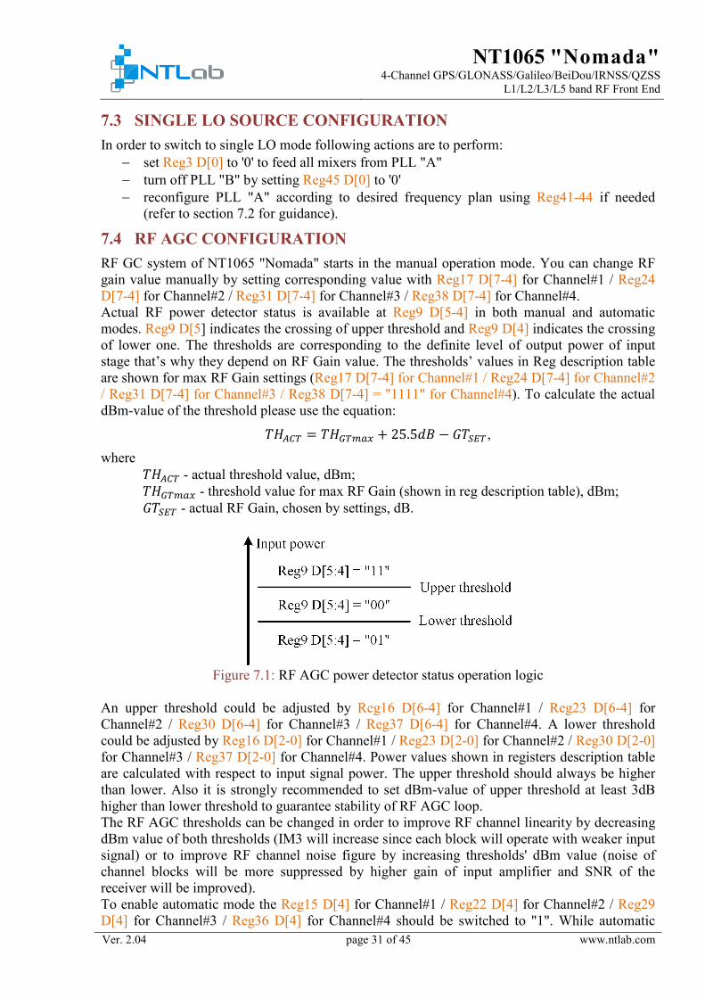
NT1065 Nomada 4-Channel GPSGLONASSGalileoBeiDouIRNSSQZSS
L1L2L3L5 band RF Front End
Ver 204 page 31 of 45 wwwntlabcom
73 SINGLE LO SOURCE CONFIGURATION In order to switch to single LO mode following actions are to perform
minus set Reg3 D[0] to 0 to feed all mixers from PLL A minus turn off PLL B by setting Reg45 D[0] to 0 minus reconfigure PLL A according to desired frequency plan using Reg41-44 if needed
(refer to section 72 for guidance)
74 RF AGC CONFIGURATION RF GC system of NT1065 Nomada starts in the manual operation mode You can change RF gain value manually by setting corresponding value with Reg17 D[7-4] for Channel1 Reg24 D[7-4] for Channel2 Reg31 D[7-4] for Channel3 Reg38 D[7-4] for Channel4 Actual RF power detector status is available at Reg9 D[5-4] in both manual and automatic modes Reg9 D[5] indicates the crossing of upper threshold and Reg9 D[4] indicates the crossing of lower one The thresholds are corresponding to the definite level of output power of input stage thatrsquos why they depend on RF Gain value The thresholdsrsquo values in Reg description table are shown for max RF Gain settings (Reg17 D[7-4] for Channel1 Reg24 D[7-4] for Channel2 Reg31 D[7-4] for Channel3 Reg38 D[7-4] = 1111 for Channel4) To calculate the actual dBm-value of the threshold please use the equation
119879119879119879119879119860119860119860119860119860119860 = 119879119879119879119879119866119866119860119860119866119866119866119866119866119866 + 255119889119889119889119889 minus 119866119866119879119879119878119878119878119878119860119860 where 119879119879119879119879119860119860119860119860119860119860 - actual threshold value dBm 119879119879119879119879119866119866119860119860119866119866119866119866119866119866 - threshold value for max RF Gain (shown in reg description table) dBm 119866119866119879119879119878119878119878119878119860119860 - actual RF Gain chosen by settings dB
Figure 71 RF AGC power detector status operation logic
An upper threshold could be adjusted by Reg16 D[6-4] for Channel1 Reg23 D[6-4] for Channel2 Reg30 D[6-4] for Channel3 Reg37 D[6-4] for Channel4 A lower threshold could be adjusted by Reg16 D[2-0] for Channel1 Reg23 D[2-0] for Channel2 Reg30 D[2-0] for Channel3 Reg37 D[2-0] for Channel4 Power values shown in registers description table are calculated with respect to input signal power The upper threshold should always be higher than lower Also it is strongly recommended to set dBm-value of upper threshold at least 3dB higher than lower threshold to guarantee stability of RF AGC loop The RF AGC thresholds can be changed in order to improve RF channel linearity by decreasing dBm value of both thresholds (IM3 will increase since each block will operate with weaker input signal) or to improve RF channel noise figure by increasing thresholds dBm value (noise of channel blocks will be more suppressed by higher gain of input amplifier and SNR of the receiver will be improved) To enable automatic mode the Reg15 D[4] for Channel1 Reg22 D[4] for Channel2 Reg29 D[4] for Channel3 Reg36 D[4] for Channel4 should be switched to 1 While automatic
NT1065 Nomada 4-Channel GPSGLONASSGalileoBeiDouIRNSSQZSS
L1L2L3L5 band RF Front End
Ver 204 page 32 of 45 wwwntlabcom
mode enabled the RF AGC system will adjust the RF gain to keep its output power between RF AGC thresholds The status of RF gain control register is available at Reg9 D[3-0]
75 IF AGC THRESHOLD CONFIGURATION If 400mV (wrt sine wave signal) option is chosen for output peak-to peak voltage (Reg15 D[6] for Channel1 Reg22 D[6] for Channel2 Reg29 D[6] for Channel3 Reg36 D[6] for Channel4) it is recommended not to solder terminating 200 Ohm resistor and to write appropriate values (0) to D[5] of the same registers It will result in better linearity performance
76 CLK FREQUENCY CONFIGURATION CLK signal is intended for clocking all 2-bit ADCs as well as clocking external correlator engine It is generated from LO frequency either from PLL A or PLL B according to the formula 119865119865119860119860119871119871119862119862 = 119865119865119871119871119879119879
2lowast119860119860 CLK source and frequency can be customized by procedure
minus choose CLK source by setting appropriate value to Reg12 D[5] minus write C value to Reg11 D[4-0]
77 CLK OUTPUT TYPE USAGE Although CMOS output is available for usage it is recommended to select LVDS CLK output It is related to appearing of interferences at the LNA_IN pins and then down converting to IF band These interferences are caused by CLK signal harmonics and allocated frequencies can be calculated as 119865119865119895119895119866119866119866119866 = 119873119873 lowast 119865119865119860119860119871119871119862119862119873119873 = 1234 hellip
78 TEMPERATURE MEASUREMENT PROCEDURE Two modes of temperature modes are available single and continuous (Reg5 D[1]) In single mode the measurement is done once upon request to Reg5 D[0] by setting 1 and result will be stored in Reg7 D[1-0] + Reg8 D[7-0] after procedure is finished (auto reset to 0 in Reg5 D[0] indicates this) until next execution One temperature measurement procedure time is up to 17 ms To enter in continuous mode set Reg5 D[1] to 1 first then execute with Reg5 D[0] In this case embedded temperature sensor periodically runs the measurement procedure and only the latest result is stored in Reg7 D[1-0] + Reg8 D[7-0] In order to stop continuous execution Reg5 D[1] should be set to 0
NT1065 Nomada 4-Channel GPSGLONASSGalileoBeiDouIRNSSQZSS
L1L2L3L5 band RF Front End
Ver 204 page 33 of 45 wwwntlabcom
79 OPERATION EXAMPLES CONFIGURATION SET 1 791
General settings Reference frequency (TCXO) 10MHz LO source PLL laquoAraquo for ch1 ch2
PLL laquoBraquo for ch3 ch4 CLK settings CLK frequency source PLL laquoAraquo CLK frequencyMHz 53 CLK type LVDS CLK amplitude V Preset 4 Channel settings Ch1 GNSS LSB
(GPS L1-O QZSS L1 Galileo E1 BeiDou B1-C GLONASS L1-OC) Ch2 GNSS USB
(GLONASS L1-OF) Ch3 GNSS USB
(GLONASS L2-OF) Ch4 GNSS LSB
(GPS L2-O QZSS L2) Ch1 IF passband MHz 271 Ch2 IF passband MHz 20 Ch3 IF passband MHz 173 Ch4 IF passband MHz 151 Output data interface 2-bit ADC GC mode RF manual + IF auto IF AGC threshold 30 ADC output logic-level high ext (VCC) ADC type Clocked by rising edge PLL settings FLO PLL laquoAraquo MHz 1590 FLO PLL laquoBraquo MHz 1235 Configuration file Please double click here to download -gt ConfigSet01txt configuration file may be also uploaded to NT1065 Nomada under GUI v2018 (or later) if renamed to hex
NT1065 Nomada 4-Channel GPSGLONASSGalileoBeiDouIRNSSQZSS
L1L2L3L5 band RF Front End
Ver 204 page 32 of 45 wwwntlabcom
mode enabled the RF AGC system will adjust the RF gain to keep its output power between RF AGC thresholds The status of RF gain control register is available at Reg9 D[3-0]
75 IF AGC THRESHOLD CONFIGURATION If 400mV (wrt sine wave signal) option is chosen for output peak-to peak voltage (Reg15 D[6] for Channel1 Reg22 D[6] for Channel2 Reg29 D[6] for Channel3 Reg36 D[6] for Channel4) it is recommended not to solder terminating 200 Ohm resistor and to write appropriate values (0) to D[5] of the same registers It will result in better linearity performance
76 CLK FREQUENCY CONFIGURATION CLK signal is intended for clocking all 2-bit ADCs as well as clocking external correlator engine It is generated from LO frequency either from PLL A or PLL B according to the formula 119865119865119860119860119871119871119862119862 = 119865119865119871119871119879119879
2lowast119860119860 CLK source and frequency can be customized by procedure
minus choose CLK source by setting appropriate value to Reg12 D[5] minus write C value to Reg11 D[4-0]
77 CLK OUTPUT TYPE USAGE Although CMOS output is available for usage it is recommended to select LVDS CLK output It is related to appearing of interferences at the LNA_IN pins and then down converting to IF band These interferences are caused by CLK signal harmonics and allocated frequencies can be calculated as 119865119865119895119895119866119866119866119866 = 119873119873 lowast 119865119865119860119860119871119871119862119862119873119873 = 1234 hellip
78 TEMPERATURE MEASUREMENT PROCEDURE Two modes of temperature modes are available single and continuous (Reg5 D[1]) In single mode the measurement is done once upon request to Reg5 D[0] by setting 1 and result will be stored in Reg7 D[1-0] + Reg8 D[7-0] after procedure is finished (auto reset to 0 in Reg5 D[0] indicates this) until next execution One temperature measurement procedure time is up to 17 ms To enter in continuous mode set Reg5 D[1] to 1 first then execute with Reg5 D[0] In this case embedded temperature sensor periodically runs the measurement procedure and only the latest result is stored in Reg7 D[1-0] + Reg8 D[7-0] In order to stop continuous execution Reg5 D[1] should be set to 0
NT1065 Nomada 4-Channel GPSGLONASSGalileoBeiDouIRNSSQZSS
L1L2L3L5 band RF Front End
Ver 204 page 33 of 45 wwwntlabcom
79 OPERATION EXAMPLES CONFIGURATION SET 1 791
General settings Reference frequency (TCXO) 10MHz LO source PLL laquoAraquo for ch1 ch2
PLL laquoBraquo for ch3 ch4 CLK settings CLK frequency source PLL laquoAraquo CLK frequencyMHz 53 CLK type LVDS CLK amplitude V Preset 4 Channel settings Ch1 GNSS LSB
(GPS L1-O QZSS L1 Galileo E1 BeiDou B1-C GLONASS L1-OC) Ch2 GNSS USB
(GLONASS L1-OF) Ch3 GNSS USB
(GLONASS L2-OF) Ch4 GNSS LSB
(GPS L2-O QZSS L2) Ch1 IF passband MHz 271 Ch2 IF passband MHz 20 Ch3 IF passband MHz 173 Ch4 IF passband MHz 151 Output data interface 2-bit ADC GC mode RF manual + IF auto IF AGC threshold 30 ADC output logic-level high ext (VCC) ADC type Clocked by rising edge PLL settings FLO PLL laquoAraquo MHz 1590 FLO PLL laquoBraquo MHz 1235 Configuration file Please double click here to download -gt ConfigSet01txt configuration file may be also uploaded to NT1065 Nomada under GUI v2018 (or later) if renamed to hex

NT1065 Nomada 4-Channel GPSGLONASSGalileoBeiDouIRNSSQZSS
L1L2L3L5 band RF Front End
Ver 204 page 34 of 45 wwwntlabcom
CONFIGURATION SET 2 792
General settings Reference frequency (TCXO) 10MHz LO source PLL laquoAraquo for ch1 ch2
PLL laquoBraquo for ch3 ch4 CLK settings CLK frequency source PLL laquoAraquo CLK frequencyMHz 99375 CLK type CMOS CLK amplitude V ext Channel settings Ch1 GNSS LSB
(GPS L1-O QZSS L1 Galileo E1 BeiDou B1 GLONASS L1-OC) Ch2 GNSS USB
(GLONASS L1-OF) Ch3 GNSS USB
(GLONASS L3 Galileo E5b BeiDou B2) Ch4 GNSS LSB
(GPS L5-O GLONASS L5-OC Galileo E5a QZSS L5 BeiDou B2 IRNSS L5) Ch1 IF passband MHz 331 Ch2 IF passband MHz 20 Ch3 IF passband MHz 302 Ch4 IF passband MHz 271 Output data interface 2-bit ADC GC mode RF manual + IF auto IF AGC threshold 30 ADC output logic-level high ext (VCC) ADC type Clocked by rising edge PLL settings FLO PLL laquoAraquo MHz 1590 FLO PLL laquoBraquo MHz 1190 Configuration file Please double click here to download -gt ConfigSet02txt configuration file may be also uploaded to NT1065 Nomada under GUI v2018 (or later) if renamed to hex

NT1065 Nomada 4-Channel GPSGLONASSGalileoBeiDouIRNSSQZSS
L1L2L3L5 band RF Front End
Ver 204 page 35 of 45 wwwntlabcom
CONFIGURATION SET 3 793
General settings Reference frequency (TCXO) 16368MHz LO source PLL laquoAraquo for ch1 ch2
PLL laquoBraquo for ch3 ch4 CLK settings CLK frequency source PLL laquoAraquo CLK frequencyMHz 99231 CLK type CMOS CLK amplitude V ext Channel settings Ch1 GNSS LSB
(GPS L1-O QZSS L1 Galileo E1 BeiDou B1-C GLONASS L1-OC) Ch2 GNSS USB
(GLONASS L1-OF) Ch3 GNSS USB
(GLONASS L2-OF) Ch4 GNSS LSB
(GPS L2-O QZSS L2) Ch1 IF passband MHz 308 Ch2 IF passband MHz 226 Ch3 IF passband MHz 173 Ch4 IF passband MHz 16 Output data interface 2-bit ADC GC mode RF manual + IF auto IF AGC threshold 30 ADC output logic-level high ext (VCC) ADC type Clocked by rising edge PLL settings FLO PLL laquoAraquo MHz 1587696 FLO PLL laquoBraquo MHz 1235784 Configuration file Please double click here to download -gt ConfigSet03txt configuration file may be also uploaded to NT1065 Nomada under GUI v2018 (or later) if renamed to hex

NT1065 Nomada 4-Channel GPSGLONASSGalileoBeiDouIRNSSQZSS
L1L2L3L5 band RF Front End
Ver 204 page 36 of 45 wwwntlabcom
CONFIGURATION SET 4 794
General settings Reference frequency (TCXO) 2484MHz LO source PLL laquoAraquo for ch1 ch2 ch3 ch4 CLK settings CLK frequency source PLL laquoAraquo CLK frequencyMHz 52992 CLK type LVDS CLK amplitude V Preset 3 Channel settings Ch1 GNSS LSB
(GPS L1-O QZSS L1 BeiDou B1-C GLONASS L1-OC) Ch2 GNSS USB
(GLONASS L1-OF) Ch3 GNSS USB
(GLONASS L1-OF) Ch4 GNSS LSB
(GPS L1-O QZSS L1 BeiDou B1-C GLONASS L1-OC) Ch1 IF passband MHz 251 Ch2 IF passband MHz 251 Ch3 IF passband MHz 251 Ch4 IF passband MHz 251 Output data interface Analog differential GC mode RF manual + IF auto IF AGC threshold 200 mV ADC output logic-level high - ADC type - PLL settings FLO PLL laquoAraquo MHz 158976 FLO PLL laquoBraquo MHz - Configuration file Please double click here to download -gt ConfigSet04txt configuration file may be also uploaded to NT1065 Nomada under GUI v2018 (or later) if renamed to hex
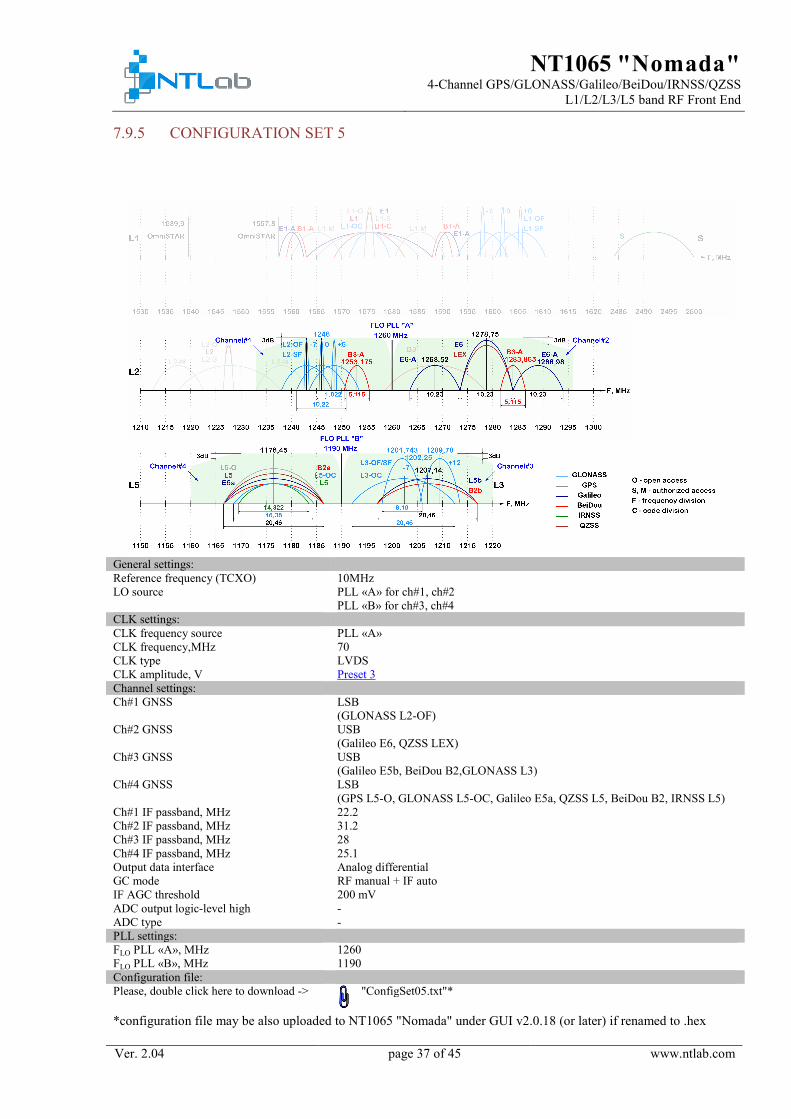
NT1065 Nomada 4-Channel GPSGLONASSGalileoBeiDouIRNSSQZSS
L1L2L3L5 band RF Front End
Ver 204 page 37 of 45 wwwntlabcom
CONFIGURATION SET 5 795
General settings Reference frequency (TCXO) 10MHz LO source PLL laquoAraquo for ch1 ch2
PLL laquoBraquo for ch3 ch4 CLK settings CLK frequency source PLL laquoAraquo CLK frequencyMHz 70 CLK type LVDS CLK amplitude V Preset 3 Channel settings Ch1 GNSS LSB
(GLONASS L2-OF) Ch2 GNSS USB
(Galileo E6 QZSS LEX) Ch3 GNSS USB
(Galileo E5b BeiDou B2GLONASS L3) Ch4 GNSS LSB
(GPS L5-O GLONASS L5-OC Galileo E5a QZSS L5 BeiDou B2 IRNSS L5) Ch1 IF passband MHz 222 Ch2 IF passband MHz 312 Ch3 IF passband MHz 28 Ch4 IF passband MHz 251 Output data interface Analog differential GC mode RF manual + IF auto IF AGC threshold 200 mV ADC output logic-level high - ADC type - PLL settings FLO PLL laquoAraquo MHz 1260 FLO PLL laquoBraquo MHz 1190 Configuration file Please double click here to download -gt ConfigSet05txt configuration file may be also uploaded to NT1065 Nomada under GUI v2018 (or later) if renamed to hex
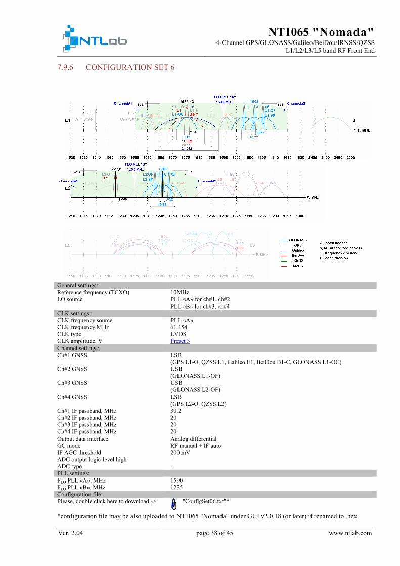
NT1065 Nomada 4-Channel GPSGLONASSGalileoBeiDouIRNSSQZSS
L1L2L3L5 band RF Front End
Ver 204 page 38 of 45 wwwntlabcom
CONFIGURATION SET 6 796
General settings Reference frequency (TCXO) 10MHz LO source PLL laquoAraquo for ch1 ch2
PLL laquoBraquo for ch3 ch4 CLK settings CLK frequency source PLL laquoAraquo CLK frequencyMHz 61154 CLK type LVDS CLK amplitude V Preset 3 Channel settings Ch1 GNSS LSB
(GPS L1-O QZSS L1 Galileo E1 BeiDou B1-C GLONASS L1-OC) Ch2 GNSS USB
(GLONASS L1-OF) Ch3 GNSS USB
(GLONASS L2-OF) Ch4 GNSS LSB
(GPS L2-O QZSS L2) Ch1 IF passband MHz 302 Ch2 IF passband MHz 20 Ch3 IF passband MHz 20 Ch4 IF passband MHz 20 Output data interface Analog differential GC mode RF manual + IF auto IF AGC threshold 200 mV ADC output logic-level high - ADC type - PLL settings FLO PLL laquoAraquo MHz 1590 FLO PLL laquoBraquo MHz 1235 Configuration file Please double click here to download -gt ConfigSet06txt configuration file may be also uploaded to NT1065 Nomada under GUI v2018 (or later) if renamed to hex
NT1065 Nomada 4-Channel GPSGLONASSGalileoBeiDouIRNSSQZSS
L1L2L3L5 band RF Front End
Ver 204 page 39 of 45 wwwntlabcom
CONFIGURATION SET 7 797
General settings Reference frequency (TCXO) 10MHz LO source PLL laquoAraquo for ch1 ch2
PLL laquoBraquo for ch3 ch4 CLK settings CLK frequency source PLL laquoAraquo CLK frequencyMHz 97812 CLK type CMOS CLK amplitude V ext Channel settings Ch1 GNSS LSB
(OmniSTAR 15399 OmniSTAR 15578) Ch2 GNSS USB
(GPS L1-O QZSS L1 Beidou B1 GLONASS L1-OC) Ch3 GNSS USB
(GLONASS L3 Galileo E5b Beidou B2) Ch4 GNSS LSB
(GPS L5-O GLONASS L5-OC Galileo E5a QZSS L5 Beidou B2 IRNSS L5) Ch1 IF passband MHz 35 Ch2 IF passband MHz 251 Ch3 IF passband MHz 302 Ch4 IF passband MHz 271 Output data interface 2-bit ADC output GC mode RF manual + IF auto IF AGC threshold 30 ADC output logic-level high ext (VCC) ADC type Clocked by rising edge PLL settings FLO PLL laquoAraquo MHz 1565 FLO PLL laquoBraquo MHz 1190 Configuration file Please double click here to download -gt ConfigSet07txt configuration file may be also uploaded to NT1065 Nomada under GUI v2018 (or later) if renamed to hex

NT1065 Nomada 4-Channel GPSGLONASSGalileoBeiDouIRNSSQZSS
L1L2L3L5 band RF Front End
Ver 204 page 40 of 45 wwwntlabcom
710 PCB LAYOUT RECOMMENDATIONS NT1065 Nomada is easy-to-use and easy-to-implement solution where no special layout tricks required Although common RF related layout techniques and information given below are recommended not to be ignored
1 Analog power domain separated from digital domain is recommended to be allocated for NT1065
2 EMI-RFI shielding are highly recommended above NT1065 Nomada and related stuff 3 Wave impedance should be kept up in accordance to the following
Figure 72 Recommended land pattern QFN88
The red plaid traces on the Figure 72 should have 50 Ohm impedance and orange inclined striped traces on the Figure 72 should have 200 Ohm impedance (if analog differential output)
NT1065 Nomada 4-Channel GPSGLONASSGalileoBeiDouIRNSSQZSS
L1L2L3L5 band RF Front End
Ver 204 page 41 of 45 wwwntlabcom
ROGERS STACK UP 7101
Figure 73 Trace calculation example Rogers
Rogers Core RO4350B PrePreg RO4450B NT1065 Nomada electric characteristics described in Sections 5 and 6 were proven on this very stack up
NT1065 Nomada 4-Channel GPSGLONASSGalileoBeiDouIRNSSQZSS
L1L2L3L5 band RF Front End
Ver 204 page 42 of 45 wwwntlabcom
FR4 STACK UP 7102
Figure 74 Trace calculation example FR4
FR4 Core High Tg FR4 PrePreg 7628-45 NT1065 Nomada electric characteristics described in Sections 5 and 6 were reevaluated on this very stack up No essential differences relative to Rogers stack up ware observed Although input VSWR may exceed 20 value over specified temperature range and reach up to 25 value
NT1065 Nomada 4-Channel GPSGLONASSGalileoBeiDouIRNSSQZSS
L1L2L3L5 band RF Front End
Ver 204 page 43 of 45 wwwntlabcom
8 PACKAGE INFORMATION
Figure 81 Package QFN88-10times10
Table 81 Package QFN88-10times10 dimensions Unit A A1 A3 b D D2 E E2 e L
min mm 080 000 020
015 990 805 990 805 04
030 typ mm 085 002 020 1000 820 1000 820 040 max mm 090 005 025 1010 835 1010 835 050 Package drawing and dimensions are for reference only Actual values are compliant to JEDEC standard outlines MO-220
NT1065 Nomada 4-Channel GPSGLONASSGalileoBeiDouIRNSSQZSS
L1L2L3L5 band RF Front End
Ver 204 page 44 of 45 wwwntlabcom
9 REVISION HISTORY From version 203 Subsection 43 Application schematic Table 41 updated
- Description of C1 C8 C9 C27 L1 L2 L3 L5 R2 R3 R4 R5 was clarified From version 202 onmiSTAR differential data support was successfully evaluated
- Subsection 52 updated input frequency range for L1 band was enlarged to 15301620 MHz
- Subsection 79 updated new configuration set 7 example was added Subsection 74 RF AGC configuration updated
- Registers reference of RF gain control was updated Subsection 78 Temperature measurement procedure updated
- Temperature measurement procedure execution time was added Subsection 710 PCB layout recommendation updated
- FR4 stack up was added - Rogers stack up was updated
From version 201 Subsection 42 Pins description updated
- Description of pin 80 was corrected from 1st channel down converter ground to 1st channel RF ground
Subsection 445 Timing diagram Table 43 updated - Max value of parameter SCLK frequency was changed from 50 MHz to 40
MHz Section 5 OPERATING CHARACTERISTICS updated
- Absolute maximum ratings was added Subsection 52 AC electrical characteristics updated
- Value of parameter Noise figure for L1 L2 L3 and L5 band was changed from 45 dB to 38 dB
Section 8 PACKAGE INFORMATION updated - Note Package drawing and dimensions are for reference only Actual values are
compliant to JEDEC standard outlines MO-220 was added From version 20 Subsection 42 Pins description updated
- Description of pin 54 was corrected from ldquoCLKrdquo LDO output voltage 27V to ldquoCLKrdquo LDO output voltage 17VVCC (Reg12ltD4-D0gt dependent)
Subsection 52 AC electrical characteristics - Condition for LPF 3dB cut-off frequency Relative to 5 MHz was added
Subsection 6 TYPICAL CHARACTERISTICS - Figure 633 ADC quantization levels was added
Section 7APPLICATION NOTES - The description of start up behavior after power up in Subsection 71 was updated - Subsection 79 Configuration examples was replaced with Operation
examples content was updated Updates and modifications from NT10651 (refer to Reg0 and Reg1 for chip number and version)
NT1065 Nomada 4-Channel GPSGLONASSGalileoBeiDouIRNSSQZSS
L1L2L3L5 band RF Front End
Ver 204 page 45 of 45 wwwntlabcom
Power up hysteresis was increased from 27us(min)330us(max) to 65us790us RF AGC system was corrected and improved
- Now it is also stable to multi-tone input interferences - RF AGC system starts in manual mode on power up but can be reconfigured to
auto mode (refer to Reg15ltD3gt) - Operating threshold options are now given wrt input power (Reg16ltD6-D4
D2-D0gt Reg23ltD6-D4 D2-D0gt Reg30ltD6-D4 D2-D0gt Reg37ltD6-D4 D2-D0gt)
- Indicators are excluded from default settings but still can be set if needed (Reg6ltD1gt)
- Subsection 74 RF AGC configuration was updated and contains RF AGC system guidelines
Single LO source configuration was simplified Refer to subsection 73 for guidelines Section 2 Features updated Subsection 51 DC electrical characteristics updated
- Parameters Die temperature measurement range and Die temperature measurement accuracy were added
- Max value of parameter Supply voltage was changed from 36 V to 33 V Subsection 52 AC electrical characteristics updated
- Max value of parameters Output frequency range and LPF 3dB cut-off frequency were changed from 25 MHz to 31 MHz
Power up default settings were changed - Reg1ltD2-D0gt=010 Reg15ltD4gt=0 Reg18ltD4-D0gt=01010 Re19ltD3-
D2gt=10 Reg22ltD4gt=0 Reg25ltD4-D0gt=01010 Reg29ltD4gt=0 Reg32ltD4-D0gt=01010 Reg33ltD3-D2gt=10 Reg36ltD4gt=0 Reg39ltD4-D0gt01010 Reg40ltD3-D2gt=10
Section 7 Application notes were updated accordingly to actual chip behavior Subsection 4462 updated
- Value Reg2ltD1D0gt was changed - Formula for on-die temperature calculation was corrected Refer to Reg7ltD1-
D0gt+Reg8ltD7-D0gt for new data Subsection 4464 updated
- LFP 3 dB cut-off frequency was corrected to widen the bandwidth Refer to Reg14Reg21Reg28Reg35ltD6-D0gt for new data
Subsection 4465 updated - Description of VCO input voltage indication was clarified Refer to
Reg44Reg48ltD2-D1gt Minor changes in ACDC electrical characteristics Minor changes in registers description Subsection 79 Configuration examples updated
- 1 OVERVIEW
- 2 FEATURES
- 3 APPLICATIONS
- 4 DESCRIPTION
-
- 41 Structure
- 42 Pins description
- 43 Application schematic
- 44 Serial Interface description
-
- 441 General description
- 442 Writing to register
- 443 Reading from register
- 444 Burst data transfer
- 445 Timing diagram
- 446 Programmable registers
-
- 4461 System info
- 4462 General settings and status
- 4463 CLK settings
- 4464 Channel settings
- 4465 PLL settings and status
-
- 5 OPERATING CHARACTERISTICS
-
- Absolute maximum ratings
- 51 DC electrical characteristics
- 52 AC electrical characteristics
-
- 6 TYPICAL CHARACTERISTICS
- 7 APPLICATION NOTES
-
- 71 Reference frequency (TCXO) configuration and start up procedure
- 72 PLL A PLL B reconfiguration
- 73 Single LO source configuration
- 74 RF AGC configuration
- 75 IF AGC threshold configuration
- 76 CLK frequency configuration
- 77 CLK output type usage
- 78 Temperature measurement procedure
- 79 Operation examples
-
- 791 Configuration set 1
- 792 Configuration set 2
- 793 Configuration set 3
- 794 Configuration set 4
- 795 Configuration set 5
- 796 Configuration set 6
- 797 Configuration set 7
-
- 710 PCB layout recommendations
-
- 7101 Rogers stack up
- 7102 FR4 stack up
-
- 8 PACKAGE INFORMATION
- 9 REVISION HISTORY
-

NT1065 Nomada 4-Channel GPSGLONASSGalileoBeiDouIRNSSQZSS
L1L2L3L5 band RF Front End
Ver 204 page 43 of 45 wwwntlabcom
8 PACKAGE INFORMATION
Figure 81 Package QFN88-10times10
Table 81 Package QFN88-10times10 dimensions Unit A A1 A3 b D D2 E E2 e L
min mm 080 000 020
015 990 805 990 805 04
030 typ mm 085 002 020 1000 820 1000 820 040 max mm 090 005 025 1010 835 1010 835 050 Package drawing and dimensions are for reference only Actual values are compliant to JEDEC standard outlines MO-220
NT1065 Nomada 4-Channel GPSGLONASSGalileoBeiDouIRNSSQZSS
L1L2L3L5 band RF Front End
Ver 204 page 44 of 45 wwwntlabcom
9 REVISION HISTORY From version 203 Subsection 43 Application schematic Table 41 updated
- Description of C1 C8 C9 C27 L1 L2 L3 L5 R2 R3 R4 R5 was clarified From version 202 onmiSTAR differential data support was successfully evaluated
- Subsection 52 updated input frequency range for L1 band was enlarged to 15301620 MHz
- Subsection 79 updated new configuration set 7 example was added Subsection 74 RF AGC configuration updated
- Registers reference of RF gain control was updated Subsection 78 Temperature measurement procedure updated
- Temperature measurement procedure execution time was added Subsection 710 PCB layout recommendation updated
- FR4 stack up was added - Rogers stack up was updated
From version 201 Subsection 42 Pins description updated
- Description of pin 80 was corrected from 1st channel down converter ground to 1st channel RF ground
Subsection 445 Timing diagram Table 43 updated - Max value of parameter SCLK frequency was changed from 50 MHz to 40
MHz Section 5 OPERATING CHARACTERISTICS updated
- Absolute maximum ratings was added Subsection 52 AC electrical characteristics updated
- Value of parameter Noise figure for L1 L2 L3 and L5 band was changed from 45 dB to 38 dB
Section 8 PACKAGE INFORMATION updated - Note Package drawing and dimensions are for reference only Actual values are
compliant to JEDEC standard outlines MO-220 was added From version 20 Subsection 42 Pins description updated
- Description of pin 54 was corrected from ldquoCLKrdquo LDO output voltage 27V to ldquoCLKrdquo LDO output voltage 17VVCC (Reg12ltD4-D0gt dependent)
Subsection 52 AC electrical characteristics - Condition for LPF 3dB cut-off frequency Relative to 5 MHz was added
Subsection 6 TYPICAL CHARACTERISTICS - Figure 633 ADC quantization levels was added
Section 7APPLICATION NOTES - The description of start up behavior after power up in Subsection 71 was updated - Subsection 79 Configuration examples was replaced with Operation
examples content was updated Updates and modifications from NT10651 (refer to Reg0 and Reg1 for chip number and version)
NT1065 Nomada 4-Channel GPSGLONASSGalileoBeiDouIRNSSQZSS
L1L2L3L5 band RF Front End
Ver 204 page 45 of 45 wwwntlabcom
Power up hysteresis was increased from 27us(min)330us(max) to 65us790us RF AGC system was corrected and improved
- Now it is also stable to multi-tone input interferences - RF AGC system starts in manual mode on power up but can be reconfigured to
auto mode (refer to Reg15ltD3gt) - Operating threshold options are now given wrt input power (Reg16ltD6-D4
D2-D0gt Reg23ltD6-D4 D2-D0gt Reg30ltD6-D4 D2-D0gt Reg37ltD6-D4 D2-D0gt)
- Indicators are excluded from default settings but still can be set if needed (Reg6ltD1gt)
- Subsection 74 RF AGC configuration was updated and contains RF AGC system guidelines
Single LO source configuration was simplified Refer to subsection 73 for guidelines Section 2 Features updated Subsection 51 DC electrical characteristics updated
- Parameters Die temperature measurement range and Die temperature measurement accuracy were added
- Max value of parameter Supply voltage was changed from 36 V to 33 V Subsection 52 AC electrical characteristics updated
- Max value of parameters Output frequency range and LPF 3dB cut-off frequency were changed from 25 MHz to 31 MHz
Power up default settings were changed - Reg1ltD2-D0gt=010 Reg15ltD4gt=0 Reg18ltD4-D0gt=01010 Re19ltD3-
D2gt=10 Reg22ltD4gt=0 Reg25ltD4-D0gt=01010 Reg29ltD4gt=0 Reg32ltD4-D0gt=01010 Reg33ltD3-D2gt=10 Reg36ltD4gt=0 Reg39ltD4-D0gt01010 Reg40ltD3-D2gt=10
Section 7 Application notes were updated accordingly to actual chip behavior Subsection 4462 updated
- Value Reg2ltD1D0gt was changed - Formula for on-die temperature calculation was corrected Refer to Reg7ltD1-
D0gt+Reg8ltD7-D0gt for new data Subsection 4464 updated
- LFP 3 dB cut-off frequency was corrected to widen the bandwidth Refer to Reg14Reg21Reg28Reg35ltD6-D0gt for new data
Subsection 4465 updated - Description of VCO input voltage indication was clarified Refer to
Reg44Reg48ltD2-D1gt Minor changes in ACDC electrical characteristics Minor changes in registers description Subsection 79 Configuration examples updated
- 1 OVERVIEW
- 2 FEATURES
- 3 APPLICATIONS
- 4 DESCRIPTION
-
- 41 Structure
- 42 Pins description
- 43 Application schematic
- 44 Serial Interface description
-
- 441 General description
- 442 Writing to register
- 443 Reading from register
- 444 Burst data transfer
- 445 Timing diagram
- 446 Programmable registers
-
- 4461 System info
- 4462 General settings and status
- 4463 CLK settings
- 4464 Channel settings
- 4465 PLL settings and status
-
- 5 OPERATING CHARACTERISTICS
-
- Absolute maximum ratings
- 51 DC electrical characteristics
- 52 AC electrical characteristics
-
- 6 TYPICAL CHARACTERISTICS
- 7 APPLICATION NOTES
-
- 71 Reference frequency (TCXO) configuration and start up procedure
- 72 PLL A PLL B reconfiguration
- 73 Single LO source configuration
- 74 RF AGC configuration
- 75 IF AGC threshold configuration
- 76 CLK frequency configuration
- 77 CLK output type usage
- 78 Temperature measurement procedure
- 79 Operation examples
-
- 791 Configuration set 1
- 792 Configuration set 2
- 793 Configuration set 3
- 794 Configuration set 4
- 795 Configuration set 5
- 796 Configuration set 6
- 797 Configuration set 7
-
- 710 PCB layout recommendations
-
- 7101 Rogers stack up
- 7102 FR4 stack up
-
- 8 PACKAGE INFORMATION
- 9 REVISION HISTORY
-
NT1065 Nomada 4-Channel GPSGLONASSGalileoBeiDouIRNSSQZSS
L1L2L3L5 band RF Front End
Ver 204 page 45 of 45 wwwntlabcom
Power up hysteresis was increased from 27us(min)330us(max) to 65us790us RF AGC system was corrected and improved
- Now it is also stable to multi-tone input interferences - RF AGC system starts in manual mode on power up but can be reconfigured to
auto mode (refer to Reg15ltD3gt) - Operating threshold options are now given wrt input power (Reg16ltD6-D4
D2-D0gt Reg23ltD6-D4 D2-D0gt Reg30ltD6-D4 D2-D0gt Reg37ltD6-D4 D2-D0gt)
- Indicators are excluded from default settings but still can be set if needed (Reg6ltD1gt)
- Subsection 74 RF AGC configuration was updated and contains RF AGC system guidelines
Single LO source configuration was simplified Refer to subsection 73 for guidelines Section 2 Features updated Subsection 51 DC electrical characteristics updated
- Parameters Die temperature measurement range and Die temperature measurement accuracy were added
- Max value of parameter Supply voltage was changed from 36 V to 33 V Subsection 52 AC electrical characteristics updated
- Max value of parameters Output frequency range and LPF 3dB cut-off frequency were changed from 25 MHz to 31 MHz
Power up default settings were changed - Reg1ltD2-D0gt=010 Reg15ltD4gt=0 Reg18ltD4-D0gt=01010 Re19ltD3-
D2gt=10 Reg22ltD4gt=0 Reg25ltD4-D0gt=01010 Reg29ltD4gt=0 Reg32ltD4-D0gt=01010 Reg33ltD3-D2gt=10 Reg36ltD4gt=0 Reg39ltD4-D0gt01010 Reg40ltD3-D2gt=10
Section 7 Application notes were updated accordingly to actual chip behavior Subsection 4462 updated
- Value Reg2ltD1D0gt was changed - Formula for on-die temperature calculation was corrected Refer to Reg7ltD1-
D0gt+Reg8ltD7-D0gt for new data Subsection 4464 updated
- LFP 3 dB cut-off frequency was corrected to widen the bandwidth Refer to Reg14Reg21Reg28Reg35ltD6-D0gt for new data
Subsection 4465 updated - Description of VCO input voltage indication was clarified Refer to
Reg44Reg48ltD2-D1gt Minor changes in ACDC electrical characteristics Minor changes in registers description Subsection 79 Configuration examples updated
- 1 OVERVIEW
- 2 FEATURES
- 3 APPLICATIONS
- 4 DESCRIPTION
-
- 41 Structure
- 42 Pins description
- 43 Application schematic
- 44 Serial Interface description
-
- 441 General description
- 442 Writing to register
- 443 Reading from register
- 444 Burst data transfer
- 445 Timing diagram
- 446 Programmable registers
-
- 4461 System info
- 4462 General settings and status
- 4463 CLK settings
- 4464 Channel settings
- 4465 PLL settings and status
-
- 5 OPERATING CHARACTERISTICS
-
- Absolute maximum ratings
- 51 DC electrical characteristics
- 52 AC electrical characteristics
-
- 6 TYPICAL CHARACTERISTICS
- 7 APPLICATION NOTES
-
- 71 Reference frequency (TCXO) configuration and start up procedure
- 72 PLL A PLL B reconfiguration
- 73 Single LO source configuration
- 74 RF AGC configuration
- 75 IF AGC threshold configuration
- 76 CLK frequency configuration
- 77 CLK output type usage
- 78 Temperature measurement procedure
- 79 Operation examples
-
- 791 Configuration set 1
- 792 Configuration set 2
- 793 Configuration set 3
- 794 Configuration set 4
- 795 Configuration set 5
- 796 Configuration set 6
- 797 Configuration set 7
-
- 710 PCB layout recommendations
-
- 7101 Rogers stack up
- 7102 FR4 stack up
-
- 8 PACKAGE INFORMATION
- 9 REVISION HISTORY
-