Nonvolatile multilevel memories for digital applications
23
Nonvolatile Multilevel Memories for Digital Applications BRUNO RICC ` O, SENIOR MEMBER, IEEE, GUIDO TORELLI, SENIOR MEMBER, IEEE, MASSIMO LANZONI, ALESSANDRO MANSTRETTA, HERMAN E. MAES, FELLOW, IEEE, DONATO MONTANARI, AND ALBERTO MODELLI When thinking of semiconductor memories, it comes naturally to associate stored bits and memory cells with a one-to-one relation- ship that, however, is not really a must nor necessarily the most convenient solution for data storage, since using analog signals and digital-to-analog as well as analog-to digital conversions a large number of bits could be memorized in a single cell, although, of course, the use of analog signals presents all the drawbacks of signal-to-noise ratio that are so well known in electronics. In fact, the real question in this sense concerns the number of bits used for the and conversions, since the conventional (fully) digital case can be seen as the simplest realization of a general approach tending to infinitely precise analog storage (i.e., an infinite number of stored bits per cell) at the other extreme. Naturally, in the real world the conflicting aspects of density (measured in bits per cell) and noise immunity (in a general sense) should be traded off one against the other looking for optimum use of silicon area, of course depending on technology, architectures, circuits and reliability. From this point of view it is obvious that the fully digital approach based on the one-bit one-cell concept does not represent necessarily the best solution. Recently, this general question has assumed real and practical significance for nonvolatile memories, since devices storing two bits per cell are now being introduced on the market. At the same time, in a number of research labs a significant effort is currently being dedicated to the study of the limits and practical convenience of storage density considering the current state of the art in technology and circuit design. This problem, however, presents a number of interacting aspects concerning cell concept, pro- gramming and reading schemes, and architectures and reliability that are of interest well beyond the field of nonvolatile memories, because they are ultimately dealing with the basic question of analog versus digital signals. In this context, the present paper considers the question of mul- tilevel nonvolatile memories in all its interacting aspects, analyzing both the current state of the art and the future possibilities. Manuscript received April 28, 1998; revised September 29, 1998. This work was supported in part by the ESPRIT Project 20 959 NEW MUSIC. B. Ricc` o and M. Lanzoni are with DEIS, University of Bologna, Bologna 40136 Italy. G. Torelli and A. Manstretta are with the Department of Electronics, University of Pavia, Pavia 27100 Italy. H. E. Maes and D. Montanari are with IMEC, Leuven B-3001 Belgium. A. Modelli is with SGS-Thomson Microelectronics, Agrate Brianza (Milano) Italy. Publisher Item Identifier S 0018-9219(98)09352-9. Keywords— Devices, microelectronics, multilevel, nonvolatile memories. I. INTRODUCTION A. Outline All the projections dedicated to the future of nonvolatile (NV) memories include the so-called multilevel (ML) op- tion as a likely development able to increase significantly the cost effectiveness of NV products; a first generation of this type of memories has already been announced. From a physical point of view, the multiplicity mentioned with regard to ML memories concerns the levels (quantities) of charge stored on the floating gate (FG) of the memory cells, while from an application standpoint, such a multi- plicity results in the storing of more than 1 bit per memory cell (bit/cell). As for technology, ML (charge) storage is a technique that can be essentially applied to all types of NV processes and memories [erasable programmable ROM’s (EPROM’s), electrically erasable programmable ROM’s (EEPROM’s), and Flash EEPROM’s (often simply referred to as Flash memories)] in order to multiply the density of data, thus increasing the device cost effectiveness. Thus, it is not closely associated with technology (in the strict sense of the term), and for this reason we will not deal with such a subject here, although in practice the ML approach is of interest for the most advanced memories, hence will be used together with the newest processes. Rather, the ML approach implies a number of specific problems primarily at circuit and architectural levels, and the present paper is particularly dedicated to these (crucial) aspects of the question. In more detail, the use of a multiplicity of charge storage levels implies the need for: 1) accurate placement of the right amount of charge on the cell FG (programming); 2) distinguishing the (effects of) different charge levels (reading) reliably and rapidly; and 3) long-term stability of the stored charge levels so that they do not merge and remain distinguishable (reliability). 0018–9219/98$10.00 1998 IEEE PROCEEDINGS OF THE IEEE, VOL. 86, NO. 12, DECEMBER 1998 2399
Transcript of Nonvolatile multilevel memories for digital applications

Nonvolatile Multilevel Memoriesfor Digital Applications
BRUNO RICCO, SENIOR MEMBER, IEEE, GUIDO TORELLI, SENIOR MEMBER, IEEE,MASSIMO LANZONI, ALESSANDRO MANSTRETTA, HERMAN E. MAES,FELLOW, IEEE,DONATO MONTANARI, AND ALBERTO MODELLI
When thinking of semiconductor memories, it comes naturally toassociate stored bits and memory cells with a one-to-one relation-ship that, however, is not really a must nor necessarily the mostconvenient solution for data storage, since using analog signalsand digital-to-analog(D=A) as well as analog-to digital(A=D)conversions a large number of bits could be memorized in a singlecell, although, of course, the use of analog signals presents allthe drawbacks of signal-to-noise ratio that are so well known inelectronics. In fact, the real question in this sense concerns thenumber of bits used for theA=D and D=A conversions, sincethe conventional (fully) digital case can be seen as the simplestrealization of a general approach tending to infinitely preciseanalog storage (i.e., an infinite number of stored bits per cell)at the other extreme. Naturally, in the real world the conflictingaspects of density (measured in bits per cell) and noise immunity(in a general sense) should be traded off one against the otherlooking for optimum use of silicon area, of course depending ontechnology, architectures, circuits and reliability. From this pointof view it is obvious that the fully digital approach based on theone-bit one-cell concept does not represent necessarily the bestsolution.
Recently, this general question has assumed real and practicalsignificance for nonvolatile memories, since devices storing twobits per cell are now being introduced on the market. At the sametime, in a number of research labs a significant effort is currentlybeing dedicated to the study of the limits and practical convenienceof storage density considering the current state of the art intechnology and circuit design. This problem, however, presentsa number of interacting aspects concerning cell concept, pro-gramming and reading schemes, and architectures and reliabilitythat are of interest well beyond the field of nonvolatile memories,because they are ultimately dealing with the basic question ofanalog versus digital signals.
In this context, the present paper considers the question of mul-tilevel nonvolatile memories in all its interacting aspects, analyzingboth the current state of the art and the future possibilities.
Manuscript received April 28, 1998; revised September 29, 1998. Thiswork was supported in part by the ESPRIT Project 20 959 NEW MUSIC.
B. Ricco and M. Lanzoni are with DEIS, University of Bologna,Bologna 40136 Italy.
G. Torelli and A. Manstretta are with the Department of Electronics,University of Pavia, Pavia 27100 Italy.
H. E. Maes and D. Montanari are with IMEC, Leuven B-3001 Belgium.A. Modelli is with SGS-Thomson Microelectronics, Agrate Brianza
(Milano) Italy.Publisher Item Identifier S 0018-9219(98)09352-9.
Keywords—Devices, microelectronics, multilevel, nonvolatilememories.
I. INTRODUCTION
A. Outline
All the projections dedicated to the future of nonvolatile(NV) memories include the so-called multilevel (ML) op-tion as a likely development able to increase significantlythe cost effectiveness of NV products; a first generation ofthis type of memories has already been announced.
From a physical point of view, the multiplicity mentionedwith regard to ML memories concerns the levels (quantities)of charge stored on the floating gate (FG) of the memorycells, while from an application standpoint, such a multi-plicity results in the storing of more than 1 bit per memorycell (bit/cell). As for technology, ML (charge) storage is atechnique that can be essentially applied to all types of NVprocesses and memories [erasable programmable ROM’s(EPROM’s), electrically erasable programmable ROM’s(EEPROM’s), and Flash EEPROM’s (often simply referredto as Flash memories)] in order to multiply the density ofdata, thus increasing the device cost effectiveness. Thus, itis not closely associated with technology (in the strict senseof the term), and for this reason we will not deal with sucha subject here, although in practice the ML approach isof interest for the most advanced memories, hence will beused together with the newest processes.
Rather, the ML approach implies a number of specificproblems primarily at circuit and architectural levels, andthe present paper is particularly dedicated to these (crucial)aspects of the question.
In more detail, the use of a multiplicity of charge storagelevels implies the need for: 1) accurate placement of theright amount of charge on the cell FG (programming);2) distinguishing the (effects of) different charge levels(reading) reliably and rapidly; and 3) long-term stabilityof the stored charge levels so that they do not merge andremain distinguishable (reliability).
0018–9219/98$10.00 1998 IEEE
PROCEEDINGS OF THE IEEE, VOL. 86, NO. 12, DECEMBER 1998 2399
(a) (b) (c)
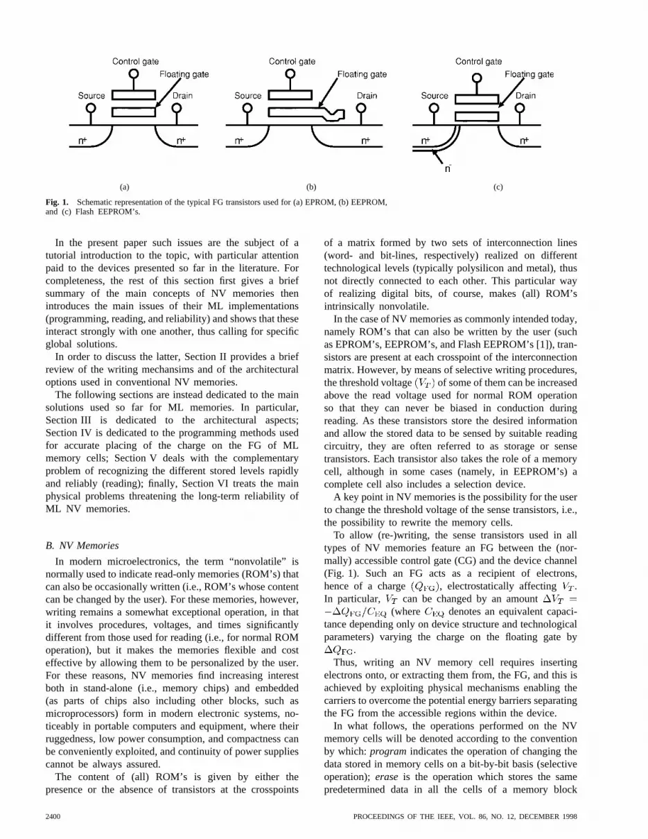
Fig. 1. Schematic representation of the typical FG transistors used for (a) EPROM, (b) EEPROM,and (c) Flash EEPROM’s.
In the present paper such issues are the subject of atutorial introduction to the topic, with particular attentionpaid to the devices presented so far in the literature. Forcompleteness, the rest of this section first gives a briefsummary of the main concepts of NV memories thenintroduces the main issues of their ML implementations(programming, reading, and reliability) and shows that theseinteract strongly with one another, thus calling for specificglobal solutions.
In order to discuss the latter, Section II provides a briefreview of the writing mechansims and of the architecturaloptions used in conventional NV memories.
The following sections are instead dedicated to the mainsolutions used so far for ML memories. In particular,Section III is dedicated to the architectural aspects;Section IV is dedicated to the programming methods usedfor accurate placing of the charge on the FG of MLmemory cells; Section V deals with the complementaryproblem of recognizing the different stored levels rapidlyand reliably (reading); finally, Section VI treats the mainphysical problems threatening the long-term reliability ofML NV memories.
B. NV Memories
In modern microelectronics, the term “nonvolatile” isnormally used to indicate read-only memories (ROM’s) thatcan also be occasionally written (i.e., ROM’s whose contentcan be changed by the user). For these memories, however,writing remains a somewhat exceptional operation, in thatit involves procedures, voltages, and times significantlydifferent from those used for reading (i.e., for normal ROMoperation), but it makes the memories flexible and costeffective by allowing them to be personalized by the user.For these reasons, NV memories find increasing interestboth in stand-alone (i.e., memory chips) and embedded(as parts of chips also including other blocks, such asmicroprocessors) form in modern electronic systems, no-ticeably in portable computers and equipment, where theirruggedness, low power consumption, and compactness canbe conveniently exploited, and continuity of power suppliescannot be always assured.
The content of (all) ROM’s is given by either thepresence or the absence of transistors at the crosspoints
of a matrix formed by two sets of interconnection lines(word- and bit-lines, respectively) realized on differenttechnological levels (typically polysilicon and metal), thusnot directly connected to each other. This particular wayof realizing digital bits, of course, makes (all) ROM’sintrinsically nonvolatile.
In the case of NV memories as commonly intended today,namely ROM’s that can also be written by the user (suchas EPROM’s, EEPROM’s, and Flash EEPROM’s [1]), tran-sistors are present at each crosspoint of the interconnectionmatrix. However, by means of selective writing procedures,the threshold voltage of some of them can be increasedabove the read voltage used for normal ROM operationso that they can never be biased in conduction duringreading. As these transistors store the desired informationand allow the stored data to be sensed by suitable readingcircuitry, they are often referred to as storage or sensetransistors. Each transistor also takes the role of a memorycell, although in some cases (namely, in EEPROM’s) acomplete cell also includes a selection device.
A key point in NV memories is the possibility for the userto change the threshold voltage of the sense transistors, i.e.,the possibility to rewrite the memory cells.
To allow (re-)writing, the sense transistors used in alltypes of NV memories feature an FG between the (nor-mally) accessible control gate (CG) and the device channel(Fig. 1). Such an FG acts as a recipient of electrons,hence of a charge , electrostatically affecting .In particular, can be changed by an amount
(where denotes an equivalent capaci-tance depending only on device structure and technologicalparameters) varying the charge on the floating gate by
.Thus, writing an NV memory cell requires inserting
electrons onto, or extracting them from, the FG, and this isachieved by exploiting physical mechanisms enabling thecarriers to overcome the potential energy barriers separatingthe FG from the accessible regions within the device.
In what follows, the operations performed on the NVmemory cells will be denoted according to the conventionby which: program indicates the operation of changing thedata stored in memory cells on a bit-by-bit basis (selectiveoperation);erase is the operation which stores the samepredetermined data in all the cells of a memory block
2400 PROCEEDINGS OF THE IEEE, VOL. 86, NO. 12, DECEMBER 1998

(unselective data operation);write indicates one or the otherof these operations indifferently.
In the case of EPROM and Flash memories, eitherprogram or erase is selective (i.e., is performed on a selectednumber of cells), while the other operation has a highdegree of parallelism, in that a whole sector or the entirememory is written simultaneously. Both these operations,instead, are selective in EEPROM’s, defined functionallyjust by the possibility to program and erase single bytes.
Naturally, for the memory to adequately retain the storeddata, the leakage current to and from the FG under normalreading conditions must be extremely small, and this isusually the case since the FG is completely isolated bymeans of silicon dioxide (SiO). Thus, data retention (i.e.,the time required for the stored charge to vary by 10%)normally is extremely long, although defective cells anddecreased oxide thickness are causes of concern in thisrespect.
On the contrary, during program and erase it is necessaryto force a significant current through the oxide isolating theFG, and different physical mechanisms can be used for thispurpose.
In particular, channel hot electrons (CHE’s) can be in-jected into the FG by applying to the device channel adriving field much higher (in the order of 10V/cm) thanthat used during normal reading, so as to make a significantfraction of the carriers sufficiently energetic to surmountthe energy barrier (about 3 eV) of the Si–SiOsystem [2],[3]. Alternatively, the Si–SiO energy barrier can be madesufficiently transparent for electrons to pass through it byFowler–Nordheim (FN) tunneling [4] by applying a verystrong field (in the range of 10V/cm) across the insulator.
Electrons can be extracted from the FG by means of FNtunneling, or be made sufficiently energetic to surmountthe Si–SiO energy barrier by bombardment with ultraviolet(UV) photons. The latter procedure is obviously non (fully)electrical and, being inherently nonselective, can be usedonly for erasing.
All the mentioned writing methods are used in differenttypes of NV memories. In particular, EPROM’s are pro-grammed by means of CHE’s and erased by UV exposure,while EEPROM’s are both programmed and erased by FNtunneling. As for Flash devices, they are erased by FNtunneling, while currently most of them are programmedby means of CHE’s, although memories exploiting FNtunneling for both program and erase operations have beenproposed and might become important in the future.
C. The ML Solution
As is already known, the density of data storage (i.e., thenumber of bits that can be stored per unit area) and thecost-per-bit are the essential driving factors for memorydevelopment.
As both these factors are strictly dependent on the physi-cal dimensions of the memory cells, so far the developmentof new generations of NV memories has entirely reliedon the geometry scaling characterizing advanced micro-electronics. This approach, however, can be accompanied
and augmented by the ML data-storage concept, whichin principle is very simple and intuitive, and that can beapplied to the same technology and devices of conventionalbilevel memories.
In the case of the latter, as described in Section I-B,the memory cells can have only two different values of
(or, rather, two distributions of values), and duringreading it is only necessary to sense whether or not theaddressed transistor is conductive. This is generally doneby comparing the drain current of the sense transistor
to that of a reference cell under the same, fixedbias conditions, either directly or by means of a current-to-voltage conversion.
However, the of NV (sense) transistors dependsanalogically on the amount of charge stored on the FG;thus, , hence can be changed over a large rangeof values simply varying .
Thus, if the reading (sensing) circuitry can resolve adifference in the current, in principle each cell canbe made to store bits, with ,where denotes the value of through the mostconductive cell (i.e., the cell with the lowest ).
In the extreme case of negligibly small values of, the cell would be operated as a fully analog
device able to store an arbitrarily large amount of data;however, sensing would be critically difficult and prone toerrors, and reliability problems would become prohibitivelycritical. On the contrary, in the traditional digital case
, we have , but sensing is easierthan for higher values of . In practice, a number ofintermediate cases can be considered, and the questionarises of which value of leads to the most cost-effectiveuse of silicon area. Naturally, the answer to this questiondepends not only on technology and architecture, but alsoon programming and reading circuitry, as well as on cellreliability.
To have a quantitative idea of the possible advantages, letus consider, for instance, a 64-Mbit memory organized in8-bit words. With the conventional bilevel approach, eightblocks of 8 M cells are required. Storing two bits per cell,only four blocks of 8 M cells would be necessary, whileif 4 bits could be stored on the same cell, two 8-M cellblocks would be enough. Furthermore, it should be pointedout that reducing the dimension of the cell array also leadsto a corresponding reduction in decoder circuitry.
This example makes it immediately clear that the MLapproach offers very significant advantages. At this re-gard, Table 1 [5] compares estimated performance of ahypothetical 64-Mbit (8 8-Mbit) Flash memory with anNOR architecture for different numbers of bits per cell. Forthis example, a state-of-the-art 0.6m CMOS technologyallowing cell areas of 2.9 m has been considered. In thisexercise, the basic building blocks of the reading circuitryare the same.
The current state of the art is that NV Flash memoriesstoring two bits per cell (i.e., four-level charge storage)have already been presented [6]–[10], and the same resultis also in reach for EPROM’s and EEPROM’s, while the
RICCO et al.: NONVOLATILE MULTILEVEL MEMORIES 2401

Table 1Comparison Between Different Realization of a64-Mbit (8 � 8-Mbit) Memory Using 2, 4, and16 Levels Per Cell and Different Read Schemes
3-bit/cell solution is considered feasible, though significantresearch is still needed for it to become a reality. Instead,the possibility to go beyond this limit needs careful investi-gation [11], [12] and is generally looked at with skepticism(but microelectronics has consistently shown that the limitsto what can or cannot be done are continuously movingforward).
In fact, 256-level storage has already been implementedin EEPROM technology for voice recording [13]. This,however, is considered practically to be an analog case withspecial features (since the application is largely tolerant oferrors) and will no longer be considered in this work.
From the device point of view, ML charge storage posesthree main problems, all of which are becoming moresevere as the distance between different levels (measured interms of either stored charge or cell conductivity) decreaseswith increasing number of bits per cell, namely: 1) accuratewriting, i.e., the placement of exactly the required amountof charge on the FG of the cell transistors; 2) precisereading, i.e., the capacity to recognize different cell conduc-tivities in a short time; and 3) reliability, in particular, thecell capability to avoid merging of adjacent stored levels.
The first problem is generally tackled by means of bit-by-bit program and verify ( - ) schemes (Section IV),in which a number of partial steps are used to programthe cells and the result is sensed after each of them(program–verify, - ) in order to determine whether or notthe target is achieved, so as to continue programming ifthis is not the case. This procedure ensures that the targetis reached (with the accuracy allowed by the quantizationinherent in the use of finite programming steps), but it canbe very long and must be controlled by on-chip logics,leading to a non-negligible area overhead.
The alternative approach is based on self-convergingor self-controlling techniques able to stop programmingautomatically when reaching the target . These proce-dures are less developed and looked at with somewhatless confidence than - schemes: thus they have notyet been used in commercial products, but they couldprovide faster and simpler operation, and thus deservecareful consideration [14], [15].
As far as writing techniques are concerned, CHE in-jection and FN tunneling present different characteristics,advantages, and drawbacks, making them somewhat com-plementary and suitable for different types of architecturesand applications [16].
Fig. 2. Conceptual representation of the threshold voltage distri-butions needed for four-level charge storage (i.e., for 2 bits/cellMLM’s).
The distribution for an ML memory (MLM) usingCHE injection for programming and channel FN tunnelingfor erasing is shown in Fig. 2 (four levels per cell,NOR
architecture). In this figure, the threshold voltages of thereference cells used for the verify operation following anerase step (“erase-verify”), for - and for reading (EV,PVi, and Ri, to , respectively) are also illustrated.The lowest level derives from erasing unselectively awhole memory sector; the dispersion of cell characteristicsgives rise to a distribution as large as 1.5 V ormore [17]. Since in conventionalNOR architectures all
’s must be sufficiently positive, the large width ofthis level greatly decreases the threshold voltage win-dow allowed for the programmed states. Several methodshave been proposed to tighten the eraseddistribution[18]–[20], however, a severe limitation is imposed by therequirement that verification after erasure can be carriedout only when bit-line leakage is negligible to preventfalse results.
The highest level can be placed above the readvoltage, as it can be detected by sensing zero currentthrough the selected cell during both- and reading.However, the read gate voltage must be higher thanthe maximum value of the third level (01) by a givenamount (in the range of 0.5 to 1 V) to allow the two highest
levels to be discriminated.Reliability aspects (read disturb of erased cells in the
addressed word line) and design considerations (need forlimiting silicon area and power consumption overhead dueto the charge pumps required to generate read voltageshigher than ) suggest a maximum value around 6 Vfor [21].
The distribution width of the three programmed levelscan be reduced by using suitable algorithms based on thebit-by-bit - approach (Section IV), with the drawbackof longer times needed for programming.
In MLM’s, enhanced sensitivity to program disturbs isexpected because of reduced margins between adjacentstates and/or larger window (increasing with the numberof stored levels for the same separation among them)and increased program time (because the higher accuracyrequired in charge placing makes the time needed for theoperation to be completed successfully longer).
2402 PROCEEDINGS OF THE IEEE, VOL. 86, NO. 12, DECEMBER 1998

The worst case occurs for the bit-line disturb on a cellprogrammed to the highest level because of the large
shift with respect to the neutral state. Moreover, pro-gramming the drain voltage is the same as in conventionalFlash memories but the time is longer. On the contrary,word-line disturb should not be affected substantially bythe increase in program time, at least for a staircase gate-voltage programming algorithm, since during most of thetime the word-line voltage is rather low and only thelast few pulses will effectively contribute to the disturb.Optimized cell design for low drain voltage programmingand divided bit-line organization are probably required toguarantee sufficient program disturb immunity.
As for reading, the operation essentially can be consid-ered as an analog-to-digital (A/D) conversion of the signalproduced by the addressed cell, and the key issue concernsthe tradeoff between speed and accuracy, in that as thelatter is increased (i.e., as smaller values of canbe safely recognized) a larger number of bits can be storedon a single cell, but the sensing circuitry becomes moreexpensive and globally slower. In general, the required A/Dconversion can be done in parallel or sequentially for higherspeed and smaller area occupation, respectively, whileintermediate solutions offer interesting tradeoffs betweenthese conflicting aspects.
With regard to reliability, instead, the crucial problem ofdata retention is better expressed in terms of the numberof stored electrons. With FG capacitances in the 10F range, threshold voltage windows of a few requirevariations of about 30 000 electrons in the FG. If thisvariation is split, for instance, in four levels, the states of thesense transistors differ from one another by about 10 000electrons, and this difference should be maintained for morethan ten years. This implies that less than about 1 000electrons should leak out from (or into) the FG in one year,i.e., that the (average) leakage currents through the oxideinsulating the FG should be smaller than 10A (or, about10 A/cm ). Of course, this problem is significantlyaggravated if the number of levels programmed in a cellis increased and/or the total window is narrowed.
The problem can (and must) be alleviated in part withthe use of redundancy- and error-detecting codes, but thevery small numbers given above clearly indicate the need ofoutstanding insulating properties. From this point of view,stress-induced leakage current (SILC), i.e., the excess low-field conductivity of the oxide induced by the high fieldstress used during tunnel programming [22], [23] and/oroxide time-dependent breakdown poses serious problems.
In any case, MLM’s must meet much more stringentrequirements than conventional bilevel memories in termsof threshold voltage distribution for each stored level, dataretention, program/read disturb immunity, and design issues(namely, sense and program accuracies) [21], [24], [25].
D. Problem Interaction
The successful realization of MLM’s and the numberof bits that can be stored in a single cell depend on thesolutions given to the main problems mentioned above
(accurate charge placement, cell sensing, and reliability).Such solutions, however, are strongly dependent on thephysical mechanism used for cell writing as well as onthe memory architectures, which are fundamental ingre-dients determining the complexity, performance, and costeffectiveness of memory chips.
Thus, the realization of MLM’s represents a uniqueglobal problem composed of many interacting aspects thatmust be considered concurrently in the conception anddevelopment of real products, as well as in the analysisof the subject, as is done in the rest of this paper.
II. BASICS IN NV MEMORIES
A. Writing Mechanisms
MLM’s make use of the same physical mechanismsfor injecting and/or extracting electrons from the FG astheir conventional (i.e., bilevel) counterparts, namely CHEinjection and FN tunneling, while UV exposure can alsobe used for erasing. ML operation, however, has morestringent requirements since it needs accurate control ofthe distributions of the different levels, which must notonly be narrow but also well separated.
CHE injection and FN tunneling present specific featuresthat interact strongly with circuit and architectural aspects;these are briefly reviewed below.
The CHE mechanism enables electrons to be injectedinto the cell FG by applying a suitable medium–high drainvoltage (to heat the electrons within the transistor channel)and a high gate voltage, providing both adequate electrondensity in the channel and sufficient electric field in thegate oxide ( , in any case significantly lower than thatrequired for FN tunneling).
The injection efficiency of CHE injection is very small,as the current flowing through the gate oxide is only a verysmall fraction of the cell-drain current. Typical values ofdrain currents during programming are in the range of a fewhundred A per cell, although an optimized cell structurecan operate with currents around 100A or less [26], whilethe average current injected into the gate oxide is inthe range of 0.1 to 1 nA.
Naturally, it is not possible to heat electrons within theFG by means of an electric field; thus the hot electronmechanism cannot be used to extract electrons from it.
FN tunneling, instead, allows injection of cold carriersand gives rise to a current flowing into (or from) the FG,that exhibits a (quasi) exponential dependence on andcan be reversed by simply changing the sign of such afield; thus it can be used for both injection and extractionof electrons into/from the FG. For these operations to becompleted in practical times, a very high field is needed (inthe range of 8–10 MV/cm), which gives rise to reliabilityproblems ultimately limiting the writing speed, while thehigh voltages required to generate adequate fields are noteasy to handle at the circuit level.
Two different FN tunneling schemes are of interest forNV memories. In the first one (channel FN tunneling),
RICCO et al.: NONVOLATILE MULTILEVEL MEMORIES 2403

the high voltage is applied between the cell CG and thesubstrate, while drain and source are floating or tied to thesubstrate. Under these conditions, the injection efficiencyis close to unity because, apart from very small leakagecontributions, the only current flowing in the cell is thetunneling current (today limited by reliability constraints tovalues in the range of a few pA).
In the second case (source- or drain-side FN tunnel-ing), the high voltage is applied between the drain orsource electrode (positively biased) and the CG (which isgrounded or negatively biased), while keeping the substrategrounded. In this condition the leakage current of thereverse biased source/substrate or drain/substrate junctioncan be significant because of carrier generation by band-to-band tunneling in the high-field region at the silicon/oxideinterface. The field present at the reversely biased junctionsseparates the generated carriers, thus giving rise to a non-negligible parasitic current, which can reach a fewA percell under worst-case conditions.
The main advantages of CHE injection with respect to FNtunneling as a program mechanism are the higher speed andlower electric fields, which imply better endurance [16],lower voltages, less circuit overhead, and disturbs in thearray. The last item deserves particular attention in the caseof MLM’s due to the longer program time needed to achievethe required accuracy. The higher program speed allowsfor a larger number of program pulses in any given timeinterval, which leads theoretically to better controlleddistributions by adopting - techniques.
On the other hand, FN tunneling requires much lowerpower consumption, thus allowing large program paral-lelism, exploitable for page-mode operation, to increase theoverall program throughput [7], [9]. Although it allows oneto overcome the low speed of FN tunneling, page program-ming requires considerable additional on-chip circuitry,hence it implies significant area overheads that, in practice,are justified only in stand-alone memories. Low powerconsumption also makes it easier to generate internally thehigh voltages required for programming/erasing by meansof on-chip charge-pumps [27], [28].
In order to reach a good compromise between the lowpower consumption of FN tunneling and the high programspeed allowed by CHE injection, a particular kind ofhot electron injection named source side injection (SSI)has been proposed [29], [30]. It operates on a standard-CMOS compatible split-gate Flash-memory cell referredto as HIMOS (high injection MOS) cell, and it achievesvery high speed with reasonably low voltages. Extremelyhigh injection efficiency is obtained by appropriately bi-asing the CG, thus requiring program currents of onlyabout 25 A per cell and resulting in a medium/lowpower consumption. The injection current is only weaklydependent on lateral device geometry, which reduces itssensitivity to process variations [31]. Furthermore, thanksto the split-gate structure (Section II-B) of the cell, SSIcan be combined with a large read-out threshold window,which is extremely important to space apart the differentlevels in ML applications [15]. However, due to a larger
cell area, this approach is of practical interest primarily forembedded applications.
In terms of process dependency, CHE injection is sensi-tive mainly to the effective channel length of the device,while FN tunneling is affected more by variations in tunneloxide thickness. Both these writing mechanisms are alsosensitive to coupling coefficients between the FG and othercell electrodes. Generally, the intrinsic (i.e., nonverified)
distribution turns out to be wider for FN tunneling,exhibiting stronger process sensitivity than CHE injection[16]. Moreover, FN tunneling is also affected by the so-called erratic bit problem (Section VI). Finally, it shouldbe pointed out that the use of CHE injection allows fordecoupling programs and erase operations (which take placein different sections of the cell), thus simplifying celloptimization.
B. Array Architectures
NV memories can have anNOR or anNAND architecture[32]. In the former case (also referred to as common-groundNOR), the cells belonging to any array column are connectedin parallel between the respective bit-line and a commonsource line (ground) [Fig. 3(a)]. Cells can be addressed forreading by forcing the corresponding word-line to a positiveread voltage, while all unselected word-lines are grounded.Under these conditions, the bit-line current to be sensedfor reading is due only to the addressed cell, providedthat all other (unselected) cells connected to the samebit-line, with grounded gates, have sufficiently positivethreshold voltages. Unselected cells not complying with thiscondition produce bit-line leakage, which severely disturbscorrect reading; thus theNOR architecture is very sensitiveto cell overerasure. To avoid this problem, the split-gateconcept has also been introduced [33]–[35], where a selecttransistor, merged with the storage element in a singlecell, keeps the unselected cells in the off-state regardlessof the threshold voltage of the storage device. However,the resulting cell size increase reduces substantially theachievable integration density.
The NOR architecture allows both CHE and FN program-ming as well as high sensing speed (since the selected cellis directly connected between the bit-line and ground) andis suitable for both stand-alone and embedded applications.For these reasons, it is widely used at the industrial level;consequently it is very well understood and has the ad-vantage of a very strong experience gathered in years ofdevelopment and production. The main disadvantage of thisarchitecture is its relatively low integration density due tothe need for one bit-line contact hole every two cells.
Higher density is achieved by means of theNAND archi-tecture [36], [37] [Fig. 3(b)]. In this case, the bit-lines areorganized in strings made up of a given number (e.g., eight,16, or 32) of series-connected cells. The strings belonging tothe same bit-line are connected in parallel between the bit-line and a common source line (ground). Each string alsoincludes two select transistors driven by the string selectline (SSL) and ground select line (GSL) for connection tothe bit-line and ground, respectively. To access any given
2404 PROCEEDINGS OF THE IEEE, VOL. 86, NO. 12, DECEMBER 1998

(a)
(b)
Fig. 3. Schematic representation of (a)NOR and (b)NAND memory architecture.
cell in a selected string, it is necessary not only to activatethe corresponding select transistors, but also to set all theother cells of the string in their conductive state. To this end,the word lines of the unselected cells of the string are biasedwith a positive voltage higher than the highest allowed.A suitable lower read voltage is obviously applied to theselected word-line.
In spite of the need for the two additional select tran-sistors per string, an appreciable increase in integrationdensity is achieved, as no contact hole is present within thestring. However, selected cells must be accessed through theother (unselected) cells of the string. This gives rise to anon-negligible series resistance (depending on programmedthreshold voltages) that limits the maximum number ofstring cells and reduces reading speed (in practice, restrict-ing the application of this architecture to mass storage,where page-mode operation makes the sensing time of
individual cells not so important). Moreover, due to theseries connection of a number of transistors, the use ofCHE injection would require program voltages that are toohigh, and it would lead to very critical disturbs on the cellsthat are not to be programmed; thus, only FN tunneling canbe used as the programming mechanism. Furthermore, thehigh voltages applied to the unselected word lines duringreading cause substantial read disturbs. Finally, theNAND
architecture suffers from inter-bit-line capacitive couplingnoise, due to simultaneous activation of adjacent bit linesfor page parallel sensing [38], which obviously increasesas the bit-line pitch is narrowed. To minimize this couplingnoise, causing undesired broadening of thedistributions,a sensing technique has been proposed where selected bitlines are sandwiched between shielding grounded bit lines.
Based on the fundamentalNOR concept, other arrayarchitectures have been developed [1], [16] with the main
RICCO et al.: NONVOLATILE MULTILEVEL MEMORIES 2405

Table 2CHE Versus FN Programming Mechanism
Table 3NOR VersusNAND Architecture
purpose of increasing integration density. These includethe divided NOR (DINOR) array, where each bit line isorganized in strings made up of parallel-connected cells[39], [40], the AND array, which combines the commongroundNOR and DINOR concepts [41], and theNOR virtualground array, which can be based on a conventional cellstructure (such as the alternate metal ground (AMG) [42],[43], where one metal line is present every two diffusedbit lines), or on a split-gate cell [30], [44]. Each of thesearchitecture has specific advantages and disadvantages.However, the common groundNOR array remains by farthe most widespread choice in industrial products.
To conclude, Tables 2 and 3 summarize the compari-son of the analyzed programming mechanisms and arrayarchitectures, respectively.
III. A RCHITECTURES FOR THEML A PPROACH
Even though, in principle, the ML concept can be coupledto any kind of memory architecture, in this paper we con-sider specifically the cases reported so far in the literature[6]–[10], all implementing a four-level (i.e., 2-bit/cell) MLscheme but differing substantially as far as programmingmechanisms, architectures, and implementations are con-cerned (Table 4).
Since the basic features of the MLM prototype presentedin [6], which has a standardNOR architecture and uses CHEprogramming and source-side FN erasing, have alreadybeen discussed in Section I-B, we will now briefly describethe characteristics of the other prototypes.
In the NOR MLM presented in [10], programming isachieved by extracting electrons from the FG by drain-side FN tunneling, and erasing is performed by injectingelectrons into the FG by channel FN tunneling (Fig. 4).The resulting distribution is shown in Fig. 5, where the
Table 4Key Features of ML Flash Experimental Chips (2 Bits Per Cell)
Fig. 4. Writing mechanisms as a function of different architec-tures: (a) [6], (b) [10], and (c) [9].
Fig. 5. Schematic representation of the threshold voltage distri-butions used in theNOR ML memory of [10].
2406 PROCEEDINGS OF THE IEEE, VOL. 86, NO. 12, DECEMBER 1998
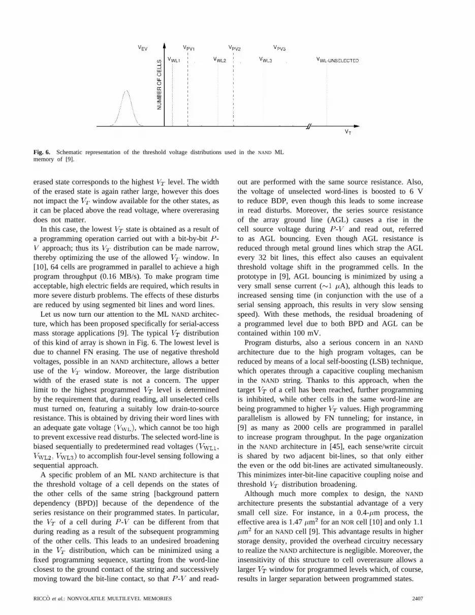
Fig. 6. Schematic representation of the threshold voltage distributions used in theNAND MLmemory of [9].
erased state corresponds to the highestlevel. The widthof the erased state is again rather large, however this doesnot impact the window available for the other states, asit can be placed above the read voltage, where overerasingdoes not matter.
In this case, the lowest state is obtained as a result ofa programming operation carried out with a bit-by-bit-
approach; thus its distribution can be made narrow,thereby optimizing the use of the allowed window. In[10], 64 cells are programmed in parallel to achieve a highprogram throughput (0.16 MB/s). To make program timeacceptable, high electric fields are required, which results inmore severe disturb problems. The effects of these disturbsare reduced by using segmented bit lines and word lines.
Let us now turn our attention to the MLNAND architec-ture, which has been proposed specifically for serial-accessmass storage applications [9]. The typical distributionof this kind of array is shown in Fig. 6. The lowest level isdue to channel FN erasing. The use of negative thresholdvoltages, possible in anNAND architecture, allows a betteruse of the window. Moreover, the large distributionwidth of the erased state is not a concern. The upperlimit to the highest programmed level is determinedby the requirement that, during reading, all unselected cellsmust turned on, featuring a suitably low drain-to-sourceresistance. This is obtained by driving their word lines withan adequate gate voltage , which cannot be too highto prevent excessive read disturbs. The selected word-line isbiased sequentially to predetermined read voltages
to accomplish four-level sensing following asequential approach.
A specific problem of an MLNAND architecture is thatthe threshold voltage of a cell depends on the states ofthe other cells of the same string [background patterndependency (BPD)] because of the dependence of theseries resistance on their programmed states. In particular,the of a cell during - can be different from thatduring reading as a result of the subsequent programmingof the other cells. This leads to an undesired broadeningin the distribution, which can be minimized using afixed programming sequence, starting from the word-lineclosest to the ground contact of the string and successivelymoving toward the bit-line contact, so that- and read-
out are performed with the same source resistance. Also,the voltage of unselected word-lines is boosted to 6 Vto reduce BDP, even though this leads to some increasein read disturbs. Moreover, the series source resistanceof the array ground line (AGL) causes a rise in thecell source voltage during - and read out, referredto as AGL bouncing. Even though AGL resistance isreduced through metal ground lines which strap the AGLevery 32 bit lines, this effect also causes an equivalentthreshold voltage shift in the programmed cells. In theprototype in [9], AGL bouncing is minimized by using avery small sense current ( A), although this leads toincreased sensing time (in conjunction with the use of aserial sensing approach, this results in very slow sensingspeed). With these methods, the residual broadening ofa programmed level due to both BPD and AGL can becontained within 100 mV.
Program disturbs, also a serious concern in anNAND
architecture due to the high program voltages, can bereduced by means of a local self-boosting (LSB) technique,which operates through a capacitive coupling mechanismin the NAND string. Thanks to this approach, when thetarget of a cell has been reached, further programmingis inhibited, while other cells in the same word-line arebeing programmed to higher values. High programmingparallelism is allowed by FN tunneling; for instance, in[9] as many as 2000 cells are programmed in parallelto increase program throughput. In the page organizationin the NAND architecture in [45], each sense/write circuitis shared by two adjacent bit-lines, so that only eitherthe even or the odd bit-lines are activated simultaneously.This minimizes inter-bit-line capacitive coupling noise andthreshold distribution broadening.
Although much more complex to design, theNAND
architecture presents the substantial advantage of a verysmall cell size. For instance, in a 0.4-m process, theeffective area is 1.47m for anNOR cell [10] and only 1.1
m for an NAND cell [9]. This advantage results in higherstorage density, provided the overhead circuitry necessaryto realize theNAND architecture is negligible. Moreover, theinsensitivity of this structure to cell overerasure allows alarger window for programmed levels which, of course,results in larger separation between programmed states.
RICCO et al.: NONVOLATILE MULTILEVEL MEMORIES 2407

As mentioned above, however, in practice theNAND
architecture requires complex design as it needs pageprogramming (to achieve high throughput), high read-out voltages, suitable programming sequences (to elim-inate BPD), low sensing current (to reduce AGL), andsuitable LSB technique (to minimize program disturbs).Furthermore, to solve the problems of the series resistanceand BPD due to the series-connected cells in a string, aparticular technique has also been proposed [46] where eachcell includes a transfer transistor connected in parallel withthe FG transistor that, when unselected, can be bypassedso as to minimize the cell series resistance. To save siliconarea, the transfer device is located at the sidewall of theshallow trench isolation region at the cost of increasedfabrication complexity.
Since these solutions increase not only the chip area butalso the complexity of the design and/or fabrication process,it seems that theNAND architecture needs many effortsat the design and technological levels to allow successfulimplementation of ML storage [16].
IV. ML PROGRAM SCHEMES
A. Programming and Accuracy
The goal of ML program schemes is to implementsuitable algorithms and on-chip circuitry able to achieveadequately narrow and spaced distributions in a reason-able time. Obviously, to allocate more than two thresholdlevels within a predetermined window, much morestringent requirements than in the case of conventional bi-level memories must be met: in particular, the distributionwidth of each programmed level becomes more critical,and this generates the need for accurate control of theprogrammed of FG transistors, that finds applicationseven beyond the field of NV memories [47]. For a popula-tion of nominally identical cells, accurate programmingrequires precise control of charge transfer into/from theFG, hence of (for given program times). Since, onthe other hand, (due to either CHE injection or FNtunneling) depends only on the cells bias conditions, inprinciple precise values could be achieved by accuratelycontrolling applied voltages and program times.
If the cell bias is kept fixed during programming, as elec-trons are moved through the oxide, the FG potential changesand decreases. Thus, charge transfer becomes progres-sively less efficient. Fig. 7 shows the program curves (and versus time) typical of Flash cells programmed bymeans of CHE injection, but a qualitatively similar behavioris found also when FN tunneling is used.
For the same drain voltage and pulse duration, a higherprogram gate voltage results in a higher oxidecurrent, hence in a larger threshold voltage shift .For any given cell, a linear relationship exists between theapplied and the obtained , evaluated with respectto the threshold voltage of the UV-erased cell [21], [24].However, the absolute value of for a given valueof strongly depends on process parameters, and the
(a)
(b)
Fig. 7. Typical programming curves of Flash memories, showing(a) the threshold voltage shift and (b) estimated injection currentas a function of time.
convergence of to its target value is too slow; thus, inpractice, this simple method can hardly provide adequatelyreproducible and narrow distributions. Consequently,some adjustment in the program conditions must be doneto account for the real characteristics of individual cells.
This result can be achieved in different ways. A first typeof solution consists of using self-convergent program mech-anisms providing a well-defined final state, independent ofthe cell actual characteristics. From this point of view CHEinjection offers some (theoretical) possibilities [48], whosereal viability, however, is still to be investigated.
The other approach, used universally to achieve thenecessary precision, is that of verifying the result of pro-gramming, which is continued until the target is actuallyreached. Such an approach, however, can have different im-plementations according to whether the verification is doneunder reading conditions or during programming itself.
In the former case, corresponding to the- techniquementioned in the Section I, programming is divided in anumber of partial steps, and at the end of each of themthe cell is read with the same circuitry that will be usedfor normal ROM operation, in order to determine whetheror not has reached the target values. If this is notthe case, another programming step is performed and thewhole procedure is repeated until successful completion.In applying this scheme, the obvious choice is a cell-by-cell - approach [49] that can be used with bothNOR
and NAND architectures [38], [50] and is compatible withparallel programming. With cell-by-cell - procedures,as the cell threshold voltage is controlled individually,endurance issues due to the window closure [51]
2408 PROCEEDINGS OF THE IEEE, VOL. 86, NO. 12, DECEMBER 1998

are not a major concern, provided that sufficiently longprogram times are allowed, because the target value of
is always reached (although with a variable numberof program steps). In fact, the achievable accuracy dependsideally only on the quantization error inherent to the useof finite program steps, although if these are made small(for high precision), program time can become excessivelylong. Beside that concerning endurance,- programmingoffers further reliability advantages due to the fact thatonly the minimum required charge flows through the oxide.Since - schemes lead to nonnegligible area overhead,they are typically suited for stand-alone applications, wherelarge memory arrays are present. Alternatively, verificationcan be done during a unique program operation, automati-cally stopping when reaching the desired target. Comparedwith standard - schemes, these self-controlled methodsoffer a better tradeoff between accuracy and program time,maintain all the advantages in terms of reliability, andmay require simpler control circuitry (hence smaller areaoverhead). However, cell sensing is made under programconditions, hence significant differences can occur betweenverification and normal cell reading, with obvious effectson the functional accuracy of the whole operation.
Furthermore, it must be mentioned that the significantgrowth of the demand for embedded memories has in-creased the interest for reliable, fast, and nonverified pro-gram methods, requiring minimum additional circuitry,though leading to worse endurance performance and widerthreshold distributions than in verified cases [52]. In par-ticular, a technique has been proposed for HIMOS cells[15] that utilizes a voltage variant source side injection(VVSSI) mechanism, where gate voltage pulses with fixedtime width and different amplitude are applied to achievedifferent levels, while source and drain voltages arekept constant. Narrow and well-separated distributionscan be achieved. The spacing between adjacent distributionlevels can be further improved and optimized by adaptingthe various program voltages.
Finally, a consideration must be made about the possibil-ity to program NV memories (possibly with ML operation)off chip, at the end of fabrication or even by the user.This procedure needs special circuitry for direct access tothe memory array, requires external programming systems,and is inherently slow; thus, it is particularly suitable formemories that must be programmed only once (or at mosta limited number of times). However, it has interestingaspects, because with sophisticated equipments and suffi-ciently long program time, very narrow distributionscan be obtained.
In the rest of this section, a number of specific pro-gram methods proposed for NV MLM’s will be brieflyoverviewed.
B. P-V Techniques
1) Gate-Voltage Programming:A - technique suit-able for ML schemes using CHE injection exploits thelinear relationship between and by using astaircase waveform for the gate voltage, which is increased
Fig. 8. Threshold shift as a function of the number of pro-gramming pulses when using an adaptive staircase gate voltagealgorithm for CHE programming (the gate voltage step is 0.5 V)[21]. The gate voltageVG used at each program step is shown inthe upper axis. Three different cell channel lengths were used.
Fig. 9. Threshold shift as a function of the number of pro-gramming pulses when using an adaptive staircase gate voltagealgorithm for Fowler–Nordheim programming. Three differentstaircase steps were used [9].
at each program step by a fixed amount . In thisregard, Fig. 8 clearly shows that for any channel length,after the first few steps, the increase after each programpulse is equal to the program gate voltage increase .Similar results are obtained when cell width or oxide-thickness spreads are considered [21].
The concept illustrated above is also valid in the case ofFN tunneling. For this reason staircase programming [49]has also been proposed for the case of MLM’s making useof FN tunneling [9], [45], [53]–[56]. The program curvesobtained in [9] are shown in Fig. 9. When programming isperformed by drain-side FN tunneling, this technique canbe implemented either by using a fixed drain voltage and astaircase gate voltage, or by applying a fixed gate voltageand a stepped drain voltage (in the latter case, however, themethod is sensitive to process variations).
RICCO et al.: NONVOLATILE MULTILEVEL MEMORIES 2409

Fig. 10. Programming curves obtained using the DCMP tech-nique [10].
- staircase programming should theoretically givedistribution widths not larger than independent
of the number of cells programmed to that state since,neglecting errors due to sense amplifier accuracy or voltagefluctuations; the last program pulse applied to a cell willcause its threshold voltage to be shifted above the decisionlevel used for verification by an amount at most as largeas .
Using small incremental steps for distributionsadequate for a large number of levels can be achieved.However, this also results in increased program time, and asearch for optimum tradeoffs between time and the numberof usable levels and/or suitable architectural solutions is inorder. In this respect,NAND multipage architectures [57]have been proposed to increase program throughput.
2) Drain Voltage Programming:When programming bymeans of drain-side FN tunneling, (hence also )can be varied by changing and/or the drain volt-age . In particular, for parallel ML programming atechnique called drain-voltage controlled multilevel pro-gramming (DCMP) [10] has been proposed, with whichtarget values are achieved by applying suitable drainvoltages , while keeping at a constant value(Fig. 10). Memory cells belonging to the selected word linecan be programmed to different levels in the same programperiod by providing the required different voltages toeach bit line: different bit-line voltages are used forsimultaneously programming different levels. Eachprogram step has a fixed time duration. Fig. 10 shows thata difference in the range of 1.5 V between adjacentstates is obtained after a 100-s program time by setting
equal to 9 V and in the range from 0 V to 6 V.A - approach using a parallel multilevel verify (PMV)scheme is adopted to achieve the requiredcontrol ofthe cells being programmed.
C. Self-Controlled Programming
As already mentioned, an attractive way to speed upprogramming and eliminate the need for iterative-sequences, thus simplifying additional circuitry (hence area
overhead), consists of controlling the cell while this isbeing programmed. This concept, which can be exploitedwith both CHE and FN programming and has been inves-tigated in pioneering studies, has not yet applied in realdevices but could become important in the future, especiallyfor embedded MLM’s, where simplicity and speed can bedecisive factors.
Self-controlling techniques can be applied to both writingand erasing, as well as to CHE injection and FN tunneling.Below, a couple of significant examples of this concept arebriefly described.
1) Drain Current Monitoring: When using CHE pro-gramming, for fixed values of and , a one-to-onerelationship exists between and the drain current forany given cell. Thus, such a current can be monitored duringprogramming to determine when the target has actuallybeen reached. The accuracy of the whole scheme dependson the characteristics (offsets, parameter dispersion, etc.)and speed of the circuitry used to monitor. With accuratedesign and cumulative expertise, acceptable precisionshould be achieved. So far, however, this method, has beenimplemented only in a split-gate bilevel Flash memory [44]that has provided interesting results, but as of yet it has notprovided the accuracy needed for ML applications.
2) Self-Controlled FN Programming:FN tunneling al-lows one to implement conceptually simple programmingmethods able to stop automatically when reaching a targetvalue of , with an accuracy that is largely independentof cell characteristics and program time (provided that thelatter is sufficiently long) and good enough to allow use ofFG transistors even as analog memories [47].
The exponential dependence of on plays anessential role for this purpose, because programming isstopped simply by (slightly) decreasing by meansof either suitable feedback circuitry or embedded controlmechanisms.
As explained below, this concept can be used for eitherelectron injection or extraction from the FG [14], [58],although, for conciseness, only the latter case will bedescribed here.
In self-limiting programming, the cell itself acts as asense element inhibiting further variations after thecorrect value has been reached. The method proposed forfull-featured EEPROM’s [14], [59] (Fig. 11) represents asignificant example.
The conventional scheme for extracting electrons fromthe FG in an EEPROM cell is realized by applying ahigh-voltage pulse directly to the cell drain through a passtransistor (not shown in Fig. 11) while keeping the CGgrounded and the source floating.
On the contrary, self-limiting electron extraction isachieved by decoupling the pulse generator from the cellby means of a program capacitor , making it possible tocontrol the drain voltage (hence electron injection) duringerasing.
When starting from a high , a high-voltage pulse isapplied to the drain through the capacitorwhile the CGis driven to a constant bias . Since is high, the
2410 PROCEEDINGS OF THE IEEE, VOL. 86, NO. 12, DECEMBER 1998

Fig. 11. Conceptual representation of the self-controlled erasingmethod for FG transistors based on Fowler–Nordheim tunneling[14].
cell is initially off. Due to the capacitive coupling , thedrain voltage therefore follows the voltage at node .When in the tunnel oxide is high enough, electrons areextracted from the floating gate and the cell decreases.This process automatically stops when the FG potentialturns on the cell, thereby discharging the capacitorandinhibiting further electron extraction. This method allowsone to set the final to the desired value, which islinearly dependent on the program gate voltage and (ideally)independent of program pulse characteristics, program time,initial charge on the FG, and value of, as well as oftunnel injector characteristics and aging. For these reasons,the final threshold voltage distribution is very narrow.
Furthermore, this technique allows one to minimize thecharge injected through the tunnel injector during program-ming, with significant benefits in terms of reliability. Areaoverhead can be made very small, because the additionalcircuits needed (mainly, the capacitor) can be sharedamong a column line or a whole array sector, depending onthe memory organization. In an interesting case (256 000-cell EEPROM) taken as an example, area overhead is lessthan 2% of the total die size.
D. Self-Converging Programming
This technique, which is used to obtain low-voltage pro-gramming of Flash cells but is also suitable for EPROM’s,exploits inherent characteristics of CHE injection [60], [61].
As already mentioned, when using CHE with fixed-drainand gate-bias voltage, the injection current decreases intime (as the FG voltage lowers while the stored chargeprogressively increases) and, if enough time is allowed,
eventually vanishes taking the program operation toa natural limit. Since, of course, all the physical processesof interest are controlled directly by the FG, such a limitcorresponds to a specific value of the FG potential,essentially depending only on technological parameters(and not on device bias).
During programming, as lowers, the oxide fielddriving the electrons toward the FG decreases, until it(normally) changes sign near the device drain, where carrierheating is higher. When this is the case, becomesrepulsive for electrons and increases the barrier height forelectron injection, which gets progressively more difficult.
Fig. 12. Conceptual representation of injection currents (of hotelectrons and hot holes) as a function of the potential of thetransistor FG.
This process, however, has complementary effects on theenergetic holes (generated by impact ionization and heatedby field) necessarily accompanying hot electrons. Thus holeinjection probability (much lower than that of electronsat the beginning of programming) becomes progressivelylarger until hole and electron injections become equal toone another and goes to zero.
The role of (hot) holes in making programming reach itsfinal limit is important because it helps in makingwell defined, as is shown conceptually in Fig. 12.
Since does not depend on the gate voltage , ifprogramming is left to extinguish spontaneously the chargeon the FG would be , whererepresents the capacitance between CG and FG.
Thus, varies (linearly) with gate voltage, and ifdifferent values of were used, the method brieflydescribed above could be exploited for ML programming(although so far it has not been proposed for this purpose).
In practice, however, several drawbacks make the actualapplicability of such a method seriously doubtful. In partic-ular, this type of programming: 1) is very slow (sincebecomes vanishingly small when approaches ); 2)leads to serious reliability problems (since the simultaneousinjection of electrons and holes represents the most criticalsituation for oxide reliability); 3) has an accuracy in termsof distributions limited by the dispersion of valuesdue to technology.
The first two of these points are particularly importantand difficult to overcome, at least for mainstream applica-tions, where speed and reliability are the primary targets.
E. Off-Chip Programming
Because of practical limitations in achievable dis-tribution widths, the realization of on-chip programmingcircuitry suitable for more than 2-bit/cell ML storage rep-resents a challenging issue [21], [24]. To overcome someof the main difficulties, very accurate electrical factoryprogramming exploiting a direct memory access (DMA)
- scheme to obtain very narrow distributions can
RICCO et al.: NONVOLATILE MULTILEVEL MEMORIES 2411

be used for high-density MLM’s, which represents aninteresting alternative to mask-programmed ROM’s [11].
In fact, ML high-density ROM’s based on the con-ventional stacked-gate EPROM cell using this type ofprogramming can achieve a better accuracy/area ratio thanML mask-programmed ROM’s [62]. When using EPROMtechnology, additional benefits are gained from using UVerasure to guarantee a narrow distribution of the lowest
level (experimentally found to produce disper-sions as narrow as 12A). The DMA approach is usedto program the intermediate states for achieving currentdistribution widths within 5 A or even less (with ensuingincrease in overall program time). As for the case of Flashmemories, the highest threshold state can be placed abovethe read gate voltage (zero read current).
V. ML SENSING SCHEMES
A. Accuracy Versus Time
In NV memories, cell reading (or sensing) is a very crit-ical operation. Furthermore, as mentioned in Section I, inMLM’s this operation plays a dominant role in determiningthe number of bits that can be stored in a single cell.
From a functional point of view, cell reading can belooked at as consisting of two parts: signal production andrecognition. The former deals with the choice of sensingmethodology (i.e., current or voltage sensing) and tacklesthe problem of producing tight and distinguishable MLsignals. The second, instead, deals with the circuitry neededfor safely detecting the produced signal, aiming at achievinggood tradeoffs between complexity (hence, area occupationand power consumption) and speed. From this point ofview, a fundamental choice is that between few (possiblyonly one) sense amplifiers to be used sequentially fordetermining all the bits stored in the selected cell anda (simpler) sensing circuit for each programmable level(i.e., many sense amplifiers to be used in parallel) for fastreading.
Naturally, the convenience of one scheme compared tothe other, as well as that of possible intermediate solu-tions, depends on the application and must be accuratelyevaluated.
1) Signal Production:Cell reading can be done by cur-rent sensing, i.e., by directly looking at the cell current,or by voltage sensing, i.e., by detecting the voltage dropproduced by such a current across a fixed load. In bothcases, the operation is performed by comparing the cellsignal with adequate references produced by cells identicalto those to be read but programmed at suitable decisionlevels. This general scheme is used also in MLM’s; how-ever, compared to conventional bilevel memories, MLM’shave much more stringent requirements and become moresevere with increasing number of bits per cell.
Because of the crucial importance of reading operationfor the memory functionality, it is necessary to minimizeall possible causes of current dispersion, biasing both thecell gate and drain with well-defined, fixed voltages, even
Fig. 13. I-V characteristics of an FG memory cell for differentvalues of the programmed threshold voltage.
Fig. 14. Simplified schematic diagram for the circuit used toproduce the signal to be sensed in memory reading.
when, as in the case of voltage sensing, we are ultimatelyinterested in different voltage levels [1]. In practice, the gateread voltage is applied to the addressed word line,while the drain read voltage is obtained by suitablydriving the selected bit lines. The resulting relationshipbetween and the read cell current is schematicallyillustrated in Fig. 13, while a simplified schematic diagramof circuitry used to produce the signal to be sensed is shownin Fig. 14 [63].
The choice of and is a key point to reachan acceptable tradeoff between reliability and design con-siderations, particularly in the case of MLM’s. On theone hand, in fact, these voltages cannot be too high inorder to minimize read disturbs, namely variations in theFG charge during normal reading of the same cell or ofneighboring ones; on the other hand, they cannot be toolow to avoid the need for sensing excessively small signals.
2412 PROCEEDINGS OF THE IEEE, VOL. 86, NO. 12, DECEMBER 1998

Naturally, the programmed distributions give rise tocurrent distributions, which should be adequately spaced forsafe recognition. With state-of-the-art technologies, typicalvalues for and are about 1 V and 6 V, respectively[21].
Extending the approach generally adopted for conven-tional bilevel NV memories, the most straightforward sens-ing technique consists of comparing the current of theselected cell with that of identical reference cells biasedin the same read conditions but programmed at suitablethreshold voltages so as to provide adequate decision levels.In practice, to read a cell capable of storinglevels, we need references, which must be placedmidway between adjacent programmed levels. This ap-proach ensures optimal tracking versus process spreads andenvironmental conditions (in particular, temperature andsupply voltage).
2) Signal Detection:Obviously, sensing in MLM’s ismore complex than in the bilevel case since, in practice, itimplies an A/D conversion, which involves a small numberof bits, but must be fast and realized with on-chip circuitryrequiring minimum area overhead and power consumption.With regard to speed, it should be pointed out that sens-ing time is only a part of the total access time, wherethe dominant contribution comes from decoding/addressingoperations and data output transfer; thus a reasonably lowincrease in sensing time is not dramatic for the overallperformance. As for silicon area and power consumption,in -level memories, memory cells must be sensedsimultaneously to read bits in parallel, as each cellstores bits, hence sensing blocks are required. As aconsequence, on the one hand a large value ofincreasesthe complexity of a single sensing block, but on the other itleads to a smaller number of sensing blocks for any givendata read-out parallelism. For example, to read an 8-bitword, eight sensing blocks are needed in a conventionalNOR-based bilevel memory, while four blocks are requiredin a four-level memory. The sensing block count is as lowas two in the case of a device with 16-level cells.
As mentioned above, to carry out the comparison betweenthe cell content and the reference, both current-mode andvoltage-mode sensing techniques can be adopted. Withthe first approach, the cell and the reference currentsare applied to the inputs of respective current differentialamplifiers, which sense the input current difference anddrive cascaded stages so as to provide an output dig-ital voltage. With the second method, the cell and thereference currents are first converted into voltage sig-nals, which are then applied to sense amplifiers capableof detecting and amplifying the input voltage difference.Generally speaking, current-mode techniques seem veryattractive for low-voltage analog applications, especiallyin the presence of large capacitive loads, such as verylong bit-lines, and when using submicron devices whichcan provide modest small-signal voltage gain [64]. Design-ing sense amplifiers for MLM’s follows similar criteria,as in the case of bilevel sensing. However, more strin-gent requirements have to be met in terms of sensitivity
Fig. 15. Parallel sensing architecture.
and speed, in the presence of much smaller differentialinput signals.
B. Sensing Architectures
At the architectural level, several approaches can be usedfor ML sensing. Basically, three sensing methodologieshave been proposed: parallel-, serial-, and mixed-serial-parallel sensing, the last one being suitable for a largenumber of programmed levels.
1) Parallel Sensing:Parallel sensing [65], [66] follows aFlash conversion approach: the current of the selected cellis compared simultaneously with 2 reference currents(Fig. 15). The thermometric code delivered by the bank of2 sense amplifiers is converted into a binary code bya simple digital encoder.
A single comparison step is required to carry out acomplete sensing, which ensures very high sensing speed.However, the number of sense amplifiers increases expo-nentially with , with a corresponding increase in siliconarea and power consumption. Moreover, careful attentionmust be paid in distributing the information of the cell con-tent to all sense amplifiers. In particular, suitable accuracyis required, and kickback effects due to the fast switchingof the amplifiers [67] must be prevented, especially whenfast structures based on regenerative feedback are used.
A particular case of the parallel approach uses a “levelidentifying” technique based on small-area read-out circuitscombined with a “winner-take-all” discriminator [68]. Thisapproach, which has been proposed for nonverified em-bedded memories, determines the cell content by sensingthe minimum Euclidean distance between the cell and thereference currents.
2) Serial Sensing:The basic principle of serial sensingis to compare sequentially the cell current with a referencecurrent which is varied at each comparison step accordingto a predetermined law. A single comparison is carried out
RICCO et al.: NONVOLATILE MULTILEVEL MEMORIES 2413

at each step, hence a single comparator is required. Thisminimizes area occupation and power consumption. How-ever, additional circuitry is required to control a completeread operation, which is more complex than in the case ofparallel sensing. The serial approach also eliminates anyproblem due to distributing the cell current to many senseamplifiers as well as kickback effects.
Two different serial sensing approaches have been pro-posed, i.e., sequential serial and dichotomic serial sensing.The sequential-serial technique can be derived from thesensing method presented for ML DRAM’s in [69]. Thecell current is successively compared with increasing (de-creasing) reference currents starting from the lowest (or thehighest) one. Sensing is stopped when the reference currentbecomes larger (smaller) than the cell current. The basicdisadvantage of this approach is that the sensing time canbe very large: in the worst-case, 2 sensing steps mustbe performed. Moreover, sensing time depends on the levelstored in the selected cell.
For NV MLM’s, the sequential serial scheme hasbeen implemented by successively applying different gatevoltages to the selected word line [9], and comparingthe obtained cell current with a given fixed reference.The main advantage is that multiple reference circuitsare not required. This approach is particularly suitablefor page-mode applications, where the simplicity of thepage buffer is a key factor. Sensing speed is inherentlylower as compared to fixed-gate biasing sensing methodsdue to settling time requirements for the varying readvoltage.
The dichotomic-serial (or binary-search) sensing tech-nique differs from the sequential serial method in the lawused to vary the reference current [6], [10], [70], that fol-lows a successive-approximation conversion concept. Thecurrent range allowed is divided into two equal subranges(“dichotomy”). A comparison with a first reference current,allocated in the middle of the entire range, detects in whichsubrange the cell current lies. The detected subrange isagain divided into two equal parts, and a new comparisonstep determines to which part the cell current belongs. Thisprocedure is iterated until the finest range containing thecell current has been detected [Fig. 16(a)]. A single senseamplifier is used successively for all comparisons, while asuccessive-approximation register (SAR) stores the result ofeach comparison and controls the selection of the referencecurrent used at each search step [Fig. 16(b)].
The number of steps required to complete a read opera-tion is equal to the number of stored bits per cell. Thesensing time is higher with respect to the parallel sensingapproach, as it increases linearly with. On the other hand,the dichotomic-serial technique can provide more efficientarea occupation, especially in the case of MLM’s with morethan 2 bits per cell.
While the complexity of this solution increases sublin-early with , that of the parallel sensing circuitry does soexponentially. Moreover, some parts of the logic circuitryimplementing the dichotomic technique (e.g., timing signalgenerators) can be shared by all sensing blocks.
(a)
(b)
Fig. 16. Dichotomic-serial sensing technique: (a) sensing se-quence for 16-level cells;IR;i represents theith reference current;S is the sense amplifier output; (b) architecture.
Parallel- and dichotomic-serial sensing schemes seemsuitable for different application fields. In MLM’s with 2bits per cell, the parallel approach is more attractive becauseof its low sensing time and reasonable area and powerconsumption overhead. On the other hand, parallel-sensingis less suited to MLM’s with a larger number of bits percell, because circuit complexity can become unacceptable.
A niche product application very attractive for thedichotomic-serial approach is the field of page-modememories, such as those used in bootstrap boards forprinters, computers and workstations, as the increase insensing time does not affect read-out throughput.
3) Mixed Parallel-Dichotomic Serial Sensing:For MLM’swith more than 2 bits per cell, the high sensing timeinherent in the dichotomic-serial approach can represent aserious concern, and the ensuing increase in data accesstime can be unacceptable for many applications. On theother hand, the circuit complexity of the parallel sensingtechnique also constitutes a severe drawback. For thiscase, a mixed technique [11] has been proposed, whichis a combination of the parallel and the dichotomic-serialapproaches (Fig. 17).
2414 PROCEEDINGS OF THE IEEE, VOL. 86, NO. 12, DECEMBER 1998

(a)
(b)
Fig. 17. Mixed parallel-serial sensing technique: (a) sensing se-quence for 16-level cells;Si represents the output of theith senseamplifier; (b) architecture.
A serial search is performed following the dichotomicalgorithm, however each search step is carried out witha parallel approach. In the case of 16-level cells, readingis achieved in two successive steps, each performing threeparallel comparisons. The first step carries out a 2-bit coarseconversion of the cell content, and the second gives the 2
fine bits. In general, assuming that the same number of bitsis detected at each step, sensing an-bit cell is carried
out in steps. The total comparator count is .The mixed technique provides a reasonable tradeoff be-
tween the performance of the parallel and dichotomic-serial approaches in terms of sensing speed and circuitcomplexity.
VI. RELIABILITY
A. General Outlook
For any fixed technology, the reliability of MLM’s ismore critical than that of their conventional counterpartsfor different aspects of the same global question: largerwindow (to keep adequate spacing among the stored levels)and/or reduced spacing between adjacent levels (to limit theincrease in the window).
In essence, an increased window leads to largercharge transfer through the oxide and, in practice, tohigher voltages, thereby worsening problems related tocharge trapping within the oxide (with possible impact onendurance) and excessive oxide leakage (degrading dataretention). On the other hand, for any given number ofstored levels, decreasing the separation between adjacentlevels helps to limit the phenomena mentioned above butmakes the memory more sensitive to their effects. Inparticular, for instance, if the same window is used toallocate levels, the data retention in principle degradesas (as the charge difference between adjacent levelsbecomes smaller by the same factor).
As, in practice, MLM’s require both higher windowsand smaller level separation, all the aspects mentionedabove must be taken into account. Consequently, reliabilitymargins decrease from more than 1 V for 1 bit/cell mem-ories to values in the order of few hundreds mV for thecase of 2 bit/cell, and even less for 3 or 4 bit/cell storage.At this regard, however, it should also be mentionedthat no systematic study of the reliability of MLM’s isyet available, thus all predictions are made essentiallyextrapolating the knowledge acquired with conventionalbilevel memories.
B. Physical Effects
At the present state of knowledge, no specific failuremechanism in ML Flash memories is foreseen, but theimpact of every known failure mode, either endurance ordata loss related, must be carefully considered.
As far as performance degradation induced by pro-gram/erase cycling is concerned, no major problem ariseswhen dealing with ML storage. The increase in erasetime with cycle number, due to electron trapping in thetunnel oxide, is expected to be the same as in conven-tional memories, apart from the effect of the slightlylarger amount of charge flowing through the tunnel oxidedue to the increased window. A similar considerationholds for programming, with the additional concern thataccurate CHE programming requires a low gate voltage
RICCO et al.: NONVOLATILE MULTILEVEL MEMORIES 2415

Fig. 18. Read current of an erratic bit as a function of erasingtime during three consecutive program/erase cycles.
overdrive, which is supposed to be a critical conditionfor cell transconductance degradation [71]. Nevertheless,the endurance limitation of a properly designed MLMcell should be of the same order of that of bilevel cells,which can reach program/erase cycles withacceptable writing performance degradation and no de-tectable transconductance reduction. Actually, the mostcritical reliability issue concerning tunnel oxide degra-dation after extended cycling is related to read disturband data retention, as will be discussed later in this sec-tion.
A potential failure mode affecting FN programmingis related to the erratic bit behavior. This phenomenonwas actually observed in the FN erase of standardNOR
memories [72], [73], but it should be inherent to everytunneling process. Few bits per million sometimes exhibita sudden change of tunneling current from a normal toan anomalously large value and vice versa, causing awidely different shift under the same bias voltageconditions. Fig. 18 [51] shows an example of this behavior.In this figure, the read current of an erratic bit, which isrelated to its threshold voltage, is plotted as a function ofthe erasing time for three consecutive cycles. A normalerase behavior is observed in the first cycle, while in thefollowing one the transition to a much higher tunnelingcurrent is demonstrated by the abrupt increase of the erasingcurve slope. The large cell current at the end of the secondcycle corresponds to a cell nearly 2 V lower thanthat at the end of the first one. The erratic erase effecthas been attributed to trapping and detrapping of holes inthe oxide during tunnel conduction. This positive chargecan strongly affect the tunneling current if it is located inclusters of two or more charges, a condition which has alow, but finite, occurrence probability. Such a phenomenonis of course a potential threat to the accuracy of FNprogramming.
Data retention is obviously a key issue for ML Flashmemories. Accelerated tests indicate that a maximumshift of about 0.1 V is to be expected within the devicelifetime, which is compatible with ML storage, at least up
Fig. 19. Four-levelVT distributions for a 1-Mbit array beforeand after a bake at 250�C for 500 h.
to 3–4 bit/cell. Fig. 19 shows the distribution before andafter a 500 h bake at 250C. This test condition correspondsto more than ten years at 100C for a leakage mechanismhaving an activation energy higher than 0.6 eV. It canbe observed from the figure that the shift of the threeprogrammed levels is roughly linear with their programmed
, so that the spacing between them is reduced byonly a fraction of the maximum shift. This fact canbe effectively exploited performing the reading operationby comparison with suitably programmed reference cells,which experience the same charge loss of an array cellprogrammed to the same level.
Another key issue concerning reliability is read disturb,which affects memory cells in the lowest state. Thisdisturb is due to tunneling injection of electrons into theFG of a cell, occurring when reading the cell itself oranother cell in the same word-line. In anNAND array,an additional and stronger disturb is caused by the word-line voltage applied to all unselected cells in a string. Thedriving force for read disturb is the difference between theread voltage and the cell , measured with respect to thethreshold voltage of a neutral cell (no net charge on theFG). Enhanced sensitivity to read disturb is expected in thecase of ML storage because of the higher read gate voltageand the lower erased . When considering a fresh device(i.e., a device which has not undergone program/erasecycles), the margin is more than enough for reliable deviceoperation, even taking into account the small fraction ofcells (around 0.1% for state-of-the-art technology) whichexhibit higher low-field leakage. However, much largerread-disturb margins are likely needed when the effect ofcycling is considered, because of the oxide degradationcaused by the high fields used during writing operations.
A high-field stress on a thin oxide is known to increasethe current density at low electric field [22]. The excesscurrent component, which causes a significant deviationof the I–V curve from the theoretical Fowler–Nordheimcharacteristic at low field, is usually referred to as SILC.SILC is related to stress-induced oxide defects and, as faras the conduction mechanism is concerned, it is attributedto trap assisted tunneling [23], [74]. The main parameters
2416 PROCEEDINGS OF THE IEEE, VOL. 86, NO. 12, DECEMBER 1998

Fig. 20. Normalized gate stress time for a 0.1-VVT shift as afunction of the number of program/erase cycles. Stress voltage is8 V. Program/erase times are 0.005/100 ms for CHE injection and0.1/100 ms for FN tunneling.
controlling SILC are the stress field, the amount of chargeinjected during the stress, and the oxide thickness [75]. Forfixed stress conditions the leakage current increases stronglywith decreasing oxide thickness below 10 nm.
The effect of SILC can be observed in a Flash memorycell as an enhanced sensitivity to low-voltage gate stressafter cycling. Fig. 20 shows the sensitivity to gate stress ofa typical cell with a thin tunnel oxide as a function of thenumber of cycles; it is apparent that increasing the numberof cycles worsens the effect of gate stress. The figurecompares CHE and drain-side FN programming schemes,showing an enhanced degradation in the latter case due tothe inherent higher oxide field during programming. Themajor concern does not come from a typical cell but fromthe tail of the distribution, as is shown in Fig. 21, wherethe results of a low-voltage gate stress experiment on a1-Mb array before and after cycling are compared. Thedifferent magnitude of the shift for different cells canbe explained by the random spatial distribution of oxidetraps responsible for the tunneling current enhancement, asfor the case of erratic bits. The analogy with the erraticbit phenomenon is enforced by the erratic behavior of the“anomalous” SILC current reported in [48].
The impact of SILC on read disturb is dependent ontunnel oxide thickness. For very thin tunnel oxide (below 8nm), SILC is not negligible even at an electric field as lowas the one typical of reading conditions. For thicker oxides,around 10 nm, the effect of SILC can still be observed asan increased sensitivity to read disturb with cycling, but anegligibly low failure rate is estimated for a conventionalbilevel memory [76]. In the case of MLM’s, the combinedrequirements of a high read voltage and a low erasedcan lead to a substantial increase of the failure rate.
For very thin tunnel oxide, anomalous SILC can alsoaffect data retention, even though in this case the electricfield is usually much lower than in the case of read disturb.Fig. 22 shows the results of a room temperature retention
Fig. 21. VT distribution for a 1-Mbit array after gate stress onthe fresh sample (triangles) and on the sample cycled 100 000times (black circles). Stress time and voltage were 63 h and 8V, respectively, in both cases. The white circles represent theVT
distribution after UV erasure.
Fig. 22. VT distribution for a 1-Mbit array cycled 100 000 timesafter programming at different time steps during room temperaturestorage.
test on a 1-Mbit array with 8-nm tunnel oxide after 100 000cycles: while almost the totality of the array does notpresent any detectable threshold shift, we can observe a tailof cells that lose charge. While for a conventional memorythe data retention issue can be solved by using a minimumoxide thickness around 10 nm, this may not be enough forMLM’s. The problem is again associated with the increased
window. The electric field during storage is proportionalto the programmed shift, which for a bilevel cell canbe much smaller than for a ML cell programmed to theuppermost level.
From the above considerations, we conclude that eventhough the behavior of a “normal” memory cell is reliableenough for ML storage, the existence of a small number(at the ppm level) of “anomalous” cells will probablyneed some error correction technique [56], [77] to achievethe same reliability performance of conventional mem-ories, in particular for applications demanding a largenumber of program/erase cycles. In this respect, it shouldbe emphasized that, although error correction techniques
RICCO et al.: NONVOLATILE MULTILEVEL MEMORIES 2417

cause overhead in area occupation, power consumption,and access time, they also relax technology and designconstraints, thereby leading to easier design and fastertime-to-market.
VII. CONCLUSION
The practical feasibility of four-level NV storage withpresent fabrication technology has been demonstrated byboth experimental prototypes and technology, reliabilityand design considerations. A comparison between the threefour-level multimegabit Flash memory prototypes presentedso far in the literature shows that device performance payssome penalty with respect to conventional Flash memories,but future improvements are expected.
Reliability is an important constraint, and the practicalexploitation of the ML storage concept for mass productionof Flash memories will probably require some error correc-tion techniques, mainly to cope with the oxide degradationinduced by program/erase cycling.
Storage of three or more bits/cell is, in principle, feasible,however new design and technology solutions are neededto achieve the required performance and reliability targets.Obtaining narrower distributions and increasing the readgate voltage is the way, but this leads to increased programtime and larger read disturbs, respectively. Oxide reliabilitymust be improved. New sensing schemes must be designedto allow fast and correct sensing. Program algorithms mustbe developed which are capable of ensuring the requiredaccuracy in programming with reasonable program through-put. Therefore, many research efforts are being devoted inthis field so as to fully exploit the advantage of achievingreduced cost-per-bit while using the current generationof fabrication processes and, hence, of silicon processequipment while minimizing performance degradation fromthe user standpoint.
At the moment, NV memories storing 2 bits/cells arealready a reality, but depending on the effectiveness of theglobal solution given to the problems mentioned above, thenumber of bits/cell will probably grow, moving toward theideal limit of analog storage with an unlimited number ofstored bits/cell.
Although it is not possible to forecast where thecost/benefit tradeoff will take the number of bits/cell,it is likely that (with the use of data redundancy anderror-correction-codes) storing one word per cell willbecome possible (and convenient) within the next two/threegenerations of products.
Besides being of interest for mainstream digital systems,ML data storage will also spur new interest in the moregeneral field of ML logics, which could ideally be inter-faced to such memories to form systems of outstandingperformance.
ACKNOWLEDGMENT
The authors wish to thank C. Calligaro for his help andmany fruitful discussions.
REFERENCES
[1] P. Pavan, R. Bez, P. Olivo, and E. Zanoni, “Flash memorycells—An overview,”Proc. IEEE, vol. 85, pp. 1248–1271, Aug.1997.
[2] D. Frohman-Bentchkowski, “FAMOS—A new semiconductorcharge storage device,”Solid-State Electron., vol. 17, no. 6, pp.517–529, June 1974.
[3] B. Eitan and D. Frohman-Bentchkowski, “Hot electron injectioninto the oxide in n-channel MOS devices,”IEEE Trans. ElectronDevices, vol. ED-28, pp. 328–340, Mar. 1981.
[4] M. Lenzlinger and E. H. Snow, “Fowler–Nordheim tunnelinginto thermally grown SiO2,” J. Applied Physics, vol. 40, no. 1,pp. 273–283, Jan. 1969.
[5] C. Calligaro, A. Manstretta, A. Pierin, and G. Torelli, “Com-parative analysis of sensing schemes for multilevel nonvolatilememories,” inProc. 1997 IEEE Int. Conf. Innovative Systemson Silicon, pp. 266–273.
[6] M. Bauer, R. Alexis, G. Atwood, B. Baltar, A. Fazio, K. Frary,M. Hensel, M. Ishac, J. Javanifard, M. Landgraf, D. Leak, K.Loe, D. Mills, P. Ruby, R. Rozman, S. Sweha, S. Talreja, andK. Wojciechowski, “A multilevel-cell 32 Mb Flash memory,”in 1995 IEEE ISSCC Dig. Tech. Pap., vol. 351, pp. 132–133.
[7] T.-S. Jung, Y.-J. Choi, K.-D. Suh, B.-H. Suh, J.-K. Kim, Y.-H. Lim, Y.-N. Koh, J.-W. Park, K.-J. Lee, J.-H. Park, K.-T.Park, J.-R. Kim, J.-H. Lee, and H.-K. Lim, “A 3.3 V 128 Mbmultilevel NAND Flash memory for mass storage applications,”in 1996 IEEE ISSCC Dig. Tech. Pap., vol. 412, pp. 32–33.
[8] M. Ohkawa, H. Sugawara, N. Sudo, M. Tsukiji, K. Nakagawa,M. Kawata, K. Oyama, T. Takeshima, and S. Ohya, “A 98 mm2
3.3 V 64 Mb Flash memory with FN-NOR type 4-level cell,”in 1996 IEEE ISSCC Dig. Tech. Pap., vol. 413, pp. 36–37.
[9] T.-S. Jung, Y.-J. Choi, K.-D. Suh, B.-H. Suh, J.-K. Kim, Y.-H. Lim, Y.-N. Koh, J.-W. Park, K.-J. Lee, J.-H. Park, K.-T.Park, J.-R. Kim, J.-H. Lee, and H.-K. Lim, “A 117-mm2 3.3V only 128-Mb multilevel NAND Flash memory for massstorage applications,”IEEE J. Solid-State Circuits, vol. 31, pp.1575–1583, Nov. 1996.
[10] M. Ohkawa, H. Sugawara, N. Sudo, M. Tsukiji, K. Nakagawa,M. Kawata, K. Oyama, T. Takeshima, and S. Ohya, “A 98 mm2
die size 3.3-V 64-Mb Flash memory with FN-NOR type four-level cell,” IEEE J. Solid-State Circuits, vol. 31, pp. 1584–1589,Nov. 1996.
[11] C. Calligaro, A. Manstretta, P. Rolandi, and G. Torelli, “Mixedsensing architecture for 64 Mbit 16-level-cell nonvolatile mem-ories,” in Proc. 1996 IEEE Int. Conf. Innovative Systems onSilicon, pp. 133–140.
[12] D. L. Kencke, R. Richart, S. Garg, and S. K. Banerjee, “Asixteen level scheme enabling 64 Mbit Flash memory using 16Mbit technology,” in IEDM 1996 Tech. Dig., pp. 937–939.
[13] H. Van Tran, T. Blyth, D. Sowards, L. Engh, B. S. Nataraj, T.Dunne, H. Wang, V. Sarin, T. Lam, H. Nazarian, and G. Hu,“A 2.5 V 256-level nonvolatile analog storage device usingEEPROM technology,” in1996 IEEE ISSCC Dig. Tech. Pap.,vol. 458, pp. 270–271.
[14] M. Lanzoni, L. Briozzo, and B. Ricc`o, “A novel approachto controlled programming of tunnel-based floating-gate MOS-FET’s,” IEEE J. Solid-State Circuits, vol. 29, pp. 147–150, Feb.1994.
[15] D. Montanari, J. V. Houdt, D. Wellekens, P. Hendrickx, G.Groeseneken, and H. E. Maes, “Comparison of the suitabil-ity of various programming mechanisms used for multilevelnonvolatile information storage,” inProc. ESSDERC’96, pp.139–142.
[16] B. Eitan, R. Kazerounian, A. Roy, G. Crisenza, P. Cappelletti,and A. Modelli, “Multilevel Flash cells and their trade-offs,” inIEDM 1996 Tech. Dig., pp. 169–172.
[17] K. Yoshikawa, S. Yamada, J. Miyamoto, T. Suzuki, M. Oshikiri,E. Obi, Y. Hiura, K. Yamada, Y. Ohshima, and S. Atsumi,“Comparison of current Flash EEPROM erasing methods: Sta-bility and how to control,” in IEDM 1992 Tech. Dig., pp.595–598.
[18] S. Yamada, T. Suzuki, E. Obi, M. Oshikiri, K. Naruke, and M.Wada, “A self-convergence erasing scheme for a simple stackedgate Flash EEPROM,” inIEDM 1991 Tech. Dig., pp. 307–310.
[19] K. Oyama, H. Shirai, N. Kodama, K. Kanamori, K. Saitoh, Y.S. Hisamune, and T. Okazawa, “A novel erasing technology
2418 PROCEEDINGS OF THE IEEE, VOL. 86, NO. 12, DECEMBER 1998

for 3.3 V Flash memory with 64 Mb capacity and beyond,” inIEDM 1992 Tech. Dig., pp. 607–610.
[20] C. Y. Hu, D. L. Kencke, S. K. Banerjee, R. Richart, B. Bandy-opadhyay, B. Moore, E. Ibok, and S. Garg, “A convergencescheme for over-erased Flash EEPROM’s using substrate-bias-enhanced hot electron injection,”IEEE Electron Device Lett.,vol. 16, pp. 500–502, Nov. 1995.
[21] C. Calligaro, A. Manstretta, A. Modelli, and G. Torelli, “Tech-nological and design constraints for multilevel Flash memories,”in Proc. 3rd IEEE Int. Conf. Electronics, Circuits and Systems,Oct. 1996, pp. 1003–1008.
[22] P. Olivo, T. N. Nguyen, and B. Ricc`o, “High-field induceddegradation in ultra-thin SiO2 films,” IEEE Trans. ElectronDevices, vol. ED-35, pp. 2259–2267, Dec. 1988.
[23] J. D. Blauwe, J. V. Houdt, D. Wellekens, R. Degraeve, P.Roussel, L. Haspeslagh, L. Deferm, G. Groeseneken, and H.E. Maes, “A new quantitative model to predict SILC-relateddisturb characteristics in Flash EEPROM devices,” inIEDM1996 Tech. Dig., pp. 343–346.
[24] C. de Graaf, P. Young, and D. Hulsbos, “Feasibility of multi-level storage in Flash EEPROM cells,” inProc. ESSDERC’95,pp. 213–216.
[25] K. Yoshikawa, “Impact of cell threshold voltage distribution inthe array of Flash memories on scaled and multilevel Flash celldesign,” in 1996 Symp. VLSI Technology Dig. Tech. Pap., pp.240–241.
[26] J. D. Bude, A. Frommer, M. R. Pinto, and G. R. Weber, “EEP-ROM Flash sub 3.0 V drain-source bias hot carrier writing,” inIEDM 1995 Tech. Dig., pp. 989–991.
[27] J. Dickson, “On-chip high-voltage generation in MNOS inte-grated circuits using an improved voltage multiplier technique,”IEEE J. Solid-State Circuits, vol. SC-11, pp. 374–378, June1976.
[28] T. Tanzawa and T. Tanaka, “A dynamic analysis of the Dicksoncharge pump circuit,”IEEE J. Solid-State Circuits, vol. 32, pp.1231–1240, Aug. 1997.
[29] J. V. Houdt, D. Wellekens, G. Groeseneken, L. Deferm, andH. E. Maes, “The high injection MOS cell: A novel 5 V-onlyFlash EEPROM concept with a 1s programming time,” inProc. ESSDERC’91, reprinted fromMicroelectron. Eng., vol.15, pp. 617–620, 1991.
[30] J. V. Houdt, D. Wellekens, L. Faraone, L. Haspeslagh, L.Deferm, G. Groeseneken, and H. E. Maes, “A 5 V-compatibleFlash EEPROM cell with microsecond programming time forembedded memory applications,”IEEE Trans. Comp., Packag.,Manufact. Technol. A, vol. 17, pp. 380–389, Sept. 1994.
[31] J. Van Houdt, L. Haspelagh, D. Wellekens, L. Deferm, G.Groeseneken, and H. E. Maes, “HIMOS—A high efficiencyFlash E2PROM cell for embedded memory applications,”IEEETrans. Electron Devices, vol. 40, pp. 2255–2263, Dec. 1993.
[32] B. Prince, Semiconductor Memories. A Handbook of Design,Manufacture and Applications. Chichester, U.K.: Wiley, 1983,ch. 10, 11.
[33] F. Masuoka, M. Asano, H. Iwahashi, T. Komuro, N. Tozawa,and S. Tanaka, “A 256-kbit Flash E2PROM using triple-polysilicon technology,”IEEE J. Solid-State Circuits, vol. SC-22, pp. 548–552, Aug. 1987.
[34] G. Samachisa, C.-S. Su, Y.-S. Kao, G. Smarandoiu, C.-Y. M.Wang, T. Wong, and C. Hu, “A 128 K Flash EEPROM usingdouble-polysilicon technology,”IEEE J. Solid-State Circuits,vol. SC-22, pp. 676–683, Oct. 1987.
[35] S. D’Arrigo, G. Imondi, G. Santin, M. Gill, R. Cleavelin, S.Spagliccia, E. Tomassetti, S. Lin, A. Nguyen, P. Shah, G.Savarese, and D. McElroy, “A 5 V-only 256 K bit CMOS FlashEEPROM,” in1989 IEEE ISSCC Dig. Tech. Pap., vol. 313, pp.132–133.
[36] F. Masuoka, M. Momodami, Y. Iwata, and R. Shirota, “Newultra high density EPROM and Flash EEPROM withNANDstructure cell,”IEDM 1987 Tech. Dig, pp. 552–555.
[37] M. Momodomi, Y. Itoh, R. Shirota, Y. Iwata, R. Nakayama,R. Kirisawa, T. Tanaka, S. Aritome, T. Endoh, K. Ohuchi, andF. Masuoka, “An experimental 4-Mbit CMOS EEPROM witha NAND-structured cell,”IEEE J. Solid-State Circuits, vol. 24,pp. 1238–1243, Oct. 1989.
[38] T. Tanaka, Y. Tanaka, H. Nakamura, K. Sakui, H. Oodaira, R.Shirota, K. Ohuchi, F. Masuoka, and H. Hara, “A quick in-telligent page-programming architecture and a shielding bitlinesensing method for 3 V-onlyNAND Flash memory,”IEEE J.
Solid-State Circuits, vol. 29, pp. 1366–1373, Nov. 1994.[39] S. Kobayashi, H. Nakai, Y. Kunori, T. Nakayama, Y. Miyawaki,
Y. Terada, H. Onoda, N. Ajika, M. Hatanaka, H. Miyoshi, andT. Yoshiwara, “Memory array architecture and decoding schemefor 3 V only sector erasable DINOR Flash memory,”IEEE J.Solid-State Circuits, vol. 29, pp. 454–460, Apr. 1994.
[40] S. Kobayashi, M. Mihara, Y. Miyawaki, M. Ishii, T. Futatsuya,A. Hosogane, A. Ohba, Y. Terada, N. Ajika, Y. Kunori, K.Yuzuriha, M. Hatanaka, H. Miyoshi, T. Yoshihara, Y. Uji, A.Matsuo, Y. Taniguchi, and Y. Kiguchi, “A 3.3 V-only 16 MbDINOR Flash memory,” in1995 IEEE ISSCC Dig. Tech. Pap.,vol. 349, pp. 122–123.
[41] M. Kato, T. Adachi, T. Tanaka, A. Sato, T. Kobayashi, Y. Sudo,T. Morimoto, H. Kume, T. Nishida, and K. Kimura, “A 0.4
m2 self-aligned contactless memory cell technology suitablefor 256-Mbit Flash memories,” inIEDM 1994 Tech. Dig., pp.921–923.
[42] B. Eitan, R. Kazerounian, and A. Bergemont, “Alternate metalvirtual ground (AMG)—A new scaling concept for very high-density EPROM’s,”IEEE Electron Device Lett., vol. EDL-12,pp. 450–452, Aug. 1991.
[43] R. Kazerounian, A. Bergemont, A. Roy, G. Wolsteholme, R.Irani, M. Shamay, H. Gaffur, G. A. Rezvani, L. Anderson, H.Haggag, E. Shacham, P. Kauk, P. Nielson, A. Kablanian, K.Chhor, J. Perry, R. Sethi, and B. Eitan, “Alternate metal virtualground EPROM array implemented in a 0.8m process forvery high density applications,” inIEDM 1991 Tech. Dig., pp.311–314, Dec. 1991.
[44] R. Cernea, D. J. Lee, M. Mofidi, E. Y. Chang, W.-Y. Chien, L.Goh, Y. Fong, J. H. Yuan, G. Samachisa, D. C. Guterman, S.Mehrotra, K. Sato, H. Onishi, K. Ueda, F. Noro, K. Miyamoto,M. Morita, K. Umeda, and K. Kubo, “A 34 Mb 3.3 V serialFlash EEPROM for solid-state disk applications,” in1995 IEEEISSCC Dig. Tech. Pap., vol. 350, pp. 126–127.
[45] K. Takeuchi, T. Tanaka, and H. Nakamura, “A double-level-Vth select gate array architecture for multilevelNAND Flashmemories,”IEEE J. Solid-State Circuits, vol. 31, pp. 602–609,Apr. 1996.
[46] S. Aritome, Y. Takeuchi, S. Sato, H. Watanabe, K. Shimizu, G.Hemink, and R. Shirota, “A novel side-wall transfer-transistorcell (SWATT cell) for multi-levelNAND EEPROM’s,” inIEDM1995 Tech. Dig., pp. 275–278.
[47] M. Lanzoni, G. Tondi, P. Galbiati, and B. Ricco, “Auto-matic and continuous offset compensation of MOS operationalamplifiers using floating-gate transistors,”IEEE J. Solid-StateCircuits, vol. 33, pp. 287–290, Feb. 1998.
[48] S. Yamada, K. Amemiya, T. Yamane, H. Hazama, and K.Hashimoto, “Non-uniform current flow through thin oxide af-ter Fowler-Nordheim current stress,” inProc. Int. ReliabilityPhysics Symp., Apr. 1996, pp. 108–112.
[49] G. Torelli and P. Lupi, “An improved method for programminga word-erasable EEPROM,”Alta Frequenza, vol. LII, no. 6,pp. 487–494, Nov./Dec. 1983.
[50] V. N. Kynett, M. L. Fandrich, J. Anderson, P. Dix, O. Jungroth,J. A. Kreifels, R. A. Lodenquai, B. Vajdic, S. Wells, M. D.Winston, and L. Yang, “A 90-ns one-million erase/programcycle 1-Mbit Flash memory,”IEEE J. Solid-State Circuits, vol.SC-24, pp. 1259–1264, Oct. 1989.
[51] P. Cappelletti, R. Bez, D. Cantarelli, and L. Fratin, “Failuremechanisms of Flash cell in program/erase cycling,” inIEDM1994 Tech. Dig., pp. 291–294.
[52] D. Montanari, J. Van Houdt, D. Wellekens, L. Haspeslagh, L.Deferm, G. Groeseneken, and H. E. Maes, “Multi-level chargestorage in source-side injection Flash EEPROM,” inProc. 1997Int. Non Volatile Memory Technology Conf., pp. 80–83.
[53] R. Shirota, G. J. Hemink, K. Takeuchi, H. Nakamura, andS. Aritome, “A new programming method and cell archi-tecture for multi-levelNAND Flash memories,” presented at14th IEEE Non-Volatile Semiconductor Memory Workshop,Monterey, CA, Aug. 1995, paper 2.7.
[54] Y.-J. Choi, K.-D. Suh, Y.-N. Koh, J.-W. Park, K.-J. Lee, Y.-J.Cho, and B.-H. Suh, “A high speed program scheme for multi-level NAND Flash memory,” in1996 Symp. VLSI Circuits Dig.Tech. Pap., pp. 170–171.
[55] G. J. Hemink, T. Tanaka, T. Endoh, S. Aritome, and R. Shirota,“Fast and accurate programming method for multi-levelNANDEEPROM’s,” in 1995 Symp. VLSI Technology Dig. Tech. Pap.,pp. 129–130.
RICCO et al.: NONVOLATILE MULTILEVEL MEMORIES 2419

[56] T. Tanaka, T. Tanzawa, and K. Takekuchi, “A 3.4-Mbyte/secprogramming 3-levelNAND Flash memory saving 40% die sizeper bit,” in 1997 Symp. VLSI Circuits Dig. Tech. Pap., pp. 65–66.
[57] K. Takekuchi, T. Tanaka, and T. Tanzawa, “A multi-page cellarchitecture for high-speed programming multi-levelNANDFlash memories,” in1997 Symp. VLSI Circuits Dig. Tech. Pap.,pp. 67–68.
[58] M. Lanzoni and B. Ricc`o, “Experimental characterization of cir-cuits for controlled programming of floating gate MOSFET’s,”IEEE J. Solid-State Circuits, vol. 30, pp. 706–709, June 1995.
[59] M. Lanzoni, J. Sun´e, P. Olivo, and B. Ricc`o, “Advancedelectrical-level modeling of EEPROM cells,”IEEE Trans. Elec-tron Devices, vol. 40, pp. 951–957, May 1993.
[60] D. P. Shum, C. T. Swift, J. M. Higman, W. J. Taylor, K.-T.Chang, K.-M. Chang, and J. R. Yeargain, “A novel band-to-bandtunneling induced convergence mechanism for low current highdensity Flash EEPROM applications,” inIEDM Tech. Dig., pp.41–44, Dec. 1994.
[61] A. Bergemont, M. Chi, and H. Haggag, “Low voltage NVG: Anew high performance 3 V/5 V Flash technology for portablecomputing and telecommunications applications,” inIEEETrans. Electron Devices, vol. 43, pp. 1510–1517, Sept. 1996.
[62] S. Pathak, J. Kupec, C. Murphy, D. Sawtelle, R. Shrivastava,and F. B. Jenne, “A 25-ns 16-Kbit CMOS PROM using afour-transistor cell and differential design techniques,”IEEEJ. Solid-State Circuits, vol. SC-20, pp. 964–970, Oct. 1985.
[63] R. Gastaldi, D. Novosel, M. Dallabora, and G. Casagrande, “A1-Mbit CMOS EPROM with enhanced verification,”IEEE J.Solid-State Circuits, vol. SC-23, pp. 1150–1156, Oct. 1988.
[64] E. Seevinck, “Analog interface circuits for VLSI,” inAna-logue IC Design: The Current-Mode Approach, C. Toumazou,F. J. Lidgey, and D. G. Haigh, Eds. London, U.K.: PeterPeregrinus, Ltd., 1990, ch. 12.
[65] A. Bleiker and H. Melchior, “A four-state EEPROM usingfloating-gate memory cells,”IEEE J. Solid-State Circuits, vol.SC-22, pp. 460–463, July 1987.
[66] C. Calligaro, R. Gastaldi, A. Manstretta, and G. Torelli, “Ahigh-speed parallel sensing scheme for multi-level nonvolatilememories,” inProc. IEEE Int. Workshop on Memory Technol-ogy, Design and Testing 1997, pp. 96–99.
[67] B. Razavi,Principles of Data Conversion System Design. Pis-cataway, NJ: IEEE Press, 1995, ch. 6, 7.
[68] D. Montanari, J. Van Houdt, D. Wellekens, G. Groeseneken, andH. E. Maes, “Novel small-area read-out circuit for multilevelmemories,” presented at 16th IEEE Non-Volatile SemiconductorMemory Workshop, Monterey, CA, Feb. 1997, paper 6.2.
[69] M. Horiguchi, M. Aoki, Y. Nakagome, S. Ikenaga, and K.Shimohigashi, “An experimental large-capacity semiconductorfile memory using 16-levels/cell storage,”IEEE J. Solid-StateCircuits, vol. SC-23, pp. 27–33, Feb. 1988.
[70] C. Calligaro, V. Daniele, R. Gastaldi, A. Manstretta, andG. Torelli, “A new serial sensing approach for multistoragenonvolatile memories,” inProc. IEEE Int. Workshop MemoryTechnology, Design and Testing 1995, pp. 21–26.
[71] S. Yamada, Y. Hiura, T. Yamane, K. Amemiya, Y. Ohshima,and K. Yoshikawa, “Degradation mechanism of Flash EEPROMprogramming after program/erase cycles,” inIEDM 1993 Tech.Dig., pp. 23–26.
[72] T. C. Ong, A. Fazio, N. Mielke, S. Pan, N. Righos, G. Atwood,and S. Lai, “Erratic erase in ETOXTM Flash memory array,”in 1993 Symp. VLSI Technology Dig. Tech. Pap., pp. 82–83.
[73] C. Dunn, C. Kaya, T. Lewis, T. Strauss, J. Schreck, P. Hefley,M. Middendorf, and T. San, “Flash EEPROM disturb mecha-nisms,” inProc. Int. Rel. Phys. Symp., Apr. 1994, pp. 299–308.
[74] B. Ricco, G. Gozzi, and M. Lanzoni, “Modeling and simulationof stress-induced leakage current in ultra thin SiO2 films,” IEEETrans. Electron Devices, vol. 45, pp. 1554–1560, July 1998.
[75] R. Moazzami and C. Hu, “Stress-induced current in thin silicondioxide films,” in IEDM 1992 Tech. Dig., pp. 139–142.
[76] A. Brand, K. Wu, S. Pan, and D. Chin, “Novel read disturbfailure mechanism induced by Flash cycling,” inProc. Int.Reliability Physics Symp., Apr. 1993, pp. 127–132.
[77] T. Tanzawa, T. Tanaka, K. Takekuchi, R. Shirota, S. Aritome,H. Watanabe, G. Hemink, K. Shimizu, S. Sato, Y. Takekuchi,and K. Ohuchi, “A compact on-chip ECC for low cost Flashmemories,”IEEE J. Solid-State Circuits, vol. 32, pp. 662–669,May 1997.
Bruno Ricco (Senior Member, IEEE) wasborn in Parma, Italy, on February 8, 1947.In 1971 he received the Laurea degree inelectrical engineering from University ofBologna, Bologna, Italy, and in 1975 he receivedthe Ph.D. degree from Cambridge University,Cambridge, U.K.
While at Cambridge he worked at theCavendish Laboratory. In 1980 he became a FullProfessor of Applied Electronics at Universityof Padua, Italy, and in 1983 he joined the
Department of Electronics at University of Bologna. Since 1978 he hasbeen teaching courses on electron devices, digital integrated electronics,and semiconductor technology. In 1981 he was a Visiting Professor atStanford University, and from 1983 to 1986 he spent two years at IBMT. J. Watson Research Center, Yorktown Heights, NY. Throughout hiscareer, he has collaborated continuously with major companies interestedin IC fabrication and evaluation, and he has been a Consultant for theCommission of the European Union for the definition, evaluation, andreview of research projects in microelectronics. In the past, he has workedin the field of solid-state devices and integrated circuits. In particular,he has made many contributions to the understanding and modeling ofelectron transport in polycrystalline silicon, tunneling in heterostructures,silicon dioxide physics, hot electron effects in MOSFET’s, latch-up inCMOS structures, and Monte Carlo device simulation. He is currentlyworking also in the field of IC design, evaluation, and testing. He is theauthor or co-author of over 250 publications (more than half of whichhave appeared on major international journals), three books, and fivepatents in the field of nonvolatile memories.
Dr. Ricco was European Editor of IEEE TRANSACTIONS ON ELECTRON
DEVICES from 1986 to 1996. In 1991 he was appointed Chairman of theTechnical Board of the Consortium Uisse. In 1995 he received the G.Marconi Award from the Italian Association of Electrical and ElectronicsEngineers (AEI) for his research in electronics. In 1996 he becamePresident of the Group of Electron Devices, Technologies and Circuitsof AEI, and in 1998 he was elected President of the Italian Group ofElectronics Engineers.
Guido Torelli (Senior Member, IEEE) was bornin Rome, Italy, in 1949. He received the Laureadegree (with honors) in electronic engineeringin 1973 from University of Pavia, Pavia, Italy.
After graduating from University of Pavia, heworked for one year in the Institute of Elec-tronics on a scholarship. In 1974 he joinedSGS-ATES (now part of STMicroelectronics),Agrate Brianza (Milano), Italy, where he servedas Design Engineer for MOS IC’s and wasinvolved in both digital and analog circuit devel-
opment, and where he is became Head of the MOS IC’s Design Group forConsumer Applications. In 1987 he joined the Department of Electronicsof University of Pavia as an Associate Professor. His research interestsare in the area of MOS integrated circuit design. At present he is mainlyconcerned with the fields of CMOS analog and mixed analog/digitalcircuits and nonvolatile memories.
Prof. Torelli was a co-recipient of the IEE Ambrose Fleming Premium(session 1994–1995). He is a member of the Italian Association ofElectrical and Electronics Engineers (AEI).
Massimo Lanzoni was born in Bologna, Italy,on August 9, 1961. He received the Laureadegree in electronic engineering degree fromUniversity of Bologna, Bologna, Italy, in 1987.
Since then he has been with the Microelec-tronics Research Group at the Department ofElectronics at University of Bologna working onresearch projects in the fields of the experimen-tal characterization and simulation of EEPROMmemory cells and MOS devices, and on theautomatic test of VLSI devices. In particular his
scientific interests cover the characterization of thin dielectrics reliability,nonvolatile memory cell characteristics and reliability, and MOS transis-tors experimental characterization. He is also involved in research topicsconcerning new techniques for IC testing, such as nonvolatile memoriesendurance testing and CMOS IC latch-up testing.
2420 PROCEEDINGS OF THE IEEE, VOL. 86, NO. 12, DECEMBER 1998

Alessandro Manstretta was born in Stradella,Italy, in 1969. He received the Laurea degree(with honors) in electronic engineering fromUniversity of Pavia, Pavia, Italy, in 1994 and thePh.D. degree in 1998, also from University ofPavia, for his work on the subject of multilevelnonvolatile memories for digital applications.
In 1994 he was with the Department of Elec-tronics, University of Pavia, where he worked incollaboration with SGS-Thomson (now part ofSTMicroelectronics), Agrate Brianza (Milano),
Italy, on the design of nonvolatile memory architectures. In 1998 hejoined the Memory Product Group of STMicroelectronics, where he isnow involved in Flash memories development.
Herman E. Maes (Fellow, IEEE) was born inLeuven, Belgium, on August 15, 1947. He re-ceived the M.Sc. degree in electrical engineeringin 1971 and the Ph.D. degree in 1974, bothfrom Katholieke Universiteit, Leuven, Leuven,Belgium.
From 1971 to 1974, he was a Research Assis-tant (Fellow of the National Fund of ScientificResearch of Belgium, NFWO) in the Labora-tory for Physics and Electronics at Universityof Leuven. In 1974, he was granted a CRB
fellowship by the Belgian American Educational Foundation and spent 14months at the Electrical Engineering Research Laboratory of Universityof Illinois, Urbana, as a Research Associate. From 1975 until 1985, hewas with the ESAT Laboratory at University of Leuven as a SeniorResearch Associate of the Belgian National Fund for Scientific Researchand a Lecturer. Since 1985, he has been a Professor at University ofLeuven. In 1985, he joined the newly established R&D Laboratory ofthe Interuniversity Micro-Electronics Center (IMEC) in Leuven, Belgium,as Head of Analysis and Reliability. In 1990 he became an AssociateVice-President in IMEC. He has authored or coauthored more than 280international technical papers, including eight book chapters, and morethan 300 conference papers, including more than 40 invited papers. Hehas guided 22 students to the Ph.D. degree over the past ten years.His current interests cover nonvolatile memory devices (including Ferro-electric memories), physics of semiconductor devices, reliability issuesand physics of integrated circuits, and the use of physical techniques insemiconductor-related problems.
Dr. Maes he was elected Fellow of the IEEE in January 1998 forcontributions in the field of nonvolatile silicon memory devices and forcontributions to MOS Reliability Physics.
Donato Montanari was born in Ferrara, Italy,on April 12, 1969. He received the B.S. degreein electrical engineering in 1993 from Universityof Pavia, Pavia, Italy, and the M.S. degree,also in electrical engineering, from KatholiekeUniversiteit Leuven, Leuven, Belgium. From1993 to 1997 he worked toward the Ph.D. degreeat IMEC, Leuven, Belgium, for his work onmultilevel nonvolatile memories.
Since October 1997 he has been with Cy-press Semiconductor, San Jose, CA, where he
is currently a Senior Design Engineer working on SRAM and nonvolatilememories development. His research interests are nonvolatile memories,SRAM’s, and analog design.
Alberto Modelli was born in Milan, Italy, in1953. He received the Ph.D. degree in physicsfrom University of Milan, Milan, Italy, in 1978.
In that same year he joined the Device PhysicsLaboratory in the R&D Department of SGS(now part of STMicroelectronics), where heinitially worked on the development of siliconsolar cells and later on the physics and electricalcharacterization of the Si/SiO2 system. In 1994he joined the Nonvolatile Memory Process De-velopment Group, where he has been working
on the reliability of Flash memories. Since 1996 he has been in charge ofmultilevel Flash development.
RICCO et al.: NONVOLATILE MULTILEVEL MEMORIES 2421