Noncontact and Full-Field Measurement of Residual ... - MDPI
8
Article Noncontact and Full-Field Measurement of Residual and Thermal Stress in Film/Substrate Structures Dong Yang, Xumeng Zhang and Jianguo Zhu * Citation: Yang, D.; Zhang, X.; Zhu, J. Noncontact and Full-Field Measurement of Residual and Thermal Stress in Film/Substrate Structures. Surfaces 2021, 4, 89–96. https://doi.org/10.3390/ surfaces4010011 Academic Editor: Gaetano Granozzi Received: 9 February 2021 Accepted: 3 March 2021 Published: 19 March 2021 Publisher’s Note: MDPI stays neutral with regard to jurisdictional claims in published maps and institutional affil- iations. Copyright: © 2021 by the authors. Licensee MDPI, Basel, Switzerland. This article is an open access article distributed under the terms and conditions of the Creative Commons Attribution (CC BY) license (https:// creativecommons.org/licenses/by/ 4.0/). Faculty of Civil Engineering and Mechanics, Jiangsu University, Zhenjiang 212013, China; [email protected] (D.Y.); [email protected] (X.Z.) * Correspondence: [email protected] Abstract: Residual stress and thermal stress of a film/substrate system are determined based on the curvature measurement with a 3D digital image correlation method (DIC) and calculation of the thin-film stresses by the extension of Stoney’s formula. A Ni film electroplated on a H62Cu plate is used to verify the proposed method. The full fields of nonuniform thin-film stresses are obtained in a room temperature to high-temperature environment of 200 ◦ C, which can be potentially extended to higher temperatures. These results provide a fundamental approach to understanding thin-film stresses and a feasible measurement method for high temperature. Keywords: thin film; curvature measurement; stress; digital image correlation method 1. Introduction Thin films are widely used in a large number of technologies ranging from micro- /optoelectronic devices, MEMS/NEMS (thermal sensors and actuators), optical compo- nents (lenses, mirrors, filters, etc.) to protective and functional coatings intended to impart thermal, mechanical, tribological, environmental, electrical, magnetic, or biological func- tions [1]. Thin films can develop large intrinsic stresses during their growth, such as physical or chemical vapor deposition (PVD/CVD), electrochemical deposition, etc., since excessive residual stress levels can dramatically affect the performance, reliability, and durability of thin films as functional components. For example, hard coatings have tensile stress that can lead to cracking and compressive stress can lead to buckling, blistering, and delamination [2]. In addition, stress evolution due to temperature change or thermal cycling is difficult to identify in thin film in electronic packages [3,4] or thermal barrier coatings [5–7]. Various research strategies to tailor and control the stress state are currently being devised, which has generated intense research and innovation activity over the last few decades related to the measurement of stress state in thin films. A method currently and widely used to estimate the stresses in thin films is based on the measurement of the substrate curvature. As a pioneering work, Stoney derived a relationship between the film stress and the amount of substrate bend in the early 1900s [8]. Because it is nondestructive and can be used in real-time, it has been widely used for quantifying stress in thin films [9–11]. However, the rigid assumptions of Stoney’s formula, such as uniform thin-film stress, uniform deformation over the entire system, and infinitesimal strains and rotations of the system, cannot be satisfied in real situations [12]. Feng et al. derived an extension of Stoney’s formula for a multilayer thin-film/substrate system subjected to nonuniform and nonaxisymmetrical temperature distribution [13,14]. As for the curvature measurement, multiple techniques have been developed, such as laser scanning, shearing interferometry [15,16], coherent gradient sensing [17,18], multi- beam optical stress sensor [19], and so on. The 3D digital image correlation (DIC) method is a full-field, real-time, noncontact optical technique which is insensitive to vibration and able to provide the full-field curvatures of specimens [20]. Moreover, out-of-plane displacement and curvature can be automatically obtained without phase analysis of Surfaces 2021, 4, 89–96. https://doi.org/10.3390/surfaces4010011 https://www.mdpi.com/journal/surfaces
-
Upload
khangminh22 -
Category
Documents
-
view
3 -
download
0
Transcript of Noncontact and Full-Field Measurement of Residual ... - MDPI
Article
Noncontact and Full-Field Measurement of Residual andThermal Stress in Film/Substrate Structures
Dong Yang, Xumeng Zhang and Jianguo Zhu *
�����������������
Citation: Yang, D.; Zhang, X.; Zhu, J.
Noncontact and Full-Field
Measurement of Residual and
Thermal Stress in Film/Substrate
Structures. Surfaces 2021, 4, 89–96.
https://doi.org/10.3390/
surfaces4010011
Academic Editor: Gaetano Granozzi
Received: 9 February 2021
Accepted: 3 March 2021
Published: 19 March 2021
Publisher’s Note: MDPI stays neutral
with regard to jurisdictional claims in
published maps and institutional affil-
iations.
Copyright: © 2021 by the authors.
Licensee MDPI, Basel, Switzerland.
This article is an open access article
distributed under the terms and
conditions of the Creative Commons
Attribution (CC BY) license (https://
creativecommons.org/licenses/by/
4.0/).
Faculty of Civil Engineering and Mechanics, Jiangsu University, Zhenjiang 212013, China;[email protected] (D.Y.); [email protected] (X.Z.)* Correspondence: [email protected]
Abstract: Residual stress and thermal stress of a film/substrate system are determined based on thecurvature measurement with a 3D digital image correlation method (DIC) and calculation of thethin-film stresses by the extension of Stoney’s formula. A Ni film electroplated on a H62Cu plate isused to verify the proposed method. The full fields of nonuniform thin-film stresses are obtained in aroom temperature to high-temperature environment of 200 ◦C, which can be potentially extendedto higher temperatures. These results provide a fundamental approach to understanding thin-filmstresses and a feasible measurement method for high temperature.
Keywords: thin film; curvature measurement; stress; digital image correlation method
1. Introduction
Thin films are widely used in a large number of technologies ranging from micro-/optoelectronic devices, MEMS/NEMS (thermal sensors and actuators), optical compo-nents (lenses, mirrors, filters, etc.) to protective and functional coatings intended to impartthermal, mechanical, tribological, environmental, electrical, magnetic, or biological func-tions [1]. Thin films can develop large intrinsic stresses during their growth, such asphysical or chemical vapor deposition (PVD/CVD), electrochemical deposition, etc., sinceexcessive residual stress levels can dramatically affect the performance, reliability, anddurability of thin films as functional components. For example, hard coatings have tensilestress that can lead to cracking and compressive stress can lead to buckling, blistering,and delamination [2]. In addition, stress evolution due to temperature change or thermalcycling is difficult to identify in thin film in electronic packages [3,4] or thermal barriercoatings [5–7]. Various research strategies to tailor and control the stress state are currentlybeing devised, which has generated intense research and innovation activity over the lastfew decades related to the measurement of stress state in thin films.
A method currently and widely used to estimate the stresses in thin films is basedon the measurement of the substrate curvature. As a pioneering work, Stoney deriveda relationship between the film stress and the amount of substrate bend in the early1900s [8]. Because it is nondestructive and can be used in real-time, it has been widelyused for quantifying stress in thin films [9–11]. However, the rigid assumptions of Stoney’sformula, such as uniform thin-film stress, uniform deformation over the entire system, andinfinitesimal strains and rotations of the system, cannot be satisfied in real situations [12].Feng et al. derived an extension of Stoney’s formula for a multilayer thin-film/substratesystem subjected to nonuniform and nonaxisymmetrical temperature distribution [13,14].As for the curvature measurement, multiple techniques have been developed, such aslaser scanning, shearing interferometry [15,16], coherent gradient sensing [17,18], multi-beam optical stress sensor [19], and so on. The 3D digital image correlation (DIC) methodis a full-field, real-time, noncontact optical technique which is insensitive to vibrationand able to provide the full-field curvatures of specimens [20]. Moreover, out-of-planedisplacement and curvature can be automatically obtained without phase analysis of
Surfaces 2021, 4, 89–96. https://doi.org/10.3390/surfaces4010011 https://www.mdpi.com/journal/surfaces
Surfaces 2021, 4 90
interference fringes. This work presents an effective method based on 3D DIC for full-fieldslopes and curvature measurement of a Ni/Cu film in a high-temperature environmentgoing from room temperature to 200 ◦C. Nonuniform residual stress and thermal stress ofthe thin film at high temperature are obtained by the extension of Stoney’s formula. Thestress evolution process of the film was analyzed.
2. Theoretical Equation
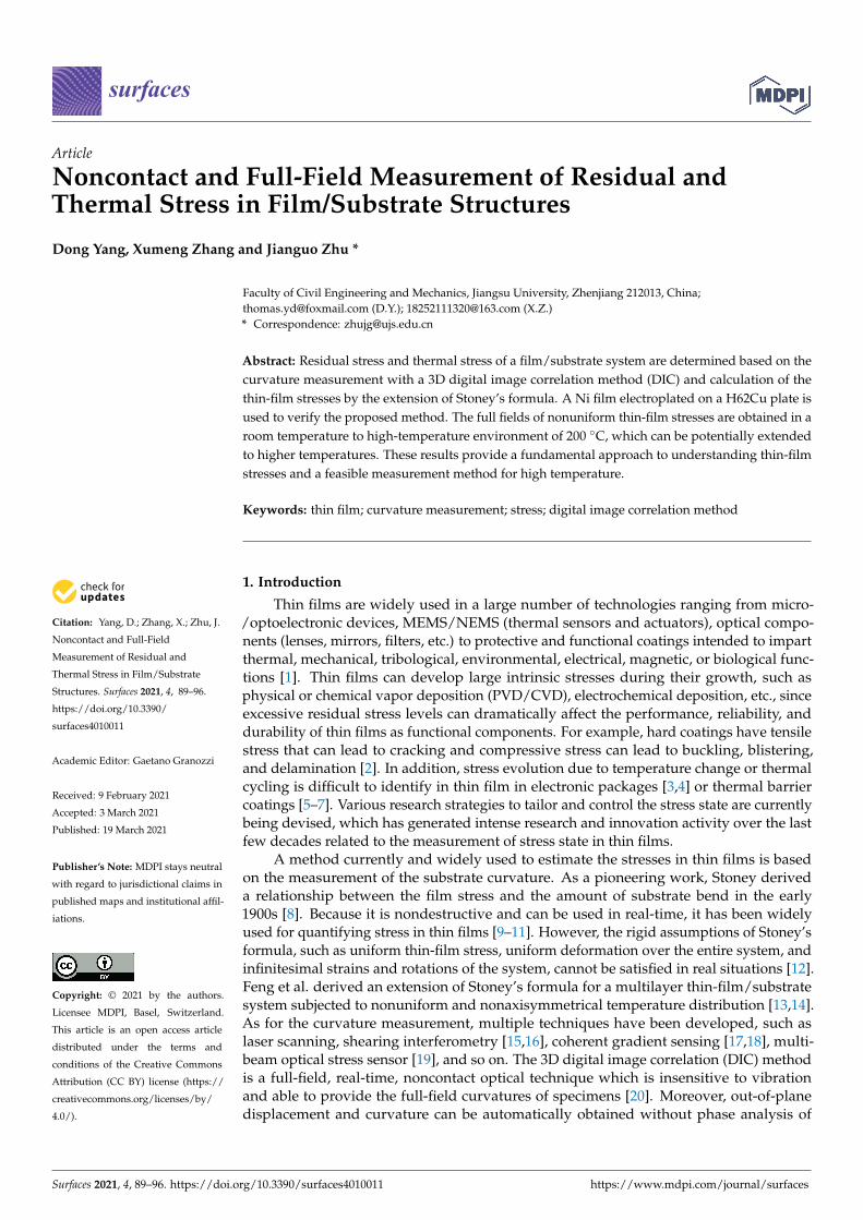
A thin film deposited on a circular substrate of radius R is shown in Figure 1. The filmand substrate were subjected to uniform temperature distribution. The film is modeledas a membrane since it is very thin (hf) and the substrate is modeled as a plate of smallthickness (hs). The radial and circumferential stresses of the thin film can be obtained fromthe linear thermoelastic constitutive model, and the theoretical relationship between thecurvature of the sample of the disk thin film and the stress of the thin film can be obtainedthrough formula derivation [13,14]:
σfrr − σ
fθθ =
Esh2s αs
6(1 − νs)
E f
1 + ν f
krr − kθθ
Aνα(1)
σfrr + σ
fθθ =
Esh2s
6(1 − νs)
E f
1 − ν f
[αs − α f
Aαkrr + kθθ +
(1 + νs)αs − 2α f
(1 + νs)Aνα
(krr + kθθ − krr + kθθ
)](2)
where Aα ≡ E f h f1−ν f
(αs − α f
), Avα =
E f h f
1−ν2f
[(1 + νs)αs −
(1 + ν f
)α f
]are constant;
krr =d2wdr2 is the radial curvature, kθθ = 1
rdwdr is the circumferential curvature; krr + kθθ =
1πR2
s
A(krr + kθθ)ηdηdθ = 2
R2
R∫0
η(krr + kθθ)dη is the average system curvature. The Young’s
modulus, Poisson’s ratio, and coefficient of thermal expansion are denoted by Ef, Es; vf,vs; and αf and αs, respectively, and the subscripts “f ” and “s” denote the thin film andsubstrate, respectively. w is displacement alone the z direction. The interface shear stresscan also be directly related to the system curvature:
τ =Esh2
s6(1 − ν2
s )
d(krr + kθθ)
dr. (3)
Figure 1. Schematic and photo of a thin-film/substrate system.
Surfaces 2021, 4 91
3. Numerical Simulation
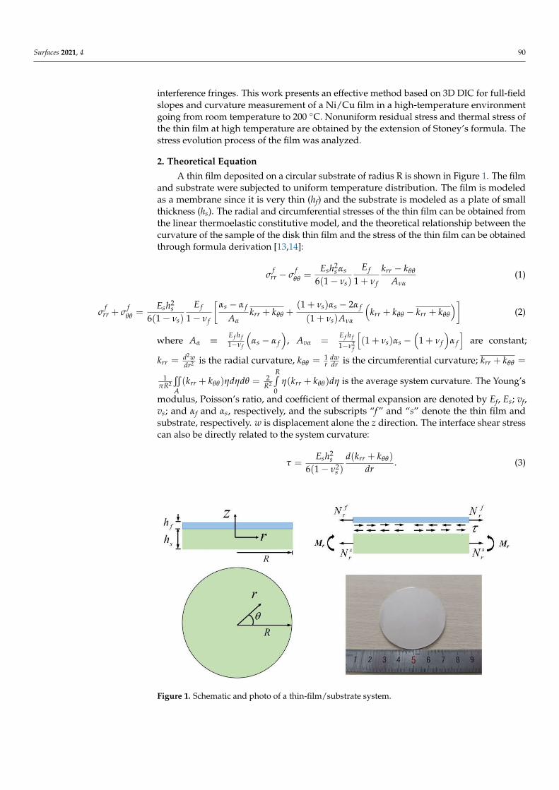
A 3D finite element model of film/substrate system was established as shown inFigure 2a, in which the thin film was Ni and the substrate was H62Cu. The mechanicalproperties are shown in Table 1. The sample was isothermally heated from room tempera-ture (25 ◦C) to 140 ◦C with a free boundary condition, and the radial and circumferentialstresses of the film were calculated. Linear elasticity was assumed for all the materials.
Figure 2. Numerical simulation results: (a) off-plane deformation field; (b) radial stress field of the film; (c) the circumferen-tial stress field of the thin film.
Table 1. Dimension and physical properties of specimen [21,22].
Diameter (mm) Thickness (µm) E (GPa) v α (×10−6/◦C)
Substrate(H62Cu) 50 500 100 0.324 18.8Film(Ni) 50 10 207 0.291 13
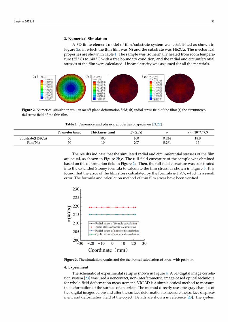
The results indicate that the simulated radial and circumferential stresses of the filmare equal, as shown in Figure 2b,c. The full-field curvature of the sample was obtainedbased on the deformation field in Figure 2a. Then, the full-field curvature was substitutedinto the extended Stoney formula to calculate the film stress, as shown in Figure 3. It isfound that the error of the film stress calculated by the formula is 1.9%, which is a smallerror. The formula and calculation method of thin film stress have been verified.
Figure 3. The simulation results and the theoretical calculation of stress with position.
4. Experiment
The schematic of experimental setup is shown in Figure 4. A 3D digital image correla-tion system [23] was used a noncontact, non-interferometric, image-based optical techniquefor whole-field deformation measurement. VIC-3D is a simple optical method to measurethe deformation of the surface of an object. The method directly uses the gray changes oftwo digital images before and after the surface deformation to measure the surface displace-ment and deformation field of the object. Details are shown in reference [23]. The system
Surfaces 2021, 4 92
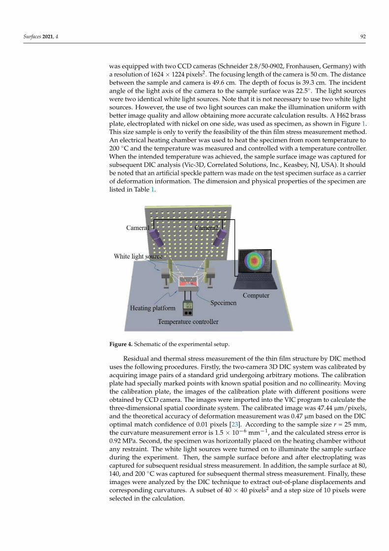
was equipped with two CCD cameras (Schneider 2.8/50-0902, Fronhausen, Germany) witha resolution of 1624 × 1224 pixels2. The focusing length of the camera is 50 cm. The distancebetween the sample and camera is 49.6 cm. The depth of focus is 39.3 cm. The incidentangle of the light axis of the camera to the sample surface was 22.5◦. The light sourceswere two identical white light sources. Note that it is not necessary to use two white lightsources. However, the use of two light sources can make the illumination uniform withbetter image quality and allow obtaining more accurate calculation results. A H62 brassplate, electroplated with nickel on one side, was used as specimen, as shown in Figure 1.This size sample is only to verify the feasibility of the thin film stress measurement method.An electrical heating chamber was used to heat the specimen from room temperature to200 ◦C and the temperature was measured and controlled with a temperature controller.When the intended temperature was achieved, the sample surface image was captured forsubsequent DIC analysis (Vic-3D, Correlated Solutions, Inc., Keasbey, NJ, USA). It shouldbe noted that an artificial speckle pattern was made on the test specimen surface as a carrierof deformation information. The dimension and physical properties of the specimen arelisted in Table 1.
Figure 4. Schematic of the experimental setup.
Residual and thermal stress measurement of the thin film structure by DIC methoduses the following procedures. Firstly, the two-camera 3D DIC system was calibrated byacquiring image pairs of a standard grid undergoing arbitrary motions. The calibrationplate had specially marked points with known spatial position and no collinearity. Movingthe calibration plate, the images of the calibration plate with different positions wereobtained by CCD camera. The images were imported into the VIC program to calculate thethree-dimensional spatial coordinate system. The calibrated image was 47.44 µm/pixels,and the theoretical accuracy of deformation measurement was 0.47 µm based on the DICoptimal match confidence of 0.01 pixels [23]. According to the sample size r = 25 mm,the curvature measurement error is 1.5 × 10⁻⁶ mm−1, and the calculated stress error is0.92 MPa. Second, the specimen was horizontally placed on the heating chamber withoutany restraint. The white light sources were turned on to illuminate the sample surfaceduring the experiment. Then, the sample surface before and after electroplating wascaptured for subsequent residual stress measurement. In addition, the sample surface at 80,140, and 200 ◦C was captured for subsequent thermal stress measurement. Finally, theseimages were analyzed by the DIC technique to extract out-of-plane displacements andcorresponding curvatures. A subset of 40 × 40 pixels2 and a step size of 10 pixels wereselected in the calculation.

Surfaces 2021, 4 93
5. Results and Discussion5.1. Residual Stress
Morphology diagrams of substrate before electroplating and after electroplating atroom temperature are shown in Figure 5a,b. The corresponding out-of-plane deformationdiagram of the thin structure based on 3D DIC calculation is shown in Figure 5c, whichwill be used for determination of residual stress because of the electroplating process. zis the coordinate height, and w is the relative displacement in the height direction. Itshould be noted that the substrate has a very small curvature (order of 10−4 mm−1)before electroplating due to the machining process and is approximately regarded as aplate. Similarly, Figure 5b was set as reference image, and morphology diagrams of theelectroplating sample at 80, 140, and 200 ◦C were set as deformed images (not shown), thenthe out-of-plane deformation diagrams of the thin structure were calculated and are shownin Figure 5d–f, which will be used for determination of thermal stress due to temperaturevariation. The off-plane displacement refers to the displacement of the morphology atroom temperature in the direction of height.
Figure 5. Morphology diagram of sample: (a) before electroplating and (b) after electroplating at room temperature.Out-of-plane deformation diagram of the electroplating sample at: (c) the substrate is electroplated, (d) 80 ◦C, (e) 140 ◦C,and (f) 200 ◦C.
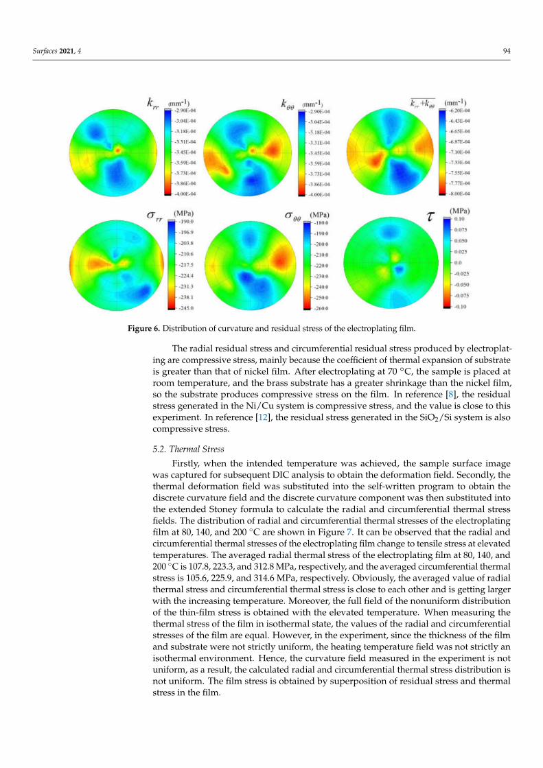
To calculate the residual stress due to the electroplating process, Zernike polyno-mials were used to fit the out-of-plane displacement map (Figure 5c) and differentiatedto extract the radial and circumferential curvatures of the thin structure according toEquations (1)–(3). As shown in Figure 6, the curvature fields of the electroplating sam-ple show nonuniform distribution and the curvatures in the vicinity of the edge becomeobviously much greater than those in the other area due to the edge effect. Then, thedistribution of residual stress in the electroplating film is calculated as shown in Figure 6. Itcan be observed that the radial and circumferential stresses of the thin film are compressivestress; the averaged magnitude of the radial and circumferential stresses of the thin film is−215.7 and −217.4 MPa, respectively. In addition, the interface shear stress is relativelysmall with maximum value less than 0.1 MPa. The residual stress caused by electroplatingis related to electroplating material, substrate thickness, electroplating environment, andelectroplating thickness.
Surfaces 2021, 4 94
Figure 6. Distribution of curvature and residual stress of the electroplating film.
The radial residual stress and circumferential residual stress produced by electroplat-ing are compressive stress, mainly because the coefficient of thermal expansion of substrateis greater than that of nickel film. After electroplating at 70 ◦C, the sample is placed atroom temperature, and the brass substrate has a greater shrinkage than the nickel film,so the substrate produces compressive stress on the film. In reference [8], the residualstress generated in the Ni/Cu system is compressive stress, and the value is close to thisexperiment. In reference [12], the residual stress generated in the SiO2/Si system is alsocompressive stress.
5.2. Thermal Stress
Firstly, when the intended temperature was achieved, the sample surface imagewas captured for subsequent DIC analysis to obtain the deformation field. Secondly, thethermal deformation field was substituted into the self-written program to obtain thediscrete curvature field and the discrete curvature component was then substituted intothe extended Stoney formula to calculate the radial and circumferential thermal stressfields. The distribution of radial and circumferential thermal stresses of the electroplatingfilm at 80, 140, and 200 ◦C are shown in Figure 7. It can be observed that the radial andcircumferential thermal stresses of the electroplating film change to tensile stress at elevatedtemperatures. The averaged radial thermal stress of the electroplating film at 80, 140, and200 ◦C is 107.8, 223.3, and 312.8 MPa, respectively, and the averaged circumferential thermalstress is 105.6, 225.9, and 314.6 MPa, respectively. Obviously, the averaged value of radialthermal stress and circumferential thermal stress is close to each other and is getting largerwith the increasing temperature. Moreover, the full field of the nonuniform distributionof the thin-film stress is obtained with the elevated temperature. When measuring thethermal stress of the film in isothermal state, the values of the radial and circumferentialstresses of the film are equal. However, in the experiment, since the thickness of the filmand substrate were not strictly uniform, the heating temperature field was not strictly anisothermal environment. Hence, the curvature field measured in the experiment is notuniform, as a result, the calculated radial and circumferential thermal stress distribution isnot uniform. The film stress is obtained by superposition of residual stress and thermalstress in the film.

Surfaces 2021, 4 95
Figure 7. Distribution of radial and circumferential thermal stress of the electroplating film at 80 ◦C (a,d), 140 ◦C (b,e), and200 ◦C (c,f).
6. Conclusions
The results presented here demonstrate the use of a 3D digital image correlationmethod to measure the thin-film/substrate system curvature at high temperature andcalculate the nonuniform stresses of the film by the extension of Stoney’s formula. Thisoptical technique is featured as full-field nonuniform curvature measurement. A Ni filmelectroplated on a H62Cu plate is used to verify the proposed method. These results providea fundamental approach to understand thin-film stresses and a feasible measurementmethod for residual stress and thermal stress.
Author Contributions: Experiment, D.Y.; data curation, D.Y.; validation, X.Z.; writing—originaldraft preparation, D.Y.; writing—review and editing, J.Z. All authors have read and agreed to thepublished version of the manuscript.
Funding: This research received no external funding.
Institutional Review Board Statement: Not applicable.
Informed Consent Statement: Not applicable.
Data Availability Statement: Data is contained within the article.
Conflicts of Interest: The authors declare no conflict of interest.
References1. Abadias, G.; Chason, E.; Keckes, J.; Sebastiani, M.; Thompson, G.B.; Barthel, E.; Doll, G.; Murray, C.; Stoessel, C.H.; Martinu, L.
Review Article: Stress in thin films and coatings: Current status, challenges, and prospects. J. Vac. Sci. Technol. A 2018, 36, 020801.[CrossRef]
2. Chason, E.; Guduru, P.R. Tutorial: Understanding residual stress in polycrystalline thin films through real-time measure-mentsand physical models. J. Appl. Phys. 2016, 119, 1032–1114. [CrossRef]
3. Yamamoto, T.; Nagayama, T.; Nakamura, T. Thermal Expansion and Thermal Stress Behavior of Electroless-Plated Fe–Ni–B AlloyThin Film for High-Density Packaging. J. Electrochem. Soc. 2018, 166, D3238–D3245. [CrossRef]
4. Zhang, X.; Meng, H.; Wang, H.; Guo, F. Effect of thermal misfit stress on steam-driven delamination in electronic packages. Eng.Fract. Mech. 2018, 194, 61–72. [CrossRef]
5. Zhu, J.G.; Xie, H.M.; Li, Y.J.; Hu, Z.X.; Luo, Q.; Gu, C.Z. Interfacial Residual Stress Analysis of Thermal Spray Coatings byMiniature Ring-Core Cutting Combined with DIC Method. Exp. Mech. 2014, 54, 127–136. [CrossRef]
6. Yang, X.; Liu, Z.; Xie, H. A real time deformation evaluation method for surface and interface of thermal barrier coatings during1100 ◦C thermal shock. Meas. Sci. Technol. 2012, 23, 105604. [CrossRef]
Surfaces 2021, 4 96
7. Zhu, J.G.; Chen, W.; Xie, H.M. Simulation of residual stresses and their effects on thermal barrier coating systems using finiteelement method. Sci. China Phys. Mech. Astron. 2015, 58, 1–10. [CrossRef]
8. Stoney, G. The tension of metallic films deposited by electrolysis. J. R. Soc. Lond. Ser. A 1909, 82, 172–175.9. Yu, H.Z.; Thompson, C.V. Effects of oblique-angle deposition on intrinsic stress evolution during polycrystalline film growth.
Acta Mater. 2014, 77, 284–293. [CrossRef]10. Yu, H.Z.; Thompson, C.V. Grain growth and complex stress evolution during Volmer–Weber growth of polycrystalline thin films.
Acta Mater. 2014, 67, 189–198. [CrossRef]11. Al-Masha’Al, A.; Bunting, A.; Cheung, R. Evaluation of residual stress in sputtered tantalum thin-film. Appl. Surf. Sci. 2016, 371,
571–575. [CrossRef]12. Dong, X.; Feng, X.; Hwang, K.-C.; Ma, S.; Ma, Q. Full-field measurement of nonuniform stresses of thin films at high temperature.
Opt. Express 2011, 19, 13201–13208. [CrossRef] [PubMed]13. Dong, X.L.; Feng, X.; Hwang, K.C. Non-uniform stress distribution and deformation bifurcation of thin film/substrate sys-tem
subjected to gradient temperature. Thin Solid Films 2011, 519, 2464–2469. [CrossRef]14. Feng, X.; Huang, Y.; Rosakis, A.J. Stresses in a Multilayer Thin Film/Substrate System Subjected to Nonuniform Temperature. J.
Appl. Mech. 2008, 75, 021022. [CrossRef]15. Zhang, C.; Dong, X.; Feng, X.; Hwang, K.-C. Multiwavelength shearing interferometry for measuring the slopes, curvatures, and
shapes of thin films/substrate systems. Opt. Lett. 2013, 38, 5446–5449. [CrossRef] [PubMed]16. Tippur, H.V. Simultaneous and real-time measurement of slope and curvature fringes in thin structures using shearing in-
terferometery. Opt. Eng. 2004, 43, 3014–3020. [CrossRef]17. Ma, K.; Xie, H.; Zhu, J. Two modified coherent gradient sensing methods for slope measurement of reflective surfaces. Meas. Sci.
Technol. 2014, 25, 125202. [CrossRef]18. Dong, X.; Zhang, C.; Feng, X.; Duan, Z. Analysis and improvement of accuracy, sensitivity, and resolution of the coherent gradient
sensing method. Appl. Opt. 2016, 55, 4752–4758. [CrossRef]19. Colin, J.J.; Abadias, G.; Michel, A.; Jaouen, C. On the origin of the metastable beta-Ta phase stabilization in tantalum sputtered
thin films. Acta Mater. 2017, 126, 481–493. [CrossRef]20. Pan, B. Digital image correlation for surface deformation measurement: Historical developments, recent advances and future
goals. Meas. Sci. Technol. 2018, 29, 082001. [CrossRef]21. Pelleg, J. Mechanical properties of materials. Solid Mech. Appl. 2013, 190, 1–634.22. Touloukian, Y.S.; Kirby, R.K.; Taylor, R.E.; Desai, P.D. Thermophysical Properties of Matters. Thermal Expansion of Metallic Elements
and Alloys; Plenum: New York, NY, USA, 1976; Volume 12.23. Sutton, M.A.; Orteu, J.J.; Schreier, H. Image Correlation for Shape, Motion and Deformation Measurements; Springer: New York, NY,
USA, 2009.