Classical duals, Legendre transforms and the Vainshtein mechanism
Upload
independentCategory
view
3download
0
IEEE TRANSACTIONS ON COMMUNICATIONS, VOL. 37, NO. 7, JULY 1989 713
Narrow-Band Interference Rejection Using Real-Time Fourier Transforms
Abstract-This paper performs the analysis of a BPSK-PN demodu- lator when present narrow-band interference is attenuated using trans- form domain filtering. The signal of interest is a wide-band direct- sequence speed-spectrum signal (DS-SS). The interference is a narrow-band signal which may be of high power and which is either intentionally or unintentionally collocated in frequency and interfering with the signal of interest. The effect of windowing the input signal by a rectangular or Hamming windows as well as the use of an overlap and save scheme will be presented. It will be shown that the Hamming window far outperforms the rectangular window, and that the interference is for all purposes completely eliminated when the Hamming window is used in conjunction with the overlap and save scheme. The criterion used to evaluate the effectiveness of the different interference rejection tech- niques is the bit error rate (BER) as measured at the output of the demodulator.
I. INTRODUCTION HE excision of narrow-band interferers in the frequency T domain has been analyzed extensively by Milstein et al.
His analysis considers a communication system in which the receiver has full knowledge of the time of transitions of the data bits. Further, each data bit is spread by a full PN sequence. The shape of both, the data as well as the random bits is rectangular. The system makes use of the data timing knowledge to perform a Fourier transform in real time (as with a surface acoustic wave device (SAW), [2], [3], [4]) over the duration of one data bit. The interference excision takes place exclusively in the frequency domain, after which the signal is restored to the time domain where the rest of the signal processing takes place. The short coming of the system described above stems from the inherent time limited nature of the signal processing. This creates significant sidelobes, thus effectively splattering the interferer's energy over a wide frequency range. Excising a large percentage of the interfer- er's energy would result in significant distortion of the wide- band DS-SS signal. Thus, it is proposed that the energy of the narrow-band interferer be concentrated in a smaller fraction of the spectrum by using a windowing function. The window to be used is the Hamming window, which effectively reduces the interferer's sidelobes at the expense of a wider main lobe [ 5 ] . This approach has also been used in [9] using a weighting function which approximates a cosine-squared function. A further increase in performance can be obtained if the system uses the overlap and save scheme (which, however, requires two transformer filters). A review of previous work will be given in Section I1 where the system analyzed by Milstein et al. [l] will be shown. In Section 111, a complete description of the proposed systems will be given, incorporating both, the Hamming window alone, as well as in conjunction with the overlap and save scheme. The computation of the transform and demodulator filter outputs will be shown in Sections IV and V, and the probability of error for the above systems will
Paper approved by the Editor for Spread Spectrum of the IEEE Communi- cations Society. Manuscript received August 11, 1987; revised lune 20, 1988.
The authors are with the Department of Electrical and Computer Engineer- ing, Rutgers University, Piscataway, NJ 08855-0909.
IEEE Log Number 8928213.
P W
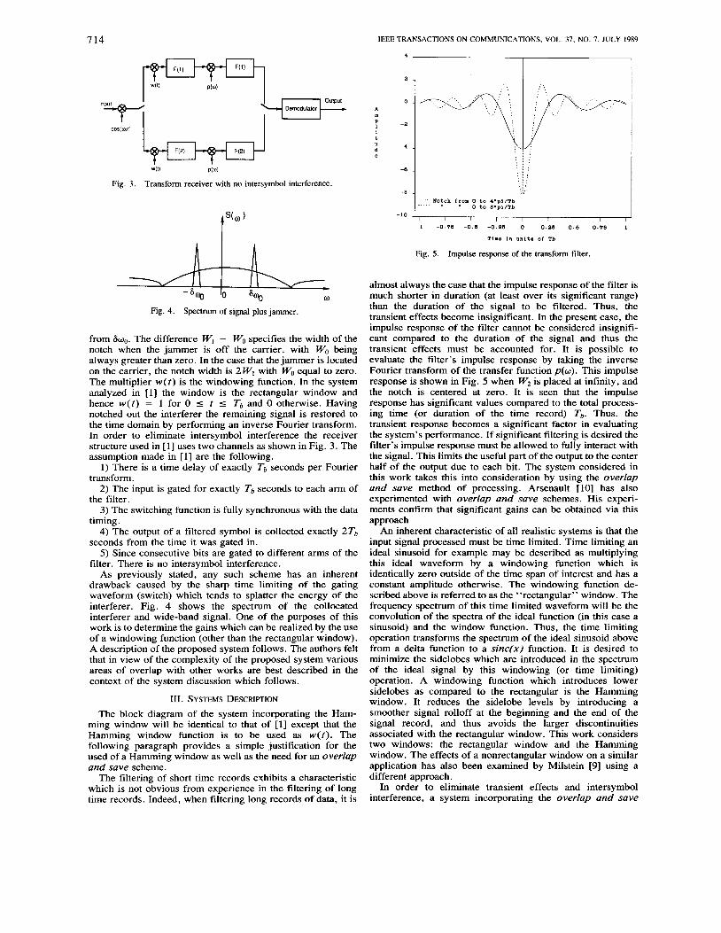
Fig. 1. Transform domain filter.
Fig. 2. Excision function.
be calculated in Section VI. The numerical results as well as comparisons of the above systems will be presented in Section VII. A robust performance baseline is obtained by deriving the probability of error using a simple matched filter receiver. Finally, Section VI11 presents a summary of the above work and conclusions.
11. PREVIOUS WORK The block diagram of the system proposed by Milstein is
shown in Fig. 1 where
X ( t ) = s ( t ) + j ( t ) + n( t ) . (1) The system uses a BPSK modulation scheme with a PN sequence used for the signal spreading function. The PN code is chosen such that a data bit is modulated by a full sequence of the PN code. Perfect data tracking is assumed and the signal can be expressed as
N - I
s ( t ) = c a;[u(t-iT,)-u(t-(i+l)T,)] cos (wot ) r = O
(2) where NT, = Tb, P, is the signal power, u ( t ) is the step function, cyr E [ 1, - 11 and T,, T b are the chip and bit periods, respectively. The interferer is a narrow-band signal which may be centered off the carrier frequency of the desired DS-SS signal. The interferer can be expressed as
j ( t ) = J2pi COS 6wo)t+ e ) (3) where PJ is the jamming power, 6w0 the offset from the carrier frequency wo and the phase t9 is assumed to be a random variable uniformly distributed from 0 to 2 ~ .
The noise n ( t ) is AWGN of zero mean and two-sided power spectral density N0/2. The excising functionp(w) in Fig. 1 is an odoff switch which implements a notching function in the frequency domain thus eliminating a large part of the interfering energy. The functionp(w) is shown in Fig. 2 where Wz is taken to be 2a/Tc, whereas WO and W, are equidistant
OO90-6778/89/07OO-0713$01 .OO O 1989 IEEE
7 14 IEEE TRANSACTIONS ON COMMUNICATIONS, VOL. 31, NO. I , JULY 1989
I Demodulator zl-=-
COS(0at)
WO) P(W
Fig. 3. Transform receiver with no intersymbol interference.
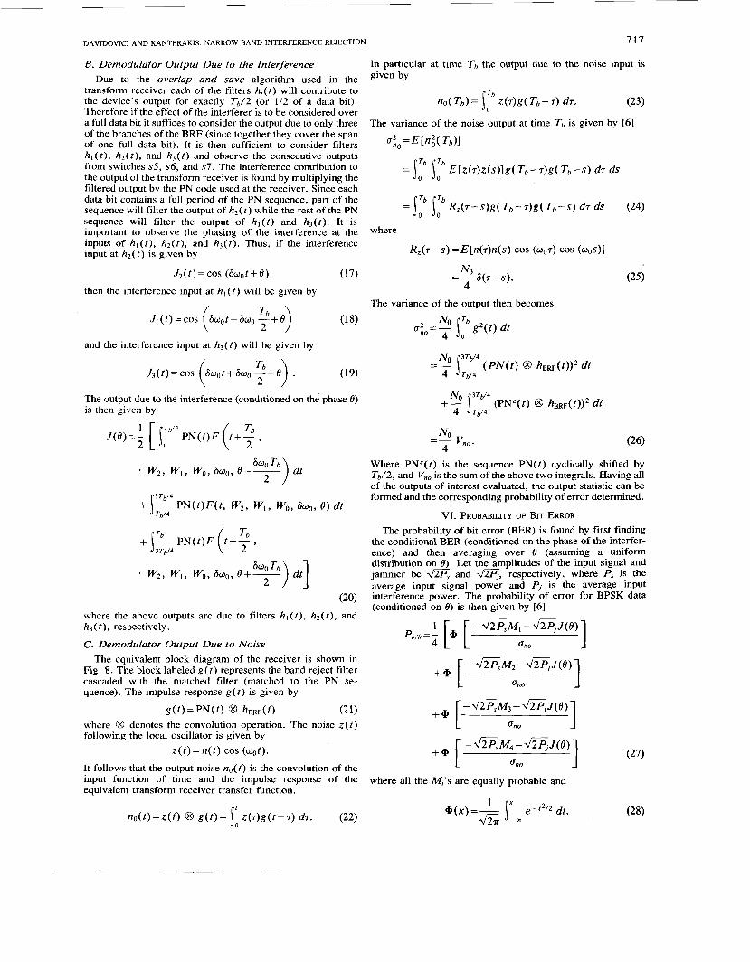
J w
Fig. 4. Spectrum of signal plus jammer.
from 6wo. The difference Wl - WO specifies the width of the notch when the jammer is off the carrier, with WO being always greater than zero. In the case that the jammer is located on the carrier, the notch width is 2 Wl with WO equal to zero. The multiplier w( t ) is the windowing function. In the system analyzed in [l] the window is the rectangular window and hence w ( t ) = 1 for 0 5 t 5 Tb and 0 otherwise. Having notched out the interferer the remaining signal is restored to the time domain by performing an inverse Fourier transform. In order to eliminate intersymbol interference the receiver structure used in [ 11 uses two channels as shown in Fig. 3. The assumption made in [l] are the following.
1) There is a time delay of exactly Tb seconds per Fourier transform.
2) The input is gated for exactly T b seconds to each arm of the filter.
3) The switching function is fully synchronous with the data timing.
4) The output of a filtered symbol is collected exactly 2Tb seconds from the time it was gated in.
5) Since consecutive bits are gated to different arms of the filter. There is no intersymbol interference.
As previously stated, any such scheme has an inherent drawback caused by the sharp time limiting of the gating waveform (switch) which tends to splatter the energy of the interferer. Fig. 4 shows the spectrum of the collocated interferer and wide-band signal. One of the purposes of this work is to determine the gains which can be realized by the use of a windowing function (other than the rectangular window). A description of the proposed system follows. The authors felt that in view of the complexity of the proposed system various areas of overlap with other works are best described in the context of the system discussion which follows.
111. SYSTEMS DESCFUFTION The block diagram of the system incorporating the Ham-
ming window will be identical to that of [l] except that the Hamming window function is to be used as w ( t ) . The following paragraph provides a simple justification for the used of a Hamming window as well as the need for an overlap and save scheme.
The filtering of short time records exhibits a characteristic which is not obvious from experience in the filtering of long time records. Indeed, when filtering long records of data, it is
ROtcb from 0 to 4*pl/Tb ’ 0 to B*pl/Tb
- .... .
-10 I I I I I I I 1
-1 -0.78 -0 .e -0.a8 o o.as 0.8 0 . 7 ~ ) 1
Tlme In m l t s of Tb
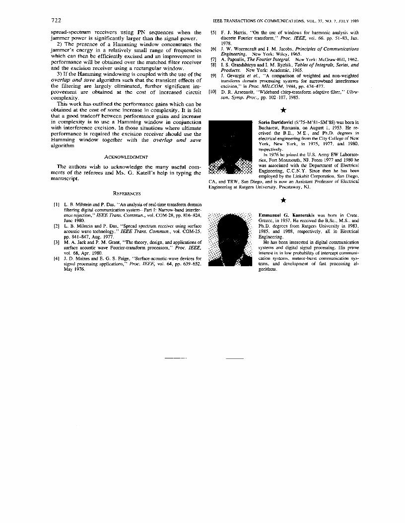
Fig. 5 . Impulse response of the transform filter.
almost always the case that the impulse response of the filter is much shorter in duration (at least over its significant range) than the duration of the signal to be filtered. Thus, the transient effects become insignificant. In the present case, the impulse response of the filter cannot be considered insignifi- cant compared to the duration of the signal and thus the transient effects must be accounted for. It is possible to evaluate the filter’s impulse response by taking the inverse Fourier transform of the transfer function p(w). This impulse response is shown in Fig. 5 when W2 is placed at infinity, and the notch is centered at zero. It is seen that the impulse response has significant values compared to the total process- ing time (or duration of the time record) Tb. Thus, the transient response becomes a significant factor in evaluating the system’s performance. If significant filtering is desired the filter’s impulse response must be allowed to fully interact with the signal. This limits the useful part of the output to the center half of the output due to each bit. The system considered in this work takes this into consideration by using the overlap and save method of processing. Arsenault [lo] has also experimented with overlap and save schemes. His experi- ments confirm that significant gains can be obtained via this approach
An inherent characteristic of all realistic systems is that the input signal processed must be time limited. Time limiting an ideal sinusoid for example may be described as multiplying this ideal waveform by a windowing function which is identically zero outside of the time span of interest and has a constant amplitude otherwise. The windowing function de- scribed above is referred to as the “rectangular” window. The frequency spectrum of this time limited waveform will be the convolution of the spectra of the ideal function (in this case a sinusoid) and the window function. Thus, the time limiting operation transforms the spectrum of the ideal sinusoid above from a delta function to a sinc(x) function. It is desired to minimize the sidelobes which are introduced in the spectrum of the ideal signal by this windowing (or time limiting) operation. A windowing function which introduces lower sidelobes as compared to the rectangular is the Hamming window. It reduces the sidelobe levels by introducing a smoother signal rolloff at the beginning and the end of the signal record, and thus avoids the larger discontinuities associated with the rectangular window. This work considers two windows: the rectangular window and the Hamming window. The effects of a nonrectangular window on a similar application has also been examined by Milstein [9] using a different approach.
In order to eliminate transient effects and intersymbol interference, a system incorporating the overlap and save

DAVIDOVICI AND KANTERAKIS: NARROW-BAND INTERFERENCE REJECTION 715
Fig. 6. Transform receiver for the “overlap and save” method.
s1
52
53
54
55
S6
s7
58 -
Fig. 7.
Ti4 Ti2 3Ti4 T 5T/4 6T/4 7Ti4 2T time
riming diagram for the “overlap and save” method.
COS(o0t)
Fig. 8. Equivalent receiver structure.
scheme is proposed and shown in Fig. 6. Due to the overlap and save method the system’s filter complexity is double that of Milstein’s. All filters h j ( t ) are identical to the one shown in Fig. 1. The operation of the system can be best understood by a description of the windowing function and the time diagram of the system’s operation. The windowing function is finite in time; for values of the time argument larger the Tb and less than 0 it equals zero. The overlap and save method of operation dictates that the system’s timing diagram be as shown in Fig. 8. The input switches sl, s2, s3 and s4 each stays open for Tb seconds after which they close for the next Tb seconds. This cycle is repeated throughout the system’s operation. Because of the overlap and save mode of operation the input filters lag each other by Tb/2 seconds. The transform filters exhibit a 2Tb seconds delay from the input to the output. Since the receiver operates on a 2Tb cycle this delay can be ignored (modulo 2Tb). Due to the overlap and save algorithm used in the transform receiver the output switches operate on a cycle during which they are on for Tb/2 seconds and off for 3Tb/2 seconds. Again, the full cycle is 2Tb. Having described the basic system configuration and mode of operation the system performance will now be analyzed. Since this is a linear system the signal, the noise and the interference components will be considered separately.
IV. TRANSFORM FILTER OUTPUTS A . Interference Output
The task of finding the transform receiver’s output due to the input interference is approached via first finding the output
due to the input interference when the excision filter is an ideal LPF, then applying the results to find the corresponding output when the excision filter is a band reject filter (BRF). Since the equations tend to be very long and tedious we only present an outline of the final derivations. The Fourier transform of a sinusoidal signal of duration Tb seconds, frequency 6w, and phase 13 is given by
(4) L +
- 6wo) Correspondingly, the output of the LPF with cutoff angular frequency set a W can be shown to be
1
21T z ( t , w, awe, e)=- [COS (6wot+e)[si(( w + ~ ~ , ) t )
+si(( w-6wo)t)-si((t- Tb)w
+ ( t - Tb)6Wo) - si(( t - Tb) w - ( t - Tb)6wo)] + sin (6wot + e ) - [ci(( W - 6wo)t)-ci(( W + 6wo) t )
- c i ( ( t - Tb) w-(t- Tb)6Wo)
+ ci(( t - Tb) w+ ( t - Tb)&Jo)]] (5 ) Having found the output of the LPF due to the sinusoidal interferer we proceed to find the same output for the case when the interferer is first weighted by a Hamming window which is given by
(?) * ~( t )=0 .54 -0 .46 COS
The interference input to the LPF then becomes
COS (swot + e ) ~ ( t ) = 0.54 cos (hwot + e )
- 0.23 COS ((swo+g) t+ 6)
- 0.23 COS (@U, -;) t + 6) . (7)
Using the results in (5) the output of the LPF becomes:
zw( t , w, 6wo, e ) = o s z ( t , w, &WO, e )
21T t , W, tho--, Tb 0) (8)
and the output of a BRF is found to be given by

716 IEEE TRANSACTIONS ON COMMUNICATIONS, VOL. 31, NO. I, JULY 1989
where the frequencies WO, W , , and W2 are interpreted as shown in Fig. 2 . Next, we proceed to find the output of the transform receiver generated by the signal component of the input.
B. Transform Receiver Output Due to the Signal In the case under consideration the signal is a DS-SS signal
which is formed by BPSK modulating a carrier. The modula- tion consists of a sequence of narrow pulses, each of which has an amplitude of + 1 or - 1. The output of the transform receiver due to a sequence of such pulses (PN chips), can be found by adding the responses due to the individual pulses of the PN sequence. The output of the transform receiver to a pulse input is found by repeating the derivation of the output due to the interferer but with 6wo and 0 set to 0. Therefore, starting with (5) it becomes
1 z(t, w, 6w0, 0) / 2 , , = O = - [S i ( w t ) - S i ( W ( t - Tb))]. a
(10) The response of a LPF to a signal of the form u ( t - T I ) - u(t - T2) where u ( t ) is the pulse function, and T2 > TI is given by
1 P l ( t , W, T i , T z ) = - [Si( W ( t - T l ) ) -S i ( W ( t - T2))I.
a
( 1 1 ) When this signal (pulse) is multiplied by cos (2?rt/Tb) the output can again be found from (5) with the factor 6w0 set to 2a/Tb and 0 = 0. Substituting it becomes
P2 t w - 0 ( 9
and the output of the LPF due to the same signal but windowed at the input is given by
Pw(t, W, Ti, T2)=0.54Pi(t, W , Ti , T2)
-0.46Pz(t, W , Ti, T2). (13)
Finally, the output of the filter due to a sequence of such pulses (or a PN sequence for example) can be found to be given by
PNw(t, W ) = aiPw(t, W, iT,, (i+ l )Tc) (14) N - I
i = O
TABLE I ALL POSSIBLE CONTRIBUTIONS FROM ADJACENT BITS
segment number: 1 2 3 4 5 6 7 8 9 10 11 12
+ + + + + + + + + + + + + + + + + + + + - - - -
+ + + + + + + + + + + + - - - -
_ _ _ ~
_ _ _ -
previous bit present bit next bit
where iT,, ( i + 1) T, denote the start and stop time, and ai the polarity of the ith PN chip.
The output of the band reject filter is then given by
-PNw(t , WI)+PNW(t, WO) ( 1 5 ) where each term represents the output of an ideal filter. Having determined the output of the BRF it is now possible to determine the resulting system BER by first finding the output of the demodulator and then determining the resultant proba- bility of error. The derivation of the probability of error when the Hamming window is used without the overlap and save method, follows closely the derivation of [I], [9] and it will be given in Section VI. Because of the complex operation of the system incorporating the overlap and save scheme, the following section will be devoted to finding the outputs needed to compute the probability of error for this system.
V . DEMODULATOR OUTPUT A . Demodulator Output Due to the Signal
The timing diagram of the system shows each channel contributing to the output transform for a continuous duration of Tb/2 seconds after which the output is taken from a different branch of the BRF (another hi ( t ) in Fig. 6 ) . Each branch will in fact contribute a continuous Tb/2 waveform segment every 2Tb seconds. This timing is dictated by the use of the overlap and save algorithm. Thus, the output corres- ponding to each full data bit will be generated from multiple branches of the BRF or different (hi( t ) 's) . Assume, for example, that the current bit of interest is positive and starts at time t = 0. Then, referring to the timing diagram, it is seen that the center half of the bit (i.e., switch s5) is generated from one branch of the BRF while the first and last one fourth of the data bit are generated by two other branches of the BRF (i.e., switches s6 and s8). But while the contribution to the center one half of the output bit is due entirely to the input bit under consideration, the first and last one fourth of the output bit of interest will be affected by the polarity of the bits preceding and following the input data bit under consideration. Thus, the effect of all possible polarities of the two adjacent data bits must be evaluated and averaged. Table I summarizes all of the possible combinations of adjacent bits if the current bit is assumed' to be positive.
The output of the demodulator due to the signal will then have one of four possible values denoted as M I , M2, M3, and M4 where
and PNBRi(t, W2, W l , WO) is the response of the band-reject filter to one of the four different signal combinations as shown in Table I.
DAVIDOVICI AND KANTERAKIS: NARROW-BAND INTERFERENCE REJECTION 717
B. Demodulator Output Due to the Interference Due to the overlap and save algorithm used in the
transform receiver each of the filters h j ( t ) will contribute to the device's output for exactly Tb/2 (or 1/2 of a data bit). Therefore if the effect of the interferer is to be considered over a full data bit it suffices to consider the output due to only three of the branches of the BRF (since together they cover the span of one full data bit). It is then sufficient to consider filters h l ( t ) , hz(t) , and h 3 ( t ) and observe the consecutive outputs from switches s5, s6, and s7. The interference contribution to the output of the transform receiver is found by multiplying the filtered output by the PN code used at the receiver. Since each data bit contains a full period of the PN sequence, part of the sequence will filter the output of h 2 ( t ) while the rest of the PN sequence will filter the output of hl(t) and h3(t). It is important to observe the phasing of the interference at the inputs of h l ( t ) , h2(t) , and h3( t ) . Thus, if the interference input at h2( t ) is given by
~ ~ ( t ) = c o S (hwot+e) (17) then the interference input at h, ( t ) will be given by
and the interference input at h3(t) will be given by
The output due to the interference (conditioned on the phase 0) is then given by
+ s3Tb'4 PN(t )F( t , W2, WI, WO, 6w0, 8) d f Tb/4
(20) where the above outputs are due to filters h l ( t ) , h2( t ) , and h3(t), respectively.
C. Demodulator Output Due to Noise The equivalent block diagram of the receiver is shown in
Fig. 8. The block labeled g ( t ) represents the band reject filter cascaded with the matched filter (matched to the PN se- quence). The impulse response g ( t ) is given by
g ( f ) = P N ( t ) @ ~ B R F ( ~ ) (21) where (8 denotes the convolution operation. The noise z ( t ) following the local oscillator is given by
z ( t ) = n ( t ) cos (oot).
It follows that the output noise no(t) is the convolution of the input function of time and the impulse response of the equivalent transform receiver transfer function.
no(t)=z(t) @ g ( t ) = z ( ~ ) g ( t - ~ ) d7. (22)
In particular at time Tb the output due to the noise input is given by
no( Tb)= 1: Z(7)g(Tb-7) d7. (23)
The variance of the noise output at time T b is given by [6]
ako=E[ni( Tb)]
where
NO 4
_- - 6(7-S).
The variance of the output then becomes
NO 4
aio = - 1," gz( t ) dt
NO _- - v f l o . 4 Where PNC(t) is the sequence PN(t) cyclically shifted by T d 2 , and V,,, is the sum of the above two integrals. Having all of the outputs of interest evaluated, the output statistic can be formed and the corresponding probability of error determined.
VI. PROBABILITY OF BIT ERROR The probability of bit error (BER) is found by first finding
the conditional BER (conditioned on the phase of the interfer- ence) and then averaging over 0 (assuming a uniform distribution on 0). Let the amplitudes of the input signal and jammer be e and m, respectively, where P, is the average input signal power and Pj is the average input interference power. The probability of error for BPSK data (conditioned on 0) is then given by [61
1 1
1
- m s M l -m.J(O) P e/B -
718 IEEE TRANSACTIONS ON COMMUNICATIONS, VOL. 37, NO. 7, JULY 1989
As previously shown (see Fig. 7 showing the timing of the system) the overlap and save algorithm produces an output valid for one half of a data bit Tb/2 for every input which lasts for a full data bit duration Tb. Again, this is done in order to avoid the transients associated with processing a data record which is comparable in duration to the impulse response of the filter. Thus, if the output corresponding to a whole data bit is to be obtained this output must be formed of three segments.
The middle segment which lasts for Tb/2 seconds is obtained by processing an input segment of duration Tb seconds and discarding the beginning and end segments (each of duration Tb/4 seconds which contain the transient response. Referring back to Table I if the desired data bit is made up of segments 5, 6 , 7 , and 8 , and the delay line is processing the Tb seconds input waveform due to the above segments, then that output corresponding to the segments 6 and 7 which is of duration Tb/2 seconds will be valid and it will be retained. The output segments corresponding to the input segments 5 and 8 which are of duration Tb/4 each will contain the transient effects and they well be discarded.
The output corresponding to those segments will be taken from the processing of data input segments of duration Tb which are be composed of segments 3, 4 , 5, and 6 , and segments 7 , 8, 9, and 10. From the output, those portions corresponding to input segments 5 and 8 (each of duration Ti,/ 4 s) will be retained and together with the previous output segment will form the complete output corresponding to the middle data bit in Table I.
But the end segments of the output will differ according to the polarity of the adjacent bits. This is because the input which generated those segments at the output include portions of the adjacent bits. Thus, the demodulator output will be conditioned on the polarity of the immediately adjacent bits. Since there are four possible combinations of the adjacent bits polarities there will be four different signal outputs, MI through M4. Each of these possible outputs is equally likely and thus they are averaged as shown in (27).
Since the phase of the interference is uniformly distributed on [0, 2n] the average probability of error is given by
(29) 1 2 r
P e = - 1 Pe/O de.
For the system incorporating the Hamming window (but not the overlap and save algorithm), the probability of error is computed as follows. The demodulator output noise variance is again give by (26) where each data bit is fully filtered by only one filter h , ( t ) . New (14) in [ l ] can be used to compute the jammer and signal outputs of the demodulator giving:
2a 0
and
Equations (30a-c) are used in this case because of the significantly lower computation time required. Then the probability of error for this system conditioned on 0 is given by
] (31) [ - . J P , M H - J2pi J H ( e )
Pe/o = * OnoH
where (29) can be used again to remove the condition on 0. Last, the computation of the probability of error when only
P e
'., '. '., '.
,~, 1. '~ , \. 10-6-
- Notch-2'pllTb - - NOtch-6spl/Tb
-8 - Notch-a*pl/Tb 10 ... Natch-12'pllTb
Matched fllter
-a. 10 I I I I I I I
4 6 a io 12 14 ie ia a0 EblNO
(a)
P e
4 6 8 10 12 14 16 10 20
Eb/NO
(b)
-1 10
10-2
-3 10
p
10-6
10-6
IO-'
4 8 0 10 12 14 16 18 20
EblNO
(C) Fig. 9. (a) BPSK-PN transform receiver using rectangular window. (b)
BPSK-PN transform receiver using Hamming window. (c) BPSK-PN transform receiver using Hamming window with O/S.
performed for comparison purposes. Its derivation can be found in [ 11.
VII. NUMERICAL RESULTS This section evaluates the results obtained using the
derivations presented in the previous sections. The BER obtained using the different interference excision methods are plotted in Fig. (9) and (10). These results are benchmarked
a filter matched to the transmitted signal receiver is used is ggainst a matched filter receiver. The interferer is a CW signal

DAVIDOVICI AND KANTERAKIS: NARROW-BAND INTERFERENCE RUECTION 719
10-1 1 I
P 0
4 6 8 10 12 14 10 18 20
Eb/NO
(a)
-1 10
10-2
-4 p 10
- 5 10
10-6
IO-’
-8 10
-1 10
-2 10
p
10-6
-7 10
10-8 4 6 8 10 12 14 16 18 20
Eb/NO
(C)
Fig. 10. (a) BPSK-PN transform receiver using rectangular window. (b) BPSK-PN transform receiver using Hamming window. (c) BPSK-PN transform receiver using Hamming window with O/S .
located either at the signal’s carrier frequency (i.e., 6wo = 0) or off the signal’s carrier frequency (i.e., 6wo = 47r/Tb). Thus, the jammer is placed either exactly on carrier or slightly off carrier. The processing gain is defined as PG = Tb/ T, and the sequence used for spreading is a PN sequence.
Figs. 9(a)-(c) and 10(a)-(c) plot the BER as a function of
&,/No and notch filter width for given Pj/Ps. The interference excision capability of the system varies widely as a function of the window, processing method and notch width. The value of P,/Ps used is sometimes varied within a plot such that meaningful results may be presented. These variations in P,/ P, are clearly marked where they occur. In the first set of figures, Fig. 9(a)-(c) the jammer is centered at the signal’s carrier frequency. In the second set of figures, Fig. 10(a)-(c) the jammer is located off the signal’s carrier frequency at 6woTb = 47r. The general trend as apparent from these figures is that when interference is present the system will perform worst in the absence of any notch filter. The system performance shows an improvement when a notch filter is introduced. The exception to that is the case when the jammer is located at the signal’s carrier frequency and the N = 3 1 bit sequence is used for spreading. As shown in Fig. 9(a) the receiver using only a matched filter outperforms the receiver using interference excision with rectangular windowing for all notch widths. When the notch filter is used the Hamming window outper- forms the rectangular window and the Hamming window used in conjunction with overlap and save ( O / S ) processing outperforms both window for any notch width greater than 87r/Tb. The gains introduced by the notch filter can be as large as 30-35 dB.
It is felt that this paper would not be complete without an explanation of the mechanism which governs these gains. First examine the effect of the notch width upon the signal in the absence of any interference. In Fig. ll(a)-(c), the notch widths are varied from 27r/Tb to 127r/Tb. A different window applies to each of the figures. In the interest of improving the readability of the figures only the upper and the lower limit curves are plotted. In each of the figures, Fig. ll(a)-(c), two cases are considered: the notch is centered at the signal’s carrier frequency or off the signal’s carrier frequency at 6woT = 47r. Thus, for each of the two notch center frequencies the performance curves for the different notch widths lie between the upper and lower limit curves. A comparison between different figures is facilitated by the presence of the baseline case which is only the matched filter (without any windowing of notching). Thus, the rectangular window is closest to this baseline case followed by the Hamming window with O/S processing and by the Hamming window. All of these cases are very close together with the visible variations due mainly to the signal mismatch introduced by the Hammong window. As the O/S processing only uses the center portion of each signal record it’s performance in the absence of the jammer is closest to the rectangular window (since the Hamming window is relatively flat in its center region).
The second effect to be considered is that of the interference rejection. The interferer is a CW signal and the relative rejection is plotted as a function of the notch width in Fig. 12(a)-(f). Each figure refers to a specific match filter (i.e., PN sequence) and jammer location. There is one rejection curve given for each of the signal processing methods considered. The measured quantity consists of the envelope at the output of the receiver due to the CW interferer only and it is measured relative to the output of a receiver which only uses a matched filter. It is a function of the interferer’s center frequency and of the interaction between the notch filter and the matched filter. This interaction generates a rejection characteristic which tends to exhibit monotonic behavior with increasing notch width as an overall trend bot not at the fine detail level. As an example consider the 7 bit sequence case with the interferer centered at the signal’s carrier frequency. Processing by a receiver using a rectangular window generates a monotonic behavior versus notch width for notches up to 27r/Tb width as shown in Fig. 12(a). The behavior does not remain monotonic as the notch width increases even though the general trend will remain so. Also, the notch width alone is not sufficient to fully describe the degree of interference rejection. The matched

720 IEEE TRANSACTIONS ON COMMUNICATIONS. VOL. 37, NO. 7, JULY 1989
P e
4 8 8 10 12 14 18
Xb/NO
(a)
P e
4 8 8 10 12 14 18
Eb/NO
(b)
4 8 8 10 14 18
BL/NO
(C) (a) BPSK-PN transform receiver using rectangular window with no
jammer. Effect of the notch on P,. (b) BPSK-PN transform receiver using Hamming window with no jammer. Effect of the notch on P,. (c) BPSK-PN transform receiver using Hamming window with O/S and no jammer. Effect of the notch P,.
Fig. 11.
VIII. SUMMARY AND CONCLUSIONS filter (PN sequence) structure has a significant effect. Observe the interference rejection curves illustrated in Fig. 12(a)-(f) Fig. (9)-(12) illustrate the performance of the four kinds of for a given value of notch width. The interference rejection receivers considered in this work. From these figures the varies significantly over the three PN sequences used. A following conclusions can be drawn. general comment can however be made: a notch of width 1) The excision of narrow-band interferers does not 6woT = 87r would perform well for all cases considered here. necessarily improve the BER performance of direct-sequence

DAVIDOVICI AND KANTERAKIS: NARROW-BAND INTERFERENCE REJECTION
A T T E N u A T I 0 N
I N
d B
A T T E N u A T I 0 N
I N
d B
A T T E N u A T I 0 N
I N
d B
y?INIPQ~WINDOW WITH 01s
0 2 4 0 8 10 12
NOTCR WIDTH IN UNITS OP plITb
(a)
o a 4 e 8 io 12 14 le 18 20 22 a4
NOTCH WIDTH IN UNITS OP pl/Tb
(C)
5 T I
-30 1 -38
1 1 1 1 1 1 1 I I o 1 2 3 4 8 e 7 a e i o
NOTCB WIDTB IN UNITS OF pl/Tb
(e)
A T T E N U A T I 0 N
I N
d B
A T T B N u A T I 0 N
I N
d B
A T T E N u A T I 0 N
I N
d B
72 1
5 I
-30
-a8 I . . I , -38
I I I I I a 4 0 a 10 12 0
UOTCB WIDTH IN UNITS OF pl/Tb
(b)
8
-38 I I I I I I I I I
o 1 a 3 4 5 e 7 8 e 10
NOTCB WIDTH IN UNITS OF pl/Tb
(d)
WITCHED FILTER RBCTANGWLAR WINDOW W I N Q WINDOW W I N G WINDOW WITH O/S
-5
, -.. , \ .. -10
NOTCE WIME IN UNITS OF pl/Tb
(f) Fig. 12. (a) BPSK-PN transform receiver, 7 bit PN-sequence with jammer located at carrier. Interference attenuation versus notch-
width. (b) BPSK-PN transform receiver, 15 bit PN-sequence with jammer located at carrier. Interference attenuation versus notch- width. (c) BPSK-PN transform receiver, 31 bit PN-sequence with jammer located at carrier. Interference attenuation versus notch- width. (d) BPSK-PN transform receiver, 7 bit PN-sequence with jammer located at 4K/Tb. Interference attenuation versus notch-width. (e) BPSK-PN transform receiver, 15 bit PN-sequence with jammer located at 47r/Tb. Interference attenuation versus notch-width. (f) BPSK-PN transform receiver, 3 1 bit PN-sequence with jammer located at 4r/Tb. Interference attenuation versus notch-width.
7 2 2 IEEE TRANSACTIONS ON COMMUNICATIONS, VOL. 31, NO. 7, JULY 1989
[5] F. J. Harris, “On the use of windows for harmonic analysis with discrete Fourier transform,” Proc. ZEEE, vol. 66, pp. 51-83, Jan. 1978.
[6] J. W. Wozencraft and I. M. Jacobs, Principles of Communications Engineering. New York: Wiley, 1965.
[7] A. Papoulis, The Fourier Integral. New York: McGraw-Hill, 1962. [8] I. S. Grandshteyn and I. M. Ryzhik, Tables of Integrals, Series, and
Products. New York: Academic, 1965. [9] J. Gevargiz et al., “A comparison of weighted and non-weighted
transform domain processing systems for narrowband interference excision,” in Proc. MZLCOM, 1984, pp. 474-477. D. R. Arsenault, “Wideband chirp-transform adaptive filter,” Ultra- son. Symp. Proc., pp. 102-107, 1985.
[lo]
spread-spectrum receivers using PN sequences when the jammer power is significantly larger than the signal power.
2) The presence of a Hamming window concentrates the jammer’s energy in a relatively small range of frequencies which can then be efficiently excised and an improvement in performance will be obtained over the matched filter receiver and the excision receiver using a rectangular window.
3) If the Hamming windowing is coupled with the use of the overlap and save algorithm such that the transient effects of the filtering are largely eliminated, further significant im- provement are obtained at the cost of increased circuit complexity.
This work has outlined the performance gains which can be obtained at the cost of some increase in complexity. It is felt that a good tradeoff between performance gains and increase in complexity is to use a Hamming window in conjunction with interference excision. In those situations where ultimate performance is required the excision receiver should use the Hamming window together with the overlap and save algorithm
ACKNOWLEDGMENT
The authors wish to acknowledge the many useful com- ments of the referees and Ms. G. Katell’s help in typing the manuscript.
REFERENCES
L. B. Milstein and P. Das, “An analysis of real-time transform domain filtering digital communication system-Part I: Narrow-band interfer- ence rejection,” ZEEE Trans. Commun., vol. COM-28, pp. 816-824, June 1980. L. B. Milstein and P. Das, “Spread spectrum receiver using surface acoustic wave technology,” ZEEE Trans. Commun., vol. COM-25,
M. A. Jack and P. M. Grant, “The theory, design, and applications of surface acoustic wave Fourier-transform processors,” Proc. ZEEE, vol. 68, Apr. 1980. J. D. Maines and E. G. S. Paige, “Surface-acoustic-wave devices for signal processing applications,” Proc. ZEEE, vol. 64, pp. 639-652, May 1976.
pp. 841-847, Aug. 1977.
* Sorin Davidovici (S’75-M’81-SM’88) was born in Bucharest, Rumania, on August 1, 1953. He re- ceived the B.E., M.E., and Ph.D. degrees in electrical engineering from the City College of New York, New York, in 1975, 1977, and 1980, respectively.
In 1976 he joined the U.S. Army EW Laborato- ries, Fort Monmouth, NJ. From 1977 and 1980 he was associated with the Department of Electrical Engineering, C.C.N.Y. Since then he has been employed by the Linkabit Corporation, San Diego,
CA, and TRW, San Diego, and is now an Assistant Professor of Electrical Engineering at Rutgers University, Piscataway , NJ.
* Emmanuel G. Kanterakis was born in Crete, Greece, in 1957. He received the B.Sc., M.S., and Ph.D. degrees from Rutgers University in 1983, 1985, and 1988, respectively, all in Electrical Engineering.
He has been interested in digital communication systems and digital signal processing. His prime interest in in low probability of intercept communi- cation systems, meteor-burst communication sys- tems, and development of fast processing al- gorithms.
Copyright © 2022 FDOKUMEN