Nanotube Fountain Pen: Towards 3D Manufacturing of Metallic Nanostructures
8
Nanotube fountain pen: Towards 3D manufacturing of metallic nanostructures Zheng Fan a , Xinyong Tao b , Xudong Fan c , Xiaobin Zhang d , Lixin Dong a, * a Department of Electrical and Computer Engineering, Michigan State University, East Lansing, MI 48824, USA b College of Materials Science and Engineering, Zhejiang University of Technology, Hangzhou 310014, China c Center for Advanced Microscopy, Michigan State University, East Lansing, MI 48824, USA d Department of Materials Science and Engineering, Zhejiang University, Hangzhou 310027, China ARTICLE INFO Article history: Received 9 September 2014 Accepted 23 January 2015 Available online 31 January 2015 ABSTRACT The additive manufacturing of structures and devices in nanoscale yields the possibility of extending the functionalities of nanoelectronics and developing the alternative nanofabri- cation technologies for the post-silicon era. The nanorobotic spot-welding that is imple- mented by the transporting of mass inter/intra through the carbon nanotube has been demonstrated in previous works. However, the continuous feeding of the metal mass in nanoscale, as well as the servo control of such mass feeding rate and 3D path of the nano- tube injector is still unsolved. In this report, we demonstrated a nanotube fountain pen (NFP). It is equipped with a metal-filled carbon nanotube (m@CNT) as a pen-tip injector to ‘‘write’’ and a nanotube network as an ‘‘ink reservoir’’. In this way, it is able to provide the possibility of fabricating 3D nanostructures in a continuous fashion. The resolution of NFP depending on the diameter of the nanotube-injector and the mass flow rate of it can be modulated by external electrical driven energy. The development and control of NFP provide a new additive manufacturing technique in nanoscale, and thereby enables potential to develop a NFP-based metallic 3D nanoprinting system for the large-scale, high-throughput manufacturing of nanodevices. Ó 2015 Elsevier Ltd. All rights reserved. 1. Introduction Additive manufacturing (AM) techniques are approaches to the fabrication of structures and devices, especially 3D ones, by depositing materials onto a substrate, which have the advantages of distributed manufacturing and building from bottom up [1–5]. Based on the concept of the AM, several novel fabrication methods as well as some interesting tools were developed, such as the 3D printer and 3Doodler (the world’s first 3D printing pen) [6]. Moreover, directly manufacturing with metals, treated as the final frontier in AM techniques, has achieved remarkable advancement in recent years [7–12]. Compared with conven- tional metal component manufacturing process that usually lasts from weeks to months and lacks dynamics in product design, AM techniques allow the lean manufacturing of the machine parts [5,13,14], indicating a new revolution in the manufacturing industry. The recent progress in the miniatur- ization of the electromechanical system raises the question of whether the 3D metal printing can be realized at the nano- scale or even atomic level, which is also the core of bottom- up nanotechnology defined as molecular manufacturing [15]. At the nanometer scale, unlike conventional nanolitho- graphic technologies [16–18], additive nanolithography http://dx.doi.org/10.1016/j.carbon.2015.01.043 0008-6223/Ó 2015 Elsevier Ltd. All rights reserved. * Corresponding author: Fax: +1 517 3531980. E-mail address: [email protected] (L. Dong). CARBON 86 (2015) 280 – 287 Available at www.sciencedirect.com ScienceDirect journal homepage: www.elsevier.com/locate/carbon
-
Upload
michiganstate -
Category
Documents
-
view
0 -
download
0
Transcript of Nanotube Fountain Pen: Towards 3D Manufacturing of Metallic Nanostructures
C A R B O N 8 6 ( 2 0 1 5 ) 2 8 0 – 2 8 7
.sc iencedi rect .com
Avai lab le at wwwScienceDirect
journal homepage: www.elsev ier .com/ locate /carbon
Nanotube fountain pen: Towards 3D manufacturingof metallic nanostructures
http://dx.doi.org/10.1016/j.carbon.2015.01.0430008-6223/� 2015 Elsevier Ltd. All rights reserved.
* Corresponding author: Fax: +1 517 3531980.E-mail address: [email protected] (L. Dong).
Zheng Fan a, Xinyong Tao b, Xudong Fan c, Xiaobin Zhang d, Lixin Dong a,*
a Department of Electrical and Computer Engineering, Michigan State University, East Lansing, MI 48824, USAb College of Materials Science and Engineering, Zhejiang University of Technology, Hangzhou 310014, Chinac Center for Advanced Microscopy, Michigan State University, East Lansing, MI 48824, USAd Department of Materials Science and Engineering, Zhejiang University, Hangzhou 310027, China
A R T I C L E I N F O A B S T R A C T
Article history:
Received 9 September 2014
Accepted 23 January 2015
Available online 31 January 2015
The additive manufacturing of structures and devices in nanoscale yields the possibility of
extending the functionalities of nanoelectronics and developing the alternative nanofabri-
cation technologies for the post-silicon era. The nanorobotic spot-welding that is imple-
mented by the transporting of mass inter/intra through the carbon nanotube has been
demonstrated in previous works. However, the continuous feeding of the metal mass in
nanoscale, as well as the servo control of such mass feeding rate and 3D path of the nano-
tube injector is still unsolved. In this report, we demonstrated a nanotube fountain pen
(NFP). It is equipped with a metal-filled carbon nanotube (m@CNT) as a pen-tip injector
to ‘‘write’’ and a nanotube network as an ‘‘ink reservoir’’. In this way, it is able to provide
the possibility of fabricating 3D nanostructures in a continuous fashion. The resolution
of NFP depending on the diameter of the nanotube-injector and the mass flow rate of it
can be modulated by external electrical driven energy. The development and control of
NFP provide a new additive manufacturing technique in nanoscale, and thereby enables
potential to develop a NFP-based metallic 3D nanoprinting system for the large-scale,
high-throughput manufacturing of nanodevices.
� 2015 Elsevier Ltd. All rights reserved.
1. Introduction
Additive manufacturing (AM) techniques are approaches to
the fabrication of structures and devices, especially 3D ones,
by depositing materials onto a substrate, which have the
advantages of distributed manufacturing and building from
bottom up [1–5]. Based on the concept of the AM, several
novel fabrication methods as well as some interesting tools
were developed, such as the 3D printer and 3Doodler (the
world’s first 3D printing pen) [6].
Moreover, directly manufacturing with metals, treated as
the final frontier in AM techniques, has achieved remarkable
advancement in recent years [7–12]. Compared with conven-
tional metal component manufacturing process that usually
lasts from weeks to months and lacks dynamics in product
design, AM techniques allow the lean manufacturing of the
machine parts [5,13,14], indicating a new revolution in the
manufacturing industry. The recent progress in the miniatur-
ization of the electromechanical system raises the question of
whether the 3D metal printing can be realized at the nano-
scale or even atomic level, which is also the core of bottom-
up nanotechnology defined as molecular manufacturing [15].
At the nanometer scale, unlike conventional nanolitho-
graphic technologies [16–18], additive nanolithography

C A R B O N 8 6 ( 2 0 1 5 ) 2 8 0 – 2 8 7 281
typically involves a high energy beam or a scanning probe.
Among the beam-based methods, the direct laser writing
(DLW) [19] has the advantage of fast prototyping speed, but
this technique cannot be used to deposit metal materials.
Electron-beam-induced deposition (EBID) [20] and the
focused-ion-beam chemical vapor deposition (FIB-CVD) [21]
have higher resolution and allow multi-material such as met-
als, and high resolution deposition, but their limitations of
energy and large consumption of time constraints their appli-
cations to the 3D nanodevice batch fabrication. Other solu-
tions that have been proposed are probe-based additive
nanolithographic methods, such as dip-pen nanolithography
(DPN) [22] and polymer pen lithography (PPL) [23]. They are
developed with advantages of high-throughput and lower
energy consumption than the beam-based methods. How-
ever, no metallic deposits have been obtained.
Therefore, the 3D metal nanostructure AM is still a tech-
nical challenge for the existing additive nanolithographic
methods. Here we propose a nanotube fountain pen (NFP)
worked as a 3Doodler in nanoscale for direct writing with
metallic ‘‘inks’’. The NFP is consisted of a reservoir and a
nanotube injector. As shown in Fig. 1a, a single copper-filled
carbon nanotube (Cu@CNT) is used as the pen tip and the
‘‘ink’’, i.e., the mass reservoir is attached with the pen injec-
tor. The pen tip transports attogram metal from the mass
reservoir onto a conductive substrate to form the 3D
nanostructures. As a pen-type lithography method not only
benefits from the availability of metallic structures, the NFP
also has the advantage of continuous writing ability as
compared with a nanotube pencil [18] and the DPN. This
resembles the development of their macroscale counter-
parts, from pencils, to dip pens, to fountain pens, and to
the 3Doodler. Three main issues of the development of
NFP were addressed in this report: the continuous mass
feeding, the control of the mass flow rate, and the position
servo control.
Fig. 1 – NFP (a) the setup of a NFP. (b) I–t characterization during t
as ‘‘OFF’’ (external bias: 1.0 V) and the state after the mass mig
initial mass inside the nanotube injector is 1.9 fg, while the dep
mass). (c) Inner mass leaked out of carbon shell and accumulate
can be viewed online.)
2. Experiment
The Cu@CNTs that used as NFP prototype were synthesized
by a one-step CVD method [24]. We have experimentally
investigated the feasibility of NFP in fabricating complex
metal nanostructures from 0D to 3D with a manual servo
position control. The manipulation of the NFP is realized by
using a scanning tunneling microscope (STM) built inside a
transmission electron microscope (TEM) holder (FM2000E
STM-TEM holder, Nanofactory Instruments AB). As the NFP
attached on a conductive substrate, a circuit can be estab-
lished. By controlling the external input voltage, the writing
or reloading of the NFP could be realized.
As shown in Fig. 1b, under a stable bias (1.5–2.5 V), the
inner ink/mass continuously flows out of the NFP. It has been
estimated based on the geometry and the density of copper
that the initial mass inside the nanotube injector is 1.9 fg,
while the deposited mass is 29.0 fg (about 15 times more than
the original mass). The extra mass is from the ink/mass res-
ervoir: the nanotube network that attached to the CNT
injector.
3. Discussion
3.1. NFP writing process
The current–time (I–t) behavior during the continuous mass
delivery is demonstrated in Fig. 1b. The mass delivery started
when the external bias reached 1.5 V that increased from 0 V
at increments of 0.1 V. In order to prevent the electric break-
down of the nanotube that was caused by the sharp increas-
ing of the current [25–26], the current value was restricted
around 90 lA with the external bias of 1.5 V. The nanotubes
served as the bridge through which the mass could be trans-
ferred from the CNT network (the mass reservoir) to the injec-
tor, and finally be deposited onto the object [27,28].
he NFP ‘‘writing’’ process. The initial state (0–300) is defined
ration starts as ‘‘ON’’ (external bias: 1.5 V). Insets show the
osited mass is 29.0 fg (about 15 times more than the original
d on the side-wall of the CNT. (A color version of this figure

Fig. 2 – The schematic of NFP ‘‘writing’’. (a) The initial I–V curve of NFP in the ‘‘OFF’’ state shows a non-ohmic/charging
characteristic. The CNT–Substrate (C–S) junction and the CNT–CNT (C–C) junction are placed at the two ends of the nanotube
respectively. (b) The I–V performances in the C–C and C–S junction. (c) The generation of super-fine nanowire by using a
Cu@CNT. Inset shows a hole on the tip of CNT. (A color version of this figure can be viewed online.)
282 C A R B O N 8 6 ( 2 0 1 5 ) 2 8 0 – 2 8 7
As shown in Fig. 1c, because the rate of the mass trans-
porting from reservoir into the front NFP injector was higher
than that of the mass flowing out, the pressure in the CNT
was accelerated due to the increasing mass volume in the
tube. It is highly possible that this is due to the nanotube
shell’s occasional defects or flaws that were generated during
the synthesis process, the inner mass would leak out of the
tube from these flaws with the increasing of the inner pres-
sure. The leaked mass gathered on the side wall of CNT and
formed a bubble. The bubble did not migrate on the exterior
of the tube. Instead, it would stay in the original leaking spot.
To analyze the NFP writing process, we defined the initial
state (0–300 s) as ‘‘OFF’’ (external bias: 1.0 V) and the state
after the writing begins as ‘‘ON’’ (external bias: 1.5 V). The cur-
rent–voltage (I–V) curves at ON and OFF contain important
information for deciphering the nature of mass accumulation
and migration. A non-ohmic/rectifying contact exists at the
CNT injector–Substrate (C–S) interface or the CNT injector–
CNT network (C–C) interface (Fig. 2a). To identify the specific
roles of each interface, as well as the contributions of them
to the mass accumulation, we have carried out an experiment
to verify the performance of each interface. We used different
CNTs to make contact with CNT and Au surfaces, and then
obtained the I–V curves of each of them. The linear I–V curve
demonstrated that both the interfaces (CNT network–CNT
injector, CNT injector–CNT) were ohmic (Fig. 2b). However,
C A R B O N 8 6 ( 2 0 1 5 ) 2 8 0 – 2 8 7 283
the contact between the CNT injector and the Au object
revealed a non-ohmic characteristic, which suggested that
there was at least one interface that was limited by the
non-ohmic transport. Due to the contact resistance and other
effects (e.g., metal oxidation or bad contact condition) that
may exist on the CNT surface, the non-ohmic I–V behavior
was generated at lower external energy (OFF) state. When
the bias voltage was increased and the system was turned
ON, the non-ohmic junction (C–S) would collapse and shift
to an ohmic contact. The previously mentioned metal accu-
mulation process (Fig. 1c) further confirmed the junction
model: as the current was sharply increased at the transition
state between OFF and ON, the electromigration-driven force
was increased accordingly [27,29]. Due to the equal energy
barrier at the C–C junction and the electromigration effect
from cathode to anode [30,31], the mass from the reservoir
continuously migrated into the injector (Fig. 1b). Comparing
the I–V curves at ON and OFF states, we concluded that at
the OFF state, the C–C junction was ohmic and C–S junction
was rectified. At the ON state, the blocked junction was col-
lapsed because of the higher bias voltage and enabled the
mass transport. However, what is the sequence of an initially
opened C–S junction? We selected a Cu@CNT with a hole as
starting material for the ‘‘writing’’ test (Fig. 2c). This time,
no transition between the OFF and ON state occurred because
of the direct contact between the inner metal and the probe
surface. In other words, the writing began instantly once
the connection was established. This produced a superfine
metal nanowire. In addition, the generated nanowire had
the diameter of 11 nm, which was comparable to the hole
diameter of 19 nm (Fig. 2c, inset). The writing tests demon-
strated the fabricating a superfine metal nanowire with the
diameter controlled by a hole on the nanotube, which showed
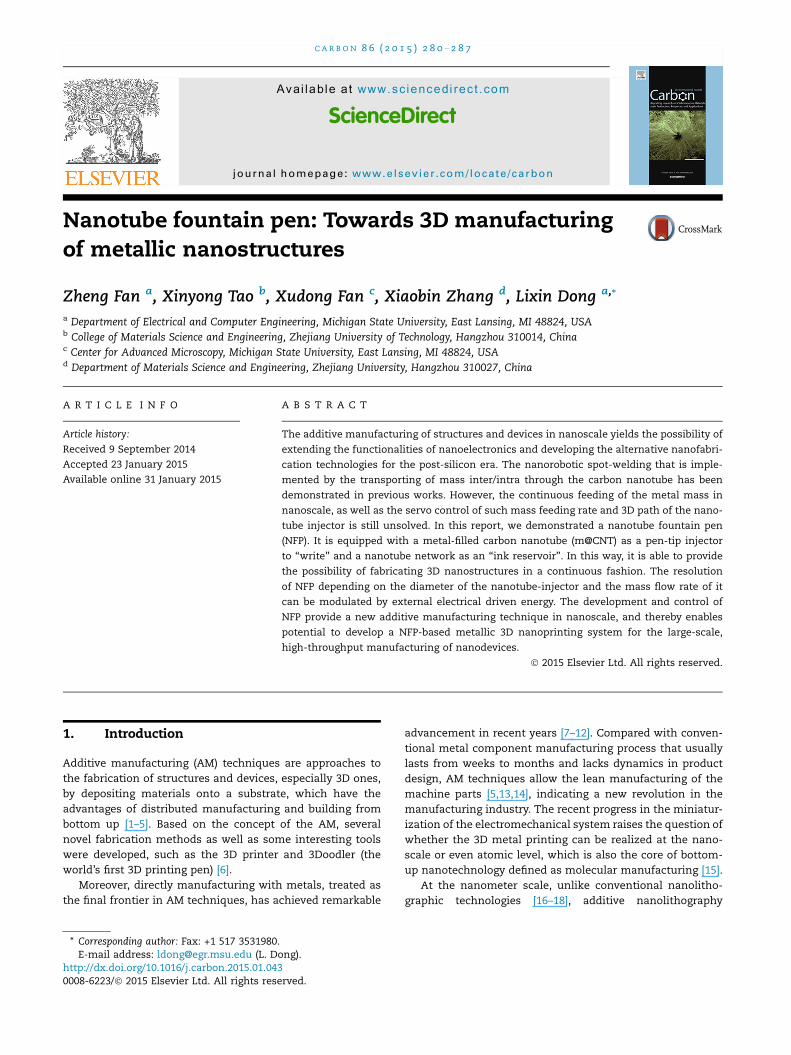
Fig. 3 – The mechanism analysis of NFP ‘‘writing’’. (a) Mass mig
illustrates the competition between electromigration force and
mass flow rate study on a Cu@CNT combined with the reservoir.
the mass flow rate and the acceleration current. (A color versio
the potentials of reducing the diameter of the nanowire down
to a few nanometers.
3.2. NFP writing mechanism
The remaining question is what factor drives the mass to
flow. Prior works in the area have showed that the electromi-
gration effect and the thermal gradient effect are the main
driving forces of the mass flowing [29,32–36]. These two
effects were also observed in the NFP writing process.
Fig. 3a shows the mass delivery inside a NFP without the res-
ervoir. When the external bias reaches 2.0 V (0 s), the dark
contrast and the boiling sign indicate the molten state of
the copper wire. As the voltage is increased to 2.2 V (7 s), the
mass in the center suddenly evaporates, clearly revealing
the thermal effect [37]. Nevertheless, by further increasing
the voltage in 0.1 V increments until the external bias reaches
a higher value (2.5 V, 11 s), the mass begins to migrate from
the upper part to the lower portion of the tube, following
the direction of the electromigration force. As we carried
out the experiment with the same setup but using a nanotube
attached with a reservoir, the mass migrating procedure was
similar to the previous experiment. However, the difference
between these two experiments is that when the reservoir
was attached to the upper side (cathode), the mass from the
reservoir continuously migrated into the nanotube following
the direction of the electron migration and finally filled up
the gap in the nanotube. Fig. 3b illustrates that the relation
between the mass migration inside the tube and the time is
given as: m = 0.0168t2 � 0.0681t + 1.9971 (ag), the external bias
here was remain in 2.5 V. Thus, the mass flow rate can be
expressed as: dm/dt = 0.0336t � 0.0681 (ag/s), indicating a lin-
ear mass flow.
ration from cathode to anode illustrates. The process
thermal gradient force during the mass transport. (b) The
(c) The model of the mass transport. (d) The relation between
n of this figure can be viewed online.)
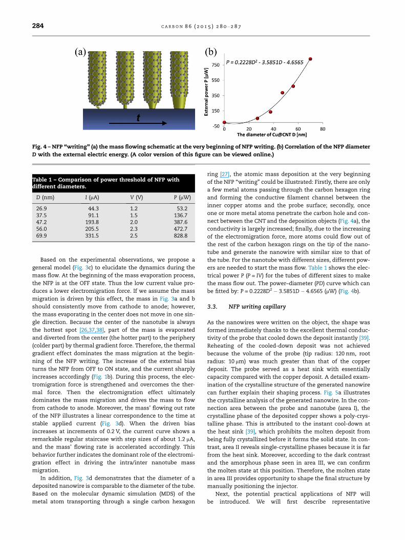
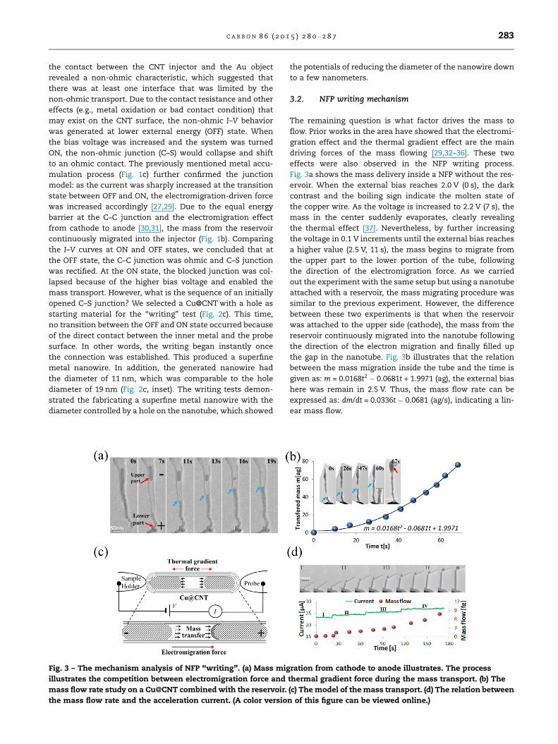
Fig. 4 – NFP ‘‘writing’’ (a) the mass flowing schematic at the very beginning of NFP writing. (b) Correlation of the NFP diameter
D with the external electric energy. (A color version of this figure can be viewed online.)
Table 1 – Comparison of power threshold of NFP withdifferent diameters.
D (nm) I (lA) V (V) P (lW)
26.9 44.3 1.2 53.237.5 91.1 1.5 136.747.2 193.8 2.0 387.656.0 205.5 2.3 472.769.9 331.5 2.5 828.8
284 C A R B O N 8 6 ( 2 0 1 5 ) 2 8 0 – 2 8 7
Based on the experimental observations, we propose a
general model (Fig. 3c) to elucidate the dynamics during the
mass flow. At the beginning of the mass evaporation process,
the NFP is at the OFF state. Thus the low current value pro-
duces a lower electromigration force. If we assume the mass
migration is driven by this effect, the mass in Fig. 3a and b
should consistently move from cathode to anode; however,
the mass evaporating in the center does not move in one sin-
gle direction. Because the center of the nanotube is always
the hottest spot [26,37,38], part of the mass is evaporated
and diverted from the center (the hotter part) to the periphery
(colder part) by thermal gradient force. Therefore, the thermal
gradient effect dominates the mass migration at the begin-
ning of the NFP writing. The increase of the external bias
turns the NFP from OFF to ON state, and the current sharply
increases accordingly (Fig. 1b). During this process, the elec-
tromigration force is strengthened and overcomes the ther-
mal force. Then the electromigration effect ultimately
dominates the mass migration and drives the mass to flow
from cathode to anode. Moreover, the mass’ flowing out rate
of the NFP illustrates a linear correspondence to the time at
stable applied current (Fig. 3d). When the driven bias
increases at increments of 0.2 V, the current curve shows a
remarkable regular staircase with step sizes of about 1.2 lA,
and the mass’ flowing rate is accelerated accordingly. This
behavior further indicates the dominant role of the electromi-
gration effect in driving the intra/inter nanotube mass
migration.
In addition, Fig. 3d demonstrates that the diameter of a
deposited nanowire is comparable to the diameter of the tube.
Based on the molecular dynamic simulation (MDS) of the
metal atom transporting through a single carbon hexagon
ring [27], the atomic mass deposition at the very beginning
of the NFP ‘‘writing’’ could be illustrated: Firstly, there are only
a few metal atoms passing through the carbon hexagon ring
and forming the conductive filament channel between the
inner copper atoms and the probe surface; secondly, once
one or more metal atoms penetrate the carbon hole and con-
nect between the CNT and the deposition objects (Fig. 4a), the
conductivity is largely increased; finally, due to the increasing
of the electromigration force, more atoms could flow out of
the rest of the carbon hexagon rings on the tip of the nano-
tube and generate the nanowire with similar size to that of
the tube. For the nanotube with different sizes, different pow-
ers are needed to start the mass flow. Table 1 shows the elec-
trical power P (P = IV) for the tubes of different sizes to make
the mass flow out. The power–diameter (PD) curve which can
be fitted by: P = 0.2228D2 � 3.5851D � 4.6565 (lW) (Fig. 4b).
3.3. NFP writing capillary
As the nanowires were written on the object, the shape was
formed immediately thanks to the excellent thermal conduc-
tivity of the probe that cooled down the deposit instantly [39].
Reheating of the cooled-down deposit was not achieved
because the volume of the probe (tip radius: 120 nm, root
radius: 10 lm) was much greater than that of the copper
deposit. The probe served as a heat sink with essentially
capacity compared with the copper deposit. A detailed exam-
ination of the crystalline structure of the generated nanowire
can further explain their shaping process. Fig. 5a illustrates
the crystalline analysis of the generated nanowire. In the con-
nection area between the probe and nanotube (area I), the
crystalline phase of the deposited copper shows a poly-crys-
talline phase. This is attributed to the instant cool-down at
the heat sink [39], which prohibits the molten deposit from
being fully crystallized before it forms the solid state. In con-
trast, area II reveals single-crystalline phases because it is far
from the heat sink. Moreover, according to the dark contrast
and the amorphous phase seen in area III, we can confirm
the molten state at this position. Therefore, the molten state
in area III provides opportunity to shape the final structure by
manually positioning the injector.
Next, the potential practical applications of NFP will
be introduced. We will first describe representative
Fig. 5 – The applications of NFP. (a) The crystalline phase analysis of as-generated nanowire. Due to the molten state at the
connection between the deposit and the injector, it provides possible to shape the deposited structures. (b) The writing
process of the letter ‘‘N’’. By manually positioning the molten copper onto the probe can freeze it immediately, and thereby
construct the nanostructure as depicted a stick figure. (c) The writing process of the letter ‘‘L’’. (d) The demonstration of using
different sized CNTs to fabricate the nanostructures. (e) The demonstration of the modulating of deposits by adjusting the
position of injector. (A color version of this figure can be viewed online.)
C A R B O N 8 6 ( 2 0 1 5 ) 2 8 0 – 2 8 7 285
experiments with multi-NFP, and then compare the drawing
with a single NFP. Although the servo control was not
applied in the experiment, manual control of the nanowire
deposit during the NFP writing is possible. By attaching the
tip of the injector to the probe during the mass flow
(Fig. 5b), the shape of the molten nanowire deposit can be
adjusted, and the 3D nanostructure similar to the letter
‘‘N’’ can be produced eventually. In Fig. 5c, for the capital
letter ‘‘L’’, the injector was moved during the mass flow to
form the letter. Moreover, it is possible to construct a nano-
scale composition with the components of different diame-
ters (Fig. 5d). Since it is difficult to use nanotubes with
different diameters to fabricate, we have also investigated
using a single nanotube to fabricate components of differ-
ent sizes. The representative demonstration shows that
the injector moved back and forth in a small range
(Fig. 5e), trying to deposit the mass at the height as similar
as possible so that the deposits would melt together and
form a component that is much larger than the original
size of the copper core inside the tube.
3.4. NFP ‘‘ink’’ reloading
Although we can accumulate the mass from the reservoir that
contains the mass several ten times more than the original
mass in the CNT, it is still not enough to construct complex
devices, such as large scale integrated circuits. As a result,
‘‘mass reloading’’ was investigated to reload the mass into
the NFP after the mass in both the nanotube injector and res-
ervoir were used up. We selected a Cu@CNT half filled with
mass to carry out the mass reloading experiment. The
‘‘reloading’’ process (frames 1–2) occurred as the external bias
reached 1 V (Fig. 6a); however, due to the lower input driving
energy, only a small amount of mass was melted and trans-
ported, and the mass accumulation rate during 63 s was only
0.52 nm/s (Fig. 6b). However, as the bias voltage increased to
1.5 V (Fig. 6c), a significant mass reloading occurred. During
this process (frames 3,4,6 s), the mass transport rate reached
96.2 nm/s. We simulated the NFP under these two external
voltages to understand the nature of mass reloading. As the
NFP was simulated as a single Cu@CNT with the diameter of

Fig. 6 – NFP ‘‘ink’’ reloading (a) the reloading in a NFP with a lower driven energy. (b) I–t characterization of NFP ‘‘ink’’
reloading with different driven energies. (c) The reloading process with higher electrical energy, the reload process lasts for
6 s. (d) The simulation of the thermal distribution along a CNT as the external bias increased. (A color version of this figure
can be viewed online.)
286 C A R B O N 8 6 ( 2 0 1 5 ) 2 8 0 – 2 8 7
12 nm (Fig. 6d), the current-induced thermal distribution
illustrated that the high temperature portion along the tube
(red portion) was enlarged due to the increasing bias from
1.0 to 1.5 V. This allowed more mass to melt, and with the
increase of the electromigration force, the transport of this
mass was rapidly realized. Therefore, we concluded that the
increased input of electrical energy induced the melting and
migration of a large amount of mass, which provided the
potential for reloading the mass.
4. Future plan
NFP has several advantages over previous additive nanoman-
ufacturing methods. Compared with the existing beam-based
additive nanolithography process, the direct laser writing
(DLW) [19] has the advantage of high prototyping speed, but
this technique cannot be used to deposit metal materials.
While the EBID [20] and the FIB-CVD [21] have higher resolu-
tion and allow multi-material deposition including metals,
their features of energy and time consuming limit their appli-
cations in the 3D nanodevice batch fabrication. The third type
of solutions, the probe-based additive nanolithographic
methods, such as DPN [22] and polymer pen lithography
(PPL) [23], are developed with the advantages of high-through-
put and lower energy consumption than the beam-based
methods. Yet, no metallic deposits have been obtained.
For the future prospects of the NFP, the physical ultimate
can be atomic ones if a CNT encapsulated with a single metal-
lic atom chain [40] is used as pen-tip. As a preliminary estima-
tion, with a 10 nm (in. dia.) · 1 lm (length) CNT tip with a
5 lm (side) · 5 lm (height) pyramid reservoir (�0.5 million
times larger than the CNT in volume) in the cantilever, we
can write a 50-m-long line or 1000 lines with full length
(5 mm) on a 5 mm · 5 mm chip if the system achieves a
tmin = 1 nm thickness. If a cross bar (two lines) forms a device,
these are 0.25 million devices. By using a 10 · 10 array of drip-
pers, we can fabricate 25 million devices with a single filling.
If the bulk reservoir for refilling the pyramid reservoir in
the cantilevers has a 100 · larger dimension (500 lm
(side) · 500 lm (height) pyramid), we will be able to obtain
25 trillion devices—remarkably overpass the upper limit of
the state-of-art ICs without considering that the bulk reser-
voirs can also be refilled. Although the NFP develop in this
report only performs as a nanoscale 3Doodler, using an array
of nanotube pen-tips, parallel writing could be implemented.
Then, each nanotube serves as a pin of the NFP-based 3D
nanoprinter, which enables the batch fabrication of the
nanostructures.
5. Conclusions
In summary, we have demonstrated the implementation of
the continuous attogram metallic mass deposition using an
NFP and its mass flow rate/position servo control. Such imple-
mentation and control of NFP provide a new additive
manufacturing technique for nanostructure fabrication with
advantages over the existing techniques, for example, the
NFP is more efficient than EBID and FIB-CVD, and superior
to DPN, NFP can produce the metallic nanostructures. Given
that NFPs are able to be arranged in parallel in an array for
the batch writing and the deposited material of NFP is not
limited to metal [39], the NFP can be developed to a multi-
material 3D nanoprinting system, and thereby open a new
ground towards fabricating of nanodevices.
Acknowledgements
Z. Fan would like to thank Mr. John Doroshewitz for the final
polish of this paper.
This work is supported by the NSF (IIS-1054585), the
NSFC (51002138), the Natural Science Foundation of Zhejiang
Province (Grants LR13E020002 and LY13E020010) and New
Century Excellent Talents in University (NCET 111079).
C A R B O N 8 6 ( 2 0 1 5 ) 2 8 0 – 2 8 7 287
Appendix A. Supplementary data
Supplementary data associated with this article can be found,
in the online version, at http://dx.doi.org/10.1016/j.carbon.
2015.01.043.
R E F E R E N C E S
[1] Gibson I, Rosen DW, Stucker B. Additive manufacturingtechnologies: rapid prototyping to direct digitalmanufacturing. Berlin: Springer-Verlag, Berlin; 2010.
[2] Sachs E, Allen S, Guo HL, Banos J, Cima M, Serdy J, et al.Progress on tooling by 3D printing: conformal cooling,dimensional control, surface finish and hardness. In: BourellDL et al., editors. Solid freeform fabricationproceedings. Austin: Univ Texas Austin; 1997. p. 115–23.
[3] Sachs E, Cima M, Williams P, Brancazio D, Cornie J. Threedimensional printing: rapid tooling and prototypes directlyfrom a cad model 1992;114(4):481–8.
[4] Hu DM, Kovacevic R. Sensing, modeling and control for laser-based additive manufacturing. Int J Mach Tools Manuf2003;43(1):51–60.
[5] Murr LE, Gaytan SM, Ramirez DA, Martinez E, Hernandez J,Amato KN, et al. Metal fabrication by additive manufacturingusing laser and electron beam melting technologies. J MaterSci Technol 2012;28(1):1–14.
[6] 3Doodler. The world’s first 3D printing pen <http://the3doodler.com/>.
[7] Kochan A. Rapid prototyping gains speed, volume andprecision. Assem Autom 2000;20(4):295–9.
[8] Williams CB, Cochran JK, Rosen DW. Additive manufacturingof metallic cellular materials via three-dimensional printing.Int J Adv Manuf Technol 2011;53(1–4):231–9.
[9] Kim MS, Chu WS, Kim YM, Avila APG, Ahn SH. Direct metalprinting of 3D electrical circuit using rapid prototyping. Int JPrecis Eng Manuf 2009;10(5):147–50.
[10] Ko SH, Chung J, Hotz N, Nam KH, Grigoropoulos CP. Metalnanoparticle direct inkjet printing for low-temperature 3Dmicro metal structure fabrication. J Micromech Microeng2010;20(12):125010.
[11] Gill SS, Kaplas M. Comparative study of 3D printingtechnologies for rapid casting of aluminium alloy. MaterManuf Process 2009;24(12):1405–11.
[12] Sanchez-Romaguera V, Madec MB, Yeates SG. Inkjet printingof 3D metal-insulator-metal crossovers. React Funct Polym2008;68(6):1052–8.
[13] Hu D, Mei H, Kovacevic R. Improving solid freeformfabrication by laser-based additive manufacturing. Proc InstMech Eng Part B–J Eng Manuf 2002;216(9):1253–64.
[14] Gu DD, Meiners W, Wissenbach K, Poprawe R. Laser additivemanufacturing of metallic components: materials, processesand mechanisms. Int Mater Rev 2012;57(3):133–64.
[15] Drexler KE. Nanotechnology - the past and the future.Science 1992;255(5042):268–9.
[16] Heidenre RD, Thompson LF, Feit ED, Melliars CM.Fundamental aspects of electron-beam lithography.1. Depth-dose response of polymeric electron-beam resists. J ApplPhys 1973;44(9):4039–47.
[17] Thompson LF, Feit ED, Melliars CM, Heidenre RD.Fundamental aspects of electron-beam lithography.2. Low-voltage exposure of negative resists. J Appl Phys1973;44(9):4048–51.
[18] Dai HJ, Franklin N, Han J. Exploiting the properties of carbonnanotubes for nanolithography. Appl Phys Lett1998;73(11):1508–10.
[19] Anscombe N. Direct laser writing. Nat Photonics2010;4(1):22–3.
[20] Koops HWP, Kretz J, Rudolph M, Weber M. Constructive 3-dimensional lithography with electron-beam-induceddeposition for quantum effect devices. J Vac Sci Technol, B1993;11(6):2386–9.
[21] Matsui S, Kaito T, Fujita J, Komuro M, Kanda K, Haruyama Y.Three-dimensional nanostructure fabrication by focused-ion-beam chemical vapor deposition. J Vac Sci Technol, B2000;18(6):3181–4.
[22] Piner RD, Zhu J, Xu F, Hong SH, Mirkin CA. ‘‘Dip-pen’’Nanolithography. Science 1999;283(5402):661–3.
[23] Huo FW, Zheng ZJ, Zheng GF, Giam LR, Zhang H, Mirkin CA.Polymer pen lithography. Science 2008;321(5896):1658–60.
[24] Tao XY, Zhang XB, Cheng JP, Luo ZQ, Zhou SM, Liu F. ThermalCVD synthesis of carbon nanotubes filled with single-crystalline cu nanoneedles at tips. Diamond Relat Mater2006;15(9):1271–5.
[25] Collins PC, Arnold MS, Avouris P. Engineering carbonnanotubes and nanotube circuits using electrical breakdown.Science 2001;292(5517):706–9.
[26] Huang JY, Chen S, Jo SH, Wang Z, Han DX, Chen G, et al.Atomic-scale imaging of wall-by-wall breakdown andconcurrent transport measurements in multiwall carbonnanotubes. Phys Rev Lett 2005;94(23):236802.
[27] Dong LX, Tao XY, Hamdi M, Zhang L, Zhang XB, Ferreira A,et al. Nanotube fluidic junctions: internanotube attogrammass transport through walls. Nano Lett 2009;9(1):210–4.
[28] Dong LX, Tao XY, Zhang L, Zhang X, Nelson B. Plumbing thedepths of the nanometer scale. IEEE Nanotechnol Mag2010;4(1):13–22.
[29] Dong LX, Tao XY, Zhang L, Zhang XB, Nelson BJ. Nanoroboticspot welding: controlled metal deposition with attogramprecision from copper-filled carbon nanotubes. Nano Lett2007;7(1):58–63.
[30] Dekker JP, Lodder A. Calculated electromigration wind forcein face-centered-cubic and body-centered-cubic metals. JAppl Phys 1998;84(4):1958–62.
[31] Dekker JP, Lodder A, van Ek J. Theory for the electromigrationwind force in dilute alloys. Phys Rev B 1997;56(19):12167–77.
[32] Svensson K, Olin H, Olsson E. Nanopipettes for metaltransport. Phys Rev Lett 2004;93(14):145901.
[33] Heinze S, Wang NP, Tersoff J. Electromigration forces on ionsin carbon nanotubes. Phys Rev Lett 2005;95(18):186802.
[34] Regan BC, Aloni S, Ritchie RO, Dahmen U, Zettl A. Carbonnanotubes as nanoscale mass conveyors. Nature2004;428(6986):924–7.
[35] Barreiro A, Rurali R, Hernandez ER, Moser J, Pichler T, Forro L,et al. Subnanometer motion of cargoes driven by thermalgradients along carbon nanotubes. Science2008;320(5877):775–8.
[36] Zhao JO, Huang JQ, Wei F, Zhu J. Mass transportationmechanism in electric-biased carbon nanotubes. Nano Lett2010;10(11):4309–15.
[37] Huang XY, Zhang ZY, Liu Y, Peng LM. Analytical analysis ofheat conduction in a suspended one-dimensional object.Appl Phys Lett 2009;95(14):143109.
[38] Collins PG, Hersam M, Arnold M, Martel R, Avouris P. Currentsaturation and electrical breakdown in multiwalled carbonnanotubes. Phys Rev Lett 2001;86(14).
[39] Fan Z, Tao XY, Cui XD, Fan XD, Zhang XB, Dong LX. Proc 2010IEEE Nanotechnol Mater Dev Conf (IEEE-NMDC2010) 2010:22–5.
[40] Kitaura R, Nakanishi R, Saito T, Yoshikawa H, Awaga K,Shinohara H. High-yield synthesis of ultrathin metalnanowires in carbon nanotubes. Angew Chem Int Edit2009;48(44):8298–302.