Murdocca en
650
Miles J. Murdocca Department of Computer Science Rutgers University New Brunswick, NJ 08903 (USA) [email protected] http://www.cs.rutgers.edu/~murdocca/ Vincent P. Heuring Department of Electrical and Computer Engineering University of Colorado Boulder, CO 80309-0425 (USA) [email protected] http://ece-www.colorado.edu/faculty/heuring.html Copyright © 1999 Prentice Hall PRINCIPLES OF COMPUTER ARCHITECTURE CLASS TEST EDITION – AUGUST 1999
-
Upload
independent -
Category
Documents
-
view
0 -
download
0
Transcript of Murdocca en
Miles J. Murdocca
Department of Computer ScienceRutgers University
New Brunswick, NJ 08903 (USA)[email protected]
http://www.cs.rutgers.edu/~murdocca/
Vincent P. Heuring
Department of Electrical and Computer EngineeringUniversity of Colorado
Boulder, CO 80309-0425 (USA)[email protected]
http://ece-www.colorado.edu/faculty/heuring.html
Copyright © 1999 Prentice Hall
PRINCIPLES OF COMPUTER
ARCHITECTURE
CLASS TEST EDITION – AUGUST 1999

For Ellen, Alexandra, and Nicole
and
For Gretchen
PREFACE
iii
About the Book
Our goal in writing this book is to expose the inner workings of the moderndigital computer at a level that demystifies what goes on inside the machine.The only prerequisite to
Principles of Computer Architecture
is a workingknowledge of a high-level programming language. The breadth of material hasbeen chosen to cover topics normally found in a first course in computerarchitecture or computer organization. The breadth and depth of coveragehave been steered to also place the beginning student on a solid track for con-tinuing studies in computer related disciplines.
In creating a computer architecture textbook, the technical issues fall intoplace fairly naturally, and it is the organizational issues that bring importantfeatures to fruition. Some of the features that received the greatest attention in
Principles of Computer Architecture
include the choice of the instruction setarchitecture (ISA), the use of case studies, and a voluminous use of examplesand exercises.
THE INSTRUCTIONAL ISA
A textbook that covers assembly language programming needs to deal with theissue of which instruction set architecture (ISA) to use: a model architecture,or one of the many commercial architectures. The choice impacts the instruc-tor, who may want an ISA that matches a local platform used for studentassembly language programming assignments. To complicate matters, thelocal platform may change from semester to semester: yesterday the MIPS,today the Pentium, tomorrow the SPARC. The authors opted for having itboth ways by adopting a SPARC-subset for an instructional ISA, called “ARISC Computer” (ARC), which is carried through the mainstream of the
PREFACE
iv
PREFACE
book, and complementing it with platform-independent software tools that sim-ulate the ARC ISA as well as the MIPS and x86 (Pentium) ISAs.
CASE STUDIES, EXAMPLES, AND EXERCISES
Every chapter contains at least one case study as a means for introducing the stu-dent to “real world” examples of the topic being covered. This places the topic inperspective, and in the authors’ opinion, lends an air of reality and interest to thematerial.
We incorporated as many examples and exercises as we practically could, cover-ing the most significant points in the text. Additional examples and solutions areavailable on-line, at the companion Web site (see below.)
Coverage of Topics
Our presentation views a computer as an integrated system. If we were to choosea subtitle for the book, it might be “An Integrated Approach,” which reflects highlevel threads that tie the material together. Each topic is covered in the context ofthe entire machine of which it is a part, and with a perspective as to how theimplementation affects behavior. For example, the finite precision of binarynumbers is brought to bear in observing how many 1’s can be added to a floatingpoint number before the error in the representation exceeds 1. (This is one rea-son why floating point numbers should be avoided as loop control variables.) Asanother example, subroutine linkage is covered with the expectation that thereader may someday be faced with writing C or Java programs that make calls toroutines in other high level languages, such as Fortran.
As yet another example of the integrated approach, error detection and correc-tion are covered in the context of mass storage and transmission, with the expec-tation that the reader may tackle networking applications (where bit errors anddata packet losses are a fact of life) or may have to deal with an unreliable storagemedium such as a compact disk read-only memory (CD-ROM.)
Computer architecture impacts many of the ordinary things that computer pro-fessionals do, and the emphasis on taking an integrated approach addresses thegreat diversity of areas in which a computer professional should be educated.This emphasis reflects a transition that is taking place in many computer relatedundergraduate curricula. As computer architectures become more complex theymust be treated at correspondingly higher levels of abstraction, and in some ways
PREFACE
v
they also become more technology-dependent. For this reason, the major portionof the text deals with a high level look at computer architecture, while the appen-dices and case studies cover lower level, technology-dependent aspects.
THE CHAPTERS
Chapter 1: Introduction
introduces the textbook with a brief history of com-puter architecture, and progresses through the basic parts of a computer, leavingthe student with a high level view of a computer system. The conventional vonNeumann model of a digital computer is introduced, followed by the System BusModel, followed by a topical exploration of a typical computer. This chapter laysthe groundwork for the more detailed discussions in later chapters.
Chapter 2
: Data Representation
covers basic data representation. One’s comple-ment, two’s complement, signed magnitude and excess representations of signednumbers are covered. Binary coded decimal (BCD) representation, which is fre-quently found in calculators, is also covered in Chapter 2. The representation offloating point numbers is covered, including the IEEE 754 floating point stan-dard for binary numbers. The ASCII, EBCDIC, and Unicode character repre-sentations are also covered.
Chapter 3
: Arithmetic
covers computer arithmetic and advanced data represen-tations. Fixed point addition, subtraction, multiplication, and division are cov-ered for signed and unsigned integers. Nine’s complement and ten’s complementrepresentations, used in BCD arithmetic, are covered. BCD and floating pointarithmetic are also covered. High performance methods such as carry-lookaheadaddition, array multiplication, and division by functional iteration are covered. Ashort discussion of residue arithmetic introduces an unconventional high perfor-mance approach.
Chapter 4
: The Instruction Set Architecture
introduces the basic architecturalcomponents involved in program execution. Machine language and thefetch-execute cycle are covered. The organization of a central processing unit isdetailed, and the role of the system bus in interconnecting the arithmetic/logicunit, registers, memory, input and output units, and the control unit are dis-cussed.
Assembly language programming is covered in the context of the instructionalARC (A RISC Computer), which is loosely based on the commercial SPARCarchitecture. The instruction names, instruction formats, data formats, and the
vi
PREFACE
suggested assembly language syntax for the SPARC have been retained in theARC, but a number of simplifications have been made. Only 15 SPARC instruc-tions are used for most of the chapter, and only a 32-bit unsigned integer datatype is allowed initially. Instruction formats are covered, as well as addressingmodes. Subroutine linkage is explored in a number of styles, with a detailed dis-cussion of parameter passing using a stack.
Chapter 5
: Languages and the Machine
connects the programmer’s view of acomputer system with the architecture of the underlying machine. System soft-ware issues are covered with the goal of making the low level machine visible to aprogrammer. The chapter starts with an explanation of the compilation process,first covering the steps involved in compilation, and then focusing on code gen-eration. The assembly process is described for a two-pass assembler, and examplesare given of generating symbol tables. Linking, loading, and macros are also cov-ered.
Chapter 6
: Datapath and Control
provides a step-by-step analysis of a datapathand a control unit. Two methods of control are discussed: microprogrammed andhardwired. The instructor may adopt one method and omit the other, or coverboth methods as time permits. The example microprogrammed and hardwiredcontrol units implement the ARC subset of the SPARC assembly language intro-duced in Chapter 4.
Chapter 7
: Memory
covers computer memory beginning with the organizationof a basic random access memory, and moving to advanced concepts such ascache and virtual memory. The traditional direct, associative, and set associativecache mapping schemes are covered, as well as multilevel caches. Issues such asoverlays, replacement policies, segmentation, fragmentation, and the translationlookaside buffer are also discussed.
Chapter 8
: Input and Output
covers bus communication and bus access meth-ods. Bus-to-bus bridging is also described. The chapter covers various I/Odevices commonly in use such as disks, keyboards, printers, and displays.
Chapter 9
: Communication
covers network architectures, focusing on modems,local area networks, and wide area networks. The emphasis is primarily on
net-work architecture
, with accessible discussions of protocols that spotlight key fea-tures of network architecture. Error detection and correction are covered indepth. The TCP/IP protocol suite is introduced in the context of the Internet.
PREFACE
vii
Chapter 10
: Trends in Computer Architecture
covers advanced architecturalfeatures that have either emerged or taken new forms in recent years. The earlypart of the chapter covers the motivation for reduced instruction set computer(RISC) processors, and the architectural implications of RISC. The latter portionof the chapter covers multiple instruction issue machines, and very large instruc-tion word (VLIW) machines. A case study makes RISC features visible to theprogrammer in a step-by-step analysis of a C compiler-generated SPARC pro-gram, with explanations of the stack frame usage, register usage, and pipelining.The chapter covers parallel and distributed architectures, and interconnectionnetworks used in parallel and distributed processing.
Appendix A
: Digital Logic
covers combinational logic and sequential logic, andprovides a foundation for understanding the logical makeup of components dis-cussed in the rest of the book. Appendix A begins with a description of truthtables, Boolean algebra, and logic equations. The synthesis of combinationallogic circuits is described, and a number of examples are explored. Medium scaleintegration (MSI) components such as multiplexers and decoders are discussed,and examples of synthesizing circuits using MSI components are explored.
Synchronous logic is also covered in Appendix A, starting with an introductionto timing issues that relate to flip-flops. The synthesis of synchronous logic cir-cuits is covered with respect to state transition diagrams, state tables, and syn-chronous logic designs.
Appendix A can be paired with
Appendix B
: Reduction of Digital Logic
whichcovers reduction for combinational and sequential logic. Minimization is coveredusing algebraic reduction, Karnaugh maps, and the tabular (Quine-McCluskey)method for single and multiple functions. State reduction and state assignmentare also covered.
CHAPTER ORDERING
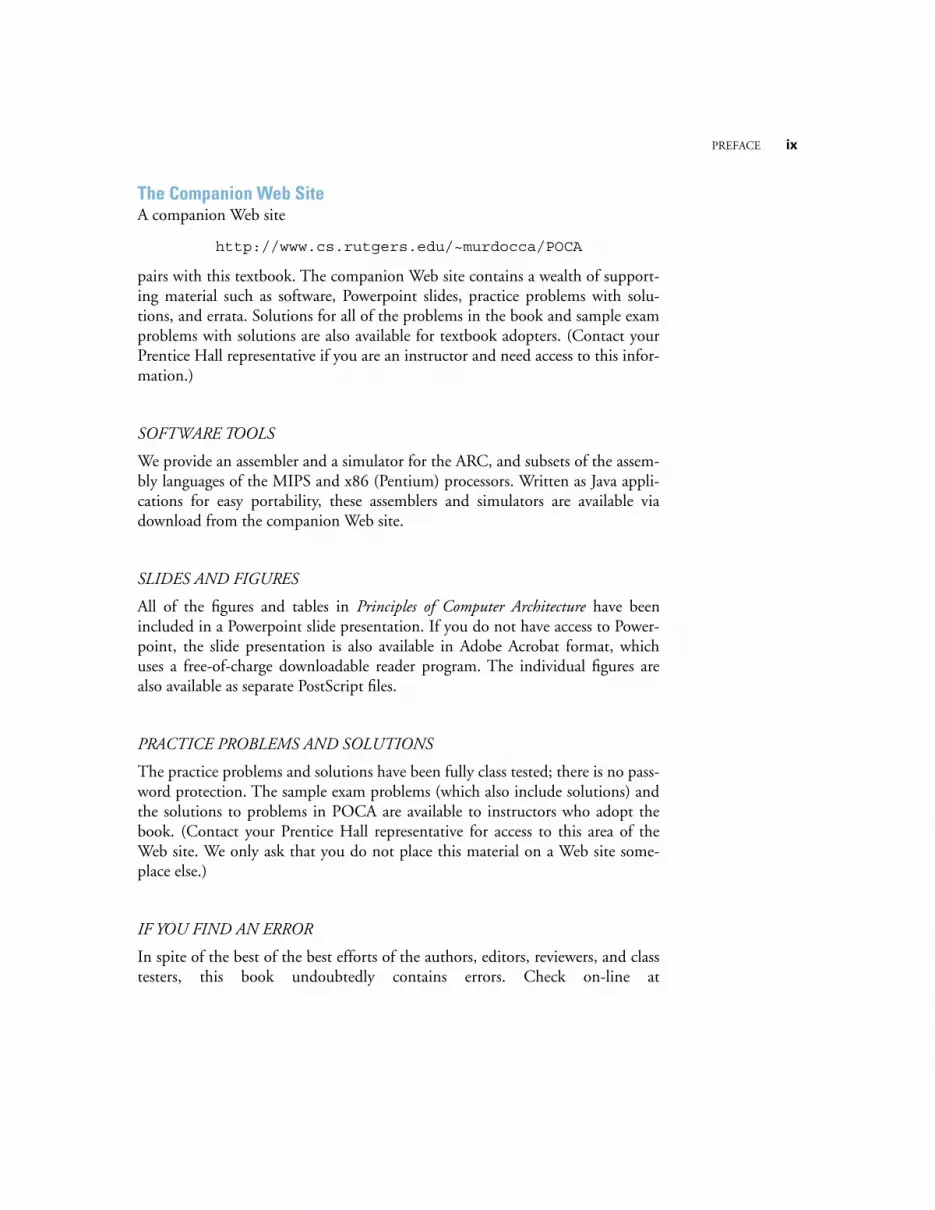
The order of chapters is created so that the chapters can be taught in numericalorder, but an instructor can modify the ordering to suit a particular curriculumand syllabus. Figure P-1 shows prerequisite relationships among the chapters.Special considerations regarding chapter sequencing are detailed below.
Chapter 2 (Data Representation) should be covered prior to Chapter 3 (Arith-metic), which has the greatest need for it. Appendix A (Digital Logic) andAppendix B (Reduction of Digital Logic) can be omitted if digital logic is cov-
viii
PREFACE
ered earlier in the curriculum, but if the material is not covered, then the struc-ture of some components (such as an arithmetic logic unit or a register) willremain a mystery in later chapters if at least Appendix A is not covered earlierthan Chapter 3.
Chapter 4 (The Instruction Set Architecture) and Chapter 5 (Languages and theMachine) appear in the early half of the book for two reasons: (1) they introducethe student to the workings of a computer at a fairly high level, which allows fora top-down approach to the study of computer architecture; and (2) it is impor-tant to get started on assembly language programming early if hands-on pro-gramming is part of the course.
The material in Chapter 10 (Trends in Computer Architecture) typically appearsin graduate level architecture courses, and should therefore be covered only astime permits, after the material in the earlier chapters is covered.
Chapter 1: Introduction
Chapter 2: Data Representation
Chapter 3: Arithmetic Appendix A: Digital Logic
Appendix B: Reduction of Digital Logic
Chapter 4: The Instruction Set Architecture
Chapter 5: Languages and the Machine
Chapter 7: Memory
Chapter 6: Datapath and Chapter 8: Input and Output
Chapter 9: Communication
Chapter 10: Trends inComputer Architecture
Control
Figure P-1 Prerequisite relationships among chapters.
PREFACE
ix
The Companion Web Site
A companion Web site
http://www.cs.rutgers.edu/~murdocca/POCA
pairs with this textbook. The companion Web site contains a wealth of support-ing material such as software, Powerpoint slides, practice problems with solu-tions, and errata. Solutions for all of the problems in the book and sample examproblems with solutions are also available for textbook adopters. (Contact yourPrentice Hall representative if you are an instructor and need access to this infor-mation.)
SOFTWARE TOOLS
We provide an assembler and a simulator for the ARC, and subsets of the assem-bly languages of the MIPS and x86 (Pentium) processors. Written as Java appli-cations for easy portability, these assemblers and simulators are available viadownload from the companion Web site.
SLIDES AND FIGURES
All of the figures and tables in
Principles of Computer Architecture
have beenincluded in a Powerpoint slide presentation. If you do not have access to Power-point, the slide presentation is also available in Adobe Acrobat format, whichuses a free-of-charge downloadable reader program. The individual figures arealso available as separate PostScript files.
PRACTICE PROBLEMS AND SOLUTIONS
The practice problems and solutions have been fully class tested; there is no pass-word protection. The sample exam problems (which also include solutions) andthe solutions to problems in POCA are available to instructors who adopt thebook. (Contact your Prentice Hall representative for access to this area of theWeb site. We only ask that you do not place this material on a Web site some-place else.)
IF YOU FIND AN ERROR
In spite of the best of the best efforts of the authors, editors, reviewers, and classtesters, this book undoubtedly contains errors. Check on-line at

x
PREFACE
http://www.cs.rutgers.edu/~murdocca/POCA
to see if it has been cat-alogued. You can report errors to
. Please men-tion the chapter number where the error occurs in the
Subject:
header.
Credits and Acknowledgments
We did not create this book entirely on our own, and we gratefully acknowledgethe support of many people for their influence in the preparation of the bookand on our thinking in general. We first wish to thank our Acquisitions Editors:Thomas Robbins and Paul Becker, who had the foresight and vision to guide thisbook and its supporting materials through to completion. Donald Chiarulli wasan important influence on an early version of the book, which was class-tested atRutgers University and the University of Pittsburgh. Saul Levy, Donald Smith,Vidyadhar Phalke, Ajay Bakre, Jinsong Huang, and Srimat Chakradhar helpedtest the material in courses at Rutgers, and provided some of the text, problems,and valuable explanations. Brian Davison and Shridhar Venkatanarisam workedon an early version of the solutions and provided many helpful comments. IrvingRabinowitz provided a number of problem sets. Larry Greenfield providedadvice from the perspective of a student who is new to the subject, and is cred-ited with helping in the organization of Chapter 2. Blair Gabett Bizjak is creditedwith providing the framework for much of the LAN material. Ann Yasuhara pro-vided text on Turing’s contributions to computer science. William Waite pro-vided a number of the assembly language examples.
The reviewers, whose names we do not know, are gratefully acknowledged fortheir help in steering the project. Ann Root did a superb job on the developmentof the supporting ARCSim tools which are available on the companion Web site.The Rutgers University and University of Colorado student populations pro-vided important proving grounds for the material, and we are grateful for theirpatience and recommendations while the book was under development.
I (MJM) was encouraged by my parents Dolores and Nicholas Murdocca, my sis-ter Marybeth, and my brother Mark. My wife Ellen and my daughters Alexandraand Nicole have been an endless source of encouragement and inspiration. I donot think I could have found the energy for such an undertaking without all oftheir support.
I (VPH) wish to acknowledge the support of my wife Gretchen, who was exceed-ingly patient and encouraging throughout the process of writing this book.

PREFACE
xi
There are surely other people and institutions who have contributed to thisbook, either directly or indirectly, whose names we have inadvertently omitted.To those people and institutions we offer our tacit appreciation and apologize forhaving omitted explicit recognition here.
Miles J. MurdoccaRutgers [email protected]
Vincent P. HeuringUniversity of Colorado at [email protected]

xii
PREFACE
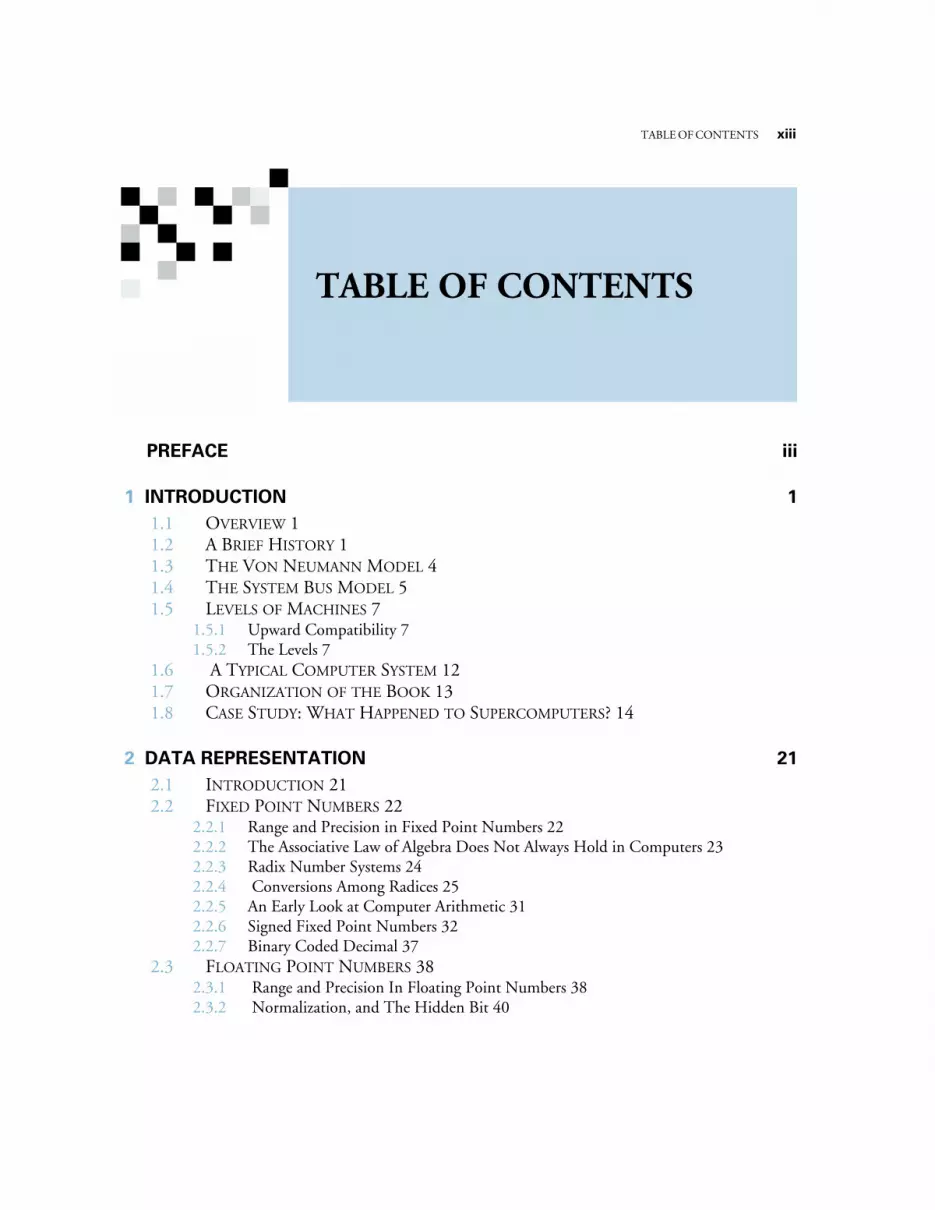
TABLE OF CONTENTS
xiii
PREFACE iii
1 INTRODUCTION 1
1.1 O
VERVIEW
11.2 A B
RIEF
H
ISTORY
11.3 T
HE
V
ON
N
EUMANN
M
ODEL
41.4 T
HE
S
YSTEM
B
US
M
ODEL
51.5 L
EVELS
OF
M
ACHINES
7
1.5.1 Upward Compatibility 71.5.2 The Levels 7
1.6 A T
YPICAL
C
OMPUTER
S
YSTEM
121.7 O
RGANIZATION
OF
THE
B
OOK
131.8 C
ASE
S
TUDY
: W
HAT
H
APPENED
TO
S
UPERCOMPUTERS
? 14
2 DATA REPRESENTATION 21
2.1 I
NTRODUCTION
212.2 F
IXED
P
OINT
N
UMBERS
22
2.2.1 Range and Precision in Fixed Point Numbers 222.2.2 The Associative Law of Algebra Does Not Always Hold in Computers 232.2.3 Radix Number Systems 242.2.4 Conversions Among Radices 252.2.5 An Early Look at Computer Arithmetic 312.2.6 Signed Fixed Point Numbers 322.2.7 Binary Coded Decimal 37
2.3 F
LOATING
P
OINT
N
UMBERS
38
2.3.1 Range and Precision In Floating Point Numbers 382.3.2 Normalization, and The Hidden Bit 40
TABLE OF CONTENTS
xiv
TABLE OF CONTENTS
2.3.3 Representing Floating Point Numbers in the Computer—Preliminaries 402.3.4 Error in Floating Point Representations 442.3.5 The IEEE 754 Floating Point Standard 48
2.4 C
ASE
S
TUDY
: P
ATRIOT
M
ISSILE
D
EFENSE
F
AILURE
C
AUSED
BY
L
OSS
OF
P
RECISION
512.5 C
HARACTER
C
ODES
53
2.5.1 The ASCII Character Set 532.5.2 The EBCDIC Character Set 542.5.3 The Unicode Character Set 55
3 ARITHMETIC 65
3.1 O
VERVIEW
653.2 F
IXED
P
OINT
A
DDITION
AND
S
UBTRACTION
65
3.2.1 Two’s complement addition and subtraction 663.2.2 Hardware implementation of adders and subtractors 693.2.3 One’s Complement Addition and Subtraction 71
3.3 F
IXED
P
OINT
M
ULTIPLICATION
AND
D
IVISION
73
3.3.1 Unsigned Multiplication 733.3.2 Unsigned Division 753.3.3 Signed Multiplication and Division 77
3.4 F
LOATING
P
OINT
A
RITHMETIC
79
3.4.1 Floating Point Addition and Subtraction 793.4.2 Floating Point Multiplication and Division 80
3.5 H
IGH
P
ERFORMANCE
A
RITHMETIC
81
3.5.1 High Performance Addition 813.5.2 High Performance Multiplication 833.5.3 High Performance Division 873.5.4 Residue Arithmetic 90
3.6 C
ASE
S
TUDY
: C
ALCULATOR
A
RITHMETIC
U
SING
B
INARY
C
ODED
D
ECIMAL
93
3.6.1 The HP9100A Calculator 943.6.2 Binary Coded Decimal Addition and subtraction 943.6.3 BCD Floating Point Addition and Subtraction 97
4 T
HE
I
NSTRUCTION
S
ET
A
RCHITECTURE
105
4.1 H
ARDWARE
C
OMPONENTS
OF
THE
I
NSTRUCTION
S
ET
A
RCHITECTURE
106
4.1.1 The System Bus Model Revisited 1064.1.2 Memory 1074.1.3 The CPU 110
4.2 ARC, A RISC C
OMPUTER
114
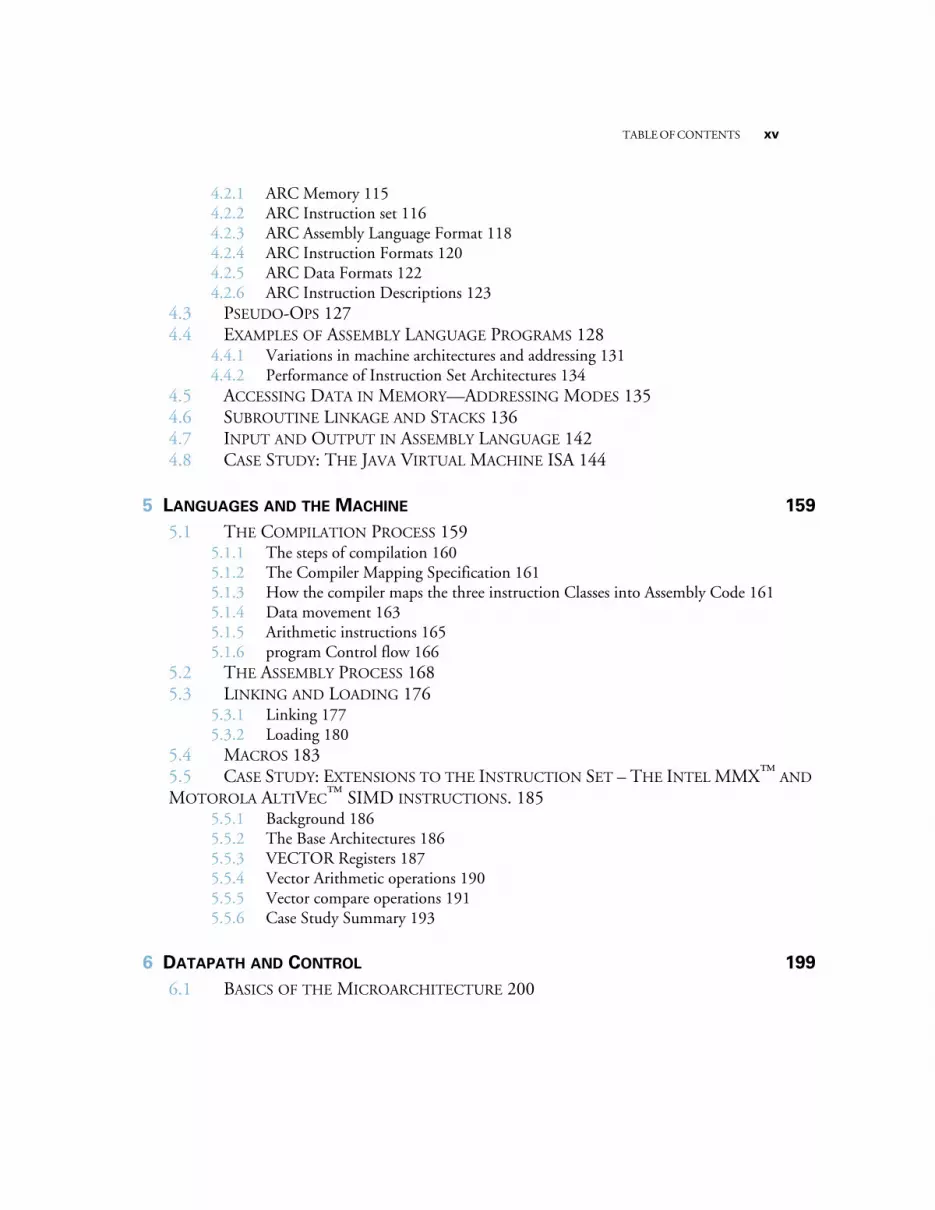
TABLE OF CONTENTS
xv
4.2.1 ARC Memory 1154.2.2 ARC Instruction set 1164.2.3 ARC Assembly Language Format 1184.2.4 ARC Instruction Formats 1204.2.5 ARC Data Formats 1224.2.6 ARC Instruction Descriptions 123
4.3 P
SEUDO
-O
PS
1274.4 E
XAMPLES
OF ASSEMBLY LANGUAGE PROGRAMS 1284.4.1 Variations in machine architectures and addressing 1314.4.2 Performance of Instruction Set Architectures 134
4.5 ACCESSING DATA IN MEMORY—ADDRESSING MODES 1354.6 SUBROUTINE LINKAGE AND STACKS 1364.7 INPUT AND OUTPUT IN ASSEMBLY LANGUAGE 1424.8 CASE STUDY: THE JAVA VIRTUAL MACHINE ISA 144
5 LANGUAGES AND THE MACHINE 159
5.1 THE COMPILATION PROCESS 1595.1.1 The steps of compilation 1605.1.2 The Compiler Mapping Specification 1615.1.3 How the compiler maps the three instruction Classes into Assembly Code 1615.1.4 Data movement 1635.1.5 Arithmetic instructions 1655.1.6 program Control flow 166
5.2 THE ASSEMBLY PROCESS 1685.3 LINKING AND LOADING 176
5.3.1 Linking 1775.3.2 Loading 180
5.4 MACROS 1835.5 CASE STUDY: EXTENSIONS TO THE INSTRUCTION SET – THE INTEL MMX™ AND MOTOROLA ALTIVEC™ SIMD INSTRUCTIONS. 185
5.5.1 Background 1865.5.2 The Base Architectures 1865.5.3 VECTOR Registers 1875.5.4 Vector Arithmetic operations 1905.5.5 Vector compare operations 1915.5.6 Case Study Summary 193
6 DATAPATH AND CONTROL 199
6.1 BASICS OF THE MICROARCHITECTURE 200
xvi TABLE OF CONTENTS
6.2 A MICROARCHITECTURE FOR THE ARC 2016.2.1 The Datapath 2016.2.2 The Control Section 2106.2.3 Timing 2136.2.4 Developing the Microprogram 2146.2.5 Traps and Interrupts 2256.2.6 Nanoprogramming 227
6.3 HARDWIRED CONTROL 2286.4 CASE STUDY: THE VHDL HARDWARE DESCRIPTION LANGUAGE 237
6.4.1 Background 2386.4.2 What is VHDL? 2396.4.3 A VHDL specification of the Majority FUNCTION 2406.4.4 9-Value logic system 243
7 MEMORY 255
7.1 THE MEMORY HIERARCHY 2557.2 RANDOM ACCESS MEMORY 2577.3 CHIP ORGANIZATION 258
7.3.1 Constructing LARGE RAMS FROm SMALL RAMS 2617.4 COMMERCIAL MEMORY MODULES 2627.5 READ-ONLY MEMORY 2637.6 CACHE MEMORY 266
7.6.1 Associative Mapped Cache 2687.6.2 Direct Mapped Cache 2717.6.3 Set Associative Mapped Cache 2747.6.4 Cache performance 2757.6.5 Hit Ratios and Effective Access Times 2777.6.6 Multilevel Caches 2797.6.7 Cache management 279
7.7 VIRTUAL MEMORY 2817.7.1 Overlays 2817.7.2 Paging 2837.7.3 Segmentation 2867.7.4 Fragmentation 2877.7.5 Virtual Memory vs. Cache Memory 2897.7.6 THE TRANSLATION LOOKASIDE BUFFER 289
7.8 ADVANCED TOPICS 2917.8.1 Tree decoders 2917.8.2 Decoders for large RAMs 292
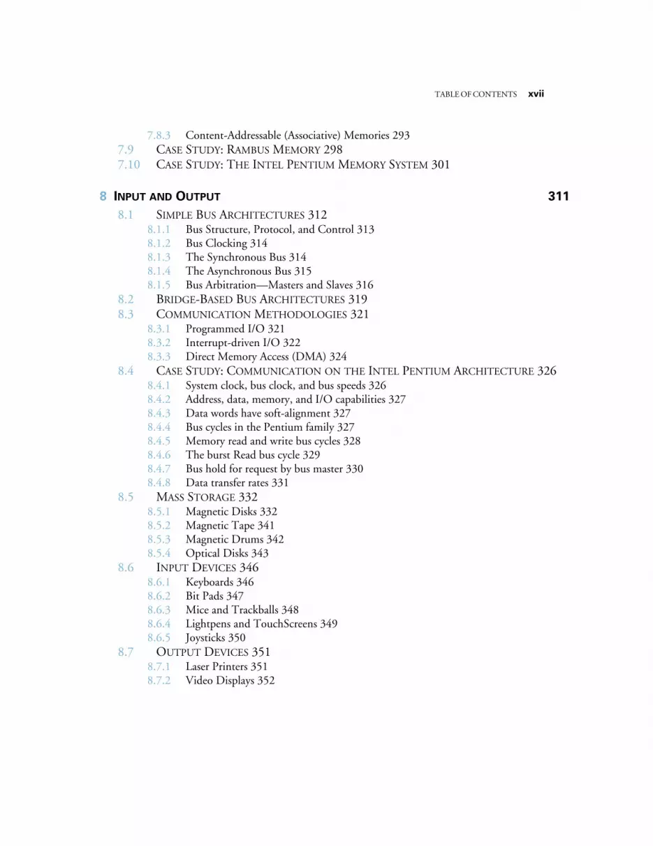
TABLE OF CONTENTS xvii
7.8.3 Content-Addressable (Associative) Memories 2937.9 CASE STUDY: RAMBUS MEMORY 2987.10 CASE STUDY: THE INTEL PENTIUM MEMORY SYSTEM 301
8 INPUT AND OUTPUT 311
8.1 SIMPLE BUS ARCHITECTURES 3128.1.1 Bus Structure, Protocol, and Control 3138.1.2 Bus Clocking 3148.1.3 The Synchronous Bus 3148.1.4 The Asynchronous Bus 3158.1.5 Bus Arbitration—Masters and Slaves 316
8.2 BRIDGE-BASED BUS ARCHITECTURES 3198.3 COMMUNICATION METHODOLOGIES 321
8.3.1 Programmed I/O 3218.3.2 Interrupt-driven I/O 3228.3.3 Direct Memory Access (DMA) 324
8.4 CASE STUDY: COMMUNICATION ON THE INTEL PENTIUM ARCHITECTURE 3268.4.1 System clock, bus clock, and bus speeds 3268.4.2 Address, data, memory, and I/O capabilities 3278.4.3 Data words have soft-alignment 3278.4.4 Bus cycles in the Pentium family 3278.4.5 Memory read and write bus cycles 3288.4.6 The burst Read bus cycle 3298.4.7 Bus hold for request by bus master 3308.4.8 Data transfer rates 331
8.5 MASS STORAGE 3328.5.1 Magnetic Disks 3328.5.2 Magnetic Tape 3418.5.3 Magnetic Drums 3428.5.4 Optical Disks 343
8.6 INPUT DEVICES 3468.6.1 Keyboards 3468.6.2 Bit Pads 3478.6.3 Mice and Trackballs 3488.6.4 Lightpens and TouchScreens 3498.6.5 Joysticks 350
8.7 OUTPUT DEVICES 3518.7.1 Laser Printers 3518.7.2 Video Displays 352
xviii TABLE OF CONTENTS
9 COMMUNICATION 361
9.1 MODEMS 3619.2 TRANSMISSION MEDIA 364
9.2.1 Two-Wire Open Lines 3659.2.2 Twisted-Pair Lines 3669.2.3 Coaxial Cable 3669.2.4 Optical Fiber 3669.2.5 Satellites 3679.2.6 Terrestrial Microwave 3689.2.7 Radio 368
9.3 NETWORK ARCHITECTURE: LOCAL AREA NETWORKS 3689.3.1 The OSI Model 3699.3.2 Topologies 3719.3.3 Data Transmission 3729.3.4 Bridges, Routers, and Gateways 374
9.4 COMMUNICATION ERRORS AND ERROR CORRECTING CODES 3759.4.1 Bit Error Rate Defined 3759.4.2 Error Detection and Correction 3769.4.3 Vertical Redundancy Checking 3829.4.4 Cyclic Redundancy Checking 383
9.5 NETWORK ARCHITECTURE: THE INTERNET 3869.5.1 The Internet Model 3869.5.2 Bridges and Routers Revisited, and Switches 392
9.6 CASE STUDY: ASYNCHRONOUS TRANSFER MODE 3939.6.1 Synchronous vs. Asynchronous Transfer Mode 3959.6.2 What is ATM? 3959.6.3 ATM Network Architecture 3969.6.4 Outlook on ATM 398
10 TRENDS IN COMPUTER ARCHITECTURE 403
10.1 QUANTITATIVE ANALYSES OF PROGRAM EXECUTION 40310.1.1 quantitative performance analysis 406
10.2 FROM CISC TO RISC 40710.3 PIPELINING THE DATAPATH 409
10.3.1 arithmetic, branch, and load-store instructions 40910.3.2 Pipelining instructions 41110.3.3 Keeping the pipeline Filled 411
10.4 OVERLAPPING REGISTER WINDOWS 41510.5 MULTIPLE INSTRUCTION ISSUE (SUPERSCALAR) MACHINES – THE POWERPC 601
TABLE OF CONTENTS xix
42310.6 CASE STUDY: THE POWERPC™ 601 AS A SUPERSCALAR ARCHITECTURE 425
10.6.1 Instruction Set Architecture of the PowerPC 601 42510.6.2 Hardware architecture of the PowerPC 601 425
10.7 VLIW MACHINES 42810.8 CASE STUDY: THE INTEL IA-64 (MERCED) ARCHITECTURE 428
10.8.1 background—the 80x86 Cisc architecture 42810.8.2 The merced: an epic architecture 429
10.9 PARALLEL ARCHITECTURE 43210.9.1 The Flynn Taxonomy 43410.9.2 Interconnection Networks 43610.9.3 Mapping an Algorithm onto a Parallel Architecture 44210.9.4 Fine-Grain Parallelism – The Connection Machine CM-1 44710.9.5 Course-Grain Parallelism: The CM-5 450
10.10 CASE STUDY: PARALLEL PROCESSING IN THE SEGA GENESIS 45310.10.1 The SEGA Genesis Architecture 45310.10.2 Sega Genesis Operation 45510.10.3 Sega Genesis Programming 455
A APPENDIX A: DIGITAL LOGIC 461
A.1 INTRODUCTION 461A.2 COMBINATIONAL LOGIC 461A.3 TRUTH TABLES 462A.4 LOGIC GATES 464
A.4.1 Electronic implementation of logic gates 467A.4.2 Tri-STATE Buffers 470
A.5 PROPERTIES OF BOOLEAN ALGEBRA 470A.6 THE SUM-OF-PRODUCTS FORM, AND LOGIC DIAGRAMS 473A.7 THE PRODUCT-OF-SUMS FORM 475A.8 POSITIVE VS. NEGATIVE LOGIC 477A.9 THE DATA SHEET 479A.10 DIGITAL COMPONENTS 481
A.10.1 Levels of Integration 481A.10.2 Multiplexers 482A.10.3 Demultiplexers 484A.10.4 Decoders 485A.10.5 Priority Encoders 487A.10.6 Programmable Logic Arrays 487
A.11 SEQUENTIAL LOGIC 492
xx TABLE OF CONTENTS
A.11.1 The S-R Flip-Flop 493A.11.2 The Clocked S-R Flip-Flop 495A.11.3 The D Flip-Flop and the Master-Slave Configuration 497A.11.4 J-K and T Flip-Flops 499
A.12 DESIGN OF FINITE STATE MACHINES 500A.13 MEALY VS. MOORE MACHINES 509A.14 REGISTERS 510A.15 COUNTERS 511
B APPENDIX B: REDUCTION OF DIGITAL LOGIC 523
B.1 REDUCTION OF COMBINATIONAL LOGIC AND SEQUENTIAL LOGIC 523B.2 REDUCTION OF TWO-LEVEL EXPRESSIONS 523
B.2.1 The Algebraic Method 524B.2.2 The K-Map Method 525B.2.3 The Tabular Method 534B.2.4 Logic reduction: EFFECT ON speed and performance 542
B.3 STATE REDUCTION 546B.3.1 The State Assignment Problem 550B.3.2 Excitation Tables 554
SOLUTIONS TO PROBLEMS 569
INDEX 623
CHAPTER 1 INTRODUCTION
1
INTRODUCTION
1
1.1 Overview
Computer
architecture
deals with the functional behavior of a computer systemas viewed by a programmer. This view includes aspects such as the sizes of datatypes (
e.g.
using 16 binary digits to represent an integer), and the types of opera-tions that are supported (like addition, subtraction, and subroutine calls). Com-puter
organization
deals with structural relationships that are not visible to theprogrammer, such as interfaces to peripheral devices, the clock frequency, andthe technology used for the memory. This textbook deals with both architectureand organization, with the term “architecture” referring broadly to both architec-ture and organization.
There is a concept of
levels
in computer architecture. The basic idea is that thereare many levels, or views, at which a computer can be considered, from the high-est level, where the user is running programs, or
using
the computer, to the low-est level, consisting of transistors and wires. Between the high and low levels are anumber of intermediate levels. Before we discuss those levels we will present abrief history of computing in order to gain a perspective on how it all cameabout.
1.2 A Brief History
Mechanical devices for controlling complex operations have been in existencesince at least the 1500’s, when rotating pegged cylinders were used in musicboxes much as they are today. Machines that perform calculations, as opposed tosimply repeating a predetermined melody, came in the next century.
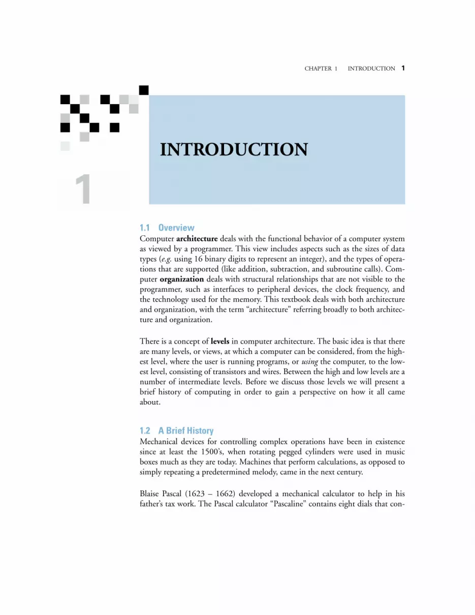
Blaise Pascal (1623 – 1662) developed a mechanical calculator to help in hisfather’s tax work. The Pascal calculator “Pascaline” contains eight dials that con-
2
CHAPTER 1 INTRODUCTION
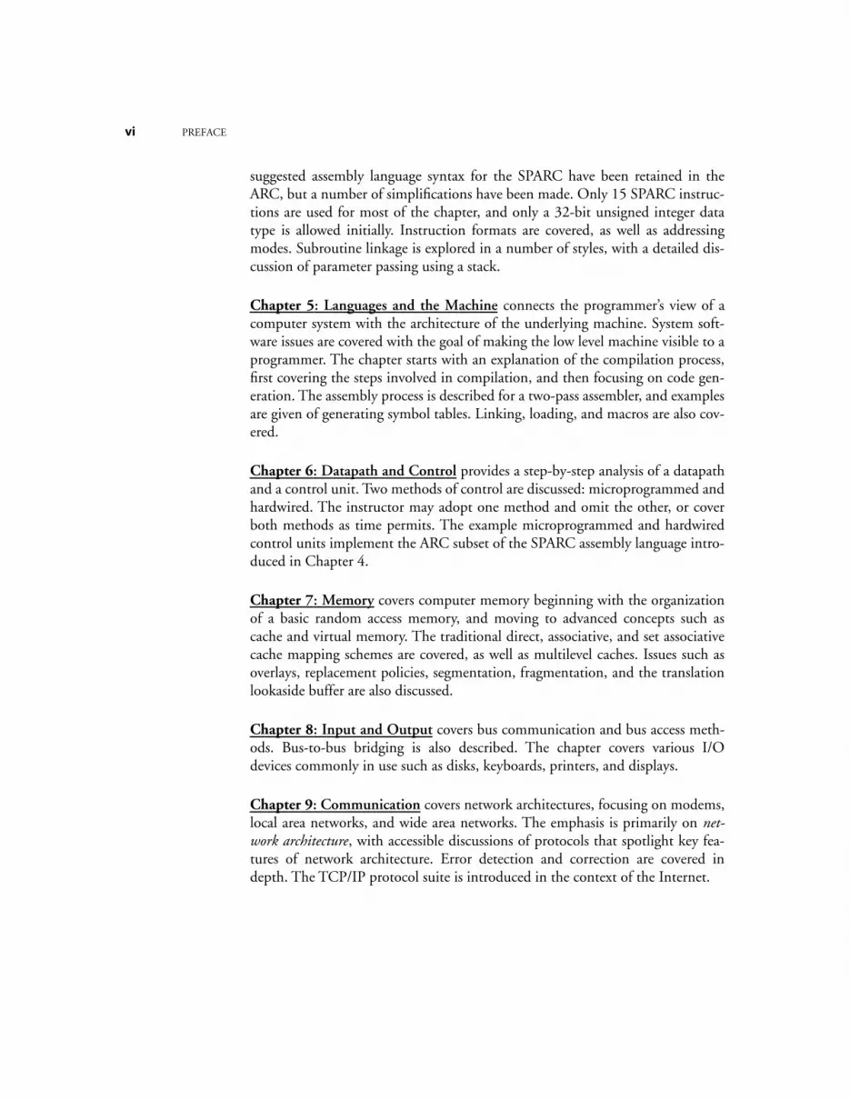
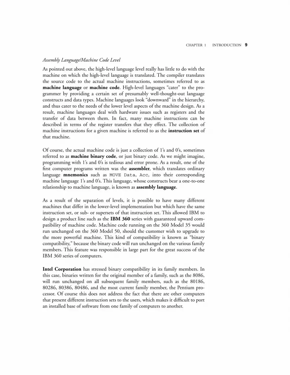
nect to a drum (Figure 1-1), with an innovative linkage that causes a dial to
rotate one notch when a carry is produced from a dial in a lower position. A win-dow is placed over the dial to allow its position to be observed, much like theodometer in a car except that the dials are positioned horizontally, like a rotarytelephone dial. Some of Pascal’s adding machines, which he started to build in1642, still exist today. It would not be until the 1800’s, however, until someonewould put the concepts of mechanical control and mechanical calculationtogether into a machine that we recognize today as having the basic parts of adigital computer. That person was Charles Babbage.
Charles Babbage (1791 – 1871) is sometimes referred to as the
grandfather
of thecomputer, rather than the father of the computer, because he never built a practi-cal version of the machines he designed. Babbage lived in England at a timewhen mathematical tables were used in navigation and scientific work. The tableswere computed manually, and as a result, they contained numerous errors. Frus-trated by the inaccuracies, Babbage set out to create a machine that would com-pute tables by simply setting and turning gears. The machine he designed couldeven produce a plate to be used by a printer, thus eliminating errors that mightbe introduced by a typesetter.
Babbage’s machines had a means for reading input data, storing data, performingcalculations, producing output data, and automatically controlling the operationof the machine. These are basic functions that are found in nearly every moderncomputer. Babbage created a small prototype of his
difference engine
, whichevaluates polynomials using the method of finite differences. The success of the
Figure 1-1 Pascal’s calculating machine (Reproduced from an IBM Archives photograph.)
CHAPTER 1 INTRODUCTION
3
difference engine concept gained him government support for the much larger
analytical engine
, which was a more sophisticated machine that had a mecha-nism for
branching
(making decisions) and a means for programming, usingpunched cards in the manner of what is known as the
Jacquard pattern-weav-ing loom
.
The analytical engine was designed, but was never built by Babbage because themechanical tolerances required by the design could not be met with the technol-ogy of the day. A version of Babbage’s difference engine was actually built by theScience Museum in London in 1991, and can still be viewed today.
It took over a century, until the start of World War II, before the next majorthrust in computing was initiated. In England, German
U-boat
submarines wereinflicting heavy damage on Allied shipping. The U-boats received communica-tions from their bases in Germany using an encryption code, which was imple-mented by a machine made by Siemens AG known as
ENIGMA
.
The process of encrypting information had been known for a long time, andeven the United States president Thomas Jefferson (1743 – 1826) designed aforerunner of ENIGMA, though he did not construct the machine. The processof decoding encrypted data was a much harder task. It was this problem thatprompted the efforts of Alan Turing (1912 – 1954), and other scientists inEngland in creating codebreaking machines. During World War II, Turing wasthe leading cryptographer in England and was among those who changed cryp-tography from a subject for people who deciphered ancient languages to a subjectfor mathematicians.
The
Colossus
was a successful codebreaking machine that came out of BletchleyPark, England, where Turing worked. Vacuum tubes store the contents of a papertape that is fed into the machine, and computations take place among the vac-uum tubes and a second tape that is fed into the machine. Programming is per-formed with plugboards. Turing’s involvement in the various Collosi machineversions remains obscure due to the secrecy that surrounds the project, but someaspects of his work and his life can be seen in the Broadway play
Breaking theCode
which was performed in London and New York in the late 1980’s.
Around the same time as Turing’s efforts, J. Presper Eckert and John Mauchly setout to create a machine that could be used to compute tables of ballistic trajecto-ries for the U.S. Army. The result of the Eckert-Mauchly effort was the Elec-tronic Numerical Integrator And Computer (
ENIAC
). The ENIAC consists of
4
CHAPTER 1 INTRODUCTION
18,000 vacuum tubes, which make up the computing section of the machine.Programming and data entry are performed by setting switches and changingcables. There is no concept of a stored program, and there is no central memoryunit, but these are not serious limitations because all that the ENIAC needed todo was to compute ballistic trajectories. Even though it did not become opera-tional until 1946, after the War was over, it was considered quite a success, andwas used for nine years.
After the success of ENIAC, Eckert and Mauchly, who were at the Moore Schoolat the University of Pennsylvania, were joined by John von Neumann (1903 –1957), who was at the Institute for Advanced Study at Princeton. Together, theyworked on the design of a stored program computer called the
EDVAC
. A con-flict developed, however, and the Pennsylvania and Princeton groups split. Theconcept of a stored program computer thrived, however, and a working model ofthe stored program computer, the
EDSAC
, was constructed by Maurice Wilkes,of Cambridge University, in 1947.
1.3 The Von Neumann Model
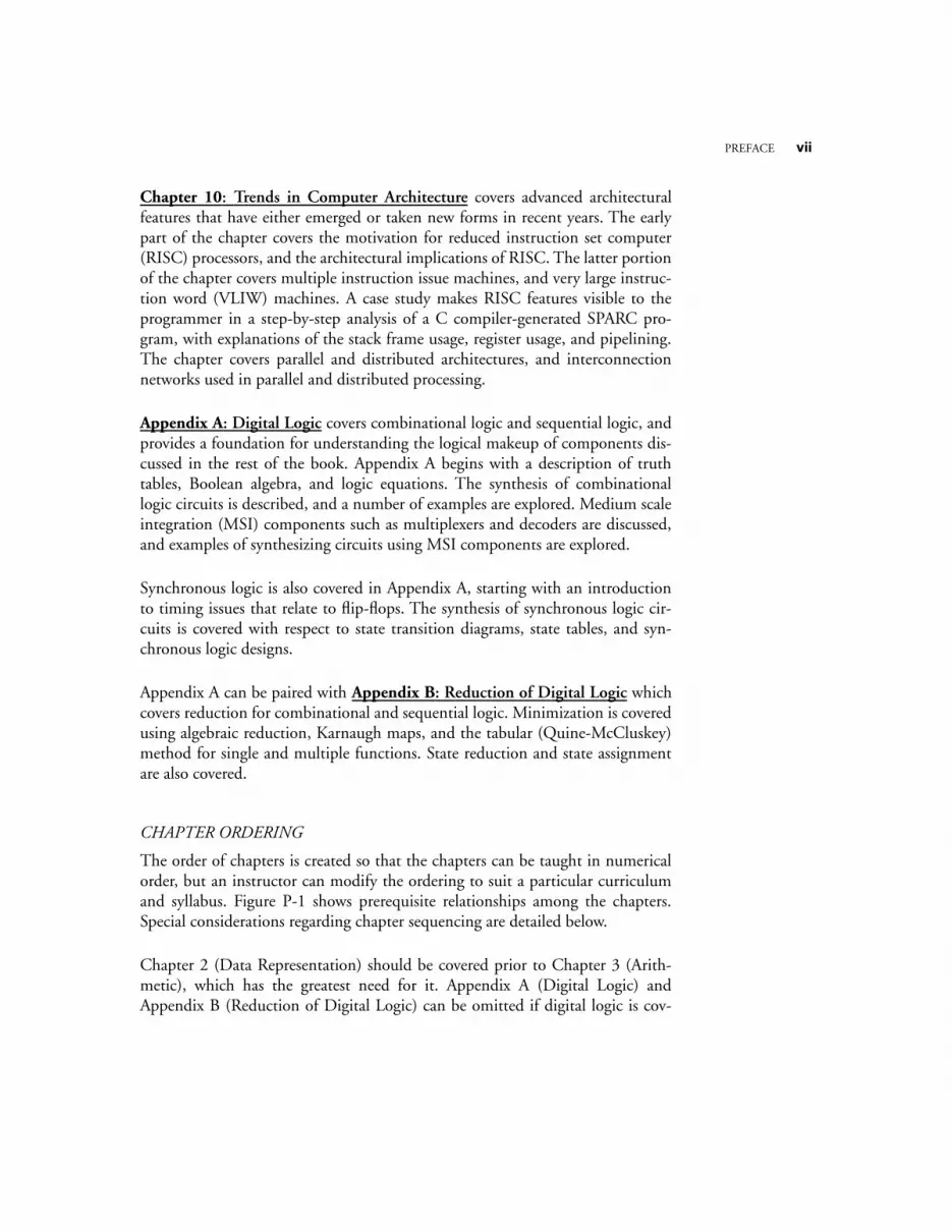
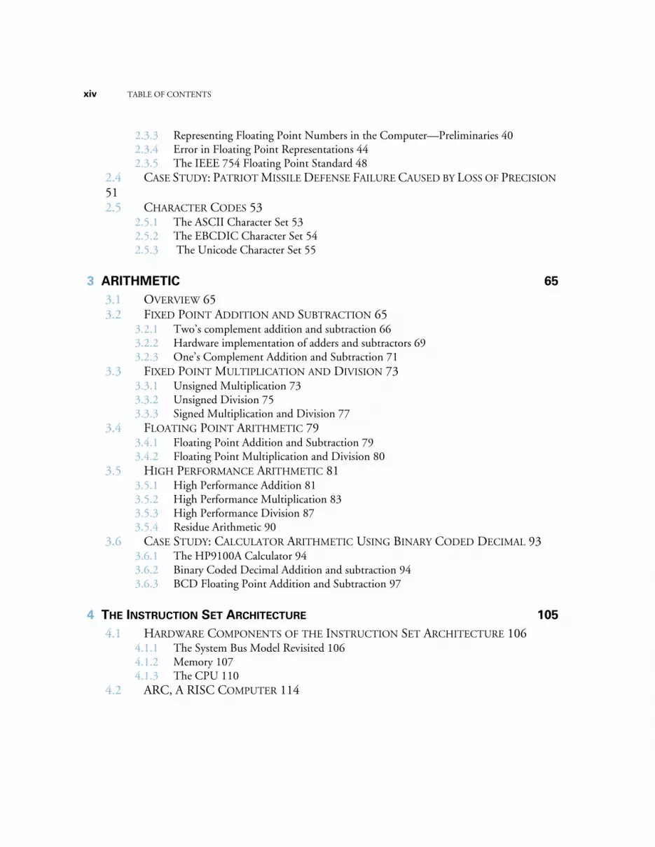
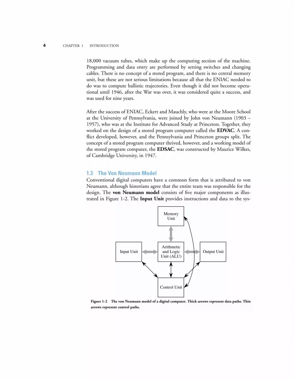
Conventional digital computers have a common form that is attributed to vonNeumann, although historians agree that the entire team was responsible for thedesign. The
von Neumann model
consists of five major components as illus-trated in Figure 1-2. The
Input Unit
provides instructions and data to the sys-
Input UnitArithmetic and Logic
Unit (ALU)Output Unit
Memory Unit
Control Unit
Figure 1-2 The von Neumann model of a digital computer. Thick arrows represent data paths. Thin
arrows represent control paths.
CHAPTER 1 INTRODUCTION
5
tem, which are subsequently stored in the
Memory Unit
. The instructions anddata are processed by the
Arithmetic and Logic Unit
(ALU) under the directionof the
Control Unit
. The results are sent to the
Output Unit
. The ALU andcontrol unit are frequently referred to collectively as the
central processing unit(CPU)
. Most commercial computers can be decomposed into these five basicunits.
The
stored program
is the most important aspect of the von Neumann model.A program is stored in the computer’s memory along with the data to be pro-cessed. Although we now take this for granted, prior to the development of thestored program computer programs were stored on external media, such as plug-boards (mentioned earlier) or punched cards or tape. In the stored program com-puter the program can be manipulated as if it is data. This gave rise to compilersand operating systems, and makes possible the great versatility of the moderncomputer.
1.4 The System Bus Model
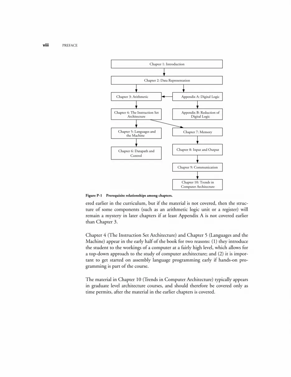
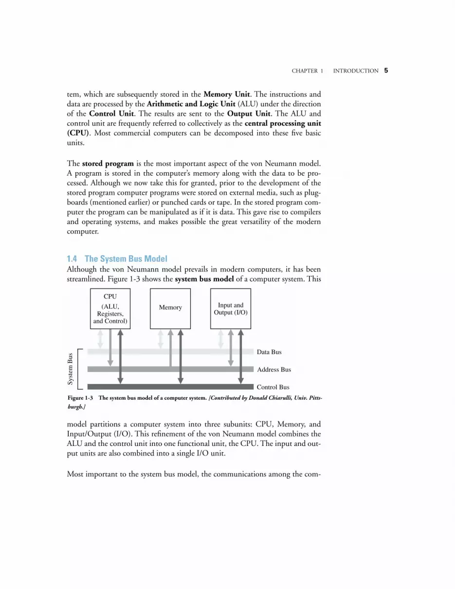
Although the von Neumann model prevails in modern computers, it has beenstreamlined. Figure 1-3 shows the
system bus model
of a computer system. This
model partitions a computer system into three subunits: CPU, Memory, andInput/Output (I/O). This refinement of the von Neumann model combines theALU and the control unit into one functional unit, the CPU. The input and out-put units are also combined into a single I/O unit.
Most important to the system bus model, the communications among the com-
Syst
em B
us
Data Bus
Address Bus
Control Bus
(ALU, Registers,
and Control)
Memory Input and Output (I/O)
CPU
Figure 1-3 The system bus model of a computer system. [Contributed by Donald Chiarulli, Univ. Pitts-
burgh.]
6
CHAPTER 1 INTRODUCTION
ponents are by means of a shared pathway called the
system bus
, which is madeup of the
data bus
(which carries the information being transmitted), the
address bus
(which identifies where the information is being sent), and the
con-trol bus
(which describes aspects of how the information is being sent, and inwhat manner). There is also a
power bus
for electrical power to the components,which is not shown, but its presence is understood. Some architectures may alsohave a separate I/O bus.
Physically, busses are made up of collections of wires that are grouped by func-tion. A 32-bit data bus has 32 individual wires, each of which carries one bit ofdata (as opposed to address or control information). In this sense, the system busis actually a group of individual busses classified by their function.
The data bus moves data among the system components. Some systems have sep-arate data buses for moving information to and from the CPU, in which casethere is a
data-in
bus and a
data-out
bus. More often a single data bus movesdata in either direction, although never both directions at the same time.
If the bus is to be shared among communicating entities, then the entities musthave distinguished identities: addresses. In some computers all addresses areassumed to be memory addresses whether they are in fact part of the computer’smemory, or are actually I/O devices, while in others I/O devices have separateI/O addresses. (This topic of I/O addresses is covered in more detail in Chapter8, Input, Output, and Communication.)
A
memory address,
or location, identifies a memory location where data isstored, similar to the way a postal address identifies the location where a recipientreceives and sends mail. During a memory read or write operation the addressbus contains the address of the memory location where the data is to be readfrom or written to. Note that the terms “read” and “write” are with respect to theCPU: the CPU
reads
data from memory and
writes
data into memory. If data isto be read from memory then the data bus contains the value read from thataddress in memory. If the data is to be written into memory then the data buscontains the data value to be written into memory.
The control bus is somewhat more complex, and we defer discussion of this busto later chapters. For now the control bus can be thought of as coordinatingaccess to the data bus and to the address bus, and directing data to specific com-ponents.
CHAPTER 1 INTRODUCTION
7
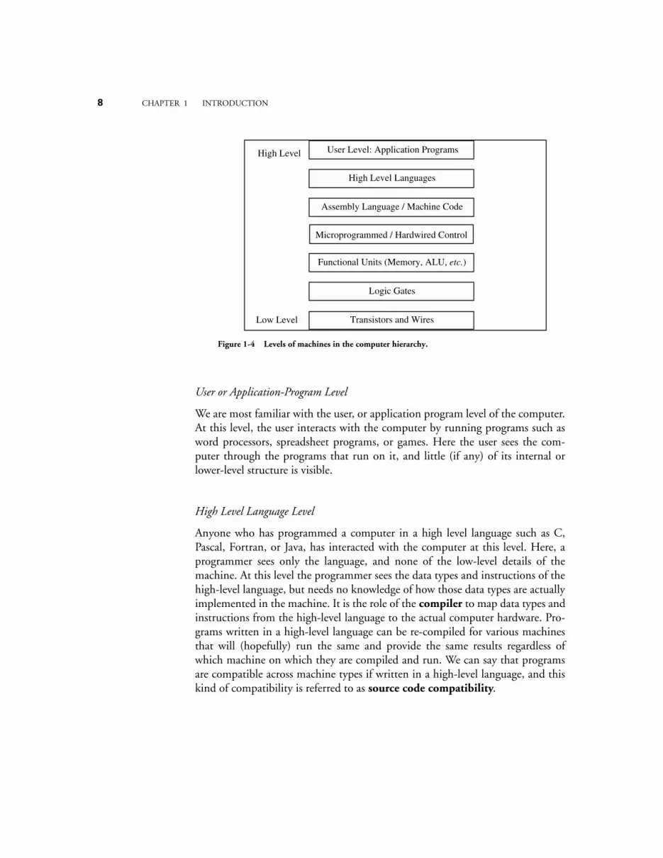
1.5 Levels of Machines
As with any complex system, the computer can be viewed from a number of per-spectives, or levels, from the highest “user” level to the lowest, transistor level.Each of these levels represents an abstraction of the computer. Perhaps one of thereasons for the enormous success of the digital computer is the extent to whichthese levels of abstraction are separate, or independent from one another. This isreadily seen: a user who runs a word processing program on a computer needs toknow nothing about its programming. Likewise a programmer need not be con-cerned with the logic gate structure inside the computer. One interesting waythat the separation of levels has been exploited is in the development ofupwardly-compatible machines.
1.5.1
UPWARD COMPATIBILITY
The invention of the transistor led to a rapid development of computer hard-ware, and with this development came a problem of compatibility. Computerusers wanted to take advantage of the newest and fastest machines, but each newcomputer model had a new architecture, and the old software would not run onthe new hardware. The hardware / software compatibility problem became soserious that users often delayed purchasing a new machine because of the cost ofrewriting the software to run on the new hardware. When a new computer waspurchased, it would often sit unavailable to the target users for months while theold software and data sets were converted to the new systems.
In a successful gamble that pitted compatibility against performance, IBM pio-neered the concept of a “family of machines” with its 360 series. More capablemachines in the same family could run programs written for less capablemachines without modifications to those programs—upward compatibility.Upward compatibility allows a user to upgrade to a faster, more capable machinewithout rewriting the software that runs on the less capable model.
1.5.2
THE LEVELS
Figure 1-4 shows seven levels in the computer, from the user level down to thetransistor level. As we progress from the top level downward, the levels becomeless “abstract” and more of the internal structure of the computer shows through.We discuss these levels below.
8
CHAPTER 1 INTRODUCTION
User or Application-Program Level
We are most familiar with the user, or application program level of the computer.At this level, the user interacts with the computer by running programs such asword processors, spreadsheet programs, or games. Here the user sees the com-puter through the programs that run on it, and little (if any) of its internal orlower-level structure is visible.
High Level Language Level
Anyone who has programmed a computer in a high level language such as C,Pascal, Fortran, or Java, has interacted with the computer at this level. Here, aprogrammer sees only the language, and none of the low-level details of themachine. At this level the programmer sees the data types and instructions of thehigh-level language, but needs no knowledge of how those data types are actuallyimplemented in the machine. It is the role of the
compiler
to map data types andinstructions from the high-level language to the actual computer hardware. Pro-grams written in a high-level language can be re-compiled for various machinesthat will (hopefully) run the same and provide the same results regardless ofwhich machine on which they are compiled and run. We can say that programsare compatible across machine types if written in a high-level language, and thiskind of compatibility is referred to as
source code compatibility
.
High Level
High Level Languages
User Level: Application Programs
Low Level
Functional Units (Memory, ALU, etc.)
Logic Gates
Transistors and Wires
Assembly Language / Machine Code
Microprogrammed / Hardwired Control
Figure 1-4 Levels of machines in the computer hierarchy.
CHAPTER 1 INTRODUCTION
9
Assembly Language/Machine Code Level
As pointed out above, the high-level language level really has little to do with themachine on which the high-level language is translated. The compiler translatesthe source code to the actual machine instructions, sometimes referred to as
machine language
or
machine code
. High-level languages “cater” to the pro-grammer by providing a certain set of presumably well-thought-out languageconstructs and data types. Machine languages look “downward” in the hierarchy,and thus cater to the needs of the lower level aspects of the machine design. As aresult, machine languages deal with hardware issues such as registers and thetransfer of data between them. In fact, many machine instructions can bedescribed in terms of the register transfers that they effect. The collection ofmachine instructions for a given machine is referred to as the
instruction set
ofthat machine.
Of course, the actual machine code is just a collection of 1’s and 0’s, sometimesreferred to as
machine binary code
, or just binary code. As we might imagine,programming with 1’s and 0’s is tedious and error prone. As a result, one of thefirst computer programs written was the
assembler
, which translates ordinarylanguage
mnemonics
such as
MOVE
Data
,
Acc
, into their correspondingmachine language 1’s and 0’s. This language, whose constructs bear a one-to-onerelationship to machine language, is known as
assembly language
.
As a result of the separation of levels, it is possible to have many differentmachines that differ in the lower-level implementation but which have the sameinstruction set, or sub- or supersets of that instruction set. This allowed IBM todesign a product line such as the
IBM 360
series with guaranteed upward com-patibility of machine code. Machine code running on the 360 Model 35 wouldrun unchanged on the 360 Model 50, should the customer wish to upgrade tothe more powerful machine. This kind of compatibility is known as “binarycompatibility,” because the binary code will run unchanged on the various familymembers. This feature was responsible in large part for the great success of theIBM 360 series of computers.
Intel Corporation
has stressed binary compatibility in its family members. Inthis case, binaries written for the original member of a family, such as the 8086,will run unchanged on all subsequent family members, such as the 80186,80286, 80386, 80486, and the most current family member, the Pentium pro-cessor. Of course this does not address the fact that there are other computersthat present different instruction sets to the users, which makes it difficult to portan installed base of software from one family of computers to another.
10
CHAPTER 1 INTRODUCTION
The Control Level
It is the
control unit
that effects the register transfers described above. It does soby means of
control signals
that transfer the data from register to register, possi-bly through a logic circuit that transforms it in some way. The control unit inter-prets the machine instructions one by one, causing the specified register transferor other action to occur.
How it does this is of no need of concern to the assembly language programmer.The Intel 80x86 family of processors presents the same behavioral view to anassembly language programmer regardless of which processor in the family isconsidered. This is because each future member of the family is designed to exe-cute the original 8086 instructions in addition to any new instructions imple-mented for that particular family member.
As Figure 1-4 indicates, there are several ways of implementing the control unit.Probably the most popular way at the present time is by “hardwiring” the controlunit. This means that the control signals that effect the register transfers are gen-erated from a block of digital logic components. Hardwired control units havethe advantages of speed and component count, but until recently were exceed-ingly difficult to design and modify. (We will study this technique more fully inChapter 9.)
A somewhat slower but simpler approach is to implement the instructions as a
microprogram
. A microprogram is actually a small program written in an evenlower-level language, and implemented in the hardware, whose job is to interpretthe machine-language instructions. This microprogram is referred to as
firmware
because it spans both hardware and software. Firmware is executed by a
micro-controller
, which executes the actual microinstructions. (We will also exploremicroprogramming in Chapter 9.)
Functional Unit Level
The register transfers and other operations implemented by the control unitmove data in and out of “functional units,” so-called because they perform somefunction that is important to the operation of the computer. Functional unitsinclude internal CPU registers, the ALU, and the computer’s main memory.
CHAPTER 1 INTRODUCTION
11
Logic Gates, Transistors, and Wires
The lowest levels at which any semblance of the computer’s higher-level func-tioning is visible is at the
logic gate
and
transistor
levels. It is from logic gatesthat the functional units are built, and from transistors that logic gates are built.The logic gates implement the lowest-level logical operations upon which thecomputer’s functioning depends. At the very lowest level, a computer consists ofelectrical components such as transistors and wires, which make up the logicgates, but at this level the functioning of the computer is lost in details of voltage,current, signal propagation delays, quantum effects, and other low-level matters.
Interactions Between Levels
The distinctions within levels and between levels are frequently blurred. Forinstance, a new computer architecture may contain floating point instructions ina full-blown implementation, but a minimal implementation may have onlyenough hardware for integer instructions. The floating point instructions are
trapped
†
prior to execution and replaced with a sequence of machine languageinstructions that imitate, or
emulate
the floating point instructions using theexisting integer instructions. This is the case for
microprocessors
that useoptional floating point coprocessors. Those without floating point coprocessorsemulate the floating point instructions by a series of floating point routines thatare implemented in the machine language of the microprocessor, and frequentlystored in a
ROM
, which is a read-only memory chip. The assembly language andhigh level language view for both implementations is the same except for execu-tion speed.
It is possible to take this emulation to the extreme of emulating the entireinstruction set of one computer on another computer. The software that doesthis is known as an
emulator
, and was used by
Apple Computer
to maintainbinary code compatibility when they began employing Motorola PowerPC chipsin place of Motorola 68000 chips, which had an entirely different instruction set.
The high level language level and the firmware and functional unit levels can beso intermixed that it is hard to identify what operation is happening at whichlevel. The value in stratifying a computer architecture into a hierarchy of levels isnot so much for the purpose of classification, which we just saw can be difficultat times, but rather to simply give us some focus when we study these levels in
†. Traps are covered in Chapter 6.
12
CHAPTER 1 INTRODUCTION
the chapters that follow.
The Programmer’s View—The Instruction Set Architecture
As described in the discussion of levels above, the assembly language programmeris concerned with the assembly language and functional units of the machine.This collection of instruction set and functional units is known as the
instruc-tion set architecture
(ISA) of the machine.
The Computer Architect’s View
On the other hand, the computer architect views the system at all levels. Thearchitect that focuses on the design of a computer is invariably driven by perfor-mance requirements and cost constraints. Performance may be specified by thespeed of program execution, the storage capacity of the machine, or a number ofother parameters. Cost may be reflected in monetary terms, or in size or weight,or power consumption. The design proposed by a computer architect mustattempt to meet the performance goals while staying within the cost constraints.This usually requires trade-offs between and among the levels of the machine.
1.6 A Typical Computer System
Modern computers have evolved from the great behemoths of the 1950’s and1960’s to the much smaller and more powerful computers that surround ustoday. Even with all of the great advances in computer technology that have beenmade in the past few decades, the five basic units of the von Neumann model arestill distinguishable in modern computers.
Figure 1-5 shows a typical configuration for a desktop computer. The input unitis composed of the keyboard, through which a user enters data and commands.A video monitor comprises the output unit, which displays the output in avisual form. The ALU and the control unit are bundled into a single micropro-cessor that serves as the CPU. The memory unit consists of individual memorycircuits, and also a hard disk unit, a diskette unit, and a CD-ROM (compactdisk - read only memory) device.
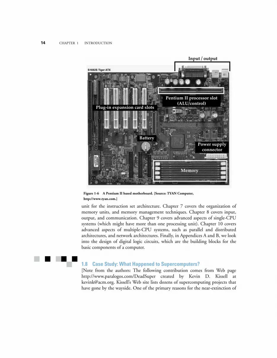
As we look deeper inside of the machine, we can see that the heart of themachine is contained on a single motherboard, similar to the one shown in Fig-ure 1-6. The motherboard contains integrated circuits (ICs), plug-in expansioncard slots, and the wires that interconnect the ICs and expansion card slots. The
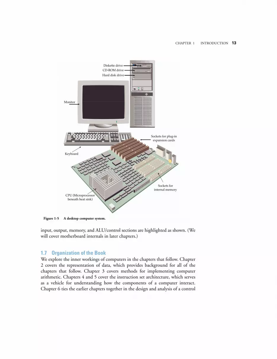
CHAPTER 1 INTRODUCTION 13
input, output, memory, and ALU/control sections are highlighted as shown. (Wewill cover motherboard internals in later chapters.)
1.7 Organization of the BookWe explore the inner workings of computers in the chapters that follow. Chapter2 covers the representation of data, which provides background for all of thechapters that follow. Chapter 3 covers methods for implementing computerarithmetic. Chapters 4 and 5 cover the instruction set architecture, which servesas a vehicle for understanding how the components of a computer interact.Chapter 6 ties the earlier chapters together in the design and analysis of a control
Monitor
CD-ROM drive
Hard disk drive
Keyboard
Sockets for internal memory
CPU (Microprocessor beneath heat sink)
Sockets for plug-in expansion cards
Diskette drive
Figure 1-5 A desktop computer system.
14 CHAPTER 1 INTRODUCTION
unit for the instruction set architecture. Chapter 7 covers the organization ofmemory units, and memory management techniques. Chapter 8 covers input,output, and communication. Chapter 9 covers advanced aspects of single-CPUsystems (which might have more than one processing unit). Chapter 10 coversadvanced aspects of multiple-CPU systems, such as parallel and distributedarchitectures, and network architectures. Finally, in Appendices A and B, we lookinto the design of digital logic circuits, which are the building blocks for thebasic components of a computer.
1.8 Case Study: What Happened to Supercomputers?[Note from the authors: The following contribution comes from Web pagehttp://www.paralogos.com/DeadSuper created by Kevin D. Kissell [email protected]. Kissell’s Web site lists dozens of supercomputing projects thathave gone by the wayside. One of the primary reasons for the near-extinction of
Memory
Input / output
Battery
Plug-in expansion card slots
Power supply connector
Pentium II processor slot (ALU/control)
Figure 1-6 A Pentium II based motherboard. [Source: TYAN Computer,
http://www.tyan.com.]
CHAPTER 1 INTRODUCTION 15
supercomputers is that ordinary, everyday computers achieve a significant frac-tion of supercomputing power at a price that the common person can afford.The price-to-performance ratio for desktop computers is very favorable due tolow costs achieved through mass market sales. Supercomputers enjoy no suchmass markets, and continue to suffer very high price-to-performance ratios.
Following Kissell’s contribution is an excerpt from an Electrical EngineeringTimes article that highlights the enormous investment in everyday microproces-sor development, which helps maintain the favorable price-to-performance ratiofor low-cost desktop computers.]
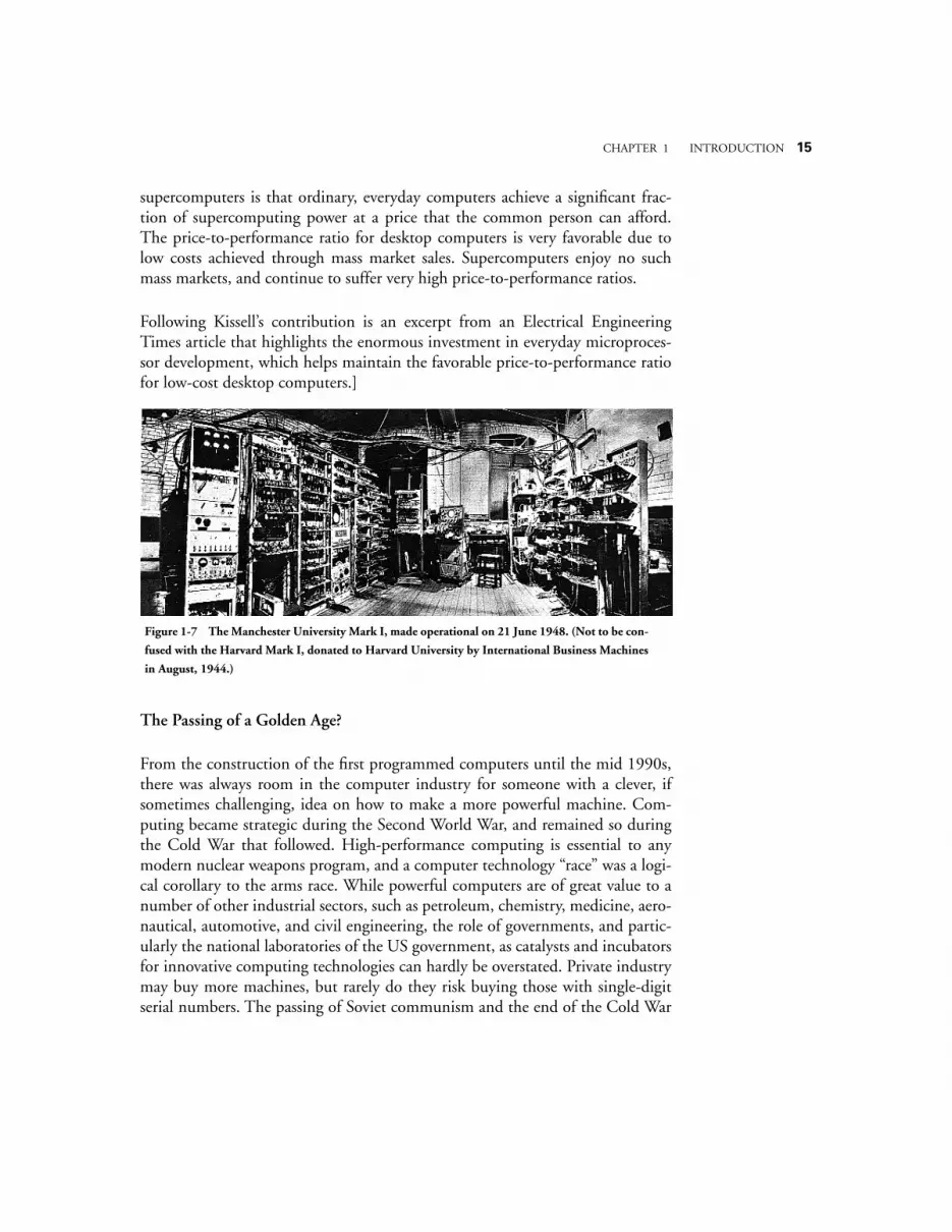
The Passing of a Golden Age?
From the construction of the first programmed computers until the mid 1990s,there was always room in the computer industry for someone with a clever, ifsometimes challenging, idea on how to make a more powerful machine. Com-puting became strategic during the Second World War, and remained so duringthe Cold War that followed. High-performance computing is essential to anymodern nuclear weapons program, and a computer technology “race” was a logi-cal corollary to the arms race. While powerful computers are of great value to anumber of other industrial sectors, such as petroleum, chemistry, medicine, aero-nautical, automotive, and civil engineering, the role of governments, and partic-ularly the national laboratories of the US government, as catalysts and incubatorsfor innovative computing technologies can hardly be overstated. Private industrymay buy more machines, but rarely do they risk buying those with single-digitserial numbers. The passing of Soviet communism and the end of the Cold War
Figure 1-7 The Manchester University Mark I, made operational on 21 June 1948. (Not to be con-
fused with the Harvard Mark I, donated to Harvard University by International Business Machines
in August, 1944.)

16 CHAPTER 1 INTRODUCTION
brought us a generally safer and more prosperous world, but it removed the rai-son d'etre for many merchants of performance-at-any-price.
Accompanying these geopolitical changes were some technological and economictrends that spelled trouble for specialized producers of high-end computers.Microprocessors began in the 1970s as devices whose main claim to fame wasthat it was possible to put a stored-program computer on a single piece of silicon.Competitive pressures, and the desire to generate sales by obsoleting last year’sproduct, made for the doubling of microprocessor computing power every 18months, Moore's celebrated “law.” Along the way, microprocessor designers bor-rowed almost all the tricks that designers of mainframe and numerical supercom-puters had used in the past: storage hierarchies, pipelining, multiple functionalunits, multiprocessing, out-of-order execution, branch prediction, SIMD pro-cessing, speculative and predicated execution. By the mid 1990s, research ideaswere going directly from simulation to implementation in microprocessors des-tined for the desktops of the masses. Nevertheless, it must be noted that most ofthe gains in raw performance achieved by microprocessors in the precedingdecade came, not from these advanced techniques of computer architecture, butfrom the simple speedup of processor clocks and quantitative increase in proces-sor resources made possible by advances in semiconductor technology. By 1998,the CPU of a high-end Windows-based personal computer was running at ahigher clock rate than the top-of-the-line Cray Research supercomputer of 1994.
It is thus hardly surprising that the policy of the US national laboratories hasshifted from the acquisition of systems architected from the ground up to besupercomputers to the deployment of large ensembles of mass-produced micro-processor-based systems, with the ASCI project as the flagship of this activity. Asof this writing, it remains to be seen if these agglomerations will prove to be suf-ficiently stable and usable for production work, but the preliminary results havebeen at least satisfactory. The halcyon days of supercomputers based on exotictechnology and innovative architecture may well be over.
[...]
Kevin D. Kissell [email protected] February, 1998
[Note from the authors: The following excerpt is taken from the Electronic Engi-
CHAPTER 1 INTRODUCTION 17
neering Times, source:http://techweb.cmp.com/eet/news/98/994news/invest.html.]
Invest or die: Intel’s life on the edge
By Ron Wilson and Brian Fuller
SANTA CLARA, Calif. -- With about $600 million to pumpinto venture companies this year, Intel Corp. hasjoined the major leagues of venture-capital firms. Butthe unique imperative that drives the microprocessorgiant to invest gives it influence disproportionate toeven this large sum. For Intel, venture investmentsare not just a source of income; they are a vital toolin the fight to survive.
Survival might seem an odd preoccupation for theworld's largest semiconductor company. But Intel, in away all its own, lives hanging in the balance. Forevery new generation of CPUs, Intel must make hugeinvestments in process development, in buildings andin fabs-an investment too huge to lose.
Gordon Moore, Intel chairman emeritus, gave scale tothe wager. "An R&D fab today costs $400 million justfor the building. Then you put about $1 billion ofequipment in it. That gets you a quarter-micron fabfor maybe 5,000 wafers per week, about the smallestpractical fab. For the next generation," Moore said,"the minimum investment will be $2 billion, with maybe$3 billion to $4 billion for any sort of volume produc-tion. No other industry has such a short life on suchhuge investments."
Much of this money will be spent before there is aproven need for the microprocessors the fab will pro-duce. In essence, the entire $4 billion per fab is beton the proposition that the industry will absorb ahuge number of premium-priced CPUs that are only some-what faster than the currently available parts. If forjust one generation that didn't happen-if everyonejudged, say, that the Pentium II was fast enough,thank you-the results would be unthinkable.
"My nightmare is to wake up some day and not need anymore computing power," Moore said.
18 CHAPTER 1 INTRODUCTION
SUMMARY
Computer architecture deals with those aspects of a computer that are visible to aprogrammer, while computer organization deals with those aspects that are at amore physical level and are not made visible to a programmer. Historically, pro-grammers had to deal with every aspect of a computer – Babbage with mechanicalgears, and ENIAC programmers with plugboard cables. As computers grew insophistication, the concept of levels of machines became more pronounced, allow-ing computers to have very different internal and external behaviors while man-aging complexity in stratified levels. The single most significant development thatmakes this possible is the stored program computer, which is embodied in the vonNeumann model. It is the von Neumann model that we see in most conventionalcomputers today.
Further ReadingThe history of computing is riddled with interesting personalities and mile-stones. (Anderson, 1991) gives a short, readable account of both during the lastcentury. (Bashe et. al., 1986) give an interesting account of the IBM machines.(Bromley, 1987) chronicles Babbage’s machines. (Ralston and Reilly, 1993) giveshort biographies of the more celebrated personalities. (Randell, 1982) covers thehistory of digital computers. A very readable Web based history of computers byMichelle A. Hoyle can be found at http://www.interpac.net/~eingang/Lec-ture/toc.html. (SciAm, 1993) covers a readable version of the method of finitedifferences as it appears in Babbage’s machines, and the version of the analyticaldifference engine created by the Science Museum in London.
(Tanenbaum, 1999) is one of a number of texts that popularizes the notion oflevels of machines.
Anderson, Harlan, Dedication address for the Digital Computer Laboratory atthe University of Illinois, April 17, 1991, as reprinted in IEEE Circuits and Sys-tems: Society Newsletter, vol. 2, no. 1, pp. 3–6, (March 1991).
Bashe, Charles J., Lyle R. Johnson, John H. Palmer, and Emerson W. Pugh,IBM’s Early Computers, The MIT Press, (1986).
CHAPTER 1 INTRODUCTION 19
Bromley, A. G., “The Evolution of Babbage’s Calculating Engines,” Annals of theHistory of Computing, 9, pp. 113-138, (1987).
Randell, B., The Origins of Digital Computers, 3/e, Springer-Verlag, (1982).
Ralston, A. and E. D. Reilly, eds., Encyclopedia of Computer Science, 3/e, vanNostrand Reinhold, (1993).
Tanenbaum, A., Structured Computer Organization, 4/e, Prentice Hall, Engle-wood Cliffs, New Jersey, (1999).
PROBLEMS1.1 Moore’s law, which is attributed to Intel founder Gordon Moore, states
that computing power doubles every 18 months for the same price. An unre-lated observation is that floating point instructions are executed 100 timesfaster in hardware than via emulation. Using Moore’s law as a guide, how longwill it take for computing power to improve to the point that floating pointinstructions are emulated as quickly as their (earlier) hardware counterparts?

20 CHAPTER 1 INTRODUCTION

CHAPTER 2 DATA REPRESENTATION
21
2.1 Introduction
In the early days of computing, there were common misconceptions about com-puters. One misconception was that the computer was only a giant addingmachine performing arithmetic operations. Computers could do much morethan that, even in the early days. The other common misconception, in contra-diction to the first, was that the computer could do “anything.” We now knowthat there are indeed classes of problems that even the most powerful imaginablecomputer finds intractable with the von Neumann model. The correct percep-tion, of course, is somewhere between the two.
We are familiar with computer operations that are non-arithmetic: computergraphics, digital audio, even the manipulation of the computer mouse. Regard-less of what kind of information is being manipulated by the computer, theinformation must be represented by patterns of 1’s and 0’s (also known as“on-off” codes). This immediately raises the question of how that informationshould be described or represented in the machine—this is the
data representa-tion
, or
data encoding
. Graphical images, digital audio, or mouse clicks must allbe encoded in a systematic, agreed-upon manner.
We might think of the decimal representation of information as the most naturalwhen we know it the best, but the use of on-off codes to represent informationpredated the computer by many years, in the form of Morse code.
This chapter introduces several of the simplest and most important encodings:the encoding of signed and unsigned fixed point numbers, real numbers (referredto as
floating point numbers
in computer jargon), and the printing characters.We shall see that in all cases there are multiple ways of encoding a given kind ofdata, some useful in one context, some in another. We will also take an early look
DATA REPRESENTATION
2
22
CHAPTER 2 DATA REPRESENTATION
at computer arithmetic for the purpose of understanding some of the encodingschemes, though we will defer details of computer arithmetic until Chapter 3.
In the process of developing a data representation for computing, a crucial issueis deciding how much storage should be devoted to each data value. For example,a computer architect may decide to treat integers as being 32 bits in size, and toimplement an ALU that supports arithmetic operations on those 32-bit valuesthat return 32 bit results. Some numbers can be too large to represent using 32bits, however, and in other cases, the operands may fit into 32 bits, but the resultof a computation will not, creating an
overflow
condition, which is described inChapter 3. Thus we need to understand the limits imposed on the accuracy andrange of numeric calculations by the finite nature of the data representations. Wewill investigate these limits in the next few sections.
2.2 Fixed Point Numbers
In a fixed point number system, each number has exactly the same number ofdigits, and the “point” is always in the same place. Examples from the decimalnumber system would be 0.23, 5.12, and 9.11. In these examples each numberhas 3 digits, and the decimal point is located two places from the right. Examplesfrom the
binary
number system (in which each digit can take on only one of thevalues: 0 or 1) would be 11.10, 01.10, and 00.11, where there are 4 binary digitsand the binary point is in the middle. An important difference between the waythat we represent fixed point numbers on paper and the way that we representthem in the computer is that when fixed point numbers are represented in thecomputer
the binary point is not stored anywhere
, but only assumed to be in a cer-tain position. One could say that the binary point exists only in the mind of theprogrammer.
We begin coverage of fixed point numbers by investigating the range and preci-sion of fixed point numbers, using the decimal number system. We then take alook at the nature of number bases, such as decimal and binary, and how to con-vert between the bases. With this foundation, we then investigate several ways ofrepresenting negative fixed point numbers, and take a look at simple arithmeticoperations that can be performed on them.
2.2.1
RANGE AND PRECISION IN FIXED POINT NUMBERS
A fixed point representation can be characterized by the
range
of expressiblenumbers (that is, the distance between the largest and smallest numbers) and the
CHAPTER 2 DATA REPRESENTATION
23
precision
(the distance between two adjacent numbers on a number line.) Forthe fixed-point decimal example above, using three digits and the decimal pointplaced two digits from the right, the range is from 0.00 to 9.99 inclusive of theendpoints, denoted as [0.00, 9.99], the precision is .01, and the
error
is 1/2 ofthe difference between two “adjoining” numbers, such as 5.01 and 5.02, whichhave a difference of .01. The error is thus .01/2 = .005. That is, we can representany number within the range 0.00 to 9.99 to within .005 of its true or precisevalue.
Notice how range and precision trade off: with the decimal point on the farright, the range is [000, 999] and the precision is 1.0. With the decimal point atthe far left, the range is [.000, .999] and the precision is .001.
In either case, there are only 10
3
different decimal “objects,” ranging from 000 to999 or from .000 to .999, and thus it is possible to represent only 1,000 differentitems, regardless of how we apportion range and precision.
There is no reason why the range must begin with 0. A 2-digit decimal numbercan have a range of [00,99] or a range of [-50, +49], or even a range of [-99, +0].The representation of negative numbers is covered more fully in Section 2.2.6.
Range and precision are important issues in computer architecture because bothare finite in the implementation of the architecture, but are infinite in the realworld, and so the user must be aware of the limitations of trying to representexternal information in internal form.
2.2.2
THE ASSOCIATIVE LAW OF ALGEBRA DOES NOT ALWAYS HOLD IN COMPUTERS
In early mathematics, we learned the associative law of algebra:
a
+ (
b
+
c
) = (
a
+
b
) +
c
As we will see, the associative law of algebra does not hold for fixed point num-bers having a finite representation. Consider a 1-digit decimal fixed point repre-sentation with the decimal point on the right, and a range of [-9, 9], with a = 7,b=4, and c=–3. Now
a
+ (
b
+
c
) = 7 + (4 + –3) = 7 + 1 =8. But (
a
+
b
) +
c =
(7 +4) + –3 = 11 + –3, but 11 is outside the range of our number system! We haveoverflow in an intermediate calculation, but the final result is within the numbersystem. This is every bit as bad because the final result will be wrong if an inter-
24
CHAPTER 2 DATA REPRESENTATION
mediate result is wrong.
Thus we can see by example that the associative law of algebra does not hold forfinite-length fixed point numbers. This is an unavoidable consequence of thisform of representation, and there is nothing practical to be done except to detectoverflow wherever it occurs, and either terminate the computation immediatelyand notify the user of the condition, or, having detected the overflow, repeat thecomputation with numbers of greater range. (The latter technique is seldomused except in critical applications.)
2.2.3
RADIX NUMBER SYSTEMS
In this section, we learn how to work with numbers having arbitrary bases,although we will focus on the bases most used in digital computers, such as base2 (binary), and its close cousins base 8 (octal), and base 16 (hexadecimal.)
The
base
, or
radix
of a number system defines the range of possible values that adigit may have. In the base 10 (decimal) number system, one of the 10 values: 0,1, 2, 3, 4, 5, 6, 7, 8, 9 is used for each digit of a number. The most natural sys-tem for representing numbers in a computer is base 2, in which data is repre-sented as a collection of 1’s and 0’s.
The general form for determining the decimal value of a number in a radix
k
fixed point number system is shown below:
The value of the digit in position
i
is given by
b
i
. There are
n
digits to the left ofthe radix point and there are
m
digits to the right of the radix point. This form ofa number, in which each position has an assigned weight, is referred to as a
weighted position code
. Consider evaluating (541.25)
10
, in which the subscript10 represents the base. We have
n
= 3,
m
= 2, and
k
= 10:
5
×
10
2
+ 4
×
10
1
+ 1
×
10
0
+ 2
×
10
-1
+ 5
×
10
-2
=
(500)
10
+ (40)
10
+ (1)
10
+ (2/10)
10
+ (5/100)
10
= (541.25)
10
Value bi ki⋅i m–=
n 1–
∑=

CHAPTER 2 DATA REPRESENTATION
25
Now consider the base 2 number (1010.01)
2
in which
n
= 4,
m
= 2, and
k
= 2:
1
×
2
3
+ 0
×
2
2
+ 1
×
2
1
+ 0
×
2
0
+ 0
×
2
-1
+ 1
×
2
-2
=
(8)
10
+ (0)
10
+ (2)
10
+ (0)
10
+ (0/2)
10
+ (1/4)
10
= (10.25)
10
This suggests how to convert a number from an arbitrary base into a base 10number using the
polynomial method
. The idea is to multiply each digit by theweight assigned to its position (powers of two in this example) and then sum upthe terms to obtain the converted number. Although conversions can be madeamong all of the bases in this way, some bases pose special problems, as we willsee in the next section.
Note: in these weighted number systems we define the bit that carries the mostweight as the
most significant bit
(MSB)
, and the bit that carries the leastweight as the
least significant bit (LSB)
. Conventionally the MSB is the left-most bit and the LSB the rightmost bit.
2.2.4
CONVERSIONS AMONG RADICES
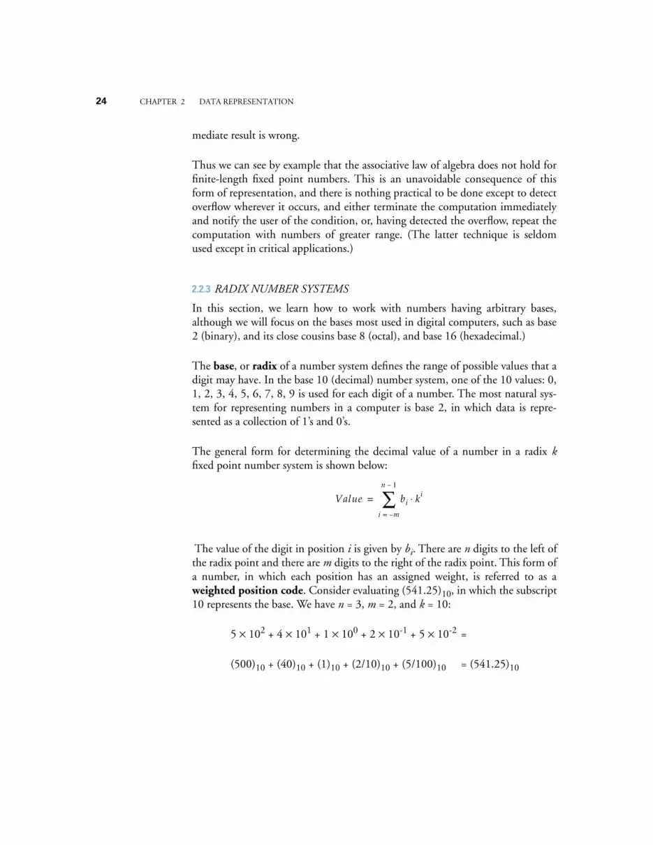
In the previous section, we saw an example of how a base 2 number can be con-verted into a base 10 number. A conversion in the reverse direction is moreinvolved. The easiest way to convert fixed point numbers containing both integerand fractional parts is to convert each part separately. Consider converting(23.375)
10
to base 2. We begin by separating the number into its integer andfractional parts:
(23.375)
10
= (23)
10
+ (.375)
10
.
Converting the Integer Part of a Fixed Point Number—The Remainder Method
As suggested in the previous section, the general polynomial form for represent-ing a binary integer is:
bi 2i× bi 1– 2i 1–× … b1 21× b0 20×+ + + +
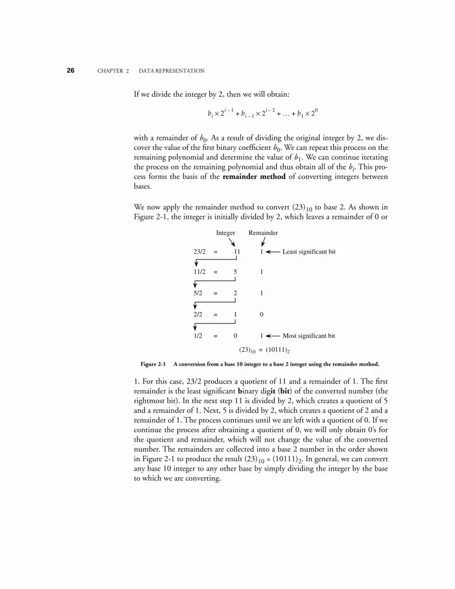
26 CHAPTER 2 DATA REPRESENTATION
If we divide the integer by 2, then we will obtain:
with a remainder of b0. As a result of dividing the original integer by 2, we dis-cover the value of the first binary coefficient b0. We can repeat this process on theremaining polynomial and determine the value of b1. We can continue iteratingthe process on the remaining polynomial and thus obtain all of the bi. This pro-cess forms the basis of the remainder method of converting integers betweenbases.
We now apply the remainder method to convert (23)10 to base 2. As shown inFigure 2-1, the integer is initially divided by 2, which leaves a remainder of 0 or
1. For this case, 23/2 produces a quotient of 11 and a remainder of 1. The firstremainder is the least significant binary digit (bit) of the converted number (therightmost bit). In the next step 11 is divided by 2, which creates a quotient of 5and a remainder of 1. Next, 5 is divided by 2, which creates a quotient of 2 and aremainder of 1. The process continues until we are left with a quotient of 0. If wecontinue the process after obtaining a quotient of 0, we will only obtain 0’s forthe quotient and remainder, which will not change the value of the convertednumber. The remainders are collected into a base 2 number in the order shownin Figure 2-1 to produce the result (23)10 = (10111)2. In general, we can convertany base 10 integer to any other base by simply dividing the integer by the baseto which we are converting.
bi 2i 1–× bi 1– 2i 2–× … b1 20×+ + +
23/2 = 11 R 1
11/2 = 5 R 1
5/2 = 2 R 1
2/2 = 1 R 0
1/2 = 0 R 1
Integer Remainder
Least significant bit
Most significant bit
(23)10 = (10111)2
Figure 2-1 A conversion from a base 10 integer to a base 2 integer using the remainder method.

CHAPTER 2 DATA REPRESENTATION 27
We can check the result by converting it from base 2 back to base 10 using thepolynomial method:
(10111)2 = 1 × 24 + 0 × 23 + 1 × 22 + 1 × 21 + 1 × 20
= 16 + 0 + 4 + 2 + 1
= (23)10
At this point, we have converted the integer portion of (23.375)10 into base 2.
Converting the Fractional Part of a Fixed Point Number—The Multiplication Method
The conversion of the fractional portion can be accomplished by successivelymultiplying the fraction by 2 as described below.
A binary fraction is represented in the general form:
If we multiply the fraction by 2, then we will obtain:
We thus discover the coefficient b−1. If we iterate this process on the remainingfraction, then we will obtain successive bi. This process forms the basis of themultiplication method of converting fractions between bases. For the exampleused here (Figure 2-2), the initial fraction (.375)10 is less than 1. If we multiply itby 2, then the resulting number will be less than 2. The digit to the left of theradix point will then be 0 or 1. This is the first digit to the right of the radix pointin the converted base 2 number, as shown in the figure. We repeat the process onthe fractional portion until we are either left with a fraction of 0, at which pointonly trailing 0’s are created by additional iterations, or we have reached the limitof precision used in our representation. The digits are collected and the result isobtained: (.375)10 = (.011)2.
For this process, the multiplier is the same as the target base. The multiplier is 2here, but if we wanted to make a conversion to another base, such as 3, then we
b 1– 2 1–× b 2– 2 2–× b 3– 2 3–× …+ + +
b 1– b 2– 2 1–× b 3– 2 2–× …+ + +
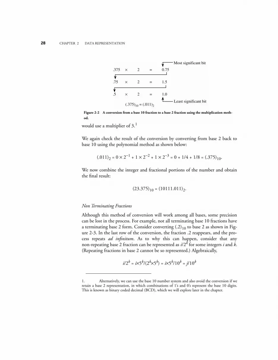
28 CHAPTER 2 DATA REPRESENTATION
would use a multiplier of 3.1
We again check the result of the conversion by converting from base 2 back tobase 10 using the polynomial method as shown below:
(.011)2 = 0 × 2−1 + 1 × 2−2 + 1 × 2−3 = 0 + 1/4 + 1/8 = (.375)10.
We now combine the integer and fractional portions of the number and obtainthe final result:
(23.375)10 = (10111.011)2.
Non Terminating Fractions
Although this method of conversion will work among all bases, some precisioncan be lost in the process. For example, not all terminating base 10 fractions havea terminating base 2 form. Consider converting (.2)10 to base 2 as shown in Fig-ure 2-3. In the last row of the conversion, the fraction .2 reappears, and the pro-cess repeats ad infinitum. As to why this can happen, consider that anynon-repeating base 2 fraction can be represented as i/2k for some integers i and k.(Repeating fractions in base 2 cannot be so represented.) Algebraically,
i/2k = i×5k/(2k×5k) = i×5k/10k = j/10k
1. Alternatively, we can use the base 10 number system and also avoid the conversion if weretain a base 2 representation, in which combinations of 1’s and 0’s represent the base 10 digits.This is known as binary coded decimal (BCD), which we will explore later in the chapter.
.375 × 2 = 0.75
.75 × 2 = 1.50
.5 × 2 = 1.00
Least significant bit
Most significant bit
(.375)10 = (.011)2
Figure 2-2 A conversion from a base 10 fraction to a base 2 fraction using the multiplication meth-
od.

CHAPTER 2 DATA REPRESENTATION 29
where j is the integer i×5k. The fraction is thus non-repeating in base 10. Thishinges on the fact that only non-repeating fractions in base b can be representedas i/bk for some integers i and k. The condition that must be satisfied for anon-repeating base 10 fraction to have an equivalent non-repeating base 2 frac-tion is:
i/10k = i/(5k×2k) = j/2k
where j = i/5k, and 5k must be a factor of i. For one digit decimal fractions, only(.0)10 and (.5)10 are non-repeating in base 2 (20% of the possible fractions); fortwo digit decimal fractions, only (.00)10, (.25)10, (.50)10, and (.75)10 arenon-repeating (4% of the possible fractions); etc. There is a link between rela-tively prime numbers and repeating fractions, which is helpful in understandingwhy some terminating base 10 fractions do not have a terminating base 2 form.(Knuth, 1981) provides some insight in this area.
Binary versus Decimal Representations
While most computers use base 2 for internal representation and arithmetic,some calculators and business computers use an internal representation of base10, and thus do not suffer from this representational problem. The motivationfor using base 10 in business computers is not entirely to avoid the terminatingfraction problem, however, but also to avoid the conversion process at the inputand output units which historically have taken a significant amount of time.
.2
.4
.8
.6
.2
.
.
.
0.4
0.8
1.6
1.2
0.4
=
=
=
=
=
2
2
2
2
2
×
×
×
×
×
Figure 2-3 A terminating base 10 fraction that does not have a terminating base 2 form.
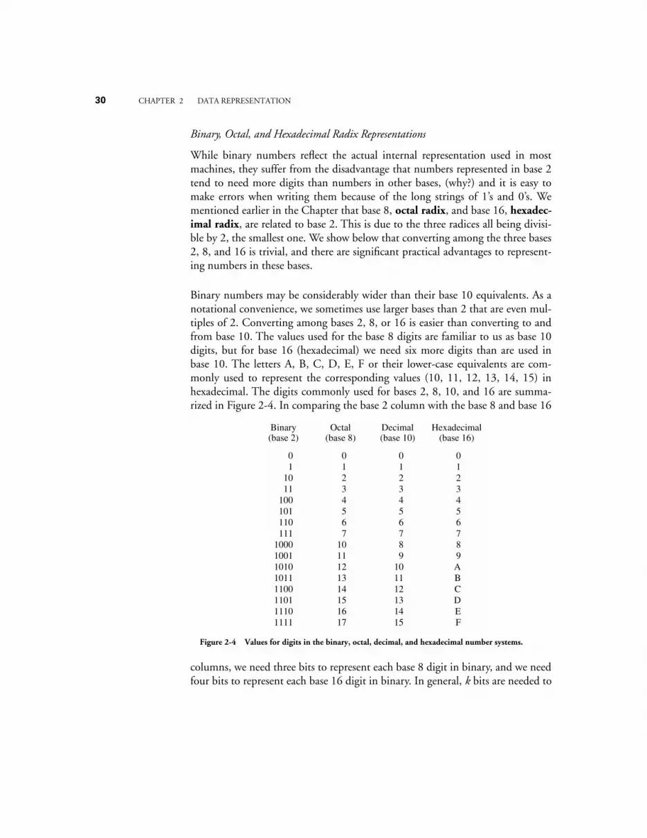
30 CHAPTER 2 DATA REPRESENTATION
Binary, Octal, and Hexadecimal Radix Representations
While binary numbers reflect the actual internal representation used in mostmachines, they suffer from the disadvantage that numbers represented in base 2tend to need more digits than numbers in other bases, (why?) and it is easy tomake errors when writing them because of the long strings of 1’s and 0’s. Wementioned earlier in the Chapter that base 8, octal radix, and base 16, hexadec-imal radix, are related to base 2. This is due to the three radices all being divisi-ble by 2, the smallest one. We show below that converting among the three bases2, 8, and 16 is trivial, and there are significant practical advantages to represent-ing numbers in these bases.
Binary numbers may be considerably wider than their base 10 equivalents. As anotational convenience, we sometimes use larger bases than 2 that are even mul-tiples of 2. Converting among bases 2, 8, or 16 is easier than converting to andfrom base 10. The values used for the base 8 digits are familiar to us as base 10digits, but for base 16 (hexadecimal) we need six more digits than are used inbase 10. The letters A, B, C, D, E, F or their lower-case equivalents are com-monly used to represent the corresponding values (10, 11, 12, 13, 14, 15) inhexadecimal. The digits commonly used for bases 2, 8, 10, and 16 are summa-rized in Figure 2-4. In comparing the base 2 column with the base 8 and base 16
columns, we need three bits to represent each base 8 digit in binary, and we needfour bits to represent each base 16 digit in binary. In general, k bits are needed to
Binary(base 2)
01
1011
100101110111
10001001101010111100110111101111
Octal(base 8)
01234567
1011121314151617
Decimal(base 10)
0123456789
101112131415
Hexadecimal(base 16)
0123456789ABCDEF
Figure 2-4 Values for digits in the binary, octal, decimal, and hexadecimal number systems.
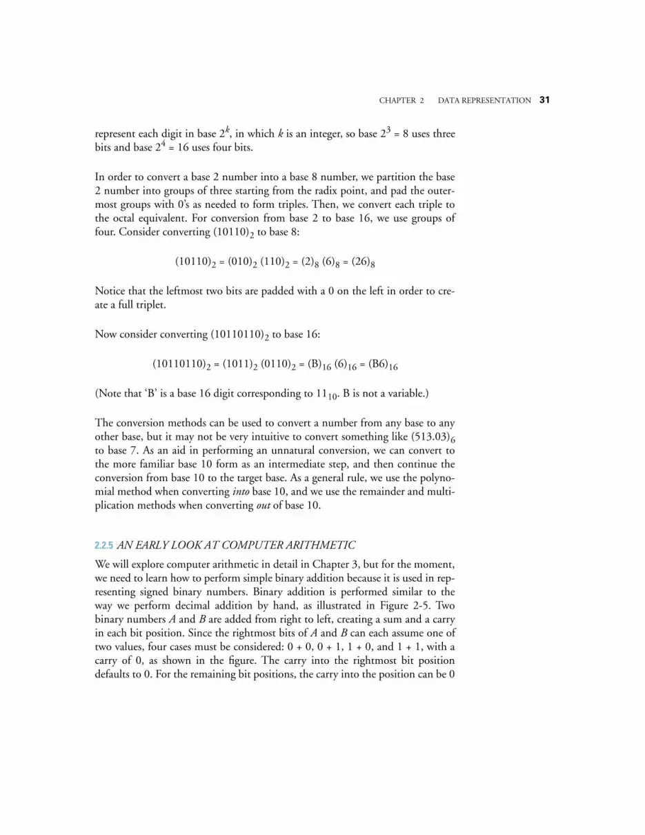
CHAPTER 2 DATA REPRESENTATION 31
represent each digit in base 2k, in which k is an integer, so base 23 = 8 uses threebits and base 24 = 16 uses four bits.
In order to convert a base 2 number into a base 8 number, we partition the base2 number into groups of three starting from the radix point, and pad the outer-most groups with 0’s as needed to form triples. Then, we convert each triple tothe octal equivalent. For conversion from base 2 to base 16, we use groups offour. Consider converting (10110)2 to base 8:
(10110)2 = (010)2 (110)2 = (2)8 (6)8 = (26)8
Notice that the leftmost two bits are padded with a 0 on the left in order to cre-ate a full triplet.
Now consider converting (10110110)2 to base 16:
(10110110)2 = (1011)2 (0110)2 = (B)16 (6)16 = (B6)16
(Note that ‘B’ is a base 16 digit corresponding to 1110. B is not a variable.)
The conversion methods can be used to convert a number from any base to anyother base, but it may not be very intuitive to convert something like (513.03)6to base 7. As an aid in performing an unnatural conversion, we can convert tothe more familiar base 10 form as an intermediate step, and then continue theconversion from base 10 to the target base. As a general rule, we use the polyno-mial method when converting into base 10, and we use the remainder and multi-plication methods when converting out of base 10.
2.2.5 AN EARLY LOOK AT COMPUTER ARITHMETIC
We will explore computer arithmetic in detail in Chapter 3, but for the moment,we need to learn how to perform simple binary addition because it is used in rep-resenting signed binary numbers. Binary addition is performed similar to theway we perform decimal addition by hand, as illustrated in Figure 2-5. Twobinary numbers A and B are added from right to left, creating a sum and a carryin each bit position. Since the rightmost bits of A and B can each assume one oftwo values, four cases must be considered: 0 + 0, 0 + 1, 1 + 0, and 1 + 1, with acarry of 0, as shown in the figure. The carry into the rightmost bit positiondefaults to 0. For the remaining bit positions, the carry into the position can be 0
32 CHAPTER 2 DATA REPRESENTATION
or 1, so that a total of eight input combinations must be considered as shown inthe figure.
Notice that the largest number we can represent using the eight-bit formatshown in Figure 2-5 is (11111111)2 = (255)10 and that the smallest number thatcan be represented is (00000000)2 = (0)10. The bit patterns 11111111 and00000000 and all of the intermediate bit patterns represent numbers on theclosed interval from 0 to 255, which are all positive numbers. Up to this pointwe have considered only unsigned numbers, but we need to represent signednumbers as well, in which (approximately) one half of the bit patterns is assignedto positive numbers and the other half is assigned to negative numbers. Fourcommon representations for base 2 signed numbers are discussed in the next sec-tion.
2.2.6 SIGNED FIXED POINT NUMBERS
Up to this point we have considered only the representation of unsigned fixedpoint numbers. The situation is quite different in representing signed fixed pointnumbers. There are four different ways of representing signed numbers that arecommonly used: sign-magnitude, one’s complement, two’s complement, andexcess notation. We will cover each in turn, using integers for our examples.Throughout the discussion, the reader may wish to refer to Table 2.1 whichshows for a 3-bit number how the various representations appear.
Operands0
0+
00
SumCarry out
Carry in 0
0
1+
10
0
1
0+
10
0
1
1+
01
0
Example:
Carry
Addend: A
Augend: B
Sum
0 1 1 1 1 1 0 0
0 1 0 1 1 0 1 0
1 1 1 1 0 0 0 0
1 1 0 1 0 1 1 0
+
(124)10
(90)10
(214)10
0
0+
10
1
0
1+
01
1
1
0+
01
1
1
1+
11
1
Figure 2-5 Example of binary addition.
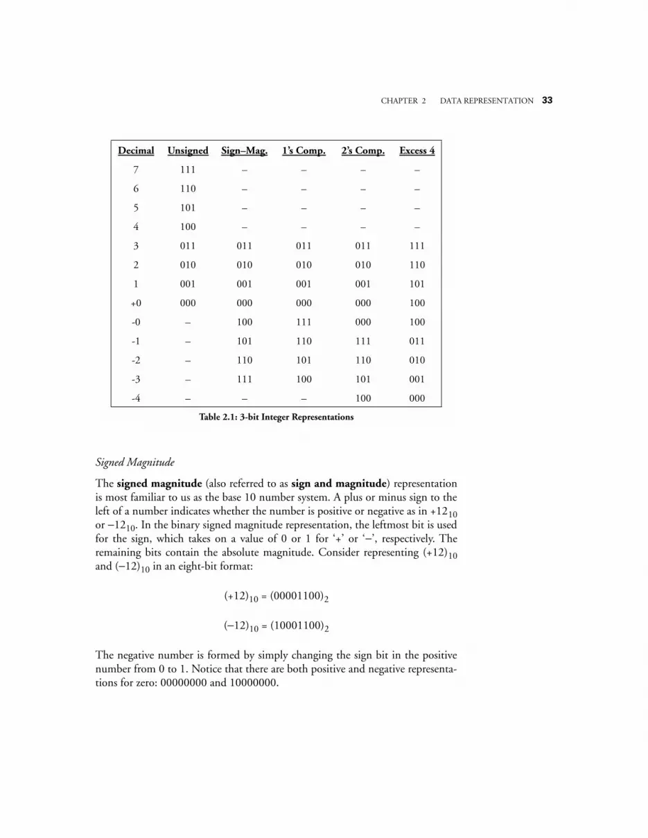
CHAPTER 2 DATA REPRESENTATION 33
Signed Magnitude
The signed magnitude (also referred to as sign and magnitude) representationis most familiar to us as the base 10 number system. A plus or minus sign to theleft of a number indicates whether the number is positive or negative as in +1210or −1210. In the binary signed magnitude representation, the leftmost bit is usedfor the sign, which takes on a value of 0 or 1 for ‘+’ or ‘−’, respectively. Theremaining bits contain the absolute magnitude. Consider representing (+12)10and (−12)10 in an eight-bit format:
(+12)10 = (00001100)2
(−12)10 = (10001100)2
The negative number is formed by simply changing the sign bit in the positivenumber from 0 to 1. Notice that there are both positive and negative representa-tions for zero: 00000000 and 10000000.
Decimal Unsigned Sign–Mag. 1’s Comp. 2’s Comp. Excess 4
7 111 – – – –
6 110 – – – –
5 101 – – – –
4 100 – – – –
3 011 011 011 011 111
2 010 010 010 010 110
1 001 001 001 001 101
+0 000 000 000 000 100
-0 – 100 111 000 100
-1 – 101 110 111 011
-2 – 110 101 110 010
-3 – 111 100 101 001
-4 – – – 100 000
Table 2.1: 3-bit Integer Representations
34 CHAPTER 2 DATA REPRESENTATION
There are eight bits in this example format, and all bit patterns represent validnumbers, so there are 28 = 256 possible patterns. Only 28 − 1 = 255 differentnumbers can be represented, however, since +0 and −0 represent the same num-ber.
We will make use of the signed magnitude representation when we look at float-ing point numbers in Section 2.3.
One’s Complement
The one’s complement operation is trivial to perform: convert all of the 1’s inthe number to 0’s, and all of the 0’s to 1’s. See the fourth column in Table 2.1 forexamples. We can observe from the table that in the one’s complement represen-tation the leftmost bit is 0 for positive numbers and 1 for negative numbers, as itis for the signed magnitude representation. This negation, changing 1’s to 0’s andchanging 0’s to 1’s, is known as complementing the bits. Consider again repre-senting (+12)10 and (−12)10 in an eight-bit format, now using the one’s comple-ment representation:
(+12)10 = (00001100)2
(−12)10 = (11110011)2
Note again that there are representations for both +0 and −0, which are00000000 and 11111111, respectively. As a result, there are only 28 − 1 = 255different numbers that can be represented even though there are 28 different bitpatterns.
The one’s complement representation is not commonly used. This is at leastpartly due to the difficulty in making comparisons when there are two represen-tations for 0. There is also additional complexity involved in adding numbers,which is discussed further in Chapter 3.
Two’s Complement
The two’s complement is formed in a way similar to forming the one’s comple-ment: complement all of the bits in the number, but then add 1, and if that addi-tion results in a carry-out from the most significant bit of the number, discardthe carry-out. Examination of the fifth column of Table 2.1 shows that in the
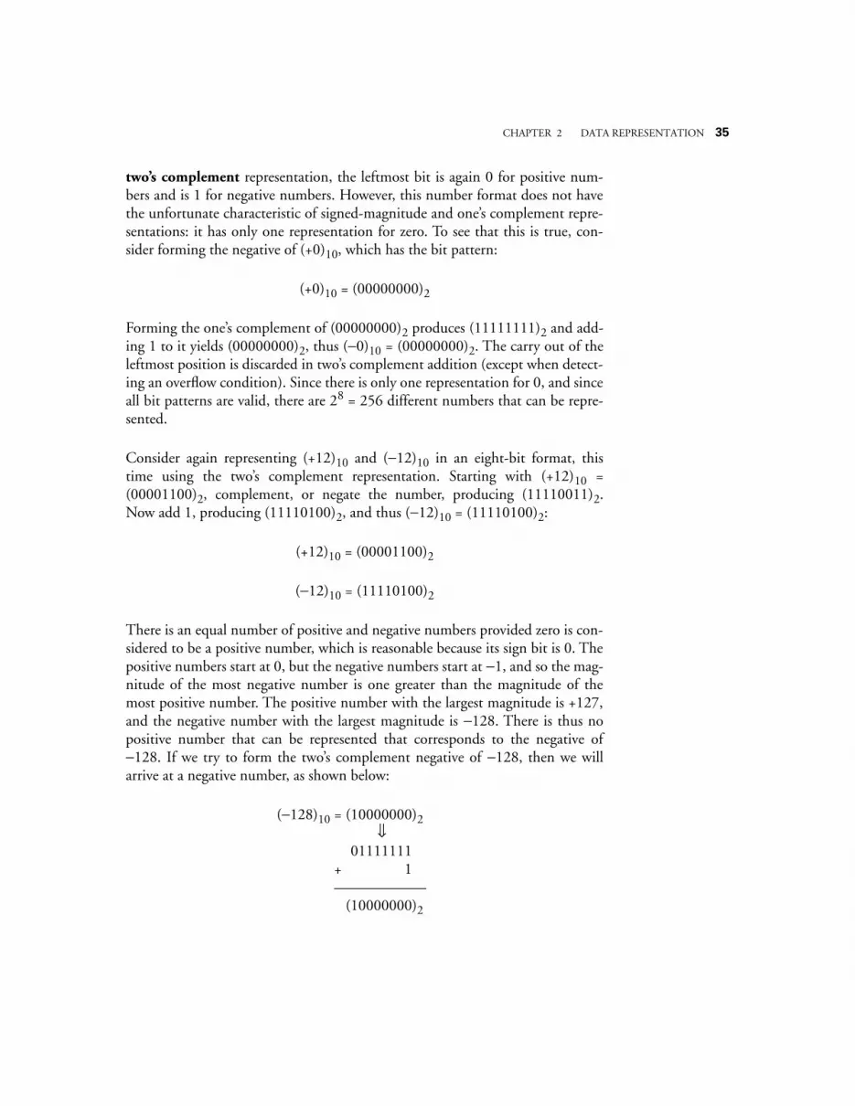
CHAPTER 2 DATA REPRESENTATION 35
two’s complement representation, the leftmost bit is again 0 for positive num-bers and is 1 for negative numbers. However, this number format does not havethe unfortunate characteristic of signed-magnitude and one’s complement repre-sentations: it has only one representation for zero. To see that this is true, con-sider forming the negative of (+0)10, which has the bit pattern:
(+0)10 = (00000000)2
Forming the one’s complement of (00000000)2 produces (11111111)2 and add-ing 1 to it yields (00000000)2, thus (−0)10 = (00000000)2. The carry out of theleftmost position is discarded in two’s complement addition (except when detect-ing an overflow condition). Since there is only one representation for 0, and sinceall bit patterns are valid, there are 28 = 256 different numbers that can be repre-sented.
Consider again representing (+12)10 and (−12)10 in an eight-bit format, thistime using the two’s complement representation. Starting with (+12)10 =(00001100)2, complement, or negate the number, producing (11110011)2.Now add 1, producing (11110100)2, and thus (−12)10 = (11110100)2:
(+12)10 = (00001100)2
(−12)10 = (11110100)2
There is an equal number of positive and negative numbers provided zero is con-sidered to be a positive number, which is reasonable because its sign bit is 0. Thepositive numbers start at 0, but the negative numbers start at −1, and so the mag-nitude of the most negative number is one greater than the magnitude of themost positive number. The positive number with the largest magnitude is +127,and the negative number with the largest magnitude is −128. There is thus nopositive number that can be represented that corresponds to the negative of−128. If we try to form the two’s complement negative of −128, then we willarrive at a negative number, as shown below:
(−128)10 = (10000000)2⇓
(−128)10 = (01111111(−128)10 + (+0000001)2(−128)10 ——————)2(−128)10 = (10000000)2
36 CHAPTER 2 DATA REPRESENTATION
The two’s complement representation is the representation most commonly usedin conventional computers, and we will use it throughout the book.
Excess Representation
In the excess or biased representation, the number is treated as unsigned, but is“shifted” in value by subtracting the bias from it. The concept is to assign thesmallest numerical bit pattern, all zeros, to the negative of the bias, and assign theremaining numbers in sequence as the bit patterns increase in magnitude. A con-venient way to think of an excess representation is that a number is representedas the sum of its two’s complement form and another number, which is known asthe “excess,” or “bias.” Once again, refer to Table 2.1, the rightmost column, forexamples.
Consider again representing (+12)10 and (−12)10 in an eight-bit format but nowusing an excess 128 representation. An excess 128 number is formed by adding128 to the original number, and then creating the unsigned binary version. For(+12)10, we compute (128 + 12 = 140)10 and produce the bit pattern(10001100)2. For (−12)10, we compute (128 + −12 = 116)10 and produce thebit pattern (01110100)2:
(+12)10 = (10001100)2
(−12)10 = (01110100)2
Note that there is no numerical significance to the excess value: it simply has theeffect of shifting the representation of the two’s complement numbers.
There is only one excess representation for 0, since the excess representation issimply a shifted version of the two’s complement representation. For the previouscase, the excess value is chosen to have the same bit pattern as the largest negativenumber, which has the effect of making the numbers appear in numericallysorted order if the numbers are viewed in an unsigned binary representation.Thus, the most negative number is (−128)10 = (00000000)2 and the most posi-tive number is (+127)10 = (11111111)2. This representation simplifies makingcomparisons between numbers, since the bit patterns for negative numbers havenumerically smaller values than the bit patterns for positive numbers. This isimportant for representing the exponents of floating point numbers, in whichexponents of two numbers are compared in order to make them equal for addi-
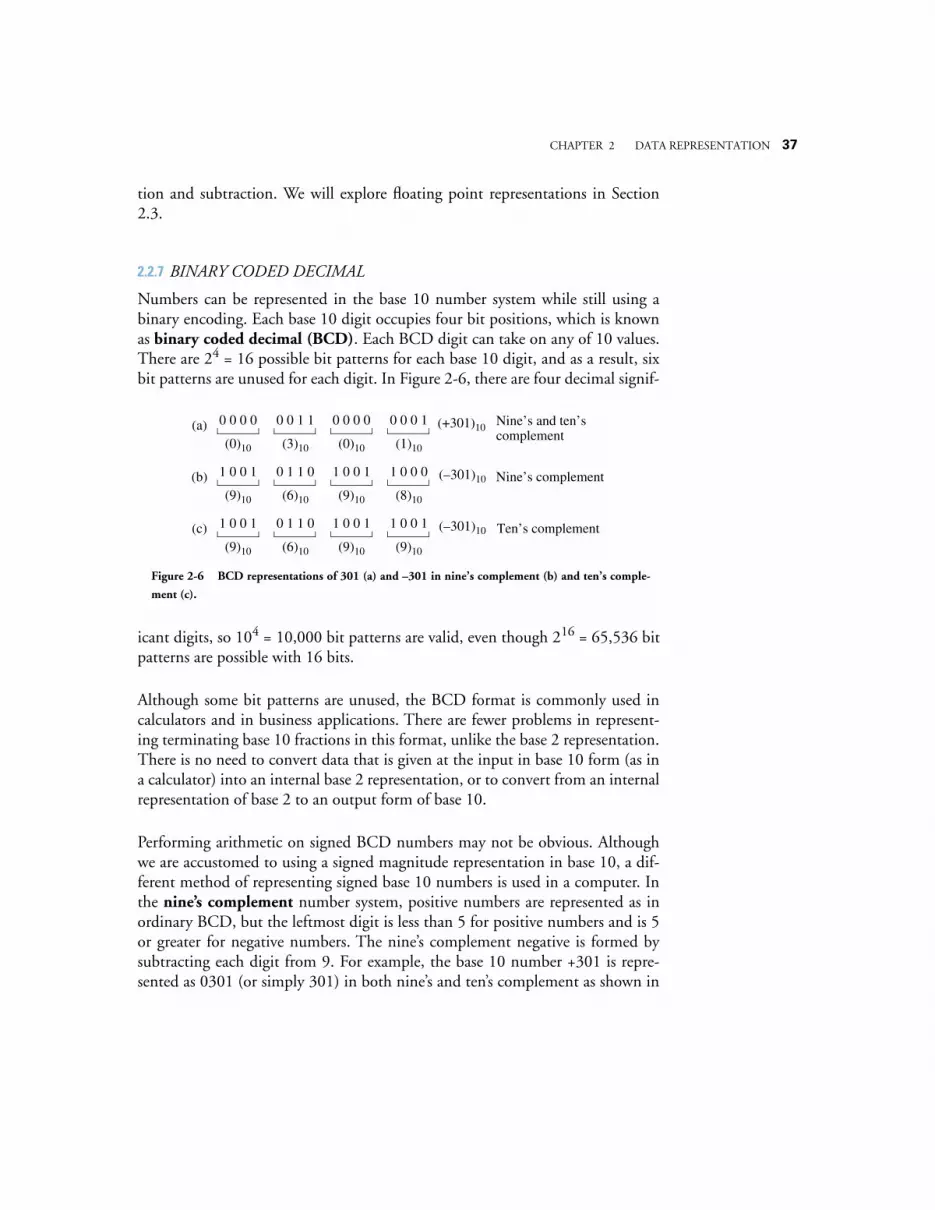
CHAPTER 2 DATA REPRESENTATION 37
tion and subtraction. We will explore floating point representations in Section2.3.
2.2.7 BINARY CODED DECIMAL
Numbers can be represented in the base 10 number system while still using abinary encoding. Each base 10 digit occupies four bit positions, which is knownas binary coded decimal (BCD). Each BCD digit can take on any of 10 values.There are 24 = 16 possible bit patterns for each base 10 digit, and as a result, sixbit patterns are unused for each digit. In Figure 2-6, there are four decimal signif-
icant digits, so 104 = 10,000 bit patterns are valid, even though 216 = 65,536 bitpatterns are possible with 16 bits.
Although some bit patterns are unused, the BCD format is commonly used incalculators and in business applications. There are fewer problems in represent-ing terminating base 10 fractions in this format, unlike the base 2 representation.There is no need to convert data that is given at the input in base 10 form (as ina calculator) into an internal base 2 representation, or to convert from an internalrepresentation of base 2 to an output form of base 10.
Performing arithmetic on signed BCD numbers may not be obvious. Althoughwe are accustomed to using a signed magnitude representation in base 10, a dif-ferent method of representing signed base 10 numbers is used in a computer. Inthe nine’s complement number system, positive numbers are represented as inordinary BCD, but the leftmost digit is less than 5 for positive numbers and is 5or greater for negative numbers. The nine’s complement negative is formed bysubtracting each digit from 9. For example, the base 10 number +301 is repre-sented as 0301 (or simply 301) in both nine’s and ten’s complement as shown in
0 0 0 0
(0)10
0 0 1 1
(3)10
0 0 0 0
(0)10
0 0 0 1
(1)10
(+301)10
1 0 0 1
(9)10
0 1 1 0
(6)10
1 0 0 1
(9)10
1 0 0 0
(8)10
(–301)10
1 0 0 1
(9)10
0 1 1 0
(6)10
1 0 0 1
(9)10
1 0 0 1
(9)10
(–301)10
Nine’s complement
Ten’s complement
Nine’s and ten’s complement
(a)
(b)
(c)
Figure 2-6 BCD representations of 301 (a) and –301 in nine’s complement (b) and ten’s comple-
ment (c).
38 CHAPTER 2 DATA REPRESENTATION
Figure 2-6a. The nine’s complement negative is 9698 (Figure 2-6b), which isobtained by subtracting each digit in 0301 from 9.
The ten’s complement negative is formed by adding 1 to the nine’s complementnegative, so the ten’s complement representation of −301 is then 9698 + 1 =9699 as shown in Figure 2-6c. For this example, the positive numbers range from0 – 4999 and the negative numbers range from 5000 to 9999.
2.3 Floating Point NumbersThe fixed point number representation, which we explored in Section 2.2, has afixed position for the radix point, and a fixed number of digits to the left andright of the radix point. A fixed point representation may need a great many dig-its in order to represent a practical range of numbers. For example, a computerthat can represent a number as large as a trillion1 maintains at least 40 bits to theleft of the radix point since 240 ≈ 1012. If the same computer needs to representone trillionth, then 40 bits must also be maintained to the right of the radixpoint, which results in a total of 80 bits per number.
In practice, much larger numbers and much smaller numbers appear during thecourse of computation, which places even greater demands on a computer. Agreat deal of hardware is required in order to store and manipulate numbers with80 or more bits of precision, and computation proceeds more slowly for a largenumber of digits than for a small number of digits. Fine precision, however, isgenerally not needed when large numbers are used, and conversely, large num-bers do not generally need to be represented when calculations are made withsmall numbers. A more efficient computer can be realized when only as muchprecision is retained as is needed.
2.3.1 RANGE AND PRECISION IN FLOATING POINT NUMBERS
A floating point representation allows a large range of expressible numbers to berepresented in a small number of digits by separating the digits used for precisionfrom the digits used for range. The base 10 floating point number representingAvogadro’s number is shown below:
1. In the American number system, which is used here, a trillion = 1012. In the Britishnumber system, this is a “million million,” or simply a “billion.” The British “milliard,” or a “thou-sand million” is what Americans call a “billion.”
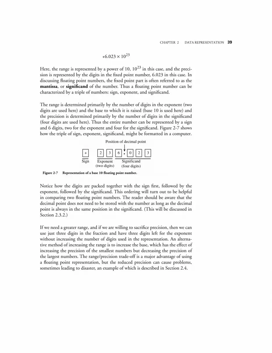
CHAPTER 2 DATA REPRESENTATION 39
+6.023 × 10²³
Here, the range is represented by a power of 10, 1023 in this case, and the preci-sion is represented by the digits in the fixed point number, 6.023 in this case. Indiscussing floating point numbers, the fixed point part is often referred to as themantissa, or significand of the number. Thus a floating point number can becharacterized by a triple of numbers: sign, exponent, and significand.
The range is determined primarily by the number of digits in the exponent (twodigits are used here) and the base to which it is raised (base 10 is used here) andthe precision is determined primarily by the number of digits in the significand(four digits are used here). Thus the entire number can be represented by a signand 6 digits, two for the exponent and four for the significand. Figure 2-7 showshow the triple of sign, exponent, significand, might be formatted in a computer.
Notice how the digits are packed together with the sign first, followed by theexponent, followed by the significand. This ordering will turn out to be helpfulin comparing two floating point numbers. The reader should be aware that thedecimal point does not need to be stored with the number as long as the decimalpoint is always in the same position in the significand. (This will be discussed inSection 2.3.2.)
If we need a greater range, and if we are willing to sacrifice precision, then we canuse just three digits in the fraction and have three digits left for the exponentwithout increasing the number of digits used in the representation. An alterna-tive method of increasing the range is to increase the base, which has the effect ofincreasing the precision of the smallest numbers but decreasing the precision ofthe largest numbers. The range/precision trade-off is a major advantage of usinga floating point representation, but the reduced precision can cause problems,sometimes leading to disaster, an example of which is described in Section 2.4.
+
Sign
2 3 6 0 2
Exponent(two digits)
Significand(four digits)
Position of decimal point
3.
Figure 2-7 Representation of a base 10 floating point number.
40 CHAPTER 2 DATA REPRESENTATION
2.3.2 NORMALIZATION, AND THE HIDDEN BIT
A potential problem with representing floating point numbers is that the samenumber can be represented in different ways, which makes comparisons andarithmetic operations difficult. For example, consider the numerically equivalentforms shown below:
3584.1 × 100 = 3.5841 × 103 = .35841 × 104.
In order to avoid multiple representations for the same number, floating pointnumbers are maintained in normalized form. That is, the radix point is shiftedto the left or to the right and the exponent is adjusted accordingly until the radixpoint is to the left of the leftmost nonzero digit. So the rightmost number aboveis the normalized one. Unfortunately, the number zero cannot be represented inthis scheme, so to represent zero an exception is made. The exception to this ruleis that zero is represented as all 0’s in the mantissa.
If the mantissa is represented as a binary, that is, base 2, number, and if the nor-malization condition is that there is a leading “1” in the normalized mantissa,then there is no need to store that “1” and in fact, most floating point formats donot store it. Rather, it is “chopped off ” before packing up the number for storage,and it is restored when unpacking the number into exponent and mantissa. Thisresults in having an additional bit of precision on the right of the number, due toremoving the bit on the left. This missing bit is referred to as the hidden bit, alsoknown as a hidden 1. For example, if the mantissa in a given format is .11010after normalization, then the bit pattern that is stored is 1010—the left-most bitis truncated, or hidden. We will see that the IEEE 754 floating point format usesa hidden bit.
2.3.3 REPRESENTING FLOATING POINT NUMBERS IN THE COM-PUTER—PRELIMINARIES
Let us design a simple floating point format to illustrate the important factors inrepresenting floating point numbers on the computer. Our format may at firstseem to be unnecessarily complex. We will represent the significand in signedmagnitude format, with a single bit for the sign bit, and three hexadecimal digitsfor the magnitude. The exponent will be a 3-bit excess-4 number, with a radix of16. The normalized form of the number has the hexadecimal point to the left ofthe three hexadecimal digits.
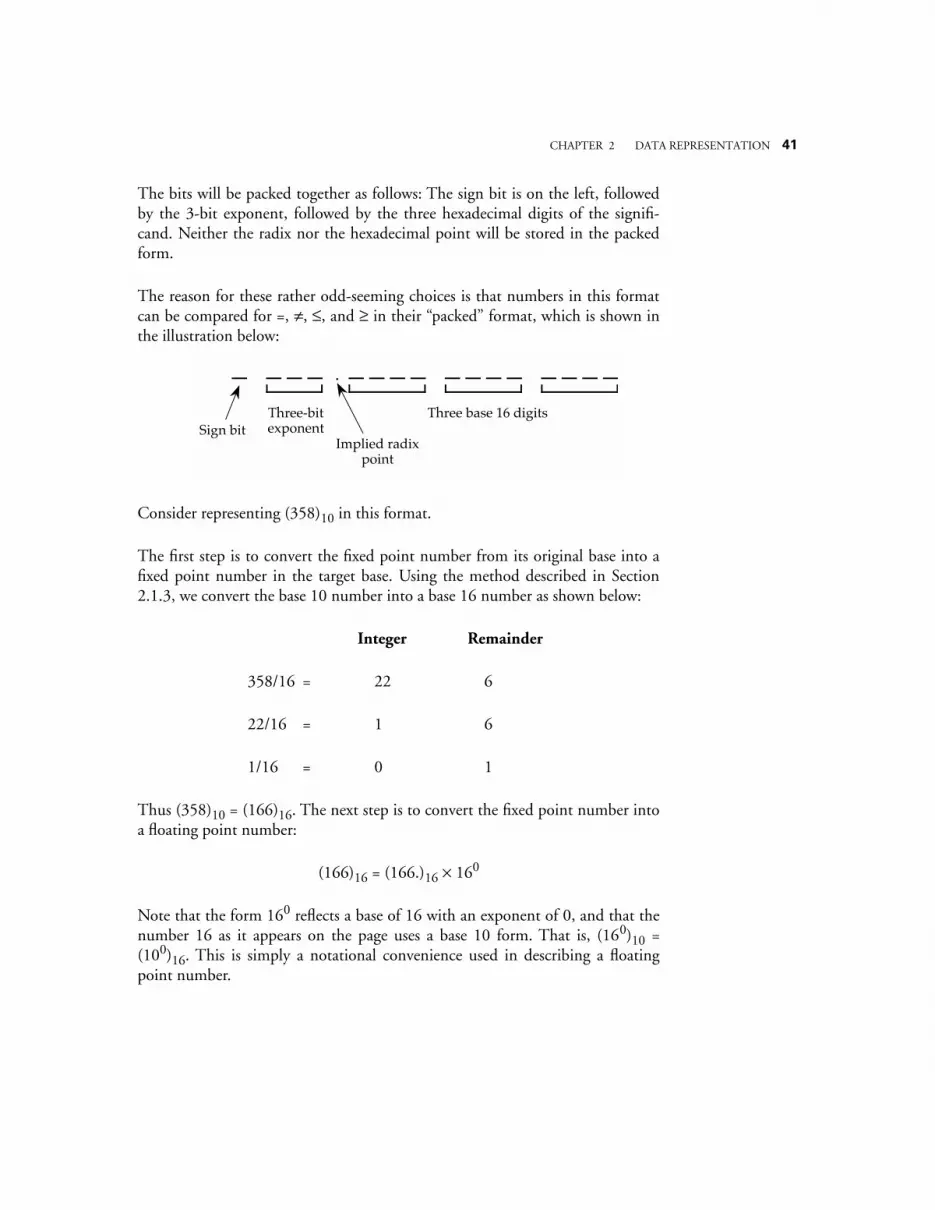
CHAPTER 2 DATA REPRESENTATION 41
The bits will be packed together as follows: The sign bit is on the left, followedby the 3-bit exponent, followed by the three hexadecimal digits of the signifi-cand. Neither the radix nor the hexadecimal point will be stored in the packedform.
The reason for these rather odd-seeming choices is that numbers in this formatcan be compared for =, ≠, ≤, and ≥ in their “packed” format, which is shown inthe illustration below:
Consider representing (358)10 in this format.
The first step is to convert the fixed point number from its original base into afixed point number in the target base. Using the method described in Section2.1.3, we convert the base 10 number into a base 16 number as shown below:
Integer Remainder
358/16 = 22 6
22/16 = 1 6
1/16 = 0 1
Thus (358)10 = (166)16. The next step is to convert the fixed point number intoa floating point number:
(166)16 = (166.)16 × 160
Note that the form 160 reflects a base of 16 with an exponent of 0, and that thenumber 16 as it appears on the page uses a base 10 form. That is, (160)10 =(100)16. This is simply a notational convenience used in describing a floatingpoint number.
Sign bitThree-bit exponent
Implied radix point
Three base 16 digits
.
42 CHAPTER 2 DATA REPRESENTATION
The next step is to normalize the number:
(166.)16 × 160 = (.166)16 × 163
Finally, we fill in the bit fields of the number. The number is positive, and so weplace a 0 in the sign bit position. The exponent is 3, but we represent it in excess4, so the bit pattern for the exponent is computed as shown below:
Alternatively, we could have simply computed 3 + 4 = 7 in base 10, and thenmade the equivalent conversion (7)10 = (111)2.
Finally, each of the base 16 digits is represented in binary as 1 = 0001, 6 = 0110,and 6 = 0110. The final bit pattern is shown below:
Notice again that the radix point is not explicitly represented in the bit pattern,but its presence is implied. The spaces between digits are for clarity only, and donot suggest that the bits are stored with spaces between them. The bit pattern asstored in a computer’s memory would look like this:
0111000101100110
The use of an excess 4 exponent instead of a two’s complement or a signed mag-nitude exponent simplifies addition and subtraction of floating point numbers(which we will cover in detail in Chapter 3). In order to add or subtract two nor-malized floating point numbers, the smaller exponent (smaller in degree, notmagnitude) must first be increased to the larger exponent (this retains the range),which also has the effect of unnormalizing the smaller number. In order to deter-mine which exponent is larger, we only need to treat the bit patterns as unsignednumbers and then make our comparison. That is, using an excess 4 representa-
Excess 4 +
01
1
10
1
10
1
(+3)10(+4)10
Excess 4 exponent
Sign Exponent Fraction
.0 1 1 1 0 0 0 1 0 1 1 0 0 1 1 0
6 613+
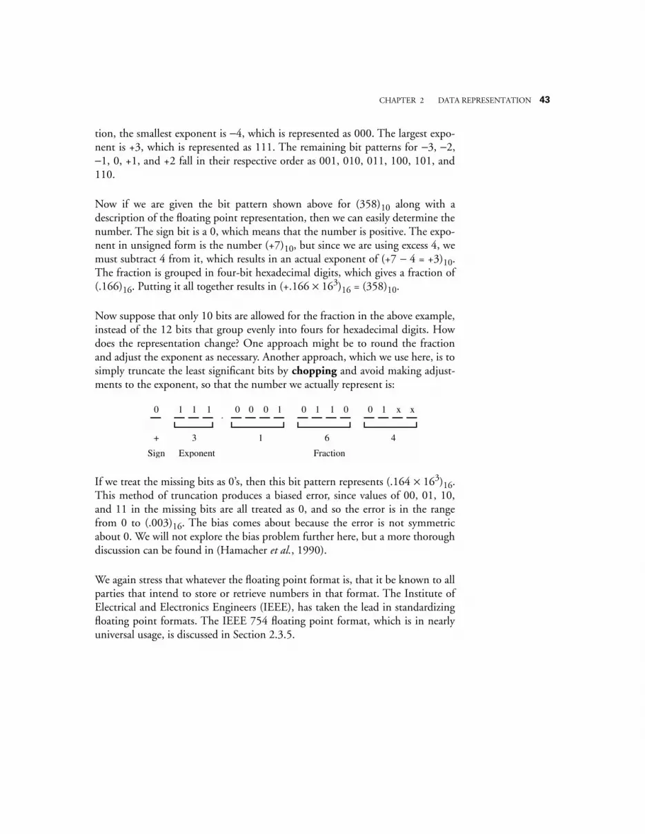
CHAPTER 2 DATA REPRESENTATION 43
tion, the smallest exponent is −4, which is represented as 000. The largest expo-nent is +3, which is represented as 111. The remaining bit patterns for −3, −2,−1, 0, +1, and +2 fall in their respective order as 001, 010, 011, 100, 101, and110.
Now if we are given the bit pattern shown above for (358)10 along with adescription of the floating point representation, then we can easily determine thenumber. The sign bit is a 0, which means that the number is positive. The expo-nent in unsigned form is the number (+7)10, but since we are using excess 4, wemust subtract 4 from it, which results in an actual exponent of (+7 − 4 = +3)10.The fraction is grouped in four-bit hexadecimal digits, which gives a fraction of(.166)16. Putting it all together results in (+.166 × 163)16 = (358)10.
Now suppose that only 10 bits are allowed for the fraction in the above example,instead of the 12 bits that group evenly into fours for hexadecimal digits. Howdoes the representation change? One approach might be to round the fractionand adjust the exponent as necessary. Another approach, which we use here, is tosimply truncate the least significant bits by chopping and avoid making adjust-ments to the exponent, so that the number we actually represent is:
If we treat the missing bits as 0’s, then this bit pattern represents (.164 × 163)16.This method of truncation produces a biased error, since values of 00, 01, 10,and 11 in the missing bits are all treated as 0, and so the error is in the rangefrom 0 to (.003)16. The bias comes about because the error is not symmetricabout 0. We will not explore the bias problem further here, but a more thoroughdiscussion can be found in (Hamacher et al., 1990).
We again stress that whatever the floating point format is, that it be known to allparties that intend to store or retrieve numbers in that format. The Institute ofElectrical and Electronics Engineers (IEEE), has taken the lead in standardizingfloating point formats. The IEEE 754 floating point format, which is in nearlyuniversal usage, is discussed in Section 2.3.5.
Sign Exponent Fraction
.0 1 1 1 0 0 0 1 0 1 1 0 0 1 x x
6 413+
44 CHAPTER 2 DATA REPRESENTATION
2.3.4 ERROR IN FLOATING POINT REPRESENTATIONS
The fact that finite precision introduces error means that we should considerhow great the error is (by “error”, we mean the distance between two adjacentrepresentable numbers), and whether it is acceptable for our application. As anexample of a potential pitfall, consider representing one million in floating point,and then subtracting one million 1’s from it. We may still be left with a million ifthe error is greater than 1.1
In order to characterize error, range, and precision, we use the following nota-tion:
b Base
s Number of significant digits (not bits) in the fraction
M Largest exponent
m Smallest exponent
The number of significant digits in the fraction is represented by s, which is dif-ferent than the number of bits in the fraction if the base is anything other than 2(for example, base 16 uses four bits for each digit). In general, if the base is 2k
where k is an integer, then k bits are needed to represent each digit. The use of ahidden 1 increases s by one bit even though it does not increase the number ofrepresentable numbers. In the previous example, there are three significant digitsin the base 16 fraction and there are 12 bits that make up the three digits. Thereare three bits in the excess 4 exponent, which gives an exponent range of [−22 to22 − 1]. For this case, b = 16, s = 3, M = 3, and m = −4.
In the analysis of a floating point representation, there are five characteristics thatwe consider: the number of representable numbers, the numbers that have thelargest and smallest magnitudes (other than zero), and the sizes of the largest andsmallest gaps between successive numbers.
The number of representable numbers can be determined as shown in Figure
1. Most computers these days will let this upper bound get at least as highas 8 million using the default precision.
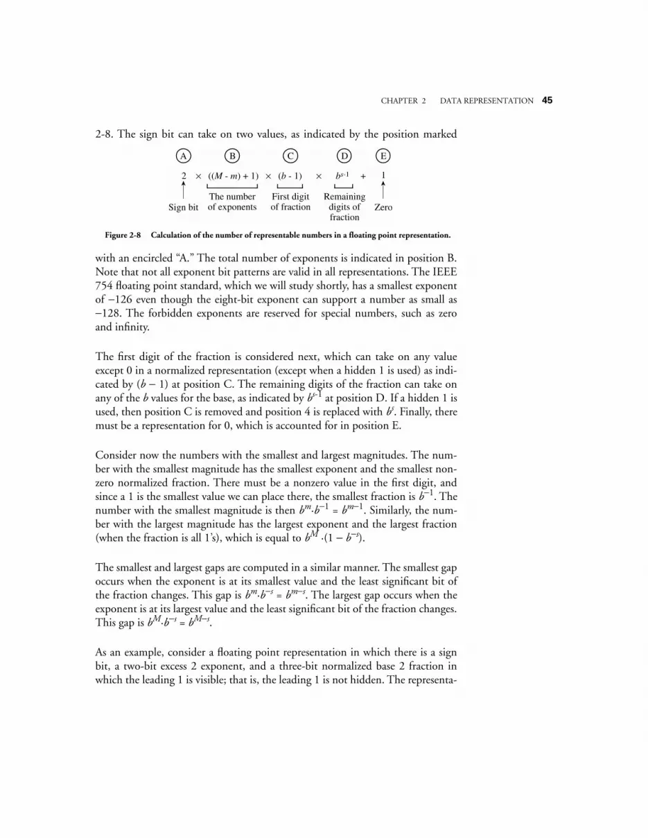
CHAPTER 2 DATA REPRESENTATION 45
2-8. The sign bit can take on two values, as indicated by the position marked
with an encircled “A.” The total number of exponents is indicated in position B.Note that not all exponent bit patterns are valid in all representations. The IEEE754 floating point standard, which we will study shortly, has a smallest exponentof −126 even though the eight-bit exponent can support a number as small as−128. The forbidden exponents are reserved for special numbers, such as zeroand infinity.
The first digit of the fraction is considered next, which can take on any valueexcept 0 in a normalized representation (except when a hidden 1 is used) as indi-cated by (b − 1) at position C. The remaining digits of the fraction can take onany of the b values for the base, as indicated by bs-1 at position D. If a hidden 1 isused, then position C is removed and position 4 is replaced with bs. Finally, theremust be a representation for 0, which is accounted for in position E.
Consider now the numbers with the smallest and largest magnitudes. The num-ber with the smallest magnitude has the smallest exponent and the smallest non-zero normalized fraction. There must be a nonzero value in the first digit, andsince a 1 is the smallest value we can place there, the smallest fraction is b−1. Thenumber with the smallest magnitude is then bm·b−1 = bm−1. Similarly, the num-ber with the largest magnitude has the largest exponent and the largest fraction(when the fraction is all 1’s), which is equal to bM ·(1 − b−s).
The smallest and largest gaps are computed in a similar manner. The smallest gapoccurs when the exponent is at its smallest value and the least significant bit ofthe fraction changes. This gap is bm·b−s = bm−s. The largest gap occurs when theexponent is at its largest value and the least significant bit of the fraction changes.This gap is bM·b−s = bM−s.
As an example, consider a floating point representation in which there is a signbit, a two-bit excess 2 exponent, and a three-bit normalized base 2 fraction inwhich the leading 1 is visible; that is, the leading 1 is not hidden. The representa-
2 × ((M - m) + 1) × (b - 1) × bs-1 +
Sign bitFirst digit of fraction
Remaining digits of fraction
The number of exponents Zero
A EB C D
1
Figure 2-8 Calculation of the number of representable numbers in a floating point representation.
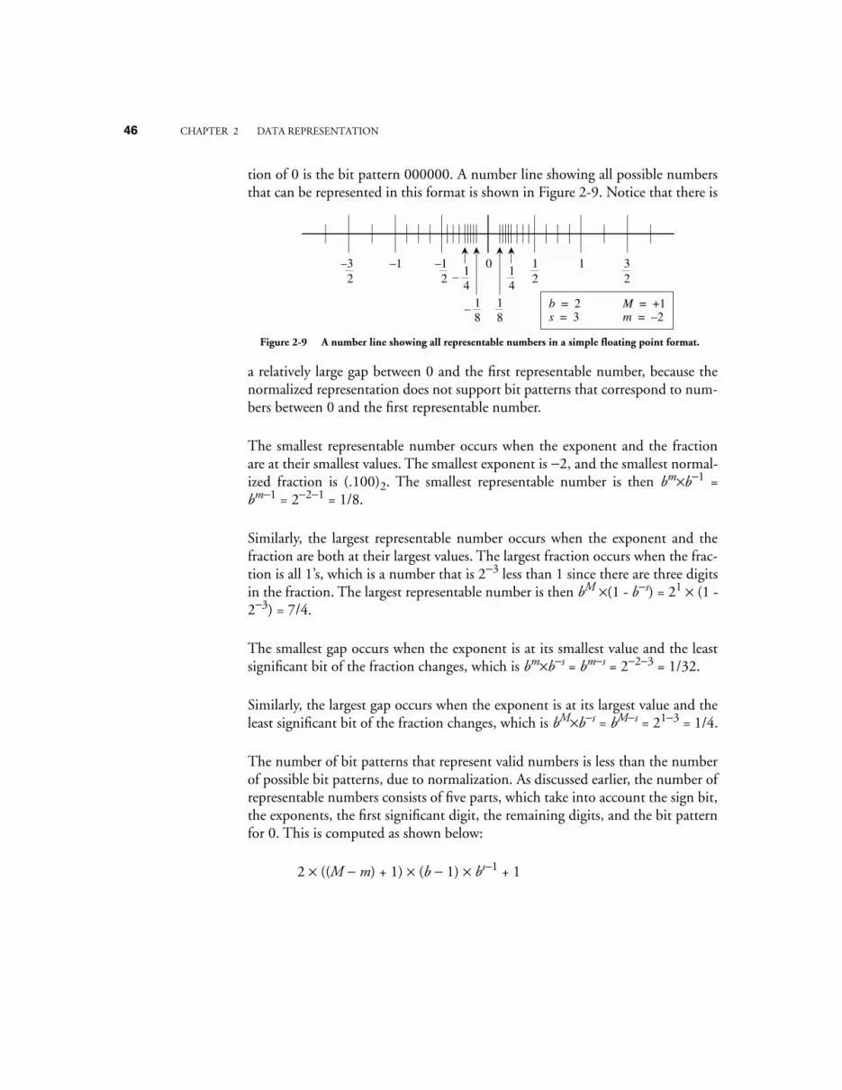
46 CHAPTER 2 DATA REPRESENTATION
tion of 0 is the bit pattern 000000. A number line showing all possible numbersthat can be represented in this format is shown in Figure 2-9. Notice that there is
a relatively large gap between 0 and the first representable number, because thenormalized representation does not support bit patterns that correspond to num-bers between 0 and the first representable number.
The smallest representable number occurs when the exponent and the fractionare at their smallest values. The smallest exponent is −2, and the smallest normal-ized fraction is (.100)2. The smallest representable number is then bm×b−1 =bm−1 = 2−2−1 = 1/8.
Similarly, the largest representable number occurs when the exponent and thefraction are both at their largest values. The largest fraction occurs when the frac-tion is all 1’s, which is a number that is 2−3 less than 1 since there are three digitsin the fraction. The largest representable number is then bM ×(1 - b−s) = 21 × (1 -2−3) = 7/4.
The smallest gap occurs when the exponent is at its smallest value and the leastsignificant bit of the fraction changes, which is bm×b−s = bm−s = 2−2−3 = 1/32.
Similarly, the largest gap occurs when the exponent is at its largest value and theleast significant bit of the fraction changes, which is bM×b−s = bM−s = 21−3 = 1/4.
The number of bit patterns that represent valid numbers is less than the numberof possible bit patterns, due to normalization. As discussed earlier, the number ofrepresentable numbers consists of five parts, which take into account the sign bit,the exponents, the first significant digit, the remaining digits, and the bit patternfor 0. This is computed as shown below:
2 × ((M − m) + 1) × (b − 1) × bs−1 + 1
–3 –1 –1 0 1 1 3– 1
414
– 18
18
22 2 2
b = 2 M = +1s = 3 m = –2
Figure 2-9 A number line showing all representable numbers in a simple floating point format.
CHAPTER 2 DATA REPRESENTATION 47
= 2 × ((1 − (−2)) + 1) × (2 − 1) × 23−1 + 1
= 33.
Notice that the gaps are small for small numbers and that the gaps are large forlarge numbers. In fact, the relative error is approximately the same for all num-bers. If we take the ratio of a large gap to a large number, and compare that to theratio of a small gap to a small number, then the ratios are the same:
and
The representation for a “small number” is used here, rather than the smallestnumber, because the large gap between zero and the first representable number isa special case.
EXAMPLE
Consider the problem of converting (9.375 × 10⁻²)10 to base 2 scientific notation. That is, the result should have the form x.yy × 2z. We start by converting from base 10 floating point to base 10 fixed point by moving the decimal point two positions to the left, which corresponds to the −2 exponent: .09375. We then con-vert from base 10 fixed point to base 2 fixed point by using the multiplication method:
.09375 × 2 = 0.1875
.1875 × 2 = 0.375
.375 × 2 = 0.75
.75 × 2 = 1.5
bM × (1 – b–s)
bM–s
1 – b–s
b–s
= =bs–1A large number
A large gap 1
bm × (1 – b–s)
bm–s
1 – b–s
b–s
= =bs–1A small number
A small gap 1
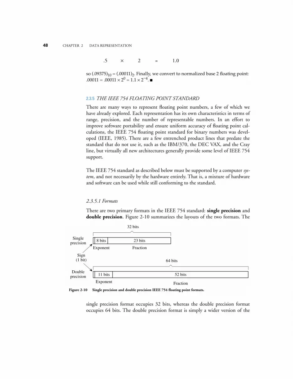
48 CHAPTER 2 DATA REPRESENTATION
.5 × 2 = 1.0
so (.09375)10 = (.00011)2. Finally, we convert to normalized base 2 floating point: .00011 = .00011 × 20 = 1.1 × 2−4.
2.3.5 THE IEEE 754 FLOATING POINT STANDARD
There are many ways to represent floating point numbers, a few of which wehave already explored. Each representation has its own characteristics in terms ofrange, precision, and the number of representable numbers. In an effort toimprove software portability and ensure uniform accuracy of floating point cal-culations, the IEEE 754 floating point standard for binary numbers was devel-oped (IEEE, 1985). There are a few entrenched product lines that predate thestandard that do not use it, such as the IBM/370, the DEC VAX, and the Crayline, but virtually all new architectures generally provide some level of IEEE 754support.
The IEEE 754 standard as described below must be supported by a computer sys-tem, and not necessarily by the hardware entirely. That is, a mixture of hardwareand software can be used while still conforming to the standard.
2.3.5.1 Formats
There are two primary formats in the IEEE 754 standard: single precision anddouble precision. Figure 2-10 summarizes the layouts of the two formats. The
single precision format occupies 32 bits, whereas the double precision formatoccupies 64 bits. The double precision format is simply a wider version of the
Single precision
Sign (1 bit)
Exponent Fraction
8 bits 23 bits
Double precision
Exponent Fraction
11 bits 52 bits
32 bits
64 bits
Figure 2-10 Single precision and double precision IEEE 754 floating point formats.
CHAPTER 2 DATA REPRESENTATION 49
single precision format.
The sign bit is in the leftmost position and indicates a positive or negative num-ber for a 0 or a 1, respectively. The 8-bit excess 127 (not 128) exponent follows,in which the bit patterns 00000000 and 11111111 are reserved for special cases,as described below. For double precision, the 11-bit exponent is represented inexcess 1023, with 00000000000 and 11111111111 reserved. The 23-bit base 2fraction follows. There is a hidden bit to the left of the binary point, which whentaken together with the single-precision fraction form a 23 + 1 = 24-bit signifi-cand of the form 1.fff...f where the fff...f pattern represents the 23-bit fractionalpart that is stored. The double-precision format also uses a hidden bit to the leftof the binary point, which supports a 52 + 1 = 53 bit significand. For both for-mats, the number is normalized unless denormalized numbers are supported, asdescribed later.
There are five basic types of numbers that can be represented. Nonzero normal-ized numbers take the form described above. A so-called “clean zero” is repre-sented by the reserved bit pattern 00000000 in the exponent and all 0’s in thefraction. The sign bit can be 0 or 1, and so there are two representations for zero:+0 and −0.
Infinity has a representation in which the exponent contains the reserved bit pat-tern 11111111, the fraction contains all 0’s, and the sign bit is 0 or 1. Infinity isuseful in handling overflow situations or in giving a valid representation to anumber (other than zero) divided by zero. If zero is divided by zero or infinity isdivided by infinity, then the result is undefined. This is represented by the NaN(not a number) format in which the exponent contains the reserved bit pattern11111111, the fraction is nonzero and the sign bit is 0 or 1. A NaN can also beproduced by attempting to take the square root of −1.
As with all normalized representations, there is a large gap between zero and thefirst representable number. The denormalized, “dirty zero” representation allowsnumbers in this gap to be represented. The sign bit can be 0 or 1, the exponentcontains the reserved bit pattern 00000000 which represents −126 for single pre-cision (−1022 for double precision), and the fraction contains the actual bit pat-tern for the magnitude of the number. Thus, there is no hidden 1 for this format.Note that the denormalized representation is not an unnormalized representation.The key difference is that there is only one representation for each denormalizednumber, whereas there are infinitely many unnormalized representations.
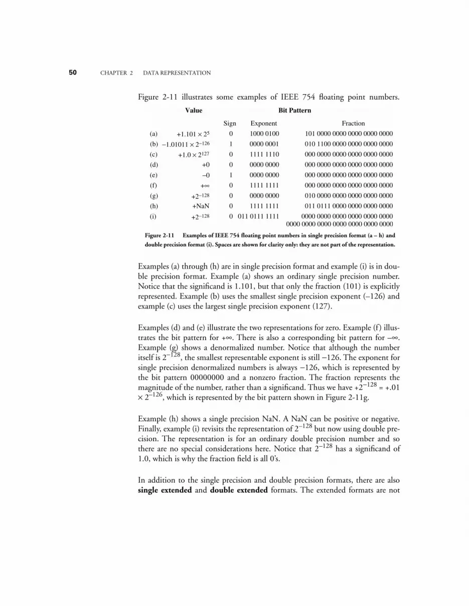
50 CHAPTER 2 DATA REPRESENTATION
Figure 2-11 illustrates some examples of IEEE 754 floating point numbers.
Examples (a) through (h) are in single precision format and example (i) is in dou-ble precision format. Example (a) shows an ordinary single precision number.Notice that the significand is 1.101, but that only the fraction (101) is explicitlyrepresented. Example (b) uses the smallest single precision exponent (–126) andexample (c) uses the largest single precision exponent (127).
Examples (d) and (e) illustrate the two representations for zero. Example (f ) illus-trates the bit pattern for +∞. There is also a corresponding bit pattern for –∞.Example (g) shows a denormalized number. Notice that although the numberitself is 2−128, the smallest representable exponent is still −126. The exponent forsingle precision denormalized numbers is always −126, which is represented bythe bit pattern 00000000 and a nonzero fraction. The fraction represents themagnitude of the number, rather than a significand. Thus we have +2−128 = +.01× 2–126, which is represented by the bit pattern shown in Figure 2-11g.
Example (h) shows a single precision NaN. A NaN can be positive or negative.Finally, example (i) revisits the representation of 2–128 but now using double pre-cision. The representation is for an ordinary double precision number and sothere are no special considerations here. Notice that 2–128 has a significand of1.0, which is why the fraction field is all 0’s.
In addition to the single precision and double precision formats, there are alsosingle extended and double extended formats. The extended formats are not
(a) +1.101 × 25
Value
0
Sign Exponent Fraction
Bit Pattern
1000 0100 101 0000 0000 0000 0000 0000
(b) −1.01011 × 2−126 1 0000 0001 010 1100 0000 0000 0000 0000
(c) +1.0 × 2127 0 1111 1110 000 0000 0000 0000 0000 0000
(d) +0 0 0000 0000 000 0000 0000 0000 0000 0000
(e) −0 1 0000 0000 000 0000 0000 0000 0000 0000
(f) +∞ 0 1111 1111 000 0000 0000 0000 0000 0000
(g) +2−128 0 0000 0000 010 0000 0000 0000 0000 0000
(h) +NaN 0 1111 1111 011 0111 0000 0000 0000 0000
(i) +2−128 0 011 0111 1111 0000 0000 0000 0000 0000 00000000 0000 0000 0000 0000 0000 0000
Figure 2-11 Examples of IEEE 754 floating point numbers in single precision format (a – h) and
double precision format (i). Spaces are shown for clarity only: they are not part of the representation.
CHAPTER 2 DATA REPRESENTATION 51
visible to the user, but they are used to retain a greater amount of internal preci-sion during calculations to reduce the effects of roundoff errors. The extendedformats increase the widths of the exponents and fractions by a number of bitsthat can vary depending on the implementation. For instance, the singleextended format adds at least three bits to the exponent and eight bits to the frac-tion. The double extended format is typically 80 bits wide, with a 15-bit expo-nent and a 64-bit fraction.
2.3.5.2 Rounding
An implementation of IEEE 754 must provide at least single precision, whereasthe remaining formats are optional. Further, the result of any single operation onfloating point numbers must be accurate to within half a bit in the least signifi-cant bit of the fraction. This means that some additional bits of precision mayneed to be retained during computation (referred to as guard bits), and theremust be an appropriate method of rounding the intermediate result to the num-ber of bits in the fraction.
There are four rounding modes in the IEEE 754 standard. One mode rounds to0, another rounds toward +∞, and another rounds toward −∞. The default moderounds to the nearest representable number. Halfway cases round to the numberwhose low order digit is even. For example, 1.01101 rounds to 1.0110 whereas1.01111 rounds to 1.1000.
2.4 Case Study: Patriot Missile Defense Failure Caused by Loss of PrecisionDuring the 1991-1992 Operation Desert Storm conflict between Coalitionforces and Iraq, the Coalition used a military base in Dhahran, Saudi Arabia thatwas protected by six U.S. Patriot Missile batteries. The Patriot system was origi-nally designed to be mobile and to operate for only a few hours in order to avoiddetection.
The Patriot system tracks and intercepts certain types of objects, such as cruisemissiles or Scud ballistic missiles, one of which hit a U.S. Army barracks atDhahran on February 5, 1991, killing 28 Americans. The Patriot system failed totrack and intercept the incoming Scud due to a loss of precision in convertingintegers to a floating point number representation.
A radar system operates by sending out a train of electromagnetic pulses in vari-
52 CHAPTER 2 DATA REPRESENTATION
ous directions and then listening for return signals that are reflected from objectsin the path of the radar beam. If an airborne object of interest such as a Scud isdetected by the Patriot radar system, then the position of a range gate is deter-mined (see Figure 2-12), which estimates the position of the object being tracked
during the next scan. The range gate also allows information outside of itsboundaries to be filtered out, which simplifies tracking. The position of theobject (a Scud for this case) is confirmed if it is found within the range gate.
The prediction of where the Scud will next appear is a function of the Scud’svelocity. The Scud’s velocity is determined by its change in position with respectto time, and time is updated in the Patriot’s internal clock in 100 ms intervals.Velocity is represented as a 24-bit floating point number, and time is representedas a 24-bit integer, but both must be represented as 24-bit floating point num-bers in order to predict where the Scud will next appear.
The conversion from integer time to real time results in a loss of precision thatincreases as the internal clock time increases. The error introduced by the conver-sion results in an error in the range gate calculation, which is proportional to thetarget’s velocity and the length of time that the system is running. The cause ofthe Dhahran incident, after the Patriot battery had been operating continuously
Range Gate Area
Missile
Search action locates missile somewhere within beam
Validation action
Missile outside of range gate
Patriot Radar System
Figure 2-12 Effect of conversion error on range gate calculation.
CHAPTER 2 DATA REPRESENTATION 53
for over 100 hours, is that the range gate shifted by 687 m, resulting in the failedinterception of a Scud.
The conversion problem was known two weeks in advance of the Dhahran inci-dent as a result of data provided by Israel, but it took until the day after theattack for new software to arrive due to the difficulty of distributing bug fixes ina wartime environment. A solution to the problem, until a software fix could bemade available, would have been to simply reboot the system every few hourswhich would have the effect of resetting the internal clock. Since field personnelwere not informed of how long was too long to keep a system running, whichwas in fact known at the time from data provided by Israel, this solution wasnever implemented. The lesson for us is to be very aware of the limitations ofrelying on calculations that use finite precision.
2.5 Character CodesUnlike real numbers, which have an infinite range, there is only a finite numberof characters. An entire character set can be represented with a small number ofbits per character. Three of the most common character representations, ASCII,EBCDIC, and Unicode, are described here.
2.5.1 THE ASCII CHARACTER SET
The American Standard Code for Information Interchange (ASCII) is summa-rized in Figure 2-13, using hexadecimal indices. The representation for eachcharacter consists of 7 bits, and all 27 possible bit patterns represent valid charac-ters. The characters in positions 00 – 1F and position 7F are special control char-acters that are used for transmission, printing control, and other non-textualpurposes. The remaining characters are all printable, and include letters, num-bers, punctuation, and a space. The digits 0-9 appear in sequence, as do theupper and lower case letters1. This organization simplifies character manipula-tion. In order to change the character representation of a digit into its numericalvalue, we can subtract (30)16 from it. In order to convert the ASCII character ‘5,’which is in position (35)16, into the number 5, we compute (35 – 30 = 5)16. In
1. As an aside, the character ‘a’ and the character ‘A’ are different, and have different codesin the ASCII table. The small letters like ‘a’ are called lower case, and the capital letters like ‘A’ arecalled upper case. The naming comes from the positions of the characters in a printer’s typecase.The capital letters appear above the small letters, which resulted in the upper case / lower case nam-ing. These days, typesetting is almost always performed electronically, but the traditional naming isstill used.
54 CHAPTER 2 DATA REPRESENTATION
order to convert an upper case letter into a lower case letter, we add (20)16. Forexample, to convert the letter ‘H,’ which is at location (48)16 in the ASCII table,into the letter ‘h,’ which is at position (68)16, we compute (48 + 20 = 68)16.
2.5.2 THE EBCDIC CHARACTER SET
A problem with the ASCII code is that only 128 characters can be represented,which is a limitation for many keyboards that have a lot of special characters inaddition to upper and lower case letters. The Extended Binary Coded DecimalInterchange Code (EBCDIC) is an eight-bit code that is used extensively in IBMmainframe computers. Since seven-bit ASCII characters are frequently repre-sented in an eight-bit modified form (one character per byte), in which a 0 or a 1is appended to the left of the seven-bit pattern, the use of EBCDIC does not
00 NUL01 SOH02 STX03 ETX04 EOT05 ENQ06 ACK07 BEL08 BS09 HT0A LF0B VT0C FF0D CR0E SO0F SI
10 DLE11 DC112 DC213 DC314 DC415 NAK16 SYN17 ETB18 CAN19 EM1A SUB1B ESC1C FS1D GS1E RS1F US
20 SP21 !22 "23 #24 $25 %26 &27 '28 (29 )2A *2B +2C ´2D -2E .2F /
30 031 132 233 334 435 536 637 738 839 93A :3B ;3C <3D =3E >3F ?
40 @41 A42 B43 C44 D45 E46 F47 G48 H49 I4A J4B K4C L4D M4E N4F O
50 P51 Q52 R53 S54 T55 U56 V57 W58 X59 Y5A Z5B [5C \5D ]5E ^5F _
60 `61 a62 b63 c64 d65 e66 f67 g68 h69 i6A j6B k6C l6D m6E n6F o
70 p71 q72 r73 s74 t75 u76 v77 w78 x79 y7A z7B 7C |7D 7E ~7F DEL
NULSOHSTXETXEOTENQACKBEL
NullStart of headingStart of textEnd of textEnd of transmissionEnquiryAcknowledgeBell
BSHTLFVT
BackspaceHorizontal tabLine feedVertical tab
FFCRSOSIDLEDC1DC2DC3DC4NAKSYNETB
Form feedCarriage returnShift outShift inData link escapeDevice control 1Device control 2Device control 3Device control 4Negative acknowledgeSynchronous idleEnd of transmission block
CANEMSUBESCFSGSRSUSSPDEL
CancelEnd of mediumSubstituteEscapeFile separatorGroup separatorRecord separatorUnit separatorSpaceDelete
Figure 2-13 The ASCII character code, shown with hexadecimal indices.

CHAPTER 2 DATA REPRESENTATION 55
place a greater demand on the storage of characters in a computer. For serialtransmission, however, (see Chapter 8), an eight-bit code takes more time totransmit than a seven-bit code, and for this case the wider code does make a dif-ference.
The EBCDIC code is summarized in Figure 2-14. There are gaps in the table,which can be used for application specific characters. The fact that there are gapsin the upper and lower case sequences is not a major disadvantage because char-acter manipulations can still be done as for ASCII, but using different offsets.
2.5.3 THE UNICODE CHARACTER SET
The ASCII and EBCDIC codes support the historically dominant (Latin) char-acter sets used in computers. There are many more character sets in the world,and a simple ASCII-to-language-X mapping does not work for the general case,and so a new universal character standard was developed that supports a greatbreadth of the world’s character sets, called Unicode.
Unicode is an evolving standard. It changes as new character sets are introducedinto it, and as existing character sets evolve and their representations are refined.In version 2.0 of the Unicode standard, there are 38,885 distinct coded charac-ters that cover the principal written languages of the Americas, Europe, the Mid-dle East, Africa, India, Asia, and Pacifica.
The Unicode Standard uses a 16-bit code set in which there is a one-to-one cor-respondence between 16-bit codes and characters. Like ASCII, there are no com-plex modes or escape codes. While Unicode supports many more characters thanASCII or EBCDIC, it is not the end-all standard. In fact, the 16-bit Unicodestandard is a subset of the 32-bit ISO 10646 Universal Character Set (UCS-4).
Glyphs for the first 256 Unicode characters are shown in Figure 2-15, accordingto Unicode version 2.1. Note that the first 128 characters are the same as forASCII.
SUMMARY
All data in a computer is represented in terms of bits, which can be organized andinterpreted as integers, fixed point numbers, floating point numbers, or characters.
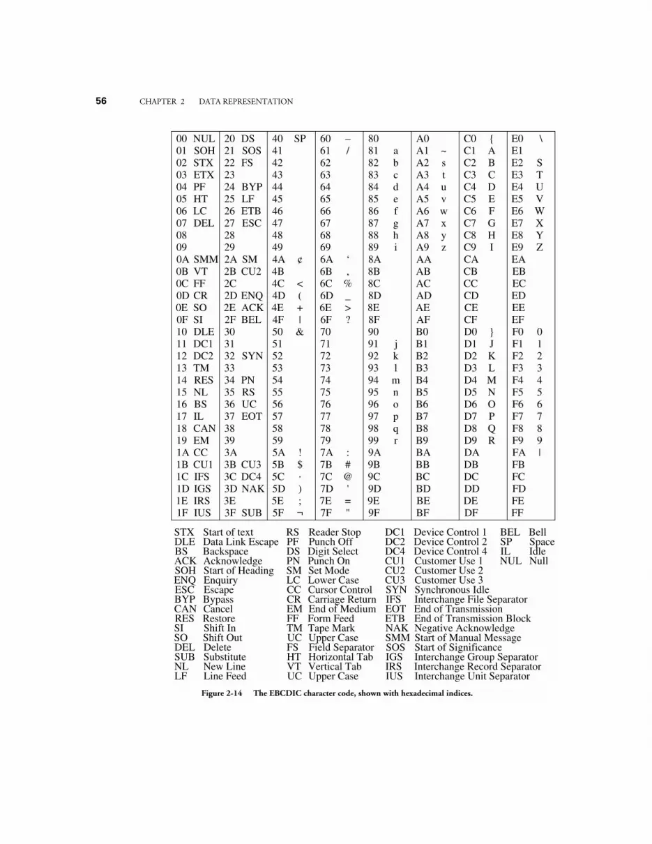
56 CHAPTER 2 DATA REPRESENTATION
00 NUL 20 DS 40 SP 60 – 80 A0 C0 E0 \01 SOH 21 SOS 41 61 / 81 a A1 ~ C1 A E1 02 STX 22 FS 42 62 82 b A2 s C2 B E2 S03 ETX 23 43 63 83 c A3 t C3 C E3 T04 PF 24 BYP 44 64 84 d A4 u C4 D E4 U05 HT 25 LF 45 65 85 e A5 v C5 E E5 V06 LC 26 ETB 46 66 86 f A6 w C6 F E6 W07 DEL 27 ESC 47 67 87 g A7 x C7 G E7 X08 28 48 68 88 h A8 y C8 H E8 Y09 29 49 69 89 i A9 z C9 I E9 Z0A SMM 2A SM 4A ¢ 6A ‘ 8A AA CA EA 0B VT 2B CU2 4B 6B , 8B AB CB EB 0C FF 2C 4C < 6C % 8C AC CC EC 0D CR 2D ENQ 4D ( 6D _ 8D AD CD ED 0E SO 2E ACK 4E + 6E > 8E AE CE EE 0F SI 2F BEL 4F | 6F ? 8F AF CF EF 10 DLE 30 50 & 70 90 B0 D0 F0 011 DC1 31 51 71 91 j B1 D1 J F1 112 DC2 32 SYN 52 72 92 k B2 D2 K F2 213 TM 33 53 73 93 l B3 D3 L F3 314 RES 34 PN 54 74 94 m B4 D4 M F4 415 NL 35 RS 55 75 95 n B5 D5 N F5 516 BS 36 UC 56 76 96 o B6 D6 O F6 617 IL 37 EOT 57 77 97 p B7 D7 P F7 718 CAN 38 58 78 98 q B8 D8 Q F8 819 EM 39 59 79 99 r B9 D9 R F9 91A CC 3A 5A ! 7A : 9A BA DA FA | 1B CU1 3B CU3 5B $ 7B # 9B BB DB FB 1C IFS 3C DC4 5C . 7C @ 9C BC DC FC 1D IGS 3D NAK 5D ) 7D ' 9D BD DD FD 1E IRS 3E 5E ; 7E = 9E BE DE FE 1F IUS 3F SUB 5F ¬ 7F " 9F BF DF FF
STX Start of text RS Reader Stop DC1 Device Control 1 BEL BellDLE Data Link Escape PF Punch Off DC2 Device Control 2 SP SpaceBS Backspace DS Digit Select DC4 Device Control 4 IL IdleACK Acknowledge PN Punch On CU1 Customer Use 1 NUL NullSOH Start of Heading SM Set Mode CU2 Customer Use 2ENQ Enquiry LC Lower Case CU3 Customer Use 3ESC Escape CC Cursor Control SYN Synchronous IdleBYP Bypass CR Carriage Return IFS Interchange File SeparatorCAN Cancel EM End of Medium EOT End of TransmissionRES Restore FF Form Feed ETB End of Transmission BlockSI Shift In TM Tape Mark NAK Negative AcknowledgeSO Shift Out UC Upper Case SMM Start of Manual MessageDEL Delete FS Field Separator SOS Start of SignificanceSUB Substitute HT Horizontal Tab IGS Interchange Group SeparatorNL New Line VT Vertical Tab IRS Interchange Record SeparatorLF Line Feed UC Upper Case IUS Interchange Unit Separator
Figure 2-14 The EBCDIC character code, shown with hexadecimal indices.
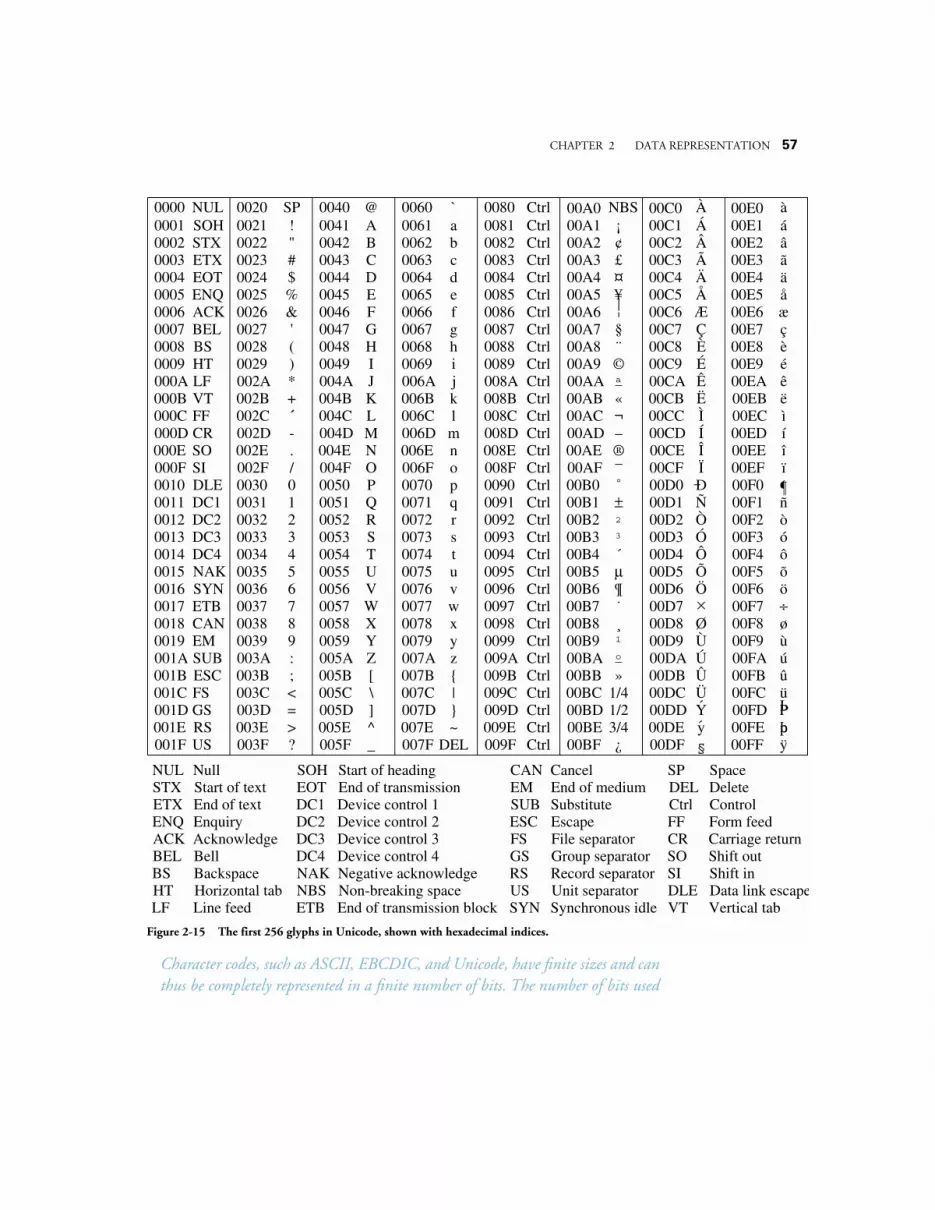
CHAPTER 2 DATA REPRESENTATION 57
Character codes, such as ASCII, EBCDIC, and Unicode, have finite sizes and canthus be completely represented in a finite number of bits. The number of bits used
0000000100020003000400050006000700080009000A000B000C000D000E000F0010001100120013001400150016001700180019001A001B001C001D001E001F
NULSTXETX
Start of textEnd of text
ENQACKBEL
EnquiryAcknowledgeBell
BSHTLF
BackspaceHorizontal tabLine feed VT Vertical tab
SOH Start of headingEOT End of transmission
DLE Data link escape
DC1DC2DC3DC4NAKNBSETB
Device control 1Device control 2Device control 3Device control 4Negative acknowledgeNon-breaking spaceEnd of transmission block
EMSUBESCFSGSRSUS
End of mediumSubstituteEscapeFile separatorGroup separatorRecord separatorUnit separator
Null CAN Cancel
NUL 0020SOH 0021STX 0022ETX 0023EOT 0024ENQ 0025ACK 0026BEL 0027
00280029
LF 002AVT 002BFF 002CCR 002DSO 002ESI 002FDLE 0030DC1 0031DC2 0032DC3 0033DC4 0034NAK 0035SYN 0036ETB 0037CAN 0038EM 0039SUB 003AESC 003BFS 003CGS 003DRS 003EUS 003F
BSHT
0040004100420043004400450046004700480049004A004B004C004D004E004F0050005100520053005400550056005700580059005A005B005C005D005E005F
SP!"#$%&'()*+´-./0123456789:;<=>?
0060006100620063006400650066006700680069006A006B006C006D006E006F0070007100720073007400750076007700780079007A007B007C007D007E007F
@ABCDEFGHIJKLMNOPQRSTUVWXYZ[\]^_
0080008100820083008400850086008700880089008A008B008C008D008E008F0090009100920093009400950096009700980099009A009B009C009D009E009F
`abcdefghijklmnopqrstuvwxyz|~
DEL
00A000A100A200A300A400A500A600A700A800A900AA00AB00AC00AD00AE00AF00B000B100B200B300B400B500B600B700B800B900BA00BB00BC00BD00BE00BF
CtrlCtrlCtrlCtrlCtrlCtrlCtrlCtrlCtrlCtrlCtrlCtrlCtrlCtrlCtrlCtrlCtrlCtrlCtrlCtrlCtrlCtrlCtrlCtrlCtrlCtrlCtrlCtrlCtrlCtrlCtrlCtrl
00C000C100C200C300C400C500C600C700C800C900CA00CB00CC00CD00CE00CF00D000D100D200D300D400D500D600D700D800D900DA00DB00DC00DD00DE00DF
NBS¡¢£¤¥
§¨©a
«¬–®–
˚±2
3
´µ¶˙
1
o
»1/41/23/4¿
Ç
00E000E100E200E300E400E500E600E700E800E900EA00EB00EC00ED00EE00EF00F000F100F200F300F400F500F600F700F800F900FA00FB00FC00FD00FE00FF
ÀÁÂÃÄÅÆÇÈÉÊËÌÍÎÏ
ÑÒÓÔÕÖ×ØÙÚÛÜYy
D
´´
àáâãäåæçèéêëìíîï
ñòóôõö÷øùúûü
ÿ
¶
PP
pp
CR Carriage returnSO Shift outSI Shift in
FF Form feed
SPDEL
SpaceDelete
Ctrl Control
SYN Synchronous idle
§
Figure 2-15 The first 256 glyphs in Unicode, shown with hexadecimal indices.
58 CHAPTER 2 DATA REPRESENTATION
for representing numbers is also finite, and as a result only a subset of the realnumbers can be represented. This leads to the notions of range, precision, anderror. The range for a number representation defines the largest and smallest mag-nitudes that can be represented, and is almost entirely determined by the base andthe number of bits in the exponent for a floating point representation. The preci-sion is determined by the number of bits used in representing the magnitude(excluding the exponent bits in a floating point representation). Error arises infloating point representations because there are real numbers that fall within thegaps between adjacent representable numbers.
Further Reading(Hamacher et al., 1990) provides a good explanation of biased error in floatingpoint representations. The IEEE 754 floating point standard is described in(IEEE, 1985). The analysis of range, error, and precision in Section 2.3 wasinfluenced by (Forsythe, 1970). The GAO report (U.S. GAO reportGAO/IMTEC-92-26) gives a very readable account of the software problem thatled to the Patriot failure in Dhahran. See http://www.unicode.org for informa-tion on the Unicode standard.
PROBLEMS2.1 Given a signed, fixed point representation in base 10, with three digits to
the left and right of the decimal point:
a) What is the range? (Calculate the highest positive number and the lowestnegative number.)
b) What is the precision? (Calculate the difference between two adjacent num-bers on a number line. Remember that the error is 1/2 the precision.)
2.2 Convert the following numbers as indicated, using as few digits in theresults as necessary.
a) (47)10 to unsigned binary.
b) (−27)10 to binary signed magnitude.
c) (213)16 to base 10.

CHAPTER 2 DATA REPRESENTATION 59
d) (10110.101)2 to base 10.
e) (34.625)10 to base 4.
2.3 Convert the following numbers as indicated, using as few digits in theresults as necessary.
a) (011011)2 to base 10.
b) (−27)10 to excess 32 in binary.
c) (011011)2 to base 16.
d) (55.875)10 to unsigned binary.
e) (132.2)4 to base 16.
2.4 Convert .2013 to decimal.
2.5 Convert (43.3)7 to base 8 using no more than one octal digit to the rightof the radix point. Truncate any remainder by chopping excess digits. Use anordinary unsigned octal representation.
2.6 Represent (17.5)10 in base 3, then convert the result back to base 10. Usetwo digits of precision to the right of the radix point for the intermediate base3 form.
2.7 Find the decimal equivalent of the four-bit two’s complement number:1000.
2.8 Find the decimal equivalent of the four-bit one’s complement number:1111.
2.9 Show the representation for (305)10 using three BCD digits.
2.10 Show the 10’s complement representation for (−305)10 using three BCDdigits.
2.11 For a given number of bits, are there more representable integers in one’s
60 CHAPTER 2 DATA REPRESENTATION
complement, two’s complement, or are they the same?
2.12 Complete the following table for the 5-bit representations (including thesign bits) indicated below. Show your answers as signed base 10 integers.
2.13 Complete the following table using base 2 scientific notation and aneight-bit floating point representation in which there is a three-bit exponentin excess 3 notation (not excess 4), and a four-bit normalized fraction with ahidden ‘1’. In this representation, the hidden 1 is to the left of the radix point.This means that the number 1.0101 is in normalized form, whereas .101 isnot.
2.14 The IBM short floating point representation uses base 16, one sign bit, aseven-bit excess 64 exponent and a normalized 24-bit fraction.
a) What number is represented by the bit pattern shown below?
1 0111111 01110000 00000000 00000000
Show your answer in decimal. Note: the spaces are included in the number forreadability only.
b) Represent (14.3)6 in this notation.
2.15 For a normalized floating point representation, keeping everything else
Largest number
Most negative number
No. of distinct numbers
5-bit signed magnitude 5-bit excess 16
–1.0101 × 2-2
Floating point representationBase 2 scientific notationSign Exponent Fraction
+1.1 × 22
0
1
001
110
0000
1111

CHAPTER 2 DATA REPRESENTATION 61
the same but:
a) decreasing the base will increase / decrease / not change the number of rep-resentable numbers.
b) increasing the number of significant digits will increase / decrease / notchange the smallest representable positive number.
c) increasing the number of bits in the exponent will increase / decrease / notchange the range.
d) changing the representation of the exponent from excess 64 to two’s com-plement will increase / decrease / not change the range.
2.16 For parts (a) through (e), use a floating point representation with a signbit in the leftmost position, followed by a two-bit two’s complement expo-nent, followed by a normalized three-bit fraction in base 2. Zero is representedby the bit pattern: 0 0 0 0 0 0. There is no hidden ‘1’.
a) What decimal number is represented by the bit pattern: 1 0 0 1 0 0?
b) Keeping everything else the same but changing the base to 4 will: increase /decrease / not change the smallest representable positive number.
c) What is the smallest gap between successive numbers?
d) What is the largest gap between successive numbers?
e) There are a total of six bits in this floating point representation, and thereare 26 = 64 unique bit patterns. How many of these bit patterns are valid?
2.17 Represent (107.15)10 in a floating point representation with a sign bit, aseven-bit excess 64 exponent, and a normalized 24-bit fraction in base 2.There is no hidden 1. Truncate the fraction by chopping bits as necessary.
2.18 For the following single precision IEEE 754 bit patterns show the numer-ical value as a base 2 significand with an exponent (e.g. 1.11 × 25).
a) 0 10000011 01100000000000000000000
62 CHAPTER 2 DATA REPRESENTATION
b) 1 10000000 00000000000000000000000
c) 1 00000000 00000000000000000000000
d) 1 11111111 00000000000000000000000
e) 0 11111111 11010000000000000000000
f ) 0 00000001 10010000000000000000000
g) 0 00000011 01101000000000000000000
2.19 Show the IEEE 754 bit patterns for the following numbers:
a) +1.1011 × 25 (single precision)
b) +0 (single precision)
c) −1.00111 × 2−1 (double precision)
d) −NaN (single precision)
2.20 Using the IEEE 754 single precision format, show the value (not the bitpattern) of:
a) The largest positive representable number (note: ∞ is not a number).
b) The smallest positive nonzero number that is normalized.
c) The smallest positive nonzero number in denormalized format.
d) The smallest normalized gap.
e) The largest normalized gap.
f ) The number of normalized representable numbers (including 0; note that∞ and NaN are not numbers).
2.21 Two programmers write random number generators for normalized float-
CHAPTER 2 DATA REPRESENTATION 63
ing point numbers using the same method. Programmer A’s generator createsrandom numbers on the closed interval from 0 to 1/2, and programmer B’sgenerator creates random numbers on the closed interval from 1/2 to 1. Pro-grammer B’s generator works correctly, but Programmer A’s generator pro-duces a skewed distribution of numbers. What could be the problem withProgrammer A’s approach?
2.22 A hidden 1 representation will not work for base 16. Why not?
2.23 With a hidden 1 representation, can 0 be represented if all possible bitpatterns in the exponent and fraction fields are used for nonzero numbers?
2.24 Given a base 10 floating point number (e.g. .583 × 103), can the numberbe converted into the equivalent base 2 form: .x × 2y by separately convertingthe fraction (.583) and the exponent (3) into base 2?

64 CHAPTER 2 DATA REPRESENTATION
CHAPTER 3 ARITHMETIC
65
3.1 Overview
In the previous chapter we explored a few ways that numbers can be representedin a digital computer, but we only briefly touched upon arithmetic operationsthat can be performed on those numbers. In this chapter we cover four basicarithmetic operations: addition, subtraction, multiplication, and division. Webegin by describing how these four operations can be performed on fixed pointnumbers, and continue with a description of how these four operations can beperformed on floating point numbers.
Some of the largest problems, such as weather calculations, quantum mechanicalsimulations, and land-use modeling, tax the abilities of even today’s largest com-puters. Thus the topic of high-performance arithmetic is also important. Weconclude the chapter with an introduction to some of the algorithms and tech-niques used in speeding arithmetic operations.
3.2 Fixed Point Addition and Subtraction
The addition of binary numbers and the concept of overflow were briefly dis-cussed in Chapter 2. Here, we cover addition and subtraction of both signed andunsigned fixed point numbers in detail. Since the two’s complement representa-tion of integers is almost universal in today’s computers, we will focus primarilyon two’s complement operations. We will briefly cover operations on 1’s comple-ment and BCD numbers, which have a foundational significance for other areasof computing, such as networking (for 1’s complement addition) and hand-heldcalculators (for BCD arithmetic.)
ARITHMETIC
3
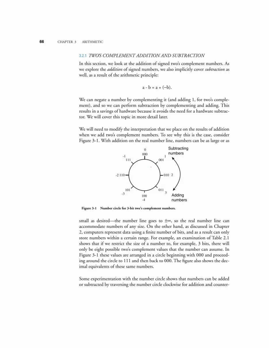
66
CHAPTER 3 ARITHMETIC
3.2.1
TWO’S COMPLEMENT ADDITION AND SUBTRACTION
In this section, we look at the addition of signed two’s complement numbers. Aswe explore the
addition
of signed numbers, we also implicitly cover
subtraction
aswell, as a result of the arithmetic principle:
a - b = a + (
−
b).
We can negate a number by complementing it (and adding 1, for two’s comple-ment), and so we can perform subtraction by complementing and adding. Thisresults in a savings of hardware because it avoids the need for a hardware subtrac-tor. We will cover this topic in more detail later.
We will need to modify the interpretation that we place on the results of additionwhen we add two’s complement numbers. To see why this is the case, considerFigure 3-1. With addition on the real number line, numbers can be as large or as
small as desired—the number line goes to
±∞
, so the real number line canaccommodate numbers of any size. On the other hand, as discussed in Chapter2, computers represent data using a finite number of bits, and as a result can onlystore numbers within a certain range. For example, an examination of Table 2.1shows that if we restrict the size of a number to, for example, 3 bits, there willonly be eight possible two’s complement values that the number can assume. InFigure 3-1 these values are arranged in a circle beginning with 000 and proceed-ing around the circle to 111 and then back to 000. The figure also shows the dec-imal equivalents of these same numbers.
Some experimentation with the number circle shows that numbers can be addedor subtracted by traversing the number circle clockwise for addition and counter-
100
010110
000
111
101 011
001
0
1
2
3
-4
-3
-2
-1
Addingnumbers
Subtractingnumbers
Figure 3-1 Number circle for 3-bit two’s complement numbers.
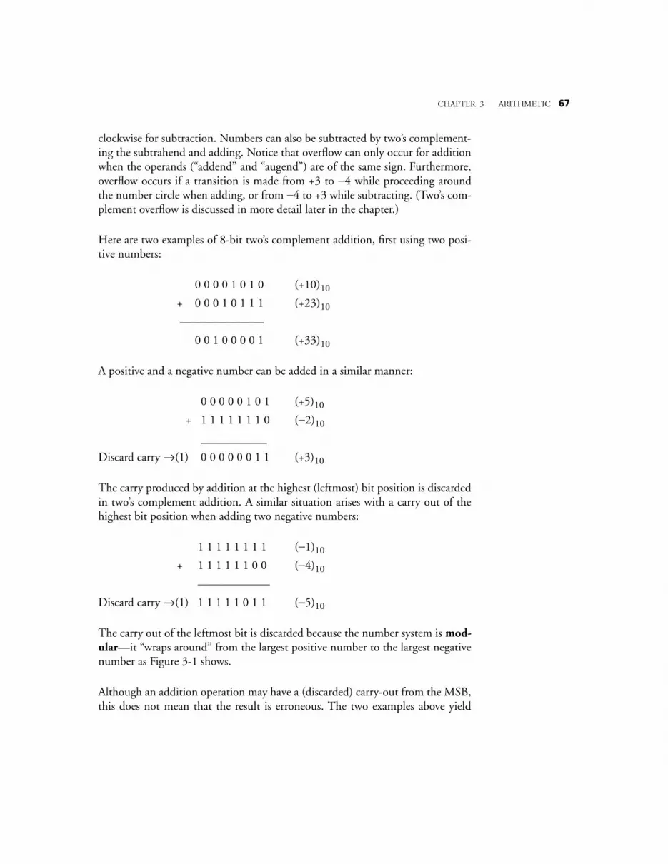
CHAPTER 3 ARITHMETIC
67
clockwise for subtraction. Numbers can also be subtracted by two’s complement-ing the subtrahend and adding. Notice that overflow can only occur for additionwhen the operands (“addend” and “augend”) are of the same sign. Furthermore,overflow occurs if a transition is made from +3 to
−
4 while proceeding aroundthe number circle when adding, or from
−
4 to +3 while subtracting. (Two’s com-plement overflow is discussed in more detail later in the chapter.)
Here are two examples of 8-bit two’s complement addition, first using two posi-tive numbers:
0 0 0 0 1 0 1 0 (+10)
10
+ 0 0 0 1 0 1 1 1 (+23)
10
———————
0 0 1 0 0 0 0 1 (+33)
10
A positive and a negative number can be added in a similar manner:
0 0 0 0 0 1 0 1 (+5)
10
+ 1 1 1 1 1 1 1 0 (
−
2)
10
___________
Discard carry
→
(1) 0 0 0 0 0 0 1 1 (+3)
10
The carry produced by addition at the highest (leftmost) bit position is discardedin two’s complement addition. A similar situation arises with a carry out of thehighest bit position when adding two negative numbers:
1 1 1 1 1 1 1 1 (
−
1)
10
+ 1 1 1 1 1 1 0 0 (
−
4)
10
——————
Discard carry
→
(1) 1 1 1 1 1 0 1 1 (
−
5)
10
The carry out of the leftmost bit is discarded because the number system is
mod-ular
—it “wraps around” from the largest positive number to the largest negativenumber as Figure 3-1 shows.
Although an addition operation may have a (discarded) carry-out from the MSB,this does not mean that the result is erroneous. The two examples above yield
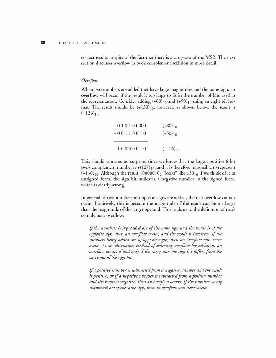
68
CHAPTER 3 ARITHMETIC
correct results in spite of the fact that there is a carry-out of the MSB. The nextsection discusses overflow in two’s complement addition in more detail.
Overflow
When two numbers are added that have large magnitudes and the same sign, an
overflow
will occur if the result is too large to fit in the number of bits used inthe representation. Consider adding (+80)
10
and (+50)
10
using an eight bit for-mat. The result should be (+130)
10
, however, as shown below, the result is(
−
126)
10
:
+ 0 1 0 1 0 0 0 0 (+80)
10
+ 0 0 1 1 0 0 1 0 (+50)
10
———————
+ 1 0 0 0 0 0 1 0 (
−
126)
10
This should come as no surprise, since we know that the largest positive 8-bittwo’s complement number is +(127)
10
, and it is therefore impossible to represent(+130)
10
. Although the result 10000010
2
“looks” like 130
10
if we think of it inunsigned form, the sign bit indicates a negative number in the signed form,which is clearly wrong.
In general, if two numbers of opposite signs are added, then an overflow cannotoccur. Intuitively, this is because the magnitude of the result can be no largerthan the magnitude of the larger operand. This leads us to the definition of two’scomplement overflow:
If the numbers being added are of the same sign and the result is of theopposite sign, then an overflow occurs and the result is incorrect. If thenumbers being added are of opposite signs, then an overflow will neveroccur. As an alternative method of detecting overflow for addition, anoverflow occurs if and only if the carry into the sign bit differs from thecarry out of the sign bit.
If a positive number is subtracted from a negative number and the resultis positive, or if a negative number is subtracted from a positive numberand the result is negative, then an overflow occurs. If the numbers beingsubtracted are of the same sign, then an overflow will never occur.
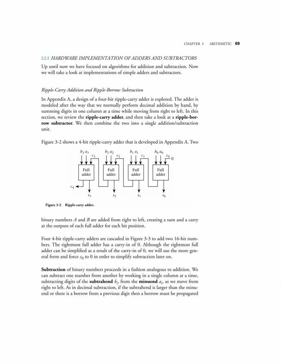
CHAPTER 3 ARITHMETIC
69
3.2.2
HARDWARE IMPLEMENTATION OF ADDERS AND SUBTRACTORS
Up until now we have focused on algorithms for addition and subtraction. Nowwe will take a look at implementations of simple adders and subtractors.
Ripple-Carry Addition and Ripple-Borrow Subtraction
In Appendix A, a design of a four-bit ripple-carry adder is explored. The adder ismodeled after the way that we normally perform decimal addition by hand, bysumming digits in one column at a time while moving from right to left. In thissection, we review the
ripple-carry adder
, and then take a look at a
ripple-bor-row subtractor
. We then combine the two into a single addition/subtractionunit.
Figure 3-2 shows a 4-bit ripple-carry adder that is developed in Appendix A. Two
binary numbers
A
and
B
are added from right to left, creating a sum and a carryat the outputs of each full adder for each bit position.
Four 4-bit ripple-carry adders are cascaded in Figure 3-3 to add two 16-bit num-bers. The rightmost full adder has a carry-in of 0. Although the rightmost fulladder can be simplified as a result of the carry-in of 0, we will use the more gen-eral form and force
c
0
to 0 in order to simplify subtraction later on.
Subtraction
of binary numbers proceeds in a fashion analogous to addition. Wecan subtract one number from another by working in a single column at a time,subtracting digits of the
subtrahend
b
i
, from the
minuend
a
i
, as we move fromright to left. As in decimal subtraction, if the subtrahend is larger than the minu-end or there is a borrow from a previous digit then a borrow must be propagated
Fulladder
b0 a0
s0
Fulladder
b1 a1
s1
Fulladder
b2 a2
s2
Fulladder
b3 a3
c4
s3
0c0c1c2c3
Figure 3-2 Ripple-carry adder.
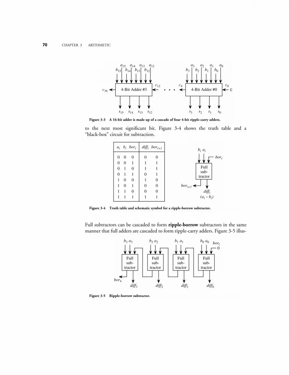
70
CHAPTER 3 ARITHMETIC
to the next most significant bit. Figure 3-4 shows the truth table and a“black-box” circuit for subtraction.
Full subtractors can be cascaded to form
ripple-borrow
subtractors in the samemanner that full adders are cascaded to form ripple-carry adders. Figure 3-5 illus-
s0
b1
a1
s1
b2
a2
s2
b3
a3
c4
s3
04-Bit Adder #0
b0
a0
s12
b13
a13
s13
b14
a14
s14
b15
a15
c16
s15
4-Bit Adder #3
b12
a12
. . .c12 c0
Figure 3-3 A 16-bit adder is made up of a cascade of four 4-bit ripple-carry adders.
00110011
01010101
bi bori
00001111
ai
01101001
diffi
01110001
bori+1
Fullsub-
tractor
bi ai
bori
bori+1
diffi(ai – bi)
Figure 3-4 Truth table and schematic symbol for a ripple-borrow subtractor.
b0 a0
diff0
b1 a1
diff1
b2 a2
diff2
Fullsub-
tractor
b3 a3
bor4
diff3
0
Fullsub-
tractor
Fullsub-
tractor
Fullsub-
tractor
bor0
Figure 3-5 Ripple-borrow subtractor.
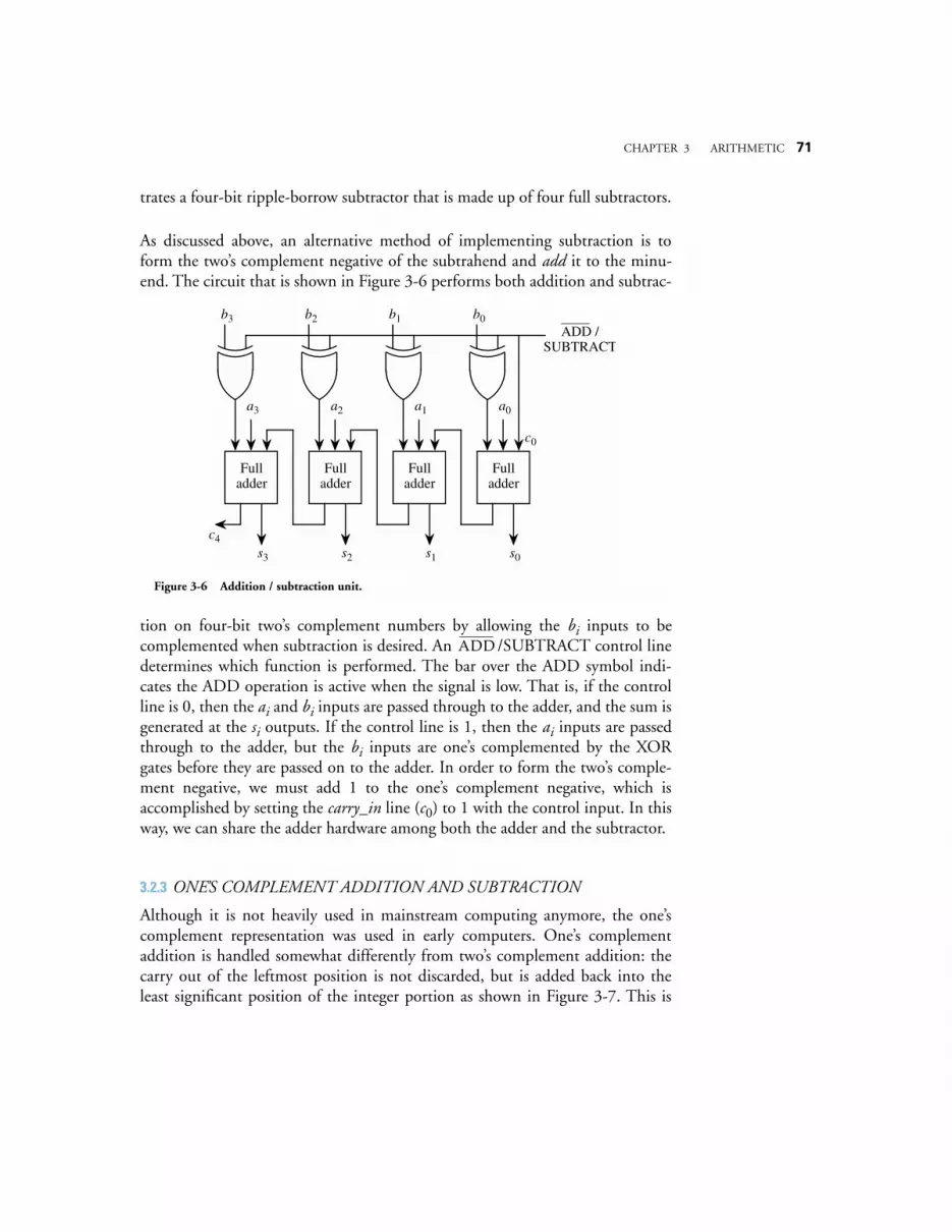
CHAPTER 3 ARITHMETIC
71
trates a four-bit ripple-borrow subtractor that is made up of four full subtractors.
As discussed above, an alternative method of implementing subtraction is toform the two’s complement negative of the subtrahend and
add
it to the minu-end. The circuit that is shown in Figure 3-6 performs both addition and subtrac-
tion on four-bit two’s complement numbers by allowing the
b
i
inputs to becomplemented when subtraction is desired. An /SUBTRACT control linedetermines which function is performed. The bar over the ADD symbol indi-cates the ADD operation is active when the signal is low. That is, if the controlline is 0, then the
a
i
and
b
i
inputs are passed through to the adder, and the sum isgenerated at the
s
i
outputs. If the control line is 1, then the
a
i
inputs are passedthrough to the adder, but the
b
i
inputs are one’s complemented by the XORgates before they are passed on to the adder. In order to form the two’s comple-ment negative, we must add 1 to the one’s complement negative, which isaccomplished by setting the
carry_in
line (
c
0
) to 1 with the control input. In thisway, we can share the adder hardware among both the adder and the subtractor.
3.2.3
ONE’S COMPLEMENT ADDITION AND SUBTRACTION
Although it is not heavily used in mainstream computing anymore, the one’scomplement representation was used in early computers. One’s complementaddition is handled somewhat differently from two’s complement addition: thecarry out of the leftmost position is not discarded, but is added back into theleast significant position of the integer portion as shown in Figure 3-7. This is
Fulladder
b0
a0
s0
Fulladder
b1
a1
s1
Fulladder
b2
a2
s2
Fulladder
b3
a3
c4
s3
c0
ADD /SUBTRACT
Figure 3-6 Addition / subtraction unit.
ADD

72
CHAPTER 3 ARITHMETIC
known as an
end-around carry
.
We can better visualize the reason that the end-around carry is needed by exam-ining the 3-bit one’s complement number circle in Figure 3-8. Notice that the
number circle has two positions for 0. When we add two numbers, if we traversethrough both
−
0 and +0, then we must compensate for the fact that 0 is visitedtwice. The end-around carry advances the result by one position for this situa-tion.
Notice that the distance between
−
0 and +0 on the number circle is the distancebetween two integers, and is
not
the distance between two successive represent-able numbers. As an illustration of this point, consider adding (5.5)
10
and(
−
1.0)
10
in one’s complement arithmetic, which is shown in Figure 3-9. (Notethat we can also treat this as a subtraction problem, in which the subtrahend isnegated by complementing all of the bits, before adding it to the minuend.) In
+
1
10
0
01
0
01
0
10
0
11
0
(–12)10(+13)10
+
0
0
0
0
1
1 (+1)10
End-around carry
Figure 3-7 An example of one’s complement addition with an end-around carry.
100
010110
000
111
101 011
001
+0
1
2
3
-3
-2
-1
-0
Addingnumbers
Subtractingnumbers
Figure 3-8 Number circle for a three-bit signed one’s complement representation.
CHAPTER 3 ARITHMETIC
73
order to add (+5.5)
10
and (
−
1.0)
10
and obtain the correct result in one’s comple-ment, we add the end-around carry into the one’s position as shown. This addscomplexity to our number circle, because in the gap between +0 and
−
0, thereare valid numbers that represent fractions that are less than 0, yet they appear onthe number circle before
−
0 appears. If the number circle is reordered to avoidthis anomaly, then addition must be handled in a more complex manner.
The need to look for two different representations for zero, and the potentialneed to perform another addition for the end-around carry are two importantreasons for preferring the two’s complement arithmetic to one’s complementarithmetic.
3.3 Fixed Point Multiplication and DivisionMultiplication and division of fixed point numbers can be accomplished withaddition, subtraction, and shift operations. The sections that follow describemethods for performing multiplication and division of fixed point numbers inboth unsigned and signed forms using these basic operations. We will first coverunsigned multiplication and division, and then we will cover signed multiplica-tion and division.
3.3.1 UNSIGNED MULTIPLICATION
Multiplication of unsigned binary integers is handled similar to the way it is car-ried out by hand for decimal numbers. Figure 3-10 illustrates the multiplicationprocess for two unsigned binary integers. Each bit of the multiplier determineswhether or not the multiplicand, shifted left according to the position of themultiplier bit, is added into the product. When two unsigned n-bit numbers aremultiplied, the result can be as large as 2n bits. For the example shown in Figure3-10, the multiplication of two four-bit operands results in an eight-bit product.When two signed n-bit numbers are multiplied, the result can be as large as only
1
01
0
11
0
01
1
10
1
.
.
.
(+5.5)10(–1.0)10
+
(+4.5)10
10
1
+
0
1
0
1
0
.
.
0
1
Figure 3-9 The end-around carry complicates addition for non-integers.
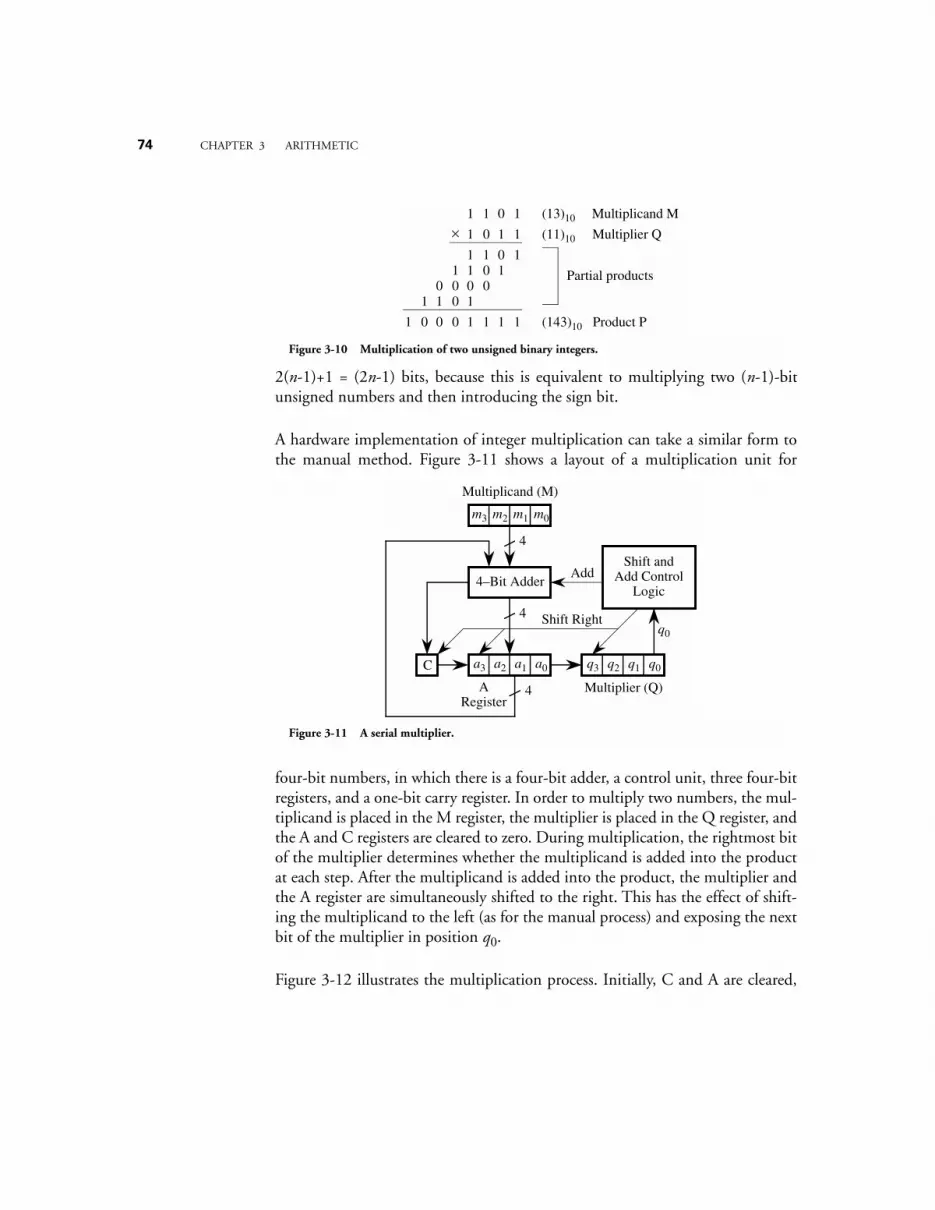
74 CHAPTER 3 ARITHMETIC
2(n-1)+1 = (2n-1) bits, because this is equivalent to multiplying two (n-1)-bitunsigned numbers and then introducing the sign bit.
A hardware implementation of integer multiplication can take a similar form tothe manual method. Figure 3-11 shows a layout of a multiplication unit for
four-bit numbers, in which there is a four-bit adder, a control unit, three four-bitregisters, and a one-bit carry register. In order to multiply two numbers, the mul-tiplicand is placed in the M register, the multiplier is placed in the Q register, andthe A and C registers are cleared to zero. During multiplication, the rightmost bitof the multiplier determines whether the multiplicand is added into the productat each step. After the multiplicand is added into the product, the multiplier andthe A register are simultaneously shifted to the right. This has the effect of shift-ing the multiplicand to the left (as for the manual process) and exposing the nextbit of the multiplier in position q0.
Figure 3-12 illustrates the multiplication process. Initially, C and A are cleared,
1 1 0 1
1 0 1 1×1 1 0 1
1 1 0 10 0 0 0
1 1 0 1
1 0 0 0 1 1 1 1
(11)10
(13)10 Multiplicand M
Multiplier Q
(143)10 Product P
Partial products
Figure 3-10 Multiplication of two unsigned binary integers.
Multiplicand (M)
m0m1m2m3
a0a1a2a3 q0q1q2q3
Multiplier (Q)
C
4–Bit Adder
Shift and Add Control
LogicAdd
4
4
4
Shift Rightq0
A Register
Figure 3-11 A serial multiplier.
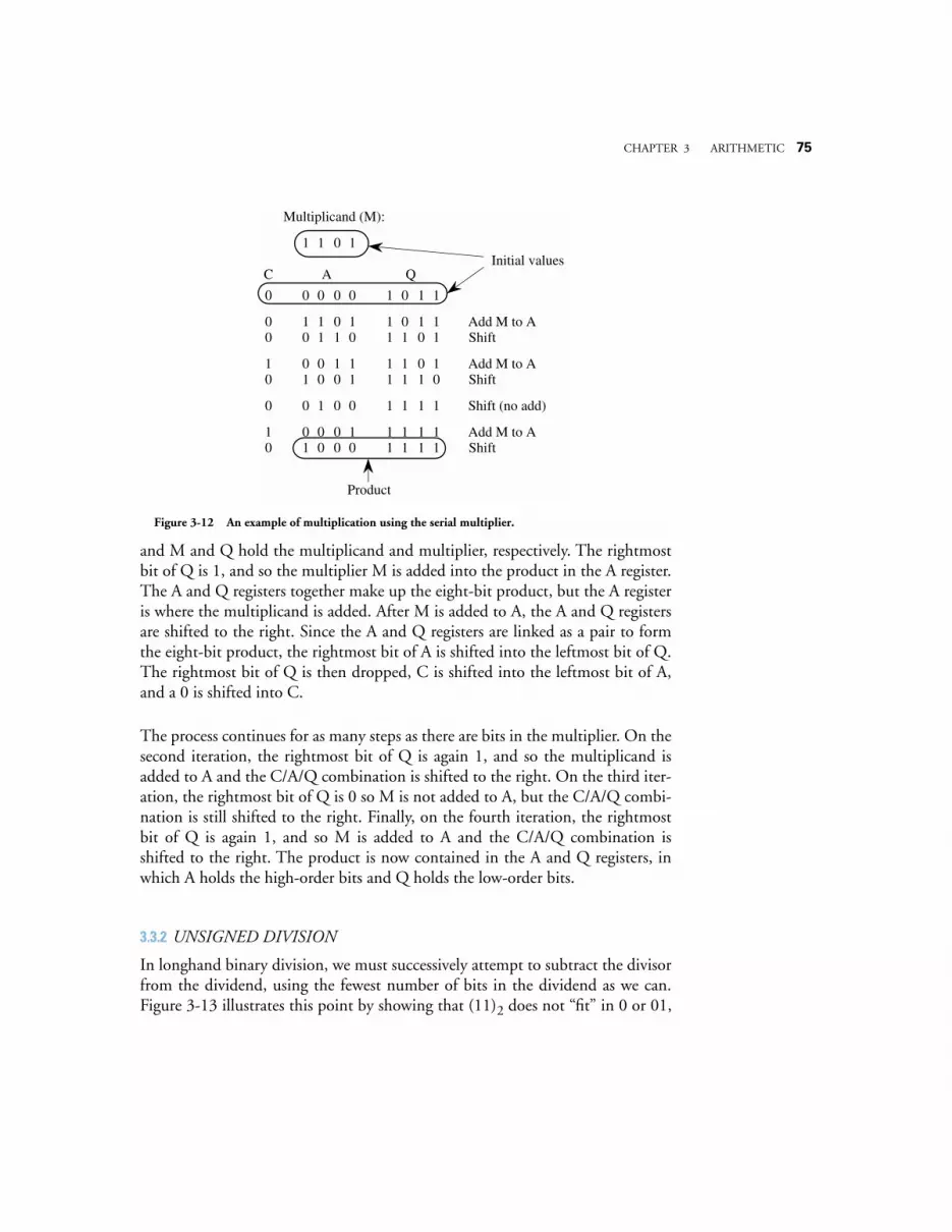
CHAPTER 3 ARITHMETIC 75
and M and Q hold the multiplicand and multiplier, respectively. The rightmostbit of Q is 1, and so the multiplier M is added into the product in the A register.The A and Q registers together make up the eight-bit product, but the A registeris where the multiplicand is added. After M is added to A, the A and Q registersare shifted to the right. Since the A and Q registers are linked as a pair to formthe eight-bit product, the rightmost bit of A is shifted into the leftmost bit of Q.The rightmost bit of Q is then dropped, C is shifted into the leftmost bit of A,and a 0 is shifted into C.
The process continues for as many steps as there are bits in the multiplier. On thesecond iteration, the rightmost bit of Q is again 1, and so the multiplicand isadded to A and the C/A/Q combination is shifted to the right. On the third iter-ation, the rightmost bit of Q is 0 so M is not added to A, but the C/A/Q combi-nation is still shifted to the right. Finally, on the fourth iteration, the rightmostbit of Q is again 1, and so M is added to A and the C/A/Q combination isshifted to the right. The product is now contained in the A and Q registers, inwhich A holds the high-order bits and Q holds the low-order bits.
3.3.2 UNSIGNED DIVISION
In longhand binary division, we must successively attempt to subtract the divisorfrom the dividend, using the fewest number of bits in the dividend as we can.Figure 3-13 illustrates this point by showing that (11)2 does not “fit” in 0 or 01,
C
0
00
10
0
10
0
A
0 0 0
1 1 0 10 1 1 0
0 0 1 11 0 0 1
0 1 0 0
0 0 0 11 0 0 0
1
Q
0 1 1
1 0 1 11 1 0 1
1 1 0 11 1 1 0
1 1 1 1
1 1 1 11 1 1 1
Multiplicand (M):
1 1 0 1Initial values
Add M to AShift
Add M to AShift
Shift (no add)
Add M to AShift
Product
Figure 3-12 An example of multiplication using the serial multiplier.
76 CHAPTER 3 ARITHMETIC
but does fit in 011 as indicated by the pattern 001 that starts the quotient.
Computer-based division of binary integers can be handled similar to the waythat binary integer multiplication is carried out, but with the complication thatthe only way to tell if the dividend does not “fit” is to actually do the subtractionand test if the remainder is negative. If the remainder is negative then the sub-traction must be “backed out” by adding the divisor back in, as described below.
In the division algorithm, instead of shifting the product to the right as we didfor multiplication, we now shift the quotient to the left, and we subtract insteadof adding. When two n-bit unsigned numbers are being divided, the result is nolarger than n bits.
Figure 3-14 shows a layout of a division unit for four-bit numbers in which there
is a five-bit adder, a control unit, a four-bit register for the dividend Q, and twofive-bit registers for the divisor M and the remainder A. Five-bit registers are usedfor A and M, instead of 4-bit registers as we might expect, because an extra bit is
1 1
0 0 1 0
0 1 1 11 1
0
R 1
1
Figure 3-13 Example of base 2 division.
Divisor (M)
m0m1m2m3
a0a1a2a3 q0q1q2q3
Dividend (Q)
5–Bit Adder
Shift andAdd / Sub
Control LogicAdd /
Sub
5
5
5
Shift Leftq0
A Register
a4
0
a4
Figure 3-14 A serial divider.
CHAPTER 3 ARITHMETIC 77
needed to indicate the sign of the intermediate result. Although this divisionmethod is for unsigned numbers, subtraction is used in the process and negativepartial results sometimes arise, which extends the range from −16 through +15,thus there is a need for 5 bits to store intermediate results.
In order to divide two four-bit numbers, the dividend is placed in the Q register,the divisor is placed in the M register, and the A register and the high order bit ofM are cleared to zero. The leftmost bit of the A register determines whether thedivisor is added back into the dividend at each step. This is necessary in order torestore the dividend when the result of subtracting the divisor is negative, asdescribed above. This is referred to as restoring division, because the dividend isrestored to its former value when the remainder is negative. When the result isnot negative, then the least significant bit of Q is set to 1, which indicates thatthe divisor “fits” in the dividend at that point.
Figure 3-15 illustrates the division process. Initially, A and the high order bit ofM are cleared, and Q and the low order bits of M are loaded with the dividendand divisor, respectively. The A and Q registers are shifted to the left as a pair andthe divisor M is subtracted from A. Since the result is negative, the divisor isadded back to restore the dividend, and q0 is cleared to 0. The process repeats byshifting A and Q to the left, and by subtracting M from A. Again, the result isnegative, so the dividend is restored and q0 is cleared to 0. On the third iteration,A and Q are shifted to the left and M is again subtracted from A, but now theresult of the subtraction is not negative, so q0 is set to 1. The process continuesfor one final iteration, in which A and Q are shifted to the left and M is sub-tracted from A, which produces a negative result. The dividend is restored and q0is cleared to 0. The quotient is now contained in the Q register and the remain-der is contained in the A register.
3.3.3 SIGNED MULTIPLICATION AND DIVISION
If we apply the multiplication and division methods described in the previoussections to signed integers, then we will run into some trouble. Consider multi-plying −1 by +1 using four-bit words, as shown in the left side of Figure 3-16.The eight-bit equivalent of +15 is produced instead of −1. What went wrong isthat the sign bit did not get extended to the left of the result. This is not a prob-lem for a positive result because the high order bits default to 0, producing thecorrect sign bit 0.
A solution is shown in the right side of Figure 3-16, in which each partial prod-
78 CHAPTER 3 ARITHMETIC
uct is extended to the width of the result, and only the rightmost eight bits of theresult are retained. If both operands are negative, then the signs are extended forboth operands, again retaining only the rightmost eight bits of the result.
Signed division is more difficult. We will not explore the methods here, but as a
0
01
00
0
A
0 0 0
0 0 0 01 1 0 1
0 0 1 10 0 0 0
0
Q
1 1 1
1 1 1 01 1 1 0
1 0 0 01 0 0 0
Divisor (M):
0 0 1 1Initial values
Shift leftSubtract M from A
Shift leftSubtract M from A
0 0 0 0 0 1 1 1 0 Restore A (Add M to A)
01
0 0 0 11 1 1 0
1 1 0 01 1 0 0
Shift leftSubtract M from A
0 0 0 0 1 1 1 0 0 Restore A
0 0 0 0 0 1 1 1 0 Clear q0
0 0 0 0 1 1 1 0 0 Clear q0
0 0 0 0 0 1 0 0 1 Set q0
01
0 0 0 11 1 1 0
0 0 1 00 0 1 0
Shift leftSubtract M from A
0 0 0 0 1 0 0 1 0 Restore A0 0 0 0 1 0 0 1 0 Clear q0
Remainder Quotient
0
Figure 3-15 An example of division using the serial divider.
1 1 1 1
0 0 0 1×1 1 1 1
0 0 0 00 0 0 0
0 0 0 0
0 0 0 0 1 1 1 1
(+1)10
(–1)10
(+15)10
(Incorrect; result should be –1)
1 1 1 1
0 0 0 1×1 1 1 1
0 0 0 00 0 0 0
0 0 0 0
1 1 1 1 1 1 1 1
(+1)10
(–1)10
(–1)10
1 1 1 1
1 1 1 10 0 00 00
Figure 3-16 Multiplication of signed integers.

CHAPTER 3 ARITHMETIC 79
general technique, we can convert the operands into their positive forms, per-form the division, and then convert the result into its true signed form as a finalstep.
3.4 Floating Point ArithmeticArithmetic operations on floating point numbers can be carried out using thefixed point arithmetic operations described in the previous sections, with atten-tion given to maintaining aspects of the floating point representation. In the sec-tions that follow, we explore floating point arithmetic in base 2 and base 10,keeping the requirements of the floating point representation in mind.
3.4.1 FLOATING POINT ADDITION AND SUBTRACTION
Floating point arithmetic differs from integer arithmetic in that exponents mustbe handled as well as the magnitudes of the operands. As in ordinary base 10arithmetic using scientific notation, the exponents of the operands must be madeequal for addition and subtraction. The fractions are then added or subtracted asappropriate, and the result is normalized.
This process of adjusting the fractional part, and also rounding the result canlead to a loss of precision in the result. Consider the unsigned floating pointaddition (.101 × 23 + .111 × 24) in which the fractions have three significant dig-its. We start by adjusting the smaller exponent to be equal to the larger exponent,and adjusting the fraction accordingly. Thus we have .101 × 23 = .010 × 24, los-ing .001 × 23 of precision in the process. The resulting sum is
(.010 + .111) × 24 = 1.001 × 24 = .1001 × 25,
and rounding to three significant digits, .100 × 25, and we have lost another0.001 × 24 in the rounding process.
Why do floating point numbers have such complicated formats?
We may wonder why floating point numbers have such a complicated structure,with the mantissa being stored in signed magnitude representation, the exponentstored in excess notation, and the sign bit separated from the rest of the magni-tude by the intervening exponent field. There is a simple explanation for thisstructure. Consider the complexity of performing floating point arithmetic in acomputer. Before any arithmetic can be done, the number must be unpacked
80 CHAPTER 3 ARITHMETIC
from the form it takes in storage. (See Chapter 2 for a description of the IEEE754 floating point format.) The exponent and mantissa must be extracted fromthe packed bit pattern before an arithmetic operation can be performed; after thearithmetic operation(s) are performed, the result must be renormalized androunded, and then the bit patterns are re-packed into the requisite format.
The virtue of a floating point format that contains a sign bit followed by anexponent in excess notation, followed by the magnitude of the mantissa, is thattwo floating point numbers can be compared for >, <, and = without unpacking.The sign bit is most important in such a comparison, and it appropriately is theMSB in the floating point format. Next most important in comparing two num-bers is the exponent, since a change of ± 1 in the exponent changes the value by afactor of 2 (for a base 2 format), whereas a change in even the MSB of the frac-tional part will change the value of the floating point number by less than that.
In order to account for the sign bit, the signed magnitude fractions are repre-sented as integers and are converted into two’s complement form. After the addi-tion or subtraction operation takes place in two’s complement, there may be aneed to normalize the result and adjust the sign bit. The result is then convertedback to signed magnitude form.
3.4.2 FLOATING POINT MULTIPLICATION AND DIVISION
Floating point multiplication and division are performed in a manner similar tofloating point addition and subtraction, except that the sign, exponent, and frac-tion of the result can be computed separately. If the operands have the same sign,then the sign of the result is positive. Unlike signs produce a negative result. Theexponent of the result before normalization is obtained by adding the exponentsof the source operands for multiplication, or by subtracting the divisor exponentfrom the dividend exponent for division. The fractions are multiplied or dividedaccording to the operation, followed by normalization.
Consider using three-bit fractions in performing the base 2 computation: (+.101× 22) × (−.110 × 2-3). The source operand signs differ, which means that theresult will have a negative sign. We add exponents for multiplication, and so theexponent of the result is 2 + −3 = −1. We multiply the fractions, which producesthe product .01111. Normalizing the product and retaining only three bits in thefraction produces −.111 × 2−2.
Now consider using three-bit fractions in performing the base 2 computation:

CHAPTER 3 ARITHMETIC 81
(+.110 × 25) / (+.100 × 24). The source operand signs are the same, which meansthat the result will have a positive sign. We subtract exponents for division, andso the exponent of the result is 5 – 4 = 1. We divide fractions, which can be donein a number of ways. If we treat the fractions as unsigned integers, then we willhave 110/100 = 1 with a remainder of 10. What we really want is a contiguousset of bits representing the fraction instead of a separate result and remainder,and so we can scale the dividend to the left by two positions, producing theresult: 11000/100 = 110. We then scale the result to the right by two positions torestore the original scale factor, producing 1.1. Putting it all together, the resultof dividing (+.110 × 25) by (+.100 × 24) produces (+1.10 × 21). After normaliza-tion, the final result is (+.110 × 22).
3.5 High Performance ArithmeticFor many applications, the speed of arithmetic operations are the bottleneck toperformance. Most supercomputers, such as the Cray, the Tera, and the IntelHypercube are considered “super” because they excel at performing fixed andfloating point arithmetic. In this section we discuss a number of ways to improvethe speed of addition, subtraction, multiplication, and division.
3.5.1 HIGH PERFORMANCE ADDITION
The ripple-carry adder that we reviewed in Section 3.2.2 may introduce toomuch delay into a system. The longest path through the adder is from the inputsof the least significant full adder to the outputs of the most significant full adder.The process of summing the inputs at each bit position is relatively fast (a smalltwo-level circuit suffices) but the carry propagation takes a long time to work itsway through the circuit. In fact, the propagation time is proportional to thenumber of bits in the operands. This is unfortunate, since more significant fig-ures in an addition translates to more time to perform the addition. In this sec-tion, we look at a method of speeding the carry propagation in what is known asa carry lookahead adder.
In Appendix B, reduced Boolean expressions for the sum (si) and carry outputs(ci+1) of a full adder are created. These expressions are repeated below, with sub-scripts added to denote the relative position of a full adder in a ripple-carryadder:
si aibici aibici aibici aibici+ + +=

82 CHAPTER 3 ARITHMETIC
We can factor the second equation and obtain:
which can be rewritten as:
where: Gi = aibi and Pi = ai + bi.
The Gi and Pi terms are referred to as generate and propagate functions, respec-tively, for the effect they have on the carry. When Gi = 1, a carry is generated atstage i. When Pi = 1, then a carry is propagated through stage i if either ai or bi isa 1. The Gi and Pi terms can be created in one level of logic since they onlydepend on an AND or an OR of the input variables, respectively.
The carries again take the most time. The carry c1 out of stage 0 is G0 + P0c0, andsince c0 = 0 for addition, we can rewrite this as c1 = G0. The carry c2 out of stage1 is G1 + P1c1, and since c1 = G0, we can rewrite this as: c2 = G1 + P1G0. Thecarry c3 out of stage 2 is G2 + P2c2, and since c2 = G1 + P1G0, we can rewrite thisas: c3 = G2 + P2G1 + P2P1G0. Continuing one more time for a four-bit adder, thecarry out of stage 3 is G3 + P3c3, and since c3 = G2 + P2G1 + P2P1G0, we canrewrite this as: c4 = G3 + P3G2 + P3P2G1 + P3P2P1G0.
We can now create a four-bit carry lookahead adder as shown in Figure 3-17. Westill have the delay through the full adders as before, but now the carry chain isbroken into independent pieces that require one gate delay for Gi and Pi and twomore gate delays to generate ci+1. Thus, a depth of three gate delays is added, butthe ripple-carry chain is removed. If we assume that each full adder introduces agate delay of two, then a four-bit carry lookahead adder will have a maximumgate delay of five, whereas a four-bit ripple-carry adder will have a maximum gatedelay of eight. The difference between the two approaches is more pronouncedfor wider operands. This process is limited to about eight bits of carry-lookahead,because of gate fanin limitations discussed in Appendix A. For additions of num-bers having more than eight bits, the carry-lookahead circuits can be cascaded tocompute the carry in and carry out of each carry-lookahead unit. (See theEXAMPLE at the end of the chapter.)
ci 1+ bici aici aibi+ +=
ci 1+ aibi ai bi+( )ci+=
ci 1+ Gi Pici+=
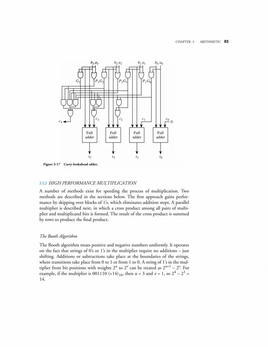
CHAPTER 3 ARITHMETIC 83
3.5.2 HIGH PERFORMANCE MULTIPLICATION
A number of methods exist for speeding the process of multiplication. Twomethods are described in the sections below. The first approach gains perfor-mance by skipping over blocks of 1’s, which eliminates addition steps. A parallelmultiplier is described next, in which a cross product among all pairs of multi-plier and multiplicand bits is formed. The result of the cross product is summedby rows to produce the final product.
The Booth Algorithm
The Booth algorithm treats positive and negative numbers uniformly. It operateson the fact that strings of 0’s or 1’s in the multiplier require no additions – justshifting. Additions or subtractions take place at the boundaries of the strings,where transitions take place from 0 to 1 or from 1 to 0. A string of 1’s in the mul-tiplier from bit positions with weights 2u to 2v can be treated as 2u+1 – 2v. Forexample, if the multiplier is 001110 (+14)10, then u = 3 and v = 1, so 24 – 21 =14.
Fulladder
s0
Fulladder
s1
Fulladder
s2
Fulladder
s3
0c0
b3 a3b3 a3 b2 a2 b1 a1 b0 a0
G0P1G1P2G2
c1c2c3
P3G3
c4
Figure 3-17 Carry-lookahead adder.

84 CHAPTER 3 ARITHMETIC
In a hardware implementation, the multiplier is scanned from right to left. Thefirst transition is observed going from 0 to 1, and so 21 is subtracted from the ini-tial value (0). On the next transition, from 1 to 0, 24 is added, which results in+14. A 0 is considered to be appended to the right side of the multiplier in orderto define the situation in which a 1 is in the rightmost digit of the multiplier.
If the multiplier is recoded according to the Booth algorithm, then fewer stepsmay be needed in the multiplication process. Consider the multiplication exam-ple shown in Figure 3-18. The multiplier (14)10 contains three 1’s, which means
that three addition operations are required for the shift/add multiplication proce-dure that is described in Section 3.3.1. The Booth recoded multiplier is obtainedby scanning the original multiplier from right to left, and placing a −1 in theposition where the first 1 in a string is encountered, and placing a +1 in the posi-tion where the next 0 is seen. The multiplier 001110 thus becomes 0 +1 0 0 −10. The Booth recoded multiplier contains just two nonzero digits: +1 and −1,which means that only one addition operation and one subtraction operation areneeded, and so a savings is realized for this example.
A savings is not always realized, however, and in some cases the Booth algorithmmay cause more operations to take place than if it is not used at all. Consider theexample shown in Figure 3-19, in which the multiplier consists of alternating 1’sand 0’s. This is the same example shown in Figure 3-18 but with the multipli-cand and multiplier swapped. Without Booth recoding of the multiplier, threeaddition operations are required for the three 1’s in the multiplier. The Boothrecoded multiplier, however, requires six addition and subtraction operations,which is clearly worse. We improve on this in the next section.
0 1 0 1
1 1 1 0
1 0 1 1
1
(14)10
(21)10 Multiplicand
Multiplier
(294)10 Product
1
0
0
0
0
1
0 0 −1 0× Booth recoded multiplier
+10
ShiftAdd
ShiftSubtract
Shift
1111
01010
0 0 1 11001000
(−21 × 2)10
(21 × 16)10
1
00
0
0
0
000
Figure 3-18 Multiplication of signed integers.
CHAPTER 3 ARITHMETIC 85
The Modified Booth Algorithm
One solution to this problem is to group the recoded multiplier bits in pairs,known as bit pair recoding, which is also known as the modified Booth algo-rithm. Grouping bit pairs from right to left produces three “+1,−1” pairs asshown in Figure 3-20. Since the +1 term is to the left of the −1 term, it has a
weight that is twice as large as the weight for the −1 position. Thus, we mightthink of the pair as having the collective value +2 – 1 = +1.
In a similar manner, the pair −1,+1 is equivalent to −2 + 1 = −1. The pairs +1,+1and −1,−1 cannot occur. There are a total of seven pairs that can occur, which areshown in Figure 3-21. For each case, the value of the recoded bit pair is multi-
1 1 1 0
0 1 0 1
1 0 0 1
1
(21)10
(14)10 Multiplicand
Multiplier
(294)10 Product
0
1
1
0
0
1
+1 −1 +1 −1× Booth recoded multiplier
−1+1
Add
Subtract
1111
00000
0 0 1 11001000
(−14 × 1)10
(14 × 2)10
1
00
0
0
0
011
1 0 0 1
1
11111
00000 0
0
011
1 0 0 1
1
111
000 0
0
011 0
0
0
0
0
0
0
0
0
0
0
0 (−14 × 4)10
(14 × 8)10
(−14 × 16)10
(14 × 32)10
Figure 3-19 A worst case Booth recoded multiplication example.
1 1 1 0
0 1 0 1
0
(14)10
(21)10 Multiplicand
Multiplier
(294)10 Product
0
1
0
0
+1 −1 +1 −1× Booth recoded multiplier−1+1
00000
0 0 1 11001000
(14 × 1)1000
0
0111
0 1 1 1
1
00000
10000 0
0
001 0
0
0
0 (14 × 4)10
(14 × 16)10
Bit pair recoded multiplier+1 +1+1
Figure 3-20 Multiplication with bit-pair recoding of the multiplier.
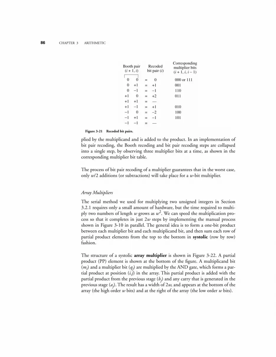
86 CHAPTER 3 ARITHMETIC
plied by the multiplicand and is added to the product. In an implementation ofbit pair recoding, the Booth recoding and bit pair recoding steps are collapsedinto a single step, by observing three multiplier bits at a time, as shown in thecorresponding multiplier bit table.
The process of bit pair recoding of a multiplier guarantees that in the worst case,only w/2 additions (or subtractions) will take place for a w-bit multiplier.
Array Multipliers
The serial method we used for multiplying two unsigned integers in Section3.2.1 requires only a small amount of hardware, but the time required to multi-ply two numbers of length w grows as w2. We can speed the multiplication pro-cess so that it completes in just 2w steps by implementing the manual processshown in Figure 3-10 in parallel. The general idea is to form a one-bit productbetween each multiplier bit and each multiplicand bit, and then sum each row ofpartial product elements from the top to the bottom in systolic (row by row)fashion.
The structure of a systolic array multiplier is shown in Figure 3-22. A partialproduct (PP) element is shown at the bottom of the figure. A multiplicand bit(mi) and a multiplier bit (qj) are multiplied by the AND gate, which forms a par-tial product at position (i,j) in the array. This partial product is added with thepartial product from the previous stage (bj) and any carry that is generated in theprevious stage (aj). The result has a width of 2w, and appears at the bottom of thearray (the high order w bits) and at the right of the array (the low order w bits).
000
+1+1+1−1−1−1
0+1−1
0+1−1
0+1−1
=========
0+1−1+2––+1−2−1––
Recoded bit pair (i)
Booth pair(i + 1, i)
Corresponding multiplier bits (i + 1, i, i − 1)
000 or 111001110011
010100101
Figure 3-21 Recoded bit pairs.
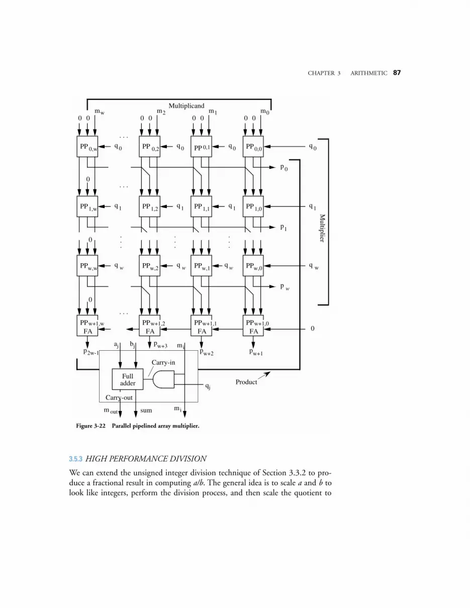
CHAPTER 3 ARITHMETIC 87
3.5.3 HIGH PERFORMANCE DIVISION
We can extend the unsigned integer division technique of Section 3.3.2 to pro-duce a fractional result in computing a/b. The general idea is to scale a and b tolook like integers, perform the division process, and then scale the quotient to
. . .
q 0 q 0 q 0 q 0
0 0 0 0 0 0 0 0m0m1m2mw
Multiplicand
0. . .
p 0
q 1 q 1 q 1 q 1
p1
q w q w q w q w
. . .
0
p2w-1
pw+3pw+2 pw+1
0
p w
.
.
.
.
.
.
.
.
.
Multiplier
Product
0
Fulladder
Carry-in
Carry-out
sum
qj
aj bj
m out
mi
mi
PP 0,w PP 0,2 PP 0,1 PP0,0
PP1,w PP1,2 PP1,1 PP1,0
PPw,w PPw,2 PPw,1 PPw,0
FA FA FA FAw+1,0w+1,1w+1,2w+1,wPP PP PP PP
Figure 3-22 Parallel pipelined array multiplier.
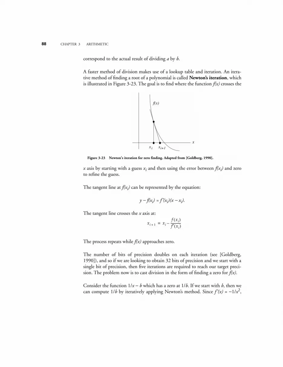
88 CHAPTER 3 ARITHMETIC
correspond to the actual result of dividing a by b.
A faster method of division makes use of a lookup table and iteration. An itera-tive method of finding a root of a polynomial is called Newton’s iteration, whichis illustrated in Figure 3-23. The goal is to find where the function f(x) crosses the
x axis by starting with a guess xi and then using the error between f(xi) and zeroto refine the guess.
The tangent line at f(xi) can be represented by the equation:
y − f(xi) = f ’(xi)(x − xi).
The tangent line crosses the x axis at:
The process repeats while f(x) approaches zero.
The number of bits of precision doubles on each iteration (see [Goldberg,1990]), and so if we are looking to obtain 32 bits of precision and we start with asingle bit of precision, then five iterations are required to reach our target preci-sion. The problem now is to cast division in the form of finding a zero for f(x).
Consider the function 1/x − b which has a zero at 1/b. If we start with b, then wecan compute 1/b by iteratively applying Newton’s method. Since f ’(x) = −1/x2,
f(x)
xxi+1x i
Figure 3-23 Newton’s iteration for zero finding. Adapted from [Goldberg, 1990].
xi 1+ xif xi( )f′ xi( )--------------–=
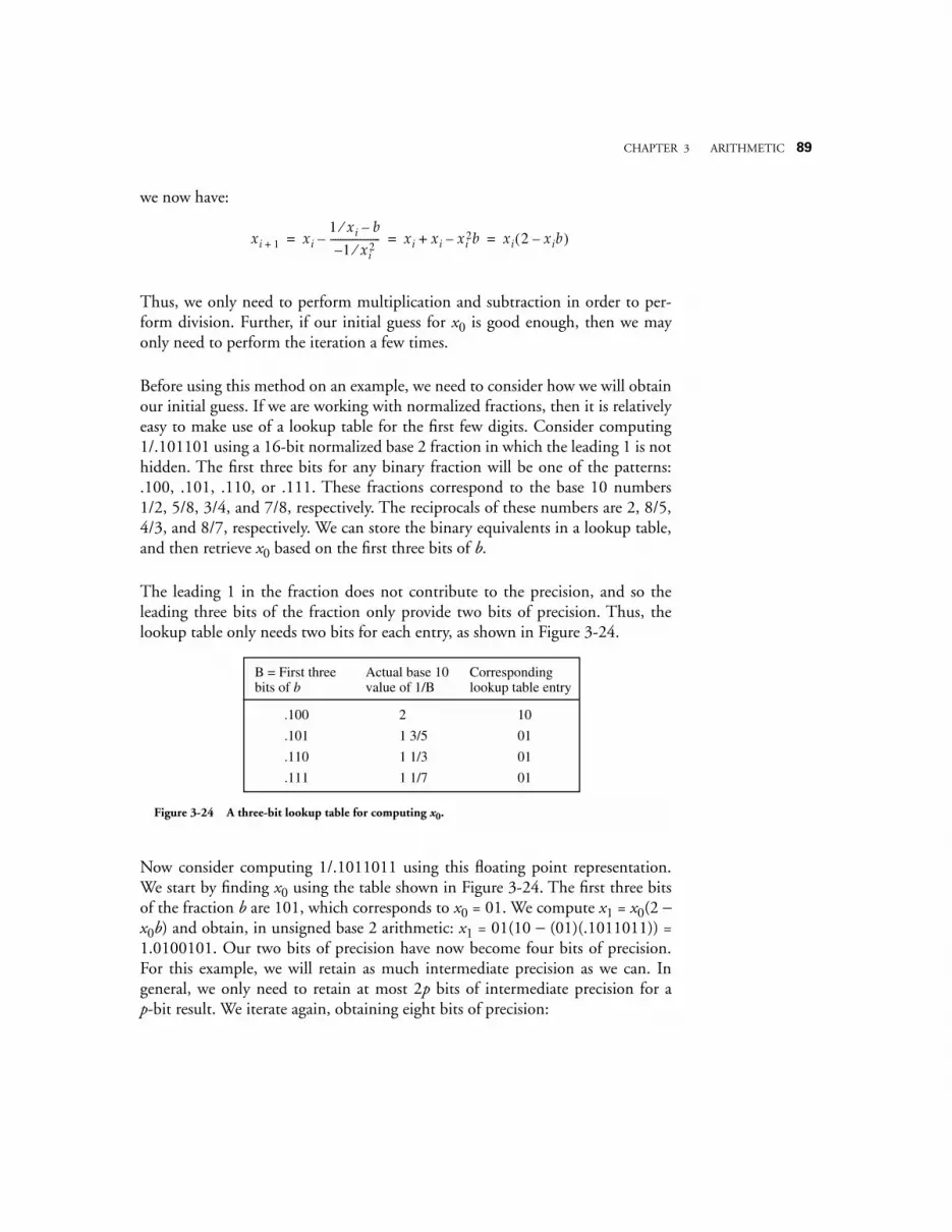
CHAPTER 3 ARITHMETIC 89
we now have:
Thus, we only need to perform multiplication and subtraction in order to per-form division. Further, if our initial guess for x0 is good enough, then we mayonly need to perform the iteration a few times.
Before using this method on an example, we need to consider how we will obtainour initial guess. If we are working with normalized fractions, then it is relativelyeasy to make use of a lookup table for the first few digits. Consider computing1/.101101 using a 16-bit normalized base 2 fraction in which the leading 1 is nothidden. The first three bits for any binary fraction will be one of the patterns:.100, .101, .110, or .111. These fractions correspond to the base 10 numbers1/2, 5/8, 3/4, and 7/8, respectively. The reciprocals of these numbers are 2, 8/5,4/3, and 8/7, respectively. We can store the binary equivalents in a lookup table,and then retrieve x0 based on the first three bits of b.
The leading 1 in the fraction does not contribute to the precision, and so theleading three bits of the fraction only provide two bits of precision. Thus, thelookup table only needs two bits for each entry, as shown in Figure 3-24.
Now consider computing 1/.1011011 using this floating point representation.We start by finding x0 using the table shown in Figure 3-24. The first three bitsof the fraction b are 101, which corresponds to x0 = 01. We compute x1 = x0(2 −x0b) and obtain, in unsigned base 2 arithmetic: x1 = 01(10 − (01)(.1011011)) =1.0100101. Our two bits of precision have now become four bits of precision.For this example, we will retain as much intermediate precision as we can. Ingeneral, we only need to retain at most 2p bits of intermediate precision for ap-bit result. We iterate again, obtaining eight bits of precision:
xi 1+ xi1 xi⁄ b–
1 xi2⁄–
--------------------– xi xi xi2–+ b xi 2 xib–( )= = =
.100 2 10
B = First three bits of b
Corresponding lookup table entry
Actual base 10 value of 1/B
.101 1 3/5 01
.110 1 1/3 01
.111 1 1/7 01
Figure 3-24 A three-bit lookup table for computing x0.
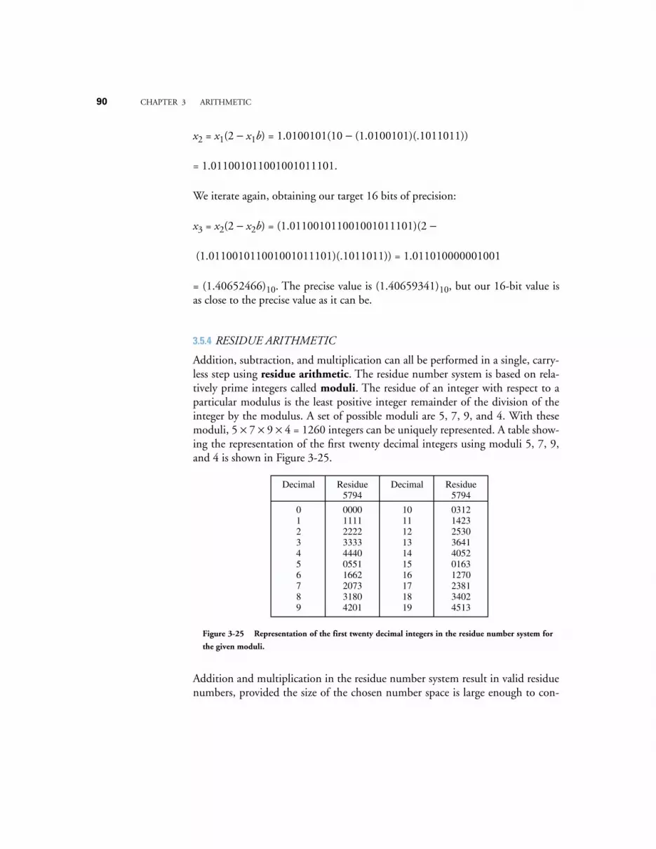
90 CHAPTER 3 ARITHMETIC
x2 = x1(2 − x1b) = 1.0100101(10 − (1.0100101)(.1011011))
= 1.011001011001001011101.
We iterate again, obtaining our target 16 bits of precision:
x3 = x2(2 − x2b) = (1.011001011001001011101)(2 −
(1.011001011001001011101)(.1011011)) = 1.011010000001001
= (1.40652466)10. The precise value is (1.40659341)10, but our 16-bit value isas close to the precise value as it can be.
3.5.4 RESIDUE ARITHMETIC
Addition, subtraction, and multiplication can all be performed in a single, carry-less step using residue arithmetic. The residue number system is based on rela-tively prime integers called moduli. The residue of an integer with respect to aparticular modulus is the least positive integer remainder of the division of theinteger by the modulus. A set of possible moduli are 5, 7, 9, and 4. With thesemoduli, 5 × 7 × 9 × 4 = 1260 integers can be uniquely represented. A table show-ing the representation of the first twenty decimal integers using moduli 5, 7, 9,and 4 is shown in Figure 3-25.
Addition and multiplication in the residue number system result in valid residuenumbers, provided the size of the chosen number space is large enough to con-
Decimal Residue Decimal Residue5794
0 0000 10 0312
5794
1 1111 11 14232 2222 12 25303 3333 13 36414 4440 14 40525 0551 15 01636 1662 16 12707 2073 17 23818 3180 18 34029 4201 19 4513
Figure 3-25 Representation of the first twenty decimal integers in the residue number system for
the given moduli.
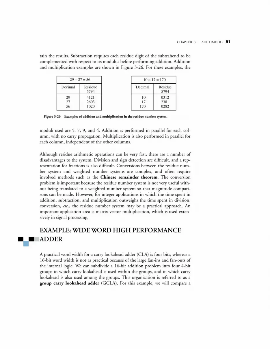
CHAPTER 3 ARITHMETIC 91
tain the results. Subtraction requires each residue digit of the subtrahend to becomplemented with respect to its modulus before performing addition. Additionand multiplication examples are shown in Figure 3-26. For these examples, the
moduli used are 5, 7, 9, and 4. Addition is performed in parallel for each col-umn, with no carry propagation. Multiplication is also performed in parallel foreach column, independent of the other columns.
Although residue arithmetic operations can be very fast, there are a number ofdisadvantages to the system. Division and sign detection are difficult, and a rep-resentation for fractions is also difficult. Conversions between the residue num-ber system and weighted number systems are complex, and often requireinvolved methods such as the Chinese remainder theorem. The conversionproblem is important because the residue number system is not very useful with-out being translated to a weighted number system so that magnitude compari-sons can be made. However, for integer applications in which the time spent inaddition, subtraction, and multiplication outweighs the time spent in division,conversion, etc., the residue number system may be a practical approach. Animportant application area is matrix-vector multiplication, which is used exten-sively in signal processing.
EXAMPLE: WIDE WORD HIGH PERFORMANCE ADDER
A practical word width for a carry lookahead adder (CLA) is four bits, whereas a16-bit word width is not as practical because of the large fan-ins and fan-outs ofthe internal logic. We can subdivide a 16-bit addition problem into four 4-bitgroups in which carry lookahead is used within the groups, and in which carrylookahead is also used among the groups. This organization is referred to as agroup carry lookahead adder (GCLA). For this example, we will compare a
Decimal Residue5794
29 412127 260356 1020
29 + 27 = 56
Decimal Residue5794
10 031217 2381
170 0282
10 × 17 = 170
Figure 3-26 Examples of addition and multiplication in the residue number system.

92 CHAPTER 3 ARITHMETIC
16-bit CLA with a 16-bit GCLA in terms of gate delays, fan-ins, and fan-outs.
Figure 3-27 shows a 16-bit GCLA that is composed of four 4-bit CLAs, with
some additional logic that generates the carries between the four-bit groups.Each group behaves as an ordinary CLA, except that the least significant carryinto each CLA is treated as a variable instead of as a 0, and that group generate(GG) and group propagate (GP) signals are generated. A GG signal is generatedwhen a carry is generated somewhere within a group, and all of the more signifi-cant propagate signals are true. This means that a carry into a group will propa-gate all the way through the group. The corresponding equations for the leastsignificant GG and GP signals in Figure 3-27 are shown below:
GG0 = G3 + P3G2 + P3P2G1 + P3P2P1G0
GP0 = P3P2P1P0
The remaining GG and GP signals are computed similarly.
The carry into each group, except for the carry into CLA0, is computed from theGG and GP signals. For example, c4 is true when GG0 is true or when GP0 andc0 are both true. The corresponding equation is:
c4 = GG0 + GP0c0.
c16Group Carry Lookahead Logic
CLA0
4
a0 – a3
4
b0 – b3
4
s0 – s3
GG0GP0
CLA1
4
a4 – a7
4
b4 – b7
4
s4 – s7
GG1GP1
CLA2
4
a8 – a11
4
b8 – b11
4
s8 – s11
GG2GP2
CLA3
4
a12 – a15
4
b12 – b15
4
s12 – s15
GG3GP3
c4c8c12
c0
Figure 3-27 A 16-bit group carry lookahead adder.
CHAPTER 3 ARITHMETIC 93
Higher order carries out of each group are computed in a similar manner:
c8 = GG1 + GP1c4 = GG1 + GP1GG0 + GP1GP0c0.
c12 = GG2 + GP2c8 = GG2 + GP2GG1 + GP2GP1GG0 +
GP2GP1GP0c0.
c16 = GG3 + GP3c12 = GG3 + GP3GG2 + GP3GP2GG1 +
GP3GP2GP1GG0 + GP3GP2GP1GP0c0.
In terms of gate delays, a 16-bit CLA has a longest path of five gate delays to pro-duce the most significant sum bit, as discussed in Section 3.5.1. Each of theCLAs in the 16-bit GCLA also has at least five gate delays on the longest path.The GG and GP signals are generated in three gate delays, and the carry signalsout of each group are generated in two more gate delays, resulting in a total offive gate delays to generate the carry out of each group. In the highest bit posi-tion (s15), five gate delays are needed to generate c12, and another five gate delaysare needed to generate s15, for a worst case path of 10 gate delays through the16-bit GCLA.
With regard to fan-in and fan-out, the maximum fan-in of any gate in a four-bitCLA is four (refer to Figure 3-17), and in general, the maximum fan-in of anygate in an n-bit CLA is n. Thus, the maximum fan-in of any gate in a 16-bitCLA is 16. In comparison, the maximum fan-in for a 16-bit GCLA is five (forgenerating c16). The fan-outs for both cases are the same as the fan-ins.
In summary, the 16-bit CLA has only half of the depth of the 16-bit GCLA (fivegate delays vs. 10 gate delays). The highest fan-in for a 16-bit CLA is 16, which ismore than three times the highest fan-in for a 16-bit GCLA (16 vs. five). Thehighest fan-outs are the same as the highest fan-ins for each case.
3.6 Case Study: Calculator Arithmetic Using Binary Coded DecimalCalculator arithmetic has traditionally been done in base 10, rather than in base2. Calculators need to be small and inexpensive, and for that reason base 10numbers are represented in binary coded decimal (BCD – see Chapter 2) using 4bits per BCD digit, instead of using base 2 which would require a somewhatresource-intensive base conversion. A small 4-bit ALU can then do the computa-tions in serial fashion, BCD digit by BCD digit.
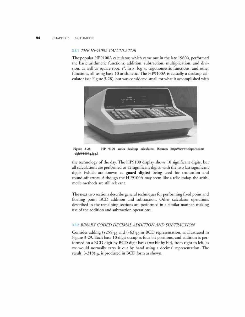
94 CHAPTER 3 ARITHMETIC
3.6.1 THE HP9100A CALCULATOR
The popular HP9100A calculator, which came out in the late 1960’s, performedthe basic arithmetic functions: addition, subtraction, multiplication, and divi-sion, as well as square root, ex, ln x, log x, trigonometric functions, and otherfunctions, all using base 10 arithmetic. The HP9100A is actually a desktop cal-culator (see Figure 3-28), but was considered small for what it accomplished with
the technology of the day. The HP9100 display shows 10 significant digits, butall calculations are performed to 12 significant digits, with the two last significantdigits (which are known as guard digits) being used for truncation andround-off errors. Although the HP9100A may seem like a relic today, the arith-metic methods are still relevant.
The next two sections describe general techniques for performing fixed point andfloating point BCD addition and subtraction. Other calculator operationsdescribed in the remaining sections are performed in a similar manner, makinguse of the addition and subtraction operations.
3.6.2 BINARY CODED DECIMAL ADDITION AND SUBTRACTION
Consider adding (+255)10 and (+63)10 in BCD representation, as illustrated inFigure 3-29. Each base 10 digit occupies four bit positions, and addition is per-formed on a BCD digit by BCD digit basis (not bit by bit), from right to left, aswe would normally carry it out by hand using a decimal representation. Theresult, (+318)10, is produced in BCD form as shown.
Figure 3-28 HP 9100 series desktop calculator. [Source: http://www.teleport.com/
~dgh/91003q.jpg.]
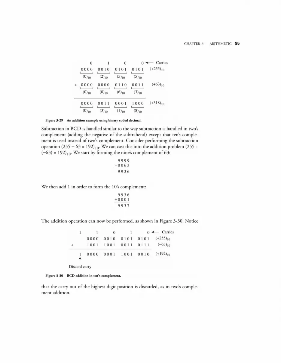
CHAPTER 3 ARITHMETIC 95
Subtraction in BCD is handled similar to the way subtraction is handled in two’scomplement (adding the negative of the subtrahend) except that ten’s comple-ment is used instead of two’s complement. Consider performing the subtractionoperation (255 − 63 = 192)10. We can cast this into the addition problem (255 +(−63) = 192)10. We start by forming the nine’s complement of 63:
We then add 1 in order to form the 10’s complement:
The addition operation can now be performed, as shown in Figure 3-30. Notice
that the carry out of the highest digit position is discarded, as in two’s comple-ment addition.
0 0 0 0
(0)10
0 0 1 0
(2)10
0 1 0 1
(5)10
0 1 0 1
(5)10
(+255)10
0 0 0 0
(0)10
0 0 0 0
(0)10
0 1 1 0
(6)10
0 0 1 1
(3)10
(+63)10+
0 0 0 0
(0)10
0 0 1 1
(3)10
0 0 0 1
(1)10
1 0 0 0
(8)10
(+318)10
0 1 0 0 Carries
Figure 3-29 An addition example using binary coded decimal.
9 9 9 90 0 6 3
9 9 3 6
−
9 9 3 60 0 0 1
9 9 3 7
+
0 0 0 0 0 0 1 0 0 1 0 1 0 1 0 1 (+255)10
1 0 0 1 1 0 0 1 0 0 1 1 0 1 1 1 (−63)10+
0 0 0 0 0 0 0 1 1 0 0 1 0 0 1 0 (+192)10
1 0 1 0 Carries1
1
Discard carry
Figure 3-30 BCD addition in ten’s complement.

96 CHAPTER 3 ARITHMETIC
Unlike the two’s complement representation, we cannot simply look at the left-most bit to determine the sign. In ten’s complement, the number is positive if theleftmost digit is between 0 and 4, inclusive, and is negative otherwise. (The BCDbit patterns for 4 and 5 are 0100 and 0101, respectively, which both have a 0 inthe leftmost bit, yet 4 indicates a positive number and 5 indicates a negativenumber.) If we use an excess 3 encoding for each digit, then the leftmost bit willindicate the sign. Figure 3-31 shows the encoding. Notice that six of the bit pat-
terns cannot occur, and so they are marked as don’t cares, ‘d’.
Now consider the design of a BCD full adder. The BCD full adder should sumtwo BCD digits and a carry-in, and should produce a sum BCD digit and acarry-out, all using excess 3. A design using two’s complement full adders isshown in Figure 3-32. The excess 3 BCD digits are added in the upper four two’scomplement full adders (FAs). Since each operand is represented in excess 3, theresult is in excess 6. In order to restore the result to excess 3, we need to subtract3 from the result. As an alternative, we can add 13 to the result since 16 − 3 = 16+ 13 in a four-bit representation, discarding the carry out of the highest bit posi-tion. The latter approach is used in Figure 3-32, in which 1310 = 11012 is addedto the result. Note that this only works if there is no carry. When there is a carry,then we need to also subtract 10 (or equivalently, add 6) from the result, besidessubtracting 3 (or adding 13) to restore the excess 3 representation, and produce a
0011001100110011
0101010101010101
0000111100001111
0123456789dddddd
0000000011111111
BCD Bit Pattern
Normal BCD value
Positive numbers
ddd0123456789ddd
Excess 3 value
Negative numbers
Figure 3-31 Excess 3 encoding of BCD digits.
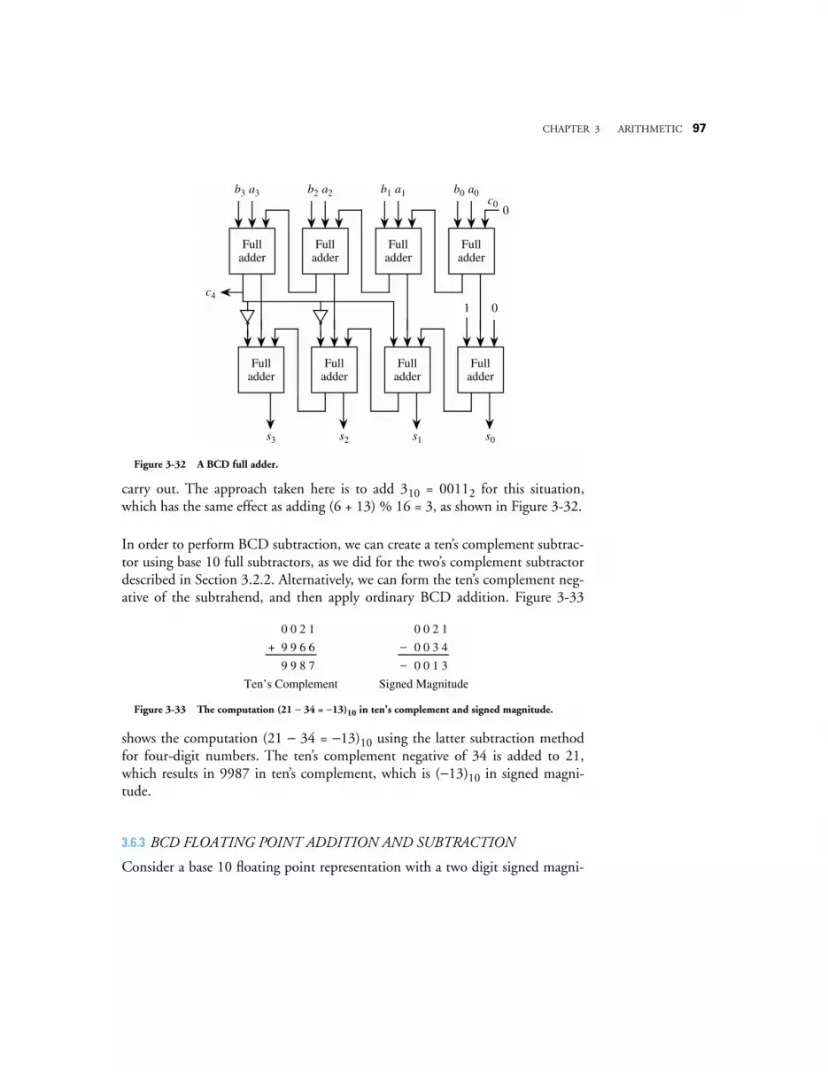
CHAPTER 3 ARITHMETIC 97
carry out. The approach taken here is to add 310 = 00112 for this situation,which has the same effect as adding (6 + 13) % 16 = 3, as shown in Figure 3-32.
In order to perform BCD subtraction, we can create a ten’s complement subtrac-tor using base 10 full subtractors, as we did for the two’s complement subtractordescribed in Section 3.2.2. Alternatively, we can form the ten’s complement neg-ative of the subtrahend, and then apply ordinary BCD addition. Figure 3-33
shows the computation (21 − 34 = −13)10 using the latter subtraction methodfor four-digit numbers. The ten’s complement negative of 34 is added to 21,which results in 9987 in ten’s complement, which is (−13)10 in signed magni-tude.
3.6.3 BCD FLOATING POINT ADDITION AND SUBTRACTION
Consider a base 10 floating point representation with a two digit signed magni-
Fulladder
b0 a0
Fulladder
b1 a1
Fulladder
b2 a2
Fulladder
b3 a3
c4
0c0
Fulladder
s0
Fulladder
s1
Fulladder
s2
Fulladder
s3
01
Figure 3-32 A BCD full adder.
+
0
9
9
0
9
9
2
6
8
1
6
7
Ten’s Complement
−−
0
0
0
0
0
0
2
3
1
1
4
3
Signed Magnitude
Figure 3-33 The computation (21 − 34 = −13)10 in ten’s complement and signed magnitude.
98 CHAPTER 3 ARITHMETIC
tude exponent and an eight digit signed magnitude fraction. On a calculator, asample entry might look like:
−.37100000 × 10−12
which is in normalized form.
Now how is the number stored? A calculator user sees signed magnitude for boththe exponent and the fraction, but internally, we might use a ten’s complementrepresentation for both the exponent and the fraction. For the case above, therepresentation using ten’s complement would be: 88 for the exponent, and62900000 for the fraction. Using an excess 3 representation in binary results inan exponent of 1011 1011 and a fraction of 1001 0101 1100 0011 0011 00110011 0011. Note that since we are using the leftmost bit for the sign, that theexponent range is [−50 to +49] and that the fraction range is [−.50000000 to+.49999999].
If we now try to represent +.9 in base 10, then we are again stuck because theleftmost bit of the fraction is used for a sign bit. That is, we cannot use 1100 inthe most significant digit of the fraction, because although that is the excess 3representation of 9, it makes the fraction appear negative. Here is a better solu-tion: Just use ten’s complement for base 10 integer arithmetic, such as for expo-nents, and use signed magnitude for fractions.
Here is the summary thus far: we use a ten’s complement representation for theexponent since it is an integer, and we use a base 10 signed magnitude represen-tation for the fraction. A separate sign bit is maintained for the fraction, so thateach digit can take on any of the 10 values 0–9 (except for the first digit, whichcannot be a zero) and so we can now represent +.9. We should also represent theexponent in excess 50 to make comparisons easier. The example above now lookslike this internally, still in excess 3 binary form, with a two digit excess 50 expo-nent:
Sign bit: 1
Exponent: 0110 1011
Fraction: 0110 1010 0100 0011 0011 0011 0011 0011 0011
CHAPTER 3 ARITHMETIC 99
In order to add two numbers in this representation, we just go through the samesteps that we did for the base 2 floating point representation described earlier. Westart by adjusting the exponent and fraction of the smaller operand until theexponents of both operands are the same. If the difference in exponents is sogreat that the fraction of the smaller operand is shifted all the way to the right,then the smaller operand is treated as 0. After adjusting the smaller fraction, weconvert either or both operands from signed magnitude to ten’s complementaccording to whether we are adding or subtracting, and whether the operands arepositive or negative. Note that this will work now because we can treat the frac-tions as integers.
SUMMARY
Computer arithmetic can be carried out as we normally carry out decimal arith-metic by hand, while taking the base into account. A two’s complement or a ten’scomplement representation is normally used for integers, whereas signed magni-tude is normally used for fractions due to the difficulty of manipulating positiveand negative fractions in a uniform manner.
Performance can be improved by skipping over 1’s in the Booth and bit-pairrecoding techniques. An alternative method of improving performance is to usecarryless addition, such as in residue arithmetic. Although carryless addition maybe the fastest approach in terms of time complexity and circuit complexity, themore common weighted position codes are normally used in practice in order tosimplify comparisons and represent fractions.
FURTHER READING(Goldberg, 1990) is a concise but thorough source of numerous aspects of com-puter arithmetic. (Hamacher et al., 1990) provides a classic treatment of integerarithmetic. (Flynn, 1970) gives an early treatment of division by zero finding.(Garner, 1959) gives a complete description of the residue number system,whereas (Koren, 1993) gives a more tutorial treatment of the subject. (Huangand Goodman, 1979) describes how a memory based residue processor can beconstructed. Koren (1993) also provides additional details on cascadingcarry-lookahead units. (Cochran, 1968) is a good source for the programming ofthe HP9100A calculator.
100 CHAPTER 3 ARITHMETIC
Cochran, D. S., “Internal Programming of the 9100A Calculator,” Hewlett-Pack-ard Journal, (Sept. 1968); Also see http://www.hpmuseum.org/jour-nals/9100:prg.htm.
Flynn, M. J., “On division by functional iteration,” IEEE Trans. Comp., C-19,no. 8, pp. 702-706, (Aug. 1970).
Garner, H. L., “The Residue Number System,” IRE Transactions on ElectronicComputers, vol. 8, pp. 140-147, (Jun. 1959).
Goldberg, D., “Computer Arithmetic,” in Patterson, D. A. and J. L. Hennessy,Computer Architecture: A Quantitative Approach, 2/e, Morgan Kaufmann,(1995).
Hamacher, V. C., Z. G. Vranesic, and S. G. Zaky, Computer Organization, 3/e,McGraw Hill, (1990).
Huang, A. and J. W. Goodman, “Number Theoretic Processors, Optical andElectronic,” SPIE Optical Processing Systems, vol. 185, pp. 28-35, (1979).
Koren, I., Computer Arithmetic Algorithms, Prentice Hall, Englewood Cliffs,(1993).
PROBLEMS3.1 Show the results of adding the following pairs of five-bit (i.e. one sign bit
and four data bits) two’s complement numbers and indicate whether or notoverflow occurs for each case:
3.2 One way to determine that overflow has occurred when adding two num-bers is to detect that the result of adding two positive numbers is negative, orthat the result of adding two negative numbers is positive. The overflow rulesare different for subtraction: there is overflow if the result of subtracting a neg-ative number from a positive number is negative or the result of subtracting apositive number from a negative number is positive.
1 0 1 1 01 0 1 1 1+
1 1 1 1 01 1 1 0 1+
1 1 1 1 10 1 1 1 1+
CHAPTER 3 ARITHMETIC 101
Subtract the numbers shown below and determine whether or not an overflowhas occurred. Do not form the two’s complement of the subtrahend and add:perform the subtraction bit by bit, showing the borrows generated at eachposition:
- 0 1 0 1- 0 1 1 0__________
3.3 Add the following two’s complement and one’s complement binary num-bers as indicated. For each case, indicate if there is overflow.
Two’s complement One’s complement+ 1 0 1 1.1 0 1 + 1 0 1 1.1 0 1+ 0 1 1 1.0 1 1 + 0 1 1 1.0 1 1_______________ _______________
3.4 Show the process of serial unsigned multiplication for 1010 (multipli-cand) multiplied by 0101 (multiplier). Use the form shown in Figure 3-12.
3.5 Show the process of serial unsigned multiplication for 11.1 (multiplicand)multiplied by 01.1 (multiplier) by treating the operands as integers. The resultshould be 101.01.
3.6 Show the process of serial unsigned division for 1010 divided by 0101.Use the form shown in Figure 3-15.
3.7 Show the process of serial unsigned division for 1010 divided by 0100,but instead of generating a remainder, compute the fraction by continuing theprocess. That is, the result should be 10.12.
3.8 The equation used in Section 3.5.1 for c4 in a carry lookahead adderassumes that c0 is 0 for addition. If we perform subtraction by using the addi-tion / subtraction unit shown in Figure 3-6, then c0 = 1. Rewrite the equationfor c4 when c0 = 1.
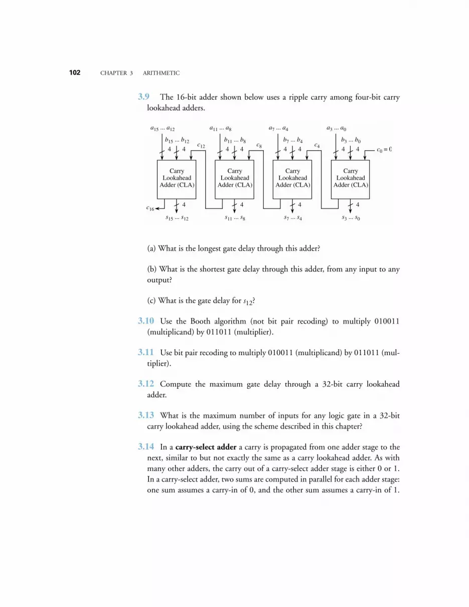
102 CHAPTER 3 ARITHMETIC
3.9 The 16-bit adder shown below uses a ripple carry among four-bit carrylookahead adders.
(a) What is the longest gate delay through this adder?
(b) What is the shortest gate delay through this adder, from any input to anyoutput?
(c) What is the gate delay for s12?
3.10 Use the Booth algorithm (not bit pair recoding) to multiply 010011(multiplicand) by 011011 (multiplier).
3.11 Use bit pair recoding to multiply 010011 (multiplicand) by 011011 (mul-tiplier).
3.12 Compute the maximum gate delay through a 32-bit carry lookaheadadder.
3.13 What is the maximum number of inputs for any logic gate in a 32-bitcarry lookahead adder, using the scheme described in this chapter?
3.14 In a carry-select adder a carry is propagated from one adder stage to thenext, similar to but not exactly the same as a carry lookahead adder. As withmany other adders, the carry out of a carry-select adder stage is either 0 or 1.In a carry-select adder, two sums are computed in parallel for each adder stage:one sum assumes a carry-in of 0, and the other sum assumes a carry-in of 1.
Carry Lookahead
Adder (CLA)
4
a15 ... a12
4
b15 ... b12 c12
4
s15 ... s12
Carry Lookahead
Adder (CLA)
4
a11 ... a8
4
b11 ... b8 c8
4
s11 ... s8
Carry Lookahead
Adder (CLA)
4
a7 ... a4
4
b7 ... b4 c4
4
s7 ... s4
Carry Lookahead
Adder (CLA)
4
a3 ... a0
4
b3 ... b0
c0 = 0
4
s3 ... s0
c16
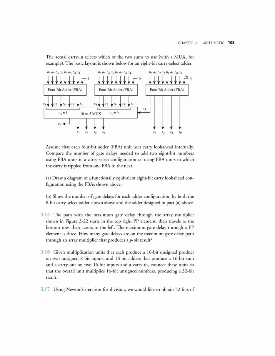
CHAPTER 3 ARITHMETIC 103
The actual carry-in selects which of the two sums to use (with a MUX, forexample). The basic layout is shown below for an eight-bit carry-select adder:
Assume that each four-bit adder (FBA) unit uses carry lookahead internally.Compare the number of gate delays needed to add two eight-bit numbersusing FBA units in a carry-select configuration vs. using FBA units in whichthe carry is rippled from one FBA to the next.
(a) Draw a diagram of a functionally equivalent eight-bit carry lookahead con-figuration using the FBAs shown above.
(b) Show the number of gate delays for each adder configuration, by both the8-bit carry-select adder shown above and the adder designed in part (a) above.
3.15 The path with the maximum gate delay through the array multipliershown in Figure 3-22 starts in the top right PP element, then travels to thebottom row, then across to the left. The maximum gate delay through a PPelement is three. How many gate delays are on the maximum gate delay paththrough an array multiplier that produces a p-bit result?
3.16 Given multiplication units that each produce a 16-bit unsigned producton two unsigned 8-bit inputs, and 16-bit adders that produce a 16-bit sumand a carry-out on two 16-bit inputs and a carry-in, connect these units sothat the overall unit multiplies 16-bit unsigned numbers, producing a 32-bitresult.
3.17 Using Newton’s iteration for division, we would like to obtain 32 bits of
b0 a0b1 a1b2 a2b3 a3
c4
0c0
Four-Bit Adder (FBA)
b4 a4
s4
b5 a5
s5
b6 a6
s6
b7 a7
s7
0
Four-Bit Adder (FBA)
b4 a4
s4
b5 a5
s5
b6 a6
s6
b7 a7
s7
1
Four-Bit Adder (FBA)
c8c8
c8
10-to-5 MUX c4 = 0c4 = 1
s0s1s2s3s4s5s6s7

104 CHAPTER 3 ARITHMETIC
precision. If we use a lookup table that provides eight bits of precision for theinitial guess, how many iterations need to be applied?
3.18 Add (641)10 to (259)10 in unsigned BCD, using as few digits in the resultas necessary.
3.19 Add (123)10 and (−178)10 in signed BCD, using four digit words.
CHAPTER 4 MACHINE LANGUAGE AND ASSEMBLY LANGUAGE
103
In this chapter we tackle a central topic in computer architecture: the languageunderstood by the computer’s hardware, referred to as its
machine language
.The machine language is usually discussed in terms of its
assembly language
,which is functionally equivalent to the corresponding machine language exceptthat the assembly language uses more intuitive names such as Move, Add, andJump instead of the actual binary words of the language. (Programmers find con-structs such as “Add r0, r1, r2” to be more easily understood and rendered with-out error than 0110101110101101.)
We begin by describing the
I
nstruction Set Architecture
(ISA) view of themachine and its operations. The ISA view corresponds to the Assembly Lan-guage/Machine Code level described in Figure 1-4: it is between the High LevelLanguage view, where little or none of the machine hardware is visible or of con-cern, and the Control level, where machine instructions are interpreted as regis-ter transfer actions, at the Functional Unit level.
In order to describe the nature of assembly language and assembly language pro-gramming, we choose as a model architecture the
ARC
machine, which is a sim-plification of the commercial SPARC architecture common to Sun computers.(Additional architectural models are covered in
The Computer Architecture Com-panion
volume.)
We illustrate the utility of the various instruction classes with practical examplesof assembly language programming, and we conclude with a Case Study of theJava bytecodes as an example of a common, portable assembly language that canbe implemented using the native language of another machine.
MACHINE LANGUAGE AND ASSEMBLY LANGUAGE
4
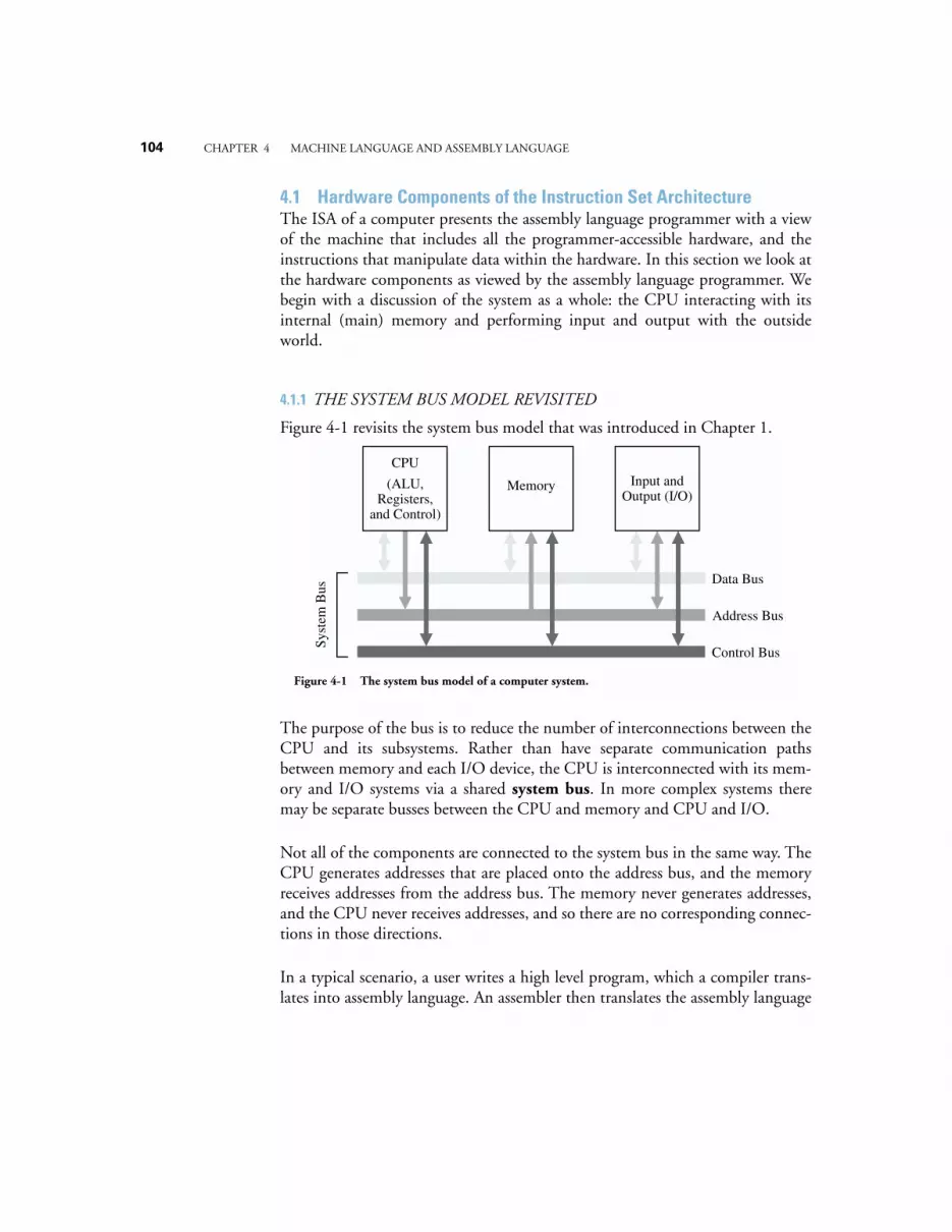
104
CHAPTER 4 MACHINE LANGUAGE AND ASSEMBLY LANGUAGE
4.1 Hardware Components of the Instruction Set Architecture
The ISA of a computer presents the assembly language programmer with a viewof the machine that includes all the programmer-accessible hardware, and theinstructions that manipulate data within the hardware. In this section we look atthe hardware components as viewed by the assembly language programmer. Webegin with a discussion of the system as a whole: the CPU interacting with itsinternal (main) memory and performing input and output with the outsideworld.
4.1.1
THE SYSTEM BUS MODEL REVISITED
Figure 4-1 revisits the system bus model that was introduced in Chapter 1.
The purpose of the bus is to reduce the number of interconnections between theCPU and its subsystems. Rather than have separate communication pathsbetween memory and each I/O device, the CPU is interconnected with its mem-ory and I/O systems via a shared
system bus
. In more complex systems theremay be separate busses between the CPU and memory and CPU and I/O.
Not all of the components are connected to the system bus in the same way. TheCPU generates addresses that are placed onto the address bus, and the memoryreceives addresses from the address bus. The memory never generates addresses,and the CPU never receives addresses, and so there are no corresponding connec-tions in those directions.
In a typical scenario, a user writes a high level program, which a compiler trans-lates into assembly language. An assembler then translates the assembly language
Syst
em B
us
Data Bus
Address Bus
Control Bus
(ALU, Registers,
and Control)
Memory Input and Output (I/O)
CPU
Figure 4-1 The system bus model of a computer system.
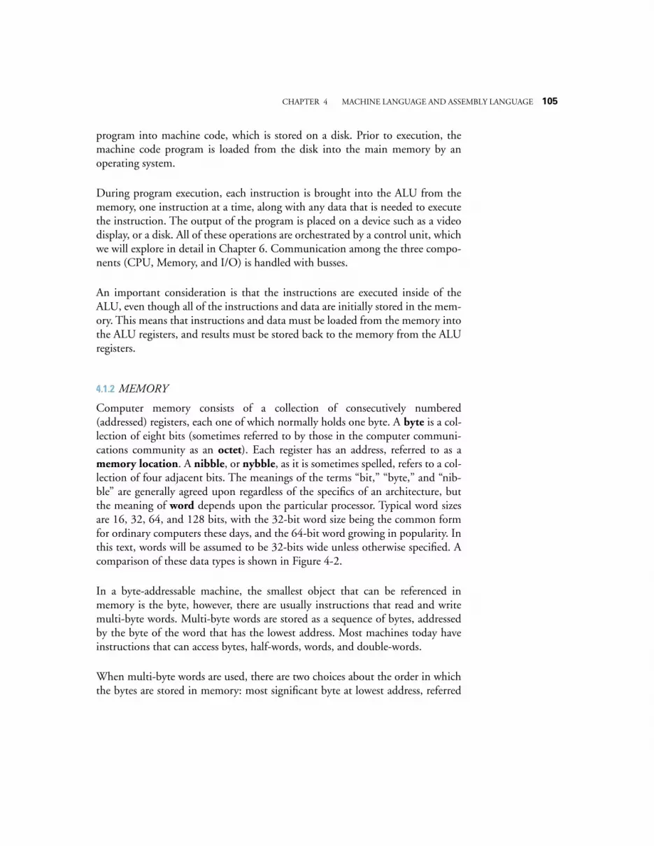
CHAPTER 4 MACHINE LANGUAGE AND ASSEMBLY LANGUAGE
105
program into machine code, which is stored on a disk. Prior to execution, themachine code program is loaded from the disk into the main memory by anoperating system.
During program execution, each instruction is brought into the ALU from thememory, one instruction at a time, along with any data that is needed to executethe instruction. The output of the program is placed on a device such as a videodisplay, or a disk. All of these operations are orchestrated by a control unit, whichwe will explore in detail in Chapter 6. Communication among the three compo-nents (CPU, Memory, and I/O) is handled with busses.
An important consideration is that the instructions are executed inside of theALU, even though all of the instructions and data are initially stored in the mem-ory. This means that instructions and data must be loaded from the memory intothe ALU registers, and results must be stored back to the memory from the ALUregisters.
4.1.2
MEMORY
Computer memory consists of a collection of consecutively numbered(addressed) registers, each one of which normally holds one byte. A
byte
is a col-lection of eight bits (sometimes referred to by those in the computer communi-cations community as an
octet
). Each register has an address, referred to as a
memory location
. A
nibble
, or
nybble
, as it is sometimes spelled, refers to a col-lection of four adjacent bits. The meanings of the terms “bit,” “byte,” and “nib-ble” are generally agreed upon regardless of the specifics of an architecture, butthe meaning of
word
depends upon the particular processor. Typical word sizesare 16, 32, 64, and 128 bits, with the 32-bit word size being the common formfor ordinary computers these days, and the 64-bit word growing in popularity. Inthis text, words will be assumed to be 32-bits wide unless otherwise specified. Acomparison of these data types is shown in Figure 4-2.
In a byte-addressable machine, the smallest object that can be referenced inmemory is the byte, however, there are usually instructions that read and writemulti-byte words. Multi-byte words are stored as a sequence of bytes, addressedby the byte of the word that has the lowest address. Most machines today haveinstructions that can access bytes, half-words, words, and double-words.
When multi-byte words are used, there are two choices about the order in whichthe bytes are stored in memory: most significant byte at lowest address, referred
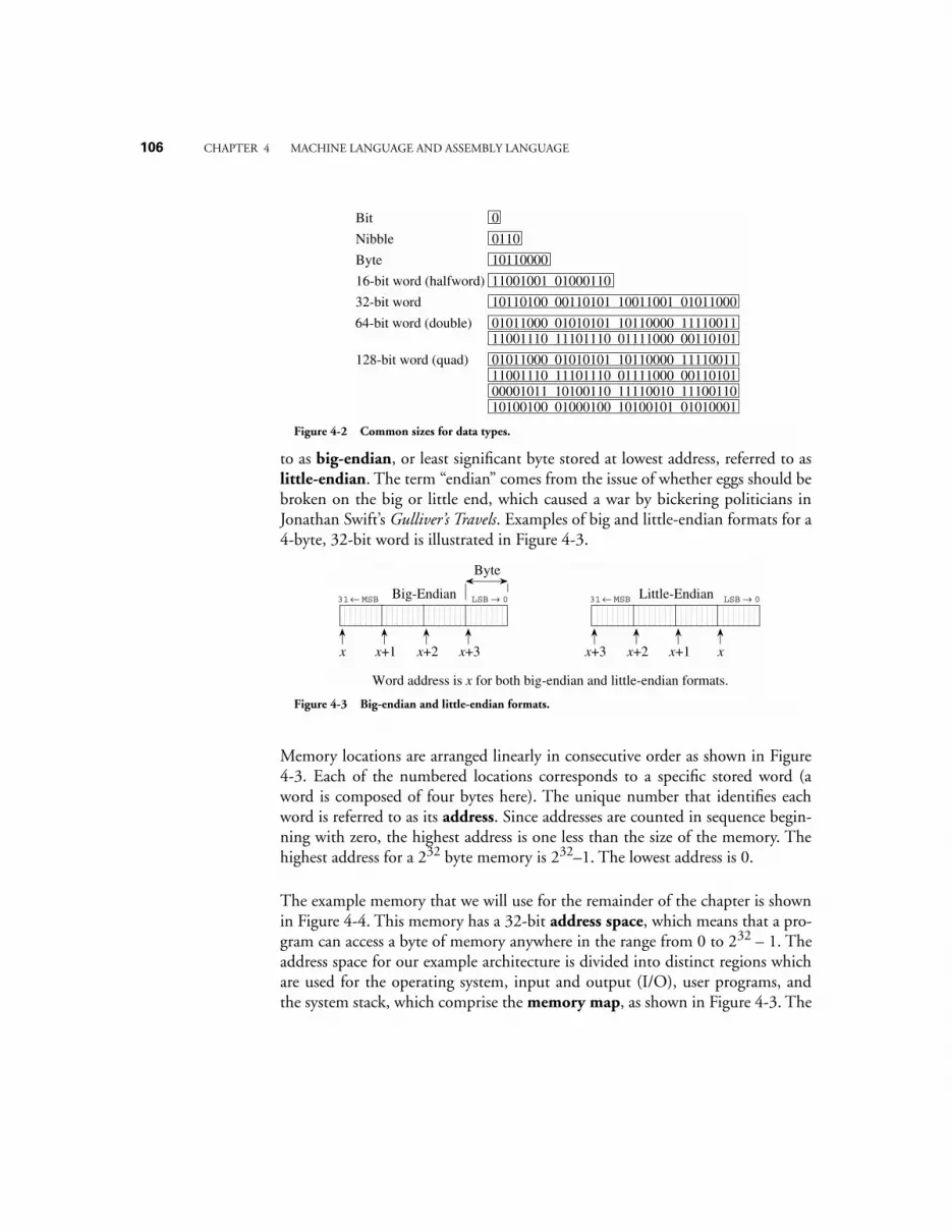
106
CHAPTER 4 MACHINE LANGUAGE AND ASSEMBLY LANGUAGE
to as
big-endian
, or least significant byte stored at lowest address, referred to as
little-endian
. The term “endian” comes from the issue of whether eggs should bebroken on the big or little end, which caused a war by bickering politicians inJonathan Swift’s
Gulliver’s Travels
. Examples of big and little-endian formats for a4-byte, 32-bit word is illustrated in Figure 4-3.
Memory locations are arranged linearly in consecutive order as shown in Figure4-3. Each of the numbered locations corresponds to a specific stored word (aword is composed of four bytes here). The unique number that identifies eachword is referred to as its
address
. Since addresses are counted in sequence begin-ning with zero, the highest address is one less than the size of the memory. Thehighest address for a 2
32
byte memory is 2
32
–1. The lowest address is 0.
The example memory that we will use for the remainder of the chapter is shownin Figure 4-4. This memory has a 32-bit
address space
, which means that a pro-gram can access a byte of memory anywhere in the range from 0 to 2
32
– 1. Theaddress space for our example architecture is divided into distinct regions whichare used for the operating system, input and output (I/O), user programs, andthe system stack, which comprise the
memory map
, as shown in Figure 4-3. The
Bit
Nibble
Byte
16-bit word (halfword)
32-bit word
64-bit word (double)
0
0110
10110000
11001001 01000110
10110100 00110101 10011001 01011000
01011000 01010101 10110000 1111001111001110 11101110 01111000 00110101
128-bit word (quad) 01011000 01010101 10110000 1111001111001110 11101110 01111000 0011010100001011 10100110 11110010 1110011010100100 01000100 10100101 01010001
Figure 4-2 Common sizes for data types.
Big-Endian
x x+1 x+2 x+3
31 Little-Endian
x+3 x+2 x+1 x
0
Word address is x for both big-endian and little-endian formats.
0 31
Byte
← MSB LSB → ← MSB LSB →
Figure 4-3 Big-endian and little-endian formats.
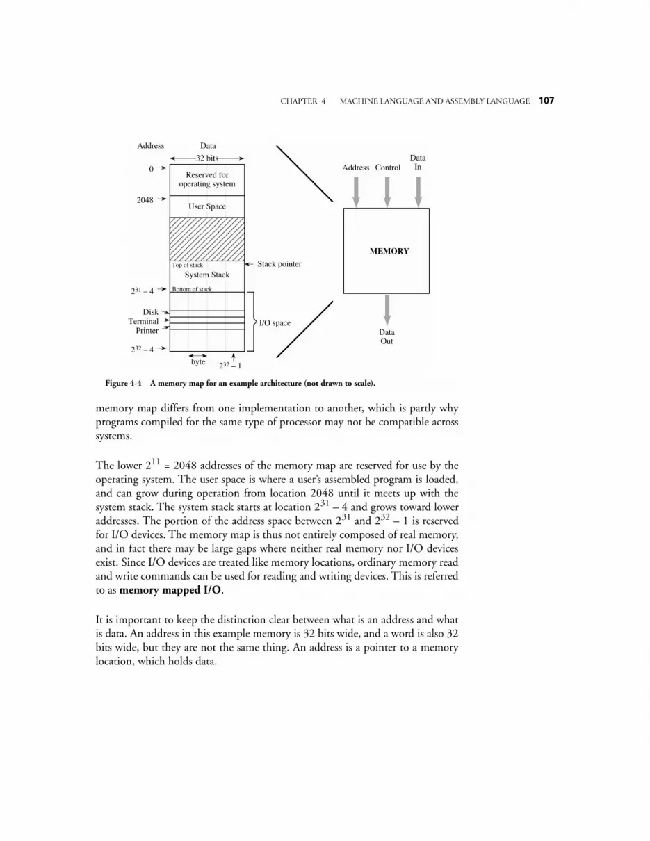
CHAPTER 4 MACHINE LANGUAGE AND ASSEMBLY LANGUAGE
107
memory map differs from one implementation to another, which is partly whyprograms compiled for the same type of processor may not be compatible acrosssystems.
The lower 2
11
= 2048 addresses of the memory map are reserved for use by theoperating system. The user space is where a user’s assembled program is loaded,and can grow during operation from location 2048 until it meets up with thesystem stack. The system stack starts at location 2
31
– 4 and grows toward loweraddresses. The portion of the address space between 2
31
and 2
32
– 1 is reservedfor I/O devices. The memory map is thus not entirely composed of real memory,and in fact there may be large gaps where neither real memory nor I/O devicesexist. Since I/O devices are treated like memory locations, ordinary memory readand write commands can be used for reading and writing devices. This is referredto as
memory mapped I/O
.
It is important to keep the distinction clear between what is an address and whatis data. An address in this example memory is 32 bits wide, and a word is also 32bits wide, but they are not the same thing. An address is a pointer to a memorylocation, which holds data.
Reserved for operating system
User Space
I/O space
0
2048
Stack pointerSystem Stack
Top of stack
Bottom of stack
DiskTerminal
Printer
232 – 4
231 – 4
32 bits
Address Data
232 – 1byte
MEMORY
Address Control
Data Out
Data In
Figure 4-4 A memory map for an example architecture (not drawn to scale).
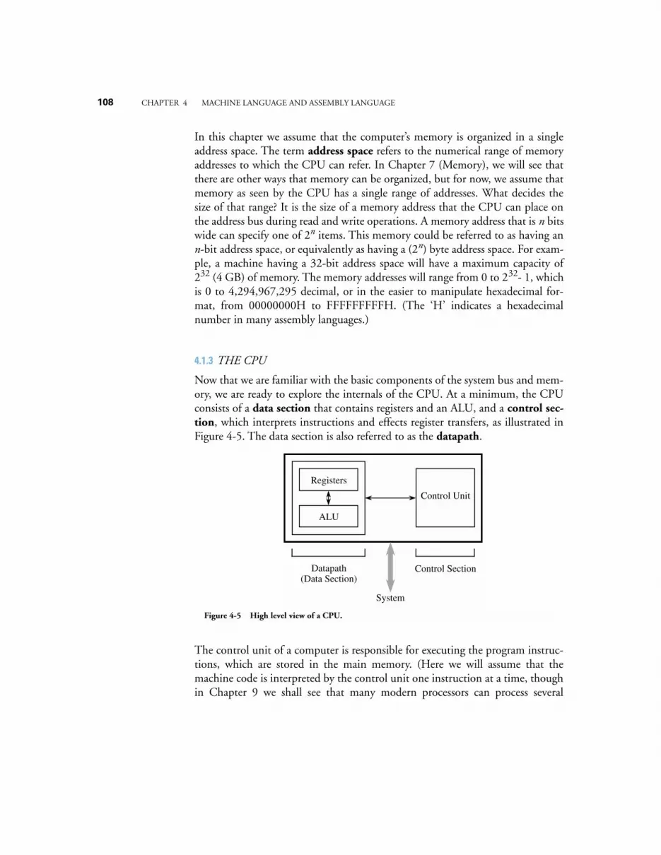
108
CHAPTER 4 MACHINE LANGUAGE AND ASSEMBLY LANGUAGE
In this chapter we assume that the computer’s memory is organized in a singleaddress space. The term
address space
refers to the numerical range of memoryaddresses to which the CPU can refer. In Chapter 7 (Memory), we will see thatthere are other ways that memory can be organized, but for now, we assume thatmemory as seen by the CPU has a single range of addresses. What decides thesize of that range? It is the size of a memory address that the CPU can place onthe address bus during read and write operations. A memory address that is
n
bitswide can specify one of 2
n
items. This memory could be referred to as having an
n
-bit address space, or equivalently as having a (2
n
) byte address space. For exam-ple, a machine having a 32-bit address space will have a maximum capacity of2
32
(4 GB) of memory. The memory addresses will range from 0 to 2
32
- 1, whichis 0 to 4,294,967,295 decimal, or in the easier to manipulate hexadecimal for-mat, from 00000000H to FFFFFFFFFH. (The ‘H’ indicates a hexadecimalnumber in many assembly languages.)
4.1.3
THE CPU
Now that we are familiar with the basic components of the system bus and mem-ory, we are ready to explore the internals of the CPU. At a minimum, the CPUconsists of a
data section
that contains registers and an ALU, and a
control sec-tion
, which interprets instructions and effects register transfers, as illustrated inFigure 4-5. The data section is also referred to as the
datapath
.
The control unit of a computer is responsible for executing the program instruc-tions, which are stored in the main memory. (Here we will assume that themachine code is interpreted by the control unit one instruction at a time, thoughin Chapter 9 we shall see that many modern processors can process several
Control Unit
Control Section
Registers
ALU
Datapath(Data Section)
System
Figure 4-5 High level view of a CPU.
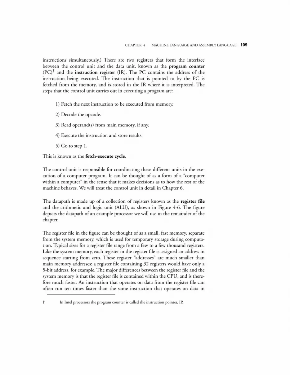
CHAPTER 4 MACHINE LANGUAGE AND ASSEMBLY LANGUAGE
109
instructions simultaneously.) There are two registers that form the interfacebetween the control unit and the data unit, known as the
program counter
(PC)
†
and the
instruction register
(IR). The PC contains the address of theinstruction being executed. The instruction that is pointed to by the PC isfetched from the memory, and is stored in the IR where it is interpreted. Thesteps that the control unit carries out in executing a program are:
1) Fetch the next instruction to be executed from memory.
2) Decode the opcode.
3) Read operand(s) from main memory, if any.
4) Execute the instruction and store results.
5) Go to step 1.
This is known as the
fetch-execute cycle
.
The control unit is responsible for coordinating these different units in the exe-cution of a computer program. It can be thought of as a form of a “computerwithin a computer” in the sense that it makes decisions as to how the rest of themachine behaves. We will treat the control unit in detail in Chapter 6.
The datapath is made up of a collection of registers known as the
register file
and the arithmetic and logic unit (ALU), as shown in Figure 4-6. The figuredepicts the datapath of an example processor we will use in the remainder of thechapter.
The register file in the figure can be thought of as a small, fast memory, separatefrom the system memory, which is used for temporary storage during computa-tion. Typical sizes for a register file range from a few to a few thousand registers.Like the system memory, each register in the register file is assigned an address insequence starting from zero. These register “addresses” are much smaller thanmain memory addresses: a register file containing 32 registers would have only a5-bit address, for example. The major differences between the register file and thesystem memory is that the register file is contained within the CPU, and is there-fore much faster. An instruction that operates on data from the register file canoften run ten times faster than the same instruction that operates on data in
† In Intel processors the program counter is called the instruction pointer, IP.
110
CHAPTER 4 MACHINE LANGUAGE AND ASSEMBLY LANGUAGE
memory. For this reason, register-intensive programs are faster than the equiva-lent memory intensive programs, even if it takes more register operations to dothe same tasks that would require fewer operations with the operands located inmemory.
Notice that there are several busses
inside
the datapath of Figure 4-6. Three bus-ses connect the datapath to the system bus. This allows data to be transferred toand from main memory and the register file. Three additional busses connect theregister file to the ALU. These busses allow two operands to be fetched from theregister file simultaneously, which are operated on by the ALU, with the resultsreturned to the register file.
The ALU implements a variety of binary (two-operand) and unary (one-oper-and) operations. Examples include add, and, not, or, and multiply. Operationsand operands to be used during the operations are selected by the Control Unit.The two source operands are fetched from the register file onto busses labeled“Register Source 1 (rs1)” and “Register Source 2 (rs2).” The output from theALU is placed on the bus labeled “Register Destination (rd),” where the resultsare conveyed back to the register file. In most systems these connections alsoinclude a path to the System Bus so that memory and devices can be accessed.This is shown as the three connections labeled “From Data Bus”, “To Data Bus”,and “To Address Bus.”
Register File
ALU
From Data Bus
To Data Bus
To Address Bus
Register Source 1
(rs1)
Register Source 2
(rs2)
Register Destination (rd)
Control Unit selects registers and ALU
function
Status to Control Unit
Figure 4-6 An example datapath.

CHAPTER 4 MACHINE LANGUAGE AND ASSEMBLY LANGUAGE
111
The Instruction Set
The
instruction set
is the collection of instructions that a processor can execute,and in effect, it defines the processor. The instruction sets for each processor typeare completely different one from the other. They differ in the sizes of instruc-tions, the kind of operations they allow, the type of operands they operate on,and the types of results they provide.This incompatibility in instruction sets is instark contrast to the compatibility of higher level languages such as C, Pascal,and Ada. Programs written in these higher level languages can run almostunchanged on many different processors if they are
re-compiled
for the targetprocessor.
(One exception to this incompatibility of machine languages is programs com-piled into Java bytecodes, which are a machine language for a
virtual machine
.They will run unchanged on any processor that is running the Java VirtualMachine. The Java Virtual Machine, written in the assembly language of the tar-get machine, intercepts each Java byte code and executes it as if it were runningon a Java hardware (“real”) machine. See the Case Study at the end of the chapterfor more details.)
Because of this incompatibility among instruction sets, computer systems areoften identified by the type of CPU that is incorporated into the computer sys-tem. The instruction set determines the programs the system can execute and hasa significant impact on performance. Programs compiled for an IBM PC (orcompatible) system use the instruction set of an 80x86 CPU, where the ‘x’ isreplaced with a digit that corresponds to the version, such as 80586, more com-monly referred to as a Pentium processor. These programs will not run on anApple Macintosh or an IBM RS6000 computer, since the Macintosh and IBMmachines execute the instruction set of the Motorola
PowerPC
CPU. This doesnot mean that all computer systems that use the same CPU can execute the sameprograms, however. A PowerPC program written for the IBM RS6000 will notexecute on the Macintosh without extensive modifications, however, because ofdifferences in operating systems and I/O conventions.
We will cover one instruction set in detail later in the chapter.
Software for generating machine language programs
A
compiler
is a computer program that transforms programs written in ahigh-level language such as C, Pascal, or Fortran into machine language. Com-
112
CHAPTER 4 MACHINE LANGUAGE AND ASSEMBLY LANGUAGE
pilers for the same high level language generally have the same “front end,” thepart that recognizes statements in the high-level language. They will have differ-ent “back ends,” however, one for each target processor. The compiler’s back endis responsible for generating machine code for a specific target processor. On theother hand, the same program, compiled by different C compilers for the
same
machine can produce different compiled programs for the same source code, aswe will see.
In the process of compiling a program (referred to as the
translation process
), ahigh-level source program is transformed into
assembly language
, and theassembly language is then translated into machine code for the target machine byan
assembler
. These translations take place at
compile time
and
assembly time
,respectively. The resulting object program can be linked with other object pro-grams, at
link time
. The linked program, usually stored on a disk, is loaded intomain memory, at
load time
, and executed by the CPU, at
run time
.
Although most code is written in high level languages, programmers may useassembly language for programs or fragments of programs that are time orspace-critical. In addition, compilers may not be available for some special pur-pose processors, or their compilers may be inadequate to express the special oper-ations which are required. In these cases also, the programmer may need to resortto programming in assembly language.
High level languages allow us to ignore the target computer architecture duringcoding. At the machine language level, however, the underlying architecture isthe primary consideration. A program written in a high level language like C,Pascal, or Fortran may look the same and execute correctly after compilation onseveral different computer systems. The object code that the compiler producesfor each machine, however, will be very different for each computer system, evenif the systems use the same instruction set, such as programs compiled for thePowerPC but running on a Macintosh vs. running on an IBM RS6000.
Having discussed the system bus, main memory, and the CPU, we now examinedetails of a model instruction set, the ARC.
4.2 ARC, A RISC Computer
In the remainder of this chapter, we will study a model architecture that is basedon the commercial Scalable Processor Architecture (
SPARC
) processor that wasdeveloped at Sun Microsystems in the mid-1980’s. The SPARC has become a
CHAPTER 4 MACHINE LANGUAGE AND ASSEMBLY LANGUAGE
113
popular architecture since its introduction, which is partly due to its “open”nature: the full definition of the SPARC architecture is made readily available tothe public (SPARC, 1992). In this chapter, we will look at just a subset of theSPARC, which we call “A RISC Computer” (
ARC
). “RISC” is yet another acro-nym, for
reduced instruction set computer
, which is discussed in Chapter 9. TheARC has most of the important features of the SPARC architecture, but withoutsome of the more complex features that are present in a commercial processor.
4.2.1
ARC MEMORY
The ARC is a 32-bit machine with byte-addressable memory: it can manipulate32-bit data types, but all data is stored in memory as bytes, and the address of a32-bit word is the address of its byte that has the lowest address. As describedearlier in the chapter in the context of Figure 4-4, the ARC has a 32-bit addressspace, in which our example architecture is divided into distinct regions for useby the operating system code, user program code, the system stack (used to storetemporary data), and input and output, (I/O). These memory regions aredetailed as follows:
• The lowest 2
11
= 2048 addresses of the memory map are reserved for useby the operating system.
• The user space is where a user’s assembled program is loaded, and can growduring operation from location 2048 until it meets up with the systemstack.
• The system stack starts at location 2
31
– 4 and grows toward lower address-es. The reason for this organization of programs growing upward in mem-ory and the system stack growing downward can be seen in Figure 4-4: itaccommodates both large programs with small stacks and small programswith large stacks.
• The portion of the address space between 2
31
and 2
32
– 1 is reserved forI/O devices—each device has a collection of memory addresses where itsdata is stored, which is referred to as “memory mapped I/O.”
The ARC has several data types (byte, halfword, integer,
etc.
), but for now wewill consider only the 32-bit integer data type. Each integer is stored in memoryas a collection of four bytes. ARC is a
big-endian
architecture, so the high-est-order byte is stored at the lowest address. The largest possible byte address inthe ARC is 2
32
– 1, so the address of the highest word in the memory map is
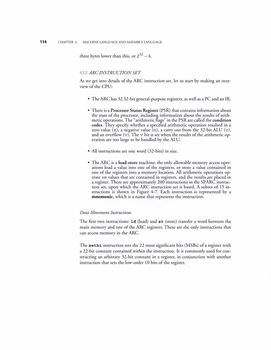
114
CHAPTER 4 MACHINE LANGUAGE AND ASSEMBLY LANGUAGE
three bytes lower than this, or 2
32
– 4.
4.2.2
ARC INSTRUCTION SET
As we get into details of the ARC instruction set, let us start by making an over-view of the CPU:
• The ARC has 32 32-bit general-purpose registers, as well as a PC and an IR.
• There is a
Processor Status Register
(PSR) that contains information aboutthe state of the processor, including information about the results of arith-metic operations. The “arithmetic flags” in the PSR are called the
conditioncodes
. They specify whether a specified arithmetic operation resulted in azero value (
z), a negative value (n), a carry out from the 32-bit ALU (c),and an overflow (v). The v bit is set when the results of the arithmetic op-eration are too large to be handled by the ALU.
• All instructions are one word (32-bits) in size.
• The ARC is a load-store machine: the only allowable memory access oper-ations load a value into one of the registers, or store a value contained inone of the registers into a memory location. All arithmetic operations op-erate on values that are contained in registers, and the results are placed ina register. There are approximately 200 instructions in the SPARC instruc-tion set, upon which the ARC instruction set is based. A subset of 15 in-structions is shown in Figure 4-7. Each instruction is represented by amnemonic, which is a name that represents the instruction.
Data Movement Instructions
The first two instructions: ld (load) and st (store) transfer a word between themain memory and one of the ARC registers. These are the only instructions thatcan access memory in the ARC.
The sethi instruction sets the 22 most significant bits (MSBs) of a register witha 22-bit constant contained within the instruction. It is commonly used for con-structing an arbitrary 32-bit constant in a register, in conjunction with anotherinstruction that sets the low-order 10 bits of the register.
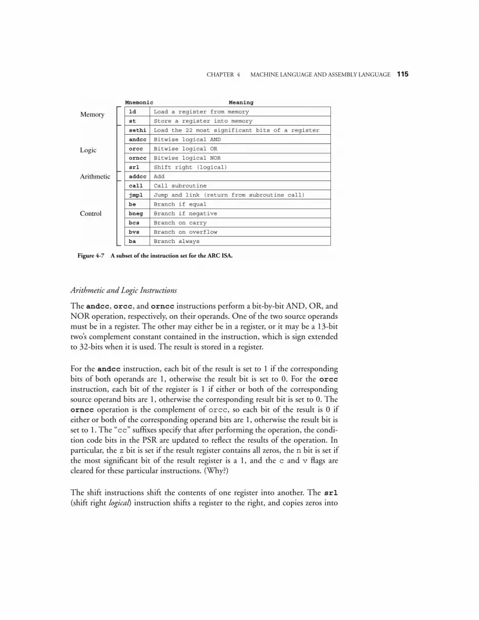
CHAPTER 4 MACHINE LANGUAGE AND ASSEMBLY LANGUAGE 115
Arithmetic and Logic Instructions
The andcc, orcc, and orncc instructions perform a bit-by-bit AND, OR, andNOR operation, respectively, on their operands. One of the two source operandsmust be in a register. The other may either be in a register, or it may be a 13-bittwo’s complement constant contained in the instruction, which is sign extendedto 32-bits when it is used. The result is stored in a register.
For the andcc instruction, each bit of the result is set to 1 if the correspondingbits of both operands are 1, otherwise the result bit is set to 0. For the orccinstruction, each bit of the register is 1 if either or both of the correspondingsource operand bits are 1, otherwise the corresponding result bit is set to 0. Theorncc operation is the complement of orcc, so each bit of the result is 0 ifeither or both of the corresponding operand bits are 1, otherwise the result bit isset to 1. The “cc” suffixes specify that after performing the operation, the condi-tion code bits in the PSR are updated to reflect the results of the operation. Inparticular, the z bit is set if the result register contains all zeros, the n bit is set ifthe most significant bit of the result register is a 1, and the c and v flags arecleared for these particular instructions. (Why?)
The shift instructions shift the contents of one register into another. The srl(shift right logical) instruction shifts a register to the right, and copies zeros into
ld Load a register from memory
Mnemonic Meaning
st
sethi
andcc
addcc
call
jmpl
be
orcc
orncc
Store a register into memory
Load the 22 most significant bits of a register
Bitwise logical AND
Add
Branch on overflow
Call subroutine
Jump and link (return from subroutine call)
Branch if equal
Bitwise logical OR
Bitwise logical NOR
bneg
bcs
Branch if negative
Branch on carry
srl Shift right (logical)
bvs
ba Branch always
Memory
Logic
Arithmetic
Control
Figure 4-7 A subset of the instruction set for the ARC ISA.
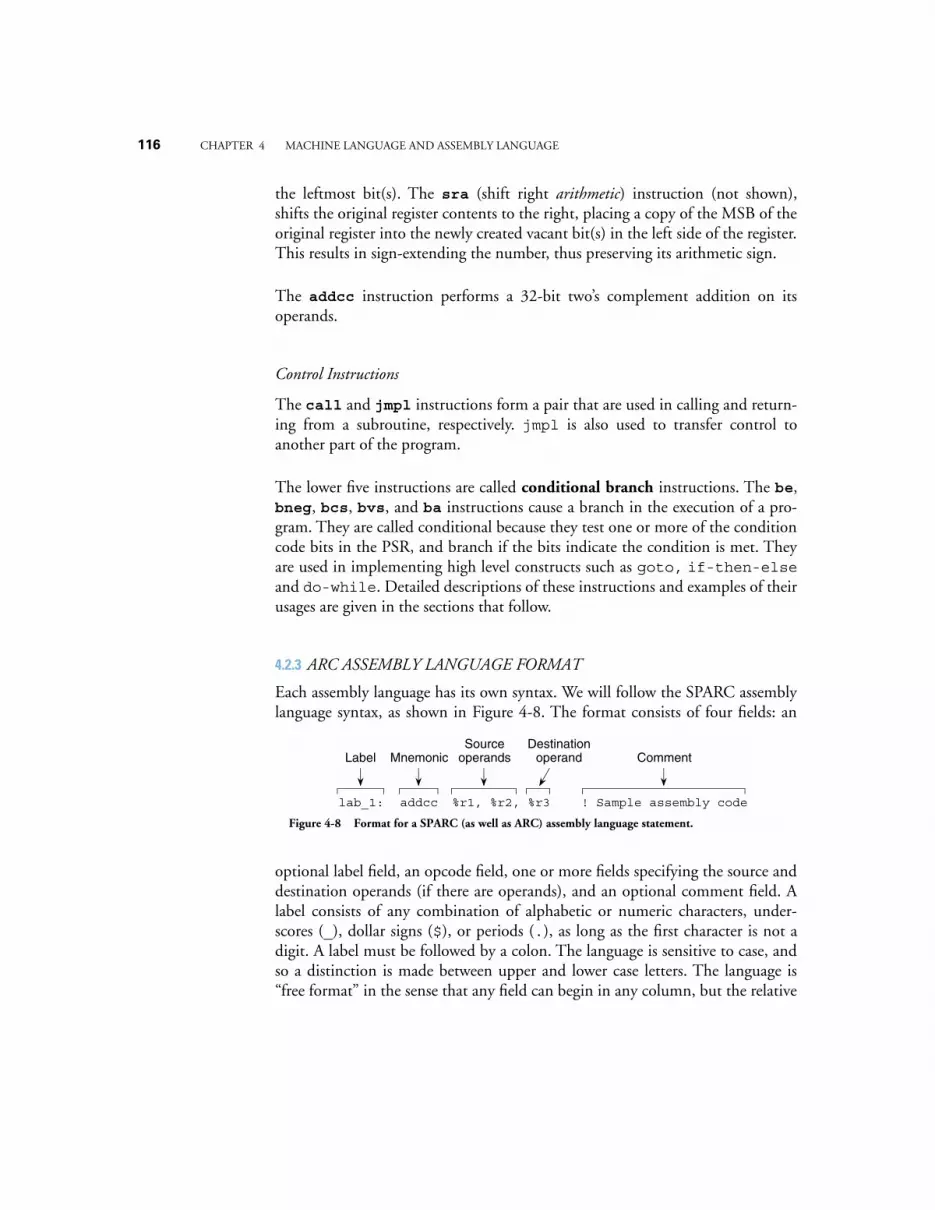
116 CHAPTER 4 MACHINE LANGUAGE AND ASSEMBLY LANGUAGE
the leftmost bit(s). The sra (shift right arithmetic) instruction (not shown),shifts the original register contents to the right, placing a copy of the MSB of theoriginal register into the newly created vacant bit(s) in the left side of the register.This results in sign-extending the number, thus preserving its arithmetic sign.
The addcc instruction performs a 32-bit two’s complement addition on itsoperands.
Control Instructions
The call and jmpl instructions form a pair that are used in calling and return-ing from a subroutine, respectively. jmpl is also used to transfer control toanother part of the program.
The lower five instructions are called conditional branch instructions. The be,bneg, bcs, bvs, and ba instructions cause a branch in the execution of a pro-gram. They are called conditional because they test one or more of the conditioncode bits in the PSR, and branch if the bits indicate the condition is met. Theyare used in implementing high level constructs such as goto, if-then-elseand do-while. Detailed descriptions of these instructions and examples of theirusages are given in the sections that follow.
4.2.3 ARC ASSEMBLY LANGUAGE FORMAT
Each assembly language has its own syntax. We will follow the SPARC assemblylanguage syntax, as shown in Figure 4-8. The format consists of four fields: an
optional label field, an opcode field, one or more fields specifying the source anddestination operands (if there are operands), and an optional comment field. Alabel consists of any combination of alphabetic or numeric characters, under-scores (_), dollar signs ($), or periods (.), as long as the first character is not adigit. A label must be followed by a colon. The language is sensitive to case, andso a distinction is made between upper and lower case letters. The language is“free format” in the sense that any field can begin in any column, but the relative
lab_1: addcc %r1, %r2, %r3 ! Sample assembly code
Label MnemonicSource
operands CommentDestination
operand
Figure 4-8 Format for a SPARC (as well as ARC) assembly language statement.

CHAPTER 4 MACHINE LANGUAGE AND ASSEMBLY LANGUAGE 117
left-to-right ordering must be maintained.
The ARC architecture contains 32 registers labeled %r0 – %r31, that each holda 32-bit word. There is also a 32-bit Processor State Register (PSR) that describesthe current state of the processor, and a 32-bit program counter (PC), thatkeeps track of the instruction being executed, as illustrated in Figure 4-9. The
PSR is labeled %psr and the PC register is labeled %pc. Register %r0 alwayscontains the value 0, which cannot be changed. Registers %r14 and %r15 haveadditional uses as a stack pointer (%sp) and a link register, respectively, asdescribed later.
Operands in an assembly language statement are separated by commas, and thedestination operand always appears in the rightmost position in the operandfield. Thus, the example shown in Figure 4-8 specifies adding registers %r1 and%r2, with the result placed in %r3. If %r0 appears in the destination operandfield instead of %r3, the result is discarded. The default base for a numeric oper-and is 10, so the assembly language statement:
addcc %r1, 12, %r3
shows an operand of (12)10 that will be added to %r1, with the result placed in%r3. Numbers are interpreted in base 10 unless preceeded by “0x” or ending in“H”, either of which denotes a hexadecimal number. The comment field follows
Register 00 %r0 [= 0]
Register 01 %r1
Register 02 %r2
Register 03 %r3
Register 04 %r4
Register 05 %r5
Register 06 %r6
Register 07 %r7
Register 08 %r8
PSR %psr PC %pc
Register 09 %r9
Register 10 %r10
Register 11 %r11
Register 12 %r12
Register 13 %r13
Register14 %r14 [%sp]
Register 15 %r15 [link]
32 bits 32 bits
Register 16 %r16
Register 17 %r17
Register 18 %r18
Register 19 %r19
Register 20 %r20
Register 21 %r21
Register 22 %r22
Register 23 %r23
Register 24 %r24
Register 25 %r25
Register 26 %r26
Register 27 %r27
Register 28 %r28
Register 29 %r29
Register 30 %r30
Register 31 %r31
Figure 4-9 User-visible registers in the ARC.
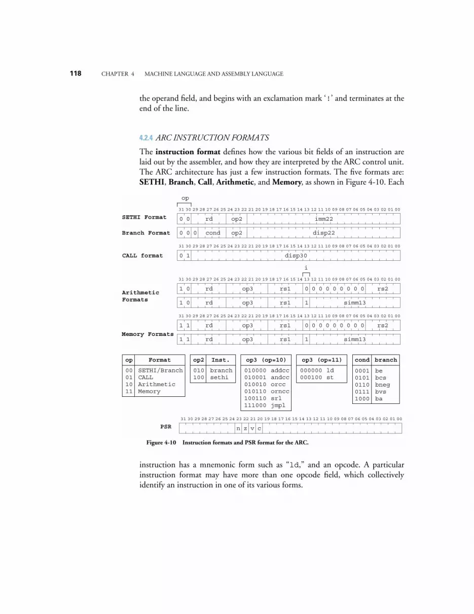
118 CHAPTER 4 MACHINE LANGUAGE AND ASSEMBLY LANGUAGE
the operand field, and begins with an exclamation mark ‘!’ and terminates at theend of the line.
4.2.4 ARC INSTRUCTION FORMATS
The instruction format defines how the various bit fields of an instruction arelaid out by the assembler, and how they are interpreted by the ARC control unit.The ARC architecture has just a few instruction formats. The five formats are:SETHI, Branch, Call, Arithmetic, and Memory, as shown in Figure 4-10. Each
instruction has a mnemonic form such as “ld,” and an opcode. A particularinstruction format may have more than one opcode field, which collectivelyidentify an instruction in one of its various forms.
op3 (op=10)
010000010001010010010110100110111000
addccandccorccornccsrljmpl
00010101011001111000
cond
bebcsbnegbvsba
branch
010100
op2
branchsethi
Inst.
00011011
op
SETHI/BranchCALLArithmeticMemory
Format
000000000100
ldst
op3 (op=11)
op
CALL format disp30
31 30 29 28 27 26 25 24 23 22 21 20 19 18 17 16 15 14 13 12 11 10 09 08 07 06 05 04 03 02 01 00
0 1
SETHI Format imm22
31 30 29 28 27 26 25 24 23 22 21 20 19 18 17 16 15 14 13 12 11 10 09 08 07 06 05 04 03 02 01 00
rd
disp220 cond
0 0
0 0Branch Format
op2
op2
31 30 29 28 27 26 25 24 23 22 21 20 19 18 17 16 15 14 13 12 11 10 09 08 07 06 05 04 03 02 01 00
rs11 op3
simm131 op3
1
Memory Formats1
rd
rd rs1
0
1
0 0 0 0 0 0 0 0 rs2
Arithmetic Formats
31 30 29 28 27 26 25 24 23 22 21 20 19 18 17 16 15 14 13 12 11 10 09 08 07 06 05 04 03 02 01 00
rs11 op3
simm131 op3
0
0
rd
rd rs1
0
1
0 0 0 0 0 0 0 0 rs2
i
PSR31 30 29 28 27 26 25 24 23 22 21 20 19 18 17 16 15 14 13 12 11 10 09 08 07 06 05 04 03 02 01 00
z v cn
Figure 4-10 Instruction formats and PSR format for the ARC.
CHAPTER 4 MACHINE LANGUAGE AND ASSEMBLY LANGUAGE 119
The leftmost two bits of each instruction form the op (opcode) field, whichidentifies the format. The SETHI and Branch formats both contain 00 in the opfield, and so they can be considered together as the SETHI/Branch format. Theactual SETHI or Branch format is determined by the bit pattern in the op2opcode field (010 = Branch; 100 = SETHI). Bit 29 in the Branch format alwayscontains a zero. The five-bit rd field identifies the target register for the SETHIoperation.
The cond field identifies the type of branch, based on the condition code bits (n,z, v, and c) in the PSR, as indicated at the bottom of Figure 4-10. The result ofexecuting an instruction in which the mnemonic ends with “cc” sets the condi-tion code bits such that n=1 if the result of the operation is negative; z=1 if theresult is zero; v=1 if the operation causes an overflow; and c=1 if the operationproduces a carry. The instructions that do not end in “cc” do not affect the con-dition codes. The imm22 and disp22 fields each hold a 22-bit constant that isused as the operand for the SETHI format (for imm22) or for calculating a dis-placement for a branch address (for disp22).
The CALL format contains only two fields: the op field, which contains the bitpattern 01, and the disp30 field, which contains a 30-bit displacement that isused in calculating the address of the called routine.
The Arithmetic (op = 10) and Memory (op = 11) formats both make use ofrd fields to identify either a source register for st, or a destination register forthe remaining instructions. The rs1 field identifies the first source register, andthe rs2 field identifies the second source register. The op3 opcode field identi-fies the instruction according to the op3 tables shown in Figure 4-10.
The simm13 field is a 13-bit immediate value that is sign extended to 32 bits forthe second source when the i (immediate) field is 1. The meaning of “signextended” is that the leftmost bit of the simm13 field (the sign bit) is copied tothe left into the remaining bits that make up a 32-bit integer, before adding it tors1 in this case. This ensures that a two’s complement negative number remainsnegative (and a two’s complement positive number remains positive). Forinstance, (−13)10 = (1111111110011)2, and after sign extension to a 32-bit inte-ger, we have (11111111111111111111111111110011)2 which is still equivalentto (−13)10.
The Arithmetic instructions need two source operands and a destination oper-and, for a total of three operands. The Memory instructions only need two oper-
120 CHAPTER 4 MACHINE LANGUAGE AND ASSEMBLY LANGUAGE
ands: one for the address and one for the data. The remaining source operand isalso used for the address, however. The operands in the rs1 and rs2 fields areadded to obtain the address when i = 0. When i = 1, then the rs1 field andthe simm13 field are added to obtain the address. For the first few examples wewill encounter, %r0 will be used for rs2 and so only the remaining source oper-and will be specified.
4.2.5 ARC DATA FORMATS
The ARC supports 12 different data formats as illustrated in Figure 4-11. Thedata formats are grouped into three types: signed integer, unsigned integer, andfloating point. Within these types, allowable format widths are byte (8 bits), half-word (16 bits), word/singleword (32 bits), tagged word (32 bits, in which thetwo least significant bits form a tag and the most significant 30 bits form thevalue), doubleword (64 bits), and quadword (128 bits).
In reality, the ARC does not differentiate between unsigned and signed integers.Both are stored and manipulated as two’s complement integers. It is their inter-pretation that varies. In particular one subset of the branch instructions assumesthat the value(s) being compared are signed integers, while the other subsetassumes they are unsigned. Likewise, the c bit indicates unsigned integer over-flow, and the v bit, signed overflow.
The tagged word uses the two least significant bits to indicate overflow, in whichan attempt is made to store a value that is larger than 30 bits into the allocated30 bits of the 32-bit word. Tagged arithmetic operations are used in languageswith dynamically typed data, such as Lisp and Smalltalk. In its generic form, a 1in either bit of the tag field indicates an overflow situation for that word. Thetags can be used to ensure proper alignment conditions (that words begin onfour-byte boundaries, quadwords begin on eight-byte boundaries, etc.), particu-larly for pointers.
The floating point formats conform to the IEEE 754-1985 standard (see Chap-ter 2). There are special instructions that invoke the floating point formats thatare not described here, that can be found in (SPARC, 1992).
4.2.6 ARC INSTRUCTION DESCRIPTIONS
Now that we know the instruction formats, we can create detailed descriptions ofthe 15 instructions listed in Figure 4-7, which are given below. The translation to
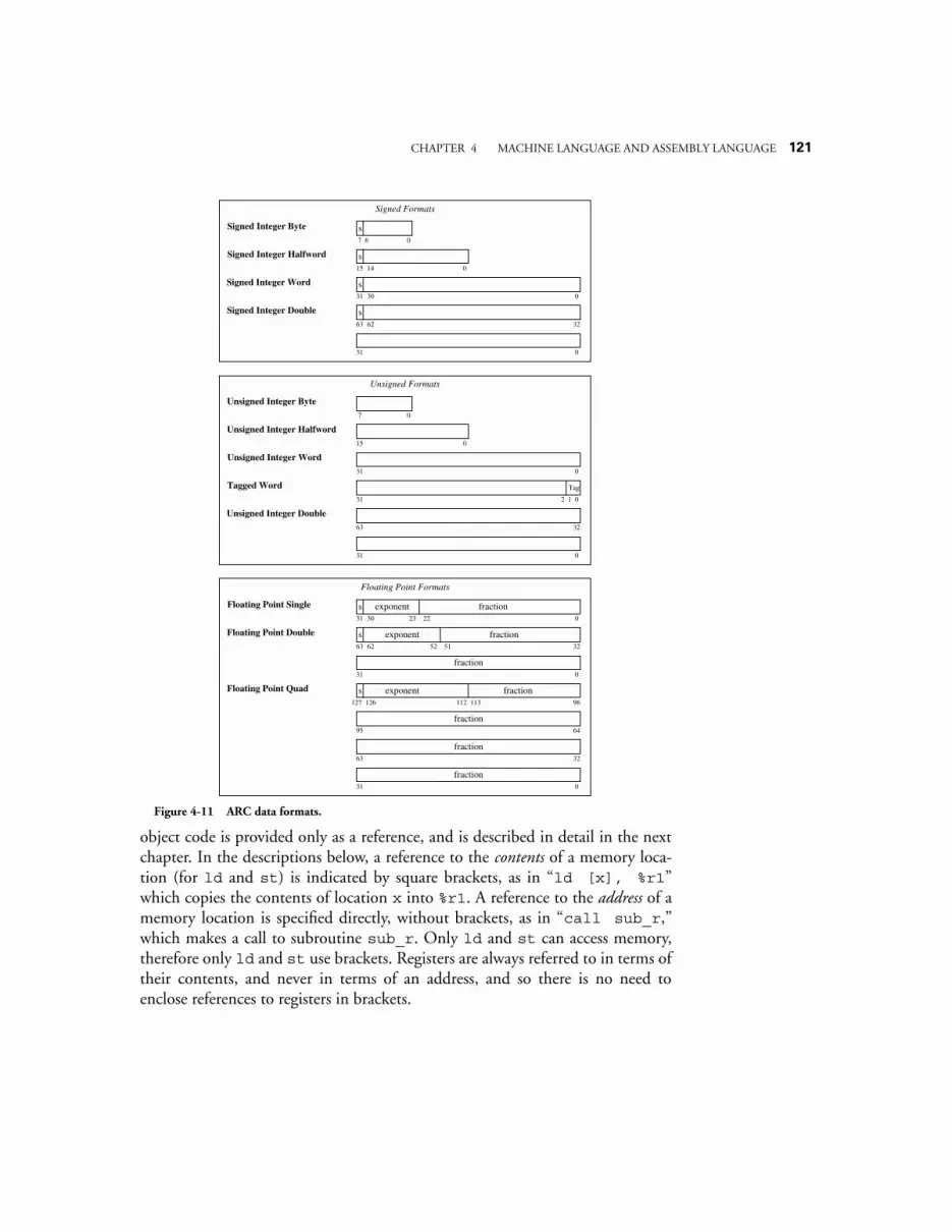
CHAPTER 4 MACHINE LANGUAGE AND ASSEMBLY LANGUAGE 121
object code is provided only as a reference, and is described in detail in the nextchapter. In the descriptions below, a reference to the contents of a memory loca-tion (for ld and st) is indicated by square brackets, as in “ld [x], %r1”which copies the contents of location x into %r1. A reference to the address of amemory location is specified directly, without brackets, as in “call sub_r,”which makes a call to subroutine sub_r. Only ld and st can access memory,therefore only ld and st use brackets. Registers are always referred to in terms oftheir contents, and never in terms of an address, and so there is no need toenclose references to registers in brackets.
Signed Integer Byte s7 6 0
Signed Integer Halfword s15 14 0
Signed Integer Word s31 30 0
Signed Integer Double s63 62 32
31 0
Signed Formats
Unsigned Integer Byte7 0
Unsigned Integer Halfword15 0
Unsigned Integer Word31 0
Unsigned Integer Double63 32
31 0
Unsigned Formats
Floating Point Single
Floating Point Double
Floating Point Quad
31 0
s127 126 96
95 64
Floating Point Formats
Tagged Word31 0
Tag
12
s31 30 0
exponent fraction23 22
s63 62 32
exponent fraction
fraction
63 32
31 0
exponent fraction
52 51
113112
fraction
fraction
fraction
Figure 4-11 ARC data formats.
122 CHAPTER 4 MACHINE LANGUAGE AND ASSEMBLY LANGUAGE
Instruction: ldDescription: Load a register from main memory. The memory address must be alignedon a word boundary (that is, the address must be evenly divisible by 4). The address iscomputed by adding the contents of the register in the rs1 field to either the contents ofthe register in the rs2 field or the value in the simm13 field, as appropriate for the con-text.Example usage: ld [x], %r1
or ld [x], %r0, %r1or ld %r0+x, %r1
Meaning: Copy the contents of memory location x into register %r1.Object code: 11000010000000000010100000010000 (x = 2064)
Instruction: stDescription: Store a register into main memory. The memory address must be alignedon a word boundary. The address is computed by adding the contents of the register inthe rs1 field to either the contents of the register in the rs2 field or the value in thesimm13 field, as appropriate for the context. The rd field of this instruction is actuallyused for the source register.Example usage: st %r1, [x]Meaning: Copy the contents of register %r1 into memory location x.Object code: 11000010001000000010100000010000 (x = 2064)
Instruction: sethiDescription: Set the high 22 bits and zero the low 10 bits of a register. If the operand is0 and the register is %r0, then the instruction behaves as a no-op (NOP), which meansthat no operation takes place.Example usage: sethi 0x304F15, %r1Meaning: Set the high 22 bits of %r1 to (304F15)16, and set the low 10 bits to zero.Object code: 00000011001100000100111100010101
Instruction: andccDescription: Bitwise AND the source operands into the destination operand. The con-dition codes are set according to the result.Example usage: andcc %r1, %r2, %r3Meaning: Logically AND %r1 and %r2 and place the result in %r3.Object code: 10000110100010000100000000000010
Instruction: orccDescription: Bitwise OR the source operands into the destination operand. The condi-tion codes are set according to the result.Example usage: orcc %r1, 1, %r1Meaning: Set the least significant bit of %r1 to 1.Object code: 10000010100100000110000000000001

CHAPTER 4 MACHINE LANGUAGE AND ASSEMBLY LANGUAGE 123
Instruction: ornccDescription: Bitwise NOR the source operands into the destination operand. The con-dition codes are set according to the result.Example usage: orncc %r1, %r0, %r1Meaning: Complement %r1.Object code: 10000010101100000100000000000000
Instruction: srlDescription: Shift a register to the right by 0 – 31 bits. The vacant bit positions in theleft side of the shifted register are filled with 0’s.Example usage: srl %r1, 3, %r2Meaning: Shift %r1 right by three bits and store in %r2. Zeros are copied into the threemost significant bits of %r2.Object code: 10000101001100000110000000000011
Instruction: addccDescription: Add the source operands into the destination operand using two’s comple-ment arithmetic. The condition codes are set according to the result.Example usage: addcc %r1, 5, %r1Meaning: Add 5 to %r1.Object code: 10000010100000000110000000000101
Instruction: callDescription: Call a subroutine and store the address of the current instruction (wherethe call itself is stored) in %r15, which effects a “call and link” operation. In the assem-bled code, the disp30 field in the CALL format will contain a 30-bit displacementfrom the address of the call instruction. The address of the next instruction to be exe-cuted is computed by adding 4 × disp30 (which shifts disp30 to the high 30 bits ofthe 32-bit address) to the address of the current instruction. Note that disp30 can benegative.Example usage: call sub_rMeaning: Call a subroutine that begins at location sub_r. For the object code shownbelow, sub_r is 25 words (100 bytes) farther in memory than the call instruction.Object code: 01000000000000000000000000011001
Instruction: jmplDescription: Jump and link (return from subroutine). Jump to a new address and storethe address of the current instruction (where the jmpl instruction is located) in the des-tination register.Example usage: jmpl %r15 + 4, %r0Meaning: Return from subroutine. The value of the PC for the call instruction was pre-viously saved in %r15, and so the return address should be computed for the instructionthat follows the call, at %r15 + 4. The current address is discarded in %r0.Object code: 10000001110000111110000000000100
124 CHAPTER 4 MACHINE LANGUAGE AND ASSEMBLY LANGUAGE
Instruction: beDescription: If the z condition code is 1, then branch to the address computed by add-ing 4 × disp22 in the Branch instruction format to the address of the current instruc-tion. If the z condition code is 0, then control is transferred to the instruction thatfollows be.Example usage: be labelMeaning: Branch to label if the z condition code is 1. For the object code shownbelow, label is five words (20 bytes) farther in memory than the be instruction.Object code: 00000010100000000000000000000101
Instruction: bnegDescription: If the n condition code is 1, then branch to the address computed by add-ing 4 × disp22 in the Branch instruction format to the address of the current instruc-tion. If the n condition code is 0, then control is transferred to the instruction thatfollows bneg.Example usage: bneg labelMeaning: Branch to label if the n condition code is 1. For the object code shownbelow, label is five words farther in memory than the bneg instruction.Object code: 00001100100000000000000000000101
Instruction: bcsDescription: If the c condition code is 1, then branch to the address computed by add-ing 4 × disp22 in the Branch instruction format to the address of the current instruc-tion. If the c condition code is 0, then control is transferred to the instruction thatfollows bcs.Example usage: bcs labelMeaning: Branch to label if the c condition code is 1. For the object code shownbelow, label is five words farther in memory than the bcs instruction.Object code: 00001010100000000000000000000101
Instruction: bvsDescription: If the v condition code is 1, then branch to the address computed by add-ing 4 × disp22 in the Branch instruction format to the address of the current instruc-tion. If the v condition code is 0, then control is transferred to the instruction thatfollows bvs.Example usage: bvs labelMeaning: Branch to label if the v condition code is 1. For the object code shownbelow, label is five words farther in memory than the bvs instruction.Object code: 00001110100000000000000000000101
Instruction: baDescription: Branch to the address computed by adding 4 × disp22 in the Branchinstruction format to the address of the current instruction.Example usage: ba label
CHAPTER 4 MACHINE LANGUAGE AND ASSEMBLY LANGUAGE 125
Meaning: Branch to label regardless of the settings of the condition codes. For theobject code shown below, label is five words earlier in memory than the ba instruc-tion.Object code: 00010000101111111111111111111011
4.3 Pseudo-OpsIn addition to the ARC instructions that are supported by the architecture, thereare also pseudo-operations (pseudo-ops) that are not opcodes at all, but ratherinstructions to the assembler to perform some action at assembly time. A list ofpseudo-ops and examples of their usages are shown in Figure 4-12. Note that
unlike processor opcodes, which are specific to a given machine, the kind andnature of the pseudo-ops are specific to a given assembler, because they are exe-cuted by the assembler itself.
The .equ pseudo-op instructs the assembler to equate a value or a characterstring with a symbol, so that the symbol can be used throughout a program as ifthe value or string is written in its place. The .begin and .end pseudo-ops tellthe assembler when to start and stop assembling. Any statements that appearbefore .begin or after .end are ignored. A single program may have more thanone .begin/.end pair, but there must be a .end for every .begin, and theremust be at least one .begin. The use of .begin and .end are helpful in mak-ing portions of the program invisible to the assembler during debugging.
Pseudo-Op Usage Meaning
.equ .equ #10 Treat symbol X as (10)16
.begin .begin Start assembling
.end .end Stop assembling
.org .org 2048 Change location counter to 2048
.dwb .dwb 25 Reserve a block of 25 words
X
.global .global Y Y is used in another module
.extern .extern Z Z is defined in another module
.macro .macro M a, b, ...
parameters a, b, ...
.endmacro .endmacro End of macro definition
.if .if <cond> Assemble if <cond> is true
.endif .endif End of .if construct
Define macro M with formal
Figure 4-12 Pseudo-ops for the ARC assembly language.
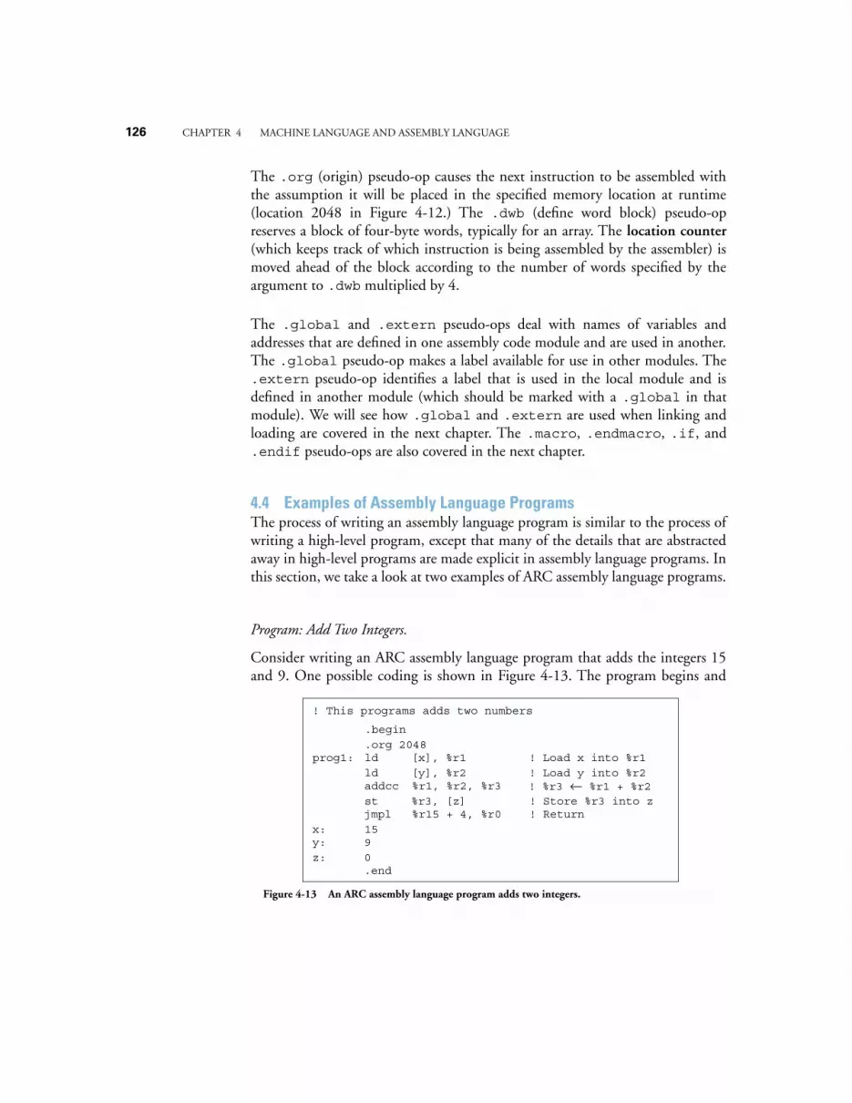
126 CHAPTER 4 MACHINE LANGUAGE AND ASSEMBLY LANGUAGE
The .org (origin) pseudo-op causes the next instruction to be assembled withthe assumption it will be placed in the specified memory location at runtime(location 2048 in Figure 4-12.) The .dwb (define word block) pseudo-opreserves a block of four-byte words, typically for an array. The location counter(which keeps track of which instruction is being assembled by the assembler) ismoved ahead of the block according to the number of words specified by theargument to .dwb multiplied by 4.
The .global and .extern pseudo-ops deal with names of variables andaddresses that are defined in one assembly code module and are used in another.The .global pseudo-op makes a label available for use in other modules. The.extern pseudo-op identifies a label that is used in the local module and isdefined in another module (which should be marked with a .global in thatmodule). We will see how .global and .extern are used when linking andloading are covered in the next chapter. The .macro, .endmacro, .if, and.endif pseudo-ops are also covered in the next chapter.
4.4 Examples of Assembly Language ProgramsThe process of writing an assembly language program is similar to the process ofwriting a high-level program, except that many of the details that are abstractedaway in high-level programs are made explicit in assembly language programs. Inthis section, we take a look at two examples of ARC assembly language programs.
Program: Add Two Integers.
Consider writing an ARC assembly language program that adds the integers 15and 9. One possible coding is shown in Figure 4-13. The program begins and
! This programs adds two numbers
.org 2048ld [x], %r1 ! Load x into %r1ld [y], %r2 ! Load y into %r2addcc %r1, %r2, %r3 ! %r3 ← %r1 + %r2
jmpl %r15 + 4, %r0 ! Returnx: 15y: 9
.end
.begin
prog1:
z: 0
st %r3, [z] ! Store %r3 into z
Figure 4-13 An ARC assembly language program adds two integers.
CHAPTER 4 MACHINE LANGUAGE AND ASSEMBLY LANGUAGE 127
ends with a .begin/.end pair. The .org pseudo-op instructs the assembler tobegin assembling so that the assembled code is loaded into memory starting atlocation 2048. The operands 15 and 9 are stored in variables x and y, respec-tively. We can only add numbers that are stored in registers in the ARC (becauseonly ld and st can access main memory), and so the program begins by loadingregisters %r1 and %r2 with x and y. The addcc instruction adds %r1 and %r2and places the result in %r3. The st instruction then stores %r3 in memorylocation z. The jmpl instruction with operands %r15 + 4, %r0 causes areturn to the next instruction in the calling routine, which is the operating sys-tem if this is the highest level of a user’s program as we can assume it is here. Thevariables x, y, and z follow the program.
In practice, the SPARC code equivalent to the ARC code shown in Figure 4-13 isnot entirely correct. The ld, st, and jmpl instructions all take at least twoinstruction cycles to complete, and since SPARC begins a new instruction ateach clock tick, these instructions need to be followed by an instruction that doesnot rely on their results. This property of launching a new instruction before theprevious one has completed is called pipelining, and is covered in more detail inChapter 9.
Program: Sum an Array of Integers
Now consider a more complex program that sums an array of integers. One pos-sible coding is shown in Figure 4-14. As in the previous example, the programbegins and ends with a .begin/.end pair. The .org pseudo-op instructs theassembler to begin assembling so that the assembled code is loaded into memorystarting at location 2048. A pseudo-operand is created for the symbol a_startwhich is assigned a value of 3000.
The program begins by loading the length of array a, which is given in bytes,into %r1. The program then loads the starting address of array a into %r2, andclears %r3 which will hold the partial sum. Register %r3 is cleared by ANDing itwith %r0, which always holds the value 0. Register %r0 can be ANDed with anyregister for that matter, and the result will still be zero.
The label loop begins a loop that adds successive elements of array a into thepartial sum (%r3) on each iteration. The loop starts by checking if the number ofremaining array elements to sum (%r1) is zero. It does this by ANDing %r1 withitself, which has the side effect of setting the condition codes. We are interestedin the z flag, which will be set to 1 if %r1 = 0. The remaining flags (n, v, and c)
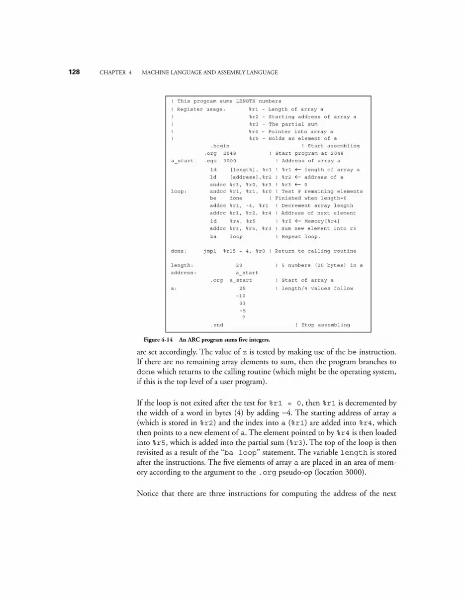
128 CHAPTER 4 MACHINE LANGUAGE AND ASSEMBLY LANGUAGE
are set accordingly. The value of z is tested by making use of the be instruction.If there are no remaining array elements to sum, then the program branches todone which returns to the calling routine (which might be the operating system,if this is the top level of a user program).
If the loop is not exited after the test for %r1 = 0, then %r1 is decremented bythe width of a word in bytes (4) by adding −4. The starting address of array a(which is stored in %r2) and the index into a (%r1) are added into %r4, whichthen points to a new element of a. The element pointed to by %r4 is then loadedinto %r5, which is added into the partial sum (%r3). The top of the loop is thenrevisited as a result of the “ba loop” statement. The variable length is storedafter the instructions. The five elements of array a are placed in an area of mem-ory according to the argument to the .org pseudo-op (location 3000).
Notice that there are three instructions for computing the address of the next
! %r5 – Holds an element of a
.begin ! Start assembling
.org 2048 ! Start program at 2048
be done ! Finished when length=0
addcc %r1, -4, %r1 ! Decrement array length
ld %r4, %r5 ! %r5 ← Memory[%r4]
addcc %r3, %r5, %r3 ! Sum new element into r3
ba loop ! Repeat loop.
done: jmpl %r15 + 4, %r0 ! Return to calling routine
length: 20 ! 5 numbers (20 bytes) in a
.org a_start ! Start of array a
a: 25 ! length/4 values follow
–10
33
–5 7
.end ! Stop assembling
! %r4 – Pointer into array a
! %r3 – The partial sum
! %r2 – Starting address of array a
! Register usage: %r1 – Length of array a
! This program sums LENGTH numbers
loop: andcc %r1, %r1, %r0 ! Test # remaining elements andcc %r3, %r0, %r3 ! %r3 ← 0
ld [address],%r2 ! %r2 ← address of a
ld [length], %r1 ! %r1 ← length of array a
addcc %r1, %r2, %r4 ! Address of next element
a_start .equ 3000 ! Address of array a
address: a_start
Figure 4-14 An ARC program sums five integers.
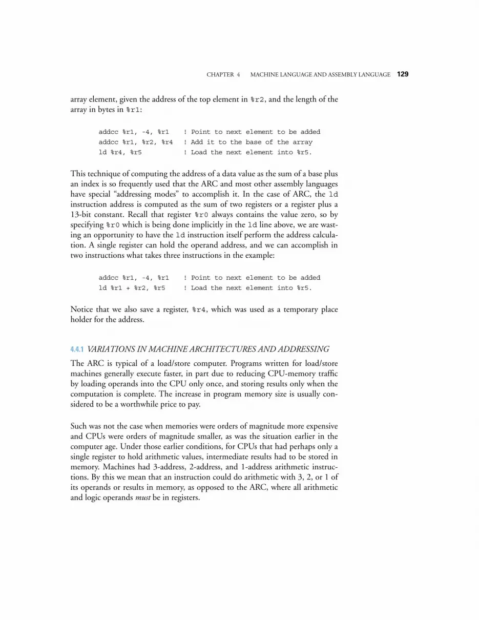
CHAPTER 4 MACHINE LANGUAGE AND ASSEMBLY LANGUAGE 129
array element, given the address of the top element in %r2, and the length of thearray in bytes in %r1:
addcc %r1, -4, %r1 ! Point to next element to be added
addcc %r1, %r2, %r4 ! Add it to the base of the array
ld %r4, %r5 ! Load the next element into %r5.
This technique of computing the address of a data value as the sum of a base plusan index is so frequently used that the ARC and most other assembly languageshave special “addressing modes” to accomplish it. In the case of ARC, the ldinstruction address is computed as the sum of two registers or a register plus a13-bit constant. Recall that register %r0 always contains the value zero, so byspecifying %r0 which is being done implicitly in the ld line above, we are wast-ing an opportunity to have the ld instruction itself perform the address calcula-tion. A single register can hold the operand address, and we can accomplish intwo instructions what takes three instructions in the example:
addcc %r1, -4, %r1 ! Point to next element to be added
ld %r1 + %r2, %r5 ! Load the next element into %r5.
Notice that we also save a register, %r4, which was used as a temporary placeholder for the address.
4.4.1 VARIATIONS IN MACHINE ARCHITECTURES AND ADDRESSING
The ARC is typical of a load/store computer. Programs written for load/storemachines generally execute faster, in part due to reducing CPU-memory trafficby loading operands into the CPU only once, and storing results only when thecomputation is complete. The increase in program memory size is usually con-sidered to be a worthwhile price to pay.
Such was not the case when memories were orders of magnitude more expensiveand CPUs were orders of magnitude smaller, as was the situation earlier in thecomputer age. Under those earlier conditions, for CPUs that had perhaps only asingle register to hold arithmetic values, intermediate results had to be stored inmemory. Machines had 3-address, 2-address, and 1-address arithmetic instruc-tions. By this we mean that an instruction could do arithmetic with 3, 2, or 1 ofits operands or results in memory, as opposed to the ARC, where all arithmeticand logic operands must be in registers.
130 CHAPTER 4 MACHINE LANGUAGE AND ASSEMBLY LANGUAGE
Let us consider how the C expression A = B*C + D might be evaluated by each ofthe three instruction types. In the examples below, when referring to a variable“A,” this actually means “the operand whose address is A.” In order to calculatesome performance statistics for the program fragments below we will make thefollowing assumptions:
• Addresses, opcodes, and data words are 16-bits – a not uncommon size inearlier machines.
• Opcodes are 8-bits in size.
• Operands are moved to and from memory one word at a time.
We will compute both program size, in bytes, and program memory traffic withthese assumptions.
Memory traffic has two components: the code itself, which must be fetched frommemory to the CPU in order to be executed, and the data values—operandsmust be moved into the CPU in order to be operated upon, and results movedback to memory when the computation is complete. Observing these computa-tions allows us to visualize some of the trade-offs between program size andmemory traffic that the various instruction classes offer.
Three-Address Instructions
In a 3-address instruction, the expression A = B*C + D might be coded as:
mult B, C, Aadd D, A, A
which means multiply B by C and store the result at A. (The mult and addoperations are generic; they are not ARC instructions.) Then, add D to A (at thispoint in the program, A holds the temporary result of multiplying B times C)and store the result at address A. The program size is 8×2 or 16 bytes. Memorytraffic is 16 + 2×2×3 or 28 bytes.
Two Address Instructions
In a two-address instruction, one of the operands is overwritten by the result.
CHAPTER 4 MACHINE LANGUAGE AND ASSEMBLY LANGUAGE 131
Here, the code for the expression A = B*C + D is:
load B, Amult C, Aadd D, A
The program size is now 3×3×2 or 18 bytes. Memory traffic is 18 + 2×2 + 2×2×3or 34 bytes.
One Address, or Accumulator Instructions
A one-address instruction employs a single arithmetic register in the CPU,known as the accumulator. The accumulator typically holds one arithmeticoperand, and also serves as the target for the result of an arithmetic operation.The one-address format is not in common use these days, but was more commonin the early days of computing when registers were more expensive and fre-quently served multiple purposes. It serves as temporary storage for one of theoperands and also for the result. The code for the expression A = B*C + D isnow:
load Bmult Cadd Dstore A
The load instruction loads B into the accumulator, mult multiplies C by theaccumulator and stores the result in the accumulator, and add does the corre-sponding addition. The store instruction stores the accumulator in A. The pro-gram size is now 2×2×4 or 16 bytes, and memory traffic is 16 + 4×2 or 24 bytes.
Special-Purpose Registers
In addition to the general-purpose registers and the accumulator describedabove, most modern architectures include other registers that are dedicated tospecific purposes. Examples include
• Memory index registers: The Intel 80x86 Source Index (SI) and Destina-tion Index (DI) registers. These are used to point to the beginning or endof an array in memory. Special “string” instructions transfer a byte or a
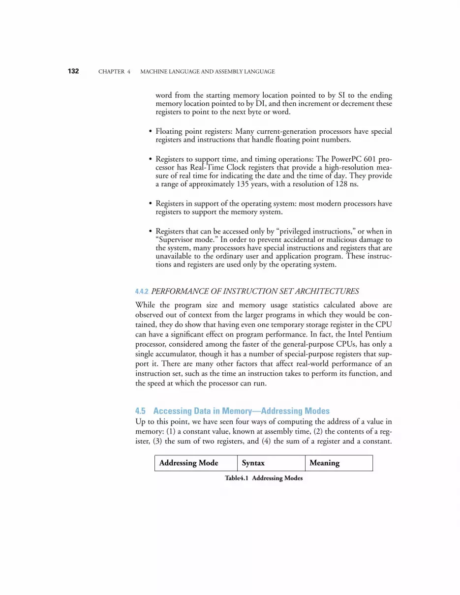
132 CHAPTER 4 MACHINE LANGUAGE AND ASSEMBLY LANGUAGE
word from the starting memory location pointed to by SI to the endingmemory location pointed to by DI, and then increment or decrement theseregisters to point to the next byte or word.
• Floating point registers: Many current-generation processors have specialregisters and instructions that handle floating point numbers.
• Registers to support time, and timing operations: The PowerPC 601 pro-cessor has Real-Time Clock registers that provide a high-resolution mea-sure of real time for indicating the date and the time of day. They providea range of approximately 135 years, with a resolution of 128 ns.
• Registers in support of the operating system: most modern processors haveregisters to support the memory system.
• Registers that can be accessed only by “privileged instructions,” or when in“Supervisor mode.” In order to prevent accidental or malicious damage tothe system, many processors have special instructions and registers that areunavailable to the ordinary user and application program. These instruc-tions and registers are used only by the operating system.
4.4.2 PERFORMANCE OF INSTRUCTION SET ARCHITECTURES
While the program size and memory usage statistics calculated above areobserved out of context from the larger programs in which they would be con-tained, they do show that having even one temporary storage register in the CPUcan have a significant effect on program performance. In fact, the Intel Pentiumprocessor, considered among the faster of the general-purpose CPUs, has only asingle accumulator, though it has a number of special-purpose registers that sup-port it. There are many other factors that affect real-world performance of aninstruction set, such as the time an instruction takes to perform its function, andthe speed at which the processor can run.
4.5 Accessing Data in Memory—Addressing ModesUp to this point, we have seen four ways of computing the address of a value inmemory: (1) a constant value, known at assembly time, (2) the contents of a reg-ister, (3) the sum of two registers, and (4) the sum of a register and a constant.
Addressing Mode Syntax Meaning
Table4.1 Addressing Modes
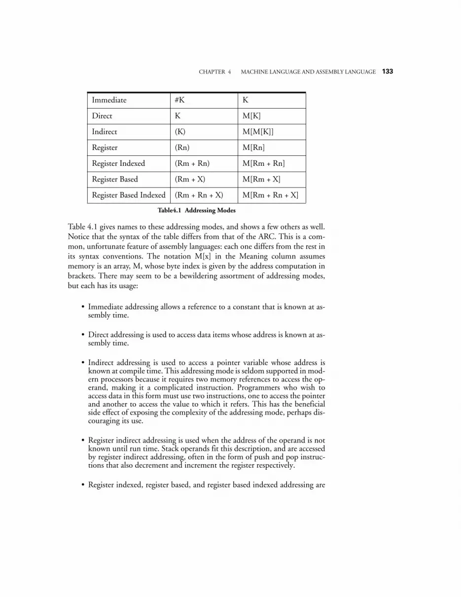
CHAPTER 4 MACHINE LANGUAGE AND ASSEMBLY LANGUAGE 133
Table 4.1 gives names to these addressing modes, and shows a few others as well.Notice that the syntax of the table differs from that of the ARC. This is a com-mon, unfortunate feature of assembly languages: each one differs from the rest inits syntax conventions. The notation M[x] in the Meaning column assumesmemory is an array, M, whose byte index is given by the address computation inbrackets. There may seem to be a bewildering assortment of addressing modes,but each has its usage:
• Immediate addressing allows a reference to a constant that is known at as-sembly time.
• Direct addressing is used to access data items whose address is known at as-sembly time.
• Indirect addressing is used to access a pointer variable whose address isknown at compile time. This addressing mode is seldom supported in mod-ern processors because it requires two memory references to access the op-erand, making it a complicated instruction. Programmers who wish toaccess data in this form must use two instructions, one to access the pointerand another to access the value to which it refers. This has the beneficialside effect of exposing the complexity of the addressing mode, perhaps dis-couraging its use.
• Register indirect addressing is used when the address of the operand is notknown until run time. Stack operands fit this description, and are accessedby register indirect addressing, often in the form of push and pop instruc-tions that also decrement and increment the register respectively.
• Register indexed, register based, and register based indexed addressing are
Immediate #K K
Direct K M[K]
Indirect (K) M[M[K]]
Register (Rn) M[Rn]
Register Indexed (Rm + Rn) M[Rm + Rn]
Register Based (Rm + X) M[Rm + X]
Register Based Indexed (Rm + Rn + X) M[Rm + Rn + X]
Table4.1 Addressing Modes
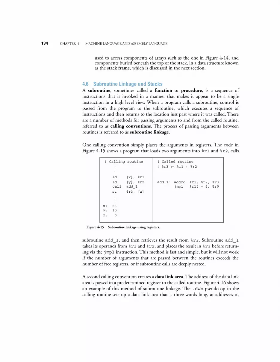
134 CHAPTER 4 MACHINE LANGUAGE AND ASSEMBLY LANGUAGE
used to access components of arrays such as the one in Figure 4-14, andcomponents buried beneath the top of the stack, in a data structure knownas the stack frame, which is discussed in the next section.
4.6 Subroutine Linkage and StacksA subroutine, sometimes called a function or procedure, is a sequence ofinstructions that is invoked in a manner that makes it appear to be a singleinstruction in a high level view. When a program calls a subroutine, control ispassed from the program to the subroutine, which executes a sequence ofinstructions and then returns to the location just past where it was called. Thereare a number of methods for passing arguments to and from the called routine,referred to as calling conventions. The process of passing arguments betweenroutines is referred to as subroutine linkage.
One calling convention simply places the arguments in registers. The code inFigure 4-15 shows a program that loads two arguments into %r1 and %r2, calls
subroutine add_1, and then retrieves the result from %r3. Subroutine add_1takes its operands from %r1 and %r2, and places the result in %r3 before return-ing via the jmpl instruction. This method is fast and simple, but it will not workif the number of arguments that are passed between the routines exceeds thenumber of free registers, or if subroutine calls are deeply nested.
A second calling convention creates a data link area. The address of the data linkarea is passed in a predetermined register to the called routine. Figure 4-16 showsan example of this method of subroutine linkage. The .dwb pseudo-op in thecalling routine sets up a data link area that is three words long, at addresses x,
! Calling routine
ld [x], %r1ld [y], %r2call add_1
st %r3, [z]
.
.
.
! Called routine
addcc %r1, %r2, %r3jmpl %r15 + 4, %r0
add_1:
.
.
.
! %r3 ← %r1 + %r2
53x:10y: 0z:
Figure 4-15 Subroutine linkage using registers.
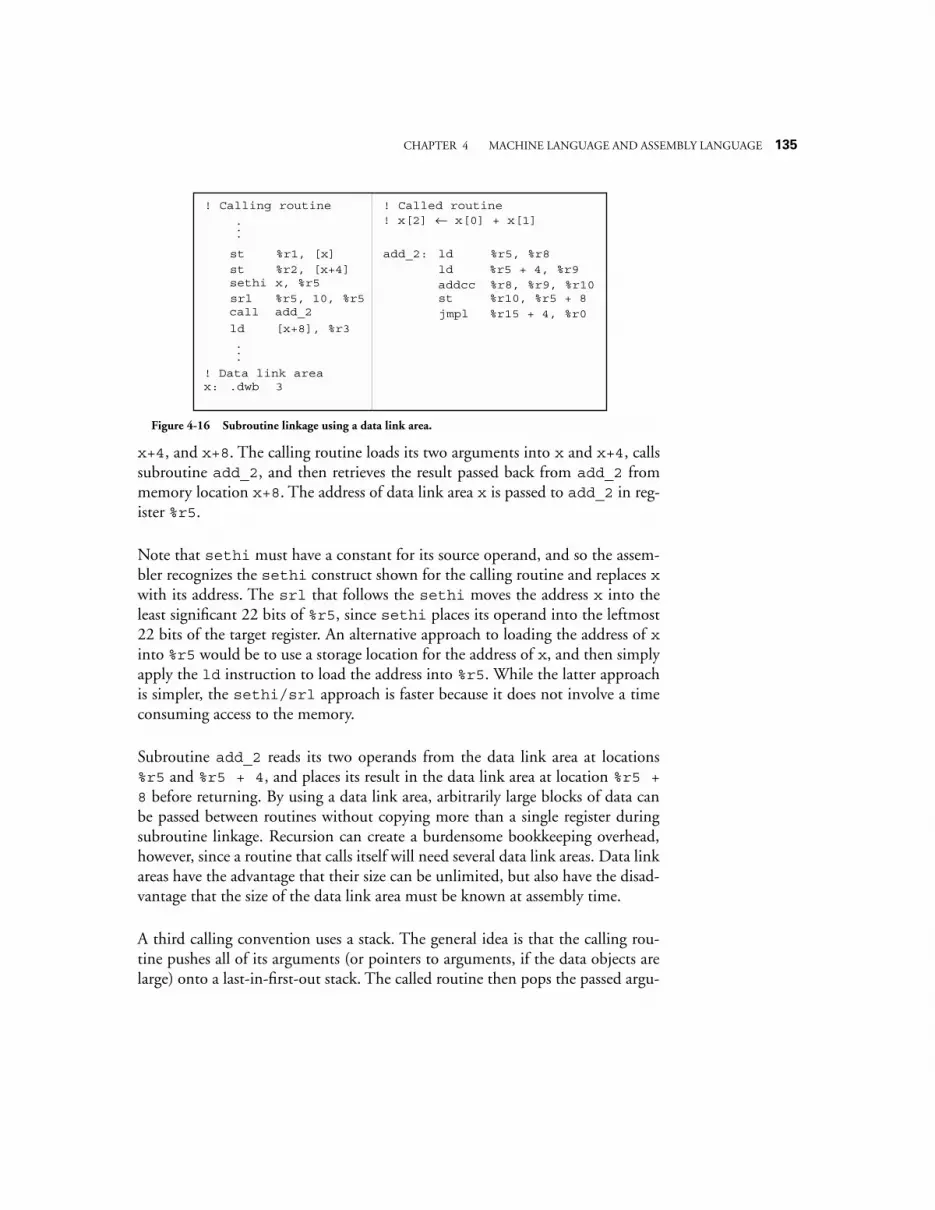
CHAPTER 4 MACHINE LANGUAGE AND ASSEMBLY LANGUAGE 135
x+4, and x+8. The calling routine loads its two arguments into x and x+4, callssubroutine add_2, and then retrieves the result passed back from add_2 frommemory location x+8. The address of data link area x is passed to add_2 in reg-ister %r5.
Note that sethi must have a constant for its source operand, and so the assem-bler recognizes the sethi construct shown for the calling routine and replaces xwith its address. The srl that follows the sethi moves the address x into theleast significant 22 bits of %r5, since sethi places its operand into the leftmost22 bits of the target register. An alternative approach to loading the address of xinto %r5 would be to use a storage location for the address of x, and then simplyapply the ld instruction to load the address into %r5. While the latter approachis simpler, the sethi/srl approach is faster because it does not involve a timeconsuming access to the memory.
Subroutine add_2 reads its two operands from the data link area at locations%r5 and %r5 + 4, and places its result in the data link area at location %r5 +8 before returning. By using a data link area, arbitrarily large blocks of data canbe passed between routines without copying more than a single register duringsubroutine linkage. Recursion can create a burdensome bookkeeping overhead,however, since a routine that calls itself will need several data link areas. Data linkareas have the advantage that their size can be unlimited, but also have the disad-vantage that the size of the data link area must be known at assembly time.
A third calling convention uses a stack. The general idea is that the calling rou-tine pushes all of its arguments (or pointers to arguments, if the data objects arelarge) onto a last-in-first-out stack. The called routine then pops the passed argu-
! Calling routine
st %r1, [x]st %r2, [x+4]sethi x, %r5
call add_2
x:
ld
.dwb
.
.
.
.
.
.
[x+8], %r3
3
! Called routine
ld %r5, %r8ld %r5 + 4, %r9addccst
%r8, %r9, %r10%r10, %r5 + 8
add_2:
jmpl %r15 + 4, %r0srl %r5, 10, %r5
! Data link area
! x[2] ← x[0] + x[1]
Figure 4-16 Subroutine linkage using a data link area.
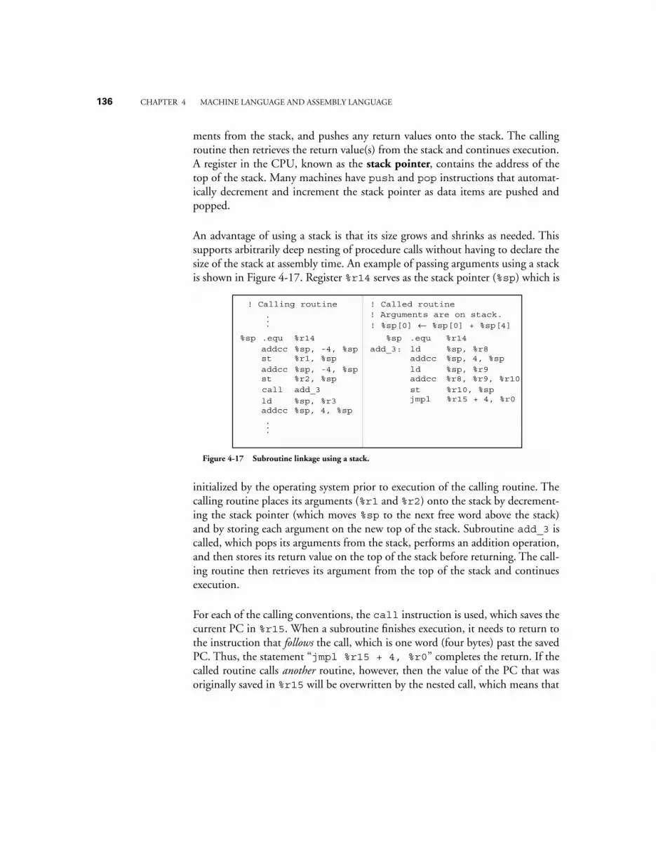
136 CHAPTER 4 MACHINE LANGUAGE AND ASSEMBLY LANGUAGE
ments from the stack, and pushes any return values onto the stack. The callingroutine then retrieves the return value(s) from the stack and continues execution.A register in the CPU, known as the stack pointer, contains the address of thetop of the stack. Many machines have push and pop instructions that automat-ically decrement and increment the stack pointer as data items are pushed andpopped.
An advantage of using a stack is that its size grows and shrinks as needed. Thissupports arbitrarily deep nesting of procedure calls without having to declare thesize of the stack at assembly time. An example of passing arguments using a stackis shown in Figure 4-17. Register %r14 serves as the stack pointer (%sp) which is
initialized by the operating system prior to execution of the calling routine. Thecalling routine places its arguments (%r1 and %r2) onto the stack by decrement-ing the stack pointer (which moves %sp to the next free word above the stack)and by storing each argument on the new top of the stack. Subroutine add_3 iscalled, which pops its arguments from the stack, performs an addition operation,and then stores its return value on the top of the stack before returning. The call-ing routine then retrieves its argument from the top of the stack and continuesexecution.
For each of the calling conventions, the call instruction is used, which saves thecurrent PC in %r15. When a subroutine finishes execution, it needs to return tothe instruction that follows the call, which is one word (four bytes) past the savedPC. Thus, the statement “jmpl %r15 + 4, %r0” completes the return. If thecalled routine calls another routine, however, then the value of the PC that wasoriginally saved in %r15 will be overwritten by the nested call, which means that
! Calling routine
.equ %r14addcc %sp, -4, %spst %r1, %spaddcc %sp, -4, %sp
%sp
stcall
.
.
.
.
.
.
%r2, %spadd_3
! Called routine
.equ %r14ld %sp, %r8addcc %sp, 4, %spld %sp, %r9addccst
%r8, %r9, %r10%r10, %sp
%sp
jmpl %r15 + 4, %r0
add_3:
ld %sp, %r3addcc %sp, 4, %sp
! Arguments are on stack.! %sp[0] ← %sp[0] + %sp[4]
Figure 4-17 Subroutine linkage using a stack.

CHAPTER 4 MACHINE LANGUAGE AND ASSEMBLY LANGUAGE 137
a correct return to the original calling routine through %r15 will no longer bepossible. In order to allow nested calls and returns, the current value of %r15(which is called the link register) should be saved on the stack, along with anyother registers that need to be restored after the return.
If a register based calling convention is used, then the link register should besaved in one of the unused registers before a nested call is made. If a data linkarea is used, then there should be space reserved within it for the link register. If astack scheme is used, then the link register should be saved on the stack. For eachof the calling conventions, the link register and the local variables in the calledroutines should be saved before a nested call is made, otherwise, a nested call tothe same routine will cause the local variables to be overwritten.
There are many variations to the basic calling conventions, but the stack-ori-ented approach to subroutine linkage is probably the most popular. When astack based calling convention is used that handles nested subroutine calls, astack frame is built that contains arguments that are passed to a called routine,the return address for the calling routine, and any local variables. A sample highlevel program is shown in Figure 4-18 that illustrates nested function calls. Theoperation that the program performs is not important, nor is the fact that the Cprogramming language is used, but what is important is how the subroutine callsare implemented.
The behavior of the stack for this program is shown in Figure 4-19. The mainprogram calls func_1 with arguments 1 and 2, and then calls func_2 withargument 10 before finishing execution. Function func_1 has two local vari-ables i and j that are used in computing the return value j. Function func_2has two local variables m and n that are used in creating the arguments to passthrough to func_1 before returning m.
The stack pointer (%r14 by convention, which will be referred to as %sp) is ini-tialized before the program starts executing, usually by the operating system. Thecompiler is responsible for implementing the calling convention, and so thecompiler produces code for pushing parameters and the return address onto thestack, reserving room on the stack for local variables, and then reversing the pro-cess as routines return from their calls. The stack behavior shown in Figure 4-19is thus produced as the result of executing compiler generated code, but the codemay just as well have been written directly in assembly language.
As the main program begins execution, the stack pointer points to the top ele-
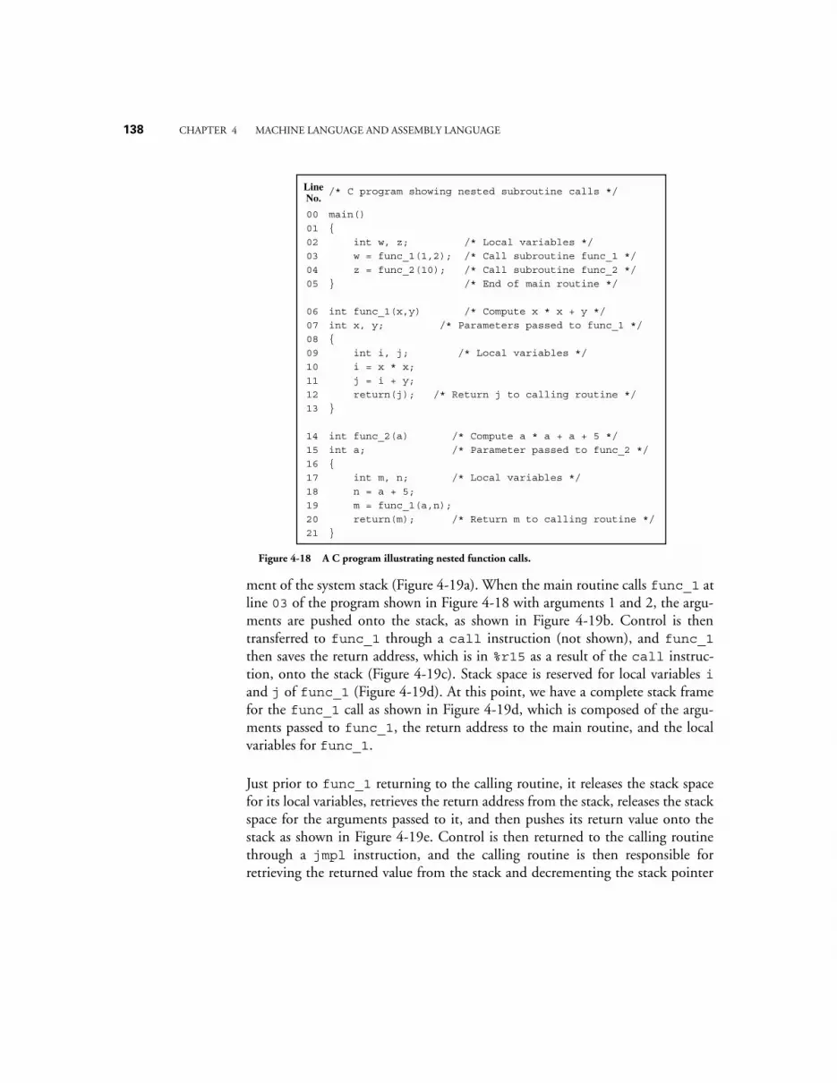
138 CHAPTER 4 MACHINE LANGUAGE AND ASSEMBLY LANGUAGE
ment of the system stack (Figure 4-19a). When the main routine calls func_1 atline 03 of the program shown in Figure 4-18 with arguments 1 and 2, the argu-ments are pushed onto the stack, as shown in Figure 4-19b. Control is thentransferred to func_1 through a call instruction (not shown), and func_1then saves the return address, which is in %r15 as a result of the call instruc-tion, onto the stack (Figure 4-19c). Stack space is reserved for local variables iand j of func_1 (Figure 4-19d). At this point, we have a complete stack framefor the func_1 call as shown in Figure 4-19d, which is composed of the argu-ments passed to func_1, the return address to the main routine, and the localvariables for func_1.
Just prior to func_1 returning to the calling routine, it releases the stack spacefor its local variables, retrieves the return address from the stack, releases the stackspace for the arguments passed to it, and then pushes its return value onto thestack as shown in Figure 4-19e. Control is then returned to the calling routinethrough a jmpl instruction, and the calling routine is then responsible forretrieving the returned value from the stack and decrementing the stack pointer
/* C program showing nested subroutine calls */
00
01
02
03
04
05
06
07
08
09
10
11
12
13
14
15
16
17
18
19
20
21
Line No.
main()
int w, z; /* Local variables */
w = func_1(1,2); /* Call subroutine func_1 */
z = func_2(10); /* Call subroutine func_2 */
/* End of main routine */
int func_1(x,y) /* Compute x * x + y */
int x, y; /* Parameters passed to func_1 */
int i, j; /* Local variables */
i = x * x;
j = i + y;
return(j); /* Return j to calling routine */
int func_2(a) /* Compute a * a + a + 5 */
int a; /* Parameter passed to func_2 */
int m, n; /* Local variables */
n = a + 5;
m = func_1(a,n);
return(m); /* Return m to calling routine */
Figure 4-18 A C program illustrating nested function calls.
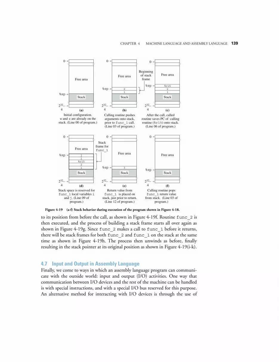
CHAPTER 4 MACHINE LANGUAGE AND ASSEMBLY LANGUAGE 139
to its position from before the call, as shown in Figure 4-19f. Routine func_2 isthen executed, and the process of building a stack frame starts all over again asshown in Figure 4-19g. Since func_2 makes a call to func_1 before it returns,there will be stack frames for both func_2 and func_1 on the stack at the sametime as shown in Figure 4-19h. The process then unwinds as before, finallyresulting in the stack pointer at its original position as shown in Figure 4-19(i-k).
4.7 Input and Output in Assembly LanguageFinally, we come to ways in which an assembly language program can communi-cate with the outside world: input and output (I/O) activities. One way thatcommunication between I/O devices and the rest of the machine can be handledis with special instructions, and with a special I/O bus reserved for this purpose.An alternative method for interacting with I/O devices is through the use of
Initial configuration.w and z are already on the
stack. (Line 00 of program.)
(a)Calling routine pushes arguments onto stack, prior to func_1 call.(Line 03 of program.)
(b)After the call, called
routine saves PC of calling routine (%r15) onto stack.
(Line 06 of program.)
(c)
0
232–4
Free area
%spStack
0
232–4
Free area
%sp
Stack
0
232–4
Free area
%sp
12
12
%r15
Beginning of stack frame
Stack space is reserved for func_1 local variables i
and j. (Line 09 of program.)
(d)Return value from
func_1 is placed on stack, just prior to return.
(Line 12 of program.)
(e)Calling routine pops func_1 return value
from stack. (Line 03 of program.)
(f)
0
232–4
Free area
Stack
0
232–4
Free area
Stack
0
232–4
3
Stack
%sp
Stack frame for func_1
%sp
Free area
%spStack
12
%r15ij
Figure 4-19 (a-f) Stack behavior during execution of the program shown in Figure 4-18.
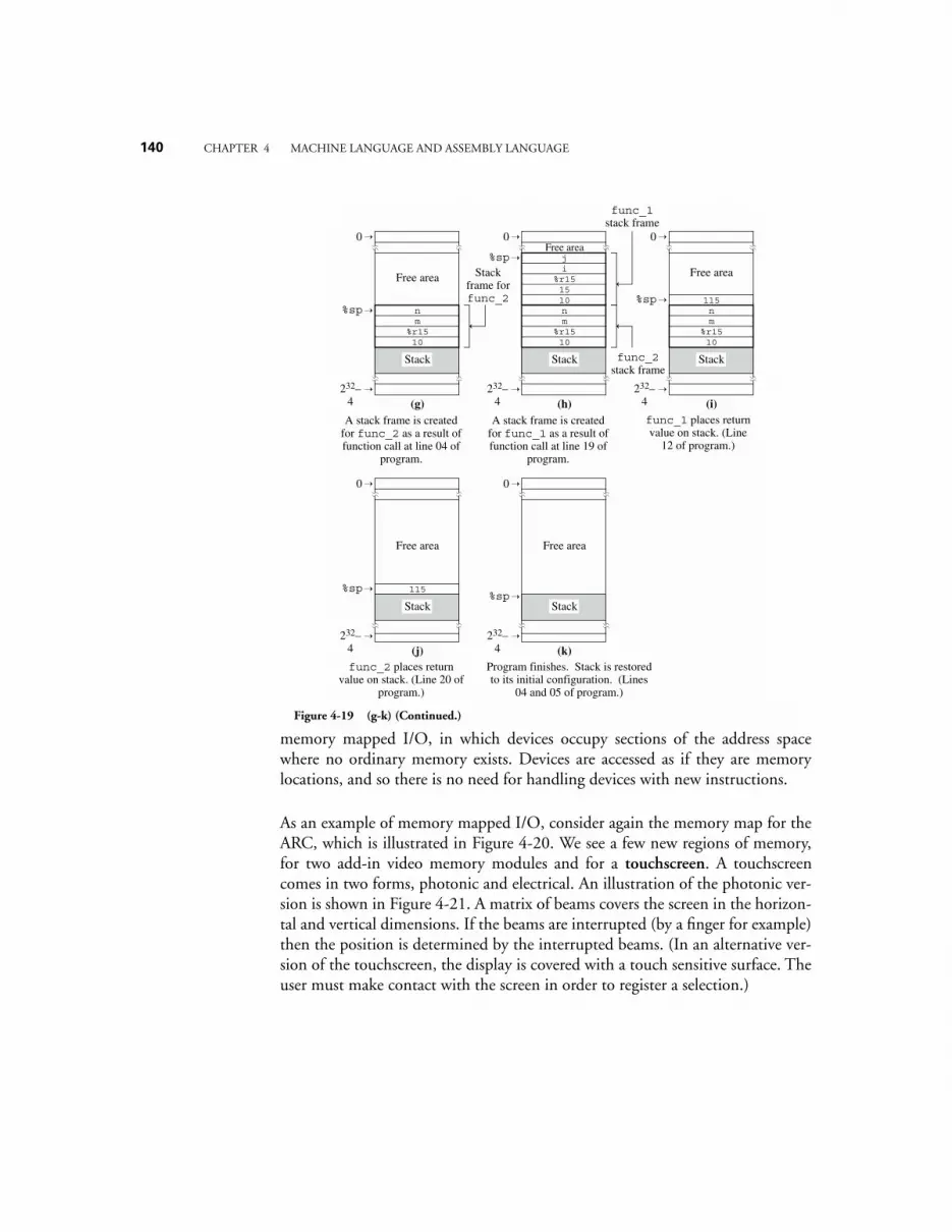
140 CHAPTER 4 MACHINE LANGUAGE AND ASSEMBLY LANGUAGE
memory mapped I/O, in which devices occupy sections of the address spacewhere no ordinary memory exists. Devices are accessed as if they are memorylocations, and so there is no need for handling devices with new instructions.
As an example of memory mapped I/O, consider again the memory map for theARC, which is illustrated in Figure 4-20. We see a few new regions of memory,for two add-in video memory modules and for a touchscreen. A touchscreencomes in two forms, photonic and electrical. An illustration of the photonic ver-sion is shown in Figure 4-21. A matrix of beams covers the screen in the horizon-tal and vertical dimensions. If the beams are interrupted (by a finger for example)then the position is determined by the interrupted beams. (In an alternative ver-sion of the touchscreen, the display is covered with a touch sensitive surface. Theuser must make contact with the screen in order to register a selection.)
A stack frame is created for func_2 as a result of function call at line 04 of
program.
(g)A stack frame is created
for func_1 as a result of function call at line 19 of
program.
(h)func_1 places return value on stack. (Line
12 of program.)
(i)
0
232–4
Free area
0
232–4
%sp
Stack
0
232–4
Free area
%sp
func_2 places return value on stack. (Line 20 of
program.)
(j)Program finishes. Stack is restored to its initial configuration. (Lines
04 and 05 of program.)
(k)
0
232–4
Free area
0
232–4
Stack
115%sp
Stack frame for func_2
Free area
%spStack
Stack
%sp
10%r15mn
10%r15mn1015
%r15ij
func_2 stack frame
func_1 stack frame
115
%r15mn
10
Stack
Free area
Figure 4-19 (g-k) (Continued.)
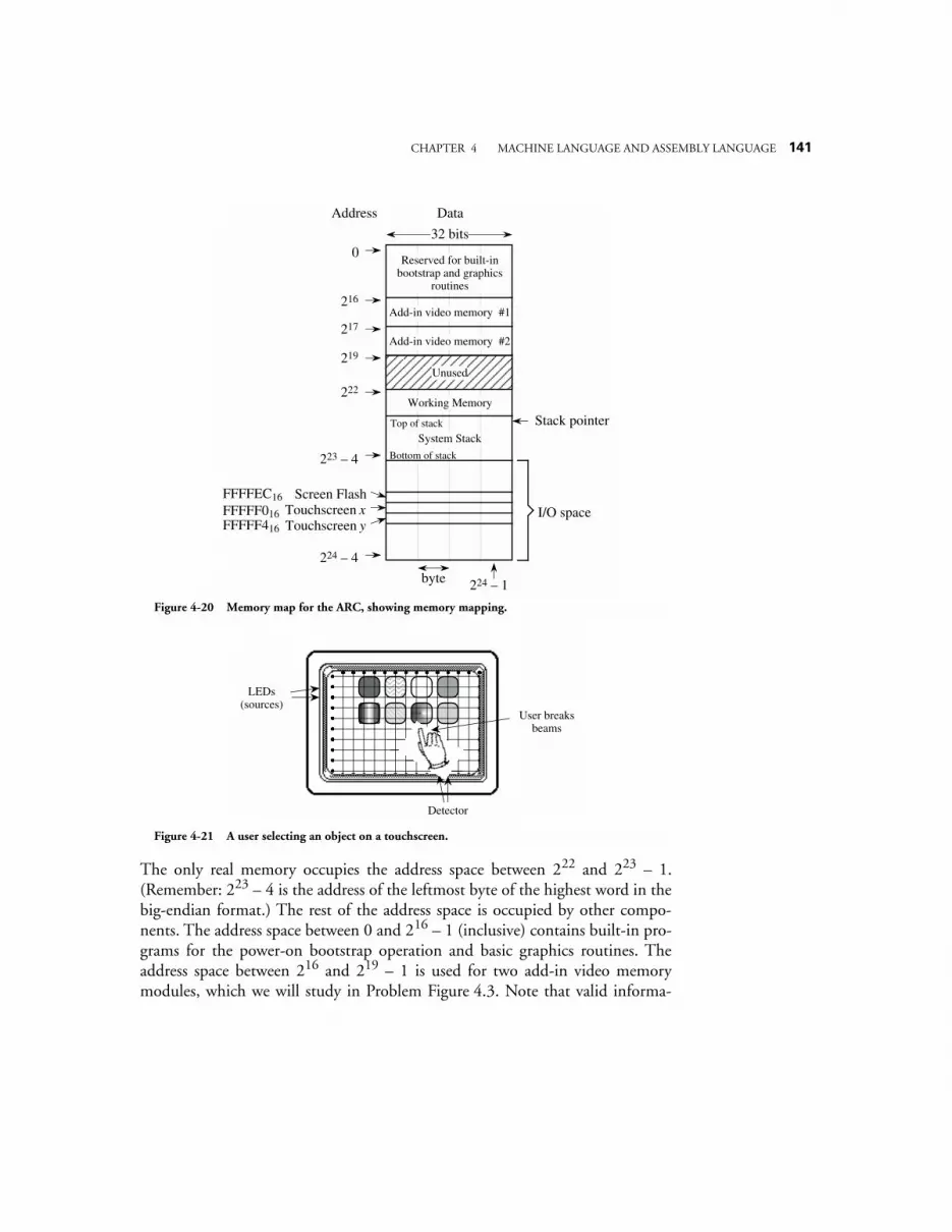
CHAPTER 4 MACHINE LANGUAGE AND ASSEMBLY LANGUAGE 141
The only real memory occupies the address space between 222 and 223 – 1.(Remember: 223 – 4 is the address of the leftmost byte of the highest word in thebig-endian format.) The rest of the address space is occupied by other compo-nents. The address space between 0 and 216 – 1 (inclusive) contains built-in pro-grams for the power-on bootstrap operation and basic graphics routines. Theaddress space between 216 and 219 – 1 is used for two add-in video memorymodules, which we will study in Problem Figure 4.3. Note that valid informa-
Reserved for built-in bootstrap and graphics
routines
Add-in video memory #1
I/O space
0
216
Stack pointerSystem Stack
Top of stack
Bottom of stack
Screen FlashTouchscreen xTouchscreen y
224 – 4
223 – 4
32 bits
Address Data
224 – 1byte
Add-in video memory #2217
219
Working Memory
Unused
222
FFFFEC16FFFFF016FFFFF416
Figure 4-20 Memory map for the ARC, showing memory mapping.
LEDs (sources)
Detector
User breaks beams
Figure 4-21 A user selecting an object on a touchscreen.
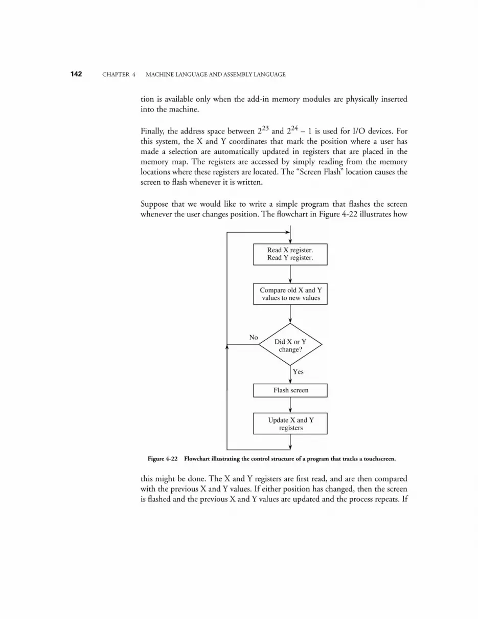
142 CHAPTER 4 MACHINE LANGUAGE AND ASSEMBLY LANGUAGE
tion is available only when the add-in memory modules are physically insertedinto the machine.
Finally, the address space between 223 and 224 – 1 is used for I/O devices. Forthis system, the X and Y coordinates that mark the position where a user hasmade a selection are automatically updated in registers that are placed in thememory map. The registers are accessed by simply reading from the memorylocations where these registers are located. The “Screen Flash” location causes thescreen to flash whenever it is written.
Suppose that we would like to write a simple program that flashes the screenwhenever the user changes position. The flowchart in Figure 4-22 illustrates how
this might be done. The X and Y registers are first read, and are then comparedwith the previous X and Y values. If either position has changed, then the screenis flashed and the previous X and Y values are updated and the process repeats. If
Compare old X and Y values to new values
Did X or Y change?
No
Yes
Read X register.Read Y register.
Flash screen
Update X and Y registers
Figure 4-22 Flowchart illustrating the control structure of a program that tracks a touchscreen.
CHAPTER 4 MACHINE LANGUAGE AND ASSEMBLY LANGUAGE 143
neither position has changed, then the process simply repeats. This is an exampleof the programmed I/O method of accessing a device. (See problem 4.3 at theend of the chapter for a more detailed description.)
4.8 Case Study: The Java Virtual Machine ISAJava is a high-level programming language developed by Sun Microsystems thathas taken a prominent position in the programming community. A key aspect ofJava is that Java binary codes are platform-independent, which means that thesame compiled code can run without modification on any computer that sup-ports the Java Virtual Machine (JVM). The JVM is how Java achieves its plat-form-independence: a standard specification of the JVM is implemented in thenative instruction sets of many underlying machines, and compiled Java codescan then run in any JVM environment.
Programs that are written in fully compiled languages like C, C++, and Fortran,are compiled into the native code of the target architecture, and are generally notportable across platforms unless the source code is recompiled for the targetmachine. Interpreted languages, like Perl, Tcl, AppleScript, and shell script, arelargely platform independent, but can execute 100 to 200 times slower than afully compiled language. Java programs are compiled into an intermediate formknown as bytecodes, which execute on the order of 10 times more slowly thanfully compiled languages, but the cross-platform compatibility and other lan-guage features make Java a favorable programming language for many applica-tions.
A high level view of the JVM architecture is shown in Figure 4-23. The JVM is astack-based machine, which means that the operands are pushed and poppedfrom a stack, instead of being transferred among general purpose registers. Thereare, however, a number of special purpose registers, and also a number of localvariables that serve the function of general purpose registers in a “real” (non-vir-tual) architecture. The Java Execution Engine takes compiled Java bytecodes atits input, and interprets the bytecodes in a software implementation of the JVM,or executes the bytecodes directly in a hardware implementation of the JVM.
Figure 4-24 shows a Java implementation of the SPARC program we studied inFigure 4-13. The figure shows both the Java source program and the bytecodesinto which it was compiled. The bytecode file is known as a Java class file (whichis what a compiled Java program is called.)
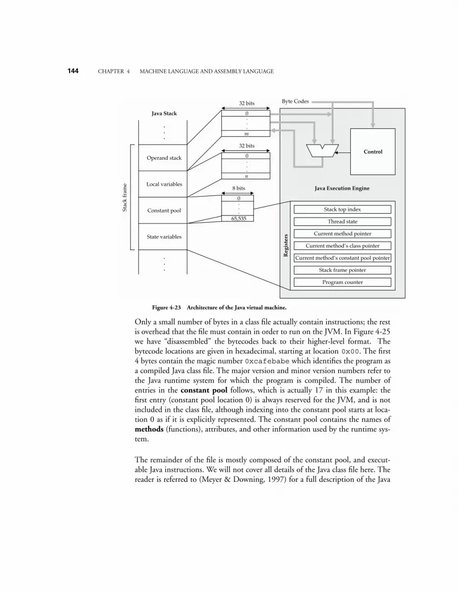
144 CHAPTER 4 MACHINE LANGUAGE AND ASSEMBLY LANGUAGE
Only a small number of bytes in a class file actually contain instructions; the restis overhead that the file must contain in order to run on the JVM. In Figure 4-25we have “disassembled” the bytecodes back to their higher-level format. Thebytecode locations are given in hexadecimal, starting at location 0x00. The first4 bytes contain the magic number 0xcafebabe which identifies the program asa compiled Java class file. The major version and minor version numbers refer tothe Java runtime system for which the program is compiled. The number ofentries in the constant pool follows, which is actually 17 in this example: thefirst entry (constant pool location 0) is always reserved for the JVM, and is notincluded in the class file, although indexing into the constant pool starts at loca-tion 0 as if it is explicitly represented. The constant pool contains the names ofmethods (functions), attributes, and other information used by the runtime sys-tem.
The remainder of the file is mostly composed of the constant pool, and execut-able Java instructions. We will not cover all details of the Java class file here. Thereader is referred to (Meyer & Downing, 1997) for a full description of the Java
State variables
Constant pool
Local variables
Operand stack
.
.
.
.
.
.
Stac
k fr
ame
Java Stack
Java Execution Engine
32 bits
32 bits
8 bits
.
.
.
0
n
.
.
.
0
65,535
Stack top index
Thread state
Current method pointer
Current method’s class pointer
Current method’s constant pool pointer
Stack frame pointer
Program counterR
egis
ters
.
.
.
0
m
Byte Codes
Control
Figure 4-23 Architecture of the Java virtual machine.

CHAPTER 4 MACHINE LANGUAGE AND ASSEMBLY LANGUAGE 145
class file format.
The actual code that corresponds to the Java source program, which simply addsthe constants 15 and 9, and returns the result (24) to the calling routine on thestack, appears in locations 0x00e3 - 0x00ef. Figure 4-26 shows how that por-tion of the bytecode is interpreted. The program pushes the constants 15 and 9onto the stack, using local variables 0 and 1 as intermediaries, and invokes theiadd instruction which pops the top two stack elements, adds them, and placesthe result on the top of the stack. The program then returns.
A cursory glance at the code shows some of the reasons why the JVM runs 10times slower than native code. Notice that the program stores the arguments inlocal variables 1 and 2, and then transfers them to the Java stack before addingthem. This transfer would be viewed as redundant by native code compilers forother langauges, and would be eliminated. Given this example alone, there isprobably considerable room for speed improvements from the 10× slower execu-tion time of today’s JVMs. Other improvements may also come in the form ofjust in time (JIT) compilers. Rather than interpreting the JVM bytecodes one
0000 cafe babe 0003 002d 0012 0700 0e07 0010 ................0010 0a00 0200 040c 0007 0005 0100 0328 2956 .............()V0020 0100 1628 5b4c 6a61 7661 2f6c 616e 672f ...([Ljava/lang/0030 5374 7269 6e67 3b29 5601 0006 3c69 6e69 String;)V...<ini0040 743e 0100 0443 6f64 6501 000d 436f 6e73 t>...Code...Cons0050 7461 6e74 5661 6c75 6501 000a 4578 6365 tantValue...Exce0060 7074 696f 6e73 0100 0f4c 696e 654e 756d ptions...LineNum0070 6265 7254 6162 6c65 0100 0e4c 6f63 616c berTable...Local0080 5661 7269 6162 6c65 7301 000a 536f 7572 Variables...Sour0090 6365 4669 6c65 0100 0361 6464 0100 0861 ceFile...add...a00a0 6464 2e6a 6176 6101 0010 6a61 7661 2f6c dd.java...java/l00b0 616e 672f 4f62 6a65 6374 0100 046d 6169 ang/Object...mai00c0 6e00 2100 0100 0200 0000 0000 0200 0900 n...............00d0 1100 0600 0100 0800 0000 2d00 0200 0400 ................00e0 0000 0d10 0f3c 1009 3d03 3e1b 1c60 3eb1 ................00f0 0000 0001 000b 0000 000e 0003 0000 0004 ................0100 0008 0006 000c 0002 0001 0007 0005 0001 ................0110 0008 0000 001d 0001 0001 0000 0005 2ab7 ................0120 0003 b100 0000 0100 0b00 0000 0600 0100 ................0130 0000 0100 0100 0d00 0000 0200 0f00 ..............
// This is file add.java
public class add public static void main(String args[]) int x=15, y=9, z=0; z = x + y;
Figure 4-24 Java program and compiled class file.

146 CHAPTER 4 MACHINE LANGUAGE AND ASSEMBLY LANGUAGE
by one into the target machine code each time they are encountered, JIT compil-ers take advantage of the fact that most programs spend most of their time inloops and other iterative routines. As the JIT encounters each line of code for thefirst time, it compiles it into native code and stores it away in memory for possi-
Magic number
Minor versionMajor version
Tag = 7 (Class)18 items in constant pool
Name index = 14Tag = 7 (Class)
Name index = 16
Location
Tag = 10 (Methodref)
Class index = 2
Name and type index = 4
Tag = 12 (NameAndType)Name index = 7
Type index = 5Tag = 1 (Utf)
Length = 3 bytes“()V”
Tag = 1 (Utf)Length = 22 bytes “([Ljava/lang/”
“String;)V”
Tag = 1 (Utf) Length = 6 bytes“<ini”
“t>”
Tag = 1 (Utf)Length = 4 bytes “Code”
Tag = 1 (Utf)Length = 13 bytes “Cons”
“tantValue”
Tag = 1 (Utf)Length = 10 bytes “Exce”
“ptions”
Tag = 1 (Utf)Length = 15 bytes “LineNum”
“berTable”
Tag = 1 (Utf)Length = 14 bytes “Local”
“Variables”
Tag = 1 (Utf)Length = 10 bytes “Sour”
“ceFile”
Tag = 1 (Utf)Length = 3 bytes “add”
Tag = 1 (Utf)Length = 8 bytes
“a”
0000 cafe babe 0003 002d 0012 0700 0e07 0010
0010 0a00 0200 040c 0007 0005 0100 0328 2956
0020 0100 1628 5b4c 6a61 7661 2f6c 616e 672f
0030 5374 7269 6e67 3b29 5601 0006 3c69 6e69
0040 743e 0100 0443 6f64 6501 000d 436f 6e73
0050 7461 6e74 5661 6c75 6501 000a 4578 6365
0060 7074 696f 6e73 0100 0f4c 696e 654e 756d
0070 6265 7254 6162 6c65 0100 0e4c 6f63 616c
0080 5661 7269 6162 6c65 7301 000a 536f 7572
0090 6365 4669 6c65 0100 0361 6464 0100 0861
Figure 4-25 A Java class file.
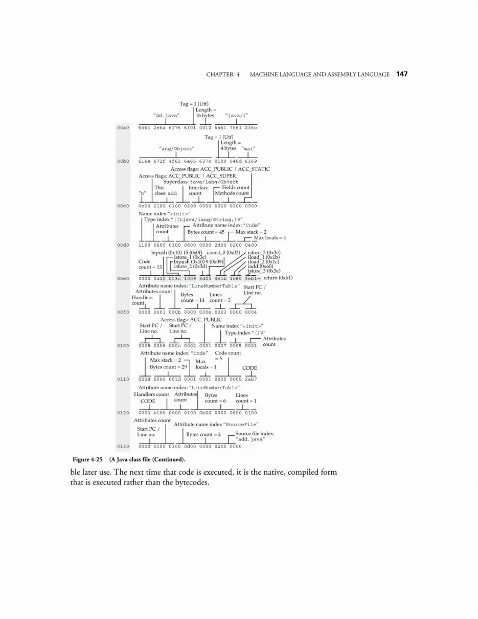
CHAPTER 4 MACHINE LANGUAGE AND ASSEMBLY LANGUAGE 147
ble later use. The next time that code is executed, it is the native, compiled formthat is executed rather than the bytecodes.
“dd.java”
Tag = 1 (Utf)Length = 16 bytes “java/l”
“ang/Object”
Tag = 1 (Utf)Length = 4 bytes “mai”
“n”
Access flags: ACC_PUBLIC | ACC_SUPER
Thisclass: add
Superclass: java/lang/ObjectInterface count
Fields countMethods count
Access flags: ACC_PUBLIC | ACC_STATIC
Type index “([Ljava/lang/String;)V”Attributes count
Attribute name index: “Code”
Name index “<init>”
Bytes count = 45 Max stack = 2Max locals = 4
Code count = 13
Attributes countHandlers count
Attribute name index: “LineNumberTable”
Bytes count = 14
Lines count = 3
Access flags: ACC_PUBLICName index “<init>”
Type index “()V”Attributes count
Attribute name index: “Code”
Bytes count = 29Max stack = 2 Max
locals = 1
Code count = 5
CODEAttributes count
Handlers countAttribute name index: “LineNumberTable”
Bytes count = 6
Lines count = 1
Attributes countAttribute name index “SourceFile”
Bytes count = 2 Source file index: “add.java”
Start PC / Line no.
Start PC / Line no.
Start PC / Line no.
Start PC / Line no.
bipush (0x10) 15 (0x0f)istore_1 (0x3c)bipush (0x10) 9 (0x09)
iconst_0 (0x03)
istore_2 (0x3d)
istore_3 (0x3e)iload_1 (0x1b)iload_2 (0x1c)iadd (0x60)istore_3 (0x3e)
return (0xb1)
CODE
00a0 6464 2e6a 6176 6101 0010 6a61 7661 2f6c
00b0 616e 672f 4f62 6a65 6374 0100 046d 6169
00c0 6e00 2100 0100 0200 0000 0000 0200 0900
00d0 1100 0600 0100 0800 0000 2d00 0200 0400
00e0 0000 0d10 0f3c 1009 3d03 3e1b 1c60 3eb1
00f0 0000 0001 000b 0000 000e 0003 0000 0004
0100 0008 0006 000c 0002 0001 0007 0005 0001
0110 0008 0000 001d 0001 0001 0000 0005 2ab7
0120 0003 b100 0000 0100 0b00 0000 0600 0100
0130 0000 0100 0100 0d00 0000 0200 0f00
Figure 4-25 (A Java class file (Continued).
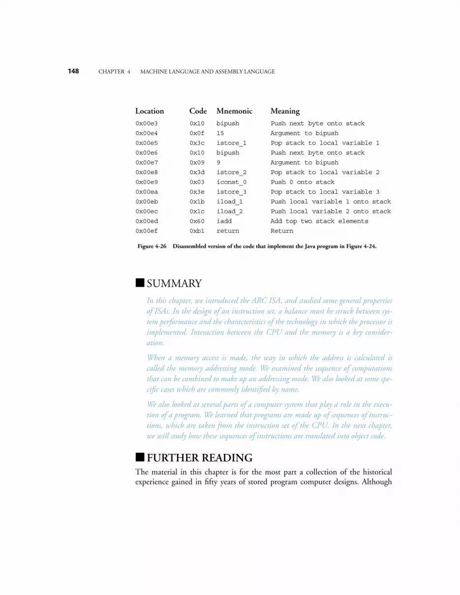
148 CHAPTER 4 MACHINE LANGUAGE AND ASSEMBLY LANGUAGE
SUMMARY
In this chapter, we introduced the ARC ISA, and studied some general propertiesof ISAs. In the design of an instruction set, a balance must be struck between sys-tem performance and the characteristics of the technology in which the processor isimplemented. Interaction between the CPU and the memory is a key consider-ation.
When a memory access is made, the way in which the address is calculated iscalled the memory addressing mode. We examined the sequence of computationsthat can be combined to make up an addressing mode. We also looked at some spe-cific cases which are commonly identified by name.
We also looked at several parts of a computer system that play a role in the execu-tion of a program. We learned that programs are made up of sequences of instruc-tions, which are taken from the instruction set of the CPU. In the next chapter,we will study how these sequences of instructions are translated into object code.
FURTHER READINGThe material in this chapter is for the most part a collection of the historicalexperience gained in fifty years of stored program computer designs. Although
Figure 4-26 Disassembled version of the code that implement the Java program in Figure 4-24.
Location Code Mnemonic Meaning
0x00e3 0x10 bipush Push next byte onto stack
0x00e4 0x0f 15 Argument to bipush
0x00e5 0x3c istore_1 Pop stack to local variable 1
0x00e6 0x10 bipush Push next byte onto stack
0x00e7 0x09 9 Argument to bipush
0x00e8 0x3d istore_2 Pop stack to local variable 2
0x00e9 0x03 iconst_0 Push 0 onto stack
0x00ea 0x3e istore_3 Pop stack to local variable 3
0x00eb 0x1b iload_1 Push local variable 1 onto stack
0x00ec 0x1c iload_2 Push local variable 2 onto stack
0x00ed 0x60 iadd Add top two stack elements
0x00ef 0xb1 return Return
CHAPTER 4 MACHINE LANGUAGE AND ASSEMBLY LANGUAGE 149
each generation of computer systems is typically identified by a specific hardwaretechnology, there have also been historically important instruction set architec-tures. In the first generation systems of the 1950’s, such as Von Neuman’sEDVAC, Eckert and Mauchly’s UNIVAC and the IBM 701, programming wasperformed by hand in machine language. Although simple, these instruction setarchitectures defined the fundamental concepts surrounding opcodes and oper-ands.
The concept of an instruction set architecture as an identifiable entity can betraced to the designers of the IBM S/360 in the 1960’s. The VAX architecture forDigital Equipment Corporation can also trace its roots to this period when theminicomputers, the PDP-4 and PDP-8 were being developed. Both the S/360and VAX are two-address architectures. Significant one-address architecturesinclude the Intel 8080 which is the predecessor to the modern 80x86, and itscontemporary at that time: the Zilog Z-80. As a zero-address architecture, theBurroughs B5000 is also of historical significance.
There are a host of references that cover the various machine languages in exist-ence, too many to enumerate here, and so we mention only a few of the morecelebrated cases. The machine languages of Babbage’s machines are covered in(Bromley, 1987). The machine language of the early Institute for AdvancedStudy (IAS) computer is covered in (Stallings, 1996). The IBM 360 machine lan-guage is covered in (Strubl, 1975). The machine language of the 68000 can befound in (Gill, 1987) and the machine language of the SPARC can be found in(SPARC, 1992). A full description of the JVM and the Java class file format canbe found in (Meyer & Downing, 1997.)
Bromley, A. G., “The Evolution of Babbage’s Calculating Engines,” Annals of theHistory of Computing, 9, pp. 113-138, (1987).
Gill, A., E. Corwin, and A. Logar, Assembly Language Programming for the 68000,Prentice-Hall, Englewood Cliffs, New Jersey, (1987).
Meyer, J. and T. Downing, Java Virtual Machine, O’Reilly & Associates, Sepasto-pol, California, (1997).
SPARC International, Inc., The SPARC Architecture Manual: Version 8, PrenticeHall, Englewood Cliffs, New Jersey, (1992).
Stallings, W., Computer Organization and Architecture, 4/e, Prentice Hall, Upper
150 CHAPTER 4 MACHINE LANGUAGE AND ASSEMBLY LANGUAGE
Saddle River, (1996).
Struble, G. W., Assembler Language Programming: The IBM System/360 and 370,2/e, Addison-Wesley, Reading, (1975).
PROBLEMS4.1 A memory has 224 addressable locations. What is the smallest width in
bits that the address can be while still being able to address all 224 locations?
4.2 What are the lowest and highest addresses in a 220 byte memory, in whicha four-byte word is the smallest addressable unit?
4.3 The memory map for the ARC is shown in Figure 4-20.
(a) How much memory (in bytes) is available for each of the add-in videomemory modules? (Give your answer as powers of two or sums of powers oftwo, e.g. 210.)
(b) When a finger is drawn across the touchscreen, the horizontal (x) and ver-tical (y) positions of the joystick are updated in registers that are accessed atlocations (FFFFF0)16 and (FFFFF4)16, respectively. When the number ‘1’ iswritten to the register at memory location (FFFFEC)16 the screen flashes, andthen location (FFFFEC)16 is automatically cleared to zero by the hardware(the software does not have to clear it). Write an ARC program that flashes thescreen every time the user’s position changes. Use the skeleton program shownbelow.
.beginld [x], %r7! %r7 and %r8 now point to theld [y], %r8! touchscreen x and y locationsld [flash], %r9! %r9 points to flash location
loop:ld %r7, %r1 ! Load current touchscreen positionld %r8, %r2! in %r1=x and %r2=yld [old_x], %r3! Load old touchscreen positionld [old_y], %r4! in %r3=x and %r4=yorncc %r3, %r0, %r3! Form 1’s complement of old_xaddcc %r3, 1, %r3! Form 2’s complement of old_xaddcc %r1, %r3, %r3! %r3 <- x - old_xbe x_not_moved! Branch if x did not changeba moved ! x changed, so no need to check y
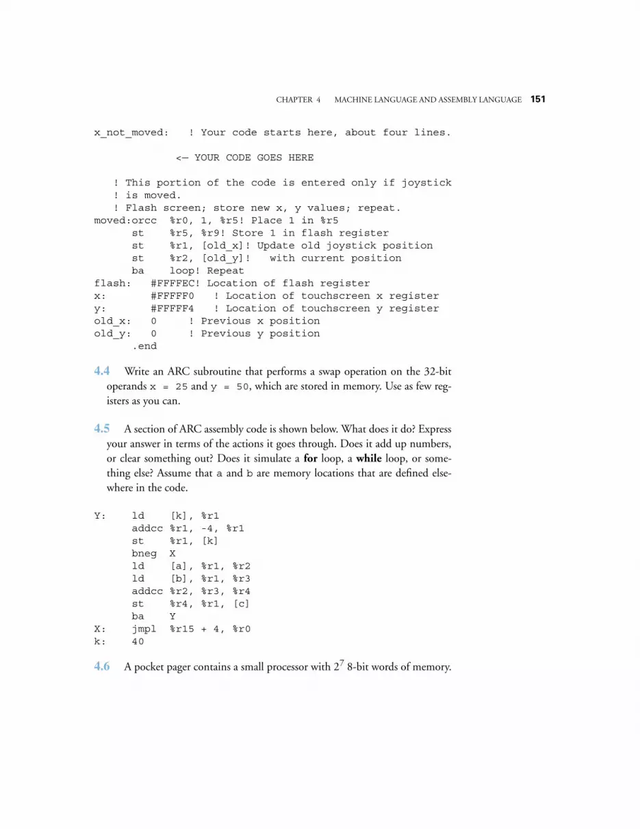
CHAPTER 4 MACHINE LANGUAGE AND ASSEMBLY LANGUAGE 151
x_not_moved: ! Your code starts here, about four lines.
<— YOUR CODE GOES HERE
! This portion of the code is entered only if joystick! is moved.! Flash screen; store new x, y values; repeat.
moved:orcc %r0, 1, %r5! Place 1 in %r5st %r5, %r9! Store 1 in flash registerst %r1, [old_x]! Update old joystick positionst %r2, [old_y]! with current positionba loop! Repeat
flash: #FFFFEC! Location of flash registerx: #FFFFF0 ! Location of touchscreen x registery: #FFFFF4 ! Location of touchscreen y register old_x: 0 ! Previous x positionold_y: 0 ! Previous y position
.end
4.4 Write an ARC subroutine that performs a swap operation on the 32-bitoperands x = 25 and y = 50, which are stored in memory. Use as few reg-isters as you can.
4.5 A section of ARC assembly code is shown below. What does it do? Expressyour answer in terms of the actions it goes through. Does it add up numbers,or clear something out? Does it simulate a for loop, a while loop, or some-thing else? Assume that a and b are memory locations that are defined else-where in the code.
Y: ld [k], %r1addcc %r1, -4, %r1st %r1, [k]bneg Xld [a], %r1, %r2ld [b], %r1, %r3addcc %r2, %r3, %r4st %r4, %r1, [c]ba Y
X: jmpl %r15 + 4, %r0k: 40
4.6 A pocket pager contains a small processor with 27 8-bit words of memory.
152 CHAPTER 4 MACHINE LANGUAGE AND ASSEMBLY LANGUAGE
The ISA has four registers: R0, R1, R2, and R3. The instruction set is shownin Figure 4-27, as well as the bit patterns that correspond to each register, the
instruction format, and the modes, which determine if the operand is a regis-ter (mode bit = 0) or the operand is a memory location (mode bit = 1). Eitheror both of the operands can be registers, but both operands cannot be mem-ory locations. If the source or destination is a memory location, then the cor-responding source or destination field in the instruction is not used since theaddress field is used instead.
(a) Write a program using object code (not mnemonics) that swaps the con-tents of registers R0 and R1. You are free to use the other registers as necessary,but do not use memory. Use no more than four lines of code (fewer lines arepossible). Place 0’s in any positions where the value does not matter.
(b) Write a program using object code that swaps the contents of memorylocations 12 and 13. As in part (a), you are free to use the other registers asnecessary, but do not use other memory locations. Place 0’s in any positionswhere the value does not matter.
INSTRUCTION FORMAT
OpcodeSrc
Mode SrcDst
Mode Dst Operand Address
MODE BIT PATTERNS
Mode Bit Pattern
Register
Direct
0
1
REGISTER BIT PATTERNS
Register Bit Pattern
R0
R1
00
01
R2 10
R3 11
INSTRUCTION SET
Mnemonic Opcode
LOAD 000
Meaning
Dst ← Src or Memory
STORE 001 Dst or Memory ← Src
ADD 010 Dst ← Src + Dst
AND 011 Dst ← AND(Src, Dst)
BZERO 100 Branch if Src = 0
JUMP 101 Unconditional jump
COMP 110 Dst ← Complement of Src
RSHIFT 111 Dst ← Src shifted right 1 bit
Note: Dst = Destination registerSrc = Source register
Figure 4-27 A pocket pager ISA.
CHAPTER 4 MACHINE LANGUAGE AND ASSEMBLY LANGUAGE 153
4.7 An ARC program calls the subroutine foo, passing it three arguments, a,b, and c. The subroutine has two local variables, m and n. Show the positionof the stack pointer and the contents of the relevant stack elements for a stackbased calling convention at the points in the program shown below:
(1) just before executing the call at label x;
(2) when the stack frame for foo is completed;
(3) just before executing the ld at label z (i.e., when the calling routineresumes).
Use the stack notation shown in Figure 4-19.
! Push the arguments a, b, and cx: call fooz: ld %r1, %r2
.
.
.foo:! Subroutine starts here
.
.
.y: jmpl %r15 + 4, %r0
4.8 Why does sethi only load the high 22 bits of a register? It would bemore useful if sethi loaded all 32 bits of a register. What is the problem withhaving sethi load all 32 bits?
4.9 Which of the three subroutine linkage conventions covered in this chapter(registers, data link area, stack) is used in Figure 4-14?
4.10 A program compiled for a SPARC ISA writes the 32-bit unsigned integer0xABCDEF01 to a file, and reads it back correctly. The same program com-piled for a Pentium ISA also works correctly. However, when the file is trans-ferred between machines, the program incorrectly reads the integer from thefile as 0x01EFCDAB. What is going wrong?
4.11 Refer to Figure 4-25. Show the Java assembly language instructions for the

154 CHAPTER 4 MACHINE LANGUAGE AND ASSEMBLY LANGUAGE
code shown in locations 0x011e - 0x0122. Use the syntax format shown inlocations 0x00e3 - 0x0ef of that same figure.
You will need to make use of the following Java instructions:
invokespecial n (opcode 0xb7) – Invoke a method with index n into theconstant pool. Note that n is a 16-bit (two-byte) index that follows theinvokespecial opcode.
aload_0 (opcode 0x2a) – Push local variable 0 onto the stack.
4.12 Is the JVM a little-endian or big-endian machine? Hint: Examine the firstline of the bytecode program in Figure 4-24.
4.13 Write an ARC program that implements the bytecode program shown inFigure 4-26. Assume that, analogous in the code in the figure, the argumentsare passed on a stack, and that the return value is placed on the top of thestack.
4.14 A JVM is implemented using the ARC ISA.
a) How much memory traffic will be generated when the program of Figure4-26 executes?
b) For exercise 4-13, compute the memory traffic your program will generate.Then, for part (a) above, compare that traffic with the amount generated byyour program. If most of the execution time of a program is due to its mem-ory accesses, how much faster will your program be compared to the programin Figure 4-26?
4.15 Can a Java bytecode program ever run as fast as a program written in thenative language of the processor? Defend your answer in one or two para-graphs.
4.16 (a) Write three-address, two-address, and one-address programs to com-pute the function A = (B-C)*(D-E). Assume 8-bit opcodes, 16-bit operandsand addresses, and that data is moved to and from memory in 16-bit chunks.(Also assume that the opcode must be transferred from memory by itself.)Your code should not overwrite any of the operands. Use any temporary regis-

CHAPTER 4 MACHINE LANGUAGE AND ASSEMBLY LANGUAGE 155
ters needed.
b. Compute the size of your program in bytes.
c. Compute the memory traffic your program will generate at execution time,including instruction fetches.
4.17 Repeat Exercise 4.12 above, using ARC assembly language.

156 CHAPTER 4 MACHINE LANGUAGE AND ASSEMBLY LANGUAGE
CHAPTER 5 LANGUAGES AND THE MACHINE
159
In the last chapter we looked at the relationship between the ISA, the assemblylanguage, and machine language. We also saw in some detail how instructionseffected register transfers and the movement of data between memory and theCPU, but we touched only briefly on the actual process of assembly and programlinking and loading. In this chapter we widen our view of the relationshipsbetween computer languages and the machine.
We begin by discussing
compilation
, the process of translating a program writ-ten in a high level language into a functionally equivalent program in assemblylanguage. Following that, we discuss the process of
assembly
, the translation ofan assembly language program into a functionally equivalent machine languageprogram. We then discuss
linking
, the process of linking together separatelyassembled modules into a single program, and
loading
, the process of movingprograms into memory and preparing them for execution. Following that, wediscuss the use of assembly language
macros
, which can be thought of as akin toassembly-time procedures, with the exception that they are placed inline, orexpanded, in the assembly language program at every location where they areinvoked.
5.1 The Compilation Process
As we will see later in the chapter, the process of assembling an assembly lan-guage program into machine code is rather straightforward, because there is aone to one mapping between assembly language statements and the equivalentmachine binary codes. High-level languages, on the other hand, present a muchmore complex problem.
LANGUAGES AND THE MACHINE
5
160
CHAPTER 5 LANGUAGES AND THE MACHINE
5.1.1
THE STEPS OF COMPILATION
Consider a simple assignment statement
A = B + 4
;
The compiler is faced with a number of fairly complex tasks in converting thisstatement into one or more assembly language statements:
• Reducing the program text to the basic symbols of the language, for exam-ple into identifiers such as
A
and
B
, denotations such as the constant value
4
, and program delimiters such as
=
and
+
. This portion of compilation isreferred to as
lexical analysis
.
• Parsing the symbols to recognize the underlying program structure. In thesample statement above, for example, the
parser
must recognize the state-ment as being an assignment statement of the form
Identifier “=” Expression,where Expression is further parsed into the form
Identifier “+” Constant.Parsing is sometimes called
syntactic analysis
.
• Name analysis: associating the names A and B with particular program vari-ables, and further associating them with particular memory locations wherethe variables will be located at run time.
• Type analysis: determining the type of all data items. In the case above, thevariables
A
and
B
, and constant
4
would be recognized as being of type
int
in some languages. Name and type analysis are sometimes referred to to-gether as
semantic analysis
: determining the underlying meaning of pro-gram components.
•
Action mapping
and
code generation
: associating program statementswith their appropriate assembly language sequence. In the statement above,the assembly language sequence might be as follows:
!Simple assignment statementld [B], %r0, %r1 !get variable B into a registeradd %r1, 4, %r2 !compute the value of the expr.st %r2, %r0, [A] !make the assignment
• There are additional steps that the compiler must take such as allocatingvariables to registers, tracking register usage, and, should the programmerdesire it, optimizing the program.

CHAPTER 5 LANGUAGES AND THE MACHINE
161
5.1.2
THE COMPILER MAPPING SPECIFICATION
When the compiler itself is being created, information about the particular ISAmust be embedded into it. (Note that the ISA on which the compiler executesdoes not need to be the same as the ISA code that the compiler generates, a pro-cess known as
cross compilation
.) This embedding is sometimes called the
mapping specification
for the compiler. For example, the compiler writer mustdecide how to map variables and constants of various types into the machine’sresources. This may be a function of both the machine and the high level lan-guage. In the C language, for example, integers (ints) can be 16, 32, or someother number of bits in size, while Java specifies that all ints be 32-bits in size.The example in the previous section, if considered for the C language, maps inte-gers to ARC 32-bit words.
The compiler writer must also take into account the features and limitations ofthe machine when mapping high level language constructs to assembly languagestatements or statement sequences. For example, the ARC instruction setrequires that all arithmetic operands must be either immediate constants or regis-ter variables. Therefore the compiler must generate code to get all variables intoregisters before any arithmetic instructions can be executed. This is the reason forthe instruction:
ld [B], %r1
in the example above.
In this text we concentrate on the mapping of common high level language con-structs to their equivalent assembly language constructs, leaving the details oflexical and syntactic and semantic analysis to compiler texts. (Several compilertexts are described in the Further Reading section at the end of this chapter forthe interested reader.)
5.1.3
HOW THE COMPILER MAPS THE THREE INSTRUCTION CLASSES INTO ASSEMBLY CODE
Let us consider in detail the mapping of the three instruction classes: data move-ment, arithmetic, and control flow, from high level language into assembly lan-guage. In the discussion and examples below we will use C as the examplelanguage. We choose C because of its popularity, and because its syntax andsemantics, while certainly high level, are still fairly close to assembly languageconcepts. The reader who is unfamiliar with C should not be distracted by this
162
CHAPTER 5 LANGUAGES AND THE MACHINE
choice; the syntax and semantics of C are easy to understand and carry over toother high level languages.
Variable storage in memory
In the example above, and in most of the programming examples in this text, ithas been assumed that variables can be accessed directly by their name, which ismapped to a memory location that is known at the time the program is assem-bled, sometimes called “assembly time.” In the example above,
A = B + 4
, it isassumed that the variables
A
and
B
have addresses that are known when the state-ment is compiled. In fact, only
global variables
, known as
static variables
in C,have addresses that are known at compile time. Variables declared inside of func-tions or inside of blocks that are not explicitly declared as static or global onlycome into existence when the function or block is entered, and they disappearwhen the function or block is exited for the last time. These variables are called
local
, or in C,
automatic variables
. In most programs, local variables are actu-ally much more common than global variables.
Given this ephemeral nature of local variables, a natural way of implementingthem is on a last-in-first-out stack as described in Chapter 4. Variables that arestored on the stack come into existence when the stack frame is created and thefunction is called, and they disappear when the function is exited for the lasttime. While the previous chapter employed the stack pointer,
%sp
, to access thestack frame, it is also common to copy the contents of
%sp
into another registercalled the frame pointer
%fp
(also known as the base pointer) upon entry intothe function, and then to use
%fp
to access variables on the stack frame for theduration of the function’s life. This is because temporary variables may be contin-ually pushed and popped onto and off of the stack during the lifetime of thefunction, resulting in a changing offset between
%sp
and the items on the stackframe. Using
%fp
means that the compiler can define a constant offset between
%fp
and a value stored on the stack that will remain fixed for the life of theframe.
Based addressing
is used to access stack variables. For example, an ARCvariable located on the stack at a location 12 bytes below
%fp
can loaded intoregister
%r1
by the instruction
ld %fp, -12, %r1
or, to use the more common notation,
ld [%fp - 12], %r1.
CHAPTER 5 LANGUAGES AND THE MACHINE
163
The use of based addressing thus allows the address arithmetic, “add the contentsof
%fp
to
-12
” to be performed in a single instruction. Based addressing is socommon that all popular instruction sets contain that addressing mode. Someinstruction sets contain even more complicated addressing modes to assist inaccessing complex data structures that are stored in the stack frame.
To emphasize the point, variables that are stored on the stack have memoryaddresses that are not known until run time. Their compile time addresses areknown as offsets from
%fp
. It is only at function entry time that the actual mem-ory address of the value is known. Thus even though stack variable addressessuch as
[%fp - 12]
are much more common than global variable addressessuch as
A,
we will assume global variables are used in the discussion belowbecause of the greater ease in understanding the relationship between the highlevel language variable name and the address as specified in assembly language.With that provision, let us now proceed to discuss three classes of program state-ments: data movement, arithmetic, and control flow.
5.1.4
DATA MOVEMENT
In addition to simple scalar variables, most programming languages provide vari-ous kinds of more complex data structures, including fixed record structures suchas the C
struct
data type, which is similar to the Pascal
record
, and the arraydata type common to most programming languages.
Structures
An example of a C
struct
is the representation of a point in 3-dimensionalspace having integer coordinates
x
,
y
, and
z
. In C this structure could be declaredas:
struct point int x;int y;int z;
An instance of this
struct
would be defined by the C statement
164
CHAPTER 5 LANGUAGES AND THE MACHINE
struct point pt;
Having defined point
pt
, the programmer can now refer to the individual com-ponents of
pt
by notation such as
pt.x
, which refers to the
x
component ofstruct
pt
. The compiler would lay out this structure in memory as three consec-utive memory locations.
The memory address of the entire structure is taken to be the lowest, or baseaddress of the structure, so the
x component would be located at address pt, they component at address pt + 4, and the z component at address pt + 8.Thus the y component of pt would be loaded into register %r1 by the instruc-tion
ld [pt + 4], %r1 !%r1 ← y
Arrays
Most programming languages also allow the declaration of arrays of objects, thatis, collections of identical components that can be referred to either individuallyor collectively. In C an array of ten integers can be defined with:
int A[10];
This definition would result in a collection of ten integers, indexed from 0 to 9.
The components of a struct must be explicitly named at programming time,for example, pt.z. References such as pt.i where i is a variable whose name isnot determined until run time are not allowed. With arrays, on the other hand,the array index can be computed at run time. For example, the programmer mayspecify array element A[i], where i is a variable whose value is computed at runtime and which may assume any integer value from 0 through 9. Whereas in Cthe index of the first element in the array always has an index of 0, other pro-gramming languages allow more flexibility. In Pascal, for example, array declara-tions such as:
A: array [-10..10] of integer
are permitted. This declaration would result in an array of 21 integers with indi-ces running from -10 to +10.
CHAPTER 5 LANGUAGES AND THE MACHINE 165
Accessing array elements presents a more complicated issue because of this needto compute the index at run time, and the possibility that indices may not beginwith 0. The general expression for computing the machine address of an arrayelement at run time is given by:
ElementAddress = BASE + (INDEX - START)*SIZE
where BASE is the starting address of the array, INDEX is the index of thedesired element, START is the starting index of the array, and SIZE is the size ofan individual element in bytes. Thus element 5 in the Pascal array declared abovewould have an address of A + (5 - (-10))*4 = A + 60. In ARC assembly language,assuming BASE in %r2, INDEX in %r3, START in %r4, and assuming SIZE =4, the code to load an array value into memory would be given by
sub %r3, %r4, %r6 !%r6 ← INDEX - STARTsll %r6, 2, %r6 !%r6 ← %r6 * 4ld [A + %r6], %r1 !%r1 ← array value
(sll is “shift left logical,” which shifts %r6 2 bits to the left is this example,bringing in two 0’s on the right.) Note that it costs three instructions to access anarray element, and more if SIZE is not a power of 2. Also note that in the C pro-gramming language, which specifies that START = 0, one machine instruction issaved for each array access. This may result in a considerable savings in scientificand engineering calculations, where heavy array references are common.
5.1.5 ARITHMETIC INSTRUCTIONS
Arithmetic instructions are mapped pretty much as expected from their usage.There is a possible complication in load-store machines such as ARC and com-mercial RISC machines, however. Regardless of how many registers with which amachine is endowed, there is always the possibility that the compiler willencounter an arithmetic instruction that requires more registers than are avail-able. In this case the compiler must temporarily store variables on the stack, aso-called “register spill.” Compilers use sophisticated techniques to decide whichregisters are available, using a graph-theoretic technique known as register color-ing, and to decide when the value in a register is no longer needed to store a par-ticular value, which is known as “live-dead analysis.”
166 CHAPTER 5 LANGUAGES AND THE MACHINE
5.1.6 PROGRAM CONTROL FLOW
Most ISAs use unconditional and conditional branches, and the CPU’s arith-metic flags to implement program control flow structures. In this section we con-sider the mapping of the most common control flow statements.
The goto statement
The most trivial control flow statement is the goto statement, goto Label,which is simply implemented by the ba (branch always) unconditional branch:
ba Label
The if-else statement
The C if-else statement has the syntax
if (expr) stmt1 else stmt2;
which has the meaning, “If expr yields a value of true, execute stmt1, other-wise execute stmt2.” Thus the compiler must evaluate the truth of expr, andexecute one or the other of the two statements depending upon the truth or fal-sity of the expression. Assume for brevity in the example below that expr is(%r1 == %r2), and introducing the bne, branch if not equal instruction, thenthe code to implement the if-else statement is:
subcc %r1, %r2, %r0 ! set flags, discard rsltbne Over!stmt1 codeba End ! exit if-else
Over: !stmt2 codeEnd: ! ...
Note that the sign of the conditional branch, bne, branch if not equal, is theinverse of the expression, (%r1 == %r2), equals. This is because the code fallsthrough to the stmt1 code if the condition is met, and must branch around thiscode if the condition is not met.
CHAPTER 5 LANGUAGES AND THE MACHINE 167
The while statement
The C while statement has the syntax:
while (expr) stmt;
The statement means, “Evaluate expr. If it is true, execute stmt, and repeat thisprocess until expr evaluates to false.” The assembly language mapping of thisstatement has the interesting feature that the most efficient mapping has theexpression evaluation code following the statement code. Consider the C whilestatement:
while (%r1 == %r2) %r3 = %r3 + 1;
where again we use register variables to simplify the code. This statement is effi-ciently implemented as:
ba TestTrue: add %r3, 1, %r3Test: subcc %r1, %r2, %r0
be True
The reader can verify that placing the expression evaluation code below the state-ment code is more efficient than having the expression evaluation code above thestatement code.
The do-while statement
C also has a do-while statement with the syntax:
do stmt while (expr);
This statement works like the while statement above except that stmt is alwaysexecuted once prior to testing expr. It is implemented exactly like the whilestatement above except that the first ba instruction is eliminated.
168 CHAPTER 5 LANGUAGES AND THE MACHINE
The for statement
The C for statement has the syntax:
for (expr1; expr2; expr3) stmt;
The C language definition says that this statement is equivalent to:
expr1;while (expr2)
stmtexpr3;
Thus it is implemented exactly like the while statements above, with the additionof code for expr1 and expr3.
5.2 The Assembly ProcessThe process of translating an assembly language program into a machine lan-guage program is referred to as the assembly process. The assembly process isstraightforward and rather simple, since there is a straightforward one-to-onemapping of assembly language statements to their machine language counter-parts. This is in opposition to compilation, for example, in which a givenhigh-level language statement may be translated into a number of computation-ally equivalent machine language statements.
While assembly is a straightforward process, it is tedious and error-prone if doneby hand. In fact, the assembler was one of the first software tools developed afterthe invention of the digital electronic computer.
Commercial assemblers provide at least the following capabilities:
• Allow the programmer to specify the run-time location of data values andprograms. (Most often, however, the programmer would not specify an ab-solute starting location for a program, because the program will be movedaround, or relocated, by the linker and perhaps the loader, as discussed be-low.)
• Provide a means for the programmer to initialize data values in memoryprior to program execution.
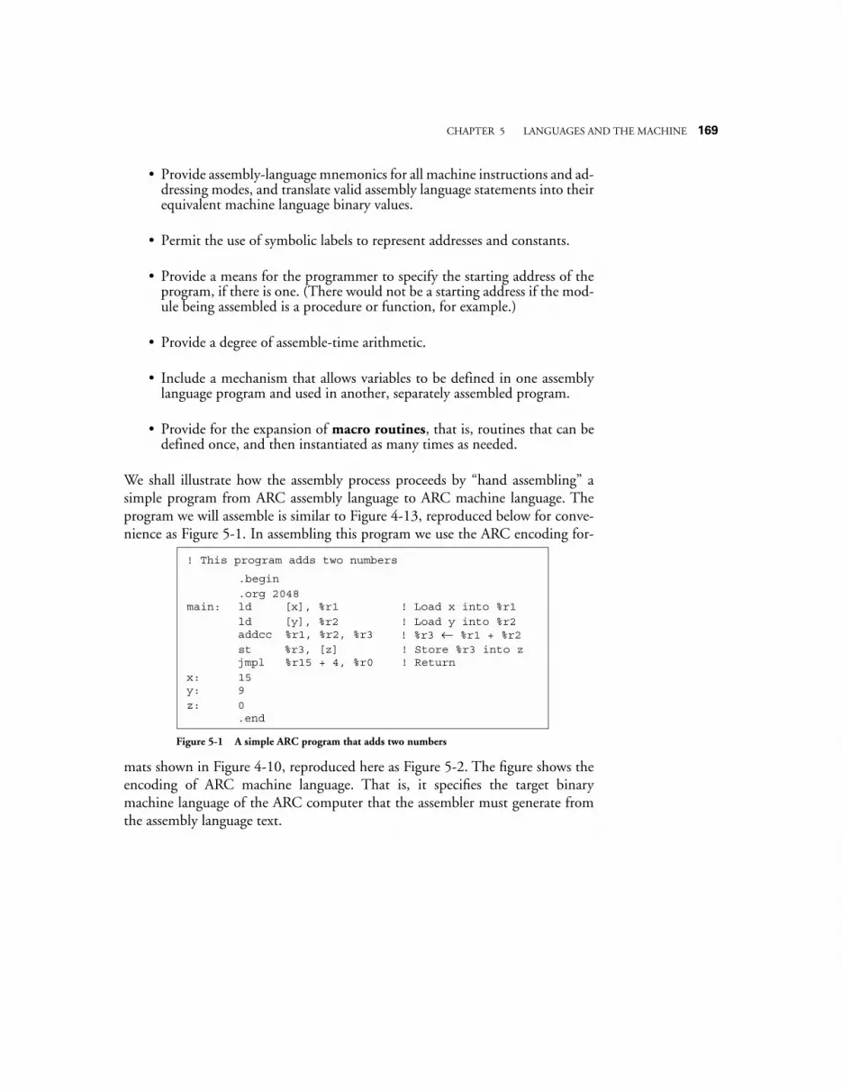
CHAPTER 5 LANGUAGES AND THE MACHINE 169
• Provide assembly-language mnemonics for all machine instructions and ad-dressing modes, and translate valid assembly language statements into theirequivalent machine language binary values.
• Permit the use of symbolic labels to represent addresses and constants.
• Provide a means for the programmer to specify the starting address of theprogram, if there is one. (There would not be a starting address if the mod-ule being assembled is a procedure or function, for example.)
• Provide a degree of assemble-time arithmetic.
• Include a mechanism that allows variables to be defined in one assemblylanguage program and used in another, separately assembled program.
• Provide for the expansion of macro routines, that is, routines that can bedefined once, and then instantiated as many times as needed.
We shall illustrate how the assembly process proceeds by “hand assembling” asimple program from ARC assembly language to ARC machine language. Theprogram we will assemble is similar to Figure 4-13, reproduced below for conve-nience as Figure 5-1. In assembling this program we use the ARC encoding for-
mats shown in Figure 4-10, reproduced here as Figure 5-2. The figure shows theencoding of ARC machine language. That is, it specifies the target binarymachine language of the ARC computer that the assembler must generate fromthe assembly language text.
! This program adds two numbers
.org 2048ld [x], %r1 ! Load x into %r1ld [y], %r2 ! Load y into %r2addcc %r1, %r2, %r3 ! %r3 ← %r1 + %r2
jmpl %r15 + 4, %r0 ! Returnx: 15y: 9
.end
.begin
main:
z: 0
st %r3, [z] ! Store %r3 into z
Figure 5-1 A simple ARC program that adds two numbers
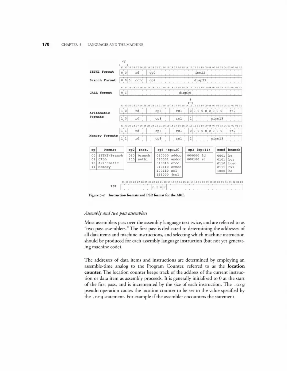
170 CHAPTER 5 LANGUAGES AND THE MACHINE
Assembly and two pass assemblers
Most assemblers pass over the assembly language text twice, and are referred to as“two-pass assemblers.” The first pass is dedicated to determining the addresses ofall data items and machine instructions, and selecting which machine instructionshould be produced for each assembly language instruction (but not yet generat-ing machine code).
The addresses of data items and instructions are determined by employing anassemble-time analog to the Program Counter, referred to as the locationcounter. The location counter keeps track of the address of the current instruc-tion or data item as assembly proceeds. It is generally initialized to 0 at the startof the first pass, and is incremented by the size of each instruction. The .orgpseudo operation causes the location counter to be set to the value specified bythe .org statement. For example if the assembler encounters the statement
op3 (op=10)
010000010001010010010110100110111000
addccandccorccornccsrljmpl
00010101011001111000
cond
bebcsbnegbvsba
branch
010100
op2
branchsethi
Inst.
00011011
op
SETHI/BranchCALLArithmeticMemory
Format
000000000100
ldst
op3 (op=11)
op
CALL format disp30
31 30 29 28 27 26 25 24 23 22 21 20 19 18 17 16 15 14 13 12 11 10 09 08 07 06 05 04 03 02 01 00
0 1
SETHI Format imm22
31 30 29 28 27 26 25 24 23 22 21 20 19 18 17 16 15 14 13 12 11 10 09 08 07 06 05 04 03 02 01 00
rd
disp220 cond
0 0
0 0Branch Format
op2
op2
31 30 29 28 27 26 25 24 23 22 21 20 19 18 17 16 15 14 13 12 11 10 09 08 07 06 05 04 03 02 01 00
rs11 op3
simm131 op3
1
Memory Formats1
rd
rd rs1
0
1
0 0 0 0 0 0 0 0 rs2
Arithmetic Formats
31 30 29 28 27 26 25 24 23 22 21 20 19 18 17 16 15 14 13 12 11 10 09 08 07 06 05 04 03 02 01 00
rs11 op3
simm131 op3
0
0
rd
rd rs1
0
1
0 0 0 0 0 0 0 0 rs2
i
PSR31 30 29 28 27 26 25 24 23 22 21 20 19 18 17 16 15 14 13 12 11 10 09 08 07 06 05 04 03 02 01 00
z v cn
Figure 5-2 Instruction formats and PSR format for the ARC.
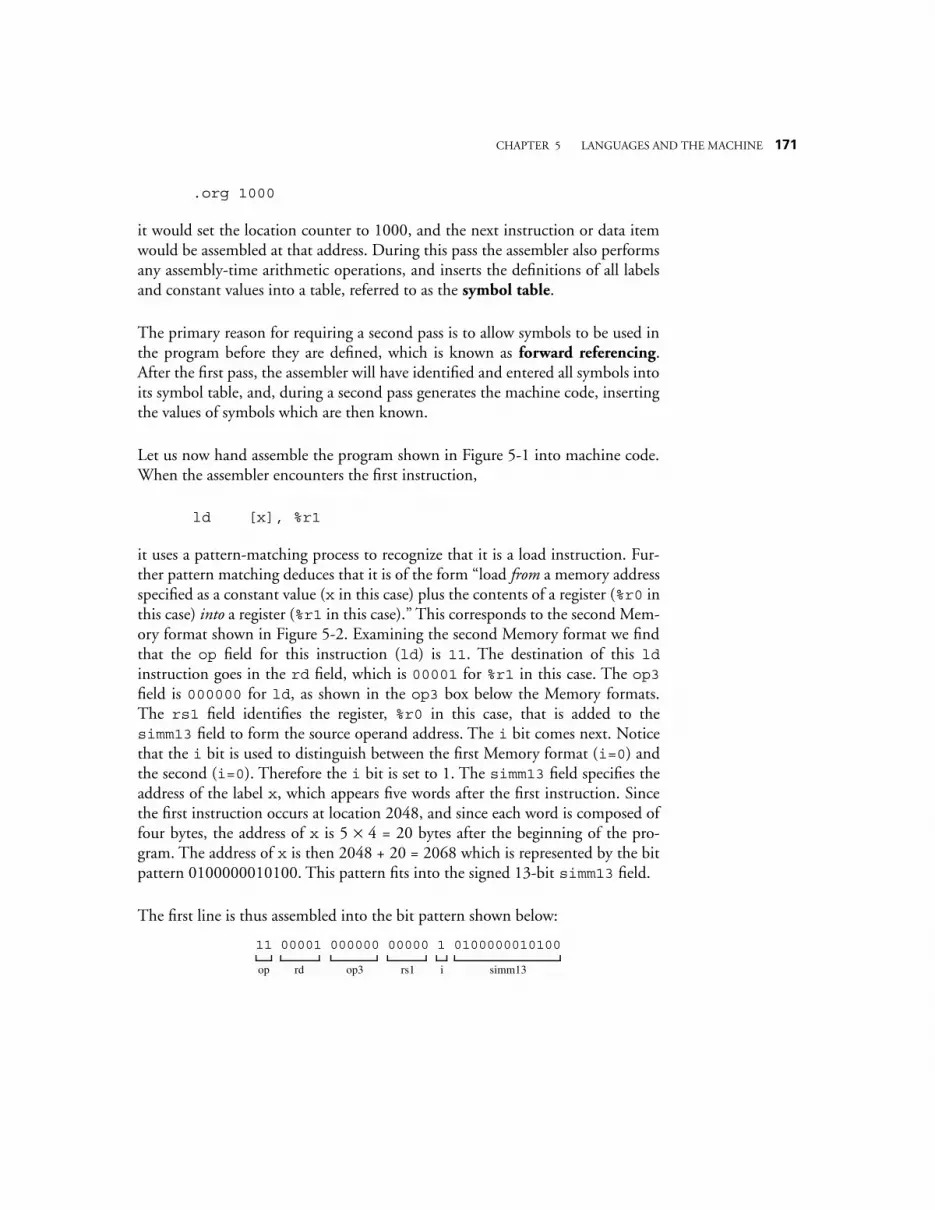
CHAPTER 5 LANGUAGES AND THE MACHINE 171
.org 1000
it would set the location counter to 1000, and the next instruction or data itemwould be assembled at that address. During this pass the assembler also performsany assembly-time arithmetic operations, and inserts the definitions of all labelsand constant values into a table, referred to as the symbol table.
The primary reason for requiring a second pass is to allow symbols to be used inthe program before they are defined, which is known as forward referencing.After the first pass, the assembler will have identified and entered all symbols intoits symbol table, and, during a second pass generates the machine code, insertingthe values of symbols which are then known.
Let us now hand assemble the program shown in Figure 5-1 into machine code.When the assembler encounters the first instruction,
ld [x], %r1
it uses a pattern-matching process to recognize that it is a load instruction. Fur-ther pattern matching deduces that it is of the form “load from a memory addressspecified as a constant value (x in this case) plus the contents of a register (%r0 inthis case) into a register (%r1 in this case).” This corresponds to the second Mem-ory format shown in Figure 5-2. Examining the second Memory format we findthat the op field for this instruction (ld) is 11. The destination of this ldinstruction goes in the rd field, which is 00001 for %r1 in this case. The op3field is 000000 for ld, as shown in the op3 box below the Memory formats.The rs1 field identifies the register, %r0 in this case, that is added to thesimm13 field to form the source operand address. The i bit comes next. Noticethat the i bit is used to distinguish between the first Memory format (i=0) andthe second (i=0). Therefore the i bit is set to 1. The simm13 field specifies theaddress of the label x, which appears five words after the first instruction. Sincethe first instruction occurs at location 2048, and since each word is composed offour bytes, the address of x is 5 × 4 = 20 bytes after the beginning of the pro-gram. The address of x is then 2048 + 20 = 2068 which is represented by the bitpattern 0100000010100. This pattern fits into the signed 13-bit simm13 field.
The first line is thus assembled into the bit pattern shown below:
11 00001 000000 00000 1 0100000010100
op rd op3 rs1 i simm13
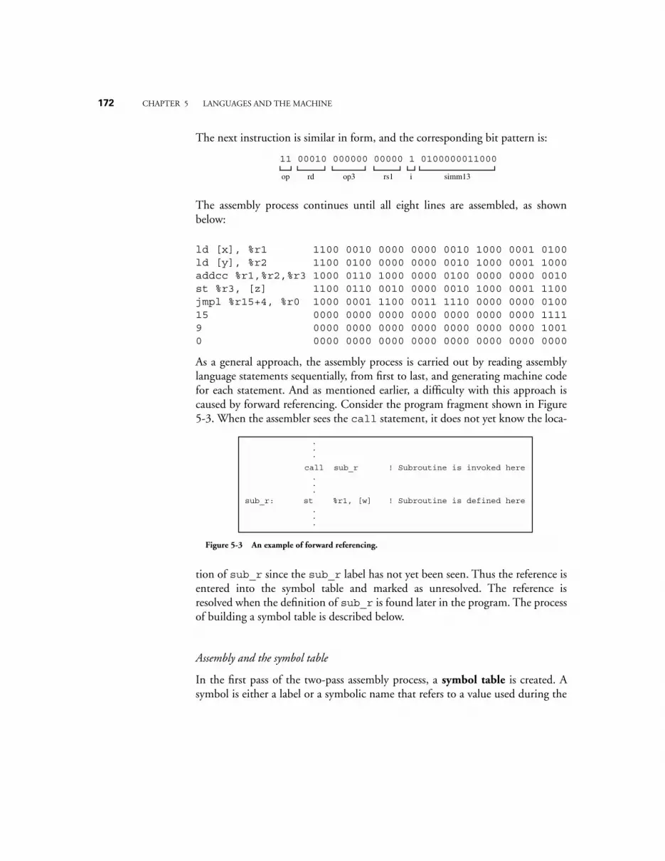
172 CHAPTER 5 LANGUAGES AND THE MACHINE
The next instruction is similar in form, and the corresponding bit pattern is:
The assembly process continues until all eight lines are assembled, as shownbelow:
ld [x], %r1 1100 0010 0000 0000 0010 1000 0001 0100ld [y], %r2 1100 0100 0000 0000 0010 1000 0001 1000addcc %r1,%r2,%r3 1000 0110 1000 0000 0100 0000 0000 0010st %r3, [z] 1100 0110 0010 0000 0010 1000 0001 1100jmpl %r15+4, %r0 1000 0001 1100 0011 1110 0000 0000 010015 0000 0000 0000 0000 0000 0000 0000 11119 0000 0000 0000 0000 0000 0000 0000 10010 0000 0000 0000 0000 0000 0000 0000 0000
As a general approach, the assembly process is carried out by reading assemblylanguage statements sequentially, from first to last, and generating machine codefor each statement. And as mentioned earlier, a difficulty with this approach iscaused by forward referencing. Consider the program fragment shown in Figure5-3. When the assembler sees the call statement, it does not yet know the loca-
tion of sub_r since the sub_r label has not yet been seen. Thus the reference isentered into the symbol table and marked as unresolved. The reference isresolved when the definition of sub_r is found later in the program. The processof building a symbol table is described below.
Assembly and the symbol table
In the first pass of the two-pass assembly process, a symbol table is created. Asymbol is either a label or a symbolic name that refers to a value used during the
11 00010 000000 00000 1 0100000011000
op rd op3 rs1 i simm13
call sub_r
sub_r: st %r1, [w]...
.
.
.
.
.
.
! Subroutine is invoked here
! Subroutine is defined here
Figure 5-3 An example of forward referencing.
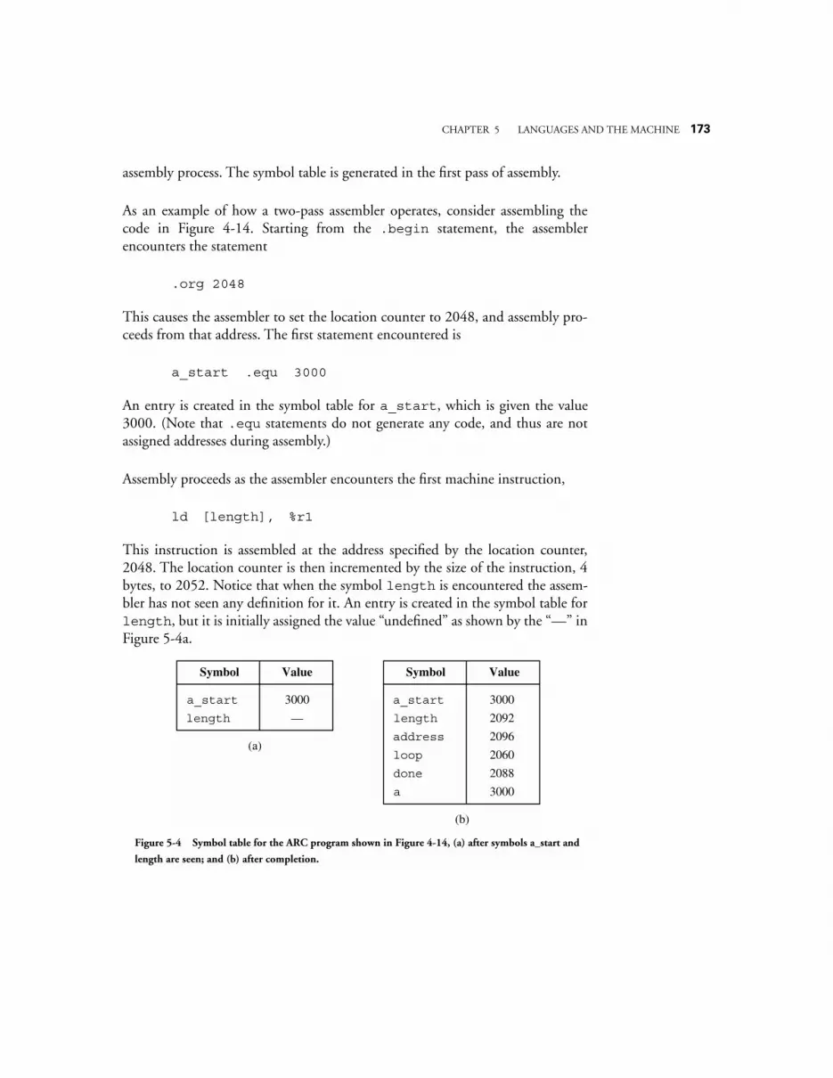
CHAPTER 5 LANGUAGES AND THE MACHINE 173
assembly process. The symbol table is generated in the first pass of assembly.
As an example of how a two-pass assembler operates, consider assembling thecode in Figure 4-14. Starting from the .begin statement, the assemblerencounters the statement
.org 2048
This causes the assembler to set the location counter to 2048, and assembly pro-ceeds from that address. The first statement encountered is
a_start .equ 3000
An entry is created in the symbol table for a_start, which is given the value3000. (Note that .equ statements do not generate any code, and thus are notassigned addresses during assembly.)
Assembly proceeds as the assembler encounters the first machine instruction,
ld [length], %r1
This instruction is assembled at the address specified by the location counter,2048. The location counter is then incremented by the size of the instruction, 4bytes, to 2052. Notice that when the symbol length is encountered the assem-bler has not seen any definition for it. An entry is created in the symbol table forlength, but it is initially assigned the value “undefined” as shown by the “—” inFigure 5-4a.
Symbol Value
length 2092
loop 2060
done 2088
a 3000
(b)
Symbol Value
a_start 3000
(a)
length ––
a_start 3000
address 2096
Figure 5-4 Symbol table for the ARC program shown in Figure 4-14, (a) after symbols a_start and
length are seen; and (b) after completion.
174 CHAPTER 5 LANGUAGES AND THE MACHINE
The assembler then encounters the second instruction
ld [address], %r2
It assembles this instruction at address 2052 and enters the symbol addressinto the symbol table, again setting its value to “undefined,” since its definitionhas not been seen. It then increments the location counter by 4 to 2056. Theandcc instruction is assembled at address 2056, and the location counter isincremented by the size of the instruction, again 4 bytes, to 2060. The next sym-bol that is seen is loop, which is entered into the symbol table with a value of2060, the value of the location counter. The next symbol that is encountered thatis not in the symbol table is done, which is also entered into the symbol tablewithout a value since it likewise has not been defined.
The first pass of assembly continues, and the unresolved symbols length,address, and done are assigned the values 2092, 2096, and 2088, respectivelyas they are encountered. The label a is encountered, and is entered into the tablewith a value of 3000. The label done appears at location 2088 because there are10 instructions (40 bytes) between the beginning of the program and done.Addresses for the remaining labels are computed in a similar manner. If anylabels are still undefined at the end of the first pass, then an error exists in theprogram and the assembler will flag the undefined symbols and terminate.
After the symbol table is created, the second pass of assembly begins. The pro-gram is read a second time, starting from the .begin statement, but now objectcode is generated. The first statement that is encountered that causes code to begenerated is ld at location 2048. The symbol table shows that the address por-tion of the ld instruction is (2092)10 for the address of length, and so oneword of code is generated using the Memory format as shown in Figure 5-5. Thesecond pass continues in this manner until all of the code is translated. Theassembled program is shown in Figure 5-5. Notice that the displacements forbranch addresses are given in words, rather than in bytes, because the branchinstructions multiply the displacements by four.
Final tasks of the assembler
After assembly is complete the assembler must add additional information to theassembled module for the linker and loader:
• The module name and size. If the execution model involves memory seg-
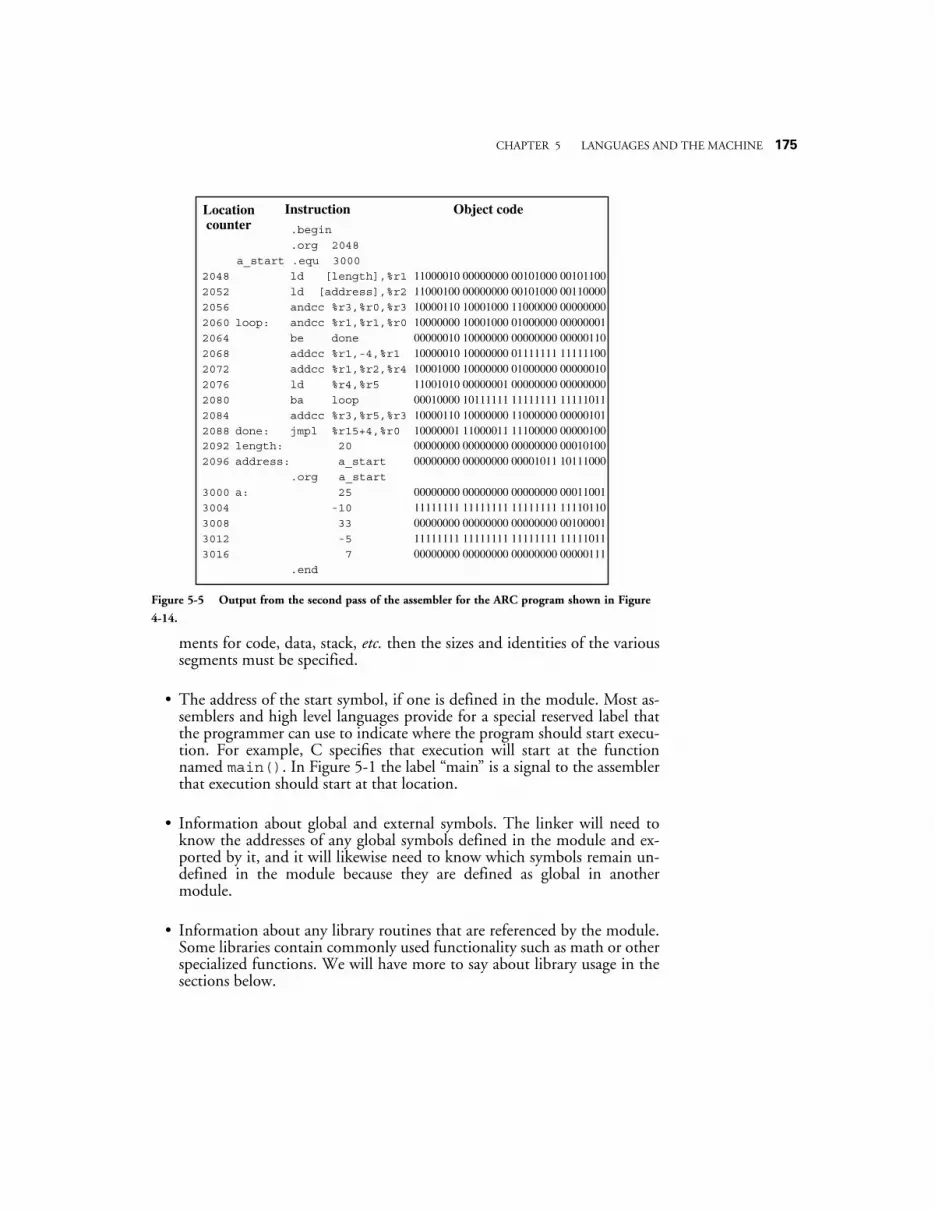
CHAPTER 5 LANGUAGES AND THE MACHINE 175
ments for code, data, stack, etc. then the sizes and identities of the varioussegments must be specified.
• The address of the start symbol, if one is defined in the module. Most as-semblers and high level languages provide for a special reserved label thatthe programmer can use to indicate where the program should start execu-tion. For example, C specifies that execution will start at the functionnamed main(). In Figure 5-1 the label “main” is a signal to the assemblerthat execution should start at that location.
• Information about global and external symbols. The linker will need toknow the addresses of any global symbols defined in the module and ex-ported by it, and it will likewise need to know which symbols remain un-defined in the module because they are defined as global in anothermodule.
• Information about any library routines that are referenced by the module.Some libraries contain commonly used functionality such as math or otherspecialized functions. We will have more to say about library usage in thesections below.
.begin
.org 2048
a_start .equ 3000
ld [length],%r1 11000010 00000000 00101000 00101100 ld [address],%r2 11000100 00000000 00101000 00110000 andcc %r3,%r0,%r3 10000110 10001000 11000000 00000000
loop: andcc %r1,%r1,%r0 10000000 10001000 01000000 00000001 be done 00000010 10000000 00000000 00000110 addcc %r1,-4,%r1 10000010 10000000 01111111 11111100 addcc %r1,%r2,%r4 10001000 10000000 01000000 00000010 ld %r4,%r5 11001010 00000001 00000000 00000000
addcc %r3,%r5,%r3 10000110 10000000 11000000 00000101 ba loop 00010000 10111111 11111111 11111011
done: jmpl %r15+4,%r0 10000001 11000011 11100000 00000100length: 20 00000000 00000000 00000000 00010100
.org a_start
a: 25 00000000 00000000 00000000 00011001 -10 11111111 11111111 11111111 11110110 33 00000000 00000000 00000000 00100001 -5 11111111 11111111 11111111 11111011
Object codeInstructionLocation counter
2048
2052
2056
2060
2064
2068
2072
2076
2080
2084
2088
3004
3000
3008
3012
3016
2092
.end
7 00000000 00000000 00000000 00000111
address: a_start 00000000 00000000 00001011 101110002096
Figure 5-5 Output from the second pass of the assembler for the ARC program shown in Figure
4-14.
176 CHAPTER 5 LANGUAGES AND THE MACHINE
• The values of any constants that are to be loaded into memory. Some load-ers expect data initialization to be specified separately from the binary code.
• Relocation information. When the linker is invoked most of the modulesthat are to be linked will need to be relocated as the modules are concate-nated. The whole issue of module relocation is complicated because someaddress references can be relocated and others cannot. We discuss reloca-tion later, but here we note that the assembler specifies which addresses canbe relocated and which others cannot.
Location of programs in memory
Up until now we have assumed that programs are located in memory at anaddress that is specified by a .org pseudo operation. This may indeed be thecase in systems programming, where the programmer has a reason for wanting aprogram to be located at a specific memory location, but typically the program-mer does not care where the program is located in memory. Furthermore, whenseparately assembled or compiled programs are linked together, it is difficult orimpossible for the programmer to know exactly where each module will belocated after linking, as they are concatenated one after the other. For this reasonmost addresses are specified as being relocatable in memory, except perhaps foraddresses such as I/O addresses, which may be fixed at an absolute memory loca-tion.
In the next section we discuss relocation in more detail; here we merely note thatit is the assembler’s responsibility to mark symbols as being relocatable. Whethera given symbol is relocatable or not depends upon both the assembly languageand the operating system’s conventions. In any case, this relocation informationis included in the assembled module for use by the linker and/or loader in a relo-cation dictionary. Symbols that are relocatable are often marked with an “R”after their value in the assembler’s listing file.
5.3 Linking and LoadingMost applications of any size will have a number of separately compiled orassembled modules. These modules may be generated by different programminglanguages or they may be present in a library provided as part of the program-ming language environment or operating system. Each module must provide theinformation described above, so that they can be linked together for loading andexecution.
CHAPTER 5 LANGUAGES AND THE MACHINE 177
A linkage editor, or linker, is a software program that combines separatelyassembled programs (called object modules) into a single program, which iscalled a load module. The linker resolves all global-external references and relo-cates addresses in the separate modules. The load module can then be loaded intomemory by a loader, which may also need to modify addresses if the program isloaded at a location that differs from the loading origin used by the linker.
A relatively new technique called dynamic link libraries (DLLs), popularizedby Microsoft in the Windows operating system, and present in similar forms inother operating systems, postpones the linking of some components until theyare actually needed at run time. We will have more to say about dynamic linkinglater in this section.
5.3.1 LINKING
In combining the separately compiled or assembled modules into a load module,the linker must:
• Resolve address references that are external to modules as it links them.
• Relocate each module by combining them end-to-end as appropriate. Dur-ing this relocation process many of the addresses in the module must bechanged to reflect their new location.
• Specify the starting symbol of the load module.
• If the memory model includes more than one memory segment, the linkermust specify the identities and contents of the various segments.
Resolving external references
In resolving address references the linker needs to distinguish local symbol names(used within a single source module) from global symbol names (used in morethan one module). This is accomplished by making use of the .global and.extern pseudo-ops during assembly. The .global pseudo-op instructs theassembler to mark a symbol as being available to other object modules during thelinking phase. The .extern pseudo-op identifies a label that is used in onemodule but is defined in another. A .global is thus used in the module wherea symbol is defined (such as where a subroutine is located) and a .extern isused in every other module that refers to it. Note that only address labels can be
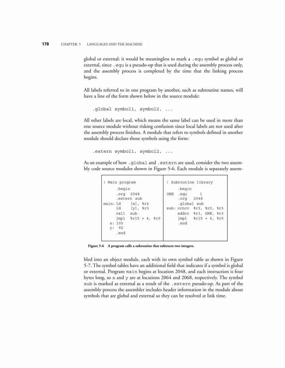
178 CHAPTER 5 LANGUAGES AND THE MACHINE
global or external: it would be meaningless to mark a .equ symbol as global orexternal, since .equ is a pseudo-op that is used during the assembly process only,and the assembly process is completed by the time that the linking processbegins.
All labels referred to in one program by another, such as subroutine names, willhave a line of the form shown below in the source module:
.global symbol1, symbol2, ...
All other labels are local, which means the same label can be used in more thanone source module without risking confusion since local labels are not used afterthe assembly process finishes. A module that refers to symbols defined in anothermodule should declare those symbols using the form:
.extern symbol1, symbol2, ...
As an example of how .global and .extern are used, consider the two assem-bly code source modules shown in Figure 5-6. Each module is separately assem-
bled into an object module, each with its own symbol table as shown in Figure5-7. The symbol tables have an additional field that indicates if a symbol is globalor external. Program main begins at location 2048, and each instruction is fourbytes long, so x and y are at locations 2064 and 2068, respectively. The symbolsub is marked as external as a result of the .extern pseudo-op. As part of theassembly process the assembler includes header information in the module aboutsymbols that are global and external so they can be resolved at link time.
! Main program
.begin
.org 2048
.extern subld [x], %r2ldcall
[y], %r3sub
! Subroutine library
.begin
.org 2048
.global suborncc %r3, %r0, %r3
jmpl %r15 + 4, %r0jmpl %r15 + 4, %r0105 92
main:
.end
x:y:
sub:
.end
.equ 1ONE
addcc %r3, ONE, %r3
Figure 5-6 A program calls a subroutine that subtracts two integers.
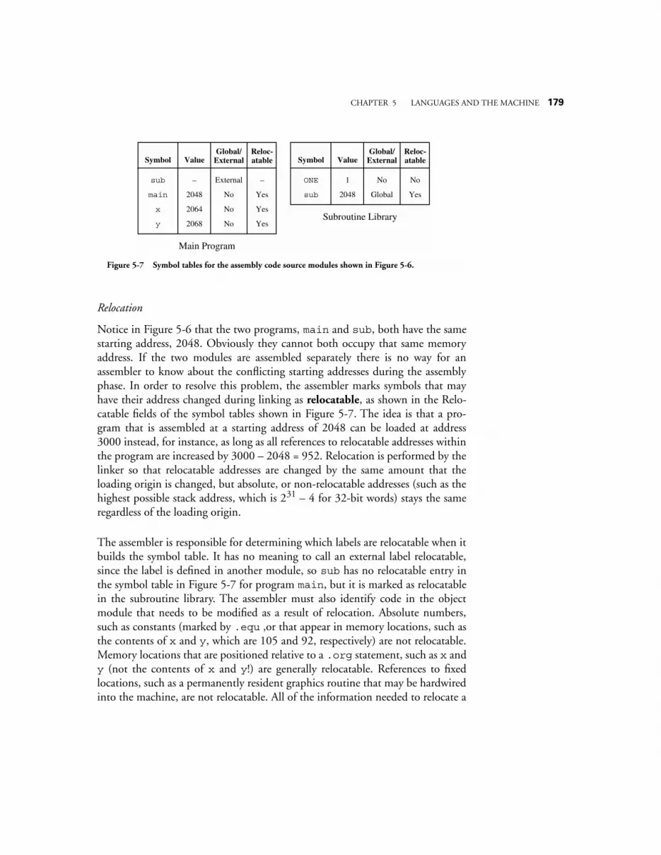
CHAPTER 5 LANGUAGES AND THE MACHINE 179
Relocation
Notice in Figure 5-6 that the two programs, main and sub, both have the samestarting address, 2048. Obviously they cannot both occupy that same memoryaddress. If the two modules are assembled separately there is no way for anassembler to know about the conflicting starting addresses during the assemblyphase. In order to resolve this problem, the assembler marks symbols that mayhave their address changed during linking as relocatable, as shown in the Relo-catable fields of the symbol tables shown in Figure 5-7. The idea is that a pro-gram that is assembled at a starting address of 2048 can be loaded at address3000 instead, for instance, as long as all references to relocatable addresses withinthe program are increased by 3000 – 2048 = 952. Relocation is performed by thelinker so that relocatable addresses are changed by the same amount that theloading origin is changed, but absolute, or non-relocatable addresses (such as thehighest possible stack address, which is 231 – 4 for 32-bit words) stays the sameregardless of the loading origin.
The assembler is responsible for determining which labels are relocatable when itbuilds the symbol table. It has no meaning to call an external label relocatable,since the label is defined in another module, so sub has no relocatable entry inthe symbol table in Figure 5-7 for program main, but it is marked as relocatablein the subroutine library. The assembler must also identify code in the objectmodule that needs to be modified as a result of relocation. Absolute numbers,such as constants (marked by .equ ,or that appear in memory locations, such asthe contents of x and y, which are 105 and 92, respectively) are not relocatable.Memory locations that are positioned relative to a .org statement, such as x andy (not the contents of x and y!) are generally relocatable. References to fixedlocations, such as a permanently resident graphics routine that may be hardwiredinto the machine, are not relocatable. All of the information needed to relocate a
Symbol Value
sub –
main 2048
x 2064
y 2068
Global/External
Reloc-atable
No
No
–
Yes
Yes
Yes
No
External
Main Program
Symbol Value
ONE 1
Global/External
Reloc-atable
NoNo
Subroutine Library
sub 2048 YesGlobal
Figure 5-7 Symbol tables for the assembly code source modules shown in Figure 5-6.
180 CHAPTER 5 LANGUAGES AND THE MACHINE
module is stored in the relocation dictionary contained in the assembled file, andis therefore available to the linker.
5.3.2 LOADING
The loader is a software program that places the load module into main mem-ory. Conceptually the tasks of the loader are not difficult. It must load the vari-ous memory segments with the appropriate values and initialize certain registerssuch as the stack pointer %sp, and the program counter, %pc, to their initial val-ues.
If there is only one load module executing at any time, then this model workswell. In modern operating systems, however, several programs are resident inmemory at any time, and there is no way that the assembler or linker can knowat which address they will reside. The loader must relocate these modules at loadtime by adding an offset to all of the relocatable code in a module. This kind ofloader is known as a relocating loader. The relocating loader does not simplyrepeat the job of the linker: the linker has to combine several object modules intoa single load module, whereas the loader simply modifies relocatable addresseswithin a single load module so that several programs can reside in memorysimultaneously. A linking loader performs both the linking process and theloading process: it resolves external references, relocates object modules, andloads them into memory.
The linked executable file contains header information describing where itshould be loaded, starting addresses, and possibly relocation information, andentry points for any routines that should be made available externally.
An alternative approach that relies on memory management accomplishes reloca-tion by loading a segment base register with the appropriate base to locate thecode (or data) at the appropriate place in physical memory. The memory man-agement unit (MMU), adds the contents of this base register to all memory ref-erences. As a result, each program can begin execution at address 0 and rely onthe MMU to relocate all memory references transparently.
Dynamic link libraries
Returning to dynamic link libraries, the concept has a number of attractive fea-tures. Commonly used routines such as memory management or graphics pack-ages need be present at only one place, the DLL library. This results in smaller

CHAPTER 5 LANGUAGES AND THE MACHINE 181
program sizes because each program does not need to have its own copy of theDLL code, as would otherwise be needed. All programs share the exact samecode, even while simultaneously executing.
Furthermore, the DLL can be upgraded with bug fixes or feature enhancementsin just one place, and programs that use it need not be recompiled or relinked ina separate step. These same features can also become disadvantages, however,because program behavior may change in unintended ways (such as running outof memory as a result of a larger DLL). The DLL library must be present at alltimes, and must contain the version expected by each program. Many Windowsusers have seen the cryptic message, “A file is missing from the dynamic linklibrary.” Complicating the issue in the Windows implementation, there are anumber of locations in the file system where DLLs are placed. The more sophis-ticated user may have little difficulty resolving these problems, but the naive usermay be baffled.
A PROGRAMMING EXAMPLE
Consider the problem of adding two 64-bit numbers using the ARC assemblylanguage. We can store the 64-bit numbers in successive words in memory andthen separately add the low and high order words. If a carry is generated fromadding the low order words, then the carry is added into the high order word ofthe result. (See problem 5.3 for the generation of the symbol table, and problem5.4 for the translation of the assembly code in this example to machine code.)
Figure 5-8 shows one possible coding. The 64-bit operands A and B are stored inmemory in a high endian format, in which the most significant 32 bits are storedin lower memory addresses than the least significant 32 bits. The program beginsby loading the high and low order words of A into %r1 and %r2, respectively,and then loading the high and low order words of B into %r3 and %r4, respec-tively. Subroutine add_64 is called, which adds A and B and places the highorder word of the result in %r5 and the low order word of the result in %r6. The64-bit result is then stored in C, and the program returns.
Subroutine add_64 starts by adding the low order words. If a carry is not gener-ated, then the high order words are added and the subroutine finishes. If a carryis generated from adding the low order words, then it must be added into the

182 CHAPTER 5 LANGUAGES AND THE MACHINE
high order word of the result. If a carry is not generated when the high orderwords are added, then the carry from the low order word of the result is simplyadded into the high order word of the result and the subroutine finishes. If, how-ever, a carry is generated when the high order words are added, then when thecarry from the low order word is added into the high order word, the final stateof the condition codes will show that there is no carry out of the high orderword, which is incorrect. The condition code for the carry is restored by placing
! %r5 – Most significant 32 bits of C
.begin
! Start assembling
.org 2048 ! Start program at 2048
ld [B+4], %r4 ! Get low word of B
st %r5, [C] ! Store high word of C
st %r6, [C+4] ! Store low word of C
! %r4 – Least significant 32 bits of B
! %r3 – Most significant 32 bits of B
! %r2 – Least significant 32 bits of A
! Register usage: %r1 – Most significant 32 bits of A
! Perform a 64-bit addition: C
call add_64 ! Perform 64-bit addition
ld [B], %r3 ! Get high word of B
! %r6 – Least significant 32 bits of C
ld [A+4], %r2 ! Get low word of A
main: ld [A], %r1 ! Get high word of A
! %r7 – Used for restoring carry bit
addcc %r1, %r3, %r5 ! Add high order words
lo_carry: addcc %r1, %r3, %r5 ! Add high order words
bcs hi_carry ! Branch if carry set
jmpl %r15 + 4, %r0 ! Return to calling routine
bcs lo_carry ! Branch if carry set
add_64: addcc %r2, %r4, %r6 ! Add low order words
.
.
.
sethi #3FFFFF, %r7 ! Set up %r7 for carry
jmpl %r15 + 4, %r0 ! Return to calling routine
A: 0 ! High 32 bits of 25
addcc %r7, %r7, %r0 ! Generate a carry
jmpl %r15, 4, %r0 ! Return to calling routine
addcc %r5, 1, %r5 ! Add in carry
.end ! Stop assembling
25 ! Low 32 bits of 25
B: #FFFFFFFF ! High 32 bits of -1
#FFFFFFFF ! Low 32 bits of -1
C: 0 ! High 32 bits of result
0 ! Low 32 bits of result
hi_carry: addcc %r5, 1, %r5 ! Add in carry
.org 3072 ! Start add_64 at 3072
.global main
← A + B
Figure 5-8 An ARC program adds two 64-bit integers.
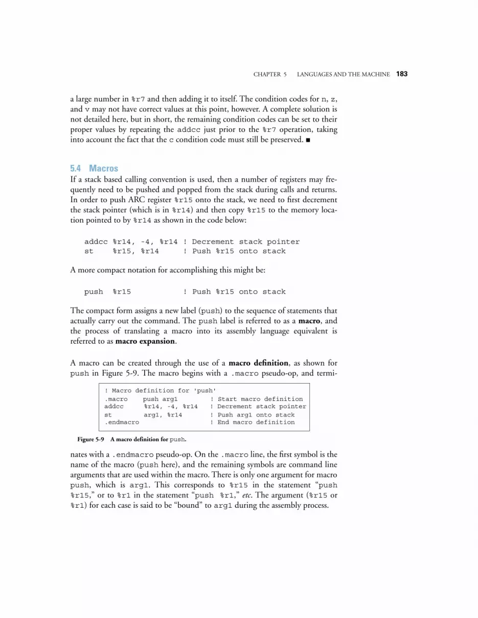
CHAPTER 5 LANGUAGES AND THE MACHINE 183
a large number in %r7 and then adding it to itself. The condition codes for n, z,and v may not have correct values at this point, however. A complete solution isnot detailed here, but in short, the remaining condition codes can be set to theirproper values by repeating the addcc just prior to the %r7 operation, takinginto account the fact that the c condition code must still be preserved.
5.4 MacrosIf a stack based calling convention is used, then a number of registers may fre-quently need to be pushed and popped from the stack during calls and returns.In order to push ARC register %r15 onto the stack, we need to first decrementthe stack pointer (which is in %r14) and then copy %r15 to the memory loca-tion pointed to by %r14 as shown in the code below:
addcc %r14, -4, %r14 ! Decrement stack pointerst %r15, %r14 ! Push %r15 onto stack
A more compact notation for accomplishing this might be:
push %r15 ! Push %r15 onto stack
The compact form assigns a new label (push) to the sequence of statements thatactually carry out the command. The push label is referred to as a macro, andthe process of translating a macro into its assembly language equivalent isreferred to as macro expansion.
A macro can be created through the use of a macro definition, as shown forpush in Figure 5-9. The macro begins with a .macro pseudo-op, and termi-
nates with a .endmacro pseudo-op. On the .macro line, the first symbol is thename of the macro (push here), and the remaining symbols are command linearguments that are used within the macro. There is only one argument for macropush, which is arg1. This corresponds to %r15 in the statement “push%r15,” or to %r1 in the statement “push %r1,” etc. The argument (%r15 or%r1) for each case is said to be “bound” to arg1 during the assembly process.
! Macro definition for 'push'.macro push arg1
st arg1, %r14 ! Push arg1 onto stackaddcc %r14, -4, %r14 ! Decrement stack pointer
! End macro definition.endmacro
! Start macro definition
Figure 5-9 A macro definition for push.
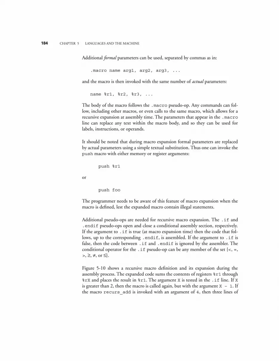
184 CHAPTER 5 LANGUAGES AND THE MACHINE
Additional formal parameters can be used, separated by commas as in:
.macro name arg1, arg2, arg3, ...
and the macro is then invoked with the same number of actual parameters:
name %r1, %r2, %r3, ...
The body of the macro follows the .macro pseudo-op. Any commands can fol-low, including other macros, or even calls to the same macro, which allows for arecursive expansion at assembly time. The parameters that appear in the .macroline can replace any text within the macro body, and so they can be used forlabels, instructions, or operands.
It should be noted that during macro expansion formal parameters are replacedby actual parameters using a simple textual substitution. Thus one can invoke thepush macro with either memory or register arguments:
push %r1
or
push foo
The programmer needs to be aware of this feature of macro expansion when themacro is defined, lest the expanded macro contain illegal statements.
Additional pseudo-ops are needed for recursive macro expansion. The .if and.endif pseudo-ops open and close a conditional assembly section, respectively.If the argument to .if is true (at macro expansion time) then the code that fol-lows, up to the corresponding .endif, is assembled. If the argument to .if isfalse, then the code between .if and .endif is ignored by the assembler. Theconditional operator for the .if pseudo-op can be any member of the set <, =,>, ≥, ≠, or ≤.
Figure 5-10 shows a recursive macro definition and its expansion during theassembly process. The expanded code sums the contents of registers %r1 through%rX and places the result in %r1. The argument X is tested in the .if line. If Xis greater than 2, then the macro is called again, but with the argument X – 1. Ifthe macro recurs_add is invoked with an argument of 4, then three lines of
CHAPTER 5 LANGUAGES AND THE MACHINE 185
code are generated as shown in the bottom of the figure. The first time thatrecurs_add is invoked, X has a value of 4. The macro is invoked again with X= 3 and X = 2, at which point the first addcc statement is generated. The sec-ond and third addcc statements are then generated as the recursion unwinds.
As mentioned earlier, for an assembler that supports macros, there must be amacro expansion phase that takes place prior to the two-pass assembly process.Macro expansion is normally performed by a macro preprocessor before theprogram is assembled. The macro expansion process may be invisible to a pro-grammer, however, since it may be invoked by the assembler itself. Macro expan-sion typically requires two passes, in which the first pass records macrodefinitions, and the second pass generates assembly language statements. Thesecond pass of macro expansion can be very involved, however, if recursive macrodefinitions are supported. A more detailed description of macro expansion can befound in (Donovan, 1972).
5.5 Case Study: Extensions to the Instruction Set – The Intel MMX™ and Motorola AltiVec™ SIMD instructions.As integrated circuit technology provides ever increasing capacity within the pro-cessor, processor vendors search for new ways to use that capacity. One way thatboth Intel and Motorola capitalized on the additional capacity was to extendtheir ISAs with new registers and instructions that are specialized for processingstreams or blocks of data. Intel provides the MMX extension to their Pentiumprocessors and Motorola provides the AltiVec extension to their PowerPC pro-cessors. In this section we will discuss why the extensions are useful, and how thetwo companies implemented them.
! A recursive macro definitionrecurs_add X
recurs_add X – 1 ! Recursive call.if X > 2 ! Assemble code if X > 2
! End .if construct.endif
! Start macro definition
addcc %r1, %rX, %r1 ! Add argument into %r1.endmacro ! End macro definition
recurs_add 4 ! Invoke the macro
Expands to:
addcc %r1, %r2, %r1addcc %r1, %r3, %r1addcc %r1, %r4, %r1
.macro
Figure 5-10 A recursive macro definition, and the corresponding macro expansion.
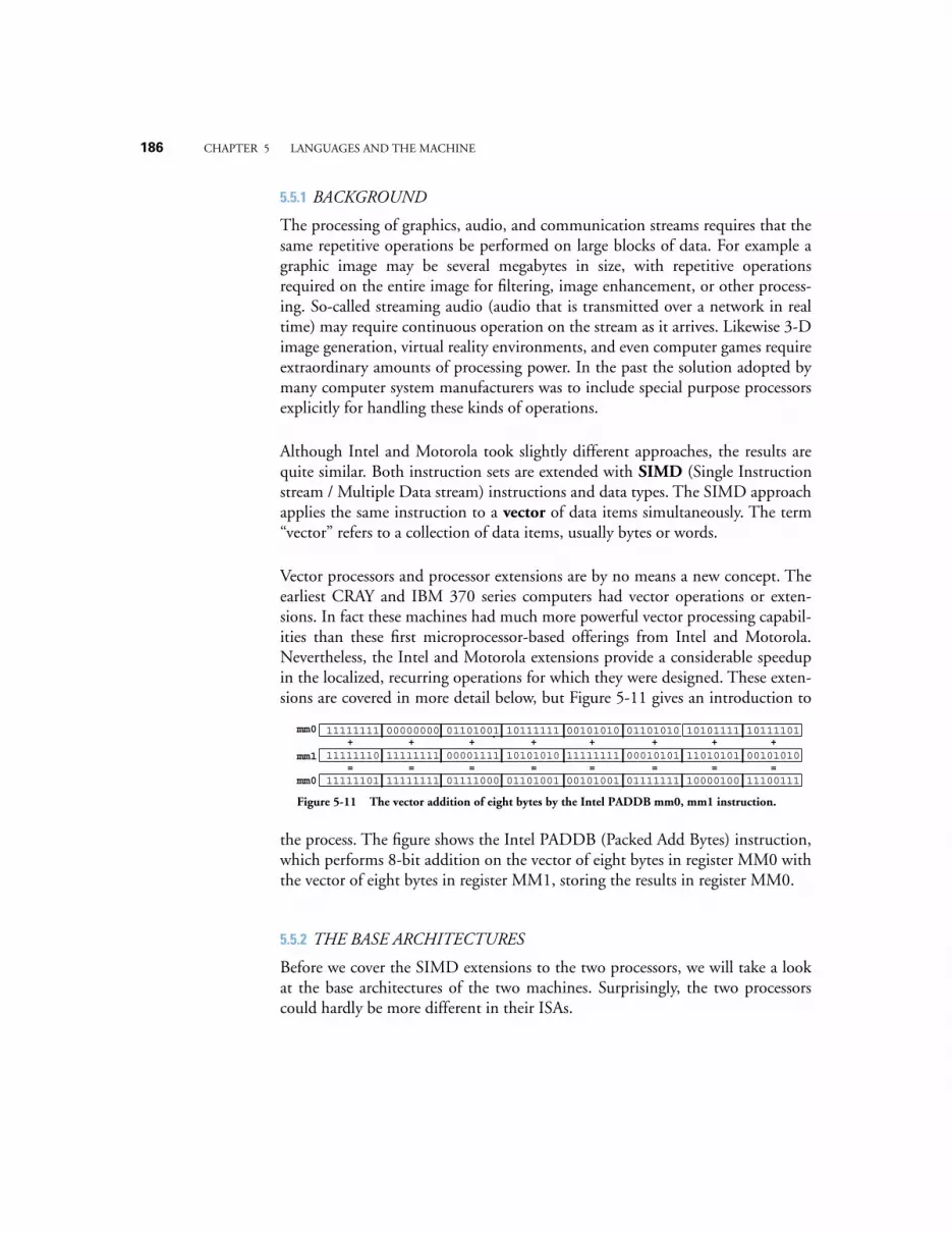
186 CHAPTER 5 LANGUAGES AND THE MACHINE
5.5.1 BACKGROUND
The processing of graphics, audio, and communication streams requires that thesame repetitive operations be performed on large blocks of data. For example agraphic image may be several megabytes in size, with repetitive operationsrequired on the entire image for filtering, image enhancement, or other process-ing. So-called streaming audio (audio that is transmitted over a network in realtime) may require continuous operation on the stream as it arrives. Likewise 3-Dimage generation, virtual reality environments, and even computer games requireextraordinary amounts of processing power. In the past the solution adopted bymany computer system manufacturers was to include special purpose processorsexplicitly for handling these kinds of operations.
Although Intel and Motorola took slightly different approaches, the results arequite similar. Both instruction sets are extended with SIMD (Single Instructionstream / Multiple Data stream) instructions and data types. The SIMD approachapplies the same instruction to a vector of data items simultaneously. The term“vector” refers to a collection of data items, usually bytes or words.
Vector processors and processor extensions are by no means a new concept. Theearliest CRAY and IBM 370 series computers had vector operations or exten-sions. In fact these machines had much more powerful vector processing capabil-ities than these first microprocessor-based offerings from Intel and Motorola.Nevertheless, the Intel and Motorola extensions provide a considerable speedupin the localized, recurring operations for which they were designed. These exten-sions are covered in more detail below, but Figure 5-11 gives an introduction to
the process. The figure shows the Intel PADDB (Packed Add Bytes) instruction,which performs 8-bit addition on the vector of eight bytes in register MM0 withthe vector of eight bytes in register MM1, storing the results in register MM0.
5.5.2 THE BASE ARCHITECTURES
Before we cover the SIMD extensions to the two processors, we will take a lookat the base architectures of the two machines. Surprisingly, the two processorscould hardly be more different in their ISAs.
mm0
mm1
mm0
+
=
+
=
+
=
+
=
+
=
+
=
+
=
+
=
11111111 00000000 01101001 10111111 00101010 01101010 10101111 10111101
11111110 11111111 00001111 10101010 11111111 00010101 11010101 00101010
11111101 11111111 01111000 01101001 00101001 01111111 10000100 11100111
Figure 5-11 The vector addition of eight bytes by the Intel PADDB mm0, mm1 instruction.
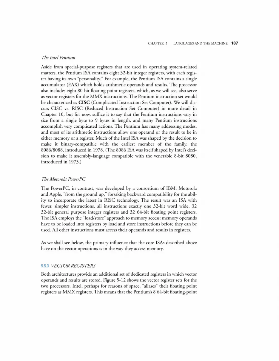
CHAPTER 5 LANGUAGES AND THE MACHINE 187
The Intel Pentium
Aside from special-purpose registers that are used in operating system-relatedmatters, the Pentium ISA contains eight 32-bit integer registers, with each regis-ter having its own “personality.” For example, the Pentium ISA contains a singleaccumulator (EAX) which holds arithmetic operands and results. The processoralso includes eight 80-bit floating-point registers, which, as we will see, also serveas vector registers for the MMX instructions. The Pentium instruction set wouldbe characterized as CISC (Complicated Instruction Set Computer). We will dis-cuss CISC vs. RISC (Reduced Instruction Set Computer) in more detail inChapter 10, but for now, suffice it to say that the Pentium instructions vary insize from a single byte to 9 bytes in length, and many Pentium instructionsaccomplish very complicated actions. The Pentium has many addressing modes,and most of its arithmetic instructions allow one operand or the result to be ineither memory or a register. Much of the Intel ISA was shaped by the decision tomake it binary-compatible with the earliest member of the family, the8086/8088, introduced in 1978. (The 8086 ISA was itself shaped by Intel’s deci-sion to make it assembly-language compatible with the venerable 8-bit 8080,introduced in 1973.)
The Motorola PowerPC
The PowerPC, in contrast, was developed by a consortium of IBM, Motorolaand Apple, “from the ground up,” forsaking backward compatibility for the abil-ity to incorporate the latest in RISC technology. The result was an ISA withfewer, simpler instructions, all instructions exactly one 32-bit word wide, 3232-bit general purpose integer registers and 32 64-bit floating point registers.The ISA employs the “load/store” approach to memory access: memory operandshave to be loaded into registers by load and store instructions before they can beused. All other instructions must access their operands and results in registers.
As we shall see below, the primary influence that the core ISAs described abovehave on the vector operations is in the way they access memory.
5.5.3 VECTOR REGISTERS
Both architectures provide an additional set of dedicated registers in which vectoroperands and results are stored. Figure 5-12 shows the vector register sets for thetwo processors. Intel, perhaps for reasons of space, “aliases” their floating pointregisters as MMX registers. This means that the Pentium’s 8 64-bit floating-point
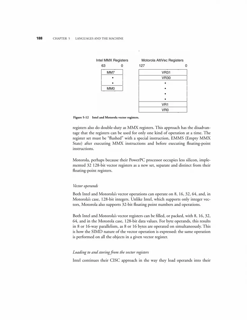
188 CHAPTER 5 LANGUAGES AND THE MACHINE
registers also do double-duty as MMX registers. This approach has the disadvan-tage that the registers can be used for only one kind of operation at a time. Theregister set must be “flushed” with a special instruction, EMMS (Empty MMXState) after executing MMX instructions and before executing floating-pointinstructions.
Motorola, perhaps because their PowerPC processor occupies less silicon, imple-mented 32 128-bit vector registers as a new set, separate and distinct from theirfloating-point registers.
Vector operands
Both Intel and Motorola’s vector operations can operate on 8, 16, 32, 64, and, inMotorola’s case, 128-bit integers. Unlike Intel, which supports only integer vec-tors, Motorola also supports 32-bit floating point numbers and operations.
Both Intel and Motorola’s vector registers can be filled, or packed, with 8, 16, 32,64, and in the Motorola case, 128-bit data values. For byte operands, this resultsin 8 or 16-way parallelism, as 8 or 16 bytes are operated on simultaneously. Thisis how the SIMD nature of the vector operation is expressed: the same operationis performed on all the objects in a given vector register.
Loading to and storing from the vector registers
Intel continues their CISC approach in the way they load operands into their
Intel MMX Registers
63 0
MM7
•
•
MM0
Motorola AltiVec Registers
127 0
VR31
VR30
•
•
•
•
VR1
VR0
Figure 5-12 Intel and Motorola vector registers.
CHAPTER 5 LANGUAGES AND THE MACHINE 189
vector registers. There are two instructions for loading and storing values to andfrom the vector registers, MOVD and MOVQ, which move 32-bit doublewordsand 64-bit quadwords, respectively. (The Intel word is 16-bits in size.) The syn-tax is:
MOVD mm, mm/m32 ;move doubleword to a vector reg.
MOVD mm/m32, mm ;move doubleword from a vector reg.
MOVQ mm, mm/m64 ;move quadword to a vector reg.
MOVQ mm/m64, mm ;move quadword from a vector reg.
• mm stands for one of the 8 MM vector registers;
• mm/mm32 stands for either one of the integer registers, an MM register,or a memory location;
• mm/m64 stands for either an MM register or a memory location.
In addition, in the Intel vector arithmetic operations one of the operands can bein memory, as we will see below.
Motorola likewise remained true to their professed RISC philosophy in theirload and store operations. The only way to access an operand in memory isthrough the vector load and store operations. There is no way to move an oper-and between any of the other internal registers and the vector registers. All oper-ands must be loaded from memory and stored to memory. Typical load opcodesare:
lvebx vD, rA|0, rB ;load byte to vector reg vD, indexed.
lvehx vD, rA|0, rB ;move halfword to vector reg vD indexed.
lvewx vD, rA|0, rB ;move word to vector reg vD indexed.
lvx vD, rA|0, rB ;move doubleword to vector reg vD.
where vD stands for one of the 32 vector registers. The memory address of theoperand is computed from (rA|0 + rB), where rA and rB represent any two of theinteger registers r0-r32, and the “|0” symbol means that the value zero may besubstituted for rA. The byte, half word, word, or doubleword is fetched fromthat address. (PowerPC words are 32 bits in size.)
The term “indexed” in the list above refers to the location where the byte, half-word or word will be stored in the vector register. The least significant bits of thememory address specify the index into the vector register. For example, LSB’s
190 CHAPTER 5 LANGUAGES AND THE MACHINE
011 would specify that the byte should be loaded into the third byte of the regis-ter. Other bytes in the vector register are undefined.
The store operations work exactly like the load instructions above except that thevalue from one of the vector registers is stored in memory.
5.5.4 VECTOR ARITHMETIC OPERATIONS
The vector arithmetic operations form the heart of the SIMD process. We willsee that there is a new form of arithmetic, saturation arithmetic, and several newand exotic operations.
Saturation arithmetic
Both vector processors provide the option of doing saturation arithmeticinstead of the more familiar modulo wraparound kind discussed in Chapters 2and 3. Saturation arithmetic works just like two’s complement arithmetic as longas the results do not overflow or underflow. When results do overflow or under-flow, in saturation arithmetic the result is held at the maximum or minimumallowable value, respectively, rather than being allowed to wrap around. Forexample two’s complement bytes are saturated at the high end at +127 and at thelow end at −128. Unsigned bytes are saturated at 255 and 0. If an arithmeticresult overflows or underflows these bounds the result is clipped, or “saturated” atthe boundary.
The need for saturation arithmetic is encountered in the processing of colorinformation. If color is represented by a byte in which 0 represents black and 255represents white, then saturation allows the color to remain pure black or purewhite after an operation rather than inverting upon overflow or underflow.
Instruction formats
As the two architectures have different approaches to addressing modes, so theirSIMD instruction formats also differ. Intel continues using two-address instruc-tions, where the first source operand can be in an MM register, an integer regis-ter, or memory, and the second operand and destination is an MM register:
OP mm, mm32or64 ;mm ← mm OP mm/mm32/64
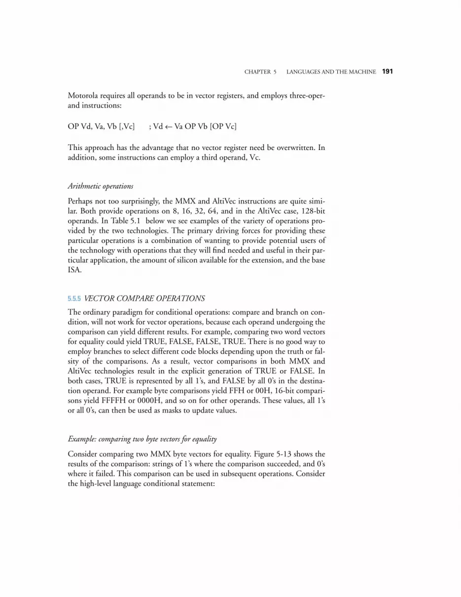
CHAPTER 5 LANGUAGES AND THE MACHINE 191
Motorola requires all operands to be in vector registers, and employs three-oper-and instructions:
OP Vd, Va, Vb [,Vc] ; Vd ← Va OP Vb [OP Vc]
This approach has the advantage that no vector register need be overwritten. Inaddition, some instructions can employ a third operand, Vc.
Arithmetic operations
Perhaps not too surprisingly, the MMX and AltiVec instructions are quite simi-lar. Both provide operations on 8, 16, 32, 64, and in the AltiVec case, 128-bitoperands. In Table 5.1 below we see examples of the variety of operations pro-vided by the two technologies. The primary driving forces for providing theseparticular operations is a combination of wanting to provide potential users ofthe technology with operations that they will find needed and useful in their par-ticular application, the amount of silicon available for the extension, and the baseISA.
5.5.5 VECTOR COMPARE OPERATIONS
The ordinary paradigm for conditional operations: compare and branch on con-dition, will not work for vector operations, because each operand undergoing thecomparison can yield different results. For example, comparing two word vectorsfor equality could yield TRUE, FALSE, FALSE, TRUE. There is no good way toemploy branches to select different code blocks depending upon the truth or fal-sity of the comparisons. As a result, vector comparisons in both MMX andAltiVec technologies result in the explicit generation of TRUE or FALSE. Inboth cases, TRUE is represented by all 1’s, and FALSE by all 0’s in the destina-tion operand. For example byte comparisons yield FFH or 00H, 16-bit compari-sons yield FFFFH or 0000H, and so on for other operands. These values, all 1’sor all 0’s, can then be used as masks to update values.
Example: comparing two byte vectors for equality
Consider comparing two MMX byte vectors for equality. Figure 5-13 shows theresults of the comparison: strings of 1’s where the comparison succeeded, and 0’swhere it failed. This comparison can be used in subsequent operations. Considerthe high-level language conditional statement:
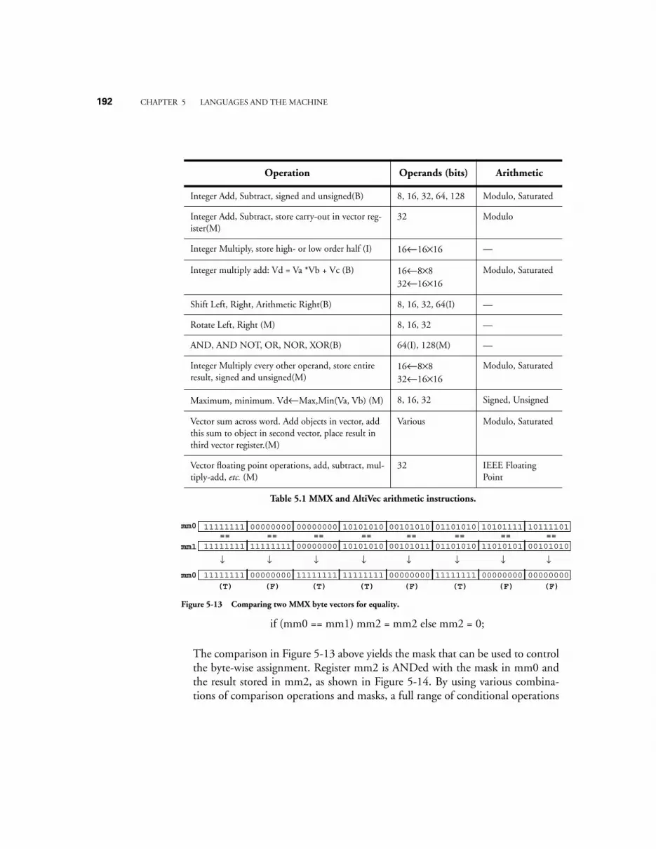
192 CHAPTER 5 LANGUAGES AND THE MACHINE
if (mm0 == mm1) mm2 = mm2 else mm2 = 0;
The comparison in Figure 5-13 above yields the mask that can be used to controlthe byte-wise assignment. Register mm2 is ANDed with the mask in mm0 andthe result stored in mm2, as shown in Figure 5-14. By using various combina-tions of comparison operations and masks, a full range of conditional operations
Operation Operands (bits) Arithmetic
Integer Add, Subtract, signed and unsigned(B) 8, 16, 32, 64, 128 Modulo, Saturated
Integer Add, Subtract, store carry-out in vector reg-ister(M)
32 Modulo
Integer Multiply, store high- or low order half (I) 16←16×16 —
Integer multiply add: Vd = Va *Vb + Vc (B) 16←8×832←16×16
Modulo, Saturated
Shift Left, Right, Arithmetic Right(B) 8, 16, 32, 64(I) —
Rotate Left, Right (M) 8, 16, 32 —
AND, AND NOT, OR, NOR, XOR(B) 64(I), 128(M) —
Integer Multiply every other operand, store entire result, signed and unsigned(M)
16←8×832←16×16
Modulo, Saturated
Maximum, minimum. Vd←Max,Min(Va, Vb) (M) 8, 16, 32 Signed, Unsigned
Vector sum across word. Add objects in vector, add this sum to object in second vector, place result in third vector register.(M)
Various Modulo, Saturated
Vector floating point operations, add, subtract, mul-tiply-add, etc. (M)
32 IEEE Floating Point
Table 5.1 MMX and AltiVec arithmetic instructions.
mm0
mm1
mm0
==
↓
==
↓
==
↓
==
↓
==
↓
==
↓
==
↓
==
(T) (F) (T) (T) (F) (T) (F) (F)
↓
11111111 00000000 00000000 10101010 00101010 01101010 10101111 10111101
11111111 11111111 00000000 10101010 00101011 01101010 11010101 00101010
11111111 00000000 11111111 11111111 00000000 11111111 00000000 00000000
Figure 5-13 Comparing two MMX byte vectors for equality.
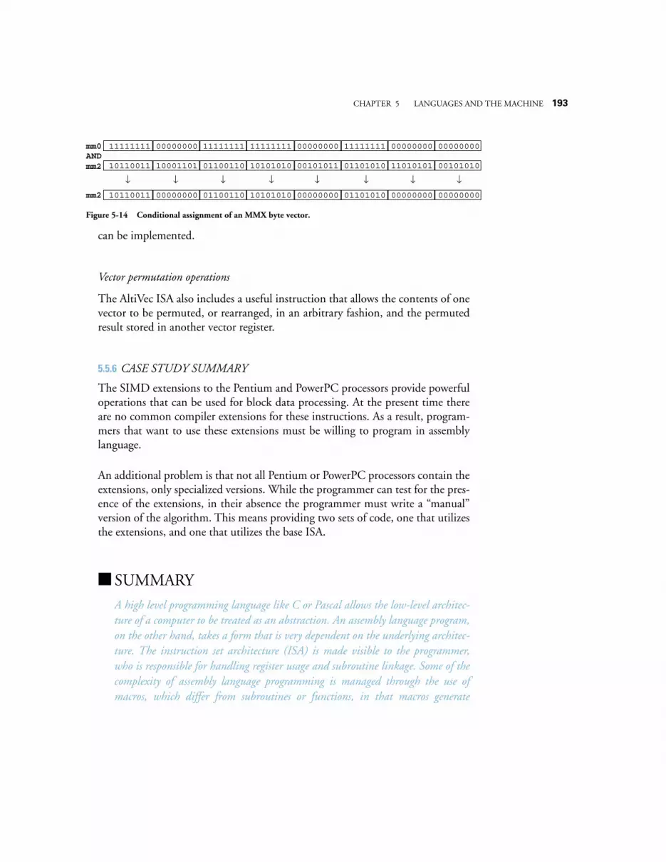
CHAPTER 5 LANGUAGES AND THE MACHINE 193
can be implemented.
Vector permutation operations
The AltiVec ISA also includes a useful instruction that allows the contents of onevector to be permuted, or rearranged, in an arbitrary fashion, and the permutedresult stored in another vector register.
5.5.6 CASE STUDY SUMMARY
The SIMD extensions to the Pentium and PowerPC processors provide powerfuloperations that can be used for block data processing. At the present time thereare no common compiler extensions for these instructions. As a result, program-mers that want to use these extensions must be willing to program in assemblylanguage.
An additional problem is that not all Pentium or PowerPC processors contain theextensions, only specialized versions. While the programmer can test for the pres-ence of the extensions, in their absence the programmer must write a “manual”version of the algorithm. This means providing two sets of code, one that utilizesthe extensions, and one that utilizes the base ISA.
SUMMARY
A high level programming language like C or Pascal allows the low-level architec-ture of a computer to be treated as an abstraction. An assembly language program,on the other hand, takes a form that is very dependent on the underlying architec-ture. The instruction set architecture (ISA) is made visible to the programmer,who is responsible for handling register usage and subroutine linkage. Some of thecomplexity of assembly language programming is managed through the use ofmacros, which differ from subroutines or functions, in that macros generate
mm2
mm2
mm0
↓ ↓ ↓ ↓ ↓ ↓ ↓ ↓
10110011 10001101 01100110 10101010 00101011 01101010 11010101 00101010
10110011 00000000 01100110 10101010 00000000 01101010 00000000 00000000
11111111 00000000 11111111 11111111 00000000 11111111 00000000 00000000AND
Figure 5-14 Conditional assignment of an MMX byte vector.
194 CHAPTER 5 LANGUAGES AND THE MACHINE
in-line code at assembly time, whereas subroutines are executed at run time.
A linker combines separately assembled modules into a single load module, whichtypically involves relocating code. A loader places the load module in memory andstarts the execution of the program. The loader may also need to perform reloca-tion if two or more load modules overlap in memory.
In practice the details of assembly, linking and loading is highly system-dependentand language-dependent. Some simple assemblers merely produce executablebinary files, but more commonly an assembler will produce additional informa-tion so that modules can be linked together by a linker. Some systems provide link-ing loaders that combine the linking task with the loading task. Others separatelinking from loading. Some loaders can only load a program at the address speci-fied in the binary file, while more commonly, relocating loaders can relocate pro-grams to a load-time-specified address. The file formats that support these processesare also operating-system dependent.
Before compilers were developed, programs were written directly in assembly lan-guage. Nowadays, assembly language is not normally used directly since compilersfor high-level languages are so prevalent and also produce efficient code, butassembly language is still important for understanding aspects of computer archi-tecture, such as how to link programs that are compiled for different calling con-ventions, and for exploiting extensions to architectures such as MMX and AltiVec.
FURTHER READINGCompilers and compilation are treated by (Aho et al, 1985) and (Waite andCarter, 1993). There are a great many references on assembly language program-ming. (Donovan, 1972) is a classic reference on assemblers, linkers, and loaders.(Gill et al., 1987) covers the 68000. (Goodman and Miller, 1993) serves as agood instructional text, with examples taken from the MIPS architecture. Theappendix in (Patterson and Hennessy, 1998) also covers the MIPS architecture.(SPARC, 1992) deals specifically with the definition of the SPARC, and SPARCassembly language.
Aho, A. V., Sethi, R., and Ullman, J. D., Compilers, Addison Wesley Longman,Reading, Massachusetts (1985).
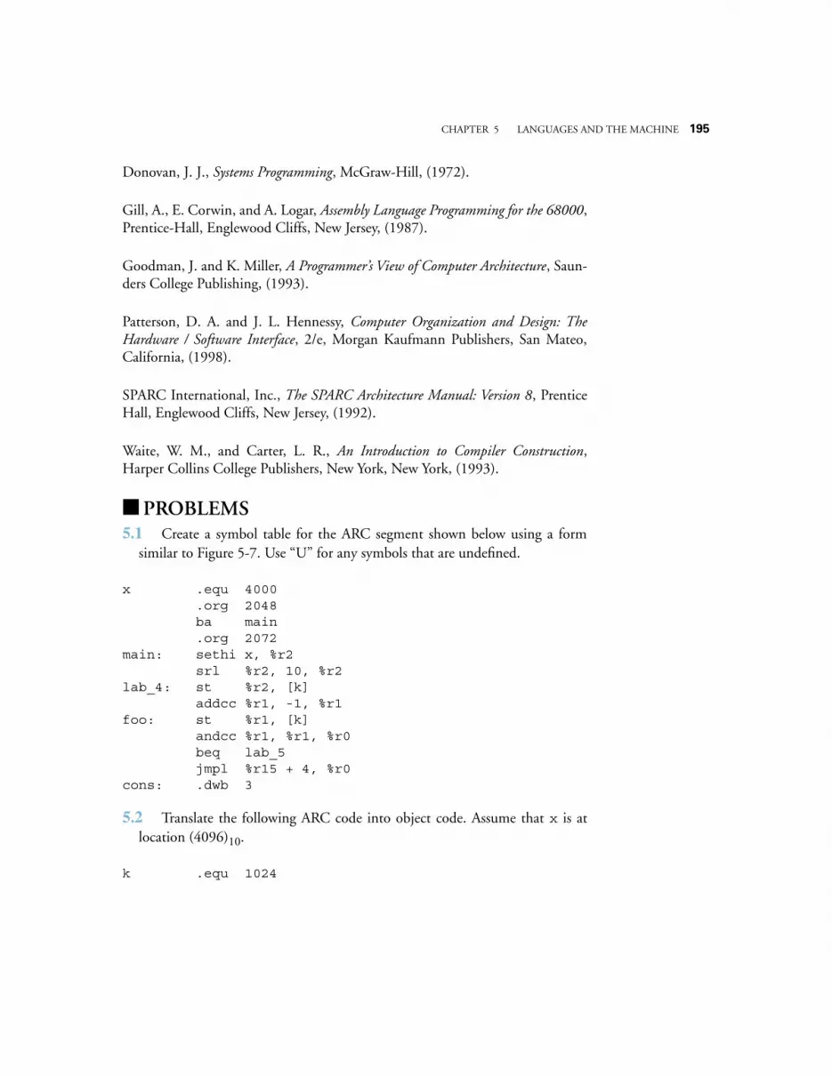
CHAPTER 5 LANGUAGES AND THE MACHINE 195
Donovan, J. J., Systems Programming, McGraw-Hill, (1972).
Gill, A., E. Corwin, and A. Logar, Assembly Language Programming for the 68000,Prentice-Hall, Englewood Cliffs, New Jersey, (1987).
Goodman, J. and K. Miller, A Programmer’s View of Computer Architecture, Saun-ders College Publishing, (1993).
Patterson, D. A. and J. L. Hennessy, Computer Organization and Design: TheHardware / Software Interface, 2/e, Morgan Kaufmann Publishers, San Mateo,California, (1998).
SPARC International, Inc., The SPARC Architecture Manual: Version 8, PrenticeHall, Englewood Cliffs, New Jersey, (1992).
Waite, W. M., and Carter, L. R., An Introduction to Compiler Construction,Harper Collins College Publishers, New York, New York, (1993).
PROBLEMS5.1 Create a symbol table for the ARC segment shown below using a form
similar to Figure 5-7. Use “U” for any symbols that are undefined.
x .equ 4000 .org 2048 ba main .org 2072
main: sethi x, %r2srl %r2, 10, %r2
lab_4: st %r2, [k]addcc %r1, -1, %r1
foo: st %r1, [k]andcc %r1, %r1, %r0beq lab_5jmpl %r15 + 4, %r0
cons: .dwb 3
5.2 Translate the following ARC code into object code. Assume that x is atlocation (4096)10.
k .equ 1024
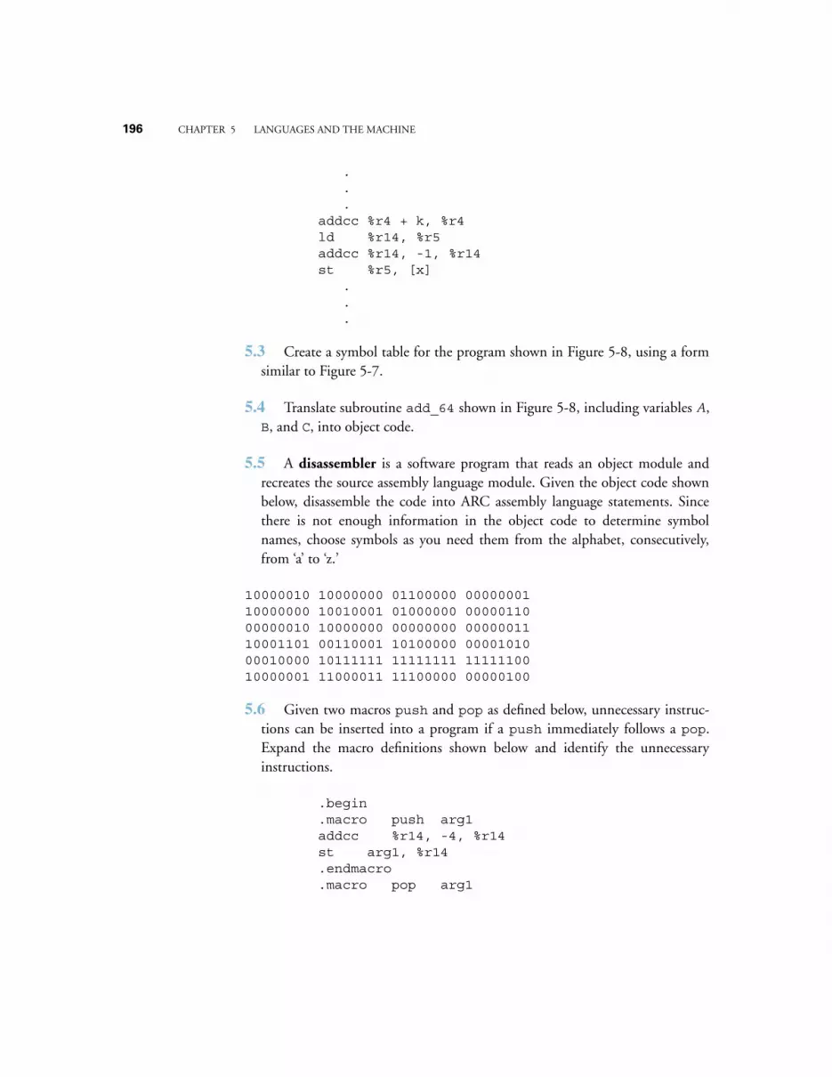
196 CHAPTER 5 LANGUAGES AND THE MACHINE
.
.
.addcc %r4 + k, %r4ld %r14, %r5addcc %r14, -1, %r14st %r5, [x]
.
.
.
5.3 Create a symbol table for the program shown in Figure 5-8, using a formsimilar to Figure 5-7.
5.4 Translate subroutine add_64 shown in Figure 5-8, including variables A,B, and C, into object code.
5.5 A disassembler is a software program that reads an object module andrecreates the source assembly language module. Given the object code shownbelow, disassemble the code into ARC assembly language statements. Sincethere is not enough information in the object code to determine symbolnames, choose symbols as you need them from the alphabet, consecutively,from ‘a’ to ‘z.’
10000010 10000000 01100000 0000000110000000 10010001 01000000 0000011000000010 10000000 00000000 0000001110001101 00110001 10100000 0000101000010000 10111111 11111111 1111110010000001 11000011 11100000 00000100
5.6 Given two macros push and pop as defined below, unnecessary instruc-tions can be inserted into a program if a push immediately follows a pop.Expand the macro definitions shown below and identify the unnecessaryinstructions.
.begin
.macro push arg1addcc %r14, -4, %r14st arg1, %r14.endmacro.macro pop arg1
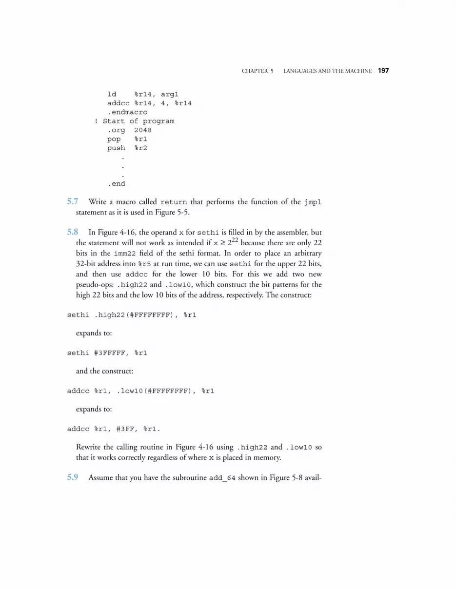
CHAPTER 5 LANGUAGES AND THE MACHINE 197
ld %r14, arg1addcc %r14, 4, %r14.endmacro
! Start of program.org 2048pop %r1push %r2
.
.
..end
5.7 Write a macro called return that performs the function of the jmplstatement as it is used in Figure 5-5.
5.8 In Figure 4-16, the operand x for sethi is filled in by the assembler, butthe statement will not work as intended if x ≥ 222 because there are only 22bits in the imm22 field of the sethi format. In order to place an arbitrary32-bit address into %r5 at run time, we can use sethi for the upper 22 bits,and then use addcc for the lower 10 bits. For this we add two newpseudo-ops: .high22 and .low10, which construct the bit patterns for thehigh 22 bits and the low 10 bits of the address, respectively. The construct:
sethi .high22(#FFFFFFFF), %r1
expands to:
sethi #3FFFFF, %r1
and the construct:
addcc %r1, .low10(#FFFFFFFF), %r1
expands to:
addcc %r1, #3FF, %r1.
Rewrite the calling routine in Figure 4-16 using .high22 and .low10 sothat it works correctly regardless of where x is placed in memory.
5.9 Assume that you have the subroutine add_64 shown in Figure 5-8 avail-
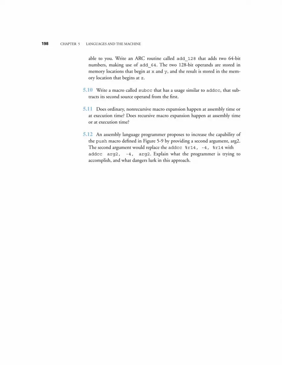
198 CHAPTER 5 LANGUAGES AND THE MACHINE
able to you. Write an ARC routine called add_128 that adds two 64-bitnumbers, making use of add_64. The two 128-bit operands are stored inmemory locations that begin at x and y, and the result is stored in the mem-ory location that begins at z.
5.10 Write a macro called subcc that has a usage similar to addcc, that sub-tracts its second source operand from the first.
5.11 Does ordinary, nonrecursive macro expansion happen at assembly time orat execution time? Does recursive macro expansion happen at assembly timeor at execution time?
5.12 An assembly language programmer proposes to increase the capability ofthe push macro defined in Figure 5-9 by providing a second argument, arg2.The second argument would replace the addcc %r14, -4, %r14 with addcc arg2, -4, arg2. Explain what the programmer is trying toaccomplish, and what dangers lurk in this approach.
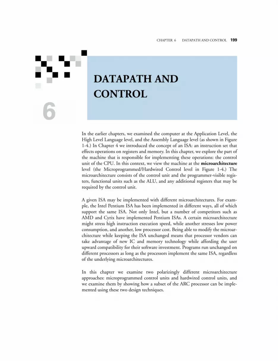
CHAPTER 6 DATAPATH AND CONTROL
199
In the earlier chapters, we examined the computer at the Application Level, theHigh Level Language level, and the Assembly Language level (as shown in Figure1-4.) In Chapter 4 we introduced the concept of an ISA: an instruction set thateffects operations on registers and memory. In this chapter, we explore the part ofthe machine that is responsible for implementing these operations: the controlunit of the CPU. In this context, we view the machine at the
microarchitecture
level (the Microprogrammed/Hardwired Control level in Figure 1-4.) Themicroarchitecture consists of the control unit and the programmer-visible regis-ters, functional units such as the ALU, and any additional registers that may berequired by the control unit.
A given ISA may be implemented with different microarchitectures. For exam-ple, the Intel Pentium ISA has been implemented in different ways, all of whichsupport the same ISA. Not only Intel, but a number of competitors such asAMD and Cyrix have implemented Pentium ISAs. A certain microarchitecturemight stress high instruction execution speed, while another stresses low powerconsumption, and another, low processor cost. Being able to modify the microar-chitecture while keeping the ISA unchanged means that processor vendors cantake advantage of new IC and memory technology while affording the userupward compatibility for their software investment. Programs run unchanged ondifferent processors as long as the processors implement the same ISA, regardlessof the underlying microarchitectures.
In this chapter we examine two polarizingly different microarchitectureapproaches: microprogrammed control units and hardwired control units, andwe examine them by showing how a subset of the ARC processor can be imple-mented using these two design techniques.
DATAPATH AND CONTROL
6
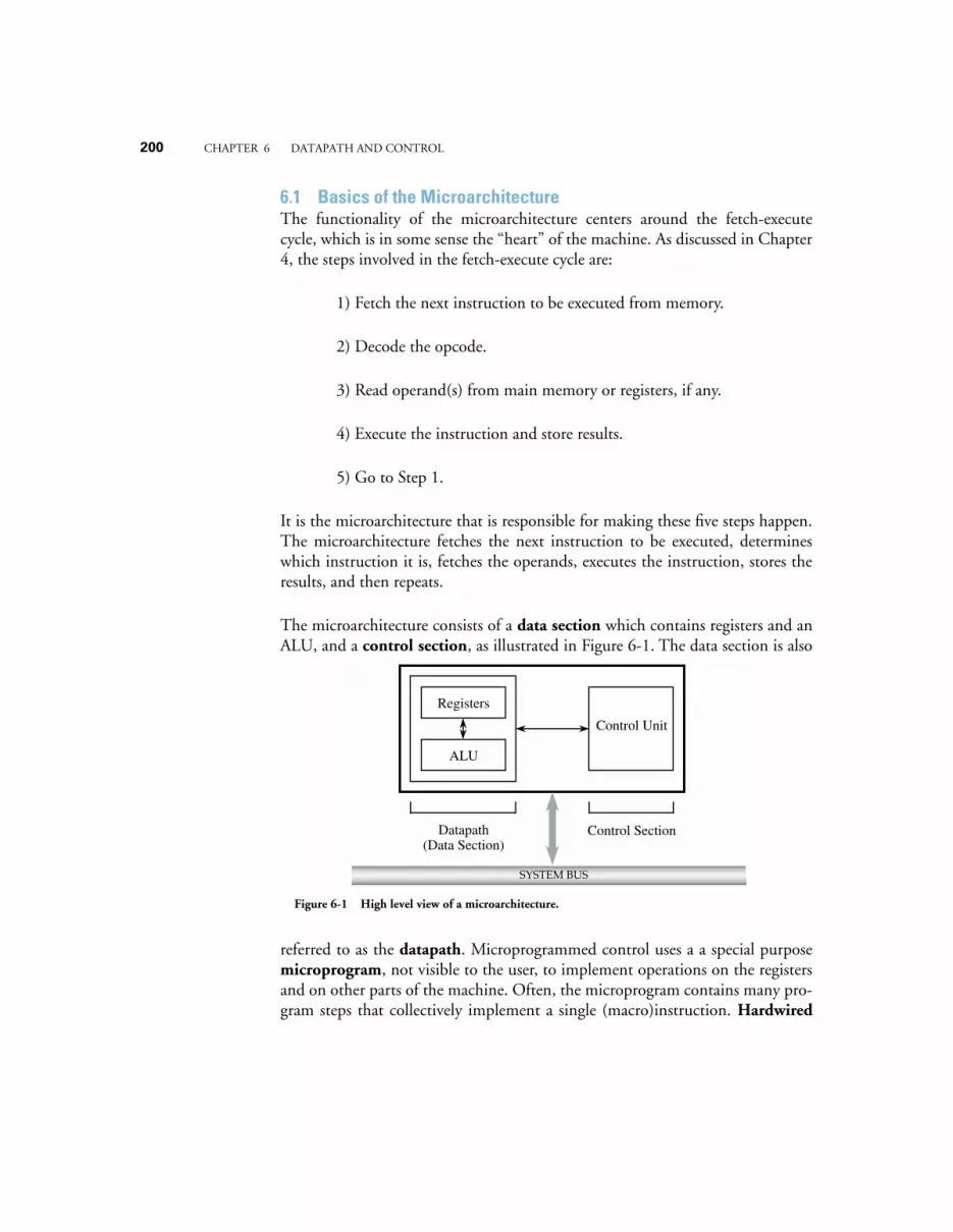
200
CHAPTER 6 DATAPATH AND CONTROL
6.1 Basics of the Microarchitecture
The functionality of the microarchitecture centers around the fetch-executecycle, which is in some sense the “heart” of the machine. As discussed in Chapter4, the steps involved in the fetch-execute cycle are:
1) Fetch the next instruction to be executed from memory.
2) Decode the opcode.
3) Read operand(s) from main memory or registers, if any.
4) Execute the instruction and store results.
5) Go to Step 1.
It is the microarchitecture that is responsible for making these five steps happen.The microarchitecture fetches the next instruction to be executed, determineswhich instruction it is, fetches the operands, executes the instruction, stores theresults, and then repeats.
The microarchitecture consists of a
data section
which contains registers and anALU, and a
control section
, as illustrated in Figure 6-1. The data section is also
referred to as the
datapath
. Microprogrammed control uses a a special purpose
microprogram
, not visible to the user, to implement operations on the registersand on other parts of the machine. Often, the microprogram contains many pro-gram steps that collectively implement a single (macro)instruction.
Hardwired
Control Unit
Control Section
Registers
ALU
Datapath(Data Section)
SYSTEM BUS
Figure 6-1 High level view of a microarchitecture.
CHAPTER 6 DATAPATH AND CONTROL
201
control units adopt the view that the steps to be taken to implement an opera-tion comprise states in a finite state machine, and the design proceeds using con-ventional digital design methods (such as the methods covered in Appendix A.)In either case, the datapath remains largely unchanged, although there may beminor differences to support the differing forms of control. In designing theARC control unit, the microprogrammed approach will be explored first, andthen the hardwired approach, and for both cases the datapath will remainunchanged.
6.2 A Microarchitecture for the ARC
In this section we consider a microprogrammed approach for designing the ARCcontrol unit. We begin by describing the datapath and its associated control sig-nals.
The instruction set and instruction format for the ARC subset is repeated fromChapter 4 in Figure 6-2. There are 15 instructions that are grouped into four for-mats according to the leftmost two bits of the coded instruction. The ProcessorStatus Register
%psr
is also shown.
6.2.1
THE DATAPATH
A datapath for the ARC is illustrated in Figure 6-3. The datapath contains 32user-visible data registers (
%r0 – %r31
), the program counter (
%pc
), theinstruction register (
%ir
), the ALU, four temporary registers not visible at theISA level (
%temp0 – %temp3
), and the connections among these components.The number adjacent to a diagonal slash on some of the lines is a simplificationthat indicates the number of separate wires that are represented by the corre-sponding single line.
Registers
%r0 – %r31
are directly accessible by a user. Register
%r0
always con-tains the value 0, and cannot be changed. The
%pc
register is the programcounter, which keeps track of the next instruction to be read from the mainmemory. The user has direct access to
%pc
only through the
call
and
jmpl
instructions. The temporary registers are used in interpreting the ARC instruc-tion set, and are not visible to the user. The
%ir
register holds the currentinstruction that is being executed. It is not visible to the user.
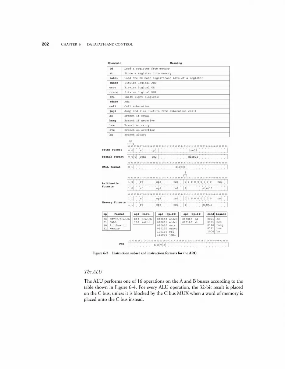
202
CHAPTER 6 DATAPATH AND CONTROL
The ALU
The ALU performs one of 16 operations on the A and B busses according to thetable shown in Figure 6-4. For every ALU operation, the 32-bit result is placedon the C bus, unless it is blocked by the C bus MUX when a word of memory isplaced onto the C bus instead.
ld Load a register from memory
Mnemonic Meaning
st
sethi
andcc
addcc
call
jmpl
be
orcc
orncc
Store a register into memory
Load the 22 most significant bits of a register
Bitwise logical AND
Add
Branch on overflow
Call subroutine
Jump and link (return from subroutine call)
Branch if equal
Bitwise logical OR
Bitwise logical NOR
bneg
bcs
Branch if negative
Branch on carry
srl Shift right (logical)
bvs
ba Branch always
op3 (op=10)
010000010001010010010110100110111000
addccandccorccornccsrljmpl
00010101011001111000
cond
bebcsbnegbvsba
branch
010100
op2
branchsethi
Inst.
00011011
op
SETHI/BranchCALLArithmeticMemory
Format
000000000100
ldst
op3 (op=11)
op
CALL format disp30
31 30 29 28 27 26 25 24 23 22 21 20 19 18 17 16 15 14 13 12 11 10 09 08 07 06 05 04 03 02 01 00
0 1
SETHI Format imm22
31 30 29 28 27 26 25 24 23 22 21 20 19 18 17 16 15 14 13 12 11 10 09 08 07 06 05 04 03 02 01 00
rd
disp220 cond
0 0
0 0Branch Format
op2
op2
31 30 29 28 27 26 25 24 23 22 21 20 19 18 17 16 15 14 13 12 11 10 09 08 07 06 05 04 03 02 01 00
rs11 op3
simm131 op3
1
Memory Formats1
rd
rd rs1
0
1
0 0 0 0 0 0 0 0 rs2
Arithmetic Formats
31 30 29 28 27 26 25 24 23 22 21 20 19 18 17 16 15 14 13 12 11 10 09 08 07 06 05 04 03 02 01 00
rs11 op3
simm131 op3
0
0
rd
rd rs1
0
1
0 0 0 0 0 0 0 0 rs2
i
PSR31 30 29 28 27 26 25 24 23 22 21 20 19 18 17 16 15 14 13 12 11 10 09 08 07 06 05 04 03 02 01 00
z v cn
Figure 6-2 Instruction subset and instruction formats for the ARC.
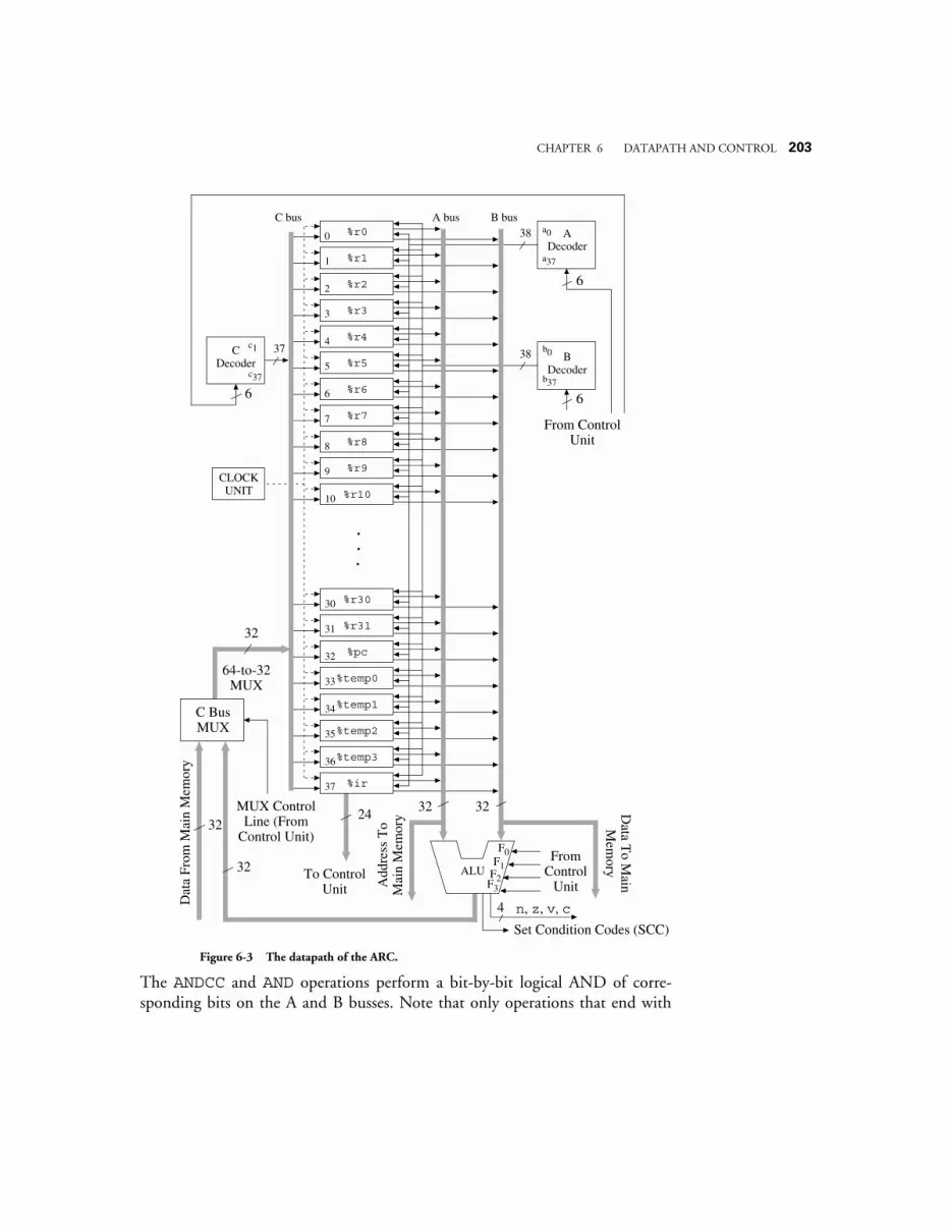
CHAPTER 6 DATAPATH AND CONTROL
203
The
ANDCC
and
AND
operations perform a bit-by-bit logical AND of corre-sponding bits on the A and B busses. Note that only operations that end with
%r0A bus B busC bus
F1F2
ALU
32
32
4
%r1
64-to-32 MUX
C Bus MUX
n, z, v, c
F0
C Decoder %r5
%pc
%temp0
%r2
%r3
%r4
%r6
%r7
%r8
%r9
%r10
%r30
%r31
B Decoder
F3
6
c1
c37
37 38 b0
b37
6
A Decoder
38 a0
a37
6
Dat
a Fr
om M
ain
Mem
ory
MUX Control Line (From
Control Unit)
%temp1
%temp2
%temp3
%ir
Data T
o Main
Mem
ory
Add
ress
To
Mai
n M
emor
y
CLOCK UNIT
0
1
2
3
4
5
6
7
8
9
10
30
31
32
33
34
35
36
37
32
From Control
Unit
From Control Unit
Set Condition Codes (SCC)
32
32
.
.
.
To Control Unit
24
Figure 6-3 The datapath of the ARC.
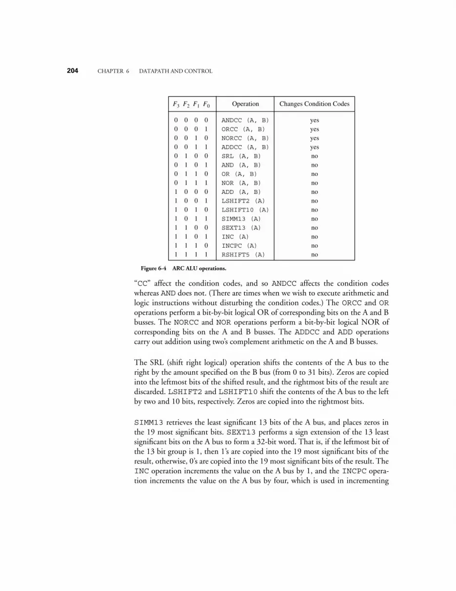
204
CHAPTER 6 DATAPATH AND CONTROL
“
CC
” affect the condition codes, and so
ANDCC
affects the condition codeswhereas
AND
does not. (There are times when we wish to execute arithmetic andlogic instructions without disturbing the condition codes.) The
ORCC
and
OR
operations perform a bit-by-bit logical OR of corresponding bits on the A and Bbusses. The
NORCC
and
NOR
operations perform a bit-by-bit logical NOR ofcorresponding bits on the A and B busses. The
ADDCC
and
ADD
operationscarry out addition using two’s complement arithmetic on the A and B busses.
The SRL (shift right logical) operation shifts the contents of the A bus to theright by the amount specified on the B bus (from 0 to 31 bits). Zeros are copiedinto the leftmost bits of the shifted result, and the rightmost bits of the result arediscarded.
LSHIFT2
and
LSHIFT10
shift the contents of the A bus to the leftby two and 10 bits, respectively. Zeros are copied into the rightmost bits.
SIMM13
retrieves the least significant 13 bits of the A bus, and places zeros inthe 19 most significant bits.
SEXT13
performs a sign extension of the 13 leastsignificant bits on the A bus to form a 32-bit word. That is, if the leftmost bit ofthe 13 bit group is 1, then 1’s are copied into the 19 most significant bits of theresult, otherwise, 0’s are copied into the 19 most significant bits of the result. The
INC
operation increments the value on the A bus by 1, and the
INCPC
opera-tion increments the value on the A bus by four, which is used in incrementing
0011001100110011
0101010101010101
F1 F0
ANDCC (A, B)
ORCC (A, B)
NORCC (A, B)
ADDCC (A, B)
SRL (A, B)
AND (A, B)
OR (A, B)
NOR (A, B)
ADD (A, B)
LSHIFT2 (A)
LSHIFT10 (A)
SIMM13 (A)
SEXT13 (A)
INC (A)
INCPC (A)
RSHIFT5 (A)
Operation
0000111100001111
F2 Changes Condition Codes
yesyesyesyesnononononononononononono
0000000011111111
F3
Figure 6-4 ARC ALU operations.
CHAPTER 6 DATAPATH AND CONTROL
205
the PC register by one word (four bytes).
INCPC
can be used on any registerplaced on the A bus.
The
RSHIFT5
operation shifts the operand on the A bus to the right by 5 bits,copying the leftmost bit (the sign bit) into the 5 new bits on the left. This has theeffect of performing a 5-bit sign extension. When applied three times in succes-sion to a 32-bit instruction, this operation also has the effect of placing the left-most bit of the
COND
field in the Branch format (refer to Figure 6-2) into theposition of bit 13. This operation is useful in decoding the Branch instructions,as we will see later in the chapter. The sign extension for this case is inconsequen-tial.
Every arithmetic and logic operation can be implemented with just these ALUoperations. As an example, a subtraction operation can be implemented by form-ing the two’s complement negative of the subtrahend (making use of the
NOR
operation and adding 1 to it with
INC
) and then performing addition on theoperands. A shift to the left by one bit can be performed by adding a number toitself. A “do-nothing” operation, which is frequently needed for simply passingdata through the ALU without changing it, can be implemented by logicallyANDing an operand with itself and discarding the result in
%r0
. A logical XORcan be implemented with the AND, OR, and NOR operations, making use ofDeMorgan’s theorem (see problem 6.5).
The ALU generates the
c
,
n
,
z
, and
v
condition codes which are true for a carry,negative, zero, or overflow result, respectively. The condition codes are changedonly for the operations indicated in Figure 6-4. A signal (SCC) is also generatedthat tells the
%psr
register when to update the condition codes.
The ALU can be implemented in a number of ways. For the sake of simplicity,let us consider using a
lookup table
(LUT) approach. The ALU has two 32-bitdata inputs
A
and
B
, a 32-bit data output
C
, a four-bit control input
F
, a four-bitcondition code output (
N, V, C, Z
), and a signal (SCC) that sets the flags in the
%psr
register. We can decompose the ALU into a cascade of 32 LUTs thatimplement the arithmetic and logic functions, followed by a
barrel shifter
thatimplements the shifts. A block diagram is shown in Figure 6-5.
The barrel shifter shifts the input word by an arbitrary amount (from 0 to 31bits) according to the settings of the control inputs. The barrel shifter performsshifts in levels, in which a different bit of the Shift Amount (SA) input isobserved at each level. A partial gate-level layout for the barrel shifter is shown in

206
CHAPTER 6 DATAPATH AND CONTROL
Figure 6-6. Starting at the bottom of the circuit, we can see that the outputs ofthe bottom stage will be the same as the inputs to that stage if the SA
0
bit is 0. Ifthe SA
0
bit is 1, then each output position will take on the value of its immediateleft or right neighbor, according to the direction of the shift, which is indicatedby the Shift Right input. At the next higher level, the method is applied again,except that the SA
1 bit is observed and the amount of the shift is doubled. Theprocess continues until bit SA4 is observed at the highest level. Zeros are copiedinto positions that have no corresponding inputs. With this structure, an arbi-trary shift from 0 to 31 bits to the left or the right can be implemented.
Each of the 32 ALU LUTs is implemented (almost) identically, using the samelookup table entries, except for changes in certain positions such as for the INCand INCPC operations (see problem Figure 6.20). The first few entries for eachLUT are shown in Figure 6-7. The barrel shifter control LUT is constructed in asimilar manner, but with different LUT entries.
ALU LUT0
b0 a0
ALU LUT1
b1 a1
ALU LUT30
b30 a30
ALU LUT31
b31 a31
C c0c1c30c31
carry
BARREL SHIFTER
z0z1z30z31
. . .
F0:3
Barrel Shifter Control LUT
b0-4
Direction of Shift
Shift Amount (SA)5
NV Z
. . .
SCC: Set Condition Codes
F3 F2
0
2
4
4
4
Figure 6-5 Block diagram of the 32-bit ALU.

CHAPTER 6 DATAPATH AND CONTROL 207
The condition code bits n, z, v, and c are implemented directly. The n and cbits are taken directly from the c31 output of the barrel shifter and the carry-outposition of ALU LUT31, respectively. The z bit is computed as the NOR overthe barrel shifter outputs. The z bit is 1 only if all of the barrel shifter outputs are0. The v (overflow) bit is set if the carry into the most significant position is dif-ferent than the carry out of the most significant position, which is implementedwith an XOR gate.
Only the operations that end in “CC” should set the condition codes, and so asignal is generated that informs the condition codes to change, as indicated bythe label “SCC: Set Condition Codes.” This signal is true when both F3 and F2are false.
The Registers
All of the registers are composed of falling edge-triggered D flip-flops (see Appen-
c31 c30 c1 c0
SA0
. . .
Shift Right
SA1
. . .
Shift Right
.
..
Bit 31 Bit 30 Bit 1 Bit 0
Bit 29 Bit 28
Bit 3 Bit 2
Bit 29
Bit 2
Figure 6-6 Gate-level layout of barrel shifter.
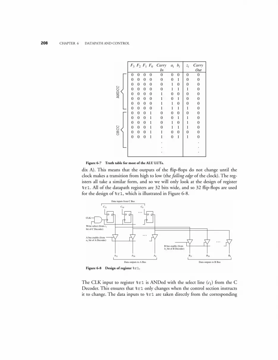
208 CHAPTER 6 DATAPATH AND CONTROL
dix A). This means that the outputs of the flip-flops do not change until theclock makes a transition from high to low (the falling edge of the clock). The reg-isters all take a similar form, and so we will only look at the design of register%r1. All of the datapath registers are 32 bits wide, and so 32 flip-flops are usedfor the design of %r1, which is illustrated in Figure 6-8.
The CLK input to register %r1 is ANDed with the select line (c1) from the CDecoder. This ensures that %r1 only changes when the control section instructsit to change. The data inputs to %r1 are taken directly from the corresponding
F3
00000000000000
F2
00000000000000
F1
00000000000000
F0
00000000111111
Carry In00001111000011...
ai
00110011001100
bi
01010101010101
zi
00010001011101
Carry Out00000000000000...
ANDCC
ORCC
Figure 6-7 Truth table for most of the ALU LUTs.
CLKQD
C31
Write select (from c1 bit of C Decoder)
A31 B31
QD
C30
A30 B30
QD
C0
A0 B0
. . .
. . .A bus enable (from a1 bit of A Decoder)
B bus enable (from b1 bit of B Decoder)
. . .
Data inputs from C Bus
Data outputs to B BusData outputs to A Bus
Figure 6-8 Design of register %r1.
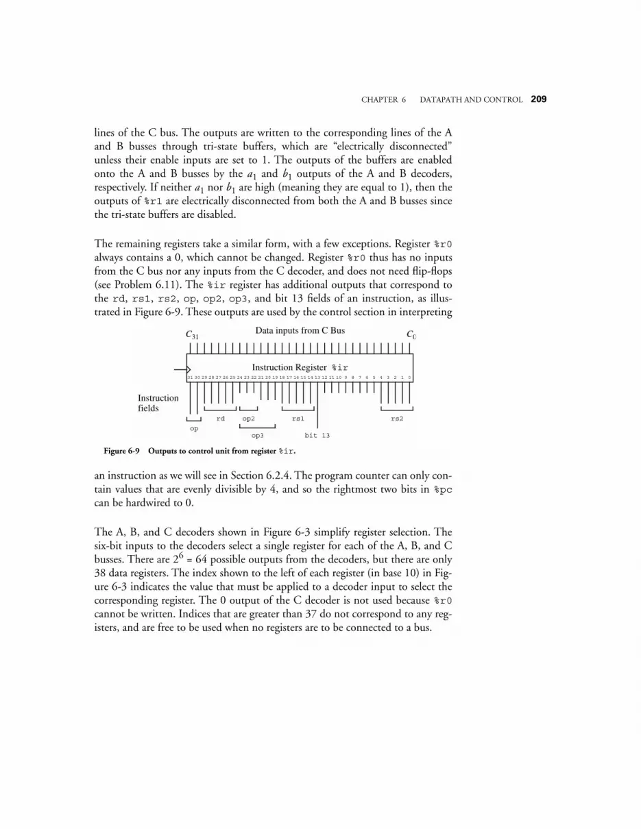
CHAPTER 6 DATAPATH AND CONTROL 209
lines of the C bus. The outputs are written to the corresponding lines of the Aand B busses through tri-state buffers, which are “electrically disconnected”unless their enable inputs are set to 1. The outputs of the buffers are enabledonto the A and B busses by the a1 and b1 outputs of the A and B decoders,respectively. If neither a1 nor b1 are high (meaning they are equal to 1), then theoutputs of %r1 are electrically disconnected from both the A and B busses sincethe tri-state buffers are disabled.
The remaining registers take a similar form, with a few exceptions. Register %r0always contains a 0, which cannot be changed. Register %r0 thus has no inputsfrom the C bus nor any inputs from the C decoder, and does not need flip-flops(see Problem 6.11). The %ir register has additional outputs that correspond tothe rd, rs1, rs2, op, op2, op3, and bit 13 fields of an instruction, as illus-trated in Figure 6-9. These outputs are used by the control section in interpreting
an instruction as we will see in Section 6.2.4. The program counter can only con-tain values that are evenly divisible by 4, and so the rightmost two bits in %pccan be hardwired to 0.
The A, B, and C decoders shown in Figure 6-3 simplify register selection. Thesix-bit inputs to the decoders select a single register for each of the A, B, and Cbusses. There are 26 = 64 possible outputs from the decoders, but there are only38 data registers. The index shown to the left of each register (in base 10) in Fig-ure 6-3 indicates the value that must be applied to a decoder input to select thecorresponding register. The 0 output of the C decoder is not used because %r0cannot be written. Indices that are greater than 37 do not correspond to any reg-isters, and are free to be used when no registers are to be connected to a bus.
Data inputs from C Bus
31 30 29 28 27 26 25 24 23 22 21 20 19 18 17 16 15 14 13 12 11 10 9 8 7 6 5 4 3 2 1 0
Instruction fields
C0C31
Instruction Register %ir
op
op2
op3
rd rs1 rs2
bit 13
Figure 6-9 Outputs to control unit from register %ir.
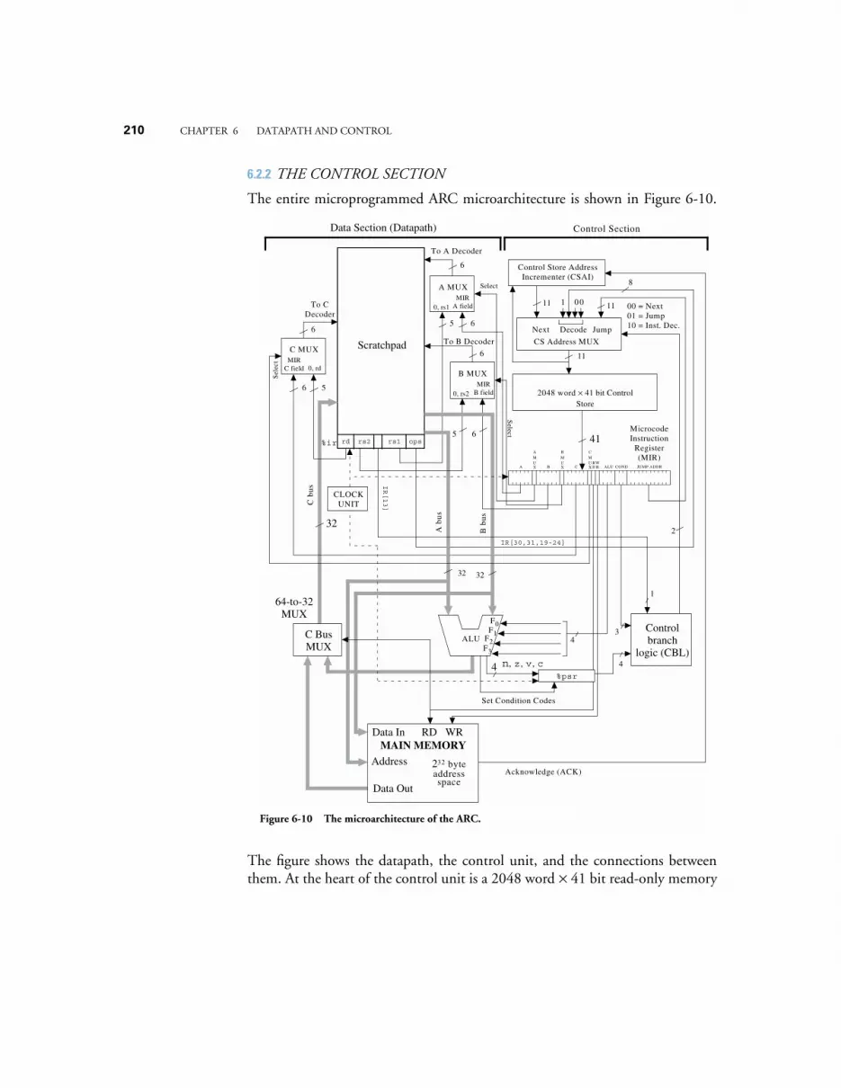
210 CHAPTER 6 DATAPATH AND CONTROL
6.2.2 THE CONTROL SECTION
The entire microprogrammed ARC microarchitecture is shown in Figure 6-10.
The figure shows the datapath, the control unit, and the connections betweenthem. At the heart of the control unit is a 2048 word × 41 bit read-only memory
32
A b
us
B b
us
C b
us
2048 word × 41 bit Control Store
CS Address MUX
Jump
Control branch
logic (CBL)
F1F2ALU
Microcode Instruction
Register (MIR)
CLOCK UNIT
41
11
11
MAIN MEMORYWRRD
Data Section (Datapath)
32
Address
Data In
00 = Next01 = Jump10 = Inst. Dec.
4
8
2
Decode
1 0 0
4
232 byte address space
32
3
Data Out
64-to-32 MUX
C Bus MUX
%psr
n, z, v, c
F0
Next
11
Control Store Address Incrementer (CSAI)
Acknowledge (ACK)
To C Decoder
%ir
C MUX
0, rd
Control Section
A MUX
0, rs1
To B Decoder
B MUX
0, rs2
F3
4
1
IR[30,31,19-24]
6 5
6
MIR C field
Sel
ect
MIR A field
MIR B field
6
6
5 6S
elect
Select
Scratchpad
To A Decoder
rd rs2 rs1 ops
IR[13]
5 6
Set Condition Codes
%ir
RD
WRCA B JUMP ADDRALU COND
AMUX
BMUX
CMUX
Figure 6-10 The microarchitecture of the ARC.
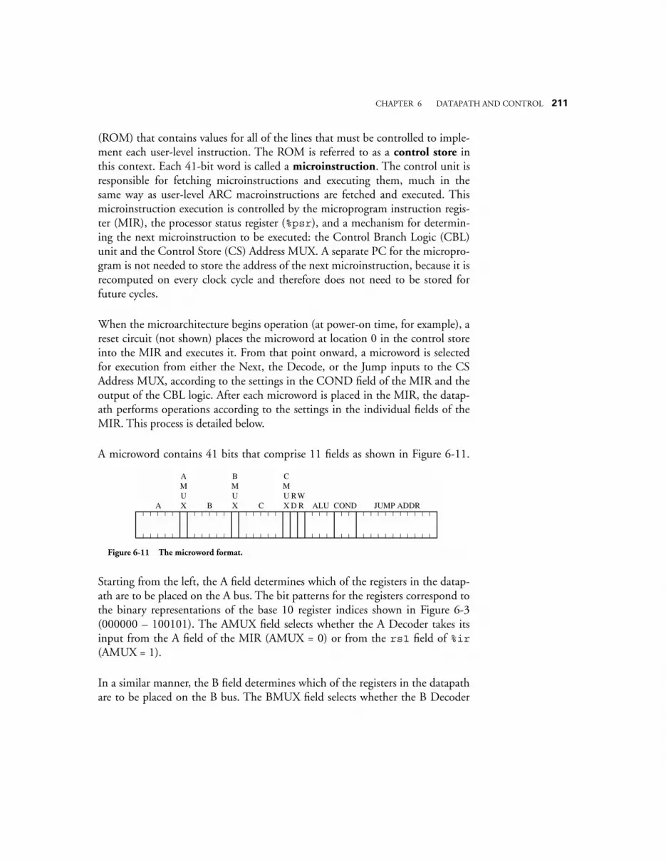
CHAPTER 6 DATAPATH AND CONTROL 211
(ROM) that contains values for all of the lines that must be controlled to imple-ment each user-level instruction. The ROM is referred to as a control store inthis context. Each 41-bit word is called a microinstruction. The control unit isresponsible for fetching microinstructions and executing them, much in thesame way as user-level ARC macroinstructions are fetched and executed. Thismicroinstruction execution is controlled by the microprogram instruction regis-ter (MIR), the processor status register (%psr), and a mechanism for determin-ing the next microinstruction to be executed: the Control Branch Logic (CBL)unit and the Control Store (CS) Address MUX. A separate PC for the micropro-gram is not needed to store the address of the next microinstruction, because it isrecomputed on every clock cycle and therefore does not need to be stored forfuture cycles.
When the microarchitecture begins operation (at power-on time, for example), areset circuit (not shown) places the microword at location 0 in the control storeinto the MIR and executes it. From that point onward, a microword is selectedfor execution from either the Next, the Decode, or the Jump inputs to the CSAddress MUX, according to the settings in the COND field of the MIR and theoutput of the CBL logic. After each microword is placed in the MIR, the datap-ath performs operations according to the settings in the individual fields of theMIR. This process is detailed below.
A microword contains 41 bits that comprise 11 fields as shown in Figure 6-11.
Starting from the left, the A field determines which of the registers in the datap-ath are to be placed on the A bus. The bit patterns for the registers correspond tothe binary representations of the base 10 register indices shown in Figure 6-3(000000 – 100101). The AMUX field selects whether the A Decoder takes itsinput from the A field of the MIR (AMUX = 0) or from the rs1 field of %ir(AMUX = 1).
In a similar manner, the B field determines which of the registers in the datapathare to be placed on the B bus. The BMUX field selects whether the B Decoder
RD
WRCA B JUMP ADDRALU COND
AMUX
BMUX
CMUX
Figure 6-11 The microword format.
212 CHAPTER 6 DATAPATH AND CONTROL
takes its input from the B field of the MIR (BMUX = 0) or from the rs2 field of%ir (BMUX = 1). The C field determines which of the registers in the datapathis to be written from the C bus. The CMUX field selects whether the C Decodertakes its input from the C field of the MIR (CMUX = 0) or from the rd field of%ir (CMUX = 1). Since %r0 cannot be changed, the bit pattern 000000 can beused in the C field when none of these registers are to be changed.
The RD and WR lines determine whether the memory will be read or written,respectively. A read takes place if RD = 1, and a write takes place if WR = 1. Boththe RD and WR fields cannot be set to 1 at the same time, but both fields can be0 if neither a read nor a write operation is to take place. For both RD and WR,the address for the memory is taken directly from the A bus. The data input tothe memory is taken from the B bus, and the data output from the memory isplaced on the C bus. The RD line controls the 64-to-32 C Bus MUX, whichdetermines whether the C bus is loaded from the memory (RD = 1) or from theALU (RD = 0).
The ALU field determines which of the ALU operations is performed accordingto the settings shown in Figure 6-4. All 16 possible ALU field bit patterns corre-spond to valid ALU operations. This means that there is no way to “turn theALU off” when it is not needed, such as during a read or write to memory. Forthis situation, an ALU operation should be selected that has no unwanted sideeffects. For example, ANDCC changes the condition codes and would not beappropriate, whereas the AND operation does not affect the condition codes, andwould therefore be appropriate.
The COND (conditional jump) field instructs the microcontroller to take thenext microword from either the next control store location, or from the locationin the JUMP ADDR field of the MIR, or from the opcode bits of the instructionin %ir. The COND field is interpreted according to the table shown in Figure6-12. If the COND field is 000, then no jump is taken, and the Next input tothe CS Address MUX is used. The Next input to the CS Address MUX is com-puted by the control store address incrementer (CSAI) shown in Figure 6-10,which increments the current output of the CS Address MUX by 1. If theCOND field is 001, 010, 011, 100, or 101, then a conditional jump is taken tothe control store location in the JUMP ADDR field, according to the value ofthe n, z, v, or c flags, or bit 13 of %ir, respectively. The syntax “IR[13]” means“bit 13 of the instruction register %ir.” If the COND field is 110, then anunconditional jump is taken.
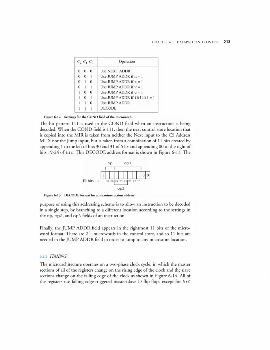
CHAPTER 6 DATAPATH AND CONTROL 213
The bit pattern 111 is used in the COND field when an instruction is beingdecoded. When the COND field is 111, then the next control store location thatis copied into the MIR is taken from neither the Next input to the CS AddressMUX nor the Jump input, but is taken from a combination of 11 bits created byappending 1 to the left of bits 30 and 31 of %ir and appending 00 to the right ofbits 19-24 of %ir. This DECODE address format is shown in Figure 6-13. The
purpose of using this addressing scheme is to allow an instruction to be decodedin a single step, by branching to a different location according to the settings inthe op, op2, and op3 fields of an instruction.
Finally, the JUMP ADDR field appears in the rightmost 11 bits of the micro-word format. There are 211 microwords in the control store, and so 11 bits areneeded in the JUMP ADDR field in order to jump to any microstore location.
6.2.3 TIMING
The microarchitecture operates on a two-phase clock cycle, in which the mastersections of all of the registers change on the rising edge of the clock and the slavesections change on the falling edge of the clock as shown in Figure 6-14. All ofthe registers use falling edge-triggered master/slave D flip-flops except for %r0
00110011
01010101
C1 C0
Use NEXT ADDRUse JUMP ADDR if n = 1Use JUMP ADDR if z = 1Use JUMP ADDR if v = 1Use JUMP ADDR if c = 1Use JUMP ADDR if IR[13] = 1Use JUMP ADDRDECODE
Operation
00001111
C2
Figure 6-12 Settings for the COND field of the microword.
op
1 0 0
op2
op3
31 30 24 23 22 21 20 19IR bits
Figure 6-13 DECODE format for a microinstruction address.
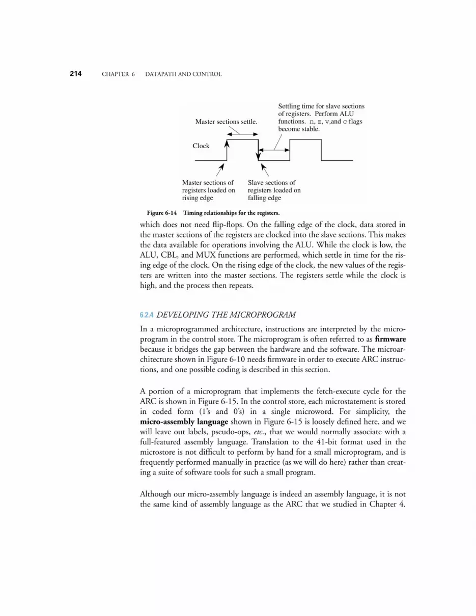
214 CHAPTER 6 DATAPATH AND CONTROL
which does not need flip-flops. On the falling edge of the clock, data stored inthe master sections of the registers are clocked into the slave sections. This makesthe data available for operations involving the ALU. While the clock is low, theALU, CBL, and MUX functions are performed, which settle in time for the ris-ing edge of the clock. On the rising edge of the clock, the new values of the regis-ters are written into the master sections. The registers settle while the clock ishigh, and the process then repeats.
6.2.4 DEVELOPING THE MICROPROGRAM
In a microprogrammed architecture, instructions are interpreted by the micro-program in the control store. The microprogram is often referred to as firmwarebecause it bridges the gap between the hardware and the software. The microar-chitecture shown in Figure 6-10 needs firmware in order to execute ARC instruc-tions, and one possible coding is described in this section.
A portion of a microprogram that implements the fetch-execute cycle for theARC is shown in Figure 6-15. In the control store, each microstatement is storedin coded form (1’s and 0’s) in a single microword. For simplicity, themicro-assembly language shown in Figure 6-15 is loosely defined here, and wewill leave out labels, pseudo-ops, etc., that we would normally associate with afull-featured assembly language. Translation to the 41-bit format used in themicrostore is not difficult to perform by hand for a small microprogram, and isfrequently performed manually in practice (as we will do here) rather than creat-ing a suite of software tools for such a small program.
Although our micro-assembly language is indeed an assembly language, it is notthe same kind of assembly language as the ARC that we studied in Chapter 4.
Clock
Settling time for slave sections of registers. Perform ALU functions. n, z, v,and c flags become stable.
Master sections settle.
Master sections of registers loaded on rising edge
Slave sections of registers loaded on falling edge
Figure 6-14 Timing relationships for the registers.
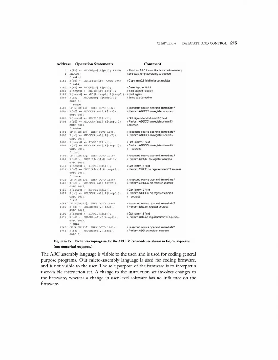
CHAPTER 6 DATAPATH AND CONTROL 215
The ARC assembly language is visible to the user, and is used for coding generalpurpose programs. Our micro-assembly language is used for coding firmware,and is not visible to the user. The sole purpose of the firmware is to interpret auser-visible instruction set. A change to the instruction set involves changes tothe firmware, whereas a change in user-level software has no influence on thefirmware.
0000: R[ir] ← AND(R[pc],R[pc]); READ; / Read an ARC instruction from main memory0001: DECODE; / 256-way jump according to opcode00// / sethi1152: R[rd] ← LSHIFT10(ir); GOTO 2047; / Copy imm22 field to target register00// / call1280: R[15] ← AND(R[pc],R[pc]); / Save %pc in %r151281: R[temp0] ← ADD(R[ir],R[ir]); / Shift disp30 field left1282: R[temp0] ← ADD(R[temp0],R[temp0]); / Shift again1283: R[pc] ← ADD(R[pc],R[temp0]); / Jump to subroutine GOTO 0;0//0 / addcc1600: IF R[IR[13]] THEN GOTO 1602; / Is second source operand immediate?1601: R[rd] ← ADDCC(R[rs1],R[rs2]); / Perform ADDCC on register sources GOTO 2047;1602: R[temp0] ← SEXT13(R[ir]); / Get sign extended simm13 field1603: R[rd] ← ADDCC(R[rs1],R[temp0]); / Perform ADDCC on register/simm13 GOTO 2047; / sources00// / andcc1604: IF R[IR[13]] THEN GOTO 1606; / Is second source operand immediate?1605: R[rd] ← ANDCC(R[rs1],R[rs2]); / Perform ANDCC on register sources GOTO 2047;1606: R[temp0] ← SIMM13(R[ir]); / Get simm13 field1607: R[rd] ← ANDCC(R[rs1],R[temp0]); / Perform ANDCC on register/simm13 GOTO 2047; / sources 00// / orcc1608: IF R[IR[13]] THEN GOTO 1610; / Is second source operand immediate?1609: R[rd] ← ORCC(R[rs1],R[rs2]); / Perform ORCC on register sources GOTO 2047;1610: R[temp0] ← SIMM13(R[ir]); / Get simm13 field1611: R[rd] ← ORCC(R[rs1],R[temp0]); / Perform ORCC on register/simm13 sources GOTO 2047;00// / orncc1624: IF R[IR[13]] THEN GOTO 1626; / Is second source operand immediate?1625: R[rd] ← NORCC(R[rs1],R[rs2]); / Perform ORNCC on register sources GOTO 2047;1626: R[temp0] ← SIMM13(R[ir]); / Get simm13 field1627: R[rd] ← NORCC(R[rs1],R[temp0]); / Perform NORCC on register/simm13 GOTO 2047; / sources 00// / srl1688: IF R[IR[13]] THEN GOTO 1690; / Is second source operand immediate?1689: R[rd] ← SRL(R[rs1],R[rs2]); / Perform SRL on register sources GOTO 2047;1690: R[temp0] ← SIMM13(R[ir]); / Get simm13 field1691: R[rd] ← SRL(R[rs1],R[temp0]); / Perform SRL on register/simm13 sources GOTO 2047;00// / jmpl1760: IF R[IR[13]] THEN GOTO 1762; / Is second source operand immediate?1761: R[pc] ← ADD(R[rs1],R[rs2]); / Perform ADD on register sources GOTO 0;
Address Operation Statements Comment
Figure 6-15 Partial microprogram for the ARC. Microwords are shown in logical sequence
(not numerical sequence.)
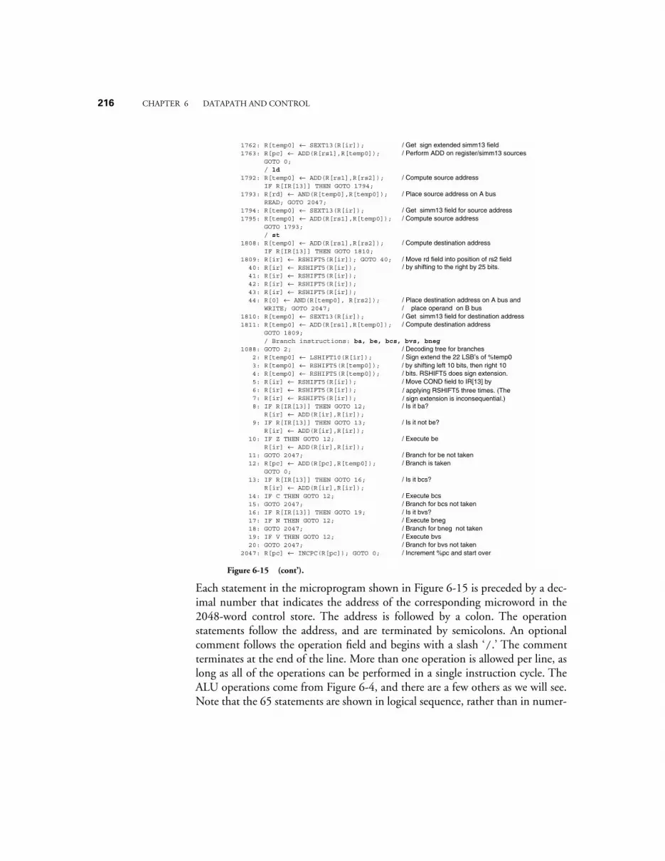
216 CHAPTER 6 DATAPATH AND CONTROL
Each statement in the microprogram shown in Figure 6-15 is preceded by a dec-imal number that indicates the address of the corresponding microword in the2048-word control store. The address is followed by a colon. The operationstatements follow the address, and are terminated by semicolons. An optionalcomment follows the operation field and begins with a slash ‘/.’ The commentterminates at the end of the line. More than one operation is allowed per line, aslong as all of the operations can be performed in a single instruction cycle. TheALU operations come from Figure 6-4, and there are a few others as we will see.Note that the 65 statements are shown in logical sequence, rather than in numer-
1762: R[temp0] ← SEXT13(R[ir]); / Get sign extended simm13 field1763: R[pc] ← ADD(R[rs1],R[temp0]); / Perform ADD on register/simm13 sources GOTO 0;00// / ld1792: R[temp0] ← ADD(R[rs1],R[rs2]); / Compute source address IF R[IR[13]] THEN GOTO 1794;1793: R[rd] ← AND(R[temp0],R[temp0]); / Place source address on A bus READ; GOTO 2047;1794: R[temp0] ← SEXT13(R[ir]); / Get simm13 field for source address1795: R[temp0] ← ADD(R[rs1],R[temp0]); / Compute source address GOTO 1793;00// / st1808: R[temp0] ← ADD(R[rs1],R[rs2]); / Compute destination address IF R[IR[13]] THEN GOTO 1810;1809: R[ir] ← RSHIFT5(R[ir]); GOTO 40; / Move rd field into position of rs2 field 40: R[ir] ← RSHIFT5(R[ir]); 41: R[ir] ← RSHIFT5(R[ir]); 42: R[ir] ← RSHIFT5(R[ir]); 43: R[ir] ← RSHIFT5(R[ir]); 44: R[0] ← AND(R[temp0], R[rs2]); / Place destination address on A bus and WRITE; GOTO 2047; / place operand on B bus1810: R[temp0] ← SEXT13(R[ir]); / Get simm13 field for destination address1811: R[temp0] ← ADD(R[rs1],R[temp0]); / Compute destination address GOTO 1809;00// / Branch instructions: ba, be, bcs, bvs, bneg1088: GOTO 2; / Decoding tree for branches 2: R[temp0] ← LSHIFT10(R[ir]); / Sign extend the 22 LSB’s of %temp0 3: R[temp0] ← RSHIFT5(R[temp0]); 4: R[temp0] ← RSHIFT5(R[temp0]); / bits. RSHIFT5 does sign extension. 5: R[ir] ← RSHIFT5(R[ir]); / Move COND field to IR[13] by 6: R[ir] ← RSHIFT5(R[ir]); 7: R[ir] ← RSHIFT5(R[ir]); 8: IF R[IR[13]] THEN GOTO 12; / Is it ba? R[ir] ← ADD(R[ir],R[ir]); 9: IF R[IR[13]] THEN GOTO 13; / Is it not be? R[ir] ← ADD(R[ir],R[ir]); 10: IF Z THEN GOTO 12; / Execute be R[ir] ← ADD(R[ir],R[ir]); 11: GOTO 2047; / Branch for be not taken 12: R[pc] ← ADD(R[pc],R[temp0]); / Branch is taken GOTO 0; 13: IF R[IR[13]] THEN GOTO 16; / Is it bcs? R[ir] ← ADD(R[ir],R[ir]); 14: IF C THEN GOTO 12; / Execute bcs 15: GOTO 2047; / Branch for bcs not taken 16: IF R[IR[13]] THEN GOTO 19; / Is it bvs? 17: IF N THEN GOTO 12; / Execute bneg 18: GOTO 2047; / Branch for bneg not taken 19: IF V THEN GOTO 12; / Execute bvs 20: GOTO 2047; / Branch for bvs not taken2047: R[pc] ← INCPC(R[pc]); GOTO 0; / Increment %pc and start over
/ by shifting left 10 bits, then right 10
/ applying RSHIFT5 three times. (The/ sign extension is inconsequential.)
/ by shifting to the right by 25 bits.
Figure 6-15 (cont’).
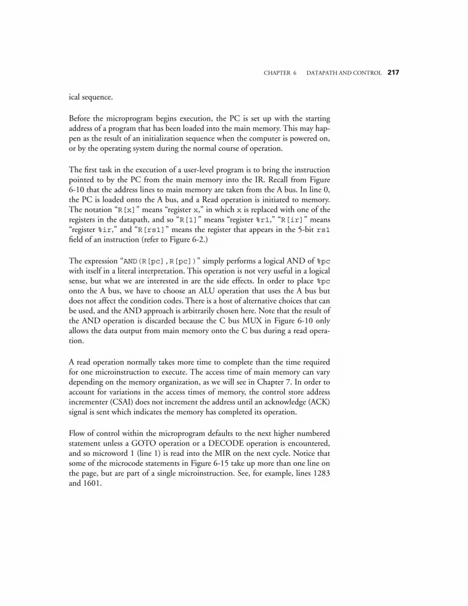
CHAPTER 6 DATAPATH AND CONTROL 217
ical sequence.
Before the microprogram begins execution, the PC is set up with the startingaddress of a program that has been loaded into the main memory. This may hap-pen as the result of an initialization sequence when the computer is powered on,or by the operating system during the normal course of operation.
The first task in the execution of a user-level program is to bring the instructionpointed to by the PC from the main memory into the IR. Recall from Figure6-10 that the address lines to main memory are taken from the A bus. In line 0,the PC is loaded onto the A bus, and a Read operation is initiated to memory.The notation “R[x]” means “register x,” in which x is replaced with one of theregisters in the datapath, and so “R[1]” means “register %r1,” “R[ir]” means“register %ir,” and “R[rs1]” means the register that appears in the 5-bit rs1field of an instruction (refer to Figure 6-2.)
The expression “AND(R[pc],R[pc])” simply performs a logical AND of %pcwith itself in a literal interpretation. This operation is not very useful in a logicalsense, but what we are interested in are the side effects. In order to place %pconto the A bus, we have to choose an ALU operation that uses the A bus butdoes not affect the condition codes. There is a host of alternative choices that canbe used, and the AND approach is arbitrarily chosen here. Note that the result ofthe AND operation is discarded because the C bus MUX in Figure 6-10 onlyallows the data output from main memory onto the C bus during a read opera-tion.
A read operation normally takes more time to complete than the time requiredfor one microinstruction to execute. The access time of main memory can varydepending on the memory organization, as we will see in Chapter 7. In order toaccount for variations in the access times of memory, the control store addressincrementer (CSAI) does not increment the address until an acknowledge (ACK)signal is sent which indicates the memory has completed its operation.
Flow of control within the microprogram defaults to the next higher numberedstatement unless a GOTO operation or a DECODE operation is encountered,and so microword 1 (line 1) is read into the MIR on the next cycle. Notice thatsome of the microcode statements in Figure 6-15 take up more than one line onthe page, but are part of a single microinstruction. See, for example, lines 1283and 1601.
218 CHAPTER 6 DATAPATH AND CONTROL
Now that the instruction is in the IR as a result of the read operation in line 0,the next step is to decode the opcode fields. This is performed by taking a256-way branch into the microcode as indicated by the DECODE keyword in line1 of the microprogram. The 11-bit pattern for the branch is constructed byappending a 1 to the left of bits 30 and 31 of the IR, followed by bits 19-24 ofthe IR, followed by the pattern 00. After the opcode fields are decoded, execu-tion of the microcode continues according to which of the 15 ARC instructionsis being interpreted.
As an example of how the decode operation works, consider the addcc instruc-tion. According to the Arithmetic instruction format in Figure 6-2, the op fieldis 10 and the op3 field is 010000. If we append a 1 to the left of the op bit pat-tern, followed by the op3 bit pattern, followed by 00, the DECODE address is11001000000 = (1600)10. This means that the microinstructions that interpretthe addcc instruction begin at control store location 1600.
A number of DECODE addresses should never arise in practice. There is no Arith-metic instruction that corresponds to the invalid op3 field 111111, but if thissituation does arise, possibly due to an errant program, then a microstore routineshould be placed at the corresponding DECODE address 11011111100 =(1788)10 in order to deal with the illegal instruction. These locations are leftblank in the microprogram shown in Figure 6-15.
Instructions in the SETHI/Branch and Call formats do not have op3 fields. TheSETHI/Branch formats have op and op2 fields, and the Call format has onlythe op field. In order to maintain a simple decoding mechanism, we can createduplicate entries in the control store. Consider the SETHI format. If we followthe rule for constructing the DECODE address, then the DECODE address willhave a 1 in the leftmost position, followed by 00 for the op field, followed by100 which identifies SETHI in bit positions 19 – 21, followed by the bits inpositions 22 – 24 of the IR, followed by 00, resulting in the bit pattern100100xxx00 where xxx can take on any value, depending on the imm22 field.There are eight possible bit patterns for the xxx bits, and so we need to haveduplicate SETHI codes at locations 10010000000, 10010000100,10010001000, 10010001100, 10010010000, 10010010100, 10010011000,and 10010011100. DECODE addresses for the Branch and CALL formats areconstructed in duplicate locations in a similar manner. Only the lowest addressedversion of each set of duplicate codes is shown in Figure 6-15.
Although this method of decoding is fast and simple, a large amount of control
CHAPTER 6 DATAPATH AND CONTROL 219
store memory is wasted. An alternative approach that wastes much less space is tomodify the decoder for the control store so that all possible branch patterns forSETHI point to the same location, and the same for the Branch and Call formatinstructions. For our microarchitecture, we will stay with the simpler approachand pay the price of having a large control store.
Consider now how the ld instruction is interpreted. The microprogram beginsat location 0, and at this point does not know that ld is the instruction that thePC points to in main memory. Line 0 of the microprogram begins the Readoperation as indicated by the READ keyword, which brings an instruction intothe IR from the main memory address pointed to by the PC. For this case, let usassume that the IR now contains the 32-bit pattern:
which is a translation of the ARC assembly code: ld %r5 + 80, %r2. Line 1then performs a branch to control store address (11100000000)2 = (1792)10.
At line 1792, execution of the ld instruction begins. In line 1792, the immedi-ate bit i is tested. For this example, i = 1, and so control is transferred tomicroword 1794. If instead we had i = 0, then control would pass to the nexthigher numbered microword, which is 1793 for this case. Line 1792 adds theregisters in the rs1 and rs2 fields of the instruction, in anticipation of anon-immediate form of ld, but this only makes sense if i = 0, which it is notfor this example. The result that is stored in %temp0 is thus discarded when con-trol is transferred to microword 1794, but this introduces no time penalty anddoes not produce any unwanted side effects (ADD does not change the conditioncodes).
In microword 1794, the simm13 field is extracted (using sign extension, as indi-cated by the SEXT13 operation), which is added with the register in the rs1field in microword 1795. Control is then passed to microword 1793 which iswhere the READ operation takes place. Control passes to line 2047 where the PCis incremented in anticipation of reading the next instruction from main mem-ory. Since instructions are four bytes long and must be aligned on word bound-aries in memory, the PC is incremented by four. Control then returns to line 0where the process repeats. A total of seven microinstructions are thus executed in
11op
00010rd
000000op3
00101rs1
1i
0000001010000simm13
220 CHAPTER 6 DATAPATH AND CONTROL
interpreting the ld instruction. These microinstructions are repeated below:
The remaining instructions, except for branches, are interpreted similar to theway ld is interpreted. Additional decoding is needed for the branch instructionsbecause the type of branch is determined by the COND field of the branch format(bits 25 – 28), which is not used during a DECODE operation. The approach usedhere is to shift the COND bits into IR[13] one bit at a time, and then jump todifferent locations in the microcode depending on the COND bit pattern.
For branch instructions, the DECODE operation on line 2 of the microprogramtransfers control to location 1088. We need more space for the branch instruc-tions than the four-word per instruction allocation, so line 1088 transfers controlto line 2 which is the starting address of a large section of available control storememory.
Lines 2 – 4 extract the 22-bit displacement for the branch by zeroing the highorder 10 bits and storing the result in %temp0. This is accomplished by shifting%ir to the left by 10 bits and storing it in %temp0, and then shifting the resultback to the right by 10 bits. (Notice that sign extension is performed on the dis-placement, which may be negative. RSHIFT5 implements sign extension.) Lines5 – 7 shift %ir to the right by 15 bits so that the most significant COND bit(IR[28]) lines up in position IR[13], which allows the Jump on IR[13]=1operation to test each bit. Alternatively, we could shift the COND field toIR[31] one bit at a time, and use the Jump on n condition to test each bit.(Note that there is a subtle error in how the PC is updated in line 12. See Prob-lem 6.21 for an explanation.)
Line 8 starts the branch decoding process, which is summarized in Figure 6-16.If IR[28], which is now in IR[13], is set to 1, then the instruction is ba,which is executed in line 12. Notice that control returns to line 0, rather than toline 2047, so that the PC does not get changed twice for the same instruction.
0000: R[ir] ← AND(R[pc],R[pc]); READ; / Read an ARC instruction from main memory.0001: DECODE; / 256-way jump according to opcode1792: R[temp0] ← ADD(R[rs1],R[rs2]); / Compute source address IF IR[13] THEN GOTO 1794;
1794: R[temp0] ← SEXT13(R[ir]); / Get simm13 field for source address1795: R[temp0] ← ADD(R[rs1],R[temp0]); Compute source address GOTO 1793;
1793: R[rd] ← AND(R[temp0],R[temp0]); / Place source address on A bus READ; GOTO 2047;
2047: R[pc] ← INCPC(R[pc]); GOTO 0; / Increment %pc and start over
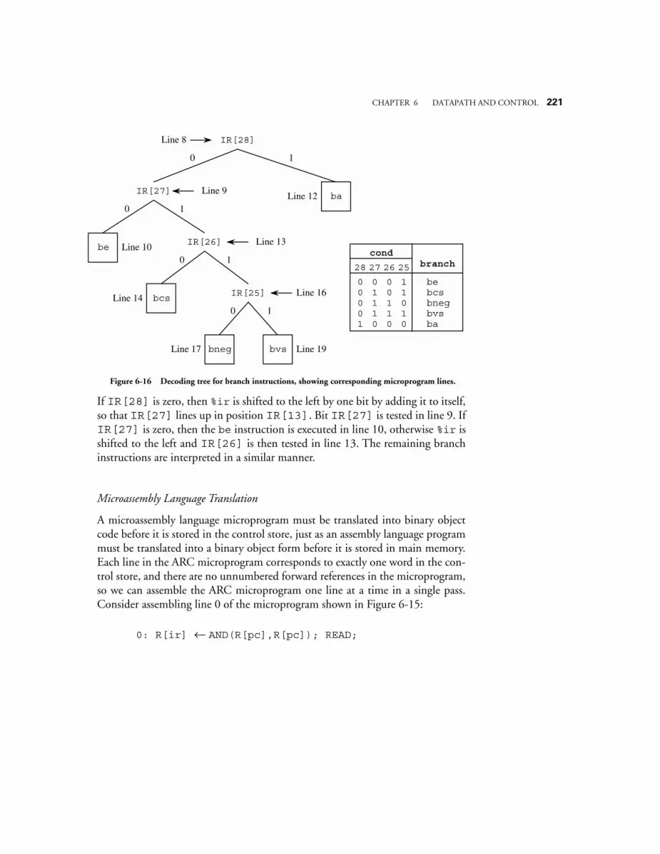
CHAPTER 6 DATAPATH AND CONTROL 221
If IR[28] is zero, then %ir is shifted to the left by one bit by adding it to itself,so that IR[27] lines up in position IR[13]. Bit IR[27] is tested in line 9. IfIR[27] is zero, then the be instruction is executed in line 10, otherwise %ir isshifted to the left and IR[26] is then tested in line 13. The remaining branchinstructions are interpreted in a similar manner.
Microassembly Language Translation
A microassembly language microprogram must be translated into binary objectcode before it is stored in the control store, just as an assembly language programmust be translated into a binary object form before it is stored in main memory.Each line in the ARC microprogram corresponds to exactly one word in the con-trol store, and there are no unnumbered forward references in the microprogram,so we can assemble the ARC microprogram one line at a time in a single pass.Consider assembling line 0 of the microprogram shown in Figure 6-15:
0: R[ir] ← AND(R[pc],R[pc]); READ;
bneg bvs
bcs
be
ba
IR[25]
IR[26]
IR[27]
IR[28]Line 8
Line 13
Line 16
Line 12
Line 19Line 17
Line 10
Line 14
condbranch
11010
25
bebcsbnegbvsba
00110
26
01110
27
00001
28
Line 9
0 1
0 1
0 1
0 1
Figure 6-16 Decoding tree for branch instructions, showing corresponding microprogram lines.
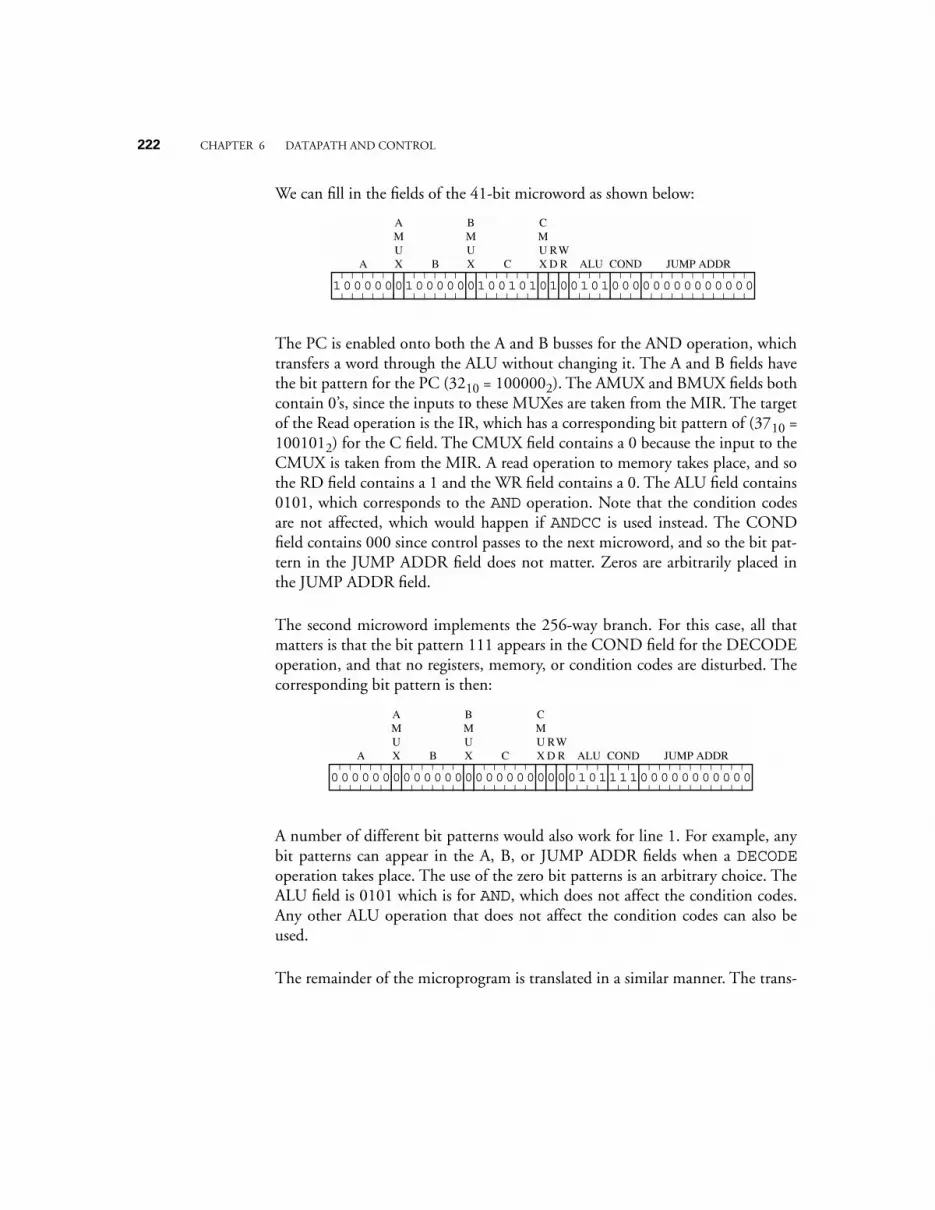
222 CHAPTER 6 DATAPATH AND CONTROL
We can fill in the fields of the 41-bit microword as shown below:
The PC is enabled onto both the A and B busses for the AND operation, whichtransfers a word through the ALU without changing it. The A and B fields havethe bit pattern for the PC (3210 = 1000002). The AMUX and BMUX fields bothcontain 0’s, since the inputs to these MUXes are taken from the MIR. The targetof the Read operation is the IR, which has a corresponding bit pattern of (3710 =1001012) for the C field. The CMUX field contains a 0 because the input to theCMUX is taken from the MIR. A read operation to memory takes place, and sothe RD field contains a 1 and the WR field contains a 0. The ALU field contains0101, which corresponds to the AND operation. Note that the condition codesare not affected, which would happen if ANDCC is used instead. The CONDfield contains 000 since control passes to the next microword, and so the bit pat-tern in the JUMP ADDR field does not matter. Zeros are arbitrarily placed inthe JUMP ADDR field.
The second microword implements the 256-way branch. For this case, all thatmatters is that the bit pattern 111 appears in the COND field for the DECODEoperation, and that no registers, memory, or condition codes are disturbed. Thecorresponding bit pattern is then:
A number of different bit patterns would also work for line 1. For example, anybit patterns can appear in the A, B, or JUMP ADDR fields when a DECODEoperation takes place. The use of the zero bit patterns is an arbitrary choice. TheALU field is 0101 which is for AND, which does not affect the condition codes.Any other ALU operation that does not affect the condition codes can also beused.
The remainder of the microprogram is translated in a similar manner. The trans-
RD
WRCA B JUMP ADDRALU COND
AMUX
BMUX
CMUX
000000 000000 001010100101000000000000001 1 1
RD
WRCA B JUMP ADDRALU COND
AMUX
BMUX
CMUX
000000 000000 000000000101111000000000000 0 0
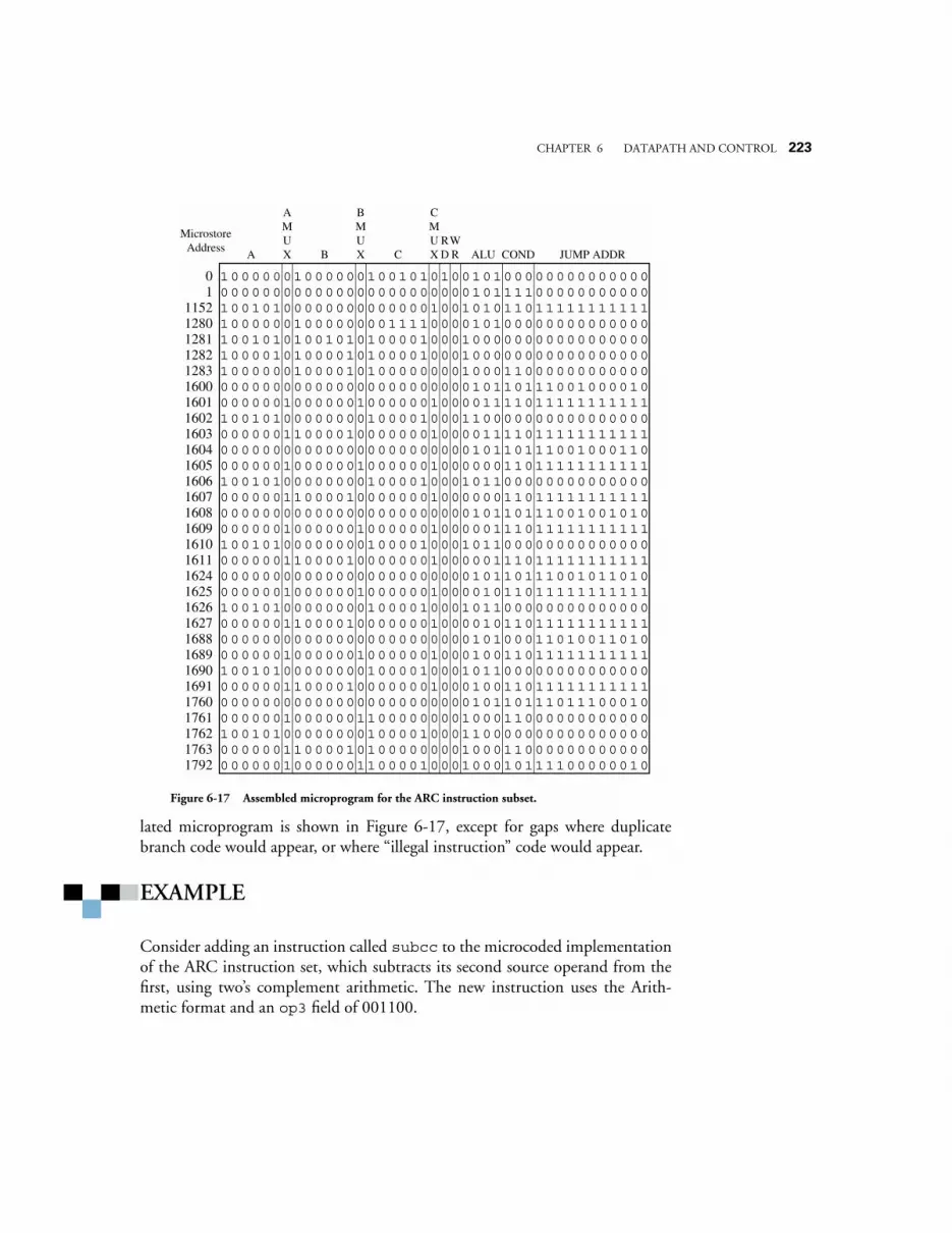
CHAPTER 6 DATAPATH AND CONTROL 223
lated microprogram is shown in Figure 6-17, except for gaps where duplicatebranch code would appear, or where “illegal instruction” code would appear.
EXAMPLE
Consider adding an instruction called subcc to the microcoded implementationof the ARC instruction set, which subtracts its second source operand from thefirst, using two’s complement arithmetic. The new instruction uses the Arith-metic format and an op3 field of 001100.
RD
WRCA B JUMP ADDRALU COND
AMUX
BMUX
CMUX
1 000001 00000 001010100101000
11111111111
00 000000 00000 0000000001011110000000000011 010100 00000 000001001010110
00000000000
11521 000001 00000 0111100001010000000000000012801 010101 01010 0000100010000000000000000012811 000101 00010 0000100010000000000000000012821 000001 00010 00000000100011012830 000000 00000 0000000001011011100100001016000 000010 00001 00000100001111016011 010100 00000 0000100011000000000000000016020 000011 00010 00000100001111016030 000000 00000 0000000001011011100100011016040 000010 00001 00000100000011016051 010100 00000 0000100010110000000000000016060 000011 00010 00000100000011016070 000000 00000 0000000001011011100100101016080 000010 00001 00000100000111016091 010100 00000 0000100010110000000000000016100 000011 00010 000001000001110
0
16110 000000 00000 0000000001011011100101101016240 000010 00001 00000100001011016251 010100 00000 0000100010110000000000000016260 000011 00010 0000010000101116270 000000 00000 0000000001010001101001101016880 000010 00001 00000100010011016891 010100 00000 0000100010110000000000000016900 000011 00010 00000100010011016910 000000 00000 0000000001011011101110001017600 000010 00001 0000000010001100000000000017611 010100 00000 0000100011000000000000000017620 000011 00010 000000001000110000000000001763
000010 00001 000010001000101111000000101792
11111111111
11111111111
11111111111
00000000000
11111111111
11111111111
11111111111
11111111111
11111111111
11111111111
11111111111
Microstore Address
0
10001110010001000100010001001111
00000000000000000000000000000000
00000000000000000000000000000000
Figure 6-17 Assembled microprogram for the ARC instruction subset.
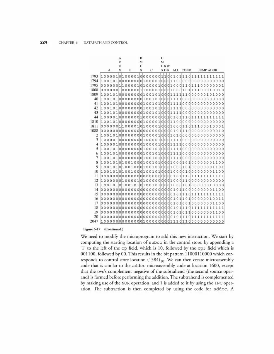
224 CHAPTER 6 DATAPATH AND CONTROL
We need to modify the microprogram to add this new instruction. We start bycomputing the starting location of subcc in the control store, by appending a‘1’ to the left of the op field, which is 10, followed by the op3 field which is001100, followed by 00. This results in the bit pattern 11000110000 which cor-responds to control store location (1584)10. We can then create microassemblycode that is similar to the addcc microassembly code at location 1600, exceptthat the two’s complement negative of the subtrahend (the second source oper-and) is formed before performing the addition. The subtrahend is complementedby making use of the NOR operation, and 1 is added to it by using the INC oper-ation. The subtraction is then completed by using the code for addcc. A
0 000000 000000 00000000101110201 000000 000001 0000000111011000000000002047
RD
WRCA B JUMP ADDRALU COND
AMUX
BMUX
CMUX
1 000101 000100 000011001011101111111111117931 010100 000001 000100011000000000000000017940 000011 000101 000100010001101110000000117950 000010 000011 000100010001011110001001018081 010100 000001 010100011111100000010100018091 010100 000001 0101000111100000000000000401 010100 000001 0101000111100000000000000411 010100 000001 0101000111100000000000000421 010100 000001 0101000111100000000000000431 000100 000010 0000001010111011111111111441 010100 000001 000100011000000000000000018100 000011 000101 000100010001101110001000118110 000000 000000 000000001011100000000001010881 010100 000001 000100010100000000000000021 000100 000001 000100011110000000000000031 000100 000001 000100011110000000000000041 010100 000001 010100011110000000000000051 010100 000001 010100011110000000000000061 010100 000001 010100011110000000000000071 010101 010001 010100010001010000000110081 010101 010001 010100010001010000000110191 010101 010001 0101000100001000000001100100 000000 000000 00000000101110
11111111111
111 000001 000101 0000000100011000000000000121 010101 010101 0101000100010100000010000130 000000 000000 0000000010110000000001100140 000000 000000 00000000101110150 000000 000000 0000000010110100000010011160 000000 000000 0000000010100100000001100170 000000 000000 00000000101110180 000000 000000 000000001010110000000110019
11111111111
11111111111
11111111111
00 0 00 0 0
0 0 00 0 00 0 00 0 00 0 00 0 00 0 00 0 00 0 00 0 00 0 00 0 00 0 00 0 00 0 00 0 00 0 00 0 00 0 00 0 0
0 0 00 0 00 0 00 0 00 0 00 0 00 0 00 0 00 0 00 0 00 0 0
Figure 6-17 (Continued.)

CHAPTER 6 DATAPATH AND CONTROL 225
microassembly coding for subcc is shown below:
The corresponding microcode for one possible translation is then:
6.2.5 TRAPS AND INTERRUPTS
A trap is an automatic procedure call initiated by the hardware after an excep-tional condition caused by an executing program, such as an illegal instruction,overflow, underflow, dividing by zero, etc. When a trap occurs, control is trans-ferred to a “trap handler” which is a routine that is part of the operating system.The handler might do something like print a message and terminate the offend-ing program.
One way to handle traps is to modify the microcode, possibly to check the statusbits. For instance, we can check the v bit to see if an overflow has occurred. Themicrocode can then load an address into the PC (if a trap occurs) for the startinglocation of the trap handler.
Normally, there is a fixed section of memory for trap handler starting addresseswhere only a single word is allocated for each handler. This section of memoryforms a branch table that transfers control to the handlers, as illustrated in Fig-ure 6-18. The reason for using a branch table is that the absolute addresses foreach type of trap can be embedded in the microcode this way, while the targets ofthe jumps can be changed at the user level to handle traps differently.
1584: R[temp0] ← SEXT13(R[ir]); / Extract rs2 operand
IF IR[13] THEN GOTO 1586; / Is second source immediate?
1585: R[temp0] ← R[rs2]; / Extract sign extended immediate operand
1586: R[temp0] ← NOR(R[temp0], R[0]); / Form one’s complement of subtrahend
1587: R[temp0] ← INC(R[temp0]); GOTO 1603; / Form two’s complement of subtrahend
RD
WRCA B JUMP ADDRALU COND
AMUX
BMUX
CMUX
01010 000001 00010001100101110001100101584
00000 00001 00010001000000000000000001585
00010 00000 00010000111000000000000001586
00010 00000 00010001101110110010000111587
1 0
0 0 1
1 0 1
1 0 1
0 0 0
0 0 0
0 0 0
0 0 0
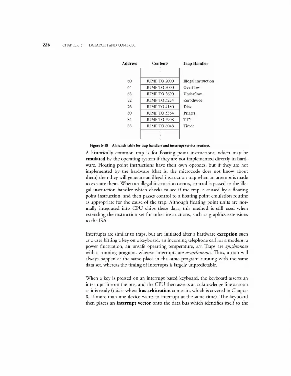
226 CHAPTER 6 DATAPATH AND CONTROL
A historically common trap is for floating point instructions, which may beemulated by the operating system if they are not implemented directly in hard-ware. Floating point instructions have their own opcodes, but if they are notimplemented by the hardware (that is, the microcode does not know aboutthem) then they will generate an illegal instruction trap when an attempt is madeto execute them. When an illegal instruction occurs, control is passed to the ille-gal instruction handler which checks to see if the trap is caused by a floatingpoint instruction, and then passes control to a floating point emulation routineas appropriate for the cause of the trap. Although floating point units are nor-mally integrated into CPU chips these days, this method is still used whenextending the instruction set for other instructions, such as graphics extensionsto the ISA.
Interrupts are similar to traps, but are initiated after a hardware exception suchas a user hitting a key on a keyboard, an incoming telephone call for a modem, apower fluctuation, an unsafe operating temperature, etc. Traps are synchronouswith a running program, whereas interrupts are asynchronous. Thus, a trap willalways happen at the same place in the same program running with the samedata set, whereas the timing of interrupts is largely unpredictable.
When a key is pressed on an interrupt based keyboard, the keyboard asserts aninterrupt line on the bus, and the CPU then asserts an acknowledge line as soonas it is ready (this is where bus arbitration comes in, which is covered in Chapter8, if more than one device wants to interrupt at the same time). The keyboardthen places an interrupt vector onto the data bus which identifies itself to the
JUMP TO 2000
ContentsAddress Trap Handler...
.
.
.
60 Illegal instruction
JUMP TO 300064 Overflow
JUMP TO 360068 Underflow
JUMP TO 522472 Zerodivide
JUMP TO 418076 Disk
JUMP TO 536480 Printer
JUMP TO 590884 TTY
88 TimerJUMP TO 6048
Figure 6-18 A branch table for trap handlers and interrupt service routines.
CHAPTER 6 DATAPATH AND CONTROL 227
CPU. The CPU then pushes the program counter and processor status register(where the flags are stored) onto the stack. The interrupt vector is used to indexinto the branch table, which lists the starting addresses of the interrupt serviceroutines.
When a trap handler or an interrupt service routine begins execution, it saves theregisters that it plans to modify on the stack, performs its task, restores the regis-ters, and then returns from the interrupt. The process of returning from a trap isdifferent from returning from a subroutine, since the process of entering a trap isdifferent from a subroutine call (because the %psr register is also saved andrestored). For the ARC, the rett instruction (see Chapter 8) is used for return-ing from a trap or interrupt. Interrupts can interrupt other interrupts, and so thefirst thing that an interrupt service routine might do is to raise its priority (usinga special supervisor mode instruction) so that no interrupts of lower priority areaccepted.
6.2.6 NANOPROGRAMMING
If the microstore is wide, and has lots of the same words, then we can savemicrostore memory by placing one copy of each unique microword in a nanos-tore, and then use the microstore to index into the nanostore. For instance, inthe microprogram shown in Figure 6-15, lines 1281 and 1282 are the same.Lines 3, 4, and 40-44 are the same, and there are a number of other microin-structions that recur, especially for the duplicated branch microcode and theduplicated illegal instruction microcode.
Figure 6-19a illustrates the space requirement for the original microstore ROM.There are n=2048 words that are each 41 bits wide, giving an area complexity of2048 × 41 = 83,968 bits. Suppose now that there are 100 unique microwords inthe ROM (the microprogram in Figure 6-15 is only partially complete so we can-not measure the number of unique microwords directly). Figure 6-19b illustratesa configuration that uses a nanostore, in which an area savings can be realized ifthere are a number of bit patterns that recur in the original microcode sequence.The unique microwords (100 for this case) form a nanoprogram, which is storedin a ROM that is 100 words deep by 41 bits wide.
The microprogram now indexes into the nanostore. The microprogram has thesame number of microwords regardless of whether or not a nanostore is used, butwhen a nanostore is used, pointers into the nanostore are stored in the microstorerather than the wider 41-bit words. For this case, the microstore is now 2048
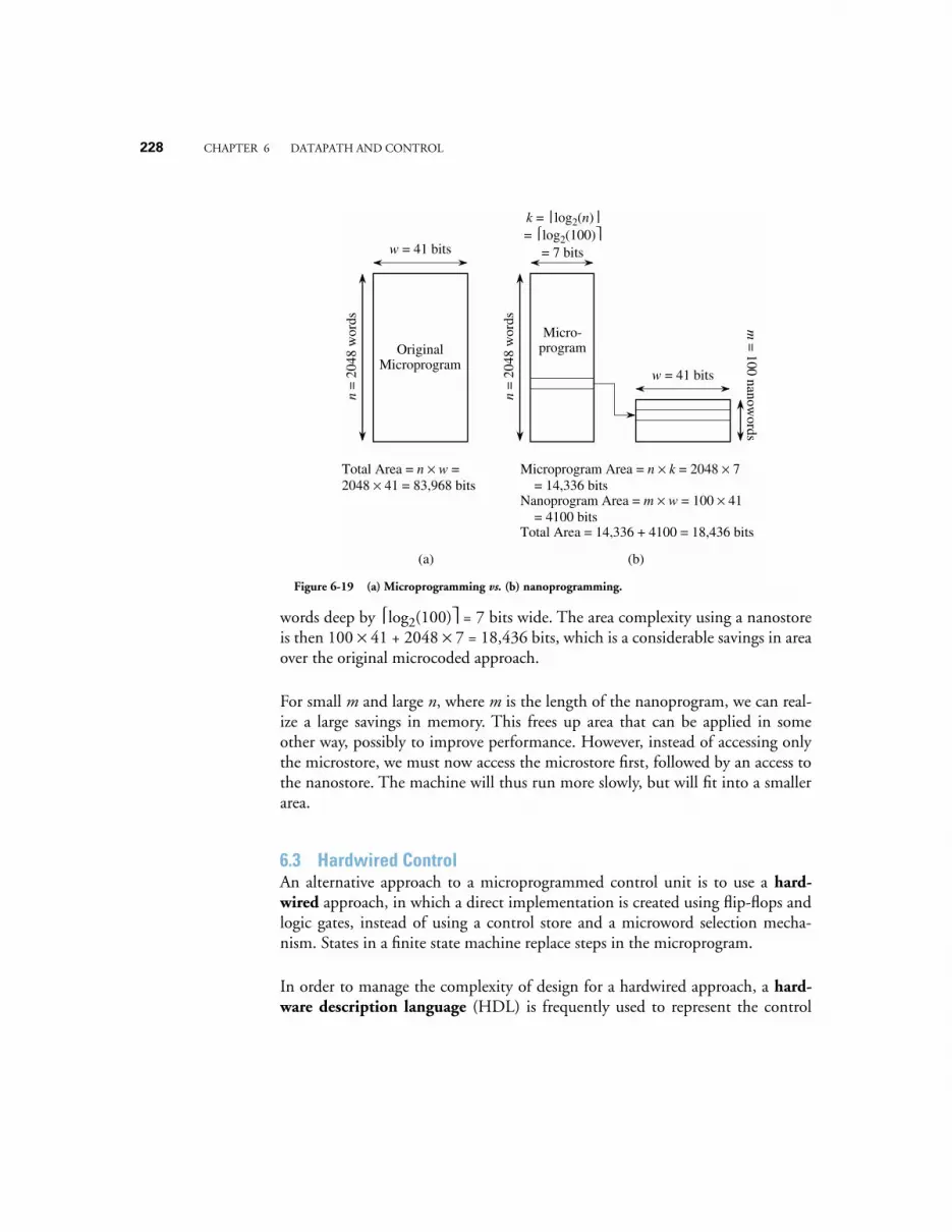
228 CHAPTER 6 DATAPATH AND CONTROL
words deep by log2(100) = 7 bits wide. The area complexity using a nanostoreis then 100 × 41 + 2048 × 7 = 18,436 bits, which is a considerable savings in areaover the original microcoded approach.
For small m and large n, where m is the length of the nanoprogram, we can real-ize a large savings in memory. This frees up area that can be applied in someother way, possibly to improve performance. However, instead of accessing onlythe microstore, we must now access the microstore first, followed by an access tothe nanostore. The machine will thus run more slowly, but will fit into a smallerarea.
6.3 Hardwired ControlAn alternative approach to a microprogrammed control unit is to use a hard-wired approach, in which a direct implementation is created using flip-flops andlogic gates, instead of using a control store and a microword selection mecha-nism. States in a finite state machine replace steps in the microprogram.
In order to manage the complexity of design for a hardwired approach, a hard-ware description language (HDL) is frequently used to represent the control
Original Microprogram
w = 41 bits
n =
204
8 w
ords
k = log2(n) = log2(100)
= 7 bits
n =
204
8 w
ords
w = 41 bits
(a) (b)
m =
100 nanowords
Micro-program
Total Area = n × w = 2048 × 41 = 83,968 bits
Microprogram Area = n × k = 2048 × 7 = 14,336 bitsNanoprogram Area = m × w = 100 × 41 = 4100 bitsTotal Area = 14,336 + 4100 = 18,436 bits
Figure 6-19 (a) Microprogramming vs. (b) nanoprogramming.
CHAPTER 6 DATAPATH AND CONTROL 229
structure. One example of an HDL is VHDL, which is an acronym for VHSICHardware Description Language (in which VHSIC is yet another acronym forVery High Speed Integrated Circuit). VHDL is used for describing an architec-ture at a very high level, and can be compiled into hardware designs through aprocess known as silicon compilation. For the hardwired control unit we willdesign here, a lower level HDL that is sometimes referred to as a register trans-fer language (RTL) is more appropriate.
We will define a simple HDL/RTL in this section that loosely resembles Hill &Peterson’s A Hardware Programming Language (AHPL) (Hill and Peterson,1987). The general idea is to express a control sequence as a series of numberedstatements, which can then be directly translated into a hardware design. Eachstatement consists of a data portion and a transfer portion, as shown below:
5: A ← ADD(B,C); ! Data portionGOTO 10 CONDITIONED ON IR[12]. ! Control portion
The statement is labelled “5,” which means that it is preceded by statement 4and is succeeded by statement 6, unless an out-of-sequence transfer of controltakes place. The left arrow (←) indicates a data transfer, to register A for thiscase. The “ADD(B,C)” construct indicates that registers B and C are sent to acombinational logic unit (CLU) that performs the addition. Comments beginwith an exclamation mark (!) and terminate at the end of the line. The GOTOconstruct indicates a transfer of control. For this case, control is transferred tostatement 10 if bit 12 of register IR is true, otherwise control is transferred to thenext higher numbered statement (6 for this case).
Figure 6-20 shows an HDL description of a modulo 4 counter. The counter pro-duces the output sequence: 00, 01, 10, 11 and then repeats as long as the inputline x is 0. If the input line is set to 1, then the counter returns to state 0 at theend of the next clock cycle. The comma is the catenation operator, and so thestatement “Z ← 0,0;” assigns the two-bit pattern 00 to the two-bit output Z.
The HDL sequence is composed of three sections: the preamble, the numberedstatements, and the epilogue. The preamble names the module with the “MODULE”keyword and declares the inputs with the “INPUTS” keyword, the outputs withthe “OUTPUTS” keyword, and the arity (number of signals) of both, as well asany additional storage with the “MEMORY” keyword (none for this example). Thenumbered statements follow the preamble. The epilogue closes the sequencewith the key phrase “END SEQUENCE.” The key phrase “END
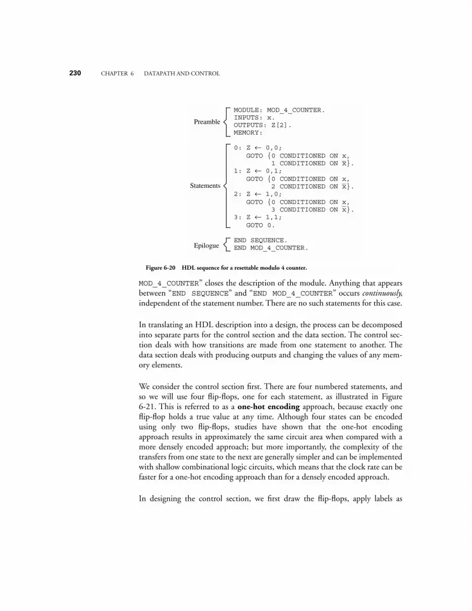
230 CHAPTER 6 DATAPATH AND CONTROL
MOD_4_COUNTER” closes the description of the module. Anything that appearsbetween “END SEQUENCE” and “END MOD_4_COUNTER” occurs continuously,independent of the statement number. There are no such statements for this case.
In translating an HDL description into a design, the process can be decomposedinto separate parts for the control section and the data section. The control sec-tion deals with how transitions are made from one statement to another. Thedata section deals with producing outputs and changing the values of any mem-ory elements.
We consider the control section first. There are four numbered statements, andso we will use four flip-flops, one for each statement, as illustrated in Figure6-21. This is referred to as a one-hot encoding approach, because exactly oneflip-flop holds a true value at any time. Although four states can be encodedusing only two flip-flops, studies have shown that the one-hot encodingapproach results in approximately the same circuit area when compared with amore densely encoded approach; but more importantly, the complexity of thetransfers from one state to the next are generally simpler and can be implementedwith shallow combinational logic circuits, which means that the clock rate can befaster for a one-hot encoding approach than for a densely encoded approach.
In designing the control section, we first draw the flip-flops, apply labels as
MODULE: MOD_4_COUNTER.INPUTS: x.OUTPUTS: Z[2].MEMORY:
0: Z ← 0,0; GOTO 0 CONDITIONED ON x, 1 CONDITIONED ON x.1: Z ← 0,1; GOTO 0 CONDITIONED ON x, 2 CONDITIONED ON x.2: Z ← 1,0; GOTO 0 CONDITIONED ON x, 3 CONDITIONED ON x.3: Z ← 1,1; GOTO 0.
END SEQUENCE.END MOD_4_COUNTER.
Preamble
Statements
Epilogue
Figure 6-20 HDL sequence for a resettable modulo 4 counter.
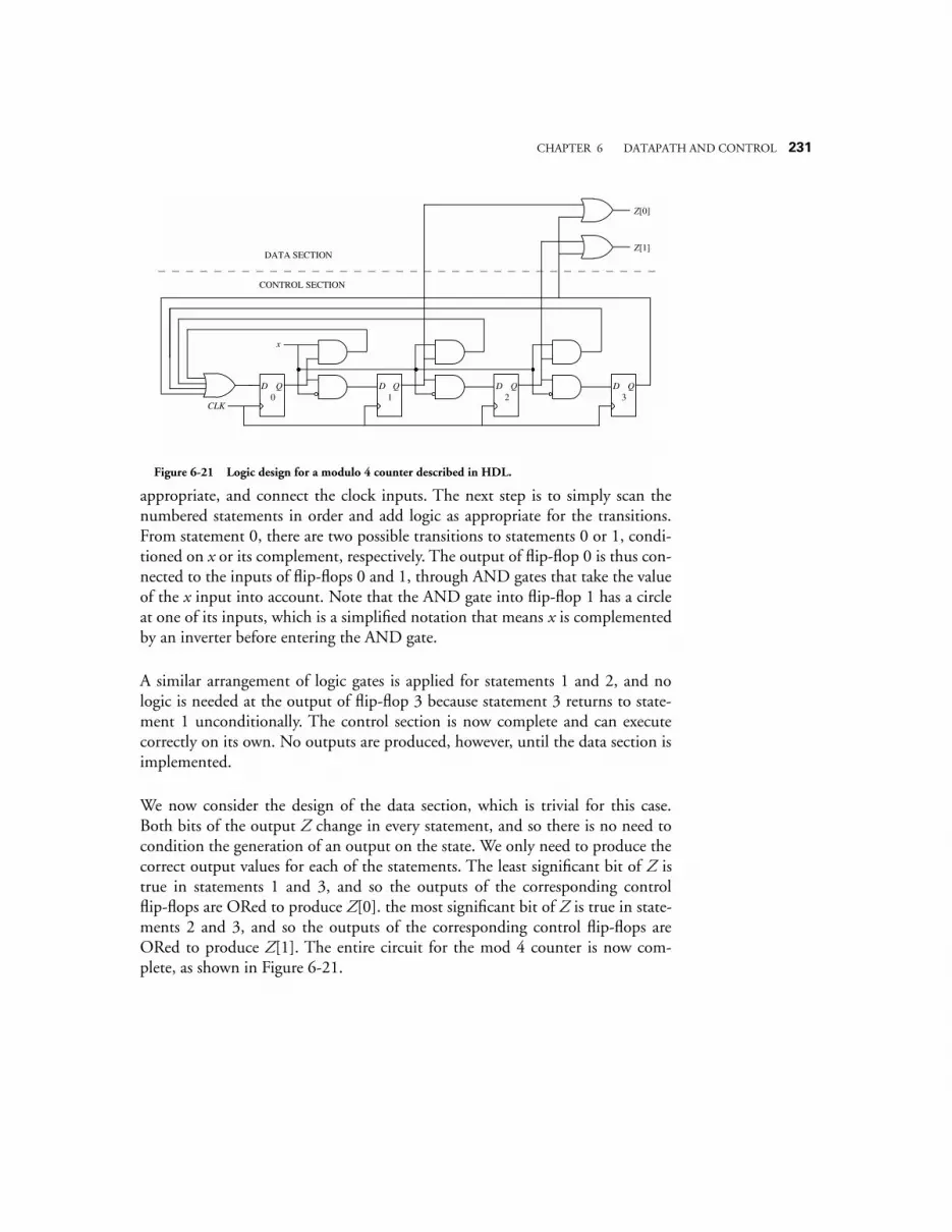
CHAPTER 6 DATAPATH AND CONTROL 231
appropriate, and connect the clock inputs. The next step is to simply scan thenumbered statements in order and add logic as appropriate for the transitions.From statement 0, there are two possible transitions to statements 0 or 1, condi-tioned on x or its complement, respectively. The output of flip-flop 0 is thus con-nected to the inputs of flip-flops 0 and 1, through AND gates that take the valueof the x input into account. Note that the AND gate into flip-flop 1 has a circleat one of its inputs, which is a simplified notation that means x is complementedby an inverter before entering the AND gate.
A similar arrangement of logic gates is applied for statements 1 and 2, and nologic is needed at the output of flip-flop 3 because statement 3 returns to state-ment 1 unconditionally. The control section is now complete and can executecorrectly on its own. No outputs are produced, however, until the data section isimplemented.
We now consider the design of the data section, which is trivial for this case.Both bits of the output Z change in every statement, and so there is no need tocondition the generation of an output on the state. We only need to produce thecorrect output values for each of the statements. The least significant bit of Z istrue in statements 1 and 3, and so the outputs of the corresponding controlflip-flops are ORed to produce Z[0]. the most significant bit of Z is true in state-ments 2 and 3, and so the outputs of the corresponding control flip-flops areORed to produce Z[1]. The entire circuit for the mod 4 counter is now com-plete, as shown in Figure 6-21.
CLK
QD0
x
QD QD QD1 2 3
Z[1]
Z[0]
CONTROL SECTION
DATA SECTION
Figure 6-21 Logic design for a modulo 4 counter described in HDL.
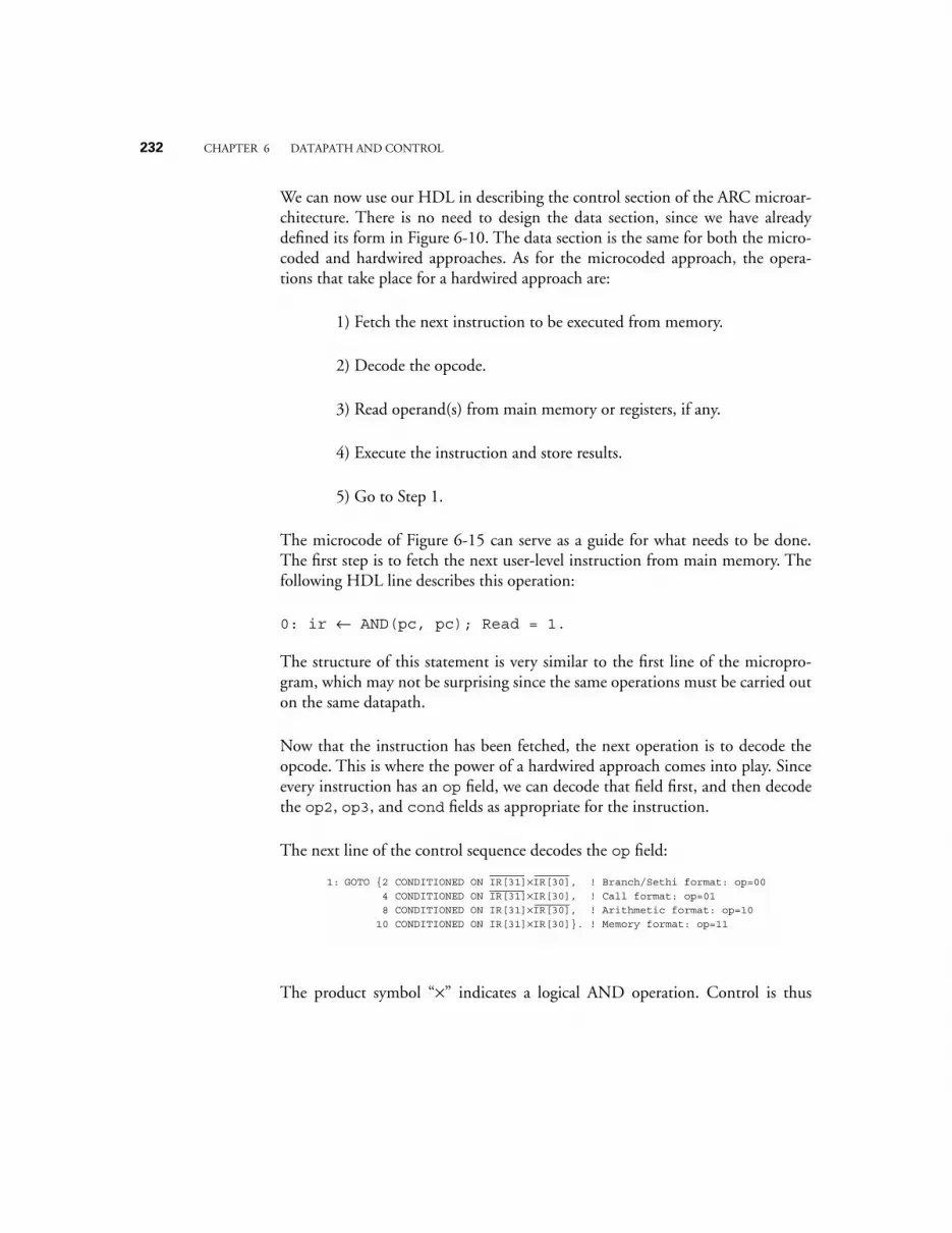
232 CHAPTER 6 DATAPATH AND CONTROL
We can now use our HDL in describing the control section of the ARC microar-chitecture. There is no need to design the data section, since we have alreadydefined its form in Figure 6-10. The data section is the same for both the micro-coded and hardwired approaches. As for the microcoded approach, the opera-tions that take place for a hardwired approach are:
1) Fetch the next instruction to be executed from memory.
2) Decode the opcode.
3) Read operand(s) from main memory or registers, if any.
4) Execute the instruction and store results.
5) Go to Step 1.
The microcode of Figure 6-15 can serve as a guide for what needs to be done.The first step is to fetch the next user-level instruction from main memory. Thefollowing HDL line describes this operation:
0: ir ← AND(pc, pc); Read = 1.
The structure of this statement is very similar to the first line of the micropro-gram, which may not be surprising since the same operations must be carried outon the same datapath.
Now that the instruction has been fetched, the next operation is to decode theopcode. This is where the power of a hardwired approach comes into play. Sinceevery instruction has an op field, we can decode that field first, and then decodethe op2, op3, and cond fields as appropriate for the instruction.
The next line of the control sequence decodes the op field:
The product symbol “×” indicates a logical AND operation. Control is thus
GOTO 2 CONDITIONED ON IR[31]×IR[30], ! Branch/Sethi format: op=00 4 CONDITIONED ON IR[31]×IR[30], ! Call format: op=01 8 CONDITIONED ON IR[31]×IR[30], ! Arithmetic format: op=10 10 CONDITIONED ON IR[31]×IR[30]. ! Memory format: op=11
1:
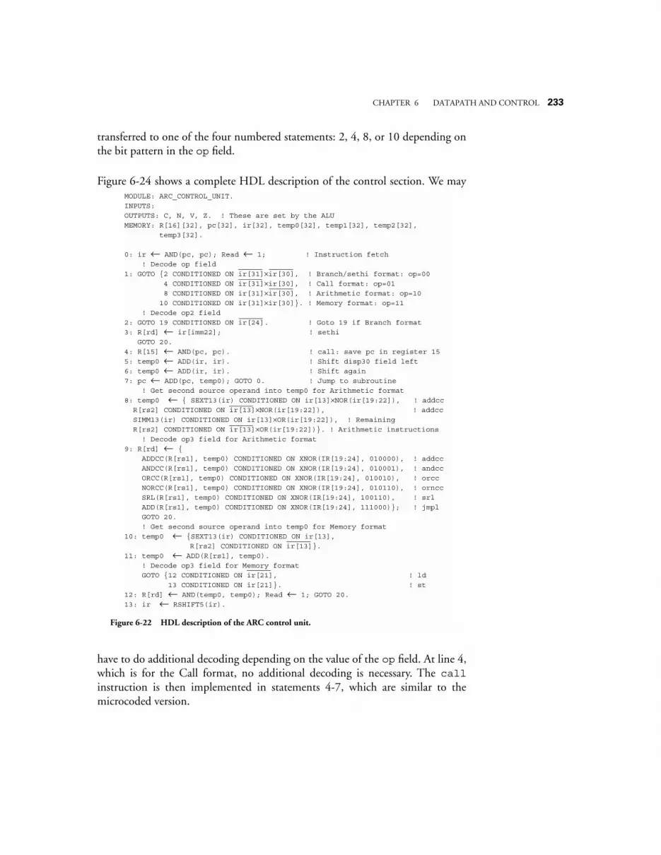
CHAPTER 6 DATAPATH AND CONTROL 233
transferred to one of the four numbered statements: 2, 4, 8, or 10 depending onthe bit pattern in the op field.
Figure 6-24 shows a complete HDL description of the control section. We may
have to do additional decoding depending on the value of the op field. At line 4,which is for the Call format, no additional decoding is necessary. The callinstruction is then implemented in statements 4-7, which are similar to themicrocoded version.
MODULE: ARC_CONTROL_UNIT.
INPUTS:
OUTPUTS: C, N, V, Z. ! These are set by the ALU
MEMORY: R[16][32], pc[32], ir[32], temp0[32], temp1[32], temp2[32],
temp3[32].
0: ir ← AND(pc, pc); Read ← 1; ! Instruction fetch
! Decode op field
1: GOTO 2 CONDITIONED ON ir[31]×ir[30], ! Branch/sethi format: op=00 4 CONDITIONED ON ir[31]×ir[30], ! Call format: op=01 8 CONDITIONED ON ir[31]×ir[30], ! Arithmetic format: op=10 10 CONDITIONED ON ir[31]×ir[30]. ! Memory format: op=11 ! Decode op2 field
2: GOTO 19 CONDITIONED ON ir[24]. ! Goto 19 if Branch format
3: R[rd] ← ir[imm22]; ! sethi
GOTO 20.
4: R[15] ← AND(pc, pc). ! call: save pc in register 15
5: temp0 ← ADD(ir, ir). ! Shift disp30 field left
6: temp0 ← ADD(ir, ir). ! Shift again
7: pc ← ADD(pc, temp0); GOTO 0. ! Jump to subroutine
! Get second source operand into temp0 for Arithmetic format
8: temp0 ← SEXT13(ir) CONDITIONED ON ir[13]×NOR(ir[19:22]), ! addcc R[rs2] CONDITIONED ON ir[13]×NOR(ir[19:22]), ! addcc SIMM13(ir) CONDITIONED ON ir[13]×OR(ir[19:22]), ! Remaining R[rs2] CONDITIONED ON ir[13]×OR(ir[19:22]). ! Arithmetic instructions ! Decode op3 field for Arithmetic format
9: R[rd] ← ADDCC(R[rs1], temp0) CONDITIONED ON XNOR(IR[19:24], 010000), ! addcc
ANDCC(R[rs1], temp0) CONDITIONED ON XNOR(IR[19:24], 010001), ! andcc
ORCC(R[rs1], temp0) CONDITIONED ON XNOR(IR[19:24], 010010), ! orcc
NORCC(R[rs1], temp0) CONDITIONED ON XNOR(IR[19:24], 010110), ! orncc
SRL(R[rs1], temp0) CONDITIONED ON XNOR(IR[19:24], 100110), ! srl
ADD(R[rs1], temp0) CONDITIONED ON XNOR(IR[19:24], 111000); ! jmpl
GOTO 20.
! Get second source operand into temp0 for Memory format
10: temp0 ← SEXT13(ir) CONDITIONED ON ir[13],
R[rs2] CONDITIONED ON ir[13].
11: temp0 ← ADD(R[rs1], temp0).
! Decode op3 field for Memory format
GOTO 12 CONDITIONED ON ir[21], ! ld
13 CONDITIONED ON ir[21]. ! st
12: R[rd] ← AND(temp0, temp0); Read ← 1; GOTO 20.
13: ir ← RSHIFT5(ir).
Figure 6-22 HDL description of the ARC control unit.
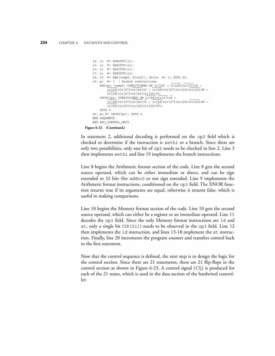
234 CHAPTER 6 DATAPATH AND CONTROL
In statement 2, additional decoding is performed on the op2 field which ischecked to determine if the instruction is sethi or a branch. Since there areonly two possibilities, only one bit of op2 needs to be checked in line 2. Line 3then implements sethi and line 19 implements the branch instructions.
Line 8 begins the Arithmetic format section of the code. Line 8 gets the secondsource operand, which can be either immediate or direct, and can be signextended to 32 bits (for addcc) or not sign extended. Line 9 implements theArithmetic format instructions, conditioned on the op3 field. The XNOR func-tion returns true if its arguments are equal, otherwise it returns false, which isuseful in making comparisons.
Line 10 begins the Memory format section of the code. Line 10 gets the secondsource operand, which can either be a register or an immediate operand. Line 11decodes the op3 field. Since the only Memory format instructions are ld andst, only a single bit (IR[21]) needs to be observed in the op3 field. Line 12then implements the ld instruction, and lines 13-18 implement the st instruc-tion. Finally, line 20 increments the program counter and transfers control backto the first statement.
Now that the control sequence is defined, the next step is to design the logic forthe control section. Since there are 21 statements, there are 21 flip-flops in thecontrol section as shown in Figure 6-23. A control signal (CSi) is produced foreach of the 21 states, which is used in the data section of the hardwired control-ler.
14: ir ← RSHIFT5(ir).
15: ir ← RSHIFT5(ir).
16: ir ← RSHIFT5(ir).
17: ir ← RSHIFT5(ir).
18: r0 ← AND(temp0, R[rs2]); Write ← 1; GOTO 20.
19: pc ← ! Branch instructions
ADD(pc, temp0) CONDITIONED ON ir[28] + ir[28]×ir[27]×Z + ir[28]×ir[27]×ir[26]×C + ir[28]×ir[27]×ir[26]×ir[25]×N + ir[28]×ir[27]×ir[26]×ir[25]×V, INCPC(pc) CONDITIONED ON ir[28]×ir[27]×Z + ir[28]×ir[27]×ir[26]×C + ir[28]×ir[27]×ir[26]×ir[25]×N + ir[28]×ir[27]×ir[26]×ir[25]×V; GOTO 0.
20: pc ← INCPC(pc); GOTO 0.
END SEQUENCE.
END ARC_CONTROL_UNIT.
Figure 6-22 (Continued.)
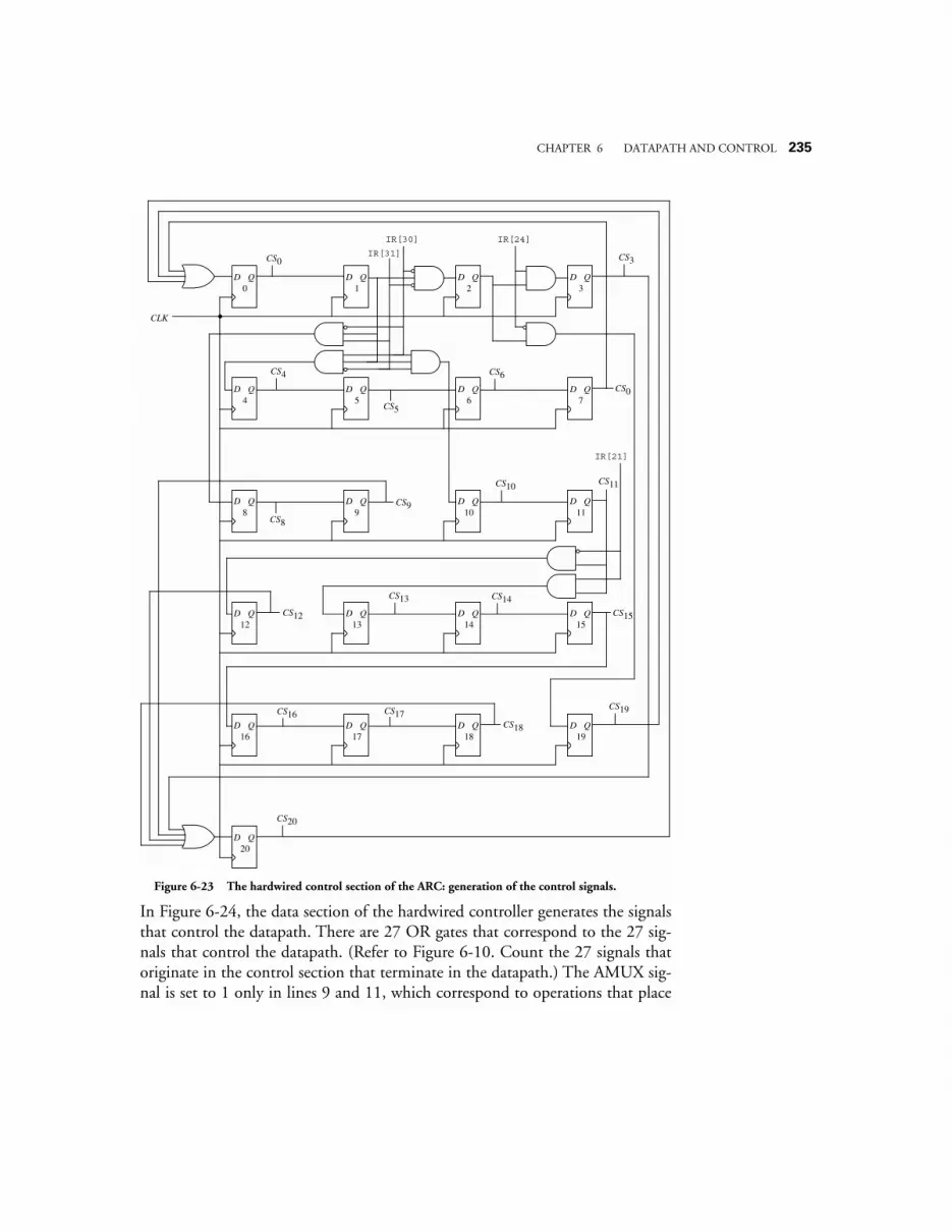
CHAPTER 6 DATAPATH AND CONTROL 235
In Figure 6-24, the data section of the hardwired controller generates the signalsthat control the datapath. There are 27 OR gates that correspond to the 27 sig-nals that control the datapath. (Refer to Figure 6-10. Count the 27 signals thatoriginate in the control section that terminate in the datapath.) The AMUX sig-nal is set to 1 only in lines 9 and 11, which correspond to operations that place
CLK
QD0
QD1
QD2
QD3
QD4
QD5
QD6
QD7
QD8
QD9
QD10
QD11
QD12
QD13
QD14
QD15
QD16
QD17
QD18
QD19
IR[31]
IR[30] IR[24]
IR[21]
QD20
CS0 CS3
CS4
CS5
CS6
CS0
CS8
CS9
CS10CS11
CS12
CS13 CS14
CS15
CS16 CS17CS18
CS19
CS20
Figure 6-23 The hardwired control section of the ARC: generation of the control signals.

236 CHAPTER 6 DATAPATH AND CONTROL
rs1 onto the A bus. Signals CS9 and CS11 are thus logically OR’d to produceAMUX. Likewise, rd is placed on the C bus in lines 3, 9, and 12, and so CS3,CS9, and CS12 are logically OR’d to produce CMUX.
The BMUX signal is more complex. rs2 is placed on the B bus in lines 8, 10,and 18, and so CS8, CS10, and CS18 are used to generate BMUX as shown.However, in line 8, BMUX is set (indicating rs2 is placed on the B bus) only ifIR[13] = 0 and IR[19:22] are all 0 (for the rightmost 4 bits of the 6-bitop3 pattern for addcc: 010000.) The corresponding logic is shown for this case.Likewise, in line 10, BMUX is set to 1 only when IR[13] = 0. Again, the cor-responding logic is shown.
The Read signal is set in lines 10 and 12, and so CS0 and CS12 are logically OR’dto produce Read. The Write signal is generated only in line 18, and thus needsno logic other than the signal CS18.
AMUXCS9
CS11
WriteCS18
CMUXCS3
CS9CS12
ReadCS0
CS12
BMUX
CS18IR[13]
CS10
CS8
IR[1
9] IR[2
2]IR
[20]
IR[2
1]
ALU[3]
CS9
IR[19]IR[20]
IR[24]
IR[23]
IR[22]IR[21]
CS20CS19
CS8
CS5CS6CS7
CS16CS14
CS15
CS17
CS11
CS13
ALU[2]
CS20CS18
CS4
CS10
CS12
CS16
CS14
CS15
CS1
CS13CS17
CS2
CS3
CS8
IR[13]
IR[19]IR[20]
IR[22]IR[21]
CS9
IR[2
4]IR
[23]
IR[19]IR[20]IR
[22]
IR[21]
CS19IR[28]
IR[28]IR[27]
IR[26]IR[25]
C
IR[28]IR[27]
IR[26]IR[25] N
IR[28]IR[27]
IR[26]C
IR[28]
IR[27]Z
CS2CS3IR[24]
ALU[0]
ALU[1]
CS20CS16
CS14CS15
CS13
CS17
IR[20]IR[21]
CS19
CS8
IR[13]IR[19]
IR[22]
IR[20]
IR[21]
CS9
IR[1
9]IR
[22]
IR[24]IR[23]
CS4 CS1
CS0
IR[13]CS8
IR[22]IR[21]
IR[19]
IR[23]
B[5]
B[2]
B[3]
B[4]
B[0]
B[1]
C[3]
C[4]
C[5]
IR[13]
IR[13]
A[1]
A[3]
A[4]
0
0
0
A[0]
CS5CS6
CS16CS14
CS15
CS17
CS13
CS12CS8
CS10
CS18
A[2]
A[5]CS4
CS0
CS20CS19
CS7
C[0]
C[1]
C[2]
Figure 6-24 The hardwired control section of the ARC: signals from the data section of the control
unit to the datapath. (Shaded areas are not detailed.)
CHAPTER 6 DATAPATH AND CONTROL 237
There are 4 signals that control the ALU: ALU[0], ALU[1], ALU[2], andALU[3], which correspond to F0, F1, F2, and F3, respectively, in the ALU opera-tion table shown in Figure 9-4. These four signals need values in each of the 20HDL lines. In line 0, the ALU operation is AND, which corresponds toALU[3:0] = 0101. Line 1 has no ALU operation specified, and so we can arbi-trarily choose an ALU operation that has no side effects, like AND (0101). Con-tinuing in this way, taking CONDITIONED ON statements into account, producesthe logic for ALU[3:0] as shown in the figure.
The control signals are sent to the datapath, similar to the way that the MIR con-trols the datapath in the microprogrammed approach of Figure 6-10. The hard-wired and microcontrolled approaches can thus be considered interchangeable,except with varying costs. There are only 21 flip-flops in the hardwired approach,but there are 2048×41 = 83,968 flip-flops in the microprogrammed approach(although in actuality, a ROM would be used, which consumes less space becausesmaller storage elements than flip/flops can be used.) The amount of additionalcombinational logic is comparable. The hardwired approach is faster in executingARC instructions, especially in decoding the Branch format instructions, but ismore difficult to change once it is committed to fabrication.
EXAMPLE
Consider adding the same subcc instruction from the previous EXAMPLE to thehardwired implementation of the ARC instruction set. As before, the subccinstruction uses the Arithmetic format and an op3 field of 001100.
Only line 9 of the HDL code needs to be changed, by inserting the expression:
ADDCC (R[rs1], INC_1(temp0)) CONDITIONED ON XNOR(IR[19:24], 001100), ! subcc
before the line for addcc.
The corresponding signals that need to be modified are ALU[3:0]. The INC_1construct in the line above indicates that an adder CLU, which would be definedin another HDL module, should be created (in a hardwired control unit, there isa lot of flexibility on what can be done.)
6.4 Case Study: The VHDL Hardware Description LanguageIn this section we present a brief overview of VHDL (VHSIC Hardware
238 CHAPTER 6 DATAPATH AND CONTROL
Description Language, in which VHSIC is yet another acronym for Very HighSpeed Integrated Circuit). Hardware description languages (HDLs), like VHDLand AHPL, are languages used for describing computer hardware, focusing pri-marily on logic devices and IC design. In the case of VHDL, however, designscan be specified at many different levels. For example, the control unit imple-mented in this chapter could be specified in VHDL.
We first cover the background that led to the development of VHDL, and thendescribe some of its properties. We then take a look at a VHDL specification ofthe majority function.
6.4.1 BACKGROUND
VHDL was the result of a collaboration between the Department of Defense(DOD), and many US industries. DOD, primarily through its DefenseAdvanced Research Products Agency (DARPA), realized in the late 1970’s thatIC design and fabrication was becoming so complex that a set of integrateddesign tools was needed for both design and simulation. It was felt that the toolsshould allow the user to specify a circuit or system from the highest, or behav-ioral level down to the lowest levels of actual IC layout and design, and further-more, all of these specifications should be verifiable by simulators and other rulecheckers.
The first preliminary requirements definition for the language was issued byDOD in 1981, as a recognition of the need for a more consistent approach tocomputer hardware design. The contract for the first version of the language waswon by a consortium of IBM, Texas Instruments, and Intermetrics, a softwareengineering firm specializing in programming language design and implementa-tion.
The consortium released a preliminary version for testing and comment in 1985.An updated version was submitted to the IEEE for standardization in 1986, theresult being named IEEE 1076-1987. In 1993, a newer version, IEEE1076-1993, was approved that addressed a number of minor problems andadded several new features.
By almost any measure VHDL is a success, with many users both inside and out-side the defense contractor community. DOD now requires that all Applica-tion-Specific Integrated Circuits (ASICs) be accompanied by their VHDL modelfor checking and simulation. Almost all CAD vendors now support VHDL in
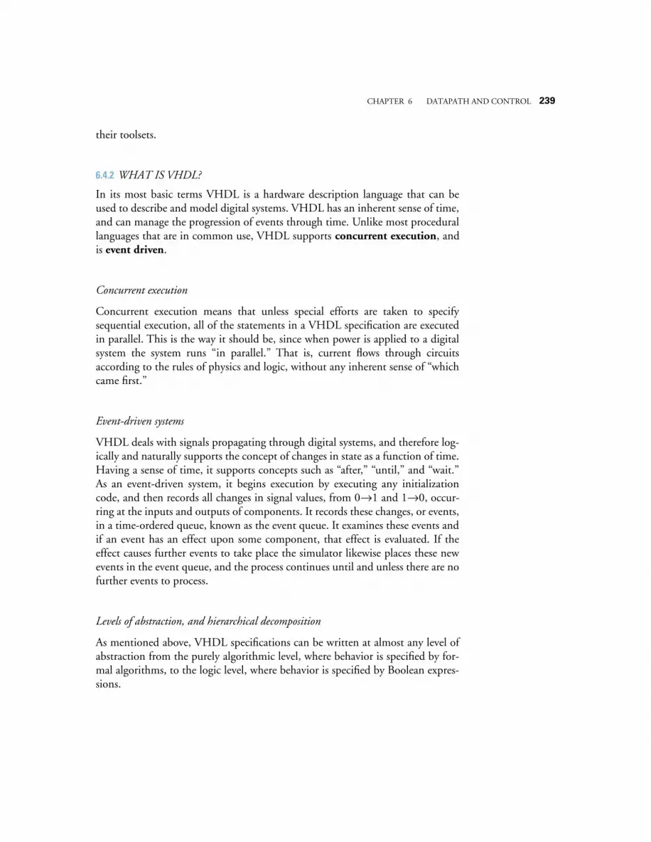
CHAPTER 6 DATAPATH AND CONTROL 239
their toolsets.
6.4.2 WHAT IS VHDL?
In its most basic terms VHDL is a hardware description language that can beused to describe and model digital systems. VHDL has an inherent sense of time,and can manage the progression of events through time. Unlike most procedurallanguages that are in common use, VHDL supports concurrent execution, andis event driven.
Concurrent execution
Concurrent execution means that unless special efforts are taken to specifysequential execution, all of the statements in a VHDL specification are executedin parallel. This is the way it should be, since when power is applied to a digitalsystem the system runs “in parallel.” That is, current flows through circuitsaccording to the rules of physics and logic, without any inherent sense of “whichcame first.”
Event-driven systems
VHDL deals with signals propagating through digital systems, and therefore log-ically and naturally supports the concept of changes in state as a function of time.Having a sense of time, it supports concepts such as “after,” “until,” and “wait.”As an event-driven system, it begins execution by executing any initializationcode, and then records all changes in signal values, from 0→1 and 1→0, occur-ring at the inputs and outputs of components. It records these changes, or events,in a time-ordered queue, known as the event queue. It examines these events andif an event has an effect upon some component, that effect is evaluated. If theeffect causes further events to take place the simulator likewise places these newevents in the event queue, and the process continues until and unless there are nofurther events to process.
Levels of abstraction, and hierarchical decomposition
As mentioned above, VHDL specifications can be written at almost any level ofabstraction from the purely algorithmic level, where behavior is specified by for-mal algorithms, to the logic level, where behavior is specified by Boolean expres-sions.
240 CHAPTER 6 DATAPATH AND CONTROL
Furthermore, a VHDL specification may be composed of a hierarchy of compo-nents, that is, components may contain components, which may themselves con-tain components. This models the physical world, where, for example, amotherboard may contain IC chips, which are composed of modules, which arein turn composed of sub-modules, all the way down to individual logic gates,and finally transistors.
6.4.3 A VHDL SPECIFICATION OF THE MAJORITY FUNCTION
Let us explore how VHDL can be used to implement a small digital componentby examining several implementations of the majority function, which pro-duces a 1 at its output when more than half of its inputs are 1, otherwise it pro-duces a 0 at its output. This is a useful function for fault tolerance, in whichmultiple systems that perform the same operations on the same data set “vote,”and if one of the systems deviates from the others, its output is effectivelyignored. The majority function is discussed in detail in Appendix A. Its truthtable is shown in Figure A-15 and Figure A-16, reproduced here as Figure 6-25.
In VHDL the specification of any component such as the majority function issplit into two parts, an entity part and an architecture part. These correspondroughly to the syntactic and semantic parts of a language specification: the entitypart describes the interface of the component without saying anything about itsinternal structure. The architecture part describes the internal behavior of thecomponent. Here is an entity specification for the 3-input majority function:
B CA
b) c)a)
F
MajorityFunction
00110011
01010101
B C
00001111
A
00010111
F
01234567
MintermIndex
F
A B C
A B C
A B C
A B C
A B C
Figure 6-25 The majority function. a) truth table, b) AND-OR implementation, c) black box represen-
tation.
CHAPTER 6 DATAPATH AND CONTROL 241
Interface specification for the majority component
-- Interfaceentity MAJORITY is
port(A_IN, B_IN, C_IN : in BIT F_OUT : out BIT);
end MAJORITY;
Keywords are shown in bold, and comments begin with “--” and end at the endof the line. Statements are separated by semicolons, “;”.
The entity specification describes just the “black box” input and output sig-nals in Figure 6-25c. The port declaration describes the kind of signals goinginto and out of the entity. Port modes include in for signals that flow into theentity, out for signals that flow out of the entity, and inout for bidirectionalsignals. There are also several other special purpose port modes.
With the interface to the majority component specified we can now model theinternal functioning of the component, using the architecture specification:
Behavioral model for the majority component
-- Bodyarchitecture LOGIC_SPEC of MAJORITY isbegin-- compute the output using a Boolean expressionF_OUT <= (not A_IN and B_IN and C_IN) or
(A_IN and not B_IN and C_IN) or(A_IN and B_IN and not C_IN) or(A_IN and B_IN and C_IN) after 4 ns;
end LOGIC_SPEC;
This model describes the relationship between the entity declaration of MAJOR-ITY and the architecture of MAJORITY. The names A_IN, B_IN, C_IN,and F_OUT in the architecture model must match the names used in the entitydeclaration.
This kind of architectural specification is referred to as a behavioral one, since itdefines the input/output function by specifying an explicit transfer function.That function is a Boolean expression that implements the Boolean functionshown in Figure 6-25a,b. Notice, however, that even at this level of specification
242 CHAPTER 6 DATAPATH AND CONTROL
that we can include a time delay between inputs and outputs, using the afterkeyword. In this case, the event computing the value of F_OUT will be triggered4 ns after a change in any of the input values.
It is also possible to specify the architecture at a level closer to the hardware byspecifying logic gates instead of logic equations. This is referred to as a structuralmodel. Here is such a specification:
Structural model for the majority component
In generating a structural model for the MAJORITY entity we will follow thegate design given in Figure 6-25b. We begin the model by describing a collectionof logic operators, in a special construct of VHDL known as a package. Thepackage is assumed to be stored in a working library called WORK. Followingthe package specification we repeat the entity declaration, and then, using thepackage and entity declarations we specify the internal workings of the majoritycomponent by specifying the architecture at a structural level:
-- Package declaration, in library WORKpackage LOGIC_GATES iscomponent AND3
port (A, B, C : in BIT; X : out BIT);end component;component OR4
port (A, B, C, D : in BIT; X : out BIT);end component;component NOT1
port (A : in BIT; X : out BIT);end component;
-- Interfaceentity MAJORITY is
port(A_IN, B_IN, C_IN : in BIT F_OUT : out BIT);
end MAJORITY;
-- Body-- Uses components declared in package LOGIC_GATES -- in the WORK library-- import all the components in WORK.LOGIC_GATESuse WORK.LOGIC_GATES.all architecture LOGIC_SPEC of MAJORITY is-- declare signals used internally in MAJORITYsignal A_BAR, B_BAR, C_BAR, I1, I2, I3, I4: BIT;begin-- connect the logic gatesNOT_1 : NOT1 port map (A_IN, A_BAR);NOT_2 : NOT1 port map (B_IN, B_BAR);NOT_3 : NOT1 port map (C_IN, C_BAR);

CHAPTER 6 DATAPATH AND CONTROL 243
AND_1 : AND3 port map (A_BAR, B_IN, C_IN, I1);AND_2 : AND3 port map (A_IN, B_BAR, C_IN, I2);AND_3 : AND3 port map (A_IN, B_IN, C_BAR, I3);AND_4 : AND3 port map (A_IN, B_IN, C_IN, I4);OR_1 : OR3 port map (I1, I2, I3, I4, F_OUT);end LOGIC_SPEC;
The package declaration supplies three gates, a 3-input AND gate, AND3, a4-input OR gate, OR4, and a NOT gate, NOT1. The architectures of thesegates are assumed to be declared elsewhere in the package. The entity declara-tion is unchanged, as we would expect, since it specifies MAJORITY as a “blackbox.”
The body specification begins with a use clause, which imports all of the dec-larations in the LOGIC_GATES package within the WORK library. The sig-nal declaration declares seven BIT signals that will be used internally. Thesesignals are used to interconnect the components within the architecture.
The instantiations of the three NOT gates follow, NOT_1, NOT_2, andNOT_3, all of which are NOT1 gates, and the mapping of their input and out-put signals are specified, following the port map keywords. Signals at theinputs and outputs of the logic gates are mapped according to the order in whichthey were declared within the package.
The rest of the body specification connects the NOT gates, the AND gates, andthe OR gate together as shown in Figure 6-25b.
Notice that this form of architecture specification separates the design and imple-mentation of the logic gates from the design of the MAJORITY entity. It wouldbe possible to have several different implementations of the logic gates in differ-ent packages, and to use any one of them by merely changing the uses clause.
6.4.4 9-VALUE LOGIC SYSTEM
This brief treatment of VHDL only gives a small taste of the scope and power ofthe language. The full language contains capabilities to specify clock signals andvarious timing mechanisms, sequential processes, and several different kinds ofsignals. There is an IEEE standard 9-value logic system, known asSTD_ULOGIC, IEEE 1164-1993. It has the following logic values:
type STD_ULOGIC is (‘U’, -- Uninitialized
244 CHAPTER 6 DATAPATH AND CONTROL
‘X’, -- Forcing unknown‘0’, -- Forcing 0‘1’, -- Forcing 1‘Z’, -- High impedance‘W’, -- Weak unknown‘L’, -- Weak 0‘H’, -- Weak 1‘-’, -- Don’t care);
Without getting into too much detail, these values allow the user to detect logicflaws within a design, and to follow the propagation of uninitialized or weak sig-nals through the design.
SUMMARY
A microarchitecture consists of a datapath and a control section. The datapathcontains data registers, an ALU, and the connections among them. The controlsection contains registers for microinstructions (for a microprogrammingapproach) and for condition codes, and a controller. The controller can be micro-programmed or hardwired. A microprogrammed controller interprets microin-structions by executing a microprogram that is stored in a control store. Ahardwired controller is organized as a collection of flip-flops that maintain stateinformation, and combinational logic that implements transitions among thestates.
The hardwired approach is fast, and consumes a small amount of hardware incomparison with the microprogrammed approach. The microprogrammedapproach is flexible, and simplifies the process of modifying the instruction set. Thecontrol store consumes a significant amount of hardware, which can be reduced toa degree through the use of nanoprogramming. Nanoprogramming adds delay tothe microinstruction execution time. The choice of microprogrammed or hard-wired control thus involves trade-offs: the microprogrammed approach is largeand slow, but is flexible and lends itself to simple implementations, whereas thehardwired approach is small and fast, but is difficult to modify, and typicallyresults in more complicated implementations.
CHAPTER 6 DATAPATH AND CONTROL 245
FURTHER READING(Wilkes, 1958) is a classic reference on microprogramming. (Mudge, 1978) cov-ers microprogramming on the DEC PDP 11/60. (Tanenbaum, 1990) and(Mano, 1991) provide instructional examples of microprogrammed architec-tures. (Hill and Peterson, 1987) gives a tutorial treatment of the AHPL hardwaredescription language, and hardwired control in general. (Lipsett et. al., 1989)and (Navabi, 1993) describe the commercial VHDL hardware description lan-guage and provide examples of its use. (Gajski, 1988) covers various aspects ofsilicon compilation.
Gajski, D., Silicon Compilation, Addison Wesley, (1988).
Hill, F. J. and G. R. Peterson, Digital Systems: Hardware Organization andDesign, 3/e, John Wiley & Sons, (1987).
Lipsett, R., C. Schaefer, and C. Ussery, VHDL: Hardware Description and Design,Kluwer Academic Publishers, (1989).
Mano, M., Digital Design, 2/e, Prentice Hall, (1991).
Mudge, J. Craig, Design Decisions for the PDP11/60 Mid-Range Minicomputer, inComputer Engineering, A DEC View of Hardware Systems Design, Digital Press,Bedford MA, (1978).
Navabi, Z., VHDL: Analysis and Modeling of Digital Systems, McGraw Hill,(1993).
Tanenbaum, A., Structured Computer Organization, 3/e, Prentice Hall, Engle-wood Cliffs, New Jersey, (1990).
Wilkes, M. V., W. Redwick, and D. Wheeler, “The Design of a Control Unit ofan Electronic Digital Computer,” Proc. IRE, vol. 105, p. 21, (1958).
PROBLEMS6.1 Design a 1-bit arithmetic logic unit (ALU) using the circuit shown in Fig-
ure 6-26 that performs bitwise addition, AND, OR, and NOT on the 1-bitinputs A and B. A 1-bit output Z is produced for each operation, and a carryis also produced for the case of addition. The carry is zero for AND, OR, and
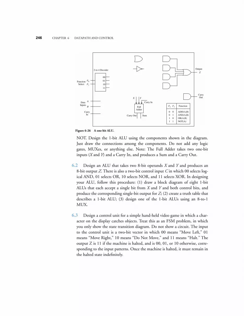
246 CHAPTER 6 DATAPATH AND CONTROL
NOT. Design the 1-bit ALU using the components shown in the diagram.Just draw the connections among the components. Do not add any logicgates, MUXes, or anything else. Note: The Full Adder takes two one-bitinputs (X and Y) and a Carry In, and produces a Sum and a Carry Out.
6.2 Design an ALU that takes two 8-bit operands X and Y and produces an8-bit output Z. There is also a two-bit control input C in which 00 selects log-ical AND, 01 selects OR, 10 selects NOR, and 11 selects XOR. In designingyour ALU, follow this procedure: (1) draw a block diagram of eight 1-bitALUs that each accept a single bit from X and Y and both control bits, andproduce the corresponding single-bit output for Z; (2) create a truth table thatdescribes a 1-bit ALU; (3) design one of the 1-bit ALUs using an 8-to-1MUX.
6.3 Design a control unit for a simple hand-held video game in which a char-acter on the display catches objects. Treat this as an FSM problem, in whichyou only show the state transition diagram. Do not show a circuit. The inputto the control unit is a two-bit vector in which 00 means “Move Left,” 01means “Move Right,” 10 means “Do Not Move,” and 11 means “Halt.” Theoutput Z is 11 if the machine is halted, and is 00, 01, or 10 otherwise, corre-sponding to the input patterns. Once the machine is halted, it must remain inthe halted state indefinitely.
Z
Carry Out
Output
FullAdder
X Y
Carry In
Carry Out Sum
A
B
Carry In
Data Inputs
F0
F1
00
01
10
11
2-to-4 Decoder
Function Select
0011
0101
Fo F1
ADD(A,B)AND(A,B)OR(A,B)NOT(A)
Function
Figure 6-26 A one-bit ALU.
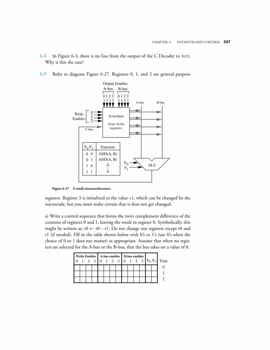
CHAPTER 6 DATAPATH AND CONTROL 247
6.4 In Figure 6-3, there is no line from the output of the C Decoder to %r0.Why is this the case?
6.5 Refer to diagram Figure 6-27. Registers 0, 1, and 2 are general purpose
registers. Register 3 is initialized to the value +1, which can be changed by themicrocode, but you must make certain that it does not get changed.
a) Write a control sequence that forms the two’s complement difference of thecontents of registers 0 and 1, leaving the result in register 0. Symbolically, thismight be written as: r0 ← r0 – r1. Do not change any registers except r0 andr1 (if needed). Fill in the table shown below with 0’s or 1’s (use 0’s when thechoice of 0 or 1 does not matter) as appropriate. Assume that when no regis-ters are selected for the A-bus or the B-bus, that the bus takes on a value of 0.
F0F1
Scratchpad
(Four 16-bitregisters)
A-bus B-bus
C-bus
0 1 2 3 0 1 2 3
0123
Output EnablesA-bus B-bus
WriteEnables
ALU
F0 F1
0
0
1
1
0
1
0
1
ADD(A, B)
AND(A, B)A_A
Function
Figure 6-27 A small microarchitecture.
F0 F10 1 2 30 1 2 30 1 2 3Write Enables A-bus enables B-bus enables
Time
0
1
2
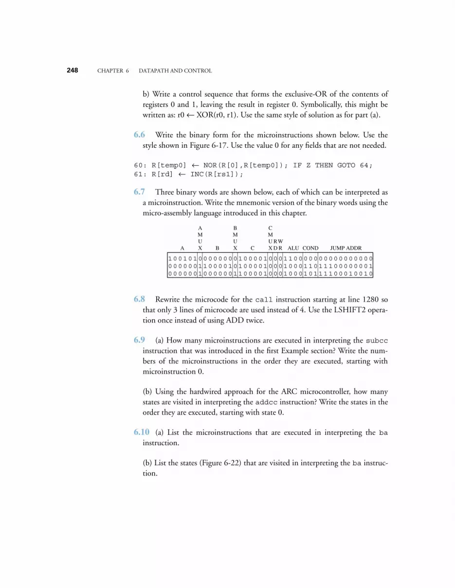
248 CHAPTER 6 DATAPATH AND CONTROL
b) Write a control sequence that forms the exclusive-OR of the contents ofregisters 0 and 1, leaving the result in register 0. Symbolically, this might bewritten as: r0 ← XOR(r0, r1). Use the same style of solution as for part (a).
6.6 Write the binary form for the microinstructions shown below. Use thestyle shown in Figure 6-17. Use the value 0 for any fields that are not needed.
60: R[temp0] ← NOR(R[0],R[temp0]); IF Z THEN GOTO 64;61: R[rd] ← INC(R[rs1]);
6.7 Three binary words are shown below, each of which can be interpreted asa microinstruction. Write the mnemonic version of the binary words using themicro-assembly language introduced in this chapter.
6.8 Rewrite the microcode for the call instruction starting at line 1280 sothat only 3 lines of microcode are used instead of 4. Use the LSHIFT2 opera-tion once instead of using ADD twice.
6.9 (a) How many microinstructions are executed in interpreting the subccinstruction that was introduced in the first Example section? Write the num-bers of the microinstructions in the order they are executed, starting withmicroinstruction 0.
(b) Using the hardwired approach for the ARC microcontroller, how manystates are visited in interpreting the addcc instruction? Write the states in theorder they are executed, starting with state 0.
6.10 (a) List the microinstructions that are executed in interpreting the bainstruction.
(b) List the states (Figure 6-22) that are visited in interpreting the ba instruc-tion.
RD
WRCA B JUMP ADDRALU COND
AMUX
BMUX
CMUX
010100 000001 0001000110000000000000000000011 000101 0001000100011011100000001
100 000010 000011 0001000100010111100010010
0 0 00 0 00 0 0
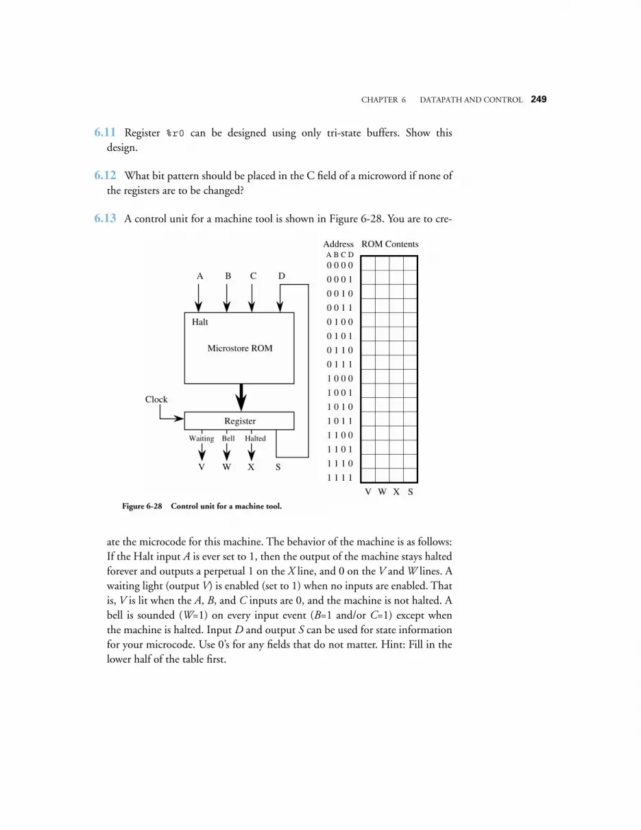
CHAPTER 6 DATAPATH AND CONTROL 249
6.11 Register %r0 can be designed using only tri-state buffers. Show thisdesign.
6.12 What bit pattern should be placed in the C field of a microword if none ofthe registers are to be changed?
6.13 A control unit for a machine tool is shown in Figure 6-28. You are to cre-
ate the microcode for this machine. The behavior of the machine is as follows:If the Halt input A is ever set to 1, then the output of the machine stays haltedforever and outputs a perpetual 1 on the X line, and 0 on the V and W lines. Awaiting light (output V) is enabled (set to 1) when no inputs are enabled. Thatis, V is lit when the A, B, and C inputs are 0, and the machine is not halted. Abell is sounded (W=1) on every input event (B=1 and/or C=1) except whenthe machine is halted. Input D and output S can be used for state informationfor your microcode. Use 0’s for any fields that do not matter. Hint: Fill in thelower half of the table first.
Microstore ROM
A
Clock
ROM ContentsAddress
0 0 0 0
0 0 0 1
0 0 1 0
0 0 1 1
0 1 0 0
0 1 0 1
0 1 1 0
0 1 1 1
1 0 0 0
1 0 0 1
1 0 1 0
1 0 1 1
1 1 0 0
1 1 0 1
1 1 1 0
1 1 1 1
A B C D
B C D
V W
V W X
SX
Register
S
Halt
Waiting Bell Halted
Figure 6-28 Control unit for a machine tool.
250 CHAPTER 6 DATAPATH AND CONTROL
6.14 For this problem, you are to extend the ARC instruction set to include anew instruction by modifying the microprogram. The new ARC instructionto be microcoded is:
xorcc — Perform an exclusive OR on the operands, and set the conditioncodes accordingly. This is an Arithmetic format instruction. The op3 field is010011.
Show the new microinstructions that will be added for xorcc.
6.15 Show a design for a four-word register stack, using 32-bit registers of theform shown below:
Four registers are stacked so that the output of the top register is the input tothe second register, which outputs to the input of the third, which outputs tothe input of the fourth. The input to the stack goes into the top register, andthe output of the stack is taken from the output of the top register (not thebottom register). There are two additional control lines, push and pop,which cause data to be pushed onto the stack or popped off the stack, respec-tively, when the corresponding line is 1. If neither line is 1, or if both lines are1, then the stack is unchanged.
6.16 In line 1792 of the ARC microprogram, the conditional GOTO appears atthe end of the line, but in line 8 it appears at the beginning. Does the positionof the GOTO within a micro-assembly line matter?
6.17 A microarchitecture is shown in Figure 6-29. The datapath has four regis-ters and an ALU. The control section is a finite state machine, in which thereis a RAM and a register. For this microarchitecture, a compiler translates ahigh level program directly into microcode; there is no intermediate assembly
Read
Data In
32
Data Out
32
WriteClock
32-Bit Register
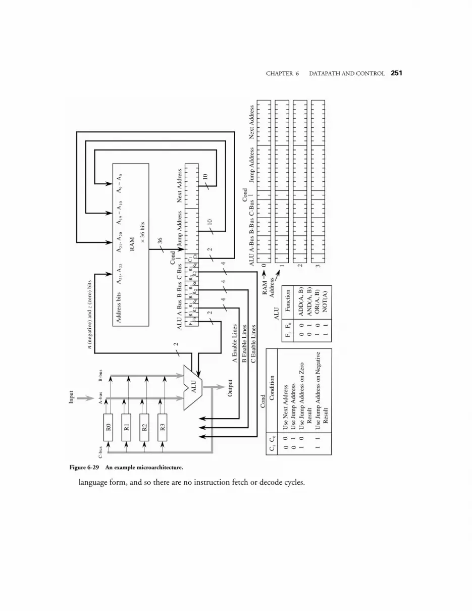
CHAPTER 6 DATAPATH AND CONTROL 251
language form, and so there are no instruction fetch or decode cycles.
F 1F 0
0 0 1 1
0 1 0 1
Func
tion
AD
D(A
, B)
AN
D(A
, B)
OR
(A, B
)N
OT
(A)
AL
UC
1C
0
0 0 1 1
0 1 0 1
Con
ditio
n
Use
Nex
t Add
ress
Use
Jum
p A
ddre
ssU
se J
ump
Add
ress
on
Zer
o
Res
ult
Use
Jum
p A
ddre
ss o
n N
egat
ive
R
esul
tCon
d
AL
UA
-Bus
B-B
usC
-Bus
Con
dJu
mp
Add
ress
Nex
t Add
ress
F0
AL
U
R0
R1
R2
R3
A-b
usB
-bus
C-b
us
F1
Inpu
t
Out
put
RA
M
224 w
ords
× 3
6 bi
ts
36
1010
2
2n (n
egat
ive)
and
z (
zero
) bi
ts
2
C0
C1
A2
3, A
22
A2
1, A
20
A1
9 –
A1
0A
9 –
A0
Add
ress
bits
AL
UA
-Bus
B-B
usC
-Bus
Con
dJu
mp
Add
ress
Nex
t Add
ress
0 1 2 3
RA
M
Add
ress
44
4
R2
R3
R0
R1
R2
R3
R0
R1
R2
R3
R0
R1
A E
nabl
e L
ines
B E
nabl
e L
ines
C E
nabl
e L
ines
Figure 6-29 An example microarchitecture.
252 CHAPTER 6 DATAPATH AND CONTROL
For this problem, you are to write the microcode that implements the instruc-tions listed below. The microcode should be stored in locations 0, 1, 2, and 3of the RAM. Although there are no lines that show it, assume that the n and zbits are both 0 when C0C1 = 00. That is, A23 and A22 are both 0 when there isno possible jump. Note: Each bit of the A, B, and C fields correspondsdirectly to a register. Thus, the pattern 1000 selects register R3, not register 8,which does not exist. There are some complexities with respect to howbranches are made in this microarchitecture, but you do not need to be con-cerned with how this is done in order to generate the microcode.
0: R1 ← ADD(R2, R3)1: Jump if negative to (15)102: R3 ← AND(R1, R2)3: Jump to (20)10
6.18 In line 2047 of the ARC microprogram shown in Figure 6-15, would theprogram behave differently if the “GOTO 0” portion of the instruction isdeleted?
6.19 In horizontal microprogramming, the microwords are wide, whereas invertical microprogramming the words are narrow. In general, horizontalmicrowords can be executed quickly, but require more space than verticalmicrowords, which take more time to execute. If we make the microword for-mat shown in Figure 6-11 more horizontal by expanding the A, B, and Cfields to contain a single bit for each of the 38 registers instead of a codedsix-bit version, then we can eliminate the A, B, and C decoders shown in Fig-ure 6-3. This allows the clock frequency to be increased, but also increases thespace for the microstore.
(a) How wide will the new horizontal microword be?
(b) By what percentage will the microstore increase in size?
6.20 Refer to Figure 6-7. Show the ALU LUT0 and ALU LUTx (x > 0) entriesfor the INC(A) operation.
6.21 On some architectures, there is special hardware that updates the PC,which takes into account the fact that the rightmost two bits are always 0.There is no special hardware presented in this chapter for updating the PC,

CHAPTER 6 DATAPATH AND CONTROL 253
and the branch microcode in lines 2 - 20 of Figure 6-15 has an error in howthe PC is updated on line 12 because branch displacements are given in termsof words. Identify the error, and explain how to fix it.

254 CHAPTER 6 DATAPATH AND CONTROL
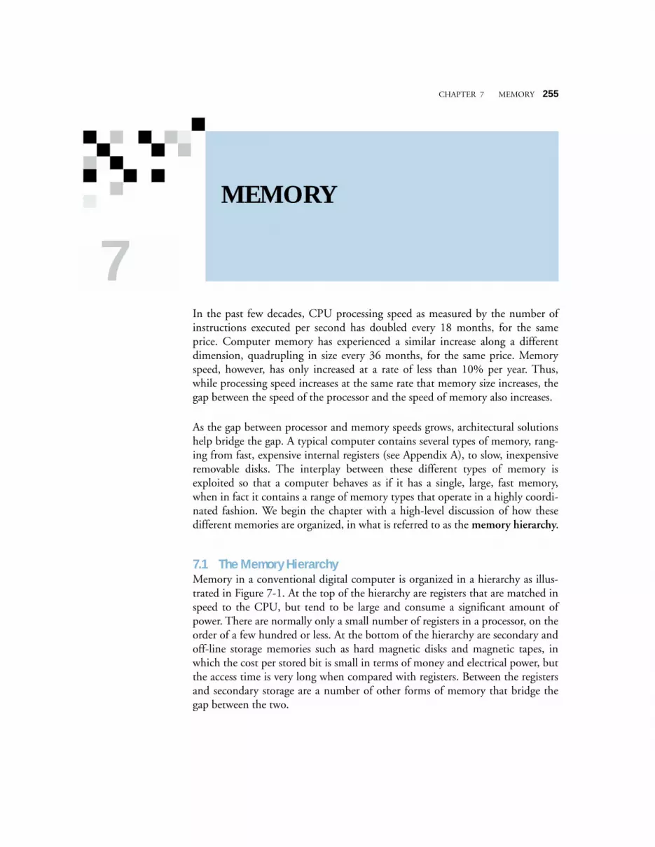
CHAPTER 7 MEMORY
255
In the past few decades, CPU processing speed as measured by the number ofinstructions executed per second has doubled every 18 months, for the sameprice. Computer memory has experienced a similar increase along a differentdimension, quadrupling in size every 36 months, for the same price. Memoryspeed, however, has only increased at a rate of less than 10% per year. Thus,while processing speed increases at the same rate that memory size increases, thegap between the speed of the processor and the speed of memory also increases.
As the gap between processor and memory speeds grows, architectural solutionshelp bridge the gap. A typical computer contains several types of memory, rang-ing from fast, expensive internal registers (see Appendix A), to slow, inexpensiveremovable disks. The interplay between these different types of memory isexploited so that a computer behaves as if it has a single, large, fast memory,when in fact it contains a range of memory types that operate in a highly coordi-nated fashion. We begin the chapter with a high-level discussion of how thesedifferent memories are organized, in what is referred to as the
memory hierarchy
.
7.1 The Memory Hierarchy
Memory in a conventional digital computer is organized in a hierarchy as illus-trated in Figure 7-1. At the top of the hierarchy are registers that are matched inspeed to the CPU, but tend to be large and consume a significant amount ofpower. There are normally only a small number of registers in a processor, on theorder of a few hundred or less. At the bottom of the hierarchy are secondary andoff-line storage memories such as hard magnetic disks and magnetic tapes, inwhich the cost per stored bit is small in terms of money and electrical power, butthe access time is very long when compared with registers. Between the registersand secondary storage are a number of other forms of memory that bridge thegap between the two.
MEMORY
7
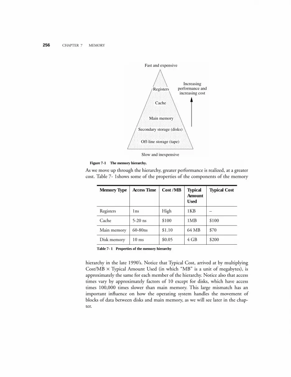
256
CHAPTER 7 MEMORY
As we move up through the hierarchy, greater performance is realized, at a greatercost. Table 7- 1shows some of the properties of the components of the memory
hierarchy in the late 1990’s. Notice that Typical Cost, arrived at by multiplyingCost/MB
×
Typical Amount Used (in which “MB” is a unit of megabytes), isapproximately the same for each member of the hierarchy. Notice also that accesstimes vary by approximately factors of 10 except for disks, which have accesstimes 100,000 times slower than main memory. This large mismatch has animportant influence on how the operating system handles the movement ofblocks of data between disks and main memory, as we will see later in the chap-ter.
Memory Type Access Time Cost /MB Typical Amount Used
Typical Cost
Registers 1ns High 1KB –
Cache 5-20 ns $100 1MB $100
Main memory 60-80ns $1.10 64 MB $70
Disk memory 10 ms $0.05 4 GB $200
Table 7- 1 Properties of the memory hierarchy
Registers
Cache
Main memory
Secondary storage (disks)
Off-line storage (tape)
Fast and expensive
Slow and inexpensive
Increasing performance andincreasing cost
Figure 7-1 The memory hierarchy.
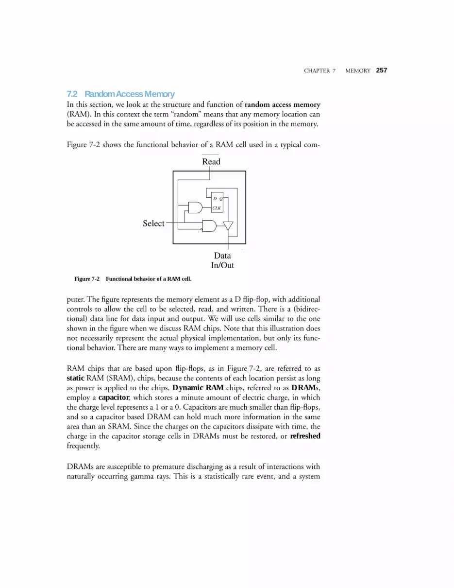
CHAPTER 7 MEMORY
257
7.2 Random Access Memory
In this section, we look at the structure and function of
random access memory
(RAM). In this context the term “random” means that any memory location canbe accessed in the same amount of time, regardless of its position in the memory.
Figure 7-2 shows the functional behavior of a RAM cell used in a typical com-
puter. The figure represents the memory element as a D flip-flop, with additionalcontrols to allow the cell to be selected, read, and written. There is a (bidirec-tional) data line for data input and output. We will use cells similar to the oneshown in the figure when we discuss RAM chips. Note that this illustration doesnot necessarily represent the actual physical implementation, but only its func-tional behavior. There are many ways to implement a memory cell.
RAM chips that are based upon flip-flops, as in Figure 7-2, are referred to as
static
RAM (SRAM), chips, because the contents of each location persist as longas power is applied to the chips.
Dynamic RAM
chips, referred to as
DRAM
s,employ a
capacitor
, which stores a minute amount of electric charge, in whichthe charge level represents a 1 or a 0. Capacitors are much smaller than flip-flops,and so a capacitor based DRAM can hold much more information in the samearea than an SRAM. Since the charges on the capacitors dissipate with time, thecharge in the capacitor storage cells in DRAMs must be restored, or
refreshed
frequently.
DRAMs are susceptible to premature discharging as a result of interactions withnaturally occurring gamma rays. This is a statistically rare event, and a system
QD
CLK
Read
Select
Data In/Out
Figure 7-2 Functional behavior of a RAM cell.
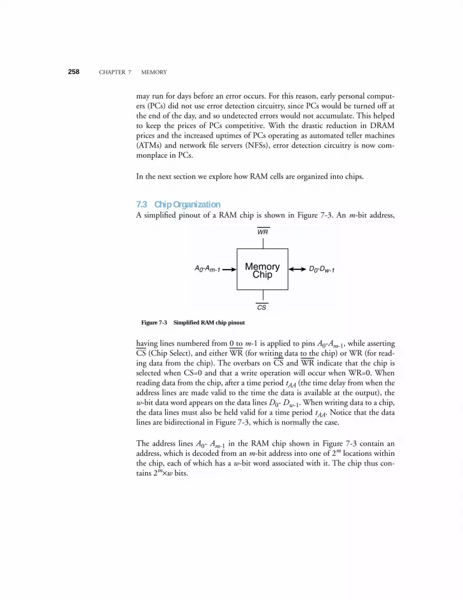
258
CHAPTER 7 MEMORY
may run for days before an error occurs. For this reason, early personal comput-ers (PCs) did not use error detection circuitry, since PCs would be turned off atthe end of the day, and so undetected errors would not accumulate. This helpedto keep the prices of PCs competitive. With the drastic reduction in DRAMprices and the increased uptimes of PCs operating as automated teller machines(ATMs) and network file servers (NFSs), error detection circuitry is now com-monplace in PCs.
In the next section we explore how RAM cells are organized into chips.
7.3 Chip Organization
A simplified pinout of a RAM chip is shown in Figure 7-3. An
m
-bit address,
having lines numbered from 0 to
m
-1 is applied to pins
A
0
-
A
m
-1
, while assertingCS (Chip Select), and either WR (for writing data to the chip) or WR (for read-ing data from the chip). The overbars on CS and WR indicate that the chip isselected when CS=0 and that a write operation will occur when WR=0. Whenreading data from the chip, after a time period
t
AA
(the time delay from when theaddress lines are made valid to the time the data is available at the output), the
w
-bit data word appears on the data lines
D
0
-
D
w
-1
. When writing data to a chip,the data lines must also be held valid for a time period
t
AA
. Notice that the datalines are bidirectional in Figure 7-3, which is normally the case.
The address lines
A
0
-
A
m
-1
in the RAM chip shown in Figure 7-3 contain anaddress, which is decoded from an
m
-bit address into one of 2
m
locations withinthe chip, each of which has a
w
-bit word associated with it. The chip thus con-tains 2
m
×
w
bits.
A0-Am-1 D0-Dw-1
WR
CS
MemoryChip
Figure 7-3 Simplified RAM chip pinout
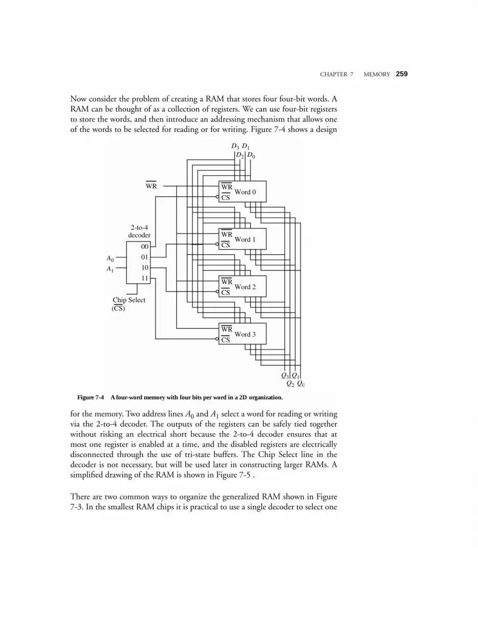
CHAPTER 7 MEMORY
259
Now consider the problem of creating a RAM that stores four four-bit words. ARAM can be thought of as a collection of registers. We can use four-bit registersto store the words, and then introduce an addressing mechanism that allows oneof the words to be selected for reading or for writing. Figure 7-4 shows a design
for the memory. Two address lines
A
0
and
A
1
select a word for reading or writingvia the 2-to-4 decoder. The outputs of the registers can be safely tied togetherwithout risking an electrical short because the 2-to-4 decoder ensures that atmost one register is enabled at a time, and the disabled registers are electricallydisconnected through the use of tri-state buffers. The Chip Select line in thedecoder is not necessary, but will be used later in constructing larger RAMs. Asimplified drawing of the RAM is shown in Figure 7-5 .
There are two common ways to organize the generalized RAM shown in Figure7-3. In the smallest RAM chips it is practical to use a single decoder to select one
D3D2
D1D0
Q3Q2
Q1Q0
WR
CSWord 0
00
01
10
11
A0
A1
WR
WR
CSWord 1
WR
CSWord 2
WR
CSWord 3
2-to-4decoder
Chip Select(CS)
Figure 7-4 A four-word memory with four bits per word in a 2D organization.
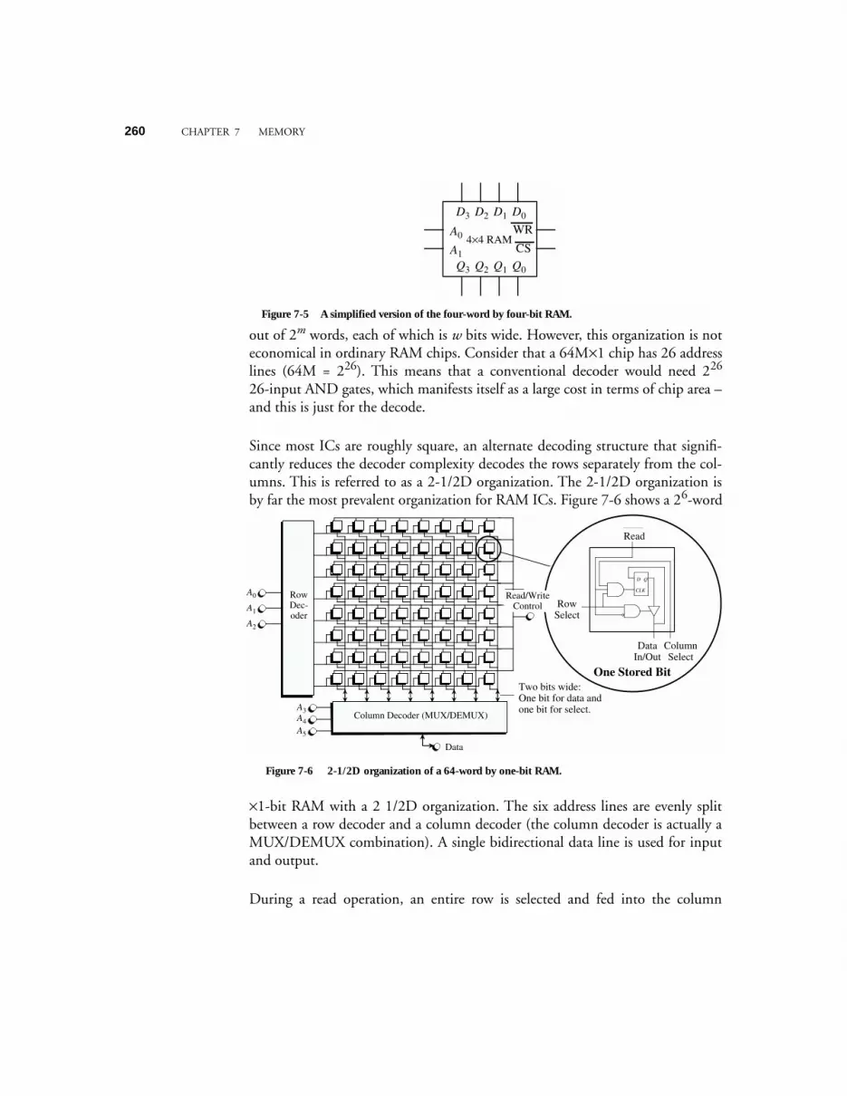
260
CHAPTER 7 MEMORY
out of 2
m
words, each of which is
w
bits wide. However, this organization is noteconomical in ordinary RAM chips. Consider that a 64M
×
1 chip has 26 addresslines (64M = 2
26
). This means that a conventional decoder would need 2
26
26-input AND gates, which manifests itself as a large cost in terms of chip area –and this is just for the decode.
Since most ICs are roughly square, an alternate decoding structure that signifi-cantly reduces the decoder complexity decodes the rows separately from the col-umns. This is referred to as a 2-1/2D organization. The 2-1/2D organization isby far the most prevalent organization for RAM ICs. Figure 7-6 shows a 2
6
-word
×
1-bit RAM with a 2 1/2D organization. The six address lines are evenly splitbetween a row decoder and a column decoder (the column decoder is actually aMUX/DEMUX combination). A single bidirectional data line is used for inputand output.
During a read operation, an entire row is selected and fed into the column
Q3 Q2 Q1 Q0
A0
A1
WR
CS
D3 D2 D1 D0
4×4 RAM
Figure 7-5 A simplified version of the four-word by four-bit RAM.
RowDec-oder
Column Decoder (MUX/DEMUX)
A0
A1
A2
A3A4
A5
Data
One Stored Bit
QD
CLK
Read
Row Select
Column Select
Data In/Out
Read/WriteControl
Two bits wide:One bit for data andone bit for select.
Figure 7-6 2-1/2D organization of a 64-word by one-bit RAM.
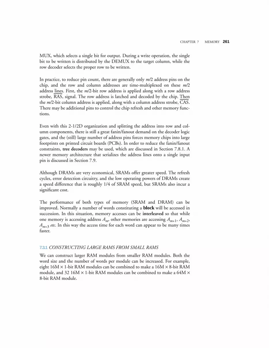
CHAPTER 7 MEMORY
261
MUX, which selects a single bit for output. During a write operation, the singlebit to be written is distributed by the DEMUX to the target column, while therow decoder selects the proper row to be written.
In practice, to reduce pin count, there are generally only
m/
2 address pins on thechip, and the row and column addresses are time-multiplexed on these
m/
2address lines. First, the
m/
2-bit row address is applied along with a row addressstrobe, RAS, signal. The row address is latched and decoded by the chip. Thenthe
m/
2-bit column address is applied, along with a column address strobe, CAS.There may be additional pins to control the chip refresh and other memory func-tions.
Even with this 2-1/2D organization and splitting the address into row and col-umn components, there is still a great fanin/fanout demand on the decoder logicgates, and the (still) large number of address pins forces memory chips into largefootprints on printed circuit boards (PCBs). In order to reduce the fanin/fanoutconstraints,
tree decoders
may be used, which are discussed in Section 7.8.1. Anewer memory architecture that serializes the address lines onto a single inputpin is discussed in Section 7.9.
Although DRAMs are very economical, SRAMs offer greater speed. The refreshcycles, error detection circuitry, and the low operating powers of DRAMs createa speed difference that is roughly 1/4 of SRAM speed, but SRAMs also incur asignificant cost.
The performance of both types of memory (SRAM and DRAM) can beimproved. Normally a number of words constituting a
block
will be accessed insuccession. In this situation, memory accesses can be
interleaved
so that whileone memory is accessing address
A
m
, other memories are accessing
A
m
+1
,
A
m
+2
,
A
m
+3
etc
. In this way the access time for each word can appear to be many timesfaster.
7.3.1
CONSTRUCTING LARGE RAMS FROM SMALL RAMS
We can construct larger RAM modules from smaller RAM modules. Both theword size and the number of words per module can be increased. For example,eight 16M
×
1-bit RAM modules can be combined to make a 16M
×
8-bit RAMmodule, and 32 16M
×
1-bit RAM modules can be combined to make a 64M
×
8-bit RAM module.
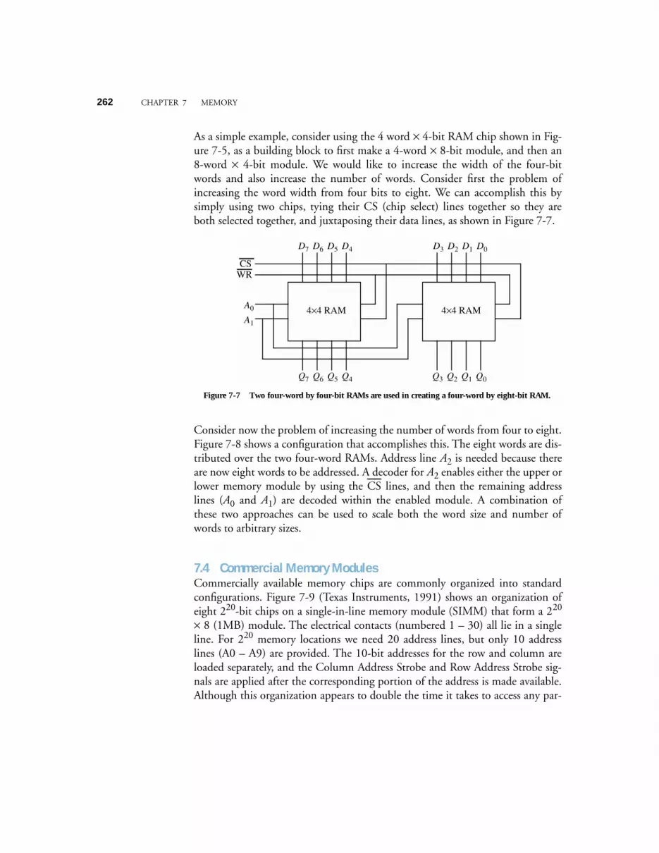
262
CHAPTER 7 MEMORY
As a simple example, consider using the 4 word
×
4-bit RAM chip shown in Fig-ure 7-5, as a building block to first make a 4-word
×
8-bit module, and then an8-word
×
4-bit module. We would like to increase the width of the four-bitwords and also increase the number of words. Consider first the problem ofincreasing the word width from four bits to eight. We can accomplish this bysimply using two chips, tying their CS (chip select) lines together so they areboth selected together, and juxtaposing their data lines, as shown in Figure 7-7.
Consider now the problem of increasing the number of words from four to eight.Figure 7-8 shows a configuration that accomplishes this. The eight words are dis-tributed over the two four-word RAMs. Address line
A
2
is needed because thereare now eight words to be addressed. A decoder for
A
2
enables either the upper orlower memory module by using the CS lines, and then the remaining addresslines (
A
0
and
A
1
) are decoded within the enabled module. A combination ofthese two approaches can be used to scale both the word size and number ofwords to arbitrary sizes.
7.4 Commercial Memory Modules
Commercially available memory chips are commonly organized into standardconfigurations. Figure 7-9 (Texas Instruments, 1991) shows an organization ofeight 2
20
-bit chips on a single-in-line memory module (SIMM) that form a 2
20
×
8 (1MB) module. The electrical contacts (numbered 1 – 30) all lie in a singleline. For 2
20
memory locations we need 20 address lines, but only 10 addresslines (A0 – A9) are provided. The 10-bit addresses for the row and column areloaded separately, and the Column Address Strobe and Row Address Strobe sig-nals are applied after the corresponding portion of the address is made available.Although this organization appears to double the time it takes to access any par-
A0
A1
WRCS
D7 D6 D5 D4 D3 D2 D1 D0
4×4 RAM
Q7 Q6 Q5 Q4 Q3 Q2 Q1 Q0
4×4 RAM
Figure 7-7 Two four-word by four-bit RAMs are used in creating a four-word by eight-bit RAM.
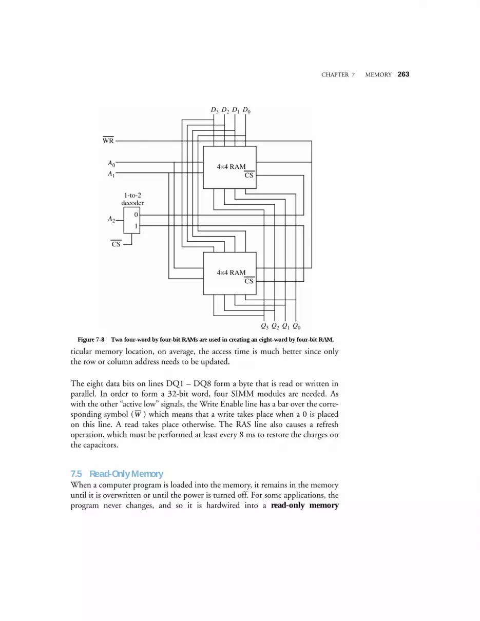
CHAPTER 7 MEMORY
263
ticular memory location, on average, the access time is much better since onlythe row or column address needs to be updated.
The eight data bits on lines DQ1 – DQ8 form a byte that is read or written inparallel. In order to form a 32-bit word, four SIMM modules are needed. Aswith the other “active low” signals, the Write Enable line has a bar over the corre-sponding symbol ( ) which means that a write takes place when a 0 is placedon this line. A read takes place otherwise. The RAS line also causes a refreshoperation, which must be performed at least every 8 ms to restore the charges onthe capacitors.
7.5 Read-Only Memory
When a computer program is loaded into the memory, it remains in the memoryuntil it is overwritten or until the power is turned off. For some applications, theprogram never changes, and so it is hardwired into a
read-only memory
A0
A1
WR
D3 D2 D1 D0
4×4 RAM
Q3 Q2 Q1 Q0
4×4 RAM
1-to-2decoder
0
1A2
CS
CS
CS
Figure 7-8 Two four-word by four-bit RAMs are used in creating an eight-word by four-bit RAM.
W
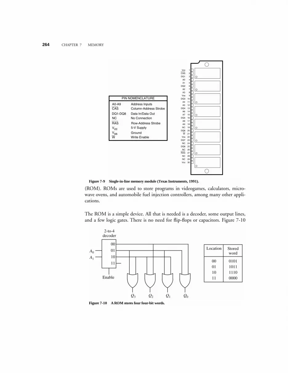
264 CHAPTER 7 MEMORY
(ROM). ROMs are used to store programs in videogames, calculators, micro-wave ovens, and automobile fuel injection controllers, among many other appli-cations.
The ROM is a simple device. All that is needed is a decoder, some output lines,and a few logic gates. There is no need for flip-flops or capacitors. Figure 7-10
1
2
3
4
5
6
7
8
9
10
11
12
13
14
15
16
17
18
19
20
21
22
23
24
25
26
27
28
29
30
Vcc
CAS
DQ1
A0
A1
DQ2
A2
A3
Vss
DQ3
A4
A5
DQ4
A6
A7
DQ5
A8
A9
NC
DQ6
W
Vss
DQ7
NC
DQ8
NC
RAS
NC
NC
Vcc
PIN NOMENCLATURE
Address InputsColumn-Address Strobe
Data In/Data OutNo Connection
Row-Address Strobe5-V Supply
GroundWrite Enable
DQ1-DQ8
CASA0-A9
NC
RASVccVssW
Figure 7-9 Single-in-line memory module (Texas Instruments, 1991).
Q3 Q2 Q1 Q0
00
01
10
11
A0
A1
2-to-4decoder
Enable
Location Storedword
00011011
0101101111100000
Figure 7-10 A ROM stores four four-bit words.
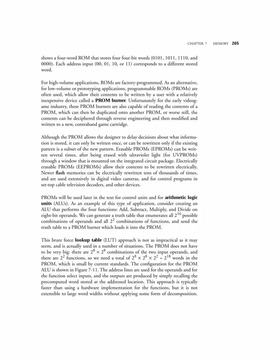
CHAPTER 7 MEMORY 265
shows a four-word ROM that stores four four-bit words (0101, 1011, 1110, and0000). Each address input (00, 01, 10, or 11) corresponds to a different storedword.
For high-volume applications, ROMs are factory-programmed. As an alternative,for low-volume or prototyping applications, programmable ROMs (PROMs) areoften used, which allow their contents to be written by a user with a relativelyinexpensive device called a PROM burner. Unfortunately for the early videog-ame industry, these PROM burners are also capable of reading the contents of aPROM, which can then be duplicated onto another PROM, or worse still, thecontents can be deciphered through reverse engineering and then modified andwritten to a new, contraband game cartridge.
Although the PROM allows the designer to delay decisions about what informa-tion is stored, it can only be written once, or can be rewritten only if the existingpattern is a subset of the new pattern. Erasable PROMs (EPROMs) can be writ-ten several times, after being erased with ultraviolet light (for UVPROMs)through a window that is mounted on the integrated circuit package. Electricallyerasable PROMs (EEPROMs) allow their contents to be rewritten electrically.Newer flash memories can be electrically rewritten tens of thousands of times,and are used extensively in digital video cameras, and for control programs inset-top cable television decoders, and other devices.
PROMs will be used later in the text for control units and for arithmetic logicunits (ALUs). As an example of this type of application, consider creating anALU that performs the four functions: Add, Subtract, Multiply, and Divide oneight-bit operands. We can generate a truth table that enumerates all 216 possiblecombinations of operands and all 22 combinations of functions, and send thetruth table to a PROM burner which loads it into the PROM.
This brute force lookup table (LUT) approach is not as impractical as it mayseem, and is actually used in a number of situations. The PROM does not haveto be very big: there are 28 × 28 combinations of the two input operands, andthere are 22 functions, so we need a total of 28 × 28 × 22 = 218 words in thePROM, which is small by current standards. The configuration for the PROMALU is shown in Figure 7-11. The address lines are used for the operands and forthe function select inputs, and the outputs are produced by simply recalling theprecomputed word stored at the addressed location. This approach is typicallyfaster than using a hardware implementation for the functions, but it is notextensible to large word widths without applying some form of decomposition.
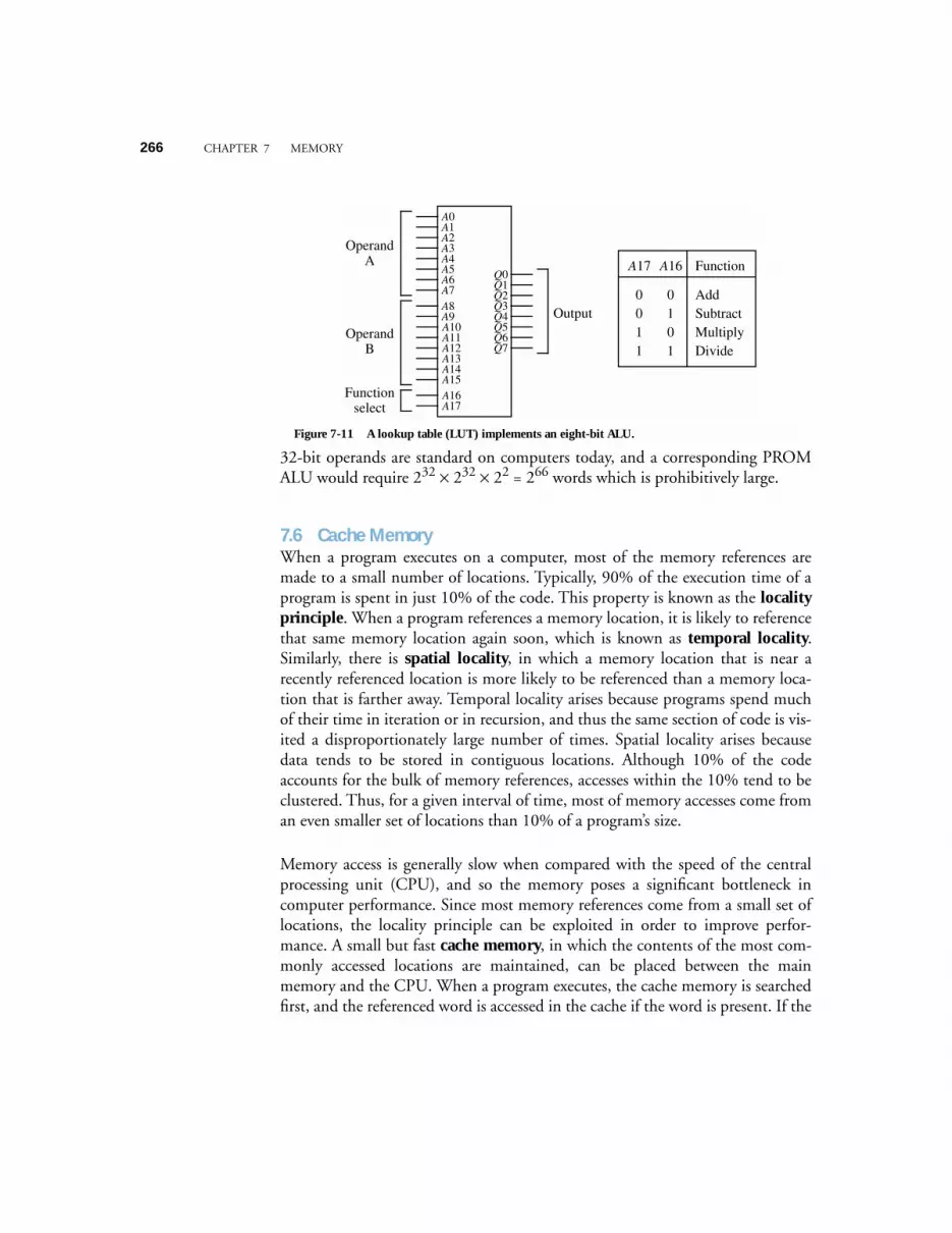
266 CHAPTER 7 MEMORY
32-bit operands are standard on computers today, and a corresponding PROMALU would require 232 × 232 × 22 = 266 words which is prohibitively large.
7.6 Cache MemoryWhen a program executes on a computer, most of the memory references aremade to a small number of locations. Typically, 90% of the execution time of aprogram is spent in just 10% of the code. This property is known as the localityprinciple. When a program references a memory location, it is likely to referencethat same memory location again soon, which is known as temporal locality.Similarly, there is spatial locality, in which a memory location that is near arecently referenced location is more likely to be referenced than a memory loca-tion that is farther away. Temporal locality arises because programs spend muchof their time in iteration or in recursion, and thus the same section of code is vis-ited a disproportionately large number of times. Spatial locality arises becausedata tends to be stored in contiguous locations. Although 10% of the codeaccounts for the bulk of memory references, accesses within the 10% tend to beclustered. Thus, for a given interval of time, most of memory accesses come froman even smaller set of locations than 10% of a program’s size.
Memory access is generally slow when compared with the speed of the centralprocessing unit (CPU), and so the memory poses a significant bottleneck incomputer performance. Since most memory references come from a small set oflocations, the locality principle can be exploited in order to improve perfor-mance. A small but fast cache memory, in which the contents of the most com-monly accessed locations are maintained, can be placed between the mainmemory and the CPU. When a program executes, the cache memory is searchedfirst, and the referenced word is accessed in the cache if the word is present. If the
A0A1A2A3A4A5A6A7A8A9A10A11A12A13A14A15A16A17
Q0Q1Q2Q3Q4Q5Q6Q7
Operand A
Operand B
Functionselect
Output0011
0101
AddSubtractMultiplyDivide
A17 A16 Function
Figure 7-11 A lookup table (LUT) implements an eight-bit ALU.

CHAPTER 7 MEMORY 267
referenced word is not in the cache, then a free location is created in the cacheand the referenced word is brought into the cache from the main memory. Theword is then accessed in the cache. Although this process takes longer thanaccessing main memory directly, the overall performance can be improved if ahigh proportion of memory accesses are satisfied by the cache.
Modern memory systems may have several levels of cache, referred to as Level 1(L1), Level 2 (L2), and even, in some cases, Level 3 (L3). In most instances theL1 cache is implemented right on the CPU chip. Both the Intel Pentium and theIBM-Motorola PowerPC G3 processors have 32 Kbytes of L1 cache on the CPUchip.
A cache memory is faster than main memory for a number of reasons. Fasterelectronics can be used, which also results in a greater expense in terms of money,size, and power requirements. Since the cache is small, this increase in cost is rel-atively small. A cache memory has fewer locations than a main memory, and as aresult it has a shallow decoding tree, which reduces the access time. The cache isplaced both physically closer and logically closer to the CPU than the mainmemory, and this placement avoids communication delays over a shared bus.
A typical situation is shown in Figure 7-12. A simple computer without a cache
memory is shown in the left side of the figure. This cache-less computer containsa CPU that has a clock speed of 400 MHz, but communicates over a 66 MHzbus to a main memory that supports a lower clock speed of 10 MHz. A few buscycles are normally needed to synchronize the CPU with the bus, and thus thedifference in speed between main memory and the CPU can be as large as a fac-tor of ten or more. A cache memory can be positioned closer to the CPU asshown in the right side of Figure 7-12, so that the CPU sees fast accesses over a400 MHz direct path to the cache.
CPU400 MHz
MainMemory10 MHz
Bus 66 MHz
MainMemory10 MHz
Bus 66 MHz
CPU
Cache
400 MHz
Without cache With cache
Figure 7-12 Placement of cache in a computer system.
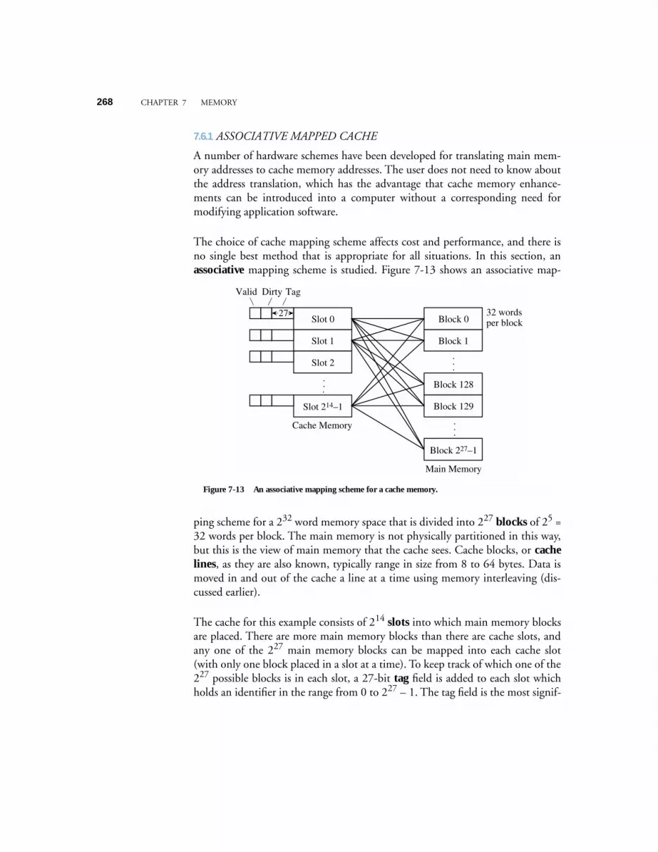
268 CHAPTER 7 MEMORY
7.6.1 ASSOCIATIVE MAPPED CACHE
A number of hardware schemes have been developed for translating main mem-ory addresses to cache memory addresses. The user does not need to know aboutthe address translation, which has the advantage that cache memory enhance-ments can be introduced into a computer without a corresponding need formodifying application software.
The choice of cache mapping scheme affects cost and performance, and there isno single best method that is appropriate for all situations. In this section, anassociative mapping scheme is studied. Figure 7-13 shows an associative map-
ping scheme for a 232 word memory space that is divided into 227 blocks of 25 =32 words per block. The main memory is not physically partitioned in this way,but this is the view of main memory that the cache sees. Cache blocks, or cachelines, as they are also known, typically range in size from 8 to 64 bytes. Data ismoved in and out of the cache a line at a time using memory interleaving (dis-cussed earlier).
The cache for this example consists of 214 slots into which main memory blocksare placed. There are more main memory blocks than there are cache slots, andany one of the 227 main memory blocks can be mapped into each cache slot(with only one block placed in a slot at a time). To keep track of which one of the227 possible blocks is in each slot, a 27-bit tag field is added to each slot whichholds an identifier in the range from 0 to 227 – 1. The tag field is the most signif-
Slot 0
Slot 1
Slot 2
Slot 214–1
.
.
.
.
.
.
Block 0
Block 1
Block 128
Block 129
Block 227–1
Cache Memory
Main Memory
TagValid Dirty
32 words per block
27
.
.
.
Figure 7-13 An associative mapping scheme for a cache memory.
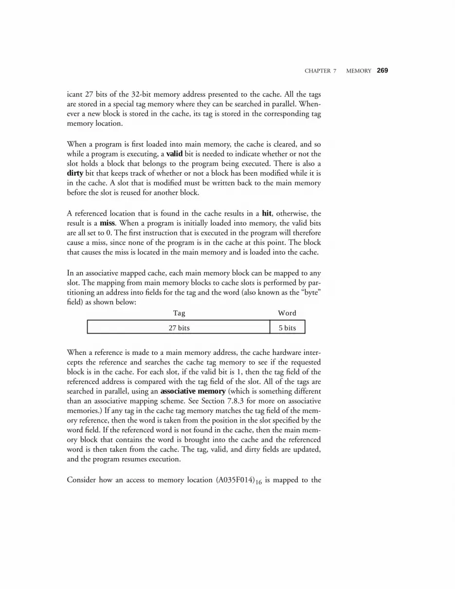
CHAPTER 7 MEMORY 269
icant 27 bits of the 32-bit memory address presented to the cache. All the tagsare stored in a special tag memory where they can be searched in parallel. When-ever a new block is stored in the cache, its tag is stored in the corresponding tagmemory location.
When a program is first loaded into main memory, the cache is cleared, and sowhile a program is executing, a valid bit is needed to indicate whether or not theslot holds a block that belongs to the program being executed. There is also adirty bit that keeps track of whether or not a block has been modified while it isin the cache. A slot that is modified must be written back to the main memorybefore the slot is reused for another block.
A referenced location that is found in the cache results in a hit, otherwise, theresult is a miss. When a program is initially loaded into memory, the valid bitsare all set to 0. The first instruction that is executed in the program will thereforecause a miss, since none of the program is in the cache at this point. The blockthat causes the miss is located in the main memory and is loaded into the cache.
In an associative mapped cache, each main memory block can be mapped to anyslot. The mapping from main memory blocks to cache slots is performed by par-titioning an address into fields for the tag and the word (also known as the “byte”field) as shown below:
When a reference is made to a main memory address, the cache hardware inter-cepts the reference and searches the cache tag memory to see if the requestedblock is in the cache. For each slot, if the valid bit is 1, then the tag field of thereferenced address is compared with the tag field of the slot. All of the tags aresearched in parallel, using an associative memory (which is something differentthan an associative mapping scheme. See Section 7.8.3 for more on associativememories.) If any tag in the cache tag memory matches the tag field of the mem-ory reference, then the word is taken from the position in the slot specified by theword field. If the referenced word is not found in the cache, then the main mem-ory block that contains the word is brought into the cache and the referencedword is then taken from the cache. The tag, valid, and dirty fields are updated,and the program resumes execution.
Consider how an access to memory location (A035F014)16 is mapped to the
27 bits 5 bits
Tag Word
270 CHAPTER 7 MEMORY
cache. The leftmost 27 bits of the address form the tag field, and the remainingfive bits form the word field as shown below:
If the addressed word is in the cache, it will be found in word (14)16 of a slot thathas a tag of (501AF80)16, which is made up of the 27 most significant bits of theaddress. If the addressed word is not in the cache, then the block correspondingto the tag field (501AF80)16 will be brought into an available slot in the cachefrom the main memory, and the memory reference that caused the “cache miss”will then be satisfied from the cache.
Although this mapping scheme is powerful enough to satisfy a wide range ofmemory access situations, there are two implementation problems that limit per-formance. First, the process of deciding which slot should be freed when a newblock is brought into the cache can be complex. This process requires a signifi-cant amount of hardware and introduces delays in memory accesses. A secondproblem is that when the cache is searched, the tag field of the referenced addressmust be compared with all 214 tag fields in the cache. (Alternative methods thatlimit the number of comparisons are described in Sections 7.6.2 and 7.6.3.)
Replacement Policies in Associative Mapped Caches
When a new block needs to be placed in an associative mapped cache, an avail-able slot must be identified. If there are unused slots, such as when a programbegins execution, then the first slot with a valid bit of 0 can simply be used.When all of the valid bits for all cache slots are 1, however, then one of the activeslots must be freed for the new block. Four replacement policies that are com-monly used are: least recently used (LRU), first-in first-out (FIFO), least fre-quently used (LFU), and random. A fifth policy that is used for analysispurposes only, is optimal.
For the LRU policy, a time stamp is added to each slot, which is updated whenany slot is accessed. When a slot must be freed for a new block, the contents ofthe least recently used slot, as identified by the age of the corresponding timestamp, are discarded and the new block is written to that slot. The LFU policyworks similarly, except that only one slot is updated at a time by incrementing afrequency counter that is attached to each slot. When a slot is needed for a newblock, the least frequently used slot is freed. The FIFO policy replaces slots in
Tag Word
1 0 1 0 0 0 0 0 0 0 1 1 0 1 0 1 1 1 1 1 0 0 0 0 0 0 0 1 0 1 0 0

CHAPTER 7 MEMORY 271
round-robin fashion, one after the next in the order of their physical locations inthe cache. The random replacement policy simply chooses a slot at random.
The optimal replacement policy is not practical, but is used for comparison pur-poses to determine how effective other replacement policies are to the best possi-ble. That is, the optimal replacement policy is determined only after a programhas already executed, and so it is of little help to a running program.
Studies have shown that the LFU policy is only slightly better than the randompolicy. The LRU policy can be implemented efficiently, and is sometimes pre-ferred over the others for that reason. A simple implementation of the LRU pol-icy is covered in Section 7.6.7.
Advantages and Disadvantages of the Associative Mapped Cache
The associative mapped cache has the advantage that any main memory blockcan be placed into any cache slot. This means that regardless of how irregular thedata and program references are, if a slot is available for the block, it can bestored in the cache. This results in considerable hardware overhead needed forcache bookkeeping. Each slot must have a 27-bit tag that identifies its location inmain memory, and each tag must be searched in parallel. This means that in theexample above the tag memory must be 27 × 214 bits in size, and as describedabove, there must be a mechanism for searching the tag memory in parallel.Memories that can be searched for their contents, in parallel, are referred to asassociative, or content-addressable memories. We will discuss this kind ofmemory later in the chapter.
By restricting where each main memory block can be placed in the cache, we caneliminate the need for an associative memory. This kind of cache is referred to asa direct mapped cache, which is discussed in the next section.
7.6.2 DIRECT MAPPED CACHE
Figure 7-14 shows a direct mapping scheme for a 232 word memory. As before,the memory is divided into 227 blocks of 25 = 32 words per block, and the cacheconsists of 214 slots. There are more main memory blocks than there are cacheslots, and a total of 227/214 = 213 main memory blocks can be mapped onto eachcache slot. In order to keep track of which of the 213 possible blocks is in eachslot, a 13-bit tag field is added to each slot which holds an identifier in the range
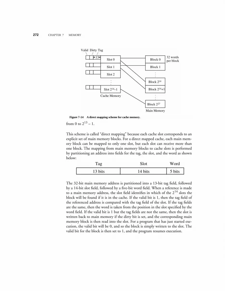
272 CHAPTER 7 MEMORY
from 0 to 213 – 1.
This scheme is called “direct mapping” because each cache slot corresponds to anexplicit set of main memory blocks. For a direct mapped cache, each main mem-ory block can be mapped to only one slot, but each slot can receive more thanone block. The mapping from main memory blocks to cache slots is performedby partitioning an address into fields for the tag, the slot, and the word as shownbelow:
The 32-bit main memory address is partitioned into a 13-bit tag field, followedby a 14-bit slot field, followed by a five-bit word field. When a reference is madeto a main memory address, the slot field identifies in which of the 214 slots theblock will be found if it is in the cache. If the valid bit is 1, then the tag field ofthe referenced address is compared with the tag field of the slot. If the tag fieldsare the same, then the word is taken from the position in the slot specified by theword field. If the valid bit is 1 but the tag fields are not the same, then the slot iswritten back to main memory if the dirty bit is set, and the corresponding mainmemory block is then read into the slot. For a program that has just started exe-cution, the valid bit will be 0, and so the block is simply written to the slot. Thevalid bit for the block is then set to 1, and the program resumes execution.
Slot 0
Slot 1
Slot 2
Slot 214–1
.
.
.
.
.
.
.
.
.
Block 0
Block 1
Block 2
Block 2
Block 227
+1
Cache Memory
Main Memory
TagValid Dirty
32 words per block
13
14
14
Figure 7-14 A direct mapping scheme for cache memory.
13 bits 5 bits14 bits
Tag WordSlot
CHAPTER 7 MEMORY 273
Consider how an access to memory location (A035F014)16 is mapped to thecache. The bit pattern is partitioned according to the word format shown above.The leftmost 13 bits form the tag field, the next 14 bits form the slot field, andthe remaining five bits form the word field as shown below:
If the addressed word is in the cache, it will be found in word (14)16 of slot(2F80)16, which will have a tag of (1406)16.
Advantages and Disadvantages of the Direct Mapped Cache
The direct mapped cache is a relatively simple scheme to implement. The tagmemory in the example above is only 13 × 214 bits in size, less than half of theassociative mapped cache. Furthermore, there is no need for an associativesearch, since the slot field of the main memory address from the CPU is used to“direct” the comparison to the single slot where the block will be if it is indeed inthe cache.
This simplicity comes at a cost. Consider what happens when a program refer-ences locations that are 219 words apart, which is the size of the cache. This pat-tern can arise naturally if a matrix is stored in memory by rows and is accessed bycolumns. Every memory reference will result in a miss, which will cause an entireblock to be read into the cache even though only a single word is used. Worsestill, only a small fraction of the available cache memory will actually be used.
Now it may seem that any programmer who writes a program this way deservesthe resulting poor performance, but in fact, fast matrix calculations usepower-of-two dimensions (which allows shift operations to replace costly multi-plications and divisions for array indexing), and so the worst-case scenario ofaccessing memory locations that are 219 addresses apart is not all that unlikely.To avoid this situation without paying the high implementation price of a fullyassociative cache memory, the set associative mapping scheme can be used,which combines aspects of both direct mapping and associative mapping. Setassociative mapping, which is also known as set-direct mapping, is described inthe next section.
Tag Word
1 0 1 0 0 0 0 0 0 0 1 1 0 1 0 1 1 1 1 1 0 0 0 0 0 0 0 1 0 1 0 0
Slot
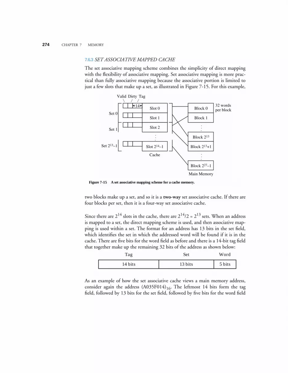
274 CHAPTER 7 MEMORY
7.6.3 SET ASSOCIATIVE MAPPED CACHE
The set associative mapping scheme combines the simplicity of direct mappingwith the flexibility of associative mapping. Set associative mapping is more prac-tical than fully associative mapping because the associative portion is limited tojust a few slots that make up a set, as illustrated in Figure 7-15. For this example,
two blocks make up a set, and so it is a two-way set associative cache. If there arefour blocks per set, then it is a four-way set associative cache.
Since there are 214 slots in the cache, there are 214/2 = 213 sets. When an addressis mapped to a set, the direct mapping scheme is used, and then associative map-ping is used within a set. The format for an address has 13 bits in the set field,which identifies the set in which the addressed word will be found if it is in thecache. There are five bits for the word field as before and there is a 14-bit tag fieldthat together make up the remaining 32 bits of the address as shown below:
As an example of how the set associative cache views a main memory address,consider again the address (A035F014)16. The leftmost 14 bits form the tagfield, followed by 13 bits for the set field, followed by five bits for the word field
Slot 0
Slot 1
Slot 2
Slot 214–1
.
.
.
.
.
.
.
.
.
Block 0
Block 1
Block 213
Block 213+1
Block 227–1
Cache
Main Memory
TagValid Dirty
32 words per block
Set 0
Set 1
Set 213–1
14
Figure 7-15 A set associative mapping scheme for a cache memory.
Tag WordSet
14 bits 5 bits13 bits

CHAPTER 7 MEMORY 275
as shown below:
As before, the partitioning of the address field is known only to the cache, andthe rest of the computer is oblivious to any address translation.
Advantages and Disadvantages of the Set Associative Mapped Cache
In the example above, the tag memory increases only slightly from the directmapping example, to 13 × 214 bits, and only two tags need to be searched foreach memory reference. The set associative cache is almost universally used intoday’s microprocessors.
7.6.4 CACHE PERFORMANCE
Notice that we can readily replace the cache direct mapping hardware with asso-ciative or set associative mapping hardware, without making any other changesto the computer or the software. Only the runtime performance will changebetween methods.
Runtime performance is the purpose behind using a cache memory, and there area number of issues that need to be addressed as to what triggers a word or blockto be moved between the cache and the main memory. Cache read and write pol-icies are summarized in Figure 7-16. The policies depend upon whether or notthe requested word is in the cache. If a cache read operation is taking place, andthe referenced data is in the cache, then there is a “cache hit” and the referenceddata is immediately forwarded to the CPU. When a cache miss occurs, then theentire block that contains the referenced word is read into the cache.
In some cache organizations, the word that causes the miss is immediately for-warded to the CPU as soon as it is read into the cache, rather than waiting for theremainder of the cache slot to be filled, which is known as a load-through oper-ation. For a non-interleaved main memory, if the word occurs in the last positionof the block, then no performance gain is realized since the entire slot is broughtin before load-through can take place. For an interleaved main memory, theorder of accesses can be organized so that a load-through operation will alwaysresult in a performance gain.
Tag Word
1 0 1 0 0 0 0 0 0 0 1 1 0 1 0 1 1 1 1 1 0 0 0 0 0 0 0 1 0 1 0 0
Set

276 CHAPTER 7 MEMORY
For write operations, if the word is in the cache, then there may be two copies ofthe word, one in the cache, and one in main memory. If both are updated simul-taneously, this is referred to as write-through. If the write is deferred until thecache line is flushed from the cache, this is referred to as write-back. Even if thedata item is not in the cache when the write occurs, there is the choice of bring-ing the block containing the word into the cache and then updating it, known aswrite-allocate, or to update it in main memory without involving the cache,known as write-no-allocate.
Some computers have separate caches for instructions and data, which is a varia-tion of a configuration known as the Harvard architecture (also known as asplit cache), in which instructions and data are stored in separate sections ofmemory. Since instruction slots can never be dirty (unless we write self-modify-ing code, which is rare these days), an instruction cache is simpler than a datacache. In support of this configuration, observations have shown that most of thememory traffic moves away from main memory rather than toward it. Statisti-cally, there is only one write to memory for every four read operations frommemory. One reason for this is that instructions in an executing program areonly read from the main memory, and are never written to the memory except by
CacheRead
CacheWrite
Data isin thecache
Data isnot in thecache
Data isin thecache
Data isnot in thecache
Forwardto CPU.
Write Through:Write data to bothcache and mainmemory,
Write Back: Write data to cache only. Defer main memory write until block is flushed.
Load Through: Forward the word as cache line is filled, -or-Fill cache line and then forward word.
Write Allocate: Bring line into cache, then update it, -or-Write No-Allocate:Update main memory only.
-or-
Figure 7-16 Cache read and write policies.
CHAPTER 7 MEMORY 277
the system loader. Another reason is that operations on data typically involvereading two operands and storing a single result, which means there are two readoperations for every write operation. A cache that only handles reads, while send-ing writes directly to main memory can thus also be effective, although not nec-essarily as effective as a fully functional cache.
As to which cache read and write policies are best, there is no simple answer. Theorganization of a cache is optimized for each computer architecture and the mixof programs that the computer executes. Cache organization and cache sizes arenormally determined by the results of simulation runs that expose the nature ofmemory traffic.
7.6.5 HIT RATIOS AND EFFECTIVE ACCESS TIMES
Two measures that characterize the performance of a cache memory are the hitratio and the effective access time. The hit ratio is computed by dividing thenumber of times referenced words are found in the cache by the total number ofmemory references. The effective access time is computed by dividing the totaltime spent accessing memory (summing the main memory and cache accesstimes) by the total number of memory references. The corresponding equationsare given below:
Consider computing the hit ratio and the effective access time for a programrunning on a computer that has a direct mapped cache with four 16-word slots.The layout of the cache and the main memory are shown in Figure 7-17. Thecache access time is 80 ns, and the time for transferring a main memory block tothe cache is 2500 ns. Assume that load-through is used in this architecture andthat the cache is initially empty. A sample program executes from memory loca-tions 48 – 95, and then loops 10 times from 15 – 31 before halting.
We record the events as the program executes as shown in Figure 7-18. Since thememory is initially empty, the first instruction that executes causes a miss. A missthus occurs at location 48, which causes main memory block #3 to be read intocache slot #3. This first memory access takes 2500 ns to complete. Load-throughis used for this example, and so the word that causes the miss at location 48 ispassed directly to the CPU while the rest of the block is loaded into the cache
Hit ratio No. times referenced words are in cacheTotal number of memory accesses
-----------------------------------------------------------------------------------------------=
Eff. access time # hits( ) Time per hit( ) # misses( ) Time per miss( )+Total number of memory access
-----------------------------------------------------------------------------------------------------------------------------=
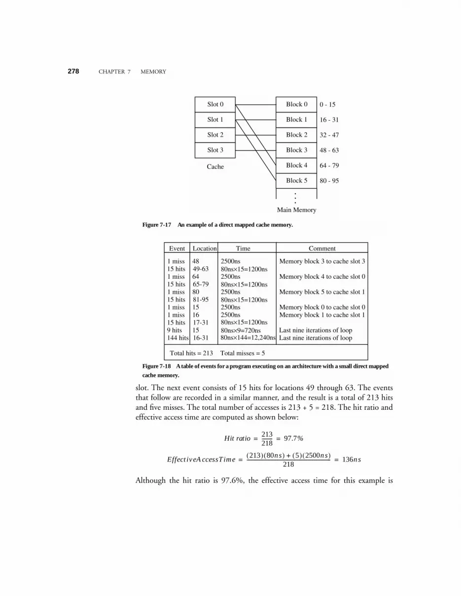
278 CHAPTER 7 MEMORY
slot. The next event consists of 15 hits for locations 49 through 63. The eventsthat follow are recorded in a similar manner, and the result is a total of 213 hitsand five misses. The total number of accesses is 213 + 5 = 218. The hit ratio andeffective access time are computed as shown below:
Although the hit ratio is 97.6%, the effective access time for this example is
Slot 0
Slot 1
Slot 2
Slot 3
Block 0
Block 1
Block 2
Block 3
Block 4
Block 5
0 - 15
Cache
Main Memory
16 - 31
32 - 47
48 - 63
64 - 79
80 - 95
.
.
.
Figure 7-17 An example of a direct mapped cache memory.
Event Location Time Comment
48 2500ns Memory block 3 to cache slot 31 miss49-63 80ns×15=1200ns15 hits64 2500ns Memory block 4 to cache slot 01 miss65-79 80ns×15=1200ns15 hits80 2500ns Memory block 5 to cache slot 11 miss81-95 80ns×15=1200ns15 hits15 2500ns Memory block 0 to cache slot 01 miss16 2500ns Memory block 1 to cache slot 11 miss17-31 80ns×15=1200ns15 hits15 80ns×9=720ns Last nine iterations of loop9 hits16-31 80ns×144=12,240ns Last nine iterations of loop144 hits
Total hits = 213 Total misses = 5
Figure 7-18 A table of events for a program executing on an architecture with a small direct mapped
cache memory.
Hit ratio 213218--------- 97.7%= =
EffectiveAccessTime 213( ) 80ns( ) 5( ) 2500ns( )+218
--------------------------------------------------------------------- 136ns= =
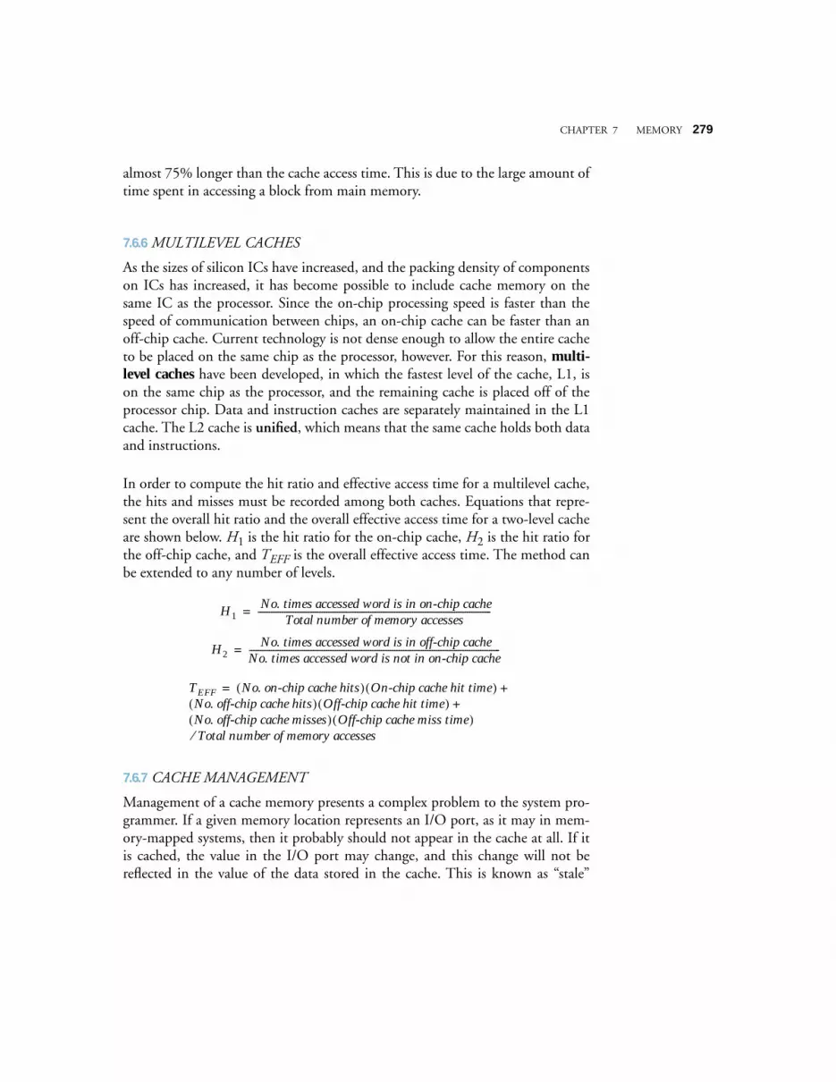
CHAPTER 7 MEMORY 279
almost 75% longer than the cache access time. This is due to the large amount oftime spent in accessing a block from main memory.
7.6.6 MULTILEVEL CACHES
As the sizes of silicon ICs have increased, and the packing density of componentson ICs has increased, it has become possible to include cache memory on thesame IC as the processor. Since the on-chip processing speed is faster than thespeed of communication between chips, an on-chip cache can be faster than anoff-chip cache. Current technology is not dense enough to allow the entire cacheto be placed on the same chip as the processor, however. For this reason, multi-level caches have been developed, in which the fastest level of the cache, L1, ison the same chip as the processor, and the remaining cache is placed off of theprocessor chip. Data and instruction caches are separately maintained in the L1cache. The L2 cache is unified, which means that the same cache holds both dataand instructions.
In order to compute the hit ratio and effective access time for a multilevel cache,the hits and misses must be recorded among both caches. Equations that repre-sent the overall hit ratio and the overall effective access time for a two-level cacheare shown below. H1 is the hit ratio for the on-chip cache, H2 is the hit ratio forthe off-chip cache, and TEFF is the overall effective access time. The method canbe extended to any number of levels.
7.6.7 CACHE MANAGEMENT
Management of a cache memory presents a complex problem to the system pro-grammer. If a given memory location represents an I/O port, as it may in mem-ory-mapped systems, then it probably should not appear in the cache at all. If itis cached, the value in the I/O port may change, and this change will not bereflected in the value of the data stored in the cache. This is known as “stale”
H1 No. times accessed word is in on-chip cache
Total number of memory accesses----------------------------------------------------------------------------------------------------------=
H2 No. times accessed word is in off-chip cache
No. times accessed word is not in on-chip cache------------------------------------------------------------------------------------------------------------------=
TEFF No. on-chip cache hits( ) On-chip cache hit time( )No. off-chip cache hits( ) Off-chip cache hit time( )No. off-chip cache misses( ) Off-chip cache miss time( )
++
Total number of memory accesses⁄
=
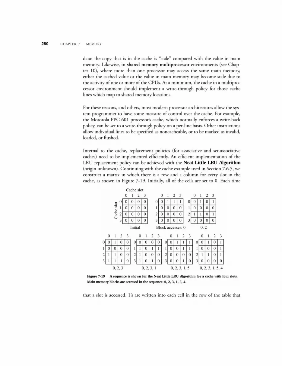
280 CHAPTER 7 MEMORY
data: the copy that is in the cache is “stale” compared with the value in mainmemory. Likewise, in shared-memory multiprocessor environments (see Chap-ter 10), where more than one processor may access the same main memory,either the cached value or the value in main memory may become stale due tothe activity of one or more of the CPUs. At a minimum, the cache in a multipro-cessor environment should implement a write-through policy for those cachelines which map to shared memory locations.
For these reasons, and others, most modern processor architectures allow the sys-tem programmer to have some measure of control over the cache. For example,the Motorola PPC 601 processor’s cache, which normally enforces a write-backpolicy, can be set to a write-through policy on a per-line basis. Other instructionsallow individual lines to be specified as noncacheable, or to be marked as invalid,loaded, or flushed.
Internal to the cache, replacement policies (for associative and set-associativecaches) need to be implemented efficiently. An efficient implementation of theLRU replacement policy can be achieved with the Neat Little LRU Algorithm(origin unknown). Continuing with the cache example used in Section 7.6.5, weconstruct a matrix in which there is a row and a column for every slot in thecache, as shown in Figure 7-19. Initially, all of the cells are set to 0. Each time
that a slot is accessed, 1’s are written into each cell in the row of the table that
0
1
2
3
0 1 2 3
0 0 0 0
0 0 0 0
0 0 0 0
0 0 0 0
Cache slot
Cac
he s
lot
0
1
2
3
0 1 2 3
0 1 0 0
0 0 0 0
1 1 0 0
1 1 1 0
0
1
2
3
0 1 2 3
0 0 0 0
1 0 1 1
1 0 0 0
1 0 1 0
0
1
2
3
0 1 2 3
0 1 1 1
0 0 1 1
0 0 0 0
0 0 1 0
0
1
2
3
0 1 2 3
0 1 0 1
0 0 0 1
1 1 0 1
0 0 0 0
0
1
2
3
0 1 2 3
0 1 1 1
0 0 0 0
0 0 0 0
0 0 0 0
0
1
2
3
0 1 2 3
0 1 0 1
0 0 0 0
1 1 0 1
0 0 0 0
Initial Block accesses: 0 0, 2
0, 2, 3 0, 2, 3, 1 0, 2, 3, 1, 5 0, 2, 3, 1, 5, 4
Figure 7-19 A sequence is shown for the Neat Little LRU Algorithm for a cache with four slots.
Main memory blocks are accessed in the sequence: 0, 2, 3, 1, 5, 4.
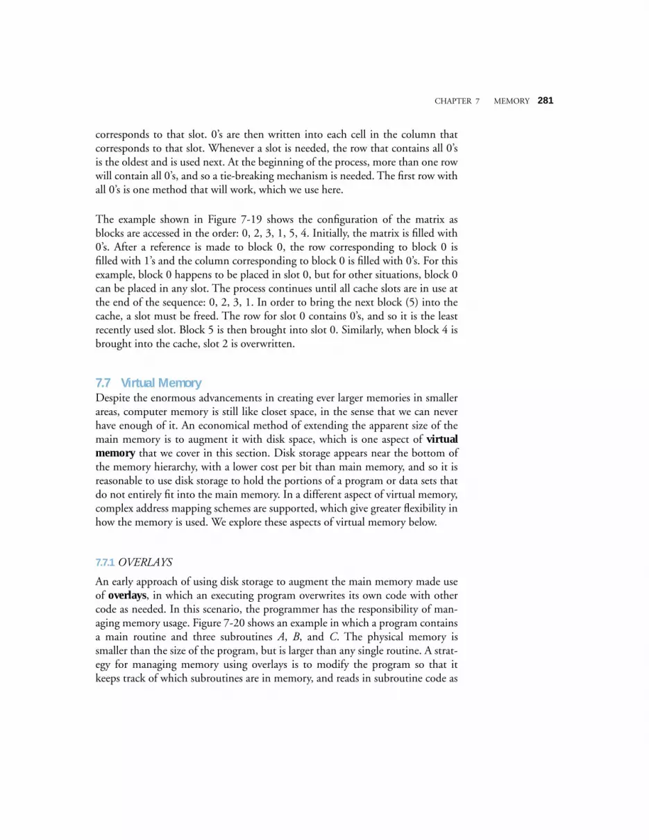
CHAPTER 7 MEMORY 281
corresponds to that slot. 0’s are then written into each cell in the column thatcorresponds to that slot. Whenever a slot is needed, the row that contains all 0’sis the oldest and is used next. At the beginning of the process, more than one rowwill contain all 0’s, and so a tie-breaking mechanism is needed. The first row withall 0’s is one method that will work, which we use here.
The example shown in Figure 7-19 shows the configuration of the matrix asblocks are accessed in the order: 0, 2, 3, 1, 5, 4. Initially, the matrix is filled with0’s. After a reference is made to block 0, the row corresponding to block 0 isfilled with 1’s and the column corresponding to block 0 is filled with 0’s. For thisexample, block 0 happens to be placed in slot 0, but for other situations, block 0can be placed in any slot. The process continues until all cache slots are in use atthe end of the sequence: 0, 2, 3, 1. In order to bring the next block (5) into thecache, a slot must be freed. The row for slot 0 contains 0’s, and so it is the leastrecently used slot. Block 5 is then brought into slot 0. Similarly, when block 4 isbrought into the cache, slot 2 is overwritten.
7.7 Virtual MemoryDespite the enormous advancements in creating ever larger memories in smallerareas, computer memory is still like closet space, in the sense that we can neverhave enough of it. An economical method of extending the apparent size of themain memory is to augment it with disk space, which is one aspect of virtualmemory that we cover in this section. Disk storage appears near the bottom ofthe memory hierarchy, with a lower cost per bit than main memory, and so it isreasonable to use disk storage to hold the portions of a program or data sets thatdo not entirely fit into the main memory. In a different aspect of virtual memory,complex address mapping schemes are supported, which give greater flexibility inhow the memory is used. We explore these aspects of virtual memory below.
7.7.1 OVERLAYS
An early approach of using disk storage to augment the main memory made useof overlays, in which an executing program overwrites its own code with othercode as needed. In this scenario, the programmer has the responsibility of man-aging memory usage. Figure 7-20 shows an example in which a program containsa main routine and three subroutines A, B, and C. The physical memory issmaller than the size of the program, but is larger than any single routine. A strat-egy for managing memory using overlays is to modify the program so that itkeeps track of which subroutines are in memory, and reads in subroutine code as
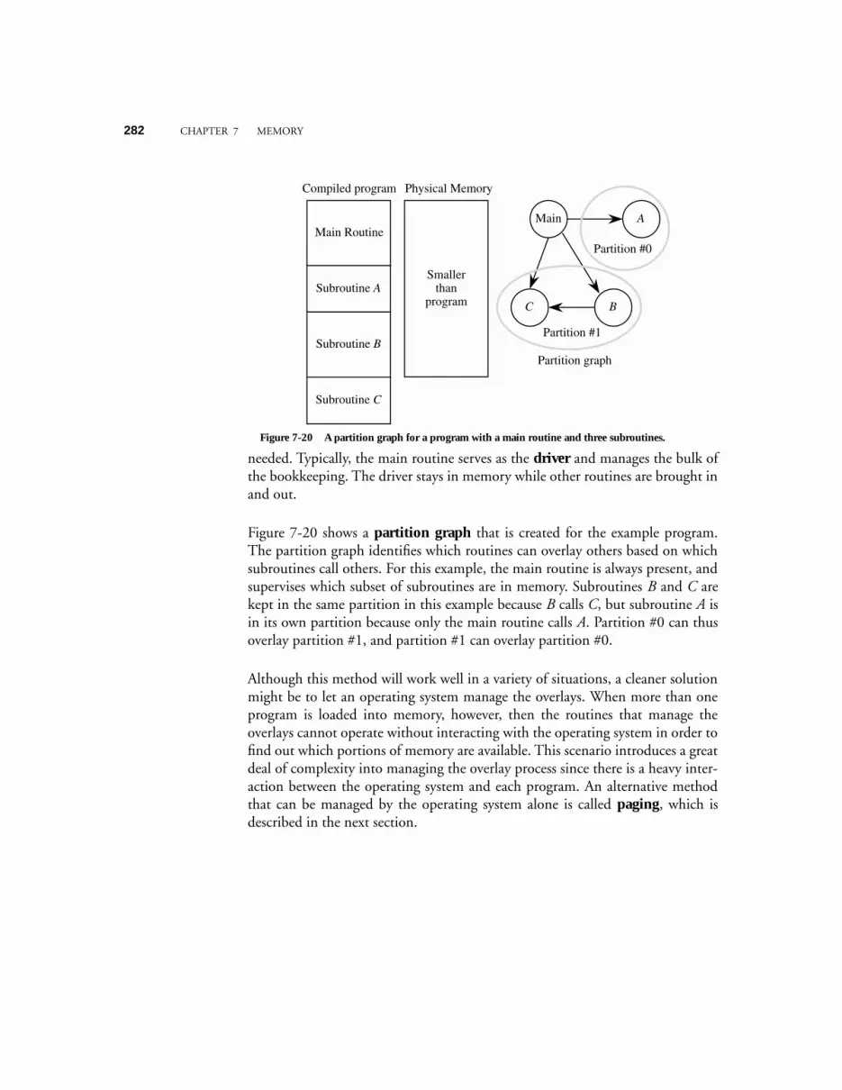
282 CHAPTER 7 MEMORY
needed. Typically, the main routine serves as the driver and manages the bulk ofthe bookkeeping. The driver stays in memory while other routines are brought inand out.
Figure 7-20 shows a partition graph that is created for the example program.The partition graph identifies which routines can overlay others based on whichsubroutines call others. For this example, the main routine is always present, andsupervises which subset of subroutines are in memory. Subroutines B and C arekept in the same partition in this example because B calls C, but subroutine A isin its own partition because only the main routine calls A. Partition #0 can thusoverlay partition #1, and partition #1 can overlay partition #0.
Although this method will work well in a variety of situations, a cleaner solutionmight be to let an operating system manage the overlays. When more than oneprogram is loaded into memory, however, then the routines that manage theoverlays cannot operate without interacting with the operating system in order tofind out which portions of memory are available. This scenario introduces a greatdeal of complexity into managing the overlay process since there is a heavy inter-action between the operating system and each program. An alternative methodthat can be managed by the operating system alone is called paging, which isdescribed in the next section.
Main Routine
Subroutine A
Subroutine B
Subroutine C
Compiled program
Main A
BC
Partition graph
Partition #0
Partition #1
Physical Memory
Smaller than
program
Figure 7-20 A partition graph for a program with a main routine and three subroutines.
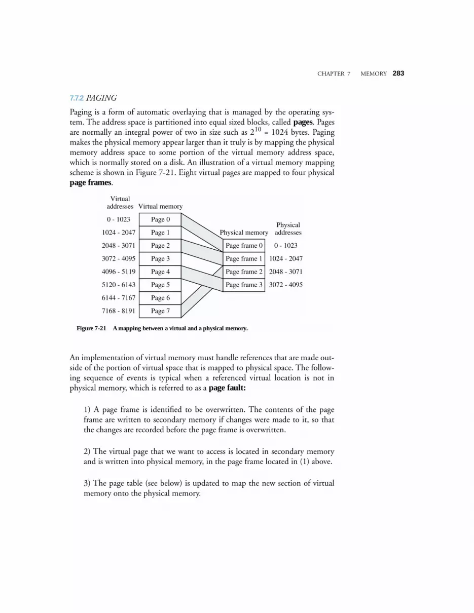
CHAPTER 7 MEMORY 283
7.7.2 PAGING
Paging is a form of automatic overlaying that is managed by the operating sys-tem. The address space is partitioned into equal sized blocks, called pages. Pagesare normally an integral power of two in size such as 210 = 1024 bytes. Pagingmakes the physical memory appear larger than it truly is by mapping the physicalmemory address space to some portion of the virtual memory address space,which is normally stored on a disk. An illustration of a virtual memory mappingscheme is shown in Figure 7-21. Eight virtual pages are mapped to four physicalpage frames.
An implementation of virtual memory must handle references that are made out-side of the portion of virtual space that is mapped to physical space. The follow-ing sequence of events is typical when a referenced virtual location is not inphysical memory, which is referred to as a page fault:
1) A page frame is identified to be overwritten. The contents of the pageframe are written to secondary memory if changes were made to it, so thatthe changes are recorded before the page frame is overwritten.
2) The virtual page that we want to access is located in secondary memoryand is written into physical memory, in the page frame located in (1) above.
3) The page table (see below) is updated to map the new section of virtualmemory onto the physical memory.
Virtual memory
Physical memory
Page frame 0
Page frame 1
Page frame 2
Page frame 3
Page 0
Page 1
Page 2
Page 3
Page 4
Page 5
Page 6
Page 7
Virtual addresses
Physical addresses
0 - 1023
1024 - 2047
2048 - 3071
3072 - 4095
4096 - 5119
5120 - 6143
6144 - 7167
7168 - 8191
0 - 1023
1024 - 2047
2048 - 3071
3072 - 4095
Figure 7-21 A mapping between a virtual and a physical memory.
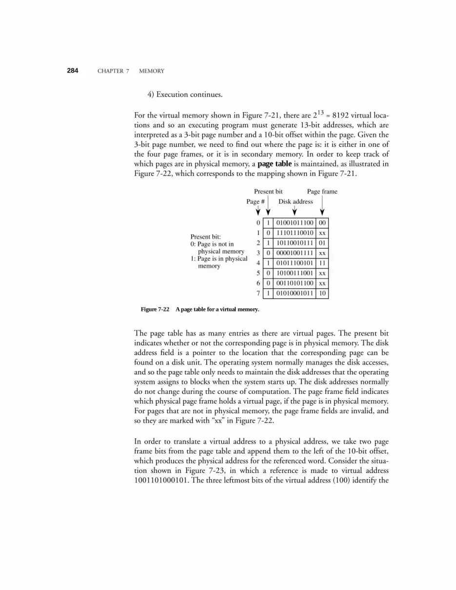
284 CHAPTER 7 MEMORY
4) Execution continues.
For the virtual memory shown in Figure 7-21, there are 213 = 8192 virtual loca-tions and so an executing program must generate 13-bit addresses, which areinterpreted as a 3-bit page number and a 10-bit offset within the page. Given the3-bit page number, we need to find out where the page is: it is either in one ofthe four page frames, or it is in secondary memory. In order to keep track ofwhich pages are in physical memory, a page table is maintained, as illustrated inFigure 7-22, which corresponds to the mapping shown in Figure 7-21.
The page table has as many entries as there are virtual pages. The present bitindicates whether or not the corresponding page is in physical memory. The diskaddress field is a pointer to the location that the corresponding page can befound on a disk unit. The operating system normally manages the disk accesses,and so the page table only needs to maintain the disk addresses that the operatingsystem assigns to blocks when the system starts up. The disk addresses normallydo not change during the course of computation. The page frame field indicateswhich physical page frame holds a virtual page, if the page is in physical memory.For pages that are not in physical memory, the page frame fields are invalid, andso they are marked with “xx” in Figure 7-22.
In order to translate a virtual address to a physical address, we take two pageframe bits from the page table and append them to the left of the 10-bit offset,which produces the physical address for the referenced word. Consider the situa-tion shown in Figure 7-23, in which a reference is made to virtual address1001101000101. The three leftmost bits of the virtual address (100) identify the
Present bit:0: Page is not in
physical memory1: Page is in physical
memory
Present bit
Page #
0
1
2
3
4
5
6
7
1
0
1
0
1
0
0
1
00
xx
01
xx
11
xx
xx
10
Disk address
Page frame
01001011100
11101110010
10110010111
00001001111
01011100101
10100111001
00110101100
01010001011
Figure 7-22 A page table for a virtual memory.
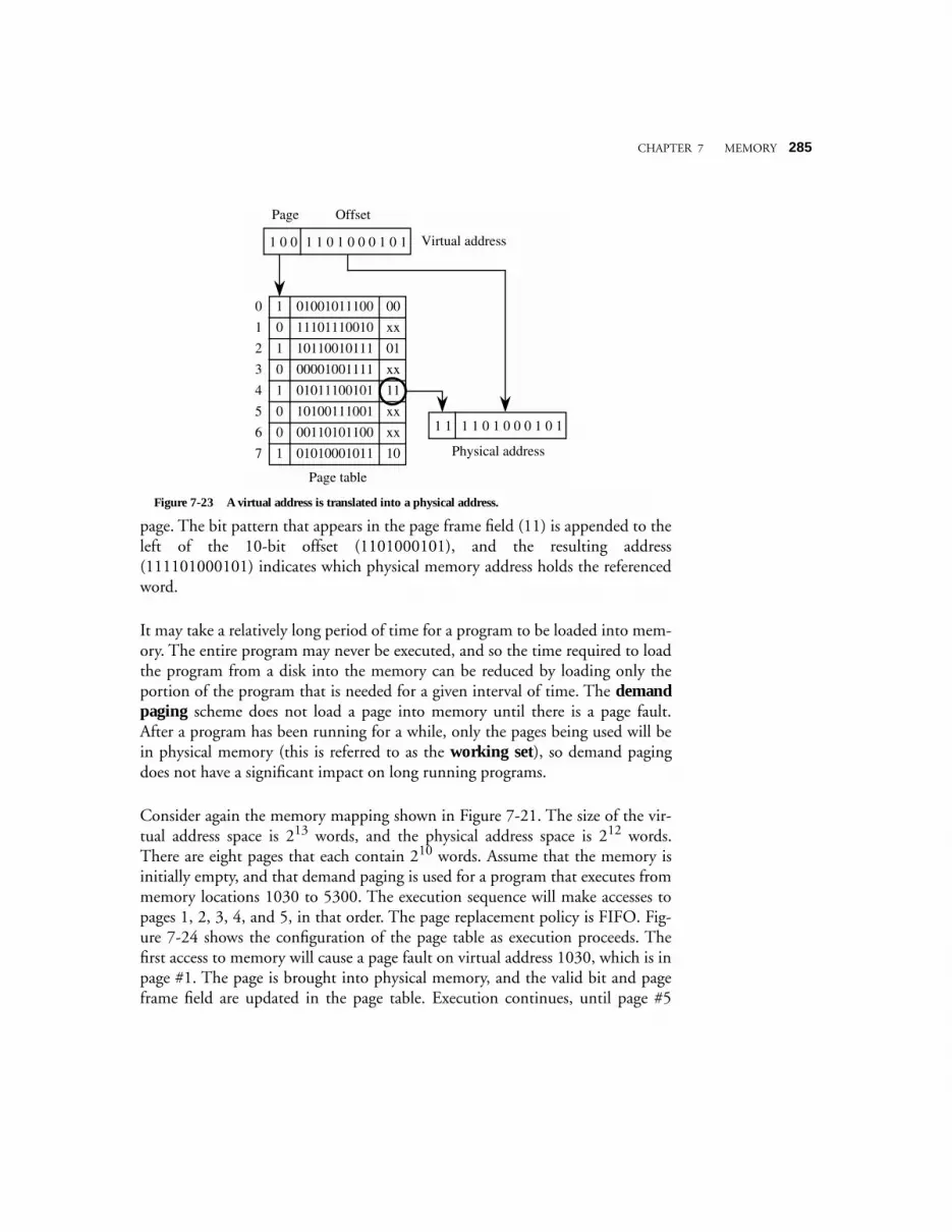
CHAPTER 7 MEMORY 285
page. The bit pattern that appears in the page frame field (11) is appended to theleft of the 10-bit offset (1101000101), and the resulting address(111101000101) indicates which physical memory address holds the referencedword.
It may take a relatively long period of time for a program to be loaded into mem-ory. The entire program may never be executed, and so the time required to loadthe program from a disk into the memory can be reduced by loading only theportion of the program that is needed for a given interval of time. The demandpaging scheme does not load a page into memory until there is a page fault.After a program has been running for a while, only the pages being used will bein physical memory (this is referred to as the working set), so demand pagingdoes not have a significant impact on long running programs.
Consider again the memory mapping shown in Figure 7-21. The size of the vir-tual address space is 213 words, and the physical address space is 212 words.There are eight pages that each contain 210 words. Assume that the memory isinitially empty, and that demand paging is used for a program that executes frommemory locations 1030 to 5300. The execution sequence will make accesses topages 1, 2, 3, 4, and 5, in that order. The page replacement policy is FIFO. Fig-ure 7-24 shows the configuration of the page table as execution proceeds. Thefirst access to memory will cause a page fault on virtual address 1030, which is inpage #1. The page is brought into physical memory, and the valid bit and pageframe field are updated in the page table. Execution continues, until page #5
0
1
2
3
4
5
6
7
1
0
1
0
1
0
0
1
00
xx
01
xx
11
xx
xx
10
01001011100
11101110010
10110010111
00001001111
01011100101
10100111001
00110101100
01010001011
1 0 0 1 1 0 1 0 0 0 1 0 1 Virtual address
Page table
1 1 1 1 0 1 0 0 0 1 0 1
Physical address
Page Offset
Figure 7-23 A virtual address is translated into a physical address.
286 CHAPTER 7 MEMORY
must be brought in, which forces out page #1 due to the FIFO page replacementpolicy. The final configuration of the page table in Figure 7-24 is shown afterlocation 5300 is accessed.
7.7.3 SEGMENTATION
Virtual memory as we have discussed it up to this point is one-dimensional inthe sense that addresses grow either up or down. Segmentation divides theaddress space into segments, which may be of arbitrary size. Each segment is itsown one-dimensional address space. This allows tables, stacks, and other datastructures to be maintained as logical entities that grow without bumping intoeach other. Segmentation allows for protection, so that a segment may be speci-fied as “read only” to prevent changes, or “execute only” to prevent unauthorizedcopying. This also protects users from trying to write data into instruction areas.
When segmentation is used with virtual memory, the size of each segment’saddress space can be very large, and so the physical memory devoted to each seg-ment is not committed until needed.
0
1
2
3
4
5
6
7
0
1
0
0
0
0
0
0
xx
00
xx
xx
xx
xx
xx
xx
01001011100
11101110010
10110010111
00001001111
01011100101
10100111001
00110101100
01010001011
After fault on page #1
0
1
2
3
4
5
6
7
0
1
1
1
0
0
0
0
xx
00
01
10
xx
xx
xx
xx
01001011100
11101110010
10110010111
00001001111
01011100101
10100111001
00110101100
01010001011
0
1
2
3
4
5
6
7
0
1
1
0
0
0
0
0
xx
00
01
xx
xx
xx
xx
xx
01001011100
11101110010
10110010111
00001001111
01011100101
10100111001
00110101100
01010001011
0
1
2
3
4
5
6
7
0
0
1
1
1
1
0
0
xx
xx
01
10
11
00
xx
xx
01001011100
11101110010
10110010111
00001001111
01011100101
10100111001
00110101100
01010001011
Final
After fault on page #2
After fault on page #3
Figure 7-24 The configuration of a page table changes as a program executes. Initially, the page
table is empty. In the final configuration, four pages are in physical memory.

CHAPTER 7 MEMORY 287
Figure 7-25 illustrates a segmented memory. The executable code for a word pro-
cessing program is loaded into Segment #0. This segment is marked as “executeonly” and is thus protected from writing. Segment #1 is used for the data spacefor user #0, and is marked as “read/write” for user #0, so that no other user canhave access to this area. Segment #2 is used for the data space for user #1, and ismarked as “read/write” for user #1. The same word processor can be used by bothuser #0 and user #1, in which case the code in segment #0 is shared, but eachuser has a separate data segment.
Segmentation is not the same thing as paging. With paging, the user does not seethe automatic overlaying. With segmentation, the user is aware of where segmentboundaries are. The operating system manages protection and mapping, and soan ordinary user does not normally need to deal with bookkeeping, but a moresophisticated user such as a computer programmer may see the segmentation fre-quently when array pointers are pushed past segment boundaries in errant pro-grams.
In order to specify an address in a segmented memory, the user’s program mustspecify a segment number and an address within the segment. The operating sys-tem then translates the user’s segmented address to a physical address.
7.7.4 FRAGMENTATION
When a computer is “booted up,” it goes through an initialization sequence thatloads the operating system into memory. A portion of the address space may bereserved for I/O devices, and the remainder of the address space is then availablefor use by the operating system. This remaining portion of the address space may
Address space for code segment of word processor
Data space for user #0
Data space for user #1
Used
Used
Used
Free
Free
Unused
Segment #0Execute only
Segment #1Read/write by
user #0
Segment #2 Read/write by
user #1
Figure 7-25 A segmented memory allows two users to share the same word processor.
288 CHAPTER 7 MEMORY
be only partially filled with physical memory: the rest comprises a “Dead Zone”which must never be accessed since there is no hardware that responds to theDead Zone addresses.
Figure 7-26a shows the state of a memory just after the initialization sequence.
The “Free Area” is a section of memory that is available to the operating systemfor loading and executing programs. During the course of operation, programs ofvarious sizes will be loaded into memory and executed. When a program finishesexecution, the memory space that is assigned to that program is released to theoperating system. As programs are loaded and executed, the Free Area becomessubdivided into a collection of small areas, none of which may be large enough tohold a program that would fit unless some or all of the free areas are combinedinto a single large area. This is a problem known as fragmentation, and isencountered with segmentation, because the segments must ultimately bemapped within a single linear address space.
Figure 7-26b illustrates the fragmentation problem. When the operating systemneeds to find a free area that is large enough to hold a program, it will rarely findan exact match. The free area will generally be larger than the program, whichhas the effect of subdividing the free areas more finely as programs are mis-matched with free areas. One method of assigning programs to free areas is calledfirst fit, in which the free areas are scanned until a large enough area is foundthat will satisfy the program. Another method is called best fit, in which the free
(a) (b) (c)
Operating System
Free Area
I/O Space
Dead Zone
Operating System
I/O Space
Dead Zone
Free Area
Free Area
Free Area
Free Area
Program A
Program B
Program C
Operating System
I/O Space
Dead Zone
Free Area
Free Area
Free Area
Program A
Program B
Program C
Figure 7-26 (a) Free area of memory after initialization; (b) after fragmentation; (c) after coalescing.
CHAPTER 7 MEMORY 289
area is used that wastes the least amount of space. While best fit makes better useof memory than first fit, it requires more time because all of the free areas mustbe scanned.
Regardless of which algorithm is used, the process of assigning programs or datato free areas tends to produce smaller free areas (Knuth, 1974). This makes itmore difficult to find a single contiguous free area that is large enough to satisfythe needs of the operating system. An approach that helps to solve this problemcoalesces adjacent free areas into a single larger free area. In Figure 7-26b, the twoadjacent free areas are combined into a single free area, as illustrated in Figure7-26c.
7.7.5 VIRTUAL MEMORY VS. CACHE MEMORY
Virtual memory is divided into pages, which are relatively large when comparedwith cache memory blocks, which tend to be only a few words in size. Copies ofthe most heavily used blocks are kept in cache memory as well as in main mem-ory, and also in the virtual memory image that is stored on a hard disk. When amemory reference is made on a computer that contains both cache and virtualmemories, the cache hardware sees the reference first and satisfies the reference ifthe word is in the cache. If the referenced word is not in the cache, then theblock that contains the word is read into the cache from the main memory, andthe referenced word is then taken from the cache. If the page that contains theword is not in the main memory, then the page is brought into the main memoryfrom a disk unit, and the block is then loaded into the cache so that the referencecan be satisfied.
The use of virtual memory causes some intricate interactions with the cache. Forexample, since more than one program may be using the cache and the virtualmemory, the timing statistics for two runs of a program executing on the sameset of data may be different. Also, when a dirty block needs to be written back tomain memory, it is possible that the page frame that contains the correspondingvirtual page has been overwritten. This causes the page to be loaded back to mainmemory from secondary memory in order to flush the dirty block from the cachememory to the main memory.
7.7.6 THE TRANSLATION LOOKASIDE BUFFER
The virtual memory mechanism, while being an elegant solution to the problemof accessing large programs and data files, has a significant problem associated
290 CHAPTER 7 MEMORY
with it. At least two memory references are needed to access a value in memory:One reference is to the page table to find the physical page frame, and anotherreference is for the actual data value. The translation lookaside buffer (TLB) isa solution to this problem.
The TLB is a small associative memory typically placed inside of the CPU thatstores the most recent translations from virtual to physical address. The first timea given virtual address is translated into a physical address, this translation isstored in the TLB. Each time the CPU issues a virtual address, the TLB issearched for that virtual address. If the virtual page number exists in the TLB, theTLB returns the physical page number, which can be immediately sent to themain memory (but normally, the cache memory would intercept the reference tomain memory and satisfy the reference out of the cache.)
An example TLB is shown in Figure 7-27. The TLB holds 8 entries, for a system
that has 32 pages and 16 page frames. The virtual page field is 5 bits widebecause there are 25 = 32 pages. Likewise, the physical page field is 4 bits widebecause there are 24=16 page frames.
TLB misses are handled in much the same way as with other memory misses.Upon a TLB miss the virtual address is applied to the virtual memory system,where it is looked up in the page table in main memory. If it is found in the pagetable, then the TLB is updated, and the next reference to that page will thusresult in a TLB hit.
ValidVirtual page
numberPhysical
page number
1
1
0
0
1
0
1
0
0 1 0 0 1 1 1 0 0
1 0 1 1 1 1 0 0 1
- - - - - - - - -
- - - - - - - - -
0 1 1 1 0 0 0 0 0
- - - - - - - - -
0 0 1 1 0 0 1 1 1
- - - - - - - - -
Figure 7-27 An example TLB that holds 8 entries for a system with 32 virtual pages and 16 page
frames.
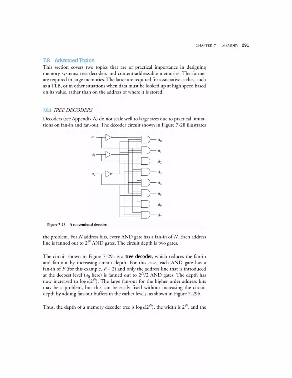
CHAPTER 7 MEMORY 291
7.8 Advanced TopicsThis section covers two topics that are of practical importance in designingmemory systems: tree decoders and content-addressable memories. The formerare required in large memories. The latter are required for associative caches, suchas a TLB, or in other situations when data must be looked up at high speed basedon its value, rather than on the address of where it is stored.
7.8.1 TREE DECODERS
Decoders (see Appendix A) do not scale well to large sizes due to practical limita-tions on fan-in and fan-out. The decoder circuit shown in Figure 7-28 illustrates
the problem. For N address bits, every AND gate has a fan-in of N. Each addressline is fanned out to 2N AND gates. The circuit depth is two gates.
The circuit shown in Figure 7-29a is a tree decoder, which reduces the fan-inand fan-out by increasing circuit depth. For this case, each AND gate has afan-in of F (for this example, F = 2) and only the address line that is introducedat the deepest level (a0 here) is fanned out to 2N/2 AND gates. The depth hasnow increased to logF(2N). The large fan-out for the higher order address bitsmay be a problem, but this can be easily fixed without increasing the circuitdepth by adding fan-out buffers in the earlier levels, as shown in Figure 7-29b.
Thus, the depth of a memory decoder tree is logF(2N), the width is 2N, and the
d0
d1
d2
d3
d4
d5
d6
d7
a0
a1
a2
Figure 7-28 A conventional decoder.
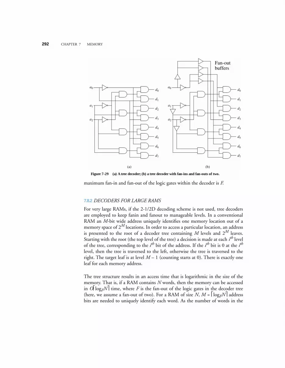
292 CHAPTER 7 MEMORY
maximum fan-in and fan-out of the logic gates within the decoder is F.
7.8.2 DECODERS FOR LARGE RAMS
For very large RAMs, if the 2-1/2D decoding scheme is not used, tree decodersare employed to keep fanin and fanout to manageable levels. In a conventionalRAM an M-bit wide address uniquely identifies one memory location out of amemory space of 2M locations. In order to access a particular location, an addressis presented to the root of a decoder tree containing M levels and 2M leaves.Starting with the root (the top level of the tree) a decision is made at each ith levelof the tree, corresponding to the ith bit of the address. If the ith bit is 0 at the ith
level, then the tree is traversed to the left, otherwise the tree is traversed to theright. The target leaf is at level M – 1 (counting starts at 0). There is exactly oneleaf for each memory address.
The tree structure results in an access time that is logarithmic in the size of thememory. That is, if a RAM contains N words, then the memory can be accessedin OlogFN time, where F is the fan-out of the logic gates in the decoder tree(here, we assume a fan-out of two). For a RAM of size N, M = logFN addressbits are needed to uniquely identify each word. As the number of words in the
a0
a1
d0
d1
d2
d3
d4
d5
d6
d7
a2
(a)
a0
a1
d0
d1
d2
d3
d4
d5
d6
d7
a2
(b)
Fan-out buffers
Figure 7-29 (a) A tree decoder; (b) a tree decoder with fan-ins and fan-outs of two.
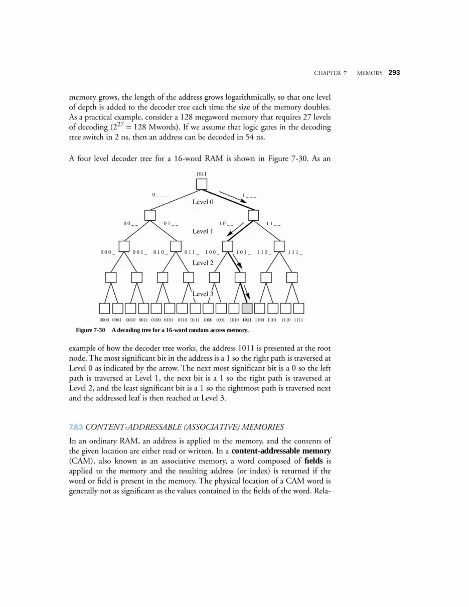
CHAPTER 7 MEMORY 293
memory grows, the length of the address grows logarithmically, so that one levelof depth is added to the decoder tree each time the size of the memory doubles.As a practical example, consider a 128 megaword memory that requires 27 levelsof decoding (227 = 128 Mwords). If we assume that logic gates in the decodingtree switch in 2 ns, then an address can be decoded in 54 ns.
A four level decoder tree for a 16-word RAM is shown in Figure 7-30. As an
example of how the decoder tree works, the address 1011 is presented at the rootnode. The most significant bit in the address is a 1 so the right path is traversed atLevel 0 as indicated by the arrow. The next most significant bit is a 0 so the leftpath is traversed at Level 1, the next bit is a 1 so the right path is traversed atLevel 2, and the least significant bit is a 1 so the rightmost path is traversed nextand the addressed leaf is then reached at Level 3.
7.8.3 CONTENT-ADDRESSABLE (ASSOCIATIVE) MEMORIES
In an ordinary RAM, an address is applied to the memory, and the contents ofthe given location are either read or written. In a content-addressable memory(CAM), also known as an associative memory, a word composed of fields isapplied to the memory and the resulting address (or index) is returned if theword or field is present in the memory. The physical location of a CAM word isgenerally not as significant as the values contained in the fields of the word. Rela-
0000 0001 0010 0011 0100 0101 0110 0111 1000 1001 1010 1011 1100 1101 1110 1111
1011
0 _ _ _ 1 _ _ _
0 0 _ _ 0 1 _ _ 1 0 _ _ 1 1 _ _
0 0 0 _ 0 0 1 _ 0 1 0 _ 0 1 1 _ 1 0 0 _ 1 0 1 _ 1 1 0 _ 1 1 1 _
Level 0
Level 1
Level 2
Level 3
Figure 7-30 A decoding tree for a 16-word random access memory.
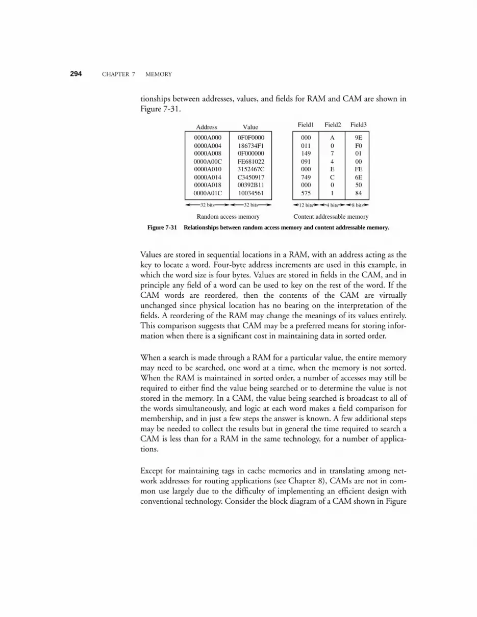
294 CHAPTER 7 MEMORY
tionships between addresses, values, and fields for RAM and CAM are shown inFigure 7-31.
Values are stored in sequential locations in a RAM, with an address acting as thekey to locate a word. Four-byte address increments are used in this example, inwhich the word size is four bytes. Values are stored in fields in the CAM, and inprinciple any field of a word can be used to key on the rest of the word. If theCAM words are reordered, then the contents of the CAM are virtuallyunchanged since physical location has no bearing on the interpretation of thefields. A reordering of the RAM may change the meanings of its values entirely.This comparison suggests that CAM may be a preferred means for storing infor-mation when there is a significant cost in maintaining data in sorted order.
When a search is made through a RAM for a particular value, the entire memorymay need to be searched, one word at a time, when the memory is not sorted.When the RAM is maintained in sorted order, a number of accesses may still berequired to either find the value being searched or to determine the value is notstored in the memory. In a CAM, the value being searched is broadcast to all ofthe words simultaneously, and logic at each word makes a field comparison formembership, and in just a few steps the answer is known. A few additional stepsmay be needed to collect the results but in general the time required to search aCAM is less than for a RAM in the same technology, for a number of applica-tions.
Except for maintaining tags in cache memories and in translating among net-work addresses for routing applications (see Chapter 8), CAMs are not in com-mon use largely due to the difficulty of implementing an efficient design withconventional technology. Consider the block diagram of a CAM shown in Figure
Address Value Field1 Field2 Field3
Random access memory Content addressable memory
0000A000 0F0F0000 000 A 9E186734F10F000000FE6810223152467CC345091700392B1110034561
0000A0040000A0080000A00C0000A0100000A0140000A0180000A01C
011149091000749000575
074EC01
F00100FE6E5084
32 bits 32 bits 12 bits 4 bits 8 bits
Figure 7-31 Relationships between random access memory and content addressable memory.
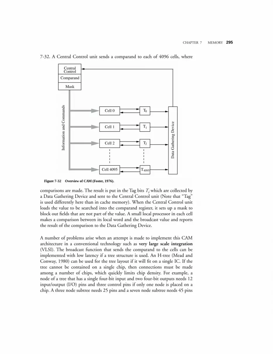
CHAPTER 7 MEMORY 295
7-32. A Central Control unit sends a comparand to each of 4096 cells, where
comparisons are made. The result is put in the Tag bits Ti which are collected bya Data Gathering Device and sent to the Central Control unit (Note that “Tag”is used differently here than in cache memory). When the Central Control unitloads the value to be searched into the comparand register, it sets up a mask toblock out fields that are not part of the value. A small local processor in each cellmakes a comparison between its local word and the broadcast value and reportsthe result of the comparison to the Data Gathering Device.
A number of problems arise when an attempt is made to implement this CAMarchitecture in a conventional technology such as very large scale integration(VLSI). The broadcast function that sends the comparand to the cells can beimplemented with low latency if a tree structure is used. An H-tree (Mead andConway, 1980) can be used for the tree layout if it will fit on a single IC. If thetree cannot be contained on a single chip, then connections must be madeamong a number of chips, which quickly limits chip density. For example, anode of a tree that has a single four-bit input and two four-bit outputs needs 12input/output (I/O) pins and three control pins if only one node is placed on achip. A three node subtree needs 25 pins and a seven node subtree needs 45 pins
Info
rmat
ion
and
Com
man
ds
Dat
a G
athe
ring
Dev
ice
T0
T1
T2
T4095
Cell 0
Cell 1
Cell 2
Cell 4095
CentralControl
Comparand
Mask
Figure 7-32 Overview of CAM (Foster, 1976).
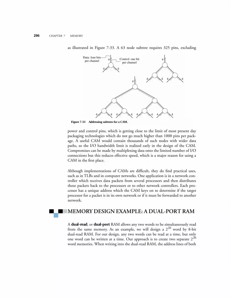
296 CHAPTER 7 MEMORY
as illustrated in Figure 7-33. A 63 node subtree requires 325 pins, excluding
power and control pins, which is getting close to the limit of most present daypackaging technologies which do not go much higher than 1000 pins per pack-age. A useful CAM would contain thousands of such nodes with wider datapaths, so the I/O bandwidth limit is realized early in the design of the CAM.Compromises can be made by multiplexing data onto the limited number of I/Oconnections but this reduces effective speed, which is a major reason for using aCAM in the first place.
Although implementations of CAMs are difficult, they do find practical uses,such as in TLBs and in computer networks. One application is in a network con-troller which receives data packets from several processors and then distributesthose packets back to the processors or to other network controllers. Each pro-cessor has a unique address which the CAM keys on to determine if the targetprocessor for a packet is in its own network or if it must be forwarded to anothernetwork.
MEMORY DESIGN EXAMPLE: A DUAL-PORT RAM
A dual-read, or dual-port RAM allows any two words to be simultaneously readfrom the same memory. As an example, we will design a 220 word by 8-bitdual-read RAM. For our design, any two words can be read at a time, but onlyone word can be written at a time. Our approach is to create two separate 220
word memories. When writing into the dual-read RAM, the address lines of both
4
44 44
44 44 44 44
4
4
4
4
Control: one bitper channel
Data: four bitsper channel
Figure 7-33 Addressing subtrees for a CAM.
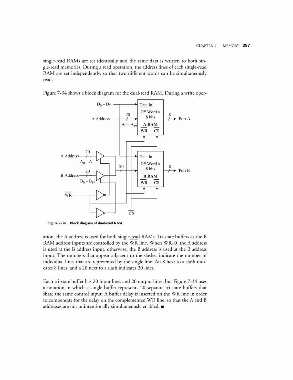
CHAPTER 7 MEMORY 297
single-read RAMs are set identically and the same data is written to both sin-gle-read memories. During a read operation, the address lines of each single-readRAM are set independently, so that two different words can be simultaneouslyread.
Figure 7-34 shows a block diagram for the dual-read RAM. During a write oper-
ation, the A address is used for both single-read RAMs. Tri-state buffers at the BRAM address inputs are controlled by the WR line. When WR=0, the A addressis used at the B address input, otherwise, the B address is used at the B addressinput. The numbers that appear adjacent to the slashes indicate the number ofindividual lines that are represented by the single line. An 8 next to a slash indi-cates 8 lines, and a 20 next to a slash indicates 20 lines.
Each tri-state buffer has 20 input lines and 20 output lines, but Figure 7-34 usesa notation in which a single buffer represents 20 separate tri-state buffers thatshare the same control input. A buffer delay is inserted on the WR line in orderto compensate for the delay on the complemented WR line, so that the A and Baddresses are not unintentionally simultaneously enabled.
Data In
220 Word × 8 bits
A RAM
WR CS
D0 – D7
A0 – A19
20A Address
8Port A
Data In
220 Word × 8 bits
B RAM
WR CS
8Port B
A0 – A19
20A Address
B0 – B19
20B Address
20
WR
CS
Figure 7-34 Block diagram of dual-read RAM.
298 CHAPTER 7 MEMORY
7.9 Case Study: Rambus MemoryThere was a time when computer technology would be pushed from the labora-tory into the marketplace. As the consumer marketplace for computing devicesexploded, the “technology push” was replaced by “market pull,” and consumerdemand then dominated the preferences of technologists when it came to devel-oping a new memory technology. High performance, expensive memory forhigh-end processors was displaced by high density, low-cost memory for con-sumer electronics, such as videogames. It became more profitable for memorymanufacturers to address the needs of high volume consumer markets, ratherthan devote costly chip fabrication facilities to a comparatively small high-endmarket.
The consumer electronics industry now dominates the memory market, andeven high-end, non-consumer processors make heavy use of consumer electron-ics technology, exploiting architectural enhancements instead, or innovations insupporting technologies (such as high speed interconnects) to compensate for theperformance shortcomings of what we might call “videogame memory.”
Videogame memory is not all that low-end, however, and in fact, makes use ofextraordinary technology enhancements that squeeze the most performance outof ever denser, low-cost devices. A leading memory technology that is beingintroduced into Intel-based personal computers in 1999 was developed by Ram-bus, Inc. The Rambus DRAM (RDRAM) retrieves a block of 8 bytes internal tothe DRAM chip on every access, and multiplexes the 8 bytes onto a narrow 8-bitor 16-bit channel, operating at a rate of 800 MHz (or higher).
A typical DRAM core (that is, the storage portion of an ordinary DRAM) canstore or retrieve a line of 8 bytes with a 100 MHz cycle. This is internal to theDRAM chip: most DRAMs only deliver one byte per cycle, but the RDRAMtechnology can multiplex that up to 1 byte per cycle using a higher external clockof 800 MHz. That higher rate is fed to a memory controller (the “chipset” on anIntel machine) which demuxes it to a 32-bit wide data stream at a lower rate,such as 200 MHz, going into a Pentium (or other processor chip).
The Rambus “RIMM” modules (Rambus Inline Memory Modules) look similarto ordinary SIMMs and DIMMs, but they operate differently. The Rambusmemory uses microstrip technology (also known as transmission lines) on themotherboard, which implements a crude shield that reduces radio frequency(RF) effects that interfere with data traveling through wires on the motherboard,which are called board traces. In designing a printed circuit board (PCB) for

CHAPTER 7 MEMORY 299
Rambus technology, the critical parameters are (1) dielectric thickness of thePCB, (2) separation of the memory modules, and (3) trace width. There must bea ground plane (an electrical return path) beneath every signal line, with no vias(connections between board layers) along the path. All signals go on the toplayer of the PCB. (A PCB can have a number of layers, typically no more than 8).The memory controller and memory modules must all be equally spaced, such as.5 inches from the memory controller to the first RIMM, then .5 in to the next,etc.
The “Rambus Channel” is made up of transmission line traces. The trace widthsend up being about twice as wide as ordinary traces, on the order of 12 mils (300microns). Although 300 microns is relatively small for a board trace, if we wantto send 128 signals over a PCB, using a 600 micron pitch (center-to-center spac-ing) with 300 microns between 300 micron traces, this corresponds to a foot-print of 128 × 600 microns = 76 mm. This is a large footprint compared withlower speed solutions that allow a much closer packing density.
In reality, the Rambus Channel only has 13 high speed signals, (the address isserialized onto a single line, there are 8 data lines, 1 parity line, 2 clock lines, and1 command line) and so the seemingly large footprint is not a near-term prob-lem. With a 16-bit version of the Rambus Channel on the horizon, the band-width problem appears to be in hand for a number of years using this technology.Extensibility to large word widths such as 64 bits or 128 bits will pose a signifi-cant challenge down the road, however, because the chipset will need to supportthat same word width – a formidable task with current packaging methods, thatalready have over 500 pins on the chipset.
Although Rambus memory of this type became available in 1998, the RIMMmodules were not widely available until 1999, timed for the availability of a newmemory controller (chipset) for the RIMMs. The memory controller is animportant aspect of this type of memory because the view of memory that theCPU perceives is different from the physical memory.
Rambus memory is more expensive than conventional DRAM memory, butoverall system cost can be reduced, which makes it attractive in low-cost, highperformance consumer electronics such as the Nintendo 64 video game console.The Nintendo 64 (see Figure 7-35) has four primary chips: a 64-bit MIPSRS4300i CPU; a Reality coprocessor which integrates all graphics, audio andmemory management functions; and two Rambus memory chips.

300 CHAPTER 7 MEMORY
The Rambus technology provides the Nintendo 64 with a bandwidth of 562.5MB/s using a 31-pin interface to the memory controller. By comparison, a sys-tem using typical 64-bit-wide synchronous DRAMs (SDRAMs) requires a110-pin interface to the memory controller. This reduction in pin count allowsthe memory controller to fit on the same die (the silicon chip) as the graphicsand sound functions, in a relatively low-cost, 160-pin packaged chip.
The Rambus memory subsystem is made up of two memory chips which occupy1.5 square inches of board space. An equivalent SDRAM design would require 6square inches of board space. The space savings of using the Rambus approachenabled Nintendo to fit all of its components on a board measuring five by sixinches, which is one quarter the size of the system board used in the competingSega Saturn. In addition, Nintendo was able to use only a two-layer boardinstead of the four layers used in the Sega Saturn.
The cost savings Nintendo realized by choosing the Rambus solution over the64-bit SDRAM approach are considerable, but should be placed in perspectivewith the overall market. The ability to use a two-layer implementation savedNintendo $5 per unit in manufacturing costs. Taken altogether, Nintendo esti-
Figure 7-35 Rambus technology on the Nintendo 64 motherboard (top left and bottom right) en-
ables cost savings over the conventional Sega Saturn motherboard design (bottom left). The Ninten-
do 64 uses costlier plug-in cartridges (top right), as opposed to inexpensive CD-ROMs used by the
Sega Saturn. [Photo source: Rambus, Inc.]
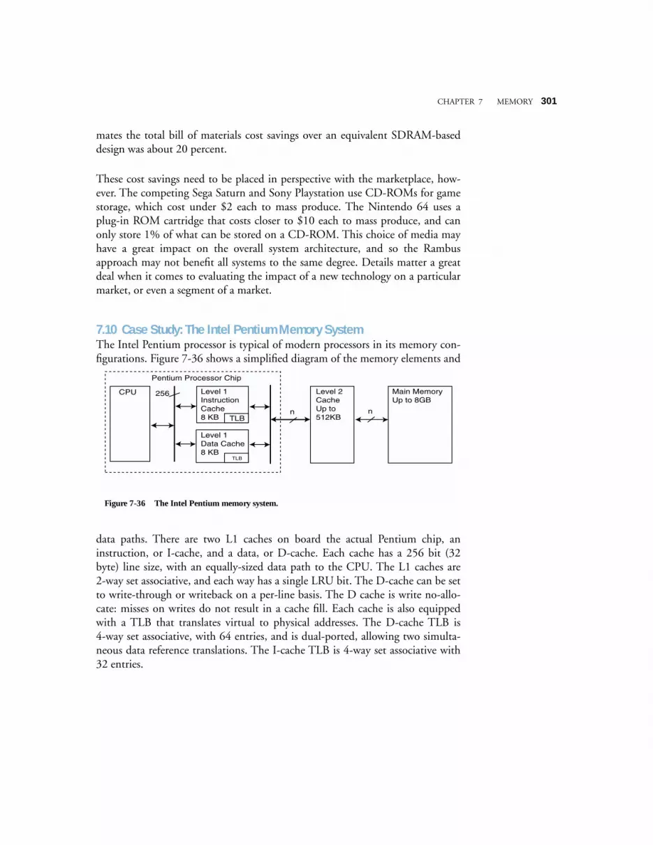
CHAPTER 7 MEMORY 301
mates the total bill of materials cost savings over an equivalent SDRAM-baseddesign was about 20 percent.
These cost savings need to be placed in perspective with the marketplace, how-ever. The competing Sega Saturn and Sony Playstation use CD-ROMs for gamestorage, which cost under $2 each to mass produce. The Nintendo 64 uses aplug-in ROM cartridge that costs closer to $10 each to mass produce, and canonly store 1% of what can be stored on a CD-ROM. This choice of media mayhave a great impact on the overall system architecture, and so the Rambusapproach may not benefit all systems to the same degree. Details matter a greatdeal when it comes to evaluating the impact of a new technology on a particularmarket, or even a segment of a market.
7.10 Case Study: The Intel Pentium Memory SystemThe Intel Pentium processor is typical of modern processors in its memory con-figurations. Figure 7-36 shows a simplified diagram of the memory elements and
data paths. There are two L1 caches on board the actual Pentium chip, aninstruction, or I-cache, and a data, or D-cache. Each cache has a 256 bit (32byte) line size, with an equally-sized data path to the CPU. The L1 caches are2-way set associative, and each way has a single LRU bit. The D-cache can be setto write-through or writeback on a per-line basis. The D cache is write no-allo-cate: misses on writes do not result in a cache fill. Each cache is also equippedwith a TLB that translates virtual to physical addresses. The D-cache TLB is4-way set associative, with 64 entries, and is dual-ported, allowing two simulta-neous data reference translations. The I-cache TLB is 4-way set associative with32 entries.
CPU Level 1InstructionCache8 KB
Level 1Data Cache8 KB
Level 2CacheUp to 512KB
Main MemoryUp to 8GB
256
Pentium Processor Chip
n nTLB
TLB
Figure 7-36 The Intel Pentium memory system.
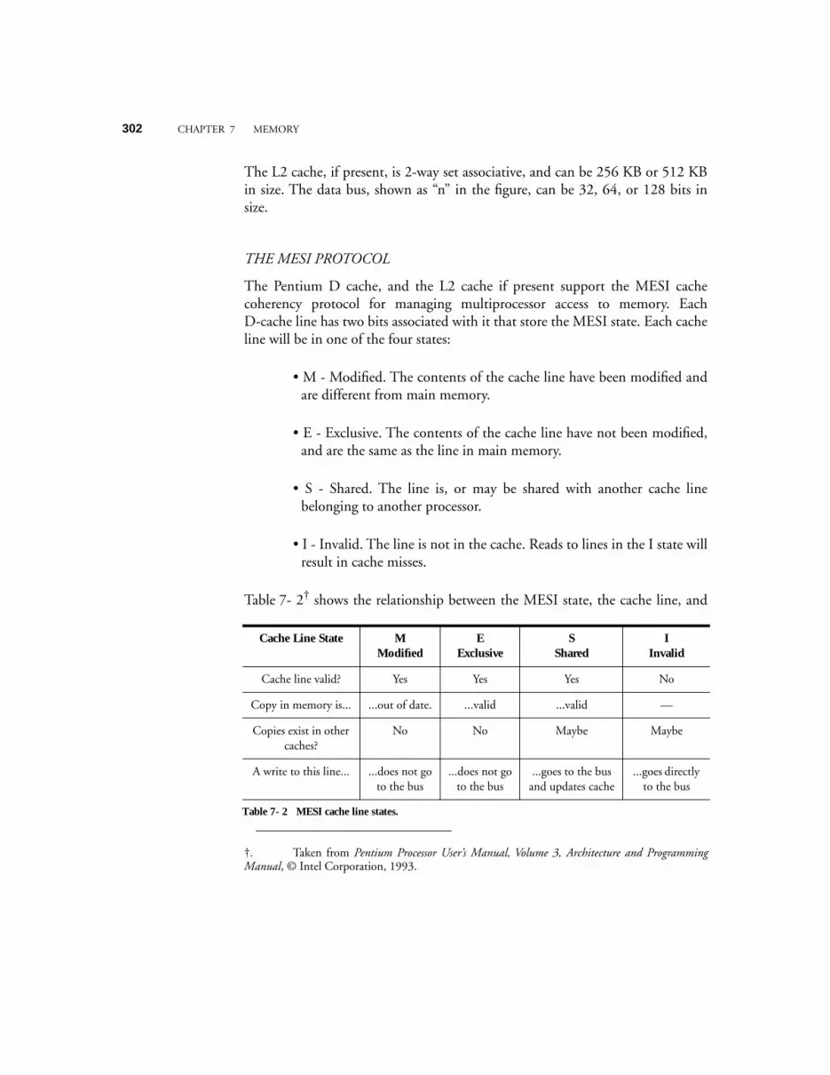
302 CHAPTER 7 MEMORY
The L2 cache, if present, is 2-way set associative, and can be 256 KB or 512 KBin size. The data bus, shown as “n” in the figure, can be 32, 64, or 128 bits insize.
THE MESI PROTOCOL
The Pentium D cache, and the L2 cache if present support the MESI cachecoherency protocol for managing multiprocessor access to memory. EachD-cache line has two bits associated with it that store the MESI state. Each cacheline will be in one of the four states:
• M - Modified. The contents of the cache line have been modified andare different from main memory.
• E - Exclusive. The contents of the cache line have not been modified,and are the same as the line in main memory.
• S - Shared. The line is, or may be shared with another cache linebelonging to another processor.
• I - Invalid. The line is not in the cache. Reads to lines in the I state willresult in cache misses.
Table 7- 2† shows the relationship between the MESI state, the cache line, and
Cache Line State MModified
EExclusive
SShared
IInvalid
Cache line valid? Yes Yes Yes No
Copy in memory is... ...out of date. ...valid ...valid —
Copies exist in other caches?
No No Maybe Maybe
A write to this line... ...does not goto the bus
...does not goto the bus
...goes to the busand updates cache
...goes directly to the bus
Table 7- 2 MESI cache line states.
†. Taken from Pentium Processor User’s Manual, Volume 3, Architecture and ProgrammingManual, © Intel Corporation, 1993.
CHAPTER 7 MEMORY 303
the equivalent line in main memory. The MESI protocol is becoming a standardway of dealing with cache coherency in multiprocessor systems.
The Pentium processor also supports up to six main memory segments (there canbe several thousand segments, but no more than 6 can be referenced through thesegment registers.) As discussed in the chapter, each segment is a separate addressspace. Each segment has a base—a starting location within the 32-bit physicaladdress space, and a limit, the maximum size of the segment. The limit may beeither 216 bytes or 216 × 212 bytes in size. That is, the granularity of the limitmay be one byte or 212 bytes in size.
Paging and segmentation on the Pentium can be applied in any combination:
Unsegmented, unpaged memory: The virtual address space is the same as the phys-ical address space. No page tables or mapping hardware is needed. This is goodfor high performance applications that do not have a lot of complexity, that donot need to support growing tables, for example.
Unsegmented, paged memory: Same as for the unsegmented, unpaged memoryabove, except that the linear address space is larger as a result of using disk stor-age. A page table is needed to translate between virtual and physical addresses. Atranslation lookaside buffer is needed on the Pentium core, working in conjunc-tion with the L1 cache, to reduce the number of page table accesses.
Segmented, unpaged memory: Good for high complexity applications that need tosupport growing data structures. This is also fast: segments are fewer in numberthan pages in a virtual memory, and all of the segmentation mapping hardwaretypically fits on the CPU chip. There is no need for disk accesses as there wouldbe for paging, and so access times are more predictable than when paging is used.
Segmented, paged memory: A page table, segment mapping registers, and TLB allwork in conjunction to support multiple address spaces.
Segmentation on the Intel Pentium processor is quite powerful but is also quitecomplex. We only explore the basics here, and the interested reader is referred to(Intel, 1993) for a more complete description.

304 CHAPTER 7 MEMORY
SUMMARY
Memory is organized in a hierarchy in which the densest memory offers the leastperformance, whereas the greatest performance is realized with the memory thathas the least density. In order to bridge the gap between the two, the principle oflocality is exploited in cache and virtual memories.
A cache memory maintains the most frequently used blocks in a small, fast mem-ory that is local to the CPU. A paged virtual memory augments a main memorywith disk storage. The physical memory serves as a window on the paged virtualmemory, which is maintained in its entirety on a hard magnetic disk.
Cache and paged virtual memories are commonly used on the same computer, butfor different reasons. A cache memory improves the average access time to the mainmemory, whereas a paged virtual memory extends the size of the main memory.
In an example memory architecture, the Intel Pentium has a split L1 cache and aTLB that reside on the Pentium core, and a unified L2 cache that resides in thesame package as the Pentium although on a different silicon die. When paging isimplemented, the page table is located in main memory, with the TLB reducingthe number of times that the TLB is referenced. The L1 and L2 cache memoriesthen reduce the number of times main memory is accessed for data. The Pentiumalso supports segmentation, which has its own set of mapping registers and controlhardware that resides on the Pentium.
FURTHER READING(Stallings, 1993) and (Mano, 1991) give readable explanations of RAM. A num-ber of memory databooks (Micron, 1992) and (Texas Instruments, 1991) givepractical examples of memory organization. (Foster, 1976) is the seminal refer-ence on CAM. (Mead and Conway, 1980) describe the H-tree structure in thecontext of VLSI design. (Franklin et al, 1982) explores issues in partitioningchips, which arise in splitting an H-tree for a CAM. (Sedra and Smith, 1997)discuss the implementation of several kinds of static and dynamic RAM.
(Hamacher et al, 1990) gives a classic treatment of cache memory. (Tanenbaum,1990) gives a readable explanation of virtual memory. (Hennessy and Patterson,1995) and (Przybylski, 1990) cover issues relating to cache performance. Seg-mentation on the Intel Pentium processor is covered in (Intel, 1993). Kingston
CHAPTER 7 MEMORY 305
Technology gives a broad tutorial on memory technologies at http://www.king-ston.com/king/mg0.htm.
Foster, C. C., Content Addressable Parallel Processors, Van Nostrand ReinholdCompany, (1976).
Franklin, M. A., D. F. Wann, and W. J. Thomas, “Pin Limitations and Partition-ing of VLSI Interconnection Networks,” IEEE Trans Comp., C-31, 1109, (Nov.1982).
Hamacher, V. C., Z. G. Vranesic, and S. G. Zaky, Computer Organization, 3/e,McGraw Hill, (1990).
Hennessy, J. L. and D. A. Patterson, Computer Architecture: A QuantitativeApproach, 2/e, Morgan Kaufmann Publishers, San Mateo, California, (1995).
Intel Corporation, Pentium Processor User’s Manual, Volume 3: Architecture andProgramming Manual, (1993).
Knuth, D., The Art of Computer Programming: Fundamental Algorithms, vol. 1,2/e, Addison-Wesley, (1974).
Mano, M., Digital Design, 2/e, Prentice Hall, (1991).
Mead, C. and L. Conway, Introduction to VLSI Systems, Addison Wesley, (1980).
Micron, DRAM Data Book, Micron Technologies, Inc., 2805 East ColumbiaRoad, Boise, Idaho, (1992).
Przybylski, S. A., Cache and Memory Hierarchy Design, Morgan Kaufmann Pub-lishers, (1990).
Sedra, A., and Smith, K., Microelectronic Circuits, 4/e, Oxford University Press,New York, (1997).
Stallings, W., Computer Organization and Architecture, 3/e, MacMillan Publish-ing, New York, (1993).
Tanenbaum, A., Structured Computer Organization, 3/e, Prentice Hall, Engle-
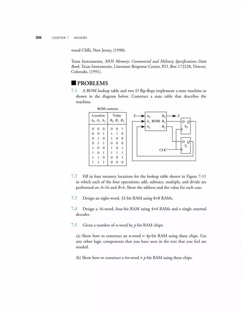
306 CHAPTER 7 MEMORY
wood Cliffs, New Jersey, (1990).
Texas Instruments, MOS Memory: Commercial and Military Specifications DataBook, Texas Instruments, Literature Response Center, P.O. Box 172228, Denver,Colorado, (1991).
PROBLEMS7.1 A ROM lookup table and two D flip-flops implement a state machine as
shown in the diagram below. Construct a state table that describes themachine.
7.2 Fill in four memory locations for the lookup table shown in Figure 7-11in which each of the four operations: add, subtract, multiply, and divide areperformed on A=16 and B=4. Show the address and the value for each case.
7.3 Design an eight-word, 32-bit RAM using 8×8 RAMs.
7.4 Design a 16-word, four-bit RAM using 4×4 RAMs and a single externaldecoder.
7.5 Given a number of n-word by p-bit RAM chips:
(a) Show how to construct an n-word × 4p-bit RAM using these chips. Useany other logic components that you have seen in the text that you feel areneeded.
(b) Show how to construct a 4n-word × p-bit RAM using these chips.
00110011
01010101
A2
00001111
A1A0
01000100
10001110
R2
01101100
R1R0
Location Value
ROM contents
ROM
A0
A1
A2
X ZR0
R1
R2
QDS0
QDS1
CLK
CHAPTER 7 MEMORY 307
7.6 Draw the circuit for a 4-to-16 tree decoder, using a maximum fan-in andfan-out of two.
7.7 A direct mapped cache consists of 128 slots. Main memory contains 16Kblocks of 16 words each. Access time of the cache is 10 ns, and the timerequired to fill a cache slot is 200 ns. Load-through is not used; that is, whenan accessed word is not found in the cache, the entire block is brought intothe cache, and the word is then accessed through the cache. Initially, the cacheis empty. Note: When referring to memory, 1K = 1024.
(a) Show the format of the memory address.
(b) Compute the hit ratio for a program that loops 10 times from locations 15– 200. Note that although the memory is accessed twice during a miss (oncefor the miss, and once again to satisfy the reference), a hit does not occur forthis case. To a running program, only a single memory reference is observed.
(c) Compute the effective access time for this program.
7.8 A fully associative mapped cache has 16 blocks, with eight words perblock. The size of main memory is 216 words, and the cache is initially empty.Access time of the cache is 40 ns, and the time required to transfer eight wordsbetween main memory and the cache is 1 µs.
(a) Compute the sizes of the tag and word fields.
(b) Compute the hit ratio for a program that executes from 20–45, then loopsfour times from 28–45 before halting. Assume that when there is a miss, thatthe entire cache slot is filled in 1 µs, and that the first word is not seen by theCPU until the entire slot is filled. That is, assume load-through is not used.Initially, the cache is empty.
(c) Compute the effective access time for the program described in part (b)above.
7.9 Compute the total number of bits of storage needed for the associativemapped cache shown in Figure 7-13 and the direct mapped cache shown inFigure 7-14. Include Valid, Dirty, and Tag bits in your count. Assume that theword size is eight bits.
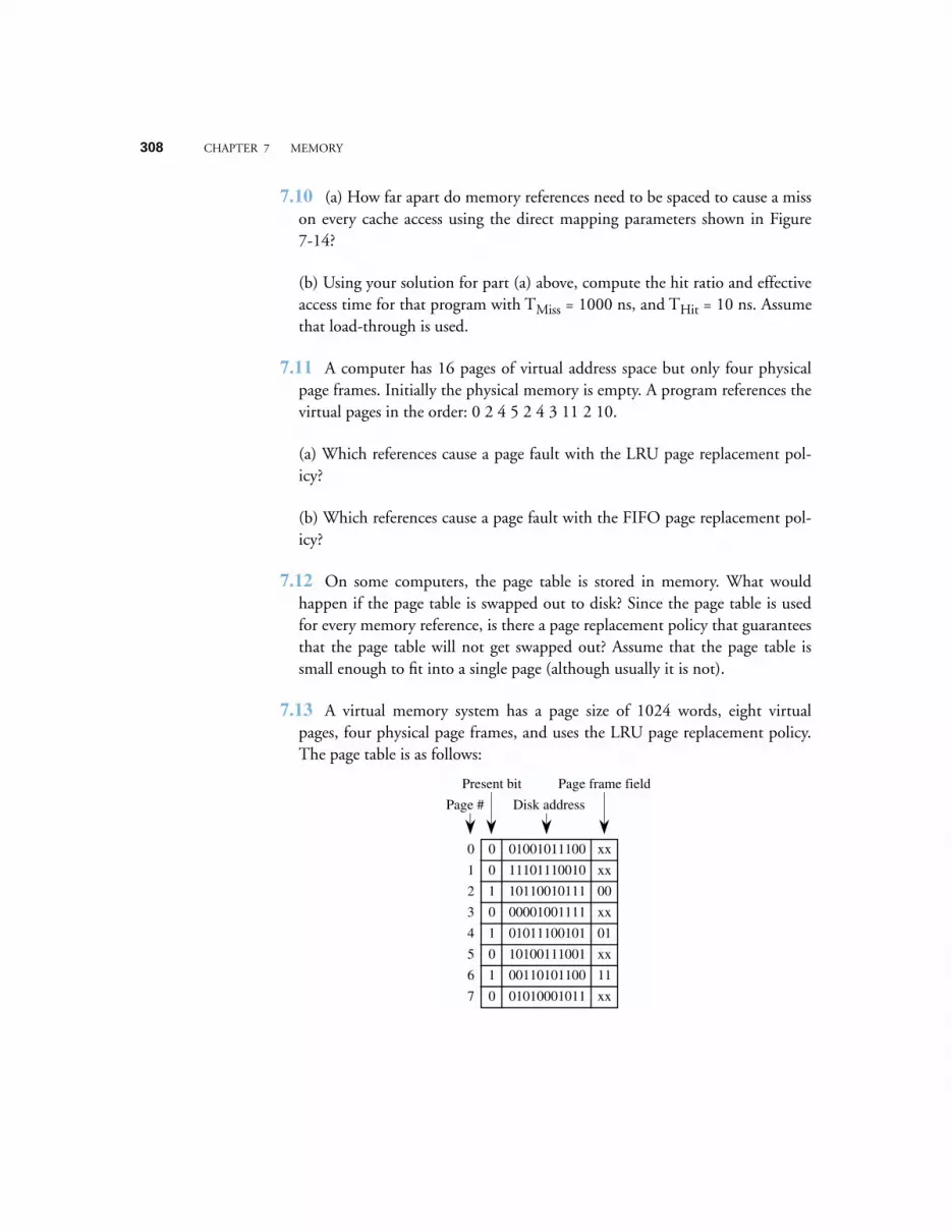
308 CHAPTER 7 MEMORY
7.10 (a) How far apart do memory references need to be spaced to cause a misson every cache access using the direct mapping parameters shown in Figure7-14?
(b) Using your solution for part (a) above, compute the hit ratio and effectiveaccess time for that program with TMiss = 1000 ns, and THit = 10 ns. Assumethat load-through is used.
7.11 A computer has 16 pages of virtual address space but only four physicalpage frames. Initially the physical memory is empty. A program references thevirtual pages in the order: 0 2 4 5 2 4 3 11 2 10.
(a) Which references cause a page fault with the LRU page replacement pol-icy?
(b) Which references cause a page fault with the FIFO page replacement pol-icy?
7.12 On some computers, the page table is stored in memory. What wouldhappen if the page table is swapped out to disk? Since the page table is usedfor every memory reference, is there a page replacement policy that guaranteesthat the page table will not get swapped out? Assume that the page table issmall enough to fit into a single page (although usually it is not).
7.13 A virtual memory system has a page size of 1024 words, eight virtualpages, four physical page frames, and uses the LRU page replacement policy.The page table is as follows:
Present bit
Page #
0
1
2
3
4
5
6
7
0
0
1
0
1
0
1
0
xx
xx
00
xx
01
xx
11
xx
Disk address
Page frame field
01001011100
11101110010
10110010111
00001001111
01011100101
10100111001
00110101100
01010001011
CHAPTER 7 MEMORY 309
(a) What is the main memory address for virtual address 4096?
(b) What is the main memory address for virtual address 1024?
(c) A fault occurs on page 0. Which page frame will be used for virtual page 0?
7.14 When running a particular program with N memory accesses, a computerwith a cache and paged virtual memory generates a total of M cache missesand F page faults. T1 is the time for a cache hit; T2 is the time for a mainmemory hit; and T3 is the time to load a page into main memory from thedisk.
(a) What is the cache hit ratio?
(b) What is the main memory hit ratio? That is, what percentage of mainmemory accesses do not generate a page fault?
(c) What is the overall effective access time for the system?
7.15 A computer contains both cache and paged virtual memories. The cachecan hold either physical or virtual addresses, but not both. What are the issuesinvolved in choosing between caching virtual or physical addresses? How canthese problems be solved by using a single unit that manages all memory map-ping functions?
7.16 How much storage is needed for the page table for a virtual memory thathas 232 bytes, with 212 bytes per page, and 8 bytes per page table entry?
7.17 Compute the gate input count for the decoder(s) of a 64 × 1-bit RAM forboth the 2D and the 2-1/2D cases. Assume that an unlimited fan-in/fan-outis allowed. For both cases, use ordinary two-level decoders. For the 2 1/2Dcase, treat the column decoder as an ordinary MUX. That is, ignore its behav-ior as a DEMUX during a write operation.
7.18 How many levels of decoding are needed for a 220 word 2D memory if afan-in of four and a fan-out of four are used in the decoder tree?
7.19 A video game cartridge needs to store 220 bytes in a ROM.
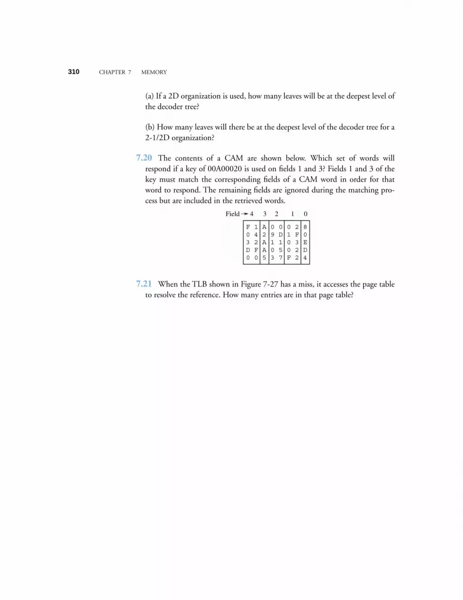
310 CHAPTER 7 MEMORY
(a) If a 2D organization is used, how many leaves will be at the deepest level ofthe decoder tree?
(b) How many leaves will there be at the deepest level of the decoder tree for a2-1/2D organization?
7.20 The contents of a CAM are shown below. Which set of words willrespond if a key of 00A00020 is used on fields 1 and 3? Fields 1 and 3 of thekey must match the corresponding fields of a CAM word in order for thatword to respond. The remaining fields are ignored during the matching pro-cess but are included in the retrieved words.
7.21 When the TLB shown in Figure 7-27 has a miss, it accesses the page tableto resolve the reference. How many entries are in that page table?
Field
F 1 A 0 0 0 2 8
01234
0 4 2 9 D 1 F 03 2 A 1 1 0 3 ED F A 0 5 0 2 D0 0 5 3 7 F 2 4
CHAPTER 8 INPUT, OUTPUT, AND COMMUNICATION
293
In the earlier chapters, we considered how the CPU interacts with data that isaccessed internal to the CPU, or is accessed within the main memory, which maybe extended to a hard magnetic disk through virtual memory. While the accessspeeds at the different levels of the memory hierarchy vary dramatically, for themost part, the CPU sees the same response rate from one access to the next. Thesituation when accessing input/output (I/O) devices is very different.
• The speeds of I/O data transfers can range from extremely slow, such asreading data entered from a keyboard, to so fast that the CPU may not beable to keep up, as may be the case with data streaming from a fast diskdrive, or real time graphics being written to a video monitor.
• I/O activities are
asynchronous
, that is, not synchronized to the CPUclock, as are memory data transfers. Additional signals, called
handshaking
signals, may need to be incorporated on the I/O bus to coordinate whenthe device is ready to have data read from it or written to it.
• The quality of the data may be suspect. For example, line noise during datatransfers using the public telephone network, or errors caused by media de-fects on disk drives mean that error detection and correction strategies maybe needed to ensure data integrity.
• Many I/O devices are mechanical, and are in general more prone to failurethan the CPU and main memory. A data transfer may be interrupted dueto mechanical failure, or special conditions such as a printer being out ofpaper, for example.
• I/O software modules, referred to as
device drivers
, must be written insuch a way as to compensate for the properties mentioned above.
In this chapter we will first discuss the nature of the I/O devices themselves,
INPUT, OUTPUT, AND COMMUNICATION
8
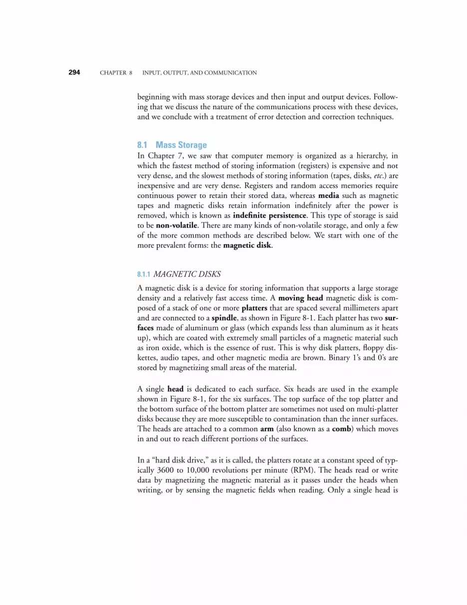
294
CHAPTER 8 INPUT, OUTPUT, AND COMMUNICATION
beginning with mass storage devices and then input and output devices. Follow-ing that we discuss the nature of the communications process with these devices,and we conclude with a treatment of error detection and correction techniques.
8.1 Mass Storage
In Chapter 7, we saw that computer memory is organized as a hierarchy, inwhich the fastest method of storing information (registers) is expensive and notvery dense, and the slowest methods of storing information (tapes, disks,
etc
.) areinexpensive and are very dense. Registers and random access memories requirecontinuous power to retain their stored data, whereas
media
such as magnetictapes and magnetic disks retain information indefinitely after the power isremoved, which is known as
indefinite persistence
. This type of storage is saidto be
non-volatile
. There are many kinds of non-volatile storage, and only a fewof the more common methods are described below. We start with one of themore prevalent forms: the
magnetic disk
.
8.1.1
MAGNETIC DISKS
A magnetic disk is a device for storing information that supports a large storagedensity and a relatively fast access time. A
moving head
magnetic disk is com-posed of a stack of one or more
platters
that are spaced several millimeters apartand are connected to a
spindle
, as shown in Figure 8-1. Each platter has two
sur-faces
made of aluminum or glass (which expands less than aluminum as it heatsup), which are coated with extremely small particles of a magnetic material suchas iron oxide, which is the essence of rust. This is why disk platters, floppy dis-kettes, audio tapes, and other magnetic media are brown. Binary 1’s and 0’s arestored by magnetizing small areas of the material.
A single
head
is dedicated to each surface. Six heads are used in the exampleshown in Figure 8-1, for the six surfaces. The top surface of the top platter andthe bottom surface of the bottom platter are sometimes not used on multi-platterdisks because they are more susceptible to contamination than the inner surfaces.The heads are attached to a common
arm
(also known as a
comb
) which movesin and out to reach different portions of the surfaces.
In a “hard disk drive,” as it is called, the platters rotate at a constant speed of typ-ically 3600 to 10,000 revolutions per minute (RPM). The heads read or writedata by magnetizing the magnetic material as it passes under the heads whenwriting, or by sensing the magnetic fields when reading. Only a single head is
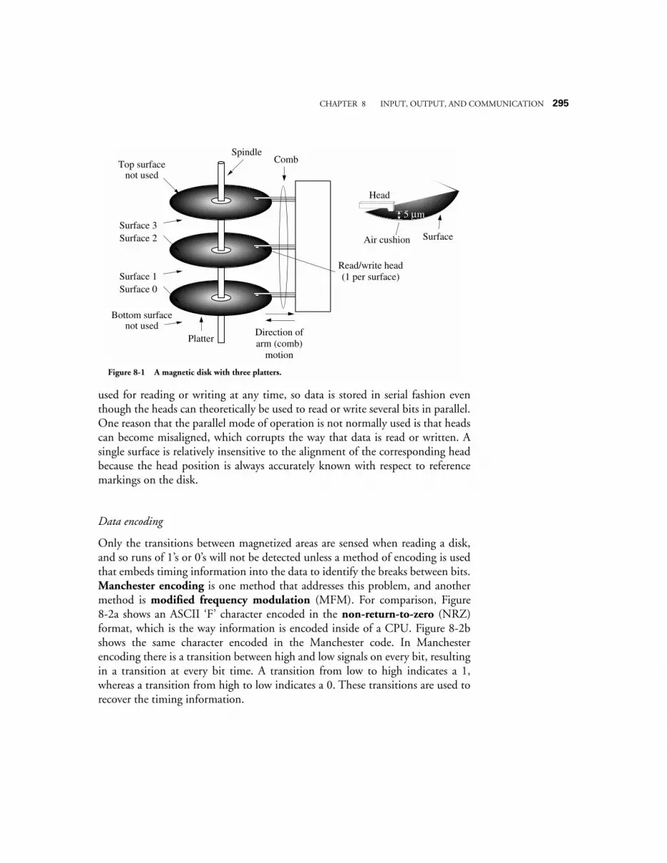
CHAPTER 8 INPUT, OUTPUT, AND COMMUNICATION
295
used for reading or writing at any time, so data is stored in serial fashion eventhough the heads can theoretically be used to read or write several bits in parallel.One reason that the parallel mode of operation is not normally used is that headscan become misaligned, which corrupts the way that data is read or written. Asingle surface is relatively insensitive to the alignment of the corresponding headbecause the head position is always accurately known with respect to referencemarkings on the disk.
Data encoding
Only the transitions between magnetized areas are sensed when reading a disk,and so runs of 1’s or 0’s will not be detected unless a method of encoding is usedthat embeds timing information into the data to identify the breaks between bits.
Manchester encoding
is one method that addresses this problem, and anothermethod is
modified frequency modulation
(MFM). For comparison, Figure8-2a shows an ASCII ‘F’ character encoded in the
non-return-to-zero
(NRZ)format, which is the way information is encoded inside of a CPU. Figure 8-2bshows the same character encoded in the Manchester code. In Manchesterencoding there is a transition between high and low signals on every bit, resultingin a transition at every bit time. A transition from low to high indicates a 1,whereas a transition from high to low indicates a 0. These transitions are used torecover the timing information.
Direction ofarm (comb)
motion
Surface 3Surface 2
Surface 1Surface 0
Top surface not used
Bottom surface not used
Spindle
Platter
Head
SurfaceAir cushion
5 µm
Comb
Read/write head(1 per surface)
Figure 8-1 A magnetic disk with three platters.
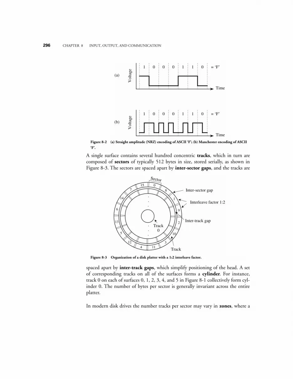
296
CHAPTER 8 INPUT, OUTPUT, AND COMMUNICATION
A single surface contains several hundred concentric
tracks
, which in turn arecomposed of
sectors
of typically 512 bytes in size, stored serially, as shown inFigure 8-3. The sectors are spaced apart by
inter-sector gaps
, and the tracks are
spaced apart by
inter-track gaps
, which simplify positioning of the head. A setof corresponding tracks on all of the surfaces forms a
cylinder
. For instance,track 0 on each of surfaces 0, 1, 2, 3, 4, and 5 in Figure 8-1 collectively form cyl-inder 0. The number of bytes per sector is generally invariant across the entireplatter.
In modern disk drives the number tracks per sector may vary in
zones
, where a
(a)
Time
Vol
tage
1 0 0 0 1 1 0 = ‘F’
(b)
TimeV
olta
ge
1 0 0 0 1 1 0 = ‘F’
Figure 8-2 (a) Straight amplitude (NRZ) encoding of ASCII ‘F’; (b) Manchester encoding of ASCII
‘F’.
Sector
.
.
.
Inter-sector gap
Inter-track gap
Interleave factor 1:2
Track
Track 0
.
.
.
0
8
1
9
2
10
3114
12
5
13
6
14
715
Figure 8-3 Organization of a disk platter with a 1:2 interleave factor.
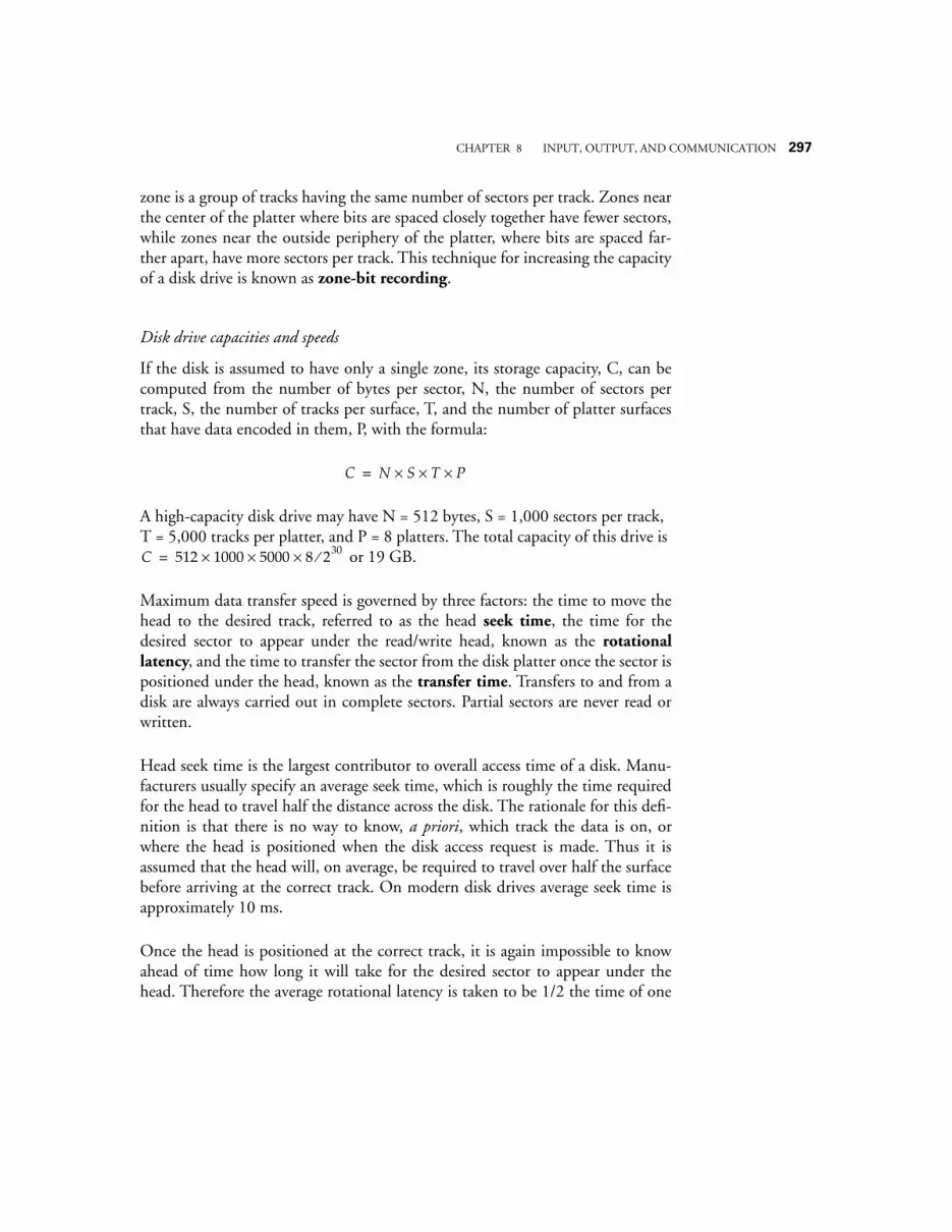
CHAPTER 8 INPUT, OUTPUT, AND COMMUNICATION
297
zone is a group of tracks having the same number of sectors per track. Zones nearthe center of the platter where bits are spaced closely together have fewer sectors,while zones near the outside periphery of the platter, where bits are spaced far-ther apart, have more sectors per track. This technique for increasing the capacityof a disk drive is known as
zone-bit recording
.
Disk drive capacities and speeds
If the disk is assumed to have only a single zone, its storage capacity, C, can becomputed from the number of bytes per sector, N, the number of sectors pertrack, S, the number of tracks per surface, T, and the number of platter surfacesthat have data encoded in them, P, with the formula:
A high-capacity disk drive may have N = 512 bytes, S = 1,000 sectors per track, T = 5,000 tracks per platter, and P = 8 platters. The total capacity of this drive is
or 19 GB.
Maximum data transfer speed is governed by three factors: the time to move thehead to the desired track, referred to as the head
seek time
, the time for thedesired sector to appear under the read/write head, known as the
rotationallatency
, and the time to transfer the sector from the disk platter once the sector ispositioned under the head, known as the
transfer time
. Transfers to and from adisk are always carried out in complete sectors. Partial sectors are never read orwritten.
Head seek time is the largest contributor to overall access time of a disk. Manu-facturers usually specify an average seek time, which is roughly the time requiredfor the head to travel half the distance across the disk. The rationale for this defi-nition is that there is no way to know,
a priori
, which track the data is on, orwhere the head is positioned when the disk access request is made. Thus it isassumed that the head will, on average, be required to travel over half the surfacebefore arriving at the correct track. On modern disk drives average seek time isapproximately 10 ms.
Once the head is positioned at the correct track, it is again impossible to knowahead of time how long it will take for the desired sector to appear under thehead. Therefore the average rotational latency is taken to be 1/2 the time of one
C N S× T P××=
C 512 1000× 5000 8×× 230⁄=
298
CHAPTER 8 INPUT, OUTPUT, AND COMMUNICATION
complete revolution, which is on the order of 4-8 ms. The sector transfer time isjust the time for one complete revolution divided by the number of sectors pertrack. If large amounts of data are to be transferred, then after a complete track istransferred, the head must move to the next track. The parameter of interest hereis the track-to-track access time, which is approximately 2 ms (notice that thetime for the head to travel past multiple tracks is much less than 2 ms per track).An important parameter related to the sector transfer time is the
burst rate
, therate at which data streams on or off the disk once the read/write operation hasstarted. The burst rate equals the disk speed in revolutions per second
×
thecapacity per track. This is not necessarily the same as the transfer rate, becausethere is a setup time needed to position the head and synchronize timing for eachsector.
The maximum transfer rate computed from the factors above may not be real-ized in practice. The limiting factor may be the speed of the bus interconnectingthe disk drive and its interface, or it may be the time required by the CPU totransfer the data between the disk and main memory. For example, disks thatoperate with the
Small Computer Systems Interface
(SCSI) standards have atransfer rate between the disk and a host computer of from 5 to 40 MB/second,which may be slower than the transfer rate between the head and the internalbuffer on the disk. Disk drives invariably contain internal buffers that helpmatch the speed of the disk with the speed of transfer from the disk unit to thehost computer.
Disk drives are delicate mechanisms.
The strength of a magnetic field drops off as the square of the distance from thesource of the field, and for that reason, it is important for the head of the disk totravel as close to the surface as possible. The distance between the head and theplatter can be as small as 5 µm. The engineering and assembly of a disk do nothave to adhere to such a tight tolerance – the head assembly is aerodynamicallydesigned so that the spinning motion of the disk creates a cushion of air thatmaintains a distance between the heads and the platters. Particles in the air con-tained within the disk unit that are larger than 5 µm can come between the headassembly and the platter, which results in a
head crash
.
Smoke particles from cigarette ash are 10 µm or larger, and so smoking shouldnot take place when disks are exposed to the environment. Disks are usuallyassembled into sealed units in
clean rooms
, so that virtually no large particles areintroduced during assembly. Unfortunately, materials used in manufacturing
CHAPTER 8 INPUT, OUTPUT, AND COMMUNICATION
299
(such as glue) that are internal to the unit can deteriorate over time and can gen-erate particles large enough to cause a head crash. For this reason, sealed disks(formerly called
Winchester
disks) contain filters that remove particles generatedwithin the unit and that prevent particulate matter from entering the drive fromthe external environment.
Floppy disks
A
floppy disk
, or
diskette
, contains a flexible plastic platter coated with a mag-netic material like iron oxide. Although only a single side is used on one surfaceof a floppy disk in many systems, both sides of the disks are coated with the samematerial in order to prevent warping. Access time is generally slower than a harddisk because a flexible disk cannot spin as quickly as a hard disk. The rotationalspeed of a typical floppy disk mechanism is only 300 RPM, and may be varied asthe head moves from track to track to optimize data transfer rates. Such slowrotational speeds mean that access times of floppy drives are 250-300 ms,roughly 10 times slower than hard drives. Capacities vary, but range up to 1.44MB.
Floppies are inexpensive because they can be removed from the drive mechanismand because of their small size. The head comes in physical contact with thefloppy disk but this does not result in a head crash. It does, however, place wearon the head and on the media. For this reason, floppies only spin when they arebeing accessed.
When floppies were first introduced, they were encased in flexible, thin plasticenclosures, which gave rise to their name. The flexible platters are currentlyencased in rigid plastic and are referred to as “diskettes.”
Several high-capacity floppy-like disk drives have made their appearance inrecent years. The Iomega Zip drive has a capacity of 100 MB, and access timesthat are about twice those of hard drives, and the larger Iomega Jaz drive has acapacity of 2GB, with similar access times.
Another floppy drive recently introduced by Imation Corp., the SuperDisk, hasfloppy-like disks with 120MB capacity, and in addition can read and write ordi-nary 1.44 MB floppy disks.
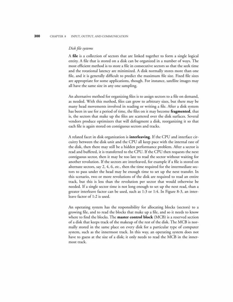
300
CHAPTER 8 INPUT, OUTPUT, AND COMMUNICATION
Disk file systems
A
file
is a collection of sectors that are linked together to form a single logicalentity. A file that is stored on a disk can be organized in a number of ways. Themost efficient method is to store a file in consecutive sectors so that the seek timeand the rotational latency are minimized. A disk normally stores more than onefile, and it is generally difficult to predict the maximum file size. Fixed file sizesare appropriate for some applications, though. For instance, satellite images mayall have the same size in any one sampling.
An alternative method for organizing files is to assign sectors to a file on demand,as needed. With this method, files can grow to arbitrary sizes, but there may bemany head movements involved in reading or writing a file. After a disk systemhas been in use for a period of time, the files on it may become
fragmented
, thatis, the sectors that make up the files are scattered over the disk surfaces. Severalvendors produce optimizers that will defragment a disk, reorganizing it so thateach file is again stored on contiguous sectors and tracks.
A related facet in disk organization is
interleaving
. If the CPU and interface cir-cuitry between the disk unit and the CPU all keep pace with the internal rate ofthe disk, then there may still be a hidden performance problem. After a sector isread and buffered, it is transferred to the CPU. If the CPU then requests the nextcontiguous sector, then it may be too late to read the sector without waiting foranother revolution. If the sectors are interleaved, for example if a file is stored onalternate sectors, say 2, 4, 6,
etc.
, then the time required for the intermediate sec-tors to pass under the head may be enough time to set up the next transfer. Inthis scenario, two or more revolutions of the disk are required to read an entiretrack, but this is less than the revolution per sector that would otherwise beneeded. If a single sector time is not long enough to set up the next read, than agreater interleave factor can be used, such as 1:3 or 1:4. In Figure 8-3, an inter-leave factor of 1:2 is used.
An operating system has the responsibility for allocating blocks (sectors) to agrowing file, and to read the blocks that make up a file, and so it needs to knowwhere to find the blocks. The
master control block
(MCB) is a reserved sectionof a disk that keeps track of the makeup of the rest of the disk. The MCB is nor-mally stored in the same place on every disk for a particular type of computersystem, such as the innermost track. In this way, an operating system does nothave to guess at the size of a disk; it only needs to read the MCB in the inner-most track.
CHAPTER 8 INPUT, OUTPUT, AND COMMUNICATION
301
Figure 8-4 shows one version of an MCB. Not all systems keep all of this infor-
mation in the MCB, but it has to be kept
somewhere
, and some of it may even bekept in part of the file itself. There are four major components to the MCB. ThePreamble section specifies information relating to the physical layout of the disk,such as the number of surfaces, number of sectors per surface,
etc
. The Files sec-tion cross references file names with the list of sectors of which they are com-posed, and file attributes such as the file creation date, last modification date, theidentification of the owner, and protections. Only the starting sector is neededfor a fixed file size disk, otherwise, a list of all of the sectors that make up a file ismaintained.
The Free blocks section lists the positions of blocks that are free to be used fornew or growing files. The Bad blocks section lists positions of blocks that are freebut produce
checksums
(see Section 8.5) that indicate errors. The bad blocks arethus unused.
No. surfaces on disk = 4No. tracks/surface = 814No. sectors/track = 32No. bytes/sector = 512Interleave factor = 1:3
Filename
xyz.p
Surface Track Sector
Starting sector, or sector list
Prea
mbl
eFi
les
Free
blo
cks
Bad
blo
cks
1 10 51 12 72 23 4
ab.c 1 10 83 95 22 12 0
1 1 01 1 11 2 5
...
...
1 1 32 5 7
...
CreationDate
LastModified
Owner Protec-tions
11/14/93 11/14/93 16 RWX by10:30:57 19:30:57 Owner
8/18/93 1/21/94 20 RX - All16:03:12 14:45:03 W-Owner
R = ReadW = WriteX = Execute
Figure 8-4 Simplified example of an MCB.
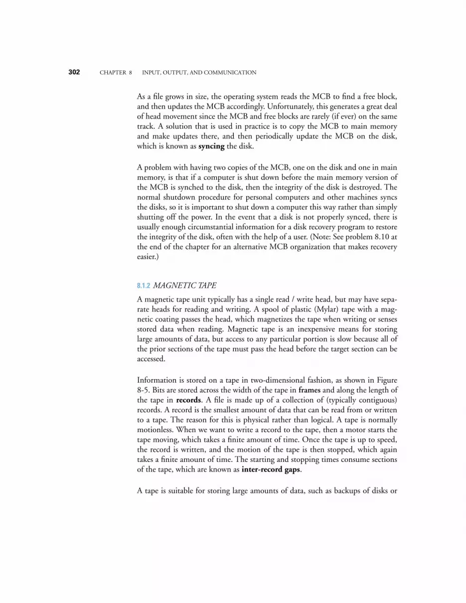
302
CHAPTER 8 INPUT, OUTPUT, AND COMMUNICATION
As a file grows in size, the operating system reads the MCB to find a free block,and then updates the MCB accordingly. Unfortunately, this generates a great dealof head movement since the MCB and free blocks are rarely (if ever) on the sametrack. A solution that is used in practice is to copy the MCB to main memoryand make updates there, and then periodically update the MCB on the disk,which is known as
syncing
the disk.
A problem with having two copies of the MCB, one on the disk and one in mainmemory, is that if a computer is shut down before the main memory version ofthe MCB is synched to the disk, then the integrity of the disk is destroyed. Thenormal shutdown procedure for personal computers and other machines syncsthe disks, so it is important to shut down a computer this way rather than simplyshutting off the power. In the event that a disk is not properly synced, there isusually enough circumstantial information for a disk recovery program to restorethe integrity of the disk, often with the help of a user. (Note: See problem 8.10 atthe end of the chapter for an alternative MCB organization that makes recoveryeasier.)
8.1.2
MAGNETIC TAPE
A magnetic tape unit typically has a single read / write head, but may have sepa-rate heads for reading and writing. A spool of plastic (Mylar) tape with a mag-netic coating passes the head, which magnetizes the tape when writing or sensesstored data when reading. Magnetic tape is an inexpensive means for storinglarge amounts of data, but access to any particular portion is slow because all ofthe prior sections of the tape must pass the head before the target section can beaccessed.
Information is stored on a tape in two-dimensional fashion, as shown in Figure8-5. Bits are stored across the width of the tape in
frames
and along the length ofthe tape in
records
. A file is made up of a collection of (typically contiguous)records. A record is the smallest amount of data that can be read from or writtento a tape. The reason for this is physical rather than logical. A tape is normallymotionless. When we want to write a record to the tape, then a motor starts thetape moving, which takes a finite amount of time. Once the tape is up to speed,the record is written, and the motion of the tape is then stopped, which againtakes a finite amount of time. The starting and stopping times consume sectionsof the tape, which are known as
inter-record gaps
.
A tape is suitable for storing large amounts of data, such as backups of disks or
CHAPTER 8 INPUT, OUTPUT, AND COMMUNICATION
303
scanned images, but is not suitable for random access reading and writing. Thereare two reasons for this. First, the sequential access can require a great deal oftime if the head is not positioned near the target section of tape. The second rea-son is caused when records are overwritten in the middle of the tape, which is notgenerally an operation that is allowed in tape systems. Although individualrecords are the same size, the inter-record gaps eventually creep into the records(this is called
jitter
) because starting and stopping is not precise.
A
physical record
may be subdivided into an integral number of
logicalrecords
. For example, a physical record that is 4096 bytes in length may be com-posed of four logical records that are each 1024 bytes in length. Access to logicalrecords is managed by an operating system, so that the user has the perspectivethat the logical record size relates directly to a physical record size, when in fact,only physical records are read from or written to the tape. There are thus nointer-record gaps between logical records.
Another organization is to use variable length records. A special mark is placed atthe beginning of each record so that there is no confusion as to where recordsbegin.
8.1.3
MAGNETIC DRUMS
Although they are nearly obsolete today, magnetic drum units have traditionallybeen faster than magnetic disks. The reason for the speed advantage of drums isthat there is one stationary head per track, which means that there is no headmovement component in the access time. The rotation rate of a drum can bemuch higher than a disk as a result of a narrow cylindrical shape, and rotationaldelay is thus reduced.
File mark
Record
Inter-record gap
Record Record
File
Frames
Figure 8-5 A portion of a magnetic tape (adapted from [Hamacher, 1990]).
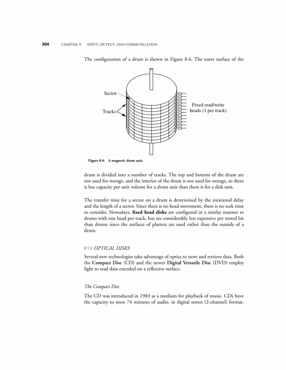
304
CHAPTER 8 INPUT, OUTPUT, AND COMMUNICATION
The configuration of a drum is shown in Figure 8-6. The outer surface of the
drum is divided into a number of tracks. The top and bottom of the drum arenot used for storage, and the interior of the drum is not used for storage, so thereis less capacity per unit volume for a drum unit than there is for a disk unit.
The transfer time for a sector on a drum is determined by the rotational delayand the length of a sector. Since there is no head movement, there is no seek timeto consider. Nowadays,
fixed head disks
are configured in a similar manner todrums with one head per track, but are considerably less expensive per stored bitthan drums since the surfaces of platters are used rather than the outside of adrum.
8.1.4
OPTICAL DISKS
Several new technologies take advantage of optics to store and retrieve data. Boththe
Compact Disc
(CD) and the newer
Digital Versatile Disc
(DVD) employlight to read data encoded on a reflective surface.
The Compact Disc
The CD was introduced in 1983 as a medium for playback of music. CDs havethe capacity to store 74 minutes of audio, in digital stereo (2-channel) format.
Fixed read/writeheads (1 per track)Tracks
Sector
Figure 8-6 A magnetic drum unit.
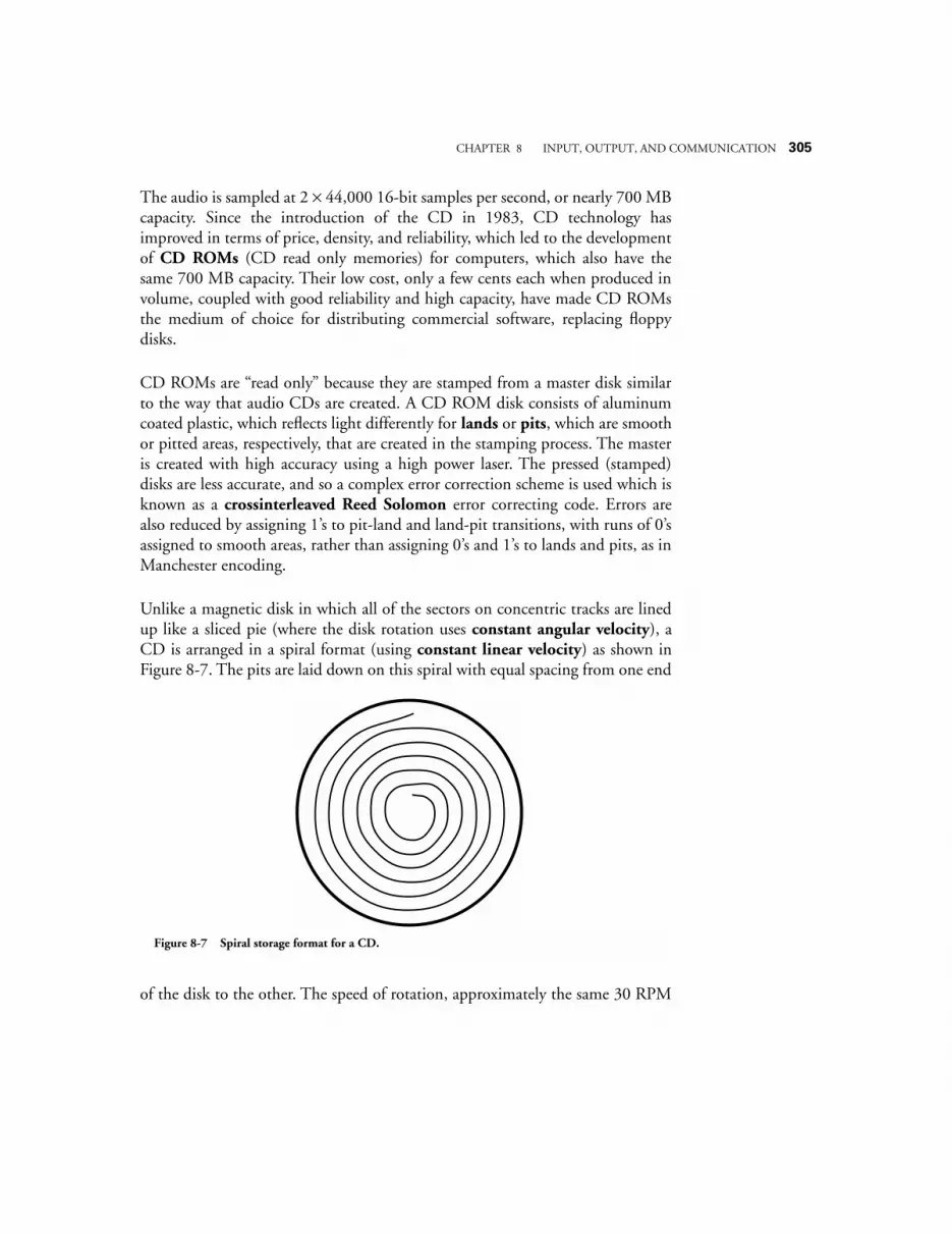
CHAPTER 8 INPUT, OUTPUT, AND COMMUNICATION
305
The audio is sampled at 2
×
44,000 16-bit samples per second, or nearly 700 MBcapacity. Since the introduction of the CD in 1983, CD technology hasimproved in terms of price, density, and reliability, which led to the developmentof
CD ROMs
(CD read only memories) for computers, which also have thesame 700 MB capacity. Their low cost, only a few cents each when produced involume, coupled with good reliability and high capacity, have made CD ROMsthe medium of choice for distributing commercial software, replacing floppydisks.
CD ROMs are “read only” because they are stamped from a master disk similarto the way that audio CDs are created. A CD ROM disk consists of aluminumcoated plastic, which reflects light differently for
lands
or
pits
, which are smoothor pitted areas, respectively, that are created in the stamping process. The masteris created with high accuracy using a high power laser. The pressed (stamped)disks are less accurate, and so a complex error correction scheme is used which isknown as a
crossinterleaved Reed Solomon
error correcting code. Errors arealso reduced by assigning 1’s to pit-land and land-pit transitions, with runs of 0’sassigned to smooth areas, rather than assigning 0’s and 1’s to lands and pits, as inManchester encoding.
Unlike a magnetic disk in which all of the sectors on concentric tracks are linedup like a sliced pie (where the disk rotation uses constant angular velocity), aCD is arranged in a spiral format (using constant linear velocity) as shown inFigure 8-7. The pits are laid down on this spiral with equal spacing from one end
of the disk to the other. The speed of rotation, approximately the same 30 RPM
Figure 8-7 Spiral storage format for a CD.
306 CHAPTER 8 INPUT, OUTPUT, AND COMMUNICATION
as the floppy disk, is adjusted so that the disk moves more slowly when the headis at the edge than when it is at the center. Thus CD ROMs suffer from the samelong access time as floppy disks because of the high rotational latency. CD ROMdrives are available with rotational speeds up to 24×, or 24 times the rotationalspeed of an audio CD, with a resulting decrease in average access time.
CD ROM technology is appropriate for distributing large amounts of data inex-pensively when there are many copies to be made, because the cost of creating amaster and pressing the copies is distributed over the cost of each copy. If only afew copies are made, then the cost of each disk is high because CDs cannot beeconomically pressed in small quantities. CDs also cannot be written after theyare pressed. A newer technology that addresses these problem is the write onceread many (WORM) optical disk, in which a low intensity laser in the CD con-troller writes onto the optical disk (but only once for each bit location). Thewriting process is normally slower than the reading process, and the controllerand media are more expensive than for CD ROMs.
The Digital Versatile Disc
A newer version of optical disk storage is the Digital Versatile Disc, or DVD.There are industry standards for DVD-Audio, DVD-Video, and DVD-ROMand DVD-RAM data storage. When a single side of the DVD is used, its storagecapacity can be up to 4.7 GB. The DVD standards also include the capability ofstoring data on both sides in two layers on each side, for a total capacity of 17GB. The DVD technology is an evolutionary step up from the CD, rather thanbeing an entirely new technology, and in fact the DVD player is backwardlycompatible–it can be used to play CDs and CD ROMs as well as DVDs.
8.2 Input DevicesDisk units, tape units, and drum units are all input/output (I/O) devices, andthey share a common use for mass storage. In this section, we look at a fewdevices that are used exclusively for input of data. We start with one of the mostprevalent devices – the keyboard.
8.2.1 KEYBOARDS
Keyboards are used for manual input to a computer. A keyboard layout using theECMA-23 Standard (2nd ed.) is shown in Figure 8-8. The “QWERTY” layout(for the upper left row of letters D01 – D06) conforms to the traditional layout
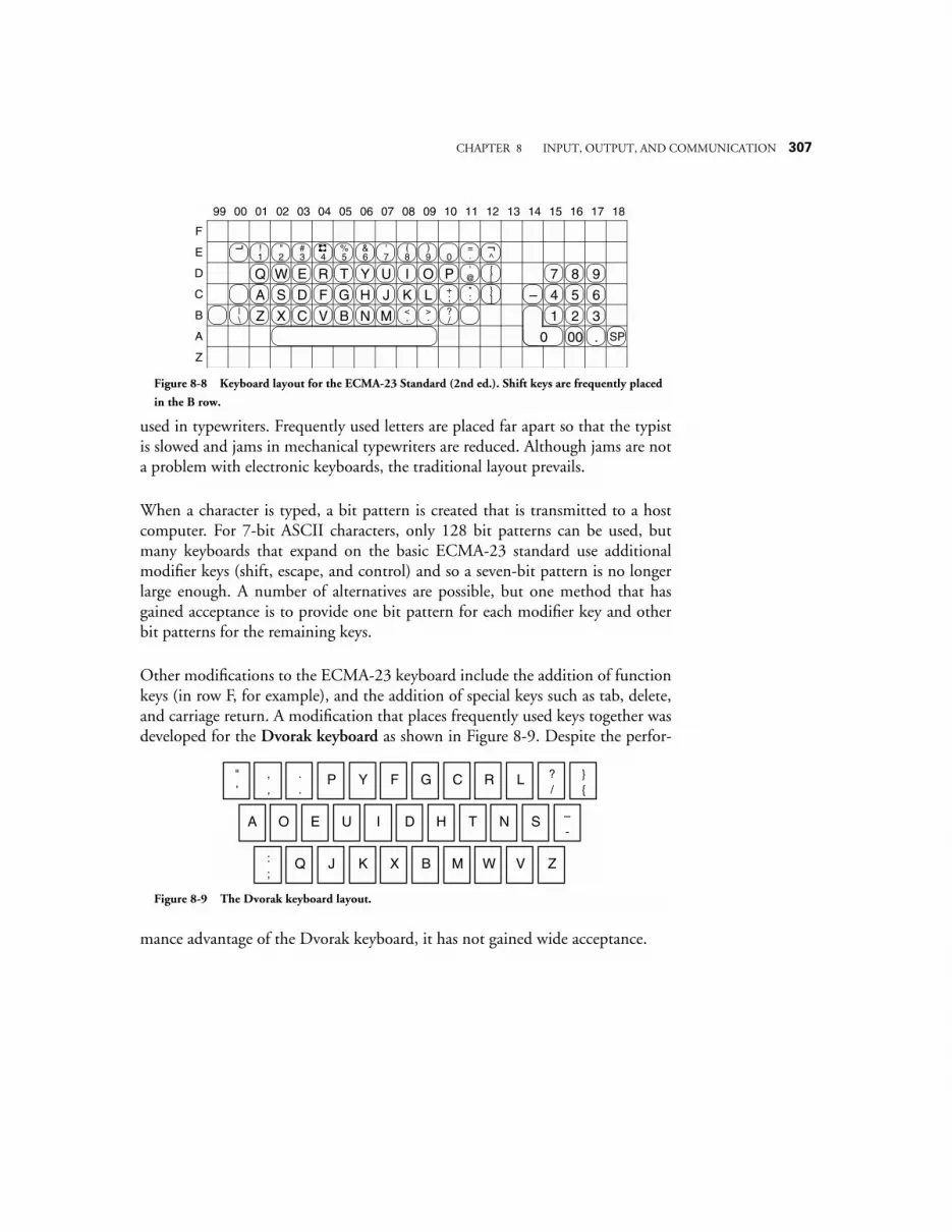
CHAPTER 8 INPUT, OUTPUT, AND COMMUNICATION 307
used in typewriters. Frequently used letters are placed far apart so that the typistis slowed and jams in mechanical typewriters are reduced. Although jams are nota problem with electronic keyboards, the traditional layout prevails.
When a character is typed, a bit pattern is created that is transmitted to a hostcomputer. For 7-bit ASCII characters, only 128 bit patterns can be used, butmany keyboards that expand on the basic ECMA-23 standard use additionalmodifier keys (shift, escape, and control) and so a seven-bit pattern is no longerlarge enough. A number of alternatives are possible, but one method that hasgained acceptance is to provide one bit pattern for each modifier key and otherbit patterns for the remaining keys.
Other modifications to the ECMA-23 keyboard include the addition of functionkeys (in row F, for example), and the addition of special keys such as tab, delete,and carriage return. A modification that places frequently used keys together wasdeveloped for the Dvorak keyboard as shown in Figure 8-9. Despite the perfor-
mance advantage of the Dvorak keyboard, it has not gained wide acceptance.
99 00 01 02 03 04 05 06 07 08 09 10 11 12 13 14 15 16 17 18
F
E
D
C
B
A
Z
Q W E R T Y U I O P
A S D F G H J K L
Z X C V B N M
7 8 9
4 5 6
1 2 3
00 . SP
–
0
1!
2"
3#
4 5%
6&
7'
8(
9)
0 .= ¬
¬
@'
[
;+
:*
/?
,<
.>
]
\|
Figure 8-8 Keyboard layout for the ECMA-23 Standard (2nd ed.). Shift keys are frequently placed
in the B row.
P Y F G C R L
A O E U I D H T N S
Q J K X B M W V Z
?/
–-
"'
,,
.
.
:;
Figure 8-9 The Dvorak keyboard layout.
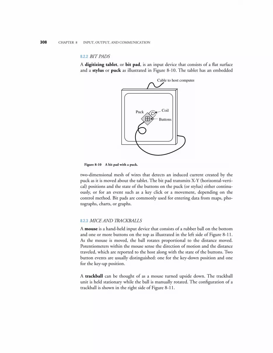
308 CHAPTER 8 INPUT, OUTPUT, AND COMMUNICATION
8.2.2 BIT PADS
A digitizing tablet, or bit pad, is an input device that consists of a flat surfaceand a stylus or puck as illustrated in Figure 8-10. The tablet has an embedded
two-dimensional mesh of wires that detects an induced current created by thepuck as it is moved about the tablet. The bit pad transmits X-Y (horizontal-verti-cal) positions and the state of the buttons on the puck (or stylus) either continu-ously, or for an event such as a key click or a movement, depending on thecontrol method. Bit pads are commonly used for entering data from maps, pho-tographs, charts, or graphs.
8.2.3 MICE AND TRACKBALLS
A mouse is a hand-held input device that consists of a rubber ball on the bottomand one or more buttons on the top as illustrated in the left side of Figure 8-11.As the mouse is moved, the ball rotates proportional to the distance moved.Potentiometers within the mouse sense the direction of motion and the distancetraveled, which are reported to the host along with the state of the buttons. Twobutton events are usually distinguished: one for the key-down position and onefor the key-up position.
A trackball can be thought of as a mouse turned upside down. The trackballunit is held stationary while the ball is manually rotated. The configuration of atrackball is shown in the right side of Figure 8-11.
Puck
Cable to host computer
Coil
Buttons
Figure 8-10 A bit pad with a puck.
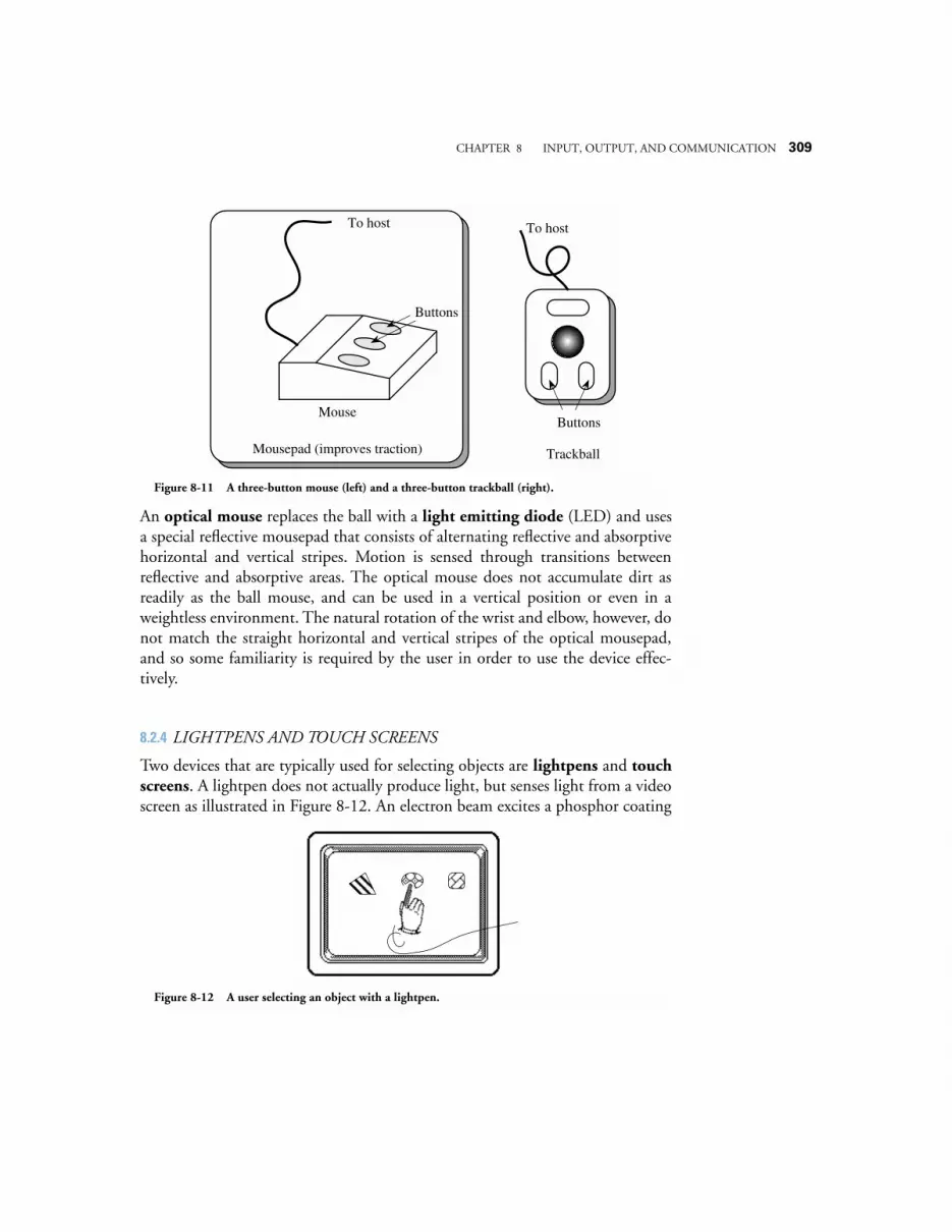
CHAPTER 8 INPUT, OUTPUT, AND COMMUNICATION 309
An optical mouse replaces the ball with a light emitting diode (LED) and usesa special reflective mousepad that consists of alternating reflective and absorptivehorizontal and vertical stripes. Motion is sensed through transitions betweenreflective and absorptive areas. The optical mouse does not accumulate dirt asreadily as the ball mouse, and can be used in a vertical position or even in aweightless environment. The natural rotation of the wrist and elbow, however, donot match the straight horizontal and vertical stripes of the optical mousepad,and so some familiarity is required by the user in order to use the device effec-tively.
8.2.4 LIGHTPENS AND TOUCH SCREENS
Two devices that are typically used for selecting objects are lightpens and touchscreens. A lightpen does not actually produce light, but senses light from a videoscreen as illustrated in Figure 8-12. An electron beam excites a phosphor coating
To host
Mousepad (improves traction) Trackball
Mouse
Buttons
To host
Buttons
Figure 8-11 A three-button mouse (left) and a three-button trackball (right).
Figure 8-12 A user selecting an object with a lightpen.
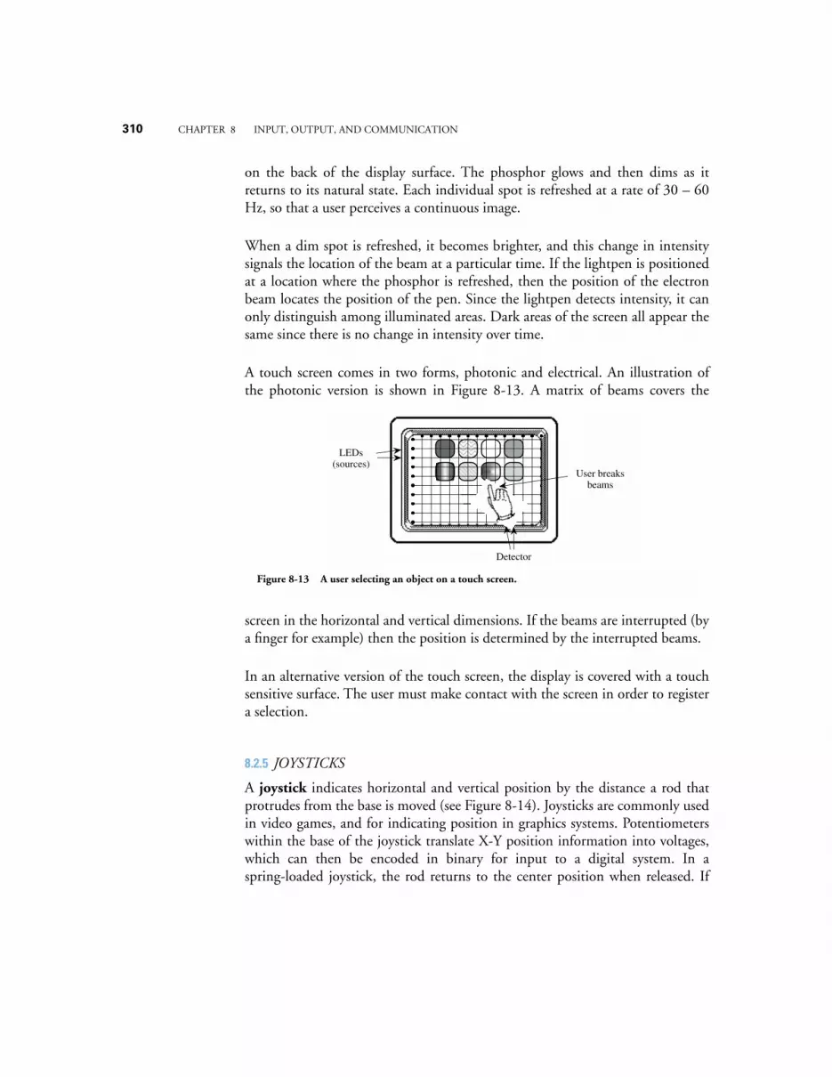
310 CHAPTER 8 INPUT, OUTPUT, AND COMMUNICATION
on the back of the display surface. The phosphor glows and then dims as itreturns to its natural state. Each individual spot is refreshed at a rate of 30 – 60Hz, so that a user perceives a continuous image.
When a dim spot is refreshed, it becomes brighter, and this change in intensitysignals the location of the beam at a particular time. If the lightpen is positionedat a location where the phosphor is refreshed, then the position of the electronbeam locates the position of the pen. Since the lightpen detects intensity, it canonly distinguish among illuminated areas. Dark areas of the screen all appear thesame since there is no change in intensity over time.
A touch screen comes in two forms, photonic and electrical. An illustration ofthe photonic version is shown in Figure 8-13. A matrix of beams covers the
screen in the horizontal and vertical dimensions. If the beams are interrupted (bya finger for example) then the position is determined by the interrupted beams.
In an alternative version of the touch screen, the display is covered with a touchsensitive surface. The user must make contact with the screen in order to registera selection.
8.2.5 JOYSTICKS
A joystick indicates horizontal and vertical position by the distance a rod thatprotrudes from the base is moved (see Figure 8-14). Joysticks are commonly usedin video games, and for indicating position in graphics systems. Potentiometerswithin the base of the joystick translate X-Y position information into voltages,which can then be encoded in binary for input to a digital system. In aspring-loaded joystick, the rod returns to the center position when released. If
LEDs (sources)
Detector
User breaks beams
Figure 8-13 A user selecting an object on a touch screen.
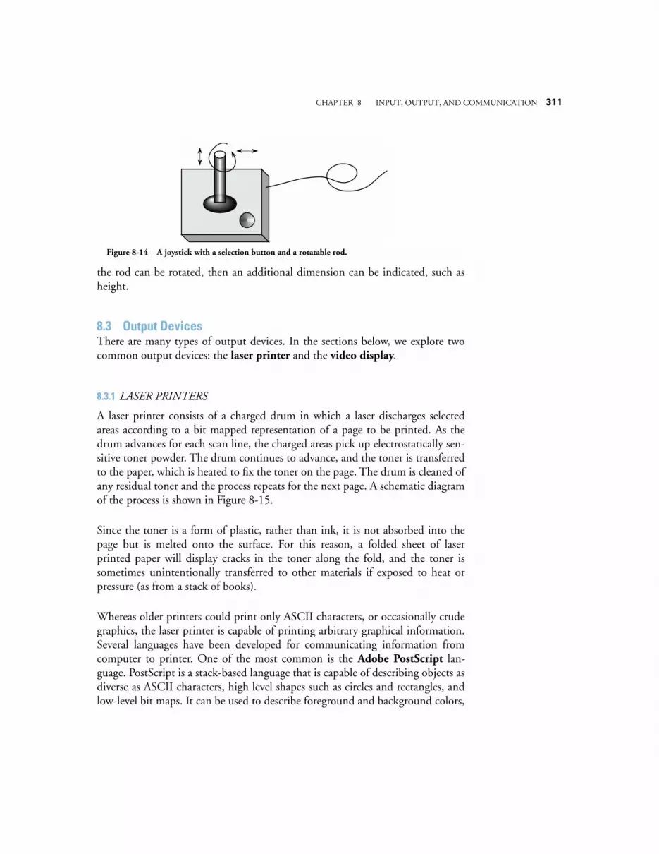
CHAPTER 8 INPUT, OUTPUT, AND COMMUNICATION 311
the rod can be rotated, then an additional dimension can be indicated, such asheight.
8.3 Output DevicesThere are many types of output devices. In the sections below, we explore twocommon output devices: the laser printer and the video display.
8.3.1 LASER PRINTERS
A laser printer consists of a charged drum in which a laser discharges selectedareas according to a bit mapped representation of a page to be printed. As thedrum advances for each scan line, the charged areas pick up electrostatically sen-sitive toner powder. The drum continues to advance, and the toner is transferredto the paper, which is heated to fix the toner on the page. The drum is cleaned ofany residual toner and the process repeats for the next page. A schematic diagramof the process is shown in Figure 8-15.
Since the toner is a form of plastic, rather than ink, it is not absorbed into thepage but is melted onto the surface. For this reason, a folded sheet of laserprinted paper will display cracks in the toner along the fold, and the toner issometimes unintentionally transferred to other materials if exposed to heat orpressure (as from a stack of books).
Whereas older printers could print only ASCII characters, or occasionally crudegraphics, the laser printer is capable of printing arbitrary graphical information.Several languages have been developed for communicating information fromcomputer to printer. One of the most common is the Adobe PostScript lan-guage. PostScript is a stack-based language that is capable of describing objects asdiverse as ASCII characters, high level shapes such as circles and rectangles, andlow-level bit maps. It can be used to describe foreground and background colors,
Figure 8-14 A joystick with a selection button and a rotatable rod.

312 CHAPTER 8 INPUT, OUTPUT, AND COMMUNICATION
and fill colors with which to fill objects.
8.3.2 VIDEO DISPLAYS
A video display, or monitor, consists of a luminescent display device such as acathode ray tube (CRT) or a liquid crystal panel, and controlling circuitry. In aCRT, vertical and horizontal deflection plates steer an electron beam that sweepsthe display screen in raster fashion (one line at a time, from left to right, startingat the top).
A configuration for a CRT is shown in Figure 8-16. An electron gun generates a
stream of electrons that is imaged onto a phosphor coated screen at positions
Paper input
Paper output
The quick brown fox jumps
Heated rollers
Toner cartridge
Cleaner and discharger
Stationary laser source
Page composing
circuitry
Page description from host computer
Charged pattern
Rotating mirror
Figure 8-15 Schematic of a laser printer (adapted from [Tanenbaum, 1999]).
Horizontal control
Vertical control
Intensity control
Electron gun
Vertical deflection plate
Vacuum
GridHorizontal deflection plate
Phosphor coated screen
Figure 8-16 A CRT with a single electron gun.
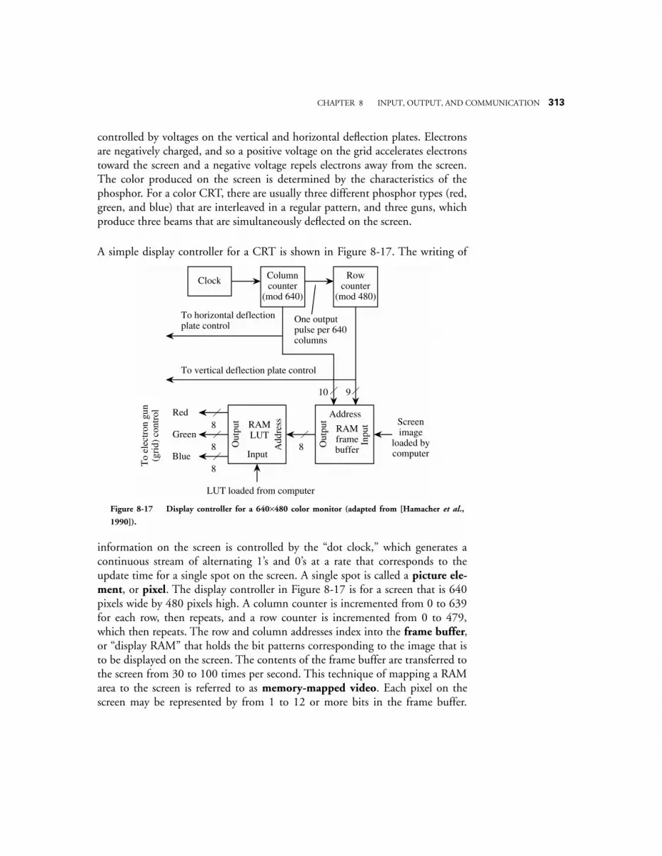
CHAPTER 8 INPUT, OUTPUT, AND COMMUNICATION 313
controlled by voltages on the vertical and horizontal deflection plates. Electronsare negatively charged, and so a positive voltage on the grid accelerates electronstoward the screen and a negative voltage repels electrons away from the screen.The color produced on the screen is determined by the characteristics of thephosphor. For a color CRT, there are usually three different phosphor types (red,green, and blue) that are interleaved in a regular pattern, and three guns, whichproduce three beams that are simultaneously deflected on the screen.
A simple display controller for a CRT is shown in Figure 8-17. The writing of
information on the screen is controlled by the “dot clock,” which generates acontinuous stream of alternating 1’s and 0’s at a rate that corresponds to theupdate time for a single spot on the screen. A single spot is called a picture ele-ment, or pixel. The display controller in Figure 8-17 is for a screen that is 640pixels wide by 480 pixels high. A column counter is incremented from 0 to 639for each row, then repeats, and a row counter is incremented from 0 to 479,which then repeats. The row and column addresses index into the frame buffer,or “display RAM” that holds the bit patterns corresponding to the image that isto be displayed on the screen. The contents of the frame buffer are transferred tothe screen from 30 to 100 times per second. This technique of mapping a RAMarea to the screen is referred to as memory-mapped video. Each pixel on thescreen may be represented by from 1 to 12 or more bits in the frame buffer.
To horizontal deflection plate control
To vertical deflection plate control
10 9
To
elec
tron
gun
(g
rid)
con
trol Red
Green
Blue8
LUT loaded from computer
Screen image
loaded by computer
Clock Column counter
(mod 640)
Row counter
(mod 480)
Address
Out
put
Inpu
t
Out
put
Add
ress
8Input
RAM frame buffer
RAM LUT
8
8
One output pulse per 640 columns
Figure 8-17 Display controller for a 640×480 color monitor (adapted from [Hamacher et al.,
1990]).

314 CHAPTER 8 INPUT, OUTPUT, AND COMMUNICATION
When there is only a single bit per pixel, the pixel can only be on or off, black orwhite; multiple bits per pixel allow a pixel to have varying colors, or shades ofgray.
Each pixel in the display controller of Figure 8-17 is represented by eight bits inthe frame buffer, which means that one out of 28, or 256 different intensities canbe used for each pixel. In a simple configuration the eight bits can be partitionedfor the red, green, and blue (R, G, and B) inputs to the CRT as three bits for red,three bits for green, and two bits for blue. An alternative is to pass the eight-bitpixel value to a color lookup table (LUT) in which the eight-bit value is trans-lated into 256 different 24-bit colors. Eight bits of the 24-bit output are thenused for each of the red, green, and blue guns. A total of 224 different colors canbe displayed, but only 28 of the 224 can be displayed at any one time since theLUT has only 28 entries. The LUT can be reloaded as necessary to select differ-ent subsets of the 224 colors. For example, in order to display a gray scale image(no color), we must have R=G=B and so a ramp from 0 to 255 is stored for eachof the red, green, and blue guns.
The human eye is relatively slow when compared with the speed of an electronicdevice, and cannot perceive a break in motion that happens at a rate of about 25Hz or greater. A computer screen only needs to be updated 25 or 30 times a sec-ond in order for an observer to perceive a continuous image. Whereas videomonitors for computer applications can have any scan rate that the designer ofthe monitor and video interface card wish, in television applications the scan ratemust be standardized. In Europe, a rate of 25 Hz is used for standard television,and a rate of 30 Hz is used in North America. The phosphor types used in thescreens do not have a long persistence, and so scan lines are updated alternatelyin order to reduce flicker. The screen is thus updated at a 50 Hz rate in Europeand at a 60 Hz rate in North America, but only alternating lines are updated oneach sweep. For high resolution graphics, the entire screen may be updated at a50 Hz or 60 Hz rate, rather than just the alternating lines. Many observersbelieve that the European choice of 50 Hz was a bad one, because many viewerscan detect the 50 Hz as a flicker in dim lighting or when viewed at the peripheryof vision.
On the other hand, the Europeans point to the United States NTSC video trans-mission standard as being inferior to their PAL system, referring to the NTSCsystem as standing for “Never The Same Color,” because of its poorer ability tomaintain consistent color from frame to frame.
CHAPTER 8 INPUT, OUTPUT, AND COMMUNICATION 315
The data rates between computer and video monitor can be quite high. Considerthat a 24-bit monitor with 1024 × 768 pixel resolution and a refresh rate of 60Hz will requires a bandwidth (that is, the amount of information that can becarried over a given period of time) of 3 bytes/pixel × (1024 × 768) pixels × 60Hz, or roughly 140 MB per second. Fortunately, the hardware described abovemaps the frame buffer onto the screen without CPU intervention, but it is stillup to the CPU to output pixels to the frame buffer as the image on the screenchanges.
8.4 Communication“Communication” is the process of transferring information from a source to adestination, and “telecommunications” is the process of communicating at a dis-tance. Communication systems range from busses within an integrated circuit tothe public telephone system, and radio and television. Wide-area telecommuni-cation systems have become very complex, with all combinations of voice, video,and data being transferred by wire, optical fiber, radio, and microwaves. Theroutes that communication takes may traverse cross-country, under water,through local radio cells, and via satellite. Data that originates as analog voice sig-nals may be converted to digital data streams for efficient routing over long dis-tances, and then converted back to an analog signal, without the knowledge ofthose communicating.
In this chapter we focus on the relatively short range communications betweenentities located at distances ranging from millimeters to a kilometer or so. Anexample of the former is the interactions between a CPU and main memory, andan example of the latter is a local area network (LAN). The LAN is used tointerconnect computers located within a kilometer or so of one another. InChapter 10 we extend our discussion to wide area networks (WANs) as typifiedby the Internet.
In the next sections we discuss communications from the viewpoints of commu-nications at the CPU and motherboard level, and then branch out to the localarea network.
8.4.1 BUSSES
Unlike the long distance telecommunications network, in which there may bemany senders and receivers over a large geographical distance, a computer hasonly a small number of devices that are geographically very local, within a few
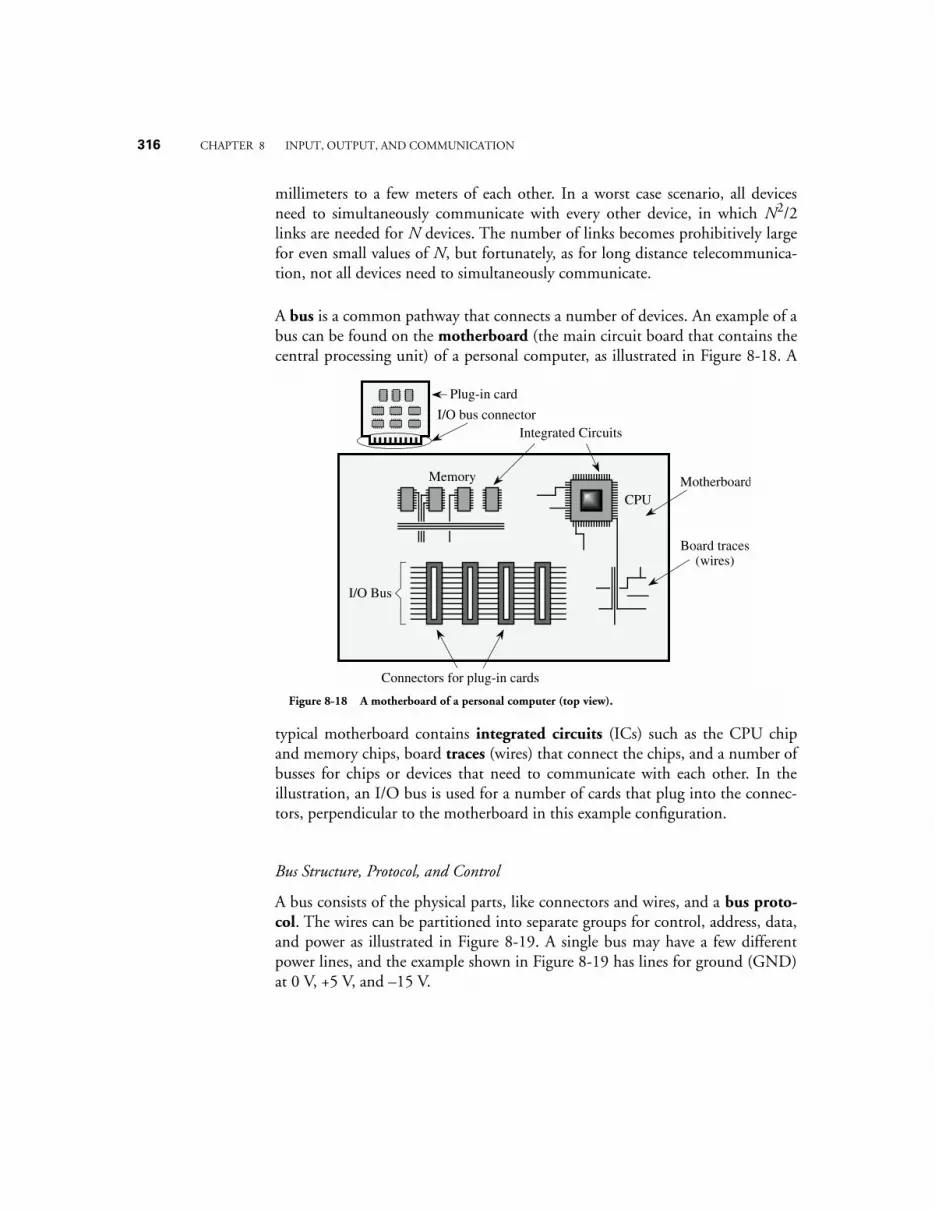
316 CHAPTER 8 INPUT, OUTPUT, AND COMMUNICATION
millimeters to a few meters of each other. In a worst case scenario, all devicesneed to simultaneously communicate with every other device, in which N2/2links are needed for N devices. The number of links becomes prohibitively largefor even small values of N, but fortunately, as for long distance telecommunica-tion, not all devices need to simultaneously communicate.
A bus is a common pathway that connects a number of devices. An example of abus can be found on the motherboard (the main circuit board that contains thecentral processing unit) of a personal computer, as illustrated in Figure 8-18. A
typical motherboard contains integrated circuits (ICs) such as the CPU chipand memory chips, board traces (wires) that connect the chips, and a number ofbusses for chips or devices that need to communicate with each other. In theillustration, an I/O bus is used for a number of cards that plug into the connec-tors, perpendicular to the motherboard in this example configuration.
Bus Structure, Protocol, and Control
A bus consists of the physical parts, like connectors and wires, and a bus proto-col. The wires can be partitioned into separate groups for control, address, data,and power as illustrated in Figure 8-19. A single bus may have a few differentpower lines, and the example shown in Figure 8-19 has lines for ground (GND)at 0 V, +5 V, and –15 V.
Motherboard
I/O Bus
Board traces (wires)
Connectors for plug-in cards
Integrated Circuits
Plug-in card
I/O bus connector
Memory
CPU
Figure 8-18 A motherboard of a personal computer (top view).
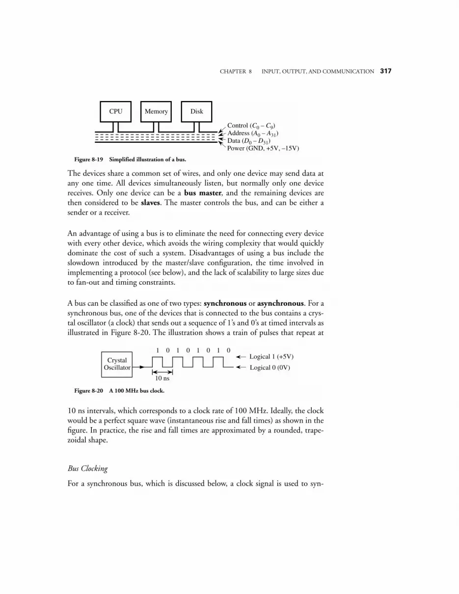
CHAPTER 8 INPUT, OUTPUT, AND COMMUNICATION 317
The devices share a common set of wires, and only one device may send data atany one time. All devices simultaneously listen, but normally only one devicereceives. Only one device can be a bus master, and the remaining devices arethen considered to be slaves. The master controls the bus, and can be either asender or a receiver.
An advantage of using a bus is to eliminate the need for connecting every devicewith every other device, which avoids the wiring complexity that would quicklydominate the cost of such a system. Disadvantages of using a bus include theslowdown introduced by the master/slave configuration, the time involved inimplementing a protocol (see below), and the lack of scalability to large sizes dueto fan-out and timing constraints.
A bus can be classified as one of two types: synchronous or asynchronous. For asynchronous bus, one of the devices that is connected to the bus contains a crys-tal oscillator (a clock) that sends out a sequence of 1’s and 0’s at timed intervals asillustrated in Figure 8-20. The illustration shows a train of pulses that repeat at
10 ns intervals, which corresponds to a clock rate of 100 MHz. Ideally, the clockwould be a perfect square wave (instantaneous rise and fall times) as shown in thefigure. In practice, the rise and fall times are approximated by a rounded, trape-zoidal shape.
Bus Clocking
For a synchronous bus, which is discussed below, a clock signal is used to syn-
CPU DiskMemory
Control (C0 – C9)Address (A0 – A31)Data (D0 – D31)Power (GND, +5V, –15V)
Figure 8-19 Simplified illustration of a bus.
CrystalOscillator
1 0 1 0 1 0 1 0
Logical 0 (0V)
Logical 1 (+5V)
10 ns
Figure 8-20 A 100 MHz bus clock.
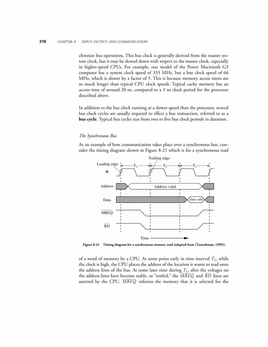
318 CHAPTER 8 INPUT, OUTPUT, AND COMMUNICATION
chronize bus operations. This bus clock is generally derived from the master sys-tem clock, but it may be slowed down with respect to the master clock, especiallyin higher-speed CPUs. For example, one model of the Power Macintosh G3computer has a system clock speed of 333 MHz, but a bus clock speed of 66MHz, which is slower by a factor of 5. This is because memory access times areso much longer than typical CPU clock speeds. Typical cache memory has anaccess time of around 20 ns, compared to a 3 ns clock period for the processordescribed above.
In addition to the bus clock running at a slower speed than the processor, severalbus clock cycles are usually required to effect a bus transaction, referred to as abus cycle. Typical bus cycles run from two to five bus clock periods in duration.
The Synchronous Bus
As an example of how communication takes place over a synchronous bus, con-sider the timing diagram shown in Figure 8-21 which is for a synchronous read
of a word of memory by a CPU. At some point early in time interval T1, whilethe clock is high, the CPU places the address of the location it wants to read ontothe address lines of the bus. At some later time during T1, after the voltages onthe address lines have become stable, or “settled,” the and lines areasserted by the CPU. informs the memory that it is selected for the
Φ
Address
Data
MREQ
RD
T1 T2 T3Leading edge
Trailing edge
Data valid
Time
Address valid
Figure 8-21 Timing diagram for a synchronous memory read (adapted from [Tanenbaum, 1999]).
MREQ RDMREQ
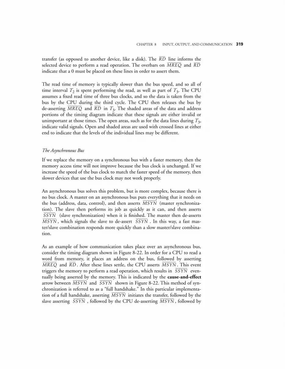
CHAPTER 8 INPUT, OUTPUT, AND COMMUNICATION 319
transfer (as opposed to another device, like a disk). The line informs theselected device to perform a read operation. The overbars on and indicate that a 0 must be placed on these lines in order to assert them.
The read time of memory is typically slower than the bus speed, and so all oftime interval T2 is spent performing the read, as well as part of T3. The CPUassumes a fixed read time of three bus clocks, and so the data is taken from thebus by the CPU during the third cycle. The CPU then releases the bus byde-asserting and in T3. The shaded areas of the data and addressportions of the timing diagram indicate that these signals are either invalid orunimportant at those times. The open areas, such as for the data lines during T3,indicate valid signals. Open and shaded areas are used with crossed lines at eitherend to indicate that the levels of the individual lines may be different.
The Asynchronous Bus
If we replace the memory on a synchronous bus with a faster memory, then thememory access time will not improve because the bus clock is unchanged. If weincrease the speed of the bus clock to match the faster speed of the memory, thenslower devices that use the bus clock may not work properly.
An asynchronous bus solves this problem, but is more complex, because there isno bus clock. A master on an asynchronous bus puts everything that it needs onthe bus (address, data, control), and then asserts (master synchroniza-tion). The slave then performs its job as quickly as it can, and then asserts
(slave synchronization) when it is finished. The master then de-asserts, which signals the slave to de-assert . In this way, a fast mas-
ter/slave combination responds more quickly than a slow master/slave combina-tion.
As an example of how communication takes place over an asynchronous bus,consider the timing diagram shown in Figure 8-22. In order for a CPU to read aword from memory, it places an address on the bus, followed by asserting
and . After these lines settle, the CPU asserts . This eventtriggers the memory to perform a read operation, which results in even-tually being asserted by the memory. This is indicated by the cause-and-effectarrow between and shown in Figure 8-22. This method of syn-chronization is referred to as a “full handshake.” In this particular implementa-tion of a full handshake, asserting initiates the transfer, followed by theslave asserting , followed by the CPU de-asserting , followed by
RDMREQ RD
MREQ RD
MSYN
SSYNMSYN SSYN
MREQ RD MSYNSSYN
MSYN SSYN
MSYNSSYN MSYN
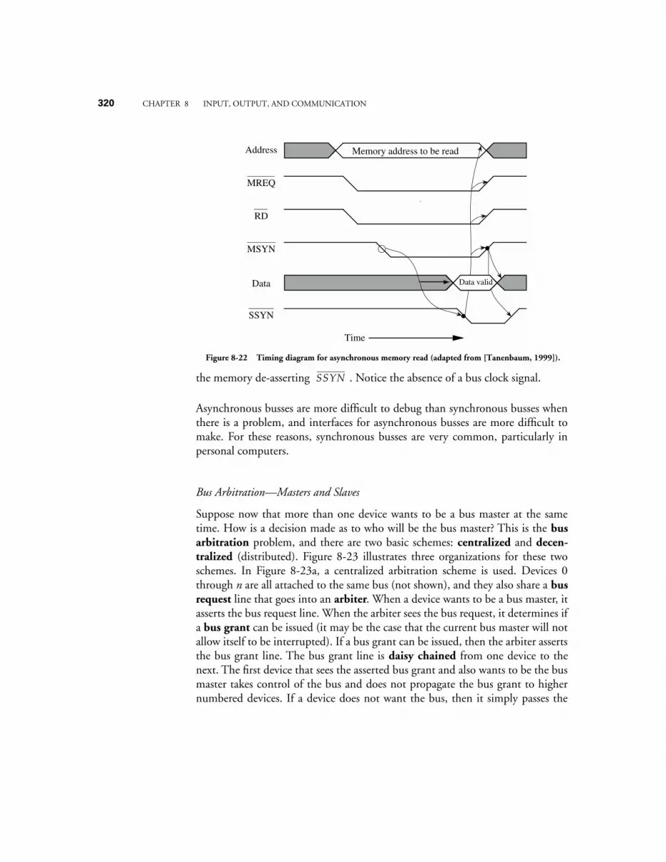
320 CHAPTER 8 INPUT, OUTPUT, AND COMMUNICATION
the memory de-asserting . Notice the absence of a bus clock signal.
Asynchronous busses are more difficult to debug than synchronous busses whenthere is a problem, and interfaces for asynchronous busses are more difficult tomake. For these reasons, synchronous busses are very common, particularly inpersonal computers.
Bus Arbitration—Masters and Slaves
Suppose now that more than one device wants to be a bus master at the sametime. How is a decision made as to who will be the bus master? This is the busarbitration problem, and there are two basic schemes: centralized and decen-tralized (distributed). Figure 8-23 illustrates three organizations for these twoschemes. In Figure 8-23a, a centralized arbitration scheme is used. Devices 0through n are all attached to the same bus (not shown), and they also share a busrequest line that goes into an arbiter. When a device wants to be a bus master, itasserts the bus request line. When the arbiter sees the bus request, it determines ifa bus grant can be issued (it may be the case that the current bus master will notallow itself to be interrupted). If a bus grant can be issued, then the arbiter assertsthe bus grant line. The bus grant line is daisy chained from one device to thenext. The first device that sees the asserted bus grant and also wants to be the busmaster takes control of the bus and does not propagate the bus grant to highernumbered devices. If a device does not want the bus, then it simply passes the
Address
MSYN
RD
Data
Time
Memory address to be read
MREQ
SSYN
Data valid
Figure 8-22 Timing diagram for asynchronous memory read (adapted from [Tanenbaum, 1999]).
SSYN
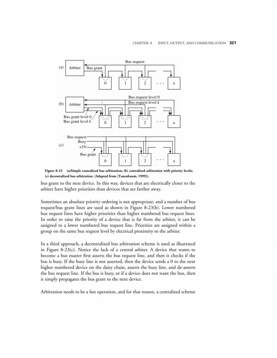
CHAPTER 8 INPUT, OUTPUT, AND COMMUNICATION 321
bus grant to the next device. In this way, devices that are electrically closer to thearbiter have higher priorities than devices that are farther away.
Sometimes an absolute priority ordering is not appropriate, and a number of busrequest/bus grant lines are used as shown in Figure 8-23(b). Lower numberedbus request lines have higher priorities than higher numbered bus request lines.In order to raise the priority of a device that is far from the arbiter, it can beassigned to a lower numbered bus request line. Priorities are assigned within agroup on the same bus request level by electrical proximity to the arbiter.
In a third approach, a decentralized bus arbitration scheme is used as illustratedin Figure 8-23(c). Notice the lack of a central arbiter. A device that wants tobecome a bus master first asserts the bus request line, and then it checks if thebus is busy. If the busy line is not asserted, then the device sends a 0 to the nexthigher numbered device on the daisy chain, asserts the busy line, and de-assertsthe bus request line. If the bus is busy, or if a device does not want the bus, thenit simply propagates the bus grant to the next device.
Arbitration needs to be a fast operation, and for that reason, a centralized scheme
Arbiter Bus grant
Bus request
0 1 2 n. . .
(a)
Arbiter
Bus grant level 0
Bus request level 0
0 1 2 n. . .
(b)
Bus grant
Bus request
0 1 2 n. . .
(c)Busy+5V
Bus grant level k
Bus request level k...
Figure 8-23 (a)Simple centralized bus arbitration; (b) centralized arbitration with priority levels;
(c) decentralized bus arbitration. (Adapted from [Tanenbaum, 1999]).

322 CHAPTER 8 INPUT, OUTPUT, AND COMMUNICATION
will only work well for a small number of devices (up to about eight). For a largenumber of devices, a decentralized scheme is more appropriate.
Given a system that makes use of one of these arbitration schemes, imagine a sit-uation in which n card slots are used, and then card m is removed, where m < n.What happens? Since each bus request line is directly connected to all devices ina group, and the bus grant line is passed through each device in a group, a busrequest from a device with an index greater than m will never see an asserted busgrant line, which can result in a system crash. This can be a frustrating problemto identify, because a system can run indefinitely with no problems, until thehigher numbered device is accessed.
When a card is removed, higher cards should be repositioned to fill in the miss-ing slot, or a dummy card that continues the bus grant line should be inserted inplace of the removed card. Fast devices (like disk controllers) should be givenhigher priority than slow devices (like terminals), and should thus be placed closeto the arbiter in a centralized scheme, or close to the beginning of the Bus grantline in a decentralized scheme.
8.4.2 COMMUNICATION BETWEEN PROCESSORS AND MEMORIES
Computer systems have a wide range of communication tasks. The CPU mustcommunicate with memory, and with a wide range of I/O devices, ranging fromextremely slow devices such as keyboards, to high-speed devices like disk drivesand network interfaces. In fact, there may be multiple CPUs that communicatewith one another either directly or through a shared memory, in a typical config-uration.
Three methods for managing input and output are programmed I/O (alsoknown as polling), interrupt driven I/O, and direct memory access (DMA).
Programmed I/O
Consider reading a block of data from a disk. In programmed I/O, the CPUpolls each device to see if it needs servicing. In a restaurant analogy, the hostwould approach the patron and ask if the patron is ready.
The operations that take place for programmed I/O are shown in the flowchartin Figure 8-24. The CPU first checks the status of the disk by reading a special
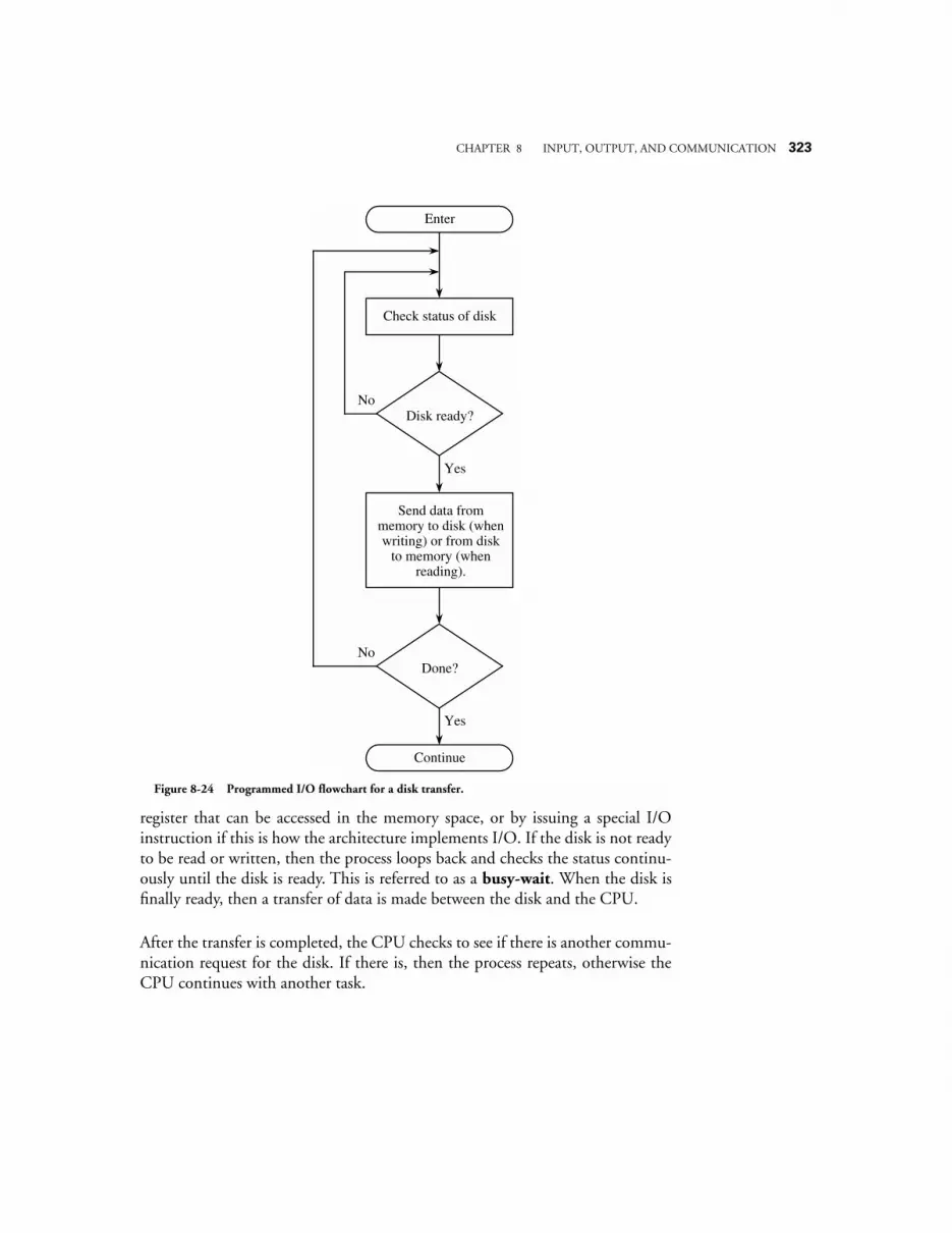
CHAPTER 8 INPUT, OUTPUT, AND COMMUNICATION 323
register that can be accessed in the memory space, or by issuing a special I/Oinstruction if this is how the architecture implements I/O. If the disk is not readyto be read or written, then the process loops back and checks the status continu-ously until the disk is ready. This is referred to as a busy-wait. When the disk isfinally ready, then a transfer of data is made between the disk and the CPU.
After the transfer is completed, the CPU checks to see if there is another commu-nication request for the disk. If there is, then the process repeats, otherwise theCPU continues with another task.
Check status of disk
Disk ready?No
Yes
Send data from memory to disk (when writing) or from disk
to memory (when reading).
Done?No
Yes
Continue
Enter
Figure 8-24 Programmed I/O flowchart for a disk transfer.
324 CHAPTER 8 INPUT, OUTPUT, AND COMMUNICATION
In programmed I/O the CPU wastes time polling devices. Another problem isthat high priority devices are not checked until the CPU is finished with its cur-rent I/O task, which may have a low priority. Programmed I/O is simple toimplement, however, and so it has advantages in some applications.
Interrupt-driven I/O
With interrupt driven I/O, the CPU does not access a device until it needs ser-vicing, and so it does not get caught up in busy-waits. In interrupt-driven I/O,the device requests service through a special interrupt request line that goesdirectly to the CPU. The restaurant analogy would have the patron politely tap-ping silverware on a water glass, thus interrupting the waiter when service isrequired.
A flowchart for interrupt driven I/O is shown in Figure 8-25. The CPU issues arequest to the disk for reading or for writing, and then immediately resumes exe-cution of another process. At some later time, when the disk is ready, it inter-rupts the CPU. The CPU then invokes an interrupt service routine (ISR) forthe disk, and returns to normal execution when the interrupt service routinecompletes its task. The ISR is similar in structure to the procedure presented inChapter 4, except that interrupts occur asynchronously with respect to the pro-cess being executed by the CPU: an interrupt can occur at any time during pro-gram execution.
There are times when a process being executed by the CPU should not be inter-rupted because some critical operation is taking place. For this reason, instruc-tion sets include instructions to disable and enable interrupts under programmedcontrol. (The waiter can ignore the patron at times.) Whether or not interruptsare accepted is generally determined by the state of the Interrupt Flag (IF) whichis part of the Processor Status Register. Furthermore, in most systems prioritiesare assigned to the interrupts, either enforced by the processor or by a peripheralinterrupt controller (PIC). (The waiter may attend to the head table first.) Atthe top priority level in many systems, there is a non-maskable interrupt (NMI)which, as the name implies, cannot be disabled. (The waiter will in all cases payattention to the fire alarm!) The NMI is used for handling potentially cata-strophic events such as power failures, and more ordinary but crucially uninter-ruptible operations such as file system updates.
At the time when an interrupt occurs (which is sometimes loosely referred to as atrap, even though traps usually have a different meaning, as explained in Chap-
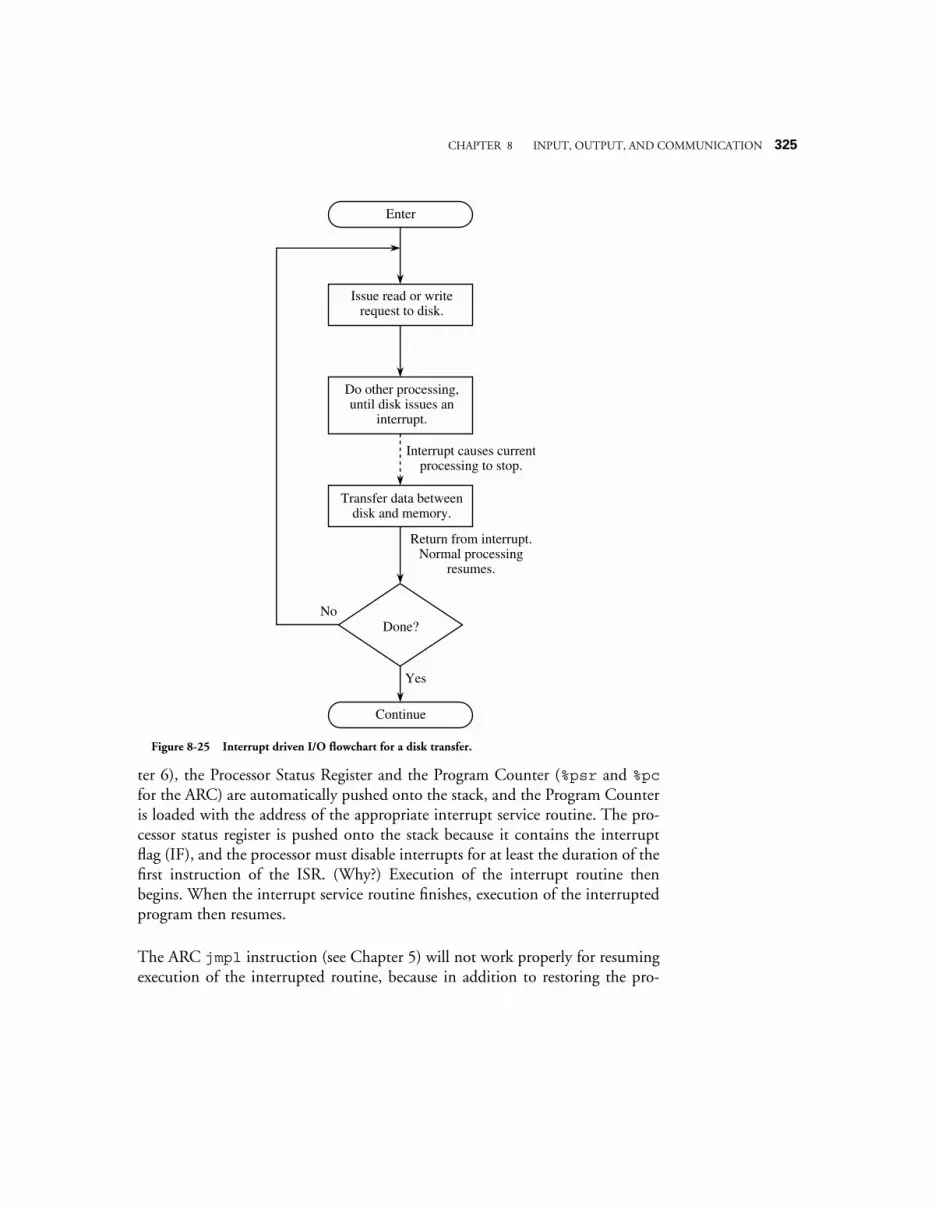
CHAPTER 8 INPUT, OUTPUT, AND COMMUNICATION 325
ter 6), the Processor Status Register and the Program Counter (%psr and %pcfor the ARC) are automatically pushed onto the stack, and the Program Counteris loaded with the address of the appropriate interrupt service routine. The pro-cessor status register is pushed onto the stack because it contains the interruptflag (IF), and the processor must disable interrupts for at least the duration of thefirst instruction of the ISR. (Why?) Execution of the interrupt routine thenbegins. When the interrupt service routine finishes, execution of the interruptedprogram then resumes.
The ARC jmpl instruction (see Chapter 5) will not work properly for resumingexecution of the interrupted routine, because in addition to restoring the pro-
Transfer data between disk and memory.
Done?No
Yes
Continue
Return from interrupt. Normal processing
resumes.
Do other processing, until disk issues an
interrupt.
Interrupt causes currentprocessing to stop.
Issue read or write request to disk.
Enter
Figure 8-25 Interrupt driven I/O flowchart for a disk transfer.
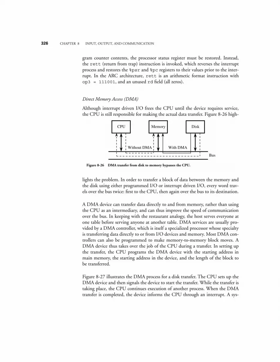
326 CHAPTER 8 INPUT, OUTPUT, AND COMMUNICATION
gram counter contents, the processor status register must be restored. Instead,the rett (return from trap) instruction is invoked, which reverses the interruptprocess and restores the %psr and %pc registers to their values prior to the inter-rupt. In the ARC architecture, rett is an arithmetic format instruction withop3 = 111001, and an unused rd field (all zeros).
Direct Memory Access (DMA)
Although interrupt driven I/O frees the CPU until the device requires service,the CPU is still responsible for making the actual data transfer. Figure 8-26 high-
lights the problem. In order to transfer a block of data between the memory andthe disk using either programmed I/O or interrupt driven I/O, every word trav-els over the bus twice: first to the CPU, then again over the bus to its destination.
A DMA device can transfer data directly to and from memory, rather than usingthe CPU as an intermediary, and can thus improve the speed of communicationover the bus. In keeping with the restaurant analogy, the host serves everyone atone table before serving anyone at another table. DMA services are usually pro-vided by a DMA controller, which is itself a specialized processor whose specialtyis transferring data directly to or from I/O devices and memory. Most DMA con-trollers can also be programmed to make memory-to-memory block moves. ADMA device thus takes over the job of the CPU during a transfer. In setting upthe transfer, the CPU programs the DMA device with the starting address inmain memory, the starting address in the device, and the length of the block tobe transferred.
Figure 8-27 illustrates the DMA process for a disk transfer. The CPU sets up theDMA device and then signals the device to start the transfer. While the transfer istaking place, the CPU continues execution of another process. When the DMAtransfer is completed, the device informs the CPU through an interrupt. A sys-
CPU DiskMemory
Without DMA With DMA
Bus
Figure 8-26 DMA transfer from disk to memory bypasses the CPU.
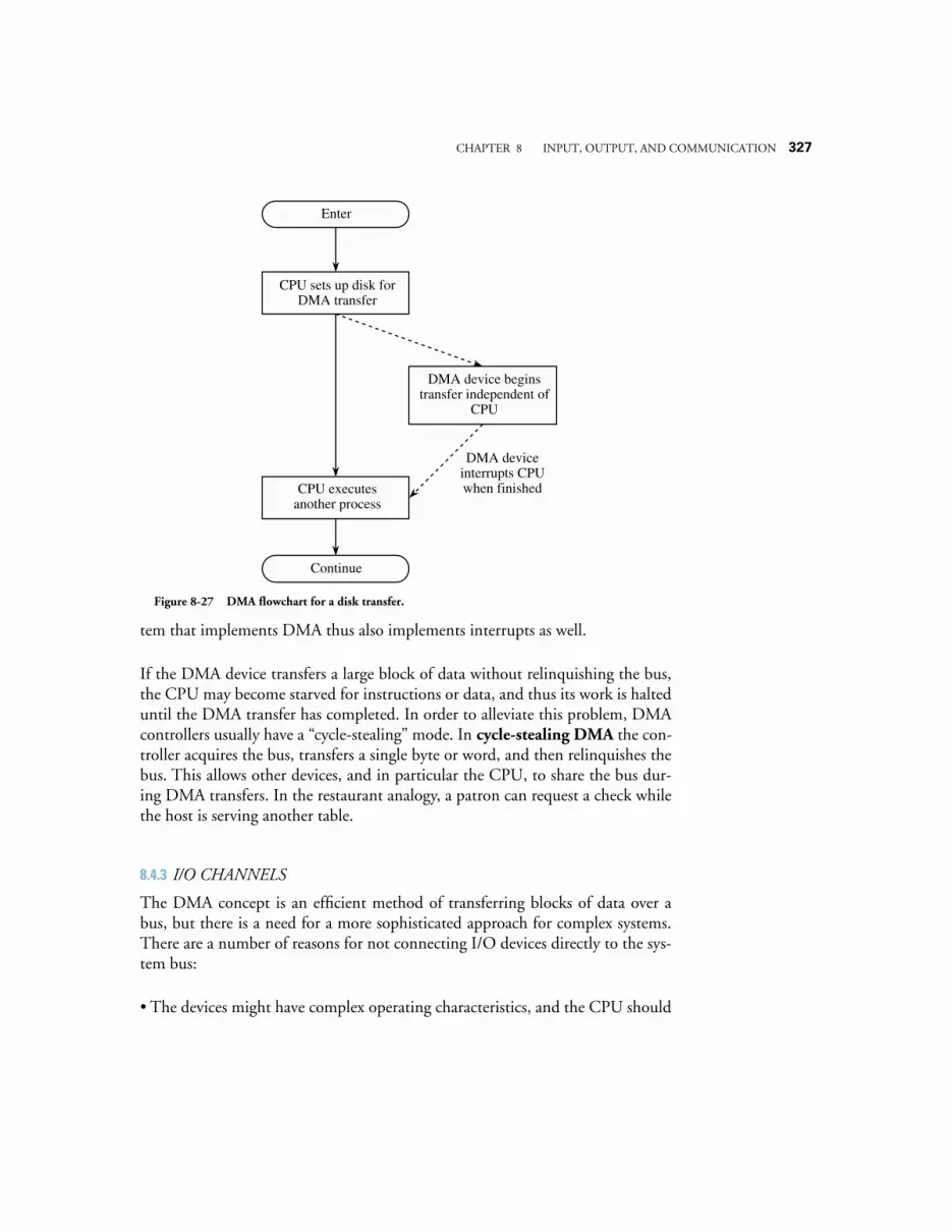
CHAPTER 8 INPUT, OUTPUT, AND COMMUNICATION 327
tem that implements DMA thus also implements interrupts as well.
If the DMA device transfers a large block of data without relinquishing the bus,the CPU may become starved for instructions or data, and thus its work is halteduntil the DMA transfer has completed. In order to alleviate this problem, DMAcontrollers usually have a “cycle-stealing” mode. In cycle-stealing DMA the con-troller acquires the bus, transfers a single byte or word, and then relinquishes thebus. This allows other devices, and in particular the CPU, to share the bus dur-ing DMA transfers. In the restaurant analogy, a patron can request a check whilethe host is serving another table.
8.4.3 I/O CHANNELS
The DMA concept is an efficient method of transferring blocks of data over abus, but there is a need for a more sophisticated approach for complex systems.There are a number of reasons for not connecting I/O devices directly to the sys-tem bus:
• The devices might have complex operating characteristics, and the CPU should
CPU executes another process
Continue
DMA device begins transfer independent of
CPU
DMA device interrupts CPU when finished
CPU sets up disk for DMA transfer
Enter
Figure 8-27 DMA flowchart for a disk transfer.
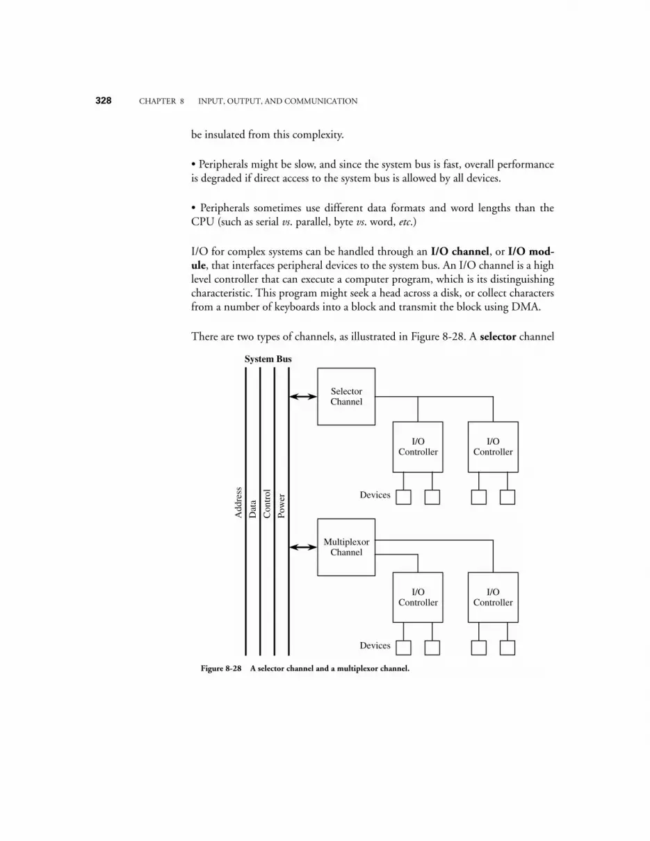
328 CHAPTER 8 INPUT, OUTPUT, AND COMMUNICATION
be insulated from this complexity.
• Peripherals might be slow, and since the system bus is fast, overall performanceis degraded if direct access to the system bus is allowed by all devices.
• Peripherals sometimes use different data formats and word lengths than theCPU (such as serial vs. parallel, byte vs. word, etc.)
I/O for complex systems can be handled through an I/O channel, or I/O mod-ule, that interfaces peripheral devices to the system bus. An I/O channel is a highlevel controller that can execute a computer program, which is its distinguishingcharacteristic. This program might seek a head across a disk, or collect charactersfrom a number of keyboards into a block and transmit the block using DMA.
There are two types of channels, as illustrated in Figure 8-28. A selector channel
Add
ress
Dat
a
Con
trol
Pow
er
System Bus
Selector Channel
I/O Controller
Devices
I/O Controller
Multiplexor Channel
I/O Controller
Devices
I/O Controller
Figure 8-28 A selector channel and a multiplexor channel.
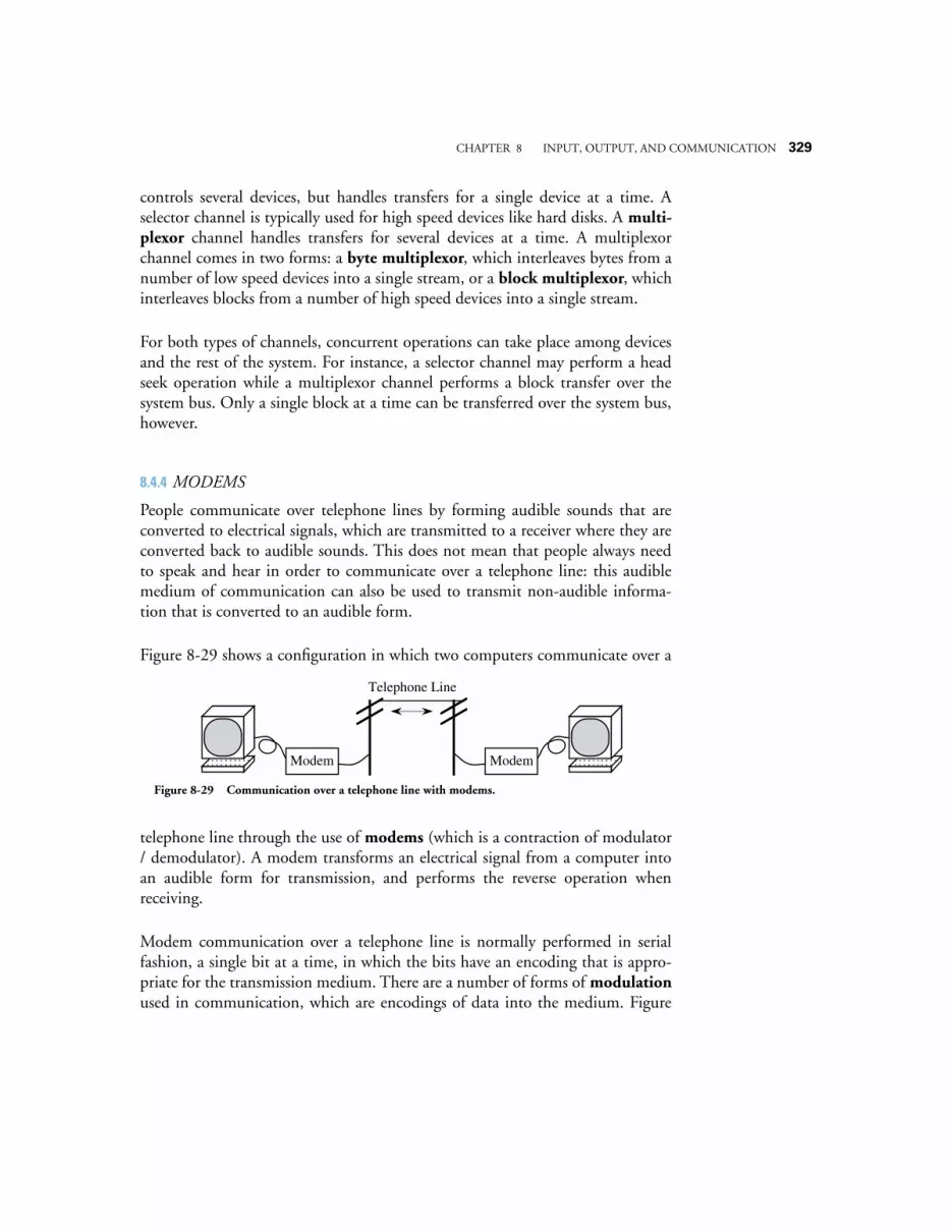
CHAPTER 8 INPUT, OUTPUT, AND COMMUNICATION 329
controls several devices, but handles transfers for a single device at a time. Aselector channel is typically used for high speed devices like hard disks. A multi-plexor channel handles transfers for several devices at a time. A multiplexorchannel comes in two forms: a byte multiplexor, which interleaves bytes from anumber of low speed devices into a single stream, or a block multiplexor, whichinterleaves blocks from a number of high speed devices into a single stream.
For both types of channels, concurrent operations can take place among devicesand the rest of the system. For instance, a selector channel may perform a headseek operation while a multiplexor channel performs a block transfer over thesystem bus. Only a single block at a time can be transferred over the system bus,however.
8.4.4 MODEMS
People communicate over telephone lines by forming audible sounds that areconverted to electrical signals, which are transmitted to a receiver where they areconverted back to audible sounds. This does not mean that people always needto speak and hear in order to communicate over a telephone line: this audiblemedium of communication can also be used to transmit non-audible informa-tion that is converted to an audible form.
Figure 8-29 shows a configuration in which two computers communicate over a
telephone line through the use of modems (which is a contraction of modulator/ demodulator). A modem transforms an electrical signal from a computer intoan audible form for transmission, and performs the reverse operation whenreceiving.
Modem communication over a telephone line is normally performed in serialfashion, a single bit at a time, in which the bits have an encoding that is appro-priate for the transmission medium. There are a number of forms of modulationused in communication, which are encodings of data into the medium. Figure
Modem Modem
Telephone Line
Figure 8-29 Communication over a telephone line with modems.
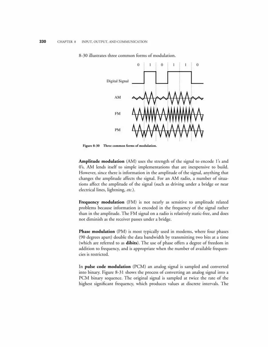
330 CHAPTER 8 INPUT, OUTPUT, AND COMMUNICATION
8-30 illustrates three common forms of modulation.
Amplitude modulation (AM) uses the strength of the signal to encode 1’s and0’s. AM lends itself to simple implementations that are inexpensive to build.However, since there is information in the amplitude of the signal, anything thatchanges the amplitude affects the signal. For an AM radio, a number of situa-tions affect the amplitude of the signal (such as driving under a bridge or nearelectrical lines, lightning, etc.).
Frequency modulation (FM) is not nearly as sensitive to amplitude relatedproblems because information is encoded in the frequency of the signal ratherthan in the amplitude. The FM signal on a radio is relatively static-free, and doesnot diminish as the receiver passes under a bridge.
Phase modulation (PM) is most typically used in modems, where four phases(90 degrees apart) double the data bandwidth by transmitting two bits at a time(which are referred to as dibits). The use of phase offers a degree of freedom inaddition to frequency, and is appropriate when the number of available frequen-cies is restricted.
In pulse code modulation (PCM) an analog signal is sampled and convertedinto binary. Figure 8-31 shows the process of converting an analog signal into aPCM binary sequence. The original signal is sampled at twice the rate of thehighest significant frequency, which produces values at discrete intervals. The
Digital Signal
AM
FM
PM
0 1 0 1 1 0
Figure 8-30 Three common forms of modulation.
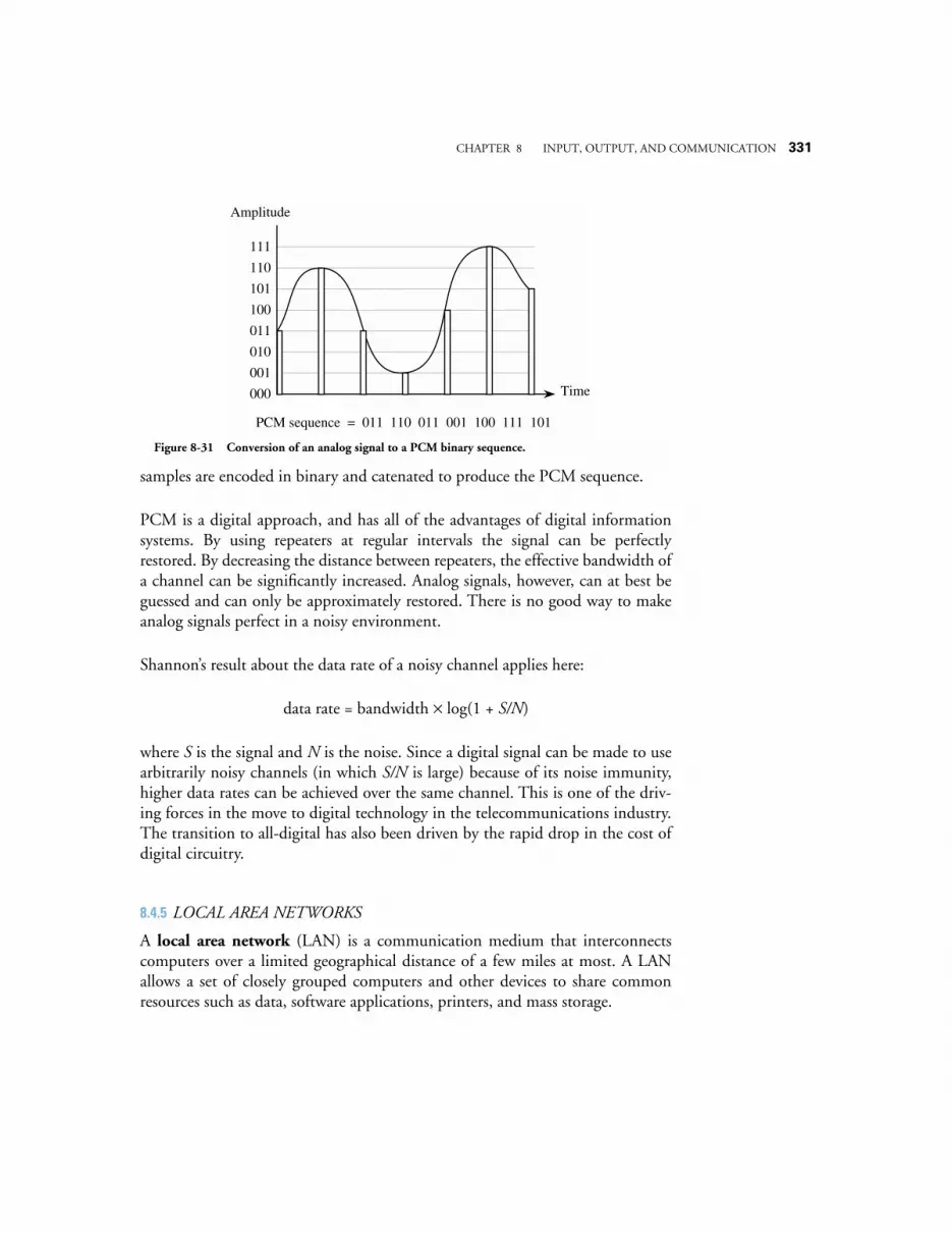
CHAPTER 8 INPUT, OUTPUT, AND COMMUNICATION 331
samples are encoded in binary and catenated to produce the PCM sequence.
PCM is a digital approach, and has all of the advantages of digital informationsystems. By using repeaters at regular intervals the signal can be perfectlyrestored. By decreasing the distance between repeaters, the effective bandwidth ofa channel can be significantly increased. Analog signals, however, can at best beguessed and can only be approximately restored. There is no good way to makeanalog signals perfect in a noisy environment.
Shannon’s result about the data rate of a noisy channel applies here:
data rate = bandwidth × log(1 + S/N)
where S is the signal and N is the noise. Since a digital signal can be made to usearbitrarily noisy channels (in which S/N is large) because of its noise immunity,higher data rates can be achieved over the same channel. This is one of the driv-ing forces in the move to digital technology in the telecommunications industry.The transition to all-digital has also been driven by the rapid drop in the cost ofdigital circuitry.
8.4.5 LOCAL AREA NETWORKS
A local area network (LAN) is a communication medium that interconnectscomputers over a limited geographical distance of a few miles at most. A LANallows a set of closely grouped computers and other devices to share commonresources such as data, software applications, printers, and mass storage.
Amplitude
000
001
010
011
100
101
110
111
Time
PCM sequence = 011 110 011 001 100 111 101
Figure 8-31 Conversion of an analog signal to a PCM binary sequence.
332 CHAPTER 8 INPUT, OUTPUT, AND COMMUNICATION
A LAN consists of hardware, software, and protocols. The hardware may be inthe form of cables and interface circuitry. The software is typically embedded inan operating system, and is responsible for connecting a user to the network. Theprotocols are sets of rules that govern format, timing, sequencing, and error con-trol. Protocols are important for ensuring that data is packaged for injection intothe network and is extracted from the network properly. The data to be transmit-ted is decomposed into pieces, each of which is prepended with a header thatcontains information about parameters such as the destination, the source, errorprotection bits, and a time stamp. The data, which is often referred to as the pay-load, is combined with the header to form a packet that is injected into the net-work. A receiver goes through the reverse process of extracting the data from thepacket.
The process of communicating over a network is normally carried out in a hier-archy of steps, each of which has its own protocol. The steps must be followed insequence for transmission, and in the reverse sequence when receiving. This leadsto the notion of a protocol stack which isolates the protocol being used withinthe hierarchy.
The OSI Model
The Open System Interconnection (OSI) model is a set of protocols establishedby the International Standards Organization (ISO) in an attempt to define andstandardize data communications. The OSI model has been largely displaced bythe Internet TCP/IP model (see Chapter 10) but still heavily influences networkcommunication, particularly for telecommunication companies.
In the OSI model the communication process is divided into seven layers: appli-cation, presentation, session, transport, network, data link, and physical assummarized in Figure 8-32. As an aid in remembering the layers, the mnemonicis sometimes used: A Powered-down System Transmits No Data Packets.
The OSI model does not give a single definition of how data communicationsactually take place. Instead, the OSI model serves as a reference for how the pro-cess should be divided and what protocols should be used at each layer. The con-cept is that equipment providers can select a protocol for each layer whileensuring compatibility with equipment from other providers that may use differ-ent protocols.
The highest level in the OSI model is the application layer, which provides an

CHAPTER 8 INPUT, OUTPUT, AND COMMUNICATION 333
interface for allowing applications to communicate with each other over the net-work. It offers high level support for applications that interact over the networksuch as database services for network database programs, message handling forelectronic mail (e-mail) programs, and file handling for file transfer programs.
The presentation layer ensures that information is presented to communicationapplications in a common format. This is necessary because different systemsmay use different internal data formats. For instance, some systems use abig-endian internal format while others use a little-endian internal format. Thefunction of the presentation layer is to insulate the applications from these differ-ences.
The session layer establishes and terminates communication sessions betweenhost processes. The session layer is responsible for maintaining the integrity ofcommunication even if the layers below it lose data. It also synchronizes theexchange, and establishes reference points for continuing an interrupted commu-nication.
The transport layer ensures reliable transmission from source to destination. It
1. Physical
2. Data Link
3. Network
4. Transport
5. Session
6. Presentation
7. Application
Figure 8-32 The seven layers of the OSI model.
334 CHAPTER 8 INPUT, OUTPUT, AND COMMUNICATION
allocates communication resources so that data is transferred both quickly andcost effectively. The session layer makes requests to the transport layer, which pri-oritizes the requests and makes trade-offs among speed, cost, and capacity. Forexample, a transmission may be split into several packets which are transmittedover a number of networks in order to obtain a faster communication time.Packets may thus arrive at the destination out of order, and it is the responsibilityof the transport layer to ensure that the session layer receives data in the sameorder it is sent. The transport layer provides error recovery from source to desti-nation, and also provides flow control (that is, it ensures that the speeds of thesender and receiver are matched).
The network layer routes data through intermediate systems and subnetworks.Unlike the upper layers, the network layer is aware of the network topology,which is the connectivity among the network components. The network layerinforms the transport layer of the status of potential and existing connections inthe network in terms of speed, reliability, and availability. The network layer istypically implemented with routers, which connect different networks that usethe same transport protocol.
The data link layer manages the direct connections between components on anetwork. This layer is divided into the logical link control (LLC) which is inde-pendent of the network topology, and the media access control (MAC) which isspecific to the topology. In some networks the physical connections betweendevices are not permanent, and it is the responsibility of the data link layer toinform the physical layer when to make connections. This layer deals in units offrames (single packets, or collections of packets that may be interleaved), whichcontain addresses, data, and control information.
The physical layer ensures that raw data is transmitted from a source to a destina-tion over the physical medium. It transmits and repeats signals across networkboundaries. The physical layer does not include the hardware itself, but includesmethods of accessing the hardware.
Topologies
There are three primary LAN organizations, as illustrated in Figure 8-33. Thebus topology is the simplest of the three. Components are connected to a bussystem by simply plugging them into the single cable that runs through the net-work, or in the case of a wireless network, by simply emitting signals into a com-mon medium. An advantage to this type of topology is that each component can
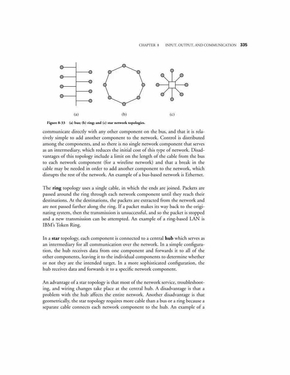
CHAPTER 8 INPUT, OUTPUT, AND COMMUNICATION 335
communicate directly with any other component on the bus, and that it is rela-tively simple to add another component to the network. Control is distributedamong the components, and so there is no single network component that servesas an intermediary, which reduces the initial cost of this type of network. Disad-vantages of this topology include a limit on the length of the cable from the busto each network component (for a wireline network) and that a break in thecable may be needed in order to add another component to the network, whichdisrupts the rest of the network. An example of a bus-based network is Ethernet.
The ring topology uses a single cable, in which the ends are joined. Packets arepassed around the ring through each network component until they reach theirdestinations. At the destinations, the packets are extracted from the network andare not passed farther along the ring. If a packet makes its way back to the origi-nating system, then the transmission is unsuccessful, and so the packet is stoppedand a new transmission can be attempted. An example of a ring-based LAN isIBM’s Token Ring.
In a star topology, each component is connected to a central hub which serves asan intermediary for all communication over the network. In a simple configura-tion, the hub receives data from one component and forwards it to all of theother components, leaving it to the individual components to determine whetheror not they are the intended target. In a more sophisticated configuration, thehub receives data and forwards it to a specific network component.
An advantage of a star topology is that most of the network service, troubleshoot-ing, and wiring changes take place at the central hub. A disadvantage is that aproblem with the hub affects the entire network. Another disadvantage is thatgeometrically, the star topology requires more cable than a bus or a ring because aseparate cable connects each network component to the hub. An example of a
(b) (c)(a)
Figure 8-33 (a) bus; (b) ring; and (c) star network topologies.
336 CHAPTER 8 INPUT, OUTPUT, AND COMMUNICATION
star-based network is ARCnet (although it is actually a bus-based network).
Data Transmission
Communication within a computer is synchronized by a common clock, and sothe transmission of a 1 or a 0 is signalled by a high or low voltage that is sampledat a time determined by the clock. This scheme is simple, but does not work wellover longer distances, as in a LAN. The problem is that there is no timing refer-ence to signal the start or stop of a bit. When there is a long string of 1’s or 0’s,timing with respect to the sending and receiving clocks may drift because theclocks are not precisely synchronized. The distances over a LAN are too great tomaintain both a global clock and high speed at the same time. LANs thus typi-cally use the Manchester encoding scheme (see Section 8.1.1), in which timing isembedded in the data.
Manchester encoding is applied at the lowest level of transmission. At the nextlevel, a data stream is decomposed into packets and frames that are transmittedover the network, not necessarily in order. The data link layer is responsible fordecomposing a data stream into packets, forming packets into frames, and inject-ing frames into the network. When receiving frames, the data link layer extractsthe packets and assembles them into a format that the higher level network layerscan use. The size of a data packet is commonly on the order of a kilobyte, andrequires a few microseconds for transmission at typical speeds and distances.
Ethernet is one of the most prevalent bus-based networks. Ethernet uses carriersense multiple access with collision detection (CSMA/CD) for transmission.Under CSMA/CD, when a network component wants to transmit data, it firstlistens for a carrier. If there is a carrier present on the line, which is placed thereby a transmitting device, then it transmits nothing and listens again after a ran-dom waiting period. The random waiting period is important in order to avoid adeadlock in which components that are trying to access the bus perpetually lis-ten and wait in synchrony.
If there is no traffic on the line, then transmission can begin by sending a carrieron the line as well as the data. The source also listens for collisions, in which twoor more components simultaneously transmit. A collision is detected by the pres-ence of more than one carrier. Collisions can occur in a fully operational networkas a result of the finite time it takes for a signal to travel the length of the bus.The propagation of signals on the bus is bounded by the speed of light over thelength of the bus, which can be 500 m in a generic Ethernet installation. When a
CHAPTER 8 INPUT, OUTPUT, AND COMMUNICATION 337
collision occurs, the transmitting components wait for a random interval beforeretransmitting.
Transmitted data moves in both directions over the bus. Every component seesevery packet of data, but only extracts those packets with corresponding destina-tion addresses. After a packet is successfully delivered, the destination can gener-ate an acknowledgment to the sender, typically at the transport layer. If thesender does not receive an acknowledgment after a fixed period of time (whichmust be greater than the round trip delay through the network), then it retrans-mits the message.
Collisions should occur infrequently in practice, and so the overhead of recover-ing from a collision is not very significant. A serious degradation in Ethernet per-formance does not occur until traffic increases to about 35% of network capacity.
Bridges, Routers, and Gateways
As networks grow in size, they can be subdivided into smaller networks that areinterconnected. The smaller subnetworks operate almost entirely independentlyof each other, and can use different protocols and topologies.
If the subnetworks all use the same topology and the same protocols, then it maybe the case that all that is needed to extend the network are repeaters. A repeateramplifies the signals on the network, which become attenuated in proportion tothe distance traveled. The overall network is divided into subnetworks, in whicheach subnetwork operates somewhat independently with respect to the others.The subnetworks are not entirely independent because every subnetwork sees allof the traffic that occurs on the other subnetworks. A network with simplerepeaters is not extensible to large sizes. Since noise is amplified as well as the sig-nal, the noise will eventually dominate the signal if too many repeaters are usedin succession.
A bridge does more than simply amplify voltage levels. A bridge restores theindividual voltage levels to logical 1 or 0, which prevents noise from accumulat-ing. Bridges have some level of intelligence, and can typically interpret the desti-nation address of a packet and route it to the appropriate subnetwork. In thisway, network traffic can be reduced, since the alternative method would be toblindly send each incoming packet to each subnetwork (as for a repeater basednetwork).

338 CHAPTER 8 INPUT, OUTPUT, AND COMMUNICATION
Although bridges have some level of intelligence in that they sense the incomingbits and make routing decisions based on destination addresses, they are unawareof protocols. A router operates at a higher level, in the network layer. Routerstypically connect logically separate networks that use the same transport proto-col.
A gateway translates packets up through the application layer of the OSI model(layers 4 through 7). Gateways connect dissimilar networks by performing proto-col conversions, message format conversions, and other high level functions.
8.5 Communication Errors and Error Correcting CodesIn all computer architectures, and especially in situations involving communica-tions between computers, there is a finite chance that the data is received in error,due to noise in the communication channel. The data representations we haveconsidered up to this point make use of the binary symbols 1 and 0. In reality,the binary symbols take on physical forms such as voltages or electric current.The physical form is subject to noise that is introduced from the environment,such as atmospheric phenomena, gamma rays, and power fluctuations, to namejust a few. The noise can cause errors, also known as faults, in which a 0 is turnedinto a 1 or a 1 is turned into a 0.
Suppose that the ASCII character ‘b’ is transmitted from a sender to a receiver,and during transmission, an error occurs, so that the least significant bit isinverted. The correct bit pattern for ASCII ‘b’ is 1100010. The bit pattern thatthe receiver sees is 1100011, which corresponds to the character ‘c.’ There is noway for the receiver to know that an error occurred simply by looking at thereceived character. The problem is that all of the possible 27 ASCII bit patternsrepresent valid characters, and if any of the bit patterns is transformed intoanother through an error, then the resulting bit pattern appears to be valid.
It is possible for the sender to transmit additional “check bits” along with thedata bits. The receiver can examine these check bits and under certain conditionsnot only detect errors, but correct them as well. Two methods of computingthese additional bits are described below. We start by introducing some prelimi-nary information and definitions.
8.5.1 BIT ERROR RATE DEFINED
There are many different ways that errors can be introduced into a computer sys-
CHAPTER 8 INPUT, OUTPUT, AND COMMUNICATION 339
tem, and those errors can take many different forms. For the moment, we willassume that the probability that a given bit is received in error is independent ofthe probability that other bits near it are received in error. In this case, we candefine the bit error rate (BER) as the probability that a given bit is erroneous.Obviously this must be a very small number, and is usually less than 10-12 errorsper bit examined for many networks. That means, loosely speaking, that as bitsare examined, only one in every 1012 bits will be erroneous.
Inside the computer system typical BER’s may run 10-18 or less. As a rough esti-mate, if the clock rate of the computer is 100 MHz, and 32 bits are manipulatedduring each clock period, then the number of errors per second for that portionof the computer will be 10-18 × 100 × 106 × 32 or 3.2 × 10⁻⁹ errors per second,approximately one erroneous bit once every 10 years.
On the other hand, if one is receiving a bit stream from a serial communicationsline at, say, 1 million bits per second, and the BER is 10-10, then a the number oferrors per second will be 1 × 106 × 10-10 or 10-4 errors per second, approxi-mately 10 errors per day.
8.5.2 ERROR DETECTION AND CORRECTION
One of the simplest and oldest methods of error detection was used to detecterrors in transmitting and receiving characters in telegraphy. A parity bit, 1 or 0,was added to each character to make the total number of 1’s in the character evenor odd, as agreed upon by sender and receiver. In our example of transmitting theASCII character ‘b,’ 1100010, assuming even parity, a 1 would be attached as aparity bit to make the total number of 1’s even, resulting in the bit pattern11000101 being transmitted. The receiver could then examine the bit pattern,and if there was an even number of 1’s, the receiver could assume that the charac-ter was received without error. (This method fails if there is significant probabil-ity of two or more bits being received in error. In this case, other methods mustbe used, as discussed later in this section.) The intuition behind this approach isexplored below.
Hamming Codes
If additional bits are added to the data then it is possible to not only detecterrors, but to correct them as well. Some of the most popular error-correctingcodes are based on the work of Richard Hamming of Bell Telephone Laborato-ries (now operated by Lucent Technologies).
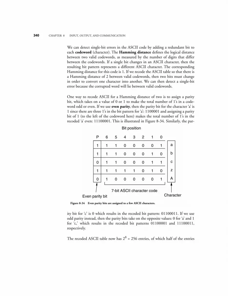
340 CHAPTER 8 INPUT, OUTPUT, AND COMMUNICATION
We can detect single-bit errors in the ASCII code by adding a redundant bit toeach codeword (character). The Hamming distance defines the logical distancebetween two valid codewords, as measured by the number of digits that differbetween the codewords. If a single bit changes in an ASCII character, then theresulting bit pattern represents a different ASCII character. The correspondingHamming distance for this code is 1. If we recode the ASCII table so that there isa Hamming distance of 2 between valid codewords, then two bits must changein order to convert one character into another. We can then detect a single-biterror because the corrupted word will lie between valid codewords.
One way to recode ASCII for a Hamming distance of two is to assign a paritybit, which takes on a value of 0 or 1 to make the total number of 1’s in a code-word odd or even. If we use even parity, then the parity bit for the character ‘a’ is1 since there are three 1’s in the bit pattern for ‘a’: 1100001 and assigning a paritybit of 1 (to the left of the codeword here) makes the total number of 1’s in therecoded ‘a’ even: 11100001. This is illustrated in Figure 8-34. Similarly, the par-
ity bit for ‘c’ is 0 which results in the recoded bit pattern: 01100011. If we useodd parity instead, then the parity bits take on the opposite values: 0 for ‘a’ and 1for ‘c,’ which results in the recoded bit patterns 01100001 and 11100011,respectively.
The recoded ASCII table now has 28 = 256 entries, of which half of the entries
P
1
1
0
1
0
6
1
1
1
1
1
5
1
1
1
1
0
4
0
0
0
1
0
3
0
0
0
1
0
2
0
0
0
0
0
1
0
1
1
1
0
0
1
0
1
0
1
Even parity bit
Bit position
7-bit ASCII character code
a
b
c
z
A
Character
Figure 8-34 Even parity bits are assigned to a few ASCII characters.
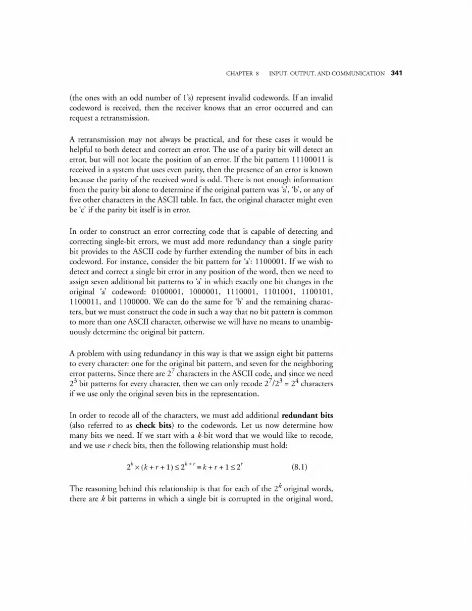
CHAPTER 8 INPUT, OUTPUT, AND COMMUNICATION 341
(the ones with an odd number of 1’s) represent invalid codewords. If an invalidcodeword is received, then the receiver knows that an error occurred and canrequest a retransmission.
A retransmission may not always be practical, and for these cases it would behelpful to both detect and correct an error. The use of a parity bit will detect anerror, but will not locate the position of an error. If the bit pattern 11100011 isreceived in a system that uses even parity, then the presence of an error is knownbecause the parity of the received word is odd. There is not enough informationfrom the parity bit alone to determine if the original pattern was ‘a’, ‘b’, or any offive other characters in the ASCII table. In fact, the original character might evenbe ‘c’ if the parity bit itself is in error.
In order to construct an error correcting code that is capable of detecting andcorrecting single-bit errors, we must add more redundancy than a single paritybit provides to the ASCII code by further extending the number of bits in eachcodeword. For instance, consider the bit pattern for ‘a’: 1100001. If we wish todetect and correct a single bit error in any position of the word, then we need toassign seven additional bit patterns to ‘a’ in which exactly one bit changes in theoriginal ‘a’ codeword: 0100001, 1000001, 1110001, 1101001, 1100101,1100011, and 1100000. We can do the same for ‘b’ and the remaining charac-ters, but we must construct the code in such a way that no bit pattern is commonto more than one ASCII character, otherwise we will have no means to unambig-uously determine the original bit pattern.
A problem with using redundancy in this way is that we assign eight bit patternsto every character: one for the original bit pattern, and seven for the neighboringerror patterns. Since there are 27 characters in the ASCII code, and since we need23 bit patterns for every character, then we can only recode 27/23 = 24 charactersif we use only the original seven bits in the representation.
In order to recode all of the characters, we must add additional redundant bits(also referred to as check bits) to the codewords. Let us now determine howmany bits we need. If we start with a k-bit word that we would like to recode,and we use r check bits, then the following relationship must hold:
(8.1)
The reasoning behind this relationship is that for each of the 2k original words,there are k bit patterns in which a single bit is corrupted in the original word,
2k k r 1+ +( )× 2k r+≤ k r 1+ + 2r≤≡

342 CHAPTER 8 INPUT, OUTPUT, AND COMMUNICATION
plus r bit patterns in which one of the check bits is in error, plus the originaluncorrupted bit pattern. Thus, our error correcting code will have a total of 2k ×(k + r + 1) bit patterns. In order to support all of these bit patterns, there must beenough bit patterns generated by k + r bits, thus 2k+r must be greater than orequal to the number of bit patterns in the error correcting code. There are k = 7bits in the ASCII code, and so we must now solve for r. If we try a few successivevalues, starting at 1, we find that r = 4 is the smallest value that satisfies relation8.1. The resulting codewords will thus have 7 + 4 = 11 bits.
We now consider how to recode the ASCII table into the 11-bit code. Our goalis to assign the redundant bits to the original words in such a way that any sin-gle-bit error can be identified. One way to make the assignment is shown in Fig-ure 8-35. Each of the 11 bits in the recoded word are assigned a position in the
table indexed from 1 to 11, and the 4-bit binary representations of the integers 1through 11 are shown next to each index. With this assignment, reading acrosseach of the 11 rows of four check bits, there is a unique positioning of the 1 bitsin each row, and so no two rows are the same. For example, the top row has a sin-gle 1 in position C1, but no other row has only a single 1 in position C1 (otherrows have a 1 in position C1, but they also have 1’s in the other check bit posi-tions.)
Now, reading down each of the four check bit columns, the positions of the 1bits tell us which bits, listed in the rightmost ‘Bit position checked’ column, areincluded in a group that must form even parity. For example, check bit C8 coversa group of 4 bits in positions 8, 9, 10, and 11, that collectively must form evenparity. If this property is satisfied when the 11-bit word is transmitted, but an
C8
00000001111
C4
00011110000
C2
01100110011
C1
10101010101
1234567891011
Check bits Bit position checked
Figure 8-35 Check bits for a single error correcting ASCII code.
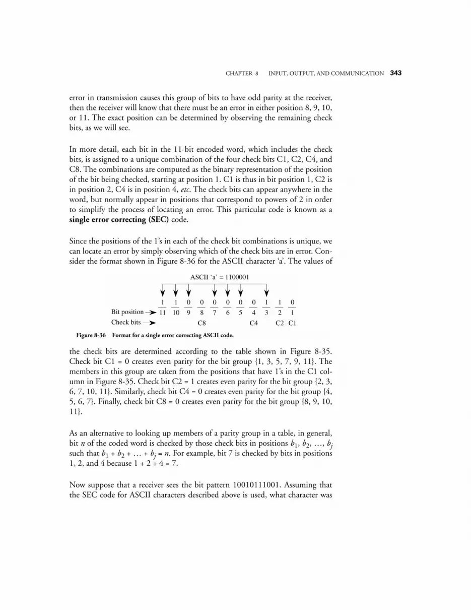
CHAPTER 8 INPUT, OUTPUT, AND COMMUNICATION 343
error in transmission causes this group of bits to have odd parity at the receiver,then the receiver will know that there must be an error in either position 8, 9, 10,or 11. The exact position can be determined by observing the remaining checkbits, as we will see.
In more detail, each bit in the 11-bit encoded word, which includes the checkbits, is assigned to a unique combination of the four check bits C1, C2, C4, andC8. The combinations are computed as the binary representation of the positionof the bit being checked, starting at position 1. C1 is thus in bit position 1, C2 isin position 2, C4 is in position 4, etc. The check bits can appear anywhere in theword, but normally appear in positions that correspond to powers of 2 in orderto simplify the process of locating an error. This particular code is known as asingle error correcting (SEC) code.
Since the positions of the 1’s in each of the check bit combinations is unique, wecan locate an error by simply observing which of the check bits are in error. Con-sider the format shown in Figure 8-36 for the ASCII character ‘a’. The values of
the check bits are determined according to the table shown in Figure 8-35.Check bit C1 = 0 creates even parity for the bit group 1, 3, 5, 7, 9, 11. Themembers in this group are taken from the positions that have 1’s in the C1 col-umn in Figure 8-35. Check bit C2 = 1 creates even parity for the bit group 2, 3,6, 7, 10, 11. Similarly, check bit C4 = 0 creates even parity for the bit group 4,5, 6, 7. Finally, check bit C8 = 0 creates even parity for the bit group 8, 9, 10,11.
As an alternative to looking up members of a parity group in a table, in general,bit n of the coded word is checked by those check bits in positions b1, b2, …, bjsuch that b1 + b2 + … + bj = n. For example, bit 7 is checked by bits in positions1, 2, and 4 because 1 + 2 + 4 = 7.
Now suppose that a receiver sees the bit pattern 10010111001. Assuming thatthe SEC code for ASCII characters described above is used, what character was
Bit position1 1 0 0 0 0 0 0 1 1 0
11 10 9 8 7 6 5 4 3 2 1Check bits C2 C1C8 C4
ASCII ‘a’ = 1100001
Figure 8-36 Format for a single error correcting ASCII code.

344 CHAPTER 8 INPUT, OUTPUT, AND COMMUNICATION
sent? We start by computing the parity for each of the check bits as shown in Fig-ure 8-37. As shown in the figure, check bits C1 and C4 have odd parity. In order
to locate the error, we simply add up the positions of the odd check bits. Theerror then, is in position 1 + 4 = 5. The word that was sent is 10010101001. Ifwe strip away the check bits, then we end up with the bit pattern 1000100 whichcorresponds to the ASCII character ‘D’.
One way to think about an SEC code is that valid codewords are spaced farenough apart so that a single error places a corrupted codeword closer to one par-ticular valid codeword than to any other valid codeword. For example, consideran SEC code for a set of just two symbols: 000, 111. The Hamming distancerelationships for all three-bit patterns are shown for this code in the cube in Fig-ure 8-38. The cube has correspondingly higher dimensions for larger word sizes,
resulting in what is called a hypercube. The two valid codewords are shown on
Bit position1 0 0 1 0 1 1 1 0 0 1
11 10 9 8 7 6 5 4 3 2 1Check bits C2 C1C8 C4
Location of error
C1 checks: 1, 3, 5, 7, 9, 11 oddC2 checks: 2, 3, 6, 7, 10, 11 evenC4 checks: 4, 5, 6, 7 oddC8 checks: 8, 9, 10, 11 even
Parity
Figure 8-37 Parity computation for an ASCII character in an SEC code.
000 001
010 011
100 101
110 111
Validcodeword
Validcodeword
Three changed bits between valid codewords results in a Hamming distance of 3.
Error codewords
Error codewords
Figure 8-38 Hamming distance relationships among three-bit codewords. Valid codewords are 000
and 111. The remaining codewords represent errors.
CHAPTER 8 INPUT, OUTPUT, AND COMMUNICATION 345
opposing vertices. Any single bit error will locate an invalid codeword at a differ-ent vertex on the cube. Every error codeword has a closest valid codeword, whichmakes single error correction possible.
SECDED Encoding
If we now consider the case in which there are two errors, then we can see thatthe SEC code works for double error detection (DED), but not for doubleerror correction (DEC). This is sometimes referred to as SECDED encoding.Since valid codewords are spaced at a Hamming distance of 3, two errors willlocate an error codeword on the cube, and thus two errors can be detected. Theoriginal codeword cannot be determined unambiguously, however, since verticesthat correspond to two errors from one codeword overlap vertices that corre-spond to a single error from another codeword. Thus, every SEC code is also aDED code, but every DED code is not necessarily a DEC code. In order to cor-rect two errors, a Hamming distance of five must be maintained. In general, aHamming distance of p + 1 must be maintained in order to detect p errors, and aHamming distance of 2p + 1 must be maintained to correct p errors.
8.5.3 VERTICAL REDUNDANCY CHECKING
The SEC code described in the previous section is used for detecting and correct-ing single bit errors in individual data words. Redundant bits are added to eachdata word, and each resulting codeword is treated independently. The recodingscheme is sometimes referred to as horizontal or longitudinal redundancychecking (LRC) because the width of the codeword is extended for the redun-dant bits.
An alternative approach is to use a vertical redundancy checking (VRC) code,in which a checksum word is added at the end of a group of words that are trans-mitted. In this case, parity is computed on a column by column basis, forming achecksum word that is appended to the message. The checksum word is com-puted and transmitted by the sender, and is recomputed and compared to thetransmitted checksum word by the receiver. If an error is detected, then thereceiver must request a retransmission since there is not enough redundancy toidentify the position of an error. The VRC and LRC codes can be combined toimprove error checking, as shown for the ASCII characters ‘A’ through ‘H’ inFigure 8-39.
In some situations, errors are bursty, and may corrupt several contiguous bits
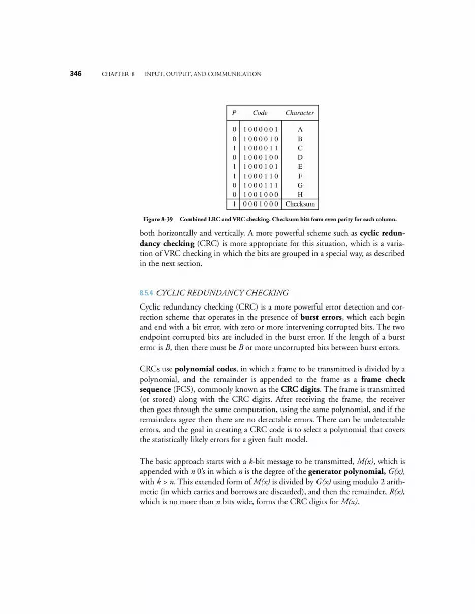
346 CHAPTER 8 INPUT, OUTPUT, AND COMMUNICATION
both horizontally and vertically. A more powerful scheme such as cyclic redun-dancy checking (CRC) is more appropriate for this situation, which is a varia-tion of VRC checking in which the bits are grouped in a special way, as describedin the next section.
8.5.4 CYCLIC REDUNDANCY CHECKING
Cyclic redundancy checking (CRC) is a more powerful error detection and cor-rection scheme that operates in the presence of burst errors, which each beginand end with a bit error, with zero or more intervening corrupted bits. The twoendpoint corrupted bits are included in the burst error. If the length of a bursterror is B, then there must be B or more uncorrupted bits between burst errors.
CRCs use polynomial codes, in which a frame to be transmitted is divided by apolynomial, and the remainder is appended to the frame as a frame checksequence (FCS), commonly known as the CRC digits. The frame is transmitted(or stored) along with the CRC digits. After receiving the frame, the receiverthen goes through the same computation, using the same polynomial, and if theremainders agree then there are no detectable errors. There can be undetectableerrors, and the goal in creating a CRC code is to select a polynomial that coversthe statistically likely errors for a given fault model.
The basic approach starts with a k-bit message to be transmitted, M(x), which isappended with n 0’s in which n is the degree of the generator polynomial, G(x),with k > n. This extended form of M(x) is divided by G(x) using modulo 2 arith-metic (in which carries and borrows are discarded), and then the remainder, R(x),which is no more than n bits wide, forms the CRC digits for M(x).
111111110
000000000
Code
001011001
P
000000000
Character
ABCDEFGH
Checksum
000000011
000111100
011001100
101010100
Figure 8-39 Combined LRC and VRC checking. Checksum bits form even parity for each column.
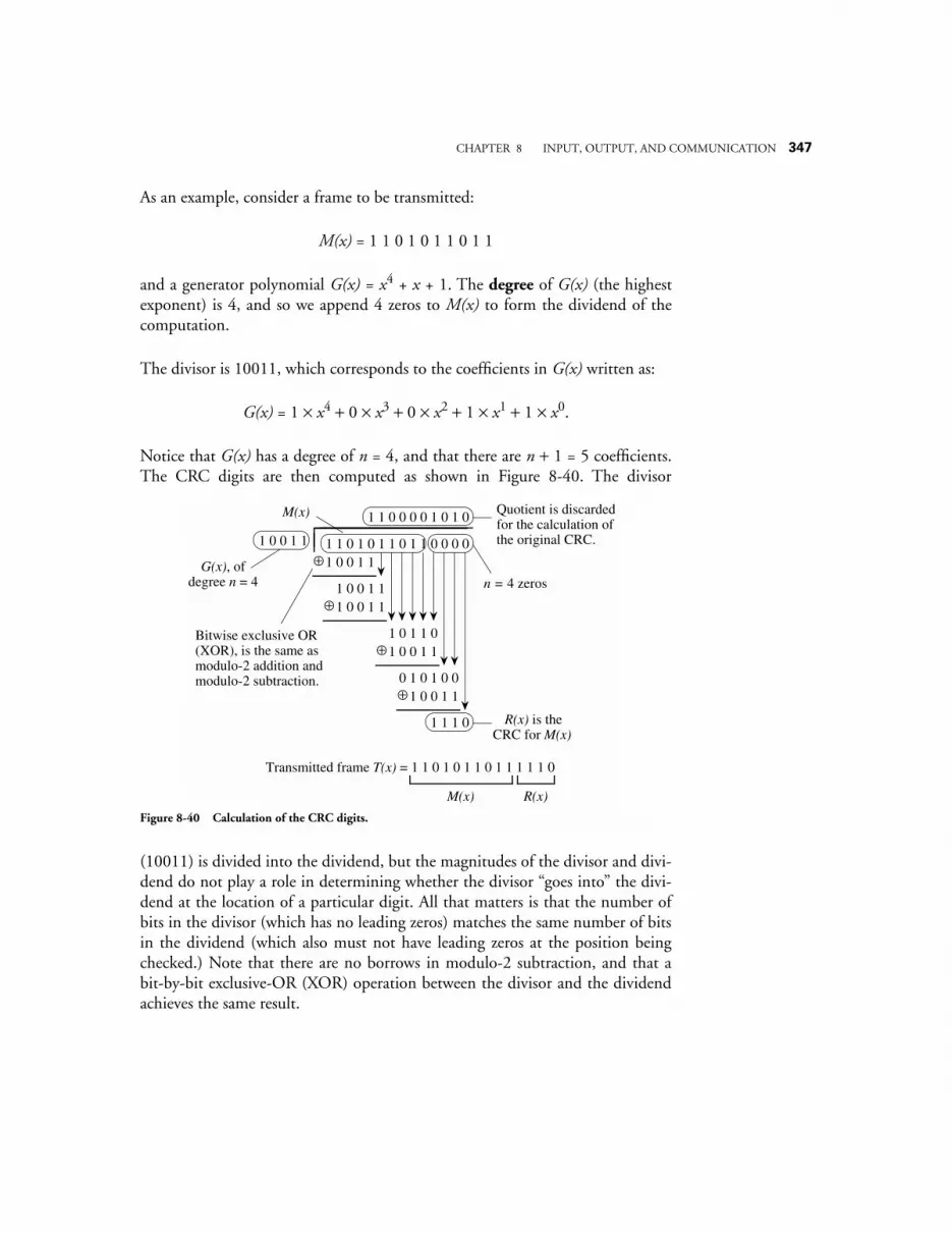
CHAPTER 8 INPUT, OUTPUT, AND COMMUNICATION 347
As an example, consider a frame to be transmitted:
M(x) = 1 1 0 1 0 1 1 0 1 1
and a generator polynomial G(x) = x4 + x + 1. The degree of G(x) (the highestexponent) is 4, and so we append 4 zeros to M(x) to form the dividend of thecomputation.
The divisor is 10011, which corresponds to the coefficients in G(x) written as:
G(x) = 1 × x4 + 0 × x3 + 0 × x2 + 1 × x1 + 1 × x0.
Notice that G(x) has a degree of n = 4, and that there are n + 1 = 5 coefficients.The CRC digits are then computed as shown in Figure 8-40. The divisor
(10011) is divided into the dividend, but the magnitudes of the divisor and divi-dend do not play a role in determining whether the divisor “goes into” the divi-dend at the location of a particular digit. All that matters is that the number ofbits in the divisor (which has no leading zeros) matches the same number of bitsin the dividend (which also must not have leading zeros at the position beingchecked.) Note that there are no borrows in modulo-2 subtraction, and that abit-by-bit exclusive-OR (XOR) operation between the divisor and the dividendachieves the same result.
1 1 0 1 0 1 1 0 1 1 0 0 0 01 0 0 1 1
1 1 0 0 0 0 1 0 1 0
1 0 0 1 1⊕
1 0 0 1 11 0 0 1 1⊕
11 0 0 1 1⊕
0 1 0 1 01 0 0 1 1⊕
1 1 1 0
0 1 1 0
0
G(x), of degree n = 4
M(x)
n = 4 zeros
Bitwise exclusive OR (XOR), is the same as modulo-2 addition and modulo-2 subtraction.
Quotient is discarded for the calculation of the original CRC.
R(x) is the CRC for M(x)
Transmitted frame T(x) = 1 1 0 1 0 1 1 0 1 1 1 1 1 0
M(x) R(x)
Figure 8-40 Calculation of the CRC digits.
348 CHAPTER 8 INPUT, OUTPUT, AND COMMUNICATION
Now suppose that the transmitted frame T(x) = M(x) + R(x) gets corrupted dur-ing transmission. The receiver needs to detect that this has happened. Thereceiver divides the received frame by G(x), and all burst errors that do notinclude G(x) as a factor will be caught because there will be a nonzero remainderfor these cases. That is, as long as the 1’s in 10011 do not coincide with the posi-tions of errors in the received frame, all errors will be caught. In general, a poly-nomial code of degree n will catch all burst errors of length ≤ n.
Common polynomials that give good error coverage include:
CRC-16 = x16 + x15 + x2 + 1
CRC-CCITT = x16 + x12 + x5 + 1
CRC-32 = x32 + x26 + x23 + x16 + x12 + x11 + x10 + x8 + x7 + x5 + x4 + x2 + x + 1
A deeper analysis of CRC codes is beyond the scope of this book, and the readeris referred to (Hamming, 1986) for further details.
EXAMPLE: ERROR CORRECTION
Consider how many check bits are needed for a double-error correcting ASCII code. There are k = 7 bits for each ASCII character, and we need to add r check bits to each codeword. For each of the 2k ASCII characters there are k + r possible one-bit error patterns, there are possible two-bit error pat-terns, and there is one bit pattern for the uncorrupted codeword. There are 2k+r possible bit patterns, and so the following relation must hold:
Simplifying, using k = 7, yields: r2 + 15r + 58 ≤ 2r+1 for which r = 7 is the smallest value that satisfies the relation.
k r+( ) k r 1–+( )2
-----------------------------------------
Number of original
codewords
Number of one-bit errors
Number of two-bit errors
Uncorrupted codeword
2k × k + r +k + r k + r – 1
2 + 1 ≤ 2k + r
Number of possible bit
patterns
CHAPTER 8 INPUT, OUTPUT, AND COMMUNICATION 349
Since a Hamming distance of 2p + 1 must be maintained to correct p errors, the Hamming distance for this DEC code must be at least 2 × 2 + 1 = 5. If we use the same encoding for error detection instead, then we have p + 1 = 5, and since a Hamming distance of p + 1 must be maintained to detect p errors, then p = 4 errors can be detected.
EXAMPLE: TRANSFER TIME FOR A HARD DISK
Consider calculating the transfer time of a hard magnetic disk. For this example,assume that a disk rotates once every 16 ms. The seek time to move the headbetween adjacent tracks is 2 ms. There are 32 sectors per track that are stored inlinear order (non-interleaved), from sector 0 to sector 31. The head sees the sec-tors in that order.
Assume the read/write head is positioned at the start of sector 1 on track 12.There is a memory buffer that is large enough to hold an entire track. Data istransferred between disk locations by reading the source data into memory, posi-tioning the read/write head over the destination location, and writing the data tothe destination.
How long will it take to transfer sector 1 on track 12 to sector 1 on track 13?How long will it take to transfer all of the sectors of track 12 to the correspond-ing sectors on track 13? Note that sectors do not have to be written in the sameorder they are read.
Solution:
The time to transfer a sector from one track to the next can be decomposed intoits parts: the sector read time, the head movement time, the rotational delay, andthe sector write time.
The time to read or write a sector is simply the time it takes for the sector to passunder the head, which is (16 ms/track) × (1/32 tracks/sector) = .5 ms/sector. Forthis example, the head movement time is only 2 ms because the head movesbetween adjacent tracks. After reading sector 1 on track 12, which takes .5 ms,an additional 15.5 ms of rotational delay is needed for the head to line up withsector 1 again. The head movement time of 2 ms overlaps the 15.5 ms of rota-tional delay, and so only the greater of the two times (15.5 ms) is used.
350 CHAPTER 8 INPUT, OUTPUT, AND COMMUNICATION
We sum the individual times and obtain: .5 ms + 15.5 ms + .5 ms = 16.5 ms totransfer sector 1 on track 12 to sector 1 on track 13.
The time to transfer all of track 12 to track 13 is computed in a similar manner.The memory buffer can hold an entire track, and so the time to read or write anentire track is simply the rotational delay for a track, which is 16 ms. The headmovement time is 2 ms, which is also the time for four sectors to pass under thehead. Thus, after reading a track and moving the head, the head is now on track13, at four sectors past the initial sector that was read on track 12.
Sectors can be written in a different order than they are read. Track 13 can thusbe written with a four sector offset with respect to how track 12 was read. Thetime to write track 13 is 16 ms, and the time for the entire transfer then is: 16 ms+ 2 ms + 16 ms = 34 ms. Notice that the rotational delay is zero for this examplebecause the head lands at the beginning of the first sector to be written.
8.6 Case Study: Communication on the Intel Pentium ArchitectureThe Intel Pentium processor family is Intel’s current state-of-the art implementa-tion of their venerable x86 family, which began with the Intel 8086, released in1978. The Pentium is itself a processor family, with versions that emphasize highspeed, multiprocessor environments, graphics, low power, etc. In this section weexamine the common features that underlie the Pentium system bus.
System clock, bus clock, and bus speeds
Interestingly, the system clock speed is set as a multiple of the bus clock. Thevalue of the multiple is set by the processor whenever it is reset, according to thevalues on several of its pins. The possible values of the multiple vary across familymembers. For example, the Pentium Pro, a family member adapted for multipleCPU applications, can have multipliers ranging from 2 to 3-1/2. We mentionagain here that the reason for clocking the system bus at a slower rate than theCPU is that CPU operations can take place faster than memory access opera-tions. A common bus clock frequency in Pentium systems is 66 MHz.
Address, data, memory, and I/O capabilities
The system bus effectively has 32 address lines, and can thus address up to 4 GBof main memory. Its data bus is 64 bits wide; thus the processor is capable oftransferring an 8-byte quadword in one bus cycle. (Intel x86 words are 16-bits
CHAPTER 8 INPUT, OUTPUT, AND COMMUNICATION 351
long.) We say “effectively” because in fact the Pentium processor decodes theleast significant three address lines, A2-A0, into eight “byte enable” lines,BE0#-BE7#, prior to placing them on the system bus.1 The values on these eightlines specify the byte, word, double word, or quad word that is to be transferredfrom the base address specified by A31-A3.
Data words have soft-alignment
Data values have so-called soft alignment, meaning that words, double words,and quad words should be aligned on even word, double word, and quad wordboundaries for maximum efficiency, but the processor can tolerate misaligneddata items. The penalty for accessing misaligned words may be two bus cycles,which are required to access both halves of the datum.2
As a bow to the small address spaces of early family members, all Intel processorshave separate address spaces for memory and I/O accesses. The address space tobe selected is specified by the M/IO# bus line. A high value on this line selectsthe 2 GB memory address space, and low specifies the I/O address space. Sepa-rate opcodes, IN and OUT, are used to access this space. It is the responsibility ofall devices on the bus to sample the M/IO# line at the beginning of each buscycle to determine the address space to which the bus cycle is referring—memoryor I/O. Figure 8-41shows these address spaces graphically. I/O addresses in thex86 family are limited to 16 bits, allowing up to 64K I/O locations. Figure 8-41shows the two address spaces.
Bus cycles in the Pentium family
The Pentium processor has a total of 18 different bus cycles, to serve differentneeds. These include the standard memory read and write bus cycles, the bushold cycle, used to allow other devices to become the bus master, an interruptacknowledge cycle, various “burst” cache access cycles, and a number of otherspecial purpose bus cycles. In this Case Study we examine the read and write buscycles, the “burst read” cycle, in which a burst of data can be transferred, and thebus hold/hold acknowledge cycle, which is used by devices that wish to become
1. The “#” symbol is Intel’s notation for a bus line that is active low.
2. Many systems require so-called hard alignment. Misaligned words are not allowed, andtheir detection causes a processor exception to be raised.
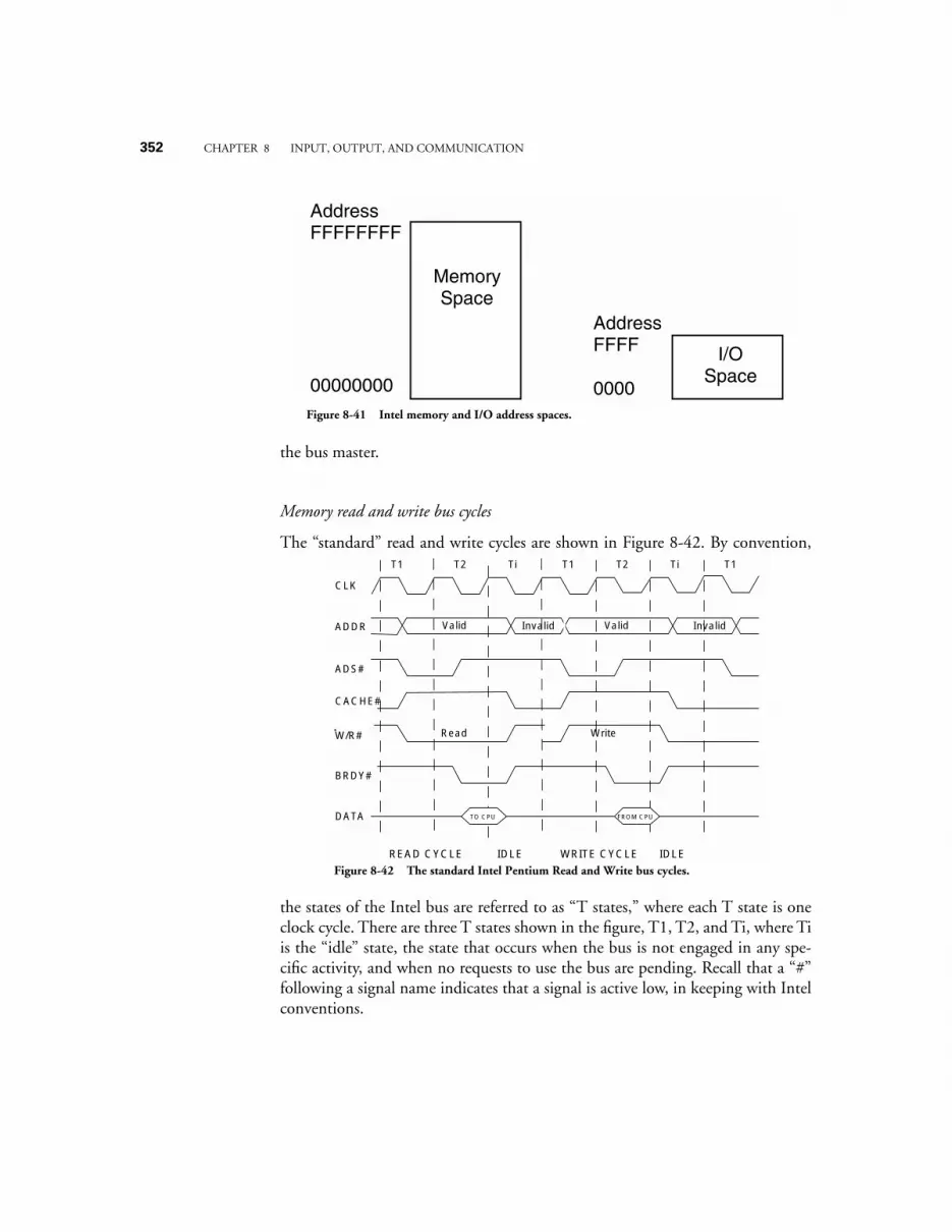
352 CHAPTER 8 INPUT, OUTPUT, AND COMMUNICATION
the bus master.
Memory read and write bus cycles
The “standard” read and write cycles are shown in Figure 8-42. By convention,
the states of the Intel bus are referred to as “T states,” where each T state is oneclock cycle. There are three T states shown in the figure, T1, T2, and Ti, where Tiis the “idle” state, the state that occurs when the bus is not engaged in any spe-cific activity, and when no requests to use the bus are pending. Recall that a “#”following a signal name indicates that a signal is active low, in keeping with Intelconventions.
AddressFFFFFFFF
00000000
AddressFFFF
0000
MemorySpace
I/OSpace
Figure 8-41 Intel memory and I/O address spaces.
T1 T2 Ti T1 T2 Ti T1
Read Write
TO CPU FROM CPU
READ CYCLE IDLE IDLEWRITE CYCLE
ADDR
ADS#
Valid ValidInvalid Invalid
W/R#
BRDY#
CACHE#
DATA
CLK
Figure 8-42 The standard Intel Pentium Read and Write bus cycles.
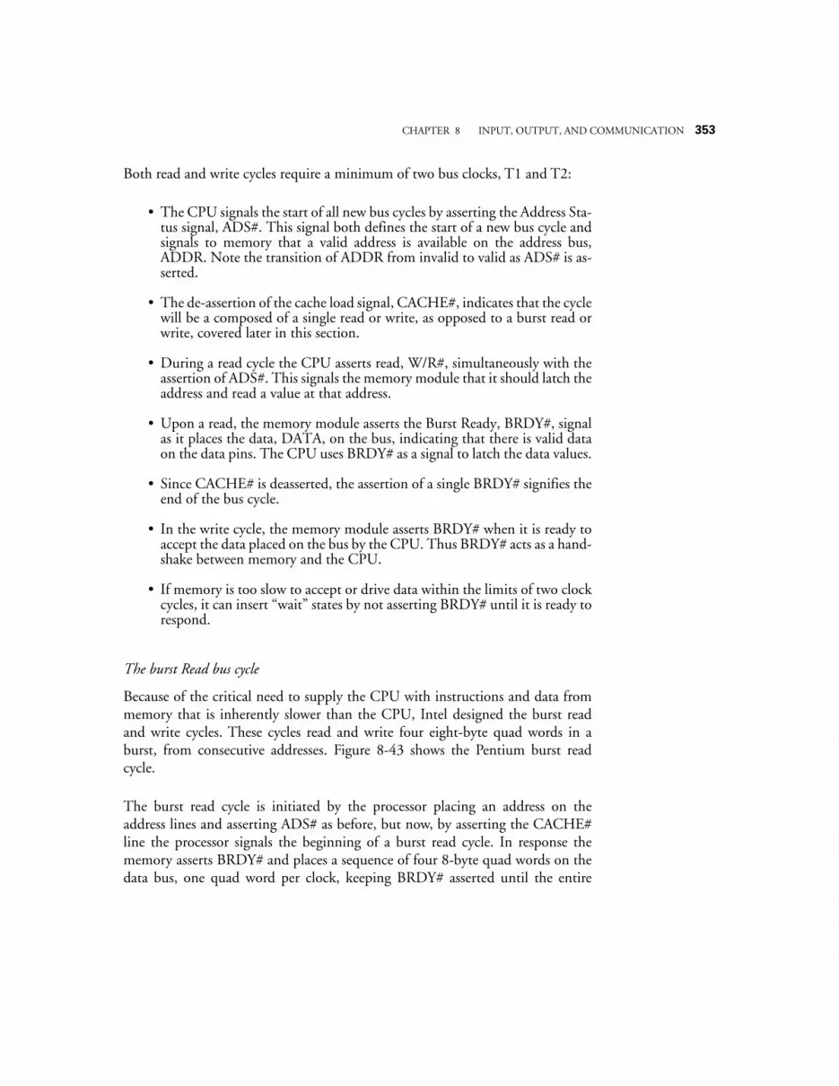
CHAPTER 8 INPUT, OUTPUT, AND COMMUNICATION 353
Both read and write cycles require a minimum of two bus clocks, T1 and T2:
• The CPU signals the start of all new bus cycles by asserting the Address Sta-tus signal, ADS#. This signal both defines the start of a new bus cycle andsignals to memory that a valid address is available on the address bus,ADDR. Note the transition of ADDR from invalid to valid as ADS# is as-serted.
• The de-assertion of the cache load signal, CACHE#, indicates that the cyclewill be a composed of a single read or write, as opposed to a burst read orwrite, covered later in this section.
• During a read cycle the CPU asserts read, W/R#, simultaneously with theassertion of ADS#. This signals the memory module that it should latch theaddress and read a value at that address.
• Upon a read, the memory module asserts the Burst Ready, BRDY#, signalas it places the data, DATA, on the bus, indicating that there is valid dataon the data pins. The CPU uses BRDY# as a signal to latch the data values.
• Since CACHE# is deasserted, the assertion of a single BRDY# signifies theend of the bus cycle.
• In the write cycle, the memory module asserts BRDY# when it is ready toaccept the data placed on the bus by the CPU. Thus BRDY# acts as a hand-shake between memory and the CPU.
• If memory is too slow to accept or drive data within the limits of two clockcycles, it can insert “wait” states by not asserting BRDY# until it is ready torespond.
The burst Read bus cycle
Because of the critical need to supply the CPU with instructions and data frommemory that is inherently slower than the CPU, Intel designed the burst readand write cycles. These cycles read and write four eight-byte quad words in aburst, from consecutive addresses. Figure 8-43 shows the Pentium burst readcycle.
The burst read cycle is initiated by the processor placing an address on theaddress lines and asserting ADS# as before, but now, by asserting the CACHE#line the processor signals the beginning of a burst read cycle. In response thememory asserts BRDY# and places a sequence of four 8-byte quad words on thedata bus, one quad word per clock, keeping BRDY# asserted until the entire
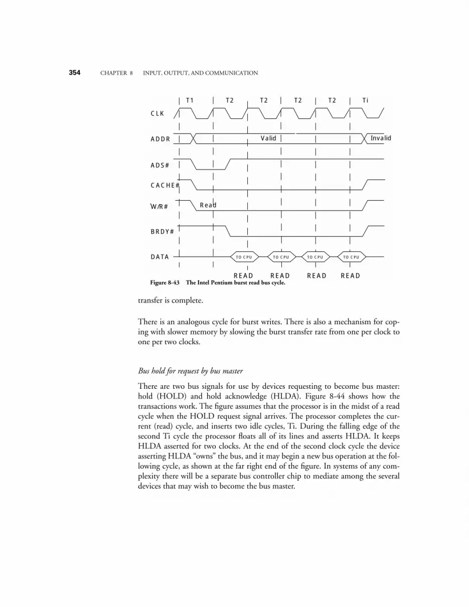
354 CHAPTER 8 INPUT, OUTPUT, AND COMMUNICATION
transfer is complete.
There is an analogous cycle for burst writes. There is also a mechanism for cop-ing with slower memory by slowing the burst transfer rate from one per clock toone per two clocks.
Bus hold for request by bus master
There are two bus signals for use by devices requesting to become bus master:hold (HOLD) and hold acknowledge (HLDA). Figure 8-44 shows how thetransactions work. The figure assumes that the processor is in the midst of a readcycle when the HOLD request signal arrives. The processor completes the cur-rent (read) cycle, and inserts two idle cycles, Ti. During the falling edge of thesecond Ti cycle the processor floats all of its lines and asserts HLDA. It keepsHLDA asserted for two clocks. At the end of the second clock cycle the deviceasserting HLDA “owns” the bus, and it may begin a new bus operation at the fol-lowing cycle, as shown at the far right end of the figure. In systems of any com-plexity there will be a separate bus controller chip to mediate among the severaldevices that may wish to become the bus master.
T1 T2 T2 T2 T2 Ti
Read
TO CPU TO CPU TO CPU TO CPU
READ READ READ READ
ADDR
ADS#
Valid Invalid
W/R#
BRDY#
CACHE#
DATA
CLK
Figure 8-43 The Intel Pentium burst read bus cycle.
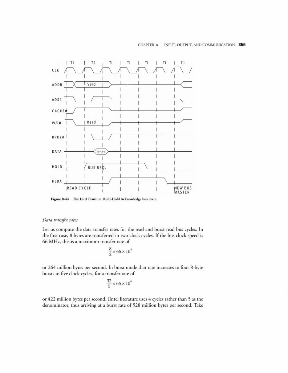
CHAPTER 8 INPUT, OUTPUT, AND COMMUNICATION 355
Data transfer rates
Let us compute the data transfer rates for the read and burst read bus cycles. Inthe first case, 8 bytes are transferred in two clock cycles. If the bus clock speed is66 MHz, this is a maximum transfer rate of
or 264 million bytes per second. In burst mode that rate increases to four 8-bytebursts in five clock cycles, for a transfer rate of
or 422 million bytes per second. (Intel literature uses 4 cycles rather than 5 as thedenominator, thus arriving at a burst rate of 528 million bytes per second. Take
T1 T2 Ti Ti Ti Ti T1
Read
TO CPU
READ CYCLE
BUS REQ.
NEW BUSMASTER
ADDR
ADS#
Valid
W/R#
BRDY#
CACHE#
DATA
HOLD
HLDA
CLK
Figure 8-44 The Intel Pentium Hold-Hold Acknowledge bus cycle.
82--- 66× 106×
325------ 66 106××
356 CHAPTER 8 INPUT, OUTPUT, AND COMMUNICATION
your pick.)
At the 422 million byte rate, with a bus clock multiplier of 3-1/2, the data trans-fer rate to the CPU is
or about 2 bytes per clock cycle. Thus under optimum, or ideal conditions, theCPU is probably just barely kept supplied with bytes. In the event of a branchinstruction or other interruption in memory activity, the CPU will becomestarved for instructions and data.
The Intel Pentium is typical of modern processors. It has a number of specializedbus cycles that support multiprocessors, cache memory transfers, and other kindsof special situations. Refer to the Intel literature (see below) for more details.
SUMMARY
Mass storage devices come in a variety of forms. Examples of mass storage devicesare hard disks and magnetic tape units. Optical storage provides greater densityper unit area than magnetic storage, but is more expensive and does not offer thesame degree of user writability. An example of an optical storage device is a CDROM.
There is a wide range of other input/output devices. The few that we studied inthis chapter that are not mass storage devices can be grouped into input devicesand output devices. Examples of input devices are keyboards, bit pads, mice,trackballs, lightpens, touch screens, and joysticks. Examples of output devices arelaser printers and video displays.
Input, output, and communication involve the transfer of information betweentransmitters and receivers. The transmitters, receivers, and methods of communi-cation are often mismatched in terms of speed and in how information is repre-sented, and so an important consideration is how to match input and outputdevices with a system using a particular method of communication.
A bus provides a fixed bandwidth that is shared among a number of devices.When a bus is used within a computer, communication is handled via pro-grammed I/O, interrupt driven I/O, or DMA. In complex systems, a higher level
422 106×3.5 66 106××----------------------------------
CHAPTER 8 INPUT, OUTPUT, AND COMMUNICATION 357
organization is used, which is known as an I/O channel.
One method of interconnecting systems is through the use of modems, and anothermethod is through the use of LANs. A LAN operates over a limited geographicaldistance, and is generally self-contained. LANs provide greater bandwidth perchannel than modems, but require a substantially greater investment in hardwareand maintenance.
With the proliferation of personal communication devices and the expansion oftelecommunications providers into LAN markets, the distinctions between modembased communication networks and LANs grow more obscure. The various medi-ums of communication among systems are frequently referred to collectively as“communication networks,” without making distinctions among the specific formsof communication.
Error detection and correction are possible through redundancy, in which there aremore bit patterns possible than the number of valid bit patterns. If the error bitpatterns do not have a single closest valid codeword, then error detection is possiblebut error correction is not possible. If every error bit pattern is reachable from onlyone valid bit pattern, then error correction is also possible.
FURTHER READING(Hamacher et al., 1990) provides explanations of communication devices and anumber of peripherals such as an alphanumeric CRT controller. (Tanenbaum,1999) and (Stallings, 1996) also give readable explanations of peripheral devices.The material on synchronous and asynchronous busses, and bus arbitration, isinfluenced by a detailed presentation in (Tanenbaum, 1999). (Stallings, 1996)covers I/O channels.
(Needleman, 1990) and (Schnaidt, 1990) give a thorough treatment of local areanetworks according to the OSI model, and (Tanenbaum, 1996) is a good refer-ence on communications in general.
(Tanenbaum, 1999) and (Stallings, 1993) give readable explanations of Ham-ming encoding. (Hamming, 1986) and (Peterson and Weldon, 1972) give moredetailed treatments of error-correcting codes.
358 CHAPTER 8 INPUT, OUTPUT, AND COMMUNICATION
Intel data sheets and other literature, including the Pentium, Pentium II, andPentium Pro hardware and programmer’s manuals can be ordered from Intel Lit-erature Sales, PO Box 7641, Mt. Prospect IL 60056-7641, or, in the U. S. andCanada, by calling (800) 548-4725.
Hamacher, V. C., Z. G. Vranesic, and S. G. Zaky, Computer Organization, 3/e,McGraw Hill, (1990).
Hamming, R. W., Coding and Information Theory, 2/e, Prentice-Hall, (1986).
Needleman, R., Understanding Networks, Simon and Schuster, New York,(1990).
Peterson, W. Wesley and E. J. Weldon, Jr., Error-Correcting Codes, 2/e, The MITPress, (1972).
Schnaidt, P., LAN Tutorial, Miller Freeman Publications, California, (1990).
Stallings, W., Data and Computer Communications, 2/e, MacMillan Publishing,New York, (1988).
Stallings, W., Computer Organization and Architecture: Designing for Performance,4/e, Prentice Hall, Upper Saddle River, (1996).
Tanenbaum, A., Computer Networks, 3/e, Prentice Hall, Upper Saddle River,(1996).
Tanenbaum, A., Structured Computer Organization, 4/e, Prentice Hall, Engle-wood Cliffs, (1999).
PROBLEMS8.1 Show the Manchester encoding of the bit sequence: 10011101.
8.2 A disk that has 16 sectors per track uses an interleave factor of 1:4. Whatis the smallest number of revolutions of the disk required to read all of the sec-tors of a track in sequence.
8.3 A hard magnetic disk has two surfaces. The storage area on each surface
CHAPTER 8 INPUT, OUTPUT, AND COMMUNICATION 359
has an inner radius of 1 cm and an outer radius of 5 cm. Each track holds thesame number of bits, even though each track differs in size from every other.The maximum storage density of the media is 10,000 bits/cm. The spacingbetween corresponding points on adjacent tracks is .1 mm, which includes theinter-track gap. Assume that the inter-sector gaps are negligible, and that atrack exists on each edge of the storage area.
(a) What is the maximum number of bits that can be stored on the disk?
(b) What is the data transfer rate from the disk to the head in bits per secondat a rotational speed of 3600 RPM?
8.4 A disk has 128 tracks of 32 sectors each, on each surface of eight platters.The disk spins at 3600 rpm, and takes 15 ms to move between adjacenttracks. What is the longest time needed to read an arbitrary sector located any-where on the disk?
8.5 A 300 Mbyte (300 × 220 bytes) disk has 815 cylinders, with 19 heads, atrack-to-track speed of 7.5 m/s (that is, 7.5 meters per second), and a rotationrate of 3600 RPM. The fact that there are 19 heads means that there are 10platters, and only 19 surfaces are used for storing data. Each sector holds thesame amount of data, and each track has the same number of sectors. Thetransfer time between the disk and the CPU is 300 Kbytes/sec. Thetrack-to-track spacing is .25 mm.
(a) Compute the time to read a track (not the time to transmit the track to ahost). Assume that interleaving is not used.
(b) What is the minimum time required to read the entire disk pack to aCPU, given the best of all possible circumstances? Assume that the head of thefirst surface to be read is positioned at the beginning of the first sector of thefirst track, and that an entire cylinder is read before the arm is moved. Alsoassume that the disk unit can buffer an entire cylinder, but no more. Duringoperation, the disk unit first fills its buffer, then it empties it to the CPU, andonly then does it read more of the disk.
8.6 A fixed head disk has one head per track. The heads do not move, andthus, there is no head movement component in calculating the access time.
360 CHAPTER 8 INPUT, OUTPUT, AND COMMUNICATION
For this problem, calculate the time that it takes to copy one surface toanother surface. This is an internal operation to the disk, and does not involveany communication with the host. There are 1000 cylinders, each track holds10 sectors, and the rotation rate of the disk is 3000 RPM. The sectors all lineup with each other. That is, within a cylinder, sector 0 on each track lines upwith sector 0 on every other track, and within a surface, sector 0 in each trackbegins on the same line drawn from the center of the surface to the edge.
An internal buffer holds a single sector. When a sector is read from one track,it is held in the buffer until it is written onto another track. Only then cananother sector be read. It is not possible to simultaneously read and write thebuffer, and the buffer must be entirely loaded or entirely emptied – partialreads or writes are not allowed. Calculate the minimum time required to copyone surface to another, given the best starting conditions. The surfaces mustbe direct images of each other. That is, sector i in the source surface must bedirectly above or below sector i in the destination surface.
8.7 Compute the storage capacity of a 6250 byte per inch (BPI) tape that is600 ft long and has a record size of 2048 bytes. The size of an inter-record gapis .5 in.
8.8 A bit mapped display is 1024 pixels wide by 1024 pixels high. The refreshrate is 60 Hz, which means that every pixel is rewritten to the screen 60 timesa second, but only one pixel is written at any time. What is the maximumtime allowed to write a single pixel?
8.9 How many bits need to be stored in the LUT in Figure 8-17? If the LUTis removed, and the RAM is changed to provide the 24-bit R, G, and B out-put directly, how many additional bits need to be stored in the RAM? Assumethat the initial size of the RAM is 210 × 29 = 219 words × 8 bits/word.
8.10 The MCB as presented in Section 8.2.1 keeps track of every sector on thedisk. An alternative organization, which significantly reduces the size of theMCB, is to store blocks in chains. The idea is to store only the first block of afile in the MCB, and then store a pointer to the succeeding block at the end ofthe first block. Each succeeding block is linked in a similar manner.
(a) How does this approach affect the time to access the middle of a file?

CHAPTER 8 INPUT, OUTPUT, AND COMMUNICATION 361
(b) After a system crash, would a disk recovery be easier if only the first sectorof a file is stored in the MCB, and the remaining list of sectors is stored in aheader at the beginning of each file? How does this approach affect storage?
8.11 You are now the administrator for a computer system that is maintainedby Mega Equipment Corporation (MEC). As part of routine maintenance,MEC realigns the heads on one of the disks, and now the disk cannot be reador written without producing errors. What went wrong? Would this happenwith or without the use of a timing track?
8.12 Why must the CPU ensure that interrupts are disabled before handingcontrol over to the ISR?
8.13 What is the Hamming distance for the ASCII SEC code discussed in Sec-tion 8.5.2?
8.14 Construct the SEC code for the ASCII character ‘Q’ using even parity.
8.15 For parts (a) through (d) below, use a SEC code with even parity.
a) How many check bits should be added to encode a six-bit word?
b) Construct the SEC code for the six-bit word: 1 0 1 1 0 0. When construct-ing the code, number the bits from right to left starting with 1 as for themethod described in Section 8.5.2.
c) A receiver sees a two-bit SEC encoded word that looks like this: 1 1 1 0 0.What is the initial two-bit pattern?
d) The 12-bit word: 1 0 1 1 1 0 0 1 1 0 0 1 complete with an SEC code (evenparity) is received. What 12-bit word was actually sent?
8.16 How many check bits are needed for a SEC code for an initial word size of1024?
8.17 Construct a checksum word for EBCDIC characters ‘V’ through ‘Z’ usingvertical redundancy checking with even parity. DO NOT use longitudinalredundancy checking. Show your work.
362 CHAPTER 8 INPUT, OUTPUT, AND COMMUNICATION
8.18 Compare the number of bits used for parity in the SEC code with thesimple parity VRC code, for 1024 eight-bit characters:
a) Compute the number of check bits generated using SEC only (horizon-tally).
b) Compute the number of checksum bits using VRC only.
8.19 The SEC code discussed in Section 8.5.2 can be turned into a doubleerror detecting/SEC (DED/SEC) code by adding one more bit that createseven parity over the SEC code (which includes the parity bit being added.)Explain how double error detection works while also maintaining single errorcorrection with this approach.
8.20 Compute the CRC for a message to be transmitted M(x) = 101100110and a generator polynomial G(x) = x3 + x2 + 1.
8.21 What is the longest burst error that CRC-32 is sure to catch?
CHAPTER 9 MODERN ARCHITECTURES
363
9.1 The Emergence of RISC Architectures
The 1960’s saw a rapid growth in the complexity of computers. New, sophisti-cated instructions were made available at the assembly language level, and pro-grammers were writing ever more complex programs. Although assemblylanguage instructions increased in complexity, the instructions were generallymore primitive than the high level constructs that programmers used. This
semantic gap
as it is known, fueled an explosion of architectural complexity.
Unfortunately, as computer architects attempted to close the semantic gap, theysometimes made it worse. The IBM 360 architecture has the
MVC
(move charac-ter) instruction that copies a string of up to 256 bytes between two arbitrarylocations. If the source and destination strings overlap, then the overlapped por-tion is copied one byte at a time. The runtime analysis that determines the degreeof overlap adds a significant overhead to the execution time of the
MVC
instruc-tion. Measurements show that overlaps occur only a few percent of the time, andthat the average string size is only eight bytes. In general, faster execution resultswhen the
MVC
instruction is entirely ignored. Although a greater number ofinstructions may be executed without the
MVC
instruction, on average, fewercycles are needed to implement the copy operation without using
MVC
than byusing it.
Architectures with complex instruction sets that have highly specialized com-mands (like
MVC
), are known as
complex instruction set computers
(CISCs).Despite the
MVC
case and others like it, CISCs are not bad. In the 1960’s, thespeed of a computer’s memory was much slower than the speed of the CPU, andthe size of the memory was very small. It thus made sense to send a few verypowerful instructions from the memory to the CPU, rather than to send a greatnumber of simpler instructions.
MODERN ARCHITECTURES
9
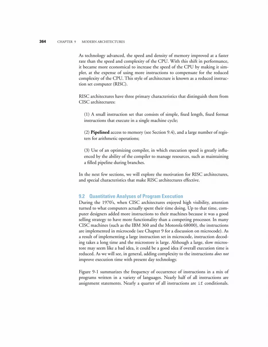
364
CHAPTER 9 MODERN ARCHITECTURES
As technology advanced, the speed and density of memory improved at a fasterrate than the speed and complexity of the CPU. With this shift in performance,it became more economical to increase the speed of the CPU by making it sim-pler, at the expense of using more instructions to compensate for the reducedcomplexity of the CPU. This style of architecture is known as a reduced instruc-tion set computer (RISC).
RISC architectures have three primary characteristics that distinguish them fromCISC architectures:
(1) A small instruction set that consists of simple, fixed length, fixed formatinstructions that execute in a single machine cycle;
(2)
Pipelined
access to memory (see Section 9.4), and a large number of regis-ters for arithmetic operations;
(3) Use of an optimizing compiler, in which execution speed is greatly influ-enced by the ability of the compiler to manage resources, such as maintaininga filled pipeline during branches.
In the next few sections, we will explore the motivation for RISC architectures,and special characteristics that make RISC architectures effective.
9.2 Quantitative Analyses of Program Execution
During the 1970’s, when CISC architectures enjoyed high visibility, attentionturned to what computers actually spent their time doing. Up to that time, com-puter designers added more instructions to their machines because it was a goodselling strategy to have more functionality than a competing processor. In manyCISC machines (such as the IBM 360 and the Motorola 68000), the instructionsare implemented in microcode (see Chapter 9 for a discussion on microcode). Asa result of implementing a large instruction set in microcode, instruction decod-ing takes a long time and the microstore is large. Although a large, slow micros-tore may seem like a bad idea, it could be a good idea if overall execution time isreduced. As we will see, in general, adding complexity to the instructions
does not
improve execution time with present day technology.
Figure 9-1 summarizes the frequency of occurrence of instructions in a mix ofprograms written in a variety of languages. Nearly half of all instructions areassignment statements. Nearly a quarter of all instructions are
if
conditionals.
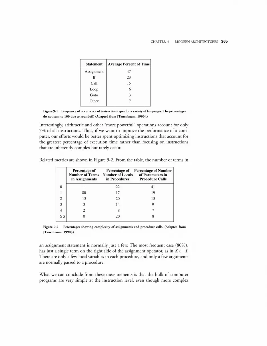
CHAPTER 9 MODERN ARCHITECTURES
365
Interestingly, arithmetic and other “more powerful” operations account for only7% of all instructions. Thus, if we want to improve the performance of a com-puter, our efforts would be better spent optimizing instructions that account forthe greatest percentage of execution time rather than focusing on instructionsthat are inherently complex but rarely occur.
Related metrics are shown in Figure 9-2. From the table, the number of terms in
an assignment statement is normally just a few. The most frequent case (80%),has just a single term on the right side of the assignment operator, as in
X
←
Y
.There are only a few local variables in each procedure, and only a few argumentsare normally passed to a procedure.
What we can conclude from these measurements is that the bulk of computerprograms are very simple at the instruction level, even though more complex
Statement Average Percent of Time
Assignment
If
Call
Loop
Goto
Other
47
23
15
6
3
7
Figure 9-1 Frequency of occurrence of instruction types for a variety of languages. The percentages
do not sum to 100 due to roundoff. (Adapted from [Tanenbaum, 1990].)
Percentage of Number of Terms
in Assignments
0
1
2
3
4
≥ 5
–
80
15
3
2
0
Percentage of Number of Locals
in Procedures
22
17
20
14
8
20
Percentage of Number of Parameters in Procedure Calls
41
19
15
9
7
8
Figure 9-2 Percentages showing complexity of assignments and procedure calls. (Adapted from
[Tanenbaum, 1990].)
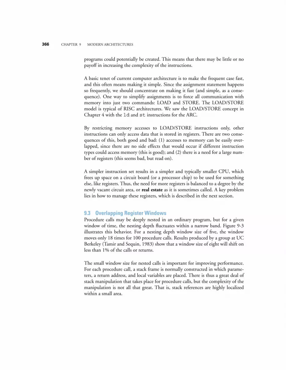
366
CHAPTER 9 MODERN ARCHITECTURES
programs could potentially be created. This means that there may be little or nopayoff in increasing the complexity of the instructions.
A basic tenet of current computer architecture is to make the frequent case fast,and this often means making it simple. Since the assignment statement happensso frequently, we should concentrate on making it fast (and simple, as a conse-quence). One way to simplify assignments is to force all communication withmemory into just two commands: LOAD and STORE. The LOAD/STOREmodel is typical of RISC architectures. We saw the LOAD/STORE concept inChapter 4 with the
ld
and
st
instructions for the ARC.
By restricting memory accesses to LOAD/STORE instructions only, otherinstructions can only access data that is stored in registers. There are two conse-quences of this, both good and bad: (1) accesses to memory can be easily over-lapped, since there are no side effects that would occur if different instructiontypes could access memory (this is good); and (2) there is a need for a large num-ber of registers (this seems bad, but read on).
A simpler instruction set results in a simpler and typically smaller CPU, whichfrees up space on a circuit board (or a processor chip) to be used for somethingelse, like registers. Thus, the need for more registers is balanced to a degree by thenewly vacant circuit area, or
real estate
as it is sometimes called. A key problemlies in how to manage these registers, which is described in the next section.
9.3 Overlapping Register Windows
Procedure calls may be deeply nested in an ordinary program, but for a givenwindow of time, the nesting depth fluctuates within a narrow band. Figure 9-3illustrates this behavior. For a nesting depth window size of five, the windowmoves only 18 times for 100 procedure calls. Results produced by a group at UCBerkeley (Tamir and Sequin, 1983) show that a window size of eight will shift onless than 1% of the calls or returns.
The small window size for nested calls is important for improving performance.For each procedure call, a stack frame is normally constructed in which parame-ters, a return address, and local variables are placed. There is thus a great deal ofstack manipulation that takes place for procedure calls, but the complexity of themanipulation is not all that great. That is, stack references are highly localizedwithin a small area.
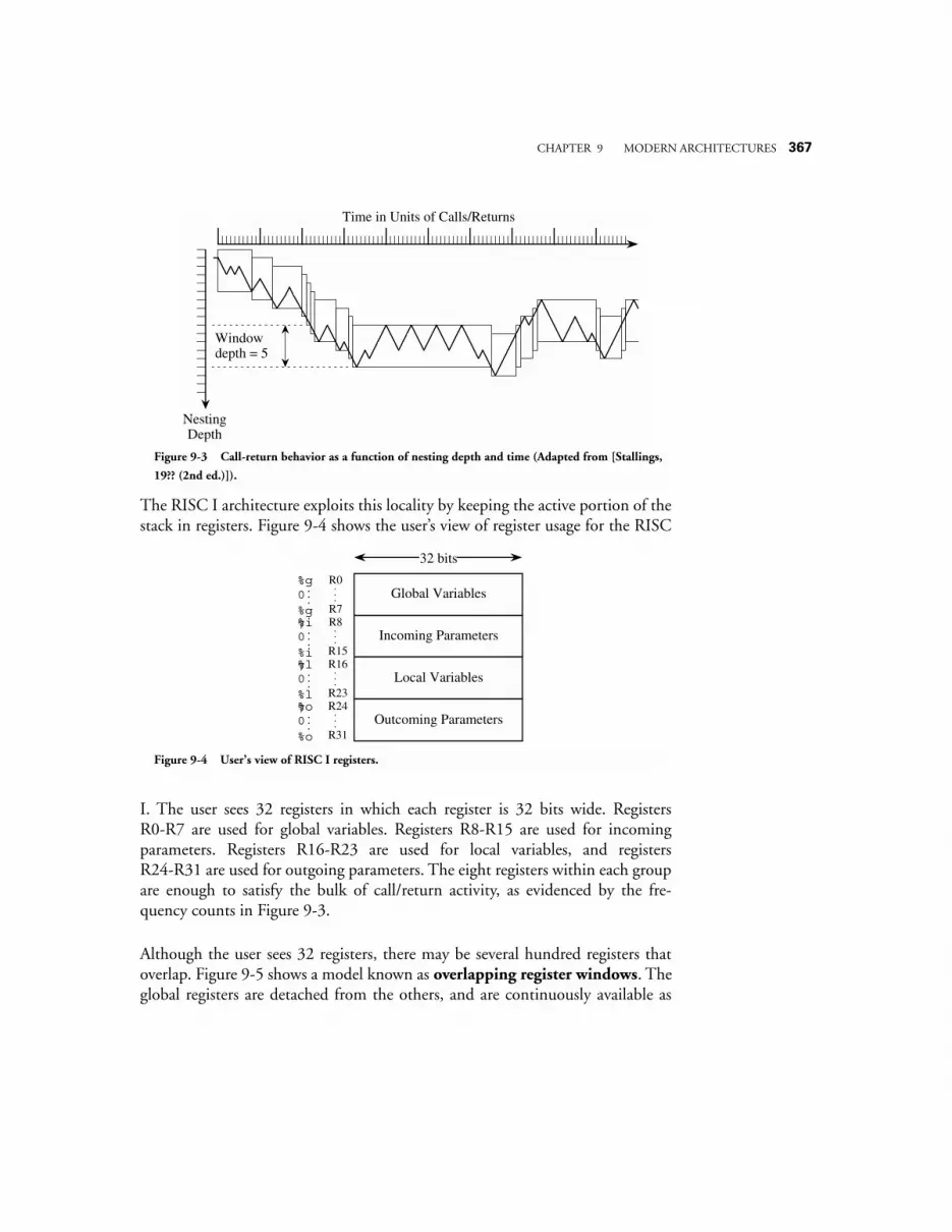
CHAPTER 9 MODERN ARCHITECTURES
367
The RISC I architecture exploits this locality by keeping the active portion of thestack in registers. Figure 9-4 shows the user’s view of register usage for the RISC
I. The user sees 32 registers in which each register is 32 bits wide. RegistersR0-R7 are used for global variables. Registers R8-R15 are used for incomingparameters. Registers R16-R23 are used for local variables, and registersR24-R31 are used for outgoing parameters. The eight registers within each groupare enough to satisfy the bulk of call/return activity, as evidenced by the fre-quency counts in Figure 9-3.
Although the user sees 32 registers, there may be several hundred registers thatoverlap. Figure 9-5 shows a model known as
overlapping register windows
. Theglobal registers are detached from the others, and are continuously available as
Nesting Depth
Time in Units of Calls/Returns
Window depth = 5
Figure 9-3 Call-return behavior as a function of nesting depth and time (Adapted from [Stallings,
19?? (2nd ed.)]).
Global Variables
Incoming Parameters
Local Variables
Outcoming Parameters
32 bits
R0
R7R8
R15R16
R23R24
R31
...
...
...
...
%g0%g7%i0%i7%l0%l7%o0%o
...
...
...
...
Figure 9-4 User’s view of RISC I registers.
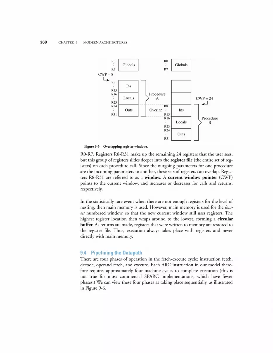
368
CHAPTER 9 MODERN ARCHITECTURES
R0-R7. Registers R8-R31 make up the remaining 24 registers that the user sees,but this group of registers slides deeper into the
register file
(the entire set of reg-isters) on each procedure call. Since the outgoing parameters for one procedureare the incoming parameters to another, these sets of registers can overlap. Regis-ters R8-R31 are referred to as a
window
. A
current window pointer
(CWP)points to the current window, and increases or decreases for calls and returns,respectively.
In the statistically rare event when there are not enough registers for the level ofnesting, then main memory is used. However, main memory is used for the
low-est
numbered window, so that the new current window still uses registers. Thehighest register location then wraps around to the lowest, forming a
circularbuffer
. As returns are made, registers that were written to memory are restored tothe register file. Thus, execution always takes place with registers and neverdirectly with main memory.
9.4 Pipelining the Datapath
There are four phases of operation in the fetch-execute cycle: instruction fetch,decode, operand fetch, and execute. Each ARC instruction in our model there-fore requires approximately four machine cycles to complete execution (this isnot true for most commercial SPARC implementations, which have fewerphases.) We can view these four phases as taking place sequentially, as illustratedin Figure 9-6.
GlobalsR0
R7
R8
R15R16
R23R24
R31
...
...
...
...
Ins
Locals
Outs
ProcedureA
GlobalsR0
R7
...
R8
R15R16
R23R24
R31
...
...
...
Ins
Locals
Outs
ProcedureB
CWP = 8
Overlap
CWP = 24
Figure 9-5 Overlapping register windows.
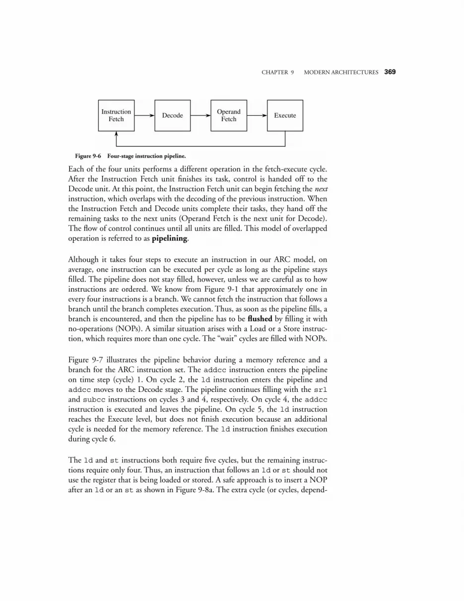
CHAPTER 9 MODERN ARCHITECTURES
369
Each of the four units performs a different operation in the fetch-execute cycle.After the Instruction Fetch unit finishes its task, control is handed off to theDecode unit. At this point, the Instruction Fetch unit can begin fetching the
next
instruction, which overlaps with the decoding of the previous instruction. Whenthe Instruction Fetch and Decode units complete their tasks, they hand off theremaining tasks to the next units (Operand Fetch is the next unit for Decode).The flow of control continues until all units are filled. This model of overlappedoperation is referred to as
pipelining
.
Although it takes four steps to execute an instruction in our ARC model, onaverage, one instruction can be executed per cycle as long as the pipeline staysfilled. The pipeline does not stay filled, however, unless we are careful as to howinstructions are ordered. We know from Figure 9-1 that approximately one inevery four instructions is a branch. We cannot fetch the instruction that follows abranch until the branch completes execution. Thus, as soon as the pipeline fills, abranch is encountered, and then the pipeline has to be
flushed
by filling it withno-operations (NOPs). A similar situation arises with a Load or a Store instruc-tion, which requires more than one cycle. The “wait” cycles are filled with NOPs.
Figure 9-7 illustrates the pipeline behavior during a memory reference and abranch for the ARC instruction set. The
addcc
instruction enters the pipelineon time step (cycle) 1. On cycle 2, the
ld
instruction enters the pipeline and
addcc
moves to the Decode stage. The pipeline continues filling with the
srl
and
subcc
instructions on cycles 3 and 4, respectively. On cycle 4, the
addcc
instruction is executed and leaves the pipeline. On cycle 5, the
ld
instructionreaches the Execute level, but does not finish execution because an additionalcycle is needed for the memory reference. The
ld
instruction finishes executionduring cycle 6.
The
ld
and
st
instructions both require five cycles, but the remaining instruc-tions require only four. Thus, an instruction that follows an
ld
or
st
should notuse the register that is being loaded or stored. A safe approach is to insert a NOPafter an
ld
or an
st
as shown in Figure 9-8a. The extra cycle (or cycles, depend-
Instruction Fetch Decode Operand
Fetch Execute
Figure 9-6 Four-stage instruction pipeline.
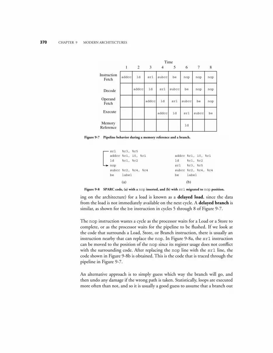
370
CHAPTER 9 MODERN ARCHITECTURES
ing on the architecture) for a load is known as a
delayed load
, since the datafrom the load is not immediately available on the next cycle. A
delayed branch
issimilar, as shown for the
be
instruction in cycles 5 through 8 of Figure 9-7.
The
nop
instruction wastes a cycle as the processor waits for a Load or a Store tocomplete, or as the processor waits for the pipeline to be flushed. If we look atthe code that surrounds a Load, Store, or Branch instruction, there is usually aninstruction nearby that can replace the
nop
. In Figure 9-8a, the
srl
instructioncan be moved to the position of the
nop
since its register usage does not conflictwith the surrounding code. After replacing the
nop
line with the
srl
line, thecode shown in Figure 9-8b is obtained. This is the code that is traced through thepipeline in Figure 9-7.
An alternative approach is to simply guess which way the branch will go, andthen undo any damage if the wrong path is taken. Statistically, loops are executedmore often than not, and so it is usually a good guess to assume that a branch out
Instruction Fetch
Decode
Operand Fetch
Execute
1 2 3 4 5 6 7 8
addcc ld srl subcc be nop nop nop
addcc ld srl subcc be nop nop
addcc ld srl subcc be nop
addcc ld srl subcc be
ldMemory
Reference
Time
Figure 9-7 Pipeline behavior during a memory reference and a branch.
(a)
addcc %r1, 10, %r1
ld %r1, %r2
nop
subcc %r2, %r4, %r4
be label
srl %r3, %r5
(b)
addcc %r1, 10, %r1
ld %r1, %r2
srl %r3, %r5
subcc %r2, %r4, %r4
be label
Figure 9-8 SPARC code, (a) with a nop inserted, and (b) with srl migrated to nop position.
CHAPTER 9 MODERN ARCHITECTURES
371
of a loop will not be taken. Thus, a processor can start processing the nextinstruction in anticipation of the direction of the branch. If the branch goes thewrong way, then the execution phase for the next instruction, and any subse-quent instructions that enter the pipeline, can be stopped so that the pipeline canbe flushed. This approach works well for a number of architectures, particularlythose with slow cycle speeds or deep pipelines. For RISCs, however, the overheadof determining when a branch goes the wrong way and then cleaning up any sideeffects caused by wrong instructions entering the pipeline is generally too great.The
nop
instruction is normally used in RISC pipelines when something usefulcannot be used to replace it.
9.5 Multiple Instruction Issue Machines
[Placeholder for future section.]
9.6 VLIW Machines
[Placeholder for future section. Discussion of the Intel Merced architecture.]
EXAMPLE: PLACEHOLDER
[Placeholder for future section.]
9.7 Case Study: Inspecting Compiled Code[Note from authors: This section is not finished.]
In this section, we analyze a C compiler produced SPARC assembly program. Westart with the C program shown in Figure 9-9 , in which the main routine passestwo integers to a subroutine, which returns the sum of the integers to the mainroutine. The code produced by a Solaris Unix C compiler using the commandline:
gcc -S file.c
is shown in Figure 9-10.
A line by line explanation of the assembled code is given in Figure 9-10. Thereare a number of new instructions and pseudo-ops introduced in this code:
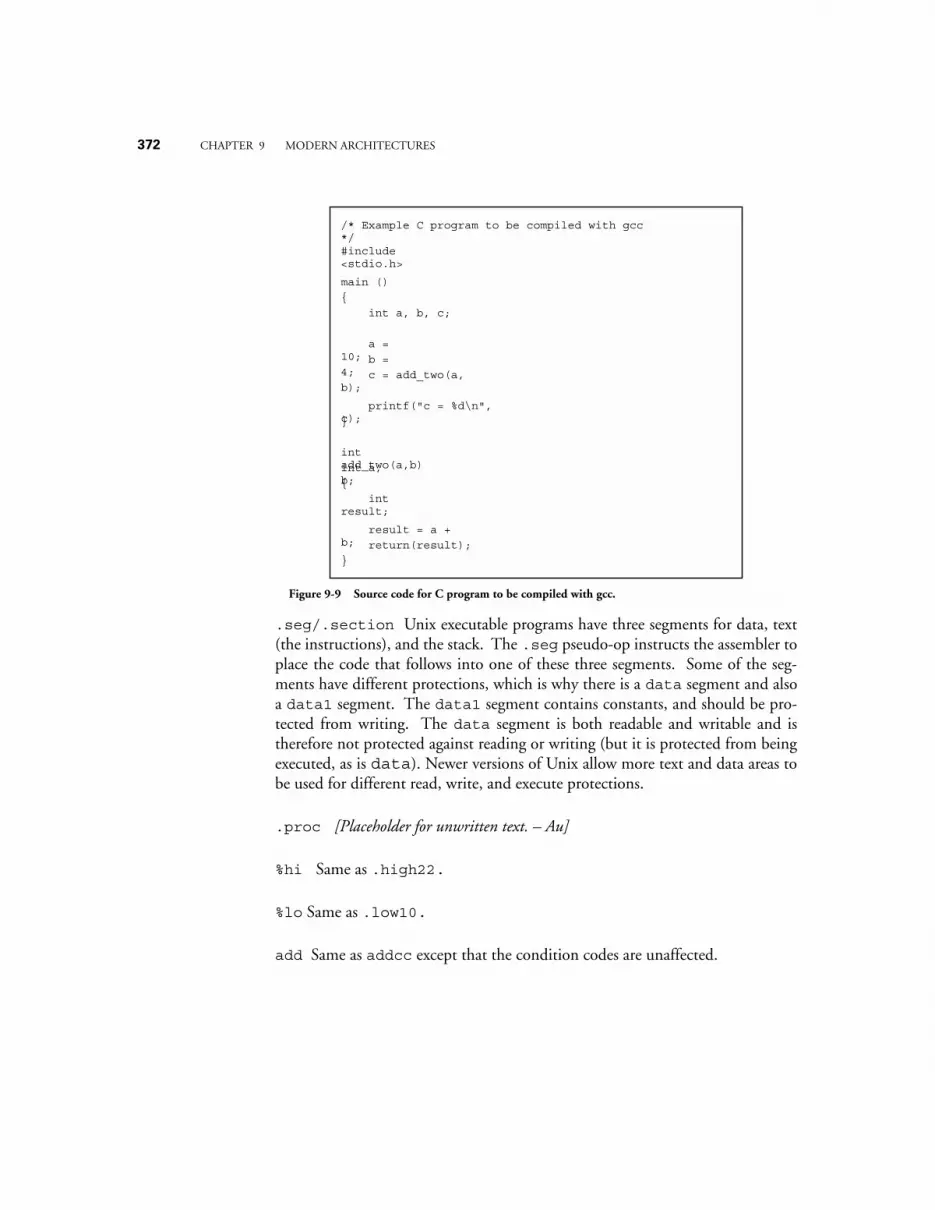
372 CHAPTER 9 MODERN ARCHITECTURES
.seg/.section Unix executable programs have three segments for data, text(the instructions), and the stack. The .seg pseudo-op instructs the assembler toplace the code that follows into one of these three segments. Some of the seg-ments have different protections, which is why there is a data segment and alsoa data1 segment. The data1 segment contains constants, and should be pro-tected from writing. The data segment is both readable and writable and istherefore not protected against reading or writing (but it is protected from beingexecuted, as is data). Newer versions of Unix allow more text and data areas tobe used for different read, write, and execute protections.
.proc [Placeholder for unwritten text. – Au]
%hi Same as .high22.
%lo Same as .low10.
add Same as addcc except that the condition codes are unaffected.
/* Example C program to be compiled with gcc */
main ()
int a, b, c;
a = 10;
int add_two(a,b)int a, b;
int result;
result = a + b; return(result);
#include <stdio.h>
b = 4; c = add_two(a, b);
printf("c = %d\n", c);
Figure 9-9 Source code for C program to be compiled with gcc.
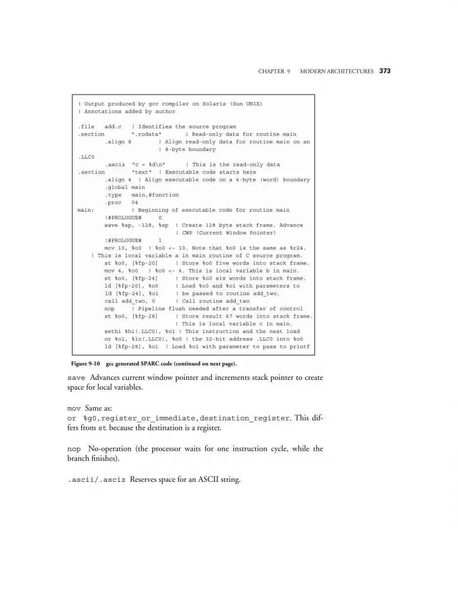
CHAPTER 9 MODERN ARCHITECTURES 373
save Advances current window pointer and increments stack pointer to createspace for local variables.
mov Same as:or %g0,register_or_immediate,destination_register. This dif-fers from st because the destination is a register.
nop No-operation (the processor waits for one instruction cycle, while thebranch finishes).
.ascii/.asciz Reserves space for an ASCII string.
! Output produced by gcc compiler on Solaris (Sun UNIX)
.section ".rodata" ! Read-only data for routine main
.align 8 ! Align read-only data for routine main on an
! 8-byte boundary
.asciz "c = %d\n" ! This is the read-only data
.proc 04
!#PROLOGUE# 0
save %sp, -128, %sp ! Create 128 byte stack frame. Advance
! CWP (Current Window Pointer)
!#PROLOGUE# 1
! This is local variable a in main routine of C source program.
st %o0, [%fp-20] ! Store %o0 five words into stack frame.
mov 4, %o0 ! %o0 <- 4. This is local variable b in main.
.file add.c ! Identifies the source program
.section "text" ! Executable code starts here
.align 4 ! Align executable code on a 4-byte (word) boundary
.type main,#function
! Annotations added by author
.LLC0
.global main
main: ! Beginning of executable code for routine main
mov 10, %o0 ! %o0 <- 10. Note that %o0 is the same as %r24.
st %o0, [%fp-24] ! Store %o0 six words into stack frame.
ld [%fp-20], %o0 ! Load %o0 and %o1 with parameters to
ld [%fp-24], %o1 ! be passed to routine add_two.
call add_two, 0 ! Call routine add_two
nop ! Pipeline flush needed after a transfer of control
st %o0, [%fp-28] ! Store result 67 words into stack frame.
! This is local variable c in main.
sethi %hi(.LLC0), %o1 ! This instruction and the next load
or %o1, %lo(.LLC0), %o0 ! the 32-bit address .LLC0 into %o0
ld [%fp-28], %o1 ! Load %o1 with parameter to pass to printf
Figure 9-10 gcc generated SPARC code (continued on next page).
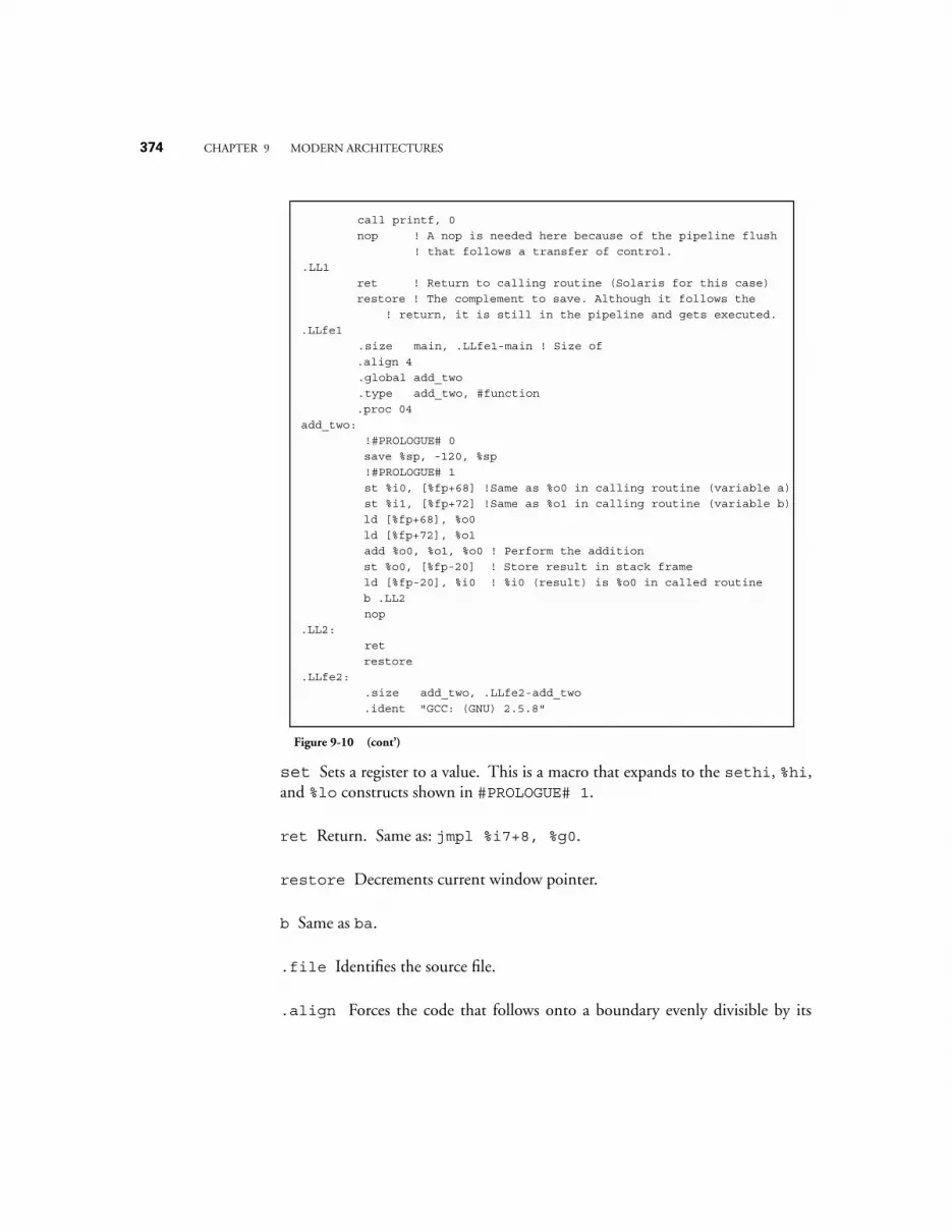
374 CHAPTER 9 MODERN ARCHITECTURES
set Sets a register to a value. This is a macro that expands to the sethi, %hi,and %lo constructs shown in #PROLOGUE# 1.
ret Return. Same as: jmpl %i7+8, %g0.
restore Decrements current window pointer.
b Same as ba.
.file Identifies the source file.
.align Forces the code that follows onto a boundary evenly divisible by its
call printf, 0
nop ! A nop is needed here because of the pipeline flush
! that follows a transfer of control.
.LL1
ret ! Return to calling routine (Solaris for this case)
restore ! The complement to save. Although it follows the
! return, it is still in the pipeline and gets executed.
.LLfe1
.size main, .LLfe1-main ! Size of
.align 4
.global add_two
.type add_two, #function
.proc 04
add_two:
!#PROLOGUE# 0
save %sp, -120, %sp
!#PROLOGUE# 1
st %i0, [%fp+68] !Same as %o0 in calling routine (variable a)
st %i1, [%fp+72] !Same as %o1 in calling routine (variable b)
ld [%fp+68], %o0
ld [%fp+72], %o1
add %o0, %o1, %o0 ! Perform the addition
st %o0, [%fp-20] ! Store result in stack frame
ld [%fp-20], %i0 ! %i0 (result) is %o0 in called routine
b .LL2
nop
.LL2:
ret
restore
.LLfe2:
.size add_two, .LLfe2-add_two
.ident "GCC: (GNU) 2.5.8"
Figure 9-10 (cont’)
CHAPTER 9 MODERN ARCHITECTURES 375
argument.
.type Associates a label with its type.
.size Computes the size of a segment.
.ident Identifies the compiler version.
Notice that the compiler does not seem to be consistent with its choice of regis-ters for parameter passing. Prior to the call to add_two, the compiler uses %o0and %o1 (%r24 and %r25) for parameters passed to add_two. Then, %r25 isused for the parameters passed to printf. Why did the compiler not start with%r24 again, or choose the next available register (%o2)? This is the registerassignment problem, which has been the object of a great deal of study. We willnot go into details here1, as this is more appropriate for a course in compilerdesign, but suffice it to say that any logically correct assignment of variables toregisters will work, but that some assignments are better than others in terms ofthe number of registers used and the overall program execution time.
Why are the stack frames so large? We only need three words on the stack framefor local variables a, b, and c in main. We might also need a word to store thereturn address, although the compiler does not seem to generate code for that.There are no parameters passed to main by the operating system, and so thestack frame that main sees should only be four words (16 bytes) in size. Thus,the line at the beginning of routine main:
save %sp, -128, %sp
should only be:
save %sp, -16, %sp.
What is all of the extra space for? There are a number of runtime situations thatmay need stack space. For instance, if the nesting depth is greater than the num-
1. Here are a few details, for the curious: %r0 (%o0) is still in use (add_two is expectingthe address of LLC0 to show up in %r0), and %r1 is no longer needed at this point, so it can bereassigned. But then, why is %r1 used in the sethi line? Would it have made sense to use %r0instead of introducing another register into the computation? See problem 9.2 at the end of thechapter for more on this topic.
376 CHAPTER 9 MODERN ARCHITECTURES
ber of windows, then the stack must be used for overflow. (See Figure D-2 in[SPARC, 1992])
If a scalar is passed from one routine to another, then everything is fine. But if acallee refers to the address of a passed scalar (or aggregate), then the scalar (oraggregate) must be copied to the stack and be referenced from there for the life-time of the pointer (or for the lifetime of the procedure, if the pointer lifetime isnot known).
Why does the return statement ret cause a return to the code that is 8 bytes pastthe call, instead of 4 as we have been doing it? This is because there is a nopthat follows call (the so-called “delay-slot instruction”).
Notice that routine labels that appear in the source code are prepended with anunderscore in the assembly code, so that main, add_two, and printf in Cbecome _main, _add_two, and _printf in gcc generated SPARC code. Thismeans that if we want to write a C program that is linked to a gcc generatedSPARC program, that the C calls should be made to routines that begin withunderscores. For example, if add_two is compiled into SPARC code, and weinvoke it from a C main program in another file, then the C program shouldmake a call to _add_two, and not add_two, even though the routine startedout as add_two. Further, the C program needs to declare _add_two as exter-nal.
If the compilation for add_two is continued down to an executable file, thenthere is no need to treat the labels differently. The add_two routine will still belabeled _add_two, but routine main will be compiled into code that expects tosee _add_two and so everything will work OK. This is not the case, however, ifa gcc program makes calls to a Fortran library.
Fortran is a commonly used language in the scientific community, and there are anumber of significant Fortran libraries that are used for linear algebra (LIN-PACK), modeling and simulation (__), and parallel scientific applications (__).As C programmers, we sometimes find ourselves wanting to write C programsthat make calls to Fortran routines. This is easy to do once we understand what ishappening.
There are two significant differences that need to be addressed:
(1) differences in routine labels;
CHAPTER 9 MODERN ARCHITECTURES 377
(2) differences in subroutine linkage.
In Fortran, the source code labels are prepended with two underscores in theassembly code. A C program that makes a call to Fortran routine add_twowould then make a call to _ _add_two, which also must be declared as externalin the C source code (and declared as global in the Fortran program).
If all of the parameters that are passed to the Fortran routines are pointers, theneverything will work OK. If there are any scalars passed, then there will be trou-ble because C uses call-by-value for scalars whereas Fortran uses call-by-reference.We need to “trick” the C compiler into using call-by-reference by making itexplicit. Wherever a Fortran routine expects a scalar in its argument list, we use apointer to the scalar in the C code. As an example, a C/Fortran version of theadd_two code is shown below:
[Placeholder for unwritten C/Fortran figure.]
As a practical consideration, the gcc compiler will compile Fortran programs. Itknows what to do by observing the extension of the source file, which should be.f for Fortran. [The rest of this section is unfinished. – Au(s)]
[Note to Au: Manipulation of %sp needs to be atomic. See page 191 of SPARCArchitecture manual, under first bullet.]
9.8 Case Study: Superscalar Assembly Language Programming on the Intel Pentium II with MMX TechnologyDiscussion of the Intel Merced architecture.
EXAMPLE
A processor has a five stage pipeline. If a branch is taken, then four cycles areneeded to flush the pipeline. The branch penalty b is thus 4. The probability Pbthat a particular instruction is a branch is .25. The probability Pt that the branchis taken is .5. We would like to compute the average number of cycles needed toexecute an instruction, and the execution efficiency.
378 CHAPTER 9 MODERN ARCHITECTURES
When the pipeline is filled and there are no branches, then the average numberof cycles per instruction (CPINo_Branch) is 1. The average number of cycles perinstruction when there are branches is then:
CPIAvg = (1 - Pb)(CPINo_Branch) + Pb[Pt(1 + b) + (1 - Pt)(CPINo_Branch)]
= 1 + bPbPt.
After making substitutions, we have:
CPIAvg = (1 - .25)(1) + .25[.5(1 + 4) + (1 - .5)(1)]
= 1.5 cycles.
The execution efficiency is the ratio of the cycles per instruction when there areno branches to the cycles per instruction when there are branches. Thus we have:
Execution efficiency = (CPINo_Branch)/(CPIAvg) = 1/1.5 = 67%.
The processor runs at 67% of its potential speed as a result of branches, but thisis still much better than the five cycles per instruction that might be neededwithout pipelining.
There are techniques for improving the efficiency. We know that loops are usu-ally executed more than once, so we can guess that a branch out of the loop willnot be taken and be right most of the time. We can also run simulations on thenon-loop branches, and get a statistical sampling of which branches are likely tobe taken, and then guess the branches accordingly. As explained earlier, thisapproach works best when the pipeline is deep or the clock rate is slow.
SUMMARY
In the RISC approach, the most frequently occuring instructions are optimized byeliminating or reducing the complexity of other instructions and addressing modescommonly found in CISC architectures. The performance of RISC architectures isfurther enhanced by pipelining and increasing the number of registers available tothe CPU.

CHAPTER 9 MODERN ARCHITECTURES 379
FURTHER READINGThe three characteristics of RISC architectures originated at IBM’s T. J. WatsonResearch Center, as summarized in (Ralston and Reilly, 1993, pp. 1165 - 1167).(Hennessy and Patterson, 1990) is the seminal reference on much of the workthat led to the RISC concept, although the word “RISC” does not appear in thetitle of their textbook. (Stallings, 1990) is a thorough reference on RISCs. (Tamirand Sequin, 1983) show that a window size of eight will shift on less than 1% ofthe calls or returns. (Tanenbaum, 1990) provides a readable introduction to theRISC concept.
Hennessy, J. L. and D. A. Patterson, Computer Architecture: A QuantitativeApproach, Morgan Kaufmann Publishers, San Mateo, California, (1990).
Ralston, A. and E. D. Reilly, eds., Encyclopedia of Computer Science, 3/e, vanNostrand Reinhold, (1993).
Stallings, W., Reduced Instruction Set Computers, 3/e, IEEE Computer SocietyPress, Washington, D.C., (1991).
Tamir, Y., and C. Sequin, “Strategies for Managing the Register File in RISC,”IEEE Trans. Comp., (Nov. 1983).
Tanenbaum, A., Structured Computer Organization, 3/e, Prentice Hall, Engle-wood Cliffs, New Jersey, (1990).
PROBLEMS9.1 Increasing the number of cycles per instruction can sometimes improve
the execution efficiency of a pipeline. If the time per cycle for the pipelinedescribed in Section 5.6.3 is 20 ns, then CPIAvg is 1.5 × 20 ns = 30 ns. Com-pute the execution efficiency for the same pipeline in which the pipeline depthincreases from 5 to 6 and the cycle time decreases from 20 ns to 10 ns.
9.2 The SPARC code below is taken from the gcc generated code in Figure9-10. Can %r0 be used in all three lines, instead of “wasting” %r1 in the sec-ond line?
...st %o0, [%fp-28]

380 CHAPTER 9 MODERN ARCHITECTURES
sethi %hi(.LLC0), %o1or %o1, %lo(.LLC0), %o1
...
CHAPTER 10 TRENDS IN COMPUTER ARCHITECTURE
403
In the earlier chapters, the fetch-execute cycle is described in the form: “fetch aninstruction, execute that instruction, fetch the next instruction,
etc.
” This givesthe impression of a straight-line linear progression of program execution. In fact,the processor architectures of today have many advanced features that go beyondthis simple paradigm. These features include
pipelining
, in which severalinstructions sharing the same hardware can simultaneously be in various phasesof execution,
superscalar execution
, in which several instructions are executedsimultaneously using different portions of the hardware, with possibly only someof the results contributing to the overall computation,
very long instructionword
(VLIW) architectures, in which each instruction word specifies multipleinstructions (of smaller widths) that are executed simultaneously, and
parallelprocessing
, in which multiple processors are coordinated to work on a singleproblem.
In this chapter we cover issues that relate to these features. The discussion beginswith issues that led to the emergence of the reduced instruction set computer(RISC) and examples of RISC features and characteristics. Following that, wecover an advanced feature used specifically in SPARC architectures:
overlappingregister windows
. We then cover two important architectural features: supersca-lar execution and VLIW architectures. We then move into the topic of parallelprocessing, touching both on parallel architectures and program decomposition.The chapter includes with case studies covering Intel’s Merced architecture, thePowerPC 601, and an example of a pervasive parallel architecture that can befound in a home videogame system.
10.1 Quantitative Analyses of Program Execution
Prior to the late 1970’s, computer architects exploited improvements in inte-grated circuit technology by increasing the complexity of instructions and
TRENDS IN COMPUTER ARCHITECTURE
10
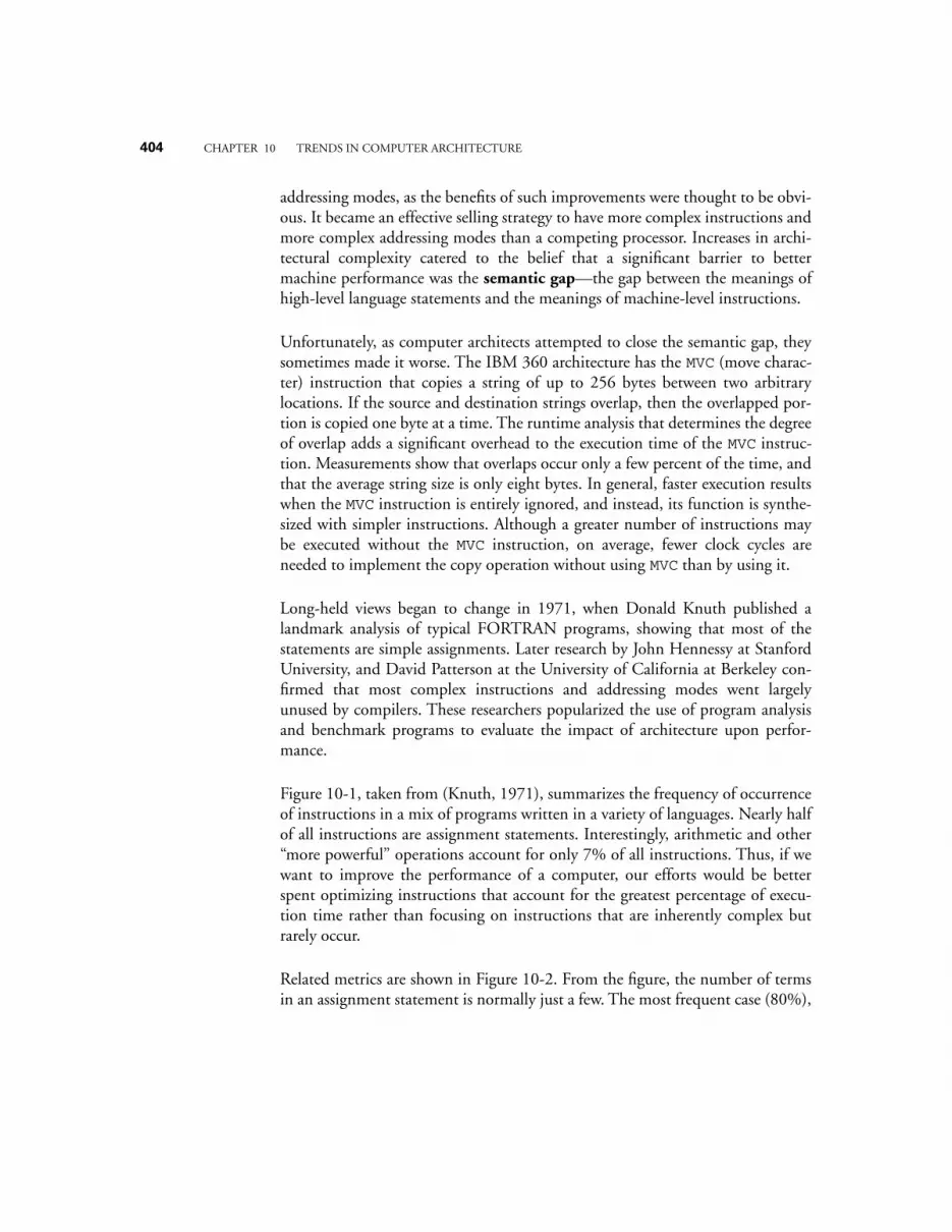
404
CHAPTER 10 TRENDS IN COMPUTER ARCHITECTURE
addressing modes, as the benefits of such improvements were thought to be obvi-ous. It became an effective selling strategy to have more complex instructions andmore complex addressing modes than a competing processor. Increases in archi-tectural complexity catered to the belief that a significant barrier to bettermachine performance was the
semantic gap
—the gap between the meanings ofhigh-level language statements and the meanings of machine-level instructions.
Unfortunately, as computer architects attempted to close the semantic gap, theysometimes made it worse. The IBM 360 architecture has the
MVC
(move charac-ter) instruction that copies a string of up to 256 bytes between two arbitrarylocations. If the source and destination strings overlap, then the overlapped por-tion is copied one byte at a time. The runtime analysis that determines the degreeof overlap adds a significant overhead to the execution time of the
MVC
instruc-tion. Measurements show that overlaps occur only a few percent of the time, andthat the average string size is only eight bytes. In general, faster execution resultswhen the
MVC
instruction is entirely ignored, and instead, its function is synthe-sized with simpler instructions. Although a greater number of instructions maybe executed without the
MVC
instruction, on average, fewer clock cycles areneeded to implement the copy operation without using
MVC
than by using it.
Long-held views began to change in 1971, when Donald Knuth published alandmark analysis of typical FORTRAN programs, showing that most of thestatements are simple assignments. Later research by John Hennessy at StanfordUniversity, and David Patterson at the University of California at Berkeley con-firmed that most complex instructions and addressing modes went largelyunused by compilers. These researchers popularized the use of program analysisand benchmark programs to evaluate the impact of architecture upon perfor-mance.
Figure 10-1, taken from (Knuth, 1971), summarizes the frequency of occurrenceof instructions in a mix of programs written in a variety of languages. Nearly halfof all instructions are assignment statements. Interestingly, arithmetic and other“more powerful” operations account for only 7% of all instructions. Thus, if wewant to improve the performance of a computer, our efforts would be betterspent optimizing instructions that account for the greatest percentage of execu-tion time rather than focusing on instructions that are inherently complex butrarely occur.
Related metrics are shown in Figure 10-2. From the figure, the number of termsin an assignment statement is normally just a few. The most frequent case (80%),
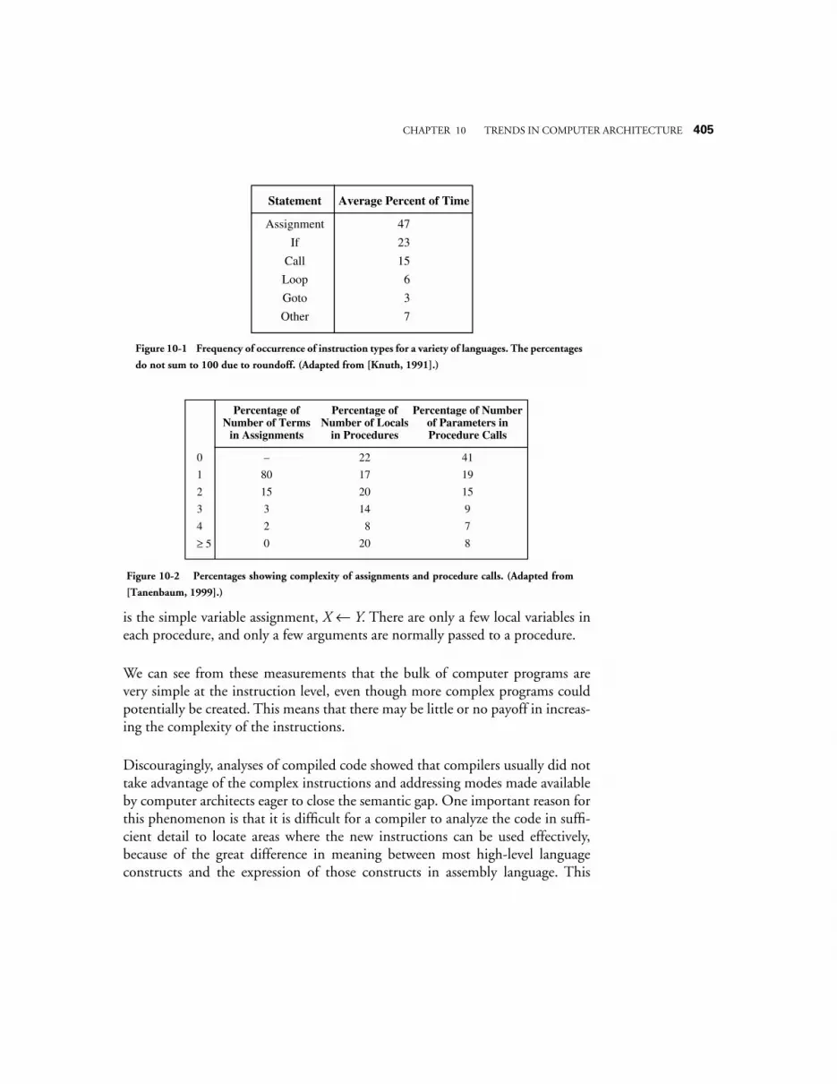
CHAPTER 10 TRENDS IN COMPUTER ARCHITECTURE
405
is the simple variable assignment,
X
←
Y
. There are only a few local variables ineach procedure, and only a few arguments are normally passed to a procedure.
We can see from these measurements that the bulk of computer programs arevery simple at the instruction level, even though more complex programs couldpotentially be created. This means that there may be little or no payoff in increas-ing the complexity of the instructions.
Discouragingly, analyses of compiled code showed that compilers usually did nottake advantage of the complex instructions and addressing modes made availableby computer architects eager to close the semantic gap. One important reason forthis phenomenon is that it is difficult for a compiler to analyze the code in suffi-cient detail to locate areas where the new instructions can be used effectively,because of the great difference in meaning between most high-level languageconstructs and the expression of those constructs in assembly language. This
Statement Average Percent of Time
Assignment
If
Call
Loop
Goto
Other
47
23
15
6
3
7
Figure 10-1 Frequency of occurrence of instruction types for a variety of languages. The percentages
do not sum to 100 due to roundoff. (Adapted from [Knuth, 1991].)
Percentage of Number of Terms
in Assignments
0
1
2
3
4
≥ 5
–
80
15
3
2
0
Percentage of Number of Locals
in Procedures
22
17
20
14
8
20
Percentage of Number of Parameters in Procedure Calls
41
19
15
9
7
8
Figure 10-2 Percentages showing complexity of assignments and procedure calls. (Adapted from
[Tanenbaum, 1999].)
406
CHAPTER 10 TRENDS IN COMPUTER ARCHITECTURE
observation, and the ever increasing speed and capacity of integrated circuit tech-nology, converged to bring about an evolution from complex instruction setcomputer (CISC) machines to RISC machines.
A basic tenet of current computer architecture is to make the frequent case fast,and this often means making it simple. Since the assignment statement happensso frequently, we should concentrate on making it fast (and simple, as a conse-quence). One way to simplify assignments is to force all communication withmemory into just two commands: LOAD and STORE. The LOAD/STOREmodel is typical of RISC architectures. We see the LOAD/STORE concept inChapter 4 with the
ld
and
st
instructions for the ARC.
By restricting memory accesses to LOAD/STORE instructions only, otherinstructions can only access data that is stored in registers. There are two conse-quences of this, both good and bad: (1) accesses to memory can be easily over-lapped, since there are fewer side effects that would occur if different instructiontypes could access memory (this is good); and (2) there is a need for a large num-ber of registers (this seems bad, but read on).
A simpler instruction set results in a simpler and typically smaller CPU, whichfrees up space on a microprocessor to be used for something else, like registers.Thus, the need for more registers is balanced to a degree by the newly vacant cir-cuit area, or chip
real estate
as it is sometimes called. A key problem lies in howto manage these registers, which is discussed in Section 10.4.
10.1.1
QUANTITATIVE PERFORMANCE ANALYSIS
When we estimate machine performance, the measure that is generally mostimportant is execution time,
T
. When considering the impact of some perfor-mance improvement, the effect of the improvement is usually expressed in termsof the
speedup
,
S
, taken as the ratio of the execution time without the improve-ment (
T
wo
) to the execution time with the improvement (
T
w
):
For example, if adding a 1MB cache module to a computer system results in low-ering the execution time of some benchmark program from 12 seconds to 8 sec-onds, then the speedup would be 12/8, = 1.5, or 50%. An equation to calculate
STwo
Tw---------=
CHAPTER 10 TRENDS IN COMPUTER ARCHITECTURE
407
speedup as a direct percent can be represented as:
We can develop a more fine-grained equation for estimating
T
if we have infor-mation about the machine’s clock period,
τ
, the number of clock cycles perinstruction,
CPI
, and a count of the number of instructions executed by the pro-gram during its execution,
IC
. In this case the total execution time for the pro-gram is given by:
CPI and IC can be expressed either as an average over the instruction set andtotal count, respectively, or summed over each kind and number of instructionsin the instruction set and program. Substituting the latter equation into theformer we get:
These equations and others derived from them, are useful in computing and esti-mating the impact of changes in instructions and architecture upon perfor-mance.
EXAMPLE: CALCULATING SPEEDUP FOR A NEW INSTRUCTION SET
Suppose we wish to estimate the speedup obtained by replacing a CPU having anaverage CPI of 5 with another CPU having an average CPI of 3.5, with the clockperiod increased from 100 ns to 120 ns. The equation above becomes:
Thus, without actually running a benchmark program we can estimate theimpact of an architectural change upon performance.
10.2 From CISC to RISC
Historically, when memory cycle times were very long and when memory prices
STwo Tw–
Tw---------------------- 100×=
T IC CPI τ××=
SICwo CPIwo τwo×× ICw CPIw τw××–
ICw CPIw τw××------------------------------------------------------------------------------------------------- 100×=
S 5 100× 3.5 120×–3.5 120×
----------------------------------------------- 100× = 19%=

408
CHAPTER 10 TRENDS IN COMPUTER ARCHITECTURE
were high, fewer, complicated instructions held an advantage over more, simplerinstructions. There came a point, however, when memory became inexpensiveenough and memory hierarchies became fast and large enough, that computerarchitects began reexamining this advantage. One technology that affected thisexamination was
pipelining
—that is, keeping the execution unit more or lessthe same, but allowing different instructions (which each require several clockcycles to execute) to use different parts of the execution unit on each clock cycle.For example, one instruction might be accessing operands in the register filewhile another is using the ALU.
We will cover pipelining in more detail later in the chapter, but the importantpoint to make here is that computer architects learned that CISC instructions donot fit pipelined architectures very well. For pipelining to work effectively, eachinstruction needs to have similarities to other instructions, at least in terms of rel-ative instruction complexity. The reason can be viewed in analogy to an assemblyline that produces different models of an automobile. For efficiency, each “sta-tion” of the assembly line should do approximately the same amount and kind ofwork. If the amount or kind of work done at each station is radically different fordifferent models, then periodically the assembly line will have to “stall” toaccommodate the requirements of the given model.
CISC instruction sets have the disadvantage that some instructions, such as regis-ter-to-register moves, are inherently simple, whereas others, such as the
MVC
instruction and others like it are complex, and take many more clock cycles toexecute.
The main philosophical underpinnings of the RISC approach are:
• Prefetch instructions into an instruction queue in the CPU before they areneeded. This has the effect of hiding the latency associated with the instruc-tion fetch.
• With instruction fetch times no longer a penalty, and with cheap memoryto hold a greater number of instructions, there is no real advantage to CISCinstructions. All instructions should be composed of sequences of RISC in-structions, even though the number of instructions needed may increase(typically by as much as 1/3 over a CISC approach).
• Moving operands between registers and memory is expensive, and shouldbe minimized.
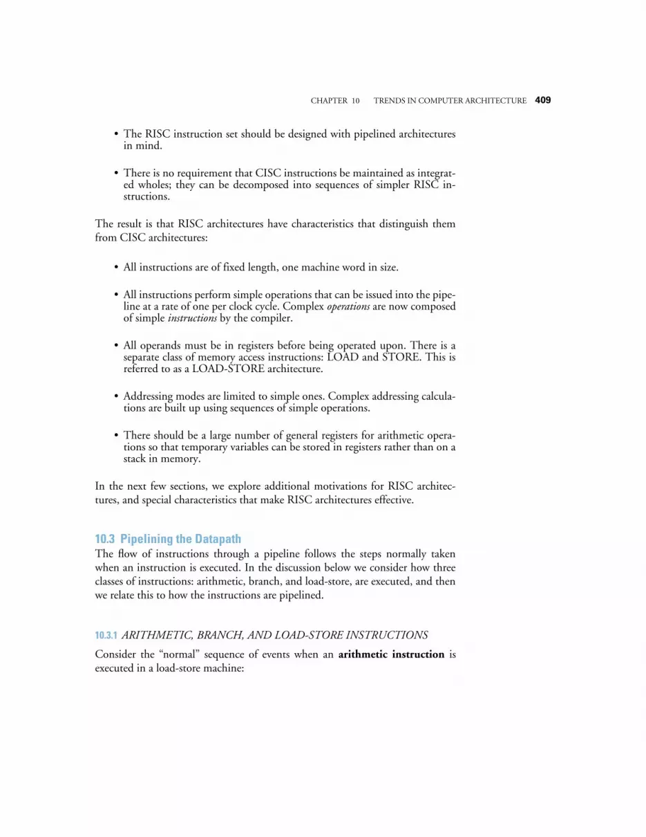
CHAPTER 10 TRENDS IN COMPUTER ARCHITECTURE
409
• The RISC instruction set should be designed with pipelined architecturesin mind.
• There is no requirement that CISC instructions be maintained as integrat-ed wholes; they can be decomposed into sequences of simpler RISC in-structions.
The result is that RISC architectures have characteristics that distinguish themfrom CISC architectures:
• All instructions are of fixed length, one machine word in size.
• All instructions perform simple operations that can be issued into the pipe-line at a rate of one per clock cycle. Complex
operations
are now composedof simple
instructions
by the compiler.
• All operands must be in registers before being operated upon. There is aseparate class of memory access instructions: LOAD and STORE. This isreferred to as a LOAD-STORE architecture.
• Addressing modes are limited to simple ones. Complex addressing calcula-tions are built up using sequences of simple operations.
• There should be a large number of general registers for arithmetic opera-tions so that temporary variables can be stored in registers rather than on astack in memory.
In the next few sections, we explore additional motivations for RISC architec-tures, and special characteristics that make RISC architectures effective.
10.3 Pipelining the Datapath
The flow of instructions through a pipeline follows the steps normally takenwhen an instruction is executed. In the discussion below we consider how threeclasses of instructions: arithmetic, branch, and load-store, are executed, and thenwe relate this to how the instructions are pipelined.
10.3.1
ARITHMETIC, BRANCH, AND LOAD-STORE INSTRUCTIONS
Consider the “normal” sequence of events when an
arithmetic instruction
isexecuted in a load-store machine:

410
CHAPTER 10 TRENDS IN COMPUTER ARCHITECTURE
1) Fetch the instruction from memory;
2) Decode the instruction (it is an arithmetic instruction, but the CPU hasto find that out through a decode operation);
3) Fetch the operands from the register file;
4) Apply the operands to the ALU;
5) Write the result back to the register file.
There are similar patterns for other instruction classes. For
branch instructions
the sequence is:
1) Fetch the instruction from memory;
2) Decode the instruction (it is a branch instruction);
3) Fetch the components of the address from the instruction or register file;
4) Apply the components of the address to the ALU (address arithmetic);
5) Copy the resulting effective address into the PC, thus accomplishing thebranch.
The sequence for
load and store instructions
is:
1) Fetch the instruction from memory;
2) Decode the instruction (it is a load or store instruction);
3) Fetch the components of the address from the instruction or register file;
4) Apply the components of the address to the ALU (address arithmetic);
5) Apply the resulting effective address to memory along with a read (load)or write (store) signal. If it is a write signal, the data item to be writtenmust also be retrieved from the register file.
The three sequences above show a high degree of similarity in what is done ateach stage: (1) fetch, (2) decode, (3) operand fetch, (4) ALU operation, (5) resultwriteback.
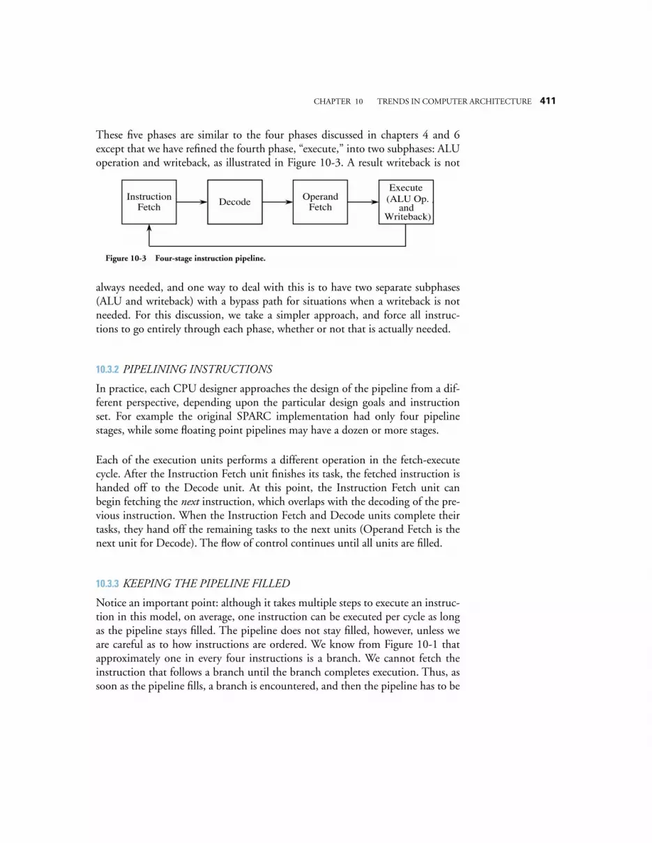
CHAPTER 10 TRENDS IN COMPUTER ARCHITECTURE
411
These five phases are similar to the four phases discussed in chapters 4 and 6except that we have refined the fourth phase, “execute,” into two subphases: ALUoperation and writeback, as illustrated in Figure 10-3. A result writeback is not
always needed, and one way to deal with this is to have two separate subphases(ALU and writeback) with a bypass path for situations when a writeback is notneeded. For this discussion, we take a simpler approach, and force all instruc-tions to go entirely through each phase, whether or not that is actually needed.
10.3.2
PIPELINING INSTRUCTIONS
In practice, each CPU designer approaches the design of the pipeline from a dif-ferent perspective, depending upon the particular design goals and instructionset. For example the original SPARC implementation had only four pipelinestages, while some floating point pipelines may have a dozen or more stages.
Each of the execution units performs a different operation in the fetch-executecycle. After the Instruction Fetch unit finishes its task, the fetched instruction ishanded off to the Decode unit. At this point, the Instruction Fetch unit canbegin fetching the
next
instruction, which overlaps with the decoding of the pre-vious instruction. When the Instruction Fetch and Decode units complete theirtasks, they hand off the remaining tasks to the next units (Operand Fetch is thenext unit for Decode). The flow of control continues until all units are filled.
10.3.3
KEEPING THE PIPELINE FILLED
Notice an important point: although it takes multiple steps to execute an instruc-tion in this model, on average, one instruction can be executed per cycle as longas the pipeline stays filled. The pipeline does not stay filled, however, unless weare careful as to how instructions are ordered. We know from Figure 10-1 thatapproximately one in every four instructions is a branch. We cannot fetch theinstruction that follows a branch until the branch completes execution. Thus, assoon as the pipeline fills, a branch is encountered, and then the pipeline has to be
Instruction Fetch Decode Operand
Fetch(ALU Op.
and Writeback)
Execute
Figure 10-3 Four-stage instruction pipeline.
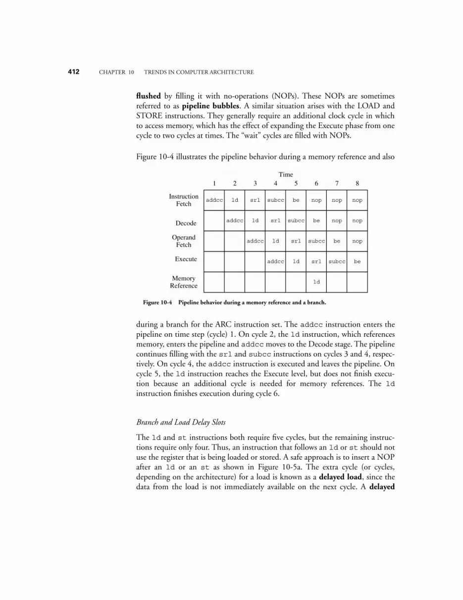
412
CHAPTER 10 TRENDS IN COMPUTER ARCHITECTURE
flushed
by filling it with no-operations (NOPs). These NOPs are sometimesreferred to as
pipeline bubbles
. A similar situation arises with the LOAD andSTORE instructions. They generally require an additional clock cycle in whichto access memory, which has the effect of expanding the Execute phase from onecycle to two cycles at times. The “wait” cycles are filled with NOPs.
Figure 10-4 illustrates the pipeline behavior during a memory reference and also
during a branch for the ARC instruction set. The
addcc
instruction enters thepipeline on time step (cycle) 1. On cycle 2, the
ld
instruction, which referencesmemory, enters the pipeline and
addcc
moves to the Decode stage. The pipelinecontinues filling with the
srl
and
subcc
instructions on cycles 3 and 4, respec-tively. On cycle 4, the addcc instruction is executed and leaves the pipeline. Oncycle 5, the ld instruction reaches the Execute level, but does not finish execu-tion because an additional cycle is needed for memory references. The ldinstruction finishes execution during cycle 6.
Branch and Load Delay Slots
The ld and st instructions both require five cycles, but the remaining instruc-tions require only four. Thus, an instruction that follows an ld or st should notuse the register that is being loaded or stored. A safe approach is to insert a NOPafter an ld or an st as shown in Figure 10-5a. The extra cycle (or cycles,depending on the architecture) for a load is known as a delayed load, since thedata from the load is not immediately available on the next cycle. A delayed
Instruction Fetch
Decode
Operand Fetch
Execute
1 2 3 4 5 6 7 8
addcc ld srl subcc be nop nop nop
addcc ld srl subcc be nop nop
addcc ld srl subcc be nop
addcc ld srl subcc be
ldMemory
Reference
Time
Figure 10-4 Pipeline behavior during a memory reference and a branch.

CHAPTER 10 TRENDS IN COMPUTER ARCHITECTURE 413
branch is similar, as shown for the be instruction in cycles 5 through 8 of Figure10-4. The position occupied by this NOP instruction is known as a load delayslot or branch delay slot respectively.
It is often possible for the compiler to find a nearby instruction to fill the delayslot. In Figure 10-5a, the srl instruction can be moved to the position of thenop since its register usage does not conflict with the surrounding code and reor-dering instructions this way does not impact the result. After replacing the nopline with the srl line, the code shown in Figure 10-5b is obtained. This is thecode that is traced through the pipeline in Figure 10-4.
Speculative Execution of Instructions
An alternative approach to dealing with branch behavior in pipelines is to simplyguess which way the branch will go, and then undo any damage if the wrongpath is taken. Statistically, loops are executed more often than not, and so it isusually a good guess to assume that a branch that exits a loop will not be taken.Thus, a processor can start processing the next instruction in anticipation of thedirection of the branch. If the branch goes the wrong way, then the executionphase for the next instruction, and any subsequent instructions that enter thepipeline, can be stopped so that the pipeline can be flushed. This approach workswell for a number of architectures, particularly those with slow cycle speeds ordeep pipelines. For RISCs, however, the overhead of determining when a branchgoes the wrong way and then cleaning up any side effects caused by wronginstructions entering the pipeline is generally too great. The nop instruction isnormally used in RISC pipelines when something useful cannot be used toreplace it.
(a)
addcc %r1, 10, %r1
ld %r1, %r2
nop
subcc %r2, %r4, %r4
be label
srl %r3, %r5
(b)
addcc %r1, 10, %r1
ld %r1, %r2
srl %r3, %r5
subcc %r2, %r4, %r4
be label
Figure 10-5 SPARC code, (a) with a nop inserted, and (b) with srl migrated to nop position.

414 CHAPTER 10 TRENDS IN COMPUTER ARCHITECTURE
EXAMPLE: ANALYSIS OF PIPELINE EFFICIENCY
In this example, we analyze the efficiency of a pipeline.
A processor has a five stage pipeline. If a branch is taken, then four cycles areneeded to flush the pipeline. The branch penalty b is thus 4. The probability Pbthat a particular instruction is a branch is .25. The probability Pt that the branchis taken is .5. We would like to compute the average number of cycles needed toexecute an instruction, and the execution efficiency.
When the pipeline is filled and there are no branches, then the average numberof cycles per instruction (CPINo_Branch) is 1. The average number of cycles perinstruction when there are branches is then:
CPIAvg = (1 - Pb)(CPINo_Branch) + Pb[Pt(1 + b) + (1 - Pt)(CPINo_Branch)]
= 1 + bPbPt.
After making substitutions, we have:
CPIAvg = (1 - .25)(1) + .25[.5(1 + 4) + (1 - .5)(1)]
= 1.5 cycles.
The execution efficiency is the ratio of the cycles per instruction when there areno branches to the cycles per instruction when there are branches. Thus we have:
Execution efficiency = (CPINo_Branch)/(CPIAvg) = 1/1.5 = 67%.
The processor runs at 67% of its potential speed as a result of branches, but thisis still much better than the five cycles per instruction that might be neededwithout pipelining.
There are techniques for improving the efficiency. As stated above, we know thatloops are usually executed more than once, so we can guess that a branch out of aloop will not be taken and be right most of the time. We can also run simulationson the non-loop branches, and get a statistical sampling of which branches arelikely to be taken, and then guess the branches accordingly. As explained above,
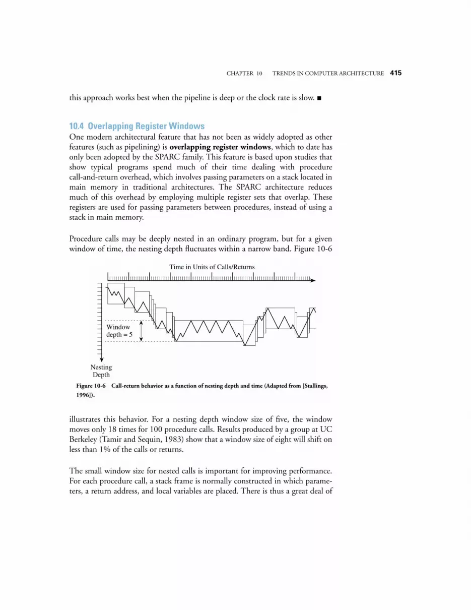
CHAPTER 10 TRENDS IN COMPUTER ARCHITECTURE 415
this approach works best when the pipeline is deep or the clock rate is slow.
10.4 Overlapping Register WindowsOne modern architectural feature that has not been as widely adopted as otherfeatures (such as pipelining) is overlapping register windows, which to date hasonly been adopted by the SPARC family. This feature is based upon studies thatshow typical programs spend much of their time dealing with procedurecall-and-return overhead, which involves passing parameters on a stack located inmain memory in traditional architectures. The SPARC architecture reducesmuch of this overhead by employing multiple register sets that overlap. Theseregisters are used for passing parameters between procedures, instead of using astack in main memory.
Procedure calls may be deeply nested in an ordinary program, but for a givenwindow of time, the nesting depth fluctuates within a narrow band. Figure 10-6
illustrates this behavior. For a nesting depth window size of five, the windowmoves only 18 times for 100 procedure calls. Results produced by a group at UCBerkeley (Tamir and Sequin, 1983) show that a window size of eight will shift onless than 1% of the calls or returns.
The small window size for nested calls is important for improving performance.For each procedure call, a stack frame is normally constructed in which parame-ters, a return address, and local variables are placed. There is thus a great deal of
Nesting Depth
Time in Units of Calls/Returns
Window depth = 5
Figure 10-6 Call-return behavior as a function of nesting depth and time (Adapted from [Stallings,
1996]).
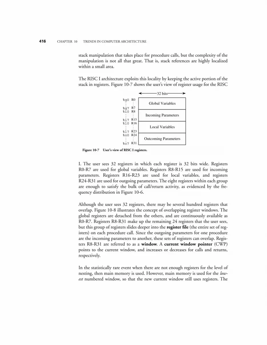
416 CHAPTER 10 TRENDS IN COMPUTER ARCHITECTURE
stack manipulation that takes place for procedure calls, but the complexity of themanipulation is not all that great. That is, stack references are highly localizedwithin a small area.
The RISC I architecture exploits this locality by keeping the active portion of thestack in registers. Figure 10-7 shows the user’s view of register usage for the RISC
I. The user sees 32 registers in which each register is 32 bits wide. RegistersR0-R7 are used for global variables. Registers R8-R15 are used for incomingparameters. Registers R16-R23 are used for local variables, and registersR24-R31 are used for outgoing parameters. The eight registers within each groupare enough to satisfy the bulk of call/return activity, as evidenced by the fre-quency distribution in Figure 10-6.
Although the user sees 32 registers, there may be several hundred registers thatoverlap. Figure 10-8 illustrates the concept of overlapping register windows. Theglobal registers are detached from the others, and are continuously available asR0-R7. Registers R8-R31 make up the remaining 24 registers that the user sees,but this group of registers slides deeper into the register file (the entire set of reg-isters) on each procedure call. Since the outgoing parameters for one procedureare the incoming parameters to another, these sets of registers can overlap. Regis-ters R8-R31 are referred to as a window. A current window pointer (CWP)points to the current window, and increases or decreases for calls and returns,respectively.
In the statistically rare event when there are not enough registers for the level ofnesting, then main memory is used. However, main memory is used for the low-est numbered window, so that the new current window still uses registers. The
%l0
%i0
Global Variables
Incoming Parameters
Local Variables
Outcoming Parameters
32 bits
R0
R7R8
R15R16
R23R24
R31
...
...
...
...
%g0
%g7
%i7
%l7%o0
%o7
...
...
...
...
Figure 10-7 User’s view of RISC I registers.
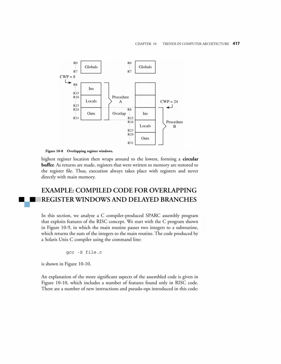
CHAPTER 10 TRENDS IN COMPUTER ARCHITECTURE 417
highest register location then wraps around to the lowest, forming a circularbuffer. As returns are made, registers that were written to memory are restored tothe register file. Thus, execution always takes place with registers and neverdirectly with main memory.
EXAMPLE: COMPILED CODE FOR OVERLAPPING REGISTER WINDOWS AND DELAYED BRANCHES
In this section, we analyze a C compiler-produced SPARC assembly programthat exploits features of the RISC concept. We start with the C program shownin Figure 10-9, in which the main routine passes two integers to a subroutine,which returns the sum of the integers to the main routine. The code produced bya Solaris Unix C compiler using the command line:
gcc -S file.c
is shown in Figure 10-10.
An explanation of the more significant aspects of the assembled code is given inFigure 10-10, which includes a number of features found only in RISC code.There are a number of new instructions and pseudo-ops introduced in this code:
GlobalsR0
R7
R8
R15R16
R23R24
R31
...
...
...
...
Ins
Locals
Outs
ProcedureA
GlobalsR0
R7
...
R8
R15R16
R23R24
R31
...
...
...
Ins
Locals
Outs
ProcedureB
CWP = 8
Overlap
CWP = 24
Figure 10-8 Overlapping register windows.
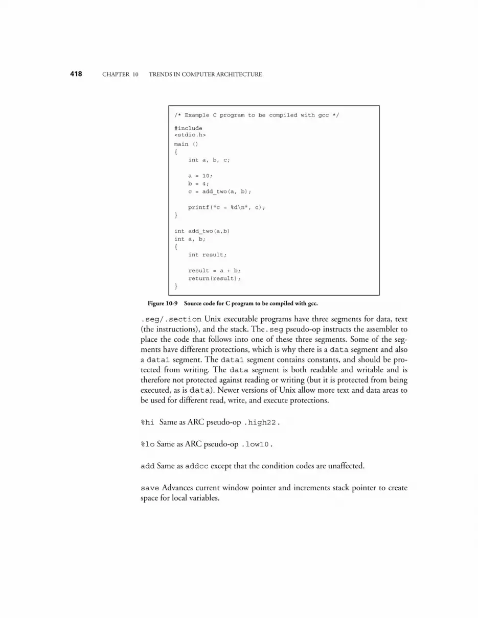
418 CHAPTER 10 TRENDS IN COMPUTER ARCHITECTURE
.seg/.section Unix executable programs have three segments for data, text(the instructions), and the stack. The.seg pseudo-op instructs the assembler toplace the code that follows into one of these three segments. Some of the seg-ments have different protections, which is why there is a data segment and alsoa data1 segment. The data1 segment contains constants, and should be pro-tected from writing. The data segment is both readable and writable and istherefore not protected against reading or writing (but it is protected from beingexecuted, as is data). Newer versions of Unix allow more text and data areas tobe used for different read, write, and execute protections.
%hi Same as ARC pseudo-op .high22.
%lo Same as ARC pseudo-op .low10.
add Same as addcc except that the condition codes are unaffected.
save Advances current window pointer and increments stack pointer to createspace for local variables.
/* Example C program to be compiled with gcc */
main ()
int a, b, c;
a = 10;
int add_two(a,b)
int a, b;
int result;
result = a + b;
return(result);
#include <stdio.h>
b = 4;
c = add_two(a, b);
printf("c = %d\n", c);
Figure 10-9 Source code for C program to be compiled with gcc.
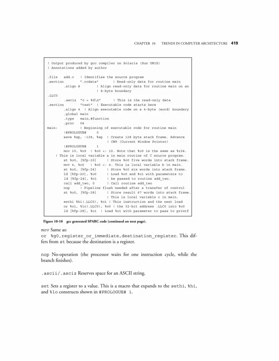
CHAPTER 10 TRENDS IN COMPUTER ARCHITECTURE 419
mov Same as:or %g0,register_or_immediate,destination_register. This dif-fers from st because the destination is a register.
nop No-operation (the processor waits for one instruction cycle, while thebranch finishes).
.ascii/.asciz Reserves space for an ASCII string.
set Sets a register to a value. This is a macro that expands to the sethi, %hi,and %lo constructs shown in #PROLOGUE# 1.
! Output produced by gcc compiler on Solaris (Sun UNIX)
.section ".rodata" ! Read-only data for routine main
.align 8 ! Align read-only data for routine main on an
! 8-byte boundary
.asciz "c = %d\n" ! This is the read-only data
.proc 04
!#PROLOGUE# 0
save %sp, -128, %sp ! Create 128 byte stack frame. Advance
! CWP (Current Window Pointer)
!#PROLOGUE# 1
! This is local variable a in main routine of C source program.
st %o0, [%fp-20] ! Store %o0 five words into stack frame.
mov 4, %o0 ! %o0 <- 4. This is local variable b in main.
.file add.c ! Identifies the source program
.section "text" ! Executable code starts here
.align 4 ! Align executable code on a 4-byte (word) boundary
.type main,#function
! Annotations added by author
.LLC0
.global main
main: ! Beginning of executable code for routine main
mov 10, %o0 ! %o0 <- 10. Note that %o0 is the same as %r24.
st %o0, [%fp-24] ! Store %o0 six words into stack frame.
ld [%fp-20], %o0 ! Load %o0 and %o1 with parameters to
ld [%fp-24], %o1 ! be passed to routine add_two.
call add_two, 0 ! Call routine add_two
nop ! Pipeline flush needed after a transfer of control
st %o0, [%fp-28] ! Store result 67 words into stack frame.
! This is local variable c in main.
sethi %hi(.LLC0), %o1 ! This instruction and the next load
or %o1, %lo(.LLC0), %o0 ! the 32-bit address .LLC0 into %o0
ld [%fp-28], %o1 ! Load %o1 with parameter to pass to printf
Figure 10-10 gcc generated SPARC code (continued on next page).
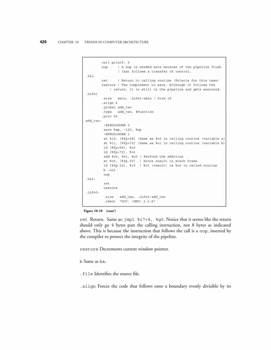
420 CHAPTER 10 TRENDS IN COMPUTER ARCHITECTURE
ret Return. Same as: jmpl %i7+8, %g0. Notice that it seems like the returnshould only go 4 bytes past the calling instruction, not 8 bytes as indicatedabove. This is because the instruction that follows the call is a nop, inserted bythe compiler to protect the integrity of the pipeline.
restore Decrements current window pointer.
b Same as ba.
.file Identifies the source file.
.align Forces the code that follows onto a boundary evenly divisible by its
call printf, 0
nop ! A nop is needed here because of the pipeline flush
! that follows a transfer of control.
.LL1
ret ! Return to calling routine (Solaris for this case)
restore ! The complement to save. Although it follows the
! return, it is still in the pipeline and gets executed.
.LLfe1
.size main, .LLfe1-main ! Size of
.align 4
.global add_two
.type add_two, #function
.proc 04
add_two:
!#PROLOGUE# 0
save %sp, -120, %sp
!#PROLOGUE# 1
st %i0, [%fp+68] !Same as %o0 in calling routine (variable a)
st %i1, [%fp+72] !Same as %o1 in calling routine (variable b)
ld [%fp+68], %o0
ld [%fp+72], %o1
add %o0, %o1, %o0 ! Perform the addition
st %o0, [%fp-20] ! Store result in stack frame
ld [%fp-20], %i0 ! %i0 (result) is %o0 in called routine
b .LL2
nop
.LL2:
ret
restore
.LLfe2:
.size add_two, .LLfe2-add_two
.ident "GCC: (GNU) 2.5.8"
Figure 10-10 (cont’)
CHAPTER 10 TRENDS IN COMPUTER ARCHITECTURE 421
argument.
.type Associates a label with its type.
.size Computes the size of a segment.
.ident Identifies the compiler version.
We can see the positions of the delay slots, marked with nop instructions. (Theoptimizing feature of the compiler has not been applied yet.) Despite the avail-ability of overlapping register windows in the SPARC architecture, the unopti-mized code makes no use of this feature: parameters to be passed to a routine arecopied to the stack, and the called routine then retrieves these parameters fromthe stack. Again, the optimizing feature of the compiler has not yet beeninvoked. (But read on).
Notice that the compiler does not seem to be consistent with its choice of regis-ters for parameter passing. Prior to the call to add_two, the compiler uses %o0and %o1 (%r0 and %r1) for parameters passed to add_two. Then, %r1 is usedfor the parameters passed to printf. Why did the compiler not start with %r0again, or choose the next available register (%o2)? This is the register assignmentproblem, which has been the object of a great deal of study. We will not go intodetails here1, as this is more appropriate for a course in compiler design, but suf-fice it to say that any logically correct assignment of variables to registers willwork, but that some assignments are better than others in terms of the number ofregisters used and the overall program execution time.
Why are the stack frames so large? We only need three words on the stack framefor local variables a, b, and c in main. We might also need a word to store thereturn address, although the compiler does not seem to generate code for that.There are no parameters passed to main by the operating system, and so thestack frame that main sees should only be four words (16 bytes) in size. Thus,the line at the beginning of routine main:
1. Here are a few details, for the curious: %r0 (%o0) is still in use (add_two is expectingthe address of LLC0 to show up in %r0), and %r1 is no longer needed at this point, so it can bereassigned. But then, why is %r1 used in the sethi line? Would it have made sense to use %r0instead of introducing another register into the computation? See problem 10.2 at the end of thechapter for more on this topic.
422 CHAPTER 10 TRENDS IN COMPUTER ARCHITECTURE
save %sp, -128, %sp
should only be:
save %sp, -16, %sp.
What is all of the extra space for? There are a number of runtime situations thatmay need stack space. For instance, if the nesting depth is greater than the num-ber of windows, then the stack must be used for overflow. (See Figure D-2 in[SPARC, 1992])
If a scalar is passed from one routine to another, then everything is fine. But if acallee refers to the address of a passed scalar (or aggregate), then the scalar (oraggregate) must be copied to the stack and be referenced from there for the life-time of the pointer (or for the lifetime of the procedure, if the pointer lifetime isnot known).
Why does the return statement ret cause a return to the code that is 8 bytes pastthe call, instead of 4 as we have been doing it? As mentioned above, this isbecause there is a nop that follows call (the so-called “delay-slot instruction”).
Notice that routine labels that appear in the source code are prepended with anunderscore in the assembly code, so that main, add_two, and printf in Cbecome _main, _add_two, and _printf in gcc generated SPARC code. Thismeans that if we want to write a C program that is linked to a gcc generatedSPARC program, that the C calls should be made to routines that begin withunderscores. For example, if add_two is compiled into SPARC code, and weinvoke it from a C main program in another file, then the C program shouldmake a call to _add_two, and not add_two, even though the routine startedout as add_two. Further, the C program needs to declare _add_two as exter-nal.
If the compilation for add_two is continued down to an executable file, thenthere is no need to treat the labels differently. The add_two routine will still belabeled _add_two, but routine main will be compiled into code that expects tosee _add_two and so everything will work OK. This is not the case, however, ifa gcc program makes calls to a Fortran library.
Fortran is a commonly used language in the scientific community, and there are anumber of significant Fortran libraries that are used for linear algebra, modeling

CHAPTER 10 TRENDS IN COMPUTER ARCHITECTURE 423
and simulation, and parallel scientific applications. As programmers of languageXYZ (whatever language that may be), we sometimes find ourselves wanting towrite XYZ programs that make calls to Fortran routines. This is easy to do oncewe understand what is happening.
There are two significant issues that need to be addressed:
(1) differences in routine labels;
(2) differences in subroutine linkage.
In Fortran, the source code labels are prepended with two underscores in theassembly code. A C program (if C is language XYZ) that makes a call to Fortranroutine add_two would then make a call to _ _add_two, which also must bedeclared as external in the C source code (and declared as global in the Fortranprogram).
If all of the parameters that are passed to the Fortran routines are pointers, theneverything will work OK. If there are any scalars passed, then there will be trou-ble because C (like Java) uses call-by-value for scalars whereas Fortran usescall-by-reference. We need to “trick” the C compiler into using call-by-referenceby making it explicit. Wherever a Fortran routine expects a scalar in its argumentlist, we use a pointer to the scalar in the C code.
As a practical consideration, the gcc compiler will compile Fortran programs. Itknows what to do by observing the extension of the source file, which should be.f for Fortran.
Now, let us take a look at how an optimizing compiler improves the code. Figure10-11 shows the optimized code using the compiler’s -O flag. Notice there is nota single nop, ld, or st instruction. Wasted cycles devoted to nop instructionshave been reclaimed, and memory references devoted to stack manipulation havebeen eliminated.
10.5 Multiple Instruction Issue (Superscalar) Machines – The Pow-erPC 601In the earlier pipelining discussion, we see how several instructions can be in var-ious phases of execution at once. Here, we look at superscalar architecture,where, with separate execution units, several instructions can be executed simul-
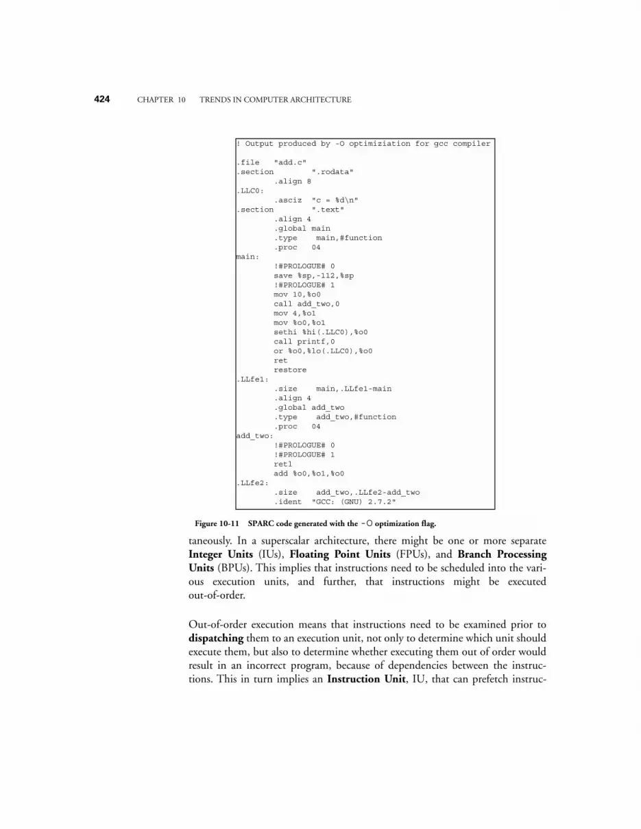
424 CHAPTER 10 TRENDS IN COMPUTER ARCHITECTURE
taneously. In a superscalar architecture, there might be one or more separateInteger Units (IUs), Floating Point Units (FPUs), and Branch ProcessingUnits (BPUs). This implies that instructions need to be scheduled into the vari-ous execution units, and further, that instructions might be executedout-of-order.
Out-of-order execution means that instructions need to be examined prior todispatching them to an execution unit, not only to determine which unit shouldexecute them, but also to determine whether executing them out of order wouldresult in an incorrect program, because of dependencies between the instruc-tions. This in turn implies an Instruction Unit, IU, that can prefetch instruc-
! Output produced by -O optimiziation for gcc compiler
.file "add.c"
.section ".rodata" .align 8.LLC0: .asciz "c = %d\n".section ".text" .align 4 .global main .type main,#function .proc 04main: !#PROLOGUE# 0 save %sp,-112,%sp !#PROLOGUE# 1 mov 10,%o0 call add_two,0 mov 4,%o1 mov %o0,%o1 sethi %hi(.LLC0),%o0 call printf,0 or %o0,%lo(.LLC0),%o0 ret restore.LLfe1: .size main,.LLfe1-main .align 4 .global add_two .type add_two,#function .proc 04add_two: !#PROLOGUE# 0 !#PROLOGUE# 1 retl add %o0,%o1,%o0.LLfe2: .size add_two,.LLfe2-add_two .ident "GCC: (GNU) 2.7.2"
Figure 10-11 SPARC code generated with the -O optimization flag.

CHAPTER 10 TRENDS IN COMPUTER ARCHITECTURE 425
tions into an instruction queue, determine the kinds of instructions and thedependence relations among them, and schedule them into the various executionunits.
10.6 Case Study: The PowerPC™ 601 as a Superscalar ArchitectureAs an example of a modern superscalar architecture let us examine the MotorolaPowerPC™ 601. The 601 has actually been superseded by more powerful mem-bers of the PowerPC family, but it will serve to illustrate the important features ofsuperscalar architectures without introducing unnecessary complexity into ourdiscussion.
10.6.1 INSTRUCTION SET ARCHITECTURE OF THE POWERPC 601
The 601 is a 32-bit general register RISC machine whose ISA includes:
• 32 32-bit general purpose integer registers (GPRs);
• 32 64-bit floating point registers (FPRs);
• 8 4-bit condition code registers;
• nearly 50 special-purpose 32-bit registers that are used to control variousaspects of memory management and the operating system;
• over 250 instructions (many of which are special-purpose).
10.6.2 HARDWARE ARCHITECTURE OF THE POWERPC 601
Figure 10-12, taken from the Motorola PowerPC 601 user’s manual, shows themicroarchitecture of the 601. The flow of instructions and data proceed via theSystem Interface, shown at the bottom of the figure, into the 32KByte cache.From there, instructions are fetched eight at a time into the Instruction Unit,shown at the top of the fiture.The issue logic within the Instruction Unit exam-ines the instructions in the queue for their kind and dependence, and issues theminto one of the three execution units: IU, BPU, or FPU.
The IU is shown as containing the GPR file and an integer exception register,XER, which holds information about exceptions that arise within the IU. TheIU can execute most integer instructions in a single clock cycle, thus obviating
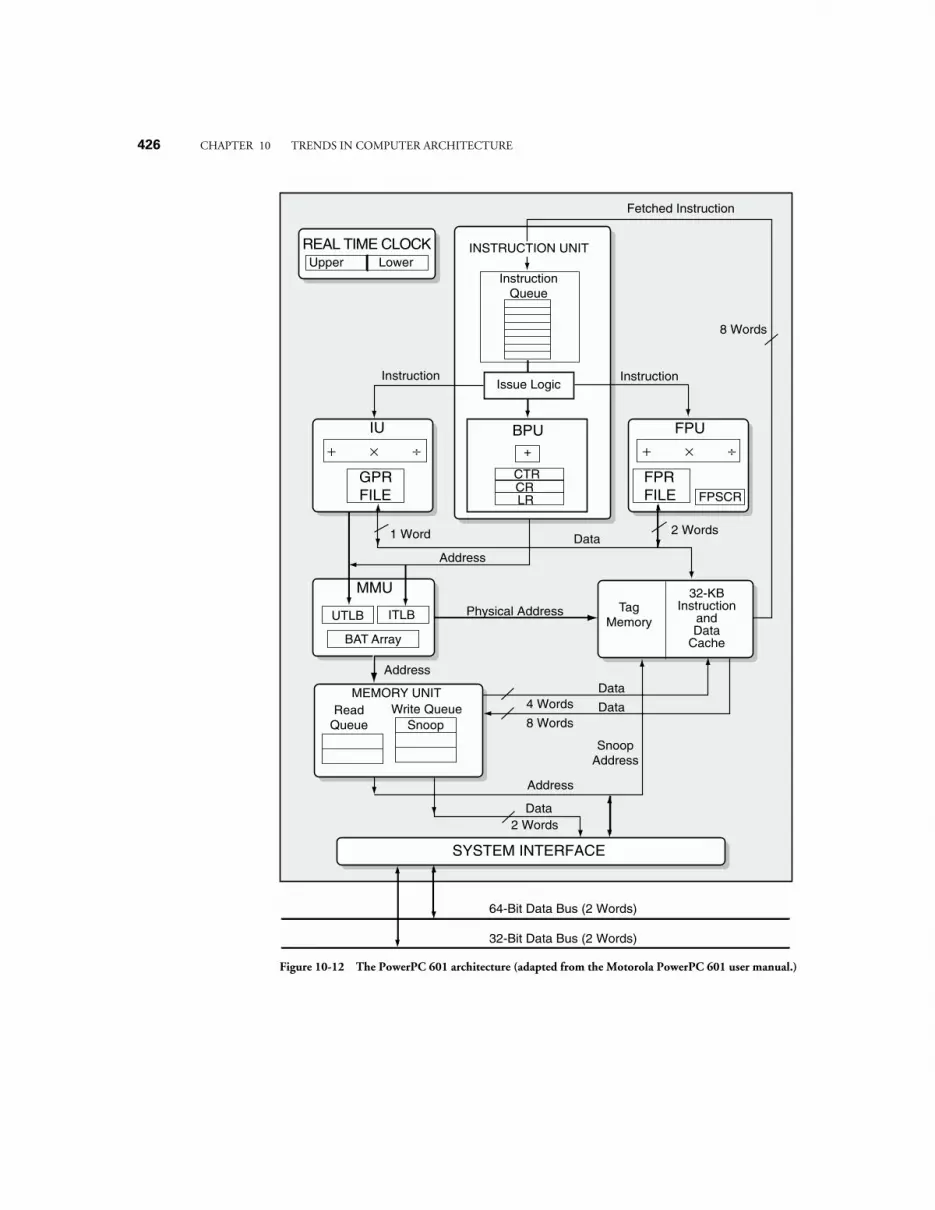
426 CHAPTER 10 TRENDS IN COMPUTER ARCHITECTURE
REAL TIME CLOCK Upper Lower
CR
InstructionQueue
BPU
CTR
LR
+
IU FPU
FPSCR
FPRFILE
GPRFILE
+ × ÷+ × ÷
TagMemory
32-KBInstruction
andData
Cache
MMU
UTLB ITLB
BAT Array
MEMORY UNITRead
QueueWrite Queue
Snoop
SYSTEM INTERFACE
64-Bit Data Bus (2 Words)
32-Bit Data Bus (2 Words)
2 Words
4 Words
1 Word 2 Words
8 Words
8 Words
Fetched Instruction
Instruction Instruction
Data
Data
Data
Data
Address
Address
Physical Address
Address
SnoopAddress
Issue Logic
INSTRUCTION UNIT
Figure 10-12 The PowerPC 601 architecture (adapted from the Motorola PowerPC 601 user manual.)
CHAPTER 10 TRENDS IN COMPUTER ARCHITECTURE 427
the need for any kind of pipelining of integer instructions.
The FPU contains the FPRs and the floating point status and control register(FPSCR). The FPSCR contains information about floating point exceptions andthe type of result produced by the FPR. The FPU is pipelined, and most FPinstructions can be issued at a rate of one per clock.
As we mentioned above in the section on pipelining, branch instructions, espe-cially conditional branch instructions, pose a bottleneck when trying to overlapinstruction execution. This is because the branch condition must first be ascer-tained to be true, for example “branch on plus” must test the N flag to ascertainthat it is cleared. The branch address must then be computed, which ofteninvolves address arithmetic. Only then can the PC be loaded with the branchaddress.
The 601 attacks this problem in several ways. First, as mentioned above, there areeight 4-bit condition code registers instead of the usual one. This allows up toeight instructions to have separate condition code bits, and therefore not inter-fere with each other’s ability to set condition codes. The BPU looks in theinstruction queue, and if it finds a conditional branch instruction it proceeds tocompute the branch target address ahead of time, and fetches instructions at thebranch target. If the branch is taken, this results in effectively a zero-cyclebranch, since the instruction at the branch target has already been fetched inanticipation of the branch condition being satisfied. The BPU also has a link reg-ister (LR) in which it can store subroutine return addresses, thus saving one GPRas well as several other registers used for special purposes. Note that the BPU canissue its addresses over a separate bus directly to the MME and Memory unit forprefetching instructions.
The RTC unit shown in the figure is a Real Time Clock which has a calendarrange of 137 years, with an accuracy of 1 ns.
The MMU and Memory Unit assist in fetching both instructions and data. Notethe separate path for data items that goes from the cache directly to the GPR andFPR register files.
The PowerPC 601, and its more powerful descendants are typical of the moderngeneral purpose microprocessor. Current microprocessor families are superscalarin design, often having several of each kind of execution unit.
428 CHAPTER 10 TRENDS IN COMPUTER ARCHITECTURE
10.7 VLIW MachinesThere is an architecture that is in a sense competitive with superscalar architec-tures, referred to as the VLIW (Very Long Instruction Word) architecture. InVLIW machines, multiple operations are packed into a single instruction wordthat may be 128 or more bits wide. The VLIW machine has multiple executionunits, similar to the superscalar machine. A typical VLIW CPU might have twoIUs, two FPUs, two load/store units, and a BPU. It is the responsibility of thecompiler to organize multiple operations into the instruction word. This relievesthe CPU of the need to examine instructions for dependencies, or to order orreorder instructions. A disadvantage is that the compiler must out of necessity bepessimistic in its estimates of dependencies. If it cannot find enough instructionsto fill the instruction word, it must fill the blank spots with NOP instructions.Furthermore, VLIW architectural improvements require software to be recom-piled to take advantage of them.
There have been a number of attempts to market VLIW machines, but mainly,VLIW machines have fallen out of favor in recent years. Performance is the pri-mary culprit, for the reasons above, among others.
10.8 Case Study: The Intel IA-64 (Merced) ArchitectureThis section discusses a microprocessor family in development by an alliancebetween Intel and Hewlett-Packard, which is hoped will take the consortiuminto the 21st century. We first look into the background that led to the decisionto develop a new architecture, and then we look at what is currently knownabout the architecture. (The information in this section is taken from variouspublications and Web sites, and has not been confirmed by Intel orHewlett-Packard.)
10.8.1 BACKGROUND—THE 80X86 CISC ARCHITECTURE
The current Intel 80x86 architecture, which runs on some 80% of desktop com-puters in the late 1990’s, had its roots in the 8086 microprocessor, designed inthe late 1970’s. The architectural roots of the family go back to the original Intel8080, designed in the early 1970’s. Being a persistent advocate of upward com-patibility, Intel has been in a sense hobbled by a CISC architecture that is over 20years old. Other vendors such as Motorola abandoned hardware compatibilityfor modernization, relying upon emulators to ease the transition to a new ISA.
In any case, Intel and Hewlett-Packard decided several years ago that the x86
CHAPTER 10 TRENDS IN COMPUTER ARCHITECTURE 429
architecture would soon reach the end of its useful life, and they began jointresearch on a new architecture. Intel and Hewlett-Packard have been quoted assaying that RISC architectures have “run out of gas,” so to speak, so their searchled in other directions. The result of their research led to the IA-64, which standsfor “Intel Architecture-64.” The first of the IA-64 family is known by the codename Merced, after the Merced River, near San Jose, California.
10.8.2 THE MERCED: AN EPIC ARCHITECTURE
Although Intel has not released significant details of the Merced ISA, it refers toits architecture as Explicitly Parallel Instruction Computing, or EPIC. Intel takespains to point out that it is not a VLIW or even an LIW machine, perhaps out ofsensitivity to the bad reputation that VLIW machines have received, however,some industry analysts refer to it as “the VLIW-like EPIC architecture.”
Features
While exact details are not publicly known as of this writing, published sourcesreport that the Merced is expected to have the following characteristics:
• 128 64-bit GPRs and perhaps 128 80-bit FPRs;
• 64 1-bit predicate registers (explained later);
• Instruction words contain three instructions packed into one 128-bit par-cel;
• Execution units, roughly equivalent to IU, FPU, and BPU, appear in mul-tiples of three, and the IA-64 will be able to schedule instructions into thesemultiples;
• It will be the burden of the compiler to schedule the instructions to takeadvantage of the multiple execution units;
• Most of the instructions seem to be RISC-like, although it is rumored thatthe processor will (still!) execute 80x86 binary codes, in a dedicated execu-tion unit, known as the DXU;
• Speculative loads. The processor will be able to load values from memorywell in advance of when they are needed. Exceptions caused by the loadsare postponed until execution has proceeded to the place where the loads
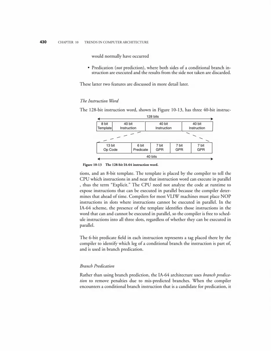
430 CHAPTER 10 TRENDS IN COMPUTER ARCHITECTURE
would normally have occurred
• Predication (not prediction), where both sides of a conditional branch in-struction are executed and the results from the side not taken are discarded.
These latter two features are discussed in more detail later.
The Instruction Word
The 128-bit instruction word, shown in Figure 10-13, has three 40-bit instruc-
tions, and an 8-bit template. The template is placed by the compiler to tell theCPU which instructions in and near that instruction word can execute in parallel, thus the term “Explicit.” The CPU need not analyze the code at runtime toexpose instructions that can be executed in parallel because the compiler deter-mines that ahead of time. Compilers for most VLIW machines must place NOPinstructions in slots where instructions cannot be executed in parallel. In theIA-64 scheme, the presence of the template identifies those instructions in theword that can and cannot be executed in parallel, so the compiler is free to sched-ule instructions into all three slots, regardless of whether they can be executed inparallel.
The 6-bit predicate field in each instruction represents a tag placed there by thecompiler to identify which leg of a conditional branch the instruction is part of,and is used in branch predication.
Branch Predication
Rather than using branch prediction, the IA-64 architecture uses branch predica-tion to remove penalties due to mis-predicted branches. When the compilerencounters a conditional branch instruction that is a candidate for predication, it
Figure 10-13 The 128-bit IA-64 instruction word.
8 bitTemplate
40 bitInstruction
40 bitInstruction
40 bitInstruction
6 bitPredicate
7 bitGPR
7 bitGPR
7 bitGPR
13 bitOp Code
128 bits
40 bits

CHAPTER 10 TRENDS IN COMPUTER ARCHITECTURE 431
selects two unique labels and labels the instructions in each leg of the branchinstruction with one of the two labels, identifying which leg they belong to. Bothlegs can then be executed in parallel. There are 64 one-bit predicate registers, onecorresponding to each of the 64 possible predicate identifiers.
When the actual branch outcome is known, the corresponding one-bit predicateregister is set if the branch outcome is TRUE, and the one-bit predicate registercorresponding to the FALSE label is cleared. Then the results from instructionshaving the correct predicate label are kept, and results from instructions havingthe incorrect (mis-predicted) label are discarded.
Speculative Loads
The architecture also employs speculative loads, that is, examining the instruc-tion stream for upcoming load instructions and loading the value ahead of time,speculating that the value will actually be needed and will not have been alteredby intervening operations. If successful, this eliminates the normal latency inher-ent in memory accesses. The compiler examines the instruction stream for candi-date load operations that it can “hoist” to a location earlier in the instructionsequence. It inserts a check instruction at the point where the load instructionwas originally located. The data value is thus available in the CPU when thecheck instruction is encountered.
The problem that is normally faced by speculative loads is that the load opera-tion may generate an exception, for example because the address is invalid. How-ever, the exception may not be genuine, because the load may be beyond abranch instruction that is not taken, and thus would never actually be executed.The IA-64 architecture postpones processing the exception until the checkinstruction is encountered. If the branch is not taken then the check instructionwill not be executed, and thus the exception will not be processed.
All of this complexity places a heavy burden on the compiler, which must beclever about how it schedules operations into the instruction words.
80x86 Compatibility
Intel was recently granted a patent for a method, presumably to be used withIA-64, for supporting two instruction sets, one of which is the x86 instructionset. It describes instructions to allow switching between the two execution
432 CHAPTER 10 TRENDS IN COMPUTER ARCHITECTURE
modes, and for data sharing between them.
Estimated Performance
It has been estimated that the first Merced implementation will appear sometimein the year 2000, and will have an 800 MHz clock speed. Goals are for it to haveperformance several times that of current-generation processors when running inEPIC mode, and that of a 500 MHz Pentium II in x86 mode. Intel has statedthat initially the IA-64 microprocessor will be reserved for use in high-perfor-mance workstations and servers, and at an estimated initial price of $5000 eachthis will undoubtedly be the case.
On the other hand, skeptics, who seem to abound when new technology isannounced, say that the technology is unlikely to meet expectations, and that theIA-64 may never see the light of day. Time will tell.
10.9 Parallel ArchitectureOne method of improving the performance of a processor is to decrease the timeneeded to execute instructions. This will work up to a limit of about 400 MHz(Stone, 1991), at which point an effect known as ringing on busses prohibitsfurther speedup with conventional bus technology. This is not to say that higherclock speeds are not possible, because indeed current microprocessors have clockrates well above 400 MHz, but that “shared bus” approaches become impracticalat these speeds. As conventional architectural approaches to improving perfor-mance wear thin, we need to consider alternative methods of improving perfor-mance.
One alternative approach to increasing bus speed is to increase the number ofprocessors, and decompose and distribute a single program onto the processors.This approach is known as parallel processing, in which a number of processorswork collectively, in parallel, on a common problem. We see an example of paral-lel processing earlier in the chapter with pipelining. For that case, four processorsare connected in series (Figure 10-3), each performing a different task, like anassembly line in a factory. The interleaved memory described in Chapter 7 isanother example of pipelining.
A parallel architecture can be characterized in terms of three parameters: (1) thenumber of processing elements (PEs); (2) the interconnection network amongthe PEs; and (3) the organization of the memory. In the four-stage instruction
CHAPTER 10 TRENDS IN COMPUTER ARCHITECTURE 433
pipeline of Figure 10-3, there are four PEs. The interconnection network amongthe PEs is a simple ring. The memory is an ordinary RAM that is external to thepipeline.
Characterizing the architecture of a parallel processor is a relatively easy task, butmeasuring the performance is not nearly so simple. Although we can easily mea-sure the increased speed that a simple enhancement like a pipeline offers, theoverall speedup is data dependent: not all programs and data sets map well ontoa pipelined architecture. Other performance considerations of pipelined architec-tures that are also data dependent are the cost of flushing a pipeline, the increasedarea cost, the latency (input to output delay) of the pipeline, etc.
A few common measures of performance are parallel time, speedup, efficiency,and throughput. The parallel time is simply the absolute time needed for a pro-gram to execute on a parallel processor. The speedup is the ratio of the time for aprogram to execute on a sequential (non-parallel, that is) processor to the timefor that same program to execute on a parallel processor. In a simple form, wecan represent speedup (S, now in the context of parallel processing) as:
Since a sequential algorithm and a parallel version of the same algorithm may beprogrammed very differently for each machine, we need to qualify TSequential andTParallel so that they apply to the best implementation for each machine.
There is more to the story. If we want to achieve a speedup of 100, it is notenough to simply distribute a single program over 100 processors. The problemis that not many computations are easily decomposed in a way that fully utilizesthe available PEs. If there are even a small number of sequential operations in aparallel program, then the speedup can be significantly limited. This is summa-rized by Amdahl’s law, in which speedup is expressed in terms of the number ofprocessors p and the fraction of operations that must be performed sequentially f:
For example, if f = 10% of the operations must be performed sequentially, thenspeedup can be no greater than 10 regardless of how many processors are used:
STSequential
TParallel-------------------------=
S 1
f 1 f–p
------------+----------------------=
434 CHAPTER 10 TRENDS IN COMPUTER ARCHITECTURE
This brings us to measurements of efficiency. Efficiency is the ratio of speedupto the number of processors used. For a speedup of 5.3 with 10 processors, theefficiency is:
If we double the number of processors to 20, then the speedup increases to 6.9but the efficiency reduces to 34%. Thus, parallelizing an algorithm can improveperformance to a limit that is determined by the amount of sequential opera-tions. Efficiency is drastically reduced as speedup approaches its limit, and so itdoes not make sense to simply use more processors in a computation in the hopethat a corresponding gain in performance will be achieved.
Throughput is a measure of how much computation is achieved over time, andis of special concern for I/O bound and pipelined applications. For the case of afour stage pipeline that remains filled, in which each pipeline stage completes itstask in 10 ns, the average time to complete an operation is 10 ns even though ittakes 40 ns to execute any one operation. The overall throughput for this situa-tion is then:
= 108 operations per second.
10.9.1 THE FLYNN TAXONOMY
Computer architectures can be classified in terms of their instruction streamsand their data streams, using a taxonomy developed by M. J. Flynn (Flynn,1972). A conventional sequential processor fits into the single-instructionstream, single data stream (SISD) category, as illustrated in Figure 10-14a.Only a single instruction is executed at a time in a SISD processor, althoughpipelining may allow several instructions to be in different phases of execution atany given time.
S 1
0.1 0.910-------+
--------------------- 5.3≅=
p 10 processors=
S 1
0.1 0.9∞
-------+--------------------- 10= =
p ∞ processors=
5.310------- .53, or 53%=
0.1operationns
----------------------
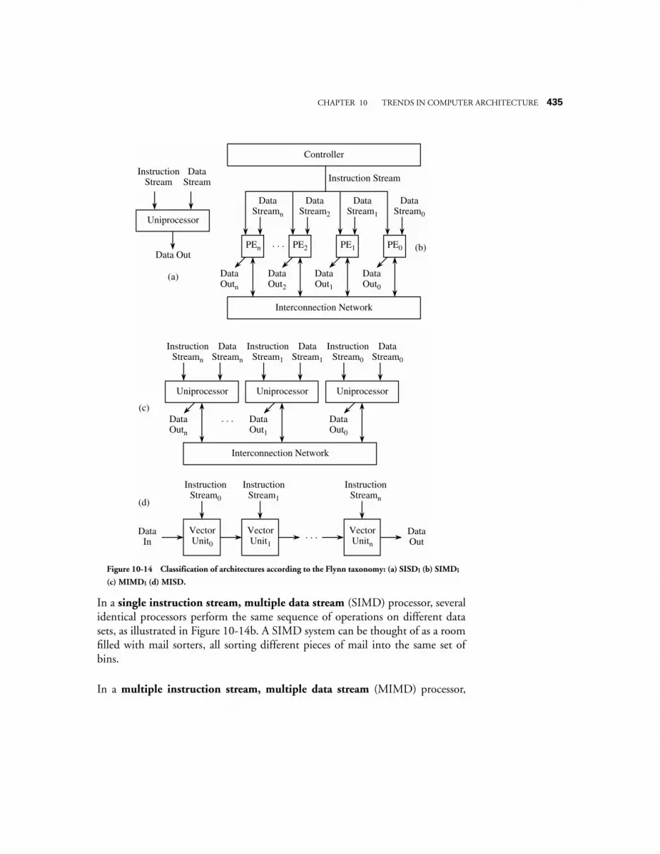
CHAPTER 10 TRENDS IN COMPUTER ARCHITECTURE 435
In a single instruction stream, multiple data stream (SIMD) processor, severalidentical processors perform the same sequence of operations on different datasets, as illustrated in Figure 10-14b. A SIMD system can be thought of as a roomfilled with mail sorters, all sorting different pieces of mail into the same set ofbins.
In a multiple instruction stream, multiple data stream (MIMD) processor,
(a)
Uniprocessor
Instruction Stream
Data Stream
Data Out
Interconnection Network
(b)
Controller
PEn PE2 PE1 PE0. . .
Data Outn
Data Out2
Data Out1
Data Out0
Data Streamn
Data Stream2
Data Stream1
Data Stream0
Instruction Stream
Uniprocessor
Interconnection Network
Data Outn
Instruction Streamn
Data Streamn
Uniprocessor
Data Out1
Instruction Stream1
Data Stream1
Uniprocessor
Data Out0
Instruction Stream0
Data Stream0
(c)
Vector Unit0
Data In
Instruction Stream0
. . .
Vector Unit1
Instruction Stream1
Vector Unitn
Instruction Streamn
. . . Data Out
(d)
Figure 10-14 Classification of architectures according to the Flynn taxonomy: (a) SISD; (b) SIMD;
(c) MIMD; (d) MISD.
436 CHAPTER 10 TRENDS IN COMPUTER ARCHITECTURE
several processors perform different operations on different data sets, but are allcoordinated to execute a single parallel program, as illustrated in Figure 10-14c.An example of a MIMD processor is the Sega home video entertainment system,which has four processors for (1) sound synthesis (a Yamaha synthesis processor);(2) sound filtering (a Texas Instruments programmable sound generator); (3)program execution (a 68000); and (4) background processing (a Z80). We willsee more of the Sega Genesis in a Case Study at the end of the chapter.
In a multiple instruction stream, single data stream (MISD) processor, a sin-gle data stream is operated on by several functional units, as illustrated in Figure10-14d. The data stream is typically a vector of several related streams. This con-figuration is known as a systolic array, which we see in Chapter 3 in the form ofan array multiplier.
10.9.2 INTERCONNECTION NETWORKS
When a computation is distributed over a number of PEs, the PEs need to com-municate with each other through an interconnection network. There is a hostof topologies for interconnection networks, each with their own characteristics interms of crosspoint complexity (an asymptotic measure of area), diameter (thelength of the worst case path through the network), and blocking (whether ornot a new connection can be established in the presence of other connections). Afew representative topologies and control strategies for configuring networks aredescribed below.
One of the most powerful network topologies is the crossbar, in which every PEis directly connected to every other PE. An abstract view of a crossbar is illus-trated in Figure 10-15a, in which four PEs are interconnected. In a closeup viewillustrated in Figure 10-16, the crossbar contains crosspoint switches, which areconfigurable devices that either connect or disconnect the lines that go throughit. In general, for N PEs, the crosspoint complexity (the number of crosspointswitches) is N2. In Figure 10-15a, N = 4 (not 8) because the output ports of thePEs on the left and the input ports of the PEs on the right belong to the samePEs. The crosspoint complexity is thus 42 = 16. The network diameter is 1 sinceevery PE can directly communicate with every other PE, with no interveningPEs. The number of crosspoint switches that are traversed is not normally con-sidered in evaluating the network diameter. The crossbar is strictly nonblock-ing, which means that there is always an available path between every input andoutput regardless of the configuration of existing paths.
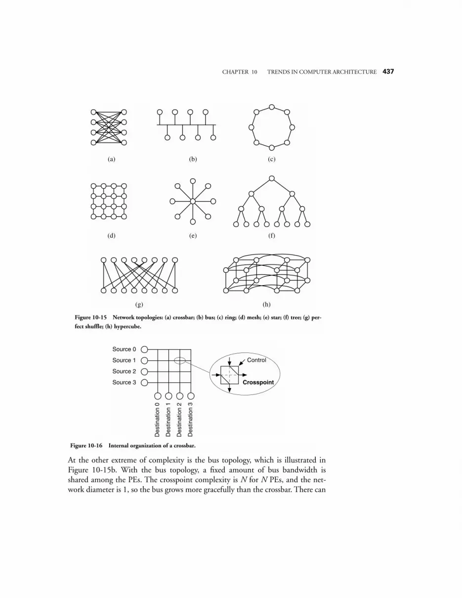
CHAPTER 10 TRENDS IN COMPUTER ARCHITECTURE 437
At the other extreme of complexity is the bus topology, which is illustrated inFigure 10-15b. With the bus topology, a fixed amount of bus bandwidth isshared among the PEs. The crosspoint complexity is N for N PEs, and the net-work diameter is 1, so the bus grows more gracefully than the crossbar. There can
(a) (c)(b)
(d) (e) (f)
(g) (h)
Figure 10-15 Network topologies: (a) crossbar; (b) bus; (c) ring; (d) mesh; (e) star; (f) tree; (g) per-
fect shuffle; (h) hypercube.
Source 0
Source 1
Source 2
Source 3
Des
tinat
ion
0
Des
tinat
ion
1
Des
tinat
ion
2
Des
tinat
ion
3
Control
Crosspoint
Figure 10-16 Internal organization of a crossbar.
438 CHAPTER 10 TRENDS IN COMPUTER ARCHITECTURE
only be one source at a time, and there is normally only one receiver, so blockingis a frequent situation for a bus.
In a ring topology, there are N crosspoints for N PEs as shown in Figure 10-15c.As for the crossbar, each crosspoint is contained within a PE. The network diam-eter is N/2, but the collective bandwidth is N times greater than for the case ofthe bus. This is because adjacent PEs can communicate directly with each otherover their common link without affecting the rest of the network.
In the mesh topology, there are N crosspoints for N PEs, but the diameter is only as shown in Figure 10-15d. All PEs can simultaneously communicate in
just steps, as discussed in (Leighton, 1992) using an off-line routing algo-rithm (in which the crosspoint settings are determined external to the PEs).
In the star topology, there is a central hub through which all PEs communicate asshown in Figure 10-15e. Since all of the connection complexity is centralized,the star can only grow to sizes that are bounded by the technology, which is nor-mally less than for decentralized topologies like the mesh. The crosspoint com-plexity within the hub varies according to the implementation, which can beanything from a bus to a crossbar.
In the tree topology, there are N crosspoints for N PEs, and the diameter is2log2N – 1 as shown in Figure 10-15f. The tree is effective for applications inwhich there is a great deal of distributing and collecting of data.
In the perfect shuffle topology, there are N crosspoints for N PEs as shown inFigure 10-15g. The diameter is log2N since it takes log2N passes through the net-work to connect any PE with any other in the worst case. The perfect shufflename comes from the property that if a deck of 2N cards, in which N is an inte-ger, is cut in half and interleaved N times, then the original configuration of thedeck is restored. All N PEs can simultaneously communicate in 3log2N – 1passes through the network as presented in (Wu and Feng, 1981).
Finally, the hypercube has N crosspoints for N PEs, with a diameter of log2N-1,as shown in Figure 10-15h. The smaller number of crosspoints with respect tothe perfect shuffle topology is balanced by a greater connection complexity in thePEs.
Let us now consider the behavior of blocking in interconnection networks. Fig-ure 10-17a shows a configuration in which four processors are interconnected
2 N3 N
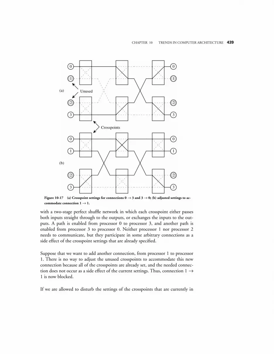
CHAPTER 10 TRENDS IN COMPUTER ARCHITECTURE 439
with a two-stage perfect shuffle network in which each crosspoint either passesboth inputs straight through to the outputs, or exchanges the inputs to the out-puts. A path is enabled from processor 0 to processor 3, and another path isenabled from processor 3 to processor 0. Neither processor 1 nor processor 2needs to communicate, but they participate in some arbitrary connections as aside effect of the crosspoint settings that are already specified.
Suppose that we want to add another connection, from processor 1 to processor1. There is no way to adjust the unused crosspoints to accommodate this newconnection because all of the crosspoints are already set, and the needed connec-tion does not occur as a side effect of the current settings. Thus, connection 1 →1 is now blocked.
If we are allowed to disturb the settings of the crosspoints that are currently in
0
1
2
3
0
1
2
3
(a)
0
1
2
3
0
1
2
3
(b)
Crosspoints
Unused
Figure 10-17 (a) Crosspoint settings for connections 0 → 3 and 3 → 0; (b) adjusted settings to ac-
commodate connection 1 → 1.
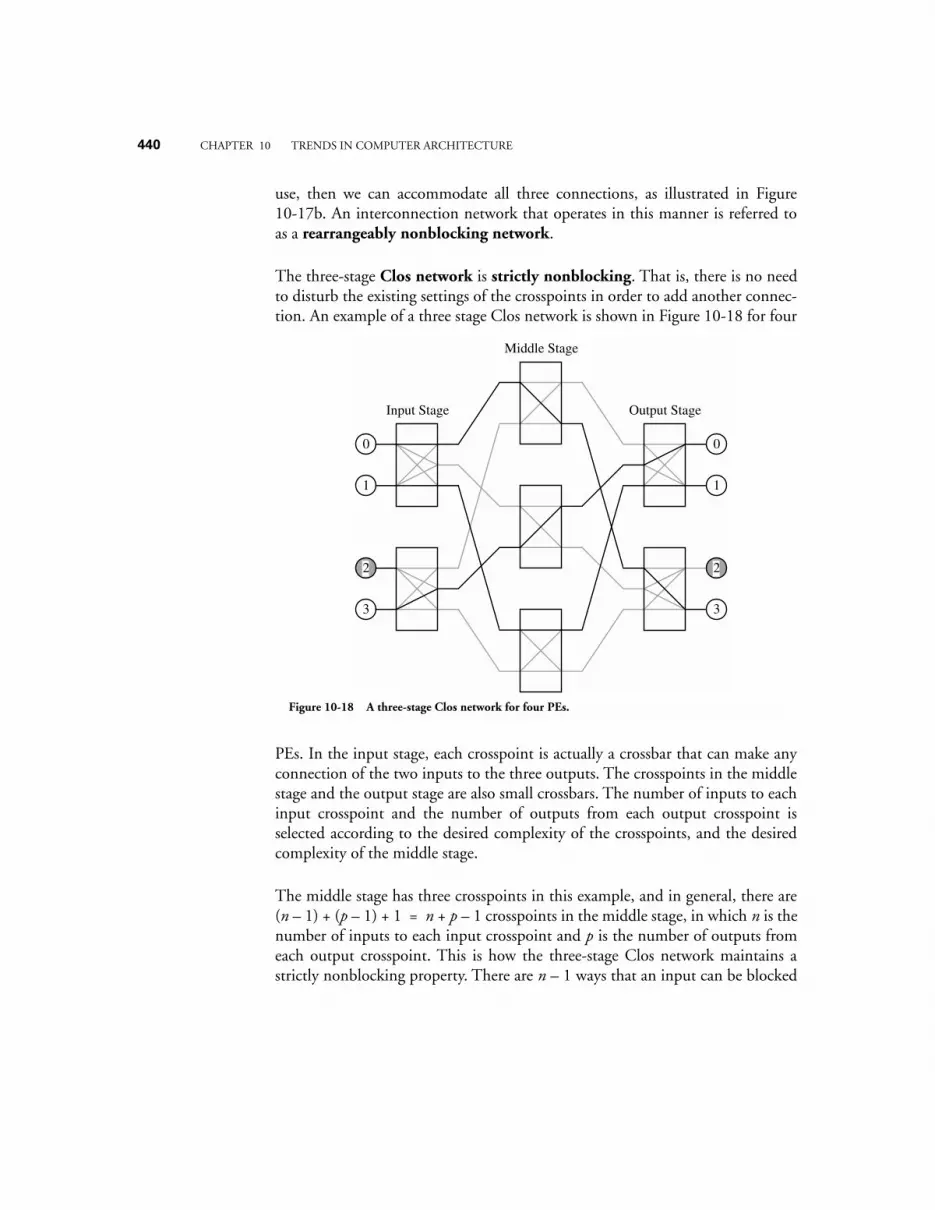
440 CHAPTER 10 TRENDS IN COMPUTER ARCHITECTURE
use, then we can accommodate all three connections, as illustrated in Figure10-17b. An interconnection network that operates in this manner is referred toas a rearrangeably nonblocking network.
The three-stage Clos network is strictly nonblocking. That is, there is no needto disturb the existing settings of the crosspoints in order to add another connec-tion. An example of a three stage Clos network is shown in Figure 10-18 for four
PEs. In the input stage, each crosspoint is actually a crossbar that can make anyconnection of the two inputs to the three outputs. The crosspoints in the middlestage and the output stage are also small crossbars. The number of inputs to eachinput crosspoint and the number of outputs from each output crosspoint isselected according to the desired complexity of the crosspoints, and the desiredcomplexity of the middle stage.
The middle stage has three crosspoints in this example, and in general, there are(n – 1) + (p – 1) + 1 = n + p – 1 crosspoints in the middle stage, in which n is thenumber of inputs to each input crosspoint and p is the number of outputs fromeach output crosspoint. This is how the three-stage Clos network maintains astrictly nonblocking property. There are n – 1 ways that an input can be blocked
0
1
3
0
1
3
Input Stage Output Stage
Middle Stage
2 2
Figure 10-18 A three-stage Clos network for four PEs.
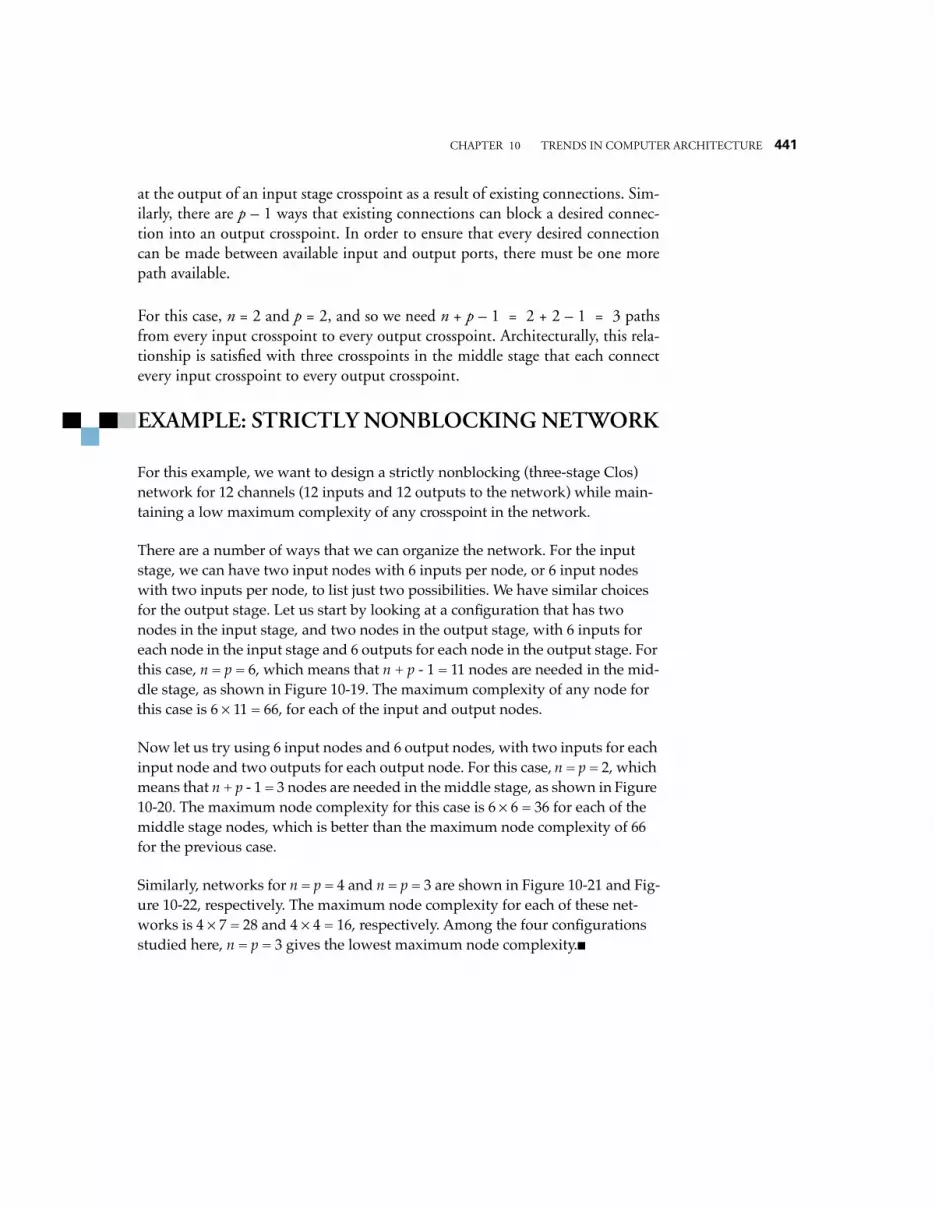
CHAPTER 10 TRENDS IN COMPUTER ARCHITECTURE 441
at the output of an input stage crosspoint as a result of existing connections. Sim-ilarly, there are p – 1 ways that existing connections can block a desired connec-tion into an output crosspoint. In order to ensure that every desired connectioncan be made between available input and output ports, there must be one morepath available.
For this case, n = 2 and p = 2, and so we need n + p – 1 = 2 + 2 – 1 = 3 pathsfrom every input crosspoint to every output crosspoint. Architecturally, this rela-tionship is satisfied with three crosspoints in the middle stage that each connectevery input crosspoint to every output crosspoint.
EXAMPLE: STRICTLY NONBLOCKING NETWORK
For this example, we want to design a strictly nonblocking (three-stage Clos) network for 12 channels (12 inputs and 12 outputs to the network) while main-taining a low maximum complexity of any crosspoint in the network.
There are a number of ways that we can organize the network. For the input stage, we can have two input nodes with 6 inputs per node, or 6 input nodes with two inputs per node, to list just two possibilities. We have similar choices for the output stage. Let us start by looking at a configuration that has two nodes in the input stage, and two nodes in the output stage, with 6 inputs for each node in the input stage and 6 outputs for each node in the output stage. For this case, n = p = 6, which means that n + p - 1 = 11 nodes are needed in the mid-dle stage, as shown in Figure 10-19. The maximum complexity of any node for this case is 6 × 11 = 66, for each of the input and output nodes.
Now let us try using 6 input nodes and 6 output nodes, with two inputs for each input node and two outputs for each output node. For this case, n = p = 2, which means that n + p - 1 = 3 nodes are needed in the middle stage, as shown in Figure 10-20. The maximum node complexity for this case is 6 × 6 = 36 for each of the middle stage nodes, which is better than the maximum node complexity of 66 for the previous case.
Similarly, networks for n = p = 4 and n = p = 3 are shown in Figure 10-21 and Fig-ure 10-22, respectively. The maximum node complexity for each of these net-works is 4 × 7 = 28 and 4 × 4 = 16, respectively. Among the four configurations studied here, n = p = 3 gives the lowest maximum node complexity.
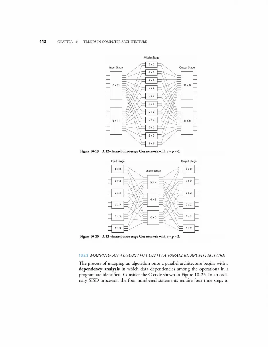
442 CHAPTER 10 TRENDS IN COMPUTER ARCHITECTURE
10.9.3 MAPPING AN ALGORITHM ONTO A PARALLEL ARCHITECTURE
The process of mapping an algorithm onto a parallel architecture begins with adependency analysis in which data dependencies among the operations in aprogram are identified. Consider the C code shown in Figure 10-23. In an ordi-nary SISD processor, the four numbered statements require four time steps to
6 x 11
6 x 11
Input Stage
11 x 6
11 x 6
Output Stage
Middle Stage
2 x 2
2 x 2
2 x 2
2 x 2
2 x 2
2 x 2
2 x 2
2 x 2
2 x 2
2 x 2
2 x 2
Figure 10-19 A 12-channel three-stage Clos network with n = p = 6.
Input Stage Output Stage
Middle Stage2 x 3
2 x 3
2 x 3
2 x 3
2 x 3
2 x 3
6 x 6
6 x 6
6 x 6
3 x 2
3 x 2
3 x 2
3 x 2
3 x 2
3 x 2
Figure 10-20 A 12-channel three-stage Clos network with n = p = 2.

CHAPTER 10 TRENDS IN COMPUTER ARCHITECTURE 443
complete, as illustrated in the control sequence of Figure 10-24a. The depen-dency graph shown in Figure 10-24b exposes the natural parallelism in the con-trol sequence. The dependency graph is created by assigning each operation inthe original program to a node in the graph, and then drawing a directed arcfrom each node that produces a result to the node(s) that needs it.
The control sequence requires four time steps to complete, but the dependencygraph shows that the program can be completed in just three time steps, sinceoperations 0 and 1 do not depend on each other and can be executed simulta-
4 x 7
Input Stage Output StageMiddle Stage
3 x 3
3 x 3
3 x 3
3 x 3
3 x 3
3 x 3
3 x 3
4 x 7
4 x 7
7 x 4
7 x 4
7 x 4
Figure 10-21 A 12-channel three-stage Clos network with n = p = 4.
Input Stage Output StageMiddle Stage
3 x 5 4 x 4
4 x 4
4 x 4
4 x 4
4 x 4
3 x 5
3 x 5
3 x 5
5 x 3
5 x 3
5 x 3
5 x 3
Figure 10-22 A 12-channel three-stage Clos network with n = p = 3.

444 CHAPTER 10 TRENDS IN COMPUTER ARCHITECTURE
neously (as long as there are two processors available.) The resulting speedup of
may not be very great, but for other programs, the opportunity for speedup can
func(x, y) /* Compute (x2 + y2) × y2 */int x, y;
int temp0, temp1, temp2, temp3;
temp0 = x * x;
temp1 = y * y;
temp2 = temp1 + temp2;
temp3 = temp1 * temp2;
return(temp3);
0123
Operation numbers
Figure 10-23 A C function computes (x2 + y2) × y2.
0*
1
0*
1*
2+
3
14*
2+
3*
*
Arrows represent flow of control
*
Arrows represent
flow of data
x y
x2
y2
x2 + y2
(x2 + y2)×y2
(x2 + y2)×y2
x2 + y2
x2 y2 y2
(a)
(b)
Figure 10-24 (a) Control sequence for C program; (b) dependency graph for C program.
TSequential
TParallel------------------------- 4
3--- 1.3= =
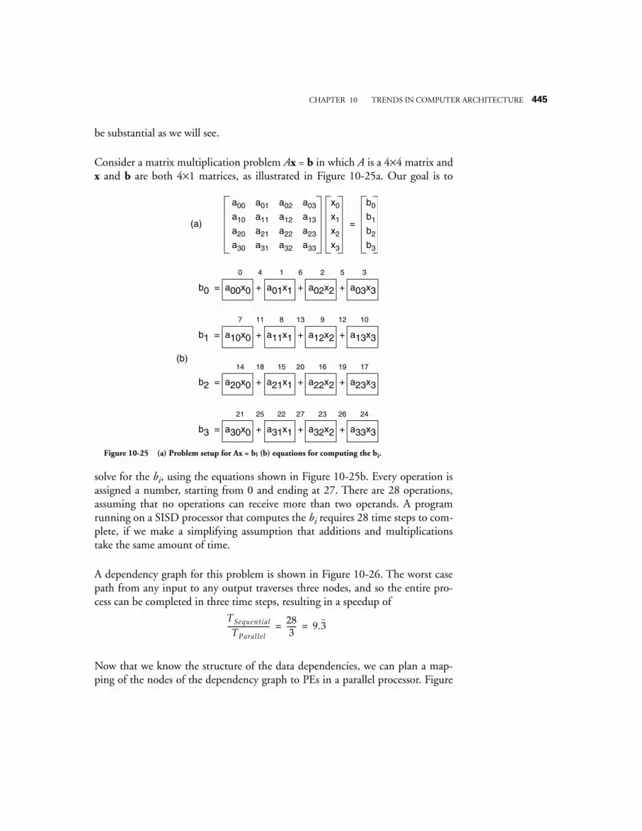
CHAPTER 10 TRENDS IN COMPUTER ARCHITECTURE 445
be substantial as we will see.
Consider a matrix multiplication problem Ax = b in which A is a 4×4 matrix andx and b are both 4×1 matrices, as illustrated in Figure 10-25a. Our goal is to
solve for the bi, using the equations shown in Figure 10-25b. Every operation isassigned a number, starting from 0 and ending at 27. There are 28 operations,assuming that no operations can receive more than two operands. A programrunning on a SISD processor that computes the bi requires 28 time steps to com-plete, if we make a simplifying assumption that additions and multiplicationstake the same amount of time.
A dependency graph for this problem is shown in Figure 10-26. The worst casepath from any input to any output traverses three nodes, and so the entire pro-cess can be completed in three time steps, resulting in a speedup of
Now that we know the structure of the data dependencies, we can plan a map-ping of the nodes of the dependency graph to PEs in a parallel processor. Figure
a00 a01 a02 a03
a10 a11 a12 a13
a20 a21 a22 a23
a30 a31 a32 a33
x0
x1
x2
x3
=
b0
b1
b2
b3
b0 = a00x0 + a01x1 + a02x2 + a03x3
0 1 2 34 6 5
b1 = a10x0 + a11x1 + a12x2 + a13x3
7 8 9 1011 13 12
b2 = a20x0 + a21x1 + a22x2 + a23x3
14 15 16 1718 20 19
b3 = a30x0 + a31x1 + a32x2 + a33x3
21 22 23 2425 27 26
(a)
(b)
Figure 10-25 (a) Problem setup for Ax = b; (b) equations for computing the bi.
TSequential
TParallel------------------------- 28
3------ 9.3= =
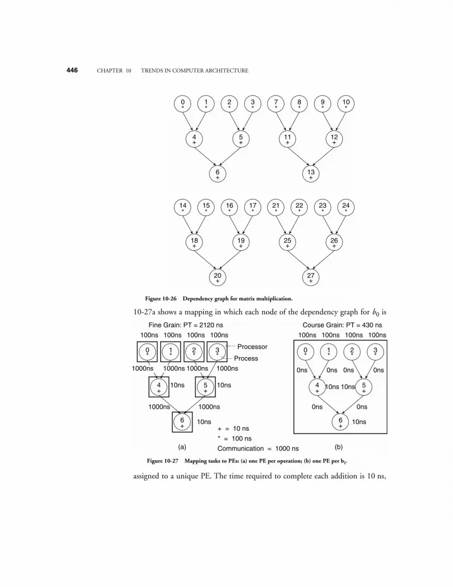
446 CHAPTER 10 TRENDS IN COMPUTER ARCHITECTURE
10-27a shows a mapping in which each node of the dependency graph for b0 is
assigned to a unique PE. The time required to complete each addition is 10 ns,
0*
1*
2*
3*
4+
6+
5+
7*
8*
9*
10*
11+
13+
12+
14*
15*
16*
17*
18+
20+
19+
21*
22*
23*
24*
25+
27+
26+
Figure 10-26 Dependency graph for matrix multiplication.
0*
1*
2*
3*
4+
6+
5+
+ = 10 ns
* = 100 ns
Communication = 1000 ns
Fine Grain: PT = 2120 ns
100ns 100ns 100ns 100ns
10ns 10ns
10ns
0*
1*
2*
3*
4+
6+
5+
100ns 100ns 100ns 100ns
10ns
10ns
10ns
1000ns 1000ns 1000ns
1000ns 1000ns
1000ns
Course Grain: PT = 430 ns
0ns 0ns 0ns
0ns 0ns
0ns
(a) (b)
Processor
Process
Figure 10-27 Mapping tasks to PEs: (a) one PE per operation; (b) one PE per bi.
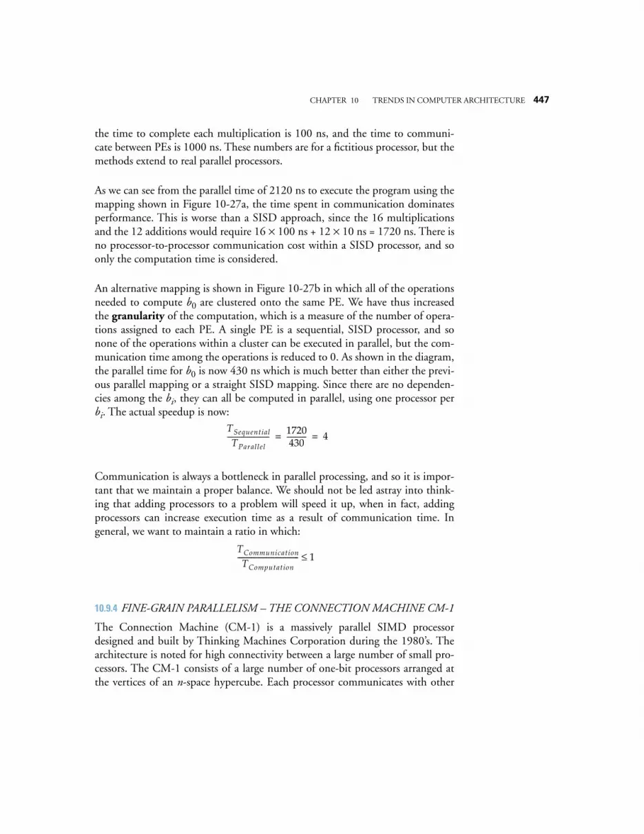
CHAPTER 10 TRENDS IN COMPUTER ARCHITECTURE 447
the time to complete each multiplication is 100 ns, and the time to communi-cate between PEs is 1000 ns. These numbers are for a fictitious processor, but themethods extend to real parallel processors.
As we can see from the parallel time of 2120 ns to execute the program using themapping shown in Figure 10-27a, the time spent in communication dominatesperformance. This is worse than a SISD approach, since the 16 multiplicationsand the 12 additions would require 16 × 100 ns + 12 × 10 ns = 1720 ns. There isno processor-to-processor communication cost within a SISD processor, and soonly the computation time is considered.
An alternative mapping is shown in Figure 10-27b in which all of the operationsneeded to compute b0 are clustered onto the same PE. We have thus increasedthe granularity of the computation, which is a measure of the number of opera-tions assigned to each PE. A single PE is a sequential, SISD processor, and sonone of the operations within a cluster can be executed in parallel, but the com-munication time among the operations is reduced to 0. As shown in the diagram,the parallel time for b0 is now 430 ns which is much better than either the previ-ous parallel mapping or a straight SISD mapping. Since there are no dependen-cies among the bi, they can all be computed in parallel, using one processor perbi. The actual speedup is now:
Communication is always a bottleneck in parallel processing, and so it is impor-tant that we maintain a proper balance. We should not be led astray into think-ing that adding processors to a problem will speed it up, when in fact, addingprocessors can increase execution time as a result of communication time. Ingeneral, we want to maintain a ratio in which:
10.9.4 FINE-GRAIN PARALLELISM – THE CONNECTION MACHINE CM-1
The Connection Machine (CM-1) is a massively parallel SIMD processordesigned and built by Thinking Machines Corporation during the 1980’s. Thearchitecture is noted for high connectivity between a large number of small pro-cessors. The CM-1 consists of a large number of one-bit processors arranged atthe vertices of an n-space hypercube. Each processor communicates with other
TSequential
TParallel------------------------- 1720
430------------ 4= =
TCommunication
TComputation------------------------------------ 1≤
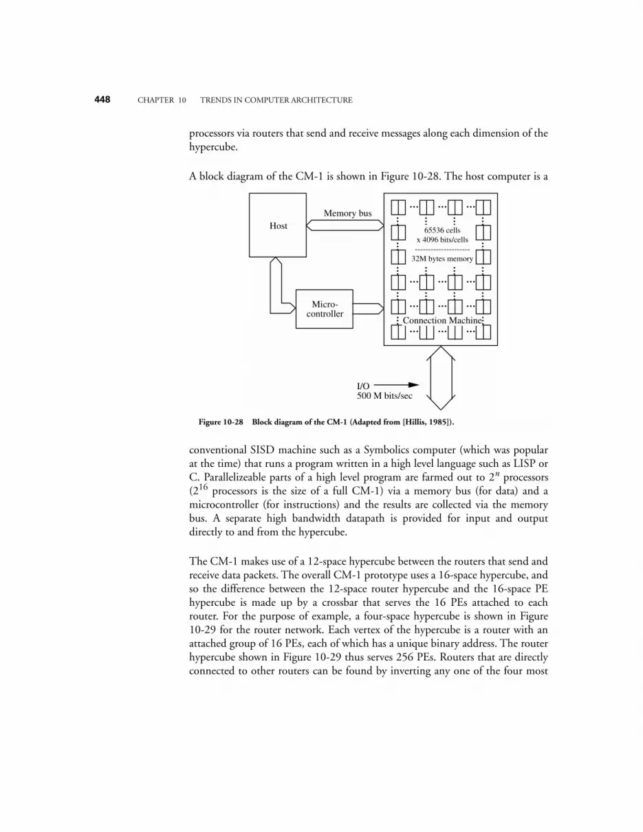
448 CHAPTER 10 TRENDS IN COMPUTER ARCHITECTURE
processors via routers that send and receive messages along each dimension of thehypercube.
A block diagram of the CM-1 is shown in Figure 10-28. The host computer is a
conventional SISD machine such as a Symbolics computer (which was popularat the time) that runs a program written in a high level language such as LISP orC. Parallelizeable parts of a high level program are farmed out to 2n processors(216 processors is the size of a full CM-1) via a memory bus (for data) and amicrocontroller (for instructions) and the results are collected via the memorybus. A separate high bandwidth datapath is provided for input and outputdirectly to and from the hypercube.
The CM-1 makes use of a 12-space hypercube between the routers that send andreceive data packets. The overall CM-1 prototype uses a 16-space hypercube, andso the difference between the 12-space router hypercube and the 16-space PEhypercube is made up by a crossbar that serves the 16 PEs attached to eachrouter. For the purpose of example, a four-space hypercube is shown in Figure10-29 for the router network. Each vertex of the hypercube is a router with anattached group of 16 PEs, each of which has a unique binary address. The routerhypercube shown in Figure 10-29 thus serves 256 PEs. Routers that are directlyconnected to other routers can be found by inverting any one of the four most
… … …
… … …
… … …
… … …
… … … …
… …
… … … …
… … … …
… … … …Connection Machine
65536 cellsx 4096 bits/cells---------------------
32M bytes memory
I/O500 M bits/sec
HostMemory bus
Micro-controller
Figure 10-28 Block diagram of the CM-1 (Adapted from [Hillis, 1985]).
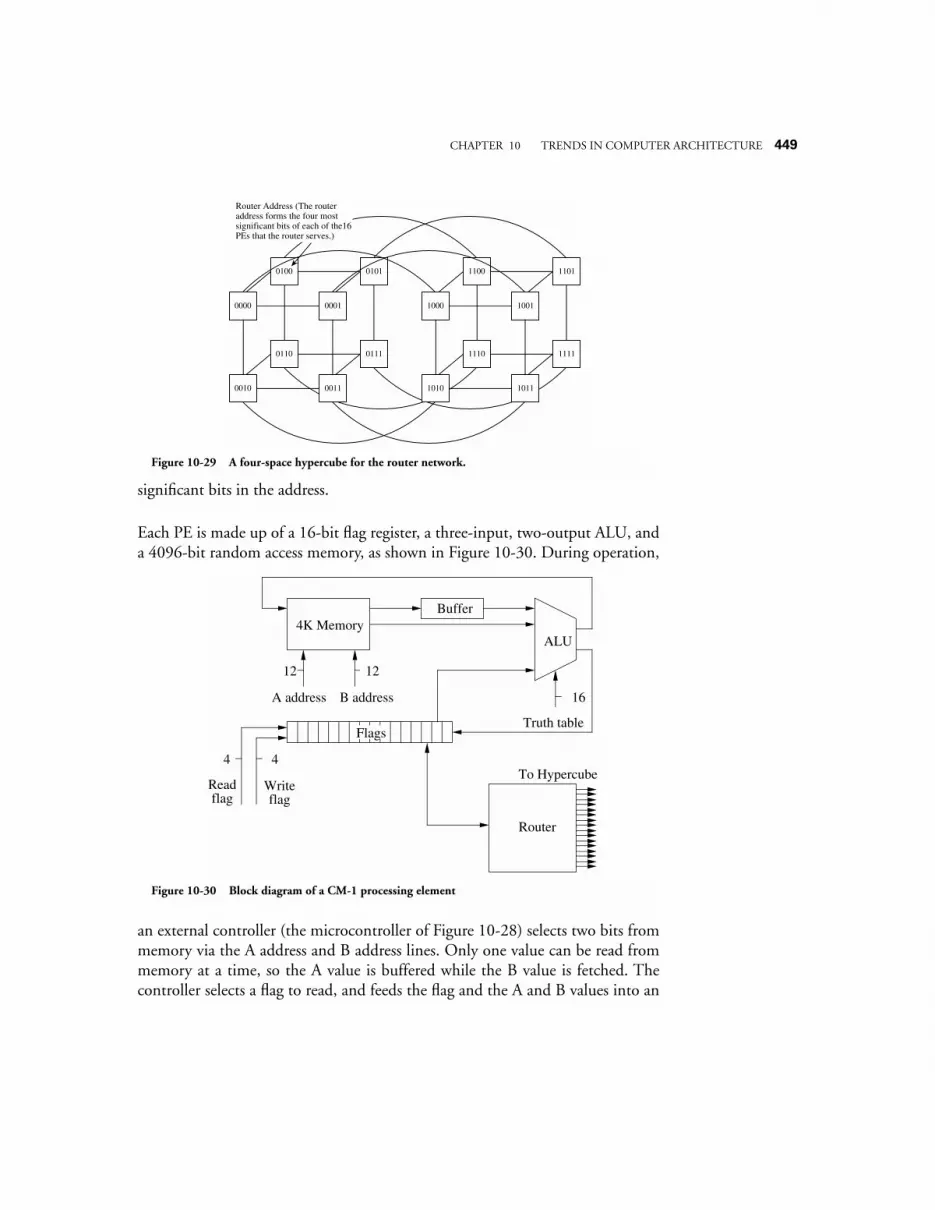
CHAPTER 10 TRENDS IN COMPUTER ARCHITECTURE 449
significant bits in the address.
Each PE is made up of a 16-bit flag register, a three-input, two-output ALU, anda 4096-bit random access memory, as shown in Figure 10-30. During operation,
an external controller (the microcontroller of Figure 10-28) selects two bits frommemory via the A address and B address lines. Only one value can be read frommemory at a time, so the A value is buffered while the B value is fetched. Thecontroller selects a flag to read, and feeds the flag and the A and B values into an
0000 0001
0010 0011
0100 0101
0110 0111
1000 1001
1010 1011
1100 1101
1110 1111
Router Address (The router address forms the four most significant bits of each of the16 PEs that the router serves.)
Figure 10-29 A four-space hypercube for the router network.
12 12
A address B address 16
Truth table
4 4
Readflag
Writeflag
4K Memory
Flags
Buffer
ALU
To Hypercube
Router
Figure 10-30 Block diagram of a CM-1 processing element
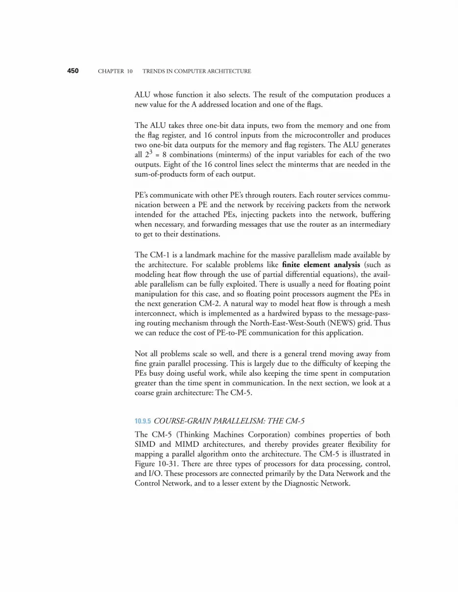
450 CHAPTER 10 TRENDS IN COMPUTER ARCHITECTURE
ALU whose function it also selects. The result of the computation produces anew value for the A addressed location and one of the flags.
The ALU takes three one-bit data inputs, two from the memory and one fromthe flag register, and 16 control inputs from the microcontroller and producestwo one-bit data outputs for the memory and flag registers. The ALU generatesall 23 = 8 combinations (minterms) of the input variables for each of the twooutputs. Eight of the 16 control lines select the minterms that are needed in thesum-of-products form of each output.
PE’s communicate with other PE’s through routers. Each router services commu-nication between a PE and the network by receiving packets from the networkintended for the attached PEs, injecting packets into the network, bufferingwhen necessary, and forwarding messages that use the router as an intermediaryto get to their destinations.
The CM-1 is a landmark machine for the massive parallelism made available bythe architecture. For scalable problems like finite element analysis (such asmodeling heat flow through the use of partial differential equations), the avail-able parallelism can be fully exploited. There is usually a need for floating pointmanipulation for this case, and so floating point processors augment the PEs inthe next generation CM-2. A natural way to model heat flow is through a meshinterconnect, which is implemented as a hardwired bypass to the message-pass-ing routing mechanism through the North-East-West-South (NEWS) grid. Thuswe can reduce the cost of PE-to-PE communication for this application.
Not all problems scale so well, and there is a general trend moving away fromfine grain parallel processing. This is largely due to the difficulty of keeping thePEs busy doing useful work, while also keeping the time spent in computationgreater than the time spent in communication. In the next section, we look at acoarse grain architecture: The CM-5.
10.9.5 COURSE-GRAIN PARALLELISM: THE CM-5
The CM-5 (Thinking Machines Corporation) combines properties of bothSIMD and MIMD architectures, and thereby provides greater flexibility formapping a parallel algorithm onto the architecture. The CM-5 is illustrated inFigure 10-31. There are three types of processors for data processing, control,and I/O. These processors are connected primarily by the Data Network and theControl Network, and to a lesser extent by the Diagnostic Network.
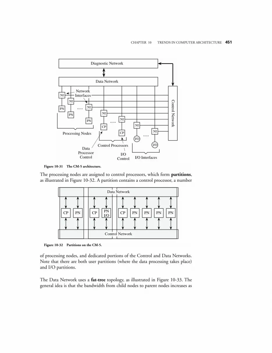
CHAPTER 10 TRENDS IN COMPUTER ARCHITECTURE 451
The processing nodes are assigned to control processors, which form partitions,as illustrated in Figure 10-32. A partition contains a control processor, a number
of processing nodes, and dedicated portions of the Control and Data Networks.Note that there are both user partitions (where the data processing takes place)and I/O partitions.
The Data Network uses a fat-tree topology, as illustrated in Figure 10-33. Thegeneral idea is that the bandwidth from child nodes to parent nodes increases as
Data Network
Diagnostic Network
NI
PN
NI
PN
NI
PN
NI
CP
NI
CP
NI
I/O
NI
I/O
. . .
. . .
. . .Processing Nodes
I/O Interfaces
Network Interfaces
Data Processor Control
I/O Control
Control Processors
Control N
etwork
Figure 10-31 The CM-5 architecture.
Data Network
CP PNI/O
CP PN PN PN PNCP PN
Control Network
Figure 10-32 Partitions on the CM-5.
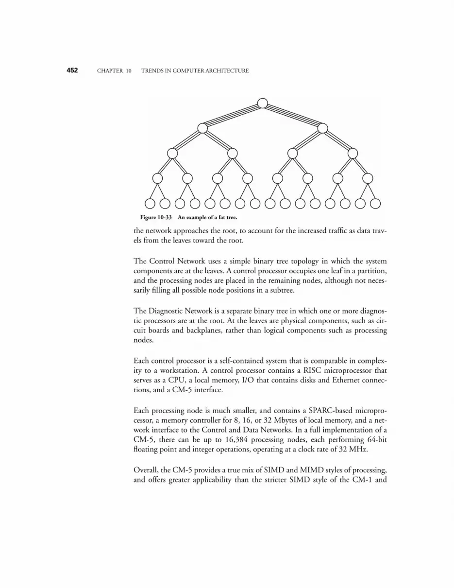
452 CHAPTER 10 TRENDS IN COMPUTER ARCHITECTURE
the network approaches the root, to account for the increased traffic as data trav-els from the leaves toward the root.
The Control Network uses a simple binary tree topology in which the systemcomponents are at the leaves. A control processor occupies one leaf in a partition,and the processing nodes are placed in the remaining nodes, although not neces-sarily filling all possible node positions in a subtree.
The Diagnostic Network is a separate binary tree in which one or more diagnos-tic processors are at the root. At the leaves are physical components, such as cir-cuit boards and backplanes, rather than logical components such as processingnodes.
Each control processor is a self-contained system that is comparable in complex-ity to a workstation. A control processor contains a RISC microprocessor thatserves as a CPU, a local memory, I/O that contains disks and Ethernet connec-tions, and a CM-5 interface.
Each processing node is much smaller, and contains a SPARC-based micropro-cessor, a memory controller for 8, 16, or 32 Mbytes of local memory, and a net-work interface to the Control and Data Networks. In a full implementation of aCM-5, there can be up to 16,384 processing nodes, each performing 64-bitfloating point and integer operations, operating at a clock rate of 32 MHz.
Overall, the CM-5 provides a true mix of SIMD and MIMD styles of processing,and offers greater applicability than the stricter SIMD style of the CM-1 and
Figure 10-33 An example of a fat tree.
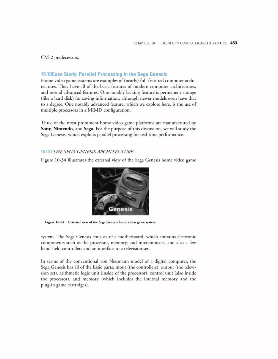
CHAPTER 10 TRENDS IN COMPUTER ARCHITECTURE 453
CM-2 predecessors.
10.10Case Study: Parallel Processing in the Sega GenesisHome video game systems are examples of (nearly) full-featured computer archi-tectures. They have all of the basic features of modern computer architectures,and several advanced features. One notably lacking feature is permanent storage(like a hard disk) for saving information, although newer models even have thatto a degree. One notably advanced feature, which we explore here, is the use ofmultiple processors in a MIMD configuration.
Three of the most prominent home video game platforms are manufactured bySony, Nintendo, and Sega. For the purpose of this discussion, we will study theSega Genesis, which exploits parallel processing for real-time performance.
10.10.1THE SEGA GENESIS ARCHITECTURE
Figure 10-34 illustrates the external view of the Sega Genesis home video game
system. The Sega Genesis consists of a motherboard, which contains electroniccomponents such as the processor, memory, and interconnects, and also a fewhand-held controllers and an interface to a television set.
In terms of the conventional von Neumann model of a digital computer, theSega Genesis has all of the basic parts: input (the controllers), output (the televi-sion set), arithmetic logic unit (inside of the processor), control unit (also insidethe processor), and memory (which includes the internal memory and theplug-in game cartridges).
Figure 10-34 External view of the Sega Genesis home video game system.
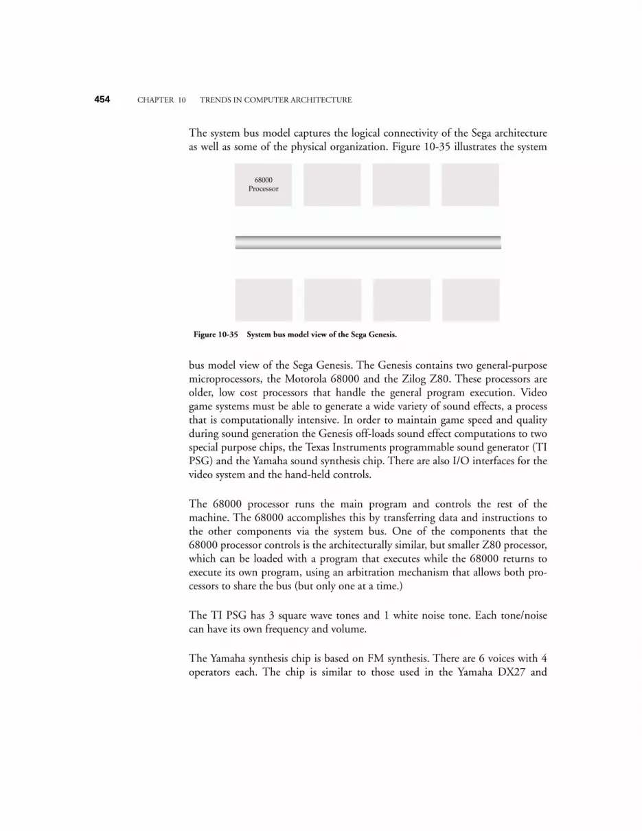
454 CHAPTER 10 TRENDS IN COMPUTER ARCHITECTURE
The system bus model captures the logical connectivity of the Sega architectureas well as some of the physical organization. Figure 10-35 illustrates the system
bus model view of the Sega Genesis. The Genesis contains two general-purposemicroprocessors, the Motorola 68000 and the Zilog Z80. These processors areolder, low cost processors that handle the general program execution. Videogame systems must be able to generate a wide variety of sound effects, a processthat is computationally intensive. In order to maintain game speed and qualityduring sound generation the Genesis off-loads sound effect computations to twospecial purpose chips, the Texas Instruments programmable sound generator (TIPSG) and the Yamaha sound synthesis chip. There are also I/O interfaces for thevideo system and the hand-held controls.
The 68000 processor runs the main program and controls the rest of themachine. The 68000 accomplishes this by transferring data and instructions tothe other components via the system bus. One of the components that the68000 processor controls is the architecturally similar, but smaller Z80 processor,which can be loaded with a program that executes while the 68000 returns toexecute its own program, using an arbitration mechanism that allows both pro-cessors to share the bus (but only one at a time.)
The TI PSG has 3 square wave tones and 1 white noise tone. Each tone/noisecan have its own frequency and volume.
The Yamaha synthesis chip is based on FM synthesis. There are 6 voices with 4operators each. The chip is similar to those used in the Yamaha DX27 and
68000 Processor
Figure 10-35 System bus model view of the Sega Genesis.

CHAPTER 10 TRENDS IN COMPUTER ARCHITECTURE 455
DX100 synthesizers. By setting up registers within the chips, a rich variety ofsounds can be created.
The plug-in game cartridges contain the programs, and there is additional runt-ime memory available in a separate unit (labeled “Main memory” in Figure10-35.) Additional components are provided for video output, sound output,and hand-held controllers.
10.10.2SEGA GENESIS OPERATION
When the Sega Genesis is initially powered on, a RESET signal is enabled, whichallows all of the electrical voltage levels to stabilize and initializes a number ofruntime variables. The RESET signal is then automatically disabled, and the68000 begins reading and executing instructions from the game cartridge.
During operation, the instructions in the game cartridge instruct the 68000 toload a program into the Z80 processor, and to start the Z80 program executionwhile the 68000 returns to its own program. The Z80 program controls thesound chips, while the 68000 carries out graphical operations, probes thehand-held controllers for activity, and runs the overall game program.
10.10.3SEGA GENESIS PROGRAMMING
[Note from Authors: This section is adapted from a contribution by David Ashley,[email protected].]
The Sega Genesis uses plug-in cartridges to store the game software. Blank car-tridges can be purchased from third party vendors, which can then be pro-grammed using an inexpensive PROM burner card that be plugged into the cardcage of a desktop computer. Games can be written in high level languages andcompiled into assembly language, or more commonly, programmed in assemblylanguage directly (even today, assembly language is still heavily used for gameprogramming). A suite of development tools translates the source code intoobject code that can then be burned directly into the cartridges (once per car-tridge.) As an alternative to burning cartridges during development, the cartridgecan be replaced with a reprogrammable development card.
The Genesis contains two general-purpose microprocessors, the Motorola 68000and the Zilog Z80. The 68000 runs at 8 MHz and has 64 KB of memory
456 CHAPTER 10 TRENDS IN COMPUTER ARCHITECTURE
devoted to it. The ROM cartridge appears at memory location 0. The 68000off-loads sound effect computations to the TI PSG and the Yamaha sound syn-thesis chip.
The Genesis graphics hardware consists of 2 scrollable planes. Each plane is madeup of tiles. Each tile is an 8×8 pixel square with 4 bits per pixel. Each pixel canthus have 16 colors. Each tile can use 1 of 4 color tables, so on the screen therecan be 64 colors at once, but only 16 different colors can be in any specific tile.Tiles require 32 bytes. There is 64 KB of graphics memory, which allows for2048 unique tiles if memory is used for nothing else.
Each plane can be scrolled independently in various ways. Planes consist of tablesof words, in which each word describes a tile. A word contains 11 bits for identi-fying the tile, 2 bits for “flip x” and “flip y,” 2 bits for the selection of the colortable, and 1 bit for a depth selector. Sprites are also composed of tiles. A spritecan be up to 4 tiles wide by four tiles high. Since the size of each tile is 8×8, thismeans sprites can be anywhere from 8×8 pixels to 32×32 pixels in size. There canbe 80 sprites on the screen at one time. On a single scan line there can be 1032-pixel wide sprites or 20 16-pixel wide sprites. Each sprite can only have 16colors taken from the 4 different color tables. Colors are allocated 3 bits for eachgun, and so 512 colors are possible. (Color 0=transparent.)
There is a memory copier program that is resident in hardware that performs fastcopies from the 68000 RAM into the graphics RAM. The Z80 also has 8KB ofRAM. The Z80 can access the graphics chip or the sound chips, but usually thesechips are controlled by the 68000.
The process of creating a game cartridge involves (1) writing the game program,(2) translating the program into object code (compiling, assembling, and linkingthe code into an executable object module; some parts of the program may bewritten in a high level language, and other parts, directly in assembly language),(3) testing the program on a reprogrammable development card (if a reprogram-mable development card is available), and (4) burning the program into a blankgame cartridge.
See Further Reading below for more information on programming the SegaGenesis.
CHAPTER 10 TRENDS IN COMPUTER ARCHITECTURE 457
SUMMARY
In the RISC approach, the most frequently occurring instructions are optimized byeliminating or reducing the complexity of other instructions and addressing modescommonly found in CISC architectures. The performance of RISC architectures isfurther enhanced by pipelining and increasing the number of registers available tothe CPU. Superscalar and VLIW architectures are examples of newer perfor-mance enhancements that extend, rather than replace, the RISC approach.
Parallel architectures can be classified as MISD, SIMD, or MIMD. The MISDapproach is used for systolic array processing, and is the least general architectureof the three. In a SIMD architecture, all PEs carry out the same operations on dif-ferent data sets, in an “army of ants” approach to parallel processing. The MIMDapproach can be characterized as “herd of elephants,” because there are a smallnumber of powerful processors, each with their own data and instruction streams.
The current trend is moving away from the fine grain parallelism that is exempli-fied by the MISD and SIMD approaches, and toward the MIMD approach. Thistrend is due to the high time cost of communicating among PEs, and the economyof using networks of workstations over tightly coupled parallel processors. The goalof the MIMD approach is to better balance the time spent in computation withthe time spent in communication.
FURTHER READINGThree primary characteristics of RISC architectures enumerated in Section 10.2originated at IBM’s T. J. Watson Research Center, as summarized in (Ralston andReilly, 1993, pp. 1165 - 1167). (Hennessy and Patterson, 1995) is a classic refer-ence on much of the work that led to the RISC concept, although the word“RISC” does not appear in the title of their textbook. (Stallings, 1991) is a thor-ough reference on RISCs. (Tamir and Sequin, 1983) show that a window size ofeight will shift on less than 1% of the calls or returns. (Tanenbaum, 1999) pro-vides a readable introduction to the RISC concept. (Dulong, 1998) describes theIA-64. The PowerPC 601 architecture is described in (Motorola).
(Quinn, 1987) and (Hwang, 1993) overview the field of parallel processing interms of architectures and algorithms. (Flynn, 1972) covers the Flynn taxonomyof architectures. (Yang and Gerasoulis, 1991) argue for maintaining a ratio ofcommunication time to computation time of less than 1. (Hillis, 1985) and (Hil-lis, 1993) describe the architectures of the CM-1 and CM-5, respectively. (Hui,1990) covers interconnection networks, and (Leighton, 1992) covers routing
458 CHAPTER 10 TRENDS IN COMPUTER ARCHITECTURE
algorithms for a few types of interconnection networks. (Wu and Feng, 1981)cover routing on a shuffle-exchange network.
Additional information can be found on programming the Sega Genesis athttp://hiwaay.net/~jfrohwei/sega/genesis.html.
Dulong, C., “The IA-64 Architecture at Work,” IEEE Computer, vol. 31, pp.24-32, (July 1998).
Flynn, M. J., “Some Computer Organizations and Their Effectiveness,” IEEETransactions on Computers, vol. 30, no. 7, pp. 948-960, (1972).
Hennessy, J. L. and D. A. Patterson, Computer Architecture: A QuantitativeApproach, 2/e, Morgan Kaufmann Publishers, San Mateo, (1995).
Hillis, W. D., The Connection Machine, The MIT Press, (1985).
Hillis, W. D. and L. W. Tucker, “The CM-5 Connection Machine: A ScalableSupercomputer,” Communications of the ACM, vol. 36, no. 11, pp. 31-40, (Nov.,1993).
Hui, J. Y., Switching and Traffic Theory for Integrated Broadband Networks, Klu-wer Academic Publishers, (1990).
Hwang, K., Advanced Computer Architecture: Parallelism, Scalability, Programma-bility, McGraw-Hill, (1993).
Knuth, D. E., An Empirical Study of FORTRAN Programs, Software—Practiceand Experience, 1, 105-133, 1971.
Leighton, F. T., Introduction to Parallel Algorithms and Architectures: Arrays, Trees,Hypercubes, Morgan Kaufmann, (1992).
Motorola Inc., PowerPC 601 RISC Microprocessor User’s Manual, Motorola Liter-ature Distribution, P. O. Box 20912, Phoenix, AZ, 85036.
Quinn, M. J., Designing Efficient Algorithms for Parallel Computers,McGraw-Hill, (1987).
CHAPTER 10 TRENDS IN COMPUTER ARCHITECTURE 459
Ralston, A. and E. D. Reilly, eds., Encyclopedia of Computer Science, 3/e, vanNostrand Reinhold, (1993).
SPARC International, Inc., The SPARC Architecture Manual: Version 8, PrenticeHall, Englewood Cliffs, New Jersey, (1992).
Stone, H. S. and J. Cocke, “Computer Architecture in the 1990s,” IEEE Com-puter, vol. 24, no. 9, pp. 30-38, (Sept., 1991).
Stallings, W., Computer Organization and Architecture: Designing for Performance,4/e, Prentice Hall, Upper Saddle River, (1996).
Stallings, W., Reduced Instruction Set Computers, 3/e, IEEE Computer SocietyPress, Washington, D.C., (1991).
Tamir, Y., and C. Sequin, “Strategies for Managing the Register File in RISC,”IEEE Trans. Comp., (Nov. 1983).
Tanenbaum, A., Structured Computer Organization, 4/e, Prentice Hall, UpperSaddle River, New Jersey, (1999).
Yang, T. and A. Gerasoulis, “A Fast Static Scheduling Algorithm for DAGs on anUnbounded Number of Processors,” Proceedings of Supercomputing ’91, Albu-querque, New Mexico, (Nov. 1991).
Wu, C.-L. and T.-Y. Feng, “The Universality of the Shuffle-Exchange Network,”IEEE Transactions on Computers, vol. C-30, no. 5, pp. 324-, (1981).
PROBLEMS10.1 Increasing the number of cycles per instruction can sometimes improve
the execution efficiency of a pipeline. If the time per cycle for the pipelinedescribed in Section 10.3 is 20 ns, then CPIAvg is 1.5 × 20 ns = 30 ns. Com-pute the execution efficiency for the same pipeline in which the pipeline depthincreases from 5 to 6 and the cycle time decreases from 20 ns to 10 ns.
10.2 The SPARC code below is taken from the gcc generated code in Figure10-10. Can %r0 be used in all three lines, instead of “wasting” %r1 in thesecond line?
460 CHAPTER 10 TRENDS IN COMPUTER ARCHITECTURE
...st %o0, [%fp-28]sethi %hi(.LLC0), %o1or %o1, %lo(.LLC0), %o1
...
10.3 Calculate the speedup that can be expected if a 200 MHz Pentium chip isreplaced with a 300 MHz Pentium chip, if all other parameters remainunchanged.
10.4 What is the speedup that can be expected if the instruction set of a certainmachine is changed so that the branch instruction takes 1 clock cycle insteadof 3 clock cycles, if branch instructions account for 20% of all instructionsexecuted by a certain program? Assume that other instructions average 3 clockcycles per instruction, and that nothing else is altered by the change.
10.5 Create a dependency graph for the following expression:
f(x, y) = x2 + 2xy + y2
10.6 Given 100 processors for a computation with 5% of the code that cannotbe parallelized, compute speedup and efficiency.
10.7 What is the diameter of a 16-space hypercube?
10.8 For the EXAMPLE at the end of Section 10.9.2, compute the total cross-point complexity over all three stages.
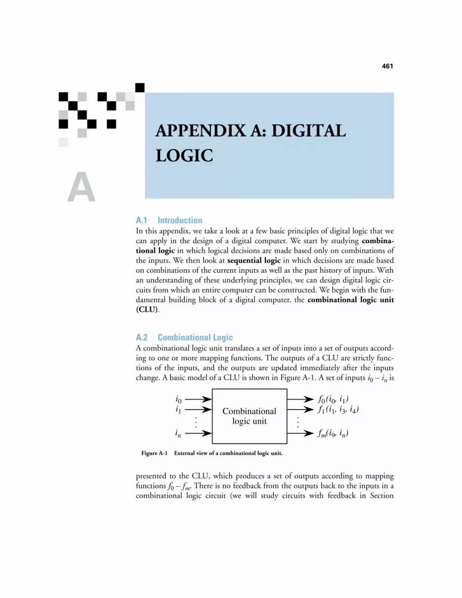
461
APPENDIX A: DIGITAL LOGIC
A.1 Introduction
In this appendix, we take a look at a few basic principles of digital logic that wecan apply in the design of a digital computer. We start by studying
combina-tional logic
in which logical decisions are made based only on combinations ofthe inputs. We then look at
sequential logic
in which decisions are made basedon combinations of the current inputs as well as the past history of inputs. Withan understanding of these underlying principles, we can design digital logic cir-cuits from which an entire computer can be constructed. We begin with the fun-damental building block of a digital computer, the
combinational logic unit(CLU)
.
A.2 Combinational Logic
A combinational logic unit
translates a set of inputs into a set of outputs accord-ing to one or more mapping functions. The outputs of a CLU are strictly func-tions of the inputs, and the outputs are updated immediately after the inputschange. A basic model of a CLU is shown in Figure A-1. A set of inputs
i
0
–
i
n
is
presented to the CLU, which produces a set of outputs according to mappingfunctions
f
0
–
f
m
. There is no feedback from the outputs back to the inputs in acombinational logic circuit (we will study circuits with feedback in Section
Combinationallogic unit
. . .
i0i1
in
. . .
f0f1
fm
(i0, i1)(i1, i3, i4)
(i9, in)
Figure A-1 External view of a combinational logic unit.
A
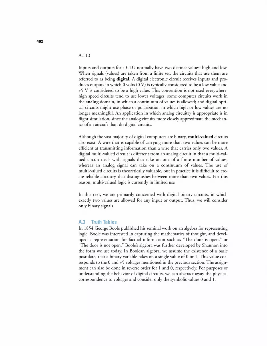
462
A.11.)
Inputs and outputs for a CLU normally have two distinct values: high and low.When signals (values) are taken from a finite set, the circuits that use them arereferred to as being
digital
. A digital electronic circuit receives inputs and pro-duces outputs in which 0 volts (0 V) is typically considered to be a low value and+5 V is considered to be a high value. This convention is not used everywhere:high speed circuits tend to use lower voltages; some computer circuits work inthe
analog
domain, in which a continuum of values is allowed; and digital opti-cal circuits might use phase or polarization in which high or low values are nolonger meaningful. An application in which analog circuitry is appropriate is inflight simulation, since the analog circuits more closely approximate the mechan-ics of an aircraft than do digital circuits.
Although the vast majority of digital computers are binary,
multi-valued
circuitsalso exist. A wire that is capable of carrying more than two values can be moreefficient at transmitting information than a wire that carries only two values. Adigital multi-valued circuit is different from an analog circuit in that a multi-val-ued circuit deals with signals that take on one of a finite number of values,whereas an analog signal can take on a continuum of values. The use ofmulti-valued circuits is theoretically valuable, but in practice it is difficult to cre-ate reliable circuitry that distinguishes between more than two values. For thisreason, multi-valued logic is currently in limited use
In this text, we are primarily concerned with digital binary circuits, in whichexactly two values are allowed for any input or output. Thus, we will consideronly binary signals.
A.3 Truth Tables
In 1854 George Boole published his seminal work on an algebra for representinglogic. Boole was interested in capturing the mathematics of thought, and devel-oped a representation for factual information such as “The door is open.” or“The door is not open.” Boole’s algebra was further developed by Shannon intothe form we use today. In Boolean algebra, we assume the existence of a basicpostulate, that a binary variable takes on a single value of 0 or 1. This value cor-responds to the 0 and +5 voltages mentioned in the previous section. The assign-ment can also be done in reverse order for 1 and 0, respectively. For purposes ofunderstanding the behavior of digital circuits, we can abstract away the physicalcorrespondence to voltages and consider only the symbolic values 0 and 1.
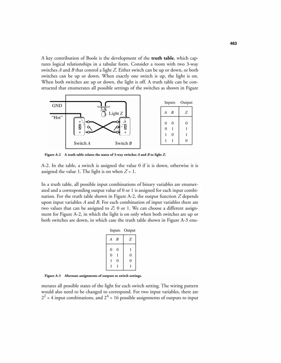
463
A key contribution of Boole is the development of the
truth table
, which cap-tures logical relationships in a tabular form. Consider a room with two 3-wayswitches
A
and
B
that control a light
Z
. Either switch can be up or down, or bothswitches can be up or down. When exactly one switch is up, the light is on.When both switches are up or down, the light is off. A truth table can be con-structed that enumerates all possible settings of the switches as shown in Figure
A-2. In the table, a switch is assigned the value 0 if it is down, otherwise it isassigned the value 1. The light is on when
Z
= 1.
In a truth table, all possible input combinations of binary variables are enumer-ated and a corresponding output value of 0 or 1 is assigned for each input combi-nation. For the truth table shown in Figure A-2, the output function
Z
dependsupon input variables
A
and
B
. For each combination of input variables there aretwo values that can be assigned to
Z
: 0 or 1. We can choose a different assign-ment for Figure A-2, in which the light is on only when both switches are up orboth switches are down, in which case the truth table shown in Figure A-3 enu-
merates all possible states of the light for each switch setting. The wiring patternwould also need to be changed to correspond. For two input variables, there are2
2
= 4 input combinations, and 2
4
= 16 possible assignments of outputs to input
00
1
1
01
0
1
A B
01
1
0
Z
Inputs Output
Switch A Switch B
“Hot”
GND
Light Z
Figure A-2 A truth table relates the states of 3-way switches A and B to light Z.
0011
0101
A B
1001
Z
Inputs Output
Figure A-3 Alternate assignments of outputs to switch settings.
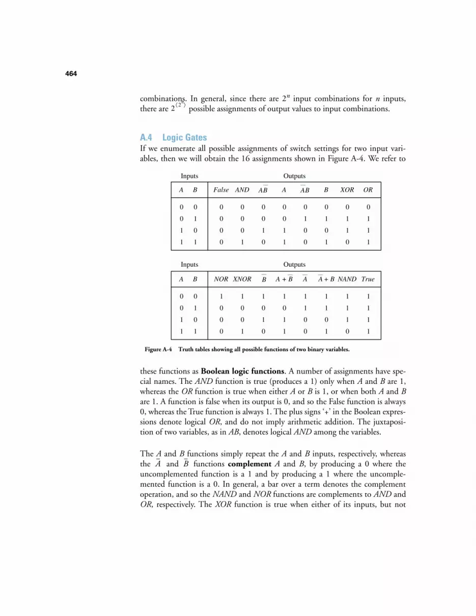
464
combinations. In general, since there are 2
n
input combinations for
n
inputs,there are possible assignments of output values to input combinations.
A.4 Logic Gates
If we enumerate all possible assignments of switch settings for two input vari-ables, then we will obtain the 16 assignments shown in Figure A-4. We refer to
these functions as
Boolean logic functions
. A number of assignments have spe-cial names. The
AND
function is true (produces a 1) only when
A
and
B
are 1,whereas the
OR
function is true when either
A
or
B
is 1, or when both
A
and
B
are 1. A function is false when its output is 0, and so the False function is always0, whereas the True function is always 1. The plus signs ‘+’ in the Boolean expres-sions denote logical
OR
, and do not imply arithmetic addition. The juxtaposi-tion of two variables, as in
AB
, denotes logical
AND
among the variables.
The
A
and
B
functions simply repeat the
A
and
B
inputs, respectively, whereasthe and functions
complement
A
and
B
, by producing a 0 where theuncomplemented function is a 1 and by producing a 1 where the uncomple-mented function is a 0. In general, a bar over a term denotes the complementoperation, and so the
NAND
and
NOR
functions are complements to
AND
and
OR
, respectively. The
XOR
function is true when either of its inputs, but not
2 2n⟨ ⟩
0
0
1
1
0
1
0
1
0
0
0
0
0
0
0
1
0
0
1
0
0
0
1
1
0
1
0
0
0
1
0
1
0
1
1
0
0
1
1
1
A B False AND A B XOR OR
0
0
1
1
0
1
0
1
1
0
0
0
1
0
0
1
1
0
1
0
1
0
1
1
1
1
0
0
1
1
0
1
1
1
1
0
1
1
1
1
A B NOR XNOR A + B NAND True
AB AB
B A A + B
Inputs Outputs
Inputs Outputs
Figure A-4 Truth tables showing all possible functions of two binary variables.
A B
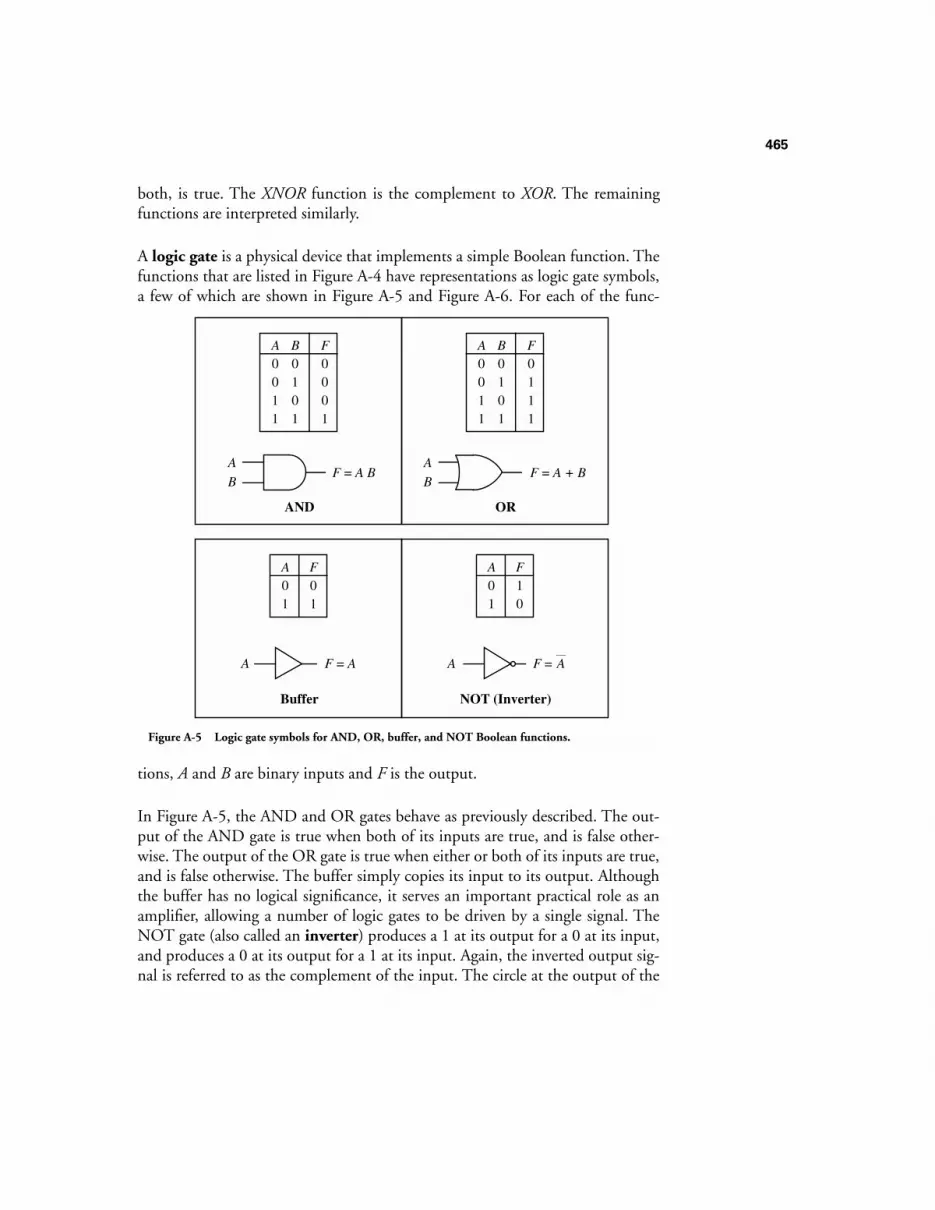
465
both, is true. The
XNOR
function is the complement to
XOR
. The remainingfunctions are interpreted similarly.
A
logic gate
is a physical device that implements a simple Boolean function. Thefunctions that are listed in Figure A-4 have representations as logic gate symbols,a few of which are shown in Figure A-5 and Figure A-6. For each of the func-
tions,
A
and
B
are binary inputs and
F
is the output.
In Figure A-5, the AND and OR gates behave as previously described. The out-put of the AND gate is true when both of its inputs are true, and is false other-wise. The output of the OR gate is true when either or both of its inputs are true,and is false otherwise. The buffer simply copies its input to its output. Althoughthe buffer has no logical significance, it serves an important practical role as anamplifier, allowing a number of logic gates to be driven by a single signal. TheNOT gate (also called an
inverter
) produces a 1 at its output for a 0 at its input,and produces a 0 at its output for a 1 at its input. Again, the inverted output sig-nal is referred to as the complement of the input. The circle at the output of the
A
BF = A B
A0011
B0101
F0001
AND
A0011
B0101
F0111
OR
A
BF = A + B
A01
F01
Buffer
A01
F10
NOT (Inverter)
A F = A A F = A
Figure A-5 Logic gate symbols for AND, OR, buffer, and NOT Boolean functions.
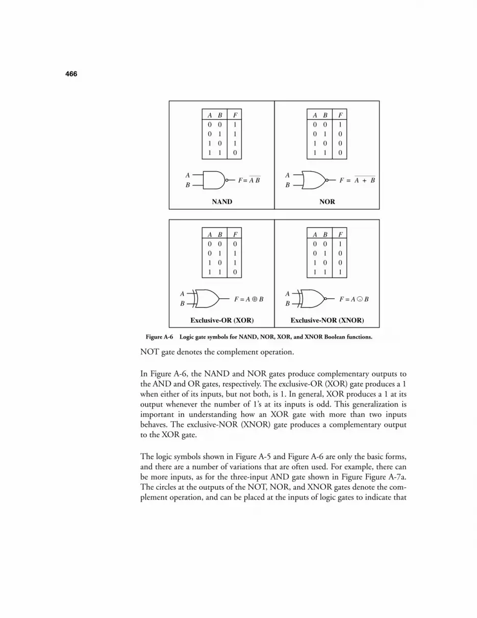
466
NOT gate denotes the complement operation.
In Figure A-6, the NAND and NOR gates produce complementary outputs tothe AND and OR gates, respectively. The exclusive-OR (XOR) gate produces a 1when either of its inputs, but not both, is 1. In general, XOR produces a 1 at itsoutput whenever the number of 1’s at its inputs is odd. This generalization isimportant in understanding how an XOR gate with more than two inputsbehaves. The exclusive-NOR (XNOR) gate produces a complementary outputto the XOR gate.
The logic symbols shown in Figure A-5 and Figure A-6 are only the basic forms,and there are a number of variations that are often used. For example, there canbe more inputs, as for the three-input AND gate shown in Figure Figure A-7a.The circles at the outputs of the NOT, NOR, and XNOR gates denote the com-plement operation, and can be placed at the inputs of logic gates to indicate that
A
B
A0011
B0101
F1110
NAND
A0011
B0101
F1000
NOR
A
BF = A B F = A + B
A0011
B0101
F0110
Exclusive-OR (XOR)
A
BF = A ⊕ B
A0011
B0101
F1001
Exclusive-NOR (XNOR)
A
BF = A ⊕ B.
Figure A-6 Logic gate symbols for NAND, NOR, XOR, and XNOR Boolean functions.
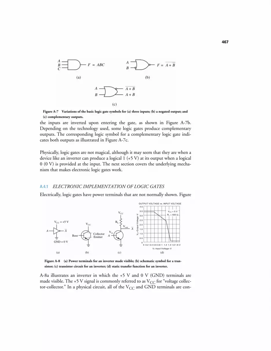
467
the inputs are inverted upon entering the gate, as shown in Figure A-7b.Depending on the technology used, some logic gates produce complementaryoutputs. The corresponding logic symbol for a complementary logic gate indi-cates both outputs as illustrated in Figure A-7c.
Physically, logic gates are not magical, although it may seem that they are when adevice like an inverter can produce a logical 1 (+5 V) at its output when a logical0 (0 V) is provided at the input. The next section covers the underlying mecha-nism that makes electronic logic gates work.
A.4.1
ELECTRONIC IMPLEMENTATION OF LOGIC GATES
Electrically, logic gates have power terminals that are not normally shown. Figure
A-8a illustrates an inverter in which the +5 V and 0 V (GND) terminals aremade visible. The +5 V signal is commonly referred to as V
CC
for “voltage collec-tor-collector.” In a physical circuit, all of the V
CC
and GND terminals are con-
ABC
F = ABC
(a) (b)
A
BF = A + B
(c)
A + B
A + BA
B
Figure A-7 Variations of the basic logic gate symbols for (a) three inputs; (b) a negated output; and
(c) complementary outputs.
A A
GND = 0 V
VCC = +5 V
(a)
VCC
BaseCollectorEmitter
(b)
VCC
Vin
(c)
Vout
A
A
RL
(d)
4.0
3.5
3.0
2.5
2.0
1.5
1.0
0.5
00.20 0.4 0.6 0.8 1 1.2 1.4 1.6 21.8
VI–Input Voltage–V
VO
–O
utp
ut
Vo
ltag
e–
V
OUTPUT VOLTAGE vs. INPUT VOLTAGE
VCC = 5 V
RL = 400 Ω
Figure A-8 (a) Power terminals for an inverter made visible; (b) schematic symbol for a tran-
sistor; (c) transistor circuit for an inverter; (d) static transfer function for an inverter.
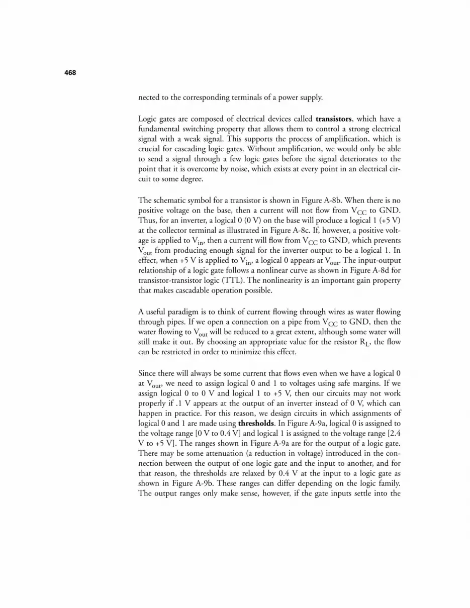
468
nected to the corresponding terminals of a power supply.
Logic gates are composed of electrical devices called
transistors
, which have afundamental switching property that allows them to control a strong electricalsignal with a weak signal. This supports the process of amplification, which iscrucial for cascading logic gates. Without amplification, we would only be ableto send a signal through a few logic gates before the signal deteriorates to thepoint that it is overcome by noise, which exists at every point in an electrical cir-cuit to some degree.
The schematic symbol for a transistor is shown in Figure A-8b. When there is nopositive voltage on the base, then a current will not flow from V
CC
to GND.Thus, for an inverter, a logical 0 (0 V) on the base will produce a logical 1 (+5 V)at the collector terminal as illustrated in Figure A-8c. If, however, a positive volt-age is applied to V
in
, then a current will flow from V
CC
to GND, which preventsV
out
from producing enough signal for the inverter output to be a logical 1. Ineffect, when +5 V is applied to V
in
, a logical 0 appears at V
out
. The input-outputrelationship of a logic gate follows a nonlinear curve as shown in Figure A-8d fortransistor-transistor logic (TTL). The nonlinearity is an important gain propertythat makes cascadable operation possible.
A useful paradigm is to think of current flowing through wires as water flowingthrough pipes. If we open a connection on a pipe from V
CC
to GND, then thewater flowing to V
out
will be reduced to a great extent, although some water willstill make it out. By choosing an appropriate value for the resistor R
L
, the flowcan be restricted in order to minimize this effect.
Since there will always be some current that flows even when we have a logical 0at V
out
, we need to assign logical 0 and 1 to voltages using safe margins. If weassign logical 0 to 0 V and logical 1 to +5 V, then our circuits may not workproperly if .1 V appears at the output of an inverter instead of 0 V, which canhappen in practice. For this reason, we design circuits in which assignments oflogical 0 and 1 are made using
thresholds
. In Figure A-9a, logical 0 is assigned tothe voltage range [0 V to 0.4 V] and logical 1 is assigned to the voltage range [2.4V to +5 V]. The ranges shown in Figure A-9a are for the output of a logic gate.There may be some attenuation (a reduction in voltage) introduced in the con-nection between the output of one logic gate and the input to another, and forthat reason, the thresholds are relaxed by 0.4 V at the input to a logic gate asshown in Figure A-9b. These ranges can differ depending on the logic family.The output ranges only make sense, however, if the gate inputs settle into the
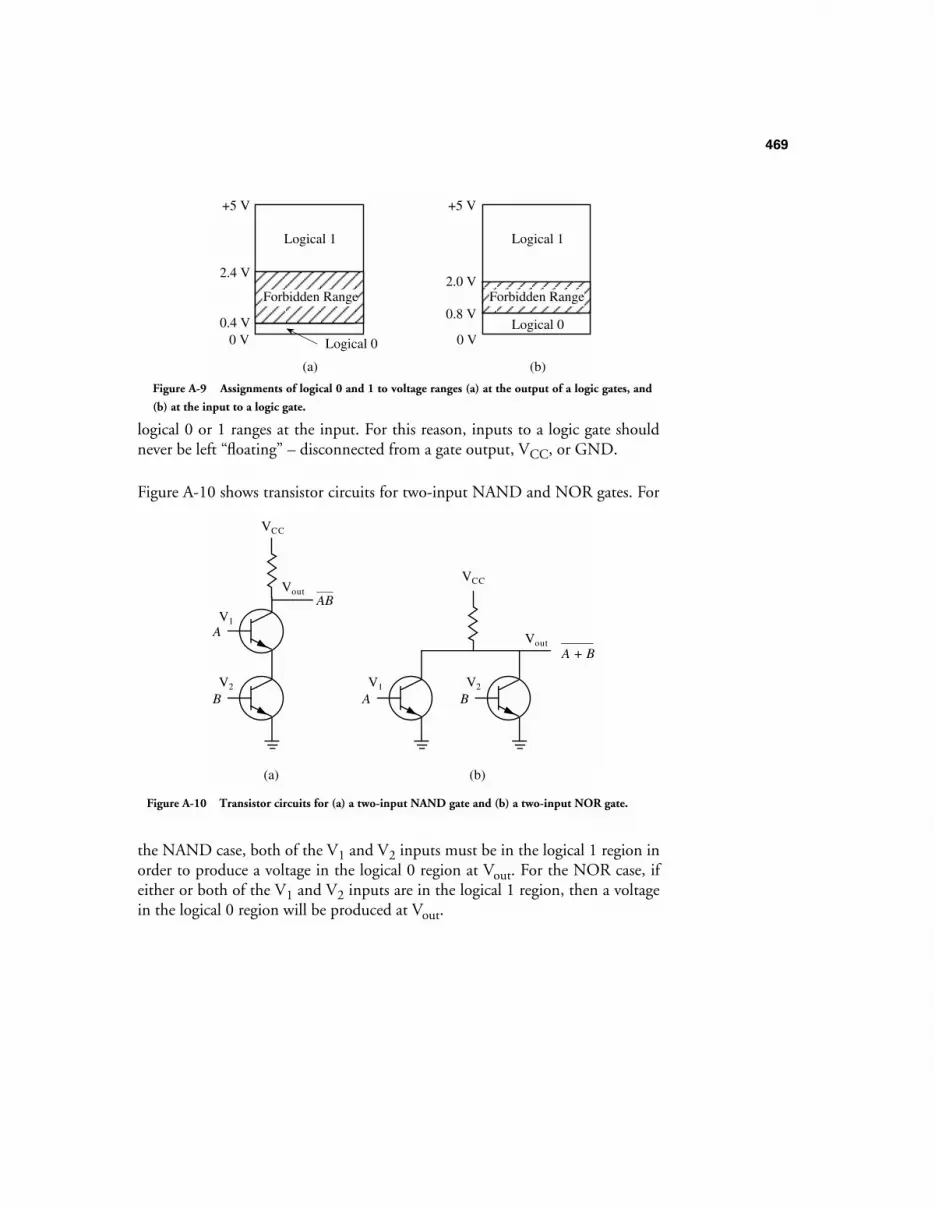
469
logical 0 or 1 ranges at the input. For this reason, inputs to a logic gate shouldnever be left “floating” – disconnected from a gate output, VCC, or GND.
Figure A-10 shows transistor circuits for two-input NAND and NOR gates. For
the NAND case, both of the V1 and V2 inputs must be in the logical 1 region inorder to produce a voltage in the logical 0 region at Vout. For the NOR case, ifeither or both of the V1 and V2 inputs are in the logical 1 region, then a voltagein the logical 0 region will be produced at Vout.
(a)
0 V
+5 V
Logical 1
0.4 V
2.4 V
Logical 0
(b)
0 V
+5 V
Logical 1
Forbidden Range0.8 V
2.0 V
Logical 0
Forbidden Range
Figure A-9 Assignments of logical 0 and 1 to voltage ranges (a) at the output of a logic gates, and
(b) at the input to a logic gate.
VCC
V1
(a)
Vout
A
AB
V2
BV1
AV2
B
VCC
VoutA + B
(b)
Figure A-10 Transistor circuits for (a) a two-input NAND gate and (b) a two-input NOR gate.
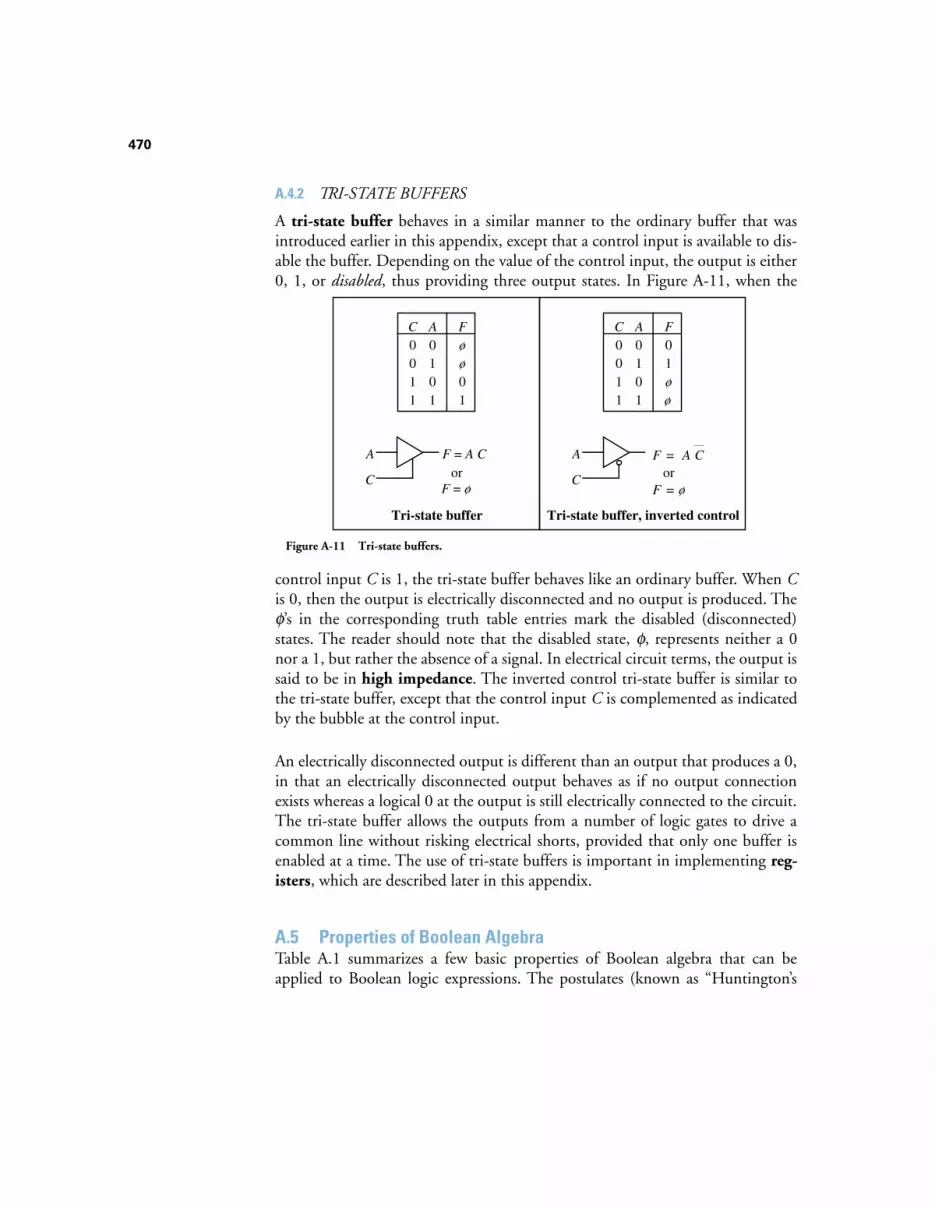
470
A.4.2 TRI-STATE BUFFERS
A tri-state buffer behaves in a similar manner to the ordinary buffer that wasintroduced earlier in this appendix, except that a control input is available to dis-able the buffer. Depending on the value of the control input, the output is either0, 1, or disabled, thus providing three output states. In Figure A-11, when the
control input C is 1, the tri-state buffer behaves like an ordinary buffer. When Cis 0, then the output is electrically disconnected and no output is produced. Theφ’s in the corresponding truth table entries mark the disabled (disconnected)states. The reader should note that the disabled state, φ, represents neither a 0nor a 1, but rather the absence of a signal. In electrical circuit terms, the output issaid to be in high impedance. The inverted control tri-state buffer is similar tothe tri-state buffer, except that the control input C is complemented as indicatedby the bubble at the control input.
An electrically disconnected output is different than an output that produces a 0,in that an electrically disconnected output behaves as if no output connectionexists whereas a logical 0 at the output is still electrically connected to the circuit.The tri-state buffer allows the outputs from a number of logic gates to drive acommon line without risking electrical shorts, provided that only one buffer isenabled at a time. The use of tri-state buffers is important in implementing reg-isters, which are described later in this appendix.
A.5 Properties of Boolean AlgebraTable A.1 summarizes a few basic properties of Boolean algebra that can beapplied to Boolean logic expressions. The postulates (known as “Huntington’s
C0011
A0101
Føø01
Tri-state buffer
C0011
A0101
F01øø
Tri-state buffer, inverted control
A F = A C
C
A
C
F = A C
F = ø F = øor or
Figure A-11 Tri-state buffers.
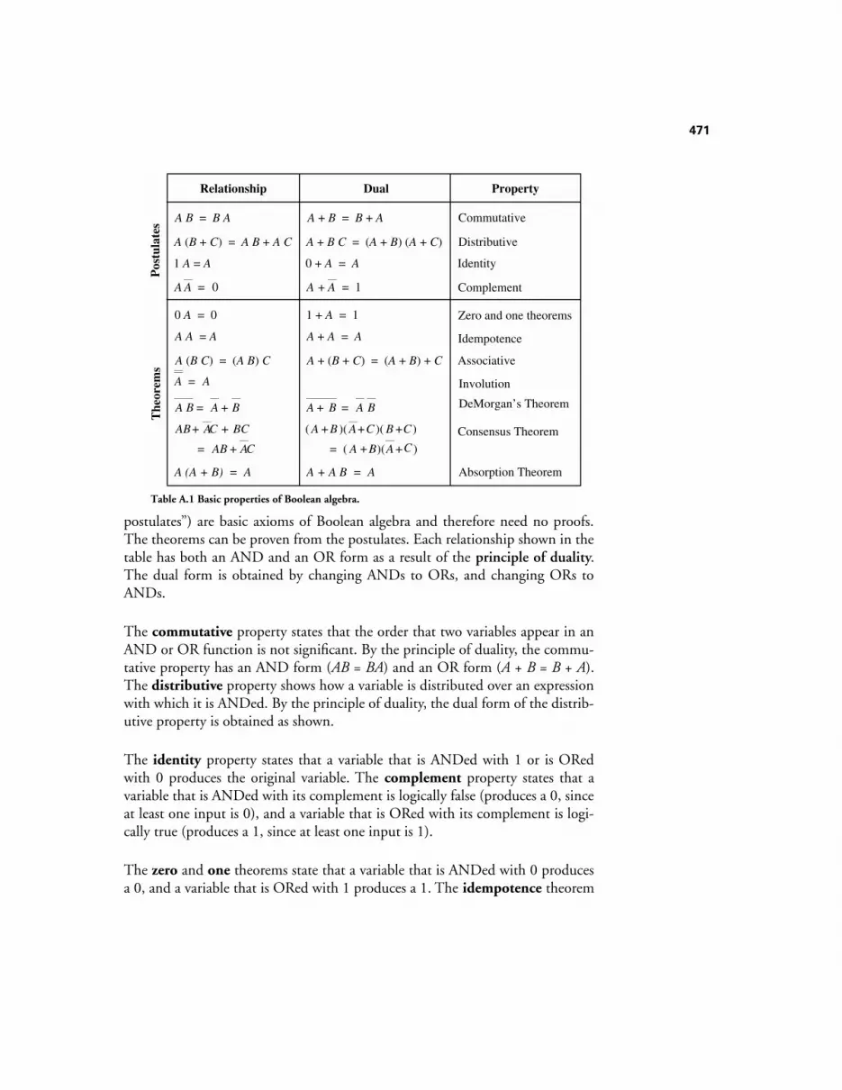
471
postulates”) are basic axioms of Boolean algebra and therefore need no proofs.The theorems can be proven from the postulates. Each relationship shown in thetable has both an AND and an OR form as a result of the principle of duality.The dual form is obtained by changing ANDs to ORs, and changing ORs toANDs.
The commutative property states that the order that two variables appear in anAND or OR function is not significant. By the principle of duality, the commu-tative property has an AND form (AB = BA) and an OR form (A + B = B + A).The distributive property shows how a variable is distributed over an expressionwith which it is ANDed. By the principle of duality, the dual form of the distrib-utive property is obtained as shown.
The identity property states that a variable that is ANDed with 1 or is ORedwith 0 produces the original variable. The complement property states that avariable that is ANDed with its complement is logically false (produces a 0, sinceat least one input is 0), and a variable that is ORed with its complement is logi-cally true (produces a 1, since at least one input is 1).
The zero and one theorems state that a variable that is ANDed with 0 producesa 0, and a variable that is ORed with 1 produces a 1. The idempotence theorem
A B = B A
A (B + C) = A B + A C
1 A = A
A A = 0
0 A = 0
A A = A
A (B C) = (A B) C
A + B = B + A
A + B C = (A + B) (A + C)
0 + A = A
1 + A = 1
A + A = 1
A + A = A
A + (B + C) = (A + B) + C
Commutative
Distributive
Identity
Complement
Associative
A B = A + B A + B = A B DeMorgan’s Theorem
PropertyRelationship Dual
Zero and one theorems
Idempotence
A = A Involution
Consensus Theorem( A + B )( A+C )( B +C)
= ( A + B)(A +C )
AB+ AC + BC
= AB + AC
A (A + B) = A A + A B = A Absorption Theorem
The
orem
sP
ostu
late
s
Table A.1 Basic properties of Boolean algebra.
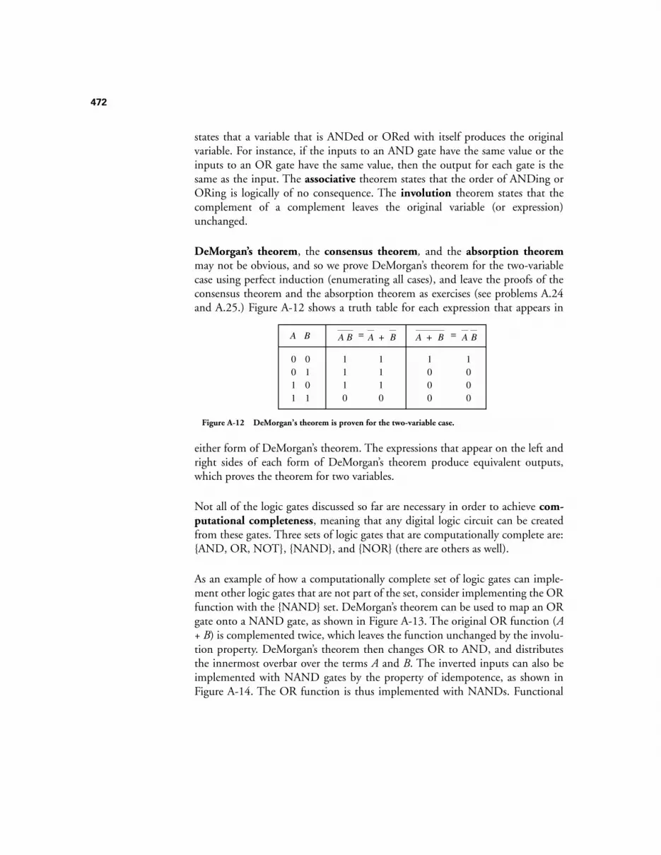
472
states that a variable that is ANDed or ORed with itself produces the originalvariable. For instance, if the inputs to an AND gate have the same value or theinputs to an OR gate have the same value, then the output for each gate is thesame as the input. The associative theorem states that the order of ANDing orORing is logically of no consequence. The involution theorem states that thecomplement of a complement leaves the original variable (or expression)unchanged.
DeMorgan’s theorem, the consensus theorem, and the absorption theoremmay not be obvious, and so we prove DeMorgan’s theorem for the two-variablecase using perfect induction (enumerating all cases), and leave the proofs of theconsensus theorem and the absorption theorem as exercises (see problems A.24and A.25.) Figure A-12 shows a truth table for each expression that appears in
either form of DeMorgan’s theorem. The expressions that appear on the left andright sides of each form of DeMorgan’s theorem produce equivalent outputs,which proves the theorem for two variables.
Not all of the logic gates discussed so far are necessary in order to achieve com-putational completeness, meaning that any digital logic circuit can be createdfrom these gates. Three sets of logic gates that are computationally complete are:AND, OR, NOT, NAND, and NOR (there are others as well).
As an example of how a computationally complete set of logic gates can imple-ment other logic gates that are not part of the set, consider implementing the ORfunction with the NAND set. DeMorgan’s theorem can be used to map an ORgate onto a NAND gate, as shown in Figure A-13. The original OR function (A+ B) is complemented twice, which leaves the function unchanged by the involu-tion property. DeMorgan’s theorem then changes OR to AND, and distributesthe innermost overbar over the terms A and B. The inverted inputs can also beimplemented with NAND gates by the property of idempotence, as shown inFigure A-14. The OR function is thus implemented with NANDs. Functional
0011
0101
A B
1110
1110
1000
1000
= =A B A + B A + B A B
Figure A-12 DeMorgan’s theorem is proven for the two-variable case.

473
equivalence among logic gates is important for practical considerations, becauseone type of logic gate may have better operating characteristics than another for agiven technology.
A.6 The Sum-of-Products Form, and Logic DiagramsSuppose now that we need to implement a more complex function than just asimple logic gate, such as the three-input majority function described by thetruth table shown in Figure A-15. The majority function is true whenever more
than half of its inputs are true, and can be thought of as a balance that tips to theleft or right depending on whether there are more 0’s or 1’s at the input. This is acommon operation used in fault recovery, in which the outputs of identical cir-cuits operating on the same data are compared, and the greatest number of simi-lar values determine the output (also referred to as “voting” or “odd one out”).
A
BF = A + B
A + B = A + B = A BDeMorgan’s theorem:
A
BF = A B
Figure A-13 DeMorgan’s theorem is used in mapping an OR gate onto a NAND gate.
A
B A + B
A
B
A + B
Figure A-14 Inverted inputs to a NAND gate implemented with NAND gates.
00110011
01010101
B C
00001111
A
00010111
F
01234567
A balance tips to the left or right depending on whether there are more 0’s or 1’s.
0-side 1-side
1
00
MintermIndex
Figure A-15 Truth table for the majority function.
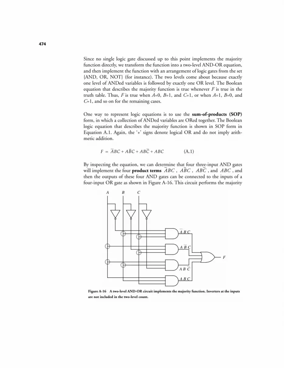
474
Since no single logic gate discussed up to this point implements the majorityfunction directly, we transform the function into a two-level AND-OR equation,and then implement the function with an arrangement of logic gates from the setAND, OR, NOT (for instance). The two levels come about because exactlyone level of ANDed variables is followed by exactly one OR level. The Booleanequation that describes the majority function is true whenever F is true in thetruth table. Thus, F is true when A=0, B=1, and C=1, or when A=1, B=0, andC=1, and so on for the remaining cases.
One way to represent logic equations is to use the sum-of-products (SOP)form, in which a collection of ANDed variables are ORed together. The Booleanlogic equation that describes the majority function is shown in SOP form inEquation A.1. Again, the ‘+’ signs denote logical OR and do not imply arith-metic addition.
(A.1)
By inspecting the equation, we can determine that four three-input AND gateswill implement the four product terms , , , and , andthen the outputs of these four AND gates can be connected to the inputs of afour-input OR gate as shown in Figure A-16. This circuit performs the majority
F ABC ABC ABC ABC+ + +=
ABC ABC ABC ABC
F
A B C
A B C
A B C
A B C
A B C
Figure A-16 A two-level AND-OR circuit implements the majority function. Inverters at the inputs
are not included in the two-level count.
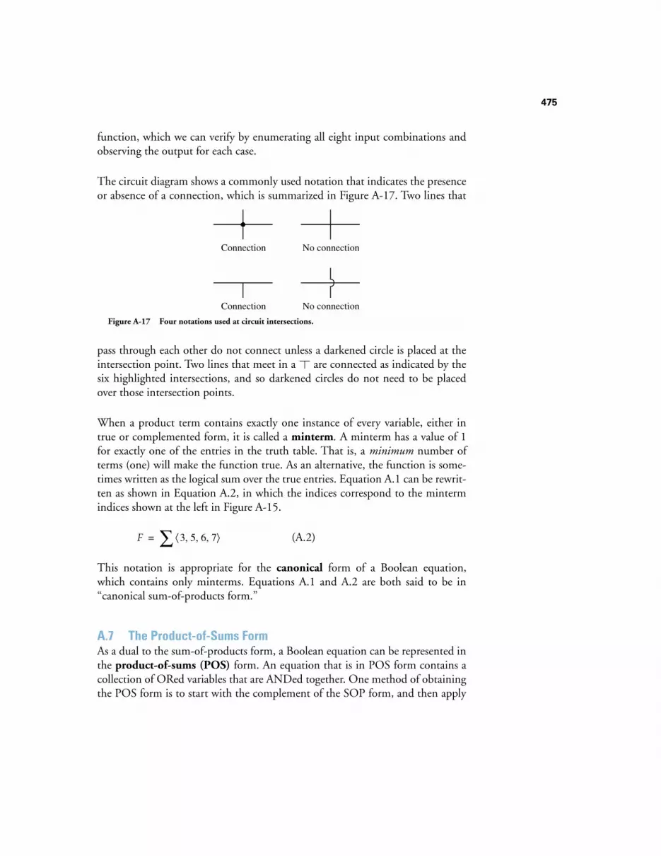
475
function, which we can verify by enumerating all eight input combinations andobserving the output for each case.
The circuit diagram shows a commonly used notation that indicates the presenceor absence of a connection, which is summarized in Figure A-17. Two lines that
pass through each other do not connect unless a darkened circle is placed at theintersection point. Two lines that meet in a are connected as indicated by thesix highlighted intersections, and so darkened circles do not need to be placedover those intersection points.
When a product term contains exactly one instance of every variable, either intrue or complemented form, it is called a minterm. A minterm has a value of 1for exactly one of the entries in the truth table. That is, a minimum number ofterms (one) will make the function true. As an alternative, the function is some-times written as the logical sum over the true entries. Equation A.1 can be rewrit-ten as shown in Equation A.2, in which the indices correspond to the mintermindices shown at the left in Figure A-15.
(A.2)
This notation is appropriate for the canonical form of a Boolean equation,which contains only minterms. Equations A.1 and A.2 are both said to be in“canonical sum-of-products form.”
A.7 The Product-of-Sums FormAs a dual to the sum-of-products form, a Boolean equation can be represented inthe product-of-sums (POS) form. An equation that is in POS form contains acollection of ORed variables that are ANDed together. One method of obtainingthe POS form is to start with the complement of the SOP form, and then apply
No connection
No connection
Connection
Connection
Figure A-17 Four notations used at circuit intersections.
F 3 5 6 7, , ,⟨ ⟩∑=
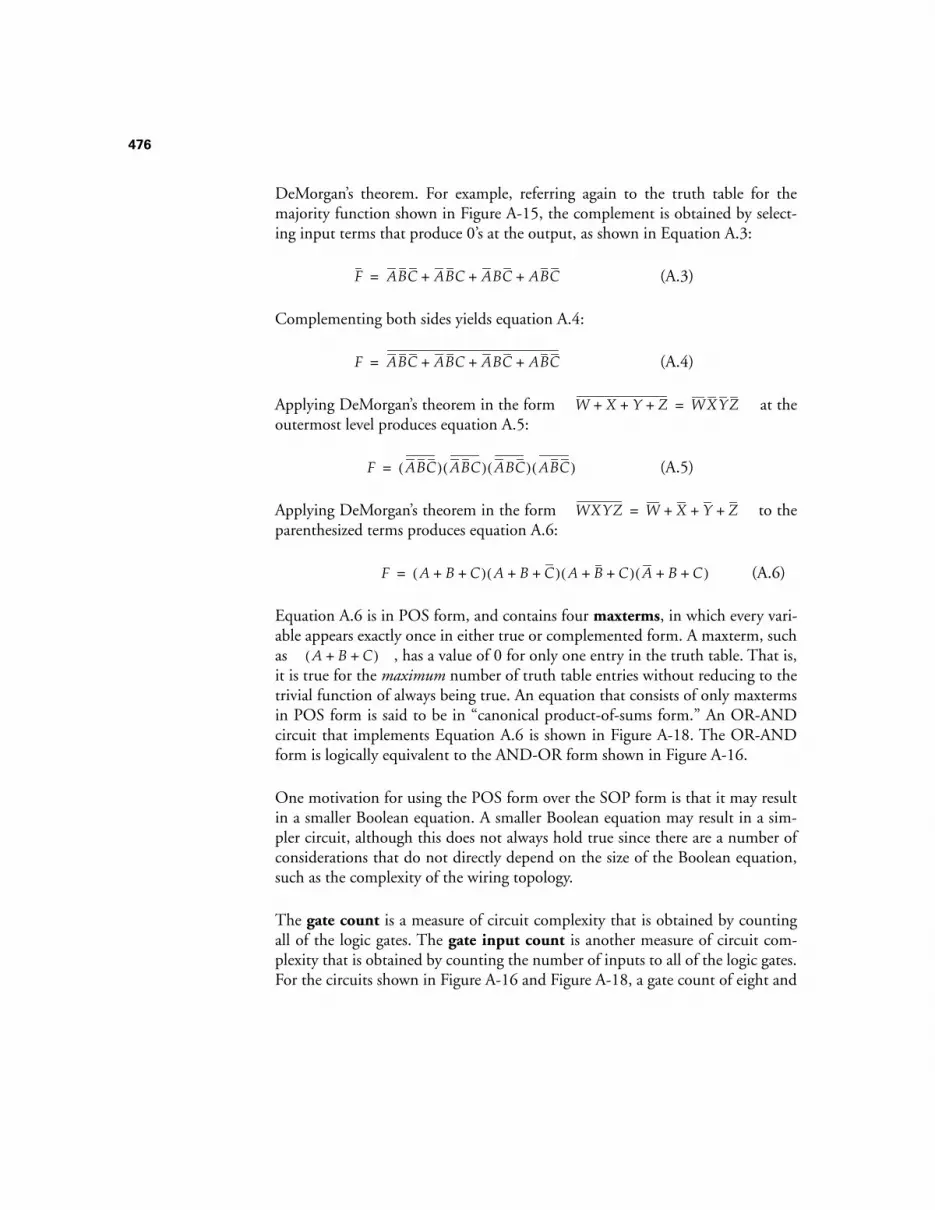
476
DeMorgan’s theorem. For example, referring again to the truth table for themajority function shown in Figure A-15, the complement is obtained by select-ing input terms that produce 0’s at the output, as shown in Equation A.3:
(A.3)
Complementing both sides yields equation A.4:
(A.4)
Applying DeMorgan’s theorem in the form at theoutermost level produces equation A.5:
(A.5)
Applying DeMorgan’s theorem in the form to theparenthesized terms produces equation A.6:
(A.6)
Equation A.6 is in POS form, and contains four maxterms, in which every vari-able appears exactly once in either true or complemented form. A maxterm, suchas , has a value of 0 for only one entry in the truth table. That is,it is true for the maximum number of truth table entries without reducing to thetrivial function of always being true. An equation that consists of only maxtermsin POS form is said to be in “canonical product-of-sums form.” An OR-ANDcircuit that implements Equation A.6 is shown in Figure A-18. The OR-ANDform is logically equivalent to the AND-OR form shown in Figure A-16.
One motivation for using the POS form over the SOP form is that it may resultin a smaller Boolean equation. A smaller Boolean equation may result in a sim-pler circuit, although this does not always hold true since there are a number ofconsiderations that do not directly depend on the size of the Boolean equation,such as the complexity of the wiring topology.
The gate count is a measure of circuit complexity that is obtained by countingall of the logic gates. The gate input count is another measure of circuit com-plexity that is obtained by counting the number of inputs to all of the logic gates.For the circuits shown in Figure A-16 and Figure A-18, a gate count of eight and
F ABC ABC ABC ABC+ + +=
F ABC ABC ABC ABC+ + +=
W X Y Z+ + + WXYZ=
F ABC( ) ABC( ) ABC( ) ABC( )=
WXYZ W X Y Z+ + +=
F A B C+ +( ) A B C+ +( ) A B C+ +( ) A B C+ +( )=
A B C+ +( )
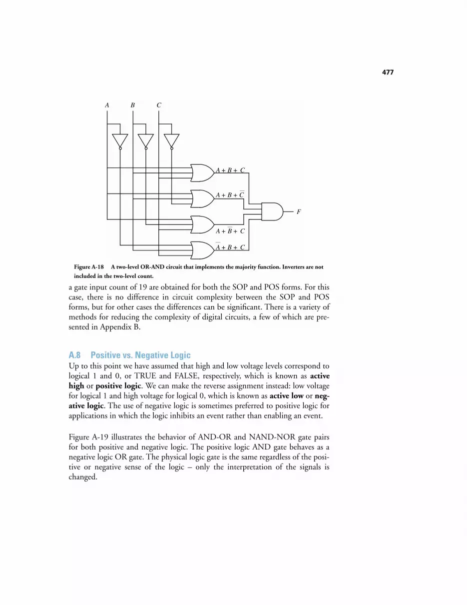
477
a gate input count of 19 are obtained for both the SOP and POS forms. For thiscase, there is no difference in circuit complexity between the SOP and POSforms, but for other cases the differences can be significant. There is a variety ofmethods for reducing the complexity of digital circuits, a few of which are pre-sented in Appendix B.
A.8 Positive vs. Negative LogicUp to this point we have assumed that high and low voltage levels correspond tological 1 and 0, or TRUE and FALSE, respectively, which is known as activehigh or positive logic. We can make the reverse assignment instead: low voltagefor logical 1 and high voltage for logical 0, which is known as active low or neg-ative logic. The use of negative logic is sometimes preferred to positive logic forapplications in which the logic inhibits an event rather than enabling an event.
Figure A-19 illustrates the behavior of AND-OR and NAND-NOR gate pairsfor both positive and negative logic. The positive logic AND gate behaves as anegative logic OR gate. The physical logic gate is the same regardless of the posi-tive or negative sense of the logic – only the interpretation of the signals ischanged.
F
A B C
A + B + C
A + B + C
A + B + C
A + B + C
Figure A-18 A two-level OR-AND circuit that implements the majority function. Inverters are not
included in the two-level count.
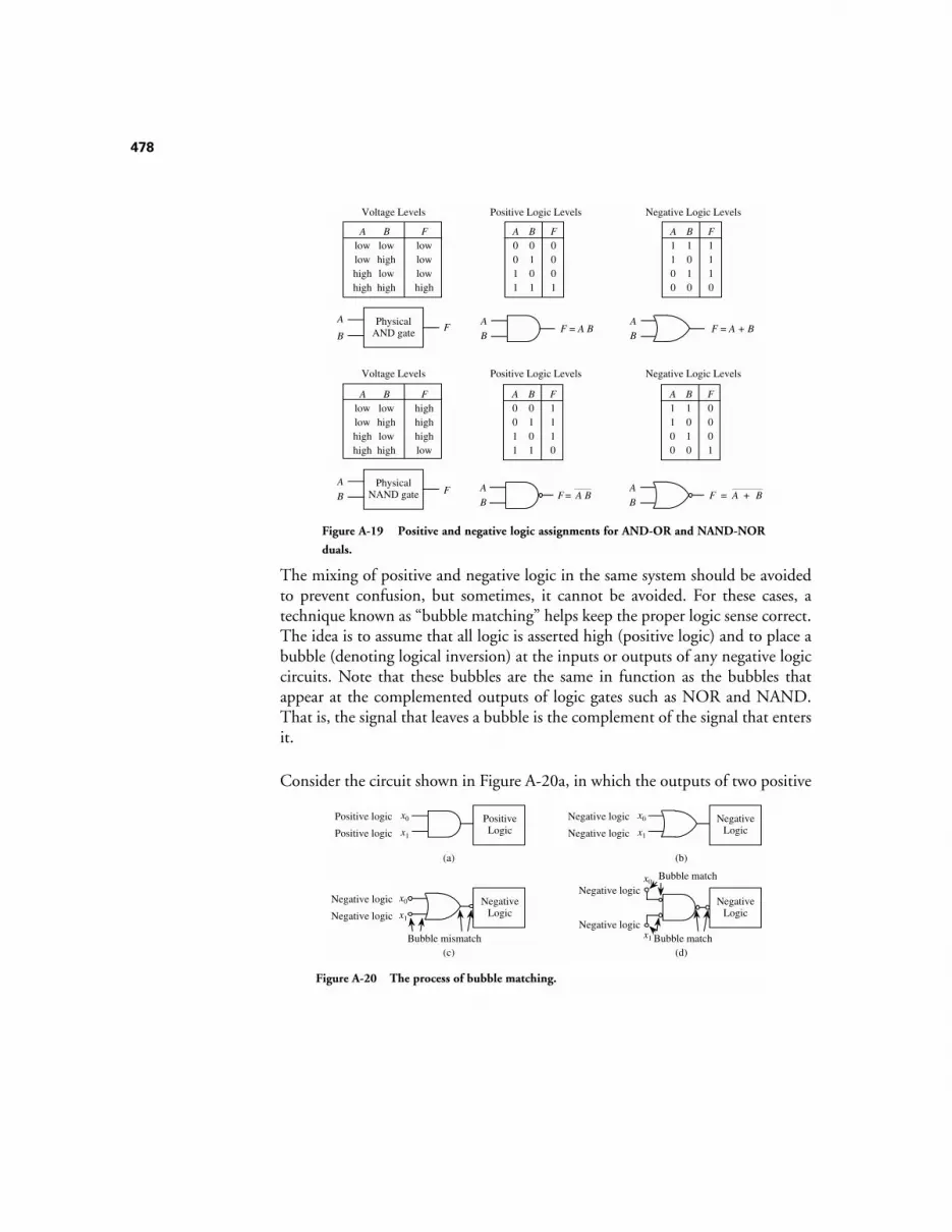
478
The mixing of positive and negative logic in the same system should be avoidedto prevent confusion, but sometimes, it cannot be avoided. For these cases, atechnique known as “bubble matching” helps keep the proper logic sense correct.The idea is to assume that all logic is asserted high (positive logic) and to place abubble (denoting logical inversion) at the inputs or outputs of any negative logiccircuits. Note that these bubbles are the same in function as the bubbles thatappear at the complemented outputs of logic gates such as NOR and NAND.That is, the signal that leaves a bubble is the complement of the signal that entersit.
Consider the circuit shown in Figure A-20a, in which the outputs of two positive
A
BF = A B
A0011
B0101
F0001
A1100
B1010
F1110
A
BF = A + B
A0011
B0101
F1110
A1100
B1010
F0001
A
BF = A B
A
BF = A + B
Positive Logic Levels Negative Logic Levels
Alowlowhighhigh
Blowhighlowhigh
Flowlowlowhigh
Voltage Levels
Physical AND gate
A
BF
Positive Logic Levels Negative Logic Levels
Alowlowhighhigh
Blowhighlowhigh
Fhighhighhighlow
Voltage Levels
Physical NAND gate
A
BF
Figure A-19 Positive and negative logic assignments for AND-OR and NAND-NOR
duals.
x0 Positive Logicx1
x0
x1
NegativeLogic
Positive logic
(a) (b)
Positive logic
Negative logic
Negative logic
x0 NegativeLogicx1
x0
x1
NegativeLogic
Negative logic
(c) (d)
Negative logic
Negative logic
Negative logicBubble mismatch Bubble match
Bubble match
Figure A-20 The process of bubble matching.
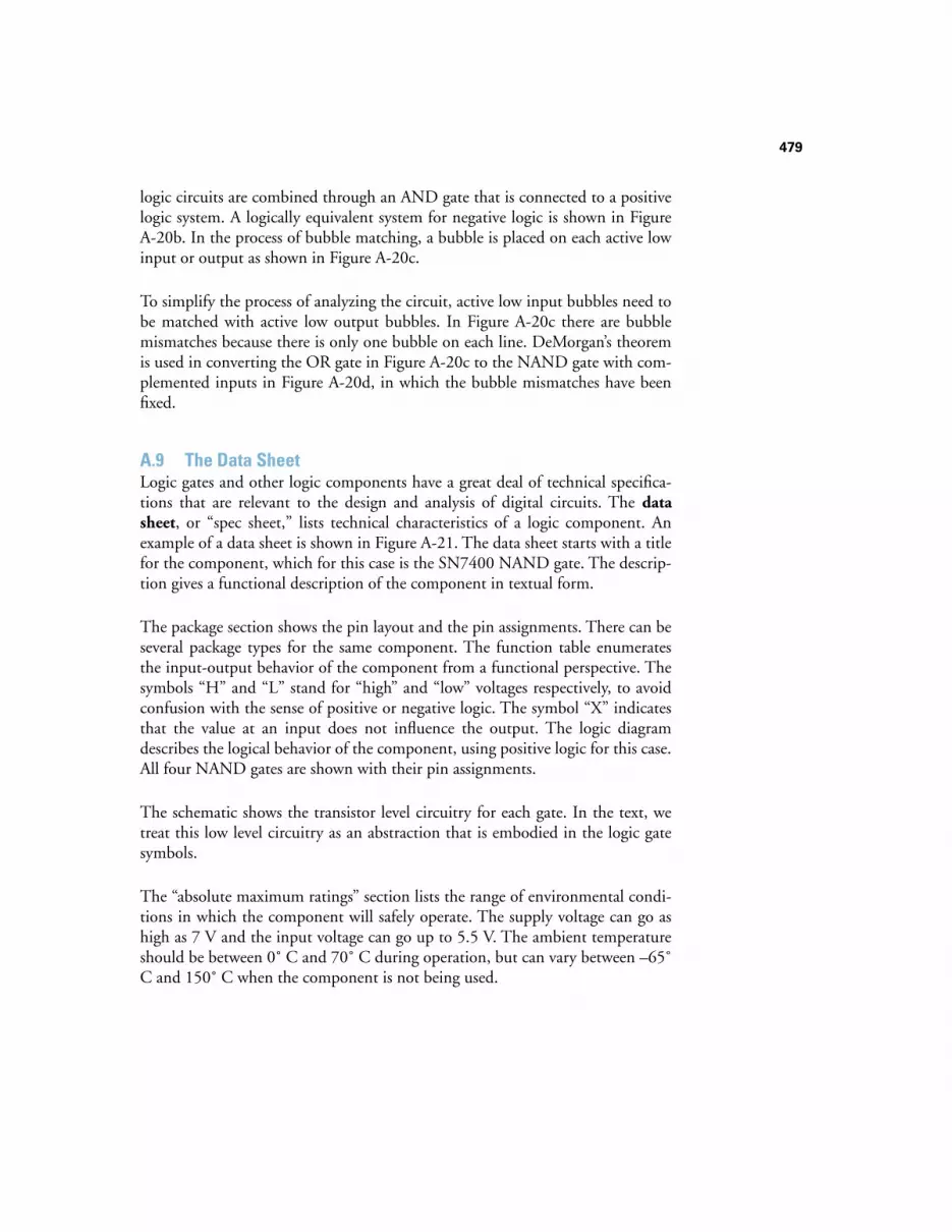
479
logic circuits are combined through an AND gate that is connected to a positivelogic system. A logically equivalent system for negative logic is shown in FigureA-20b. In the process of bubble matching, a bubble is placed on each active lowinput or output as shown in Figure A-20c.
To simplify the process of analyzing the circuit, active low input bubbles need tobe matched with active low output bubbles. In Figure A-20c there are bubblemismatches because there is only one bubble on each line. DeMorgan’s theoremis used in converting the OR gate in Figure A-20c to the NAND gate with com-plemented inputs in Figure A-20d, in which the bubble mismatches have beenfixed.
A.9 The Data SheetLogic gates and other logic components have a great deal of technical specifica-tions that are relevant to the design and analysis of digital circuits. The datasheet, or “spec sheet,” lists technical characteristics of a logic component. Anexample of a data sheet is shown in Figure A-21. The data sheet starts with a titlefor the component, which for this case is the SN7400 NAND gate. The descrip-tion gives a functional description of the component in textual form.
The package section shows the pin layout and the pin assignments. There can beseveral package types for the same component. The function table enumeratesthe input-output behavior of the component from a functional perspective. Thesymbols “H” and “L” stand for “high” and “low” voltages respectively, to avoidconfusion with the sense of positive or negative logic. The symbol “X” indicatesthat the value at an input does not influence the output. The logic diagramdescribes the logical behavior of the component, using positive logic for this case.All four NAND gates are shown with their pin assignments.
The schematic shows the transistor level circuitry for each gate. In the text, wetreat this low level circuitry as an abstraction that is embodied in the logic gatesymbols.
The “absolute maximum ratings” section lists the range of environmental condi-tions in which the component will safely operate. The supply voltage can go ashigh as 7 V and the input voltage can go up to 5.5 V. The ambient temperatureshould be between 0˚ C and 70˚ C during operation, but can vary between –65˚C and 150˚ C when the component is not being used.
480
Despite the absolute maximum rating specifications, the recommended operat-ing conditions should be used during operation. The recommended operatingconditions are characterized by minimum (MIN), normal (NOM), and maxi-mum (MAX) ratings.
The electrical characteristics describe the behavior of the component under cer-tain operating conditions. VOH and VOL are the minimum output high voltageand the maximum output low voltage, respectively. IIH and IIL are the maximum
SN7400 QUADRUPLE 2-INPUT POSITIVE-NAND GATES
description
These devices contain four independent 2-input NAND gates.
package (top view)
1A1B1Y2A2B2Y
GND
VCC
4B4A4Y3B3A3Y
1
2
3
4
5
6
7
14
13
12
11
10
9
8
1A1B 1Y
2A2B 2Y
3A3B 3Y
4A4B 4Y
Y = A B
logic diagram (positive logic)
function table (each gate)
INPUTSA B
OUTPUTY
HL
X
HX
L
LH
H
VCC
schematic (each gate)
130 Ω1.6 kΩ4 kΩ
A
B
Y
GND
1 kΩ
recommended operating conditions
IOL Low-level output current
IOH High-level output current
VIL Low-level input voltage
VIH High-level input voltage
VCC Supply voltage
MIN
TA Operating free-air temperature
NOM MAX UNIT
4.75 5 5.25 V
2 V
0.8 V
– 0.4 mA
16 mA
0 70 ˚C
electrical characteristics over recommended operating free-air temperature range
ICCH VCC = MAX, VI = 0 V
IIL VCC = MAX, VI = 0.4 V
IIH VCC = MAX, VI = 2.4 V
VOL VCC = MIN, VIH = 2 V, IOL = 16 mA
VOH VCC = MIN, VIL = 0.8 V, IOH = – 0.4 mA
MIN
ICCL VCC = MAX, VI = 4.5 V
TYP MAX UNIT
2.4 3.4
0.4
V
V
40 µA
– 1.6 mA
8 mA
22 mA
0.2
4
12
absolute maximum ratings
Supply voltage, VCCInput voltage:Operating free-air temperature range:Storage temperature range
7 V5.5 V
0 ˚C to 70 ˚C– 65 ˚C to 150 ˚C
switching characteristics, VCC = 5 V, TA = 25˚ C
tPHL
tPLH
MIN TYP MAX UNIT
11 22 ns
ns7 15
PARAMETER FROM (input) TO (output) TEST CONDITIONS
A or B YRL = 400 Ω CL = 15 pF
Figure A-21 Simplified data sheet for 7400 NAND gate, adapted from Texas Instruments
TTL Databook [Texas Instruments, 1988].

481
currents into an input pin when the input is high or low, respectively. ICCH andICCL are the package’s power supply currents when all outputs are high or low,respectively.
This data can be used in determining maximum fan-outs under the given condi-tions. Fan-out is a measure of the number of inputs that a single output candrive, for logic gates implemented in the same technology. That is, a logic gatewith a fan-out of 10 can drive the inputs of 10 other logic gates of the same type.Similarly, fan-in is a measure of the number of inputs that a logic gate can accept(simply, the number of input lines to that gate). The absolute value of IOH mustbe greater than or equal to the sum of all IIH currents that are being driven, andIOL must be greater than or equal to the sum of all IIL currents (absolute values)that are being driven. The absolute value of IOH for a 7400 gate is .4 mA (or 400µA), and so a 7400 gate output can thus drive ten 7400 inputs (IIH = 40 µA perinput).
The switching characteristics show the propagation delay to switch the outputfrom a low to a high voltage (tPLH) and the propagation delay to switch the out-put from a high to a low voltage (tPHL). The maximum ratings show the worstcases. A circuit can be safely designed using the typical case as the worst case, butonly if a test-and-select-the-best approach is used. That is, since tPLH variesbetween 11 ns and 22 ns and tPHL varies between 7 ns and 15 ns from one pack-aged component to the next, components can be individually tested to deter-mine their true characteristics. Not all components of the same type behaveidentically, even under the most stringent fabrication controls, and the differ-ences can be reduced by testing and selecting the best components.
A.10 Digital ComponentsHigh level digital circuit designs are normally made using collections of logicgates referred to as components, rather than using individual logic gates. Thisallows a degree of circuit complexity to be abstracted away, and also simplifies theprocess of modeling the behavior of circuits and characterizing their perfor-mance. A few of the more common components are described in the sectionsthat follow.
A.10.1 LEVELS OF INTEGRATION
Up to this point, we have focused on the design of combinational logic units.Since we have been working with individual logic gates, we have been working at
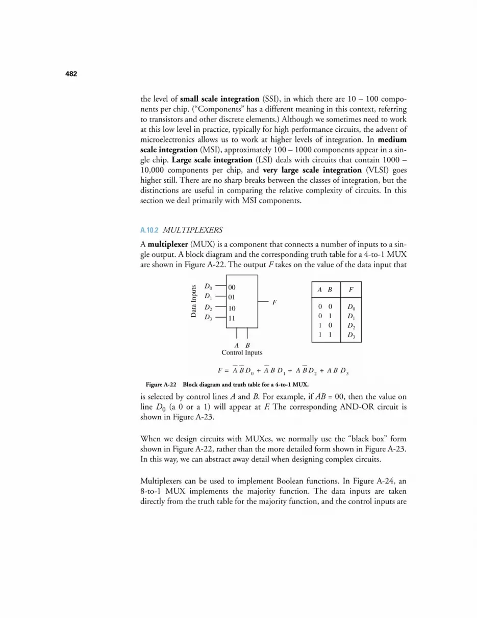
482
the level of small scale integration (SSI), in which there are 10 – 100 compo-nents per chip. (“Components” has a different meaning in this context, referringto transistors and other discrete elements.) Although we sometimes need to workat this low level in practice, typically for high performance circuits, the advent ofmicroelectronics allows us to work at higher levels of integration. In mediumscale integration (MSI), approximately 100 – 1000 components appear in a sin-gle chip. Large scale integration (LSI) deals with circuits that contain 1000 –10,000 components per chip, and very large scale integration (VLSI) goeshigher still. There are no sharp breaks between the classes of integration, but thedistinctions are useful in comparing the relative complexity of circuits. In thissection we deal primarily with MSI components.
A.10.2 MULTIPLEXERS
A multiplexer (MUX) is a component that connects a number of inputs to a sin-gle output. A block diagram and the corresponding truth table for a 4-to-1 MUXare shown in Figure A-22. The output F takes on the value of the data input that
is selected by control lines A and B. For example, if AB = 00, then the value online D0 (a 0 or a 1) will appear at F. The corresponding AND-OR circuit isshown in Figure A-23.
When we design circuits with MUXes, we normally use the “black box” formshown in Figure A-22, rather than the more detailed form shown in Figure A-23.In this way, we can abstract away detail when designing complex circuits.
Multiplexers can be used to implement Boolean functions. In Figure A-24, an8-to-1 MUX implements the majority function. The data inputs are takendirectly from the truth table for the majority function, and the control inputs are
0011
0101
A B
D0
D1
D2
D3
FD0
A
D1
D2
D3
B
F
0001
1011
F = A B D0
+ A B D1
+ A B D2
+ A B D3
Dat
a In
puts
Control Inputs
Figure A-22 Block diagram and truth table for a 4-to-1 MUX.
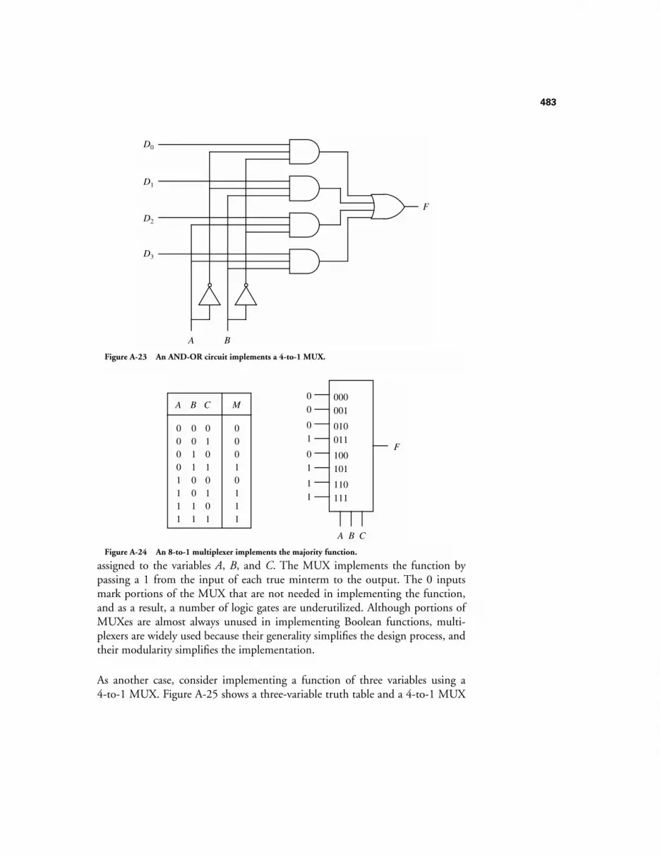
483
assigned to the variables A, B, and C. The MUX implements the function bypassing a 1 from the input of each true minterm to the output. The 0 inputsmark portions of the MUX that are not needed in implementing the function,and as a result, a number of logic gates are underutilized. Although portions ofMUXes are almost always unused in implementing Boolean functions, multi-plexers are widely used because their generality simplifies the design process, andtheir modularity simplifies the implementation.
As another case, consider implementing a function of three variables using a4-to-1 MUX. Figure A-25 shows a three-variable truth table and a 4-to-1 MUX
F
A B
D0
D1
D2
D3
Figure A-23 An AND-OR circuit implements a 4-to-1 MUX.
A C
F
000001
010011
B
100101
110111
00
01
01
11
00110011
01010101
B C
00001111
A
00010111
M
Figure A-24 An 8-to-1 multiplexer implements the majority function.
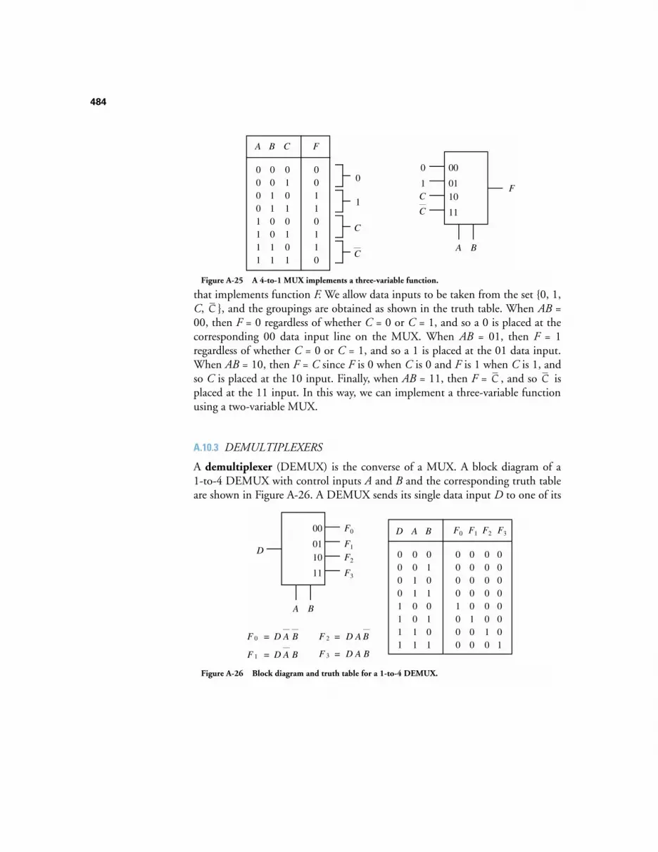
484
that implements function F. We allow data inputs to be taken from the set 0, 1,C, , and the groupings are obtained as shown in the truth table. When AB =00, then F = 0 regardless of whether C = 0 or C = 1, and so a 0 is placed at thecorresponding 00 data input line on the MUX. When AB = 01, then F = 1regardless of whether C = 0 or C = 1, and so a 1 is placed at the 01 data input.When AB = 10, then F = C since F is 0 when C is 0 and F is 1 when C is 1, andso C is placed at the 10 input. Finally, when AB = 11, then F = , and so isplaced at the 11 input. In this way, we can implement a three-variable functionusing a two-variable MUX.
A.10.3 DEMULTIPLEXERS
A demultiplexer (DEMUX) is the converse of a MUX. A block diagram of a1-to-4 DEMUX with control inputs A and B and the corresponding truth tableare shown in Figure A-26. A DEMUX sends its single data input D to one of its
A B
F
00
0110
11
0
1C
C
00110011
01010101
B C
00110110
F
00001111
A
0
1
C
C
Figure A-25 A 4-to-1 MUX implements a three-variable function.
C
C C
F0
A
F1
F2
F3
B
00
0110
11
D
F 0 = D A B
F 1 = D A B
F 2 = D A B
F 3 = D A B
00110011
01010101
A B
00001000
F0
00000100
F1
00000010
F2
00000001
F3
00001111
D
Figure A-26 Block diagram and truth table for a 1-to-4 DEMUX.
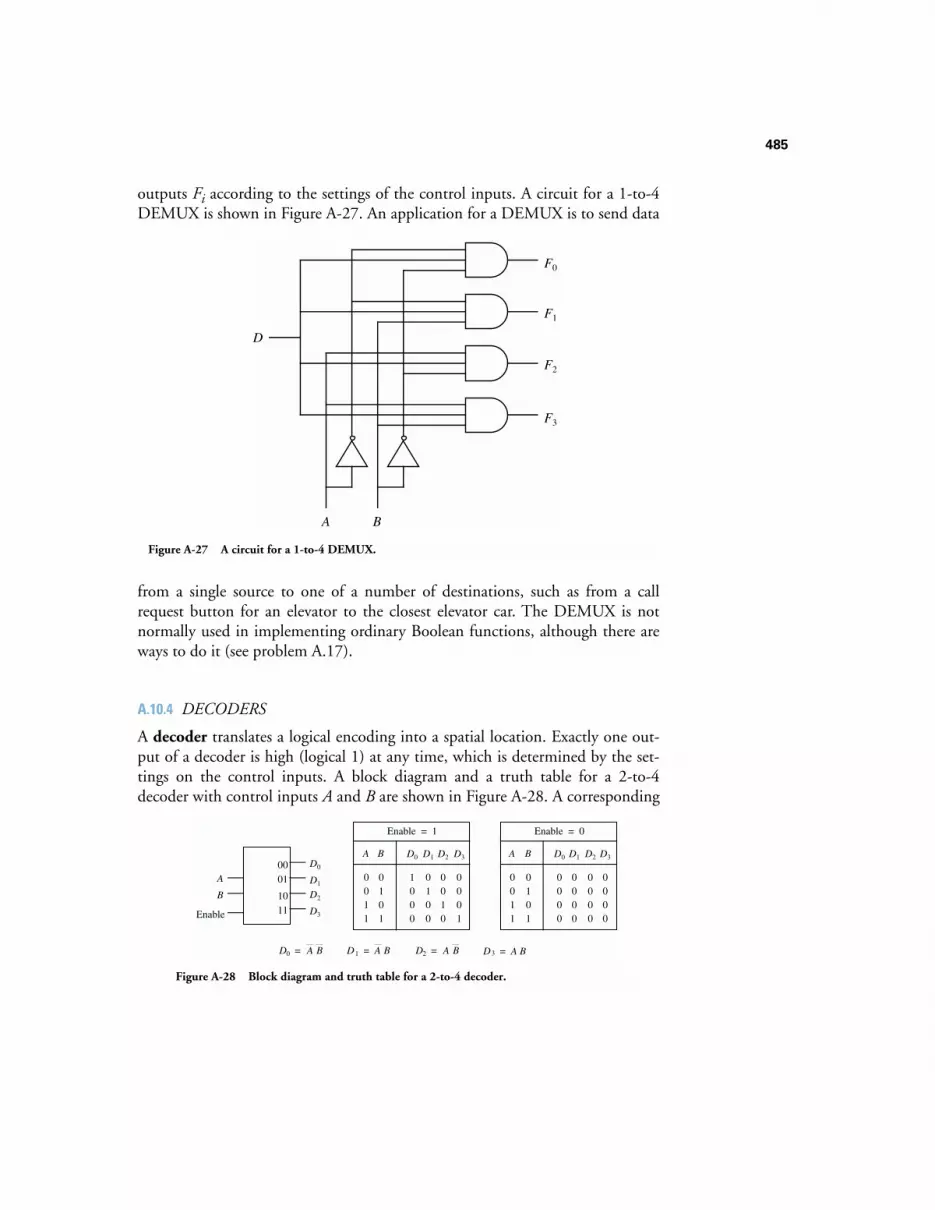
485
outputs Fi according to the settings of the control inputs. A circuit for a 1-to-4DEMUX is shown in Figure A-27. An application for a DEMUX is to send data
from a single source to one of a number of destinations, such as from a callrequest button for an elevator to the closest elevator car. The DEMUX is notnormally used in implementing ordinary Boolean functions, although there areways to do it (see problem A.17).
A.10.4 DECODERS
A decoder translates a logical encoding into a spatial location. Exactly one out-put of a decoder is high (logical 1) at any time, which is determined by the set-tings on the control inputs. A block diagram and a truth table for a 2-to-4decoder with control inputs A and B are shown in Figure A-28. A corresponding
A B
F0
F1
F2
F3
D
Figure A-27 A circuit for a 1-to-4 DEMUX.
D0
A D1
D2
D3
B
0001
1011
0011
0101
A B
1000
D0
0100
D1
0010
D2
0001
D3
D3 = A BD1 = A B D2 = A BD0 = A B
Enable
Enable = 1
0011
0101
A B
0000
D0
0000
D1
0000
D2
0000
D3
Enable = 0
Figure A-28 Block diagram and truth table for a 2-to-4 decoder.
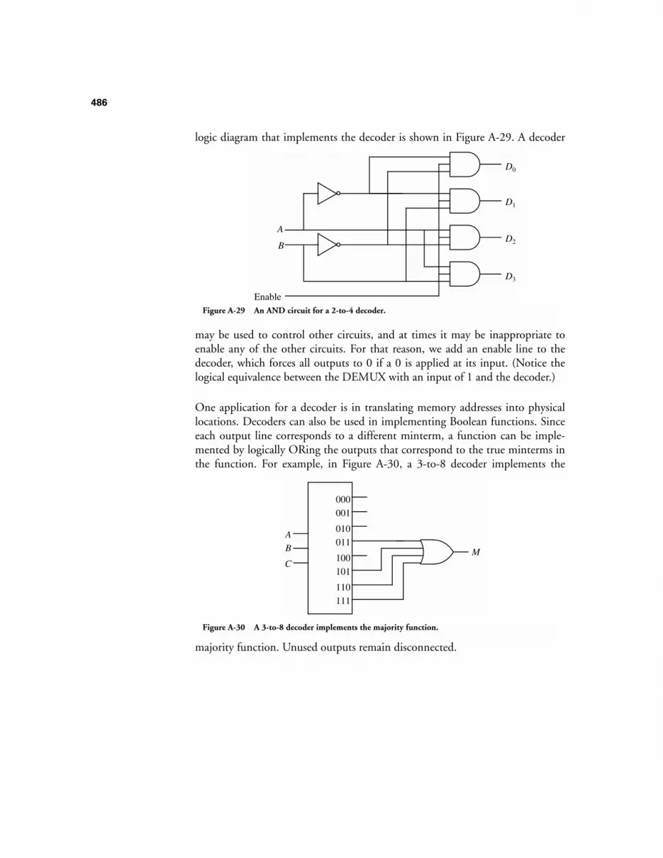
486
logic diagram that implements the decoder is shown in Figure A-29. A decoder
may be used to control other circuits, and at times it may be inappropriate toenable any of the other circuits. For that reason, we add an enable line to thedecoder, which forces all outputs to 0 if a 0 is applied at its input. (Notice thelogical equivalence between the DEMUX with an input of 1 and the decoder.)
One application for a decoder is in translating memory addresses into physicallocations. Decoders can also be used in implementing Boolean functions. Sinceeach output line corresponds to a different minterm, a function can be imple-mented by logically ORing the outputs that correspond to the true minterms inthe function. For example, in Figure A-30, a 3-to-8 decoder implements the
majority function. Unused outputs remain disconnected.
A
B
D0
D1
D2
D3
EnableFigure A-29 An AND circuit for a 2-to-4 decoder.
A
CM
000001
010011
B100101
110111
Figure A-30 A 3-to-8 decoder implements the majority function.
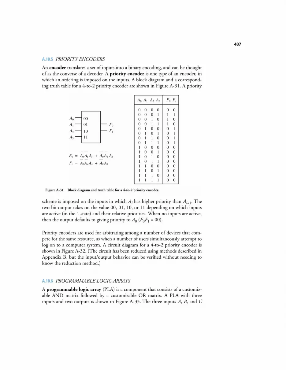
487
A.10.5 PRIORITY ENCODERS
An encoder translates a set of inputs into a binary encoding, and can be thoughtof as the converse of a decoder. A priority encoder is one type of an encoder, inwhich an ordering is imposed on the inputs. A block diagram and a correspond-ing truth table for a 4-to-2 priority encoder are shown in Figure A-31. A priority
scheme is imposed on the inputs in which Ai has higher priority than Ai+1. Thetwo-bit output takes on the value 00, 01, 10, or 11 depending on which inputsare active (in the 1 state) and their relative priorities. When no inputs are active,then the output defaults to giving priority to A0 (F0F1 = 00).
Priority encoders are used for arbitrating among a number of devices that com-pete for the same resource, as when a number of users simultaneously attempt tolog on to a computer system. A circuit diagram for a 4-to-2 priority encoder isshown in Figure A-32. (The circuit has been reduced using methods described inAppendix B, but the input/output behavior can be verified without needing toknow the reduction method.)
A.10.6 PROGRAMMABLE LOGIC ARRAYS
A programmable logic array (PLA) is a component that consists of a customiz-able AND matrix followed by a customizable OR matrix. A PLA with threeinputs and two outputs is shown in Figure A-33. The three inputs A, B, and C
0111000000000000
0100111100000000
F0 F1
0000000011111111
A0
0000111100001111
A1
0011001100110011
A2
0101010101010101
A3
F0
F1
0001
1011
A0
A1
A2
A3
F0 = A0 A1 A3 + A0 A1 A2
F1 = A0 A2 A3 + A0 A1
Figure A-31 Block diagram and truth table for a 4-to-2 priority encoder.
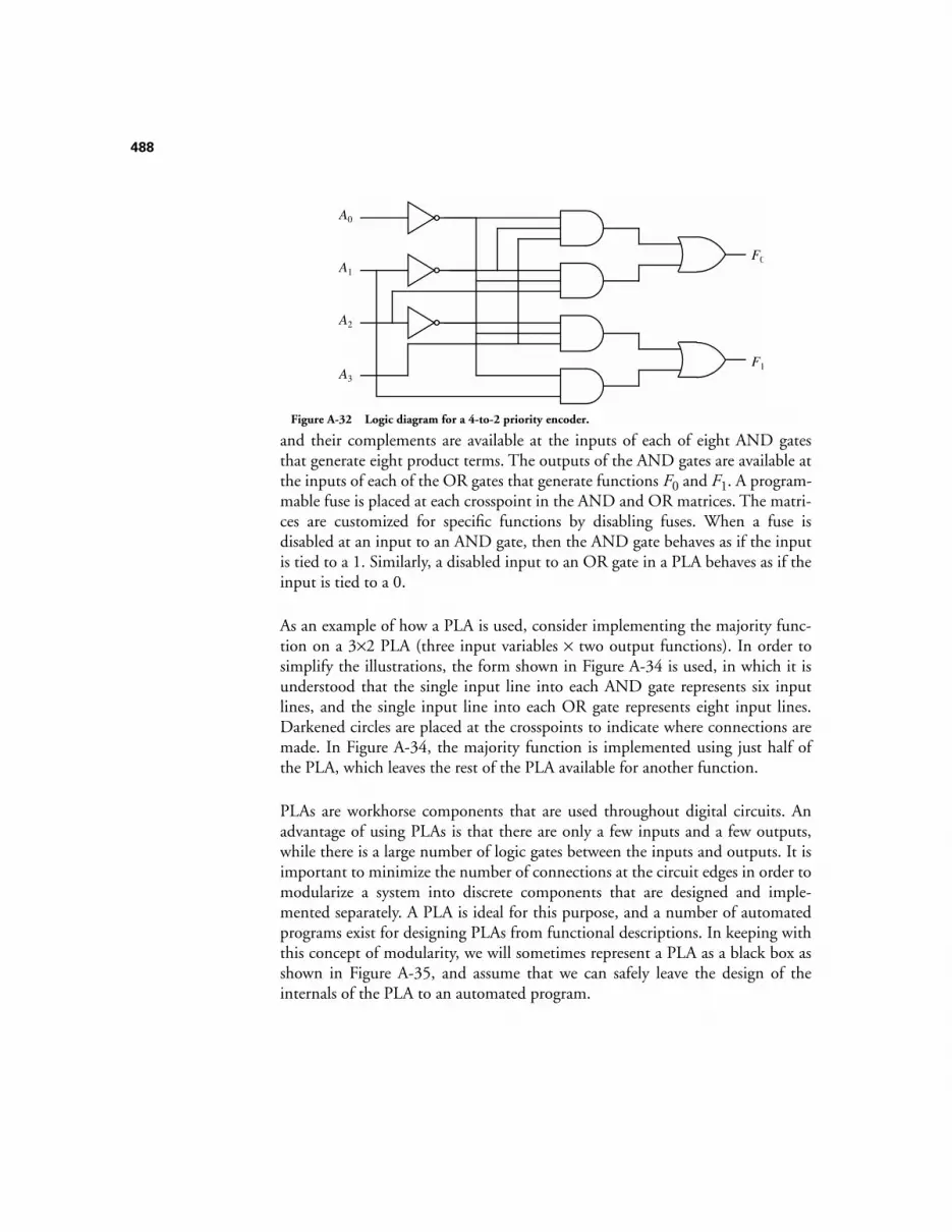
488
and their complements are available at the inputs of each of eight AND gatesthat generate eight product terms. The outputs of the AND gates are available atthe inputs of each of the OR gates that generate functions F0 and F1. A program-mable fuse is placed at each crosspoint in the AND and OR matrices. The matri-ces are customized for specific functions by disabling fuses. When a fuse isdisabled at an input to an AND gate, then the AND gate behaves as if the inputis tied to a 1. Similarly, a disabled input to an OR gate in a PLA behaves as if theinput is tied to a 0.
As an example of how a PLA is used, consider implementing the majority func-tion on a 3×2 PLA (three input variables × two output functions). In order tosimplify the illustrations, the form shown in Figure A-34 is used, in which it isunderstood that the single input line into each AND gate represents six inputlines, and the single input line into each OR gate represents eight input lines.Darkened circles are placed at the crosspoints to indicate where connections aremade. In Figure A-34, the majority function is implemented using just half ofthe PLA, which leaves the rest of the PLA available for another function.
PLAs are workhorse components that are used throughout digital circuits. Anadvantage of using PLAs is that there are only a few inputs and a few outputs,while there is a large number of logic gates between the inputs and outputs. It isimportant to minimize the number of connections at the circuit edges in order tomodularize a system into discrete components that are designed and imple-mented separately. A PLA is ideal for this purpose, and a number of automatedprograms exist for designing PLAs from functional descriptions. In keeping withthis concept of modularity, we will sometimes represent a PLA as a black box asshown in Figure A-35, and assume that we can safely leave the design of theinternals of the PLA to an automated program.
F0A1
A2
A3
F1
A0
Figure A-32 Logic diagram for a 4-to-2 priority encoder.
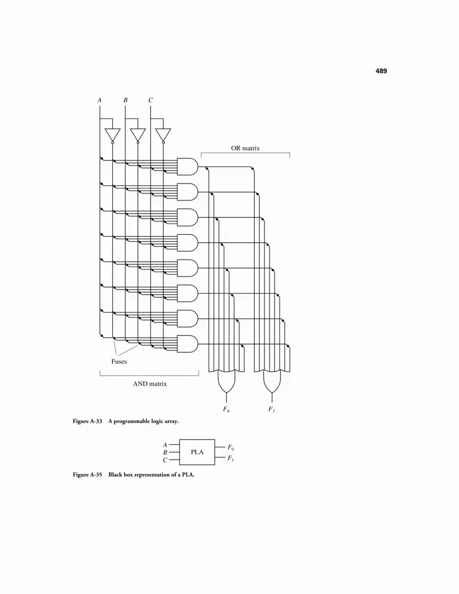
489
F0
A B C
Fuses
F1
AND matrix
OR matrix
Figure A-33 A programmable logic array.
ABC
PLAF0
F1
Figure A-35 Black box representation of a PLA.
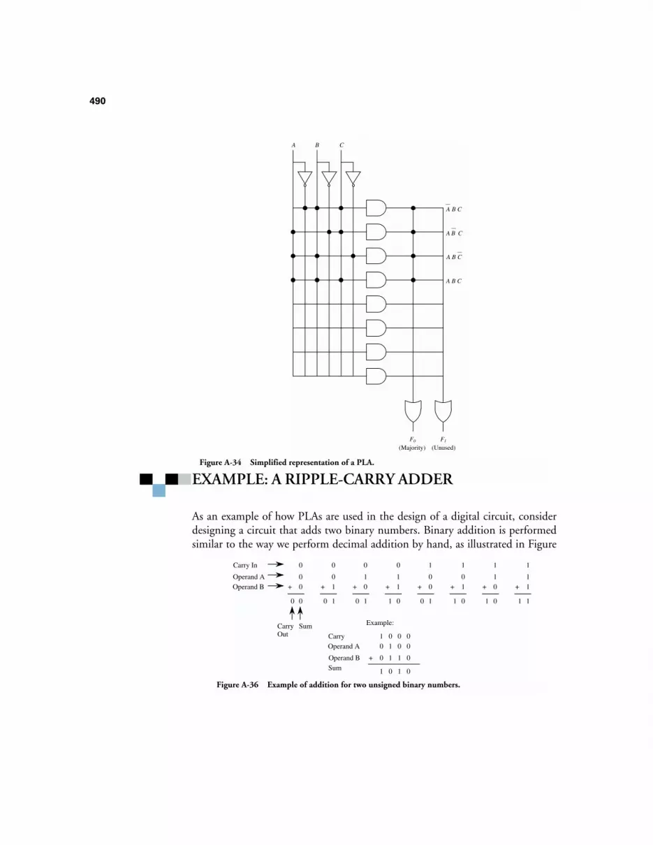
490
EXAMPLE: A RIPPLE-CARRY ADDER
As an example of how PLAs are used in the design of a digital circuit, considerdesigning a circuit that adds two binary numbers. Binary addition is performedsimilar to the way we perform decimal addition by hand, as illustrated in Figure
F0
A B C
F1
(Majority)
A B C
A B C
A B C
A B C
(Unused)
Figure A-34 Simplified representation of a PLA.
Operand AOperand B
00+
00
SumCarry Out
01+
10
11+
01
Example:
CarryOperand A
Operand BSum
0 1 0 0
0 1 1 0
1 0 0 0
1 0 1 0
+
Carry In 0 0
10+
10
0 0
00+
10
1
01+
01
1
10+
01
1
11+
11
1
Figure A-36 Example of addition for two unsigned binary numbers.
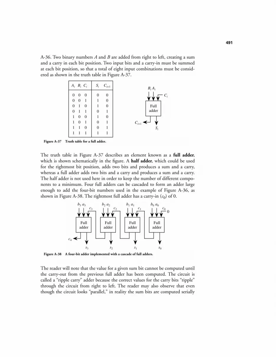
491
A-36. Two binary numbers A and B are added from right to left, creating a sumand a carry in each bit position. Two input bits and a carry-in must be summedat each bit position, so that a total of eight input combinations must be consid-ered as shown in the truth table in Figure A-37.
The truth table in Figure A-37 describes an element known as a full adder,which is shown schematically in the figure. A half adder, which could be usedfor the rightmost bit position, adds two bits and produces a sum and a carry,whereas a full adder adds two bits and a carry and produces a sum and a carry.The half adder is not used here in order to keep the number of different compo-nents to a minimum. Four full adders can be cascaded to form an adder largeenough to add the four-bit numbers used in the example of Figure A-36, asshown in Figure A-38. The rightmost full adder has a carry-in (c0) of 0.
The reader will note that the value for a given sum bit cannot be computed untilthe carry-out from the previous full adder has been computed. The circuit iscalled a “ripple carry” adder because the correct values for the carry bits “ripple”through the circuit from right to left. The reader may also observe that eventhough the circuit looks “parallel,” in reality the sum bits are computed serially
00110011
01010101
Bi Ci
00001111
Ai
01101001
Si
00010111
Ci+1
Fulladder
Bi Ai
Ci
Ci+1
Si
Figure A-37 Truth table for a full adder.
Fulladder
b0 a0
s0
Fulladder
b1 a1
s1
Fulladder
b2 a2
s2
Fulladder
b3 a3
c4
s3
0c0c1c2c3
Figure A-38 A four-bit adder implemented with a cascade of full adders.

492
from right to left. This is a major disadvantage to the circuit. We discusss ways ofspeeding up addition in Chapter 3, Arithmetic.
An approach to designing a full adder is to use a PLA, as shown in Figure A-39.
The PLA approach is very general, and computer-aided design (CAD) tools forVLSI typically favor the use of PLAs over random logic or MUXes because oftheir generality. CAD tools typically reduce the sizes of the PLAs (we will see afew reduction techniques in Appendix B) and so the seemingly high gate countfor the PLA is not actually so high in practice.
A.11 Sequential LogicIn the earlier part of this appendix we explored combinational logic units, inwhich the outputs are completely determined by functions of the inputs. Asequential logic unit, commonly referred to as a finite state machine (FSM),takes an input and a current state, and produces an output and a new state. AnFSM is distinguished from a CLU in that the past history of the inputs to the
Sum
A B Cin
Cout
Figure A-39 PLA realization of a full adder.
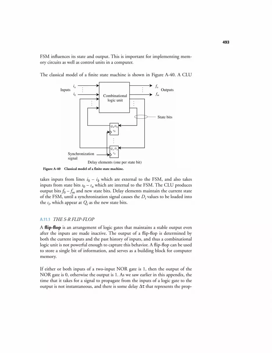
493
FSM influences its state and output. This is important for implementing mem-ory circuits as well as control units in a computer.
The classical model of a finite state machine is shown in Figure A-40. A CLU
takes inputs from lines i0 – ik which are external to the FSM, and also takesinputs from state bits s0 – sn which are internal to the FSM. The CLU producesoutput bits f0 – fm and new state bits. Delay elements maintain the current stateof the FSM, until a synchronization signal causes the Di values to be loaded intothe si, which appear at Qi as the new state bits.
A.11.1 THE S-R FLIP-FLOP
A flip-flop is an arrangement of logic gates that maintains a stable output evenafter the inputs are made inactive. The output of a flip-flop is determined byboth the current inputs and the past history of inputs, and thus a combinationallogic unit is not powerful enough to capture this behavior. A flip-flop can be usedto store a single bit of information, and serves as a building block for computermemory.
If either or both inputs of a two-input NOR gate is 1, then the output of theNOR gate is 0, otherwise the output is 1. As we saw earlier in this appendix, thetime that it takes for a signal to propagate from the inputs of a logic gate to theoutput is not instantaneous, and there is some delay ∆τ that represents the prop-
Synchronization signal
Combinationallogic unit
. . .
. . .
Inputs Outputs
Delay elements (one per state bit)
. . .
D0Q0
DnQn
. . .
. . .s0
sn
io
ik
fo
fm
State bits
Figure A-40 Classical model of a finite state machine.
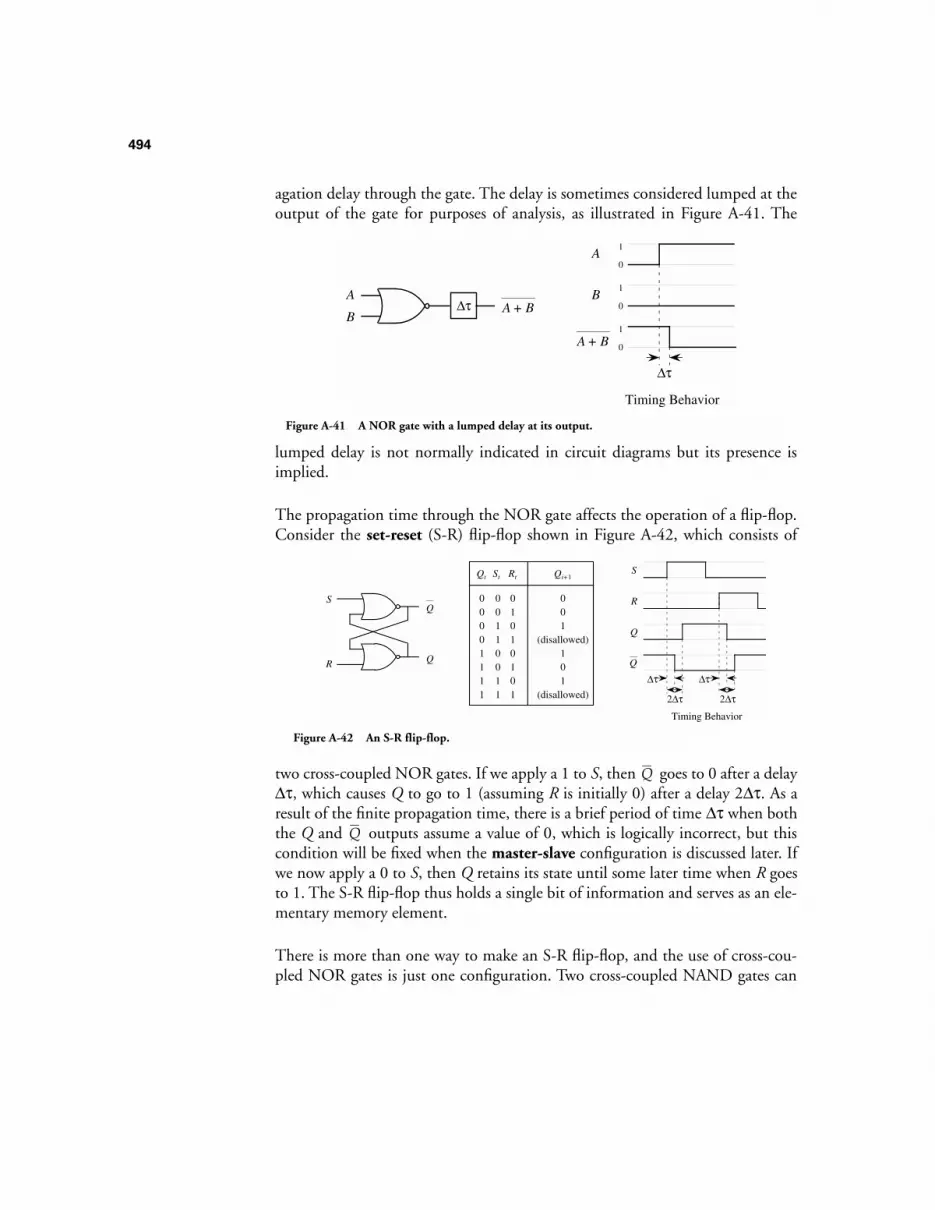
494
agation delay through the gate. The delay is sometimes considered lumped at theoutput of the gate for purposes of analysis, as illustrated in Figure A-41. The
lumped delay is not normally indicated in circuit diagrams but its presence isimplied.
The propagation time through the NOR gate affects the operation of a flip-flop.Consider the set-reset (S-R) flip-flop shown in Figure A-42, which consists of
two cross-coupled NOR gates. If we apply a 1 to S, then goes to 0 after a delay∆τ, which causes Q to go to 1 (assuming R is initially 0) after a delay 2∆τ. As aresult of the finite propagation time, there is a brief period of time ∆τ when boththe Q and outputs assume a value of 0, which is logically incorrect, but thiscondition will be fixed when the master-slave configuration is discussed later. Ifwe now apply a 0 to S, then Q retains its state until some later time when R goesto 1. The S-R flip-flop thus holds a single bit of information and serves as an ele-mentary memory element.
There is more than one way to make an S-R flip-flop, and the use of cross-cou-pled NOR gates is just one configuration. Two cross-coupled NAND gates can
A
B∆τ A + B
Timing Behavior
A + B
A
B
∆τ
0
1
0
1
0
1
Figure A-41 A NOR gate with a lumped delay at its output.
S
R Q
Q
Timing Behavior
Q
S
R
∆τ
Q
2∆τ
∆τ
2∆τ
00110011
01010101
St Rt
00001111
Qt
001
(disallowed)101
(disallowed)
Qi+1
Figure A-42 An S-R flip-flop.
Q
Q

495
also implement an S-R flip-flop, with S = R = 1 being the quiescent state. Makinguse of DeMorgan’s theorem, we can convert the NOR gates of an S-R flip-flopinto AND gates as shown in Figure A-43. By “bubble pushing,” we change the
AND gates into NAND gates, and then reverse the sense of S and R to removethe remaining input bubbles.
A.11.2 THE CLOCKED S-R FLIP-FLOP
Now consider that the inputs to the S-R flip-flop may originate from the outputsof some other circuits, whose inputs may originate from the outputs of other cir-cuits, forming a cascade of logic circuits. This mirrors the form of conventionaldigital circuits. A problem with cascading circuits is that transitions may occur attimes that are not desired.
Consider the circuit shown in Figure A-44. If signals A, B, and C all change from
QS
R Q
QR
S Q
QS
R Q
S
R Q
Q
Figure A-43 A NOR implementation of an S-R flip-flop is converted into a NAND implemen-
tation.
S
R Q
QB
A
C
AB
Timing Behavior
Q
S
R
∆τ
Q
∆τ
2∆τ
A
B
C
ABGlitch caused by a hazard
Figure A-44 A circuit with a hazard.

496
the 0 state to the 1 state, then signal C may reach the XOR gate before A and Bpropagate through the AND gate, which will momentarily produce a 1 output atS, which will revert to 0 when the output of the AND gate settles and is XORedwith C. At this point it may be too late, however, since S may be in the 1 statelong enough to set the flip-flop, destroying the integrity of the stored bit.
When the final state of a flip-flop is sensitive to the relative arrival times of sig-nals, the result may be a glitch, which is an unwanted state or output. A circuitthat can produce a glitch is said to have a hazard. The hazard may or may notmanifest itself as a glitch, depending on the operating conditions of the circuit ata particular time.
In order to achieve synchronization in a controlled fashion, a clock signal is pro-vided, to which every state-dependent circuit (such as a flip-flop) synchronizesitself by accepting inputs only at discrete times. A clock circuit produces a con-tinuous stream of 1’s and 0’s, as indicated by the waveform shown in Figure
A-45. The time required for the clock to rise, then fall, then begin to rise again iscalled the cycle time. The square edges that are shown in the waveform representan ideal square wave. In practice, the edges are rounded because instantaneousrise and fall times do not occur.
The clock rate is taken as the inverse of the cycle time. For a cycle time of 25ns/cycle, the corresponding clock rate is 1/25 cycles/ns, which corresponds to40,000,000 cycles per second, or 40 MHz (for 40 megahertz). A list of otherabbreviations that are commonly used to specify cycle times and clock rates isshown in Table A.2.
We can make use of the clock signal to eliminate the hazard by creating aclocked S-R flip-flop, which is shown in Figure A-46. The symbol CLK labelsthe clock input. Now, S and R cannot change the state of the flip-flop until the
Cycle time = 25ns
Am
plitu
de
Time
Figure A-45 A clock waveform.
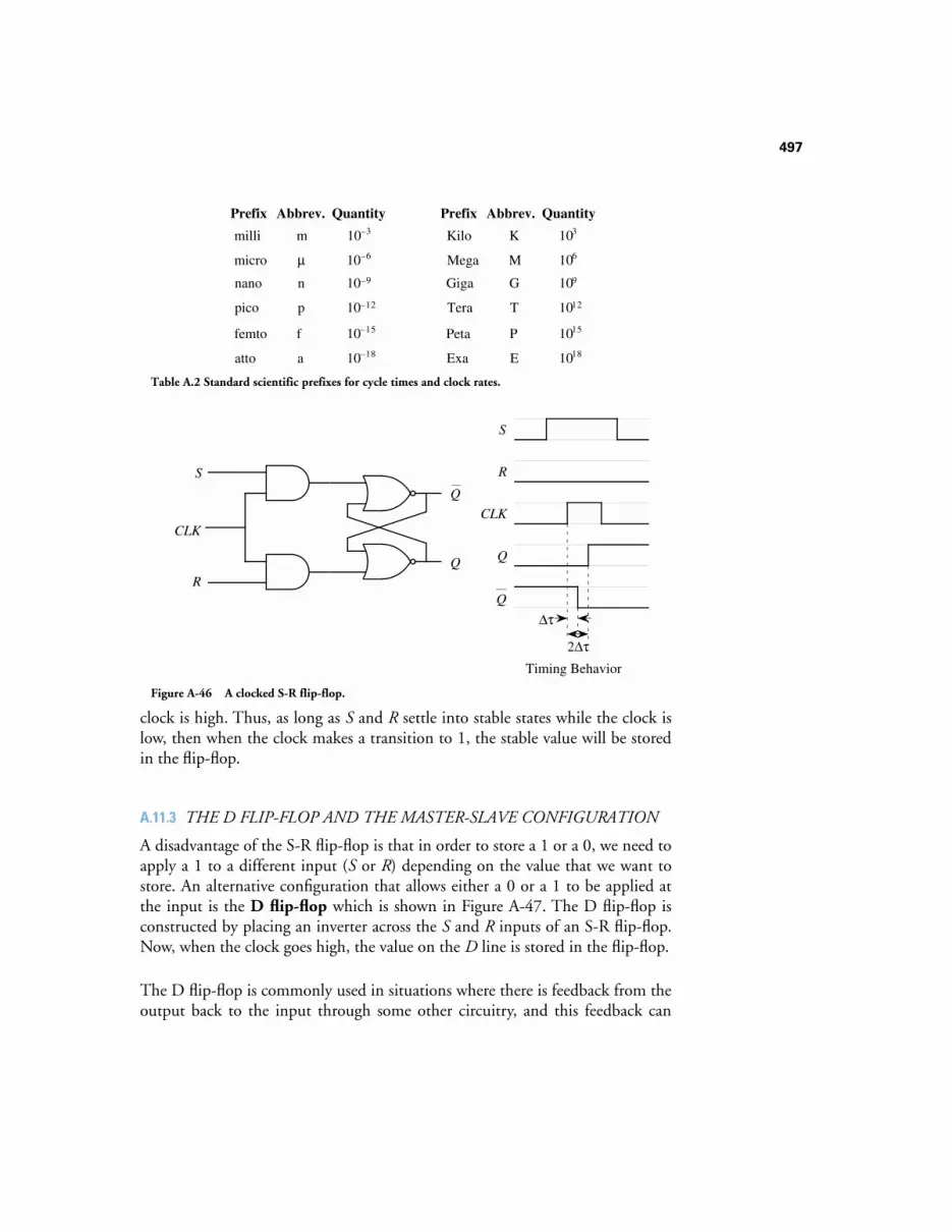
497
clock is high. Thus, as long as S and R settle into stable states while the clock islow, then when the clock makes a transition to 1, the stable value will be storedin the flip-flop.
A.11.3 THE D FLIP-FLOP AND THE MASTER-SLAVE CONFIGURATION
A disadvantage of the S-R flip-flop is that in order to store a 1 or a 0, we need toapply a 1 to a different input (S or R) depending on the value that we want tostore. An alternative configuration that allows either a 0 or a 1 to be applied atthe input is the D flip-flop which is shown in Figure A-47. The D flip-flop isconstructed by placing an inverter across the S and R inputs of an S-R flip-flop.Now, when the clock goes high, the value on the D line is stored in the flip-flop.
The D flip-flop is commonly used in situations where there is feedback from theoutput back to the input through some other circuitry, and this feedback can
m
µ
n
p
f
a
10–3
10–6
10–9
10–12
10–15
10–18
K
M
G
T
P
E
103
106
109
1012
1015
1018
Prefix Abbrev. Quantity
milli
micro
nano
pico
femto
atto
Kilo
Mega
Giga
Tera
Peta
Exa
Prefix Abbrev. Quantity
Table A.2 Standard scientific prefixes for cycle times and clock rates.
Q
Q
S
CLK
R
Timing Behavior
Q
S
R
∆τ
Q
2∆τ
CLK
Figure A-46 A clocked S-R flip-flop.
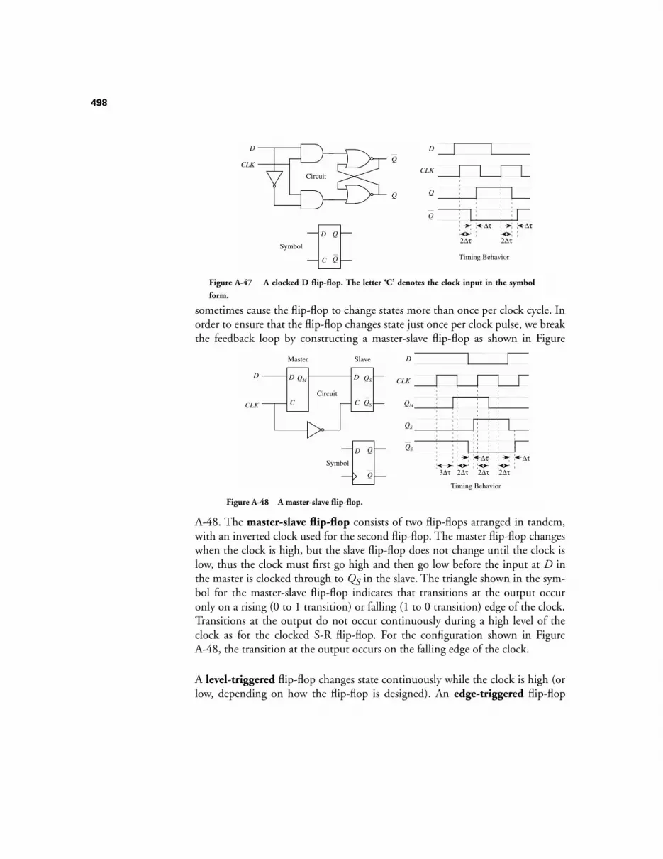
498
sometimes cause the flip-flop to change states more than once per clock cycle. Inorder to ensure that the flip-flop changes state just once per clock pulse, we breakthe feedback loop by constructing a master-slave flip-flop as shown in Figure
A-48. The master-slave flip-flop consists of two flip-flops arranged in tandem,with an inverted clock used for the second flip-flop. The master flip-flop changeswhen the clock is high, but the slave flip-flop does not change until the clock islow, thus the clock must first go high and then go low before the input at D inthe master is clocked through to QS in the slave. The triangle shown in the sym-bol for the master-slave flip-flop indicates that transitions at the output occuronly on a rising (0 to 1 transition) or falling (1 to 0 transition) edge of the clock.Transitions at the output do not occur continuously during a high level of theclock as for the clocked S-R flip-flop. For the configuration shown in FigureA-48, the transition at the output occurs on the falling edge of the clock.
A level-triggered flip-flop changes state continuously while the clock is high (orlow, depending on how the flip-flop is designed). An edge-triggered flip-flop
Q
Q
D
CLK
Circuit
D
Q
Q
C
Symbol
Timing Behavior
Q
D
∆τ
Q
2∆τ
CLK
2∆τ
∆τ
Figure A-47 A clocked D flip-flop. The letter ‘C’ denotes the clock input in the symbol
form.
Symbol
D
Q
Q
Circuit
D
CLK
D QM
C
D
QS
QS
C
Master Slave
Timing Behavior
QS
D
∆τ
QS
2∆τ
CLK
∆τ
2∆τ
QM
3∆τ 2∆τ
Figure A-48 A master-slave flip-flop.
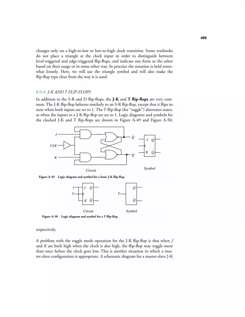
499
changes only on a high-to-low or low-to-high clock transition. Some textbooksdo not place a triangle at the clock input in order to distinguish betweenlevel-triggered and edge-triggered flip-flops, and indicate one form or the otherbased on their usage or in some other way. In practice the notation is held some-what loosely. Here, we will use the triangle symbol and will also make theflip-flop type clear from the way it is used.
A.11.4 J-K AND T FLIP-FLOPS
In addition to the S-R and D flip-flops, the J-K and T flip-flops are very com-mon. The J-K flip-flop behaves similarly to an S-R flip-flop, except that it flips itsstate when both inputs are set to 1. The T flip-flop (for “toggle”) alternates states,as when the inputs to a J-K flip-flop are set to 1. Logic diagrams and symbols forthe clocked J-K and T flip-flops are shown in Figure A-49 and Figure A-50,
respectively.
A problem with the toggle mode operation for the J-K flip-flop is that when Jand K are both high when the clock is also high, the flip-flop may toggle morethan once before the clock goes low. This is another situation in which a mas-ter-slave configuration is appropriate. A schematic diagram for a master-slave J-K
Q
QJ
CLK
J
Q
Q
K
CircuitSymbol
K
Figure A-49 Logic diagram and symbol for a basic J-K flip-flop.
J
Q
Q
K
Circuit
Q
Q
Symbol
1
T T
Figure A-50 Logic diagram and symbol for a T flip-flop.
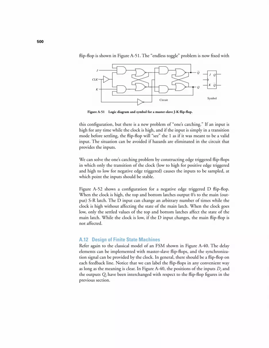
500
flip-flop is shown in Figure A-51. The “endless toggle” problem is now fixed with
this configuration, but there is a new problem of “one’s catching.” If an input ishigh for any time while the clock is high, and if the input is simply in a transitionmode before settling, the flip-flop will “see” the 1 as if it was meant to be a validinput. The situation can be avoided if hazards are eliminated in the circuit thatprovides the inputs.
We can solve the one’s catching problem by constructing edge triggered flip-flopsin which only the transition of the clock (low to high for positive edge triggeredand high to low for negative edge triggered) causes the inputs to be sampled, atwhich point the inputs should be stable.
Figure A-52 shows a configuration for a negative edge triggered D flip-flop.When the clock is high, the top and bottom latches output 0’s to the main (out-put) S-R latch. The D input can change an arbitrary number of times while theclock is high without affecting the state of the main latch. When the clock goeslow, only the settled values of the top and bottom latches affect the state of themain latch. While the clock is low, if the D input changes, the main flip-flop isnot affected.
A.12 Design of Finite State MachinesRefer again to the classical model of an FSM shown in Figure A-40. The delayelements can be implemented with master-slave flip-flops, and the synchroniza-tion signal can be provided by the clock. In general, there should be a flip-flop oneach feedback line. Notice that we can label the flip-flops in any convenient wayas long as the meaning is clear. In Figure A-40, the positions of the inputs Di andthe outputs Qi have been interchanged with respect to the flip-flop figures in theprevious section.
Q
QJ
CLK
J
Q
Q
K
CircuitSymbol
K
Figure A-51 Logic diagram and symbol for a master-slave J-K flip-flop.
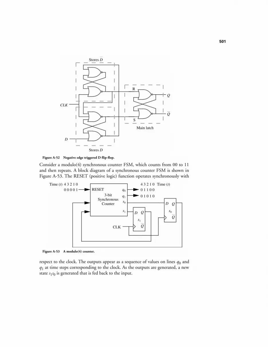
501
Consider a modulo(4) synchronous counter FSM, which counts from 00 to 11and then repeats. A block diagram of a synchronous counter FSM is shown inFigure A-53. The RESET (positive logic) function operates synchronously with
respect to the clock. The outputs appear as a sequence of values on lines q0 andq1 at time steps corresponding to the clock. As the outputs are generated, a newstate s1s0 is generated that is fed back to the input.
Q
Q
CLK
D
R
S
Main latch
Stores D
Stores D
Figure A-52 Negative edge triggered D flip-flop.
3-bit Synchronous
Counter
0 0 0 0 1 0 1 1 0 0RESET q0
4 3 2 1 04 3 2 1 0 Time (t)Time (t)
0 1 0 1 0
D
Q
Q
CLK
s0
s1
D
Q
Q
q1
s0
s1
Figure A-53 A modulo(4) counter.
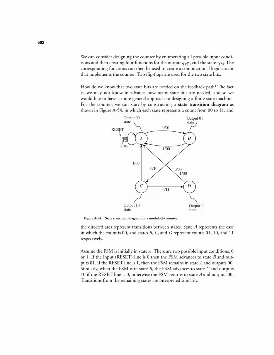
502
We can consider designing the counter by enumerating all possible input condi-tions and then creating four functions for the output q1q0 and the state s1s0. Thecorresponding functions can then be used to create a combinational logic circuitthat implements the counter. Two flip-flops are used for the two state bits.
How do we know that two state bits are needed on the feedback path? The factis, we may not know in advance how many state bits are needed, and so wewould like to have a more general approach to designing a finite state machine.For the counter, we can start by constructing a state transition diagram asshown in Figure A-54, in which each state represents a count from 00 to 11, and
the directed arcs represent transitions between states. State A represents the casein which the count is 00, and states B, C, and D represent counts 01, 10, and 11respectively.
Assume the FSM is initially in state A. There are two possible input conditions: 0or 1. If the input (RESET) line is 0 then the FSM advances to state B and out-puts 01. If the RESET line is 1, then the FSM remains in state A and outputs 00.Similarly, when the FSM is in state B, the FSM advances to state C and outputs10 if the RESET line is 0, otherwise the FSM returns to state A and outputs 00.Transitions from the remaining states are interpreted similarly.
A B1/00
0/01
1/00
Output 00state
Output 01state
RESET
q1
C D
Output 10state
Output 11state
q0
0/101/00
0/00
0/11
1/00
Figure A-54 State transition diagram for a modulo(4) counter.
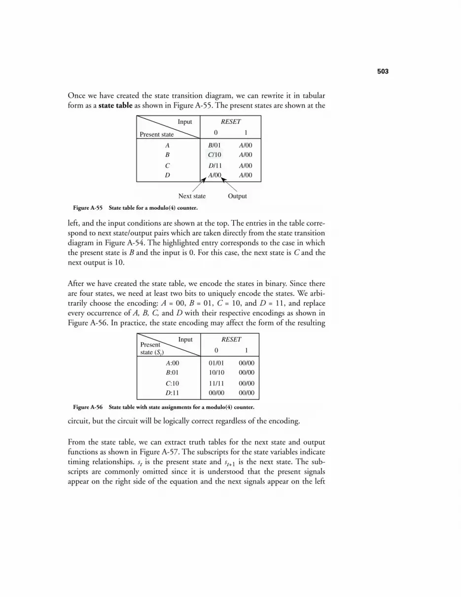
503
Once we have created the state transition diagram, we can rewrite it in tabularform as a state table as shown in Figure A-55. The present states are shown at the
left, and the input conditions are shown at the top. The entries in the table corre-spond to next state/output pairs which are taken directly from the state transitiondiagram in Figure A-54. The highlighted entry corresponds to the case in whichthe present state is B and the input is 0. For this case, the next state is C and thenext output is 10.
After we have created the state table, we encode the states in binary. Since thereare four states, we need at least two bits to uniquely encode the states. We arbi-trarily choose the encoding: A = 00, B = 01, C = 10, and D = 11, and replaceevery occurrence of A, B, C, and D with their respective encodings as shown inFigure A-56. In practice, the state encoding may affect the form of the resulting
circuit, but the circuit will be logically correct regardless of the encoding.
From the state table, we can extract truth tables for the next state and outputfunctions as shown in Figure A-57. The subscripts for the state variables indicatetiming relationships. st is the present state and st+1 is the next state. The sub-scripts are commonly omitted since it is understood that the present signalsappear on the right side of the equation and the next signals appear on the left
Present state
Input RESET
0 1
A B/01 A/00B C/10 A/00
Next state Output
C D/11 A/00D A/00 A/00
Figure A-55 State table for a modulo(4) counter.
Presentstate (St)
Input RESET
0 1
A:00 01/01 00/00B:01 10/10 00/00
C:10 11/11 00/00D:11 00/00 00/00
Figure A-56 State table with state assignments for a modulo(4) counter.
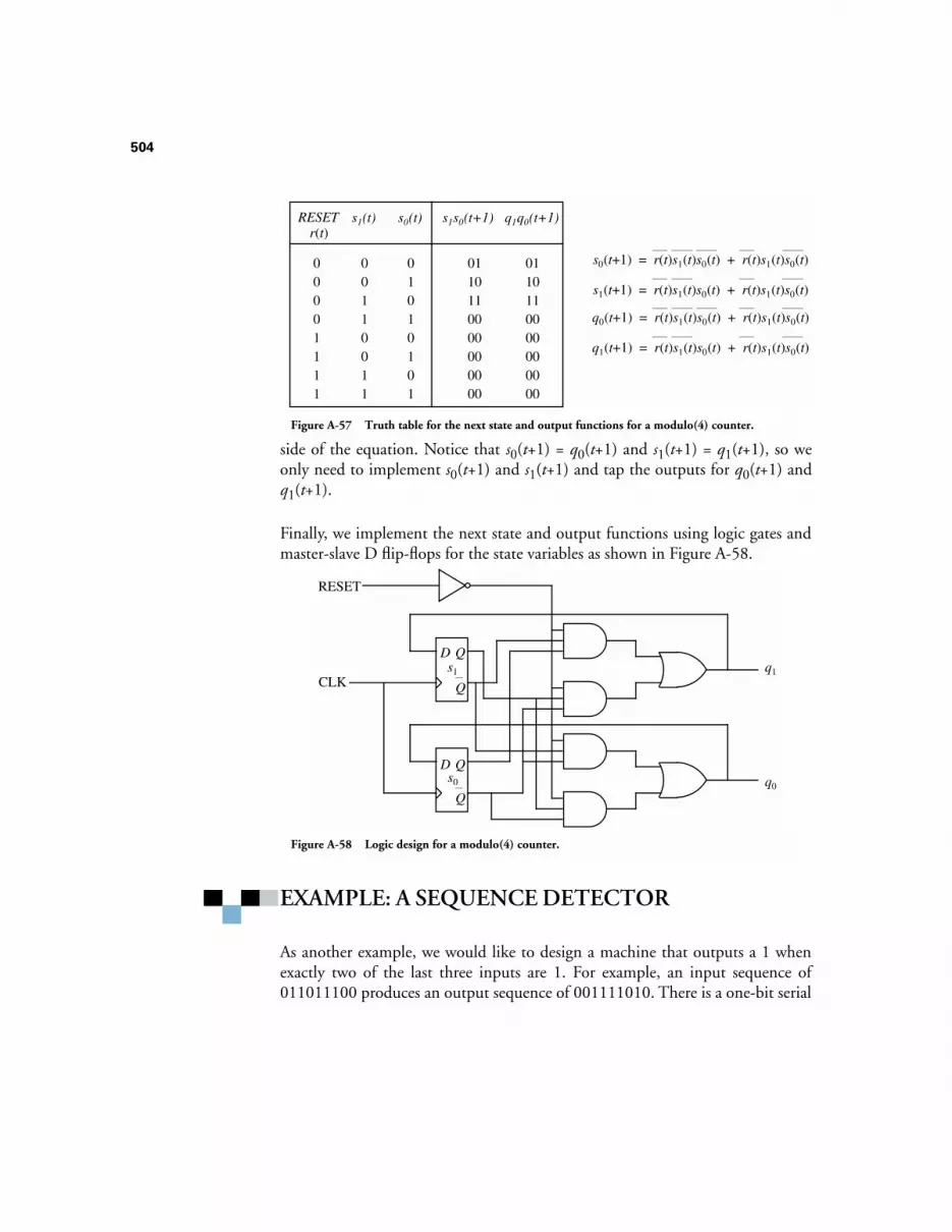
504
side of the equation. Notice that s0(t+1) = q0(t+1) and s1(t+1) = q1(t+1), so weonly need to implement s0(t+1) and s1(t+1) and tap the outputs for q0(t+1) andq1(t+1).
Finally, we implement the next state and output functions using logic gates andmaster-slave D flip-flops for the state variables as shown in Figure A-58.
EXAMPLE: A SEQUENCE DETECTOR
As another example, we would like to design a machine that outputs a 1 whenexactly two of the last three inputs are 1. For example, an input sequence of011011100 produces an output sequence of 001111010. There is a one-bit serial
00110011
01010101
s1(t) s0(t)
00001111
RESET r(t)
0110110000000000
s1s0(t+1)
0110110000000000
q1q0(t+1)
s1(t+1) = r(t)s1(t)s0(t) + r(t)s1(t)s0(t)
s0(t+1) = r(t)s1(t)s0(t) + r(t)s1(t)s0(t)
q1(t+1) = r(t)s1(t)s0(t) + r(t)s1(t)s0(t)
q0(t+1) = r(t)s1(t)s0(t) + r(t)s1(t)s0(t)
Figure A-57 Truth table for the next state and output functions for a modulo(4) counter.
CLK
QD
Q
s1
QD
Q
s0
RESET
q1
q0
Figure A-58 Logic design for a modulo(4) counter.

505
input line, and we can assume that initially no inputs have been seen. For thisproblem, we will use D flip-flops and 8-to-1 MUXes.
We start by constructing a state transition diagram, as shown in Figure A-59.
There are eight possible three-bit sequences that our machine will observe: 000,001, 010, 011, 100, 101, 110, and 111. State A is the initial state, in which weassume that no inputs have yet been seen. In states B and C, we have seen onlyone input, so we cannot output a 1 yet. In states D, E, F, and G we have onlyseen two inputs, so we cannot output a 1 yet, even though we have seen two 1’sat the input when we enter state G. The machine makes all subsequent transi-tions among states D, E, F, and G. State D is visited when the last two inputs are00. States E, F, and G are visited when the last two inputs are 01, 10, or 11,respectively.
The next step is to create a state table as shown in Figure A-60, which is takendirectly from the state transition diagram. Next, we make a state assignment asshown in Figure A-61a. We then use the state assignment to create a truth tablefor the next state and output functions as shown in Figure Figure A-61b. The lasttwo entries in the table correspond to state 111, which cannot arise in practice,
A
B0/0
1/0
C
D
E
F
G
0/0
1/0
0/0
1/0
0/0
1/0
1/0
1/1
0/01/1
0/0
0/1
Figure A-59 State transition diagram for sequence detector.
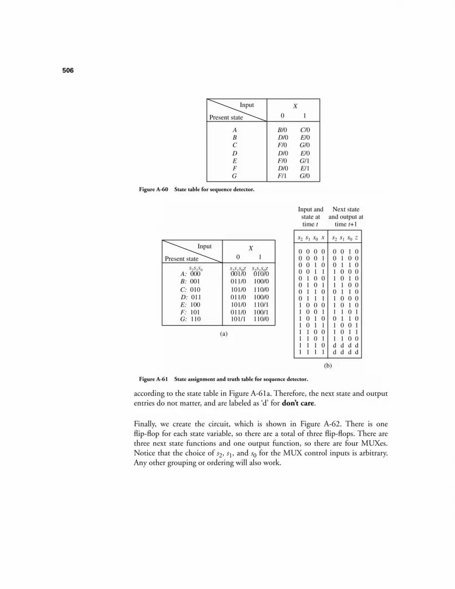
506
according to the state table in Figure A-61a. Therefore, the next state and outputentries do not matter, and are labeled as ‘d’ for don’t care.
Finally, we create the circuit, which is shown in Figure A-62. There is oneflip-flop for each state variable, so there are a total of three flip-flops. There arethree next state functions and one output function, so there are four MUXes.Notice that the choice of s2, s1, and s0 for the MUX control inputs is arbitrary.Any other grouping or ordering will also work.
X
0 1
A B/0 C/0
Present state
Input
BCDE
D/0 E/0F/0 G/0D/0 E/0F/0 G/1
F D/0 E/1G F/1 G/0
Figure A-60 State table for sequence detector.
X0 1
A: 000 001/0 010/0
Present state
Input
B: 001C: 010D: 011E: 100
011/0 100/0101/0 110/0011/0 100/0101/0 110/1
F: 101 011/0 100/1
S2S1S0 S2S1S0Z S2S1S0Z
G: 110 101/1 110/0
(a)
0011001100110011
0101010101010101
s0 x
0000111100001111
s1
00011101110111dd
0000000011111111
s2
(b)
01100110011001dd
10101010101010dd
00000000010110dd
zs0s1s2
Input and state at time t
Next state and output at
time t+1
Figure A-61 State assignment and truth table for sequence detector.
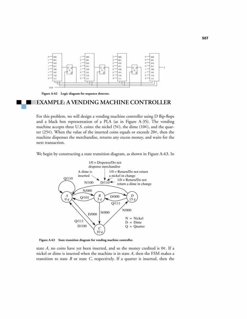
507
EXAMPLE: A VENDING MACHINE CONTROLLER
For this problem, we will design a vending machine controller using D flip-flopsand a black box representation of a PLA (as in Figure A-35). The vendingmachine accepts three U.S. coins: the nickel (5¢), the dime (10¢), and the quar-ter (25¢). When the value of the inserted coins equals or exceeds 20¢, then themachine dispenses the merchandise, returns any excess money, and waits for thenext transaction.
We begin by constructing a state transition diagram, as shown in Figure A-63. In
state A, no coins have yet been inserted, and so the money credited is 0¢. If anickel or dime is inserted when the machine is in state A, then the FSM makes atransition to state B or state C, respectively. If a quarter is inserted, then the
QD
QS2
000
001
010
011
100
101
110
111
0
x
1
x
1
x
1
0
QD
QS1
000
001
010
011
100
101
110
111
x
0
QD
QS0
000
001
010
011
100
101
110
1110
000
001
010
011
100
101
110
111
0
0
0
0
x
0
Z
xx
CLK
x
xx
x
xx
x
xx
xx
xx
xx
xx
xx
xx
x
xx
Figure A-62 Logic diagram for sequence detector.
A B D
C
0 ¢ 5 ¢ 15 ¢
10 ¢
N/000
Q/101
Q/110
N = NickelD = DimeQ = Quarter
N/100 D/110
Q/111
D/000
N/000
D/100Q/111
D/000 N/000
A dime is inserted
1/0 = Dispense/Do not dispense merchandise
1/0 = Return/Do not return a nickel in change
1/0 = Return/Do not return a dime in change
Figure A-63 State transition diagram for vending machine controller.
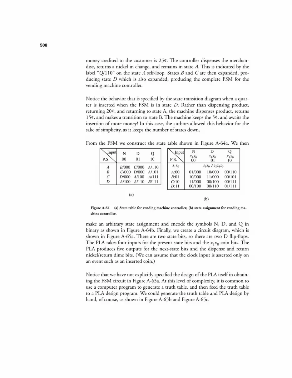
508
money credited to the customer is 25¢. The controller dispenses the merchan-dise, returns a nickel in change, and remains in state A. This is indicated by thelabel “Q/110” on the state A self-loop. States B and C are then expanded, pro-ducing state D which is also expanded, producing the complete FSM for thevending machine controller.
Notice the behavior that is specified by the state transition diagram when a quar-ter is inserted when the FSM is in state D. Rather than dispensing product,returning 20¢, and returning to state A, the machine dispenses product, returns15¢, and makes a transition to state B. The machine keeps the 5¢, and awaits theinsertion of more money! In this case, the authors allowed this behavior for thesake of simplicity, as it keeps the number of states down.
From the FSM we construct the state table shown in Figure A-64a. We then
make an arbitrary state assignment and encode the symbols N, D, and Q inbinary as shown in Figure A-64b. Finally, we create a circuit diagram, which isshown in Figure A-65a. There are two state bits, so there are two D flip-flops.The PLA takes four inputs for the present-state bits and the x1x0 coin bits. ThePLA produces five outputs for the next-state bits and the dispense and returnnickel/return dime bits. (We can assume that the clock input is asserted only onan event such as an inserted coin.)
Notice that we have not explicitly specified the design of the PLA itself in obtain-ing the FSM circuit in Figure A-65a. At this level of complexity, it is common touse a computer program to generate a truth table, and then feed the truth tableto a PLA design program. We could generate the truth table and PLA design byhand, of course, as shown in Figure A-65b and Figure A-65c.
N00 01
A B/000 C/000
P.S.
Input
BCD
C/000 D/000D/000 A/100A/100 A/110
(a)
D10
A/110A/101A/111B/111
Q N
00 01
A:00 01/000 10/000
P.S.
Input
10/000 11/00011/000 00/10000/100 00/110
(b)
D
10
00/11000/10100/11101/111
Q
B:01C:10D:11
s1s0
x1x0 x1x0 x1x0
z2z1z0s1s0 /
Figure A-64 (a) State table for vending machine controller; (b) state assignment for vending ma-
chine controller.
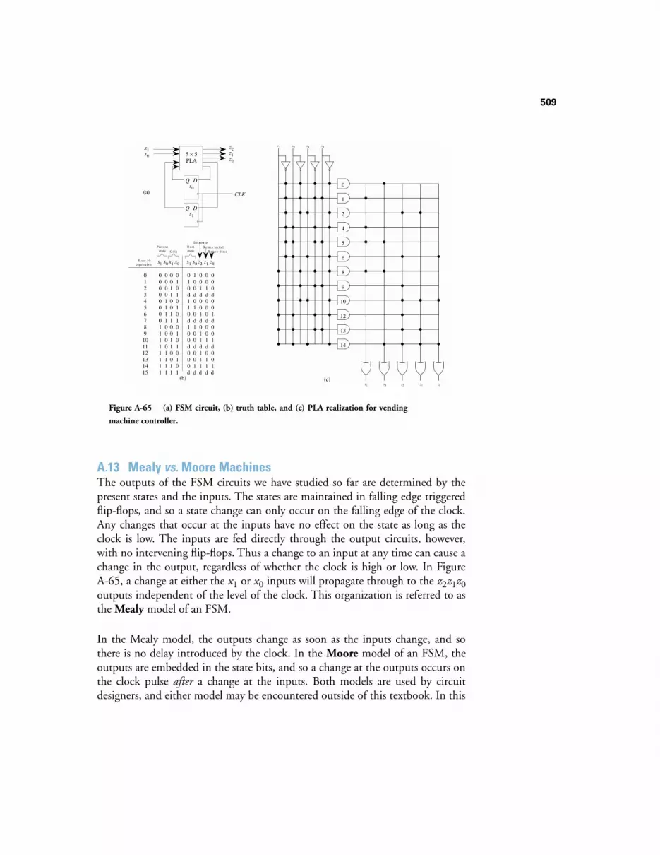
509
A.13 Mealy vs. Moore MachinesThe outputs of the FSM circuits we have studied so far are determined by thepresent states and the inputs. The states are maintained in falling edge triggeredflip-flops, and so a state change can only occur on the falling edge of the clock.Any changes that occur at the inputs have no effect on the state as long as theclock is low. The inputs are fed directly through the output circuits, however,with no intervening flip-flops. Thus a change to an input at any time can cause achange in the output, regardless of whether the clock is high or low. In FigureA-65, a change at either the x1 or x0 inputs will propagate through to the z2z1z0outputs independent of the level of the clock. This organization is referred to asthe Mealy model of an FSM.
In the Mealy model, the outputs change as soon as the inputs change, and sothere is no delay introduced by the clock. In the Moore model of an FSM, theoutputs are embedded in the state bits, and so a change at the outputs occurs onthe clock pulse after a change at the inputs. Both models are used by circuitdesigners, and either model may be encountered outside of this textbook. In this
s1 s0 x1 x0
s1 s0 z2 z1 z0
0
1
2
4
5
6
8
9
10
12
13
14
(c)
5 × 5 PLA
z1z0
x1x0
(a)
DQs0
DQs1
CLK
0000000011111111
0000111100001111
0011001100110011
0101010101010101
100d010d100d001d
001d001d011d111d
001d000d001d011d
000d001d001d001d
0123456789101112131415
s1 s0 x1 x0
Present state Coin
010d110d100d000d
s1 s0 z2 z1 z0
N ext state
D ispenseReturn nickel
Base 10 equivalent
(b)
R eturn dim e
z2
Figure A-65 (a) FSM circuit, (b) truth table, and (c) PLA realization for vending
machine controller.
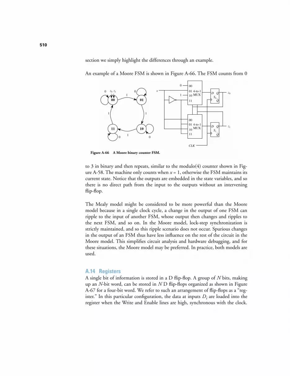
510
section we simply highlight the differences through an example.
An example of a Moore FSM is shown in Figure A-66. The FSM counts from 0
to 3 in binary and then repeats, similar to the modulo(4) counter shown in Fig-ure A-58. The machine only counts when x = 1, otherwise the FSM maintains itscurrent state. Notice that the outputs are embedded in the state variables, and sothere is no direct path from the input to the outputs without an interveningflip-flop.
The Mealy model might be considered to be more powerful than the Mooremodel because in a single clock cycle, a change in the output of one FSM canripple to the input of another FSM, whose output then changes and ripples tothe next FSM, and so on. In the Moore model, lock-step synchronization isstrictly maintained, and so this ripple scenario does not occur. Spurious changesin the output of an FSM thus have less influence on the rest of the circuit in theMoore model. This simplifies circuit analysis and hardware debugging, and forthese situations, the Moore model may be preferred. In practice, both models areused.
A.14 RegistersA single bit of information is stored in a D flip-flop. A group of N bits, makingup an N-bit word, can be stored in N D flip-flops organized as shown in FigureA-67 for a four-bit word. We refer to such an arrangement of flip-flops as a “reg-ister.” In this particular configuration, the data at inputs Di are loaded into theregister when the Write and Enable lines are high, synchronous with the clock.
QD
QS0
QD
QS1
CLK
0
1
00
0110
11
0001
1011
x z0
z1
00 01
11 10
0 0
0 0
1
11
1
z0 z1 4-to-1 MUX
4-to-1 MUX
Figure A-66 A Moore binary counter FSM.
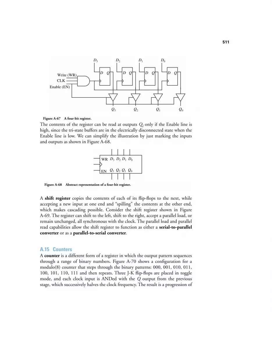
511
The contents of the register can be read at outputs Qi only if the Enable line ishigh, since the tri-state buffers are in the electrically disconnected state when theEnable line is low. We can simplify the illustration by just marking the inputsand outputs as shown in Figure A-68.
A shift register copies the contents of each of its flip-flops to the next, whileaccepting a new input at one end and “spilling” the contents at the other end,which makes cascading possible. Consider the shift register shown in FigureA-69. The register can shift to the left, shift to the right, accept a parallel load, orremain unchanged, all synchronous with the clock. The parallel load and parallelread capabilities allow the shift register to function as either a serial-to-parallelconverter or as a parallel-to-serial converter.
A.15 CountersA counter is a different form of a register in which the output pattern sequencesthrough a range of binary numbers. Figure A-70 shows a configuration for amodulo(8) counter that steps through the binary patterns: 000, 001, 010, 011,100, 101, 110, 111 and then repeats. Three J-K flip-flops are placed in togglemode, and each clock input is ANDed with the Q output from the previousstage, which successively halves the clock frequency. The result is a progression of
QD
D3
Write (WR)
Enable (EN)
Q3
QD
D2
Q2
QD
D1
Q1
QD
D0
Q0
CLK
Figure A-67 A four-bit register.
D3
Q3
D2
Q2
D1
Q1
D0
Q0
WR
EN
Figure A-68 Abstract representation of a four-bit register.
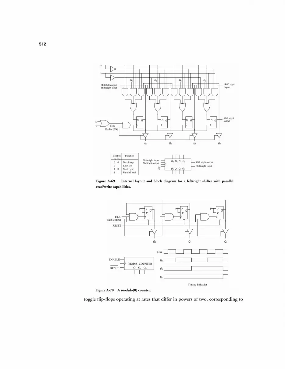
512
toggle flip-flops operating at rates that differ in powers of two, corresponding to
D3
Q3
D2
Q2
D1
Q1
D0
Q0
Shift right inputShift right output
Shift right inputShift left output
c0c1
Control Functionc0c1
0011
0101
No changeShift leftShift rightParallel load
QD
D3
Enable (EN)
Q3
QD
D2
Q2
QD
D1
Q1
QD
D0
Q0
CLK
c0
c1
Shift right input
c0
c1
Shift rightoutput
Shift rightinput
Shift left output
Figure A-69 Internal layout and block diagram for a left/right shifter with parallel
read/write capabilities.
Enable (EN)
QJ
Q2
CLKK
1 QJ
Q1
K
1 QJ
Q0
K
1
RESET
Q2 Q1 Q0
ENABLE
MOD(8) COUNTER
RESET
Timing Behavior
Q0
CLK
Q1
Q2
Figure A-70 A modulo(8) counter.

513
the sequence of binary patterns from 000 to 111.
Notice that we have added an active low asynchronous RESET line to thecounter, which resets it to 000, independent of the states of the clock or enablelines. Except for the flip-flop in the least significant position, the remainingflip-flops change state according to changes in states from their neighbors to theright rather than synchronous with respect to the clock. It is similar in functionto the modulo(4) counter in Figure A-58, but is more easily extended to largesizes because it is not treated like an ordinary FSM for design purposes, in whichall states are enumerated. It is, nevertheless, an FSM.
SUMMARY
In theory, any Boolean function can be represented as a truth table, which canthen be transformed into a two-level Boolean equation and implemented withlogic gates. In practice, collections of logic gates may be grouped together to formMSI components, which contain on the order of a few to a few dozen logic gates.MUXes and PLAs are two types of MSI components that are used for implement-ing functions. Decoders are used for enabling a single output line based on the bitpattern at the input, which translates a logical encoding into a spatial location.There are several other types of MSI components as well. We find ourselves usingMSI components in abstracting away the gate level complexity of a digital circuit.LSI and VLSI circuits abstract away the underlying circuit complexity at higherlevels still.
A finite state machine (FSM) differs from a combinational logic unit (CLU) inthat the outputs of a CLU at any time are strictly a function of the inputs at thattime whereas the outputs of an FSM are a function of its past history of inputs.
Further ReadingShannon’s contributions to switching algebra (Shannon, 1938; Shannon, 1949)are based on the work of (Boole, 1854), and form the basis of switching theory aswe now know it. There is a vast number of contributions to Boolean algebra thatare too great to enumerate here. (Kohavi, 1978) is a good general reference forCLUs and FSMs. A contribution by (Davidson, 1979) covers a method ofdecomposing NAND based circuits, which is of interest because some computers
514
are composed entirely of NAND gates.
(Xilinx, 1992) covers the philosophy and practical aspects of the gate arrayapproach, and describes configurations of the Xilinx line of field programmablegate arrays (FPGAs).
Some texts distinguish between a flip-flop and a latch. (Tanenbaum, 1999) dis-tinguishes between the two by defining a flip-flop to be edge-triggered, whereas alatch is level-triggered. This may be the correct definition, but in practice, theterms are frequently interchanged and any distinction between the two isobscured.
Boole, G., An Investigation of the Laws of Thought, Dover Publications, Inc., NewYork, (1854).
Davidson, E. S., “An algorithm for NAND decomposition under network con-straints,” IEEE Trans. Comp., C-18, (12), 1098, (1979).
Kohavi, Z., Switching and Finite Automata Theory, 2/e, McGraw-Hill, New York,(1978).
Shannon, C. E., “A Symbolic Analysis of Relay and Switching Circuits,” Trans.AIEE, 57, pp. 713-723, (1938).
Shannon, C. E., “The Synthesis of Two-Terminal Switching Circuits,” Bell Sys-tem Technical Journal, 28, pp. 59-98, (1949).
Tanenbaum, A., Structured Computer Organization, 4/e, Prentice Hall, Engle-wood Cliffs, New Jersey, (1999).
Xilinx, The Programmable Gate Array Data Book, Xilinx, Inc., 2100 Logic Drive,San Jose, California, (1992).
PROBLEMSA.1 Figure A-13 shows an OR gate implemented with a NAND gate and
inverters, and Figure A-14 shows inverters implemented with NAND gates.Show the logic diagram for an AND gate implemented entirely with NANDgates.
515
A.2 Draw logic diagrams for each member of the computationally completeset AND, OR, NOT using only the computationally complete set NOR.
A.3 Given the logic circuit shown below, construct a truth table that describesits behavior.
A.4 Construct a truth table for a three-input XOR gate.
A.5 Compute the gate input count of the 4-to-2 priority encoder shown inFigure A-32. Include the inverters in your count.
A.6 Design a circuit that implements function f below using AND, OR, andNOT gates.
A.7 Design a circuit that implements function g below using AND, OR, andNOT gates. Do not attempt to change the form of the equation.
A.8 Are functions f and g shown below equivalent? Show how you arrive atyour answer.
A.9 Write a Boolean equation that describes function F in the circuit shownbelow. Put your answer in SOP form (without parentheses).
A.10 A four-bit comparator is a component that takes two four-bit words asinputs and produces a single bit of output. The output is a 0 if the words areidentical, and is a 1 otherwise. Design a four-bit comparator with any of the
F
C
G
A
B
f A B C, ,( ) ABC ABC ABC+ +=
g A B C D E, , , ,( ) A BC BC+( ) B CD E+( )+=
f A B C, ,( ) ABC ABC+= g A B C, ,( ) A C⊕( )B=
C
FA
B
516
logic gates you have seen in this appendix. Hint: Think of the four-bit com-parator as four one-bit comparators combined in some fashion.
A.11 Redraw the circuit shown below so that the bubble matching is correct.The overbars on the variable and function names indicate active low logic.
A.12 Use two 4-to-1 MUXes to implement the functions:
A.13 Use one 4-to-1 MUX to implement the majority function.
A.14 Use a 2-to-4 decoder and an OR gate to implement the XOR of twoinputs A and B.
A.15 Draw a logic diagram that uses a decoder and two OR gates to implementfunctions F and G below. Be sure to label all lines in your diagram.
A.16 Design a circuit using only 2-to-1 multiplexers that implements the func-tion of an 8-to-1 multiplexer. Show your design in the form of a logic dia-gram, and label all of the lines.
A.17 Since any combinational circuit can be constructed using only two-input
F
x0
x1
x2
x3
x4
Active low
0101
B
0011
A
0110
0001
F1F0
F A B C, ,( ) ABC ABC ABC ABC+ + +=
G A B C, ,( ) ABC ABC+=
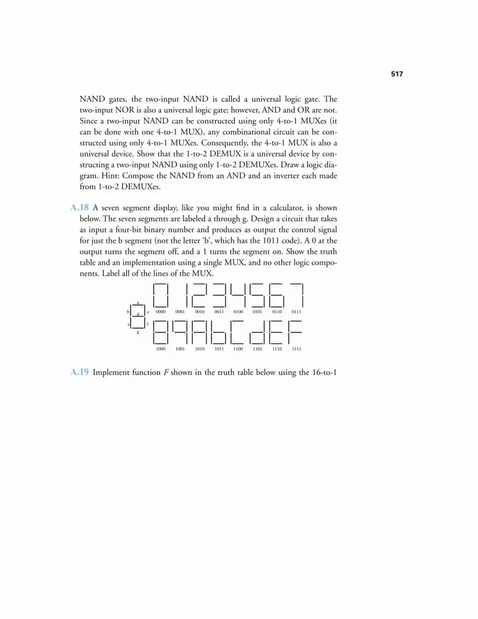
517
NAND gates, the two-input NAND is called a universal logic gate. Thetwo-input NOR is also a universal logic gate; however, AND and OR are not.Since a two-input NAND can be constructed using only 4-to-1 MUXes (itcan be done with one 4-to-1 MUX), any combinational circuit can be con-structed using only 4-to-1 MUXes. Consequently, the 4-to-1 MUX is also auniversal device. Show that the 1-to-2 DEMUX is a universal device by con-structing a two-input NAND using only 1-to-2 DEMUXes. Draw a logic dia-gram. Hint: Compose the NAND from an AND and an inverter each madefrom 1-to-2 DEMUXes.
A.18 A seven segment display, like you might find in a calculator, is shownbelow. The seven segments are labeled a through g. Design a circuit that takesas input a four-bit binary number and produces as output the control signalfor just the b segment (not the letter ‘b’, which has the 1011 code). A 0 at theoutput turns the segment off, and a 1 turns the segment on. Show the truthtable and an implementation using a single MUX, and no other logic compo-nents. Label all of the lines of the MUX.
A.19 Implement function F shown in the truth table below using the 16-to-1
a
b cd
g
e f
0000 0001 0010 0011 0100 0101 0110 0111
1000 1001 1010 1011 1100 1101 1110 1111

518
MUX shown. Label all of the lines, including the unmarked control line.
A.20 A strict encoder takes 2N binary inputs, of which exactly one input is 1 atany time and the remaining inputs are 0, and produces an N-bit coded binaryoutput that indicates which of the N inputs is high. For this problem, create atruth table for a 4-to-2 strict encoder in which there are four inputs: A, B, C,and D, and two outputs: X and Y. A and X are the most significant bits.
A.21 Consider a combinational logic circuit with three inputs a, b, and c, andsix outputs u, v, w, x, y, and z. The input is an unsigned number between 0and 7, and the output is the square of the input. The most significant bit ofthe input is a, and the most significant bit of the output is u. Create a truthtable for the six functions.
A.22 Consider the function f(a, b, c, d) that takes on the value 1 if and only ifthe number of 1’s in b and c is greater than or equal to the number of 1’s in aand d.
(a) Write the truth table for function f.
(b) Use an 8-to-1 multiplexer to implement function f.
A.23 Create a truth table for a single digit ternary (base 3) comparator. The ter-nary inputs are A and B which are each a single ternary digit wide. The outputZ is 0 for A < B, 1 for A = B, and 2 for A > B. Using this truth table as a guide,rewrite the truth table in binary using the assignment (0)3 → (00)2, (1)3 →
00110011
01010101
B C
00001111
A
01100001
F
A C
F
0000000100100011
B
010001010110011110001001101010111100110111101111

519
(01)2, and (2)3 → (10)2.
A.24 Prove the consensus theorem for three variables using perfect induction.
A.25 Use the properties of Boolean algebra to prove DeMorgan’s theorem alge-braically.
A.26 Can an S-R flip-flop be constructed with two cross-coupled XOR gates?Explain your answer.
A.27 Modify the state transition diagram in the Vending Machine example toprovide more realistic behavior (that is, it returns all excess money) when aquarter is inserted in state D.
A.28 Create a state transition diagram for an FSM that sorts two binary wordsA and B, most significant bit first, onto two binary outputs GE and LT. If A isgreater than or equal to B, then A appears on the GE line and B appears on theLT line. If B is greater than A, then B appears on the GE line and A appears onthe LT line.
A.29 Design a circuit that produces a 1 at the Z output when the input Xchanges from 0 to 1 or from 1 to 0, and produces a zero at all other times. Forthe initial state, assume a 0 was last seen at the input. For example, if the inputsequence is 00110 (from left to right), then the output sequence is 00101.Show the state transition diagram, the state table, state assignment, and thefinal circuit using MUXes.
A.30 Design an FSM that outputs a 1 when the last three inputs are 011 or110. Just show the state table. Do not draw a circuit.
A.31 Design a finite state machine that takes two binary words X and Y in serialform, least significant bit (LSB) first, and produces a 1-bit output Z that istrue when X > Y and is 0 for X ≤ Y. When the machine starts, assume that X =Y. That is, Z produces 0’s until X > Y. A sample input sequence and the corre-

520
sponding output sequence are shown below.
A.32 Create a state transition diagram for an FSM that sorts two ternary inputs,most significant digit first, onto two ternary outputs GE and LT. If A is greaterthan or equal to B, then A appears on the GE line and B appears on the LTline, otherwise B appears on the GE line and A appears on the LT line. A sam-ple input/output sequence is shown below. Use the ternary symbols 0, 1, and2 when you label the arcs.
A.33 Create a state transition diagram for a machine that computes an evenparity bit z for its two-bit input x1x0. The machine outputs a 0 when all of theprevious two-bit inputs collectively have an even number of 1’s, and outputs a1 otherwise. For the initial state, assume that the machine starts with evenparity.
A.34 Given the state transition diagram shown below,
(a) Create a state table.
(b) Design a circuit for the state machine described by your state table usingD flip-flop(s), a single decoder, and OR gates. For the state assignment, usethe bit pattern that corresponds to the position of each letter in the alphabet,starting from 0. For example, A is at position 0, so the state assignment is 000;
Serialcomparator
X
Y
Z1 0 1 1 0
1 1 1 0 00 0 1 1 0
Input B: 0 2 1 2 0 2 1 1
Output LT: 0 2 1 1 2 0 1 2Time: 0 1 2 3 4 5 6 7
Input A: 0 2 1 1 2 0 1 2
Output GE: 0 2 1 2 0 2 1 1
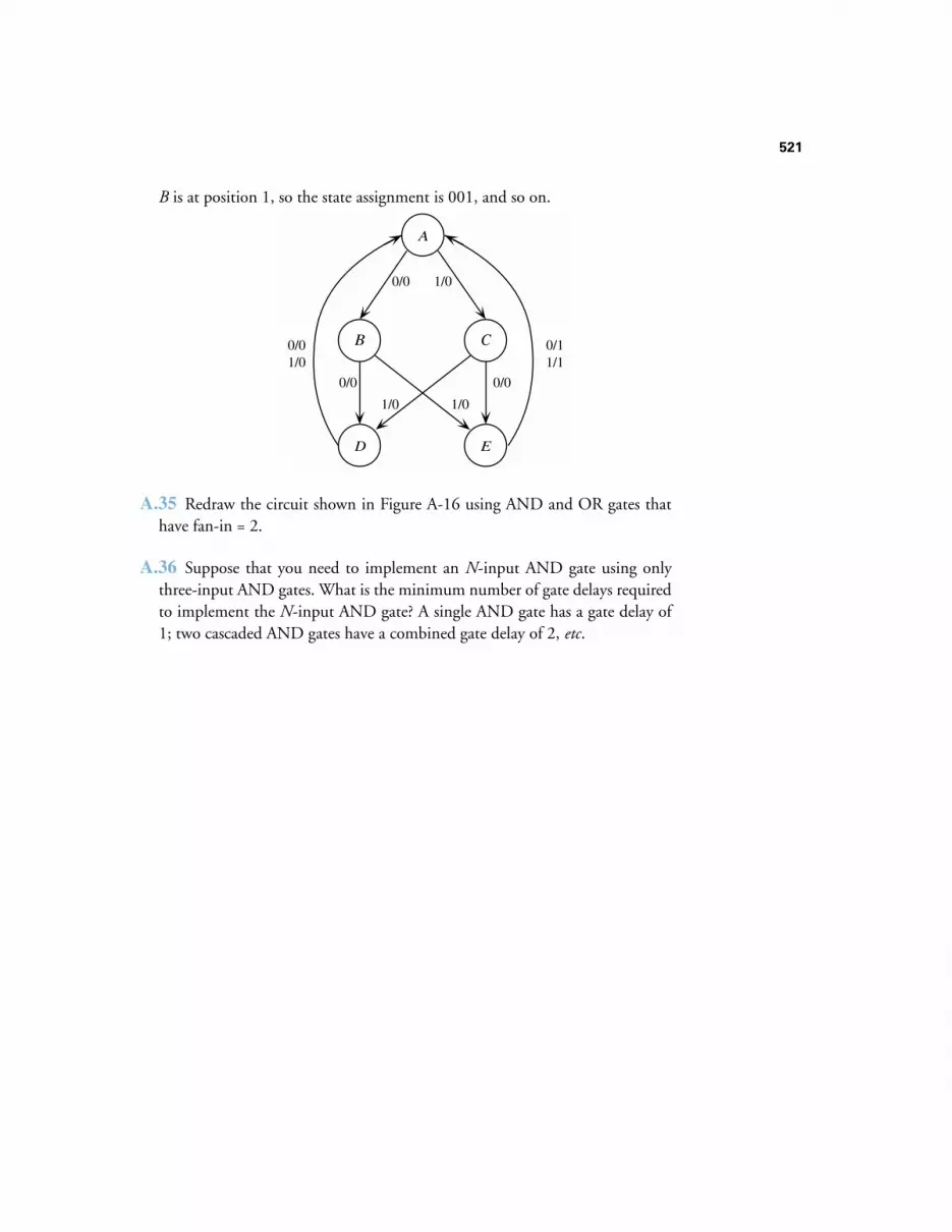
521
B is at position 1, so the state assignment is 001, and so on.
A.35 Redraw the circuit shown in Figure A-16 using AND and OR gates thathave fan-in = 2.
A.36 Suppose that you need to implement an N-input AND gate using onlythree-input AND gates. What is the minimum number of gate delays requiredto implement the N-input AND gate? A single AND gate has a gate delay of1; two cascaded AND gates have a combined gate delay of 2, etc.
0/0
A
B C
D E
1/0
0/0 0/0
1/0 1/0
0/01/0
0/11/1

522
523
APPENDIX B: REDUCTION OF DIGITAL LOGIC
B.1 Reduction of Combinational Logic and Sequential Logic
In Appendix A, we focused primarily on the functional correctness of digitallogic circuits. Only a small amount of consideration was given to the possibilitythat there may be more than one way to design a circuit, with some designs beingbetter than others in terms of component count (that is, the numbers and sizes ofthe logic gates.)
In this appendix, we take a systematic approach to reducing the numbers of com-ponents in a design. We first look at reducing the sizes of combinational logicexpressions, which loosely correspond to the numbers and sizes of the logic gatesin an implementation of a digital circuit. We then look at reducing the numbersof states in finite state machines (FSMs), and explore a few areas of FSM designthat impact the numbers and sizes of logic gates in implementations of FSMs.
B.2 Reduction of Two-Level Expressions
It many cases the canonical
sum-of-products
(SOP) or
product-of-sums
(POS)forms are not minimal in terms of their number and size. Since a smaller Booleanequation translates to a lower gate input count in the target circuit, reduction ofthe equation is an important consideration when circuit complexity is an issue.
Three methods of reducing Boolean equations are described in the sections thatfollow:
algebraic reduction
,
Karnaugh map (K-Map) reduction
, and
tabularreduction
. The algebraic method forms the basis for the other two methods. It isalso the most abstract method, relying as it does on only the theorems of Booleanalgebra.
The K-map and tabular methods are in fact pencil-and-paper implementations
B
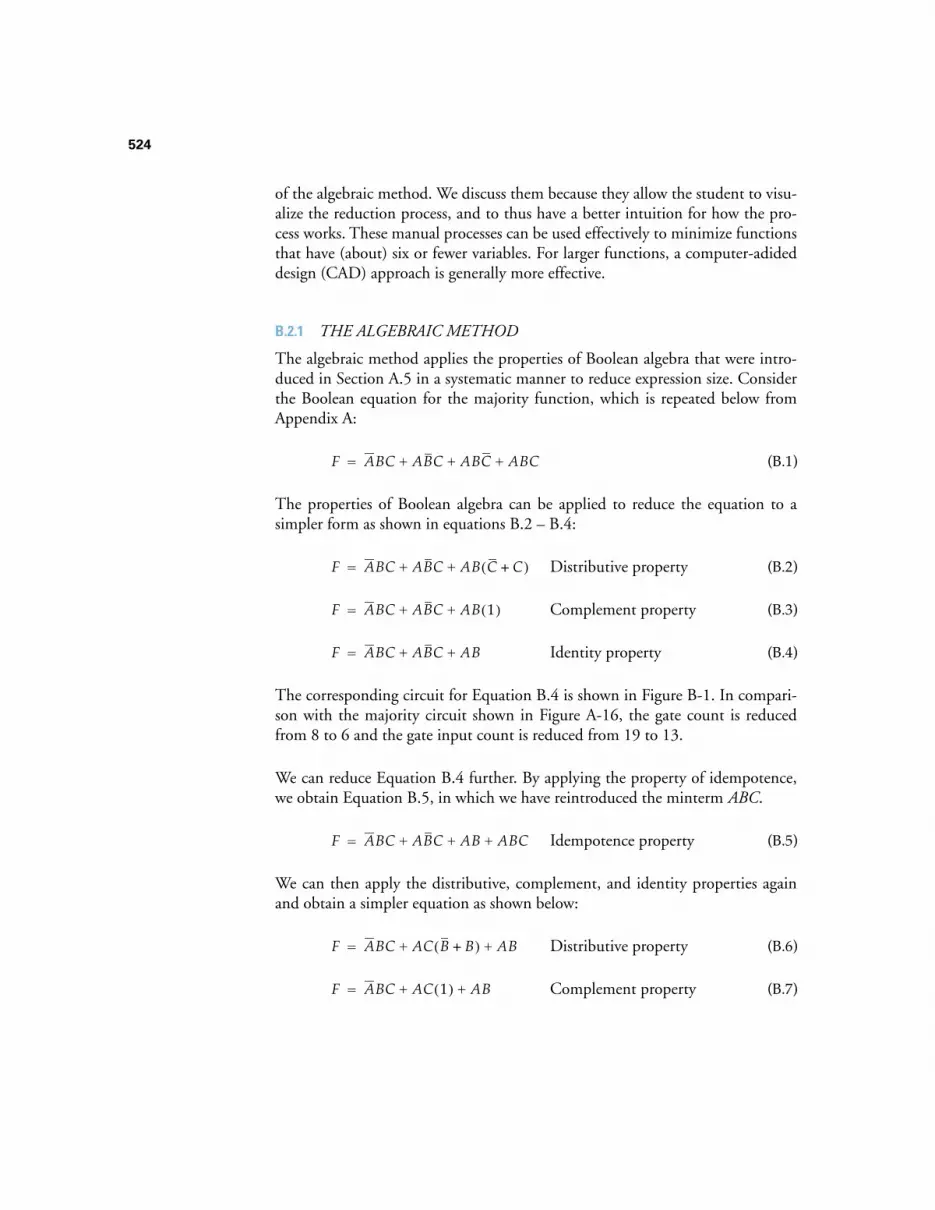
524
of the algebraic method. We discuss them because they allow the student to visu-alize the reduction process, and to thus have a better intuition for how the pro-cess works. These manual processes can be used effectively to minimize functionsthat have (about) six or fewer variables. For larger functions, a computer-adideddesign (CAD) approach is generally more effective.
B.2.1
THE ALGEBRAIC METHOD
The algebraic method applies the properties of Boolean algebra that were intro-duced in Section A.5 in a systematic manner to reduce expression size. Considerthe Boolean equation for the majority function, which is repeated below fromAppendix A:
(B.1)
The properties of Boolean algebra can be applied to reduce the equation to asimpler form as shown in equations B.2 – B.4:
Distributive property
(B.2)
Complement property
(B.3)
Identity property
(B.4)
The corresponding circuit for Equation B.4 is shown in Figure B-1. In compari-son with the majority circuit shown in Figure A-16, the gate count is reducedfrom 8 to 6 and the gate input count is reduced from 19 to 13.
We can reduce Equation B.4 further. By applying the property of idempotence,we obtain Equation B.5, in which we have reintroduced the minterm
ABC
.
Idempotence property
(B.5)
We can then apply the distributive, complement, and identity properties againand obtain a simpler equation as shown below:
Distributive property
(B.6)
Complement property
(B.7)
F ABC ABC ABC ABC+ + +=
F ABC ABC AB C C+( )+ +=
F ABC ABC AB 1( )+ +=
F ABC ABC AB+ +=
F ABC ABC AB ABC+ + +=
F ABC AC B B+( ) AB+ +=
F ABC AC 1( ) AB+ +=
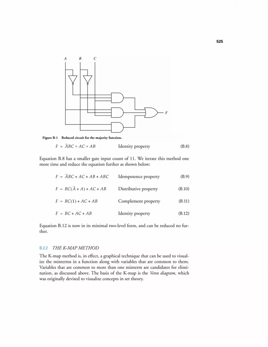
525
Identity property
(B.8)
Equation B.8 has a smaller gate input count of 11. We iterate this method onemore time and reduce the equation further as shown below:
Idempotence property
(B.9)
Distributive property
(B.10)
Complement property
(B.11)
Identity property
(B.12)
Equation B.12 is now in its minimal two-level form, and can be reduced no fur-ther.
B.2.2
THE K-MAP METHOD
The K-map method is, in effect, a graphical technique that can be used to visual-ize the minterms in a function along with variables that are common to them.Variables that are common to more than one minterm are candidates for elimi-nation, as discussed above. The basis of the K-map is the
Venn diagram
, whichwas originally devised to visualize concepts in set theory.
F
A CB
Figure B-1 Reduced circuit for the majority function.
F ABC AC AB+ +=
F ABC AC AB ABC+ + +=
F BC A A+( ) AC AB+ +=
F BC 1( ) AC AB+ +=
F BC AC AB+ +=
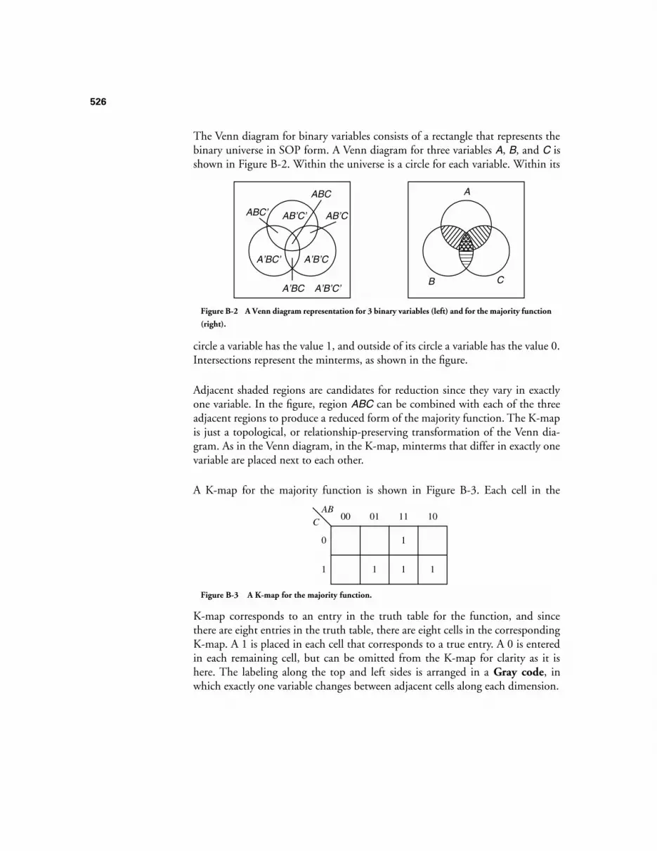
526
The Venn diagram for binary variables consists of a rectangle that represents thebinary universe in SOP form. A Venn diagram for three variables
A
,
B
, and
C
isshown in Figure B-2. Within the universe is a circle for each variable. Within its
circle a variable has the value 1, and outside of its circle a variable has the value 0.Intersections represent the minterms, as shown in the figure.
Adjacent shaded regions are candidates for reduction since they vary in exactlyone variable. In the figure, region
ABC
can be combined with each of the threeadjacent regions to produce a reduced form of the majority function. The K-mapis just a topological, or relationship-preserving transformation of the Venn dia-gram. As in the Venn diagram, in the K-map, minterms that differ in exactly onevariable are placed next to each other.
A K-map for the majority function is shown in Figure B-3. Each cell in the
K-map corresponds to an entry in the truth table for the function, and sincethere are eight entries in the truth table, there are eight cells in the correspondingK-map. A 1 is placed in each cell that corresponds to a true entry. A 0 is enteredin each remaining cell, but can be omitted from the K-map for clarity as it ishere. The labeling along the top and left sides is arranged in a
Gray code
, inwhich exactly one variable changes between adjacent cells along each dimension.
ABC
ABC’ AB’CAB’C’
A’BC
A’BC’ A’B’C
A’B’C’B
A
C
Figure B-2 A Venn diagram representation for 3 binary variables (left) and for the majority function
(right).
00 01 11 10
0
1
ABC
1
11 1
Figure B-3 A K-map for the majority function.
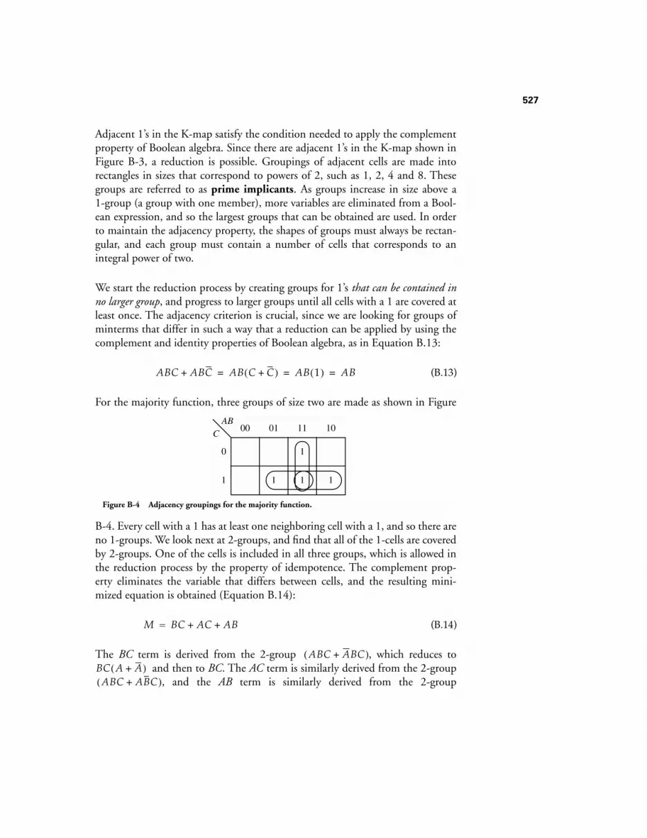
527
Adjacent 1’s in the K-map satisfy the condition needed to apply the complementproperty of Boolean algebra. Since there are adjacent 1’s in the K-map shown inFigure B-3, a reduction is possible. Groupings of adjacent cells are made intorectangles in sizes that correspond to powers of 2, such as 1, 2, 4 and 8. Thesegroups are referred to as
prime implicants
. As groups increase in size above a1-group (a group with one member), more variables are eliminated from a Bool-ean expression, and so the largest groups that can be obtained are used. In orderto maintain the adjacency property, the shapes of groups must always be rectan-gular, and each group must contain a number of cells that corresponds to anintegral power of two.
We start the reduction process by creating groups for 1’s
that can be contained inno larger group
, and progress to larger groups until all cells with a 1 are covered atleast once. The adjacency criterion is crucial, since we are looking for groups ofminterms that differ in such a way that a reduction can be applied by using thecomplement and identity properties of Boolean algebra, as in Equation B.13:
(B.13)
For the majority function, three groups of size two are made as shown in Figure
B-4. Every cell with a 1 has at least one neighboring cell with a 1, and so there areno 1-groups. We look next at 2-groups, and find that all of the 1-cells are coveredby 2-groups. One of the cells is included in all three groups, which is allowed inthe reduction process by the property of idempotence. The complement prop-erty eliminates the variable that differs between cells, and the resulting mini-mized equation is obtained (Equation B.14):
(B.14)
The
BC
term is derived from the 2-group , which reduces to and then to
BC
. The
AC
term is similarly derived from the 2-group, and the
AB
term is similarly derived from the 2-group
ABC ABC+ AB C C+( ) AB 1( ) AB= = =
00 01 11 10
0
1
ABC
1
11 1
Figure B-4 Adjacency groupings for the majority function.
M BC AC AB+ +=
ABC ABC+( )BC A A+( )ABC ABC+( )
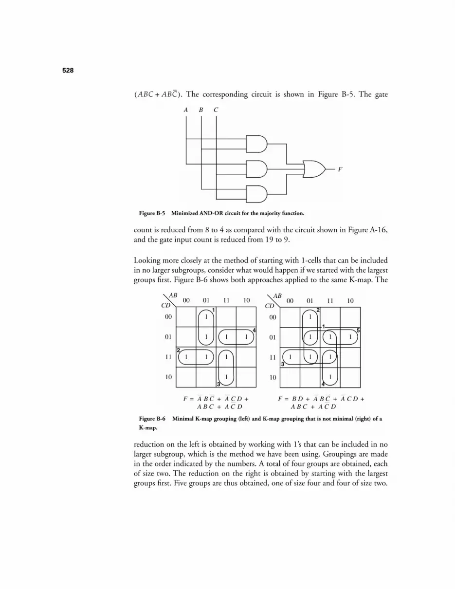
528
. The corresponding circuit is shown in Figure B-5. The gate
count is reduced from 8 to 4 as compared with the circuit shown in Figure A-16,and the gate input count is reduced from 19 to 9.
Looking more closely at the method of starting with 1-cells that can be includedin no larger subgroups, consider what would happen if we started with the largestgroups first. Figure B-6 shows both approaches applied to the same K-map. The
reduction on the left is obtained by working with 1’s that can be included in nolarger subgroup, which is the method we have been using. Groupings are madein the order indicated by the numbers. A total of four groups are obtained, eachof size two. The reduction on the right is obtained by starting with the largestgroups first. Five groups are thus obtained, one of size four and four of size two.
ABC ABC+( )
F
A B C
Figure B-5 Minimized AND-OR circuit for the majority function.
00 01 11
1
01
11
11
10AB
1
CD
10
00
01 11
01
11
10CD
10
00
00AB
1
1
1
1
1
2
3
4
1
11
1
1
1
1
1
2
4
51
F = A B C + A C D + A B C + A C D
F = B D + A B C + A C D + A B C + A C D
3
Figure B-6 Minimal K-map grouping (left) and K-map grouping that is not minimal (right) of a
K-map.
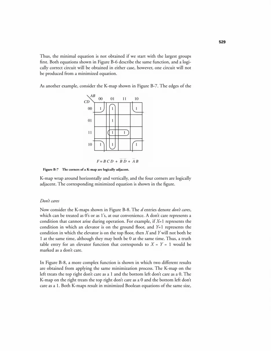
529
Thus, the minimal equation is not obtained if we start with the largest groupsfirst. Both equations shown in Figure B-6 describe the same function, and a logi-cally correct circuit will be obtained in either case, however, one circuit will notbe produced from a minimized equation.
As another example, consider the K-map shown in Figure B-7. The edges of the
K-map wrap around horizontally and vertically, and the four corners are logicallyadjacent. The corresponding minimized equation is shown in the figure.
Don’t cares
Now consider the K-maps shown in Figure B-8. The
d
entries denote
don’t cares
,which can be treated as 0’s or as 1’s, at our convenience. A don’t care represents acondition that cannot arise during operation. For example, if
X
=1 represents thecondition in which an elevator is on the ground floor, and
Y
=1 represents thecondition in which the elevator is on the top floor, then
X
and
Y
will not both be1 at the same time, although they may both be 0 at the same time. Thus, a truthtable entry for an elevator function that corresponds to
X
=
Y
= 1 would bemarked as a don’t care.
In Figure B-8, a more complex function is shown in which two different resultsare obtained from applying the same minimization process. The K-map on theleft treats the top right don’t care as a 1 and the bottom left don’t care as a 0. TheK-map on the right treats the top right don’t care as a 0 and the bottom left don’tcare as a 1. Both K-maps result in minimized Boolean equations of the same size,
00 01 11
1
1
1
01
11
1
1
1
1
1
10AB
1
CD
00
10
F = B C D + B D + A B
Figure B-7 The corners of a K-map are logically adjacent.
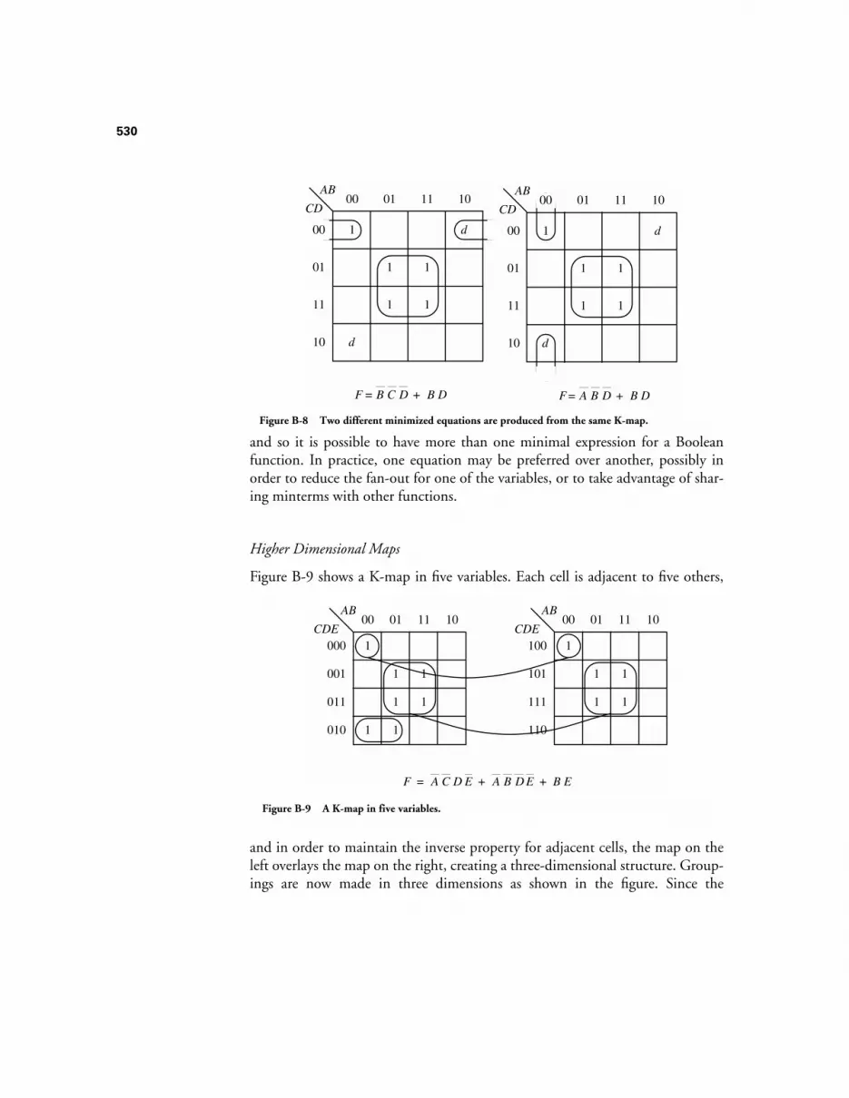
530
and so it is possible to have more than one minimal expression for a Booleanfunction. In practice, one equation may be preferred over another, possibly inorder to reduce the fan-out for one of the variables, or to take advantage of shar-ing minterms with other functions.
Higher Dimensional Maps
Figure B-9 shows a K-map in five variables. Each cell is adjacent to five others,
and in order to maintain the inverse property for adjacent cells, the map on theleft overlays the map on the right, creating a three-dimensional structure. Group-ings are now made in three dimensions as shown in the figure. Since the
00 01 11
1
01
11
11
10AB
1
CD
10 d
00 d
F = B C D + B D
01 11
1
01
11
11
10
1
CD
10 d
00 d
00AB
F = A B D + B D
1 1
Figure B-8 Two different minimized equations are produced from the same K-map.
01 11
001
011
10CDE
010
000
00AB
01 11
101
111
10CDE
110
100
00AB
1 1
1 1
1 11 1
1 1
11
F = A C D E + A B D E + B E
Figure B-9 A K-map in five variables.
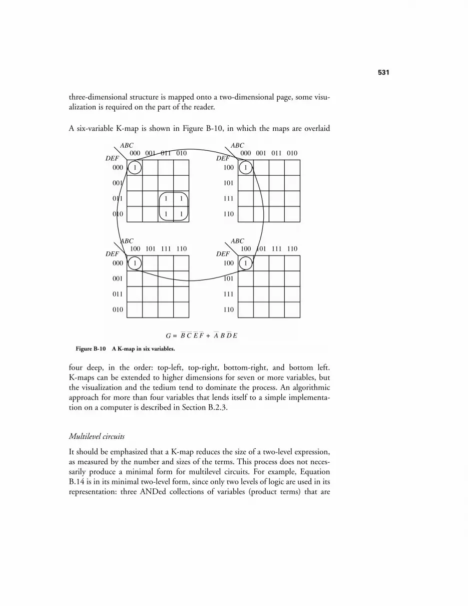
531
three-dimensional structure is mapped onto a two-dimensional page, some visu-alization is required on the part of the reader.
A six-variable K-map is shown in Figure B-10, in which the maps are overlaid
four deep, in the order: top-left, top-right, bottom-right, and bottom left.K-maps can be extended to higher dimensions for seven or more variables, butthe visualization and the tedium tend to dominate the process. An algorithmicapproach for more than four variables that lends itself to a simple implementa-tion on a computer is described in Section B.2.3.
Multilevel circuits
It should be emphasized that a K-map reduces the size of a two-level expression,as measured by the number and sizes of the terms. This process does not neces-sarily produce a minimal form for multilevel circuits. For example, EquationB.14 is in its minimal two-level form, since only two levels of logic are used in itsrepresentation: three ANDed collections of variables (product terms) that are
001 011
001
011
010DEF
010
000
000ABC
001 011
101
111
010DEF
110
100
000ABC
101 111
001
011
110DEF
010
000
100ABC
101 111
101
111
110DEF
110
100
100ABC
1
11
1
1
1 1
1
G = B C E F + A B D E
Figure B-10 A K-map in six variables.
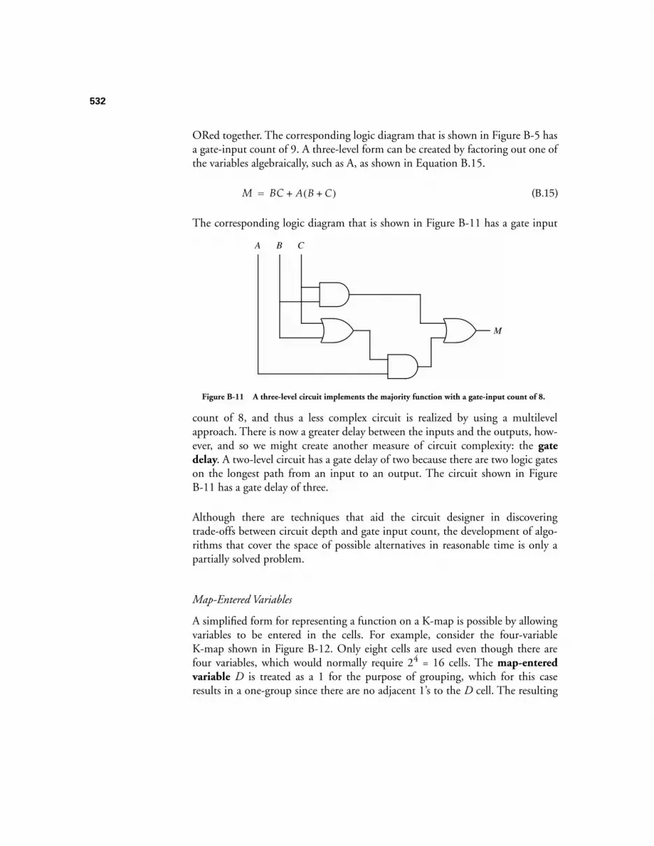
532
ORed together. The corresponding logic diagram that is shown in Figure B-5 hasa gate-input count of 9. A three-level form can be created by factoring out one ofthe variables algebraically, such as A, as shown in Equation B.15.
(B.15)
The corresponding logic diagram that is shown in Figure B-11 has a gate input
count of 8, and thus a less complex circuit is realized by using a multilevelapproach. There is now a greater delay between the inputs and the outputs, how-ever, and so we might create another measure of circuit complexity: the
gatedelay. A two-level circuit has a gate delay of two because there are two logic gateson the longest path from an input to an output. The circuit shown in FigureB-11 has a gate delay of three.
Although there are techniques that aid the circuit designer in discoveringtrade-offs between circuit depth and gate input count, the development of algo-rithms that cover the space of possible alternatives in reasonable time is only apartially solved problem.
Map-Entered Variables
A simplified form for representing a function on a K-map is possible by allowingvariables to be entered in the cells. For example, consider the four-variableK-map shown in Figure B-12. Only eight cells are used even though there arefour variables, which would normally require 24 = 16 cells. The map-enteredvariable D is treated as a 1 for the purpose of grouping, which for this caseresults in a one-group since there are no adjacent 1’s to the D cell. The resulting
M BC A B C+( )+=
M
A B C
Figure B-11 A three-level circuit implements the majority function with a gate-input count of 8.
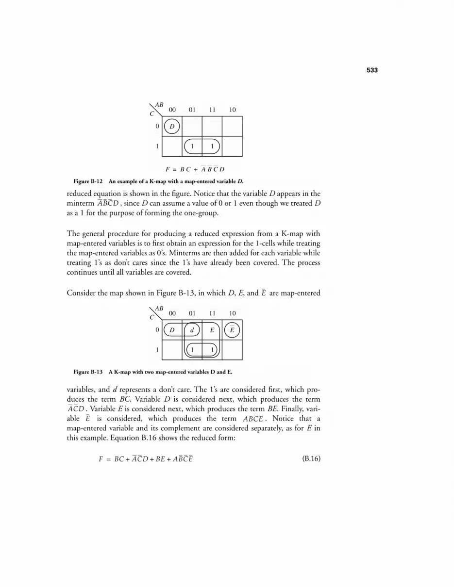
533
reduced equation is shown in the figure. Notice that the variable D appears in theminterm , since D can assume a value of 0 or 1 even though we treated Das a 1 for the purpose of forming the one-group.
The general procedure for producing a reduced expression from a K-map withmap-entered variables is to first obtain an expression for the 1-cells while treatingthe map-entered variables as 0’s. Minterms are then added for each variable whiletreating 1’s as don’t cares since the 1’s have already been covered. The processcontinues until all variables are covered.
Consider the map shown in Figure B-13, in which D, E, and are map-entered
variables, and d represents a don’t care. The 1’s are considered first, which pro-duces the term BC. Variable D is considered next, which produces the term
. Variable E is considered next, which produces the term BE. Finally, vari-able is considered, which produces the term . Notice that amap-entered variable and its complement are considered separately, as for E inthis example. Equation B.16 shows the reduced form:
(B.16)
00 01 11 10
0
1
ABC
11
D
F = B C + A B C D
Figure B-12 An example of a K-map with a map-entered variable D.
ABCD
00 01 11 10
0
1
ABC
11
D d E E
Figure B-13 A K-map with two map-entered variables D and E.
E
ACDE ABCE
F BC ACD BE ABCE+ + +=

534
B.2.3 THE TABULAR METHOD
An automated approach to reducing Boolean expressions is commonly used forsingle and multiple output functions. The tabular method, also known as theQuine-McCluskey method, successively forms Boolean cross products amonggroups of terms that differ in one variable, and then uses the smallest set ofreduced terms to cover the functions. This process is easier than the map methodto implement on a computer, and an extension of the method allows terms to beshared among functions.
Reduction of Single Functions
The truth table shown in Figure B-14 describes a function F in four variables A,
B, C, and D, and includes three don’t cares. The tabular reduction process beginsby grouping minterms for which F is nonzero according to the number of 1’s ineach minterm. Don’t care conditions are considered to be nonzero for this pro-cess. Minterm 0000 contains no 1’s and is in its own group, as shown in FigureB-15a. Minterms 0001, 0010, 0100, and 1000 all contain a single 1, but onlyminterm 0001 has a nonzero entry and so it forms another group.
The next group has two 1’s in each minterm, and there are six possible minterms
0011001100110011
0101010101010101
C D
0000111100001111
B
d1010111001d010d
F
0000000011111111
A
Figure B-14 A truth table representation of a function with don’t cares.
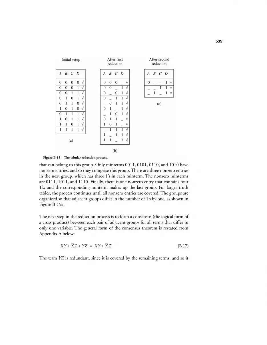
535
that can belong to this group. Only minterms 0011, 0101, 0110, and 1010 havenonzero entries, and so they comprise this group. There are three nonzero entriesin the next group, which has three 1’s in each minterm. The nonzero mintermsare 0111, 1011, and 1110. Finally, there is one nonzero entry that contains four1’s, and the corresponding minterm makes up the last group. For larger truthtables, the process continues until all nonzero entries are covered. The groups areorganized so that adjacent groups differ in the number of 1’s by one, as shown inFigure B-15a.
The next step in the reduction process is to form a consensus (the logical form ofa cross product) between each pair of adjacent groups for all terms that differ inonly one variable. The general form of the consensus theorem is restated fromAppendix A below:
(B.17)
The term YZ is redundant, since it is covered by the remaining terms, and so it
0010111101
0111001111
C D
0001101011
B
0000010111
A
√√√√√√√√√√
0_011_01111_
_111111__111
C D
00__011101_1
B
0000_0_01_11
A
*√√√√ √√ **√√√
_1_
111
C D
__1
B
0__
A
***
Initial setup After firstreduction
After secondreduction
(a)
(b)
(c)
Figure B-15 The tabular reduction process.
XY XZ YZ+ + XY XZ+=

536
can be eliminated. Algebraically, we can prove the theorem as shown below:
The consensus theorem also has a dual form:
(B.18)
The idea of applying consensus in tabular reduction is to take advantage of theinverse property of Boolean algebra, similar to the way we did for K-maps in theprevious section. For example, 0000 and 0001 differ in variable D, so 000_ islisted at the top of the reduced table shown in Figure B-15b. The underscoremarks the position of the variable that has been eliminated, which is D for thiscase. Minterms 0000 and 0001 in Figure B-15a are marked with checks to indi-cate that they are now covered in the reduced table.
After every term in the first group is crossed with every term in the second group,we then move on to form a consensus between terms in the second and thirdgroups. Note that it is possible that some terms cannot be combined into asmaller term because they differ in more than one variable. For example, terms0001 and 0011 combine into the smaller term 00_1 as shown in the top of thesecond group in Figure B-15b, but terms 0001 and 0110 cannot be combinedbecause they differ in three variables.
Once a term is marked with a check, it can still be used in the reduction processby the property of idempotence. The objective in this step of the process is to dis-cover all of the possible reduced terms, so that we can find the smallest set ofterms that covers the function in a later step.
The process continues for the remaining groups. Any term that is not coveredafter all consensus groupings are made is marked with an asterisk to indicate thatit is a prime implicant. After the first reduction is made for this example, all ofthe minterms shown in Figure B-15a are covered so there are no prime impli-cants at this point.
XY + XZ + YZ = XY + XZ + YZ(X + X)
= XY + XZ + XYZ + XYZ= XY + XYZ + XZ + XYZ= XY (1 + Z) + XZ(1 + Y )
= XY + XZ
X Y+( ) X Z+( ) Y Z+( ) X Y+( ) X Z+( )=
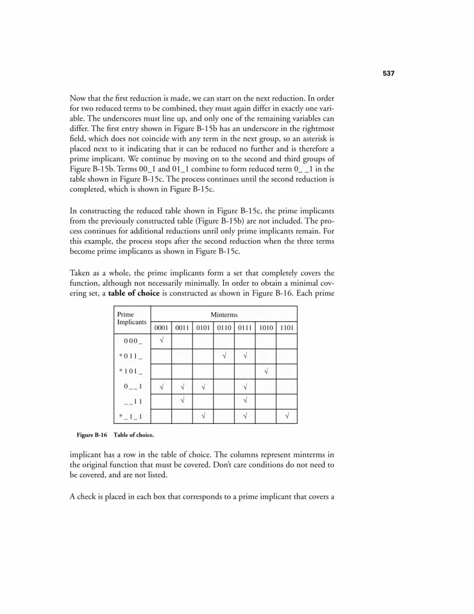
537
Now that the first reduction is made, we can start on the next reduction. In orderfor two reduced terms to be combined, they must again differ in exactly one vari-able. The underscores must line up, and only one of the remaining variables candiffer. The first entry shown in Figure B-15b has an underscore in the rightmostfield, which does not coincide with any term in the next group, so an asterisk isplaced next to it indicating that it can be reduced no further and is therefore aprime implicant. We continue by moving on to the second and third groups ofFigure B-15b. Terms 00_1 and 01_1 combine to form reduced term 0_._1 in thetable shown in Figure B-15c. The process continues until the second reduction iscompleted, which is shown in Figure B-15c.
In constructing the reduced table shown in Figure B-15c, the prime implicantsfrom the previously constructed table (Figure B-15b) are not included. The pro-cess continues for additional reductions until only prime implicants remain. Forthis example, the process stops after the second reduction when the three termsbecome prime implicants as shown in Figure B-15c.
Taken as a whole, the prime implicants form a set that completely covers thefunction, although not necessarily minimally. In order to obtain a minimal cov-ering set, a table of choice is constructed as shown in Figure B-16. Each prime
implicant has a row in the table of choice. The columns represent minterms inthe original function that must be covered. Don’t care conditions do not need tobe covered, and are not listed.
A check is placed in each box that corresponds to a prime implicant that covers a
0
0
1
0
_
_
0
1
0
_
_
1
0
1
1
_
1
_
_
_
_
1
1
1
0001 0011 0101 0110 0111 1010 1101
MintermsPrimeImplicants
√
√
√
√
√ √ √ √
√ √
√ √ √
*
*
*
Figure B-16 Table of choice.
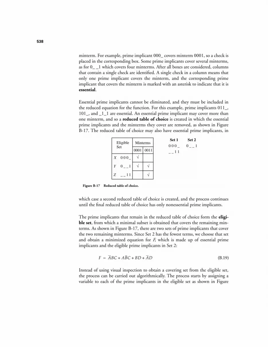
538
minterm. For example, prime implicant 000_ covers minterm 0001, so a check isplaced in the corresponding box. Some prime implicants cover several minterms,as for 0_ _1 which covers four minterms. After all boxes are considered, columnsthat contain a single check are identified. A single check in a column means thatonly one prime implicant covers the minterm, and the corresponding primeimplicant that covers the minterm is marked with an asterisk to indicate that it isessential.
Essential prime implicants cannot be eliminated, and they must be included inthe reduced equation for the function. For this example, prime implicants 011_,101_, and _1_1 are essential. An essential prime implicant may cover more thanone minterm, and so a reduced table of choice is created in which the essentialprime implicants and the minterms they cover are removed, as shown in FigureB-17. The reduced table of choice may also have essential prime implicants, in
which case a second reduced table of choice is created, and the process continuesuntil the final reduced table of choice has only nonessential prime implicants.
The prime implicants that remain in the reduced table of choice form the eligi-ble set, from which a minimal subset is obtained that covers the remaining min-terms. As shown in Figure B-17, there are two sets of prime implicants that coverthe two remaining minterms. Since Set 2 has the fewest terms, we choose that setand obtain a minimized equation for F, which is made up of essential primeimplicants and the eligible prime implicants in Set 2:
(B.19)
Instead of using visual inspection to obtain a covering set from the eligible set,the process can be carried out algorithmically. The process starts by assigning avariable to each of the prime implicants in the eligible set as shown in Figure
0
0
_
0
_
_
0
_
1
_
1
1
0001 0011
MintermsEligibleSet
√
√
Set 1
0 0 0 _
_ _ 1 1
Set 2
0 _ _ 1
X
Y
Z √
√
Figure B-17 Reduced table of choice.
F ABC ABC BD AD+ + +=

539
B-17. A logical expression is written for each column in the reduced table ofchoice as shown below:
Column Logical Sums
0001 (X + Y)
0011 (Y + Z)
In order to find a set that completely covers the function, prime implicants aregrouped so that there is at least one check in each column. This means that thefollowing relation must hold, in which G represents the terms in the reducedtable of choice:
Applying the properties of Boolean algebra yields:
Each of the product terms in this equation represents a set of prime implicantsthat covers the terms in the reduced table of choice. The smallest product term(Y) represents the smallest set of prime implicants (0 _ _ 1) that covers theremaining terms. The same final equation is produced as before:
(B.20)
Reduction of Multiple Functions
The tabular reduction method reduces a single Boolean function. When there ismore than one function that use the same variables, then it may be possible toshare terms, resulting in a smaller collective size of the equations. The methoddescribed here forms an intersection among all possible combinations of sharedterms, and then selects the smallest set that covers all of the functions.
As an example, consider the truth table shown in Figure B-18 that representsthree functions in three variables. The notation mi denotes minterms accordingto the indexing shown in the table.
The canonical (unreduced) form of the Boolean equations is:
G X Y+( ) Y Z+( )=
G X Y+( ) Y Z+( ) XY XZ Y YZ+ + + XZ Y+= = =
F ABC ABC BD AD+ + +=
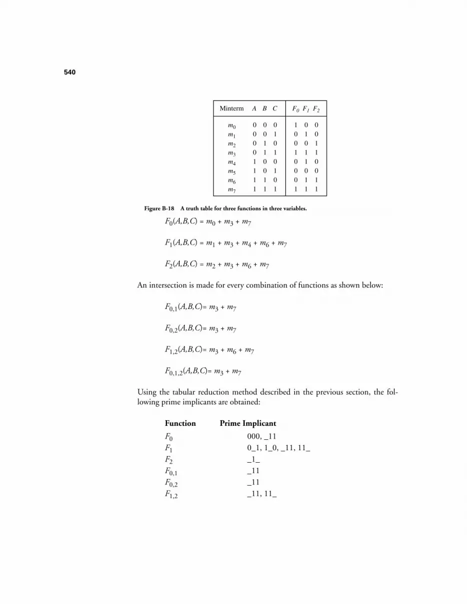
540
F0(A,B,C) = m0 + m3 + m7
F1(A,B,C) = m1 + m3 + m4 + m6 + m7
F2(A,B,C) = m2 + m3 + m6 + m7
An intersection is made for every combination of functions as shown below:
F0,1(A,B,C)= m3 + m7
F0,2(A,B,C)= m3 + m7
F1,2(A,B,C)= m3 + m6 + m7
F0,1,2(A,B,C)= m3 + m7
Using the tabular reduction method described in the previous section, the fol-lowing prime implicants are obtained:
Function Prime Implicant
F0 000, _11F1 0_1, 1_0, _11, 11_F2 _1_F0,1 _11F0,2 _11F1,2 _11, 11_
00110011
01010101
B C
00001111
A
10010001
F0
01011011
F1
00110011
F2
m0
m1
m2
m3
m4
m5
m6
m7
Minterm
Figure B-18 A truth table for three functions in three variables.

541
F0,1,2 _11
The list of prime implicants is reduced by eliminating those prime implicants infunctions that are covered by higher order functions. For example, _11 appearsin F0,1,2, thus it does not need to be included in the remaining functions. Simi-larly, 11_ appears in F1,2, and does not need to appear in F1 or in F2 (for thiscase, it does not appear as a prime implicant in F2 anyway.) Continuing in thismanner, a reduced set of prime implicants is obtained:
Function Prime Implicant
F0 000F1 0_1, 1_0F2 _1_F0,1 noneF0,2 noneF1,2 11_F0,1,2 _11
A multiple output table of choice is then constructed as shown in Figure B-19.
The rows correspond to the prime implicants, and the columns correspond tothe minterms that must be covered for each function. Portions of rows areblocked out where prime implicants from one function cannot be used to coveranother. For example, prime implicant 000 was obtained from function F0, andtherefore cannot be used to cover a minterm in F1 or F2, and so these regions are
0
0
1
_
1
_
0
_
_
1
1
1
0
1
0
_
_
1
PrimeImplicants
√
m0 m3 m7 m1 m3 m4 m6 m7 m2 m3 m6 m7
F0(A,B,C) F1(A,B,C) F2(A,B,C)Min-terms
F0
F1
F1
F2
F1,2
F0,1,2
√ √
√ √
√ √ √ √
√ √
√√ √ √ √ √
*
*
*
*
*
√ √
Figure B-19 A multiple output table of choice.
542
blocked out. If, in fact, a prime implicant in F0 can be used to cover a mintermin one of the remaining functions, then it will appear in a higher order functionsuch as F0,1 or F0,1,2.
The minimal form for the output equations is obtained in a manner similar tothe tabular reduction process. We start by finding all of the essential prime impli-cants. For example, minterm m0 in function F0 is covered only by prime impli-cant 000, and thus 000 is essential. The row containing 000 is then removedfrom the table and all columns that contain a check mark in the row are alsodeleted. The process continues until either all functions are covered or until onlynonessential prime implicants remain, in which case the smallest set of nonessen-tial prime implicants that are needed to cover the remaining functions isobtained using the method described in the previous section.
The essential prime implicants are marked with asterisks in Figure B-19. For thiscase, only one nonessential prime implicant (11_) remains, but since all min-terms are covered by the essential prime implicants, there is no need to constructa reduced table. The corresponding reduced equations are:
F0(A,B,C)=
F1(A,B,C)=
F2(A,B,C)=
B.2.4 LOGIC REDUCTION: EFFECT ON SPEED AND PERFORMANCE
Up to this point, we have largely ignored physical characteristics that affect per-formance, and have focused entirely on organizational issues such as circuitdepth and gate count. In this section, we explore a few practical considerations ofdigital logic.
Switching speed: The propagation delay (latency) between the inputs and outputof a logic gate is a continuous effect, even though we considered propagationdelay to be negligible in the early part of Appendix A. A change at an input to alogic gate is also a continuous effect. In Figure B-20, an input to a NOT gate hasa finite transition time, which is measured as the time between the 10% and90% points on the waveform. This is referred to as the rise time for a rising signaland the fall time for a falling signal.
ABC BC+
AC AC BC+ +
B

543
The propagation delay is the time between the 50% transitions on the input andoutput waveforms. The propagation delay is influenced by a number of parame-ters, and power is one parameter over which we have a good deal of control. Aspower consumption increases, propagation delay decreases, up to a limit. A ruleof thumb is that the product of power consumption and the propagation delayfor a logic gate stays roughly the same. Although we generally want fast logic, wedo not want to operate with a high power dissipation because the consumedpower manifests itself as heat that must be removed to maintain a safe and reli-able operating condition.
In the complementary metal-oxide semiconductor (CMOS) logic family, powerdissipation scales with speed. At a switching rate of 1 MHz, the power dissipa-tion of a CMOS gate is about 1 mW. At this rate of power dissipation, 10,000CMOS logic gates dissipate 10,000 gates × 1mW/gate = 10W, which is at thelimit of heat removal for a single integrated circuit using conventionalapproaches (for a 1 cm2 chip).
Single CMOS chips can have on the order of 107 logic gates, however, and oper-ate at rates up to several hundred MHz. This gate count and speed are achievedpartially by increasing the chip size, although this accounts for little more than afactor of 10. The key to achieving such a high component count and switchingspeed while managing power dissipation is to switch only a fraction of the logicgates at any time, which luckily is the most typical operating mode for an inte-grated circuit.
Circuit depth: The latency between the inputs and outputs of a circuit is governed
+5V
0V
+5V
0V
10%
90%
Transition Time
90%
10%
50%(2.5V)
50%(2.5V)
Propagation Delay
Transition Time
Time
A NOT gate input changes from 1 to 0
The NOT gate output changes from 0 to 1
(Fall Time)
(Latency)
(Rise Time)
Figure B-20 Propagation delay for a NOT gate (adapted from [Hamacher et al., 1990]).

544
by the number of logic gates on the longest path from any input to any output.This is known as circuit depth. In general, a circuit with a small circuit depthoperates more quickly than a circuit with a large circuit depth. There are a num-ber of ways to reduce circuit depth that involve increasing the complexity ofsome other parameter. We look at one way of making this trade-off here.
In Appendix A, we used a MUX to implement the majority function. Now con-sider using a four variable MUX to implement Equation B.21 shown below. Theequation is in two-level form, because only two levels of logic are used in its rep-resentation: six AND terms that are ORed together. A single MUX can imple-ment this function, which is shown in the left side of Figure B-21. The
corresponding circuit depth is two (that is, the gate-level configuration of theinside of the MUX has two gate delays). If we factor out A and B then we obtainthe four-level Equation B.22, and the corresponding four-level circuit shown inthe right side of Figure B-21.
(B.21)
(B.22)
The gate input count of a 4-to-1 MUX is 18 as taken from Figure A-23 (includ-ing inverters), so the gate input count of the decomposed MUX circuit is 3×18 =54. A single 16-to-1 MUX has a gate input count of 100. The 4-to-1 MUX
A C
F
0000000100100011
B
010001010110011110001001101010111100110111101111
D
1001011001000001 A D
F
00011011
B C
00011011
B C
00011011
1001
0110
0
B C + B C
B C + B C
Figure B-21 A four-variable function implemented with a 16-to-1 MUX (left) and with 4-to-1
MUXes (right).
F A B C D, , ,( ) ABCD ABCD ABCD ABCD ABCD ABCD+ + + + +=
F A B C D, , ,( ) AB CD CD+( ) AB CD CD+( ) AB CD( )AB CD( )
+ ++
=
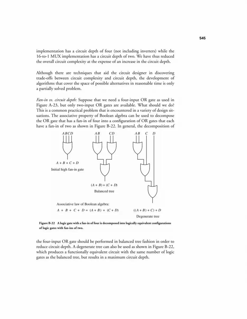
545
implementation has a circuit depth of four (not including inverters) while the16-to-1 MUX implementation has a circuit depth of two. We have thus reducedthe overall circuit complexity at the expense of an increase in the circuit depth.
Although there are techniques that aid the circuit designer in discoveringtrade-offs between circuit complexity and circuit depth, the development ofalgorithms that cover the space of possible alternatives in reasonable time is onlya partially solved problem.
Fan-in vs. circuit depth: Suppose that we need a four-input OR gate as used inFigure A-23, but only two-input OR gates are available. What should we do?This is a common practical problem that is encountered in a variety of design sit-uations. The associative property of Boolean algebra can be used to decomposethe OR gate that has a fan-in of four into a configuration of OR gates that eachhave a fan-in of two as shown in Figure B-22. In general, the decomposition of
the four-input OR gate should be performed in balanced tree fashion in order toreduce circuit depth. A degenerate tree can also be used as shown in Figure B-22,which produces a functionally equivalent circuit with the same number of logicgates as the balanced tree, but results in a maximum circuit depth.
A + B + C + D
A BCD
Associative law of Boolean algebra:
Initial high fan-in gate
Balanced tree
A B CD
(A + B) + (C + D)
Degenerate tree
A B C D
A + B + C + D = (A + B) + (C + D) ((A + B) + C) + D
Figure B-22 A logic gate with a fan-in of four is decomposed into logically equivalent configurations
of logic gates with fan-ins of two.
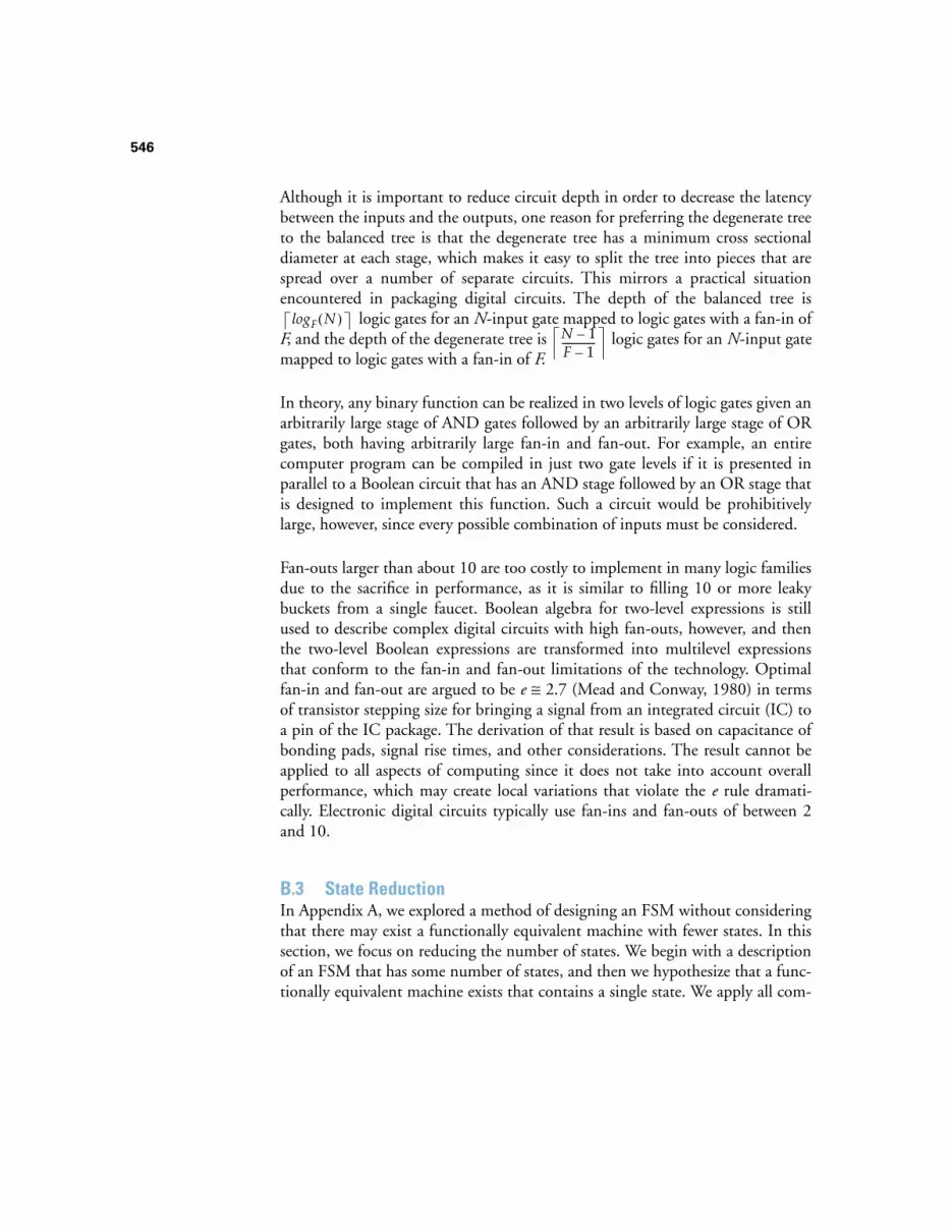
546
Although it is important to reduce circuit depth in order to decrease the latencybetween the inputs and the outputs, one reason for preferring the degenerate treeto the balanced tree is that the degenerate tree has a minimum cross sectionaldiameter at each stage, which makes it easy to split the tree into pieces that arespread over a number of separate circuits. This mirrors a practical situationencountered in packaging digital circuits. The depth of the balanced tree is
logic gates for an N-input gate mapped to logic gates with a fan-in ofF, and the depth of the degenerate tree is logic gates for an N-input gatemapped to logic gates with a fan-in of F.
In theory, any binary function can be realized in two levels of logic gates given anarbitrarily large stage of AND gates followed by an arbitrarily large stage of ORgates, both having arbitrarily large fan-in and fan-out. For example, an entirecomputer program can be compiled in just two gate levels if it is presented inparallel to a Boolean circuit that has an AND stage followed by an OR stage thatis designed to implement this function. Such a circuit would be prohibitivelylarge, however, since every possible combination of inputs must be considered.
Fan-outs larger than about 10 are too costly to implement in many logic familiesdue to the sacrifice in performance, as it is similar to filling 10 or more leakybuckets from a single faucet. Boolean algebra for two-level expressions is stillused to describe complex digital circuits with high fan-outs, however, and thenthe two-level Boolean expressions are transformed into multilevel expressionsthat conform to the fan-in and fan-out limitations of the technology. Optimalfan-in and fan-out are argued to be e ≅ 2.7 (Mead and Conway, 1980) in termsof transistor stepping size for bringing a signal from an integrated circuit (IC) toa pin of the IC package. The derivation of that result is based on capacitance ofbonding pads, signal rise times, and other considerations. The result cannot beapplied to all aspects of computing since it does not take into account overallperformance, which may create local variations that violate the e rule dramati-cally. Electronic digital circuits typically use fan-ins and fan-outs of between 2and 10.
B.3 State ReductionIn Appendix A, we explored a method of designing an FSM without consideringthat there may exist a functionally equivalent machine with fewer states. In thissection, we focus on reducing the number of states. We begin with a descriptionof an FSM that has some number of states, and then we hypothesize that a func-tionally equivalent machine exists that contains a single state. We apply all com-
logF N( )N 1–F 1–-------------
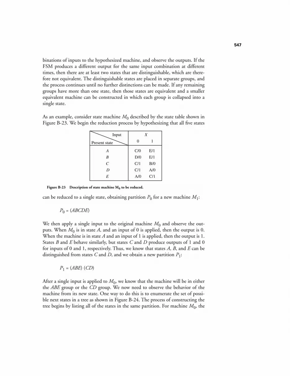
547
binations of inputs to the hypothesized machine, and observe the outputs. If theFSM produces a different output for the same input combination at differenttimes, then there are at least two states that are distinguishable, which are there-fore not equivalent. The distinguishable states are placed in separate groups, andthe process continues until no further distinctions can be made. If any remaininggroups have more than one state, then those states are equivalent and a smallerequivalent machine can be constructed in which each group is collapsed into asingle state.
As an example, consider state machine M0 described by the state table shown inFigure B-23. We begin the reduction process by hypothesizing that all five states
can be reduced to a single state, obtaining partition P0 for a new machine M1:
P0 = (ABCDE)
We then apply a single input to the original machine M0 and observe the out-puts. When M0 is in state A, and an input of 0 is applied, then the output is 0.When the machine is in state A and an input of 1 is applied, then the output is 1.States B and E behave similarly, but states C and D produce outputs of 1 and 0for inputs of 0 and 1, respectively. Thus, we know that states A, B, and E can bedistinguished from states C and D, and we obtain a new partition P1:
P1 = (ABE) (CD)
After a single input is applied to M0, we know that the machine will be in eitherthe ABE group or the CD group. We now need to observe the behavior of themachine from its new state. One way to do this is to enumerate the set of possi-ble next states in a tree as shown in Figure B-24. The process of constructing thetree begins by listing all of the states in the same partition. For machine M0, the
X
0 1
A C/0 E/1
Present state
Input
B
C
D
E
D/0 E/1
C/1 B/0
C/1 A/0
A/0 C/1
Figure B-23 Description of state machine M0 to be reduced.
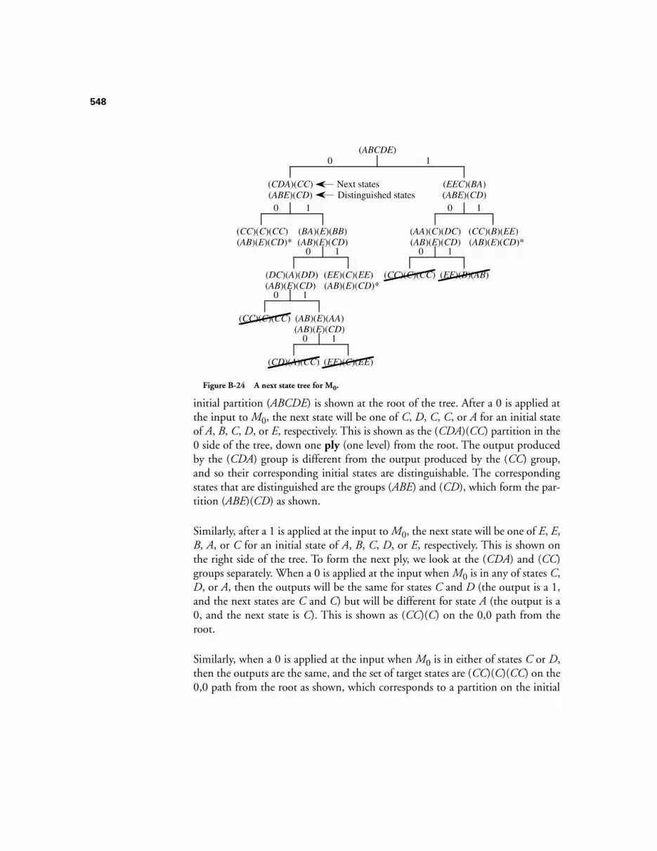
548
initial partition (ABCDE) is shown at the root of the tree. After a 0 is applied atthe input to M0, the next state will be one of C, D, C, C, or A for an initial stateof A, B, C, D, or E, respectively. This is shown as the (CDA)(CC) partition in the0 side of the tree, down one ply (one level) from the root. The output producedby the (CDA) group is different from the output produced by the (CC) group,and so their corresponding initial states are distinguishable. The correspondingstates that are distinguished are the groups (ABE) and (CD), which form the par-tition (ABE)(CD) as shown.
Similarly, after a 1 is applied at the input to M0, the next state will be one of E, E,B, A, or C for an initial state of A, B, C, D, or E, respectively. This is shown onthe right side of the tree. To form the next ply, we look at the (CDA) and (CC)groups separately. When a 0 is applied at the input when M0 is in any of states C,D, or A, then the outputs will be the same for states C and D (the output is a 1,and the next states are C and C) but will be different for state A (the output is a0, and the next state is C). This is shown as (CC)(C) on the 0,0 path from theroot.
Similarly, when a 0 is applied at the input when M0 is in either of states C or D,then the outputs are the same, and the set of target states are (CC)(C)(CC) on the0,0 path from the root as shown, which corresponds to a partition on the initial
(ABCDE)
(CDA)(CC)(ABE)(CD)
(CC)(C)(CC)(AB)(E)(CD)*
(BA)(E)(BB)(AB)(E)(CD)
(DC)(A)(DD)(AB)(E)(CD)
(EE)(C)(EE)(AB)(E)(CD)*
(CC)(C)(CC) (AB)(E)(AA)(AB)(E)(CD)
(CD)(A)(CC) (EE)(C)(EE)
(EEC)(BA)(ABE)(CD)
(AA)(C)(DC)(AB)(E)(CD)
(CC)(B)(EE)(AB)(E)(CD)*
(CC)(C)(CC) (EE)(B)(AB)
0 1
0 10 1
0 10 1
0 1
0 1
Next statesDistinguished states
Figure B-24 A next state tree for M0.

549
states of (AB)(E)(CD) if we trace back to the root. Thus, at this point, A is indis-tinguishable from B, and C is indistinguishable from D, but each parenthesizedgroup can be distinguished from each other if we apply the sequence 0,0 to M0and observe the outputs, regardless of the initial state.
Continuing in this manner, the tree is expanded until no finer partitions can becreated. For example, when a partition contains a group of states that can nolonger be distinguished, as for (CC)(C)(CC), then an asterisk is placed adjacentto the partition for the corresponding initial states and the tree is not expandedfurther from that point. The tree shown in Figure B-24 is expanded beyond thispoint only to illustrate various situations that can arise.
If a partition is created that is visited elsewhere in the tree, then a slash is drawnthrough it and the tree is not expanded from that point. For purposes of compar-ing similar partitions, (CD)(A)(CC) is considered to be the same as (CD)(A)(C),and (AA)(C)(DC) is considered to be the same as (A)(C)(DC), which is the sameas (DC)(A)(C) and (CD)(A)(C). Thus the (CD)(A)(CC) and (AA)(C)(DC) parti-tions are considered to be the same. After the tree is constructed, the partitionswith asterisks expose the indistinguishable states. Each group of parentheses inan asterisk partition identifies a group of indistinguishable states. For machineM0, states A and B are indistinguishable, and states C and D are indistinguish-able. Thus, we can construct a functionally equivalent machine to M0 that con-tains only three states, in which A and B are combined into a single state and Cand D are combined into a single state.
The process of constructing the next state tree is laborious because of its potentialsize, but we use it here in order to understand a simpler method. Rather thanconstruct the entire tree, we can simply observe that once we have the first parti-tion P1, the next partition can be constructing by looking at the next states foreach group and noting that if two states within a group have next states that arein different groups, then they are distinguishable since the resulting outputs willeventually differ. This can be shown by constructing the corresponding distin-guishing tree. Starting with P1 for M0, we observe that states A and B have nextstates C and D for an input of 0, and have a next state of E for an input of 1, andso A and B are grouped together in the next partition. State E, however, has nextstates of A and C for inputs of 0 and 1, respectively, which differ from the nextstates for A and B, and thus state E is distinguishable from states A and B. Con-tinuing for the (CD) group of P1, the next partition is obtained as shown below:
P2 = (AB) (CD) (E)
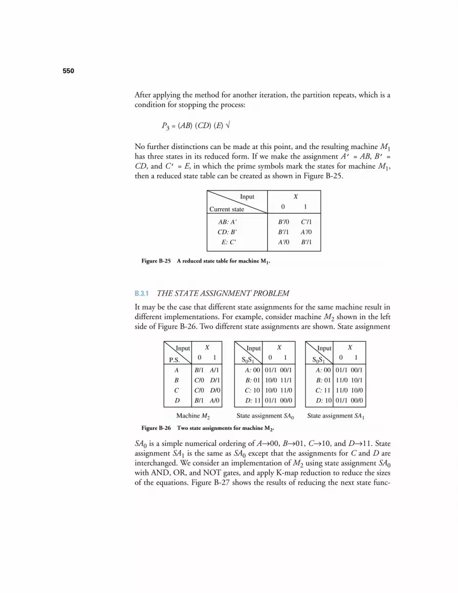
550
After applying the method for another iteration, the partition repeats, which is acondition for stopping the process:
P3 = (AB) (CD) (E) √
No further distinctions can be made at this point, and the resulting machine M1has three states in its reduced form. If we make the assignment A’ = AB, B’ =CD, and C’ = E, in which the prime symbols mark the states for machine M1,then a reduced state table can be created as shown in Figure B-25.
B.3.1 THE STATE ASSIGNMENT PROBLEM
It may be the case that different state assignments for the same machine result indifferent implementations. For example, consider machine M2 shown in the leftside of Figure B-26. Two different state assignments are shown. State assignment
SA0 is a simple numerical ordering of A→00, B→01, C→10, and D→11. Stateassignment SA1 is the same as SA0 except that the assignments for C and D areinterchanged. We consider an implementation of M2 using state assignment SA0with AND, OR, and NOT gates, and apply K-map reduction to reduce the sizesof the equations. Figure B-27 shows the results of reducing the next state func-
X
0 1
AB: A' B'/0 C'/1
Current state
Input
CD: B'
E: C'
B'/1 A'/0
A'/0 B'/1
Figure B-25 A reduced state table for machine M1.
P.S.
Input X
0 1
A B/1 A/1
B C/0 D/1
C C/0 D/0
D B/1 A/0
Machine M2
Input X
0 1
A: 00 01/1 00/1
B: 01 10/0 11/1
C: 10 10/0 11/0
D: 11 01/1 00/0
State assignment SA0
S0S1
Input X
0 1
A: 00 01/1 00/1
B: 01 11/0 10/1
C: 11 11/0 10/0
D: 10 01/1 00/0
State assignment SA1
S0S1
Figure B-26 Two state assignments for machine M2.
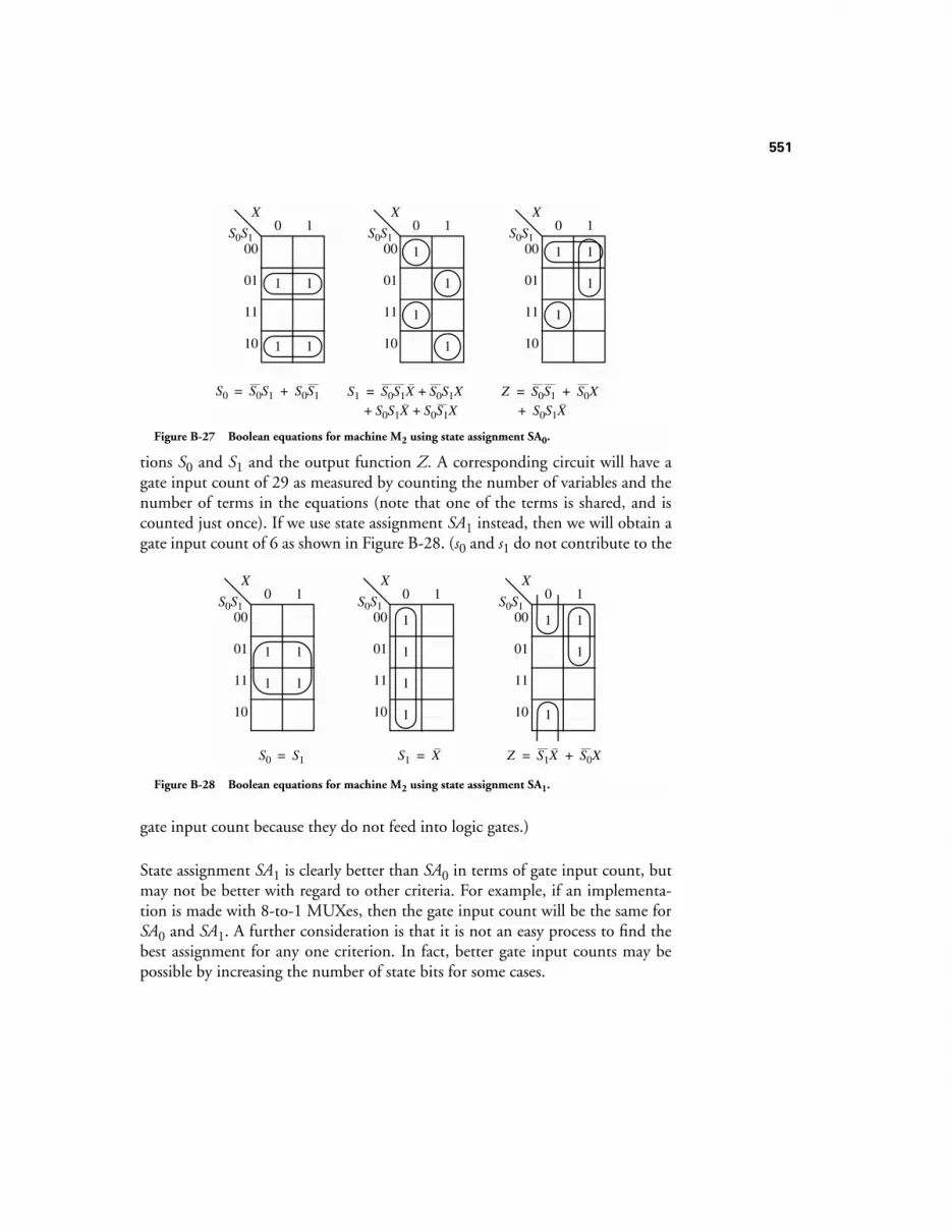
551
tions S0 and S1 and the output function Z. A corresponding circuit will have agate input count of 29 as measured by counting the number of variables and thenumber of terms in the equations (note that one of the terms is shared, and iscounted just once). If we use state assignment SA1 instead, then we will obtain agate input count of 6 as shown in Figure B-28. (s0 and s1 do not contribute to the
gate input count because they do not feed into logic gates.)
State assignment SA1 is clearly better than SA0 in terms of gate input count, butmay not be better with regard to other criteria. For example, if an implementa-tion is made with 8-to-1 MUXes, then the gate input count will be the same forSA0 and SA1. A further consideration is that it is not an easy process to find thebest assignment for any one criterion. In fact, better gate input counts may bepossible by increasing the number of state bits for some cases.
01
11
1
10
X0
00S0S1
1 1
11
01
11
1
10
0
00 1
1
1
1
X
S0S1
01
11
1
10
0
00 1 1
1
1
X
S0S1
S0 = S0S1 + S0S1 Z = S0S1 + S0X
+ S0S1X
S1 = S0S1X + S0S1X
+ S0S1X + S0S1X
Figure B-27 Boolean equations for machine M2 using state assignment SA0.
01
11
1
10
X0
00S0S1
1 1
11
01
11
1
10
0
00 1
1
1
1
X
S0S1
01
11
1
10
00
X
1 1
1
1
S0S10
S1 = XS0 = S1 Z = S1X + S0X
Figure B-28 Boolean equations for machine M2 using state assignment SA1.
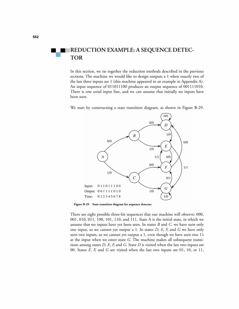
552
REDUCTION EXAMPLE: A SEQUENCE DETEC-TOR
In this section, we tie together the reduction methods described in the previoussections. The machine we would like to design outputs a 1 when exactly two ofthe last three inputs are 1 (this machine appeared in an example in Appendix A).An input sequence of 011011100 produces an output sequence of 001111010.There is one serial input line, and we can assume that initially no inputs havebeen seen.
We start by constructing a state transition diagram, as shown in Figure B-29.
There are eight possible three-bit sequences that our machine will observe: 000,001, 010, 011, 100, 101, 110, and 111. State A is the initial state, in which weassume that no inputs have yet been seen. In states B and C, we have seen onlyone input, so we cannot yet output a 1. In states D, E, F, and G we have onlyseen two inputs, so we cannot yet output a 1, even though we have seen two 1’sat the input when we enter state G. The machine makes all subsequent transi-tions among states D, E, F, and G. State D is visited when the last two inputs are00. States E, F, and G are visited when the last two inputs are 01, 10, or 11,
A
B0/0
1/0
C
D
E
F
G
0/0
1/0
0/0
1/0
0/0
1/0
1/0
1/1
0/01/1
0/0
0/1
Input: 0 1 1 0 1 1 1 0 0
Output: 0 0 1 1 1 1 0 1 0
Time: 0 1 2 3 4 5 6 7 8
Figure B-29 State transition diagram for sequence detector.
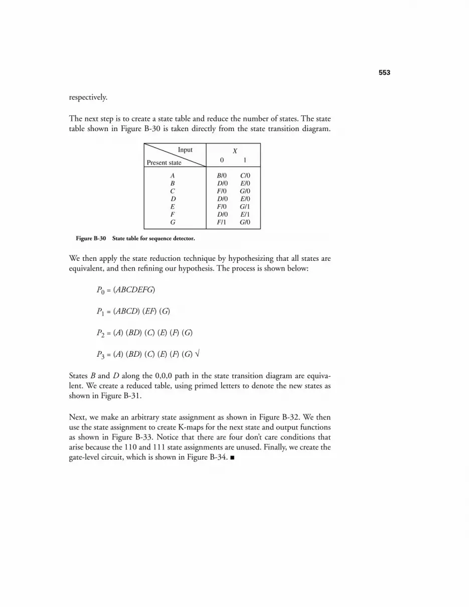
553
respectively.
The next step is to create a state table and reduce the number of states. The statetable shown in Figure B-30 is taken directly from the state transition diagram.
We then apply the state reduction technique by hypothesizing that all states areequivalent, and then refining our hypothesis. The process is shown below:
P0 = (ABCDEFG)
P1 = (ABCD) (EF) (G)
P2 = (A) (BD) (C) (E) (F) (G)
P3 = (A) (BD) (C) (E) (F) (G) √
States B and D along the 0,0,0 path in the state transition diagram are equiva-lent. We create a reduced table, using primed letters to denote the new states asshown in Figure B-31.
Next, we make an arbitrary state assignment as shown in Figure B-32. We thenuse the state assignment to create K-maps for the next state and output functionsas shown in Figure B-33. Notice that there are four don’t care conditions thatarise because the 110 and 111 state assignments are unused. Finally, we create thegate-level circuit, which is shown in Figure B-34.
X0 1
A B/0 C/0
Present state
Input
BCDE
D/0 E/0F/0 G/0D/0 E/0F/0 G/1
F D/0 E/1G F/1 G/0
Figure B-30 State table for sequence detector.
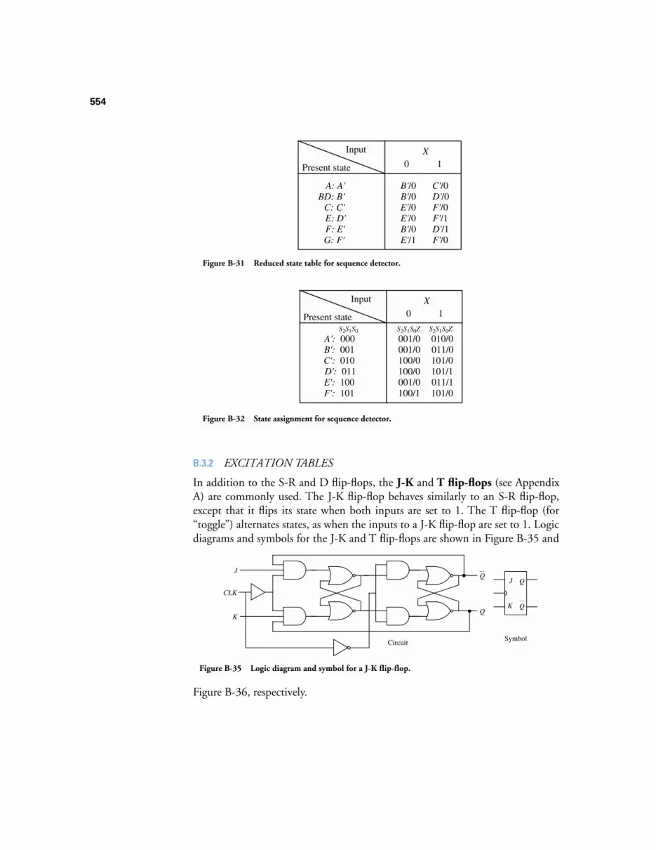
554
B.3.2 EXCITATION TABLES
In addition to the S-R and D flip-flops, the J-K and T flip-flops (see AppendixA) are commonly used. The J-K flip-flop behaves similarly to an S-R flip-flop,except that it flips its state when both inputs are set to 1. The T flip-flop (for“toggle”) alternates states, as when the inputs to a J-K flip-flop are set to 1. Logicdiagrams and symbols for the J-K and T flip-flops are shown in Figure B-35 and
Figure B-36, respectively.
X0 1
B'/0 C'/0
Present state
Input
B'/0 D'/0E'/0 F'/0E'/0 F'/1B'/0 D'/1E'/1 F'/0
A: A'BD: B'
C: C'E: D'F: E'G: F'
Figure B-31 Reduced state table for sequence detector.
X0 1
A': 000 001/0 010/0
Present state
Input
B': 001C': 010D': 011E': 100
001/0 011/0100/0 101/0100/0 101/1001/0 011/1
F': 101 100/1 101/0
S2S1S0 S2S1S0Z S2S1S0Z
Figure B-32 State assignment for sequence detector.
Q
QJ
CLK
J
Q
Q
K
CircuitSymbol
K
Figure B-35 Logic diagram and symbol for a J-K flip-flop.
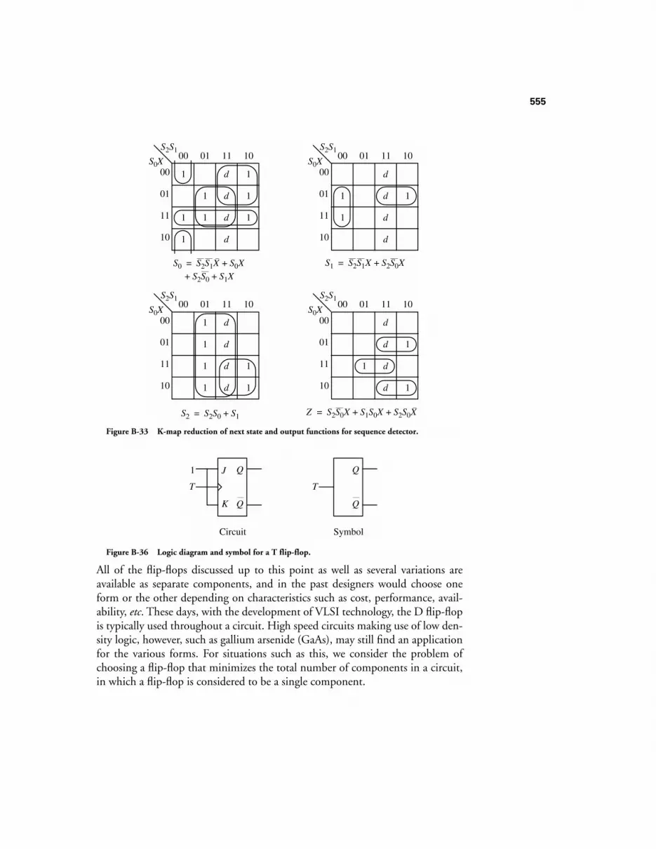
555
All of the flip-flops discussed up to this point as well as several variations areavailable as separate components, and in the past designers would choose oneform or the other depending on characteristics such as cost, performance, avail-ability, etc. These days, with the development of VLSI technology, the D flip-flopis typically used throughout a circuit. High speed circuits making use of low den-sity logic, however, such as gallium arsenide (GaAs), may still find an applicationfor the various forms. For situations such as this, we consider the problem ofchoosing a flip-flop that minimizes the total number of components in a circuit,in which a flip-flop is considered to be a single component.
01
11
10
00S0X
1
1
1
1
01 11 10
d
d
d
d
1
1
1
1
00S2S1
01
11
10
00S0X
1
1
01 11 10
d
d
d
d
1
00S2S1
01
11
10
00S0X
1
1 1
10
d
d
d
d
00S2S1
01
11
10
00S0X
1
01 11 10
d
d
d
d
1
1
00S2S1
01 11
S0 = S2S1X + S0X
+ S2S0 + S1X
S1 = S2S1X + S2S0X
Z = S2S0X + S1S0X + S2S0X
11
1
S2 = S2S0 + S1
Figure B-33 K-map reduction of next state and output functions for sequence detector.
J
Q
Q
K
Circuit
Q
Q
Symbol
1
T T
Figure B-36 Logic diagram and symbol for a T flip-flop.
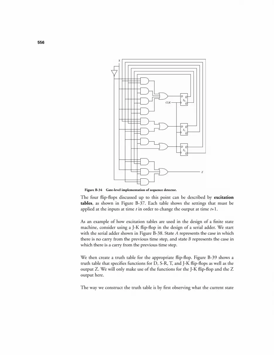
556
The four flip-flops discussed up to this point can be described by excitationtables, as shown in Figure B-37. Each table shows the settings that must beapplied at the inputs at time t in order to change the output at time t+1.
As an example of how excitation tables are used in the design of a finite statemachine, consider using a J-K flip-flop in the design of a serial adder. We startwith the serial adder shown in Figure B-38. State A represents the case in whichthere is no carry from the previous time step, and state B represents the case inwhich there is a carry from the previous time step.
We then create a truth table for the appropriate flip-flop. Figure B-39 shows atruth table that specifies functions for D, S-R, T, and J-K flip-flops as well as theoutput Z. We will only make use of the functions for the J-K flip-flop and the Zoutput here.
The way we construct the truth table is by first observing what the current state
CLK
QD
QS0
Z
QD
QS1
QD
QS2
X
Figure B-34 Gate-level implementation of sequence detector.
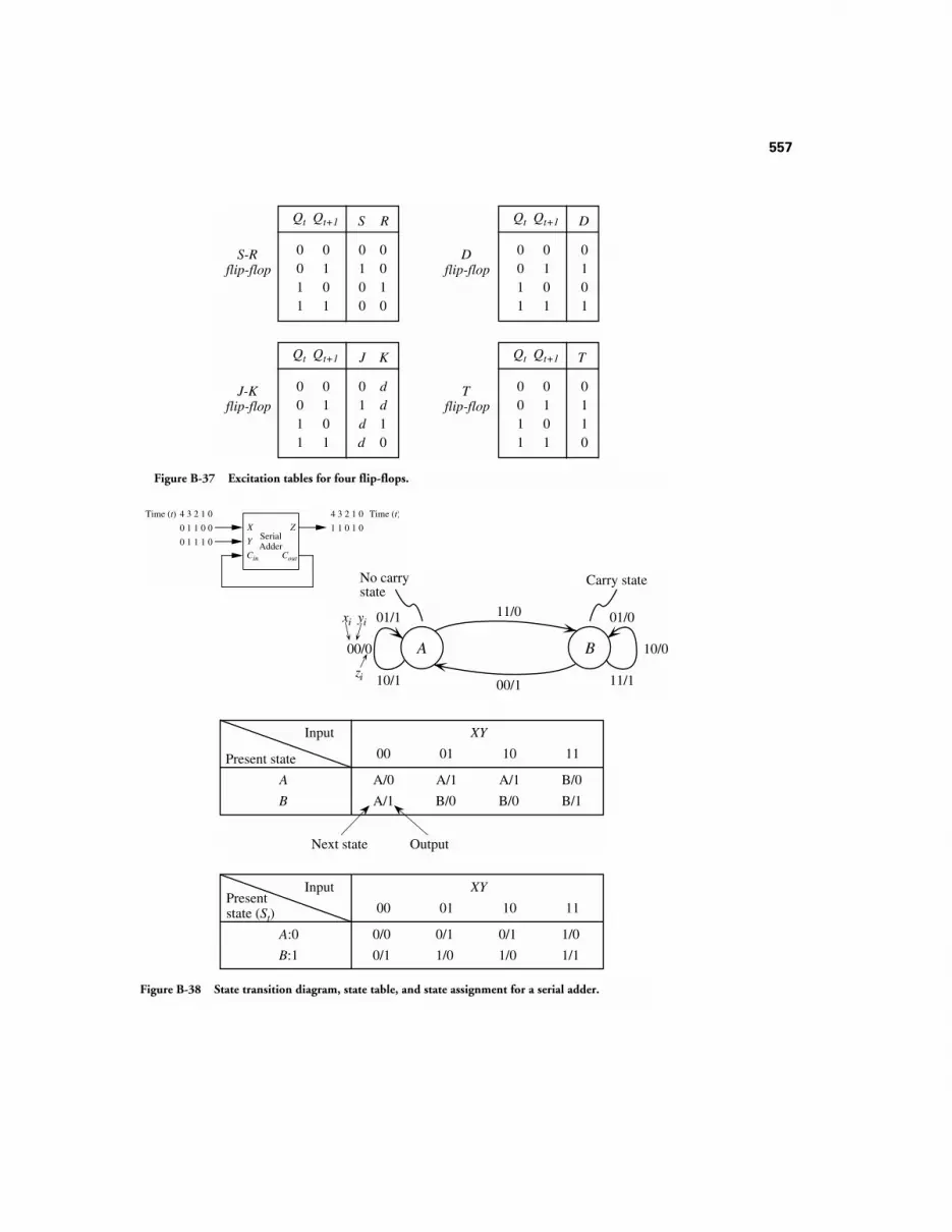
557
0011
0101
Qt Qt+1 S
0100
R
0010
S-Rflip-flop
0011
0101
Qt Qt+1 D
0101
Dflip-flop
0011
0101
Qt Qt+1 J
01dd
K
dd10
J-Kflip-flop
0011
0101
Qt Qt+1 T
0110
Tflip-flop
Figure B-37 Excitation tables for four flip-flops.
Present state
Input XY
00 01 10 11
A A/0 A/1 A/1 B/0
B A/1 B/0 B/0 B/1
Next state Output
Presentstate (St)
Input XY
00 01 10 11
A:0 0/0 0/1 0/1 1/0
B:1 0/1 1/0 1/0 1/1
SerialAdder
0 1 1 0 0
0 1 1 1 0
1 1 0 1 0X
Y
Z
Cin Cout
4 3 2 1 04 3 2 1 0 Time (t)Time (t)
Figure B-38 State transition diagram, state table, and state assignment for a serial adder.
A B00/0
01/1
10/1
11/0
00/1
10/0
01/0
11/1
No carrystate
Carry state
xi yi
zi
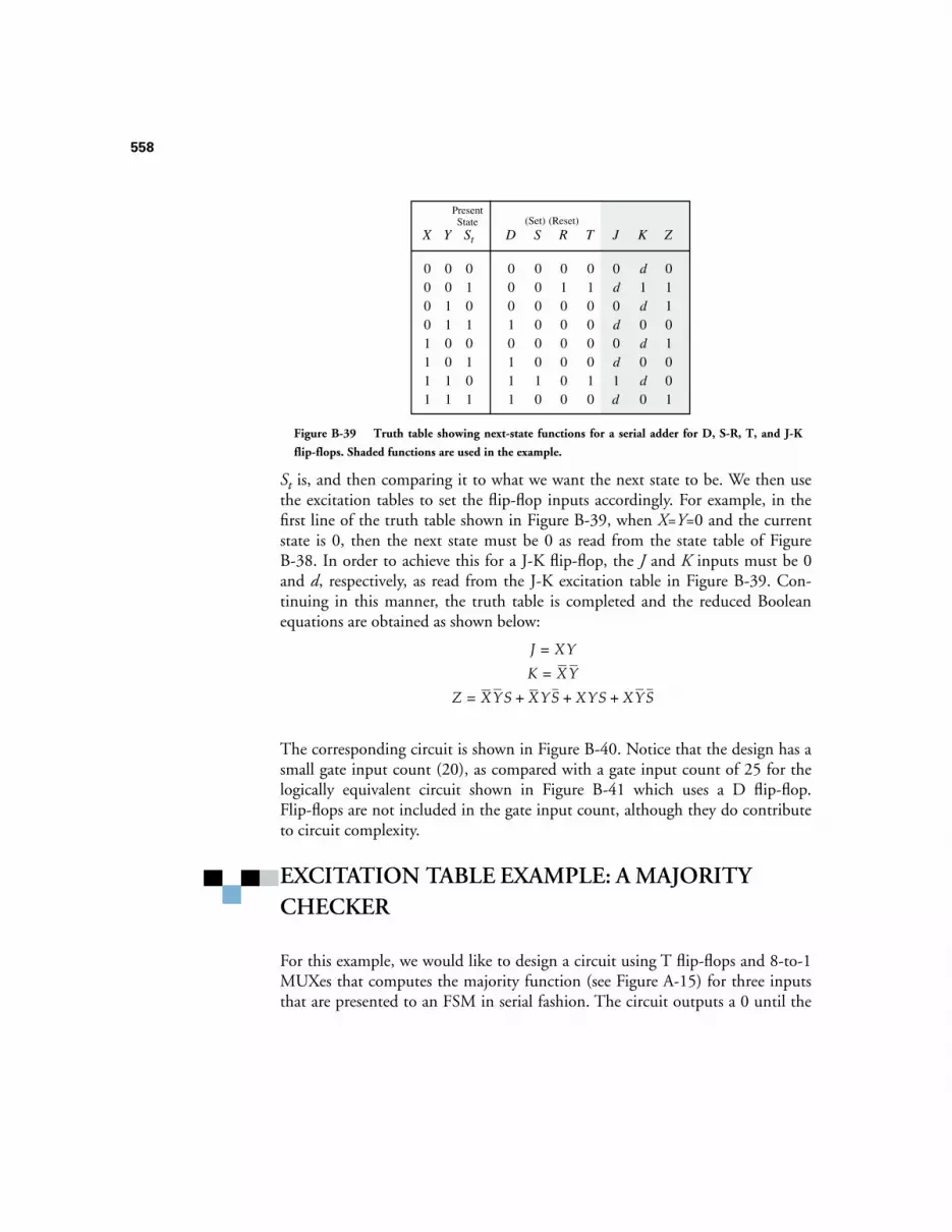
558
St is, and then comparing it to what we want the next state to be. We then usethe excitation tables to set the flip-flop inputs accordingly. For example, in thefirst line of the truth table shown in Figure B-39, when X=Y=0 and the currentstate is 0, then the next state must be 0 as read from the state table of FigureB-38. In order to achieve this for a J-K flip-flop, the J and K inputs must be 0and d, respectively, as read from the J-K excitation table in Figure B-39. Con-tinuing in this manner, the truth table is completed and the reduced Booleanequations are obtained as shown below:
The corresponding circuit is shown in Figure B-40. Notice that the design has asmall gate input count (20), as compared with a gate input count of 25 for thelogically equivalent circuit shown in Figure B-41 which uses a D flip-flop.Flip-flops are not included in the gate input count, although they do contributeto circuit complexity.
EXCITATION TABLE EXAMPLE: A MAJORITY CHECKER
For this example, we would like to design a circuit using T flip-flops and 8-to-1MUXes that computes the majority function (see Figure A-15) for three inputsthat are presented to an FSM in serial fashion. The circuit outputs a 0 until the
00110011
01010101
Y St
00001111
X
00010111
D
00000010
S
01000000
R
0d0d0d1d
J
d1d0d0d0
K
01000010
T
01101001
Z
Present State (Set) (Reset)
Figure B-39 Truth table showing next-state functions for a serial adder for D, S-R, T, and J-K
flip-flops. Shaded functions are used in the example.
J XY=
K XY=
Z XYS XYS XYS XYS+ + +=
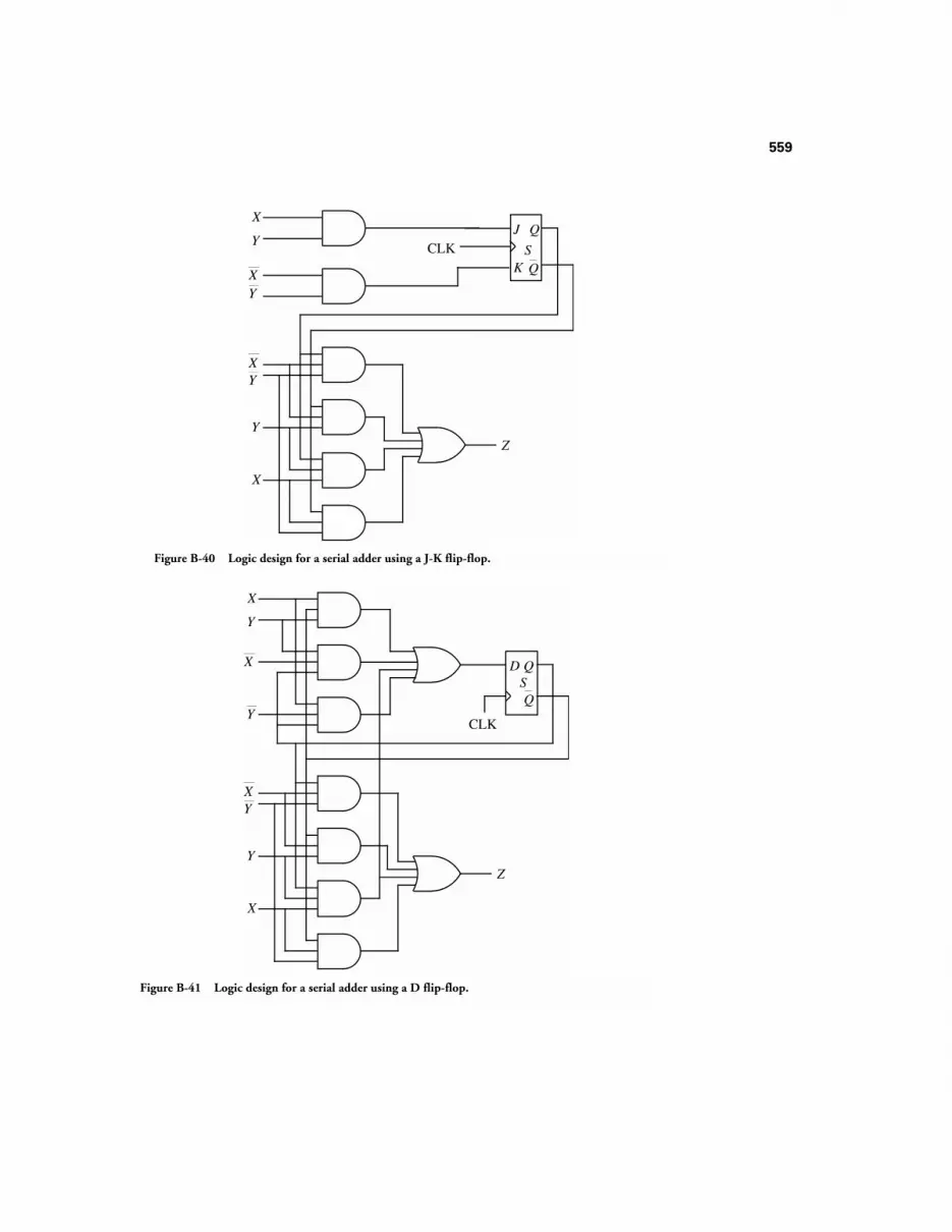
559
CLKQJ
X
Y
Q
XY
Y
X
Z
SKX
Y
Figure B-40 Logic design for a serial adder using a J-K flip-flop.
CLK
QD
X
Y
Q
XY
Y
X
Z
S
X
Y
Figure B-41 Logic design for a serial adder using a D flip-flop.

560
third input is seen, at which point a 0 or a 1 is produced at the output accordingto whether there are more 0’s or 1’s at the input, respectively. For example, aninput of 011100101 produces an output of 001000001.
We start by creating a state transition diagram that enumerates all possible statesof the FSM. In Figure B-42, a state transition diagram is shown in which thestates are organized according to the number of inputs that have been seen. StateA is the initial state in which no inputs have yet been seen. The three inputs aresymbolized with the notation: _ _ _. After the first input is seen, the FSM makesa transition to state B or state C for an input of 0 or 1, respectively. The inputhistory is symbolized with the notation: 0_ _ and 1_ _ for states B and C, respec-tively. States D, E, F, and G enumerate all possible histories for two inputs, assymbolized by the notation: 00_, 01_, 10_, and 11_, respectively.
The FSM outputs a 0 when making transitions to states B through G. On thethird input, the FSM returns to state A and outputs a 0 or a 1 according to themajority function. A total of eight states are used in the FSM of Figure B-42,
which are summarized in the state table shown in Figure B-43a.
The eight state FSM can be reduced to a seven state FSM. The reduction processis shown in Figure B-43b. States E and F can be combined, as shown in thereduced table of Figure B-43c. We use the reduced state table in creating a state
A
0/0
B
C
D
E
F
G0/1
1/0
1/1
0/0
1/0
0/0
1/0
0/0
1/0
0/0 1/1
0/0 1/1
Input: 0 1 1 1 0 0 1 0 1
Output: 0 0 1 0 0 0 0 0 1
Time: 0 1 2 3 4 5 6 7 8
Input History _ _ _0 _ _
1 _ _
0 0 _
0 1 _
1 0 _
1 1 _
Figure B-42 State transition diagram for a majority FSM.
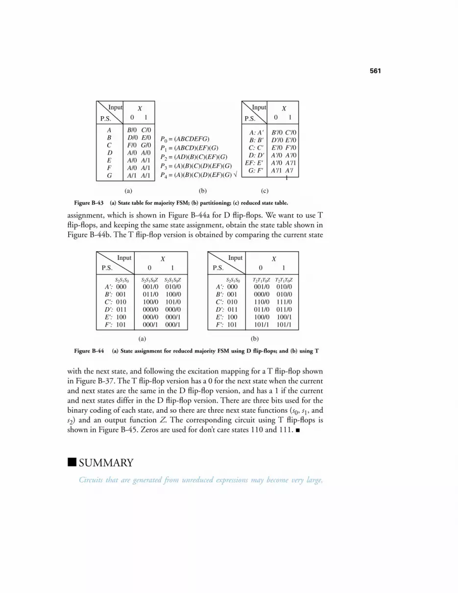
561
assignment, which is shown in Figure B-44a for D flip-flops. We want to use Tflip-flops, and keeping the same state assignment, obtain the state table shown inFigure B-44b. The T flip-flop version is obtained by comparing the current state
with the next state, and following the excitation mapping for a T flip-flop shownin Figure B-37. The T flip-flop version has a 0 for the next state when the currentand next states are the same in the D flip-flop version, and has a 1 if the currentand next states differ in the D flip-flop version. There are three bits used for thebinary coding of each state, and so there are three next state functions (s0, s1, ands2) and an output function Z. The corresponding circuit using T flip-flops isshown in Figure B-45. Zeros are used for don’t care states 110 and 111.
SUMMARY
Circuits that are generated from unreduced expressions may become very large,
X0 1
A B/0 C/0
P.S.
Input
BCDE
D/0 E/0F/0 G/0A/0 A/0A/0 A/1
F A/0 A/1G A/1 A/1
(a)
X0 1
B'/0 C'/0D'/0 E'/0E'/0 F'/0A'/0 A'/0A'/0 A'/1A'/1 A'/
1
A: A'B: B'C: C'D: D'
EF: E'G: F'
(c)
P0 = (ABCDEFG)P1 = (ABCD)(EF)(G)P2 = (AD)(B)(C)(EF)(G)P3 = (A)(B)(C)(D)(EF)(G)P4 = (A)(B)(C)(D)(EF)(G) √
P.S.
Input
(b)
Figure B-43 (a) State table for majority FSM; (b) partitioning; (c) reduced state table.
X0 1
A': 000 001/0 010/0
P.S.
Input
B': 001C': 010D': 011E': 100
011/0 100/0100/0 101/0000/0 000/0000/0 000/1
F': 101 000/1 000/1
S2S1S0 S2S1S0Z S2S1S0Z
X0 1
A': 000 001/0 010/0
P.S.
Input
B': 001C': 010D': 011E': 100
000/0 010/0110/0 111/0011/0 011/0100/0 100/1
F': 101 101/1 101/1
S2S1S0 T2T1T0Z T2T1T0Z
(a) (b)
Figure B-44 (a) State assignment for reduced majority FSM using D flip-flops; and (b) using T
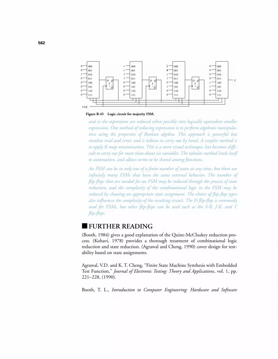
562
and so the expressions are reduced when possible into logically equivalent smallerexpressions. One method of reducing expressions is to perform algebraic manipula-tion using the properties of Boolean algebra. This approach is powerful butinvolves trial and error, and is tedious to carry out by hand. A simpler method isto apply K-map minimization. This is a more visual technique, but becomes diffi-cult to carry out for more than about six variables. The tabular method lends itselfto automation, and allows terms to be shared among functions.
An FSM can be in only one of a finite number of states at any time, but there areinfinitely many FSMs that have the same external behavior. The number offlip-flops that are needed for an FSM may be reduced through the process of statereduction, and the complexity of the combinational logic in the FSM may bereduced by choosing an appropriate state assignment. The choice of flip-flop typesalso influences the complexity of the resulting circuit. The D flip-flop is commonlyused for FSMs, but other flip-flops can be used such as the S-R, J-K, and Tflip-flops.
FURTHER READING(Booth, 1984) gives a good explanation of the Quine-McCluskey reduction pro-cess. (Kohavi, 1978) provides a thorough treatment of combinational logicreduction and state reduction. (Agrawal and Cheng, 1990) cover design for test-ability based on state assignments.
Agrawal, V.D. and K. T. Cheng, “Finite State Machine Synthesis with EmbeddedTest Function,” Journal of Electronic Testing: Theory and Applications, vol. 1, pp.221–228, (1990).
Booth, T. L., Introduction to Computer Engineering: Hardware and Software
QD
QT2
000
001
010
011
100
101
110
111
0
0
1
0
0
0
0
0
QD
QT1
000
001
010
011
100
101
110
111
x
1
1
0
0
0
0
QD
QT0
000
001
010
011
100
101
110
111
x
1
0
1
0
0
000
001
010
011
100
101
110
111
0
0
0
0
x
1
0
0
Z
x0
xx
CLK
x
Figure B-45 Logic circuit for majority FSM.
563
Design, 3/e, John Wiley & Sons, New York, (1984).
Kohavi, Z., Switching and Finite Automata Theory, 2/e, McGraw-Hill, New York,(1978).
PROBLEMSB.1 Given the following functions, construct K-maps and find minimal
sum-of-products expressions for f and g.
f(A,B,C,D) = 1 when two or more inputs are 1, otherwise f(A,B,C,D) = 0.
g(A,B,C,D) = 1 when the number of inputs that are 1 is even (including thecase when no inputs are 1), otherwise g(A,B,C,D) = .
B.2 Use K-maps to simplify function f and its don’t care condition below. Per-form the reduction for (a) the sum-of-products form and (b) the prod-uct-of-sums form.
B.3 Given a logic circuit, is it possible to generate a truth table that containsdon’t cares? Explain your answer.
B.4 The following K-map is formed incorrectly. Show the reduced equationthat is produced by the incorrect map, and then form the K-map correctly andderive the reduced equation from the correct map. Note that both K-mapswill produce functionally correct equations, but only the properly formedK-map will produce a minimized two-level equation.
B.5 A 4-to-1 multiplexer can be represented by the truth table shown below.
f A B C D, , ,( )
f A B C D, , ,( ) 2 8 10 11, , ,( )∑ ∑ d 0 9,( )+=
1
D
0
000ABC
001 011 010 110 111 101 100
1
1
1
1
1
1
1
1
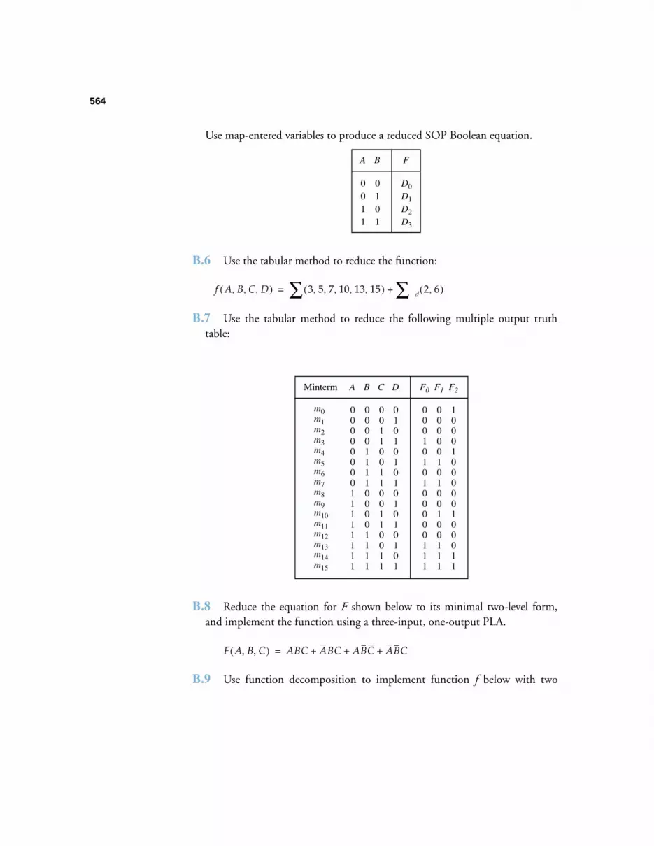
564
Use map-entered variables to produce a reduced SOP Boolean equation.
B.6 Use the tabular method to reduce the function:
B.7 Use the tabular method to reduce the following multiple output truthtable:
B.8 Reduce the equation for F shown below to its minimal two-level form,and implement the function using a three-input, one-output PLA.
B.9 Use function decomposition to implement function f below with two
0011
0101
A B
D0
D1
D2
D3
F
f A B C D, , ,( ) 3 5 7 10 13 15, , , , ,( )∑ a∑ d 2 6,( )+=
0000111100001111
0011001100110011
B C
0000000011111111
A
0001010100000111
F0
0000010100100111
F1
1000100000100011
F2
m0m1m2m3m4m5m6m7m8m9m10m11m12m13m14m15
Minterm
0101010101010101
D
F A B C, ,( ) ABC ABC ABC ABC+ + +=
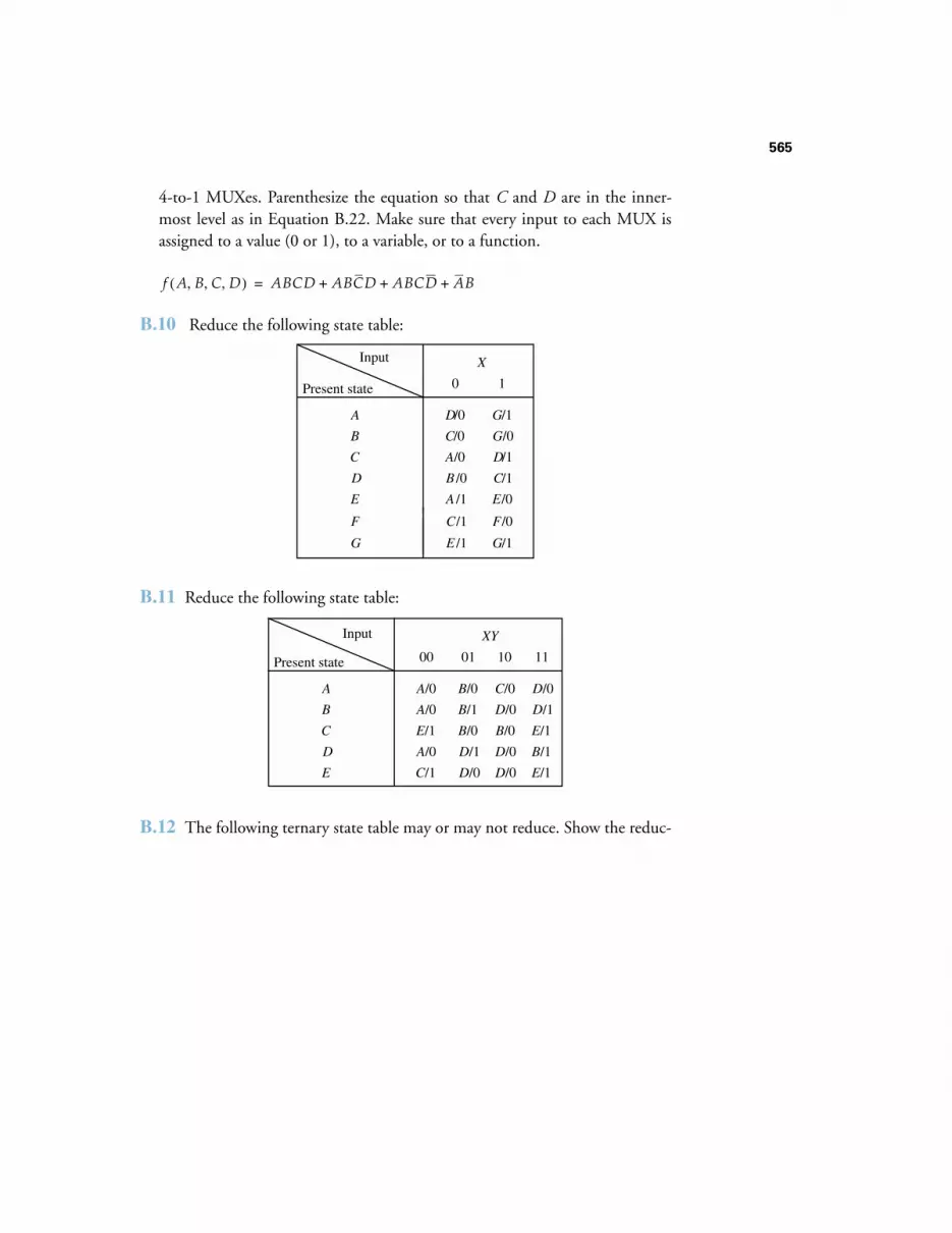
565
4-to-1 MUXes. Parenthesize the equation so that C and D are in the inner-most level as in Equation B.22. Make sure that every input to each MUX isassigned to a value (0 or 1), to a variable, or to a function.
B.10 Reduce the following state table:
B.11 Reduce the following state table:
B.12 The following ternary state table may or may not reduce. Show the reduc-
f A B C D, , ,( ) ABCD ABCD ABCD AB+ + +=
X
0 1
A D/0 G/1
Present state
Input
B
C
D
E
C/0 G/0
A/0 D/1
B /0 C/1
A /1 E/0
F C/1 F/0
G E /1 G/1
XY
00 01
A A/0 B/0
Present state
Input
B
C
D
E
A/0 B/1
E/1 B/0
A/0 D/1
C/1 D/0
10
C/0
D/0
B/0
D/0
D/0
11
D/0
D/1
E/1
B/1
E/1
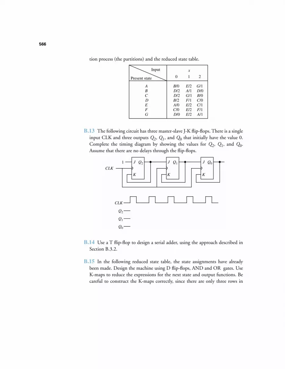
566
tion process (the partitions) and the reduced state table.
B.13 The following circuit has three master-slave J-K flip-flops. There is a singleinput CLK and three outputs Q2, Q1, and Q0 that initially have the value 0.Complete the timing diagram by showing the values for Q2, Q1, and Q0.Assume that there are no delays through the flip-flops.
B.14 Use a T flip-flop to design a serial adder, using the approach described inSection B.3.2.
B.15 In the following reduced state table, the state assignments have alreadybeen made. Design the machine using D flip-flops, AND and OR gates. UseK-maps to reduce the expressions for the next state and output functions. Becareful to construct the K-maps correctly, since there are only three rows in
x
0 1
A B/0 E/2
Present state
Input
BCDE
D/2 A/1D/2 G/1B/2 F/1A/0 E/2
2
G/1D/0B/0C/0C/1
F C/0 E/2 F/1G D/0 E/2 A/1
J
CLK
Q2 J J
K K K
1 Q1 Q0
CLK
Q2
Q1
Q0
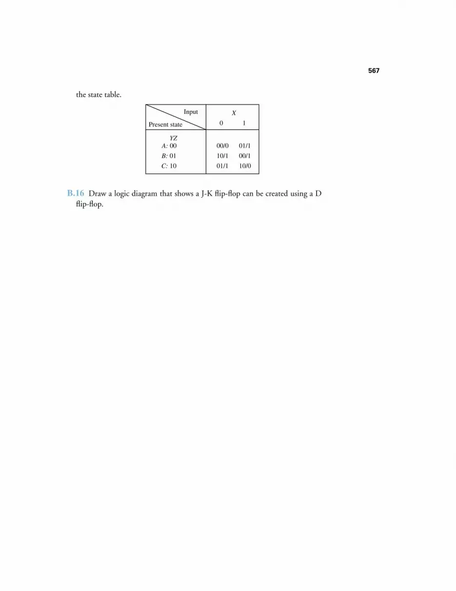
567
the state table.
B.16 Draw a logic diagram that shows a J-K flip-flop can be created using a Dflip-flop.
X
0 1
A: 00 00/0 01/1
Present state
Input
B: 01
C: 10
10/1 00/1
01/1 10/0
YZ

568
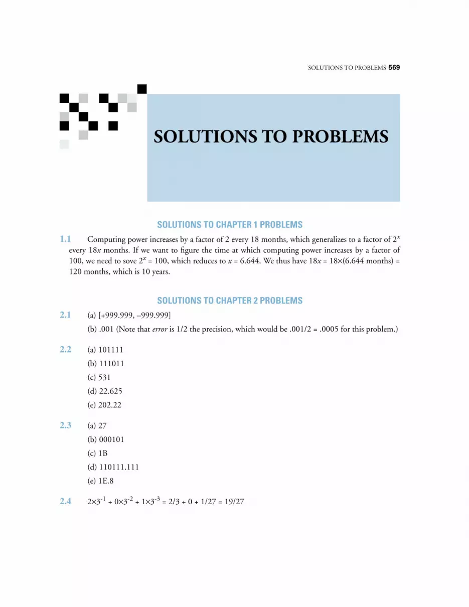
SOLUTIONS TO PROBLEMS
569
SOLUTIONS TO CHAPTER 1 PROBLEMS
1.1
Computing power increases by a factor of 2 every 18 months, which generalizes to a factor of 2
x
every 18
x
months. If we want to figure the time at which computing power increases by a factor of100, we need to sove 2
x
= 100, which reduces to
x
= 6.644. We thus have 18
x
= 18
×
(6.644 months) =120 months, which is 10 years.
SOLUTIONS TO CHAPTER 2 PROBLEMS
2.1
(a) [+999.999, –999.999]
(b) .001 (Note that
error
is 1/2 the precision, which would be .001/2 = .0005 for this problem.)
2.2
(a) 101111
(b) 111011
(c) 531
(d) 22.625
(e) 202.22
2.3
(a) 27
(b) 000101
(c) 1B
(d) 110111.111
(e) 1E.8
2.4
2
×
3
-1
+ 0
×
3
-2
+ 1
×
3
-3
= 2/3 + 0 + 1/27 = 19/27
SOLUTIONS TO PROBLEMS
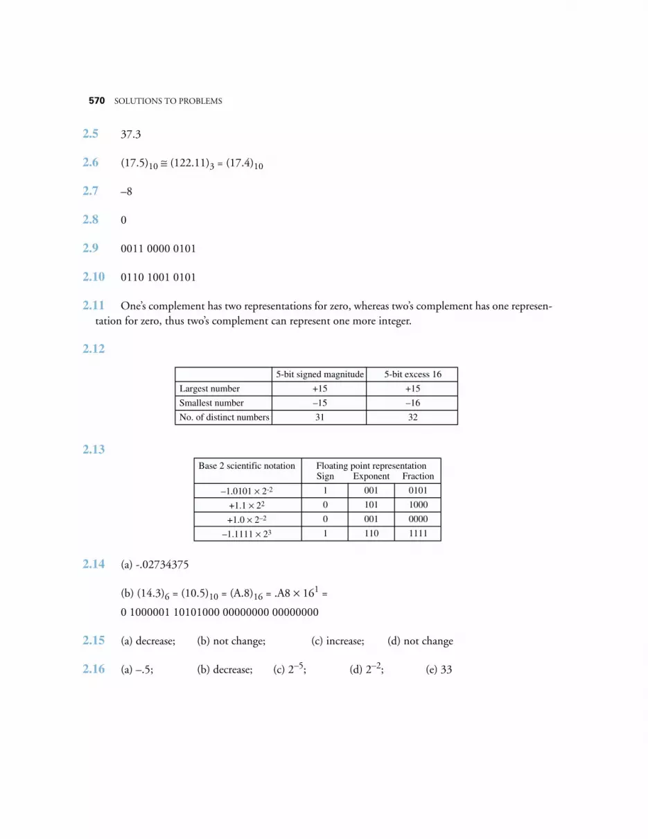
570
SOLUTIONS TO PROBLEMS
2.5
37.3
2.6
(17.5)
10
≅
(122.11)
3
= (17.4)
10
2.7
–8
2.8
0
2.9
0011 0000 0101
2.10
0110 1001 0101
2.11
One’s complement has two representations for zero, whereas two’s complement has one represen-tation for zero, thus two’s complement can represent one more integer.
2.12
2.13
2.14
(a) -.02734375
(b) (14.3)
6
= (10.5)
10
= (A.8)
16
= .A8
×
16
1
=
0 1000001 10101000 00000000 00000000
2.15
(a) decrease; (b) not change; (c) increase; (d) not change
2.16
(a) –.5; (b) decrease; (c) 2
–5
; (d) 2
–2
; (e) 33
Largest number
Smallest number
No. of distinct numbers
5-bit signed magnitude 5-bit excess 16
+15
–15
31
+15
–16
32
–1.0101 × 2-2
Floating point representationBase 2 scientific notationSign Exponent Fraction
+1.1 × 22
0
1
001
110
0000
1111
+1.0 × 2–2
–1.1111 × 23
0 101 1000
1 001 0101

SOLUTIONS TO PROBLEMS
571
2.17
(107.15)
10
= 1101011.00100110011001100
0 1000111 11010110 01001100 11001100
2.18
(a) +1.011
×
2
4
(b) -1.0
×
2
1
(c) -0
(d) -
∞
(e) +NaN
(f ) +1.1001
×
2
-126
(g) +1.01101
×
2
-124
2.19
(a) 0 10000100 1011 0000 0000 0000 0000 000
(b) 0 00000000 0000 0000 0000 0000 0000 000
(c) 1 01111111110 0011 1000 0000 0000 0000
0000 0000 0000 0000 0000 0000 0000 0000
(d) 1 11111111 1011 1000 0000 0000 0000 000
2.20
(a) (2 – 2
-23
)
×
2
127
(b) 1.0
×
2
-126
(c) 2
-23
×
2
-126
= 2
-149
(d) 2
-23
×
2
-126
= 2
-149
(e) 2
-23
×
2
127
= 2
104
(f ) 2
×
(127 – -126 + 1)
×
1
×
2
23
+ 1 = 254
×
2
24
+ 1
2.21
The distance from zero to the first representable number is greater than the gap size for the sameexponent values.
2.22
If we remove the leftmost digit, there is no way to know which value from 1 to 15 should berestored.
2.23
No, because there are no unused bit patterns.
2.24
No. The exponent determines the position of the radix point in the fixed point equivalent repre-sentation of a number. This will almost always be different between the orginal and converted num-bers, and so the value of the exponent will be different in general.
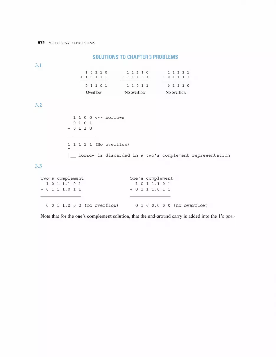
572
SOLUTIONS TO PROBLEMS
SOLUTIONS TO CHAPTER 3 PROBLEMS
3.1
3.2
- 1 1 0 0 <-- borrows- 0 1 0 1- 0 1 1 0__________
1 1 1 1 1 (No overflow)^|__ borrow is discarded in a two’s complement representation
3.3
Two’s complement One’s complement+ 1 0 1 1.1 0 1 + 1 0 1 1.1 0 1+ 0 1 1 1.0 1 1 + 0 1 1 1.0 1 1_______________ _______________
+ 0 0 1 1.0 0 0 (no overflow) + 0 1 0 0.0 0 0 (no overflow)
Note that for the one’s complement solution, that the end-around carry is added into the 1’s posi-
1 0 1 1 0+ 1 0 1 1 1
0 1 1 0 1
Overflow
1 1 1 1 0+ 1 1 1 0 1
1 1 0 1 1
No overflow
1 1 1 1 1+ 0 1 1 1 1
0 1 1 1 0
No overflow
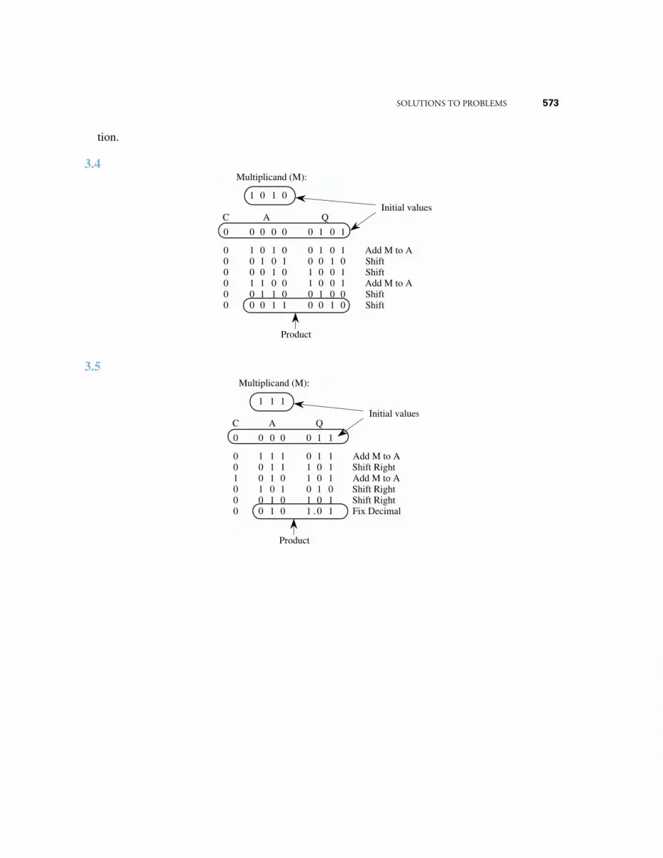
SOLUTIONS TO PROBLEMS
573
tion.
3.4
3.5
C
0
000000
0
A
0 0 0
1 0 1 00 1 0 10 0 1 01 1 0 00 1 1 00 0 1 1
0
Q
1 0 1
0 1 0 10 0 1 01 0 0 11 0 0 10 1 0 00 0 1 0
Multiplicand (M):
1 0 1 0Initial values
Add M to AShiftShift
ShiftAdd M to A
Shift
Product
C
0
001000
A
0 0 0
1 1 10 1 10 1 01 0 10 1 00 1 0
Q
0 1 1
0 1 11 0 11 0 10 1 01 0 11 0 1
Multiplicand (M):
1 1 1Initial values
Add M to AShift RightAdd M to A
Shift RightShift Right
Fix Decimal
Product
.
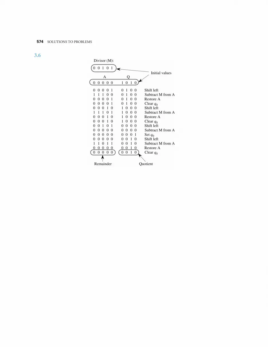
574
SOLUTIONS TO PROBLEMS
3.6
0
01
00
0
A
0 0 0
0 0 0 11 1 0 0
0 1 0 10 0 0 0
1
Q
0 1 0
0 1 0 00 1 0 0
0 0 0 00 0 0 0
Divisor (M):
0 1 0 1Initial values
Shift leftSubtract M from A
Shift leftSubtract M from A
0 0 0 0 1 0 1 0 0 Restore A
01
0 0 1 01 1 0 1
1 0 0 01 0 0 0
Shift leftSubtract M from A
0 0 0 1 0 1 0 0 0 Restore A
0 0 0 0 1 0 1 0 0 Clear q0
0 0 0 1 0 1 0 0 0 Clear q0
0 0 0 0 0 0 0 0 1 Set q001
0 0 0 01 0 1 1
0 0 1 00 0 1 0
Shift leftSubtract M from A
0 0 0 0 0 0 0 1 0 Restore A0 0 0 0 0 0 0 1 0 Clear q0
Remainder Quotient
0

SOLUTIONS TO PROBLEMS
575
3.7
3.8
c
4
=
G
3
+
P
3
G
2
+
P
3
P
2
G
1
+
P
3
P
2
P1G0 + P3P2P1P0
3.9 (a) The carry out of each CLA is generated in just three gate delays after the inputs settle. Thelongest path through a CLA is five gate delays. The longest path through the 16-bit CLA/ripple adderis 14 (nine to generate c12, plus five to generate s15).
(b) s0 is generated in just two gate delays.
(c) s12 is generated in 11 gate delays. It takes 3 gate delays to generate c4, which is needed to gen-erate c 3 gate delays later, which is needed to generate c12 3 gate delays after that, for a total of 9 gatedelays before c12 can be used in the leftmost CLA. The s12 output is generated 2 gate delays after that,for a total of 11 gate delays.
0
01
00
0
A
0 0 0
0 0 0 11 1 0 1
0 1 0 10 0 0 1
1
Q
0 1 0
0 1 0 00 1 0 0
0 0 0 00 0 0 0
Divisor (M):
0 1 0 0Initial values
Shift leftSubtract M from A
Shift leftSubtract M from A
0 0 0 0 1 0 1 0 0 Restore A
01
0 0 1 01 1 1 0
1 0 0 01 0 0 0
Shift leftSubtract M from A
0 0 0 1 0 1 0 0 0 Restore A
0 0 0 0 1 0 1 0 0 Clear q0
0 0 0 1 0 1 0 0 0 Clear q0
0 0 0 0 1 0 0 0 1 Set q001
0 0 1 01 1 0 0
0 0 1 00 0 1 0
Shift leftSubtract M from A
0 0 0 1 0 0 0 1 0 Restore A0 0 0 1 0 0 0 1 0 Clear q0
Quotient
0
00
0 1 0 00 0 0 0
0 1 0 00 1 0 0
Shift leftSubtract M from A
0 0 0 0 0 0 1 0 1 Set q0, fix decimal.

576 SOLUTIONS TO PROBLEMS
3.10
3.11
3.12 The carry bit generated by the ith full adder is: ci = Gi + PiGi-1 + ...+ PiP1G0. The Gi and Pi bitsare computed in one gate delay. The ci bit is computed in two additional gate delays. Once we have ci,the sum outputs are computed in two more gate delays. There are 1 + 2 + 2 = 5 gate delays in any carrylookahead adder regardless of the word width, assuming arbitrary fan-in and fan-out.
3.13 Refer to Figure 3-21. The OR gate for each ci has i inputs. The OR gate for c32 has 32 inputs.No other logic gate has more inputs.
×
00
1 0 0 11 1 0 1
11
MultiplicandMultiplier
+1 0 −1 +1 0 −1 Booth coded multiplier
Booth algorithm:Scan multiplier from right to left.use −1 for a 0 to 1 transition;use −1 for the rightmost 1;use +1 for a 1 to 0 transition;use 0 for no change.
0 1 0 0 1 1 Multiplicand+1 0 −1 +1 0 −1 Booth coded multiplier
1000
0000
1100
1110
0000
1011
1111
1000
1010
1011
1010+
10000000010
Negative multiplicandMultiplicand shifted left by 2Negative multiplicand shifted left by 3Multiplicand shifted left by 5
Product
×
00
1 0 0 11 1 0 1
11
MultiplicandMultiplier
+1 0 −1 +1 0 −1 Booth coded multiplier
0 1 0 0 1 1 Multiplicand+2 −1 −1
100
000
110
100
010
111
101
110
110
111
110+
10000000010
(−1 × 19 × 1)(−1 × 19 × 4)(+2 × 19 × 16)
Product
+2 −1 −1 Bit-pair recoded multiplier
Bit-pair recoded multiplier
110
0
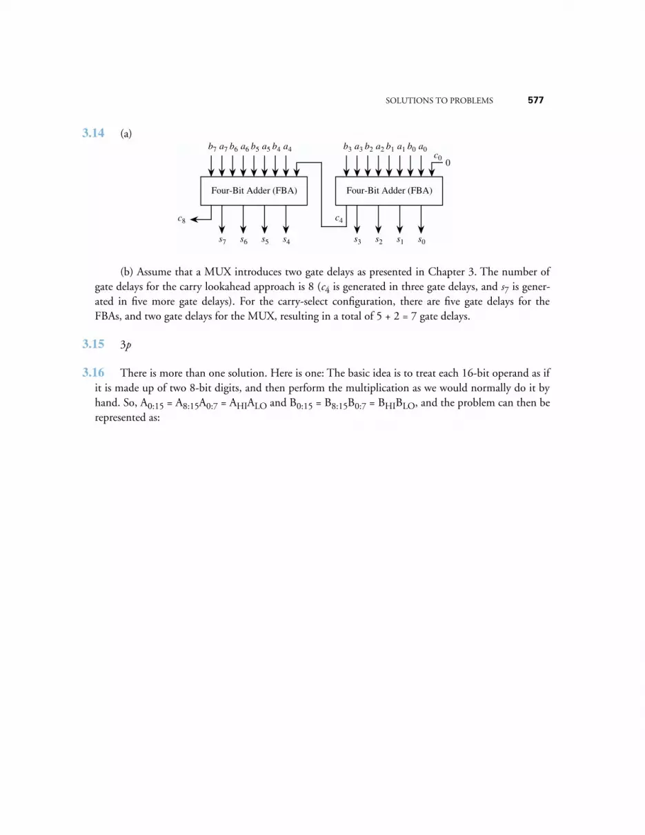
SOLUTIONS TO PROBLEMS 577
3.14 (a)
(b) Assume that a MUX introduces two gate delays as presented in Chapter 3. The number ofgate delays for the carry lookahead approach is 8 (c4 is generated in three gate delays, and s7 is gener-ated in five more gate delays). For the carry-select configuration, there are five gate delays for theFBAs, and two gate delays for the MUX, resulting in a total of 5 + 2 = 7 gate delays.
3.15 3p
3.16 There is more than one solution. Here is one: The basic idea is to treat each 16-bit operand as ifit is made up of two 8-bit digits, and then perform the multiplication as we would normally do it byhand. So, A0:15 = A8:15A0:7 = AHIALO and B0:15 = B8:15B0:7 = BHIBLO, and the problem can then berepresented as:
b0 a0b1 a1b2 a2b3 a3
c4
0c0
Four-Bit Adder (FBA)
b4 a4
s4
b5 a5
s5
b6 a6
s6
b7 a7
s7
Four-Bit Adder (FBA)
c8
s0s1s2s3

578 SOLUTIONS TO PROBLEMS
3.17 Two iterations.
3.18
3.19
SOLUTIONS TO CHAPTER 4 PROBLEMS
4.1 24
4.2 Lowest: 0; Highest: 218 – 1
This is not a byte addressable architecture and so all addresses are in units of words, even though we
ALO
BLOBHI
AHI
×
ALOBLO ×
BLO ×
ALO×
×
AHI
BHI
BHI AHI
32-bit sum of partial products
+
+
+
+
8 bits
16-bit partial products
32-bit product
Adder
Adder
Adder
Multipliers
0
0
BHI AHI BLOALO
88
8
8
1616 16
16
8
8
16
88
16
bits 0:7
bits 8:15
bits 0:7bits 8:15
×BHI AHI ALO×BHI ALOBLO ×BLO × AHI
0110 0100 0001+ 0010 0101 1001
1001 0000 0000
0000 0001 0010 0011+ 1001 1000 0010 0010
1001 1001 0100 0101
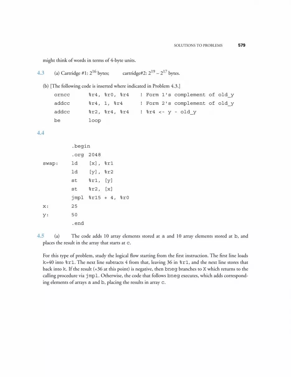
SOLUTIONS TO PROBLEMS 579
might think of words in terms of 4-byte units.
4.3 (a) Cartridge #1: 216 bytes; cartridge#2: 219 – 217 bytes.
(b) [The following code is inserted where indicated in Problem 4.3.]
orncc %r4, %r0, %r4 ! Form 1's complement of old_y
addcc %r4, 1, %r4 ! Form 2's complement of old_y
addcc %r2, %r4, %r4 ! %r4 <- y - old_y
be loop
4.4
.begin
.org 2048
swap: ld [x], %r1
ld [y], %r2
st %r1, [y]
st %r2, [x]
jmpl %r15 + 4, %r0
x: 25
y: 50
.end
4.5 (a) The code adds 10 array elements stored at a and 10 array elements stored at b, andplaces the result in the array that starts at c.
For this type of problem, study the logical flow starting from the first instruction. The first line loadsk=40 into %r1. The next line subtracts 4 from that, leaving 36 in %r1, and the next line stores thatback into k. If the result (+36 at this point) is negative, then bneg branches to X which returns to thecalling procedure via jmpl. Otherwise, the code that follows bneg executes, which adds correspond-ing elements of arrays a and b, placing the results in array c.
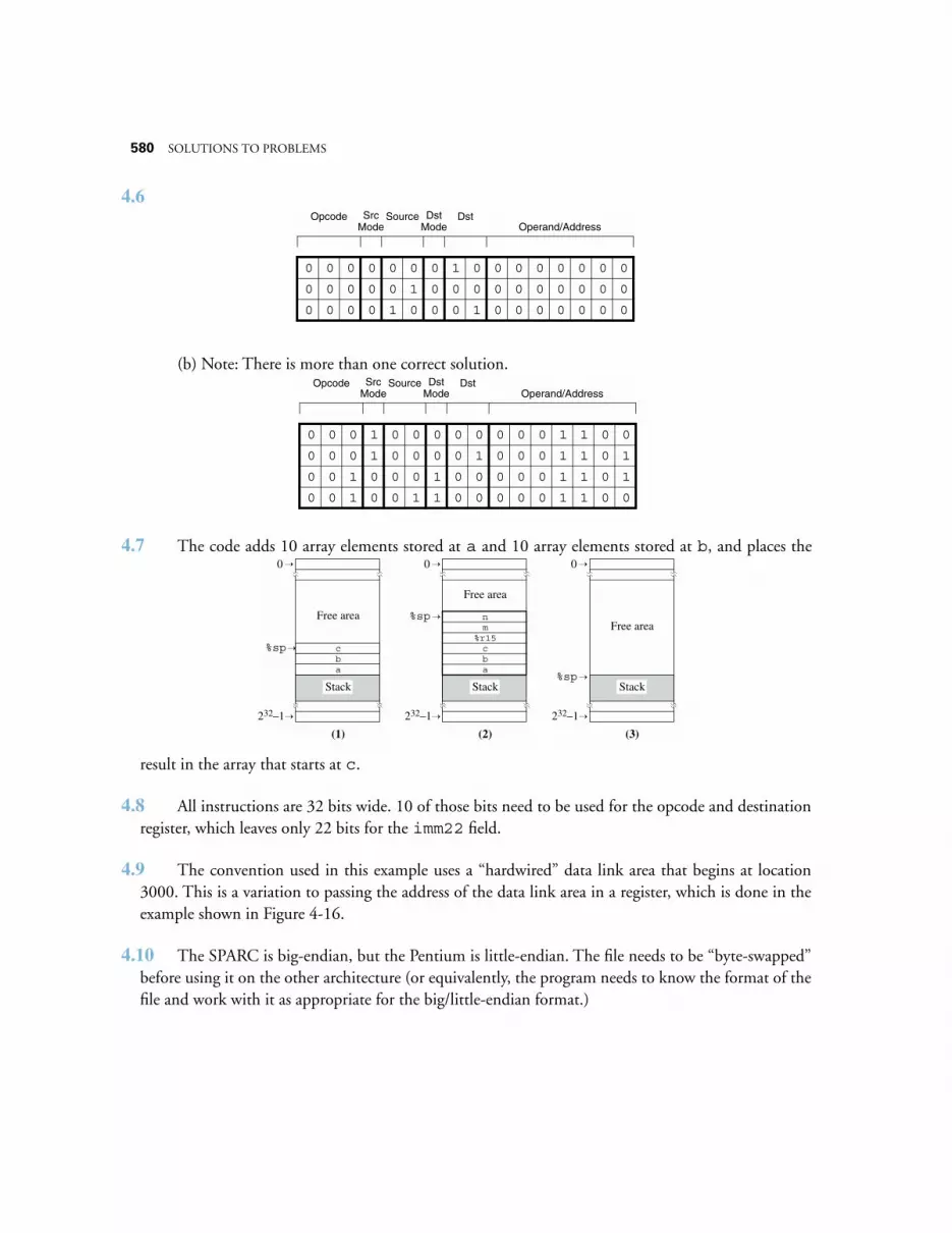
580 SOLUTIONS TO PROBLEMS
4.6
(b) Note: There is more than one correct solution.
4.7 The code adds 10 array elements stored at a and 10 array elements stored at b, and places the
result in the array that starts at c.
4.8 All instructions are 32 bits wide. 10 of those bits need to be used for the opcode and destinationregister, which leaves only 22 bits for the imm22 field.
4.9 The convention used in this example uses a “hardwired” data link area that begins at location3000. This is a variation to passing the address of the data link area in a register, which is done in theexample shown in Figure 4-16.
4.10 The SPARC is big-endian, but the Pentium is little-endian. The file needs to be “byte-swapped”before using it on the other architecture (or equivalently, the program needs to know the format of thefile and work with it as appropriate for the big/little-endian format.)
Opcode Src Mode
Source DstOperand/Address
DstMode
0 0 0 0 0 0 0 1 0 0 0 0 0 0 0 0
0 0 0 0 0 1 0 0 0 0 0 0 0 0 0 0
0 0 0 0 1 0 0 0 1 0 0 0 0 0 0 0
Opcode Src Mode
Source DstOperand/Address
DstMode
0 0 0 1 0 0 0 0 0 0 0 0 1 1 0 0
0 0 0 1 0 0 0 0 1 0 0 0 1 1 0 1
0 0 1 0 0 0 1 0 0 0 0 0 1 1 0 1
0 0 1 0 0 1 1 0 0 0 0 0 1 1 0 0
(1)
0
232–1
Free area
%sp
Stack
ab
(2) (3)
0
232–1
Free area
Stack
0
232–1
%spFree area
%spStack
abc
%r15m
c
n
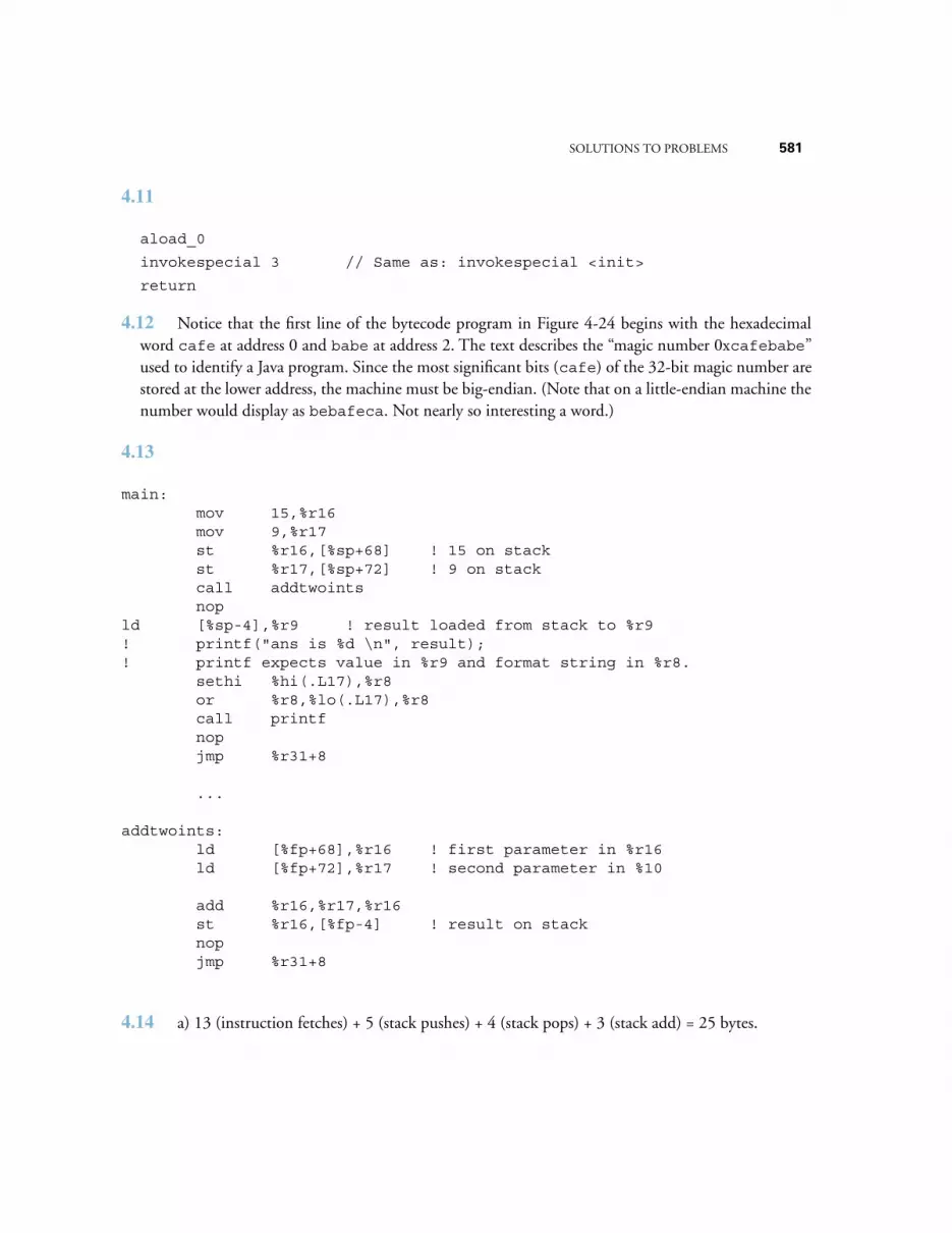
SOLUTIONS TO PROBLEMS 581
4.11
aload_0
invokespecial 3 // Same as: invokespecial <init>
return
4.12 Notice that the first line of the bytecode program in Figure 4-24 begins with the hexadecimalword cafe at address 0 and babe at address 2. The text describes the “magic number 0xcafebabe”used to identify a Java program. Since the most significant bits (cafe) of the 32-bit magic number arestored at the lower address, the machine must be big-endian. (Note that on a little-endian machine thenumber would display as bebafeca. Not nearly so interesting a word.)
4.13
main: mov 15,%r16 mov 9,%r17 st %r16,[%sp+68] ! 15 on stack st %r17,[%sp+72] ! 9 on stack call addtwoints nopld [%sp-4],%r9 ! result loaded from stack to %r9! printf("ans is %d \n", result);! printf expects value in %r9 and format string in %r8. sethi %hi(.L17),%r8 or %r8,%lo(.L17),%r8 call printf nop jmp %r31+8
...
addtwoints: ld [%fp+68],%r16 ! first parameter in %r16 ld [%fp+72],%r17 ! second parameter in %10
add %r16,%r17,%r16 st %r16,[%fp-4] ! result on stack nop jmp %r31+8
4.14 a) 13 (instruction fetches) + 5 (stack pushes) + 4 (stack pops) + 3 (stack add) = 25 bytes.
582 SOLUTIONS TO PROBLEMS
b) [Placeholder for missing solution.]
4.15 It is doubtful that a bytecode program will ever run as fast as the equivalent program written inthe native language. Even if the program is run using a just-in-time (JIT) compiler, it still will usestack-based operations, and will thus not be able to take advantage of the register-based operations ofthe native machine.
4.16
3-address: 2-address 1-addressSUB B, C, A MOV B, A LOAD BSUB D, E, Tmp SUB C, A SUB CMPY A, Tmp, A MOV D, Tmp STO Tmp
SUB E, Tmp LOAD DMPY Tmp, A SUB E
MPY TmpSTO A
Size: 7×3=21 bytes 5×5 = 25 bytes 3×7 = 21 bytes.
Traffic: 3×4+3×3 = 21 wds. 5×3 + 2×2 7×2 + 7 = 21 wds.+ 3×3 = 28 wds.
4.17
ld [B], %r1ld [C], %r2ld [D], %r3ld [E], %r4subcc %r1, %r2, %r2subcc %r3, %r4, %r4smul %r2, %r4, %r4st %r4, [A]
Size: 8 32-bit words. Traffic: 8 + 4 +1 = 13 32-bit words. Note how the load-store, general registerarchitecture leads to less memory traffic than either of the architectures in the exercise above.
SOLUTIONS TO PROBLEMS 583
SOLUTIONS TO CHAPTER 5 PROBLEMS
5.1 The symbol table is shown below. The basic approach is to create an entry in the table for eachsymbol that appears in the assembly language program. The symbols can appear in any order, and asimple way to collect up all of the symbols is to simply read the program from top to bottom, andfrom left to right within each line. The symbols will then be encountered in the order: x, main,lab_4, k, foo, lab_5, and cons. Of these labels, x, main, lab_4, foo, and cons are definedin the program. k and lab_5 are not defined and are marked with a U. Excluded from the symboltable are mnemonics (like addcc), constants, pseudo-ops, and register names.
x has the value 4000 because .equ defines that. main is at location 2072, and so it has that value inthe symbol table. lab_4 is 8 bytes past main (because each instruction is exactly 4 bytes in size) andso lab_4 is at location 2800, etc.
5.2 Notice that the rd field for the st instruction in the last line is used for the source register.
10001000 10000001 00100100 00000000
11001010 00000011 10000000 00000000
10011100 10000011 10111111 11111111
11001010 00100000 00110000 00000000
5.3 [Placeholder for missing solution.]
5.4
3072: 10001100 10000000 10000000 00000100
3076: 00001010 10000000 00000000 00000011
3080: 10001010 10000000 01000000 00000011
Symbol Value
main 2072
lab_4 2080
k U
foo 2088
x 4000
lab_5 U
cons 2104
584 SOLUTIONS TO PROBLEMS
3084: 10000001 11000011 11100000 00000100
3088: 10001010 10000000 01000000 00000011
3092: 00001010 10000000 00000000 00000011
3096: 10001010 10000001 01100000 00000001
3100: 10000001 11000011 11100000 00000100
3104: 10001010 10000001 01100000 00000001
3108: 00001111 00111111 11111111 11111111
3112: 10000000 10000001 11000000 00000111
3116: 10000001 11000011 11100000 00000100
3120: 00000000 00000000 00000000 00000000
3124: 00000000 00000000 00000000 00011001
3128: 11111111 11111111 11111111 11111111
3132: 11111111 11111111 11111111 11111111
3136: 00000000 00000000 00000000 00000000
3140: 00000000 00000000 00000000 00000000
5.5
b: addcc %r1, 1, %r1
orcc %r5, %r6, %r0
be a
srl %r6, 10, %r6
ba b
a: jmpl %r15 + 4, %r0
5.6
ld %r14, %r1
addcc %r14, 4, %r14 ! This line can be deleted
addcc %r14, -4, %r14 ! This line can be deleted
st % r2, %r14
SOLUTIONS TO PROBLEMS 585
5.7
.macro return
jmpl %r15 + 4, %r0
.endmacro
5.8
.
.
.
st %r1, [x]
st %r2, [x+4]
sethi .high22(x), %r5
addcc %r5, .low10(x), %r5
call add_2
ld [x+8], %r3
.
.
.
x: .dwb 3
5.9
.begin
.org 2048
add_128: ld [x+8], %r1 ! Load bits 32-63 of x
ld [x+12], %r2 ! Load bits 0 - 31 of x
ld [y+8], %r3 ! Load bits 32 - 63 of y
ld [y + 12], %r4 ! Load bits 0 -31 of y
call add_64 ! Add lower 64 bits
st %r5, [z + 8] ! Store bits 32 - 63 of result
st %r6, [z + 12] ! Store bits 0 - 31 of result
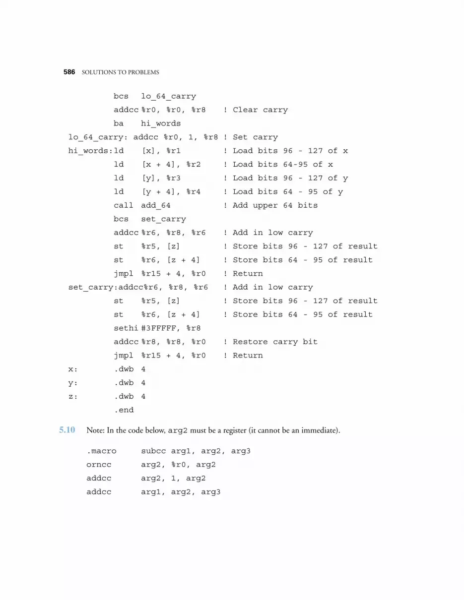
586 SOLUTIONS TO PROBLEMS
bcs lo_64_carry
addcc %r0, %r0, %r8 ! Clear carry
ba hi_words
lo_64_carry: addcc %r0, 1, %r8 ! Set carry
hi_words:ld [x], %r1 ! Load bits 96 - 127 of x
ld [x + 4], %r2 ! Load bits 64-95 of x
ld [y], %r3 ! Load bits 96 - 127 of y
ld [y + 4], %r4 ! Load bits 64 - 95 of y
call add_64 ! Add upper 64 bits
bcs set_carry
addcc %r6, %r8, %r6 ! Add in low carry
st %r5, [z] ! Store bits 96 - 127 of result
st %r6, [z + 4] ! Store bits 64 - 95 of result
jmpl %r15 + 4, %r0 ! Return
set_carry:addcc%r6, %r8, %r6 ! Add in low carry
st %r5, [z] ! Store bits 96 - 127 of result
st %r6, [z + 4] ! Store bits 64 - 95 of result
sethi #3FFFFF, %r8
addcc %r8, %r8, %r0 ! Restore carry bit
jmpl %r15 + 4, %r0 ! Return
x: .dwb 4
y: .dwb 4
z: .dwb 4
.end
5.10 Note: In the code below, arg2 must be a register (it cannot be an immediate).
.macro subcc arg1, arg2, arg3
orncc arg2, %r0, arg2
addcc arg2, 1, arg2
addcc arg1, arg2, arg3
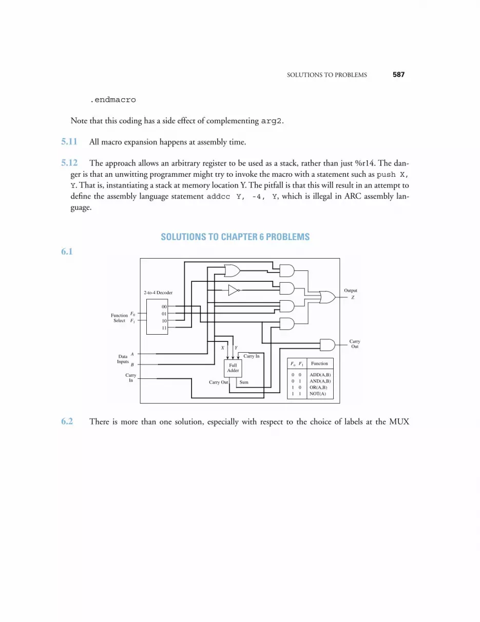
SOLUTIONS TO PROBLEMS 587
.endmacro
Note that this coding has a side effect of complementing arg2.
5.11 All macro expansion happens at assembly time.
5.12 The approach allows an arbitrary register to be used as a stack, rather than just %r14. The dan-ger is that an unwitting programmer might try to invoke the macro with a statement such as push X,Y. That is, instantiating a stack at memory location Y. The pitfall is that this will result in an attempt todefine the assembly language statement addcc Y, -4, Y, which is illegal in ARC assembly lan-guage.
SOLUTIONS TO CHAPTER 6 PROBLEMS
6.1
6.2 There is more than one solution, especially with respect to the choice of labels at the MUX
Z
Carry Out
Output
FullAdder
X Y
Carry In
Carry Out Sum
A
B
Carry In
Data Inputs
F0
F1
00
01
10
11
2-to-4 Decoder
Function Select
0011
0101
Fo F1
ADD(A,B)AND(A,B)OR(A,B)NOT(A)
Function

588 SOLUTIONS TO PROBLEMS
inputs. Here is one solution:
6.3
6.4 Register %r0 cannot be changed, and so there is no need for it to have a write enable line.
6.5 (a)
ALU0
y0 x0
z0
y1 x1
z1
y2 x2
z2
y3 x3
z3
ALU1ALU2ALU3c0c1
y4 x4
z4
ALU4
y5 x5
z5
ALU5
y6 x6
z6
ALU6
y7 x7
z7
ALU7
0011001100110011
0101010101010101
yi xi
0000111100001111
c0
0001011110000110
zi
0000000011111111
c1
c0 xi
zi
000
001
010
011
yi
100
101
110
111
c1
0
0
c1
0
1
1
c1
A B00/00
11/1100/11
Nothalted
Halted
01/0110/10
01/1110/1111/11
F0 F10 1 2 30 1 2 30 1 2 3Write Enables A-bus enables B-bus enables
Time
0
1
2
0 1 0 0 0 1 0 0 0 0 0 0 1 1
1 0 0 0 1 0 0 0 0 1 0 0 0 0
1 0 0 0 1 0 0 0 0 0 0 1 0 0

SOLUTIONS TO PROBLEMS 589
(b)
6.6
6.7
6.81280: R[15] <- AND(R[pc], R[pc]); / Save %pc in %r15
1281: R[temp0] <- LSHIFT2(R[ir]); / Shift disp30 left two bits1282: R[pc] <- ADD(R[pc], R[temp0]); / Jump to subroutine GOTO 0;
6.9 Either seven or eight microinstructions are executed, depending on the value of IR[13]:
IR[13] = 0: (Eight microinstructions) 0, 1, 1584, 1585, 1586, 1587, 1603, 2047.
IR[13] = 1: (Seven microinstructions) 0, 1, 1584, 1586, 1587, 1603, 2047.
6.10 (a) (11 microinstructions): 0, 1, 1088, 2, 3, 4, 5, 6, 7, 8, 12.
F0 F10 1 2 30 1 2 30 1 2 3Write Enables A-bus enables B-bus enables
Time
0
1
2
0 0 1 0 1 0 0 0 0 0 0 0 1 0
1 0 0 0 0 1 0 0 0 0 0 0 1 1
1 0 0 0 1 0 0 0 0 0 1 0 0 1
1 0 0 0 1 0 0 0 0 0 0 0 1 1
0 0 1 0 0 0 1 0 0 0 0 0 1 1
0 0 1 0 0 0 1 0 0 1 0 0 0 1
0 0 1 0 0 0 1 0 0 0 0 0 1 1
1 0 0 0 1 0 0 0 0 0 1 0 0 1
1 0 0 0 1 0 0 0 0 0 0 0 1 1
3
4
5
6
7
8
r0 ⊕ r1 = r0r1 + r0r1 = r0r1 +r0 r1 = r0 r1 r0r1
r0 r1 r0r1
Save r0
Compute
Compute
Compute
Compute
Compute
Compute
Compute
Compute
r0 r1 r0r1
r r0 1
r r0 1
r r0 1
r0
r r0 1
r1
RD
WRCA B JUMP ADDRALU COND
AMUX
BMUX
CMUX
0000001 000101 00010000111010000010000000000010 000000 0000100110100000000000000
6061
00
00
00
R[temp0] ← SEXT13(R[ir]);R[temp0] ← ADD(R[rs1],R[temp0]); GOTO 1793;R[temp0] ← ADD(R[rs1],R[rs2]); IF IR[13] THEN GOTO 1810;
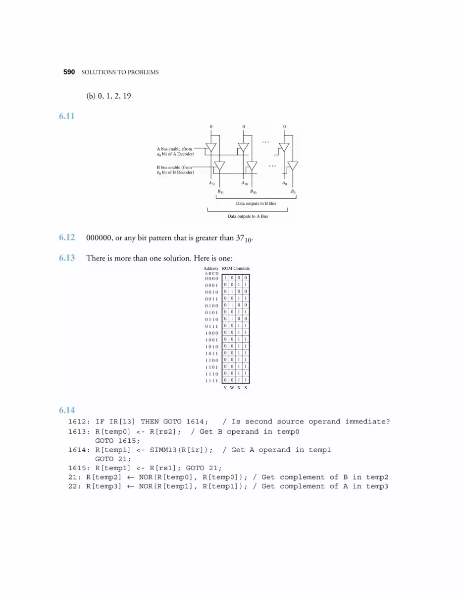
590 SOLUTIONS TO PROBLEMS
(b) 0, 1, 2, 19
6.11
6.12 000000, or any bit pattern that is greater than 3710.
6.13 There is more than one solution. Here is one:
6.141612: IF IR[13] THEN GOTO 1614; / Is second source operand immediate?
1613: R[temp0] <- R[rs2]; / Get B operand in temp0 GOTO 1615;1614: R[temp1] <- SIMM13(R[ir]); / Get A operand in temp1 GOTO 21;1615: R[temp1] <- R[rs1]; GOTO 21;21: R[temp2] ← NOR(R[temp0], R[temp0]); / Get complement of B in temp222: R[temp3] ← NOR(R[temp1], R[temp1]); / Get complement of A in temp3
A31
B31
A30
B30
A0
B0
. . .
A bus enable (from a0 bit of A Decoder)
B bus enable (from b0 bit of B Decoder)
. . .
Data outputs to B Bus
Data outputs to A Bus
0 0 0
ROM ContentsAddress
0 0 0 0
0 0 0 1
0 0 1 0
0 0 1 1
0 1 0 0
0 1 0 1
0 1 1 0
0 1 1 1
1 0 0 0
1 0 0 1
1 0 1 0
1 0 1 1
1 1 0 0
1 1 0 1
1 1 1 0
1 1 1 1
A B C D
V W X S
1
0
0
0
0
0
0
0
0
0
0
0
0
0
0
0
0 0 0
0 1 1
1 0 0
0 1 1
1 0 0
0 1 1
1 0 0
0 1 1
0 1 1
0 1 1
0 1 1
0 1 1
0 1 1
0 1 1
0 1 1
0 1 1

SOLUTIONS TO PROBLEMS 591
23: R[temp1] ← NOR(R[temp1], R[temp2]); / temp1 gets AND(A, B')24: R[temp2] ← NOR(R[temp0], R[temp3]); / temp2 gets AND(A’, B)25: R[rd] ← ORCC(R[temp1],R[temp2]); GOTO 2047; / Extract rs2 operand
6.15
6.16 No.
6.17
Read (Peek at top of stack)
Data In
32
Data Out
Write
Clock
32
32
Top of Stack
32
Push
Pop
0
0
0
32
0
32
32
32
32
32
32
32
CondALU A-Bus B-Bus C-Bus Jump Address Next Address
0
1
2
3
00 010 0 10 00 0 01 000 000 000 000 0 00 00 00 0 001
00 000 0 00 00 0 00 011 000 000 111 1 00 00 00 0 010
01 001 0 01 00 1 00 000 000 000 000 0 00 00 00 0 011
00 000 0 00 00 0 00 001 000 001 010 0 00 00 00 0 000
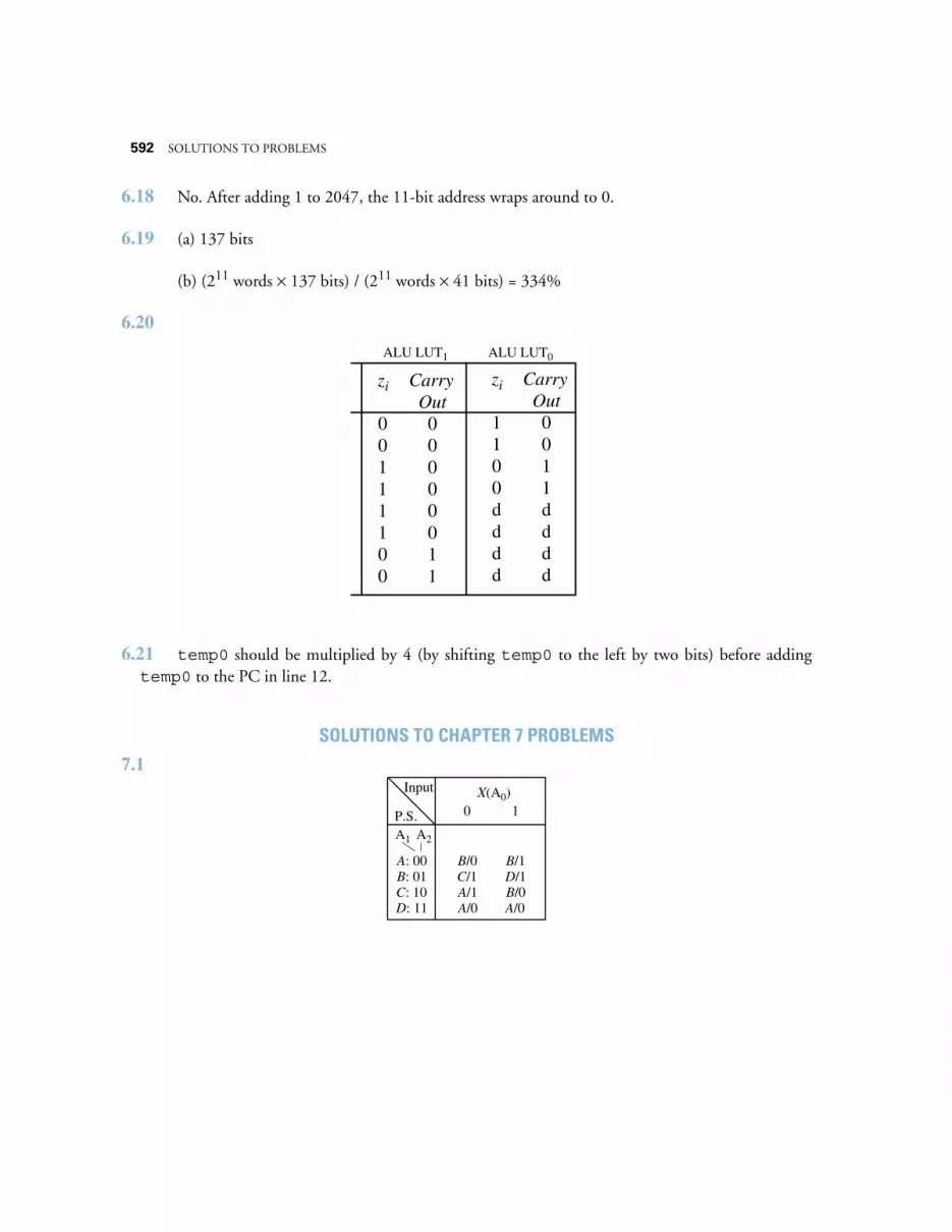
592 SOLUTIONS TO PROBLEMS
6.18 No. After adding 1 to 2047, the 11-bit address wraps around to 0.
6.19 (a) 137 bits
(b) (211 words × 137 bits) / (211 words × 41 bits) = 334%
6.20
6.21 temp0 should be multiplied by 4 (by shifting temp0 to the left by two bits) before addingtemp0 to the PC in line 12.
SOLUTIONS TO CHAPTER 7 PROBLEMS
7.1
zi
00111100
Carry Out00000011
zi
1100dddd
Carry Out0011dddd
ALU LUT1 ALU LUT0
X(A0)0 1
A: 00 B/0 B/1
P.S.
Input
B: 01C: 10D: 11
C/1 D/1A/1 B/0A/0 A/0
A1 A2
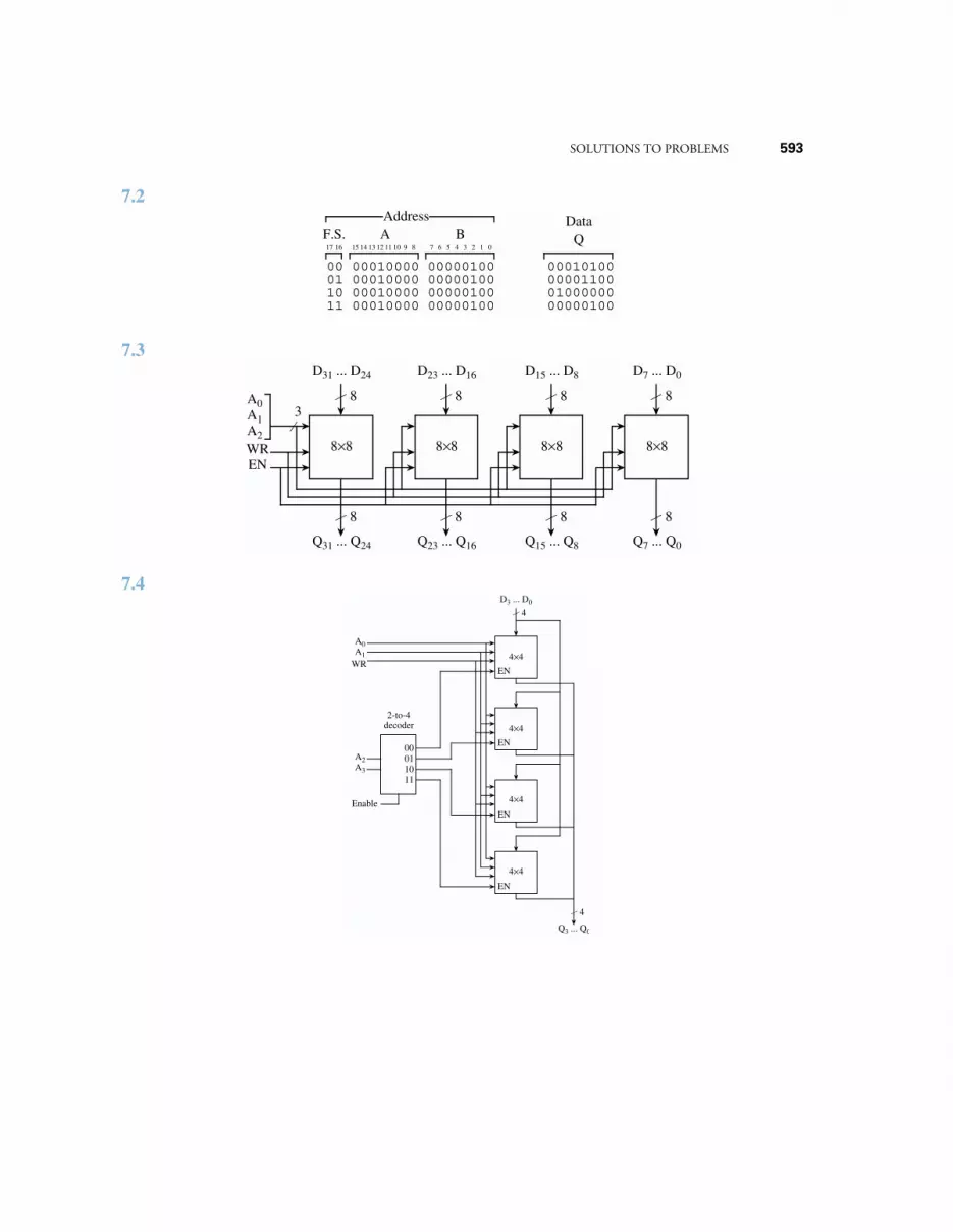
SOLUTIONS TO PROBLEMS 593
7.2
7.3
7.4
00 00010000 00000100 00010100
F.S. A B QDataAddress
01 00010000 00000100 0000110010 00010000 00000100 0100000011 00010000 00000100 00000100
17 16 15 14 13 12 11 10 9 8 7 6 5 4 3 2 1 0
8×8 8×8 8×8 8×8
8
D31 ... D24
8
D23 ... D16
8
D15 ... D8
8
D7 ... D0
3A0
A2
A1
WREN
Q31 ... Q24 Q23 ... Q16 Q15 ... Q8 Q7 ... Q0
8 8 8 8
4×4
4
D3 ... D0
A0
A2
A1
WREN
Q3 ... Q0
4
4×4
4×4
4×4
EN
EN
EN
00011011
A3
Enable
2-to-4 decoder

594 SOLUTIONS TO PROBLEMS
7.5
p
D4p-1 ... D3p
p
D3p-1 ... D2p
p
D2p-1 ... Dp
p
Dp-1 ... D0
log2nAddress
WREN
Q4p-1 ... Q3p Q3p-1 ... Q2p Q2p-1 ... Qp Qp-1 ... Q0
p p p p
(a)
(b)
n×p
p
Dp-1 ... D0
A0
A[log2n]
WREN
Qp-1 ... Q0
p
n×p
n×p
n×p
EN
EN
EN
00011011
Enable
2-to-4 decoder
n×p n×p n×p n×p
A[log2n] + 1
A[log2n] − 1
...
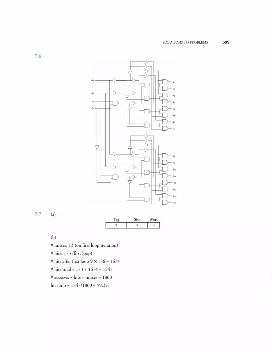
SOLUTIONS TO PROBLEMS 595
7.6
7.7 (a)
(b)
# misses: 13 (on first loop iteration)
# hits: 173 (first loop)
# hits after first loop 9 × 186 = 1674
# hits total = 173 + 1674 = 1847
# accesses = hits + misses = 1860
hit ratio = 1847/1860 = 99.3%
a0
a1
d0
d1
d2
d3
d4
d5
d6
d7
a2
d8
d9
d10
d11
d12
d13
d14
d15
a3
7 7 4
Tag Slot Word
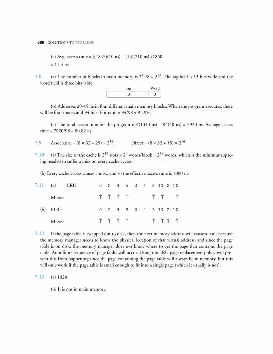
596 SOLUTIONS TO PROBLEMS
(c) Avg. access time = [(1847)(10 ns) + (13)(210 ns)]/1860
= 11.4 ns
7.8 (a) The number of blocks in main memory is 216/8 = 213. The tag field is 13 bits wide and theword field is three bits wide.
(b) Addresses 20-45 lie in four different main memory blocks. When the program executes, therewill be four misses and 94 hits. Hit ratio = 94/98 = 95.9%.
(c) The total access time for the program is 4(1040 ns) + 94(40 ns) = 7920 ns. Average accesstime = 7920/98 = 80.82 ns.
7.9 Associative = (8 × 32 + 29) × 214; Direct = (8 × 32 + 15) × 214
7.10 (a) The size of the cache is 214 slots × 25 words/block = 219 words, which is the minimum spac-ing needed to suffer a miss on every cache access.
(b) Every cache access causes a miss, and so the effective access time is 1000 ns.
7.11 (a) LRU 0 2 4 5 2 4 3 11 2 10
Misses: ↑XX↑XX↑XX↑XXXXXXXX↑XX↑XXXX↑
(b) FIFO 0 2 4 5 2 4 3 11 2 10
Misses: ↑XX↑XX↑XX↑XXXXXXXX↑XX↑X↑XX↑
7.12 If the page table is swapped out to disk, then the next memory address will cause a fault becausethe memory manager needs to know the physical location of that virtual address, and since the pagetable is on disk, the memory manager does not know where to get the page that contains the pagetable. An infinite sequence of page faults will occur. Using the LRU page replacement policy will pre-vent this from happening since the page containing the page table will always be in memory, but thiswill only work if the page table is small enough to fit into a single page (which it usually is not).
7.13 (a) 1024
(b) It is not in main memory.
13 3
Tag Word

SOLUTIONS TO PROBLEMS 597
(c) Page frame 2
7.14 (a) (N – M) / N
(b) (M – F) / M
(c) [(N – M)T1 + (M – F)T2 + FT3]/N
7.15 Virtual addresses tend to be large (typically 32 bits). If virtual addresses are cached, then the tagfields will be correspondingly large as well as the hardware that looks at the tags. If physical addressesare cached, then every memory reference will go through the page table. This slows down the cache,but the tag fields are smaller, which simplifies the hardware.
If we cluster the virtual memory and cache memory into a single memory management unit (MMU),then we can cache physical addresses and simultaneously search the cache and the page table, using thelower order bits of the address (which are identical for physical and virtual addresses). If the page tablesearch is successful, then that means the corresponding cache block (if we found a block) is the blockwe want. Thus, we can get the benefits of small size in caching physical addresses while not beingforced to access main memory to look at the page table, because the page table is now in hardware.Stated more simply: this is the purpose of a translation lookaside buffer.
7.16 There are 232 bytes / 212 bytes/page = 220 pages. There is a page table entry for each page, and sothe size of the page table is 220 × 8 bytes = 223 bytes.
7.17 For the 2D case, each AND gate of the decoder needs a fan-in of 6, assuming the decoder has aform similar to Figure 7-4. There are 26 AND gates and 6 inverters, giving a total gate input count of26 × 6 + 6 = 390 for the 2D case. For the 2-1/2D case, there are two decoders, each with 23 ANDgates and 3 inverters, and a fan-in of 3 to the AND gates. The total gate input count is then 2 × (23 ×3 + 3) = 54 for the 2-1/2D case.
7.18 log4(220) = 10
7.19 (a) 220
(b) 211
7.20 Words F1A0028 and DFA0502D
7.21 32
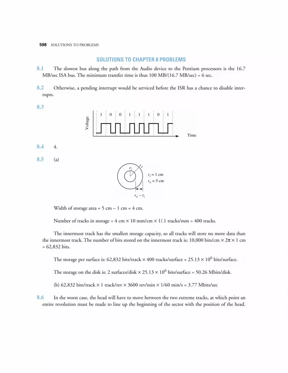
598 SOLUTIONS TO PROBLEMS
SOLUTIONS TO CHAPTER 8 PROBLEMS
8.1 The slowest bus along the path from the Audio device to the Pentium processors is the 16.7MB/sec ISA bus. The minimum transfer time is thus 100 MB/(16.7 MB/sec) = 6 sec.
8.2 Otherwise, a pending interrupt would be serviced before the ISR has a chance to disable inter-rupts.
8.3
8.4 4.
8.5 (a)
Width of storage area = 5 cm – 1 cm = 4 cm.
Number of tracks in storage = 4 cm × 10 mm/cm × 1/.1 tracks/mm = 400 tracks.
The innermost track has the smallest storage capacity, so all tracks will store no more data thanthe innermost track. The number of bits stored on the innermost track is: 10,000 bits/cm × 2π × 1 cm= 62,832 bits.
The storage per surface is: 62,832 bits/track × 400 tracks/surface = 25.13 × 106 bits/surface.
The storage on the disk is: 2 surfaces/disk × 25.13 × 106 bits/surface = 50.26 Mbits/disk.
(b) 62,832 bits/track × 1 track/rev × 3600 rev/min × 1/60 min/s = 3.77 Mbits/sec
8.6 In the worst case, the head will have to move between the two extreme tracks, at which point anentire revolution must be made to line up the beginning of the sector with the position of the head.
Time
Vol
tage
1 0 0 1 1 1 0 1
ri = 1 cm
ro = 5 cm
ro − ri
riro

SOLUTIONS TO PROBLEMS 599
The entire sector must then move under the head. The worst case access time for a sector is thus com-posed of three parts:
8.7 (a) The time to read a track is the same as the rotational delay, which is:
1/3600 min/rev × 1 rev/track × 60,000 ms/min = 16.67 ms.
(b) The time to read a track is 16.67ms (from 8.5a). The time to read a cylinder is 19 × 16.67 ms= 316.67 ms. The time to move the arm between cylinders is:
.25 mm × 1/7.5 s/m × 1000 ms/s × 1/1000 m/mm = 1/7.5 ms = .033 ms.
The storage per cylinder is 300/815 MB/cyl = .37 MB/cyl.
The time to transfer the buffer to the host is:
1/300 s/KB × .37 MB/cyl × 1024 KB/MB = 1.26 seconds/cylinder.
We are looking for the minimum time to transfer the entire disk to the host, and so we canassume that after the buffer is emptied, that the head is exactly positioned at the starting sector of thenext cylinder. The entire transfer time is then (.317s/cyl + 1.26 s/cyl) × 815 cyl = 1285 s, or 21.4 min.Notice that the head movement time does not contribute to the transfer time because it overlaps withthe 1.26 buffer transfer time.
8.8 A sector can be read into the buffer in .1 revolutions (rev). The disk must then continue for .9rev in order to align the corresponding sector on the target surface with its head. The disk then contin-ues through another .1 rev to write the sector, at which point the next sector to be read is lined up withits head, which is true regardless of which track the next sector is on. The time to transfer each sectoris thus 1.1 rev. There are 10,000 sectors per surface, and so the time to copy one surface to another is:
10,000 sectors × 1.1 rev/sector × 1/3000 min/rev = 3.67 min.
8.9 The size of a record is:
15 ms/head movement × 127 head movements +
(1/3600 min/rev × 60,000 ms/min)(1 + 1/32) = 1922 ms
Seek time
Rotational delay Sector read time
600 SOLUTIONS TO PROBLEMS
2048 bytes × 1/6250 in/byte = .327 in.
There are x records and x – 1 inter-record gaps in 600 ft, and so we have the relation:
(.327 in)(x) + (.5 in) (x – 1) = 600 ft × 12 in/ft = 7200 in.
Solving for x, we have x = 8706 (whole) records, which translates to: 8706 records × 2048bytes/record = 17.8 MB.
8.10 The number of bits written to the display each second is 1024 × 1024 × 60 = 62,914,560 bits/s.The maximum time allowed to write each pixel is then: 1/62,914,560 s/bit × 109 ns/s = 15.9 ns.
8.11 The LUT size = 28 words × 24 bits/word = 6144 bits, and the RAM size is 219 words × 8bits/word = 4,194,304. Without a LUT, the RAM size is 219 words × 24 bits/word = 12,582,912 bits.The increase in RAM size is 8,388,608 bits, which is much larger than the size of the LUT.
8.12 (a) We no longer have random access to sectors, and must look at all intervening sectors beforereaching the target sector.
(b) Disk recovery would be easier if the MCB is badly damaged, because the sector lists are dis-tributed throughout the disk. An extra block is needed at the beginning of each file for this, but nowthe MCB can have a fixed size.
8.13 The problem is that the data was written with the heads in a particular alignment, and that thehead alignment was changed after the data was written. This means that the beginning of each trackno longer corresponds to the relative positioning of each track prior to realignment. The use of a tim-ing track will not fix the problem, unless a separate timing track is used for each surface (which is notthe usual case).
SOLUTIONS TO CHAPTER 9 PROBLEMS
9.1 Hamming distance = 3.

SOLUTIONS TO PROBLEMS 601
9.2
9.3 (a) k + r + 1 ≤ 2r for k = 6. Simplifying yields: 7 + r ≤ 2r for which r = 4 is the smallest value thatsatisfies the relation.
(b)
(c) 11
(d) 101111011001
9.4 k + r + 1 ≤ 2r for k = 1024. Simplifying yields 1025 + r ≤ 2r for which r = 11 is the smallest valuethat satisfies the relation.
9.5
9.6 (a) 4096
(b) 8
9.7 First, we look for errors in the check bit computations for the SEC code. If all of the check bitcomputations are correct, then there are no single bit errors nor any double bit errors. If any of theSEC check bit computations are wrong, then there is either a single bit error or a double bit error.
The DED parity bit creates even parity over the entire word when there are no errors. If the DED par-ity computation is in error, then there is an odd number of errors, which we can assume is a single bit
1 0 1 0 0 0 0 0 1 0 1
11 10 9 8 7 6 5 4 3 2 1
C2 C1C8 C4
ASCII ‘Q’ = 1010001
1 0 1 1 1 0 0 0 1 1
10 9 8 7 6 5 4 3 2 1
C2 C1C8 C4
Code
111111
Character
111111
111111
000000
000110
111001
011000
101011
VWXYZ
Checksum
602 SOLUTIONS TO PROBLEMS
error for this problem. If the DED parity computation is even, and the SEC computation indicatesthere is an error, then there must be at least a double bit error.
9.8 CRC = 101. The entire frame to be transmitted is 101100110 101.
9.9 32 bits
9.10 Class B
9.11 27 + 214 + 221
9.12 63 ns for bit-serial transfer, 32 ns for word-parallel. The word-parallel version requires 32 timesas much hardware, but only halves the transmission time, as a result of the time-of-flight delaythrough the connection.
9.13 [Placeholder for solution.]
SOLUTIONS TO CHAPTER 10 PROBLEMS
10.1 CPIAVG = 1 + 5(.25)(.5) = 1.625 × 10 = 16.25 ns
Execution efficiency = 1/1.625 = 62%
10.2
No, for the ARC architecture, we cannot use %r0 immediately after the st because st needs two cyclesto finish execution. If we did reuse %r0 in the second line, then a nop (or some other instruction thatdoes not produce a register conflict) would have to be inserted between the st and sethi lines. How-ever, for the SPARC architecture, the pipeline stalls when a conflict is detected, so nops are never actuallyneeded for delayed loads in the SPARC. The nop instruction is needed for delayed branches in theSPARC, however.
10.3 [Placeholder for solution.]
10.4 [Placeholder for solution.]
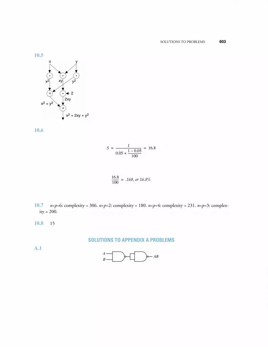
SOLUTIONS TO PROBLEMS 603
10.5
10.6
10.7 n=p=6: complexity = 306. n=p=2: complexity = 180. n=p=4: complexity = 231. n=p=3: complex-ity = 200.
10.8 15
SOLUTIONS TO APPENDIX A PROBLEMS
A.1
x2 y2xy
2xy
2
x2 + y2
x2 + 2xy + y2
* * *
x y
*+
+
S 1
0.05˙ 1 0.05–100
-------------------+------------------------------------ 16.8= =
16.8100---------- .168, or 16.8%=
A
BAB
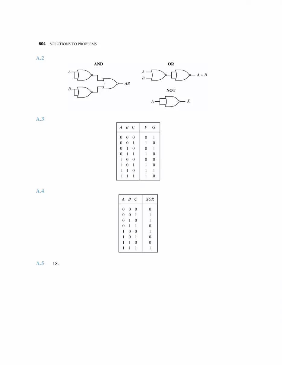
604 SOLUTIONS TO PROBLEMS
A.2
A.3
A.4
A.5 18.
A
BA + B
OR
A
NOT
A
A
BAB
AND
00110011
01010101
B C
00001111
A
01010111
F
10100010
G
00110011
01010101
B C
00001111
A
01101001
XOR

SOLUTIONS TO PROBLEMS 605
A.6
A.7
A.8 Not equivalent:
f(A,B,C)
A B C
A B C
A B C
A CB
g(A,B,C,D,E)
B C E D A
00110011
01010101
B C
00001111
A
00100001
F
00010010
G
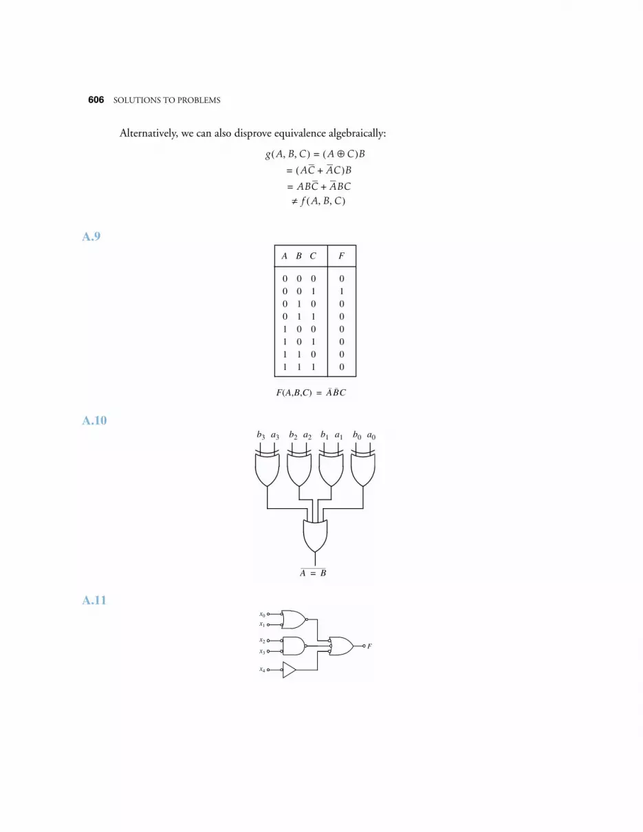
606 SOLUTIONS TO PROBLEMS
Alternatively, we can also disprove equivalence algebraically:
A.9
A.10
A.11
g A B C, ,( ) A C⊕( )B=
a AC AC+( )B=
a ABC ABC+=
a f≠ A B C, ,( )
00110011
01010101
B C
00001111
A
01000000
F
F(A,B,C) = ABC
a0b0a1b1a2b2a3b3
A = B
F
x0
x1
x2
x3
x4
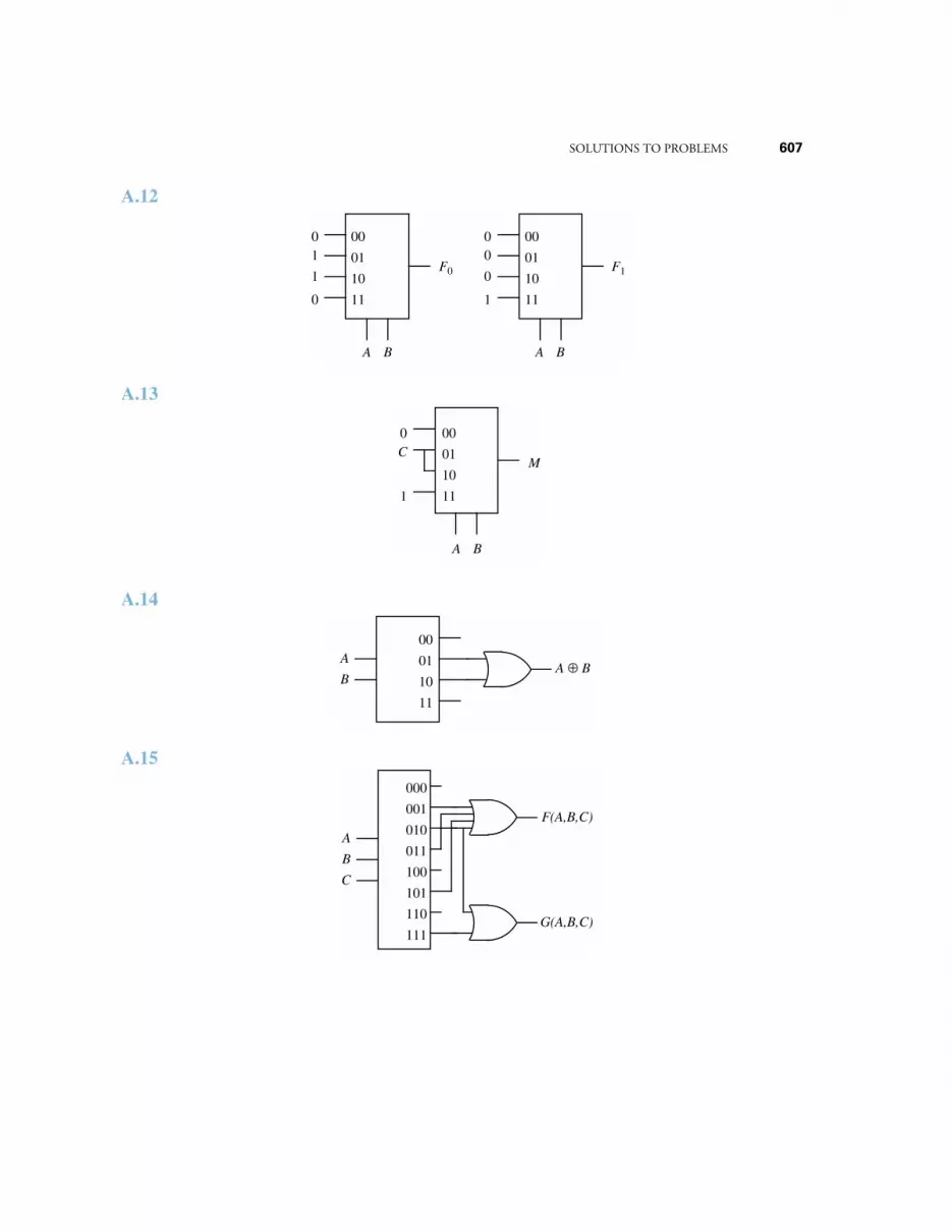
SOLUTIONS TO PROBLEMS 607
A.12
A.13
A.14
A.15
A B
F0
00
01
10
11
0
0
1
1
A B
F1
00
01
10
11
0
1
0
0
A B
M
00
01
10
11
0
1
C
A
B
00
01
10
11
A ⊕ B
A
B
000
001
010
011
F(A,B,C)
100
101
110
111
C
G(A,B,C)
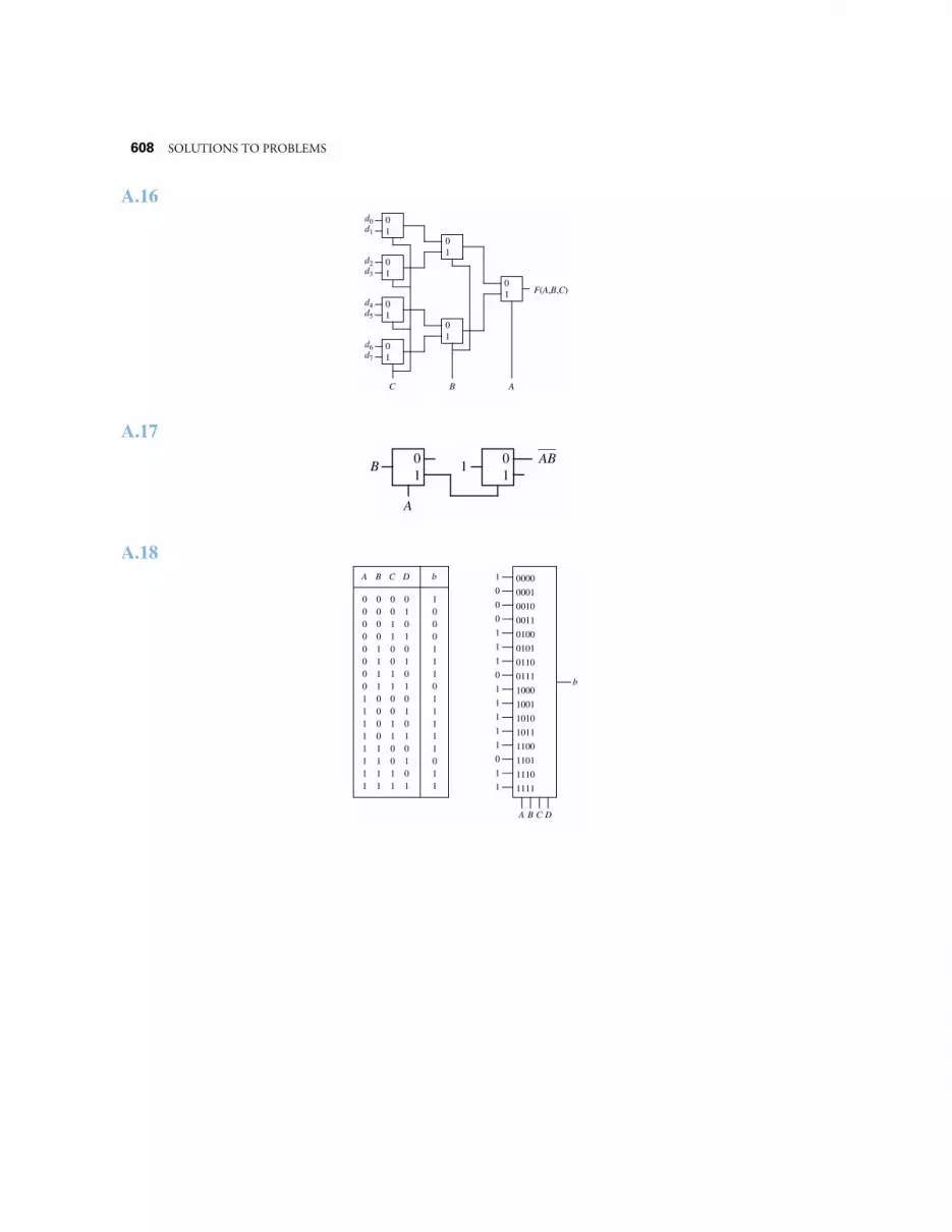
608 SOLUTIONS TO PROBLEMS
A.16
A.17
A.18
d0 01d1
d2 01d3
d4 01d5
d6 01d7
C
01
01
01
B A
F(A,B,C)
01
B
A
01
1AB
0011001100110011
0101010101010101
C D
0000111100001111
B
1000111011111011
b
0000000011111111
A
b
0001
0010
0011
0100
0101
0110
0111
0000
A B C D
1
0
0
0
1
1
1
0
1001
1010
1011
1100
1101
1110
1111
10001
1
1
1
1
0
1
1
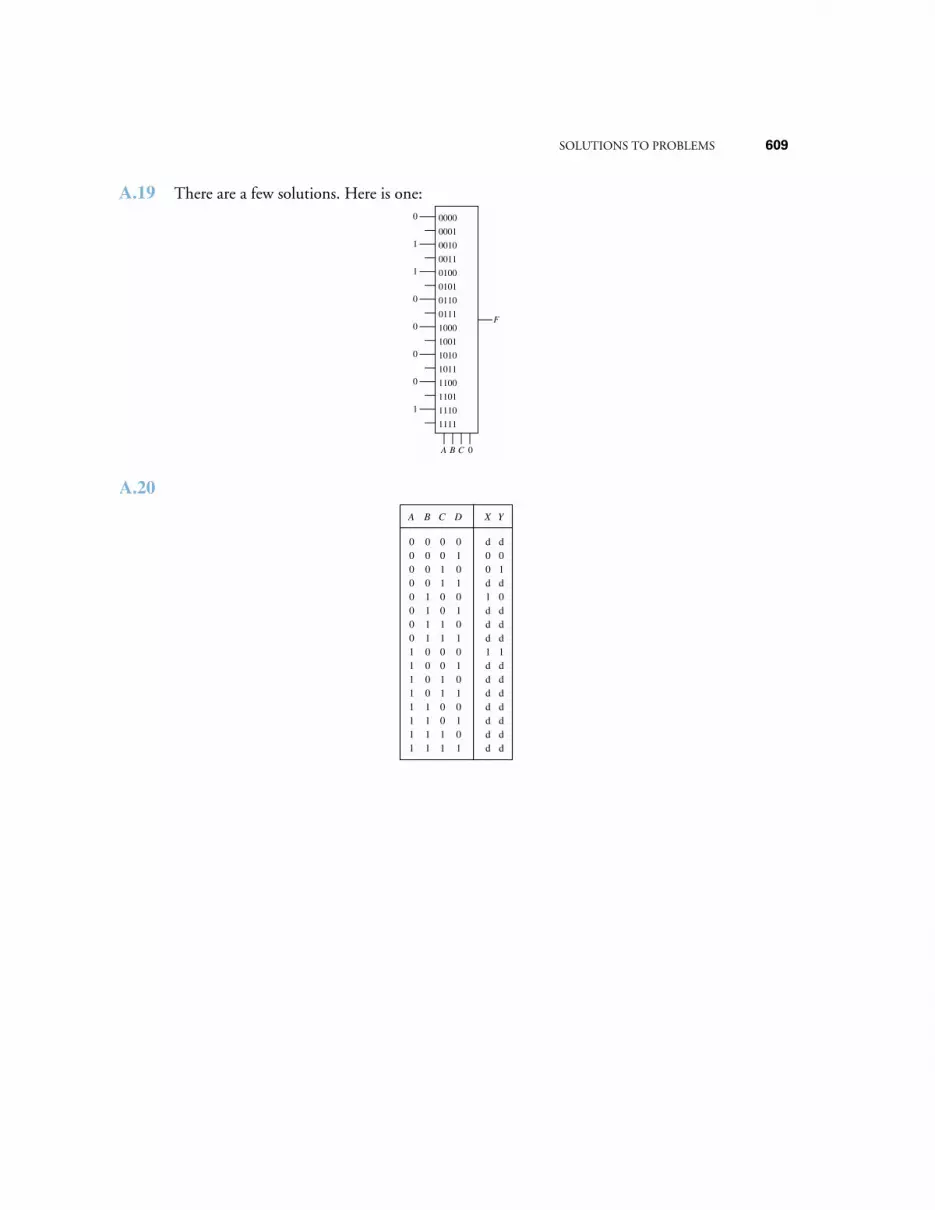
SOLUTIONS TO PROBLEMS 609
A.19 There are a few solutions. Here is one:
A.20
F
0001
0010
0011
0100
0101
0110
0111
0000
A B C 0
0
1
1
0
1001
1010
1011
1100
1101
1110
1111
10000
0
0
1
0011001100110011
0101010101010101
C D
0000111100001111
B
d00d1ddd1ddddddd
X
0000000011111111
A
d01d0ddd1ddddddd
Y
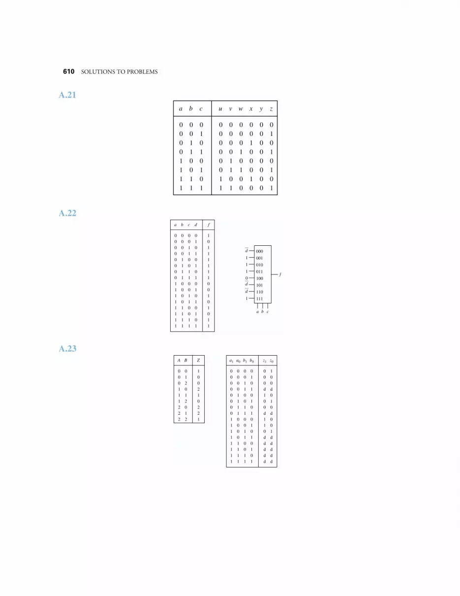
610 SOLUTIONS TO PROBLEMS
A.21
A.22
A.23
00110011
01010101
b c
00001111
a
00000011
u
00001101
v
00010100
w
00100010
x
00000000
y
01010101
z
0011001100110011
0101010101010101
c d
0000111100001111
b
1011111100101011
f
0000000011111111
a
a b
f
c
001
010
011
100
101
110
111
000d
1
1
1
0
1
d
d
0011001100110011
0101010101010101
b1 b0
0000111100001111
a0
000d100d110ddddd
z1
0000000011111111
a1
100d010d001ddddd
z0
000111222
012012012
A B
100210221
Z
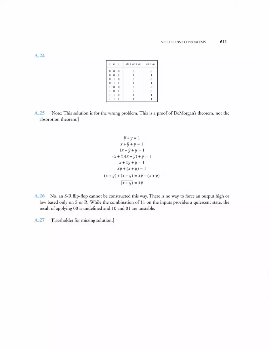
SOLUTIONS TO PROBLEMS 611
A.24
A.25 [Note: This solution is for the wrong problem. This is a proof of DeMorgan’s theorem, not theabsorption theorem.]
A.26 No, an S-R flip-flop cannot be constructed this way. There is no way to force an output high orlow based only on S or R. While the combination of 11 on the inputs provides a quiescent state, theresult of applying 00 is undefined and 10 and 01 are unstable.
A.27 [Placeholder for missing solution.]
00110011
01010101
b c
00001111
a
01010011
01010011
ab + ac + bc ab + ac
y y+ 1=
x y y+ + 1=
1x y y+ + 1=
x x+( ) x y+( ) y+ 1=
x xy y+ + 1=
xy x y+( )+ 1=
x y+( ) x y+( )+ xy x y+( )+=
x y+( ) xy=
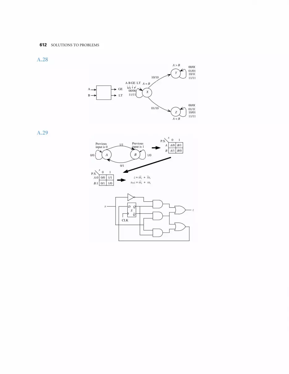
612 SOLUTIONS TO PROBLEMS
A.28
A.29
01/1000/00
10/01
01/0100/00
10/10
X
Y
00/0011/11
10/10
01/10Z
A = B
A > B
A < B
A B GE LT
11/11
11/11
A
B
GE
LT
0/0 1/0
1/1
0/1
Previous input is 0
Previousinput is 1
BA
A/0 B/1
A/1 B/0
A
B
0 1x
P.S.
0/0 1/1
0/1 1/0
A:0
B:1
0 1x
P.S.
CLK
QD
Q
xS z
z = xst + xst
st+1 = xst + xst
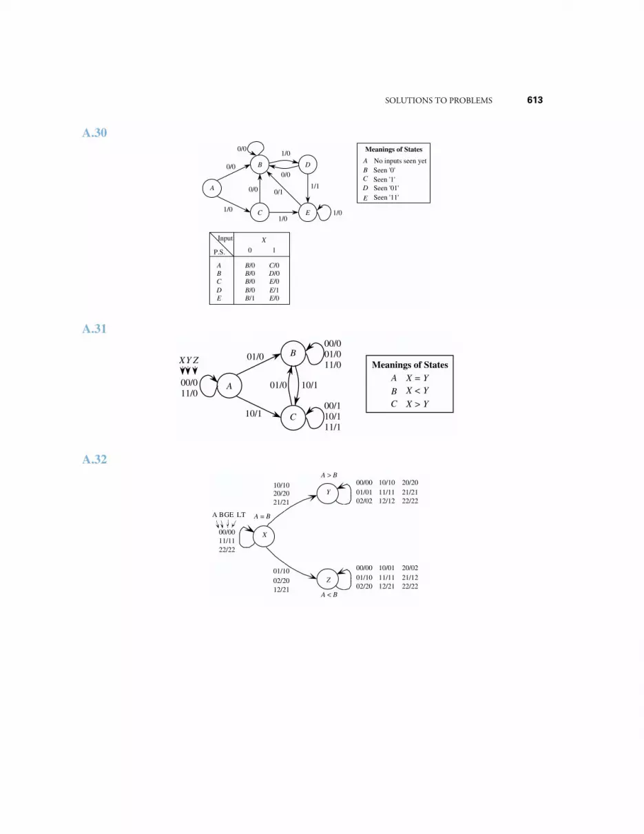
SOLUTIONS TO PROBLEMS 613
A.30
A.31
A.32
A
B
C
D
E
0/0
0/0
1/0
0/0
1/0
0/0
0/1
1/0
1/1
1/0
No inputs seen yet
Meanings of States
ABCD
E
Seen '0'Seen '1'Seen '01'Seen '11'
X
0 1
A B/0 C/0
P.S.
Input
BCDE
B/0 D/0B/0 E/0B/0 E/1B/1 E/0
A
B
C
01/0
10/1
Meanings of StatesX = YA
BC
X < Y
X > Y
01/0 10/1
00/110/111/1
00/001/011/0
00/011/0
XY Z
00/0001/10
00/0001/01
X
Y
00/0011/11
21/21
01/10Z
A = B
A > B
A < B
A BGE LT
02/02
02/20
22/22
20/2010/10
02/2012/21
10/0111/11
10/1011/1112/12
12/21
20/0221/12
20/2021/2122/22
22/22
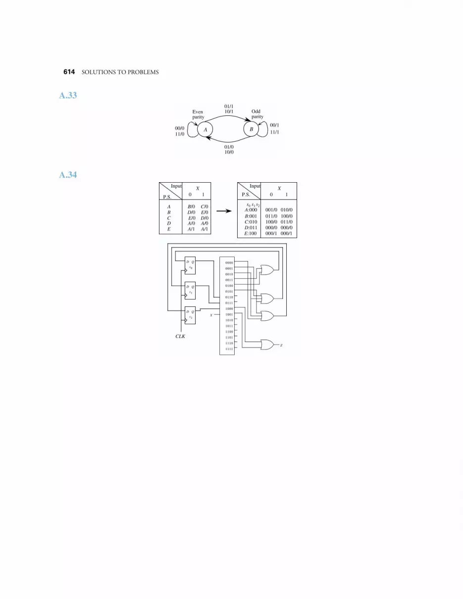
614 SOLUTIONS TO PROBLEMS
A.33
A.34
00/000/1
10/1
01/0
Even parity
Odd parity
11/0
10/0
BA
01/1
11/1
X0 1
A B/0 C/0
P.S.
Input
BCD
D/0 E/0E/0 D/0A/0 A/0
X0 1
A:000 001/0 010/0
P.S.
Input
B:001C:010D:011
011/0 100/0100/0 011/0000/0 000/0E A/1 A/1
E:100 000/1 000/1
s0 s1 s2
D Q
s0
D Q
s1
D Q
s2
CLK
0000
0001
0010
0011
0100
0101
0110
0111
1000
1001
1010
1011
1100
1101
1110
1111Z
X
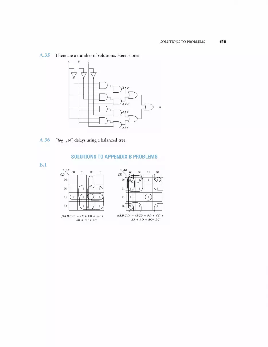
SOLUTIONS TO PROBLEMS 615
A.35 There are a number of solutions. Here is one:
A.36 delays using a balanced tree.
SOLUTIONS TO APPENDIX B PROBLEMS
B.1
M
A B C
A B C
A B C
A B C
A B C
33Nlog
00 01 11
1
1
1
01
11
1
1
1
1
1
10AB
1
CD
00
10
11
1
111
1
1
1
1
1
10AB
1
CD
10
1
1 1
1
1
1
00 01
01
00
f (A,B,C,D) = AB + CD + BD +AD + BC + AC
g(A,B,C,D) = ABCD + BD + CD +AB + AD + AC+ BC
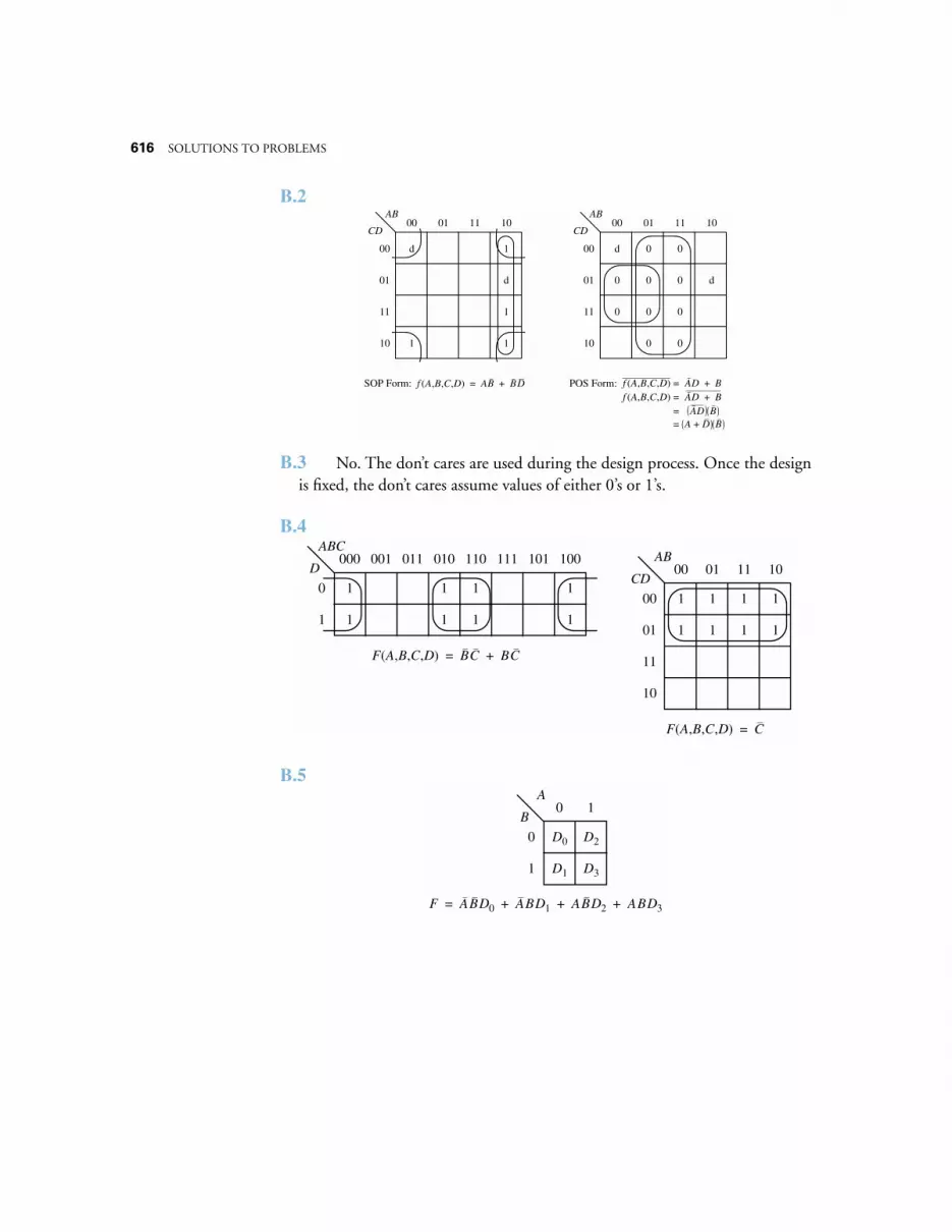
616 SOLUTIONS TO PROBLEMS
B.2
B.3 No. The don’t cares are used during the design process. Once the designis fixed, the don’t cares assume values of either 0’s or 1’s.
B.4
B.5
01 11
1
01
11
d
11
11
0 011
0
0
0
0
0
10AB
d
CD
10
d
0
0
d
0
00 01
01
001
10
1000AB
CD
00
SOP Form: POS Form:f (A,B,C,D) = AB + BD f (A,B,C,D) = AD + Bf (A,B,C,D) = AD + B
= AD B= A + D B
000ABC
001 011 010 110 111 101 100
1
1
1
1
1
1
1
11
D
000
AB01 11 10
1
1
1
1
1 1
01
CD
00
11
10
1 1
F(A,B,C,D) = BC + BC
F(A,B,C,D) = C
0A
1
D0
1
B
0
D1
D2
D3
F = ABD0 + ABD1 + ABD2 + ABD3
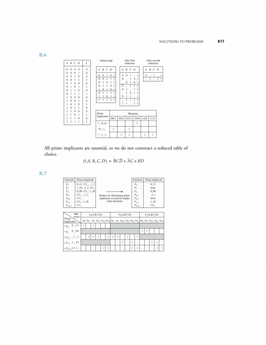
SOLUTIONS TO PROBLEMS 617
B.6
All prime implicants are essential, so we do not construct a reduced table ofchoice.
B.7
0011001100110011
0101010101010101
C D
0000111100001111
B
00d101d100100101
F
0000000011111111
A
11011101
01100111
C D
00110111
B
00001011
A
√√√√√√√√
Initial setup
1111_011_
_00111_11
C D
0_0_11111
B
00_00_0_1
A
√√*√√ √√ √√
After firstreduction
1_
_1
C D
_1
B
0_
A
**
After secondreduction
_
0
_
0
_
1
1
1
_
0
_
1
0011 0101 0111 1010 1101 1111
MintermsPrimeImplicants
√
√
√√√
√
√
*
*
*
f A B C D, , ,( ) BCD AC BD+ +=
_
_
1
_
1
1
0
_
1
1
1
0
1
0
_
PrimeImplicants
√
m3 m5 m7 m13 m14 m15 m5 m7 m10 m13 m14 m15 m0 m4 m10 m14 m15
F0(A,B,C,D) F1(A,B,C,D) F2(A,B,C,D)Min-terms
F0
F2
F0,1
F1,2
F0,1,2
√ √
√
√
√ √
√ √
√√√√
0
0
_
1
1
*
*
*
*
*
√
√√ √ √ √
√
√ √
Function Prime Implicant
F0
F1
F2
F0,1
F0,2
F1,2
F0,1,2
0_11, 111_, _1_11_10, _1_1, 111_0_00, 111_, 1_10111_, _1_1111_111_, 1_10111_
Function Prime Implicant
F0
F1
F2
F0,1
F0,2
F1,2
F0,1,2
0_11none0_00_1_1none1_10111_
Reduce by eliminating prime implicants covered by higher
order functions
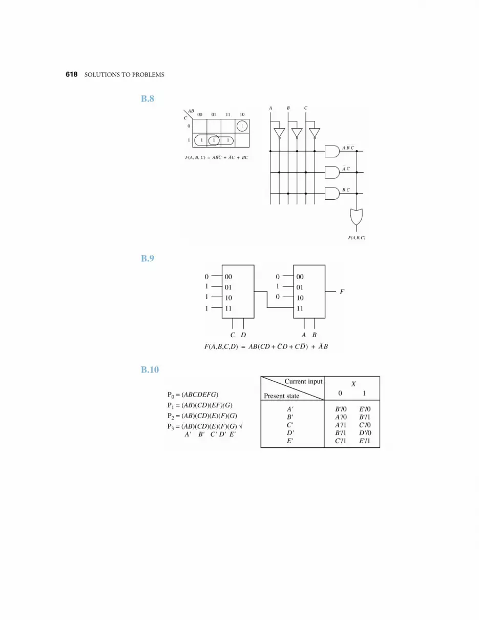
618 SOLUTIONS TO PROBLEMS
B.8
B.9
B.10
00 01 11
1 1
1
1
10AB
C
0
1
F(A,B,C)
A B C
A CB
F(A, B, C) = ABC + AC + BC
A C
B C
C D
00
01
10
11
0
1
1
1
A B
F
00
01
10
11
01
0
F(A,B,C,D) = AB(CD + CD + CD) + AB
P0 = (ABCDEFG)
P1 = (AB)(CD)(EF)(G)
P2 = (AB)(CD)(E)(F)(G)
P3 = (AB)(CD)(E)(F)(G) √A' B' C' D' E'
X0 1
A' B'/0 E'/0
Present state
Current input
B'C'D'E'
A'/0 B'/1A'/1 C'/0B'/1 D'/0C'/1 E'/1
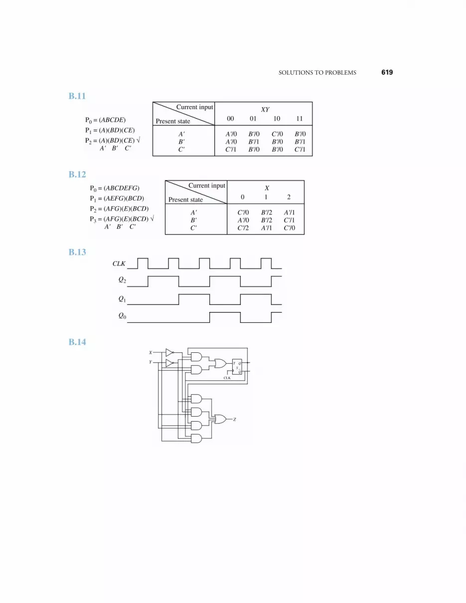
SOLUTIONS TO PROBLEMS 619
B.11
B.12
B.13
B.14
P0 = (ABCDE)
P1 = (A)(BD)(CE)
P2 = (A)(BD)(CE) √A' B' C'
XY00 01
A' A'/0 B'/0
Present state
Current input
B'C'
A'/0 B'/1C'/1 B'/0
10
C'/0B'/0B'/0
11
B'/0B'/1C'/1
P0 = (ABCDEFG)
P1 = (AEFG)(BCD)
P3 = (AFG)(E)(BCD) √A' B' C'
X0 1
A' C'/0 B'/2
Present state
Current input
B'C'
A'/0 B'/2C'/2 A'/1
2
A'/1C'/1C'/0
P2 = (AFG)(E)(BCD)
CLK
Q2
Q1
Q0
CLK
QT
QS
X
Y
Z
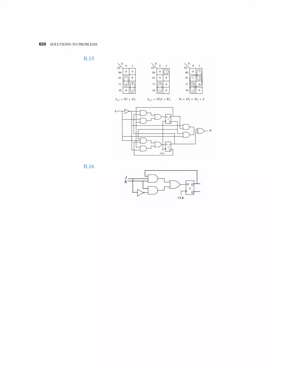
620 SOLUTIONS TO PROBLEMS
B.15
B.16
QD
QY
X
CLK
QD
QZ
W
0
11
0
1
0
X
0YZ
10
1
d
0 1
01
00
d
1
11
1
0
0
X
0YZ
10
0
d
0 1
01
00
d
1
11
1
0
1
X
0YZ
10
1
d
0 1
01
00
d
Yt+1 = XZ + XYt W = XYt + XYt + ZZt+1 = XYtZ + XYt
CLK
QD
QS
JK

SOLUTIONS TO PROBLEMS 621

622 SOLUTIONS TO PROBLEMS
INDEX
623
Numerics
360, IBM
, 151
68000, Motorola
, 151, 454, 455
80486, Intel
, 113
8080, Intel
, 151
80x86, Intel
, 113, 151
A
A Hardware Programming Language
, 229
accumulator
, 133
action mapping
, 160
activehigh
, 477
low
, 477
address
, 108
bus
, 6
space
, 108, 110
addressing modesbased
, 162
direct
, 135
immediate
, 135
indirect
, 135
register based
, 135, 136
register based indexed
, 135, 136
register indexed
, 135, 136
register indirect
, 135, 136
Adobe Postscript
, 352
Advanced Graphics Port
, 320
AGP
, 320
AHPL
, 229
algebraic reduction
, 523
alignmenthard
, 327
soft
, 327
AltiVec
, 185–193
ALU
, 265
as part of computer
, 5
AM, amplitude modulation
, 362
Amdahl’s law
, 433
amplitude modulation
, 362
analog circuits
, 462
Apple Computeremulation of 68000
, 11
Apple Macintosh
, 113
arbiter, bus
, 317
ARC
, 114–127
addressing modes
, 131
INDEX

624
INDEX
assembly language
, 118–120
data formats
, 122
instruction descriptions
, 123–127
instruction formats
, 120–122
instruction set
, 116–118
instructions
addcc
, 125
andcc
, 124
ba
, 127
bcs
, 126
be
, 126
bne
, 166
bneg
, 126
bvs
, 126
call
, 125
jmpl
, 125
ld
, 124
orcc
, 125
orncc
, 125
rett
, 227, 324
sethi
, 124
smul
, 157
srl
, 125
st
, 124
subcc
, 157
xorcc
, 250
memory
, 115
memory mapped I/O
, 115
arithmetic and logic unit, see ALUarm, magnetic disk
, 333
array multiplier
, 86
ASCII
, 55
ASIC
, 238
assembler
, 9
assemblyafter compilation
, 114
languagedefined
, 9
vs.
machine language
, 105
process
, 159, 168
associativemapped cache
, 268
memory
, 269, 293
theorem
, 472
asynchronousbus
, 313
I/O
, 311
transfer mode, ATM
, 395
B
B5000
, 151
Babbage, Charles
, 2, 151
backside bus
, 319
bandwidth
, 354, 387
barrel shifter
, 205
based addressing
, 162
Basic Rate Interface
, 394
BER, bit error rate
, 375
best fit
, 288
big-endian
, 108, 115
binarycode
, 9
coded decimal
, 37
compatibility
, 9
numbers
, 22
BISDN
, 394bit
error rate, 375pad, 347pair recoding, 85
black box, 482blocking in a network, 436blocks
in associative memory, 268memory, 261
bonding, in ISDN, 395Boolean logic function, 464Booth algorithm, 85branch
predication, in IA-64 architecture, 430processing unit, 424table, 225
BRI, 394bridge, 319, 374, 392broadband-ISDN, 394bubble
matching, 478pushing, 495
bubblesort, 393Burroughs B5000, 151burst
error, 383rate, disk transfer speed, 336
bus, 312address, 6arbiter, 317arbitration, 226, 317control, 6cycle, 314data, 6

INDEX 625
data-in, 6data-out, 6defined, 6grant, 317master, 313protocol, 313request line, 317system, 6topology, 371
busy-wait, 321byte, 107bytecode, 145
CC language translation
arrays, 164automatic variables, 162global variables, 162local variables, 162program flow control, 166–168static variables, 162structs, 163
cache, 266–281access time, 277associative mapped, 268blocks, 268hit ratio, 277lines, 268memory, 266multilevel, 279performance, 275write-allocate, 276write-back, 276write-no-allocate, 276write-through, 276
calling convention, 136CAM, 271, 293canonical
form of a Boolean equation, 475product-of-sums form, 476sum-of-products form, 475
capacitor, 257carrier sense multiple access, 373carry lookahead adder, 81carry-select adder, 102cause-and-effect arrow, 316CD, 343CD ROM, 343
cell loss priority, in ATM packets, 397cellular radio communications, 368central processing unit, see CPU, 5centralized arbitration, 317channel, 386checksum, 339Chinese remainder theorem, 91circuit depth, 544circular buffer, 417CISC
and RISC machines, 407–409Intel Pentium ISA as, 187
clean rooms, 337clock rate, 496Clos network, 440CLP, in ATM packets, 397code generation, 160collision detection, 373Collossus, early computer, 3column address strobe, CAS, 261comb, magnetic disk, 333combinational logic, 461
unit, CLU, 461commutative property, of Boolean algebra, 471compact disc, 343compatibility, binary, 9compilation, 159–168compiler, 113
defined, 8complement
one’s, 34, 464, 471two’s, 34
components, digital, 481computational completeness, 472computer architecture levels, 1computers, history of, 1concurrent execution, of VHDL, 239condition codes, 116conditional branch instructions, in ARC, 118consensus theorem, 472constant
angular velocity, disk, 344linear velocity, disk, 344pool, in Java Virtual Machine, 146
content-addressable memory, 271, 293control
bus, 6section, 110, 200

626 INDEX
signals, 10store, 211unit
as part of computer, 5defined, 10hardwired, 200microprogrammed, 200
CPU, 110as part of computer, 5
Cray vector operations, 186CRC, 382, 383cross compilation, 161crossbar, 436crossinterleaved Reed Solomon error correcting code, 343crosspoint
complexity, 436switch, 436
CSMA/CD, 373current window pointer, CWP, 416cycle time, 496cycle-stealing DMA, 325cyclic redundancy checking, 382, 383cylinder, magnetic disk, 335
Ddaisy chain, 317data
bus, 6encoding, 21link area, 137representation, 21section, of CPU, 110, 200sheet, 479
datapath, 110, 200deadlock, 373decentralized arbitration, 317decoder, 485degenerate tree, 545delayed
branch, 412load, 412
demand paging, 285DeMorgan’s theorem, 472demultiplexer, 484DEMUX, 484dependence, among instructions, 424dependency
analysis, 442
graph, 443device drivers, 311diameter of a network, 436dibit, 363die, 300digital
circuits, 462versatile disk, DVD, 343, 345
digitizing tablet, 347direct
addressing mode, 135memory access, 321, 324–325
dirty bit, 269disassembler, 196diskette, floppy, 338distributive property, of Boolean algebra, 471DLLs, 177DMA, 321, 324, 325
cycle-stealing, 325don’t care, 96doubleword, 122DRAM, 257driver, in overlay management, 282dual-port RAM, 296dual-read RAM, 296DVD, 343, 345Dvorak keyboard, 347dynamic
linking libraries, 177RAM, 257
EEBCDIC, 55Eckert, J. Presper, 3ECMA-23, 347EDSAC, 4EDVAC, 4, 151EEPROM, 265effective access time, 277efficiency, 433, 434electronic mail, 369eligible set, 538e-mail, 369emulation, 11, 226emulator, 11encapsulation, 390encoder, 487encryption, early efforts, 3
INDEX 627
end-around carry, 72ENIAC, 3ENIGMA computer, 3EPIC, explicitly parallel instruction computing, 429EPROMs, 265error
in fixed point numbers, 23in floating point numbers, 44
error correctionSEC, 380SECDED, 382
essential prime implicant, 538event driven VHDL simulations, 239excess representation, 36excitation tables, 556execution efficiency, 414
Ffan-in, 481fan-out, 481fat-tree, 451FCS, 383fetch-execute cycle, 111field programmable gate array, 514fields, in associative memory, 293FIFO, 270file, 338finite
element analysis, 450state machine, 492
firmware, 214defined, 10
first fit, 288first-in first-out, 270fixed
head disk, 343point numbers, 22–38
error, 23precision, 23range, 22
flash memory, 265flip-flop, 493floating point
numbers, 38–51definition, 21hidden bit, 40mantissa, 39precision, 38range, 38
significand, 39unit, 424
floppy disk, 337flushed pipeline, 412FM, 363forward reference, 171, 172FPGA, 514fragmentation
disk, 338memory, 288
framebuffer, 353check sequence, 383in magnetic tape, 341
frequency modulation, 363frontside bus, 319FSM, 492full adder, 491function, 136
Ggate
count, 476delay, 532input count, 476
gateway, 374generate, in carry lookahead, 82generator polynomial, 383generic flow control, in ATM networks, 397Genesis, Sega, 453GFC, in ATM packets, 397glitch, 496granularity, in parallel architectures, 447Gray code, 526group
carry lookahead adder, 91generate, 92propagate, 92
guard digit, 94Gulliver’s Travels, 108
Hhalf adder, 491handoff, 368handshaking, 311hardware description language, 228hardwired control units, 200, 228
628 INDEX
Harvard architecture, 276hazard, 496HDL, 228head
crash, 337magnetic disk, 333
header error control, HEC, in ATM packets, 397hidden bit, in floating point numbers, 40high impedance, 470history of computers, 1hit
cache memory, 269ratio, 277
home video game, 13host bridge, 319HP9100A calculator, 94hub, 372, 392Huntington’s postulates, 470
II/O address, 6IA-64, 428–432IBM
360, 7, 9, 151370 vector operations, 186701, 151book about, 18
IC, 12, 312idempotence, 471identity, 471immediate addressing mode, 135impedance, 470indefinite persistence, of magnetic media, 332indirect addressing mode, 135Industry Standard Architecture, ISA, 321input unit, 4instruction
dependence, 424dispatch, 424format, ARC, 120register, IR, 111set, 9, 113set architecture, ISA, 12, 105unit, IU, 424
integer unit, 424integrated circuit, 12, 312Integrated Services Digital Network, ISDN, 394Intel
8080, 151IA-64, Merced, 428–432MMX, 185–193Pentium, 187Pentium II, 14processor family, 9
interconnection network, 436interleaving, 261, 338International Standards Organization, 369inter-record gap, tape, 341interrupt
driven I/O, 321service routine, ISR, 323vector, 226
interrupts, 225–227inter-sector gap, 335inter-track gap, 335inverter, 465involution, 472IPv4, 388IPv6, 388ISA, industry standard architecture, 321ISA, instruction set architecture, 12
Chapter 4, 105ISDN, 394ISO, 369
JJacquard loom, 3Java
class file, 146virtual machine, 144–150
jitter, tape, 341joystick, 350just in time compiler, 149
KKarnaugh map reduction, 523keyboard, 12, 346
LLAN, 368lands, in compact disks, 343large scale integration, 482least
frequently used, LFU, 270recently used, LRU, 270

INDEX 629
LED, 349levels of machines, 7lexical analysis, in compilation, 160LFU, 270light emitting diode, 349lightpen, 349link register, 119, 139linkage editor, 177linker, 177linking, 159
loader, 180little-endian, 108LLC, 371load module, 177loader, 177, 180loading, 159load-store, 116load-through, 275local area network, LAN, 361, 368locality principle, 266location counter, 128, 170logic gate, 11, 465logical link control, 371logical record, tape, 342LRU, 270LSB, least significant bit, 25LSI, 482LUT, lookup table
in ALU design, 205, 265
MMAC, 371machine
code, 9language, 9, 105
Macintosh, 113macros, assembly language, 159, 169, 183–185magnetic disks, 332
zone-bit recording, 335majority function, 240, 473MAL, 214Manchester encoding, 334mantissa, of floating point number, 39map-entered variable, 532mapping specification, in compilers, 161master control block, 339master-slave, 494Mauchley, John, 3
maxterm, 476MCB, 339media
access control, 371storage, 332
medium scale integration, 482memory
address, defined, 6content-addressable, 271, 293flash, 265hierarchy, 255–256location, 107management unit, 180map, 109mapped I/O, 109
in ARC, 115mapped video, 353unit, defined, 5
Merced, 403, 428–432methods, Java, 146MFM, 334microarchitecture, 199micro-assembly language, 214microcontroller, 212
defined, 10microinstruction, 211microprocessors, 11microprogram, 10microprogrammed control units, 200microstrip technology, 298MIMD, 435minterm, 475minuend, 69MISD, 436MMU, 180MMX, 185–193
instructions, 185mnemonic, instruction, 9, 116modem, 361modified frequency modulation, 334modular number system, 67modulation, in telecommunications, 362moduli, 90monitor, video, 12, 352motherboard, 12, 13, 14, 312, 453Motorola
68000, see 68000, MotorolaAltiVec, 185–193

630 INDEX
PowerPC, 187, 425–428mouse, 348moving head, 333MSB, most significant bit, 25MSI, 482multicast, 389multilevel cache, 279multimode fiber, 366multiple instruction stream
multiple data stream, 435single data stream, 436
multiplexer, 482multi-valued logic, 462MUX, 482
Nnanostore, 227narrowband-ISDN, 394Neat Little LRU Algorithm, 280negative logic, 477network-to-network interface, in ATM packets, 397Newton’s iteration, 88nibble, 107Nintendo, 453NISDN, 394NNI, 397non-maskable interrupt, NMI, 324non-return-to-zero, 334non-volatile memory, 332NRZ, 334NTSC video standard, 354number
conversionbetween bases, 25multiplication method, 27remainder method, 26
representationbinary coded decimal, 37excess, 36
representationsone’s complement, 34signed magnitude, 33two’s complement, 34
nybble, 107
Oobject module, 177octet, 107odd parity, 377
offline routing algorithm, 438one theorem, 471one’s complement, 34one-address instructions, 132, 133one-hot encoding, 230Open System Interconnection, 369optical
disks, 343mouse, 349
optimal replacement policy, 270OSI, 369output unit, computer, 5overflow, 22, 68, 122overlapping register windows, 403, 415, 416overlays, 281
Ppacket, 369page
fault, 283frames, 283table, 284
paging, 282PAL video standard, 354parallel
processing, 403, 432time, 433
parity bit, 376parser, 160partition graph, 282partitions, in the CM-5, 451Pascal, Blaise, 1Pascaline, 1payload
in data packets, 369type identifier, in ATM packets, 397
PC, 119PCI, 320PCM, 363PDP-4, 151PDP-8, 151PE, 432Pentium, Intel, 187
II, 14Peripheral Component Interconnect, 320peripheral interrupt controller, PIC, 324phase modulation, 363physical record, tape, 342
INDEX 631
picture element, 353pipelining, 403, 408
in SPARC, 129pits, in compact disks, 343pixel, 353PLA, 487platter, magnetic disk, 333ply, 548PM, 363polling, 321polynomial
code, 383method, 25
port, 389POS, 475, 523positive logic, 477Postscript, 352PowerPC, 113, 187, 425–428precision
in fixed point numbers, 23in floating point numbers, 38
PRI, 395Primary Rate Interface, 395prime implicants, 527principle of duality, 471priority encoder, 487procedure, 136processing elements, 432processor state register, 119product terms, 474product-of-sums, 475, 523program counter, 111, 119programmable
logic array, 487sound generator, 454
programmed I/O, 321PROM, 265
burner, 265, 455propagate, in carry lookahead, 82protection, 286protocol stack, 369pseudo-operations, pseudo-ops, 127–128PSG, programmable sound generator, 454PSR, 119PTI, in ATM packets, 397puck, 347pulse code modulation, 363
Qquadword, 122Quine-McCluskey method, 534QWERTY, 346
Rradio frequency, 298radix
conversion, see number conversiondefinition, 24
RAM, 257Rambus, Inc., 298random
access memory, RAM, 257replacement policy, 270
rangein fixed point numbers, 22in floating point numbers, 38
raster, 352read-only memory, ROM, 11, 263real estate, circuit area, 406rearrangeably nonblocking, 440re-compilation, 113record, tape, 341reduced
instruction set computer, 115table of choice, 538
register, 510assignment problem, 421based addressing, 135, 136based indexed addressing, 135, 136file, 111, 416indexed addressing, 135, 136indirect addressing, 135, 136transfer language, 229window, 403
relocatability of programs, 176relocating loader, 180relocation, 179
dictionary, 176repeater, 374residue arithmetic, 90resolver, 391restoring division, 77ring
in parallel processing, 433network topology, 372
632 INDEX
ringing, 432ripple-borrow subtractor, 69, 70ripple-carry adder, 69ROM, 11, 263rotational latency, 336router, 371, 393row address strobe, RAS, 261RTL, 229
SS/360, 151saturation arithmetic, 190Scalable Processor Architecture, 114SCP, 396SCSI, 320, 337SEC, single error correcting code, 380SECDED encoding, 382seek time, 336Sega, 453
Genesis, 453, 455segment, 286segmentation, 286self-routing network, 393semantic
analysis, in compilation, 160gap, 404
sequential logic, 461set associative mapping, 273set-direct mapping, 273set-reset flip-flop, 494shared bus, 267shared-memory multiprocessor, 280sign extension, in ARC, 121signaling control point, 396signed magnitude, 33significand, of floating point number, 39silicon compilation, 229SIMD, 435
processors, 186single
mode fiber, 367single instruction stream
multiple data stream, 435single data stream, 434
SISD, 434slots, 268Small Computer Systems Interface, 320, 337small scale integration, 482
SMP, 319socket, 388Sony, 453SOP, 474, 523source code compatibility, 8SPARC, 114
pipelining, 129spatial locality, 266spec sheet, 479speculative loading, 431speedup, 406, 433spindle, 333split cache, 276SRAM, 257SSI, 482stack
frame, 136, 139pointer, 119, 138
star topology, 372static RAM, 257Stega, 453, 454STM, 395stored program computer, 4strictly nonblocking, 436stylus, 347subnetwork, 374subroutine linkage, 136subtraction, binary, 69subtrahend, 69sum-of-products, 474, 523superscalar execution, 403supervisor mode, 227surface, magnetic disk, 333Swift, Jonathan, 108switch, 393symbol table, 171, 172symmetric multiprocessor, 319synchronous
bus, 313transfer mode, 395
syncing, magnetic disk, 340syntactic analysis, in compilation, 160synthesizer, 455system bus, 6, 106
model, 5systolic array, 436

INDEX 633
Ttable of choice, 537tabular reduction, 523tag field, 268tagged word, SPARC data format, 122TDM, 395temporal locality, 266Texas Instruments, 454three-address instructions, 132threshold, for logic gate, 468throughput, 433, 434TI, Texas Instruments, 454time division multiplexing, 395TLB, 290toggle, 554touchscreen, 143, 349trace, wire, 298, 313trackball, 349transfer time, 336transistor, 11, 468translation
lookaside buffer, 290process, compilation, 114
transmission line, 298trap, 11, 225–227, 324tree decoder, 261, 291truth table, 463Turing, Alan, 3two’s complement numbers, 34two-address instructions, 132, 133TYAN Computer, 14
UUNI, in ATM packets, 397Unicode, 55UNIVAC, 151Universal Serial Bus, 321upward compatibility, 7USB, 321user-to-network interface, 397
Vvalid bit, 269VAX, 151VCI, in ATM packets, 397vector processors, 186Venn diagram, 525
very high speed integrated circuit, VHSIC, 229very large scale integration, 295, 482very long instruction word, VLIW, 403VHDL, 229, 237VHSIC hardware description language, 229virtual
channel identifier, 397machine, 113memory, 281path identifier, in ATM packets, 397
VLIW, 428VLIW, very long instruction word, 403, 428VLSI, 295, 482von Neumann model, 4, 453VPI, in ATM packets, 397
Wweighted position code, 24well-known ports, 389wide area network, WAN, 361Wilkes, Maurice, 4Winchester disk, 337window, register, in SPARC, 416word, 107working set, 285write once read many, WORM, 344write-allocate policy, cache, 276write-back policy, cache, 276write-no-allocate policy, cache, 276write-through policy, cache, 276
XXeon, 319
YYamaha, 454, 456
Zzero theorem, 471Zilog Z-80, 151, 454, 455zone
disk drive, 335Internet, 391
zone-bit recording, in magnetic disks, 335

634 INDEX