Multi-domain Polarization Switching in Hf0.5Zr0.5O2 ... - arXiv
7
Atanu K. Saha 1,a) , Mengwei Si 1 , Peide D. Ye 1 , and Sumeet K. Gupta 1 1 School of Electrical and Computer Engineering, Purdue University, West Lafayette, IN 47907, US a) Author to whom correspondence should be addressed: [email protected] ABSTRACT We investigate the polarization switching mechanism in ferroelectric-dielectric (FE-DE) stacks and its dependence on the dielectric thickness (TDE). We fabricate HZO-Al2O3 (FE-DE) stack and experimentally demonstrate a decrease in remnant polarization and an increase in coercive voltage of the FE-DE stack with an increase in TDE. Using phase-field simulations, we show that an increase in TDE results in a larger number of reverse domains in the FE layer to suppress the depolarization field, which leads to a decrease in remanent polarization and an increase in coercive voltage. Further, the applied voltage- driven polarization switching suggests domain-nucleation dominant characteristics for low TDE, and domain-wall motion- induced behavior for higher TDE. In addition, we show that the hysteretic charge-voltage characteristics of the FE layer in the FE-DE stack exhibit a negative slope region due to the multi-domain polarization switching in the FE layer. Based on our analysis, the trends in charge-voltage characteristics of the FE-DE stack with respect to different TDE (which are out of the scope of single-domain models) can be described well with multi-domain polarization switching mechanisms. Ferroelectric (FE) hafnium oxide, by virtue of its CMOS process compatibility 1,2 and rich domain dynamics 3,4 , has been identified as one of the most promising candidates for enabling future electronic devices. By integrating doped HfO 2 (as FE) in the gate stack of a transistor (FE-FET), non-volatile memory (NVM) 5-6 , neuron 7 and synaptic 8,9 functionalities have been demonstrated. Such diverse functionalities demand different characteristics of polarization (P) switching in the FE layer. For example, an abrupt P-switching is beneficial for neurons and binary NVMs, while a gradual P-switching is favorable for multi-bit memories and synapses. Therefore, it becomes essential to appropriately design FEFET for application-specific device behavior, for which gate stack optimization plays a key role. In the FEFET gate stack, a dielectric (DE) layer exists between the FE and the semiconductor channel 5-10 , which can significantly impact the FEFET characteristics 11 . According to the single-domain Landau-Khalatnikov (LK) model of FE, an increase in DE thickness (T DE ) should increase the depolarization field and reduce the coercive voltage (V C ) of the FE-DE stack 12,13 . However, the FE-DE stack with Zr-doped HfO 2 (HZO) as the FE and Al 2 O 3 /HfO 2 as the DE have been demonstrated 14-15 to exhibit an increasing coercive voltage (V C ) with the increase in T DE . Therefore, it is important to bridge the gap between the theoretical understanding and experimental observations regarding the role of T DE in FEFET and for that, a common approach is to analyze the FE-DE stack 12-13 . To that end, in this letter, we experimentally and theoretically analyze the P-switching in FE-DE stack with HZO as the FE and Al 2 O 3 as the DE layer. Our results signify an increase in V C , a decrease in remanent-P (P R ) and a decrease in P-switching slope with the increase in T DE . By employing phase-field simulations, we show that such dependencies can be attributed to the multi-domain phenomena in FE 16 which cannot be captured in the single-domain P-switching model. To further study the role of the dielectric, we analyze the dependence of V C , P R and the switching slope of the FE-DE stack on the dielectric permittivity through phase-field simulations. For the fabrication of the FE-DE stacks, we start with the standard solvent cleaning of heavily p-doped Si substrates. Then, 30nm TiN layer is deposited by atomic layer deposition (ALD) at 250 °C, using [(CH 3 ) 2 N] 4 Ti and NH 3 as the Ti and N precursors, respectively. After this, an HZO film is deposited by ALD at 200 °C, using [(CH 3 ) 2 N] 4 Hf, [(CH 3 ) 2 N] 4 Zr, and H 2 O as the Hf, Zr, and O precursors, respectively. HfO 2 :ZrO 2 cycle ratio of 1:1 is used to form the 10nm Hf 0.5 Zr 0.5 O 2 film. Similarly, on top of HZO, an Al 2 O 3 layer is deposited followed by a 30nm TiN layer deposition. After that, the samples are annealed at 500 °C in N 2 environment for 1 minute by rapid thermal annealing. Then, Ti/Au top electrodes are fabricated using photolithography, e-beam evaporation, and lift-off process (area=5024μm 2 ). The average polarization (P avg ) versus applied voltage (V app ) measurement is carried out using a Radiant RT66C FE tester at room temperature at a very low frequency (50Hz). Considering the polarization switching time in HZO (<1µs) 17 , such low-frequency measurements can be considered as quasi-static. Fig. 1(a) shows the P avg - V app characteristics of FE-DE stack for 10nm HZO and 1/3/5nm Al 2 O 3 . Our results show a decrease in P R (P avg at V app =0V), an increase in V C (V app at P avg =0) and a decrease in P-switching slope with the increases in T DE . To explain such dependencies, we now analyze the P-switching in the FE-DE stack based on multi-domain phase-field simulation. Multi-domain Polarization Switching in Hf 0.5 Zr 0.5 O 2 -Dielectric Stack: The Role of Dielectric Thickness
-
Upload
khangminh22 -
Category
Documents
-
view
0 -
download
0
Transcript of Multi-domain Polarization Switching in Hf0.5Zr0.5O2 ... - arXiv
Atanu K. Saha1,a), Mengwei Si1, Peide D. Ye1, and Sumeet K. Gupta1 1School of Electrical and Computer Engineering, Purdue University, West Lafayette, IN 47907, US
a)Author to whom correspondence should be addressed: [email protected]
ABSTRACT
We investigate the polarization switching mechanism in ferroelectric-dielectric (FE-DE) stacks and its dependence on the dielectric thickness (TDE). We fabricate HZO-Al2O3 (FE-DE) stack and experimentally demonstrate a decrease in remnant polarization and an increase in coercive voltage of the FE-DE stack with an increase in TDE. Using phase-field simulations, we show that an increase in TDE results in a larger number of reverse domains in the FE layer to suppress the depolarization field, which leads to a decrease in remanent polarization and an increase in coercive voltage. Further, the applied voltage-driven polarization switching suggests domain-nucleation dominant characteristics for low TDE, and domain-wall motion-induced behavior for higher TDE. In addition, we show that the hysteretic charge-voltage characteristics of the FE layer in the FE-DE stack exhibit a negative slope region due to the multi-domain polarization switching in the FE layer. Based on our analysis, the trends in charge-voltage characteristics of the FE-DE stack with respect to different TDE (which are out of the scope of single-domain models) can be described well with multi-domain polarization switching mechanisms.
Ferroelectric (FE) hafnium oxide, by virtue of its CMOS process compatibility1,2 and rich domain dynamics3,4, has been
identified as one of the most promising candidates for enabling future electronic devices. By integrating doped HfO2 (as FE) in the gate stack of a transistor (FE-FET), non-volatile memory (NVM)5-6, neuron7 and synaptic8,9 functionalities have been demonstrated. Such diverse functionalities demand different characteristics of polarization (P) switching in the FE layer. For example, an abrupt P-switching is beneficial for neurons and binary NVMs, while a gradual P-switching is favorable for multi-bit memories and synapses. Therefore, it becomes essential to appropriately design FEFET for application-specific device behavior, for which gate stack optimization plays a key role.
In the FEFET gate stack, a dielectric (DE) layer exists between the FE and the semiconductor channel5-10, which can significantly
impact the FEFET characteristics11. According to the single-domain Landau-Khalatnikov (LK) model of FE, an increase in DE thickness (TDE) should increase the depolarization field and reduce the coercive voltage (VC) of the FE-DE stack12,13. However, the FE-DE stack with Zr-doped HfO2 (HZO) as the FE and Al2O3/HfO2 as the DE have been demonstrated14-15 to exhibit an increasing coercive voltage (VC) with the increase in TDE. Therefore, it is important to bridge the gap between the theoretical understanding and experimental observations regarding the role of TDE in FEFET and for that, a common approach is to analyze the FE-DE stack12-13. To that end, in this letter, we experimentally and theoretically analyze the P-switching in FE-DE stack with HZO as the FE and Al2O3 as the DE layer. Our results signify an increase in VC, a decrease in remanent-P (PR) and a decrease in P-switching slope with the increase in TDE. By employing phase-field simulations, we show that such dependencies can be attributed to the multi-domain phenomena in FE16 which cannot be captured in the single-domain P-switching model. To further study the role of the dielectric, we analyze the dependence of VC, PR and the switching slope of the FE-DE stack on the dielectric permittivity through phase-field simulations.
For the fabrication of the FE-DE stacks, we start with the standard solvent cleaning of heavily p-doped Si substrates. Then,
30nm TiN layer is deposited by atomic layer deposition (ALD) at 250 °C, using [(CH3)2N]4Ti and NH3 as the Ti and N precursors, respectively. After this, an HZO film is deposited by ALD at 200 °C, using [(CH3)2N]4Hf, [(CH3)2N]4Zr, and H2O as the Hf, Zr, and O precursors, respectively. HfO2:ZrO2 cycle ratio of 1:1 is used to form the 10nm Hf0.5Zr0.5O2 film. Similarly, on top of HZO, an Al2O3 layer is deposited followed by a 30nm TiN layer deposition. After that, the samples are annealed at 500 °C in N2 environment for 1 minute by rapid thermal annealing. Then, Ti/Au top electrodes are fabricated using photolithography, e-beam evaporation, and lift-off process (area=5024μm2). The average polarization (Pavg) versus applied voltage (Vapp) measurement is carried out using a Radiant RT66C FE tester at room temperature at a very low frequency (50Hz). Considering the polarization switching time in HZO (<1µs)17, such low-frequency measurements can be considered as quasi-static. Fig. 1(a) shows the Pavg-Vapp characteristics of FE-DE stack for 10nm HZO and 1/3/5nm Al2O3. Our results show a decrease in PR (Pavg at Vapp=0V), an increase in VC (Vapp at Pavg=0) and a decrease in P-switching slope with the increases in TDE. To explain such dependencies, we now analyze the P-switching in the FE-DE stack based on multi-domain phase-field simulation.
Multi-domain Polarization Switching in Hf0.5Zr0.5O2-Dielectric Stack: The Role of Dielectric Thickness
Figure 1: (a) Measured and (b) simulated Pavg-Vapp characteristics of FE-DE stack for different TDE. (c) average VC (Vapp at Pavg=0) and PR (Pavg at Vapp=0) for different TDE. (d) Table showing the simulation parameters.
In our 2D phase-field simulation, we self-consistently solve the time-dependent Ginzburg-Landau (TDGL) equation (eqn. 1)
and Poisson’s equation (eqn. 2) as shown below18,19.
−1Γ𝜕𝜕𝜕𝜕𝜕𝜕𝜕𝜕
= 𝛼𝛼𝜕𝜕 + 𝛽𝛽𝜕𝜕3 + 𝛾𝛾𝜕𝜕5 − 𝑔𝑔11𝑑𝑑2𝜕𝜕𝑑𝑑𝑧𝑧2
− 𝑔𝑔44𝑑𝑑2𝜕𝜕𝑑𝑑𝑥𝑥2
+𝑑𝑑𝑑𝑑𝑑𝑑𝑧𝑧
(1)
−𝜖𝜖0 �𝜕𝜕𝜕𝜕𝑥𝑥
�𝜖𝜖𝑥𝑥𝜕𝜕𝑑𝑑𝜕𝜕𝑥𝑥� +
𝜕𝜕𝜕𝜕𝑧𝑧�𝜖𝜖𝑧𝑧
𝜕𝜕𝑑𝑑𝜕𝜕𝑧𝑧�� = −
𝑑𝑑𝜕𝜕𝑑𝑑𝑧𝑧
(2)
Here, 𝛼𝛼, 𝛽𝛽, and 𝛾𝛾 are Landau coefficients; g11(44) is the gradient coefficient; ϵz(x) is relative background permittivity; Γ is viscosity coefficient; 𝑑𝑑 is potential; P is the polarization of FE unit cell. We assume that the P-direction (c-axis of the orthorhombic HZO crystal) is parallel to the film thickness (z-axis)18,19. Note that the dP/dz induces charges in the FE layer and thus enters in eqn. 2. At the FE-DE interface, 𝜆𝜆(𝑑𝑑𝜕𝜕/𝑑𝑑𝑧𝑧)-𝜕𝜕=0 is used for the surface energy contribution, where 𝜆𝜆 is the extrapolation length20,21. All simulation parameters are given in Fig. 1(d). Due to the noncentrosymmetric crystal and lower elastic interactions in the out-of-plane direction compared to the in-plane direction in HZO22, we use g11<g44. Similarly, as the P-direction is along the z-axis, therefore, a lower number of atoms per unit cell take part in 𝜖𝜖𝑧𝑧 compared to 𝜖𝜖𝑥𝑥 and hence, 𝜖𝜖𝑧𝑧<𝜖𝜖𝑥𝑥 (which is similar to other FE like PZT23). We consider the length (l, along the x-direction) of the system to be 30nm which is analogous to the average grain size of HZO24. To be consistent with the experimental measurements, the simulations are performed based on the quasi-static criteria (negligible dP/dt). Therefore, our simulation results are independent of the value of Γ. Further, we use a smaller FE region (equivalent to the size of a grain ~30nm) in simulation compared to the area of our experimental sample because of the scale-free nature of the FE HZO22. Thus, our simulations capture the trends with respect to the mean behavior of a single grain; however, for capturing the effects such as variation in coercive fields, a multi-grain simulation is needed which is out of the scope of this work. In the multi-domain scenario, Pavg is computed by integrating the displacement field at the metal-DE (or metal-FE) interface (Pavg= (∫ 𝜖𝜖0𝜖𝜖𝑧𝑧,𝐷𝐷𝐷𝐷𝐸𝐸𝑧𝑧,𝐷𝐷𝐷𝐷𝑑𝑑𝑥𝑥)/l = (∫ (𝜕𝜕 + 𝜖𝜖0𝜖𝜖𝑧𝑧,𝐹𝐹𝐷𝐷Ez,FE)dx)/l). Here, the Ez,FE(DE) is the out-of-plane (z) component of the electric field in the FE (DE) layer. The simulated Pavg-Vapp characteristics of the FE-DE stack is shown in Fig. 1(b) illustrating a good agreement with the experiments (Fig. 1(c)). The mismatch in the P-switching region can be reduced by simulating multiple grains (discussed later).
Figure 2: Simulated P (color map) and E-field (arrow) profile in FE-DE for TDE = (a) 1nm (b) 3nm, and (c) 5nm. The blue (red) regions signifying -P (+P) domains. (d) Ez,FE in FE at the yellow circle shown in (a-c).
To explain these characteristics, let us start with Vapp=0V and PR <0. In an FE-DE stack, the P-induced bound charges appear
near the FE-DE interface leading to a non-zero Ez,DE and Ez,FE. If P is homogeneous (e.g. in single-domain (SD) state), then Ez,FE will be directed opposite to the P-direction yielding depolarization energy fdep (= –PEz,FE). At the same time, Ez,FE will reduce the P magnitude (|P|) leading to an increase in the free energy (ffree). In order to suppress fdep and ffree (to minimize the overall energy), FE breaks into multiple domains with opposite P-directions. In this multi-domain (MD) state, the P-induced bound charges at the FE-DE interface not only give rise to Ez,FE(DE) (as before), but also form in-plane E-field (Ex,FE(DE)) called stray field18,25. As a portion of the bound charge gets compensated by the stray-field, Ez,FE(DE) is reduced in the MD state (compared to the SD state) leading to a reduction in fdep and ffree. However, this suppression of fdep and ffree occurs at the cost of (i) gradient energy, fgrad (=g44(dP/dx)2) due to the spatial variation of P in the domain-walls (DW) and (ii) electrostatic energy felec (=𝜖𝜖0𝜖𝜖𝑥𝑥,𝐹𝐹𝐷𝐷𝐸𝐸𝑥𝑥,𝐹𝐹𝐷𝐷
2 ) due to the stray fields. Hence, the formation of the MD state occurs as an interplay among competing energy components to obtain the minimum energy. With this understanding, let us now discuss the impact of TDE on PR.
In the FE-DE stack (at Vapp=0 and PR<0), an increase in TDE tends to increase Ez,FE due to the higher voltage drop across DE
and an equal and opposite voltage drop across the FE layer. This increase in Ez,FE tends to increase fdep and ffree. To counter this, a larger number of oppositely polarized domains (+P in Fig. 2) appear that create more stray fields to suppress Ez,FE. The simulated P and E-field profiles in Fig. 2(a-c) validate the increase in the number of +P domains (red domains) and suppression of Ez,FE (Fig. 2(d)) with the increase in TDE. The appearance of a larger number of +P domains leads to a smaller size of -P domains (blue) and hence, reduced |PR| with the increase in TDE (Fig. 1(a-c)).

Figure 3: Simulated polarization profile in FE at a different applied voltage (Vapp) in FE-DE stack for different TDE = (a) 1nm, (b) 3nm and (c) 5nm showing domain nucleation and domain-wall motion based polarization switching. In all the cases, the FE thickness is 10nm.
Now, let us discuss Vapp-induced P-switching. P-switching can take place if fgrad+fdep+felec+ffree > max(ffree). In the MD state, Ez,FE is maximum away from DW near the FE-DE interface, which leads to maximum fdep. In contrast, fgrad is maximum near the DW due to the largest variation in P. Now, with an increase in Vapp, Ez,FE increases leading to a change in P magnitude (|P| increases in +P domains and decreases in -P domains). Thus, f=fgrad+fdep+felec+ffree increases16. If the increase in f is dominant near the DW, then P-switching occurs through DW motion. However, if the increase in f is dominant away from the DW, then P-switching occurs through the nucleation of new domains. P profiles at different Vapp are shown in Fig. 3(a)-i for TDE=1nm. With the increase in Vapp, P-switching starts through DW motion (at Vapp=1.5V) and at Vapp>3V several new domains nucleate causing a denser domain pattern. The transient nature of domain nucleation is shown in Fig. 3(a)-ii signifying their formation starting from the FE-DE interface. Once, the domain pattern becomes denser, a significant portion of Ez,FE is suppressed by the stray fields at the expense of an increased fgrad. Hence, with further increase in Vapp, P-switching takes place through DW motion leading to complete switching of several domains. Similarly, for TDE=3nm (Fig. 3(b)-i-ii), P-switching initiates through DW motion (at Vapp=1.85V) followed by domain nucleation (at Vapp>3.15V) and then DW motion. However, for TDE=5nm (Fig. 3(c)), the initial domain pattern is much denser, which suppresses Ez,FE at the cost of fgrad. Hence, nucleation of new domains is not observed, and P-switching takes place only through DW motion (at Vapp>3.6V).
Figure 4: Extracted Pavg-VFE characteristics of FE in the FE-DE stack from the (a) experimental and (b) simulated Pavg-Vapp characteristics.
The extracted Pavg-VFE characteristics from experimental and simulated Pavg-Vapp characteristics are shown in Fig. 4 (a-b) signifying the negative dPavg/dVFE region. Such negative dPavg/dVFE exists during the P-switching in the FE layer via domain nucleation and/or DW motion. Recall that the local Ez,FE in the FE layer is depolarizing i.e. opposite to the direction of P. Now, let
us consider the FE-DE stack is in the PR<0 state (average Ez,FE>0). When Vapp is increased and leads to MD P-switching, the Pavg increases either through the formation of new +P domains (nucleation) or through the size increase of +P domains (DW displacement). Both of these phenomena lead to a decrease in average Ez,FE (i.e. the average Ez,FE becomes less positive). As the increase in Pavg accompanies the decrease in average VFE (=TFEEz,FE), thus the dPavg/dVFE becomes negative. A similar effective negative capacitance effect occurs for PR>0. It is important to note that the appearance of negative dPavg/dVFE is an electrostatic effect rather than a transient artifact. However, the actual slope of dPavg/dVFE can certainly be impacted by the frequency of the applied Vapp due to the time-dependency of domain-nucleation and DW-motion.
The DW motion occurs via lattice-by-lattice propagation yielding a gradual increase in Pavg. However, the nucleation of a new
domain involves simultaneous P-switching in several lattices leading to a sharper change in Pavg. Since, with an increase in TDE, the dominant P-switching mechanism changes from nucleation to DW-motion-based, P-switching becomes more gradual - Fig. 1(a-b)). Further, our simulations show a step-wise P-switching behavior for TDE=5nm (Fig. 1(b)), where each step jump signifies the DW displacement, and the flatter region corresponds to no DW displacement. The non-zero slope of the flat region is due to the response of P magnitudes and 𝜖𝜖𝑧𝑧,𝐹𝐹𝐷𝐷 to Ez,FE. In this flat region, with an increase in Vapp, Ez,FE first increases. If the increase in Ez,FE is beyond a critical value so that f>max(ffree), then the P-switching takes place via DW displacement. Recall that the P-switching leads to an increase in Pavg and a simultaneous reduction in Ez,FE. This yields a negative slope in the Pavg-VFE characteristics (dPavg/dVFE<0) and a step jump in the Pavg-Vapp characteristics. Now, after each P-switching step, to induce further DW motion, Vapp needs to be increased to increase Ez,FE beyond a (new) critical value. Consequently, we observe a step-wise P-switching behavior in Fig. 1(b) and Fig 4(b). However, such step-jumps are absent in the measured characteristics because of the larger area (lots of grains) of the fabricated sample compared to our simulation (~one grain). Thus, even though the DW motion may absent in some of the grains of the experimental sample, it may be present in other grains (due to the variation in grain size and/or crystallographic angle) leading to a continuous increase in Pavg. Hence, we expect that simulation of a larger system considering multiple grains may reduce this mismatch between the simulation and experimental results.
Let us now explain the effect of TDE on VC (defined as the Vapp where Pavg = 0). For that, we consider the voltage drop across FE
averaged along the length (referred as VFE=(∬𝐸𝐸𝑧𝑧,𝐹𝐹𝐷𝐷𝑑𝑑𝑥𝑥𝑑𝑑𝑧𝑧)/l). As an increase in TDE suppresses Ez,FE (discussed before), it leads to a decrease in VFE at Vapp=0V. With the decrease in initial VFE, a higher Vapp is required to achieve a critical VFE to trigger P-switching. Therefore, the DW motion initiates at Vapp=1.5V for TDE=1nm and at 1.85V for TDE=3nm. Similarly, the domain nucleation takes place at Vapp>3V for TDE=1nm and Vapp>3.15V for TDE=3nm. Further, dPavg/dVapp decreases with the decrease in TDE (discussed before) leading to an increase in required Vapp to achieve Pavg=0. Due to the decrease in initial VFE (at Vapp=0V) and lower dPavg/dVapp, VC of the FE-DE stack increases with an increase in TDE. Note that the increase in VC for larger TDE cannot be captured by the SD mode, but can be described well considering the MD effects (as explained above).
So far we have discussed different attributes of Pavg-Vapp characteristics of FE-DE stack with respect to different TDE. This can also be regarded as the equivalent of different DE capacitances, CDE=𝜖𝜖0𝜖𝜖𝐷𝐷𝐷𝐷/𝑇𝑇𝐷𝐷𝐷𝐷. Now, one may argue that the Pavg-Vapp characteristics can be also tuned by using a different DE material (𝜖𝜖𝐷𝐷𝐷𝐷). While this is indeed possible (and can be an important design knob), the effect of 𝜖𝜖𝐷𝐷𝐷𝐷 is not just changing CDE, but involves some more physical processes that mandate further analysis. To decouple the effect of 𝜖𝜖𝐷𝐷𝐷𝐷on CDE, we theoretically analyze the dependence of FE-DE characteristics on 𝜖𝜖𝐷𝐷𝐷𝐷 in the supplementary sections by simultaneously and proportionally changing TDE to keep the same CDE. We show that the Pavg-Vapp characteristics are not unique to CDE, rather depends on the choice of 𝜖𝜖𝐷𝐷𝐷𝐷. Such dependency originates due to the electrostatic boundary condition of the in-plane electric field at the FE-DE interface. Considering different 𝜖𝜖𝐷𝐷𝐷𝐷 (but same CDE), our simulation results suggest that the VC decreases and PR increases with the decrease in 𝜖𝜖𝐷𝐷𝐷𝐷. We discuss such 𝜖𝜖𝐷𝐷𝐷𝐷 dependency on the P-switching in FE-DE stack in the supplementary section.
In summary, we show that the FE layer forms a denser domain pattern with increasing TDE by suppressing the depolarization field
and leading to a higher hysteresis in the FE-DE stack. Simultaneously, the mechanism of P-switching can be modulated from nucleation to DW-motion dominant by increasing TDE. In addition, we show that the DW energy and thus the coercive voltage and remanent P can further be modulated by 𝜖𝜖𝐷𝐷𝐷𝐷 while keeping the same CDE. Such TDE and 𝜖𝜖𝐷𝐷𝐷𝐷 dependency can serve as the potential knobs to deploy the application-driven optimization of the FEFET gate stack. For instance, FEFETs with low TDE (high switching slope) can be used for the design of binary NVMs and neurons, while high TDE can be utilized for multi-bit memories and synapse designs.
ACKNOWLEDGEMENT This work was supported in part by Semiconductor Research Corporation (SRC) under contract no. 2020-LM-2959 and National Science Foundation (NSF) under grant no. 1814756 and grant no. 2008412.
DATA AVAILABILITY
The data that support the findings of this study are available from the corresponding author upon reasonable request. REFERENCES [1] J. Müller, T. S. Böscke, S. Müller, E. Yurchuk, P. Polakowski, J. Paul, D. Martin, T. Schenk, K. Khullar, A. Kersch, W. Weinreich, S. Riedel, K. Seidel, A.
Kumar, T. M. Arruda, S. V. Kalinin, T. Schlösser, R. Boschke, R. van Bentum, U. Schröder, and T. Mikolajick, IEDM Tech. Dig., pp. 10.8.1–10.8.4, Dec. 2013. DOI: 10.1109/IEDM.2013.6724605
[2] A. K. Saha, B. Grisafe, S. Datta, and S. K. Gupta, Proc. IEEE VLSI Technol., pp. T226-T227, Jun. 2017. DOI: 10.23919/VLSIT.2019.8776533 [3] K. Ni, B. Grisafe, W. Chakraborty, A. K. Saha, S. Dutta, M. Jerry, J. A. Smith, S. Gupta, and S. Datta, IEDM Tech. Dig., pp. 16.1.1-16.1.4, Dec. 2018. DOI:
10.1109/IEDM.2018.8614527 [4] A. K. Saha, K. Ni, S. Dutta, S. Datta, and S. Gupta, Appl. Phys. Lett., vol. 114, no. 20, pp. 20903, May. 2019. DOI: 10.1063/1.5092707 [5] K. Chatterjee, S. Kim, G. Karbasian, A. J. Tan, A. K. Yadav, A. I. Khan, C. Hu, and S. Salahuddin, IEEE Electron Device Lett., vol. 38, no. 10, pp. 1379-
1382, Oct. 2017. DOI: 10.1109/LED.2017.2748992 [6] S. Dünkel, M. Trentzsch, R. Richter, P. Moll, C. Fuchs, O. Gehring, M. Majer, S. Wittek, B. Müller, T. Melde, H. Mulaosmanovic, Stefan Slesazeck, S.
Müller, J. Ocker, M. Noack, D-A Löhr, P. Polakowski, J. Müller, T. Mikolajick, J. Höntschel, B. Rice, J. Pellerin, S. Beyer, IEDM Tech. Dig., pp. 19.7.1-19.7.4, Dec. 2017. DOI: 10.1109/IEDM.2017.8268425
[7] H. Mulaosmanovic, E. Chicca, M. Bertele, T. Mikolajickac, and S. Slesazecka, Nanoscale, vol. 10, no. 46, pp. 21755-21763, Nov. 2018. DOI: 10.1039/C8NR07135G
[8] H. Mulaosmanovic, J. Ocker, S. Müller, M. Noack, J. Müller, P. Polakowski, T. Mikolajick, and S. Slesazeck, IEEE VLSI Technol., pp. T176-T177, Jun. 2017. DOI: 10.23919/VLSIT.2017.7998165
[9] M. Jerry, P. Chen, J. Zhang, P. Sharma, K. Ni, S. Yu, and S. Datta, IEDM Tech. Dig., pp. 6.2.1-6.2.4, Dec. 2017. DOI: 10.1109/IEDM.2017.8268338 [10] P. Sharma, K. Tapily, A. K. Saha, J. Zhang, A. Shaughnessy, A. Aziz, G. L. Snider, S. Gupta, R. D. Clark, and S. Datta, IEEE VLSI Technol., pp. T154–
T155, Jun. 2017. DOI: 10.23919/VLSIT.2017.7998160 [11] V. Gaddam, D. Das, and S. Jeon, IEEE Trans. on Electron Devices, vol. 67, no. 2, pp. 745-750, Feb. 2020. DOI: 10.1109/TED.2019.2961208) [12] S. Salahuddin, and S. Datta, Nano Lett., vol. 8, no. 2, pp. 405-410, Dec. 2007. DOI: 10.1021/nl071804g [13] A. K. Saha, S. Datta, and S. Gupta, J. Appl. Phys., vol. 123, no. 10, pp. 105102, Mar. 2018. DOI: 10.1063/1.5016152 [14] W. Xiao , C. Liu, Y. Peng, S. Zheng , Q. Feng , C. Zhang ,J. Zhang , Y. Hao, M. Liao, and Y. Zhou, IEEE Electron Device Lett., vol. 40, no. 5, pp. 714-717,
Mar. 2019. DOI: 10.1109/LED.2019.2903641 [15] M. Si, X. Lyu, and P. D. Ye, ACS Appl. Electron. Mater., vol. 1, no. 5, pp. 745-751, May. 2019. DOI: 10.1021/acsaelm.9b00092 [16] A. M. Bratkovsky and A. P. Levanyuk, “Abrupt appearance of the domain pattern and fatigue of thin ferroelectric films,” AIP Conference Proceedings, vol.
535, no. 1, pp. 218-228, Sep. 2000. DOI: 10.1063/1.1324458 [17] M. Si, X. Lyu, P. R. Shrestha, X. Sun, H. Wang, K. P. Cheung, and P. D. Ye, Appl. Phys. Lett., vol. 115, no. 7, pp. 072107, Aug. 2019. DOI: 10.1063/1.5098786 [18] A. K. Saha, and S. K. Gupta, Scientific Reports, vol. 10, no. 1, pp. 10207, Jun. 2020. DOI: 10.1038/s41598-020-66313-1 [19] H.W. Park, J. Roh, Y. B. Lee, and C. S. Hwang, Adv. Mater., vol. 31, no. 32, pp. 1805266, Jun. 2019. DOI: 10.1002/adma.201805266 [20] M. D. Glinchuk and E. A. Eliseev, J. Appl. Phys., vol. 93, no. 2, pp. 1150, Dec. 2003. DOI: 10.1063/1.1529091 [21] P. Chandra and P. B. Littlewood, Physics of Ferroelectrics: A Modern Perspective, Topics Appl. Physics, vol. 105, K. Rabe, C. H. Ahn, J.-M. Triscone, Eds.,
Berlin: Springer-Verlag, 2007, pp. 69-116. DOI: 10.1007/978-3-540-34591-6 [22] H.-J. Lee, M. Lee, K. Lee, J. Jo, H. Yang, Y. Kim, S. C. Chae, U. Waghmare, J. H. Lee, Science, vol. 369, no. 6509, pp. 1343-1347, Sep. 2020. DOI:
10.1126/science.aba0067 [23] A. I. Kurchak, E. A. Eliseev, S. V. Kalinin, M. V. Strikha, and A. N. Morozovska, Phys. Rev. Applied, vol. 8, no. 2, pp. 024027, Aug. 2017.DOI:
10.1103/PhysRevApplied.8.024027 [24] H. J. Kim, M. H. Park, Y. J. Kim, Y. H. Lee, W. Jeon, T. Gwon, T. Moon, K. D. Kim, and C. S. Hwanga, Appl. Phys. Lett., vol. 105, no. 19, pp. 192903,
Nov. 2014. DOI: 10.1063/1.4902072 [25] J. Íñiguez, P. Zubko, I. Luk’yanchuk, and A. Cano, Nat. Rev. Mater., vol. 4, no. 4, pp. 243–256, Mar. 2019. DOI: 10.1038/s41578-019-0089-0
Supplementary Section
Multi-domain Polarization Switching in Hf0.5Zr0.5O2-Dielectric Stack:
The Role of Dielectric Thickness Atanu K. Saha, Mengwei Si, Peide D. Ye, and Sumeet K. Gupta
School of Electrical and Computer Engineering, Purdue University, West Lafayette, IN 47907, US
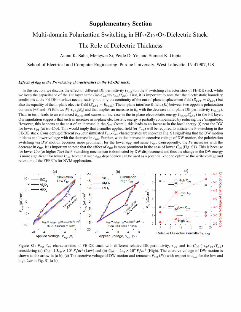
Effects of 𝝐𝝐𝑫𝑫𝑫𝑫 in the P-switching characteristics in the FE-DE stack:
In this section, we discuss the effect of different DE permittivity (𝜖𝜖𝐷𝐷𝐷𝐷) on the P switching characteristics of FE-DE stack while we keep the capacitance of the DE layer same (iso-CDE=𝜖𝜖0𝜖𝜖𝐷𝐷𝐷𝐷/𝑇𝑇𝐷𝐷𝐷𝐷). First, it is important to note that the electrostatic boundary conditions at the FE-DE interface need to satisfy not only the continuity of the out-of-plane displacement field (𝐷𝐷𝑧𝑧,𝐹𝐹𝐷𝐷 = 𝐷𝐷𝑧𝑧,𝐷𝐷𝐷𝐷) but also the equality of the in-plane electric-field (𝐸𝐸𝑥𝑥,𝐹𝐹𝐷𝐷 = 𝐸𝐸𝑥𝑥,𝐷𝐷𝐷𝐷). The in-plane interface E-field (Ex) between two opposite polarization domains (+P and -P) follows |P|=𝜖𝜖0𝜖𝜖𝑥𝑥|𝐸𝐸𝑥𝑥| and that implies an increase in 𝐸𝐸𝑥𝑥 with the decrease in in-plane DE permittivity (𝜖𝜖𝑥𝑥,𝐷𝐷𝐷𝐷). That, in turn, leads to an enhanced 𝐸𝐸𝑥𝑥,𝐹𝐹𝐷𝐷 and causes an increase in the in-plane electrostatic energy (𝜖𝜖𝑥𝑥,𝐹𝐹𝐷𝐷𝐸𝐸𝑥𝑥,𝐹𝐹𝐷𝐷
2 ) in the FE layer. Our simulation suggests that such an increase in in-plane electrostatic energy is partially compensated by reducing the P magnitude. However, this happens at the cost of an increase in the ffree. Overall, this leads to an increase in the local energy (f) near the DW for lower 𝜖𝜖𝐷𝐷𝐷𝐷 (at iso-CDE). This would imply that a smaller applied field (or Vapp) will be required to initiate the P-switching in the FE-DE stack. Considering different 𝜖𝜖𝐷𝐷𝐷𝐷, our simulated Pavg-Vapp characteristics are shown in Fig. S1 signifying that the DW motion initiates at a lower voltage with the decrease in 𝜖𝜖𝐷𝐷𝐷𝐷. Further, with the increase in coercive voltage of DW motion, the polarization switching via DW motion becomes more prominent for the lower 𝜖𝜖𝐷𝐷𝐷𝐷 and same Vapp. Consequently, the PR increases with the decrease in 𝜖𝜖𝐷𝐷𝐷𝐷. It is important to note that the effect of 𝜖𝜖𝐷𝐷𝐷𝐷 is more prominent in the case of lower CDE (Fig. S1). This is because for lower CDE (or higher TDE) the P-switching mechanism is dominated by DW displacement and thus the change in the DW energy is more significant for lower CDE. Note that such 𝜖𝜖𝐷𝐷𝐷𝐷 dependency can be used as a potential knob to optimize the write voltage and retention of the FEFETs for NVM application.
Figure S1: Pavg-Vapp characteristics of FE-DE stack with different relative DE permittivity, 𝜖𝜖𝐷𝐷𝐷𝐷 and iso-CDE (=𝜖𝜖0𝜖𝜖𝐷𝐷𝐷𝐷/𝑇𝑇𝐷𝐷𝐷𝐷) considering (a) CDE =1.3𝜖𝜖0 × 109 𝐹𝐹/𝑚𝑚2 (Low) and (b) CDE = 2𝜖𝜖0 × 109 𝐹𝐹/𝑚𝑚2 (High). The coercive voltage of DW motion is shown as the arrow in (a-b). (c) The coercive voltage of DW motion and remanent Pavg (PR) with respect to 𝜖𝜖𝐷𝐷𝐷𝐷 for the low and high CDE in Fig. S1 (a-b).