
MSc DE Project Report.xps
131
The University of Brighton, School of Engineering & The University of Sussex, School of Engineering & IT MSc degree in Digital Electronics MSc Project (DGM10) Title: “Trip Computer & Recorder for Long-Haul Vehicles” Project Supervisor: Mr. C. S. Knight Submitted by: Panagiotis Kenterlis September 2002 A dissertation submitted in partial fulfilment of the requirements of the University of Brighton and the University of Sussex for the degree of Master of Science in Digital Electronics.
-
Upload
khangminh22 -
Category
Documents
-
view
1 -
download
0
Transcript of MSc DE Project Report.xps

The University of Brighton, School of Engineering &
The University of Sussex, School of Engineering & IT
MSc degree in Digital Electronics MSc Project (DGM10)
Title:
“Trip Computer & Recorder for Long-Haul Vehicles”
Project Supervisor: Mr. C. S. Knight
Submitted by:
Panagiotis Kenterlis
September 2002
A dissertation submitted in partial fulfilment
of the requirements of the University of
Brighton and the University of Sussex for the
degree of Master of Science in Digital
Electronics.

DDiissccllaaiimmeerr
I hereby certify that the attached dissertation is my own work except where otherwise
indicated. I have identified my sources of information; in particular I have put in quotation
marks any passages that have been quoted word-for-word, and identified their origins.
Information displayed in this report was valid at the time that it was written. The author is
not liable for any future changes.
Date:
Signed:
Panagiotis Kenterlis
o 1-Wire bus, 1-Wire devices, MicroLan, and iButton are all trademarks of Dallas Semiconductors (now
Dallas/Maxim).
o CodeWarrior is a trademark of Metrowerks Inc.
o PowerPC is a trademark of International Business Machines (IBM) Corp.
o Visual Basic is a trademark of Microsoft Corp.
o CompactFlash is a trademark of SanDisk Corporation and is licensed royalty-free to the CFA which in turn
licenses it royalty-free to its members.

AAbbssttrraacctt
The Motorola MPC555 is a powerful microcontroller with a large set of on-chip modules,
which is targeted to the automotive industry for engine control, or other real-time control
applications. This microcontroller was a candidate for use as an education tool by the
Department of Engineering at the University of Brighton.
This report discusses the steps on researching, drawing the basic specifications and
developing a digital trip computer with embedded trip data recorder facilities as a product.
The actual aim of this project is to evaluate the specific microcontroller in a real application
and also promote new ideas in product design in the automotive field. In addition, a number
of different peripheral interfaces are being explored.
Both hardware and software designs are analysed in order to familiarise the reader with
the technology and techniques used. Being considered as an educational tool, this report is
largely shifted to the hardware part of the project, giving it more emphasis; however it is still
significantly linked to the software tools used to produce the generated programs.
The report was written keeping in mind that the reader has some basic knowledge of
microcontrollers and digital electronics. Wherever needed, topics are being discussed in
much detail, while other parts are only briefly mentioned.

CCoonntteennttss
1. INTRODUCTION 1-1
1.1. AIMS OF THE PROJECT 1-2 1.2. MARKET RESEARCH 1-3
2. PROJECT SPECIFICATIONS 2-5
2.1. FUNCTIONAL SYSTEM DIAGRAM 2-6 2.2. JUSTIFICATION OF SELECTIONS 2-8 2.2.1. DATA PROCESSING HARDWARE 2-8 2.2.2. INFORMATION DISPLAY UNIT 2-8 2.2.3. USER DATA INPUT UNIT 2-12 2.2.4. DIGITAL IDENTIFICATION DEVICES 2-12 2.2.5. TEMPERATURE SENSORS 2-16 2.2.6. REAL TIME CLOCK 2-19 2.2.7. STORAGE DEVICE 2-21 2.2.8. COMMUNICATIONS BUS 2-23 2.3. FINALISED SYSTEM OUTLINE 2-24
3. PROJECT DESIGN 3-25
3.1. HARDWARE DESIGN 3-25 3.1.1. AUTOMOTIVE SENSORS 3-25 3.1.1.1. Engine Speed Sensor 3-25 3.1.1.2. Road Speed Sensor 3-26 3.1.1.3. In-Tank Fuel Sensor 3-27 3.1.1.4. Fuel Flow Meter 3-28 3.1.2. MICROCONTROLLER PRESENTATION 3-29 3.1.2.1. Use of Microcontroller Modules in the Project / Configuration 3-30 3.1.3. PERIPHERAL DEVICES 3-42 3.1.3.1. Real Time Clock 3-42 3.1.3.2. Information Display Unit (VFD Module) 3-45 3.1.3.3. Data Entry Unit (Keyboard) 3-47 3.1.3.4. Storage Device (CompactFlash Card) 3-50 3.1.3.5. Digital Identification Devices 3-53 3.1.3.6. Temperature Sensing Devices 3-56 3.1.3.7. Other Circuits 3-58

3.2. SOFTWARE DESIGN 3-59 3.2.1. DEVELOPMENT TOOLS USED 3-59 3.2.1.1. Metrowerks CodeWarrior Registration Issues 3-61 3.2.1.2. Using the Metrowerks CodeWarrior IDE 3-62 3.2.1.3. Configuring the Metrowerks CodeWarrior IDE 3-66 3.2.2. MICROCONTROLLER FIRMWARE CODE EXPLANATION 3-72 3.2.2.1. Trip Data Storage 3-80 3.2.3. PC SOFTWARE CODE EXPLANATION 3-83
4. BUILDING THE PROJECT 4-89
4.1. PRACTICAL BUILDING CONSIDERATIONS 4-89 4.1.1. HARDWARE 4-89 4.1.2. SOFTWARE 4-90
5. TESTING & DEBUGGING 5-91
5.1. ELECTROMAGNETIC COMPATIBILITY ISSUES 5-96
6. PROJECT RESULTS 6-97
7. FUTURE UPGRADES AND DEVELOPMENT 7-99
8. CONCLUSIONS 8-100
9. PROJECT MANAGEMENT 9-101
9.1. HOW WAS THE PROJECT PLANNED? 9-101 9.2. PROBLEMS AND ACHIEVEMENTS 9-102
10. BIBLIOGRAPHY 10-103
11. REFERENCES - OTHER DOCUMENTS 11-104
11.1. URLS 11-105
A. APPENDIX 108

LLiisstt ooff FFiigguurreess
Figure 2-1 Typical trip computer provided by the car manufacturer. ________________________________________ 1-3 Figure 2-2 Typical low-cost/limited-functionality trip computer sold as a Do-It-Yourself kit.______________________ 1-3 Figure 4-1 Generic System Outline___________________________________________________________________ 2-6 Figure 4-2 Finalized System Outline ________________________________________________________________ 2-24 Figure 5-1 Pickup Coil Sensor _____________________________________________________________________ 3-25 Figure 5-2 Engine Speed Sensor (G Sensor)___________________________________________________________ 3-26 Figure 5-3 In-Tank Fuel Sensor ____________________________________________________________________ 3-27 Figure 5-4 Fuel Flow Meter Operation ______________________________________________________________ 3-28 Figure 5-5 Clock Control _________________________________________________________________________ 3-31 Figure 5-6 Interrupt Controller ____________________________________________________________________ 3-33 Figure 5-7 QADC_A Channel Connections ___________________________________________________________ 3-36 Figure 5-8 External RTC Connections _______________________________________________________________ 3-42 Figure 5-9 SPI Single-Byte Write ___________________________________________________________________ 3-44 Figure 5-10 SPI Single-Byte Read __________________________________________________________________ 3-44 Figure 5-11 VFD Module Diagram _________________________________________________________________ 3-45 Figure 5-12 VFD Connections to the Microcontroller ___________________________________________________ 3-46 Figure 5-13 Keyboard Layout______________________________________________________________________ 3-47 Figure 5-14 Matrix Layout ________________________________________________________________________ 3-47 Figure 5-15 Keyboard I/O Connections ______________________________________________________________ 3-48 Figure 5-16 iButton Container Dimensions ___________________________________________________________ 3-53 Figure 5-17 iButton connection to a microcontroller____________________________________________________ 3-53 Figure 5-18 iButton ROM Code ____________________________________________________________________ 3-54 Figure 5-19 Temperature Sensor Connections to the Microcontroller_______________________________________ 3-57 Figure 5-20 Buzzer Control _______________________________________________________________________ 3-58 Figure 5-21 Metrowerks CodeWarrior IDE Main Interface_______________________________________________ 3-59 Figure 5-22 Microsoft Visual Basic 6.0 Programming Environment ________________________________________ 3-60 Figure 5-23 Metrowerks CodeWarrior Registration Utility _______________________________________________ 3-61 Figure 5-24 Project Creation #1____________________________________________________________________ 3-62 Figure 5-25 Project Creation #2____________________________________________________________________ 3-63 Figure 5-26 Project Creation #3____________________________________________________________________ 3-63 Figure 5-27 Project Creation #4____________________________________________________________________ 3-64 Figure 5-28 Project Creation #5____________________________________________________________________ 3-65 Figure 5-29 Project Manager Window_______________________________________________________________ 3-65 Figure 5-30 Project Menu_________________________________________________________________________ 3-66 Figure 5-31 Target Selection ______________________________________________________________________ 3-67 Figure 5-32 Target Settings _______________________________________________________________________ 3-67 Figure 5-33 Debug Version Settings_________________________________________________________________ 3-68 Figure 5-34 Debug Target Memory Map _____________________________________________________________ 3-68 Figure 5-35 IDE Preferences Menu _________________________________________________________________ 3-69 Figure 5-36 IDE Preferences ______________________________________________________________________ 3-69
Figure 5-37 ROM Version Settings__________________________________________________________________ 3-70 Figure 5-38 ROM Target Memory Map ______________________________________________________________ 3-71 Figure 5-39 CPU Code Execution Priority____________________________________________________________ 3-72 Figure 5-40 Trip Stop Record______________________________________________________________________ 3-80 Figure 5-41 Trailer ID Record _____________________________________________________________________ 3-81 Figure 5-42 Tachograph Record____________________________________________________________________ 3-81 Figure 5-43 CompactFlash Information Storage Map ___________________________________________________ 3-82 Figure 5-44 Hardware Configuration Utility __________________________________________________________ 3-84 Figure 5-45 Trip Data Upload Utility________________________________________________________________ 3-86 Figure 6-1 Photograph of the MPC555 Development Board ______________________________________________ 4-89 Figure 6-2 Development Board with Connected Motherboard_____________________________________________ 4-90 Figure 7-1 Oscilloscope view of square wave signal ____________________________________________________ 5-91 Figure 7-2 Multimeter used to test voltage level of I/O pin _______________________________________________ 5-91 Figure 7-3 PC Terminal Debugging_________________________________________________________________ 5-92 Figure 7-4 Debugging of the application software using BDM/OCD inside Metrowerks CodeWarrior _____________ 5-93 Figure 7-5 General Purpose Registers of the Microcontroller in BDM while executing the application. ____________ 5-94 Figure 7-6 Source Code Execution Window___________________________________________________________ 5-94 Figure 7-7 Sector Contents as uploaded to the PC (1/2) _________________________________________________ 5-95 Figure 7-8 Sector Contents as uploaded to the PC (2/2) _________________________________________________ 5-95
LLiisstt ooff AAppppeennddiicceess
Appendix 1 Contents of 555_Axiom_ROM.lcf File _______________________________________________________ 108 Appendix 2 Contents of 555_AXIOM_flash_init.cfg File __________________________________________________ 109 Appendix 3 Photo of Hardware during Development Period _______________________________________________ 113 Appendix 4 Photo of Developed Hardware_____________________________________________________________ 114 Appendix 5 GUI Screenshots________________________________________________________________________ 115 Appendix 6 Gantt chart ____________________________________________________________________________ 117 Appendix 7 Manuals and Documents not in Electronic Form ______________________________________________ 120

LLiisstt ooff TTaabblleess
Table 4-1 Display Unit Weights Matrix _______________________________________________________________ 2-9 Table 4-2 Display Unit Analyzed Weighted Selection Criteria______________________________________________ 2-9 Table 4-3 Display Unit Weighted Decision Matrix______________________________________________________ 2-11 Table 4-4 Digital Identification Device Weights Matrix__________________________________________________ 2-12 Table 4-5 Digital Identification Device Analyzed Weighted Selection Criteria ________________________________ 2-13 Table 4-6 Digital Identification Devices______________________________________________________________ 2-14 Table 4-7 Digital Identification Device Weighted Decision Matrix _________________________________________ 2-15 Table 4-8 Temperature Sensor Weights Matrix ________________________________________________________ 2-16 Table 4-9 Temperature Sensor Analyzed Weighted Selection Criteria_______________________________________ 2-16 Table 4-10 Temperature Sensors ___________________________________________________________________ 2-17 Table 4-11 Temperature Sensor Weighted Decision Matrix_______________________________________________ 2-18 Table 4-12 Real Time Clock Weights Matrix __________________________________________________________ 2-19 Table 4-13 Real Time Clock Analyzed Weighted Selection Criteria_________________________________________ 2-19 Table 4-14 Real Time Clock Devices ________________________________________________________________ 2-20 Table 4-15 Real Time Clock Weighted Decision Matrix__________________________________________________ 2-20 Table 4-16 Storage Media Weights Matrix ____________________________________________________________ 2-21 Table 4-17 Storage Media Analyzed Weighted Selection Criteria __________________________________________ 2-21 Table 4-18 Storage Media_________________________________________________________________________ 2-23 Table 4-19 Storage Media Weighted Decision Matrix ___________________________________________________ 2-23 Table 5-1 Interrupt Sources and Priorities____________________________________________________________ 3-32 Table 5-2 MIOS1 Parallel I/O Port Pin Connections____________________________________________________ 3-39 Table 5-3 TPU3 Microcode ROM Functions __________________________________________________________ 3-40 Table 5-4 Use of TPU3_A Channels_________________________________________________________________ 3-41 Table 5-5 External RTC's Registers and Address Map___________________________________________________ 3-43 Table 5-6 Keyboard Row Scan Pattern Codes _________________________________________________________ 3-48 Table 5-7 Keyboard Column Scan Return Codes _______________________________________________________ 3-48 Table 5-8 Pressed Key Lookup Table ________________________________________________________________ 3-49 Table 5-9 AT Task Files (True IDE mode) ____________________________________________________________ 3-51 Table 5-10 CompactFlash Connections to the microcontroller ____________________________________________ 3-52
TTeerrmmss UUsseedd
ACK - Acknowledge BDM – Background Debug Mode CAN – Controller Area Network CF Card – CompactFlash Card
CPU – Central Processing Unit DPTRAM – Dual Ported TPU RAM EBI – External Bus Interface ECM – Engine Control Module. Also see ECU.
ECU – Engine Control Unit
EEPROM – Electrically Erasable and Programmable Read Only Memory FPU – Floating-Point Unit G1 Sensor – Camshaft Position Sensor G1 Signal – Output Signal of the G1 Sensor GPIO – General Purpose I/O GUI – Graphics User Interface ICE – In-Circuit Emulator IDE – Integrated Development Environment IMB – Inter-Module Bus IRQ – Interrupt Request ISR – Interrupt Service Routine JTAG – Joint Testing Action Group
LBA – Logic Block Addressing MCU – Micro-Controller Unit MIOS1 – Modular Input Output System version 1 NACK – Negative Acknowledge NMI – Non Maskable Interrupt OCD – On-Chip Debugging PSU – Power Supply Unit PWM – Pulse Width Modulation QADC – Queued Analogue to Digital Converter QSMCM – Queued Serial Multi-Channel Module QSPI – Queued Serial Peripheral Interface RTC – Real Time Clock
SCI – Serial Communication Interface SGPIO – SIU General Purpose I/O SIU – System Interface Unit, see USIU

SPI – Serial Peripheral Interface SRAM – Static Random Access Memory TPU3 – Time Processor Unit version 3 UIMB - U-BUS TO IMB3 BUS INTERFACE
USIU – Unified System Interface Unit VCC – Power Supply +5V (unless otherwise specified) VDD – Power Supply +5V (unless otherwise specified) VFD – Vacuum Fluorescent Display VSS – Vehicle Speed Sensor

AAcckknnoowwlleeddggeemmeennttss
I would like to thank my parents for their support through these demanding years of my life
and especially for the year spent in England studying for the MSc in Digital Electronics.
I would also like to thank Mr. John Ellinas and Mr. Panagiotis Drosinopoulos, both
professors during my undergraduate studies at the Technological Education Institute of
Piraeus in Greece for their friendly support and encouragement during my internship at the
Microprocessors laboratory of the same institute.
And of course, Mr. C. S. Knight my supervisor for this project, the report for which you are
reading right now, for the interesting subject.

DE MSc dissertation Issue 1: 16/9/02 Page 1-1 Panagiotis Kenterlis
11.. IInnttrroodduuccttiioonn
Most medium to large sized companies support their own fleet of small cars, vans and
trucks, to meet their transportation demands. Supervising activities of the fleet’s drivers and
minimizing usage costs is always an issue. In addition in the unfortunate case of an accident,
large amounts of money need to be spent on fines, compensations and law suits.
A way of minimizing and avoiding such problems is to be able to record every use of the
fleet’s vehicles. A trip data recorder similar to flight data recorders found in airplanes, also
called a ‘black-box’ by people of the media, is a way of monitoring the driver’s and vehicle’s
road behaviour. Vehicle’s engine and road travel parameters are recorded on a type of
storage media hundreds or even thousands of times a second before and after a crash
accident. These data can then be used to help in simulation to discover the actual events of
the accident.
By implementing a trip computer, a series of information is available to the driver to allow
better trip planning and evaluation. By recording all or some of these pieces of information on
a storage media, they can be afterwards downloaded to a personal computer and examined
to locate points in time where driver or vehicle fails to comply with company’s fleet policy or
plan more efficient routes and trip plans.

DE MSc dissertation Issue 1: 16/9/02 Page 1-2 Panagiotis Kenterlis
11..11.. AAiimmss ooff tthhee PPrroojjeecctt
By taking up this project it was essential to create an innovative product. To achieve this
goal some objectives were considered:
Firstly include functions that are of most interest to a Long-Haul vehicle driver. It is of great
importance for the success of the product to be accepted by the end-user, the driver. If the
driver is reluctant to use the device, then this attitude will have an impact to the adoption of
the product in a wider range inside a company, which means more sales and technical
support charges from the manufacturer’s side.
Secondly, to help a company manage its fleet of vehicles more efficiently by allowing
recording of the road behaviour of its drivers and log events such as loading/unloading,
stopping for fuel/rest etc. These will eventually help the company plan more efficient routes
for its transportation needs. For a company any investment, such as the installation of the trip
computer to all the vehicles of its fleet, should return some profit in any way.
And last but not least, as a bonus function to make the device useful in the investigation of
an accident. This will require from the trip computer to have some trip recorder capabilities,
such as those found on flight recorders of airplanes.

DE MSc dissertation Issue 1: 16/9/02 Page 1-3 Panagiotis Kenterlis
11..22.. MMaarrkkeett RReesseeaarrcchh
In the automotive industry some vehicle manufacturers offer their own solution in either or
both fields of trip computers and trip data recorders. Most modern vehicles offer trip computer
functionalities, however they offer basic pieces of information using a rudimentary user
interface to the driver (Figure 1-1, URL [4], [11], [14]). Some other manufacturers, such as
SCANIA (URL [25]), follow another path of providing a connection port to the vehicle’s control
unit, so that specially engineered software running on a PDA or portable PC can display and
handle all trip and vehicle information. A typical low-cost limited-functionality trip computer for
cars can be found at prices of $100, displaying only a minimum set of information with a
primitive user interface compared to PC user interfaces (Figure 1-2, URL [33]).
Figure 1-1 Typical trip computer provided by the car manufacturer.
Figure 1-2 Typical low-cost/limited-functionality trip computer sold as a Do-It-Yourself kit.
In the field of trip data recording few are the manufacturers that offer such functions in their
standard production-line vehicles. Vehicle data recorders are found primarily in F1 racer cars,
where the parameters being recorded are out of proportions to the ones needed for a typical
automotive car installation. Currently IEEE has formed a committee trying to draw a standard
for automotive data recorders that will be adopted by the automotive industry. However a
final standard proposal is not expected to be available for at least 1-1.5 years. In the market
there are only a handful of companies that manufacture data recorders at very high prices,
which is one of the reasons why they are not popular in cars being sold worldwide. In addition
to that, legislation in force on most countries doesn’t require or even promote the use of
vehicle data recorders.
An academic project in digital data recorders for vehicles is currently in progress by
undergraduate students S. Kapetanakis and L. Netsopoulos at the Technological Education
Institute of Piraeus, Faculty of Technology Applications, Department of Electronic Computer
Systems Engineering, in Greece. The team of students is developing an automotive data

DE MSc dissertation Issue 1: 16/9/02 Page 1-4 Panagiotis Kenterlis
recorder based on an 8bit microcontroller and although it acquires information from various
sensors, the limited architecture of their design (small and slow memory) does not allow
recording of many seconds before and after an accident has taken place. In addition a limited
number of samples are acquired every second. Their research although it involves creating a
very interesting piece of hardware it is limited in its design as it is targeted to the low-end of
the automotive market where every penny added in the vehicle’s price counts. Their work is
remarkable in the sense it tries to deal with the actual problem by using low-complexity, low-
cost and easy to find hardware.
Although another, more complex, implementation could arise from this project, the short
time allocated and the complexity of such a venture strictly prohibits any more thoughts on
accident data recorders for automotive purposes.

DE MSc dissertation Issue 1: 16/9/02 Page 2-5 Panagiotis Kenterlis
22.. PPrroojjeecctt SSppeecciiffiiccaattiioonnss
After having researched on the current products available on the market and wanting to
develop a product not similar to what is already available, a list of specifications was drawn.
The device to be built, a Trip Computer for long haul vehicles, will display a series of
vehicle and trip information for use by the driver. In addition, some of this information will be
stored on a non-volatile memory medium for later reviewing and processing at the company’s
headquarters, where useful conclusions can be extracted and help to better manage the
company’s fleet of vehicles.
The preliminary specifications outline published in the pre-course assignment for the MPE
module included most of the items on the finalised specifications list that follows.
1. Average speed.
2. Current speed.
3. Present vehicle location (relative to total trip distance entered at start point).
4. Total elapsed trip time.
5. Battery voltage.
6. Fuel remaining.
7. Distance to empty fuel tank.
8. Total amount of fuel used since trip start.
9. Instantaneous fuel flow rate.
10. Refuel mark-up entry.
11. Elapsed time from last stop point.
12. Estimated time of arrival.
13. Time/Date.
14. Local time.
15. Alarm clock.
16. Engine RPM.
17. Odometer.
18. Outside temperature.
19. Cabin temperature.
20. Tiredness warning after x hours of continuous driving.
21. Driver access control using a digital key.
22. Trailer identification.

DE MSc dissertation Issue 1: 16/9/02 Page 2-6 Panagiotis Kenterlis
22..11.. FFuunnccttiioonnaall SSyysstteemm DDiiaaggrraamm
The following basic diagram presents a generic overview of the connections and
architecture of the system while more explanation is given on the following pages.
Automotive sensors assigned as being either analogue or digital can be found in many forms
by different manufacturers, however in most current vehicles they are found to have outputs
as referenced below.
Figure 2-1 Generic System Outline
The entire project is based on a Micro-Controller Unit (MCU), which processes information
and manages the peripheral modules, in order to deliver to the user the end-effect of a
perfectly working system.
The engine’s speed, vehicle’s road speed and fuel consumption (flow meter) are digital
inputs with the information carried in the frequency of the generated pulses (or otherwise
stated the number of pulses within a time window of e.g. 1sec). For the analogue signals,
some conversion is required by A/D converters before being fed to the MCU, so that the
information carried by the voltage value can be extracted. The in-tank fuel sensor measures

DE MSc dissertation Issue 1: 16/9/02 Page 2-7 Panagiotis Kenterlis
the amount of fuel left in the fuel tank and the battery voltage input gives an indication of the
vehicle’s battery health.
Both cabin and outside temperature are measured by thermometer devices and the
temperature readings are only used for display purposes, and not for control.
These ID devices are marked with a unique serial number used in conjunction to a
database to identify the driver’s name or trailer contents.
The external Real Time clock is used to hold current time and date, which can be
presented on the display unit. It should also be able to provide a time reference of one
second, which can be useful for various functions e.g. speed measurement.
A non-volatile storage media is used to store trip and vehicle data, which can be uploaded
to a PC at the end of a trip for further process and statistical analysis. Information such as
speed, attached trailers, distance covered, driver on wheel, amount of fuel used, etc are
recorded on specific intervals or upon activation of an event.
A communications interface allows a PC with the proper software to connect to the trip
computer while the vehicle is stopped and perform functions such as to download sensor
configuration data and/or upload the data stored in the memory device. A high speed
communications bus is desirable to minimize upload times when the amount of stored data is
large.

DE MSc dissertation Issue 1: 16/9/02 Page 2-8 Panagiotis Kenterlis
22..22.. JJuussttiiffiiccaattiioonn ooff SSeelleeccttiioonnss
After having drawn an initial project specifications outline, the technology behind every box
needs to be defined. The following pages describe how decisions were made towards finding
the right parts for the project.
22..22..11.. DDaattaa PPrroocceessssiinngg HHaarrddwwaarree
In the automotive field of applications few processors are currently used. Most of them are
high-speed 32bit processors or microcontrollers with embedded modules providing functions
that fit in the automotive environment. Right from the start of this project the selection of the
processor to be used had been pre-determined by the supervisor as an attempt to evaluate
the microcontroller for use as an educational tool. The Motorola MPC555, a very powerful
32bit microcontroller oriented towards automotive applications and largely used for Engine
Control Units (ECUs), was available by the University in a development board and was
accompanied by all the necessary development tools.
Taking into account the number and functionality of modules available on the
microcontroller, the specifications for the peripheral devices to follow were limited to fit the
microcontroller and help make decisions easier.
22..22..22.. IInnffoorrmmaattiioonn DDiissppllaayy UUnniitt
The digital Trip Computer must provide very important information to the driver by means of
a User Interface. Information needs to be displayed, selected and inputted to the trip
computer. The driver can select from a pre-defined set of information and determine which
functions should be activated and when. As a first step, information needs to be displayed in
a form that is directly recognizable and utilizable. Text and graphics is the most important and
commonly found form. Four display interfaces are most used for control applications: LED,
LCD, VFD and CRT. The following pages contain analyzed information on each display type
and through comparative thinking one of them will be selected as the best fit for the project.
Where text/numerical displays are discussed a 4 row x 20 characters standard display is
considered, and for the graphics displays, a pixel matrix of 128x64 at minimum.

DE MSc dissertation Issue 1: 16/9/02 Page 2-9 Panagiotis Kenterlis
Table 2-1 Display Unit Weights Matrix A B C D E F G H De-normalized Normalized Amount of Displayable Information A = + + + = = - - 1 9 Discernible Display B - = + + + + - - 1 9 Interface Type C - - = - - - - - -7 1 Interfacing Complexity D - - + = - + - = -2 6 Custom Information Type Display E = - + + = + - + 2 10 Power Consumption F = - + - - = = - -4 4 Dimensions G + + + + + = = + 6 14 Relative Cost per Amount of Information Displayable
H + + + = - + - = 2 10
Table 2-2 Display Unit Analyzed Weighted Selection Criteria Selection Criteria Description Points Weighted
Points Less than 10 Characters 1 9 More than 10 Characters – Less than 80 Characters 2 18
A. Amount of Displayable Information
More than 80 Characters 3 27 Only in Dark Environments -1 -9 Only in Bright Environments -1 -9 Special Lighting Circuit Required 1 9
B. Discernible Display
Irrespective of Environment Lighting 2 18 Serial Interface 3 3 Parallel Interface 2 2
C. Interface Type:
Proprietary Interface -1 -1 Requires External Logic 1 6 Requires Special Connector -1 -6 Requires External Logic & Special Connector -2 -12
D. Interfacing Complexity:
Requires No External Logic 2 12 Numbers Only -1 -10 Text Only 1 10 Text Only + Custom Characters 2 20 Graphics + Text 3 30
E. Custom Information Type Display
Graphics + Text + Custom Characters 4 40 Normal Power Supply (less than 1A) 2 8 Normal Power Supply (more than 1A) 1 4
F. Power Consumption
Special Power Supply -2 -8 Small 2 28 Medium 1 14
G. Dimensions (relative to the dimensions of the information display area) Large -1 -14
Low 2 20 Average 1 10
H. Relative Cost per Amount of Information Displayable High -1 -10

DE MSc dissertation Issue 1: 16/9/02 Page 2-10 Panagiotis Kenterlis
Some information on every type of displays is given below. Advantages and
disadvantages given are considered from the writer’s point of view.
7-Segment LED Displays
Found in many sizes. High visibility in most lighting conditions. Relatively low cost in small displays. High power consumption. Driving circuits are complex when using multiplexing for large displays. Data conversion is required. Standard non-customisable display font. Aesthetic result is not always respectable from a user’s point of view.
VFD (Vacuum Fluorescent Display)
Excellent visibility/brightness No need for backlight hardware. Available in wide range of colours. Available in graphics and text displays. Wide operating temperature range. Wide viewing angle. Medium cost relative to size. Higher cost than LCD modules.
LCD (Liquid Crystal Display)
Character LCD
Easy to interface. Relatively of low-medium cost according to text dimensions. Standard controller interface and programming. Assisted by backlight techniques for dark environments. Few customisable characters (up to 8). Standard character set. Limited row x column dimensions. Backlight hardware can draw much current or require
special hardware. Limited viewing angle.
Graphic LCD
Entire character set can be customized. Able to display bitmapped graphics to allow a friendlier user
interface. Easy to interface to any microcontroller. Found in a variety of dimensions and pixel count. Also found in colour versions. Assisted by backlight techniques for dark environments. Found in pre-assembled module form. Programming is highly dependent on the controller used. Backlight hardware can draw much current or require
special hardware. High cost relative to size. Limited viewing angle.

DE MSc dissertation Issue 1: 16/9/02 Page 2-11 Panagiotis Kenterlis
CRT (Cathode Ray Tube)
All purpose (graphics, text, and moving picture). Found in colour and monochrome phosphor coating. Need special interfacing hardware. Require high voltages to operate (15-25KV). Bulky. Heavy. Relatively of low cost according to size, quality,
resolution, display type (colour or monochrome) and interface technique.
Table 2-3 Display Unit Weighted Decision Matrix Display Technology A B C D E F G H Total Points LED 9 -9 2 6 -10 8 14 -10 10 VFD (Text) 18 18 2 6 10 8 28 10 100 VFD (Graphics) 27 18 2 6 30 8 28 20 139 LCD (Text) 18 9 2 6 20 8 28 10 101 LCD (Graphics) 27 9 2 6 40 4 28 20 136 CRT 27 18 -1 -12 30 8 -14 20 76

DE MSc dissertation Issue 1: 16/9/02 Page 2-12 Panagiotis Kenterlis
22..22..33.. UUsseerr DDaattaa IInnppuutt UUnniitt
At some points in time the driver may need to input data or select different information
screens. In PC environments this is usually done by using a keyboard and/or a mouse.
However in control applications there is rarely the need for a full alphanumerical keyboard or
even more unlikely a high-precision pointing device.
The most common input device is the matrix keyboard, which is easily manufactured to fit
specifications and at low cost. Other options available, such as touch-screens, voice
recognition, etc, not only require exotic driving circuits but also add software overhead and
most importantly exceed cost for use and therefore are rejected.
22..22..44.. DDiiggiittaall IIddeennttiiffiiccaattiioonn DDeevviicceess
For the project it is essential to identify different drivers and attached trailers using a
medium that is cost effective, require little or no extra hardware, easy to use, reliable, small in
dimensions and capable of operating in long distances from the main device, and at harsh
environmental conditions.
To make a selection easier, a list of criteria to be considered was drawn and different
weight of significance was assigned to each criterion.
Table 2-4 Digital Identification Device Weights Matrix A B C D E F G H I J K De-normalized Normalized Unique ID A = = + - - - - + - - - -5 6 Programmability B = = + - - - - + - - - -5 6 Secure Communications C - - = - - - - - - - - -10 1 Multiple Devices Support on Same Reader
D + + + = + = + + = = - 5 16
Interfacing Complexity E + + + - = - + = - - = 0 11 Endurance at Harsh Environments
F + + + = + = + + = + - 6 17
Dimensions G + + + - - - = = - = - -2 9 Ease of Installation H - - + - = - = = = - - -5 6 Maintenance I + + + = + = + = = = = 5 16 Cost of ID Device J + + + = + - = + = = = 4 15 Cost of Interfacing K + + + + = + + + = = = 7 18
Having weighed the significance of each criterion for the project, an analytical options table
for each of them was built with points assigned to define the desired qualities from the device
to be selected for use in the project.

DE MSc dissertation Issue 1: 16/9/02 Page 2-13 Panagiotis Kenterlis
Table 2-5 Digital Identification Device Analyzed Weighted Selection Criteria Selection Criteria Description Points Weighted
Points No 1 6 A. Unique ID Yes 2 12 No 1 6 Some Programmable Features 2 12
B. Programmability
Yes 3 18 No 1 1 Some Security Features 2 2
C. Secure Communications
Yes 3 3 No -1 -16 D. Multiple Device
Support on Same Reader Yes 1 16 No Special Hardware Needed 2 22 Special Connector Needed 1 11 External Circuits Needed -1 -11
E. Interfacing Complexity
External Circuits + Connector Needed -2 -22 Sensitive Device -2 -34 F. Endurance at
Harsh Environments Durable 2 34 Tiny 1 9 Small 2 18 Medium-Sized -1 -9
G. Dimensions
Bulky -2 -18 Simple Placement 2 12 Some Special Fitting Required 1 6
H. Simplicity of Installation
Special Fitting Required -2 -12 No Maintenance Required 2 32 Periodical Service May Be Required 1 16
I. Maintenance
Frequent Service Required -2 -32 Low 2 30 Average 1 15
J. Cost of ID Device
High -1 -15 Low 2 36 Average 1 18
K. Cost of Interfacing
High -1 -18
A unique ID code although being a very attractive idea, it is not always present or
applicable in actual products. In this case, it is necessary for the ID device to be
programmable at least partly. By programming a device using a centralized control tool to
assign unique serial numbers for own use, it is easy to create databases of categorized ID
codes for drivers, trailers, containers etc.
For this project, increased security features are not required, since no security issues can
be located, however should that is requested in the future, a device that allows secure
information storage and exchange is always desirable as long as cost is not increased
dramatically.
The ability to use the same device reader to access multiple ID keys at the same time is a
highly important feature, since it can effectively reduce the number of readers needed and
hence reduce cost. Connecting ID devices over a common medium is one way of achieving
this goal.

DE MSc dissertation Issue 1: 16/9/02 Page 2-14 Panagiotis Kenterlis
Interface complexity should always be kept to a minimum level, to avoid introducing
unstable behaviour and cost increase.
Endurance at harsh environments is another wanted feature, since the devices are likely to
experience a wide range of climate changes and mechanical strain during a trip. Physical
dimensions are important when the ID key needs to be carried by a driver or to be placed in
the tractor, or trailers. Extremely small or large devices can be difficult to manipulate in all
cases. Installation can become an issue if there is need to remove parts or otherwise
physically alter the vehicle’s or the trailers’ structure. Simple installation is always desirable.
Maintenance can be brought to a minimum if the device’s endurance is high and lifetime
long. Maintenance increases cost of use and makes a product less appealing, should
frequent service or replacement is needed. If maintenance is required while still on a trip,
unwanted problems in use of the trip computer may arise.
As always cost of the ID devices and interfacing should be kept to a minimum. Costly
products are seldom appealing.
Table 2-6 Digital Identification Devices RFID SmartCard iButton Magnetic
Strip Card Barcode
Unique ID Depending on Device
Depending on Card Yes (64bit) No No
Programmability Depending on Device Yes Depending on
Device Yes No
Secure Communication
Depending on Device
Depending on Device
Depending on Device
Depending on Device No
Reliable Communication
Depending on Distance -
Error Checking
Error Checking
Error Checking
Error Checking
Error Checking
Multiple Device Support on Same Reader
Yes No Yes No No
Interfacing Complexity Special
Hardware Reader
Required
Special Hardware Reader & Connector Required
2-Terminal Connector &
Software Emulation of Interface by
any microcontroller
Special Hardware Reader & Connector Required
Special Hardware Reader
Required
Endurance at Harsh Environments Yes Average Yes No No
Dimensions Small/Average Small/Average Small Average/Large Average/Large Simplicity of Installation
Transceiver and RF Antenna Fitting
Required
Small Card Socket
Installation
Simple Battery Holder
or Two Terminal
Probe
Reader Device
Installation
Reader Device
Installation
Maintenance Periodical Service May Be Required
Periodical Service May Be Required
None - Little Periodical
Service May Be Required
Periodical Service May Be Required
Cost of ID Device Low Low Low Low Low Cost of Interfacing High Average Low High High

DE MSc dissertation Issue 1: 16/9/02 Page 2-15 Panagiotis Kenterlis
The above introduced digital ID devices need to be weighted to select the best fit for the
project.
Table 2-7 Digital Identification Device Weighted Decision Matrix A B C D E F G H I J K Total Points RFID 12 12 2 16 -11 34 9 -12 16 30 -18 90 SmartCard 12 12 2 -16 -22 34 18 6 16 30 18 110 iButton 12 12 2 16 22 34 18 12 32 30 36 226 Magnetic Swipe Card 6 18 2 -16 -22 -34 -9 6 16 30 -18 -21 Barcode 6 6 1 -16 -11 -34 18 12 16 30 -18 10
Having used parts of the 1-Wire family range of products by Dallas Semiconductors as
basic elements of my undergraduate project, accumulated knowledge can be considered an
asset in developing the project in shorter time.

DE MSc dissertation Issue 1: 16/9/02 Page 2-16 Panagiotis Kenterlis
22..22..55.. TTeemmppeerraattuurree SSeennssoorrss
A set of temperature sensors needs to be used to provide temperature readings of the
driver’s cabin (cockpit) and the outside environment. These readings will be printed on the
display unit already selected in previous pages. To make sure the right temperature sensor is
to be used, the selection procedure is performed with the use of decision matrices.
Table 2-8 Temperature Sensor Weights Matrix Criteria A B C D E F G De-normalized Normalized Interface Type A = + - - = - - -3 1 Temperature Range B - = = + - - - -3 1 Temperature Resolution C + = = = - - - -2 2 Accuracy D + - = = - - - -3 1 Required Wiring E = + + + = - - 1 5 Cost of Sensor F + + + + + = = 5 9 Cost of Interfacing G + + + + + = = 5 9
Table 2-9 Temperature Sensor Analyzed Weighted Selection Criteria Selection Criteria Description Points Weighted
Points Analogue 1 1 Digital – Parallel -1 -1 Digital – Serial (I2C) -1 -1 Digital – Serial (SPI) 2 2
A. Interface Type
Digital – Serial (1-Wire) 3 3 -40οC +55οC 1 1 -55οC +85οC 2 2
B. Temperature Range
-55οC +125οC 3 3 1οC 1 2 0.5οC 2 4 0.25οC 3 6 0.125οC 4 8
C. Temperature Resolution
0.0625οC 5 10 ±4οC 1 1 ±3οC 2 2 ±2οC 3 3 ±1οC 4 4
D. Accuracy
±0.5οC 5 5 2 – Wires 3 15 3 – Wires 2 10 4 – Wires 1 5
E. Required Wiring
More than 4 Wires -1 -5 Low Cost (<$1) 2 18 Medium Cost – ($1< cost > $2) 1 9
F. Cost of Sensor
High Cost – (> $2) -1 -9 Low 2 18 Average 1 9
G. Cost of Interfacing
High -1 -9

DE MSc dissertation Issue 1: 16/9/02 Page 2-17 Panagiotis Kenterlis
Analogue sensors although very commonly used in many applications, in the case of
automotive applications can become a source of problems because of high electrical noise
levels created by the engine. Digital sensors can circumvent this problem by using an error
detection technique. In addition the temperature reading from a digital sensor is always
formatted as a value in units of a measurement system, most commonly degrees Celsius,
and therefore no calculations or conversions are required from voltage levels to digital
values.
The type of interface although it is important, it can always be emulated by a
microcontroller with enough I/O pins. In the case of the microcontroller SPI and parallel
interfaces are available in hardware, while I2C and 1-Wire need to be emulated.
Using a temperature sensor that works in extreme temperatures allows a future upgrade to
include temperature readings from various engine sections.
Although a high resolution in temperature readings is not required for this application, it is
always considered a credit. Accuracy of temperature reading is always desired to be as good
as possible, but without an increase in cost.
The number of wires is again related to electrical noise present as well as cost, cable
length and installation complexity. The fewer the wires required to connect to the sensor, the
better.
In the following description table, four of the most used temperature sensors are analysed.
Table 2-10 Temperature Sensors Thermistor MAX6662 DS1820 LM75 A. Interface Type Analogue SPI 1-Wire I2C B. Temperature Range Depending
on Device -55°C to +150°C -55°C to +125°C -55°C to +125°C
C. Temperature Resolution
Depending on Device –
Average
12-Bit + Sign, 0.0625°C Resolution
12-Bit + Sign, 0.0625°C
Resolution .5 °C
D. Accuracy Depending on Device –
Not Very Good
±1°C max to ±2.5 typ depending on
temperature range
±1οC ±3οC
E. Required Wiring 2-3 Wires 7 Wires 3 Wires 8 Wires F. Cost of Sensor Depending
on Device – Average/High
$1.37 $1.76 $0.90
G. Cost of Interfacing Low Low Low Low Packaging - 8/SOT23 TO-92 SOP-8 Manufacturer - Maxim/Dallas Maxim/Dallas National
Semiconductors

DE MSc dissertation Issue 1: 16/9/02 Page 2-18 Panagiotis Kenterlis
Only one of the above temperature sensors is the most suitable for the project, and by
creating the weighted decision matrix above the right part was found.
Table 2-11 Temperature Sensor Weighted Decision Matrix Temperature Sensor A B C D E F G Total Points Thermistor 1 3 4 1 15 -9 18 33 MAX6662 2 3 10 2 -5 9 18 39 DS18B20 3 3 10 5 15 9 18 63 LM75 -1 3 4 2 -5 18 18 39
The DS18B20 having the same interface as the digital identification device selected in
previous pages, can be characterized as an excellent selection, considering the fact that
most software routines developed will be common and no extra hardware is required.

DE MSc dissertation Issue 1: 16/9/02 Page 2-19 Panagiotis Kenterlis
22..22..66.. RReeaall TTiimmee CClloocckk
A Real Time Clock is a device that holds the current time and date in a set of counters
clocked by a time reference signal, usually a square wave with a frequency of 1Hz. This
reference square wave pulse is derived from an external crystal or other square wave signal
source.
Dallas/Maxim is a huge manufacturer of RTC’s and also provides samples of products,
free of charge. All of the below mentioned RTC’s were obtained as samples before deciding
which to use.
Table 2-12 Real Time Clock Weights Matrix A B C D E F G H De-normalized Normalized Real Time Data Format A = + + + + + + + 7 14 Interface Type B - = = = + - + - 0 7 Interfacing Complexity C - = = + + + + = 4 11 Backup Power Supply D - = - = + - = - -2 5 Interrupt Outputs E - - - - = - - - -6 1 Interrupt (1Hz) F - + - + + = + - 2 9 CMOS RAM on-chip G - - - = + - = - -3 4 Cost H - + = + + + + = 5 12
Table 2-13 Real Time Clock Analyzed Weighted Selection Criteria Selection Criteria Description Points Weighted
Points Binary -1 -14 A. Real Time Data Format: Full format – hh:mm:ss dd/mm/yy 1 14 Serial Interface – SPI 2 14 Serial Interface – 1-Wire bus 1 7 Serial Interface – I2C/3-Wire -1 -7 Parallel Interface (De-multiplexed) 1 14
B. Interface Type:
Parallel Interface (Multiplexed) -2 -14 Requires External Logic -1 -11 C. Interfacing Complexity: Requires No External Logic 1 11 Backup Battery Input 1 5 D. Backup Power Supply: No Backup Power Supply -1 -5 No Interrupt Outputs -2 -2 One Interrupt Output 1 1
E. Interrupt Outputs:
Two Interrupt Outputs 2 2 Available 1 9 F. Interrupt (1Hz): Unavailable -1 -9 No RAM -1 -4 Less than 32bytes 1 4 More than 32bytes – Less than or Equal to 96bytes
2 8
G. CMOS RAM on-chip:
More than 96bytes 3 12 Low Cost (<$2) 2 24 Medium – ($2< cost > $4) 1 12
H. Cost
High – (>$4) -1 -12

DE MSc dissertation Issue 1: 16/9/02 Page 2-20 Panagiotis Kenterlis
Having the RTC counting in binary format can be a source of problems, since there is
need to convert the amount of seconds counted into minutes, hours, days, months, etc allow
for calendar corrections according to a reference day. Practically this would require a great
deal of calculations to convert the number of seconds into meaningful and displayable time
information. On the other hand counting in full format (as explained above) only requires for
some registers to be read and possibly converting their contents into displayable information.
Interfaces available directly by the microcontroller are SPI and de-multiplexed
data/address bus. Communications protocols such as 1-Wire and I2C although not available
in hardware; they can be emulated in software, with 1-Wire being already used for Digital
Identification keys and Temperature Sensor devices.
Interfacing complexity is always an issue when having to create a prototype or build a
finalized circuit board. If additional external circuitry is needed, then total cost increases.
Combining a backup power supply (a battery) with internal RAM, makes the RTC chip an
ideal backup storage for important system data.
The number of interrupt outputs is important if every output can generate interrupt signals
with different programmed time period or at a specific time/date. An interrupt signal
generated every 1 second can be extremely useful for measurements, calculations or simply
as a means of knowing when the contents of the RTC have changed.
Cost, as always, is an important factor when selecting parts for a project. The lowest the
cost of parts used, the better.
Table 2-14 Real Time Clock Devices DS12C887 DS2417 DS1305 MAX6902 Real Time Data Format Full Format Binary Full Format Full Format Interface Type Muxed Data/Address Bus 1-Wire Bus SPI SPI Backup Power Supply Yes No Yes Yes Interrupt Outputs 1 1 2 0 Interrupt (1Hz) Yes Yes Yes No CMOS RAM on-chip 113 Bytes - 96 Bytes 31 Bytes Cost $4.80 $0.92 $1.84 $1.45 Manufacturer Dallas/Maxim Dallas/Maxim Dallas/Maxim Dallas/Maxim
Table 2-15 Real Time Clock Weighted Decision Matrix Display Technology A B C D E F G H Total Points DS12C887 14 -14 -11 5 1 9 12 -12 4 DS2417 -14 7 11 -5 1 9 -4 24 29 DS1305 14 14 11 5 2 9 8 24 87 MAX6902 14 14 11 5 -2 -9 4 24 61

DE MSc dissertation Issue 1: 16/9/02 Page 2-21 Panagiotis Kenterlis
22..22..77.. SSttoorraaggee DDeevviiccee
Some of the data acquired from the vehicle’s sensors and digital ID devices need to be
stored for later process at the company’s headquarters. Due to the extended time of a trip the
amount of data can be large, so memory devices with correspondingly large capacities are
required. The storage device to be used needs to be non-volatile to retain data even after
power disconnection or momentary loss. On the following pages some of the most popular
memory devices on the market are analysed and through comparative thinking the most
suitable for the project is selected.
Table 2-16 Storage Media Weights Matrix A B C D E F De-normalized Normalized Capacity Range A = - - + - - -3 3 Interface Type B + = - + + - 1 7 Interfacing Complexity C + + = + + - 3 9 Access Mode D - - - = - - -5 1 Transfer Speed E + - - + = - -1 5 Cost/MB F + + + + + = 5 11
Table 2-17 Storage Media Analyzed Weighted Selection Criteria Selection Criteria Description Points Weighted
Points Below 1MByte per unit -2 -6 Over 1MByte and less than 32MB 1 3
A. Capacity Range:
Over 1Mbyte and up to 1GB 2 6 Serial Interface 1 7 B. Interface Type: Parallel Interface 2 14 Requires External Logic 1 9 Requires Special Connector 1 9 Requires External Logic & Special Connector -1 -9
C. Interfacing Complexity:
Requires No External Logic 2 18 Byte Read – Byte Write 3 3 Byte Read – Block Write 2 2
D. Access Mode:
Block Read – Block Write 1 1 Slow (less than 100KB/sec) -1 -5 Medium (more than 100KB/sec – less than 1MB/sec) 1 5
E. Transfer Speed:
Fast (more than 1MB/sec) 2 10 Low (less than 50p) 2 22 Average (more than 50p -less than £1) 1 11
F. Cost per MB
High (more than £2) -1 -11

DE MSc dissertation Issue 1: 16/9/02 Page 2-22 Panagiotis Kenterlis
E2PROM & FLASH
Both these data storage technologies are available by many
manufacturers, however due to packaging and pin count (because
of individual byte read support) it is very difficult to market large
capacity devices due to cost. The basics behind their technologies
are used by the other devices analysed.
CompactFlash Card
The CompactFlash Card is a FLASH memory device that uses
the same interface protocols and signals as ordinary ATA drives,
that is hard disk drives. Its capacity ranges from a few hundred
kilobytes to a few hundred megabytes. It implements three different
interface protocols to allow interfacing for different application
requirements. It is small in dimensions, fast, reliable and robust.
SmartMedia
The SmartMedia is a FLASH memory device that uses a
proprietary parallel interface. It is small in dimensions, fast, reliable
and robust. It can be easily interfaced and is used in many
applications for data storage. Its parallel interface uses time
multiplexing to reduce pin count, thus requires a multiplexed
address/data bus from the processor.
Memory Stick
The Memory Stick is a FLASH memory device that uses a
proprietary serial interface, thus allowing the use of less I/O pins. It
is small in dimensions, fast, reliable and robust.

DE MSc dissertation Issue 1: 16/9/02 Page 2-23 Panagiotis Kenterlis
Table 2-18 Storage Media E2PROM FLASH CompactFlash Smart Media Memory Stick Capacity Range 16kbit-4Mbit 256kbit-64Mbit 4-256MBytes 32-256MBytes 4-128MBytes Interface Parallel Parallel Proprietary
Parallel - ATA Proprietary
Parallel Proprietary
Serial Access Mode Block Alterable
Byte Access Block Alterable
Byte Access Block Alterable Block Access
Block Alterable Block Access
Block Alterable Block Access
Write Times Slow Average Fast Fast Fast Cost £27
(for 1Mbit) £16-23
(for 8Mbit) 48p per MByte
(for 32MB) 33p per MByte
(for 32MB) 62p per MByte
(for 32MB) Other Separate
Programming Power Supply
Required
Three Different Access Modes
• Prices and capacity ranges as found on July-August 2002
Table 2-19 Storage Media Weighted Decision Matrix Storage Device A B C D E F Total Points E2PROM 3 14 9 2 -5 -11 12 FLASH 3 14 9 2 5 -11 12 CompactFlash 6 14 18 1 10 22 71 SmartMedia 6 14 -9 1 10 22 44 Memory Stick 6 7 -9 1 10 11 26
The CompactFlash Card having collected the most points for its features is effectively
characterized as the most suitable storage media for the project and will be analysed in more
depth in the Hardware Design section o this report (Chapter 3.1.3.4, p. 3-50).
22..22..88.. CCoommmmuunniiccaattiioonnss BBuuss
Having nearly reached the budget limit for the project, an exotic solution in the decision for
a high-speed communications bus for connection to a personal computer, could not be
followed. Instead as a communication medium to a Personal Computer to download or
upload data, one of the serial ports on the microcontroller was selected, running at the
highest possible speed.

DE MSc dissertation Issue 1: 16/9/02 Page 2-24 Panagiotis Kenterlis
22..33.. FFiinnaalliisseedd SSyysstteemm OOuuttlliinnee
Having selected the parts most suitable the project, a finalized system outline was drawn
and is shown in Figure 2-2 below.
Figure 2-2 Finalized System Outline
DE MSc dissertation Issue 1: 16/9/02 Page 3-25 Panagiotis Kenterlis
33.. PPrroojjeecctt DDeessiiggnn
The project can be partitioned into two design areas, the Hardware Design and the
Software Design. In this chapter both partitions will be presented and analysed as much as
possible without reaching into much depth. For more in-depth information on modules and
functions, please consult the datasheets that are found in the accompanying CD-ROM.
33..11.. HHaarrddwwaarree DDeessiiggnn
33..11..11.. AAuuttoommoottiivvee SSeennssoorrss
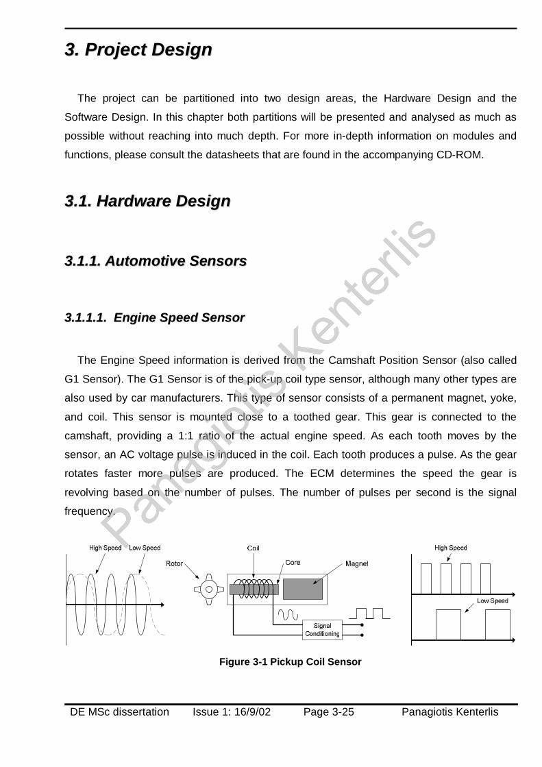
33..11..11..11.. EEnnggiinnee SSppeeeedd SSeennssoorr
The Engine Speed information is derived from the Camshaft Position Sensor (also called
G1 Sensor). The G1 Sensor is of the pick-up coil type sensor, although many other types are
also used by car manufacturers. This type of sensor consists of a permanent magnet, yoke,
and coil. This sensor is mounted close to a toothed gear. This gear is connected to the
camshaft, providing a 1:1 ratio of the actual engine speed. As each tooth moves by the
sensor, an AC voltage pulse is induced in the coil. Each tooth produces a pulse. As the gear
rotates faster more pulses are produced. The ECM determines the speed the gear is
revolving based on the number of pulses. The number of pulses per second is the signal
frequency.
Figure 3-1 Pickup Coil Sensor

DE MSc dissertation Issue 1: 16/9/02 Page 3-26 Panagiotis Kenterlis
Figure 3-2 Engine Speed Sensor (G1 Sensor)
In the case of the G1 Sensor, by multiplying the number of pulses counted in a second
with the number of seconds per minute, the engine’s speed per minute is calculated.
However a camshaft gear may have more than one tooth hence the number of pulses
counted per engine revolution are a multiple of the number of teeth on the gear. Before doing
any further calculations, division of the counted pulses by the number of teeth present is
required to extract the number of engine revolutions.
The output of the G1 Sensor, after being conditioned to output clean square wave pulses,
is fed to the microcontroller by using a TPU3 channel input as will be discussed later in this
report.
33..11..11..22.. RRooaadd SSppeeeedd SSeennssoorr
The Road Speed Sensor (or Vehicle Speed Sensor, VSS) is typically of the same type as
the Engine Speed Sensor, although many other types also exist. It is either located in the
transaxle or the transmission of the vehicle. The vehicle’s speed is again coded in the
frequency of the output signal.
Knowing the number of pulses produced per wheel revolution, the number of pulses
counted in one second and the perimeter (circumference) of the tire it is easy to calculate the
vehicle’s speed.
60mins60secsPerimeter TireRevolution Per Wheel Pulses
Second 1in Pulses CountedSpeed Vehicle ⋅⋅⋅=

DE MSc dissertation Issue 1: 16/9/02 Page 3-27 Panagiotis Kenterlis
33..11..11..33.. IInn--TTaannkk FFuueell SSeennssoorr
The In-Tank Fuel Sensor, also known as Fuel Tank Sending Unit, is as its name reveals
located in the fuel tank of the car. It consists of a float, usually made of foam, connected to a
thin, metal rod. The end of the rod is mounted on a potentiometer. In a fuel tank, the
potentiometer consists of a strip of resistive material connected on one side to the ground. A
wiper connected to the gauge slides along this strip of material, conducting the current from
the gauge to the resistor.
Figure 3-3 In-Tank Fuel Sensor
If the wiper is close to the grounded side of the strip, there is less resistive material in the
path of the current, so the resistance is small and the voltage that is measured on the wiper
terminal is small. If the wiper is at the other end of the strip, there is more resistive material in
the current's path, so the resistance is large and the voltage that is measured on the wiper
terminal is very close to VCC (or equal to it, depending on potentiometer structure). By
inference, the more fuel present inside the fuel tank the closer the voltage measured on the
sensor’s output (wiper).
For the project a linear behaviour of the float and the output of the sensor are assumed in
relation to the amount of fuel in the tank. Simply by measuring the voltage on the sensor’s
output is enough to calculate the remaining fuel in a tank of a known capacity.
CapacityTank Fuel12
Result Conversion Channel ADCTankin Fuel ResolutionBit ADC ⋅−
=

DE MSc dissertation Issue 1: 16/9/02 Page 3-28 Panagiotis Kenterlis
33..11..11..44.. FFuueell FFllooww MMeetteerr
A flow meter is a device that produces a
specific output when a specific amount of liquid
or gas flows through it. For our purposes, a flow
meter device for liquid fuel is assumed. There
are many different technologies used to
measure the quantity of fuel that flows through
the gauge. The technology used is not a subject
of this report.
Figure 3-4 Fuel Flow Meter Operation
For the report a typical flow meter with digital output (TTL) is assumed, this means that for
a given quantity of fuel having flowed through the meter, a pulse is generated on the output
of the flow meter device.
By accumulating the number of pulses received from the flow meter during the course of
time and multiplying with the amount of fuel flowing per pulse, the total fuel consumption of
the vehicle is calculated. Again by using the flow meter’s output pulses it is easy enough to
calculate the fuel consumption of the vehicle per distance measuring unit.
PulsePer Quantity FuelPulsesMeter FlownConsumptio Fuel TotalFinish Trip
Start Trip⋅
= ∑
Although fuel consumption can be calculated by measuring the amount of time that the
injectors are on, the flow meter device is used instead, in order to simplify both hardware and
software design for the project at this stage. Of course as expected there is an increase in
cost, however by using a flow meter, the trip computer actually becomes independent of the
vehicle’s engine specifications and also prevents us from tampering with the ECU.
Had the fuel consumption information been acquired otherwise, much knowledge would be
required of at least the amount of fuel sprayed by an injector within a specific amount of time
and the number of injectors in the engine. In addition, a facility that allows counting the “ON”
time of the injectors is required. This solution although it allows to keep cost down, it adds
extra complexity to the project, which at this stage would not be possible to deal with, without
proper equipment and facilities.
DE MSc dissertation Issue 1: 16/9/02 Page 3-29 Panagiotis Kenterlis
33..11..22.. MMiiccrrooccoonnttrroolllleerr PPrreesseennttaattiioonn
Discussion on the hardware section of the project should fairly start with the heart of the
project, the Motorola MPC555 microcontroller.
The MPC555 is a very powerful 32bit microcontroller based on the PowerPC core with on-
chip floating point unit (FPU) targeted for the automotive industry. With a large amount of
FLASH program memory of 448Kbytes in total, it can store large programs as well as large
arrays of read-only data. It is equipped with 26Kbytes of internal SRAM, used for system
variables and other storage requirements.
The Unified System Interface Unit (see USIU p. 3-30, Ref. [6]) of the MPC555 is
responsible for controlling system start-up, system initialisation and operation, system
protection, system interrupt handling, and the external system bus. Two serial asynchronous,
one synchronous SPI and two CAN bus controllers constitute the microcontroller’s
communications facilities (see QMSCM p. 3-38 and TouCAN, Ref. [6]). The modular I/O
system (MIOS1) consists of a library of flexible I/O and timer functions including I/O port,
counters, input capture, output compare, pulse and period measurement, and PWM (see
MIOS1 p. 3-39, Ref. [6]). Two Queued Analogue-to-Digital Conversion modules are available
for interfacing analogue signals to the microcontroller (see QADC64 p. 3-36, Ref. [6]).
The strongest feature of the microcontroller however, is the Time Processor Unit, which is
a programmable microcontroller itself, which deals with time related functions (see TPU3 p.
3-40, Ref. [6]). Having two TPU modules the MPC555 can control almost any function.
6Kbytes of Dual Ported RAM can be used for TPU related operations.
All these functionalities combined with an internal clock frequency of 40MHz maximum;
make the MPC555 one of the most powerful microcontrollers available.

DE MSc dissertation Issue 1: 16/9/02 Page 3-30 Panagiotis Kenterlis
33..11..22..11.. UUssee ooff MMiiccrrooccoonnttrroolllleerr MMoodduulleess iinn tthhee PPrroojjeecctt // CCoonnffiigguurraattiioonn
•• UUSSIIUU –– UUnniiffiieedd SSyysstteemm IInntteerrffaaccee UUnniitt
The USIU, as already described, is a module that plays an important role in the operation
of the MPC555. It controls and coordinates various critical system functions, which include
the following:
o System configuration and protection: Controls the overall system configuration
and provides various monitors and timers, including the bus monitor, software
watchdog timer, periodic interrupt timer, PowerPC decrementer, time base, and real
time clock.
o Interrupt controller: Handles interrupt requests according to hard-coded priority and
masking. Both external and internal interrupt sources are supported.
o System reset monitoring and generation: Receives input from a number of reset
sources and takes appropriate actions, depending on the source.
o Clock synthesizer: Generates the clock signals used by the SIU as well as the other
modules and external devices.
o Power management: Various low-power modes are supported and configured for
use by the system.
o External bus interface (EBI) control: Handles the transfer of information between
the internal busses and the memory or peripherals in the external address space.
Also allows external devices to become bus masters.
o Memory controller: Provides a programmable glueless interface to various types of
external memory devices and peripherals. Four chip select pins are provided, with
programmable timing attributes and activation address range.
o Debug support: Provides an interface which allows testing and debugging of
programs by use of some external hardware and software running on a PC (see
Testing & Debugging Methods p. 5-91).
Those functions used in the project are analysed in the following pages.

DE MSc dissertation Issue 1: 16/9/02 Page 3-31 Panagiotis Kenterlis
oo CClloocckk SSyynntthheessiizzeerr
The CPU core, internal counter/timers and other facilities make use of clock signals that
are produced by the microcontroller’s internal circuits. System clocks can be configured to
have any of three clock sources, the external quartz crystal (4MHz or 20MHz), the internal
backup clock oscillator, and an external clock source connected to the EXTCLK pin. The
external clock source should have a frequency of 4MHz or the same as the desired system
frequency. These limitations exist due to the use of internal frequency division and
multiplication circuits.
For the purposes of this project, only the clock oscillator using an external quartz crystal at
4MHz was used as a clock source (main clock oscillator). This clock drives the System
Phase Lock Loop circuit, which acts as a programmable multiplier of 20
( [ ] 21... ⋅+⋅= MFBPLPRCRUSIUSPLLSPLL inputoutput , where MF=9) generating an 80MHz clock,
which is next fed to a prescaler circuit and divided by a programmable divider of 2
( 0000B.DFNLUSIU.SCCR. b= ). The output of the prescaler, after amplified, is fed to the CPU
core as the main system clock ( CPUf ).
The main clock after being fed to a programmable prescaler (Divide by 4, or by 16), and
divided by 4 ( 0b0B.TBSUSIU.SCCR. = ) and amplified, becomes the Time Base Clock, which
is used to clock the Decrementer. The main clock also drives another programmable
prescaler (Divide by 4, or by 256), which divides the clock signal by 256
( 0b1B.RTDIVUSIU.SCCR. = ) to generate a 15625Hz clock signal. This clock after
amplification is fed to the internal RTC and the Periodic Interrupt Timer.
Clock programming explanatory diagram is displayed in Figure 3-5 below (Ref. [6]).
Figure 3-5 Clock Control

DE MSc dissertation Issue 1: 16/9/02 Page 3-32 Panagiotis Kenterlis
oo IInntteerrrruupptt CCoonnffiigguurraattiioonn
The Interrupt Controller (Ref. [2]) on the microcontroller has been configured for two
external and three internal interrupt sources. Two more internal sources are configured but
not enabled. Every source is assigned a priority that is hardware coded but can be altered by
software to handle lower fixed priority sources first. External interrupt sources are hard-wired
to specific IRQ pins of the microcontroller. 0IRQ is a Non Maskable Interrupt (NMI) source
hence it cannot be blocked from generating an interrupt. 0IRQ should only be used by
external hardware to indicate a catastrophic system fault. In total there are 8 external
interrupt sources 70 IRQIRQ − and 32 internal interrupt sources 310 LEVELLEVEL − . Interrupt
sources with a small index number have higher priority. Internal interrupt sources
317 LEVELLEVEL − are mapped to USIU interrupt request level seven ( 7LEVEL ). The
software must read the UIPEND register of the Inter-Module Bus (IMB) to determine the
actual source of the interrupt. SIVEC is a 32-bit register holds an 8-bit code representing the
unmasked interrupt source of the highest priority level.
Interrupt sources can be masked by clearing the corresponding bit on the System Interrupt
Mask Register (SIMASK). After having serviced an external interrupt source, it is important to
clear the interrupt flag bit in SIPEND, in order to clear the corresponding interrupt request
latch if a logic ‘0’ is no longer present on the pin. Clearing an interrupt request flag in SIPEND
is done by writing logic ‘1’ in the bit position of the interrupt source.
For the project, the interrupt sources and priorities shown in Table 3-1 were configured
and used.
Table 3-1 Interrupt Sources and Priorities Priority*1 Interrupt Interrupt Source Enabled
0 Level 0 Internal RTC Yes 1*2 Level 1 TPU3_A Yes 2 1IRQ External RTC 0INT Yes
3 2IRQ External RTC 1INT Yes
4 Level 2 SCI Yes 5 Level 3 QSPI No 6 Level 4 QADC No
*1 Highest priority has smallest value. Lowest Priority has largest value.
*2 Level 1 although actually of lowest hardware priority, inside the ISR is handled before external interrupt sources.

DE MSc dissertation Issue 1: 16/9/02 Page 3-33 Panagiotis Kenterlis
Figu
re 3
-6 In
terr
upt C
ontr
olle
r
DE MSc dissertation Issue 1: 16/9/02 Page 3-34 Panagiotis Kenterlis
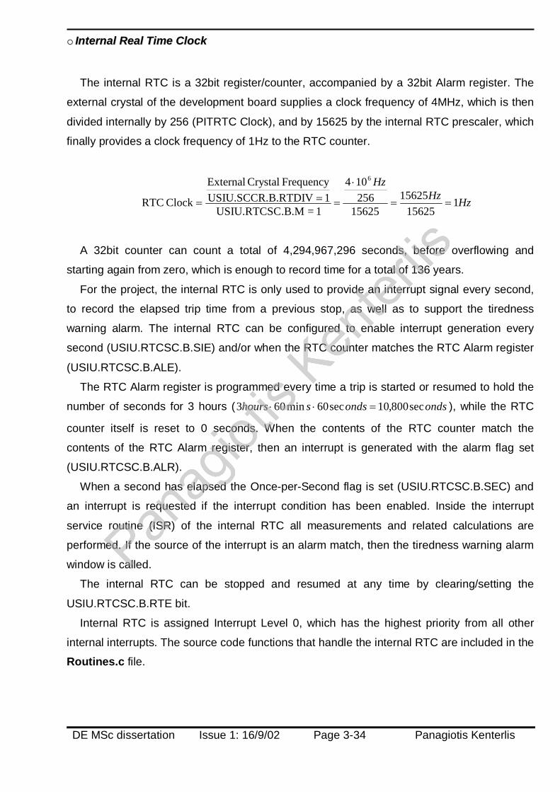
oo IInntteerrnnaall RReeaall TTiimmee CClloocckk
The internal RTC is a 32bit register/counter, accompanied by a 32bit Alarm register. The
external crystal of the development board supplies a clock frequency of 4MHz, which is then
divided internally by 256 (PITRTC Clock), and by 15625 by the internal RTC prescaler, which
finally provides a clock frequency of 1Hz to the RTC counter.
HzHzHz
115625
1562515625
256104
1=.B.MUSIU.RTCSC1B.RTDIVUSIU.SCCR.
Frequency Crystal External
Clock RTC
6
==
⋅
===
A 32bit counter can count a total of 4,294,967,296 seconds, before overflowing and
starting again from zero, which is enough to record time for a total of 136 years.
For the project, the internal RTC is only used to provide an interrupt signal every second,
to record the elapsed trip time from a previous stop, as well as to support the tiredness
warning alarm. The internal RTC can be configured to enable interrupt generation every
second (USIU.RTCSC.B.SIE) and/or when the RTC counter matches the RTC Alarm register
(USIU.RTCSC.B.ALE).
The RTC Alarm register is programmed every time a trip is started or resumed to hold the
number of seconds for 3 hours ( ondsondsshours sec800,10sec60min603 =⋅⋅ ), while the RTC
counter itself is reset to 0 seconds. When the contents of the RTC counter match the
contents of the RTC Alarm register, then an interrupt is generated with the alarm flag set
(USIU.RTCSC.B.ALR).
When a second has elapsed the Once-per-Second flag is set (USIU.RTCSC.B.SEC) and
an interrupt is requested if the interrupt condition has been enabled. Inside the interrupt
service routine (ISR) of the internal RTC all measurements and related calculations are
performed. If the source of the interrupt is an alarm match, then the tiredness warning alarm
window is called.
The internal RTC can be stopped and resumed at any time by clearing/setting the
USIU.RTCSC.B.RTE bit.
Internal RTC is assigned Interrupt Level 0, which has the highest priority from all other
internal interrupts. The source code functions that handle the internal RTC are included in the
Routines.c file.
DE MSc dissertation Issue 1: 16/9/02 Page 3-35 Panagiotis Kenterlis
oo DDeeccrreemmeenntteerr
The Decrementer is a 32bit timer/counter register configured by software to be clocked by
a signal with a time period of 1μsec. As it name implies, the register decrements its contents
at every clock pulse.
Inside the project the Decrementer is used to provide a basic time delay in multiples of a
Decrementer clock period ( sec1TTMBCLK µ= ). The delay function needs to initialise the
Decrementer with the number of periods to wait, start the Decrementer and wait in a check
loop until the contents have reached a terminating value (0).
However, since the Decrementer generates an exception when it underflows, an offset
value is added to the number of periods to wait, and it is this number that is used as the
terminating value. Termination of the check loop occurs when the Decrementer register’s
value is equal or less than the offset value. This is done in order to avoid the software
overhead of executing the exception handling routine every time the delay function is used.
However, if the software check snippet misses to identify that the requested number of
periods has been counted and the Decrementer underflows (if because of an exception or
interrupt being processed for too long) then the software check loop will not be aware of this
condition and will continue to count down causing a very long delay (232–offset μseconds).
This problem can be eliminated by including as well as with a minimum check, a check on
a global flag. If the Decrementer underflows, it will cause an exception, inside the service
routine of which, the global flag is set and that will force the check loop to terminate when the
exception service routine returns control to it. After that the Decrementer must be disabled to
prevent it from causing unwanted exceptions.
Source code functions to control the Decrementer can be found in the Routines.c file.
oo GGeenneerraall PPuurrppoossee II//OO
Pins primarily assigned for use as address, data and control bus can be configured for I/O
functions by programming registers SGPIO Data Register 1 (SGPIODT1), SGPIO Data
Register 2 (SGPIODT2) and SGPIO Control Register (SGPIOCR).
SGPIODT1 controls the I/O pins for the Data bus. SGPIODT2 controls I/O pins for the
address and control bus. SGPIOCR controls the data direction of these I/O pins. For the
external bus lines to be used as GPIO, the Single-Chip field (SC) on SIU Module
Configuration Register (USIU.SIUMCR) must be configured accordingly.

DE MSc dissertation Issue 1: 16/9/02 Page 3-36 Panagiotis Kenterlis
•• QQAADDCC –– QQuueeuueedd AADDCC
The MPC555 microcontroller embeds two QADC modules, for analogue signal interfacing
of 16 inputs each. A total of 32 analogue inputs are controlled by the two modules, which can
be increased to 82 channels by external multiplexing. The QADC module offers two queues
of 32 entries each (Queue 1 & 2) used for conversion commands and 64 result registers,
directly related with each other.
Every conversion command queue entry can control any of the 16 analogue input pins
associated with the module and order the conversion of the voltage present on the pin
defined by the command. The result of the conversion is stored in the conversion result word
queue in three formats (right-justified unsigned, left-justified unsigned, left-justified signed).
Figure 3-7 QADC_A Channel Connections
Both QADC modules have been configured to measure input voltages in the range of 0 to
5V by connecting voltage reference pins VRH (Reference High) and VRL (Reference Low) to
VCC (5V) and GND respectively (see Figure 3-7). Six power supply input pins are also
connected for analogue power supply (VDDA and VSSA), external digital power supply (VDDH
and VSSE) and internal digital power supply shared with other modules (VDD and VSS). The
reason for using different analogue and digital supply pins is to reduce the amount of noise
normally present in digital power supply pins. QADC conversion result has a 10bit resolution

DE MSc dissertation Issue 1: 16/9/02 Page 3-37 Panagiotis Kenterlis
and given an input signal with a voltage range 0-5V, then the voltage resolution is calculated
as being equal to mVVVVVV RLRH 89,410235
1102405
1210 ≈=−
−=
−− .
For the project, QADC_A is used with two of its analogue inputs connected to the In-Tank
Fuel Sensor (Channel Pin 0 – AN0) and the Battery Voltage divider (Channel Pin 1 – AN1).
Both these inputs are conditioned to give a voltage value in the range of 0 to 5V. Queue 1,
has been configured to operate in Periodic Timer Continuous Scan Mode with the maximum
possible scan period of 172⋅QCLK , where QCLK has been configured by prescaling to have
a period of sec1000,12540periodsclock IMB40 µ==⋅=⋅= nsnsQCLK , thus giving a scan
period of ms131072,131sec1217 ≈⋅=⋅ µQCLK . Two queue entries have been programmed to
control these two channels. Both channels are read every 131ms and their conversion results
are made available for use by the software. For software simplicity the data format used is
right-justified unsigned giving result values in the range 0x000-0x3FF (0-102310).
After executing the conversion commands for the two used channels, the third queue entry
containing an End of Queue command terminates Queue 1 and waits for the wait period to
elapse before restarting queue execution.
The voltage divider for the Battery Voltage input (see Figure 3-7) is used to condition the
voltage level and fit it in the range of 0-5V. To accommodate a real maximum voltage value
of 50V, a 1/10 divider is needed to provide to the QADC channel pin a maximum voltage
level of 5V. A potentiometer/trimmer is a practical way of achieving this, by setting the wiper
at 1/10 of the resistor’s value, e.g. for a 10KΩ trimmer, the wiper should be set at 1KΩ. One
terminal of the trimmer is connected to the battery voltage power line, the other to the ground
and the wiper to the QADC channel pin. The 1KΩ resistance value should be measured
between the QADC pin and the ground. Any battery voltage applied will be divided by ten
before being fed to the QADC for conversion. For example, by applying 42V as the battery
voltage (new automotive battery standard value) gives 4,2V in the QADC pin. This value can
then be multiplied in software by 10 to display the real value of the battery’s voltage.
Source code function that configures the QADC_A module can be found in the
QADC_Functions.c file.

DE MSc dissertation Issue 1: 16/9/02 Page 3-38 Panagiotis Kenterlis
•• QQSSMMCCMM –– QQuueeuueedd SSeerriiaall MMuullttii--CChhaannnneell MMoodduullee
The Queued Serial Multi-Channel Module of the microcontroller provides two
asynchronous serial ports (SCI, Serial Communication Interface) and one QSPI (Queued
Serial Peripheral Interface) port. Both SPI and the first SCI port are queued. This means that
a set of information can be written to or read from the port, without requiring constant
monitoring by software. The software will only have to transfer data when these are needed
to be sent or are available to read. The amount of information to send or accept before re-
involving the software is programmable.
For the project, all ports are used. The first SCI port is configured for operation at
115,200bps, 8 data bits, 1 stop bit and no parity bit. It is used to connect the trip computer to
a personal computer and upload data stored on the CF Card, as well as download
configuration information on the sensors used. Before connecting to the PC’s serial port, the
TTL voltage levels of the microcontroller’s serial port need to be translated to RS-232 voltage
levels. This voltage translation is performed by any RS-232 line driver/receiver.
The second SCI port is configured for operation at 19,200bps, 8 data bits, 1 stop bit and
no parity bit. It is used to control the VFD module for printing information on the display. All
commands and data are sent to the VFD and also some data can be read back from it.
The QSPI port is used to interface to the external RTC device at a speed of 500kbps
(clock speed of 500 kHz). For the external RTC only one peripheral select pin is used
(PCS0), out of the four available.
Although the queue facility could have been enabled for both the first SCI port and the
QSPI port, this was not done, firstly to allow different time delays between data transfers to
be inserted, and secondly, due to the need to verify whether a transfer has been successful
or not, before sending more data. Instead, software flow control is implemented for both
sending and receiving data from the communications module. Since most communication is
performed outside the ISR, inside which most calculations take place, there is little or no CPU
hogging because of executing wait loops to send or receive data.
Source code functions that control the SCI ports can be found in the SerialPort.c file.
Source code functions for the QSPI port can be found in the SPI_Functions.c file.
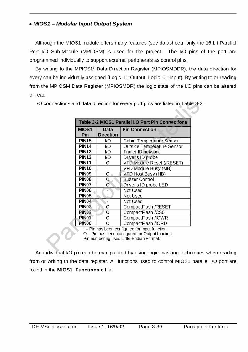
DE MSc dissertation Issue 1: 16/9/02 Page 3-39 Panagiotis Kenterlis
•• MMIIOOSS11 –– MMoodduullaarr IInnppuutt OOuuttppuutt SSyysstteemm
Although the MIOS1 module offers many features (see datasheet), only the 16-bit Parallel
Port I/O Sub-Module (MPIOSM) is used for the project. The I/O pins of the port are
programmed individually to support external peripherals as control pins.
By writing to the MPIOSM Data Direction Register (MPIOSMDDR), the data direction for
every can be individually assigned (Logic ‘1’=Output, Logic ‘0’=Input). By writing to or reading
from the MPIOSM Data Register (MPIOSMDR) the logic state of the I/O pins can be altered
or read.
I/O connections and data direction for every port pins are listed in Table 3-2.
Table 3-2 MIOS1 Parallel I/O Port Pin Connections MIOS1
Pin Data
Direction Pin Connection
PIN15 I/O Cabin Temperature Sensor PIN14 I/O Outside Temperature Sensor PIN13 I/O Trailer ID network PIN12 I/O Driver's ID probe PIN11 O VFD Module Reset (/RESET) PIN10 I VFD Module Busy (MB) PIN09 O VFD Host Busy (HB) PIN08 O Buzzer Control PIN07 O Driver's ID probe LED PIN06 - Not Used PIN05 - Not Used PIN04 - Not Used PIN03 O CompactFlash /RESET PIN02 O CompactFlash /CS0 PIN01 O CompactFlash /IOWR PIN00 O CompactFlash /IORD
I – Pin has been configured for Input function. O – Pin has been configured for Output function. Pin numbering uses Little-Endian Format.
An individual I/O pin can be manipulated by using logic masking techniques when reading
from or writing to the data register. All functions used to control MIOS1 parallel I/O port are
found in the MIOS1_Functions.c file.

DE MSc dissertation Issue 1: 16/9/02 Page 3-40 Panagiotis Kenterlis
•• TTPPUU33 –– TTiimmee PPrroocceessssoorr UUnniitt
The Time Processor Unit version 3 (TPU3), is an intelligent programmable microcontroller
designed for timing control. The MPC555 contains two independent TPU3 modules. The
TPU3 module executes micro-instructions stored either in its own memory, which is
completely invisible to the CPU, or from the Dual-Port Memory on the MPC555 chip. In the
latter case, the TPU3 executes micro-instructions from RAM, which is no longer accessible
by the CPU. The TPU3 in this case is said to be operating in Emulation mode. The TPU3
module has 16 channels, where every channel can be thought of as being similar to a task
executed in a multitasking operating system. Every channel is assigned a function number
and a priority level by the CPU software. An internal scheduler engine distributes processing
time of the TPU3 execution engine to every channel according to its priority and status
(enabled/disabled). I/O operations can be executed by the channel’s selected function for the
corresponding I/O pin. Connecting two or more channels is also possible by use of shared
data space for inter-channel communication as long as the function executed by each
channel permits it. The most important feature of the TPU3 is its requirement for minimum to
zero CPU intervention in executing complex timing operations in real time by hardware.
The TPU3 module comes from Motorola with 16 pre-programmed functions in its
microcode ROM. A full list of these functions is found in Table 3-3, however it is likely that
some versions of the MPC555 may be shipped with other functions in the microcode ROM.
Table 3-3 TPU3 Microcode ROM Functions Function Number
Function Nickname
Function Name
0xF PTA Programmable Time Accumulator 0xE QOM Queued Output Match 0xD TSM Table Stepper Motor 0xC FQM Frequency Measurement 0xB UART Universal Asynchronous Receiver/Transmitter 0xA NITC New Input Capture/Input Transition Counter 0x9 COMM Multiphase Motor Commutation 0x8 HALLD Hall Effect Decode 0x7 MCPWM Multi-Channel Pulse Width Modulation 0x6 FQD Fast Quadrature Decode 0x5 PPWA Period/Pulse Width Accumulator 0x4 OC Output Compare 0x3 PWM Pulse Width Modulation 0x2 DIO Discrete Input/Output 0x1 SPWM Synchronized Pulse Width Modulation 0x0 SIOP Serial Input/output Port
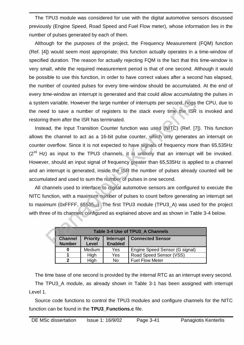
DE MSc dissertation Issue 1: 16/9/02 Page 3-41 Panagiotis Kenterlis
The TPU3 module was considered for use with the digital automotive sensors discussed
previously (Engine Speed, Road Speed and Fuel Flow meter), whose information lies in the
number of pulses generated by each of them.
Although for the purposes of the project, the Frequency Measurement (FQM) function
(Ref. [4]) would seem most appropriate; this function actually operates in a time-window of
specified duration. The reason for actually rejecting FQM is the fact that this time-window is
very small, while the required measurement period is that of one second. Although it would
be possible to use this function, in order to have correct values after a second has elapsed,
the number of counted pulses for every time-window should be accumulated. At the end of
every time-window an interrupt is generated and that could allow accumulating the pulses in
a system variable. However the large number of interrupts per second, hogs the CPU, due to
the need to save a number of registers to the stack every time the ISR is invoked and
restoring them after the ISR has terminated.
Instead, the Input Transition Counter function was used (NITC) (Ref. [7]). This function
allows the channel to act as a 16-bit pulse counter, which only generates an interrupt on
counter overflow. Since it is not expected to have signals of frequency more than 65,535Hz
(216 Hz) as input to the TPU3 channels, it is unlikely that an interrupt will be invoked.
However, should an input signal of frequency greater than 65,535Hz is applied to a channel
and an interrupt is generated, inside the ISR the number of pulses already counted will be
accumulated and used to sum the number of pulses in one second.
All channels used to interface to digital automotive sensors are configured to execute the
NITC function, with a maximum number of pulses to count before generating an interrupt set
to maximum (0xFFFF, 6553510). The first TPU3 module (TPU3_A) was used for the project
with three of its channels configured as explained above and as shown in Table 3-4 below.
Table 3-4 Use of TPU3_A Channels Channel Number
Priority Level
Interrupt Enabled
Connected Sensor
0 Medium Yes Engine Speed Sensor (G signal) 1 High Yes Road Speed Sensor (VSS) 2 High No Fuel Flow Meter
The time base of one second is provided by the internal RTC as an interrupt every second.
The TPU3_A module, as already shown in Table 3-1 has been assigned with interrupt
Level 1.
Source code functions to control the TPU3 modules and configure channels for the NITC
function can be found in the TPU3_Functions.c file.

DE MSc dissertation Issue 1: 16/9/02 Page 3-42 Panagiotis Kenterlis
33..11..33.. PPeerriipphheerraall DDeevviicceess
In the following pages, the use and configuration of peripheral devices in the project is
discussed.
33..11..33..11.. RReeaall TTiimmee CClloocckk
The external Real Time Clock is connected to the microcontroller through the SPI port (see
Figure 3-8). For the project development phase, the external RTC is connected to a
temperature compensating crystal oscillator with an output frequency of 32.768 kHz and a
3.6V NiMH rechargeable battery. The crystal oscillator provides the reference frequency,
which after a series of divisions inside the RTC chip, results to a frequency signal of 1Hz
used for controlling the time registers on the RTC. The NiMH rechargeable battery is used to
provide backup power supply for RTC functions and memory when the main power supply on
VCC pin has fallen below the voltage level of pin Vbat. Doing so, the RTC does not lose track
of time or corrupt the contents of its memory when power is removed. For this reason, the
RAM on the RTC is used as backup storage for various system variables and sensor
configuration parameters.
Figure 3-8 External RTC Connections

DE MSc dissertation Issue 1: 16/9/02 Page 3-43 Panagiotis Kenterlis
Please notice that only four I/O lines are required for SPI communication, SDI (Serial Data
Input), SDO (Serial Data Output), SCLK (Serial Clock) and CE (Chip Enable). Unlike most
devices the CE line is asserted when logic ‘1’ is present. Two interrupt lines, 0INT and 1INT ,
originating from the RTC are connected to 1IRQ and 2IRQ of the microcontroller,
respectively. Output pin 0INT / 1IRQ is controlled by Alarm0 facility on the RTC, which is
programmed to generate a low pulse on the pin every second (1Hz). Output pin 1INT / 2IRQ
is controlled by Alarm1 facility on the RTC and is programmed and enabled by GUI routines
to generate an interrupt when there is a match of the current time with the time value of the
Alarm1 registers.
Every function that needs to carry a timestamp, such as saving data on the CF card,
displaying time and date on the VFD, or displaying any other updated information on the
VFD, is related to the ISR of the external RTC. This is either done directly, by executing the
code inside the ISR, or indirectly, by setting a flag that will allow some code to be executed
when the ISR has terminated.
The DS1305 external RTC has 32 register addresses assigned to RTC related registers
and 96 bytes of RAM. These locations are accessed in different addresses for read and write
operation.
Table 3-5 External RTC's Registers and Address Map Address
Read Write Description
0x00 0x80 Seconds Register 0x01 0x81 Minutes Register 0x02 0x82 Hours Register 0x03 0x83 Day Register 0x04 0x84 Date Register 0x05 0x85 Month Register 0x06 0x86 Year Register 0x07 0x87 Alarm0 Seconds Register 0x08 0x88 Alarm0 Minutes Register 0x09 0x89 Alarm0 Hours Register 0x0A 0x8A Alarm0 Day Register 0x0B 0x8B Alarm1 Seconds Register 0x0C 0x8C Alarm1 Minutes Register 0x0D 0x8D Alarm1 Hours Register 0x0E 0x8E Alarm1 Day Register 0x0F 0x8F Control Register 0x10 0x90 Status Register 0x11 0x91 Trickle Charger Register
0x12-0x1F 0x92-0x9F Reserved 0x20-0x7F 0xA0-0xFF 96 Bytes RAM

DE MSc dissertation Issue 1: 16/9/02 Page 3-44 Panagiotis Kenterlis
The SPI port actually sends a 16bit word to the external RTC, comprising of one byte
indicating the register to be accessed and one byte of data. Data is sent always with MSB
first. When writing a byte, first the address of the register to write is sent and afterwards the
data to write (Figure 3-9). When the device is accessed for read operation then the data byte
has no meaning and its value is not important, however at the same clock ticks the data
contained in the register accessed are read from the SDO line (Figure 3-10).
Figure 3-9 SPI Single-Byte Write
Figure 3-10 SPI Single-Byte Read
Source code functions to control the external RTC device can be found in the ds1305.c
file. Source code functions to access the SPI port can be found in the SPI_Functions.c file.

DE MSc dissertation Issue 1: 16/9/02 Page 3-45 Panagiotis Kenterlis
33..11..33..22.. IInnffoorrmmaattiioonn DDiissppllaayy UUnniitt ((VVFFDD MMoodduullee))
Having decided on the type of display to use and searching even more carefully at the
available products and their prices, a specific VFD module was found that fitted the design
specifications and unexpectedly offered more than what was initially considered.
The Itron GU126x64F-K610A3-01 is a 126x64 graphics display module. It has two serial
ports, a synchronous (SPI) port and one CMOS full duplex asynchronous port, both of which
are available for use on the microcontroller and can save on connection wiring and PCB
space. A serial connection also allows for the display device to be placed away from the main
device and closer to the driver’s direct line of view. The module is powered by a transformer-
less power supply unit (PSU), therefore there is no need for extra space, cost and wiring for a
dedicated PSU. A standard 5V PSU capable of supplying 1.5-2A (7.5-10W) is enough to
supply power to the entire trip computer’s hardware circuits. The selected display module
also comes with an on-board 8 line I/O port, which can be useful especially if the device is
placed some distance away from the main device, for interfacing various circuits (see Data
Entry Unit (Keyboard) - 3.1.3.3 - p.3-47).
CON1
CON2 Figure 3-11 VFD Module Diagram
The asynchronous serial port and hardware flow control pins for it are found on the pins of
Connector 1. The SPI port pins, other control pins such as Reset and the I/O port are found
on the pins of Connector 2.
For the project, the asynchronous serial port connection to the microcontroller was
selected, to allow fewer connections, control on the status of the VFD controller (see function
of pins MB & HB) and less software overhead than the SPI functions. Connections to the
microcontroller can be seen in Figure 3-12.

DE MSc dissertation Issue 1: 16/9/02 Page 3-46 Panagiotis Kenterlis
Figure 3-12 VFD Connections to the Microcontroller
The controller on the VFD module can execute various functions, such as print text in 4
different ASCII font sizes (5x5, 5x7, 10x14 and 20x28 pixels), display bitmapped graphics,
set/clear display regions, set display brightness, power on/off the module and handle the on-
module I/O port. All these functions were used to create a Graphics User Interface (GUI), for
the driver to interact in a more friendly and productive manner with the trip computer.
Source code functions used to control the VFD module and the type of information
displayed on it can be found in the VFD_Functions.c file.

DE MSc dissertation Issue 1: 16/9/02 Page 3-47 Panagiotis Kenterlis
33..11..33..33.. DDaattaa EEnnttrryy UUnniitt ((KKeeyybbooaarrdd))
The keyboard used for entering data, as well as navigation through the Graphics User
Interface, follows the form of a standard 4x4 matrix keyboard, giving a total of 16 keys.
Because of its form, identifying a key press requires well defined steps and techniques.
1 2 3 A
4 5 6 B
7 8 9 C
* 0 # D
Figure 3-13 Keyboard Layout
1 2 3 A
4 5 6 B
7 8 9 C
* 0 # D
Row 1
Row 2
Row 3
Row 4
Col 1 Col 2 Col 3 Col 4 Figure 3-14 Matrix Layout
Reading the value of a pressed key is achieved by matrix scanning techniques. Since the
keyboard uses a 4x4 matrix, it requires 8 I/O lines in total for scanning the state of the key-
switches. These I/O lines are taken from the I/O port of the VFD module and are serially
controlled by the microcontroller, although using the same concepts as if being connected to
any parallel I/O port of the microcontroller. The I/O port on the VFD module can be
programmed to have any pin configured as either Input or Output, by writing a logic ‘1’ (Input)
or logic ‘0’ (Output) at the respective bit position.
The VFD module can be programmed to identify a change in the logic value of its input pins
and send its I/O port value to the microcontroller through either of the serial interfaces
available on it. Once this byte has been received by the microcontroller, an interrupt is
generated, which in turn will activate the keyboard scanning function to identify the key
pressed.
Since TTL and CMOS circuits assume the logic state of an input as logic ‘1’ if floating, logic
‘0’ is the dominate logic state. By writing a logic ‘0’ at the pin controlling a row, and pressing
any of the keys connected to that row, a circuit will close transferring the GND voltage (logic
‘0’) to the column’s line of the pressed key. Simply by moving a logic ‘0’ value at the scan
lines (rows) and reading the result on the return lines (columns) and by use of a look-up
table, the value of the key that was pressed can be derived.

DE MSc dissertation Issue 1: 16/9/02 Page 3-48 Panagiotis Kenterlis
The electrical connections of the matrix keyboard with the I/O port of the VFD module are
displayed on the following diagram.
O O O O I I I I
P7 P6 P5 P4 P3 P2 P1 P0
Col 1 Col 2 Col 3 Col 4
Row 1 Row 2 Row 3 Row 4
MSB LSB
Figure 3-15 Keyboard I/O Connections
To scan the key matrix, the following Scan Patterns need to be outputted on the Scan
Lines. The logic value ‘1’ on the Column bits has no real meaning because it is not presented
on the input pins, however it is used for compatibility purposes to the original program. It is
worth noting that the moving ‘0’ activates only the keys connected to it.
Table 3-6 Keyboard Row Scan Pattern Codes C4 C3 C2 C1 R1 R2 R3 R4 Scan Line P7 P6 P5 P4 P3 P2 P1 P0
Scan Code (Hex)
1st Row 1 1 1 1 0 1 1 1 0xF7 2nd Row 1 1 1 1 1 0 1 1 0xFΒ 3rd Row 1 1 1 1 1 1 0 1 0xFD 4th Row 1 1 1 1 1 1 1 0 0xFE
After reading the contents of the keyboard’s I/O port, using a bit mask of 0xF0 and AND-
ing the values, in order to mask the scan pattern code nibble. If a bit ‘0’ is found in any of the
return line bit positions, then the key-switch in that row has been pressed. If no logic ‘0’ is
found in any return lines, then no key-switch has been pressed.
Table 3-7 Keyboard Column Scan Return Codes C4 C3 C2 C1 R1 R2 R3 R4 Return Line P7 P6 P5 P4 P3 P2 P1 P0
Return Code (Hex)
Idle 1 1 1 1 0 0 0 0 0xF0 1st Column 1 1 1 0 0 0 0 0 0xE0 2nd Column 1 1 0 1 0 0 0 0 0xD0 3rd Column 1 0 1 1 0 0 0 0 0xB0 4th Column 0 1 1 1 0 0 0 0 0x70

DE MSc dissertation Issue 1: 16/9/02 Page 3-49 Panagiotis Kenterlis
The information given be the previous two arrays, are combined using a look-up table
technique, with which we it is possible to decode the coordinates of the pressed key into any
desired coding system.
For the project, and in order to make programming and debugging easier, the direct
conversion to the ASCII code of the legend on the pressed key was selected.
Table 3-8 Pressed Key Lookup Table Return Lines Scan Lines
1st Column 2nd Column 3rd Column 4th Column 1st Row 1 2 3 A 2nd Row 4 5 6 B 3rd Row 7 8 9 C 4th Row * 0 # D
Keys ‘*’ (Asterisk) and ‘#’ (Hash) are used for confirming (ENTER) or aborting (CANCEL)
operations of the Graphics User Interface.
Keys ‘1’, ‘2’ and ‘3’ are used for selecting one of the three categories of information
available “Vehicle Information”, “Trip Information” and “Clock/Calendar”, respectively.
Keys ‘A’ to ‘D’ are used to select sub-functions or information sub-pages of the currently
selected information category (see above).
Key ‘5’ is used to configure the brightness of the display from 25% to 100% in increments
of 25%.
Keys ‘7’ and ‘9’ are used for “DECREASE/YES OPTION” and “INCREASE/NO OPTION”
respectively, according to the type of selection to be made.
Key ‘0’ is used to switch on and off the display when it is required by the driver.
The above keyboard related arrays and the key scan function are included in the
keyboard.c file.

DE MSc dissertation Issue 1: 16/9/02 Page 3-50 Panagiotis Kenterlis
33..11..33..44.. SSttoorraaggee DDeevviiccee ((CCoommppaaccttFFllaasshh CCaarrdd))
The CompactFlash card is a small, removable, storage and I/O card. Originally invented by
SanDisk Corporation, the specifications are now determined by the CompactFlash
Association (CFA) (http://www.compactflash.org), a non-profit corporation that promotes the
adoption of CompactFlash. CompactFlash cards are a widely available solution for systems
requiring a compact, solid state mass storage system. CompactFlash can be used in such
applications as portable and desktop computers, digital cameras, handheld data collection
scanners, personal digital assistants (PDAs), Pocket PCs, handy terminals, personal
communicators, audio recorders, monitoring devices, set-top boxes, and networking
equipment.
CompactFlash is essentially a small form factor card version of PCMCIA’s PC Card ATA
(AT Attachment) specification and includes a True IDE (Integrated Drive Electronics) mode
which is compatible with the ATA/ATAPI-4 specification. There are 3 distinct interface modes
that a CompactFlash card can use:
o PC Card Memory Mode (uses WE , OE to access memory locations)
o PC Card I/O Mode (uses IOWR , IORD to access I/O locations)
o True IDE Mode (uses IOWR , IORD to access I/O locations)
The CompactFlash card is essentially a solid state ATA disk drive. To control an ATA disk
drive, one writes to the task file registers. The values put into these task file registers control
the drive (the ANSI T13 committee defines these registers and the commands used to control
all ATA/IDE drives — see http://www.t13.org) (Ref. [3]). These task file registers can be
mapped into either memory or I/O address space.
Wanting to avoid the use of an external PCMCIA controller or glue logic to a
CompactFlash card, the True IDE mode was selected during the project design phase. The
main disadvantage is that hot insertion and removal (while the device is still working) will not
be possible because of the probable disruption of signals on the system bus; however the CF
Card according to the specifications, is meant to be constantly mounted on the trip computer,
and only removed for replacement.
The main reason that the True IDE mode is easier to use, is because only CE1 needs to
be asserted, in order to perform a 16 bit read or write to the data register. To perform a 16 bit

DE MSc dissertation Issue 1: 16/9/02 Page 3-51 Panagiotis Kenterlis
read or write operation in PC Card mode, both CE1 and CE2 must be asserted
simultaneously which generally requires some custom glue logic.
Table 3-9 AT Task Files (True IDE mode) /CE2 /CE1 Addr. Read (-IORD = L) Write (-IOWR = L) LBA Mode
1 0 0h Data Register (16 bit) Data Register (16 bit) 1 0 1h Error Register Feature Register 1 0 2h Sector Count Register Sector Count Register
1 0 3h Sector Number Register Sector Number Register Lower Byte 1 0 4h Cylinder Low Register Cylinder Low Register Low Middle Byte 1 0 5h Cylinder High Register Cylinder High Register Upper Middle Byte 1 0 6h Drive Head Register Drive Head Register Upper Nibble Byte 1 0 7h Status Register Command Register 0 1 6h Alt. Status Register Device Control Register 0 1 7h Drive Address Register Reserved
Using the microcontroller’s external memory controller (external address, data and control
bus) to interface the CF Card would violate the CF Card’s timing. To avoid this problem, the
same data and address lines were used as General Purpose I/O lines. Data lines D0-15 (Big-
Endian) are connected to the CF Card’s D15-0 (Little-Endian) and address lines D28-30 of
the microcontroller (Big-Endian) are connected to the CF Card’s A2-0 (Little-Endian). MIOS1
16bit I/O port pins are used for connection to the CF Card’s control pins. For detailed
connections see Table 3-10. Access to the CF Card is done by emulating the address, data
and control bus with the General Purpose I/O lines.

DE MSc dissertation Issue 1: 16/9/02 Page 3-52 Panagiotis Kenterlis
Table 3-10 CompactFlash Connections to the microcontroller MCU ATA CompactFlash Power GND 40 Power GND 1 Power GND D12 – SGPIOD12 11 D3 2 D3 D11 – SGPIOD11 9 D4 3 D4 D10 – SGPIOD10 7 D5 4 D5 D9 – SGPIOD9 5 D6 5 D6 D8 – SGPIOD8 3 D7 6 D7 MIOS1 PIN2 38 /CS0 7 /CE1
Not Connected 8 A10 Power GND 9 /ATA SEL
10 A9 11 A8
Not Connected
12 A7 Power VCC 13 Power VCC
14 A6 15 A5 16 A4
Not Connected
17 A3 A28 – SGPIO28 36 A2 18 A2 A29 – SGPIO29 33 A1 19 A1 A30 – SGPIOA30 35 A0 20 A0 D15 – SGPIOD15 17 D0 21 D0 D14 – SGPIOD14 15 D1 22 D1 D13 – SGPIOD13 13 D2 23 D2 Not Connected 32 /IOCS16 24 /IOCS16
25 /CD1 Not Connected 26 /CD2
D4 – SGPIOD4 10 D11 27 D11 D3 – SGPIOD3 12 D12 28 D12 D2 – SGPIOD2 14 D13 29 D13 D1 – SGPIOD1 16 D14 30 D14 D0 – SGPIOD0 18 D15 31 D15 Power Vcc 38 /CS1 32 /CE2
Not Connected 33 /VS1 MIOS1 PIN0 25 /IORD 34 /IORD MIOS1 PIN1 23 /IOWR 35 /IOWR
Power Vcc 36 /WE 31 INTRQ 37 INTRQ
Power VCC 38 Power VCC Power GND 39 /CSEL
Not Connected 40 /VS2 MIOS1 PIN3 1 /RESET 41 /RESET Not Connected 27 IORDY 42 IORDY
Not Connected 43 /INPACK Power VCC 44 /REG
39 /DASP 45 /DASP Not Connected 34 /PDIAG 46 /PDIAG
D7 – SGPIOD7 4 D8 47 D8 D6 – SGPIOD6 6 D9 48 D9 D5 – SGPIOD5 8 D10 49 D10
Power GND 50 Power GND

DE MSc dissertation Issue 1: 16/9/02 Page 3-53 Panagiotis Kenterlis
33..11..33..55.. DDiiggiittaall IIddeennttiiffiiccaattiioonn DDeevviicceess
To provide the means of
identifying different drivers and
trailers, the iButton devices
manufactured by Dallas/Maxim
were selected and more specifically
DS1990A.
This is a read-only memory
circuit, containing a unique serial
number of 64bits. The uniqueness
of the serial number is guaranteed
by the manufacturer by use of laser
recording the number on the
memory circuit.
Figure 3-16 iButton Container Dimensions
It is distributed in a F5 MICROCAN container, with dimensions shown on the above figure.
It has two connection terminals to the reader circuit marked as DATA and GROUND. It is
noteworthy that a power supply terminal is absent. Power supply and data transfer are two
issues handled by a proprietary bus (designed by Dallas Semiconductors), named MicroLan
and is administrated by the 1-Wire protocol. This bus allows supplying a device with positive
voltage and transferring data both over a single wire, while a grounding wire is also required.
The DATA terminal can be connected to a microcontroller’s open collector I/O pin like shown
in the following diagram. The pull up resistor is required to supply the device with current.
Figure 3-17 iButton connection to a microcontroller
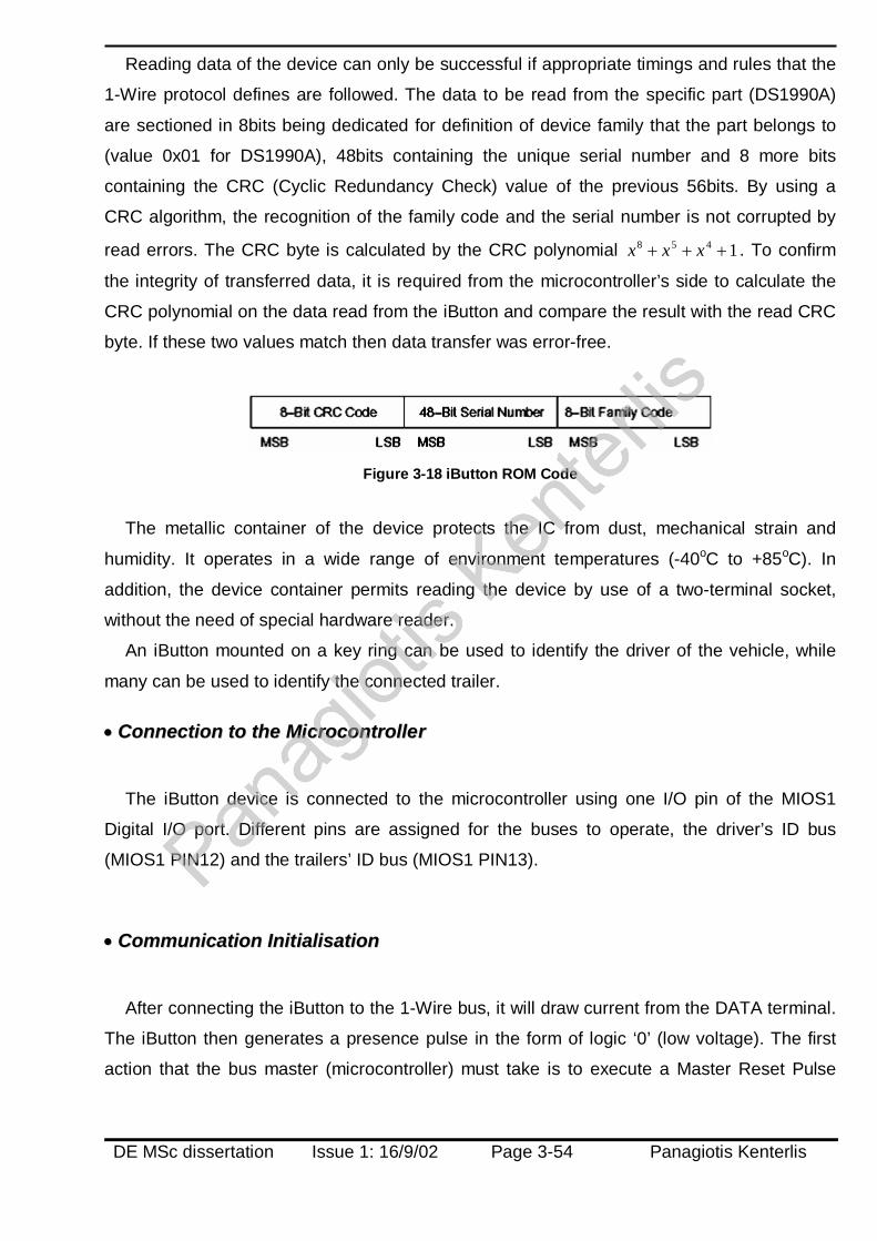
DE MSc dissertation Issue 1: 16/9/02 Page 3-54 Panagiotis Kenterlis
Reading data of the device can only be successful if appropriate timings and rules that the
1-Wire protocol defines are followed. The data to be read from the specific part (DS1990A)
are sectioned in 8bits being dedicated for definition of device family that the part belongs to
(value 0x01 for DS1990A), 48bits containing the unique serial number and 8 more bits
containing the CRC (Cyclic Redundancy Check) value of the previous 56bits. By using a
CRC algorithm, the recognition of the family code and the serial number is not corrupted by
read errors. The CRC byte is calculated by the CRC polynomial 1458 +++ xxx . To confirm
the integrity of transferred data, it is required from the microcontroller’s side to calculate the
CRC polynomial on the data read from the iButton and compare the result with the read CRC
byte. If these two values match then data transfer was error-free.
Figure 3-18 iButton ROM Code
The metallic container of the device protects the IC from dust, mechanical strain and
humidity. It operates in a wide range of environment temperatures (-40oC to +85oC). In
addition, the device container permits reading the device by use of a two-terminal socket,
without the need of special hardware reader.
An iButton mounted on a key ring can be used to identify the driver of the vehicle, while
many can be used to identify the connected trailer.
•• CCoonnnneeccttiioonn ttoo tthhee MMiiccrrooccoonnttrroolllleerr
The iButton device is connected to the microcontroller using one I/O pin of the MIOS1
Digital I/O port. Different pins are assigned for the buses to operate, the driver’s ID bus
(MIOS1 PIN12) and the trailers’ ID bus (MIOS1 PIN13).
•• CCoommmmuunniiccaattiioonn IInniittiiaalliissaattiioonn
After connecting the iButton to the 1-Wire bus, it will draw current from the DATA terminal.
The iButton then generates a presence pulse in the form of logic ‘0’ (low voltage). The first
action that the bus master (microcontroller) must take is to execute a Master Reset Pulse
DE MSc dissertation Issue 1: 16/9/02 Page 3-55 Panagiotis Kenterlis
which is effectively done by pulling the DATA line to ground. After that the iButton responds
with another presence pulse.
After executing this procedure the iButton can be accessed. If only one 1-Wire device is
connected on the bus, then in order to access it is first needed to read its ROM code. If more
devices than one are connected on the bus, then before doing anything else, the ROM code
of every device must be identified. For doing so a search algorithm must be followed, which
will allow to read the ROM code of one device while the rest remain “silent” on the bus. If this
procedure is not followed then all devices will try to respond to a command issued by the bus
master and the data read will be corrupted.
•• RReeaaddiinngg tthhee iiBBuuttttoonn
The 1-Wire protocol defines three different bus access slots: the Logic ‘1’ Write slot, the
Logic ‘0’ Write slot and the Bit Read slot. Every one of them is strictly defined by a set of time
spaces, within which the logic level of the DATA line must change state, in order to correctly
signal the above mentioned slots. With the termination of the initialisation slot, the DS1990A
enters idle state waiting for a command. After the transmission of a command has been
completed, the device executes it and returns the results to the bus master. Complete read of
the ROM code of a device is performed in less than 5ms, if standard timings are followed.
Detection, identification and reading of the device are operations performed by functions
included in the OneWire.c file. The multi-drop device search and CRC calculation are
modified functions of the code offered freely by the manufacturer company.
•• iiBBuuttttoonn OOvveerrvviieeww
Altogether the reasons for selecting the specific range of products are:
Unique 64bit serial number
Communications error detection capability
Use of two wires for basic communications
Simple communications protocols
Direct connection to the microcontroller
High endurance to harsh environments
Low cost - Minimum to zero maintenance cost

DE MSc dissertation Issue 1: 16/9/02 Page 3-56 Panagiotis Kenterlis
33..11..33..66.. TTeemmppeerraattuurree SSeennssiinngg DDeevviicceess
For the purpose of displaying the cabin and outside temperature, two temperature sensor
devices are used. These are the DS1820 device by Dallas/Maxim. This part is found in two
variants, the DS18B20 and the DS18S20. The DS18B20 variant provides programmable
temperature conversion resolution from 9bits (0.5οC) to 12bits (0.0625οC) and maximum
conversion time of 93.75ms in 9bit mode and 750ms in 12bit mode. The DS18S20 variant
provides a fixed temperature conversion resolution of 9bits (0.5οC) and maximum conversion
time of 750ms. Both these variants are supported by the microcontroller’s software, however,
for the project the DS18B20 variant was used and will be analysed henceforth.
DS18B20 uses the same communications interface as the digital identification key
DS1990A discussed in previous pages. In fact, DS18B20 is accessed the same way as
DS1990A with the addition of an array of nine byte registers, which are read successively.
This array is called the Scratchpad memory. In the first two registers of the Scratchpad, the
temperature conversion result is stored after a conversion has finished. In the third and fourth
registers, two values TH and TL are stored which are used to trigger an alarm condition when
the converted temperature is outside the range these two values define
HL TeTemperaturT ≤< . For the project’s purposes, since there is no need for controlling other
hardware, the values are set to the highest and lowest measurable temperature values
respectively, in order to prevent the thermometer from entering the alarm condition. In the
fifth register of the Scratchpad memory, a configuration byte is stored. This byte code defines
the thermometer resolution of the DS18B20 device in bits. The DS18B20 device is also
equipped with a small EEPROM memory, which is used to save the configuration register
and the two trigger registers. Special commands are used to read from and write to the
Scratchpad memory, as well as store changed trigger register and configuration register in
the EEPROM. The ninth register of the Scratchpad memory contains the CRC8 value of the
previous eight registers.
Since there is no real need for high precision in temperature measurements, the DS18B20
device is configured for 9bit (0.5οC) resolution. Every time the device’s scratchpad is read, a
check is made for its Configuration byte. If it doesn’t match the 9bit Resolution code, then the
device is re-programmed. This will happen only the first time a new sensor is connected, so,
replacing a defective part is an easy procedure and doesn’t require any other procedures to
be followed. In the case of a DS18S20 device, such operations are not performed. The
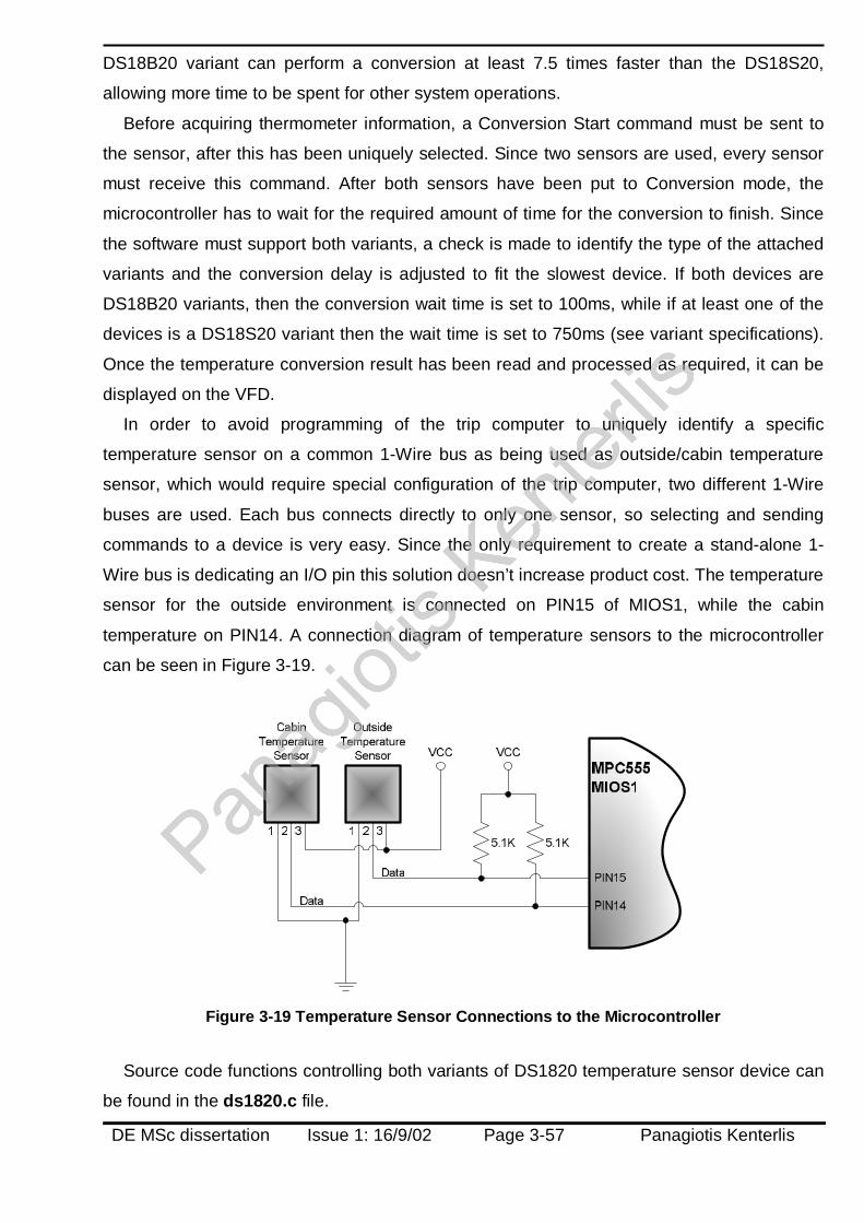
DE MSc dissertation Issue 1: 16/9/02 Page 3-57 Panagiotis Kenterlis
DS18B20 variant can perform a conversion at least 7.5 times faster than the DS18S20,
allowing more time to be spent for other system operations.
Before acquiring thermometer information, a Conversion Start command must be sent to
the sensor, after this has been uniquely selected. Since two sensors are used, every sensor
must receive this command. After both sensors have been put to Conversion mode, the
microcontroller has to wait for the required amount of time for the conversion to finish. Since
the software must support both variants, a check is made to identify the type of the attached
variants and the conversion delay is adjusted to fit the slowest device. If both devices are
DS18B20 variants, then the conversion wait time is set to 100ms, while if at least one of the
devices is a DS18S20 variant then the wait time is set to 750ms (see variant specifications).
Once the temperature conversion result has been read and processed as required, it can be
displayed on the VFD.
In order to avoid programming of the trip computer to uniquely identify a specific
temperature sensor on a common 1-Wire bus as being used as outside/cabin temperature
sensor, which would require special configuration of the trip computer, two different 1-Wire
buses are used. Each bus connects directly to only one sensor, so selecting and sending
commands to a device is very easy. Since the only requirement to create a stand-alone 1-
Wire bus is dedicating an I/O pin this solution doesn’t increase product cost. The temperature
sensor for the outside environment is connected on PIN15 of MIOS1, while the cabin
temperature on PIN14. A connection diagram of temperature sensors to the microcontroller
can be seen in Figure 3-19.
Figure 3-19 Temperature Sensor Connections to the Microcontroller
Source code functions controlling both variants of DS1820 temperature sensor device can
be found in the ds1820.c file.

DE MSc dissertation Issue 1: 16/9/02 Page 3-58 Panagiotis Kenterlis
33..11..33..77.. OOtthheerr CCiirrccuuiittss
•• BBuuzzzzeerr CCoonnttrrooll
To increase the usability of the User Interface, an audio warning capability was added. The
purpose for doing so, was to warn the driver for errors created, completion of a process,
selection of a GUI function and warnings such as activation of the alarm clock and the
tiredness warning alarm.
The circuit used is very simple since it uses only a PNP transistor and a current limiting
resistor of 1KΩ. Depending on the hfe of the transistor and the current it sinks, a resistor of
different value may need to be connected. Control of the buzzer is achieved by connecting
the base of the transistor (through the resistor) to an I/O port pin of the microcontroller
(MIOS1 PIN8). In order to activate the buzzer, a logic value of ‘0’ must be written on the I/O
pin. Respectively logic ‘1’ on the I/O pin will deactivate the buzzer.
Figure 3-20 Buzzer Control
Functions controlling the buzzer device can be found in the Routines.c source file.

DE MSc dissertation Issue 1: 16/9/02 Page 3-59 Panagiotis Kenterlis
33..22.. SSooffttwwaarree DDeessiiggnn
33..22..11.. DDeevveellooppmmeenntt TToooollss UUsseedd
•• MMeettrroowweerrkkss CCooddeeWWaarrrriioorr 66..00
To develop the resident software on the microcontroller, the Metrowerks CodeWarrior v6.0
Integrated Development Environment (IDE) was used. This is a software development suite
including a C/C++ compiler, Assembler and Emulator/Debugger facilities for Embedded
Systems based on Motorola’s PowerPC core microcontrollers, such as the MPC555.
Figure 3-21 Metrowerks CodeWarrior IDE Main Interface

DE MSc dissertation Issue 1: 16/9/02 Page 3-60 Panagiotis Kenterlis
•• MMiiccrroossoofftt VViissuuaall BBaassiicc 66..00
The Microsoft Visual Basic development system is a tool for creating software solutions for
Windows (Figure 3-22). Being a visual tool, it allows building a user interface with a few
mouse movements and linking code with objects, events and processes. Visual Basic was
used to build the PC software which controls the trip computer device. Since Visual Basic is a
standard programming Windows tool and no special configuration was performed, presenting
it is not within the scope of this report, so no discussion on using Visual Basic will follow.
Figure 3-22 Microsoft Visual Basic 6.0 Programming Environment

DE MSc dissertation Issue 1: 16/9/02 Page 3-61 Panagiotis Kenterlis
33..22..11..11.. MMeettrroowweerrkkss CCooddeeWWaarrrriioorr RReeggiissttrraattiioonn IIssssuueess
Before starting to use the IDE, there is need to register the software with the
manufacturing company. This is done in steps.
Firstly the Product Registration utility that comes installed at the same program folder as
the executable files, needs to be executed. Once this is done the following window will
appear with all fields blank.
Figure 3-23 Metrowerks CodeWarrior Registration Utility
After providing all the required information (name, university, contact email, etc) and
pressing the “Register” button, a file is created with the name MWRegistration.txt, that
contains all the above information, plus some information linked to the machine that the
software will be used, such as volume ID of the hard disk drive. This file should then be sent
by electronic mail to [email protected] to register the product. In reply, another file
will be sent after a short period of confirmation (could be a few days actually).
Once this file has been received, its contents should be copied to the clipboard and then
pasted to replace the contents of the license.dat file found in the top directory of the
installation path.
Once this is done, the full features of the software are available to use.

DE MSc dissertation Issue 1: 16/9/02 Page 3-62 Panagiotis Kenterlis
33..22..11..22.. UUssiinngg tthhee MMeettrroowweerrkkss CCooddeeWWaarrrriioorr IIDDEE
The programming environment of CodeWarrior is simple and resembles those of other
Windows based programming languages.
A software upgrade to version 6.03 was available at the time the development phase was
starting, which provided some stationery for the AXIOM development boards, however these
were not specific to the board used and some configuration settings needed to be edited
(Chapter 3.2.1.3, p. 3-66).
Developed programs are handled in projects. Every project is associated with some
source files. To create a new project, select File>New and the window in Figure 3-24 will
appear. In this window, firstly the EPPC Stationery Wizard needs to be selected, which helps
us configure the project by asking simple questions and requiring selection from a number of
options. Afterwards the name and work path of the project needs to be entered.
Figure 3-24 Project Creation #1

DE MSc dissertation Issue 1: 16/9/02 Page 3-63 Panagiotis Kenterlis
The wizard will start asking questions concerning the project to set up. The microcontroller
development board used is manufactured by AXIOM and the processor is the PowerPC 555.
Figure 3-25 Project Creation #2
The programming language is set up on the next window (Figure 3-26). For the purposes
of the project, the C compiler is used.
Figure 3-26 Project Creation #3

DE MSc dissertation Issue 1: 16/9/02 Page 3-64 Panagiotis Kenterlis
One important feature of the microcontroller is the on-chip FPU, which should be enabled
next (Figure 3-27) in order to speed up calculations that operate on floating point numbers.
Figure 3-27 Project Creation #4
The external hardware debugger interface should be selected next (Figure 3-28) to be
used when debugging the software (see Chapter 5-Testing & Debugging, p. 5-91).
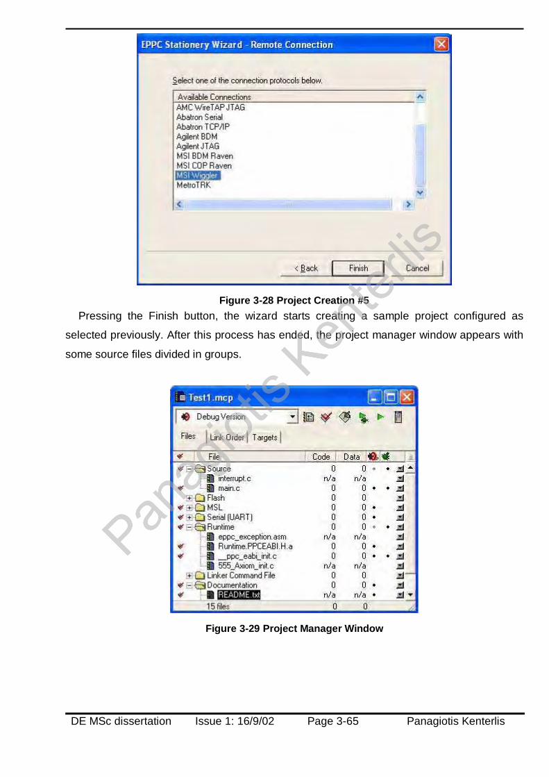
DE MSc dissertation Issue 1: 16/9/02 Page 3-65 Panagiotis Kenterlis
Figure 3-28 Project Creation #5
Pressing the Finish button, the wizard starts creating a sample project configured as
selected previously. After this process has ended, the project manager window appears with
some source files divided in groups.
Figure 3-29 Project Manager Window
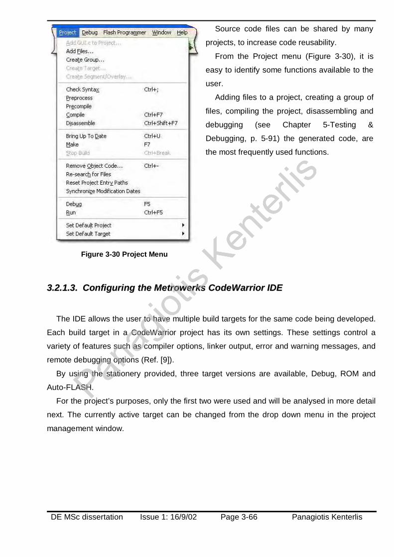
DE MSc dissertation Issue 1: 16/9/02 Page 3-66 Panagiotis Kenterlis
Figure 3-30 Project Menu
Source code files can be shared by many
projects, to increase code reusability.
From the Project menu (Figure 3-30), it is
easy to identify some functions available to the
user.
Adding files to a project, creating a group of
files, compiling the project, disassembling and
debugging (see Chapter 5-Testing &
Debugging, p. 5-91) the generated code, are
the most frequently used functions.
33..22..11..33.. CCoonnffiigguurriinngg tthhee MMeettrroowweerrkkss CCooddeeWWaarrrriioorr IIDDEE
The IDE allows the user to have multiple build targets for the same code being developed.
Each build target in a CodeWarrior project has its own settings. These settings control a
variety of features such as compiler options, linker output, error and warning messages, and
remote debugging options (Ref. [9]).
By using the stationery provided, three target versions are available, Debug, ROM and
Auto-FLASH.
For the project’s purposes, only the first two were used and will be analysed in more detail
next. The currently active target can be changed from the drop down menu in the project
management window.

DE MSc dissertation Issue 1: 16/9/02 Page 3-67 Panagiotis Kenterlis
Figure 3-31 Target Selection
Current target settings can be changed from Edit>”Target’s Name” Settings as shown in
Figure 3-32 below.
Figure 3-32 Target Settings

DE MSc dissertation Issue 1: 16/9/02 Page 3-68 Panagiotis Kenterlis
•• DDeebbuugg VVeerrssiioonn
The Debug version of the firmware code originates at address 0x003FA000, which is the
start address of the internal SRAM memory. The stack pointer is set to 0x00400000 and
decrements when data is pushed. Data is also stored at the same region as the code and the
stack (0x003FA000-0x00400000). Using the Debug target, the Metrowerks CodeWarrior IDE
can download compiled code to the microcontroller’s RAM memory and execute it like an In-
Circuit Emulator (ICE) (see Testing & Debugging p. 5-91). For the Debug Version target
settings see Figure 3-33 below.
Figure 3-33 Debug Version Settings
Figure 3-34 Debug Target Memory Map

DE MSc dissertation Issue 1: 16/9/02 Page 3-69 Panagiotis Kenterlis
Figure 3-35 IDE Preferences Menu
In order to use the Metrowerks CodeWarrior
IDE as a debugger tool, the external debugging
hardware interface needs to be connected and
configured. This is done by selecting the menu
Edit>Preferences as shown in Figure 3-35.
On the window that opens (Figure 3-36), the
MSI Wiggler, which was available for the project
together with the Axiom development board,
needs to be selected and the configuration file
for target setup should point to the configuration
script file 555_AXIOM_flash_init.cfg (Appendix
2), which is included in the source files directory.
The rest of settings mainly involve how the IDE is displayed and are of no interest to this
project. One should configure the IDE according to his/her own preference.
Figure 3-36 IDE Preferences

DE MSc dissertation Issue 1: 16/9/02 Page 3-70 Panagiotis Kenterlis
•• RROOMM VVeerrssiioonn
The ROM version compiles a ROM image of both code and data according to the settings
provided for the target. These settings are contained in the 555_Axiom_ROM.lcf file
(Appendix 1) included in the source files directory.
The ROM image originates at address 0x00010000, which is the start address of the
internal FLASH memory available for use, since the previous 64Kbytes are used by the
monitor program provided by the development board’s manufacturer.
The memory region (0x00010000- 0x0006FFFF) is used to store an image of both code
and data. On execution of the code in this region the contents of the data segment are copied
from the FLASH to the SRAM. The target start address for the data segment is that of the
SRAM memory (0x003FA000-0x003FFFFF).
The stack pointer is set to the end of the Dual Ported TPU RAM (DPTRAM), at address
0x00303800 and decrements when data is pushed. The entire 6Kbytes region of the
DPTRAM (0x00302000-0x003037FF) is assigned for use by the stack.
Figure 3-37 ROM Version Settings
The memory map for the ROM target is shown in Figure 3-38.
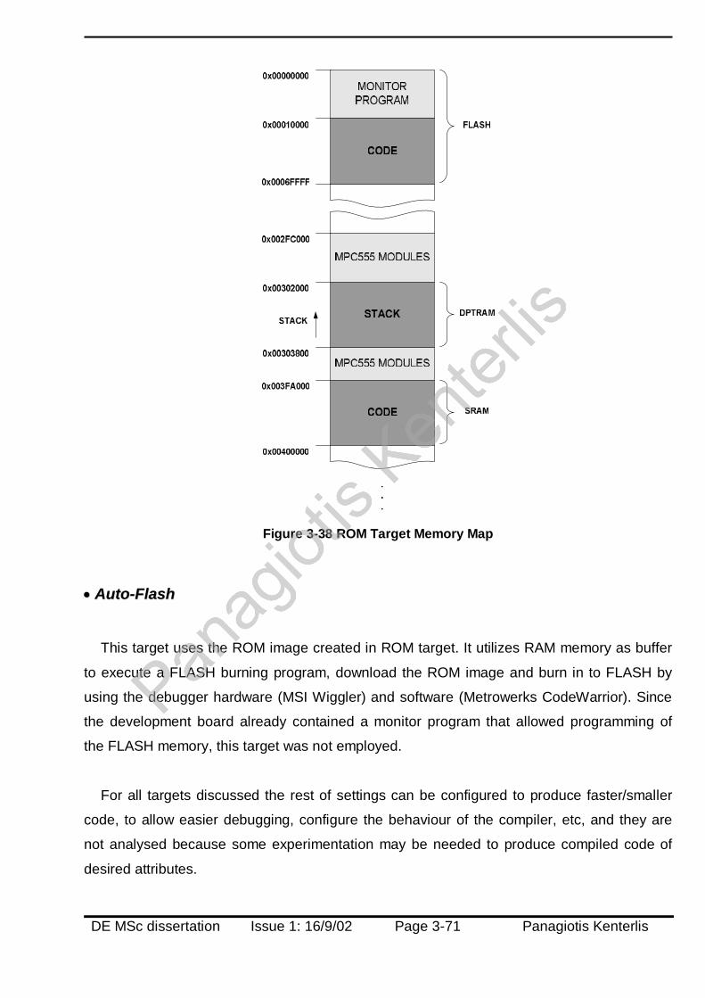
DE MSc dissertation Issue 1: 16/9/02 Page 3-71 Panagiotis Kenterlis
Figure 3-38 ROM Target Memory Map
•• AAuuttoo--FFllaasshh
This target uses the ROM image created in ROM target. It utilizes RAM memory as buffer
to execute a FLASH burning program, download the ROM image and burn in to FLASH by
using the debugger hardware (MSI Wiggler) and software (Metrowerks CodeWarrior). Since
the development board already contained a monitor program that allowed programming of
the FLASH memory, this target was not employed.
For all targets discussed the rest of settings can be configured to produce faster/smaller
code, to allow easier debugging, configure the behaviour of the compiler, etc, and they are
not analysed because some experimentation may be needed to produce compiled code of
desired attributes.

DE MSc dissertation Issue 1: 16/9/02 Page 3-72 Panagiotis Kenterlis
33..22..22.. MMiiccrrooccoonnttrroolllleerr FFiirrmmwwaarree CCooddee EExxppllaannaattiioonn
Building a real-time system can be a very tedious and complex job. Careful thought is
required when writing functions that are time-critical, and priority needs to be assigned to
them. In order to prevent some functions from hogging the CPU and losing timing of some
events which could prove catastrophic, all functions that may introduce delays and dead-
times in code execution have been removed from ISRs. The ISRs set flags that are used
after termination to initiate processes when the processor hasn’t received and interrupt
request. That way, all GUI related functions are executed outside ISRs, inside which only
time critical processes and calculations are performed. In addition, by designing the software
in this manner, the processor is more efficiently dedicated to executing real code, instead of
delay loops, and system performance is increased. GUI functions have been assigned a low
priority over the data acquisition and process functions that are executed inside ISRs (Figure
3-39).
Figure 3-39 CPU Code Execution Priority
All initialisations of modules, peripherals and interfaces are performed during the boot up
sequence, which is executed only once at system power up. Many check conditions have
been included in the source code to allow better debugging and prevent some functions from
putting the system to an invalid state, should an error or undefined condition appear. The
default measuring units used for acquiring measurement data, calculating and storing results
are kilometres and litres. These were used because of my own familiarity with these units.
However, by driver’s selection, different measuring units can be displayed.
In the following pages some flowcharts for the basic functions performed by the
microcontroller’s firmware are also provided. Due to the extreme volume and complexity of
the source code it is not possible to deliver all flowcharts before deadline. For more
information on the actual operation of the firmware it is advisable to read the source files,
which are heavily and well commented.

DE MSc dissertation Issue 1: 16/9/02 Page 3-73 Panagiotis Kenterlis
•• GGeenneerraall FFlloowwcchhaarrttss

DE MSc dissertation Issue 1: 16/9/02 Page 3-74 Panagiotis Kenterlis

DE MSc dissertation Issue 1: 16/9/02 Page 3-75 Panagiotis Kenterlis

DE MSc dissertation Issue 1: 16/9/02 Page 3-76 Panagiotis Kenterlis

DE MSc dissertation Issue 1: 16/9/02 Page 3-77 Panagiotis Kenterlis

DE MSc dissertation Issue 1: 16/9/02 Page 3-78 Panagiotis Kenterlis

DE MSc dissertation Issue 1: 16/9/02 Page 3-79 Panagiotis Kenterlis
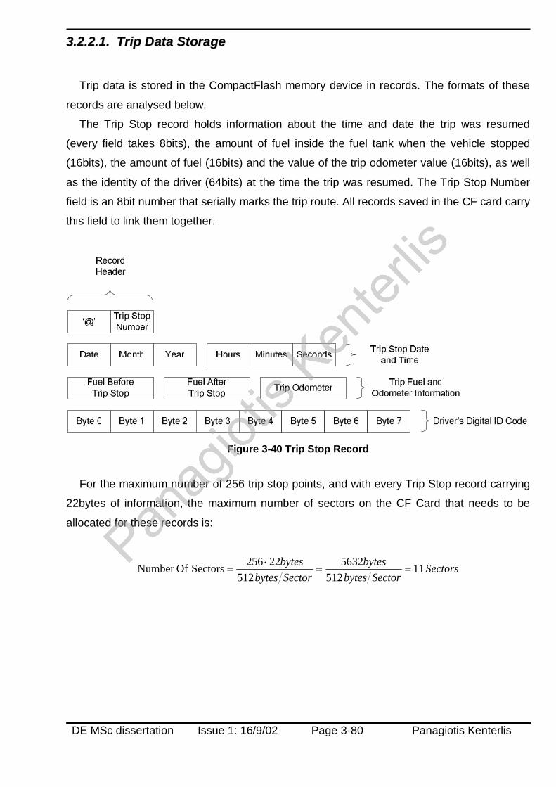
DE MSc dissertation Issue 1: 16/9/02 Page 3-80 Panagiotis Kenterlis
33..22..22..11.. TTrriipp DDaattaa SSttoorraaggee
Trip data is stored in the CompactFlash memory device in records. The formats of these
records are analysed below.
The Trip Stop record holds information about the time and date the trip was resumed
(every field takes 8bits), the amount of fuel inside the fuel tank when the vehicle stopped
(16bits), the amount of fuel (16bits) and the value of the trip odometer value (16bits), as well
as the identity of the driver (64bits) at the time the trip was resumed. The Trip Stop Number
field is an 8bit number that serially marks the trip route. All records saved in the CF card carry
this field to link them together.
Figure 3-40 Trip Stop Record
For the maximum number of 256 trip stop points, and with every Trip Stop record carrying
22bytes of information, the maximum number of sectors on the CF Card that needs to be
allocated for these records is:
SectorsSectorbytes
bytesSectorbytes
bytes 11512
5632512
22256Sectors OfNumber ==⋅
=

DE MSc dissertation Issue 1: 16/9/02 Page 3-81 Panagiotis Kenterlis
The Trailer ID record holds the ID codes of the attached trailers. A maximum of 8 trailer ID
codes is held per record. The header includes a Start-of-Record character (‘@’), the Trip
Stop number and the number of discovered ID codes. The ID codes discovered follow next.
The record ends with an End-of-Record character (‘#’), which has been added to keep the
record size to an even number of bytes.
Figure 3-41 Trailer ID Record
For the maximum number of trip stop points and the maximum number of discovered ID
codes, a total of SectorsSectorbytes
bytesSectorbytes
bytesrecords 34512
17408512
68256Sector OfNumber ==⋅
= needs
to be assigned on the CF Card.
The Tachograph record holds the vehicle’s road speed divided by 100 (16bits of data
stored in the integer form of e.g. 57.500km/h is saved as value 575), which is recorded for
every second of actual trip time.
Figure 3-42 Tachograph Record
In order to avoid reducing the CF Card’s lifetime by saving data every second, road speed
data is kept inside a buffer of 8 elements in depth (16bits per element) and flushed to the CF

DE MSc dissertation Issue 1: 16/9/02 Page 3-82 Panagiotis Kenterlis
Card when full, that is, every 8 seconds. Changing the depth of this buffer will prolong the CF
Card’s life.
During the initialisation phase of the firmware execution, the total number of sectors
available on the CF Card is discovered and used as the maximum sector value for storing
Tachograph Data. The number of sectors allocated to storing Tachograph information defines
the amount of total recorded trip time. To allow future upgrades to both software and
hardware, the Tachograph records are saved last on the CF Card.
The memory map of the CF Card is displayed in Figure 3-43 below.
Figure 3-43 CompactFlash Information Storage Map
The 4Mbytes version of the CF Card that was used for the project has a total of 7872
sectors in LBA mode, which amounts to bytesSectorbytesSectors 464,030,45127872 =⋅ . With
the memory map already displayed above, a total of 7825477872 =− Sectors are available
for Tachograph information to be stored. This capacity is enough for storing information for
seconds 2,003,200sec2
ytes4,006,400bsec2
5127825==
⋅ondbytesondbytes
SectorbytesSectors , which is equal to 23 days of
continuous driving (results to be verified by the reader).
By using a CF Card of larger capacity, Tachograph information can be stored over a much
longer period of time and by altering the firmware it is possible to increase the number of
identified trailers and use this facility for tracking contents of trailers.

DE MSc dissertation Issue 1: 16/9/02 Page 3-83 Panagiotis Kenterlis
33..22..33.. PPCC SSooffttwwaarree CCooddee EExxppllaannaattiioonn
The software utilities developed for the PC in Microsoft Visual Basic 6.0 for the Windows
platform are used to communicate with the trip computer through a serial port (by default set
to COM1, although it can be changed by the user) and control transfers of data to and from
the trip computer device. By implementing the analysed communications protocol these
programs can be easily ported to any operating system or programming language.
Short explanation and flowcharts for the most important functions executed by the
software on the PC are provided in the following pages. To obtain a more clear knowledge on
the actual code executed you are requested to read the well commented source code.

DE MSc dissertation Issue 1: 16/9/02 Page 3-84 Panagiotis Kenterlis
•• CCoonnffiigguurraattiioonn DDoowwnnllooaadd UUttiilliittyy
This utility is used for downloading configuration data for the automotive sensors
connected to the trip computer (Figure 3-44). Sensor parameters are given in clear text form
and can be saved to and/or stored in files. If required, the default communications port can
be changed to another COM port of the system where the utility is installed. Configurable
parameters are:
Tire Perimeter (in metres) (32bits).
Fuel Tank Capacity (in litres) (16bits).
Pulses per Wheel Revolution (from Road Speed Sensor) (16bits).
Pulses per Kilometre (from Road Speed Sensor) (32bits).
Pulses per Engine Revolution (from Engine Speed Sensor) (16bits).
Pulses per Litre (from Fuel Flow Meter) (32bits).
Figure 3-44 Hardware Configuration Utility
In the case that a sensor is replaced with one of different specifications, only the specific
information for its configuration needs to be changed. These parameters are stored in
the RAM of the external RTC on the trip computer and are used in calculations to
produce accurate results. The utility simply sends a Start of Communication Session
command and expects an acknowledgement (ACK) from the device, after that it sends
the Device Configuration command and the parameters. When every parameter has
been sent, acknowledgment from the device is expected to proceed with the next one.
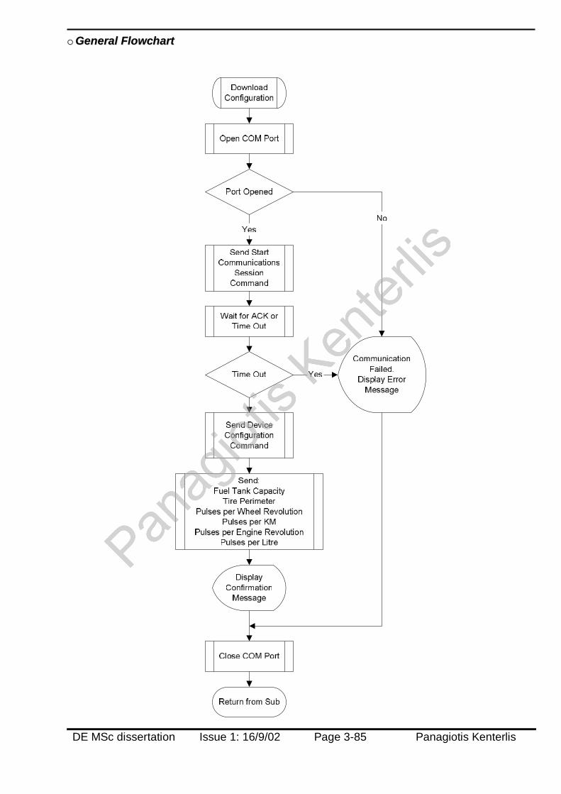
DE MSc dissertation Issue 1: 16/9/02 Page 3-85 Panagiotis Kenterlis
oo GGeenneerraall FFlloowwcchhaarrtt

DE MSc dissertation Issue 1: 16/9/02 Page 3-86 Panagiotis Kenterlis
•• TTrriipp DDaattaa UUppllooaadd UUttiilliittyy
This utility is used for uploading vehicle and trip information stored on the CompactFlash
and saving them in files (Figure 3-45). Only sectors that carry information are uploaded to the
PC through the serial port. Data uploaded are stored in three different files (Trip Stop Log,
Trailer ID log, Tachograph information). To start the upload process the utility sends the Start
of Communication Session command and expects and acknowledgement from the device,
after that it sends the Upload Trip Data command to the trip computer. The trip computer
responds with the data in one sector (512bytes) plus the calculated CRC8 value of the data
sent. The PC monitors the serial port and every byte received is added to a temporary buffer.
Once 513bytes have been received, the PC recalculates the CRC8 value of the received
data and compares it to the received CRC8 value. If these values match, then the
transmission didn’t contain errors and the received data are appended to the currently
pointed file. The PC sends an ACK (Acknowledge) command to indicate that the sector was
received correctly and that the next sector should be sent. If the CRC8 values did not match
the received data are discarded and a NACK (Negative Acknowledge) command is sent to
the trip computer to indicate a transmission fault and request retransmission of the entire
sector. The PC also monitors the buffer for the appearance of special transmission
terminating commands. These commands indicate that a set of records has been uploaded
and that the PC should save the next data to be transmitted to the appropriate file (End of
Transmission Block), and that the entire upload procedure has finished and that the PC
should not wait for any more data to be received (End of Transmission).
Figure 3-45 Trip Data Upload Utility

DE MSc dissertation Issue 1: 16/9/02 Page 3-87 Panagiotis Kenterlis
oo GGeenneerraall FFlloowwcchhaarrttss

DE MSc dissertation Issue 1: 16/9/02 Page 3-88 Panagiotis Kenterlis

DE MSc dissertation Issue 1: 16/9/02 Page 4-89 Panagiotis Kenterlis
44.. BBuuiillddiinngg tthhee PPrroojjeecctt
44..11.. PPrraaccttiiccaall BBuuiillddiinngg CCoonnssiiddeerraattiioonnss
While in the development phase of the project, some problems needed to be resolved. The
most important of them are given in the text that follows. Both hardware and software
sections are mentioned.
44..11..11.. HHaarrddwwaarree
Developing the hardware part was somewhat tricky mainly because of the development
board used for the microcontroller (Axiom PB-0555). This board (Figure 4-1) provides almost
all the pins of the microcontroller in 4 headers of 4x17 pins each. Trying to establish a fixed
connection of the developed hardware with the development board required some
manufacturing tricks, since no standard connectors are available for such a pin layout. The
main concern was to avoid using a soldering iron on the board itself that could incur possible
damage.
Figure 4-1 Photograph of the MPC555 Development Board
This obstacle was overcome by using single row pin connectors and arranging them on a
spotted matrix board, so that all of the microcontroller’s pins would become available on the

DE MSc dissertation Issue 1: 16/9/02 Page 4-90 Panagiotis Kenterlis
copper side of the matrix board. After that, the matrix board was used to form a motherboard
with connectors for all other developed peripheral boards (Figure 4-2).
Figure 4-2 Development Board with Connected Motherboard
44..11..22.. SSooffttwwaarree
The main problems encountered with the software part of the project was obtaining the
license for the Metrowerks CodeWarrior and configuring the target settings for the
microcontroller development board used, since no stationery was available for it. Having no
external memory on the development board, all software development needed to be done in
internal memory. For the Debug version the limited memory size for code development
(26Kbytes SRAM) and the fact that at this mode processing of interrupts could not be
performed was a problem. For the ROM version although code size was not an issue
(448Kbytes FLASH available) and interrupts could be processed, however, actual debugging
could not be performed and a very time-consuming FLASH program download procedure
had to be performed every time the code changed. In addition programming the FLASH
memory was limited to a maximum of 100 cycles so care had to be taken not to wear out the
FLASH memory cells. A mixture of both target versions was used; Debug when specific
routines needed to be tested and ROM when interrupts had to be processed to view system
response.

DE MSc dissertation Issue 1: 16/9/02 Page 5-91 Panagiotis Kenterlis
55.. TTeessttiinngg && DDeebbuuggggiinngg
The device developed was fully tested in laboratory conditions with all connections to
automotive sensors being emulated by standard testing methods and equipment. Field tests
could not be performed because of the requirements for such a case, i.e. the trip computer
would have to be installed on a truck and tested in a real trip scenario.
While developing the project, at all times there was need to test changes in the programs
and the operation of modules.
For this purpose the following tools were used:
o A fixed frequency crystal oscillator running at 32.768 kHz.
o A pulse generator.
o A digital Multimeter.
o The microcontroller’s serial port in connection to the PC.
o The display module, for displaying test information.
o And largely the Metrowerks CodeWarrior 6.03 Integrated Development Environment,
used as a debugger-emulator.
Figure 5-1 Oscilloscope view of square
wave signal
Both the crystal oscillator and the pulse generator
were used to provide square wave pulses to the
TPU3 inputs of the microcontroller in order to
emulate the automotive sensors for road speed,
engine speed and fuel flow.
Figure 5-2 Multimeter used to test voltage level of I/O pin
The digital Multimeter was used to measure
voltage levels on various test points while
developing system circuits. Being the first testing
device to be involved while still starting on the
project, it was first used to verify the logic value of
I/O pins of the MIOS1 module, when the control
functions for that module were developed. Also used
to check circuit boards for short-circuits and
electrical continuity of connection wiring.

DE MSc dissertation Issue 1: 16/9/02 Page 5-92 Panagiotis Kenterlis
The microcontroller’s serial port connected to the serial port of a PC running terminal
emulation software proved to be a very helpful debugging tool. Printing information on the
terminal window such as test values, contents of registers, breakpoint execution flag text,
measurement readings and time signaling, were all functions that were performed to help
eradicate bugs and improve the design of both software and hardware.
In Figure 5-3, frequency/pulse counting results of the TPU channels for Road Speed and
Engine Speed sensors are displayed with a display frequency of once per second, as code
was executed inside the ISR of the internal RTC.
Figure 5-3 PC Terminal Debugging

DE MSc dissertation Issue 1: 16/9/02 Page 5-93 Panagiotis Kenterlis
The Metrowerks CodeWarrior IDE was the most important of all development, testing and
debugging tools. With the use of a device connected on the parallel port (MSI Wiggler),
CodeWarrior was able to communicate with the microcontroller and its BDM port
(Background Debug Mode) (Ref. [6] & [10]). The Wiggler is effectively, at a minimum, a
parallel port to JTAG (Joint Testing Action Group) serial interface converter. The BDM port,
which is based on the JTAG interface, allows for instructions and data to be downloaded to
the microcontroller even at execution time, accessing and modifying memory and processor
resources, single stepping, processor reset and status control (running or halted). It
essentially allows the user to download a program in RAM and execute it by using a
software-hardware control scheme, with the microcontroller itself acting like an In-Circuit
Emulator (ICE). The entire scheme is called On-Chip Debugging (OCD) by Motorola and it is
used in many of its products.
In the screenshot of Figure 5-4, Metrowerks CodeWarrior is displayed while debugging the
application software by using the opened windows to display processor registers and
memory locations, as well as code that is executed both in C language and assembly.
Instructions can be executed step-by-step in both C and Assembly, while the result of every
instruction can be monitored by looking at the relating processor/system information window.
Figure 5-4 Debugging of the application software using BDM/OCD inside Metrowerks CodeWarrior
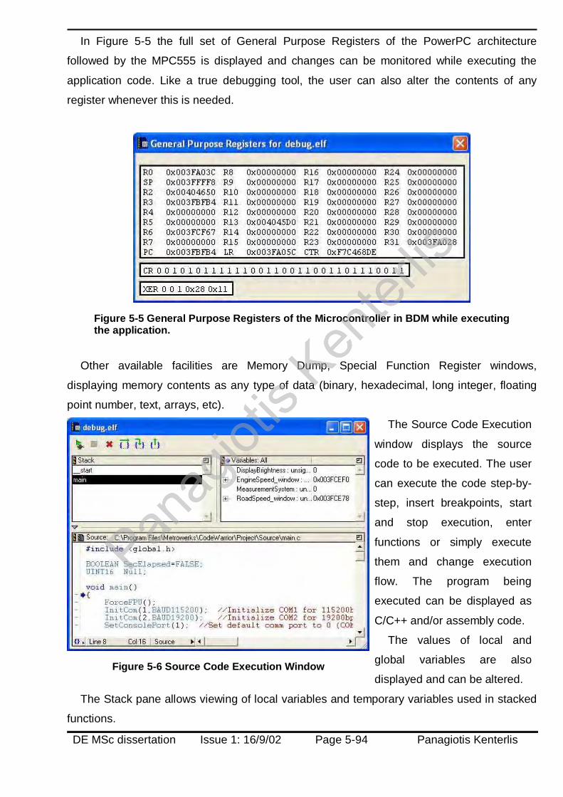
DE MSc dissertation Issue 1: 16/9/02 Page 5-94 Panagiotis Kenterlis
In Figure 5-5 the full set of General Purpose Registers of the PowerPC architecture
followed by the MPC555 is displayed and changes can be monitored while executing the
application code. Like a true debugging tool, the user can also alter the contents of any
register whenever this is needed.
Figure 5-5 General Purpose Registers of the Microcontroller in BDM while executing the application.
Other available facilities are Memory Dump, Special Function Register windows,
displaying memory contents as any type of data (binary, hexadecimal, long integer, floating
point number, text, arrays, etc).
Figure 5-6 Source Code Execution Window
The Source Code Execution
window displays the source
code to be executed. The user
can execute the code step-by-
step, insert breakpoints, start
and stop execution, enter
functions or simply execute
them and change execution
flow. The program being
executed can be displayed as
C/C++ and/or assembly code.
The values of local and
global variables are also
displayed and can be altered.
The Stack pane allows viewing of local variables and temporary variables used in stacked
functions.

DE MSc dissertation Issue 1: 16/9/02 Page 5-95 Panagiotis Kenterlis
One of the methods used to test and debug the CF Card storage functions and the serial
upload functions of the trip computer was to save an entire sector of data (512 bytes) with
incrementing values from 0 to 255 and then display them on the computer’s screen. The
same test was also executed in Metrowerks CodeWarrior and results displayed as data
elements of an array. Once the data had been uploaded to the PC and saved to a file, they
were displayed by using a Hex-Editor (in this case the Norton Commander Editor). In Figure
5-7 and Figure 5-8 the contents of one sector filled with test data are displayed in both
Hexadecimal and ASCII.
Figure 5-7 Sector Contents as uploaded to the PC (1/2)
Figure 5-8 Sector Contents as uploaded to the PC (2/2)

DE MSc dissertation Issue 1: 16/9/02 Page 5-96 Panagiotis Kenterlis
55..11.. EElleeccttrroommaaggnneettiicc CCoommppaattiibbiilliittyy IIssssuueess
With the automotive environment being extremely rich in electrical noise, due to spark
plugs and solenoids on the engine, there is need for immunization of the device. To achieve
this, the trip computer circuit boards have to be placed in a steel enclosure and ferrite beads
mounted to all wires in and out. The microcontroller is equipped with a watchdog timer on-
chip, which should be enabled to eradicate rampant processor behaviour. In addition, the
power supply to the device needs to feature a large capacitor to compensate for
instantaneous power loss when turning on the ignition, as well as transient voltage
suppressor diodes to filter out high frequency voltage spikes.

DE MSc dissertation Issue 1: 16/9/02 Page 6-97 Panagiotis Kenterlis
66.. PPrroojjeecctt RReessuullttss
Upon completion of the project all specifications drawn at the beginning and reviewed
during the course of development have been met, along with a few more not originally
included. This was made possible by performing a well-planned, methodical programming
and module usage, as well as exploiting a number of features found being hidden in the
microcontroller’s datasheets. The designed hardware device is capable of performing the
following functions:
1. Current speed shown in two measurement systems (km/h and m/h).
2. Road Speed statistics such as maximum road speed, average road speed, and
maximum average road speed.
3. Present vehicle location (relative to distance from next stop) by displaying a trip
odometer and distance to next stop and to final destination.
4. Total elapsed time since start of trip (drive time).
5. Elapsed trip time since last stop (drive time).
6. Vehicle’s Battery Voltage.
7. Fuel remaining in the fuel tank in two measurement systems (litres and gallons).
8. Distance to empty fuel tank in two measurement systems (km and miles).
9. Total amount of fuel used since trip start in two measurement systems (litres and
gallons).
10. Instantaneous fuel flow rate in two measurement systems with four variations
(km/litre, miles/litre, km/gallon and miles/gallon).
11. Estimated time till arrival to the next stop point.
12. Estimated time of arrival to the next stop point.
13. Time of day displayed on-screen (Home Time/Date).
14. Date displayed on-screen (Home Time/Date).
15. Local time, calculated by entering a time difference from Home Time.
16. Alarm clock that can be set by the driver to sound at specific time of day.
17. Engine speed in 1000x RPM.
18. Engine Speed statistics (maximum engine speed and average engine speed).
19. Vehicle’s independent digital odometer.
20. Trip independent digital odometer.
21. Outside/Cabin temperature acquired by a digital thermometer device.

DE MSc dissertation Issue 1: 16/9/02 Page 6-98 Panagiotis Kenterlis
22. Tiredness warning after 3 hours of continuous driving (according to EU traffic laws).
23. Driver’s ID logging using a digital key.
24. Trailer identification and logging using digitally coded devices.
The memory device (CF card) is used to store the following set of information:
1. Time and date of trip resume after leaving a stop point.
2. Trip odometer value displayed at trip resume point.
3. Fuel gauge indication before vehicle stopping and after vehicle continuing trip from a
stop point (refuel mark-up).
4. Driver’s digital ID code to allow tracking a driver change over the trip duration.
5. A log of all trailer digital ID codes at every stop point, to allow tracking of trailers being
transported.
6. Arrays of tachograph information (road speed) starting at every resume trip point and
stopping at every trip stop point. Values are acquired every second and saved on the
memory device every 8 seconds or when a sector buffer is full or another event e.g.
signal from a G sensor indicating an accident has occurred (should that be
implemented in future product upgrades).
Having implemented part 6 of the above list, the Trip Computer device can be used as a
simplistic trip data recorder in the undesirable event of an accident, as evidence of the
vehicle’s road speed seconds or minutes before the accident. Such functionality makes the
installation of the trip computer on a vehicle fleet even more useful to companies, since it
could be used in a court of law to relieve both driver and company from legal accusations and
financial claims.
As indicated in the finalised specifications list, all information saved in the CF Card are
uploaded to a personal computer using software utilities specifically designed for that
purpose. After the information has been saved on the PC, a software program, which was not
developed as part of the project due to limited time at hand, can be used to process the data
files and visualize the information for inspection and statistical or other analysis.
By implementing all of the above, the project can be characterized as successfully having
met with the targets that had been designated, in order to develop a product unique and
functional in its whole.

DE MSc dissertation Issue 1: 16/9/02 Page 7-99 Panagiotis Kenterlis
77.. FFuuttuurree UUppggrraaddeess aanndd DDeevveellooppmmeenntt
Like any other product, the trip computer can be deployed to include even more features
and thus exploit more of the microcontroller’s true capabilities, which exceed the ones
currently used for this project.
Future plans on the software side of the project should certainly include building an
Integrated PC Software Suite, which was not developed as part of the project and will
assume the management of entire fleets of vehicles and automate various procedures.
Future hardware upgrades could also include some ideas originally suggested, however
during the selection phase were eliminated either because of cost, complexity or time
margins:
o Implementing a high speed communications bus such as the Universal Serial Bus (USB)
will minimize data upload times, especially when collecting data after a very long trip,
with the amount of stored information being proportionately high.
o Incorporating a GPS receiver would allow recording the exact position of the vehicle at
every time. By doing so, it is possible during the data process phase, to verify that the
driver has followed the route suggested by the company. Also to make the product even
more appealing, it would be interesting and useful, if by connecting to a PC or PDA to
display vehicle’s current position on digital maps relatively to the drawn route.
o A wireless communications channel, such as GSM/DCS, could allow transferring data
from the device to the company’s computers during the trip, even when abroad. This can
prove to be very useful to a company that wishes to be aware of the location of its
vehicles at regular intervals.
o By using more sensor inputs and connecting to the Engine Control Unit of the vehicle, it
will be possible to provide more information on the vehicle’s status. Following this, the
trip computer could eventually replace the entire vehicle’s analogue instruments
dashboard.

DE MSc dissertation Issue 1: 16/9/02 Page 8-100 Panagiotis Kenterlis
88.. CCoonncclluussiioonnss
Having finished this project, I feel more confident about my abilities in handling projects of
such magnitude in real life. Managing such a project, although difficult at some points and
damaging to my bank account, it proved to be a very interesting and invaluable experience.
Much knowledge was gained from the logical reflections occurring at every moment, as many
aspects of the problems being faced with needed to be considered in order to decide on the
best likely solution.
During both research and development periods, I had the opportunity to study on real-time
embedded systems and expand my knowledge in microcontroller and microprocessor
systems design, which is my main field of interest.
Never having a driving license before or being interested in cars in any way, studying in
the field of automotive applications provided some background information on the technology
of engines, mechanical, electrical and electronic systems found on cars. Although this hasn’t
dispelled my fears of becoming a driver, it will at least assist me in understanding better what
is happening underneath the metallic hood or plastic covers, and in the future may point me
in design more products for the automotive market.
In conclusion, as expected, this project proved to be the most exciting and most educative
part of the MSc course.

DE MSc dissertation Issue 1: 16/9/02 Page 9-101 Panagiotis Kenterlis
99.. PPrroojjeecctt MMaannaaggeemmeenntt
99..11.. HHooww WWaass tthhee PPrroojjeecctt PPllaannnneedd??
The Baseline Time Schedule for the project was designed for a development period of
11weeks using a worst case scenario. This scenario assumed that every task would take up
the entire day allocated to it, without dealing with other tasks. At the time the project was
being planned little knowledge was present on the difficulty level in using the development
tools, which were therefore considered to be not extremely productive. In addition the
author’s abilities to deal with 32bit advanced microcontrollers and complex real-time software
were assumed to be basic at that point. Uncertainty in the selection of module inter-
connection protocols until the related components were available, also contributed in the
decision to follow a scenario of such a wide time spread.
However, the initially drawn baseline plan proved to be inconsistent with reality. While
working with the development tools, although initially a myriad of problems had to be solved,
seeking for advices on the internet from a forum specifically for these tools helped gradually
solve problems at a short time, and proved highly productive. Dealing with many tasks at the
same period of time also allowed to accumulate knowledge much faster and thus helped to
get a clearer picture of the project at an early time. It was thus discovered that the author was
underestimated for his abilities in dealing with such a complex project. Additionally by cutting
corners and underwriting the financial burden of purchasing the most essential components,
saved much time in obtaining the components and allowed to start development of the
related project sections earlier. The end result of these actions was for the development
phase of the project to actually last 7weeks, which is 4weeks earlier than originally planned.
This march of events was greeted with a smile of contentment since it allowed more time
to be spent preparing this assignment, as well as the project’s presentation and report.

DE MSc dissertation Issue 1: 16/9/02 Page 9-102 Panagiotis Kenterlis
99..22.. PPrroobblleemmss aanndd AAcchhiieevveemmeennttss
Some ideas that emerged during the research period, like incorporating a GPS receiver
and a high speed communications bus had to be abandoned after careful consideration of
cost levels, time available for project completion and possible impact on the product if
removed. More specifically the cost was prohibiting in both cases and only if removed (GPS)
or replaced with lower cost versions (communications bus) the project could be kept inside
budget and deadlines.
While still discussing with the project supervisor on the available funds for the project, it
became clear that there might be some problems in obtaining some of the expensive parts.
That led the author to purchase the display module using own funds. The module was
delivered 5 weeks earlier than originally planned, had it been obtained through the university.
In addition to the above, many components and parts were purchased by the author to
allow for faster delivery times, than if ordered through the university. As proven later by the
extremely slow delivery rate of components that had been ordered through the university, this
decision was very wise and saved lots of development time, although it surely cost more.
However during development stages where specifications have not been absolutely finalised,
time is of more essence, while actually finding the most cost-effective supplier for the same
parts to be used can be a matter to resolve prior the manufacturing stage. It is always
necessary to keep in mind that large deviations from the drawn budget should not become
common practice.
The above mentioned steps helped finish the project earlier than originally planned, thus
allowing more time for testing and debugging to develop a stable and full-featured product.
More available time also allowed finishing all writing works earlier or at least provided more
time to produce a better result.
At the start of the development period of the project a number of connectors were required
to build a main adapter board that would allow connection of the peripheral boards to the
microcontroller’s development board. Although having been reassured that the supplier
would be able to deliver these within a few days, in reality it took more than 6 weeks just to
receive the wrong type of connectors. Having nearly finished with the hardware development
and urgently needing these connectors, switching suppliers seemed the only solution to
obtain the parts required. The second supplier having compatible connectors at the same
price managed to deliver the parts one day after the order was placed. This allowed finishing
the project within 2-3 days (See Gantt Chart in the Appendix).

DE MSc dissertation Issue 1: 16/9/02 Page 10-103 Panagiotis Kenterlis
1100.. BBiibblliiooggrraapphhyy
[1] Kelley, A., Pohl. I., - C by Dissection, The Essentials of C Programming. Second
Edition. – Benjamin/Cummins, Redwood City, California, USA, 1992. – ISBN 0-
80533-140-9
[2] IEE, - Automotive Electronics, Conference Publication No. 346, - Institute of Electrical
Engineers, London, UK, 1991. - ISBN 0 85296 525 7, ISSN 0537-9989
[3] Bromley, P. J. - Advanced Automotive Electronics. - IFS Publications, UK, 1989. -
ISBN 1-85423-044-1
[4] Chowanietz, E., - Automobile Electronics. – Newnes, Oxford, UK, 1995. – ISBN 0-
7506-1878-7
[5] Ribbens, W. B., - Understanding Automotive Electronics. Fifth Edition. – Newnes,
Oxford, UK, 1998. – ISBN 0-7506-7008-8
[6] Nwagboso, C. O., - Automotive Sensory Systems. – Chapman & Hall, London, UK,
1993. – ISBN 0-412-45880-2
[7] BOSCH. – Automotive Handbook. Fifth Edition. – Robert Bosch GmbH, Stuttgart,
Germany, 2000. – ISBN 0-8376-0614-4
[8] IBM, International Business Machines Inc., – The PowerPC Architecture: A
Specification for a New Family of RISC Processors. – Morgan Kaufmann Publishers
Inc., San Francisco, USA, 1993- 1994. - ISBN 1-55860-316-6
[9] Cooling, J. E., - Real Time Interfacing, Engineering aspects of microprocessor
peripheral systems. – Van Norstrand Reinhold (UK) Co. Ltd, Berkshire, UK, 1986. –
ISBN 0-442-31755-7
[10] Mustafa, M. A., - Microcomputer Interfacing and Applications. Second Edition.–
Newnes, Oxford, UK, 1994. – ISBN 0-7506-1752-7

DE MSc dissertation Issue 1: 16/9/02 Page 11-104 Panagiotis Kenterlis
1111.. RReeffeerreenncceess -- OOtthheerr DDooccuummeennttss [1] 50 Ways to Touch Memory. Second Edition. October 1992 – Dallas Semiconductors.
[2] Application Note 2109 on MPC555 Interrupt Handling – PDF document describing
how to program and handle interrupts on the MPC555 – Published by Motorola Inc. -
Found on http://e-www.motorola.com (original URL too long to publish) and also
included in the project’s documentation CD (an2109sw.zip).
[3] CompactFlash Card Specifications Manual – PDF file describing the electrical,
mechanical specifications and interface protocols of the CompactFlash Card –
Published by the CompactFlash Association – Found on http://www.compactflash.org
and also included in the project’s documentation CD (cfspc1_4.pdf).
[4] Frequency Measurement Function – PDF file describing the configuration of a TPU
channel and the operation of the FQM function – Published by Motorola Inc. – Found
on http://e-www.motorola.com (original URL too long to publish) and also included in
the project’s documentation CD (TPUPN03-FQM.pdf).
[5] IDE User’s Guide – PDF document on using CodeWarrior – Published by Metrowerks
Inc. – Available in the installation CD
[6] Motorola MPC555/MPC556 User’s Guide – Set of PDF documents describing the
programming of every module on the MPC555 – Published by Motorola Inc. – Found
on http://e-www.motorola.com (original URL too long to publish) and also included in
the project’s documentation CD (mpc555um_zip.zip).
[7] New Input Capture/Input Transition Counter TPU Function – PDF file describing the
configuration of a TPU channel and the operation of the NITC function - – Published
by Motorola Inc. – Found on http://e-www.motorola.com (original URL too long to
publish) and also included in the project’s documentation CD (TPUPN08-NITC.pdf).
[8] Opesanwo, A. O., - Engine Management Using a PowerPC MPC555. Final Year
Project Report. – Project Supervisor Mr. C. S. Knight, -University of Brighton, May
2002
[9] Targeting Embedded PPC. – PDF file describing the configuration of Metrowerks
CodeWarrior IDE for Embedded PPC – Published by Metrowerks Inc. – Found on
Metrowerks CodeWarrior installation CD (Targeting_Embedded_PPC.pdf)
[10] The Zen of BDM – White paper on debugging by Craig Haller of Macgraigor Systems.
Found on http://www.metrowerks.com/tools/documentation/embedded/zenofbdm and
also included in the project’s documentation CD.

DE MSc dissertation Issue 1: 16/9/02 Page 11-105 Panagiotis Kenterlis
1111..11.. UURRLLss [1] About, Inc. – Making Sense of Sensors: Part One
Available from: http://autorepair.about.com/library/weekly/aa030301c.htm
Last Accessed 10/9/2002
[2] ACDelco – The Engine
Available from: http://www.weekendmechanicsclub.com/ACDelco/vobeng1.htm
Last Accessed 10/9/2002
[3] AudiWorld – AudiWorld Tech Articles
Available from: http://www.audiworld.com/tech/elec57.shtml
Last Accessed 10/9/2002
[4] C&H Promotions – VH Trip Computer Instructions
Available from: http://members2.easyspace.com/hotholdens/model/v/vh_trip_computer.html
Last Accessed 10/9/2002
[5] California Polytechnic State University – Design of an Aircraft Engine Management System
Available from: http://fp3.antelecom.net/tbehrens/aems555/code.html
Last Accessed 10/9/2002
[6] ChipCenter-QuestLink – PIC A COMPACTFLASH CARD
Available from: http://www.chipcenter.com/circuitcellar/february01/c0201ms1.htm
Last Accessed 10/9/2002
[7] CompactFlash Association
Available from: http://www.compactflash.org/
Last Accessed 10/9/2002
[8] Dallas/Maxim – 1Wire and iButton Products
Available from: http://dbserv.maxim-ic.com/1-Wire.cfm
Last Accessed 10/9/2002
[9] Dallas/Maxim – Integrated Circuits (ICs) for Automotive Sensors
Available from: http://dbserv.maxim-ic.com/solutions.cfm?cpk=5
Last Accessed 10/9/2002
[10] Electro-Logic Machines, Inc. – TPU Products and Information
Available from: http://www.elmi.com/tpu.html
Last Accessed 10/9/2002
[11] Ford Capri Fan Club Page – Ford Capri Trip Computer
Available from: http://www.capri.pl/garage/ford-trip-computer.php
Last Accessed 10/9/2002

DE MSc dissertation Issue 1: 16/9/02 Page 11-106 Panagiotis Kenterlis
[12] Integrated Publishing - Basic Automotive Electricity
Available from:
http://autorepair.about.com/gi/dynamic/offsite.htm?site=http%3A%2F%2Fwww.tpub.com%2Fbasae
%2F
Last Accessed 10/9/2002
[13] Ivopol A. T. – IDE, Hardware Reference & Information Document
Available from: http://www.repairfaq.org/filipg/LINK/F_IDE-tech.html
Last Accessed 10/9/2002
[14] Johnson Controls, Inc. – Reconfigurable Trip Computer
Available from:
http://www.johnsoncontrols.com/asg-electronics/products/infosys/reconfig_trip_cmptr.asp
Last Accessed 10/9/2002
[15] Kopelson C. – Speedometers and Odometers
Available from: http://www.amghummer.com/Accessories/Speedometer/Speedometers.htm
Last Accessed 10/9/2002
[16] Marshall Brain’s HowStuffWorks – How Car Computers Work
Available from: http://www.howstuffworks.com/car-computer.htm
Last Accessed 10/9/2002
[17] Marshall Brain’s HowStuffWorks – How Diesel Engines Work
Available from: http://www.howstuffworks.com/diesel.htm
Last Accessed 10/9/2002
[18] Moore W. – Wesley’s PIC pages: IDE Controller
Available from: http://www.pjrc.com/tech/8051/ide/wesley.html
Last Accessed 10/9/2002
[19] National Instruments Corp. – Automotive Electronics
Available from: http://www.ni.com/automotive/auto_electronics.htm
Last Accessed 10/9/2002
[20] Noritake-Itron – Noritake-Itron VFD Operation
Available from: http://www.noritake-itron.com/SubPages/vfdoperapn.htm
Last Accessed 10/9/2002
[21] Noritake-Itron – VFD Module Application Notes
Available from: http://www.noritake-itron.com/SubPages/vfmodapn.htm
Last Accessed 10/9/2002
[22] P.A.P. den Haan – EIDE/Ultra ATA storage page
Available from: http://thef-nym.sci.kun.nl/~pieterh/storage.html
Last Accessed 10/9/2002
[23] PicList Forum – Disk Drives
Available from: http://www.piclist.com/techref/drives.htm
Last Accessed 10/9/2002

DE MSc dissertation Issue 1: 16/9/02 Page 11-107 Panagiotis Kenterlis
[24] Powell J. – Jim Powell’s BMW Page (Fuel Sending Units)
Available from:
http://www.apexcone.com/TechProcedures/FuelSendingUnits/FuelSendingUnits.html
Last Accessed 10/9/2002
[25] Scania – Scania Trip Computer
Available from: http://www.scania.com/ms/events/000922/press/P00906EN.htm
Last Accessed 10/9/2002
[26] Sensatech Ltd – Automotive Truck, Bus & PSV Industry
Available from: http://www.sensatech.com/industries/automotive_truck.html
Last Accessed 10/9/2002
[27] SLTF Consulting – Embedded System Design Articles
Available from: http://www.sltf.com/articles/artindex.htm
Last Accessed 10/9/2002
[28] SLTF Consulting - PC Cards as EPROM replacements
Available from: http://www.sltf.com/articles/pein/pein9608.htm
Last Accessed 10/9/2002
[29] SmartTrac Computer Systems, Inc. – Dashboard Gauges
Available from: http://www.familycar.com/dashboard.htm
Last Accessed 10/9/2002
[30] ST Aviation Limited – Fuel Monitor
Available from: http://www.jabiru.co.uk/fuelmon.html
Last Accessed 10/9/2002
[31] Stoffregen P. –Paul’s 8051 Code Library, IDE Hard Drive Interface
Available from: http://www.pjrc.com/tech/8051/ide/
Last Accessed 10/9/2002
[32] Unknown Author’s Page – TPU Function Source Code and Tools
Available from: http://www.eslave.net/tpu/source/source.shtml
Last Accessed 10/9/2002
[33] Unknown Author’s Page – Trip Computer Install
Available from: http://go.jeep-xj.info/How%20to12.htm
Last Accessed 10/9/2002
[34] Web Publications Pty Limited – Inside the Black Box
Available from: http://www.autospeed.com/A_1227/P_1/article.html
Last Accessed 10/9/2002
[35] Webb J., Maier M., McFarlin K., – Automotive Engine Instrumentation System
Available from: http://www.mil.ufl.edu/~jwebb/senior-design/senior-design.html
Last Accessed 10/9/2002
DE MSc dissertation Issue 1: 16/9/02 Page A-108 Panagiotis Kenterlis
AA.. AAppppeennddiixx
Appendix 1 Contents of 555_Axiom_ROM.lcf File _flash_source = 0x00010000; // **NOTE: MUST match RAM buffer address // setting in linker preference panel MEMORY { ram : org = 0x003FA000, len=0x6000 rom : org = 0x00010000 // desired ROM address (boot address for 555) } /* We use FORCEFILES so that the linker will not deadstrip the file reset.s. The function reset would be deadstripped since it is not ever called by anything */ FORCEACTIVE { gInterruptVectorTable, __reset } SECTIONS { .reset(TEXT) BIND(0x10000) ALIGN(0x100) : {} >rom .init (TEXT) ALIGN(0x100): {} >rom GROUP BIND(0x10000): { .text (TEXT) ALIGN(0x2000): {} .rodata (CONST) : { *(.rdata) *(.rodata) } .ctors : {} .dtors : {} extab : {} extabindex : {} } > rom // for ROM images, this can be 'rom' if you want to execute in ROM // or 'code' if you want to execute in RAM GROUP : { .data : {} .sdata : {} .sbss : {} .sdata2 : {} .sbss2 : {} .bss : {} .PPC.EMB.sdata0 : {} .PPC.EMB.sbss0 : {} } > ram // The dummy section is just a placeholder. The linker automatically // generates an address for it in the ROM image, which tells us // where the end of the ROM image is. .dummy ALIGN(64): {} _flash_dest = _f_reset; // true flash address starts w/.init section

DE MSc dissertation Issue 1: 16/9/02 Page A-109 Panagiotis Kenterlis
_flash_size = _f_dummy_rom - _flash_dest; // The .fcopy section contains a small piece of code that copies the // ROM image to flash. We don't copy the .fcopy section itself to flash // because it could erase the flash if it were accidentally executed // at a later time. // // Bind it to the address it will occupy in the RAM buffer so we can // execute it directly from the RAM buffer. .fcopy BIND(_flash_source + _flash_size) ALIGN(64) : { *(.fcopy) } .fcopy_data : {} // The internal flash algorithms provided by Motorola are // packaged in a binary file. The linker includes the contents // in the .BINARY section. .BINARY : {} }
Appendix 2 Contents of 555_AXIOM_flash_init.cfg File writereg MSR 0x00003002 ; MSR writespr 27 0x3002 ; SRR1 writespr 560 0x0000 ; BBCMCR writemem.l 0x002fc384 0x55ccaa33 ; PLPRCRK: open key ;Problem on CME-555 board: SIUMCR set the IRQ0 (NMI) to a SPGOC0 writemem.l 0x002FC000 0x00000000 ;(disable) watch dog / SYPCR=0xFF88 ;writemem.l 0x002FC004 0xFFFFFF88 writemem.l 0x002FC004 0x0000FF88 ;Enable internal flash (CMF A at 0x0-0x3FFFF, CMF B at 0x40000-0x6FFFF) writereg IMMR 0xFFF00800 ;set FLEN bit in IMMR register (overwrites RCW register, FLEN flag) writemem.l 0x002FC800 0x85000000 ;CMFMCR A writemem.l 0x002FC808 0x00000022 ;CMFCTL A writemem.l 0x002FC840 0x85000000 ;CMFMCR B writemem.l 0x002FC848 0x00000022 ;CMFCTL B ;CS0: Disabled writemem.l 0x002FC100 0x00A00002 ;BR0: writemem.l 0x002FC104 0xFFF80012 ;OR0: ;CS1: Disabled writemem.l 0x002FC108 0x00C00002 ;; writemem.l 0x002FC10C 0xFFF80012 ;; ;CS2: Disabled writemem.l 0x002FC110 0x00C00002 writemem.l 0x002FC114 0xFFF80012

DE MSc dissertation Issue 1: 16/9/02 Page A-110 Panagiotis Kenterlis
;CS3: Disabled writemem.l 0x002FC118 0x00D00002 writemem.l 0x002FC11C 0xFFF80012 ;set PLPRCR to have 40 MHz (required by GMD driver for flashing) writemem.l 0x002FC284 0x00900000 writemem.l 0x002fc140 0x00000000 ; DMBR ;Dual Mapping off writemem.l 0x002fc144 0x00000000 ; DMOR writemem.w 0x00300000 0x0000 ; DPTMCR writemem.w 0x00300004 0xffa0 ; RAMBAR writemem.w 0x00305014 0x0000 ; PORTQS writemem.w 0x00305016 0x0000 ; PQSPAR/DDRQS writemem.w 0x00306100 0x0000 ; MPIOSMDR writemem.w 0x00306102 0x0000 ; MPIOSMDDR writemem.w 0x00306800 0x0000 ; MIOS1TPCR writemem.l 0x00380000 0x00000000 ; SRAMMCR writemem.l 0x002fc024 0x00000000 ; SGPIODT1 writemem.l 0x002fc028 0x00000000 ; SGPIODT2 writemem.l 0x002fc02c 0x00000000 ; SGPIOCR writemem.l 0x002fc030 0x00000000 ; EMCR writemem.l 0x00307f80 0x00000000 ; UMCR #-------------------------------------------------------------------- # The debugger sets the DER register based on the EPPC Exceptions # preference panel after running this initialization file, this # this value will be overwritten. We only put it in here because # the flash programmer uses this file also. #-------------------------------------------------------------------- writereg DER 0x73e67c0f

DE MSc dissertation Issue 1: 16/9/02 Page A-111 Panagiotis Kenterlis

DE MSc dissertation Issue 1: 16/9/02 Page A-112 Panagiotis Kenterlis

DE MSc dissertation Issue 1: 16/9/02 Page A-113 Panagiotis Kenterlis
Appendix 3 Photo of Hardware during Development Period

DE MSc dissertation Issue 1: 16/9/02 Page A-114 Panagiotis Kenterlis
Appendix 4 Photo of Developed Hardware

DE MSc dissertation Issue 1: 16/9/02 Page A-115 Panagiotis Kenterlis
Appendix 5 GUI Screenshots

DE MSc dissertation Issue 1: 16/9/02 Page A-116 Panagiotis Kenterlis

DE MSc dissertation Issue 1: 16/9/02 Page A-117 Panagiotis Kenterlis
Appendix 6 Gantt chart

DE MSc dissertation Issue 1: 16/9/02 Page A-118 Panagiotis Kenterlis

DE MSc dissertation Issue 1: 16/9/02 Page A-119 Panagiotis Kenterlis

DE MSc dissertation Issue 1: 16/9/02 Page A-120 Panagiotis Kenterlis
Appendix 7 Manuals and Documents not in Electronic Form