MRF8P23080HR3, MRF8P23080HSR3 2300-2400 MHz, 16 W Avg ...
16
RF Power Field Effect Transistors N--Channel Enhancement--Mode Lateral MOSFETs Designed for W--CDMA and LTE base station applications with frequencies from 2300 to 2620 MHz. Can be used in Class AB and Class C for all typical cellular base station modulation formats. • Typical Doherty Single--Carrier W--CDMA Performance: V DD = 28 Volts, I DQA = 280 mA, V GSB = 0.7 Vdc, P out = 16 Watts Avg., IQ Magnitude Clipping, Channel Bandwidth = 3.84 MHz, Input Signal PAR = 7.5 dB @ 0.01% Probability on CCDF. Frequency G ps (dB) η D (%) Output PAR (dB) ACPR (dBc) 2300 MHz 14.6 42.0 6.7 --29.5 2350 MHz 14.7 41.6 6.8 --31.5 2400 MHz 14.6 41.4 6.6 --32.5 • Capable of Handling 10:1 VSWR, @ 32 Vdc, 2350 MHz, 90 Watts CW Output Power (3 dB Input Overdrive from Rated P out ) • Typical P out @ 3 dB Compression Point ≃ 100 Watts CW Features • Production Tested in a Symmetrical Doherty Configuration • 100% PAR Tested for Guaranteed Output Power Capability • Characterized with Large--Signal Load--Pull Parameters and Common Source S--Parameters • Internally Matched for Ease of Use • Integrated ESD Protection • Greater Negative Gate--Source Voltage Range for Improved Class C Operation • Designed for Digital Predistortion Error Correction Systems • RoHS Compliant • NI--780--4 in Tape and Reel. R3 Suffix = 250 Units, 56 mm Tape Width, 13 inch Reel. • NI--780S--4 in Tape and Reel. R3 Suffix = 250 Units, 32 mm Tape Width, 13 inch Reel. Table 1. Maximum Ratings Rating Symbol Value Unit Drain--Source Voltage V DSS --0.5, +65 Vdc Gate--Source Voltage V GS --6.0, +10 Vdc Operating Voltage V DD 32, +0 Vdc Storage Temperature Range T stg --65 to +150 °C Case Operating Temperature T C 150 °C Operating Junction Temperature (1,2) T J 225 °C CW Operation @ T C = 25°C Derate above 25°C CW 168 2.39 W W/°C 1. Continuous use at maximum temperature will affect MTTF. 2. MTTF calculator available at http://www.freescale.com/rf . Select Software & Tools/Development Tools/Calculators to access MTTF calculators by product. Document Number: MRF8P23080H Rev. 1, 11/2010 Freescale Semiconductor Technical Data 2300--2400 MHz, 16 W AVG., 28 V W--CDMA, LTE LATERAL N--CHANNEL RF POWER MOSFETs MRF8P23080HR3 MRF8P23080HSR3 (Top View) RF outA /V DSA 3 1 Figure 1. Pin Connections 4 2 RF outB /V DSB RF inA /V GSA RF inB /V GSB CASE 465H--02, STYLE 1 NI--780S--4 MRF8P23080HSR3 CASE 465M--01, STYLE 1 NI--780--4 MRF8P23080HR3 © Freescale Semiconductor, Inc., 2010. All rights reserved.
-
Upload
khangminh22 -
Category
Documents
-
view
1 -
download
0
Transcript of MRF8P23080HR3, MRF8P23080HSR3 2300-2400 MHz, 16 W Avg ...

MRF8P23080HR3 MRF8P23080HSR3
1RF Device DataFreescale Semiconductor
RF Power Field Effect TransistorsN--Channel Enhancement--Mode Lateral MOSFETsDesigned for W--CDMA and LTE base station applications with frequencies
from 2300 to 2620 MHz. Can be used in Class AB and Class C for all typicalcellular base station modulation formats.
• Typical Doherty Single--Carrier W--CDMA Performance: VDD = 28 Volts,IDQA = 280 mA, VGSB = 0.7 Vdc, Pout = 16 Watts Avg., IQ MagnitudeClipping, Channel Bandwidth = 3.84 MHz, Input Signal PAR = 7.5 dB @0.01% Probability on CCDF.
FrequencyGps(dB)
ηD(%)
Output PAR(dB)
ACPR(dBc)
2300 MHz 14.6 42.0 6.7 --29.5
2350 MHz 14.7 41.6 6.8 --31.5
2400 MHz 14.6 41.4 6.6 --32.5
• Capable of Handling 10:1 VSWR, @ 32 Vdc, 2350 MHz, 90 Watts CWOutput Power (3 dB Input Overdrive from Rated Pout)
• Typical Pout @ 3 dB Compression Point ≃ 100 Watts CWFeatures• Production Tested in a Symmetrical Doherty Configuration
• 100% PAR Tested for Guaranteed Output Power Capability• Characterized with Large--Signal Load--Pull Parameters and Common
Source S--Parameters• Internally Matched for Ease of Use• Integrated ESD Protection• Greater Negative Gate--Source Voltage Range for Improved Class C
Operation• Designed for Digital Predistortion Error Correction Systems• RoHS Compliant• NI--780--4 in Tape and Reel. R3 Suffix = 250 Units, 56 mm Tape Width,
13 inch Reel.• NI--780S--4 in Tape and Reel. R3 Suffix = 250 Units, 32 mm Tape Width,
13 inch Reel.
Table 1. Maximum Ratings
Rating Symbol Value Unit
Drain--Source Voltage VDSS --0.5, +65 Vdc
Gate--Source Voltage VGS --6.0, +10 Vdc
Operating Voltage VDD 32, +0 Vdc
Storage Temperature Range Tstg --65 to +150 °C
Case Operating Temperature TC 150 °C
Operating Junction Temperature (1,2) TJ 225 °C
CW Operation @ TC = 25°CDerate above 25°C
CW 1682.39
WW/°C
1. Continuous use at maximum temperature will affect MTTF.2. MTTF calculator available at http://www.freescale.com/rf. Select Software & Tools/Development Tools/Calculators to access MTTF
calculators by product.
Document Number: MRF8P23080HRev. 1, 11/2010
Freescale SemiconductorTechnical Data
2300--2400 MHz, 16 W AVG., 28 VW--CDMA, LTE
LATERAL N--CHANNELRF POWER MOSFETs
MRF8P23080HR3MRF8P23080HSR3
(Top View)
RFoutA/VDSA3 1
Figure 1. Pin Connections
4 2 RFoutB/VDSB
RFinA/VGSA
RFinB/VGSB
CASE 465H--02, STYLE 1NI--780S--4
MRF8P23080HSR3
CASE 465M--01, STYLE 1NI--780--4
MRF8P23080HR3
© Freescale Semiconductor, Inc., 2010. All rights reserved.

2RF Device Data
Freescale Semiconductor
MRF8P23080HR3 MRF8P23080HSR3
Table 2. Thermal Characteristics
Characteristic Symbol Value (1,2) Unit
Thermal Resistance, Junction to CaseCase Temperature 72°C, 16 W CW, 28 Vdc, IDQA = 280 mA, VGSB = 0.7 V, 2300 MHzCase Temperature 80°C, 80 W CW(3), 28 Vdc, IDQA = 280 mA, VGSB = 0.7 V, 2300 MHz
RθJC0.890.55
°C/W
Table 3. ESD Protection Characteristics
Test Methodology Class
Human Body Model (per JESD22--A114) 2 (Minimum)
Machine Model (per EIA/JESD22--A115) A (Minimum)
Charge Device Model (per JESD22--C101) IV (Minimum)
Table 4. Electrical Characteristics (TA = 25°C unless otherwise noted)
Characteristic Symbol Min Typ Max Unit
Off Characteristics (4)
Zero Gate Voltage Drain Leakage Current(VDS = 65 Vdc, VGS = 0 Vdc)
IDSS 10 μAdc
Zero Gate Voltage Drain Leakage Current(VDS = 28 Vdc, VGS = 0 Vdc)
IDSS 1 μAdc
Gate--Source Leakage Current(VGS = 5 Vdc, VDS = 0 Vdc)
IGSS 1 μAdc
On Characteristics (4)
Gate Threshold Voltage(VDS = 10 Vdc, ID = 75 μAdc)
VGS(th) 1.0 1.8 2.5 Vdc
Gate Quiescent Voltage(VDD = 28 Vdc, IDA = 280 mAdc, Measured in Functional Test)
VGS(Q) 1.9 2.6 3.4 Vdc
Drain--Source On--Voltage(VGS = 10 Vdc, ID = 0.75 Adc)
VDS(on) 0.1 0.23 0.3 Vdc
Functional Tests (5,6) (In Freescale Doherty Test Fixture, 50 ohm system) VDD = 28 Vdc, IDQA = 280 mA, VGSB = 0.7 Vdc, Pout = 16 W Avg.,f = 2300 MHz, Single--Carrier W--CDMA, IQ Magnitude Clipping, Input Signal PAR = 7.5 dB @ 0.01% Probability on CCDF. ACPR measuredon 3.84 MHz Channel Bandwidth @ ±5 MHz Offset.
Power Gain Gps 13.5 14.6 18.5 dB
Drain Efficiency ηD 38.0 42.0 %
Output Peak--to--Average Ratio @ 0.01% Probability on CCDF PAR 6.0 6.7 dB
Adjacent Channel Power Ratio ACPR --29.5 --27.0 dBc
Typical Broadband Performance (6) (In Freescale Doherty Test Fixture, 50 ohm system) VDD = 28 Vdc, IDQA = 280 mA, VGSB = 0.7 Vdc,Pout = 16 W Avg., Single--Carrier W--CDMA, IQ Magnitude Clipping, Input Signal PAR = 7.5 dB @ 0.01% Probability on CCDF. ACPRmeasured in 3.84 MHz Channel Bandwidth @ ±5 MHz Offset.
FrequencyGps(dB)
ηD(%)
Output PAR(dB)
ACPR(dBc)
2300 MHz 14.6 42.0 6.7 --29.5
2350 MHz 14.7 41.6 6.8 --31.5
2400 MHz 14.6 41.4 6.6 --32.5
1. MTTF calculator available at http://www.freescale.com/rf. Select Software & Tools/Development Tools/Calculators to access MTTFcalculators by product.
2. Refer to AN1955, Thermal Measurement Methodology of RF Power Amplifiers. Go to http://www.freescale.com/rf. SelectDocumentation/Application Notes -- AN1955.
3. Exceeds recommended operating conditions. See CW operation data in Maximum Ratings table.4. Each side of device measured separately.5. Part internally matched both on input and output.6. Measurement made with device in a Symmetrical Doherty configuration (continued)

MRF8P23080HR3 MRF8P23080HSR3
3RF Device DataFreescale Semiconductor
Table 4. Electrical Characteristics (TA = 25°C unless otherwise noted) (continued)
Characteristic Symbol Min Typ Max Unit
Typical Performances (1) (In Freescale Doherty Test Fixture, 50 ohm system) VDD = 28 Vdc, IDQA = 280 mA, VGSB = 0.7 Vdc,2300--2400 MHz Bandwidth
Pout @ 1 dB Compression Point, CW P1dB 55 W
Pout @ 3 dB Compression Point, CW P3dB 100 W
IMD Symmetry @ 20 W PEP, Pout where IMD Third OrderIntermodulation 30 dBc(Delta IMD Third Order Intermodulation between Upper and LowerSidebands > 2 dB)
IMDsym 30
MHz
VBW Resonance Point(IMD Third Order Intermodulation Inflection Point)
VBWres 55 MHz
Gain Flatness in 100 MHz Bandwidth @ Pout = 16 W Avg. GF 0.1 dB
Gain Variation over Temperature(--30°C to +85°C)
∆G 0.013 dB/°C
Output Power Variation over Temperature(--30°C to +85°C) (2)
∆P1dB 0.005 dB/°C
1. Measurement made with device in a Symmetrical Doherty configuration.2. Exceeds recommended operating conditions. See CW operation data in Maximum Ratings table.
4RF Device Data
Freescale Semiconductor
MRF8P23080HR3 MRF8P23080HSR3
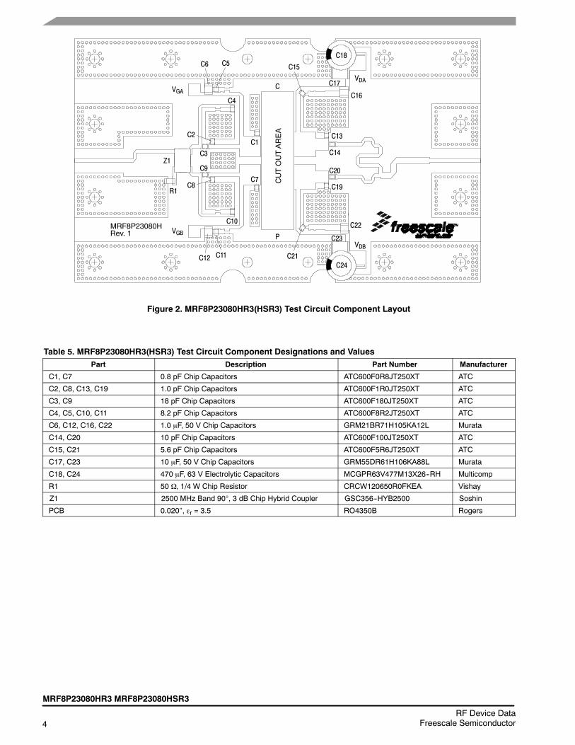
Figure 2. MRF8P23080HR3(HSR3) Test Circuit Component Layout
MRF8P23080HRev. 1
C10
VGA
Z1
CUTOUTAREA
VGB
C6 C5
C4
C2
C3
C9
C8R1
C12 C11
C1
C7
VDBC21
C22
C23
C13
C19
C14
C20
C15
C16
C17VDA
C24
C18
C
P
Table 5. MRF8P23080HR3(HSR3) Test Circuit Component Designations and ValuesPart Description Part Number Manufacturer
C1, C7 0.8 pF Chip Capacitors ATC600F0R8JT250XT ATC
C2, C8, C13, C19 1.0 pF Chip Capacitors ATC600F1R0JT250XT ATC
C3, C9 18 pF Chip Capacitors ATC600F180JT250XT ATC
C4, C5, C10, C11 8.2 pF Chip Capacitors ATC600F8R2JT250XT ATC
C6, C12, C16, C22 1.0 μF, 50 V Chip Capacitors GRM21BR71H105KA12L Murata
C14, C20 10 pF Chip Capacitors ATC600F100JT250XT ATC
C15, C21 5.6 pF Chip Capacitors ATC600F5R6JT250XT ATC
C17, C23 10 μF, 50 V Chip Capacitors GRM55DR61H106KA88L Murata
C18, C24 470 μF, 63 V Electrolytic Capacitors MCGPR63V477M13X26--RH Multicomp
R1 50 Ω, 1/4 W Chip Resistor CRCW120650R0FKEA Vishay
Z1 2500 MHz Band 90°, 3 dB Chip Hybrid Coupler GSC356--HYB2500 Soshin
PCB 0.020″, εr = 3.5 RO4350B Rogers

MRF8P23080HR3 MRF8P23080HSR3
5RF Device DataFreescale Semiconductor
4λ
2
λ
2
λ
4λ
2
λ
2
λ
Single--ended
Quadrature combined
Doherty
Push--pull
4λ4λ 4
λ4λ
Figure 3. Possible Circuit Topologies

6RF Device Data
Freescale Semiconductor
MRF8P23080HR3 MRF8P23080HSR3
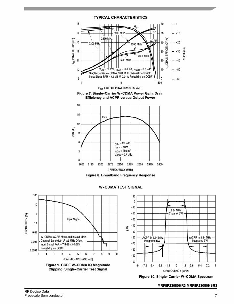
TYPICAL CHARACTERISTICS
2290
ACPR
f, FREQUENCY (MHz)
Figure 4. Output Peak--to--Average Ratio Compression (PARC)Broadband Performance @ Pout = 16 Watts Avg.
14
15
14.9
14.8
--36
44
43
42
41
--26
--28
--30
--32
ηD,DRAIN
EFFICIENCY(%)
Gps,POWER
GAIN(dB) 14.7
14.6
14.5
14.4
14.3
14.2
14.1
2305 2320 2335 2350 2365 2380 2395 2410
40
--34
PARC
PARC(dB)
--2
0
--0.5
--1
--1.5
--2.5
ACPR
(dBc)
Figure 5. Intermodulation Distortion Productsversus Two--Tone Spacing
TWO--TONE SPACING (MHz)
10--70
--20
--30
--40
--60
1 100
IMD,INTERMODULATIONDISTORTION(dBc)
--50IM7--U
Figure 6. Output Peak--to--Average RatioCompression (PARC) versus Output Power
1
Pout, OUTPUT POWER (WATTS)
--1
--3
--520
0
--2
--4
OUTPUTCOMPRESSIONAT
0.01%
PROBABILITY
ONCCDF(dB)
10 30 40 6030
60
55
50
45
40
35
ηD,DRAINEFFICIENCY(%)
--1 dB = 18.6 W
50
ηD
ACPR
PARC
ACPR
(dBc)
--34
--22
--24
--26
--30
--28
--32
17
Gps,POWER
GAIN(dB)
16
15
14
13
12
11
Gps
IM7--L
IM5--U
IM5--L
VDD = 28 Vdc, Pout = 20 W (PEP)IDQA = 280 mA, VGSB = 0.7 Vdc
VDD = 28 Vdc, Pout = 16 W (Avg.), IDQA = 280 mAVGSB = 0.7 Vdc, Single--Carrier W--CDMA
3.84 MHz Channel Bandwidth, Input SignalPAR = 7.5 dB @ 0.01% Probability on CCDF
ηD
IM3--U
Two--Tone Measurements(f1 + f2)/2 = Center Frequency of 2350 MHz
IM3--L
--2 dB = 27.5 W
--3 dB = 37.5 W
VDD = 28 Vdc, IDQA = 280 mA, VGSB = 0.7 Vdc, f = 2350 MHzSingle--Carrier W--CDMA, 3.84 MHz Channel Bandwidth, InputSignal PAR = 7.5 dB @ 0.01% Probability on CCDF
Gps
MRF8P23080HR3 MRF8P23080HSR3
7RF Device DataFreescale Semiconductor
TYPICAL CHARACTERISTICS
1
Gps
ACPR
Pout, OUTPUT POWER (WATTS) AVG.
Figure 7. Single--Carrier W--CDMA Power Gain, DrainEfficiency and ACPR versus Output Power
--10
--20
9
15
0
60
50
40
30
20
ηD,DRAINEFFICIENCY(%)
Gps,POWER
GAIN(dB)
14
13
10 100
10
--60
ACPR
(dBc)
12
11
10
0
--30
--40
--50
Figure 8. Broadband Frequency Response
0
18
2050
f, FREQUENCY (MHz)
VDD = 28 VdcPin = 0 dBmIDQA = 280 mAVGSB = 0.7 Vdc
12
9
6
2125
GAIN(dB)
15Gain
2200 2275 2350 2425 2500 2575 2650
3
VDD = 28 Vdc, IDQA = 280 mA, VGSB = 0.7 Vdc
2300 MHz
2350 MHz
2400 MHz
2300 MHz
2350 MHz2400 MHz
ηD
Single--Carrier W--CDMA, 3.84 MHz Channel BandwidthInput Signal PAR = 7.5 dB @ 0.01% Probability on CCDF
W--CDMA TEST SIGNAL
0.0001
100
0
PEAK--TO--AVERAGE (dB)
Figure 9. CCDF W--CDMA IQ MagnitudeClipping, Single--Carrier Test Signal
10
1
0.1
0.01
0.001
2 4 6 8
PROBABILITY
(%)
W--CDMA. ACPR Measured in 3.84 MHzChannel Bandwidth @ ±5 MHz Offset.Input Signal PAR = 7.5 dB @ 0.01%Probability on CCDF
Input Signal
10
--60
--100
10
(dB)
--20
--30
--40
--50
--70
--80
--90
3.84 MHzChannel BW
7.21.8 5.43.60--1.8--3.6--5.4--9 9
f, FREQUENCY (MHz)
Figure 10. Single--Carrier W--CDMA Spectrum
--7.2
--ACPR in 3.84 MHzIntegrated BW
+ACPR in 3.84 MHzIntegrated BW
--10
0
1 3 5 7 9
8RF Device Data
Freescale Semiconductor
MRF8P23080HR3 MRF8P23080HSR3
VDD = 28 Vdc, IDQA = 280 mA
fMHz
Max Pout (1) ZsourceΩ
ZloadΩWatts dBm
2300 58 47.6 8.42 -- j14.3 3.51 -- j5.02
2350 55 47.4 11.4 -- j13.4 3.75 -- j5.03
2400 55 47.4 17.7 -- j9.34 3.14 -- j5.63
(1) Maximum output power measurement reflects pulsed 1 dB gaincompression.
Zsource = Test circuit impedance as measured from gate contact toground.
Zload = Test circuit impedance as measured from drain contact toground.
Figure 11. Carrier Side Load Pull Performance Maximum P1dB Tuning
Zsource Z load
InputLoad PullTuner
DeviceUnderTest
OutputLoad PullTuner
VDD = 28 Vdc, IDQA = 280 mA
fMHz
Max Eff. (1)
%Zsource
ΩZloadΩ
2300 60.9 8.41 -- j14.3 7.02 -- j3.44
2350 60.1 11.4 -- j13.4 6.84 -- j2.41
2400 60.0 17.7 -- j9.35 6.53 -- j2.92
(1) Maximum efficiency measurement reflects pulsed 1 dB gaincompression.
Zsource = Test circuit impedance as measured from gate contact toground.
Zload = Test circuit impedance as measured from drain contact toground.
Figure 12. Carrier Side Load Pull Performance Maximum Efficiency Tuning
Zsource Z load
DeviceUnderTest
OutputLoad PullTuner
InputLoad PullTuner

MRF8P23080HR3 MRF8P23080HSR3
9RF Device DataFreescale Semiconductor
ALTERNATIVE PEAK TUNE LOAD PULL CHARACTERISTICS
30
Pin, INPUT POWER (dBm)
VDD = 28 Vdc, IDQA = 280 mA,Pulsed CW, 10 μsec(on), 10% Duty Cycle
50
47
38
P out,OUTPUTPOWER
(dBm
)
NOTE: Load Pull Test Fixture Tuned for Peak P1dB Output Power @ 28 V
44
51.5
54.5
37.52422.5
53
41
21
Ideal
Actual
27 33 36
2350 MHz2400 MHz
2300 MHz
48.5
45.5
42.5
39.5
34.531.528.525.5
2350 MHz
2300 MHz2400 MHz
f(MHz)
P1dB P3dB
Watts dBm Watts dBm
2300 59 47.7 69 48.4
2350 58 47.6 68 48.3
2400 54 47.3 68 48.3
Test Impedances per Compression Level
f(MHz)
ZsourceΩ
ZloadΩ
2300 P1dB 8.40 -- j14.3 3.60 -- j5.30
2350 P1dB 11.4 -- j13.4 3.70 -- j5.20
2400 P1dB 17.7 -- j9.30 3.10 -- j5.10
Figure 11. Pulsed CW Output Powerversus Input Power @ 28 V
NOTE: Measurement made on the Class AB, carrier side of the device.
10RF Device Data
Freescale Semiconductor
MRF8P23080HR3 MRF8P23080HSR3
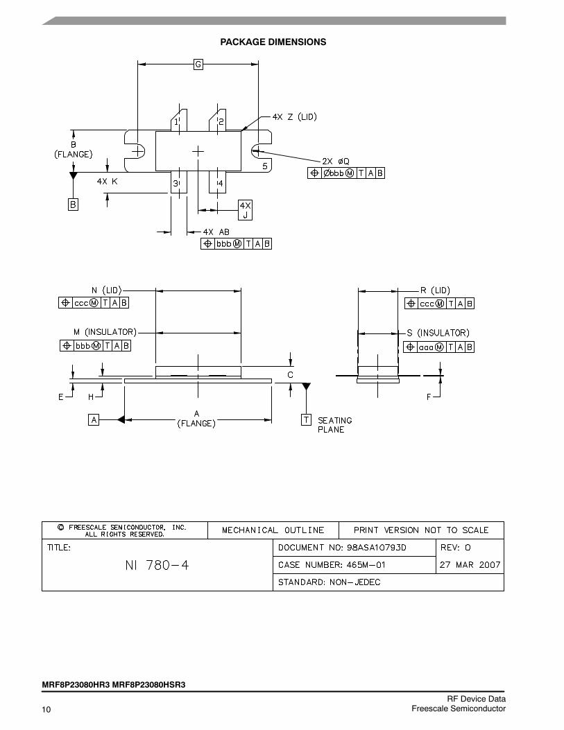
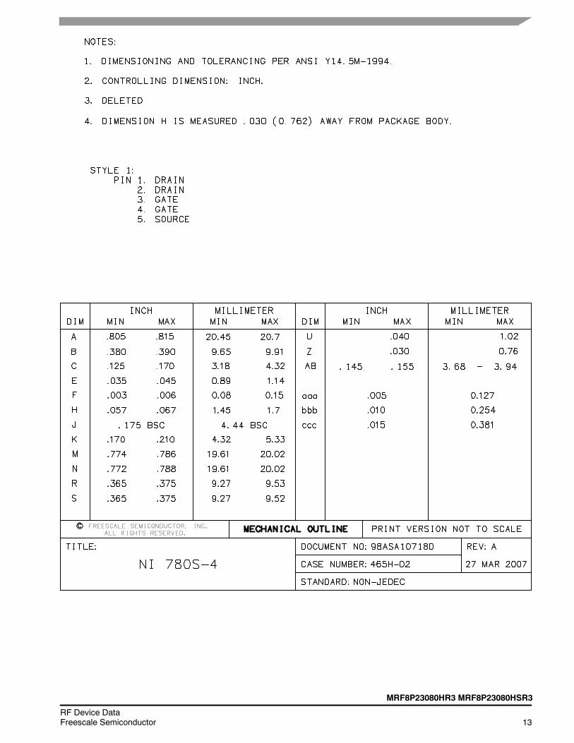
PACKAGE DIMENSIONS

MRF8P23080HR3 MRF8P23080HSR3
11RF Device DataFreescale Semiconductor

12RF Device Data
Freescale Semiconductor
MRF8P23080HR3 MRF8P23080HSR3
MRF8P23080HR3 MRF8P23080HSR3
13RF Device DataFreescale Semiconductor

14RF Device Data
Freescale Semiconductor
MRF8P23080HR3 MRF8P23080HSR3
PRODUCT DOCUMENTATION AND SOFTWARE
Refer to the following documents and software to aid your design process.
Application Notes• AN1955: Thermal Measurement Methodology of RF Power Amplifiers
Engineering Bulletins• EB212: Using Data Sheet Impedances for RF LDMOS Devices
Software• Electromigration MTTF Calculator
• RF High Power Model
• .s2p File
For Software, do a Part Number search at http://www.freescale.com, and select the Part Number link. Go to the Software &Tools tab on the parts Product Summary page to download the respective tool.
REVISION HISTORY
The following table summarizes revisions to this document.
Revision Date Description
0 May 2010 • Initial Release of Data Sheet
1 Nov. 2010 • Updated frequency in overview paragraph from 2300 to 2400 MHz to 2300 to 2620 MHz to show thebroadband performance of the part, p. 1
• In Table 2, Thermal Characteristics, Pout = 16 W CW thermal resistance value changed from 0.91 to0.89_C/W and Pout = 80 W CW thermal resistance value changed from 0.91 to 0.55_C/W. Thermalvalues now reflect the use of the combined dissipated power from the carrier amplifier and peakingamplifier, p. 2.
• Broadband IRL data removed from Fig. 4, Output Peak--to--Average Ratio Compression (PARC)Broadband Performance and Fig. 8, Broadband Frequency Response graphs. Data not valid indicator ofproduct performance due to circuit implementation, p. 6, 7.

MRF8P23080HR3 MRF8P23080HSR3
15RF Device DataFreescale Semiconductor
Information in this document is provided solely to enable system and softwareimplementers to use Freescale Semiconductor products. There are no express orimplied copyright licenses granted hereunder to design or fabricate any integratedcircuits or integrated circuits based on the information in this document.
Freescale Semiconductor reserves the right to make changes without further notice toany products herein. Freescale Semiconductor makes no warranty, representation orguarantee regarding the suitability of its products for any particular purpose, nor doesFreescale Semiconductor assume any liability arising out of the application or use ofany product or circuit, and specifically disclaims any and all liability, including withoutlimitation consequential or incidental damages. Typical parameters that may beprovided in Freescale Semiconductor data sheets and/or specifications can and dovary in different applications and actual performance may vary over time. All operatingparameters, including Typicals, must be validated for each customer application bycustomers technical experts. Freescale Semiconductor does not convey any licenseunder its patent rights nor the rights of others. Freescale Semiconductor products arenot designed, intended, or authorized for use as components in systems intended forsurgical implant into the body, or other applications intended to support or sustain life,or for any other application in which the failure of the Freescale Semiconductor productcould create a situation where personal injury or death may occur. Should Buyerpurchase or use Freescale Semiconductor products for any such unintended orunauthorized application, Buyer shall indemnify and hold Freescale Semiconductorand its officers, employees, subsidiaries, affiliates, and distributors harmless against allclaims, costs, damages, and expenses, and reasonable attorney fees arising out of,directly or indirectly, any claim of personal injury or death associated with suchunintended or unauthorized use, even if such claim alleges that FreescaleSemiconductor was negligent regarding the design or manufacture of the part.
Freescalet and the Freescale logo are trademarks of Freescale Semiconductor, Inc.All other product or service names are the property of their respective owners.© Freescale Semiconductor, Inc. 2010. All rights reserved.
How to Reach Us:
Home Page:www.freescale.com
Web Support:http://www.freescale.com/support
USA/Europe or Locations Not Listed:Freescale Semiconductor, Inc.Technical Information Center, EL5162100 East Elliot RoadTempe, Arizona 852841--800--521--6274 or +1--480--768--2130www.freescale.com/support
Europe, Middle East, and Africa:Freescale Halbleiter Deutschland GmbHTechnical Information CenterSchatzbogen 781829 Muenchen, Germany+44 1296 380 456 (English)+46 8 52200080 (English)+49 89 92103 559 (German)+33 1 69 35 48 48 (French)www.freescale.com/support
Japan:Freescale Semiconductor Japan Ltd.HeadquartersARCO Tower 15F1--8--1, Shimo--Meguro, Meguro--ku,Tokyo 153--0064Japan0120 191014 or +81 3 5437 [email protected]
Asia/Pacific:Freescale Semiconductor China Ltd.Exchange Building 23FNo. 118 Jianguo RoadChaoyang DistrictBeijing 100022China+86 10 5879 [email protected]
For Literature Requests Only:Freescale Semiconductor Literature Distribution Center1--800--441--2447 or +1--303--675--2140Fax: [email protected]
Document Number: MRF8P23080HRev. 1, 11/2010

Mouser Electronics
Authorized Distributor
Click to View Pricing, Inventory, Delivery & Lifecycle Information: Freescale Semiconductor:
MRF8P23080HR5 MRF8P23080HSR5