Modulation of residual stress in diamond like carbon films with incorporation of nanocrystalline...
8
Applied Surface Science 257 (2011) 10451–10458 Contents lists available at ScienceDirect Applied Surface Science j our nal ho me p age: www.elsevier.com/loc ate/apsusc Modulation of residual stress in diamond like carbon films with incorporation of nanocrystalline gold R. Paul 1 , S.R. Bhattacharyya 2 , R. Bhar, A.K. Pal ∗ Department of Instrumentation Science, USIC Building, Jadavpur University, Kolkata 700032, India a r t i c l e i n f o Article history: Received 10 May 2011 Received in revised form 17 June 2011 Accepted 30 June 2011 Available online 7 July 2011 Keywords: Diamond-like carbon Nanocrystalline gold Stress a b s t r a c t Residual stress modulation in the diamond-like carbon coatings with incorporation of gold nanoparticles was studied critically. The films were deposited on glass and Si (1 0 0) substrates by using capacitatively coupled plasma chemical vapor deposition. Stresses in the films were determined from the broadening of the optical absorption tail and were found to decrease from 2.3 GPa to 0.48 GPa with increasing gold content (2–7 at.% Au) in the DLC matrix. Gold incorporation also made the films harder than the corre- sponding DLC coatings. Modulation of stress with nanocrystalline gold content in the DLC matrix was related to the relative amount of sp 2 /sp 3 content in the DLC films. © 2011 Elsevier B.V. All rights reserved. 1. Introduction Realization of thin film coatings having high mechanical quality without cracking, buckling, or delamination [1,2] is very difficult without controlling the residual stress in it. Residual stress, which is also known as intrinsic stress, is developed during the thin films growth process in sputter or evaporation or chemical vapor deposition techniques. Despite the promising mechanical, opti- cal and electrical properties of diamond like carbon (DLC) films [3,4], use of pure DLC films are retarded due to inherent high compressive stresses induced by the sp 3 carbon bonding during the synthesis [5]. Researchers are trying to deposit metal–DLC composite coatings that would combine high hardness, elevated ductility and toughness [6,7] since pure DLC films lacked toughness and resistance to cross-sectional crack propagation [7]. Different deposition techniques [8–12] for the synthesis of metal incorpo- rated DLC films were tried in past but the metal nanoparticles were found to agglomerate during deposition due to high surface energy [11,12]. Ib metal (Cu, Ag, Au) doped DLC composite films by chemical or physical vapor deposition brought hope for a new tri- bological materials [13,14] but the dispersion of metal uniformly in nanocrystalline form was found hard to realize. Ahmed et al. [15] and Paul et al. [16,17] reported successful attempts to deposit nanocrystalline silver and gold incorporated DLC films, which ∗ Corresponding author. Tel.: +91 33 241 46321; fax: +91 33 241 46584. E-mail address: [email protected] (A.K. Pal). 1 Present address: Birck Nanotechnology Center, Purdue University, IN, USA. 2 Present address: Departamento de Fisica, Instituto Superior Tecnico, Universi- dade Tecnica de Lisboa, Portugal. showed enhanced surface plasmon [16,17] as well as electronic field enhancement [15] properties. Wang et al. [18] synthesized silver-DLC composite films in a mid-frequency dual magnetron system and reported the modulation of mechanical properties of DLC films with silver incorporation. During the above period, a consorted effort was given by Yu et al. [19–21] for the synthesis of chromium and silver doped DLC films and related tribological properties of Cr–DLC and Ag–DLC coatings were studied critically. In this communication, we present our studies on the mod- ulation of residual stress in DLC with the incorporation of nanocrystalline gold particles. The above composite films were pre- pared by capacitatively coupled plasma (CCP) CVD while stresses in these coatings were determined from the broadening of the opti- cal absorption tail in a nondestructive way. We have examined the possibility of reducing stress by the incorporation of metal particles in the DLC matrix. 2. Experimental Nanocrystalline gold incorporated DLC films were deposited at room temperature by r.f CCP-CVD cum sputtering technique. The details of the deposition technique have been published elsewhere [16]. Gold (Au) content in the DLC matrix was varied by varying argon content in the premixed methane + argon precursor gas mix- tures. Films were deposited with four different proportions of argon (50%, 60%, 70% and 80%). All the films were deposited at 100 W r.f power onto glass and Si (1 0 0). For comparison, pure DLC films were also deposited under same experimental conditions as Au–DLC films except the gold target. Microstuctural studies were carried out by a transmission elec- tron microscope (TEM). Optical absorbance were recorded in the 0169-4332/$ – see front matter © 2011 Elsevier B.V. All rights reserved. doi:10.1016/j.apsusc.2011.06.144
-
Upload
independent -
Category
Documents
-
view
1 -
download
0
Transcript of Modulation of residual stress in diamond like carbon films with incorporation of nanocrystalline...

Mo
RD
a
ARRAA
KDNS
1
wwifidc[ctcdadrwecbi[n
d
0d
Applied Surface Science 257 (2011) 10451– 10458
Contents lists available at ScienceDirect
Applied Surface Science
j our nal ho me p age: www.elsev ier .com/ loc ate /apsusc
odulation of residual stress in diamond like carbon films with incorporationf nanocrystalline gold
. Paul1, S.R. Bhattacharyya2, R. Bhar, A.K. Pal ∗
epartment of Instrumentation Science, USIC Building, Jadavpur University, Kolkata 700032, India
r t i c l e i n f o
rticle history:eceived 10 May 2011eceived in revised form 17 June 2011
a b s t r a c t
Residual stress modulation in the diamond-like carbon coatings with incorporation of gold nanoparticleswas studied critically. The films were deposited on glass and Si (1 0 0) substrates by using capacitativelycoupled plasma chemical vapor deposition. Stresses in the films were determined from the broadening
ccepted 30 June 2011vailable online 7 July 2011
eywords:iamond-like carbonanocrystalline gold
of the optical absorption tail and were found to decrease from 2.3 GPa to 0.48 GPa with increasing goldcontent (2–7 at.% Au) in the DLC matrix. Gold incorporation also made the films harder than the corre-sponding DLC coatings. Modulation of stress with nanocrystalline gold content in the DLC matrix wasrelated to the relative amount of sp2/sp3 content in the DLC films.
© 2011 Elsevier B.V. All rights reserved.
tress
. Introduction
Realization of thin film coatings having high mechanical qualityithout cracking, buckling, or delamination [1,2] is very difficultithout controlling the residual stress in it. Residual stress, which
s also known as intrinsic stress, is developed during the thinlms growth process in sputter or evaporation or chemical vaporeposition techniques. Despite the promising mechanical, opti-al and electrical properties of diamond like carbon (DLC) films3,4], use of pure DLC films are retarded due to inherent highompressive stresses induced by the sp3 carbon bonding duringhe synthesis [5]. Researchers are trying to deposit metal–DLComposite coatings that would combine high hardness, elevateductility and toughness [6,7] since pure DLC films lacked toughnessnd resistance to cross-sectional crack propagation [7]. Differenteposition techniques [8–12] for the synthesis of metal incorpo-ated DLC films were tried in past but the metal nanoparticlesere found to agglomerate during deposition due to high surface
nergy [11,12]. Ib metal (Cu, Ag, Au) doped DLC composite films byhemical or physical vapor deposition brought hope for a new tri-ological materials [13,14] but the dispersion of metal uniformly
n nanocrystalline form was found hard to realize. Ahmed et al.15] and Paul et al. [16,17] reported successful attempts to depositanocrystalline silver and gold incorporated DLC films, which
∗ Corresponding author. Tel.: +91 33 241 46321; fax: +91 33 241 46584.E-mail address: [email protected] (A.K. Pal).
1 Present address: Birck Nanotechnology Center, Purdue University, IN, USA.2 Present address: Departamento de Fisica, Instituto Superior Tecnico, Universi-ade Tecnica de Lisboa, Portugal.
169-4332/$ – see front matter © 2011 Elsevier B.V. All rights reserved.oi:10.1016/j.apsusc.2011.06.144
showed enhanced surface plasmon [16,17] as well as electronicfield enhancement [15] properties. Wang et al. [18] synthesizedsilver-DLC composite films in a mid-frequency dual magnetronsystem and reported the modulation of mechanical properties ofDLC films with silver incorporation. During the above period, aconsorted effort was given by Yu et al. [19–21] for the synthesisof chromium and silver doped DLC films and related tribologicalproperties of Cr–DLC and Ag–DLC coatings were studied critically.
In this communication, we present our studies on the mod-ulation of residual stress in DLC with the incorporation ofnanocrystalline gold particles. The above composite films were pre-pared by capacitatively coupled plasma (CCP) CVD while stresses inthese coatings were determined from the broadening of the opti-cal absorption tail in a nondestructive way. We have examined thepossibility of reducing stress by the incorporation of metal particlesin the DLC matrix.
2. Experimental
Nanocrystalline gold incorporated DLC films were deposited atroom temperature by r.f CCP-CVD cum sputtering technique. Thedetails of the deposition technique have been published elsewhere[16]. Gold (Au) content in the DLC matrix was varied by varyingargon content in the premixed methane + argon precursor gas mix-tures. Films were deposited with four different proportions of argon(50%, 60%, 70% and 80%). All the films were deposited at 100 W r.fpower onto glass and Si (1 0 0). For comparison, pure DLC films were
also deposited under same experimental conditions as Au–DLCfilms except the gold target.Microstuctural studies were carried out by a transmission elec-tron microscope (TEM). Optical absorbance were recorded in the
1 e Science 257 (2011) 10451– 10458
w(pCpRwtaraastMmAuctfigtthmT
3
aittdaemtbcmt
3
dsdpw(ttbs
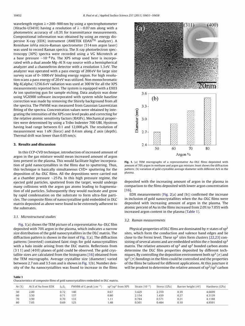
Fig. 1. (a) TEM micrographs of a representative Au–DLC films deposited with
TC
0452 R. Paul et al. / Applied Surfac
avelength region � = 200–900 nm by using a spectrophotometerHitachi-U3410) having a resolution of � ∼ 0.07 nm along with ahotometric accuracy of ±0.3% for transmittance measurements.ompositional information was obtained by using an energy dis-ersive X-ray (EDX) instrument (AMETEK EDAXTSL analyzer). Aenishaw inVia micro-Raman spectrometer (514 nm argon laser)as used to record Raman spectra. The X-ray photoelectron spec-
roscopy (XPS) spectra were recorded using a VG Microtech at base pressure ∼10−8 Pa. The XPS setup used here is incorpo-ated with a dual anode Mg–Al X-ray source with a hemisphericalnalyzer and a channeltron detector with a resolution 1.3 eV. Thenalyzer was operated with a pass energy of 200 eV for large sizeurvey scan of 0–1000 eV binding energy region. For high resolu-ion scans a pass energy of 20 eV was utilized. Non monochromatic
g-K(alpha) 1256.6 eV radiation was used at 300 W for all the XPSeasurements reported here. The system is equipped with a EX03r ion sputtering gun for sample etching. Data analysis was donesing VGX900 software incorporated with system while baselineorrection was made by removing the Shirely background from allhe spectra. The FWHM was measured from Gaussian Laurentziantting of the spectra. Concentration values were obtained by inte-rating the intensities of the XPS core level peaks and correcting forhe relative atomic sensitivity factors (RASFs). Mechanical proper-ies were determined by using a Tribo Indenter 700 UBI, Hysitronaving load range between 0.1 and 12,000 �N. The resolution ofeasurement was 1 nN (force) and 0.4 nm along Z axis (depth).
hermal drift was lower than 0.05 nm/s.
. Results and discussion
In this CCP-CVD technique, introduction of increased amount ofrgon in the gas mixture would mean increased amount of argonons present in the plasma. This would facilitate higher incorpora-ion of gold nanocrystallites in the films due to sputtering. Thus,his technique is basically simultaneous CVD+ sputtering for theeposition of Au–DLC films. All the depositions were carried outt a chamber pressure ∼25 Pa. In this high pressure regime, thejected gold particles, sputtered from the target, would undergoany collisions with the argon gas atoms leading to fragmenta-
ion of old particles. Subsequently they would nucleate and growy rapid condensation on the substrate to form ultra-fine parti-les. The composite films of nanocrystalline gold embedded in DLCatrix deposited as above were found to be extremely adherent to
he substrates.
.1. Microstructural studies
Fig. 1(a) shows the TEM picture of a representative Au–DLC filmeposited with 70% argon in the plasma, which indicates a narrowize distribution of the gold nanocrystallites in the DLC matrix. Theiffraction pattern is shown in the inset of Fig. 1(a). The diffractionatterns (inverted) contained faint rings for gold nanocrystallitesith a halo inside arising from the DLC matrix. Reflections from
3 1 1) and (4 0 0) planes of gold could be observed. The gold crys-
allite sizes are calculated from the histograms [16] obtained fromhe TEM micrographs. Average crystallite size (diameter) variedetween 2.7 nm and 3.5 nm and is shown in Fig. 1(b). Number den-ity of the Au nanocrystallites was found to increase in the filmsable 1haracteristics of composite films of gold nanocrystallites embedded in DLC matrix.
Ar (%) At.% of Au from EDX ID/IG FWHM of G peak (cm−1) sp2/sp3 from X
50 2.00 0.72 140 0.67
60 3.50 0.71 137 0.80
70 3.90 0.70 133 1.11
80 7.05 0.69 125 1.48
amount of 70% argon in methane and argon gas mixture. Inset shows the diffractionpattern; (b) variation of gold crystallite average diameter with different Ar% in theplasma.
deposited with the increasing amount of argon in the plasma incomparison to the films deposited with lower argon concentration[16].
EDX measurements (Fig. 2(a) and (b)) confirmed the increasein inclusion of gold nanocrystallites when the Au–DLC films weredeposited with increasing amount of argon in the plasma. Theatomic percent of Au in the films increased from 2.0% to 7.05% withincreased argon content in the plasma (Table 1).
3.2. Raman measurements
Physical properties of DLC films are dominated by � states of sp2
sites, which form the conduction and valence band edges and lieclose to the Fermi level. These sp2 sites form clusters [22,23] con-sisting of several atoms and are embedded within the � bonded sp3
matrix. The relative amounts of sp3 and sp2 bonded carbon atomsdetermine the DLC film properties deposited by different tech-
niques. By controlling the deposition environment both sp3 (�) andsp2 (�) bondings in the films could be controlled and the propertiesof the films be tailored for different applications. At this juncture itwill be prudent to determine the relative amount of sp2/sp3 carbonPS Strain (10−2) Stress (GPa) Barrier height (eV) Hardness (GPa)
3.429 2.359 0.39 4.66992.154 1.439 0.27 4.31390.784 0.571 0.21 4.11880.501 0.484 0.10 4.9591
R. Paul et al. / Applied Surface Science 257 (2011) 10451– 10458 10453
F8
ct
Api(titawac
([Iwlh
three deconvoluted peaks (Fig. 4(a) and (b)) under C(1s) spec-
TC
ig. 2. EDX spectrum for two representative films deposited with (a) 50% and (b)0% argon in the plasma.
ontent in the films in order to reflect possible correlation betweenhe observed physical properties with sp2/sp3 content.
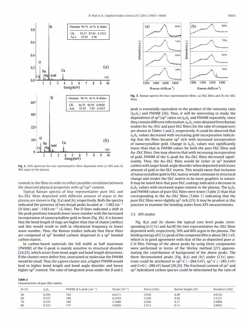
Typical Raman spectra of four representative pure DLC andu–DLC films deposited with different amount of argon in thelasma are shown in Fig. 3(a) and (b), respectively. Both the spectra
ndicated the presence of two broad peaks located at ∼1382 cm−1
D-line) and ∼1583 cm−1 (G-line). The D-lines indicated a shift inhe peak positions towards lower wave number with the increasedncorporation of nanocrystalline gold in them (Fig. 2b). It is knownhat the bond length of rings are higher than that of chains (olefins)nd this would result in shift in vibrational frequency to lowerave number. Thus, the Raman studies indicate that these films
re composed of sp2 bonded carbons dispersed in a sp3 bondedarbon matrix.
In carbon-based materials the full width at half maximumFWHM) of the G-peak is mainly sensitive to structural disorder24,25], which arises from bond angle and bond length distortions.f the clusters were defect free, unstrained or molecular the FWHM
ould be small. Thus, for a given cluster size, a higher FWHM wouldead to higher bond length and bond angle disorder and henceigher sp3 content. The ratio of integrated areas under the D and G
able 2haracteristics of pure DLC matrix.
Ar (%) ID/IG FWHM of G peak (cm−1) Strain (10−2)
50 0.595 192 6.6111
60 0.557 190 6.2543
70 0.533 186 5.7680
80 0.523 177 5.6956
Fig. 3. Raman spectra for four representative films: (a) DLC films and (b) Au–DLCfilms.
peak is essentially equivalent to the product of the intensity ratio(ID/IG) and FWHM [26]. Thus, it will be interesting to study thedependence of sp2/sp3 ratios on ID/IG and FWHM separately, sincethey contain different information. ID/IG ratio obtained from Ramanstudies for Au–DLC and pure DLC films (for the sake of comparison)are shown in Tables 1 and 2, respectively. It could be observed thatID/IG values decreased with increasing gold incorporation indicat-ing that the films became sp2 rich with increased incorporationof nanocrystalline gold. Change in ID/IG values was significantlylower than that in FWHM values for both the pure DLC films andAu–DLC films. One may observe that with increasing incorporationof gold, FWHM of the G-peak for Au–DLC films decreased signif-icantly. Thus, the Au–DLC films would be richer in sp3 bondedcarbon with larger bond-angle disorder when deposited with lesseramount of gold in the DLC matrix. This would mean that inclusionof nanocrystalline gold in DLC matrix would culminate in structuralchange and render the DLC matrix to be more graphitic in nature.It may be noted here that pure DLC coatings indicated a decrease inID/IG values with increased argon content in the plasma. The ID/IGand FWHM values of pure DLC films were lower (Table 2) than thatcorresponding to the Au–DLC films (Table 1) indicating that thepure DLC films were slightly sp3 rich [25]. It may be prudent at thisjuncture to examine the bonding states from XPS measurements.
3.3. XPS studies
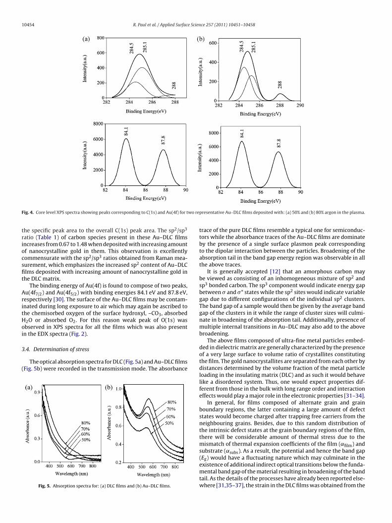
Fig. 4(a) and (b) shows the typical core level peaks corre-sponding to C(1s) and Au(4f) for two representative Au–DLC filmsdeposited with, respectively, 50% and 80% argon in the plasma. Thebinding energy of C(1s) peak of the composite film is about 285.1 eV,which is in good agreement with that of the as-deposited pure a-C:H film. Fittings of the above peaks by using three componentswere performed in terms of the Shirley method [27] approxi-mating the contribution of background of the above peaks. The
trum could be attributed to sp2-C (∼284.5 eV), sp3-C (∼285.1 eV)and C O (∼288 eV) band [28,29]. The fractional content of sp2 andsp3 hybridized carbon species could be determined by the ratio of
Stress (GPa) Barrier height (eV) Hardness (GPa)
3.918 0.47 4.91353.250 0.28 3.51212.428 0.17 2.98062.513 0.11 3.0855
10454 R. Paul et al. / Applied Surface Science 257 (2011) 10451– 10458
F wo re
triocsfit
AritHoi
3
(
ig. 4. Core level XPS spectra showing peaks corresponding to C(1s) and Au(4f) for t
he specific peak area to the overall C(1s) peak area. The sp2/sp3
atio (Table 1) of carbon species present in these Au–DLC filmsncreases from 0.67 to 1.48 when deposited with increasing amountf nanocrystalline gold in them. This observation is excellentlyommensurate with the sp2/sp3 ratios obtained from Raman mea-urement, which emphasizes the increased sp2 content of Au–DLClms deposited with increasing amount of nanocrystalline gold inhe DLC matrix.
The binding energy of Au(4f) is found to compose of two peaks,u(4f7/2) and Au(4f5/2) with binding energies 84.1 eV and 87.8 eV,espectively [30]. The surface of the Au–DLC films may be contam-nated during long exposure to air which may again be ascribed tohe chemisorbed oxygen of the surface hydroxyl, –CO3, absorbed2O or absorbed O2. For this reason weak peak of O(1s) wasbserved in XPS spectra for all the films which was also presentn the EDX spectra (Fig. 2).
.4. Determination of stress
The optical absorption spectra for DLC (Fig. 5a) and Au–DLC filmsFig. 5b) were recorded in the transmission mode. The absorbance
Fig. 5. Absorption spectra for: (a) DLC films and (b) Au–DLC films.
presentative Au–DLC films deposited with: (a) 50% and (b) 80% argon in the plasma.
trace of the pure DLC films resemble a typical one for semiconduc-tors while the absorbance traces of the Au–DLC films are dominateby the presence of a single surface plasmon peak correspondingto the dipolar interaction between the particles. Broadening of theabsorption tail in the band gap energy region was observable in allthe above traces.
It is generally accepted [12] that an amorphous carbon maybe viewed as consisting of an inhomogeneous mixture of sp2 andsp3 bonded carbon. The sp3 component would indicate energy gapbetween � and �* states while the sp2 sites would indicate variablegap due to different configurations of the individual sp2 clusters.The band gap of a sample would then be given by the average bandgap of the clusters in it while the range of cluster sizes will culmi-nate in broadening of the absorption tail. Additionally, presence ofmultiple internal transitions in Au–DLC may also add to the abovebroadening.
The above films composed of ultra-fine metal particles embed-ded in dielectric matrix are generally characterized by the presenceof a very large surface to volume ratio of crystallites constitutingthe film. The gold nanocrystallites are separated from each other bydistances determined by the volume fraction of the metal particleloading in the insulating matrix (DLC) and as such it would behavelike a disordered system. Thus, one would expect properties dif-ferent from those in the bulk with long range order and interactioneffects would play a major role in the electronic properties [31–34].
In general, for films composed of alternate grain and grainboundary regions, the latter containing a large amount of defectstates would become charged after trapping free carriers from theneighbouring grains. Besides, due to this random distribution ofthe intrinsic defect states at the grain boundary regions of the film,there will be considerable amount of thermal stress due to themismatch of thermal expansion coefficients of the film (˛film) andsubstrate (˛subs). As a result, the potential and hence the band gap(Eg) would have a fluctuating nature which may culminate in the
existence of additional indirect optical transitions below the funda-mental band gap of the material resulting in broadening of the bandtail. As the details of the processes have already been reported else-where [31,35–37], the strain in the DLC films was obtained from the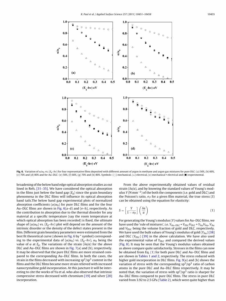
R. Paul et al. / Applied Surface Science 257 (2011) 10451– 10458 10455
F erent( (©) m
blipbaAtmwsifibivDIpsfineci
ig. 6. Variation of �/�0 vs. (Eg–h�) for four representative films deposited with diffc) 70% and (d) 80% and for Au–DLC: (e) 50%, (f) 60%, (g) 70% and (h) 80%. Symbols:
roadening of the below band edge optical absorption studies as outined in Refs. [31–35]. We have considered the optical absorptionn the films just below the band gap (Eg) since the grain boundaryhenomena in the DLC films will influence its optical absorptionand tails.The below band gap experimental plots of normalizedbsorption coefficients (˛/˛0) for pure DLC films and for the fouru–DLC films are shown in Fig. 6(a–d) and (e–h), respectively. As
he contribution to absorption due to the thermal disorder for anyaterial at a specific temperature (say the room temperature athich optical absorption has been recorded) is fixed, the ultimate
hape of (˛/˛0) vs. (Eg–h�) plot will depend on the amount of thentrinsic disorder or the density of the defect states present in thelm. Different grain boundary parameters were estimated from theest fit theoretical curve (shown in Fig. 6 by * symbol) correspond-
ng to the experimental data of (˛/˛0) vs. (Eg–h�), ˛0 being thealue of ̨ at Eg. The variations of the strain (ıa/a) for the aboveLC and Au–DLC films are shown in Fig. 7(a) and (b), respectively.
t may be observed that the pure DLC films are more strained com-ared to the corresponding Au–DLC films. In both the cases, thetrain in the films decreased with increasing sp2/sp3 content in thelms and the DLC films became more strain relieved with increased
anocrystalline gold incorporation. At this juncture it will be inter-sting to cite the works of Yu et al. who also observed that intrinsicompressive stress decreased with chromium [19] and silver [20]ncorporation.amount of argon in methane and argon gas mixtures for pure DLC: (a) 50%, (b) 60%,echanical, (�) electrical, (�) mechanical + electrical and (�) experimental.
From the above experimentally obtained values of residualstrain (ıa/a), and by knowing the standard values of Young’s mod-ulus Y (N mm−2) of the both the components (i.e. gold and DLC) andthe Poisson’s ratio, �P for a given film material, the true stress (S)can be obtained using the equation for elasticity:
S =[
Y
1 − �P
](ıa
a
)(1)
For generating the Young’s modulus (Y) values for Au–DLC films, wehave used the ‘rule of mixtures’, i.e. YAu–DLC = YDLCVDLC + YAuVAu, VAuand VDLC being the volume fraction of gold and DLC, respectively.We have used the bulk values of Young’s modulus of gold (YAu) [38]and DLC (YDLC) [39] in the above calculation. We have also usedthe experimental value of YDLC and compared the derived values(Fig. 8). It may be seen that the Young’s modulus values obtainedas above compare quite satisfactorily. Stresses in the films can nowbe obtained from Eq. (1) for both pure DLC and Au–DLC films andare shown in Tables 1 and 2, respectively. The stress reduced withhigher gold incorporation in DLC films. Fig. 9(a) and (b) shows thevariation of stress with the corresponding sp2/sp3 ratio of carbon
atoms in the pure DLC and Au–DLC films respectively. It may benoted that, the variation of stress with sp2/sp3 ratio is sharper forAu–DLC films compared to pure DLC films. The stress in pure DLCvaried from 3.92 to 2.5 GPa (Table 2), which were quite higher than
10456 R. Paul et al. / Applied Surface Science 257 (2011) 10451– 10458
(Conti
t2ificipe
pebamf
S
wsdtp
Fig. 6.
hat in Au–DLC films which showed a variation in stress between.36 and 0.49 GPa (Table 1) with nanocrystalline gold incorporation
n the DLC matrix. Yu et al. [20] obtained stress values for Ag–DLClms varying between 1.2 MPa and 3.0 MPa with decreasing silverontent in the DLC matrix. Thus, it is evident that gold incorporationn DLC films made them more graphitic by increasing the sp2 pro-ortion in them and the films got relief of stress to an appreciablextent.
This should be mentioned here that, in the presence of Peierlsotential, the lattice distortion cannot move easily under a smallxternally applied stress field. A critically applied stress (S*) has toe applied just to move the dislocation over this potential withoutny assistance from thermal or quantum lattice vibration. This ulti-ate tensile stress also called the “Peierls Stress” can be obtained
rom the discrete dislocation model [40] and is given by:
∗ ={
2�
1 − �P
}exp
{ −�h
(1 − �P)b
}(2)
here � = Y/[2(1 + �P)] is the shear modulus, b ≈ a[1 + ıa/a], the ten-
ile stress, which represents the magnitude of the Burger vector,enoting the slip direction and h is a quantity, of the order ofhe lattice parameter which represents the spacing across the sliplane.nued. )
It is known that a relation between the ultimate tensile stress(S*) and the Vickers hardness (HV) corresponding to an arbitraryindentation strain (x%) could be expressed as [41–43]:
HV = 2.9S∗
(36.8nc/x)nc (3)
where nc, the strain hardening coefficient, can be obtained by solv-ing the equation
S
S∗ =[
2.718(ıa/a)nc
]nc
(4)
A simple computer simulation was carried out to obtain the Vickershardness of Au–DLC and DLC thin film. From Eqs. (1) and (2), oneobtains:
S
S∗ ={(
ıa
a
)(1 + �P)
}exp
{(�
(1 + ıa/a)
)(1 − �P)
}(5)
Knowing the values of Youngs modulus (Y), Poissons ratio (�P),and with the help of Eq. (5), Eq. (4) was solved using theNewton–Raphson iteration technique to obtain the strain harden-ing coefficient (nc) correct upto the desired decimal places and this
nc was subsequently utilized in Eq. (3) along with calculated S* toget the Vickers hardness for the concerned materials. The values oftheoretically obtained Vickers hardness for the films deposited atdifferent argon percent are tabulated in Tables 1 and 2. It might be
R. Paul et al. / Applied Surface Science 257 (2011) 10451– 10458 10457
Fd
spipb
thiVblaAItd
Fe
Fig. 9. Variation of stress in (a) DLC films with sp2/sp3 ratio and (b) Au–DLC filmswith Au volume fraction and with sp2/sp3 ratio.
ig. 7. Variation of strain (ıa/a) for four representative (a) DLC and (b) Au–DLC filmseposited with different amount of argon in methane and argon gas mixtures.
een that most of the Au–DLC films had little higher hardness com-ared to the pure DLC ones except the film deposited with 50% Ar
n the plasma. The observed increase in hardness with gold incor-oration (up to 7 at.% Au) is in commensurate with that observedy Yu et al. [20] for Ag–DLC films.
It will be interesting to compare the above observation withhe measured ones with a Tribo Indenter 700 UBI, Hysitron. Theardness of the DLC films was determined from the measured
ndentation curve assuming a perfect geometry of the diamondickers indenter and making the correction for the tip bluntingy extrapolating the unloading curve from the maximum applied
oad, Pmax to zero load (not shown here). The hardness evaluateds above for a maximum load ∼1000 �N are shown in Fig. 10 foru–DLC films along with that evaluated from optical measurement.
t may be observed that the hardness values obtained from optical
echnique compares well with that measured directly by a nanoin-enter.ig. 8. Young’s modulus of Au–DLC films evaluated from the rule of mixtures andxperimentally obtained values.
Fig. 10. Hardness values of the Au–DLC from optical measurement and direct mea-surement.
4. Conclusions
Au–DLC composite films with various volume fractions ofnanoparticulated gold were prepared by using CCP-CVD tech-
nique. Gold nanocrystallite size increased from 2.7 nm to 3.5 nm forfilms deposited with increasing amount of gold in the DLC matrix.Raman studies indicated the presence of two broad peaks locatedat ∼1382 cm−1 (D-line) and ∼1583 cm−1 (G-line). Both the D- and
1 e Scien
GnsXtfdhi
A
(cDh
R
[[[
[
[
[[[
[[
[[[[[
[[
[
[[
[[[
[[
[
[[[
[[
0458 R. Paul et al. / Applied Surfac
-lines indicated a shift in the peak positions towards higher waveumber with the incorporation of nanocrystalline gold in them. Thep2/sp3 ratios of the hybridized carbon atoms were estimated fromPS spectra. Residual stresses in these films were evaluated from
he broadening of the band tail of the absorption spectra as well asrom direct measurements of hardness by commercially availableepth sensing indentometer. It was observed that pure DLC filmsad the higher stress and the films became stress relieved with the
ncorporation of nanocrystalline gold.
cknowledgements
The authors like to thank the University Grants CommissionUGC), Government of India, for extending financial assistance inarrying out this programme. Thanks are due to Dr. Arjun Dey andr. Anoop Kumar Mukhopadhyay, CGCRI, Kolkata, India for theirelp in the nanoindentation measurements.
eferences
[1] L.B. Freund, S. Suresh, Thin Film Materials: Stress, Defect Formation and SurfaceEvolution, Cambridge University Press, 2004.
[2] D.C. Meyer, A. Klingner, T. Holz, P. Paufler, Appl. Phys. A: Mater. Sci. Process. 69(1999) 657.
[3] J.C. Angus, Y. Wang, M. Sunkara, Annu. Rev. Mater. Sci. 21 (1991) 221–248.[4] J.C. Angus, P. Koidl, S. Domiz, in: J. Mort, F. Jansen (Eds.), Plasma Deposited Thin
Films, CRC Press, Boca Raton, FL, 1986, pp. 89–127.[5] P.C.T. Ha, D.R. McKenzie, M.M.M. Bilek, S.C.H. Kwok, Surf. Coat. Technol. 201
(2007) 6734.[6] A.A. Voevodin, J.S. Zabinski, Supertough, Thin Solid Films 370 (2000)
223–231.[7] A.A. Voevodin, S.D. Walck, J.S. Zabinski, Wear 203–204 (1997) 516–527.[8] T.F. Jaramillo, S.-H. Baeck, B.R. Cuenya, E.W. McFarlan, J. Am. Chem. Soc. 125
(2003) 7148–7149.
[9] J. Ye, K. Bonroy, D. Nelis, F. Frederix, J. D’Haenc, G. Maesb, Colloids Surf. A:Physicochem. Eng. Aspects 321 (2008) 313–317.10] I. Tanahashi, H. Iwagishi, G. Chang, Mater. Lett. 62 (2008) 2714–2716.11] A. Henglein, A.D. Meisel, Langmuir 14 (1998) 7392–7396.12] F. Kim, J.H. Song, P. Yang, J. Am. Chem. Soc. 124 (2002) 14316–14317.
[[
[
ce 257 (2011) 10451– 10458
13] K.I. Schiffmann, M. Fryda, G. Goerigk, R. Laure, P. Hinze, A. Bulack, Thin SolidFilms 347 (1999) 60–71.
14] I. Gerhards, C. Ronning, H. Hofsass, M. Seibt, H. Gibhard, J. Appl. Phys. 93 (2003)1203–1207.
15] S.F. Ahmed, M.W. Moon, K.R. Lee, Appl. Phys. Lett. 92 (2008) 193502–193504.16] R. Paul, S. Hussain, A.K. Pal, Appl. Surf. Sci. 255 (2009) 8076–8083.17] R. Paul, R.N. Gayen, S. Hussain, V. Khanna, R. Bhar, A.K. Pal, Eur. Phys. J. Appl.
Phys. 47 (2009) 10502–10513.18] C. Wang, X. Yu, M. Hua, Appl. Surf. Sci. 256 (2009) 1431–1435.19] X. Yu, C. Wang, M. Hua, Y. Liu, D. Yu, J. Nanosci. Nanotechnol. 10 (2010)
5379–5382.20] X. Yu, M. Hua, C. Wang, Y. Liu, J. Nanosci. Nanotechnol. 9 (2009) 6366–6371.21] X. Yu, C. Wang, Y. Liu, D. Yu, Diamond Relat. Mater. 15 (2006) 1223–1227.22] J. Robertson, O. Reilly, Phys. Rev. B 35 (1987) 2946–2957.23] J. Robertson, Adv. Phys. 35 (1986) 317–374.24] G. Sanchez, J. Servat, P. Gorostiza, M.C. Polo, W.L. Wang, J. Esteve, Diamond
Relat. Mater. 5 (1996) 592–597.25] A.C. Ferrari, J. Robertson, Phys. Rev. B 61 (2000) 14095–14106.26] T. Heitz, B. Dreı̌villon, C. Godet, J.E. Boureı̌e, Phys. Rev. B 58 (1998)
13957–13973.27] V. Anitaa, T. Butudac, T. Maedad, K. Takizawad, N. Saitoe, O. Takaib, Diamond
Relat. Mater. 13 (2004) 1993.28] T.T. Darrah, P. Weightman, Phys. Rev. B 58 (1998) 13957.29] T.Y. Leung, W.F. Man, P.K. Lim, W.C. Chan, F. Gaspari, S. Zukotyski, J. Non-Cryst.
Solids 254 (1999) 156.30] G. Chen, J. Zhang, S. Yang, Electrochem. Commun. 9 (2007) 1053.31] A.B. Maity, S. Chaudhuri, A.K. Pal, Phys. Stat. Sol. B 183 (1994) 185–191.32] C. Kisielowski, J. Kruger, S. Ruvimov, T. Suski, J.W. Ager III, E. Jones, Z.L. Weber,
M. Rubin, E.R. Weber, Phys. Rev. B 54 (1996) 17745–17753.33] O. Lagerstedt, B. Monemar, Phys. Rev. B 19 (1979) 3064–3071.34] G.J. Leusink, T.G.M. Oosterlaken, G.C.A.M. Janssen, S. Radelaar, J. Appl. Phys. 74
(1993) 3899–3910.35] M. Basu, J. Dutta, S. Chaudhuri, A.K. Pal, M. Nakayama, Vacuum 47 (1996)
233–238.36] J. Szczyrbowski, Phys. Stat. Sol. B 105 (1981) 515–524.37] V.I. Gavrilenko, Phys. Stat. Sol. B 139 (1987) 457–466.38] W.F. Smith, J. Hashemi, R. Prakash, Materials Science and Engineering, Tata
McGraw Hill, New Delhi, 2008, p. 879.39] J. Fontaine, J. Eng. Tribol. Proc. IMechE 222 (2007) 1015–1029.40] K. Oshawa, H. Koizumi, H.O.K. Kirchnen, T. Suzuki, Philos. Mag. A 69 (1994)
171–181.41] D. Tabor, J. Inst. Met. 79 (1951) 1–18.42] S.C. Chang, M.T. Jahn, C.M. Wan, J.Y.M. Lee, T.K. Hsu, J. Mater. Sci. 11 (1976)
623–630.43] M.O. Lai, K.B. Lim, J. Mater. Sci. 26 (1991) 2031–2036.