Modelling of hot carrier solar cell absorbers
7
This article appeared in a journal published by Elsevier. The attached copy is furnished to the author for internal non-commercial research and education use, including for instruction at the authors institution and sharing with colleagues. Other uses, including reproduction and distribution, or selling or licensing copies, or posting to personal, institutional or third party websites are prohibited. In most cases authors are permitted to post their version of the article (e.g. in Word or Tex form) to their personal website or institutional repository. Authors requiring further information regarding Elsevier’s archiving and manuscript policies are encouraged to visit: http://www.elsevier.com/copyright
Transcript of Modelling of hot carrier solar cell absorbers

This article appeared in a journal published by Elsevier. The attachedcopy is furnished to the author for internal non-commercial researchand education use, including for instruction at the authors institution
and sharing with colleagues.
Other uses, including reproduction and distribution, or selling orlicensing copies, or posting to personal, institutional or third party
websites are prohibited.
In most cases authors are permitted to post their version of thearticle (e.g. in Word or Tex form) to their personal website orinstitutional repository. Authors requiring further information
regarding Elsevier’s archiving and manuscript policies areencouraged to visit:
http://www.elsevier.com/copyright

Author's personal copy
Modelling of hot carrier solar cell absorbers
Gavin Conibeer a,n, Robert Patterson a, Lunmei Huang b, Jean-Francois Guillemoles b, Dirk K +onig a,Santosh Shrestha a, Martin A. Green a
a ARC Photovoltaics Centre of Excellence, University of New South Wales, Sydney, Australiab IRDEP: joint CNRS-EDF-ENSCP, France
a r t i c l e i n f o
Article history:
Received 29 June 2009
Received in revised form
15 December 2009
Accepted 20 January 2010Available online 24 February 2010
Keywords:
Hot carriers
Phonons
Vibronic modelling
a b s t r a c t
Hot Carrier cells aim to tackle the carrier thermalisation loss after absorption of above band gap
photons by separating and collecting carriers before they thermalise. Such slowing of carrier cooling
may be achieved by modulation of the phonon decay mechanisms in nanostructures. 3D force constant
modelling of quantum dot nanostructures indicates that complete mini-gaps in the phonon dispersion
can be achieved across reciprocal space for very small (1 nm) close packed quantum dots with a large
mass difference between quantum dot (QD) and matrix.
This work uses force constants from the literature for bulk materials. A 3D model using the more
accurate ab-initio calculation of force constants indicates that only very small mini-gaps in reciprocal
space exist for larger quantum dots with a small mass difference, although thus far the model has not
been able to simulate these small, high mass difference, closely packed QD systems.
For such small QD systems it is indicated that if correctly engineered the mini-gaps could prevent
the major Klemens’-type decay mechanism of a longitudinal/transverse optical (LTO) phonon decaying
to two longitudinal acoustic (LA) phonons of half the energy and equal and opposite momenta. As this is
the primary decay mechanism of non-equilibrium ‘hot’ phonons emitted by hot electrons, its
prevention can create a ‘hot phonon bottleneck’ which will re-heat the electron gas and thus slow the
rate of carrier cooling.
& 2010 Elsevier B.V. All rights reserved.
1. Introduction
An ideal Hot Carrier cell would absorb a wide range of photonenergies and extract a large fraction of the energy to give veryhigh efficiencies by extracting ‘hot’ carriers before they thermaliseto the band edges. Hence an important property of a hot carriercell is to slow the rate of carrier cooling to allow hot carriers to beextracted and do useful work in the external circuit. The limitingefficiency for the hot carrier cell is 65% at 1 sun and 85% atmaximum concentration – very close to the limits for an infinitenumber of energy levels [1] – although a more realistic limit withsome real material properties is closer to 50–55% [2].
The Hot Carrier cell requires an absorber material in which therate of carrier cooling is reduced from the picosecond timescaletowards the radiative recombination timescale of nanoseconds[1]. Significant reduction in cooling has been observed at veryhigh illumination intensities via a ‘phonon bottleneck’ mechanism[3], which has been demonstrated to be enhanced in QWnanostructures [4,5]. In order to reduce the illumination inten-sities at which this mechanism gives significantly slower cooling,
towards one sun intensities, it is necessary to block the decay ofoptical phonons into acoustic phonons. A Hot Carrier cell mustalso only allow extraction of carriers from the device throughcontacts that accept only a very narrow range of energies (energyselective contacts or ESCs). This is necessary in order to preventcold carriers in the contact from cooling the hot carriers, i.e. theincrease in entropy on carrier extraction is minimized [6]. Fig. 1 isa schematic band diagram of a Hot Carrier cell illustrating thesetwo requirements. This work concentrates on the first of these theslowing of carrier cooling. The design and use of ESCs is notdiscussed further here and is considered elsewhere [6].
2. Slowed carrier cooling
Carrier thermalisation in semiconductors occurs principallythrough scattering of hot electrons with zone centre opticalphonons. Hot holes also scatter with optical phonons but as mostenergy is carried by the lower effective mass electrons, the formeris the dominant energy loss mechanism. The emission of phononsis strongly peaked near zone centre because the Frohlich andrelated interactions in most materials only allow small wavevec-tor phonons because of the long range electronic oscillations setup by the phonon emission [7]. Scattering with acoustic phonons
ARTICLE IN PRESS
Contents lists available at ScienceDirect
journal homepage: www.elsevier.com/locate/solmat
Solar Energy Materials & Solar Cells
0927-0248/$ - see front matter & 2010 Elsevier B.V. All rights reserved.
doi:10.1016/j.solmat.2010.01.018
n Corresponding author.
E-mail address: [email protected] (G. Conibeer).
Solar Energy Materials & Solar Cells 94 (2010) 1516–1521

Author's personal copyARTICLE IN PRESS
also occurs but for intravalley scattering all phonons emitted areclose to zone centre and as these acoustic phonons have very littleenergy, very little energy is lost by acoustic phonon scattering.Intervalley acoustic phonon scattering is also possible and thesephonons can have appreciable energy, but the probability of thisscattering is very low so its effect is not significant. This emissionof optical phonons builds up a hot non-equilibrium population. Ifthis hot optical phonon population is large enough, the prob-ability of an electron absorbing an optical phonon increases, thusre-heating the electron population before the hot phonons candecay, and hence slowing carrier cooling. Thus the critical featurein the overall carrier cooling is the rate of decay of the hot opticalphonons.
It has been identified by other workers that the principalmechanism for this in most bulk semiconductors is the decay ofan optical phonon into two longitudinal acoustic (LA) phonons ofenergy half that of the optical phonon and of equal and oppositemomenta: LTO-2LA(only). This is the anharmonicity mechanismand was first identified by Klemens in 1966 for centro-symmetricmaterials [8]. It has since been demonstrated to apply to a widerange of other centro- and non-centro-symmetric semiconduc-tors, see for example [9]. [In these materials with different spacegroups the mechanism can encompass not only LTO-2LA butalso Optical-LA+TA or Optical-2TA. These differences are notcritical for the following discussion hence it will be referred as‘the Klemens’ mechanism’ in this paper, but it is worthmentioning that this Klemens’ decay can occur from the Brillouinzone edge as well as from the zone centre, but the occupancy ofoptical modes at the zone edge is negligible for the reasonsdiscussed above and hence it is not necessary to consider suchzone edge decay further here.]
Interruption of this Klemens’ mechanism maintains a hotoptical phonon population, which reheats the carrier population.Hence materials that do not support these specific Klemens’phonon energies would be expected to exhibit slowed carriercooling.
In some bulk semiconductors, with a large difference in theiranion and cation masses, there can be a large gap between thehighest acoustic phonon energy and the lowest optical phononenergy. In few cases – e.g. InN, GaN, BiN, BiB, AlSb and SnO – thisgap is larger than the highest acoustic phonon energy and henceprevents operation of the Klemens’ optical phonon decaymechanism described above. In few other materials – e.g. InP –the gap is almost large [10]. For a hot carrier absorber it is also
necessary to have a narrow electronic band gap to absorb a widerange of photon energies. Of these compounds only InN has aband gapo1 eV at 0.7 eV. Also some evidence of long phononlifetimes and slowed carrier cooling is seen in InN [11]. However,its usefulness as a hot carrier absorber material is limited becauseit is a very difficult material to grow at reasonable quality,again because of the disparity in size of its constituent elementatoms [10].
Another means by which the Klemens’ mechanism can beblocked is by artificially creating gaps in the phonon dispersionusing Bragg reflections at the mini-zone boundaries of nanos-tructures. Previous work by some of the current authors on 1Dmodelling of nanostructures with a modulation in acousticimpedance (the ease with which phonons are transmitted),indicates that such gaps can indeed be created [10,12-14]. Forexample, gaps in the phonon dispersion are found to be significantbut not large enough to block Klemens’ decay at half themaximum phonon energy, if the ratios of force constants and ofmasses in a 1D superlattice are both equal to two. But these gapsopen up to large values, sufficient to block the energy of Klemens’decay phonons, if the mass ratio is increased to ten [10]. Howeverit seems probable that only a quantum dot nanostructure (ofsome as yet undefined superstructure) would be capable ofproducing complete DOS gaps in reciprocal space and hencecompletely blocking Klemens’ decay [14]. This can be termed as‘‘phononic band gap’’ referring to the disallowed phonon energiescaused by a periodic modulation of atomic force constants [This isanalogous to the ‘‘photonic band gap’’ that arises from thedisallowed photon energies caused by a periodic modulation ofrefractive indices in photonic microstructure materials. Althoughthe scale involved in photonic microstructures (100 nm–1 mm)is much greater than that in these phononic nanostructures(5–50 nm), the effect is very closely related with almost identicalequations.] [12]
3. 3D phonon dispersion modelling
The previous work on 1D modelling of phonon DOS innanostructures has indicated that complete gaps can be openedup but a true picture of phonon modes that might be forbidden inall directions requires a full 3D model (again in analogy tophotonic crystals). This is significantly more complex problemand requires much more computation time. Initial work on twosuch models, one using a semi-classical approach with a finitenumber of neighbours and the other using a more sophisticateddensity functional theory approach, has been carried out.
3.1. Third nearest neighbour approximation
This uses a formulation based on the assumption of simpleharmonic motion of atoms in a matrix around their rest or lowestenergy position. This assumption is reasonable for small pertur-bations around the rest point of an atom in which the Leonard-Jones potential describing separation of atoms can be consideredparabolic over short distances. Also for this model, forces betweenthird nearest neighbour atoms were considered and Coulombeffects between ions, electrons and bond dipoles were neglected.This is a reasonable approximation for co-valent compounds andelements, such as group IVs, but is less for the more ioniccompounds including some of the III–Vs. Electrons need only bespecifically considered if one is considering the deformation ofelectronic wavefunctions as a result of ionic movement. If theyremain in their ground state then their deformity is small enoughto be negligible. This implies that the electrons are light and fastmoving enough to be instantaneously in their ground state
δE
Es
Hot carrier distribution
small Eg
Ef(n)
Ef(p)
TATHTA
e- selective energy contact
h+ selective energy contact
E
Es
ΔμA = qV
Fig. 1. Band diagram of an ideal hot carrier solar cell. The absorber has a hot
carrier distribution at temperature TH. Carriers cool isoentropically in the mono-
energetic contacts to TA. The difference of the Fermi levels of these two contacts is
manifested as a difference in chemical potential of the carriers at each contact and
hence an external voltage, V.
G. Conibeer et al. / Solar Energy Materials & Solar Cells 94 (2010) 1516–1521 1517

Author's personal copyARTICLE IN PRESS
whatever oscillations the atoms undergo and the force constantsremain constant with no dependence on the displacement of theion [15].
Force constants between atoms within the QDs and withinthe matrix are chosen such that they are similar to the literaturevalues for group IV elements. [This is an approximation which isnot unreasonable in the current context but which is addressedfurther in the full calculation of 3D force constants in section 3.2.]The calculation for atoms at the interface between QDsand matrix involves two equations: one describing the forceon the atom in the QD and the other for the matrix. In boththese equations the force constants are the same and it isthe mass of the atom that causes the forces for the twomaterials to be different, as the force constant is divided by themass.
The simulations shown in Fig. 2 were performed for fourdifferent superlattice configurations: simple cubic (SC), diamond(D), face centre cubic (FCC) and hexagonal close packed (HCP). Thesub-lattice nanocrystal quantum dot elements have a diamondstructure for all the superlattices. The spherical QDs are allapproximately 1 nm in diameter. The exact size of QDs in eachsuperlattice is chosen to maximise the phononic band gap, whichappears to be quite sensitive to this size. The diameter in D isslightly less than 1 nm at 0.94 nm,FCC slightly larger at 1.15 nmand that in HCP larger again at 1.64 nm. The QD spacing for allsuperlattices is such that nearest neighbour QDs are in contactjust at their radii in each superlattice. The mass ratio between thematrix and the QD material is 1:7 (MMatrix:MQD), mimicking amaterial like InN, which has particularly a large phononic bandgap. A constant lattice parameter is used for both QDs and matrix.
Fig. 2. Phonon dispersion curves for four different superlattice arrangements (SC, D, FCC & HCP). All have a diamond sub-lattice structure for the QDs. The QDs are
approximately 1 nm in diameter, but vary around this value for each superlattice (those in D are slightly smaller than 1 nm and those in HCP slightly bigger than 1 nm).
Nearest neighbour QDs in the superlattice are just touching. The mass ratio in the superlattice is MMatrix:MQD=1:7. The energy/frequency axes for each plot are normalised
to the highest energy phonons. The three major symmetry directions are shown for each superlattice – suggesting complete gaps in reciprocal space for all three
superlattice structures – the largest of which in each case is indicated by the dashed lines. Also indicated is the Klemens’-type decay to half the LTO phonon energy and
whether it is an allowed transition.
G. Conibeer et al. / Solar Energy Materials & Solar Cells 94 (2010) 1516–15211518

Author's personal copyARTICLE IN PRESS
Whilst this limits the range of structures that can be modelled tomaterial combinations with similar lattice parameters, whichavoids the need to consider strain at the interfaces. Again inanalogy to a bulk material, such as In N, the constant latticeparameter is not unrealistic in the lattice parameter in a bulkmaterial is constant. Hence this is a reasonable approximation, atleast for fine nanostructures in which the material remains‘strained’ in the materials growth sense and hence epitaxial. Fig. 2shows the folded Brillouin zone representation of the phonondispersions of these superstructures. Since these are model ratherthan real systems the phonon energies are comparative only.Hence the energy or frequency axes in these plots are normalisedto the highest energy phonons in each case.
Significant phononic mini band gaps are seen in the disper-sions as shown in Fig. 2. The complete gaps seen in the three mainlow index symmetry directions give a strong indication that thelargest band gap in each case is complete in reciprocal space. Thelargest phonon gaps for the superlattices shown in Fig. 2,expressed as a percentage of the maximum phonon energy, are:SC 5%, D 19%, FCC 16% and HCP 23%. These band gaps, for all butthe SC superlattice, are large enough to inhibit direct Klemens-likedecay for a wide range of zone centre states.
Both transverse and longitudinal modes are calculated. In the/1 0 0S family of directions the symmetry of the cubic ordiamond sub-lattice structure dictates that the modes aredecoupled and are largely unaffected by each other, as evidencedby the degeneracy of these modes in the /1 0 0S plots [16]. In the/1 1 0S and /1 1 1S directions transverse and longitudinalmodes interact with each other and their character is mixed. Thisasymmetry in the eigenstates for motion of the atoms wouldseem to dictate that their energies would also be different [16].This appears to be borne out by the splitting of the degeneracy inthe plots in these directions for all the superlattice structures.
3.2. All neighbour approach: DFT force constants
In the model described in section 3.1, force constants areextracted from the literature for bulk materials for both the QDand the matrix materials. These are in general not accurate for asuperlattice of two different materials as the forces betweenadjacent atoms will be modified by other superlattice elements. Inorder to get around this problem, an alternative approach has alsobeen used [17]. This uses a force constant model with diagona-lisation to include 3D effects, but with the input force constantvalues calculated separately using the Phon code [18] and an
ab-initio full electron density functional theory (DFT) approach[19] (see Fig. 3).
This takes into account precisely the force constants for allneighbours within the cut-off radius. A cut-off radius of 9.5 A istaken for the integration of force constants in real space. Includingthe full calculated long range force constants, the full phonondispersion for the crystal can be reproduced very accuratelycompared with the experimental values [17]. A mass approxima-tion was used, i.e. neglecting the dependence of the forceconstants upon changes of lattice parameter with composition.This is a similar approximation used in section 3.1 and its validityis likewise reasonable for a quantum dot superlattice material inwhich the material thicknesses remain below the critical strainrelaxation limit.
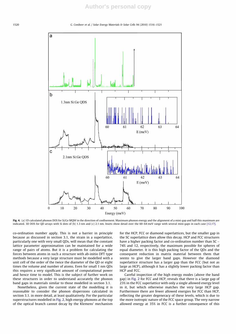
Fig. 4 shows the calculated total phonon DOS for a Si:Ge MQWand for Si:Ge QD arrays with Si QDs of 1.3 and 2.1 nm. The shapesof the total phonon DOS are very similar to the mixed behaviourof bulk Si and bulk Ge (not shown). However, the QD superlatticedoes show very discrete phonon energies, due to Bragg reflectionat the mini-Brillouin zone edges in 3D (as seen in the insertedfigures in Fig. 4) with complete gaps which decrease as the QDsize increases. These gaps are smaller than those in the QWstructure. This indicates that the big gaps in 1D are difficult toobtain just by phonon confinement in this Si:Ge nanostructuresystem, because of the broadening of the allowed energy levels in3D.
The Si:Ge system modelled here is used because the latticeparameter of Si and Ge are very similar and the approximation ofa constant lattice parameter discussed in section 3.1 is more validthan in other systems. However the mass difference between Siand Ge is much less than the 1:7 ratio used in the modelling insection 3.1. It is expected that further work on other materialssystems with larger mass differences but still with the ab-initiocalculation of force constants, will show larger gaps in the phononDOS, closer to those in section 3.1.
4. Discussion and conclusions
Carrier cooling by emission of optical phonons, which thendecay into LA phonons, can in principle be reduced by blockingthe latter decay that operates via the Klemens’-type anharmoni-city mechanism. Several compound semiconductors with largeratios of anion:cation mass have large gaps between their opticaland acoustic phonon modes. InN seems a possible candidate for ahot carrier absorber material because of its wide gap, larger thanthe acoustic phonon energy, and because of its narrow electronicband-gap for absorption. But its instability in growth and its useof the low abundance element In are problematic.
Earlier 1D force constant modelling suggested that mini-gapsdue to coherent Bragg reflection in the folded phonon dispersionof carefully tailored nanostructure superlattices, could similarlyblock the specific energies required for Klemens’ decay [14]. The3D force constant modelling in section 3.1 indicates that this isindeed the case in complete reciprocal space, but only for verysmall 1 nm QDs, which are closely packed and where there is alarge ratio between matrix and QD atomic mass (1:7). Howeverthe 3D modelling of phonon modes using the ab-initio forceconstants of section 3.2 indicates that the mini-gaps are vanish-ingly small when the mass ratio is smaller or the QDs are biggerthan 1 nm. Hence small closely packed QDs and a high mass ratioare important. The difficulty with modelling such materials withaccurate force constants from ab-initio calculations is theapproximation that the lattice parameter in QDs and matrix isthe same. There are not any pairs of bulk materials for which all ofa large mass difference, the same lattice parameter and the same
Fig. 3. DFT representation of a Si QD in a Ge matrix, using a harmonic
approximation and long range force constants.
G. Conibeer et al. / Solar Energy Materials & Solar Cells 94 (2010) 1516–1521 1519
Author's personal copyARTICLE IN PRESS
co-ordination number apply. This is not a barrier in principlebecause as discussed in section 3.1, the strain in a superlattice,particularly one with very small QDs, will mean that the constantlattice parameter approximation can be maintained for a widerange of pairs of atoms. But it is a problem for calculating theforces between atoms in such a structure with ab-initio DFT typemethods because a very large structure must be modelled with aunit cell of the order of the twice the diameter of the QD or eighttimes the volume and number of atoms. Even for small 1 nm QDsthis requires a very significant amount of computational powerand hence time to model. This is the subject of further work onthese structures in order to understand accurately the phononband gaps in materials similar to those modelled in section 3.1.
Nonetheless, given the current state of the modelling it isreasonable to consider the phonon dispersions calculated insection 3.1. in more detail, at least qualitatively. For the particularsuperstructures modelled in Fig. 2, high energy phonons at the topof the optical branch cannot decay by the Klemens’ mechanism
for the HCP, FCC or diamond superlattices, but the smaller gap inthe SC superlattice does allow this decay. HCP and FCC structureshave a higher packing factor and co-ordination number than SC –74% and 12, respectively, the maximum possible for spheres ofequal diameter. It is this high packing factor of the QDs and theconsequent reduction in matrix material between them thatseems to give the larger band gaps. However the diamondsuperlattice structure has a larger gap than the FCC (but not aslarge as HCP), although it has a slightly lower packing factor thanHCP and FCC.
Careful inspection of the high energy modes (above the bandgap) in Fig. 2 for FCC and HCP, reveals that there is a large gap of23% in the FCC superlattice with only a single allowed energy levelin it, but which otherwise matches the very large HCP gap.Furthermore there are fewer allowed energies for FCC than HCP,reflecting the greater degeneracy of these levels, which is due tothe more isotropic nature of the FCC space group. The very narrowallowed energy at 35% in FCC is a further consequence of this
Fig. 4. (a) 1D calculated phonon DOS for Si/Ge MQW in the direction of confinement. Maximum phonon energy and the alignment of a mini-gap and half this maximum are
indicated. 3D DOS for QD arrays with Si dots of (b) 1.3 nm and (c) 2.1 nm. Insets show detail over the 60–64 meV range with several mini-gaps in each case [12,17].
G. Conibeer et al. / Solar Energy Materials & Solar Cells 94 (2010) 1516–15211520

Author's personal copyARTICLE IN PRESS
greater isotropy, which means these high energy FCC modes arespread over a larger range, although they are almost discrete. Incontrast the uniaxial nature of the HCP space group results in acontinuum of energies for the modes above the band gap, becausethese are all bunched together over a narrower range of energy.
The lower energy modes below the band gap for all thestructures are very similar. This is because they all have the samediamond structure for the QD sub-lattice. Each superlattice showsa single low energy purely acoustic mode, which splits into non-degenerate LA and TA modes for the /1 1 0S and /1 1 1Sdirections. Above this the modes are almost a continuum for allcases except for SC, which shows some more degeneracy and afew more mini-gaps, because of the greater symmetry of thesuperlattice structure. The fact that the bottom edge to the bandgap differs slightly for each superlattice, reflects the slightlydifferent QD sizes, increasing in size from D to FCC to HCP andhence increasing in the allowed range of energies of the phononvibrations confined to the QD.
Hence for the high energy above band gap modes, the HCP andFCC can be considered as having a larger gap (discounting for nowthe FCC level at 55%) than diamond and much larger than SC,because the higher packing factor minimizes the number of matrixatoms. This minimization of matrix material between QDs gives thelargest gaps, which is consistent with high energy split-off modesassociated with the light matrix atoms oscillating over the veryshort distances and hence high vibrational frequency of the verynarrow matrix regions. This is qualitatively very similar to the split-off high energy modes associated with very stiff and very narrowinterface modes found in 1D force constant modelling [10].
Hence for QD superlattices which have small enough QDs thatare closely packed, Klemens’-type decay of optical phononsshould be prevented. The decay of optical phonons is then drivento less efficient processes such as Ridley decay and hence thepotential for carrier cooling should be suppressed [10]. The ratesat which these various mechanisms occur then become critical indetermining whether or not an electron will rapidly thermalise ina given structure. Calculation of such rates is the subject of furtherwork. Another factor which affects the size and position ofphononic band gaps in superlattice materials is the nature andthickness of the interface between QDs and matrix. 1D modellinghas shown the importance of this [10] and 3D modelling is thesubject of further work. In addition the quality of the periodicityof a superlattice and the effect of this quality on the dispersionand the phononic band gaps is being investigated, with importantimplications for the potential to fabricate such QD superlattices inreal materials systems.
Acknowledgements
The authors acknowledge the support of the AustralianResearch Council for the Photovoltaics Centre of Excellence; the
Global Climate and Energy Project administered by StanfordUniversity; the French research Agency and that of the Europeancommunity (FP6 program #019670).
References
[1] P. Wurfel, Sol. Energy Mater. Sol. Cells 46 (1997) 43–52;R. Ross, A.J. Nozik, J. Appl. Phys. 53 (1982) 3813–3818;M.A. Green, in: Third Generation Photovoltaics, Springer-Verlag, Berlin, 2003.
[2] Y. Takeda, T. Ito, T. Motohiro, D. Konig, S. Shestha, G. Conibeer, Hot carriersolar cells operating under practical conditions, J. Appl. Phys. 105 (2009)074905.
[3] A.J. Nozik, C.A. Parsons, D.J. Dunlary, B.M. Keyes, R.K. Ahrenkiel, Solid StateCommun., Dependence of hot carrier luminescence on barrier thickness inGaAs/AlGaAs superlattices and multiple quantum wells 75 (1990) 297–301.
[4] Y. Rosenwaks, M.C. Hanna, D.H. Levi, D.M. Szmyd, R.K. Ahrenkiel, A.J. Nozik,Hot-carrier cooling in GaAs: quantum wells versus bulk, Phys. Rev. B 48(1993) 14675–14678.
[5] W.S. Perlouch, R.J. Ellingson, P.E. Powers, C.L. Tang, Comparison of hot-carrierrelaxation in quantum wells and bulk GaAs at high carrier densities, Phys.Rev. B 45 (1992) 1450–1453.
[6] G. Conibeer, C.-W. Jiang, D. Konig, S. Shrestha, T. Walsh, M.A. Green,Selective energy contacts for hot carrier solar cells, Thin Solid Films 516(2008) 6968–6973.
[7] A. Othonos, Probing ultrafast carrier and phonon dynamics in semiconduc-tors, J. Appl. Phys. Rev. 83 (1998) 1789–1830.
[8] P.G. Klemens, Anharmonic decay of optical phonons, Phys. Rev. 148 (1966)845–848.
[9] C. Colvard, T.A. Gant, M.V. Klein, Folded acoustic and quantized optic phononsin (GaAl)As superlattices, Phys. Rev. B 31 (1985) 2080–2091.
[10] G. Conibeer, N. Ekins-Daukes, D. Konig, E.-C. Cho, C.-W. Jiang, S. Shrestha,M.A. Green, Progress on hot carrier solar cells, Sol. Energy Mater. Sol. Cells 93(2009) 713–719.
[11] F. Chen, A.N. Cartwright, H. Lu, W.J. Schaff, Time-resolved spectroscopy ofrecombination and relaxation dynamics in InN, Appl. Phys. Lett. 83 (2003)4984–4986.
[12] G. Conibeer, R. Patterson, L. Huang, J.-F. Guillemoles, D. Konig, S. Shrestha,M.A. Green, Hot carrier solar cell absorbers, in: 23rd Euro. PVSEC Valencia,2008, pp. 156–161.
[13] J.-F. Guillemoles, G.J. Conibeer, M.A. Green, Phononic engineering withnanostructures for hot carrier solar cells, in: Proceedings of the 15th PV SECShanghai, 2005, pp. 375–376.
[14] G. Conibeer, D. Konig, M.A. Green, J.F. Guillemoles, Slowing of carrier coolingin hot carrier solar cells, Thin Solid Films 516 (2008) 6948–6953. G. Conibeer.M.A. Green, Phononic engineering for hot carrier solar cell absorbers,in: Proceedings of the 19th Euro. PV Conference, Paris, 2004, pp. 270–273.
[15] N.W. Ashcroft, N.D. Mermin, in: Solid State Physics, Saunders CollegePublishing, Toronto, 1976, pp. 475–476.
[16] M. Lax, Symmetry Principles in Solid State and Molecular Physics, Wiley, NewYork, 1974.
[17] L. Huang, J. Zafran, A. Le Bris, P. Olsson, C. Domain, J.-F. Guillemoles, Phononmodes in Si–Ge nano-structures for hot carrier solar cells, in: 23rd Euro. PVConference, Valencia, 2008, pp. 689–691.
[18] D. Alf�e, (1998). Program available at /http://chianti.geol.ucl.ac.uk/�darioS.[19] G. Kresse, J. Furthmuller, J. Hafner, Ab-initio force constant approach to
phonon dispersion relations of diamond and graphite, Europhys. Lett. 32(1995) 729–734;P.E. Blochl, Projector augmented-wave method, Phys. Rev. B 50 (1994)17953–17979;G. Kresse, J. Hafner, Ab-initio molecular dynamics for liquid metals, Phys. Rev.B 47 (1993) 558–561;J.P. Perdew, Y. Wang, Accurate and simple analytical representation of theelectron–gas correlation energy, Phys. Rev. B 45 (1992) 13244–13249.
G. Conibeer et al. / Solar Energy Materials & Solar Cells 94 (2010) 1516–1521 1521