Printed Circuit Structures, the Evolution of Printed Circuit Boards
Upload
khangminh22Category
view
1download
0
This item was submitted to Loughborough's Research Repository by the author. Items in Figshare are protected by copyright, with all rights reserved, unless otherwise indicated.
Modelling and simulation of paradigms for printed circuit board assembly toModelling and simulation of paradigms for printed circuit board assembly tosupport the UK's competency in high reliability electronicssupport the UK's competency in high reliability electronics
PLEASE CITE THE PUBLISHED VERSION
PUBLISHER
© Antony Wilson
LICENCE
CC BY-NC-ND 4.0
REPOSITORY RECORD
Wilson, Antony R.. 2019. “Modelling and Simulation of Paradigms for Printed Circuit Board Assembly toSupport the Uk's Competency in High Reliability Electronics”. figshare. https://hdl.handle.net/2134/10236.

This item was submitted to Loughborough’s Institutional Repository (https://dspace.lboro.ac.uk/) by the author and is made available under the
following Creative Commons Licence conditions.
For the full text of this licence, please go to: http://creativecommons.org/licenses/by-nc-nd/2.5/

Modelling and Simulation of Paradigms for Printed CircuitBoard Assembly to Support the UK’s Competency in High
Reliability Electronics
by
Antony Richard Wilson
A Doctoral Thesis
Submitted in partial fulfilment of the requirements
for the award of
Doctor of Philosophy (PhD) of Loughborough University
December 2011
© by Antony Richard Wilson, 2011

1
Abstract
The fundamental requirement of the research reported within this thesis is the provision
of physical models to enable model based simulation of mainstream printed circuit
assembly (PCA) process discrete events for use within to-be-developed (or under
development) software tools which codify cause & effects knowledge for use in product
and process design optimisation. To support a national competitive advantage in high
reliability electronics UK based producers of aircraft electronic subsystems require
advanced simulation tools which offer model based guidance. In turn, maximization of
manufacturability and minimization of uncontrolled rework must therefore enhance in-
service sustainability for ‘power-by-the-hour’ commercial aircraft operation business
models.
It is argued that fragmentation effects from the migration of electronics production
technology will risk gap propagation within the UK’s tacit knowledge base which
previously benefited from a clustered infrastructure of volume centric producers.
Compounded by mobility requirements of consumer market led demand, cost sensitivity
drives leading-edge (i.e. miniaturized) electronic component package technology. Prior
to globalization of the electronics production network, cost competitive pressures
assumed high cost labour as a certainty - a constant which only mitigates with the
advancement of assembly processes. However, the herein reported evidence of
migration suggests an ensuing fragmentary undermining of the localized support
structure, at the detriment of residual national competencies in leading-edge reliability /
serviceability through the use of lagging-edge component package styles.

2
Lean and synergistic product and process development will be enhanced via codified
and interactive knowledge support systems; hence model based simulation of the
discrete events of mainstream PCA will enhance smart cause & effects via this
provision of novel physical models.
Given (i) the predominance of SMDs (Surface Mount Devices) the scope for the model
development exclusively addresses SMT (Surface Mount Technology) Reflow as the
mainstream printed circuit assembly process. The objectives of the developed physical
models will be (i) effects modelling capability for design-for-manufacture based causes
of printed circuit assembly (PCA) defects, and (ii) causation models for effects which
can be data mined from historical defect logs and mapped to the discrete events of the
SMT Reflow sub-processes. These are codified as (i) the deposition solder paste (i.e.
printing) (ii) SMT component placement and (iii) the dynamic behaviour of placed
components during reflow soldering.
Keywords: SMT Reflow, solder paste printing, component placement, dynamic
behaviour of components

Identification of Paradigms to Support the UK’s Competency in High Reliability Electronics
3
Acknowledgements
Firstly, from my Loughborough Uni days, I would like to thank my academic
supervisors across the two projects (STRATEC and CLOVES) which provided the
opportunity for my research and underpinned the learning opportunities therein
presented. In particular, Dr. Katherine Walsh who was in the unfortunate position to
be victim of my first attempts at academic writing / ramblings and Prof. Andy West
who has had to suffer thereon in during supervision of this doctoral research. Andy
also deserves acknowledge, along with Prof. Paul Conway and Dr. David Whalley for
beyond the call of duty services rendered in having to decipher the malaise of early
attempts at physical model development.
My thanks go to all of the STRATEC contributors (interviewees from twelve
companies) and CLOVES industrial collaborators - too many to name in person
across the three companies. I would also like to thank my colleagues and friends
within the Wolfson School common room who shared a drink (hot), laugh (hearty)
and debate (heated) over (mainly) the merits of supporting Stoke City Football Club:
but with special acknowledgement of Dr. Claire Cameron, Dr. Chris Stokes and not
least Dr. Patrick Webb for their encouragement, advice and support in this
undertaking. Also I thank the Wolfson School staff including, Sue Cramp, Carmela
Valentine and Clive Turner. Last but not least Dr. Diana Segura Velandia, Dr. Lina
Huertes Quintero and Dr Radmehr Monfared for their collaboration, guidance, and
input to the model development activities, and who together with the afore mentioned
supervisors and Patrick plus Dr. Guangbin Dou and Dr. David Hutt co-authored my
publications.

Identification of Paradigms to Support the UK’s Competency in High Reliability Electronics
4
Secondly, from my time before in joining the University (Brian Smith of Celestica for
encouragement and facilitation) and time after on joining Intelligent Energy in
supporting the completion of my studies (Richard Peart, Andy Spooner and Dr. Simon
Foster) I would like to express my appreciation. Finally to wife Liz and cat Seamus
for their unerring support in the form of (in no particular order) encouragement,
coffee and tickles.

Identification of Paradigms to Support the UK’s Competency in High Reliability Electronics
5
The most important thing in illness is never to lose heart. ~Nikolai Lenin
To Alison in support of your ongoing battle

Identification of Paradigms to Support the UK’s Competency in High Reliability Electronics
6
Journal papers
Wilson, A.R.; West, A.A.; Velandia, D.M.S.; Conway, P.P.; Whalley, D.C.; Quintero,
L.A.M.; Monfared, R.; CLOVES: Addressing The Knowledge Gaps For UK
Production Of Aircraft Electronic Subsystems, 2008, Journal of Engineering
Manufacture [submitted - in edit process]
Huertas-Quintero, Lina A. M., West, Andrew A., Velandia-Segura, Diana M.,
Conway, Paul P. and Wilson, Antony. 2010. Integrated simulation tool for
quality support in the low-volume high-complexity electronics manufacturing
domain. International Journal of Production Research, 48 (1), 45-68.
Huertas-Quintero, Lina A. M., Conway, Paul P., Velandia-Segura, Diana M., West,
Andrew A. 2010 Root cause analysis support for quality improvement in
electronics manufacturing. International Journal of Assembly Technology and
Management, Special Issue on Assembly Automation in Electronic. [Accepted]
Conference papers
Wilson, A.R.; West, A.A.; Velandia, D.M.S.; Conway, P.P.; Whalley, D.C.; Quintero,
L.A.M.; Monfared, R.; , "Characterization of printed solder paste excess and
bridge related defects," Electronics System-Integration Technology Conference,
2008. ESTC 2008. 2nd , vol., no., pp.1305-1310, 1-4 Sept. 2008
doi: 10.1109/ESTC.2008.4684543
Velandia, D.S.; Conway, P.P.; Wilson, A.; West, A.A.; Whalley, D.C.; , "A
Modelling Framework for the Reliability of Safety Critical Electronics,"
Thermal, Mechanical and Multi-Physics Simulation Experiments in
Microelectronics and Micro-Systems, 2007. EuroSime 2007. International

Identification of Paradigms to Support the UK’s Competency in High Reliability Electronics
7
Conference on , vol., no., pp.1-6, 16-18 April 2007
doi: 10.1109/ESIME.2007.359970
Guangbin Dou, D. Patrick Webb, David C. Whalley, David A. Hutt and Antony R.
Wilson, "Current Leakage Failure of Conformally Coated Electronic
Assemblies," Electronics System-Integration Technology Conference, 2008.
ESTC 2008. 2nd , vol., no., pp.1305-1310, 1-4 Sept. 2008
doi: 10.1109/ESTC.2008.4684543
Velandia, D.M.S.; Conway, P.P.; West, A.A.; Whalley, D.; Wilson, A.; Huertas, L.; ,
"Thirty-Second IEEE International Electronics Manufacturing Technology
Symposium," Electronic Manufacturing Technology Symposium, 2007. IEMT
'07. 32nd IEEE/CPMT International, vol., no., pp.i-i, 3-5 Oct. 2007
doi: 10.1109/IEMT.2007.4417038
Velandia, Diana M. Segura; Conway, Paul P.; West, Andrew A.; Whalley, David;
Wilson, Antony; Huertas, Lina; , "Complex Low Volume Electronics
Simulation Tool to Improve Yield and Reliability," Electronic Manufacturing
Technology Symposium, 2007. IEMT '07. 32nd IEEE/CPMT International, vol.,
no., pp.1-7, 3-5 Oct. 2007
doi: 10.1109/IEMT.2007.4417046
Huertas-Quintero, L. A. M., West, A. A., Velandia-Segura, D. M., Conway, P. P.,
Whalley, D. C., Wilson, A., and Monfared, R. “A simulation module for
supporting the manufacture of high value added electronics”. Proceedings of the
2nd IEEE Electronics Systems-Integration Technology Conference (ESTC 2008),
Greenwich, September 2008, ISBN 978-1-4244-2813-7.
Velandia, D.S.; West, A.A.; Conway, P.P.; Whalley, D.C.; Monfared, R.; Huertas
Quintero, L.A.M.; Wilson, A.R.; , "Integration issues in the development of a

Identification of Paradigms to Support the UK’s Competency in High Reliability Electronics
8
modelling and simulation tool for low volume high-complexity electronics
manufacture," Electronics System-Integration Technology Conference, 2008.
ESTC 2008. 2nd , vol., no., pp.1097-1102, 1-4 Sept. 2008 doi:
10.1109/ESTC.2008.4684504
Huertas-Quintero, L. A. M., West, A. A., Velandia-Segura, D. M., Conway, P. P.,
Whalley, D. C., Wilson, A., and Monfared, R. “Component based simulation as
a predictive tool for high value added electronics manufacturing”. Proceedings
of the 2008 European Electronics Assembly Reliability, Tallin, October 2008.

Identification of Paradigms to Support the UK’s Competency in High Reliability Electronics
9
TABLE OF CONTENTSABSTRACT………………………………………………………………………....……………....…..1
ACKNOWLEDGEMENTS…...…………………………………………………………...……………3
PUBLICATIONS………………………………………………………………………………….....….6
TABLES OF CONTENTS…………………………………………………………………………...... 9
TABLES OF FIGURES……………………………………………………………………………...…13
DEFINITIONS……………………………………………………………………………………… ....20
ACRONYMS…...…………………………………………………………………................................21
CHAPTER I – THESIS OVERVIEW AND INTRODUCTION
1.1. PROBLEM STATEMENT………………………………………….……………………..24
1.2. RESEARCH OBJECTIVE………………………………………….……………………..24
1.3. THESIS OVERVIEW……………………………………………………………………..24
1.4. INTRODUCTION…………………………………………………………………..……..25
1.5. THESIS PLAN…………………………………………………………………………….30
1.6. CHAPTER II OVERVIEW………………………………………………………………..32
1.7. CHAPTER III OVERVIEW……………………………………………………...………..33
1.8. CHAPTER IV OVERVIEW (LEAN PRODUCT & PROCESS DESIGN)………………34
1.9. CHAPTERS V, VI, VII & VIII OVERVIEW..........................................................………36
1.10. CHAPTER IX OVERVIEW……………………………………………………………….37
CHAPTER II – TECHNOLOGY OVERVIEW
2.1. RESEARCH CONTEXT ....................................................................................................41
2.2. CHAPTER OBJECTIVE: ...................................................................................................41
2.3. INTRODUCTION...............................................................................................................42
2.4. PRINTED CIRCUIT BOARD TECHNOLOGY ................................................................43
2.5. PLATED-THROUGH-HOLE PCBS ..................................................................................45
2.6. MULTI-LAYERED PCBS..................................................................................................48
2.7. NON-SOLDERED INTERCONNECTIONS .....................................................................50
2.8. ENABLING PROCESS INNOVATION - EN-MASSE SOLDERING .............................51
2.9. SURFACE MOUNT PACKAGE TECHNOLOGY.............................................................52
2.10. PACKAGE MINIATURISATION AND PROCESS AUTOMATION IMPLICATIONS.54
2.11. PACKAGE & PROCESS COMPATIBILITY....................................................................56
2.12. TERMINATION STYLE PROCESS DEPENDENCIES ...................................................61
2.13. CHAPTER SUMMARY: ....................................................................................................69
CHAPTER III – SOLUTIONS TO SUPPORT UK DESIGN& MANUFACTURE OF HIGH
RELIABILITY ELECTRONIC APPLICATIONS
3.1. RESEARCH CONTEXT ....................................................................................................71
3.2. CHAPTER OBJECTIVE: ...................................................................................................71
3.3. INTRODUCTION...............................................................................................................72
3.4. THE NEED FOR SUPPORT: ADDRESSING THE KNOWLEDGE GAP RISKS FROM
THE LOSS OF LOW COST / HIGH VOLUME MANUFACTURING. ...........................73

Identification of Paradigms to Support the UK’s Competency in High Reliability Electronics
10
3.5. GLOBALIZATION OF ELECTRONICS PRODUCTION NETWORK & UK
LEADERSHIP IN AIRCRAFT ELECTRONIC SUBSYSTEMS.......................................74
3.6. DIVESTED PRODUCTION...............................................................................................76
3.7. CLUSTERED INFRASTRUCTURES................................................................................77
3.8. WHAT TO SUPPORT: UK LEADERSHIP AIRCRAFT PRODUCTION AND ITS
KNOWLEDGE DEPENDENCY IN HIGH RELIABILITY / LOW VOLUME AIRCRAFT
ELECTRONIC SUBSYSTEMS..........................................................................................79
3.9. LEAN PRODUCTION........................................................................................................79
3.10. MODULARITY AND MAKE VERSUS BUY DECISIONS ............................................82
3.11. COMPONENT PACKAGE TECHNOLOGY IMPLICATIONS FOR AIRCRAFT
ELECTRONIC SUBSYSTEMS – LEADING VERSUS LAGGING EDGE .....................84
3.12. DIVESTED PRODUCTION & MODULAR PRODUCT ARCHITECTURES.................85
3.13. KNOWLEDGE INTERFACES AND GAP PROPAGATION...........................................86
3.14. HOW TO SUPPORT: CODIFICATION OF THE TACIT KNOWLEDGE REQUIRED
FOR SMART CAUSE & EFFECTS KNOWLEDGE MANAGEMENT, INTERACTIVE
DESIGN-FOR-MANUFACTURE & LEAN SYNERGISTIC PRODUCT & PROCESS
DESIGN, .............................................................................................................................88
3.15. KNOWLEDGE MANAGEMENT – FOR SMART CAUSE & EFFECTS ANALYSIS ...89
3.16. PACKAGE TECHNOLOGY KNOWLEDGE CODIFICATION FOR SMART CAUSE &
EFFECTS KNOWLEDGE MANAGEMENT ....................................................................90
3.17. INTERACTIVE DESIGN-FOR-MANUFACTURE (IDFM).............................................92
3.18. LEAN SYNERGISTIC PRODUCT & PROCESS DESIGN ..............................................94
3.19. CHAPTER SUMMARY .....................................................................................................95
CHAPTER IV - LEAN PRODUCT & PROCESS DESIGN
4.1. RESEARCH CONTEXT ....................................................................................................97
4.2. CHAPTER OBJECTIVE: ...................................................................................................97
4.3. INTRODUCTION...............................................................................................................98
4.4. DESIGN-TO-MANUFACTURE SEQUENCES. ...............................................................99
4.5. ORIGINS OF LEAN PRODUCTION. .............................................................................100
4.6. DEFINITION OF VALUE................................................................................................101
4.7. VALUE STREAM ANALYSIS........................................................................................102
4.8. THE ROLE OF CONCURRENT ENGINEERING..........................................................103
4.9. PARADIGM 1: ISOLATED PRODUCT & PROCESS DESIGN DOMAINS ................105
4.10. PARADIGM 2: SEQUENTIALLY LINKED PRODUCT & PROCESS DESIGN .........108
4.11. CONCURRENCY AND ALIGNMENT...........................................................................110
4.12. DIVESTED PRODUCTION & MODULAR PRODUCT ARCHITECTURES...............111
4.13. KNOWLEDGE INTERFACES AND GAP PROPAGATION.........................................112
4.14. HOW TO SUPPORT: CODIFICATION OF THE TACIT KNOWLEDGE REQUIRED
FOR SMART CAUSE & EFFECTS KNOWLEDGE MANAGEMENT, INTERACTIVE

Identification of Paradigms to Support the UK’s Competency in High Reliability Electronics
11
DESIGN-FOR-MANUFACTURE & LEAN SYNERGISTIC PRODUCT & PROCESS
DESIGN, ...........................................................................................................................114
4.15. KNOWLEDGE MANAGEMENT – FOR SMART CAUSE & EFFECTS ANALYSIS .115
4.16. PACKAGE TECHNOLOGY KNOWLEDGE CODIFICATION FOR SMART CAUSE &
EFFECTS KNOWLEDGE MANAGEMENT ..................................................................116
4.17. PARADIGM 3: INTERACTIVE DESIGN-FOR-MANUFACTURE (IDFM).................118
4.18. LEAN SYNERGISTIC PRODUCT & PROCESS DESIGN ............................................120
4.19. CHAPTER SUMMARY ...................................................................................................122
CHAPTER V – SMART CAUSE & EFFECTS KNOWLEDGE CODIFICATION STRUCTURE
FOR THE SMT PROCESS
5.1 CODIFICATION OF THE SMT PROCESS ......................................................................126
5.2 DISCRETE EVENT DEFINITIONS FOR THE SMT SUB PROCESSES........................127
5.3 CAUSE AND EFFECTS MODEL DEFINITIONS............................................................128
5.3 MODEL DEVELOPMENT METHODOLOGY.................................................................131
CHAPTER VI - PRINTING
6.1. CHAPTER OBJECTIVES ...............................................................................................135
6.2. DESCRIPTION OF SOLDER PASTE DEPOSITION SUB-PROCESS..........................135
6.3. SUB-PROCESS 1 DISCRETE EVENT A DISCRETE EVENT - STENCIL / PCB
ALIGNMENT ...................................................................................................................135
6.4. SUB-PROCESS 1 DISCRETE EVENT B DISCRETE EVENT - PRINT STROKE &
APERTURE FILLING......................................................................................................136
6.5. SUB-PROCESS 1 DISCRETE EVENT C - STENCIL SEPARATION / PASTE
TRANSFER.......................................................................................................................137
6.6. TACIT KNOWLEDGE RELATING TO THE SOLDER PASTE DEPOSITION SUB-
PROCESS:.........................................................................................................................138
6.7. DEVELOPMENT OF SOLDER PASTE DEPOSITION MODELS FROM TACIT
KNOWLEDGE AND REVIEW OF LITERATURE ........................................................141
6.8. GEOMETRIC ASPECT RATIOS ....................................................................................141
6.9. PASTE TRANSFER RATIOS..........................................................................................142
6.10. STENCIL / PCB MISALIGNMENT AND PASTE BLEEDING.....................................147
6.11. POSITIVE TRANSFER VALUES AND CUMULATIVE EFFECTS.............................153
6.12. DIMENSIONAL MISMATCHES ....................................................................................156
6.13. MODELS FOR SUB-PROCESS 1 DISCRETE EVENT A: STENCIL / PCB
ALIGNMENT ...................................................................................................................156
6.14. MODELS FOR SUB-PROCESS 1 DISCRETE EVENT B: PRINT STROKE &
APERTURE FILLING......................................................................................................164
6.15. MODELS FOR SUB-PROCESS 1 DISCRETE EVENT C - STENCIL SEPARATION /
PASTE TRANSFER .........................................................................................................168
6.16. CHAPTER SUMMARY ...................................................................................................174
CHAPTER VII - PLACEMENT
Identification of Paradigms to Support the UK’s Competency in High Reliability Electronics
12
7.1. CHAPTER OBJECTIVES ................................................................................................176
7.2. DESCRIPTION OF COMPONENT PLACEMENT SUB-PROCESS .............................176
7.3. SUB-PROCESS 2 DISCRETE EVENT A – COMPONENT PICKUP............................178
7.4. SUB-PROCESS 2 DISCRETE EVENT B - PCB / COMPONENT POSITIONING &
ALIGNMENT ...................................................................................................................187
7.5. QUALITATIVE MODELING TECHNIQUES - ALIGNMENT SEQUENCE MAPPING
191
7.6. PROCESS FMEA AS A QUALITATIVE MODELING TECHNIQUE ..........................193
7.7. CODIFICATION OF (PACKAGE PHYSICAL CHARACTERISTICS & PLACEMENT
RELATED PROCESS DEPENDENCIES AS) PROCESS DISTURBANCES AND
FREQUENCY-PREDICTION MODEL INPUTS ............................................................194
7.8. PLACEMENT PLATFORM CONFIGURATIONS PLACEMENT RELATED PROCESS
DEPENDENCIES .............................................................................................................198
7.9. CODIFICATION OF PROCESS DISTURBANCES AS DETECTION-PREDICTION
MODEL INPUTS..............................................................................................................201
7.10. SUB-PROCESS 2 DISCRETE EVENT C – COMPONENT PLACEMENT & PASTE
DISPLACEMENT.............................................................................................................206
7.11. POST PLACEMENT COMPONENT MOVEMENT.......................................................207
7.12. PLACEMENT PRESSURE RELATED BRIDGING OF FPT & UFPT PACKAGES ....210
7.13. PLACEMENT PRESSURE RELATED MID-CHIP SOLDER BALLS ..........................213
7.14. CHAPTER SUMMARY ...................................................................................................216
CHAPTER VIII – REFLOW
8.1. CHAPTER OBJECTIVES ................................................................................................219
8.2. DESCRIPTION OF REFLOW SOLDERING SUB-PROCESS.......................................219
8.3. SUB-PROCESS 3 DISCRETE EVENT A – SOLDER CONTACT (LEAD BEND
TOLERANCE) ..................................................................................................................223
8.4. SUB-PROCESS 3 DISCRETE EVENT B – SOLDER WETTING & FILLET
FORMATION ...................................................................................................................227
8.5. SUB-PROCESS 3 DISCRETE EVENT C – SURFACE ENERGY EFFECTS ...............229
8.6. MODEL DEVELOPMENT FOR SURFACE ENERGY EFFECTS ................................234
8.7. CHAPTER SUMMARY ...................................................................................................245
CHAPTER IX – DISCUSSIONS, CONCLUSIONS, NEW LEARNING & FUTURE WORK
9.1. DISCUSSION - RESEARCH CONTEXT........................................................................247
9.2. DISCUSSION - RESEARCH INTERACTIONS .............................................................249
9.3. DISCUSSION - PACKAGE TECHNOLOGY AND ITS IMPLICATIONS (FOR
AIRCRAFT ELECTRONIC SUBSYSTEMS...................................................................255
9.4. NEW LEARNING.............................................................................................................261
9.5. CONCLUSIONS ...............................................................................................................271
9.6. FUTURE WORK ..............................................................................................................274

Identification of Paradigms to Support the UK’s Competency in High Reliability Electronics
13
TABLE OF FIGURESFIGURE 1 - CLOVES PROJECT PARTNERS.....................................................................................28
FIGURE 2 - THESIS PLAN DIAGRAM ..............................................................................................30
FIGURE 3 - CHAPTER II OVERVIEW DIAGRAM ...........................................................................32
FIGURE 4 - CHAPTER III OVERVIEW DIAGRAM ..........................................................................33
FIGURE 5 - CHAPTER IV OVERVIEW DIAGRAM..........................................................................34
FIGURE 6 - CHAPTER V, VI, VII & VIII INTERACTION DIAGRAM ............................................36
FIGURE 7 - CHAPTER IX OVERVIEW DIAGRAM..........................................................................37
FIGURE 8 - DESIGN FOR X CAPABILITIES UNDER CONSIDERATION WITHIN THE DIY
PROJECT......................................................................................................................................39
FIGURE 9 - CHAPTER II CONTEXT DIAGRAM ..............................................................................41
FIGURE 10 - IMAGE OF AN ELECTROLYTIC CAPACITOR WITH SOLDER-ABLE TAGS
PROTRUDING FROM THE TOP ...............................................................................................43
FIGURE 12 - IMAGE SHOWING A BASIC PCA WITH TOP SIDE MOUNTED COMPONENTS &
UNDER SIDE COPPER TRACES...............................................................................................44
FIGURE 13 - GRAPHICAL REPRESENTATION OF A SECTIONAL VIEW OF A NONE-
PLATED-THROUGH-HOLE ......................................................................................................45
FIGURE 14 - GRAPHICAL REPRESENTATION OF A SECTIONAL VIEW OF A PLATED-
THROUGH-HOLE .......................................................................................................................46
FIGURE 15- IMAGES SHOWING OCTAL VALVE TECHNOLOGY...............................................46
FIGURE 16- GRAPHICAL REPRESENTATION OF A SECTIONAL VIEW OF A SOLDER
PLUGGED PLATED THROUGH HOLE & COMPONENT LEAD ..........................................47
FIGURE 17- IMAGES OF VARIOUS EXAMPLES OF PLASTIC MOLDED PTH CONNECTORS48
FIGURE 18- GRAPHICAL REPRESENTATION OF A SECTIONAL VIEW OF BLIND, BURIED
AND MICRO-VIAS .....................................................................................................................49
FIGURE 19- GRAPHICAL REPRESENTATION OF AN SMT PACKAGE DOWNSCALING
TIMELINE....................................................................................................................................54
FIGURE 20- PTH TO FLIP-CHIP MINIATURIZATION COMPARISON .........................................55
FIGURE 21 - GRAPHICAL REPRESENTATION OF A SCHEMATIC FOR A BTU PARAGON 98
FORCED-CONVECTION REFLOW TUNNEL .........................................................................58
FIGURE 22 - GRAPHICAL REPRESENTATION OF AN ELECTROVERT ELECTRA WAVE
SOLDER MACHINE ...................................................................................................................60
FIGURE 23- THE DIP PTH PACKAGE ...............................................................................................62
FIGURE 24 - GRAPHICAL REPRESENTATION OF A CERAMIC CHIP COMPONENT WITH
NAMING CONVENTION ...........................................................................................................64
FIGURE 25 –GRAPHICAL REPRESENTATION OF SMT PERIPHERAL LEADED PROFILES...65
FIGURE 26 - CUT-AWAY VIEW SHOWING DIE AND LEAD-FRAME WIRE BONDED
INTERCONNECTIONS...............................................................................................................65
FIGURE 27 - GRAPHICAL REPRESENTATION OF DUAL AND QUAD PACKAGES WITH
GULL WING LEAD PROFILES .................................................................................................66

Identification of Paradigms to Support the UK’s Competency in High Reliability Electronics
14
FIGURE 28 - GRAPHICAL REPRESENTATION OF DUAL AND QUAD PACKAGES WITH J-
LEADS..........................................................................................................................................66
FIGURE 29 - UNDERSIDE VIEW OF A PLASTIC BGA SHOWING AREA ARRAY SOLDER
INTERCONNECTIONS...............................................................................................................68
FIGURE 30 - PERIPHERAL VIEW OF BGA SOLDER JOINTS........................................................68
FIGURE 31 - GRAPHICAL REPRESENTATION OF THE SMT REFLOW PROCESS FLOW .......70
FIGURE 32 CHAPTER III CONTEXT DIAGRAM .............................................................................72
FIGURE 33 - MODULAR PRODUCT ARCHITECTURE WITHIN VERTICALLY INTEGRATED
PRODUCTION MODELS ...........................................................................................................80
FIGURE 34 - PROBERT’S TECHNOLOGY SOURCING & SUPPLIER RELATIONSHIP MATRIX
......................................................................................................................................................83
FIGURE 35 - A DIVESTED PRODUCTION STRATEGY FOR AIRCRAFT ELECTRONIC
SUBSYSTEMS WITH MODULAR ARCHITECTURES...........................................................86
FIGURE 36 - A DESIGN-TO-MANUFACTURE SEQUENCE KNOWLEDGE CHAIN WITH
RETROSPECTIVE FEEDBACK LOOPS ...................................................................................88
FIGURE 37 - CHAPTER CONTEXT DIAGRAM................................................................................98
FIGURE 38 - PARADIGM 1: ISOLATED PRODUCT & PROCESS DESIGN ................................106
FIGURE 39 - PARADIGM 2: LINKED PRODUCT & PROCESS DESIGN.....................................109
FIGURE 40 - A DIVESTED PRODUCTION STRATEGY FOR AIRCRAFT ELECTRONIC
SUBSYSTEMS WITH MODULAR ARCHITECTURES.........................................................112
FIGURE 41- A DESIGN-TO-MANUFACTURE SEQUENCE KNOWLEDGE CHAIN WITH
RETROSPECTIVE FEEDBACK LOOPS .................................................................................114
FIGURE 42 - PARADIGM 3: AN INTERACTIVE DESIGN-FOR-MANUFACTURE SEQUENCE
....................................................................................................................................................120
FIGURE 43 - PARADIGM 4 –LEAN & SYNERGISTIC PRODUCT & PROCESS DESIGN .........122
FIGURE 44 - SECTION 2 - THESIS PLAN DIAGRAM ...................................................................125
FIGURE 45 - SMT REFLOW SUB-PROCESS DEFINITION – PRINTING / PLACEMENT /
REFLOW ....................................................................................................................................127
FIGURE 46 - GRAPHICAL REPRESENTATIONS OF THE DIVERGED SUB-PROCESS
DISCRETE EVENTS .................................................................................................................128
FIGURE 47 - AN EXEMPLAR EFFECTS MODEL...........................................................................130
FIGURE 48 - AN EXEMPLAR CAUSE MODEL ..............................................................................130
FIGURE 49 - CHAPTER CONTEXT DIAGRAM..............................................................................135
FIGURE 50 - GRAPHICAL REPRESENTATION OF THE STENCIL / PCB ALIGNMENT
DISCRETE EVENT ...................................................................................................................136
FIGURE 51 - GRAPHICAL REPRESENTATION OF THE PRINT STROKE & APERTURE
FILLING DISCRETE EVENT...................................................................................................137
FIGURE 52 - GRAPHICAL REPRESENTATION OF THE STENCIL SEPARATION / PASTE
TRANSFER DISCRETE EVENT ..............................................................................................137
FIGURE 53 - DEFINITIONS OF PAD GEOMETRY.........................................................................138

Identification of Paradigms to Support the UK’s Competency in High Reliability Electronics
15
FIGURE 54 - DEFINITIONS OF APERTURE GEOMETRY............................................................142
FIGURE 55 - IMAGE OF BRIDGED SOLDER PASTE DEPOSITS VIA FULL VOLUMETRIC
SCANNING TECHNIQUES......................................................................................................144
FIGURE 56 - GRAPHICAL REPRESENTATION OF THE SCOOPING EFFECT ..........................145
FIGURE 57 - GRAPHICAL REPRESENTATION OF APERTURE ORIENTATION DEFINITIONS
....................................................................................................................................................146
FIGURE 58 - GRAPHICAL REPRESENTATION OF THE SOLDER BRIDGING – SOLDER
SHORTS EFFECT......................................................................................................................148
FIGURE 59 - GRAPHICAL REPRESENTATION OF THE EXCESS PASTE DUE TO BLEEDING
CAUSES .....................................................................................................................................148
FIGURE 60 - GRAPHICAL REPRESENTATION OF THE BLEEDING EFFECT ..........................149
FIGURE 61 - GRAPHICAL REPRESENTATION OF THE DEPOSIT / TRACK GAP REDUCTION
CAUSE .......................................................................................................................................149
FIGURE 62 - GRAPHICAL REPRESENTATION EXCESS DEPOSIT DUE TO PAD HEIGHT
DIFFERENTIAL CAUSE ..........................................................................................................150
FIGURE 63 - GRAPHICAL REPRESENTATION OF SURFACE RESIDUE TRANSFER
MECHANISM FOR PASTE BLEEDING .................................................................................153
FIGURE 64 - GRAPHICAL REPRESENTATION OF PCB / STENCIL DIMENSIONAL
MISMATCH CAUSE .................................................................................................................154
FIGURE 65 - GRAPHICAL REPRESENTATION OF THE STENCIL / PCB ALIGNMENT
EFFECTS MODEL.....................................................................................................................159
FIGURE 66 - GRAPHICAL REPRESENTATION OF THE STENCIL / PCB ALIGNMENT CAUSE
MODEL ......................................................................................................................................161
FIGURE 67 - GRAPHICAL REPRESENTATION OF THE STENCIL ALIGNMENT ABVA WITH
NOMENCLATURE ...................................................................................................................162
FIGURE 68 - GRAPHICAL REPRESENTATION OF EDGE CLAMP EFFECTS CAUSING
STENCIL / PCB GAPS ..............................................................................................................163
FIGURE 69- GRAPHICAL REPRESENTATION OF THE PRINT STROKE & APERTURE
FILLING EFFECTS MODEL ....................................................................................................167
FIGURE 71 - GRAPHICAL REPRESENTATION OF THE PRINT STROKE & APERTURE
FILLING CAUSE MODEL........................................................................................................168
FIGURE 72 - GRAPHICAL REPRESENTATION OF THE STENCIL SEPARATION / PASTE
TRANSFER EFFECTS MODEL ...............................................................................................173
FIGURE 73 - GRAPHICAL REPRESENTATION OF THE STENCIL SEPARATION / PASTE
TRANSFER CAUSE MODEL...................................................................................................174
FIGURE 74 - GRAPHICAL REPRESENTATIONS OF STENCIL / PCB ALIGNMENT ................175
FIGURE 75 - GRAPHICAL REPRESENTATIONS OF PRINT STROKE & APERTURE FILLING
....................................................................................................................................................175
FIGURE 76 - GRAPHICAL REPRESENTATIONS OF STENCIL SEPARATION / PASTE
TRANSFER ................................................................................................................................175

Identification of Paradigms to Support the UK’s Competency in High Reliability Electronics
16
FIGURE 77 – CHAPTER CONTEXT DIAGRAM .............................................................................176
FIGURE 78 - ICON REPRESENTATION OF THE COMPONENT PICKUP DISCRETE EVENT 178
FIGURE 79 - ICON REPRESENTATION OF THE PCB / COMPONENT POSITIONING &
ALIGNMENT DISCRETE EVENT...........................................................................................178
FIGURE 80 - ICON REPRESENTATION OF THE COMPONENT PLACEMENT & PASTE
DISPLACEMENT DISCRETE EVENT ....................................................................................178
FIGURE 81 - GRAPHICAL REPRESENTATION OF TAPED AND REELED COMPONENT
PRESENTATION.......................................................................................................................179
FIGURE 82 - GRAPHICAL REPRESENTATION OF AN EXEMPLAR TAPE & REEL
SPECIFICATION .......................................................................................................................180
FIGURE 83 - GRAPHICAL REPRESENTATION OF COMPONENT LOCATION ANOMALIES
WITHIN A STANDARDISED POCKET SIZE.........................................................................181
FIGURE 84 - GRAPHICAL REPRESENTATION OF VACUUM PICKUP ABVA: CERAMIC
CHIPS .........................................................................................................................................182
FIGURE 85 - GRAPHICAL REPRESENTATION OF THE COMPONENT PICKUP EFFECTS
MODEL ......................................................................................................................................186
FIGURE 86 - GRAPHICAL REPRESENTATION OF THE COMPONENT PICKUP CAUSE
MODEL ......................................................................................................................................186
FIGURE 87 - GRAPHICAL REPRESENTATION OF A TYPICAL PLACEMENT MACHINE
FEEDER CONFIGURATION....................................................................................................187
FIGURE 88 - GRAPHICAL REPRESENTATION OF OFFSET PICKUP AND NOZZLE SLIPPAGE
CAUSES OF THETA ERROR EFFECTS .................................................................................189
FIGURE 89 - GRAPHICAL REPRESENTATION OF COINCIDENCE OF TAPE INDEXING &
PLACEMENT TRAVERSE DIRECTIONS ..............................................................................189
FIGURE 90 - GRAPHICAL REPRESENTATION OF A TYPICAL PLACEMENT MACHINE
CONFIGURATION WITH CAMERA & THETA ALIGNMENT STATIONS........................191
FIGURE 91 - GRAPHICAL REPRESENTATION OF TRAVERSE PATHS FOR TAPE FED
PASSIVES AND TRAY FED ACTIVES ..................................................................................193
FIGURE 92 - GRAPHICAL REPRESENTATION OF ALIGNMENT SEQUENCE FOR MOVING
GANTRY AND STATIC CAMERA PICK-&-PLACE / GATHER-&-PLACE PLATFORMS200
FIGURE 93 - DUAL HEAD PICK-&-PLACE PLATFORM WITH STATIC MOUNT VISION
ALIGNMENT CAMERA...........................................................................................................201
FIGURE 94 - IMAGE OF A GATHER-&-PLACE SYSTEM SHOWING MULTI-NOZZLE
GATHERED COMPONENTS ...................................................................................................201
FIGURE 95- AN ON-THE-FLY ROTARY INDEXING VISION ALIGNMENT SYSTEM.............202
FIGURE 96 - A CHIP-SHOOTER TURRET WITH TWENTY ROTARY STATIONS....................206
FIGURE 97 - IMAGE OF A POST PLACEMENT DISPLACED COMPONENT ............................208
FIGURE 98 - GRAPHICAL REPRESENTATION OF INERTIAL VECTOR MAPPING OF POST
PLACEMENT MOVEMENTS ..................................................................................................211

Identification of Paradigms to Support the UK’s Competency in High Reliability Electronics
17
FIGURE 99 - GRAPHICAL REPRESENTATION OF PLACEMENT PRESSURE RELATED
LATERAL PASTE DISPLACEMENT......................................................................................211
FIGURE 100 - GRAPHICAL REPRESENTATION OF LEAD CO-PLANARITY CAUSES OF
UNSOLDERED JOINTS............................................................................................................212
FIGURE 101 - DONOHUE AND WILLIAMS DATA PRESENTED WITHIN A MODEL
CONSTRUCT.............................................................................................................................213
FIGURE 102 - IMAGE OF MID-CHIP SOLDER BALLS .................................................................214
FIGURE 103- GRAPHICAL REPRESENTATION OF SIDE AND PLAN VIEWS OF PLACEMENT
PRESSURE INFLUENCED PASTE DISPLACEMENT ..........................................................215
FIGURE 104 - IMAGE OF THE TRAPEZOIDAL SHAPED APERTURE DESIGN SOLUTION TO
THE MID-CHIP SOLDER BALL DEFECT MODE .................................................................216
FIGURE 105 - SCHEMATIC FOR THE INCORPORATION OF DATAPAK’S RELITE THERMAL
MODELLING TOOL WITHIN INMOST .................................................................................220
FIGURE 106 - ICON REPRESENTATION OF THE SOLDER CONTACT (LEAD BEND
TOLERANCE) DISCRETE EVENT .........................................................................................221
FIGURE 107 - ICON REPRESENTATION OF THE SOLDER WETTING & FILLET FORMATION
DISCRETE EVENT ...................................................................................................................221
FIGURE 108 - ICON REPRESENTATION OF THE SURFACE ENERGY EFFECTS DISCRETE
EVENT .......................................................................................................................................221
FIGURE 109 - GRAPHICAL REPRESENTATION OF POSITIVE AND NEGATIVE CO-
PLANARITY CAUSES OF UNSOLDERED JOINTS..............................................................224
FIGURE 110 - GRAPHICAL REPRESENTATION OF THE LEAD / DEPOSIT CO-PLANARITY
PROCESS WINDOW.................................................................................................................224
FIGURE 111 - GRAPHICAL REPRESENTATION OF QUALITATIVE CODIFICATION OF LEAD
BEND PROCESS WINDOWS...................................................................................................225
FIGURE 112 - GRAPHICAL REPRESENTATION OF LEAD POSITION RELATED SOLDER
CONTACT SCENARIOS...........................................................................................................226
FIGURE 113 - IMAGE OF AN SMT RESISTOR NETWORK EXHIBITING SOLDER WICKING
DEFECTS ...................................................................................................................................228
FIGURE 114 - GRAPHICAL REPRESENTATION OF FULCRUMS & VERTICAL PIVOT AXIS
DURING DYNAMIC BEHAVIOUR DURING SOLDER WETTING OF CERAMIC CHIPS
COMPONENTS .........................................................................................................................230
FIGURE 115 - GRAPHICAL REPRESENTATION OF DYNAMIC BEHAVIOUR CAUSE &
EFFECT FOR CERAMIC CHIP COMPONENTS DURING SOLDER WETTING ................231
FIGURE 116 - IMAGE OF CERAMIC CHIP RESISTOR TOMB-STONING ..................................231
FIGURE 117 - IMAGE OF CERAMIC CHIP RESISTOR FLOATATION .......................................232
FIGURE 118 - GRAPHICAL REPRESENTATION OF TOMB-STONING DYNAMIC BEHAVIOUR
PHENOMENON.........................................................................................................................232
FIGURE 119 - GRAPHICAL REPRESENTATION OF FLOATATION DYNAMIC BEHAVIOUR
PHENOMENON.........................................................................................................................233

Identification of Paradigms to Support the UK’s Competency in High Reliability Electronics
18
FIGURE 120 - GRAPHICAL REPRESENTATION OF FLOATATION DYNAMIC BEHAVIOUR
PHENOMENON.........................................................................................................................233
FIGURE 121 - GRAPHICAL REPRESENTATION OF KLIEN WASSINK AND VAN GERVEN
SCHEMATIC FOR THE CERAMIC CHIP TOMB-STONING SURFACE ENERGY EFFECT
....................................................................................................................................................235
FIGURE 122 - CODIFICATION DIAGRAM FOR THE TOMB-STONING SURFACE-ENERGY
EFFECTS AT THE TOE FILLET..............................................................................................238
FIGURE 123 - CODIFICATION DIAGRAM FOR THE TOMB-STONING SURFACE-ENERGY
EFFECTS AT THE HEEL FILLET ...........................................................................................239
FIGURE 124 - CODIFICATION DIAGRAM FOR THE FLOATATION & SELF-ALIGNMENT &
SURFACE-ENERGY EFFECTS................................................................................................241
FIGURE 125 - GRAPHICAL REPRESENTATION OF A CERAMIC CHIP CAPACITOR
SHOWING FULL WRAP ROUND METALLISED END CAP ...............................................242
FIGURE 126 - GRAPHICAL REPRESENTATION OF A CERAMIC CHIP RESISTOR SHOWING
TOP AND BOTTOM ONLY METALLISED END CAP..........................................................242
FIGURE 127 - CONCISE PHYSICAL MODEL FOR THE QUALITATIVE PREDICTION OF THE
CAUSES OF TOMB-STONING, FLOATATION, SELF-ALIGNMENT AND MID-CHIP
SOLDER BALL DEFECTS .......................................................................................................244
FIGURE 128 - CONCISE PHYSICAL MODEL FOR THE QUALITATIVE PREDICTION OF THE
EFFECTS OF TOMB-STONING, FLOATATION, SELF-ALIGNMENT AND MID-CHIP
SOLDER BALL DEFECTS .......................................................................................................244
FIGURE 129 – CHAPTER CONTEXT DIAGRAM ...........................................................................247
FIGURE 130 - GRAPHICAL REPRESENTATION OF CLOVES KNOWLEDGE, MODELS AND
SIMULATION WORK PACKAGE INTERACTIONS.............................................................248
FIGURE 131 - GRAPHICAL REPRESENTATION OF CIMOSA ABSTRACTION MECHANISMS
& CONSTRUCTS ......................................................................................................................250
FIGURE 132 - EXAMPLE OF A CIMOSA CONTEXT DIAGRAM.................................................251
FIGURE 133 - EXAMPLE OF A CIMOSA INTERACTION DIAGRAM.........................................251
FIGURE 134 - EXAMPLE OF A CIMOSA STRUCTURE DIAGRAM ............................................252
FIGURE 135 - EXAMPLE OF A CIMOSA ACTIVITY DIAGRAM.................................................252
FIGURE 136 - GRAPHICAL REPRESENTATION OF THE ELECTRONICS PRODUCTION
DOMAIN ....................................................................................................................................253
FIGURE 137 - AN SMT DEFECT OPPORTUNITY & DETECTION CONTEXT DIAGRAM .......254
FIGURE 138 - GRAPHICAL REPRESENTATION OF AN ARCHETYPAL SMT ASSEMBLY LINE
....................................................................................................................................................257
FIGURE 139 - BATH-TUB CURVE DIAGRAM...............................................................................258
FIGURE 140 - ISHIKAWA DIAGRAM SHOWING INTERNAL / EXTERNAL FAILURE EFFECTS
OF SOLDER JOINT DEFECT CAUSES...................................................................................260
FIGURE 141 - PARETO ANALYSIS OUTPUT 1 FROM INMOST .................................................262
FIGURE 142 - PARETO ANALYSIS OUTPUT 2 FROM INMOST .................................................263

Identification of Paradigms to Support the UK’s Competency in High Reliability Electronics
19
FIGURE 143 - SCREEN SHOT OF INMOST DFM GUI AND RESULTS OUTPUT FROM THE
CASE STUDY ............................................................................................................................264
FIGURE 144 - SCREEN SHOT OF INMOST RCA GUI AND RESULTS OUTPUT FROM THE
CASE STUDY ............................................................................................................................265
FIGURE 145 - SCREEN SHOT OF INMOST SENSITIVITY ANALYSIS GUI AND RESULT
FROM THE CASE STUDY .......................................................................................................267
FIGURE 146 - SCREEN SHOT OF INMOST QUALITY IMPROVEMENT PREDICTIONS .........269
FIGURE 147 - PACKAGE STYLE / AUTOMATED INSPECTION TECHNIQUES.......................270

Identification of Paradigms to Support the UK’s Competency in High Reliability Electronics
20
Definitions
Isolated Product & Process Design Dislocated in terms of geography andenterprise, product and process designfunctions which prohibit targeted design-for-manufacture
Linked Product & Process Design Product and process design functionswhich are linked by intra or interenterprise interfaces but are retrospectiverather than concurrent
Interactive DfM Model based codified knowledge whichinteractively informs product designerswith design-for-manufacture guidance atthe point of detailed design andminimises embedded defect opportunities
Lean & Synergistic Product & ProcessDesign
Model based codified knowledge whichinteractively and concurrently alignsproduct and process designer andoptimises the manufacturability ofproducts and delivers the leanest andmost cost effective solutions
Smart Cause & Effects Model based computerised cause andeffects analysis facilitates by the physicalmodels and the software tools developedin association with this research
Discrete Event Simulation Computerised simulation of productionflows with case based reasoning scenarios
CIMOSA Computer Integrated ManufactureOperational Systems Analysis abstractionmechanisms
Lagging-edge package technology The physical incarnation of electroniccomponents which have proven highreliability antecedents but lag the latestpackage technology trends

Identification of Paradigms to Support the UK’s Competency in High Reliability Electronics
21
Acronyms
DfM Design-for-ManufactureSMT Surface Mount TechnologySMD Surface Mount DevicePCA Printed Circuit AssemblyPCB Printed Circuit BoardBGA Ball Grid ArrayBQFP Bumpered Quad Flat PackCBGA Ceramic Ball Grid ArrayCFP Ceramic Flat PackCPGA Ceramic Pin Grid ArrayCQFP Ceramic Quad Flat PackTBD Ceramic Lead-Less Chip CarrierDLCC Dual Lead-Less Chip Carrier (Ceramic)FBGA Fine-pitch Ball Grid ArrayFPBGA Fine Pitch Ball Grid ArrayJLCC J-Leaded Chip Carrier (Ceramic)LCC Leaded Chip Carrier [also Leadless]LCCC Leaded Ceramic Chip Carrier;LFBGA Low-Profile, Fine-Pitch Ball Grid ArrayLGA Land Grid Array [Pins are on the Motherboard, not the socket]MLCC Micro Leadframe Chip CarrierPBGA Plastic Ball Grid ArrayPLCC Plastic Leaded Chip CarrierPQFD Plastic Quad Flat PackPQFP Plastic Quad Flat PackPSOP Plastic Small-Outline PackageQFP Quad Flat PackQSOP Quarter Size Outline PackageSOIC Small Outline ICSOJ Small-Outline Package [J-Lead]SSOP Shrink Small-Outline PackageTQFP Thin Quad Flat PackTSOP Thin Small-Outline PackageTSSOP Thin Shrink Small-Outline PackageTVSOP Thin Very Small-Outline PackageVQFB Very-thin Quad Flat PackC-DIP Ceramic Dual In-line PackageCERDIP Ceramic DIPCPGA Ceramic Pin Grid ArrayDIP Dual In-line PackageHDIP Hermetic DIPPDIP Plastic DIP [P-DIP]PGA Pin Grid Array; PGA GraphicPPGA: Plastic Pin Grid ArrayShrink DIP Shrink Dual In-Line PackageSIP Single In-line PackageDBPn X or Y deposit bridge potential ratio

Identification of Paradigms to Support the UK’s Competency in High Reliability Electronics
22
DREn X or Y deposit registration errorPPG Pad to Pad GapBDEn X & Y board dimensional errorPCn X & Y component position from PCB centroidCP Component PitchDEPn X & Y deposit excess potential ratioTR Transfer RatioAV Aperture VolumeDV Deposit VolumePHD Pad Height DifferentialCT Copper ThicknessSFT Surface Finish ThicknessDIPn X & Y deposit insufficient potential ratioSCTR Scooping Effect Transfer Ratio – see Figure 56AL Aperture LengthAW Aperture WidthST Stencil ThicknessDV Predicted Deposit VolumeAV0 Initial Aperture VolumeTR Initial Transfer RatioN Number of printsAvn-1 Resultant compounded aperture volumeAL Aperture LengthAW Aperture WidthST Stencil ThicknessABVA Assembly Build Variation AnalysisVWX Vacuum Window X DimensionVWY Vacuum Window Y DimensionCL Component LengthCW Component WidthPL Tape Pocket LengthPW Tape Pocket WidthNID Pickup Nozzle Inside DiameterM Metallised End Cap LengthSH Solder HeightDH Deposit Height∆TIPC Change in chip metallised end cap lengthHF1M Pull down momentTS Prob Qualitative probability of tomb-stoning∆ST Change in stencil thickness∆PL Change in pad length∆PG Change in the gap between associated padHF Heel fillet to fulcrum (full wet-out to pad extremities is assumed)TF Toe fillet to fulcrum (full wet-out to pad extremities is assumed)SA Prob Qualitative probability of self-alignmentFL Prob Qualitative probability of floatation∆PDH Change in paste deposit height

Identification of Paradigms to Support the UK’s Competency in High Reliability Electronics
23
Section 1 –
Key Drivers for Model based Simulation

Identification of Paradigms to Support the UK’s Competency in High Reliability Electronics
24
Chapter I –
Thesis Overview & Introduction
8.14. Problem Statement
To support the UK’s competency in high reliability electronics, advanced simulation
tools which offer model based guidance to product and process designers are needed
to maximize manufacturability and therefore enhance in service sustainability.
1.2 Research Objective:
To offer heuristic codification of existing tacit industrial knowledge and academic
learning within physical models which provide the algorithms for tool based analysis
of product and process designs and smart cause and effect simulation.
1.3 Thesis Overview:
The objectives and data sources for these paradigms are mostly elicited from (i) the
author’s contribution to the associated academia and industrial collaborative research
and (ii) heuristically supplemented by experiential knowledge as gleaned from twenty
plus years within electronics manufacturing engineering. Via a homogenous melding
of these knowledge resources, concise model based representation of the surface
mount assembly process, which is the dominant attachment methodology in
electronics manufacture.
The constructs presented characterize physical models which then enable the
algorithms for the, to be developed software simulation tools with the sponsoring
collaborative projects.

Identification of Paradigms to Support the UK’s Competency in High Reliability Electronics
25
Subdivided into sections which identify (i) the key drivers for model based
simulation, and (ii) the development of the supporting physical models, the following
thesis plan diagram provides the relationship between, and is re-referenced within its
chapters.
1.4 Introduction
On commencement of his doctoral research the author was employed in a Research
Associate (RA) role within Loughborough University’s Wolfson School of
Mechanical and Manufacturing Engineering. Enrolled on a full time basis, the model
based investigation element of the research replicates to provide axioms / algorithms
for the DTI funded CLOVES project (Complex Low Volume Electronic Systems –
Project No: TP//3/DSM/6/I/16333). The developed physical models, as documented
within Section II, offered the CLOVES tool the potential to predict product / process
design related defects and analyse cause and effects relationships for the surface
mount assembly of printed circuit assemblies (PCA). The author previously
performed a similar research role as a member of the STRATEC project (Project No:
GR/R64483/01) within the Wolfson School. Prior to this he accumulated nineteen
years’ worth of process design and optimisation experience within the UK electronics
industry, culminating as a Corporate Process Development Specialist within Celestica
Inc.’s Manufacturing Technology Department.
The aims of these research projects were:
o To understand specific challenges of complex low volume manufacture
o To develop a software tool which can model design & manufacturing
systems

Identification of Paradigms to Support the UK’s Competency in High Reliability Electronics
26
o To populate a component based database which can simulate the
design-to-manufacture sequence challenges e.g. manufacturing yields
& in service reliability
o To use the tool in DFM scenarios within product and process design
context
o To map the status of the electronics manufacturing industry in the UK
(employment characteristics, company size, geography)
o To generate industry pointers for small companies operating in low
volume or mixed volume electronics manufacturing
o To inform future planning and policy for industry
Although not officially recognised as interrelated, or regarded as follow-on projects,
the author identified a coincidental linkage between the two research topics. For
example, STRATEC reported a migration of cost sensitive electronics production
which must fragment the UK’s clustered high volume electronics manufacturing
infrastructure and impact on its knowledge base in fully automated electronic
assembly. Coincidentally, the CLOVES research highlighted a growing reliability
orientated requirement for fully automated assembly of products with low volume /
high safety-critical applications and that the CLOVES software tool had the potential
to bridge any such knowledge gaps that may appear in the UK’s support
infrastructure.
The objectives and resourcing for the, to be developed simulation tools is to be via the
DIY (Design for Increased Yield) project. The DIY project’s stated aims are:
Identification of Paradigms to Support the UK’s Competency in High Reliability Electronics
27
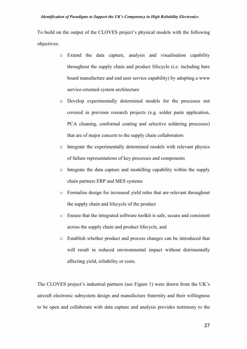
To build on the output of the CLOVES project’s physical models with the following
objectives:
o Extend the data capture, analysis and visualisation capability
throughout the supply chain and product lifecycle (i.e. including bare
board manufacture and end user service capability) by adopting a www
service-oriented system architecture
o Develop experimentally determined models for the processes not
covered in previous research projects (e.g. solder paste application,
PCA cleaning, conformal coating and selective soldering processes)
that are of major concern to the supply chain collaborators
o Integrate the experimentally determined models with relevant physics
of failure representations of key processes and components
o Integrate the data capture and modelling capability within the supply
chain partners ERP and MES systems
o Formalise design for increased yield rules that are relevant throughout
the supply chain and lifecycle of the product
o Ensure that the integrated software toolkit is safe, secure and consistent
across the supply chain and product lifecycle, and
o Establish whether product and process changes can be introduced that
will result in reduced environmental impact without detrimentally
affecting yield, reliability or costs.
The CLOVES project’s industrial partners (see Figure 1) were drawn from the UK’s
aircraft electronic subsystem design and manufacture fraternity and their willingness
to be open and collaborate with data capture and analysis provides testimony to the

Identification of Paradigms to Support the UK’s Competency in High Reliability Electronics
28
value that they placed on the goals of the project. Previously, high volume electronics
production had little relevance to the unitary demand which is typical of aircraft
production. However, the need for specialist high volume expertise in fully automated
assembly becomes more apparent as miniaturisation in electronic component
packages dictate the accuracy and repeatability which stretches human capabilities for
non-automated unitary electronic subsystem demand i.e. surface mount assembly of
printed circuit assemblies.
CLOVES Project Partners
Figure 1 – CLOVES Project Partners
From the doctoral research, a journal paper titled “CLOVES: Addressing The
Knowledge Gaps For UK Production Of Aircraft Electronic Subsystems” was
generated and submitted to the Journal of Engineering Manufacture in 2008 and
accepted with revisions by the first reviewer but further revision requested by a
second. The paper focuses on the domain capabilities which the CLOVES &
INMOST tools could facilitate and the knowledge gaps that may otherwise harm the
UK’s leadership in the production of aircraft electronic subsystems and enhance
inherent product reliability through the accuracy and repeatability potential of
automated assembly.

Identification of Paradigms to Support the UK’s Competency in High Reliability Electronics
29
A conference paper titled “Characterization of Printed Solder Paste Excess and Bridge
Related Defects” also ensued from the author’s research which he generated and
presented at ESTC 2008: 2nd Electronics System-Integration Technology conference
1st – 4th September 2008, University of Greenwich. This paper focused on the solder
paste deposition sub process of SMT Reflow. With an approximated cause ratio of 50
– 70% of post assembly defects (Lau. J.H., 1991) (Mannan S. H., 1993) solder paste
deposition represents the most significant cause initiator of surface mount assembly
sub-processes. Causation models and associated design rules and effects data,
extrapolated from academic and industrial literature and formulated into the physical
models which identify and integrate the process into three discrete solder paste
deposition events – i.e. (i) stencil / PCB alignment, (ii) print stroke / aperture filling
and (iii) stencil separation / paste transfer. The three sub-process models for the solder
paste deposition sub-process are incorporated within Chapter V (Section 2) of this
thesis.
Identification of Paradigms to Support the UK’s Competency in High Reliability Electronics
30
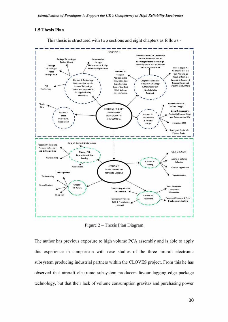
1.5 Thesis Plan
This thesis is structured with two sections and eight chapters as follows -
Figure 2 – Thesis Plan Diagram
The author has previous exposure to high volume PCA assembly and is able to apply
this experience in comparison with case studies of the three aircraft electronic
subsystem producing industrial partners within the CLOVES project. From this he has
observed that aircraft electronic subsystem producers favour lagging-edge package
technology, but that their lack of volume consumption gravitas and purchasing power

Identification of Paradigms to Support the UK’s Competency in High Reliability Electronics
31
increasingly undermines their influence over component manufacturer’s market focus,
resulting in a scarcity of their preferred packages which will inevitably result in a
pursuit of already accelerating trends in package miniaturisation.
Therefore, the hypothesis proposed in Chapter III (Section 1) propositions that if, as a
result of globalisation and price suppression in cost sensitive markets for enabling
electronics technology, the UK’s clustered infrastructure and knowledge-base for
automation is eroded by fragmentation, then its previously immune specialism in
reliability sensitive systems will be undermined. Core competencies in the design and
manufacture of aircraft electronic subsystems, will encounter knowledge gaps in
package selection and the associated enabling process technology. Codification of
industrial based tacit-generic understanding and / or results of academic applied
research (via the CLOVES / INMOST software tools), is needed to directly underpin
the future technological progression of (i) the specific research collaborator’s products
/ services and (ii) the endeavours of other UK based enterprises which contribute this
key competency and support a national competitive advantage.
Printed Circuit Assemblies (PCAs) rely on solder to electrically and mechanically
interconnect electronic components via a Printed Circuit Board (PCB). Surface Mount
Technology (SMT) is the predominant electronic component package format. The
prevalent SMT process technology involves the printing of solder paste on to the
PCB’s SMT pads prior to component placement and solder joint formation via reflow
soldering. The ultimate reliability of the solder joint is dependent on not only, (i) the
geometry of the provisional solder joint, (ii) but also its long-term mechanical
integrity.

Identification of Paradigms to Support the UK’s Competency in High Reliability Electronics
32
Section 2 elicits novel physical models which propose geometric aspect ratio causes
of solder paste deposition defect opportunities that effect solder joint defects with
consequential proportional geometries – which are analysed in Chapters V, VI and
VII with new learning outcomes reported. Both ratios are constrained and disturbed
by package styles / sizes and their relative PCB locations. Therefore package selection
and positioning has a direct influence on defect cause and effects relationships.
Chapter IV (Section 1) promotes lean and synergistic product and process design
which optimises these key design decisions interactively at the PCA layout stage. An
overview of package and PCB technology is presented in Chapter II (Section I).
1.6 Chapter II Overview
Title: Technology Overview – Package & Process Technology Trends andImplications for High Reliability Electronics
Figure 3 – Chapter II Overview Diagram
A learning outcome from the author’s research has been the identification of a
relationship between physical package related attributes and PCA assembly process
defect propensity. Cause and effects analysis of CLOVES project industrial partner
defect data has identified package and process dependencies within root causes. The

Identification of Paradigms to Support the UK’s Competency in High Reliability Electronics
33
impact of Moore’s Law (i.e. doubling of transistor densities at the wafer-level of
integration on an eighteen month cycle) on package, PCB interconnections (i.e. solder
joints) and assembly processes is explained.
As a point of convergence between disparate but linked (by modular product
architectures and customer / supplier supply chain relationships) industries, package
geometry represents the physical incarnation at the interface between component
manufacture and PCB design / PCA assembly. Surface mount package styles and
sizes have been codified by the industry’s standardization bodies, but their assembly
knowledge and its implications for high reliability electronics has not. To provide the
context for package style and size implication for aircraft electronics subsystems
within the following chapters, this chapter aims to provide the background to PCB
and package technology.
1.7 Chapter III Overview
Title: Solutions to Support UK Design & Manufacture of High Reliability ElectronicApplications
Figure 4 – Chapter III Overview Diagram
In this chapter, evidence of fragmentation and its effects are discussed with reference
to academic and governmental sponsored surveys of the UK electronics industry. A
Chapter III: Solutions toSupport UK Design &Manufacture of HighReliability Electronic
Applications
The Need forSupport:
Addressing theKnowledge GapRisks from the
Loss of Low Cost/ High VolumeManufacturing.
How to Support:Codification of the Tacit
Knowledge RequiredFor Lean SynergisticProduct & ProcessDesign and SmartCause & Effects
What to Support: UK LeadershipAircraft production and its
Knowledge Dependency in HighReliability / Low Volume Aircraft
Electronic Subsystems

Identification of Paradigms to Support the UK’s Competency in High Reliability Electronics
34
Darwinian-like process of natural selection has yielded survivors and entrepreneurial
entrants who have emerged or adapted to embrace the resulting fragmentation (of the
globalized electronics production network).
Advantageously, reliability focussed applications are less sensitive to cost and more
reliant on the manufacturing knowledge which delivers the high reliability in products
but with a dependence on lagging-edge technology. The UK’s OEMs (original
equipment manufacturers) which specialise in high reliability applications have
traditionally favoured vertically integrated business models and internal control over
design-to-manufacture operations. However, as the manufacture of cost sensitive
leading-edge technologies migrates to low wage economies, leading-edge
manufacturing experience and knowledge accumulation will migrate along with it.
Even lagging-edge technological advancement will be subjected to the gravitational
pull of the more radical, leading-edge world, thus, creating the potential for gaps to
propagate in the UK’s electronics manufacturing knowledge base.
1.8 Chapter IV Overview (Lean Product & Process Design)
Title: Interactive and Synergistic Product & Process Design for the Lean Productionof Aircraft Electronic Subsystems
Figure 5 – Chapter IV Overview Diagram
Chapter IV:Lean Product &
ProcessDesign
Isolated Product &Process Design
Linked RetrospectiveProduct & Process Design
and Retrospective DfM
Interactive DfM
Synergistic Product &Process Design

Identification of Paradigms to Support the UK’s Competency in High Reliability Electronics
35
In this chapter the author proposes that the production of aircraft electronic
subsystems would be enhanced by a software tool which facilitates product and
process design that is both interactive and synergistic.
Lean focussed stratagems have been employed and business models have been
developed that exploit opportunities that UK leadership in this sector (i.e. aircraft
systems and subsystems) has created. Literature relating to the automotive industrial
origins of lean production (i.e. the Toyota Production System), concurrent engineering
and contemporary lean methodologies are reviewed (i.e. value stream analysis) and
definitions of value extracted from economic theory publications (i.e. Porter)
extracted and the following four paradigms developed:
8.. Isolated Product & Process Design
ii) Sequentially Linked Product & Process Design
iii) Interactive Product and Process Design
iv) Lean & Synergistic Product & Process Design
The author identifies the opportunities for wasteful design errors and costly
discontinuities in the design-to-manufacture sequence. These will be increased by
isolated product and process design. Schedule overruns are an inevitability of
sequence misalignment due to retrospective design reviews and corrective action
feed-back loops within sequentially linked product & process design activities. Lean
methodologies such as value stream analysis are discussed and adapted to provide
novel and practical solutions for interactive product and process design. The author
also recommends the adoption of Heijunka techniques, a synergistic approach to

Identification of Paradigms to Support the UK’s Competency in High Reliability Electronics
36
product & process design within the CLOVES & INMOST tool. Heijunka is the
Japanese term used to describe the conversion of uneven customer demand into even
and predictable assembly line output via product and production levelling.
Kanban based demand driven pull systems, Theory-of-Constraints bottleneck relief
and Group Technology methodologies are discussed and applied to automated PCA
assembly scenarios where a unitary demand driven, hierarchical pull system provides
an ultimately lean solution. Also proposed are stratagems for the elimination of waste
potential from process setup vagaries. These are typical of unitary demand compatible
pull systems and be multiplied by differentials in physical attributes which exists
between disparate but sibling PCAs within a family group. It is anticipated that if the
CLOVES & INMOST software developments could incorporate interactive and
synergistic product & process design capabilities, then the tool might deliver lean
solutions for aircraft electronic subsystem producers.
1.9 Chapters V, VI, VII & VIII Overview
Section Title: Development of Physical Models
Figure 6 – Chapter V, VI, VII & VIII Interaction Diagram

Identification of Paradigms to Support the UK’s Competency in High Reliability Electronics
37
A structure for the codification of tacit process knowledge is provided and discrete
event definitions for the SMT sub processes are provisioned within Chapter V.
Discrete cause and effects model diagrams are originated showing not only inputs and
outputs but also constraint and disturbances. A methodology for model development
is presented.
The results of extensive data mining have shown that the CLOVES partner’s
historical defect logs only contain data pertaining to effects and not causes. This has
created the demand for effects data with linked cause information. Review of
academic and industrial literature provides individual causation formula / rules and
sporadic empirical data which relates to the study of specific product and process
design characteristics (as deemed appropriate at the time of publication and the
technology of the day) but no attempt appears to have been made to homogeneously
characterise the solder paste printing, component placement and solder paste reflow
soldering SMT process stages. Through extensive review of the published data and
trend analysis the author proposes correlations which are exploited to provide the
physical models.
1.10 Chapter IX Overview
Subtitle: Discussions, New Learning, Conclusions & Future Work
Figure 7 – Chapter IX Overview Diagram
Chapter VIIII: Conclusions& New Leaning
Research ConclusionsPackage Technology and its
Implications
New Learning
Research Context & Interactions
Future Work

Identification of Paradigms to Support the UK’s Competency in High Reliability Electronics
38
The model based cause and effects relationships as documented within Section II of
this thesis feed the algorithms for the software tool development which addressed
novel assembly process data capture, formal assembly process models, physical
models of the stencil printing process, integrated thermal model of reflow over
performance and generated initial assembly manufacturing process rules.
The follow up to this new learning will advance this work significantly. This future
work aims to provide an integrated software Design for X toolkit for aerospace
electronics manufacturing products applicable throughout the:
(i) electronics manufacturing supply chain (i.e. bare board manufacture,
assembly, end user applications)
(ii) product and process lifecycle (i.e. design, specification, analysis,
manufacture, test, deploy, maintain, reuse)
The main features supported by the Design for X aims of this research are listed below
in Figure 8. It is noted that although the main focus of the research will be on the
development and formalisation of electronics manufacturing engineering expertise,
consideration of the complete lifecycle of the product will require additional non-
engineering knowledge input.

Identification of Paradigms to Support the UK’s Competency in High Reliability Electronics
39
Design for Increased Yield
Design for manufacture Design for short time to
market
Design for cost
Design for reliability Design for quality Design for assembly
Design for minimum
risk
Design for logistics Design for safety
Design for test Design for standards Design for low quantities
Figure 8 – Design for X capabilities under consideration within the DIY project.
In the INMOST tool development, the capabilities outlined in Figure 8 will be
enabled by providing modelling and monitoring support for design, manufacturing
and operational defects and sources of unreliability via:
a. predictive physical and reduced-order physics models of products and
processes
b. data-centric models of manufacturing and operational capability
c. determination of experiential design and manufacturing rules
d. integration with relevant third party modelling software
e. integration with company ERP and MES systems
Chapter Summary:
A thesis plan to addresses the research objective in offering heuristic codification of
existing tacit industrial knowledge and academic learning within physical models
which provide the algorithms for tool based analysis of product and process designs
and smart cause and effect simulation is presented.
Presentation of the physical models and associated new learning within Section 2
(Chapters V, VI, VII and VIII) discourses the ‘how’ and ‘what next’ simulation
questions for the CLOVES and INMOST functionality whereas the ‘where’, ‘why’,

Identification of Paradigms to Support the UK’s Competency in High Reliability Electronics
40
‘who’ and ‘when’ simulation questions are addressed within Section 1’s Chapters III
and IV. By proffering a technology overview Chapter II offers context (i.e. where?)
for the knowledge which is vulnerable to fragmentation effects as hypothesised within
Chapter III (i.e. why?). Chapter IV proposes the use of these physical models by
engineers ‘who’ concurrently and interactively develop synergistic product and
process designs (i.e. when?). Finally, Chapter IX draws conclusions and presents the
new learning which arises from the purported answers to the above questions and
enables the follow on of future work which would enhance the INMOST applications
beyond Paradigm 3 (i.e. IdfM) and enable lean and synergistic product and process
development as the what next scenario.
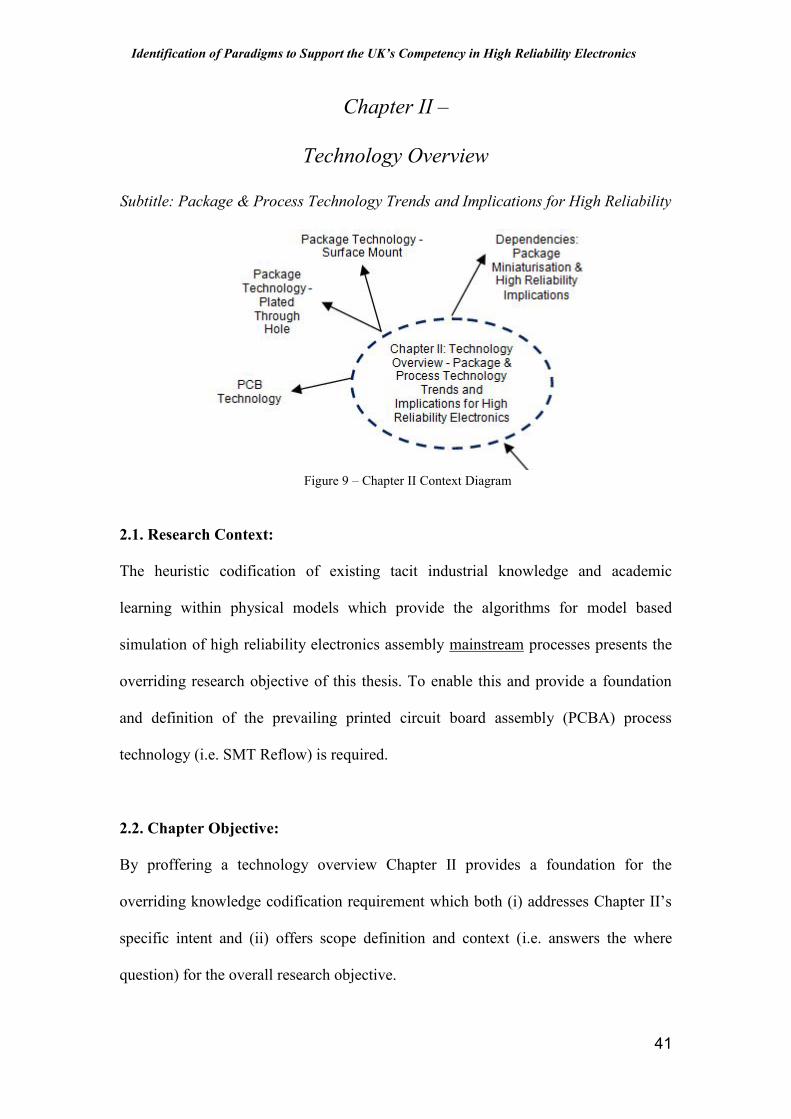
Identification of Paradigms to Support the UK’s Competency in High Reliability Electronics
41
Chapter II –
Technology Overview
Subtitle: Package & Process Technology Trends and Implications for High Reliability
Figure 9 – Chapter II Context Diagram
2.1. Research Context:
The heuristic codification of existing tacit industrial knowledge and academic
learning within physical models which provide the algorithms for model based
simulation of high reliability electronics assembly mainstream processes presents the
overriding research objective of this thesis. To enable this and provide a foundation
and definition of the prevailing printed circuit board assembly (PCBA) process
technology (i.e. SMT Reflow) is required.
2.2. Chapter Objective:
By proffering a technology overview Chapter II provides a foundation for the
overriding knowledge codification requirement which both (i) addresses Chapter II’s
specific intent and (ii) offers scope definition and context (i.e. answers the where
question) for the overall research objective.

Identification of Paradigms to Support the UK’s Competency in High Reliability Electronics
42
2.3. Introduction
Formalised taxonomy conventions for establish electronic component package
technology and definition of its associated interconnection assembly process
knowledge derive from this ever evolving industry’s component mounting trends.
Semi-conductor based “active” components have circuits which are integrated within
a ‘chip’ (usual but not exclusively produced with a silicon wafer) at levels of
miniaturisation which, by orders of magnitude, are scaled beyond the capability of
external (i.e. PCB based) circuit interconnectivity. Therefore intermediate level
packaging of the chip is required to convert and interconnect between the disparate
dimensional extremes. Although contemporary assembly process advancement now
enables direct interconnectivity between chip and PCB intermediate scale converting
packaging still prevails and the term ‘package’ is still in widespread use.
Package styles and sizes for both ‘active’ and electrically passive components (e.g.
capacitors, resistors and inductors) have been codified by the industry’s
standardization bodies such as the IPC (IPC, Association of Connecting Electronics
Industries, 2005) & JEDEC (formerly Joint Electron Devices Engineering Council:
www.jedec.org) but their assembly knowledge and its implications for high reliability
electronics has not. This chapter aims to provide the historical background to PCB
and package technology and to provide the context for its codification of its prevailing
process (i.e. SMT Reflow) within the physical models as presented within Section 2
of this thesis.

Identification of Paradigms to Support the UK’s Competency in High Reliability Electronics
43
2.3. Printed Circuit Board Technology
Initially, the provision of interconnectivity of electronic components used the point-
to-point construction techniques with components with solder-able tags (see Figure
10) mounted onto turret boards (see Figure 11) and electrically interconnected via
discrete wires.
(https://www.galco.com/scripts/cgiip.exe/wa/wcat/itemdtl.r?listtype=Catalog&pnum=FP227.7-MALY)
Figure 10 – Image of an electrolytic capacitor with solder-able tags protruding fromthe top
(http://en.wikipedia.org/wiki/File:Turret_Board_with_a_Few_Components.png)Figure – Image of electrolytic capacitors mounted onto and connected via a turret
board

Identification of Paradigms to Support the UK’s Competency in High Reliability Electronics
44
Elimination of solder-tag wiring and subsequent space savings from greater
interconnection density within a single plane arrived with the introduction of the PCB
(Petherbridge, 2004). The need for manually attached, discretely wired connections
was negated with the reconstitution of the circuitry via en masse electro-chemically
etched, integral copper tracks. The tracks are generated within a copper base and clad
to the underside surface of a laminate then electroplated to the required thickness to
form the PCB’s circuitry. With the solder-able tags replaced by solder-able leads,
direct mounting and interconnection became possible, hence the printed circuit
assembly or PCA – see Figure 12.
(http://www.bing.com/images/search?q=images+of+single+sided+printed+circuit&view=detail&id=84710E3CA13661CC9C8EC30788BA33F54401FFA6&first=121&F
ORM=IDFRIR)Figure 11 – Image Showing a Basic PCA with Top Side Mounted Components &
Under Side Copper Traces
Although some provisional patents date back to the early 1900’s, the conception of
what is now be recognizable as PCB architecture and its manufacturing knowledge is
credited to Dr. P Eisler in 1936 (Ellis, 1986) but its origins have been predated by
fifty years (Petherbridge, 2004). The adoption of the photochemical etching technique
for the definition of the copper traces from the copper clad substrate must represent an

Identification of Paradigms to Support the UK’s Competency in High Reliability Electronics
45
enabling process technology milestone, as photo-lithography offers opportunities for
down-sizing interconnections whilst still maintaining equitable geometric aspect
ratios. When inserted through pre-drilled holes and solder-joint connected to the
underside clad circuitry (see Figure 4) the solder-able leads both (i) mechanically
secured the components and (ii) facilitated the electrical connectivity via the copper
traces – see Figure 13.
Figure 12 – Graphical Representation of a Sectional View of a None-Plated-Through-Hole
2.4. Plated-Through-Hole PCBs
PTH technology developed by Motorola in 1955 (Nieter, 1955) delivered an early
breakthrough PCB geometry downscaling, in turn heralding major miniaturization
advancement in electronic component packaging. Prior to plated-through-holes (see
Figure 14), metallic inserts and jumper wires provided an interim transition to the
utilization of both sides of the PCB for tracking purposes, but a cost volume scalable
solution must only have become realizable with the arrival of PTH.

Identification of Paradigms to Support the UK’s Competency in High Reliability Electronics
46
Figure 13 – Graphical Representation of a Sectional View of a Plated-Through-Hole
The innovation of the semi-conductor would have massively reduced the footprint of
‘active’ components i.e. transistors, diode and integrated circuits. Its introduction is
traceable back to the 1950’s with the advent of octal valve packages, originally with
9mm pin spacing, and then superseded by all-glass B7G or B9A valves with 4mm pin
spaced solder tags (Ellis, 1986) – see Figure 15.
(http://oldradio.onego.ru/tubes.htm)Figure 14- Images Showing Octal Valve Technology
Due to the higher density and therefore smaller geometries of solder-able leads, single
sided circuitry would not have provisioned (i) adequate mechanical integrity to
support the mass of the glass valve packages, or (ii) sufficient tracking density to
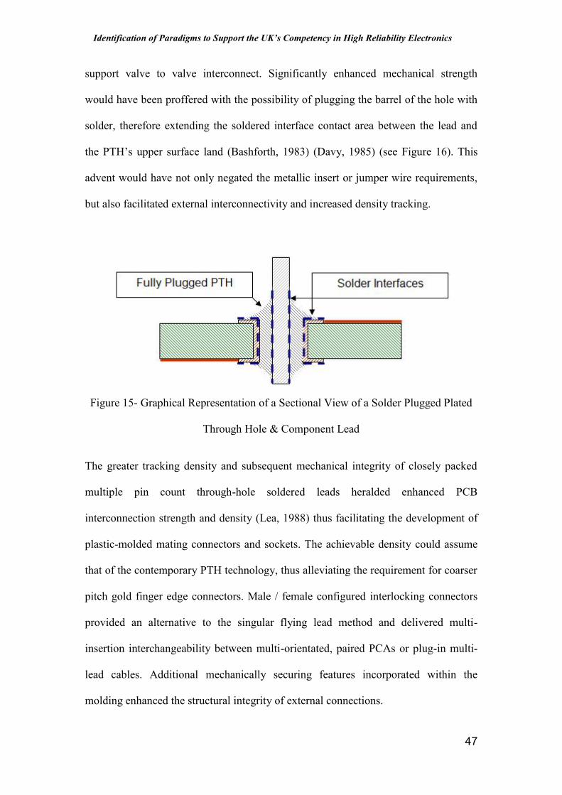
Identification of Paradigms to Support the UK’s Competency in High Reliability Electronics
47
support valve to valve interconnect. Significantly enhanced mechanical strength
would have been proffered with the possibility of plugging the barrel of the hole with
solder, therefore extending the soldered interface contact area between the lead and
the PTH’s upper surface land (Bashforth, 1983) (Davy, 1985) (see Figure 16). This
advent would have not only negated the metallic insert or jumper wire requirements,
but also facilitated external interconnectivity and increased density tracking.
Figure 15- Graphical Representation of a Sectional View of a Solder Plugged Plated
Through Hole & Component Lead
The greater tracking density and subsequent mechanical integrity of closely packed
multiple pin count through-hole soldered leads heralded enhanced PCB
interconnection strength and density (Lea, 1988) thus facilitating the development of
plastic-molded mating connectors and sockets. The achievable density could assume
that of the contemporary PTH technology, thus alleviating the requirement for coarser
pitch gold finger edge connectors. Male / female configured interlocking connectors
provided an alternative to the singular flying lead method and delivered multi-
insertion interchangeability between multi-orientated, paired PCAs or plug-in multi-
lead cables. Additional mechanically securing features incorporated within the
molding enhanced the structural integrity of external connections.

Identification of Paradigms to Support the UK’s Competency in High Reliability Electronics
48
(http://www.bing.com/images/search?q=images+of+printed+circuit+connectors&view=detail&id=65497C057FFE6F3398B9117C7C9298CBB9B6E96A&first=61&qpvt
=images+of+printed+circuit+connectors&FORM=IDFRIR)
Figure 16- Images of Various Examples of Plastic Molded PTH Connectors
With the advent of Surface Mount Technology (SMT) the need for component
mounting in through holes (with the via hole replacing the component hole) would
have been negated, but PTH technology would still remained integral to extra-PCA
and inter-plane connectivity.
2.6. Multi-layered PCBs
Component footprints and mounting holes which consume board surface area, thus
requiring extra tracking surfaces, provided a need for the development of multi-
layered PCBs (Lea, 1988).
The succession of PTH by SMT in the 1980’s (Klein Wassink, 1989) proffered
significant geometric downscaling potential. An alternative to the through-hole and
inserted lead materialised with solder joint terminations (i.e. discrete leads or
metalized surfaces) mounted directly on the PCB’s surfaces (Klein Wassink, R. J.,

Identification of Paradigms to Support the UK’s Competency in High Reliability Electronics
49
Vledder, H.J., 1983). Previously, component lead and soldered interconnection
geometries were constrained by the 2.54mm minimum pitch convention which has to
accommodate the typical 1.25mm finished hole diameter (Klein Wassink, 1989).
With the components surface mounted, via-holes assumed the inter-plane connectivity
function for multi-layered PCBs (Petherbridge, 2004) – see Figure 18. Although
through-plated and generated concurrently with the component mounting holes, by
way of a negation of the need to accommodate the component lead (with sufficient
insertion and solder wetting clearance) (Bashforth, 1983) the via-hole offers further
miniaturization benefits. Diameters would have been constrained only by their
equitable PCB manufacturing process capabilities i.e. the contemporary drilling, de-
smearing, electro-plating (Lea, 1988). Latter-day PTH technology can offer HDI
(High Density Interconnect) techniques with through-hole micro-vias at 0.2mm
diameter and blind / buried via holes 0.095 (Rasmussen. J, 2006), thus optimizing
tracking density and distribution with better utilization of the internal (copper clad and
tracked) interfaces within multilayered PCB architectures.
Figure 17- Graphical Representation of a Sectional View of Blind, Buried and Micro-Vias

Identification of Paradigms to Support the UK’s Competency in High Reliability Electronics
50
2.7. Non-soldered Interconnections
Although deficient of both chemical and physical bonds, electro-mechanical
attachment processes such as press-fit (i.e. interference fit pins inserted into plated-
through-holes in the PCB under high positive insertion forces) and gas-tight pressure
contacts (under high clamping force) provide alternatives. However, their mechanical
mechanisms of attachment preclude and therefore must supplement mainstream
bonded SMT assembly processes. Permanently bonded electro-mechanical
interconnections must involve the use of one of the following attachment methods:
soldered joints
conductive adhesive,
wire bonds
Due to either (i) their relatively slow and complicated en-masse cycle times or (ii) fast
but sequential processing, both conductive adhesive attachment (Lau, 2003) and wire
bonding (Harmen, 1997) cannot be accommodated within SMT Reflow process
capabilities and are consequently exclusive of the model based simulation tool’s main
stream process scope.
Bonds of predetermined chemical composition form as solder wets to a metallic
surface (Kay, 1976) but conductive adhesive attachment, and wire bonding, rely on
less robust, physical bond attachment processes (Ellis, 1986). For optimised bond
conditions, all connection types require prepared surfaces (Klein Wassink, 1989).
Therefore, the component and substrate bond pads must be optimized for molecular
attraction (e.g. free from interposing contamination such as greasy mono-layer films,

Identification of Paradigms to Support the UK’s Competency in High Reliability Electronics
51
oxide layers, and corporal particulates) (Cala, 1996) thus, prescribing exacting
standards of cleanliness.
Additionally, solder-able surfaces must also necessitate either (i) the preclusion of
oxide layers (or other metal salts) or (ii) their removal as the antecedent of the
soldering operation (Ellis, 1986). Prevention / removal failure will affect areas of non-
wetting (Klein-Wassink, 1967) (Davy, 1985) (Smith, 1986) (Lau. J.H., 1991).
Although far from ideal, unless obscured by the package areas of non-wetting should
never the less be more visually apparent in metallic chemically bonded areas than
would be the case with physically bonded areas of non-adhesion between the metal
pad and organic adhesive.
2.8. Enabling Process Innovation – En-masse soldering
En-masse soldering can be performed by (i) wave soldering (a.k.a. flow soldering)
and (ii) reflow soldering:
Wave SolderingBy passing one surface of the populated PCB over a wave of liquid solder (i.e. the
solder wave) fillets of solidified solder formed joints with the PCB track (SMT pads
or PTH lands) and component terminations (Hawkins, 1986). Due to their
incompatibility with immersion within molten solder the ubiquitous presence of PTH
components makes it only possible to solder one side of the PCB (i.e. the solder side)
via this technique.
Reflow SolderingThis process initiates with the printing of or, in more specialist applications,
dispensing of the solder paste deposits onto the interconnecting solder pads (a.k.a.

Identification of Paradigms to Support the UK’s Competency in High Reliability Electronics
52
lands). Formulated from microscopic balls of solder and bound together by flux and
thixotropic agents into a paste or cream, (Rubin, 1986) the paste deposits are printed
on to the pads via a screen or more commonly a stencil (Partridge, 1987) (Lea, 1988).
Subsequent population of the SMD’s (Surface Mount Devices) with their solder-able
terminations placed into the paste precedes the en-masse melting, coalescing, and
wetting constitutes the reflow soldering operation (Markstein, 1987).
The thus far un-bonded assembly either (i) via conveyorisation, progresses through
zone-by-zone controlled heated tunnel, thus following a preprogrammed temperature
profile or (ii) statically absorbs thermal energy within profile tracking batch ovens
(Markstein, 1987). Paste suppliers will recommend profiles which are optimized for
the subsequent melting and coalescence of their formulation’s solder balls, facilitating
the wet out of the solder-able surfaces and the formation solder fillets (Rubin, 1986).
Reflow soldering can be repeated for SMT population of both sides of the PCA’s and
can even be adapted for PTH soldering i.e. intrusive reflow (IPC, Association of
Connecting Industries). Note, although intrusive reflow is possible it is not captured
within the physical model scope due to (i) solder joint volume and inspection issues
preclude its use in high reliability applications such as those incumbent of the
industrial collaborators, and (ii) PTH component package styles do not lend
themselves to vacuum pick and placement via standard SMT equipment.
2.9. Surface Mount Package Technology
To enable wave solder attachment, component body materials need to (i) repel the
liquid solder (i.e. none-wet) and (ii) withstand thermal shocks when immersed in
liquid solder (i.e. 235-260°C for eutectic SnPb) (Lea, 1988). Solid state ceramic and

Identification of Paradigms to Support the UK’s Competency in High Reliability Electronics
53
tantalum based SMT capacitors superseded liquid filled, electrolytic PTH and solder-
tagged antecedents, thus offering a surface mountable process compatible solution for
both wave and reflow solder attachment. For wave soldering the pre-mounting issue
resolved with the development of heat curable SMT Adhesives (Davy, 1985).
Flat surfaces incorporated into body profiles enabled automated placement of SMDs
via vacuum gripping – surface flatness must therefore represent a critical
characteristic which dictates defect opportunities and provides a causation input for
the placement physical model – see Chapter 6. The negation of the through-hole
inserted lead subsequently eliminates the need for additional lead pre-cut / pre-form
and insertion operations which whilst adding value must also increase defect
opportunities!
Automatic pick & place machines incorporated heat curable adhesive dispensers
integrated the wave solder SMT pre-attachment process (Lea, 1988) with in-line
heated tunnel ovens providing the heat accelerated curing solution. A PCB’s ‘real
estate’ must double at a stroke with the possibility populating its underside a.k.a.
bottom side SMT. Where through holes could be replaced by SMT pads (Hawkins,
1986), population density growth followed the wafer-level integration (Minges, M. L.,
1989) and downscaling miniaturization trends of the internal integrated circuits with
lead pitches body sizes approximately subdividing within each passing decade – see
Figure 19.

Identification of Paradigms to Support the UK’s Competency in High Reliability Electronics
54
Figure 18- Graphical Representation of an SMT Package Downscaling Timeline
2.10. Package Miniaturisation and Process Automation Implications
To remain compatible during package miniaturization, automation and must retain
any symbiotic and proven scale dependent competencies. As package downscaling
tracks wafer level advancement, (Reichl, H., Grosser, V., 2001) reducing geometries
and shrinking process windows must subsequently accelerate developments in
assembly capability and progressive automation.
To allow PTH automation, auto-insertion machines needed to engineer lead pre-
insertion cut and form mechanisms for the removal of bandoleer presented, axial and
radial PTH passives, with post insertion lead re-cutting and clinching mechanisms.
Similarly, auto cut & clinch technology enabled secured, multi-leaded DILs (Dual-In-
Line) packages prior to wave soldering. Semi-automated machines, which presented

Identification of Paradigms to Support the UK’s Competency in High Reliability Electronics
55
the components and guided the operators to insert in the correct location prior to auto
re-cutting and clinching, gave way to fully automatic axial leaded, radial leaded and
DIL inserters (Lea, 1988). Drag then wave soldering processes superseded hand
soldered assembly and provisioned en-masse automation (Klein Wassink, 1989). The
additional functionality from increased component counts must necessitate higher
density interconnects and circuitry.
Double-sided population possibilities advanced SMT technology into today’s
dominant assembly process technology (Klein Wassink, 1989). Wafer-scale packages
such as flip-chips (Lau, 1996), and chip scale packages (CSPs) (Reichl, H., Grosser,
V., 2001) provide an illustration of the miniaturization possibilities (see Figure 20)
once the need for scale transition via an intermediate interconnection package negates.
Systematic process evolution, through stencil printing (Lotosky, 2006) and automatic
placement refinements plus developments in reflow oven capabilities (Markstein,
1987) has enabled direct chip attach (DCA) interconnection (Puttlitz, 2001). DCA not
only illustrates the benefits of symbiotic package and process advancement but also
their interdependencies.
Figure 19- PTH to Flip-chip miniaturization comparison

Identification of Paradigms to Support the UK’s Competency in High Reliability Electronics
56
2.11. Package & Process Compatibility
Package technology dependencies must directly impact on manufacturability and
therefore process technology in the following three ways:
i) Firstly, the scale of the miniaturisation which a package technology employs
must dictate the size of corresponding process windows. For example, the
smallest package geometries requiring the highest process accuracy and
repeatability.
ii) Also, the product and process compatibility challenge, as embedded in the
product’s design at the PCA layout stage, must likewise be dependent on
package technology; with the extent of the geometric diversity in package
selection defining the degree of flexibility required within the automated
component placement process.
iii) Lastly, the package technology’s compatibility with automated soldering
process options must be dependent on the employed lead style – not all
package technologies are compatible with the two en masse soldering
processes i.e. reflow and wave soldering.
The dominant design in contemporary reflow soldering processes involves the pasted
and SMT component populated PCB passing through a thermally profiled, forced
convection-heated tunnel with controlled pre-heat, soak, peak, and cooling zones
(IPC, Association of Connecting Industries) – see Figure 21. Soldering occurs in the
peak zone with component / board surface temperatures in the range of 215-235C for
eutectic SnPb solder and 240C plus for Pb-free alloys (Lau, 2003) – with banning of
use of lead in electronics manufacture by the European Union RoSH directive
Identification of Paradigms to Support the UK’s Competency in High Reliability Electronics
57
(Suganuma, 2001) which provisions exemptions for low volume / high reliability
applications such as aircraft electronic subsystems.
Excessive thermal ramp rates in the pre-heat and peak zones can cause premature
failure in electronic components (Gallo, 1995) (Hutchins, 1995) (Franken, 2004).
Given that discrete package types with distinct failure modes can co-inhabit PCAs a
consensus maximum of 2C/second heating and 3C/second cooling rate applies in
industrial processes (IPC, Association of Connecting Industries). The paste’s volatiles
(i.e. solvents) which hold the soldering fluxes and thixotropic agents in suspension
and help to bind together the microscopic solder balls (Rubin, 1986) evaporate and the
fluxes activated during the pre-heat stage. The microscopic solder balls melt when
they reach 183C (eutectic) (Suraski, 2000) and fully diffuse and ‘wet’ to the solder-
able surfaces in the peak temperature zone directly prior to forced-cooling. As the
assembly cools, the liquid solder then forms solid fillets with inter-metallic bonding at
the PCB copper pad boundary and the corresponding interface with the Sn/Au/Pl
(Kay, 1976) combinations as favored by SMT component manufacturers. With less
aggressive heat-up and cool-down rates (i.e. lesser thermal shocks) than with wave
soldering (Lau. J.H., 1991) Reflow soldering lends itself much more readily to SMT
assembly.

Identification of Paradigms to Support the UK’s Competency in High Reliability Electronics
58
(Courtesy BTU International http://www.btu.com)
Figure 20 – Graphical Representation of a Schematic for a BTU Paragon 98 Forced-Convection Reflow Tunnel
With its underside in lateral contact, in wave soldering the populated PCB passes over
the cascading molten metal flow as it traverses via an edge-conveyor based transport
system. Unless already attached via a preceding soldering process (e.g. double-sided
reflow) and shielded by exclusion type wave solder carriers, the bottom-side SMDs
will fully immerse in the liquid solder. Sometimes referred to as mixed technology
PCAs, SMT components which have previously been physically attached by adhesive,
but not yet connected to the bottom-side of the PCBs simultaneously solder in tandem
with their PTH counterparts.
A combination of convection and radiated energy transfer is used to pre-heat the PCA
to an industry norm minimum temperature range (e.g. 80ºC to 120C) (Lea, 1988) as

Identification of Paradigms to Support the UK’s Competency in High Reliability Electronics
59
usually recommended by the specific proprietary flux manufacturer’s data sheet and
measured at the PCB top surface directly prior to its contact with the liquid solder.
Flux is required to remove surface contaminants such as metallic oxides and organic
films from the solder-able surfaces prior to soldering (Davy, 1985). Wave solder
machines integrate flux application systems. Depending on (i) the percentage of solids
within the flux and (ii) the post solder de-fluxing requirements (in lower reliability
applications which exempt conformal coating requirements, the use of a low-solids
content flux can similarly negate the need to clean) (Brox, 1995) the following
alternative techniques are typical (Cala, 1996):
a. Higher solids fluxes which are un likely to spray or atomise well
usually require the emersion of the PCB within a foaming funnel of
liquid flux,
b. Low solids fluxes which are more jet-able are usually sprayed on to
the PCB’s solder side by a programmable reciprocating spray nozzle.
Flux manufacturers’ select their solvent carriers to suite either convention and must be
mindful to ensure that volatiles can evaporate prior to PCB contact with the liquid
solder – failure to do so could cause out-gassing and result in integral blowholes and
voids solder joints (Lea, 1988).
SMT chip component manufacturers typically recommend solder emersion contact
time be limited to a maximum of 3 to 5 seconds (Franken, 2004), but the heat transfer
needed to elevate the solder-able surfaces to the temperature required to promote good
wetting will be conducted and therefore highly accelerated when compared to

Identification of Paradigms to Support the UK’s Competency in High Reliability Electronics
60
contemporary reflow’s convection based energy transfer (IPC, Association of
Connecting Industries). As a consequence, the instantaneous thermal shock
experienced when the PCA exits the preheat zone and enters the wave, typically
around 70C (Lau. J.H., 1991), impacts bottom side mounted SMDs – see Figure 22.
(Courtesy Speedlinetech www.speedlinetech.com)
Figure 21 – Graphical Representation of an Electrovert Electra Wave Solder Machine
To provide the conducted heat source for rapid elevation of the solder-able surfaces to
the minimum wetting temperature, which must as a minimum achieve a eutectic
alloy’s liquidous temperature (e.g. 183C for eutectic Sn/Pb) (Hansen, 1958), the
solder-bath temperature typically ranges between 235C and 260C (Lea, 1988).
Process engineers target this range and refine their process windows to optimize
through-hole penetration whilst being mindful of the thermal shock and the applicable
flux’s data sheet stipulated top side preheat recommendations. When solder pumps
through the wave-forming steel plates and encounters the ambient atmosphere it can
be expected to cool, but its fluidity will only start to drop at actual temperatures below
210C (Klein Wassink, 1989). Therefore, for optimal soldering conditions, conveyor
speeds need to balance the disparate requirements of (i) flux activation temperatures

Identification of Paradigms to Support the UK’s Competency in High Reliability Electronics
61
(formulation specific) (ii) volatile evaporation (formulation specific but 84C for
Isopropyl Alcohol) (Lea, 1988) (iii) solder bath temperature and (235-260C) (iv)
maximum allowable thermal shock (2C per second).
2.12. Termination Style Process Dependencies
Certification of airworthiness will require the nomination of and compliance with
standards of workmanship for the manufacture of PCAs for aircraft electronic
subsystems via an auditable trail. Benchmarking to J-STD-100D Class III standards of
workmanship is the norm and its limits of acceptability for solder joints can be
categorised by common attributes and shared J-STD-100D clauses (IPC, Association
of Connecting Electronics Industries, 2005) – see IPC-HDBK-610 (IPC, Association
of Connecting Electronics Industries). This thesis’s codification requirements group
(as determined by their termination style and architecture) package dependent
soldered interconnectivity into the following four domain formats:
PTH ComponentsAlthough body styles and lead counts may significantly vary, PTH components
provide an obvious sub-set which share commonalities in soldering process
characteristics and joint geometry. By definition through-hole mounting and
interconnection footprints must occupy three dimensional PCB ‘real-estate’ –
therefore excluding the possibility of back-to-back PTH locations and double sided
PTH. With solder applied in liquid form and always from the underside, PTH
component body styles must have minimal impact on the wave solder process. From a
lead geometry and solder joint perspective, multi-leaded formats such as the dual
inline (DIL) package (see Figure 23) simply replicate a series of closely spaced twin
leaded PTH components.

Identification of Paradigms to Support the UK’s Competency in High Reliability Electronics
62
(http://www.topline.tv)Figure 22- The DIP PTH Package
Intrusive reflow (a.k.a. paste-in-hole) is an option in lower reliability PTH
applications (i.e. Class I and Class II) (IPC, Association of Connecting Electronics
Industries). Solder paste is over-printed onto PTH holes and their surrounding solder-
able annuluses (a.k.a. solder lands). Prior to reflow mass soldering, the pin has to
puncture and consequentially must disturb the deposit during PTH insertion, with the
wetting forces redistributing the coalesced paste about the wet-able surfaces.
However, situations where the viability of apertures, which sufficiently release the
volume of paste to satisfy the requirements of J-STD-100D Class III (IPC,
Association of Connecting Electronics Industries) for acceptable barrel fill, with PTH
exclusive stencils (IPC, Association of Connecting Industries) are hard to envisage.
Given that the main justification for intrusive reflow processing are derived from a
rationalization of process stages within single reflow operation, then the viability of
PTH only stencils must be exclusive to PTH only PCAs.
These incompatibilities create huge challenges in Class I & II (IPC, Association of
Connecting Electronics Industries) for through-hole solder penetration (IPC,
Association of Connecting Industries) mixed technology applications of intrusive

Identification of Paradigms to Support the UK’s Competency in High Reliability Electronics
63
reflow and limit applications to relatively simple package and PCB interconnections.
Even then, specialist enclosed head printing technology such as 1 Proflow is required.
Consequently, Class III PTH applications will mostly dictate liquid solder attachment
processes – namely, hand, selective and predominately wave soldering.
SMT Chip ComponentsFor purposes of common-process codification SMT packages categorize via their
interconnect termination styles as per JEDEC standards (JEDEC, 1988). SMT chips
represent the singular termination category, which excludes connectivity via a solder-
able lead protrusion. This need is negated as they instead provision interconnection
via sufficiently large and well-spaced solder-able surfaces, a.k.a. metalized end caps.
The metallization can be formed into end caps due to the fact that their ‘passive’
functionality requires only two interconnections per component e.g. resistors and
capacitors. Their naming convention reflects their (nominal) footprints e.g. 1206 – L
= 0.120” (3.00 mm), W = 0.060” (1.50 mm) (IPC, Association of Connecting
Industries) – see Figure 24.
(http://www.topline.tv)
1 ProFlow® DirEKt Imaging is the registered trade mark of DEK International 2007
Identification of Paradigms to Support the UK’s Competency in High Reliability Electronics
64
Figure 23 – Graphical Representation of a Ceramic Chip Component with NamingConvention
Due to the relatively large pitch between termination increments, which consequently
lower their susceptibility to solder bridging defects (Davy, 1985) (Lea, 1988) (Klein
Wassink, 1989), must make the SMT chip category the only relatively high yielding
SMD package technology which is therefore compatible with wave soldering. Even
when marginally compatible, SMT and PTH wave solder process windows do not
always align. For both package technologies to be mutually compatible with wave
soldering, the individual process windows need to overlap with common process
dependencies and package constraints. Process dependencies apply because of the
presence of (i) thermal shock sensitive SMT packages, (ii) high thermal demand PCB
architectures or PTH component leads and (iii) PTH barrel file challenges such as
Class III, or Class II with none-eutectic solder finishes (IPC, Association of
Connecting Electronics Industries, 2005).
SMT Peripheral LeadedAdvanced levels of integration at the silicon level must require increased
interconnectivity with external entities, e.g. intra PCA components; inter PCA
communications; extra PCA interfaces. Prior to the advent of area array technology,
peripherally lead package formats and lead styles formats that followed either gull-
wing or letter J shaped profiles (IPC, Association of Connecting Industries) (see
Figure 25) exclusively offered multi-leaded interconnectivity SMT package formats
and therefore the only option advanced silicon level integration.

Identification of Paradigms to Support the UK’s Competency in High Reliability Electronics
65
(http://www.topline.tv)Figure 24 –Graphical Representation of SMT Peripheral Leaded Profiles
The silicon chip is interconnected to the peripherally position lead frame directly via
wire bonds and conductors – see Figure 26.
(http://www.topline.tv)Figure 25 – Cut-away View Showing Die and Lead-frame Wire Bonded
Interconnections
Peripheral leads protrude from either (i) two of the package’s parallel sides or (ii)
from all four facets. With dual-in-line leads with gull-wing profiles the package
assumes 0.050” (1.25 mm) and is codified as an SOIC (Small Outline Integrated
Circuit) format (JEDEC, 1988) (IPC, Association of Connecting Industries) –
although there are many derivatives with reduced body size and lead pitches. The four
sided formats are based on the QFP (Quad Flat Pack) which is most prevalent with
0.025” (0.635 mm) and 0.020” (0.50 mm) spaced gull-wings – see Figure 27. The J-
leaded alternatives are respectively known as SOJ’s and PLCC (Plastic Leaded Chip

Identification of Paradigms to Support the UK’s Competency in High Reliability Electronics
66
Carriers) and the lead spacing of either package format does not vary from 0.050”
(0.125 mm) pitches – see Figure 28.
(http://www.topline.tv)Figure 26 – Graphical Representation of Dual and Quad Packages with Gull Wing
Lead Profiles
(http://www.topline.tv)Figure 27 – Graphical Representation of Dual and Quad Packages with J-Leads
Wave soldering is unsuited for interconnection of quad leaded peripheral packages.
Bridges will almost certainly occur as a result of the disturbed surface tension and
disrupted excess solder drainage (Lea, 1988). Unsoldered termination defects will
prevail due to the shadowing effects which the component’s body generates. With
their leading and trailing edge lead arrangements disruptive of the flow dynamics of
the liquid solder (as pumped and channelled to optimise barrel-fill and drainage
between PTH leads as the PCA exits the wave) the package must be incompatible
with the wave soldering. Quad peripheral packages could be mounted at 45°
orientations but with little benefit expected – a more even distribution but still a
disturbance of wave’s dynamic flow characteristics.

Identification of Paradigms to Support the UK’s Competency in High Reliability Electronics
67
Due to their coarser pitches J-leads must be less likely to bridge. In fact, their
massively increased PCB stand-off height may even reduce the effects of shadowing
and improve the chances of wave penetration around the target surfaces. However, the
stand-off height which is generated by the J-lead must make glue dot attachment prior
to wave soldering impractical.
This leaves the gull-winged SOIC as the only viable wave solder-able silicon
integrated package and only then with the imposition of PCA layout design rules: to
minimise bridging related defect opportunities, the fixturing or basic board layout
needs to orientate the lead bearing facets so that (i) they do not ‘comb’ the wave and
(ii) the PCB interconnection footprint is provisioned with additional sacrificial pads
which scavenge excess solder on wave exit and a.k.a. solder-thieves (Lea, 1988).
SMT Area ArraysIf area array packages such as BGAs are present on the PCB’s upper surface,
prolonged wave solder contact times could also incur the risk of secondary reflow.
This reliability impacting risk (Lau, 1995) may occur as transferred energy is
conducted directly to their solder joints by way of a matching array of via holes which
are typically present in accommodating the circuit tracking paths between a various
interconnecting layers of a multi-layer PCB architecture. This eventuality provides an
example of a package dependency that constrains a successive assembly process.
In all but the finest pitches – where the geometries are two small for reliable solder
paste printing and pre-deposited / fused solder is re-melted to form the solder joints –
the mainstream SMT attachment process is applicable i.e. Reflow soldering. Even at
the course lead pitch scales, area array properties as typical of the plastic BGA format

Identification of Paradigms to Support the UK’s Competency in High Reliability Electronics
68
(see Figure 29) facilitates a fuller utilization of PCB ‘real-estate’. Additionally the
larger clearances offer less defect opportunities and subsequent yields must be (IPC,
Association of Connecting Industries) higher than those that are typical of alternative
package formats with equitable footprint sizes and interconnection counts i.e.
peripherally leaded QFPs.
(http://www.topline.tv)Figure 28 – Underside View of a Plastic BGA Showing Area Array Solder
Interconnections
However, defect detection opportunities are limited as conventional visual techniques
require line-of-sight access which will only be apparent for outer periphery position
interconnects (see Figure 30) (Lau, 1995)
Figure 29 – Peripheral View of BGA Solder Joints

Identification of Paradigms to Support the UK’s Competency in High Reliability Electronics
69
Transmissive techniques such as X-ray inspection are required but, the technology
that can deliver Class III defect (IPC, Association of Connecting Electronics
Industries, 2005) detection requires, quantifiable volumetric assessment of area array
solder joints (Lau. J.H., 1991) via more costly techniques such as X-ray computer
tomography.
2.13. Chapter Summary:
To address this thesis’s overriding research objective (i.e. the heuristic codification of
existing tacit industrial knowledge and academic learning within physical models
which will enable model based simulation) definition and codification of the
mainstream assembly processes for high reliability electronics is needed. For this
foundation (i.e. background) knowledge and its interdependencies is required. These
interdependencies will later be codified as inputs, outputs, constraints and disturbance
factors which will be shown to influence the to-be developed physical models.
This chapter concludes that the interdependencies derive from product and process
design domains and historically, the electronic package, which represents the physical
incarnation, provides the domain linkage. Mainstream package codification has
evolved over time and is now abundant as provisioned and peer-review verified by
established industry standardisation bodies such as the IPC and JEDEC. Their auspice
cover surface mount technology and their standardisations aim to facilitate disparate
product and process design. This background research has identified that two en-
masse soldering processes have evolved but that only one of which is applicable to all
SMT packages (i.e. SMD’s) namely the SMT reflow process – see Figure 31.

Identification of Paradigms to Support the UK’s Competency in High Reliability Electronics
70
Figure 30 – Graphical Representation of the SMT Reflow Process Flow
Their (the IPC and JEDEC) intent is to enable products to be designed in isolation
irrespective of assembly capability but for this to be viable in high reliability
electronics then all assembly capability must have fully advanced and knowledge of
its operation been codified to the extent where opportunity for defects no longer exist.
This is disproved by the stated requirement for the model based simulation of the
SMT Reflow process.
In conclusion, this inherent need is then further emphasised by the fragmentation
effects of globalisation on the tacit knowledge which previously underpinned the
UK’s competency in high reliability electronics assembly. These effects will be
further discussed within Chapter III.

Identification of Paradigms to Support the UK’s Competency in High Reliability Electronics
71
Chapter III –
Solutions to Support UK Design& Manufacture of High
Reliability Electronic Applications
3.1. Research Context
From preceding published PCA output data (Reed, 2004), there is no reason to suspect
vulnerability in the UK’s knowledge base in safety critical sub-system design, but the
migration of knowledge which must accompany the globalisation and fragmentation
of its clustered infrastructure for high-volume PCA production may promote gap
propagation in design-to-manufacture sequences and undermine the UK’s competitive
advantage in this sector (Webb, 2006) (EIGT, EIGT (Electronics Innovation and
Growth Team) Report, Electronics 2015: Making a Visible Difference, 2007).
3.2. Chapter Objective
This chapter’s research objective is to investigate the hypothesis that (i) the UK has a
competitive advantage in aircraft subsystems and its enabling high reliability
electronics and (ii) that it might be vulnerable to knowledge gaps as propagated by the
fragmentation effects of transplantation of high volume electronics production within
the globalized electronic production network. If proven this hypothesis provides the
underpinning need for knowledge codification (within physical models), which
facilitates model based simulation (via the CLOVES and INMOST tools), thus
mitigating these effects and supporting this UK competency.
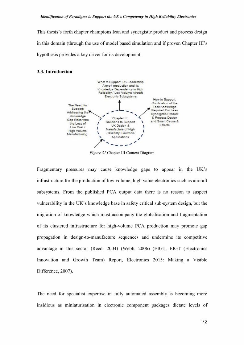
Identification of Paradigms to Support the UK’s Competency in High Reliability Electronics
72
This thesis’s forth chapter champions lean and synergistic product and process design
in this domain (through the use of model based simulation and if proven Chapter III’s
hypothesis provides a key driver for its development.
3.3. Introduction
Figure 31 Chapter III Context Diagram
Fragmentary pressures may cause knowledge gaps to appear in the UK’s
infrastructure for the production of low volume, high value electronics such as aircraft
subsystems. From the published PCA output data there is no reason to suspect
vulnerability in the UK’s knowledge base in safety critical sub-system design, but the
migration of knowledge which must accompany the globalisation and fragmentation
of its clustered infrastructure for high-volume PCA production may promote gap
propagation in design-to-manufacture sequences and undermine its competitive
advantage in this sector (Reed, 2004) (Webb, 2006) (EIGT, EIGT (Electronics
Innovation and Growth Team) Report, Electronics 2015: Making a Visible
Difference, 2007).
The need for specialist expertise in fully automated assembly is becoming more
insidious as miniaturisation in electronic component packages dictate levels of

Identification of Paradigms to Support the UK’s Competency in High Reliability Electronics
73
accuracy and repeatability which are beyond human capabilities for manual printed
circuit assembly. The research seeks to address these potential gaps through the
capture and management of critical knowledge via the development of a novel
software tool.
3.4. The Need for Support: Addressing the Knowledge Gap Risks from the Loss
of Low Cost / High Volume Manufacturing.
Infrastructure clustering, meaning a knowledge base derived from geographically and
technologically clustered enterprises which facilitate extra-enterprise knowledge
interchange (Porter, 1990) applies to the UK’s previously high concentrations of
collocated volume electronics production.
Published data (Webb, 2006) (EIGT, EIGT (Electronics Innovation and Growth
Team) Report, Electronics 2015: Making a Visible Difference, 2007) suggest that the
transplantation of high volume electronics production to far eastern destinations
(Huin, 2003) within the globalized electronic production network (EPN) may have
created fragmentation (Van Assche, 2007). This in turn may have caused knowledge
gaps to appear in the United Kingdom’s knowledge base which supports the
production of aircraft electronic subsystems (Gebus, 2007). From these data, the
thesis suggests that the downscaling of the UK’s clustered infrastructure in high
volume of PCA (printed circuit assemblies) production may impede the competitive
ability of currently buoyant industrial sectors which rely on its enabling technology
i.e. aircraft electronic subsystems. The industrial partners of the author’s collaborative
research project are members of the UK’s aircraft electronic subsystem design and
manufacture fraternity.

Identification of Paradigms to Support the UK’s Competency in High Reliability Electronics
74
A linkage may not be immediately apparent from the contrasting production output
scenarios of, (i) the cost-sensitive, high volume, consumer electronics markets and (ii)
the low volume demand which is typical of reliability-sensitive applications for
enabling, mission critical avionics. Previously, a volume-centric, clustered
infrastructure supported high volume production and differentiated the UK as a
manufacturing location of choice within Western Europe’s high-wage national
economies via a knowledge base in automated PCA assembly. This national
competitive advantage was facilitated by a human resource pool with highly
developed skills in process engineering (e.g. process design and design-for-
manufacture), manufacturing engineering (e.g. process support and equipment
maintenance) and localised supplier networks with supplemental support expertise
(e.g. process material and process optimisation).
Although Governmental reports provide a current healthy prognosis (EIGT, EIGT
(Electronics Innovation and Growth Team) Report, Electronics 2015: Making a
Visible Difference, 2007) (AIGT, AIGT (Aerospace Innovation and Growth Team)
Report, Report On Progress With The National Aerospace Technology Strategy,
2007), the effects of (i) globalisation of the EPN (ii) electronic component
miniaturisation, may undermine this position through the creation of knowledge gaps
within the clustered infrastructure which supports this industrial sector.
3.5. Globalization of Electronics Production Network & UK Leadership in
Aircraft Electronic Subsystems.
In the aftermath of globalisation of the EPN, the UK Government led reviews of its
electronics and aircraft manufacturing industries. Compiled by two Innovation and

Identification of Paradigms to Support the UK’s Competency in High Reliability Electronics
75
Growth Teams with commissions involving the assessment of the innovation and
growth potential within their respective sectors, these reviews bear testimony to the
UK’s strength in the design of complex systems and its knowledge base which
facilitates the production of safety-critical, high reliability products (EIGT, EIGT
(Electronics Innovation and Growth Team) Report, Electronics 2015: Making a
Visible Difference, 2007) (AIGT, AIGT (Aerospace Innovation and Growth Team)
Report, Report On Progress With The National Aerospace Technology Strategy,
2007).
Surveys of the UK PCB (Printed Circuit Board) production show data which
represents a 39% reduction in volume output from the electronics sector between the
years 1997 to 2003 (Reed, 2004) (Webb, 2006). A DTI sponsored sector
competitiveness study concurs with these findings. It indicates that the UK electronics
industry as a whole, shrunk by 38% between the 2000 turnover peak (£55 billion at
2001 prices) and 2003 (National Economics Research Associates, 2005) with PCB
manufacturing turnover estimated at £0.4 Billion and PCA assembly turnover at £2.4
Billion.
In contrast, the UK’s electronics design sector provides leadership in the design of
complex systems (EIGT, EIGT (Electronics Innovation and Growth Team) Report,
Electronics 2015: Making a Visible Difference, 2007) facilitated through its
ownership of intellectual property (IP) rights to leading-edge technology which
contributes to the global revolution in digital-enabled, processing functionality and
analogue-enabled, wireless-mobile applications.

Identification of Paradigms to Support the UK’s Competency in High Reliability Electronics
76
The UK also boasts an aerospace industry second only to the USA, with a turnover of
around £22 Billion per year and employing more than 120,000 people directly and
300,000 indirectly in the UK and a further 38,000 who are based overseas (Gebus,
2007). These statistics suggest a current healthy knowledge base for design and
manufacture of aircraft electronic subsystems exists within the UK.
In summary, Governmental reports and academic research show that:
i) The UK has experienced a dramatic loss of high volume production of cost
sensitive, commoditised electronic products due to globalisation and
fragmentation trade.
ii) The UK has retained leadership in both the design of complex electronic systems
and low-volume manufacture of civil and military aircraft electronic subsystems.
iii) The UK’s aerospace industry is second only to the USA, with a turnover of around
£22 B per year
3.6. Divested Production
Logically speaking, clustered infrastructures in donor economies must weaken as
recipient infrastructures in low cost manufacturing destinations benefit from the
migration of intrinsic knowledge bases, thus, propagating knowledge gaps. Also
communications challenges across inter-firm and intra-firm interfaces may create
additional knowledge (and data) transfer anomalies which initiate product and process
design errors and assembly defect opportunities.
The author suggests that enterprises which aspire to lean, divested production
strategies need to:

Identification of Paradigms to Support the UK’s Competency in High Reliability Electronics
77
(i) Recognise their critical, internal and external knowledge (and data)
transfer interfaces facilitating the targeting of error-proofing safeguards
and,
(ii) Identify and address the knowledge gap related anomalies within their
business models.
Fragmentation trade is defined as the commercial opportunities that arise through the
fragmentation of divested production strategies (e.g. outsourcing and off-shoring)
(Ruane, 1999) (Jones, 2000) (Jones, 2004). It looks to exploit the national competitive
advantages as provisioned within global value chains (GVCs). The ongoing expansion
of the globalised EPN has prompted industrialists to estimate that the 15% to 20%
cost reductions which can be expected from the relocation of manufacturing to low
wage regions may be significantly exceeded by a similar relocation of design
(Engardio, 2005). Boeing estimate that 65-70% of their aircraft design and
manufacture is now outsourced (Destafani, 2004). For reasons of product
differentiation and business model competitiveness, enterprises will need to access
these advantages through re-design of their products and / or working practices
(American Electronic Association, 1997). This suggests a fragmentation of design-to-
manufacture sequences which were previously collocated within the clustered
infrastructures of the enterprise’s locale, therefore, undermining its knowledge base
(Gebus, 2007).
3.7. Clustered Infrastructures
Logically speaking, clustered infrastructures in donor economies must weaken as
recipient infrastructures in low cost manufacturing destinations benefit from the

Identification of Paradigms to Support the UK’s Competency in High Reliability Electronics
78
migration of intrinsic knowledge bases, thus, propagating knowledge gaps. Also
communications challenges across inter-firm and intra-firm interfaces may create
additional knowledge (and data) transfer anomalies which initiate product and process
design errors and assembly defect opportunities.
The author suggests that enterprises which aspire to lean, divested production
strategies need to:
(i) Recognise their critical, internal and external knowledge (and data)
transfer interfaces facilitating the targeting of error-proofing safeguards
and,
(ii) Identify and address the knowledge gap related anomalies within their
business models.
Fragmentation trade is defined as the commercial opportunities that arise through the
fragmentation of divested production strategies (e.g. outsourcing and off-shoring)
(Ruane, 1999) (Jones, 2000) (Jones, 2004). It looks to exploit the national competitive
advantages as provisioned within global value chains (GVCs). The ongoing expansion
of the globalised EPN has prompted industrialists to estimate that the 15% to 20%
cost reductions which can be expected from the relocation of manufacturing to low
wage regions may be significantly exceeded by a similar relocation of design
(Engardio, 2005). Boeing estimate that 65-70% of their aircraft design and
manufacture is now outsourced (Destafani, 2004). For reasons of product
differentiation and business model competitiveness, enterprises will need to access
these advantages through re-design of their products and / or working practices
(American Electronic Association, 1997). This suggests a fragmentation of design-to-

Identification of Paradigms to Support the UK’s Competency in High Reliability Electronics
79
manufacture sequences which were previously collocated within the clustered
infrastructures of the enterprise’s locale, therefore, undermining its knowledge base
(Gebus, 2007).
3.8. What to Support: UK Leadership Aircraft production and its Knowledge
Dependency in High Reliability / Low Volume Aircraft Electronic Subsystems
McNamara (McNamara, 2006) expands Porter’s (Porter, 1990) classical definition of
clustering to include a more sophisticated level of geographical and technological
integration, with sector based transportation and information (i.e. knowledge)
interdependencies. The author’s research project reflects the latter definition, with UK
based aircraft electronic subsystem specialists collaborating within a common
industrial sector / technological core competency. The direct Governmental funding
for the project corroborates the complementary Innovation and Growth Team
recognitions of a national competitive advantage in electronics and aircraft
technology, thus suggesting a sector worthy of and requiring support.
3.9. Lean Production
The transitory trend from batch to lean production within the global aerospace
industry (Mathaisel, 2000) is highlighted by high profile civil and military aircraft
development programmes (e.g. Boeing’s 787 Dreamliner, Airbus’s A380 Navigator,
Eurofighter’s Typhoon). This transition cascades through the supply-chains to
intermediate levels of aircraft modular architectures – see Figure 33.

Identification of Paradigms to Support the UK’s Competency in High Reliability Electronics
80
Figure 32 – Modular Product Architecture within Vertically Integrated Production
Models
Lean customisation through architectural innovation (Henderson, 1990) is heavily
reliant on (i) architectural modularity and (ii) innovative configurations which
maximum product differential and minimize waste in the design-to-manufacture
sequence. The interchange-ability which comes from modular hierarchies must enable
“best-in-class” system configuration and maximize the value that can be captured
through modular procurement. As customer configurable microprocessor based
modules become cost competitive by commoditisation, they promote architecturally
innovative solutions via software dominant developments. Moreover, with minimal
hardware design requirements, “virtual manufacturing” and “the virtual factory”

Identification of Paradigms to Support the UK’s Competency in High Reliability Electronics
81
become viable as an ultimately lean manufacturing strategy. Modularisation (Baldwin,
2004) is said to facilitate:
a. Management of complexity e.g. modularisation of the hierarchical
subdivisions of a product’s architectural structure,
b. Concurrency in product development e.g. Concurrent Engineering,
c. Forward planning for component obsolescence and risk mitigation,
d. Future accommodation of advances in electronic component package
technology, offering design optimisation via scalable miniaturization
and weight reduction thus, extending design life-cycles and extracting
the maximum value from the design effort,
Lean opportunities can take the form of scalable management of complexity and can
be leveraged from future upgradeability in open-system architectures. Also, if
modular interchange-ability transcends the architectural system hierarchies (e.g. unit,
modules, printed circuit assemblies, common circuit blocks, printed circuit boards and
electronic components, micro-processor cores / IP blocks) it must also imbue
management of complexity advances in divested modular product development and
Concurrent Engineering. Communication linkages between vertically and horizontally
disengaged and divested development activities must consider program alignment and
concurrency.
The need for interactive and synergistic product and process development is
illustrated by the delayed the programme delivery and service entry or the Airbus
A380 (Rueters, 2006) (BBC, 2007). A flag-ship aircraft development program, which
proclaimed a lean production focus, was afflicted by a knowledge deficiency relating

Identification of Paradigms to Support the UK’s Competency in High Reliability Electronics
82
to the compatibility of the disparate CAD systems and dimensioning regimes. Sub-
decimal point rounding discrepancies between horizontally integrated (i.e. non-
divested) but geographically dislocated French and German design teams resulted in
discontinuities in the internal wiring loom interfaces between the Aircraft’s
modularised body sections. The problem was only discovered during module
assembly of the prototype sections, once they were collocated in Toulouse, thus
requiring redesign and incurring remanufacture delays and cost penalties.
3.10. Modularity and Make versus Buy Decisions
As electronic subsystems become more modular in nature they also become more
pervasive. In doing so, they provision enabling technology for non-electronic system
level end applications. Modularized electronic subsystems provide readily procurable
intelligent functionality for previously perceived “passive” end products which can be
easily assimilated within electrical, electro-mechanical or mechanical based
architecture.
In order to resist the fragmentary pressures as exerted within the design-to-
manufacture sequence by the globalising EPN, enterprises operating in high wage
regions such as the UK may need to undertake to either:
(i) The re-design their products and / or working practices (American
Electronic Association, 1997),
(ii) The re-appraisal of their overriding internal, vertically integrated business
models and philosophies (Leifer r. M.-O., 2000).
Probert (Probert, 1996) encapsulates these recommendations within the make-or-buy
decision-making process and provides codifications for the scoping of manufacturing

Identification of Paradigms to Support the UK’s Competency in High Reliability Electronics
83
business models and their vertical integration interfaces. He proposes divestiture
strategies for the management of business cycles, the structuring of supply bases and
the balancing of investment capital. Also reported are the conclusions of a survey
carried out by the Cambridge Manufacturing Group which found that whilst
recognising the need, (i) only half of the large UK based manufacturing companies
surveyed claimed to have divestiture strategies in-place, and (ii) only a third had
actually committed the prerequisite implementation resources. However, 85% of the
enterprise recognised the need for a make-or-buy decision-making framework.
Probert’s proposed framework (see Figure 34) provides qualitative ratings for
competitive position and importance to business.
(Probert, 1996)
Figure 33 – Probert’s Technology Sourcing & Supplier Relationship Matrix

Identification of Paradigms to Support the UK’s Competency in High Reliability Electronics
84
3.11. Component Package Technology Implications for Aircraft Electronic
Subsystems – Leading versus Lagging Edge
Cost sensitivity is usually more apparent in high volume products where competition
has globalized. In contrast, enterprises which address markets that prioritise
operational reliability and have safety-critical implications (e.g. aerospace) are willing
to pay a premium for products produced within a culture which places a greater
emphasis on the product’s life expectancy than on its manufacturing costs. This
philosophy relies on a design ethos which adopts lagging-edge, but proven technology
and embeds leading-edge reliability.
Specialists in the production of safety-critical systems typically develop symbiotic
relationships and exclusive supply agreements with their customers. The symbiotic
benefits to the supplier relate to this type of customer’s willingness to pay a premium
for a systematic approach to quality management and inherent product reliability.
Conversely, the unitary demand for their host aircraft transcends the hierarchical
structures within aircraft systems and imposes low volume manufacturing challenges,
which disadvantage automated PCA assembly and the suppliers the associated
divested production services and sub-assemblies.
When exclusively presented on a return on investment basis, the unitary volume
requirements, typified in aircraft production historically engender a poor justification
for assembly process automation. However, the potential for process yield and
subsequent diminished product reliability, which proportionally reduce with greater
levels of silicon integration / package miniaturisation, provide counter arguments.

Identification of Paradigms to Support the UK’s Competency in High Reliability Electronics
85
Driven by the ever accelerating levels of integration at the silicon level – as stated by
Moore’s Law# (Moore, G. E., 1965) – and subsequent reduction in electronic
component package physical geometries, even low volume PCA assembly might
justify full automation as a default prerequisite when process yield and product
reliability differentiation are prioritised. The scale of miniaturisation in contemporary
package technology now dictates process accuracy and repeatability which extends
beyond human capabilities and Moore’s Law portends that package geometries will
only continue to shrink (Kundu, 2007).
Note: Moore’s Law – Computer processing power (and more specifically, the number of
transistors on a chip) doubles every 18 months. Intel Corp’s first chip, the 4004, had 2000
transistors when it was first released in 1971. Today’s chips have over 100 million.
3.12. Divested Production & Modular Product Architectures
As electronics technology advances and products reduce in volume and weight they
become more transportable and therefore more susceptible to fragmentary outsourcing
pressures. Also, as modularized procurement from external supply chains becomes
increasingly competitive, outsourcing becomes more attractive, resulting in the
vertical disintegration and fragmentation of hierarchical structures of modularised
product architecture. This suggests that lean production and fragmentary pressures
from the globalising EPN could effect a disengagement of vertically integrated
business models and the creation of external knowledge transfer interfaces. Divested
production (i.e. outsourcing and modular procurement) to offshore locations could
induce interfacial knowledge gaps to appear which may impact on UK production of
aircraft electronic subsystems – see Figure 35.

Identification of Paradigms to Support the UK’s Competency in High Reliability Electronics
86
Figure 34 – A Divested Production Strategy for Aircraft Electronic Subsystems withModular Architectures
3.13. Knowledge Interfaces and Gap Propagation
The antipathy of lean must be waste. Within the context of the electronics production
GVC (i.e. the globalised EPN), the waste referred to can take the form of:
(i) Non-value adding activities (e.g. the return shipping from off-shore
outsourcing destination of fully assembled products solely for the purposes
of product testing and distribution) and
(ii) Assembly process defects that require reworking.
Mod
ular
ised
Pro
duct
Arc
hite
ctur
e
SystemLevel
ModuleLevel
PCALevel
ComponentLevel
Divested ProductionE.g. modular procurement, design outsourcing partnerships with EDS providers,
manufacturing outsourcing partnerships with EMS providers
E.g. Aircraft producer’s modularprocurement of electronic subsystem
E.g. Electronic subsystem produceroutsources PCA design to EDS
E.g. EDS outsourcesPCA assembly to EMS
E.g. EMS outsourcedPCB manufacture
Identification of Paradigms to Support the UK’s Competency in High Reliability Electronics
87
Any such rework impedes the production flow and compromises inherent product
reliability. The mechanical integrity of reworked solder joints, and their host PCA’s
inherent fatigue resistance can be easily undermined by the physical degradation
potential of rework processes (Lau. J.H., 1991) (Garrison, 1995). Physical degradation
risks such as inter-metallic layer growth and joint embrittlement can be accelerated
when rework processes have been manually actuated and are therefore uncontrolled
(Lea, C., 1990).
Gebus and Leiviska (Gebus, 2007) define design as a series of knowledgeable
choices. They proposed a defect-related codified knowledge-base of tacit causation
knowledge within a software application for PCA assembly line organisation and
operation, thus providing comparison opportunities within a common domain.
In automated PCA assembly, poor process optimisation and control generates
opportunities for defects. Even with the highest levels of automation, operational
decision making and general human behaviour still retain degrees of influence.
Although the potential for human factors to impart defect opportunities in high-
volume, dedicated line scenarios remains batch production will most likely increase
risks as detection feedback loops fragment. Although, referring to design activities
within their definition, Gebus and Leiviska (Gebus, 2007) focus on process
operational defect opportunities with the tacit knowledge generated applicable to
cause and effect. Their assertion that cause data does not naturally exist within typical
PCA assembly environments concurs with the research project findings that only
effects data (in the form of defect logs) are systematically captured and available for
retrospective data mining. However, their approach differs in that they place a high

Identification of Paradigms to Support the UK’s Competency in High Reliability Electronics
88
reliance on accurate operator tacit knowledge and interpretation of defect
opportunities for their causation knowledge.
3.14. How to Support: Codification of the Tacit Knowledge Required For Smart
Cause & Effects Knowledge Management, Interactive Design-for-Manufacture
& Lean Synergistic Product & Process Design,
As open-system architectural structures facilitate ever-extending levels of modularity
the procurement availability of commoditised application-independent / functionality-
specific modules should increase proportionally (Huin, 2003), (Hameri, 2005). The
creation of external knowledge transfer interfaces as a consequence of divested
production may initiate interfacial breaches in the design-to-manufacture knowledge
chain – See Figure 36 for an example.
Figure 35 – A Design-to-Manufacture Sequence Knowledge Chain with Retrospective
Feedback Loops
Smart cause & effects knowledge management, IdfM and Lean Synergistic Product &
Process Design, via the CLOVES and INMOST (Integrated Modelling and
Identification of Paradigms to Support the UK’s Competency in High Reliability Electronics
89
Simulation Tool) project software tools are proposed for the mitigation of any such
risks.
3.15. Knowledge Management – for Smart Cause & Effects Analysis
KM literature defines and differentiates knowledge as (i) tacit and (ii) codified. Tacit
knowledge is “know-how (personal skills) and know-who (how and where to get
specialised knowledge)” (McNamara, 2006). The acquisition of “know-how” and
“know-who” is informal and elicited / accumulated through experience (Gebus, 2007)
and considered personal intellectual capital (Lee, 2005). In contrast, codified
knowledge is “know-what” (facts) and “know-why” (scientific principles)”
(McNamara, 2006). It can be regarded as a corporate asset (Lee, 2005) or corporate
memory (Andrade, 2008) and modularised and redeployed within GVCs. Divested-
production based, lean business models rely on the portability of their corporate asset
or transplant-ability of their corporate memory.
The approach adopted within the research was to, (i) elicit from academic literature,
relevant causation paradigms with inclusive supporting empirical data, and then, (ii)
formulate physical models which provide smart cause & effects analysis of defect
opportunities for the respective automated PCA assembly processes. Although this
methodology is constrained by the gamut of available academic research, the
available supporting data is quantitative, scientifically sanitised (i.e. peer reviewed)
and therefore less vulnerable to human assumptions. The scope of the research was
also constrained by human factors which influence process capability of the
automatable PCB assembly processes i.e. Surface Mount Technology or SMT.

Identification of Paradigms to Support the UK’s Competency in High Reliability Electronics
90
Note: opportunistic real-time remedial actions by operators with good intent can
rectify defects (i.e. effects) but obscure the cause mechanism and obscure design
based defect opportunities and knowledge capture and codification.
3.16. Package Technology Knowledge Codification for Smart Cause & Effects
Knowledge Management
The point of convergence between electronic component design / manufacture and
PCB layout / PCA assembly is located in the package technology domain. A body of
codified knowledge is essential in accommodating disparate industries which share
hierarchical relationships within the product’s architectural structure. IPC7531(L) –
Generic Requirements for Surface Mount Design and Land Pattern Standard
(Association Connecting Electronics Industries, 2005) is a widely accepted industry
standard which provides such codification. This provides standardisation (and
therefore codification) of the default dimensions and tolerances for:
(i) The physical form of the electronic component (a.k.a. the package),
(ii) The design rules for the corresponding PCB interconnection pads – i.e.
the source data as required for the programming of vision systems as used in
the recognition and alignment functions for the automated machine placement
and inspection of SMT components and,
(iii)The computerised drafting of bespoke test systems and tooling / production
aids used the assembly of PCA’s,
SMT assembly process defects which arise from erroneous product or process design
decisions that generate defect opportunities during PCB layout can categorised as:
Identification of Paradigms to Support the UK’s Competency in High Reliability Electronics
91
(i) Flawed electronic component package selection and PCB placement
decisions and,
(ii) Ineffective DfM feedback and implementation,
Given the uneconomic repair practicalities of cost sensitive high-volume production
scenarios, the requirement for rapid assimilation of leading-edge package technology
imposes acute learning curves for yield optimisation. The ideal source of necessary
tacit knowledge would be through original empirical experimentation, but the reality
is more likely to be via fast-actuated iterative trial-and-error during new product
introduction and volume ramp-up. Even when codified and incorporated into
corporate memory, forfeited ownership of vital process design knowledge IP can
result from unintentional dissemination within clustered infrastructure knowledge
bases.
For example, UK based manufacturers of the stencils used in the deposition of the
solder paste which provides the interconnection medium for surface mount packages,
have been known to codify stencil thickness and aperture dimensional knowledge for
a given package style. They then offer this valued IP to alternative customers as a
cost-free stencil design service. Potential customers include the author’s research
project industrial partners who prefer proven package technology and consequently
benefit from external sources of codified knowledge.
As stencil manufacturers neither, assemble PCAs, nor have the capability to undertake
the empirical research needed to establish the stencil-aperture design rules, analysis of
the sources for this valuable IP would suggest unintentional dissemination by the
originating stencil customer. Cost sensitive consumer electronics market protagonists

Identification of Paradigms to Support the UK’s Competency in High Reliability Electronics
92
typically provide leading-edge package technology’s earliest adopters. The stencil
supplier then codifies it for reuse as part of its service provision for more reticent
implementers. Therefore, the departure of the high-volume originators of the
knowledge from the clustered infrastructure will terminate this parasitic route to
optimised stencil design for new users of subsequent iterations of package technology.
3.17. Interactive Design-for-Manufacture (IdfM)
Retrospective DfMIt is not unfeasible for “extended enterprises” (Thomas, 2006) to accommodate
retrospective DfM feedback loops between OEMs and their ODM (Original Design
Manufacturer) and CEM (Contract Electronics Manufacturer) outsourcing service
providers but the cost of correction / rectification must grow exponential as design-to-
manufacture sequences elongate. Further strains in aircraft GVCs will permeate with
continued globalisation of the EPN and the likelihood of embedded defects in
electronic subsystems.
If product architectures become entrenched and presented as a fait-accompli,
retrospective corrective actions are denied, thus embedding defect opportunities.
However, if the defect opportunities are (i) negated by a concurrent engineering
methodology which benefits from a smart cause & effects codified knowledge base or
(ii) trapped at source via a rule based IdfM analysis algorithm, waste in design time
and resource can be minimised. With the elimination of this waste, a software tool
which provides synergistic product and process design guidance and DfM scrutiny at
the PCB layout stage could claim to be a conduit for maximised manufacturability of
the product and an enabler of lean manufacturing processes.

Identification of Paradigms to Support the UK’s Competency in High Reliability Electronics
93
Concurrent DfMThrough the simultaneous scheduling of activities, Concurrent Engineering (a.k.a.
Simultaneous Engineering) looks to optimize the manufacturability of designs. Its
objective is to eliminate waste in product realization cycle time and apply DfM
criteria concurrently at all stages of the design process (Shina, 1999).
The sequential nature of design-to-manufacture and wide geographical distribution of
extended enterprises impedes concurrency in DfM feedback loops, which elongate in
both time and distance. Corrective action implementation is vulnerable to cost and
time based waste accumulation. Concurrent engineering and ‘right-first-time’
approaches will eliminate this waste. Moreover, if PCA product / process design and
production are collocated, the effects of incorrect package selection and placement
knowledgeable choices and their consequential rework implications remain visible to
the originator of the defect opportunity and therefore somewhat mitigated. However,
unless the OEM (Original Equipment Manufacturer) intends to return-ship outsourced
PCA assembly for in-house testing, the reliability implications of the consequential
rework are obscured, thus forfeiting the retrospective DfM feedback opportunity.
Codified DfMCodified DfM and cause & effects knowledge applied interactively at the origin of the
product design embedded defect opportunity would strategically position the error-
traps and either provision lean synergistic design-to-manufacture opportunities for the
subsystem producer who wishes to profit from the competitive advantages of the
EPN, or indemnify the producer from the knowledge gaps that outsourcing decisions
may precipitate within the UK’s clustered infrastructure. If process design originated
defect opportunities can be mitigated via the careful positioning of poke-yoke style

Identification of Paradigms to Support the UK’s Competency in High Reliability Electronics
94
(the Japanese word for error-proofing and a primary component of lean production
methodology) physical traps in production flow paths (Bhote, 2000) via phase-gates,
then the tacit type “knowledgeable choices” could be similarly codified and by way of
IdfM.
3.18. Lean Synergistic Product & Process Design
Sturgeon et al. (Sturgeon, 2008) refers to a locally tacit / globally codified dichotomy,
where codified knowledge can be easily divested. He describes pipelines for tacit
knowledge transfer which can be facilitated by advanced communication technologies
(e.g. ‘telepresence’ or ‘rich teleconferencing’ systems), but this conduit (or pipeline)
will be strained and easily fractured by the globalising EPN. At best, even state-of-
the-art telecommunications could only hope to facilitate retrospective DfM feedback
as the penultimate stage of an outsourced design-to-manufacture sequence within a
GVC extended enterprise. The probability of phase-gated milestones constraining
retrograde optimisation of manufacturability increases with isolated product and
process design (Leifer, 2000) and inhibits lean synergies.
When outsourcing product design to bureaus which specialise in PCB layout, the
author’s research project partners also face further impediments to the implementation
of retrospective DfM recommendations. For logistical and security reasons it is
untypical for either design, or assembly of safety-critical, electronic subsystems to be
outsourced to offshore destinations. However the OEM project collaborators divests a
high level of dependency for package selection and placement decisions to their UK
based design service provider, albeit, within customer specific DfM design rules.
Once completed, the bureau returns PCB layout designs to the customer for DfM

Identification of Paradigms to Support the UK’s Competency in High Reliability Electronics
95
review via its tacit knowledge base, provisioned by its process and manufacturing
engineers.
The tacit knowledge which is critical for lean-production yields (i.e. production flow
that is not interrupted by rework loops) and lean product development cycles needs to
be delivered to the defect opportunity’s point of origin. A ‘right-first-time’ approach
via synergistic product and process design will optimise manufacturability and
maximise design-to-manufacture sequence compression.
3.19. Chapter Summary
This chapter’s research objective of the proving of the hypothesis that the UK (i)
benefits from a competitive advantage aircraft subsystems and its enabling high
reliability electronics and (ii) might be vulnerable to knowledge gaps propagated via
the fragmentation effects of transplantation of high volume electronics production
within the globalized electronic production network.
The first part of the hypothesis is confirmed by the following findings:
The UK has experienced a dramatic loss of high volume production of cost
sensitive, commoditised electronic products due to globalisation and
fragmentation trade.
The UK has retained leadership in both the design of complex electronic systems
and low-volume manufacture of civil and military aircraft electronic subsystems.
The UK’s aerospace industry is second only to the USA, with a turnover of around
£22 B per year.

Identification of Paradigms to Support the UK’s Competency in High Reliability Electronics
96
The second part concludes that the transplantation of high volume electronics
production within the globalized electronic production network has initiated
fragmentary pressures which could in turn cause knowledge gaps to appear in the
UK’s infrastructure for the production of low volume, high value electronics such as
aircraft subsystems.
In providing these proofs the chapter addresses this thesis’s “why” question and
provides the key drivers for model based simulation of SMT Reflow defect
opportunities and the need for knowledge capture and codification via the CLOVES
and DIY projects.
Identification of Paradigms to Support the UK’s Competency in High Reliability Electronics
97
Chapter IV-
Lean Product & Process Design
Subtitle: Interactive and Synergistic Product & Process Design
for the Lean Production of Aircraft Electronic Subsystems
4.1. Research Context:
Both military and civil aircraft development programs now appear to be embracing
lean thinking. The opportunities for wasteful design errors and costly discontinuities
in the design-to-manufacture sequence may be increased by:
a. Isolated product and process design (herein referred to as Paradigm 1),
b. The schedule overruns that will be an inevitability of sequence
misalignment and retrospective design reviews and corrective action
feed-back loops (herein referred to as Paradigm 2).
4.2. Chapter Objective:
This chapter’s research objective is to investigate the lean production methodology
and apply it in the context of cause and effects analysis of Paradigms 1 and 2.
Definitions for the use of (i.e. ‘when’) users of (i.e. ‘who’) the physical models to be
developed within Section 2 are key deliverables.

Identification of Paradigms to Support the UK’s Competency in High Reliability Electronics
98
4.3. Introduction
Figure 36 – Chapter Context Diagram
No longer can (flight) safety-criticality requirements be used as an escape clause for
the mitigation of schedule commitment failures with lean production techniques
adoption within contemporary, high profile aircraft development (Mathaisel, 2000).
Previously, revenue streams may have been bolstered by stake-holders with none
commercial (i.e. nationalistic) incentives to prop-up failing state-owned indigenous
aircraft producers with interim payments for over-due / over-budget programs that
were overwhelmed by procedural discontinuities and wasteful practises.
The discontinuities which have afflicted the Airbus A380 development program
provide a stark illustration of the need for value delivery and waste elimination within
the hierarchical design-to-manufacture sequences of its modular architectural
structure. Consequently, this high-profile anecdote of profligacy will provide sharp
focus for lean civil and military aircraft development, with emphasis on (i) project
time-line compression and (ii) lean optimized value streams delivering demand driven
pull systems. However, in the absence of seamless connectivity and continuity in the
design-to-manufacture sequences both of these objectives will be susceptible to waste.

Identification of Paradigms to Support the UK’s Competency in High Reliability Electronics
99
4.4. Design-to-Manufacture Sequences.
Advancement of electronic complexity progressively contributes enabling technology
and subsystem functionality for a diversity of newly developed transportation
solutions. Globally standardised procedures impose regimented milestones on aircraft
development programmes before airworthiness qualification is certified. The design-
to-manufacture sequences for an aircraft’s enabling electronic subsystems and their
modular blocks of functionality link intrinsically with those of the parent system.
Therefore, sequence alignment and compliance are critical.
Concurrency is required to align the development activities within the vertical
hierarchies of parent and child system architectures to optimise the manufacturability
of the developments and facilitate lean production. Toyota Motor Company is
credited with the genesis of lean and the Toyota Production System is extolled as the
paradigm for all to follow (Womack, 1990). It is only natural that the automotive
industry be acknowledge as pioneering seamless integration and alignment of the
design-to-manufacture sequences, which cascade throughout the hierarchical
structures of their automobile system architectures.
Within the context of aircraft production, the word mass should be juxtaposed with
batch. Lagging their mass-producing automotive counterparts, the aircraft
development fraternity now seem to be attempting to redress the gap exists between
their disparate systems. Throughout the global aerospace industry, the instigation of
lean production initiatives within the below referenced developments suggest a
gathering momentum.

Identification of Paradigms to Support the UK’s Competency in High Reliability Electronics
100
Legacy programs have been transformed retrospectively via reconstitution of
assembly processes, which have been redesigned, via the use of value stream analysis
(VSA), to facilitate mass to lean conversion for existing aircraft2. The following high
profile contemporary lean development programs will have included aligned lean
product and process design aspects:-
o The Boeing 787 Dreamliner
o The Airbus A380 Navigator
o The Eurofighter Typhoon
4.5. Origins of Lean Production.
Whereas, the founding fathers of the automotive industry, primarily Henry Ford (Ford
Motor Company) but also Alfred Sloan (General Motors) are regarded as the pioneers
of mass production, Toyota executive Eiji Toyoda and production engineering guru
Taiichi Ohno are widely recognised as the originators of techniques, which would
subsequently be described as lean (Womack, 1990). The term lean production was
actual coined by Womack, Jones and Roos in their seminal study of global automotive
production techniques titled The Machine That Changed the World: The Story of Lean
Production. Latterly, the terminology has been expanded to also include lean
manufacturing and lean thinking, but their original five, process orientated lean
principles are still regarded as the cornerstone of lean methodology and are embodied
in VSA (Slack, Robert, A., 1998).
Although Womack, Jones and Roos (Womack, 1990) reported in greater detail on
manufacturing issues that differentiate between mass and lean production they also
2 The US Air Force envisages a 90 year design life for the B52 Bomber

Identification of Paradigms to Support the UK’s Competency in High Reliability Electronics
101
researched organisational aspects and Japanese approaches to automobile design /
development and marketing, thus, implying that term production can be applied
universally throughout the design, manufacture and even sales streams. This suggests
the creation of value throughout the design-to-manufacture sequence and current lean
thinking extends the value stream accordingly.
4.6. Definition of Value
Recognition of market sensitivity to value expectations is critical to competitive
advantage exploitation strategies. The source of a firm’s competitive advantage is said
to be located within its value chain (a.k.a. value stream), from which it both, delivers
and captures value (Porter, 1990). For manufactured products, the value must be
generated by design and manufacturing. The costs of the value added to product by
design are supplemental to its costs of manufacture. Profitability is dependent on
recovery of both costs within the sale price; therefore, we need to define the
following:
(i) Product value – the customer’s perception of the value for money that a
product delivers through its functionality and reliability and the premium that
they are willing to pay for that perceived value,
Also,
(ii) Added value – the profit (or loss) that is generated by the premium that the
customer is willing to pay for the functionality and reliability once the costs of
designing and producing the product have been deducted
Thus,
Profit = premium – cost = added value

Identification of Paradigms to Support the UK’s Competency in High Reliability Electronics
102
Markets and applications will dictate the value placed on reliability and provide the
justification for reliability premiums. Therefore, the following definitions of the value
of reliability are offered:
(i) Products which are targeted at markets which have value perceptions
orientated towards functionality and short duration aesthetic appeal (i.e.
fashion accessories such as mobile phones) will not command a reliability
premium
(ii) Products which are targeted at markets that have value perceptions orientated
towards functionality and safety critical reliability (i.e. aerospace, automotive,
military, medical, industrial etc) will command a reliability premium
4.7. Value Stream Analysis
Listed below are the basic tenets of VSA (Nave, 2002):
(i) Recognise the features of a product that the customer considers of value
(ii) Pinpoint the processes within the manufacturing, assembly and test
sequence that creates the valued features i.e. the value stream
(iii) Remove any impediments to production flow through the value stream and
eliminate waste by targeting the non-value adding activities
(iv) Replace mass production (or more usually batch production) with a
Kanban based pull system
(v) Continuously refine the pull system.
Albeit with an initial focus on product’s design features and functionality, the
emphasis of this five-step approach is very much on the waste incurred via the
manufacturing, assembly and test operations, which only add to the products inherent

Identification of Paradigms to Support the UK’s Competency in High Reliability Electronics
103
value. This is understandable when considering manufacturing activities in isolation.
However, if the valued features and functionality originate in design and the value
added via the subsequent stages of the design-to-manufacture sequence is
supplementary, then the source of the value stream must be located at the start of the
sequence.
This dilemma provides an illustration of the dichotomous challenges of customer
value perception and prediction; but, when the customer is an aircraft producer then
criticality of flight safety provides stark illustration of the ultra-high value placed on
reliability. Furthermore, for the growing number adopters of the lean aircraft
procurement paradigm, value premiums will be apparent in waste elimination
potential from compressed development programs. Manufacturing operations
undoubtedly influence yields, but manufacturability must be a function of product
design, DfM (design-for-manufacture) and process design. Studies have shown the
potential of human inconsistencies in the reworking of the manufacturing defects to
impact negatively on a electric system’s in-service fatigue resistance and long term
reliability (Nguty, 2000) (Garrison, 1995) (Lau. J.H., 1991) (Hutchins, 1995) (Lea, C.,
1990). If as argued, the manufacturability of a product is a function of its design then
its DfM will hugely influence PCA assembly yields and reworking. Hence, the value
added by reliability becomes as much a feature of a product’s manufacturability as its
manufacture.
4.8. The Role of Concurrent Engineering
Through the simultaneous scheduling of activities, concurrent engineering looks to
optimize the manufacturability of designs. Its objective is to eliminate waste in

Identification of Paradigms to Support the UK’s Competency in High Reliability Electronics
104
product realization cycle times and apply DfM criteria concurrently at all stages of the
design process (Shina, 1999). Yet paradoxically, by nature the design-to-manufacture
sequence dictates sequential scheduling of activities and disciplines.
In manufacture, waste can be eliminated through the identification and removal of
discrete opportunities for defect opportunities via the careful positioning of poke-yoke
style (Japanese for error-proofing) physical traps in production flow paths (Bhote,
2000). The application of this principle throughout the design-to-manufacture
sequence via phase-gate control procedures, strategically positioned at critical phases,
will help to contain design errors within their root cause domains (Leifer R. M.-O.,
2000). However, corrective actions loops that may have arisen from phase-gate
reviews and consequential root cause analysis will be limited in their DfM
effectiveness if (as per Paradigm 1) product and process design are isolated and DfM
rules are unspecific to the target process.
In aircraft development, D0-254 provisions the codification and standardisation for
programme alignment, product validation and verification, project delivery and
ultimate airworthiness certification. The Radio Technical Commission for
Aeronautics (RTCA) proffers consensus-based recommendations regarding
communications, navigation, surveillance and air traffic management (CNS/ATM)
system issues within its RTCA DO-254 / Eurocae ED-80 document. A DO-254
compliant Quality Management System (QMS) will constitute a benchmarked process
for the verification and certification of airworthiness and the path to first flight release
for aircraft systems and their electronic subsystems (RTCA). A compliant QMS must

Identification of Paradigms to Support the UK’s Competency in High Reliability Electronics
105
structure the knowledge transfer linkages to the ultimate goal of airworthiness
certification and cascade through the various levels of modularity.
Nevertheless, the conformity of electronic subsystems will only be verifiable with the
production of validated units via fully representative manufacturing processes.
Therefore, the vertical product verification paths within a DO-254 compliant design-
to-manufacture sequence is routed via NPI / production transition vertical interfaces,
meaning that product verification knowledge transfer is reliant on process validation.
In meeting the objectives of this chapter and illustrating the environment that the
software tool will have to operate within and identification of the existing paradigms
(i.e. Paradigms 1 and 2) and proposal of lean optimised and synergistic alternatives
(herein respectively referred to as Paradigms 3 and 4), D0-254 compliance is pre-
requisite.
4.9. Paradigm 1: Isolated Product & Process Design Domains
The traditional design-to-manufacture sequence for electronic subsystem development
programs typifies Paradigm 1. Requiring synergistic product and process design
solutions for batch-produced PCAs, isolated design domains are symptomatic within
this environment. Even in more enlightened and less evolutionary / investment
constrained circumstances, assembly lines are likely to have been configured with
batch logistics and generic flexibility as primary objectives. Product and process
design can occur simultaneously, but as there are no domain linkages, the model
cannot claim concurrency and alignment – see Figure 38. Moreover, product and

Identification of Paradigms to Support the UK’s Competency in High Reliability Electronics
106
process design compatibility are not be coordinated, thus prohibiting optimised
manufacturability and lean production.
Figure 37 – Paradigm 1: Isolated Product & Process Design
Piecemeal demand for the electronic subsystems stems from the unitary nature of
aircraft production and provides a typical exemplar for Paradigm 1 with high-mix /
low-volume batched production. Justification of any capital outlay for bespoke,
product and process compatible design solutions is difficult, thus reducing
opportunities for in-house, fully automated assembly. Product manufacturability
issues arise if product design specific process requirements exceed the generic process
capabilities of external manufacturing service providers. Both these scenarios have
process yield and rework / manually operated implications.
Identification of Paradigms to Support the UK’s Competency in High Reliability Electronics
107
Model based Analysis:
Product and process compatibility issues arise with specific equipment platform
selections, compromised by the inevitable prioritisation of flexibility and efficiency
requirements for batch changeover. Lack of product specific tooling will increase the
opportunities for solder paste printing and placement errors which have root causes in
generic and therefore flexible PCB support solutions: where as dedicated, relieved
support plates conform to the PCA’s component layout, enhancing co-planar printing
conditions and reducing substrate flexing during placement. DfM and NPI feedback
loops will not capture and codify any case-based tacit knowledge gleaned from cause
and effects analysis and consequential corrective actions, thus (i) impeding the
development of process specific DfM rules and (ii) denying opportunities for iterative
refinement of solder paste stencils and (exclusion) wave solder carrier tooling.
Lean issues arise from the limited automation and manual operation scenario. The
hand placement / hand soldering of electronic components to the PCB will add extra
costs (without adding any value) whilst increasing defect opportunities and
influencing in-service reliability. Especially acute in ultra-low production, the non-
permanency of component setups on placement-machine feeder beds (a logistical
advantage enjoyed by high-volume producers with dedicated assembly lines) will
increase the opportunity for human error in locating components in their correct
orientations and pickup positions. This increases the possibility of incorrect value or
component polarity defects. Component packaging format incompatibilities will
increase, along with the need to transfer fragile leaded components to alternative
formats, thus, inducing manual handling related component defects e.g. lateral lead
bend and lead co-planarity issues. Therefore, batch change-over related defect

Identification of Paradigms to Support the UK’s Competency in High Reliability Electronics
108
propensity will be inversely proportional to batch size and the subsequent yield
reductions will be directly proportional with increased rework, thus introducing the
afore mention rework related fatigue related physics-of-failure.
4.10. Paradigm 2: Sequentially Linked Product & Process Design
This paradigm represents the traditional mass production design-to-manufacture
sequence, where products and processes must be compatible to facilitate both, fully
automated assembly and optimised manufacturability. Given the high volume / low
mix scenario, bespoke automated process designs are more justifiable. However,
overall development programs are vulnerable to wasteful schedule overruns when
sequentially linked domains become misaligned by retrospective phase-gate reviews /
feedback loops. Efficiencies extracted through the elimination of non-value-adding
hand-fit activities will be of little value, when balanced against waste accrued by
sequence extension and delayed service entry for aircraft development programmes!
Model based Analysis:
Corrective action loops from the retrospective product phase-gate review stages must
feedback to process design via domain transcending linkages. However, as the
linkages provide feedback loops from the DfM and NPI phase-gate reviews, any
subsequent corrective actions will have the effect of sequentially aligning the product
and process design domains, with the inevitability of the iterative correction cycles
extending the design-to-manufacture sequence and subsequent elongation of
development windows.

Identification of Paradigms to Support the UK’s Competency in High Reliability Electronics
109
Figure 38 – Paradigm 2: Linked Product & Process Design
Design solutions for aircraft electronic sub-systems are usually bespoke and need to
reflect their host aircraft’s system architecture. Development program schedules will
need to cascade through the hierarchical structures of the architecture and
accommodate product and process design windows within design-to-manufacture
sequences. The potential for expansion of sequentially aligned domains may be
acceptable to customers who require hierarchical flexibility in host-system
development timelines with compressive implications. Moreover, the simultaneous
alignment of product and process design domains becomes more than good waste
eliminating practice and critical to overall design-to-manufacture sequence delivery.
Identification of Paradigms to Support the UK’s Competency in High Reliability Electronics
110
4.11. Concurrency and Alignment
Lean design aspirations may engender paradoxical issues where VSA eliminates
waste but promotes sequence misalignment and escalates the risk of
miscommunication errors and error trap evasion. Compressive forces may also affect
attention to detail and hamper cross checking, which, in turn may compromise,
customer value delivery, system integration and process capability with reduced
assembly yields and product reliability consequences. This circular degeneration is
completed and misalignment compounded when errors pass through traps (i.e. the
phase-gate reviews) and correction is on an iterative basis. If, due to missed
opportunities in error detection, steps in the design-to-manufacture sequence are
repeated in full, then the resulting elongation will only exaggerate the misalignment.
Therefore, circular degeneration in sequentially aligned product and process design
domains may:
(i) Inhibit design-to-manufacture sequence compression and exacerbate the
risk of delayed aircraft first flight release and entry into service.
(ii) Compromise the system specification and customer DO-254 compliant
design review control processes, thus exacerbating the risk of embedded
system functionality errors.
(iii)Compromise PCA architecture and circuit design phase-gate review
control procedure, thus exacerbating the risk of component package
selections and reducing manufacturability – see Section 2.
(iv)Compromise PCA layout and CAD design phase-gate review control
procedures, thus exacerbating the risk of component package positioning
(a.k.a. placements) and reducing manufacturability – see Section 2.
Identification of Paradigms to Support the UK’s Competency in High Reliability Electronics
111
(v) Compromise process design and the manufacturing engineering phase-gate
review control procedure, thus exacerbating the risk of product and process
incompatibilities and reduce the potential for fully automated component
placement and soldering – see Section 2.
(vi)Compromise the new product introduction procedure and its phase-gate
control, thus exacerbating the risk of PCA designs with reduced
manufacturability entering the qualification stage.
(vii) Compromise the product and process design qualification procedure
and its phase-gate control, thus exacerbating the risk of PCAs with reduced
yield potential and poor in-service reliability entering service with their
host aircraft.
4.12. Divested Production & Modular Product Architectures
As electronics technology advances and products reduce in volume and weight they
become more transportable and therefore more susceptible to fragmentary outsourcing
pressures. Also, as modularized procurement from external supply chains becomes
increasingly competitive, outsourcing becomes more attractive, resulting in the
vertical disintegration and fragmentation of hierarchical structures of modularised
product architecture. This suggests that lean production and fragmentary pressures
from the globalising EPN could effect a disengagement of vertically integrated
business models and the creation of external knowledge transfer interfaces. Divested
production (i.e. outsourcing and modular procurement) to offshore locations could
induce interfacial knowledge gaps to appear which may impact on UK production of
aircraft electronic subsystems – see Figure 40.
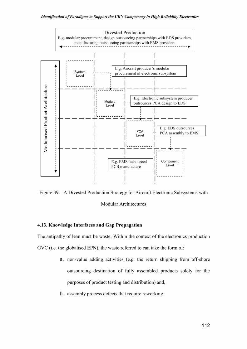
Identification of Paradigms to Support the UK’s Competency in High Reliability Electronics
112
Figure 39 – A Divested Production Strategy for Aircraft Electronic Subsystems with
Modular Architectures
4.13. Knowledge Interfaces and Gap Propagation
The antipathy of lean must be waste. Within the context of the electronics production
GVC (i.e. the globalised EPN), the waste referred to can take the form of:
a. non-value adding activities (e.g. the return shipping from off-shore
outsourcing destination of fully assembled products solely for the
purposes of product testing and distribution) and,
b. assembly process defects that require reworking.
Mod
ular
ised
Pro
duct
Arc
hite
ctur
e
SystemLevel
ModuleLevel
PCALevel
ComponentLevel
Divested ProductionE.g. modular procurement, design outsourcing partnerships with EDS providers,
manufacturing outsourcing partnerships with EMS providers
E.g. Aircraft producer’s modularprocurement of electronic subsystem
E.g. Electronic subsystem produceroutsources PCA design to EDS
E.g. EDS outsourcesPCA assembly to EMS
E.g. EMS outsourcedPCB manufacture

Identification of Paradigms to Support the UK’s Competency in High Reliability Electronics
113
Any such rework impedes the production flow and compromises inherent product
reliability. The mechanical integrity of reworked solder joints, and their host PCA’s
inherent fatigue resistance can be easily undermined by the physical degradation
potential of rework processes (Lau. J.H., 1991) (Garrison, 1995). Physical degradation
risks such as inter-metallic layer growth and joint embrittlement can be accelerated
when rework processes have been manually actuated and are therefore uncontrolled
(Lea, C., 1990).
Gebus and Leiviska (Gebus, 2007) define design as a series of knowledgeable
choices. They proposed a defect-related codified knowledge-base of tacit causation
knowledge within a software application for PCA assembly line organisation and
operation, thus providing comparison opportunities within a common domain.
In automated PCA assembly, poor process optimisation and control generates
opportunities for defects. Even with the highest levels of automation, operational
decision making and general human behaviour still retain degrees of influence.
Although the potential for human factors to impart defect opportunities in high-
volume, dedicated line scenarios remains batch production will most likely increase
risks as detection feedback loops fragment. Although, referring to design activities
within their definition, Gebus and Leiviska (Gebus, 2007) focus on process
operational defect opportunities with the tacit knowledge generated applicable to
cause and effect. Their assertion that cause data does not naturally exist within typical
PCA assembly environments concurs with the research project findings that only
effects data (in the form of defect logs) are systematically captured and available for
retrospective data mining. However, their approach differs in that they place a high

Identification of Paradigms to Support the UK’s Competency in High Reliability Electronics
114
reliance on accurate operator tacit knowledge and interpretation of defect
opportunities for their causation knowledge.
4.14. How to Support: Codification of the Tacit Knowledge Required For Smart
Cause & Effects Knowledge Management, Interactive Design-for-Manufacture
& Lean Synergistic Product & Process Design,
As open-system architectural structures facilitate ever-extending levels of modularity
the procurement availability of commoditised application-independent / functionality-
specific modules should increase proportionally (Huin, 2003), (Hameri, 2005). The
creation of external knowledge transfer interfaces as a consequence of divested
production may initiate interfacial breaches in the design-to-manufacture knowledge
chain – see Figure 41 for an example.
Figure 40- A Design-to-Manufacture Sequence Knowledge Chain with Retrospective
Feedback Loops
Identification of Paradigms to Support the UK’s Competency in High Reliability Electronics
115
Smart cause & effects knowledge management, IdfM and Lean Synergistic Product &
Process Design, via the software tool are proposed for the mitigation of any such
risks.
4.15. Knowledge Management – for Smart Cause & Effects Analysis
KM literature defines and differentiates knowledge as (i) tacit and (ii) codified. Tacit
knowledge is “know-how (personal skills) and know-who (how and where to get
specialised knowledge)” (McNamara, 2006). The acquisition of “know-how” and
“know-who” is informal and elicited / accumulated through experience (Gebus, 2007)
and considered personal intellectual capital (Lee, 2005). In contrast, codified
knowledge is “know-what” (facts) and “know-why” (scientific principles)”
(McNamara, 2006). It can be regarded as a corporate asset (Lee, 2005) or corporate
memory (Andrade, 2008) and modularised and redeployed within GVCs. Divested-
production based, lean business models rely on the portability of their corporate asset
or transplant-ability of their corporate memory.
The approach adopted within the research was to, (i) elicit from academic literature,
relevant causation paradigms with inclusive supporting empirical data, and then, (ii)
formulate physical models which provide smart cause & effects analysis of defect
opportunities for the respective automated PCA assembly processes. Although this
methodology is constrained by the gamut of available academic research, the
available supporting data is quantitative, scientifically sanitised (i.e. peer reviewed)
and therefore less vulnerable to human assumptions. The scope of the research was
also constrained by human factors which influence process capability of the
automatable PCB assembly processes i.e. Surface Mount Technology or SMT.

Identification of Paradigms to Support the UK’s Competency in High Reliability Electronics
116
Note: opportunistic real-time remedial actions by operators with good intent can
rectify defects (i.e. effects) but obscure the cause mechanism and obscure design
based defect opportunities and knowledge capture and codification.
4.16. Package Technology Knowledge Codification for Smart Cause & Effects
Knowledge Management
The point of convergence between electronic component design / manufacture and
PCB layout / PCA assembly is located in the package technology domain. A body of
codified knowledge is essential in accommodating disparate industries which share
hierarchical relationships within the product’s architectural structure. IPC7531(L) –
Generic Requirements for Surface Mount Design and Land Pattern Standard (IPC,
Association of Connecting Electronics Industries, 2005) is a widely accepted industry
standard which provides such codification. This provides standardisation (and
therefore codification) of the default dimensions and tolerances for:
(i) The physical form of the electronic component (a.k.a. the package),
(ii) The design rules for the corresponding PCB interconnection pads – i.e.
the source data as required for the programming of vision systems as used
in the recognition and alignment functions for the automated machine
placement and inspection of SMT components and,
(iii)The computerised drafting of bespoke test systems and tooling /
production aids used the assembly of PCA’s,
SMT assembly process defects which arise from erroneous product or process design
decisions that generate defect opportunities during PCB layout can categorised as:

Identification of Paradigms to Support the UK’s Competency in High Reliability Electronics
117
(i) flawed electronic component package selection and PCB placement
decisions and,
(ii) ineffective DfM feedback and implementation,
Given the uneconomic repair practicalities of cost sensitive high-volume production
scenarios, the requirement for rapid assimilation of leading-edge package technology
imposes acute learning curves for yield optimisation. The ideal source of necessary
tacit knowledge would be through original empirical experimentation, but the reality
is more likely to be via fast-actuated iterative trial-and-error during new product
introduction and volume ramp-up. Even when codified and incorporated into
corporate memory, forfeited ownership of vital process design knowledge IP can
result from unintentional dissemination within clustered infrastructure knowledge
bases.
For example, UK based manufacturers of the stencils used in the deposition of the
solder paste which provides the interconnection medium for surface mount packages,
have been known to codify stencil thickness and aperture dimensional knowledge for
a given package style. They then offer this valued IP to alternative customers as a
cost-free stencil design service. Potential customers include the author’s research
project industrial partners who prefer proven package technology and consequently
benefit from external sources of codified knowledge.
As stencil manufacturers neither, assemble PCAs, nor have the capability to undertake
the empirical research needed to establish the stencil-aperture design rules, analysis of
the sources for this valuable IP would suggest unintentional dissemination by the
Identification of Paradigms to Support the UK’s Competency in High Reliability Electronics
118
originating stencil customer. Cost sensitive consumer electronics market protagonists
typically provide leading-edge package technology’s earliest adopters. The stencil
supplier then codifies it for reuse as part of its service provision for more reticent
implementers. Therefore, the departure of the high-volume originators of the
knowledge from the clustered infrastructure will terminate this parasitic route to
optimised stencil design for new users of subsequent iterations of package technology.
4.17. Paradigm 3: Interactive Design-for-Manufacture (IdfM)
Retrospective DfM
It is not unfeasible for “extended enterprises” (Thomas, 2006) to accommodate
retrospective DfM feedback loops between OEMs and their ODM (Original Design
Manufacturer) and CEM (Contract Electronics Manufacturer) outsourcing service
providers but the cost of correction / rectification must grow exponential as design-to-
manufacture sequences elongate. Further strains in aircraft GVCs will permeate with
continued globalisation of the EPN and the likelihood of embedded defects in
electronic subsystems.
If product architectures become entrenched and presented as a fait-accompli,
retrospective corrective actions are denied, thus embedding defect opportunities.
However, if the defect opportunities are (i) negated by a concurrent engineering
methodology which benefits from a smart cause & effects codified knowledge base or
(ii) trapped at source via a rule based IdfM analysis algorithm, waste in design time
and resource can be minimised. With the elimination of this waste, a software tool
which provides synergistic product and process design guidance and DfM scrutiny at

Identification of Paradigms to Support the UK’s Competency in High Reliability Electronics
119
the PCB layout stage could claim to be a conduit for maximised manufacturability of
the product and an enabler of lean manufacturing processes.
Concurrent DfMThrough the simultaneous scheduling of activities, Concurrent Engineering (a.k.a.
Simultaneous Engineering) looks to optimize the manufacturability of designs. Its
objective is to eliminate waste in product realization cycle time and apply DfM
criteria concurrently at all stages of the design process (Shina, 1999).
The sequential nature of design-to-manufacture and wide geographical distribution of
extended enterprises impedes concurrency in DfM feedback loops, which elongate in
both time and distance. Corrective action implementation is vulnerable to cost and
time based waste accumulation. Concurrent engineering and ‘right-first-time’
approaches will eliminate this waste. Moreover, if PCA product / process design and
production are collocated, the effects of incorrect package selection and placement
knowledgeable choices and their consequential rework implications remain visible to
the originator of the defect opportunity and therefore somewhat mitigated. However,
unless the OEM (Original Equipment Manufacturer) intends to return-ship outsourced
PCA assembly for in-house testing, the reliability implications of the consequential
rework are obscured, thus forfeiting the retrospective DfM feedback opportunity.
Codified DfMCodified DfM and cause & effects knowledge applied interactively at the origin of the
product design embedded defect opportunity would strategically position the error-
traps and either provision lean synergistic design-to-manufacture opportunities for the
subsystem producer who wishes to profit from the competitive advantages of the
EPN, or indemnify the producer from the knowledge gaps that outsourcing decisions
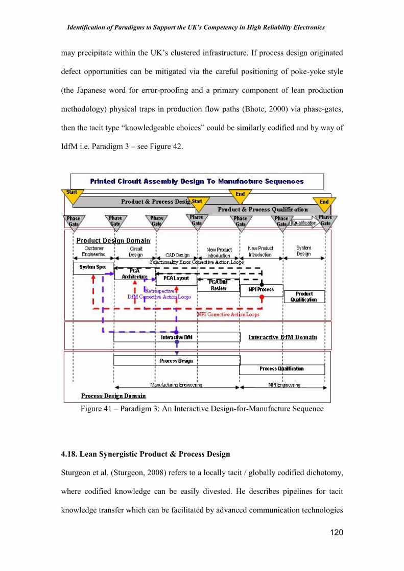
Identification of Paradigms to Support the UK’s Competency in High Reliability Electronics
120
may precipitate within the UK’s clustered infrastructure. If process design originated
defect opportunities can be mitigated via the careful positioning of poke-yoke style
(the Japanese word for error-proofing and a primary component of lean production
methodology) physical traps in production flow paths (Bhote, 2000) via phase-gates,
then the tacit type “knowledgeable choices” could be similarly codified and by way of
IdfM i.e. Paradigm 3 – see Figure 42.
Figure 41 – Paradigm 3: An Interactive Design-for-Manufacture Sequence
4.18. Lean Synergistic Product & Process Design
Sturgeon et al. (Sturgeon, 2008) refers to a locally tacit / globally codified dichotomy,
where codified knowledge can be easily divested. He describes pipelines for tacit
knowledge transfer which can be facilitated by advanced communication technologies
Identification of Paradigms to Support the UK’s Competency in High Reliability Electronics
121
(e.g. ‘telepresence’ or ‘rich teleconferencing’ systems), but this conduit (or pipeline)
will be strained and easily fractured by the globalising EPN. At best, even state-of-
the-art telecommunications could only hope to facilitate retrospective DfM feedback
as the penultimate stage of an outsourced design-to-manufacture sequence within a
GVC extended enterprise. The probability of phase-gated milestones constraining
retrograde optimisation of manufacturability increases with isolated product and
process design (Leifer R. M.-O., 2000) and inhibits lean synergies.
When outsourcing product design to bureaus which specialise in PCB layout, the
author’s research project partners also face further impediments to the implementation
of retrospective DfM recommendations. For logistical and security reasons it is
untypical for either design, or assembly of safety-critical, electronic subsystems to be
outsourced to offshore destinations. However the OEM project collaborators divests a
high level of dependency for package selection and placement decisions to their UK
based design service provider, albeit, within customer specific DfM design rules.
Once completed, the bureau returns PCB layout designs to the customer for DfM
review via its tacit knowledge base, provisioned by its process and manufacturing
engineers.
The tacit knowledge which is critical for lean-production yields (i.e. production flow
that is not interrupted by rework loops) and lean product development cycles needs to
be delivered to the defect opportunity’s point of origin. A ‘right-first-time’ approach
via synergistic product and process design (see Figure 43) will optimise
manufacturability and maximise design-to-manufacture sequence compression.

Identification of Paradigms to Support the UK’s Competency in High Reliability Electronics
122
Figure 42 – Paradigm 4 –Lean & Synergistic Product & Process Design
4.19. Chapter Summary
The intent of this chapter was to:
(i) Identify paradigms by which the research objectives will be met.
(ii) Illustrate an environment where development and utilisation the software
tool will be beneficial.
In an era of lean techniques employed within military and civil aircraft development
programs, opportunities for wasteful design errors and costly discontinuities will
become directly accountable and penalised. The chapter proposes that the
enhancement of lean production of electronic subsystems may be by product and
process design, which is both interactive and synergistic.

Identification of Paradigms to Support the UK’s Competency in High Reliability Electronics
123
The design-to-manufacture sequence may be increased by isolated product and
process design (Paradigm 1) and the schedule overruns which will be an inevitability
of sequence misalignment and retrospective design reviews / corrective action feed-
back loops (Paradigm 2) could be counteracted through model based simulation of
ineffective and retrospective DfM. The investigation into lean production
methodology as applied within the context of cause and effects analysis of Paradigms
1 and 2 addresses this chapter’s research objective.
Paradigms which propose interactive DfM (Paradigm 3) and lean & synergistic
product & process design (Paradigm 4) solutions via (i) the physical models as
proposed within Section 2 of this thesis, and (ii) their ultimate codification and
deployment within CLOVES & INMOST simulation tools are proposed.

Identification of Paradigms to Support the UK’s Competency in High Reliability Electronics
124
Section 2 –
Development of Physical Models
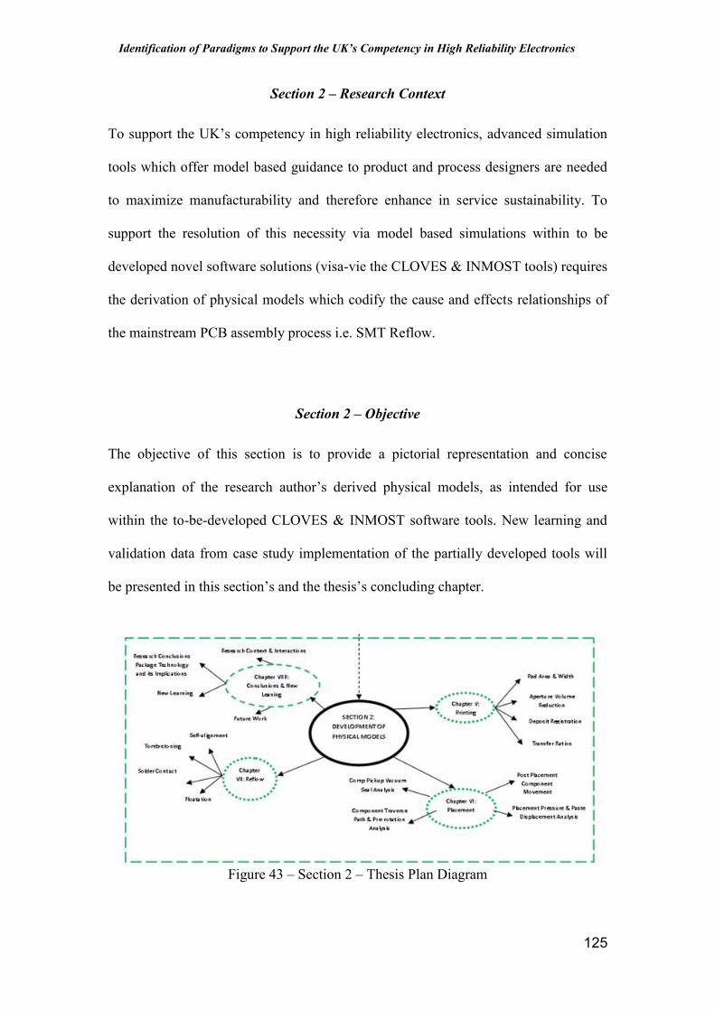
Identification of Paradigms to Support the UK’s Competency in High Reliability Electronics
125
Section 2 – Research Context
To support the UK’s competency in high reliability electronics, advanced simulation
tools which offer model based guidance to product and process designers are needed
to maximize manufacturability and therefore enhance in service sustainability. To
support the resolution of this necessity via model based simulations within to be
developed novel software solutions (visa-vie the CLOVES & INMOST tools) requires
the derivation of physical models which codify the cause and effects relationships of
the mainstream PCB assembly process i.e. SMT Reflow.
Section 2 – Objective
The objective of this section is to provide a pictorial representation and concise
explanation of the research author’s derived physical models, as intended for use
within the to-be-developed CLOVES & INMOST software tools. New learning and
validation data from case study implementation of the partially developed tools will
be presented in this section’s and the thesis’s concluding chapter.
Figure 43 – Section 2 – Thesis Plan Diagram
Identification of Paradigms to Support the UK’s Competency in High Reliability Electronics
126
Chapter V –
Smart Cause & Effects Knowledge Codification Structure for
the SMT Process
5.1 Codification of the SMT Process
To provision Paradigm 3 (IdfM) and Paradigm 4 (lean and synergistic product and
process design) cause and effects relationships for PCBA defect opportunity creation
and detection knowledge a structured approach to codification is required i.e. a Smart
Cause and Effects Codification Structure. Given (i) the predominance of SMDs
(Surface Mount Devices) and (ii) the already realised thresholds for miniaturisation
and automation that will further diminish the potential of PTH technology (see
Chapter II) in future PCA design activities, the scope for the model development
exclusively addresses the mainstream electronics packaging technology i.e. SMT
(Surface Mount Technology) Reflow assembly processes.
The objectives of the developed physical models will be (i) effects modelling
capability for design-for-manufacture based causes of printed circuit assembly (PCA)
defects, and (ii) causation models for effects that can be data mined from historical
defect logs and mapped to the discrete events of the SMT Reflow sub-processes. This
enables discrete event simulations via algorithms which are based on the developed
physical models.

Identification of Paradigms to Support the UK’s Competency in High Reliability Electronics
127
The SMT Reflow process involves the printing of solder paste onto a PCB’s (Printed
Circuit Board) SMT pads prior to component placement and solder joint formation via
reflow soldering, hence the definition of three sub-process – see figure 45.
Figure 44 – SMT Reflow Sub-process Definition – Printing / Placement / Reflow
As per the sequence shown in Figure 1, Chapter VI’s research objective focuses on
the solder paste deposition (i.e. printing) process with the subsequent chapters (VII)
corresponding to SMT component placement and (VIII) the dynamic behaviour of
placed components during reflow soldering.
5.2 Discrete Event Definitions for the SMT sub processes
The process flow for reflow soldering attachment of SMT components (i.e. SMT
Reflow), as provided in Figure 45 involves:
8.. the deposition of solder paste via stencil printing onto pre-defined and
solder-able pads,
(ii) the placement of SMT components with their solder-able terminations in
contact with the solder paste, and,
8.. the reflow melting of the solder paste and its coalescence into liquid solder
that then wets to the pads and terminations forming solder fillets on
solidification.

Identification of Paradigms to Support the UK’s Competency in High Reliability Electronics
128
This process flow generates default process subdivisions or sub-processes, but the
level of complexity in its cause and effects relationships requires further divergence
into (sub) process discrete events. Granularity and understanding of these discrete
events will facilitate more definable model inputs and enable more meaningful
simulation outputs. Figure 4 presents graphical representations of the diverged sub-
process discrete events, which also provide taxonomy for the analysis and
classification of academic and industrial paradigms and rules.
Figure 45 – Graphical Representations of the Diverged Sub-process Discrete Events
5.3 Cause and Effects Model Definitions
The author’s twenty plus years of industrial based experiential knowledge of the
electronics manufacturing processes is drawn upon to provided the tacit knowledge,
which forms the basic understanding of the sub-processes. Codification of this tacit

Identification of Paradigms to Support the UK’s Competency in High Reliability Electronics
129
understanding is via corroboration with (i) research of academic literature, (ii)
interpretation of experimental data as sourced from empirical studies within relevant
areas and, (iii) industrial publications. The subsequent model developments relate to
each of the sub-process discrete events.
Diagrammatical representations of the discrete events accompany the proposed
mathematical formula. Where applicable model inputs, constraints, disturbances,
outputs are diagrammatically presented as per the exemplars within Figures 47 and 48
and supplemented with associated rules and any such impact, effects and corrective
actions implications. The models are also differentiated by their respective
applications i.e. causes analysis or effects analysis of PCA assembly defects.

Identification of Paradigms to Support the UK’s Competency in High Reliability Electronics
130
Figure 46 – An Exemplar Effects Model
Figure 47 – An Exemplar Cause Model

Identification of Paradigms to Support the UK’s Competency in High Reliability Electronics
131
5.4 Model Development Methodology
The original charter for the research project proposed data mining and statistical
analysis of the industrial partner’s production data as the methodologies for the
elicitation of cause and effects relationships. However, this source has proven to
contain only logs of historical assembly defects. Defect logs constitute effects data
only, but to meet the project’s first objective and proffer an understanding of the
causes of these effects, correlating data are required to enable the development of
causation paradigms. Unfortunately, the partner’s logs did not systematically capture
these cause data. Only the, who, what and when minutiae of defect detection are
provisioned, but not the where, why and how details of defect creation i.e. the defect
opportunities. A clear distinction between cause and effects data is paramount in
elicitation of causation relationship rules and paradigms.
Consequently, an alternative approach is required, involving the identification of
causation paradigms, but only where corroboration by any such supporting empirical
data that could elicited from within academic studies is possible. This methodology is
reliant on the gamut of available academic research, which meets the dual publication
criteria of inclusive (i) observed results (i.e. effects data) and (ii) accompanying
design-of-experiment inputs: with the later effectively constituting the cause data for
the former. Although constrained by its limited availability, the benefit of the
approach is that the published supporting data is quantitative, scientifically sanitised
(i.e. peer reviewed) and therefore less vulnerable to erroneous human assumptions.
Acknowledgement is necessary that academic studies within this domain are usually
constrained by the scope of the research questions posed, which by nature tend

Identification of Paradigms to Support the UK’s Competency in High Reliability Electronics
132
towards the in-depth investigation of very specific knowledge requirements. This
renders the available spectrum of supporting data heterogeneous and less generic, thus
providing an explanation for the limited availability of cause data.
Paradoxically, these specific research objectives lend themselves to multilateral
applications (within the SMT sub-processes) which specifically benefit from
industrial standardisation and classification. For example, the IPC issues standards for
the limits of acceptability for electronics assembly workmanship within its IPC-610-E
publication (IPC, IPC-A-610E). It also standardises SMT component package styles
(IPC, IPC-SM-780) and defines the physical characteristics of (i) the component (IPC,
IPC-SM-784) (IPC, J-STD-032), and (ii) its PCB attachment pads plus (IPC, IPC-
7351 (L)) (iii) the ensuing solder joints (IPC, IPC-DRM-SMT-D). From this validated
source of standardised effects data, the requisite solder paste deposit volume / location
and solder joint volume / shape characteristics can be extrapolated, thus supporting
the generation of non-proprietary acceptance criteria for the paste deposition and
reflow sub-processes. This codification of the empirical study based data satisfies the
academic obligation for the avoidance of commercial discrimination.
Conversely, in standardising the SMT assembly process effects data, the IPC has
inadvertently negated the need to standardise the cause-associated data. The IPC does
not issue standards that pertain to the methods of solder paste deposition, placement
of components, or reflow of the solder deposits – although it does provide solder paste
deposition stencil design (IPC, IPC-7525) and reflow thermal profiling (IPC, IPC-
7530) and generic process set up and check list (IPC, IPC-S-816) guidelines. Hence,
the idiosyncratic characteristics of individual makes and models of printer, placement

Identification of Paradigms to Support the UK’s Competency in High Reliability Electronics
133
and reflow equipment remain unregulated. This minimises the dependence on
proprietary information for the elicitation of causation data relating to the mode of
deposition, placement, reflow and avoids any commercial sensitivity.
Since (i) the modes of deposition and reflow directly affect solder joint geometries,
and (ii) their effects data can be extrapolated from the IPC standards, model
development is facilitated by the specific empirical studies, which can provision
causation paradigms via their incumbent design-of-experimentation inputs. However,
as the effects of component placement on resultant solder joint geometries are
indirect, the model development for this sub-process is unsupportable via the
previously described methodology and an alternative method is required.
Given the relative simplicity of the discrete events associated with the placement sub-
process (i.e. component pick-up under vacuum / vision alignment with the
corresponding PCB location / placement and vacuum release) basic analytical
techniques can proposed. The methodology adopted within this model is based on
ABVA (Assembly Build Variation Analysis), which is one of a suite of
methodologies as provisioned within the automotive industry’s QS9000, a
predecessor to its current TS:16949 QMS (quality management system) standard. It is
a simplistic approach, which involves the summation of applicable cumulative
tolerances.
Mostly, the research methods employed have delivered a spectrum of studies, which
wherever possible (e.g. the SMT solder paste printing and reflow sub-processes)
compliment and corroborate each other’s findings with correlating empirical data.

Identification of Paradigms to Support the UK’s Competency in High Reliability Electronics
134
Only in instances where this is not possible, (e.g. the SMT component placement sub-
process) the proposed causation paradigms are limited to ones which assume tenants
that are derived from basic physical models and verifiable via logical argument.

Identification of Paradigms to Support the UK’s Competency in High Reliability Electronics
135
Chapter VI –Solder Paste Printing
6.1. Chapter Objectives
To enable discrete event simulations via paradigms, development of physical models
of the mainstream PCB assembly process namely SMT Reflow is required – Chapter
V addresses the solder paste printing sub-process via its discrete events and codifies
the model based cause and effects as depicted in Figure 49.
Figure 48 – Chapter Context Diagram
6.2. Description of Solder Paste Deposition Sub-process
The paste deposition sub-process is presented as three discrete events and illustrated
in Figure 50 – Stencil / PCB alignment, Figure 51 – Print Stroke / Aperture Filling
and Figure 52 – Stencil Separation / Paste Transfer).
6.3. Sub-process 1 Discrete Event A Discrete Event – Stencil / PCB Alignment
Although equipment make and model idiosyncrasies can apply, in automated
assembly, the stencil and PCB are usually aligned by the printer’s vision system via
matched pairs of Fiducial alignment marks that are located on both the upward facing
PCB surface and the stencil underside. A swinging arm mounted camera system
which is enabled with split optics scans these marks. The camera then retracts to allow
the PCB to be elevated in the vertical plane by a rising table. Depending on the system

Identification of Paradigms to Support the UK’s Competency in High Reliability Electronics
136
design, manipulation (in all three dimensions) provides alignment and allows contact
between stencil and PCB.
Figure 49 – Graphical Representation of the Stencil / PCB Alignment Discrete Event
6.4. Sub-process 1 Discrete Event B Discrete Event – Print Stroke & Aperture
Filling
Prior to the commencement of the print cycle, a quantity of solder paste (i.e. the
working paste) is loaded onto the stencil directly in front of the squeegee-blade start
position. Referred to as squeegee pressure on commencement of the automatic cycle,
lowering an incline mounted squeegee blade onto the stencil exerts a downward force.
Assuming accurate alignment and that the aperture has had a size reduction applied
during stencil design, then a stencil and PCB gasket seal is expected. The back-to-
front print-stoke is then actuated in the Y-axis. This action should gather the working
paste into a bead and produce a rolling action. This rolling action has the following
functions:
(i) to impart mechanical energy into the working paste and generate a shear-
thinning effect, which lowers its viscosity, thus improving its stencil aperture
fill / release characteristics, and

Identification of Paradigms to Support the UK’s Competency in High Reliability Electronics
137
(ii) to redirect the Y-axis horizontal force into the vertical plane (i.e. Z-axis), thus
filling the aperture.
Figure 50 – Graphical Representation of the Print Stroke & Aperture Filling DiscreteEvent
6.5. Sub-process 1 Discrete Event C – Stencil Separation / Paste Transfer
With the print stroke completed, the rising table is lowered to the input / output
conveyor height and separation ensues allowing the PCB exits the machine. With
assumed compliant contact and successful aperture release, the paste deposits form.
Figure 51 – Graphical Representation of the Stencil Separation / Paste TransferDiscrete Event
Once separation (of stencil and PCB) has occurred, relief of the squeegee pressure
precedes the elevation of the squeegee assembly, with the working paste positioned at
the end of the print-stroke. Post separation release of squeegee pressure mitigates the
ControlledZ Axis
Separation
Paste Deposit

Identification of Paradigms to Support the UK’s Competency in High Reliability Electronics
138
risk of stencil reverberation in situations where separation reluctance, due to
unintentional adhesion between paste and stencil, generates tensile forces in the
stencil mounting system. A further Y-axis movement then presents a second squeegee
with an equitable but inverse angle of inclination in front of, but also effectively
behind the working paste. This action is required in preparation for the following print
cycle, which will involve a front-to-back print-stroke.
Note: more advanced systems offer a controlled separation function with
programmable control over separation speed and distance, but only in circumstances
where aperture release has been optimised through advanced stencil design will the
significance of this level of user definable control become apparent (see following
sections).
6.6. Tacit Knowledge Relating to the Solder Paste Deposition Sub-process:
Fine pitch technology (FPT) is an acronym for SMT components with lead pitches of
0.635 mm or less. FPT invokes the more challenging pad geometries (see Figure 53)
and subsequent higher frequencies of print deposition related defects i.e. Bridged,
Excess, Insufficient and Opens.
Figure 52 – Definitions of Pad Geometry
When compared with the geometries that are apparent in silicon level integration, the
scales of miniaturisation that are presented by leading edge, electronic component
package technologies, become less significant and should not be seen as an obstacle to

Identification of Paradigms to Support the UK’s Competency in High Reliability Electronics
139
process control. If contemporary semi-conductor manufacturing can deliver parts per
billion production yields at sub-micron geometries, then by comparison, the sub-
millimetre dimensions of FPT pad geometries would appear vast.
However, when considering the diverse scales of miniaturisation apparent within the
multitude of contemporary component package formats, this association becomes
inequitable. Comparable multiplicity does not apply at the silicon level of integration
because geometric diversity is less acute. This suggests that it is not the apparent scale
of miniaturisation but the geometric diversity within a PCA design that should be the
focus of cause and effects analysis and that production yield vagaries must be linked
to compromised geometric aspects, ergo, geometric aspect ratios.
Of the solder paste deposition related defect opportunities, those which are
unilaterally inferred by the product’s design, such as the pad and stencil aperture
dimensions, must also provide opportunities for the optimisation of manufacturability
i.e. design-for-manufacture. They also provide the main inputs for the models, which
predict paste deposit heights and volumes. Historical process control endeavours
involved an assumed correlation between deposit height and volume. Height
anomalies can be indirectly associated with solder paste excess and bridge related
defects, but only in cases of extreme variation in deposit volumes. Direct correlations
between these effects and volume related causes will necessitate full volumetrically
scanned data.
Transfer ratios, via correlation between aperture and deposit transfer volumes must
offer excess and bridge defect prediction possibilities. Therefore, the aperture

Identification of Paradigms to Support the UK’s Competency in High Reliability Electronics
140
volume’s geometric aspect ratio will similarly correlate with the deposits transfer ratio
within a paradigm and accommodate defect probability rules. These particular aspect
ratios are functions of lateral aperture dimensions and stencil thickness. In turn, the
SMT pad dimensions determine the lateral aperture dimensions (i.e. length and
width). Application of a percentage reduction in the lateral dimensions of stencil
apertures facilitates pad to stencil enclosure and gasket interfacing whilst
accommodating alignment tolerance (see Figure 50). In FPT printing, the scale of this
reduction will influence both excess and insufficient deposit volumes. Compromised
gasket seals remain a possibility if the reduction is insufficient, but overcompensation
may impede paste release as the aperture’s geometric aspect ratios become
unfavourable. Stencil thickness is also a function of an aperture’s geometric aspect
ratios.
The manufacture of stencils with topographic features is an option. For instance,
localised reductions in stencil shim thicknesses are possible via confined chemical
subtractive methods such as focussed etching. Conversely, confined additive methods
such as focussed electro-plating enables localised thickness enhancement for packages
with high volumetric requirements. However, by default, both these options
compromise the fundamental necessity for stencil / PCB co-planarity, which can only
be satisfied by single thickness stencil shims. Thus, the gauge of the shim used in the
manufacture of the stencil needs to accommodate and define the allowable
multiplicity in package-to-package geometries. Failure to control conflicting package
selections during PCA design will compromise manufacturability and embed defect
opportunities.

Identification of Paradigms to Support the UK’s Competency in High Reliability Electronics
141
6.7. Development of Solder Paste Deposition Models from Tacit Knowledge and
Review of Literature
Given the complexity and diversity of electronic component package technology and
the unpredictability of human actuated operations, academic and industrial research
appears to focus on package formats that are applicable to automated assembly (i.e.
SMDs) and target specific issues that relate to particular changes in SMT package and
process innovations. Consequently, paradigms appear incongruent, with data sparse,
heterogeneous and less generic. However, through detailed analysis, levels of
correlation do emerge which suggest that a homogeneous meta-model may be viable.
6.8. Geometric Aspect Ratios
Numerous academic and industrial studies have identified aperture size related
geometric aspect ratios as being critical to optimal paste release (Pan, Critical
Variable of Solder Paste Stencil Printing for Micro-BGA and Fine-Pitch QFP,, 2004)
(Durairaj R., 2001). All refer to a two-dimensional aspect ratio (AR) between stencil
thickness and aperture width / diameter for rectilinear or round pad patterns
respectively. A consensus exists within the studies, which states that aperture width
(see Figure 54) should not be less than 150% of the stencil thickness (i.e. AR≥ 1.5:1).
Acquiesce is also apparent for a three-dimensional geometric aspect ratio. An area
aspect ratio (AAR) is cited where the pad / paste contact area (AL * AW or π * AD) is
divided by the aperture wall surface area (AL * AW * 2). An AAR should never be
less than 0.6 (i.e. AAR≥ 0.6) (Pan, Critical Variable of Solder Paste Stencil Printing
for Micro-BGA and Fine-Pitch QFP,, 2004) (Durairaj R., 2001).

Identification of Paradigms to Support the UK’s Competency in High Reliability Electronics
142
Figure 53 – Definitions of Aperture Geometry
Using the convention given in Figure 55, an aperture’s volume can be formulated as
AL * AW (or AD) * ST. The transfer ratio (TR) for a given solder deposit can be
extrapolated by dividing the measured volume by the theoretical volume (i.e.
equitable with the aperture’s volume). Assuming neutral rheological effects, the
combined effects of the paste’s attraction to the SMT pad and its internal cohesion
determine the aperture’s release characteristics. This resistance must prevail over the
paste’s attraction to the aperture wall and its consequential shear resistance, which
acts whilst it is under tensile load i.e. during stencil / PCB separation. This
relationship explains the aperture design related release characteristic that contribute
to negative-value transfer ratios; but it fails to account for the positive-value transfer
ratio realities which precursor the excess solder joint phenomenon. Due to the
omission of associated effects data, reported anecdotes of excess solder joints within
the project partner’s defect logs fail to edify their causation paradigms.
6.9. Paste Transfer Ratios
Pan et. Al. (Pan, Critical Variable of Solder Paste Stencil Printing for Micro-BGA and
Fine-Pitch QFP,, 2004) provide deposit volumetric data for each of two stencil
thicknesses (0.10 mm & 0.15 mm) per package type, of which, one has rectilinear

Identification of Paradigms to Support the UK’s Competency in High Reliability Electronics
143
pads (as applicable in QFP solder joint formation) with five discrete lead pitches, and
the other type has round pads (for BGA attachment) with three discrete ball array
pitches. From these data, extrapolation of transfer ratios and their AR & AAR
geometric aspect ratios is possible – see Table 1.
Table 1 – Pan Et Al’s Volumetric Data & Extrapolated Geometric Aspect and
Transfer Ratios
Generated via full volumetric deposit measurement, the data presented by Pan et al.
(Pan, Critical Variable of Solder Paste Stencil Printing for Micro-BGA and Fine-Pitch
QFP,, 2004) is of particular significance – see Table 1. Prior to the development and
commercialisation of cost effect, operator friendly solutions, preceding deposit
measurement methods had evolved from non-contact height sampling via manually
actuated and interpreted, focussed light based systems. Subsequent, fully automated,
triangulated laser-based solutions then provided pseudo three-dimensional capability,
via two-dimensional scanning and Z-axis sampling techniques. Manufacturers of

Identification of Paradigms to Support the UK’s Competency in High Reliability Electronics
144
solder paste printing platforms have since incorporated similar technology (i.e.
camera or triangulated laser based) and integrated it within their machines. Although
they claim pseudo three-dimensional capabilities in reality, only recent developments
have made full volumetric three-dimensional scanning of solder deposits more
prevalent.
(Courtesy http://kohyoung.com/)Figure 54 – Image of Bridged Solder Paste Deposits via Full Volumetric Scanning
Techniques
Height sampling and pseudo three-dimensional volume estimation methods rely on
the misconception that volumetric deposit variation effects are exclusively attributable
to the scooping phenomenon i.e. the scavenging of the upper surface of the paste
deposit due to a deflection of the squeegee blade within the aperture – see Figure 56.
This method of control is none quantitative and not capable of detection of aperture
release anomalies. It therefore obscures the effects of poor paste release and thus
considered unsuitable for model development.

Identification of Paradigms to Support the UK’s Competency in High Reliability Electronics
145
Figure 55 – Graphical Representation of the Scooping Effect
Mannan et al., (Mannan S. H., 1993) provide data, confirming the scooping effect (see
Figure 56) but also apportioning causation and severity to the squeegee blade’s
material and hardness. The relevancy of this research reflects its date of publication,
which coincides with the adoption of harder, metal blade squeegees. The advent of,
and multilateral user transition from polymer based screens to the more robust and
accurate metal stencils facilitated a change to metallic blade technology. With sharper
edge definition and rigidity, metal blades enable the higher squeegee pressures that
improve stencil to PCB contact and enhanced gasket sealing, whilst minimising blade
deflection and aperture scooping.
The scooping attributable differential effects, which are differentiated by aperture
orientation, are corroborated the Mannan et. Al. Data. It supports the paradigm that
rectilinear apertures with their major axis (i.e. their longest dimension) in coincidence
with the print stroke appear susceptible to a higher rate of scooping than their
perpendicular equivalents. As the dominant design in printer platforms orientate the
print stroke in front / back directions, then apertures with their major axis coinciding
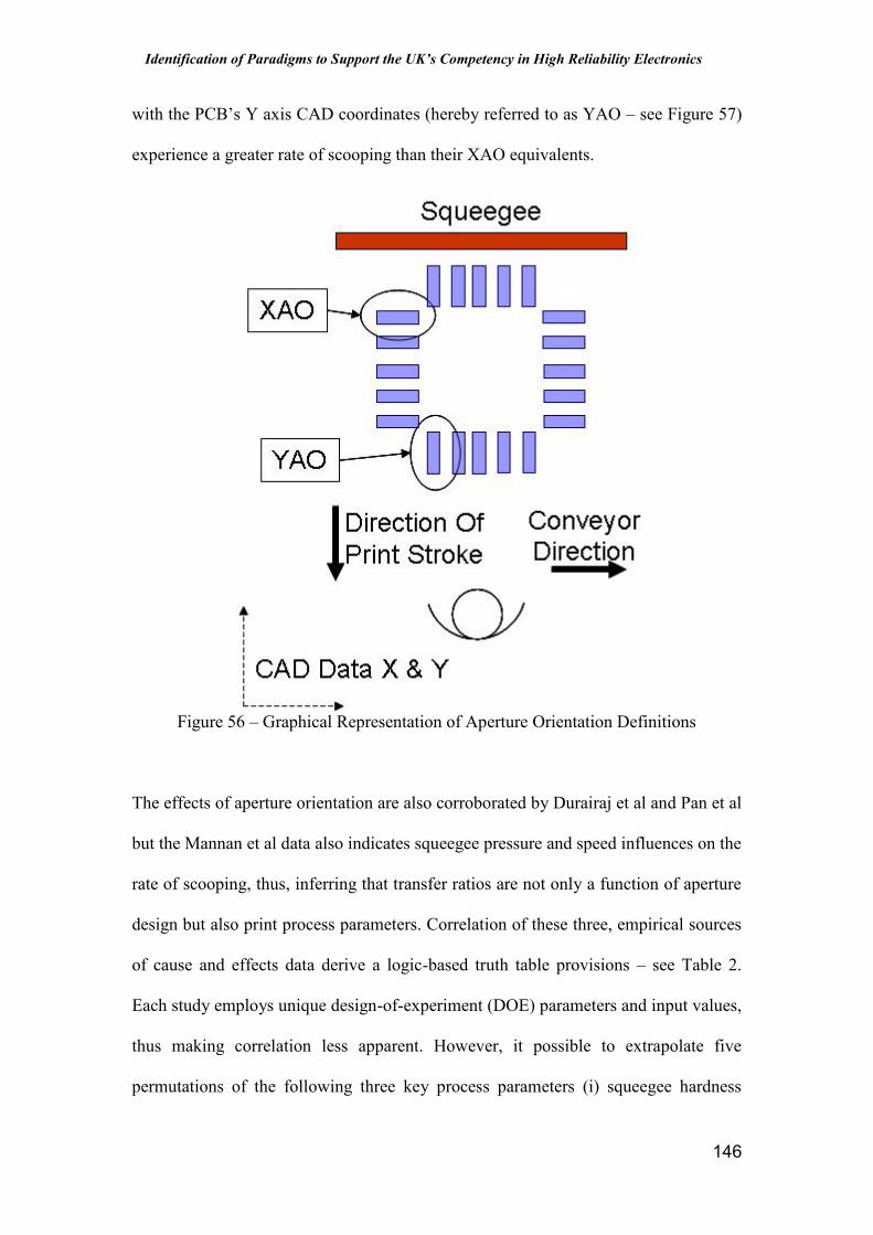
Identification of Paradigms to Support the UK’s Competency in High Reliability Electronics
146
with the PCB’s Y axis CAD coordinates (hereby referred to as YAO – see Figure 57)
experience a greater rate of scooping than their XAO equivalents.
Figure 56 – Graphical Representation of Aperture Orientation Definitions
The effects of aperture orientation are also corroborated by Durairaj et al and Pan et al
but the Mannan et al data also indicates squeegee pressure and speed influences on the
rate of scooping, thus, inferring that transfer ratios are not only a function of aperture
design but also print process parameters. Correlation of these three, empirical sources
of cause and effects data derive a logic-based truth table provisions – see Table 2.
Each study employs unique design-of-experiment (DOE) parameters and input values,
thus making correlation less apparent. However, it possible to extrapolate five
permutations of the following three key process parameters (i) squeegee hardness

Identification of Paradigms to Support the UK’s Competency in High Reliability Electronics
147
(SH), (ii) squeegee pressure (SP) and (iii) squeegee speed (SP) with categorisation of
the input variable into high / low attributes. Boundary conditions emerge for
geometric aspect ratios at AR < 1.5 and greater than > 4.5 based on the extrapolated
transfer ratios (TR) for XAO and YAO orientated apertures. This suggests that
aperture release was insufficient below 1.5 and scooping excessive above 4.5.
Summary of the five permutations shows that metal squeegees with low squeegee
pressure and high print stroke speeds facilitate optimum transfer ratios – with the
inverse of these inputs and low TR outputs corroborate this paradigm.
Table 2 – Correlation Truth Table for Print Process Parameters, AR Boundary
Conditions and Aperture Orientations
6.10. Stencil / PCB Misalignment and Paste Bleeding
Assuming coplanar contact between (i) squeegee and stencil, and (ii) stencil and PCB,
explanation of transfer ratios, which are greater than 100%, relies on an assumed
breach of the gasket seals between aperture and SMT pad. Lateral misalignment
would seem to be the most likely root cause in circumstances where incidents of
excessive solder joints and short circuits (see Figure 58) co-inside with localised
concentrations of excess and bridged deposits – see Figure 59.

Identification of Paradigms to Support the UK’s Competency in High Reliability Electronics
148
Figure 57 – Graphical Representation of the Solder Bridging – Solder Shorts Effect
Figure 58 – Graphical Representation of the Excess Paste due to Bleeding Causes
In the advent of a breached gasket seal, the vector of the force, which generates the
scooping effect, is more likely to push the paste into the resultant spaces between
stencil and PCB that lie within the path of the vector – see Figure 60. These gaps will
occur due to the stand-off created by the pad to substrate height differentials – see
Figure 14.
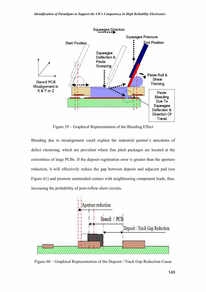
Identification of Paradigms to Support the UK’s Competency in High Reliability Electronics
149
Figure 59 – Graphical Representation of the Bleeding Effect
Bleeding due to misalignment could explain the industrial partner’s anecdotes of
defect clustering, which are prevalent where fine pitch packages are located at the
extremities of large PCBs. If the deposit registration error is greater than the aperture
reduction, it will effectively reduce the gap between deposit and adjacent pad (see
Figure 61) and promote unintended contact with neighbouring component leads, thus,
increasing the probability of post-reflow short circuits.
Figure 60 – Graphical Representation of the Deposit / Track Gap Reduction Cause

Identification of Paradigms to Support the UK’s Competency in High Reliability Electronics
150
Extension of this two dimensional error into the third dimension occurs if the gap
created by height differentials between the pad and its surround area fills (see Figure
62), thus initiating positive-value transfer ratios and the probability of post-reflow
excessive solder joints.
Figure 61 – Graphical Representation Excess Deposit Due To Pad Height Differential
Cause
The magnitude of the pad to substrate height differentials will be a function of the
copper thickness plus its specified surface finish. Unless the application requires a
high current carrying capacity and subsequent high copper mass requirement, the
average PCB will have a copper cladding / plating depth of 35.5 microns (Lea, 1988).
A typical surface mount compatible flat finish, such as, electro-less nickel /
immersion gold (ENIG) will add another 6 to 13 microns (IPC, IPC-4552/02, 2002).
A preference for optimal solder-ability over pad flatness may require the
accommodation of hot air solder levelled (HASL) fused Sn / Pb (Lea, 1988). This
surface finish will vary in height across a pad by between 2 to 25 microns (Klein
Wassink R. J., 1989). The total pad height differential (herein referred to as PHD)
could subsequently vary between 27 and 60 microns. Given that the AR<1.5:1 rule
becomes unviable for FPT (fine pitch technology) geometries at stencil thicknesses

Identification of Paradigms to Support the UK’s Competency in High Reliability Electronics
151
which exceed 125 microns, the PHD can easily equate to a significant percentage of
the overall stencil thickness (i.e. approximately 35 to 50%).
The potential to exceed Poon & Williams’ (Poon, 1999) 115% recommended upper
limitation for provisional positive-value transfer ratios is exaggerated by high
percentage PHDs. In addition, a cumulative effect becomes probable via a residue
transfer mechanism between successive prints, which is similar to the one that
accumulates paste in apertures.
The application of a solder resist mask, in the form of polymer coating, to a
substrate’s surface repels unwanted dispersed solder and protects its copper tracks
from unintended electrical shorts via conductive debris contamination. If the pad
pattern is fully defined by the mask, the gap which enables this paste leakage path
may be partially occupied and therefore lessen the potential for post reflow defects.
However, a counter argument that accounts for the influence that solder resist has on
bleeding can be derived from the fact that the limits of solder resist registration
accuracy make the chances of achieving resist-free pad definitions for 0.5 mm pitch
geometries and below, at best marginal. The probability of resist encroachment onto
the pad will make gap exaggeration a more likely outcome.
Note: by implementing a defect reducing, corrective action at the PCB layout design
stage, via the elimination of the resist webs that enclose and define ultra FPT pads a
partner has corroborated this paradigm.

Identification of Paradigms to Support the UK’s Competency in High Reliability Electronics
152
Positive Transfer Values and Cumulative Effects
By definition, transfer ratios must possess cumulative tendencies. For example, in
none scooping effect scenarios, the retention of residual paste within the aperture
provides the only cause attribution for negative TR’s (transfer ratios, which are less
than 100%). This residue, if uncorrected by remedial action (i.e. effective stencil
cleaning), will compound the aperture’s already compromised release characteristics.
The effective aperture width will decrease as the residue adheres to the walls; further
compromising the aspect ratio over successive prints. Hence, a cumulative negative-
value transfer ratio, which successively reduces the aperture volume and exaggerates
the release inefficiencies, is apparent. If uncorrected (through stencil cleaning) the
accumulation will ultimately result in total aperture blockage.
Given the propensity for a catastrophic functionality failure and subsequent detection
probability via electrical in-circuit testing, a total blockage scenario is less probable
and reactive stencil cleaning a more likely precursor of consequential open circuits.
Predictive modelling of proactive stencil cleaning regimes offers process control
potential and the mitigation of the risk of the negative-value, cumulative transfer
ratios that equate to insufficient deposit volumes. Poon and Williams recommend a
provisional 95% minimum negative-value ratio, thus providing a reasonable
benchmark.
Via volumetrically scanned nonconformity data and correlated defect rates, Poon and
Williams, exclusively provide testimony to the possibility of the previously
unacknowledged phenomenon of positive-value transfer ratios and excess deposit
nonconformities. They confirm a cumulative positive-value effect, exaggerated by

Identification of Paradigms to Support the UK’s Competency in High Reliability Electronics
153
elevated ambient temperatures and only negated by in-cycle remedial processes such
as automated, underside stencil cleaning.
A cumulative effect would compound any such positive-value scenario. Contrary to
the aperture retention / negative-value accumulation scenario, residue build-up on
immediate, aperture surrounding surfaces will promote excess and bridge related
defects; this positive-value accumulation must be via surface residue transfer between
successive prints. A residue could explain the phenomenon, which is deposited on the
underside of the stencil, webs that separate the FPT apertures as a result of paste
bleeding – see Figure 63
.
Figure 62 – Graphical Representation of Surface Residue Transfer Mechanism for
Paste Bleeding
The surface residue transfer mechanism causation paradigm is supported by the fact
that the Poon and Williams’ positive-value transfer ratios are cumulative and return to
nominal with each stencil cleaning cycle.
6.11. Dimensional Mismatches
Industrial collaborator anecdotes of a disproportional increase in excess and bridged
solder joints, which are clustered around FPT components that are located at the
extremities of large PCBs suggests a dimensional mismatch so as to result in a lateral

Identification of Paradigms to Support the UK’s Competency in High Reliability Electronics
154
misalignment between stencil apertures and SMT pads. Further analysis of the PCBs
that exhibited this phenomenon highlighted an unexpectedly large, dimensional error
that increased proportionally over distance. The corresponding solder paste stencil did
not incur a cumulative dimensional mismatch. Figure 64 illustrates this potential for
this type of anomaly.
Figure 63 – Graphical Representation of PCB / Stencil Dimensional Mismatch Cause
The stencil / PCB alignment systems as utilised within higher specification automated
SMT printers with integral vision systems to locate and align the stencil and PCB,
also include checking for dimensional errors capability, when attempting a best-fit
lateral alignment. ‘Best-fit’ correctly suggests a compromised solution which
minimises the effect of manufacturing tolerance issues, as incurred during PCB
fabrication and / or package positioning anomalies, as embedded during layout of the
PCB at the design stage. It therefore represents an imperfect accommodation of the
causes of the dimensional mismatch rather than a correction of the original
dimensional errors.

Identification of Paradigms to Support the UK’s Competency in High Reliability Electronics
155
Unless programmed about an alternative, user-defined fulcrum, the resultant best-fit
alignment centres about the PCB’s CAD data centroid. Consequentially, the location
of FPT sites at the extremities of large PCBs, will amplify dimensional mismatches,
effectively reducing the post-alignment clearance between stencil apertures and the
nearest neighbour of their corresponding PCB interconnection pad. This paradigm
provides a possible explanation for the causes of the large PCB cumulative effects that
generate both (i) deposit registration nonconformities (ii) breached gasket seals and
positive-value transfer ratio nonconformities.
Lotosky et al. (Lotosky, 2006) describe the lateral misregistration paradigm and
provide data and a corrective action, which reduced print deposit related defects by an
average of 43% via a remanufacturing of the stencil to include 0.5 microns per
millimetre, negative-scaled compensation factor. Of significance is the fact that their
application (i.e. automotive engine-control modules) required the construction of a
specialized technology substrate, with a 0.175 mm thick flexible FR-4 circuit
laminated on to a 2 mm thick rigidizer. Hence, the Lotosky et al.’s negative-error
factor (0.5 microns per PCB millimetre in X and Y) is none typical and therefore
unsuitable for adoption as a generic dimensional error rule.
Rahn (Rahn, 2006) suggests that PCBs can shrink during pre-production storage and
that stencils can stretch during extended usage, an effect exaggerating with off-contact
printer set-ups and vertical mis-registration. However, the industrial partner’s
anecdotal evidence identified a positive PCB dimensional scaling error (i.e. a lateral X
or Y board dimensional error herein referred to as BDEn) which was found to be the
cause of the increased bridging and excess effect.

Identification of Paradigms to Support the UK’s Competency in High Reliability Electronics
156
The Lotosky et al.’s corrective action (i.e. the remaking of the stencil with lateral
scaling-error compensation) assumes a constant dimensional error. This predictability
may be feasible given their specific substrate construction, but whilst Rahn has
suggested time based dimensional shrinkage vagaries, the partner anecdote has
illustrated the possibility of stretched substrate scaling errors.
The (previously stated) 50 – 70% approximated causation ratio for solder paste
deposition attributed assembly defects represents the most significant defect initiator
of the three sub-processes. Therefore, it also represents the sub-process with the
greatest scope for yield improvement delivery via smart cause and effects analysis and
offers the greatest error proofing potential for interactive DfM (Design-for-
Manufacture). Generally perceived as a “black art” which demands the maximum
tacit knowledge by industrial practitioners, it is also afforded the most in depth
attention within academic circles, hence an availability of empirical study data, which
is both sufficiently detailed and harmonized to facilitate the codification of knowledge
via arithmetic formula.
6.12. Models for Sub-process 1 Discrete Event A: Stencil / PCB Alignment
Relating to Sub-process 1 Discrete Event A, the following formula and its associated
rules provide a model’s mathematical functionality for both, (i) interactive DfM and
(ii) smart cause and effects analysis of:
Deposit Registration Error & Bridging Prediction Formula
Equation 1or,for rectilinear pads,

Identification of Paradigms to Support the UK’s Competency in High Reliability Electronics
157
Equation 2for round pads,
Equation 3where,
DBPn = X or Y deposit bridge potential ratio
DREn = X or Y deposit registration error
PPG = pad to pad gap
BDEn = X & Y board dimensional error
PCn = X & Y component position from PCB centroid
CP = component pitch
Deposit Bridging Rule
If DREn ≤ Arn then DRDP bridging possibility = 0%
where,
Arn = X & Y aperture reduction dimension
Deposit Registration Error & Excess Formula
for rectilinear pads,
Equation 4for round pads,
Equation 5where,
DEPn = X & Y deposit excess potential ratio
TR = transfer ratio
AV = aperture volume

Identification of Paradigms to Support the UK’s Competency in High Reliability Electronics
158
DV = deposit volume
PHD = pad height differential
CT = copper thickness (e.g. 1 oz Copper / inch2 = 0.036 mm)
SFT = surface finish thickness (e.g. ENIG = 0.006mm to 0.013 mm)
Deposit Registration Error Volume Rule
If provisional TR > 115% then SCF (stencil cleaning frequency) = 100%
The effects model provides the following package selection and location outputs as
interactive DfM guidance at the design stage as based on the stencil / PCB alignment
discrete event (see Figure 65) in the form of:
a. prediction of solder paste deposition defects due to positive-value TR
related causes,
b. PCB layout recommendations for component location / orientation,
c. recommendations for stencil thickness and aperture dimensions, and,
d. recommendations for stencil cleaning frequency for discrete event
simulation.

Identification of Paradigms to Support the UK’s Competency in High Reliability Electronics
159
Figure 64 – Graphical Representation of the Stencil / PCB Alignment Effects Model
Inputs for interactive DfM modelling are:
o the component’s PCB centroid as elicited from its CAD data,
o the pad dimensions as elicited from the CAD system library shape,
o the provisional stencil aperture dimensions as selected by the
manufacturing engineer during stencil design, and,
o the provisional stencil thickness as selected by the manufacturing
engineer during stencil design.

Identification of Paradigms to Support the UK’s Competency in High Reliability Electronics
160
The cause model (see Figure 66) for this discrete event could provide the following
outputs for smart cause and effects analysis for assembly defects and fault generators
for defect opportunities in SMT Reflow discrete event simulations in the form of:
o bridged solder paste deposits in FPT packages located at larger PCn’s,
o excess solder paste deposits in FPT packages located at larger PCn’s,
o dispersed solder balls in FPT packages located at larger PCn’s, and,
o ineffective or infrequent underside stencil-cleaning.
Inputs for smart cause and effects are:
o historical bridging and excess defects,
o package pitch and location from PCB CAD data,
o pad dimensions from CAD shapes libraries, and,
o aperture width and stencil thickness from stencil manufacturing data.
o the lead pitch of the provisionally selected package during circuit
design,
o the PHD for the provisional PCB copper thickness and surface finish
(see Figure 62) as proposed during PCB layout,
o the board dimensional error tolerance specification as proposed during
PCB layout.

Identification of Paradigms to Support the UK’s Competency in High Reliability Electronics
161
Figure 65 – Graphical Representation of the Stencil / PCB Alignment Cause Model
Whilst excess and bridged joint predictions (i.e. interactive DfM) and analysis (i.e.
smart cause and effects) provide the physical modelling aims, the functional objective
must be the projection of cumulative paste bleeding over successive prints in
situations of gasket seal failure.
The in-process corrective action for paste bleeding is to increase the frequency of
underside stencil wiping, thus incurring a non-value adding process together with its
own inherent process variability. Embedded in the design process, the root causes are
package selection / location related and therefore become correctable via interactive
DfM. In addition to the limitations imposed by the availability of package styles for a
given functional specification and any such PCB layout and packing density

Identification of Paradigms to Support the UK’s Competency in High Reliability Electronics
162
restrictions, constraints which apply during any such DfM modelling are, the
cumulative tolerance window ABVA which considers
o the intended printer’s X / Y alignment accuracy and stencil
manufacturing specifications (see Figure 67),
o the PHD (pad height differentials), and
o the specified PCB fabrication manufacturing tolerance.
The effectiveness of smart cause and effect modelling will be constrained if the
individual PCB under analysis is unsuitable or unavailable for measurement of its
manufacturing dimensional errors (i.e. BDEn).
Figure 66 – Graphical Representation of the Stencil Alignment ABVA with
Nomenclature
As is the case with its inverse, (i.e. scooping) cumulative bleeding will be
proportional to (i) the hardness of the squeegee blade material plus its speed and
pressure process parameters (see Table 2) and (ii) the degree of stencil / PCB non-
planarity due to the effects of edge clamps or insufficient PCB underside support (see
Figure 68). If recorded and available within historical logs, these process parameter
based model disturbances can be reconstituted as inputs and their magnitude subjected
to aperture orientation effects (see Figure 57), with YAO orientations likely to incur

Identification of Paradigms to Support the UK’s Competency in High Reliability Electronics
163
lower transfer ratios. However, the vagaries of (i) stencil wiping effectiveness, (ii) the
PHDs and (iii) the working paste’s rheology, make quantitative trend analysis via full
volumetric scanning of transfer ratios with facsimile process conditions over
successive prints a prerequisite adjustment factor for the modelling of cumulative
TRs.
Disturbances, which distort model outputs in both interactive DfM and smart cause
and effects analysis, are:
potential gasket seal failure in the X & Y axis due to either, PCB
manufacturing dimensional errors or the intended printer’s alignment
accuracy, and,
potential gasket seal failure in the Z axis due to stencil / PCB co-planarity
including the stand-off gap created by the applicable printer’s edge-clamps
– see Figure 68.
Figure 67 – Graphical Representation of Edge Clamp Effects Causing Stencil / PCB
Gaps

Identification of Paradigms to Support the UK’s Competency in High Reliability Electronics
164
External rules which are based on knowledge that has been codified by the
Association Connecting Electronics Industries (a.k.a. the IPC) – the electronics
industry’s standardised body – can provide the provisional inputs and boundary
conditions when using this model as part of a design function. IPC 7351(L) (IPC,
IPC-7351 (L)) and its predecessor (IPC, IPC-SM-782, 1987) provide recommended
pad dimensions for (i) minimum lead density / optimal bond area, (ii) nominal lead
density / bond area and (iii) maximum lead density / minimal bond area. Application
of the model’s geometric aspect rules within the boundary conditions will facilitate
interpolation of best-fit aperture dimensions, thus modelling the reliability
implications of defect opportunities and solder joint rework impact (Lau. J.H., 1991)
(Garrison, 1995) (Hutchins, 1995) (Nguty, 2000) against lead density / bond area.
6.14. Models for Sub-process 1 Discrete Event B: Print Stroke & Aperture
Filling
With the effects of stencil / PCB misalignment and gasket seal failure accommodated
within the preceding discrete event, the models for Discrete Event B assume an
uncompromised contact between aperture and pad, thus discounting the paste bleeding
effect. As the following discrete event incorporates, the modelling of paste transfer
aperture release and negative-value TRs do not yet apply. Therefore, mathematical
functionality for this discrete event focuses on the process disturbances, as induced
during the print stroke. With the empirical studies having corroborated the significant
cause and effects relationships between the three key process parameters (i.e.
squeegee hardness, squeegee speed and squeegee pressure) and package selection /
location, their status is thus transposed from process disturbance to model inputs.

Identification of Paradigms to Support the UK’s Competency in High Reliability Electronics
165
As discussed within Paste Transfer Ratios (Sub-section 9), and illustrated in the truth
table presented in Table 2, aperture orientation has a significant influence on the
scooping effect. It is important to recognise that within the independently
commissioned empirical studies that contributed this data, the disparate DOE
prohibited the alignment of parametric inputs and hindered their reconstitution within
generic models. Given this limitation, their transposition from disturbance to model
inputs must also accommodate their conversion from incremental variables to a high /
low attribute format.
A constraint of data mining methodology, which relies on the retrospective analysis of
publication data is the consequential lack of experimental design influence, hence the
preclusion of any such comparative rectilinear / round aperture comparative data. The
impact of this restriction is that the mathematical functionality for the modelling of
print stroke related effects cannot accommodate area-array package styles. Although
already lessened by their neutral orientations and round apertures, given that the
adoption of area-array technology supersedes the introduction of metallic squeegees
and stencils, further nullification of the scooping effect is expected.
The Plastic BGA (PBGA) and similar eutectic solder ball, area-array package styles
fully alleviate any residual paste scavenging concerns as, once a reflowed ball
collapses and coalesces within the total solder volume of the resultant joint, printed
paste deposits rarely constitute more than ten percent of the total solder joint volume.
Moreover, in comparison with the worsening release-characteristics imparted by the
increased percentile contact area between aperture wall and the peripheral mass of

Identification of Paradigms to Support the UK’s Competency in High Reliability Electronics
166
solder particles within a filled aperture, the scooping effect becomes background
noise.
Note: this perceived reluctance in paste release appears to be supported by Pan et al’s
data (see Table 1).
Because of these constraints, the model’s mathematical functionality focuses on
formula for rectilinear apertures, but accommodation of the three key process
parameters orientation as provided in Table 2 and factored XAO / YAO orientations.
To promote simplification and usability of the models for interactive DfM and smart
cause and effects analysis for Sub-process 1 Discrete Event B, the formula is
intentionally constrained as follows:
Deposit Insufficiency Prediction Formula
for rectilinear pads only
Equation 6or,
Equation 7where,
DIPn = X & Y deposit insufficient potential ratio
SCTR = Scooping Effect Transfer Ratio – see Figure 56
AL = Aperture Length
AW = Aperture Width
ST = Stencil Thickness

Identification of Paradigms to Support the UK’s Competency in High Reliability Electronics
167
Figure 68- Graphical Representation of the Print Stroke & Aperture Filling Effects
Model
When used in the interactive DfM mode, the software tool should read the following
product and process design related model inputs from applicable source files:
o the pad dimensions from the CAD system’s shapes library database,
o the provisional stencil aperture dimensions as selected by the
manufacturing engineer during stencil design, and
o the provisional stencil thickness as selected by the manufacturing
engineer during stencil design.

Identification of Paradigms to Support the UK’s Competency in High Reliability Electronics
168
By contrast, the software tool will require a manual user interface to facilitate input of
the high / low attribute data for the three key process parameters when used in smart
cause and effects analysis mode.
Figure 69 – Graphical Representation of the Print Stroke & Aperture Filling Cause
Model
6.15. Models for Sub-process 1 Discrete Event C – Stencil Separation / Paste
Transfer
In their study of data mined from defect logs for the production of hard disk controller
cards, Poon and Williams were able to correlate transfer ratios (i.e. effects data) with
process parameter settings (i.e. cause data) via fully scanned volumetric deposition
measurements. Although the aperture dimension and stencil thickness inputs were not
stated, the fact that the response data provided relates to ultra FPT geometries (0.4
mm pitch) suggests that the geometric aspect ratios involved must have been

Identification of Paradigms to Support the UK’s Competency in High Reliability Electronics
169
challenging in the extreme. As this empirical study utilises real-time data from the
production of saleable goods, presumably, the experimental options were constrained
by the producer’s process tooling preferences, meaning that fundamental process
design criteria, such as squeegee material selections, were in fact mandatory - - in this
case in point, only metal blades were used.
Generation of the Poon and Williams volumetric data was via qualitative
experimentation, with the toggling of high-low inputs for cleaning frequency, paste
viscosity, ambient temperature and humidity, squeegee angle, speed and pressure, and
stencil separation speed. Via the fully scanned volumetric measurements, the authors
concluded that ambient temperature and stencil cleaning frequency were the major
process disturbances on the transfer ratios and deposit non-conformities per unit
(NPU). Unfortunately, neither aperture shape nor, package type is provided, therefore,
the data cannot be assessed for XAO / YAO orientation anomalies, with rectilinear
apertures only assumed on the basis of the stated 0.4 mm pitch geometries and given
the scale of miniaturisation which was applicable at the date of submission of the
publication (i.e. 1999).
From the Poon and Williams data, very high ambient temperature generates high
positive-value transfer ratios but this finding is no longer as pertinent, as the effects of
temperature variation have been widely acknowledged within industry and are usually
closely controlled at optimal settings via localised air conditioning. Of greater
relevance is their observable trend for transfer ratios with cumulative effects and
correlation with higher NPUs. Acknowledgement is via the imposition of transfer
ratio limits of acceptability as derived within the study. Their lower transfer ratio limit

Identification of Paradigms to Support the UK’s Competency in High Reliability Electronics
170
of 0.95 (i.e. the deposit volume equating to 95% of the aperture volume) would not
appear to have been breached within the given data. With their higher limit of 1.15 (or
115%) having been transgressed by parametric combinations on four occasions – or
by eighteen process parameter combinations if an equitable positive-value TR limit of
1.05 were applied – negative-value TRs would not outwardly appear to be a
significant cause of non-conformities.
However, it is important to note that these data are mean values for two increments in
stencil cleaning frequency – i.e. intervals of 8 and 15 print cycles. Elicitation of the
explanation for this paradox comes from a correlation between the amplified NPU
rates and less frequent stencil cleaning intervals. Even where process conditions,
which promote positive-value TR accumulation, such as higher ambient temperatures
or gasket seal failure, prevail, normalisation of the data might obscure any initial
negative-value TRs.
Pan et al’s data (Table 1) suggests cumulative differentiation between rectilinear and
round apertures. Initial analysis of the rectilinear data shows transfer ratios, which
deliver sufficient paste volumes to yield adequate, solder joints (i.e. 85% to 94%) for
apertures. Despite their compliance with both minimum geometric aspect ratio rules,
these TRs fall short of Poon and William’s 95% negative-value threshold. However,
further examination of Pan et al’s applied experimental regime reveals that the
presented data represents the third print of a multi-print subset, thus mitigating the TR
vagaries that are typical of initialisation such as (i) production commencement, or (ii)
subsequent to a stencil cleaning operation. Assuming initially clear apertures, the
measurement of the third print within a cycle should reflect any such cumulative

Identification of Paradigms to Support the UK’s Competency in High Reliability Electronics
171
trends. Within this data Pan et al corroborate the AR≤1.5 rule and correlate Poon and
William’s 0.95 TR guideline for compliant geometric aspect ratios that yield 85% of
the aperture volume when compounded by a third print. To accommodate negative-
value TRs and to model the compounded release characteristics within the software
tool for Sub-process 1 Discrete Event C, the below detailed formula is provided.
Compounded Deposit Insufficiency Prediction Formula
Equation 8or,
Equation 9where,
DV = predicted deposit volume
AV0 = initial aperture volume
TR = initial transfer ratio
n = number of prints
Avn-1 = resultant compounded aperture volume
AL = aperture length
AW = aperture width
ST = stencil thickness
Deposit Insufficiency Rules
If provisional TR < 95% then SCF (stencil cleaning frequency) = 100%
Consensus within the empirical studies provides the lower boundaries for geometric
aspect ratio effects on negative-value TRs, but given the dearth of data (and
discussion) relating to upper boundary conditions, interpolation is required in the

Identification of Paradigms to Support the UK’s Competency in High Reliability Electronics
172
elicitation of the paste rules transfer for maximum geometric ratios. An optimal AR
can be projected from Pan et al’s data (see Table 1) given that TRs for rectilinear pads
(i.e. QFPs) are high yielding between the lower boundary rule of AR≥1.5 and
AR=2.5. Above this ratio data is sparse, but TRs appear to decline for AR>3.0
apertures. Although Pan at al does not differentiate between aperture orientations and
alternative squeegee blade constructions, their observable trend for improving TRs
correlates with the enhanced aperture release characteristics, which are typical of
optimised geometry. Nevertheless, even with the benefit of rigid construction
squeegee blades, an approximated tipping point of AR>3 can be observed. From this,
the upper boundary condition is projected at AR≤ 4.5.
Values for AL and AW are obtainable from the PCB’s CAD data and ST from the
stencil manufacturing data. From these inputs, the model can generate geometric
aspect ratios, but AR and AAR rule checking may highlight conflicts between co-
located packages with incongruent stencil thickness requirements. In this scenario, the
fundamental benefits of single thickness stencil printing and rule compliant geometric
aspect ratios take precedence. The corrective action for non-compliance is to limit the
range of packages with disparate deposit volume requirements and interactively
rationalise their selection. Failure to conform will compromise PCA layouts with
embedded defect opportunities and reduced manufacturability.
For smart cause and effects analysis, which accommodates the Poon and Williams
findings, the stencil cleaning frequency represents a critical input, with the efficiency
of cleaning providing a model disturbance. For predictions of subsequent deposit
volumes based on provisional effects data, the initial transfer ratio is required, but this

Identification of Paradigms to Support the UK’s Competency in High Reliability Electronics
173
will rely on the retrospective availability of fully scanned volumetric data. For
theoretical DfM modelling of deposit volumes and stencil cleaning frequencies
against quantifiable volumetric requirements at the package selection and pad design
stages, the 95% TR guideline can be applied for AR≥1.5 and scaled to 98% between
AR>1.5 and AR=3.0.
Figure 70 – Graphical Representation of the Stencil Separation / Paste Transfer
Effects Model

Identification of Paradigms to Support the UK’s Competency in High Reliability Electronics
174
Figure 71 – Graphical Representation of the Stencil Separation / Paste Transfer Cause
Model
6.16. Chapter Summary
Chapter V provides the physical models for solder paste printing sub-process via its
discrete events (i) Stencil / PCB Alignment (ii) Print Stroke & Aperture Filling, and
(iii) Stencil Separation / Paste Transfer. It codifies the model based cause and effects
providing inputs, outputs, constraints and disturbances. Graphical representations of
effects of each discrete event as utilised within the CLOVES / INMOST tools are
provided via Figures 74, 75, 76.

Identification of Paradigms to Support the UK’s Competency in High Reliability Electronics
175
Figure 72 – Graphical Representations of Stencil / PCB Alignment
Figure 73 – Graphical Representations of Print Stroke & Aperture Filling
Figure 74 – Graphical Representations of Stencil Separation / Paste Transfer
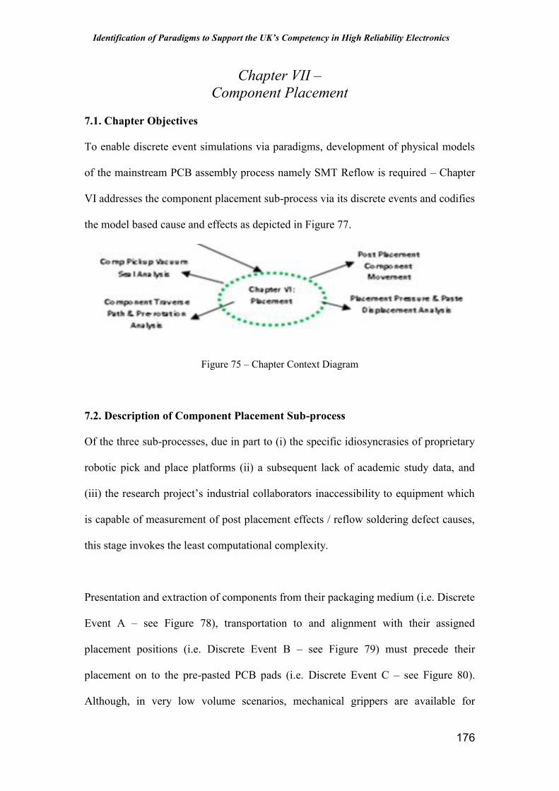
Identification of Paradigms to Support the UK’s Competency in High Reliability Electronics
176
Chapter VII –Component Placement
7.1. Chapter Objectives
To enable discrete event simulations via paradigms, development of physical models
of the mainstream PCB assembly process namely SMT Reflow is required – Chapter
VI addresses the component placement sub-process via its discrete events and codifies
the model based cause and effects as depicted in Figure 77.
Figure 75 – Chapter Context Diagram
7.2. Description of Component Placement Sub-process
Of the three sub-processes, due in part to (i) the specific idiosyncrasies of proprietary
robotic pick and place platforms (ii) a subsequent lack of academic study data, and
(iii) the research project’s industrial collaborators inaccessibility to equipment which
is capable of measurement of post placement effects / reflow soldering defect causes,
this stage invokes the least computational complexity.
Presentation and extraction of components from their packaging medium (i.e. Discrete
Event A – see Figure 78), transportation to and alignment with their assigned
placement positions (i.e. Discrete Event B – see Figure 79) must precede their
placement on to the pre-pasted PCB pads (i.e. Discrete Event C – see Figure 80).
Although, in very low volume scenarios, mechanical grippers are available for

Identification of Paradigms to Support the UK’s Competency in High Reliability Electronics
177
problematic package styles (e.g. odd-forms, PTH / SMT hybrids), but in the main, a
vacuum force is required to retain the component on a pickup nozzle during capture
and articulation by robotic systems.
Hence, a vacuum seal is necessary between the nozzle and the component’s pickup
surface. Failure to generate this seal provides the failure mechanism (i.e. root cause)
for the placement related defect opportunities for misplaced and missing components.
Due to the relatively high inertial forces of angular acceleration invoked during any
such post vision alignment rotational movements, may promote undetected
component drop off or slippage on the nozzle and therefore remain uncorrected via
the alignment correction system. By plotting the rotations the “why” question is
considered and by plotting the post-vision alignment traverse path addresses the
“where” question.

Identification of Paradigms to Support the UK’s Competency in High Reliability Electronics
178
Figure 76 – Icon representation of the Component Pickup Discrete Event
Figure 77 – Icon Representation of the PCB / Component Positioning & Alignment
Discrete Event
Figure 78 – Icon Representation of the Component Placement & paste Displacement
Discrete Event
7.3. Sub-process 2 Discrete Event A – Component Pickup
For the employed model development methodology, ABVA (see Section 2
introduction) has been adapted to accommodate an accumulation of the process
tolerance windows that apply during the presentation of an SMT component for
vacuum pickup, which is the primary discrete event of the placement sub-process. Its
aim is to identify the opportunities for vacuum seal failure, thus answering the “how”
question.

Identification of Paradigms to Support the UK’s Competency in High Reliability Electronics
179
For the (relatively) large package styles, which house active devices such as Ics
(Integrated Circuits) flat pickup surfaces can be provisioned with comparative ease,
but passive devices such as chip resistors and capacitors have (upper) topographic
features that limit pickup surface availability. In addition, the extreme scales of
miniaturisation, which are apparent in contemporary package styles proportionally
shrink the available surface area, thus presenting ever more challenging geometric
aspect ratios.
Assuming compatibility between packaging media and placement machine’s electro-
mechanical feeders, presentation of the component for pickup is in the horizontal
plane – see Figure 81.
Figure 79 – Graphical Representation of Taped and reeled Component Presentation
IEC 60286-3 Ed. 4.0 EN: 2007 (Packaging of Components for Automatic Handling –
Part 3: Packaging of Surface Mount Components on Continuous Tapes) (IEC, 2007)
provides the industry standard specification for taping and reeling of passive SMT
components. Carrier and cover tape widths, sprocket-hole sizes / pitches and reel sizes
are standardised. This standard assures compatibility with the placements machine’s
electro-mechanical feeder during the loading, repeatable indexing and cover tape

Identification of Paradigms to Support the UK’s Competency in High Reliability Electronics
180
removal operations required in the presentation of the component for pickup – see
Figure 82.
Courtesy IEC 60286-3 Ed. 4.0 EN: 2007Figure 80 – Graphical Representation of an Exemplar Tape & Reel Specification
However, as a consequence of the standardisation of generic tape pocket sizes and the
gamut of passive component package styles (and sizes), the actual location of the
component may be randomly distributed within the pocket during pickup presentation,
thus promoting vacuum leakage potential – see Figure 83.

Identification of Paradigms to Support the UK’s Competency in High Reliability Electronics
181
Figure 81 – Graphical Representation of Component Location Anomalies within a
Standardised Pocket Size
While it is possible to pack and feed active components in tape and reel formats, the
integration of complex circuitry within a single package (i.e. Ics) dictates higher lead
counts, finer pitches and larger footprints, thus raising issues relating to lead fragility
and / or package style sensitivity to moisture ingress. The advent of the chip scale
package (CSP) and other similarly miniaturised, but fragile area-array package style
technologies have negated the need for leads and a plastic body. This development
has proffered greater scales of miniaturisation, but it has also incurred additional
manufacturing cost implications. Supplementary process stages, which are required to
enhance the reliability of these ultra delicate active components such as the under-
filling process and the consequential yield implications severely limit CSP uptake in
passive applications.

Identification of Paradigms to Support the UK’s Competency in High Reliability Electronics
182
Other than the J-leaded package styles (e.g. PLCC, Tantalum Capacitors), which incur
higher topographic profiles / footprints that limit their practicality for selection during
PCB layout, the available pickup surface for passive component package styles is
defined by either,
a. peripheral leads, which constrain the maximum plastic body
dimensions for a given tape pocket size, or
b. metallised end caps, which constrain the maximum pickup surface for
a given ceramic body size.
Figure 84 provides an ABVA for ceramic chips, which are by far the most prolific of
all SMT component package styles.
Figure 82 – Graphical Representation of Vacuum Pickup ABVA: Ceramic Chips

Identification of Paradigms to Support the UK’s Competency in High Reliability Electronics
183
By subtracting the difference between the X and Y body dimensions (as specified
within the component manufacturer’s data sheet) from the tape manufacturer’s pocket
dimensions, the location window is derived in both X and Y i.e. LWX and LWY
respectively. For ceramic chips only, subtraction of the length of the metallised end
cap (i.e. M) from LWX only, delineates the vacuum pickup surface (i.e. VSX) with
LWY equating to VSY. The vacuum window is then defined by subtracting the
selected pickup nozzle’s inside diameter (i.e. NID) from both VSX and VSY to output
VWX and VWY respectively. This vacuum pickup ABVA develops the following
geometric formula the modelling of vacuum leakage potential:
Component Pickup Vacuum Window Formula
Equation 10and,
Equation 11where,
VWX = Vacuum Window X Dimension
VWY = Vacuum Window Y Dimension
CL = Component Length
CW = Component Width
PL = Tape Pocket Length
PW = Tape Pocket Width
NID = Pickup Nozzle Inside Diameter
M = Metallised End Cap Length

Identification of Paradigms to Support the UK’s Competency in High Reliability Electronics
184
Component Pickup Vacuum Window Rules
Equation 12
and,
Equation 13
CL, CW, PL, PW, M and NID represent the model’s inputs and VWX & VWY are
the outputs, which transpire to ‘Nozzle Size Mismatch!’ and ‘Vacuum Leakage
Potential!’ warnings in circuit design applications. Although, for interactive modelling
this advanced functionality would require the codification of a configuration map of
the intended placement machine’s nozzle sizes options (i.e. NIDs).
To enable sequential machine placement, all configurations must offer in-cycle nozzle
changing capability, but the gamut of NID’s and number of stations per setup will
vary – usually as a function of the machine’s theoretical placement rate per
component (a.k.a. its takt-time). Given their relative profusion, machines configured
for the placement of passive components must offer takt-times that far outstrip those
of their accuracy centric counterparts i.e. active components. Although contemporary
modular platforms claim the versatility to facilitate user reconfiguration, the degree of
flexibility within a module’s nozzle station and the range NID’s, which can be
accommodate within a single set up, dictates the vacuum leakage potential model
constraints.

Identification of Paradigms to Support the UK’s Competency in High Reliability Electronics
185
Furthermore, considering the scales of contemporary ceramic-chip package
miniaturisation and their minimal VWX & VWY dimensions, the accommodation of
closely matched NIDs is paramount. Hence, diversity in package style selection
engenders challenging geometric aspect ratios and compromises high-speed
placement machine configuration. This defines the disturbance for the vacuum
leakage model.

Identification of Paradigms to Support the UK’s Competency in High Reliability Electronics
186
Figure 83 – Graphical Representation of the Component Pickup Effects Model
Figure 84 – Graphical Representation of the Component Pickup Cause Model

Identification of Paradigms to Support the UK’s Competency in High Reliability Electronics
187
7.4. Sub-process 2 Discrete Event B – PCB / Component Positioning &
Alignment
Prior to placement, component positioning and alignment is required. This discrete
event provides the opportunity for slippage on the nozzle during position traversing
and alignment articulation. Figure 87 depicts an arbitrary machine configuration with
feeders mounted at the front and rear of the machine.
Figure 85 – Graphical Representation of a Typical Placement Machine Feeder
Configuration
Alternative configurations are possible, but the platform’s layout will have little
consequence. Component-slippage is directly attributable to vacuum strength and its
ability to resist inertial forces. Irrespective of the layout, the inertia imparts during the

Identification of Paradigms to Support the UK’s Competency in High Reliability Electronics
188
pickup and delivery of the component, with acceleration and deceleration rates
dictated by the speed of the placement cycle. Of greater significance are the (i)
alignment sequence and (ii) nozzle selection mechanism.
Note: as the package style of choice for wide-ranging resistor and capacitors
applications, ceramic chip (see Chapter II) populations tend to dominate PCA
component demography. In accommodating their (typically) high concentrations in
high speed, multiple machine assembly lines the term “chip-shooting” is often applied
– giving rise to the advent of the dedicated platform configurations often referred to as
chip-shooters. In chip-shooting applications, relatively high traversing speeds are
required.
Breached nozzle vacuum and component slippage may exaggerate the component’s
original pickup positional discrepancies. Depending on the direction of travel between
pickup and placement the inertial forces, which act during traversing have the effect
of either amplification or alleviation of the original error – see Figure 88.
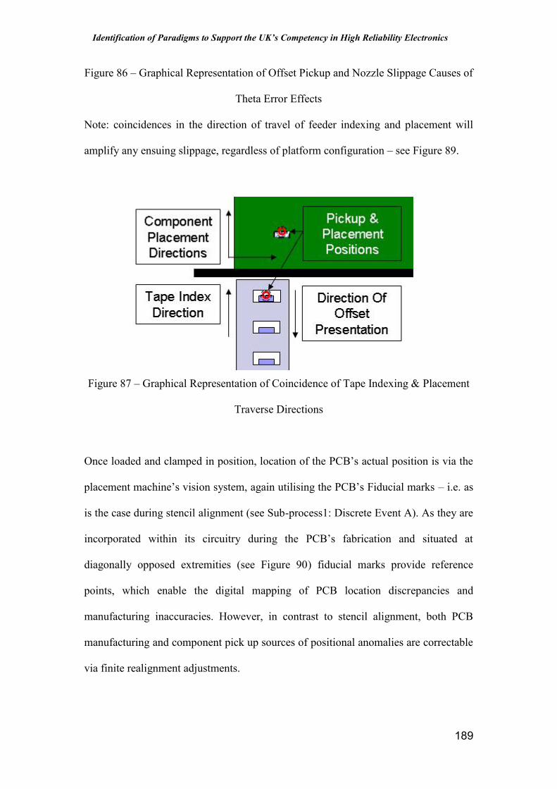
Identification of Paradigms to Support the UK’s Competency in High Reliability Electronics
189
Figure 86 – Graphical Representation of Offset Pickup and Nozzle Slippage Causes of
Theta Error Effects
Note: coincidences in the direction of travel of feeder indexing and placement will
amplify any ensuing slippage, regardless of platform configuration – see Figure 89.
Figure 87 – Graphical Representation of Coincidence of Tape Indexing & Placement
Traverse Directions
Once loaded and clamped in position, location of the PCB’s actual position is via the
placement machine’s vision system, again utilising the PCB’s Fiducial marks – i.e. as
is the case during stencil alignment (see Sub-process1: Discrete Event A). As they are
incorporated within its circuitry during the PCB’s fabrication and situated at
diagonally opposed extremities (see Figure 90) fiducial marks provide reference
points, which enable the digital mapping of PCB location discrepancies and
manufacturing inaccuracies. However, in contrast to stencil alignment, both PCB
manufacturing and component pick up sources of positional anomalies are correctable
via finite realignment adjustments.

Identification of Paradigms to Support the UK’s Competency in High Reliability Electronics
190
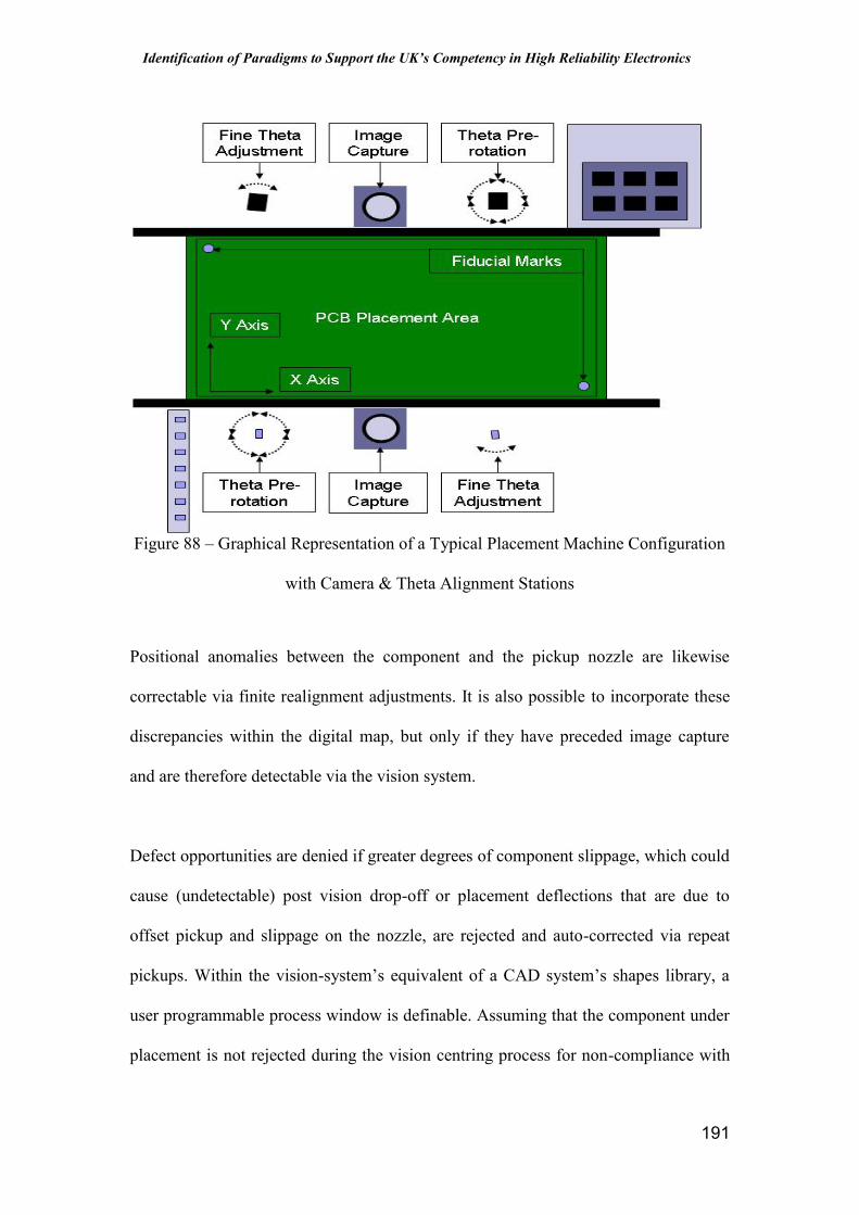
Identification of Paradigms to Support the UK’s Competency in High Reliability Electronics
191
Figure 88 – Graphical Representation of a Typical Placement Machine Configuration
with Camera & Theta Alignment Stations
Positional anomalies between the component and the pickup nozzle are likewise
correctable via finite realignment adjustments. It is also possible to incorporate these
discrepancies within the digital map, but only if they have preceded image capture
and are therefore detectable via the vision system.
Defect opportunities are denied if greater degrees of component slippage, which could
cause (undetectable) post vision drop-off or placement deflections that are due to
offset pickup and slippage on the nozzle, are rejected and auto-corrected via repeat
pickups. Within the vision-system’s equivalent of a CAD system’s shapes library, a
user programmable process window is definable. Assuming that the component under
placement is not rejected during the vision centring process for non-compliance with

Identification of Paradigms to Support the UK’s Competency in High Reliability Electronics
192
this window, lesser positional discrepancies can then be corrected through
realignment.
7.5. Qualitative Modeling Techniques – Alignment Sequence Mapping
The expediency of user abstraction of the finite data required for the modelling of on-
nozzle component slippage (e.g. real-time vacuum loss data) within the pressurised,
output centric environments, which are typical of the software tool’s envisaged
applications, makes quantitative arithmetic or geometric mathematical formulae
unviable. Therefore, qualitative modelling is required.
The inertial effects of angular accelerations and decelerations during rotational
alignment are a more likely cause of slippage as the moments generated by the
distribution of the component’s mass about its length should out-weigh the linear
inertial forces of traversing. Moreover, given the unavoidability of linear traversing,
the primacy of rotational articulation consideration during PCB layout provides
multiple opportunities for error-proofing misplacement defects.

Identification of Paradigms to Support the UK’s Competency in High Reliability Electronics
193
As stated, the sequencing of alignment actuation is critical to alignment sequence
Rotational alignment (a.k.a. Theta axis pre-rotation) should be actuated prior to vision
processing.
Figure 89 – Graphical Representation of Traverse Paths for Tape Fed Passives and
Tray Fed Actives
By mapping the alignment sequence, (see Figure 91) qualitative, smart cause and
effects prediction of positional discrepancy amplification and alleviation becomes
feasible. This logic in turn facilitates truth tables, which when codified, enable
interactive DfM guidance for package placement and lean design rules for product
and process, with embedded error forcing and trapping capabilities.

Identification of Paradigms to Support the UK’s Competency in High Reliability Electronics
194
7.6. Process FMEA as a Qualitative Modeling Technique
When used as a risk management tool, Failure Modes & Effects Analysis (FMEA)
facilitates the qualitative prediction of the likelihood of occurrence (i.e. frequency),
probability of discovery (i.e. detection) and impact assessment (i.e. severity) of defect
opportunities with causes embedded during product design (a.k.a. DFMEA) and
process design (a.k.a. PFMEA). It provides a platform for modelling system
behaviour reliability, diagnosis, and serviceability. MIL-STD-1629A (US MILITARY
STANDARD, 1980) codifies a methodology from which variants have been
developed by disparate industrial sectors, including the automotive industry within its
QS9000 / TS:16949 (The International Automotive Task Force (IATF), 2002) Quality
Management System procedures.
Within the modelling context of the PCB / Component Positioning & Alignment
discrete event, component slippage on the nozzle provides the focal, system
behaviour. Package style and size represent the model’s inputs for a qualitative
prediction of a slippage event the output.
Following FMEA conventions, calculation of RPN (Risk Priority Number) is via
multiplication of the outputs, which factor defect (i) frequency, (ii) detection, and (iii)
severity. Whilst reliant on engineering judgments and therefore vulnerable to opinions
and assumptions, it does proffer a qualitative, incremental cause and effects analysis
modelling technique and one which has been codified, generically standardised and
multilaterally sanctioned. Conversion of the process disturbances, which promote
component slippage on the nozzle into model inputs via the codified system, enables
prediction their influence on slippage event frequency. Similarly, the likelihood of the

Identification of Paradigms to Support the UK’s Competency in High Reliability Electronics
195
detection of a slippage event equates to the number of post vision movements and
their propensity to promote undetectable slippage. The impact of any such post vision
slippage event will manifest as missing and misplaced components. Therefore, Sub-
process 2: Discrete Event C (Component Placement) provisions the codification of the
severity rating.
Differentiation of alignment and placement system behavioural anomalies is by (i) the
physical characteristic of the package under consideration and (ii) placement machine
platform configuration. The fact that not all platforms are generic and that some
equipment producers develop their iterations around specific taxonomies of package
style illustrates this truism, but the model’s inputs must account for both, package and
placement platform idiosyncrasies. For example, whilst in interactive DfM mode,
taxonomies of placement attributes should enable the software tool’s user to consider
the placement implications for a given platform configuration and be accordingly
guided to select the most appropriate package style option. For smart cause and
effects analysis, attributes of package and platform configurations present RPN’s,
which predict the probable defect opportunity, root causes. Again, this will require
their codified within a platform configuration map – see Subsection 3 (Sub-process 2
Discrete Event A: Component Pick Up).
7.7 Codification of (Package Physical Characteristics & Placement Related
Process Dependencies as) Process Disturbances and Frequency-Prediction Model
Inputs
Table 3 provides an exemplar of placement attributes for the elicitation of process
dependencies. Package styles, are grouped with respect to their physical

Identification of Paradigms to Support the UK’s Competency in High Reliability Electronics
196
characteristics and placement related process dependencies. Qualitatively codified
within the table are the idiosyncrasies, which represent the process disturbances.
Computation of the discrete ratings is via both (i) summation and (ii) multiplication
then division by 1000 (underlined and bracketed), thus presenting alternative
cumulative options for the codification of the input scores for a frequency-predictive
element of the FMEA based model.
Table 3 – Exemplar of Package Placement Attributes with Defect Frequency
Predictions
Physical characteristics, as predetermined by package style and size factor pre-
selected ratings for surface flatness, surface roughness, and placement accuracy. It is
envisaged that the user will consider and utilise the qualitative assessments of next

Identification of Paradigms to Support the UK’s Competency in High Reliability Electronics
197
three characteristics (i.e. component mass, vacuum window, component demography)
on a case-by-case basis. This factoring needs to reflect the influence of the intended
placement platform’s configuration and capabilities. Please note that the provided
exemplar is for concept demonstration only and not considered as being fully
inclusive of every package style or placement platform.
The following describes the attributes and provides a template rating system for
qualitatively codifying their potential as process disturbances:
Surface flatness (Predetermined Package Attribute)
Description: topographic none-conformities, with undulating pickup surfaces
promote higher frequency breaches of vacuum seal.
Guidance Rating: uninterrupted planar top surface = 1, central planar vacuum
window with non-planar extremities = 5, central non-planer vacuum window
=10
Surface Roughness (Predetermined Package Attribute)
Description: ceramic body materials provide coarse pickup surfaces and
possess frictional advantages such as slip resistance, which more than
compensate for a potential for low-level vacuum leakage. Conversely, metallic
surfaces offer high vacuum potential but low slip resistance.
Guidance Rating: coarse, high slip resistance = 1, intermediate matt finish
plastic body material = 5, smooth metallic finish = 10
Accuracy (Predetermined Package Attribute)
Description: higher scales of miniaturisation and reduced lead pitches dictate
greater placement accuracy requirements.

Identification of Paradigms to Support the UK’s Competency in High Reliability Electronics
198
Guidance Ratings: pitch ≥ 1.25mm = 1, < 1.25mm (i.e. fine pitch) = 5, >
0.635mm (ultra fine pitch) = 10
Mass (User Defined Variable)
Description: even in the absence of a catastrophic vacuum leakage, slippage
events can occur when higher mass components have vacuum surface non-
conformities and low slip resistance. Severity of slippage will be proportional
to traversing rates of acceleration / deceleration.
Guidance Rating: lower mass / larger vacuum surface / faster placement
speeds = 1, intermediate characteristics = 5, converse characteristics = 10
Vacuum Window (User Defined Variable)
Description: due to the constraining impracticalities for the elicitation of
variable input data, in cases where the preceding discrete event’s ABVA
model has predicted a nozzle size / vacuum window mismatch, vacuum
leakage is an assumed at a constant level.
Guidance Rating: nozzle size / vacuum window OK = 1, mismatch = 10
Package Demographics (User Defined Variable)
Description: for reasons of line balancing and production smoothing, the
demographic make up of a given PCA design will require faster placement
speeds for package styles with higher percentage populations. Consequential
takt-times will incur hazardous inertial forces due to high rotational and
traversing acceleration and decelerations.
Guidance Rating: Pick-and-Place = 1, Gather-and-Place = 5, Chip-shooting =
10

Identification of Paradigms to Support the UK’s Competency in High Reliability Electronics
199
7.8. Placement Platform Configurations Placement Related Process
Dependencies
As Henry Ford had intended when devising his concepts for standardisation and
interchange-ability of component parts, it is the codification of tolerance rules and not
the method of assembly, which facilitates a system’s manufacturability (Womack,
1990). The establishment of tolerance rules enables standardisation and the
codification (via engineering drawings) of physical characteristics critical to
interchange-ability between components. This negates the need for matched pairs and
facilitates remote design and manufacture, thus deskilling assembly operations.
Applying Utterback’s dominant design theory (Utterback, 1996), the interconnection
of electronic components that are mounted on the surface of a PCB via solder joints
represents the SMT process’s dominant design. Via the EIA and JEITA package and
packaging format standards, codification of both (i) the component’s physical
characteristics and (ii) its materials handling and presentation for pickup
characteristics (together with the related tolerance rules) enables remote design and
manufacture of interchangeable parts prior to assimilated supply-chains and
collocated assembly.
Ford’s concepts also provide analogous illustrations of how standardisation and
interchange-ability negates the need to regulate methods of SMT placement. Given
the presentation of a component of known physical characteristics for pickup at a
predictable point of delivery then flexibility in the method of placement ensues.
Supplementary to the more predictable advances in technical capability, proprietary
configuration of platforms also promotes competitive differentiation. Heterogeneous
applications for placement technology will be proportional to the diversity of

Identification of Paradigms to Support the UK’s Competency in High Reliability Electronics
200
products, which utilise SMT technology over a disparate array of PCA architectures
and package styles.
Although neither standardised nor constrained by a single dominant design,
nevertheless three discrete classifications of placement techniques have emerged. As
defined by three distinct alignment sequences, placement methodologies can be
categorised as either (i) pick-&-place, (ii) gather-&-place or (iii) chip-shooting.
Assuming a moving gantry platform configuration, Figure 92 illustrates the alignment
sequences for the pick-&-place and gather-&-place methodologies:
Figure 90 – Graphical Representation of Alignment Sequence for Moving Gantry and
Static Camera Pick-&-Place / Gather-&-Place Platforms
This type of platform locates a stationary PCB adjacent to fixed feeder bank(s) with X
and Y traverses actuated by overhead gantry systems which follow Cartesian
configuration. In both types, the gantry system accommodates the Z-axis, theta pre-
rotation / fine-theta axis actuators and a fiducial mark recognition camera, but with
vision alignment camera(s) statically mounted on the platform’s superstructure in
closed proximity to its (fixed or interchangeable) feeder banks – see Figure 93.

Identification of Paradigms to Support the UK’s Competency in High Reliability Electronics
201
(Courtesy http://www.assembleon.com/)Figure 91 – Dual Head Pick-&-Place Platform with Static Mount Vision Alignment
Camera
Where the platform shown in Figure 93 represents dual-head single-nozzle pick-&-
place functionality, via a relatively simple reconfiguration the efficiencies of gather-
&-place functionality become viable. By duplication of the single nozzle within the
pickup head, multiple components can be “gang-picked” or gathered, pre-rotated,
images captured, adjusted in fine-theta and then placed sequentially. Each operation
becomes a sequence within a sequence – see Figure 94.
(Courtesy http://www.contactsystems.com)Figure 92 – Image of a Gather-&-Place System Showing Multi-Nozzle Gathered
Components

Identification of Paradigms to Support the UK’s Competency in High Reliability Electronics
202
Sub-sequence traverses are required to index the duplicated nozzles between each
alignment sequence stage. Configurations with a small number of larger nozzles are
suitable for larger UFPT placement applications, with dedicated pre and fine Theta
actuators. Either (i) laser scanning or (ii) line scan cameras, offer higher resolutions
within wider fields-of-views but CCD (Charged Couple Device) cameras are more
applicable for “sequential-on-the-fly” image capture, thus minimising indexing
movements.
However, later generations of gather-&-place configurations have adopted true on-
the-fly actuations with the sequential stages between pickup and placement performed
simultaneously via rotary indexing systems – see Figure 94.
Figure 93- An On-the-fly Rotary Indexing Vision Alignment System
7.9. Codification of Process Disturbances as Detection-Prediction Model Inputs
With the potential for component slippage on the nozzle attributable to (i) the
package’s physical characteristics (ii) its associated placement-attributes and, (iii) the
severity of the inertial forces as exerted during placement, then the probability of
slippage becomes a function of its cumulative exposures to the inertial forces per each
Identification of Paradigms to Support the UK’s Competency in High Reliability Electronics
203
placement cycle. Moreover, as contemporary placement platforms equip with highly
accurate vision alignment systems, for the purposes of modelling, the slippage
frequency calculation does not need to factor any such acceleration / deceleration
cycles, which may occur before image capture. If pickup errors (as detected by the
vision centring and alignment system) exceed pre-programmed limits of acceptability,
then an automated corrective action will reject the pickup and automatically repeat the
operation. However, if the degree of slippage is within limits, then factoring of
detected errors within the realigned placement coordinates is possible. “On-the-fly”
vision centring integrates X and Y error realignment actuations within the X and Y-
axis traverses, but theta error realignment requires additional actuations. It therefore
necessitates a dedicated actuation system.
Conversely, given that vision-centring and alignment systems also perform an error
trapping and prevention role, the actuality of placement error manifestation is
attributable to the occurrence of a detection failure i.e. a process disturbance. Thus, by
applying FMEA convention within the model, the frequency rating then represents a
qualitative codification of the possibility of occurrence. Therefore, in reality the
probability of occurrence equates to a possibility of detection evasion i.e. a post vision
occurrence. Computation of the opportunities for post vision occurrences becomes a
function of the cumulative exposure to acceleration / deceleration cycles i.e. post
vision movements (a.k.a. PVM summation).

Identification of Paradigms to Support the UK’s Competency in High Reliability Electronics
204
Table 4 provides the PVM summations for the following generic platforms
(i) Pick-&-place, – this involves discrete component pickup, theta rotation, image
capture, fine theta alignment and X & Y positioning via a single nozzle pickup
head,
(ii) Gather-&-place – a gang-picking configuration with linear nozzles, fixed
superstructure mounted vision system that utilises line scan cameras or laser
scanners, and
(iii)Gather-&-place – a gang-picking configuration with linear nozzles, fixed
superstructure mounted CCD cameras.
Table 4 – Exemplar Summation Table for the Codification of Linear Actuated PVMs
In linear configurations, multiple nozzle counts (NC) impact on the number of stop /
start indexing actuations. For example, the last pickup in a gang picking sequence
experiences the maximum number of placement indexing actuations. If a scanning

Identification of Paradigms to Support the UK’s Competency in High Reliability Electronics
205
type vision camera is used, then capture of the image can be ‘on-the-fly’, but with
CCD-camera based systems, ‘snap-shot’ acquisition necessitates stationary imaging,
thus compounding the PVM count.
Given that chip placement is the target application for this configuration, high
acceleration / deceleration rates are to be expected, thus maximising the disturbance
on the indexing process and probability of undetected nozzle slippage.
The example provided within Table 4 has a gang picking head with five nozzles, but
alternative proprietary configurations will vary as dictated by their target applications.
For example, larger, higher accuracy packages require proportionally increased nozzle
pitches and cameras with maximised fields-of-view at high resolutions. Conversely,
higher populous chip-placing requirements only require smaller nozzle pitches and
cameras, thus facilitating higher nozzle counts and a greater number of pickups per
placement cycle.
Although mechanical layouts significantly differ, these divergent approaches share
similar process constraints and disturbances, with pickup and placement staging
providing the greatest disparity. Nozzles are incorporated within the formers’ gantry
mounted, rotary indexing heads, which gang-pick static components and then places
them on to stationary PCBs. Within this cycle, pre-rotation, vision alignment and fine-
theta adjustments are performed on-the-fly, at fixed stations, which are located
sequentially around the placement head’s axis of rotation. Within the context of
proprietary Cartesian platform configurations, horizontal, vertical and even inclined
gantry mounting orientations exist.

Identification of Paradigms to Support the UK’s Competency in High Reliability Electronics
206
In contrast, chip-shooters invariably have a vertical axis of turret rotation, fixed-
mounted on to a static gantry based superstructure – see Figure 96. Feeder banks,
which index in the X-axis and X-Y PCB positioning tables, negate the need for
sequential gang picking. With both component and PCB presented at diametrically
opposed positions, which respectively precede and supersede nozzle selection (via an
indexing station), pre-rotation, image capture, fine-theta adjustment stations,
simultaneous pickup and placement cycles are enabled and takt-times minimised, thus
giving rise to the “chip-shooting” analogy.
(Courtesy http://www.smtresearch.com/)Figure 94 – A Chip-shooter Turret with Twenty Rotary Stations
Successive generations of chip-shooters have seen incremental increases in speeds of
rotation, turrets diameters and nozzle counts with consequential higher acceleration /
deceleration rates, thus maximising the disturbance factors for the modelling of
indexing factors and the probability of undetected nozzle slippage. As nozzle pitches
reduce and nozzle counts increase, ultra-high rotary indexing speeds exaggerate the
escalated PVM counts – see Table 5. However, these accompanying process

Identification of Paradigms to Support the UK’s Competency in High Reliability Electronics
207
disturbances have had the combined consequence of limiting the effective design life
of this type of single gantry platform. The effects of acceleration / deceleration cycles
during rapid X-Y table indexing between successive placements compound PVM
speed and count issues. Lateral inertial forces, which induce post-place movement in
higher mass components, have promoted the popularity of multiple gantry systems
that place concurrently on to statically located PCBs.
Table 5 – Exemplar Summation Table for the Codification of Rotary Actuated PVMs
7.10. Sub-process 2 Discrete Event C – Component Placement & Paste
Displacement
Once aligned with its corresponding PCB surface located interconnection pads, the
actual placement operation involves the lowering of the component in the Z-axis,
followed by vacuum release at the point at which it makes contact with its respective
solder paste deposits. When in contact with the paste and under vertical compression,

Identification of Paradigms to Support the UK’s Competency in High Reliability Electronics
208
visco-elastic characteristics promote forces which generate lateral displacement in
either (i) the paste deposit, (ii) the component and (iii) both deposit and component.
In chip-shooting scenarios, where the X and Y axis traversing is actuated on the
substrate, further displacement can result from subsequent post-placement
acceleration / deceleration forces, as exerted during following component placements.
This obvious constraint has had commercial implications for chip shooter
manufacturers with inevitable viability limitations imposed on the platform
configuration’s market longevity and resulting in its succession by multiple-gantry,
gather-&-place configurations. This suggests that market driven technological
differentiation between proprietary platforms have derived a dominant design, thus
negating the need for academic study and adjudication.
Figure 95 – Image of a Post Placement Displaced Component
7.11. Post Placement Component Movement
With the causes of post placement component movement being characteristics of (i)
the component’s mass, (ii) the rates of acceleration / deceleration of X / Y positioning
table (or transfer conveyors in the case of displacements that initiate during intra cycle
transportation), (iii) the tackiness (a.k.a. green strength) of the solder paste and (iv)
the paste to component contact area. Therefore, elicitation of the input data is via
manufacturer’s data sheet recommendation plus any overriding stencil data and pad

Identification of Paradigms to Support the UK’s Competency in High Reliability Electronics
209
shape data design rules respectively from IPC-7525 (IPC, IPC-7525) and IPC-7351
(IPC, IPC-7351 (L)).
The following corrective / preventative actions apply in product and process design
albeit with impractical effects modelling:
Corrective actions =
use enclosed paste print heads,
minimise time delays between printing and placement,
minimise the use of cylindrical packages e.g. MELFs
orientate high-mass / low contact area packages at 0 or 180 degrees to
conveyor movement,
use static PCB positioning placement machine platform configurations,
However, the following practicality and unviable measurement constraints and control
of process disturbances which fluctuate over time and climatic variations makes
quantitative modelling non-feasible:
Measurement Constraints =
tackiness will vary by manufacturer and between paste technology – i.e.
eutectic, Pb-free, water soluble, RMA, low solids / no-cleans,
paste manufacturers do not specify tackiness in terms of bond strength per
unit area,

Identification of Paradigms to Support the UK’s Competency in High Reliability Electronics
210
the tackiness of paste deposits is not quantitatively measurable by non-
destructive methods – i.e. contact testing would disturb the deposit’s form
and viability.
Process Disturbances =
paste tackiness changes over time – slowly during storage, quickly during
exposure on stencil, very quickly in between printing and placement,
the rate of change in paste tackiness will be proportional to ambient
temperature and humidity, with water based fluxes being more susceptible
to moisture absorption and evaporation.
Although quantitative modelling is impractical, qualitative cause and effects analysis
is viable. Where component slippage on the nozzle is the cause of component
misplacement, similar inertial forces affect post placement displacement of
components. Therefore, a software function which plots the vectors of the post
placement PCB movements indicate the inertial causes – see Figure 98.

Identification of Paradigms to Support the UK’s Competency in High Reliability Electronics
211
Figure 96 – Graphical Representation of Inertial Vector Mapping of Post Placement
Movements
7.12. Placement Pressure Related Bridging of FPT & UFPT Packages
Irrespective of any laterally acting, inertial forces, which displace previously located
components, vertically acting compression forces laterally expel solder paste as the
component terminations coincide with their respective deposits during placement. The
deposit’s visco-elasticity characteristics define the resistance to lateral displacement,
which acts against the placement pressure – see Figure 99.
Donoghue and Williams (Donoghue, 1992) undertook empirical experimentation.
They assumed correct component and deposit alignment together with coplanar
substrates, concentric pickup, and neutral visco-elastic solder paste resistance and
finite placement pressure control. Their research objective was to quantify relative
displacement of the solder paste for a range of placement pressures.
Figure 97 – Graphical Representation of Placement Pressure Related Lateral Paste
Displacement

Identification of Paradigms to Support the UK’s Competency in High Reliability Electronics
212
Contemporary, FPT & UFPT package capable machines offer programmable
placement pressure control but coplanarity of the fine pitch leads disturbs the
modelling of vertical pressure against lateral paste displacement – see Figure 100.
Figure 98 – Graphical Representation of Lead Co-planarity Causes of Unsoldered
Joints
Although the Donoghue and Williams study dates back to the early 1990’s, their
design-of-experiment would appear to identify the same measurement and
quantification constraints, which are still apparent today and impede the codification
of the afore-listed process disturbances into model inputs. Figure 101 presents their
findings within the context of the model inputs, outputs, constraints and disturbances:

Identification of Paradigms to Support the UK’s Competency in High Reliability Electronics
213
Figure 99 – Donohue and Williams Data Presented within a Model Construct
The Donoghue and Williams’s experimental approach involved the adaptation of a
Vickers Hardness Tester for the provision of regulated placement pressure control.
Their selection of ceramic chip resistors / capacitors and peripheral leaded gull-wing
devices reflects the prevalent package technology of the day, but this does not
diminish the data’s relevancy as, even if available at the time, contemporary area
array package styles would have obscured any displacement of their respective paste
deposits. This constraint was apparent in their aborted attempts to observe J-shaped
peripheral leaded devices (i.e. PLCCs) and even current state-of-the-art X-ray
computer tomography techniques would not provide volumetric scanned data.
By selecting ceramic chips and FPT and UFPT peripherals, the study reflects the
intrinsic effects of paste displacement, which are still as apparent in today’s
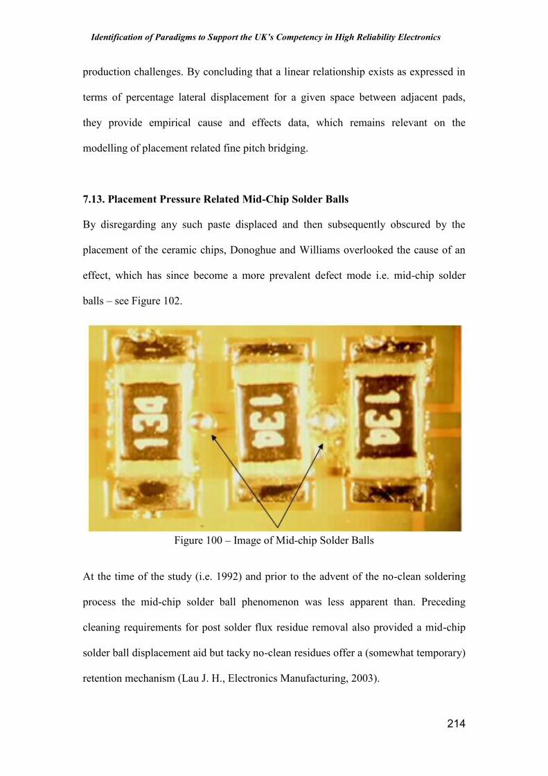
Identification of Paradigms to Support the UK’s Competency in High Reliability Electronics
214
production challenges. By concluding that a linear relationship exists as expressed in
terms of percentage lateral displacement for a given space between adjacent pads,
they provide empirical cause and effects data, which remains relevant on the
modelling of placement related fine pitch bridging.
7.13. Placement Pressure Related Mid-Chip Solder Balls
By disregarding any such paste displaced and then subsequently obscured by the
placement of the ceramic chips, Donoghue and Williams overlooked the cause of an
effect, which has since become a more prevalent defect mode i.e. mid-chip solder
balls – see Figure 102.
Figure 100 – Image of Mid-chip Solder Balls
At the time of the study (i.e. 1992) and prior to the advent of the no-clean soldering
process the mid-chip solder ball phenomenon was less apparent than. Preceding
cleaning requirements for post solder flux residue removal also provided a mid-chip
solder ball displacement aid but tacky no-clean residues offer a (somewhat temporary)
retention mechanism (Lau J. H., Electronics Manufacturing, 2003).

Identification of Paradigms to Support the UK’s Competency in High Reliability Electronics
215
Note: Prior to a global awareness of their environmental impact, cleaning processes
were a familiar part of PCA assembly lines. Either, Ozone depleting solvent-based
processes solvated the Rosin-based flux residues that entrap and bond in situ
coalesced balls of unattached solder (Ellis B. N., 1986). Usually with aided of ultra-
sonic agitation, post reflow cleaning released the mid-chip solder balls, allowing them
to cascade to the bottom of the immersion tank. Alternatively, water-based spray-in-
air equipment dispersed the water-soluble residues and subsequently blasted any
rogue solder away from the PCB surface. Once trapped by the no-clean flux residues
they have become cosmetically unacceptable and considered an in-service reliability
risk if mobilised under vibration (Cala, 1996).
This defect mode provides a classical illustration of product and process design
related causes, which present an interactive effect. Although intrinsically a function of
solder volume as dictated by the design of the stencil aperture, placement pressure can
also contribute to their formation – see Figure 103.
Figure 101- Graphical Representation of Side and Plan Views of Placement Pressure
Influenced Paste Displacement

Identification of Paradigms to Support the UK’s Competency in High Reliability Electronics
216
Due to limited availability and effectiveness of techniques for the measurement of this
discrete event’s process disturbances and the subsequent paucity of cause and effects
production data gathering, extreme modelling challenges arise for what would appear
a relatively simple robotic operation. The unavailability of line-of-sight based
monitoring and measurement opportunities inhibits the quantitative diagnosis of the
mechanism, which causes the formation of these isolated balls of solder and explains
the dearth of industrial data and equally inadequate academic sources.
Assumed displacement of expunged paste from the innermost corners of the
symmetrical deposits under vertical compression during placement of the ceramic
chip onto non-wettable surfaces provides a viable explanation. The displaced paste
will then isolate from the main body of solder during reflow-induced coalescence.
Although this lack of empirical data constrains the development of placement pressure
inclusive models, a product design-based solution as widely deployed within industry,
where the chamfering of the internally facing, aperture corners, creating a trapezoidal
shaped deposit (see Figure 104) corroborates the assumed cause.
Figure 102 – Image of the Trapezoidal Shaped Aperture Design Solution to the Mid-
chip Solder Ball Defect Mode

Identification of Paradigms to Support the UK’s Competency in High Reliability Electronics
217
Models which account for the mid-chip solder ball cause / effect relationships with
pad and aperture size dimensional inputs are incorporated within this chapter – see
Subsection 6 Sub-process 3 Discrete Event C: Surface Energy Effects.
7.14. Chapter Summary
Chapter VI provides the physical models for component placement sub-process via its
discrete events (i) Component Pickup (ii) PCB / Component Positioning &
Alignment, and (iii) Component Placement & Paste Displacement. It codifies the
model based cause and effects providing inputs, outputs, constraints and disturbances
for the Component Pickup discrete event which are derive from pickup condition
causes and component slippage on the nozzle effects. The pickup condition causes can
be modelled for use via a model based simulation tool for this discrete event as inputs,
constraints and disturbance characteristics are covered by industrial standards i.e. pre-
codified and commercially neutral.
Discrete causes and effects scenarios for Sub-process 2 Discrete Event 2 and 3 are
illustrated through graphical representation, though full modelling is seen as unviable
as the positioning, alignment and placement of discrete SMD package styles is very
much a dependency of the form and function of proprietary specific placement
platforms. This suggests an ensuing paucity in academic domain source data which
could be due sensitivities to the commercial implications of publication of effects with
causes relating to the specific idiosyncrasies of proprietary robotic pick and place
platforms.

Identification of Paradigms to Support the UK’s Competency in High Reliability Electronics
218
The models proffered suggest platform mapping and cause analysis and error capture
techniques i.e. the forced pre-rotation of polarity neutral package styles such as
ceramic chip components to maximise pre-vision nozzle slippage and error trapping.
Whilst representing new learning, preceding academic literature based support is
understandably sparse. Similarly, placement pressure and PCB support related root
causes and the lack of post placement, paste displacement measurement industrial
capability and academic data sources make concise physical modelling unviable – but
nevertheless the failure modes of these discrete event are any less valid!

Identification of Paradigms to Support the UK’s Competency in High Reliability Electronics
219
Chapter VII –Reflow
8.1. Chapter Objectives
To enable discrete event simulations via paradigms, development of physical models
of the mainstream PCB assembly process namely SMT Reflow is required – Chapter
VII addresses the reflow soldering sub-process via its component package behaviour
related discrete events.
8.2. Description of Reflow Soldering Sub-process
Given that the thermal characterisation of the reflow soldering process has been
previously sufficiently modelled (i) by academic contributors the CLOVES / DIY
projects (Sarvar, F., Conway, P.P., 1998) (Sarvar, F., Conway, P.P., 1998) (Conway,
1999) (Whalley D. C., 2004). And (ii) commercially developed as DataPak Ltd.’s
Relite (http://www.datapaq.com/Home.htm?select=r) product (Huertas-Quintero,
2010) this physical model requirement has already been addressed and incorporated
within INMOST – See Figure 105.

Identification of Paradigms to Support the UK’s Competency in High Reliability Electronics
220
Figure 103 – Schematic for the Incorporation of DataPak’s Relite Thermal Modelling
Tool within INMOST
As a consequence of this preceding enablement and the thermal process
characteristics of reflow soldering incorporated as a divergent physical model,
therefore the objective of this chapter is to model the behaviour of distinct component
package styles which whilst under reflow conditions (i.e. solder contact, solder
wetting and solder joint formation) are reported to exhibit little understood and none-
codified dynamic behaviour. To this end the discrete events of the sub-process are
categorised and reported as follows:
Discrete Event A: Solder Contact (Lead Bend Tolerance) – see Figure 106
Discrete Event B: Solder Wetting and Fillet Formation – see Figure 107
Discrete Event C: Surface Energy Effects – see Figure 108

Identification of Paradigms to Support the UK’s Competency in High Reliability Electronics
221
Figure 104 – Icon Representation of the Solder Contact (Lead Bend Tolerance)
Discrete Event
Figure 105 – Icon Representation of the Solder Wetting & Fillet Formation Discrete
Event
Figure 106 – Icon Representation of the Surface Energy Effects Discrete Event
As solder-deposits coalesce and wet to the solder-able surfaces during joint formation,
metallurgical bonding ensues as inter-metallic layers develop between the tin in the
solder alloy and base copper circuitry. Assuming an absence of surface contaminants,
forces of attraction promote extension of the wetted area a.k.a. wet-out. Repulsion
forces between the intermediate solder volumes that occupy the air spaces that
intervene between the inter-metallic boundaries also encourage wet-out via
displacement under surface tension. The repulsion is between the solder and ambient
air whilst the solder is in the molten state.
Solder-ability describes the degree of difficulty in achieving the metallurgical bond in
terms of (the component’s), (i) thermal demand, (ii) wet-ability and (iii) resistance to
soldering heat (Lea, 1988). Within the context of the discrete package styles (i)
thermal demand, and (iii) resistance to soldering heat, are constants, thus rendering

Identification of Paradigms to Support the UK’s Competency in High Reliability Electronics
222
them as non-applicable for cause & effect modelling of distinct package dynamic
behaviour under reflow. Lea defines wet-ability as the speed and degree of wetting i.e.
the time taken to achieve the metallurgical bond and the dimensional extent of the
wet-out. He characterises the inputs to wet-ability as (i) the effectiveness of the heat
source (i.e. the reflow oven – see Chapter II) and (ii) the efficacy of the flux chemistry
in both facilitation of metallurgical bonding and in controlling the degree of surface
tension within the molten solder (Smith, 1986).
Both, (i) vagaries in the thermal performance of reflow equipment and (ii)
inconsistent batch-to-batch solder-ability can influence wet-ability, but neither effect
scenario suggests product / process design embedded defect opportunities and are
therefore discounted as applicable causation inputs. Thermal demand / heat source
effectiveness characterisation studies (Klein-Wassink, 1967) (de Langen, 1990)
(Siegal, 1992) (Whalley D. C., 1995) (Sarvar, F., Conway, P.P., 1998) (Lee N. C.,
Optimising the Reflow Profile via Defect Mechanism Analysis, 1999) (Suraski, 2000)
(Whalley D. C., 2004) acknowledge the degree of contamination of the wetting
surfaces by non-metallic compounds (i.e. metal salts from oxidation and organic films
such as finger greases) as critical to wet-ability. The omission of wet-ability as
causation inputs for their models is understandable given the impractically of
quantifiable solder-ability testing by non-destructive means and unavailability in
industrial assembly processes.
Nonetheless, three studies (Klein Wassink R. J., 1986) (Klein Wassink R. J., 1989)
(Ellis J. R., 1990) proffer models, which account for the dimensional degree of wet-
ability causes and its effects of surface tension. These paradigms are applicable to

Identification of Paradigms to Support the UK’s Competency in High Reliability Electronics
223
product & process design embedded defect opportunities (i.e. component /
interconnection pad dimensions) and directly accommodate as inputs any ensuing
output variability in the preceding sub-processes (i.e. solder deposit volumes and
placement accuracy). For example, the outputs of the solder paste deposition and
placement sub-process’s input directly into the models for Sub-process 3, Discrete
Event A.
8.3. Sub-process 3 Discrete Event A – Solder Contact (Lead Bend Tolerance)
For solder joint formation to be viable, the component’s termination has to be in
contact with the paste deposit. For non-preferential wetting, the thermal demand of
the competing solder-able surfaces should be equitable. In attaining equilibrium,
differentials in thermal demand minimise as conductive transfer of thermal energy
maximises – colour selectivity and shadowing compromise radiated energy and
transfer via convection is more sensitive to inequitable thermal demands (Markstein,
1987).
Note: Subsection 4 Sub-process 3 Discrete Event B: Solder Wetting & Fillet
Formation considers energy transfer modes and relates the effects of termination /
deposit contact (as shown in Table 6) with conductive energy transfer modes and the
related contact implications.
Lead co-planarity is a direct input to termination / solder paste contact related cause of
unsoldered and insufficient joints. Positive and negative values apply in defining co-
planarity – see Figure 109.

Identification of Paradigms to Support the UK’s Competency in High Reliability Electronics
224
Figure 107 – Graphical Representation of Positive and Negative Co-planarity Causes
of Unsoldered Joints
The magnitude of the co-planarity error not only influences the frequency but also the
defect type. If the non-planarity is large and the deposit height is low then the lead (or
metal end-cap termination) will fail to contact the deposit and unsoldered joint is the
likely outcome – see Figure 110.
Figure 108 – Graphical Representation of the Lead / Deposit Co-planarity Process
Window
However, if the magnitudes of either cause are less but still erroneous and a limited
contact ensues, unsoldered or insufficient joints remain a possibility, with conducted
thermal transfer restricted and wet-out impeded. Given that a fully wetted surface of x
/ y dimensions that are equitable with the aperture (i.e. an SMT pad) will produce a
domed solder profile at 150% of the cubic height of the deposited solder (Klein
Wassink R. J., 1989) that solder pastes typically consist of approximately 50% solder
by volume, then:

Identification of Paradigms to Support the UK’s Competency in High Reliability Electronics
225
Formula for Converting Solder Deposit Heights to Wetted Solder Bump Height
SH = (DH / 2) * 1.5Equation 14
Where,
SH = solder height
DH = deposit height
Recognising that, less than 100% contact between lead and deposit will proportionally
reduce the thermal conduction path, then the allowable co-planarity error demands
submergence and displacement of the domed solder by the lead – giving dimensional
inputs for the modelling of lead / pad solder wetting. Lateral errors in positions of
solder-able leads (therefore excluding metallic end-cap terminations) will influence
domed solder contact and displacement – see Figure 111. These inputs will enhance
model accuracy, but again the practicalities of measurement in industrial situation
require consideration in software tool development.
Figure 109 – Graphical Representation of Qualitative Codification of Lead Bend
Process Windows

Identification of Paradigms to Support the UK’s Competency in High Reliability Electronics
226
Depicted lead position related solder contact circumstances against the figurative pin
numbers (see Figure 112) represent the inputs to solder contact modelling. Described
as causes in a truth table, matched to qualitatively outputs, and codified by IPC/J-STD
Class 1 defect classifications (IPC, IPC-A-610E) (IPC, IPC-HDBK-610) within Table
6 provides the effects of the said scenarios.
Figure 110 – Graphical Representation of Lead Position Related Solder Contact
Scenarios
Table 6 – Cause & Effects Truth Table for Solder Contact & Lead Position

Identification of Paradigms to Support the UK’s Competency in High Reliability Electronics
227
8.4. Sub-process 3 Discrete Event B – Solder Wetting & Fillet Formation
With adequate solder contact, equitable thermal demand and adequate / equitable
solder-ability, formation will ensue, but a joint’s acceptability against IPC/J-STD
Class 1 and ultimate reliability is dependent on its deposit’s volume the subsequent
solder’s wet-out distribution about its termination and interconnection pad. Maximum
wet-out is both desirable and probable given these favourable soldering conditions.
Therefore, solder paste deposit volume can both compensate and exaggerate co-
planarity errors and lateral lead bend anomalies.
SMT resistor networks provide extremely challenging solder distribution scenarios.
The termination’s maximum wet-out area, as defined by the extent of the vertical
solder-able castellations (Klein Wassink, R. J., Vledder, H.J., 1983), exceed the
maximum wet-out areas their respective pads, as pad widths are constrained by a
relatively small interconnection pitch. Leadless ceramic package styles (see Chapter
II) offer hermetically sealed, in service advantages, but they rely on sufficient lateral
cross sections to withstand the laminar shear forces (Lavasco, 1988), which derive in
their larger thermal expansion mismatches with typical PCB substrates. The SMT
resistor network package style presents equitable mismatches and deficiency in lead
based stress compliance, but with less capacity to manage these stresses via joint’s the
cross sectional area (CSA).
It is therefore crucial to optimise the CSA at the maximum load location i.e. the shear
plane around the component body / PCB interface. Wicking refers to the undesired
redistribution of solder away from the base of the joint via preferential wetting –
usually in the vertical plane. Figure 113 shows a SMT resistor network where,

Identification of Paradigms to Support the UK’s Competency in High Reliability Electronics
228
insufficient solder and none-wetting around the base of the joints would be unreliable
and unacceptable under IPC/J-STD Class 1 criterion. Deficient pad wet-out is evident,
suggesting, inadequate deposit volumes and / or undesirable preferential wetting in
the vertical plane i.e. solder wicking.
Figure 111 – Image of an SMT Resistor Network Exhibiting Solder Wicking Defects
Note: The example provided within Figure 113 suggests solder-ability mismatches
between the solder coated terminations and a solder-able but not solder pad finish –
i.e. an Electroless Nickel barrier under an ultra thin layer of Immersion Gold (a.k.a.
ENIG) (Suganuma, 2001). Preferential wetting is therefore a possibility – with the
image selection based on the visually clarity of the degree of wet-out. Under equitable
solder-ability conditions solder will self wet in preference over its attraction to
alternative metallic coatings at the solder-able surface interface.

Identification of Paradigms to Support the UK’s Competency in High Reliability Electronics
229
Figure 115 (Sub-process 3 Discrete Event C: Surface Energy Effect) expands the
Table 7 truth table (via the pictorial classifications of Figure 112) to a qualitative
codification of co-planarity and combinations of solder wicking causes of the
insufficient / unsoldered joint defect effects. Equitable solder-ability remains assumed
for the previously stated reasons of practicality, but with thermal demand and thermal
transfer efficacy factored, the solder flow direction is predicted as an additional
output.
Table 7 – Cause & Effects Truth Table for Solder Contact & Lead Position
Sub-process 3 Discrete Event C – Surface Energy Effects
The activity of wetting of the solder to the metallic interfaces of an interconnection
generates surface energy (Klein-Wassink, 1967), which can affect post placement
component movements and dislocation of associated interconnects (i.e. those sharing
a common component) (Klein Wassink R. J., 1986) (Klein Wassink R. J., 1989) (Ellis
J. R., 1990). Derived from the repulsion between the liquid solder and ambient
gaseous atmosphere, the forces of surface energy are tensile as surface area minimises

Identification of Paradigms to Support the UK’s Competency in High Reliability Electronics
230
(Lau. J.H., 1991). These tensile forces can coincide with and amplify the attractive
forces that derive during solder wetting and metallurgical bond formation between
terminations and pads to develop surface energy effects. However, for these surface
energy effects to generate defects, the in-process reflow movements require (i) a
horizontal pivot point or vertical acting fulcrum, as symptomatic of the Ceramic Chip
package style (see Figure 114) and (ii) a significant disparity in the wetting actions
between twined, geometrically opposing, (associated) terminations. Figure 115
provides causation and effect for disparity in wetting actions:
Figure 112 – Graphical Representation of Fulcrums & Vertical Pivot Axis during
Dynamic Behaviour During Solder Wetting of Ceramic Chips Components

Identification of Paradigms to Support the UK’s Competency in High Reliability Electronics
231
Figure 113 – Graphical Representation of Dynamic Behaviour Cause & Effect for
Ceramic Chip Components during Solder Wetting
Examination and codification of causation knowledge within academic literature is
scant and tacit knowledge is similarly lacking within industry. Nonetheless even if not
fully understood, both tomb-stoning (see Figure 116) and floatation (see Figure 117)
remain widely recognised reflow movement phenomena, which generate defect
opportunities (i.e. unsoldered joints) for ceramic chips package styles.
Figure 114 – Image of Ceramic Chip Resistor Tomb-stoning

Identification of Paradigms to Support the UK’s Competency in High Reliability Electronics
232
Figure 115 – Image of Ceramic Chip Resistor Floatation
For components to be susceptible to tomb-stoning, their package style needs to offer
pivot points and mechanical leverage and anchoring via metalized termination
surfaces, which have high aspects to low component mass ratios e.g. ceramic chip
components – see Figure 118.
Figure 116 – Graphical Representation of Tomb-stoning Dynamic BehaviourPhenomenon
For components to be susceptible to floatation, their package style needs to offer flat
metallised surfaces on the underside and end faces of the terminations e.g. ceramic
chip components – see Figure 119.

Identification of Paradigms to Support the UK’s Competency in High Reliability Electronics
233
Figure 117 – Graphical Representation of Floatation Dynamic BehaviourPhenomenon
However, a third surface energy effect, auto-corrects placement related defect modes
(see Chapter VI). Where differentiated wetting forces and a pivot point can generate
defect opportunities, simultaneous and balanced wetting can alleviate the embedded
defect opportunities of preceding SMT sub-processes – see Figure 120.
Figure 118 – Graphical Representation of Floatation Dynamic BehaviourPhenomenon

Identification of Paradigms to Support the UK’s Competency in High Reliability Electronics
234
8.6. Model Development for Surface Energy Effects
As described, surface energy driven forces can be of sufficient magnitude to affect
self-alignment and correct both (i) previously misplaced components and / or (ii) mis-
registered solder paste deposits. Industry also recognises this phenomenon (Ellis J. R.,
1990) but, with limited understanding of the associated cause and effects
relationships, anecdotes of an over-reliance on its mitigation benefits creates
opportunities for design embedded defects and compromised process capability.
Surface energy effects prediction could influence design decisions and prevent /
correct the implantation of defect opportunities at source, thus necessitating causation
models.
Although dated, academic literature does offer a source for model development,
which is still relevant. Three studies have attempted to codify its cause and effects
relationship via (i) static and (ii) dynamic models.
Expanding on a precursor study regarding draw-bridging (Klein Wassink R. J., 1986)
(i.e. a.k.a. tomb-stoning) Klien Wassink and Verguld (Klein Wassink R. J., 1989)
provided a schematic (see Figure 121) and the static model for the tombstone defect
mode for ceramic ship components. The authors identify three torque components that
act about the fulcrum,
a. the gravity acting on the mass of the chip (about its centre of gravity),
b. the surface tension of the liquid solder beneath the chip (acting about
the fulcrum and in angular coincidence with the centre of gravity),
c. the surface tension of the liquid solder in the meniscus of the solder
fillet (acting about the fulcrum in angular opposition to (i) and (ii)).
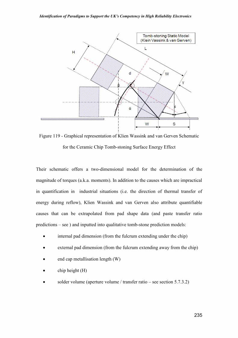
Identification of Paradigms to Support the UK’s Competency in High Reliability Electronics
235
Figure 119 - Graphical representation of Klien Wassink and van Gerven Schematic
for the Ceramic Chip Tomb-stoning Surface Energy Effect
Their schematic offers a two-dimensional model for the determination of the
magnitude of torques (a.k.a. moments). In addition to the causes which are impractical
in quantification in industrial situations (i.e. the direction of thermal transfer of
energy during reflow), Klien Wassink and van Gerven also attribute quantifiable
causes that can be extrapolated from pad shape data (and paste transfer ratio
predictions – see ) and inputted into qualitative tomb-stone prediction models:
internal pad dimension (from the fulcrum extending under the chip)
external pad dimension (from the fulcrum extending away from the chip)
end cap metallisation length (W)
chip height (H)
solder volume (aperture volume / transfer ratio – see section 5.7.3.2)

Identification of Paradigms to Support the UK’s Competency in High Reliability Electronics
236
Ellis and Masada develop Klien Wassink and van Gerven’s static model into a
dynamic system. Although regarding it as simplistic, they acknowledge that the static
model provides “a very good feel” for qualitative prediction of tomb-stoning events.
Conversely, they also express misgivings concerning (i) the neglect of hydrostatic
pressure forces, (ii) its invalid assumptions concerning liquid solder interface contact
(i.e. solder-ability dictated wet-out) and (iii) its over-simplified assumption of straight
line solder fillet formations, thus the violation of the conservation of mass of liquid
solder. Whilst refutation of the academic validity of their static model issues is
unintended, for qualitative prediction purposes, the implications of these qualms are
not apparent at the PCB design stage and therefore inapplicable in this application.
Where, Ellis and Masada (as codified with Figure 122) do add applicable value to the
development of models for the qualitative predictions of tomb-stoning surface-energy
effects (i.e. TS Probability) by corroborating / expanding the inputs to the Klien
Wassink and van Gerven static model with the following:
a. “the larger the metallization, the larger the positive moment on the chip”
i.e.
∆TIPC = +ve → HF1M = +ve → TS Probability = -veEquation 15
Where,
∆TIPC = change in chip metallised end cap length
HF1M = pull down moment
TS Probability = qualitative probability of tomb-stoning
b. “a decrease in stencil height increases the positive moment on the chip”
i.e.

Identification of Paradigms to Support the UK’s Competency in High Reliability Electronics
237
∆ST = -ve → HF1M = +ve → TS Probability = -veEquation 16
Where,
∆ST = Change in stencil thickness
c. “the solder pad length has little effect on the net moment at low angles of
inclination, but as the angle increases, the smallest pad length gives the
best results”
i.e.
∆PL = -ve → HF1M = +ve → TS Probability = -veEquation 17
Where,
∆PL = change in pad length
d. “the larger the gap between the solder pads, the larger the positive
moment on the chip”
i.e.
∆PG = -ve → HF1M = +ve → TS Probability = -veEquation 18
Where,
∆PG = change in the gap between associated pad
From these formulas, the tomb-stoning surface energy effects are definable. The
defect generating moment TF1M (i.e. a negative torque) is the cause of tomb-stoning.
However, defect preventing moments TF2M, HF1M, HF2M and CMM (i.e. positive
torques) are similarly definable and their inputs usable in qualitative predictive
modelling. When considering the pivoting action about the fulcrum, the torque
generated by the above listed positive moments opposes the toe fillet moment TF1M.
Only the advent of the simultaneous wetting of associated interconnections generates
the positive torques TF2M and HF2M that counteract TF1M.

Identification of Paradigms to Support the UK’s Competency in High Reliability Electronics
238
Both, the Klien Wassink / van Gerven and Ellis / Masada models consider only
disparate wetting scenarios, but the later report an initial upward pivoting motion,
which then subsides and the chip returns to the horizontal in an assumed balancing of
the moments. From this observed (and filmed) anecdote both, (i) the potential for
TF1M to overcome CMM, i.e. the gravitational moment (for codification see Figure
122) and (ii) an assumed delay in the wetting of the heel fillet, explain the reversal of
the tomb-stoning motion, via the counteraction of TF1M by CMM which is
supplemented by HF1M (for codification see Figure 123).
Figure 120 - Codification Diagram for the Tomb-stoning Surface-energy Effects at the
Toe Fillet
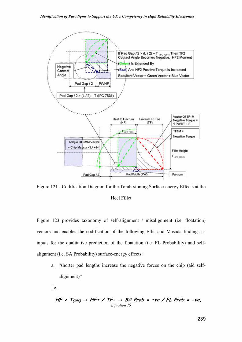
Identification of Paradigms to Support the UK’s Competency in High Reliability Electronics
239
Figure 121 - Codification Diagram for the Tomb-stoning Surface-energy Effects at the
Heel Fillet
Figure 123 provides taxonomy of self-alignment / misalignment (i.e. floatation)
vectors and enables the codification of the following Ellis and Masada findings as
inputs for the qualitative prediction of the floatation (i.e. FL Probability) and self-
alignment (i.e. SA Probability) surface-energy effects:
a. “shorter pad lengths increase the negative forces on the chip (aid self-
alignment)”
i.e.
HF > T(IPC) → HF+ / TF- → SA Prob = +ve / FL Prob = -ve,Equation 19

Identification of Paradigms to Support the UK’s Competency in High Reliability Electronics
240
Where,
HF = heel fillet to fulcrum (full wet-out to pad extremities is assumed)
TF = toe fillet to fulcrum (full wet-out to pad extremities is assumed)
SA Prob = qualitative probability of self-alignment
FL Prob = qualitative probability of floatation
b. “shorter pad gaps increase the negative forces on the chip”
i.e.
∆PG = -ve → HF+ / TF- → SA Prob = +ve / FL Prob = -ve,Equation 20
c. “larger amounts of solder (larger stencil height) increase negative forces
on the chip”
i.e.
∆PDH = +ve → HF+ / TF- → SA Prob = +ve /FL Prob = -ve,Equation 21
Where,
∆PDH = Change in paste deposit height
d. “smaller chip metallisation increase negative forces on the chip”
i.e.
∆T(IPC) = -ve → HF+ / TF- → SA Prob = +ve /FL Prob = -ve,Equation 22

Identification of Paradigms to Support the UK’s Competency in High Reliability Electronics
241
Figure 122 - Codification Diagram for the Floatation & Self-alignment & Surface-
energy Effects
Klien Wassink and van Gerven attribute both tomb-stoning and floatation to the
combined effects of (i) the minimisation of surface energy at a liquid / gas interface
and (ii) the equilibrium of surface area at the liquid / gas interface. The interface
between the molten fillets and the ambient atmosphere represents the minimised
surface. They propose that although tomb-stoning is the more common of the two
surface energy derived defect modes, but due to component buoyancy, that horizontal
component movement is a norm during wetting. Equilibrium of wet-out of the
interconnecting surfaces will develop leaving disparate or simultaneous wetting to
differentiate the probabilities of floatation / self-alignment. In situations of
simultaneous wetting, equilibrium between associated interconnects ensues, thus
promoting self-alignment. However, if only one interconnect wets then the
equilibrium will be between heel and toe fillets and the balancing of the minimised
surfaces in the homogeneous liquid will dictate the self-alignment / misalignment
vectors.

Identification of Paradigms to Support the UK’s Competency in High Reliability Electronics
242
Anecdotal support for this hypothesis comes from Klien Wassink and van Gerven’s
observation that ceramic chip resistors are more prone to rotational floatation (see
Figure 117) than their capacitor counter parts. Given the archetypal use of rectilinear
shaped pads, the extremities of the wet-out will be at diagonally opposed corners
about which the surfaces will minimise. In ceramic chip capacitor production, due to
the pre diced, dip process application of the end caps, the resultant metallisation
extends the solder-able surface along the components sides to coincide with the top
and bottom solder-able surfaces – see Figure 125.
Figure 123 - Graphical Representation of a ceramic Chip Capacitor Showing Full
Wrap Round Metallised End Cap
This presents the opportunity for the formation of supplementary side fillet, thus
balancing the number of fillets and interfaces in a corner-to-corner arrangement.
However, dicing of ceramic chip resistors follows the application of the metallisation,
thus negating the side solder-able surfaces and fillets – see Figure 126.
Figure 124 - Graphical Representation of a Ceramic Chip Resistor Showing Top and
Bottom Only Metallised End Cap

Identification of Paradigms to Support the UK’s Competency in High Reliability Electronics
243
In the absence of the side solder-able surfaces, the linear heel and toe fillets align with
the diagonally minimised surface area, generating a rotational vector – see Figure 119.
Heel and toe fillet balancing becomes a function of pad symmetry and spacing about
the degree of metallisation. Therefore, in isolation, equitable pad extension about
T(IPC) will promote and maximise self-alignment probability, but geometrical
constraints dictate compromised pad designs which need to optimise self-alignment
whilst minimising the opposing surface energy effect related defect modes i.e. tomb-
stoning, flotation and mid-chip solder balls.
Figure 127 provides a concise physical model the analysis of the causes of tomb-
stoning, floatation, self-alignment and mid-chip solder ball defect phenomena. Figure
128 an effects model for the surface energy effects based on qualitative prediction of
the probability of tomb-stoning, floatation, self-alignment and mid-chip solder ball
defects and completes the modelling of the SMT sub-processes.

Identification of Paradigms to Support the UK’s Competency in High Reliability Electronics
244
Figure 125 - Concise Physical Model for the Qualitative Prediction of the Causes of
Tomb-stoning, Floatation, Self-alignment and Mid-chip Solder Ball Defects
Figure 126 - Concise Physical Model for the Qualitative Prediction of the effects of
Tomb-stoning, Floatation, Self-alignment and Mid-chip Solder Ball Defects

Identification of Paradigms to Support the UK’s Competency in High Reliability Electronics
245
8.7. Chapter Summary
Chapter VII provides physical models in the form of truth tables. Solder Contact
(Lead Bend Tolerance) precedes the Solder Wetting & Fillet Formation discrete event
within the flow of the reflow sub-process. From the knowledge captured through this
analysis it becomes apparent that lead co-planarity has the potential to disguise some
of more obvious intra event causes of its apportioned defect effects.
For example unsoldered and insufficient solder joints archetypically link to
insufficient solder paste deposits. However, in multi leaded device scenarios, if lead
co-planarity anomalies exceed the resulting pad to pad solder height variation of
adjacent interconnects the ensuing standoff of a “lifted lead” might be greater than the
contact height which allows wetting of the molten solder deposit (an algorithm for the
modelling of this dimension is provided). Worryingly this data is not measured and
captured for causation analysis by the industrial collaborators and is unreported in
solder paste print related academic studies. It is also worth noting that in instances of
marginal contact, insufficient conducted thermal transfer might inhibit the wetting
process and misinterpreted as poor wetting.
This scenario is expanded for the Solder Wetting & Fillet Formation discrete event
apply contact related causes of poor soldering effects from lead position anomalies. Its
truth table also provides linkages between package-style specific solder wicking
issues which again appear as insufficient solder paste deposits but root-cause in
localised thermal differential which promote migration of sufficient volumes away
from the desirable fillet wet-out area.

Identification of Paradigms to Support the UK’s Competency in High Reliability Electronics
246
Finally, the third discrete event of the of the third sub-process elicits the scant
academic data by combining static and dynamic models and also incorporates a more
recently acknowledge defect mode in the form of mid-chip solder balls within a truth
table embedded within a concise physical model. By doing so the extrapolated
formula from the academically validated are interlinked and related to the mid-chip
solder ball cause to originate a new multi-dimensional paradigm which if coded for
interactive used could be used to balance the little understood and even less optimised
relationships of dynamic behaviour of chip components during solder wetting and
solidification.

Identification of Paradigms to Support the UK’s Competency in High Reliability Electronics
247
Chapter IX –Discussions, New Learning, Conclusion & Future Work
9.1. Discussion - Research Context
Figure 127 – Chapter Context Diagram
The fundamental requirement of the research reported within this thesis is the
provision of models for use in the development of a software tool which codifies
cause & effects knowledge for use in product and process design optimisation for
collaborative UK based producers of aircraft electronic subsystems. The objectives of
this chapter are to draw conclusions as elicited from the author’s research and
extrapolate new learning from any mined data and academic research.
The original project charter proposed data mining and statistical analysis of industrial
partner’s production data as the methodologies for the elicitation of the cause and
effects relationships. The conclusion that other sources of empirical data would be
needed came from the initial discovery that the collaborator’s data sources contain
only logs of historical assembly defects i.e. effects records without associated cause
information. To this end, sufficient extrapolation was possible from academic sources
and the ensuing codification is reported in Chapters V, VI, VII and XI. However, it
has been possible to elicit anecdotal and experiential leaning from the research project

Identification of Paradigms to Support the UK’s Competency in High Reliability Electronics
248
collaborators. Therefore this chapter offers conclusions from this source and the
author’s own industrial experience and proposed new learning outcomes.
The physical models for the SMT Reflow process cause and effects relationship, as
reported in Chapters VI, VII and VIII augment other work packages within the
overriding software tool development - see Figure 130 for context and work package
interactions.
Figure 128 - Graphical Representation of CLOVES Knowledge, Models and
Simulation Work Package Interactions
Knowledge of the structural and operational systems (i.e. work package 1) within the
industrial collaborator business domains and processes is elicited and codified via
academically recognised enterprise modelling techniques. The author’s physical
models (i.e. work package 2) relate to this learning via model based simulations of
discrete events and where applicable and coincidental became integrated within the
software tool. This functionality was then deployed, and utilised to support model

Identification of Paradigms to Support the UK’s Competency in High Reliability Electronics
249
based simulation of discrete events via commercially available software tool,
facilitating mutual validation.
9.2. Discussion – Research Interactions
As a commercially available and widely used generic modelling / simulation tool,
Arena™, provisions model based simulations of discrete events which impact on
throughput efficiencies and yield outputs. Within work package 3 then DIY co-
researchers developed a turnkey, bespoke modelling / simulation alternative,
INMOST (INtegrated MOdelling and Simulation Tool).
Model based Simulations of Discrete Event
Based on a hierarchical object oriented software structure (HOOSS) INMOST was
developed and evaluated for model based simulation of discrete events of the
collaborator’s SMT process domains. Although the pre-built constructs were deemed
less flexible and profligate in terms of visual representation, the overriding benefits of
ease and speed of use in model based simulation of discrete events which impact on
their SMT throughput efficiencies and yield, concluded positively in INMOST’s
favour.
Enterprise Modelling CIMOSA
Within work package 1, knowledge of business processes and enterprise activities was
elicited and contextualised via CIMOSA (Computer Integrated Manufacture
Operational Systems Analysis) abstraction mechanisms – see Figure 131.

Identification of Paradigms to Support the UK’s Competency in High Reliability Electronics
250
Figure 129 - Graphical Representation of CIMOSA Abstraction Mechanisms &
Constructs
Enterprise modelling, when integrated with discrete event simulations, dynamically
links resource entities, such as shop-floor personnel, machines, software applications,
databases. The dynamic models used in the discrete event simulations develop from
static precursors, which in turn derive from sub-set abstractions via context (see
Figure 132), interaction (Figure 133), structure (Figure 134), and activity diagrams
(Figure 135). CIMOSA process and activity static models (i.e. domain, business and
enterprise) compose from its core constructs (Monfared, 1998) e.g. Activity, Events,
Information, Human Resources, Physical Resources, Finance, and External Links.

Identification of Paradigms to Support the UK’s Competency in High Reliability Electronics
251
Figure 130 - Example of a CIMOSA Context Diagram
Figure 131 - Example of a CIMOSA Interaction Diagram

Identification of Paradigms to Support the UK’s Competency in High Reliability Electronics
252
Figure 132 - Example of a CIMOSA Structure Diagram
Figure 133 - Example of a CIMOSA Activity Diagram
Figure 136 provides a high-level context diagram describing a generic electronics
“domain model” from product development (linking product / process design and
qualification) and product realisation (divested production strategies and business
models) through to production-isation.
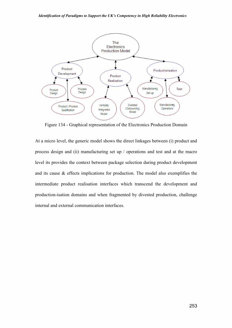
Identification of Paradigms to Support the UK’s Competency in High Reliability Electronics
253
Figure 134 - Graphical representation of the Electronics Production Domain
At a micro level, the generic model shows the direct linkages between (i) product and
process design and (ii) manufacturing set up / operations and test and at the macro
level its provides the context between package selection during product development
and its cause & effects implications for production. The model also exemplifies the
intermediate product realisation interfaces which transcend the development and
production-isation domains and when fragmented by divested production, challenge
internal and external communication interfaces.

Identification of Paradigms to Support the UK’s Competency in High Reliability Electronics
254
Figure 135 - An SMT Defect Opportunity & Detection Context Diagram
The context for the cause & effect relationship for the SMT Reflow process is
represented by the identification of the causation processes for the defect opportunity
and its internal detection processes at the test stage – see Figure 137.
9.3. Discussion - Package Technology and its Implications (for Aircraft
Electronic Subsystems
Traditionally, aircraft electronic subsystem manufacturers preferred military grade
(i.e. pre-screened) components with a field-proven legacy. By default, a field-proven
legacy implies a distrust of leading-edge package technology, but commercial (i.e.
supply chain) and technical (assembly) implications challenge this position.
Leading / Lagging-edge Package TechnologyIn technology trend following, consumer electronics markets, the thirst for the latest
gadgetry and fashions promote near-sighted customer expectations regarding product

Identification of Paradigms to Support the UK’s Competency in High Reliability Electronics
255
design-life expectancy and obsolescence-by-design becomes an attribute. Low design-
life expectancy implies a disregard for operational durability. Long term reliability is
less of an issue in today’s “throwaway society” but cost sensitivity along with size
and transportable (i.e. mobility) constraints require volume scalable automated PCA
assembly. As more and more functionality squeezes into the same space then physical
dimensions scale below the thresholds of human based assembly capabilities. A
juxtaposing challenge comes from the fact that contracting geometries, in turn, reduce
process windows. This increases the burden on automated assembly process accuracy
and repeatability and therefore heightens the reliance on optimised DfM.
As a result of functionality and mobility enhancement, geometric down-scaling
ensues. Thus, the PCA’s physical robustness and vulnerability to in-service durability
inhibiting effects such as mechanical fatigue or electro-chemical degradation must
increase. However, not all electronics market sectors have the same fatalistic view on
durability and willingness to compromise product reliability against increased
functionality at lower costs.
Moore’s Law (Moore, E., 1965) cannot provide a valid excuse for reduced robustness
in ultra-high reliability applications such as aircraft electronic subsystems. Safety
critical implications place great emphasis on not only, (i) reliability enhancement via
additional specialist processes (e.g. de-fluxing / cleaning, conformal coating, under-
filling, etc.) but also (ii) the inherent PCA reliability which is instilled by knowledge
of manufacturability cause and effects as embedded in the product design through
optimised package selection and placement at the PCA layout stage. Although
enhanced functionality and mobility (i.e. mass) remain desirable attributes, the

Identification of Paradigms to Support the UK’s Competency in High Reliability Electronics
256
pressures to geometrically down-scale are balanced against premium in-service
durability demand. Thus, a reticence exists for leading-edge package technology and a
preference for proven reliability; but paradoxically the (flight) safety-critical
electronics sector does not have the purchasing power to influence package
technology trends.
Even if considered lagging-edge by other domains, miniaturisation can still present
challenging assembly problems which become exaggerated if cohabiting (high
reliability) PCBAs with larger footprint package styles – thus distorting and
compromising geometric aspect ratios. As the volume centric leading-edge demands
overwhelm from a supply and demand perspective, reluctantly it is the high reliability
followers such as the CLOVES & DIY project collaborator / implementers who have
to accelerate their miniaturisation road maps and become earlier adopters of advanced
SMT. These challenges must only compound in an era when geographically clustered
infrastructure support has been fragmented and migrated to low cost locations. This
suggests codification of this supporting knowledge is needed to support the UK’s
competency in high reliability electronics systems.
The quality problems as targeted during the latter report case study relate to a chip
component package style (i.e. 0402) which whilst probably considered lagging-edge
within a consumer lead mobile device context, represent leading-edge miniaturisation
for high reliability applications with new knowledge requirements.
SMT Package Process AutomationAircraft electronic subsystems producers use quality parts, but due to low (unitary)
volume requirements and constrained cost / volume related justification, have

Identification of Paradigms to Support the UK’s Competency in High Reliability Electronics
257
traditionally automated less, thus requiring higher levels of manual intervention and
handling during their assembly. Experience shows that such electronic products often
demonstrate a poor first time yield and a surprisingly low hour service return rate.
The direct costs of associated rework and repair of assembly defects are high. Yet, in
fail-safe systems, the functionality burden of self monitoring and semi-redundant
backup systems, which accommodate the inconsistent failure rates of manual PCA
assembly processes, must multiply the indirect costs to produce and operate by orders
of magnitude. With lean manufacturing initiatives and in-flight fuel efficiency goals
evermore apparent, pressures to automate increase. Once lagging-edge package
technology transcends the thresholds of human capability then automation becomes
unavoidable. Once automated, the SMT assembly process (see Figure 138) becomes
less random and cause & effects predictable.
Figure 136 - Graphical Representation of an Archetypal SMT Assembly Line
A research conclusion from this scenario is that if the automated assembly processes
are more predictable then they should be the target for predictive cause & effects
software automation. The context diagram in Figure 137 shows the relationship

Identification of Paradigms to Support the UK’s Competency in High Reliability Electronics
258
between the defect opportunity causation processes (i.e. SMT Reflow) and the defect
detection process i.e. PCA test.
Defect Implications - Internal & External FailuresSMT defects have direct failure implications for all eventualities, but in safety critical
/ fail-safe applications the significance of external failure is the primary consideration
in product / process design and validation. Electronic reliability is often expressed in
terms of failure rate against time via a desirable “bath-tub” shaped curve – see the
blue line in Figure 139.
Figure 137 - Bath-tub Curve Diagram
Prior to ware-out (i.e. structural failure) a period of structured integrity needs to
deliver “normal life” with the lowest possible constant failure rate giving the flattest
“bath-tub” – i.e. the blue line. Aircraft electronic subsystems benefit from a low and
constant failure rate via fail-safe circuitry which relies on predictive mitigation of
external failures. For the subsystems to enter service with a consistent (and low)
mitigated failure rate, “infant mortalities” have to be pre-screened via accelerated
aging processes such as ESS (Environmental Stress Screening) or HASS (Highly

Identification of Paradigms to Support the UK’s Competency in High Reliability Electronics
259
Accelerated Stress Screening) production testing techniques. As a consequence of
these pre-screening activities, the period of normal life has to extend to compensate
the forced aging cycles, thus transferring the wasteful tariff for this pseudo service
duty as a supplemental fatigue resistance burden. Moreover, a high rate or longer
period of “infant mortality” implies a harsher or longer pre-screening regime thus
amplifying or extending the required period of structured integrity.
However, new learning from the author’s research suggests a paradoxical and
proportional linkage between internally detectable defects and structurally unsound
solder joints. Although premature failure modes are not exclusive to circuit
interconnections (components and external connections also contribute in-service
robustness and reliability) the ductility and yield of the interconnection bears the bulk
compliance loading. Inevitable thermal expansion mismatches between component
and PCB substrate materials (Hutchins, 1995) require compliancy in interconnections
either via peripheral leads and / or solder joints. Therefore, vagaries in solder joint
geometry link directly to inconsistent in-service durability. If in-process detectable
assembly defects and early life catastrophically failing solder joints are geometry
dependent, then so must be the in-service dependency for structurally compliant
interconnections.
Given the profligate usage and acceptable reliability of products which adopt leading-
edge package technology the geometric linkage to fatigue resistance cannot be
exclusively ascribed to miniaturisation. Therefore, if not attributable to absolute
package scaling, then the geometric relationships acting between (i) the disparate TCE
(Thermal Coefficients of Expansion) co-planar package / PCB footprints (i.e. the

Identification of Paradigms to Support the UK’s Competency in High Reliability Electronics
260
laminar vectors which induce shear stress) and (ii) the joint’s ductility at its chemical
bond interfaces and laminar, minimum cross-sectional area.
The research reported in the following section proposes a geometric aspect ratio cause
& effect relationship between product and process design via package scaling and
positioning within the PCB layout which creates defect opportunities; but this
understanding concludes an equivalent linkage is apparent for external failures – see
Figure 140 for a generic cause & effects relationship via an Ishikawa or Fish-bone
diagram.
Figure 138 - Ishikawa Diagram Showing Internal / External Failure Effects of Solder
Joint Defect Causes
Generic Ishikawa.igx
Effects:BP9.1 Internal FailuresBP9.2 External Failures
ProductRealisation
DP6: Comercialised (i.e. Part Of Or AllOf The DTM Sequence Outsourced)
ProductDevelopment
DP2: Process Dedvelopment
DP8: ManufacturingOperations
BP8.1 Comp & PCB Prep
DP7: ManufacturingSet-up
BP7.1 Documentation
BP9.1INTERNAL FAILURES:
Inherent Defects In AProduct's MechanicalIntegrity That Are DetectedDuring Printed CircuitAssembly & iTest (i.e.Yield)
Inherent Defects In AProduct's MechanicalIntegrity That Are DetectedDuring EnvironmentalStress Screening (i.e.Captured Infant Mortalities)
BP9.2EXTERNAL FAILURES:
Inherent Defects In AProduct's MechanicalIntegrity That CauseSporadic Early Life FieldFailures (i.e EscapingInfant Mortalitiity Failures)
Inherent Deficiencies In AProduct's MechanicalIntegrity That CauseSystematic Premature In-service Stress RelatedWear-out (i.e. FatigueResistance Failures
DP3: Product Qualification
DP1: Product Design DP4: Vertically Integrated (i.e.Internal Production Model)
DP5: Parallel (i.e. Production ModelIncludes Internal & Outsourcing)
BP1.1DFx Rules
BP2.1FunctionalityPre-qualification
BP3.1Process ChemistryPre-qualification
BP3.2Process ToolingPre-qualification
BP1.2ProductArchitecture
BP2.2ReliabilityPre-qualification
BP4.1Internal NPI(New Product Introduction)
BP5.1Internal NPI WithExternal Sub-assembly
BP6.1Eternal NPI
BP6.2New ContractIntroduction
BP7.2 PCB Prep
BP7.3 Component Loading
BP7.4 SMT Processes
BP7.5 PTH & Pre-wave
BP7.6 Wave & Post Wave
BP7.7 PCA Test & Rework
BP7.8 PCA Completion
BP7.9 Module Assy & Test
BP7.10 Unit Assy & Test
BP8.2 Side 1 SMT
BP8.3 Side 2 SMT
BP8.4 PTH & Pre-wave Mech CompsBP8.5 Wave Soldering & Post-waveMech Component Hand Soldering
BP8.6 PCA Test
BP8.7 PCA Completion
BP8.9 Unit Assembly & Test

Identification of Paradigms to Support the UK’s Competency in High Reliability Electronics
261
9.4. New Learning
Application of Physical Models –
Case Study Findings
Figure 141, provides the Pareto analysis showing the top defects categories for a
product selected by an industrial collaborator. They are organised according to the
average number of defects identified per product. It can be clearly seen from the chart
that a significant amount of insufficient solder defects were generated during
manufacture (i.e. an average of 417.5 with insufficient solder defects equating to 1 in
25 solder joints).
With a deficiency in cause data relating to the defect opportunity conventional cause
and effects analysis techniques were rendered as in effective due to the inclusion of
effects only data at the point of defect detection. This scenario is archetypal across the
industrial collaborator case studies and consistent with the research authors twenty
plus years of practical experience in this field. It provides the primary justification for
the development of physical models and enablement of model based simulation.
INMOSTAs an alternative approach INMOST was trialled and the corresponding results are
described. The results provided by INMOST’s model based simulation module
include time, cost and quality metrics for the manufacturing systems associated with
the product STI10139D.
The PCB fabrication and PCBA (PCB assembly – i.e. SMD population) data for
product STI10139D were inputted into INMOST. Effects data was both (i) generated

Identification of Paradigms to Support the UK’s Competency in High Reliability Electronics
262
from defect detection results on sample assembled PCBAs and (ii) model basedally
predicted by INMOST. Both data sets are summarised in Table 8 - a close match
between real and predicted data can be identified (i.e. average match: 83%).
.
Table 8 - Real and Model Based Simulated Defect Data Sets
Taking into account the percentages corresponding to each defect type, it can be seen
in Figure 142a that almost 90% of the defects can be tackled by focusing on
insufficient solder defects.
Figure 139 - Pareto Analysis Output 1 from INMOST
•Significant quality issues identified•417.5 insufficient solder defects per product (onaverage)
•Performance data not available before manufacturing•Quality data collected during visual inspection afterall the SMT processes
•Defect data limitations•There is no time, cost or process data available forthe product•The data is inconsistent possibly due to manualcollection•The data is not well structured or integrated andtherefore is diff icult to analyse
0100200300400500
Number of defects per product

Identification of Paradigms to Support the UK’s Competency in High Reliability Electronics
263
Taking into account the percentages corresponding to each defect type, it can be seen
in Figure 142a that almost 90% of the defects can be tackled by focusing on
insufficient solder defects. Following this indication, the insufficient solder defects
predicted were classified according to the part type in which they were generated
within the simulation. The results are shown in another Pareto chart illustrated in
Figure 142b.
Figure 140 - Pareto Analysis Output 2 From INMOST
The second Pareto chart indicates that more than 90% of the insufficient solder
defects were applicable to 0402 chip components (i.e. capacitors – C 0402 – and
resistors – R 0402).
Taking into account the fact that, according to quality predictions, most of the defects
generated were insufficient solder defects on 0402 chips, these deductions provide
strong evidence of the necessity to modify the design to eliminate or reduce this
particular type of defect. The analysis of these metrics show how INMOST’s
simulation results can provide sound justifications for design decisions and financial
investments required. Conversely, it could be argued that if INMOST was used
interactively during original product design then the need for the financial justification
for redesign wouldn’t have arisen in the first place.
0
100
200
300
400
500
600
Insuf f f icient Shorts
Defect count per productper defect type
87%
13%
0
50
100
150
200
250
300
350
C 0402 R 0402 SOT 223 SO 8 TQFP 100
Insufficient solder defect count per product percomponent type
58%
33%
5%2% 1%
a. b.
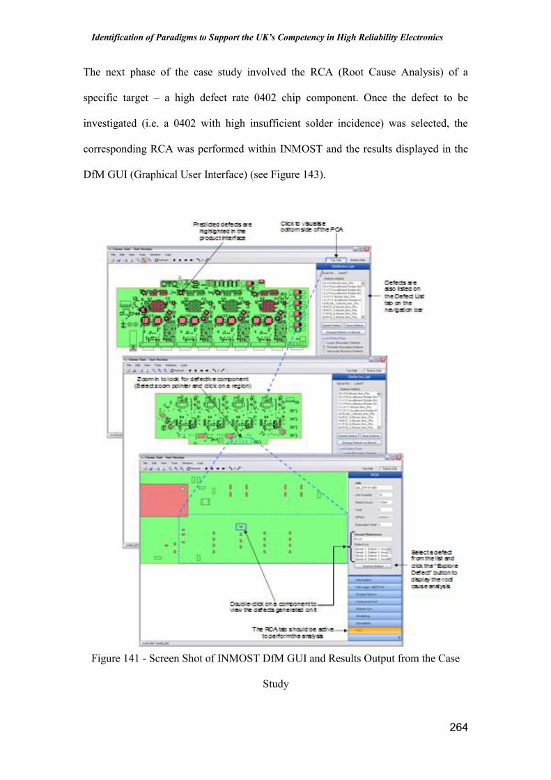
Identification of Paradigms to Support the UK’s Competency in High Reliability Electronics
264
The next phase of the case study involved the RCA (Root Cause Analysis) of a
specific target – a high defect rate 0402 chip component. Once the defect to be
investigated (i.e. a 0402 with high insufficient solder incidence) was selected, the
corresponding RCA was performed within INMOST and the results displayed in the
DfM GUI (Graphical User Interface) (see Figure 143).
Figure 141 - Screen Shot of INMOST DfM GUI and Results Output from the Case
Study

Identification of Paradigms to Support the UK’s Competency in High Reliability Electronics
265
The data corresponding to the defect investigation is given in the top half of the GUI
(i.e. under the Defect Details, Process Window and Possible Root Causes headings).
According to the information displayed under the Defect Details heading the Direct
Cause of the defect is a low solder paste Transfer Ratio from the apertures of the
stencil to the pads on the PCB, i.e. below the acceptable Process Window range.
Figure 142 - Screen Shot of INMOST RCA GUI and Results Output from the Case
Study
Possible Root Causes of the defect are presented in the tree view on the top right hand
side of the GUI. In the example shown the defect could have originated due to
parameters associated with either the actual Process (i.e. Stencil/board off set,

Identification of Paradigms to Support the UK’s Competency in High Reliability Electronics
266
Cleaning frequency), the Stencil (i.e. Thickness, Aperture Ratio, Aperture size), or the
Board (i.e. Board dimensional error, Pad Position, Pad size, Copper Thickness) used
in the fabrication of the PCB.
Experts from the PCA industry expert opinion was elicited regarding the most likely
root cause of the problem from those provided by the DfM module. Aperture size was
the most likely root cause selected by the majority of industrialists. To test the effect
of changing this variable the sensitivity analysis feature was employed. As illustrated
in Figure 144 the Current value of the Aperture size is 0.45mm. The larger the
aperture size the more paste is likely to be transferred to the board. Hence, increasing
the aperture size could eliminate the insufficient solder defects. The Analysis
Parameters in the Sensitivity Analysis section are then selected to cover a range from
0.45mm, (i.e. the current value), to 0.55mm in a step size of 0.01mm. Note: this
analysis will apply all similar parts in the product (i.e. all 0402 chips). The results of
the sensitivity analysis are shown in Figure 145.

Identification of Paradigms to Support the UK’s Competency in High Reliability Electronics
267
Figure 143 - Screen Shot of INMOST Sensitivity Analysis GUI and Result from the
Case Study
Each value tested in the sensitivity analysis corresponded to the execution of a
simulation to obtain the updated value of the direct cause, in this case the solder paste
transfer ratio. The results show that higher aperture size values lead to higher transfer
ratio values. According to the Process Window specified in Figure 145, values of the
Aperture size less than 0.53mm led to values of the direct cause outlying the process
window and therefore leading to the generation of insufficient solder defects. Hence,
the chart implied that the stencil needed to be redesigned such that the dimensions of
the apertures corresponding to 0402 components were larger than this value.
0.81
0.82
0.83
0.84
0.85
0.86
0.87
0.88
0.89
0.43 0.45 0.47 0.49 0.51 0.53 0.55 0.57
Dire
ct C
ause
: Tra
nsfe
r rat
io(m
m³/m
m³)
Root Cause Selected: Aperture size x (mm)
Process window
Current design valueoutside process window Recommended
limits
Maximum value withinprocess window andrecommended limits
Original stencil design New stencil design
Wider apertures thatimprove the transfer ratio
0.45mm0.55mm

Identification of Paradigms to Support the UK’s Competency in High Reliability Electronics
268
Accordingly, the recommendations by the component manufacturers for the aperture
size studied, should not be smaller than 0.45mm nor larger than 0.55mm. Taking this
into account, the largest possible value was selected as a potential design change (i.e.
0.55mm). This design change, illustrated in the bottom part of Figure 145, was
evaluated by including it in the manufacturing system model and running the
simulation to determine the impact of this change. The results are described below
ResultsThe results provided by the model based simulation module included time, cost and
quality metrics of the manufacturing systems. The first metric to be analysed was
quality, as this is the focus of the case study. The quality results given in Figure 146a
imply that the design change selected would result in the original number of
insufficient solder defects predicted on 0402 chips (i.e. 387 defects/PCA) being
reduced by almost 90% (i.e. to 44 defects/PCA). This was equated to an elimination
of 67.5% of the total quality issues (i.e. manufacturing defects) for the product
studied.

Identification of Paradigms to Support the UK’s Competency in High Reliability Electronics
269
Figure 144 - Screen Shot of INMOST Quality Improvement Predictions
ImpactFrom an electrical continuity perspective, solder joints can be unequivocally classified
as defective if the assembly process has (i) failed to create an interconnection (i.e. an
open joint) or (ii) unintentionally created a short circuit via the bridging of adjacent
component leads with solder. However, from a structured integrity perspective, if
provisional electrically sound solder joints are qualitatively adjudged geometrically
excessive or insufficient, then the repair of any such geometric defects could actually
result in replacement joints which are subsequently deemed geometrically acceptable
but may have been rendered mechanically less robust than their antecedents.
The subjective and none quantitative nature of manually performed, visual inspection
compounds the risk of unnecessary reworking of geometrically acceptable
misinterpretations – whilst geometrically nonconforming defects may escape this
0.0
53.5min(52.4%)
0.0
436.8min(64.5%)
0
100
200
300
400
500
VA NVA Quality Waiting
Manufacturing time savings (min)
0.00
£17.86(52.4%)
0.00 0.000
5
10
15
20
VA NVA Quality Waiting
Manufacturing cost savings (£)
100%
9%
0%
25%
50%
75%
100%
As-Is To-Be
Insufficient solder defects on0402's (scenario comparison)
b. c.
a.

Identification of Paradigms to Support the UK’s Competency in High Reliability Electronics
270
imprecise screening process. Automated Optical Inspection (AOI) can be quantitative
but is not applicable for all package styles see Figure 147.
Figure 145 - Package Style / Automated Inspection Techniques
From this and the results of the reported case study INMOST could have a twin
impact. Firstly, in the conventional application it has demonstrated a support
capability via codification of the knowledge required to retrospectively or even
interactively reduce defect opportunities, thus benefitting high reliability applications
through minimisation of essential rework requirements. Secondly, it could benefit by
predicting and pinpointing likely rework targets and mitigating ambiguous and none-
essential reworking.

Identification of Paradigms to Support the UK’s Competency in High Reliability Electronics
271
9.5. Conclusions
To support the UK’s competency in high reliability electronics, advanced simulation
tools which offer model based guidance to product and process designers are needed
to maximize manufacturability and therefore enhance in service sustainability. The
objective of this research is to offer heuristic codification of existing tacit industrial
knowledge and academic learning within physical models which provide the
algorithms for tool based analysis of product and process designs and smart cause and
effect simulation
Knowledge interfaces risk knowledge gap propagation from fragmentation effects of
divested production within the electronics production network global value chain. The
transplantation of high volume electronics production within the globalized electronic
production network has initiated fragmentary pressures which could in turn cause
knowledge gaps to appear in the UK’s infrastructure for the production of low
volume, high value electronics such as aircraft subsystems. This research concludes
that codification of tacit knowledge to facilitate Smart Cause & Effects and model
based simulation of the SMT process.
The CIMOSA context diagram within Figure 136 identifies disconnects between
effect opportunities and defect detection processes meaning data mining would
provide elicitation cause & effect relationships as defect detection data only captures
effects data highlighting a need for other sources of causation data. Even compliant
DOE 254 business enterprises within aircraft electronic subsystem producers do not
have to and do not practice defect opportunity data capture making elicitation of
causation paradigms via data mining unviable. Therefore this research has identified

Identification of Paradigms to Support the UK’s Competency in High Reliability Electronics
272
and elicited the supporting data to originate a codified knowledge structure from the
following alternative sources:
o Academic literature – empirical and peer validated but disconnected &
heterogeneous
o Industrial literature – less robust validation but wider coverage
o Experiential tacit knowledge – connects the validated data within a
codification structure to provision Smart Cause & Effects and enable
paradigmatic simulation
From these sources industrial tacit and elicited academic knowledge is codified and
structured into a novel framework for Smart Cause and Effects and the research
delivers the following physical model constructs enabling current and future model
based simulation of defect related discrete events with the SMT assembly process:
o Smart cause & effects knowledge codification structure for SMT process
discrete events
o Deposit insufficiency prediction formula (compounded) & rules & truth table
o Deposit Registration Error & Bridging Prediction Formula - Deposit Bridging
Rule
o Deposit Registration Error & Excess Formula - Deposit Registration Error
Volume Rule
o Vacuum pickup ABVA - Component pickup vacuum window formula & rules
o Exemplar of package placement attributes with defect frequency predictions
o Exemplar summation table for the codification of linear & rotary actuated
PVMs

Identification of Paradigms to Support the UK’s Competency in High Reliability Electronics
273
o Concept of inertial vector mapping of PPMs – forced pre-vision theta rotation
o Formula for converting solder deposit heights to wetted solder bump height
o Cause & effects truth table for solder contact & lead position
o Cause & effects truth table for solder wetting & fillet forming
o Codification diagrams for tomb-stoning, floatation & self-alignment surface
energy effects
o Codification diagram for tomb-stoning surface energy effects at the heel & toe
fillets
o Formula for predicting metallization impact on chip movement
o Formula for predicting stencil thickness impact on chip movement
o Formula for predicting pad length impact on chip movement
o Formula for predicting pad gap impact on chip movement
o New awareness that pad shapes for common chip sizes formats should
consider discrete package height

Identification of Paradigms to Support the UK’s Competency in High Reliability Electronics
274
9.6. Future Work
Via enhancements to INMOST or its successors, in a scenario where dimensional
scaling tolerances are considered at the design stage, aperture reductions could be
calculated and matched accordingly, and a stencil thickness recommendation, based
on the transfer ratio sub-model and minimum aspect and area aspect rules, could be
outputted. This process could be repeated for all components and an overall stencil
thickness recommendation produced based on the best-fit transfer ratio sub-model,
with bridged, excess and insufficient deposit nonconformity “hot-spots” highlighted.
Transfer ratios could likewise be calculated based on the scooping sub-model and
geometric aspect rule violations.
When used within a retrospective DfM scenario, PCB CAD inputs and BOM (Bill of
Materials) inputs could be merged to calculate the index-of-manufacturability for a
given PCA. Optimal, package location recommendations incorporated into a
maximised index-of-manufacturability. With CAD system and INMOST interactivity
consequential DfM could deliver maximised manufacturability and ultimately lean
design procedures. Central to this advanced functionality would be the physical
models as proposed in this thesis.
The effects outputs of the causation paradigms could follow the convention
established by contemporary cause & effects techniques such as FMEA (Failure
Modes and Effects Analysis) with defect opportunity, detect-ability and rework
implications, representing the Occurrence, Detection, and Severity parametric outputs
which are typical in calculation of FMEA Risk Priority Numbers. With the integration
of the component placement and solder wetting / dynamic behaviour under reflow

Identification of Paradigms to Support the UK’s Competency in High Reliability Electronics
275
discrete events causation paradigms - enabling harmonisation of extrapolated design
rules and corroboration of fragmented effects data - the physical models offer the
potential to develop powerful, automated synergistic product and process design
guidance and homogenous cause and effects analysis functionality.
This functionality could be codified and modularised as follows:
Full Spectrum Cause & Effects Analyser and Process Characterisation
Module Research into industrial partner defect root cause analysis data and
experiential case-base knowledge should provide an extensively populated
cause & effects and process characterisation database. This could be
codified to form a cause & effects analyser.
A Defect Occurrence and Probability Calculator
A full spectrum cause & effects analyser could identify potential causes
relating to a particular defect and package. A process characterisation
electronic check list could be generated and used to assess the prevailing
process conditions which would have existed when recorded defects
occurred within the product design, process design, DfM, process setup,
process maintenance, new product introduction and supply chain domains
and used to eliminate potential causes. The electronic check list could
incorporate a one to ten condition grading system which would convert
qualitative observations to quantitative inputs to the model based
simulation module (i.e. INMOST).

Identification of Paradigms to Support the UK’s Competency in High Reliability Electronics
276
References
MIT Course Work Material for ESD.60 Module 9.3. Heijunka Product & ProductionLevelling.
AIGT. (2003). Aerospace Innovation and Growth Team Report, Report On ProgressWith The National Aerospace Technology Strategy. Department of Trade andIndustry.
Airbus A380 Said To Be Safe. (2006, December 12). Retrieved October 21, 2007,from Rueters, December 12, 2006:http://money.cnn.com/2006/12/12/news/international/airbus_a380/index.htm)
American Electronic Association. (1997). 1997 Research Report "Success Strategiesfor High Technology Companies". Boston, MA: American Electronic Association.
Andrade, J. A. (2008). Formal Conceptualisation as a Basis for a More ProceduralKnowledge Management, . Decision Support Systems , 45 ((N1)), 164-179.
Baldwin, C. Y. (2004). Modularity in the Design of Complex Engineering Systems.Carliss Y. Baldwin and Kim B. Clark.
Bashforth, F. A. (1983). An Attempt to Test the Theories of Capilary Action.Cambridge University Press.
Bhote, K. R. (2000). World Class Quality: Using Design of Experiments to Make itHappen (Vol. Second Edition). American Management Association.Brox, B. T. (1995). Reliability of Electronics in Harsh Environments. Solderong &Surface Mount Technology ((N21)), 13-16.
Cala, F. W. (1996). Handbook of Aqueous Cleaning Technology for ElectronicAssemblies. Isle of Man, British Isles: Electrochemical Publication Ltd.
Conway, P. H. (1999). Development of a Closed-Loop Controlled Reflow SolderingProcess. CIRP Annals-Manufacturing Technology , 48 ((N1)), 5-8.Davy, J. G. (1985). A Comprehensive List of Wave Solder Defects and Their ProbaleCauses. Brazing & Soldering ((N9)), 50-59.
de Langen, M. T. (1990). Technical Outline Specification and Guideleine for Infra-redReflow Soldering. Soldering & Surface Mount Technology , 5, 32-37.
Destafani, J. (2004). A Look at Boeing's Outsourcing Strategy,. ManufacturingEngineering , 132 ((N3)), 56-73.
Donoghue, J. W. (1992). ''Solder Paste Displacement on Solder Placement''.Proceedings of 12th Institute of Electrical Engineers / Institute of HybridMicroelectronics. International Electronics Manufacturing Symposium, (pp. 133-138). Mainz, Germany: IEEE.
Identification of Paradigms to Support the UK’s Competency in High Reliability Electronics
277
Durairaj R., N. T. (2001). Critical Factors Affecting Paste Flow During the StencilPrinting of Solder Paste. Soldering & Surface Mount Technology , 13 ((N2)), 30-34.
EIGT. (2007). Electronics Innovation and Growth Team Report, Electronics 2015:Making a Visible Difference. URN 04/1812.
Ellis, B. N. (1986). Cleaning and Contamination of Electronics Components andAssemblies,. (Isle of Man, UK): Electrochemical Publications Limited.
Ellis, J. R. (1990). Dynamic Behavior of SMT Chip Capacitors During SolderReflow. Transactions on Components, Hybrids and Manufacturing Technology , 13((N3)), 545-552.
Engardio, P. (2005, March 21). Design ia a Commodity,. Retrieved October 10, 2007,from Business Week Outsourcing Innovation / Online Extra:www.businessweek.com/magazine/content/05_12/b3925609.htm
Franken, K. M. (2004). Finite-Element Analysis of Ceramic Multilayer Capacitors:Failure Probability Caused by Wave Soldering and Bending Loads. Journal of theAmerican Ceramic Society , 83 ((N6)).
Gallo, A. M. (1995). Popcorning: a failure mechanism in plastic-encapsulatedmicrocircuits. Reliability, IEEE Transactions On , 44 ((N3)), 362-367.
Garrison, A. L. (1995). How Much Rework is Too Much?: the Effect of Solder JointRework on Plated Through Holes in Multilayere Printed Wiring Boards. SOldering &SUrface Mount Technology ((N19)), 48-51.
Gebus, S. a. (2007). Knowledge Acquisition For Decision Support Systems On AnElectronic Assembly Line. Expert Systems with Applications , Article in Press,doi:10.1016/j.eswa.
Gunter, I. (1986). The Solderability Testing of Surface Mount Devices Using the GECMeniscograph Solderability Tester. Circuit World , 13 ((N1)), 8-12.
Hameri, A. P. (2005). Supply Network Dynamics as a Source of New Business.International Journal of Production Economics , 98 ((N1)), 41-55.
Hansen, M. (1958). The Constitution of Binary Alloys. MaGraw-Hill.
Harmen, G. (1997). Wire Bonding in Microelectronics Materials, Processes,Reliability and Yield: Second Edition (Vol. Electronic Packaging & InterconnectionSeries). McGraw-Hill.
Hawkins, S. P. (1986). The Mechanical Properties of Solder Joints to SurfaceMounted Devices. Brazing & SOldering , 10, 4-6.
Henderson, R. M. (1990, March). Architectural Innovation: The Reconfiguration ofExisting Product Technologies and the Failure of Established Firms - Technology,Organizations and Innovation. Administrative Science Quarterly .

Identification of Paradigms to Support the UK’s Competency in High Reliability Electronics
278
Huang, C. Y. (2011). The Solder Paste Printing Process: Critical Parameters, DefectScenarios, Specification, and Cost Reduction. Soldering & Surface Mount Technology, 211-223.
Huertas-Quintero, L. (2010). Novel modelling and simulation approaches to supportelectronics manufacturing in the UK: A Doctoral Thesis.
Huin, S. F. (2003). Knowledge-Based Tool For Planning Of Enterprise Recources InASEAN SMEs. Robotics and Computer Integrated Manufacturing , 19 ((N)), 409-414.
Hutchins, C. L. (1995, December). Reliability vs. Processing Temperatures. SurfaceMount Manufacturing , 16-18.
IEC. (2007). IEC 60286-3 Ed. 4.0 EN: 2007 (Packaging of Components for AutomaticHandling - Part 3: Packaging of Surface Mount Components on Continuous Tapes).International Electrotechnical Commission Webstore.
IPC, IPC-7351 (L). IPC-7351 (L) Generic Requirements for Surface Mount Designand Land Pattern Standard. Sanders Road, Northbrook, Il 60062-6135, USA.: IPC,Association of Connecting Electronics Industries.
IPC, A. o. IPC-DRM-PTH-D Through-Hole Solder Joint Evaluation Training &Reference Guide. Association of Connecting Industries.
IPC, IPC-4552/02. (2002). IPC-4552/02, Specification for ElectrolessNickel/Immersion Gold (Enig) Plating for Printed Circuit Boards, IPC. Northbrook,Il, USA: IPC, Association of Connecting Electronics Industries.
IPC, IPC-7525. IPC-7525 Stencil Design Guidelines. IPC, Association of ConnectingElectronics Industries.
IPC, IPC-7530. IPC-7530 The Definitive Guide for Temperature Profiling for MassSoldering (Reflow & Wave). IPC, Association of Connecting Electronics Industries.
IPC, IPC-A-610E. IPC-A-610E Acceptability of Electronic Assemblies. IPC,Association of Connecting Electronics Industries.
IPC, IPC-DRM-18. IPC-DRM-18 Component Identification Training & ReferenceGuide. IPC, Association of Connecting Electronics Industries.
IPC, IPC-DRM-SMT-D. IPC-DRM-SMT-D Surface Mount Joint Evaluation Training& Reference Guide. IPC, Association of Connecting Electronics Industries.
IPC, IPC-HDBK-610. IPC-HDBK-610. IPC, Association of Connecting ElectronicsIndustries.
IPC, IPC-M-108. IPC-M-108, Assembly Cleaning Guides and Handbooks. IPC,Association of Connecting Electronics Industries.

Identification of Paradigms to Support the UK’s Competency in High Reliability Electronics
279
IPC, IPC-S-816. IPC-S-816 SMT Process Guidelines and Check List. IPC,Association of Connecting Electronics Industries.
IPC, IPC-SM-780. IPC-SM-780, Component Packaging and Interconnecting withEmphasis on Surface Mount. IPC, Association of Connecting Electronics Industries.
IPC, IPC-SM-782. (1987). IPC-SM-782, Surface Mount Land patterns(Configurations and Design Rules). Institute for Interconnecting and PackagingElectronic Circuits. IPC, Institute for Interconnecting and Packaging ElectronicCircuits.
IPC, IPC-SM-784. IPC-SM-784 Guidelines for Chip-on-Board TechnologyImplementation. IPC, Association of Connecting Electronics Industries.
IPC, J-STD-032. J-STD-032, Performance Standard for BGA's. Association ofConnecting Industries.
JEDEC. (1988). JEDEC Registered and Standard Outlines for Solid State Products.Electronics Industries Association.
Jones, R. W. (2000). A Framework for Fragmentation. Tinbergergen InstituteDiscussion Paper , TI 2000-056/2.
Jones, R. W. (2004). International Fragmentation and the New Economic Geography.Graduate Institute of International Studies Geneva , HEI WOrking paper No:11/2004.
Kay, P. J. (1976). The Growth of Intermetallic Compounds on Common BasisMaterials Coated with Tin and Tin-Lead Alloys. Transactions of the Institute of MetalFinishing , 54, 68-74.
Klein Wassink, R. J. (1989). Displacement of Components and Solder during ReflowSoldering. Soldering & Surface Mount Technology , 1, 32-37.
Klein Wassink, R. J. (1986). Drawbridging of Leadless Components. Hybrid Circuits, 9, 9-12.
Klein Wassink, R. J. (1989). Soldering in Electronics. (Isle of Man, UK):Electrochemical Publications Limited.
Klein Wassink, R. J., Vledder, H.J. (1983). The Attachment of Leadless ElectronicComponents to Printed Boards. Hybrid Circuits (3) , 28-32.
Klein-Wassink, R. J. (1967). Wetting of Solid Metal Surfaces by Molten Metals.Journal of the Institute of Metals , 32, 38-43.
Kock, C. (2005). Innovations Ships Out. CIO , 18 ((N7)), 62-67.
Kundu, S. S. (2007). Forbidden pitches in sub-wavelength lithography and theirimplications on design. (14).

Identification of Paradigms to Support the UK’s Competency in High Reliability Electronics
280
Lau, J. H. (1995). Ball Grid Array technology (Vol. Electronic Packaging andInterconnection Series). McGraw-Hill, Inc.
Lau, J. H. (2003). Electronics Manufacturing. McGraw-Hill.
Lau, J. H. (1996). Flip Chip Technologies. McGraw-Hill.
Lau, J. L. (1991). Effects of Rework on the Reliability of Pin Grid ArrayInterconnects. Circuit World , 17 ((N4)), 5-10.
Lau. J.H. (1991). Solder Joint Reliability Theory and Applications. New York: VanNostrand Reihold.
Lavasco, F. (1988). Solder Joint Modelling Using Finite Element Analysis.Proceedings of the 1988 International Electronic Packaging conference, (pp. 410-415). Dallas, TX.
Lea, C. (1988). A Scientifc Guide to Surface Mount Technology. Ayr, Scotland:Electrochemical Publications Limited.
Lea, C. (1990). The Harmfulness of Reworking Cosmetically Defective Solder Joints.Teddington, Middlesex, England: National Physical Laboratory.
Lee, C. K. (2005). An Object-based Knowledge Integration System for ProductDevelopment – a Case Study. Journal of Manufacturing Technology Management , 16((N2)), 156-177.
Lee, N. C. (1999). Optimising the Reflow Profile via Defect Mechanism Analysis.Soldering & Surface Mount Technology , 11 ((N1)), 13-20.
Leifer, R. M.-O. (2000). Radical Innovation: How Mature Companies Can OutsmartUpstarts. Harvard Business School Press.
Lotosky, P. M. (2006, April). Using Stencil Design to Reduce SMT Defects. SMT ,34-36.
Mannan S. H., E. N. (1993). Predicting Scooping and Skipping in Solder PastePrinting for Reflow Soldering of SMT Devices. Soldering & Surface MountTechnology , 15, 14-17.
Markstein, H. W. (1987). SMT Reflow: IR or Vapour Phase? Electronic Packaging &Production , 27 ((N1)), 60-63.
Mathaisel, D. F. (2000). Developing, Implementing and Transfering Lean QualityInnitiatives from the Aerospace Industry to all Industries. Managing Service Quality ,10 ((N4)), 248-256.

Identification of Paradigms to Support the UK’s Competency in High Reliability Electronics
281
McNamara, D. L. (2006). New Places old Spaces: Knowledge Hierachies AmongstAsian Small and Medium Size Enterprises Abroad. Organisation , 13 ((N4)), 549-567.
Minges, M. L. (1989). Electronics Materials Handbook: Packaging (Vol. Volume 1Packaging). ASM International.
Monfared, R. B. (1998). Implementing a Model-Based Generic User Interface forComputer Integrated Manufacturing Systems. Proceedings of the Institution ofMechanical Engineers Part B: Journal of Engineering Manufacture, (pp. 501-516).
Moore, E. (1965). Cramming More Components Onto Integrated Circuits, .Electronics, 38(N38), , 114-117.
National Economics Research Associates. (2005). DTI Sector Competitiveness StudiesNo.1, Competitiveness in the UK Electronics Sector: A Report to DTI. Department ofTrade and Industry.
Nave, D. (2002, March). How To Compare Six Sigma, Lean and the Theory ofConstraints – A Framework For Choosing What’s Best For Your Organisation.Quality Progress Article .
Nguty, T. A. (2000). Rework of CSP: the Effect On Surface Intermetallic Growth.Soldering & Surface Mount Technology , 12 ((n3)), 35-38.
Nieter, T. (1955). Electroplating process for producing printed circuits. Motorola,Inc., US Patent 2699424.
Nieter, T. M. (1955). Patent No. US Patent 2699425, . USA.
Norris, K. C., Landzberg, A. H. (1969, May). Reliability of Controlled CollapseInterconnections. IBM Journal of Research and Development , 266-271.
Pan, J. T. (2004). Critical Variable of Solder Paste Stencil Printing for Micro-BGAand Fine-Pitch QFP,. IEEE Transactions on Electronics Packaging Manufacturing ,27 ((N2)), 125-132.
Partridge, S. A. (1987). The Role of the Stencil in High Definition Screen Printing.Circuit World , 13 ((N2)), 4-13.
Peng, X. (2007). A Comparative Study of Knowledge-Based Economy DevelopmentBetween China and USA. Data Science Journal , 6 ((N9)), S408-S419.
Petherbridge, K. E. (2004). The Origins and Evolution of the PCB: A Review. CircuitWorld, Vol. 31 Iss: 1, , pp.41 - 45.
Poon, G. K. (1999). Characterisation of a Solder Paste Printing Process and itsOptimisation. Soldering & Surface Mount Technology , 11 ((N3)), 23-26.

Identification of Paradigms to Support the UK’s Competency in High Reliability Electronics
282
Porter, M. E. (1990). The Competitive Advantages of Nations. Macmillan Press:Macmillan Press.
Probert, D. R. (1996). Make or Buy: Inderstanding the Impact of Technology Choices.Manufactuirng Strategy, IEE Colloquium On (pp. 4/1-4/4). Coventry, UK: IEE.
Puttlitz, K. J. (2001). Area Array Interconnection Handbook. Kluwer AcademicPublishers.
Rahn, A. (2006, February). Pastes, Stencils and Process Control. SMT , 28-34.
Rasmussen. J, L. A. (2006, April). Microvia Filling: A Challenge For Process Quality.Onboard Technology , pp. 8-10.
Reed, F. M. (2004). UK PCB Industry 1997 to 2003. Circuit World , 30 ((N3)), 43-50.
Reichl, H., Grosser, V. (2001). Overview and development trends in the field ofMEMS packaging. Micro Electro Mechanical Systems, 2001. MEMS 2001. The 14thIEEE International Conference on (pp. 1 - 5). Interlaken , Switzerland: IEEE Explore.
Roos-Kozel, B. L. (1985). Parameters Affecting the Incidence of Pad Bridging inSurface Mounted Device Attachment. Hybrid Circuits ((N6)), 5-8.
RTCA. (n.d.). The Radio Technical Commission for Aeronuatics. Retrieved October14, 2007, from DO-254 Website: http://do254.com/?p=home
Ruane, F. a. (1999). GLobalisation and Fragmentation: Evidence for the ElectronicsIndustry in Ireland. Trinity Economic papers Series , Paper No. 99/11.
Rubin, W. (1986). Solder Pastes for Surface Mounts. Electronics Production , 15((N3)), pp. 74-80.
Sarvar, F., Conway, P.P. (1998). A Modelling Tool for the Thermal Optimisation ofthe Reflow Soldering of Printed Circuit Assemblies. Finite Elements in Analysis &Design , 30 ((N1-N2)), 47-63.
Sarvar, F., Conway, P.P. (1998). Effective Modeling of the Reflow Soldering Process:Basis, Construction, and Operation of a Process Model. IEEE Transactions onComponents, Packaging and Manufacturing Technology, Part C , 21 ((N2)), 126-133.
Shina, S. G. (1999). Contract Manufacturing at Work: How to Avoid the Pitfalls ofOutsourcing in a Global Economy. Manufacturing Science and Engineering , 10((N)).
Siegal, B. S. (1992). Methodology for Thermal Characterisation of Surface MountDevices. Soldering & Surface Mount Technology , 12, 46-49.
Slack, Robert, A. (1998). The Lean Value Principle in Military Aerospace ProductDevelopment, Master of Science in Engineering and Management Thesis. Thesis,

Identification of Paradigms to Support the UK’s Competency in High Reliability Electronics
283
Centre For Technology, Policy and Industrial Development, Massachusetts Avenue,,Lean Aerospace Initiative.
Smith, G. L. (1986). Wetting and Spreading of Liquid etals: The Role of SurfaceComposition. Surface & Interface Analysis , 9, 145-150.
Sturgeon, T. V. (2008). Value Chains, Networks and Clusters: Reframing the GlobalAutomotive Industry. Journal of Economic Geography , Article in Press,doi:10.1093/jeg/lbn007.
Suganuma, K. (2001). Advances in lead-free electronics soldering. Current Opinionin Solid State and Materials Science , 5 ((N1)), 55-64.
Sunday, 21 January, 2007, Airbus Solves Wiring Glitch. (2007, January 21). (BBC)Retrieved October 21, 2007, from BBC News 24,: (accessed online on 21/10/07 athttp://news.bbc.co.uk/1/hi/business/6284449.stm)
Suraski, D. (2000, April). The Benefits of a Ramp-to-Spike Reflow Profile. SMT , 64-66.
The International Automotive Task Force (IATF). (2002). ISO/TS:16949 ISOTechnical Specification for the Development of a Quality Management System.International Standards Organisation.
Thomas, A. S. (2006). 3-Dimensional Concurrent Engineering: an Illustration of itsInformation Entailments. International Journal of Product Development , 3 ((N3/4)),447-466.
US MILITARY STANDARD. (1980). MIL-STD-1629A, MILITARY STANDARD:PROCEDURES FOR PERFORMING A FAILURE MODE, EFFECTS, ANDCRITICALITY ANALYSIS. US Department of Defense.
Utterback, J. (1996). Mastering The Dynamics Of Innovation, How Companies CanSeize Opportunities in the Face of Technological Change. Harvard Business SchoolPress Publication.
Van Assche, A. (2007). Modularity and the Organisation of International Production.Japan And The World Economy , (Article in Press,doi:10.1016/j.japwor.2007.01.001).
Webb, D. R. (2006). The UK electronics manufacturing industry 1997-2003 A casestudy of the effect of globalization. J. Engineering Manufacture (220(N)), 1373-1384.
Wei- Heng, S. S. (1985). Theory of Surface Tension of Liquid Metal Alloys. PhysicsReview B , 32, 804-811.
Weston, R. W. (2003). Use of CIMOSA and Systems Thinking to document andinform the design and development of car engine production systems. Proceedings ofthe 10th ISPE International Conference on Concurrent Engineering Research, (p.851). Madeira.

Identification of Paradigms to Support the UK’s Competency in High Reliability Electronics
284
Whalley, D. C. (2004). A Simplified Reflow Soldering Process Mode. Journal ofMaterials Processing Technology , 150, 134-144.
Whalley, D. C. (1995). Modelling of Solder Joint Geometery for Quality andReliability. Soldering & Surface Mount Technology , 21, 10-12.
Williams., e. w. ((1989)). Paul Eisler; My life with the printed circuit. Bethlehem:.Lehigh University Press. ISBN 0-934223-04-1.
Womack, J. P. (1990). The Machine That Changed The World – The Story of LeanProduction,. 10 East 53rd Street, New York, NY10022: HarperCollins Publishers,.
Copyright © 2022 FDOKUMEN