Photocatalytic reactions over TiO2 supported on porcelain spheres
Upload
independentCategory
view
4download
0
International Conference on Magnetics, Machines & Drives (AICERA-2014 iCMMD)
978-1-4799-5202-1/14/$31.00 ©2014 IEEE
Modeling and Simulation of Porcelain Disc Insulators using Finite Element Method in OPERA Software
Dr.M.Padma Lalitha , Member IEEE
Professor & H.O.D, Dept. of EEE
A.I.T.S–RAJAMPETA, A.P, INDIA [email protected],
K.Venkata Pavan Kumar PG student (EPS), Dept. of EEE
A.I.T.S–RAJAMPETA, A.P ,INDIA
Venkatesu Samala Sr.Application Engineer
ICON Design Automation Pvt.Ltd,INDIA
Abstract: The objective of this dissertation is to investigate the potential dispensation and electric stress dispensation of porcelain disc insulator. The Insulator banks used for suspension of overhead power transmission lines constitute most important part of the transmission system. Insulators plays multiple role in power transmission system, they provides mechanical support to conductors and are used to decrease leakage current from live phase to earth. Potential dispensation and Electric stress dispensation throughout insulator bank is greatly uneven. In the present work a prototype of the 132KV insulator string in both 2-Dimension & 3-Dimension was set up using OPERA, a finite element environment for the complete analysis and design of electromagnetic applications. The OPERA ST and Lossy Dielectric are used to return the field values of the electric stress and potential dispensation on the surface of the insulators. The results obtained from both 2-D and 3-D are compared.
Index Terms: Electric stress Dispensation, Finite Element Method,
Opera, Porcelain Insulator, Potential Dispensation
I. INTRODUCTION
The acquaintance of the dispensation of the electric
stress and potential throughout the insulator bank is a key
point for the design of insulators. The number of discs to be
placed depends upon the line voltage of the transmission line.
Each disc with stands for a voltage of 11KV. The Potential
and the Electric stress on the insulator discs near the
conductor exceeds by three to five times than at the other
discs, that can lead to insulator surface breakdown and flash
over may occur. Several experimental and calculation
methods have been developed for the calculation of the
voltage dispensation over an insulator bank and the study of
the fickle capacitances [1]-[3].
Number of experimental and paralleling methods are
developed for the understanding of potential and electrical
dispensation along an insulator bank [4]-[13]. Paralleling
methods give the possibility to study the behavior of
prototypes that are with complex geometry without using
analytical methods or experiments.
FEM is used to compute the Electric stress and
voltage dispensation along insulators with asymmetric
boundary conditions has been proposed by many authors[6]-
[10].
A 2-D prototype for potential and Electric stress
calculating along an composite insulators are presented in [8].
A 2-D prototype was used for paralleling of Electric stress
dispensation on ceramic insulators in [8].
The Electric stress and potential around and inside
the insulator string using 3-D FEM model was simulated in
OPERA [6] & [10].
Numerical knacks had been developed for
manipulating the electric stress and potential in and around
high voltage equipment. BI equations had developed to study
the electric stress and potential of polluted insulator [10].
In this work porcelain disc insulator strings are
modeled in 2-D & 3-D in OPERA. FEM is used to return the
field parameters. In this work a small pollutant layer is also
added on the surface of the insulators. The Electric stress and
potential dispensations along insulators are computed in both
2-D and 3-D and results are compared.
II. FINITE ELEMENT METHOD
The concept of the FEM is “dissociate and
associate’’, to dissociate is for the element to analyze and to
associate is for analysis of the whole prototype. According to

International Conference on Magnetics, Machines & Drives (AICERA-2014 iCMMD) FEM, the process of electric stress dispensation modelling
and calculation are as follows:
1. Discretization is applied to the prototype and then
elements and nodes are propagated. Elements are
coupled jointly by the nodes to form the whole
prototype.
2. Based on the divergent idiosyncrasy of various
materials attached to the prototype, corresponding
parameters of electrical idiosyncrasy will be defined
to each element.
3. Maxwell equations and boundary conditions are
used to connect all elements together according to
their original structure by proper simplifying and
then finite element equations are formed.
4. Regarding to specific feature, exact calculation
method has to be selected to solve the field equations
of unknown nodes. Distinctive result matrix that is
obtained in respect to distinctive method can be
solved by step by step method.
In the present work, the insulator strings are solved using
electrostatic solution.
III. SIMULATION PROCEDURE
OPERA is a package of solvers for 2-D and 3-D
electromagnetic field analysis. It uses the FEM to manipulate
the partial distinctiveial equations that describe the behaviour
of fields. The ST and Lossy Dielectric solver provide field
solution variables that address designs with conducting -
dielectric materials under static and transient conditions and
is applicable for the design of electric insulating components.
Opera manipulates for current flow problem and forwarded
the results as input to electrostatic problem.
The software manipulates the potential by
deciphering the conduction equation.
J = σ.E (1)
The EFI (E) is given by
E = - ∇.V (2)
Now substituting equation (2) in equation (1) and applying
divergence on both sides
∇J = ∇σ∇V = 0 (3)
The divergence of EFD (D) is equal to charge density ρ:
∇. D = ρ (4)
Now from combining equation (2) and equation (4) and
introducing the dielectric permittivity ε (D= εE) arise the
usual Poisson’s equation of the static potential:
∇ ε ∇V = −ρ (5)
The analysis of the model is done using FEM by
dissociating the region of the prototype into linear triangular
elements. The occupancy of the finite element mesh is made
to be concentrated higher at critical regions of the insulator
than in the rest of the area in the model. This gives the user
two advantages such that the complexity decreases and
simulation time is decreased.
IV. PARAMETERS OF INSULATORS
In this work the authors have modeled Porcelain disc
insulators. The physical idiosyncrasy of each insulator disc
are: dia 280mm, height 146mm and the creepage distance is
305mm.
V. SIMULATION RESULTS
In 2-D, the potential is applied to the metal pin at the
top & bottom using boundary conditions. In this model the
author simulated the model for 76.210KV one phase voltage
of the three phase transmission line which is applied at the
bottom & the Metal cap at the top is assigned to zero potential
using boundary condition.
In 3-D, the potential is applied to the long metal rod
which is modeled and connected with last insulator disc with
the help of union operation. The potential of 76.210KV is
applied by picking all the faces of the metal rod. The plate at
the top of the insulator is acted as earth plate which is
assigned as 0V. The outer boundary is also assigned with 0V

International Conference on Magnetics, Machines & Drives (AICERA-2014 iCMMD) A. Porcelain insulator in 2-dimension
The two-dimensional model of porcelain insulator
string is represented in below figure1.
Fig.1: Geometrical model of Porcelain Disc Insulator
Porcelain disc insulator consists of three main parts:
metal (pin & cap), porcelain disc, cement. The relative
permittivities of cement and porcelain are 14 & 8
respectively.
A very thin pollution layer is added to the disc to
operate in any atmospheric condition and highly polluted
areas like near Industries which releases smoke. The
conductivity of pollution layer may extend up to 40µS.
The OPERA-2d ST (electrostatic solver) in addition
with Lossy dielectric solver has been used to manipulate the
potential and electric stress dispensation throughout insulator
discs.
The potential dispensation in and around the
insulator discs is represented in below figure2.
Fig.2: Potential dispensation in and around the insulator discs
The Electric stress dispensation in and around
insulator discs is shown in figure3.
Fig.3: Electric stress dispensation in and around the insulator discs.
Figure 4 gives the voltage dispensation throughout
the creepage path of insulator. Figure 5 gives the Electric
stress through the same path. Perfect agreement had been
acquired from the results.
For understanding dispensation of potential and
electric stress about insulator string four lines are considered
at distinctive locations as represented below.
Note
Line 1: At the centre of the insulator string i.e., R=0 and Z=0
- 1600
Line 2: This is lateral to line 1 and at a distance of R=20.
Line 3: This is lateral to line 1 and at a distance of R=50.
Line 4: This is lateral to line 1 and at a distance of R=100.
Potential counters through the creepage path of the
insulator surface are represented in figure 4.
International Conference on Magnetics, Machines & Drives (AICERA-2014 iCMMD)
Fig. 4: Potential counters along creepage path of insulator discs
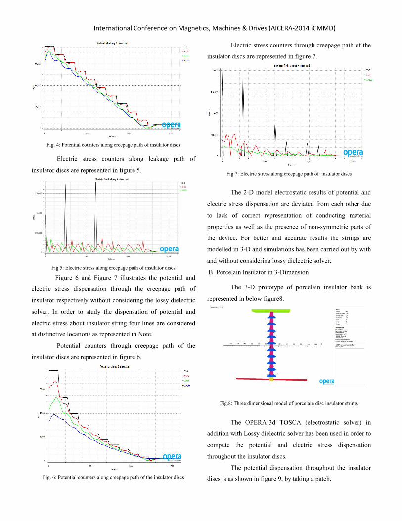
Electric stress counters along leakage path of
insulator discs are represented in figure 5.
Fig 5: Electric stress along creepage path of insulator discs
Figure 6 and Figure 7 illustrates the potential and
electric stress dispensation through the creepage path of
insulator respectively without considering the lossy dielectric
solver. In order to study the dispensation of potential and
electric stress about insulator string four lines are considered
at distinctive locations as represented in Note.
Potential counters through creepage path of the
insulator discs are represented in figure 6.
Fig. 6: Potential counters along creepage path of the insulator discs
Electric stress counters through creepage path of the
insulator discs are represented in figure 7.
Fig 7: Electric stress along creepage path of insulator discs
The 2-D model electrostatic results of potential and
electric stress dispensation are deviated from each other due
to lack of correct representation of conducting material
properties as well as the presence of non-symmetric parts of
the device. For better and accurate results the strings are
modelled in 3-D and simulations has been carried out by with
and without considering lossy dielectric solver.
B. Porcelain Insulator in 3-Dimension
The 3-D prototype of porcelain insulator bank is
represented in below figure8.
Fig.8: Three dimensional model of porcelain disc insulator string.
The OPERA-3d TOSCA (electrostatic solver) in
addition with Lossy dielectric solver has been used in order to
compute the potential and electric stress dispensation
throughout the insulator discs.
The potential dispensation throughout the insulator
discs is as shown in figure 9, by taking a patch.

International Conference on Magnetics, Machines & Drives (AICERA-2014 iCMMD)
Fig.9: Potential dispensation in and around the surface of insulator discs
The Electric stress dispensation throughout the
insulator discs is as shown in figure 10, by taking a patch.
Fig.10: Electric stress dispensation in and around the surface of
insulator discs
Figure 11 represents the potential dispensation
through the creepage path of the insulator surface. Figure 12
represents the electric stress the same path. Perfect agreement
had been acquired from the results.
In order to study the dispensation of potential and
electric stress on insulator string four lines are considered at
distinctive locations as represented in Note.
The potential counters through creepage path of the
insulator discs are represented in figure 11.
Fig.11. Potential counters along leakage path of the insulator discs
The Electric stress counters through creepage path of
the insulator discs are shown in figure 12.
Fig.12: Electric stress counters along leakage path of the insulator discs.
Figure 13 and Figure 14 illustrates the potential and
electric stress dispensation over the leakage path of the
insulator respectively without considering the lossy dielectric
solver.
In order to understand the dispensation of potential
and electric stress about insulator string four lines are
considered at distinctive locations as represented in Note.
The potential counters through creepage path of the
insulator discs are shown in figure 13.

International Conference on Magnetics, Machines & Drives (AICERA-2014 iCMMD)
Fig.13. Potential counters along creepage path of the insulator discs
The Electric stress counters through creepage path of
the insulator discs are shown in figure 14.
Fig.14: Electric stress counters along creepage path of the insulator discs.
VI. CONCLUSION
In the present work the authors attempt to
understand potential and electric stress dispensation of
porcelain insulator string using FEM. Calculation of potential
and electric stress are useful to indicate sensitive areas of
insulator units those which are prone to breakdown. For this
132 KV insulator strings are modelled in 2-D and 3-D,
simulations were carried out using OPERA. The 3-D
prototype of an insulator bank in addition with a conductor of
transmission line had finely modelled which for the
improvement of simulation accuracy. By observing the plots
a good agreement has been ascertained between the results
obtained from both 2-D and 3-D. The results obtained in 2-D
with lossy dielectric solver are nearly equal to 3-D results
(with and without LD solver). It is conformed from the results
obtained that the most sensitive areas of electric stress are at
the triple junction of the bottom disc of insulator unit. It has
also consummate, by moving away from the string, the
dispensation of potential & electric stress decreases. This
approach can be applied to any type of insulators which gives
accurate results in economic way, which helps the
manufacturers and High Voltage planers to make selection of
right insulator.
ACKNOWLEDGEMENTS
Authors want to acknowledge the department of
A.P.TRANSCO especially to P.Ganesh Reddy - Assistant
Engineer - Rajampeta for providing the technical parameters
of Insulators.
REFERENCES [1] "Investigation on the characteristics of a string of insulator due to
the effect of dirt", by S.M.A. Dhalaan, and M.A. Elhirbawy in Transmission and Dispensation Conference and Exposition,200 IEEE PES, 7-12 September 2003, Vol. 3, pp. 915-920.
[2] "Simulation of voltage distribution calculation methods over a
string of suspension insulators", by S.M.A. Dhalaan, and M.A. Elhirbawy, in Transmission and Dispensation Conference and Exposition, 2003 IEEE PES, 7 -12 September 2003, Vol. 3, pp. 909 – 914.
[3] V. T. Kontargyri, I. F. Gonos, I. A. Stathopulos, A.M.
Michaelidis, "Calculation of the Electric stress on an insulator using the Finite Elements Method", 38th International Universities Power Engineering Conference (UPEC 2003), Thessaloniki, Greece, September 1-3, 2003, pp. 65-68.
[4] "Electric field and voltage distribution along insulators under pollution conditions", by V. T. Kontargyri, , I. A. Stathopulos, I. F. Gonos, N. C. Ilia in 4th Mediterranean IEE Conference and Exhibition on Power Generation, Transmission, Dispensation and Energy Conversion (Med Power 2004), Lemesos, Cyprus, November 15 -17, 2004.
[5] "Calculation of the Electric field on an insulator using the Finite Elements Method", by, I. F. Gonos, I. A. Stathopulos, V. T. Kontargyri , A.M. Michaelides, at 38th International Universities Power Engineering Conference (UPEC 2003), Thessaloniki, Greece, September 1-3, 2003, pp. 65-68.
[6] Measurement and Verification of the Voltage Distribution on
High Voltage Insulators", by V.T. Kontargyri, I.F. Gonos, I.A. Stathopoulos, A.M. Michaelides, 12th Biennial IEEE Conference on Electromagnetic Field Computation, May 1 -3, 2006, pp. 326 – 326.
[7] “Simulation of the Electric field on Composite Insulators using
the Finite Element method” by V.T.KONTARGYRI , I.F.GONOS,N.C.ILIA, I,.A.STATHOPULOS.
[8] “ Simulation of the Electric field Dispensation on Ceramic
Insulator Using Finite Element method”, by Sh.M.Faisal, European Transactions on Electrical Power, Vol 19, No 3, (2009) , pp.526-531.

International Conference on Magnetics, Machines & Drives (AICERA-2014 iCMMD)
[9] “Measurement and Simulation of the Electric field of high voltage Suspension Insulators”, by Vassiliki T.Kontargyri , Ioannis F. Gonos and Ioannis A. Statthopulos, in European Transactions on Electrical Power, Vol 19, No 3, (2009) , pp.509-517.
[10] J.L. Rasolonjanahary, L. Krähenbühl, A. Nicolas, “Computation
of Electric stresss and potential on polluted insulators using a boundary element method”, IEEE Transactions on Magnetics, Vol. 28, No. 2, March 1992, pp. 1473-1476.
[11] Vector Fields, “OPERA-2d & 3-d User Guide”, Vector Fields
Limited, England, 1999.
Dr.M.Padma Lalitha obtained graduate
degree in Electrical & Electronics
Engineering from JNTU, Anathapur in the
year 1994. Obtained Masters (PSOC) from
SriVenkateswara.University, Tirupathi in
2002 and awarded doctorate for“Soft
Computing Techniques for optimal DG
placement in Radial Dispensation System “
from Sri Venketeswara.University,. in 2011 and Having 17 years of teaching
experience for graduate and post graduate level. Editorial board member for
Reputed International Journals. Has 50 international journal publications to
her credit and also published two books . Presently working as Professor and
HOD of EEE department in AITS, Rajampet. Areas of interest include radial
dispensation systems, soft computing in power systems, ANN, FACTS ,
Design of Electro Magnetic devices.
K.Venkata Pavan Kumar obtained graduate
degree in Electrical & Electronics Engineering
from JNTU-Ananthapur in the year 2012. He is
currently pursuing his Post Graduation in
Annamacharya Institute of Technology &
Sciences – Rajampeta (Autonomous). He is
presently working as Intern in Icon Design
Automation Pvt. Ltd-Bangalore.His areas of
interest includes Design of Power System applications, Modeling and
controlling of electrical machines, Finite Element Analysis of
electromagnetic devices , Dispensation Systems
Venkatesu Samala obtained graduate
degree in Electrical Electronics
Engineering from JNTU, Hyderabad in
the year 2006. He obtained PG
Diploma in VLSI from Semi-conductor
Laboratory, Chandigarh in 2007. He
has half decade of acquaintance and
experience for supporting the Low
Frequency Electromagnetic applications
involving Design, & Analysis. He has expertise in electromagnetic analysis
of electrical machines using Vector Fields Opera 2D / 3D FEA and analysis
of BLDC and Induction machines. Verification of electromagnetic actuators,
magnet systems and transformers electromagnetic design analysis. Areas of
interest include Finite Element Analysis (FEA), Machine Design & Analysis
and Design of Power System applications.
Copyright © 2022 FDOKUMEN