
MIPI Alliance Specification for RF Front-End Control Interface
90
MIPI ® Alliance Specification for RF Front-End Control Interface Version 1.10 26-Jul-2011 MIPI Alliance Specification for RFFE Version 1.10 – 26 July 2011 MIPI Board Approved 2-Nov-2011 Copyright © 2009-2011 MIPI Alliance, Inc. All rights reserved. MIPI Alliance Member Confidential Further technical changes to this document are expected as work continues in the RF Front-End Control Working Group
-
Upload
khangminh22 -
Category
Documents
-
view
0 -
download
0
Transcript of MIPI Alliance Specification for RF Front-End Control Interface

MIPI® Alliance Specification forRF Front-End Control Interface
Version 1.10 26-Jul-2011 MIPI Alliance Specification for RFFE
Version 1.10 – 26 July 2011
MIPI Board Approved 2-Nov-2011
Copyright © 2009-2011 MIPI Alliance, Inc. All rights reserved.MIPI Alliance Member Confidential
Further technical changes to this document are expected as work continues in the RF Front-End ControlWorking Group

Copyright © 2009-2011 MIPI Alliance, Inc. All rights reserved.MIPI Alliance Member Confidential
ii
Version 1.10 26-Jul-2011 MIPI Alliance Specification for RFFE
NOTICE OF DISCLAIMER
The material contained herein is not a license, either expressly or impliedly, to any IPR owned or controlledby any of the authors or developers of this material or MIPI®. The material contained herein is provided onan “AS IS” basis and to the maximum extent permitted by applicable law, this material is provided AS ISAND WITH ALL FAULTS, and the authors and developers of this material and MIPI hereby disclaim allother warranties and conditions, either express, implied or statutory, including, but not limited to, any (ifany) implied warranties, duties or conditions of merchantability, of fitness for a particular purpose, ofaccuracy or completeness of responses, of results, of workmanlike effort, of lack of viruses, and of lack ofnegligence.
All materials contained herein are protected by copyright laws, and may not be reproduced, republished,distributed, transmitted, displayed, broadcast or otherwise exploited in any manner without the express priorwritten permission of MIPI Alliance. MIPI, MIPI Alliance and the dotted rainbow arch and all relatedtrademarks, tradenames, and other intellectual property are the exclusive property of MIPI Alliance andcannot be used without its express prior written permission.
ALSO, THERE IS NO WARRANTY OF CONDITION OF TITLE, QUIET ENJOYMENT, QUIETPOSSESSION, CORRESPONDENCE TO DESCRIPTION OR NON-INFRINGEMENT WITH REGARDTO THIS MATERIAL OR THE CONTENTS OF THIS DOCUMENT. IN NO EVENT WILL ANYAUTHOR OR DEVELOPER OF THIS MATERIAL OR THE CONTENTS OF THIS DOCUMENT ORMIPI BE LIABLE TO ANY OTHER PARTY FOR THE COST OF PROCURING SUBSTITUTE GOODSOR SERVICES, LOST PROFITS, LOSS OF USE, LOSS OF DATA, OR ANY INCIDENTAL,CONSEQUENTIAL, DIRECT, INDIRECT, OR SPECIAL DAMAGES WHETHER UNDERCONTRACT, TORT, WARRANTY, OR OTHERWISE, ARISING IN ANY WAY OUT OF THIS OR ANYOTHER AGREEMENT, SPECIFICATION OR DOCUMENT RELATING TO THIS MATERIAL,WHETHER OR NOT SUCH PARTY HAD ADVANCE NOTICE OF THE POSSIBILITY OF SUCHDAMAGES.
Without limiting the generality of this Disclaimer stated above, the user of the contents of this Document isfurther notified that MIPI: (a) does not evaluate, test or verify the accuracy, soundness or credibility of thecontents of this Document; (b) does not monitor or enforce compliance with the contents of this Document;and (c) does not certify, test, or in any manner investigate products or services or any claims of compliancewith the contents of this Document. The use or implementation of the contents of this Document mayinvolve or require the use of intellectual property rights (“IPR”) including (but not limited to) patents, patentapplications, or copyrights owned by one or more parties, whether or not Members of MIPI. MIPI does notmake any search or investigation for IPR, nor does MIPI require or request the disclosure of any IPR orclaims of IPR as respects the contents of this Document or otherwise.
Questions pertaining to this document, or the terms or conditions of its provision, should be addressed to:
MIPI Alliance, Inc.c/o IEEE-ISTO445 Hoes LanePiscataway, NJ 08854Attn: Board Secretary

Copyright © 2009-2011 MIPI Alliance, Inc. All rights reserved.MIPI Alliance Member Confidential
iii
Version 1.10 26-Jul-2011 MIPI Alliance Specification for RFFE
ContentsContents . . . . . . . . . . . . . . . . . . . . . . . . . . . . . . . . . . . . . . . . . . . . . . . . . . . . . . . . . . . . . . iii
Figures . . . . . . . . . . . . . . . . . . . . . . . . . . . . . . . . . . . . . . . . . . . . . . . . . . . . . . . . . . . . . . . vi
Tables . . . . . . . . . . . . . . . . . . . . . . . . . . . . . . . . . . . . . . . . . . . . . . . . . . . . . . . . . . . . . . . viii
Release History . . . . . . . . . . . . . . . . . . . . . . . . . . . . . . . . . . . . . . . . . . . . . . . . . . . . . . . . ix
1 Introduction . . . . . . . . . . . . . . . . . . . . . . . . . . . . . . . . . . . . . . . . . . . . . . . . . . . . . . . 101.1 Scope . . . . . . . . . . . . . . . . . . . . . . . . . . . . . . . . . . . . . . . . . . . . . . . . . . . . . . . . . . . . . . . 101.2 Purpose . . . . . . . . . . . . . . . . . . . . . . . . . . . . . . . . . . . . . . . . . . . . . . . . . . . . . . . . . . . . . 11
2 Terminology . . . . . . . . . . . . . . . . . . . . . . . . . . . . . . . . . . . . . . . . . . . . . . . . . . . . . . . 122.1 Definitions . . . . . . . . . . . . . . . . . . . . . . . . . . . . . . . . . . . . . . . . . . . . . . . . . . . . . . . . . . . 122.2 Abbreviations . . . . . . . . . . . . . . . . . . . . . . . . . . . . . . . . . . . . . . . . . . . . . . . . . . . . . . . . 132.3 Acronyms . . . . . . . . . . . . . . . . . . . . . . . . . . . . . . . . . . . . . . . . . . . . . . . . . . . . . . . . . . . 13
3 References . . . . . . . . . . . . . . . . . . . . . . . . . . . . . . . . . . . . . . . . . . . . . . . . . . . . . . . . . 15
4 Architecture and Operations Overview . . . . . . . . . . . . . . . . . . . . . . . . . . . . . . . . . 164.1 Overview . . . . . . . . . . . . . . . . . . . . . . . . . . . . . . . . . . . . . . . . . . . . . . . . . . . . . . . . . . . . 16
4.1.1 Topology . . . . . . . . . . . . . . . . . . . . . . . . . . . . . . . . . . . . . . . . . . . . . . . . . . . . . . . . . . 174.1.1.1 Basic. . . . . . . . . . . . . . . . . . . . . . . . . . . . . . . . . . . . . . . . . . . . . . . . . . . . . . . . . . . 174.1.1.2 Diversity. . . . . . . . . . . . . . . . . . . . . . . . . . . . . . . . . . . . . . . . . . . . . . . . . . . . . . . . 184.1.1.3 MIMO . . . . . . . . . . . . . . . . . . . . . . . . . . . . . . . . . . . . . . . . . . . . . . . . . . . . . . . . . 194.1.1.4 Dual-Bus Basic . . . . . . . . . . . . . . . . . . . . . . . . . . . . . . . . . . . . . . . . . . . . . . . . . . 204.1.1.5 Dual-Bus MIMO . . . . . . . . . . . . . . . . . . . . . . . . . . . . . . . . . . . . . . . . . . . . . . . . . 21
4.1.2 Device Identification . . . . . . . . . . . . . . . . . . . . . . . . . . . . . . . . . . . . . . . . . . . . . . . . . 224.2 Read and Write Timing . . . . . . . . . . . . . . . . . . . . . . . . . . . . . . . . . . . . . . . . . . . . . . . . . 23
4.2.1 RFFE Clock (SCLK) . . . . . . . . . . . . . . . . . . . . . . . . . . . . . . . . . . . . . . . . . . . . . . . . . 234.2.1.1 Specifications for the Master SCLK Driver. . . . . . . . . . . . . . . . . . . . . . . . . . . . . 234.2.1.2 Specifications for SCLK Input. . . . . . . . . . . . . . . . . . . . . . . . . . . . . . . . . . . . . . . 25
4.2.2 RFFE Data (SDATA). . . . . . . . . . . . . . . . . . . . . . . . . . . . . . . . . . . . . . . . . . . . . . . . . 254.2.2.1 Specifications for the SDATA Driver . . . . . . . . . . . . . . . . . . . . . . . . . . . . . . . . . 254.2.2.2 Specifications for the SDATA Receiver . . . . . . . . . . . . . . . . . . . . . . . . . . . . . . . 27
4.2.3 Read/Write Access. . . . . . . . . . . . . . . . . . . . . . . . . . . . . . . . . . . . . . . . . . . . . . . . . . . 284.2.4 Write Access . . . . . . . . . . . . . . . . . . . . . . . . . . . . . . . . . . . . . . . . . . . . . . . . . . . . . . . 28
4.3 Operating States . . . . . . . . . . . . . . . . . . . . . . . . . . . . . . . . . . . . . . . . . . . . . . . . . . . . . . 284.3.1 STARTUP . . . . . . . . . . . . . . . . . . . . . . . . . . . . . . . . . . . . . . . . . . . . . . . . . . . . . . . . . 294.3.2 ACTIVE. . . . . . . . . . . . . . . . . . . . . . . . . . . . . . . . . . . . . . . . . . . . . . . . . . . . . . . . . . . 294.3.3 LOW POWER . . . . . . . . . . . . . . . . . . . . . . . . . . . . . . . . . . . . . . . . . . . . . . . . . . . . . . 294.3.4 SHUTDOWN . . . . . . . . . . . . . . . . . . . . . . . . . . . . . . . . . . . . . . . . . . . . . . . . . . . . . . 304.3.5 Exceptional State Transitions . . . . . . . . . . . . . . . . . . . . . . . . . . . . . . . . . . . . . . . . . . 30
5 Physical Layer . . . . . . . . . . . . . . . . . . . . . . . . . . . . . . . . . . . . . . . . . . . . . . . . . . . . . 315.1 I/O Structures . . . . . . . . . . . . . . . . . . . . . . . . . . . . . . . . . . . . . . . . . . . . . . . . . . . . . . . . 31
5.1.1 Signaling Voltages . . . . . . . . . . . . . . . . . . . . . . . . . . . . . . . . . . . . . . . . . . . . . . . . . . . 325.1.2 I/O Configuration with Multiple Slaves . . . . . . . . . . . . . . . . . . . . . . . . . . . . . . . . . . 33
5.2 VIO Supply . . . . . . . . . . . . . . . . . . . . . . . . . . . . . . . . . . . . . . . . . . . . . . . . . . . . . . . . . . 34

Copyright © 2009-2011 MIPI Alliance, Inc. All rights reserved.MIPI Alliance Member Confidential
iv
Version 1.10 26-Jul-2011 MIPI Alliance Specification for RFFE
5.2.1 Power-On (STARTUP) . . . . . . . . . . . . . . . . . . . . . . . . . . . . . . . . . . . . . . . . . . . . . . . 365.2.2 Power-Off (SHUTDOWN) . . . . . . . . . . . . . . . . . . . . . . . . . . . . . . . . . . . . . . . . . . . . 375.2.3 Reset . . . . . . . . . . . . . . . . . . . . . . . . . . . . . . . . . . . . . . . . . . . . . . . . . . . . . . . . . . . . . 38
5.3 Device Characterization . . . . . . . . . . . . . . . . . . . . . . . . . . . . . . . . . . . . . . . . . . . . . . . . 395.4 EMI . . . . . . . . . . . . . . . . . . . . . . . . . . . . . . . . . . . . . . . . . . . . . . . . . . . . . . . . . . . . . . . . 39
5.4.1 EMI for Readback . . . . . . . . . . . . . . . . . . . . . . . . . . . . . . . . . . . . . . . . . . . . . . . . . . . 40
6 Protocol Layer . . . . . . . . . . . . . . . . . . . . . . . . . . . . . . . . . . . . . . . . . . . . . . . . . . . . . 416.1 Bit Ordering. . . . . . . . . . . . . . . . . . . . . . . . . . . . . . . . . . . . . . . . . . . . . . . . . . . . . . . . . . 416.2 Command Sequences . . . . . . . . . . . . . . . . . . . . . . . . . . . . . . . . . . . . . . . . . . . . . . . . . . 41
6.2.1 Sequence Start Condition . . . . . . . . . . . . . . . . . . . . . . . . . . . . . . . . . . . . . . . . . . . . . 416.2.2 Frames . . . . . . . . . . . . . . . . . . . . . . . . . . . . . . . . . . . . . . . . . . . . . . . . . . . . . . . . . . . . 42
6.2.2.1 Command Frame . . . . . . . . . . . . . . . . . . . . . . . . . . . . . . . . . . . . . . . . . . . . . . . . . 426.2.2.2 Data or Address Frame . . . . . . . . . . . . . . . . . . . . . . . . . . . . . . . . . . . . . . . . . . . . 426.2.2.3 No Response Frame . . . . . . . . . . . . . . . . . . . . . . . . . . . . . . . . . . . . . . . . . . . . . . . 42
6.2.3 Parity Bit . . . . . . . . . . . . . . . . . . . . . . . . . . . . . . . . . . . . . . . . . . . . . . . . . . . . . . . . . . 436.2.3.1 Error Detection and Handling . . . . . . . . . . . . . . . . . . . . . . . . . . . . . . . . . . . . . . . 43
6.2.4 Bus Park Cycle . . . . . . . . . . . . . . . . . . . . . . . . . . . . . . . . . . . . . . . . . . . . . . . . . . . . . 446.3 Bus Idle Condition. . . . . . . . . . . . . . . . . . . . . . . . . . . . . . . . . . . . . . . . . . . . . . . . . . . . . 446.4 RFFE Command Sequences . . . . . . . . . . . . . . . . . . . . . . . . . . . . . . . . . . . . . . . . . . . . . 456.5 Broadcast Messages . . . . . . . . . . . . . . . . . . . . . . . . . . . . . . . . . . . . . . . . . . . . . . . . . . . 476.6 RFFE Register Space. . . . . . . . . . . . . . . . . . . . . . . . . . . . . . . . . . . . . . . . . . . . . . . . . . . 476.7 Command Sequences . . . . . . . . . . . . . . . . . . . . . . . . . . . . . . . . . . . . . . . . . . . . . . . . . . 48
6.7.1 Command Sequence Summary . . . . . . . . . . . . . . . . . . . . . . . . . . . . . . . . . . . . . . . . . 486.7.2 Command Sequence Descriptions . . . . . . . . . . . . . . . . . . . . . . . . . . . . . . . . . . . . . . . 48
6.7.2.1 Extended Register Write Command Sequence . . . . . . . . . . . . . . . . . . . . . . . . . . 486.7.2.2 Extended Register Read Command Sequence. . . . . . . . . . . . . . . . . . . . . . . . . . . 496.7.2.3 Extended Register Write Long Command Sequence. . . . . . . . . . . . . . . . . . . . . . 516.7.2.4 Extended Register Read Long Command Sequence . . . . . . . . . . . . . . . . . . . . . . 536.7.2.5 Register Write Command Sequence . . . . . . . . . . . . . . . . . . . . . . . . . . . . . . . . . . 556.7.2.6 Register Read Command Sequence . . . . . . . . . . . . . . . . . . . . . . . . . . . . . . . . . . . 566.7.2.7 Register 0 Write Command Sequence . . . . . . . . . . . . . . . . . . . . . . . . . . . . . . . . . 56
6.7.3 Half Speed Read Access . . . . . . . . . . . . . . . . . . . . . . . . . . . . . . . . . . . . . . . . . . . . . . 576.8 Device Enumeration . . . . . . . . . . . . . . . . . . . . . . . . . . . . . . . . . . . . . . . . . . . . . . . . . . . 58
6.8.1 Slave Device Identifier . . . . . . . . . . . . . . . . . . . . . . . . . . . . . . . . . . . . . . . . . . . . . . . 586.8.2 Unique Slave Identifier . . . . . . . . . . . . . . . . . . . . . . . . . . . . . . . . . . . . . . . . . . . . . . . 596.8.3 Programmable USID . . . . . . . . . . . . . . . . . . . . . . . . . . . . . . . . . . . . . . . . . . . . . . . . . 60
6.9 Slave Device Address Mapping . . . . . . . . . . . . . . . . . . . . . . . . . . . . . . . . . . . . . . . . . . 646.9.1 Slave Device Reserved Addresses. . . . . . . . . . . . . . . . . . . . . . . . . . . . . . . . . . . . . . . 64
6.9.1.1 PRODUCT_ID. . . . . . . . . . . . . . . . . . . . . . . . . . . . . . . . . . . . . . . . . . . . . . . . . . . 656.9.1.2 MANUFACTURER_ID . . . . . . . . . . . . . . . . . . . . . . . . . . . . . . . . . . . . . . . . . . . 656.9.1.3 USID . . . . . . . . . . . . . . . . . . . . . . . . . . . . . . . . . . . . . . . . . . . . . . . . . . . . . . . . . . 656.9.1.4 PM_TRIG . . . . . . . . . . . . . . . . . . . . . . . . . . . . . . . . . . . . . . . . . . . . . . . . . . . . . . 65
6.9.1.4.1 POWER MODES . . . . . . . . . . . . . . . . . . . . . . . . . . . . . . . . . . . . . . . . . . . . 656.9.1.4.2 Trigger Modes . . . . . . . . . . . . . . . . . . . . . . . . . . . . . . . . . . . . . . . . . . . . . . . 68
6.10 Slaves With Delayed Readback . . . . . . . . . . . . . . . . . . . . . . . . . . . . . . . . . . . . . . . . . . 686.10.1 Repeat the Register Read Command Sequence. . . . . . . . . . . . . . . . . . . . . . . . . . . . . 696.10.2 Repeat the Register Read Command Sequence with Multiple Register Reads. . . . . 70

Copyright © 2009-2011 MIPI Alliance, Inc. All rights reserved.MIPI Alliance Member Confidential
v
Version 1.10 26-Jul-2011 MIPI Alliance Specification for RFFE
6.10.3 Pre-Write a Register. . . . . . . . . . . . . . . . . . . . . . . . . . . . . . . . . . . . . . . . . . . . . . . . . . 716.10.4 Use an Extended Register Read Command Sequence. . . . . . . . . . . . . . . . . . . . . . . . 73
7 Applications . . . . . . . . . . . . . . . . . . . . . . . . . . . . . . . . . . . . . . . . . . . . . . . . . . . . . . . 757.1 Programming Model . . . . . . . . . . . . . . . . . . . . . . . . . . . . . . . . . . . . . . . . . . . . . . . . . . . 75
7.1.1 Basic Control Related Items . . . . . . . . . . . . . . . . . . . . . . . . . . . . . . . . . . . . . . . . . . . 757.1.1.1 Command Sequence Building . . . . . . . . . . . . . . . . . . . . . . . . . . . . . . . . . . . . . . . 757.1.1.2 Control Scheduling and Timing Considerations . . . . . . . . . . . . . . . . . . . . . . . . . 76
7.1.2 Procedures . . . . . . . . . . . . . . . . . . . . . . . . . . . . . . . . . . . . . . . . . . . . . . . . . . . . . . . . . 777.1.2.1 Precise Access Timing. . . . . . . . . . . . . . . . . . . . . . . . . . . . . . . . . . . . . . . . . . . . . 77
7.1.2.1.1 Write Access . . . . . . . . . . . . . . . . . . . . . . . . . . . . . . . . . . . . . . . . . . . . . . . . 777.1.2.1.2 Read Access. . . . . . . . . . . . . . . . . . . . . . . . . . . . . . . . . . . . . . . . . . . . . . . . . 77
7.1.2.2 Provisioning of Additional Clocks for Processing. . . . . . . . . . . . . . . . . . . . . . . . 787.2 Command Sequence Timing . . . . . . . . . . . . . . . . . . . . . . . . . . . . . . . . . . . . . . . . . . . . . 787.3 Additional Configurations. . . . . . . . . . . . . . . . . . . . . . . . . . . . . . . . . . . . . . . . . . . . . . . 79
7.3.1 Multiple Logical Slaves in one Device . . . . . . . . . . . . . . . . . . . . . . . . . . . . . . . . . . . 797.4 DDB in RFFE . . . . . . . . . . . . . . . . . . . . . . . . . . . . . . . . . . . . . . . . . . . . . . . . . . . . . . . . 79
Annex A Additional Information for RFFE Reference (Informative). . . . . . . . . . . 81A.1 Optional Signals . . . . . . . . . . . . . . . . . . . . . . . . . . . . . . . . . . . . . . . . . . . . . . . . . . . . . . 81
A.1.1 Optional Reset Signal . . . . . . . . . . . . . . . . . . . . . . . . . . . . . . . . . . . . . . . . . . . . . . . . 81A.2 Estimation of RFFE Bus Load Ranges for Various Configurations . . . . . . . . . . . . . . . 81
Annex B Differences between SPMI and RFFE Specifications . . . . . . . . . . . . . . . . 83B.1 Application Environment . . . . . . . . . . . . . . . . . . . . . . . . . . . . . . . . . . . . . . . . . . . . . . . 83B.2 Detailed Differences between SPMI and RFFE Specifications . . . . . . . . . . . . . . . . . . 83
B.2.1 Single Master Operation with Simple Slave Devices.. . . . . . . . . . . . . . . . . . . . . . . . 83B.2.2 No Bus Arbitration . . . . . . . . . . . . . . . . . . . . . . . . . . . . . . . . . . . . . . . . . . . . . . . . . . 83B.2.3 No Bus Arbitration Requests by Slave Devices . . . . . . . . . . . . . . . . . . . . . . . . . . . . 83B.2.4 Limited Command Sequence Set. . . . . . . . . . . . . . . . . . . . . . . . . . . . . . . . . . . . . . . . 83B.2.5 Limited Support for Device Descriptor Block Data . . . . . . . . . . . . . . . . . . . . . . . . . 84B.2.6 Unified Slave Register Space . . . . . . . . . . . . . . . . . . . . . . . . . . . . . . . . . . . . . . . . . . 84B.2.7 Pull-Down Function in Master Device . . . . . . . . . . . . . . . . . . . . . . . . . . . . . . . . . . . 85B.2.8 I/O Drive Strength Classes . . . . . . . . . . . . . . . . . . . . . . . . . . . . . . . . . . . . . . . . . . . . 85B.2.9 High Speed Devices Only . . . . . . . . . . . . . . . . . . . . . . . . . . . . . . . . . . . . . . . . . . . . . 85B.2.10 Explicit Support for Half Speed Read . . . . . . . . . . . . . . . . . . . . . . . . . . . . . . . . . . . . 85B.2.11 EMI . . . . . . . . . . . . . . . . . . . . . . . . . . . . . . . . . . . . . . . . . . . . . . . . . . . . . . . . . . . . . . 85B.2.12 Slave Identifier Allocation. . . . . . . . . . . . . . . . . . . . . . . . . . . . . . . . . . . . . . . . . . . . . 85B.2.13 Register Allocation . . . . . . . . . . . . . . . . . . . . . . . . . . . . . . . . . . . . . . . . . . . . . . . . . . 85B.2.14 VIO Sensing for State Control. . . . . . . . . . . . . . . . . . . . . . . . . . . . . . . . . . . . . . . . . . 85
B.3 SPMI Baseline and Compatibility to RFFE . . . . . . . . . . . . . . . . . . . . . . . . . . . . . . . . . 86B.4 SPMI Register Space. . . . . . . . . . . . . . . . . . . . . . . . . . . . . . . . . . . . . . . . . . . . . . . . . . . 89

Copyright © 2009-2011 MIPI Alliance, Inc. All rights reserved.MIPI Alliance Member Confidential
vi
Version 1.10 26-Jul-2011 MIPI Alliance Specification for RFFE
FiguresFigure 1 RFFE Interface and Bus Structure . . . . . . . . . . . . . . . . . . . . . . . . . . . . . . . . . . . . . . . 17
Figure 2 Basic Configuration . . . . . . . . . . . . . . . . . . . . . . . . . . . . . . . . . . . . . . . . . . . . . . . . . . 18
Figure 3 Diversity Configuration . . . . . . . . . . . . . . . . . . . . . . . . . . . . . . . . . . . . . . . . . . . . . . . 19
Figure 4 MIMO Configuration . . . . . . . . . . . . . . . . . . . . . . . . . . . . . . . . . . . . . . . . . . . . . . . . . 20
Figure 5 Dual-bus Basic Configuration . . . . . . . . . . . . . . . . . . . . . . . . . . . . . . . . . . . . . . . . . . 21
Figure 6 Dual-bus MIMO Configuration . . . . . . . . . . . . . . . . . . . . . . . . . . . . . . . . . . . . . . . . . 22
Figure 7 State Diagram of Programming a New USID . . . . . . . . . . . . . . . . . . . . . . . . . . . . . . 23
Figure 8 Clock Driver Output Waveform Constraints . . . . . . . . . . . . . . . . . . . . . . . . . . . . . . . 24
Figure 9 Received Clock Signal Constraints . . . . . . . . . . . . . . . . . . . . . . . . . . . . . . . . . . . . . . 25
Figure 10 Bus Active Data Transmission Timing Specification . . . . . . . . . . . . . . . . . . . . . . . . 26
Figure 11 Bus Park Cycle Timing . . . . . . . . . . . . . . . . . . . . . . . . . . . . . . . . . . . . . . . . . . . . . . . 27
Figure 12 Bus Active Data Receiver Timing Requirements . . . . . . . . . . . . . . . . . . . . . . . . . . . 28
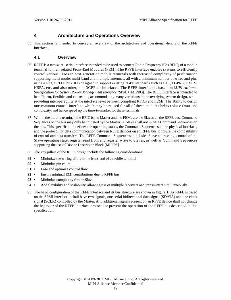
Figure 13 Slave State Diagram . . . . . . . . . . . . . . . . . . . . . . . . . . . . . . . . . . . . . . . . . . . . . . . . . . 29
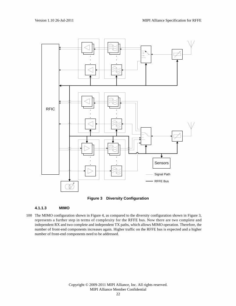
Figure 14 SDATA Master and Slave I/O Cells . . . . . . . . . . . . . . . . . . . . . . . . . . . . . . . . . . . . . 31
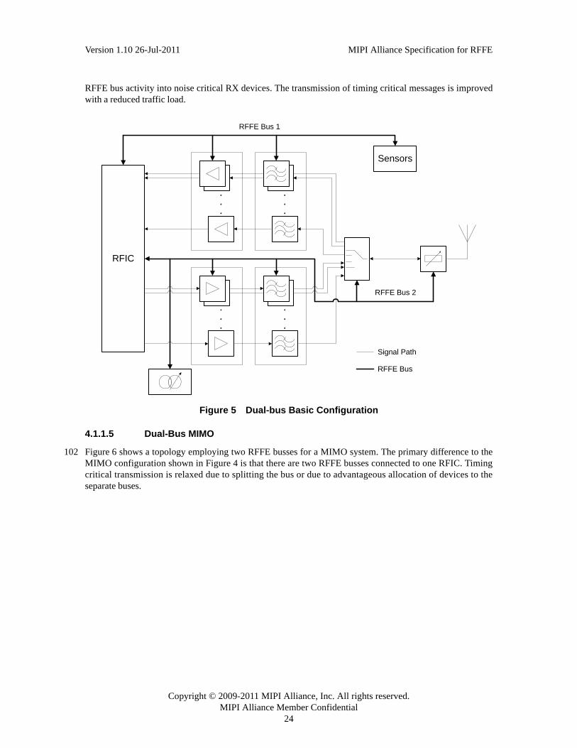
Figure 15 SDATA Master and Slave I/O Cells for an Non-readback Capable Slave . . . . . . . . 31
Figure 16 SCLK Master and Slave I/O Cells . . . . . . . . . . . . . . . . . . . . . . . . . . . . . . . . . . . . . . . 32
Figure 17 VIO Bus Supply . . . . . . . . . . . . . . . . . . . . . . . . . . . . . . . . . . . . . . . . . . . . . . . . . . . . . 33
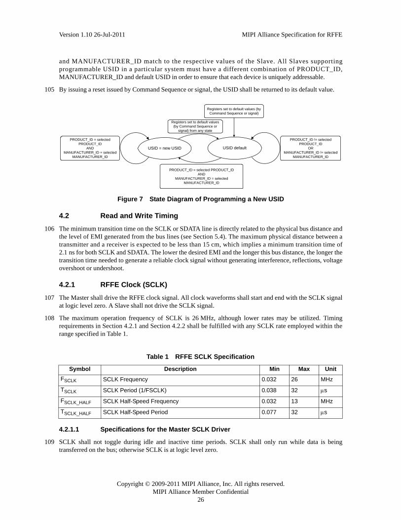
Figure 18 VIO External Bus Supply. . . . . . . . . . . . . . . . . . . . . . . . . . . . . . . . . . . . . . . . . . . . . . 34
Figure 19 Slave VIO Digital . . . . . . . . . . . . . . . . . . . . . . . . . . . . . . . . . . . . . . . . . . . . . . . . . . . . 35
Figure 20 Slave Vreg Digital . . . . . . . . . . . . . . . . . . . . . . . . . . . . . . . . . . . . . . . . . . . . . . . . . . . 35
Figure 21 Requirements for VIO-Initiated Reset . . . . . . . . . . . . . . . . . . . . . . . . . . . . . . . . . . . . 38
Figure 22 Device Characterization Circuit . . . . . . . . . . . . . . . . . . . . . . . . . . . . . . . . . . . . . . . . . 39
Figure 23 Sequence Start Condition . . . . . . . . . . . . . . . . . . . . . . . . . . . . . . . . . . . . . . . . . . . . . . 41
Figure 24 Command Frame . . . . . . . . . . . . . . . . . . . . . . . . . . . . . . . . . . . . . . . . . . . . . . . . . . . . 42
Figure 25 Data or Address Frame. . . . . . . . . . . . . . . . . . . . . . . . . . . . . . . . . . . . . . . . . . . . . . . . 42
Figure 26 No Response Frame . . . . . . . . . . . . . . . . . . . . . . . . . . . . . . . . . . . . . . . . . . . . . . . . . . 43
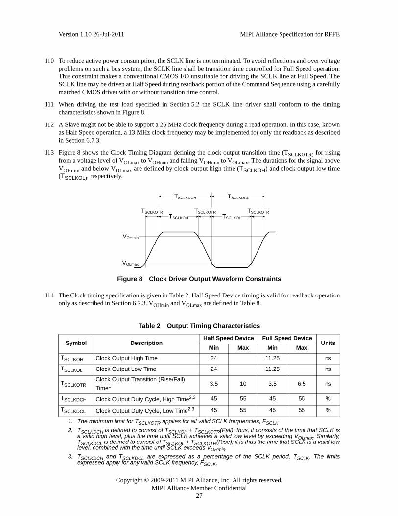
Figure 27 Bus Idle Condition . . . . . . . . . . . . . . . . . . . . . . . . . . . . . . . . . . . . . . . . . . . . . . . . . . . 45
Figure 28 Slave Register Space, RFFE. . . . . . . . . . . . . . . . . . . . . . . . . . . . . . . . . . . . . . . . . . . . 47
Figure 29 Extended Register Write Command Sequence. . . . . . . . . . . . . . . . . . . . . . . . . . . . . . 49
Figure 30 Extended Register Read Command Sequence . . . . . . . . . . . . . . . . . . . . . . . . . . . . . . 51
Figure 31 Extended Register Write Long Command Sequence . . . . . . . . . . . . . . . . . . . . . . . . . 53
Figure 32 Extended Register Read Long Command Sequence . . . . . . . . . . . . . . . . . . . . . . . . . 55

Copyright © 2009-2011 MIPI Alliance, Inc. All rights reserved.MIPI Alliance Member Confidential
vii
Version 1.10 26-Jul-2011 MIPI Alliance Specification for RFFE
Figure 33 Register Write Command Sequence. . . . . . . . . . . . . . . . . . . . . . . . . . . . . . . . . . . . . . 56
Figure 34 Register Read Command Sequence . . . . . . . . . . . . . . . . . . . . . . . . . . . . . . . . . . . . . . 56
Figure 35 Register 0 Write Command Sequence . . . . . . . . . . . . . . . . . . . . . . . . . . . . . . . . . . . . 57
Figure 36 Read Half Speed . . . . . . . . . . . . . . . . . . . . . . . . . . . . . . . . . . . . . . . . . . . . . . . . . . . . . 58
Figure 37 Register Write USID . . . . . . . . . . . . . . . . . . . . . . . . . . . . . . . . . . . . . . . . . . . . . . . . . 61
Figure 38 Extended Register Write USID . . . . . . . . . . . . . . . . . . . . . . . . . . . . . . . . . . . . . . . . . 63
Figure 39 Low Power Mode Applied to Selected Register Bit Values . . . . . . . . . . . . . . . . . . . 67
Figure 40 Repeat the Register Read Command Sequence . . . . . . . . . . . . . . . . . . . . . . . . . . . . . 70
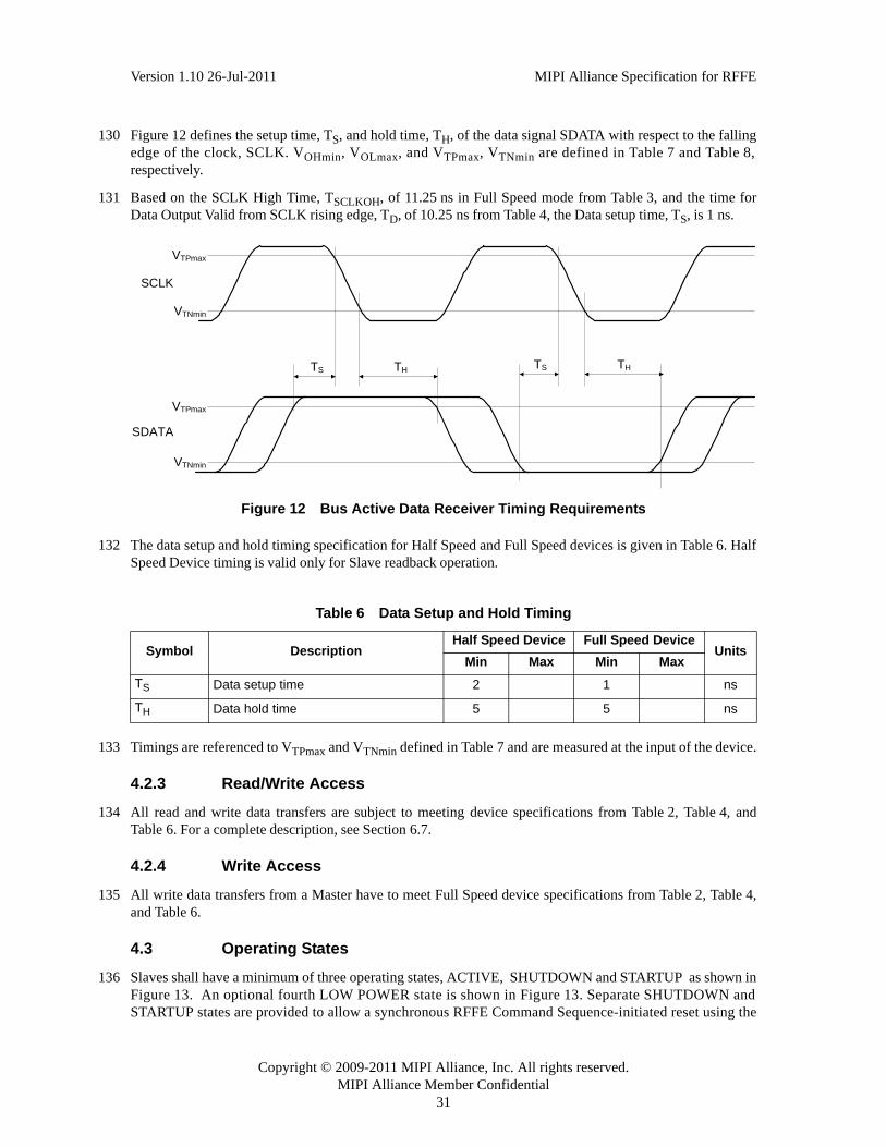
Figure 41 Slow Register Read with Multiple Read Command Sequences. . . . . . . . . . . . . . . . . 71
Figure 42 Pre-Write a Register . . . . . . . . . . . . . . . . . . . . . . . . . . . . . . . . . . . . . . . . . . . . . . . . . . 72
Figure 43 Using an Extended Register Read Command Sequence . . . . . . . . . . . . . . . . . . . . . . 74
Figure 44 Example of Multiple Logical Slaves in Single Device Configuration . . . . . . . . . . . . 79
Figure 45 Slave Register Spaces, SPMI . . . . . . . . . . . . . . . . . . . . . . . . . . . . . . . . . . . . . . . . . . . 89

Copyright © 2009-2011 MIPI Alliance, Inc. All rights reserved.MIPI Alliance Member Confidential
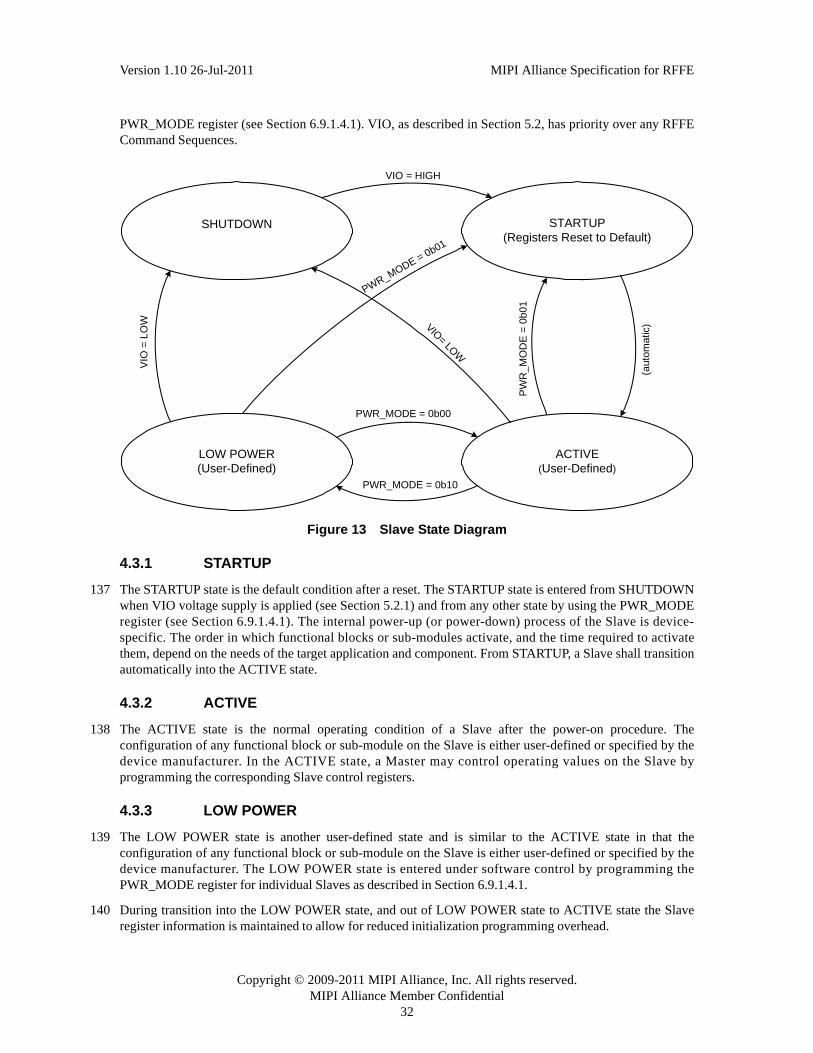
viii
Version 1.10 26-Jul-2011 MIPI Alliance Specification for RFFE
TablesTable 1 RFFE SCLK Specification . . . . . . . . . . . . . . . . . . . . . . . . . . . . . . . . . . . . . . . . . . . . . 23
Table 2 Output Timing Characteristics . . . . . . . . . . . . . . . . . . . . . . . . . . . . . . . . . . . . . . . . . . 24
Table 3 Clock Input Timing Requirements . . . . . . . . . . . . . . . . . . . . . . . . . . . . . . . . . . . . . . . 25
Table 4 SDATA Output Timing Characteristics . . . . . . . . . . . . . . . . . . . . . . . . . . . . . . . . . . . 26
Table 5 SDATA Release Timing Parameters . . . . . . . . . . . . . . . . . . . . . . . . . . . . . . . . . . . . . 27
Table 6 Data Setup and Hold Timing . . . . . . . . . . . . . . . . . . . . . . . . . . . . . . . . . . . . . . . . . . . 28
Table 7 Signaling Parameters . . . . . . . . . . . . . . . . . . . . . . . . . . . . . . . . . . . . . . . . . . . . . . . . . 32
Table 8 Static Electrical Characteristics for Signaling . . . . . . . . . . . . . . . . . . . . . . . . . . . . . . 33
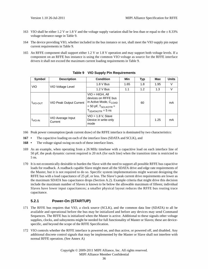
Table 9 VIO Supply Pin Requirements . . . . . . . . . . . . . . . . . . . . . . . . . . . . . . . . . . . . . . . . . . 36
Table 10 VIO Supply Reset Requirements . . . . . . . . . . . . . . . . . . . . . . . . . . . . . . . . . . . . . . . . 37
Table 11 Error Handling . . . . . . . . . . . . . . . . . . . . . . . . . . . . . . . . . . . . . . . . . . . . . . . . . . . . . . 43
Table 12 RFFE Supported Command Sequences . . . . . . . . . . . . . . . . . . . . . . . . . . . . . . . . . . . 46
Table 13 Slave Identifiers . . . . . . . . . . . . . . . . . . . . . . . . . . . . . . . . . . . . . . . . . . . . . . . . . . . . . 59
Table 14 Programmable USID Registers . . . . . . . . . . . . . . . . . . . . . . . . . . . . . . . . . . . . . . . . . 60
Table 15 Slave Register Mapping . . . . . . . . . . . . . . . . . . . . . . . . . . . . . . . . . . . . . . . . . . . . . . . 64
Table 16 Slave PRODUCT_ID Example . . . . . . . . . . . . . . . . . . . . . . . . . . . . . . . . . . . . . . . . . 65
Table 17 PM_TRIG(7:0) . . . . . . . . . . . . . . . . . . . . . . . . . . . . . . . . . . . . . . . . . . . . . . . . . . . . . . 65
Table 18 Power Modes . . . . . . . . . . . . . . . . . . . . . . . . . . . . . . . . . . . . . . . . . . . . . . . . . . . . . . . 65
Table 19 TRIG_REG Definition . . . . . . . . . . . . . . . . . . . . . . . . . . . . . . . . . . . . . . . . . . . . . . . . 68
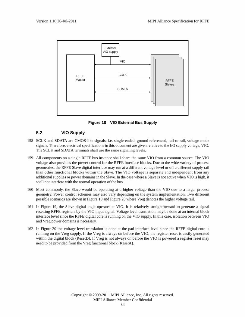
Table 20 Command Sequence Length In SCLK Cycles as Function of Access Type . . . . . . . 75
Table 21 Command Sequence Length Versus Command Sequence Type & Clock Rate . . . . 76
Table 22 Command Sequence Lengths Using Half-Speed Read . . . . . . . . . . . . . . . . . . . . . . . 76
Table 23 Building DDB Level 1 Block . . . . . . . . . . . . . . . . . . . . . . . . . . . . . . . . . . . . . . . . . . . 80
Table 24 RFFE Supported Command Sequences . . . . . . . . . . . . . . . . . . . . . . . . . . . . . . . . . . . 84
Table 25 SPMI Feature Compatibility Matrix. . . . . . . . . . . . . . . . . . . . . . . . . . . . . . . . . . . . . . 86
Copyright © 2009-2011 MIPI Alliance, Inc. All rights reserved.MIPI Alliance Member Confidential
ix
Version 1.10 26-Jul-2011 MIPI Alliance Specification for RFFE
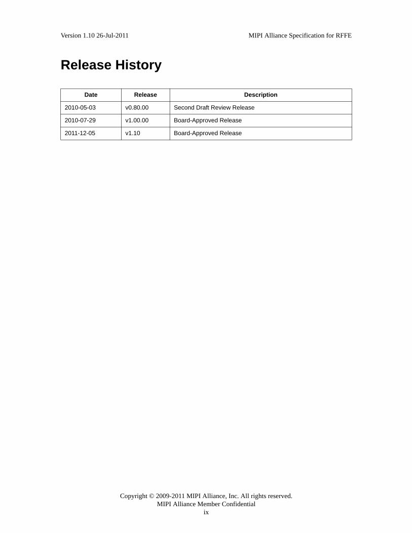
Release History
Date Release Description
2010-05-03 v0.80.00 Second Draft Review Release
2010-07-29 v1.00.00 Board-Approved Release
2011-12-05 v1.10 Board-Approved Release

Copyright © 2009-2011 MIPI Alliance, Inc. All rights reserved.MIPI Alliance Member Confidential
10
Version 1.10 26-Jul-2011 MIPI Alliance Specification for RFFE
1 Introduction
1 The RF Front-End Control Interface (later referred to as RFFE) was developed to offer a common and wide-spread method for controlling RF front-end devices. There are a variety of front-end devices, includingPower Amplifiers (PA), Low-Noise Amplifiers (LNA), filters, switches, power management modules,antenna tuners and sensors. These functions may be located either in separate devices or integrated into asingle device, depending on the application.
2 RFFE should not be confused with the MIPI Alliance DigRF specifications, [MIPI01] and [MIPI02]. DigRFspecifies the interface between the baseband and RF ICs, whereas RFFE is mainly an RF front-end-dedicatedcontrol interface. The key driver for DigRF is to offer a very high-speed interface for carrying digital RF IQdata and RF control information. RFFE, on the other hand, is targeted purely towards the control of RF front-ends, and therefore does not incorporate the signal paths associated with the front-end devices beingcontrolled. DigRF provides only a point-to-point configuration, and thus requires multiple instantiations forcomplex configurations. In contrast to DigRF, RFFE supports point-to-multipoint connectivity, thus allowingfor the control of complex RF systems comprising multiple front-end devices.
3 The trend in mobile radio communications is towards complex multi-radio systems comprised of severalparallel transceivers. This implies a leap in complexity of the RF front-end design. Thus, the RFFE bus mustbe able to operate efficiently in configurations from the simplest one Master and one Slave configuration topotentially multi-Master configurations with tens of Slaves. The emphasis of this version of the specificationis on configurations with only one Master, while also providing for future expansion to multiple Masterconfigurations. Future versions of this specification might thus allow more complex configurations thatprovide for multiple Masters in addition to multiple Slaves.
4 RF front-end modules are sometimes developed in process technologies unlike bulk digital CMOS. Diversetechnology choices are necessary to meet the functional and performance requirements of the application.The downside is that suitability for digital design might be quite low. In some of these technologies theimplementation of digital logic might be costly, so a prerequisite of the RFFE design was to offer options toreduce Slave control complexity to a minimum (approximately 300 to 500 gates). Simplicity has been a coredriver in RFFE development. The RFFE specification, positioned at the low complexity end of all interfaces,is optimized for Master and Slave implementation simplicity without sacrificing a broad set of features.
5 One challenge for RFFE is presented by the need in many radio applications for time-accurate control. This isaddressed in RFFE by utilizing a relatively high bus clock frequency of 26 MHz and by the introduction oftime-accurate triggering mechanisms to allow control of timing-critical functions in multiple devices. This ispredicated on the expectation that a simple Slave lacks the required timing accuracy, and thus is command-driven.
6 The RFFE specification is based on MIPI Alliance Specification for System Power Management Interface(SPMI) [MIPI03] developed by the SPM Working Group. The intention has been to preserve compatibilitywith SPMI by selection of a reduced SPMI feature set in RFFE. RFFE-specific features have been added tothat set. The relevant parts of the SPMI specification are copied into this document to make it a completestand-alone specification. Compatibility to SPMI might be maintained, depending on the impact to the RFFESpecification, by updating the relevant sections in future releases.
1.1 Scope
7 The scope of this document is to specify the control interface for RF front-end devices. Analog signal pathsrequired between front-end devices and other elements that control and utilize the devices, are outside thescope of this document.
8 A voltage reference is introduced as part of the control interface. The implementation of this voltage source isnot specified, although a set of electrical characteristics are defined. This document also defines interface-specific procedures, and also provides alternative means to perform certain actions. Implementers may
Copyright © 2009-2011 MIPI Alliance, Inc. All rights reserved.MIPI Alliance Member Confidential
11
Version 1.10 26-Jul-2011 MIPI Alliance Specification for RFFE
determine which optional procedures and alternative means are supported by a device. Since a Masterimplementation supports all options, the functional choices are intended primarily for Slave deviceimplementations.
1.2 Purpose
9 RFFE provides a low-complexity solution to meet the cost and performance targets of RF front-endcomponents. It offers extensibility from simple configurations with one Slave on a single bus, all the way tocomplex configurations with many Slaves on a single bus, or distributed on multiple buses. This eases boththe RF and front-end module design by requiring a mobile terminal to support only a single control interface.Ideally, this will lead to a broader range of control-compatible components, and to larger markets for RFfront-end devices.

Copyright © 2009-2011 MIPI Alliance, Inc. All rights reserved.MIPI Alliance Member Confidential
12
Version 1.10 26-Jul-2011 MIPI Alliance Specification for RFFE
2 Terminology
10 The MIPI Alliance has adopted Section 13.1 of the IEEE Specifications Style Manual, which dictates use ofthe words “shall”, “should”, “may”, and “can” in the development of documentation, as follows:
11 The word shall is used to indicate mandatory requirements strictly to be followed in orderto conform to the Specification and from which no deviation is permitted (shall equals isrequired to).
12 The use of the word must is deprecated and shall not be used when stating mandatoryrequirements; must is used only to describe unavoidable situations.
13 The use of the word will is deprecated and shall not be used when stating mandatoryrequirements; will is only used in statements of fact.
14 The word should is used to indicate that among several possibilities one is recommended asparticularly suitable, without mentioning or excluding others; or that a certain course ofaction is preferred but not necessarily required; or that (in the negative form) a certaincourse of action is deprecated but not prohibited (should equals is recommended that).
15 The word may is used to indicate a course of action permissible within the limits of theSpecification (may equals is permitted).
16 The word can is used for statements of possibility and capability, whether material,physical, or causal (can equals is able to).
17 All sections are normative, unless they are explicitly indicated to be informative.
18 Numbers are decimal unless otherwise indicated. A prefix of 0x indicates a hexadecimal number, while aprefix of 0b indicates a binary number.
2.1 Definitions
19 Address Frame: A series of nine bits with eight bits representing address information and a single parity bit.
20 Broadcast: A procedure of sending a Command Sequence to multiple recipients simultaneously using eitherBroadcast ID or GSID.
21 Broadcast ID: A unique GSID defined as 0b0000 addressing all Slaves simultaneously.
22 Bus Idle: The RFFE bus is idle when both the SCLK and SDATA are at a logic level zero between the end ofa Command Sequence.
23 Bus Park Cycle: A single clock cycle that occurs when the SDATA signal control may change betweendevices during, or at the end of, a Command Sequence.
24 Command Frame: A series of thirteen bits with four bits representing a Slave address, eight bitsrepresenting an RFFE command and a single parity bit.
25 Command Sequence: A bus transaction on the RFFE bus that begins with a SSC, a Command Frame,potentially Data and Address Frames and ends with a Bus Park Cycle.
26 Data Frame: A series of nine bits with eight bits of data and a single parity bit.
27 Group Slave ID: A 4-bit number assigned to one or more Slaves identifying them on the RFFE bus as agroup.
28 Full Speed: Operating RFFE bus with a fundamental SCLK frequency between 13 MHz and 26 MHz.
29 Half Speed: Operating RFFE bus with a fundamental SCLK frequency between 32 kHz and 13 MHz.
Copyright © 2009-2011 MIPI Alliance, Inc. All rights reserved.MIPI Alliance Member Confidential
13
Version 1.10 26-Jul-2011 MIPI Alliance Specification for RFFE
30 Master: A device on the RFFE bus that drives the SCLK line and controls the transmission of all CommandSequences.
31 No Response Frame: A Data or Address Frame that is used when no applicable data is available.
32 Slave: A device on the RFFE bus that is not capable of driving the SCLK line, i.e. not a Master.
33 Slave ID: A 4-bit number assigned to a Slave. It may be either Unique Slave ID or Group Slave ID.
34 Unique Slave ID: Unique 4-bit number assigned to a Slave identifying it on the bus.
2.2 Abbreviations
35 e.g. For example (Latin: exempli gratia)
36 i.e. That is (Latin: id est)
37 High-Z High impedance
38 SDATA RFFE data
39 SCLK RFFE clock
40 SCLKint Internal serial clock used within a Master
41 VIO RFFE Bus I/O Voltage Level
2.3 Acronyms
42 3GPP 3rd Generation Partnership Project
43 ASM Antenna Switch Module
44 DDB Device Descriptor Block
45 EDGE Enhanced Data-Rates from GSM Evolution
46 EGPRS Enhanced General Packet Radio System
47 EMI Electromagnetic Interference
48 FEM Front-End Module
49 GPRS General Packet Radio System
50 GSID Group Slave Identifier
51 GSM Global System for Mobile Communications
52 HSPA High Speed Packet Access
53 HW Hardware
54 IC Integrated Circuit
55 IEEE Institute of Electrical and Electronics Engineers
56 ISTO Industry Standards and Technology Organization
57 I/O Input/Output
58 LSB Least Significant Bit
59 LTE Long Term Evolution

Copyright © 2009-2011 MIPI Alliance, Inc. All rights reserved.MIPI Alliance Member Confidential
14
Version 1.10 26-Jul-2011 MIPI Alliance Specification for RFFE
60 MIMO Multiple Input Multiple Output
61 MIPI Mobile Industry Processor Interface
62 MSB Most Significant Bit
63 PA Power Amplifier
64 PCB Printed Circuit Board
65 RF Radio Frequency
66 RFFE RF Front-End Control Interface
67 RFIC Radio Frequency Integrated Circuit
68 RX Receiver
69 RCS Request Capable Slave
70 SA Slave Address
71 SW Software
72 SID Slave Identifier
73 SSC Sequence Start Condition
74 SPM System Power Management
75 SPMI System Power Management Interface
76 TX Transmitter
77 UMTS Universal Mobile Telecommunications System
78 USID Unique Slave Identifier
Copyright © 2009-2011 MIPI Alliance, Inc. All rights reserved.MIPI Alliance Member Confidential
15
Version 1.10 26-Jul-2011 MIPI Alliance Specification for RFFE
3 References
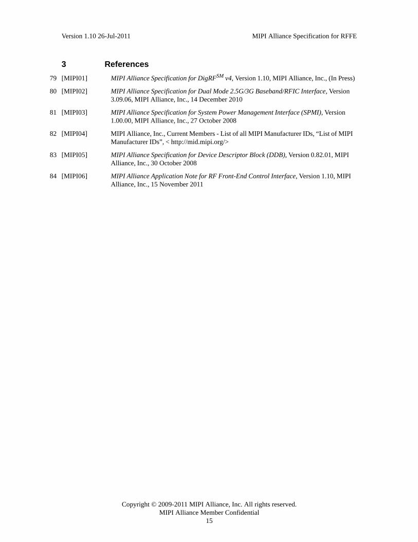
79 [MIPI01] MIPI Alliance Specification for DigRFSM v4, Version 1.10, MIPI Alliance, Inc., (In Press)
80 [MIPI02] MIPI Alliance Specification for Dual Mode 2.5G/3G Baseband/RFIC Interface, Version 3.09.06, MIPI Alliance, Inc., 14 December 2010
81 [MIPI03] MIPI Alliance Specification for System Power Management Interface (SPMI), Version 1.00.00, MIPI Alliance, Inc., 27 October 2008
82 [MIPI04] MIPI Alliance, Inc., Current Members - List of all MIPI Manufacturer IDs, “List of MIPI Manufacturer IDs”, < http://mid.mipi.org/>
83 [MIPI05] MIPI Alliance Specification for Device Descriptor Block (DDB), Version 0.82.01, MIPI Alliance, Inc., 30 October 2008
84 [MIPI06] MIPI Alliance Application Note for RF Front-End Control Interface, Version 1.10, MIPI Alliance, Inc., 15 November 2011
Copyright © 2009-2011 MIPI Alliance, Inc. All rights reserved.MIPI Alliance Member Confidential
19
Version 1.10 26-Jul-2011 MIPI Alliance Specification for RFFE
4 Architecture and Operations Overview
85 This section is intended to convey an overview of the architecture and operational details of the RFFEinterface.
4.1 Overview
86 RFFE is a two-wire, serial interface intended to be used to connect Radio Frequency ICs (RFIC) of a mobileterminal to their related Front-End Modules (FEM). The RFFE interface enables systems to efficientlycontrol various FEMs in next generation mobile terminals with increased complexity of performancesupporting multi-mode, multi-band and multiple antennas, all with a minimum number of wires and pinsusing a single RFFE bus. It is designed to support existing 3GPP standards such as LTE, EGPRS, UMTS,HSPA, etc. and also other, non-3GPP air interfaces. The RFFE interface is based on MIPI AllianceSpecification for System Power Management Interface (SPMI) [MIPI03]. The RFFE interface is intended tobe efficient, flexible, and extensible, accommodating many variations in the overlying system design, whileproviding interoperability at the interface level between compliant RFICs and FEMs. The ability to designone common control interface which may be reused for all of these modules helps reduce front-endcomplexity, and hence speed up the time-to-market for these terminals.
87 Within the mobile terminal, the RFIC is the Master and the FEMs are the Slaves on the RFFE bus. CommandSequences on the bus may only be initiated by the Master. A Slave shall not initiate Command Sequences onthe bus. This specification defines the operating states, the Command Sequence set, the physical interface,and the protocol for data communication between RFFE devices on an RFFE bus to insure the compatibilityof control and data transfers. The RFFE Command Sequence set includes Slave addressing, control of theSlave operating state, register read from and register write to Slaves, as well as Command Sequencessupporting the use of Device Descriptor Block [MIPI05].
88 The key pillars of the RFFE design include the following considerations:
89 • Minimize the wiring effort in the front-end of a mobile terminal
90 • Minimize pin count
91 • Ease and optimize control flow
92 • Ensure minimal EMI contributions due to RFFE bus
93 • Minimize complexity for the Slave
94 • Add flexibility and scalability, allowing use of multiple receivers and transmitters simultaneously
95 The basic configuration of the RFFE interface and its bus structure are shown in Figure 1. As RFFE is basedon the SPMI interface it shall have two signals, one serial bidirectional data signal (SDATA) and one clocksignal (SCLK) controlled by the Master. Any additional signals present on an RFFE device shall not changethe behavior of the RFFE interface protocol or prevent the operation of the RFFE bus described in thisspecification.

Copyright © 2009-2011 MIPI Alliance, Inc. All rights reserved.MIPI Alliance Member Confidential
20
Version 1.10 26-Jul-2011 MIPI Alliance Specification for RFFE
Figure 1 RFFE Interface and Bus Structure
4.1.1 Topology
4.1.1.1 Basic
96 Figure 2 shows a Basic Configuration of an RFFE bus implementation based on a minimal topologyconsisting of a RFIC with one RX and one TX path connected to one antenna. The main characteristic of theBasic Configuration is that there is only one RFFE bus where all front-end components are connected. TheRFIC is the Master on the RFFE bus and all front-end components act as Slaves. The TX signal path starts atthe RFIC and may comprise various outputs for different radio standards or frequency bands. Depending onthe detailed architecture these analog outputs may be connected to a set of different gain or power amplifiers,which usually need to be controlled. These gain or power amplifiers may be separate for each output or mayalso be shared for several outputs. Following the TX direction towards the antenna there are bandlimitingfilters, which may be configurable for different scenarios, the antenna switch used to select RX and TXdirections as well as different bands, and finally the antenna tuning-module. In addition, these componentsmay be accompanied by various sensors for temperature, power, voltage, etc. and adjustable power suppliesfor the front-end components like LDOs or DC/DC converters for PAs.
97 Complexity in terms of control functionality of these various front-end component types may be different aswell as process technology and manufacturing requirements of such components. Therefore, the RFFE busneeds to cover a wide range of configurations and application complexity while simultaneously enabling asmall implementation in low density process technologies. The various front-end components also may havevery different requirements regarding real time control performance, number of parameters to be controlled,amount and frequency of data to be read back, etc.
98 Furthermore, depending on the topology of the system and the use cases to be supported several front-endcomponents may need to receive control information at almost the same time. The absolute number of front-
RFIC
RFFE Master
Interface
FEM 1
RFFESlave
Interface
SCLK
SDATA
FEM 2
RFFESlave
Interface
FEM n
RFFESlave
Interface

Copyright © 2009-2011 MIPI Alliance, Inc. All rights reserved.MIPI Alliance Member Confidential
21
Version 1.10 26-Jul-2011 MIPI Alliance Specification for RFFE
end components in the overall system is a very important boundary condition since each component needs tobe individually addressable.
Figure 2 Basic Configuration
4.1.1.2 Diversity
99 Figure 3 shows a topology supporting receive diversity (RxDiv). The primary difference from the basicconfiguration shown in Figure 2 is the additional receive path with a separate antenna connected to one RFIC.The additional front-end components are connected to the same RFFE bus. This scenario might haveincreased requirements regarding bandwidth and addressable components for the RFFE bus.
Sensors
.
.
.
.
.
.
Signal Path
RFFE Bus
RFIC
.
.
.
.
.
.
Copyright © 2009-2011 MIPI Alliance, Inc. All rights reserved.MIPI Alliance Member Confidential
22
Version 1.10 26-Jul-2011 MIPI Alliance Specification for RFFE
Figure 3 Diversity Configuration
4.1.1.3 MIMO
100 The MIMO configuration shown in Figure 4, as compared to the diversity configuration shown in Figure 3,represents a further step in terms of complexity for the RFFE bus. Now there are two complete andindependent RX and two complete and independent TX paths, which allows MIMO operation. Therefore, thenumber of front-end components increases again. Higher traffic on the RFFE bus is expected and a highernumber of front-end components need to be addressed.
.
.
.
.
.
.
Signal Path
RFFE Bus
RFIC
.
.
.
Sensors
.
.
.
.
.
.
.
.
.

Copyright © 2009-2011 MIPI Alliance, Inc. All rights reserved.MIPI Alliance Member Confidential
23
Version 1.10 26-Jul-2011 MIPI Alliance Specification for RFFE
Figure 4 MIMO Configuration
4.1.1.4 Dual-Bus Basic
101 Figure 5 shows a topology employing two RFFE busses for receive and transmit front-end devices. Theprimary difference to the topology in the basic configuration shown in Figure 2 is that there are two RFFEbusses connected to one RFIC. This configuration supports a higher number of front-end devices and keepsthe capacitive load on a single bus low. The dual bus topology also allows reduction of crosstalk from the TX
.
.
.
.
.
.
Signal Path
RFFE Bus
.
.
.
.
.
.
RFIC
Sensors
.
.
.
.
.
.
.
.
.
.
.
.
Copyright © 2009-2011 MIPI Alliance, Inc. All rights reserved.MIPI Alliance Member Confidential
24
Version 1.10 26-Jul-2011 MIPI Alliance Specification for RFFE
RFFE bus activity into noise critical RX devices. The transmission of timing critical messages is improvedwith a reduced traffic load.
Figure 5 Dual-bus Basic Configuration
4.1.1.5 Dual-Bus MIMO
102 Figure 6 shows a topology employing two RFFE busses for a MIMO system. The primary difference to theMIMO configuration shown in Figure 4 is that there are two RFFE busses connected to one RFIC. Timingcritical transmission is relaxed due to splitting the bus or due to advantageous allocation of devices to theseparate buses.
Sensors
RFFE Bus 1
RFFE Bus 2
.
.
.
.
.
.
Signal Path
RFFE Bus
RFIC
.
.
.
.
.
.

Copyright © 2009-2011 MIPI Alliance, Inc. All rights reserved.MIPI Alliance Member Confidential
25
Version 1.10 26-Jul-2011 MIPI Alliance Specification for RFFE
Figure 6 Dual-bus MIMO Configuration
4.1.2 Device Identification
103 Device Allocation is described in Section 6.8 and Section 6.9.
104 Figure 7 shows the state diagram of the dynamic Slave address allocation scheme for programming a newUSID to a Slave. As explained in Section 6.8.3, a USID is programmed if both the selected PRODUCT_ID
Sensors
.
.
.
.
.
.
Signal Path
RFFE Bus
.
.
.
.
.
.
RFIC
RFFE Bus 1
RFFE Bus 2
.
.
.
.
.
.
.
.
.
.
.
.
Copyright © 2009-2011 MIPI Alliance, Inc. All rights reserved.MIPI Alliance Member Confidential
26
Version 1.10 26-Jul-2011 MIPI Alliance Specification for RFFE
and MANUFACTURER_ID match to the respective values of the Slave. All Slaves supportingprogrammable USID in a particular system must have a different combination of PRODUCT_ID,MANUFACTURER_ID and default USID in order to ensure that each device is uniquely addressable.
105 By issuing a reset issued by Command Sequence or signal, the USID shall be returned to its default value.
Figure 7 State Diagram of Programming a New USID
4.2 Read and Write Timing
106 The minimum transition time on the SCLK or SDATA line is directly related to the physical bus distance andthe level of EMI generated from the bus lines (see Section 5.4). The maximum physical distance between atransmitter and a receiver is expected to be less than 15 cm, which implies a minimum transition time of2.1 ns for both SCLK and SDATA. The lower the desired EMI and the longer this bus distance, the longer thetransition time needed to generate a reliable clock signal without generating interference, reflections, voltageovershoot or undershoot.
4.2.1 RFFE Clock (SCLK)
107 The Master shall drive the RFFE clock signal. All clock waveforms shall start and end with the SCLK signalat logic level zero. A Slave shall not drive the SCLK signal.
108 The maximum operation frequency of SCLK is 26 MHz, although lower rates may be utilized. Timingrequirements in Section 4.2.1 and Section 4.2.2 shall be fulfilled with any SCLK rate employed within therange specified in Table 1.
4.2.1.1 Specifications for the Master SCLK Driver
109 SCLK shall not toggle during idle and inactive time periods. SCLK shall only run while data is beingtransferred on the bus; otherwise SCLK is at logic level zero.
Table 1 RFFE SCLK Specification
Symbol Description Min Max Unit
FSCLK SCLK Frequency 0.032 26 MHz
TSCLK SCLK Period (1/FSCLK) 0.038 32 s
FSCLK_HALF SCLK Half-Speed Frequency 0.032 13 MHz
TSCLK_HALF SCLK Half-Speed Period 0.077 32 s
USID = new USID USID default
PRODUCT_ID = selected PRODUCT_IDAND
MANUFACTURER_ID = selected MANUFACTURER_ID
Registers set to default values (by Command Sequence or signal)
Registers set to default values (by Command Sequence or
signal) from any state
PRODUCT_ID != selected PRODUCT_ID
ORMANUFACTURER_ID != selected
MANUFACTURER_ID
PRODUCT_ID = selectedPRODUCT_ID
ANDMANUFACTURER_ID = selected
MANUFACTURER_ID
Copyright © 2009-2011 MIPI Alliance, Inc. All rights reserved.MIPI Alliance Member Confidential
27
Version 1.10 26-Jul-2011 MIPI Alliance Specification for RFFE
110 To reduce active power consumption, the SCLK line is not terminated. To avoid reflections and over voltageproblems on such a bus system, the SCLK line shall be transition time controlled for Full Speed operation.This constraint makes a conventional CMOS I/O unsuitable for driving the SCLK line at Full Speed. TheSCLK line may be driven at Half Speed during readback portion of the Command Sequence using a carefullymatched CMOS driver with or without transition time control.
111 When driving the test load specified in Section 5.2 the SCLK line driver shall conform to the timingcharacteristics shown in Figure 8.
112 A Slave might not be able to support a 26 MHz clock frequency during a read operation. In this case, knownas Half Speed operation, a 13 MHz clock frequency may be implemented for only the readback as describedin Section 6.7.3.
113 Figure 8 shows the Clock Timing Diagram defining the clock output transition time (TSCLKOTR) for risingfrom a voltage level of VOLmax to VOHmin and falling VOHmin to VOLmax. The durations for the signal aboveVOHmin and below VOLmax are defined by clock output high time (TSCLKOH) and clock output low time(TSCLKOL), respectively.
Figure 8 Clock Driver Output Waveform Constraints
114 The Clock timing specification is given in Table 2. Half Speed Device timing is valid for readback operationonly as described in Section 6.7.3. VOHmin and VOLmax are defined in Table 8.
Table 2 Output Timing Characteristics
Symbol DescriptionHalf Speed Device Full Speed Device
UnitsMin Max Min Max
TSCLKOH Clock Output High Time 24 11.25 ns
TSCLKOL Clock Output Low Time 24 11.25 ns
TSCLKOTRClock Output Transition (Rise/Fall)
Time1
1. The minimum limit for TSCLKOTR applies for all valid SCLK frequencies, FSCLK.
3.5 10 3.5 6.5 ns
TSCLKDCH Clock Output Duty Cycle, High Time2,3
2. TSCLKDCH is defined to consist of TSCLKOH + TSCLKOTR(Fall); thus, it consists of the time that SCLK isa valid high level, plus the time until SCLK achieves a valid low level by exceeding VOLmax. Similarly,TSCLKDCL is defined to consist of TSCLKOL + TSCLKOTR(Rise); it is thus the time that SCLK is a valid lowlevel, combined with the time until SCLK exceeds VOHmin.
3. TSCLKDCH and TSCLKDCL are expressed as a percentage of the SCLK period, TSCLK. The limitsexpressed apply for any valid SCLK frequency, FSCLK.
45 55 45 55 %
TSCLKDCL Clock Output Duty Cycle, Low Time2,3 45 55 45 55 %
VOLmax
VOHmin
TSCLKOH TSCLKOL
TSCLKDCH TSCLKDCL
TSCLKOTR TSCLKOTR TSCLKOTR

Copyright © 2009-2011 MIPI Alliance, Inc. All rights reserved.MIPI Alliance Member Confidential
28
Version 1.10 26-Jul-2011 MIPI Alliance Specification for RFFE
115 The rise and fall times of the clock driver constrain both the maximum operating frequency and length of theSCLK line.
116 All timing characteristics are referenced to VOH and VOL in Section 5.1.1.
4.2.1.2 Specifications for SCLK Input
117 During a read, the critical path is determined by the SCLK Input High Time.
118 The timing requirements for correct operation of an RFFE device shall meet the minimum limits of the SCLKinput high and low times given in Table 3. A glitch rejection filter may be used on the SCLK input. The clockreceiver shall be capable of receiving slowly changing edges without glitching. An RFFE device shallimplement inputs with hysteresis on the SCLK pin as defined in Table 7. It is important to note that the inputthresholds shall employ threshold windows which are reduced and skewed relative to one another for low-to-high versus high-to-low input transitions, as shown in Table 7.
Figure 9 Received Clock Signal Constraints
119 Timings are referenced to VTPmax and VTNmin. Half Speed Device timing is valid for readback operation onlyas described in Section 6.7.3.
4.2.2 RFFE Data (SDATA)
120 The RFFE SDATA signal is bidirectional, driven by the Master or a Slave. Data shall be written on the risingedge (transition from logical level zero to logical level one) of the SCLK signal by both Master and Slaves.Each node on the bus, Master or Slave, shall read the data on the falling edge (transition from logical levelone to logical level zero) of the SCLK signal.
4.2.2.1 Specifications for the SDATA Driver
121 The same signal integrity issues, maximum distance between any transmitter to any receiver device andsignal transition time factors, affect the SDATA line as well as the SCLK line as described in Section 4.2. Forthis reason, the SDATA driver of a Full Speed device shall have transition time control to meet transition timespecifications listed in Table 4.
Table 3 Clock Input Timing Requirements
Symbol DescriptionHalf Speed Device Full Speed Device
UnitsMin Max Min Max
TSCLKIH SCLK Input High Time 24 11.25 ns
TSCLKIL SCLK Input Low Time 24 11.25 ns
VTNmin
VTPmax
TSCLKIH TSCLKIL

Copyright © 2009-2011 MIPI Alliance, Inc. All rights reserved.MIPI Alliance Member Confidential
29
Version 1.10 26-Jul-2011 MIPI Alliance Specification for RFFE
122 The minimum slew time, TSDATAOTRmin, is specified for a single device driving the test load described inSection 5.3. The output driver of a SDATA terminal shall drive the test loads specified in Section 5.3 with thedynamic specifications shown in Figure 10 and Table 4. The minimum transition time limit for a Slavereadback is relaxed relative to the Master to permit a less complex Slave implementation.
123 The Data Timing Diagram is shown in Figure 10 where the Time for Data Output Valid from the rising clockedge TD and the Data Output Transition Time TSDATAOTR are defined.
Figure 10 Bus Active Data Transmission Timing Specification
124 The data timing specification is given in Table 4. Half Speed Device timing is valid for readback operationonly as described in Section 6.7.3.
125 Timing is referenced to VTPmax, VOHmin and VOLmax.
Table 4 SDATA Output Timing Characteristics
Symbol DescriptionHalf Speed Device Full Speed Device
UnitsMin Max Min Max
TDTime for Data Output Valid from SCLK rising edge
0 22 0 10.25 ns
TSDATAOTR
SDATA Output Transition (Rise/Fall) Time (Master only)
N/A N/A 3.5 6.5 ns
SDATA Output Transition (Rise/Fall) Time (Slave only)
2.1 10 2.1 6.5 ns
VTNmin
VTPmax
VOLmax
VOHmin
TSDATAOTR TSDATAOTR
SCLK
SDATA
TD TD

Copyright © 2009-2011 MIPI Alliance, Inc. All rights reserved.MIPI Alliance Member Confidential
30
Version 1.10 26-Jul-2011 MIPI Alliance Specification for RFFE
Figure 11 Bus Park Cycle Timing
126 The Bus Park Cycle as shown in Figure 11 is a special bus condition that facilitates the change of SDATAcontrol for bus turnaround purposes. The SDATA line is driven to a logic level zero while SCLK is at a logiclevel one. The SDATA line is released on the falling edge of SCLK. The Bus Park Cycle is also used at theend of all Command Sequences.
127 TSDATAZ timing specification in Table 5 is referenced to VOLmax and VTNmin in Figure 11. Half SpeedDevice timing is valid for readback operation only as described in Section 6.7.3.
128 TSDATAZ data signal specification is measured from the falling edge of SCLK (either from VOLmax when thedevice is driving SCLK and SDATA lines, or from VTNmin when the device is receiving SCLK and drivingthe SDATA lines).
4.2.2.2 Specifications for the SDATA Receiver
129 The SDATA receiver may use a glitch rejection filter on the SDATA input. The SDATA receiver shall becapable of receiving slowly changing edges without glitching. An RFFE component shall implement inputswith hysteresis on the SDATA pin as defined in Table 7. It is important to note that the input thresholds shallemploy threshold windows which are reduced and skewed relative to one another for low-to-high versushigh-to-low input transitions, as shown in Table 7.
Table 5 SDATA Release Timing Parameters
Symbol DescriptionHalf Speed Device Full Speed Device
UnitsMin Max Min Max
TSDATAZ Data drive release time 18 10 ns
SCLK
SDATA
Bus Park Cycle
VOLmax
(VTNmin)
VOHmin (VTPmax)
VOLmax
VOHmin
TSDATAZ
TSDATAZ is measured from SCLK VOL level for the master device driving SCLK and SDATA linesTSDATAZ is measured from SCLK VTN level for a device receiving SCLK and driving SDATA lines
Signal not driven; pull-down only
Signal driven
Copyright © 2009-2011 MIPI Alliance, Inc. All rights reserved.MIPI Alliance Member Confidential
31
Version 1.10 26-Jul-2011 MIPI Alliance Specification for RFFE
130 Figure 12 defines the setup time, TS, and hold time, TH, of the data signal SDATA with respect to the fallingedge of the clock, SCLK. VOHmin, VOLmax, and VTPmax, VTNmin are defined in Table 7 and Table 8,respectively.
131 Based on the SCLK High Time, TSCLKOH, of 11.25 ns in Full Speed mode from Table 3, and the time forData Output Valid from SCLK rising edge, TD, of 10.25 ns from Table 4, the Data setup time, TS, is 1 ns.
Figure 12 Bus Active Data Receiver Timing Requirements
132 The data setup and hold timing specification for Half Speed and Full Speed devices is given in Table 6. HalfSpeed Device timing is valid only for Slave readback operation.
133 Timings are referenced to VTPmax and VTNmin defined in Table 7 and are measured at the input of the device.
4.2.3 Read/Write Access
134 All read and write data transfers are subject to meeting device specifications from Table 2, Table 4, andTable 6. For a complete description, see Section 6.7.
4.2.4 Write Access
135 All write data transfers from a Master have to meet Full Speed device specifications from Table 2, Table 4,and Table 6.
4.3 Operating States
136 Slaves shall have a minimum of three operating states, ACTIVE, SHUTDOWN and STARTUP as shown inFigure 13. An optional fourth LOW POWER state is shown in Figure 13. Separate SHUTDOWN andSTARTUP states are provided to allow a synchronous RFFE Command Sequence-initiated reset using the
Table 6 Data Setup and Hold Timing
Symbol DescriptionHalf Speed Device Full Speed Device
UnitsMin Max Min Max
TS Data setup time 2 1 ns
TH Data hold time 5 5 ns
VTNmin
VTPmax
VTNmin
VTPmax
TS
SCLK
SDATA
TH TS TH
Copyright © 2009-2011 MIPI Alliance, Inc. All rights reserved.MIPI Alliance Member Confidential
32
Version 1.10 26-Jul-2011 MIPI Alliance Specification for RFFE
PWR_MODE register (see Section 6.9.1.4.1). VIO, as described in Section 5.2, has priority over any RFFECommand Sequences.
Figure 13 Slave State Diagram
4.3.1 STARTUP
137 The STARTUP state is the default condition after a reset. The STARTUP state is entered from SHUTDOWNwhen VIO voltage supply is applied (see Section 5.2.1) and from any other state by using the PWR_MODEregister (see Section 6.9.1.4.1). The internal power-up (or power-down) process of the Slave is device-specific. The order in which functional blocks or sub-modules activate, and the time required to activatethem, depend on the needs of the target application and component. From STARTUP, a Slave shall transitionautomatically into the ACTIVE state.
4.3.2 ACTIVE
138 The ACTIVE state is the normal operating condition of a Slave after the power-on procedure. Theconfiguration of any functional block or sub-module on the Slave is either user-defined or specified by thedevice manufacturer. In the ACTIVE state, a Master may control operating values on the Slave byprogramming the corresponding Slave control registers.
4.3.3 LOW POWER
139 The LOW POWER state is another user-defined state and is similar to the ACTIVE state in that theconfiguration of any functional block or sub-module on the Slave is either user-defined or specified by thedevice manufacturer. The LOW POWER state is entered under software control by programming thePWR_MODE register for individual Slaves as described in Section 6.9.1.4.1.
140 During transition into the LOW POWER state, and out of LOW POWER state to ACTIVE state the Slaveregister information is maintained to allow for reduced initialization programming overhead.
SHUTDOWN STARTUP (Registers Reset to Default)
ACTIVE(User-Defined)
LOW POWER (User-Defined)
VIO = HIGH
PWR_MODE = 0b01
VIO= LOW
PWR_MODE = 0b10
PWR_MODE = 0b00
PW
R_
MO
DE
= 0
b0
1
VIO
= L
OW
(aut
omat
ic)

Copyright © 2009-2011 MIPI Alliance, Inc. All rights reserved.MIPI Alliance Member Confidential
33
Version 1.10 26-Jul-2011 MIPI Alliance Specification for RFFE
141 In the LOW POWER state the Master may program the corresponding RFFE control registers in the Slavedevice. The only way to exit the LOW POWER state is to write to the PWR_MODE register or by togglingVIO.
4.3.4 SHUTDOWN
142 In the SHUTDOWN state, the Slave interface is off. (see Section 5.2.2)
143 SHUTDOWN state is entered from any other state when VIO is removed. Exit from the SHUTDOWN stateto STARTUP is achieved when VIO voltage supply is applied.
4.3.5 Exceptional State Transitions
144 This document does not specify the external or environmental conditions required for RFFE operation, onlythe normal operation that occurs while external and environmental factors are within operating limits. Slavesmay, for example, have operating limit monitoring, and this limit monitoring may affect RFFE componentstate, triggering state transitions such as transitioning to the SHUTDOWN state. New top-level states shallnot be added into the Slave state behavior although sub-states may be added under the top level states.Examples of exceptional state transitions are shutdown triggered by excessive die temperature or exceeding adevice's current protection limits.

Copyright © 2009-2011 MIPI Alliance, Inc. All rights reserved.MIPI Alliance Member Confidential
31
Version 1.10 26-Jul-2011 MIPI Alliance Specification for RFFE
5 Physical Layer
145 This section describes the physical layer. It is based on a subset of [MIPI03].
5.1 I/O Structures
146 The RFFE is an interface between RFFE devices that has two signals, a serial bidirectional data signal(SDATA) and a clock signal (SCLK) controlled by a Master. Figure 14 shows the I/O structures required forthe data signal for both Master and Slave for a readback capable Slave. In Figure 15 the I/O cells for Masterand non-readback capable Slave are shown.
Figure 14 SDATA Master and Slave I/O Cells
Figure 15 SDATA Master and Slave I/O Cells for an Non-readback Capable Slave
147 Figure 16 shows the I/O structures required for the clock signal for both Master and Slave.
RFFE Master RFFE Slave
To other RFFE devices
SDATA
TX DATA
RX DATA
READ/WRITE
TX DATA
RX DATA
READ/WRITE
RFFE Master RFFE Slave
To other RFFE devices
SDATA
TX DATA
RX DATA
READ/WRITE RX DATA

Copyright © 2009-2011 MIPI Alliance, Inc. All rights reserved.MIPI Alliance Member Confidential
32
Version 1.10 26-Jul-2011 MIPI Alliance Specification for RFFE
Figure 16 SCLK Master and Slave I/O Cells
148 SDATA and SCLK pull-downs may be implemented as internal or external components or current sources.Some examples are shown in Figure 14, Figure 15, and Figure 16. Internal pull-downs shall be implementedonly on a Master.
149 The I/O cells shall be implemented with high impedance input structures and output drivers that are highimpedance when not active. I/O cells with typical CMOS structures usually provide these characteristics.
5.1.1 Signaling Voltages
150 An RFFE component shall meet the requirements in Table 7 and Table 8 for 1.2 V or 1.8 V Bus operation.
151 A Master shall include, or have associated with it, a pull-down current (current sink) proportional to thenumber of Slaves supported. For example, a Master that supports sixteen devices on the bus (fifteen Slavesand one Master), each with a leakage current of -2 A, needs a current sink of at least 32 A to maintain alow input level, while a Master that supports five devices needs only 10 A current sink. For the case of anexternal pull-down this requirement shall be met by the external pull-down device.The leakage currentrequirements for the SDATA pin are relaxed relative to the SCLK pin to accommodate the I/O functionalityneeded for readback.
152 Note:
153 A positive value for input current in Table 8 denotes current into the pin, and a negative value denotescurrent out of the pin.
Table 7 Signaling Parameters
Symbol Description Condition Min Max Units
VTP Positive Going Threshold Voltage 1.2 V or 1.8 V Bus 0.4*VIO 0.7*VIO V
VTN Negative Going Threshold Voltage 1.2 V or 1.8 V Bus 0.3*VIO 0.6*VIO V
VH Hysteresis Voltage (VTP-VTN) 1.2 V or 1.8 V Bus 0.1*VIO 0.4*VIO V
RFFE Master RFFE Slave
To other RFFE devices
SCLKSCLK OUT
SCLK OUT ENABLE
SCLK IN

Copyright © 2009-2011 MIPI Alliance, Inc. All rights reserved.MIPI Alliance Member Confidential
33
Version 1.10 26-Jul-2011 MIPI Alliance Specification for RFFE
5.1.2 I/O Configuration with Multiple Slaves
154 The RFFE specification supports up to fifteen logical Slaves on a single, or on multiple, physical Slave ICs.RFFE bus components are connected in parallel to the SCLK and SDATA, therefore the Master and theSlaves see the same loading. A line driver exists for both SCLK and SDATA in the Master, whereas onlySlaves supporting readback need a line driver for SDATA. Each physical Slave has one SCLK input and oneSDATA input or bidirectional interface. Any logical Slaves inside a physical Slave share the common I/Ostructures of the physical device (see Section 7.3.1).
155 If significantly less than the maximum fifteen physical Slaves are connected to the bus, then the capacitiveload on the I/O lines may be reduced as well. When the overall capacitive load is reduced the peak currentdrive capability drops correspondingly.
156 Lower drive capability should be used when possible due to a significant reduction in EMI. The Master drivecapability on SDATA and SCLK may be adjusted such that the total system timing specification is still met.
157 All components on a single RFFE bus instance shall share the same VIO from a common source. Figure 17illustrates the more typical case where the VIO signal is provided by the Master. It is possible to use anexternal reference voltage source for VIO as shown in Figure 18.
Figure 17 VIO Bus Supply
Table 8 Static Electrical Characteristics for Signaling
Symbol Description Condition Min Max Units
VOL Output Low Voltage IOL=2 mA 0 0.2*VIO V
VOH Output High Voltage IOH=-2 mA 0.8*VIO VIO V
IIH Input Current HighSDATA = 0.8*VIO 0 +10, -2 A
SCLK = 0.8*VIO 0 +10, -1 A
IIL Input Current LowSDATA = 0.2*VIO 0 +1, -2 A
SCLK = 0.2*VIO 0 +1, -1 A
RFFEMaster
SPISlaves
VIO
SCLK
SDATA
SPISlavesRFFE
Slaves
Copyright © 2009-2011 MIPI Alliance, Inc. All rights reserved.MIPI Alliance Member Confidential
34
Version 1.10 26-Jul-2011 MIPI Alliance Specification for RFFE
Figure 18 VIO External Bus Supply
5.2 VIO Supply
158 SCLK and SDATA are CMOS-like signals, i.e. single-ended, ground referenced, rail-to-rail, voltage modesignals. Therefore, electrical specifications in this document are given relative to the I/O supply voltage, VIO.The SCLK and SDATA terminals shall use the same signaling levels.
159 All components on a single RFFE bus instance shall share the same VIO from a common source. The VIOvoltage also provides the power control for the RFFE interface blocks. Due to the wide variety of processgeometries, the RFFE Slave digital interface may run at a different voltage level or off a different supply railthan other functional blocks within the Slave. The VIO voltage is separate and independent from anyadditional supplies or power domains in the Slave. In the case where a Slave is not active when VIO is high, itshall not interfere with the normal operation of the bus.
160 Most commonly, the Slave would be operating at a higher voltage than the VIO due to a larger processgeometry. Power control schemes may also vary depending on the system implementation. Two differentpossible scenarios are shown in Figure 19 and Figure 20 where Vreg denotes the higher voltage rail.
161 In Figure 19, the Slave digital logic operates at VIO. It is relatively straightforward to generate a signalresetting RFFE registers by the VIO input signal. Voltage level translation may be done at an internal blockinterface level since the RFFE digital core is running on the VIO supply. In this case, isolation between VIOand Vreg power domains is necessary.
162 In Figure 20 the voltage level translation is done at the pad interface level since the RFFE digital core isrunning on the Vreg supply. If the Vreg is always on before the VIO, the register reset is easily generatedwithin the digital block (ResetD). If Vreg is not always on before the VIO is powered a register reset mayneed to be provided from the Vreg functional block (ResetA).
RFFEMaster
SPISlaves
VIO
SCLK
SDATA
SPISlavesRFFE
Slaves
External VIO supply

Copyright © 2009-2011 MIPI Alliance, Inc. All rights reserved.MIPI Alliance Member Confidential
35
Version 1.10 26-Jul-2011 MIPI Alliance Specification for RFFE
Figure 19 Slave VIO Digital
Figure 20 Slave Vreg Digital
VIO Vreg level
translation
RFFEDigitalCore
VIO
SCLK
SDATA
VIO Voltage
.
.
.
.
.
.
POR
Vreg Voltage
ANALOG
VregVIO
RFFEDigitalCore
ANALOG
.
.
.
.
.
.
VIO Vreg level
translation
VIO Voltage Vreg Voltage
ResetDVIO PORDigital
SCLK
SDATA
PORAnalog
ResetA
VregVIO
Copyright © 2009-2011 MIPI Alliance, Inc. All rights reserved.MIPI Alliance Member Confidential
36
Version 1.10 26-Jul-2011 MIPI Alliance Specification for RFFE
163 VIO shall be either 1.2 V or 1.8 V and the voltage supply variation shall be less than or equal to the ± 8.33%voltage tolerance range in Table 9.
164 The device providing VIO, whether included in the bus instance or not, shall meet the VIO supply pin outputcurrent requirements in Table 9.
165 An RFFE component shall support either 1.2 V or 1.8 V operation and may support both voltage levels. If acomponent on an RFFE bus instance is using the common VIO voltage as source for the RFFE interfacedrivers it shall not exceed the maximum current loading requirements in Table 9.
166 Peak power consumption (peak current draw) of the RFFE interface is dominated by two characteristics:
167 • The capacitive loading on each of the interface lines (SDATA and SCLK), and
168 • The voltage signal swing on each of these interface lines.
169 As an example, when operating from a 26 MHz timebase with a capacitive load on each interface line of50 pF, the peak dynamic current required is 20 mA (for each line) when the transition time is restricted to5 ns.
170 It is not economically desirable to burden the Slave with the need to support all possible RFFE bus capacitiveloads for readback. A readback capable Slave might meet all the SDATA drive and edge rate requirements ofthe Master, but it is not required to do so. Specific system implementations might warrant designing theRFFE bus with a load capacitance of 25 pF, or less. The Slave’s peak current drive requirements are lower asthe maximum SDATA bus capacitance drops (Section A.2). Example criteria that might drive this decisioninclude the maximum number of Slaves is known to be below the allowable maximum of fifteen; individualSlaves have lower input capacitances; a smaller physical layout reduces the RFFE bus routing tracecapacitance.
5.2.1 Power-On (STARTUP)
171 The RFFE bus requires that VIO, a clock source (SCLK), and the common data line (SDATA) to all beavailable and operational before the bus may be initialized and before any devices may send CommandSequences. The RFFE bus is initialized when the Master is active. Additional to these signals other voltagesupplies, clocks, and subsystems might be needed for full functionality of Master or Slaves; these are device-specific, and beyond the scope of the RFFE Specification.
172 VIO controls whether the RFFE interface is powered on, and thus active, or powered off, and disabled. Anyadditional discrete control signals that may be implemented by the Master or Slave shall not interfere withnormal RFFE operation. (See Annex A)
Table 9 VIO Supply Pin Requirements
Symbol Description Condition Min Typ Max Units
VIO VIO Voltage Level1.8 V Bus 1.65 1.8 1.95 V
1.2 V Bus 1.1 1.2 1.3 V
IVIO-OUT VIO Peak Output Current
VIO = HIGH, All devices on RFFE bus in Active Mode, CLOAD
= 50 pF, TSCLKOTR =
TSDATAOTR = 5 ns
60 mA
IVIO-INVIO Average Input Current
VIO = 1.8 V, Slave Device in write-only mode
1.25 mA

Copyright © 2009-2011 MIPI Alliance, Inc. All rights reserved.MIPI Alliance Member Confidential
37
Version 1.10 26-Jul-2011 MIPI Alliance Specification for RFFE
173 When the VIO voltage supply is applied to the RFFE bus it shall enable the Slave interfaces and reset theuser-defined Slave registers to the device manufacturer's default settings which may be fixed, adjustable, orprogrammable, depending on the Slave device capability.
174 SCLK and SDATA shall be at logic low levels when VIO is applied and shall remain low until the RFFEinterface is active. The SCLK and SDATA logic levels shall stay low for a minimum signal reset delay timeafter VIO is applied as specified in Table 10, and shown in Figure 21.
175 At power-on, the reserved power mode and trigger register (PM_TRIG[7:0] at address 0x001C) shall be set to0x00, effectively resetting PWR_MODE to normal operation (see Section 6.9.1.4.1) and clearing the triggermask bits TRIG_REG (see Section 6.9.1.4.2).
176 The optional programmable USID register value (USID[3:0]) shall be set to the default value, which may befixed, adjustable, or programmed, upon power-on (see Section 6.8.2).
5.2.2 Power-Off (SHUTDOWN)
177 A logic low level applied to VIO shall power-off the device interfaces on that particular RFFE bus instance.When VIO is low, both Master and Slave RFFE interfaces shall not consume any significant power fromVIO, SCLK or SDATA. Also, any internal pull-ups on inputs shall be disabled. When the VIO supply is low,the RFFE VIO, SCLK and SDATA leakage current shall meet the signal OFF current specification inTable 10. The Master shall maintain the SDATA and SCLK signals at a logic low level when VIO is notapplied.
178 If the Slave is off, the RFFE Slave interface is also off. If the Slave is active, the RFFE Slave interface is alsolikely active. However, an RFFE Slave does not have the concept of connecting or disconnecting from theRFFE bus. The Slave is simply active or not, depending on whether it responds to and receives CommandSequences on the bus it is connected to.
179 A Slave may turn off the RFFE interface when bus access is not needed by that device, even if the device isotherwise active and functioning. A Slave may autonomously turn off its RFFE interface as desired, providedthat it does not interfere with other devices on the bus.
180 A Master or Slave may monitor RFFE bus signals even when it is not connected to the bus. For example, inthe case of an external VIO reference source, the Master may monitor the VIO level to know when the Slaveswill be asynchronously reset.
Table 10 VIO Supply Reset Requirements
Symbol Description Condition Min Typ Max Units
VVIO-RSTVIO Supply Reset Voltage Level
VIO Low 0.2 V
TVIO-RST VIO Supply Reset Timing VIO Low 10 s
TVIO-R VIO Supply Rise Time 400 s
TSIGOLInput Signal Reset Delay Time
VIO >= VIO(min), SCLK, SDATA=Low
120 ns
ISIG-OFFInterface OFF State Leakage Current
VIO <= VVIO-RST
Applies to VIO, SCLK, SDATA Inputs
-1 1 A

Copyright © 2009-2011 MIPI Alliance, Inc. All rights reserved.MIPI Alliance Member Confidential
38
Version 1.10 26-Jul-2011 MIPI Alliance Specification for RFFE
5.2.3 Reset
181 The VIO input to a Slave functions as an active low reset. When VIO is asserted or re-asserted, all of theSlaves attached to that RFFE bus shall enter the STARTUP state and shall be asynchronously reset.
182 When the VIO voltage supply is reapplied to the RFFE bus, it shall re-enable the Slave interface and set theuser-defined Slave registers to the device manufacturer's default settings, whether these are fixed, adjustable,or programmable default values. After a reset, reapplying VIO initiates Slave transitions from SHUTDOWNto the STARTUP state and then automatically to the ACTIVE state. (see Section 4.3.1 and Section 5.2.1).
183 VIO is the only required reset. However, Slave registers may also be synchronously set to their default values,whether these are fixed, adjustable, or programmable default values, by register programming PWR_MODEto the Default Settings mode (see Section 6.9.1.4.1). Additionally, an optional Reset signal may be used (seeSection A.1.1), or other device-specific reset functions, but these shall not interfere with the reset methodsdefined in the RFFE Specification.
184 A diagram depicting the requirements fromTable 10 for a VIO-initiated reset is shown in Figure 21.
Figure 21 Requirements for VIO-Initiated Reset
185 As shown in Figure 21 and Table 10, certain requirements must be met by an assertion (or re-assertion) ofVIO, following any VIO deassertion. For VIO deassertion the voltage level on VIO must attain a voltage of0.2 V or less, and this must be maintained for a minimum of TVIO-RST during the dessertion of VIO.
186 Upon re-assertion the VIO voltage source shall be capable of returning VIO to the appropriate VIO(min)level within TVIO-R. After VIO attains a voltage level of VIO(min), or greater, a minimum reset time of TSIGOLmust be allotted before any RFFE bus activity is initiated on the SCLK and SDATA lines. This time is
VIO, V
Time
(0.2 V)
VIO(min)
VVIO-RST
TVIO-RSTTVIO-R
TSIGOL
All Slave Registers Set/Reset to
Manufacturer’s Defaults
[NOTE: Not to Scale]
[NOTE: SCLK & SDATA must be held at Low-Level from deassertion
of VIO until the end of TSIGOL]
VIO(max)

Copyright © 2009-2011 MIPI Alliance, Inc. All rights reserved.MIPI Alliance Member Confidential
39
Version 1.10 26-Jul-2011 MIPI Alliance Specification for RFFE
intended to allow for the asynchronous set/reset of all Slave registers to the manufacturer’s default settings,whether the default settings are fixed, adjustable, or programmable. Note that the value given for TSIGOL is aminimum requirement. Due to the fact that various implementation scenarios are possible, the time requiredfor a specific device to be able to resume normal operations after re-assertion of VIO is implementation-specific, and shall be stated in each manufacturer’s device data sheet if additional requirements are necessary.
5.3 Device Characterization
187 The device electrical characteristics for SCLK and SDATA shall be guaranteed using the devicecharacterization circuit shown in Figure 22. The characterization trace impedance in the figure is only forcharacterization purpose, and does not reflect real trace impedance in an application that may be different.
188 The slew times (TSCLKOTRmin and TSCLKOTRmax for the SCLK line, TSDATAOTRmin and TSDATAOTRmax forthe SDATA line), transient voltage, and transition time specifications of a Master and Slave shall becharacterized across device manufacturer’s specified load range through a transmission line of 75 impedance and 15 cm physical length.
Figure 22 Device Characterization Circuit
5.4 EMI
189 EMI artifacts from the RFFE bus could potentially interfere with very low noise RF circuits. In particular,harmonics generated by the RFFE bus should be less than -180 dBm/Hz in the 3GPP bands (6 dB below thenoise floor) to avoid degrading receiver LNA sensitivity.
190 The noise coupling from RFFE interface pins onto sensitive RF pins is highly dependant on package isolationand pin location. RFFE SCLK and SDATA signal pins should be located on the opposite side of the packagefrom noise sensitive RF pins when possible.For this analysis, a minimum package isolation of 40 dB at700 MHz was assumed.
191 Investigation by the RFFE Working Group shows the worst case for RFFE generated EMI interference occursin the 700 MHz frequency bands when operating at VIO = 1.8 V.
192 The conducted emissions from each RFFE signal (SCLK and SDATA) shall be less than -90 dBm (voltageequivalent) measured in a 100 kHz RBW at frequencies greater than or equal to 700 MHz measured in thecharacterization circuit shown in Figure 22. A high impedance RF probe is required to perform the necessaryimpedance transformation to 50 for this power measurement.
193 Typically, the roll-off of EMI at higher frequencies is greater than the reduction in package isolation. TheRFFE interface lines may have additional low-pass filtering with cutoff frequency exceeding 100 MHz to
Z = 75 Ohm
CLOAD
Test point forcharacterization
Device Under Test(DUT)
SCLK or
SDATA15 cm

Copyright © 2009-2011 MIPI Alliance, Inc. All rights reserved.MIPI Alliance Member Confidential
40
Version 1.10 26-Jul-2011 MIPI Alliance Specification for RFFE
provide extra EMI filtering above 700 MHz. Finite source resistance on the line driver results in such aLappish filter, though the cutoff frequency depends on the actual capacitance loading on each line.
5.4.1 EMI for Readback
194 The RFFE Working Group expects the occurrence of readback events to be low. A readback event isanticipated to be of short duration, therefore, EMI experienced from a readback event is expected to betolerable and the minimum transition time limit for a Slave readback is relaxed as shown in Table 4.

Copyright © 2009-2011 MIPI Alliance, Inc. All rights reserved.MIPI Alliance Member Confidential
41
Version 1.10 26-Jul-2011 MIPI Alliance Specification for RFFE
6 Protocol Layer
195 This section describes the Protocol Layer.
6.1 Bit Ordering
196 Bits shall be sent on the bus MSB first. In all figures, bits and Frames are shown such that both individual bitsand Frames are represented, in left-to-right, top-to-bottom reading order, as they would transfer across theinterface.
6.2 Command Sequences
197 Command Sequences shall be comprised of the following three events that occur in order:
198 • Transmission of the Sequence Start Condition (SSC)
199 • Transmission of Frames (Command Frame and possibly one or more Data Frames)
200 • Transmission of a Bus Park Cycle
201 Three events, SSC, Frames and Bus Park Cycle, form the Command Sequence.
6.2.1 Sequence Start Condition
202 The Sequence Start Condition shall be a unique condition on the bus identified by a rising edge followed by afalling edge on SDATA while SCLK remains at a logic low level. The SSC is used by the Master to identifythe start of a Command Sequence.
203 The Master shall generate the SSC by driving SDATA to logic level one for one SCLKint period, then to logiclevel zero for one SCLKint period while holding SCLK at logic level zero as shown in Figure 23.
204 A Command Frame shall start on the next SCLKint rising edge. A Slave never responds to anything unlessthe Command Sequence is correct and it is decoded as a Command Sequence for the Slave.
Figure 23 Sequence Start Condition
SCLK
SDATA
Sequence Start Condition for Master Initiated Command Sequence
SCLKint
RFFE bus signal
Signal internal to Bus Owner Master
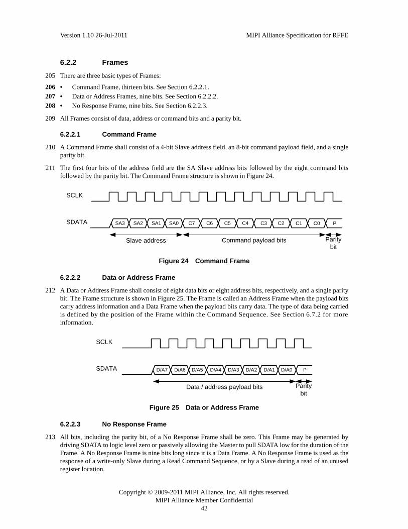
Copyright © 2009-2011 MIPI Alliance, Inc. All rights reserved.MIPI Alliance Member Confidential
42
Version 1.10 26-Jul-2011 MIPI Alliance Specification for RFFE
6.2.2 Frames
205 There are three basic types of Frames:
206 • Command Frame, thirteen bits. See Section 6.2.2.1.
207 • Data or Address Frames, nine bits. See Section 6.2.2.2.
208 • No Response Frame, nine bits. See Section 6.2.2.3.
209 All Frames consist of data, address or command bits and a parity bit.
6.2.2.1 Command Frame
210 A Command Frame shall consist of a 4-bit Slave address field, an 8-bit command payload field, and a singleparity bit.
211 The first four bits of the address field are the SA Slave address bits followed by the eight command bitsfollowed by the parity bit. The Command Frame structure is shown in Figure 24.
Figure 24 Command Frame
6.2.2.2 Data or Address Frame
212 A Data or Address Frame shall consist of eight data bits or eight address bits, respectively, and a single paritybit. The Frame structure is shown in Figure 25. The Frame is called an Address Frame when the payload bitscarry address information and a Data Frame when the payload bits carry data. The type of data being carriedis defined by the position of the Frame within the Command Sequence. See Section 6.7.2 for moreinformation.
Figure 25 Data or Address Frame
6.2.2.3 No Response Frame
213 All bits, including the parity bit, of a No Response Frame shall be zero. This Frame may be generated bydriving SDATA to logic level zero or passively allowing the Master to pull SDATA low for the duration of theFrame. A No Response Frame is nine bits long since it is a Data Frame. A No Response Frame is used as theresponse of a write-only Slave during a Read Command Sequence, or by a Slave during a read of an unusedregister location.
SDATA C1 C0 P
Slave address Command payload bits Paritybit
C2C3C4C5C6C7SA3 SA2 SA1 SA0
SCLK
P
Data / address payload bits Paritybit
SCLK
SDATA D/A7 D/A6 D/A5 D/A4 D/A3 D/A2 D/A1 D/A0

Copyright © 2009-2011 MIPI Alliance, Inc. All rights reserved.MIPI Alliance Member Confidential
43
Version 1.10 26-Jul-2011 MIPI Alliance Specification for RFFE
Figure 26 No Response Frame
6.2.3 Parity Bit
214 A Frame shall end with a single parity bit. The parity bit shall be driven such that the total number of bits inthe Frame that are driven to logic level one, including the parity bit, is odd. For example, a Data Frame withdata 0x63 (0b01100011) has a “1” parity bit and a Data Frame with data 0x4C (0b01001100) has a “0” paritybit.
6.2.3.1 Error Detection and Handling
215 In the event of error detection characterized by the cases in Table 11, each and every condition shall behandled according to the corresponding procedure. A Slave may record errors over the bus.
216 A Master shall always complete all Read Command Sequences. If a Slave ever finds a parity error it shall nottake control of the SDATA line.
217 A Slave interprets the first thirteen bits after SSC as the Command Frame. If the Slave does not receivethirteen SCLK pulses it waits for the missing clocks to appear, unless another SSC occurs. If there are extrapulses after the Command Frame, the pulses are interpreted as part of the subsequent Address and Data
Table 11 Error Handling
Error Detected Error Handling
Undefined Command Frame received
Slave ignores entire Command Sequence
Command Frame with parity error received
Slave ignores entire Command Sequence
Incompatible command length (command interrupted by SSC)
Slave executes Command Sequence up to the last correct and complete frame (multi-byte read and write operations)
Address Frame with parity error received
Slave ignores entire Command Sequence
Data Frame with parity error received
Slave ignores only the erroneous Data Frame of the Command Sequence
Read of unused register Slave sends No Response Frame
Write of an unused registerSlave discards data being written, rest of Command Sequence proceeds as normal
Read using the Broadcast ID or a GSID
Slave ignores the Command Sequence
0
No Response payload bits (logic 0)
Paritybit
SCLK
SDATA 0 0 0 0 0 0 0 0
Signal driven by Master
Signal not driven; pull-down only

Copyright © 2009-2011 MIPI Alliance, Inc. All rights reserved.MIPI Alliance Member Confidential
44
Version 1.10 26-Jul-2011 MIPI Alliance Specification for RFFE
Frames. Any additional SCLK pulses after an otherwise correctly formatted, complete Command Sequenceare ignored because the Slave is expecting an SSC, and it will synchronize itself to the next SSC when itappears. It is unlikely a Slave will be able to distinguish an incompatible Command Sequence length, but itshall be able to identify any unknown Command Sequences, parity bit errors and the occurrence of an SSCembedded in a Command Frame.
218 For the case of Extended Read and Extended Write Command Sequences, as described in Section 6.7.2, anyCommand Sequence shall be considered valid until the last completed byte in a multi-byte CommandSequence, prior to the receipt of an SSC. This does not prohibit a Slave from defining a set of registers thatare updated only after an entire Extended Command Sequence has completed. However in general, it isassumed that a Slave updates each byte immediately after the byte is successfully received in a Data Frame.
6.2.4 Bus Park Cycle
219 A device with ownership of SDATA shall initiate a Bus Park Cycle on SDATA (see Figure 11 in the electricalspecifications section) at the end of a Command Sequence or when the device transfers control of SDATA toanother device. The purpose of the Bus Park Cycle is to put the RFFE bus into a known state in preparationfor an SDATA signal control change, the start of a Command Sequence, or the start of the Bus Idle condition.
220 During the Bus Park Cycle, the device releasing SDATA shall drive the SDATA signal to a logic level zeroduring the first half of the SCLK clock cycle. Thereafter, the device releasing SDATA shall put its SDATAdriver into the high impedance state. The Master controlling the Command Sequence shall provide a normalSCLK during the Bus Park Cycle.
221 A minimum of 10 ns shall be reserved between the Bus Park Cycle and SSC separating two subsequentCommand Sequences.
6.3 Bus Idle Condition
222 The RFFE bus is in the “Idle” condition when both SCLK and SDATA signals are at logic level zero and alldevices connected to the bus other than the Master have their bus driver outputs in a high impedance state.The Master is the only device on the bus that drives the SCLK line, maintaining a strong (low-impedance)low level on that line. A pull-down source on SDATA maintains a weak (high impedance) low level on thatline. The bus is always in idle condition between the end of a Command Sequence and the beginning of a newCommand Sequence. See Figure 27 for an illustration of the Bus Idle condition.

Copyright © 2009-2011 MIPI Alliance, Inc. All rights reserved.MIPI Alliance Member Confidential
45
Version 1.10 26-Jul-2011 MIPI Alliance Specification for RFFE
Figure 27 Bus Idle Condition
6.4 RFFE Command Sequences
223 RFFE supports a number of Read and Write Command Sequences. Single byte and multi-byte CommandSequences are supported by a Master and are optional for a Slave. RFFE supports the following CommandSequences:
224 • Register Write
225 • Register 0 Write
226 • Extended Register Write of up to four data bytes mandatory and up to sixteen data bytes optional
227 • Register Read
228 • Extended Register Read of up to four data bytes mandatory and up to sixteen data bytes optional
229 • Extended Register Write Long (Optional)
230 • Extended Register Read Long (Optional)
231 An RFFE Master shall support the RFFE mandatory Command Sequences, Register Write, Register 0 Write,Extended Register Write (from one to four bytes), Register Read and Extended Register Read (from one tofour bytes). If the Extended Register Write Long and Extended Register Read Long Command Sequences arenot supported by the Master, the address space for the registers in a Slave is limited to 8-bits, which supports256 registers. A Slave may support certain Command Sequences for certain registers. For example, someregisters might be read-only or write-only, or an application-specific function might be defined that uses anExtended Register Write Command Sequence only on certain registers. By doing this, the Slave gate count iskept to a minimum. Table 12 lists all the Master and Slave supported Command Sequences.
SCLK
Possible previous SCLK cycles: - Bus Idle condition- Bus Park Cycle
Bus Idle condition Bus Idle condition or SSC start
SDATA
SDATA driver stays high-Z
During Bus Idle condition Bus Owner Master drives SCLK low.
Signal driven by Master
Signal not driven; pull-down only

Copyright ©
2009-2011 MIP
I Alliance, Inc. A
ll rights reserved.M
IPI A
lliance Mem
ber Confidential
46
Version 1.10 26-Jul-2011
MIP
I Alliance S
pecification for RF
FE
Table 12 RFFE Supported Command Sequences
M S Hex Description00 0 0 0 0
Y O -0F 1 1 1 110 (Reserved) 0 0 0 1 0 0 0 0 P11 (Reserved) 0 0 0 1 0 0 0 1 P12 (Reserved) 0 0 0 1 0 0 1 0 P13 (Reserved) 0 0 0 1 0 0 1 1 P14 (Reserved) 0 0 0 1 0 1 0 0 P15 (Reserved) 0 0 0 1 0 1 0 1 P16 (Reserved) 0 0 0 1 0 1 1 0 P17 (Reserved) 0 0 0 1 0 1 1 1 P18 (Reserved) 0 0 0 1 1 0 0 0 P19 (Reserved) 0 0 0 1 1 0 0 1 P1A (Reserved) 0 0 0 1 1 0 1 0 P1B (Reserved) 0 0 0 1 1 0 1 1 P1C (Reserved) 0 0 0 1 1 1 0 0 P1D (Reserved) 0 0 0 1 1 1 0 1 P1E (Reserved) 0 0 0 1 1 1 1 0 P1F (Reserved) 0 0 0 1 1 1 1 1 P20 0 0 0 0
Y O -2F 1 1 1 130 0 0 0
O O -37 1 1 138 0 0 0
O O -3F 1 1 140 0 0 0 0 0
Y O -5F 1 1 1 1 160 0 0 0 0 0
Y O -7F 1 1 1 1 180 0 0 0 0 0 0 0
Y O -FF 1 1 1 1 1 1 1
NotesAll non-implemented Command Sequences and register accesses are ignored, resulting in a null response.
NomenclatureBC = Byte Count M = Master P = Parity Y = MandatoryBP = Bus Park O = Optional SA = Slave Address S = Slave SSC = Sequence Start Condition
0
PBC[3:0] BP
Command Frame
0
1 0 P Data[7:0]
BC[3:0]
1 11
01
1
Information
P0 Address[7:0]
P
P
P
P
P Address[7:0]
Data[6:0]
BC[2:0]
BC[2:0]
0
Address[4:0]
Address[4:0]
00 1
Register 0 Write
SA[3:0]
SA[3:0]
SA[3:0]
SA[3:0]
SA[3:0]
SA[3:0]
Register Write
Register Read
Extended Register Write
Address[15:8]
P
0Extended Register Read
Extended Register Write Long
SA[3:0]Extended Register Read Long 0
0
1
Address[7:0]
0
P
1 BP
0 1 1
Address[7:0]
Address[15:8]
P
BPBPP Data[7:0]
BP
P
Up to 8 Bytes of Data with Parity BPBP
Up to 8 Bytes of Data with Parity BPP
P
Up to 16 Bytes of Data with ParityMaster must support up to 4 bytes
UndefinedUndefined
Undefined
BPBP
Undefined
UndefinedUndefined
UndefinedUndefined
Undefined
Undefined
Undefined
UndefinedUndefined
MandatoryCommands
SSC
UndefinedUndefined
Up to 16 Bytes of Data with ParityMaster must support up to 4 bytes
Undefined
0 0 0
Data Frame

Copyright © 2009-2011 MIPI Alliance, Inc. All rights reserved.MIPI Alliance Member Confidential
47
Version 1.10 26-Jul-2011 MIPI Alliance Specification for RFFE
6.5 Broadcast Messages
232 The RFFE protocol supports Broadcast Messages over the RFFE interface. A Broadcast Message is simply aCommand Sequence that is sent using a GSID for the USID portion of the Command Frame. A BroadcastMessage is used to write a Command Sequence to all Slaves on the bus. The SID 0b0000 is reserved forBroadcast Messages. Other SIDs may be defined as GSIDs in order to create different groups. The power andtrigger modes are broadcast-capable registers. Further, user-defined registers may also be implemented thatutilize broadcast capabilities. Only a Write Command Sequence shall be sent using a GSID or the BroadcastID. A Read Command Sequence using a GSID or the Broadcast ID shall be ignored by a Slave.
233 Other triggering mechanisms such as defining a write to a particular register address in order to configure alldevices with a common GSID to a predefined mode may be user-defined. This is similar to a trigger operationwithout the shadow registers, thereby reducing the area overhead for register triggers.
6.6 RFFE Register Space
234 The RFFE specification defines a single register space that simplifies the use of registers in a Slave. While theRFFE register space is a merged register space of SPMI, it is also backwards-compatible with SPMI registerspaces and SPMI register access Command Sequences. RFFE registers may be accessed by both single-byteand multi-byte register Command Sequences.
235 In Section B.4, the SPMI register space is discussed in order to illustrate the differences with the RFFEregister space.
236 RFFE has a single register space that contains registers 0 to 65535. RFFE registers may be accessed using theRegister 0 Write, Register Write, Register Read, Extended Register Write, Extended Register Read, ExtendedRegister Write Long and Extended Register Read Long Command Sequences. The Register 0 WriteCommand Sequence may be used for accessing Register 0, while shorter Register Write and Register ReadCommand Sequences may be used for accessing registers 0 to 31. Extended Command Sequences may beused for accessing registers 0 to 255, while Extended Long Command Sequences may be used for accessingregisters 0 to 65535.
237 By keeping RFFE registers in a single register space and backward-compatible with SPMI register spaces,the lower thirty-two registers can take advantage of both shorter single-byte and Extended multi-byteCommand Sequences.
238 Figure 28 shows registers in the RFFE register space and Command Sequences that may be used foraccessing these registers.
Figure 28 Slave Register Space, RFFE
0 1 to 31 32 to 255 256 to 65535
Register 0 Write
Register WriteRegister Read
Extended Register WriteExtended Register Read
Extended Register Write LongExtended Register Read Long
Copyright © 2009-2011 MIPI Alliance, Inc. All rights reserved.MIPI Alliance Member Confidential
48
Version 1.10 26-Jul-2011 MIPI Alliance Specification for RFFE
6.7 Command Sequences
6.7.1 Command Sequence Summary
239 This section describes all Command Sequences defined in the RFFE protocol.
240 See Section 6.2 for more information about Command Sequences and other RFFE constructs. The coding ofthe Command Frame is shown in Table 12.
6.7.2 Command Sequence Descriptions
241 Each Command Sequence is described in detail in the following sections.
6.7.2.1 Extended Register Write Command Sequence
242 The Extended Register Write provides write access to the extended register space on a Slave. One to sixteenbytes of data shall be written in a single Command Sequence. The extended register address shall be suppliedin a separate Address Frame in the Command Sequence.
243 Figure 29 shows the Extended Register Write Command Sequence. The Command Sequence starts with theSSC followed by the Extended Register Write Command Frame, an Address Frame and one or more DataFrames with the data to be written. Note that Data Frames immediately follow the Command Frame in acontinuous Command Sequence. The Command Sequence ends with a Bus Park Cycle.
244 The four LSBs of the Extended Register Write Command Frame, BC[3:0] in Figure 29, indicate the numberof bytes to be written by the Command Sequence. BC3 is the byte count MSB. 0b0000 indicates one byteshall be written and 0b1111 indicates sixteen bytes shall be written.
245 The register address in the Command Sequence contains the address of the first extended register to bewritten. If more than one byte is written in a single Command Sequence then the Slave's local extendedregister address shall be automatically incremented by one for each byte written up to address 0xFF, startingfrom the address indicated in the Address Frame. If the extended register address reaches 0xFF before the lastData Frame in the Command Sequence then the content of the register at address 0xFF is overwritten with theoverflow data.

Copyright © 2009-2011 MIPI Alliance, Inc. All rights reserved.MIPI Alliance Member Confidential
49
Version 1.10 26-Jul-2011 MIPI Alliance Specification for RFFE
Figure 29 Extended Register Write Command Sequence
6.7.2.2 Extended Register Read Command Sequence
246 The Extended Register Read Command Sequence provides read access to the extended register space on aSlave. One to sixteen bytes of data shall be read in a single Command Sequence. The extended registeraddress shall be supplied in a separate Address Frame in the Command Sequence.
247 Figure 30 shows the Extended Register Read Command Sequence. The Command Sequence starts with anSSC followed by the Extended Register Read Command Frame, an Address Frame and one or more DataFrames with the data read from the Slave. A Bus Park Cycle occurs between the Address Frame and the DataFrames. The Command Sequence ends with a Bus Park Cycle.
A1 A0 PA2A5 A4 A3A6P A7
Register Address (Data Frame) for First Register
D1 D0 PD2D5 D4 D3D6P D7
First Data Frame
SDATA
SCLK
SDATA
SCLK
… Intermediate Data Frames ...
D1 D0 PD2D5 D4 D3D6P D7 0
Last Data Frame Bus Park
SDATA
SCLK
A B
B C
C D
D
Signal driven by Master.
For reference only.
Signal not driven; pull-down only.
SA3 SA2 SA1 SA0 0 0 0 0 BC3 BC2 BC1 BC0 P
Extended Register Write Command Frame
SDATA
SCLK
SSC
A
Copyright © 2009-2011 MIPI Alliance, Inc. All rights reserved.MIPI Alliance Member Confidential
50
Version 1.10 26-Jul-2011 MIPI Alliance Specification for RFFE
248 The four LSBs of the Extended Register Read Command Frame, BC[3:0] in Figure 30, indicate the numberof bytes to be read in the Command Sequence. BC3 is the byte count MSB. 0b0000 indicates one byte shall beread and 0b1111 indicates sixteen bytes shall be read.
249 The register address in the Command Sequence contains the address of the first extended register to be read.If more than one byte is read in a single Command Sequence then the Slave's local extended register addressshall be automatically incremented by one for each byte read up to address 0xFF, starting from the addressindicated in the Address Frame. If the extended register address reaches 0xFF before the last Data Frame inthe Command Sequence, then the content of the register at address 0xFF is read multiple times. An ExtendedRegister Read Command Sequence by the Master to an unsupported Slave extended register address resultsin a No Response Frame from the Slave. If the address that results from auto-incrementing the Slave's localextended register address is for an unsupported register then the Slave sends a No Response Frame to theMaster in place of the Data Frame. The Command Sequence continues from the next extended registeraddress.

Copyright © 2009-2011 MIPI Alliance, Inc. All rights reserved.MIPI Alliance Member Confidential
51
Version 1.10 26-Jul-2011 MIPI Alliance Specification for RFFE
Figure 30 Extended Register Read Command Sequence
6.7.2.3 Extended Register Write Long Command Sequence
250 The Extended Register Write Long Command Sequence provides write access to the extended register spaceon a Slave using a 16-bit address. One to eight bytes of data may be written in a single Command Sequence.The extended register address is supplied in two Address Frames within the Command Sequence.
251 Figure 31 shows the Extended Register Write Long Command Sequence. The Extended Register Write LongCommand Sequence starts with an SSC followed by the Extended Register Write Long Command Frame,two Address Frames and one or more Data Frames with the data to be written. The Command Sequence endswith a Bus Park Cycle.
SA3 SA2 SA1 SA0 0 0 1 0 BC3 BC2 BC1 BC0 P
A1 A0 PA2A5 A4 A3A6P A7 0
Extended Register Read Command Frame
Register Address (Data Frame) for First Register Bus Park
D1 D0 PD2D5 D4 D3D60 D7
First Data Frame (from Slave)
SDATA
SCLK
SDATA
SCLK
SDATA
SCLK
D1 D0 PD2D5 D4 D3D6P D7 0
Last Data Frame (from Slave) Bus Park
SDATA
SCLK
SSC
For reference only.
Signal driven by Slave.
Signal not driven; pull-down only.
Signal driven by Master.
A
A B
B C
D
… Intermediate Data Frames ...C D

Copyright © 2009-2011 MIPI Alliance, Inc. All rights reserved.MIPI Alliance Member Confidential
52
Version 1.10 26-Jul-2011 MIPI Alliance Specification for RFFE
252 The three LSBs of the Extended Register Write Command Frame, BC[2:0] in Figure 31, indicate the numberof bytes to be written in the Command Sequence. BC2 is the byte count MSB. 0b000 indicates one byte shallbe written and 0b111 indicates eight bytes shall be written.
253 The register address in the Command Sequence contains the address of the first extended register to bewritten. If more than one byte is written in a single Command Sequence, then the Slave's local extendedregister address shall be automatically incremented by one for each byte written up to address 0xFFFF,starting from the address indicated in the Address Frame. If the extended register address reaches 0xFFFFbefore the last Data Frame in the Command Sequence, then the content of the register at address 0xFFFF isoverwritten with the overflow data.
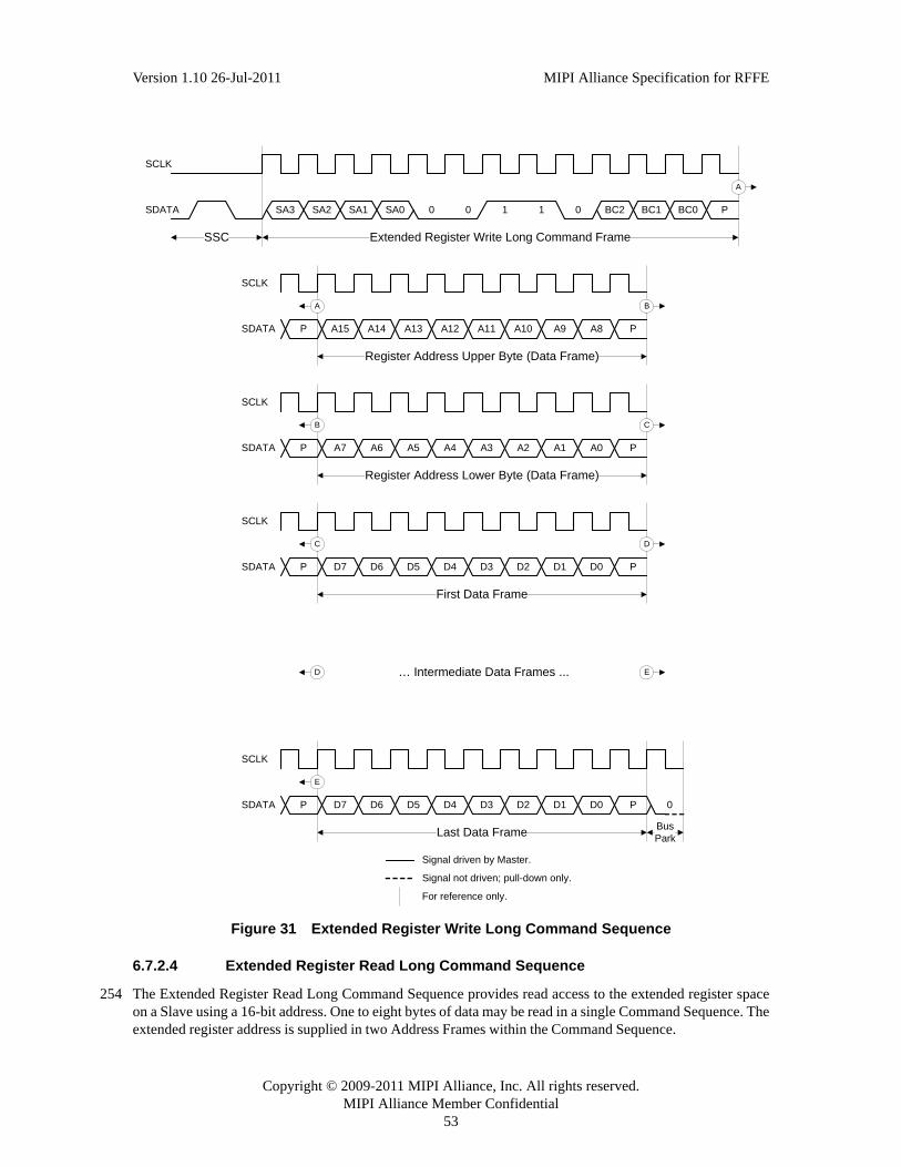
Copyright © 2009-2011 MIPI Alliance, Inc. All rights reserved.MIPI Alliance Member Confidential
53
Version 1.10 26-Jul-2011 MIPI Alliance Specification for RFFE
Figure 31 Extended Register Write Long Command Sequence
6.7.2.4 Extended Register Read Long Command Sequence
254 The Extended Register Read Long Command Sequence provides read access to the extended register spaceon a Slave using a 16-bit address. One to eight bytes of data may be read in a single Command Sequence. Theextended register address is supplied in two Address Frames within the Command Sequence.
SA3 SA2 SA1 SA0 0 0 1 1 0 BC2 BC1 BC0 P
Extended Register Write Long Command Frame
SDATA
SCLK
SSC
A
… Intermediate Data Frames ...
D1 D0 PD2D5 D4 D3D6P D7 0
Last Data Frame Bus Park
SDATA
SCLK
D E
E
Signal driven by Master.
Signal not driven; pull-down only.
For reference only.
D1 D0 PD2D5 D4 D3D6P D7
First Data Frame
SDATA
SCLK
C D
A1 A0 PA2A5 A4 A3A6P A7
Register Address Lower Byte (Data Frame)
SDATA
SCLK
B C
A9 A8 PA10A13 A12 A11A14P A15
Register Address Upper Byte (Data Frame)
SDATA
SCLK
A B

Copyright © 2009-2011 MIPI Alliance, Inc. All rights reserved.MIPI Alliance Member Confidential
54
Version 1.10 26-Jul-2011 MIPI Alliance Specification for RFFE
255 Figure 32 shows the Extended Register Read Long Command Sequence. The Command Sequence starts withan SSC followed by the Extended Register Read Long Command Frame, two Address Frames and one ormore Data Frames with the data read from the Slave. A Bus Park Cycle occurs between the Address Frameand the Data Frames. The Command Sequence ends with a Bus Park Cycle.
256 The three LSBs of the Extended Register Read Long Command Frame, BC[2:0] in Figure 32, indicate thenumber of bytes to be read in the Command Sequence. BC2 is the byte count MSB. 0b000 indicates one byteshall be read and 0b111 indicates eight bytes shall be read.
257 The register address in the Command Sequence contains the address of the first extended register to be read.If more than one byte is read in a single Command Sequence, then the Slave's local extended register addressshall be automatically incremented by one for each byte read up to address 0xFFFF, starting from the addressindicated in the Address Frame. If the extended register address reaches 0xFFFF before the last Data Framein the Command Sequence then the content of the register at address 0xFFFF is read multiple times. AnExtended Register Read Long Command Sequence by the Master to an unsupported Slave extended registeraddress results in a No Response Frame from the Slave. If the address that results from auto-incrementing theSlave's local extended register address is for an unsupported register, then the Slave sends a No ResponseFrame to the Master in place of the Data Frame. The Command Sequence continues from the next extendedregister address.

Copyright © 2009-2011 MIPI Alliance, Inc. All rights reserved.MIPI Alliance Member Confidential
55
Version 1.10 26-Jul-2011 MIPI Alliance Specification for RFFE
Figure 32 Extended Register Read Long Command Sequence
6.7.2.5 Register Write Command Sequence
258 Figure 33 shows the Register Write Command Sequence. The Command Sequence starts with an SSC,followed by the Write Command Frame containing the Slave address and the target register address and aData Frame containing the data to be written. The Command Sequence ends with a Bus Park Cycle.
SA3 SA2 SA1 SA0 0 0 1 1 1 BC2 BC1 BC0 P
Extended Register Read Long Command Frame
SDATA
SCLK
SSC
A
… Intermediate Data Frames ...
D1 D0 PD2D5 D4 D3D6P D7 0
Last Data Frame (from Slave) Bus Park
SDATA
SCLK
D E
E
D1 D0 PD2D5 D4 D3D60 D7
First Data Frame (from Slave)
SDATA
SCLK
C D
A1 A0 PA2A5 A4 A3A6P A7
Register Address Lower Byte (Data Frame)
SDATA
SCLK
B
A9 A8 PA10A13 A12 A11A14P A15
Register Address Upper Byte (Data Frame)
SDATA
SCLK
A
For reference only.
Signal driven by Slave.
Signal not driven; pull-down only.
Signal driven by Master.
0
Bus Park
C
B

Copyright © 2009-2011 MIPI Alliance, Inc. All rights reserved.MIPI Alliance Member Confidential
56
Version 1.10 26-Jul-2011 MIPI Alliance Specification for RFFE
Figure 33 Register Write Command Sequence
6.7.2.6 Register Read Command Sequence
259 Figure 34 shows the Register Read Command Sequence. The Command Sequence starts with an SSC,followed by the Read Command Frame, a one-clock cycle Bus Park Cycle and a Data Frame sent by theSlave. The Command Sequence ends with another Bus Park Cycle.
Figure 34 Register Read Command Sequence
6.7.2.7 Register 0 Write Command Sequence
260 Figure 35 shows the Register 0 Write Command Sequence. The Command Sequence starts with an SSC,followed by the Register 0 Write Command Frame containing the Slave address, a logic one, and a seven bitword to be written to Register 0. The Command Sequence ends with a Bus Park Cycle.
SA3 SA2 SA1 SA0 0 1 0 A4 A3 A2 A1 A0 P
Register Write Command Frame
SCLK
SDATA
SCLK
SSC
A
A
Signal driven by Master.
For reference only.
Signal not driven; pull-down only.
D1 D0 PD2D5 D4 D3D6P D7 0
Data Frame Bus Park
SDATA
SA3 SA2 SA1 SA0 0 1 1 A4 A3 A2 A1 A0 P
Register Read Command Frame
SCLK
SDATA
SCLK
SSC
A
A
D1 D0 PD2D5 D4 D3D6D7 0
Data Frame (from Slave) Bus Park
SDATA
For reference only.
Signal driven by Slave.
Signal not driven; pull-down only.
Signal driven by Master.
P 0
Bus Park
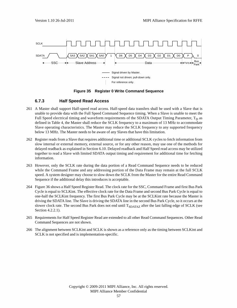
Copyright © 2009-2011 MIPI Alliance, Inc. All rights reserved.MIPI Alliance Member Confidential
57
Version 1.10 26-Jul-2011 MIPI Alliance Specification for RFFE
Figure 35 Register 0 Write Command Sequence
6.7.3 Half Speed Read Access
261 A Master shall support Half-speed read access. Half-speed data transfers shall be used with a Slave that isunable to provide data with the Full Speed Command Sequence timing. When a Slave is unable to meet theFull Speed electrical timing and waveform requirements of the SDATA Output Timing Parameter, TD asdefined in Table 4, the Master shall reduce the SCLK frequency to a maximum of 13 MHz to accommodateSlave operating characteristics. The Master may reduce the SCLK frequency to any supported frequencybelow 13 MHz. The Master needs to be aware of any Slaves that have this limitation.
262 Register reads from a Slave that requires additional time or additional SCLK cycles to fetch information fromslow internal or external memory, external source, or for any other reason, may use one of the methods fordelayed readback as explained in Section 6.10. Delayed readback and Half Speed read access may be utilizedtogether to read a Slave with limited SDATA output timing and requirement for additional time for fetchinginformation.
263 However, only the SCLK rate during the data portion of a Read Command Sequence needs to be reducedwhile the Command Frame and any addressing portion of the Data Frame may remain at the full SCLKspeed. A system designer may choose to slow down the SCLK from the Master for the entire Read CommandSequence if the additional delay this introduces is acceptable.
264 Figure 36 shows a Half Speed Register Read. The clock rate for the SSC, Command Frame and first Bus ParkCycle is equal to SCLKint. The effective clock rate for the Data Frame and second Bus Park Cycle is equal toone-half the SCLKint frequency. The first Bus Park Cycle may be at the SCLKint rate because the Master isdriving the SDATA line. The Slave is driving the SDATA line in the second Bus Park Cycle, so it occurs at theslower clock rate. The second Bus Park does not end until TSDATAZ after the last falling edge of SCLK (seeSection 4.2.2.1).
265 Requirements for Half Speed Register Read are extended to all other Read Command Sequences. Other ReadCommand Sequences are not shown.
266 The alignment between SCLKint and SCLK is shown as a reference only as the timing between SCLKint andSCLK is not specified and is implementation-specific.
Signal driven by Master.
For reference only.
Signal not driven; pull-down only.
SA3 SA2 SA1 SA0 1 P
Data
SDATA
SCLK
Slave Address
0
Bus Park
D1 D0D2D5 D4 D3D6
ParitySSC
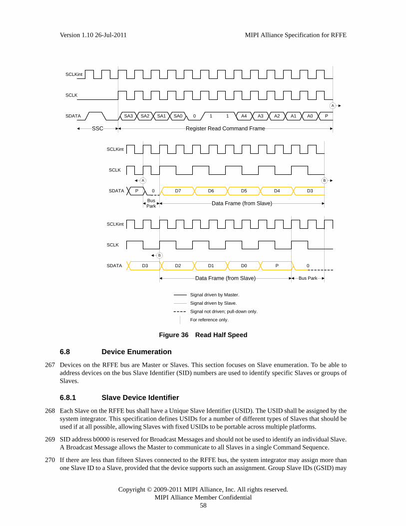
Copyright © 2009-2011 MIPI Alliance, Inc. All rights reserved.MIPI Alliance Member Confidential
58
Version 1.10 26-Jul-2011 MIPI Alliance Specification for RFFE
Figure 36 Read Half Speed
6.8 Device Enumeration
267 Devices on the RFFE bus are Master or Slaves. This section focuses on Slave enumeration. To be able toaddress devices on the bus Slave Identifier (SID) numbers are used to identify specific Slaves or groups ofSlaves.
6.8.1 Slave Device Identifier
268 Each Slave on the RFFE bus shall have a Unique Slave Identifier (USID). The USID shall be assigned by thesystem integrator. This specification defines USIDs for a number of different types of Slaves that should beused if at all possible, allowing Slaves with fixed USIDs to be portable across multiple platforms.
269 SID address b0000 is reserved for Broadcast Messages and should not be used to identify an individual Slave.A Broadcast Message allows the Master to communicate to all Slaves in a single Command Sequence.
270 If there are less than fifteen Slaves connected to the RFFE bus, the system integrator may assign more thanone Slave ID to a Slave, provided that the device supports such an assignment. Group Slave IDs (GSID) may
SA3 SA2 SA1 SA0 0 1 1 A4 A3 A2 A1 A0 P
Register Read Command Frame
SCLK
SDATA
SCLK
SSC
A
A
D5 D4 D3D6D7
0
Data Frame (from Slave)
SDATA
For reference only.
Signal driven by Slave.
Signal not driven; pull-down only.
Signal driven by Master.
P 0
Bus Park
SCLK
SDATA D0 PD1D2
Bus Park
B
B
D3
SCLKint
SCLKint
Data Frame (from Slave)
SCLKint

Copyright © 2009-2011 MIPI Alliance, Inc. All rights reserved.MIPI Alliance Member Confidential
59
Version 1.10 26-Jul-2011 MIPI Alliance Specification for RFFE
be assigned to multiple devices in a system. GSID are described in detail in Section 6.8.3. Unique SlaveIdentifier numbers and Group Slave Identifier numbers are collectively referred to as Slave Identifiers (SID).
271 In the case where the same Slave is used multiple times in the system on the same bus, Slaves need a methodto identify themselves. Devices with pins or pads which may be tied or low to provide a unique USID is oneoption. Another option is to have multiple RFFE buses. If the total number of Slaves is fifteen or less, thenSCLK could be shared. A second SCLK should be used for systems with sixteen or more Slaves. With ashared SCLK, only one SDATA may be active at a given time.
272 The predefined SIDs listed in Table 13 are a guideline for choosing IDs and are not mandatory. Guidelines aregiven so that a component may be used in multiple systems without requiring its USID to be programmed orprogrammable.
6.8.2 Unique Slave Identifier
273 An RFFE bus may have up to fifteen Slaves. Each Slave on the bus shall be assigned a USID between 0b1111and 0b0001, inclusive. USIDs do not have to be sequential. For example, in a system with four Slaves, oneSlave might have a USID of 0b0001, the second Slave might have a USID of 0b1010, the third Slave mighthave a USID of 0b1110 and the fourth Slave might have a USID of 0b0011.
274 If a device supports GSIDs, then the USID registers may be individually user-defined as to which GSIDs thedevice supports, if any. The USID registers in a device may respond to a single GSID, multiple GSIDs, oronly the USID depending on how the registers are defined.
275 The use of GSIDs limits the number of USIDs available to the system. For example, in a system that uses twoGSIDs, not including the Broadcast ID, no more than thirteen Slaves with unique SIDs may be present. GSID(or the Broadcast ID) shall be used only with Write Command Sequences.
Table 13 Slave Identifiers
SID[3:0] Description
1111 PA Module 1
1110 PA Module 2
1101 Spare (user-defined)
1100 Spare (user-defined)
1011 Antenna Switch Module 1
1010 Antenna Switch Module 2
1001 Spare (user-defined)
1000 Spare (user-defined)
0111 Antenna Tuning Module 1
0110 Spare (user-defined)
0101 Power Control Module 1
0100 Spare (user-defined)
0011 LNA Module 1
0010 Spare (user-defined)
0001 Spare (user-defined)
0000 Broadcast ID
Copyright © 2009-2011 MIPI Alliance, Inc. All rights reserved.MIPI Alliance Member Confidential
60
Version 1.10 26-Jul-2011 MIPI Alliance Specification for RFFE
6.8.3 Programmable USID
276 Due to the wide range of Slaves and vendors for these Slaves an optional programmable USID feature exists.The programmable USID feature utilizes three reserved registers. MANUFACTURER_ID is a 10-bit valuethat is split across two bytes.
277 The USID shall be programmed using only the programming procedures described in this section. A Mastershall support both USID programming procedures. A Slave shall support at least one of the USIDprogramming procedures.
278 The following programming procedure provides details for using Register Write Command Sequences toprogram the USID:
279 • Register Write Command Sequence to register 0x001D; the Data Frame needs to match PRODUCT_ID.
280 • Register Write Command Sequence to register 0x001E; the Data Frame needs to matchMANUFACTURER_ID[7:0].
281 • Register Write Command Sequence to register 0x001F with SPARE[1:0], MANUFACTURER_ID[9:8],and the new USID in the Data Frame; if the PRODUCT_ID and the MANUFACTURER_ID match, thena new USID is programmed.
282 If the programming procedure Command Sequences do not occur in the order given, the Slave shall notupdate its USID.
283 If during the programming procedure, the Slave receives any other Command Sequence with an SA equal tothe Slave’s USID, or the Broadcast ID, the Slave shall not program its USID and the programming procedureshall be terminated. However, the Master may access other devices on the RFFE bus during the programmingprocedure. Command Sequences sent to other devices on the RFFE bus shall not cause the Slave beingprogrammed to terminate the programming procedure.
Table 14 Programmable USID Registers
Register Address
Bits Register Name Notes
0x001D 7:0 PRODUCT_ID[7:0]
This is a read-only register. However during the programming of the USID a Write Command Sequence is performed on this register even though the write does not change its value.
0x001E 7:0 MANUFACTURER_ID[7:0]
This is a read-only register. However during the programming of the USID a Write Command Sequence is performed on this register even though the write does not change its value.
0x001F
7:6 SPARE[1:0]These are read-only bits that are reserved and yield a value of 0b00 at readback.
5:4 MANUFACTURER_ID[9:8]
These bits are read-only. However during the programming of the USID a Write Command Sequence is performed on this register even though the write does not change its value.
3:0 USID[3:0]
These bits are read-only for a device not supporting programmable USID; however, for programmable USID they are read/write. Performing a write to this register using the described programming sequences will program the USID in devices supporting this feature. These bits store the USID of the device.

Copyright © 2009-2011 MIPI Alliance, Inc. All rights reserved.MIPI Alliance Member Confidential
61
Version 1.10 26-Jul-2011 MIPI Alliance Specification for RFFE
284 The programming procedure for programming a new USID using the Register Write Command Sequence isshown in Figure 37.
Figure 37 Register Write USID
Signal driven by Master.
For reference only.
Signal not driven; pull-down only.
SCLK
A
PID1 PID0 PPID2PID5 PID4 PID3PID6P PID7 0
Data Frame (PRODUCT_ID[7:0]) Bus Park
SDATA
SA3 SA2 SA1 SA0 0 1 0 A4 A3 A2 A1 A0 P
Register Write Command Frame
SDATA
SCLK
SSC
A011 1 1
SCLK
B
MID1 MID0 PMID2MID5 MID4 MID3MID6P MID7 0
Data Frame (MANUFACTURER_ID[7:0]) Bus Park
SDATA
SA3 SA2 SA1 SA0 0 1 0 A4 A3 A2 A1 A0 P
Register Write Command Frame
SDATA
SCLK
SSC
B111 1 0
SCLK
C
USID1 USID0 PUSID2MID9 MID8 USID30P 0 0
Data Frame (MANUFACTURER_ID[9:8], USID[3:0]) Bus Park
SDATA
SA3 SA2 SA1 SA0 0 1 0 A4 A3 A2 A1 A0 P
Register Write Command Frame
SDATA
SCLK
SSC
C111 1 1

Copyright © 2009-2011 MIPI Alliance, Inc. All rights reserved.MIPI Alliance Member Confidential
62
Version 1.10 26-Jul-2011 MIPI Alliance Specification for RFFE
285 The following programming procedure provides details for using an Extended Register Write CommandSequence to program the USID:
286 • Command Frame: Current USID, 0b0000, BC[3:0] and Pwhere BC[3:0] = 0b0010 = three bytes of data
287 • Data Frame:Byte 1: Starting Address: Address of PRODUCT_ID (0b00011101 and P = 0b1)Byte 2: Product ID (Value of Register 0x001D and P)Byte 3: MANUFACTURER_ID[7:0] (Value of Register 0x001E and P)Byte 4: 0b00, MANUFACTURER_ID[9:8], New USID, P and BP
288 If the PRODUCT_ID and the MANUFACTURER_ID match, then a new USID is programmed.
289 The programming procedure for programming a new USID using the Extended Register Write CommandSequence is shown in Figure 38.

Copyright © 2009-2011 MIPI Alliance, Inc. All rights reserved.MIPI Alliance Member Confidential
63
Version 1.10 26-Jul-2011 MIPI Alliance Specification for RFFE
Figure 38 Extended Register Write USID
290 Since the Master supports both the Register Write and the Extended Register Write Command Sequences, aSlave may support either, or both, methods.
291 If a device supports an optional GSID, the GSID may be programmable or fixed. A programmable GSID is auser-defined register which may only be altered (reprogrammed) by a Command Sequence with a matchingUSID. The default value for a programmable GSID is 0b0000, which is the Broadcast ID. A programmableGSID may be turned off by programming the GSID to be equal to the USID.
292 When the device enters the STARTUP state the USID reverts back to its initial USID. However, if the deviceis placed in the LOW POWER state, the programmed USID remains the USID for the device. This alsoapplies to GSIDs.
Signal driven by Master.
For reference only.
Signal not driven; pull-down only.
SCLK
D
USID1 USID0 PUSID2MID9 MID8 USID30P 0 0
Last Data Frame (MANUFACTURER_ID[9:8], USID[3:0]) Bus Park
SDATA
A1 A0 PA2A5 A4 A3A6P A7
Register Address (Data Frame) for First Register
SDATA
SCLK
A B
Extended Register Write Command Frame
SCLK
SSC
A10 0 0
PID1 PID0 PPID2PID5 PID4 PID3PID6P PID7
First Data Frame (PRODUCT_ID[7:0])
SDATA
SCLK
B C
MID1 MID0 PMID2MID5 MID4 MID3MID6P MID7
Second Data Frame (MANUFACTURER_ID[7:0])
SDATA
SCLK
C D
SA3 SA2 SA1 SA0 0 0 0 0 BC3 BC2 BC1 BC0 PSDATA
01 1 100 0 1 1

Copyright © 2009-2011 MIPI Alliance, Inc. All rights reserved.MIPI Alliance Member Confidential
64
Version 1.10 26-Jul-2011 MIPI Alliance Specification for RFFE
293 If a Slave does not support the feature of a programmable USID, it shall reserve address location 0x001F, andif it is a readable device, it could output the USID during a read operation of this address.
294 Read-supporting devices shall not reuse the same USID. Though not prohibited, write-only devices shouldnot reuse the same USID. In the case where the same Slave is used multiple times, some type of mechanismsuch as having pins or pads which may be tied High or Low, or fuses within the device should be used to giveeach device a unique Slave address.
6.9 Slave Device Address Mapping
295 Registers in a device are byte addressable. Register Write and Register Read Command Sequences supportfive bits of address, which supports thirty-two addressable registers. The Extended Register Write and theExtended Register Read Command Sequences support eight bits of address which is 256 addressableregisters. The optional Extended Register Write Long and the Extended Register Read Long CommandSequences have sixteen bits of address which supports 65536 register locations.
296 The physical register length of any user-defined register may be zero to eight bits in length. During a write theunused bits are not stored by the Slave, but are used for parity check purposes. A readback of a register lessthan eight bits should read back 0's for the bits that are not populated.
297 Register 0 is a user-defined register which may be written into using with a Register Write, an ExtendedRegister Write, an Extended Register Write Long, or a Register 0 Write Command Sequence. Although allregisters may be up to eight bits, a Register 0 Write Command Sequence only writes to the seven LSBs ofRegister 0. The Slave Register Mapping is shown in Table 15.
6.9.1 Slave Device Reserved Addresses
298 There are four reserved address locations. These reserved addresses are used for power mode configuration,trigger functionality, reading the PRODUCT_ID, reading the MANUFACTURER_ID, and programming theUSID. These register locations shall be reserved in a Slave. The implementation of the reserved registersfunctionality is optional. For example a write-only device would not support reading the PRODUCT_ID andMANUFACTURER_ID registers.
Table 15 Slave Register Mapping
Register Address
Register NameNumber of
BitsNotes
0x0000 REGISTER_0 0 to 8 User-defined register content
0x0001 to 0x001B
User-defined register 0 to 8 User-defined register name and content
0x001C PM_TRIG 8 Power Mode and Trigger Register
0x001D PRODUCT_ID 8 Product Identification
0x001E MANUFACTURER_ID 8 Manufacturer Identification bits 7:0
0x001FSPARE(1:0)MANUFACTURER_ID(9:8)USID(3:0)
8Bits 7:6 SpareBits 5:4 MANUFACTURER_ID(9:8)Bits 3:0 Programmable Unique Slave Identifier
0x0020 to 0xFFFF
User-defined register 0 to 8 User-defined register

Copyright © 2009-2011 MIPI Alliance, Inc. All rights reserved.MIPI Alliance Member Confidential
65
Version 1.10 26-Jul-2011 MIPI Alliance Specification for RFFE
6.9.1.1 PRODUCT_ID
299 The PRODUCT_ID[7:0] register is eight bits, which allows for 256 unique device identifiers. These eightbits are defined by the vendors or systems outside the scope of this specification. For example, a vendormanufactures two different GSM PAs and one ASM. The vendor might define the PRODUCT_ID as shownin Table 16.
6.9.1.2 MANUFACTURER_ID
300 The MANUFACTURER_ID[9:0] register is ten bits in length, which allows for 1024 unique vendors. Thislist of manufactureres [MIPI04] is controlled by the MIPI Alliance. Members may be added to this list asneeded. In each device this register is fixed and is a read-only register. This register is also used during theprogramming of the USID.
6.9.1.3 USID
301 The reserved register USID is used to program a new USID for a Slave. The details of this function aredescribed in Section 6.8.3.
6.9.1.4 PM_TRIG
302 The PM_TRIG is a reserved register that is shared by the power modes and the trigger function. ThePWR_MODES register occupies the two MSBs and the TRIG_REG are the six LSBs of the PM_TRIGregister.
6.9.1.4.1 POWER MODES
303 In RFFE the settings for the various Power Modes are available via the reserved PWR_MODE register bits,which are the upper two bits of the PM_TRIG register (PM_TRIG[7:6]). These two bits support threepossible operating states for an RFFE Slave device, as shown in Table 18. Note that the fourth possible statefor PWR_MODE(1:0) is 0b11, which is undefined (Reserved), and thus Slaves shall ignore a Write of thisvalue to PWR_MODE(1:0). A Master shall not write this value to PWR_MODE(1:0).
Table 16 Slave PRODUCT_ID Example
Device USID[3:0] MANUFACTURER_ID PRODUCT_ID
GSM PA 1111 Company A 0b0000 0000
GSM PA 1111 Company A 0b0000 0001
ASM 1011 Company A 0b0000 0000
Table 17 PM_TRIG(7:0)
Bits Register
7:6 PWR_MODE
5:0 TRIG_REG
Table 18 Power Modes
PWR_MODE(1:0) Power Mode Write Value Read Value
00 Normal Operation (ACTIVE) 0b00 0b00
01 Default Settings (STARTUP) 0b01 0b00

Copyright © 2009-2011 MIPI Alliance, Inc. All rights reserved.MIPI Alliance Member Confidential
66
Version 1.10 26-Jul-2011 MIPI Alliance Specification for RFFE
304 When an RFFE Slave is initially powered up, and comes out of reset, the Slave registers shall be in theirdefault settings, whether these defaults are fixed, adjustable, or programmable, and the PWR_MODE state isset to Normal Operation, which is the ACTIVE state.
305 PWR_MODE sets the Default Settings mode via a Command Sequence that synchronously puts the Slaveregisters to their default settings, whether these defaults are fixed, adjustable, or programmable, after whichPWR_MODE goes to the Normal Operation Mode.
306 The Low Power Mode allows the Slave to put device-specific defined registers to their low power state value.The system user defines which registers have a low power state value. When PWR_MODE is switched out ofthe Low Power Mode back to the Normal Operation Mode, the registers shall output their ACTIVE statevalue. To exit the Low Power Mode into the Default Settings Mode, a value of 0b01 should be written toPWR_MODE(1:0). Not all Slaves and not all registers within a Slave will necessarily have a low powervalue. This is device- and system-specific.
307 Figure 39 illustrates an example implementation of the LOW POWER state value for a register. In thisexample a LOW POWER state value has been defined for bits 2 and 0 of Register A. When instructed to enterthe LOW POWER state the values of RegisterA(2) and RegisterA(0) would take on the value of “Low PowerValue” as shown in the diagram, while RegisterA(7:3) and RegisterA(1) would all retain their previous valuesfor the duration of LOW POWER. Note that “Low Power Value” may be unique for each bit.
10 Low Power (LOW POWER) 0b10 0b10
11 Reserved N/A N/A
Table 18 Power Modes (continued)
PWR_MODE(1:0) Power Mode Write Value Read Value
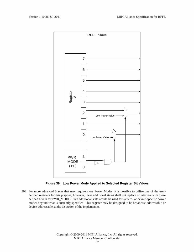
Copyright © 2009-2011 MIPI Alliance, Inc. All rights reserved.MIPI Alliance Member Confidential
67
Version 1.10 26-Jul-2011 MIPI Alliance Specification for RFFE
Figure 39 Low Power Mode Applied to Selected Register Bit Values
308 For more advanced Slaves that may require more Power Modes, it is possible to utilize one of the user-defined registers for this purpose; however, these additional states shall not replace or interfere with thosedefined herein for PWR_MODE. Such additional states could be used for system- or device-specific powermodes beyond what is currently specified. This register may be designed to be broadcast-addressable ordevice-addressable, at the discretion of the implementer.
7
Reg
iste
r A
6
5
4
3
2
1
0
RFFE Slave
1
0
PWR_ MODE (1:0)
Low Power Value
Low Power Value

Copyright © 2009-2011 MIPI Alliance, Inc. All rights reserved.MIPI Alliance Member Confidential
68
Version 1.10 26-Jul-2011 MIPI Alliance Specification for RFFE
6.9.1.4.2 Trigger Modes
309 Group trigger functionality is essential for meeting precise timing requirements especially if risk forcongestion using ordinary messages arises. Triggers provide a tool to solve bandwidth limitations, and toachieve simultaneous precise timing at multiple destinations.
310 The trigger function is not a mandatory function in every Slave, but may be used if multiple registers arerequired to be loaded at exactly the same time, or if the timing of the system requires multiple registers to beloaded in a timing critical window of time.
311 • Device trigger mode: If a register is more than eight bits, which is the maximum width of a register,multiple registers could be loaded and triggered to occur at the same time.
312 • Broadcast trigger mode: Multiple devices require registers to be updated at the same time.
313 • When reading back a register that is on a trigger the readback data is always the information stored in thedestination register and not the shadow register.
314 • If multiple triggers are triggered in the same write, they occur at the same time.
315 For more advanced Slaves that require more triggers a user-defined register can be used for system/devicespecific triggers.
316 The reserved TRIG_REG register shares an 8-bit register with the PWR_MODE register. TRIG_REG is sixbits and is the six LSBs of the PM_TRIG(5:0). The six bits support three separate triggers as shown inTable 19.
317 All three triggers may be set for each device individually or may be broadcast to multiple devices. All triggersmay be controlled individually or as a group.
318 The trigger masks may be set solely for each device individually. If a register is a trigger register by defaultthe trigger is not masked. Only a write to a specific device using the USID shall change the mask control bits.
6.10 Slaves With Delayed Readback
319 The RFFE protocol does not support the concept of a data ready bit during a read operation. A Slave mayrequire extra clock cycles or more time to retrieve data during a read operation. While the implementer is notlimited to the options given here, the solution chosen shall comply with the RFFE Command Sequence set.
Table 19 TRIG_REG Definition
Bit R/W Name Notes
5 R/W Trigger Mask 2If this bit is set trigger 2 is disabled. When disabled writing to a register that is associated to trigger 2 the data goes directly to the destination register.
4 R/W Trigger Mask 1If this bit is set trigger 1 is disabled. When disabled writing to a register that is associated to trigger 1 the data goes directly to the destination register.
3 R/W Trigger Mask 0If this bit is set trigger 0 is disabled. When disabled writing to a register that is associated to trigger 0 the data goes directly to the destination register.
2 W Trigger 2 A write of a one to this bit loads trigger 2's registers.
1 W Trigger 1 A write of a one to this bit loads trigger 1's registers.
0 W Trigger 0A write of a one to this bit loads trigger 0's registers.
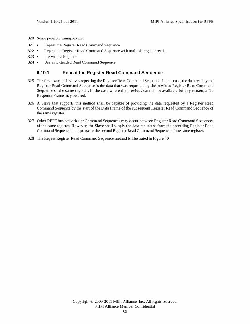
Copyright © 2009-2011 MIPI Alliance, Inc. All rights reserved.MIPI Alliance Member Confidential
69
Version 1.10 26-Jul-2011 MIPI Alliance Specification for RFFE
320 Some possible examples are:
321 • Repeat the Register Read Command Sequence
322 • Repeat the Register Read Command Sequence with multiple register reads
323 • Pre-write a Register
324 • Use an Extended Read Command Sequence
6.10.1 Repeat the Register Read Command Sequence
325 The first example involves repeating the Register Read Command Sequence. In this case, the data read by theRegister Read Command Sequence is the data that was requested by the previous Register Read CommandSequence of the same register. In the case where the previous data is not available for any reason, a NoResponse Frame may be used.
326 A Slave that supports this method shall be capable of providing the data requested by a Register ReadCommand Sequence by the start of the Data Frame of the subsequent Register Read Command Sequence ofthe same register.
327 Other RFFE bus activities or Command Sequences may occur between Register Read Command Sequencesof the same register. However, the Slave shall supply the data requested from the preceding Register ReadCommand Sequence in response to the second Register Read Command Sequence of the same register.
328 The Repeat Register Read Command Sequence method is illustrated in Figure 40.
Copyright © 2009-2011 MIPI Alliance, Inc. All rights reserved.MIPI Alliance Member Confidential
70
Version 1.10 26-Jul-2011 MIPI Alliance Specification for RFFE
Figure 40 Repeat the Register Read Command Sequence
6.10.2 Repeat the Register Read Command Sequence with Multiple Register Reads
329 The second example is similar to the previous one, but may be used when multiple bytes of data need to beread. In this case, the data read by a Register Read Command Sequence is the data that was requested by theprevious Register Read Command Sequence. In the case where the previous data is not available for anyreason, a No Response Frame may be used.
330 The Master may ignore the data provided by the Slave in the first Register Read Command Sequence, andmay repeat the Register Read Command Sequence of the last register to ensure it receives all the desired datacorrectly.
331 A Slave that supports this method shall be capable of providing the data requested by a Register ReadCommand Sequence by the start of the Data Frame of the subsequent Register Read Command Sequence.
332 Other RFFE bus activities or Command Sequences may occur between Register Read Command Sequences.
SCLK
A
D1 D0 PD2D5 D4 D3D6D7 0
Data Frame (from Slave) Bus Park
SDATA P 0
Bus Park
For reference only.
Signal driven by Slave.
Signal not driven; pull-down only.
Signal driven by Master.
SCLK
B
D1 D0 PD2D5 D4 D3D6D7 0
Data Frame (from Slave) Bus Park
SDATA P 0
Bus Park
SA3 SA2 SA1 SA0 0 1 1 A4 A3 A2 A1 A0 P
Register Read Command Frame
SDATA
SCLK
SSC
B
SA3 SA2 SA1 SA0 0 1 1 A4 A3 A2 A1 A0 P
Register Read Command Frame
SDATA
SCLK
SSC
A
Data requested from preceding Register Read Command Sequence must be available.

Copyright © 2009-2011 MIPI Alliance, Inc. All rights reserved.MIPI Alliance Member Confidential
71
Version 1.10 26-Jul-2011 MIPI Alliance Specification for RFFE
333 This method is suitable for a Slave that needs additional time to retrieve the requested data and has multiplebytes of data needed by the Master. This method is more bandwidth-efficient when the Master needs to readlarge amounts of data from the Slave.
334 The Repeat Register Read Command Sequence with Multiple Register Reads method is illustrated inFigure 41. The example in the figure shows consecutive addresses, which is not a requirement, but is used toillustrate one possible application of this method.
Figure 41 Slow Register Read with Multiple Read Command Sequences
6.10.3 Pre-Write a Register
335 The third example involves pre-writing a register using the Register Write Command Sequence to request thedelayed readback data, which is then read with a Register Read Command Sequence. In this option theRegister Write Command Sequence is used by the Slave to initiate the fetching of the delayed readback data.The register that is chosen in the Slave to initiate the fetching of the data may be the same register address asthe register it wants to read, or it may be a different register address. In the case where the pre-write registeraddress and the read register address are the same, the Register Write Command Sequence data is not stored
SCLK
A
D1 D0 PD2D5 D4 D3D6D7 0
Data Frame (from Address N - 1) Bus Park
SDATA P 0
Bus Park
For reference only.
Signal driven by Slave.
Signal not driven; pull-down only.
Signal driven by Master.
SCLK
B
D1 D0 PD2D5 D4 D3D6D7 0
Data Frame (from Address N) Bus Park
SDATA P 0
Bus Park
SA3 SA2 SA1 SA0 0 1 1 A4 A3 A2 A1 A0 P
Register Read Command Frame
SDATA
SCLK
SSC
B
SA3 SA2 SA1 SA0 0 1 1 A4 A3 A2 A1 A0 P
Register Read Command Frame
SDATA
SCLK
SSC
A
Data requested from address = N Register Read Command Sequence must be available.
Address = N
Address = N + 1

Copyright © 2009-2011 MIPI Alliance, Inc. All rights reserved.MIPI Alliance Member Confidential
72
Version 1.10 26-Jul-2011 MIPI Alliance Specification for RFFE
in the register location - it is just used to initiate the fetching of the data. The data read by the Register ReadCommand Sequence is the delayed readback data that was requested by the Register Write CommandSequence. In the same address case the data is read-only for this register address, as the Write Command onlyinitiates the fetching of the data.
336 A Slave that supports this method shall be capable of providing the data requested by the Register WriteCommand Sequence by the start of the Data Frame of the subsequent Register Read Command Sequence.
337 Other RFFE bus activities or Command Sequences may occur between the Register Write CommandSequence and the Register Read Command Sequence used by this method. However, the Slave shall supplythe data requested by the Register Write Command Sequence in response to the Register Read CommandSequence.
338 The pre-write a Register method is illustrated in Figure 42.
Figure 42 Pre-Write a Register
SA3 SA2 SA1 SA0 0 1 0 A4 A3 A2 A1 A0 P
Register Write Command Frame
SCLK
SDATA
SCLK
SSC
A
A
D1 D0 PD2D5 D4 D3D6P D7 0
Data Frame Bus Park
SDATA
SA3 SA2 SA1 SA0 0 1 1 A4 A3 A2 A1 A0 P
Register Read Command Frame
SCLK
SDATA
SCLK
SSC
B
B
D1 D0 PD2D5 D4 D3D6D7 0
Data Frame (from Slave) Bus Park
SDATA
For reference only.
Signal driven by Slave.
Signal not driven; pull-down only.
Signal driven by Master.
P 0
Bus Park
Data requested from preceding Register Write Command Sequence must be available.
Copyright © 2009-2011 MIPI Alliance, Inc. All rights reserved.MIPI Alliance Member Confidential
73
Version 1.10 26-Jul-2011 MIPI Alliance Specification for RFFE
6.10.4 Use an Extended Register Read Command Sequence
339 If the Slave supports the Extended Register Read Command Sequence it could be used for a register with aslow readback. Using the method in this example multiple bytes of data may be read in a single CommandSequence. The Command Sequence may be extended if necessitated by the amount of time or clock cyclesrequired to fetch the data. The number of clocks and the amount of time available is bounded by the length ofthe Command Sequence. The read triggering mechanism uses the first address and number of bytes argumentto trigger the data request. The data in preceding Frames is application-specific.
340 The following description is an example of using an Extended Register Read Command Sequence.
341 Register 0x0009 is a slow readback register and requires sixteen clock cycles to fetch the data.
342 The Master issues an Extended Register Read Command Sequence with a data width of three bytes and astarting address of 0x0007. Depending on whether or not addresses 0x0007 and 0x0008 are used, the Slavereturns either actual data from those registers, which may be defined as all zeroes with a parity bit of “1”, or aNo Response Frame if the respective register address is not supported. The Master may process or ignoreeach returning Data Frame individually. Data provided from address 0x0007 and 0x0008 shall be consistentwith any other Slave-supported Read Command Sequences accessing these register locations. The importantpoint to note is that the process for fetching the data from address 0x0009 begins after the Command Frameand the Address Frame are processed by the Slave.
343 The Extended Register Read Command Sequence method is illustrated in Figure 43.

Copyright © 2009-2011 MIPI Alliance, Inc. All rights reserved.MIPI Alliance Member Confidential
74
Version 1.10 26-Jul-2011 MIPI Alliance Specification for RFFE
Figure 43 Using an Extended Register Read Command Sequence
SA3 SA2 SA1 SA0 0 0 1 0 BC3 BC2 BC1 BC0 P
0 0 1 0
A1 A0 PA2A5 A4 A3A6P A7
0 0 0 0 0 1 1 1 0
0
Extended Register Read Command Frame
Register Address (Data Frame) for First Register Bus Park
D1 D0 PD2D5 D4 D3D60 D7
First Data Frame (from Slave)
SDATA
SCLK
SDATA
SCLK
SDATA
SCLK
D1 D0 PD2D5 D4 D3D6D7
Second Data Frame (from Slave)
SDATA
SCLK
D1 D0 PD2D5 D4 D3D6P D7 0
Requested and Last Data Frame (from Slave) Bus Park
SDATA
SCLK
SSC
Data requested must be available.
Process for fetching data for address 0x0009 is started.
For reference only.
Signal driven by Slave.
Signal not driven; pull-down only.
Signal driven by Master.
A
A B
B C
C D
D
P

Copyright © 2009-2011 MIPI Alliance, Inc. All rights reserved.MIPI Alliance Member Confidential
75
Version 1.10 26-Jul-2011 MIPI Alliance Specification for RFFE
7 Applications
344 This section defines features related to the usage of the RFFE specification in real world implementations andconfigurations. Some features are mandatory and defined in detail whereas others are vendor choices andthus only mentioned and briefly explained. These may be regarded as options as well, but usually do notrequire any additional functionality in the Master or Slave, so it is more of an explanation of how to useexisting mandatory features to accomplish an optional desired functionality.
345 The RFFE bus is intended to be used in conjunction with a multitude of different air interface standards.Ideally all possible use cases would be covered in this section; however, an exhaustive analysis and definitionof all possible RFFE use cases is not possible within the scope of this Specification. Instead this sectionhighlights a number of features that are necessary to ensure successful operation.
7.1 Programming Model
346 The intention of the programming model is to provide insight into how the interface is utilized inapplications, which should aid in the development of the control SW. Command Sequence lengths vary as afunction of access type and clock rate. Scheduling of the Command Sequences need to take this into accountto ensure time critical control is issued at the correct time. A timing accurate access requires a certainprocedure to be taken into account (see Section 7.1.2.1) and devices relying on the RFFE SCLK signal forclocking need to be considered appropriately (see Section 7.1.2.2) while designing the control scheme.
347 Register content, except for the specific RFFE registers defined in Section 6.9.1, is vendor-specific. Also, theallocation of the bits into the various registers is vendor-specific. Thus, it is not possible for the programmingmodel to cover all possibilities for the actual control queues and underlying Command Sequences. Therefore,the definition and specification work is left to the RF control system designer.
348 The amount and timing criticality of the control is very case-specific. Proper bus load analysis must be madeby the RF control system designer. This document provides only a toolset to help identify and solve potentialissues.
349 The programming model in general assumes the use of complete Command Sequences in a sequentialmanner. The Command Sequences are various types of register writes and reads (see Section 6.4). A devicesupplier may also give the payload bits a higher meaning (i.e. program code), but that is entirely vendor-specific. RFFE merely provides a means to transfer those bits. Scheduling and issuance of the CommandSequences is left to the Master design, and thus this is also device-specific. RFFE bus compliance isnevertheless achieved by ensuring that Master and Slaves are implemented according to this Specification,while a great deal of freedom and flexibility is left to the implementer, particularly on the RF system level.
7.1.1 Basic Control Related Items
350 This section describes some basic information necessary for successful control implementation.
7.1.1.1 Command Sequence Building
351 Table 20 illustrates the Command Sequence length in SCLK cycles including the SSC (length is two SCLKcycles in these examples as well as in Table 21). Register 0 Write is only available for the register withaddress 0x0h. There is no corresponding Read.
Table 20 Command Sequence Length In SCLK Cycles as Function of Access Type
Access Type Write Read
Register 0 Write 16 N/A
Register 25 26

Copyright © 2009-2011 MIPI Alliance, Inc. All rights reserved.MIPI Alliance Member Confidential
76
Version 1.10 26-Jul-2011 MIPI Alliance Specification for RFFE
352 Typical Write Command Sequence lengths with a single byte of data are:
353 • 16 SCLK cycles in Register 0 Write (only seven LSBs are written)
354 • 25 SCLK cycles in Register Write
355 • 34 SCLK cycles in Extended Register Write
356 • 43 SCLK cycles in Extended Register Write Long
357 The Register Write supports a 5-bit address space, Extended Register Write and Extended Register WriteLong 8-bit and 16-bit respectively. Same applies to corresponding Read Command Sequences.
358 Table 21 summarizes Command Sequence lengths in s for various accesses types as a function of a fewtypical bus clock rates. Note that only the shortest Command Sequences for Extended Register and ExtendedRegister Long accesses have been included in the table.
359 Table 22 illustrates the impact of the Half Speed read for Command Sequence lengths corresponding to therespective Read Command Sequences in Table 21. The assumption here is that the readback is performedwith a clock rate being half of the clock rate used during the Command Frame. The lengths of the CommandSequences in bits do not change but switching to a half frequency clock causes the readback Data Frames toconsume double the time than in the equivalent normal read.
Table 22 Command Sequence Lengths Using Half-Speed Read
7.1.1.2 Control Scheduling and Timing Considerations
360 The time budgeted for control varies as a function of case and actual implementation. A similar device by twodifferent vendors might require a different amount of control to perform the same task. There is additionally asettling time (in this context the time required before the controlled feature has become active, usually causedby the time analog blocks need to stabilize to the new settings) that vary significantly from oneimplementation to another.The RFFE specification cannot take vendor-specific issues like settling times intoaccount so definition of the control budget is left to the RF system designer.
Extended Register 34 to 169 35 to 170
Extended Register Long 43 to 106 44 to 107
Table 21 Command Sequence Length Versus Command Sequence Type & Clock Rate
Clock RateRegister 0
WriteRegister
WriteRegister
Read
Extended Register
Write
Extended Register
Read
Extended Register
Write Long
Extended Register
Read Long
26 MHz 0.62 s 0.96 s 1.00 s 1.31 s 1.35 s 1.65 s 1.69 s
19.2 MHz 0.83 s 1.30 s 1.35 s 1.77 s 1.82 s 2.24 s 2.29 s
13 MHz 1.33 s 1.92 s 2.00 s 2.62 s 2.69 s 3.31 s 3.38 s
Command Frame Clock Rate
Reduced Readback Clock
RateRegister Read
Extended Register Read
Extended Register Read Long
26 MHz 13 MHz 1.42 s 1.93 s 2.85 s
19.2 MHz 9.6 MHz 2.16 s 2.86 s 4.23 s
13 MHz 6.5 MHz 2.81 s 3.80 s 5.62 s
Table 20 Command Sequence Length In SCLK Cycles as Function of Access Type
Access Type Write Read
Copyright © 2009-2011 MIPI Alliance, Inc. All rights reserved.MIPI Alliance Member Confidential
77
Version 1.10 26-Jul-2011 MIPI Alliance Specification for RFFE
361 In addition to the typical length of bus access Command Sequences summarized in Table 21, a minimum of10 ns has to be reserved for the Bus Park Cycle which separates two subsequent messages (see Section 6.2.4).Knowledge of the number of control Command Sequences, their types, and the time available for controlallows the system designer to assess whether a control sequence may be accomplished. Note that the accesstime is a function of the actual clock rate (see Table 21) – the slower the clock that is used, the more time theCommand Sequences consume.
362 Pre-loading of registers and usage of the triggering mechanism may be used to circumvent a potential timingbottleneck (see Section 6.9.1.4.2). A well designed triggering approach could be capable of performing allcontrol with a precisely timed trigger Command Sequence. Defining such system is out of the scope of theRFFE specification and left to the RF system designer.
7.1.2 Procedures
363 There are two RFFE procedures to be mentioned in more detail. Precise access timing is fundamental for theapplications utilizing the RFFE bus and additional clock provisioning is necessary to ensure that devicesconnected to the bus with no other clock source obtain clocking in a controlled manner.
7.1.2.1 Precise Access Timing
364 Very precise timing is sometimes desired. The RFFE specification cannot constrain the implementations bydefining precise latency values. One reason is that although the processing time and Command Sequencetriggering point could be defined, the settling time is still solution-dependent.
365 Device suppliers are expected to define latencies and provide that information to the system designer. Thesame applies to the trigger latency. An optimal solution is to include an additional timer for every trigger inthe Slave to allow alignment or staggering of the triggering points. The lack of an always existing clock ruinsthis approach. A system designer might want to circumvent this issue by providing additional clocks (seeSection 7.1.2.2), but the design of such solution is outside the scope of this document.
7.1.2.1.1 Write Access
366 Typically, write access activates the control immediately after receiving the last Data Frame. Special casesare those situations where additional clocks are needed for activation. The Master needs to know in advancethe number of clock cycles required for each special case in order to provision the additional clock cycles.
367 It might be possible to constrain the latency variation by using the triggering mechanism (seeSection 6.9.1.4.2).
7.1.2.1.2 Read Access
368 A timing-precise read access might be harder to obtain than a corresponding write access. This appliesespecially if some of the means to provide the Slave additional clock cycles for processing (seeSection 7.1.2.2) are utilized. Only the Slave vendor may specify the exact timing for Extended Read or ReadCommand Sequences using multiple Command Sequences. For ordinary read accesses, the fetching point is,by definition, the bus turnaround unless fetching is bit-based instead of byte-based. Such a special case isoutside the scope of this document.
369 A very precise timing might be required regardless of the read access used to obtain the result. The (group)trigger function could be used in this case.
370 A triggered read access requires that one of the triggers (see Section 6.9.1.4.2) is used for storing a particularregister content for readback at a later time. Implementing such a read latch gives a timing precision of theread access corresponding to the timing precision in issuing the trigger Command Sequence. A triggered readaccess implemented in several devices could even use the group trigger functionality to enable a snapshot atmultiple devices simultaneously.

Copyright © 2009-2011 MIPI Alliance, Inc. All rights reserved.MIPI Alliance Member Confidential
78
Version 1.10 26-Jul-2011 MIPI Alliance Specification for RFFE
371 The trigger would initiate the fetching of data, although the challenge here is to provide a sufficient number ofclock cycles such that the data fetching may be completed during the clock cycles of the trigger CommandSequence (in principle this means during the remaining clock cycles of the access when trigger identificationis done; in practice this likely requires only a cycle or two). Readback data may then be acquired with a readaccess at some later time. This approach might require a specific register to temporarily store the read data,but that is left to the implementer.
372 Note that use of extended Command Sequences allows read access timing to be deterministic. The clockcycle in which the read access occurs may be known and thus, the Master may adjust the issuance of theCommand Sequence such that the read clock cycle occurs at the desired moment in time.
7.1.2.2 Provisioning of Additional Clocks for Processing
373 An RFFE device, in general, does not have any other clock input than SCLK provided by the interface. Thedevice might nevertheless require a clock to perform various actions. SCLK is used in such cases. Typically,the SCLK provided during a Command Sequence is sufficient for a Slave. However, there are situations whenadditional clock cycles are necessary.
374 There are three ways to provide these additional clocks:
375 • A Command Sequence to another device
376 • A dummy Command Sequence and Frame
377 • Use of extended Command Sequences
378 A Command Sequence to another device is equal to any normal traffic on the bus. If there is traffic on the busand it is timed suitably then there is no need for further actions to provide a clock. This is the preferred wayespecially at high bus load as other solutions further increase the load.
379 A dummy Command Sequence (examples of Command Sequences with desired dummy functionality aregiven in [MIPI06]) shall be transmitted if there is no ordinary traffic at the required time. The dummyCommand Sequence does not cause any action by a Slave, and just provides the clock cycles needed.
380 The additional clock cycles might be required in conjunction with a Command Sequence. ExtendedCommand Sequences shall be used in this case. Extended Command Sequences shall be constructed such thatthere are either unused address bytes, data bytes, or both. The actual frame construction thus becomes case-dependent. Slave implementers shall be notified that usage of all address or data bytes in extended CommandSequences prevents provisioning of the requested additional clock cycles because all available clock cyclesare used for ordinary Frame decoding and there are no spare clock cycles left for performing the actions. Inthis case, a Slave implementer needs to find another vendor-specific solution.
381 It is the responsibility of the entity controlling the Master to determine if, and when, additional clock cyclesare needed as well as selection of the method to do so. A Master shall support all three methods.
7.2 Command Sequence Timing
382 RFFE applications include cases where accurate timing of control Command Sequences is of utmostimportance. Time accurate scheduling of control Command Sequences is managed by the entity controllingthe Master; the RFFE bus cannot handle time conflicting Command Sequences. Such a case might beresolved either by shifting in time one of the conflicting Command Sequences, or if that cannot be done, byusing the triggering mechanism (see Section 6.9.1.4.2).
383 Deterministic time critical control is most easily implemented by use of a single Master configuration. . Thisis one of the major motives for restricting the RFFE bus to single Master and non-RCS operations. In the caseof systems with multiple RFFE buses, and thus involving one or more Masters, it is beyond the scope of theRFFE Specification to define the means for resolving any timing conflicts that may exist between the RFFE

Copyright © 2009-2011 MIPI Alliance, Inc. All rights reserved.MIPI Alliance Member Confidential
79
Version 1.10 26-Jul-2011 MIPI Alliance Specification for RFFE
buses. It is up to the implementers of the Master devices or the systems designers to provide for thiscapability.
384 Aborting an ongoing Command Sequence may be performed in some circumstances. However, this isprimarily reserved for malfunction condition on the bus, and thus the use of an SSC to terminate a CommandSequence in process should not be used to resolve timing conflicts.
385 A wait function may be incorporated by stalling the bus (Master retains the signal state on SDATA and SCLKuntil ready to continue). Although the wait function might not be typically needed in a single Master system,it might be useful in cases where scheduling necessitates stalling the bus.
7.3 Additional Configurations
7.3.1 Multiple Logical Slaves in one Device
386 A single device may have more than one logical Slave. Each logical Slave needs its own USID. Thus, usingmultiple, logical Slaves in one device should be considered carefully.
387 Figure 44 illustrates an example case of two logical Slaves in one device. Device N incorporates both Slave Nand N+1. Accessing device N would thus be done either through Slave N, N+1 or both. The device couldconsist of two physical dies (modules) molded into one package. In this particular case, each Slave could beconsidered an ordinary single device Slave with the difference that in the logical Slave case the VIO, SCLKand SDATA pins could be shared.
Figure 44 Example of Multiple Logical Slaves in Single Device Configuration
7.4 DDB in RFFE
388 MIPI Alliance Specification for Device Descriptor Block (DDB) [MIPI05] is defined for transfer ofdescription and configuration data between devices on an interconnect. An RFFE bus is a interconnect withthe Master and Slaves representing devices. An RFFE device shall thus be DDB compliant.
Master
Slave 1 Slave 2 Slave N+1Slave N...
IC
Device 1 Device 2 Device N

Copyright © 2009-2011 MIPI Alliance, Inc. All rights reserved.MIPI Alliance Member Confidential
80
Version 1.10 26-Jul-2011 MIPI Alliance Specification for RFFE
389 An RFFE device is a simple device, therefore only needing compliance with DDB Level 1. The response to aDDB Level 1 request is an 80-bit field, which needs many gates to support. Thus, a DDB request is not passedto Slaves.
390 In an RFFE implementation, the Master shall construct the full DDB Level 1 field for every requested device.In order to do this, the Master shall first fetch the MANUFACTURER_ID and PRODUCT_ID from therequested Slave using ordinary RFFE Read Command Sequences (see Section 6.7). Using theMANUFACTURER_ID and PRODUCT_ID the Master shall build the corresponding complete DDB blockas defined in Table 23.
391 The implementation of the DDB block builder in the Master is vendor-specific and may be accomplished inhardware, software, or some combination of the two.
392 Note that interfacing of the Master to the next hierarchal level (either in HW or SW) is out of the scope of theRFFE Specification. Thus it is assumed that such a connection exists, and that the Master has the capability ofproviding DDB Level 1 data over that connection by whatever means are specified by device implementers.
Table 23 Building DDB Level 1 Block
DDB FieldSize (bits)
RFFE Master Outputs
Revision 80b0001 0000(DDB version 1.0)
Level 80b0000 0001(DDB Level 1 only)
DeviceClass 160b0000 0000 0000 0000(Unless Device ID is specified by MIPI Alliance and known by the Master, in which case that value shall be used)
ManufacturerID 160b0000 00mm mmmm mmmm(mm mmmm mmmm being the 10-bit MANUFACTURER_ID read from the Slave)
ProductID 160b0000 0000 pppp pppp(pppp pppp being the 8-bit PRODUCT_ID read from the Slave)
Length 160b0000 0000 0000 0000(Not used)
Copyright © 2009-2011 MIPI Alliance, Inc. All rights reserved.MIPI Alliance Member Confidential
81
Version 1.10 26-Jul-2011 MIPI Alliance Specification for RFFE
Annex A Additional Information for RFFE Reference (Informative)
A.1 Optional Signals
393 Discrete signals may be added by the system integrator to provide optional functionality outside the scope ofthe RFFE Specification.
A.1.1 Optional Reset Signal
394 A Reset signal may be implemented to allow sharing VIO with components not utilizing the RFFE bus. TheReset signal overriding VIO in this case thus provides the same reset functionality as VIO (see Section 5.2.2).Reset by VIO still applies for RFFE components independent of the state of this optional Reset signal.
A.2 Estimation of RFFE Bus Load Ranges for Various Configurations
395 It is useful to consider estimated bus loads for various RFFE bus configurations in order to analyze the trade-offs of different architectures. It is also useful for IC device manufacturers to consider the environmentswhere their devices might be utilized, so as to provide devices well-suited for the maximum range ofapplications.
396 This section presents a method to calculate the bus load for various RFFE configurations, which may be usedto achieve a first-order estimate. For this estimate, only capacitance is considered as a factor in theimpedances that devices on the bus will experience. The load capacitance is a major factor in determining thetiming characteristics that may be realized in the final configuration. Note that more exact values should beused where they are available, in order to achieve the most accurate assessment of RFFE bus timing, as wellas other electrical requirements of the RFFE Specification.
397 The first step is to calculate an estimate of the total load due to the package capacitance of all devices on thebus, CL(PKG). In these calculations each Slave is assumed to contribute 2 pF of total pin capacitance (packageplus device). The load presented by the driving device (Master) should also be included in the calculation,and here is also assumed to be 2 pF. Since an RFFE bus is a single-Master system, this estimate is given bythe following general equation:
398
399 A four-Slave system configuration with package capacitance of 2 pF per Slave device (and Master) gives thefollowing result:
400
401 An eight-Slave system configuration with package pin capacitances of 2 pF per Slave device and 2 pF for theMaster then gives the following result:
402
403 A maximally-configured RFFE system, with fifteen Slaves and one Master, each with a package capacitanceof 2 pF per device gives the following result:
404
405 Note that where differing values are known for specific devices that are to be used in an RFFE system, the pincapacitance values of the Master and the pin capacitance for each of the Slave devices may be individuallysummed to achieve a more accurate estimate for the total pin capacitance value of the proposed system.
CL(PKG) n 1+ C est , where n is the # of Slaves and C(est) is per device=
CL(PKG) 5 devices 2 pF / device 10 pF= =
CL(PKG) 9 devices 2 pF / device 18 pF= =
CL(PKG) 16 devices 2 pF / device 32 pF= =

Copyright © 2009-2011 MIPI Alliance, Inc. All rights reserved.MIPI Alliance Member Confidential
82
Version 1.10 26-Jul-2011 MIPI Alliance Specification for RFFE
406 The next step is to calculate an estimate of the capacitive load due to PCB interconnect, CL(INT). The estimateused here is that the PCB interconnect contributes 4 pF for up to four Slaves connected to a single Master,with an additional 1 pF for each additional Slave. CL(INT) is expressed with the following equation:
407
408 Thus, for a four-Slave system, the capacitive load due to the estimated interconnect is 4 pF.
409 For an eight-Slave system, the estimation for interconnect load is given by the following equation:
410
411 Similarly, for a fifteen-Slave system, the estimation for interconnect load is given by the following equation:
412
413 As with pin capacitance, more accurate values for the interconnect may be substituted if they are known.More accurate estimates may be achieved in cases where factors such PCB material characteristics, layerstack-up, layout style, and other variables specific to a given situation are available.
414 The final step is to calculate the total load, CL(TOT), which is the sum of all of the package loads and theestimated interconnect load, as is shown in the following equation:
415
416 Thus, for the eight-Slave example, the total load is given by the following equation:
417
418 A fully-configured RFFE bus, with fifteen Slaves, using the estimated values assumed here, would result in atotal load as shown by the following equation:
419
420 Device manufacturers and system integrators are encouraged to utilize more accurate values for theseparameters if/when they are available. Nonetheless, it is useful to be able to utilize this type of quickestimation in order to be able to make trade-offs in potential RFFE configurations, particularly with regardsto the decision to implement single or multiple RFFE buses, when the number of Slaves to be controlledbecomes larger. Segmentation of various devices to separate buses might allow for easier realization ofcertain characteristics to be achieved for selected devices in an RFFE system. It might also be useful insystems with a large number of devices to provide separate buses to help ensure that all devices achieve thehighest speed and timing reliability.
421 As may be seen from these calculations, the actual values used for device pin capacitances, and the additionalinterconnect load contribution from the board environment utilized, can have a substantial impact on the totalRFFE bus load. These contributions will typically have to be minimized for maximally-configured RFFE busimplementations. Although the RFFE Specification provides for buses encompassing a large number ofcomponents, there are performance constraints that might require additional considerations. IC providers andsystems integrators thus need to perform trade-offs to maximize bus performance, while at the same timeminimizing additional pins and device interconnections. Such factors may actually result in a choice todeploy multiple RFFE buses, where a single bus might otherwise be possible. However, bus loading is onlyone reason why such a decision might be made, since other performance factors could also influence thisassessment.
CL(INT) 4 pF n 4– 1 pF+=
CL(INT) 4 pF 8 4– 1 pF+ 8 pF= =
CL(INT) 4 pF 15 4– 1 pF+ 15 pF= =
CL(TOT) CL(PKG) CL(INT)+=
CL(TOT) 18 pF 8 pF+ 26 pF= =
CL(TOT) 32 pF 15 pF+ 47 pF= =
Copyright © 2009-2011 MIPI Alliance, Inc. All rights reserved.MIPI Alliance Member Confidential
83
Version 1.10 26-Jul-2011 MIPI Alliance Specification for RFFE
Annex B Differences between SPMI and RFFE Specifications
422 MIPI Alliance Specification for RF Front-End Control Interface is based on MIPI Alliance Specification forSystem Power Management (SPMI) [MIPI03]. While the intention of the RFFE and SPMI Working Groupshas been to retain as much commonality and interoperability between the SPMI and RFFE bus Specificationsas possible, there are notable differences. This Annex endeavors to summarize the differences that existbetween them in a simplified fashion.
B.1 Application Environment
423 The RFFE bus is intended for connecting a Radio-Frequency IC (RFIC) to the Front-End Modules (FEMs)associated with it in a system. This interface has to support all existing 3GPP standards as well as other radiostandards. This means that very tightly controlled and predictable real-time control is required. At the sametime, semiconductor processes used to implement an FEM device as well as realistic assumptions about costfactors mean that an RFFE Slave has extremely tight implementation logic gate count restrictions, surpassingthose for any other MIPI Alliance bus application environment.
424 For these reasons the RFFE specification is a feature-limited version of the SPMI specification retaining onlythose functions and features that are absolutely necessary in this application.
B.2 Detailed Differences between SPMI and RFFE Specifications
B.2.1 Single Master Operation with Simple Slave Devices.
425 An RFFE bus has only one Master, and does not allow the use of Request Capable Slaves (RCS) on the bus.This means that the sole Master is the only device which may provide the clock on the bus, and that allCommand Sequences on the bus are initiated by the Master. The Master is assumed to be the RFIC (seeSection 4.1).
B.2.2 No Bus Arbitration
426 Single Master operation means that no bus arbitration is needed for RFFE. Master starts all communicationssequences with the Sequence Start Condition, and once the sequence is over the Master may initiate anothersequence without any intermediate bus arbitration (see Section 4.2)
B.2.3 No Bus Arbitration Requests by Slave Devices
427 Since no RCS devices are allowed on the RFFE bus, there are no bus arbitration requests from RCS devices(see Section 4.1).
B.2.4 Limited Command Sequence Set
428 The RFFE Command Sequence set is limited to Register 0 Write, Register Read, Register Write, ExtendedRegister Read, Extended Register Write, Extended Register Read Long and Extended Write Long CommandSequences. The SPMI specification defines additional Command Sequences, but these are not used by RFFEdevices (see Table 12).
429 RFFE supports a limited number of SPMI Command Sequences, as many of the SPMI Command Sequencesare not applicable for a configuration in which only one Bus Owner Master may exist on the bus.
430 Table 24 lists the Master and Slave supported SPMI Command Sequences.

Copyright © 2009-2011 MIPI Alliance, Inc. All rights reserved.MIPI Alliance Member Confidential
84
Version 1.10 26-Jul-2011 MIPI Alliance Specification for RFFE
B.2.5 Limited Support for Device Descriptor Block Data
431 The RFFE specification does not include SPMI Command Sequences supporting DDB data. Instead theRFFE specification specifies which registers RFFE devices hold the equivalent data and assumes any DDBdata requests are handled by reading this data using normal Read Command Sequences and collecting theDDB data in the Master for further use (see Section 6.9 and Section 7.4).
B.2.6 Unified Slave Register Space
432 Slave register space is uniform and linear with all Register Read and Register Write Command Sequencespointing to a single linear register address space. SPMI base register address space and extended registeraddress space are separate (see Section 6.6 and Section B.4).
Table 24 RFFE Supported Command Sequences
RFFE1
1. Y = Supported, N = Not Supported, O = Optional Support, N/A = Not Applicable
SPMI Command
Master Slave Hex Description
Y O 00 to 0F Extended Register Write
N N 10 Reset
N N 11 Sleep
N N 12 Shutdown
N N 13 Wakeup
N N 14 Authenticate
N/A N/A 15 Master Read
N/A N/A 16 Master Write
17 Reserved
18 Reserved
19 Reserved
N/A N/A 1A Transfer Bus Ownership
N/A N/A 1B Device Descriptor Block Master Read
N N 1C Device Descriptor Block Slave Read
1D Reserved
1E Reserved
1F Reserved
Y O 20 to 2F Extended Register Read
O O 30 to 37 Extended Register Write Long
O O 38 to 3F Extended Register Read Long
Y O 40 to 5F Register Write
Y O 60 to 7F Register Read
Y O 80 to FF Register 0 Write

Copyright © 2009-2011 MIPI Alliance, Inc. All rights reserved.MIPI Alliance Member Confidential
85
Version 1.10 26-Jul-2011 MIPI Alliance Specification for RFFE
B.2.7 Pull-Down Function in Master Device
433 In RFFE applications SDATA and SCLK pull-down functionality is implemented in the Master, or in aMaster-associated external device, while in SPMI the bus pull-down is implemented in Slave devices, or in aSlave-associated external device. The bus pull-down realization in RFFE and SPMI is functionallyequivalent; however, it is possible that in RFFE applications utilizing multiple SPMI Slaves that pull-downcurrents could exceed normal expectations in extreme cases. This situation may be avoided if SPMI Slavesused in RFFE applications possess pull-down devices which may be disabled. See Section 5.1 for moreinformation about bus pull-down functionality in RFFE.
B.2.8 I/O Drive Strength Classes
434 Both SPMI and RFFE specifications specify bus timing for maximum 50 pF load per signal line.Additionally, the RFFE specification allows bus drive capability to be vendor-specific.
B.2.9 High Speed Devices Only
435 An RFFE device supports bus operation up to 26 MHz. There is no low speed device class as in SPMI (seeSection 4.2)
B.2.10 Explicit Support for Half Speed Read
436 While also allowed within the SPMI specification, the RFFE specification explicitly explains and specifiesHalf Speed read operation timing for a Slave that cannot respond at Full Speed to register read operations (seeSection 4.2).
B.2.11 EMI
437 The RFFE specification places additional requirements on the signaling waveforms for EMI reductionreasons; the rise and fall times in the SPMI specification are defined differently. A Master designed for SPMImight not necessarily meet the slew rate requirements of the RFFE specification.
B.2.12 Slave Identifier Allocation
438 The RFFE specification recommends allocation of Slave identifier number for different types of FEMdevices in Table 13. The SPMI specification does not specify or recommend such values (see Table 13 andSection 6.8.1).
B.2.13 Register Allocation
439 Registers 0x001C to 0x001F have predefined functions. Register 0x001C controls trigger control and powermodes, while registers 0x001D to 0x001F are related to DDB Level 1 support as well as programmable USIDvalues for Slaves.
440 The SPMI specification does not specify device register usage. The specification does not explicitly describea method to implement a programmable USID, although the same method as described in the RFFEspecification (see Section 6.8.1) could be used as it falls outside the scope of the SPMI specification.
B.2.14 VIO Sensing for State Control
441 Instead of using external ENABLE, RESETN and VDDOK signals for power up control, sequencing andreporting like SPMI, RFFE controls Slave power-up sequencing and reset with the IO voltage pin. This altersthe state control for STARTUP, ACTIVE, POWER DOWN and SHUTDOWN states.

Copyright © 2009-2011 MIPI Alliance, Inc. All rights reserved.MIPI Alliance Member Confidential
86
Version 1.10 26-Jul-2011 MIPI Alliance Specification for RFFE
B.3 SPMI Baseline and Compatibility to RFFE
442 The objective of this section is to compare in detail all features from SPMI and RFFE specificationssummarized in Table 25. An all-encompassing mapping between SPMI and RFFE specification and featuresis listed with proper references to the sections in the respective specifications and comments pointing outwhich modifications i.e. reduction of the SPMI feature set have been applied.
Table 25 SPMI Feature Compatibility Matrix
SPMI FeatureSPMI
SectionComment
RFFESection
Physical Interface 5 5
I/O Structures 5.1 5.1
I/O Configuration with Multiple Slaves and Masters
5.1.1 5.1.2
I/O Voltage and Logic Levels 5.2 5.2
Signaling Voltages 5.2.1 5.1.1
SPMI I/O Voltage Supply 5.2.2 Superseded by Section 5.2 5.2
Device Classes 5.3RFFE does not implement device speed classes. Only high speed devices exist.
4.2
SPMI Clock (SCLK) 5.4 4.2.1
Electrical Specifications for the Master SCLK Driver
5.4.1 4.2.1.1
Electrical Specifications for SCLK Input 5.4.2 4.2.1.2
SPMI Data (SDATA) 5.5 4.2.2
Electrical Specifications for the SDATA Driver
5.5.1 4.2.2.1
Electrical Specifications for the SDATA Receiver
5.5.2 4.2.2.2
Device Characterization 5.6 5.3
Electromagnetic Interference 5.7 5.4
SPMI Constructs 6 6
Bit Ordering 6.1 6.1
Command Sequences 6.2 6.2
Bus Arbitration 6.2.1RFFE is single Master only. There is no bus arbitration.
-
Sequence Start Condition 6.2.2 6.2.1
Frames 6.2.3 6.2.2
Parity Bit 6.3 6.2.3
Bus Park Cycle 6.4 6.2.4
Device Enumeration 7 6.8
Unique Slave Identifier 7.2 6.8.2
Group Slave Identifier 7.3 6.8.3
Master Connecting on the Bus 9.2RFFE Master can turn on and off as necessary.
-

Copyright © 2009-2011 MIPI Alliance, Inc. All rights reserved.MIPI Alliance Member Confidential
87
Version 1.10 26-Jul-2011 MIPI Alliance Specification for RFFE
Connecting by Detecting SSC 9.2.1 -
Connecting by Detecting Bus Idle 9.2.2 -
Connecting by Detecting Bus Arbitration
9.2.3 -
Bus Initialization 9.3 Not needed in RFFE, single Master -
Disconnecting from the Bus 9.4 Not needed in RFFE, single Master -
Bus Monitoring by Disconnected Master
9.4.1 Not needed in RFFE, single Master -
Slave Communication Request 10 Not used in RFFE -
Alert bit on an Initialized Bus 10.1 Not used in RFFE -
Slave Request Bit on an Initialized Bus 10.2 Not used in RFFE -
Slave Communication Request on Uninitialized Bus
10.3 Not used in RFFE -
Master Operating States 11.1 Not defined in RFFE -
SPMI Slave Requirements 12 4.3
Register Spaces 12.1RFFE uses linear, unified register space
6.6
Slave External Control Signals 12.2 A.1
RESETN 12.2.1 Optional in RFFE A.1.1
ENABLE 12.2.2 Not defined in RFFE -
PWROK 12.2.3 Not defined in RFFE -
Exceptional Control Inputs 12.2.4 4.3.5
Other Control Inputs and Outputs 12.2.5 A.1
Multiple Logical Slaves on a Single Physical Device
12.2.6 7.3.1
Slave Operating States 12.3 4.3
STARTUP 12.3.1 4.3.1
ACTIVE 12.3.2 4.3.2
SLEEP 12.3.3SLEEP is called LOW POWER in RFFE.
4.3.3
SHUTDOWN 12.3.4 4.3.4
Exceptional State Transitions 12.3.5 4.3.5
Optional Command Sequence Support 12.4Not needed in RFFE due to single Master operation
-
Command Sequences 13 6.7
Command Sequence Summary 13.1 6.7.1
Command Sequence Descriptions 13.2 6.7.2
Extended Register Write Command Sequence
13.2.1 6.7.2.1
Extended Register Read Command Sequence
13.2.2 6.7.2.2
Table 25 SPMI Feature Compatibility Matrix (continued)
SPMI FeatureSPMI
SectionComment
RFFESection

Copyright © 2009-2011 MIPI Alliance, Inc. All rights reserved.MIPI Alliance Member Confidential
88
Version 1.10 26-Jul-2011 MIPI Alliance Specification for RFFE
Reset, Sleep, Shutdown, Wakeup Command Sequences
13.2.3 Not used in RFFE. -
Authentication Command Sequence 13.2.4 Not used in RFFE. -
Device Descriptor Block Slave Read Command Sequence
13.2.8 Different DDB support in RFFE. 7.4
Device Descriptor Block Master Read Command Sequence
13.2.9 Different DDB support in RFFE. 7.4
Extended Register Write Long Command Sequence
13.2.10 6.7.2.3
Extended Register Read Long Command Sequence
13.2.11 6.7.2.4
Register Write Command Sequence 13.2.12 6.7.2.5
Register Read Command Sequence 13.2.13 6.7.2.6
Register 0 Write Command Sequence 13.2.14 6.7.2.7
Error Handling 13.3 6.2.3.1
Parity Error in the Command Frame 13.3.1 RFFE Table 11 6.2.3.1
Unsupported Command Sequences 13.3.2 RFFE Table 11 6.2.3.1
Parity Error in the Address Frame 13.3.3 RFFE Table 11 6.2.3.1
Parity Error in the Data Frame 13.3.4 RFFE Table 11 6.2.3.1
Unsupported Address 13.3.5 RFFE Table 11 6.2.3.1
SPMI Reference (informative) Annex A –
High Speed (HS) Device ClassAnnex A.2.1
No device classes in RFFE. –
Low Speed (LS) Device ClassAnnex A.2.2
No device classes in RFFE. –
Other Signaling Electrical Specifications
Annex A.2.3
–
Command Sequence Reference (informative)
Annex A.3 6.4
Table 25 SPMI Feature Compatibility Matrix (continued)
SPMI FeatureSPMI
SectionComment
RFFESection

Copyright © 2009-2011 MIPI Alliance, Inc. All rights reserved.MIPI Alliance Member Confidential
89
Version 1.10 26-Jul-2011 MIPI Alliance Specification for RFFE
B.4 SPMI Register Space
443 The SPMI register space is divided into two register spaces, Base and Extended, as illustrated in Figure 45.The RFFE register space merges the two SPMI register spaces into a single register space. See Section 6.6 forfurther details regarding the RFFE register space.
444 The SPMI Base register space consists of up to thirty-two 8-bit registers. These registers may be accessed onebyte at a time using only Register Write, Register Read and Register 0 Write Command Sequences.
445 The SPMI Extended and Extended Long register space consists of up to 65536 8-bit registers. These registersmay be accessed using only Extended Register Write, Extended Register Read, Extended Register WriteLong and Extended Register Read Long Command Sequences with single-byte or multi-byte access.Extended Command Sequences may be used for accessing registers 0 to 255, while Extended LongCommand Sequences may be used for accessing registers 0 to 65535. Extended and Extended Long registersoverlap the same registers.
Figure 45 Slave Register Spaces, SPMI
0 1 to 31
0 to 255 256 to 65535
Register 0 Write
Register WriteRegister Read
Extended Register WriteExtended Register Read
Extended Register Write LongExtended Register Read Long
Copyright © 2009-2011 MIPI Alliance, Inc. All rights reserved.MIPI Alliance Member Confidential
Version 1.10 26-Jul-2011 MIPI Alliance Specification for RFFE
Participants446 The following list of individuals contributed to the development of this document, and consented to appear
on this list. For a listing of all individuals who contributed to the original RFFE v1.00.00 release, see MIPIAlliance Specification for RF Front-End Control Interface - Version 1.00.00 – 3 May 2010.
Anhofer, Robert - IEEE-ISTO (staff)Arrakoski, Jori – Nokia CorporationCalvo, Carlos – Analog Devices Inc.Chlopek, Dan – Fujitsu LimitedGruber, George – Qualcomm IncorporatedHallberg, Peter – ST-EricssonHueber, Gernot – NXP SemiconductorsKeese, Liam – National SemiconductorNgo, Chris – RF Micro DevicesOsman, Saleh – Panasonic CorporationPennanen, Juha – National SemiconductorPodsiadlo, Dave – Peregrine SemiconductorRoss, Jim – Skyworks Solutions, Inc.Seth, Marten – WiSpry Inc.Soni, Samir – Fujitsu LimitedWilkerson, Victor – MIPI Alliance (staff)