Micro Electro Mechanical System Design - X-Files
463
Micro Electro Mechanical System Design © 2005 by Taylor & Francis Group, LLC
-
Upload
khangminh22 -
Category
Documents
-
view
1 -
download
0
Transcript of Micro Electro Mechanical System Design - X-Files

MicroElectroMechanicalSystemDesign
© 2005 by Taylor & Francis Group, LLC

MECHANICAL ENGINEERING
A Series of Textbooks and Reference Books
Founding Editor
L. L. Faulkner
Columbus Division, Battelle Memorial Instituteand Department of Mechanical Engineering
The Ohio State UniversityColumbus, Ohio
1. Spring Designer’s Handbook, Harold Carlson
2. Computer-Aided Graphics and Design, Daniel L. Ryan
3. Lubrication Fundamentals, J. George Wills
4. Solar Engineering for Domestic Buildings, William A. Himmelman
5. Applied Engineering Mechanics: Statics and Dynamics, G. Boothroyd and C. Poli
6. Centrifugal Pump Clinic, Igor J. Karassik
7. Computer-Aided Kinetics for Machine Design, Daniel L. Ryan
8. Plastics Products Design Handbook, Part A: Materials and Components;Part B: Processes and Design for Processes, edited by Edward Miller
9. Turbomachinery: Basic Theory and Applications, Earl Logan, Jr.
10. Vibrations of Shells and Plates, Werner Soedel
11. Flat and Corrugated Diaphragm Design Handbook, Mario Di Giovanni
12. Practical Stress Analysis in Engineering Design, Alexander Blake
13. An Introduction to the Design and Behavior of Bolted Joints,John H. Bickford
14. Optimal Engineering Design: Principles and Applications, James N. Siddall
15. Spring Manufacturing Handbook, Harold Carlson
16. Industrial Noise Control: Fundamentals and Applications, edited by Lewis H. Bell
17. Gears and Their Vibration: A Basic Approach to Understanding Gear Noise,J. Derek Smith
18. Chains for Power Transmission and Material Handling: Design and Applications Handbook, American Chain Association
19. Corrosion and Corrosion Protection Handbook, edited by Philip A. Schweitzer
20. Gear Drive Systems: Design and Application, Peter Lynwander
21. Controlling In-Plant Airborne Contaminants: Systems Design and Calculations, John D. Constance
22. CAD/CAM Systems Planning and Implementation, Charles S. Knox
23. Probabilistic Engineering Design: Principles and Applications,James N. Siddall
24. Traction Drives: Selection and Application, Frederick W. Heilich III and Eugene E. Shube
© 2005 by Taylor & Francis Group, LLC
25. Finite Element Methods: An Introduction, Ronald L. Huston and Chris E. Passerello
26. Mechanical Fastening of Plastics: An Engineering Handbook,Brayton Lincoln, Kenneth J. Gomes, and James F. Braden
27. Lubrication in Practice: Second Edition, edited by W. S. Robertson
28. Principles of Automated Drafting, Daniel L. Ryan
29. Practical Seal Design, edited by Leonard J. Martini
30. Engineering Documentation for CAD/CAM Applications, Charles S. Knox
31. Design Dimensioning with Computer Graphics Applications,Jerome C. Lange
32. Mechanism Analysis: Simplified Graphical and Analytical Techniques,Lyndon O. Barton
33. CAD/CAM Systems: Justification, Implementation, Productivity Measurement, Edward J. Preston, George W. Crawford, and Mark E. Coticchia
34. Steam Plant Calculations Manual, V. Ganapathy
35. Design Assurance for Engineers and Managers, John A. Burgess
36. Heat Transfer Fluids and Systems for Process and Energy Applications,Jasbir Singh
37. Potential Flows: Computer Graphic Solutions, Robert H. Kirchhoff
38. Computer-Aided Graphics and Design: Second Edition, Daniel L. Ryan
39. Electronically Controlled Proportional Valves: Selection and Application,Michael J. Tonyan, edited by Tobi Goldoftas
40. Pressure Gauge Handbook, AMETEK, U.S. Gauge Division, edited by Philip W. Harland
41. Fabric Filtration for Combustion Sources: Fundamentals and Basic Technology, R. P. Donovan
42. Design of Mechanical Joints, Alexander Blake
43. CAD/CAM Dictionary, Edward J. Preston, George W. Crawford, and Mark E. Coticchia
44. Machinery Adhesives for Locking, Retaining, and Sealing, Girard S. Haviland
45. Couplings and Joints: Design, Selection, and Application, Jon R. Mancuso
46. Shaft Alignment Handbook, John Piotrowski
47. BASIC Programs for Steam Plant Engineers: Boilers, Combustion, Fluid Flow, and Heat Transfer, V. Ganapathy
48. Solving Mechanical Design Problems with Computer Graphics,Jerome C. Lange
49. Plastics Gearing: Selection and Application, Clifford E. Adams
50. Clutches and Brakes: Design and Selection, William C. Orthwein
51. Transducers in Mechanical and Electronic Design, Harry L. Trietley
52. Metallurgical Applications of Shock-Wave and High-Strain-Rate Phenomena,edited by Lawrence E. Murr, Karl P. Staudhammer, and Marc A. Meyers
53. Magnesium Products Design, Robert S. Busk
54. How to Integrate CAD/CAM Systems: Management and Technology,William D. Engelke
55. Cam Design and Manufacture: Second Edition; with cam design software for the IBM PC and compatibles, disk included, Preben W. Jensen
56. Solid-State AC Motor Controls: Selection and Application,Sylvester Campbell
© 2005 by Taylor & Francis Group, LLC

57. Fundamentals of Robotics, David D. Ardayfio
58. Belt Selection and Application for Engineers, edited by Wallace D. Erickson
59. Developing Three-Dimensional CAD Software with the IBM PC, C. Stan Wei
60. Organizing Data for CIM Applications, Charles S. Knox, with contributions by Thomas C. Boos, Ross S. Culverhouse, and Paul F. Muchnicki
61. Computer-Aided Simulation in Railway Dynamics, by Rao V. Dukkipati and Joseph R. Amyot
62. Fiber-Reinforced Composites: Materials, Manufacturing, and Design,P. K. Mallick
63. Photoelectric Sensors and Controls: Selection and Application, Scott M. Juds
64. Finite Element Analysis with Personal Computers, Edward R. Champion, Jr.and J. Michael Ensminger
65. Ultrasonics: Fundamentals, Technology, Applications: Second Edition, Revised and Expanded, Dale Ensminger
66. Applied Finite Element Modeling: Practical Problem Solving for Engineers,Jeffrey M. Steele
67. Measurement and Instrumentation in Engineering: Principles and BasicLaboratory Experiments, Francis S. Tse and Ivan E. Morse
68. Centrifugal Pump Clinic: Second Edition, Revised and Expanded,Igor J. Karassik
69. Practical Stress Analysis in Engineering Design: Second Edition, Revised and Expanded, Alexander Blake
70. An Introduction to the Design and Behavior of Bolted Joints: Second Edition,Revised and Expanded, John H. Bickford
71. High Vacuum Technology: A Practical Guide, Marsbed H. Hablanian
72. Pressure Sensors: Selection and Application, Duane Tandeske
73. Zinc Handbook: Properties, Processing, and Use in Design, Frank Porter
74. Thermal Fatigue of Metals, Andrzej Weronski and Tadeusz Hejwowski
75. Classical and Modern Mechanisms for Engineers and Inventors,Preben W. Jensen
76. Handbook of Electronic Package Design, edited by Michael Pecht
77. Shock-Wave and High-Strain-Rate Phenomena in Materials, edited by Marc A. Meyers, Lawrence E. Murr, and Karl P. Staudhammer
78. Industrial Refrigeration: Principles, Design and Applications, P. C. Koelet
79. Applied Combustion, Eugene L. Keating
80. Engine Oils and Automotive Lubrication, edited by Wilfried J. Bartz
81. Mechanism Analysis: Simplified and Graphical Techniques, Second Edition,Revised and Expanded, Lyndon O. Barton
82. Fundamental Fluid Mechanics for the Practicing Engineer,James W. Murdock
83. Fiber-Reinforced Composites: Materials, Manufacturing, and Design, Second Edition, Revised and Expanded, P. K. Mallick
84. Numerical Methods for Engineering Applications, Edward R. Champion, Jr.
85. Turbomachinery: Basic Theory and Applications, Second Edition, Revised and Expanded, Earl Logan, Jr.
86. Vibrations of Shells and Plates: Second Edition, Revised and Expanded,Werner Soedel
87. Steam Plant Calculations Manual: Second Edition, Revised and Expanded,V. Ganapathy
© 2005 by Taylor & Francis Group, LLC
88. Industrial Noise Control: Fundamentals and Applications, Second Edition,Revised and Expanded, Lewis H. Bell and Douglas H. Bell
89. Finite Elements: Their Design and Performance, Richard H. MacNeal
90. Mechanical Properties of Polymers and Composites: Second Edition, Revised and Expanded, Lawrence E. Nielsen and Robert F. Landel
91. Mechanical Wear Prediction and Prevention, Raymond G. Bayer
92. Mechanical Power Transmission Components, edited by David W. South and Jon R. Mancuso
93. Handbook of Turbomachinery, edited by Earl Logan, Jr.
94. Engineering Documentation Control Practices and Procedures,Ray E. Monahan
95. Refractory Linings Thermomechanical Design and Applications,Charles A. Schacht
96. Geometric Dimensioning and Tolerancing: Applications and Techniques for Use in Design, Manufacturing, and Inspection, James D. Meadows
97. An Introduction to the Design and Behavior of Bolted Joints: Third Edition,Revised and Expanded, John H. Bickford
98. Shaft Alignment Handbook: Second Edition, Revised and Expanded,John Piotrowski
99. Computer-Aided Design of Polymer-Matrix Composite Structures,edited by Suong Van Hoa
100. Friction Science and Technology, Peter J. Blau
101. Introduction to Plastics and Composites: Mechanical Properties and Engineering Applications, Edward Miller
102. Practical Fracture Mechanics in Design, Alexander Blake
103. Pump Characteristics and Applications, Michael W. Volk
104. Optical Principles and Technology for Engineers, James E. Stewart
105. Optimizing the Shape of Mechanical Elements and Structures, A. A. Seireg and Jorge Rodriguez
106. Kinematics and Dynamics of Machinery, Vladimír Stejskal and Michael Valásek
107. Shaft Seals for Dynamic Applications, Les Horve
108. Reliability-Based Mechanical Design, edited by Thomas A. Cruse
109. Mechanical Fastening, Joining, and Assembly, James A. Speck
110. Turbomachinery Fluid Dynamics and Heat Transfer, edited by Chunill Hah
111. High-Vacuum Technology: A Practical Guide, Second Edition, Revised and Expanded, Marsbed H. Hablanian
112. Geometric Dimensioning and Tolerancing: Workbook and Answerbook,James D. Meadows
113. Handbook of Materials Selection for Engineering Applications,edited by G. T. Murray
114. Handbook of Thermoplastic Piping System Design, Thomas Sixsmith and Reinhard Hanselka
115. Practical Guide to Finite Elements: A Solid Mechanics Approach,Steven M. Lepi
116. Applied Computational Fluid Dynamics, edited by Vijay K. Garg
117. Fluid Sealing Technology, Heinz K. Muller and Bernard S. Nau
118. Friction and Lubrication in Mechanical Design, A. A. Seireg
119. Influence Functions and Matrices, Yuri A. Melnikov
© 2005 by Taylor & Francis Group, LLC

120. Mechanical Analysis of Electronic Packaging Systems, Stephen A. McKeown
121. Couplings and Joints: Design, Selection, and Application, Second Edition,Revised and Expanded, Jon R. Mancuso
122. Thermodynamics: Processes and Applications, Earl Logan, Jr.
123. Gear Noise and Vibration, J. Derek Smith
124. Practical Fluid Mechanics for Engineering Applications, John J. Bloomer
125. Handbook of Hydraulic Fluid Technology, edited by George E. Totten
126. Heat Exchanger Design Handbook, T. Kuppan
127. Designing for Product Sound Quality, Richard H. Lyon
128. Probability Applications in Mechanical Design, Franklin E. Fisher and Joy R. Fisher
129. Nickel Alloys, edited by Ulrich Heubner
130. Rotating Machinery Vibration: Problem Analysis and Troubleshooting,Maurice L. Adams, Jr.
131. Formulas for Dynamic Analysis, Ronald L. Huston and C. Q. Liu
132. Handbook of Machinery Dynamics, Lynn L. Faulkner and Earl Logan, Jr.
133. Rapid Prototyping Technology: Selection and Application,Kenneth G. Cooper
134. Reciprocating Machinery Dynamics: Design and Analysis,Abdulla S. Rangwala
135. Maintenance Excellence: Optimizing Equipment Life-Cycle Decisions,edited by John D. Campbell and Andrew K. S. Jardine
136. Practical Guide to Industrial Boiler Systems, Ralph L. Vandagriff
137. Lubrication Fundamentals: Second Edition, Revised and Expanded,D. M. Pirro and A. A. Wessol
138. Mechanical Life Cycle Handbook: Good Environmental Design and Manufacturing, edited by Mahendra S. Hundal
139. Micromachining of Engineering Materials, edited by Joseph McGeough
140. Control Strategies for Dynamic Systems: Design and Implementation,John H. Lumkes, Jr.
141. Practical Guide to Pressure Vessel Manufacturing, Sunil Pullarcot
142. Nondestructive Evaluation: Theory, Techniques, and Applications,edited by Peter J. Shull
143. Diesel Engine Engineering: Thermodynamics, Dynamics, Design, and Control, Andrei Makartchouk
144. Handbook of Machine Tool Analysis, Ioan D. Marinescu, Constantin Ispas,and Dan Boboc
145. Implementing Concurrent Engineering in Small Companies,Susan Carlson Skalak
146. Practical Guide to the Packaging of Electronics: Thermal and MechanicalDesign and Analysis, Ali Jamnia
147. Bearing Design in Machinery: Engineering Tribology and Lubrication,Avraham Harnoy
148. Mechanical Reliability Improvement: Probability and Statistics for Experimental Testing, R. E. Little
149. Industrial Boilers and Heat Recovery Steam Generators: Design, Applications, and Calculations, V. Ganapathy
150. The CAD Guidebook: A Basic Manual for Understanding and ImprovingComputer-Aided Design, Stephen J. Schoonmaker
© 2005 by Taylor & Francis Group, LLC

151. Industrial Noise Control and Acoustics, Randall F. Barron
152. Mechanical Properties of Engineered Materials, Wolé Soboyejo
153. Reliability Verification, Testing, and Analysis in Engineering Design,Gary S. Wasserman
154. Fundamental Mechanics of Fluids: Third Edition, I. G. Currie
155. Intermediate Heat Transfer, Kau-Fui Vincent Wong
156. HVAC Water Chillers and Cooling Towers: Fundamentals, Application, and Operation, Herbert W. Stanford III
157. Gear Noise and Vibration: Second Edition, Revised and Expanded,J. Derek Smith
158. Handbook of Turbomachinery: Second Edition, Revised and Expanded,edited by Earl Logan, Jr. and Ramendra Roy
159. Piping and Pipeline Engineering: Design, Construction, Maintenance,Integrity, and Repair, George A. Antaki
160. Turbomachinery: Design and Theory, Rama S. R. Gorla and Aijaz Ahmed Khan
161. Target Costing: Market-Driven Product Design, M. Bradford Clifton, Henry M. B. Bird, Robert E. Albano, and Wesley P. Townsend
162. Fluidized Bed Combustion, Simeon N. Oka
163. Theory of Dimensioning: An Introduction to Parameterizing GeometricModels, Vijay Srinivasan
164. Handbook of Mechanical Alloy Design, edited by George E. Totten, Lin Xie, and Kiyoshi Funatani
165. Structural Analysis of Polymeric Composite Materials, Mark E. Tuttle
166. Modeling and Simulation for Material Selection and Mechanical Design,edited by George E. Totten, Lin Xie, and Kiyoshi Funatani
167. Handbook of Pneumatic Conveying Engineering, David Mills, Mark G. Jones, and Vijay K. Agarwal
168. Clutches and Brakes: Design and Selection, Second Edition,William C. Orthwein
169. Fundamentals of Fluid Film Lubrication: Second Edition,Bernard J. Hamrock, Steven R. Schmid, and Bo O. Jacobson
170. Handbook of Lead-Free Solder Technology for Microelectronic Assemblies, edited by Karl J. Puttlitz and Kathleen A. Stalter
171. Vehicle Stability, Dean Karnopp
172. Mechanical Wear Fundamentals and Testing: Second Edition, Revised and Expanded, Raymond G. Bayer
173. Liquid Pipeline Hydraulics, E. Shashi Menon
174. Solid Fuels Combustion and Gasification, Marcio L. de Souza-Santos
175. Mechanical Tolerance Stackup and Analysis, Bryan R. Fischer
176. Engineering Design for Wear, Raymond G. Bayer
177. Vibrations of Shells and Plates: Third Edition, Revised and Expanded,Werner Soedel
178. Refractories Handbook, edited by Charles A. Schacht
179. Practical Engineering Failure Analysis, Hani M. Tawancy, Anwar Ul-Hamid, and Nureddin M. Abbas
180. Mechanical Alloying and Milling, C. Suryanarayana
181. Mechanical Vibration: Analysis, Uncertainties, and Control, Second Edition, Revised and Expanded, Haym Benaroya
© 2005 by Taylor & Francis Group, LLC
182. Design of Automatic Machinery, Stephen J. Derby
183. Practical Fracture Mechanics in Design: Second Edition, Revised and Expanded, Arun Shukla
184. Practical Guide to Designed Experiments, Paul D. Funkenbusch
185. Gigacycle Fatigue in Mechanical Practive, Claude Bathias and Paul C. Paris
186. Selection of Engineering Materials and Adhesives, Lawrence W. Fisher
187. Boundary Methods: Elements, Contours, and Nodes, Subrata Mukherjee and Yu Xie Mukherjee
188. Rotordynamics, Agnieszka (Agnes) Musznyska
189. Pump Characteristics and Applications: Second Edition, Michael W. Volk
190. Reliability Engineering: Probability Models and Maintenance Methods,Joel A. Nachlas
191. Industrial Heating: Principles, Techniques, Materials, Applications, and Design, Yeshvant V. Deshmukh
192. Micro Electro Mechanical System Design, James J. Allen
193. Probability Models in Engineering and Science, Haym Benaroya and Seon Han
194. Damage Mechanics, George Z. Voyiadjis and Peter I. Kattan
© 2005 by Taylor & Francis Group, LLC

James J. Allen
MicroElectroMechanicalSystemDesign
Boca Raton London New York Singapore
A CRC title, part of the Taylor & Francis imprint, a member of the
Taylor & Francis Group, the academic division of T&F Informa plc.
© 2005 by Taylor & Francis Group, LLC
Published in 2005 by
CRC Press
Taylor & Francis Group
6000 Broken Sound Parkway NW, Suite 300
Boca Raton, FL 33487-2742
© 2005 by Taylor & Francis Group, LLC
CRC Press is an imprint of Taylor & Francis Group
No claim to original U.S. Government works
Printed in the United States of America on acid-free paper
10 9 8 7 6 5 4 3 2 1
International Standard Book Number-10: 0-8247-5824-2 (Hardcover)
International Standard Book Number-13: 978-0-8247-5824-0 (Hardcover)
Library of Congress Card Number 2005041771
This book contains information obtained from authentic and highly regarded sources. Reprinted material is
quoted with permission, and sources are indicated. A wide variety of references are listed. Reasonable efforts
have been made to publish reliable data and information, but the author and the publisher cannot assume
responsibility for the validity of all materials or for the consequences of their use.
No part of this book may be reprinted, reproduced, transmitted, or utilized in any form by any electronic,
mechanical, or other means, now known or hereafter invented, including photocopying, microfilming, and
recording, or in any information storage or retrieval system, without written permission from the publishers.
For permission to photocopy or use material electronically from this work, please access www.copyright.com
(http://www.copyright.com/) or contact the Copyright Clearance Center, Inc. (CCC) 222 Rosewood Drive,
Danvers, MA 01923, 978-750-8400. CCC is a not-for-profit organization that provides licenses and registration
for a variety of users. For organizations that have been granted a photocopy license by the CCC, a separate
system of payment has been arranged.
Trademark Notice: Product or corporate names may be trademarks or registered trademarks, and are used only
for identification and explanation without intent to infringe.
Library of Congress Cataloging-in-Publication Data
Allen, James J.
Micro electro mechanical system design / James J. Allen.
p. cm. -- (Mechanical engineering ; 192)
Includes bibliographical references and index.
ISBN 0-8247-5824-2 (alk. paper)
1. Microelectromechanical systems--Design and construction. 2. Engineering design. I. Title. II.
Mechanical engineering (Taylor & Francis) ; 192.
TK153.A47 2005
621--dc22 2005041771
Visit the Taylor & Francis Web site at http://www.taylorandfrancis.com
and the CRC Press Web site at http://www.crcpress.com
Taylor & Francis Group is the Academic Division of T&F Informa plc.
© 2005 by Taylor & Francis Group, LLC

Dedication
To Susan and Nathan
© 2005 by Taylor & Francis Group, LLC
Preface
This book attempts to provide an overview of the process of microelectromechanical
system (MEMS) design. In order to design a MEMS device successfully, an appre-
ciation for the full spectrum of issues involved must be considered. The designer
must understand
• Fabrication technologies
• Relevant physics for a device at the micron scale
• Computer-aided design issues in the implementation of the design
• Engineering of the MEMS device
• Evaluation testing of the device
• Reliability and packaging issues necessary to produce a quality MEMS
product
These diverse issues are interrelated and must be considered at the initial stages
of a design project in order to be completely successful and timely in product
development. This book has ten chapters and eight appendices:
Chapter 1. Introduction
Chapter 2. Fabrication Processes
Chapter 3. MEMS Technologies
Chapter 4. Scaling Issues for MEMS
Chapter 5. Design Realization Tools for MEMS
Chapter 6. Electromechanics
Chapter 7. Modeling and Design
Chapter 8. MEMS Sensors and Actuators
Chapter 9. Packaging
Chapter 10. Reliability
Appendices
The MEMS field is very exciting to many people for a variety of reasons. MEMS
is a multiphysics technology that provides many new, innovative ways of imple-
menting devices with functionality previously undreamed of. One of the challenges
facing the people entering this field is the breadth of knowledge required to develop
a MEMS product; many of them are from a variety of technical fields that may be
tangential to the spectrum of MEMS design issues enumerated here. This book is
written for the new entrant into the field of MEMS design. This person may be a
senior or first-year graduate student in engineering or science, as well as a practicing
engineer or scientist exploring a new field to develop a new device or product.
© 2005 by Taylor & Francis Group, LLC

The organization of the book is meant to be a logical sequence of topics that a
new MEMS designer would need to learn. At the end of each chapter, questions and
problems provide a review and promote thought into the subject matter. The Appen-
dices provide succinct information necessary in the various stages of a MEMS design
project. The chapter on modeling, actuation, and sensing focuses primarily on the
mechanical and electrical aspects of MEMS design. However, MEMS design projects
frequently involve many other realms of science and engineering, such as optics,
fluid mechanics, radio frequency (RF) devices, and electromagnetic fields. These
topics are mentioned when appropriate, but this book focuses on an overview of the
breadth of the MEMS designs technical area and the specific topics required to
develop a MEMS device or product.
© 2005 by Taylor & Francis Group, LLC

Acknowledgments
I am privileged to be a part of the Microsystems Science, Technology and Compo-
nents Center at Sandia National Laboratories, Albuquerque, New Mexico, whose
management and staff provide a collegial atmosphere of research and development
of MEMS devices for the national interest. Many references and examples cited in
this book come from their published research. I apologize in advance if I have
overlooked any one particular contribution.
I am very indebted to Dr. David R. Sandison, manager of the Microdevices
Technology Department, who encouraged the pursuit of this project and gave much
of his time to reviewing the entire manuscript. I also am grateful to Victor Yarberry,
Dr. Robert Huber, and Dr. Andrew Oliver, who reviewed sections of the manuscript.
© 2005 by Taylor & Francis Group, LLC
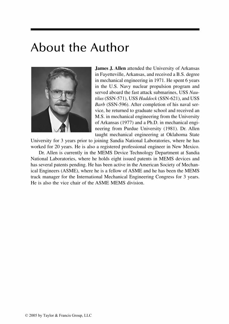
About the Author
James J. Allen attended the University of Arkansas
in Fayetteville, Arkansas, and received a B.S. degree
in mechanical engineering in 1971. He spent 6 years
in the U.S. Navy nuclear propulsion program and
served aboard the fast attack submarines, USS Nau-
tilus (SSN-571), USS Haddock (SSN-621), and USS
Barb (SSN-596). After completion of his naval ser-
vice, he returned to graduate school and received an
M.S. in mechanical engineering from the University
of Arkansas (1977) and a Ph.D. in mechanical engi-
neering from Purdue University (1981). Dr. Allen
taught mechanical engineering at Oklahoma State
University for 3 years prior to joining Sandia National Laboratories, where he has
worked for 20 years. He is also a registered professional engineer in New Mexico.
Dr. Allen is currently in the MEMS Device Technology Department at Sandia
National Laboratories, where he holds eight issued patents in MEMS devices and
has several patents pending. He has been active in the American Society of Mechan-
ical Engineers (ASME), where he is a fellow of ASME and he has been the MEMS
track manager for the International Mechanical Engineering Congress for 3 years.
He is also the vice chair of the ASME MEMS division.
© 2005 by Taylor & Francis Group, LLC
Contents
Chapter 1 Introduction ..........................................................................................1
1.1 Historical Perspective.......................................................................................1
1.2 The Development of MEMS Technology .......................................................3
1.3 MEMS: Present and Future .............................................................................6
1.4 MEMS Challenges .........................................................................................12
1.5 The Aim of This Book...................................................................................13
Questions..................................................................................................................14
References................................................................................................................14
Chapter 2 Fabrication Processes .........................................................................17
2.1 Materials.........................................................................................................17
2.1.1 Interatomic Bonds............................................................................17
2.1.2 Material Structure ............................................................................18
2.1.3 Crystal Lattices ................................................................................19
2.1.4 Miller Indices...................................................................................21
2.1.5 Crystal Imperfections ......................................................................23
2.2 Starting Material — Substrates .....................................................................25
2.2.1 Single-Crystal Substrate ..................................................................25
2.2.1.1 Czochralski Growth Process..........................................25
2.2.1.2 Float Zone Process.........................................................27
2.2.1.3 Post-Crystal Growth Processing ....................................27
2.2.2 Silicon on Insulator (SOI) Substrate ...............................................28
2.3 Physical Vapor Deposition (PVD) .................................................................30
2.3.1 Evaporation ......................................................................................32
2.3.2 Sputtering.........................................................................................34
2.4 Chemical Vapor Deposition (CVD)...............................................................35
2.5 Etching Processes...........................................................................................38
2.5.1 Wet Chemical Etching.....................................................................38
2.5.2 Plasma Etching ................................................................................39
2.5.3 Ion Milling.......................................................................................43
2.6 Patterning........................................................................................................43
2.6.1 Lithography......................................................................................43
2.6.2 Lift-Off Process ...............................................................................48
2.6.3 Damascene Process..........................................................................50
2.7 Wafer Bonding ...............................................................................................50
2.7.1 Silicon Fusion Bonding ...................................................................51
2.7.2 Anodic Bonding...............................................................................51
2.8 Annealing .......................................................................................................51
© 2005 by Taylor & Francis Group, LLC
2.9 Chemical Mechanical Polishing (CMP) ........................................................53
2.10 Material Doping .............................................................................................54
2.10.1 Diffusion ..........................................................................................56
2.10.2 Implant .............................................................................................60
2.11 Summary ........................................................................................................61
Questions..................................................................................................................62
References................................................................................................................63
Chapter 3 MEMS Technologies..........................................................................65
3.1 Bulk Micromachining ....................................................................................68
3.1.1 Wet Etching .....................................................................................70
3.1.2 Plasma Etching ................................................................................72
3.1.3 Examples of Bulk Micromachining Processes ...............................74
3.1.3.1 SCREAM .......................................................................75
3.1.3.2 PennSOIL.......................................................................76
3.2 LIGA ..............................................................................................................79
3.2.1 A LIGA Electromagnetic Microdrive .............................................80
3.3 Sacrificial Surface Micromachining ..............................................................83
3.3.1 SUMMiT™......................................................................................88
3.4 Integration of Electronics and MEMS Technology (IMEMS)......................94
3.5 Technology Characterization .........................................................................95
3.5.1 Residual Stress.................................................................................98
3.5.2 Young’s Modulus ...........................................................................101
3.5.3 Material Strength ...........................................................................102
3.5.4 Electrical Resistance......................................................................103
3.5.5 Mechanical Property Measurement for Process Control ..............105
3.6 Alternative MEMS Materials.......................................................................106
3.6.1 Silicon Carbide ..............................................................................106
3.6.2 Silicon Germanium........................................................................108
3.6.3 Diamond.........................................................................................108
3.6.4 SU-8 ...............................................................................................109
3.7 Summary ......................................................................................................109
Questions................................................................................................................110
References..............................................................................................................110
Chapter 4 Scaling Issues for MEMS................................................................115
4.1 Scaling of Physical Systems ........................................................................115
4.1.1 Geometric Scaling .........................................................................115
4.1.2 Mechanical System Scaling...........................................................117
4.1.3 Thermal System Scaling................................................................121
4.1.4 Fluidic System Scaling..................................................................124
4.1.5 Electrical System Scaling..............................................................129
4.1.6 Optical System Scaling .................................................................134
4.1.7 Chemical and Biological System Concentration ..........................135
© 2005 by Taylor & Francis Group, LLC
4.2 Computational Issues of Scale.....................................................................137
4.3 Fabrication Issues of Scale ..........................................................................139
4.4 Material Issues .............................................................................................141
4.5 Newly Relevant Physical Phenomena .........................................................144
4.6 Summary ......................................................................................................145
Questions................................................................................................................149
References..............................................................................................................152
Chapter 5 Design Realization Tools for MEMS ..............................................155
5.1 Layout...........................................................................................................155
5.2 SUMMiT Technology Layout......................................................................158
5.2.1 Anchoring Layers ..........................................................................159
5.2.2 Rotational Hubs .............................................................................164
5.2.3 Poly1 Beam with Substrate Connection .......................................170
5.2.4 Discrete Hinges..............................................................................170
5.3 Design Rules ................................................................................................176
5.3.1 Manufacturing Issues.....................................................................176
5.3.1.1 Patterning Limits..........................................................176
5.3.1.2 Etch Pattern Uniformity...............................................178
5.3.1.3 Registration Errors .......................................................178
5.3.1.4 Etch Compatibility .......................................................179
5.3.1.5 Stringers .......................................................................179
5.3.1.6 Floaters.........................................................................180
5.3.1.7 Litho Depth of Focus...................................................180
5.3.1.8 Stiction (Dimples)........................................................181
5.3.1.9 Etch Release Holes ......................................................181
5.3.1.10 Improper Anchor (Area of Anchor).............................182
5.3.2 Design Rule Checking...................................................................182
5.4 Standard Components ..................................................................................183
5.5 MEMS Visualization ....................................................................................184
5.6 MEMS Analysis ...........................................................................................186
5.7 Summary ......................................................................................................188
Questions................................................................................................................189
References..............................................................................................................190
Chapter 6 Electromechanics .............................................................................193
6.1 Structural Mechanics....................................................................................194
6.1.1 Material Models.............................................................................194
6.1.2 Thermal Strains..............................................................................200
6.1.3 Axial Rod.......................................................................................201
6.1.4 Torsion Rod ...................................................................................203
6.1.5 Beam Bending ...............................................................................205
6.1.6 Flat Plate Bending .........................................................................208
6.1.7 Columns .........................................................................................211
© 2005 by Taylor & Francis Group, LLC
6.1.8 Stiffness Coefficients .....................................................................213
6.2 Damping .......................................................................................................216
6.2.1 Oscillatory Mechanical Systems and Damping ............................217
6.2.2 Damping Mechanisms ...................................................................220
6.2.3 Viscous Damping...........................................................................222
6.2.4 Damping Models ...........................................................................224
6.2.4.1 Squeeze Film Damping Model....................................224
6.2.4.2 Slide Film Damping Model .........................................226
6.3 Electrical System Dynamics ........................................................................228
6.3.1 Electric and Magnetic Fields.........................................................229
6.3.2 Electrical Circuits — Passive Elements........................................234
6.3.2.1 Capacitor ......................................................................234
6.3.2.2 Inductor ........................................................................235
6.3.2.3 Resistor.........................................................................236
6.3.2.4 Energy Sources ............................................................238
6.3.2.5 Circuit Interconnection ................................................238
Questions................................................................................................................240
References..............................................................................................................241
Chapter 7 Modeling and Design.......................................................................243
7.1 Design Synthesis Modeling .........................................................................243
7.2 Lagrange’s Equations...................................................................................244
7.2.1 Lagrange’s Equations with Nonpotential Forces ..........................246
7.2.2 Lagrange’s Equations with Equations of Constraint.....................247
7.2.3 Use of Lagrange’s Equations to Obtain Lumped Parameter
Governing Equations of Systems ..................................................248
7.2.4 Analytical Mechanics Methods for Continuous Systems .............257
7.3 Numerical Modeling ....................................................................................262
7.4 Design Uncertainty ......................................................................................267
Questions................................................................................................................270
References..............................................................................................................271
Chapter 8 MEMS Sensors and Actuators .........................................................273
8.1 MEMS Actuators..........................................................................................273
8.1.1 Electrostatic Actuation...................................................................273
8.1.1.1 Parallel Plate Capacitor................................................273
8.1.1.2 Interdigitated Comb Capacitor ....................................278
8.1.1.3 Electrostatic Actuators .................................................278
8.1.2 Thermal Actuation .........................................................................285
8.1.3 Lorentz Force Actuation ................................................................288
8.2 MEMS Sensing ............................................................................................290
8.2.1 Capacitative Sensing......................................................................290
8.2.2 Piezoresistive Sensing....................................................................298
8.2.2.1 Piezoresistivity .............................................................298
© 2005 by Taylor & Francis Group, LLC
8.2.2.2 Piezoresistance in Single-Crystal Silicon....................299
8.2.2.3 Piezoresistivity of Polycrystalline and Amorphous
Silicon ..........................................................................304
8.2.2.4 Signal Detection...........................................................304
8.2.3 Electron Tunneling.........................................................................306
8.2.4 Sensor Noise ..................................................................................308
8.2.4.1 Noise Sources ..............................................................311
8.2.5 MEMS Physical Sensors ...............................................................314
8.2.5.1 Accelerometer ..............................................................314
8.2.5.2 Gyroscope ....................................................................319
8.2.5.3 Pressure Sensors...........................................................324
8.2.6 Chemical Sensors ..........................................................................328
8.2.6.1 Taguchi Gas Sensor .....................................................330
8.2.6.2 Combustible Gas Sensor..............................................331
Questions................................................................................................................332
References..............................................................................................................333
Chapter 9 Packaging .........................................................................................339
9.1 Packaging Process Steps ..............................................................................339
9.1.1 Postfabrication Processing.............................................................340
9.1.1.1 Release Process............................................................341
9.1.1.2 Drying Process .............................................................341
9.1.1.3 Coating Processes ........................................................342
9.1.1.4 Assembly......................................................................345
9.1.1.5 Encapsulation ...............................................................348
9.1.2 Package Selection/Design..............................................................350
9.1.3 Die Attach ......................................................................................352
9.1.4 Wire Bond and Sealing .................................................................353
9.2 Packaging Case Studies ...............................................................................353
9.2.1 R&D Prototype Packaging ............................................................355
9.2.2 DMD Packaging ............................................................................357
9.2.3 Electrical-Fluidic Packaging..........................................................359
9.3 Summary ......................................................................................................361
Questions................................................................................................................362
References..............................................................................................................363
Chapter 10 Reliability .........................................................................................367
10.1 Reliability Theory and Terminology ...........................................................367
10.2 Essential Aspects of Probability and Statistics for Reliability ...................370
10.3 Reliability Models........................................................................................380
10.3.1 Weibull Model ...............................................................................380
10.3.2 Lognormal Model ..........................................................................383
10.3.3 Exponential Model ........................................................................386
10.4 MEMS Failure Mechanisms ........................................................................386
© 2005 by Taylor & Francis Group, LLC
10.4.1 Operational Failure Mechanisms...................................................388
10.4.1.1 Wear .............................................................................388
10.4.1.2 Fracture ........................................................................390
10.4.1.3 Fatigue..........................................................................391
10.4.1.4 Charging.......................................................................391
10.4.1.5 Creep ............................................................................391
10.4.1.6 Stiction and Adhesion..................................................391
10.4.2 Degradation Mechanisms ..............................................................392
10.4.3 Environmental Failure Mechanisms..............................................392
10.4.3.1 Shock and Vibration.....................................................392
10.4.3.2 Thermal Cycling ..........................................................393
10.4.3.3 Humidity ......................................................................393
10.4.3.4 Radiation ......................................................................393
10.4.3.5 Electrostatic Discharge (ESD).....................................393
10.5 Measurement Techniques for MEMS Operational, Reliability, and
Failure Analysis Testing ...............................................................................394
10.5.1 Optical Microscopy .......................................................................394
10.5.2 Scanning Electron Microscopy......................................................396
10.5.3 Focused Ion Beam .........................................................................396
10.5.4 Atomic Force Microscope .............................................................397
10.5.5 Lift-Off...........................................................................................397
10.5.6 Stroboscopy....................................................................................397
10.5.7 Blur Envelope ................................................................................398
10.5.8 Video Imaging ...............................................................................399
10.5.9 Interferometry ................................................................................399
10.5.10 Laser Doppler Velocimeter (LDV)................................................400
10.6 MEMS Reliability and Design ....................................................................400
10.7 MEMS Reliability Case Studies ..................................................................403
10.7.1 DMD Reliability ............................................................................403
10.7.2 Sandia Microengine .......................................................................407
10.8 Summary ......................................................................................................412
Questions................................................................................................................412
References..............................................................................................................413
Appendix A — Glossary .......................................................................................417
Appendix B — Prefixes ........................................................................................419
Appendix C — Micro–MKS Conversions............................................................421
Appendix D — Physical Constants.......................................................................423
Appendix E — Material Properties.......................................................................425
© 2005 by Taylor & Francis Group, LLC

Appendix F — Stiffness Coefficients of Frequently Used MEMS Flexures .......427
Appendix G — Common MEMS Cross-Section Properties ................................433
Appendix H............................................................................................................437
© 2005 by Taylor & Francis Group, LLC
1
1 Introduction
1.1 HISTORICAL PERSPECTIVE
Making devices small has long had engineering, scientific, and aesthetic motiva-
tions. For example, John Harrison’s quest [1] to make a small (e.g., hand-sized)
chronometer in the 1700s for nautical navigation was motivated by the desire to
have an accurate time-keeping instrument that was insensitive to temperature,
humidity, and motion. A small chronometer could meet these objectives and allow
for multiple instruments on a ship for redundancy and error averaging. A number
of technological firsts came from this work, such as the development of the roller
bearing. Driven by the need for portability, the miniaturization of many mechan-
ical devices has advanced over the years.
The 20th century saw the rise of electrical and electronic devices that had an
impact on daily life. Until the advent of the point contact transistor in 1947 by
Bardeen and Brattain [2] and, later, the junction transistor by Shockley [3],
electronic devices were based upon the vacuum tube invented in 1906 by Lee de
Forest. The transistor was a great leap forward in reducing size, power require-
ments, and portability of electronic devices.
By the mid 20th century, electronic devices were produced by connecting
individual components (i.e., vacuum tubes, switches, resistors and capacitors).
This resulted in large devices that consumed significant power and were costly
to produce. The reliability of these devices was also poor due to the need to
assemble the multitude of components. The state of the art was epitomized by
the world’s first digital computer [4], ENIAC (electronic numerical integrator and
computer), which was developed at the University of Pennsylvania [5] for the
Army Ordnance Department to carry out ballistics calculations. The need for
ENIAC illustrates the need for computers to assist in the development of engi-
neering devices that was emerging at the time. However, ENIAC consisted of
thousands of electronic components, which needed to be replaced at frequent
intervals, consumed significant power, and wasted heat.
Several key events occurred in the late 1950s that would motivate develop-
ment of electronics at an increased pace beyond the discrete transistor. The
development of the planar silicon transistor [6,7] and the planar fabrication
process [8,9] set the stage for development of fabrication processes and equipment
to achieve electronic devices monolithically integrated on a single substrate with
small feature sizes. The development of this technology for integrated circuits
started the microelectronics revolution, which led to the production of microelec-
tronic devices with smaller and smaller features and continues to the present day.
© 2005 by Taylor & Francis Group, LLC
2 Micro Electro Mechanical System Design
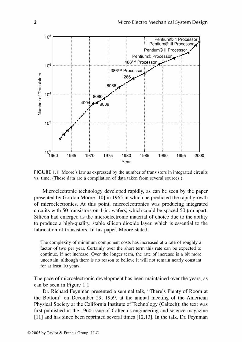
Microelectronic technology developed rapidly, as can be seen by the paper
presented by Gordon Moore [10] in 1965 in which he predicted the rapid growth
of microelectronics. At this point, microelectronics was producing integrated
circuits with 50 transistors on 1-in. wafers, which could be spaced 50 µm apart.
Silicon had emerged as the microelectronic material of choice due to the ability
to produce a high-quality, stable silicon dioxide layer, which is essential to the
fabrication of transistors. In his paper, Moore stated,
The complexity of minimum component costs has increased at a rate of roughly a
factor of two per year. Certainly over the short term this rate can be expected to
continue, if not increase. Over the longer term, the rate of increase is a bit more
uncertain, although there is no reason to believe it will not remain nearly constant
for at least 10 years.
The pace of microelectronic development has been maintained over the years, as
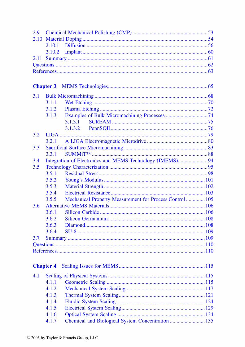
can be seen in Figure 1.1.
Dr. Richard Feynman presented a seminal talk, “There’s Plenty of Room at
the Bottom” on December 29, 1959, at the annual meeting of the American
Physical Society at the California Institute of Technology (Caltech); the text was
first published in the 1960 issue of Caltech’s engineering and science magazine
[11] and has since been reprinted several times [12,13]. In the talk, Dr. Feynman
FIGURE 1.1 Moore’s law as expressed by the number of transistors in integrated circuits
vs. time. (These data are a compilation of data taken from several sources.)
108
106
104
102
100
Num
ber
of T
ransis
tors
1960 1965 1970
4004
8080
8086
286
386™ Processor
486™ Processor
Pentium® II Processor
Pentium® Processor
Pentium® 4 Processor
Pentium® III Processor
8008
1975
Year
1980 1985 1990 1995 2000
© 2005 by Taylor & Francis Group, LLC
Introduction 3
conceptually presented, motivated, and challenged people with the desire and
advantages of exploring engineered devices at the small scale. This talk is fre-
quently sited as the conceptual beginnings of the fields of microelectromechanical
systems (MEMS) and nanotechnology. Dr. Feynman provided some very insight-
ful comments on the scaling of physical phenomena as size is reduced as well
as some prophetic uses of the small-scale devices upon which he was speculating.
• Scaling of physical phenomena
• “The effective viscosity of oil would be higher and higher in pro-
portion as we went down” in size.
• “Let the bearings run dry; they won’t run hot because the heat
escapes away from such a small device very, very rapidly.”
• Miniaturizing the computer
• “…the possibilities of computers are very interesting — if they
could be made to be more complicated by several orders of magni-
tude. If they had millions of times as many elements, they could
make judgments.”
• “For instance, the wires should be made 10 or 100 atoms in diameter,
and the circuits should be a few thousand angstroms across.”
• Use of small machines
• “…it would be interesting in surgery if you could swallow the
surgeon. You put the mechanical surgeon inside the blood vessel
and it goes into the heart and looks around.”
During this presentation, Dr. Feynman offered two $1000 prizes for the
following achievements:
• Build a working electric motor no larger than a 1/64-in. (400-µm) cube
• Print text at a scale (1/25,000) that the Encyclopedia Britannica could
fit on the head of a pin
In less than a year, a Caltech engineer, William McLellan, constructed a 250-
µg, 2000-rpm electric motor using 13 separate parts to collect his prize [14]. This
illustrated that technology was constantly moving toward miniaturization and that
aspects of the technology already existed. However, the second prize was not
rewarded until 1985, when T. Newman and R.F.W. Pease used e-beam lithography
to print the first page of A Tale of Two Cities within a 5.9-µm square [14]. The
achievement of the second prize was enabled by the developments of the micro-
electronics industry in the ensuing 25 years. Images of these achievements are
available in references 16 and 17.
1.2 THE DEVELOPMENT OF MEMS TECHNOLOGY
Microelectromechanical system (MEMS) technology (also known as microsys-
tems technology [MST] in Europe) has been inspired by the development of the
© 2005 by Taylor & Francis Group, LLC

4 Micro Electro Mechanical System Design
microelectronic revolution and the vision of Dr. Feynman. MEMS and MST were
built upon the technological and commercial needs of the latter part of the 20th
century, as well as the drive toward miniaturization that had been a driving force
for a number of reasons over a much longer period of time. The development of
MEMS technology synergistically used to a large extent the materials and fabri-
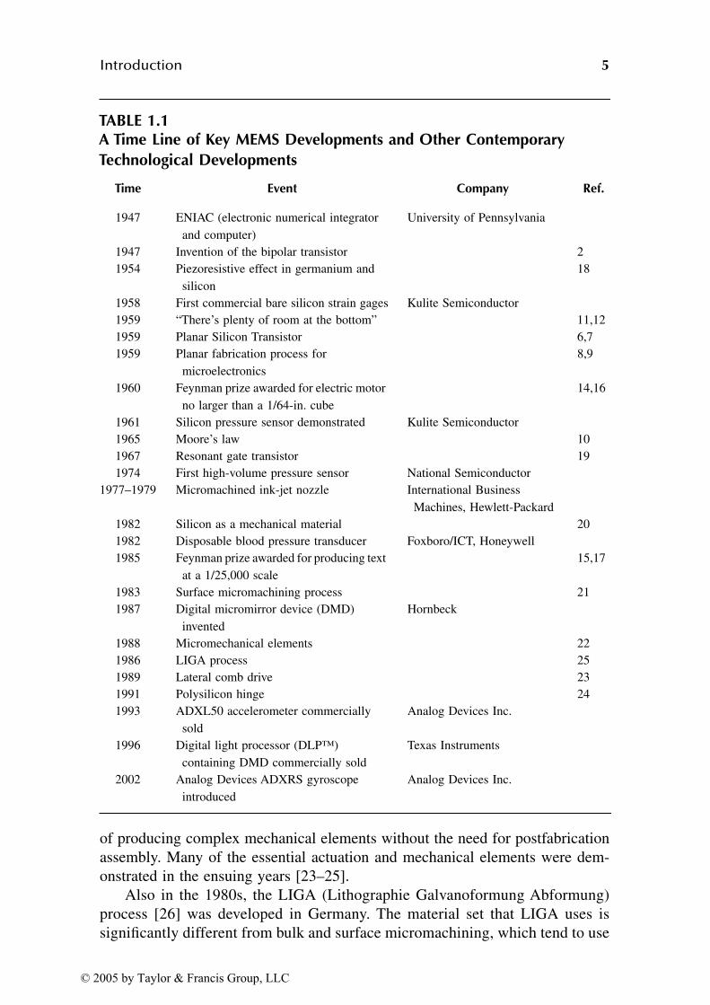
cation methods developed for microelectronics. Table 1.1 is a historical time line
of some of the key events in the development of MEMS technology.
MEMS technology is a result of a long history of technology development
starting with machine and machining development through the advent of micro-
electronics. In fact, in a continuum of devices and fabrication process MEMS
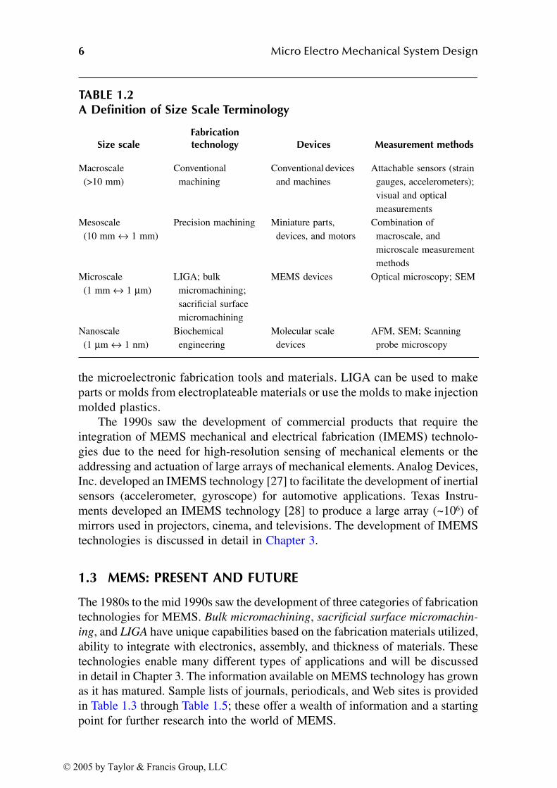
occupies the size range from 1 mm to 1 µm. In this book, size scales are referred
to as macro, meso, micro, and nano scale. Table 1.2 attempts to provide a more
definitive definition of these terms.
The development of the discrete transistor and its use began to replace the
vacuum tube in electronic applications in the 1950s. In the early days of the
development of the transistor, the piezoresistive properties of the semiconductor
materials used to develop the transistor, silicon and germanium, were researched
[18]. This advance provided a link between the electronic materials and mechan-
ical sensing. This link was exploited early in the time line of MEMS development
to produce strain gages and pressure sensors.
The key technical advances that precipitated the microelectronic revolution
were the development of the planar silicon transistor [6,7] and fabrication process
[8,9]. The planar silicon fabrication process provided a path that enabled the
integration of large numbers of transistors to create many different electronic
devices and, through continuous technical advancement of the fabrication tools
(lithography, etching, diffusion, and implantation), a continual reduction in size
of the transistor. This ability to increasingly miniaturize the electronic circuitry
over a long period of time was predicted by Moore in 1965 in what was to become
known as Moore’s law. The effects of this law continue today and at least for the
next 20 years [19]. This development of fabrication tools for increasingly smaller
dimensions is a key enabler for MEMS technology.
In 1967, Nathanson et al. developed the resonant gate transistor [20], which
showed the possibilities of an integrated mechanical–electrical device and silicon
micromachining. In the early days of microelectronics and through the 1970s,
bulk micromachining, which utilizes deep etching techniques, was developed and
used to produce pressure sensors and accelerometers. In 1982, Petersen [21] wrote
a seminal paper, “Silicon as a Mechanical Material.” Thus, silicon was considered
and utilized to an even greater extent to produce sensors that needed a mechanical
element (inertial mass, pressure diaphragm) and a transduction mechanism
(mechanical–electrical) to produce a sensor. Bulk micromachining was also uti-
lized to make ink nozzles, which were becoming a large commercial market due
to the computer revolution’s need for low-cost printers.
In 1983, Howe and Muller [22] developed the basic scheme for surface
micromachining; this utilizes two types of material (structural, sacrificial) and
the tools developed for microelectronics to create a fabrication technology capable
© 2005 by Taylor & Francis Group, LLC
Introduction 5
of producing complex mechanical elements without the need for postfabrication
assembly. Many of the essential actuation and mechanical elements were dem-
onstrated in the ensuing years [23–25].
Also in the 1980s, the LIGA (Lithographie Galvanoformung Abformung)
process [26] was developed in Germany. The material set that LIGA uses is
significantly different from bulk and surface micromachining, which tend to use
TABLE 1.1A Time Line of Key MEMS Developments and Other Contemporary
Technological Developments
Time Event Company Ref.
1947 ENIAC (electronic numerical integrator
and computer)
University of Pennsylvania
1947 Invention of the bipolar transistor 2
1954 Piezoresistive effect in germanium and
silicon
18
1958 First commercial bare silicon strain gages Kulite Semiconductor
1959 “There’s plenty of room at the bottom” 11,12
1959 Planar Silicon Transistor 6,7
1959 Planar fabrication process for
microelectronics
8,9
1960 Feynman prize awarded for electric motor
no larger than a 1/64-in. cube
14,16
1961 Silicon pressure sensor demonstrated Kulite Semiconductor
1965 Moore’s law 10
1967 Resonant gate transistor 19
1974 First high-volume pressure sensor National Semiconductor
1977–1979 Micromachined ink-jet nozzle International Business
Machines, Hewlett-Packard
1982 Silicon as a mechanical material 20
1982 Disposable blood pressure transducer Foxboro/ICT, Honeywell
1985 Feynman prize awarded for producing text
at a 1/25,000 scale
15,17
1983 Surface micromachining process 21
1987 Digital micromirror device (DMD)
invented
Hornbeck
1988 Micromechanical elements 22
1986 LIGA process 25
1989 Lateral comb drive 23
1991 Polysilicon hinge 24
1993 ADXL50 accelerometer commercially
sold
Analog Devices Inc.
1996 Digital light processor (DLP™)
containing DMD commercially sold
Texas Instruments
2002 Analog Devices ADXRS gyroscope
introduced
Analog Devices Inc.
© 2005 by Taylor & Francis Group, LLC
6 Micro Electro Mechanical System Design
the microelectronic fabrication tools and materials. LIGA can be used to make
parts or molds from electroplateable materials or use the molds to make injection
molded plastics.
The 1990s saw the development of commercial products that require the
integration of MEMS mechanical and electrical fabrication (IMEMS) technolo-
gies due to the need for high-resolution sensing of mechanical elements or the
addressing and actuation of large arrays of mechanical elements. Analog Devices,
Inc. developed an IMEMS technology [27] to facilitate the development of inertial
sensors (accelerometer, gyroscope) for automotive applications. Texas Instru-
ments developed an IMEMS technology [28] to produce a large array (~106) of
mirrors used in projectors, cinema, and televisions. The development of IMEMS
technologies is discussed in detail in Chapter 3.
1.3 MEMS: PRESENT AND FUTURE
The 1980s to the mid 1990s saw the development of three categories of fabrication
technologies for MEMS. Bulk micromachining, sacrificial surface micromachin-
ing, and LIGA have unique capabilities based on the fabrication materials utilized,
ability to integrate with electronics, assembly, and thickness of materials. These
technologies enable many different types of applications and will be discussed
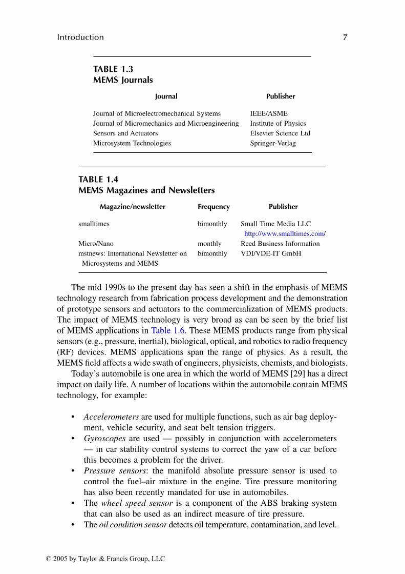
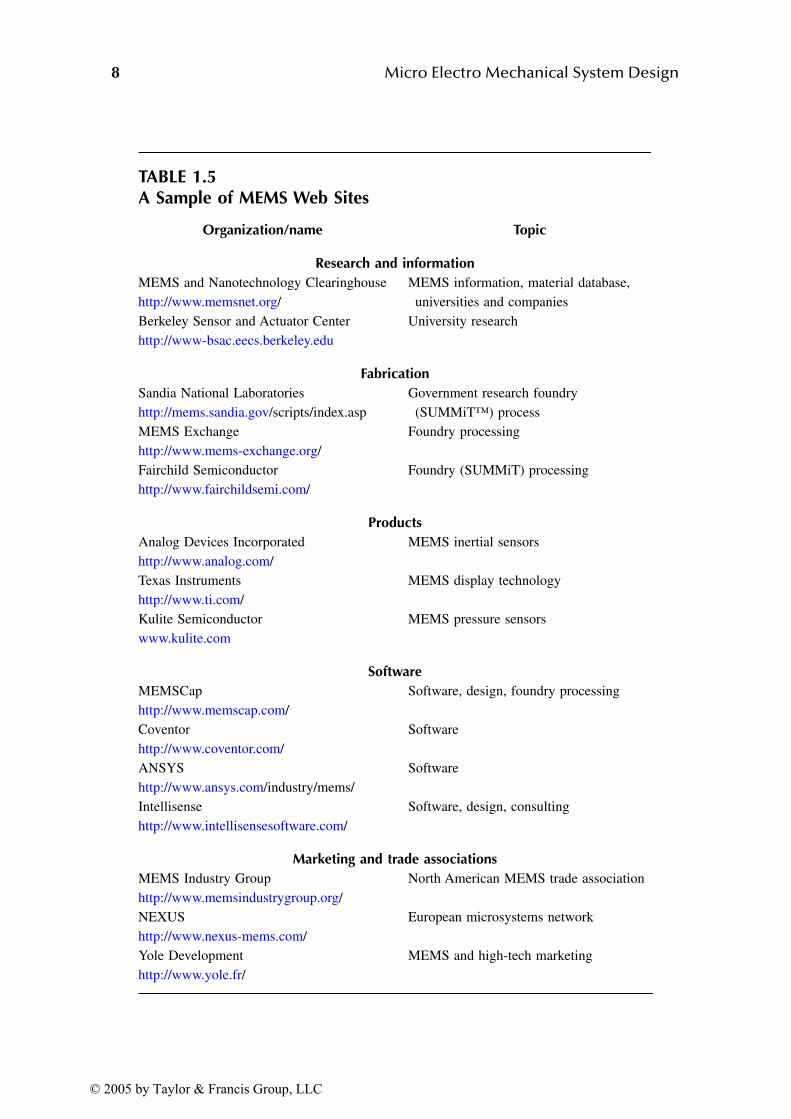
in detail in Chapter 3. The information available on MEMS technology has grown
as it has matured. Sample lists of journals, periodicals, and Web sites is provided
in Table 1.3 through Table 1.5; these offer a wealth of information and a starting
point for further research into the world of MEMS.
TABLE 1.2A Definition of Size Scale Terminology
Size scaleFabricationtechnology Devices Measurement methods
Macroscale
(>10 mm)
Conventional
machining
Conventional devices
and machines
Attachable sensors (strain
gauges, accelerometers);
visual and optical
measurements
Mesoscale
(10 mm ↔ 1 mm)
Precision machining Miniature parts,
devices, and motors
Combination of
macroscale, and
microscale measurement
methods
Microscale
(1 mm ↔ 1 µm)
LIGA; bulk
micromachining;
sacrificial surface
micromachining
MEMS devices Optical microscopy; SEM
Nanoscale
(1 µm ↔ 1 nm)
Biochemical
engineering
Molecular scale
devices
AFM, SEM; Scanning
probe microscopy
© 2005 by Taylor & Francis Group, LLC
Introduction 7
The mid 1990s to the present day has seen a shift in the emphasis of MEMS
technology research from fabrication process development and the demonstration
of prototype sensors and actuators to the commercialization of MEMS products.
The impact of MEMS technology is very broad as can be seen by the brief list
of MEMS applications in Table 1.6. These MEMS products range from physical
sensors (e.g., pressure, inertial), biological, optical, and robotics to radio frequency
(RF) devices. MEMS applications span the range of physics. As a result, the
MEMS field affects a wide swath of engineers, physicists, chemists, and biologists.
Today’s automobile is one area in which the world of MEMS [29] has a direct
impact on daily life. A number of locations within the automobile contain MEMS
technology, for example:
• Accelerometers are used for multiple functions, such as air bag deploy-
ment, vehicle security, and seat belt tension triggers.
• Gyroscopes are used — possibly in conjunction with accelerometers
— in car stability control systems to correct the yaw of a car before
this becomes a problem for the driver.
• Pressure sensors: the manifold absolute pressure sensor is used to
control the fuel–air mixture in the engine. Tire pressure monitoring
has also been recently mandated for use in automobiles.
• The wheel speed sensor is a component of the ABS braking system
that can also be used as an indirect measure of tire pressure.
• The oil condition sensor detects oil temperature, contamination, and level.
TABLE 1.3MEMS Journals
Journal Publisher
Journal of Microelectromechanical Systems IEEE/ASME
Journal of Micromechanics and Microengineering Institute of Physics
Sensors and Actuators Elsevier Science Ltd
Microsystem Technologies Springer-Verlag
TABLE 1.4MEMS Magazines and Newsletters
Magazine/newsletter Frequency Publisher
smalltimes bimonthly Small Time Media LLC
http://www.smalltimes.com/
Micro/Nano monthly Reed Business Information
mstnews: International Newsletter on
Microsystems and MEMS
bimonthly VDI/VDE-IT GmbH
© 2005 by Taylor & Francis Group, LLC
8 Micro Electro Mechanical System Design
TABLE 1.5A Sample of MEMS Web Sites
Organization/name Topic
Research and information
MEMS and Nanotechnology Clearinghouse
http://www.memsnet.org/
MEMS information, material database,
universities and companies
Berkeley Sensor and Actuator Center
http://www-bsac.eecs.berkeley.edu
University research
Fabrication
Sandia National Laboratories
http://mems.sandia.gov/scripts/index.asp
Government research foundry
(SUMMiT™) process
MEMS Exchange
http://www.mems-exchange.org/
Foundry processing
Fairchild Semiconductor
http://www.fairchildsemi.com/
Foundry (SUMMiT) processing
Products
Analog Devices Incorporated
http://www.analog.com/
MEMS inertial sensors
Texas Instruments
http://www.ti.com/
MEMS display technology
Kulite Semiconductor
www.kulite.com
MEMS pressure sensors
Software
MEMSCap
http://www.memscap.com/
Software, design, foundry processing
Coventor
http://www.coventor.com/
Software
ANSYS
http://www.ansys.com/industry/mems/
Software
Intellisense
http://www.intellisensesoftware.com/
Software, design, consulting
Marketing and trade associations
MEMS Industry Group
http://www.memsindustrygroup.org/
North American MEMS trade association
NEXUS
http://www.nexus-mems.com/
European microsystems network
Yole Development
http://www.yole.fr/
MEMS and high-tech marketing
© 2005 by Taylor & Francis Group, LLC
Introduction 9
The automotive market is a mass market in which MEMS is playing an ever
increasing role. For example, 90 million air bag accelerometers and 30 million
manifold absolute pressure sensors were supplied to the automotive market in
2002 [30].
Another mass market in which MEMS has an increasing impact is the bio-
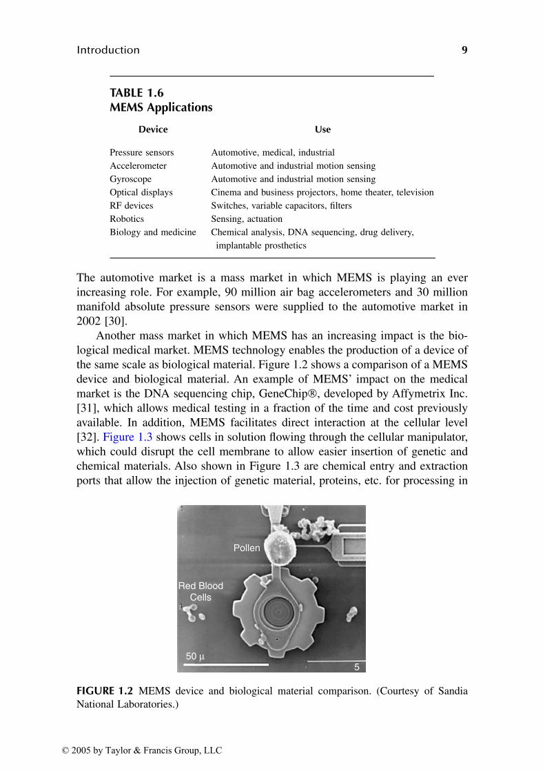
logical medical market. MEMS technology enables the production of a device of
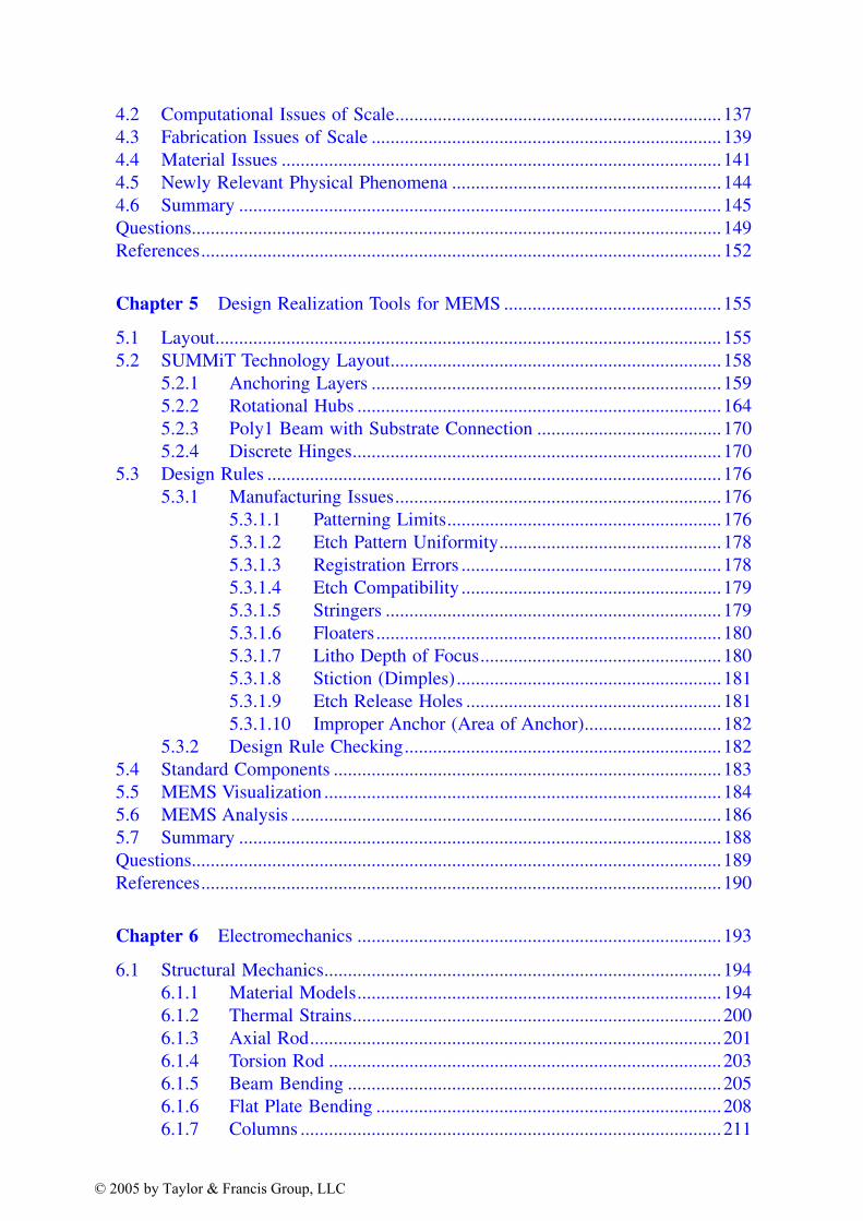
the same scale as biological material. Figure 1.2 shows a comparison of a MEMS
device and biological material. An example of MEMS’ impact on the medical
market is the DNA sequencing chip, GeneChip, developed by Affymetrix Inc.
[31], which allows medical testing in a fraction of the time and cost previously
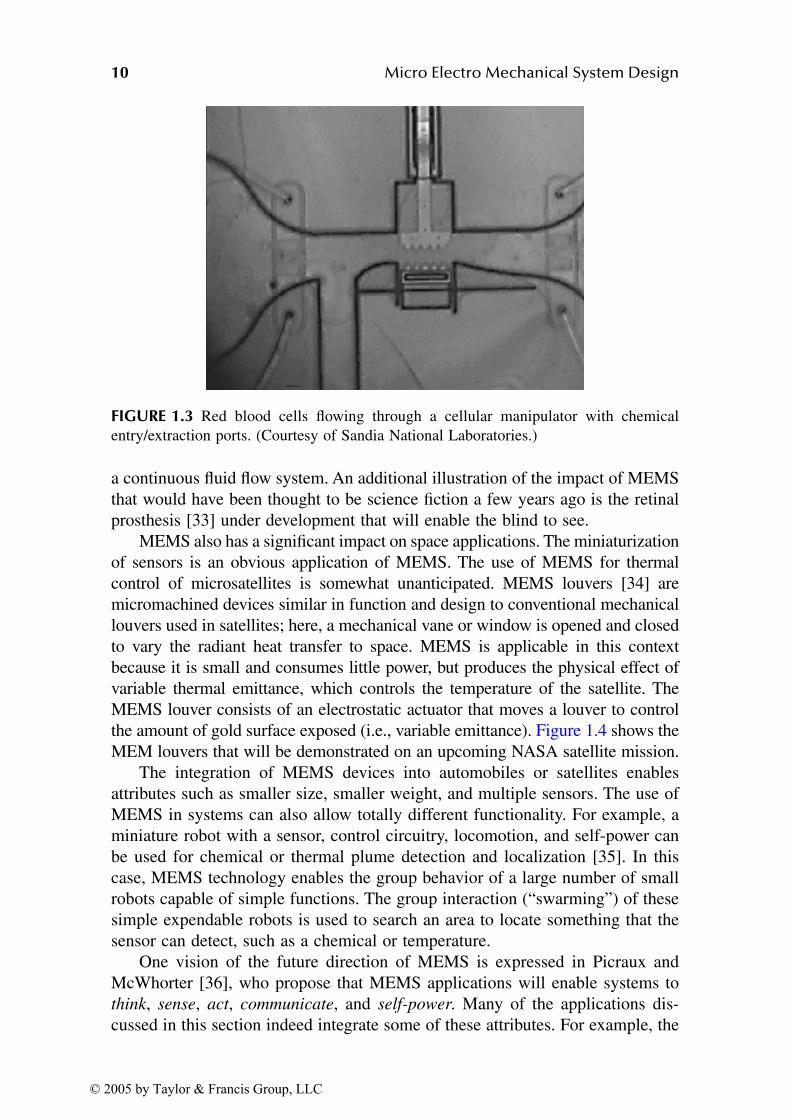
available. In addition, MEMS facilitates direct interaction at the cellular level
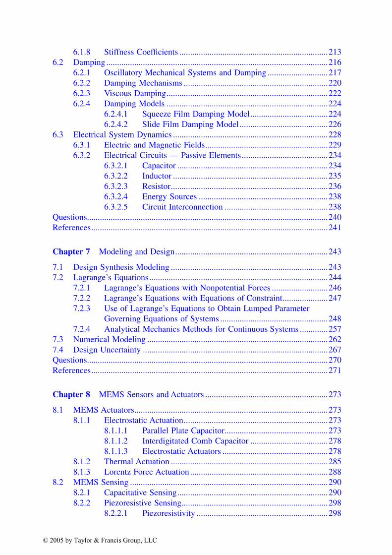
[32]. Figure 1.3 shows cells in solution flowing through the cellular manipulator,
which could disrupt the cell membrane to allow easier insertion of genetic and
chemical materials. Also shown in Figure 1.3 are chemical entry and extraction
ports that allow the injection of genetic material, proteins, etc. for processing in
TABLE 1.6MEMS Applications
Device Use
Pressure sensors Automotive, medical, industrial
Accelerometer Automotive and industrial motion sensing
Gyroscope Automotive and industrial motion sensing
Optical displays Cinema and business projectors, home theater, television
RF devices Switches, variable capacitors, filters
Robotics Sensing, actuation
Biology and medicine Chemical analysis, DNA sequencing, drug delivery,
implantable prosthetics
FIGURE 1.2 MEMS device and biological material comparison. (Courtesy of Sandia
National Laboratories.)
Red Blood
Cells
Pollen
50 µ
5
© 2005 by Taylor & Francis Group, LLC
10 Micro Electro Mechanical System Design
a continuous fluid flow system. An additional illustration of the impact of MEMS
that would have been thought to be science fiction a few years ago is the retinal
prosthesis [33] under development that will enable the blind to see.
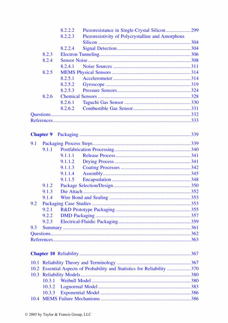
MEMS also has a significant impact on space applications. The miniaturization
of sensors is an obvious application of MEMS. The use of MEMS for thermal
control of microsatellites is somewhat unanticipated. MEMS louvers [34] are
micromachined devices similar in function and design to conventional mechanical
louvers used in satellites; here, a mechanical vane or window is opened and closed
to vary the radiant heat transfer to space. MEMS is applicable in this context
because it is small and consumes little power, but produces the physical effect of
variable thermal emittance, which controls the temperature of the satellite. The
MEMS louver consists of an electrostatic actuator that moves a louver to control
the amount of gold surface exposed (i.e., variable emittance). Figure 1.4 shows the
MEM louvers that will be demonstrated on an upcoming NASA satellite mission.
The integration of MEMS devices into automobiles or satellites enables
attributes such as smaller size, smaller weight, and multiple sensors. The use of
MEMS in systems can also allow totally different functionality. For example, a
miniature robot with a sensor, control circuitry, locomotion, and self-power can
be used for chemical or thermal plume detection and localization [35]. In this
case, MEMS technology enables the group behavior of a large number of small
robots capable of simple functions. The group interaction (“swarming”) of these
simple expendable robots is used to search an area to locate something that the
sensor can detect, such as a chemical or temperature.
One vision of the future direction of MEMS is expressed in Picraux and
McWhorter [36], who propose that MEMS applications will enable systems to
think, sense, act, communicate, and self-power. Many of the applications dis-
cussed in this section indeed integrate some of these attributes. For example, the
FIGURE 1.3 Red blood cells flowing through a cellular manipulator with chemical
entry/extraction ports. (Courtesy of Sandia National Laboratories.)
© 2005 by Taylor & Francis Group, LLC

Introduction 11
small robot shown in Figure 1.5 has a sensor, can move, and has a self-contained
power source. To integrate all of these functions on one chip may not be practical
due to financial or engineering constraints; however, integration of these functions
via packaging may be a more viable path.
MEMS is a new technology that has formally been in existence since the
1980s when the acronym MEMS was coined. This technology has been focusing
on commercial applications since the mid 1990s with significant success [37].
The MEMS commercial businesses are generally organized around three main
models: MEMS manufacturers; MEMS design; and system integrators. In 2003,
368 MEMS fabrication facilities existed worldwide, with strong centers in North
America, Japan, and Europe. There are 130 different MEMS applications in
production consisting of a few large-volume applications in the automotive (iner-
FIGURE 1.4 MEMS variable emittance lover for microsatellite thermal control. The
device was developed under a joint project with NASA, Goddard Spaceflight Center, The
Johns Hopkins Applied Physics Laboratory, and Sandia National Laboratories.
FIGURE 1.5 A small robot with a sensor, locomotion, control circuitry, and self power.
(Courtesy of Sandia National Laboratories.)
© 2005 by Taylor & Francis Group, LLC
12 Micro Electro Mechanical System Design
tial, pressure); ink-jet nozzles; and medical fields (e.g., Affymetrix GeneChip).
The MEMS commercial market is growing at a 25% annual rate [37].
1.4 MEMS CHALLENGES
MEMS is a growing field applicable to many lines of products that has been
synergistically using technology and tools from the microelectronics industry.
However, MEMS and microelectronics differ in some very fundamental ways.
Table 1.7 compares the devices and technologies of MEMS and microelectronics,
and Figure 1.6 compares the levels of device integration of MEMS and micro-
electronics. The most striking observation is that microelectronics is an enormous
industry based on a few fundamental devices with a standardized fabrication
process. The microelectronics industry derives its commercial applicability from
the ability to connect a multitude of a few fundamental types of electronic devices
(e.g., transistors, capacitors, resistors) reliably on a chip to create a plethora of
new microelectronic applications (e.g., logic circuits, amplifiers, computer pro-
cessors, etc.). The exponential growth predicted by Moore’s law comes from
improving the fabrication tools to make increasingly smaller circuit elements,
which in turn enable faster and more complex microelectronic applications.
The MEMS industry derives its commercial applicability from the ability to
address a wide variety of applications (accelerometers, pressure sensors, mirrors,
fluidic channel); however, no one fundamental unit cell [38,39] and standard
fabrication process to build the devices exists. In fact, the drive toward smaller
devices for microelectronics, which increased speed and complexity, does not
necessarily have the same impact on MEMS devices [40] due to scaling issues
(Chapter 4). MEMS is a new rapidly growing [37] technology area in which
contributions are to be made in fabrication, design, and business.
TABLE 1.7Comparison of MEMS and Microelectronics
Criteria Microelectronics MEMS
Feature size Submicron 1–3 µm
Device size Submicron ~50 µm–1 mm
Materials Silicon based Varied (silicon, metals, plastics)
Fundamental devices Limited set: transistor,
capacitor, resistor
Widely varied: fluid, mechanical, optical,
electrical elements (sensors, actuators, switches,
mirrors, etc.)
Fabrication process Standardized: planar
silicon process
Varied: three main categories of MEMS
fabrication processes plus variants:
Bulk micromachining
Surface micromachining
LIGA
© 2005 by Taylor & Francis Group, LLC
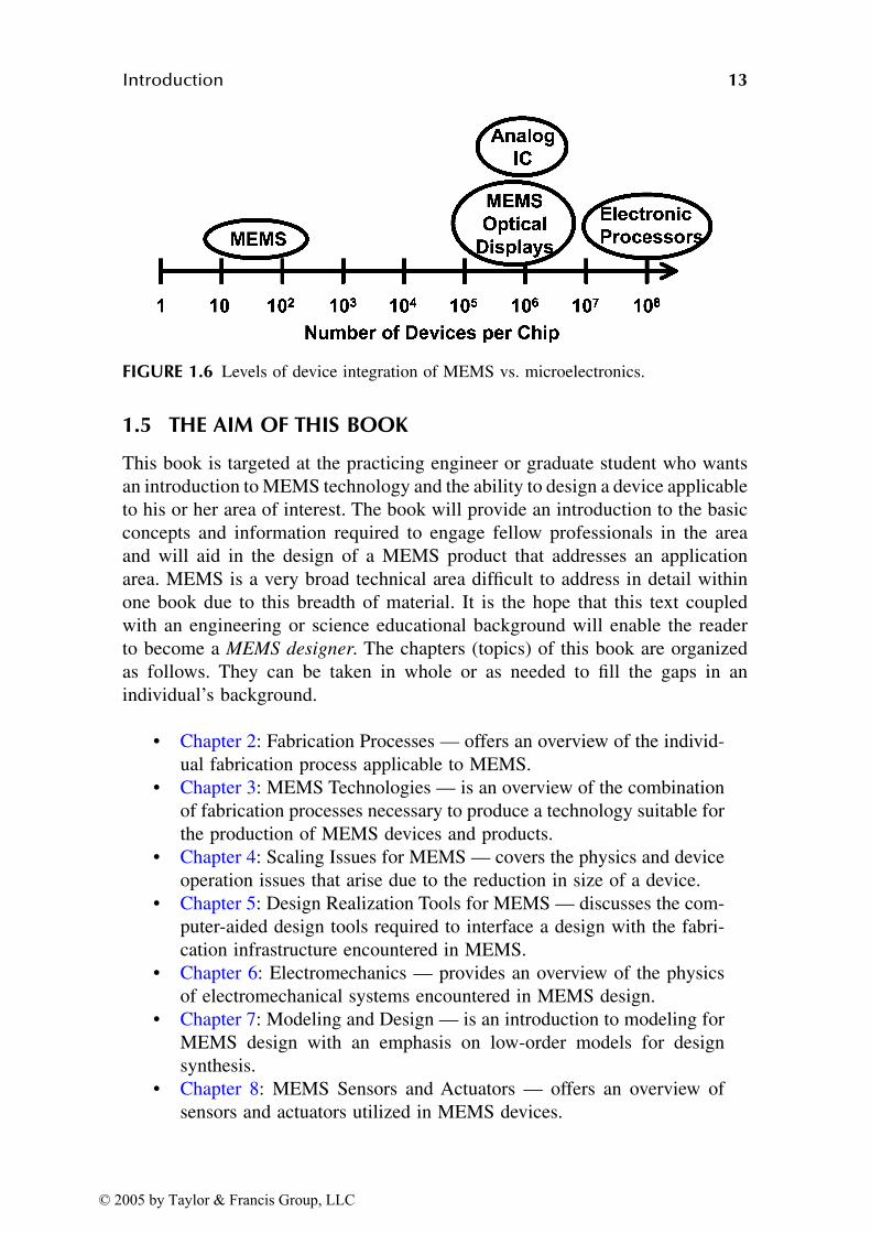
Introduction 13
1.5 THE AIM OF THIS BOOK
This book is targeted at the practicing engineer or graduate student who wants
an introduction to MEMS technology and the ability to design a device applicable
to his or her area of interest. The book will provide an introduction to the basic
concepts and information required to engage fellow professionals in the area
and will aid in the design of a MEMS product that addresses an application
area. MEMS is a very broad technical area difficult to address in detail within
one book due to this breadth of material. It is the hope that this text coupled
with an engineering or science educational background will enable the reader
to become a MEMS designer. The chapters (topics) of this book are organized
as follows. They can be taken in whole or as needed to fill the gaps in an
individual’s background.
• Chapter 2: Fabrication Processes — offers an overview of the individ-
ual fabrication process applicable to MEMS.
• Chapter 3: MEMS Technologies — is an overview of the combination
of fabrication processes necessary to produce a technology suitable for
the production of MEMS devices and products.
• Chapter 4: Scaling Issues for MEMS — covers the physics and device
operation issues that arise due to the reduction in size of a device.
• Chapter 5: Design Realization Tools for MEMS — discusses the com-
puter-aided design tools required to interface a design with the fabri-
cation infrastructure encountered in MEMS.
• Chapter 6: Electromechanics — provides an overview of the physics
of electromechanical systems encountered in MEMS design.
• Chapter 7: Modeling and Design — is an introduction to modeling for
MEMS design with an emphasis on low-order models for design
synthesis.
• Chapter 8: MEMS Sensors and Actuators — offers an overview of
sensors and actuators utilized in MEMS devices.
FIGURE 1.6 Levels of device integration of MEMS vs. microelectronics.
© 2005 by Taylor & Francis Group, LLC
14 Micro Electro Mechanical System Design
• Chapter 9: Packaging — is a review of the packaging processes and
how the packaging processes and fabrication processes interact; three
packaging case studies are presented.
• Chapter 10: Reliability — covers the basic concepts of reliability and
the aspects of reliability unique to MEMS, such as failure mechanisms
and failure analysis tools.
QUESTIONS
1. Use the Web as a tool to explore what is happening in the world of
MEMS.
2. Pick an application and research how it is used. What type of fabrication
process is used and how many companies have products in this area?
3. Look at a MEMS application that existed before MEMS technology
existed. How did MEMS technology have an impact on this application
in performance, cost, or volume production?
REFERENCES
1. D. Sobel, Longitude, The True Story of a Lone Genius Who Solved the Greatest
Scientific Problem of His Time, Penguin Books, New York, 1995.
2. J. Bardeen, W. H. Brattain, The transistor, a semiconductor triode, Phys. Rev., 74,
130–231, 1948.
3. W. Shockley, A unipolar field-effect transistor, Proc. IRE, 40, 1365, 1952.
4. ENIAC (electronic numerical integrator and computer) U.S. Patent No. 3,120,606,
filed 26 June 1947.
5. ENIAC Museum: http://www.seas.upenn.edu/~museum/.
6. J.A. Hoerni, Planar silicon transistors and diodes, IRE Transactions Electron
Devices, 8, 2, March 1961.
7. J.A. Hoerni, Method of manufacturing semiconductor devices, U.S. Patent
3,025,589, issued March 20, 1962.
8. J.S. Kilby, Miniaturized electronic circuits, U.S. Patent 3,138,743, filed February
6, 1959.
9. R.N. Noyce, Semiconductor device and lead structure, U.S. Patent 2,918,877, filed
July 30, 1959.
10. G.E. Moore, Cramming more components onto integrated circuits, Electronics,
38(8), April 19, 1965.
11. R.P. Feynman, There’s plenty of room at the bottom, Eng. Sci. (California Institute
of Technology), February 1960, 22–36.
12. R.P. Feynman, There’s plenty of room at the bottom, JMEMS, 1(1), 60–66, March
1992.
13. R.P. Feynman, There’s plenty of room at the bottom, http://nano.xerox.com/
nanotech/feynman.html.
14. E. Regis, Nano: The Emerging Science of Nanotechnology, Little, Brown and
Company, New York, 1995.
15. N. Maluf, An Introduction to Microelectromechanical Systems Engineering,
Artech House Inc., Boston, 2000.
© 2005 by Taylor & Francis Group, LLC
Introduction 15
16. The Caltech Institute Archives: http://archives.caltech.edu/index.html.
17. Pease Group Homepage: http://chomsky.stanford.edu/docs/home.html.
18. C.S. Smith, Piezoresistive effect in germanium and silicon, Phys. Rev. 94(1),
42–49, April, 1954.
19. J.D. Meindel, Q. Chen, J.A. Davis, Limits on silicon nanoelectronics for terascale
integration, Science, 293, 2044–2049, September 2001.
20. H.C. Nathanson, W.E. Newell, R.A. Wickstrom, J.R. Davis, The resonant gate
transistor, IEEE Trans. Electron Devices, ED-14, 117–133, 1967.
21. K.E. Petersen, Silicon as a mechanical material, Proc. IEEE, 70(5), 420–457, May
1982.
22. R.T. Howe and R.S. Muller, Polycrystalline silicon micromechanical beams, J.
Electrochem. Soc.: Solid-State Sci. Technol., 130(6), 1420–1423, June 1983.
23. L-S. Fan, Y-C Tai, R.S. Muller, Integrated movable micromechanical structures
for sensors and actuators, IEEE Trans. Electron Devices, 35(6), 724–730, 1988.
24. W.C. Tang, T.C.H. Nguyen, R.T. Howe, Laterally driven polysilicon resonant
microstructures, Sensors Actuators, 20(1–2), 25–32, November 1989.
25. K.S.J. Pister, M.W. Judy, S.R. Burgett, R.S. Fearing, Microfabricated hinges,
Sensors Actuators A, 33, 249–256, 1992.
26. E.W. Becker, W. Ehrfeld, P. Hagmann, A. Maner, and D. Muchmeyer, Fabrication
of microstructures with high aspect ratios and great structural heights by synchro-
tron radiation lithography, galvanoforming, and plastic molding (LIGA process),
Microelectron. Eng., 4, 35, 1986.
27. Analog Devices IMEMS technology: http://www.analog.com/.
28. Texas Instrument DLP™ technology: http://www.ti.com/.
29. D. Forman, Automotive applications, smalltimes, 3(3), 42–43, May/June 2003.
30. R. Grace, Autos continue to supply MEMS “killer apps” as convenience and safety
take a front seat, smalltimes, 3(3), 48, May/June 2003.
31. Affymetrix, Inc. http://www.affymetrix.com GeneChip.
32. M. Okandan, P. Galambos, S. Mani, J. Jakubczak, Development of surface micro-
machining technologies for microfluidics and BioMEMS, Proc. SPIE, 4560,
133–139, 2001.
33. D. Sidawi, Emerging prostheses attempt vision restoration, R&D Mag., 46(6),
30–32, June 2004.
34. R. Osiander, J. Champion, A. Darrin, D. Douglass, T. Swanson, J. Allen, E.
Wyckoff, MEMS shutters for spacecraft thermal control, NanoTech 2002, Hous-
ton, TX. 9–12 September 2002.
35. R. H. Byrne, D. R. Adkins, S. E. Eskridge, H. H. Harrington, E. J. Heller, J. E.
Hurtado, Miniature mobile robots for plume tracking and source localization
research, J. Micromechatronics, 1(3), 253–261, 2002.
36. S.T. Picraux and P.J. McWhorter, The broad sweep of integrated microsystems,
IEEE Spectrum, 35(12), 24–33, December 1998.
37. MEMS not so small after all, Micro Nano, 8(8), 6, Aug 2003
38. M.W. Scott and S.T. Walsh, Promise and problems of MEMS or nanosystem unit
cell, Micro/Nano Newslett., 8(2), 8, February 2003.
39. M. Scott, MEMS and MOEMS for national security applications, Proc. SPIE,
4979, 26–33, 2003.
40. S.D. Senturia, Microsensors vs. ICs: a study in contrasts, IEEE Circuits Devices
Mag., 20–27, November 1990.
© 2005 by Taylor & Francis Group, LLC
17
2 Fabrication Processes
This chapter will present an overview of the various processes used in the
fabrication of MEMS devices. The first section will present an introduction to
materials and their structure. The processes that will be discussed in subsequent
sections include deposition, patterning, and etching of materials as well as pro-
cesses for annealing, polishing, and doping, which are used to achieve special
mechanical, electrical, or optical properties. Many of the processes used for
MEMS are adapted from the microelectronics industry; however, the conceptual
roots for some of the fabrication processes (e.g., sputtering, damascene) signifi-
cantly predate that industry.
2.1 MATERIALS
2.1.1 INTERATOMIC BONDS
The material structure type is greatly influenced by the interatomic bonds and
their completeness. There are three types of interatomic attractions: ionic bonds,
covalent bonds, and metallic bonds (Figure 2.1). The ionic bonds occur in
materials where the interatomic attractions are due to electrostatic attraction
between adjacent ions. For example, a sodium atom (Na) has one electron in its
valence shell (i.e., outer electron shell of an atom), which can be easily released
to produce a positively charge sodium ion (Na+). A chlorine atom (Cl) can readily
accept an electron to complete its valence shell, which will produce a negatively
charged chlorine ion (Cl–). The electrostatic attraction of an ionic bond will cause
the negatively charged chlorine ion to surround itself with positively charged
sodium ions.
The electronic structure of an atom is stable if the outer valence shells are
complete. The outer valence shell can be completed by sharing electrons between
adjacent atoms. The covalent bond is the sharing of valence electrons. This bond
is a very strong interatomic force that can produce molecules such as hydrogen
(H2) or methane (CH4), which have very low melting temperature and low attrac-
tion to adjacent molecules, or diamond, which is a covalent bonded carbon crystal
with a very high melting point and great hardness. The difference between these
two types of covalent bonded materials (i.e., CH4 vs. diamond) is that the covalent
bond structure of CH4 completes the valence shell of the component atoms within
one molecule, whereas the valence shell of the carbon atoms in diamond are
© 2005 by Taylor & Francis Group, LLC
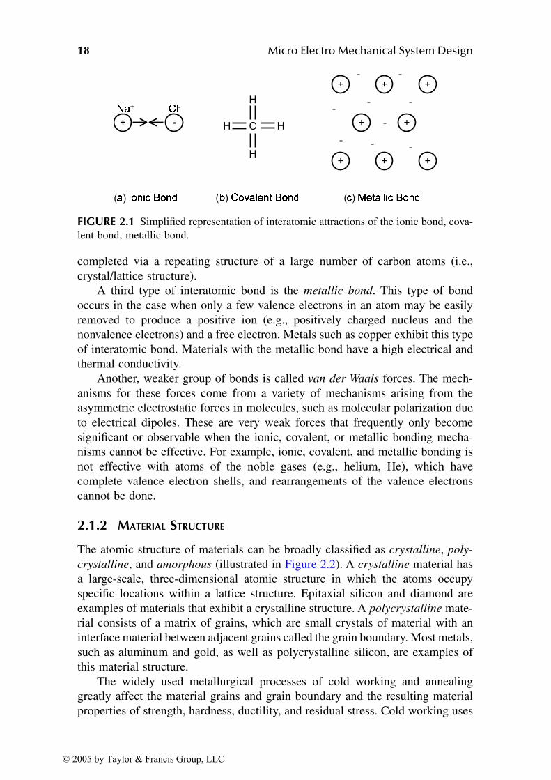
18 Micro Electro Mechanical System Design
completed via a repeating structure of a large number of carbon atoms (i.e.,
crystal/lattice structure).
A third type of interatomic bond is the metallic bond. This type of bond
occurs in the case when only a few valence electrons in an atom may be easily
removed to produce a positive ion (e.g., positively charged nucleus and the
nonvalence electrons) and a free electron. Metals such as copper exhibit this type
of interatomic bond. Materials with the metallic bond have a high electrical and
thermal conductivity.
Another, weaker group of bonds is called van der Waals forces. The mech-
anisms for these forces come from a variety of mechanisms arising from the
asymmetric electrostatic forces in molecules, such as molecular polarization due
to electrical dipoles. These are very weak forces that frequently only become
significant or observable when the ionic, covalent, or metallic bonding mecha-
nisms cannot be effective. For example, ionic, covalent, and metallic bonding is
not effective with atoms of the noble gases (e.g., helium, He), which have
complete valence electron shells, and rearrangements of the valence electrons
cannot be done.
2.1.2 MATERIAL STRUCTURE
The atomic structure of materials can be broadly classified as crystalline, poly-
crystalline, and amorphous (illustrated in Figure 2.2). A crystalline material has
a large-scale, three-dimensional atomic structure in which the atoms occupy
specific locations within a lattice structure. Epitaxial silicon and diamond are
examples of materials that exhibit a crystalline structure. A polycrystalline mate-
rial consists of a matrix of grains, which are small crystals of material with an
interface material between adjacent grains called the grain boundary. Most metals,
such as aluminum and gold, as well as polycrystalline silicon, are examples of
this material structure.
The widely used metallurgical processes of cold working and annealing
greatly affect the material grains and grain boundary and the resulting material
properties of strength, hardness, ductility, and residual stress. Cold working uses
FIGURE 2.1 Simplified representation of interatomic attractions of the ionic bond, cova-
lent bond, metallic bond.
( ( () ) )
© 2005 by Taylor & Francis Group, LLC
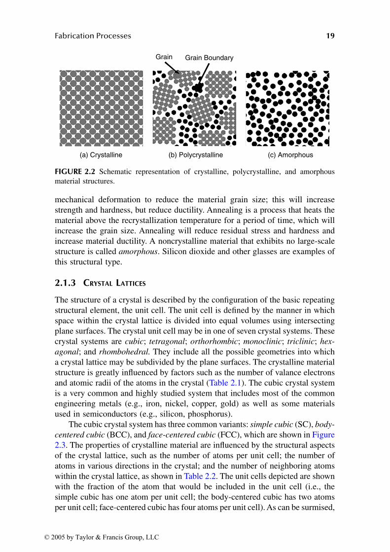
Fabrication Processes 19
mechanical deformation to reduce the material grain size; this will increase
strength and hardness, but reduce ductility. Annealing is a process that heats the
material above the recrystallization temperature for a period of time, which will
increase the grain size. Annealing will reduce residual stress and hardness and
increase material ductility. A noncrystalline material that exhibits no large-scale
structure is called amorphous. Silicon dioxide and other glasses are examples of
this structural type.
2.1.3 CRYSTAL LATTICES
The structure of a crystal is described by the configuration of the basic repeating
structural element, the unit cell. The unit cell is defined by the manner in which
space within the crystal lattice is divided into equal volumes using intersecting
plane surfaces. The crystal unit cell may be in one of seven crystal systems. These
crystal systems are cubic; tetragonal; orthorhombic; monoclinic; triclinic; hex-
agonal; and rhombohedral. They include all the possible geometries into which
a crystal lattice may be subdivided by the plane surfaces. The crystalline material
structure is greatly influenced by factors such as the number of valance electrons
and atomic radii of the atoms in the crystal (Table 2.1). The cubic crystal system
is a very common and highly studied system that includes most of the common
engineering metals (e.g., iron, nickel, copper, gold) as well as some materials
used in semiconductors (e.g., silicon, phosphorus).
The cubic crystal system has three common variants: simple cubic (SC), body-
centered cubic (BCC), and face-centered cubic (FCC), which are shown in Figure
2.3. The properties of crystalline material are influenced by the structural aspects
of the crystal lattice, such as the number of atoms per unit cell; the number of
atoms in various directions in the crystal; and the number of neighboring atoms
within the crystal lattice, as shown in Table 2.2. The unit cells depicted are shown
with the fraction of the atom that would be included in the unit cell (i.e., the
simple cubic has one atom per unit cell; the body-centered cubic has two atoms
per unit cell; face-centered cubic has four atoms per unit cell). As can be surmised,
FIGURE 2.2 Schematic representation of crystalline, polycrystalline, and amorphous
material structures.
Grain
(a) Crystalline (b) Polycrystalline (c) Amorphous
Grain Boundary
© 2005 by Taylor & Francis Group, LLC

20 Micro Electro Mechanical System Design
TABLE 2.1Atomic and Crystal Properties for Selected Elements
ElementAtomicnumber
Atomic mass(g/g-atom) Crystal Valence
Atomicradius (Å)
Boron (B) 5 10.81 Orthorhombic 3 0.46
Aluminum (Al) 13 26.98 FCC 3 1.431
Silicon (Si) 14 28.09 Diamond 4 1.176
Phosphorus (P) 15 30.97 Cubic 5 —
Iron (Fe) 26 55.85 BCC 2 1.241
Nickel (Ni) 28 58.71 FCC 2 1.245
Copper (Cu) 29 63.54 FCC 1.278
Gallium (Ga) 31 69.72 Ortho 3 1.218
Germanium (Ge) 32 72.59 Diamond 4 1.224
Arsenic (As) 33 74.92 Rhombic 5 1.25
Indium (In) 49 114.82 Tetra 3 1.625
Antimony (Sb) 51 121.75 Rhombic 5 1.452
Tungsten (W) 74 183.9 BCC — 1.369
Gold (Au) 79 197.0 FCC — 1.441
Notes: BCC — body-centered cubic; FCC — face-centered cubic.
FIGURE 2.3 Cubic crystal structures.
TABLE 2.2Properties of Different Forms of the Cubic Lattice
Crystal structureNumber of
nearest neighbors Atoms/CellPacking factora
(atom vol/cell vol)
Cubic 6 1 0.52
Body-centered cubic 8 2 0.68
Face-centered cubic 12 4 0.74
Diamond cubic 4 8 —
a Assuming only one atom type in the lattice.
(a) Simple Cubic (b) Body-Centered Cubic (c) Face-Centered Cubic
Y Y Y
Z Z ZX X X
© 2005 by Taylor & Francis Group, LLC
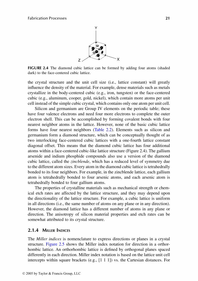
Fabrication Processes 21
the crystal structure and the unit cell size (i.e., lattice constant) will greatly
influence the density of the material. For example, dense materials such as metals
crystallize in the body-centered cubic (e.g., iron, tungsten) or the face-centered
cubic (e.g., aluminum, cooper, gold, nickel), which contain more atoms per unit
cell instead of the simple cubic crystal, which contains only one atom per unit cell.
Silicon and germanium are Group IV elements on the periodic table; these
have four valence electrons and need four more electrons to complete the outer
electron shell. This can be accomplished by forming covalent bonds with four
nearest neighbor atoms in the lattice. However, none of the basic cubic lattice
forms have four nearest neighbors (Table 2.2). Elements such as silicon and
germanium form a diamond structure, which can be conceptually thought of as
two interlocking face-centered cubic lattices with a one-fourth lattice constant
diagonal offset. This means that the diamond cubic lattice has four additional
atoms within a face-centered cubic-like lattice structure (Figure 2.4). The gallium
arsenide and indium phosphide compounds also use a version of the diamond
cubic lattice, called the zincblende, which has a reduced level of symmetry due
to the different atom sizes. Every atom in the diamond cubic lattice is tetrahedrally
bonded to its four neighbors. For example, in the zincblende lattice, each gallium
atom is tetrahedrally bonded to four arsenic atoms, and each arsenic atom is
tetrahedrally bonded to four gallium atoms.
The properties of crystalline materials such as mechanical strength or chem-
ical etch rates are affected by the lattice structure, and they may depend upon
the directionality of the lattice structure. For example, a cubic lattice is uniform
in all directions (i.e., the same number of atoms on any plane or in any direction).
However, the diamond lattice has a different number of atoms in any plane or
direction. The anisotropy of silicon material properties and etch rates can be
somewhat attributed to its crystal structure.
2.1.4 MILLER INDICES
The Miller indices is nomenclature to express directions or planes in a crystal
structure. Figure 2.5 shows the Miller index notation for direction in a orthor-
hombic lattice. An orthorhombic lattice is defined by orthogonal planes spaced
differently in each direction. Miller index notation is based on the lattice unit cell
intercepts within square brackets (e.g., [1 1 1]) vs. the Cartesian distances. For
FIGURE 2.4 The diamond cubic lattice can be formed by adding four atoms (shaded
dark) to the face-centered cubic lattice.
© 2005 by Taylor & Francis Group, LLC
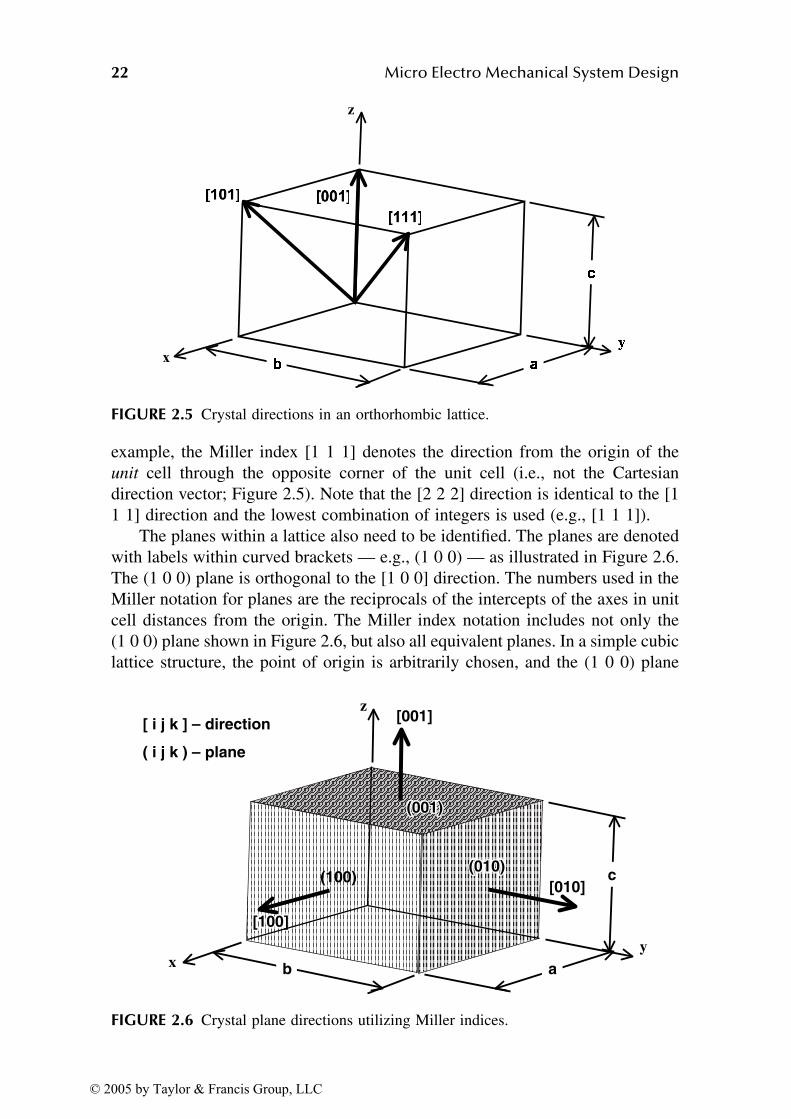
22 Micro Electro Mechanical System Design
example, the Miller index [1 1 1] denotes the direction from the origin of the
unit cell through the opposite corner of the unit cell (i.e., not the Cartesian
direction vector; Figure 2.5). Note that the [2 2 2] direction is identical to the [1
1 1] direction and the lowest combination of integers is used (e.g., [1 1 1]).
The planes within a lattice also need to be identified. The planes are denoted
with labels within curved brackets — e.g., (1 0 0) — as illustrated in Figure 2.6.
The (1 0 0) plane is orthogonal to the [1 0 0] direction. The numbers used in the
Miller notation for planes are the reciprocals of the intercepts of the axes in unit
cell distances from the origin. The Miller index notation includes not only the
(1 0 0) plane shown in Figure 2.6, but also all equivalent planes. In a simple cubic
lattice structure, the point of origin is arbitrarily chosen, and the (1 0 0) plane
FIGURE 2.5 Crystal directions in an orthorhombic lattice.
FIGURE 2.6 Crystal plane directions utilizing Miller indices.
[ i j k ] – direction
( i j k ) – plane
xy
z
b a
c[010]
[001]
(001)(001)
(010)(010)(100)
[100][100]
© 2005 by Taylor & Francis Group, LLC

Fabrication Processes 23
will have the same properties as the (0 1 0) and the (0 0 1) planes. The (1 0 0)
refers to all three planes. Conversely, in an orthorhombic lattice, the planes (1 0 0),
(0 1 0), and (0 0 1) are unique.
2.1.5 CRYSTAL IMPERFECTIONS
The symmetry of the crystal is broken at the surface of the material. The atoms
at the surface are not bound to the other atoms in the same way as the bulk
material. Therefore, the surface will behave differently than the bulk crystal. For
example, the surface can chemically react and form an oxide or the surface can
become electrically charged. Integrated circuit manufacturers frequently build the
circuits upon a single-crystal silicon wafer with a (100) orientation (i.e., the [100]
plane is the wafer surface) because this orientation minimizes surface charges.
In addition to the surface differences, imperfections in the crystal lattices can
also be found. These can influence many characteristics of the material such as
mechanical strength, electrical properties, and chemical reactivity. The lattice
imperfections can be due to missing, displaced, or extra atoms in the lattice,
which are called point defects. Line defects have an edge due to an extra plane
of atoms.
Figure 2.7 illustrates several types of point defects, which include substitu-
tional, vacancy, and interstitial types of defects. A substitutional defect is due to
an impurity atom occupying a lattice site for the bulk material. In a vacancy
defect, a lattice site is not occupied. An interstitial defect involves an atom of
the bulk material or an impurity atom occupying space between the lattice sites.
These defects can arise from the imperfect lattice formation during crystallization
or due to impurities in the material during crystallization. The defects can also
arise from thermal vibrations of the lattice atoms at elevated temperatures. Vacan-
cies may be a single or they may condense into a larger vacancy. Conversely,
defects within a single-crystal lattice structure may be intentionally created via
FIGURE 2.7 Schematic of lattice point and line defects.
© 2005 by Taylor & Francis Group, LLC

24 Micro Electro Mechanical System Design
the processes of diffusion or implantation to produce effects in the electronic
structure of the material for MEMS or microelectronics manufacturing.
The most common type of line defect is an edge dislocation, which is the
edge of an extra plane of atoms within a crystal structure (Figure 2.7). This type
of dislocation distorts the lattice, thus increasing the energy along the edge
dislocation. There can also be surface defects, which are basically the transition
region, grain boundaries, in a polycrystalline material. Each grain of a polycrys-
talline material is a crystal oriented differently, and the grain boundary is the
transition between the grains (Figure 2.2b).
Atoms can move within a solid material as shown in Figure 2.8. However,
energy is required to facilitate the movement. The energy required for the move-
ment of the atoms is called the activation energy and depends on a number of
factors, such as atom size and type of movement. A vacancy movement requires
less energy than an interstitial movement. Atoms can move within a lattice
without point or line defects using a method called ring diffusion (Figure 2.9).
These various methods of atomic movement within a crystal are utilized in
diffusion processes.
FIGURE 2.8 Atomic movements within a material.
FIGURE 2.9 Ring diffusion of atoms.
© 2005 by Taylor & Francis Group, LLC
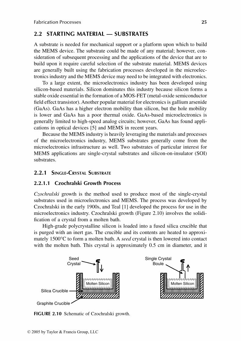
Fabrication Processes 25
2.2 STARTING MATERIAL — SUBSTRATES
A substrate is needed for mechanical support or a platform upon which to build
the MEMS device. The substrate could be made of any material; however, con-
sideration of subsequent processing and the applications of the device that are to
build upon it require careful selection of the substrate material. MEMS devices
are generally built using the fabrication processes developed in the microelec-
tronics industry and the MEMS device may need to be integrated with electronics.
To a large extent, the microelectronics industry has been developed using
silicon-based materials. Silicon dominates this industry because silicon forms a
stable oxide essential in the formation of a MOS-FET (metal-oxide semiconductor
field effect transistor). Another popular material for electronics is gallium arsenide
(GaAs). GaAs has a higher electron mobility than silicon, but the hole mobility
is lower and GaAs has a poor thermal oxide. GaAs-based microelectronics is
generally limited to high-speed analog circuits; however, GaAs has found appli-
cations in optical devices [5] and MEMS in recent years.
Because the MEMS industry is heavily leveraging the materials and processes
of the microelectronics industry, MEMS substrates generally come from the
microelectronics infrastructure as well. Two substrates of particular interest for
MEMS applications are single-crystal substrates and silicon-on-insulator (SOI)
substrates.
2.2.1 SINGLE-CRYSTAL SUBSTRATE
2.2.1.1 Czochralski Growth Process
Czochralski growth is the method used to produce most of the single-crystal
substrates used in microelectronics and MEMS. The process was developed by
Czochralski in the early 1900s, and Teal [1] developed the process for use in the
microelectronics industry. Czochralski growth (Figure 2.10) involves the solidi-
fication of a crystal from a molten bath.
High-grade polycrystalline silicon is loaded into a fused silica crucible that
is purged with an inert gas. The crucible and its contents are heated to approxi-
mately 1500°C to form a molten bath. A seed crystal is then lowered into contact
with the molten bath. This crystal is approximately 0.5 cm in diameter, and it
FIGURE 2.10 Schematic of Czochralski growth.
SeedCrystal
Single Crystal Boule
Molten Silicon Molten Silicon
Silica Crucible
Graphite Crucible
© 2005 by Taylor & Francis Group, LLC
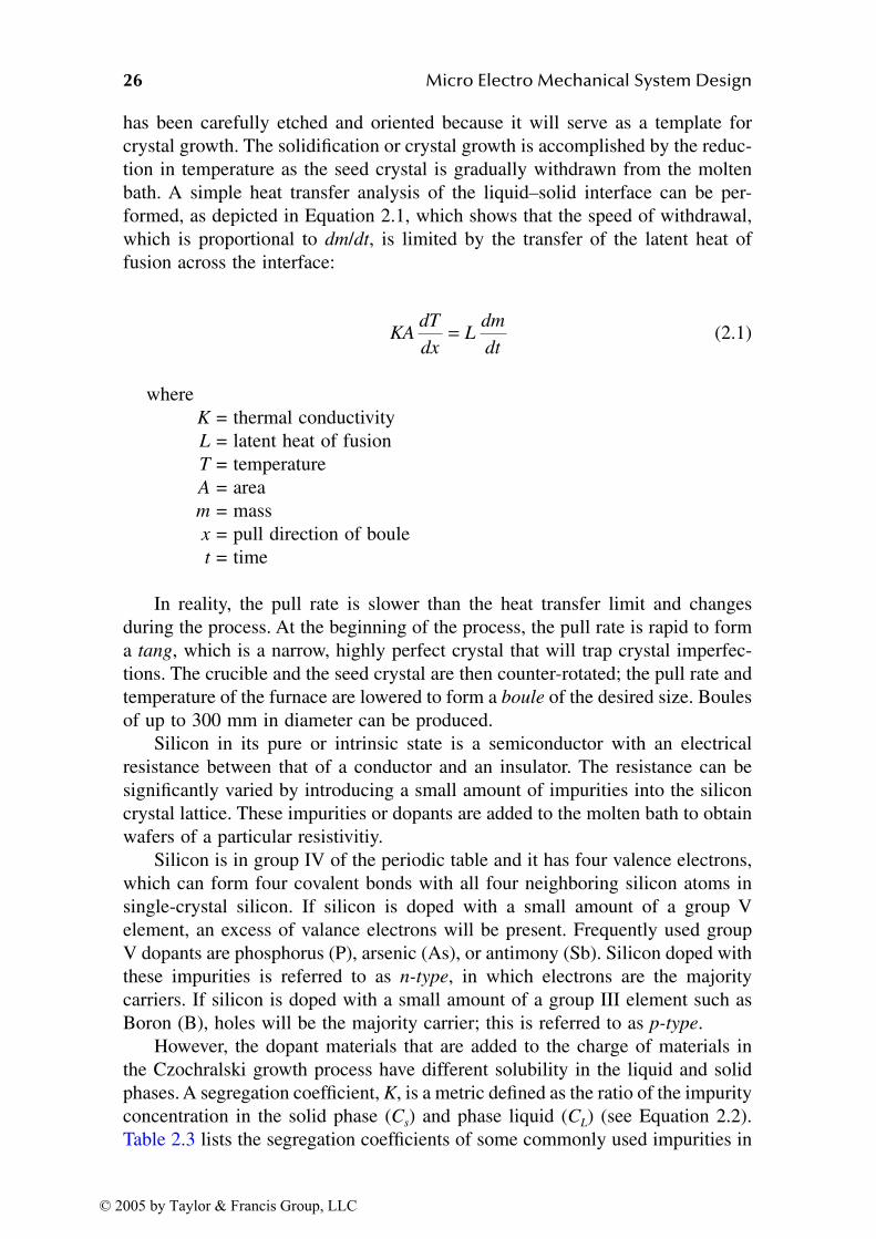
26 Micro Electro Mechanical System Design
has been carefully etched and oriented because it will serve as a template for
crystal growth. The solidification or crystal growth is accomplished by the reduc-
tion in temperature as the seed crystal is gradually withdrawn from the molten
bath. A simple heat transfer analysis of the liquid–solid interface can be per-
formed, as depicted in Equation 2.1, which shows that the speed of withdrawal,
which is proportional to dm/dt, is limited by the transfer of the latent heat of
fusion across the interface:
(2.1)
where
K = thermal conductivity
L = latent heat of fusion
T = temperature
A = area
m = mass
x = pull direction of boule
t = time
In reality, the pull rate is slower than the heat transfer limit and changes
during the process. At the beginning of the process, the pull rate is rapid to form
a tang, which is a narrow, highly perfect crystal that will trap crystal imperfec-
tions. The crucible and the seed crystal are then counter-rotated; the pull rate and
temperature of the furnace are lowered to form a boule of the desired size. Boules
of up to 300 mm in diameter can be produced.
Silicon in its pure or intrinsic state is a semiconductor with an electrical
resistance between that of a conductor and an insulator. The resistance can be
significantly varied by introducing a small amount of impurities into the silicon
crystal lattice. These impurities or dopants are added to the molten bath to obtain
wafers of a particular resistivitiy.
Silicon is in group IV of the periodic table and it has four valence electrons,
which can form four covalent bonds with all four neighboring silicon atoms in
single-crystal silicon. If silicon is doped with a small amount of a group V
element, an excess of valance electrons will be present. Frequently used group
V dopants are phosphorus (P), arsenic (As), or antimony (Sb). Silicon doped with
these impurities is referred to as n-type, in which electrons are the majority
carriers. If silicon is doped with a small amount of a group III element such as
Boron (B), holes will be the majority carrier; this is referred to as p-type.
However, the dopant materials that are added to the charge of materials in
the Czochralski growth process have different solubility in the liquid and solid
phases. A segregation coefficient, K, is a metric defined as the ratio of the impurity
concentration in the solid phase (Cs) and phase liquid (CL) (see Equation 2.2).
Table 2.3 lists the segregation coefficients of some commonly used impurities in
KAdT
dxL
dm
dt=
© 2005 by Taylor & Francis Group, LLC
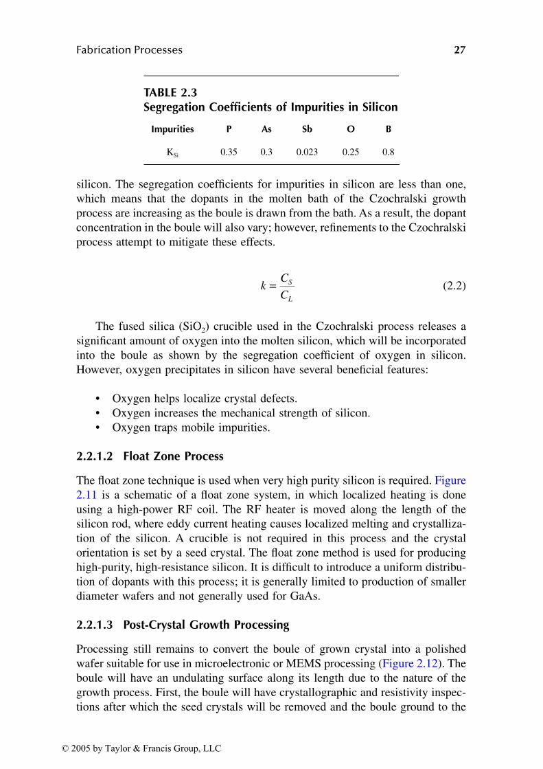
Fabrication Processes 27
silicon. The segregation coefficients for impurities in silicon are less than one,
which means that the dopants in the molten bath of the Czochralski growth
process are increasing as the boule is drawn from the bath. As a result, the dopant
concentration in the boule will also vary; however, refinements to the Czochralski
process attempt to mitigate these effects.
(2.2)
The fused silica (SiO2) crucible used in the Czochralski process releases a
significant amount of oxygen into the molten silicon, which will be incorporated
into the boule as shown by the segregation coefficient of oxygen in silicon.
However, oxygen precipitates in silicon have several beneficial features:
• Oxygen helps localize crystal defects.
• Oxygen increases the mechanical strength of silicon.
• Oxygen traps mobile impurities.
2.2.1.2 Float Zone Process
The float zone technique is used when very high purity silicon is required. Figure
2.11 is a schematic of a float zone system, in which localized heating is done
using a high-power RF coil. The RF heater is moved along the length of the
silicon rod, where eddy current heating causes localized melting and crystalliza-
tion of the silicon. A crucible is not required in this process and the crystal
orientation is set by a seed crystal. The float zone method is used for producing
high-purity, high-resistance silicon. It is difficult to introduce a uniform distribu-
tion of dopants with this process; it is generally limited to production of smaller
diameter wafers and not generally used for GaAs.
2.2.1.3 Post-Crystal Growth Processing
Processing still remains to convert the boule of grown crystal into a polished
wafer suitable for use in microelectronic or MEMS processing (Figure 2.12). The
boule will have an undulating surface along its length due to the nature of the
growth process. First, the boule will have crystallographic and resistivity inspec-
tions after which the seed crystals will be removed and the boule ground to the
TABLE 2.3Segregation Coefficients of Impurities in Silicon
Impurities P As Sb O B
KSi 0.35 0.3 0.023 0.25 0.8
kC
C
S
L
=
© 2005 by Taylor & Francis Group, LLC
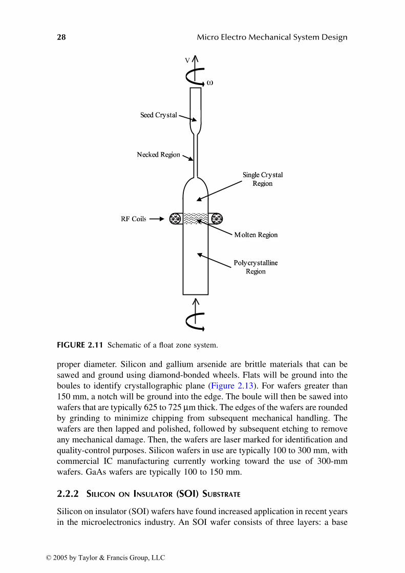
28 Micro Electro Mechanical System Design
proper diameter. Silicon and gallium arsenide are brittle materials that can be
sawed and ground using diamond-bonded wheels. Flats will be ground into the
boules to identify crystallographic plane (Figure 2.13). For wafers greater than
150 mm, a notch will be ground into the edge. The boule will then be sawed into
wafers that are typically 625 to 725 µm thick. The edges of the wafers are rounded
by grinding to minimize chipping from subsequent mechanical handling. The
wafers are then lapped and polished, followed by subsequent etching to remove
any mechanical damage. Then, the wafers are laser marked for identification and
quality-control purposes. Silicon wafers in use are typically 100 to 300 mm, with
commercial IC manufacturing currently working toward the use of 300-mm
wafers. GaAs wafers are typically 100 to 150 mm.
2.2.2 SILICON ON INSULATOR (SOI) SUBSTRATE
Silicon on insulator (SOI) wafers have found increased application in recent years
in the microelectronics industry. An SOI wafer consists of three layers: a base
FIGURE 2.11 Schematic of a float zone system.
© 2005 by Taylor & Francis Group, LLC
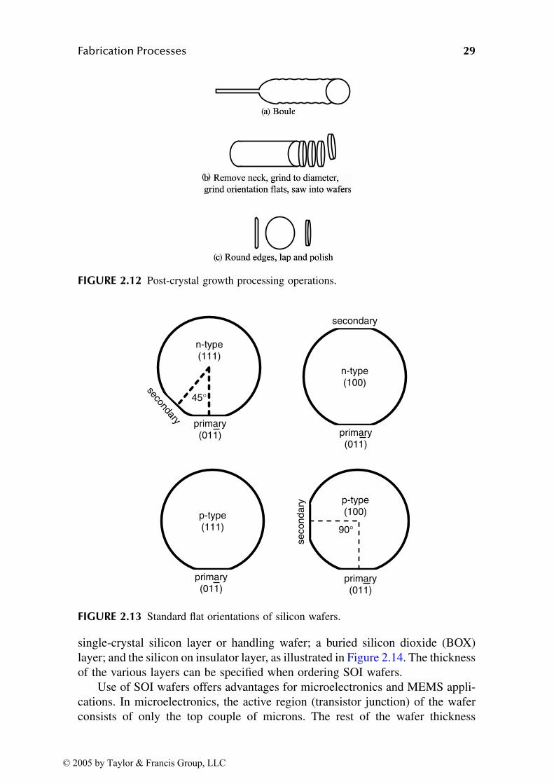
Fabrication Processes 29
single-crystal silicon layer or handling wafer; a buried silicon dioxide (BOX)
layer; and the silicon on insulator layer, as illustrated in Figure 2.14. The thickness
of the various layers can be specified when ordering SOI wafers.
Use of SOI wafers offers advantages for microelectronics and MEMS appli-
cations. In microelectronics, the active region (transistor junction) of the wafer
consists of only the top couple of microns. The rest of the wafer thickness
FIGURE 2.12 Post-crystal growth processing operations.
FIGURE 2.13 Standard flat orientations of silicon wafers.
( )
( )
( )
45°
90°
n-type(111)
p-type(111)
p-type(100)
n-type(100)
primary(011)
primary(011)
primary(011) primary
(011)
secondary
secondary
secondary
© 2005 by Taylor & Francis Group, LLC
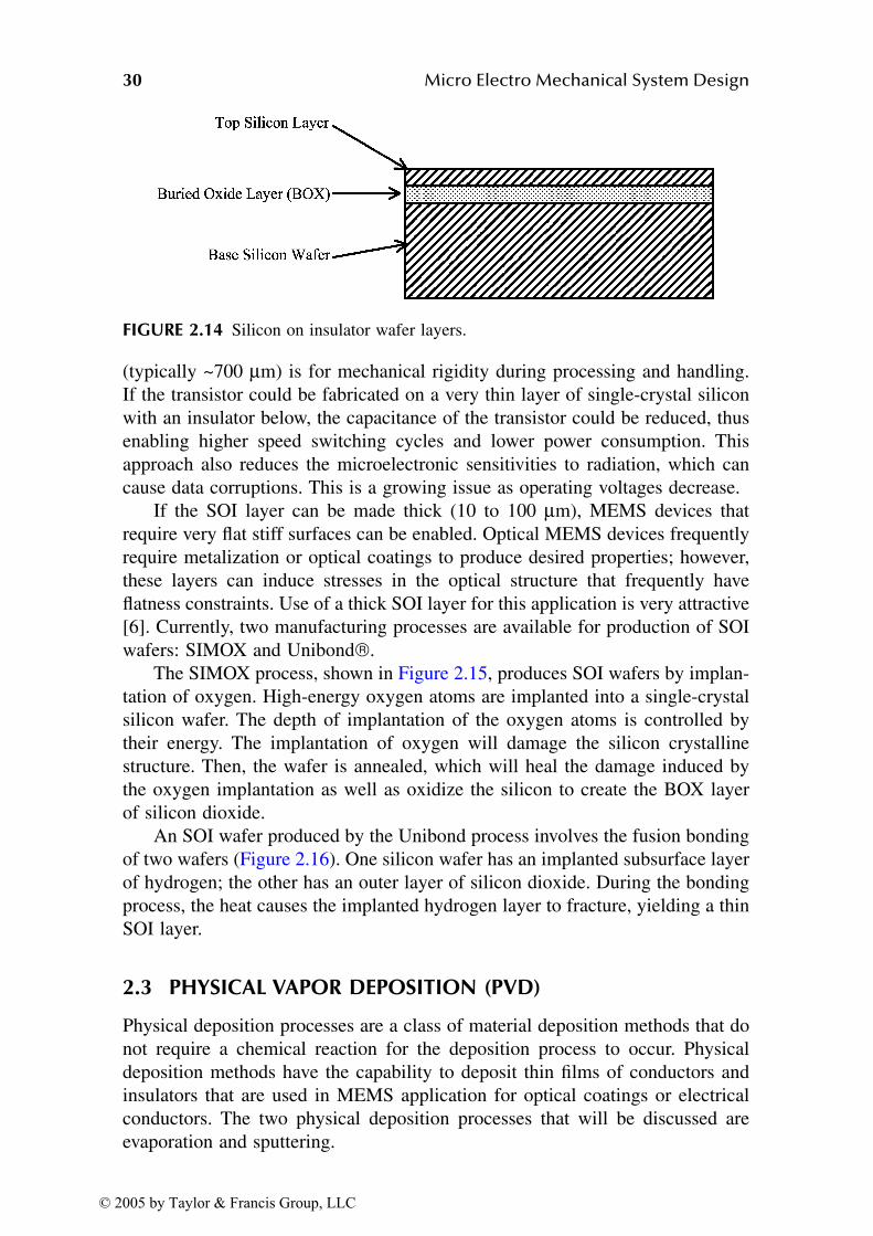
30 Micro Electro Mechanical System Design
(typically ~700 µm) is for mechanical rigidity during processing and handling.
If the transistor could be fabricated on a very thin layer of single-crystal silicon
with an insulator below, the capacitance of the transistor could be reduced, thus
enabling higher speed switching cycles and lower power consumption. This
approach also reduces the microelectronic sensitivities to radiation, which can
cause data corruptions. This is a growing issue as operating voltages decrease.
If the SOI layer can be made thick (10 to 100 µm), MEMS devices that
require very flat stiff surfaces can be enabled. Optical MEMS devices frequently
require metalization or optical coatings to produce desired properties; however,
these layers can induce stresses in the optical structure that frequently have
flatness constraints. Use of a thick SOI layer for this application is very attractive
[6]. Currently, two manufacturing processes are available for production of SOI
wafers: SIMOX and Unibond.
The SIMOX process, shown in Figure 2.15, produces SOI wafers by implan-
tation of oxygen. High-energy oxygen atoms are implanted into a single-crystal
silicon wafer. The depth of implantation of the oxygen atoms is controlled by
their energy. The implantation of oxygen will damage the silicon crystalline
structure. Then, the wafer is annealed, which will heal the damage induced by
the oxygen implantation as well as oxidize the silicon to create the BOX layer
of silicon dioxide.
An SOI wafer produced by the Unibond process involves the fusion bonding
of two wafers (Figure 2.16). One silicon wafer has an implanted subsurface layer
of hydrogen; the other has an outer layer of silicon dioxide. During the bonding
process, the heat causes the implanted hydrogen layer to fracture, yielding a thin
SOI layer.
2.3 PHYSICAL VAPOR DEPOSITION (PVD)
Physical deposition processes are a class of material deposition methods that do
not require a chemical reaction for the deposition process to occur. Physical
deposition methods have the capability to deposit thin films of conductors and
insulators that are used in MEMS application for optical coatings or electrical
conductors. The two physical deposition processes that will be discussed are
evaporation and sputtering.
FIGURE 2.14 Silicon on insulator wafer layers.
© 2005 by Taylor & Francis Group, LLC

Fabrication Processes 31
FIGURE 2.15 SIMOX process for SOI wafers.
FIGURE 2.16 Unibond process for SOI wafers.
Wafer with implanted
Hydrogen Layer
Wafer with Silicon
Dioxide top Layer
Single Crystal Silicon Layer
BOX Layer
Single Crystal Silicon Wafer
(a) Bond a Wafer with implanted hydrogen and a wafer with an oxide layer
(b) High Temperature Anneal causes the wafer with implanted
hydrogen to fracture and heals implant damage.
© 2005 by Taylor & Francis Group, LLC
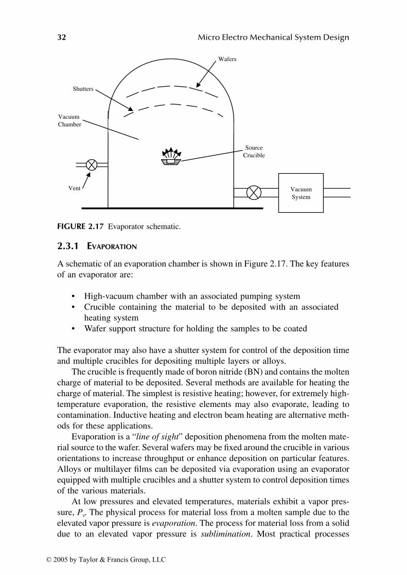
32 Micro Electro Mechanical System Design
2.3.1 EVAPORATION
A schematic of an evaporation chamber is shown in Figure 2.17. The key features
of an evaporator are:
• High-vacuum chamber with an associated pumping system
• Crucible containing the material to be deposited with an associated
heating system
• Wafer support structure for holding the samples to be coated
The evaporator may also have a shutter system for control of the deposition time
and multiple crucibles for depositing multiple layers or alloys.
The crucible is frequently made of boron nitride (BN) and contains the molten
charge of material to be deposited. Several methods are available for heating the
charge of material. The simplest is resistive heating; however, for extremely high-
temperature evaporation, the resistive elements may also evaporate, leading to
contamination. Inductive heating and electron beam heating are alternative meth-
ods for these applications.
Evaporation is a “line of sight” deposition phenomena from the molten mate-
rial source to the wafer. Several wafers may be fixed around the crucible in various
orientations to increase throughput or enhance deposition on particular features.
Alloys or multilayer films can be deposited via evaporation using an evaporator
equipped with multiple crucibles and a shutter system to control deposition times
of the various materials.
At low pressures and elevated temperatures, materials exhibit a vapor pres-
sure, Pv. The physical process for material loss from a molten sample due to the
elevated vapor pressure is evaporation. The process for material loss from a solid
due to an elevated vapor pressure is sublimination. Most practical processes
FIGURE 2.17 Evaporator schematic.
Shutters
Wafers
Source
Crucible
Vacuum
System
Vacuum
Chamber
Vent
© 2005 by Taylor & Francis Group, LLC
Fabrication Processes 33
involve evaporation of material from molten samples. For materials of interest in
MEMS fabrication, vapor pressures less than a millitorr (i.e., 1 torr = 1 mm Hg)
are typical. Table 2.4 shows melting temperatures for various materials as well
as the range of temperature necessary for these materials to exhibit a vapor
pressure of 10–3 torr. These data show that the required temperature to achieve a
vapor pressure of 10–3 torr ranges from 889°C for aluminum (Al) to 3016°C for
tungsten (W). The higher temperature materials require specialized equipment
for heating and minimization of contamination due to the elevated vapor pressure
of other materials in the chamber at these temperatures.
The kinetic of theory gases (Equation 2.3) can relate the evaporator chamber
pressure, Pv, and temperature, T, to the flux of atoms leaving the surface of the
molten sample, J:
(2.3)
where
Pv = vapor pressure
k = Boltzmann constant (1.38 × 10⁻²³ J/°K)
T = temperature (°K)
M = atomic mass
J = atomic flux
The mass flux of deposition in an evaporation process can be calculated from the
preceding equation and a geometric “view factor” from the molten sample to the
deposition surface because evaporation is a line of sight deposition process. This
information can be used to determine deposition times and material thickness.
The line of sight nature of the evaporation deposition process leads to the
issue of step coverage of topographic features on a wafer. In any MEMS pro-
cessing sequence, topography will be generated on the wafer due to the sequence
of deposition, patterning, and etching that has preceded the evaporation process.
This issue for MEMS is accentuated due to the thickness of the layers involved.
Because evaporation is a line of sight phenomena, the rate of material deposition
TABLE 2.4Melting Point and Temperatures Required to Achieve 10–3 torr Vapor Pressure for Selected Elements
Material Al Cr Si Au Ti Pt Mo Ta W
Melting point (°°°°C) 660 1900 1410 1063 1668 1774 2622 2996 3382
Temperature (°°°°C)to produce a P
v
= 10–3 torr
889 1090 1223 1316 1570 1904 2295 2820 3016
JP
kTM
v= 2
2π
© 2005 by Taylor & Francis Group, LLC
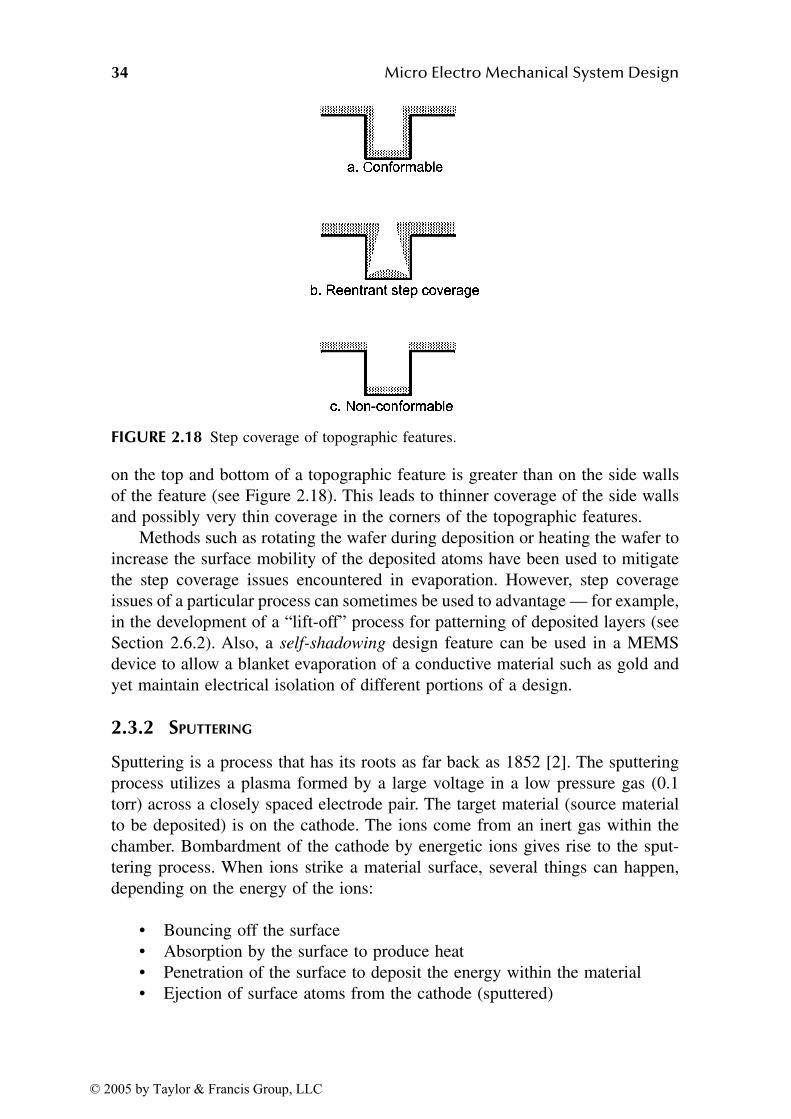
34 Micro Electro Mechanical System Design
on the top and bottom of a topographic feature is greater than on the side walls
of the feature (see Figure 2.18). This leads to thinner coverage of the side walls
and possibly very thin coverage in the corners of the topographic features.
Methods such as rotating the wafer during deposition or heating the wafer to
increase the surface mobility of the deposited atoms have been used to mitigate
the step coverage issues encountered in evaporation. However, step coverage
issues of a particular process can sometimes be used to advantage — for example,
in the development of a “lift-off” process for patterning of deposited layers (see
Section 2.6.2). Also, a self-shadowing design feature can be used in a MEMS
device to allow a blanket evaporation of a conductive material such as gold and
yet maintain electrical isolation of different portions of a design.
2.3.2 SPUTTERING
Sputtering is a process that has its roots as far back as 1852 [2]. The sputtering
process utilizes a plasma formed by a large voltage in a low pressure gas (0.1
torr) across a closely spaced electrode pair. The target material (source material
to be deposited) is on the cathode. The ions come from an inert gas within the
chamber. Bombardment of the cathode by energetic ions gives rise to the sput-
tering process. When ions strike a material surface, several things can happen,
depending on the energy of the ions:
• Bouncing off the surface
• Absorption by the surface to produce heat
• Penetration of the surface to deposit the energy within the material
• Ejection of surface atoms from the cathode (sputtered)
FIGURE 2.18 Step coverage of topographic features.
© 2005 by Taylor & Francis Group, LLC
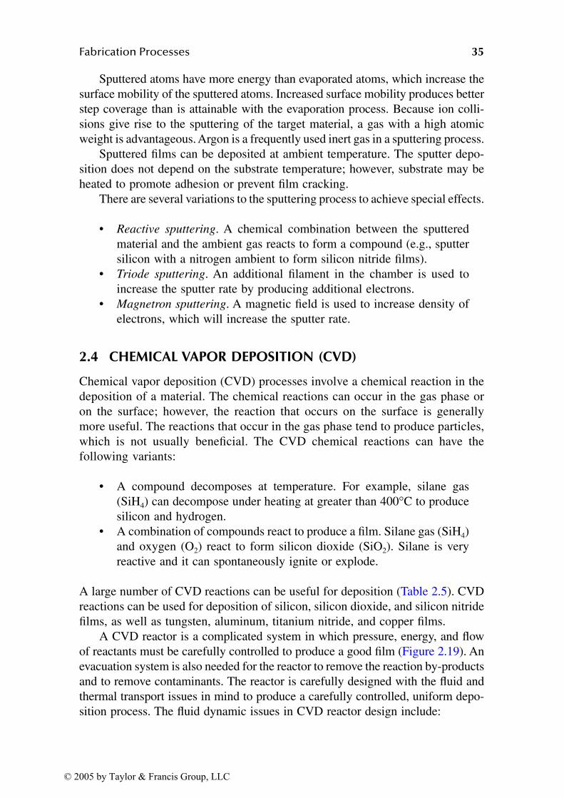
Fabrication Processes 35
Sputtered atoms have more energy than evaporated atoms, which increase the
surface mobility of the sputtered atoms. Increased surface mobility produces better
step coverage than is attainable with the evaporation process. Because ion colli-
sions give rise to the sputtering of the target material, a gas with a high atomic
weight is advantageous. Argon is a frequently used inert gas in a sputtering process.
Sputtered films can be deposited at ambient temperature. The sputter depo-
sition does not depend on the substrate temperature; however, substrate may be
heated to promote adhesion or prevent film cracking.
There are several variations to the sputtering process to achieve special effects.
• Reactive sputtering. A chemical combination between the sputtered
material and the ambient gas reacts to form a compound (e.g., sputter
silicon with a nitrogen ambient to form silicon nitride films).
• Triode sputtering. An additional filament in the chamber is used to
increase the sputter rate by producing additional electrons.
• Magnetron sputtering. A magnetic field is used to increase density of
electrons, which will increase the sputter rate.
2.4 CHEMICAL VAPOR DEPOSITION (CVD)
Chemical vapor deposition (CVD) processes involve a chemical reaction in the
deposition of a material. The chemical reactions can occur in the gas phase or
on the surface; however, the reaction that occurs on the surface is generally
more useful. The reactions that occur in the gas phase tend to produce particles,
which is not usually beneficial. The CVD chemical reactions can have the
following variants:
• A compound decomposes at temperature. For example, silane gas
(SiH4) can decompose under heating at greater than 400°C to produce
silicon and hydrogen.
• A combination of compounds react to produce a film. Silane gas (SiH4)
and oxygen (O2) react to form silicon dioxide (SiO2). Silane is very
reactive and it can spontaneously ignite or explode.
A large number of CVD reactions can be useful for deposition (Table 2.5). CVD
reactions can be used for deposition of silicon, silicon dioxide, and silicon nitride
films, as well as tungsten, aluminum, titanium nitride, and copper films.
A CVD reactor is a complicated system in which pressure, energy, and flow
of reactants must be carefully controlled to produce a good film (Figure 2.19). An
evacuation system is also needed for the reactor to remove the reaction by-products
and to remove contaminants. The reactor is carefully designed with the fluid and
thermal transport issues in mind to produce a carefully controlled, uniform depo-
sition process. The fluid dynamic issues in CVD reactor design include:
© 2005 by Taylor & Francis Group, LLC
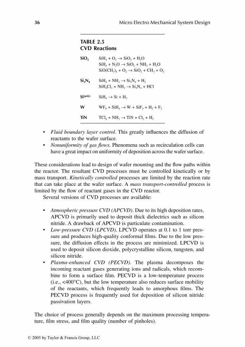
36 Micro Electro Mechanical System Design
• Fluid boundary layer control. This greatly influences the diffusion of
reactants to the wafer surface.
• Nonuniformity of gas flows. Phenomena such as recirculation cells can
have a great impact on uniformity of deposition across the wafer surface.
These considerations lead to design of wafer mounting and the flow paths within
the reactor. The resultant CVD processes must be controlled kinetically or by
mass transport. Kinetically controlled processes are limited by the reaction rate
that can take place at the wafer surface. A mass transport-controlled process is
limited by the flow of reactant gases in the CVD reactor.
Several versions of CVD processes are available:
• Atmospheric pressure CVD (APCVD). Due to its high deposition rates,
APCVD is primarily used to deposit thick dielectrics such as silicon
nitride. A drawback of APCVD is particulate contamination.
• Low-pressure CVD (LPCVD). LPCVD operates at 0.1 to 1 torr pres-
sure and produces high-quality conformal films. Due to the low pres-
sure, the diffusion effects in the process are minimized. LPCVD is
used to deposit silicon dioxide, polycrystalline silicon, tungsten, and
silicon nitride.
• Plasma-enhanced CVD (PECVD). The plasma decomposes the
incoming reactant gases generating ions and radicals, which recom-
bine to form a surface film. PECVD is a low-temperature process
(i.e., <400°C), but the low temperature also reduces surface mobility
of the reactants, which frequently leads to amorphous films. The
PECVD process is frequently used for deposition of silicon nitride
passivation layers.
The choice of process generally depends on the maximum processing tempera-
ture, film stress, and film quality (number of pinholes).
TABLE 2.5CVD Reactions
SiO2 SiH4 + O2 → SiO2 + H2O
SiH4 + N2O → SiO2 + NH3 + H2O
SiO(CH3)4 + O2 → SiO2 + CH3 + O2
Si3N4 SiH4 + NH3 → Si3N4 + H2
SiH4Cl2 + NH3 → Si3N4 + HCl
Si(poly) SiH4 → Si + H2
W WF6 + SiH4 → W + SiF4 + H2 + F2
TiN TCl4 + NH3 → TiN + Cl2 + H2
© 2005 by Taylor & Francis Group, LLC
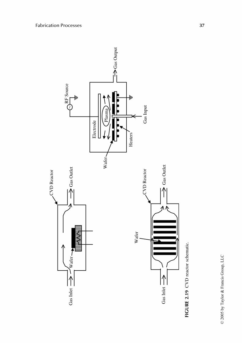
Fabrication Processes 37
FIG
UR
E 2.
19C
VD
rea
cto
r sc
hem
atic
.
Gas
In
let
Gas
In
let
Gas
Ou
tlet
Gas
Ou
tlet
CV
D R
eact
or
Waf
er
Waf
er
Waf
er
Hea
ters
Gas
In
pu
t
Pla
sma
Ele
ctro
de
RF
So
urc
e
Gas
Ou
tput
CV
D R
eact
or
© 2
005 b
y T
aylo
r &
Fra
nci
s G
roup, L
LC

38 Micro Electro Mechanical System Design
2.5 ETCHING PROCESSES
Etching processes are a fundamental process used in microelectronics and MEMS
to impress a desired pattern into a material. There are several options, depending
upon the various features that are important to be achieved. The considerations
for selection of a particular etch process include:
• Etch rate. The speed of the etch needs to be fast enough to be viable
for production but controllable.
• Uniformity. The etch is not location dependent.
• Selectivity. The etch rate ratio of the material desired to be etched vs.
the material that is not desired to be etched is important in selecting
the mask to be used in the etch process and the layer or material upon
which the etch will stop.
• Directionality. The etch can be isotropic (omnidirectional), or aniso-
tropic (directional).
Etching processes can be characterized by the method used to achieve the
material etch. Etching can be done by physical or chemical attack of the material.
Ion milling is an example of a physical attack of a material to achieve an etch.
The material is physically bombarded by ions that will remove material similar
to sputtering of a target. A chemical etch involves a chemical reaction that can
be isotropic or anisotropic. Wet etching, plasma etching, and ion milling will be
discussed further.
2.5.1 WET CHEMICAL ETCHING
Wet etching is purely a chemical process that is an isotropic etch in an amorphous
material such as silicon dioxide and can be directional in crystalline materials
such as silicon. Contaminants and particulate in this type of process are purely
a function of the chemical purity and chemical system cleanliness. Figure 2.20
illustrates the phases involved in chemical etching:
• Movement of the chemical reactants to the surface
• The chemical reaction that performs the etching
• Removal of the chemical reaction by-products
The slowest step in this process is called the rate limiting step. Agitation of
the wet chemical bath is frequently used to aid in the movement of reactants and
by-products to and from the surface. Agitation will also aid the uniformity of the
etch because the by-product may form solids or gases that must be moved. A
modern wet chemical bench will usually have agitation, temperature, and time
controls as well as filtration to remove particulate.
The etching of SiO2 is a common wet etch process employed in surface
micromachining (e.g., release etch, etch of isotropic features), which may be done
© 2005 by Taylor & Francis Group, LLC

Fabrication Processes 39
with a 6:1 by volume water to HF mixture. Equation 2.4 is the chemical reaction
involved in this etch. Because hydrofluoric (HF) acid is consumed in this reaction,
the concentration will decrease as the etch proceeds; this would require that more
HF be added to maintain concentration. Alternatively, a buffering agent could be
used to help maintain a concentration and pH in this reaction. Equation 2.5 shows
the chemical reaction that would enable NH4F to be used as a buffering agent in
the HF etch.
(2.4)
(2.5)
Wet etching methods can be used on crystalline material to achieve anisotro-
pic directional etches. For example, a common directional wet etchant for crys-
talline silicon is potassium hydroxide (KOH). KOH etches 100 times faster in
the (100) direction than the (111) direction. Patterned silicon dioxide can be used
as an etch mask for these types of etches. Very directional etches can be achieved
with these techniques, as illustrated in Figure 2.21. Note the angular features
(54.7°) that can be etched in silicon. Table 2.6 lists some of the common etchants
for crystalline silicon and their selectivity.
Boron-doped silicon has a greatly reduced etch rate in KOH. Boron-doped
diffused or implanted regions have been used to form features or as an etch stop
(Figure 2.22).
2.5.2 PLASMA ETCHING
Plasma etching offers a number of advantages compared to wet etching, including:
FIGURE 2.20 Wet chemical-etching process phases.
D D
SiO HF H SiF H O2 2 6 26 2+ → + +
NH F NH HF4 3↔ +
© 2005 by Taylor & Francis Group, LLC
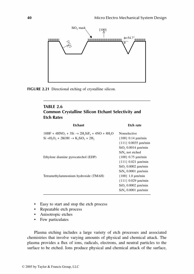
40 Micro Electro Mechanical System Design
• Easy to start and stop the etch process
• Repeatable etch process
• Anisotropic etches
• Few particulates
Plasma etching includes a large variety of etch processes and associated
chemistries that involve varying amounts of physical and chemical attack. The
plasma provides a flux of ions, radicals, electrons, and neutral particles to the
surface to be etched. Ions produce physical and chemical attack of the surface,
FIGURE 2.21 Directional etching of crystalline silicon.
TABLE 2.6Common Crystalline Silicon Etchant Selectivity and Etch Rates
Etchant Etch rate
18HF + 4HNO3 + 3Si → 2H2SiF6 + 4NO + 8H2O Nonselective
Si +H2O2 + 2KOH → K2SiO3 + 2H2 100 0.14 µm/min
111 0.0035 µm/min
SiO2 0.0014 µm/min
SiN4 not etched
Ethylene diamine pyrocatechol (EDP) 100 0.75 µm/min
111 0.021 µm/min
SiO2 0.0002 µm/min
SiN4 0.0001 µm/min
Tetramethylammonium hydroxide (TMAH) 100 1.0 µm/min
111 0.029 µm/min
SiO2 0.0002 µm/min
SiN4 0.0001 µm/min
φ=54.7°
φ
[111]
[100]SiO2 mask
© 2005 by Taylor & Francis Group, LLC
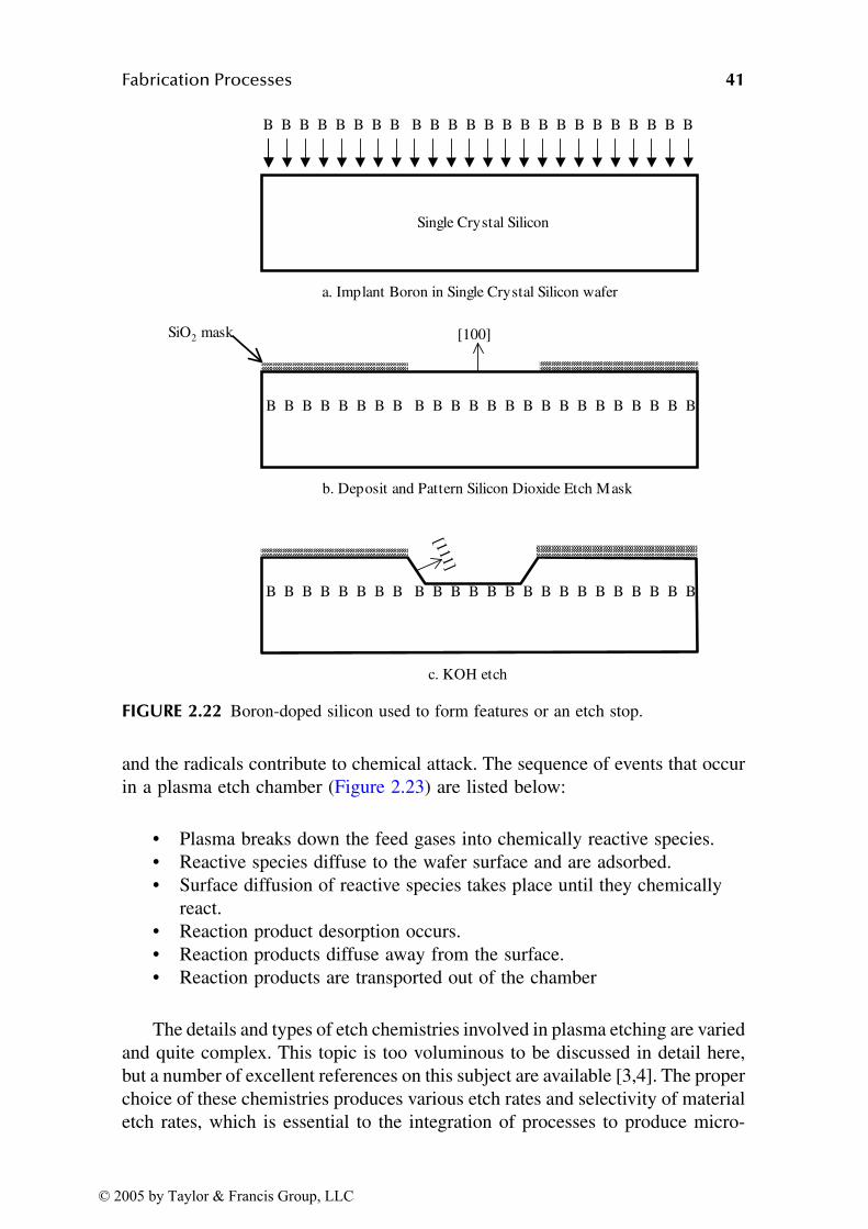
Fabrication Processes 41
and the radicals contribute to chemical attack. The sequence of events that occur
in a plasma etch chamber (Figure 2.23) are listed below:
• Plasma breaks down the feed gases into chemically reactive species.
• Reactive species diffuse to the wafer surface and are adsorbed.
• Surface diffusion of reactive species takes place until they chemically
react.
• Reaction product desorption occurs.
• Reaction products diffuse away from the surface.
• Reaction products are transported out of the chamber
The details and types of etch chemistries involved in plasma etching are varied
and quite complex. This topic is too voluminous to be discussed in detail here,
but a number of excellent references on this subject are available [3,4]. The proper
choice of these chemistries produces various etch rates and selectivity of material
etch rates, which is essential to the integration of processes to produce micro-
FIGURE 2.22 Boron-doped silicon used to form features or an etch stop.
B B B B B B B B B B B B B B B B B B B B B B B B
Single Crystal Silicon
a. Implant Boron in Single Crystal Silicon wafer
[100]
b. Deposit and Pattern Silicon Dioxide Etch Mask
SiO2 mask
B B B B B B B B B B B B B B B B B B B B B B B B
[111]
B B B B B B B B B B B B B B B B B B B B B B B B
c. KOH etch
© 2005 by Taylor & Francis Group, LLC
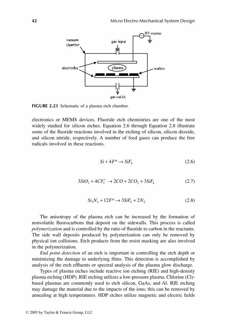
42 Micro Electro Mechanical System Design
electronics or MEMS devices. Fluoride etch chemistries are one of the most
widely studied for silicon etches. Equation 2.6 through Equation 2.8 illustrate
some of the fluoride reactions involved in the etching of silicon, silicon dioxide,
and silicon nitride, respectively. A number of feed gases can produce the free
radicals involved in these reactions.
(2.6)
(2.7)
(2.8)
The anisotropy of the plasma etch can be increased by the formation of
nonvolatile fluorocarbons that deposit on the sidewalls. This process is called
polymerization and is controlled by the ratio of fluoride to carbon in the reactants.
The side wall deposits produced by polymerization can only be removed by
physical ion collisions. Etch products from the resist masking are also involved
in the polymerization.
End point detection of an etch is important in controlling the etch depth or
minimizing the damage to underlying films. This detection is accomplished by
analysis of the etch effluents or spectral analysis of the plasma glow discharge.
Types of plasma etches include reactive ion etching (RIE) and high-density
plasma etching (HDP). RIE etching utilizes a low-pressure plasma. Chlorine (Cl)-
based plasmas are commonly used to etch silicon, GaAs, and Al. RIE etching
may damage the material due to the impacts of the ions; this can be removed by
annealing at high temperatures. HDP etches utilize magnetic and electric fields
FIGURE 2.23 Schematic of a plasma etch chamber.
Si F SiF+ →4 4*
3 4 2 2 32 3 2 4SiO CF CO CO SiF+ → + ++
Si N F SiF N3 4 4 212 3 2+ → +*
© 2005 by Taylor & Francis Group, LLC
Fabrication Processes 43
to increase dramatically the distance that free electrons can travel in the plasma.
HDP etches have good selectivity of Si to SiO2 and resist.
2.5.3 ION MILLING
Ion milling is a purely physical etching process; no chemical reactions are
involved. Ion milling uses noble gases with significant mass such as argon in a
process analogous to sputtering. This process is very isotropic because the ion
impinges the surface nearly vertically. However, the process has an etch rate
selectivity of the material to be etched to the mask material of nearly 1:1 because
the process is purely physical. Ion milling is not widely used for production
applications, and it is generally limited to the smaller wafer sizes (<200 mm).
The etch rates can be increased by increasing the ion densities impacting the
surface through the use of magnetic fields.
2.6 PATTERNING
The ability to pattern deposited layers is an essential capability required in
microelectronics and MEMS processing. Three widely utilized methods of pat-
terning will be discussed: lithography, the lift-off process, and the damascene
process.
Lithography is the mainstream process utilized for patterning in MEMS
processes. Lift-off and damascene are processes used for patterning materials in
which a reliable etch process such as metallization layers or optical coating layers
does not exist. These are frequently required in the postprocessing of MEMS
devices.
The current research and development in patterning for very fine line widths
(<0.35 µm) involve the development of sophisticated tools such as x-ray lithog-
raphy [7] or direct-write E-beam lithography [8]. Microelectronics will need the
capability to pattern features (line widths) of this size in the future in order to
continue development of microelectronic devices of increasing speed and capa-
bility. However, mainstream MEMS technology does not currently require such
fine features, so these methods will not be discussed here.
2.6.1 LITHOGRAPHY
Lithography is the most widely used method to pattern layers in microelectronic
and MEMS processing. Figure 2.24 is a schematic of a basic lithography system.
The basic components of a photolithographic system include:
• Illumination source
• Shutter
• Mask
• Wafer alignment/support system
• Photosensitive layer (photoresist or “resist”) on a wafer
© 2005 by Taylor & Francis Group, LLC
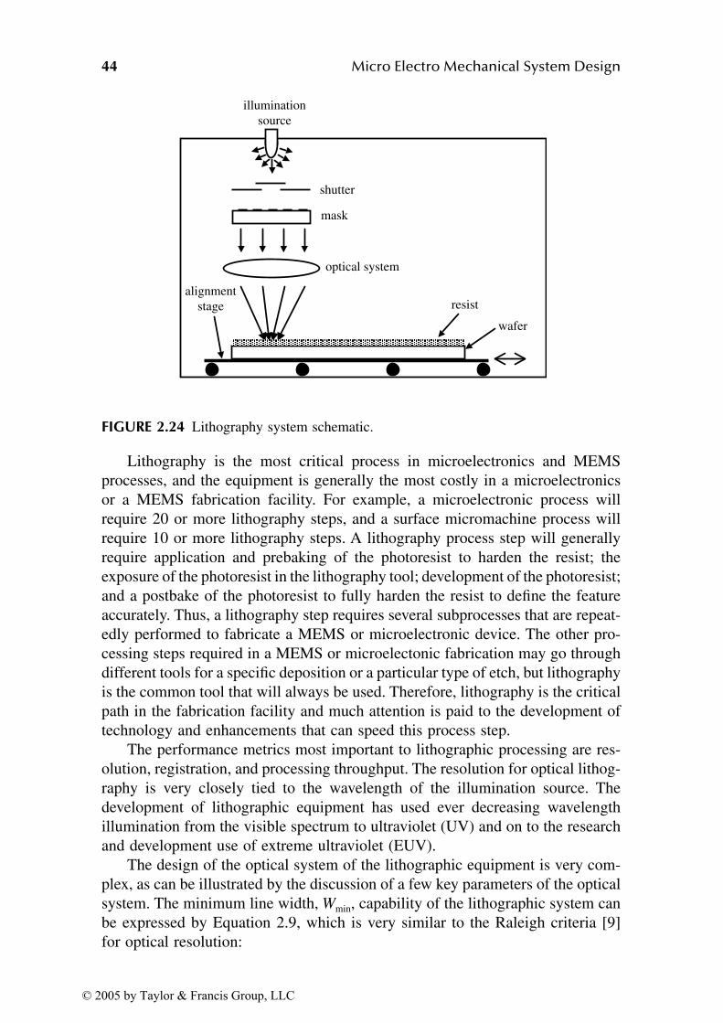
44 Micro Electro Mechanical System Design
Lithography is the most critical process in microelectronics and MEMS
processes, and the equipment is generally the most costly in a microelectronics
or a MEMS fabrication facility. For example, a microelectronic process will
require 20 or more lithography steps, and a surface micromachine process will
require 10 or more lithography steps. A lithography process step will generally
require application and prebaking of the photoresist to harden the resist; the
exposure of the photoresist in the lithography tool; development of the photoresist;
and a postbake of the photoresist to fully harden the resist to define the feature
accurately. Thus, a lithography step requires several subprocesses that are repeat-
edly performed to fabricate a MEMS or microelectronic device. The other pro-
cessing steps required in a MEMS or microelectonic fabrication may go through
different tools for a specific deposition or a particular type of etch, but lithography
is the common tool that will always be used. Therefore, lithography is the critical
path in the fabrication facility and much attention is paid to the development of
technology and enhancements that can speed this process step.
The performance metrics most important to lithographic processing are res-
olution, registration, and processing throughput. The resolution for optical lithog-
raphy is very closely tied to the wavelength of the illumination source. The
development of lithographic equipment has used ever decreasing wavelength
illumination from the visible spectrum to ultraviolet (UV) and on to the research
and development use of extreme ultraviolet (EUV).
The design of the optical system of the lithographic equipment is very com-
plex, as can be illustrated by the discussion of a few key parameters of the optical
system. The minimum line width, Wmin, capability of the lithographic system can
be expressed by Equation 2.9, which is very similar to the Raleigh criteria [9]
for optical resolution:
FIGURE 2.24 Lithography system schematic.
resist
optical system
mask
shutter
illumination
source
alignment
stage
wafer
© 2005 by Taylor & Francis Group, LLC
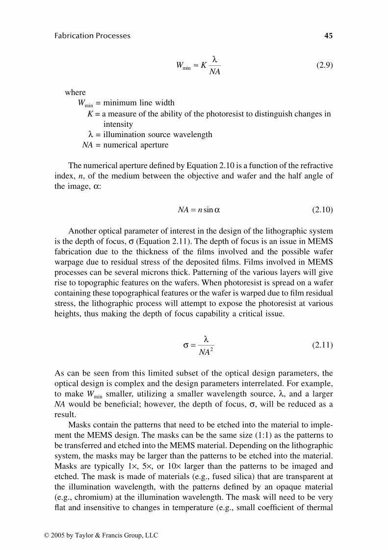
Fabrication Processes 45
(2.9)
where
Wmin = minimum line width
K = a measure of the ability of the photoresist to distinguish changes in
intensity
λ = illumination source wavelength
NA = numerical aperture
The numerical aperture defined by Equation 2.10 is a function of the refractive
index, n, of the medium between the objective and wafer and the half angle of
the image, α:
(2.10)
Another optical parameter of interest in the design of the lithographic system
is the depth of focus, σ (Equation 2.11). The depth of focus is an issue in MEMS
fabrication due to the thickness of the films involved and the possible wafer
warpage due to residual stress of the deposited films. Films involved in MEMS
processes can be several microns thick. Patterning of the various layers will give
rise to topographic features on the wafers. When photoresist is spread on a wafer
containing these topographical features or the wafer is warped due to film residual
stress, the lithographic process will attempt to expose the photoresist at various
heights, thus making the depth of focus capability a critical issue.
(2.11)
As can be seen from this limited subset of the optical design parameters, the
optical design is complex and the design parameters interrelated. For example,
to make Wmin smaller, utilizing a smaller wavelength source, λ, and a larger
NA would be beneficial; however, the depth of focus, σ, will be reduced as a
result.
Masks contain the patterns that need to be etched into the material to imple-
ment the MEMS design. The masks can be the same size (1:1) as the patterns to
be transferred and etched into the MEMS material. Depending on the lithographic
system, the masks may be larger than the patterns to be etched into the material.
Masks are typically 1×, 5×, or 10× larger than the patterns to be imaged and
etched. The mask is made of materials (e.g., fused silica) that are transparent at
the illumination wavelength, with the patterns defined by an opaque material
(e.g., chromium) at the illumination wavelength. The mask will need to be very
flat and insensitive to changes in temperature (e.g., small coefficient of thermal
W KNA
min ≈ λ
NA n= sin α
σ λ=NA2
© 2005 by Taylor & Francis Group, LLC
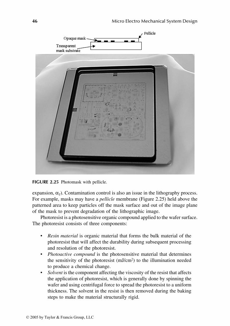
46 Micro Electro Mechanical System Design
expansion, αT). Contamination control is also an issue in the lithography process.
For example, masks may have a pellicle membrane (Figure 2.25) held above the
patterned area to keep particles off the mask surface and out of the image plane
of the mask to prevent degradation of the lithographic image.
Photoresist is a photosensitive organic compound applied to the wafer surface.
The photoresist consists of three components:
• Resin material is organic material that forms the bulk material of the
photoresist that will affect the durability during subsequent processing
and resolution of the photoresist.
• Photoactive compound is the photosensitive material that determines
the sensitivity of the photoresist (mJ/cm2) to the illumination needed
to produce a chemical change.
• Solvent is the component affecting the viscosity of the resist that affects
the application of photoresist, which is generally done by spinning the
wafer and using centrifugal force to spread the photoresist to a uniform
thickness. The solvent in the resist is then removed during the baking
steps to make the material structurally rigid.
FIGURE 2.25 Photomask with pellicle.
© 2005 by Taylor & Francis Group, LLC
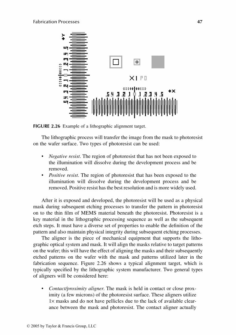
Fabrication Processes 47
The lithographic process will transfer the image from the mask to photoresist
on the wafer surface. Two types of photoresist can be used:
• Negative resist. The region of photoresist that has not been exposed to
the illumination will dissolve during the development process and be
removed.
• Positive resist. The region of photoresist that has been exposed to the
illumination will dissolve during the development process and be
removed. Positive resist has the best resolution and is more widely used.
After it is exposed and developed, the photoresist will be used as a physical
mask during subsequent etching processes to transfer the pattern in photoresist
on to the thin film of MEMS material beneath the photoresist. Photoresist is a
key material in the lithographic processing sequence as well as the subsequent
etch steps. It must have a diverse set of properties to enable the definition of the
pattern and also maintain physical integrity during subsequent etching processes.
The aligner is the piece of mechanical equipment that supports the litho-
graphic optical system and mask. It will align the masks relative to target patterns
on the wafer; this will have the effect of aligning the masks and their subsequently
etched patterns on the wafer with the mask and patterns utilized later in the
fabrication sequence. Figure 2.26 shows a typical alignment target, which is
typically specified by the lithographic system manufacturer. Two general types
of aligners will be considered here:
• Contact/proximity aligner. The mask is held in contact or close prox-
imity (a few microns) of the photoresist surface. These aligners utilize
1× masks and do not have pellicles due to the lack of available clear-
ance between the mask and photoresist. The contact aligner actually
FIGURE 2.26 Example of a lithographic alignment target.
© 2005 by Taylor & Francis Group, LLC

48 Micro Electro Mechanical System Design
presses the mask under pressure against the photoresist, which will
have the effect of degrading the mask under repeated use. This category
of aligner is the least expensive, and has the lowest resolution capa-
bility. These aligners are generally used for research or limited pro-
duction applications.
• Projection aligner. The mask and wafer are separated as dictated by
the design of the optical system. This class of aligner can have high
resolution that is only limited by optical system performance. These
systems can be very expensive and are utilized in high-volume
manufacturing.
2.6.2 LIFT-OFF PROCESS
Lift-off is a patterning process frequently used in MEMS for patterning materials
that do not possess a reliable process to etch them (e.g., noble metals). The lift-
off process is accomplished via the use of an intermediate layer and deposition
process, which has poor step coverage. Figure 2.27 is a schematic of a lift-off
process that will deposit and pattern a material on a substrate or underlying layer.
This process involves the following steps:
• Deposit and pattern a thick intermediate layer of a material that is easy
to remove (e.g., SiO2 or photoresist) and that will have a slightly
reentrant profile.
• Deposit a layer of the material to be patterned utilizing a process that
has poor step coverage (e.g., evaporation). The material thickness
should be a fraction of the intermediate layer thickness.
FIGURE 2.27 Lift-off process schematic.
patterned SiO2/resist
evaporated metal layer
substrate
a. Evaporated metal layer on a patterned SiO2 or resist layer
b. Strip the SiO2 or resist layer leaving the metal on the substrate
© 2005 by Taylor & Francis Group, LLC
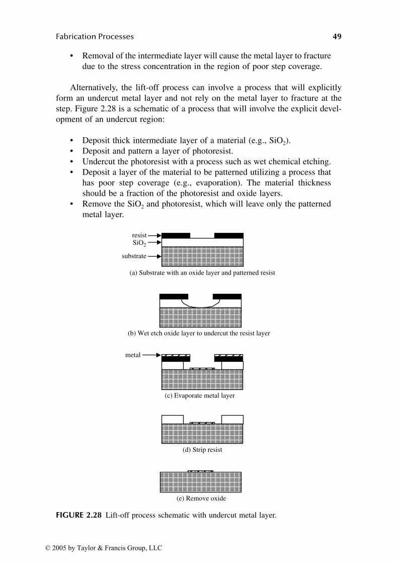
Fabrication Processes 49
• Removal of the intermediate layer will cause the metal layer to fracture
due to the stress concentration in the region of poor step coverage.
Alternatively, the lift-off process can involve a process that will explicitly
form an undercut metal layer and not rely on the metal layer to fracture at the
step. Figure 2.28 is a schematic of a process that will involve the explicit devel-
opment of an undercut region:
• Deposit thick intermediate layer of a material (e.g., SiO2).
• Deposit and pattern a layer of photoresist.
• Undercut the photoresist with a process such as wet chemical etching.
• Deposit a layer of the material to be patterned utilizing a process that
has poor step coverage (e.g., evaporation). The material thickness
should be a fraction of the photoresist and oxide layers.
• Remove the SiO2 and photoresist, which will leave only the patterned
metal layer.
FIGURE 2.28 Lift-off process schematic with undercut metal layer.
resist
substrate
(a) Substrate with an oxide layer and patterned resist
(b) Wet etch oxide layer to undercut the resist layer
(c) Evaporate metal layer
metal
(d) Strip resist
(e) Remove oxide
SiO2
© 2005 by Taylor & Francis Group, LLC
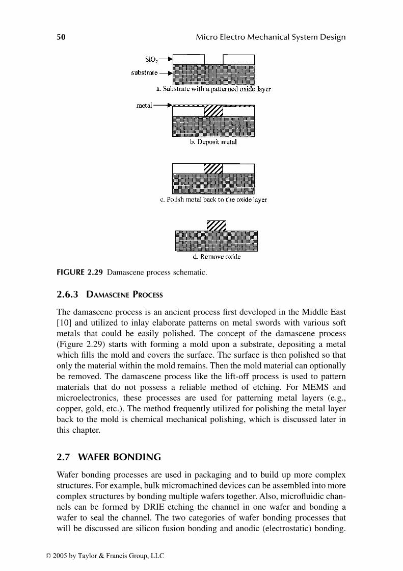
50 Micro Electro Mechanical System Design
2.6.3 DAMASCENE PROCESS
The damascene process is an ancient process first developed in the Middle East
[10] and utilized to inlay elaborate patterns on metal swords with various soft
metals that could be easily polished. The concept of the damascene process
(Figure 2.29) starts with forming a mold upon a substrate, depositing a metal
which fills the mold and covers the surface. The surface is then polished so that
only the material within the mold remains. Then the mold material can optionally
be removed. The damascene process like the lift-off process is used to pattern
materials that do not possess a reliable method of etching. For MEMS and
microelectronics, these processes are used for patterning metal layers (e.g.,
copper, gold, etc.). The method frequently utilized for polishing the metal layer
back to the mold is chemical mechanical polishing, which is discussed later in
this chapter.
2.7 WAFER BONDING
Wafer bonding processes are used in packaging and to build up more complex
structures. For example, bulk micromachined devices can be assembled into more
complex structures by bonding multiple wafers together. Also, microfluidic chan-
nels can be formed by DRIE etching the channel in one wafer and bonding a
wafer to seal the channel. The two categories of wafer bonding processes that
will be discussed are silicon fusion bonding and anodic (electrostatic) bonding.
FIGURE 2.29 Damascene process schematic.
© 2005 by Taylor & Francis Group, LLC

Fabrication Processes 51
The choice of bonding process will be influenced by the thermal budget of the
devices and materials involved.
2.7.1 SILICON FUSION BONDING
At room temperature, two highly polished flat silicon wafers brought into contact
will bond. The mechanism is believed to be hydrogen bonds between the surfaces.
The bond can be converted into a stronger Si–O–Si bond at an elevated temper-
ature (>800˚C). The main concern with this bonding technique is voids in the
bonded wafer due to surface defects, residues, and particulate on the surface. The
processing sequence for silicon fusion bonding will generally include the follow-
ing steps:
• Polishing of the wafer surfaces to be bonded
• Wafer surface wet cleaning processes to make the bond surface hydro-
philic, which will facilitate the bonding mechanism
• Wafer surface inspection
• Precise alignment of bond surfaces in a clean environment
• Annealing of the bonded wafers
Other silicon-based materials such as polycrystalline silicon (polysilicon),
silicon dioxide, and silicon nitride can be similarly bonded. However, yield of
the bonded wafers due to voids will increase due to the different mechanical
properties of the wafers.
2.7.2 ANODIC BONDING
Anodic bonding is an electrostatic bonding technique for glass to silicon wafers
or silicon wafers with a thin silicon dioxide layer between the wafers. Anodic
bonding utilizes a heated chuck with an electrode capable of applying a DC
voltage of up to 200 V. Pressure may be optionally applied to facilitate the bonding
process. Figure 2.30 is a schematic of an anodic bonding process.
2.8 ANNEALING
Annealing is a process of elevating materials to a high temperature to achieve
one of the following effects:
• Reduction of residual stresses in a material. The deposition process
temperature will greatly influence the residual stress in a deposited
film. A way to reduce the film residual stress is to anneal the film at
a high temperature for a length of time (e.g., polysilicon residual stress
can be reduced by annealing at >1100°C for several hours in an inert
atmosphere, N2, which minimizes oxidation).
• Activation of dopants. When dopants are implanted or diffused into a
material to create active electronic devices or piezoresistors, the dopants
© 2005 by Taylor & Francis Group, LLC
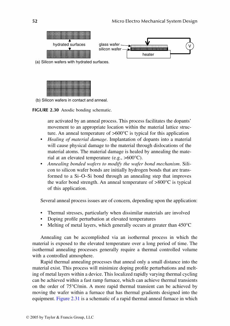
52 Micro Electro Mechanical System Design
are activated by an anneal process. This process facilitates the dopants’
movement to an appropriate location within the material lattice struc-
ture. An anneal temperature of >600°C is typical for this application
• Healing of material damage. Implantation of dopants into a material
will cause physical damage to the material through dislocations of the
material atoms. The material damage is healed by annealing the mate-
rial at an elevated temperature (e.g., >600°C).
• Annealing bonded wafers to modify the wafer bond mechanism. Sili-
con to silicon wafer bonds are initially hydrogen bonds that are trans-
formed to a Si–O–Si bond through an annealing step that improves
the wafer bond strength. An anneal temperature of >800°C is typical
of this application.
Several anneal process issues are of concern, depending upon the application:
• Thermal stresses, particularly when dissimilar materials are involved
• Doping profile perturbation at elevated temperatures
• Melting of metal layers, which generally occurs at greater than 450°C
Annealing can be accomplished via an isothermal process in which the
material is exposed to the elevated temperature over a long period of time. The
isothermal annealing processes generally require a thermal controlled volume
with a controlled atmosphere.
Rapid thermal annealing processes that anneal only a small distance into the
material exist. This process will minimize doping profile perturbations and melt-
ing of metal layers within a device. This localized rapidly varying thermal cycling
can be achieved within a fast ramp furnace, which can achieve thermal transients
on the order of 75°C/min. A more rapid thermal transient can be achieved by
moving the wafer within a furnace that has thermal gradients designed into the
equipment. Figure 2.31 is a schematic of a rapid thermal anneal furnace in which
FIGURE 2.30 Anodic bonding schematic.
hydrated surfaces glass wafersilicon wafer
heater
V
(a) Silicon wafers with hydrated surfaces.
(b) Silicon wafers in contact and anneal.
© 2005 by Taylor & Francis Group, LLC
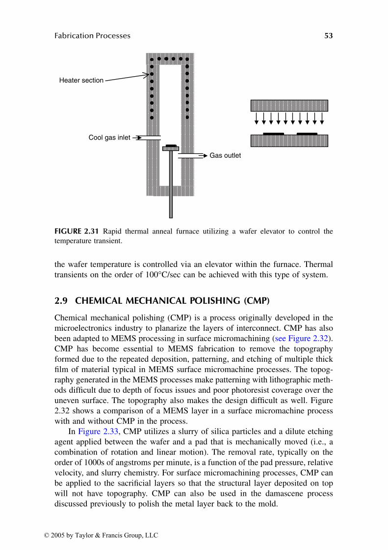
Fabrication Processes 53
the wafer temperature is controlled via an elevator within the furnace. Thermal
transients on the order of 100°C/sec can be achieved with this type of system.
2.9 CHEMICAL MECHANICAL POLISHING (CMP)
Chemical mechanical polishing (CMP) is a process originally developed in the
microelectronics industry to planarize the layers of interconnect. CMP has also
been adapted to MEMS processing in surface micromachining (see Figure 2.32).
CMP has become essential to MEMS fabrication to remove the topography
formed due to the repeated deposition, patterning, and etching of multiple thick
film of material typical in MEMS surface micromachine processes. The topog-
raphy generated in the MEMS processes make patterning with lithographic meth-
ods difficult due to depth of focus issues and poor photoresist coverage over the
uneven surface. The topography also makes the design difficult as well. Figure
2.32 shows a comparison of a MEMS layer in a surface micromachine process
with and without CMP in the process.
In Figure 2.33, CMP utilizes a slurry of silica particles and a dilute etching
agent applied between the wafer and a pad that is mechanically moved (i.e., a
combination of rotation and linear motion). The removal rate, typically on the
order of 1000s of angstroms per minute, is a function of the pad pressure, relative
velocity, and slurry chemistry. For surface micromachining processes, CMP can
be applied to the sacrificial layers so that the structural layer deposited on top
will not have topography. CMP can also be used in the damascene process
discussed previously to polish the metal layer back to the mold.
FIGURE 2.31 Rapid thermal anneal furnace utilizing a wafer elevator to control the
temperature transient.
Heater section
Cool gas inlet
Gas outlet
© 2005 by Taylor & Francis Group, LLC
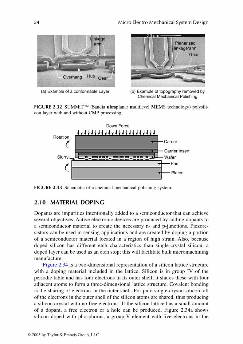
54 Micro Electro Mechanical System Design
2.10 MATERIAL DOPING
Dopants are impurities intentionally added to a semiconductor that can achieve
several objectives. Active electronic devices are produced by adding dopants to
a semiconductor material to create the necessary n- and p-junctions. Piezore-
sistors can be used in sensing applications and are created by doping a portion
of a semiconductor material located in a region of high strain. Also, because
doped silicon has different etch characteristics than single-crystal silicon, a
doped layer can be used as an etch stop; this will facilitate bulk micromachining
manufacture.
Figure 2.34 is a two-dimensional representation of a silicon lattice structure
with a doping material included in the lattice. Silicon is in group IV of the
periodic table and has four electrons in its outer shell; it shares these with four
adjacent atoms to form a three-dimensional lattice structure. Covalent bonding
is the sharing of electrons in the outer shell. For pure single-crystal silicon, all
of the electrons in the outer shell of the silicon atoms are shared, thus producing
a silicon crystal with no free electrons. If the silicon lattice has a small amount
of a dopant, a free electron or a hole can be produced. Figure 2.34a shows
silicon doped with phosphorus, a group V element with five electrons in the
FIGURE 2.32 SUMMiT (Sandia ultraplanar multilevel MEMS technology) polysili-
con layer with and without CMP processing.
FIGURE 2.33 Schematic of a chemical mechanical polishing system.
Linkagearm
Overhang
(a) Example of a conformable Layer (b) Example of topography removed by Chemical Mechanical Polishing
HubGear
Planarizedlinkage arm
Gear
20 µm
Rotation
Down Force
Carrier
Carrier Insert
Wafer
Pad
Platen
Slurry
© 2005 by Taylor & Francis Group, LLC
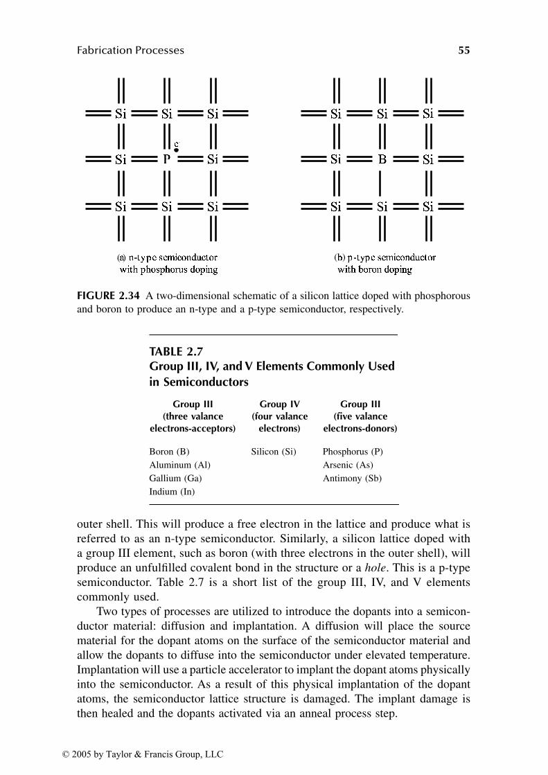
Fabrication Processes 55
outer shell. This will produce a free electron in the lattice and produce what is
referred to as an n-type semiconductor. Similarly, a silicon lattice doped with
a group III element, such as boron (with three electrons in the outer shell), will
produce an unfulfilled covalent bond in the structure or a hole. This is a p-type
semiconductor. Table 2.7 is a short list of the group III, IV, and V elements
commonly used.
Two types of processes are utilized to introduce the dopants into a semicon-
ductor material: diffusion and implantation. A diffusion will place the source
material for the dopant atoms on the surface of the semiconductor material and
allow the dopants to diffuse into the semiconductor under elevated temperature.
Implantation will use a particle accelerator to implant the dopant atoms physically
into the semiconductor. As a result of this physical implantation of the dopant
atoms, the semiconductor lattice structure is damaged. The implant damage is
then healed and the dopants activated via an anneal process step.
FIGURE 2.34 A two-dimensional schematic of a silicon lattice doped with phosphorous
and boron to produce an n-type and a p-type semiconductor, respectively.
TABLE 2.7Group III, IV, and V Elements Commonly Used in Semiconductors
Group III(three valance
electrons-acceptors)
Group IV(four valance
electrons)
Group III(five valance
electrons-donors)
Boron (B) Silicon (Si) Phosphorus (P)
Aluminum (Al) Arsenic (As)
Gallium (Ga) Antimony (Sb)
Indium (In)
( ) ( )
© 2005 by Taylor & Francis Group, LLC
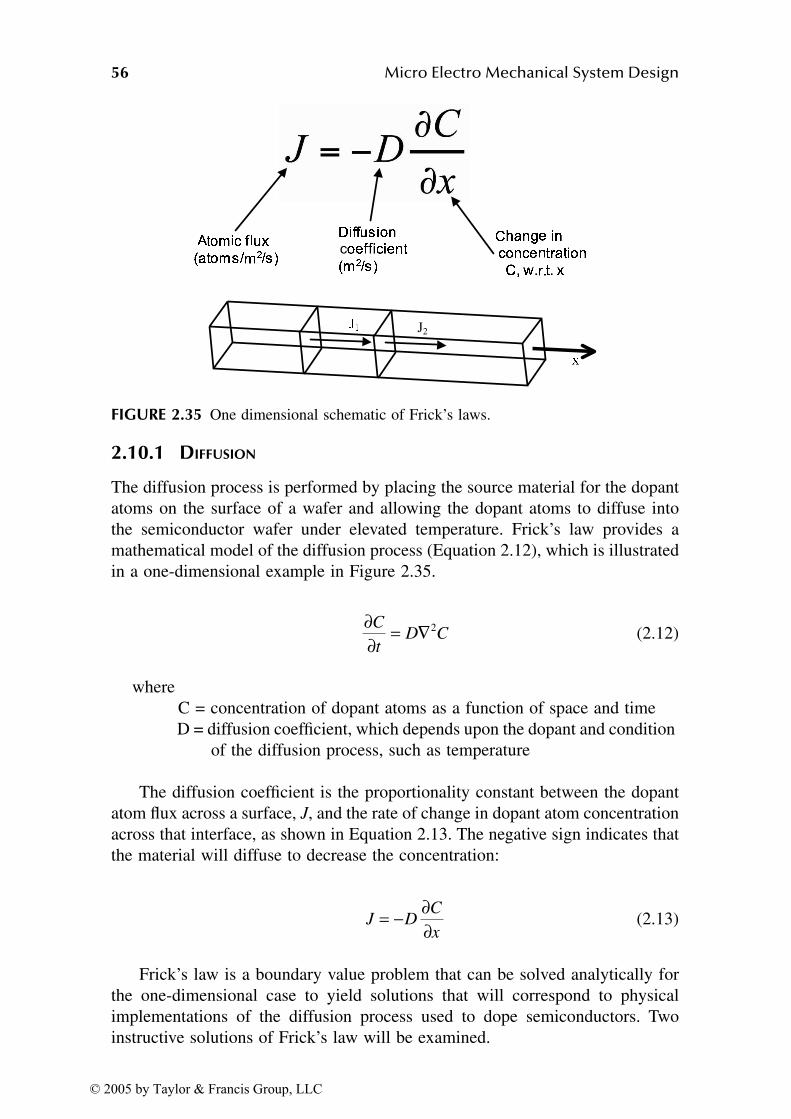
56 Micro Electro Mechanical System Design
2.10.1 DIFFUSION
The diffusion process is performed by placing the source material for the dopant
atoms on the surface of a wafer and allowing the dopant atoms to diffuse into
the semiconductor wafer under elevated temperature. Frick’s law provides a
mathematical model of the diffusion process (Equation 2.12), which is illustrated
in a one-dimensional example in Figure 2.35.
(2.12)
where
C = concentration of dopant atoms as a function of space and time
D = diffusion coefficient, which depends upon the dopant and condition
of the diffusion process, such as temperature
The diffusion coefficient is the proportionality constant between the dopant
atom flux across a surface, J, and the rate of change in dopant atom concentration
across that interface, as shown in Equation 2.13. The negative sign indicates that
the material will diffuse to decrease the concentration:
(2.13)
Frick’s law is a boundary value problem that can be solved analytically for
the one-dimensional case to yield solutions that will correspond to physical
implementations of the diffusion process used to dope semiconductors. Two
instructive solutions of Frick’s law will be examined.
FIGURE 2.35 One dimensional schematic of Frick’s laws.
J2
∂∂ = ∇C
tD C2
J DC
x= − ∂
∂
© 2005 by Taylor & Francis Group, LLC
Fabrication Processes 57
Case 1. In this case, the dopants constantly arrive at the surface of the
wafer to maintain a constant dopant concentration, Cs, on the wafer surface
(Equation 2.14). The dopant concentration deep within the wafer is 0, as shown
in Equation 2.15:
(2.14)
(2.15)
Equation 2.14 and Equation 2.15 are the problem boundary conditions. The initial
condition at t = 0 is that the concentration is zero throughout the domain:
(2.16)
Frick’s equation with these boundary and initial conditions can be solved to
yield, Equation 2.17. is called the diffusion length — a quantity that appears
in the analytical solutions of Frick’s equations. The solution of Frick’s equation
also involves the complementary error function, which is tabulated in a number
of references [11]. Figure 2.36a plots this solution of Frick’s equation, which
shows the dopant concentration increasing within the wafer and penetrating
deeper as time increases. The concentration remains constant at the wafer surface.
(2.17)
Case 2. In this situation, a fixed amount of dopant, Q, has been initially
introduced to the wafer, as shown in Equation 2.18. The initial distribution is
approximated as a delta function at x = 0, and the initial concentration elsewhere
in the wafer is 0 (Equation 2.19). There are two boundary conditions for this
case. For the surface, x = 0, no additional dopants are added (Equation 2.20).
This boundary condition is obtained from Frick’s first law, Equation 2.13, which
relates the dopant flux at a surface, J, and the rate of change of the concentration
at the surface. The second boundary condition assumes that the wafer is thick;
therefore, at x = ∞, the concentration is zero (Equation 2.21).
(2.18)
(2.19)
(2.20)
C x t C( , )= =0
C x t( , )= ∞ = 0
C x t( , )= =0 0
Dt
C x t C erfcx
Dts( , ) =
2
C x t dx Q( , )0
∞∫ = = constant
C x t x( , ) ,= = ≠0 0 0
J x tdC x t
dx( , )
( , )= = = =00
0
© 2005 by Taylor & Francis Group, LLC
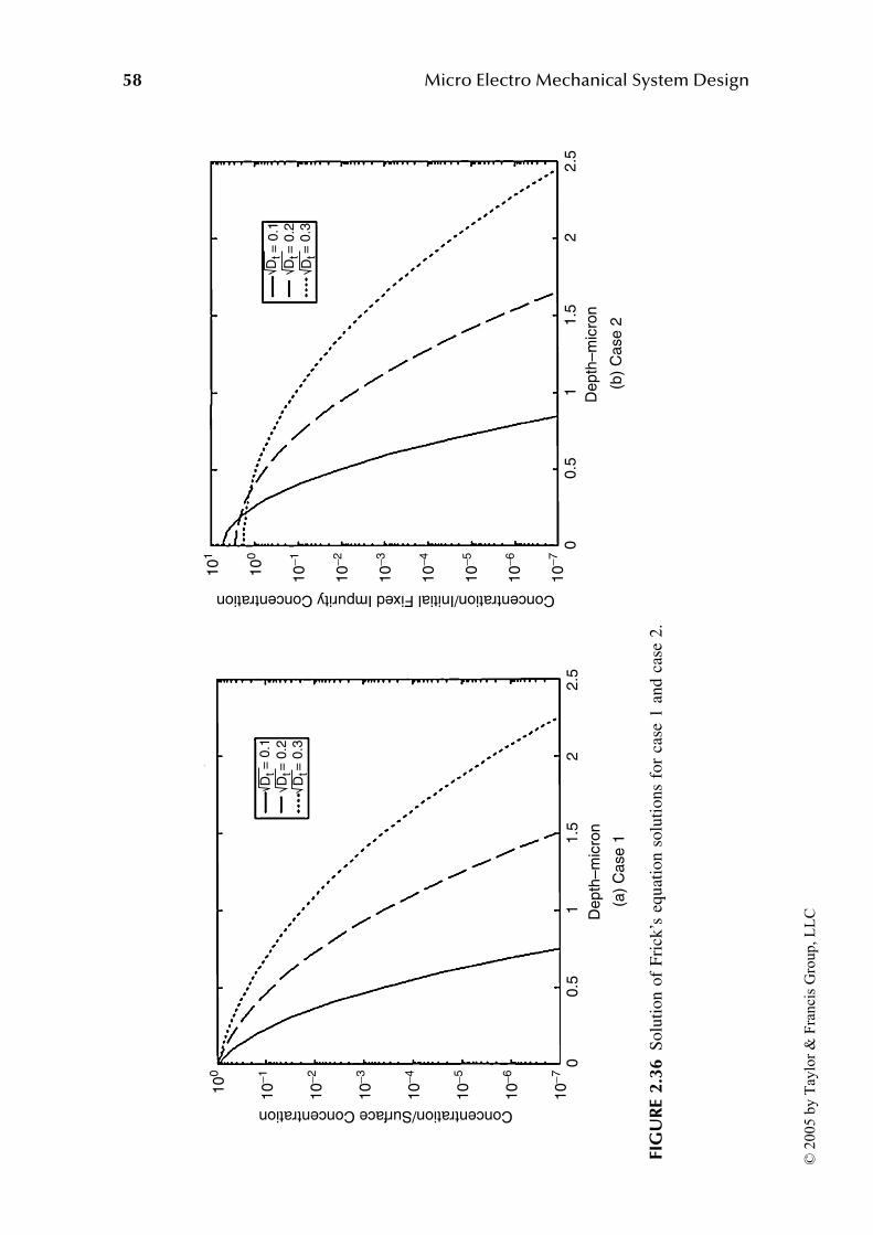
58 Micro Electro Mechanical System Design
FIG
UR
E 2.
36S
olu
tio
n o
f F
rick
’s e
qu
atio
n s
olu
tio
ns
for
case
1 a
nd
cas
e 2
.
10
010
1
10
0
00.5
1 Depth
–m
icro
n
(a)
Case 1
(b)
Case 2
= 0
.1
Depth
–m
icro
n
Concentration/Initial Fixed Impurity Concentration
1.5
20
0.5
11.5
22.5
Concentration/Surface Concentration
2.5
= 0
.1=
0.2
= 0
.3
= 0
.2=
0.3
Dt
Dt
Dt
Dt
Dt
Dt
© 2
005 b
y T
aylo
r &
Fra
nci
s G
roup, L
LC
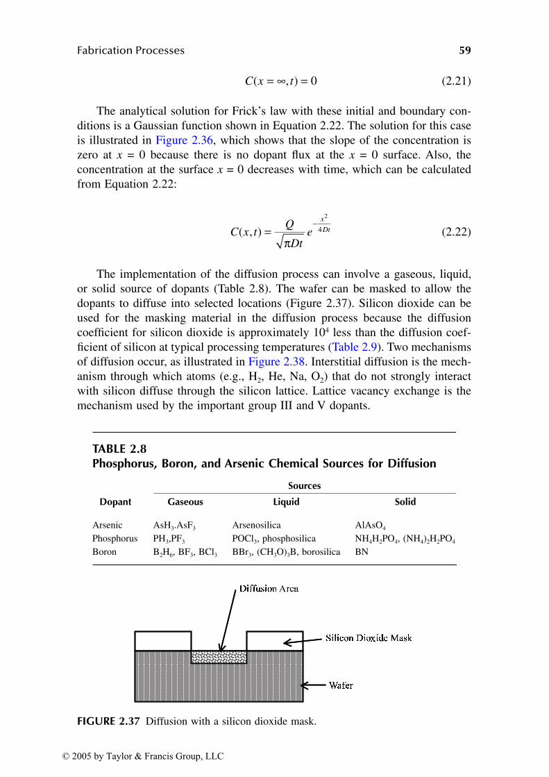
Fabrication Processes 59
(2.21)
The analytical solution for Frick’s law with these initial and boundary con-
ditions is a Gaussian function shown in Equation 2.22. The solution for this case
is illustrated in Figure 2.36, which shows that the slope of the concentration is
zero at x = 0 because there is no dopant flux at the x = 0 surface. Also, the
concentration at the surface x = 0 decreases with time, which can be calculated
from Equation 2.22:
(2.22)
The implementation of the diffusion process can involve a gaseous, liquid,
or solid source of dopants (Table 2.8). The wafer can be masked to allow the
dopants to diffuse into selected locations (Figure 2.37). Silicon dioxide can be
used for the masking material in the diffusion process because the diffusion
coefficient for silicon dioxide is approximately 104 less than the diffusion coef-
ficient of silicon at typical processing temperatures (Table 2.9). Two mechanisms
of diffusion occur, as illustrated in Figure 2.38. Interstitial diffusion is the mech-
anism through which atoms (e.g., H2, He, Na, O2) that do not strongly interact
with silicon diffuse through the silicon lattice. Lattice vacancy exchange is the
mechanism used by the important group III and V dopants.
TABLE 2.8Phosphorus, Boron, and Arsenic Chemical Sources for Diffusion
Dopant
Sources
Gaseous Liquid Solid
Arsenic AsH3.AsF3 Arsenosilica AlAsO4
Phosphorus PH3,PF3 POCl3, phosphosilica NH4H2PO4, (NH4)2H2PO4
Boron B2H6, BF3, BCl3 BBr3, (CH3O)3B, borosilica BN
FIGURE 2.37 Diffusion with a silicon dioxide mask.
C x t( , )= ∞ = 0
C x tQ
Dte
x
Dt( , ) = −π
2
4
© 2005 by Taylor & Francis Group, LLC
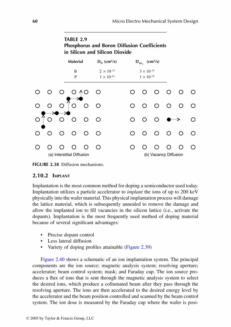
60 Micro Electro Mechanical System Design
2.10.2 IMPLANT
Implantation is the most common method for doping a semiconductor used today.
Implantation utilizes a particle accelerator to implant the ions of up to 200 keV
physically into the wafer material. This physical implantation process will damage
the lattice material, which is subsequently annealed to remove the damage and
allow the implanted ion to fill vacancies in the silicon lattice (i.e., activate the
dopants). Implantation is the most frequently used method of doping material
because of several significant advantages:
• Precise dopant control
• Less lateral diffusion
• Variety of doping profiles attainable (Figure 2.39)
Figure 2.40 shows a schematic of an ion implantation system. The principal
components are the ion source; magnetic analysis system; resolving aperture;
accelerator; beam control system; mask; and Faraday cup. The ion source pro-
duces a flux of ions that is sent through the magnetic analysis system to select
the desired ions, which produce a collumated beam after they pass through the
resolving aperture. The ions are then accelerated to the desired energy level by
the accelerator and the beam position controlled and scanned by the beam control
system. The ion dose is measured by the Faraday cup where the wafer is posi-
TABLE 2.9Phosphorus and Boron Diffusion Coefficientsin Silicon and Silicon Dioxide
Material DSi (cm2/s) (cm2/s)
B 2 × 10–15 3 × 10–19
P 1 × 10–14 1 × 10–18
FIGURE 2.38 Diffusion mechanisms.
DSiO2
(a) Interstitial Diffusion (b) Vacancy Diffusion
© 2005 by Taylor & Francis Group, LLC
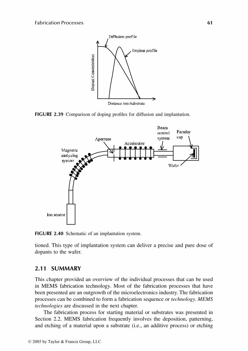
Fabrication Processes 61
tioned. This type of implantation system can deliver a precise and pure dose of
dopants to the wafer.
2.11 SUMMARY
This chapter provided an overview of the individual processes that can be used
in MEMS fabrication technology. Most of the fabrication processes that have
been presented are an outgrowth of the microelectronics industry. The fabrication
processes can be combined to form a fabrication sequence or technology. MEMS
technologies are discussed in the next chapter.
The fabrication process for starting material or substrates was presented in
Section 2.2. MEMS fabrication frequently involves the deposition, patterning,
and etching of a material upon a substrate (i.e., an additive process) or etching
FIGURE 2.39 Comparison of doping profiles for diffusion and implantation.
FIGURE 2.40 Schematic of an implantation system.
I
© 2005 by Taylor & Francis Group, LLC

62 Micro Electro Mechanical System Design
the substrate material (i.e., a subtractive process). The fabrication methods were
presented for a single-crystal substrate (i.e., Czochralski growth, float zone) as
well as for silicon on insulator (SOI) substrates (i.e., SIMOX, Unibond).
A fundamental process sequence will generally involve deposition, pattern-
ing, and etching. The deposition processes of physical vapor deposition (PVD)
and chemical vapor deposition (CVD) and their variants were presented. The
selection of deposition process and its parameters will control characteristics of
the deposited film such as residual stress, and conformal or nonconformal layer.
These characteristics can be very important to subsequent MEMS fabrication
processes or the MEMS device.
Etching processes can be isotropic or anisotropic in nature. The selection of
the specific etch process and material is important in determining these charac-
teristics. The wet chemical etching, plasma etching, and ion milling processes
were discussed. To a large degree, patterning is performed via lithographic meth-
ods. However, for materials that do not have a viable etch process, the lift-off or
damascene process can be utilized.
A number of other processes used to achieve specific effects were presented.
Annealing is utilized in a manner similar to macroscale manufacturing to relieve
residual stresses. Chemical mechanical polishing (CMP) is used to remove topog-
raphy in films or for patterning a film in a damascene process. The doping of a
material for electrical purposes can be achieved by diffusion or implantation
processes. Wafer bonding is a process that can be used to produce a specific
structure for packaging or a MEMS device.
QUESTIONS
1. List the type of atomic bonds and describe them. Give an example of
a material utilizing each type of bond.
2. What are Van der Waals forces and when are they important?
3. What are the three types of material structure?
4. Name and sketch the common variants of the cubic lattice structure.
5. Sketch a face-centered cubic lattice and the (1 0 0) plane. What is the
plane equivalent to the (1 0 0) plane? Repeat for the (1 1 1) plane.
6. Give four examples of lattice defects. What is activation energy?
7. What is the maximum pull rate of a silicon seed crystal from the molten
bath due to the heat transfer of the latent heat of fusion? (Hint: refer
to Equation 2.1.) What are the parameters that could be used to control
the boule diameter?
8. What are the majority carriers for single-crystal silicon doped with
boron?
9. What are the dopants that could be used in an n-type silicon wafer?
10. What is meant by a conformable film? What process could deposit a
conformable film?
11. What is meant by a nonconformable film? What process could be used
to deposit a nonconformable film? Why would one want to do this?
© 2005 by Taylor & Francis Group, LLC

Fabrication Processes 63
12. What is meant by step coverage? Give an example of why this is
important.
13. What etchants can anisotropically etch single-crystal silicon? What
crystal direction has the fastest etch rate? What crystal direction has
the smallest etch rate?
14. What material could be used as a mask for a KOH etch of single-crystal
silicon?
15. Describe the difference between contact and optical lithography. Which
could produce a smaller dimension pattern in the photoresist?
16. What are the elements of a photoresist? Describe how photoresist is
utilized in the patterning process.
17. Why would one use a lift-off or damascene process?
18. Describe the lift-off and damascene processes and their similarities.
19. Describe the annealing process for polysilicon. List two reasons for
annealing a deposited film.
20. Why does the implant process provide a more accurate definition of
the dopant profile and region?
REFERENCES
1. G.K. Teal, Single crystals of germanium and silicon — basic to the transistor and
the integrated circuit, IEEE Trans. Electron. Dev. ED-23, 621, 1976.
2. W.R. Grove, On the electrochemical polarity of gases, Philos. Trans. Faraday Soc.
87, 1852.
3. R.A. Morgan, Plasma Etching in Semiconductor Fabrication, Elsevier, Amster-
dam, 1985.
4. D.M. Manos and D.L. Flamm, Plasma Etching, an Introduction, Academic Press,
Boston, 1989.
5. R.A. Morgan, VCSEL — a new twist in semiconductor-lasers, Photonics Spectra,
24(12), 89, 1990.
6. M.A. Michalicek, V.M. Bright, Flip-chip fabrication of advanced micromirror
arrays, Sensors Actuators A, 95, 152–157, 2002.
7. S. Ohki, S. Ishihara, An overview of x-ray lithography, Microelectron. Eng.,
30(1–4), 171–178, January 1996.
8. R. DeJule, E-beam lithography, the debate continues, Semiconductor Int., 19, 85,
1996.
9. M.V. Klein, Optics, John Wiley & Sons, New York, 1970.
10. J.D. Verhoeven, The mystery of Damascus blades, Sci. Am., 74–79, January 2001.
11. M. Abramowitz, I.A. Stegun, Handbook of Mathematical Functions with Formu-
las, Graphs, and Mathematical Table, National Bureau of Standards Applied
Mathematics Series 55, June 1964, 10th printing, December 1972.
© 2005 by Taylor & Francis Group, LLC
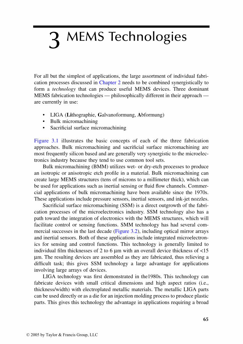
65
3 MEMS Technologies
For all but the simplest of applications, the large assortment of individual fabri-
cation processes discussed in Chapter 2 needs to be combined synergistically to
form a technology that can produce useful MEMS devices. Three dominant
MEMS fabrication technologies — philosophically different in their approach —
are currently in use:
• LIGA (Lithographie, Galvanoformung, Abformung)
• Bulk micromachining
• Sacrificial surface micromachining
Figure 3.1 illustrates the basic concepts of each of the three fabrication
approaches. Bulk micromachining and sacrificial surface micromachining are
most frequently silicon based and are generally very synergistic to the microelec-
tronics industry because they tend to use common tool sets.
Bulk micromachining (BMM) utilizes wet- or dry-etch processes to produce
an isotropic or anisotropic etch profile in a material. Bulk micromachining can
create large MEMS structures (tens of microns to a millimeter thick), which can
be used for applications such as inertial sensing or fluid flow channels. Commer-
cial applications of bulk micromachining have been available since the 1970s.
These applications include pressure sensors, inertial sensors, and ink-jet nozzles.
Sacrificial surface micromachining (SSM) is a direct outgrowth of the fabri-
cation processes of the microelectronics industry. SSM technology also has a
path toward the integration of electronics with the MEMS structures, which will
facilitate control or sensing functions. SMM technology has had several com-
mercial successes in the last decade (Figure 3.2), including optical mirror arrays
and inertial sensors. Both of these applications include integrated microelectron-
ics for sensing and control functions. This technology is generally limited to
individual film thicknesses of 2 to 6 µm with an overall device thickness of <15µm. The resulting devices are assembled as they are fabricated, thus relieving a
difficult task; this gives SSM technology a large advantage for applications
involving large arrays of devices.
LIGA technology was first demonstrated in the1980s. This technology can
fabricate devices with small critical dimensions and high aspect ratios (i.e.,
thickness/width) with electroplated metallic materials. The metallic LIGA parts
can be used directly or as a die for an injection molding process to produce plastic
parts. This gives this technology the advantage in applications requiring a broad
© 2005 by Taylor & Francis Group, LLC
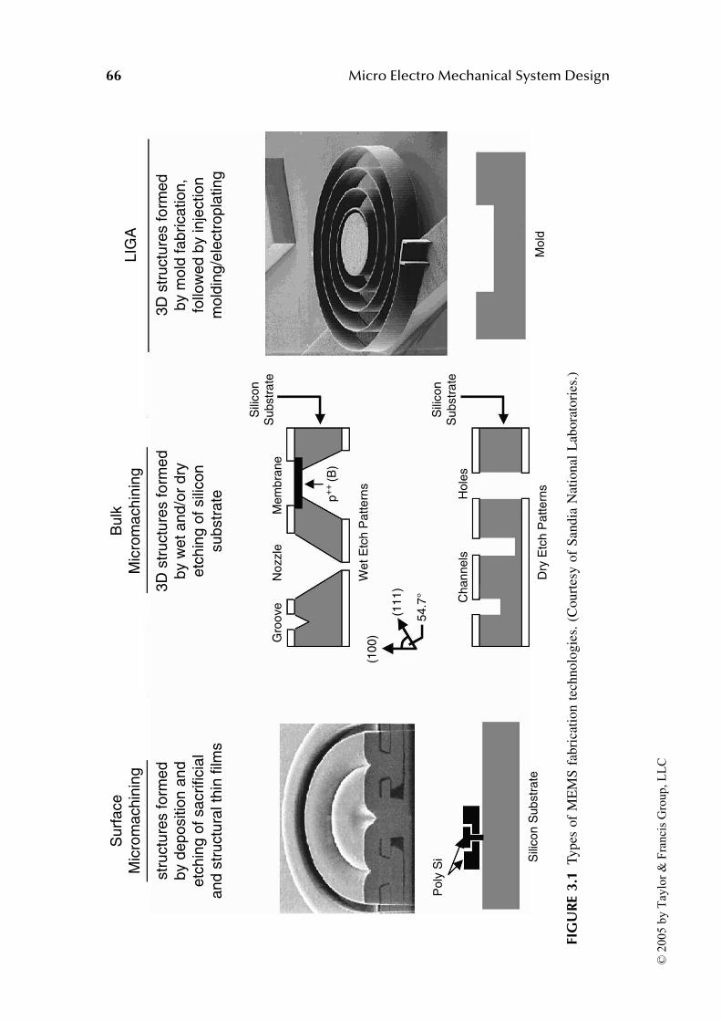
66 Micro Electro Mechanical System Design
FIG
UR
E 3.1
Ty
pes
of
ME
MS
fab
rica
tio
n t
ech
no
log
ies.
(C
ou
rtes
y o
f S
and
ia N
atio
nal
Lab
ora
tori
es.)
Surf
ace
Mic
rom
achin
ing
str
uctu
res f
orm
ed
by d
epositio
n a
nd
etc
hin
g o
f sacrificia
l
and s
tructu
ral th
in film
s
Poly
Si S
ilicon S
ubstr
ate
Dry
Etc
h P
attern
s
Channels
Hole
s
Mold
Bulk
Mic
rom
achin
ing
Gro
ove
(100)
Wet E
tch P
attern
s
(111)
54.7
°
Nozzle
p+
+(B
)
Mem
bra
ne
Sili
con
Substr
ate
Sili
con
Substr
ate
3D
str
uctu
res form
ed
by w
et and/o
r dry
etc
hin
g o
f sili
con
substr
ate
LIG
A
3D
str
uctu
res form
ed
by m
old
fabrication,
follo
wed b
y inje
ction
mold
ing/e
lectr
opla
ting
© 2
005 b
y T
aylo
r &
Fra
nci
s G
roup, L
LC

MEMS Technologies 67
FIG
UR
E 3.2
Su
rfac
e m
icro
mac
hin
ing
co
mm
erci
al a
pp
lica
tio
ns.
Mirro
r–10 d
egre
es
Dig
ital M
icro
mirro
r D
evic
e
Texas Instr
um
ents
An
alo
g D
evic
es A
DX
L A
cce
lero
me
ter
(Co
urt
esy T
exa
s I
nstr
um
en
ts.)
(Co
pyrig
ht
An
alo
g D
evic
es I
nc.
All
rig
hts
re
se
rve
d.)
Mirro
r +
10 d
egre
es
Hin
ge
Yoke Landin
g tip
CM
OS
substr
ate
© 2
005 b
y T
aylo
r &
Fra
nci
s G
roup, L
LC

68 Micro Electro Mechanical System Design
set of materials. However, assembly of large numbers or arrays of devices that
require assembly is an issue that has spurred research in microassembly methods
(see Section 9.1.1.4).
The evaluation and selection of a fabrication process appropriate for an
application requires the assessment of a number of factors:
• Feature size: the smallest dimension that can be fabricated with the
technology
• Device thickness: influences the mass and stiffness of the MEMS
device; this is related to the aspect ratio capability of the fabrication
technology
• Lateral dimension: how large a device can be made by the fabrication
technology
• Precision: the technology precision (i.e., dimensional accuracy/nomi-
nal device dimension) that can be achieved
• Materials: the materials that can be utilized in the fabrication technology
• Assembly requirements: assembly required to produce a functioning
MEMS device (i.e., piece part vs. assembled system)
• Scalability: whether the fabrication technology can produce large quan-
tities of devices if required
• Ability to be integrated with microelectronics: the ability of the tech-
nology to be integrated directly with microelectronic circuitry on the
same die
A comparison of these capabilities for the MEMS fabrication technologies
as well as conventional machining for reference purposes is presented in Table
3.1. The impacts of the fabrication process capabilities on the capabilities of a
MEMS device are summarized in Table 3.2. MEMS device capabilities include
actuation method, mass, capacitance, out-of-plane stiffness, etc. These are the
issues through which the MEMS design engineer must sort to select a fabrication
process suitable for the device of interest.
3.1 BULK MICROMACHINING
Bulk micromachining technologies can use a combination of wet and dry etching
methods to achieve isotropic and anisotropic etches of features in materials. In
order to manufacture items of practical interest, a number of different aspects of
the etch processes need to be considered. Petersen [1] and Kovacs et al. [2] present
detailed information on etch rates and selectivity of crystallographic orientation
and materials. Pister [3] offers a very instructive fold-up model of silicon and its
etching rates for various orientations:
• Masking
• Etch selectivity due to crystallographic orientation or materials
• Etch stop and/or end-point detection
© 2005 by Taylor & Francis Group, LLC
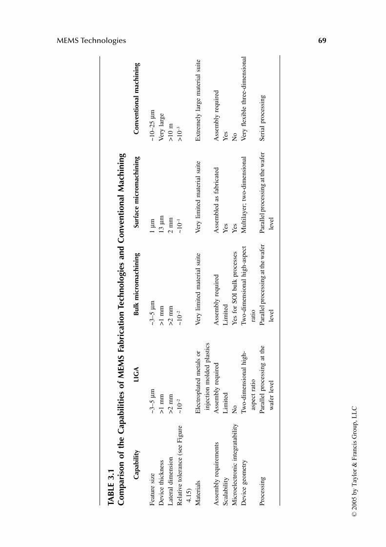
MEMS Technologies 69
TAB
LE 3
.1C
om
par
iso
n o
f th
e C
apab
ilit
ies
of
MEM
S Fa
bri
cati
on
Tech
no
logi
es a
nd
Co
nve
nti
on
al M
ach
inin
g
Cap
abil
ity
LIG
AB
ulk
mic
rom
ach
inin
gSu
rfac
e m
icro
mac
hin
ing
Co
nve
nti
on
al m
ach
inin
g
Fea
ture
siz
e~
3–5
µm~
3–5
µm1
µm~
10–25
µmD
evic
e th
icknes
s>
1 m
m>
1 m
m13
µmV
ery l
arge
Lat
eral
dim
ensi
on
>2 m
m>
2 m
m2 m
m>
10 m
Rel
ativ
e to
lera
nce
(se
e F
igure
4.1
5)
~10
–2
~10
–2
~10
–1
>10
–3
Mat
eria
lsE
lect
ropla
ted m
etal
s or
inje
ctio
n m
old
ed p
last
ics
Ver
y l
imit
ed m
ater
ial
suit
eV
ery l
imit
ed m
ater
ial
suit
eE
xtr
emel
y l
arge
mat
eria
l su
ite
Ass
embly
req
uir
emen
tsA
ssem
bly
req
uir
edA
ssem
bly
req
uir
edA
ssem
ble
d a
s fa
bri
cate
dA
ssem
bly
req
uir
ed
Sca
labil
ity
Lim
ited
Lim
ited
Yes
Yes
Mic
roel
ectr
onic
inte
gra
tabil
ity
No
Yes
for
SO
I bulk
pro
cess
esY
esN
o
Dev
ice
geo
met
ryT
wo-d
imen
sional
hig
h-
aspec
t ra
tio
Tw
o-d
imen
sional
hig
h-a
spec
t
rati
o
Mu
ltil
ayer
; tw
o-d
imen
sio
nal
Ver
y fl
exib
le t
hre
e-d
imen
sio
nal
Pro
cess
ing
Par
alle
l pro
cess
ing a
t th
e
waf
er l
evel
Par
alle
l pro
cess
ing a
t the
waf
er
level
Par
alle
l pro
cess
ing a
t the
waf
er
level
Ser
ial
pro
cess
ing
© 2
005 b
y T
aylo
r &
Fra
nci
s G
roup, L
LC
70 Micro Electro Mechanical System Design
3.1.1 WET ETCHING
Wet etching is purely a chemical process that is an isotropic etch in an amorphous
material such as silicon dioxide; it can be directional in crystalline materials such
as silicon. Contaminants and particulate in this type of process are purely a
function of the chemical purity and chemical system cleanliness. Agitation of the
wet chemical bath is frequently used to aid in the movement of reactants and by-
products to and from the surface. Agitation will also aid etch uniformity because
the by-products may form solids or gases that must be removed. A modern wet
chemical bench will usually have agitation, temperature, and time controls as well
as filtration to remove particulate. For example, etching of SiO2 utilizing a 6:1 by
volume water to HF mixture is a common wet-etch process employed in a surface
micromachining release etch or the production of isotropic features.
Wet-etching methods can also be used on crystalline materials such as silicon
to achieve anisotropic directional etches. For example, a common directional wet
etchant for crystalline silicon is potassium hydroxide (KOH). KOH etches 100
times faster in the (100) plane than the (111) plane. Patterned silicon dioxide or
silicon nitride, which etches very slowly in KOH, can be used as an etch mask
for these types of etches. Very directional etches can be achieved with these
techniques, as illustrated in Figure 3.3. Note the angular features (54.7°) that can
be etched in silicon due to the etch selectivity of the (100) vs. the (111) crystal
plane. Table 2.6, Petersen [1], and Kovacs et al. [2] list some of the common
etchants for crystalline silicon and their selectivity.
If there are no etch stops in a wet etching process, the two options available
to the process engineer to achieve a specific etch depth are a timed etch or etching
completely through the material. A timed etch is difficult to control accurately
TABLE 3.2Comparison of MEMS Device Capabilities within the Three Types of MEMS
Fabrication Technologies
Device capabilityBulk
micromachiningSurface
micromachining LIGA
Type of actuation Electrostatic Electrostatic Electromagnetic
Mass Large Small Large
Capacitance >1 pF <1 pF >1 pF
Out-of-plane stiffness Large Small Large
Range of motion Restricted to the plane
of fabrication
Three-dimensional
motion capability
Restricted to the plane
of fabrication
Large arrays of
devices
No (electrical
interconnect limited)
Yes (106 devices
demonstrated)
No (electrical
interconnect and
assembly limited)
Integral on-chip
microelectronics
Yes (on SOI wafers) Yes No
© 2005 by Taylor & Francis Group, LLC
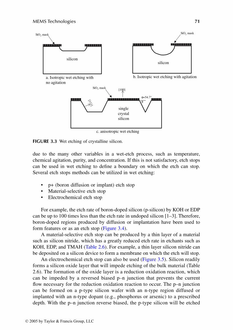
MEMS Technologies 71
due to the many other variables in a wet-etch process, such as temperature,
chemical agitation, purity, and concentration. If this is not satisfactory, etch stops
can be used in wet etching to define a boundary on which the etch can stop.
Several etch stops methods can be utilized in wet etching:
• p+ (boron diffusion or implant) etch stop
• Material-selective etch stop
• Electrochemical etch stop
For example, the etch rate of boron-doped silicon (p-silicon) by KOH or EDP
can be up to 100 times less than the etch rate in undoped silicon [1–3]. Therefore,
boron-doped regions produced by diffusion or implantation have been used to
form features or as an etch stop (Figure 3.4).
A material-selective etch stop can be produced by a thin layer of a material
such as silicon nitride, which has a greatly reduced etch rate in etchants such as
KOH, EDP, and TMAH (Table 2.6). For example, a thin layer silicon nitride can
be deposited on a silicon device to form a membrane on which the etch will stop.
An electrochemical etch stop can also be used (Figure 3.5). Silicon readily
forms a silicon oxide layer that will impede etching of the bulk material (Table
2.6). The formation of the oxide layer is a reduction oxidation reaction, which
can be impeded by a reversed biased p–n junction that prevents the current
flow necessary for the reduction oxidation reaction to occur. The p–n junction
can be formed on a p-type silicon wafer with an n-type region diffused or
implanted with an n-type dopant (e.g., phosphorus or arsenic) to a prescribed
depth. With the p–n junction reverse biased, the p-type silicon will be etched
FIGURE 3.3 Wet etching of crystalline silicon.
silicon
SiO2 mask
b. Isotropic wet etching with agitation
SiO2 mask
silicon
a. Isotropic wet etching with
no agitation
φ=54.7°
φ
[111]
[100]SiO2 mask
single
crystal
silicon
c. anisotropic wet etching
© 2005 by Taylor & Francis Group, LLC
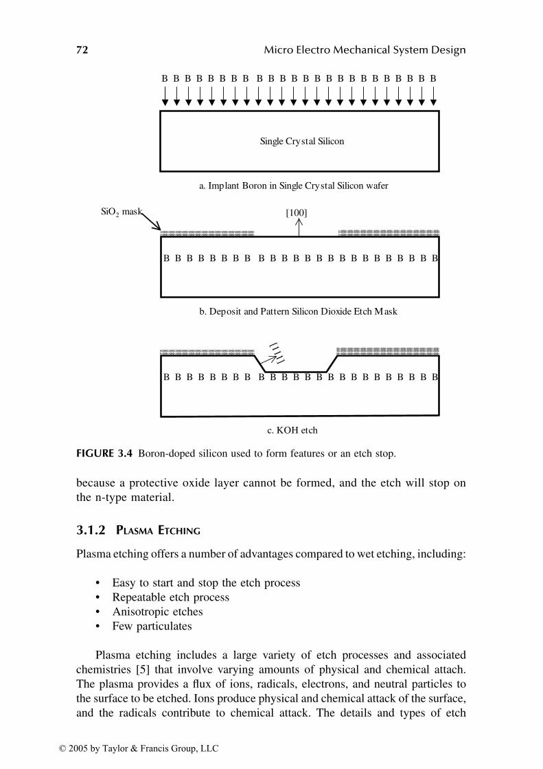
72 Micro Electro Mechanical System Design
because a protective oxide layer cannot be formed, and the etch will stop on
the n-type material.
3.1.2 PLASMA ETCHING
Plasma etching offers a number of advantages compared to wet etching, including:
• Easy to start and stop the etch process
• Repeatable etch process
• Anisotropic etches
• Few particulates
Plasma etching includes a large variety of etch processes and associated
chemistries [5] that involve varying amounts of physical and chemical attach.
The plasma provides a flux of ions, radicals, electrons, and neutral particles to
the surface to be etched. Ions produce physical and chemical attack of the surface,
and the radicals contribute to chemical attack. The details and types of etch
FIGURE 3.4 Boron-doped silicon used to form features or an etch stop.
B B B B B B B B B B B B B B B B B B B B B B B B
Single Crystal Silicon
a. Implant Boron in Single Crystal Silicon wafer
[100]
b. Deposit and Pattern Silicon Dioxide Etch Mask
SiO2 mask
B B B B B B B B B B B B B B B B B B B B B B B B
[111]
B B B B B B B B B B B B B B B B B B B B B B B B
c. KOH etch
© 2005 by Taylor & Francis Group, LLC

MEMS Technologies 73
chemistries involved in plasma etching are varied and complex and beyond the
scope of this book.
The anisotropy of the plasma etch can be increased by the formation of
nonvolatile fluorocarbons that deposit on the sidewalls (Figure 3.6). This process
is called polymerization and is controlled by the ratio of fluoride to carbon in the
reactants. The side wall deposits produced by polymerization can only be removed
by physical ion collisions. Etch products from the resist masking are also involved
in the polymerization.
End-point detection of the etch is important in controlling the etch depth or
minimizing the damage to underlying films. This detection is accomplished by
analysis of the etch effluents or spectral analysis of the plasma glow discharge
to detect.
Types of plasma etches include reactive ion etching (RIE); high-density
plasma etching (HDP); and deep reactive ion etching (DRIE). RIE etching utilizes
a low-pressure plasma. Clorine (Cl)-based plasmas are commonly used to etch
silicon, GaAs, and Al. RIE etching may damage the material due to the impacts
of the ions. However, this damage can be removed by annealing at high temper-
atures. HDP etches utilize magnetic and electric fields to increase dramatically
the distance that free electrons can travel in the plasma. HDP etches have good
selectivity of Si to SiO2 and resist. The DRIE etch cycles between the etch
FIGURE 3.5 Electrochemical etch stop process schematic.
b) Completed structure
+
-
Diffused or
implanted n-type
silicon region
electrode
etchantetchant
V
mask
container
container
a) Electrochemical etch schematic
© 2005 by Taylor & Francis Group, LLC
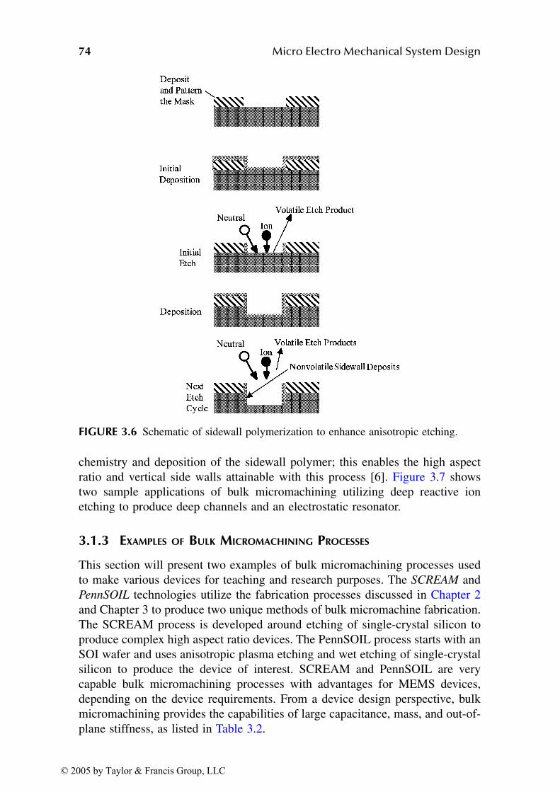
74 Micro Electro Mechanical System Design
chemistry and deposition of the sidewall polymer; this enables the high aspect
ratio and vertical side walls attainable with this process [6]. Figure 3.7 shows
two sample applications of bulk micromachining utilizing deep reactive ion
etching to produce deep channels and an electrostatic resonator.
3.1.3 EXAMPLES OF BULK MICROMACHINING PROCESSES
This section will present two examples of bulk micromachining processes used
to make various devices for teaching and research purposes. The SCREAM and
PennSOIL technologies utilize the fabrication processes discussed in Chapter 2
and Chapter 3 to produce two unique methods of bulk micromachine fabrication.
The SCREAM process is developed around etching of single-crystal silicon to
produce complex high aspect ratio devices. The PennSOIL process starts with an
SOI wafer and uses anisotropic plasma etching and wet etching of single-crystal
silicon to produce the device of interest. SCREAM and PennSOIL are very
capable bulk micromachining processes with advantages for MEMS devices,
depending on the device requirements. From a device design perspective, bulk
micromachining provides the capabilities of large capacitance, mass, and out-of-
plane stiffness, as listed in Table 3.2.
FIGURE 3.6 Schematic of sidewall polymerization to enhance anisotropic etching.
© 2005 by Taylor & Francis Group, LLC
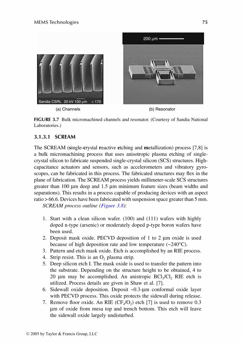
MEMS Technologies 75
3.1.3.1 SCREAM
The SCREAM (single-crystal reactive etching and metallization) process [7,8] is
a bulk micromachining process that uses anisotropic plasma etching of single-
crystal silicon to fabricate suspended single-crystal silicon (SCS) structures. High-
capacitance actuators and sensors, such as accelerometers and vibratory gyro-
scopes, can be fabricated in this process. The fabricated structures may flex in the
plane of fabrication. The SCREAM process yields millimeter-scale SCS structures
greater than 100 µm deep and 1.5 µm minimum feature sizes (beam widths and
separations). This results in a process capable of producing devices with an aspect
ratio > 66.6. Devices have been fabricated with suspension space greater than 5 mm.
SCREAM process outline (Figure 3.8):
1. Start with a clean silicon wafer. (100) and (111) wafers with highly
doped n-type (arsenic) or moderately doped p-type boron wafers have
been used.
2. Deposit mask oxide. PECVD deposition of 1 to 2 µm oxide is used
because of high deposition rate and low temperature (~240°C).
3. Pattern and etch mask oxide. Etch is accomplished by an RIE process.
4. Strip resist. This is an O2 plasma strip.
5. Deep silicon etch I. The mask oxide is used to transfer the pattern into
the substrate. Depending on the structure height to be obtained, 4 to
20 µm may be accomplished. An anistropic BCl3/Cl2 RIE etch is
utilized. Process details are given in Shaw et al. [7].
6. Sidewall oxide deposition. Deposit ~0.3-µm conformal oxide layer
with PECVD process. This oxide protects the sidewall during release.
7. Remove floor oxide. An RIE (CF4/O2) etch [7] is used to remove 0.3µm of oxide from mesa top and trench bottom. This etch will leave
the sidewall oxide largely undisturbed.
FIGURE 3.7 Bulk micromachined channels and resonator. (Courtesy of Sandia National
Laboratories.)
(a) Channels
Sandia CSRL 20 kV × 170100 µm
(b) Resonator
200 µm
© 2005 by Taylor & Francis Group, LLC
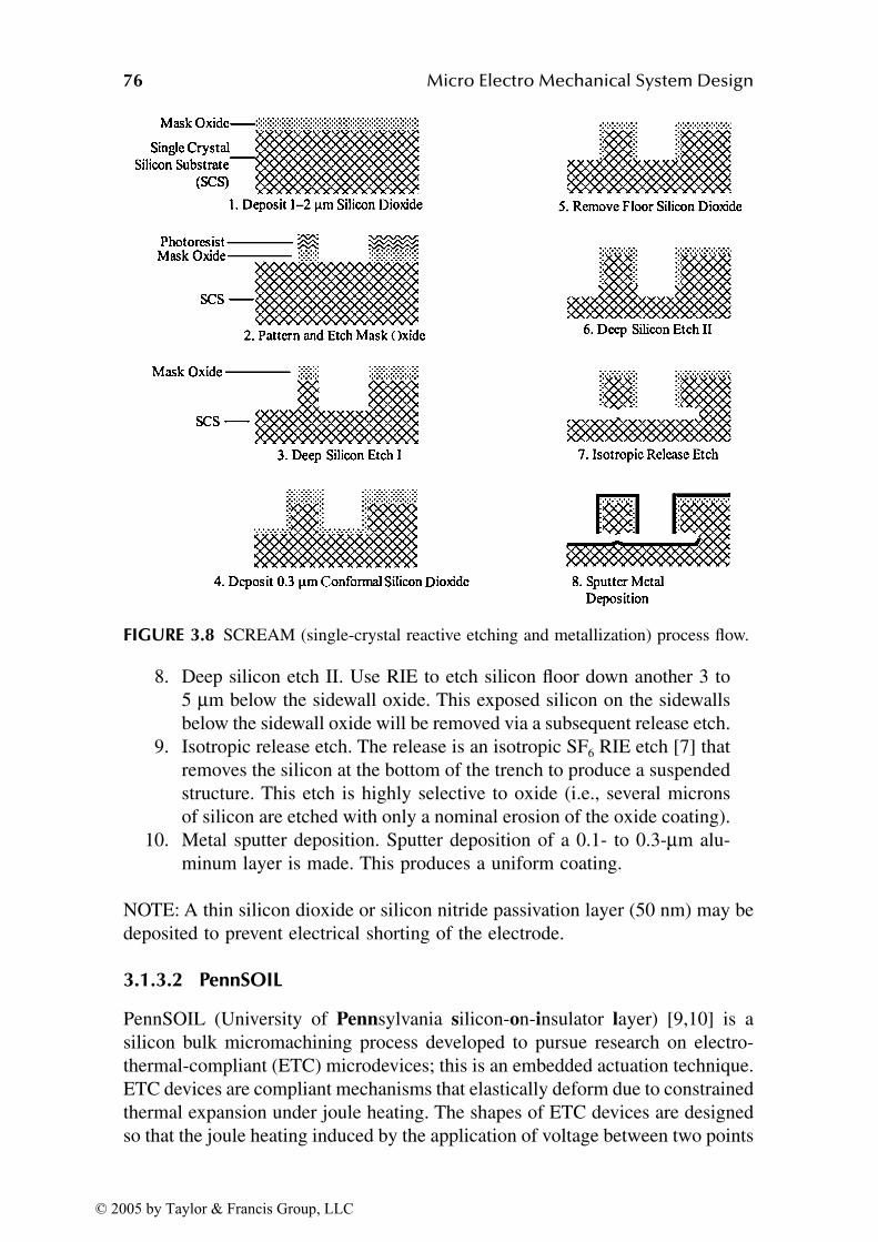
76 Micro Electro Mechanical System Design
8. Deep silicon etch II. Use RIE to etch silicon floor down another 3 to
5 µm below the sidewall oxide. This exposed silicon on the sidewalls
below the sidewall oxide will be removed via a subsequent release etch.
9. Isotropic release etch. The release is an isotropic SF6 RIE etch [7] that
removes the silicon at the bottom of the trench to produce a suspended
structure. This etch is highly selective to oxide (i.e., several microns
of silicon are etched with only a nominal erosion of the oxide coating).
10. Metal sputter deposition. Sputter deposition of a 0.1- to 0.3-µm alu-
minum layer is made. This produces a uniform coating.
NOTE: A thin silicon dioxide or silicon nitride passivation layer (50 nm) may be
deposited to prevent electrical shorting of the electrode.
3.1.3.2 PennSOIL
PennSOIL (University of Pennsylvania silicon-on-insulator layer) [9,10] is a
silicon bulk micromachining process developed to pursue research on electro-
thermal-compliant (ETC) microdevices; this is an embedded actuation technique.
ETC devices are compliant mechanisms that elastically deform due to constrained
thermal expansion under joule heating. The shapes of ETC devices are designed
so that the joule heating induced by the application of voltage between two points
FIGURE 3.8 SCREAM (single-crystal reactive etching and metallization) process flow.
© 2005 by Taylor & Francis Group, LLC
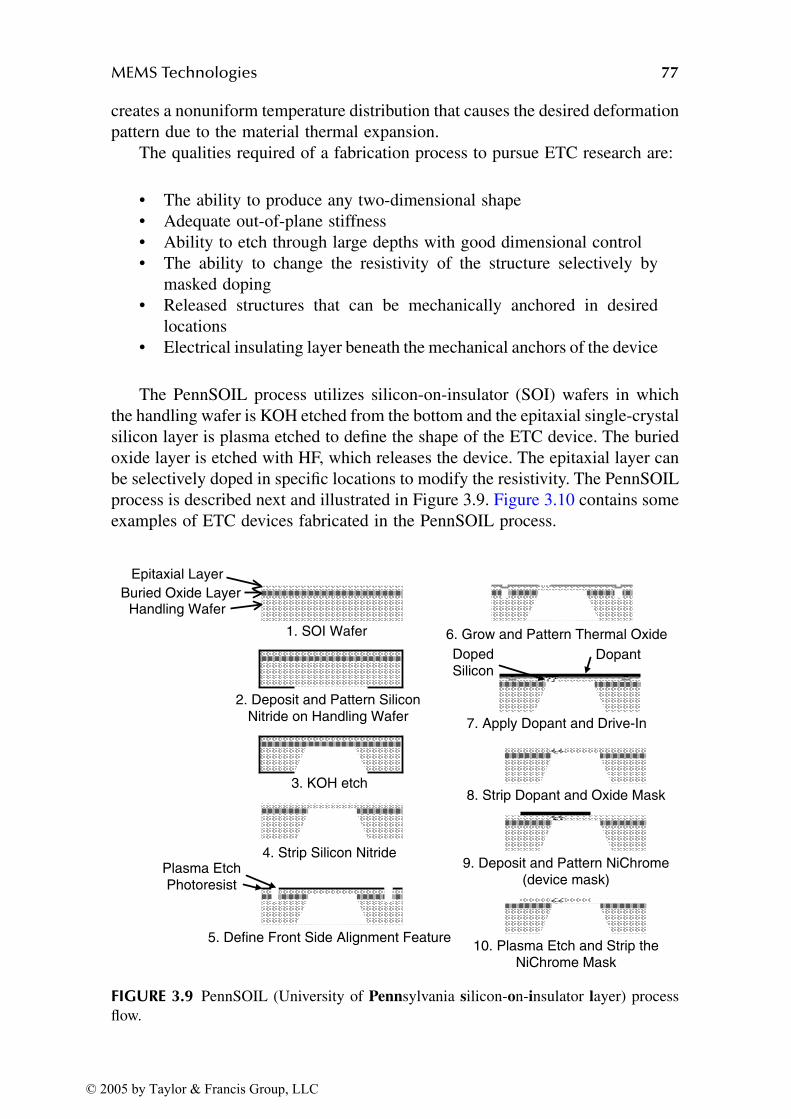
MEMS Technologies 77
creates a nonuniform temperature distribution that causes the desired deformation
pattern due to the material thermal expansion.
The qualities required of a fabrication process to pursue ETC research are:
• The ability to produce any two-dimensional shape
• Adequate out-of-plane stiffness
• Ability to etch through large depths with good dimensional control
• The ability to change the resistivity of the structure selectively by
masked doping
• Released structures that can be mechanically anchored in desired
locations
• Electrical insulating layer beneath the mechanical anchors of the device
The PennSOIL process utilizes silicon-on-insulator (SOI) wafers in which
the handling wafer is KOH etched from the bottom and the epitaxial single-crystal
silicon layer is plasma etched to define the shape of the ETC device. The buried
oxide layer is etched with HF, which releases the device. The epitaxial layer can
be selectively doped in specific locations to modify the resistivity. The PennSOIL
process is described next and illustrated in Figure 3.9. Figure 3.10 contains some
examples of ETC devices fabricated in the PennSOIL process.
FIGURE 3.9 PennSOIL (University of Pennsylvania silicon-on-insulator layer) process
flow.
Epitaxial Layer
Buried Oxide LayerHandling Wafer
Plasma Etch Photoresist
DopedSilicon
Dopant
1. SOI Wafer
3. KOH etch
6. Grow and Pattern Thermal Oxide
7. Apply Dopant and Drive-In
8. Strip Dopant and Oxide Mask
10. Plasma Etch and Strip the NiChrome Mask
9. Deposit and Pattern NiChrome (device mask)
4. Strip Silicon Nitride
5. Define Front Side Alignment Feature
2. Deposit and Pattern Silicon Nitride on Handling Wafer
© 2005 by Taylor & Francis Group, LLC
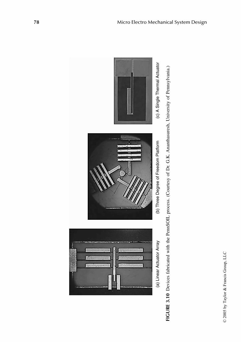
78 Micro Electro Mechanical System Design
FIG
UR
E 3
.10
Dev
ices
fab
rica
ted
wit
h t
he
Pen
nS
OIL
pro
cess
. (C
ou
rtes
y o
f D
r. G
.K.
An
anth
asu
resh
, U
niv
ersi
ty o
f P
enn
sylv
ania
.)
(a)
Lin
ea
r A
ctu
ato
r A
rra
y(b
) T
hre
e D
eg
ree
of
Fre
ed
om
Pla
tfo
rm(c
) A
Sin
gle
Th
erm
al A
ctu
ato
r
© 2
005 b
y T
aylo
r &
Fra
nci
s G
roup, L
LC
MEMS Technologies 79
PennSOIL process outline:
1. The SOI wafers that have been used in the PennSOIL process are 525
to 550 µm thick. The buried silicon dioxide layers (BOX) used in
various runs have been 0.4, 2, and 3 µm, and the epitaxial layer
thicknesses have been 10, 12, and 15 µm.
2. A thin layer of silicon nitride is deposited and patterned on the handling
wafer side of the SOI wafer to define the membrane opening.
3. Conduct a KOH etch to form the membrane opening. This opening
provides thermal isolation for the devices defined on the epitaxial layer.
4. Strip the nitride layer with an HF etch; this removes the exposed silicon
dioxide as well.
5. Define a front (epitaxial) side alignment feature in the epitaxial layer.
Apply and pattern photoresist. Perform a shallow plasma etch on the
epitaxial layer to form the alignment features.
6. Grow and pattern silicon dioxide on the epitaxial layer to form a doping
mask.
7. Apply dopant and drive in dopant with high temperature.
8. Strip dopant and oxide.
9. Deposit and pattern NiChrome to form the device mask on the epitaxial
layer.
10. Conduct a plasma etch of the epitaxial layer to form the ETC device.
11. Strip the NiChrome mask.
3.2 LIGA
The LIGA (Lithographie, Galvanoformung, Abformung) process [11] is capable
of making complex structures of electroplateable metals with very high aspect
ratios with thicknesses up to millimeters. This process utilizes x-ray lithography,
thick resist layers, and electroplated metals to form complex structures. Because
x-ray synchonotron radiation is used as the exposure source for LIGA, the mask
substrate is made of materials transparent to x-rays (e.g., silicon nitride or poly-
silicon). An appropriate mask opaque layer is a high atomic weight material such
as gold, which will block x-rays.
The LIGA fabrication sequence shown schematically in Figure 3.11 starts
with the deposition of a sacrificial material used for separating the LIGA part
from the substrate after fabrication. The sacrificial material should have good
adhesion to the substrate, yet be readily removed when desired. An example of
a sacrificial material for this process is polyimide. A thin seed layer of material
is then deposited; this will enable the electroplating of the LIGA base material.
A frequently used seed material would be a sputter-deposited alloy of titanium
and nickel. Then, a thick layer of the resist material, polymethylmethacrylate
(PMMA), is applied. A synchrotron provides a source of high-energy collimated
x-ray radiation, which is needed to expose the thick layer of resist material. The
exposure system of the mask and x-ray synchrotron radiation can produce vertical
© 2005 by Taylor & Francis Group, LLC
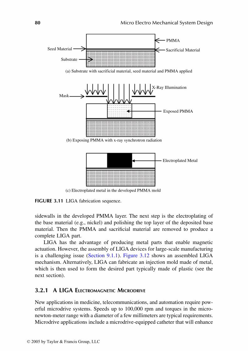
80 Micro Electro Mechanical System Design
sidewalls in the developed PMMA layer. The next step is the electroplating of
the base material (e.g., nickel) and polishing the top layer of the deposited base
material. Then the PMMA and sacrificial material are removed to produce a
complete LIGA part.
LIGA has the advantage of producing metal parts that enable magnetic
actuation. However, the assembly of LIGA devices for large-scale manufacturing
is a challenging issue (Section 9.1.1). Figure 3.12 shows an assembled LIGA
mechanism. Alternatively, LIGA can fabricate an injection mold made of metal,
which is then used to form the desired part typically made of plastic (see the
next section).
3.2.1 A LIGA ELECTROMAGNETIC MICRODRIVE
New applications in medicine, telecommunications, and automation require pow-
erful microdrive systems. Speeds up to 100,000 rpm and torques in the micro-
newton-meter range with a diameter of a few millimeters are typical requirements.
Microdrive applications include a microdrive-equipped catheter that will enhance
FIGURE 3.11 LIGA fabrication sequence.
Seed Material
Substrate
(a) Substrate with sacrificial material, seed material and PMMA applied
PMMA
Sacrificial Material
X-Ray Illumination
Exposed PMMA
Electroplated Metal
(b) Exposing PMMA with x-ray synchrotron radiation
(c) Electroplated metal in the developed PMMA mold
Mask
© 2005 by Taylor & Francis Group, LLC

MEMS Technologies 81
the capability of minimally invasive surgery, automated assembly of miniaturized
components, and use in small appliances such as a camcorder.
The Faulhaber Group [12] and the Institute for Microtechnology, Mainz, Ger-
many [13], have jointly developed an electromagnetic motor with an outer diameter
of only 1.9 mm [14–16]. Figure 3.13 shows the 1.9-mm motor and an exploded
view of its components. For flexibility in application, these micromotors must be
combined with microgear heads of the same outer diameter. The development of
this system illustrates the development of a mesoscale device (>2 mm) that contains
components fabricated with microscale fabrication technology (LIGA).
FIGURE 3.12 Assembled LIGA fabricated mechanism. (Courtesy of Sandia National
Laboratories.)
FIGURE 3.13 An exploded view of the 1.9-mm electromagnetic micromotor. (Courtesy
of Dr. Fritz Faulhaber, GmbH & Co. KG.)
3 Stage Planetary
Gearhead
Permanent
Magnet
Coil
Micro Motor
Micro Gearhead
Micro
Gearhead
Micro M
otor
© 2005 by Taylor & Francis Group, LLC
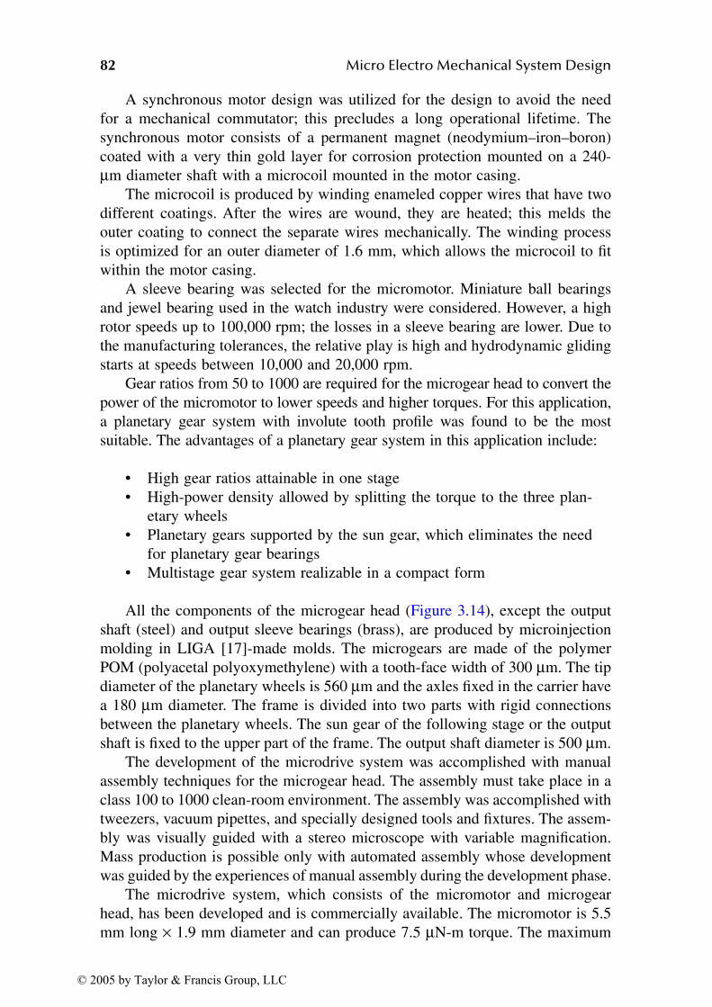
82 Micro Electro Mechanical System Design
A synchronous motor design was utilized for the design to avoid the need
for a mechanical commutator; this precludes a long operational lifetime. The
synchronous motor consists of a permanent magnet (neodymium–iron–boron)
coated with a very thin gold layer for corrosion protection mounted on a 240-µm diameter shaft with a microcoil mounted in the motor casing.
The microcoil is produced by winding enameled copper wires that have two
different coatings. After the wires are wound, they are heated; this melds the
outer coating to connect the separate wires mechanically. The winding process
is optimized for an outer diameter of 1.6 mm, which allows the microcoil to fit
within the motor casing.
A sleeve bearing was selected for the micromotor. Miniature ball bearings
and jewel bearing used in the watch industry were considered. However, a high
rotor speeds up to 100,000 rpm; the losses in a sleeve bearing are lower. Due to
the manufacturing tolerances, the relative play is high and hydrodynamic gliding
starts at speeds between 10,000 and 20,000 rpm.
Gear ratios from 50 to 1000 are required for the microgear head to convert the
power of the micromotor to lower speeds and higher torques. For this application,
a planetary gear system with involute tooth profile was found to be the most
suitable. The advantages of a planetary gear system in this application include:
• High gear ratios attainable in one stage
• High-power density allowed by splitting the torque to the three plan-
etary wheels
• Planetary gears supported by the sun gear, which eliminates the need
for planetary gear bearings
• Multistage gear system realizable in a compact form
All the components of the microgear head (Figure 3.14), except the output
shaft (steel) and output sleeve bearings (brass), are produced by microinjection
molding in LIGA [17]-made molds. The microgears are made of the polymer
POM (polyacetal polyoxymethylene) with a tooth-face width of 300 µm. The tip
diameter of the planetary wheels is 560 µm and the axles fixed in the carrier have
a 180 µm diameter. The frame is divided into two parts with rigid connections
between the planetary wheels. The sun gear of the following stage or the output
shaft is fixed to the upper part of the frame. The output shaft diameter is 500 µm.
The development of the microdrive system was accomplished with manual
assembly techniques for the microgear head. The assembly must take place in a
class 100 to 1000 clean-room environment. The assembly was accomplished with
tweezers, vacuum pipettes, and specially designed tools and fixtures. The assem-
bly was visually guided with a stereo microscope with variable magnification.
Mass production is possible only with automated assembly whose development
was guided by the experiences of manual assembly during the development phase.
The microdrive system, which consists of the micromotor and microgear
head, has been developed and is commercially available. The micromotor is 5.5
mm long × 1.9 mm diameter and can produce 7.5 µN-m torque. The maximum
© 2005 by Taylor & Francis Group, LLC
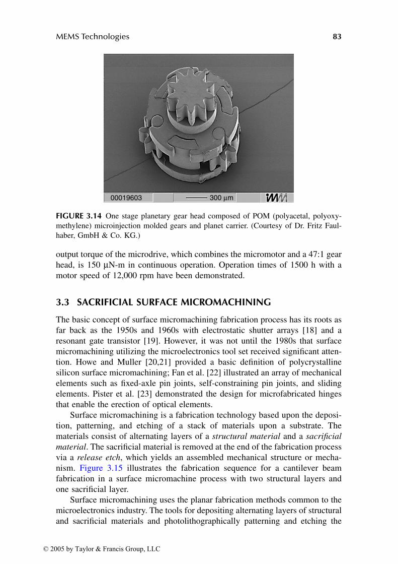
MEMS Technologies 83
output torque of the microdrive, which combines the micromotor and a 47:1 gear
head, is 150 µN-m in continuous operation. Operation times of 1500 h with a
motor speed of 12,000 rpm have been demonstrated.
3.3 SACRIFICIAL SURFACE MICROMACHINING
The basic concept of surface micromachining fabrication process has its roots as
far back as the 1950s and 1960s with electrostatic shutter arrays [18] and a
resonant gate transistor [19]. However, it was not until the 1980s that surface
micromachining utilizing the microelectronics tool set received significant atten-
tion. Howe and Muller [20,21] provided a basic definition of polycrystalline
silicon surface micromachining; Fan et al. [22] illustrated an array of mechanical
elements such as fixed-axle pin joints, self-constraining pin joints, and sliding
elements. Pister et al. [23] demonstrated the design for microfabricated hinges
that enable the erection of optical elements.
Surface micromachining is a fabrication technology based upon the deposi-
tion, patterning, and etching of a stack of materials upon a substrate. The
materials consist of alternating layers of a structural material and a sacrificial
material. The sacrificial material is removed at the end of the fabrication process
via a release etch, which yields an assembled mechanical structure or mecha-
nism. Figure 3.15 illustrates the fabrication sequence for a cantilever beam
fabrication in a surface micromachine process with two structural layers and
one sacrificial layer.
Surface micromachining uses the planar fabrication methods common to the
microelectronics industry. The tools for depositing alternating layers of structural
and sacrificial materials and photolithographically patterning and etching the
FIGURE 3.14 One stage planetary gear head composed of POM (polyacetal, polyoxy-
methylene) microinjection molded gears and planet carrier. (Courtesy of Dr. Fritz Faul-
haber, GmbH & Co. KG.)
00019603 300 µm
© 2005 by Taylor & Francis Group, LLC
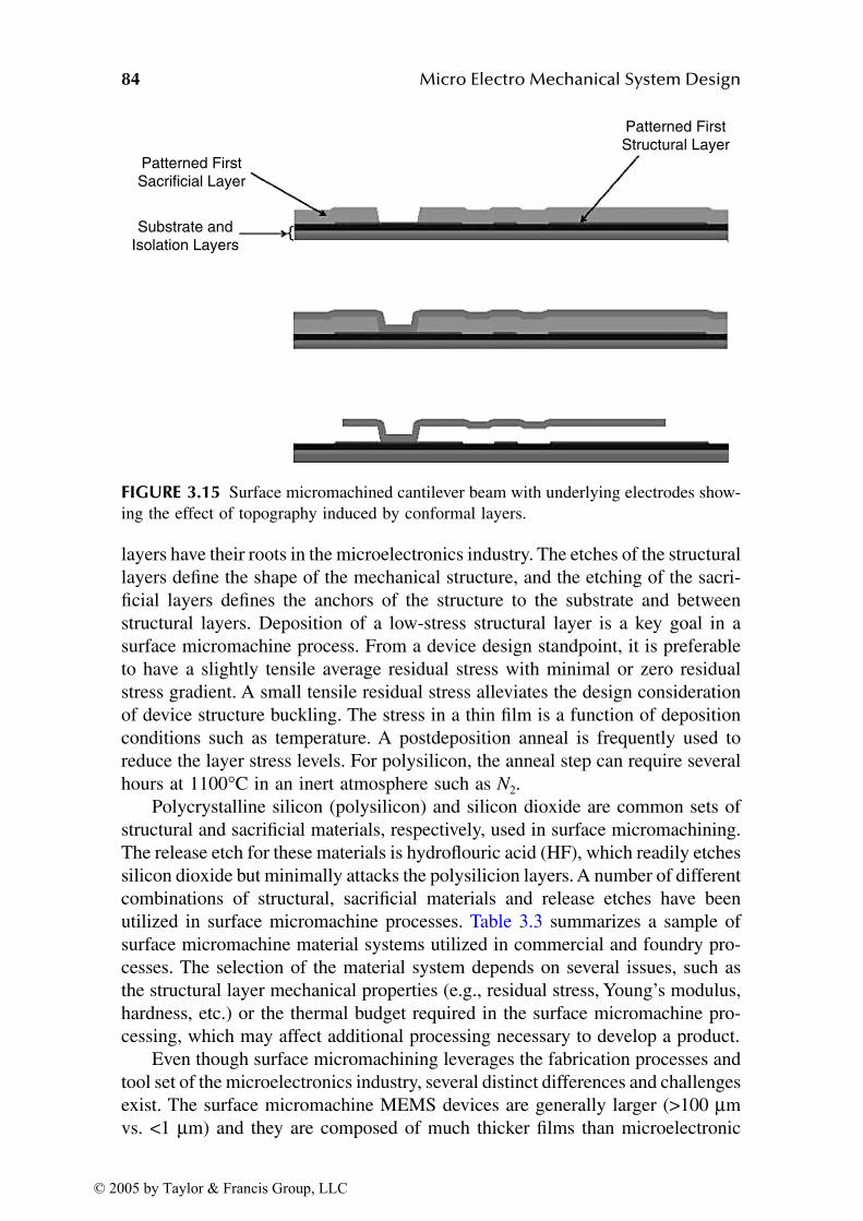
84 Micro Electro Mechanical System Design
layers have their roots in the microelectronics industry. The etches of the structural
layers define the shape of the mechanical structure, and the etching of the sacri-
ficial layers defines the anchors of the structure to the substrate and between
structural layers. Deposition of a low-stress structural layer is a key goal in a
surface micromachine process. From a device design standpoint, it is preferable
to have a slightly tensile average residual stress with minimal or zero residual
stress gradient. A small tensile residual stress alleviates the design consideration
of device structure buckling. The stress in a thin film is a function of deposition
conditions such as temperature. A postdeposition anneal is frequently used to
reduce the layer stress levels. For polysilicon, the anneal step can require several
hours at 1100°C in an inert atmosphere such as N2.
Polycrystalline silicon (polysilicon) and silicon dioxide are common sets of
structural and sacrificial materials, respectively, used in surface micromachining.
The release etch for these materials is hydroflouric acid (HF), which readily etches
silicon dioxide but minimally attacks the polysilicion layers. A number of different
combinations of structural, sacrificial materials and release etches have been
utilized in surface micromachine processes. Table 3.3 summarizes a sample of
surface micromachine material systems utilized in commercial and foundry pro-
cesses. The selection of the material system depends on several issues, such as
the structural layer mechanical properties (e.g., residual stress, Young’s modulus,
hardness, etc.) or the thermal budget required in the surface micromachine pro-
cessing, which may affect additional processing necessary to develop a product.
Even though surface micromachining leverages the fabrication processes and
tool set of the microelectronics industry, several distinct differences and challenges
exist. The surface micromachine MEMS devices are generally larger (>100 µm
vs. <1 µm) and they are composed of much thicker films than microelectronic
FIGURE 3.15 Surface micromachined cantilever beam with underlying electrodes show-
ing the effect of topography induced by conformal layers.
Patterned First Sacrificial Layer
Patterned First Structural Layer
Substrate and Isolation Layers
© 2005 by Taylor & Francis Group, LLC
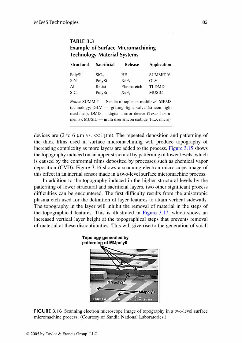
MEMS Technologies 85
devices are (2 to 6 µm vs. <<1 µm). The repeated deposition and patterning of
the thick films used in surface micromachining will produce topography of
increasing complexity as more layers are added to the process. Figure 3.15 shows
the topography induced on an upper structural by patterning of lower levels, which
is caused by the conformal films deposited by processes such as chemical vapor
deposition (CVD). Figure 3.16 shows a scanning electron microscope image of
this effect in an inertial sensor made in a two-level surface micromachine process.
In addition to the topography induced in the higher structural levels by the
patterning of lower structural and sacrificial layers, two other significant process
difficulties can be encountered. The first difficulty results from the anisotropic
plasma etch used for the definition of layer features to attain vertical sidewalls.
The topography in the layer will inhibit the removal of material in the steps of
the topographical features. This is illustrated in Figure 3.17, which shows an
increased vertical layer height at the topographical steps that prevents removal
of material at these discontinuities. This will give rise to the generation of small
TABLE 3.3Example of Surface Micromachining
Technology Material Systems
Structural Sacrificial Release Application
PolySi SiO2 HF SUMMiT V
SiN PolySi XeF2 GLV
Al Resist Plasma etch TI DMD
SiC PolySi XeF2 MUSIC
Notes: SUMMiT — Sandia ultraplanar, multilevel MEMS
technology; GLV — grating light valve (silicon light
machines); DMD — digital mirror device (Texas Instru-
ments); MUSIC — multi user silicon carbide (FLX micro).
FIGURE 3.16 Scanning electron microscope image of topography in a two-level surface
micromachine process. (Courtesy of Sandia National Laboratories.)
© 2005 by Taylor & Francis Group, LLC
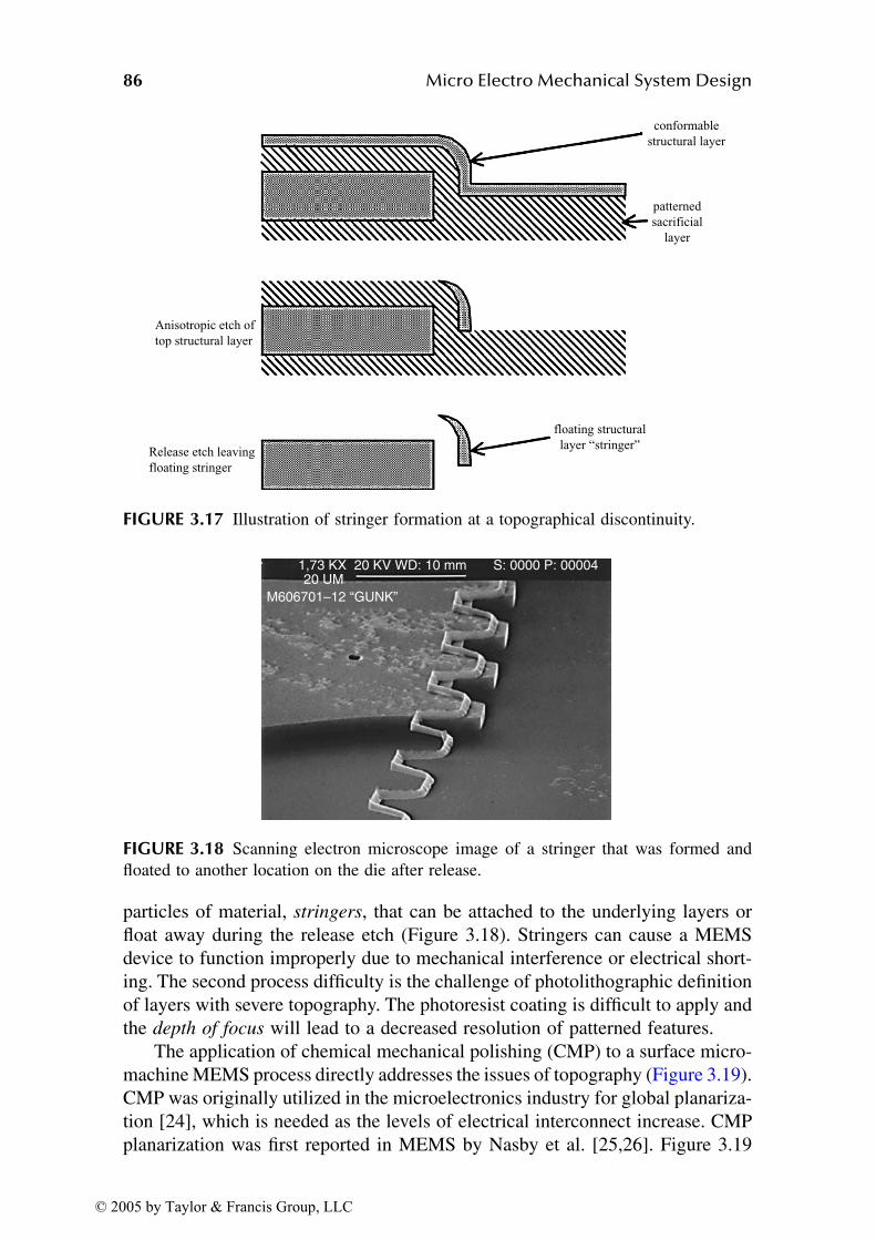
86 Micro Electro Mechanical System Design
particles of material, stringers, that can be attached to the underlying layers or
float away during the release etch (Figure 3.18). Stringers can cause a MEMS
device to function improperly due to mechanical interference or electrical short-
ing. The second process difficulty is the challenge of photolithographic definition
of layers with severe topography. The photoresist coating is difficult to apply and
the depth of focus will lead to a decreased resolution of patterned features.
The application of chemical mechanical polishing (CMP) to a surface micro-
machine MEMS process directly addresses the issues of topography (Figure 3.19).
CMP was originally utilized in the microelectronics industry for global planariza-
tion [24], which is needed as the levels of electrical interconnect increase. CMP
planarization was first reported in MEMS by Nasby et al. [25,26]. Figure 3.19
FIGURE 3.17 Illustration of stringer formation at a topographical discontinuity.
FIGURE 3.18 Scanning electron microscope image of a stringer that was formed and
floated to another location on the die after release.
Anisotropic etch of
top structural layer
Release etch leaving
floating stringer
patterned
sacrificial
layer
conformable
structural layer
floating structural
layer “stringer”
M606701–12 “GUNK”
1,73 KX20 UM
S: 0000 P: 0000420 KV WD: 10 mm
© 2005 by Taylor & Francis Group, LLC
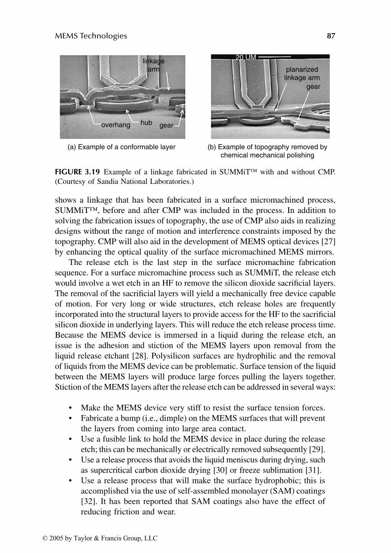
MEMS Technologies 87
shows a linkage that has been fabricated in a surface micromachined process,
SUMMiT™, before and after CMP was included in the process. In addition to
solving the fabrication issues of topography, the use of CMP also aids in realizing
designs without the range of motion and interference constraints imposed by the
topography. CMP will also aid in the development of MEMS optical devices [27]
by enhancing the optical quality of the surface micromachined MEMS mirrors.
The release etch is the last step in the surface micromachine fabrication
sequence. For a surface micromachine process such as SUMMiT, the release etch
would involve a wet etch in an HF to remove the silicon dioxide sacrificial layers.
The removal of the sacrificial layers will yield a mechanically free device capable
of motion. For very long or wide structures, etch release holes are frequently
incorporated into the structural layers to provide access for the HF to the sacrificial
silicon dioxide in underlying layers. This will reduce the etch release process time.
Because the MEMS device is immersed in a liquid during the release etch, an
issue is the adhesion and stiction of the MEMS layers upon removal from the
liquid release etchant [28]. Polysilicon surfaces are hydrophilic and the removal
of liquids from the MEMS device can be problematic. Surface tension of the liquid
between the MEMS layers will produce large forces pulling the layers together.
Stiction of the MEMS layers after the release etch can be addressed in several ways:
• Make the MEMS device very stiff to resist the surface tension forces.
• Fabricate a bump (i.e., dimple) on the MEMS surfaces that will prevent
the layers from coming into large area contact.
• Use a fusible link to hold the MEMS device in place during the release
etch; this can be mechanically or electrically removed subsequently [29].
• Use a release process that avoids the liquid meniscus during drying, such
as supercritical carbon dioxide drying [30] or freeze sublimation [31].
• Use a release process that will make the surface hydrophobic; this is
accomplished via the use of self-assembled monolayer (SAM) coatings
[32]. It has been reported that SAM coatings also have the effect of
reducing friction and wear.
FIGURE 3.19 Example of a linkage fabricated in SUMMiT with and without CMP.
(Courtesy of Sandia National Laboratories.)
linkagearm
overhang
(a) Example of a conformable layer (b) Example of topography removed by chemical mechanical polishing
hub
planarizedlinkage arm
gear
gear
20 UM
© 2005 by Taylor & Francis Group, LLC
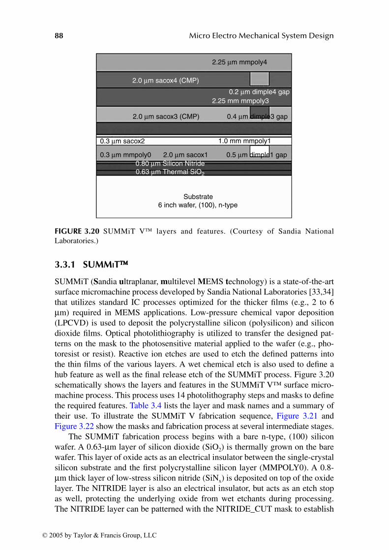
88 Micro Electro Mechanical System Design
3.3.1 SUMMITSUMMiT (Sandia ultraplanar, multilevel MEMS technology) is a state-of-the-art
surface micromachine process developed by Sandia National Laboratories [33,34]
that utilizes standard IC processes optimized for the thicker films (e.g., 2 to 6µm) required in MEMS applications. Low-pressure chemical vapor deposition
(LPCVD) is used to deposit the polycrystalline silicon (polysilicon) and silicon
dioxide films. Optical photolithiography is utilized to transfer the designed pat-
terns on the mask to the photosensitive material applied to the wafer (e.g., pho-
toresist or resist). Reactive ion etches are used to etch the defined patterns into
the thin films of the various layers. A wet chemical etch is also used to define a
hub feature as well as the final release etch of the SUMMiT process. Figure 3.20
schematically shows the layers and features in the SUMMiT V™ surface micro-
machine process. This process uses 14 photolithography steps and masks to define
the required features. Table 3.4 lists the layer and mask names and a summary of
their use. To illustrate the SUMMiT V fabrication sequence, Figure 3.21 and
Figure 3.22 show the masks and fabrication process at several intermediate stages.
The SUMMiT fabrication process begins with a bare n-type, (100) silicon
wafer. A 0.63-µm layer of silicon dioxide (SiO2) is thermally grown on the bare
wafer. This layer of oxide acts as an electrical insulator between the single-crystal
silicon substrate and the first polycrystalline silicon layer (MMPOLY0). A 0.8-µm thick layer of low-stress silicon nitride (SiNx) is deposited on top of the oxide
layer. The NITRIDE layer is also an electrical insulator, but acts as an etch stop
as well, protecting the underlying oxide from wet etchants during processing.
The NITRIDE layer can be patterned with the NITRIDE_CUT mask to establish
FIGURE 3.20 SUMMiT V layers and features. (Courtesy of Sandia National
Laboratories.)
2.0 µm sacox4 (CMP)
2.0 µm sacox3 (CMP)
0.3 µm sacox2
2.0 µm sacox1
2.25 µm mmpoly4
2.25 mm mmpoly3
0.3 µm mmpoly0
Substrate
6 inch wafer, (100), n-type
0.80 µm Silicon Nitride
0.63 µm Thermal SiO2
0.2 µm dimple4 gap
0.4 µm dimple3 gap
0.5 µm dimple1 gap
1.0 mm mmpoly1
© 2005 by Taylor & Francis Group, LLC
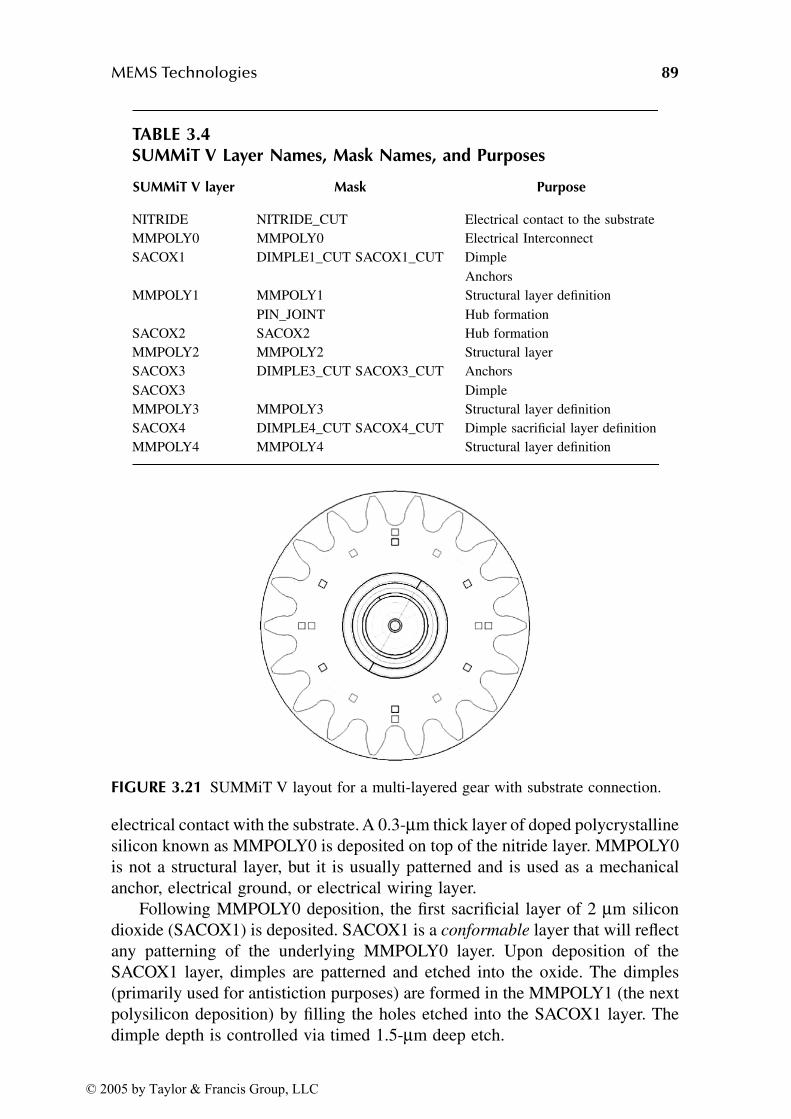
MEMS Technologies 89
electrical contact with the substrate. A 0.3-µm thick layer of doped polycrystalline
silicon known as MMPOLY0 is deposited on top of the nitride layer. MMPOLY0
is not a structural layer, but it is usually patterned and is used as a mechanical
anchor, electrical ground, or electrical wiring layer.
Following MMPOLY0 deposition, the first sacrificial layer of 2 µm silicon
dioxide (SACOX1) is deposited. SACOX1 is a conformable layer that will reflect
any patterning of the underlying MMPOLY0 layer. Upon deposition of the
SACOX1 layer, dimples are patterned and etched into the oxide. The dimples
(primarily used for antistiction purposes) are formed in the MMPOLY1 (the next
polysilicon deposition) by filling the holes etched into the SACOX1 layer. The
dimple depth is controlled via timed 1.5-µm deep etch.
TABLE 3.4SUMMiT V Layer Names, Mask Names, and Purposes
SUMMiT V layer Mask Purpose
NITRIDE NITRIDE_CUT Electrical contact to the substrate
MMPOLY0 MMPOLY0 Electrical Interconnect
SACOX1 DIMPLE1_CUT SACOX1_CUT Dimple
Anchors
MMPOLY1 MMPOLY1
PIN_JOINT
Structural layer definition
Hub formation
SACOX2 SACOX2 Hub formation
MMPOLY2 MMPOLY2 Structural layer
SACOX3
SACOX3
DIMPLE3_CUT SACOX3_CUT Anchors
Dimple
MMPOLY3 MMPOLY3 Structural layer definition
SACOX4 DIMPLE4_CUT SACOX4_CUT Dimple sacrificial layer definition
MMPOLY4 MMPOLY4 Structural layer definition
FIGURE 3.21 SUMMiT V layout for a multi-layered gear with substrate connection.
© 2005 by Taylor & Francis Group, LLC
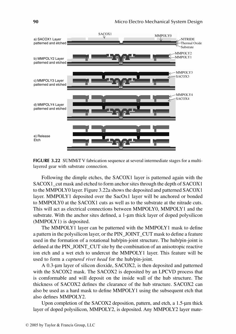
90 Micro Electro Mechanical System Design
Following the dimple etches, the SACOX1 layer is patterned again with the
SACOX1_cut mask and etched to form anchor sites through the depth of SACOX1
to the MMPOLY0 layer. Figure 3.22a shows the deposited and patterned SACOX1
layer. MMPOLY1 deposited over the SacOx1 layer will be anchored or bonded
to MMPOLY0 at the SACOX1 cuts as well as to the substrate at the nitrade cuts.
This will act as electrical connections between MMPOLY0, MMPOLY1 and the
substrate. With the anchor sites defined, a 1-µm thick layer of doped polysilicon
(MMPOLY1) is deposited.
The MMPOLY1 layer can be patterned with the MMPOLY1 mask to define
a pattern in the polysilicon layer, or the PIN_JOINT_CUT mask to define a feature
used in the formation of a rotational hub/pin-joint structure. The hub/pin-joint is
defined at the PIN_JOINT_CUT site by the combination of an anisotropic reactive
ion etch and a wet etch to undercut the MMPOLY1 layer. This feature will be
used to form a captured rivet head for the hub/pin-joint.
A 0.3-µm layer of silicon dioxide, SACOX2, is then deposited and patterned
with the SACOX2 mask. The SACOX2 is deposited by an LPCVD process that
is comformable and will deposit on the inside wall of the hub structure. The
thickness of SACOX2 defines the clearance of the hub structure. SACOX2 can
also be used as a hard mask to define MMPOLY1 using the subsequent etch that
also defines MMPOLY2.
Upon completion of the SACOX2 deposition, pattern, and etch, a 1.5-µm thick
layer of doped polysilicon, MMPOLY2, is deposited. Any MMPOLY2 layer mate-
FIGURE 3.22 SUMMiT V fabrication sequence at several intermediate stages for a multi-
layered gear with substrate connection.
e) ReleaseEtch
b) MMPOLY2 Layerpatterned and etched
MMPOLY2MMPOLY1
d) MMPOLY4 Layerpatterned and etched
MMPOLY4
SACOX4
NITRIDE
Thermal Oxide
Substrate
a) SACOX1 Layerpatterned and etched
MMPOLY0SACOX1
c) MMPOLY3 Layerpatterned and etched
MMPOLY3
SACOX3
© 2005 by Taylor & Francis Group, LLC
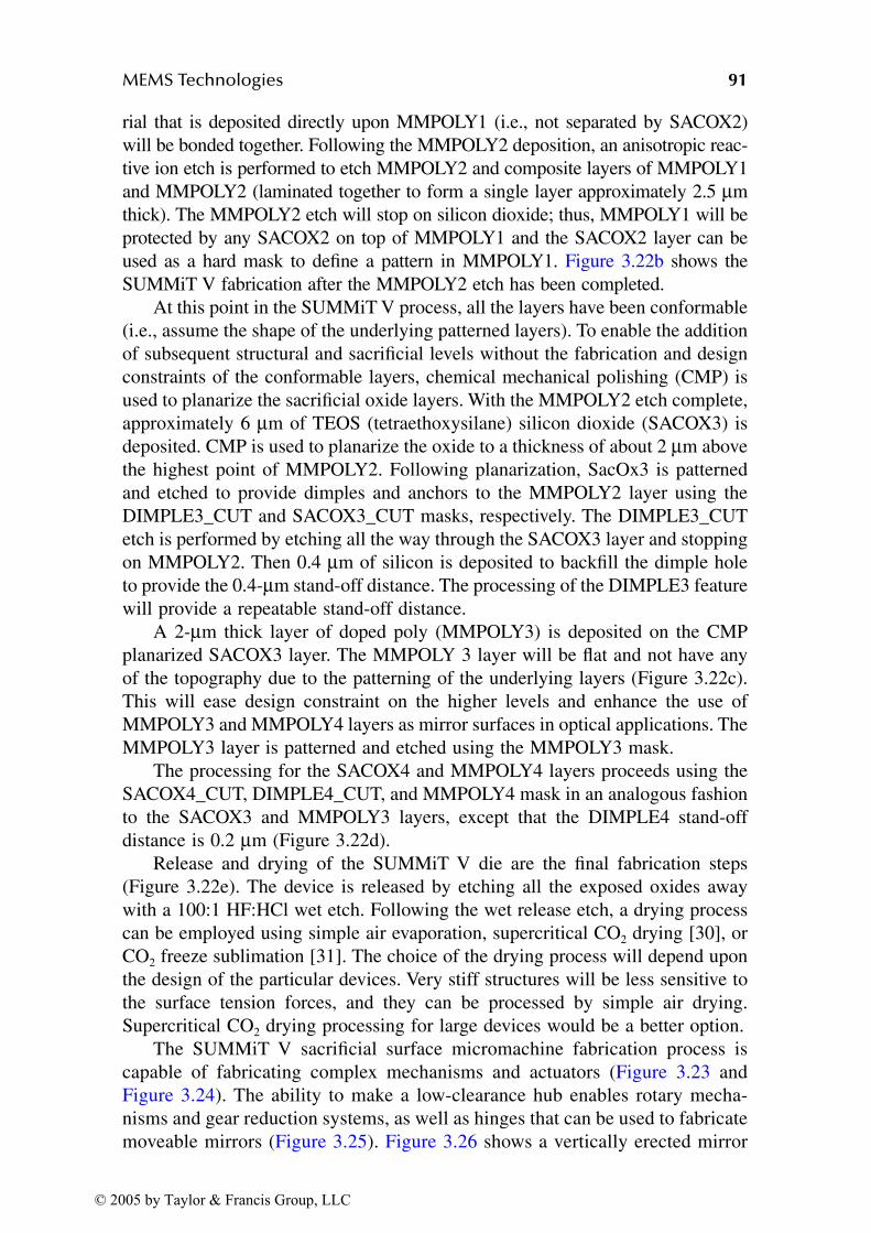
MEMS Technologies 91
rial that is deposited directly upon MMPOLY1 (i.e., not separated by SACOX2)
will be bonded together. Following the MMPOLY2 deposition, an anisotropic reac-
tive ion etch is performed to etch MMPOLY2 and composite layers of MMPOLY1
and MMPOLY2 (laminated together to form a single layer approximately 2.5 µm
thick). The MMPOLY2 etch will stop on silicon dioxide; thus, MMPOLY1 will be
protected by any SACOX2 on top of MMPOLY1 and the SACOX2 layer can be
used as a hard mask to define a pattern in MMPOLY1. Figure 3.22b shows the
SUMMiT V fabrication after the MMPOLY2 etch has been completed.
At this point in the SUMMiT V process, all the layers have been conformable
(i.e., assume the shape of the underlying patterned layers). To enable the addition
of subsequent structural and sacrificial levels without the fabrication and design
constraints of the conformable layers, chemical mechanical polishing (CMP) is
used to planarize the sacrificial oxide layers. With the MMPOLY2 etch complete,
approximately 6 µm of TEOS (tetraethoxysilane) silicon dioxide (SACOX3) is
deposited. CMP is used to planarize the oxide to a thickness of about 2 µm above
the highest point of MMPOLY2. Following planarization, SacOx3 is patterned
and etched to provide dimples and anchors to the MMPOLY2 layer using the
DIMPLE3_CUT and SACOX3_CUT masks, respectively. The DIMPLE3_CUT
etch is performed by etching all the way through the SACOX3 layer and stopping
on MMPOLY2. Then 0.4 µm of silicon is deposited to backfill the dimple hole
to provide the 0.4-µm stand-off distance. The processing of the DIMPLE3 feature
will provide a repeatable stand-off distance.
A 2-µm thick layer of doped poly (MMPOLY3) is deposited on the CMP
planarized SACOX3 layer. The MMPOLY 3 layer will be flat and not have any
of the topography due to the patterning of the underlying layers (Figure 3.22c).
This will ease design constraint on the higher levels and enhance the use of
MMPOLY3 and MMPOLY4 layers as mirror surfaces in optical applications. The
MMPOLY3 layer is patterned and etched using the MMPOLY3 mask.
The processing for the SACOX4 and MMPOLY4 layers proceeds using the
SACOX4_CUT, DIMPLE4_CUT, and MMPOLY4 mask in an analogous fashion
to the SACOX3 and MMPOLY3 layers, except that the DIMPLE4 stand-off
distance is 0.2 µm (Figure 3.22d).
Release and drying of the SUMMiT V die are the final fabrication steps
(Figure 3.22e). The device is released by etching all the exposed oxides away
with a 100:1 HF:HCl wet etch. Following the wet release etch, a drying process
can be employed using simple air evaporation, supercritical CO2 drying [30], or
CO2 freeze sublimation [31]. The choice of the drying process will depend upon
the design of the particular devices. Very stiff structures will be less sensitive to
the surface tension forces, and they can be processed by simple air drying.
Supercritical CO2 drying processing for large devices would be a better option.
The SUMMiT V sacrificial surface micromachine fabrication process is
capable of fabricating complex mechanisms and actuators (Figure 3.23 and
Figure 3.24). The ability to make a low-clearance hub enables rotary mecha-
nisms and gear reduction systems, as well as hinges that can be used to fabricate
moveable mirrors (Figure 3.25). Figure 3.26 shows a vertically erected mirror
© 2005 by Taylor & Francis Group, LLC

92 Micro Electro Mechanical System Design
FIGURE 3.23 Rack and pinion drive, gear reduction system. (Courtesy of Sandia National
Laboratories.)
FIGURE 3.24 Electrostatic drive with linear displacement multiplying mechanism.
(Courtesy of Sandia National Laboratories.)
Linear Displacement Multiplier Mechanism (Designed by Dr. S. Kota, University of Michigan)
Electrostatic Actuator
© 2005 by Taylor & Francis Group, LLC
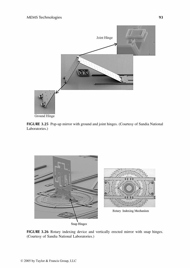
MEMS Technologies 93
FIGURE 3.25 Pop-up mirror with ground and joint hinges. (Courtesy of Sandia National
Laboratories.)
FIGURE 3.26 Rotary indexing device and vertically erected mirror with snap hinges.
(Courtesy of Sandia National Laboratories.)
© 2005 by Taylor & Francis Group, LLC

94 Micro Electro Mechanical System Design
held in place by elastic snap hinges. The vertical mirror is mounted upon a
rotationally indexing table driven by an electrostatic comb drive actuator. SUM-
MiT V has also been used to fabricate arrayed devices; this is possible because
surface micromachined devices are assembled when they are fabricated.
3.4 INTEGRATION OF ELECTRONICS AND MEMS TECHNOLOGY (IMEMS)
The integration of electronics for control and sense circuitry and MEMS tech-
nology becomes essential for sensing applications, which require increased sen-
sitivity (e.g., Analog Devices ADXL accelerometers [35]), or actuation applica-
tions that require the control of large arrays of MEMS devices (e.g., TI DMD[36]). For sensor applications, the packaging integration of a MEMS device and
an electronic ASIC becomes unacceptable when the parasitic capacitances and
wiring resistances have an impact on sensor performance (i.e., RC time constants
of the integrated MEMS system are significant). For actuation applications such
as a large array of optical devices that require individual actuation and control
circuitry, a packaging solution becomes untenable with large device counts.
Of the three MEMS fabrication technologies previously discussed, surface
micromachining is the most amenable to integration with electronics to form an
IMEMS process. The development of an IMEMS process faces some challenges:
• Large vertical topologies. Microelectronic fabrication requires planar
substrates due to the use of precision photolithographic processes.
Surface micromachine topologies can exceed 10 µm due to the thick-
ness of the various layers.
• High-temperature anneals. The mitigation of the residual stress of the
surface micromachine structural layers can require extended periods of
time at high temperatures (such as several hours at 1100°C for polysil-
icon). This would have adverse effects due to a thermal budget of micro-
electronics that is limited because of dopant diffusion and metalization.
There are three strategies for the development of an IMEMS process [37]:
• Microelectronics first. This approach overcomes the planarity restraint
imposed by the photolithographic processes by building the micro-
electronics before the nonplanar micromechanical devices (Figure
3.27). The need for extended high-temperature anneals is mitigated
by the selection of MEMS materials (e.g., aluminum, amorphous
diamond [38]) and/or selection of the microelectronic metallization
(e.g., tungsten instead of aluminum); these make the MEMS and
microelectronic processing compatible. Examples of this IMEMS
approach include an all-tungsten CMOS process developed by
researchers at Berkeley Sensor and Actuator Center [39], and the Texas
© 2005 by Taylor & Francis Group, LLC
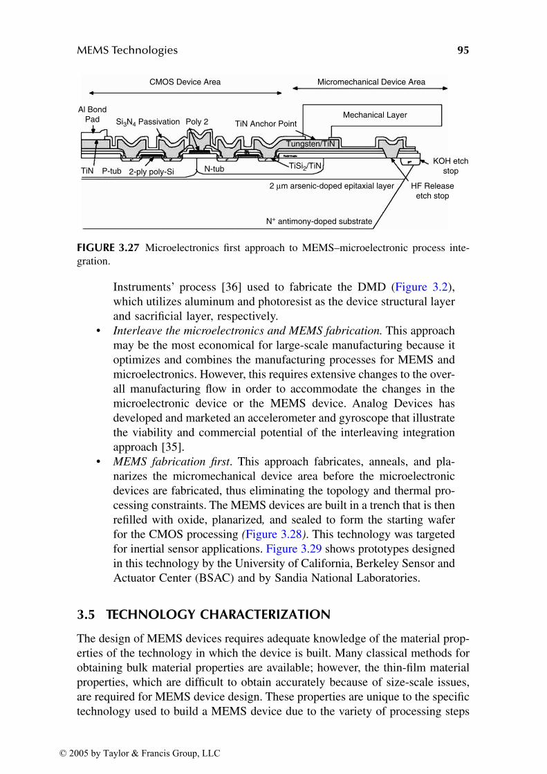
MEMS Technologies 95
Instruments’ process [36] used to fabricate the DMD (Figure 3.2),
which utilizes aluminum and photoresist as the device structural layer
and sacrificial layer, respectively.
• Interleave the microelectronics and MEMS fabrication. This approach
may be the most economical for large-scale manufacturing because it
optimizes and combines the manufacturing processes for MEMS and
microelectronics. However, this requires extensive changes to the over-
all manufacturing flow in order to accommodate the changes in the
microelectronic device or the MEMS device. Analog Devices has
developed and marketed an accelerometer and gyroscope that illustrate
the viability and commercial potential of the interleaving integration
approach [35].
• MEMS fabrication first. This approach fabricates, anneals, and pla-
narizes the micromechanical device area before the microelectronic
devices are fabricated, thus eliminating the topology and thermal pro-
cessing constraints. The MEMS devices are built in a trench that is then
refilled with oxide, planarized, and sealed to form the starting wafer
for the CMOS processing (Figure 3.28). This technology was targeted
for inertial sensor applications. Figure 3.29 shows prototypes designed
in this technology by the University of California, Berkeley Sensor and
Actuator Center (BSAC) and by Sandia National Laboratories.
3.5 TECHNOLOGY CHARACTERIZATION
The design of MEMS devices requires adequate knowledge of the material prop-
erties of the technology in which the device is built. Many classical methods for
obtaining bulk material properties are available; however, the thin-film material
properties, which are difficult to obtain accurately because of size-scale issues,
are required for MEMS device design. These properties are unique to the specific
technology used to build a MEMS device due to the variety of processing steps
FIGURE 3.27 Microelectronics first approach to MEMS–microelectronic process inte-
gration.
Al Bond
Pad Si3N4 Passivation
TiN 2-ply poly-Si
Poly 2 TiN Anchor Point
N-tubP-tub
Tungsten/TiN
2 µm arsenic-doped epitaxial layer
N+ antimony-doped substrate
TiSi2/TiN
HF Release
etch stop
KOH etch
stop
Mechanical Layer
Micromechanical Device AreaCMOS Device Area
© 2005 by Taylor & Francis Group, LLC
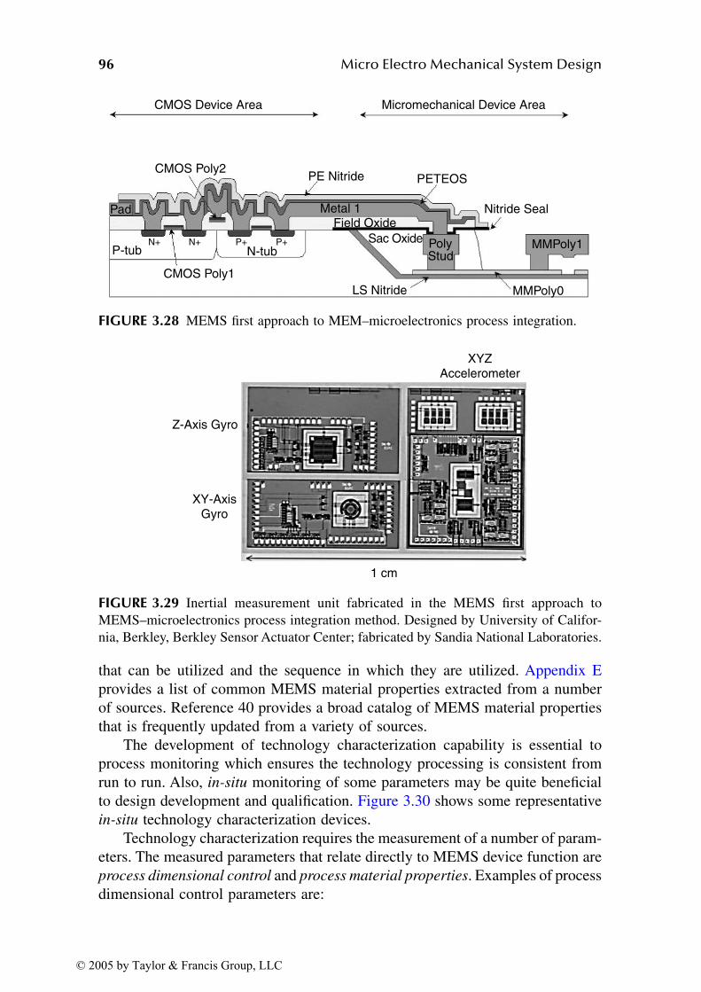
96 Micro Electro Mechanical System Design
that can be utilized and the sequence in which they are utilized. Appendix E
provides a list of common MEMS material properties extracted from a number
of sources. Reference 40 provides a broad catalog of MEMS material properties
that is frequently updated from a variety of sources.
The development of technology characterization capability is essential to
process monitoring which ensures the technology processing is consistent from
run to run. Also, in-situ monitoring of some parameters may be quite beneficial
to design development and qualification. Figure 3.30 shows some representative
in-situ technology characterization devices.
Technology characterization requires the measurement of a number of param-
eters. The measured parameters that relate directly to MEMS device function are
process dimensional control and process material properties. Examples of process
dimensional control parameters are:
FIGURE 3.28 MEMS first approach to MEM–microelectronics process integration.
FIGURE 3.29 Inertial measurement unit fabricated in the MEMS first approach to
MEMS–microelectronics process integration method. Designed by University of Califor-
nia, Berkley, Berkley Sensor Actuator Center; fabricated by Sandia National Laboratories.
CMOS Device Area Micromechanical Device Area
CMOS Poly2PE Nitride PETEOS
Nitride SealPad Metal 1Field Oxide
Sac Oxide PolyStud
MMPoly1P-tub N-tub
N+ N+ P+ P+
CMOS Poly1
LS Nitride MMPoly0
Z-Axis Gyro
XYZAccelerometer
XY-AxisGyro
1 cm
© 2005 by Taylor & Francis Group, LLC
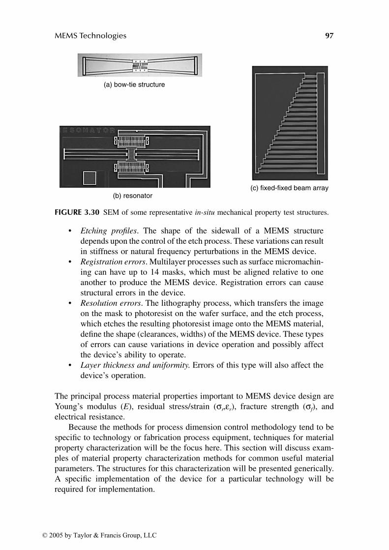
MEMS Technologies 97
• Etching profiles. The shape of the sidewall of a MEMS structure
depends upon the control of the etch process. These variations can result
in stiffness or natural frequency perturbations in the MEMS device.
• Registration errors. Multilayer processes such as surface micromachin-
ing can have up to 14 masks, which must be aligned relative to one
another to produce the MEMS device. Registration errors can cause
structural errors in the device.
• Resolution errors. The lithography process, which transfers the image
on the mask to photoresist on the wafer surface, and the etch process,
which etches the resulting photoresist image onto the MEMS material,
define the shape (clearances, widths) of the MEMS device. These types
of errors can cause variations in device operation and possibly affect
the device’s ability to operate.
• Layer thickness and uniformity. Errors of this type will also affect the
device’s operation.
The principal process material properties important to MEMS device design are
Young’s modulus (E), residual stress/strain (σr,εr), fracture strength (σf), and
electrical resistance.
Because the methods for process dimension control methodology tend to be
specific to technology or fabrication process equipment, techniques for material
property characterization will be the focus here. This section will discuss exam-
ples of material property characterization methods for common useful material
parameters. The structures for this characterization will be presented generically.
A specific implementation of the device for a particular technology will be
required for implementation.
FIGURE 3.30 SEM of some representative in-situ mechanical property test structures.
(a) bow-tie structure
(b) resonator(c) fixed-fixed beam array
© 2005 by Taylor & Francis Group, LLC
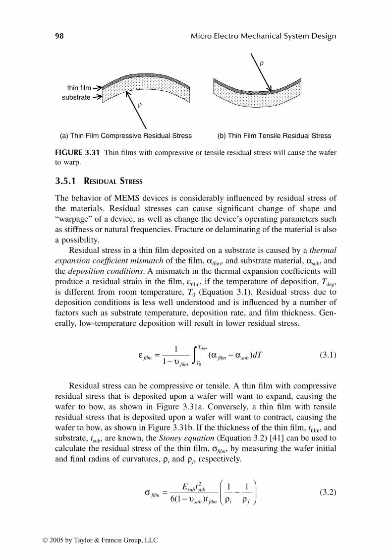
98 Micro Electro Mechanical System Design
3.5.1 RESIDUAL STRESS
The behavior of MEMS devices is considerably influenced by residual stress of
the materials. Residual stresses can cause significant change of shape and
“warpage” of a device, as well as change the device’s operating parameters such
as stiffness or natural frequencies. Fracture or delaminating of the material is also
a possibility.
Residual stress in a thin film deposited on a substrate is caused by a thermal
expansion coefficient mismatch of the film, αfilm, and substrate material, αsub, and
the deposition conditions. A mismatch in the thermal expansion coefficients will
produce a residual strain in the film, εfilm, if the temperature of deposition, Tdep,
is different from room temperature, T0 (Equation 3.1). Residual stress due to
deposition conditions is less well understood and is influenced by a number of
factors such as substrate temperature, deposition rate, and film thickness. Gen-
erally, low-temperature deposition will result in lower residual stress.
(3.1)
Residual stress can be compressive or tensile. A thin film with compressive
residual stress that is deposited upon a wafer will want to expand, causing the
wafer to bow, as shown in Figure 3.31a. Conversely, a thin film with tensile
residual stress that is deposited upon a wafer will want to contract, causing the
wafer to bow, as shown in Figure 3.31b. If the thickness of the thin film, tfilm, and
substrate, tsub, are known, the Stoney equation (Equation 3.2) [41] can be used to
calculate the residual stress of the thin film, σfilm, by measuring the wafer initial
and final radius of curvatures, ρi and ρf, respectively.
(3.2)
FIGURE 3.31 Thin films with compressive or tensile residual stress will cause the wafer
to warp.
thin film
substrateρ
ρ
(a) Thin Film Compressive Residual Stress (b) Thin Film Tensile Residual Stress
ε υ α αfilm
film
film subT
T
dTdep= − −∫1
1 0
( )
σ υ ρ ρfilmsub sub
sub film i f
E t
t= − −
2
6 1
1 1
( )
© 2005 by Taylor & Francis Group, LLC

MEMS Technologies 99
Residual stress may vary through the thickness of a MEMS material layer
(Figure 3.32). The portion of the residual stress distribution that is constant
through the material thickness is called the average residual stress. Alternatively,
the portion of the residual stress that varies through the material thickness is the
residual stress gradient. The average residual stress will cause deflections prima-
rily in the plane of the material layer except where the constrained boundary
condition of a structural member may cause buckling and deflect out of plane.
The residual stress gradient will cause an internal bending moment in the material
that will directly result in out-of-plane deflections.
The simplest test structure for compressive residual stress [42] is an array of
fixed–fixed beams (Figure 3.33a). When the underlying material (sacrificial layer)
is removed, the compressive residual stress of the material will cause expansion.
Buckling will occur on beams greater than a critical length as defined by Euler
column theory (Section 6.1.7). Buckling of the beams can be observed by inspec-
tion using a microscope, interferometer, or SEM. The fixed–fixed beam test
structure is a “proof” test device that establishes that the residual stress is greater
than a particular value by inspection of the array. The residual stress, σr, can be
calculated with Equation 3.3 if the beam thickness, t, and Young’s modulus, E,
are known for the shortest buckled beam of length, L. The negative sign in
Equation 3.3 indicates compressive residual stress. Tensile residual stress will
produce no observable effect on this test structure.
(3.3)
The ring and beam test structure [43–45] shown in Figure 3.33b is also a
“proof” test device fabricated in an array of various sizes that establish that the
tensile residual stress is greater than a particular value by inspection of the array.
When the underlying material (sacrificial layer) is removed, the tensile residual
stress of the material will cause the ring structure to contract; however, the ring
is anchored at a particular diameter. The ring diameter at a 90° position away
FIGURE 3.32 Material layer with average residual stress and residual stress gradient
components.
y y
x
(a) Average Residual Stress (b) Residual Stress Gradient
x
σx σxεx
σ πr
t E
L= − 2 2
23
© 2005 by Taylor & Francis Group, LLC
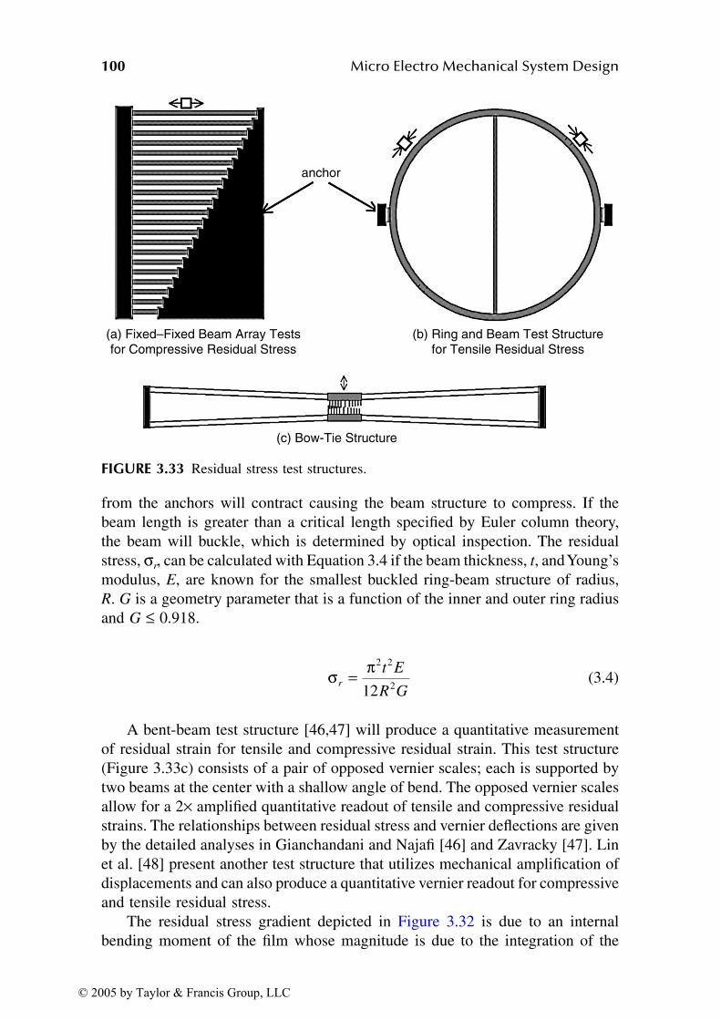
100 Micro Electro Mechanical System Design
from the anchors will contract causing the beam structure to compress. If the
beam length is greater than a critical length specified by Euler column theory,
the beam will buckle, which is determined by optical inspection. The residual
stress, σr, can be calculated with Equation 3.4 if the beam thickness, t, and Young’s
modulus, E, are known for the smallest buckled ring-beam structure of radius,
R. G is a geometry parameter that is a function of the inner and outer ring radius
and G ≤ 0.918.
(3.4)
A bent-beam test structure [46,47] will produce a quantitative measurement
of residual strain for tensile and compressive residual strain. This test structure
(Figure 3.33c) consists of a pair of opposed vernier scales; each is supported by
two beams at the center with a shallow angle of bend. The opposed vernier scales
allow for a 2× amplified quantitative readout of tensile and compressive residual
strains. The relationships between residual stress and vernier deflections are given
by the detailed analyses in Gianchandani and Najafi [46] and Zavracky [47]. Lin
et al. [48] present another test structure that utilizes mechanical amplification of
displacements and can also produce a quantitative vernier readout for compressive
and tensile residual stress.
The residual stress gradient depicted in Figure 3.32 is due to an internal
bending moment of the film whose magnitude is due to the integration of the
FIGURE 3.33 Residual stress test structures.
anchor
(a) Fixed–Fixed Beam Array Tests for Compressive Residual Stress
(c) Bow-Tie Structure
(b) Ring and Beam Test Structure for Tensile Residual Stress
σ πr
t E
R G= 2 2
212
© 2005 by Taylor & Francis Group, LLC
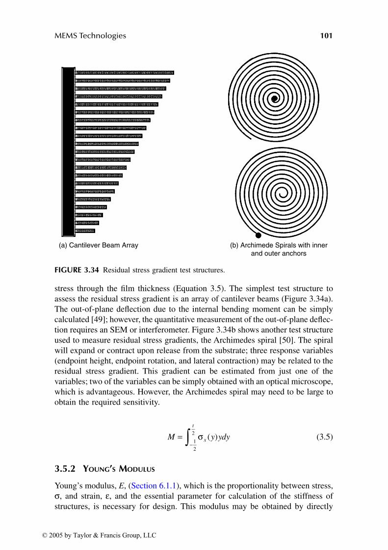
MEMS Technologies 101
stress through the film thickness (Equation 3.5). The simplest test structure to
assess the residual stress gradient is an array of cantilever beams (Figure 3.34a).
The out-of-plane deflection due to the internal bending moment can be simply
calculated [49]; however, the quantitative measurement of the out-of-plane deflec-
tion requires an SEM or interferometer. Figure 3.34b shows another test structure
used to measure residual stress gradients, the Archimedes spiral [50]. The spiral
will expand or contract upon release from the substrate; three response variables
(endpoint height, endpoint rotation, and lateral contraction) may be related to the
residual stress gradient. This gradient can be estimated from just one of the
variables; two of the variables can be simply obtained with an optical microscope,
which is advantageous. However, the Archimedes spiral may need to be large to
obtain the required sensitivity.
(3.5)
3.5.2 YOUNG’S MODULUS
Young’s modulus, E, (Section 6.1.1), which is the proportionality between stress,σ, and strain, ε, and the essential parameter for calculation of the stiffness of
structures, is necessary for design. This modulus may be obtained by directly
FIGURE 3.34 Residual stress gradient test structures.
(a) Cantilever Beam Array (b) Archimede Spirals with innerand outer anchors
M y ydyx
t
=−∫ σ ( )
1
2
2
© 2005 by Taylor & Francis Group, LLC
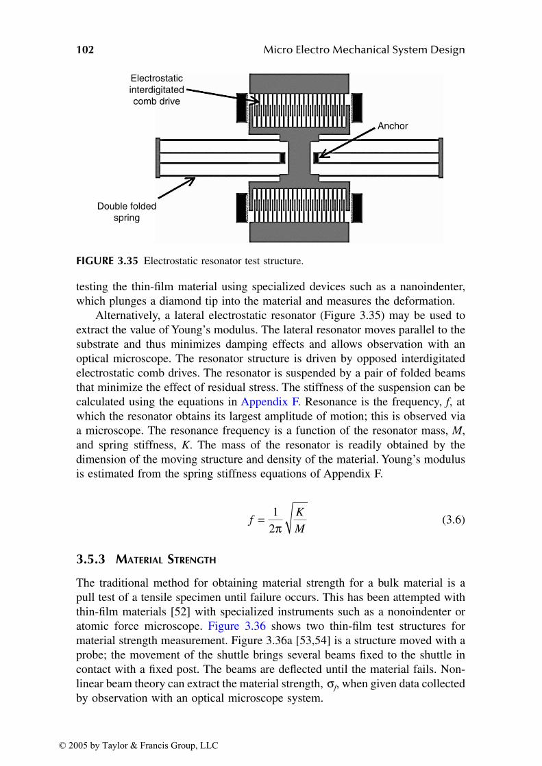
102 Micro Electro Mechanical System Design
testing the thin-film material using specialized devices such as a nanoindenter,
which plunges a diamond tip into the material and measures the deformation.
Alternatively, a lateral electrostatic resonator (Figure 3.35) may be used to
extract the value of Young’s modulus. The lateral resonator moves parallel to the
substrate and thus minimizes damping effects and allows observation with an
optical microscope. The resonator structure is driven by opposed interdigitated
electrostatic comb drives. The resonator is suspended by a pair of folded beams
that minimize the effect of residual stress. The stiffness of the suspension can be
calculated using the equations in Appendix F. Resonance is the frequency, f, at
which the resonator obtains its largest amplitude of motion; this is observed via
a microscope. The resonance frequency is a function of the resonator mass, M,
and spring stiffness, K. The mass of the resonator is readily obtained by the
dimension of the moving structure and density of the material. Young’s modulus
is estimated from the spring stiffness equations of Appendix F.
(3.6)
3.5.3 MATERIAL STRENGTH
The traditional method for obtaining material strength for a bulk material is a
pull test of a tensile specimen until failure occurs. This has been attempted with
thin-film materials [52] with specialized instruments such as a nonoindenter or
atomic force microscope. Figure 3.36 shows two thin-film test structures for
material strength measurement. Figure 3.36a [53,54] is a structure moved with a
probe; the movement of the shuttle brings several beams fixed to the shuttle in
contact with a fixed post. The beams are deflected until the material fails. Non-
linear beam theory can extract the material strength, σf, when given data collected
by observation with an optical microscope system.
FIGURE 3.35 Electrostatic resonator test structure.
Electrostatic
interdigitated
comb drive
Double folded
spring
Anchor
fK
M= 1
2π
© 2005 by Taylor & Francis Group, LLC
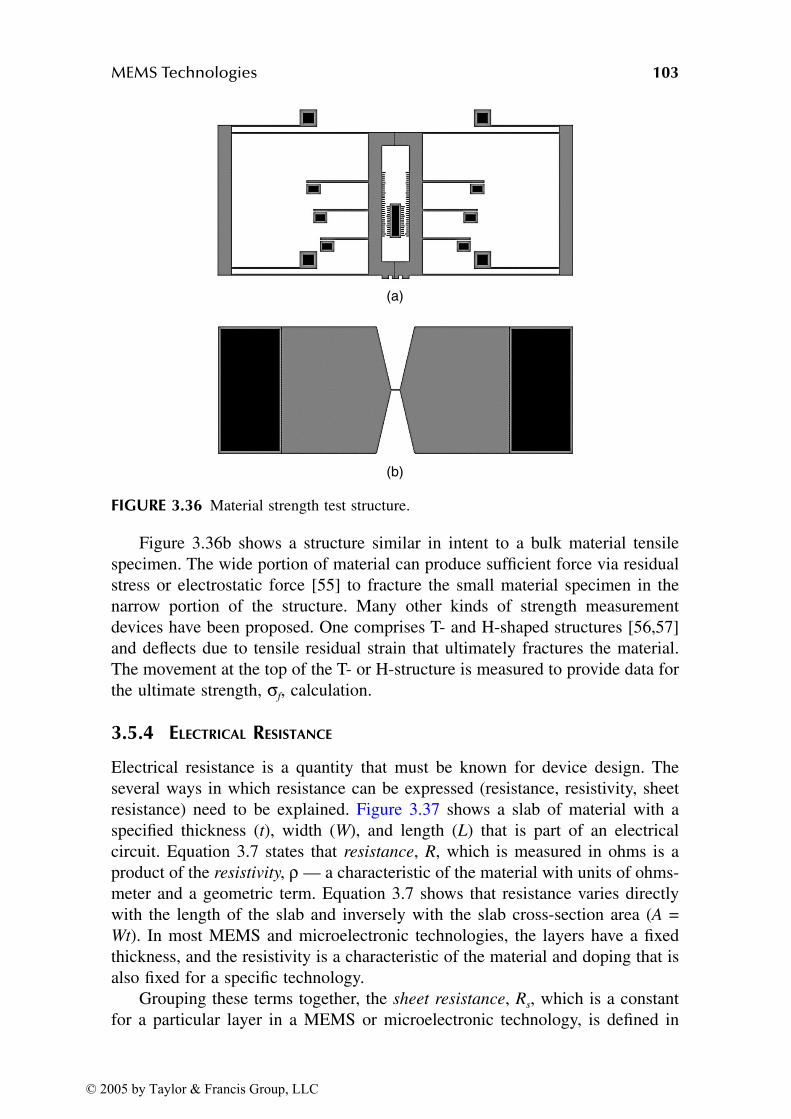
MEMS Technologies 103
Figure 3.36b shows a structure similar in intent to a bulk material tensile
specimen. The wide portion of material can produce sufficient force via residual
stress or electrostatic force [55] to fracture the small material specimen in the
narrow portion of the structure. Many other kinds of strength measurement
devices have been proposed. One comprises T- and H-shaped structures [56,57]
and deflects due to tensile residual strain that ultimately fractures the material.
The movement at the top of the T- or H-structure is measured to provide data for
the ultimate strength, σf, calculation.
3.5.4 ELECTRICAL RESISTANCE
Electrical resistance is a quantity that must be known for device design. The
several ways in which resistance can be expressed (resistance, resistivity, sheet
resistance) need to be explained. Figure 3.37 shows a slab of material with a
specified thickness (t), width (W), and length (L) that is part of an electrical
circuit. Equation 3.7 states that resistance, R, which is measured in ohms is a
product of the resistivity, ρ — a characteristic of the material with units of ohms-
meter and a geometric term. Equation 3.7 shows that resistance varies directly
with the length of the slab and inversely with the slab cross-section area (A =
Wt). In most MEMS and microelectronic technologies, the layers have a fixed
thickness, and the resistivity is a characteristic of the material and doping that is
also fixed for a specific technology.
Grouping these terms together, the sheet resistance, Rs, which is a constant
for a particular layer in a MEMS or microelectronic technology, is defined in
FIGURE 3.36 Material strength test structure.
(a)
(b)
© 2005 by Taylor & Francis Group, LLC
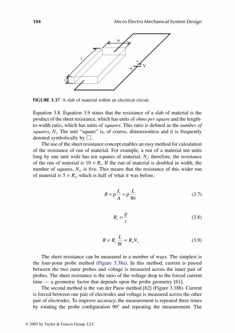
104 Micro Electro Mechanical System Design
Equation 3.8. Equation 3.9 states that the resistance of a slab of material is the
product of the sheet resistance, which has units of ohms per square and the length-
to-width ratio, which has units of squares. This ratio is defined as the number of
squares, Ns. The unit “square” is, of course, dimensionless and it is frequently
denoted symbolically by .
The use of the sheet resistance concept enables an easy method for calculation
of the resistance of run of material. For example, a run of a material ten units
long by one unit wide has ten squares of material, Ns; therefore, the resistance
of the run of material is 10 × Rs. If the run of material is doubled in width, the
number of squares, Ns, is five. This means that the resistance of this wider run
of material is 5 × Rs, which is half of what it was before.
(3.7)
(3.8)
(3.9)
The sheet resistance can be measured in a number of ways. The simplest is
the four-point probe method (Figure 3.38a). In this method, current is passed
between the two outer probes and voltage is measured across the inner pair of
probes. The sheet resistance is the ratio of the voltage drop to the forced current
time — a geometric factor that depends upon the probe geometry [61].
The second method is the van der Pauw method [62] (Figure 3.38b). Current
is forced between one pair of electrodes and voltage is measured across the other
pair of electrodes. To improve accuracy, the measurement is repeated three times
by rotating the probe configuration 90° and repeating the measurement. The
FIGURE 3.37 A slab of material within an electrical circuit.
W
L
t
V+
-
RL
A
L
Wt= =ρ ρ
Rt
s = ρ
R RL
WR Ns s s= =
© 2005 by Taylor & Francis Group, LLC
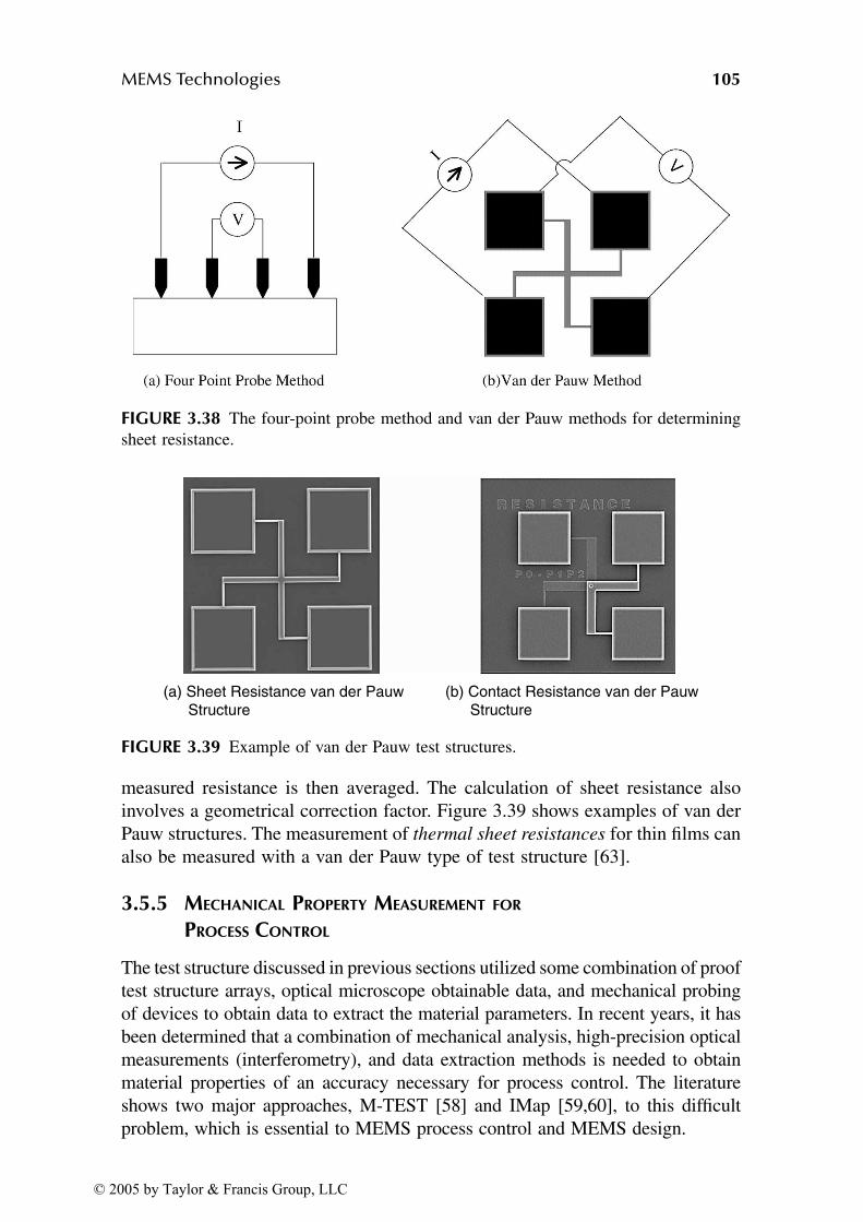
MEMS Technologies 105
measured resistance is then averaged. The calculation of sheet resistance also
involves a geometrical correction factor. Figure 3.39 shows examples of van der
Pauw structures. The measurement of thermal sheet resistances for thin films can
also be measured with a van der Pauw type of test structure [63].
3.5.5 MECHANICAL PROPERTY MEASUREMENT FOR
PROCESS CONTROL
The test structure discussed in previous sections utilized some combination of proof
test structure arrays, optical microscope obtainable data, and mechanical probing
of devices to obtain data to extract the material parameters. In recent years, it has
been determined that a combination of mechanical analysis, high-precision optical
measurements (interferometry), and data extraction methods is needed to obtain
material properties of an accuracy necessary for process control. The literature
shows two major approaches, M-TEST [58] and IMap [59,60], to this difficult
problem, which is essential to MEMS process control and MEMS design.
FIGURE 3.38 The four-point probe method and van der Pauw methods for determining
sheet resistance.
FIGURE 3.39 Example of van der Pauw test structures.
(a) Sheet Resistance van der Pauw
Structure
(b) Contact Resistance van der Pauw
Structure
© 2005 by Taylor & Francis Group, LLC
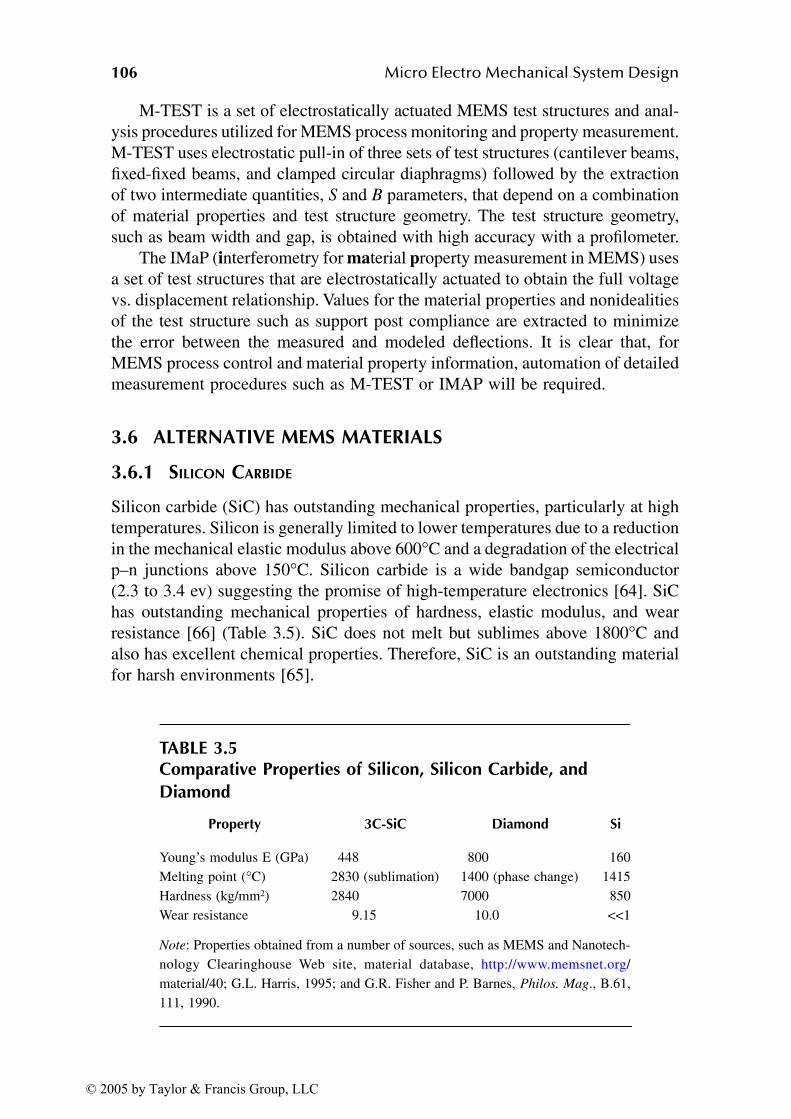
106 Micro Electro Mechanical System Design
M-TEST is a set of electrostatically actuated MEMS test structures and anal-
ysis procedures utilized for MEMS process monitoring and property measurement.
M-TEST uses electrostatic pull-in of three sets of test structures (cantilever beams,
fixed-fixed beams, and clamped circular diaphragms) followed by the extraction
of two intermediate quantities, S and B parameters, that depend on a combination
of material properties and test structure geometry. The test structure geometry,
such as beam width and gap, is obtained with high accuracy with a profilometer.
The IMaP (interferometry for material property measurement in MEMS) uses
a set of test structures that are electrostatically actuated to obtain the full voltage
vs. displacement relationship. Values for the material properties and nonidealities
of the test structure such as support post compliance are extracted to minimize
the error between the measured and modeled deflections. It is clear that, for
MEMS process control and material property information, automation of detailed
measurement procedures such as M-TEST or IMAP will be required.
3.6 ALTERNATIVE MEMS MATERIALS
3.6.1 SILICON CARBIDE
Silicon carbide (SiC) has outstanding mechanical properties, particularly at high
temperatures. Silicon is generally limited to lower temperatures due to a reduction
in the mechanical elastic modulus above 600°C and a degradation of the electrical
p–n junctions above 150°C. Silicon carbide is a wide bandgap semiconductor
(2.3 to 3.4 ev) suggesting the promise of high-temperature electronics [64]. SiC
has outstanding mechanical properties of hardness, elastic modulus, and wear
resistance [66] (Table 3.5). SiC does not melt but sublimes above 1800°C and
also has excellent chemical properties. Therefore, SiC is an outstanding material
for harsh environments [65].
TABLE 3.5Comparative Properties of Silicon, Silicon Carbide, and
Diamond
Property 3C-SiC Diamond Si
Young’s modulus E (GPa) 448 800 160
Melting point (°C) 2830 (sublimation) 1400 (phase change) 1415
Hardness (kg/mm2) 2840 7000 850
Wear resistance 9.15 10.0 <<1
Note: Properties obtained from a number of sources, such as MEMS and Nanotech-
nology Clearinghouse Web site, material database, http://www.memsnet.org/
material/40; G.L. Harris, 1995; and G.R. Fisher and P. Barnes, Philos. Mag., B.61,
111, 1990.
© 2005 by Taylor & Francis Group, LLC
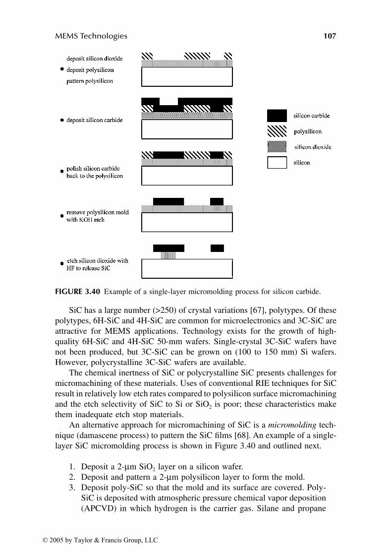
MEMS Technologies 107
SiC has a large number (>250) of crystal variations [67], polytypes. Of these
polytypes, 6H-SiC and 4H-SiC are common for microelectronics and 3C-SiC are
attractive for MEMS applications. Technology exists for the growth of high-
quality 6H-SiC and 4H-SiC 50-mm wafers. Single-crystal 3C-SiC wafers have
not been produced, but 3C-SiC can be grown on (100 to 150 mm) Si wafers.
However, polycrystalline 3C-SiC wafers are available.
The chemical inertness of SiC or polycrystalline SiC presents challenges for
micromachining of these materials. Uses of conventional RIE techniques for SiC
result in relatively low etch rates compared to polysilicon surface micromachining
and the etch selectivity of SiC to Si or SiO2 is poor; these characteristics make
them inadequate etch stop materials.
An alternative approach for micromachining of SiC is a micromolding tech-
nique (damascene process) to pattern the SiC films [68]. An example of a single-
layer SiC micromolding process is shown in Figure 3.40 and outlined next.
1. Deposit a 2-µm SiO2 layer on a silicon wafer.
2. Deposit and pattern a 2-µm polysilicon layer to form the mold.
3. Deposit poly-SiC so that the mold and its surface are covered. Poly-
SiC is deposited with atmospheric pressure chemical vapor deposition
(APCVD) in which hydrogen is the carrier gas. Silane and propane
FIGURE 3.40 Example of a single-layer micromolding process for silicon carbide.
© 2005 by Taylor & Francis Group, LLC
108 Micro Electro Mechanical System Design
are the precursor gases for the chemical reactions involved in this
CVD process.
4. Polish the wafer with a diamond slurry to remove the poly-SiC from
the top surface of the mold and planarize the wafer.
5. Remove the polysilicon mold with KOH. Poly-SiC is inert to most
acids; however, it can be etched by alkaline hydroxide bases such as
KOH at elevated temperatures (>600°C).
6. The SiO2 is not etched by the KOH in the previous step. The patterned
poly-SiC can now be released by removing the SiO2 with hydrofluoric
acid (HF) and partially undercutting the base of the poly-SiC to form
an anchored region.
The micromolding process for SiC is able to bypass the RIE etch rate and
selectivity issues for SiC mentioned earlier and yields a planarized wafer ame-
nable to multilayer processing. However, control of the in-plane stress and stress
gradients of SiC is still under development. SiC micromachining technologies
have been used to fabricate prototype devices [69] required to operate under
extreme conditions of temperature, wear, and chemical environments.
3.6.2 SILICON GERMANIUM
Polycrystalline silicon–germanium alloys (poly-Si1–x Gex) have been extensively
investigated for electronic devices and also present some attractive features as a
MEMS material [71]. Poly-Si1–x Gex has a lower melting temperature than silicon
and is more amenable to low-temperature processes, such as annealing, dopant
activation, and diffusion, than silicon is. Poly-Si1–x Gex offers the possibility of
a MEMS mechanical material with properties similar to polysilicon; however,
the fabrication processing can be accomplished as low as 650°C. This will make
poly-Si1–x Gex an attractive micromachining material for monolithic integration
with microelectronics, which requires a low thermal budget [72].
Also, a surface micromachining process can be implemented utilizing poly-
Si1–x Gex as the structural film and poly Ge as the sacrificial film with a release
etch of hydrogen peroxide when x < 0.4. Poly Ge can be deposited as a highly
conformable material and thus enables many MEMS structures.
3.6.3 DIAMOND
Diamond and hard amorphous carbon are a promising class of materials with
extraordinary properties that would enable MEMS devices. The various amor-
phous forms of carbon, such as amorphous diamond (aD) tetrahedral amorphous
carbon (ta-C) and diamond-like carbon (DLC), have hardness and elastic modulus
properties that approach crystalline diamond, which has the highest hardness
(~100 GPa) and elastic modulus (~1100 GPa) of all materials [73]. The appeal
of this class of materials for MEMS designers is the extreme wear resistance,
© 2005 by Taylor & Francis Group, LLC
MEMS Technologies 109
hydrophobic surfaces (i.e., stiction resistance), and chemical inertness. Recent
progress has been achieved in the area of surface micromachining and mold-
based processes [74,75] and a number of diamond MEMS devices have been
demonstrated [76,77]. The use of diamond films in MEMS is still in the research
stages. Recent progress in stress relaxation of the diamond films at 600°C [78,79]
has been essential to the development of diamond as a MEMS material.
3.6.4 SU-8
EPON SU-8 (from Shell Chemical) is a negative, thick, epoxy–photoplastic, high-
aspect-ratio resist for lithography [80]. SU-8 is a UV-sensitive resist that can be
spin-coated in a conventional spinner in thicknesses ranging from 1 to 300 µm.
Up to 2-mm thicknesses can be obtained with multilayer coatings. SU-8 has very
suitable mechanical and optical properties and chemical stability; however, it has
the disadvantages of adhesion selectivity, stress, and resist stripping. SU-8 adhe-
sion is good on silicon and gold, but for materials such as glass, nitrides, oxides,
and other metals the adhesion is poor. The thermal expansion coefficient mismatch
between SU-8 and silicon or glass is large. SU-8 has been applied to MEMS
fabrication [80,81] for plastic molds or electroplated metal micromolds. SU-8
MEMS structures have also been used for microfluidic channels and biological
applications [82].
3.7 SUMMARY
Three categories of micromachining fabrication technologies have been pre-
sented: bulk micromachining, LIGA, and sacrificial surface micromachining.
Bulk micromachining is primarily a silicon-based technology that employs wet
chemical etches and reactive ion etches to fabricate devices with high aspect ratio.
Control of the bulk micromachining etches with techniques such as etch stops
and material selectivity is necessary to make useful devices. Commercial appli-
cations utilizing bulk micromachining, such as accelerometers and ink-jet nozzles,
are available.
LIGA is a fabrication technology utilizing x-ray synchrotron radiation, a thick
resist material, and electroplating technology to produce high-aspect-ratio metal-
lic devices. Surface micromachining uses thick films and processes from the
microelectronic industry to produce devices. This technology employs a sacrificial
material and a structural material in alternating layers. A release process removes
the sacrificial material in the last step in the process; this produces free-function
structural devices. Surface micromachining enables large arrays of devices
because no assembly is required. It can also be integrated with microelectronics
for sensing and control. Two notable commercial applications of surface micro-
machining are Texas Instruments’ digital mirror device (DMD) [36] and Analog
Devices’ ADXL accelerometers [35].
© 2005 by Taylor & Francis Group, LLC

110 Micro Electro Mechanical System Design
QUESTIONS
1. Research a commercial MEMS application (e.g., accelerometer, pres-
sure sensor, optical device, etc.). Discuss how the device was fabri-
cated. Why was that fabrication approach selected for this application?
2. What are the difficulties involved in integrating microelectronics with
MEMS?
3. Research a commercial MEMS application that has integrated micro-
electronics and MEMS. Why was integrated microelectronics needed
for this application? How was the integration accomplished?
4. Why is it important to characterize the mechanical and electrical prop-
erties of a MEMS technology? What are the difficulties in obtaining
these properties?
5. What is a micromolding process? Why is micromolding utilized in the
process outlined in Section 3.6.1?
REFERENCES
1. K.E. Petersen, Silicon as a mechanical material, Proc. IEEE, 70(5), 420–457, May
1982.
2. G.T.A. Kovacs, N.I. Maluf, K.E. Petersen, Bulk micromachining of silicon, Proc.
IEEE, 86(8), 1536–1551, August 1998.
3. K.S.J. Pister, Foldup illustration of silicon lattice planes and etch rates,
http://www-bsac.eecs.berkeley.edu/~pister/crystal.pdf.
4. K.R. Williams, R.S. Muller, Etch rates for micromachining processing, JMEMS,
5(4), December 1996.
5. R.J. Shul, S.J. Pearton, Handbook of Advanced Plasma Processing Techniques,
Springer–Verlag, New York, 2000.
6. U.S. Patent 5,501,893: Method of anisotropically etching silicon, F. Laermer, A.
Schlp, Robert Bosch GmbH, issued March 26, 1996.
7. K.A. Shaw, Z.L. Zhang, N.C. MacDonald, SCREAM I: a single mask, single-
crystal silicon, reactive ion etching process for microelectromechanical structures,
Sensors Actuators A, 40, 63–70, 1994.
8. N.C. MacDonald, SCREAM microelectromechanical systems, Microelectron.
Eng., 32, 49–73, 1996.
9. J. Li, G.K. Ananthasuresh, A quality study on the excimer laser micromachining
of electro-thermal-compliant micro devices, J. Micromech. Microeng., 11, 38–47,
2001.
10. T. Moulton, G.K. Ananthasuresh, Micromechanical devices with embedded elec-
tro-thermal-compliant actuation, Sensors Actuators A, 90, 38–48, 2001.
11. E.W. Becker, W. Ehrfeld, P. Hagmann, A. Maner, D. Muchmeyer, Fabrication of
microstructures with high aspect ratios and great structural heights by synchrotron
radiation lithography, galvanoforming, and plastic molding (LIGA process),
Microelectron. Eng., 4, 35, 1986.
12. FAULHABER Group: http://www.faulhaber.com/.
13. Institute for Microtechnology, Mainz, Germany: http://www.imm-mainz.de/.
© 2005 by Taylor & Francis Group, LLC
MEMS Technologies 111
14. C. Thürigen, W. Ehrfeld, B. Hagemann, H. Lehr, F. Michel, Development, fabri-
cation and testing of a multi-stage micro gear system, Proc. Triboloby Issues
Opportunities MEMS, Kluwer Academic Publishers, Dordrecht, 1998.
15. C. Thürigen, U. Beckord, R. Bessey, F. Michel, Design rules and manufacturing
of micro gear systems, Actuator98 6th International Conference on New Actuators,
575–578, 1998.
16. C. Thürigen, U. Beckord, R. Bessey, F. Faulhaber, Construction and manufacturing
of a micro gearhead with 1.9 mm outer diameter for universal application, Proc.
SPIE, 3680, 526–533, March–April 1999.
17. W. Ehrfeld, H. Lehr, Deep x-ray lithographie for the production of three-dimen-
sional microstructures from metals, polymers and ceramics, Radiation Phys.
Chem., 45(3), 349–365, 1995
18. U.S. Patent 2,749,598: Method of preparing electrostatic shutter mosaics, filed
Feb. 1, 1952, issued June 12, 1956.
19. H.C. Nathanson, W.E. Newell, R.A. Wickstrom, J.R. Davis, The resonant gate
transistor, IEEE Trans. Electron Devices ED-14, 117–133, 1967.
20. R.T. Howe, R.S. Muller, Polycrystalline silicon micromechanical beams, J. Elec-
trochem. Soc.: Solid-State Sci. Technol., 130(6), 1420–1423, June 1983.
21. R.T. Howe, Surface micromachining for microsensors and microactuators, J. Vac.
Sci. Tech. B 6 (6), 1809–1813, November/December 1988.
22. L-S. Fan, Y-C Tai, R.S. Muller, Integrated movable micromechanical structures
for sensors and actuators, IEEE Trans. Electron Devices, 35(6), 724–730, 1988.
23. K.S.J. Pister, M.W. Judy, S.R. Burgett, R.S. Fearing, Microfabricated hinges,
Sensors Actuators A, 33, 249–256, 1992.
24. W. Patrick, W. Guthrie, C. Standley, P. Schiable, Application of chemical mechan-
ical polishing to the fabrication of VLSI circuit interconnections, J. Electrochem.
Soc., 138(6), 1778–1784, June 1991.
25. R.D. Nasby, J.J. Sniegowski, J.H. Smith, S. Montague, C.C. Barron, W.P. Eaton,
P.J. McWhorter, D.L. Hetherington, C.A. Apblett, J.G. Fleming, Application of
chemical mechanical polishing to planarization of surface micromachined devices,
Solid State Sensor Actuator Workshop, Hilton Head Is., SC, 48–53, June 1996.
26. U.S. Patent 5,804,084, issued September 8, 1998, Use of chemical mechanical
polishing in micromachining, R.D. Nasby, J.J. Sniegowski, P.J. McWhorter, D.L.
Hetherington, C.A. Apblett.
27. A. Yasseen, S. Smith, M. Mehregany, F. Merat, Diffraction grating scanners using
polysilicon micromotors, Proc. 8th Int. Conf. Solid-State Sensors Actuators Euro-
sensors IX, Stockholm, Sweden, 1, 206–209, 1995.
28. R. Legtenberg, J. Elders, M. Elwenspoek, Stiction of surface microstructures after
rinsing and drying: model and investigation of adhesion mechanisms, Proc. 7th
Int. Conf. Solid State Sensors Actuators, 198–201, 1993.
29. G.K. Fedder, R.T. Howe, Thermal assembly of polysilicon microstructures, Proc.
Microelectromechanical Syst. ’89, 63–68.
30. G.T. Mulhern, D.S. Soane, R.T. Howe, Supercritical carbon dioxide drying of
microstructures, Proc. Int. Conf. Solid-State Sensors Actuators (Transducers ’93),
Yokohama, Japan, 296–299, 1993.
31. H. Guckel, J.J. Sniegowski, T.R. Christenson, S. Mohney, T.F. Kelly, Fabrication
of micromechanical devices from polysilicon films with smooth surfaces, Sensors
Actuators, 20, 117–122, 1989.
© 2005 by Taylor & Francis Group, LLC
112 Micro Electro Mechanical System Design
32. M.R. Houston, R. Maboudian, R.T. Howe, Self assembled monolayer films as
durable anti-stiction coatings for polysilicon microstructures, Proc. Solid-State
Sensor Actuator Workshop, Hilton Head Island, SC, 42–47, 1996.
33. U.S. Patent 6,082,208, Method for fabricating five level microelectromechanical
structures and five level microelectromechanical transmission formed, M.S. Rodg-
ers, J.J. Sniegowski, S.L. Miller, P.J. McWhorter, issued July 4, 2000.
34. SUMMiT (Sandia ultra-planar, multi-level MEMS technology), Sandia National
Laboratories, http://mems.sandia.gov.
35. K.H. Chau, R.E. Sulouff, Technology for the high-volume manufacturing of inte-
grated surface-micromachined accelerometer products, Microelectron. J., 29,
579–586, 1998.
36. P.F. Van Kessel, L.J. Hornbeck, R.E. Meier, M.R. Douglass, A MEMS-based
projection display, Proc. IEEE, 86(8), August 1998.
37. R. Howe, Polysilicon integrated microsystems: technologies and applications,
Proc. Transducers 95, 43–46, 1995.
38. J.P. Sullivan, T.A. Friedmann, M.P. de Boer, D.A. LaVan, R.J. Hohlfelder, C.I.H.
Ashby, M. Mitchell, R.G. Dunn, Developing a new material for MEMS: amor-
phous diamond, 2000 Fall MRS Meeting, Nov. 27–Dec 1. 2000, Boston, MA.
39. W. Yun, R. Howe, P. Gray, Surface micromachined, digitally force balanced
accelerometer with integrated CMOS detection circuitry, Proc. IEEE Solid-State
Sensor Actuator Workshop’92, 126, 1992.
40. MEMS and Nanotechnology Clearinghouse Web site, material database,
http://www.memsnet.org/material/.
41. G.G. Stoney, The tension of metallic films deposited by electrolysis, Proc. R. Soc.
London, Ser. A, 82, 172, 1909.
42. H. Guckel, T. Randazzo, D.W. Burns, A simple technique for the determination
of mechanical strain in thin films with applications to polysilicon, J. Appl. Phys.,
67(5), March 1985.
43. H. Guckel, G.W. Burns, C.C.G. Viser, H.A.C. Tilmans, D. Deroo, Fine-grained
polysilicon films with built-in tensile strain, IEEE Trans. Electron Dev., 35(6),
800–801, 1988.
44. H. Guckel, G.W. Burns, C.C.G. Viser, H.A.C. Tilmans, D. Deroo, C.R. Rutigliano,
Mechanical properties of fine grained polysilicon the repeatability issue, Tech.
Dig. IEEE Solid State Sensor Actuator Workshop, Hilton Head Island, SC, 96,
1988.
45. H. Guckel, G.W. Burns, Polysilicon thin film process, U.S. Patent No. 4,897,360
1990.
46. Y.G. Gianchandani, K. Najafi, Bent-beam strain sensors, JMEMS, 5(1), 52–58,
March 1996.
47. P.M. Zavracky, G.G. Adams, P.D. Aquilino, Strain analysis of silicon-on-insulator
films produced by zone melting recrystallization, JMEMS, 4(1), 42–48, March
1995.
48. L. Lin, A.P. Pisano, R.T. Howe, A micro strain gauge with mechanical amplifier,
JMEMS, 6(4), 313–321, December 1997.
49. R.J. Roark, Formulas for Stress and Strain, McGraw-Hill Book Company, New
York, 1989.
50. L.S. Fan, R.S. Muller, W. Yun, R.T. Howe, J. Huang, Spiral microstructures for
the measurement of average strain gradients in thin films, Proc. IEEE Conf. Micro
Electro Mechanical Systems, 177, 1990.
© 2005 by Taylor & Francis Group, LLC
MEMS Technologies 113
51. T.P. Weihs, S. Hong, J.C. Bravman, W.D. Nix, Mechanical deflection of cantilever
microbeams: a new technique for testing the mechanical properties of thin films,
J. Mater. Res., 3, 931, 1988.
52. P.T. Jones, G.C. Johnson, R.T. Howe, Fracture strength of polycrystalline silicon,
Mat. Res. Soc. Proc., 518, 197–202.
53. P.T. Jones, G.C. Johnson, R.T. Howe, Micromechanical structures for fracture
testing of brittle thin films, Int. Mechanical Eng. Conf. Exposition, DSC-59,
325–330, 1996.
54. M.P. de Boer, B.D. Jensen, F. Bitsie, A small area in-situ MEMS test structure to
measure fracture strength by electrostatic probing, Proc. SPIE, 3875, 97–103,
Sept. 1999.
55. M.G. Allen, M. Mehregany, R.T. Howe, S.D. Senturia, Microfabricated structures
for the in situ measurement of residual stress, Young’s modulus, and ultimate
strain of thin films, Appl. Phys. Lett., 51(4), 241–243, July 1987.
56. M.G. Allen, M. Mehregany, R.T. Howe, S.D. Senturia, Novel structures for the
in situ measurement of mechanical properties of thin films, J. Appl. Phys., 62(9),
3579–3584, November 1987.
57. P.M. Osterberg, S.D. Senturia, M-TEST: a test chip for MEMS material property
measurement using electrostatically actuated test structures, JMEMS, 6(2),
107–118, June 1997.
58. B.D. Jensen, M.P. de Boer, S.L. Miller, IMAP: interferometry for material property
measurement in MEMS, Proc. Int. Conf. Modelling Simulation Microsystems,
Semiconductors, Sensors Actuators, 206–209, April 1999.
59. M.B. Sinclair, M.P. de Boer, N.F. Smith, B.D. Jensen, S.L. Miller, Method and
system for automated on-chip material and structural certification of MEMS
devices, U. S. Patent 6,567,715, issued May 20, 2003.
60. M. Yamashita, M. Agu, Geometrical correction factor of semiconductor resistivity
measurement by four point probe method, Jpn. J. Appl. Phys. 23, 1499, 1984.
61. L.J. van der Pauw, A method of measuring specific resistivity and Hall effect of
discs of arbitrary shape, Philips Res. Rep., 13, 1–9, 1958.
62. O. Paul, P. Ruther, L. Plattner, H. Baltes, A thermal van der Pauw test structure,
IEEE Trans. Semiconductor Manuf., 13(2), 159–166, May 2000.
63. M. Mehregany, C.A. Zorman, SiC MEMS: opportunities and challenges for appli-
cations in harsh environments, Thin Solid Films, 355–356, 518–524, 1999.
64. M. Mehregany, C.A. Zorman, N. Rajan, C.H. Wu, Silicon carbide MEMS for
harsh environments, Proc. IEEE, 86(8), 1594–1609, August 1998.
65. G.L. Harris, Properties of silicon carbide, IEEE, Stevenage, U.K., 1995.
66. G.R. Fisher, P. Barnes, Toward a unified view of polytypism in silicon carbide,
Philos. Mag., B.61, 2, 217–236, February 1990.
67. A.A. Yasseen, C.A. Zorman, M. Mehregany, Surface micromachining of polycrys-
talline SiC films using microfabricated molds of SiO2 and polysilicon, J. Micro-
electromech. Syst., 8(3), 237–242, September 1999.
68. N. Rajan, M. Mehregany, C.A. Zorman, S. Stefanescu, T.P. Kicher, Fabrication
and testing of micromachined silicon carbide and nickel fuel atomizers for gas
turbine engines, J. Microelectromech. Systems, 8(3), 251–257, September 1999.
69. G.T.A. Kovacs, Micromachined Transducers, McGraw-Hill, New York, 1998.
70. S. Sedky, P. Fiorini, M. Caymax, S. Loreti, K. Baert, L. Hermans, R. Mertens,
Structural and mechanical properties of polycrystalline silicon germanium for micro-
machining applications, J. Microelectromech. Syst., 7(4), 365–372, December 1998.
© 2005 by Taylor & Francis Group, LLC
114 Micro Electro Mechanical System Design
71. A.E. Franke, J.M. Heck, T.J. King, Polycrystalline silicon-germanium films for
integrated microsystems, J. Microelectromech. Syst., 12(2), 160–171, April 2003.
72. J.P. Sullivan, T.A. Friedmann, M.P. de Boer, D.A. LaVan, R.J. Hohlfelder, C.I.H.
Ashby, M.T. Dugger, M. Mitchell, R.G. Dunn, A.J. Magerkurth, Developing a
new material for mems: amorphous diamond, Mat. Res. Soc. Symp. Proc., 657,
2001.
73. H. Bjorkman, P. Rangsten, P. Hollman, K. Hjort, Diamond replicas from micro-
structured silicon masters, Sensors Actuators, 73, 24–29, 1999.
74. R. Ramesham, Fabrication of diamond microstructures from microelectromechan-
ical systems (MEMS) by a surface micromachining process, Thin Solid Films,
340, 1–6, 1999.
75. H. Bjorkman, P. Rangsten, P. Hollman, K. Hjort, Diamond microstructures for
optical micro electromechanical systems, Sensors Actuators, 78, 41–47, 1999.
76. T. Shibata, Y. Kitamoto, K. Unno, E. Makino, Micromachining of Diamond Film
for MEMS Applications, J. Microelectromech. Syst., 9(1), 47–51, March 2000.
77. T.A. Friedmann, J.P. Sullivan, J.A. Knapp, D.R. Tallant, D.M. Follstaedt, D.L.
Medlin, P.B. Mirkarimi, Thick stress-free amorphous-tetrahedral carbon films with
hardness near that of diamond, Appl. Phys. Lett., 71, 3820, 1997.
78. T.A. Friedmann, J.P. Sullivan, Method of forming a stress relieved amorphous
tetrahedrally coordinated carbon film, U.S. Patent no. 6,103,305, issued Aug. 15,
2000.
79. E.H. Conradie, D.F. Moore, SU-8 thick photoresist processing as a functional
material for MEMS applications, J. Micromech. Microeng. 12, 368–374, 2002.
80. H. Lorenz, M. Despont, N. Fahrni, J. Brugger, P. Vettiger, P. Renaud, High-aspect-
ratio, ultrathick, negative-tone near-UV photoresist and its applications for
MEMS, Sensors Actuators A 64, 33–39, 1998.
81. Y. Choi, R. Powers, V. Vernekar, A.B. Frazier, M.C. LaPlaca, M.G. Allen, High
aspect ratio SU-8 structures for 3-D culturing of neurons, 2003 ASME Interna-
tional Mechanical Engineering Congress, IMECE 42794, 2003.
© 2005 by Taylor & Francis Group, LLC
115
4 Scaling Issues for MEMS
Mankind has been driven over hundreds of years toward miniaturization of devicesfor various reasons. Some of these reasons are merely aesthetic and some are toattain increased functionality. However, only during the late 20th century, whenthe investigation of the engineering and physics of systems involved a very largesize scale decrease of more than three orders of magnitude (i.e., 0.001), has theissue of size had significant impact on the “relevant” physical phenomena. Theselarge-scale reductions have come about via the engineering of microelectronicand MEMS devices and on to the extreme scale reduction of quantum mechanicsat the atomic level. The issue of relevance can arise in a number of ways.
• Entering different physics regimes at a particular scale• Physical phenomena scaling at different rates, which changes their
relative importance
These are important issues for the MEMS design engineer to consider becausethe intuition attained in the engineering experience of macroscale devices doesnot directly transfer to the microscale in many ways. Figure 4.1 shows thediversity of size encountered in the macro, micro, and nano domains.
This chapter will explore a number of aspects of how things change withscale. Things that will be considered range from simple geometric effects; thebehavior of physical systems of interest (e.g., mechanics, fluidics, electrical, etc.);new physical regimes (e.g., Brownian motion, electron tunneling, etc.); fabrica-tion tolerances; material issues; and even computational issues.
4.1 SCALING OF PHYSICAL SYSTEMS
4.1.1 GEOMETRIC SCALING
In order to evaluate the effect on a system due to size reduction, it is necessaryfirst to look at the system geometry and define a framework to make that evalu-ation. For the discussions in this chapter, an isomorphic scaling of the system(i.e., all dimensions scaled equally) will be considered. A dimension of length,Xo, can be scaled to a smaller dimension, Xs, by a scale factor, S. Because we arestudying the effect of scale reduction, 0 < S ≤ 1. The geometry of length, area,and volume scale by decreasing powers of S is shown in Equation 4.1 throughEquation 4.3.
© 2005 by Taylor & Francis Group, LLC
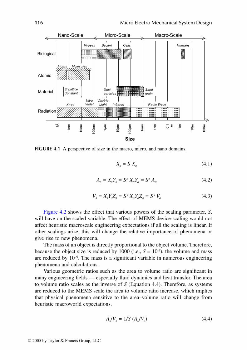
116 Micro Electro Mechanical System Design
Xs = S Xo (4.1)
As = XsYs = S2 XoYo = S2 Ao (4.2)
Vs = XsYsZs = S3 XoYoZo = S3 Vo (4.3)
Figure 4.2 shows the effect that various powers of the scaling parameter, S,will have on the scaled variable. The effect of MEMS device scaling would notaffect heuristic macroscale engineering expectations if all the scaling is linear. Ifother scalings arise, this will change the relative importance of phenomena orgive rise to new phenomena.
The mass of an object is directly proportional to the object volume. Therefore,because the object size is reduced by 1000 (i.e., S = 10-3), the volume and massare reduced by 10–9. The mass is a significant variable in numerous engineeringphenomena and calculations.
Various geometric ratios such as the area to volume ratio are significant inmany engineering fields — especially fluid dynamics and heat transfer. The areato volume ratio scales as the inverse of S (Equation 4.4). Therefore, as systemsare reduced to the MEMS scale the area to volume ratio increase, which impliesthat physical phenomena sensitive to the area–volume ratio will change fromheuristic macroworld expectations.
As/Vs = 1/S (Ao/Vo) (4.4)
FIGURE 4.1 A perspective of size in the macro, micro, and nano domains.
© 2005 by Taylor & Francis Group, LLC
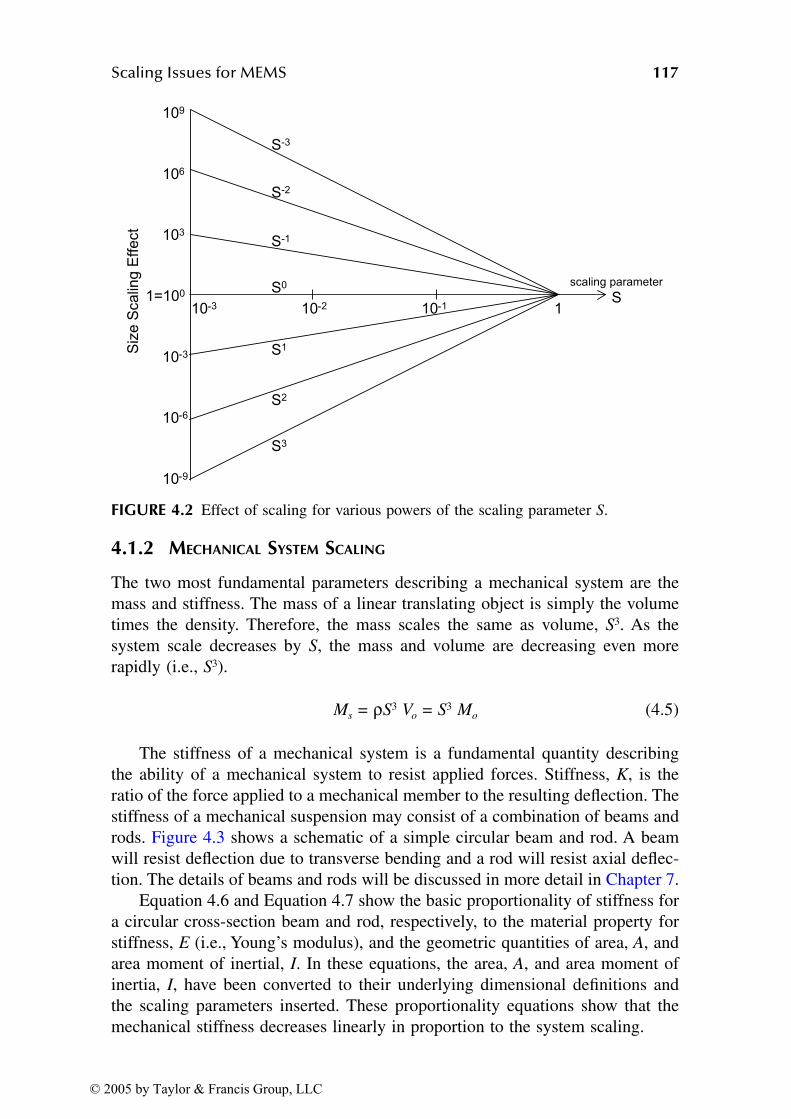
Scaling Issues for MEMS 117
4.1.2 MECHANICAL SYSTEM SCALING
The two most fundamental parameters describing a mechanical system are themass and stiffness. The mass of a linear translating object is simply the volumetimes the density. Therefore, the mass scales the same as volume, S3. As thesystem scale decreases by S, the mass and volume are decreasing even morerapidly (i.e., S3).
Ms = ρS3 Vo = S3 Mo (4.5)
The stiffness of a mechanical system is a fundamental quantity describingthe ability of a mechanical system to resist applied forces. Stiffness, K, is theratio of the force applied to a mechanical member to the resulting deflection. Thestiffness of a mechanical suspension may consist of a combination of beams androds. Figure 4.3 shows a schematic of a simple circular beam and rod. A beamwill resist deflection due to transverse bending and a rod will resist axial deflec-tion. The details of beams and rods will be discussed in more detail in Chapter 7.
Equation 4.6 and Equation 4.7 show the basic proportionality of stiffness fora circular cross-section beam and rod, respectively, to the material property forstiffness, E (i.e., Young’s modulus), and the geometric quantities of area, A, andarea moment of inertial, I. In these equations, the area, A, and area moment ofinertia, I, have been converted to their underlying dimensional definitions andthe scaling parameters inserted. These proportionality equations show that themechanical stiffness decreases linearly in proportion to the system scaling.
FIGURE 4.2 Effect of scaling for various powers of the scaling parameter S.
© 2005 by Taylor & Francis Group, LLC
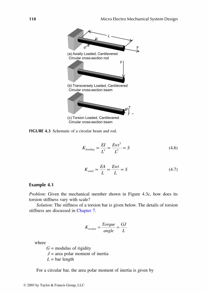
118 Micro Electro Mechanical System Design
(4.6)
(4.7)
Example 4.1
Problem: Given the mechanical member shown in Figure 4.3c, how does itstorsion stiffness vary with scale?
Solution: The stiffness of a torsion bar is given below. The details of torsionstiffness are discussed in Chapter 7.
whereG = modulus of rigidityJ = area polar moment of inertiaL = bar length
For a circular bar, the area polar moment of inertia is given by
FIGURE 4.3 Schematic of a circular beam and rod.
( )
( )
( )
-
-
-
KEI
L
Ewt
LSbending ∝ ∝ ∝
3
3
3
KEA
L
Ewt
LSaxial ∝ ∝ ∝
KTorque
angle
GJ
Ltorsion = =
© 2005 by Taylor & Francis Group, LLC
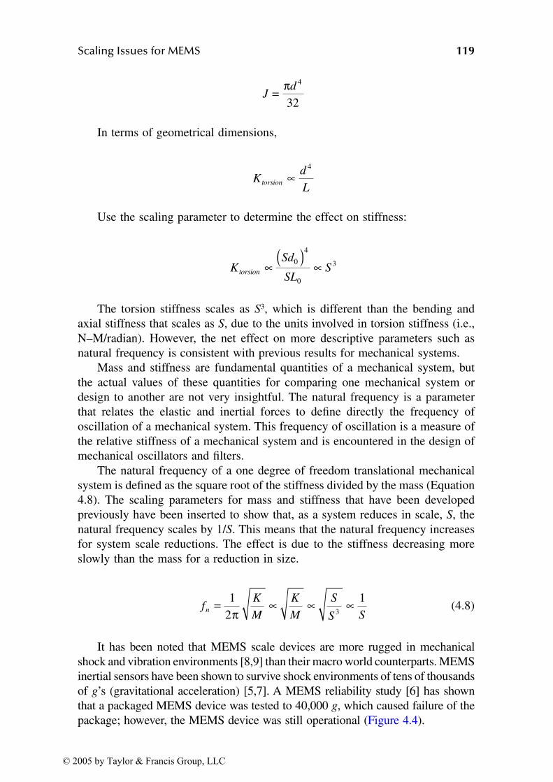
Scaling Issues for MEMS 119
In terms of geometrical dimensions,
Use the scaling parameter to determine the effect on stiffness:
The torsion stiffness scales as S3, which is different than the bending andaxial stiffness that scales as S, due to the units involved in torsion stiffness (i.e.,N–M/radian). However, the net effect on more descriptive parameters such asnatural frequency is consistent with previous results for mechanical systems.
Mass and stiffness are fundamental quantities of a mechanical system, butthe actual values of these quantities for comparing one mechanical system ordesign to another are not very insightful. The natural frequency is a parameterthat relates the elastic and inertial forces to define directly the frequency ofoscillation of a mechanical system. This frequency of oscillation is a measure ofthe relative stiffness of a mechanical system and is encountered in the design ofmechanical oscillators and filters.
The natural frequency of a one degree of freedom translational mechanicalsystem is defined as the square root of the stiffness divided by the mass (Equation4.8). The scaling parameters for mass and stiffness that have been developedpreviously have been inserted to show that, as a system reduces in scale, S, thenatural frequency scales by 1/S. This means that the natural frequency increasesfor system scale reductions. The effect is due to the stiffness decreasing moreslowly than the mass for a reduction in size.
(4.8)
It has been noted that MEMS scale devices are more rugged in mechanicalshock and vibration environments [8,9] than their macro world counterparts. MEMSinertial sensors have been shown to survive shock environments of tens of thousandsof g’s (gravitational acceleration) [5,7]. A MEMS reliability study [6] has shownthat a packaged MEMS device was tested to 40,000 g, which caused failure of thepackage; however, the MEMS device was still operational (Figure 4.4).
Jd= π 4
32
Kd
Ltorsion ∝ 4
KSd
SLStorsion ∝ ( ) ∝0
4
0
3
fK
M
K
M
S
S Sn = ∝ ∝ ∝1
21
3π
© 2005 by Taylor & Francis Group, LLC
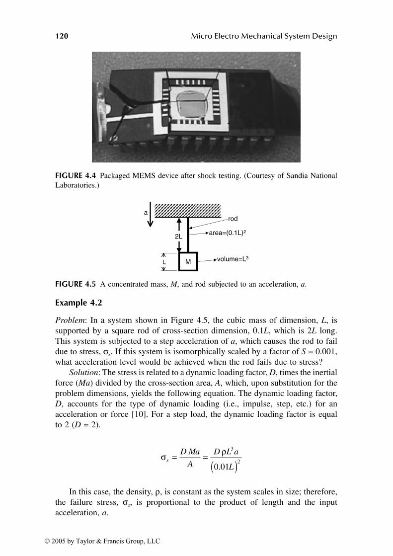
120 Micro Electro Mechanical System Design
Example 4.2
Problem: In a system shown in Figure 4.5, the cubic mass of dimension, L, issupported by a square rod of cross-section dimension, 0.1L, which is 2L long.This system is subjected to a step acceleration of a, which causes the rod to faildue to stress, σs. If this system is isomorphically scaled by a factor of S = 0.001,what acceleration level would be achieved when the rod fails due to stress?
Solution: The stress is related to a dynamic loading factor, D, times the inertialforce (Ma) divided by the cross-section area, A, which, upon substitution for theproblem dimensions, yields the following equation. The dynamic loading factor,D, accounts for the type of dynamic loading (i.e., impulse, step, etc.) for anacceleration or force [10]. For a step load, the dynamic loading factor is equalto 2 (D = 2).
In this case, the density, ρ, is constant as the system scales in size; therefore,the failure stress, σs, is proportional to the product of length and the inputacceleration, a.
FIGURE 4.4 Packaged MEMS device after shock testing. (Courtesy of Sandia NationalLaboratories.)
FIGURE 4.5 A concentrated mass, M, and rod subjected to an acceleration, a.
2Larea=(0.1L)2
volume=L3M
a
L
rod
σ ρs
D Ma
A
D L a
L= = ( )
3
20 01.
© 2005 by Taylor & Francis Group, LLC
Scaling Issues for MEMS 121
σs ∝ La
At the reduced scale, S, the failure stress, σs, is given by
σs ∝ SLa
This means that the acceleration, a, required to achieve failure due to stressscales by 1/s, as shown next.
Therefore, when this system is isomorphically scaled by a factor of S = 0.001the acceleration required for a stress failure of the rod increases by 1000.
Reduction in scale in mechanical systems has some negative consequences.For example, the deflection of an inertial mass in a sensing device will requirea more sensitive detection system, because the inertial mass and the resultinginertial force scale as S3 but the stiffness scales as S. This different scaling causesthe mass to deflect less as smaller size scales.
4.1.3 THERMAL SYSTEM SCALING
The effect of scaling a thermal system can readily be determined by analyzingthe basic heat transfer relationships [11]. The thermal energy storage capabilityfor an object is determined by Equation 4.9. The thermal energy storage of anobject is the product of the mass, m, constant pressure specific heat, cp, and thetemperature change, ∆T, in the material; it is a measure of the temperature increasein an object due to thermal input. The thermal mass for any specific system willinvolve the volume of the system, V, and it will therefore scale with size by S3:
(4.9)
Heat can be transferred within a system by the mechanisms of conduction,convection, and radiation (see Figure 4.6 and Equation 4.10 through Equation4.12, respectively). Conduction is heat transfer through the material of an objectdue to a temperature gradient, ∇T. Convection is a form of heat transfer througha liquid or gas to an object, due to a temperature difference between the objectsurface or wall, Tw, and the temperature of the bulk fluid or gas, T∞. K and h arethe conduction and convection heat transfer coefficients, respectively, and arefunctions of the medium through which the heat is transferred. The convectionheat transfer coefficient, h, also involves complex relationships of the mediumfluid flow.
Radiation heat transfer between objects in space is driven by the temperaturesof the objects to the fourth power, where σ is the Boltzmann constant. These
aSL S
s∝ ∝σ 1
mc T Vc T Sp p∆ ∆= ∝ρ 3
© 2005 by Taylor & Francis Group, LLC
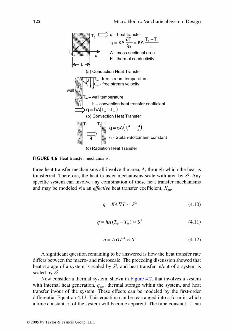
122 Micro Electro Mechanical System Design
three heat transfer mechanisms all involve the area, A, through which the heat istransferred. Therefore, the heat transfer mechanisms scale with area by S2. Anyspecific system can involve any combination of these heat transfer mechanismsand may be modeled via an effective heat transfer coefficient, Keff.
(4.10)
(4.11)
(4.12)
A significant question remaining to be answered is how the heat transfer ratediffers between the macro- and microscale. The preceding discussion showed thatheat storage of a system is scaled by S3, and heat transfer in/out of a system isscaled by S2.
Now consider a thermal system, shown in Figure 4.7, that involves a systemwith internal heat generation, qgen, thermal storage within the system, and heattransfer in/out of the system. These effects can be modeled by the first-orderdifferential Equation 4.13. This equation can be rearranged into a form in whicha time constant, τ, of the system will become apparent. The time constant, τ, can
FIGURE 4.6 Heat transfer mechanisms.
(a) Conduction Heat Transfer
T2
T1x
q – heat transfer
L
TTKA
x
TKAq 12
−=
∂
∂=
L
A - cross-sectional area
K - thermal conductivity
uu∞ - free stream velocity
T∞ - free stream temperature
Tw –
–
wall temperature
(b) Convection Heat Transfer
h convection heat transfer coefficient
wall
( )∞−= TThAq w
( )4
2
4
1TTAq −= σ
T1 T2
q σ - Stefan-Boltzmann constant
(c) Radiation Heat Transfer
q KA T S= ∇ ∝ 2
q hA T T Sw= − ∝∞( ) 2
q A T S= ∝σ 4 2
© 2005 by Taylor & Francis Group, LLC
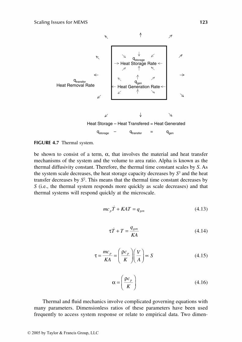
Scaling Issues for MEMS 123
be shown to consist of a term, α, that involves the material and heat transfermechanisms of the system and the volume to area ratio. Alpha is known as thethermal diffusivity constant. Therefore, the thermal time constant scales by S. Asthe system scale decreases, the heat storage capacity decreases by S3 and the heattransfer decreases by S2. This means that the thermal time constant decreases byS (i.e., the thermal system responds more quickly as scale decreases) and thatthermal systems will respond quickly at the microscale.
(4.13)
(4.14)
(4.15)
(4.16)
Thermal and fluid mechanics involve complicated governing equations withmany parameters. Dimensionless ratios of these parameters have been usedfrequently to access system response or relate to empirical data. Two dimen-
FIGURE 4.7 Thermal system.
qstorage
Heat Storage Rate
qgen
Heat Generation Rate
qtransfer
Heat Removal Rate
Heat Storage – Heat Transfered = Heat Generated
qstorage – qtransfer = qgen
mc T KAT qp genɺ + =
τ ɺT Tq
KA
gen+ =
τ ρ= =
∝mc
KA
c
K
V
AS
p p
α ρ=
c
K
p
© 2005 by Taylor & Francis Group, LLC
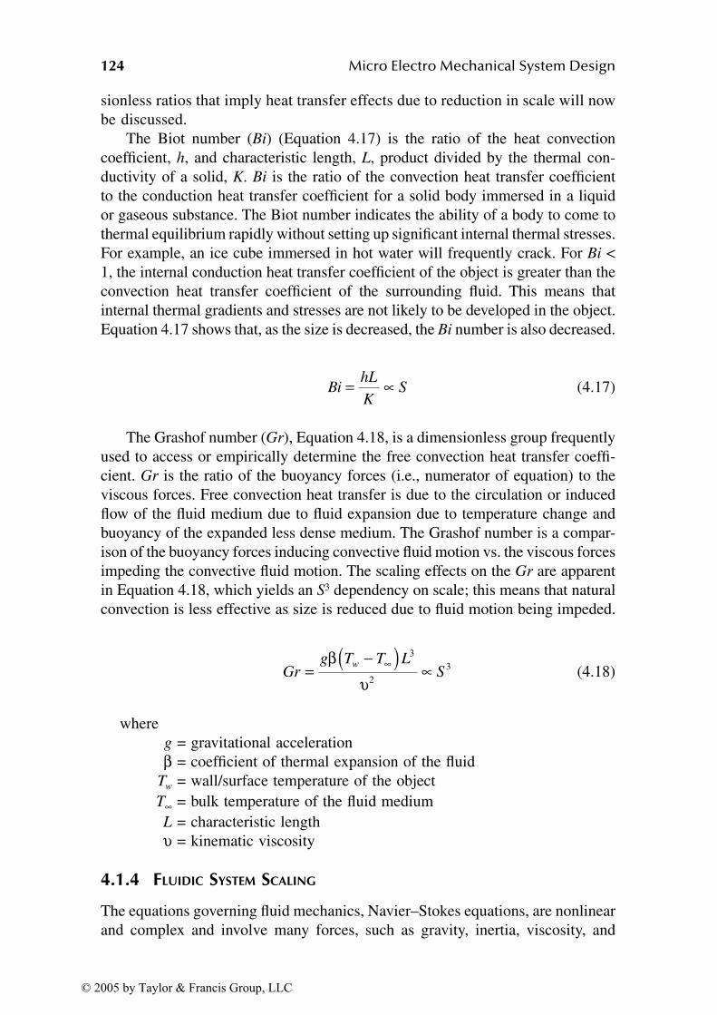
124 Micro Electro Mechanical System Design
sionless ratios that imply heat transfer effects due to reduction in scale will nowbe discussed.
The Biot number (Bi) (Equation 4.17) is the ratio of the heat convectioncoefficient, h, and characteristic length, L, product divided by the thermal con-ductivity of a solid, K. Bi is the ratio of the convection heat transfer coefficientto the conduction heat transfer coefficient for a solid body immersed in a liquidor gaseous substance. The Biot number indicates the ability of a body to come tothermal equilibrium rapidly without setting up significant internal thermal stresses.For example, an ice cube immersed in hot water will frequently crack. For Bi <1, the internal conduction heat transfer coefficient of the object is greater than theconvection heat transfer coefficient of the surrounding fluid. This means thatinternal thermal gradients and stresses are not likely to be developed in the object.Equation 4.17 shows that, as the size is decreased, the Bi number is also decreased.
(4.17)
The Grashof number (Gr), Equation 4.18, is a dimensionless group frequentlyused to access or empirically determine the free convection heat transfer coeffi-cient. Gr is the ratio of the buoyancy forces (i.e., numerator of equation) to theviscous forces. Free convection heat transfer is due to the circulation or inducedflow of the fluid medium due to fluid expansion due to temperature change andbuoyancy of the expanded less dense medium. The Grashof number is a compar-ison of the buoyancy forces inducing convective fluid motion vs. the viscous forcesimpeding the convective fluid motion. The scaling effects on the Gr are apparentin Equation 4.18, which yields an S3 dependency on scale; this means that naturalconvection is less effective as size is reduced due to fluid motion being impeded.
(4.18)
whereg = gravitational accelerationβ = coefficient of thermal expansion of the fluid
Tw = wall/surface temperature of the objectT∞ = bulk temperature of the fluid mediumL = characteristic lengthυ = kinematic viscosity
4.1.4 FLUIDIC SYSTEM SCALING
The equations governing fluid mechanics, Navier–Stokes equations, are nonlinearand complex and involve many forces, such as gravity, inertia, viscosity, and
BihL
KS= ∝
Grg T T L
Sw= −( ) ∝∞β
υ3
23
© 2005 by Taylor & Francis Group, LLC
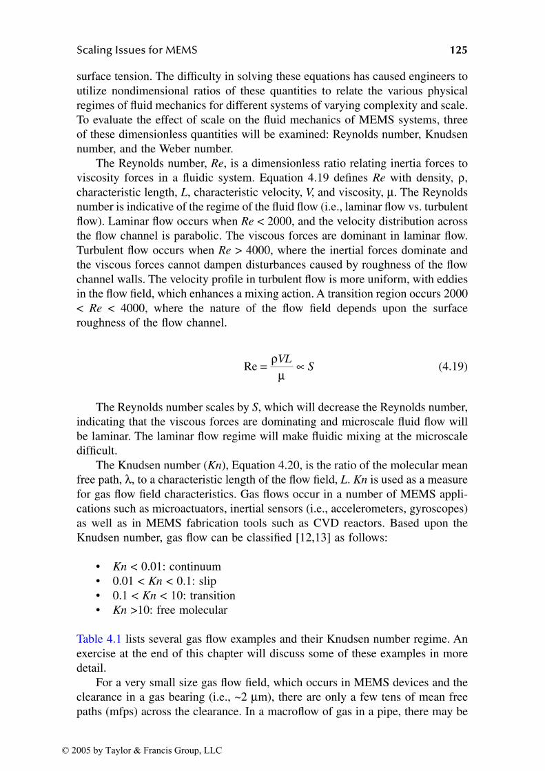
Scaling Issues for MEMS 125
surface tension. The difficulty in solving these equations has caused engineers toutilize nondimensional ratios of these quantities to relate the various physicalregimes of fluid mechanics for different systems of varying complexity and scale.To evaluate the effect of scale on the fluid mechanics of MEMS systems, threeof these dimensionless quantities will be examined: Reynolds number, Knudsennumber, and the Weber number.
The Reynolds number, Re, is a dimensionless ratio relating inertia forces toviscosity forces in a fluidic system. Equation 4.19 defines Re with density, ρ,characteristic length, L, characteristic velocity, V, and viscosity, µ. The Reynoldsnumber is indicative of the regime of the fluid flow (i.e., laminar flow vs. turbulentflow). Laminar flow occurs when Re < 2000, and the velocity distribution acrossthe flow channel is parabolic. The viscous forces are dominant in laminar flow.Turbulent flow occurs when Re > 4000, where the inertial forces dominate andthe viscous forces cannot dampen disturbances caused by roughness of the flowchannel walls. The velocity profile in turbulent flow is more uniform, with eddiesin the flow field, which enhances a mixing action. A transition region occurs 2000< Re < 4000, where the nature of the flow field depends upon the surfaceroughness of the flow channel.
(4.19)
The Reynolds number scales by S, which will decrease the Reynolds number,indicating that the viscous forces are dominating and microscale fluid flow willbe laminar. The laminar flow regime will make fluidic mixing at the microscaledifficult.
The Knudsen number (Kn), Equation 4.20, is the ratio of the molecular meanfree path, λ, to a characteristic length of the flow field, L. Kn is used as a measurefor gas flow field characteristics. Gas flows occur in a number of MEMS appli-cations such as microactuators, inertial sensors (i.e., accelerometers, gyroscopes)as well as in MEMS fabrication tools such as CVD reactors. Based upon theKnudsen number, gas flow can be classified [12,13] as follows:
• Kn < 0.01: continuum• 0.01 < Kn < 0.1: slip• 0.1 < Kn < 10: transition• Kn >10: free molecular
Table 4.1 lists several gas flow examples and their Knudsen number regime. Anexercise at the end of this chapter will discuss some of these examples in moredetail.
For a very small size gas flow field, which occurs in MEMS devices and theclearance in a gas bearing (i.e., ~2 µm), there are only a few tens of mean freepaths (mfps) across the clearance. In a macroflow of gas in a pipe, there may be
Re = ∝ρµVL
S
© 2005 by Taylor & Francis Group, LLC
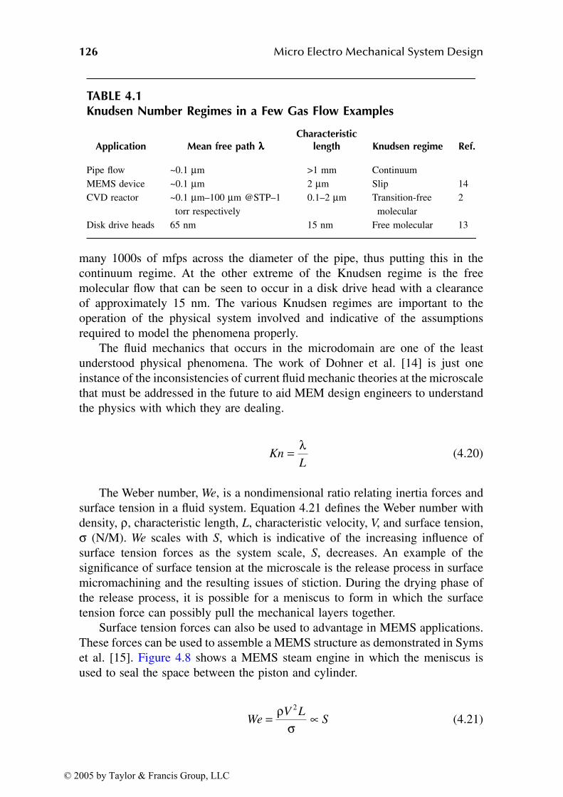
126 Micro Electro Mechanical System Design
many 1000s of mfps across the diameter of the pipe, thus putting this in thecontinuum regime. At the other extreme of the Knudsen regime is the freemolecular flow that can be seen to occur in a disk drive head with a clearanceof approximately 15 nm. The various Knudsen regimes are important to theoperation of the physical system involved and indicative of the assumptionsrequired to model the phenomena properly.
The fluid mechanics that occurs in the microdomain are one of the leastunderstood physical phenomena. The work of Dohner et al. [14] is just oneinstance of the inconsistencies of current fluid mechanic theories at the microscalethat must be addressed in the future to aid MEM design engineers to understandthe physics with which they are dealing.
(4.20)
The Weber number, We, is a nondimensional ratio relating inertia forces andsurface tension in a fluid system. Equation 4.21 defines the Weber number withdensity, ρ, characteristic length, L, characteristic velocity, V, and surface tension,σ (N/M). We scales with S, which is indicative of the increasing influence ofsurface tension forces as the system scale, S, decreases. An example of thesignificance of surface tension at the microscale is the release process in surfacemicromachining and the resulting issues of stiction. During the drying phase ofthe release process, it is possible for a meniscus to form in which the surfacetension force can possibly pull the mechanical layers together.
Surface tension forces can also be used to advantage in MEMS applications.These forces can be used to assemble a MEMS structure as demonstrated in Symset al. [15]. Figure 4.8 shows a MEMS steam engine in which the meniscus isused to seal the space between the piston and cylinder.
(4.21)
TABLE 4.1Knudsen Number Regimes in a Few Gas Flow Examples
Application Mean free path λλλλCharacteristic
length Knudsen regime Ref.
Pipe flow ~0.1 µm >1 mm ContinuumMEMS device ~0.1 µm 2 µm Slip 14CVD reactor ~0.1 µm–100 µm @STP–1
torr respectively0.1–2 µm Transition-free
molecular2
Disk drive heads 65 nm 15 nm Free molecular 13
KnL
= λ
WeV L
S= ∝ρσ
2
© 2005 by Taylor & Francis Group, LLC
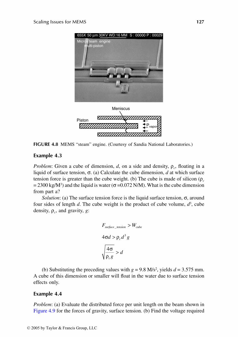
Scaling Issues for MEMS 127
Example 4.3
Problem: Given a cube of dimension, d, on a side and density, ρc, floating in aliquid of surface tension, σ. (a) Calculate the cube dimension, d at which surfacetension force is greater than the cube weight. (b) The cube is made of silicon (ρc
= 2300 kg/M3) and the liquid is water (σ =0.072 N/M). What is the cube dimensionfrom part a?
Solution: (a) The surface tension force is the liquid surface tension, σ, aroundfour sides of length d. The cube weight is the product of cube volume, d3, cubedensity, ρc, and gravity, g:
(b) Substituting the preceding values with g = 9.8 M/s2, yields d = 3.575 mm.A cube of this dimension or smaller will float in the water due to surface tensioneffects only.
Example 4.4
Problem: (a) Evaluate the distributed force per unit length on the beam shown inFigure 4.9 for the forces of gravity, surface tension. (b) Find the voltage required
FIGURE 4.8 MEMS “steam” engine. (Courtesy of Sandia National Laboratories.)
Meniscus
PistonPvapor
Micros team engine
multi-piston
655X 50 µm 30KV WD:16 MM S : 00000 P : 00029
F W
d d g
gd
surface tension cube
c
c
_ >>
>4
4
3σ ρσ
ρ
© 2005 by Taylor & Francis Group, LLC
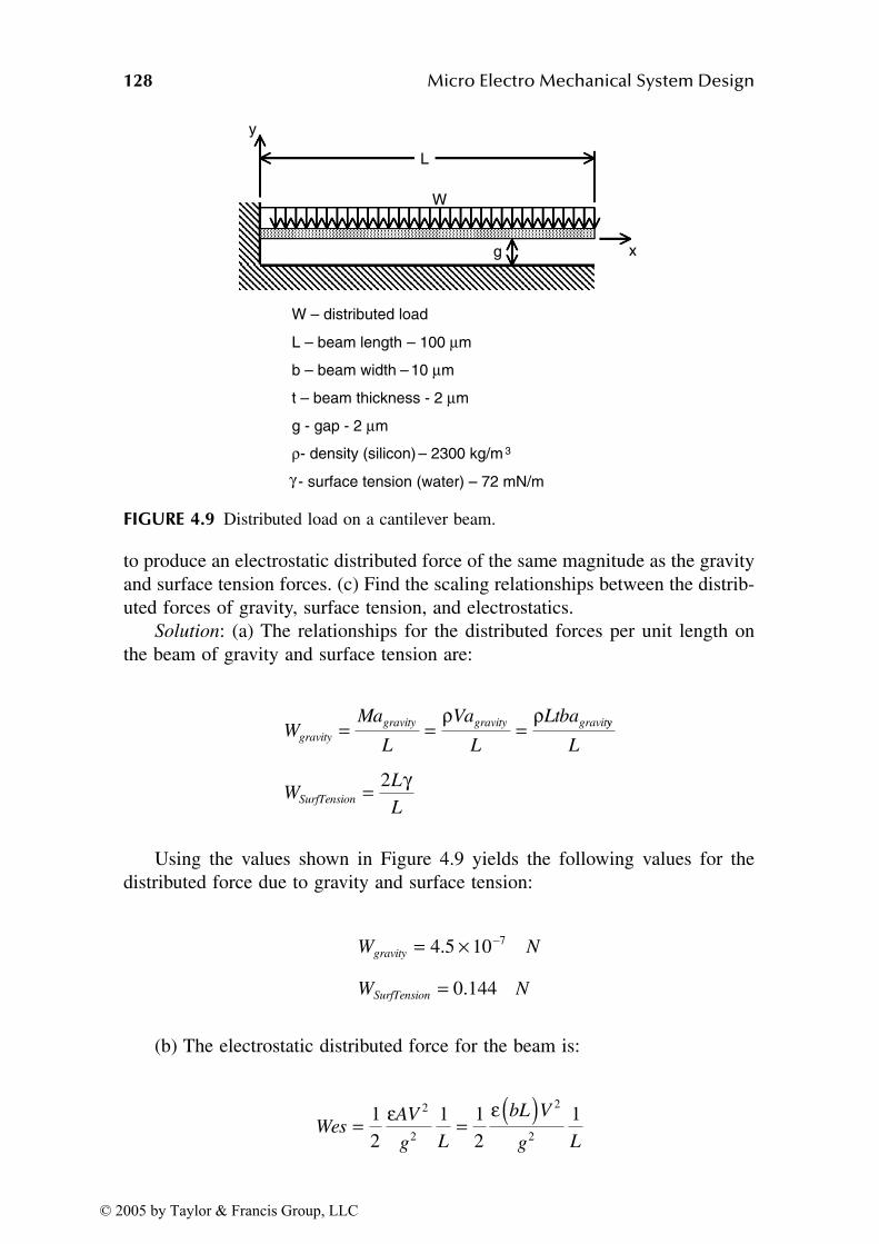
128 Micro Electro Mechanical System Design
to produce an electrostatic distributed force of the same magnitude as the gravityand surface tension forces. (c) Find the scaling relationships between the distrib-uted forces of gravity, surface tension, and electrostatics.
Solution: (a) The relationships for the distributed forces per unit length onthe beam of gravity and surface tension are:
Using the values shown in Figure 4.9 yields the following values for thedistributed force due to gravity and surface tension:
(b) The electrostatic distributed force for the beam is:
FIGURE 4.9 Distributed load on a cantilever beam.
W – distributed load
L – beam length – 100 µm
b – beam width – 10 µm
t – beam thickness - 2 µm
g - gap - 2 µm
ρ- density (silicon) – 2300 kg/m 3
γ - surface tension (water) – 72 mN/m
L
x
y
W
g
WMa
L
Va
L
Ltbagravity
gravity gravity gravit= = =ρ ρ yy
SurfTension
L
WL
L= 2 γ
W N
W N
gravity
SurfTension
= ×=
−4 5 10
0 144
7.
.
WesAV
g L
bL V
g L= = ( )1
21 1
212
2
2
2
ε ε
© 2005 by Taylor & Francis Group, LLC
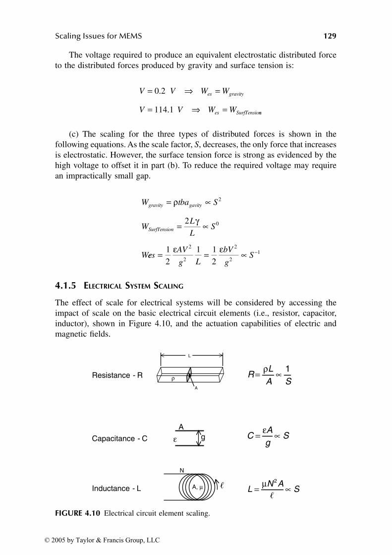
Scaling Issues for MEMS 129
The voltage required to produce an equivalent electrostatic distributed forceto the distributed forces produced by gravity and surface tension is:
(c) The scaling for the three types of distributed forces is shown in thefollowing equations. As the scale factor, S, decreases, the only force that increasesis electrostatic. However, the surface tension force is strong as evidenced by thehigh voltage to offset it in part (b). To reduce the required voltage may requirean impractically small gap.
4.1.5 ELECTRICAL SYSTEM SCALING
The effect of scale for electrical systems will be considered by accessing theimpact of scale on the basic electrical circuit elements (i.e., resistor, capacitor,inductor), shown in Figure 4.10, and the actuation capabilities of electric andmagnetic fields.
FIGURE 4.10 Electrical circuit element scaling.
V V W W
V V W W
es gravity
es SurfTensio
= ⇒ == ⇒ =
0 2
114 1
.
. nn
W tba S
WL
LS
W
gravity gavity
SurfTension
= ∝= ∝
ργ
2
02
eesAV
g L
bV
gS= = ∝ −1
21 1
2
2
2
2
21ε ε
g
A
ε
A
ρ
N
A, µ
Resistance - R
Capacitance - C
Inductance - L
SA
LR
1∝=
ρ
Sg
AC ∝=
ε
SAN
L ∝=2µ
L
© 2005 by Taylor & Francis Group, LLC

130 Micro Electro Mechanical System Design
The resistance, R, of a piece of material is a function of the resistivity, ρ, ofthe material and its geometric size. The geometry enters the equation via the ratioof the length of material, l, in direction of current flow and the cross-section area,A. This results in the resistance of an object increasing by 1/S when the objectis isomorphically reduced in size, S.
(4.22)
The capacitance of a capacitor, C, is defined by the permittivity, ε, of thedielectric material between two plates of area, A, separated by a gap, g, as shownnext. Therefore, the capacitance will be reduced by S when isomorphically scaled.
(4.23)
The inductance, L, of a N loops of material encompassing material of per-meability, µ, can be calculated by Equation 4.24. The inductance, L, similar to acapacitor, will scale by S upon isomorphic scaling.
(4.24)
Electrical circuit elements of inductance and capacitance will decrease inproportion to the reduction in scale, but resistance will increase inversely withscale. CMOS microelectronics has capabilities of fabricating transistors, resistors,and capacitors; in a simple view, CMOS transistors are just capacitance controlledswitches. This means that a simple reduction of size of an existing MEMS orCMOS design containing some combination of these circuit elements cannot bedone because the different circuit elements scale differently.
Knowledge of the scaling effects on the electrical circuit elements is usefulin the design of many MEMS devices that may contain electrical circuit elementson the same die or as part of the mechanical structure for the MEMS device. Forexample, a MEMS inertial sensing device (e.g., accelerometer, gyroscope) willcontain a suspended mass and use a variable capacitor to enable capacitativesensing of the displacement of the suspended mass.
Electrical scaling also has importance for the design of actuated MEMSdevices. In the macroworld, electromagnetic actuation dominates. With extremelyfew exceptions, electrical to mechanical (i.e., electric motors) or mechanical toelectrical (i.e., electric generators) utilize magnetic fields. As the sizes of devicesare reduced to the MEMS scale, it is necessary to evaluate whether this stillremains the best choice [21].
Rl
A S= ∝ρ 1
CA
gS= ∝ε
L NA
lS= ∝µ
© 2005 by Taylor & Francis Group, LLC
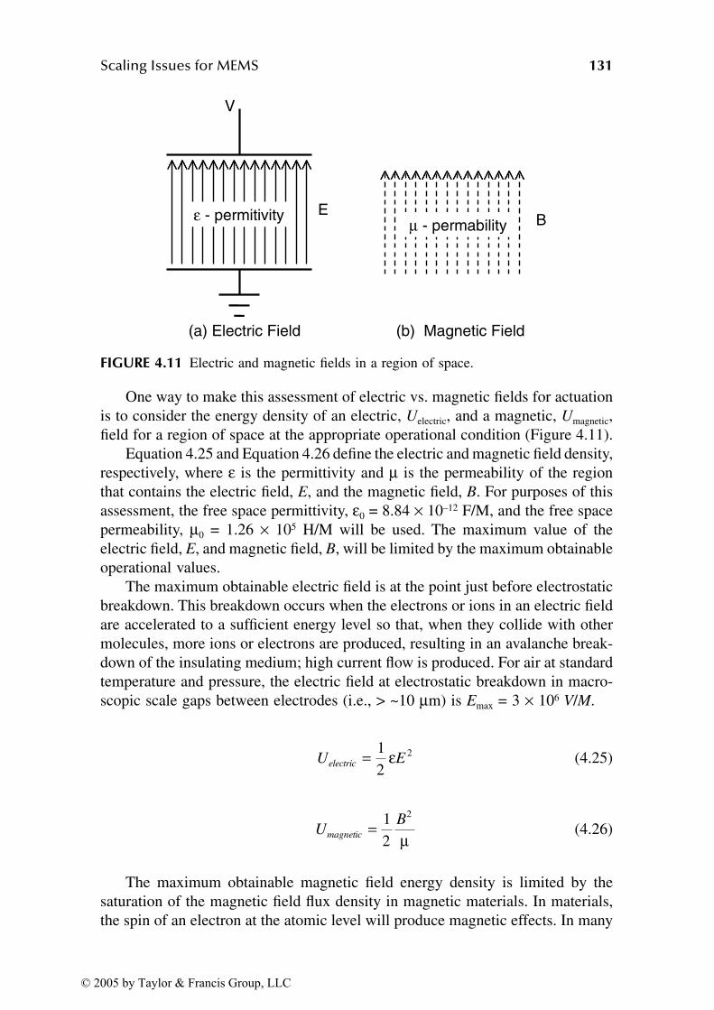
Scaling Issues for MEMS 131
One way to make this assessment of electric vs. magnetic fields for actuationis to consider the energy density of an electric, Uelectric, and a magnetic, Umagnetic,field for a region of space at the appropriate operational condition (Figure 4.11).
Equation 4.25 and Equation 4.26 define the electric and magnetic field density,respectively, where ε is the permittivity and µ is the permeability of the regionthat contains the electric field, E, and the magnetic field, B. For purposes of thisassessment, the free space permittivity, ε0 = 8.84 × 10⁻¹² F/M, and the free spacepermeability, µ0 = 1.26 × 10⁵ H/M will be used. The maximum value of theelectric field, E, and magnetic field, B, will be limited by the maximum obtainableoperational values.
The maximum obtainable electric field is at the point just before electrostaticbreakdown. This breakdown occurs when the electrons or ions in an electric fieldare accelerated to a sufficient energy level so that, when they collide with othermolecules, more ions or electrons are produced, resulting in an avalanche break-down of the insulating medium; high current flow is produced. For air at standardtemperature and pressure, the electric field at electrostatic breakdown in macro-scopic scale gaps between electrodes (i.e., > ~10 µm) is Emax = 3 × 10⁶ V/M.
(4.25)
(4.26)
The maximum obtainable magnetic field energy density is limited by thesaturation of the magnetic field flux density in magnetic materials. In materials,the spin of an electron at the atomic level will produce magnetic effects. In many
FIGURE 4.11 Electric and magnetic fields in a region of space.
V
Eε - permitivityµ - permability B
(a) Electric Field (b) Magnetic Field
U Eelectric = 12
2ε
UB
magnetic = 12
2
µ
© 2005 by Taylor & Francis Group, LLC
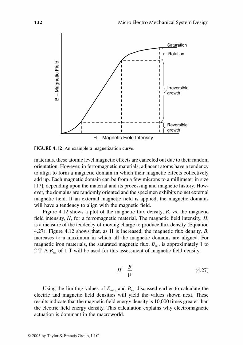
132 Micro Electro Mechanical System Design
materials, these atomic level magnetic effects are canceled out due to their randomorientation. However, in ferromagnetic materials, adjacent atoms have a tendencyto align to form a magnetic domain in which their magnetic effects collectivelyadd up. Each magnetic domain can be from a few microns to a millimeter in size[17], depending upon the material and its processing and magnetic history. How-ever, the domains are randomly oriented and the specimen exhibits no net externalmagnetic field. If an external magnetic field is applied, the magnetic domainswill have a tendency to align with the magnetic field.
Figure 4.12 shows a plot of the magnetic flux density, B, vs. the magneticfield intensity, H, for a ferromagnetic material. The magnetic field intensity, H,is a measure of the tendency of moving charge to produce flux density (Equation4.27). Figure 4.12 shows that, as H is increased, the magnetic flux density, B,increases to a maximum in which all the magnetic domains are aligned. Formagnetic iron materials, the saturated magnetic flux, Bsat, is approximately 1 to2 T. A Bsat of 1 T will be used for this assessment of magnetic field density.
(4.27)
Using the limiting values of Emax and Bsat discussed earlier to calculate theelectric and magnetic field densities will yield the values shown next. Theseresults indicate that the magnetic field energy density is 10,000 times greater thanthe electric field energy density. This calculation explains why electromagneticactuation is dominant in the macroworld.
FIGURE 4.12 An example a magnetization curve.
B –
Magnetic F
ield
H – Magnetic Field Intensity
Saturation
Rotation
Irreversible
growth
Reversible
growth
HB= µ
© 2005 by Taylor & Francis Group, LLC
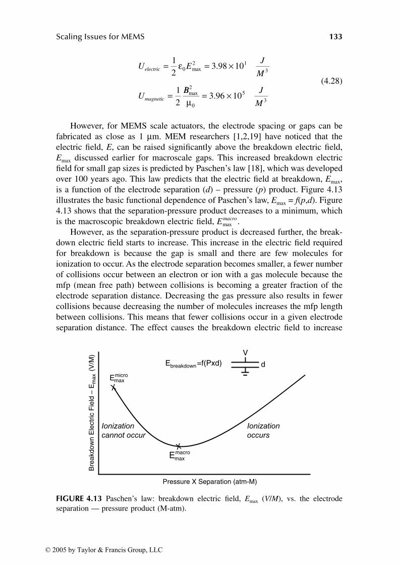
Scaling Issues for MEMS 133
(4.28)
However, for MEMS scale actuators, the electrode spacing or gaps can befabricated as close as 1 µm. MEM researchers [1,2,19] have noticed that theelectric field, E, can be raised significantly above the breakdown electric field,Emax discussed earlier for macroscale gaps. This increased breakdown electricfield for small gap sizes is predicted by Paschen’s law [18], which was developedover 100 years ago. This law predicts that the electric field at breakdown, Emax,is a function of the electrode separation (d) – pressure (p) product. Figure 4.13illustrates the basic functional dependence of Paschen’s law, Emax = f(p,d). Figure4.13 shows that the separation-pressure product decreases to a minimum, whichis the macroscopic breakdown electric field, .
However, as the separation-pressure product is decreased further, the break-down electric field starts to increase. This increase in the electric field requiredfor breakdown is because the gap is small and there are few molecules forionization to occur. As the electrode separation becomes smaller, a fewer numberof collisions occur between an electron or ion with a gas molecule because themfp (mean free path) between collisions is becoming a greater fraction of theelectrode separation distance. Decreasing the gas pressure also results in fewercollisions because decreasing the number of molecules increases the mfp lengthbetween collisions. This means that fewer collisions occur in a given electrodeseparation distance. The effect causes the breakdown electric field to increase
FIGURE 4.13 Paschen’s law: breakdown electric field, Emax (V/M), vs. the electrodeseparation — pressure product (M-atm).
U EJ
M
U
electric
magnetic
= = ×
=
12
3 98 10
12
02 1
3ε max .
BB J
M
max .2
0
53
3 96 10µ = ×
E macromax
Bre
akd
ow
n E
lectr
ic F
ield
–E
max
(V/M
)
Pressure X Separation (atm-M)
Ebreakdown=f(Pxd)
Ionization
cannot occur
Ionization
occurs
microEmax
macroEmax
X
X
d
V
© 2005 by Taylor & Francis Group, LLC
134 Micro Electro Mechanical System Design
with decreasing separation-pressure product up to a maximum, , for micros-cale electrode spacings. The electric field for small electrode separation distancesin vacuum have been reported [20] to be
Using this new value for Emax will change the comparison of the electric andmagnetic field energy density calculation of Equation 4.29 as shown next. Thisresults in a more favorable but neutral comparison of the energy density of electricand magnetic fields. However, the literature indicates that, for MEMS applica-tions, electrostatics predominates. This is due to the added fabrication and assem-bly complexity of fabricating MEMS scale permanent magnets, coils of wire,and the associated resistive power losses with their use.
(4.29)
In another simple comparison of electric and magnetic fields, it can be seenthat the magnetic field energy density, Umagnetic, does not change with size scalingbecause Bsat and µ are material properties that do not change appreciably withscaling to the microdomain. However, assuming that the applied voltage remainsconstant up to the limit of Emax at electrostatic breakdown shows that the electricfield energy density, Uelectric, varies with scale as shown in Equation 4.30. Thisgives electrostatic actuation increasing importance as devices are scaled to themicrodomain.
(4.30)
4.1.6 OPTICAL SYSTEM SCALING
Optical MEMS applications and research is an extremely active area, with MEMSdevices developed for use in optical display, switching, and modulation applica-tions. These MEMS scale optical devices [23,24] include LEDs, diffraction grat-ings, mirrors, sensors, and waveguides. Their operation can depend upon opticalabsorption or reflection for functionality.
E micromax
EV
M
micromax .= ×3 0 108
U EJ
M
U
electricmicro
magn
= ( ) = ×12
3 98 100
25
3ε max .
eetic
B J
M= = ×1
23 96 10
2
0
53
max .µ
U ES
UB
electric
magnetic
= ∝
=
∝
12
1
12
02
2
0
2
ε
µ SS 0
© 2005 by Taylor & Francis Group, LLC
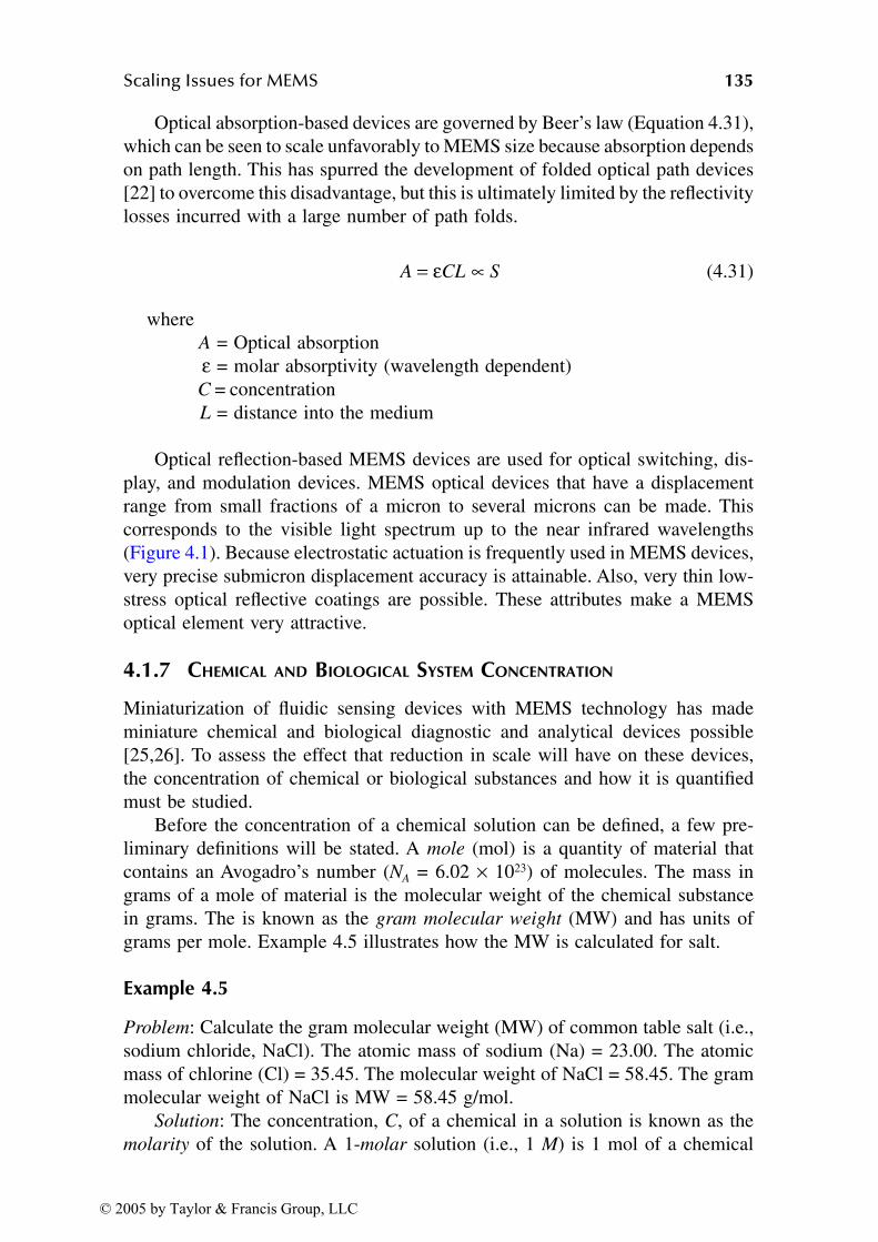
Scaling Issues for MEMS 135
Optical absorption-based devices are governed by Beer’s law (Equation 4.31),which can be seen to scale unfavorably to MEMS size because absorption dependson path length. This has spurred the development of folded optical path devices[22] to overcome this disadvantage, but this is ultimately limited by the reflectivitylosses incurred with a large number of path folds.
(4.31)
whereA = Optical absorptionε = molar absorptivity (wavelength dependent)C = concentration L = distance into the medium
Optical reflection-based MEMS devices are used for optical switching, dis-play, and modulation devices. MEMS optical devices that have a displacementrange from small fractions of a micron to several microns can be made. Thiscorresponds to the visible light spectrum up to the near infrared wavelengths(Figure 4.1). Because electrostatic actuation is frequently used in MEMS devices,very precise submicron displacement accuracy is attainable. Also, very thin low-stress optical reflective coatings are possible. These attributes make a MEMSoptical element very attractive.
4.1.7 CHEMICAL AND BIOLOGICAL SYSTEM CONCENTRATION
Miniaturization of fluidic sensing devices with MEMS technology has mademiniature chemical and biological diagnostic and analytical devices possible[25,26]. To assess the effect that reduction in scale will have on these devices,the concentration of chemical or biological substances and how it is quantifiedmust be studied.
Before the concentration of a chemical solution can be defined, a few pre-liminary definitions will be stated. A mole (mol) is a quantity of material thatcontains an Avogadro’s number (NA = 6.02 × 10²³) of molecules. The mass ingrams of a mole of material is the molecular weight of the chemical substancein grams. The is known as the gram molecular weight (MW) and has units ofgrams per mole. Example 4.5 illustrates how the MW is calculated for salt.
Example 4.5
Problem: Calculate the gram molecular weight (MW) of common table salt (i.e.,sodium chloride, NaCl). The atomic mass of sodium (Na) = 23.00. The atomicmass of chlorine (Cl) = 35.45. The molecular weight of NaCl = 58.45. The grammolecular weight of NaCl is MW = 58.45 g/mol.
Solution: The concentration, C, of a chemical in a solution is known as themolarity of the solution. A 1-molar solution (i.e., 1 M) is 1 mol of a chemical
A CL S= ∝ε
© 2005 by Taylor & Francis Group, LLC
136 Micro Electro Mechanical System Design
dissolved in 1 liter of solution. For example, a 1-M solution of NaCl consists of58.45 g of NaCl dissolved in a liter of solution. This relationship is expressed inEquation 4.32.
(4.32)
For chemical detection, the number of molecules, N, in a given samplevolume, V, may be important to quantify. This relationship between number ofmolecules in a given concentration of solution, C, and volume of solution, V, is:
(4.33)
Figure 4.14 shows the relationship between concentration, C, and samplevolume, V, as expressed by the preceding equation. The boundary for less thanone molecule, N1, of chemical or biological substance in a given sample volumeis shown; this is an absolute minimum sample volume for analysis. The numberof molecules required for detection, ND, is some amount greater than N1 (i.e.,ND > N1). The required sample volume for analysis would be at the intersectionof the ND boundary with the concentration of the analyte available for analysis.Petersen et al. [26] have shown that the typical concentrations of chemicaland biological material available for a few types of analyses are as shown inTable 4.2.
The miniaturization of chemical and biological systems has a few fundamen-tal limits:
• The trade-off between sample volume, V, and the detection limit, ND,for a given concentration of analyte, C, is illustrated in Figure 4.14.
• Further miniaturization may require increasing the concentration ofanalyte or increasing the sample volume.
• The use of small sample volumes requires increasingly sensitive detec-tors, which may be limited by other scaling issues (i.e., electrical,fluidic, etc.).
• The physical size limitation of biological sensing devices is limited bythe size of the biological entity. A cell is approximately 10 to 100 µm,whereas DNA has a width of only ~2 nm but is very long.
W MW C V
gramgram
mole
mole
literliter
= ⋅ ⋅= ⋅ ⋅
N N C V
moleculesmolecules
mole
mole
literl
A= ⋅ ⋅= ⋅ ⋅ iiter
© 2005 by Taylor & Francis Group, LLC
Scaling Issues for MEMS 137
4.2 COMPUTATIONAL ISSUES OF SCALE
The computational aspects of the scale of MEMS devices need to be consideredbecause much of modern engineering design depends upon numerical simulationto achieve success. Due to fabrication challenges, long fabrication times, andexperimental measurement difficulties, MEMS applications rely more upon sim-ulation than their macroworld counterparts do. Therefore, time would be well spentin assessing the unique issues encountered in simulation of MEMS scale devices.
Engineering calculations are almost exclusively performed on digital com-puters in which the numbers representing the input data (i.e., mechanical andelectrical properties, lengths, etc.) and the variables to be calculated are repre-sented by a fixed number of digits. Due to this digital representation of numbers,
FIGURE 4.14 Concentration vs. sample volume.
TABLE 4.2Typical Analyte Concentrations for Various
Types of Analyses
UsesConcentration(moles/liter)
Clinical chemistry assays 10–10–10–4
Immunoassays 10–17–10–6
Chemical, organisms, DNA analyses 10–22–10–17
Cs
100
100
10-3
10-3
10-6
10-6
10-9
10-9
10-12
10-12
10-15
10-15
10-18
10-18
10-21
10-21
C -
(M
) =
mole
s/liter
Molar concentration versus Volume of Solution for Various Numbers of Molecules
<1 molecule
Volume-literVs
Detectionregion
ND
© 2005 by Taylor & Francis Group, LLC

138 Micro Electro Mechanical System Design
the quantity known as machine accuracy, εm, is the smallest floating point numberthat can be represented on a given computer. The machine accuracy is a functionof the design of the particular computer. Two types of errors arise in the calcu-lations performed on digital computers [38]:
• Truncation error arises because numbers can only be represented to afinite accuracy (i.e., machine accuracy) on a digital computer.
• Round-off error arises in calculations, such as the solution of equations,due to the finite accuracy of the computer. Round-off error accumulateswith increasing amounts of calculation. If the calculations are per-formed so that the errors accumulate in a random fashion, the totalround-off error would be on the order of , where N is the numberof calculations performed. However, if the round-off errors accumulatepreferentially in one direction, the total error will be of the order Nεm.
The topics of truncation and round-off error arise in regular macroscaleengineering simulation; however, a unique aspect of computation for MEMS scalesimulation needs to be addressed:
• Convenient units scale of numbers for MEMS simulation. The systemof units typically used in engineering simulations (e.g., MKS) usesunits of measure of quantities typically encountered for macroscaledevices. For example, the MKS system of unit length measure ismeters. However, MEMS devices are on a size scale of microns (i.e.,0.000001 m).
• Numerically appropriate scale of unit for MEMS simulation. Numericalsimulations such as finite element analysis (FEM) [39,40] typicallyinvolve the solution of a large system of equations (e.g., 1,000 →1,000,000). This system of equations will become ill conditioned whenthe quantities involved in the equations vary widely in magnitude. Alarge ill-conditioned system of equations can produce inaccurate resultsor may even be unsolvable. For example, ill conditioning can arisewhen a very small number is subtracted from a very large number; thiswill make the result unobservable due to the truncation and round-offerrors of digital computation.
From a CAD layout perspective, the unit of length most appropriate for aMEMS scale device is a micron (i.e., 1 µm = 0.000001 m). This will allow theCAD design of the device to be done using reasonable multiples of a basic unitof measure.
From a numerical computation perspective, the system of units needed toexpress the basic quantities used in MEMS device simulation should be a numer-ically similar order of magnitude. This will avoid the ill conditioning of thenumerical simulation problem. A system of units for MEMS simulation has beenproposed [41] for finite element analysis. Appendix C provides the conversion
N mε
© 2005 by Taylor & Francis Group, LLC
Scaling Issues for MEMS 139
factors between the MKS system and the µMKS system, which will be used inthe design sections of this book. Several different permutations of an appropriatesystem of units are possible. However, a consistent set of units must be used inany simulation. This will maintain dimensional consistency for material propertiesand simulation problem parameters such as loads and boundary conditions.
4.3 FABRICATION ISSUES OF SCALE
To assess the fabrication issues unique for MEMS scale devices, it is necessaryto put MEMS fabrication processes and technologies in perspective with manu-facturing processes for other size scales. The size scales for manufacturing thatwill be discussed are large-scale construction, macroscale machining, MEMSfabrication, and integrated circuit (IC) and nanoscale manipulation. These areindividually discussed next. These four size groups provide a wide spectrum thatwill enable the evaluation of any fabrication issues due to scale.
• Large-scale construction (>15 m). The fabrication of things in this sizecategory includes civil structures, marine structures, and large aircraft.Manufacturing at this size scale involves a wide array of processes formaterials such as wood, metal, and composite materials.
• Macroscale machining (2 mm to 15 m). Manufacturing at this scaleincludes a plethora of processes and materials. In many cases, the man-ufacturing processes and materials have been under development andimprovement for an extended period. These manufacturing processesare mature and quite flexible. In most instances, more than one approachto the manufacture of a given item is available. Examples of itemsmanufactured in this category include automobile or aircraft engines,pumps, turbines, optical instruments, and household appliances.
• MEMS scale fabrication (1 µm to 2 mm). MEMS fabrication includesthe processes and technologies discussed in Chapter 2 and Chapter 3to produce devices that range in size from 1 µm to 2 mm. This categoryof manufacturing has been under development for 30 years and hasstarted to produce commercial devices within the last 10 years. To alarge degree, the fabrication methods for MEMS are rooted in the ICinfrastructure. As a result, the range of materials and the flexibility ofthe fabrication processes are more restrictive than in macroscalemachining. Silicon-based materials are frequently used in surface andbulk micromachining. LIGA uses electroplateable materials (e.g.,nickel, cooper, etc.). When LIGA molds are used with a hot embossing,plastic materials can be utilized to create devices.
• IC and nanoscale manipulation (<1 µm). The size scale for thesefabrication technologies is 1 µm and below (i.e., <1 µm). IC fabricationtechnology has been under development and continuous improvementfor 40 years [29] and relies on leading edge photolithography, CVDdeposition, and etching techniques similar to those presented in Chap-
© 2005 by Taylor & Francis Group, LLC
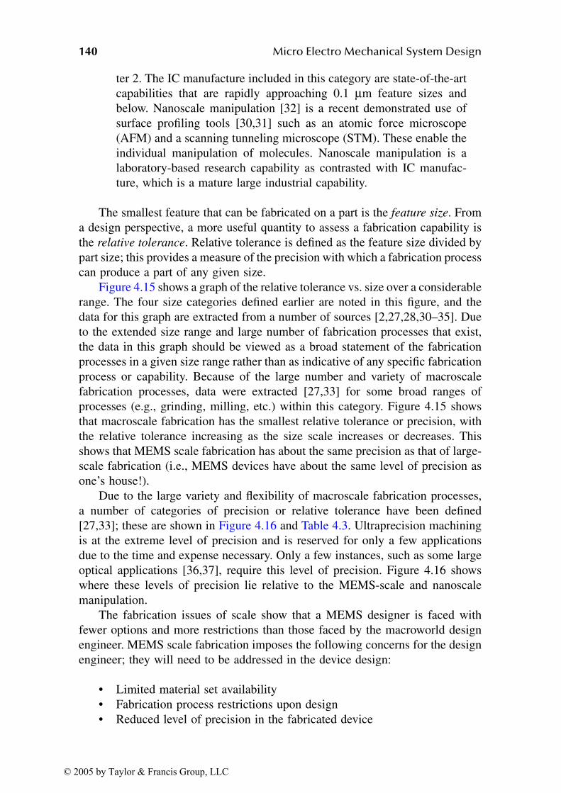
140 Micro Electro Mechanical System Design
ter 2. The IC manufacture included in this category are state-of-the-artcapabilities that are rapidly approaching 0.1 µm feature sizes andbelow. Nanoscale manipulation [32] is a recent demonstrated use ofsurface profiling tools [30,31] such as an atomic force microscope(AFM) and a scanning tunneling microscope (STM). These enable theindividual manipulation of molecules. Nanoscale manipulation is alaboratory-based research capability as contrasted with IC manufac-ture, which is a mature large industrial capability.
The smallest feature that can be fabricated on a part is the feature size. Froma design perspective, a more useful quantity to assess a fabrication capability isthe relative tolerance. Relative tolerance is defined as the feature size divided bypart size; this provides a measure of the precision with which a fabrication processcan produce a part of any given size.
Figure 4.15 shows a graph of the relative tolerance vs. size over a considerablerange. The four size categories defined earlier are noted in this figure, and thedata for this graph are extracted from a number of sources [2,27,28,30–35]. Dueto the extended size range and large number of fabrication processes that exist,the data in this graph should be viewed as a broad statement of the fabricationprocesses in a given size range rather than as indicative of any specific fabricationprocess or capability. Because of the large number and variety of macroscalefabrication processes, data were extracted [27,33] for some broad ranges ofprocesses (e.g., grinding, milling, etc.) within this category. Figure 4.15 showsthat macroscale fabrication has the smallest relative tolerance or precision, withthe relative tolerance increasing as the size scale increases or decreases. Thisshows that MEMS scale fabrication has about the same precision as that of large-scale fabrication (i.e., MEMS devices have about the same level of precision asone’s house!).
Due to the large variety and flexibility of macroscale fabrication processes,a number of categories of precision or relative tolerance have been defined[27,33]; these are shown in Figure 4.16 and Table 4.3. Ultraprecision machiningis at the extreme level of precision and is reserved for only a few applicationsdue to the time and expense necessary. Only a few instances, such as some largeoptical applications [36,37], require this level of precision. Figure 4.16 showswhere these levels of precision lie relative to the MEMS-scale and nanoscalemanipulation.
The fabrication issues of scale show that a MEMS designer is faced withfewer options and more restrictions than those faced by the macroworld designengineer. MEMS scale fabrication imposes the following concerns for the designengineer; they will need to be addressed in the device design:
• Limited material set availability• Fabrication process restrictions upon design• Reduced level of precision in the fabricated device
© 2005 by Taylor & Francis Group, LLC
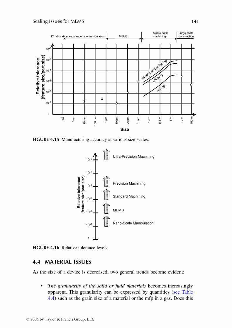
Scaling Issues for MEMS 141
4.4 MATERIAL ISSUES
As the size of a device is decreased, two general trends become evident:
• The granularity of the solid or fluid materials becomes increasinglyapparent. This granularity can be expressed by quantities (see Table4.4) such as the grain size of a material or the mfp in a gas. Does this
FIGURE 4.15 Manufacturing accuracy at various size scales.
FIGURE 4.16 Relative tolerance levels.
° 1A
1n
m
10
nm
10
0 n
m
1µ
m
10
µm
10
0µ
m
1 m
m
1 c
m
0.1
m
1 m
10
m
10
0 m
Size
Rela
tive t
ole
ran
ce
(featu
re s
ize/p
art
siz
e)
10-6
10-5
10-4
10-3
10-2
10-1
1
Macro-scale
machining
Large scale
constructionMEMSIC fabrication and nano-scale manipulation
XX
milli
ng
lapping and p
olishing
grinding
Re
lati
ve
to
lera
nc
e
(featu
re s
ize/p
art
siz
e)
10 -6
10 -5
10 -4
10 -3
10 -2
10 -1
1
Ultra-Precision Machining
Precision Machining
Standard Machining
MEMS
Nano-Scale Manipulation
© 2005 by Taylor & Francis Group, LLC
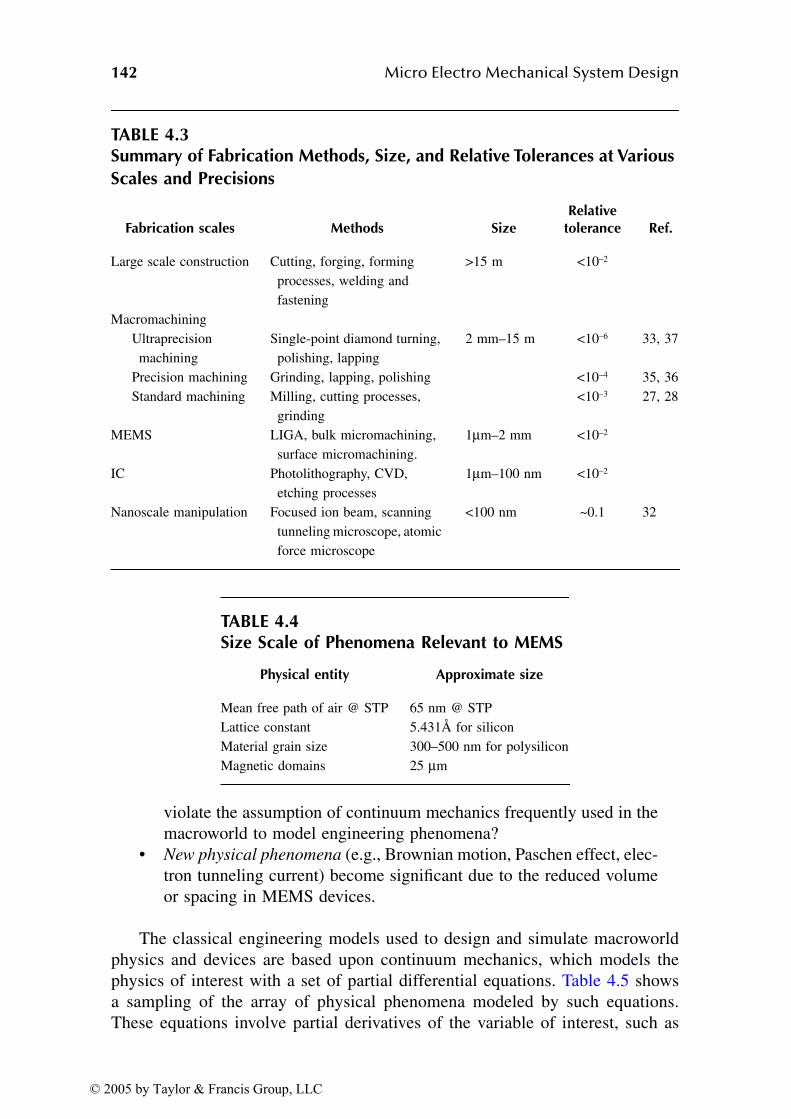
142 Micro Electro Mechanical System Design
violate the assumption of continuum mechanics frequently used in themacroworld to model engineering phenomena?
• New physical phenomena (e.g., Brownian motion, Paschen effect, elec-tron tunneling current) become significant due to the reduced volumeor spacing in MEMS devices.
The classical engineering models used to design and simulate macroworldphysics and devices are based upon continuum mechanics, which models thephysics of interest with a set of partial differential equations. Table 4.5 showsa sampling of the array of physical phenomena modeled by such equations.These equations involve partial derivatives of the variable of interest, such as
TABLE 4.3Summary of Fabrication Methods, Size, and Relative Tolerances at Various
Scales and Precisions
Fabrication scales Methods SizeRelative
tolerance Ref.
Large scale construction Cutting, forging, forming processes, welding and fastening
>15 m <10–2
MacromachiningUltraprecisionmachining
Single-point diamond turning, polishing, lapping
2 mm–15 m <10–6 33, 37
Precision machining Grinding, lapping, polishing <10–4 35, 36Standard machining Milling, cutting processes,
grinding<10–3 27, 28
MEMS LIGA, bulk micromachining, surface micromachining.
1µm–2 mm <10–2
IC Photolithography, CVD, etching processes
1µm–100 nm <10–2
Nanoscale manipulation Focused ion beam, scanning tunneling microscope, atomic force microscope
<100 nm ~0.1 32
TABLE 4.4Size Scale of Phenomena Relevant to MEMS
Physical entity Approximate size
Mean free path of air @ STP 65 nm @ STPLattice constant 5.431Å for siliconMaterial grain size 300–500 nm for polysiliconMagnetic domains 25 µm
© 2005 by Taylor & Francis Group, LLC

Scaling Issues for MEMS 143
stress, displacement, or temperature, and some parameters (i.e., modulus ofelasticity, heat transfer coefficients, speed of sound in a media) that model thedomain that the set of equations govern. For these equations to be easily solved,the parameters must be known and the variable of interest smoothly varyingover the domain of interest (i.e., differentiable). If a material is discrete or
TABLE 4.5Physical Phenomena Modeled by Continuum Mechanics
Physical phenomenon Partial differential equation
Three-dimensional heat flow
Three-dimensional wave equation
Elastic equations of equilibrium for solid mechanics
Maxwell’s free space electromagnetic equations
Navier–Stokes equations for compressible fluid dynamics
∂∂ = ∇
= ∂∂ + ∂
∂ + ∂∂
u
tc u
cu
x
u
y
u
z
2 2
22
2
2
2
2
2
∂∂ = ∇
= ∂∂ + ∂
∂ + ∂∂
2
2
2 2
22
2
2
2
2
2
u
tc u
cu
x
u
y
u
z
∂∂ + ∂
∂ + ∂∂ + =
∂∂ + ∂
∂ + ∂∂
σ τ τ
τ σ τ
x yx zx
x
xy y zy
x y zF
x y z
0
++ =∂
∂ + ∂∂ + ∂
∂ + =
F
x y zF
y
xz yz z
z
0
0τ τ σ
∇ ⋅ ( ) =∇ ⋅ =∇ × = − ∂
∂∇ × = + ∂ ( )
∂
ε ρ
µε
0
0
0
0
E
B
EB
B E
t
Jt
ρ
µ λ
∂∂ + ⋅ ∇( )
= −∇ +
−∇ × ∇ ×( ) + ∇ +
VV V F
V
tP ⋯
2µµ( ) ∇ ⋅ V
© 2005 by Taylor & Francis Group, LLC

144 Micro Electro Mechanical System Design
discontinuous (e.g., granular), it is more difficult to model the system with acontinuum mechanics approach.
As one tries to design and model systems on smaller scales, a certain gran-ularity of the physics is observed. In Chapter 2, the material structures of crys-talline, polycrystalline, and amorphous were discussed. (Figure 2.2 illustratesthese three material structures.) The spacing of atoms in crystalline and amor-phous materials is at the atomic scale (i.e., <1 nm). The size of the individualcrystals in a polycrystalline material are on the order of 100 to 500 nm, dependingupon the material processing used. Many materials of engineering significanceare polycrystalline. The physical parameters used to describe material behavior(e.g., Young’s modulus, speed of sound) in a continuum mechanics model arestatistical averages of the effects of the individual grains or molecules of materialwithin a large object (relative to the grain size).
For example, for a macrodevice that is 2 cm wide with a 500 nm grain size,the statistically averaged property representing a parameter such as Young’smodulus is adequate. However, a 2-µm wide microdevice contains only a fewgrains of material, and a statistically averaged approximation of a material prop-erty is not adequate. Research has been ongoing to measure microscale effects[42]; develop theories that apply at the microscale [43,44]; and incorporate theseeffects into simulations of the microscale phenomena [45].
The statistically averaged assumption also plays a role in the failure modelof materials. The stress at which a material yields or fails is quantified by theparameters, yield strength, Sy, or failure strength, Su. These parameters also havestatistics in their origin. A material has a certain number of defects in the materialstructure (e.g., crystal lattice imperfections, corrosion products in the grain bound-aries) that give rise to locations at which a material will yield or ultimately fail.These defects are assumed to be statistically distributed throughout the material.The defect density of a material and statistical process control is frequently usedin the microelectronic community [46] in assessments and modeling of the yield(i.e., percentage of good devices manufactured) of their processes. A potential
advantage of scaling devices down to densities approaching the defect densityof the material is that devices could be produced with a low defect rate.
4.5 NEWLY RELEVANT PHYSICAL PHENOMENA
Several new phenomena are enabled or become relevant at the MEMS scale.The three briefly discussed next are examples of such phenomena, which gainimportance because of the size of a MEMS device or the small gaps used inMEMS devices.
• Brownian noise. Also called thermal noise or Johnson noise for elec-trical systems, Brownian noise is a low-level noise present in electricaland mechanical systems. This thermal noise is present everywhere inthe environment and is due to such things as the vibrations of atomsin the materials from which a device is made and the environment in
© 2005 by Taylor & Francis Group, LLC
Scaling Issues for MEMS 145
which the device operates. This indicates that the thermal noise is afunction of temperature of these materials. The mechanisms that couplethese thermal vibrations to the mechanical or electrical device of inter-est are the energy dissipation mechanisms (i.e., damping for mechan-ical devices, resistance for electrical devices). As a device is reducedin size, these thermal noises or vibrations become significant forMEMS scale sensors. A detailed discussion of Brownian noise is inthe chapter on MEMS sensors.
• Paschen’s effect. The phenomenon that the breakdown voltage in a gapincreases as the product of the pressure of the gas in the gap and gapspacing is reduced was discovered in 1889 [19]. This phenomenon iseffective when the gap size is very small (<2 µm), which is typical ofMEMS devices. This enables increased effectiveness of electrostaticactuation as discussed in detail in Section 4.1.5.
• Electron tunneling current. Quantum entities such as electrons can“tunnel” across a very small gap (on the order of nanometers) due tothe uncertainty in the wave description of quantum mechanical entities.This especially appears to be strange due to the barrier of classicalphysics in which like charges repel. This phenomenon can be used inMEMS devices as a very sensitive displacement transduction methodcapable of resolving displacements on the order of 0.01 nm. A MEMScantilever can be fabricated with a tip suitable for tunneling that iselectrostatically brought within operating distance for this phenomenonto be effective. The tunneling phenomenon will be discussed in moredetail in the chapter on MEMS sensors.
4.6 SUMMARY
A MEMS designer needs to be aware of a number of wide ranging issues andcannot rely solely on macroworld engineering experiences and training whenconsidering the implementation of a MEMS design. System parameters willchange in relative importance as the system scale is reduced. Table 4.6 showsfour quantities that can be directly or indirectly related to actuation forces (i.e.,gravity, surface tension, electrostatic, magnetic) in a device. If these forces allscaled in the same manner, heuristic macroworld intuition would be valid; how-ever, these forces all scale differently.
Gravity forces become increasingly small with reduced size, and surfacetension increases in importance. Surface tension forces can be used for assemblyof devices; however, they can be a concern during MEMS fabrication releaseprocesses. Also, the table shows that the electric and magnetic fields and theforces derived from them scale differently, with the magnetic field forces notdepending on scale. Table 4.7 summarizes a number of scaling effects for mechan-ical, fluidic, and thermal systems. The data in this table show that mechanicaland thermal time constants are reduced for MEMS systems, and regimes ofoperation for thermal and fluidic systems are different at MEMS scale. The
© 2005 by Taylor & Francis Group, LLC
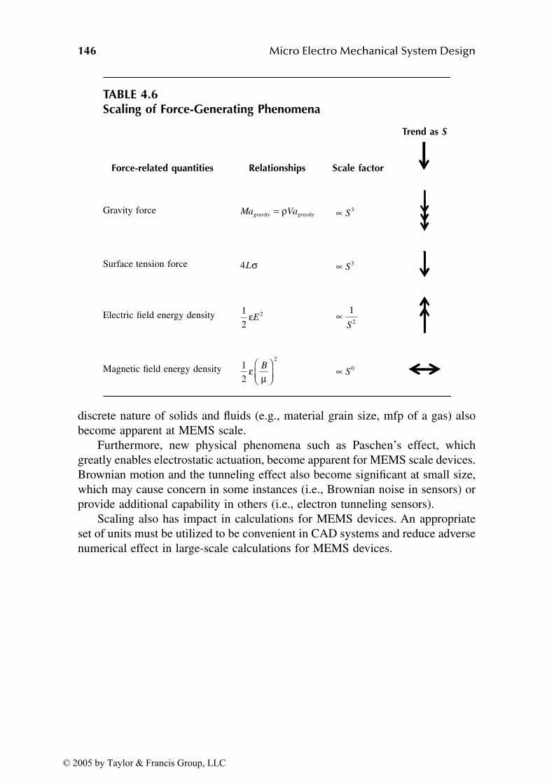
146 Micro Electro Mechanical System Design
discrete nature of solids and fluids (e.g., material grain size, mfp of a gas) alsobecome apparent at MEMS scale.
Furthermore, new physical phenomena such as Paschen’s effect, whichgreatly enables electrostatic actuation, become apparent for MEMS scale devices.Brownian motion and the tunneling effect also become significant at small size,which may cause concern in some instances (i.e., Brownian noise in sensors) orprovide additional capability in others (i.e., electron tunneling sensors).
Scaling also has impact in calculations for MEMS devices. An appropriateset of units must be utilized to be convenient in CAD systems and reduce adversenumerical effect in large-scale calculations for MEMS devices.
TABLE 4.6Scaling of Force-Generating Phenomena
Force-related quantities Relationships Scale factor
Trend as S
Gravity force
Surface tension force
Electric field energy density
Magnetic field energy density
Ma Vagravity gravity= ρ ∝ S3
4Lσ ∝ S3
1
22εE ∝ 1
2S
1
2
2
ε µB
∝ S0
© 2005 by Taylor & Francis Group, LLC
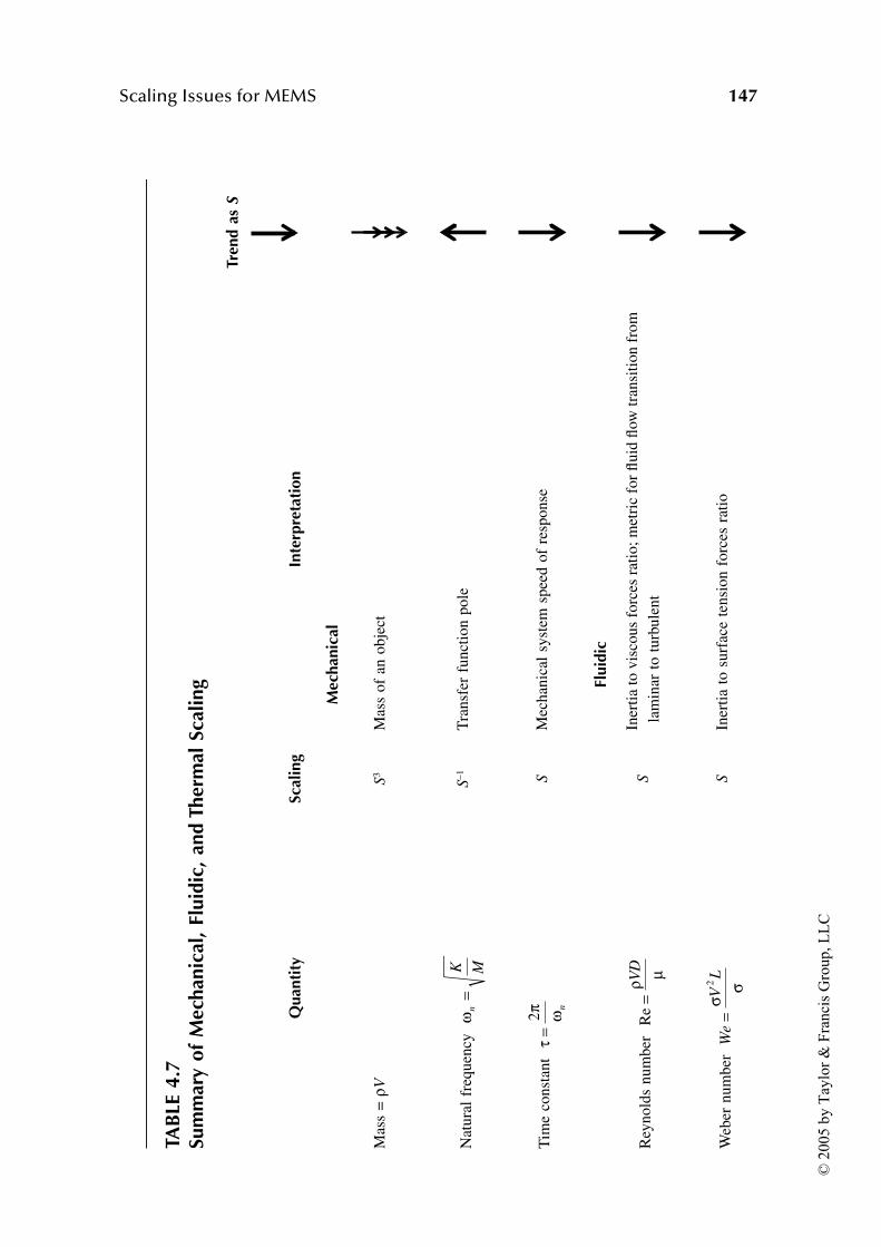
Scaling Issues for MEMS 147
TAB
LE 4
.7Su
mm
ary
of
Mec
han
ical
, Fl
uid
ic,
and
Th
erm
al S
cali
ng
Quan
tity
Scal
ing
Inte
rpre
tati
on
Tren
d a
s S
Mec
han
ical
Mas
s =
ρVS
3M
ass
of a
n ob
ject
Nat
ural
fre
quen
cy
S–1
Tra
nsfe
r fu
nctio
n po
le
Tim
e co
nsta
nt
SM
echa
nica
l sy
stem
spe
ed o
f re
spon
se
Fluid
ic
Rey
nold
s nu
mbe
r S
Iner
tia to
vis
cous
for
ces
ratio
; met
ric
for
flui
d flo
w tr
ansi
tion
from
la
min
ar t
o tu
rbul
ent
Web
er n
umbe
r S
Iner
tia t
o su
rfac
e te
nsio
n fo
rces
rat
io
ω n
K M=
τπ ω=2
n
Re
=ρ µVD
We
VL
=σ σ2
© 2
005 b
y T
aylo
r &
Fra
nci
s G
roup, L
LC
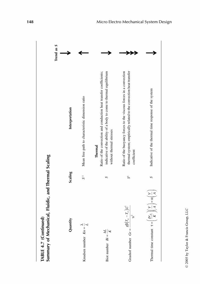
148 Micro Electro Mechanical System Design
TAB
LE 4
.7 (
Co
nti
nu
ed)
Sum
mar
y o
f M
ech
anic
al,
Flu
idic
, an
d T
her
mal
Sca
lin
g
Quan
tity
Scal
ing
Inte
rpre
tati
on
Tren
d a
s S
Knu
dsen
num
ber
S–1
Mea
n fr
ee p
ath
to c
hara
cter
istic
dim
ensi
on r
atio
Ther
mal
Bio
t nu
mbe
r S
Rat
io o
f th
e co
nvec
tion
and
cond
uctio
n he
at t
rans
fer
coef
ficie
nts;
indi
cativ
e of
the
abili
ty o
f a
body
to c
ome
to th
erm
al e
quili
briu
m
with
out
ther
mal
str
esse
s
Gra
shof
num
ber
S3
Rat
io o
f th
e bu
oyan
cy f
orce
s to
the
visc
ous
forc
es in
a c
onve
ctio
nth
erm
al s
yste
m; e
mpi
rica
lly re
late
d to
the
conv
ectio
n he
at tr
ansf
er
coef
ficie
nt
The
rmal
tim
e co
nsta
nt
SIn
dica
tive
of t
he t
herm
al t
ime
resp
onse
of
the
syst
em
Kn
L=λ
Bi
hL K= G
rg
TT
Lw
=− (
) ∞β
υ3
2
τρ
α=
=
c K
V A
V A
p
© 2
005 b
y T
aylo
r &
Fra
nci
s G
roup, L
LC
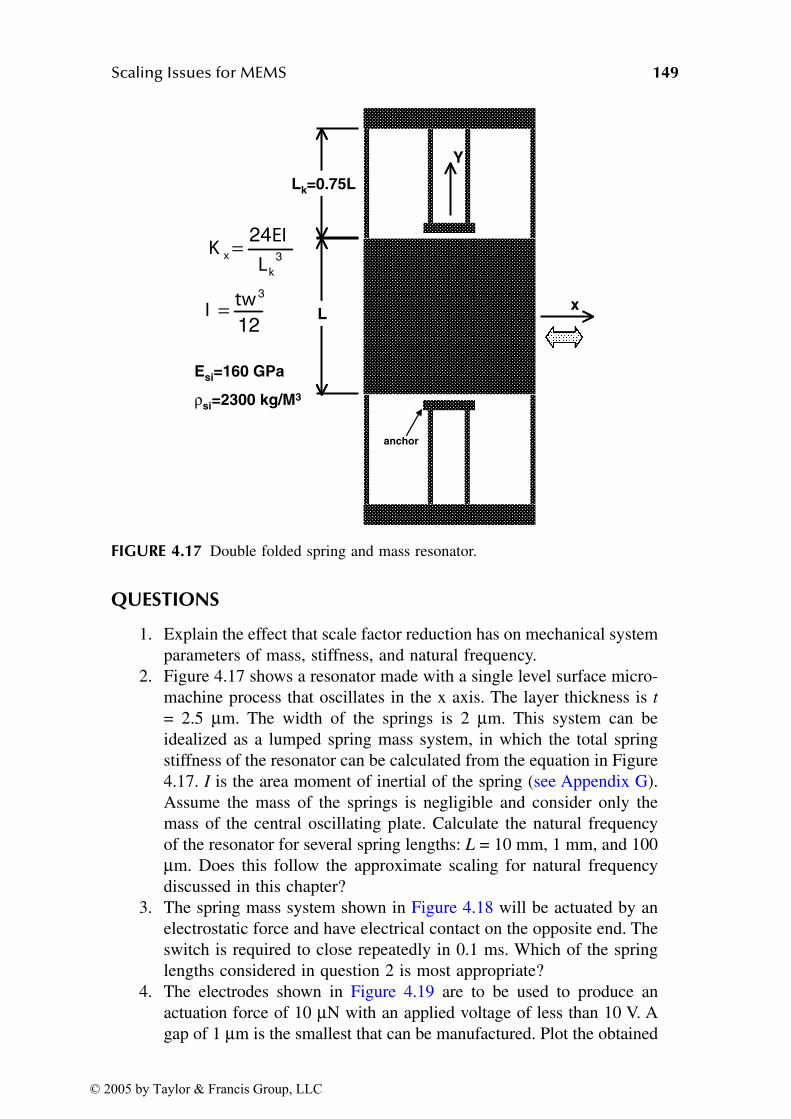
Scaling Issues for MEMS 149
QUESTIONS
1. Explain the effect that scale factor reduction has on mechanical systemparameters of mass, stiffness, and natural frequency.
2. Figure 4.17 shows a resonator made with a single level surface micro-machine process that oscillates in the x axis. The layer thickness is t= 2.5 µm. The width of the springs is 2 µm. This system can beidealized as a lumped spring mass system, in which the total springstiffness of the resonator can be calculated from the equation in Figure4.17. I is the area moment of inertial of the spring (see Appendix G).Assume the mass of the springs is negligible and consider only themass of the central oscillating plate. Calculate the natural frequencyof the resonator for several spring lengths: L = 10 mm, 1 mm, and 100µm. Does this follow the approximate scaling for natural frequencydiscussed in this chapter?
3. The spring mass system shown in Figure 4.18 will be actuated by anelectrostatic force and have electrical contact on the opposite end. Theswitch is required to close repeatedly in 0.1 ms. Which of the springlengths considered in question 2 is most appropriate?
4. The electrodes shown in Figure 4.19 are to be used to produce anactuation force of 10 µN with an applied voltage of less than 10 V. Agap of 1 µm is the smallest that can be manufactured. Plot the obtained
FIGURE 4.17 Double folded spring and mass resonator.
xL
12
24
3
3
twI
L
EIK
k
x
=
=
Lk=0.75L
Esi=160 GPa
ρsi=2300 kg/M3
Y
anchor
© 2005 by Taylor & Francis Group, LLC

150 Micro Electro Mechanical System Design
force vs. the gap for 10 V applied. What gap size is recommended? Ifthe gap cannot be made small enough, what are the possible alternatives?
5. Calculate the Reynolds number for flow in a square channel of lengthL on a side for a range of L = 10 mm, 1 mm, 100 µm, and 10 µm.
6. Calculate the Knudsen number and determine the gas flow regime forthe following situations:a. A magnetic disk drive head with a “fly” height of 10 nm. Assume
mfp of air at standard temperature and pressure.
FIGURE 4.18 Actuated spring mass electrical relay contacts.
FIGURE 4.19 Electrostatic gap for actuation.
x
Y
ElectrostaticActuationForce
ElectricalContacts
= −g
2F
1
2
εAV2
es
F/m12-permittivity = 8.84e-ε
electrostatic force–esF
Voltage–V
2mµelectrode area = 6000 –A
gap–g
g
V
© 2005 by Taylor & Francis Group, LLC

Scaling Issues for MEMS 151
b. Gas flow over a MEMS feature (i.e., a 2-µm step) in a CVD reactoroperating at low pressure with a gas mfp of 90 λm
c. Air at STP flowing through a 50-µm MEMS channeld. Air at STP between the substrate and an oscillating MEMS structure
(i.e., gap of 6 µm)7. What will be the effect of increasing pressure of a gas have on the
mean free path and the Knudson number? 8. Calculate the Reynolds number and the flow regime for the following
situations.a. A bacteria (assume 2-µm size) moving at a velocity of 0.1 µm/s in
waterb. Water flowing 20 mm/s in a 2-mm pipec. Water flowing at 10 µm/s in a 10-µm channel
9. Explain the effect of the volume/surface area ratio on the thermalcharacteristics of a system as the scale is reduced.
10. An ink-jet print head is schematically shown in Figure 4.20. The inkjet consists of a heating element, ink channels, and a nozzle. Assumethe ink has the fluidic properties of water (Table 4.8). The ink is ejecteddue to bubble formation by heating the ink. When the bubble collapses,the ink channel refills with ink. The square ink channels in the printhead are 20 µm. The ink jet ejects a 10-pL drop on each operatingcycle. Calculate the following:a. The Reynolds number in the ink-jet nozzle when the 10-pL drop is
ejected in 20 µs
FIGURE 4.20 Thermal ink-jet print head.
heater
ink
(a) Thermal ink jet
20 µm
(b) Thermally ejecting a drop
(c) Bubble collapse – ink refilling
© 2005 by Taylor & Francis Group, LLC
152 Micro Electro Mechanical System Design
b. The Reynolds number in the ink jet when the ink channel is refillingupon the collapse of the bubble. The refilling operation takes 200 µs.
c. From a thermal-scaling perspective, why are such rapid cycle timespossible in the ink jet?
d. If the ink-jet channels were decreased in size, would the thermalcycle time increase or decrease?
11. A chemical sample has a concentration of 10–6 mol/l. The detectionsystem has a detection sensitivity of ten molecules per liter.a. What volume of sample is required?b. If that volume is too big, what should be done?c. What effect would increasing the sensitivity have on the required
sample size?
REFERENCES
1. J.W. Judy, Microelectromechanical systems (MEMS): fabrication, design andapplications, Smart Mater. Struct., 10, 1115–1134, 2001.
2. M.J. Madou, Fundamentals of Microfabrication, The Science of Miniaturization,2nd ed., CRC Press, Boca Raton, FL, 2000.
3. J.D. Meindel, Q. Chen, J.A. Davis, Limits on silicon nanoelectronics for terascaleintegration, Science, 293, 2044–2049, 14, September 2001.
4. W.T. Thompson, Theory of Vibrations with Applications, Prentice Hall, Inc., Engle-wood Cliffs, NJ.
5. A. Lawrence, Modern Inertial Technology, Navigation, Guidance, and Control,2nd ed., Springer-Verlag, Heidelberg, 156, 1998.
6. D.M. Tanner, N.F. Smith, L.W. Irwin. W.P. Eaton, K.S. Helgesen, J.J. Clement,W.M. Miller, J.A. Walraven, K.A. Peterson, P. Tangyunyong, M.T. Dugger, S.L.Miller, MEMS reliability: infrastructure, test structures, experiments, and failuremodes, SAND2000-0091, Sandia National Laboratories, January 2000.
7. N. Barbour, J. Connelly, J. Gilmore, P. Greiff, A. Kourepenis, M. Weinberg,Micromechanical silicon instrument and systems development at per laboratory,AAIA Guidance, Navigation Control Conf., San Diego, CA, 20–31 July 1996.
8. D.M. Tanner, J.A. Walraven, K.S. Helgesen, L.W. Irwin, D.L. Gregory, J.R. Stake,N.F. Smith, MEMS a vibration environment, Proc. IRPS, 139–145, 2000.
TABLE 4.8Water and Air Properties
Property Water Air @ STP
Mean free path l nm — 0.65Surface tension s N/m 72 × 10–3 —Dynamic viscosity m kg/(m s) 10–3 1.85 × 10⁻⁵
Kinematic viscosity g m2/s 10–6 1.43 × 10⁻⁵
Density r kg/m3 1000 —
© 2005 by Taylor & Francis Group, LLC
Scaling Issues for MEMS 153
9. D.M. Tanner, J.A. Walraven, K. Helgesen, L.W. Irwin, F. Brown, N.F. Smith, N.Masters, MEMS reliability in shock environments, Proc. IRPS, 129–138, 2000.
10. C.M. Harris, C.E. Crede, Shock and Vibration Handbook, 2nd ed., McGraw-HillBook Company, New York, 1976.
11. J.P. Holman, Heat Transfer, 6th ed., McGraw–Hill Book Company, New York, 1986.12. G.E. Karniadakis, A. Beskok, Micro Flows: Fundamentals and Simulation,
Springer, New York, 2002.
13. P. Bahukudumbi, A. Beskok, A phenomenological lubrication model of the entireKnudsen regime, J. Micromech., Microeng., 13, 873–884, 2003.
14. J.L. Dohner, M. Jenkins, T. Walsh, K. Klody, Anomalies in the theory of viscousenergy losses due to shear in rotational MEMS resonators, Sandia National Lab-oratories Report, SAND2003-4314, December 2003.
15. R.A. Syms, E.M. Yeatman, V.M. Bright, G.M. Whitesides, Surface tension-pow-ered self-assembly of microstructures — the state of the art, J. MEMS, 12(4),August 2003.
16. R.J. Smith, Circuits, Devices, and Systems, John Wiley & Sons Inc., New York,1966.
17. C.T.A. Johnk, Engineering Electromagnetic Fields and Waves, John Wiley & Sons,New York, 1988.
18. F. Paschen, Über die zum Funkenübergang in luft, Wasserstoff and Kohlensäurebei verschiedenen Drücken erforderliche Potentialdifferenz, Weid. Ann. der Phys-
ick, 37, 69, 1889.19. S.F. Bart, T.A. Lober, R.T. Howe, J.H. Lang, M.F. Schlecht, Design considerations
for micromachined electric actuators, Sensors Actuators, 14, 269–292, 1988.20. B. Bollee, Electrostatic motors, Philips Tech. Rev., 30, 178–194, 1969.21. I.J. Busch-Vishniac, The case for magnetically driven microactuators, Sensors
Actuators A, A33, 207–220, 1992.22. A. O’Keefe, D.A.G. Deacon, Cavity ring-down optical spectrometer for absorption
measurements using pulsed laser sources, Rev. Sci. Instrum., 59, 2544–2551, 1988.23. P.F. van Kessel, L.J. Hornbeck. R.E. Meier, M.R. Douglass, A MEMS-based
projection display, Proc. IEEE 86, 1687–1704, 1998.24. D.M. Bloom, The grating light valve: revolutionizing display technology, Proc.
SPIE, 3013, 165–171, February 1997.25. A. Manz, N. Graber, H.M. Widmer, Miniaturized total chemical analysis systems:
a novel concept for chemical sensing, Sensors Actuators, B1, 244–248, 1990.26. K. Petersen, W. McMillan, G. Kovacs, A. Northrup, L. Christel, F. Pourahmadi,
The promise of miniaturized clinical diagnostic systems, IVD Technol., July 1998.
27. E. Oberg, Ed., Machinery’s Handbook, 24th ed., Industrial Press, New York, 2000.28. G. Boothroyd, W.A. Knight, Fundamentals of Machining and Machine Tools,
Marcel Dekker, New York, 1989.29. G.E. Moore, Cramming more components onto integrated circuits, Electronics,
38(8), April 19, 1965.30. Y. Martin, C.C. Williams, H.K. Wickramasinghe, Atomic force microscope force
mapping and profiling on a sub 100Å scale, J. Appl. Phys., 61(9), 4723, 1987.31. G. Benning, H. Rohrer, Scanning tunneling microscopy — from birth to adoles-
cence, Rev. Mod. Phys, 59(3), Part 1, 615, 1987.32. J.A. Stroscio, D.M. Eigler, Atomic and molecular manipulation with the scanning
tunneling microscope, Science, 254, 1319–1326, 1991.
© 2005 by Taylor & Francis Group, LLC

154 Micro Electro Mechanical System Design
33. N. Taniguchi, Current Status in and future trends of ultraprecision machining andultrafine materials processing, Ann. CIRP, 32(2), 573–582, 1983.
34. G.L. Benevides, D.P. Adams, P. Yang, Meso-scale machining capabilities andissues, Sandia National Laboratories report SAND2000-1217C, 2000.
35. A.H. Slocum, Precision Machine Design, Prentice Hall, Englewood Cliffs, NJ,1992.
36. A.H. Slocum, Precision machine design: macromachine design philosophy andits applicability to the design of micromachines, Proc. IEEE Micro Electro
Mechanical Syst. (MEMS ’92). Travemunde, Germany, 1992, 37–42.37. R. Donaldson, S. Patterson, Design and construction of a large-axis diamond
turning machine, UCRL-89738, NTIS, 1983.38. W.H. Press, B.P. Flannery, S.A. Teukolsky, W.T. Vetterling, Numerical Recipes in
C, The Art of Scientific Computing, Cambridge University Press, 1990.39. K.J. Bathe, E.L. Wilson, Numerical Methods in Finite Element Analysis, Prentice
Hall, Inc., Englewood Cliffs, NJ, 1976. 40. O.C. Zienkiewicz, The Finite Element Method, McGraw-Hill Book Company,
New York.41. ANSYS proposed system of units for MEMS scale simulation:
http://www.ansys.com/ansys/mems/mems_key_features/key_feature_units.htm.42. W.G. Knauss, I. Chasiotis, Y. Huang, Mechanical measurements at the micron and
nanometer scales, Mechanics Mater., 35, 217–231, 2003.43. J.W. Hutchinson, Plasticity at the micron scale, Int. J. Solids Struct., 37, 225–238,
2000.44. W.W. Van Arsdell, S.B. Brown, Subcritical crack growth in silicon MEMS, J.
MEMS, 8(3), 319–327, September 1999.45. S. Quilici, G. Cailletaud, FE simulation of macro-, meso- and micro-scales in
polycrystalline plasticity, Computational Mater. Sci., 16, 383–390, 1999.46. W.R. Runyan, K.E. Bean, Semiconductor Integrated Circuit Processing Technol-
ogy, Addison-Wesley, Reading, MA, 1990.
© 2005 by Taylor & Francis Group, LLC
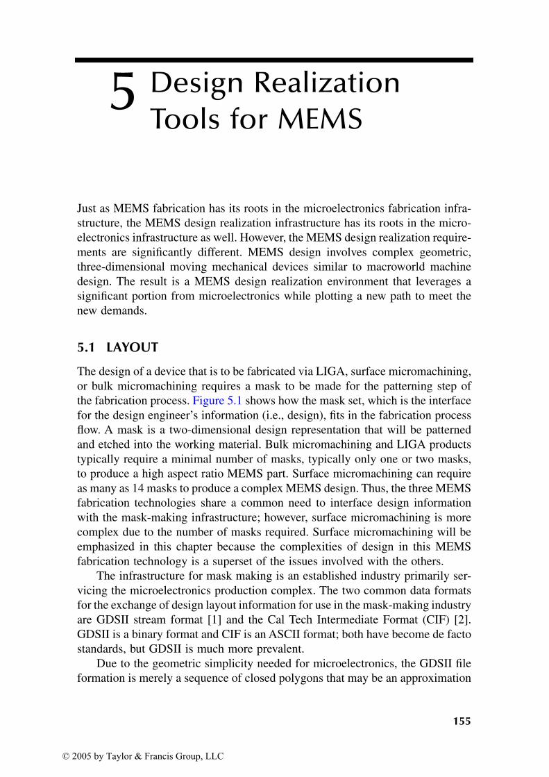
155
5 Design Realization Tools for MEMS
Just as MEMS fabrication has its roots in the microelectronics fabrication infra-
structure, the MEMS design realization infrastructure has its roots in the micro-
electronics infrastructure as well. However, the MEMS design realization require-
ments are significantly different. MEMS design involves complex geometric,
three-dimensional moving mechanical devices similar to macroworld machine
design. The result is a MEMS design realization environment that leverages a
significant portion from microelectronics while plotting a new path to meet the
new demands.
5.1 LAYOUT
The design of a device that is to be fabricated via LIGA, surface micromachining,
or bulk micromachining requires a mask to be made for the patterning step of
the fabrication process. Figure 5.1 shows how the mask set, which is the interface
for the design engineer’s information (i.e., design), fits in the fabrication process
flow. A mask is a two-dimensional design representation that will be patterned
and etched into the working material. Bulk micromachining and LIGA products
typically require a minimal number of masks, typically only one or two masks,
to produce a high aspect ratio MEMS part. Surface micromachining can require
as many as 14 masks to produce a complex MEMS design. Thus, the three MEMS
fabrication technologies share a common need to interface design information
with the mask-making infrastructure; however, surface micromachining is more
complex due to the number of masks required. Surface micromachining will be
emphasized in this chapter because the complexities of design in this MEMS
fabrication technology is a superset of the issues involved with the others.
The infrastructure for mask making is an established industry primarily ser-
vicing the microelectronics production complex. The two common data formats
for the exchange of design layout information for use in the mask-making industry
are GDSII stream format [1] and the Cal Tech Intermediate Format (CIF) [2].
GDSII is a binary format and CIF is an ASCII format; both have become de facto
standards, but GDSII is much more prevalent.
Due to the geometric simplicity needed for microelectronics, the GDSII file
formation is merely a sequence of closed polygons that may be an approximation
© 2005 by Taylor & Francis Group, LLC

156 Micro Electro Mechanical System Design
of the true geometry. However, current implementations of the GDSII file format
and the supporting translators enable a large number of line segments, which
enable a faithful representation of the desired geometry. A closed polygon is a
sequence of line segments that start and end at the same point (Figure 5.2).
Obviously, the complete suite of two- and three-dimensional geometries (e.g.,
circles, ellipses, curves, cubes, spheres, cylinders) standard in the macroworld
machine design infrastructure does not exist within the context of a GDSII file
format. Figure 5.3 shows the mask data preparation path between the CAD layout
tool and the GDSII file used by the mask supplier.
Current MEMS layout tools may have the ability to lay out complex geometric
entities such as circles, ellipses, and curves; however, when the data are exported
to a GDSII data file [1], the geometric entities are approximated by closed
FIGURE 5.1 Surface micromachining process cycle.
FIGURE 5.2 An example of a closed polygon approximation vs. the true geometric entity.
Thin film
formation
Wafer
Mask
Set
Photo-
lithography
Etching
Dicing and
packaging
Repeat N times
Geometric Entity (circle)
Closed Polygon
Representation
© 2005 by Taylor & Francis Group, LLC
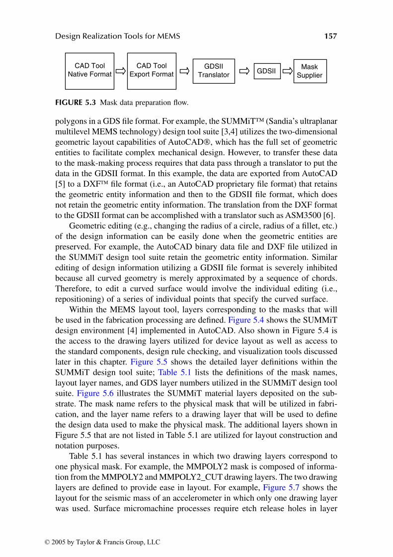
Design Realization Tools for MEMS 157
polygons in a GDS file format. For example, the SUMMiT™ (Sandia’s ultraplanar
multilevel MEMS technology) design tool suite [3,4] utilizes the two-dimensional
geometric layout capabilities of AutoCAD, which has the full set of geometric
entities to facilitate complex mechanical design. However, to transfer these data
to the mask-making process requires that data pass through a translator to put the
data in the GDSII format. In this example, the data are exported from AutoCAD
[5] to a DXF file format (i.e., an AutoCAD proprietary file format) that retains
the geometric entity information and then to the GDSII file format, which does
not retain the geometric entity information. The translation from the DXF format
to the GDSII format can be accomplished with a translator such as ASM3500 [6].
Geometric editing (e.g., changing the radius of a circle, radius of a fillet, etc.)
of the design information can be easily done when the geometric entities are
preserved. For example, the AutoCAD binary data file and DXF file utilized in
the SUMMiT design tool suite retain the geometric entity information. Similar
editing of design information utilizing a GDSII file format is severely inhibited
because all curved geometry is merely approximated by a sequence of chords.
Therefore, to edit a curved surface would involve the individual editing (i.e.,
repositioning) of a series of individual points that specify the curved surface.
Within the MEMS layout tool, layers corresponding to the masks that will
be used in the fabrication processing are defined. Figure 5.4 shows the SUMMiT
design environment [4] implemented in AutoCAD. Also shown in Figure 5.4 is
the access to the drawing layers utilized for device layout as well as access to
the standard components, design rule checking, and visualization tools discussed
later in this chapter. Figure 5.5 shows the detailed layer definitions within the
SUMMiT design tool suite; Table 5.1 lists the definitions of the mask names,
layout layer names, and GDS layer numbers utilized in the SUMMiT design tool
suite. Figure 5.6 illustrates the SUMMiT material layers deposited on the sub-
strate. The mask name refers to the physical mask that will be utilized in fabri-
cation, and the layer name refers to a drawing layer that will be used to define
the design data used to make the physical mask. The additional layers shown in
Figure 5.5 that are not listed in Table 5.1 are utilized for layout construction and
notation purposes.
Table 5.1 has several instances in which two drawing layers correspond to
one physical mask. For example, the MMPOLY2 mask is composed of informa-
tion from the MMPOLY2 and MMPOLY2_CUT drawing layers. The two drawing
layers are defined to provide ease in layout. For example, Figure 5.7 shows the
layout for the seismic mass of an accelerometer in which only one drawing layer
was used. Surface micromachine processes require etch release holes in layer
FIGURE 5.3 Mask data preparation flow.
CAD Tool
Native Format
CAD Tool
Export FormatGDSII
TranslatorGDSII
Mask
Supplier
© 2005 by Taylor & Francis Group, LLC
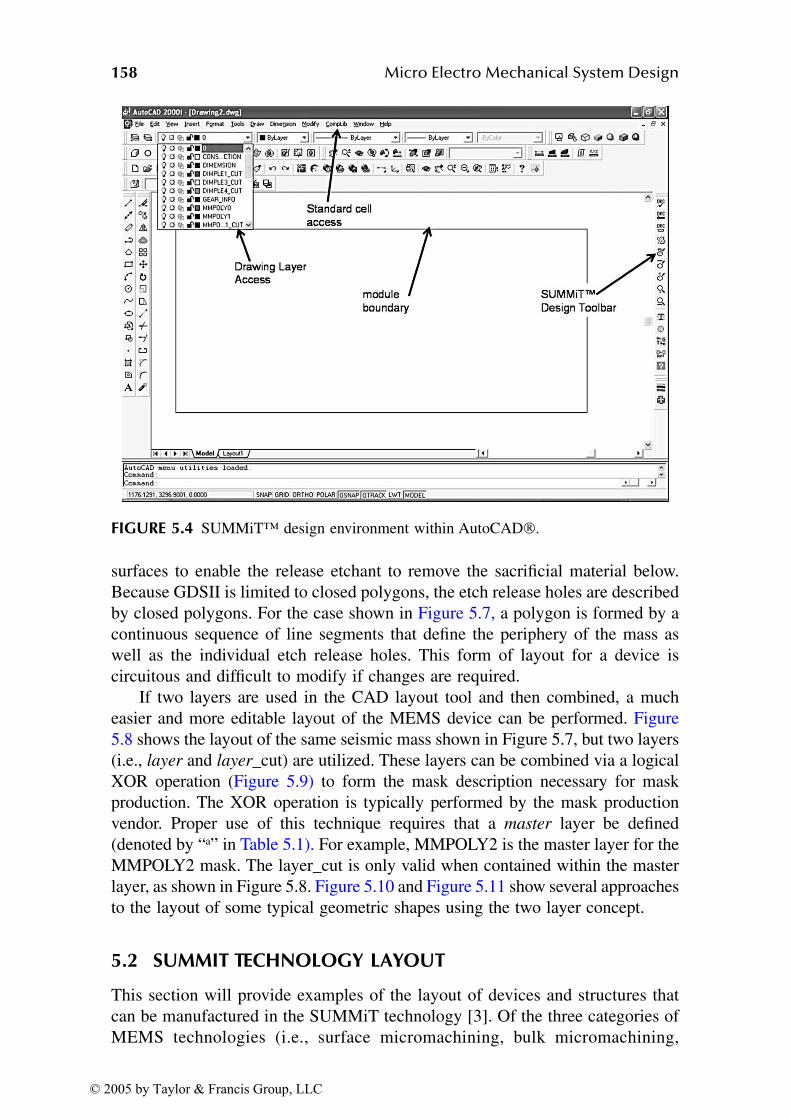
158 Micro Electro Mechanical System Design
surfaces to enable the release etchant to remove the sacrificial material below.
Because GDSII is limited to closed polygons, the etch release holes are described
by closed polygons. For the case shown in Figure 5.7, a polygon is formed by a
continuous sequence of line segments that define the periphery of the mass as
well as the individual etch release holes. This form of layout for a device is
circuitous and difficult to modify if changes are required.
If two layers are used in the CAD layout tool and then combined, a much
easier and more editable layout of the MEMS device can be performed. Figure
5.8 shows the layout of the same seismic mass shown in Figure 5.7, but two layers
(i.e., layer and layer_cut) are utilized. These layers can be combined via a logical
XOR operation (Figure 5.9) to form the mask description necessary for mask
production. The XOR operation is typically performed by the mask production
vendor. Proper use of this technique requires that a master layer be defined
(denoted by “a” in Table 5.1). For example, MMPOLY2 is the master layer for the
MMPOLY2 mask. The layer_cut is only valid when contained within the master
layer, as shown in Figure 5.8. Figure 5.10 and Figure 5.11 show several approaches
to the layout of some typical geometric shapes using the two layer concept.
5.2 SUMMIT TECHNOLOGY LAYOUT
This section will provide examples of the layout of devices and structures that
can be manufactured in the SUMMiT technology [3]. Of the three categories of
MEMS technologies (i.e., surface micromachining, bulk micromachining,
FIGURE 5.4 SUMMiT™ design environment within AutoCAD.
© 2005 by Taylor & Francis Group, LLC
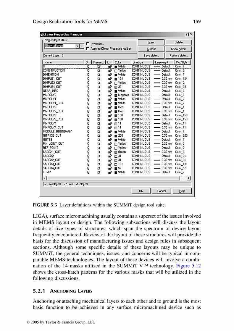
Design Realization Tools for MEMS 159
LIGA), surface micromachining usually contains a superset of the issues involved
in MEMS layout or design. The following subsections will discuss the layout
details of five types of structures, which span the spectrum of device layout
frequently encountered. Review of the layout of these structures will provide the
basis for the discussion of manufacturing issues and design rules in subsequent
sections. Although some specific details of these layouts may be unique to
SUMMiT, the general techniques, issues, and concerns will be typical in com-
parable MEMS technologies. The layout of these devices will involve a combi-
nation of the 14 masks utilized in the SUMMiT V™ technology. Figure 5.12
shows the cross-hatch patterns for the various masks that will be utilized in the
following discussions.
5.2.1 ANCHORING LAYERS
Anchoring or attaching mechanical layers to each other and to ground is the most
basic function to be achieved in any surface micromachined device such as
FIGURE 5.5 Layer definitions within the SUMMiT design tool suite.
© 2005 by Taylor & Francis Group, LLC
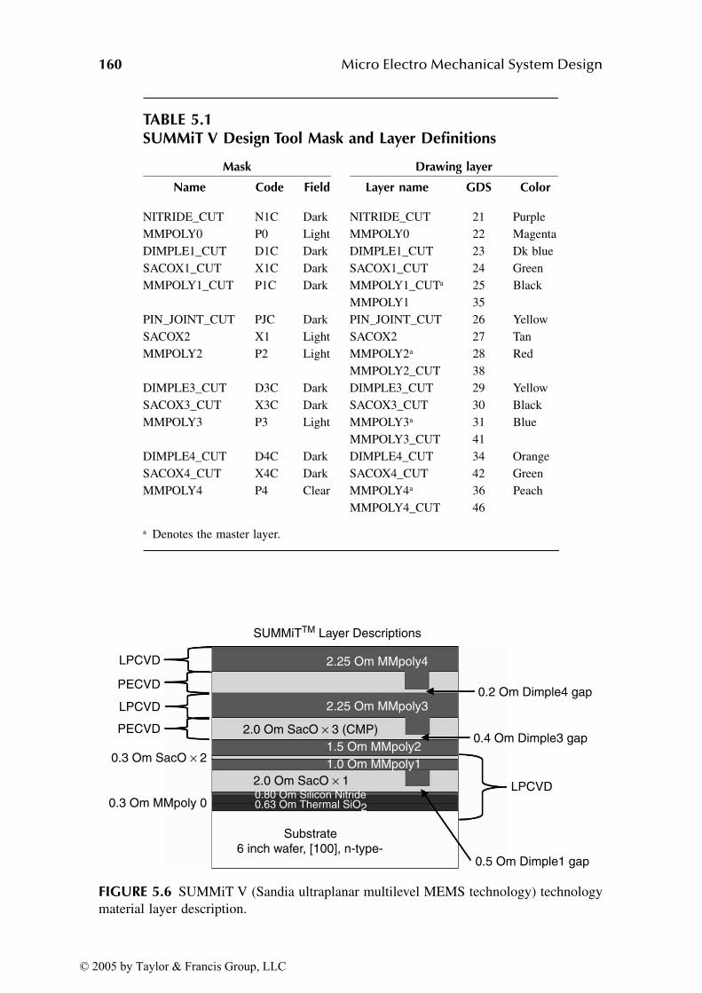
160 Micro Electro Mechanical System Design
TABLE 5.1SUMMiT V Design Tool Mask and Layer Definitions
Mask Drawing layer
Name Code Field Layer name GDS Color
NITRIDE_CUT N1C Dark NITRIDE_CUT 21 Purple
MMPOLY0 P0 Light MMPOLY0 22 Magenta
DIMPLE1_CUT D1C Dark DIMPLE1_CUT 23 Dk blue
SACOX1_CUT X1C Dark SACOX1_CUT 24 Green
MMPOLY1_CUT P1C Dark MMPOLY1_CUTa 25 Black
MMPOLY1 35
PIN_JOINT_CUT PJC Dark PIN_JOINT_CUT 26 Yellow
SACOX2 X1 Light SACOX2 27 Tan
MMPOLY2 P2 Light MMPOLY2a 28 Red
MMPOLY2_CUT 38
DIMPLE3_CUT D3C Dark DIMPLE3_CUT 29 Yellow
SACOX3_CUT X3C Dark SACOX3_CUT 30 Black
MMPOLY3 P3 Light MMPOLY3a 31 Blue
MMPOLY3_CUT 41
DIMPLE4_CUT D4C Dark DIMPLE4_CUT 34 Orange
SACOX4_CUT X4C Dark SACOX4_CUT 42 Green
MMPOLY4 P4 Clear MMPOLY4a 36 Peach
MMPOLY4_CUT 46
a Denotes the master layer.
FIGURE 5.6 SUMMiT V (Sandia ultraplanar multilevel MEMS technology) technology
material layer description.
LPCVD
PECVD
LPCVD
PECVD
LPCVD
0.3 Om SacO × 2
2.0 Om SacO × 3 (CMP)
2.0 Om SacO × 1
0.3 Om MMpoly 0
0.2 Om Dimple4 gap
0.4 Om Dimple3 gap
2.25 Om MMpoly4
SUMMiTTM Layer Descriptions
2.25 Om MMpoly3
1.5 Om MMpoly2
1.0 Om MMpoly1
Substrate
6 inch wafer, [100], n-type-0.5 Om Dimple1 gap
0.80 Om Silicon Nitride0.63 Om Thermal SiO2
© 2005 by Taylor & Francis Group, LLC
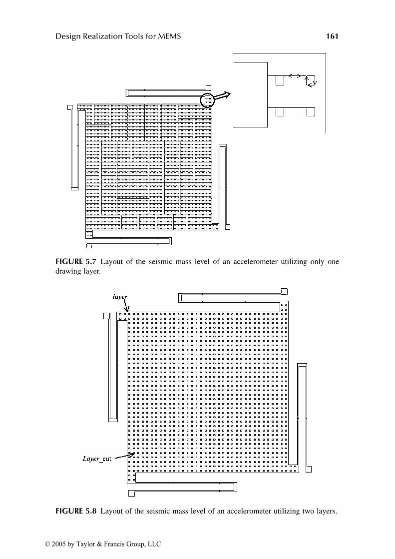
Design Realization Tools for MEMS 161
FIGURE 5.7 Layout of the seismic mass level of an accelerometer utilizing only one
drawing layer.
FIGURE 5.8 Layout of the seismic mass level of an accelerometer utilizing two layers.
© 2005 by Taylor & Francis Group, LLC
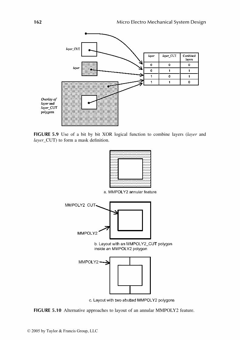
162 Micro Electro Mechanical System Design
FIGURE 5.9 Use of a bit by bit XOR logical function to combine layers (layer and
layer_CUT) to form a mask definition.
FIGURE 5.10 Alternative approaches to layout of an annular MMPOLY2 feature.
© 2005 by Taylor & Francis Group, LLC
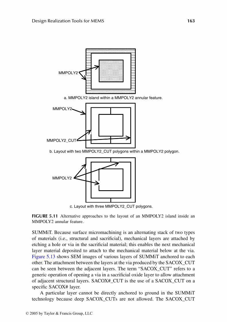
Design Realization Tools for MEMS 163
SUMMiT. Because surface micromachining is an alternating stack of two types
of materials (i.e., structural and sacrificial), mechanical layers are attached by
etching a hole or via in the sacrificial material; this enables the next mechanical
layer material deposited to attach to the mechanical material below at the via.
Figure 5.13 shows SEM images of various layers of SUMMiT anchored to each
other. The attachment between the layers at the via produced by the SACOX_CUT
can be seen between the adjacent layers. The term “SACOX_CUT” refers to a
generic operation of opening a via in a sacrificial oxide layer to allow attachment
of adjacent structural layers. SACOX#_CUT is the use of a SACOX_CUT on a
specific SACOX# layer.
A particular layer cannot be directly anchored to ground in the SUMMiT
technology because deep SACOX_CUTs are not allowed. The SACOX_CUT
FIGURE 5.11 Alternative approaches to the layout of an MMPOLY2 island inside an
MMPOLY2 annular feature.
a. MMPOLY2 island within a MMPOLY2 annular feature.
MMPOLY2
b. Layout with two MMPOLY2_CUT polygons within a MMPOLY2 polygon.
MMPOLY2
MMPOLY2_CUT
c. Layout with three MMPOLY2_CUT polygons.
MMPOLY2
© 2005 by Taylor & Francis Group, LLC
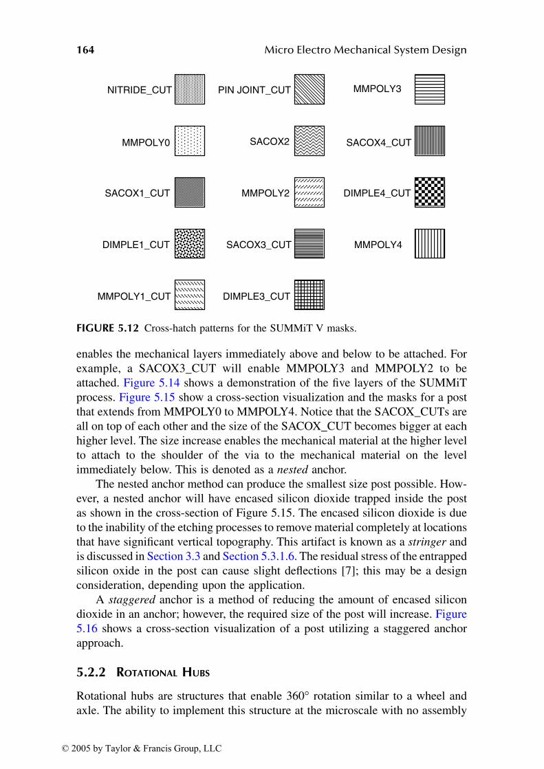
164 Micro Electro Mechanical System Design
enables the mechanical layers immediately above and below to be attached. For
example, a SACOX3_CUT will enable MMPOLY3 and MMPOLY2 to be
attached. Figure 5.14 shows a demonstration of the five layers of the SUMMiT
process. Figure 5.15 show a cross-section visualization and the masks for a post
that extends from MMPOLY0 to MMPOLY4. Notice that the SACOX_CUTs are
all on top of each other and the size of the SACOX_CUT becomes bigger at each
higher level. The size increase enables the mechanical material at the higher level
to attach to the shoulder of the via to the mechanical material on the level
immediately below. This is denoted as a nested anchor.
The nested anchor method can produce the smallest size post possible. How-
ever, a nested anchor will have encased silicon dioxide trapped inside the post
as shown in the cross-section of Figure 5.15. The encased silicon dioxide is due
to the inability of the etching processes to remove material completely at locations
that have significant vertical topography. This artifact is known as a stringer and
is discussed in Section 3.3 and Section 5.3.1.6. The residual stress of the entrapped
silicon oxide in the post can cause slight deflections [7]; this may be a design
consideration, depending upon the application.
A staggered anchor is a method of reducing the amount of encased silicon
dioxide in an anchor; however, the required size of the post will increase. Figure
5.16 shows a cross-section visualization of a post utilizing a staggered anchor
approach.
5.2.2 ROTATIONAL HUBS
Rotational hubs are structures that enable 360° rotation similar to a wheel and
axle. The ability to implement this structure at the microscale with no assembly
FIGURE 5.12 Cross-hatch patterns for the SUMMiT V masks.
NITRIDE_CUT
SACOX1_CUT
DIMPLE1_CUT
MMPOLY0
MMPOLY1_CUT
PIN JOINT_CUT
MMPOLY2
SACOX3_CUT
SACOX2
DIMPLE3_CUT
MMPOLY3
DIMPLE4_CUT
MMPOLY4
SACOX4_CUT
© 2005 by Taylor & Francis Group, LLC
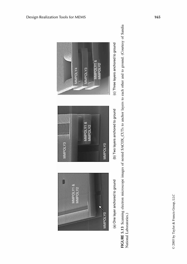
Design Realization Tools for MEMS 165
FIG
UR
E 5
.13
Sca
nn
ing
ele
ctro
n m
icro
sco
pe
imag
es o
f n
este
d S
AC
OX
_C
UT
s to
an
cho
r la
yer
s to
eac
h o
ther
an
d t
o g
rou
nd
. (C
ou
rtes
y o
f S
and
ia
Nat
ion
al L
abo
rato
ries
.)
MM
PO
LY
0
(a)
One layer
anchore
d to g
round
(b)
Tw
o layers
anchore
d to g
round
(c)
Thre
e layers
anchore
d to g
round
MM
PO
LY
0
MM
PO
LY
2
MM
PO
LY
3
MM
PO
LY
4
MM
PO
LY
1 &
MM
PO
LY
2
MM
PO
LY
3
MM
PO
LY
1 &
MM
PO
LY
2
MM
PO
LY
1 &
© 2
005 b
y T
aylo
r &
Fra
nci
s G
roup, L
LC
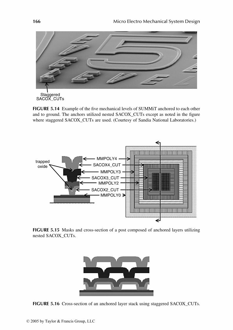
166 Micro Electro Mechanical System Design
FIGURE 5.14 Example of the five mechanical levels of SUMMiT anchored to each other
and to ground. The anchors utilized nested SACOX_CUTs except as noted in the figure
where staggered SACOX_CUTs are used. (Courtesy of Sandia National Laboratories.)
FIGURE 5.15 Masks and cross-section of a post composed of anchored layers utilizing
nested SACOX_CUTs.
FIGURE 5.16 Cross-section of an anchored layer stack using staggered SACOX_CUTs.
trappedoxide
MMPOLY4
MMPOLY3
MMPOLY2
MMPOLY0
SACOX4_CUT
SACOX3_CUT
SACOX2_CUT
© 2005 by Taylor & Francis Group, LLC
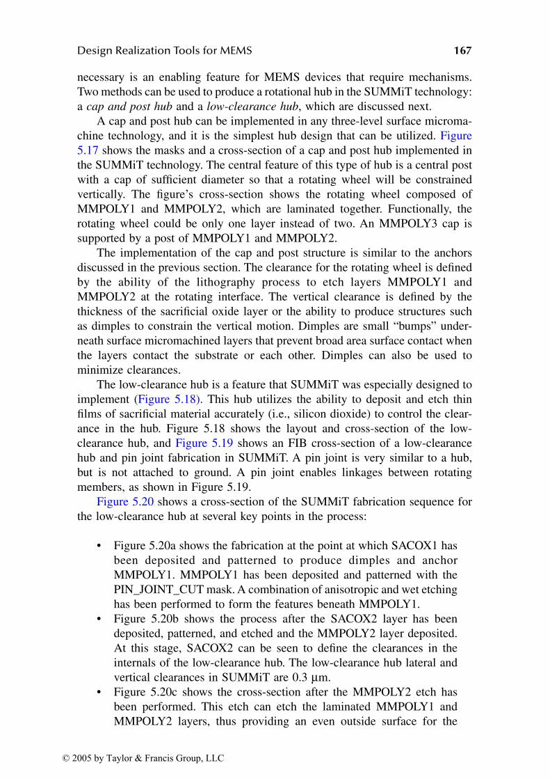
Design Realization Tools for MEMS 167
necessary is an enabling feature for MEMS devices that require mechanisms.
Two methods can be used to produce a rotational hub in the SUMMiT technology:
a cap and post hub and a low-clearance hub, which are discussed next.
A cap and post hub can be implemented in any three-level surface microma-
chine technology, and it is the simplest hub design that can be utilized. Figure
5.17 shows the masks and a cross-section of a cap and post hub implemented in
the SUMMiT technology. The central feature of this type of hub is a central post
with a cap of sufficient diameter so that a rotating wheel will be constrained
vertically. The figure’s cross-section shows the rotating wheel composed of
MMPOLY1 and MMPOLY2, which are laminated together. Functionally, the
rotating wheel could be only one layer instead of two. An MMPOLY3 cap is
supported by a post of MMPOLY1 and MMPOLY2.
The implementation of the cap and post structure is similar to the anchors
discussed in the previous section. The clearance for the rotating wheel is defined
by the ability of the lithography process to etch layers MMPOLY1 and
MMPOLY2 at the rotating interface. The vertical clearance is defined by the
thickness of the sacrificial oxide layer or the ability to produce structures such
as dimples to constrain the vertical motion. Dimples are small “bumps” under-
neath surface micromachined layers that prevent broad area surface contact when
the layers contact the substrate or each other. Dimples can also be used to
minimize clearances.
The low-clearance hub is a feature that SUMMiT was especially designed to
implement (Figure 5.18). This hub utilizes the ability to deposit and etch thin
films of sacrificial material accurately (i.e., silicon dioxide) to control the clear-
ance in the hub. Figure 5.18 shows the layout and cross-section of the low-
clearance hub, and Figure 5.19 shows an FIB cross-section of a low-clearance
hub and pin joint fabrication in SUMMiT. A pin joint is very similar to a hub,
but is not attached to ground. A pin joint enables linkages between rotating
members, as shown in Figure 5.19.
Figure 5.20 shows a cross-section of the SUMMiT fabrication sequence for
the low-clearance hub at several key points in the process:
• Figure 5.20a shows the fabrication at the point at which SACOX1 has
been deposited and patterned to produce dimples and anchor
MMPOLY1. MMPOLY1 has been deposited and patterned with the
PIN_JOINT_CUT mask. A combination of anisotropic and wet etching
has been performed to form the features beneath MMPOLY1.
• Figure 5.20b shows the process after the SACOX2 layer has been
deposited, patterned, and etched and the MMPOLY2 layer deposited.
At this stage, SACOX2 can be seen to define the clearances in the
internals of the low-clearance hub. The low-clearance hub lateral and
vertical clearances in SUMMiT are 0.3 µm.
• Figure 5.20c shows the cross-section after the MMPOLY2 etch has
been performed. This etch can etch the laminated MMPOLY1 and
MMPOLY2 layers, thus providing an even outside surface for the
© 2005 by Taylor & Francis Group, LLC
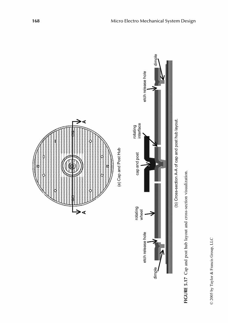
168 Micro Electro Mechanical System Design
FIG
UR
E 5
.17
Cap
an
d p
ost
hu
b l
ayo
ut
and
cro
ss-s
ecti
on
vis
ual
izat
ion
.
© 2
005 b
y T
aylo
r &
Fra
nci
s G
roup, L
LC
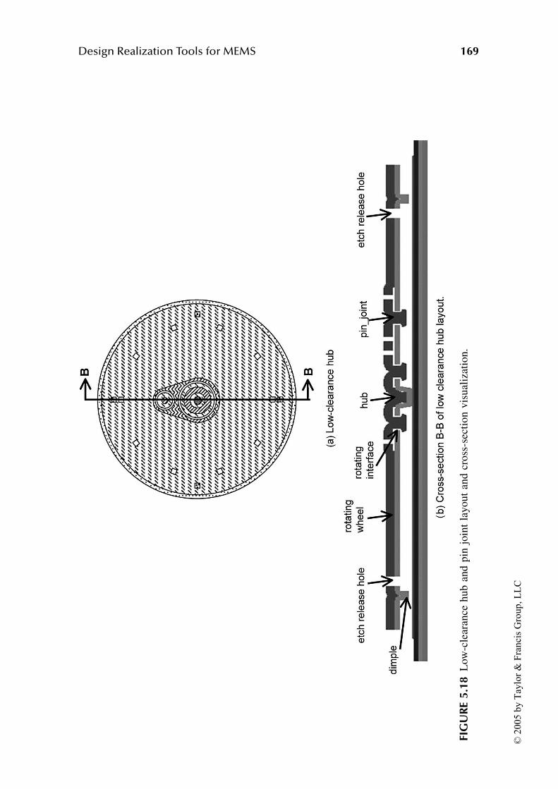
Design Realization Tools for MEMS 169
FIG
UR
E 5
.18
Low
-cle
aran
ce h
ub
an
d p
in j
oin
t la
yo
ut
and
cro
ss-s
ecti
on
vis
ual
izat
ion
.
© 2
005 b
y T
aylo
r &
Fra
nci
s G
roup, L
LC

170 Micro Electro Mechanical System Design
rotating wheel and etch release holes through the rotating wheel disc.
Note that the MMPOLY2 etch stops on the SACOX2 layer in the
internal hub features.
• Figure 5.20d shows the cross-section of the released low-clearance hub
and pin joint structure.
5.2.3 POLY1 BEAM WITH SUBSTRATE CONNECTION
The MMPOLY1 beam with a substrate connection is a simple structure illustrating
the application of two features useful in design of a number of devices in the
SUMMiT technology. The MMPOLY1 layer can be patterned in either of two
ways in SUMMiT:
• The MMPOLY1 layer can be patterned directly using the
MMPOLY1_cut mask and etch.
• The MMPOLY1 layer can also be patterned indirectly by using
SACOX2 as a “hard” mask and etching with the MMPOLY2 etch.
In the previous section, Figure 5.20c showed that the MMPOLY2 etch would
etch the MMPOLY1 and MMPOLY2 layers except when the MMPOLY1 layer
is protected by SACOX2. In this case, the SACOX2 layer was used as a “hard”
mask to stop the MMPOLY2 etch. For the MMPOLY1 beam shown in Figure
5.21, the SACOX2 mask is used to define the MMPOLY1 beam via the
MMPOLY2 etch. The MMPOLY1 beam is attached to the substrate using a
SACOX1_CUT as discussed in Section 5.2.1. If a connection is to be established
to the substrate for electrical grounding purposes, the NITRIDE_CUT mask is
used to define the etch of the NITRIDE layer.
5.2.4 DISCRETE HINGES
The concept of discrete hinges for MEMS applications was initially proposed by
Pister [8]. Since that time, a number of different variations and types of hinges
FIGURE 5.19 A focused ion beam (FIB) cross-section of a rotational hub and pin joint.
(Courtesy of Sandia National Laboratories.)
© 2005 by Taylor & Francis Group, LLC
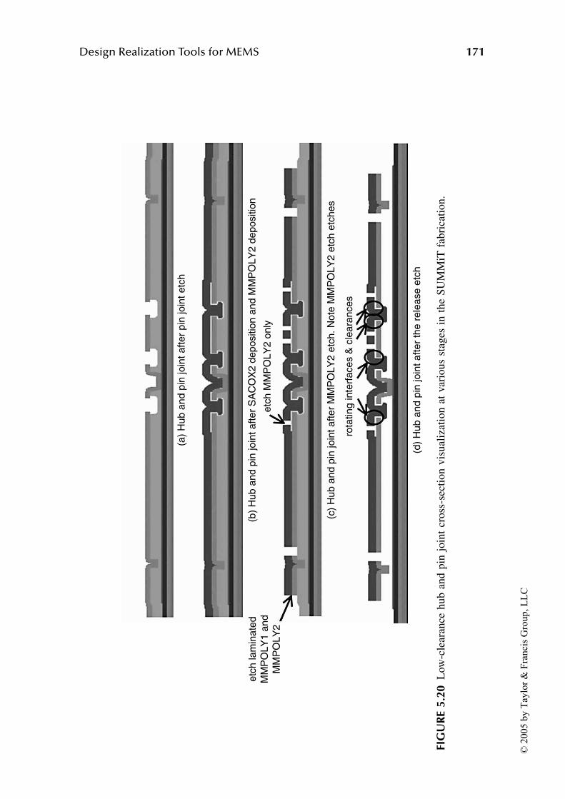
Design Realization Tools for MEMS 171
FIG
UR
E 5
.20
Low
-cle
aran
ce h
ub
an
d p
in j
oin
t cr
oss
-sec
tio
n v
isu
aliz
atio
n a
t var
iou
s st
ages
in
th
e S
UM
MiT
fab
rica
tio
n.
etc
h lam
inate
d
MM
PO
LY
1 a
nd
MM
PO
LY
2
(a)
Hub a
nd p
in join
t after
pin
join
t etc
h
etc
h M
MP
OLY
2 o
nly
rota
ting inte
rfaces &
cle
ara
nces
(b)
Hub a
nd p
in join
t after
SA
CO
X2
depositio
n a
nd M
MP
OLY
2 d
epositio
n
(c)
Hub a
nd p
in join
t after
MM
PO
LY
2 e
tch. N
ote
MM
PO
LY
2 e
tch e
tches
(d)
Hub a
nd p
in join
t after
the r
ele
ase e
tch
© 2
005 b
y T
aylo
r &
Fra
nci
s G
roup, L
LC
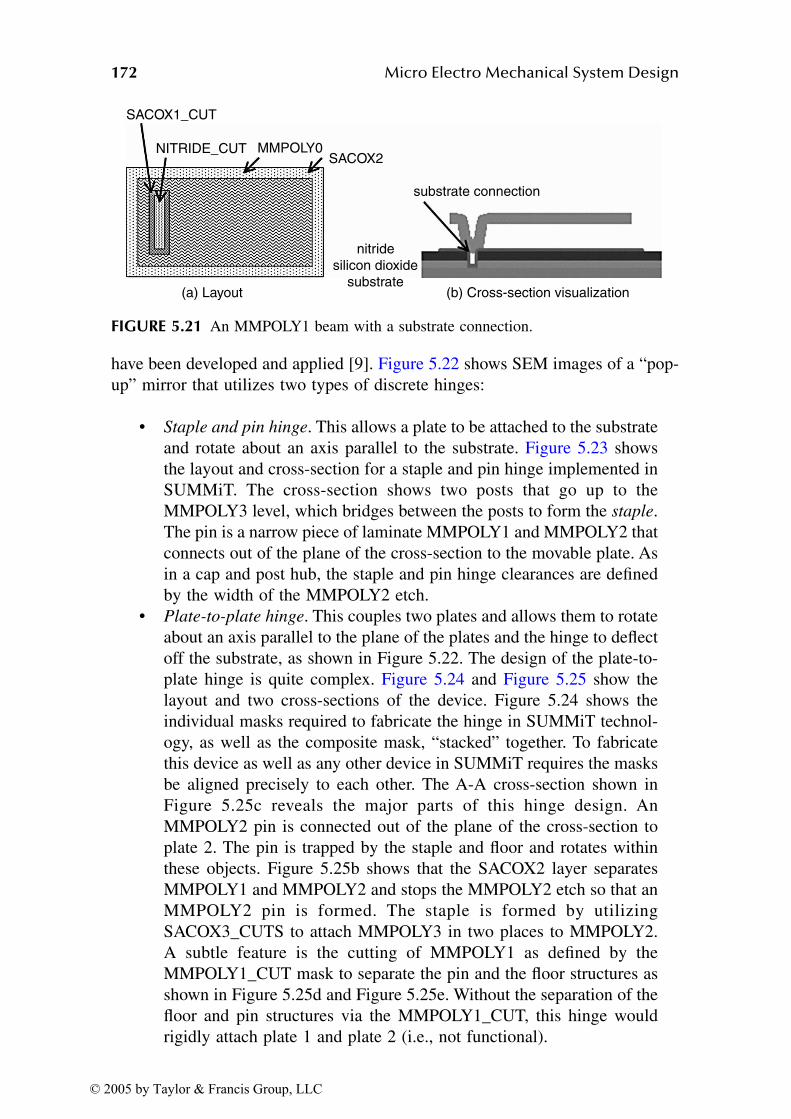
172 Micro Electro Mechanical System Design
have been developed and applied [9]. Figure 5.22 shows SEM images of a “pop-
up” mirror that utilizes two types of discrete hinges:
• Staple and pin hinge. This allows a plate to be attached to the substrate
and rotate about an axis parallel to the substrate. Figure 5.23 shows
the layout and cross-section for a staple and pin hinge implemented in
SUMMiT. The cross-section shows two posts that go up to the
MMPOLY3 level, which bridges between the posts to form the staple.
The pin is a narrow piece of laminate MMPOLY1 and MMPOLY2 that
connects out of the plane of the cross-section to the movable plate. As
in a cap and post hub, the staple and pin hinge clearances are defined
by the width of the MMPOLY2 etch.
• Plate-to-plate hinge. This couples two plates and allows them to rotate
about an axis parallel to the plane of the plates and the hinge to deflect
off the substrate, as shown in Figure 5.22. The design of the plate-to-
plate hinge is quite complex. Figure 5.24 and Figure 5.25 show the
layout and two cross-sections of the device. Figure 5.24 shows the
individual masks required to fabricate the hinge in SUMMiT technol-
ogy, as well as the composite mask, “stacked” together. To fabricate
this device as well as any other device in SUMMiT requires the masks
be aligned precisely to each other. The A-A cross-section shown in
Figure 5.25c reveals the major parts of this hinge design. An
MMPOLY2 pin is connected out of the plane of the cross-section to
plate 2. The pin is trapped by the staple and floor and rotates within
these objects. Figure 5.25b shows that the SACOX2 layer separates
MMPOLY1 and MMPOLY2 and stops the MMPOLY2 etch so that an
MMPOLY2 pin is formed. The staple is formed by utilizing
SACOX3_CUTS to attach MMPOLY3 in two places to MMPOLY2.
A subtle feature is the cutting of MMPOLY1 as defined by the
MMPOLY1_CUT mask to separate the pin and the floor structures as
shown in Figure 5.25d and Figure 5.25e. Without the separation of the
floor and pin structures via the MMPOLY1_CUT, this hinge would
rigidly attach plate 1 and plate 2 (i.e., not functional).
FIGURE 5.21 An MMPOLY1 beam with a substrate connection.
SACOX1_CUT
SACOX2
substrate connection
nitride
silicon dioxide
substrate(a) Layout (b) Cross-section visualization
NITRIDE_CUT MMPOLY0
© 2005 by Taylor & Francis Group, LLC
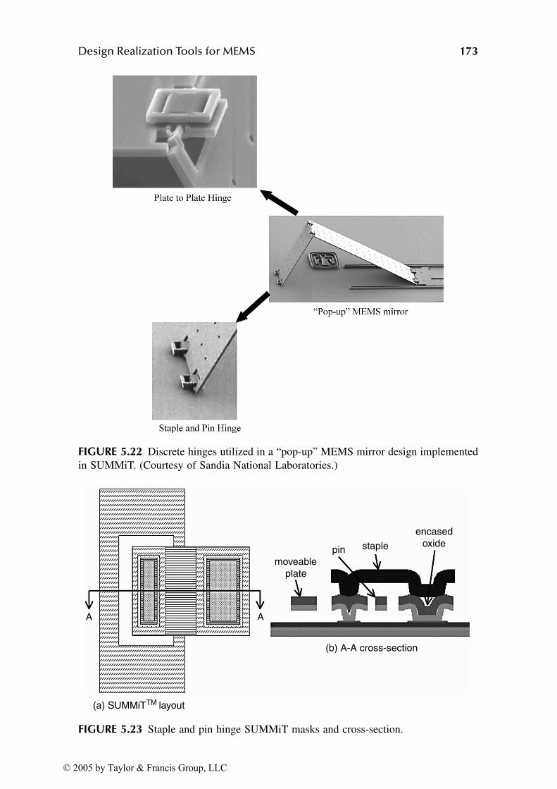
Design Realization Tools for MEMS 173
FIGURE 5.22 Discrete hinges utilized in a “pop-up” MEMS mirror design implemented
in SUMMiT. (Courtesy of Sandia National Laboratories.)
FIGURE 5.23 Staple and pin hinge SUMMiT masks and cross-section.
(a) SUMMiTTM layout
(b) A-A cross-section
moveable
plate
pin staple
encased
oxide
A A
© 2005 by Taylor & Francis Group, LLC

174 Micro Electro Mechanical System Design
FIG
UR
E 5
.24
SU
MM
iT m
ask
s fo
r th
e p
late
-to
-pla
te h
ing
e.
A
B
(a)
MM
PO
LY
1_C
UT
mask
(c)
MM
PO
LY
2 m
ask
(e)
MM
PO
LY
3 m
ask
(f)
Alig
ned c
om
posite m
asks
for
the p
late
-to-p
late
hin
ge
(b)
SA
CO
X2 m
ask
(d)
SA
CO
X3_ C
UT
maskB
BB
BB
B
AA
A
AA
A
AAA
A A
BB
BB
B
© 2
005 b
y T
aylo
r &
Fra
nci
s G
roup, L
LC
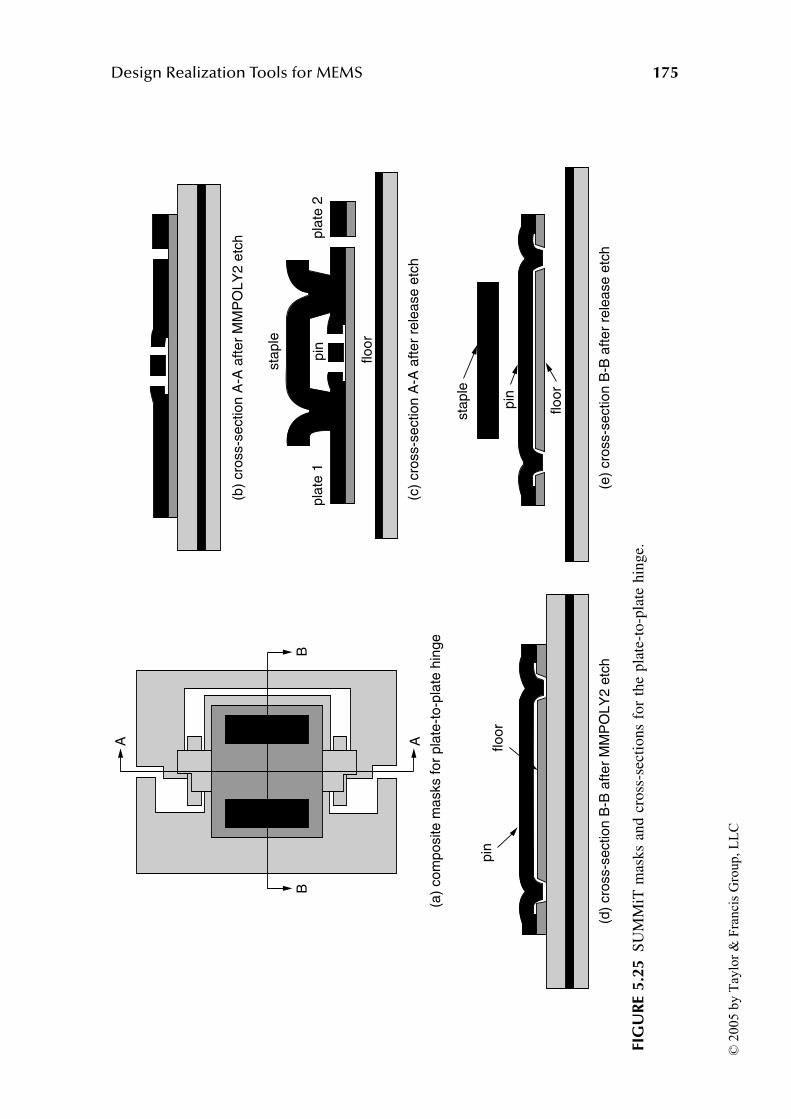
Design Realization Tools for MEMS 175
FIG
UR
E 5
.25
SU
MM
iT m
ask
s an
d c
ross
-sec
tio
ns
for
the
pla
te-t
o-p
late
hin
ge.
A A
BB
(a)
com
posite m
asks for
pla
te-t
o-p
late
hin
ge
(b)
cro
ss-s
ection A
-A a
fter
MM
PO
LY
2 e
tch
(c)
cro
ss-s
ection A
-A a
fter
rele
ase e
tch
(d)
cro
ss-s
ection B
-B a
fter
MM
PO
LY
2 e
tch
(e)
cro
ss-s
ection B
-B a
fter
rele
ase e
tch
sta
ple
sta
ple
pla
te 1
pla
te 2
pin
pin
pin
floor
floor
floor
© 2
005 b
y T
aylo
r &
Fra
nci
s G
roup, L
LC
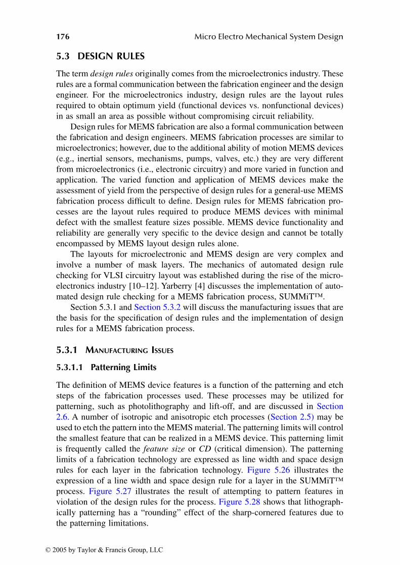
176 Micro Electro Mechanical System Design
5.3 DESIGN RULES
The term design rules originally comes from the microelectronics industry. These
rules are a formal communication between the fabrication engineer and the design
engineer. For the microelectronics industry, design rules are the layout rules
required to obtain optimum yield (functional devices vs. nonfunctional devices)
in as small an area as possible without compromising circuit reliability.
Design rules for MEMS fabrication are also a formal communication between
the fabrication and design engineers. MEMS fabrication processes are similar to
microelectronics; however, due to the additional ability of motion MEMS devices
(e.g., inertial sensors, mechanisms, pumps, valves, etc.) they are very different
from microelectronics (i.e., electronic circuitry) and more varied in function and
application. The varied function and application of MEMS devices make the
assessment of yield from the perspective of design rules for a general-use MEMS
fabrication process difficult to define. Design rules for MEMS fabrication pro-
cesses are the layout rules required to produce MEMS devices with minimal
defect with the smallest feature sizes possible. MEMS device functionality and
reliability are generally very specific to the device design and cannot be totally
encompassed by MEMS layout design rules alone.
The layouts for microelectronic and MEMS design are very complex and
involve a number of mask layers. The mechanics of automated design rule
checking for VLSI circuitry layout was established during the rise of the micro-
electronics industry [10–12]. Yarberry [4] discusses the implementation of auto-
mated design rule checking for a MEMS fabrication process, SUMMiT™.
Section 5.3.1 and Section 5.3.2 will discuss the manufacturing issues that are
the basis for the specification of design rules and the implementation of design
rules for a MEMS fabrication process.
5.3.1 MANUFACTURING ISSUES
5.3.1.1 Patterning Limits
The definition of MEMS device features is a function of the patterning and etch
steps of the fabrication processes used. These processes may be utilized for
patterning, such as photolithography and lift-off, and are discussed in Section
2.6. A number of isotropic and anisotropic etch processes (Section 2.5) may be
used to etch the pattern into the MEMS material. The patterning limits will control
the smallest feature that can be realized in a MEMS device. This patterning limit
is frequently called the feature size or CD (critical dimension). The patterning
limits of a fabrication technology are expressed as line width and space design
rules for each layer in the fabrication technology. Figure 5.26 illustrates the
expression of a line width and space design rule for a layer in the SUMMiT™
process. Figure 5.27 illustrates the result of attempting to pattern features in
violation of the design rules for the process. Figure 5.28 shows that lithograph-
ically patterning has a “rounding” effect of the sharp-cornered features due to
the patterning limitations.
© 2005 by Taylor & Francis Group, LLC
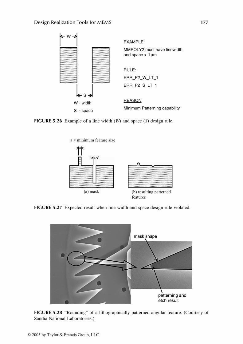
Design Realization Tools for MEMS 177
FIGURE 5.26 Example of a line width (W) and space (S) design rule.
FIGURE 5.27 Expected result when line width and space design rule violated.
FIGURE 5.28 “Rounding” of a lithographically patterned angular feature. (Courtesy of
Sandia National Laboratories.)
W - width
S - space
EXAMPLE:
MMPOLY2 must have linewidth
and space > 1µm
RULE:
ERR_P2_W_LT_1
ERR_P2_S_LT_1
REASON:
Minimum Patterning capability
S
W
a
a
a < minimum feature size
(a) mask (b) resulting patterned
features
© 2005 by Taylor & Francis Group, LLC
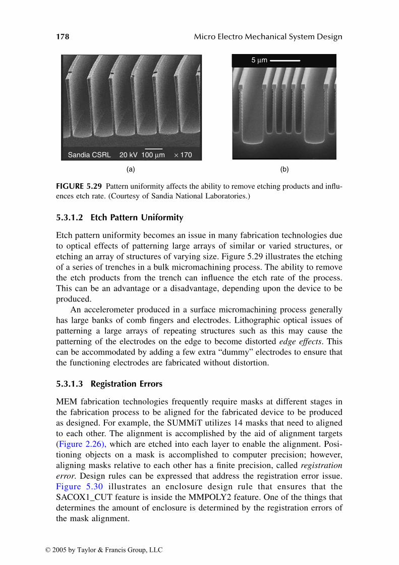
178 Micro Electro Mechanical System Design
5.3.1.2 Etch Pattern Uniformity
Etch pattern uniformity becomes an issue in many fabrication technologies due
to optical effects of patterning large arrays of similar or varied structures, or
etching an array of structures of varying size. Figure 5.29 illustrates the etching
of a series of trenches in a bulk micromachining process. The ability to remove
the etch products from the trench can influence the etch rate of the process.
This can be an advantage or a disadvantage, depending upon the device to be
produced.
An accelerometer produced in a surface micromachining process generally
has large banks of comb fingers and electrodes. Lithographic optical issues of
patterning a large arrays of repeating structures such as this may cause the
patterning of the electrodes on the edge to become distorted edge effects. This
can be accommodated by adding a few extra “dummy” electrodes to ensure that
the functioning electrodes are fabricated without distortion.
5.3.1.3 Registration Errors
MEM fabrication technologies frequently require masks at different stages in
the fabrication process to be aligned for the fabricated device to be produced
as designed. For example, the SUMMiT utilizes 14 masks that need to aligned
to each other. The alignment is accomplished by the aid of alignment targets
(Figure 2.26), which are etched into each layer to enable the alignment. Posi-
tioning objects on a mask is accomplished to computer precision; however,
aligning masks relative to each other has a finite precision, called registration
error. Design rules can be expressed that address the registration error issue.
Figure 5.30 illustrates an enclosure design rule that ensures that the
SACOX1_CUT feature is inside the MMPOLY2 feature. One of the things that
determines the amount of enclosure is determined by the registration errors of
the mask alignment.
FIGURE 5.29 Pattern uniformity affects the ability to remove etching products and influ-
ences etch rate. (Courtesy of Sandia National Laboratories.)
Sandia CSRL 20 kV × 170100 µm
5 µm
(a) (b)
© 2005 by Taylor & Francis Group, LLC
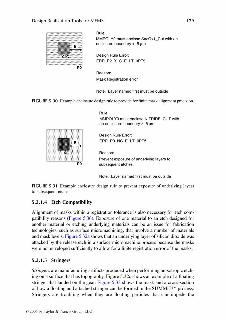
Design Realization Tools for MEMS 179
5.3.1.4 Etch Compatibility
Alignment of masks within a registration tolerance is also necessary for etch com-
patibility reasons (Figure 5.36). Exposure of one material to an etch designed for
another material or etching underlying materials can be an issue for fabrication
technologies, such as surface micromachining, that involve a number of materials
and mask levels. Figure 5.32a shows that an underlying layer of silicon dioxide was
attacked by the release etch in a surface micromachine process because the masks
were not enveloped sufficiently to allow for a finite registration error of the masks.
5.3.1.5 Stringers
Stringers are manufacturing artifacts produced when performing anisotropic etch-
ing on a surface that has topography. Figure 5.32c shows an example of a floating
stringer that landed on the gear. Figure 5.33 shows the mask and a cross-section
of how a floating and attached stringer can be formed in the SUMMiT™ process.
Stringers are troubling when they are floating particles that can impede the
FIGURE 5.30 Example enclosure design rule to provide for finite mask alignment precision.
FIGURE 5.31 Example enclosure design rule to prevent exposure of underlying layers
to subsequent etches.
Rule:
MMPOLY2 must enclose SacOx1_Cut with an
enclosure boundary > .5 µm
Design Rule Error:
ERR_P2_X1C_E_LT_0PT5
Reason:
Mask Registration error
Note: Layer named first must be outside
E
P2
X1C
Rule:
MMPOLY0 must enclose NITRIDE_CUT with
an enclosure boundary > .5 µm
Design Rule Error:
ERR_P0_NC_E_LT_0PT5
Reason:
Prevent exposure of underlying layers to
subsequent etches.
Note: Layer named first must be outside
E
P0
NC
© 2005 by Taylor & Francis Group, LLC
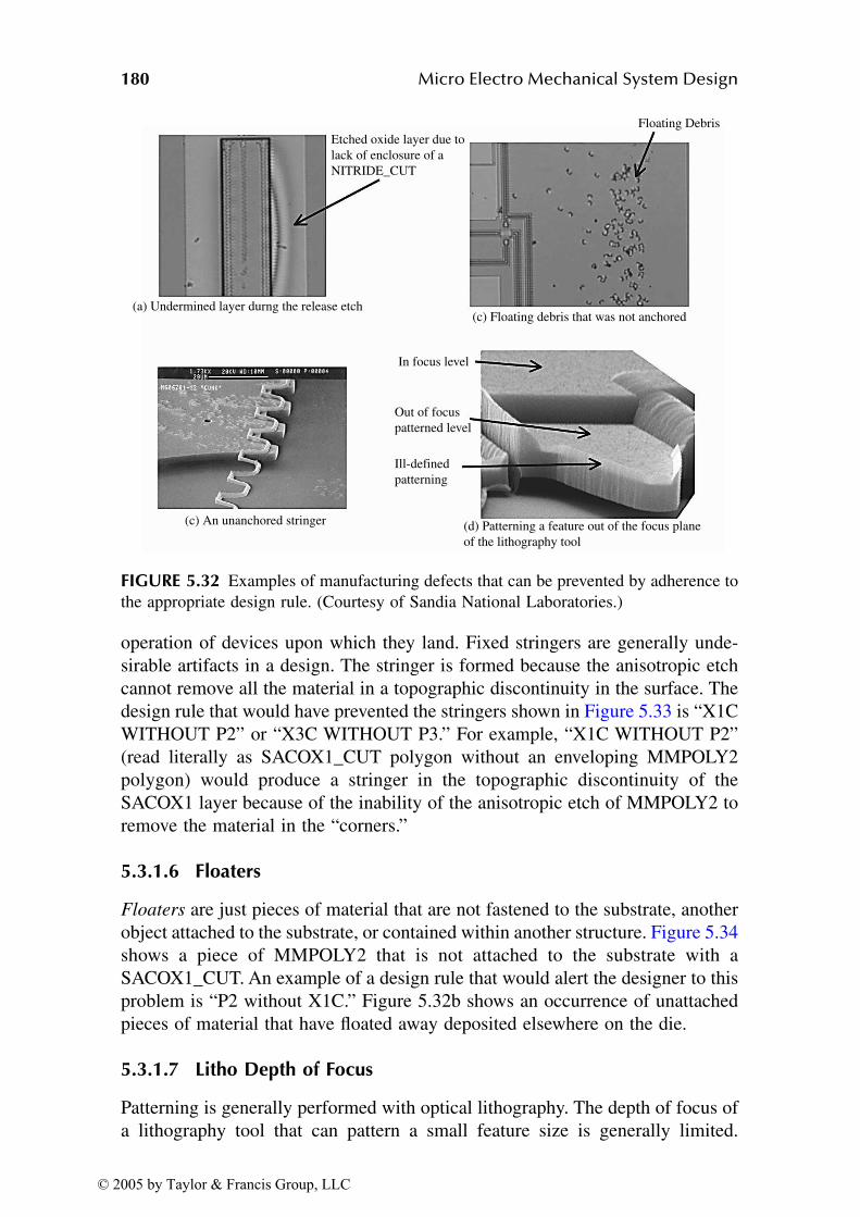
180 Micro Electro Mechanical System Design
operation of devices upon which they land. Fixed stringers are generally unde-
sirable artifacts in a design. The stringer is formed because the anisotropic etch
cannot remove all the material in a topographic discontinuity in the surface. The
design rule that would have prevented the stringers shown in Figure 5.33 is “X1C
WITHOUT P2” or “X3C WITHOUT P3.” For example, “X1C WITHOUT P2”
(read literally as SACOX1_CUT polygon without an enveloping MMPOLY2
polygon) would produce a stringer in the topographic discontinuity of the
SACOX1 layer because of the inability of the anisotropic etch of MMPOLY2 to
remove the material in the “corners.”
5.3.1.6 Floaters
Floaters are just pieces of material that are not fastened to the substrate, another
object attached to the substrate, or contained within another structure. Figure 5.34
shows a piece of MMPOLY2 that is not attached to the substrate with a
SACOX1_CUT. An example of a design rule that would alert the designer to this
problem is “P2 without X1C.” Figure 5.32b shows an occurrence of unattached
pieces of material that have floated away deposited elsewhere on the die.
5.3.1.7 Litho Depth of Focus
Patterning is generally performed with optical lithography. The depth of focus of
a lithography tool that can pattern a small feature size is generally limited.
FIGURE 5.32 Examples of manufacturing defects that can be prevented by adherence to
the appropriate design rule. (Courtesy of Sandia National Laboratories.)
Etched oxide layer due to
lack of enclosure of a
NITRIDE_CUT
Floating Debris
(a) Undermined layer durng the release etch
(c) An unanchored stringer
(c) Floating debris that was not anchored
(d) Patterning a feature out of the focus plane
of the lithography tool
In focus level
Out of focus
patterned level
Ill-defined
patterning
© 2005 by Taylor & Francis Group, LLC

Design Realization Tools for MEMS 181
Attempting to pattern an object outside the focus of the lithography tool will
generally perform poorly. Figure 5.32d is an example of attempting to pattern
MMPOLY2 within a cut in the sacrificial oxide cut.
5.3.1.8 Stiction (Dimples)
Dimples are small “bumps” on the bottom side of the mechanical layers of a
surface micromachine process for the purpose of preventing broad area surface
contact, which could cause layers to stick together or stick to the substrate.
Dimples are placed at a certain frequency and prevent stiction of the layer. Design
rules that would address this issue are usually informational or advisory because
the designer may intentionally decide not to have dimples because the structure
is sufficiently stiff to prevent stiction.
5.3.1.9 Etch Release Holes
Etch release holes are holes placed in a large area of a surface micromachined
layer to allow the release etchant to remove the sacrificial material immediately
below more readily. An example of a SUMMiT design rule that addresses this
FIGURE 5.33 Example of stringer formation in a surface micromachine process.
Sacrificalmaterial
Structural material
(b) Structural material covering an etch in the sacrificial
material which produces topography.
Stringers
(a) Mask for a cut in the sacrificial material which is
not enveloped by the structural material.
(c) Anisotropic etch to remove the structural material
which leaves a stringer.
© 2005 by Taylor & Francis Group, LLC
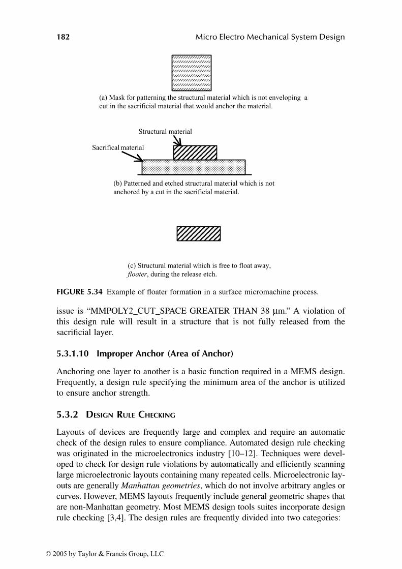
182 Micro Electro Mechanical System Design
issue is “MMPOLY2_CUT_SPACE GREATER THAN 38 µm.” A violation of
this design rule will result in a structure that is not fully released from the
sacrificial layer.
5.3.1.10 Improper Anchor (Area of Anchor)
Anchoring one layer to another is a basic function required in a MEMS design.
Frequently, a design rule specifying the minimum area of the anchor is utilized
to ensure anchor strength.
5.3.2 DESIGN RULE CHECKING
Layouts of devices are frequently large and complex and require an automatic
check of the design rules to ensure compliance. Automated design rule checking
was originated in the microelectronics industry [10–12]. Techniques were devel-
oped to check for design rule violations by automatically and efficiently scanning
large microelectronic layouts containing many repeated cells. Microelectronic lay-
outs are generally Manhattan geometries, which do not involve arbitrary angles or
curves. However, MEMS layouts frequently include general geometric shapes that
are non-Manhattan geometry. Most MEMS design tools suites incorporate design
rule checking [3,4]. The design rules are frequently divided into two categories:
FIGURE 5.34 Example of floater formation in a surface micromachine process.
(a) Mask for patterning the structural material which is not enveloping a
cut in the sacrificial material that would anchor the material.
Sacrifical material
Structural material
(b) Patterned and etched structural material which is not
anchored by a cut in the sacrificial material.
(c) Structural material which is free to float away,
floater, during the release etch.
© 2005 by Taylor & Francis Group, LLC
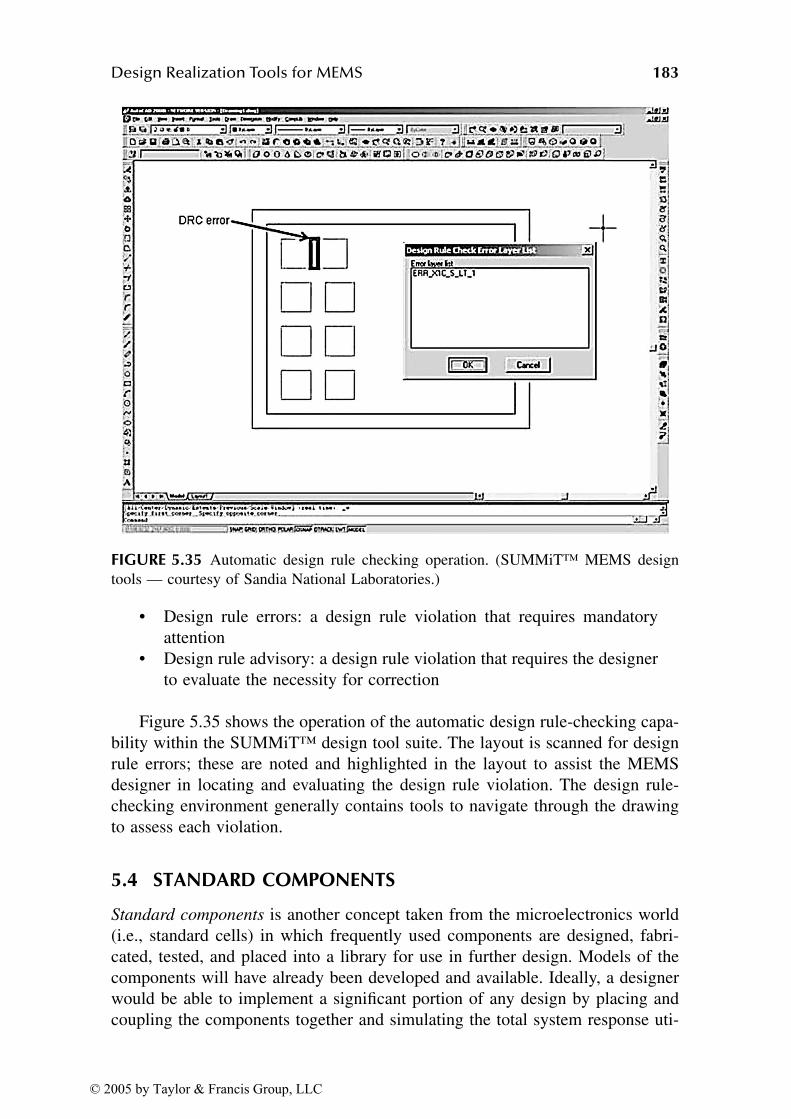
Design Realization Tools for MEMS 183
• Design rule errors: a design rule violation that requires mandatory
attention
• Design rule advisory: a design rule violation that requires the designer
to evaluate the necessity for correction
Figure 5.35 shows the operation of the automatic design rule-checking capa-
bility within the SUMMiT™ design tool suite. The layout is scanned for design
rule errors; these are noted and highlighted in the layout to assist the MEMS
designer in locating and evaluating the design rule violation. The design rule-
checking environment generally contains tools to navigate through the drawing
to assess each violation.
5.4 STANDARD COMPONENTS
Standard components is another concept taken from the microelectronics world
(i.e., standard cells) in which frequently used components are designed, fabri-
cated, tested, and placed into a library for use in further design. Models of the
components will have already been developed and available. Ideally, a designer
would be able to implement a significant portion of any design by placing and
coupling the components together and simulating the total system response uti-
FIGURE 5.35 Automatic design rule checking operation. (SUMMiT™ MEMS design
tools — courtesy of Sandia National Laboratories.)
© 2005 by Taylor & Francis Group, LLC
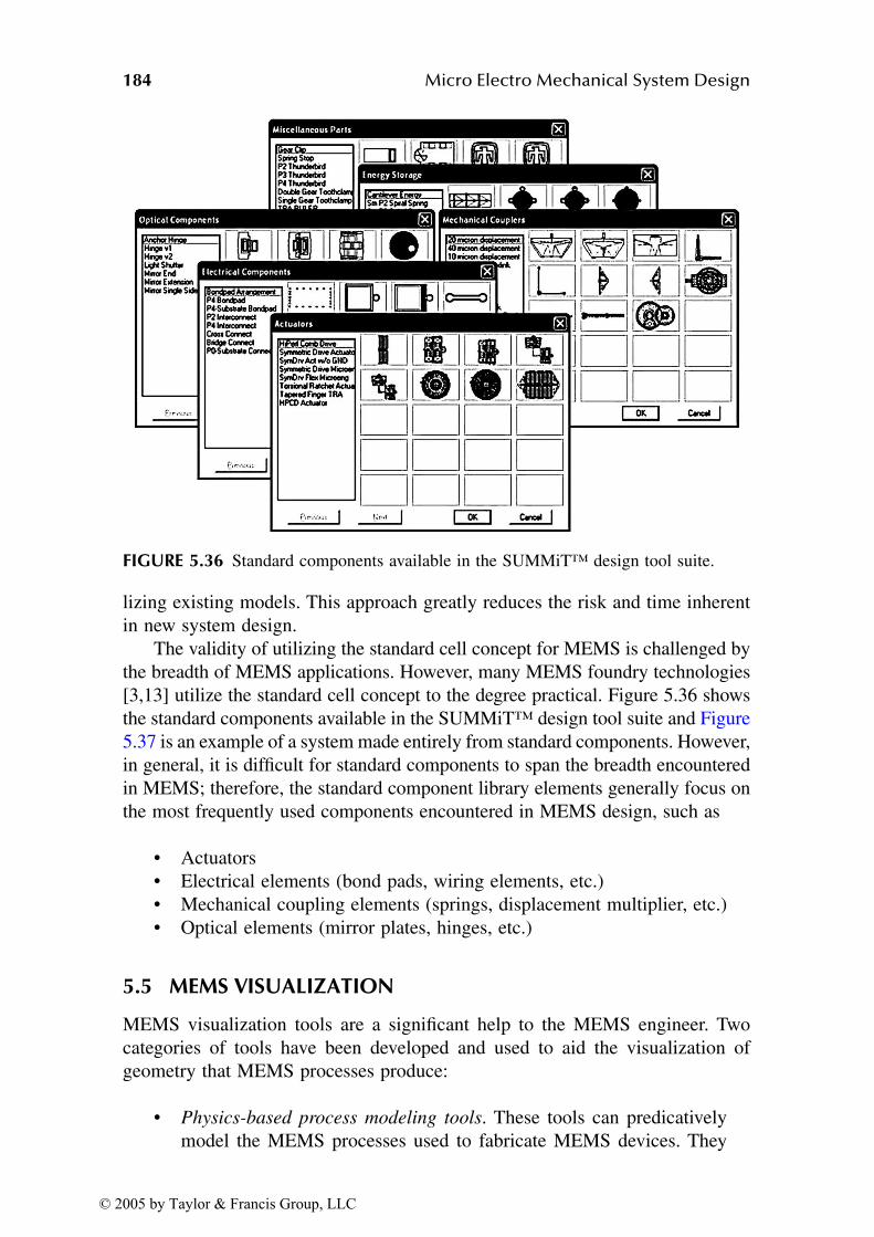
184 Micro Electro Mechanical System Design
lizing existing models. This approach greatly reduces the risk and time inherent
in new system design.
The validity of utilizing the standard cell concept for MEMS is challenged by
the breadth of MEMS applications. However, many MEMS foundry technologies
[3,13] utilize the standard cell concept to the degree practical. Figure 5.36 shows
the standard components available in the SUMMiT™ design tool suite and Figure
5.37 is an example of a system made entirely from standard components. However,
in general, it is difficult for standard components to span the breadth encountered
in MEMS; therefore, the standard component library elements generally focus on
the most frequently used components encountered in MEMS design, such as
• Actuators
• Electrical elements (bond pads, wiring elements, etc.)
• Mechanical coupling elements (springs, displacement multiplier, etc.)
• Optical elements (mirror plates, hinges, etc.)
5.5 MEMS VISUALIZATION
MEMS visualization tools are a significant help to the MEMS engineer. Two
categories of tools have been developed and used to aid the visualization of
geometry that MEMS processes produce:
• Physics-based process modeling tools. These tools can predicatively
model the MEMS processes used to fabricate MEMS devices. They
FIGURE 5.36 Standard components available in the SUMMiT™ design tool suite.
© 2005 by Taylor & Francis Group, LLC
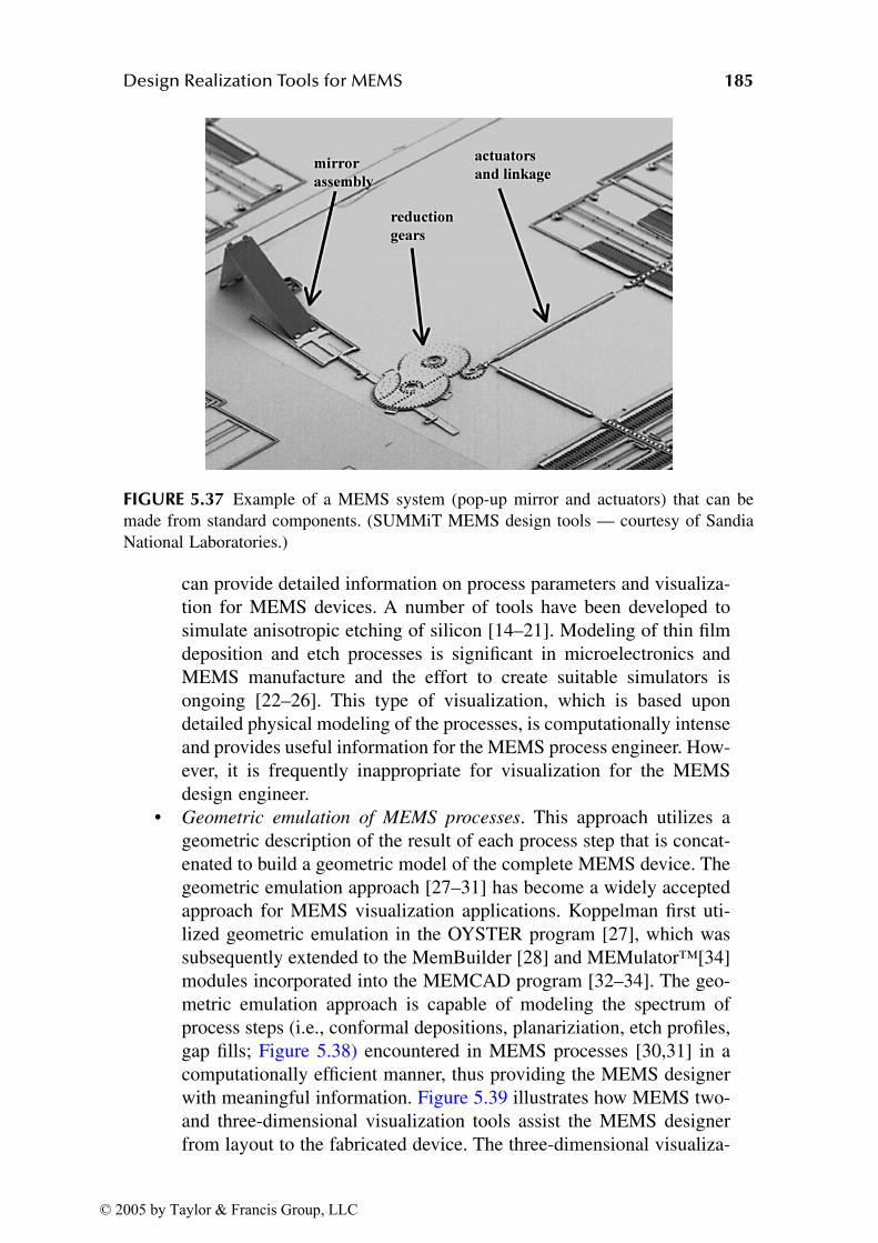
Design Realization Tools for MEMS 185
can provide detailed information on process parameters and visualiza-
tion for MEMS devices. A number of tools have been developed to
simulate anisotropic etching of silicon [14–21]. Modeling of thin film
deposition and etch processes is significant in microelectronics and
MEMS manufacture and the effort to create suitable simulators is
ongoing [22–26]. This type of visualization, which is based upon
detailed physical modeling of the processes, is computationally intense
and provides useful information for the MEMS process engineer. How-
ever, it is frequently inappropriate for visualization for the MEMS
design engineer.
• Geometric emulation of MEMS processes. This approach utilizes a
geometric description of the result of each process step that is concat-
enated to build a geometric model of the complete MEMS device. The
geometric emulation approach [27–31] has become a widely accepted
approach for MEMS visualization applications. Koppelman first uti-
lized geometric emulation in the OYSTER program [27], which was
subsequently extended to the MemBuilder [28] and MEMulator™[34]
modules incorporated into the MEMCAD program [32–34]. The geo-
metric emulation approach is capable of modeling the spectrum of
process steps (i.e., conformal depositions, planariziation, etch profiles,
gap fills; Figure 5.38) encountered in MEMS processes [30,31] in a
computationally efficient manner, thus providing the MEMS designer
with meaningful information. Figure 5.39 illustrates how MEMS two-
and three-dimensional visualization tools assist the MEMS designer
from layout to the fabricated device. The three-dimensional visualiza-
FIGURE 5.37 Example of a MEMS system (pop-up mirror and actuators) that can be
made from standard components. (SUMMiT MEMS design tools — courtesy of Sandia
National Laboratories.)
© 2005 by Taylor & Francis Group, LLC
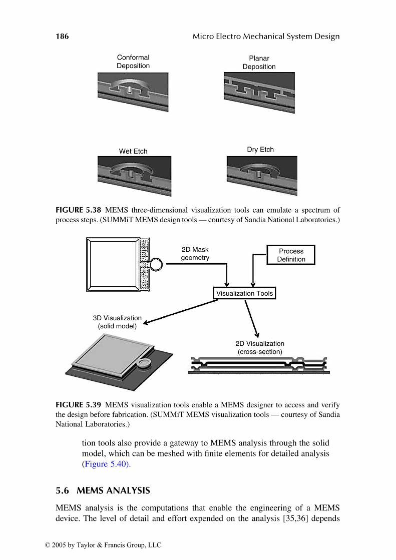
186 Micro Electro Mechanical System Design
tion tools also provide a gateway to MEMS analysis through the solid
model, which can be meshed with finite elements for detailed analysis
(Figure 5.40).
5.6 MEMS ANALYSIS
MEMS analysis is the computations that enable the engineering of a MEMS
device. The level of detail and effort expended on the analysis [35,36] depends
FIGURE 5.38 MEMS three-dimensional visualization tools can emulate a spectrum of
process steps. (SUMMiT MEMS design tools — courtesy of Sandia National Laboratories.)
FIGURE 5.39 MEMS visualization tools enable a MEMS designer to access and verify
the design before fabrication. (SUMMiT MEMS visualization tools — courtesy of Sandia
National Laboratories.)
ConformalDeposition
Wet Etch Dry Etch
PlanarDeposition
2D Mask geometry
3D Visualization (solid model)
2D Visualization (cross-section)
ProcessDefinition
Visualization Tools
© 2005 by Taylor & Francis Group, LLC
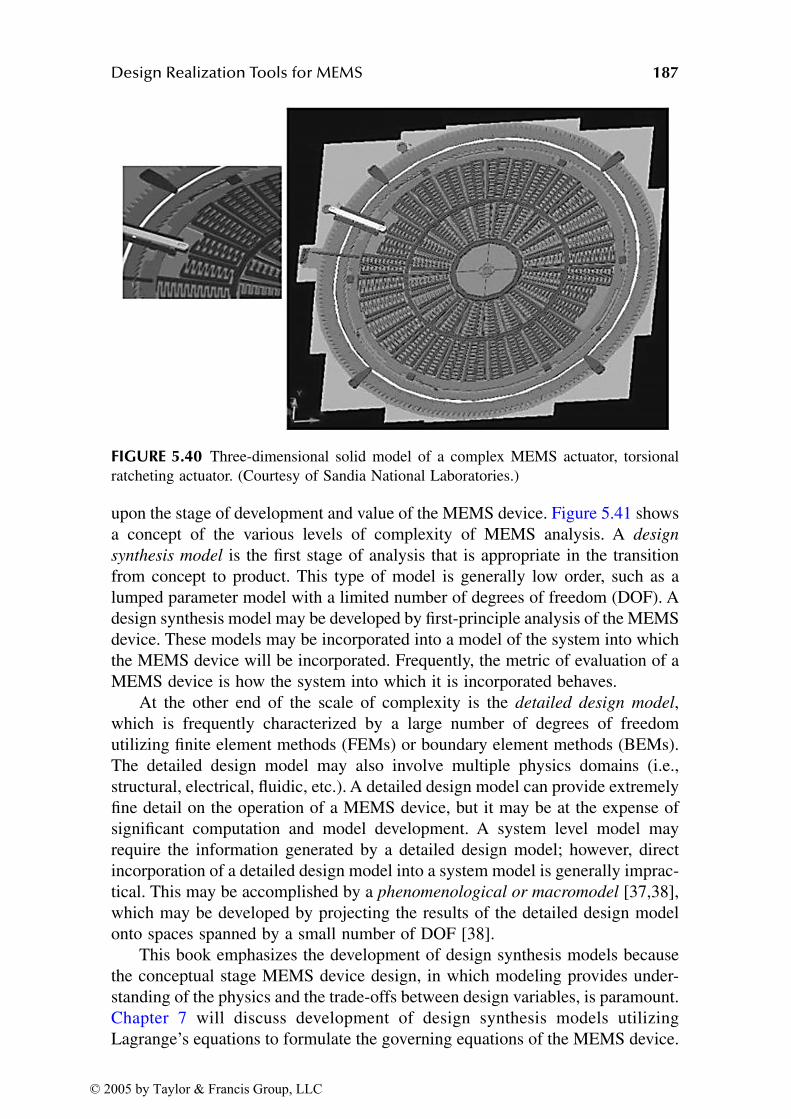
Design Realization Tools for MEMS 187
upon the stage of development and value of the MEMS device. Figure 5.41 shows
a concept of the various levels of complexity of MEMS analysis. A design
synthesis model is the first stage of analysis that is appropriate in the transition
from concept to product. This type of model is generally low order, such as a
lumped parameter model with a limited number of degrees of freedom (DOF). A
design synthesis model may be developed by first-principle analysis of the MEMS
device. These models may be incorporated into a model of the system into which
the MEMS device will be incorporated. Frequently, the metric of evaluation of a
MEMS device is how the system into which it is incorporated behaves.
At the other end of the scale of complexity is the detailed design model,
which is frequently characterized by a large number of degrees of freedom
utilizing finite element methods (FEMs) or boundary element methods (BEMs).
The detailed design model may also involve multiple physics domains (i.e.,
structural, electrical, fluidic, etc.). A detailed design model can provide extremely
fine detail on the operation of a MEMS device, but it may be at the expense of
significant computation and model development. A system level model may
require the information generated by a detailed design model; however, direct
incorporation of a detailed design model into a system model is generally imprac-
tical. This may be accomplished by a phenomenological or macromodel [37,38],
which may be developed by projecting the results of the detailed design model
onto spaces spanned by a small number of DOF [38].
This book emphasizes the development of design synthesis models because
the conceptual stage MEMS device design, in which modeling provides under-
standing of the physics and the trade-offs between design variables, is paramount.
Chapter 7 will discuss development of design synthesis models utilizing
Lagrange’s equations to formulate the governing equations of the MEMS device.
FIGURE 5.40 Three-dimensional solid model of a complex MEMS actuator, torsional
ratcheting actuator. (Courtesy of Sandia National Laboratories.)
© 2005 by Taylor & Francis Group, LLC
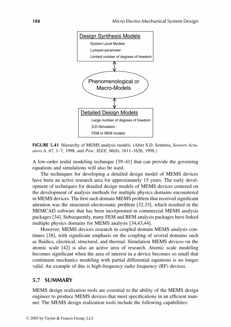
188 Micro Electro Mechanical System Design
A low-order nodal modeling technique [39–41] that can provide the governing
equations and simulations will also be used.
The techniques for developing a detailed design model of MEMS devices
have been an active research area for approximately 15 years. The early devel-
opment of techniques for detailed design models of MEMS devices centered on
the development of analysis methods for multiple physics domains encountered
in MEMS devices. The first such domain MEMS problem that received significant
attention was the structural–electrostatic problem [32,33], which resulted in the
MEMCAD software that has been incorporated in commercial MEMS analysis
packages [34]. Subsequently, many FEM and BEM analysis packages have linked
multiple physics domains for MEMS analysis [34,43,44].
However, MEMS devices research in coupled domain MEMS analysis con-
tinues [38], with significant emphasis on the coupling of several domains such
as fluidics, electrical, structural, and thermal. Simulation MEMS devices on the
atomic scale [42] is also an active area of research. Atomic scale modeling
becomes significant when the area of interest in a device becomes so small that
continuum mechanics modeling with partial differential equations is no longer
valid. An example of this is high-frequency radio frequency (RF) devices.
5.7 SUMMARY
MEMS design realization tools are essential to the ability of the MEMS design
engineer to produce MEMS devices that meet specifications in an efficient man-
ner. The MEMS design realization tools include the following capabilities:
FIGURE 5.41 Hierarchy of MEMS analysis models. (After S.D. Senturia, Sensors Actu-
ators A, 67, 1–7, 1998, and Proc. IEEE, 86(8), 1611–1626, 1998.)
Detailed Design Models
Large number of degrees of freedom
3-D Simulation
FEM or BEM models
Design Synthesis Models
System Level Models
Lumped parameter
Limited number of degrees of freedom
Phenomenological or
Macro-Models
© 2005 by Taylor & Francis Group, LLC
Design Realization Tools for MEMS 189
• Layout tools (prototype or technology file and two-dimensional layout
capability)
• Standard components
• Automated design rule checking
• MEMS visualization
The MEMS visualization tools that were discussed in Section 5.5 construct
a cross-section or three-dimensional solid model (Figure 5.39) of the MEMS
device given the device layout and a process description. This technique is called
art to part (i.e., layout art to solid model of the part). Recent research [45–47]
has developed the basic algorithms for the part-to-art problem (i.e., solid model
of the part to the layout art). With further development and the use of the part-
to-art algorithms, a new method of design realization for MEMS may be possible.
Instead of the MEMS designer producing two-dimensional layouts to produce
the three-dimensional MEMS device, he or she may in the future develop a three-
dimensional solid model of the MEMS device; the part-to-art algorithm could
produce the two-dimensional layouts of the masks to make the part in a particular
technology. This would enable a MEMS designer to work in the same manner
as a macroworld design engineer, who develops a three-dimensional solid model
of a device to be designed.
MEMS analysis capability is essential to the ability of the MEMS designer
to engineer a device. A range of complexity of MEMS analysis models exists:
• Design synthesis model: low number of DOF or lumped parameter
models
• Phenomenological or macromodel: a model that can map complex
phenomena or detailed model data to a low-order space
• Detailed design model: large number of DOF, FEM, or BEM models
In subsequent chapters, MEMS analysis — in particular methods for developing
the design synthesis model — will be discussed in detail.
QUESTIONS
1. What information does a prototype file or technology file contain?
2. Why is the GDSII file important? Who uses it?
3. What is the difference in how a GDS file represents geometry and the
binary layout file in the design environment?
4. What is the advantage of using two layers (i.e., layer and a layer_cut)
and the XOR logical operation to create a mask layout? Why is a
polygon drawn in layer_cut only valid within a poly drawn in layer?
(Hint: see Figure 5.8 and Figure 5.9.)
5. Compare the advantages and disadvantages of the nested anchor vs.
the staggered anchor.
© 2005 by Taylor & Francis Group, LLC

190 Micro Electro Mechanical System Design
6. Compare the advantages and disadvantages of the cap and post hub
vs. the low-clearance hub.
7. What advantages do standard components have for MEMS device
layout?
8. What is the difference between the philosophy for definition of MEMS
and microelectronic design rules?
9. Consider the layout of a nested anchor vs. the staggered anchor.
Assume that all SACOX_CUT for anchors should be a minimum of 2
µm square. The line width and space rules for all layers are 1 µm. The
layer envelope rules for the MMPOLY layers enveloping the
SACOX_CUT layers are >0.5 µm. What is the minimum size anchor
for the nested anchor vs. the staggered anchor? Why would you choose
one type of anchor over the other?
10. Layout a post in the SUMMiT™ technology that goes from
MMPOLY0 to MMPOLY4 utilizing the staggered anchor concept.
11. What can be done with the staple and pin hinge (Figure 5.23) to reduce
the clearances?
12. What are the types of design rule errors? What is their significance?
REFERENCES
1. GDSII Stream Format Manual, release 6.0, G.E. Calma, February 1987. See also
http://www.cadence.com and http://www.cnf.cornell.edu/SPIEBook/spie9.htm).
2. A.M. Carver, L.A. Conway, Introduction to VLSI Systems, Reading, MA, Addison-
Wesley, 1980.
3. E. Shepherd, Prototyping with SUMMiT™ technology, Sandia’s ultraplanar mul-
tilevel MEMS technology, ASME International Mechanical Engineering Congress
& Exposition, IMECE 2002, paper no. IMECE 2002-34258.
4. V.R. Yarberry, Meeting the MEMS design-to-analysis challenge: the SUMMiT™
V design tool environment, ASME International Mechanical Engineering Con-
gress & Exposition, IMECE 2002, paper no. IMECE 2002-34205.
5. AutoCAD 2000i, User’s Guide, Autodesk, Inc., San Rafael, CA,
http://www.autodesk.com.
6. ASM 3500 DXF to GDSII Bidirectional Translator, Artwork Conversion Software,
Inc., Santa Cruz, CA. http://www.artwork.com/gdsii/asm3500/index.htm.
7. M.S. Baker, M.P. de Boer, N.F. Smith, L.K. Warne, M.B. Sinclair, Integrated
measurement-modeling approaches for evaluating residual stress using microma-
chined fixed-fixed beams, J. Microelectromechanical Syst., 11(6), 743–753,
December 2002.
8. K.S.J. Pister, M.W. Judy, S.R. Burgett, Fearing, Microfabricated hinges, Sensors
Actuators A, 33, 249–256, 1992.
9. R. Yeh, E.J.J. Kruglick, K.S.J. Pister, Surface micromachined components for
articulated microrobots, J. Microelectromechanical Syst., 5(1), 10–17, March 1996.
10. C.M. Baker, C.J. Terman, Tools for verifying integrated circuit designs, Lambda
Mag. (VLSI Design), 4th quarter, 22–30, 1980.
© 2005 by Taylor & Francis Group, LLC
Design Realization Tools for MEMS 191
11. T.G. Szymanski, C.J. Van Wyk, Space efficient algorithms for VLSI artwork
analysis, Proc. 20th Design Automation Conf., 734–739, June 1983.
12. H.S. Baird, Fast algorithms for LSI artwork analysis, Proc. 14th Design Automa-
tion Conf., 303–311, 1977.
13. http://www.memscap.com/memsrus/crmumps.html.
14. R.A. Buser, N.F. de Rooij, ASEP: a CAD program for silicon anisotropic etching
(micromechanical structure), Sensors Actuators A, A28(1), 71–78, 1991.
15. C.H. Sequin, Computer simulation of anisotropic etching, Proc. 6th Int. Conf.
Solid-State Sensors Actuators (Transducers ’91), San Francisco, CA, 28–28 June,
1991, 801–806.
16. T.J. Hubbard, E.K. Antonsson, Emergent faces in crystal etching, J Microelectro-
mech, Syst., 3, 19–28, 1994.
17. J. Fruhauf, K. Trautmann, J. Wittig, D. Zielke, A simulation tool for orientation
dependent etching, J. Micromech. Microeng., 3(3), 113–115, 1993.
18. D. Dietrich, J. Fruhauf, Computer simulation of the development of dish-shaped
deepenings by orientation-dependent etching of (100) silicon, Sensors Actuators
A, A39(3), 261–262, 1993.
19. U. Heim, A new approach for the determination of the shape of etched devices,
J. Micromech. Microeng., 3(3), 116–117, 1993.
20. D. Zielke, J. Fruhauf, Determination of rates for orientation-dependent etching,
Sensors Actuators A, A48(a), 151–156, 1995.
21. H. Camon, A. Moktadir, M. Djafari-Rouhani, New trends in atomic scale simu-
lation of wet chemical etching of silicon with KOH, Mater. Sci. Eng. B, B37(1–3),
142–145, 1996.
22. W.G. Oldham, A.R. Neureuther, J.L. Reynolds, S.N. Nandaonkar, C. Sung, A
general simulator for VLSI lithography and etching processes, II: Application to
deposition and etching, IEEE Trans. Electron Devices, ED-27(8), 1455–1459,
1980.
23. S. Yamamato, T. Kure, M. Ohgo, T. Matsuzama, S. Tachi, H. Sunami, A two-
dimensional etching profile simulator: ESPRIT, IEEE Trans. Computer-Aided
Design, CAD-6(3), 417–422, 1987.
24. J. Pelka, K.P. Muller, H. Mader, Simulation of dry etch processes by COMPOS-
ITE, IEEE Trans. Computer-Aided Design, 7(2), 154–159, 1988.
25. C. Hedlund, C. Strandman, I.V. Katardjiev, Y. Backlund, S. Berg, H.O. Blom,
Method for the determination of the angular dependence during dry etching, J.
Vac. Sci. Tech. B, 14(5), 3239–3243, 1996.
26. M. Fujinaga, N. Kotani, 3-D topography simulator (3-D MULSS) based on a
physical description of material topography, IEEE Trans. Electron Devices, 44,
226–238, 1997.
27. G.M. Koppelman, OYSTER, a three-dimensional structural simulator for micro-
electromechanical design, Sensors Actuators, 20(1/2), 179–185, 1989.
28. P.M. Osterberg, S.D. Senturia, Membuilder: an automated 3D solid-model con-
struction program for microelectromechanical structures, Proc. Transducers ’95,
Stockholm, Sweden, June 1995, 2, 21–24.
29. N.R. Lo, K.S.J. Pister, 3D µV — a MEMS 3-D visualization package, Proc. SPIE
Micromachined Devices Components, Austin, TX, Oct. 23–24, 1995, 290–295.
30. C.R. Jorgensen, V.R. Yarberry, A 3D geometry modeler for the SUMMiT V MEMS
designer, Proc. Modeling Simulation Microsyst. Conf., 606–609, 2001.
© 2005 by Taylor & Francis Group, LLC
192 Micro Electro Mechanical System Design
31. C.R. Jorgensen, V.R. Yarberry, A 2D visualization tool for SUMMiT V designs,
Proc. Modeling Simulation Microsyst. Conf., 594–597, 2001.
32. S.D. Senturia, R.M. Harris, B.P. Johnson, S. Kim, K. Nabors, M.A. Shulman, J.K.
White, A computer-aided design system for microelectromechanical systems
(MEMCAD), J. Microelectromech. Syst., 1(1), 3–13, 1992.
33. J.R. Gilbert, P.M. Osterberg, R.M. Harris, D.O. Ouma, X. Cai, A. Pfajfer, J. White,
S.D. Senturia, Implementation of MEMCAD system for electrostatic and mechan-
ical analysis of complex structures from mask descriptions, Proc. IEEE Micro
Electro Mechanical Syst., Fort Lauderdale, FL, Feb. 7–10, 1993, 207–212.
34. Coventer: http://www.coventor.com.
35. S.D. Senturia, Simulation and design of microsystems: a 10-year perspective,
Sensors Actuators A, 67, 1–7, 1998.
36. S.D. Senturia, CAD challenges for microsensors, microactuators, and microsys-
tems, Proc. IEEE, 86(8), 1611–1626, 1998.
37. S.D. Senturia, N. Aluru, J. White, Simulating the behavior of MEMS devices:
computational methods and needs, IEEE Computational Sci. Eng., 30–43,
Jan.–Mar., 1997.
38. R.M. Kirby, G.E. Karniadakis, O. Mikulchenko, K. Mayaram, An integrated
simulator for coupled domain problems in MEMS, J. Microelectromech. Syst.,
10(3), 379–391, 2001.
39. SUGAR: http://bsac.berkeley.edu/cadtools/sugar/sugar/#overview.
40. J.V. Clark, D. Bindel, W. Kao, E. Zhu, A. Kuo, N. Zhou, J. Nie, J. Demmel, Z.
Bai, S. Govindjee, K.S.J. Pister, M. Gu, A. Agogino, Addressing the needs of
complex MEMS design, Proc. MEMS 2002, Las Vegas, January 20–24, 2002.
41. J.V. Clark, N. Zhou, K.S.J. Pister, Modified nodal analysis for MEMS with multi-
energy domains, Int. Conf. Modeling Simulation Microsyst., Semiconductors, Sen-
sors Actuators, San Diego, CA, March 27–29, 2000, 31–34.
42. R.E. Rudd, The atomic limit of finite element modeling in MEMS: coupling of
length scales, Analog Integrated Circuits Signal Process., 29, 17–26, 2001.
43. MEMSCAP: http://www.memscap.com.
44. ANSYS: http://www.ansys.com.
45. V. Venkataraman, R. Sarma, S. Ananthasuresh, Part to art: basis for a systematic
geometric design tool for surface micromachined MEMS, Proc. ASME Design
Eng. Tech. Conf., 1–14, 2000.
46. A. Perrin, V. Ananthakrishnan, F. Gao, R. Sarma, G.K. Ananthasuresh, Voxel-
based hetrogeneous geometric modeling for surface micromachined MEMS, Proc.
Modeling Simulation Microsys. Conf., 136–139, 2001.
47. R. Schiek, R. Schmidt, A new, topology driven method for automatic mask
generation from three-dimensional models, NanoTech 2003, San Francisco, CA,
Feb. 2003.
© 2005 by Taylor & Francis Group, LLC

193
6 Electromechanics
MEMS devices invariably involve engineering of multiphysics designs to attaina design objective. The two physical domains most frequently utilized in MEMSdevices are structural and electrical dynamics. Regardless of the design objec-tive, a structure invariably needs to be designed to support, contain, or possiblydeflect to perform a function. An electrical system is needed to sense themechanical motion of the structure. At the microscale, damping due to viscouslosses of the device to the surrounding atmosphere greatly influences the dynam-ics of the system.
For example, a MEMS accelerometer requires the suspended seismic massto have a preferred mode of vibration in the sensitive axis at a specific resonantfrequency. This device would also have an electrical sense interface to transducethe motion of the seismic mass and, possibly, electrical force feedback to maintainthe position of the accelerometer sense mass at a neutral position. The dampingof the accelerometer seismic mass will greatly influence the dynamics of thesystem and needs to be considered in the design.
This chapter will present an overview of the important topics in structuralmechanics, damping, and electrical circuit elements. Due to space limitations, anin-depth treatment of these topics is not possible; however, the topics relevant tothe design of MEMS devices will be presented. References 1 through 4 providea more complete background in structural mechanics.
Structural mechanics necessitates the development of the following conceptsto obtain a basic understanding of the subject for purposes of MEMS design:
• Structural material models• Models of the basic structural elements (bending, torsion, axial rods,
columns)• Combining the basic structural elements
Damping mechanisms for vertical and laterally moving MEMS devices willbe presented. The basic electrical circuit elements and models for them will bepresented along with methods for combining them to form a circuit. The set ofequations that describe the electrical circuit elements will also be developed.
© 2005 by Taylor & Francis Group, LLC
194 Micro Electro Mechanical System Design
6.1 STRUCTURAL MECHANICS
6.1.1 MATERIAL MODELS
The atomic structure of materials — broadly classified as crystalline, polycrys-
talline, and amorphous — is illustrated in Figure 2.2. A crystalline material hasa large-scale, three-dimensional atomic structure in which the atoms occupyspecific locations within a lattice (e.g., epitaxial silicon, diamond). The atomicpacking may be in one of seven main crystal patterns with orientations measuredvia the Miller indices (discussed in Chapter 2).
A polycrystalline material consists of a matrix of grains, which are smallcrystals of material; the interface material between adjacent grains is called thegrain boundary. Most metals, such as aluminum and gold as well as polycrystal-line silicon, are examples of this material structure. A noncrystalline material thatexhibits no large-scale structure is called amorphous. Silicon dioxide and otherglasses are examples of this material structure.
The material type greatly influences fundamental structure and completenessof interatomic bonds. This basic material structure affects a number of materialproperties, such as the electrical and thermal conductivities, chemical reactivity,and mechanical strength. For example, the metallurgical processes of cold work-ing and annealing greatly affect the material grains and grain boundary and theresulting material properties of strength, hardness, ductility.
The characteristics of a material that first come to mind in connection withthe design of a structure are strength, elasticity, and ductility. These characteristicsrelate to the ability of the material to resist mechanical forces and how the materialwill fail. In order to establish a meaningful way to design with these consider-ations, it is necessary first to define some commonly used engineering terms.
Given a bar of material loaded with a uniform force distribution across thecross-sectional area, A, as shown in Figure 6.1, a quantity, stress σ, is defined asthe total force, F, per unit cross-sectional area A (Equation 6.1). The applied loadwill deform the material, which will require the definition of a metric to describethe extent of deformation. The metric for localized deformation of a material,strain, is a dimensionless quantity defined as the change in length, δ, per length,L (Equation 6.2).
(6.1)
(6.2)
When an experiment is performed on the specimen of Figure 6.1 in whichthe load is increased in a controlled manner, stress vs. strain can be plotted (Figure6.2). The material shown in this figure exhibits elastic strain. The material deformsunder load as indicated by strain, but the deformation is not permanent. Whenthe load is removed, the stress and strain return to zero.
σ = F A/
ε δ= / L
© 2005 by Taylor & Francis Group, LLC
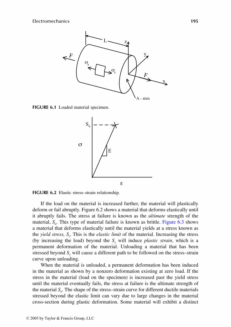
Electromechanics 195
If the load on the material is increased further, the material will plasticallydeform or fail abruptly. Figure 6.2 shows a material that deforms elastically untilit abruptly fails. The stress at failure is known as the ultimate strength of thematerial, Su. This type of material failure is known as brittle. Figure 6.3 showsa material that deforms elastically until the material yields at a stress known asthe yield stress, Sy. This is the elastic limit of the material. Increasing the stress(by increasing the load) beyond the Sy will induce plastic strain, which is apermanent deformation of the material. Unloading a material that has beenstressed beyond Sy will cause a different path to be followed on the stress–straincurve upon unloading.
When the material is unloaded, a permanent deformation has been inducedin the material as shown by a nonzero deformation existing at zero load. If thestress in the material (load on the specimen) is increased past the yield stressuntil the material eventually fails, the stress at failure is the ultimate strength ofthe material Su. The shape of the stress–strain curve for different ductile materialsstressed beyond the elastic limit can vary due to large changes in the materialcross-section during plastic deformation. Some material will exhibit a distinct
FIGURE 6.1 Loaded material specimen.
FIGURE 6.2 Elastic stress–strain relationship.
© 2005 by Taylor & Francis Group, LLC

196 Micro Electro Mechanical System Design
change in slope or distinct plastic deformation at the yield point, but others willbe more subtle. When the yield point is not distinct (Figure 6.4), the yield pointis generally defined as that stress, which induces 0.2% (0.002) plastic strain.
Most engineering applications will not intentionally stress a material past theyield strength. The system will be designed to operate within the elastic regionof the material. The slope of the elastic region of the stress–strain curve is awidely used engineering property of a material known as Young’s modulus, E,which has units of force per area and is a measure of material stiffness. AppendixE lists typical values of Young’s modulus for a number of materials frequentlyused in MEMS devices.
A frequently used material model for operation within the elastic region ofa material is Hooke’s law, which states that the stress in a material is proportionalto the strain that produced it. This is merely the mathematical relationship forthe material operating within the elastic portion of the stress–strain curve:
(6.3)
FIGURE 6.3 Plastic stress–strain relationship.
FIGURE 6.4 Plastic stress–strain relationship.
σ ε= E
© 2005 by Taylor & Francis Group, LLC
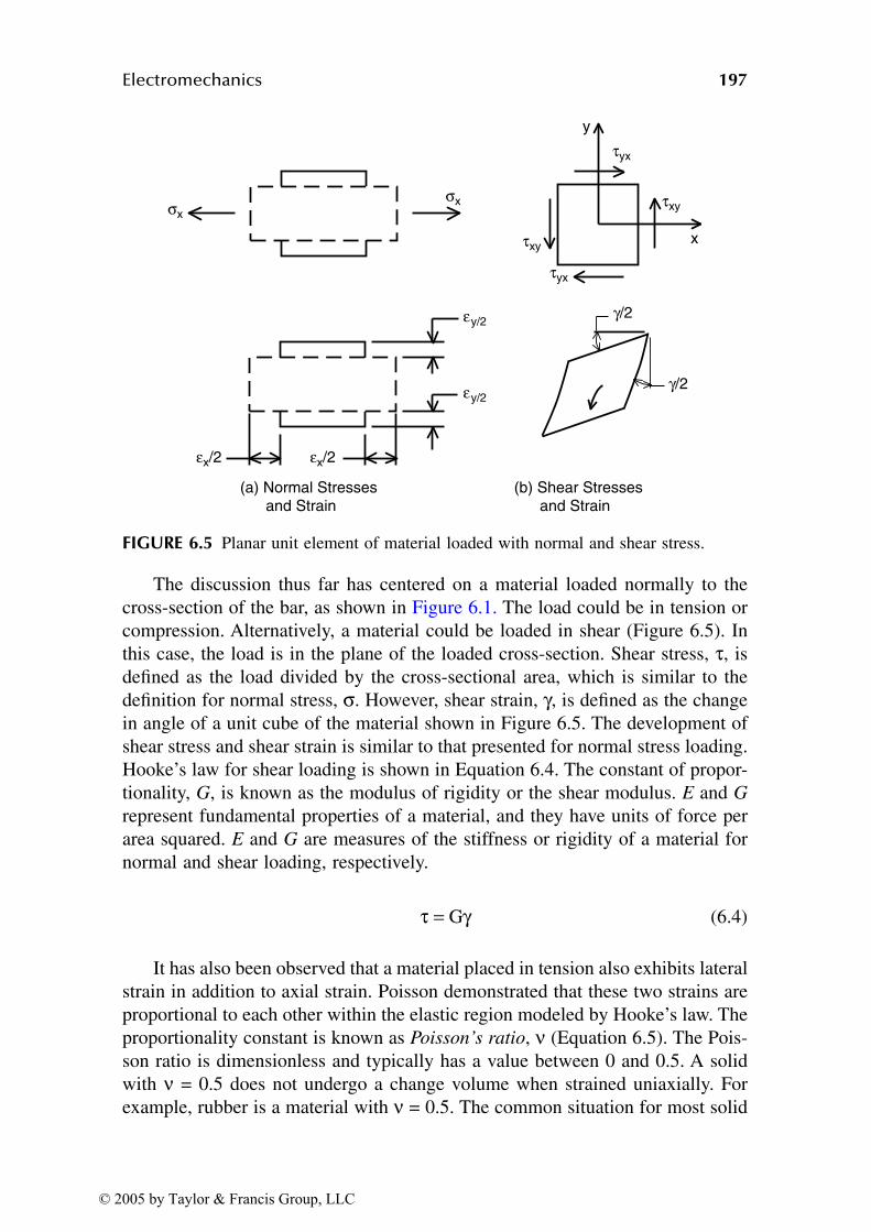
Electromechanics 197
The discussion thus far has centered on a material loaded normally to thecross-section of the bar, as shown in Figure 6.1. The load could be in tension orcompression. Alternatively, a material could be loaded in shear (Figure 6.5). Inthis case, the load is in the plane of the loaded cross-section. Shear stress, τ, isdefined as the load divided by the cross-sectional area, which is similar to thedefinition for normal stress, σ. However, shear strain, γ, is defined as the changein angle of a unit cube of the material shown in Figure 6.5. The development ofshear stress and shear strain is similar to that presented for normal stress loading.Hooke’s law for shear loading is shown in Equation 6.4. The constant of propor-tionality, G, is known as the modulus of rigidity or the shear modulus. E and Grepresent fundamental properties of a material, and they have units of force perarea squared. E and G are measures of the stiffness or rigidity of a material fornormal and shear loading, respectively.
(6.4)
It has also been observed that a material placed in tension also exhibits lateralstrain in addition to axial strain. Poisson demonstrated that these two strains areproportional to each other within the elastic region modeled by Hooke’s law. Theproportionality constant is known as Poisson’s ratio, ν (Equation 6.5). The Pois-son ratio is dimensionless and typically has a value between 0 and 0.5. A solidwith ν = 0.5 does not undergo a change volume when strained uniaxially. Forexample, rubber is a material with ν = 0.5. The common situation for most solid
FIGURE 6.5 Planar unit element of material loaded with normal and shear stress.
σx
σx
εy/2
εy/2
εx/2 εx/2
τxy
τxy
τyx
τyx
γ/2
γ/2
x
y
(a) Normal Stresses and Strain
(b) Shear Stresses and Strain
τ γ= G
© 2005 by Taylor & Francis Group, LLC
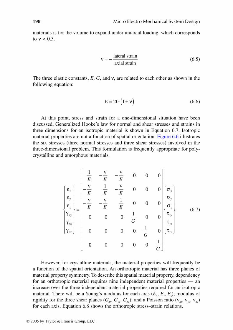
198 Micro Electro Mechanical System Design
materials is for the volume to expand under uniaxial loading, which correspondsto ν < 0.5.
(6.5)
The three elastic constants, E, G, and ν, are related to each other as shown in thefollowing equation:
(6.6)
At this point, stress and strain for a one-dimensional situation have beendiscussed. Generalized Hooke’s law for normal and shear stresses and strains inthree dimensions for an isotropic material is shown in Equation 6.7. Isotropicmaterial properties are not a function of spatial orientation. Figure 6.6 illustratesthe six stresses (three normal stresses and three shear stresses) involved in thethree-dimensional problem. This formulation is frequently appropriate for poly-crystalline and amorphous materials.
(6.7)
However, for crystalline materials, the material properties will frequently bea function of the spatial orientation. An orthotropic material has three planes ofmaterial property symmetry. To describe this spatial material property, dependencyfor an orthotropic material requires nine independent material properties — anincrease over the three independent material properties required for an isotropicmaterial. There will be a Young’s modulus for each axis (Ex, Ey, Ez); modulus ofrigidity for the three shear planes (Gxy, Gyz, Gxz); and a Poisson ratio (νxy, νyz, νxz)for each axis. Equation 6.8 shows the orthotropic stress–strain relations.
ν = − lateral strainaxial strain
E 2G= +( )1 ν
εεε
γγγ
ν
x
y
z
xy
yz
zx
E E
=
−1 −−− −− −
νν νν ν
E
E E E
E E E
G
G
0 0 0
10 0 0
10 0 0
0 0 01
0 0
0 0 0 01
0
00 0 0 0 01G
σ xx
y
z
xy
yz
zx
σστττ
© 2005 by Taylor & Francis Group, LLC
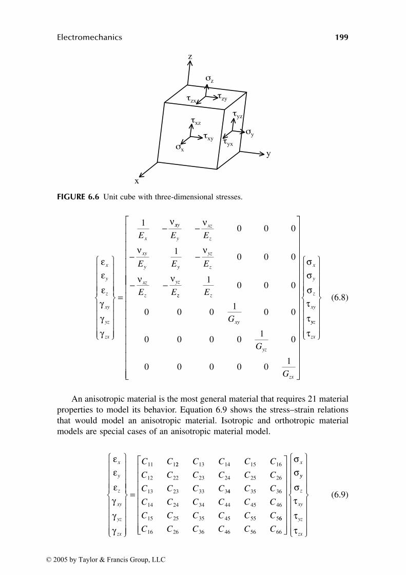
Electromechanics 199
(6.8)
An anisotropic material is the most general material that requires 21 materialproperties to model its behavior. Equation 6.9 shows the stress–strain relationsthat would model an anisotropic material. Isotropic and orthotropic materialmodels are special cases of an anisotropic material model.
(6.9)
FIGURE 6.6 Unit cube with three-dimensional stresses.
εεε
γγγ
ν
x
y
z
xy
yz
zx
xE
=
−1 xxy
y
xz
z
xy
y y
yz
z
xz
z
yz
E E
E E E
E E
−
− −
− −
νν ν
ν ν
0 0 0
10 0 0
zz z
xy
yz
zx
E
G
G
G
10 0 0
0 0 01
0 0
0 0 0 01
0
0 0 0 0 01
σσσττ
x
y
z
xy
yyz
zxτ
εεε
γγγ
x
y
z
xy
yz
zx
C C
=
11 122 13 14 15 16
12 22 23 24 25 26
13 23 33 3
C C C C
C C C C C C
C C C C 44 35 36
14 24 34 44 45 46
15 25 35 45 55 5
C C
C C C C C C
C C C C C C 66
16 26 36 46 56 66C C C C C C
x
σσ yy
z
xy
yz
zx
στττ
© 2005 by Taylor & Francis Group, LLC
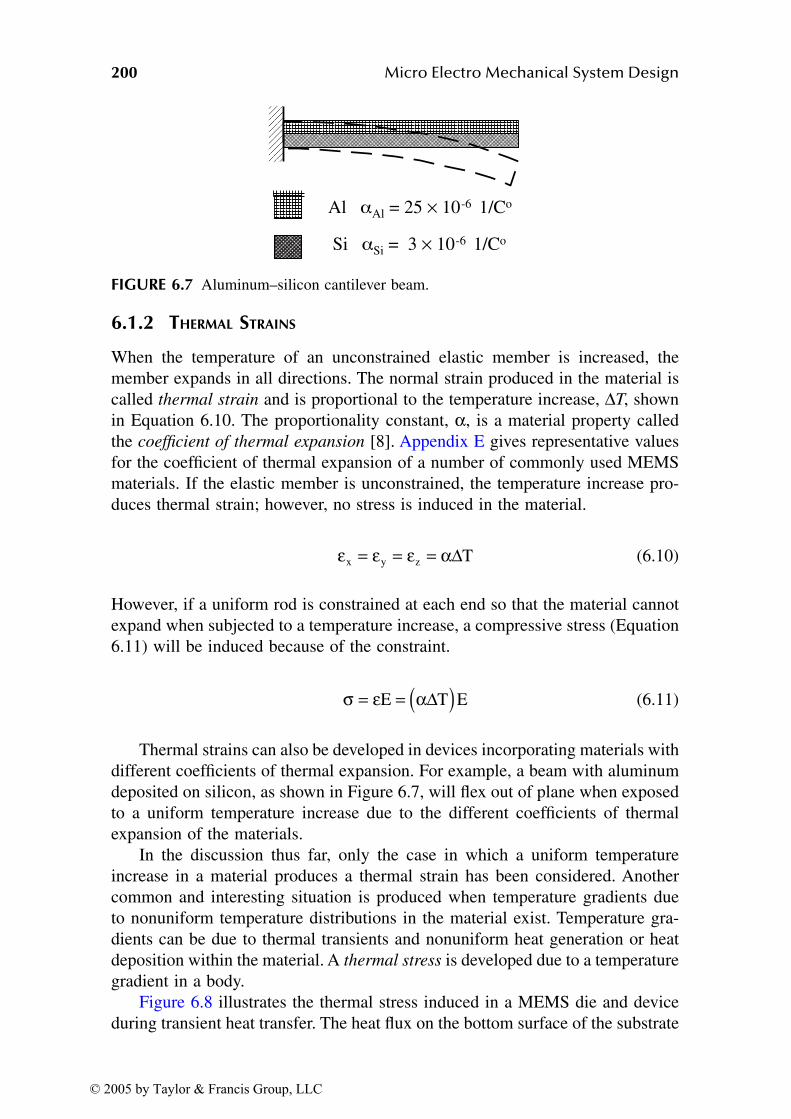
200 Micro Electro Mechanical System Design
6.1.2 THERMAL STRAINS
When the temperature of an unconstrained elastic member is increased, themember expands in all directions. The normal strain produced in the material iscalled thermal strain and is proportional to the temperature increase, ∆T, shownin Equation 6.10. The proportionality constant, α, is a material property calledthe coefficient of thermal expansion [8]. Appendix E gives representative valuesfor the coefficient of thermal expansion of a number of commonly used MEMSmaterials. If the elastic member is unconstrained, the temperature increase pro-duces thermal strain; however, no stress is induced in the material.
(6.10)
However, if a uniform rod is constrained at each end so that the material cannotexpand when subjected to a temperature increase, a compressive stress (Equation6.11) will be induced because of the constraint.
(6.11)
Thermal strains can also be developed in devices incorporating materials withdifferent coefficients of thermal expansion. For example, a beam with aluminumdeposited on silicon, as shown in Figure 6.7, will flex out of plane when exposedto a uniform temperature increase due to the different coefficients of thermalexpansion of the materials.
In the discussion thus far, only the case in which a uniform temperatureincrease in a material produces a thermal strain has been considered. Anothercommon and interesting situation is produced when temperature gradients dueto nonuniform temperature distributions in the material exist. Temperature gra-dients can be due to thermal transients and nonuniform heat generation or heatdeposition within the material. A thermal stress is developed due to a temperaturegradient in a body.
Figure 6.8 illustrates the thermal stress induced in a MEMS die and deviceduring transient heat transfer. The heat flux on the bottom surface of the substrate
FIGURE 6.7 Aluminum–silicon cantilever beam.
Al Al = 25 × 10-6 1/Co
Si Si = 3 × 10⁻⁶ 1/Co
ε ε ε αx y z T= = = ∆
σ ε α= = ( )E T E∆
© 2005 by Taylor & Francis Group, LLC
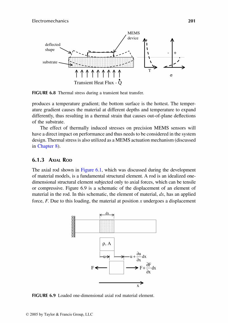
Electromechanics 201
produces a temperature gradient; the bottom surface is the hottest. The temper-ature gradient causes the material at different depths and temperature to expanddifferently, thus resulting in a thermal strain that causes out-of-plane deflectionsof the substrate.
The effect of thermally induced stresses on precision MEMS sensors willhave a direct impact on performance and thus needs to be considered in the systemdesign. Thermal stress is also utilized as a MEMS actuation mechanism (discussedin Chapter 8).
6.1.3 AXIAL ROD
The axial rod shown in Figure 6.1, which was discussed during the developmentof material models, is a fundamental structural element. A rod is an idealized one-dimensional structural element subjected only to axial forces, which can be tensileor compressive. Figure 6.9 is a schematic of the displacement of an element ofmaterial in the rod. In this schematic, the element of material, dx, has an appliedforce, F. Due to this loading, the material at position x undergoes a displacement
FIGURE 6.8 Thermal stress during a transient heat transfer.
FIGURE 6.9 Loaded one-dimensional axial rod material element.
substrate
deflectedshape
MEMSdevice
Transient Heat Flux - Q
Tσ
- +
x
F dxx
FF
∂
∂+
u dxx
uu
∂
∂+
ρ, A
dx
© 2005 by Taylor & Francis Group, LLC
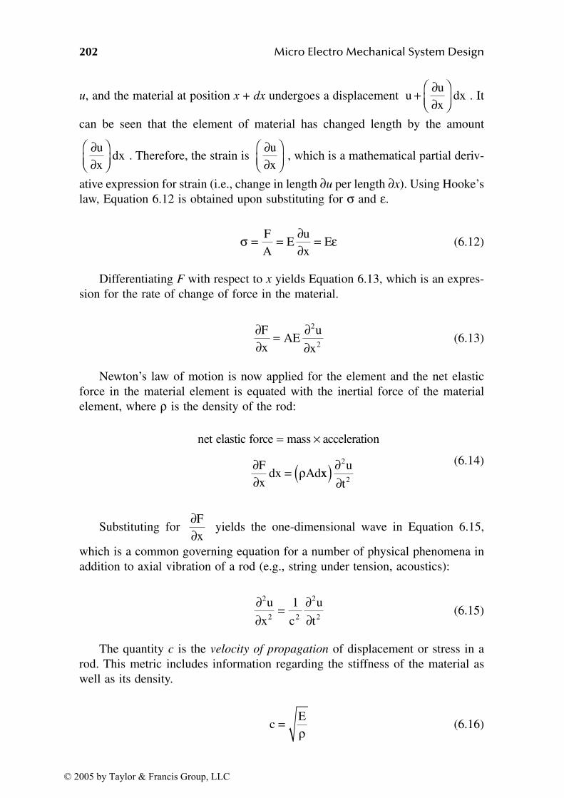
202 Micro Electro Mechanical System Design
u, and the material at position x + dx undergoes a displacement . It
can be seen that the element of material has changed length by the amount
. Therefore, the strain is , which is a mathematical partial deriv-
ative expression for strain (i.e., change in length ∂u per length ∂x). Using Hooke’slaw, Equation 6.12 is obtained upon substituting for σ and ε.
(6.12)
Differentiating F with respect to x yields Equation 6.13, which is an expres-sion for the rate of change of force in the material.
(6.13)
Newton’s law of motion is now applied for the element and the net elasticforce in the material element is equated with the inertial force of the materialelement, where ρ is the density of the rod:
(6.14)
Substituting for yields the one-dimensional wave in Equation 6.15,
which is a common governing equation for a number of physical phenomena inaddition to axial vibration of a rod (e.g., string under tension, acoustics):
(6.15)
The quantity c is the velocity of propagation of displacement or stress in arod. This metric includes information regarding the stiffness of the material aswell as its density.
(6.16)
uux
dx+ ∂∂
∂∂
ux
dx∂∂
ux
σ ε= = ∂∂ =F
AE
ux
E
∂∂ = ∂
∂Fx
AEu
x
2
2
net elastic force mass acceleration
Fx
dx Ad
= ×∂∂ = ρ xx
u
t
2
2( ) ∂∂
∂∂Fx
∂∂ = ∂
∂2
2 2
2
2
u
x
1
c
u
t
cE= ρ
© 2005 by Taylor & Francis Group, LLC
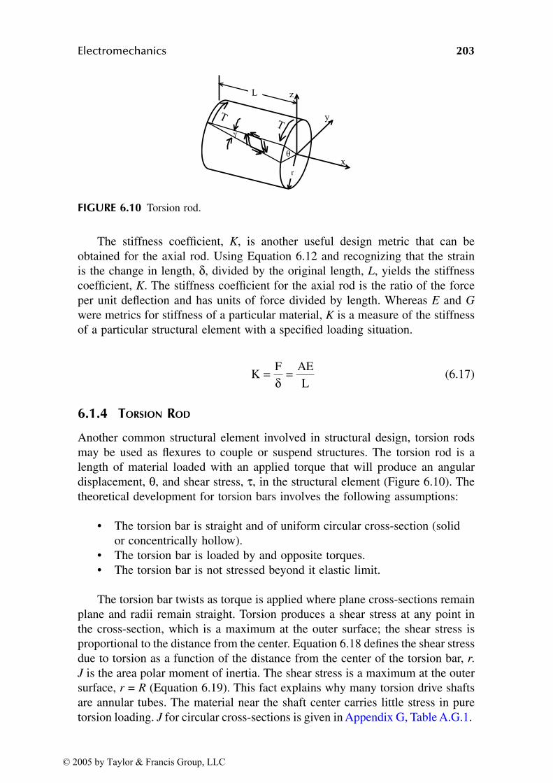
Electromechanics 203
The stiffness coefficient, K, is another useful design metric that can beobtained for the axial rod. Using Equation 6.12 and recognizing that the strainis the change in length, δ, divided by the original length, L, yields the stiffnesscoefficient, K. The stiffness coefficient for the axial rod is the ratio of the forceper unit deflection and has units of force divided by length. Whereas E and Gwere metrics for stiffness of a particular material, K is a measure of the stiffnessof a particular structural element with a specified loading situation.
(6.17)
6.1.4 TORSION ROD
Another common structural element involved in structural design, torsion rodsmay be used as flexures to couple or suspend structures. The torsion rod is alength of material loaded with an applied torque that will produce an angulardisplacement, θ, and shear stress, τ, in the structural element (Figure 6.10). Thetheoretical development for torsion bars involves the following assumptions:
• The torsion bar is straight and of uniform circular cross-section (solidor concentrically hollow).
• The torsion bar is loaded by and opposite torques.• The torsion bar is not stressed beyond it elastic limit.
The torsion bar twists as torque is applied where plane cross-sections remainplane and radii remain straight. Torsion produces a shear stress at any point inthe cross-section, which is a maximum at the outer surface; the shear stress isproportional to the distance from the center. Equation 6.18 defines the shear stressdue to torsion as a function of the distance from the center of the torsion bar, r.J is the area polar moment of inertia. The shear stress is a maximum at the outersurface, r = R (Equation 6.19). This fact explains why many torsion drive shaftsare annular tubes. The material near the shaft center carries little stress in puretorsion loading. J for circular cross-sections is given in Appendix G, Table A.G.1.
FIGURE 6.10 Torsion rod.
KF AE
L= =δ
© 2005 by Taylor & Francis Group, LLC
204 Micro Electro Mechanical System Design
(6.18)
(6.19)
The development of the governing equation for the torsion rod is similar tothat for the axial rod. Once again, the governing equation is the one-dimensionalwave equation (Equation 6.20) involving a speed of propagation, c, for torsionaldisplacement and stress (Equation 6.21). A stiffness coefficient for a torsion rodthat relates the applied torque to the angular displacement can also be developed(Equation 6.22). The stiffness coefficient, K, has units of torque per radian. Theseequations involve the coefficient of rigidity, G, and material density, ρ, as wellas the length of the torsion rod, L.
(6.20)
(6.21)
(6.22)
where,
(6.23)
MEMS applications rarely encounter circular cross-sections. Rectangular andsquare cross-sections are more common due to the restrictions of MEMS fabri-cation techniques. When a torsion load is applied to a noncircular cross-section,some basic assumptions for torsion are violated. The cross-sections becomewarped; the greatest stress occurs at a point on the perimeter nearest the axis oftwist and the corners of the rectangular and square cross-sections have no stress.The analysis of torsion for these cross-sections becomes complex and has beenstudied for years [4,5]. Table A.G.1 in Appendix G gives values for the torsionalconstant, J, that account for the effects of noncircular cross-sections; these canbe used in calculations for torsional stiffness.
τ = TrJ
τmax
TRJ
=
∂∂ = ∂
∂2
2 2
2
2x
1
c t
θ θ
cG= ρ
T K= θ
KJGL
=
© 2005 by Taylor & Francis Group, LLC
Electromechanics 205
6.1.5 BEAM BENDING
Lateral beam bending is a one-dimensional element in which the loading isperpendicular to the axis of the beam. The loading may be distributed along thelength of the beam or concentrated at a specific location; it can also be a com-bination of these situations. A basic formulation of lateral beam bending is calledthe Euler–Bernouli beam. The assumptions involved in the development of theEuler–Bernouli beam model are:
• The material is homogenous and isotropic and obeys Hooke’s law.• The beam is initially straight with a constant cross-section.• The beam is subjected to pure bending (i.e., no torsion or axial loads).• Plane cross-sections (y–z plane) remain plane during bending.• The beam has an axis of symmetry.
The lateral deflection of a Euler–Bernouli beam, shown in Figure 6.11, isdue to a bending moment, M, that bends the beam in a curve with a radius ofcurvature, ρ. The radius of curvature is assumed to be related to the bendingmoment, as shown in Equation 6.24, where E is Young’s modulus and I is thearea moment of inertia about the axis of bending (z axis in Figure 6.11a). TheEI product is the proportionality constant in Equation 6.24, which is frequentlycalled the beam cross-section stiffness. The stiffness of the entire beam willinvolve other information, such as the beam length and the beam end conditions.The radius of curvature, ρ, is also shown in Equation 6.24 to be approximatelyequal to second derivative of y with respect to x. This approximation used in the
FIGURE 6.11 Beam bending.
M
M M M M
M
(a) Beam loading
(b) Beam strain (c) Beam stress
z
y
x
ds
ds
dφ
y ymax
ρ
dφ
ρ
Neutralaxis
−
+
Compressive
Tensile
© 2005 by Taylor & Francis Group, LLC
206 Micro Electro Mechanical System Design
formulation of the Euler–Bernouli beam will limit the resulting governing equa-tion’s validity to small deflections. The deflection of the beam has a “neutralaxis” that is not stressed during bending deformation. Table A.G.2 and TableA.G.3 in Appendix G show the calculation of the area moment of inertia for thecommon beam cross-sections encountered in MEMS devices.
For the beam shown in Figure 6.11c, the material above the neutral axis isin compression and below the neutral axis is in tension. Equation 6.25 shows themathematical expression for the stress distribution across the beam cross-sectionillustrated in Figure 6.11c. As shown in this figure, the stress is a maximum atthe outer fibers of material (Equation 6.26). Depending on the direction of thebending moment at a particular cross-section, the stress is compressive on oneside of the neutral axis and tensile on the other side, with the maximum tensileand compressive stresses occurring at the outer surfaces.
(6.24)
(6.25)
(6.26)
Figure 6.12 schematically illustrates a beam undergoing lateral bending dueto a distributed load q(x), which is a measure of applied force per length alongthe beam. The beam also has a mass per length, m. This figure also shows theforces and moments that will exist on a unit length, dx, of beam material, whereM is a moment and V is a shear force.
The governing equation for a Euler–Bernouli beam can be developed fromthis schematic representation. Equation 6.27 shows an application of Newton’ssecond law in the lateral direction for the unit length of material. Equation 6.28can be obtained by summing moments with respect to the right face of the unitelement of material. A limiting process results in the elimination of the dx2 term.
(6.27)
MEI
1d y
dx
1 dydx
d y
dx
2
2
23
2
2
2= =
+
≈ρ
σ = − MyI
σmaxmaxMy
I= −
my
tdx
Vx
dx qdx
my
t
Vx
q
2
2
2
2
∂∂ = − ∂
∂ +∂∂ = − ∂
∂ +
© 2005 by Taylor & Francis Group, LLC
Electromechanics 207
(6.28)
Combining Equation 6.24, Equation 6.27, and Equation 6.28 results in Equa-tion 6.29, which is the governing partial differential equation for a Euler–Bernoulibeam.
(6.29)
This formulation can be further simplified for a beam with a uniform cross-sectionvs. length:
(6.30)
Solution of the governing equation for a specific beam configuration neces-sitates the definition of the end conditions of the beam. Because the governingequation for a beam is higher order than the governing equation for torsion oran axial rod, the specification of the boundary condition at the ends of the beamrequires two variables to be defined. A beam requires the specification of anytwo of the following: deflection (y), slope (θ), moment (M), or shear force (V).Table 6.1 shows examples of the various classical specifications of beam endconditions. The solutions of the Euler–Bernouli beam equation have been studiedextensively and solutions for a great variety of loading and boundary conditionsituations are readily available [2–4].
FIGURE 6.12 Element of material undergoing beam bending.
∂∂ − − =
∂∂ =
Mx
dx Vdx12
qdx 0
Mx
V
2
my
t xEI
y
xq
2
2
2
2
2
2
∂∂ + ∂
∂∂∂
=
my
tEI
y
xq
2
2
4
4
∂∂ + ∂
∂ =
© 2005 by Taylor & Francis Group, LLC
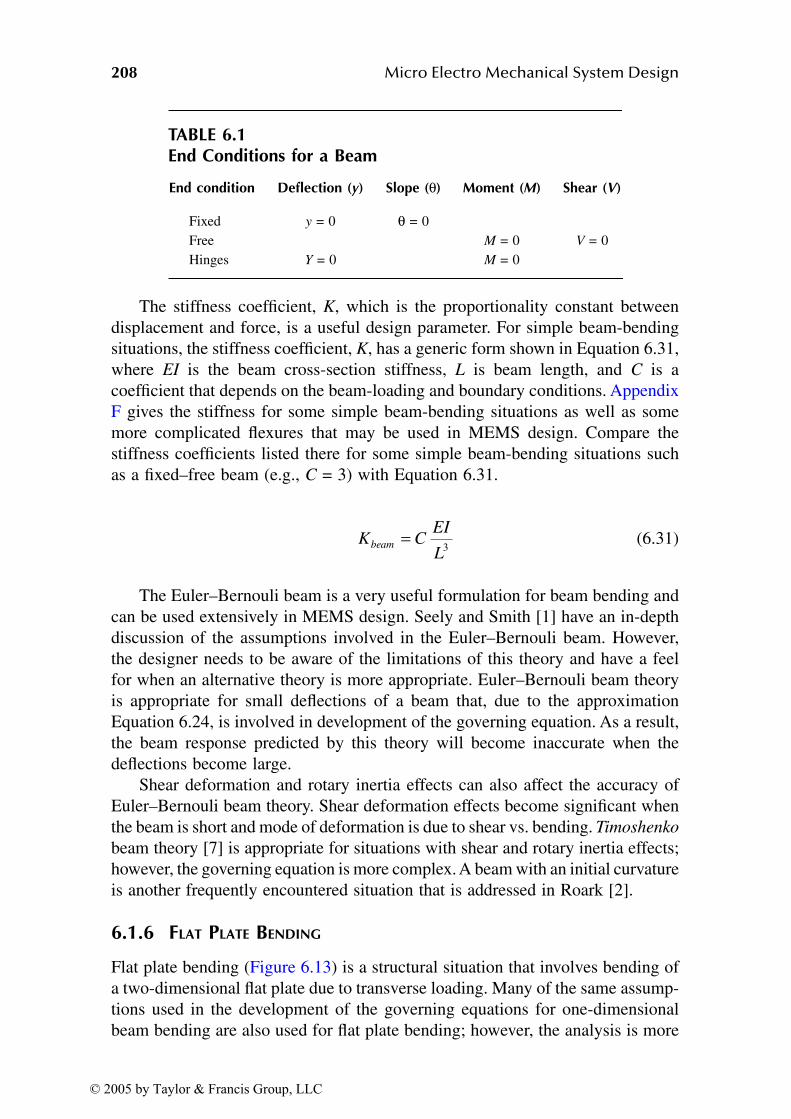
208 Micro Electro Mechanical System Design
The stiffness coefficient, K, which is the proportionality constant betweendisplacement and force, is a useful design parameter. For simple beam-bendingsituations, the stiffness coefficient, K, has a generic form shown in Equation 6.31,where EI is the beam cross-section stiffness, L is beam length, and C is acoefficient that depends on the beam-loading and boundary conditions. AppendixF gives the stiffness for some simple beam-bending situations as well as somemore complicated flexures that may be used in MEMS design. Compare thestiffness coefficients listed there for some simple beam-bending situations suchas a fixed–free beam (e.g., C = 3) with Equation 6.31.
(6.31)
The Euler–Bernouli beam is a very useful formulation for beam bending andcan be used extensively in MEMS design. Seely and Smith [1] have an in-depthdiscussion of the assumptions involved in the Euler–Bernouli beam. However,the designer needs to be aware of the limitations of this theory and have a feelfor when an alternative theory is more appropriate. Euler–Bernouli beam theoryis appropriate for small deflections of a beam that, due to the approximationEquation 6.24, is involved in development of the governing equation. As a result,the beam response predicted by this theory will become inaccurate when thedeflections become large.
Shear deformation and rotary inertia effects can also affect the accuracy ofEuler–Bernouli beam theory. Shear deformation effects become significant whenthe beam is short and mode of deformation is due to shear vs. bending. Timoshenko
beam theory [7] is appropriate for situations with shear and rotary inertia effects;however, the governing equation is more complex. A beam with an initial curvatureis another frequently encountered situation that is addressed in Roark [2].
6.1.6 FLAT PLATE BENDING
Flat plate bending (Figure 6.13) is a structural situation that involves bending ofa two-dimensional flat plate due to transverse loading. Many of the same assump-tions used in the development of the governing equations for one-dimensionalbeam bending are also used for flat plate bending; however, the analysis is more
TABLE 6.1End Conditions for a Beam
End condition Deflection (y) Slope (θ) Moment (M) Shear (V)
Fixed y = 0 θ = 0Free M = 0 V = 0Hinges Y = 0 M = 0
K CEI
Lbeam =
3
© 2005 by Taylor & Francis Group, LLC
Electromechanics 209
complex because of multiaxis bending. Soedel [6] and Timoshenko and Woi-nowsky-Krieger [7] provide the detailed governing equation development for theflat plate (Equation 6.32). The quantity, D, is known as the plate flexural rigidity
(Equation 6.33). Beam bending and flat plate bending are fourth-order partialdifferential equations. The boundary conditions for a flat plate are conceptuallythe same as those for beam bending except that the boundary conditions areapplied along the length of the plate edges.
(6.32)
(6.33)
The analysis of flat plate bending is very important to the design of MEMSdevices such as pressure sensors. Plate theory has been studied extensively anda number of theories have been developed to analyze plates of various configu-rations and loadings. For thick plates, transverse shear becomes important andfor thin plates or membranes, the restoring force is primarily due to tension.Equation 6.32 can be used for the analysis of plates in which flexural stressdominates and the deflections are small relative to the thickness of the plate (e.g.,y < 0.4 t). Analytical solutions of flat plate bending [6,7] have been developedfor a number of cases, but due to their complexity, they are not generally usefulfor design synthesis calculations. Figure 6.14 and Figure 6.15 show simplifiedformulas for pressure loaded circular and rectangular plates with fixed boundaryconditions. These two cases are particularly relevant for MEMS devices.
FIGURE 6.13 Flat plate bending schematic.
ρ ∂∂ + ∂
∂ + ∂∂
∂∂ + ∂
∂
2
2
2
2
2
2
2
2
2
2
w
tD
x y
w
x
w
y = p
DEh
12 1
3
2= −( )ν
© 2005 by Taylor & Francis Group, LLC

210 Micro Electro Mechanical System Design
FIGURE 6.14 Pressure loaded, fixed-boundary circular plate deformation and stress.
FIGURE 6.15 Pressure loaded, fixed-boundary rectangular plate deformation and stress.
© 2005 by Taylor & Francis Group, LLC
Electromechanics 211
6.1.7 COLUMNS
Axial loading of a structural member (Figure 6.16) is a frequently encounteredsituation. The axial load, F, can be tensile or compressive. A member in tensionwould behave as an axial rod (described in a previous section). However, astructural member under axial compression will have two modes of failure:
• Material failure. This occurs when a structural member behaves as anaxial rod where the material will fail.
• Instability failure. If the structural member is sufficiently long andslender, the member will deflect laterally even though the loading ispurely axial. At certain critical loads, this will cause a sudden andcatastrophic collapse of the structure.
In structural mechanics, columns generally refer to axial compressive loading ofa member and the analysis of this instability phenomenon.
Using a very similar approach to the development of the governing equationsfor a beam, but with axial loads included, the governing equation for a compressiveaxial loaded column can be developed (Equation 6.34). The resulting governingequation is the same as the Euler–Bernouli beam except for an additional termthat accounts for the axial loading effects. The second and third terms on the left-hand side of the equation model the stiffness of the beam.
The overall stiffness of a beam or column is greatly influenced by the typeof end condition. Various combinations of idealized end conditions for a columnare illustrated in Figure 6.16. A pinned end condition constrains the lateral deflec-tion of the beam, but the rotation is not constrained. The fixed end conditionconstrains both the deflection and rotation of the beam end, and conversely thefree end condition constrains neither the deflection nor rotation. An idealized fixed
FIGURE 6.16 Axially loaded columns with different end conditions.
F
L
F
L
F
L
L/4
L/2
L/4
F
L
L2
a) pinned-pinned b) fixed-fixed c) fixed-free d) fixed-pinned
© 2005 by Taylor & Francis Group, LLC
212 Micro Electro Mechanical System Design
end condition is difficult to realize in practice; therefore, the theoretical resultsdeveloped using this idealization are sometimes modified (see note Table 6.2).
(6.34)
A simple analysis of a compressive axially loaded column (Figure 6.16c) canbe done with Equation 6.34 as the starting point. Assuming the beam in Figure6.16a is statically loaded, only by the axial force, F, allows neglect of the firstterm on the left and right sides of Equation 6.34. This would result in the followingequation after some simplification:
(6.35)
This second-order differential equation for the column, which is pin supportedat each end, would have the following simple solution:
(6.36)
If the column is about the collapse, the constant, A, in the preceding equationcannot equal zero because the column will deflect laterally. Therefore, the sin
term will need to equal zero. This will be true if . Solving for F
will produce the critical load, Fcr, at which the column will collapse.
(6.37)
This analysis of a pinned-pinned column has resulted in the classical theoryof column collapse known as Euler column theory. This basic analysis can begeneralized for beam of various end conditions (Figure 6.16). Table 6.2 show thevarious fundamental column loading situations and the end condition constants,C, that can be used in the generalized form of the Euler column formula (Equation6.38). This can be used to provide an estimate of the critical load for columncollapse. However, the analysis and prediction of Fcr for a real-world situation isvery difficult. Column instability is very sensitive to small perturbation in theend conditions and structural imperfections. Also, a fixed boundary condition isvery difficult to achieve in practice. Therefore, use of a value of C of no greaterthan 1.2 is recommended to avoid predicting a value too high for Fcr.
my
t xEI
y
x+F
y
xq
2
2
2
2
2
2
2
2
∂∂ + ∂
∂∂∂
∂∂ =
d y
dx
FEI
y 02
2+ =
A sinFEI
L 0
=
F EI L = π
FEI
Lcr
2
2= π
© 2005 by Taylor & Francis Group, LLC
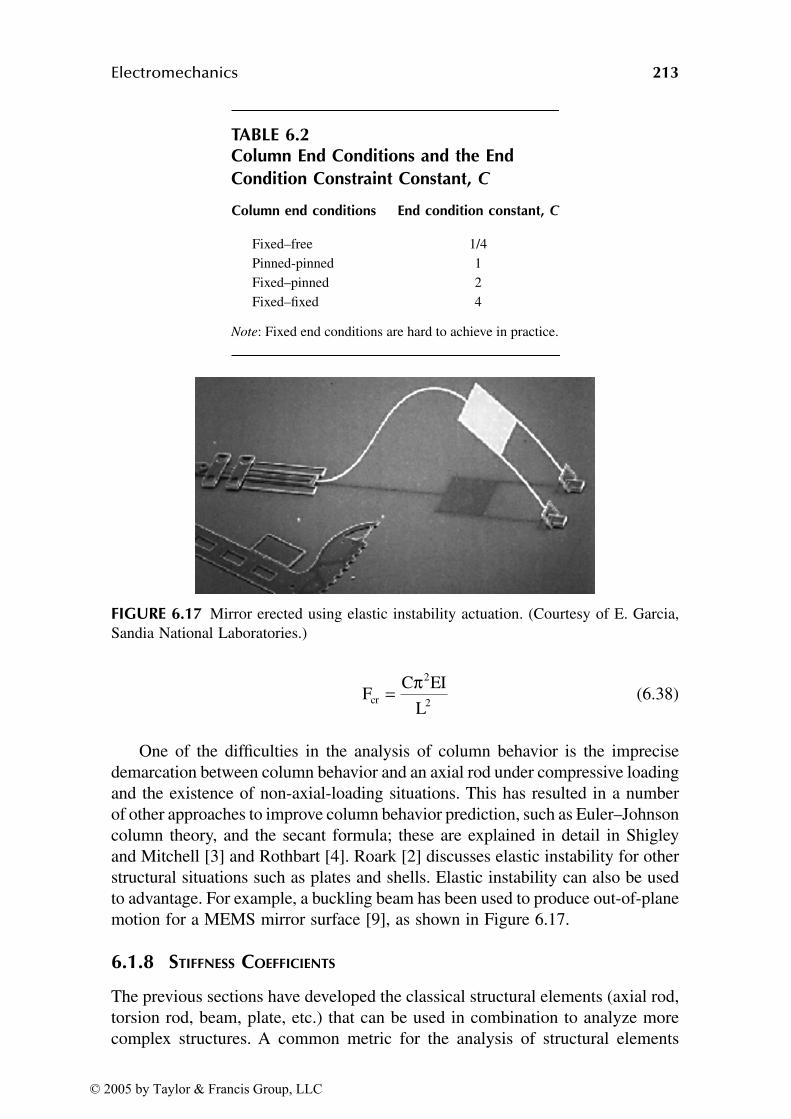
Electromechanics 213
(6.38)
One of the difficulties in the analysis of column behavior is the imprecisedemarcation between column behavior and an axial rod under compressive loadingand the existence of non-axial-loading situations. This has resulted in a numberof other approaches to improve column behavior prediction, such as Euler–Johnsoncolumn theory, and the secant formula; these are explained in detail in Shigleyand Mitchell [3] and Rothbart [4]. Roark [2] discusses elastic instability for otherstructural situations such as plates and shells. Elastic instability can also be usedto advantage. For example, a buckling beam has been used to produce out-of-planemotion for a MEMS mirror surface [9], as shown in Figure 6.17.
6.1.8 STIFFNESS COEFFICIENTS
The previous sections have developed the classical structural elements (axial rod,torsion rod, beam, plate, etc.) that can be used in combination to analyze morecomplex structures. A common metric for the analysis of structural elements
TABLE 6.2Column End Conditions and the End
Condition Constraint Constant, C
Column end conditions End condition constant, C
Fixed–free 1/4Pinned-pinned 1Fixed–pinned 2Fixed–fixed 4
Note: Fixed end conditions are hard to achieve in practice.
FIGURE 6.17 Mirror erected using elastic instability actuation. (Courtesy of E. Garcia,Sandia National Laboratories.)
FC EI
Lcr
2
2= π
© 2005 by Taylor & Francis Group, LLC
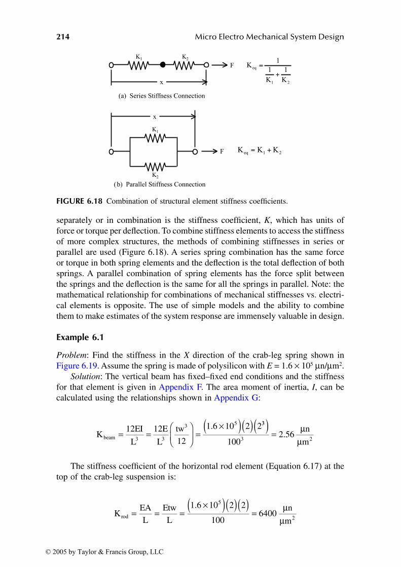
214 Micro Electro Mechanical System Design
separately or in combination is the stiffness coefficient, K, which has units offorce or torque per deflection. To combine stiffness elements to access the stiffnessof more complex structures, the methods of combining stiffnesses in series orparallel are used (Figure 6.18). A series spring combination has the same forceor torque in both spring elements and the deflection is the total deflection of bothsprings. A parallel combination of spring elements has the force split betweenthe springs and the deflection is the same for all the springs in parallel. Note: themathematical relationship for combinations of mechanical stiffnesses vs. electri-cal elements is opposite. The use of simple models and the ability to combinethem to make estimates of the system response are immensely valuable in design.
Example 6.1
Problem: Find the stiffness in the X direction of the crab-leg spring shown inFigure 6.19. Assume the spring is made of polysilicon with E = 1.6 × 10⁵ µn/µm2.
Solution: The vertical beam has fixed–fixed end conditions and the stiffnessfor that element is given in Appendix F. The area moment of inertia, I, can becalculated using the relationships shown in Appendix G:
The stiffness coefficient of the horizontal rod element (Equation 6.17) at thetop of the crab-leg suspension is:
FIGURE 6.18 Combination of structural element stiffness coefficients.
K12EI
L
12E
L
tw12
1.6 10 2 2beam 3 3
3 5
= =
= ×( ) ( ) 33
3 21002.56
n
m
( ) = µµ
KEAL
EtwL
1.6 10 2 2
1006400
n
mrod
5
2= = = ×( ) ( ) ( ) = µ
µ
© 2005 by Taylor & Francis Group, LLC
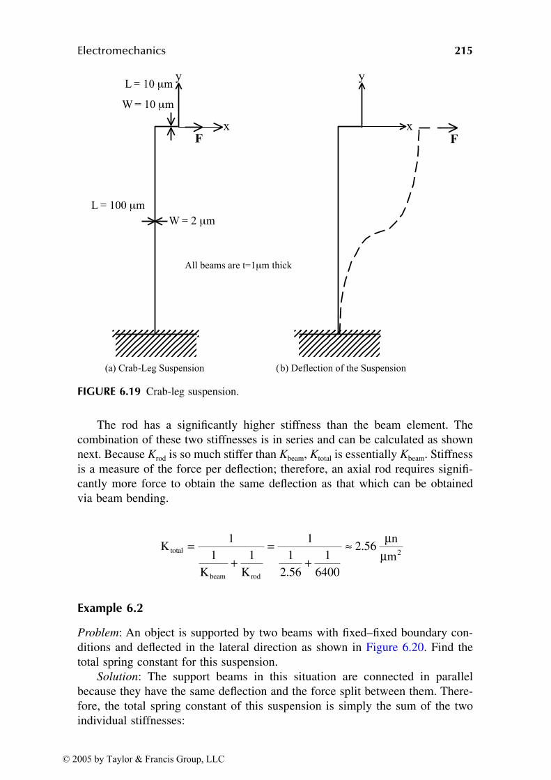
Electromechanics 215
The rod has a significantly higher stiffness than the beam element. Thecombination of these two stiffnesses is in series and can be calculated as shownnext. Because Krod is so much stiffer than Kbeam, Ktotal is essentially Kbeam. Stiffnessis a measure of the force per deflection; therefore, an axial rod requires signifi-cantly more force to obtain the same deflection as that which can be obtainedvia beam bending.
Example 6.2
Problem: An object is supported by two beams with fixed–fixed boundary con-ditions and deflected in the lateral direction as shown in Figure 6.20. Find thetotal spring constant for this suspension.
Solution: The support beams in this situation are connected in parallelbecause they have the same deflection and the force split between them. There-fore, the total spring constant of this suspension is simply the sum of the twoindividual stiffnesses:
FIGURE 6.19 Crab-leg suspension.
K1
1K
1K
11
2.561
6400
2.56n
mtotal
beam rod
2=
+=
+≈ µ
µ
© 2005 by Taylor & Francis Group, LLC
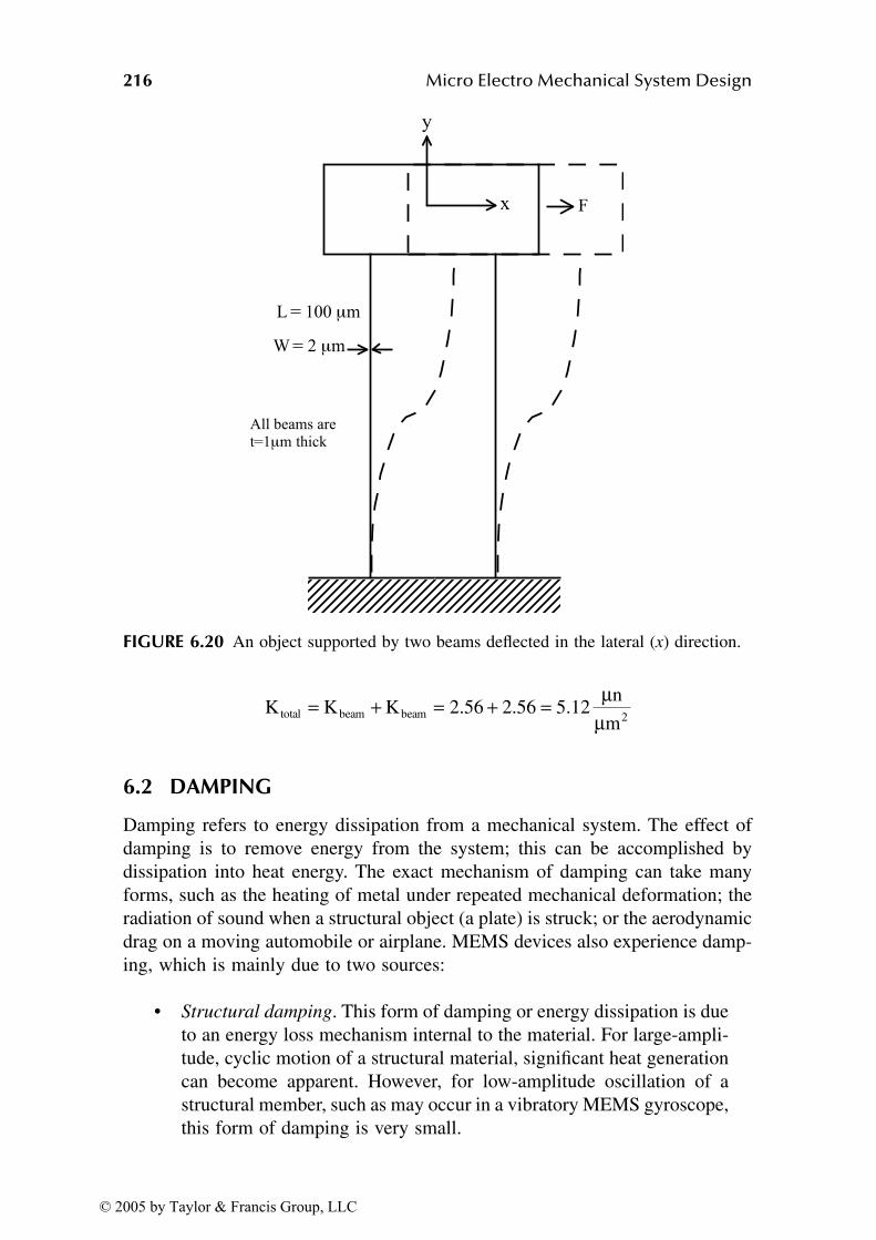
216 Micro Electro Mechanical System Design
6.2 DAMPING
Damping refers to energy dissipation from a mechanical system. The effect ofdamping is to remove energy from the system; this can be accomplished bydissipation into heat energy. The exact mechanism of damping can take manyforms, such as the heating of metal under repeated mechanical deformation; theradiation of sound when a structural object (a plate) is struck; or the aerodynamicdrag on a moving automobile or airplane. MEMS devices also experience damp-ing, which is mainly due to two sources:
• Structural damping. This form of damping or energy dissipation is dueto an energy loss mechanism internal to the material. For large-ampli-tude, cyclic motion of a structural material, significant heat generationcan become apparent. However, for low-amplitude oscillation of astructural member, such as may occur in a vibratory MEMS gyroscope,this form of damping is very small.
FIGURE 6.20 An object supported by two beams deflected in the lateral (x) direction.
K K Kn
mtotal beam beam= + = + =2 56 2 56 5 12
2. . .
µµ
© 2005 by Taylor & Francis Group, LLC
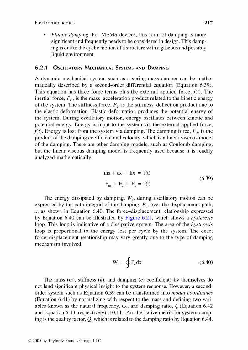
Electromechanics 217
• Fluidic damping. For MEMS devices, this form of damping is moresignificant and frequently needs to be considered in design. This damp-ing is due to the cyclic motion of a structure with a gaseous and possiblyliquid environment.
6.2.1 OSCILLATORY MECHANICAL SYSTEMS AND DAMPING
A dynamic mechanical system such as a spring-mass-damper can be mathe-matically described by a second-order differential equation (Equation 6.39).This equation has three force terms plus the external applied force, f(t). Theinertial force, Fm, is the mass–acceleration product related to the kinetic energyof the system. The stiffness force, Fk, is the stiffness–deflection product due tothe elastic deformation. Elastic deformation produces the potential energy ofthe system. During oscillatory motion, energy oscillates between kinetic andpotential energy. Energy is input to the system via the external applied force,f(t). Energy is lost from the system via damping. The damping force, Fd, is theproduct of the damping coefficient and velocity, which is a linear viscous modelof the damping. There are other damping models, such as Coulomb damping,but the linear viscous damping model is frequently used because it is readilyanalyzed mathematically.
(6.39)
The energy dissipated by damping, Wd, during oscillatory motion can beexpressed by the path integral of the damping, Fd, over the displacement path,x, as shown in Equation 6.40. The force–displacement relationship expressedby Equation 6.40 can be illustrated by Figure 6.21, which shows a hysteresis
loop. This loop is indicative of a dissipative system. The area of the hysteresis
loop is proportional to the energy lost per cycle by the system. The exactforce–displacement relationship may vary greatly due to the type of dampingmechanism involved.
(6.40)
The mass (m), stiffness (k), and damping (c) coefficients by themselves donot lend significant physical insight to the system response. However, a second-order system such as Equation 6.39 can be transformed into modal coordinates
(Equation 6.41) by normalizing with respect to the mass and defining two vari-ables known as the natural frequency, ωn, and damping ratio, ζ (Equation 6.42and Equation 6.43, respectively) [10,11]. An alternative metric for system damp-ing is the quality factor, Q, which is related to the damping ratio by Equation 6.44.
mx cx kx f(t)
F F F f(t)m d k
ɺɺ ɺ+ + =+ + =
W F dxd d= ∫
© 2005 by Taylor & Francis Group, LLC

218 Micro Electro Mechanical System Design
(6.41)
(6.42)
(6.43)
(6.44)
The maximum system response, x, will be obtained if the system is excitedwith an oscillatory force at the natural frequency (e.g., f sin[wnt]). This conditionis known as resonance. If the system has no damping (c and ζ are zero), theresponse at resonance is mathematically infinite; however, every system containsat least some small amount of damping, which will limit the response. At reso-nance, the kinetic and potential energy of the system are equal and the systemenergy is oscillating in form between kinetic and potential energy.
The damping ratio, ζ, is any positive real number. The damping ratio directlycontrols the nature of the system response as illustrated in Figure 6.22. Figure6.22 shows the response for a spring–mass–damper system that is displaced andreleased. For values of the damping ratio 0 ≤ ζ < 1, the system has an oscillatory
FIGURE 6.21 The force–displacement hysteresis loop, which illustrates the energy dis-sipated by damping.
Energydissipation
Fd
x
ɺɺ ɺx 2 x x f(t)n n2+ + =ζω ω
ζ = c
2 km
ωn
km
=
Q1
2= ζ
© 2005 by Taylor & Francis Group, LLC
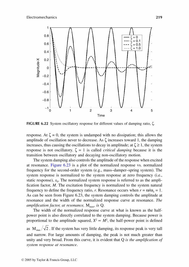
Electromechanics 219
response. At ζ = 0, the system is undamped with no dissipation; this allows theamplitude of oscillation never to decrease. As ζ increases toward 1, the dampingincreases, thus causing the oscillations to decay in amplitude; at ζ ≥ 1, the systemresponse is not oscillatory. ζ = 1 is called critical damping because it is thetransition between oscillatory and decaying non-oscillatory motion.
The system damping also controls the amplitude of the response when excitedat resonance. Figure 6.23 is a plot of the normalized response vs. normalizedfrequency for the second-order system (e.g., mass–damper–spring system). Thesystem response is normalized to the system response at zero frequency (i.e.,static response), x0. The normalized system response is referred to as the ampli-fication factor, M. The excitation frequency is normalized to the system naturalfrequency to define the frequency ratio, r. Resonance occurs when r = ω/ωn = 1.As can be seen from Figure 6.23, the system damping controls the amplitude atresonance and the width of the normalized response curve at resonance. The
amplification factor, at resonance, Mmax, is Q. The width of the normalized response curve at what is known as the half-
power point is also directly correlated to the system damping. Because power isproportional to the amplitude squared, X2 ∝ M2, the half-power point is defined
as . If the system has very little damping, its response peak is very tall
and narrow. For large amounts of damping, the peak is not much greater thanunity and very broad. From this curve, it is evident that Q is the amplification of
system response at resonance.
FIGURE 6.22 System oscillatory response for different values of damping ratio, ζ.
−1
1
0.2
0.4
0.6
0.8
0
−0.2
−0.4
−0.6
−0.8
Magnitude-X
0 1 2 3 4 5
ζ = 0ζ = 0.1ζ = 0.5ζ = 1.0
Time
Mmax 2
© 2005 by Taylor & Francis Group, LLC
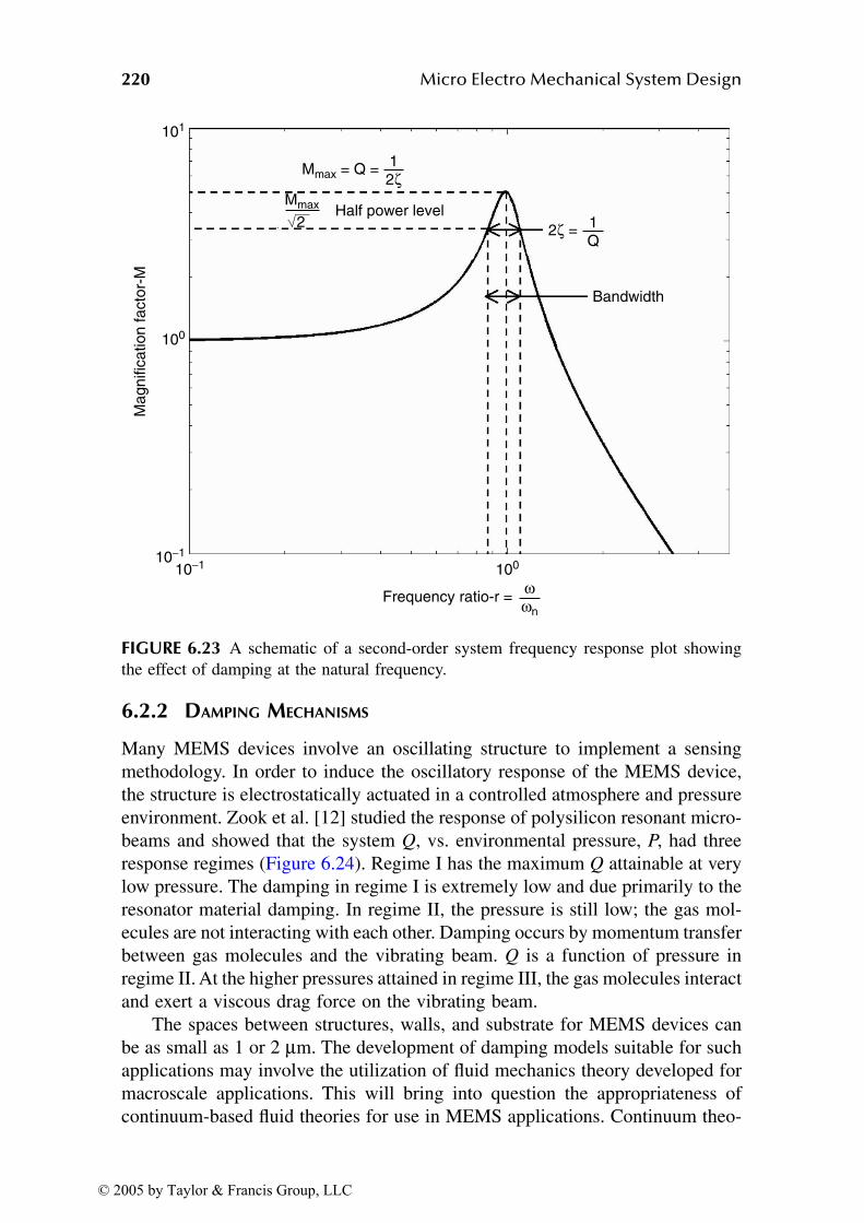
220 Micro Electro Mechanical System Design
6.2.2 DAMPING MECHANISMS
Many MEMS devices involve an oscillating structure to implement a sensingmethodology. In order to induce the oscillatory response of the MEMS device,the structure is electrostatically actuated in a controlled atmosphere and pressureenvironment. Zook et al. [12] studied the response of polysilicon resonant micro-beams and showed that the system Q, vs. environmental pressure, P, had threeresponse regimes (Figure 6.24). Regime I has the maximum Q attainable at verylow pressure. The damping in regime I is extremely low and due primarily to theresonator material damping. In regime II, the pressure is still low; the gas mol-ecules are not interacting with each other. Damping occurs by momentum transferbetween gas molecules and the vibrating beam. Q is a function of pressure inregime II. At the higher pressures attained in regime III, the gas molecules interactand exert a viscous drag force on the vibrating beam.
The spaces between structures, walls, and substrate for MEMS devices canbe as small as 1 or 2 µm. The development of damping models suitable for suchapplications may involve the utilization of fluid mechanics theory developed formacroscale applications. This will bring into question the appropriateness ofcontinuum-based fluid theories for use in MEMS applications. Continuum theo-
FIGURE 6.23 A schematic of a second-order system frequency response plot showingthe effect of damping at the natural frequency.
Magnific
ation facto
r-M
101
100
10−1
10−1 100
Frequency ratio-r =ωωn
1
2ζMmax = Q =
1
Q2ζ =
Mmax
2Half power level
Bandwidth
© 2005 by Taylor & Francis Group, LLC

Electromechanics 221
ries assume that, in any analysis domain, a large number of atoms is present thatuse continuous partial differential equations to describe the relevant physics vs.the discrete dynamic interactions of individual molecules.
An appropriate metric to assess this situation is the mean free path, λ, of thegas surrounding the MEMS device; this is the distance that a molecule travelsbefore it collides with another molecule. Collisions are the primary momentumtransfer mechanism of gases. These collisions will give rise to energy dissipationon the surface of a moving MEMS device. If a molecule of diameter, d, travelswithin a distance, d, of another molecule of the same type, a collision will occur.Therefore, the collision cross-section of the molecule is πd2. For molecules suchas N2 and O2, d ≈ 3 Å is a good estimate. The probability of collision, P, withina distance, D, of a volume containing a molecular density (molecules/volume),n, is given by:
(6.45)
If the probability of a collision within a distance λ is 1, an estimate of themean free path is approximately given by:
FIGURE 6.24 Quality factor, Q, vs. pressure regimes for a MEMS resonator. (Reprintedfrom J.D. Zook et al., Sensors Actuators A, 35, 51–59, 1992. With permission fromElsevier.)
10−1
10−3 10−2 10−1
100
100 101 102 103 104 105
101
102
103
104
105
Q
Pressure (torr)
I
II
III
P D d n2= π
© 2005 by Taylor & Francis Group, LLC
222 Micro Electro Mechanical System Design
(6.46)
A more statistically accurate estimate of the mean free path, λ, is given by:
(6.47)
The molecular density, n, may be calculated from the ideal gas law:
(6.48)
Combining equations yields the mean free path for an ideal gas equation,where p is pressure; kB = 1.38 × 10⁻²³ J/K; and T is absolute temperature:
(6.49)
Example 6.3
Problem: (a) Plot the mean free path, λ, for N2 at T = 300°K for pressure, p,varying from 50 mtorr to 1 atm pressure (760 torr). (b) What is λ at atmosphericpressure? (c) What is λ at 0.050 torr? (d) At what pressure is λ = 2 µm?
Solution: (a) Figure 6.25 is a plot of the mean free path vs. pressure obtainedvia evaluation of Equation 6.49; d was taken to be approximately 3Å for N2. (b)At atmospheric pressure (760 torr), the mean free path in N2 is 102 nm. (c) At apressure of 50 mtorr, the mean free path in N2 is 1554 µm. (d) The mean freepath is λ = 2 µm in N2 when the pressure is 38.8 torr.
6.2.3 VISCOUS DAMPING
Gas damping is the source of most MEMS damping and it is a strong functionof viscosity. The absolute viscosity µ of a fluid or gas is a measure of theresistance to flow. The absolute viscosity, µ, is the ratio of the shear stress, τ,between flow layers to the velocity gradient, dv/dy, through the fluid channel(Equation 6.50). The flow field for this situation has the fluid fixed to the surfaceof both plates with a linear velocity profile between the plates as illustrated inFigure 6.26. The kinematic viscosity, ν, is the absolute viscosity scaled by thedensity, ρ, of the fluid. This parameter is called kinematic because the units arelength2 per time.
λ π≈ 12d n
λ π≈ 1
2 2d n
np
k TB
=
λ π= k T
d pB
2 2
© 2005 by Taylor & Francis Group, LLC
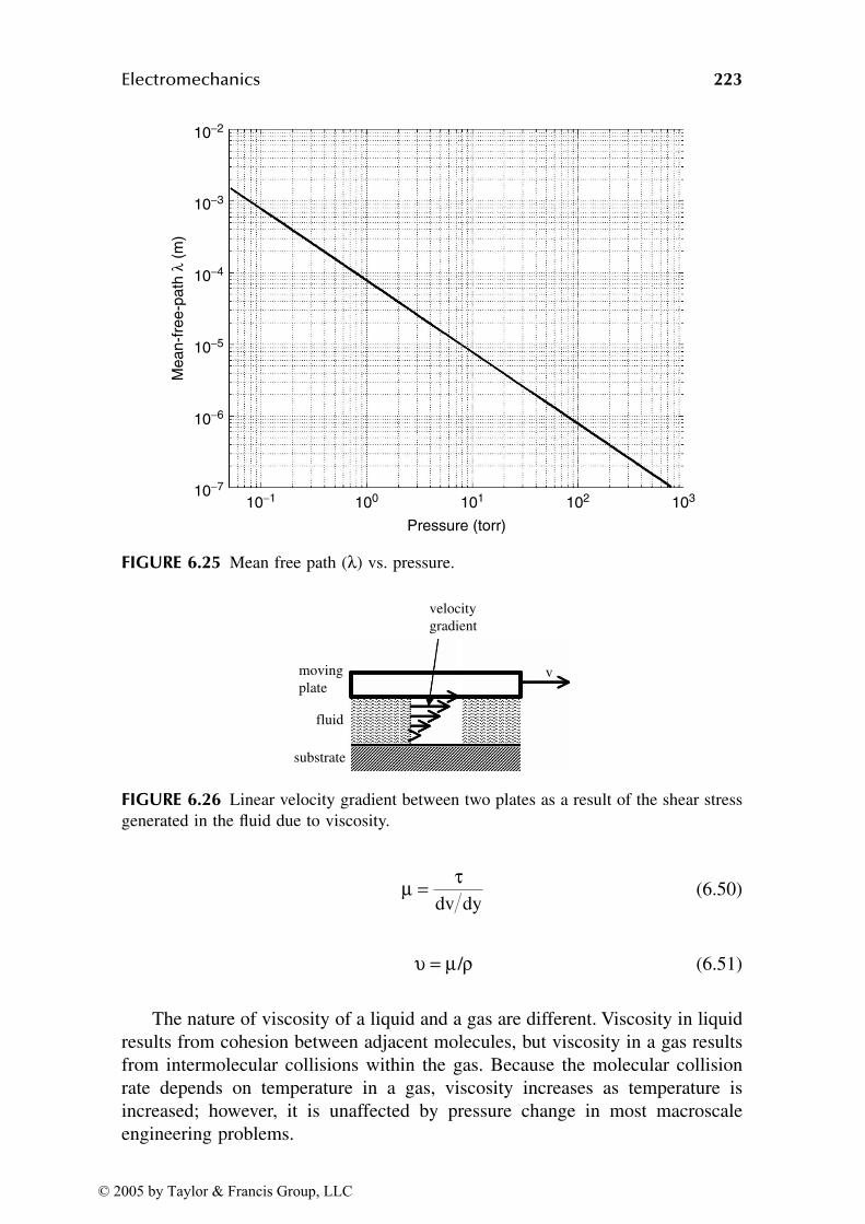
Electromechanics 223
(6.50)
(6.51)
The nature of viscosity of a liquid and a gas are different. Viscosity in liquidresults from cohesion between adjacent molecules, but viscosity in a gas resultsfrom intermolecular collisions within the gas. Because the molecular collisionrate depends on temperature in a gas, viscosity increases as temperature isincreased; however, it is unaffected by pressure change in most macroscaleengineering problems.
FIGURE 6.25 Mean free path (λ) vs. pressure.
FIGURE 6.26 Linear velocity gradient between two plates as a result of the shear stressgenerated in the fluid due to viscosity.
10−7
10−1 100 101 102
10−6
10−5
10−4
10−3
10−2
103
Mean-f
ree-p
ath
λ (
m)
Pressure (torr)
v
substrate
fluid
moving plate
velocity gradient
µ τ=dv dy
υ µ ρ= /
© 2005 by Taylor & Francis Group, LLC
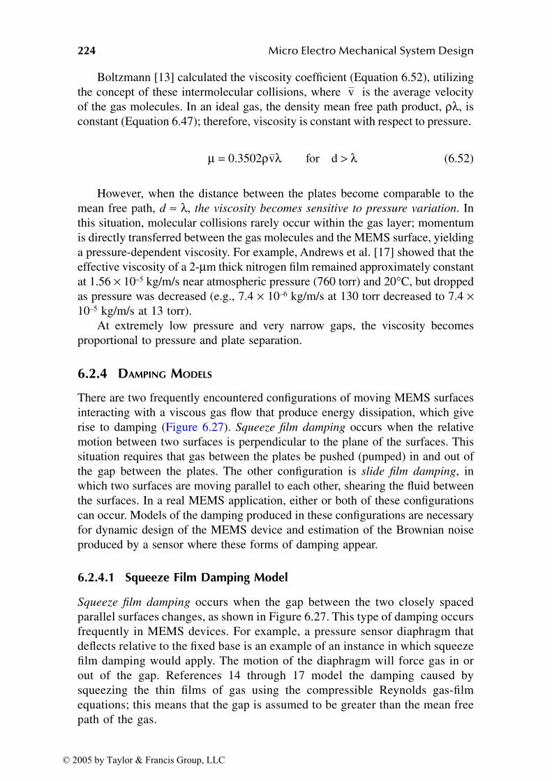
224 Micro Electro Mechanical System Design
Boltzmann [13] calculated the viscosity coefficient (Equation 6.52), utilizingthe concept of these intermolecular collisions, where is the average velocityof the gas molecules. In an ideal gas, the density mean free path product, ρλ, isconstant (Equation 6.47); therefore, viscosity is constant with respect to pressure.
(6.52)
However, when the distance between the plates become comparable to themean free path, d ≈ λ, the viscosity becomes sensitive to pressure variation. Inthis situation, molecular collisions rarely occur within the gas layer; momentumis directly transferred between the gas molecules and the MEMS surface, yieldinga pressure-dependent viscosity. For example, Andrews et al. [17] showed that theeffective viscosity of a 2-µm thick nitrogen film remained approximately constantat 1.56 × 10⁻⁵ kg/m/s near atmospheric pressure (760 torr) and 20°C, but droppedas pressure was decreased (e.g., 7.4 × 10⁻⁶ kg/m/s at 130 torr decreased to 7.4 ×10⁻⁵ kg/m/s at 13 torr).
At extremely low pressure and very narrow gaps, the viscosity becomesproportional to pressure and plate separation.
6.2.4 DAMPING MODELS
There are two frequently encountered configurations of moving MEMS surfacesinteracting with a viscous gas flow that produce energy dissipation, which giverise to damping (Figure 6.27). Squeeze film damping occurs when the relativemotion between two surfaces is perpendicular to the plane of the surfaces. Thissituation requires that gas between the plates be pushed (pumped) in and out ofthe gap between the plates. The other configuration is slide film damping, inwhich two surfaces are moving parallel to each other, shearing the fluid betweenthe surfaces. In a real MEMS application, either or both of these configurationscan occur. Models of the damping produced in these configurations are necessaryfor dynamic design of the MEMS device and estimation of the Brownian noiseproduced by a sensor where these forms of damping appear.
6.2.4.1 Squeeze Film Damping Model
Squeeze film damping occurs when the gap between the two closely spacedparallel surfaces changes, as shown in Figure 6.27. This type of damping occursfrequently in MEMS devices. For example, a pressure sensor diaphragm thatdeflects relative to the fixed base is an example of an instance in which squeezefilm damping would apply. The motion of the diaphragm will force gas in orout of the gap. References 14 through 17 model the damping caused bysqueezing the thin films of gas using the compressible Reynolds gas-filmequations; this means that the gap is assumed to be greater than the mean freepath of the gas.
v
µ ρ λ λ= >0.3502 v for d
© 2005 by Taylor & Francis Group, LLC
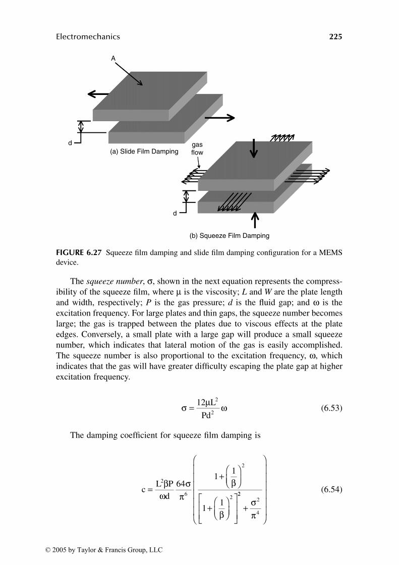
Electromechanics 225
The squeeze number, σ, shown in the next equation represents the compress-ibility of the squeeze film, where µ is the viscosity; L and W are the plate lengthand width, respectively; P is the gas pressure; d is the fluid gap; and ω is theexcitation frequency. For large plates and thin gaps, the squeeze number becomeslarge; the gas is trapped between the plates due to viscous effects at the plateedges. Conversely, a small plate with a large gap will produce a small squeezenumber, which indicates that lateral motion of the gas is easily accomplished.The squeeze number is also proportional to the excitation frequency, ω, whichindicates that the gas will have greater difficulty escaping the plate gap at higherexcitation frequency.
(6.53)
The damping coefficient for squeeze film damping is
(6.54)
FIGURE 6.27 Squeeze film damping and slide film damping configuration for a MEMSdevice.
d
d
(a) Slide Film Damping
A
gasflow
(b) Squeeze Film Damping
σ µ ω= 12 L
Pd
2
2
cL P
d=
+
+
2
6
2
2
641
1
11
βω
σπ
β
β22
2
4+
σπ
© 2005 by Taylor & Francis Group, LLC
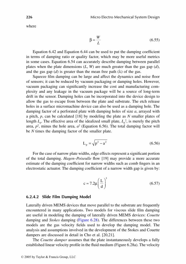
226 Micro Electro Mechanical System Design
where
(6.55)
Equation 6.42 and Equation 6.44 can be used to put the damping coefficientin terms of damping ratio or quality factor, which may be more useful metricsin some cases. Equation 6.54 can accurately describe damping between parallelplates when the plate dimensions (L, W) are much greater than the gas gap (d),and the gas gap (d) is greater than the mean free path (λ) of the gas.
Squeeze film damping can be large and affect the dynamics and noise floorof sensors; it can be reduced by vacuum packaging or damping holes. However,vacuum packaging can significantly increase the cost and manufacturing com-plexity and any leakage in the vacuum package will be a source of long-termdrift in the sensor. Damping holes can be incorporated into the device design toallow the gas to escape from between the plate and substrate. The etch releaseholes in a surface micromachine device can also be used as a damping hole. Thedamping factor of a perforated plate with damping holes of size a, arrayed witha pitch, p, can be calculated [18] by modeling the plate as N smaller plates oflength Lp. The effective area of the idealized small plate, Lp
2, is merely the pitcharea, p2, minus the hole area, a2 (Equation 6.56). The total damping factor willbe N times the damping factor of the smaller plate.
(6.56)
For the case of narrow plate widths, edge effects represent a significant portionof the total damping. Hagen–Poiseulle flow [19] may provide a more accurateestimate of the damping coefficient for narrow widths such as comb fingers in anelectrostatic actuator. The damping coefficient of a narrow width gap is given by:
(6.57)
6.2.4.2 Slide Film Damping Model
Laterally driven MEMS devices that move parallel to the substrate are frequentlyencountered in many applications. Two models for viscous slide film dampingare useful in modeling the damping of laterally driven MEMS devices: Couette
damping and Stokes damping (Figure 6.28). The differences between these twomodels are the gas velocity fields used to develop the damping model. Theanalysis and assumptions involved in the development of the Stokes and Couettedampers are discussed in detail in Cho et al. [20,21].
The Couette damper assumes that the plate instantaneously develops a fullyestablished linear velocity profile in the fluid medium (Figure 6.28a). The velocity
β = W
L
L p ap2 2= −
c 7.2Ld
3
≈
µ
© 2005 by Taylor & Francis Group, LLC
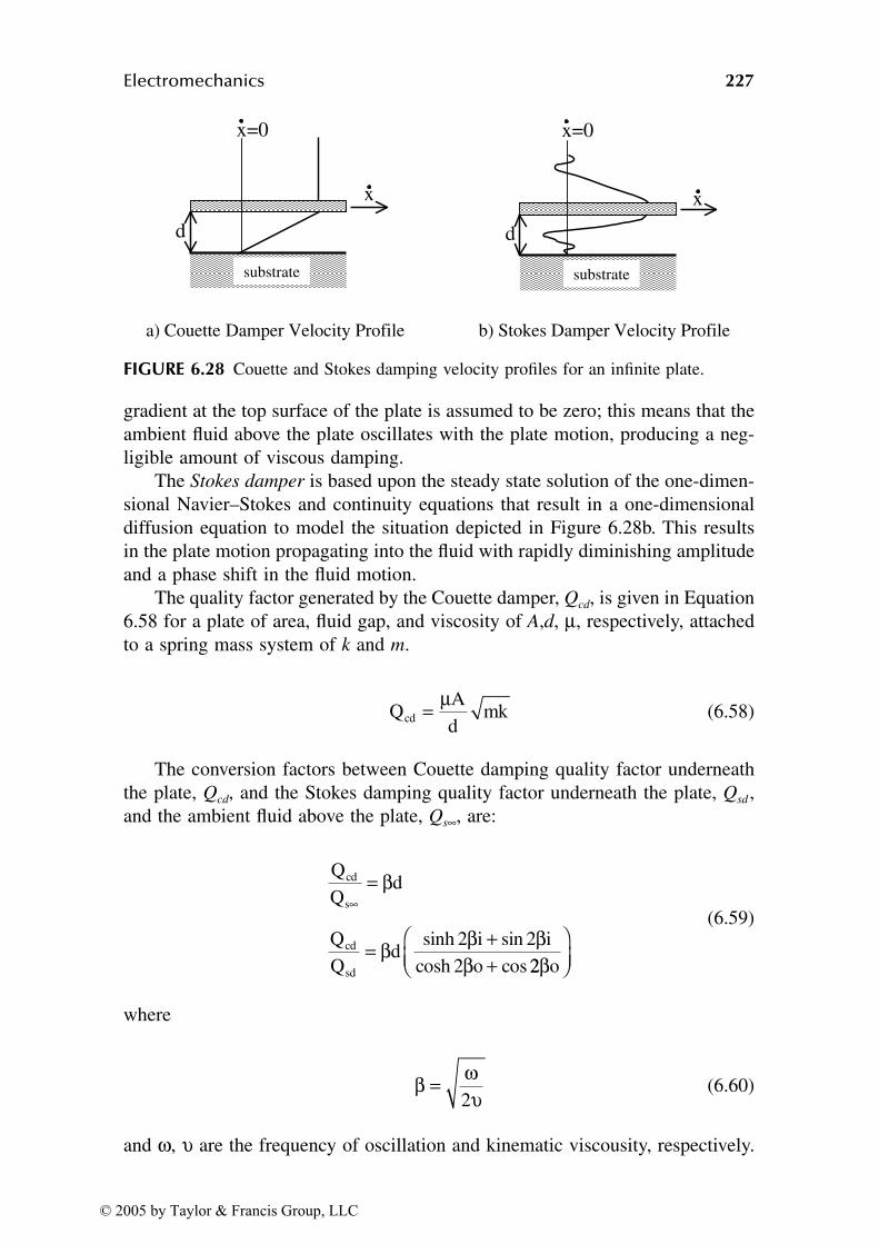
Electromechanics 227
gradient at the top surface of the plate is assumed to be zero; this means that theambient fluid above the plate oscillates with the plate motion, producing a neg-ligible amount of viscous damping.
The Stokes damper is based upon the steady state solution of the one-dimen-sional Navier–Stokes and continuity equations that result in a one-dimensionaldiffusion equation to model the situation depicted in Figure 6.28b. This resultsin the plate motion propagating into the fluid with rapidly diminishing amplitudeand a phase shift in the fluid motion.
The quality factor generated by the Couette damper, Qcd, is given in Equation6.58 for a plate of area, fluid gap, and viscosity of A,d, µ, respectively, attachedto a spring mass system of k and m.
(6.58)
The conversion factors between Couette damping quality factor underneaththe plate, Qcd, and the Stokes damping quality factor underneath the plate, Qsd ,and the ambient fluid above the plate, Qs∞, are:
(6.59)
where
(6.60)
and ω, υ are the frequency of oscillation and kinematic viscousity, respectively.
FIGURE 6.28 Couette and Stokes damping velocity profiles for an infinite plate.
d
substrate
b) Stokes Damper Velocity Profile
x
x=0
d
substrate
a) Couette Damper Velocity Profile
x
x=0
QAd
mkcd = µ
d
d
cd
s
cd
sd
∞=
= ++
β
β β ββ
sinh sincosh cos
2 22
i io 22βo
β ωυ=
2
© 2005 by Taylor & Francis Group, LLC
228 Micro Electro Mechanical System Design
6.3 ELECTRICAL SYSTEM DYNAMICS
The objective of this presentation of electromechanics is to provide the basis foranalysis of actuator and sensor systems, which frequently involve a coupling ofthe mechanics of a structure (i.e., membrane, seismic mass, flexural supports)and an electrical system that senses the motion or provides a force for actuation.This section will provide an overview of the terminology and key physics nec-essary for the analysis of an electromechanical system. Table 6.3 is a list ofelectrical quantities, symbols, and units discussed in this section.
The mechanics of electrical systems are described by Maxwell’s equations,which can be written in differential or integral forms and incorporate a numberof assumptions for specific applications. An in-depth treatment of Maxwell’sequations is a very complex subject and beyond the scope of this book. However,a number of references can provide a variety of views on this subject. Johnk [22]provides an in-depth theoretical treatment of Maxwell’s equations. Moon [23]provides a link between the theoretical study of Maxwell’s equations and appli-cations that utilize electromechanics. Smith [24] provides an introductory, verypractical application of electrical systems and electromechanics to engineeringsolutions. Crandall et al. [25] present a detailed explanation of the analysis ofelectromechanical systems that is very useful for the analysis of transducers suchas those utilized in MEMS applications.
TABLE 6.3Electrical Quantities and Units
Electrical quantity Symbol Units Type
Charge q Coulomb (C) Scalar
Electric potential e or V Volt (V)V = (N – m)/C
Scalar
Electric field intensity E V/m or N/C Vector
Magnetic flux density B Tesla (T) T = Wb/m2 = (V – s)/m2
Vector
Current i Ampere (A)A = C/s
Scalar
Flux linkage λ Weber (Wb)Wb = V – s
Scalar
Capacitance C Farad (F)F = C/V
Scalar
Inductance L Henry (H)H = Wb/A = (V – s)/A
Scalar
Resistance R Ohm (Ω)Ω = V/A
Scalar
© 2005 by Taylor & Francis Group, LLC
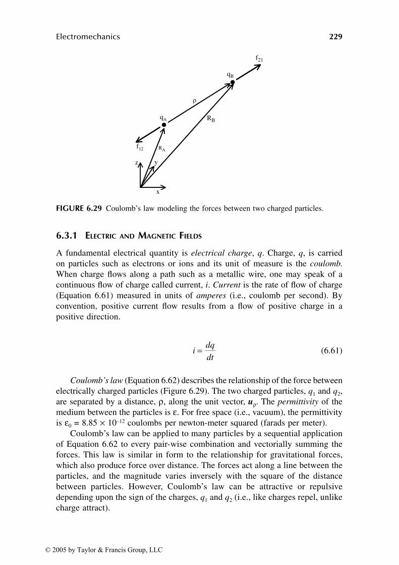
Electromechanics 229
6.3.1 ELECTRIC AND MAGNETIC FIELDS
A fundamental electrical quantity is electrical charge, q. Charge, q, is carriedon particles such as electrons or ions and its unit of measure is the coulomb.When charge flows along a path such as a metallic wire, one may speak of acontinuous flow of charge called current, i. Current is the rate of flow of charge(Equation 6.61) measured in units of amperes (i.e., coulomb per second). Byconvention, positive current flow results from a flow of positive charge in apositive direction.
(6.61)
Coulomb’s law (Equation 6.62) describes the relationship of the force betweenelectrically charged particles (Figure 6.29). The two charged particles, q1 and q2,are separated by a distance, ρ, along the unit vector, uρ. The permittivity of themedium between the particles is ε. For free space (i.e., vacuum), the permittivityis ε0 = 8.85 × 10⁻¹² coulombs per newton-meter squared (farads per meter).
Coulomb’s law can be applied to many particles by a sequential applicationof Equation 6.62 to every pair-wise combination and vectorially summing theforces. This law is similar in form to the relationship for gravitational forces,which also produce force over distance. The forces act along a line between theparticles, and the magnitude varies inversely with the square of the distancebetween particles. However, Coulomb’s law can be attractive or repulsivedepending upon the sign of the charges, q1 and q2 (i.e., like charges repel, unlikecharge attract).
FIGURE 6.29 Coulomb’s law modeling the forces between two charged particles.
qA
f21
f12
ρ
x
yz
RA
RB
qB
idq
dt=
© 2005 by Taylor & Francis Group, LLC
230 Micro Electro Mechanical System Design
(6.62)
The forces produced by the electrostatic charges described by Coulomb’slaw are a vector field, f(R). These forces are a conservative field with thefollowing meaning:
• The forces are a function of position only (i.e., f[R]).• The line integral of the electrostatic force field from point RA to point
RB (Equation 6.63) is a function of the end points only and is inde-pendent of the path taken.
(6.63)
Thus, the electrostatic forces on a reference particle at location R0 among anarray of other charges at fixed locations are a function of reference particleposition only. This is a conservative field and the potential energy per unit charge,e(R), on the reference particle is shown in Equation 6.64. R0 is the datum(reference point) for the integral of Equation 6.65. The potential energy per unitcharge, e(R), is also known as the electrical potential, which has units of a voltor, alternatively, a newton-meter per coulomb.
The change in electrical potential, ∆e or electrical potential difference, dueto moving a charge from point RA to point RB with respect to the array of othercharges is simply the difference in the electric potential at point A and point B(Equation 6.65) because the electrostatic force field is conservative. The choiceof the datum, R0, for the electric potential, e(R), does not influence the value ofthe electrical potential difference, ∆e.
(6.64)
(6.65)
The potential energy, W, of a charge, q, in an electric field is given by Equation6.66 and has units of newton-meters. The datum chosen for the electrical potentialdifference, e(R), does not change the potential energy.
(6.66)
− = =f f12 211 2
2
14π ε ρ ρ
q qu
f RR
R ⋅∫ dA
B
e( )Rf R
R
R
0
= − ⋅∫ d
q
∆e e eB A= −( ) ( )R R
W q e= ∆
© 2005 by Taylor & Francis Group, LLC

Electromechanics 231
If the charge is moving along a path from RA to RB within a time interval, dt,the potential energy is time varying. The increase in potential energy of the chargeper unit time is power, P, which has a unit of a watt (volt-ampere).
(6.67)
Maxwell’s equations are a set of equations [22] that can be expressed indifferential or integral form involving a number of variables; the magnetic field
density, B, and electric field intensity, E, predominate. Mathematically, B and Eare vector fields that have magnitude, direction, and the properties previouslydescribed for the forces produced by charges in Coulomb’s law (i.e., a functionof position, their line integral is not path dependent).
The electric field intensity, E, which is frequently referred to as electric field,is the negative of the gradient of the electric potential e in Equation 6.68. Thegradient, ∇, is a spatial rate of change operation on a scalar that produces a vector.In the one-dimensional case, the gradient reduces to a simple differentiation.Therefore, the electric field, E, is the spatial rate of change of electric potential, e.
(6.68)
The electric field intensity, E, is also the direction and magnitude of the forceon a positive charge in the electric field (Equation 6.69), which can be obtainedfrom Equation 6.64 by differentiation. As illustrated in Figure 6.30, the forceproduced on the charge by the electric field is in the same direction as the electricfield. The electric field, E, has units of newton per coulomb or volts per meter,which is consistent with Equation 6.68 and Equation 6.69 definitions.
(6.69)
Traditionally, magnetic fields were first described in terms of lines of force
or flux. This is due to the familiar experiment that allows these magnetic lines offorce to be visualized by iron filling sprinkled on a surface in the presence of amagnetic field produced by a permanent magnet or electromagnet. Magnetic flux,φ, is a scalar quantity (i.e., described only by magnitude) with units of webers.However, the vector field magnetic flux density, B, utilized in Maxwell’s equationsis generally considered the primary metric to describe a magnetic field. Themagnetic flux density, B, has units of tesla or weber per meter squared and isrelated to the magnetic flux, φ, by Equation 6.71, which is the integration of themagnetic flux density, B, over an area, A:
(6.70)
P = i e∆
E = −∇e
f E= q
φ = ⋅∫ B Ad
© 2005 by Taylor & Francis Group, LLC
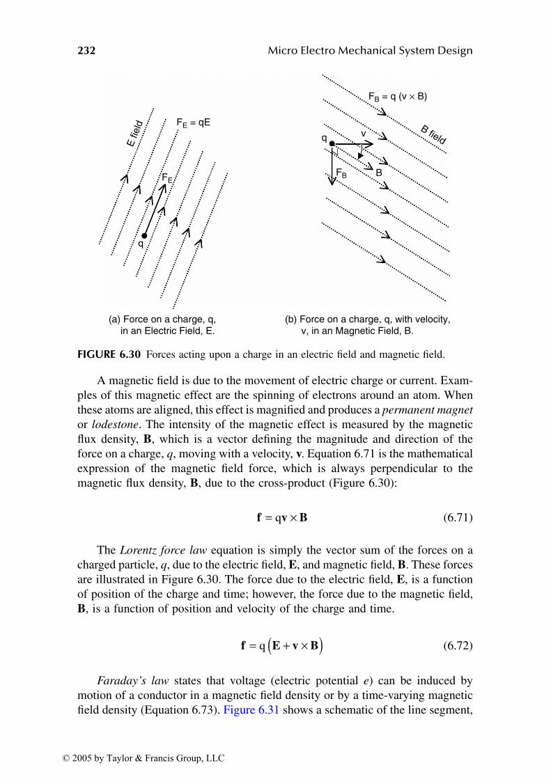
232 Micro Electro Mechanical System Design
A magnetic field is due to the movement of electric charge or current. Exam-ples of this magnetic effect are the spinning of electrons around an atom. Whenthese atoms are aligned, this effect is magnified and produces a permanent magnet
or lodestone. The intensity of the magnetic effect is measured by the magneticflux density, B, which is a vector defining the magnitude and direction of theforce on a charge, q, moving with a velocity, v. Equation 6.71 is the mathematicalexpression of the magnetic field force, which is always perpendicular to themagnetic flux density, B, due to the cross-product (Figure 6.30):
(6.71)
The Lorentz force law equation is simply the vector sum of the forces on acharged particle, q, due to the electric field, E, and magnetic field, B. These forcesare illustrated in Figure 6.30. The force due to the electric field, E, is a functionof position of the charge and time; however, the force due to the magnetic field,B, is a function of position and velocity of the charge and time.
(6.72)
Faraday’s law states that voltage (electric potential e) can be induced bymotion of a conductor in a magnetic field density or by a time-varying magneticfield density (Equation 6.73). Figure 6.31 shows a schematic of the line segment,
FIGURE 6.30 Forces acting upon a charge in an electric field and magnetic field.
(a) Force on a charge, q, in an Electric Field, E.
(b) Force on a charge, q, with velocity, v, in an Magnetic Field, B.
q
q
FEFB
FE = qE
FB = q (v × B)
E fie
ld B fieldv
B
f v B= ×q
f E v B= + ×( )q
© 2005 by Taylor & Francis Group, LLC

Electromechanics 233
dl, area and line integrals involved in Equation 6.73. The first term of the equationexpresses the voltage induced by a time-varying magnetic field density, whichoccurs within the closed conducting path over which the surface integral is taken.The second term is the voltage induced in a moving conduction within a magneticfield. The mechanics of Faraday’s law explain the physics involved in commondevices such as electric generators, electric motors, and inductors.
(6.73)
Equation 6.74 states that a small segment of conducting wire of length dl
moving with a velocity, v, in a magnetic field will produce an electric potential, de,across the wire segment induced by the motion of the conductor in a magnetic field:
(6.74)
The force generated on the conductor segment, dl, can be obtained from thesecond term of the Lorentz force law (Equation 6.72) by utilizing the relationshipi dl = q v. Equation 6.74 shows the right-hand rule relationship among velocity,magnetic field, and electric potential, which is a result of the vector cross-product.Current–magnetic field–force has a similar relationship due to the vector cross-product in Equation 6.75.
(6.75)
FIGURE 6.31 Faraday’s law illustrating a time-varying magnetic field, ∂B/∂t, and motionof a line segment, dl, in a magnetic field, B.
B i
dl
de
v
lBve dd ⋅×=
B i
dl
de
df
Blf ×= idd(a) Voltage, e, and current, i, generated by a moving conductor, v, segment in a magnetic field, B.
(b) Force, df, generated by current, i, flowing in a magnetic field, B.
e d( )t dlt
d lSl l
= ⋅ = − ∂∂ ⋅ + ×( ) ⋅∫∫ ∫EB
s v B
de d= × ⋅v B l
d df l B= ×i
© 2005 by Taylor & Francis Group, LLC
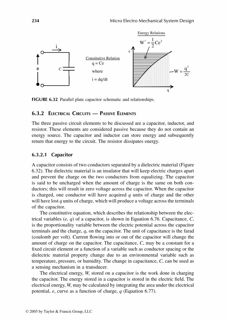
234 Micro Electro Mechanical System Design
6.3.2 ELECTRICAL CIRCUITS — PASSIVE ELEMENTS
The three passive circuit elements to be discussed are a capacitor, inductor, andresistor. These elements are considered passive because they do not contain anenergy source. The capacitor and inductor can store energy and subsequentlyreturn that energy to the circuit. The resistor dissipates energy.
6.3.2.1 Capacitor
A capacitor consists of two conductors separated by a dielectric material (Figure6.32). The dielectric material is an insulator that will keep electric charges apartand prevent the charge on the two conductors from equalizing. The capacitoris said to be uncharged when the amount of charge is the same on both con-ductors; this will result in zero voltage across the capacitor. When the capacitoris charged, one conductor will have acquired q units of charge and the otherwill have lost q units of charge, which will produce a voltage across the terminalsof the capacitor.
The constitutive equation, which describes the relationship between the elec-trical variables (e, q) of a capacitor, is shown in Equation 6.76. Capacitance, C,is the proportionality variable between the electric potential across the capacitorterminals and the charge, q, on the capacitor. The unit of capacitance is the farad(coulomb per volt). Current flowing into or out of the capacitor will change theamount of charge on the capacitor. The capacitance, C, may be a constant for afixed circuit element or a function of a variable such as conductor spacing or thedielectric material property change due to an environmental variable such astemperature, pressure, or humidity. The change in capacitance, C, can be used asa sensing mechanism in a transducer.
The electrical energy, W, stored on a capacitor is the work done in chargingthe capacitor. The energy stored in a capacitor is stored in the electric field. Theelectrical energy, W, may be calculated by integrating the area under the electricalpotential, e, curve as a function of charge, q (Equation 6.77).
FIGURE 6.32 Parallel plate capacitor schematic and relationships.
C
i
e
Constitutive Relationq = Ce
where
i = dq/ dt
qW
2
=
2* Ce12
W =
q
2C
e
Energy Relations
© 2005 by Taylor & Francis Group, LLC

Electromechanics 235
(6.76)
(6.77)
Alternatively, a complementary energy function, W*, may be calculated byintegrating the area under the charge q curve as a function of electrical potential, e:
(6.78)
Utilizing the constitutive equation for a capacitor (Equation 6.76), the energyand complementary energy functions can be found:
(6.79)
The energy function, W, and complementary energy function, W*, have afunctional duality that can be seen by Equation 6.81, which differentiates W andW* with respect to their independent variable and utilizing the capacitor consti-tutive equation, Equation 6.76. W and W* describe the same constitutive relationwith different independent variables. The relationship (Equation 6.81) betweenW and W* can readily be graphically obtained from Figure 6.32 and is called aLegendre transformation. Dual functions of this nature are utilized frequently inthermodynamics where enthalpy and internal energy are dual. These energy andcomplementary energy functions will be employed in the development of thegoverning equations of electromechanical systems, where the use of differentindependent variables can be used to advantage.
(6.80)
(6.81)
6.3.2.2 Inductor
An inductor consists of a conducting coil of one or more loops, Figure 6.33.When current flows through an inductor, a magnetic field is produced that sur-rounds the coils; this is called flux linkage, λ. Assuming that the magnetic fluxdensity, B, is uniform inside the coil, the flux linkage is the product of the number
q Ce=
W(q) edqq= ∫0
W (e) qde*
0
q= ∫
W qq2C
W eCe
2
2*
2( ) = ( ) =
dWdq
edWde
q*= =
W e eq W q* ( ) = − ( )
© 2005 by Taylor & Francis Group, LLC
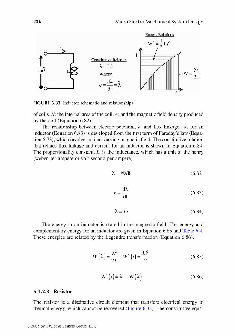
236 Micro Electro Mechanical System Design
of coils, N; the internal area of the coil, A; and the magnetic field density producedby the coil (Equation 6.82).
The relationship between electric potential, e, and flux linkage, λ, for aninductor (Equation 6.83) is developed from the first term of Faraday’s law (Equa-tion 6.73), which involves a time-varying magnetic field. The constitutive relationthat relates flux linkage and current for an inductor is shown in Equation 6.84.The proportionality constant, L, is the inductance, which has a unit of the henry(weber per ampere or volt-second per ampere).
(6.82)
(6.83)
(6.84)
The energy in an inductor is stored in the magnetic field. The energy andcomplementary energy for an inductor are given in Equation 6.85 and Table 6.4.These energies are related by the Legendre transformation (Equation 6.86).
(6.85)
(6.86)
6.3.2.3 Resistor
The resistor is a dissipative circuit element that transfers electrical energy tothermal energy, which cannot be recovered (Figure 6.34). The constitutive equa-
FIGURE 6.33 Inductor schematic and relationships.
•
λ = NAB
eddt
= λ
λ = Li
WL
W iLiλ λ( ) = ( ) =2 2
2 2*
W i i W* ( ) = − ( )λ λ
© 2005 by Taylor & Francis Group, LLC
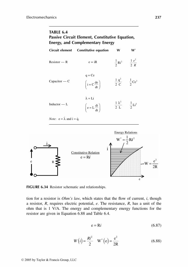
Electromechanics 237
tion for a resistor is Ohm’s law, which states that the flow of current, i, thougha resistor, R, requires electric potential, e. The resistance, R, has a unit of theohm that is 1 V/A. The energy and complementary energy functions for theresistor are given in Equation 6.88 and Table 6.4.
(6.87)
(6.88)
TABLE 6.4Passive Circuit Element, Constitutive Equation,
Energy, and Complementary Energy
Circuit element Constitutive equation W W*
Resistor — R e = iR
Capacitor — C
Inductor — L
Note:
FIGURE 6.34 Resistor schematic and relationships.
1
22Ri
1
2
2e
R
q Ce
i Cde
dt
==
1
2
2q
C
1
22Ce
λ ==
Li
e Ldi
dt
1
2
2λL
1
22Li
e i q= =ɺ ɺλ and .
2R
eW
2
=
2* R2
1W i=
e
i
Energy Relations
R
i
e
Constitutive Relation
iRe =
e R= i
W iRi( ) = ( ) =2
2W e
e2R
*2
© 2005 by Taylor & Francis Group, LLC

238 Micro Electro Mechanical System Design
6.3.2.4 Energy Sources
Two idealizations of electrical energy sources are:
• The ideal voltage source, which will produce a prescribed voltage, e(t),regardless of the current requirements
• The ideal current source, which will produce a prescribed current, i(t),regardless of the voltage requirements
However, ideal sources cannot be realized due to the infinite power required by theirdefinition. An example is an ideal voltage source with a resistor, R, across theterminals. As the resistance is reduced to zero, the current requirements due to Ohm’slaw will become infinite, which implies infinite power. A real voltage and currentsource can be modeled by inclusion of a resistance, RS, as shown in Figure 6.35.
6.3.2.5 Circuit Interconnection
Combining the circuit elements discussed previously (resistor, capacitor, inductor,voltage and current sources) is required to produce a working device or transducer.This section will discuss the method of Kirchhoff’s law to combine these circuitelements. The development of an analytical model of a transducer often willrequire the combination of electrical as well as mechanical components. Thecombination of electrical and mechanical components can be accomplished usingKirchhoff’s laws and the physics of the electromechanical coupling. Chapter 7will discuss methods for coupling electromechanical transducers utilizing themethods of analytical mechanics (Lagrange’s equations). The discussion in thischapter of the energy stored or dissipated in components is a prelude to that.
Two forms of Kirchhoff’s law can be used to combine circuit elements toform an equation describing the system:
• Kirchhoff’s current law. The algebraic sum of the currents into a nodeat any instant is zero. Figure 6.36 is a circuit with a junction or nodeshown in which current can flow in or out.
FIGURE 6.35 Real voltage and current sources and their voltage vs. current characteristic.
es
Rs
e0
is
(a) Ideal Voltage Source
esRsi0
is
(b) Ideal Current Source
(i q)= ɺ
© 2005 by Taylor & Francis Group, LLC
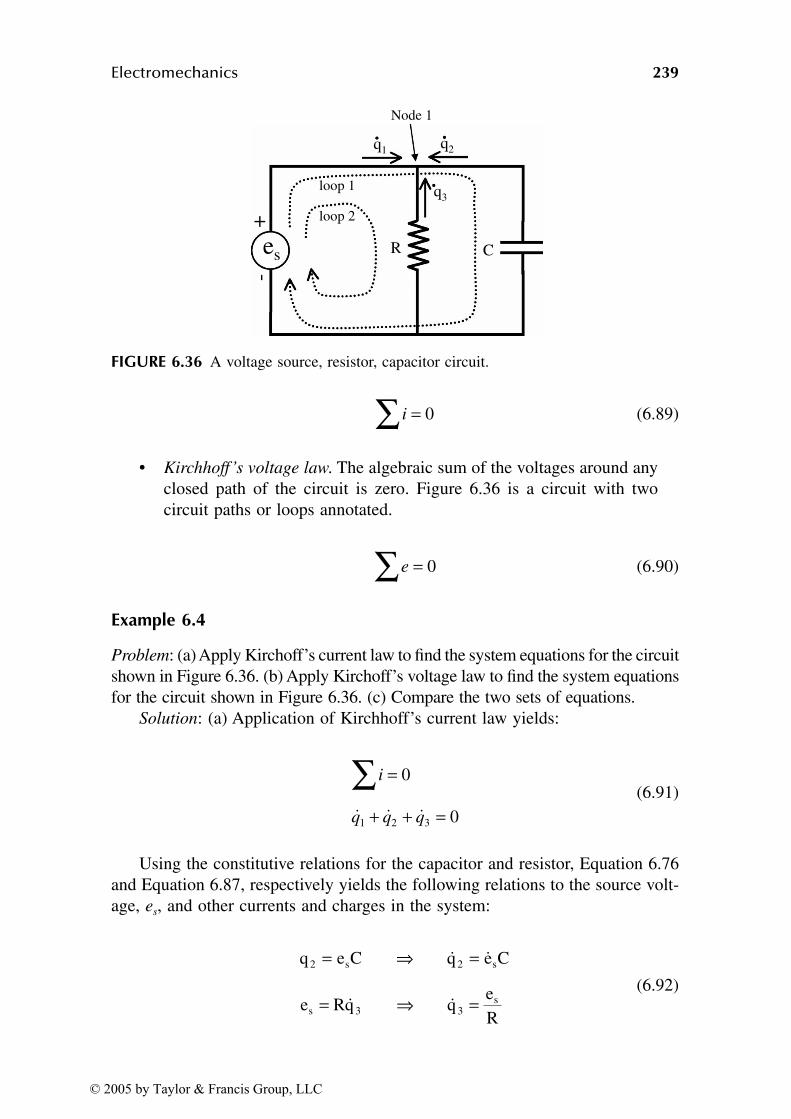
Electromechanics 239
(6.89)
• Kirchhoff’s voltage law. The algebraic sum of the voltages around anyclosed path of the circuit is zero. Figure 6.36 is a circuit with twocircuit paths or loops annotated.
(6.90)
Example 6.4
Problem: (a) Apply Kirchoff’s current law to find the system equations for the circuitshown in Figure 6.36. (b) Apply Kirchoff’s voltage law to find the system equationsfor the circuit shown in Figure 6.36. (c) Compare the two sets of equations.
Solution: (a) Application of Kirchhoff’s current law yields:
(6.91)
Using the constitutive relations for the capacitor and resistor, Equation 6.76and Equation 6.87, respectively yields the following relations to the source volt-age, es, and other currents and charges in the system:
(6.92)
FIGURE 6.36 A voltage source, resistor, capacitor circuit.
-+
R C
loop 2
loop 1
q1 q2
q3
Node 1
es
i =∑ 0
e =∑ 0
i
q q q
=+ + =
∑ 0
01 2 3ɺ ɺ ɺ
q e C q e C
e Rq qeR
2 s 2 s
s 3 3s
= ⇒ == ⇒ =
ɺ ɺ
ɺ ɺ
© 2005 by Taylor & Francis Group, LLC
240 Micro Electro Mechanical System Design
Substituting Equation 6.92 into Equation 6.91 yields the following systemequation in which es, C, and R are specified variables and q1 is the unknownvariable to be solved for:
(6.93)
(b) Application of Kirchhoff’s voltage law around the two loops shown inFigure 6.36 yields the following two equations:
(6.94)
This method results in two equations and two unknowns (q2,q3) in terms of thespecified variables es, C, and R.
(c) Kirchhoff’s current law resulted in one first-order differential equation interms of q1. However, Kirchhoff’s voltage law results in two equations: a first-order differential equation in terms of q3 and an algebraic equation in terms ofq2. The reason for this discrepancy is that only one independent node is in thiscircuit, but two independent loops are. For more complex circuits, a judiciouschoice of approach (i.e., voltage law vs. current law) can be important to resultin a smaller number of equations to describe the system.
QUESTIONS
1. A structural member has a thickness, width, and length of t, w, and L,respectively. The area moment of inertia about the bending axis ofinterest is I = wt3/12. • a. List the stiffness equations for torsion, axial tension, and bending.• b. If t is doubled in thickness, what are the percent changes in the
three stiffnesses?• c. Which of the stiffnesses is the most sensitive to a change in
length?2. Given a 500-µm long polysilicon beam with a 2-µm square cross-
section and fixed–fixed boundary conditions. Assume polysilicon hasa failure stress of 1600 µn/µm2. What is the compressive load thatwill cause the beam to fail (consider both material failure and columnbuckling failure)? What is the tensile load that will cause the beamto fail?
ɺ ɺq e CeR
01 ss+ + =
e 0
Loop 1: eqC
0
Loop 2: e Rq 0
s2
s 3
=− =− =
∑ɺ
© 2005 by Taylor & Francis Group, LLC
Electromechanics 241
3. Given a 100-µm square plate made of 2.5-µm thick polysilicon sus-pended by a 1-N/M spring. This device is in an air environment at 1atm, 20°C, with υ = 0.15 cm2/s. The air gap is 2 µm and the plate willoscillate at 1000 Hz. Calculate the quality factors, Q, for normal andlateral motion relative to the substrate. Which type of motion is moreheavily damped?
REFERENCES
1. F.B. Seely, J.O. Smith, Advanced Mechanics of Materials, 2nd ed., John Wiley &Sons, Inc., New York, 1952.
2. R.J. Roark, Formulas for Stress and Strain, McGraw-Hill Company, New York,1965.
3. J.E. Shigley, L.D. Mitchell, Mechanical Engineering Design, McGraw-Hill BookCompany, New York, 1983.
4. H.A. Rothbart (Ed.), Mechanical Design Handbook, McGraw-Hill, New York,1996.
5. R. Plunkett (Ed.), Mechanical Impedance Methods for Mechanical Vibrations,American Society of Mechanical Engineers, New York, 1958.
6. W. Soedel, Vibrations of Shells and Plates, Marcel Dekker, Inc., New York, 1981.7. S.P. Timoshenko, S. Woinowsky–Krieger, Theory of Plates and Shells, McGraw-
Hill, New York, 1959.8. B.A. Boley, J.H. Weiner, Theory of Thermal Stresses, John Wiley & Sons, New
York, 1960.9. E.J. Garcia, Micro-flex mirror and instability actuation technique, 11th IEEE Int.
Workshop Micro Electro Mechanical Syst., Janaury 25–29, 1998 in Heldelberg,Germany.
10. W.T. Thomson, Theory of Vibration with Applications, Prentice Hall, Inc., Engle-wood Cliffs, NJ, 1981.
11. F.S. Tse, I.E. Morse, R.T. Hinkle, Mechanical Vibrations, Theory and Applications,Allyn and Bacon, Inc., Boston, 1978.
12. J.D. Zook, D.W. Burns, H. Guckel, J.J. Sniegowski, R.L. Engelstad, Z. Feng,Characteristics of polysilicon resonant microbeams, Sensors Actuators A, 35,51–59, 1992.
13. S. Dushman, Scientific Foundations of Vacuum Technique, John Wiley & Sons,New York, 1962.
14. J.J. Blech, On isothermal squeeze films, J. Lubrication Technol., 105, 615–620,October, 1983.
15. W. Griffin, H. Richardson, S. Yamanami, A study of squeeze film damping, ASME
J. Basic Eng., 451–456, June 1966.16. M. Andrews, I. Harris, G. Turner, A comparison of squeeze-film theory with
measurements on a microstructure, Sensors Actuators A, 36, 79–87, 1993.17. M.K. Andrews, G.C. Turner, P.D. Harris, I.M. Harris, A resonant pressure sensor
based on a squeezed film of gas, Sensors Actuators A, 36, 219–226, 1993.18. N. Yazdi, K. Najafi, An all-silison single-wafer micro-g accelerometer with a
combined surface and bulk micromachining process, JMEMS, 9(4), 544–550, Dec.2000.
© 2005 by Taylor & Francis Group, LLC
242 Micro Electro Mechanical System Design
19. W. Kuehnel, Modeling of the mechanical behavior of a differential capacitoracceleration sensor, Sensors and Actuators A, 48, 101–108, 1995.
20. Y.H. Cho, B.M. Kwak, A.P. Pisano, R.T. Howe, Slide film damping in laterallydriven microstructures, Sensors Actuators A, 40, 31–39, 1994.
21. Y.H. Cho, A.P. Pisano, R.T. Howe, Viscous damping model for laterally oscillatingmicrostructures, J. MEMS, 3(2), 81–87, June 1994.
22. C.T.A. Johnk, Engineering Electromagnetic Fields and Waves, John Wiley & Sons,New York, 1988.
23. F.C. Moon, Magneto-Solid Mechanics, John Wiley & Sons, New York, 1984.24. R.J. Smith, Circuits, Devices and Systems, John Wiley & Sons, New York, 1968.25. S.H. Crandall, D.C. Karnopp, E.F. Kurtz, D.C. Pridemore-Brown, Dynamics of
Mechanical and Electromechanical Systems, Original Edition 1968, McGraw-Hill,reprint edition, 1982, Krieger Publishing.
© 2005 by Taylor & Francis Group, LLC
243
7 Modeling and Design
This chapter will discuss a number of topics relating to modeling and simulation
of MEMS devices. As a design progresses from concept to a fully mature product,
the modeling and simulation needs change. In the early stages of transitioning a
design from a concept in the designer’s imagination to an initial design layout
of the device, the modeling and simulation requirements are different from those
for perfecting the operation of an existing MEMS device design.
The concept to first design phase is design synthesis, which requires informa-
tion of what design parameters are important, how they interact with each other,
and the sensitivity of the device performance metric to the design variables. This
type of information can most easily be obtained from an analytical model or low-
order lumped parameter models of the device. In these types of models, the design
variables of interest are frequently explicit and a large number of calculations to
determine variable relationships and sensitivities can be easily performed.
The detailed design analysis of existing MEMS design to further optimize
performance may require high-order numerical analysis calculations. For exam-
ple, the analysis of a MEMS support anchor to determine dissipation losses to
the substrate, which is important for a resonant device, will require a detailed
solid model of the anchor–substrate region. This type of modeling is not feasible
with design synthesis approaches and requires a large-order solid model of
detailed effects such as material damping and hysteresis.
7.1 DESIGN SYNTHESIS MODELING
The challenge of design synthesis modeling is to capture as succinctly as possible
the fundamental physics of a device. The method most frequently taught in
undergraduate engineering courses is the use of Newtonian mechanics, free-body
diagrams to develop the governing equations of a device, and lumped parameter
circuit models. As anyone who has survived these courses knows, there is plenty
of room for error. The main roadblock is maintaining correct signs for variables
and dealing with multiple interacting bodies and systems.
Analytical mechanics [1–6] is an alternative approach for the development
of the equations of motion for a system based on the minimization of the energy
functions of the system. Hamilton’s and Lagrange’s equations are two alternative
formulations of this approach. Lagrange’s equations will be presented here as
well as MATLAB-based functions [7] (Sections H.1 and H.2 in Appendix H)
© 2005 by Taylor & Francis Group, LLC

244 Micro Electro Mechanical System Design
to aid in the required computations. These functions require MATLAB and the
Symbolic Math Toolbox.
7.2 LAGRANGE’S EQUATIONS
Lagrange’s equations are the differential equations of motions of a device
expressed in terms of generalized coordinates, which are a set of coordinates that
completely describes the system dynamics. Generalized coordinates are not
unique for a system and can be defined in several ways. They can be quantities
such as angles, linear displacements, voltages, or electric charges, depending on
the physical system that is to be modeled. Generalized coordinates will be denoted
by qk (k = 1,2,…n), where n is the number of generalized coordinates. The
minimum number of independent generalized coordinates required to describe
the dynamics of a system fully is referred to as the system degree of freedom
(DOF), N.
Figure 7.1 shows a diagram of a simple pendulum that has 1 DOF, with
alternative expressions for the generalized coordinates that could be used to
describe the system. The most direct and simple choice for the system generalized
coordinate is θ. X could be used for the generalized coordinate, but the resulting
equation would be not as meaningful. X and Y can be used as generalized
coordinates, but they are not independent and a method for dealing with the
constraint equation relating them (r2 = X2 + Y2) needs to be developed.
A basic version of Lagrange’s equations can be derived from the principle that
the sum of the kinetic and potential energies of a conservative system is constant:
d(T + U) = 0 (7.1)
FIGURE 7.1 Pendulum with alternative choices of generalized coordinates.
© 2005 by Taylor & Francis Group, LLC
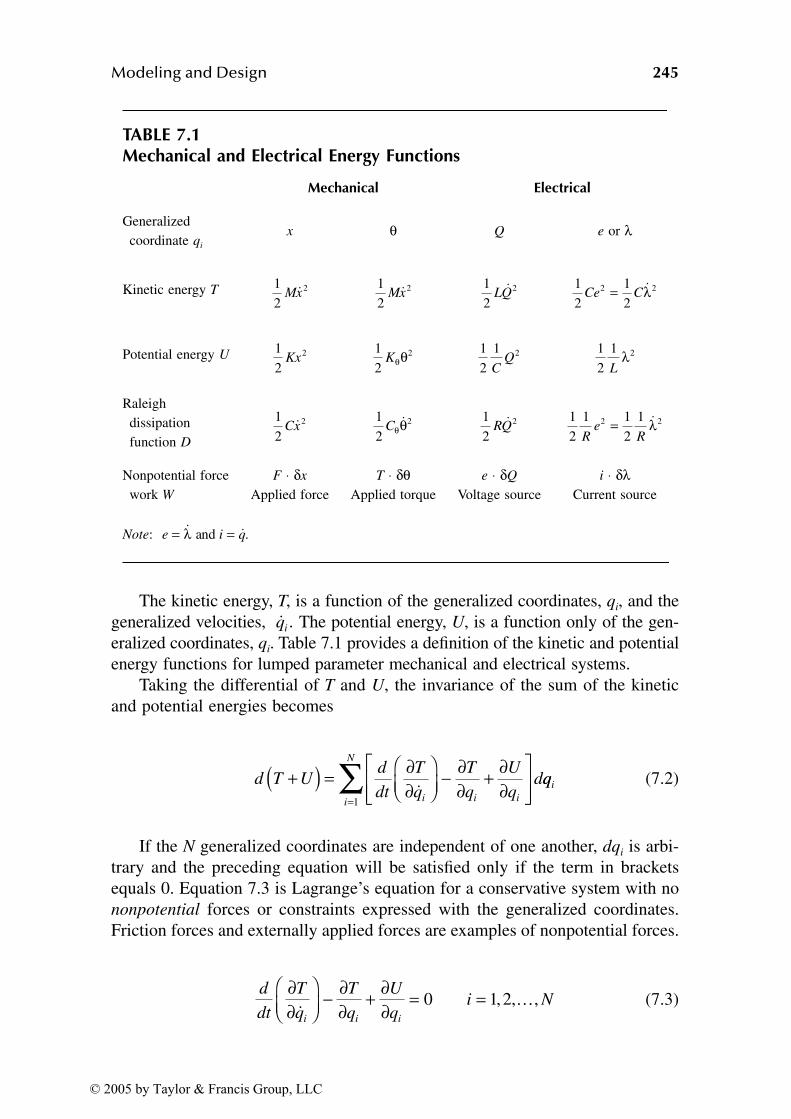
Modeling and Design 245
The kinetic energy, T, is a function of the generalized coordinates, qi, and the
generalized velocities, The potential energy, U, is a function only of the gen-
eralized coordinates, qi. Table 7.1 provides a definition of the kinetic and potential
energy functions for lumped parameter mechanical and electrical systems.
Taking the differential of T and U, the invariance of the sum of the kinetic
and potential energies becomes
(7.2)
If the N generalized coordinates are independent of one another, dqi is arbi-
trary and the preceding equation will be satisfied only if the term in brackets
equals 0. Equation 7.3 is Lagrange’s equation for a conservative system with no
nonpotential forces or constraints expressed with the generalized coordinates.
Friction forces and externally applied forces are examples of nonpotential forces.
(7.3)
TABLE 7.1Mechanical and Electrical Energy Functions
Mechanical Electrical
Generalized
coordinate qi
x θ Q e or λ
Kinetic energy T
Potential energy U
Raleigh
dissipation
function D
Nonpotential force
work W
F ⋅ δx
Applied force
T ⋅ δθApplied torque
e ⋅ δQ
Voltage source
i ⋅ δλCurrent source
Note:
1
2
2Mxɺ1
2
2Mxɺ1
2
2LQɺ1
2
1
2
2 2Ce C= ɺλ
1
2
2Kx1
2
2Kθθ 1
2
1 2
CQ
1
2
1 2
Lλ
1
2
2Cxɺ1
2
2Cθθɺ 1
2
2RQɺ1
2
1 1
2
12 2
Re
R= ɺλ
e i q= =ɺ ɺλ and .
ɺqi .
d T Ud
dt
T
q
T
q
U
qd
i i i
+( ) = ∂∂
−
∂∂ + ∂
∂
ɺ
qqi
i
N
=∑
1
d
dt
T
q
T
q
U
qi N
i i i
∂∂
−
∂∂ + ∂
∂ = = …ɺ
0 1 2, , ,
© 2005 by Taylor & Francis Group, LLC
246 Micro Electro Mechanical System Design
Nonpotential forces can be included in the formulation of Lagrange’s equa-
tions by the addition of the work of the nonpotential forces into the system total
energy expression of Equation 7.1. This results in Equation 7.4, where Qi is a
generalized force or moment acting over an infinitesimal displacement of the
generalized coordinate, qi:
(7.4)
Mathematically proceeding as before to find an expression of Lagrange’s
equations that includes the nonpotential forces results in:
(7.5)
7.2.1 LAGRANGE’S EQUATIONS WITH NONPOTENTIAL FORCES
Viscous damping is a nonconservative force frequently arising in system modeling
of devices that deserves special attention. If the damping forces are proportional
to the generalized velocities, it is possible to devise a function, the Raleigh
dissipation function, D (Equation 7.6), where the proportionality constant, crs, is
the viscous damping coefficient.
(7.6)
From this definition of D, it is obvious that the viscous damping force is
merely a constant viscous damping coefficient multiplied by the generalized
velocity:
(7.7)
If the nonpotential forces, Qi, in Equation 7.5 are separated into externally
applied nonpotential forces and dissipative forces, Lagrange’s equations can be
rewritten as
(7.8)
d T U dW Q dqi i
i
N
+( ) = ==∑
1
d
dt
T
q
T
q
U
qQ i N
i i i
i
∂∂
−
∂∂ + ∂
∂ = = …ɺ
1 2, , ,
D c q qrs r s
s
n
r
n
===∑∑1
211
ɺ ɺ
QD
qi ni
i
= − ∂∂ = …1 2, , ,
d
dt
T
q
T
q
U
q
D
qQ i
i i i i
i
∂∂
−
∂∂ + ∂
∂ + ∂∂ = = …
ɺ1 2, , ,,n
© 2005 by Taylor & Francis Group, LLC
Modeling and Design 247
At this point, a form of Lagrange’s equations, Equation 7.8, can be used to
model a device for which a kinetic energy function (T); a potential energy function
(U); a Raleigh dissipation function (D); and the nonpotential applied forces, Qi,
can be written in terms of the generalized coordinates and velocities This
is a frequently used form of Lagrange’s equations.
7.2.2 LAGRANGE’S EQUATIONS WITH EQUATIONS
OF CONSTRAINT
One additional modification of Lagrange’s equations may be useful in situations
when defining the number of generalized coordinates, n, to be equal to the system
degree of freedom, N, cannot be easily accomplished, or it is deemed advanta-
geous to deal with an excess of generalized coordinates (n > N > M). To utilize
this approach, M number of constraint equations (Equation 7.9) need to be defined
and Lagrange’s equations modified to account for the additional variables neces-
sary to satisfy the constraints.
(7.9)
To have a uniquely solvable set of equations defining the system, the number
of generalized coordinates, constraint equations, and system degrees of freedom
will have the following relationship:
n – M = N (7.10)
If N + M generalized coordinates are identified for use with the Lagrange
equation formulation of a system with N degrees of freedom, this means that M
equations of constraint must be involved in the formulation so that all of the N
+ M variables can be uniquely found. The result of having constraints between
the generalized coordinates of the equations modeling any physical system will
result in M constraint forces, which are needed to enforce the constraint
conditions (Equation 7.9) upon the system.
(7.11)
This additional constraint force term in Lagrange’s equations is developed
via the Lagrange multiplier method, which results in new variables, Lagrange
multipliers, λl 1 = 1,…,M.
(7.12)
( , ).q qi iɺ
g q q q MN1 1 2 0 1 1 2, , , , , ,…( ) = = …
Qicon ,
d
dt
T
q
T
q
U
q
D
qQ Q
i i i i
i icon∂
∂
−
∂∂ + ∂
∂ + ∂∂ = +
ɺ ɺii n= …1 2, , ,
Qg
qicon
ll
il
M
= ∂∂=
∑λ1
© 2005 by Taylor & Francis Group, LLC
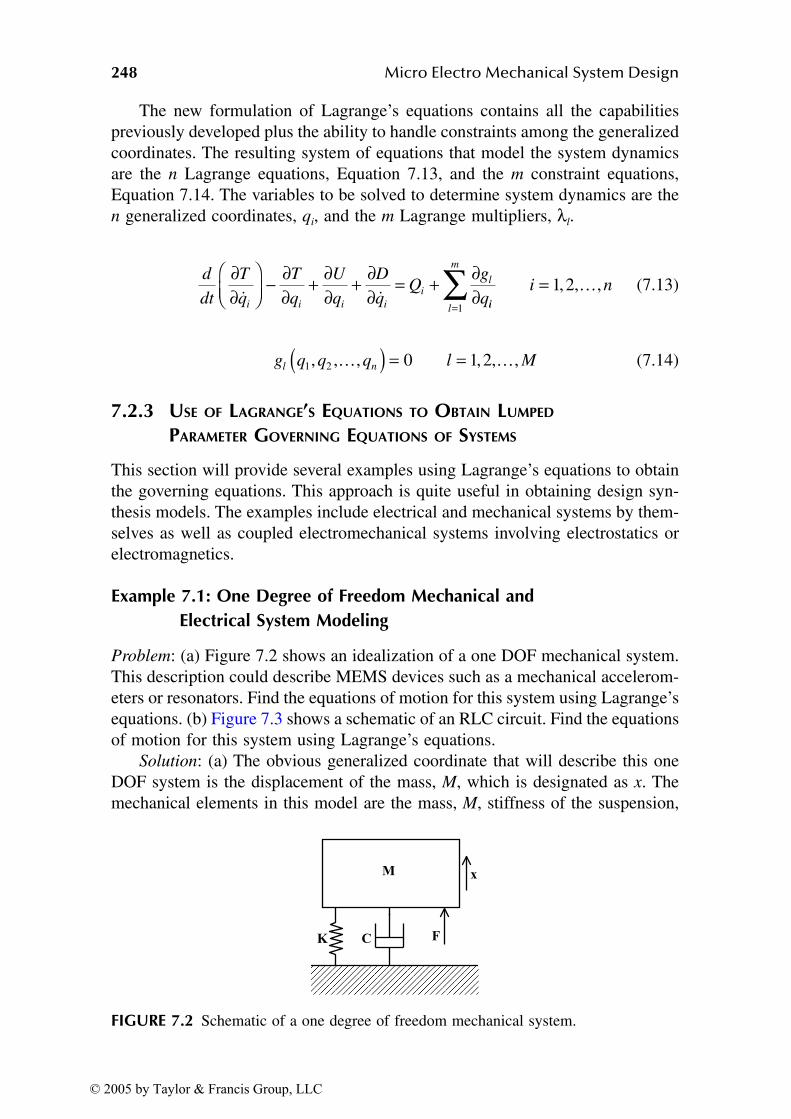
248 Micro Electro Mechanical System Design
The new formulation of Lagrange’s equations contains all the capabilities
previously developed plus the ability to handle constraints among the generalized
coordinates. The resulting system of equations that model the system dynamics
are the n Lagrange equations, Equation 7.13, and the m constraint equations,
Equation 7.14. The variables to be solved to determine system dynamics are the
n generalized coordinates, qi, and the m Lagrange multipliers, λl.
(7.13)
(7.14)
7.2.3 USE OF LAGRANGE’S EQUATIONS TO OBTAIN LUMPED
PARAMETER GOVERNING EQUATIONS OF SYSTEMS
This section will provide several examples using Lagrange’s equations to obtain
the governing equations. This approach is quite useful in obtaining design syn-
thesis models. The examples include electrical and mechanical systems by them-
selves as well as coupled electromechanical systems involving electrostatics or
electromagnetics.
Example 7.1: One Degree of Freedom Mechanical and
Electrical System Modeling
Problem: (a) Figure 7.2 shows an idealization of a one DOF mechanical system.
This description could describe MEMS devices such as a mechanical accelerom-
eters or resonators. Find the equations of motion for this system using Lagrange’s
equations. (b) Figure 7.3 shows a schematic of an RLC circuit. Find the equations
of motion for this system using Lagrange’s equations.
Solution: (a) The obvious generalized coordinate that will describe this one
DOF system is the displacement of the mass, M, which is designated as x. The
mechanical elements in this model are the mass, M, stiffness of the suspension,
FIGURE 7.2 Schematic of a one degree of freedom mechanical system.
d
dt
T
q
T
q
U
q
D
g
qi i i i
il∂
∂
−
∂∂ + ∂
∂ + ∂∂ = + ∂
∂ɺ ɺ iil
m
i n
=∑ = …
1
1 2, , ,
g q q q l Ml n1 2 0 1 2, , , , , ,…( ) = = …
© 2005 by Taylor & Francis Group, LLC
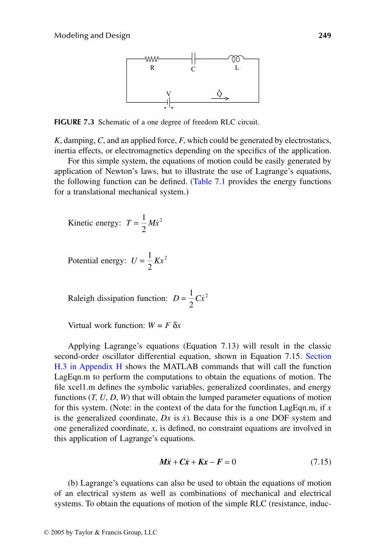
Modeling and Design 249
K, damping, C, and an applied force, F, which could be generated by electrostatics,
inertia effects, or electromagnetics depending on the specifics of the application.
For this simple system, the equations of motion could be easily generated by
application of Newton’s laws, but to illustrate the use of Lagrange’s equations,
the following function can be defined. (Table 7.1 provides the energy functions
for a translational mechanical system.)
Kinetic energy:
Potential energy:
Raleigh dissipation function:
Virtual work function: W = F δx
Applying Lagrange’s equations (Equation 7.13) will result in the classic
second-order oscillator differential equation, shown in Equation 7.15. Section
H.3 in Appendix H shows the MATLAB commands that will call the function
LagEqn.m to perform the computations to obtain the equations of motion. The
file xcel1.m defines the symbolic variables, generalized coordinates, and energy
functions (T, U, D, W) that will obtain the lumped parameter equations of motion
for this system. (Note: in the context of the data for the function LagEqn.m, if x
is the generalized coordinate, Dx is Because this is a one DOF system and
one generalized coordinate, x, is defined, no constraint equations are involved in
this application of Lagrange’s equations.
(7.15)
(b) Lagrange’s equations can also be used to obtain the equations of motion
of an electrical system as well as combinations of mechanical and electrical
systems. To obtain the equations of motion of the simple RLC (resistance, induc-
FIGURE 7.3 Schematic of a one degree of freedom RLC circuit.
T Mx= 1
2
2ɺ
U Kx= 1
2
2
D Cx= 1
2
2ɺ
ɺx).
Mx Cx Kx Fɺɺ ɺ+ + − = 0
© 2005 by Taylor & Francis Group, LLC
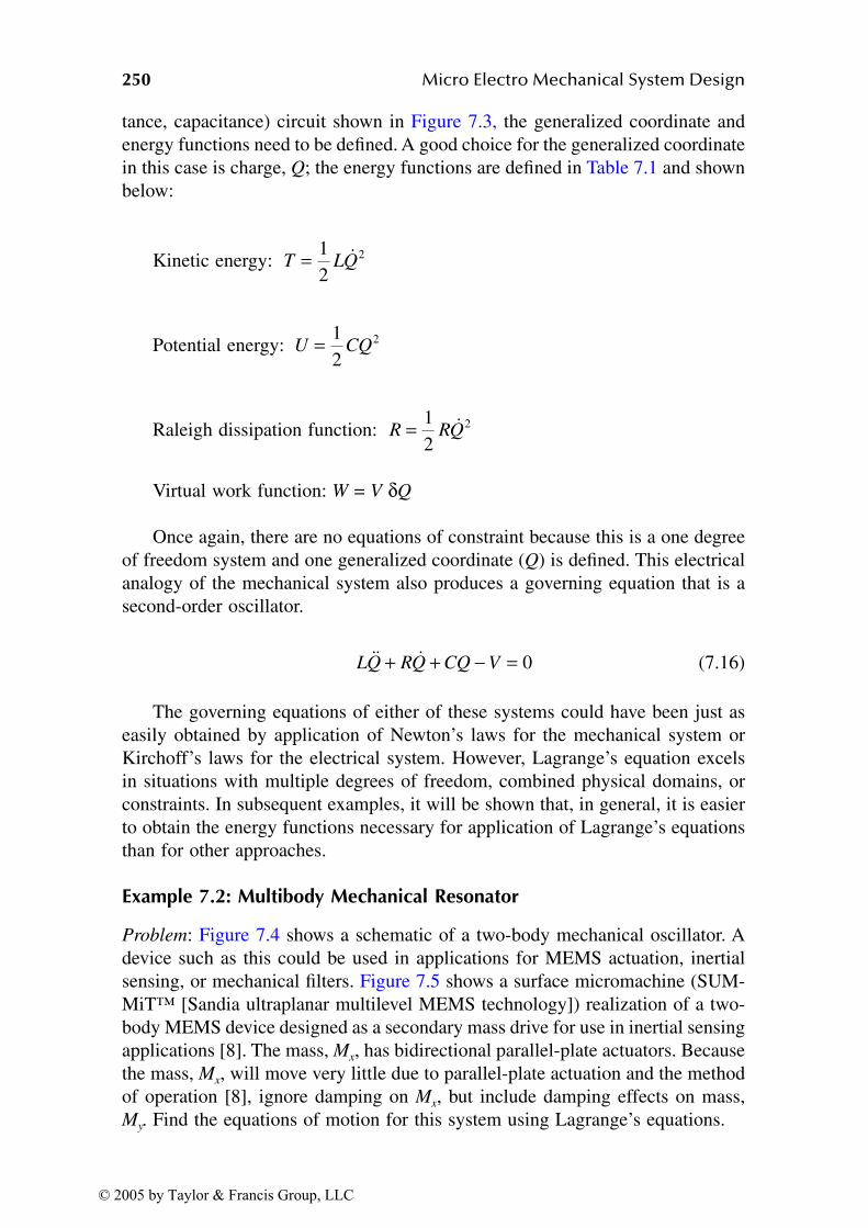
250 Micro Electro Mechanical System Design
tance, capacitance) circuit shown in Figure 7.3, the generalized coordinate and
energy functions need to be defined. A good choice for the generalized coordinate
in this case is charge, Q; the energy functions are defined in Table 7.1 and shown
below:
Kinetic energy:
Potential energy:
Raleigh dissipation function:
Virtual work function: W = V δQ
Once again, there are no equations of constraint because this is a one degree
of freedom system and one generalized coordinate (Q) is defined. This electrical
analogy of the mechanical system also produces a governing equation that is a
second-order oscillator.
(7.16)
The governing equations of either of these systems could have been just as
easily obtained by application of Newton’s laws for the mechanical system or
Kirchoff’s laws for the electrical system. However, Lagrange’s equation excels
in situations with multiple degrees of freedom, combined physical domains, or
constraints. In subsequent examples, it will be shown that, in general, it is easier
to obtain the energy functions necessary for application of Lagrange’s equations
than for other approaches.
Example 7.2: Multibody Mechanical Resonator
Problem: Figure 7.4 shows a schematic of a two-body mechanical oscillator. A
device such as this could be used in applications for MEMS actuation, inertial
sensing, or mechanical filters. Figure 7.5 shows a surface micromachine (SUM-
MiT™ [Sandia ultraplanar multilevel MEMS technology]) realization of a two-
body MEMS device designed as a secondary mass drive for use in inertial sensing
applications [8]. The mass, Mx, has bidirectional parallel-plate actuators. Because
the mass, Mx, will move very little due to parallel-plate actuation and the method
of operation [8], ignore damping on Mx, but include damping effects on mass,
My. Find the equations of motion for this system using Lagrange’s equations.
T LQ= 1
2
2ɺ
U CQ= 1
2
2
R RQ= 1
2
2ɺ
LQ RQ CQ Vɺɺ ɺ+ + − = 0
© 2005 by Taylor & Francis Group, LLC
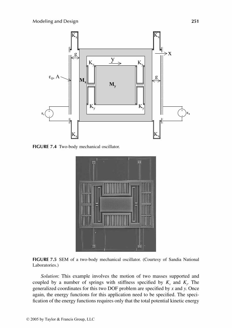
Modeling and Design 251
Solution: This example involves the motion of two masses supported and
coupled by a number of springs with stiffness specified by Kx and Ky. The
generalized coordinates for this two DOF problem are specified by x and y. Once
again, the energy functions for this application need to be specified. The speci-
fication of the energy functions requires only that the total potential kinetic energy
FIGURE 7.4 Two-body mechanical oscillator.
FIGURE 7.5 SEM of a two-body mechanical oscillator. (Courtesy of Sandia National
Laboratories.)
© 2005 by Taylor & Francis Group, LLC
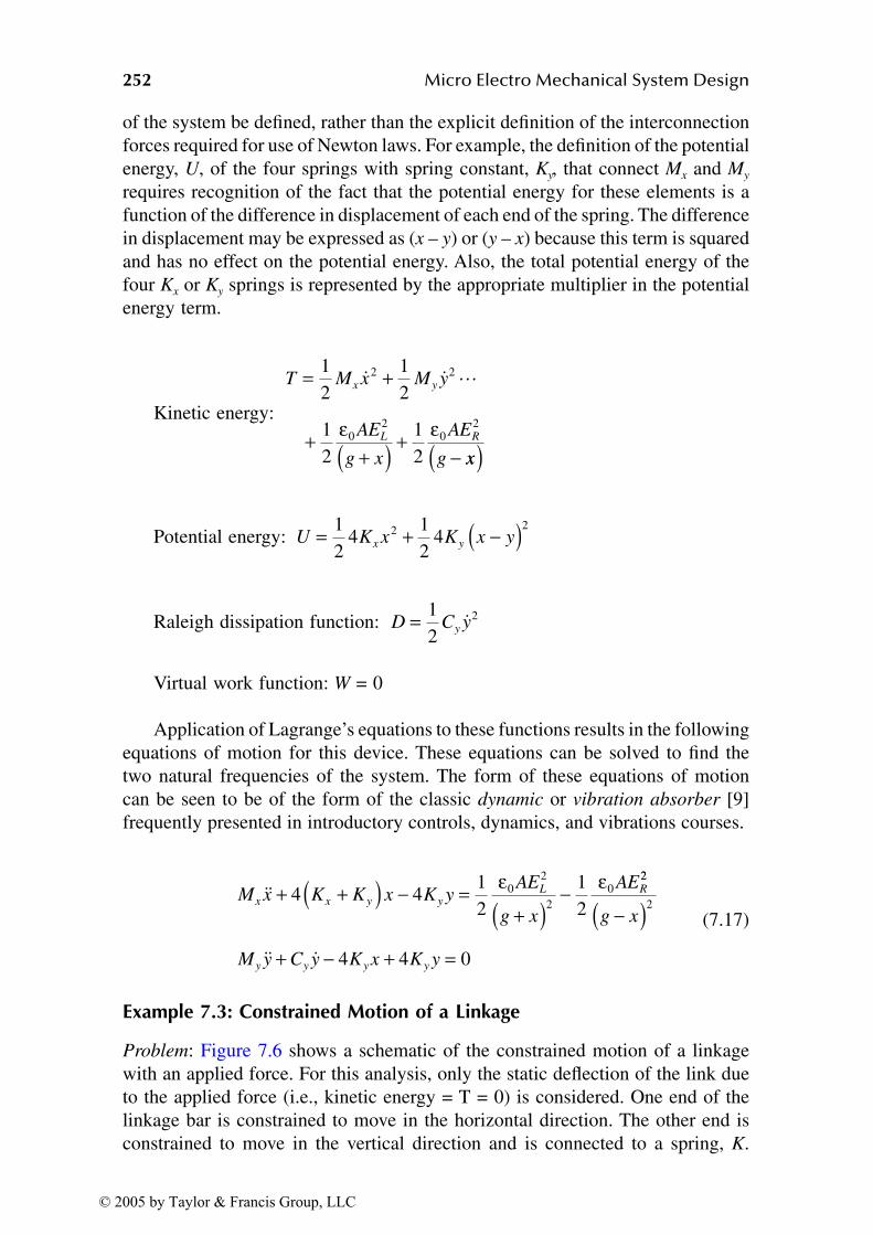
252 Micro Electro Mechanical System Design
of the system be defined, rather than the explicit definition of the interconnection
forces required for use of Newton laws. For example, the definition of the potential
energy, U, of the four springs with spring constant, Ky, that connect Mx and My
requires recognition of the fact that the potential energy for these elements is a
function of the difference in displacement of each end of the spring. The difference
in displacement may be expressed as (x – y) or (y – x) because this term is squared
and has no effect on the potential energy. Also, the total potential energy of the
four Kx or Ky springs is represented by the appropriate multiplier in the potential
energy term.
Kinetic energy:
Potential energy:
Raleigh dissipation function:
Virtual work function: W = 0
Application of Lagrange’s equations to these functions results in the following
equations of motion for this device. These equations can be solved to find the
two natural frequencies of the system. The form of these equations of motion
can be seen to be of the form of the classic dynamic or vibration absorber [9]
frequently presented in introductory controls, dynamics, and vibrations courses.
(7.17)
Example 7.3: Constrained Motion of a Linkage
Problem: Figure 7.6 shows a schematic of the constrained motion of a linkage
with an applied force. For this analysis, only the static deflection of the link due
to the applied force (i.e., kinetic energy = T = 0) is considered. One end of the
linkage bar is constrained to move in the horizontal direction. The other end is
constrained to move in the vertical direction and is connected to a spring, K.
T M x M y
AE
g x
AE
g
x y
L R
= +
+ +( ) + −
1
2
1
2
1
2
1
2
2 2
02
02
ɺ ɺ ⋯
ε εxx( )
U K x K x yx y= + −( )1
24
1
242 2
D C yy= 1
2
2ɺ
M x K K x K yAE
g x
AEx x y y
L Rɺɺ+ +( ) − = +( ) −4 41
2
1
2
02
2
0ε ε 22
2
4 4 0
g x
M y C y K x K yy y y y
−( )+ − + =ɺɺ ɺ
© 2005 by Taylor & Francis Group, LLC
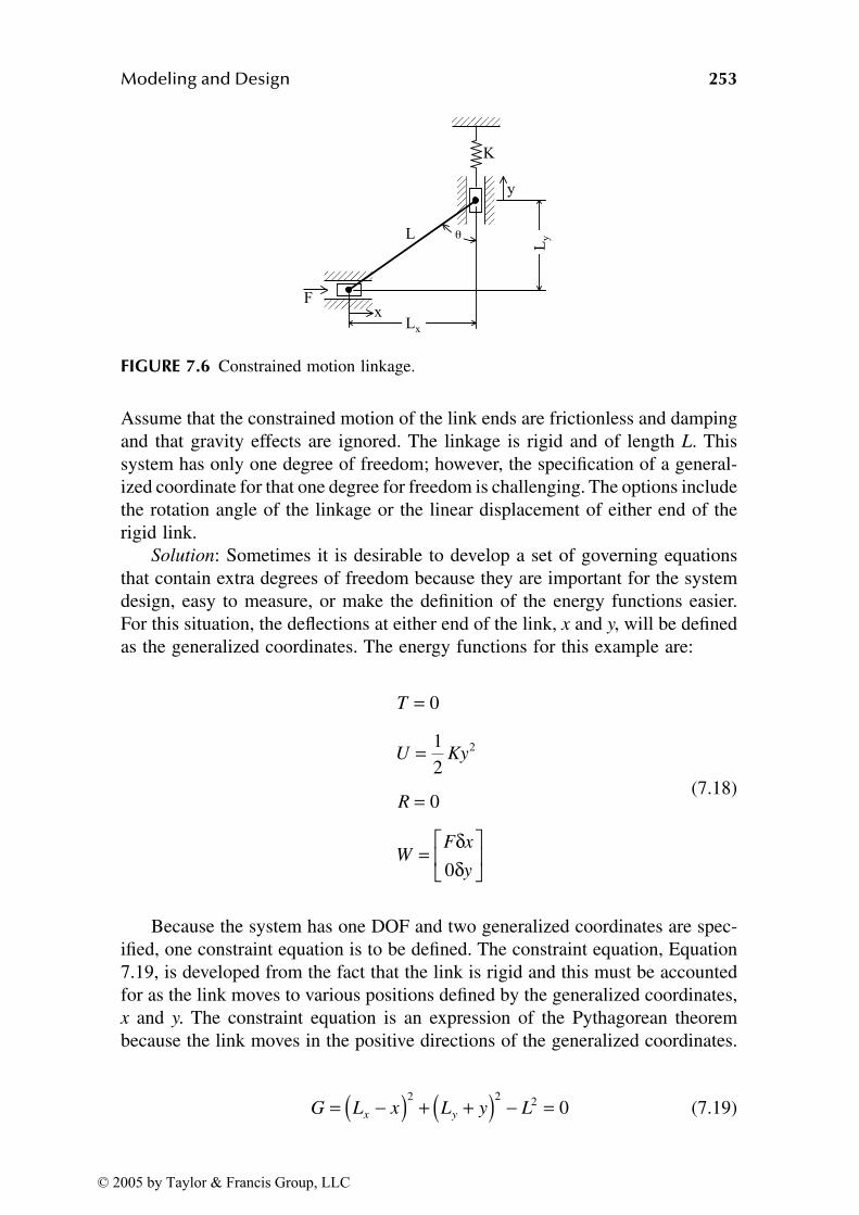
Modeling and Design 253
Assume that the constrained motion of the link ends are frictionless and damping
and that gravity effects are ignored. The linkage is rigid and of length L. This
system has only one degree of freedom; however, the specification of a general-
ized coordinate for that one degree for freedom is challenging. The options include
the rotation angle of the linkage or the linear displacement of either end of the
rigid link.
Solution: Sometimes it is desirable to develop a set of governing equations
that contain extra degrees of freedom because they are important for the system
design, easy to measure, or make the definition of the energy functions easier.
For this situation, the deflections at either end of the link, x and y, will be defined
as the generalized coordinates. The energy functions for this example are:
(7.18)
Because the system has one DOF and two generalized coordinates are spec-
ified, one constraint equation is to be defined. The constraint equation, Equation
7.19, is developed from the fact that the link is rigid and this must be accounted
for as the link moves to various positions defined by the generalized coordinates,
x and y. The constraint equation is an expression of the Pythagorean theorem
because the link moves in the positive directions of the generalized coordinates.
(7.19)
FIGURE 7.6 Constrained motion linkage.
T
U Ky
R
WF x
y
====
0
1
2
0
0
2
δδ
G L x L y Lx y= −( ) + +( ) − =2 22 0
© 2005 by Taylor & Francis Group, LLC

254 Micro Electro Mechanical System Design
Applying Lagrange’s equations for constrained motion (Equation 7.13) results
in the governing equation for the link, Equation 7.20. The system is fully
described by Equation 7.19 and Equation 7.20 and the variables x, y, and λ1. The
solution for the system deflections will involve the solution of constraint equation
and the two governing equations for the variables x, y, and λ1. The Lagrange
multiplier used in the formulation is λ1. The terms in the governing equation that
involve λ1 can be physically interpreted as the forces of constraint required to
enforce the constraint.
(7.20)
Equation 7.20 can be solved for the Lagrange multiplier, λ1, to yield a
relationship with the generalized coordinates, x or y.
(7.21)
This equation can be used in conjunction with the link length constraint equa-
tion, Equation 7.19, to form an equation in terms of either generalized coordinate.
For example, Equation 7.22 is the equation that relates y to the given constants of
K, L, Ly, and F. This is a nonlinear equation that could be solved numerically for
y. A solution for the generalized coordinate, x, can be similarly obtained.
(7.22)
Equation 7.23 is a relationship between x and y and another possibility for
a generalized coordinate, θ, which can be obtained from Equation 7.21. Equa-
tion 7.23 provides a relationship between the applied force, F, and the spring
force, Ky. This shows the force multiplication advantage of this mechanism at
various angles.
(7.23)
Example 7.4: Parallel RLC Circuit
Problem: Find the governing equations for the RLC circuit shown in Figure 7.7
using Lagrange’s equations.
F L x
Ky L y
x
y
− −( ) =− +( ) =λλ1
1
2 0
2 0
λ12 2
= −( ) = +( )F
L x
Ky
L yx y
Ky L Ky F L yy( ) = ( ) +( ) +( )2 2 2 22
F
Ky
L x
L y
x
y
= −( )+( ) = ( )tan θ
© 2005 by Taylor & Francis Group, LLC
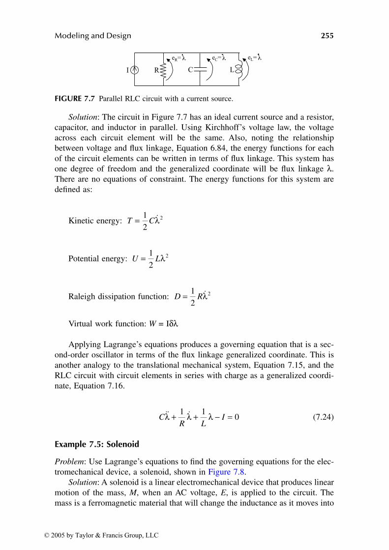
Modeling and Design 255
Solution: The circuit in Figure 7.7 has an ideal current source and a resistor,
capacitor, and inductor in parallel. Using Kirchhoff’s voltage law, the voltage
across each circuit element will be the same. Also, noting the relationship
between voltage and flux linkage, Equation 6.84, the energy functions for each
of the circuit elements can be written in terms of flux linkage. This system has
one degree of freedom and the generalized coordinate will be flux linkage λ.
There are no equations of constraint. The energy functions for this system are
defined as:
Kinetic energy:
Potential energy:
Raleigh dissipation function:
Virtual work function: W = IδλApplying Lagrange’s equations produces a governing equation that is a sec-
ond-order oscillator in terms of the flux linkage generalized coordinate. This is
another analogy to the translational mechanical system, Equation 7.15, and the
RLC circuit with circuit elements in series with charge as a generalized coordi-
nate, Equation 7.16.
(7.24)
Example 7.5: Solenoid
Problem: Use Lagrange’s equations to find the governing equations for the elec-
tromechanical device, a solenoid, shown in Figure 7.8.
Solution: A solenoid is a linear electromechanical device that produces linear
motion of the mass, M, when an AC voltage, E, is applied to the circuit. The
mass is a ferromagnetic material that will change the inductance as it moves into
FIGURE 7.7 Parallel RLC circuit with a current source.
T C= 1
2
2ɺλ
U L= 1
2
2λ
D R= 1
2
2ɺλ
CR L
Iɺɺ ɺλ λ λ+ + − =1 10
© 2005 by Taylor & Francis Group, LLC
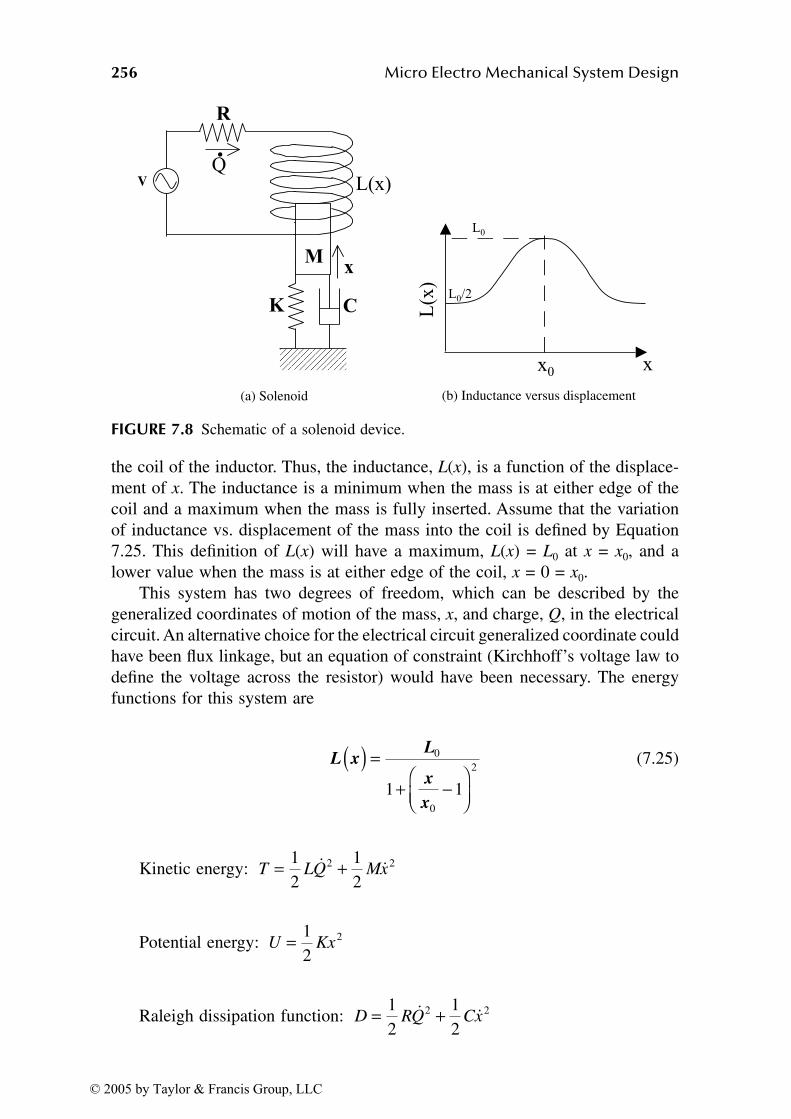
256 Micro Electro Mechanical System Design
the coil of the inductor. Thus, the inductance, L(x), is a function of the displace-
ment of x. The inductance is a minimum when the mass is at either edge of the
coil and a maximum when the mass is fully inserted. Assume that the variation
of inductance vs. displacement of the mass into the coil is defined by Equation
7.25. This definition of L(x) will have a maximum, L(x) = L0 at x = x0, and a
lower value when the mass is at either edge of the coil, x = 0 = x0.
This system has two degrees of freedom, which can be described by the
generalized coordinates of motion of the mass, x, and charge, Q, in the electrical
circuit. An alternative choice for the electrical circuit generalized coordinate could
have been flux linkage, but an equation of constraint (Kirchhoff’s voltage law to
define the voltage across the resistor) would have been necessary. The energy
functions for this system are
(7.25)
Kinetic energy:
Potential energy:
Raleigh dissipation function:
FIGURE 7.8 Schematic of a solenoid device.
(a) Solenoid (b) Inductance versus displacement
V
L xL
x
x
( ) =+ −
0
0
2
1 1
T LQ Mx= +1
2
1
2
2 2ɺ ɺ
U Kx= 1
2
2
D RQ Cx= +1
2
1
2
2 2ɺ ɺ
© 2005 by Taylor & Francis Group, LLC
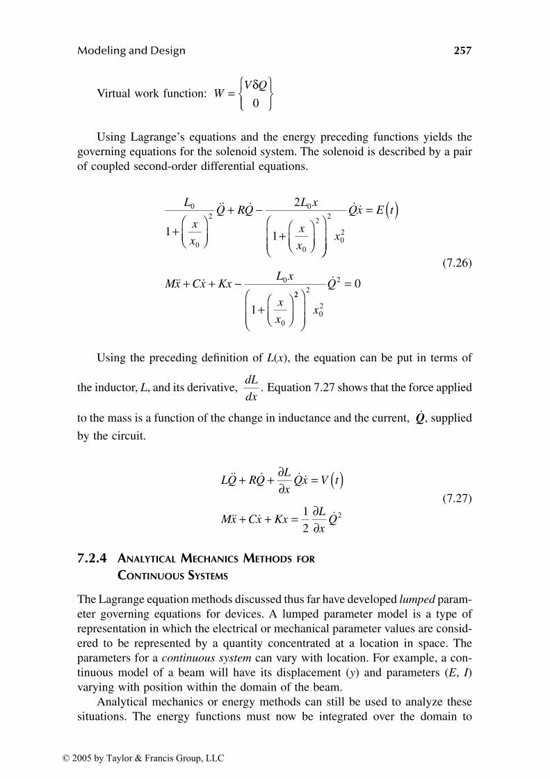
Modeling and Design 257
Virtual work function:
Using Lagrange’s equations and the energy preceding functions yields the
governing equations for the solenoid system. The solenoid is described by a pair
of coupled second-order differential equations.
(7.26)
Using the preceding definition of L(x), the equation can be put in terms of
the inductor, L, and its derivative, Equation 7.27 shows that the force applied
to the mass is a function of the change in inductance and the current, supplied
by the circuit.
(7.27)
7.2.4 ANALYTICAL MECHANICS METHODS FOR
CONTINUOUS SYSTEMS
The Lagrange equation methods discussed thus far have developed lumped param-
eter governing equations for devices. A lumped parameter model is a type of
representation in which the electrical or mechanical parameter values are consid-
ered to be represented by a quantity concentrated at a location in space. The
parameters for a continuous system can vary with location. For example, a con-
tinuous model of a beam will have its displacement (y) and parameters (E, I)
varying with position within the domain of the beam.
Analytical mechanics or energy methods can still be used to analyze these
situations. The energy functions must now be integrated over the domain to
WV Q=
δ0
L
x
x
Q RQL x
x
x
0
0
2
0
0
2
1
2
1+
+ −+
ɺɺ ɺ
= ( )
+ + −+
2
02
0
0
1
x
Qx E t
Mx Cx KxL x
x
x
ɺ ɺ
ɺɺ ɺ22
2
02
2 0
=x
Qɺ
dL
dx.
ɺQ,
LQ RQL
xQx V t
Mx Cx KxL
xQ
ɺɺ ɺ ɺ ɺ
ɺɺ ɺ ɺ
+ + ∂∂ = ( )
+ + = ∂∂
1
2
2
© 2005 by Taylor & Francis Group, LLC
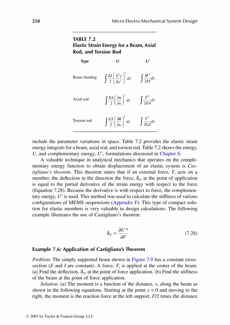
258 Micro Electro Mechanical System Design
include the parameter variations in space. Table 7.2 provides the elastic strain
energy integrals for a beam, axial rod, and torsion rod. Table 7.2 shows the energy,
U, and complementary energy, U*, formulations discussed in Chapter 6.
A valuable technique in analytical mechanics that operates on the comple-
mentary energy function to obtain displacement of an elastic system is Cas-
tigliano’s theorem. This theorem states that if an external force, F, acts on a
member, the deflection in the direction the force, δF, at the point of application
is equal to the partial derivative of the strain energy with respect to the force
(Equation 7.28). Because the derivative is with respect to force, the complemen-
tary energy, U* is used. This method was used to calculate the stiffness of various
configurations of MEMS suspensions (Appendix F). This type of compact solu-
tion for elastic members is very valuable in design calculations. The following
example illustrates the use of Castigliano’s theorem.
(7.28)
Example 7.6: Application of Castigliano’s Theorem
Problem: The simply supported beam shown in Figure 7.9 has a constant cross-
section (E and I are constant). A force, F, is applied at the center of the beam.
(a) Find the deflection, δF, at the point of force application. (b) Find the stiffness
of the beam at the point of force application.
Solution: (a) The moment is a function of the distance, x, along the beam as
shown in the following equations. Starting at the point x = 0 and moving to the
right, the moment is the reaction force at the left support, F/2 times the distance
TABLE 7.2Elastic Strain Energy for a Beam, Axial
Rod, and Torsion Rod
Type U U*
Beam bending
Axial rod
Torsion rod
EI y
xdx
2
2
2
2∫ ∂∂
M
EIdx
2
2∫EA u
xdx
2
2∫ ∂∂
F
EAdx
2
2∫GJ
xdx
2
2∫ ∂∂
θ T
GJdx
2
2∫
δF
U
F= ∂
∂*
© 2005 by Taylor & Francis Group, LLC

Modeling and Design 259
x. At x = L/2, the applied force at the center of the beam is encountered and must
now be included in the moment equation. Thus, moment is a function of distance
along the beam for two sections of the beam.
(7.29)
(7.30)
The strain energy of the beam is calculated using the complementary beam
strain energy formulation. The strain energy integral is the sum of two parts due
to the preceding moment equations.
(7.31)
(7.32)
Applying Castigliano’s theorem, Equation 7.28, yields the deflection of the
beam at the position of the center load.
(7.33)
(b) The stiffness of the beam at the center load is simply the ratio of force
to deflection.
(7.34)
FIGURE 7.9 Simply supported beam with center load.
M xF
x xL( ) = ≤ ≤
20
2
M xF
x F xL L
x L( ) = − −
≤ ≤
2 2 2
UEI
Fxdx
EI
FL Fxd
L
* =
+ −
∫1
2 2
1
2 2 2
2
0
22
xxL
L
2∫
UF L
EI
* = 1
96
2 3
δF
U
F
FL
EI= ∂
∂ =* 1
48
3
KF EI
LF
= =δ 483
© 2005 by Taylor & Francis Group, LLC
260 Micro Electro Mechanical System Design
The Raleigh–Ritz method approximates the solution of a continuous system
through the use of a summation of assumed solutions. If the system variable of
interest, u(x,t), is a function of space and time, assume the solution can be
approximated by a summation of functions that are products of separate functions
of space, Φi(x) and time ai(t) as shown in Equation 7.35. Equation 7.36 shows
this summation written in matrix notation. The function Φi(x) is generally referred
to as a basis or shape function. The basis function, Φi(x), which approximates
the solution, u, within the domain of the system, must satisfy two requirements:
• Φi(x) must satisfy the geometric boundary conditions of the system.
• Φi(x) must be differentiable at least to the order appearing in the energy
functions.
For most situations, a number of possible basis functions can satisfy these
requirements. The number of functions that will approximate the solution to a
desired level of accuracy depends on the function selected as well as the loading
applied in the domain of the system. The Raleigh–Ritz method has transformed
the problem from an exact continuous representation of the system to an approx-
imate discrete system representation in terms of the coefficient, ai. The use of
the Raleigh–Ritz method is best illustrated in the following example.
(7.35)
(7.36)
Example 7.7: Raleigh–Ritz Solution for a Beam
Problem: Find the deflection at the center of a fixed–fixed beam with a distributed
load, w, across the length of the beam.
Solution: Choose the basis functions as shown next. This series of basis
functions has zero deflection and slope at the beam ends (x= 0 and x = L), which
satisfy the geometric boundary conditions. They can be twice differentiated as
required by the beam strain energy function (see Table 7.2).
(7.37)
u x t x a ti
i
n
i,( ) = ( ) ( )=∑Φ
1
u x t
a
a
a
an
n
,( ) =
=Φ Φ Φ Φ1 2
1
2⋯
⋮
Φi x ix
L( ) =
−cos 2 1π
© 2005 by Taylor & Francis Group, LLC
Modeling and Design 261
The beam displacement is approximated by the following series:
(7.38)
Lagrange’s equations can be used to find the governing equations. Because
this is a static problem, the kinetic energy and Raleigh dissipation function are
zero. The Raleigh–Ritz approach has discretized the problem, and the generalized
coordinates for this problem are the basis function coefficients, ai. The energy
functions for this situation are:
Potential energy:
Virtual work function: W = wΦiδai
MATLAB and the function LagEqn were used to assist in the calculations.
The MATLAB file used for this example is shown in Appendix H. Lagrange’s
equation yields the following series of equations in terms of the generalized
coordinates, ai.
(7.39)
This system of equations can be solved for the generalized coordinates, ai.
(7.40)
Given the basis function, Equation 7.37, and the generalized coordinates, ai,
the displacement of the beam at any position x is:
(7.41)
y x t x a ti
i
n
i,( ) = ( ) ( )=∑Φ
1
UEI y
xdx
EI
xdx
L
i
= ∂∂
= ∂∂
∫ 2
2
0
2
2
2
2
2
2Φ00
1
L
i
i
n
a∫∑
=
8 0 14
3i
EI
La Lw i niπ( ) + = = ,
ai
L
EIwi = ( )1
84
4
π
y x ix
Lai
i
n
( ) cos=
−
=
∑ 2 1
1
π
© 2005 by Taylor & Francis Group, LLC
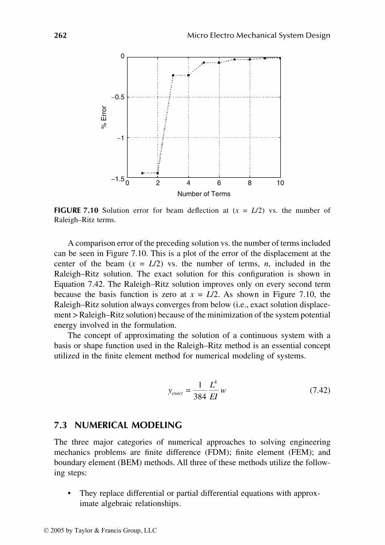
262 Micro Electro Mechanical System Design
A comparison error of the preceding solution vs. the number of terms included
can be seen in Figure 7.10. This is a plot of the error of the displacement at the
center of the beam (x = L/2) vs. the number of terms, n, included in the
Raleigh–Ritz solution. The exact solution for this configuration is shown in
Equation 7.42. The Raleigh–Ritz solution improves only on every second term
because the basis function is zero at x = L/2. As shown in Figure 7.10, the
Raleigh–Ritz solution always converges from below (i.e., exact solution displace-
ment > Raleigh–Ritz solution) because of the minimization of the system potential
energy involved in the formulation.
The concept of approximating the solution of a continuous system with a
basis or shape function used in the Raleigh–Ritz method is an essential concept
utilized in the finite element method for numerical modeling of systems.
(7.42)
7.3 NUMERICAL MODELING
The three major categories of numerical approaches to solving engineering
mechanics problems are finite difference (FDM); finite element (FEM); and
boundary element (BEM) methods. All three of these methods utilize the follow-
ing steps:
• They replace differential or partial differential equations with approx-
imate algebraic relationships.
FIGURE 7.10 Solution error for beam deflection at (x = L/2) vs. the number of
Raleigh–Ritz terms.
0
−0.5
−1
−1.5
% E
rror
1086420
Number of Terms
yL
EIwexact = 1
384
4
© 2005 by Taylor & Francis Group, LLC

Modeling and Design 263
• They define a computational grid or mesh that describes the geometry
of the solution domain. The boundary conditions and responses are
calculated at these grid positions.
• They solve the set of simultaneous algebraic equations to determine
the response at the grid points.
Figure 7.11 shows examples of the FDM, FEM, and BEM meshes. The inter-
section of the grid lines is called nodes. The FDM approach [10] approximates the
governing equation within the domain of the mesh with a finite difference approx-
imation at each node. The FDM mesh size is chosen to achieve an accurate solution.
Generally, the finer the mesh is, the more accurate the solution is. An FDM mesh
is generally uniform due to the nature of the finite difference approximations.
The BEM [11] approach transforms the governing differential equations into
equivalent integral equations using calculus relationships (e.g., Gauss–Green
theorem) that contain no volume integrals involving the unknown response. This
transformation utilizes fundamental known solutions (Green’s functions).
The FEM [12] approach utilizes a subdomain or “element” in which the
governing differential equation is transformed into an equivalent integral equa-
tion. The integral equation is discretized by an interpolation function that inter-
polates the response inside the element to the nodes on the periphery of the
element. The elements are assembled to form the entire domain by ensuring that
the responses of adjacent elements at their nodes are equivalent.
Each of these approaches to numerical modeling has advantages and disad-
vantages. Issues such as the ability of model boundary conditions of complex
shapes; nonlinearities; infinite boundary conditions; calculation complexity; and
user interaction to set up the problem will tend to make one approach more
frequently used in one application over another. Table 7.3 is a comparison of the
different approaches. MEMS analysis frequently requires the analysis of different
physical phenomena such as structure, electrostatics, and fluidics. The FEM
approach is most frequently used, except that electrostatics that encounter infinite
boundary conditions are sometime best modeled with the BEM approach. The
BEM and FEM methods can be coupled to model these multiphysics problems.
Due to space limitation, the details of the FDM and BEM methods will not be
discussed in detail. However, an example of the use of a simple, easy-to-use FEM
software that has been developed for MEMS analysis will be discussed.
SUGAR is an open source simulation tool for MEMS [13] that has been
under development at the Berkeley Sensor and Actuator Center (BSAC) at the
University of California for several years [14,15].The SUGAR software is built
upon MATLAB, which is frequently used for engineering analysis of various
types. SUGAR was developed for MEMS with the same philosophy that has
made simulation program with integrated circuit emphasis (SPICE) an essential
tool for microelectronic designers. SUGAR is not an acronym but was named
because of its duality with SPICE. SUGAR provides an environment for the
development of low-order models (design synthesis) of a MEMS device, thus
enabling the designer to explore the design space quickly.
© 2005 by Taylor & Francis Group, LLC
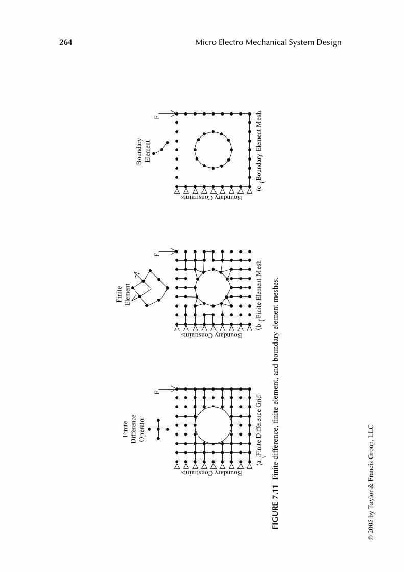
264 Micro Electro Mechanical System Design
FIG
UR
E 7.1
1F
init
e d
iffe
ren
ce,
fin
ite
elem
ent,
an
d b
ou
nd
ary
ele
men
t m
esh
es.
(
(
(
(
(
(
Boundary Constraints
Boundary Constraints
Boundary Constraints©
2005 b
y T
aylo
r &
Fra
nci
s G
roup, L
LC
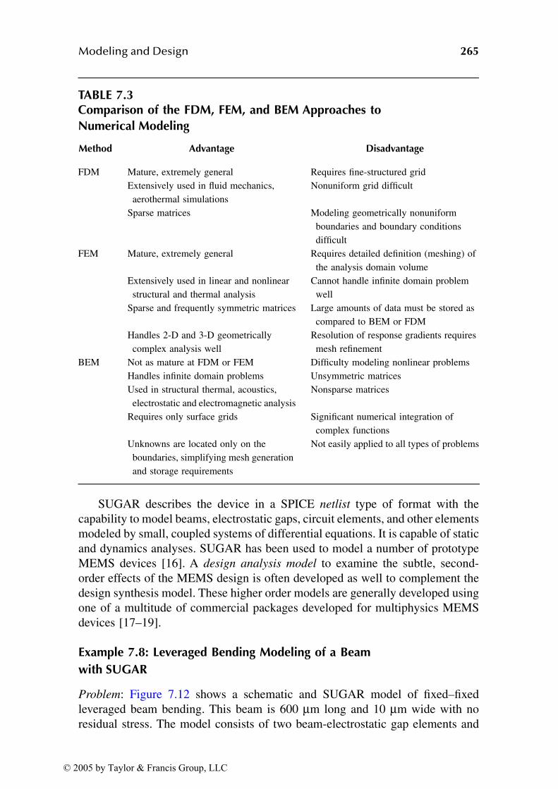
Modeling and Design 265
SUGAR describes the device in a SPICE netlist type of format with the
capability to model beams, electrostatic gaps, circuit elements, and other elements
modeled by small, coupled systems of differential equations. It is capable of static
and dynamics analyses. SUGAR has been used to model a number of prototype
MEMS devices [16]. A design analysis model to examine the subtle, second-
order effects of the MEMS design is often developed as well to complement the
design synthesis model. These higher order models are generally developed using
one of a multitude of commercial packages developed for multiphysics MEMS
devices [17–19].
Example 7.8: Leveraged Bending Modeling of a Beam
with SUGAR
Problem: Figure 7.12 shows a schematic and SUGAR model of fixed–fixed
leveraged beam bending. This beam is 600 µm long and 10 µm wide with no
residual stress. The model consists of two beam-electrostatic gap elements and
TABLE 7.3Comparison of the FDM, FEM, and BEM Approaches to
Numerical Modeling
Method Advantage Disadvantage
FDM Mature, extremely general Requires fine-structured grid
Extensively used in fluid mechanics,
aerothermal simulations
Nonuniform grid difficult
Sparse matrices Modeling geometrically nonuniform
boundaries and boundary conditions
difficult
FEM Mature, extremely general Requires detailed definition (meshing) of
the analysis domain volume
Extensively used in linear and nonlinear
structural and thermal analysis
Cannot handle infinite domain problem
well
Sparse and frequently symmetric matrices Large amounts of data must be stored as
compared to BEM or FDM
Handles 2-D and 3-D geometrically
complex analysis well
Resolution of response gradients requires
mesh refinement
BEM Not as mature at FDM or FEM Difficulty modeling nonlinear problems
Handles infinite domain problems Unsymmetric matrices
Used in structural thermal, acoustics,
electrostatic and electromagnetic analysis
Nonsparse matrices
Requires only surface grids Significant numerical integration of
complex functions
Unknowns are located only on the
boundaries, simplifying mesh generation
and storage requirements
Not easily applied to all types of problems
© 2005 by Taylor & Francis Group, LLC
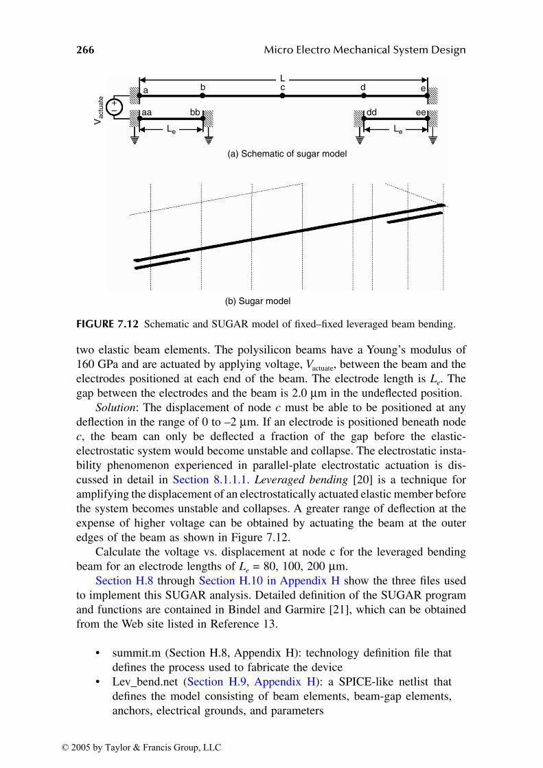
266 Micro Electro Mechanical System Design
two elastic beam elements. The polysilicon beams have a Young’s modulus of
160 GPa and are actuated by applying voltage, Vactuate, between the beam and the
electrodes positioned at each end of the beam. The electrode length is Le. The
gap between the electrodes and the beam is 2.0 µm in the undeflected position.
Solution: The displacement of node c must be able to be positioned at any
deflection in the range of 0 to –2 µm. If an electrode is positioned beneath node
c, the beam can only be deflected a fraction of the gap before the elastic-
electrostatic system would become unstable and collapse. The electrostatic insta-
bility phenomenon experienced in parallel-plate electrostatic actuation is dis-
cussed in detail in Section 8.1.1.1. Leveraged bending [20] is a technique for
amplifying the displacement of an electrostatically actuated elastic member before
the system becomes unstable and collapses. A greater range of deflection at the
expense of higher voltage can be obtained by actuating the beam at the outer
edges of the beam as shown in Figure 7.12.
Calculate the voltage vs. displacement at node c for the leveraged bending
beam for an electrode lengths of Le = 80, 100, 200 µm.
Section H.8 through Section H.10 in Appendix H show the three files used
to implement this SUGAR analysis. Detailed definition of the SUGAR program
and functions are contained in Bindel and Garmire [21], which can be obtained
from the Web site listed in Reference 13.
• summit.m (Section H.8, Appendix H): technology definition file that
defines the process used to fabricate the device
• Lev_bend.net (Section H.9, Appendix H): a SPICE-like netlist that
defines the model consisting of beam elements, beam-gap elements,
anchors, electrical grounds, and parameters
FIGURE 7.12 Schematic and SUGAR model of fixed–fixed leveraged beam bending.
Va
ctu
ate
a b c d e
aa bb dd ee
LeLe
L
(a) Schematic of sugar model
(b) Sugar model
+–
© 2005 by Taylor & Francis Group, LLC
Modeling and Design 267
• Lev_bend.m (Section H.10, Appendix H): MATLAB file that loads the
netlist, defines the parameters, loops through a voltages to be applied,
and calculates the beam deflections
The SUGAR netlist is the starting point for most analyses. The first line calls
summit.net, which defines the fabrication technology parameters such as material
properties, layer names, and thicknesses. This particular file has been specialized
for the SUMMiT surface micromachine technology. The SUGAR Web site proves
a few other frequently used technology files. The next statement calls stdlib.net,
which is a SUGAR-specific file that defines the functions for SUGAR. The param
statement defines the parameters, which can be changed from outside this netlist
(i.e., these parameters can be defined by the MATLAB file, which runs SUGAR
and controls the program flow). The beams, beam-gap, anchors, electrical
grounds, and voltage source parameters are defined in the Lev_bend.net file.
Lev_bend.m is the MATLAB file that executes SUGAR. This file defines the
problem parameters and performs a loop from 0 to 200 V applied to the beam.
The solution is checked for convergence. Nonconvergence indicates that the
system has become unstable at a particular voltage and the solution loop should
be terminated.
Figure 7.13 is a node c displacement vs. voltage for three different electrode
lengths, Le. The deflection of a system with Le = 200 µm becomes electrostatically
unstable at approximately 35 V and 0.65 µm displacement, which does not achieve
the stated objective. As the electrode length is shortened, the stable deflection
range and the required voltage increase.
7.4 DESIGN UNCERTAINTY
Many MEMS devices must attain specified design metrics accurately to achieve
proper performance. For example, inertial sensors such as an accelerometer may
require the natural frequency of the suspension that defines the mechanical sen-
sitivity to be within a specified range or have a specified value as accurately as
possible. A gyroscope may require the drive mode natural frequency to be higher
and within a specified ratio of the sense mode natural frequency [22]. These are
examples of absolute and relative design metrics, respectively. For many MEMS
fabrication technologies, it is easier to attain a relative design metric (e.g.,
matched devices such as transistors in microelectronics) than an absolute design
metric. Many MEMS processes are starting to obtain process uncertainty infor-
mation [23,24]; however, the MEMS designer may need to design specific test
structures (Section 3.5) to quantify process uncertainty relevant to a particular
design. The ability of a design to meet a design metric is a function of the
tolerances of the fabrication process and the device design.
MEMS fabrication techniques utilize a combination of deposition, patterning,
and etching techniques (Chapter 2), which can make devices with feature sizes
of ~1 µm; however, these process do not have a high relative tolerance as
compared to traditional machining processes (see Section 4.3). Relative tolerance
© 2005 by Taylor & Francis Group, LLC
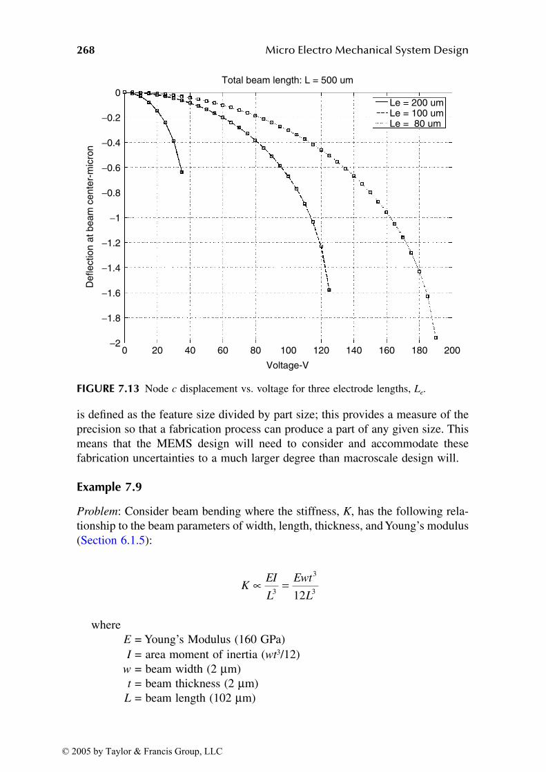
268 Micro Electro Mechanical System Design
is defined as the feature size divided by part size; this provides a measure of the
precision so that a fabrication process can produce a part of any given size. This
means that the MEMS design will need to consider and accommodate these
fabrication uncertainties to a much larger degree than macroscale design will.
Example 7.9
Problem: Consider beam bending where the stiffness, K, has the following rela-
tionship to the beam parameters of width, length, thickness, and Young’s modulus
(Section 6.1.5):
where
E = Young’s Modulus (160 GPa)
I = area moment of inertia (wt3/12)
w = beam width (2 µm)
t = beam thickness (2 µm)
L = beam length (102 µm)
FIGURE 7.13 Node c displacement vs. voltage for three electrode lengths, Le.
Total beam length: L = 500 um
Le = 200 umLe = 100 umLe = 80 um
200180160140120100806040200
0
−0.2
−0.4
−0.6
−0.8
−1
−1.4
−1.2
−1.6
−1.8
−2
Deflection a
t beam
cente
r-m
icro
n
Voltage-V
KEI
L
Ewt
L∝ =
3
3
312
© 2005 by Taylor & Francis Group, LLC
Modeling and Design 269
For the nominal parameters, the beam stiffness K = 0.2 N/m. Assume that the
RIE etch can narrow the line width up to a maximum of 0.2 µm from the nominal
line width drawn on the mask used to photolithographically pattern the material.
Solution: (a) If the RIE fabrication variation is applied to the width, w, of a
spring, what is the effect on the spring constant?
, a stiffness variation of 10%.
(b) What is the effect on stiffness of this fabrication variation applied to the
spring length?
, a stiffness variation of 0.5%.
A variation in an aspect of fabrication, such as discussed earlier, will produce
an effect on several parameters (e.g., length, width) that will affect the design
metric (K in this case) unequally. In most real design situations, multiple uncer-
tainties are present, such as line width variations, thickness variations, and mate-
rial property variations, that will affect multiple parameters in a design (spring
width, length, thickness, material) to produce various effects in a design metric, K.
Heuristically, the preceding example would illustrate that increasing the width
of the beam to reduce the percentage of uncertainty in the width and increasing
the beam length to maintain the desired spring constant is a viable approach.
The estimation of the effects of uncertainty is a stochastic problem that may
be approximated using the partial derivative rule, Equation 7.43. This method of
uncertainty prediction is very useful when an analytical model of the design
metric, f, which can be used to calculate the partial derivative of the design metric
with respect to the design parameter, pi, is available. If the standard deviation of
the design parameters is available, Equation 7.43 will allow the prediction of the
standard deviation of the design metric.
(7.43)
where
f = design metric
pi = design parameter
σf = standard deviation of f
σi = standard deviation of pi
KE w w t
L= + =( )
.∆ 3
31222 N/m
KEwt
L L= +( ) =3
3
12 ∆ .201 N/m
σ σ σf
i
f
p
f
p
f
p
2
1
2
12
2
2
22= ∂
∂
+ ∂
∂
+ + ∂
∂⋯
2
2σ i
© 2005 by Taylor & Francis Group, LLC
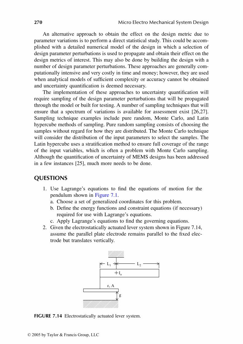
270 Micro Electro Mechanical System Design
An alternative approach to obtain the effect on the design metric due to
parameter variations is to perform a direct statistical study. This could be accom-
plished with a detailed numerical model of the design in which a selection of
design parameter perturbations is used to propagate and obtain their effect on the
design metrics of interest. This may also be done by building the design with a
number of design parameter perturbations. These approaches are generally com-
putationally intensive and very costly in time and money; however, they are used
when analytical models of sufficient complexity or accuracy cannot be obtained
and uncertainty quantification is deemed necessary.
The implementation of these approaches to uncertainty quantification will
require sampling of the design parameter perturbations that will be propagated
through the model or built for testing. A number of sampling techniques that will
ensure that a spectrum of variations is available for assessment exist [26,27].
Sampling technique examples include pure random, Monte Carlo, and Latin
hypercube methods of sampling. Pure random sampling consists of choosing the
samples without regard for how they are distributed. The Monte Carlo technique
will consider the distribution of the input parameters to select the samples. The
Latin hypercube uses a stratification method to ensure full coverage of the range
of the input variables, which is often a problem with Monte Carlo sampling.
Although the quantification of uncertainty of MEMS designs has been addressed
in a few instances [25], much more needs to be done.
QUESTIONS
1. Use Lagrange’s equations to find the equations of motion for the
pendulum shown in Figure 7.1.
a. Choose a set of generalized coordinates for this problem.
b. Define the energy functions and constraint equations (if necessary)
required for use with Lagrange’s equations.
c. Apply Lagrange’s equations to find the governing equations.
2. Given the electrostatically actuated lever system shown in Figure 7.14,
assume the parallel plate electrode remains parallel to the fixed elec-
trode but translates vertically.
FIGURE 7.14 Electrostatically actuated lever system.
© 2005 by Taylor & Francis Group, LLC

Modeling and Design 271
a. How many degrees of freedom does this system have?
b. Choose a set a generalized coordinates for this problem.
c. Define the energy functions.
d. Find governing equations for this system.
e. Does this system have an electrostatic instability (i.e., pull-in)? If
so, what is the pull-in voltage? What is the displacement in terms
of the generalized coordinate that you defined?
3. Use the Raleigh–Ritz method to find the deflection of the simply
supported beam shown in Figure 7.9.
a. Define an appropriate set of basis functions.
b. Compare the Raleigh–Ritz solution to the solution obtained for the
deflection in Example 7.6.
c. Plot the number of terms used in the Raleigh–Ritz solution vs. the
solution accuracy.
4. Use Appendix F to design a double-folded beam with a transverse
stiffness of Kx = 1 N/m. For the process that will be used to fabricate
this beam, the minimum line width is 1 µm, and the layer thickness is
2 µm. The fabricated line width will have a standard deviation of σw
= 0.1.
a. What is the standard deviation of the stiffness for your design?
b. What would you do to minimize the stiffness variability?
c. What are some practical constraints that may limit your ability to
minimize the stiffness variability?
5. Determine the Kx stiffness of the crab-leg flexure shown in Appendix
F, using Castigliano’s theorem. Use only bending strain energy in your
formulation.
6. Explore the literature to find a MEMS sensor such as an accelerometer,
gyroscope, pressure sensor, or magnetometer that you can analyze
using SUGAR. Perform the analysis required to determine the opera-
tional dynamics of the system (e.g., natural frequencies, deflections,
transfer function) needed for design.
REFERENCES
1. C. Lanczos, The Variational Principles of Mechanics, University of Toronto Press,
1970.
2. L. Meirovitch, Methods of Analytical Dynamics, McGraw-Hill Book Company,
New York, 1970.
3. L. Meirovitch, Elements of Vibration Analysis, McGraw-Hill Book Company, New
York, 1975.
4. M.R. Spiegel, Theoretical Mechanics, McGraw-Hill Book Company, New York,
1967.
5. D.A. Wells, Lagrangian Dynamics, McGraw-Hill Book Company, New York,
1967.
© 2005 by Taylor & Francis Group, LLC
272 Micro Electro Mechanical System Design
6. S.H. Crandall, D.C. Karnopp, E.F. Kurtz, D.C. Pridmore-Brown, Dynamics of
Mechanical and Electromechanical Systems, Krieger Publishing Company, 1982.
Original edition published by McGraw-Hill, Inc, 1968.
7. The Mathworks Inc., http://www.mathworks.com/.
8. C.W. Dyck, J.J. Allen, R.J. Huber, Parallel-plate electrostatic dual-mass resonator,
Proc. SPIE, 3876, 198–209, 1999.
9. W.T. Thomson, Theory of Vibration with Applications, Prentice Hall, Inc., Engle-
wood Cliffs, NJ, 1981.
10. R.G. Stanton, Numerical Methods for Science and Engineering, Prentice Hall,
Englewood Cliffs, NJ, 1961.
11. P.K. Kythe, An Introduction to Boundary Element Methods, CRC Press, Boca
Raton, FL.
12. O.C. Zienkiewicz, The Finite Element Method in Engineering Science, McGraw-
Hill, New York, 1971.
13. http://www-bsac.eecs.berkeley.edu/cadtools/sugar/sugar/.
14. J.V. Clark, N. Zhou, K.S.J. Pister, Modified nodal analysis for MEMS with
multienergy domains, Proc. Int. Conf. Modeling Simulation Microsyst., Semicon-
ductors, Sensors Actuators, MSM 2000, 31–34, 2000.
15. J.V. Clark, D. Bindel, W. Kao, E. Zhu, A. Kuo, N. Zhou, J. Nie, J. Demmel, Z.
Bai, S. Govindjee, K.S.J. Pister, M. Gu, A. Agogino, Addressing the needs of
complex MEMS design, MEMS 2002, Las Vegas, Nevada, January 20–24, 2002.
16. S.X.P. Su, H.S. Yang, Analytical modeling and FEM simulations of single-stage
microleverage mechanism, Intl. J. Mechanical Sci., 44, 2217–2238, 2002.
17. MEMSCAP: http://www.memscap.com.
18. ANSYS: http://www.ansys.com.
19. CoventorWare: http://www.coventor.com/.
20. E.S. Hung, S.D. Senturia, Extending the travel range of analog-tuned electrostatic
actuators, JMEMS, 8(4), 497–505, Dec. 1999.
21. D. Bindel, D. Garmire, SUGAR 3.0: A MEMS Simulation Program (User’s Guide),
March 2002.
22. W.A. Clark, Micromachined vibratory rate gyroscopes, Ph.D. dissertation, Uni-
versity of California, Berkeley, Fall 1997.
23. D.A. Koester, R. Mahadevan, B. Hardy, K.W. Markus, MUMPs Design Hand-
book, Revision 5.0, Cronos Integrated Microsystems.
24. S. Livmary, H. Stewart, L. Irwin, J. McBrayer, J. Sniegowski, S. Montague, J.
Smith, M. de Boer, J. Jakubczak, Reproducibility data on SUMMiT, Proc. SPIE,
3874, 102–112, September 1999.
25. J.W. Wittwer, T. Gomm, L.L. Howell, Surface micromachined force gauges:
uncertainty and reliability, J. Micromech. Microeng., 12, 13–20, 2002.
26. M.D. McKay, R.J. Beckman, W.J. Conover, A comparison of three methods for
selecting values of input variables in the analysis of output from a computer code,
Technometrics, 21(2), 239–245, 1979.
27. S.F. Wojtkiewicz, M.S. Eldred, R.V. Field, A. Urbina, J.R. Red-Horse, Uncertainty
quantification in large computational engineering models, American Institute of
Aeronautics and Astro., AIAA-2001-1455.
© 2005 by Taylor & Francis Group, LLC
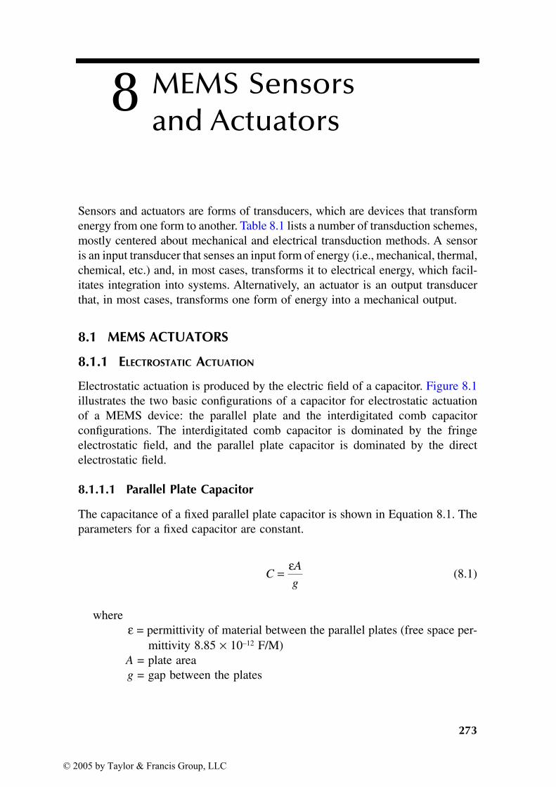
273
8 MEMS Sensors and Actuators
Sensors and actuators are forms of transducers, which are devices that transformenergy from one form to another. Table 8.1 lists a number of transduction schemes,mostly centered about mechanical and electrical transduction methods. A sensoris an input transducer that senses an input form of energy (i.e., mechanical, thermal,chemical, etc.) and, in most cases, transforms it to electrical energy, which facil-itates integration into systems. Alternatively, an actuator is an output transducerthat, in most cases, transforms one form of energy into a mechanical output.
8.1 MEMS ACTUATORS
8.1.1 ELECTROSTATIC ACTUATION
Electrostatic actuation is produced by the electric field of a capacitor. Figure 8.1illustrates the two basic configurations of a capacitor for electrostatic actuationof a MEMS device: the parallel plate and the interdigitated comb capacitorconfigurations. The interdigitated comb capacitor is dominated by the fringeelectrostatic field, and the parallel plate capacitor is dominated by the directelectrostatic field.
8.1.1.1 Parallel Plate Capacitor
The capacitance of a fixed parallel plate capacitor is shown in Equation 8.1. Theparameters for a fixed capacitor are constant.
(8.1)
where ε = permittivity of material between the parallel plates (free space per-mittivity 8.85 × 10⁻¹² F/M)
A = plate areag = gap between the plates
CA
g= ε
© 2005 by Taylor & Francis Group, LLC
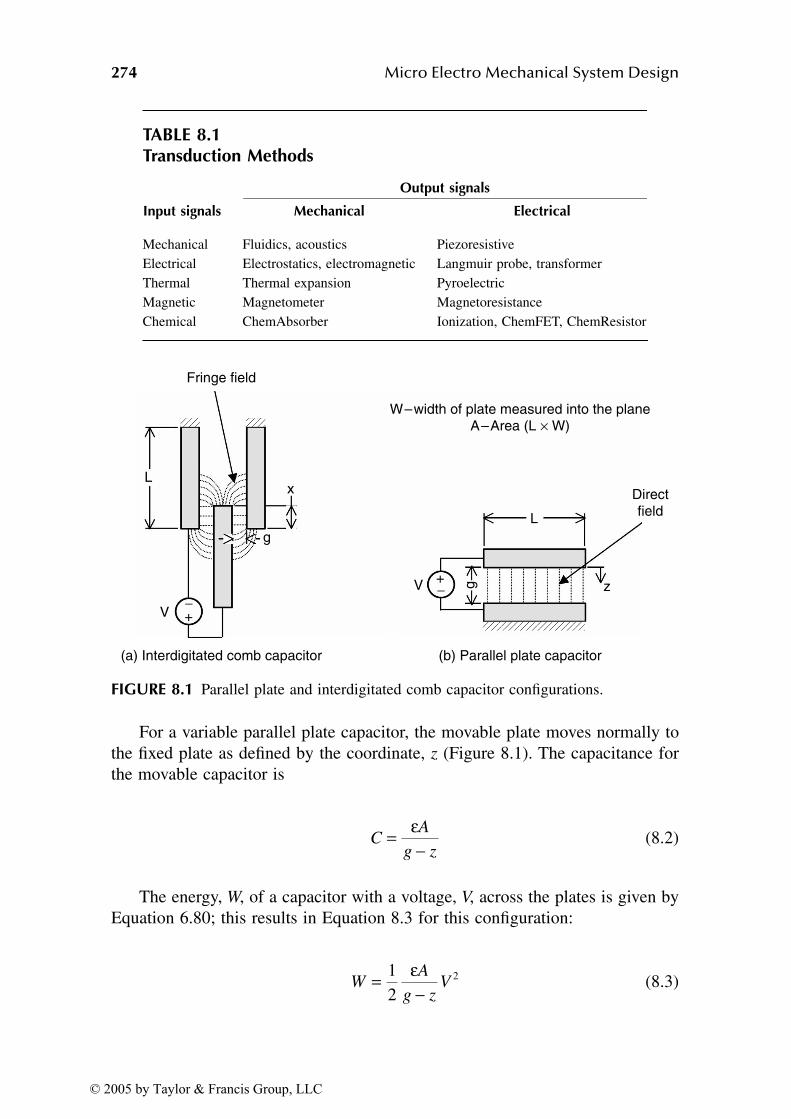
274 Micro Electro Mechanical System Design
For a variable parallel plate capacitor, the movable plate moves normally tothe fixed plate as defined by the coordinate, z (Figure 8.1). The capacitance forthe movable capacitor is
(8.2)
The energy, W, of a capacitor with a voltage, V, across the plates is given byEquation 6.80; this results in Equation 8.3 for this configuration:
(8.3)
TABLE 8.1Transduction Methods
Input signals
Output signals
Mechanical Electrical
Mechanical Fluidics, acoustics PiezoresistiveElectrical Electrostatics, electromagnetic Langmuir probe, transformerThermal Thermal expansion PyroelectricMagnetic Magnetometer MagnetoresistanceChemical ChemAbsorber Ionization, ChemFET, ChemResistor
FIGURE 8.1 Parallel plate and interdigitated comb capacitor configurations.
Lx
g
+−V
(a) Interdigitated comb capacitor
Fringe field
L
zg+−V
(b) Parallel plate capacitor
Directfield
W–width of plate measured into the plane A–Area (L × W)
CA
g z= −
ε
WA
g zV= −
12
2ε
© 2005 by Taylor & Francis Group, LLC
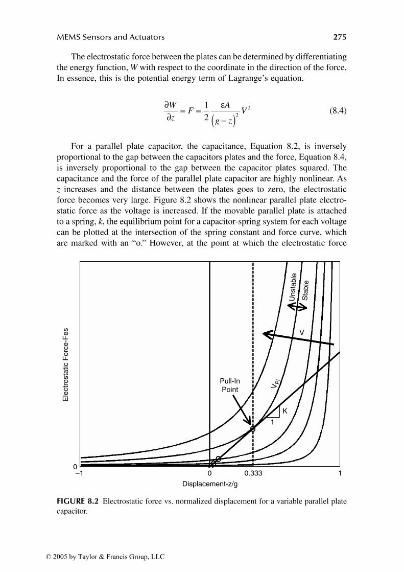
MEMS Sensors and Actuators 275
The electrostatic force between the plates can be determined by differentiatingthe energy function, W with respect to the coordinate in the direction of the force.In essence, this is the potential energy term of Lagrange’s equation.
(8.4)
For a parallel plate capacitor, the capacitance, Equation 8.2, is inverselyproportional to the gap between the capacitors plates and the force, Equation 8.4,is inversely proportional to the gap between the capacitor plates squared. Thecapacitance and the force of the parallel plate capacitor are highly nonlinear. Asz increases and the distance between the plates goes to zero, the electrostaticforce becomes very large. Figure 8.2 shows the nonlinear parallel plate electro-static force as the voltage is increased. If the movable parallel plate is attachedto a spring, k, the equilibrium point for a capacitor-spring system for each voltagecan be plotted at the intersection of the spring constant and force curve, whichare marked with an “o.” However, at the point at which the electrostatic force
FIGURE 8.2 Electrostatic force vs. normalized displacement for a variable parallel platecapacitor.
∂∂ = = −( )W
zF
A
g zV
12 2
2ε
Displacement-z/g
0.3330−1 1
Ele
ctr
osta
tic F
orc
e-F
es
0
1
K
Pull-InPoint V
PI
V
Unsta
ble
Sta
ble
© 2005 by Taylor & Francis Group, LLC
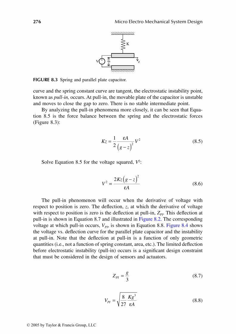
276 Micro Electro Mechanical System Design
curve and the spring constant curve are tangent, the electrostatic instability point,known as pull-in, occurs. At pull-in, the movable plate of the capacitor is unstableand moves to close the gap to zero. There is no stable intermediate point.
By analyzing the pull-in phenomena more closely, it can be seen that Equa-tion 8.5 is the force balance between the spring and the electrostatic forces(Figure 8.3):
(8.5)
Solve Equation 8.5 for the voltage squared, V2:
(8.6)
The pull-in phenomenon will occur when the derivative of voltage withrespect to position is zero. The deflection, z, at which the derivative of voltagewith respect to position is zero is the deflection at pull-in, ZPI. This deflection atpull-in is shown in Equation 8.7 and illustrated in Figure 8.2. The correspondingvoltage at which pull-in occurs, VPI, is shown in Equation 8.8. Figure 8.4 showsthe voltage vs. deflection curve for the parallel plate capacitor and the instabilityat pull-in. Note that the deflection at pull-in is a function of only geometricquantities (i.e., not a function of spring constant, area, etc.). The limited deflectionbefore electrostatic instability (pull-in) occurs is a significant design constraintthat must be considered in the design of sensors and actuators.
(8.7)
(8.8)
FIGURE 8.3 Spring and parallel plate capacitor.
+-
V
K
zg
KzA
g zV= −( )1
2 22ε
VKz g z
A
2
22= −( )
ε
Zg
PI =3
VKg
API = 8
27
3
ε
© 2005 by Taylor & Francis Group, LLC

MEMS Sensors and Actuators 277
Another significant effect in design involving a variable parallel plate capac-itor is electrostatic spring softening. This effect can be explained by using a two-term Taylor series approximation for the electrostatic force term in Equation 8.9.The linear term of the Taylor series is the slope of the electrostatic force vs.deflection curve (Figure 8.2). The linear term, Equation 8.10, can also be viewedas a negative electrostatic stiffness, Kes, that will cancel the elastic stiffness atpull-in. The electrostatic spring softening can be used to soften or tune the springstiffness electrostatically (Equation 8.11) or the resulting natural frequency of adesign where this is critical.
(8.9)
(8.10)
(8.11)
Another frequently encountered configuration for a variable parallel platecapacitor is that in which the movable electrode has a fixed electrode on both
FIGURE 8.4 Voltage vs. deflection curve of a parallel plate capacitor.
g
0
x -
disp
lace
men
t
V - voltage0 VPI
g/3
unst
able
stable
KzA
g zV
AV
g
AV
gz= −( ) ≈ +1
2 222
2
2 3
ε ε ε
KAV
ges = ε
3
K K zAV
ges−( ) = ε 2
22
© 2005 by Taylor & Francis Group, LLC
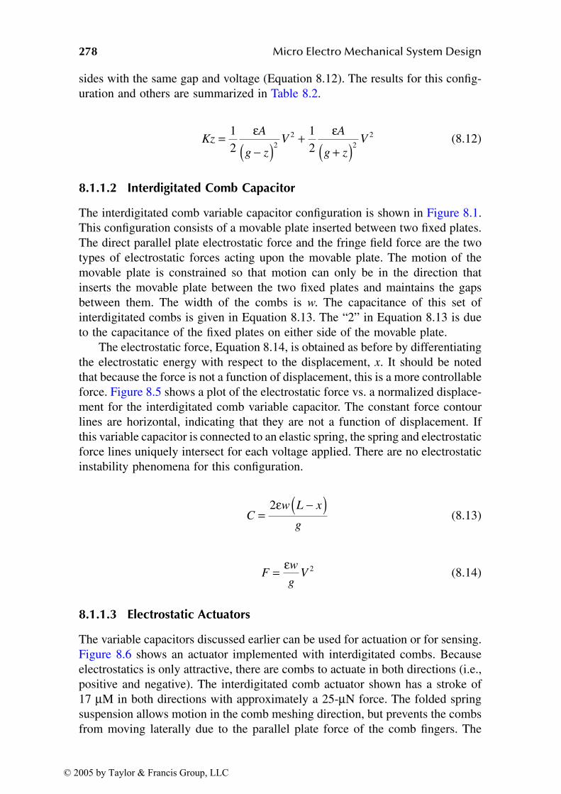
278 Micro Electro Mechanical System Design
sides with the same gap and voltage (Equation 8.12). The results for this config-uration and others are summarized in Table 8.2.
(8.12)
8.1.1.2 Interdigitated Comb Capacitor
The interdigitated comb variable capacitor configuration is shown in Figure 8.1.This configuration consists of a movable plate inserted between two fixed plates.The direct parallel plate electrostatic force and the fringe field force are the twotypes of electrostatic forces acting upon the movable plate. The motion of themovable plate is constrained so that motion can only be in the direction thatinserts the movable plate between the two fixed plates and maintains the gapsbetween them. The width of the combs is w. The capacitance of this set ofinterdigitated combs is given in Equation 8.13. The “2” in Equation 8.13 is dueto the capacitance of the fixed plates on either side of the movable plate.
The electrostatic force, Equation 8.14, is obtained as before by differentiatingthe electrostatic energy with respect to the displacement, x. It should be notedthat because the force is not a function of displacement, this is a more controllableforce. Figure 8.5 shows a plot of the electrostatic force vs. a normalized displace-ment for the interdigitated comb variable capacitor. The constant force contourlines are horizontal, indicating that they are not a function of displacement. Ifthis variable capacitor is connected to an elastic spring, the spring and electrostaticforce lines uniquely intersect for each voltage applied. There are no electrostaticinstability phenomena for this configuration.
(8.13)
(8.14)
8.1.1.3 Electrostatic Actuators
The variable capacitors discussed earlier can be used for actuation or for sensing.Figure 8.6 shows an actuator implemented with interdigitated combs. Becauseelectrostatics is only attractive, there are combs to actuate in both directions (i.e.,positive and negative). The interdigitated comb actuator shown has a stroke of17 µM in both directions with approximately a 25-µN force. The folded springsuspension allows motion in the comb meshing direction, but prevents the combsfrom moving laterally due to the parallel plate force of the comb fingers. The
KzA
g zV
A
g zV= −( ) + +( )1
2122
22
2ε ε
Cw L x
g= −( )2ε
Fw
gV= ε 2
© 2005 by Taylor & Francis Group, LLC
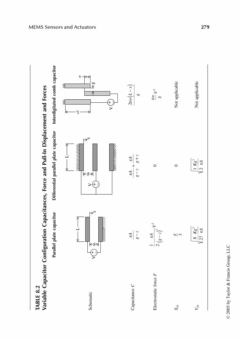
MEMS Sensors and Actuators 279
TAB
LE 8
.2V
aria
ble
Cap
acit
or
Co
nfi
gura
tio
n C
apac
itan
ces,
Fo
rce
and
Pu
ll-I
n D
isp
lace
men
t an
d F
orc
es
Para
llel
pla
te c
apac
ito
rD
iffe
ren
tial
par
alle
l p
late
cap
acit
or
Inte
rdig
itat
ed c
om
b c
apac
ito
r
Sche
mat
ic
Cap
acita
nce
C
Ele
ctro
stat
ic f
orce
F0
XP
I0
Not
app
licab
le
VP
IN
ot a
pplic
able
V+ –
L
xg
L
xV
g
+ –
L
x
V
g
+ –
εA gz−
εε
A
gz
A
gz
−+
+2εw
Lx
g
− ()
1 22
2εA
gz
V
− ()
εw gV
2
g 3
8 27
3K
g Aε1 2
3K
g Aε
© 2
005 b
y T
aylo
r &
Fra
nci
s G
roup, L
LC
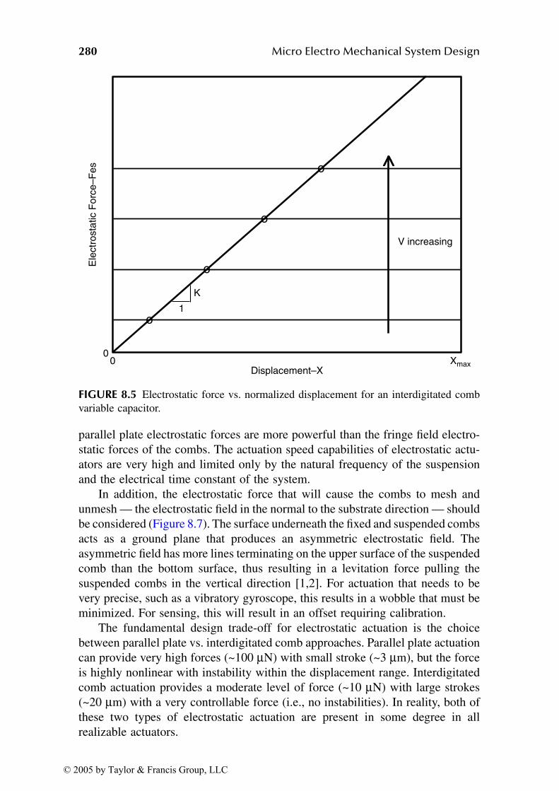
280 Micro Electro Mechanical System Design
parallel plate electrostatic forces are more powerful than the fringe field electro-static forces of the combs. The actuation speed capabilities of electrostatic actu-ators are very high and limited only by the natural frequency of the suspensionand the electrical time constant of the system.
In addition, the electrostatic force that will cause the combs to mesh andunmesh — the electrostatic field in the normal to the substrate direction — shouldbe considered (Figure 8.7). The surface underneath the fixed and suspended combsacts as a ground plane that produces an asymmetric electrostatic field. Theasymmetric field has more lines terminating on the upper surface of the suspendedcomb than the bottom surface, thus resulting in a levitation force pulling thesuspended combs in the vertical direction [1,2]. For actuation that needs to bevery precise, such as a vibratory gyroscope, this results in a wobble that must beminimized. For sensing, this will result in an offset requiring calibration.
The fundamental design trade-off for electrostatic actuation is the choicebetween parallel plate vs. interdigitated comb approaches. Parallel plate actuationcan provide very high forces (~100 µN) with small stroke (~3 µm), but the forceis highly nonlinear with instability within the displacement range. Interdigitatedcomb actuation provides a moderate level of force (~10 µN) with large strokes(~20 µm) with a very controllable force (i.e., no instabilities). In reality, both ofthese two types of electrostatic actuation are present in some degree in allrealizable actuators.
FIGURE 8.5 Electrostatic force vs. normalized displacement for an interdigitated combvariable capacitor.
o
o
o
o
Ele
ctr
osta
tic F
orc
e–F
es
00 Xmax
Displacement–X
V increasing
1
K
© 2005 by Taylor & Francis Group, LLC

MEMS Sensors and Actuators 281
A number of very innovative approaches to electrostatic actuator design havebeen and will continue to be developed in order to attain specific performancemetrics for various applications. For example, Figure 8.8 [3] shows an array ofparallel plate electrodes utilized to attain high force, coupled with a compliantmechanism consisting of flexures to implement a leverage system to attain the
FIGURE 8.6 Electrostatic interdigitated comb actuators. (Courtesy of Sandia NationalLaboratories.)
FIGURE 8.7 Interdigitated combs and levitation forces.
0
0V V
(b) Interdigitated Comb(a) Comb Levitation Forces
© 2005 by Taylor & Francis Group, LLC
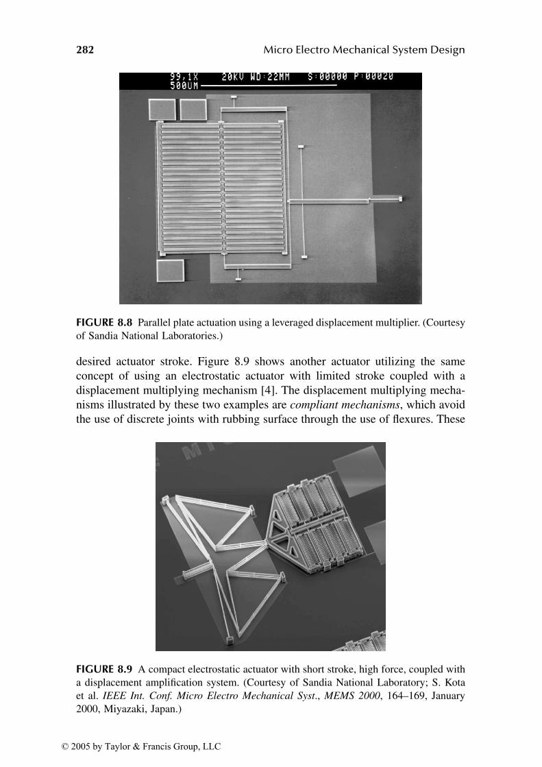
282 Micro Electro Mechanical System Design
desired actuator stroke. Figure 8.9 shows another actuator utilizing the sameconcept of using an electrostatic actuator with limited stroke coupled with adisplacement multiplying mechanism [4]. The displacement multiplying mecha-nisms illustrated by these two examples are compliant mechanisms, which avoidthe use of discrete joints with rubbing surface through the use of flexures. These
FIGURE 8.8 Parallel plate actuation using a leveraged displacement multiplier. (Courtesyof Sandia National Laboratories.)
FIGURE 8.9 A compact electrostatic actuator with short stroke, high force, coupled witha displacement amplification system. (Courtesy of Sandia National Laboratory; S. Kotaet al. IEEE Int. Conf. Micro Electro Mechanical Syst., MEMS 2000, 164–169, January2000, Miyazaki, Japan.)
© 2005 by Taylor & Francis Group, LLC
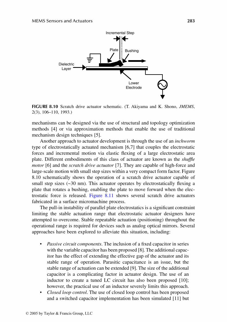
MEMS Sensors and Actuators 283
mechanisms can be designed via the use of structural and topology optimizationmethods [4] or via approximation methods that enable the use of traditionalmechanism design techniques [5].
Another approach to actuator development is through the use of an inchworm
type of electrostatically actuated mechanism [6,7] that couples the electrostaticforces and incremental motion via elastic flexing of a large electrostatic areaplate. Different embodiments of this class of actuator are known as the shuffle
motor [6] and the scratch drive actuator [7]. They are capable of high-force andlarge-scale motion with small step sizes within a very compact form factor. Figure8.10 schematically shows the operation of a scratch drive actuator capable ofsmall step sizes (~30 nm). This actuator operates by electrostatically flexing aplate that rotates a bushing, enabling the plate to move forward when the elec-trostatic force is released. Figure 8.11 shows several scratch drive actuatorsfabricated in a surface micromachine process.
The pull-in instability of parallel plate electrostatics is a significant constraintlimiting the stable actuation range that electrostatic actuator designers haveattempted to overcome. Stable repeatable actuation (positioning) throughout theoperational range is required for devices such as analog optical mirrors. Severalapproaches have been explored to alleviate this situation, including:
• Passive circuit components. The inclusion of a fixed capacitor in serieswith the variable capacitor has been proposed [8]. The additional capac-itor has the effect of extending the effective gap of the actuator and itsstable range of operation. Parasitic capacitance is an issue, but thestable range of actuation can be extended [9]. The size of the additionalcapacitor is a complicating factor in actuator design. The use of aninductor to create a tuned LC circuit has also been proposed [10];however, the practical use of an inductor severely limits this approach.
• Closed loop control. The use of closed loop control has been proposedand a switched capacitor implementation has been simulated [11] but
FIGURE 8.10 Scratch drive actuator schematic. (T. Akiyama and K. Shono, JMEMS,2(3), 106–110, 1993.)
LowerElectrode
DielectricLayer
Plate Bushing
Incremental Step
© 2005 by Taylor & Francis Group, LLC
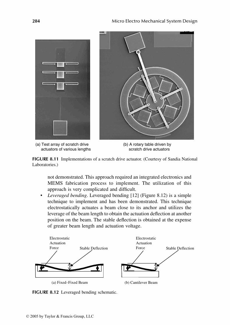
284 Micro Electro Mechanical System Design
not demonstrated. This approach required an integrated electronics andMEMS fabrication process to implement. The utilization of thisapproach is very complicated and difficult.
• Leveraged bending. Leveraged bending [12] (Figure 8.12) is a simpletechnique to implement and has been demonstrated. This techniqueelectrostatically actuates a beam close to its anchor and utilizes theleverage of the beam length to obtain the actuation deflection at anotherposition on the beam. The stable deflection is obtained at the expenseof greater beam length and actuation voltage.
FIGURE 8.11 Implementations of a scratch drive actuator. (Courtesy of Sandia NationalLaboratories.)
FIGURE 8.12 Leveraged bending schematic.
(a) Test array of scratch drive actuators of various lengths
(b) A rotary table driven by scratch drive actuators
Electrostatic Actuation Force Stable Deflection
(a) Fixed–Fixed Beam
Electrostatic Actuation Force Stable Deflection
(b) Cantilever Beam
© 2005 by Taylor & Francis Group, LLC
MEMS Sensors and Actuators 285
8.1.2 THERMAL ACTUATION
Thermal actuation uses the thermal expansion of materials (solid, liquid, gas) toachieve mechanical actuation. The thermal expansion of a solid material is charac-terized by coefficient of thermal expansion (CTE), αT. Equation 8.15 states that themechanical strain, ε, of a material is directly proportional to the temperature change,∆T, where the proportionality constant αT is the CTE. The CTE for a material hasunits of strain per change in temperature (1/°C). The CTE of a material is frequentlya function of temperature, generally increasing with required temperature.
(8.15)
Example 8.1
Problem: A 100-µm long beam is anchored to the substrate at both ends. Thetemperature of the beam is raised by 300°C. The beam is 2.5 µm thick by 4 µmwide and is made of polysilicon (assume E = 160 GPa and αT = 2.5 micro-strain/°C). (a) Calculate the stress and strain in the beam. (b) Calculate the forceand displacement produced in the beam. (c) Is buckling a concern for this beam?
Solution: (a) ε = αT ∆T = (2.5 × 10⁻⁶ °C–1) (300°C) = 750 µ-strain
σ = E αT ∆T = (1.6 × 10¹¹ Pa) (2.5 × 10⁻⁶ °C–1) (300°C) = 120 × 106 Pa
(b) F = A E αT ∆T
= (2.5 × 10⁻⁶ µm)(4 × 10⁻⁶ µm)(1.6 × 10¹¹ Pa) (2.5 × 10⁻⁶ °C–1) (300°C)= 1200 µN∆L = L ε = (100 µm) (0.000750) = 0.075 µm
The thermal expansion of a solid produced high forces if constrained but alow amount of stroke. Thermal actuator design based on thermal expansion mustbe careful of “parasitic strains” in such things as anchors, which may easily negatethe thermal strain. To achieve more change in length (stroke), a longer lengthbeam is necessary, but as length is increased, buckling may occur.
(c) The Euler column formula for the buckling of a beam is given by Equation6.38. The beam can deflect laterally in two directions, but will fail due to bucklingin the direction with the minimum area moment of inertia, I.
I = w t3/12 = (4 × 10⁻⁶ µm) (2.5 × 10⁻⁶ µm)3/12 = 5.21 × 10⁻²⁴ µm4
The force at which buckling can occur is calculated by the following Eulercolumn formula. Buckling is very sensitive to the end conditions of the column.Table 6.2 lists the end condition constants for various column end conditions.The end condition constant, C, for a clamped–clamped beam is chosen to be 1.2.C = 4 would generally be too high because a clamped–clamped boundary con-
ε α= T T∆
© 2005 by Taylor & Francis Group, LLC
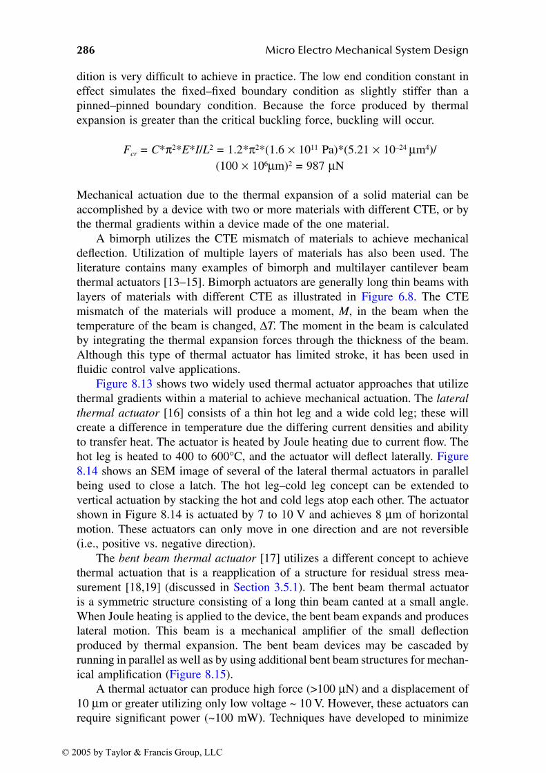
286 Micro Electro Mechanical System Design
dition is very difficult to achieve in practice. The low end condition constant ineffect simulates the fixed–fixed boundary condition as slightly stiffer than apinned–pinned boundary condition. Because the force produced by thermalexpansion is greater than the critical buckling force, buckling will occur.
Fcr = C*π2*E*I/L2 = 1.2*π2*(1.6 × 1011 Pa)*(5.21 × 10⁻²⁴ µm4)/(100 × 106µm)2 = 987 µN
Mechanical actuation due to the thermal expansion of a solid material can beaccomplished by a device with two or more materials with different CTE, or bythe thermal gradients within a device made of the one material.
A bimorph utilizes the CTE mismatch of materials to achieve mechanicaldeflection. Utilization of multiple layers of materials has also been used. Theliterature contains many examples of bimorph and multilayer cantilever beamthermal actuators [13–15]. Bimorph actuators are generally long thin beams withlayers of materials with different CTE as illustrated in Figure 6.8. The CTEmismatch of the materials will produce a moment, M, in the beam when thetemperature of the beam is changed, ∆T. The moment in the beam is calculatedby integrating the thermal expansion forces through the thickness of the beam.Although this type of thermal actuator has limited stroke, it has been used influidic control valve applications.
Figure 8.13 shows two widely used thermal actuator approaches that utilizethermal gradients within a material to achieve mechanical actuation. The lateral
thermal actuator [16] consists of a thin hot leg and a wide cold leg; these willcreate a difference in temperature due the differing current densities and abilityto transfer heat. The actuator is heated by Joule heating due to current flow. Thehot leg is heated to 400 to 600°C, and the actuator will deflect laterally. Figure8.14 shows an SEM image of several of the lateral thermal actuators in parallelbeing used to close a latch. The hot leg–cold leg concept can be extended tovertical actuation by stacking the hot and cold legs atop each other. The actuatorshown in Figure 8.14 is actuated by 7 to 10 V and achieves 8 µm of horizontalmotion. These actuators can only move in one direction and are not reversible(i.e., positive vs. negative direction).
The bent beam thermal actuator [17] utilizes a different concept to achievethermal actuation that is a reapplication of a structure for residual stress mea-surement [18,19] (discussed in Section 3.5.1). The bent beam thermal actuatoris a symmetric structure consisting of a long thin beam canted at a small angle.When Joule heating is applied to the device, the bent beam expands and produceslateral motion. This beam is a mechanical amplifier of the small deflectionproduced by thermal expansion. The bent beam devices may be cascaded byrunning in parallel as well as by using additional bent beam structures for mechan-ical amplification (Figure 8.15).
A thermal actuator can produce high force (>100 µN) and a displacement of10 µm or greater utilizing only low voltage ~ 10 V. However, these actuators canrequire significant power (~100 mW). Techniques have developed to minimize
© 2005 by Taylor & Francis Group, LLC
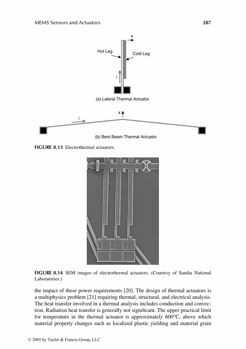
MEMS Sensors and Actuators 287
the impact of these power requirements [20]. The design of thermal actuators isa multiphysics problem [21] requiring thermal, structural, and electrical analysis.The heat transfer involved in a thermal analysis includes conduction and convec-tion. Radiation heat transfer is generally not significant. The upper practical limitfor temperature in the thermal actuator is approximately 600°C, above whichmaterial property changes such as localized plastic yielding and material grain
FIGURE 8.13 Electrothermal actuators.
FIGURE 8.14 SEM images of electrothermal actuators. (Courtesy of Sandia NationalLaboratories.)
i
x
Cold Leg Hot Leg
i
x
(a) Lateral Thermal Actuator
(b) Bent Beam Thermal Actuator
© 2005 by Taylor & Francis Group, LLC
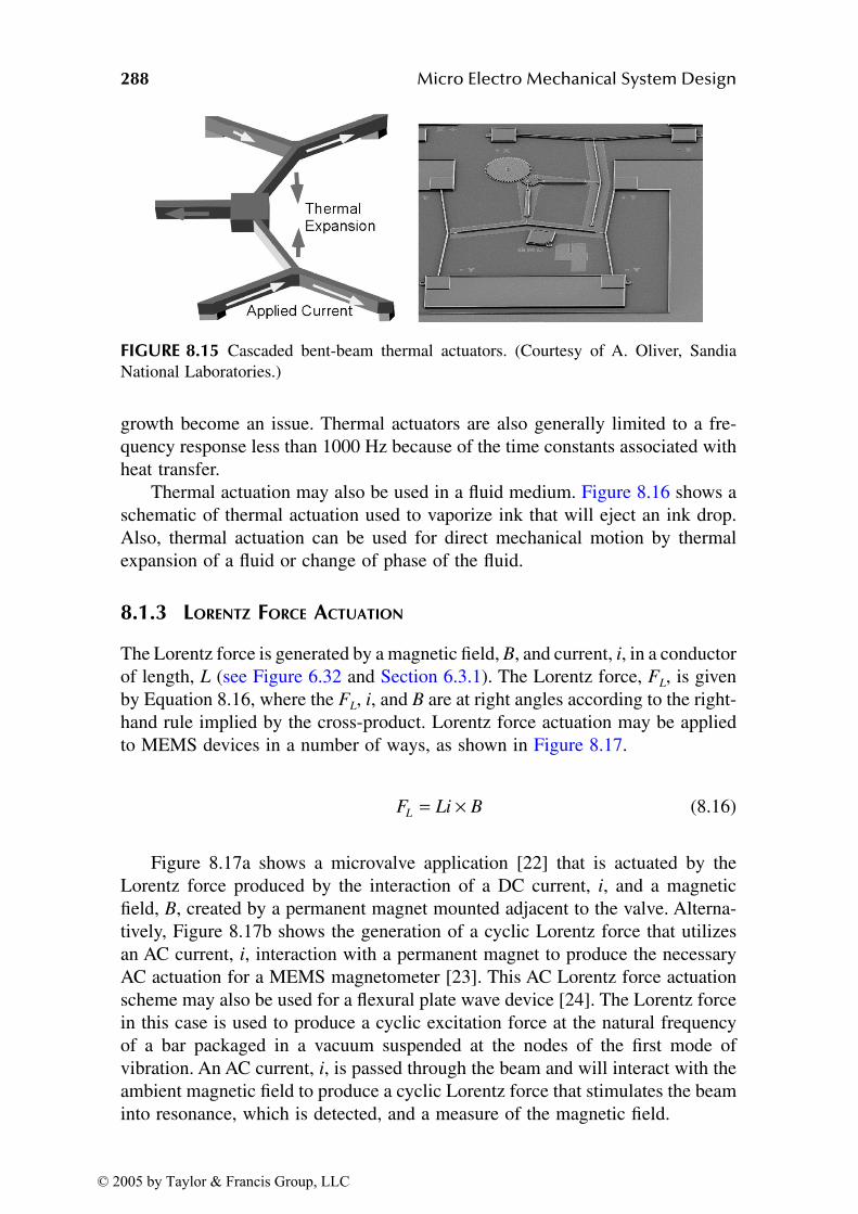
288 Micro Electro Mechanical System Design
growth become an issue. Thermal actuators are also generally limited to a fre-quency response less than 1000 Hz because of the time constants associated withheat transfer.
Thermal actuation may also be used in a fluid medium. Figure 8.16 shows aschematic of thermal actuation used to vaporize ink that will eject an ink drop.Also, thermal actuation can be used for direct mechanical motion by thermalexpansion of a fluid or change of phase of the fluid.
8.1.3 LORENTZ FORCE ACTUATION
The Lorentz force is generated by a magnetic field, B, and current, i, in a conductorof length, L (see Figure 6.32 and Section 6.3.1). The Lorentz force, FL, is givenby Equation 8.16, where the FL, i, and B are at right angles according to the right-hand rule implied by the cross-product. Lorentz force actuation may be appliedto MEMS devices in a number of ways, as shown in Figure 8.17.
(8.16)
Figure 8.17a shows a microvalve application [22] that is actuated by theLorentz force produced by the interaction of a DC current, i, and a magneticfield, B, created by a permanent magnet mounted adjacent to the valve. Alterna-tively, Figure 8.17b shows the generation of a cyclic Lorentz force that utilizesan AC current, i, interaction with a permanent magnet to produce the necessaryAC actuation for a MEMS magnetometer [23]. This AC Lorentz force actuationscheme may also be used for a flexural plate wave device [24]. The Lorentz forcein this case is used to produce a cyclic excitation force at the natural frequencyof a bar packaged in a vacuum suspended at the nodes of the first mode ofvibration. An AC current, i, is passed through the beam and will interact with theambient magnetic field to produce a cyclic Lorentz force that stimulates the beaminto resonance, which is detected, and a measure of the magnetic field.
FIGURE 8.15 Cascaded bent-beam thermal actuators. (Courtesy of A. Oliver, SandiaNational Laboratories.)
F Li BL = ×
© 2005 by Taylor & Francis Group, LLC

MEMS Sensors and Actuators 289
FIGURE 8.16 Thermal actuation in a fluid medium.
FIGURE 8.17 Examples of Lorentz force actuation for MEMS.
(a) Thermally ejecting a drop
Pvapor
Meniscus
Piston
(b) Fluid piston
(c) Fluidic piston engine
(Courtesy Sandia National Laboratories)
I B
flow
F
e
into page
flexible membrane
I
B
e
F
(a) Valve (b) Magnetometer
© 2005 by Taylor & Francis Group, LLC

290 Micro Electro Mechanical System Design
8.2 MEMS SENSING
8.2.1 CAPACITATIVE SENSING
Electrostatic capacitance sensing is a frequently used transduction method forMEMS devices. MEMS fabrication techniques can readily produce parallel plateor interdigitated comb finger capacitors in a MEMS device that can move as aresult of a physical variable (acceleration, pressure) excitation. Figure 8.18shows schematically some variations of parallel plate and interdigitated capac-itance structures. The relative motion of the plates can be in any direction(vertical or horizontal).
Differential capacitors are two capacitors that share a common electrode.Figure 8.19 shows a schematic of some differential capacitor structures, andFigure 8.20 shows some MEMS devices that employ a differential capacitor.Differential capacitors can be fabricated in such a manner that the two capacitorshave nearly equal capacitance in the unperturbed position and change by equaland opposite amounts as the structure is deflected. The differential capacitorstructure enables differential sensing, which can cancel many adverse or commonmode effects to first order. Changing two capacitors by the same amount is acommon mode effect to which a differential capacitor structure does not respond.
The size of the capacitors utilized in MEMS devices is small — generally afraction of a picofarad. The variation of the nominal capacitance to be sensed toprovide the dynamic signal of interest is in the femtofarad range or less. Also,undesirable stray capacitances called parasitic capacitances can interfere withcapacitance sensing. Examples of parasitic capacitances may include the capac-itance between a sense line and the substrate or the capacitance between twosense lines. Figure 8.21 illustrates the capacitances in a MEMS accelerometer,which include the direct capacitance, Cpp, as well as the fringe field, Cf1, Cf2, andparasitic capacitances, Cpl, Cpu, that exist between the upper plate, lower plate,and the substrate.
Frequently, the magnitudes of the parasitic capacitances are greater than thenominal and dynamic capacitance of the device, and the parasitic capacitances
FIGURE 8.18 Examples of parallel plate and interdigitated capacitance structures.
C
Parallel Plate Capacitor
Parallel Plate Capacitor
InterdigitatedComb Capacitor
Circuit Schematic
© 2005 by Taylor & Francis Group, LLC
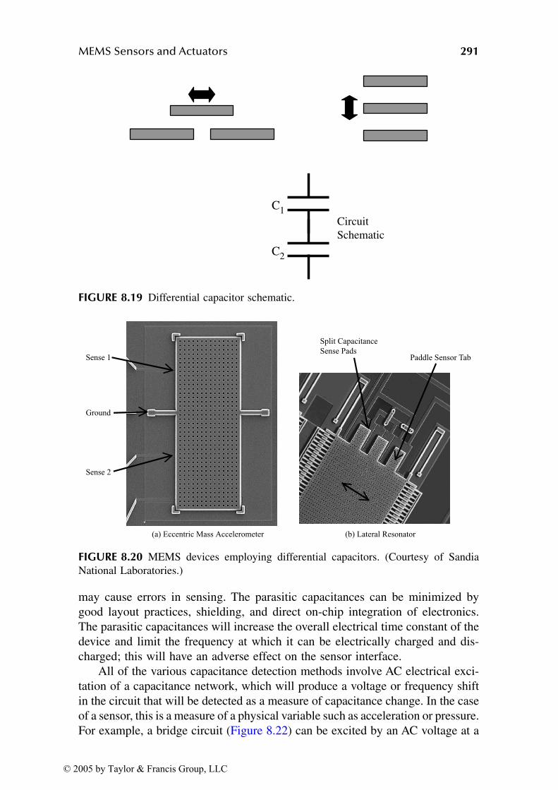
MEMS Sensors and Actuators 291
may cause errors in sensing. The parasitic capacitances can be minimized bygood layout practices, shielding, and direct on-chip integration of electronics.The parasitic capacitances will increase the overall electrical time constant of thedevice and limit the frequency at which it can be electrically charged and dis-charged; this will have an adverse effect on the sensor interface.
All of the various capacitance detection methods involve AC electrical exci-tation of a capacitance network, which will produce a voltage or frequency shiftin the circuit that will be detected as a measure of capacitance change. In the caseof a sensor, this is a measure of a physical variable such as acceleration or pressure.For example, a bridge circuit (Figure 8.22) can be excited by an AC voltage at a
FIGURE 8.19 Differential capacitor schematic.
FIGURE 8.20 MEMS devices employing differential capacitors. (Courtesy of SandiaNational Laboratories.)
C2
Circuit Schematic
C1
(b) Lateral Resonator
Paddle Sensor Tab
Split Capacitance
Sense Pads
(a) Eccentric Mass Accelerometer
Sense 1
Sense 2
Ground
© 2005 by Taylor & Francis Group, LLC
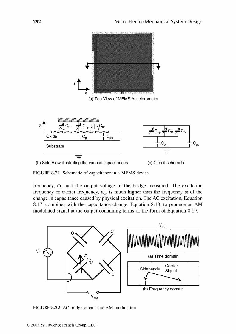
292 Micro Electro Mechanical System Design
frequency, ωc, and the output voltage of the bridge measured. The excitationfrequency or carrier frequency, ωc, is much higher than the frequency ω of thechange in capacitance caused by physical excitation. The AC excitation, Equation8.17, combines with the capacitance change, Equation 8.18, to produce an AMmodulated signal at the output containing terms of the form of Equation 8.19.
FIGURE 8.21 Schematic of capacitance in a MEMS device.
FIGURE 8.22 AC bridge circuit and AM modulation.
Cpp
Cpp
Cpl Cpu
CpuCpl
Cf1 Cf2
Cf2Cf1
(c) Circuit schematic
(a) Top View of MEMS Accelerometer
x
y
Oxide
Substrate
(b) Side View illustrating the various capacitances
z
C
C
C
C+
∆C
Vout
Vout
Vin
CarrierSignalSidebands
(a) Time domain
(b) Frequency domain
© 2005 by Taylor & Francis Group, LLC
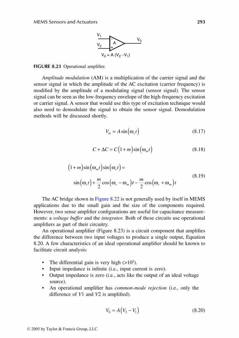
MEMS Sensors and Actuators 293
Amplitude modulation (AM) is a multiplication of the carrier signal and thesensor signal in which the amplitude of the AC excitation (carrier frequency) ismodified by the amplitude of a modulating signal (sensor signal). The sensorsignal can be seen as the low-frequency envelope of the high-frequency excitationor carrier signal. A sensor that would use this type of excitation technique wouldalso need to demodulate the signal to obtain the sensor signal. Demodulationmethods will be discussed shortly.
(8.17)
(8.18)
(8.19)
The AC bridge shown in Figure 8.22 is not generally used by itself in MEMSapplications due to the small gain and the size of the components required.However, two sense amplifier configurations are useful for capacitance measure-ments: a voltage buffer and the integrator. Both of these circuits use operationalamplifiers as part of their circuitry.
An operational amplifier (Figure 8.23) is a circuit component that amplifiesthe difference between two input voltages to produce a single output, Equation8.20. A few characteristics of an ideal operational amplifier should be known tofacilitate circuit analysis:
• The differential gain is very high (>105).• Input impedance is infinite (i.e., input current is zero).• Output impedance is zero (i.e., acts like the output of an ideal voltage
source).• An operational amplifier has common-mode rejection (i.e., only the
difference of V1 and V2 is amplified).
(8.20)
FIGURE 8.23 Operational amplifier.
+
− V0
V1
V2A
V0 = A (V2 −V1)
V A tin c= ( )sin ω
C C C m tm+ = +( ) ( )∆ 1 sin ω
1
2
+( ) ( ) ( ) =( ) + −( )
m t t
tm
m c
c c m
sin sin
sin cos
ω ωω ω ω tt
mtc m− +( )
2cos ω ω
V A V V0 2 1= −( )© 2005 by Taylor & Francis Group, LLC
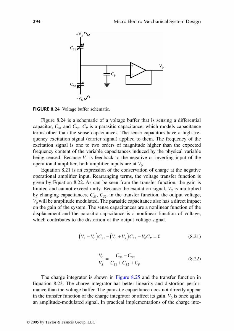
294 Micro Electro Mechanical System Design
Figure 8.24 is a schematic of a voltage buffer that is sensing a differentialcapacitor, CS1 and CS2. CP is a parasitic capacitance, which models capacitanceterms other than the sense capacitances. The sense capacitors have a high-fre-quency excitation signal (carrier signal) applied to them. The frequency of theexcitation signal is one to two orders of magnitude higher than the expectedfrequency content of the variable capacitances induced by the physical variablebeing sensed. Because V0 is feedback to the negative or inverting input of theoperational amplifier, both amplifier inputs are at V0.
Equation 8.21 is an expression of the conservation of charge at the negativeoperational amplifier input. Rearranging terms, the voltage transfer function isgiven by Equation 8.22. As can be seen from the transfer function, the gain islimited and cannot exceed unity. Because the excitation signal, VS is multipliedby changing capacitances, CS1, CS2, in the transfer function, the output voltage,V0 will be amplitude modulated. The parasitic capacitance also has a direct impacton the gain of the system. The sense capacitances are a nonlinear function of thedisplacement and the parasitic capacitance is a nonlinear function of voltage,which contributes to the distortion of the output voltage signal.
(8.21)
(8.22)
The charge integrator is shown in Figure 8.25 and the transfer function inEquation 8.23. The charge integrator has better linearity and distortion perfor-mance than the voltage buffer. The parasitic capacitance does not directly appearin the transfer function of the charge integrator or affect its gain. V0 is once againan amplitude-modulated signal. In practical implementations of the charge inte-
FIGURE 8.24 Voltage buffer schematic.
+
-
CS1
CS2
+VS
-VS
CP
V0
V V C V V C V CS S S S P−( ) − +( ) − =0 1 0 2 0 0
V
V
C C
C C CS
S S
S S P
0 1 2
1 2
= −+ +
© 2005 by Taylor & Francis Group, LLC
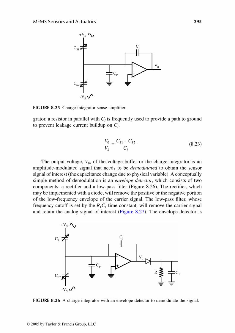
MEMS Sensors and Actuators 295
grator, a resistor in parallel with CI is frequently used to provide a path to groundto prevent leakage current buildup on CI.
(8.23)
The output voltage, V0, of the voltage buffer or the charge integrator is anamplitude-modulated signal that needs to be demodulated to obtain the sensorsignal of interest (the capacitance change due to physical variable). A conceptuallysimple method of demodulation is an envelope detector, which consists of twocomponents: a rectifier and a low-pass filter (Figure 8.26). The rectifier, whichmay be implemented with a diode, will remove the positive or the negative portionof the low-frequency envelope of the carrier signal. The low-pass filter, whosefrequency cutoff is set by the R1C1 time constant, will remove the carrier signaland retain the analog signal of interest (Figure 8.27). The envelope detector is
FIGURE 8.25 Charge integrator sense amplifier.
FIGURE 8.26 A charge integrator with an envelope detector to demodulate the signal.
+
-
CS1
CS2
+VS
-VS
CP
V0
CI
V
V
C C
CS
S S
I
0 1 2= −
+
-
CS1
CS2
+VS
-VS
CP
V0
CI
R1 C1
© 2005 by Taylor & Francis Group, LLC
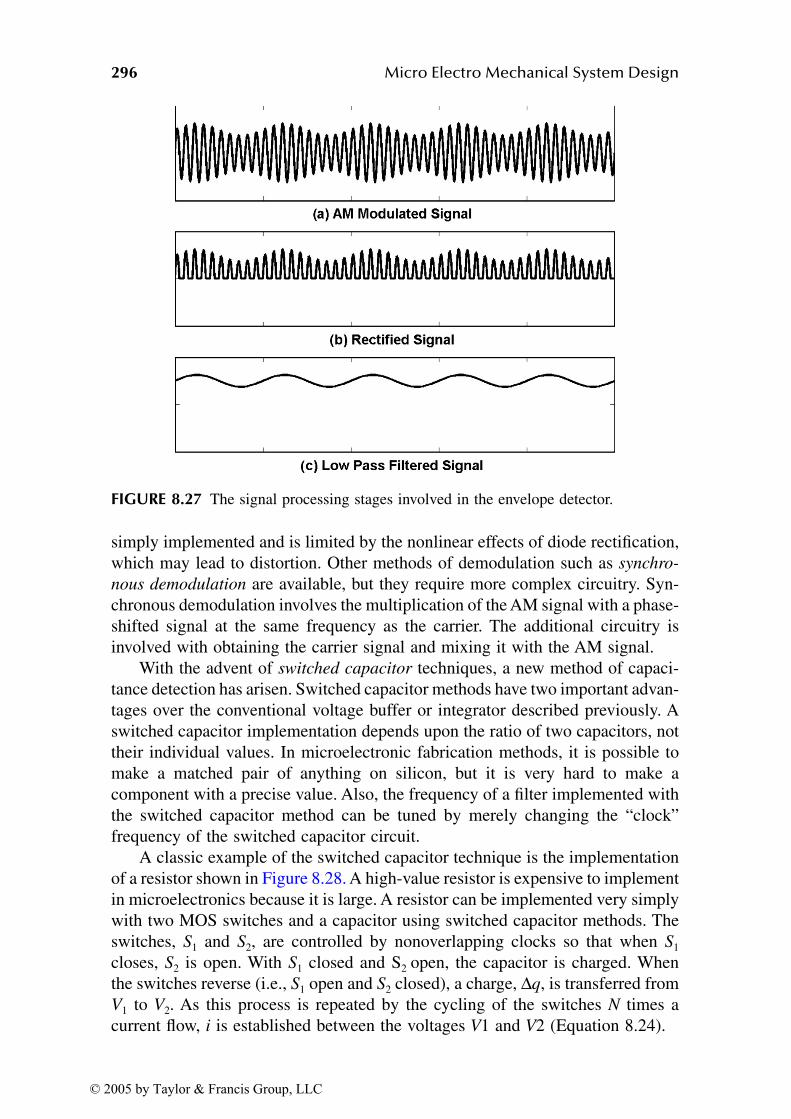
296 Micro Electro Mechanical System Design
simply implemented and is limited by the nonlinear effects of diode rectification,which may lead to distortion. Other methods of demodulation such as synchro-
nous demodulation are available, but they require more complex circuitry. Syn-chronous demodulation involves the multiplication of the AM signal with a phase-shifted signal at the same frequency as the carrier. The additional circuitry isinvolved with obtaining the carrier signal and mixing it with the AM signal.
With the advent of switched capacitor techniques, a new method of capaci-tance detection has arisen. Switched capacitor methods have two important advan-tages over the conventional voltage buffer or integrator described previously. Aswitched capacitor implementation depends upon the ratio of two capacitors, nottheir individual values. In microelectronic fabrication methods, it is possible tomake a matched pair of anything on silicon, but it is very hard to make acomponent with a precise value. Also, the frequency of a filter implemented withthe switched capacitor method can be tuned by merely changing the “clock”frequency of the switched capacitor circuit.
A classic example of the switched capacitor technique is the implementationof a resistor shown in Figure 8.28. A high-value resistor is expensive to implementin microelectronics because it is large. A resistor can be implemented very simplywith two MOS switches and a capacitor using switched capacitor methods. Theswitches, S1 and S2, are controlled by nonoverlapping clocks so that when S1
closes, S2 is open. With S1 closed and S2 open, the capacitor is charged. Whenthe switches reverse (i.e., S1 open and S2 closed), a charge, ∆q, is transferred fromV1 to V2. As this process is repeated by the cycling of the switches N times acurrent flow, i is established between the voltages V1 and V2 (Equation 8.24).
FIGURE 8.27 The signal processing stages involved in the envelope detector.
© 2005 by Taylor & Francis Group, LLC
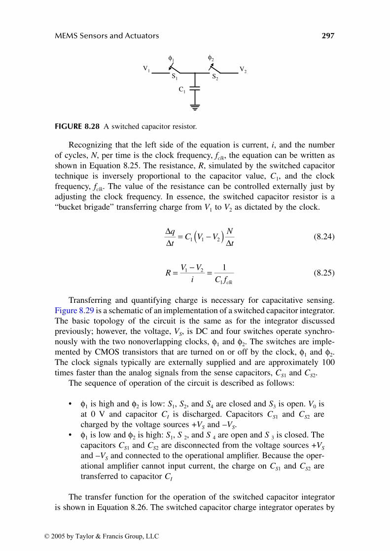
MEMS Sensors and Actuators 297
Recognizing that the left side of the equation is current, i, and the numberof cycles, N, per time is the clock frequency, fclk, the equation can be written asshown in Equation 8.25. The resistance, R, simulated by the switched capacitortechnique is inversely proportional to the capacitor value, C1, and the clockfrequency, fclk. The value of the resistance can be controlled externally just byadjusting the clock frequency. In essence, the switched capacitor resistor is a“bucket brigade” transferring charge from V1 to V2 as dictated by the clock.
(8.24)
(8.25)
Transferring and quantifying charge is necessary for capacitative sensing.Figure 8.29 is a schematic of an implementation of a switched capacitor integrator.The basic topology of the circuit is the same as for the integrator discussedpreviously; however, the voltage, VS, is DC and four switches operate synchro-nously with the two nonoverlapping clocks, φ1 and φ2. The switches are imple-mented by CMOS transistors that are turned on or off by the clock, φ1 and φ2.The clock signals typically are externally supplied and are approximately 100times faster than the analog signals from the sense capacitors, CS1 and CS2.
The sequence of operation of the circuit is described as follows:
• φ1 is high and φ2 is low: S1, S2, and S4 are closed and S3 is open. V0 isat 0 V and capacitor CI is discharged. Capacitors CS1 and CS2 arecharged by the voltage sources +VS and –VS.
• φ1 is low and φ2 is high: S1, S 2, and S 4 are open and S 3 is closed. Thecapacitors CS1 and CS2 are disconnected from the voltage sources +VS
and –VS and connected to the operational amplifier. Because the oper-ational amplifier cannot input current, the charge on CS1 and CS2 aretransferred to capacitor CI
The transfer function for the operation of the switched capacitor integratoris shown in Equation 8.26. The switched capacitor charge integrator operates by
FIGURE 8.28 A switched capacitor resistor.
C1
V1 V2S2
φ2
S1
φ1
∆∆ ∆
q
tC V V
N
t= −( )1 1 2
RV V
i C fclk
= − =1 2
1
1
© 2005 by Taylor & Francis Group, LLC
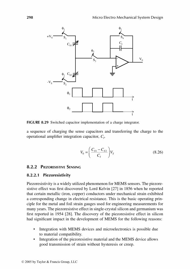
298 Micro Electro Mechanical System Design
a sequence of charging the sense capacitors and transferring the charge to theoperational amplifier integration capacitor, CI.
(8.26)
8.2.2 PIEZORESISTIVE SENSING
8.2.2.1 Piezoresistivity
Piezoresistivity is a widely utilized phenomenon for MEMS sensors. The piezore-sistive effect was first discovered by Lord Kelvin [27] in 1856 when he reportedthat certain metallic (iron, copper) conductors under mechanical strain exhibiteda corresponding change in electrical resistance. This is the basic operating prin-ciple for the metal and foil strain gauges used for engineering measurements formany years. The piezoresistive effect in single-crystal silicon and germanium wasfirst reported in 1954 [28]. The discovery of the piezoresistive effect in siliconhad significant impact in the development of MEMS for the following reasons:
• Integration with MEMS devices and microelectronics is possible dueto material compatibility.
• Integration of the piezoresistive material and the MEMS device allowsgood transmission of strain without hysteresis or creep.
FIGURE 8.29 Switched capacitor implementation of a charge integrator.
+
-
CS1
CS2
+VS
-VS
V0
CI
S4
φ1
S3
φ2
S2
φ1
S1
φ1
φ1
φ2
t
t
VC C
CVS S
I
S01 2= −
© 2005 by Taylor & Francis Group, LLC

MEMS Sensors and Actuators 299
• The piezoresistive effect in silicon is over an order of magnitude greaterthan in metals.
• MEMS fabrication processes allow good matching of resistors utilizedin the Wheatstone bridge-sensing circuits.
The resistivity, ρ, of a semiconductor expressed by the Equation 8.27 is afunction of the number of charge carriers, N, and their mobility, µ. The resistivityof a semiconductor such as silicon can be controlled by the concentration of animpurity that directly controls the number of charge carriers N. The addition ofboron to silicon produces a p-type semiconductor material (positive charge holesare the majority carrier). An n-type semiconductor material (electrons are themajority carriers) can be created by the addition of arsenic or phosphorus as theimpurities. For doping concentrations (charge carrier) varying from 1013 cm–3 to1019 cm–3, the resistivity of silicon varies over a wide range of approximately 500Ω-cm to 5 mΩ-cm. The carrier mobility, µ, is a function of temperature anddoping concentration. Mobility decreases with increasing temperature becauselattice vibrations caused by increased temperature scatter the electrons. In silicon,hole mobilities are less than electron mobilities. For example, with a dopantconcentration of 2.5 × 10⁻¹⁶ cm–3, the electron mobility is µe ≈ 1000 cm2/Vscompared to the hole mobility of µp ≈ 500 cm2/Vs.
(8.27)
where ρ = resistivity (Ω-cm)q = electron charge (1.6 × 10⁻¹⁹ C) N = number of charge carriers (cm–3)µ = carrier (electron or hole) mobility (cm2/Vs)
The piezoresistive effect is present in single-crystal and polycrystalline semi-conductor materials. The analysis of piezoresistive single-crystal material will bediscussed first, followed by a discussion of piezoresistivity in polycrystallinematerials.
8.2.2.2 Piezoresistance in Single-Crystal Silicon
For single crystal silicon that has an anisotropic crystal structure of the cubicfamily, the electric field vector, E, is related to the current density vector, J,by a 3 × 3 resistivity matrix, [ρρρρ] (Equation 8.28). (Note: boldface indicate matrixvariables; column or row matrices; and [] square or rectangular matrices.) TheE, J, and [ρρρρ] matrix variables are direction dependent due to the anisotropiccrystal structure.
ρ µ= 1qN
© 2005 by Taylor & Francis Group, LLC
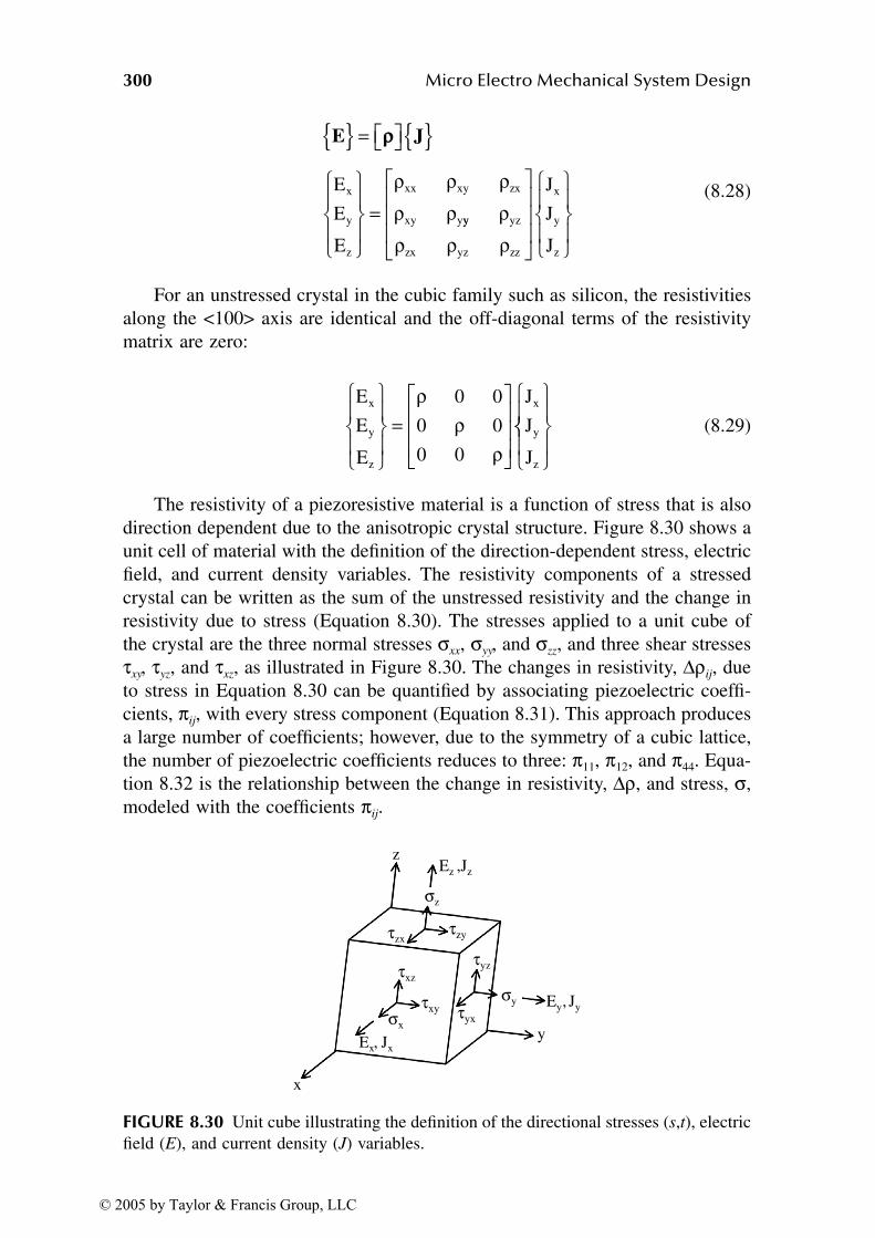
300 Micro Electro Mechanical System Design
(8.28)
For an unstressed crystal in the cubic family such as silicon, the resistivitiesalong the <100> axis are identical and the off-diagonal terms of the resistivitymatrix are zero:
(8.29)
The resistivity of a piezoresistive material is a function of stress that is alsodirection dependent due to the anisotropic crystal structure. Figure 8.30 shows aunit cell of material with the definition of the direction-dependent stress, electricfield, and current density variables. The resistivity components of a stressedcrystal can be written as the sum of the unstressed resistivity and the change inresistivity due to stress (Equation 8.30). The stresses applied to a unit cube ofthe crystal are the three normal stresses σxx, σyy, and σzz, and three shear stressesτxy, τyz, and τxz, as illustrated in Figure 8.30. The changes in resistivity, ∆ρij, dueto stress in Equation 8.30 can be quantified by associating piezoelectric coeffi-cients, πij, with every stress component (Equation 8.31). This approach producesa large number of coefficients; however, due to the symmetry of a cubic lattice,the number of piezoelectric coefficients reduces to three: π11, π12, and π44. Equa-tion 8.32 is the relationship between the change in resistivity, ∆ρ, and stress, σ,modeled with the coefficients πij.
FIGURE 8.30 Unit cube illustrating the definition of the directional stresses (s,t), electricfield (E), and current density (J) variables.
E J =
=
ρρE
E
E
x
y
z
xx xy zx
xy y
ρ ρ ρρ ρ yy yz
zx yz zz
x
y
z
J
J
J
ρρ ρ ρ
E
E
E
J
J
J
x
y
z
x
y
z
=
ρρ
ρ0 0
0 0
0 0
y
z
x
σx
σy
σz
τzxτzy
τxz
τxy
τyz
τyx
Ex , Jx
Ey, Jy
Ez ,Jz
© 2005 by Taylor & Francis Group, LLC
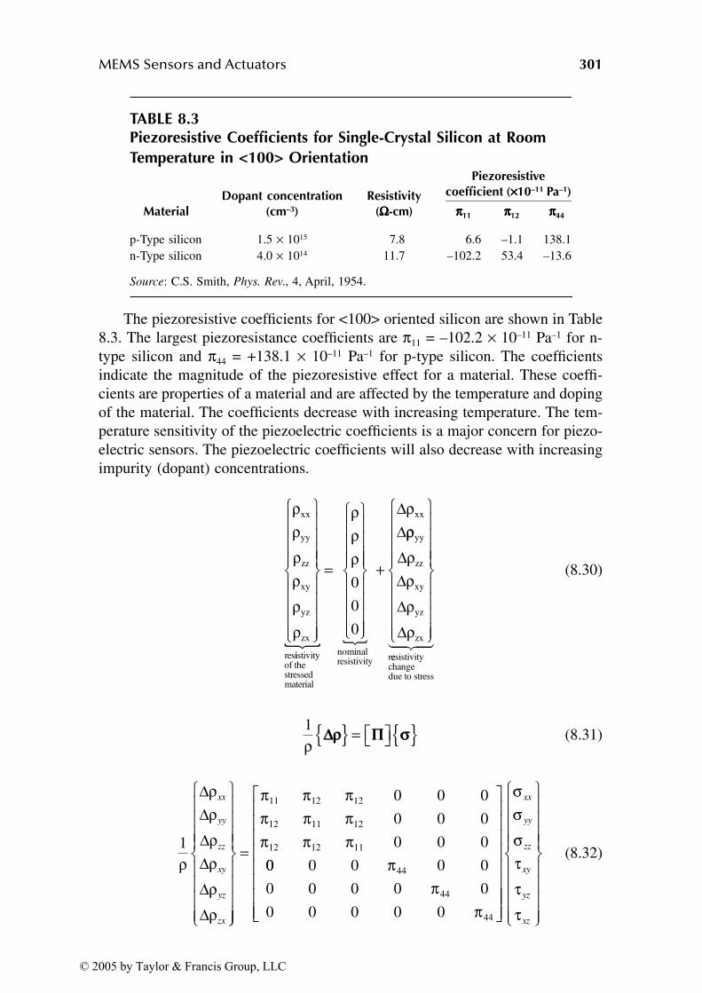
MEMS Sensors and Actuators 301
The piezoresistive coefficients for <100> oriented silicon are shown in Table8.3. The largest piezoresistance coefficients are π11 = –102.2 × 10⁻¹¹ Pa–1 for n-type silicon and π44 = +138.1 × 10⁻¹¹ Pa–1 for p-type silicon. The coefficientsindicate the magnitude of the piezoresistive effect for a material. These coeffi-cients are properties of a material and are affected by the temperature and dopingof the material. The coefficients decrease with increasing temperature. The tem-perature sensitivity of the piezoelectric coefficients is a major concern for piezo-electric sensors. The piezoelectric coefficients will also decrease with increasingimpurity (dopant) concentrations.
(8.30)
(8.31)
(8.32)
TABLE 8.3Piezoresistive Coefficients for Single-Crystal Silicon at Room
Temperature in <100> Orientation
MaterialDopant concentration
(cm–3)Resistivity
(ΩΩΩΩ-cm)
Piezoresistive coefficient (××××10–11 Pa–1)
ππππ11 ππππ12 ππππ44
p-Type silicon 1.5 × 10¹⁵ 7.8 6.6 –1.1 138.1n-Type silicon 4.0 × 10¹⁴ 11.7 –102.2 53.4 –13.6
Source: C.S. Smith, Phys. Rev., 4, April, 1954.
ρρρρρρ
xx
yy
zz
xy
yz
zx
res
iistivity
of thestressedmaterial
=
ρρρ0
0
0
+
nominalresistivity
∆∆
ρxx
ρρρρρρ
yy
zz
xy
yz
zx
∆∆∆∆
reesistivitychangedue to stress
1ρ ∆∆ρρ ΠΠ σσ =
1ρ
ρρρρρρ
∆∆∆∆∆∆
xx
yy
zz
xy
yz
zx
=
π π ππ π ππ π π
11 12 12
12 11 12
12 12 11
0 0 0
0 0 0
0 0 0
00 0 0 0 0
0 0 0 0 0
0 0 0 0 0
44
44
44
ππ
π
σσστττ
xx
yy
zz
xy
yz
xz
© 2005 by Taylor & Francis Group, LLC
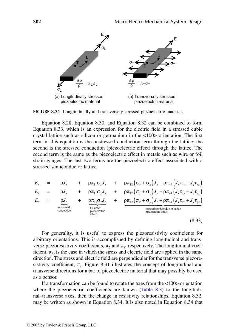
302 Micro Electro Mechanical System Design
Equation 8.28, Equation 8.30, and Equation 8.32 can be combined to formEquation 8.33, which is an expression for the electric field in a stressed cubiccrystal lattice such as silicon or germanium in the <100> orientation. The firstterm in this equation is the unstressed conduction term through the lattice; thesecond is the stressed conduction (piezoelectric effect) through the lattice. Thesecond term is the same as the piezoelectric effect in metals such as wire or foilstrain gauges. The last two terms are the piezoelectric effect associated with astressed semiconductor lattice.
(8.33)
For generality, it is useful to express the piezoresistivity coefficients forarbitrary orientations. This is accomplished by defining longitudinal and trans-verse piezoresistivity coefficients, πL and πT, respectively. The longitudinal coef-ficient, πL, is the case in which the stress and electric field are applied in the samedirection. The stress and electric field are perpendicular for the transverse piezore-sistivity coefficient, πT. Figure 8.31 illustrates the concept of longitudinal andtransverse directions for a bar of piezoelectric material that may possibly be usedas a sensor.
If a transformation can be found to rotate the axes from the <100> orientationwhere the piezoelectric coefficients are known (Table 8.3) to the longitudi-nal–transverse axes, then the change in resistivity relationships, Equation 8.32,may be written as shown in Equation 8.34. It is also noted in Equation 8.34 that
FIGURE 8.31 Longitudinally and transversely stressed piezoelectric material.
EE
LL
TT
σL
σT σT
σL
∆ρ ρ = πLσL
∆ρ ρ = πTσT
(a) Longitudinally stressed piezoelectric material
(b) Transversely stressed piezoelectric material
E J J J J Jx x x x y z x y xy z= + + +( ) + +ρ ρπ σ ρπ σ σ ρπ τ τ11 12 44 xxz
y y y y x z y x xE J J J J
( )= + + +( ) +ρ ρπ σ ρπ σ σ ρπ τ11 12 44 yy z yz
z z
J
E J
+( )= +
τρ ρπ σ
unstressedconduction
11 zz zJ
1st orderpiezoelectriceffect
+ ρπ σ12 xx y z x xz y yzJ J J+( ) + +( )σ ρπ τ τ44
stressed semicondductor latticepiezoelectric effect
© 2005 by Taylor & Francis Group, LLC
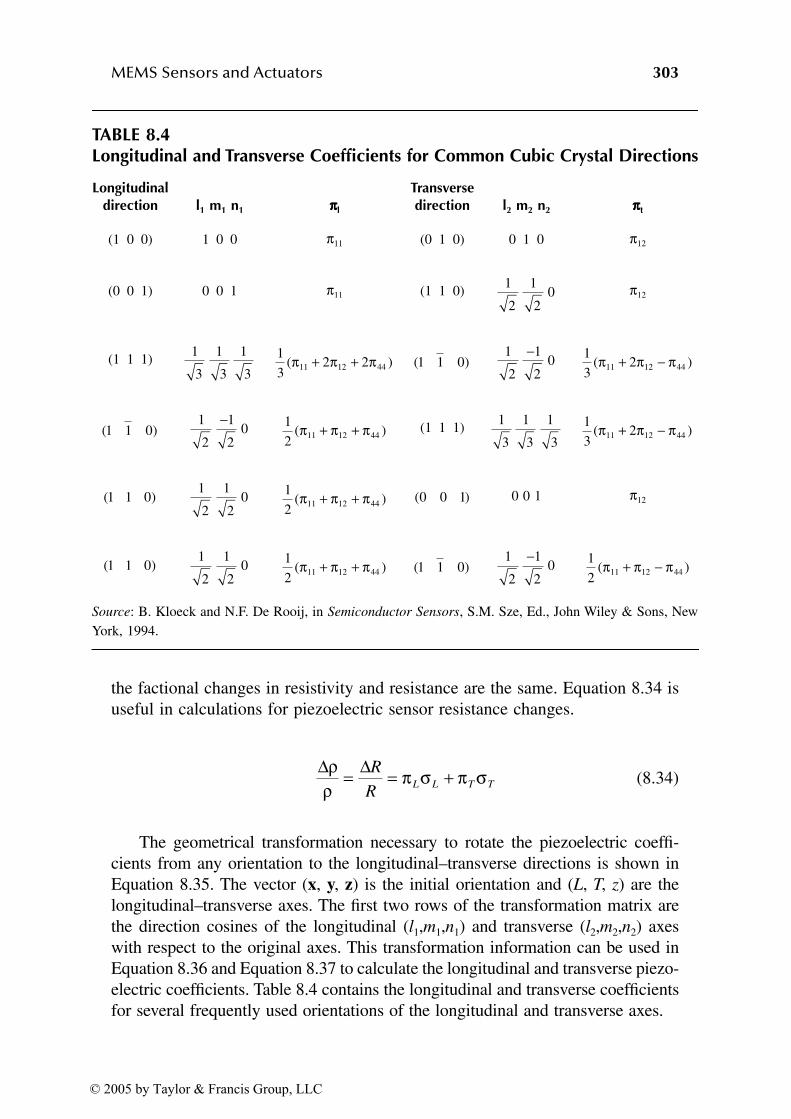
MEMS Sensors and Actuators 303
the factional changes in resistivity and resistance are the same. Equation 8.34 isuseful in calculations for piezoelectric sensor resistance changes.
(8.34)
The geometrical transformation necessary to rotate the piezoelectric coeffi-cients from any orientation to the longitudinal–transverse directions is shown inEquation 8.35. The vector (x, y, z) is the initial orientation and (L, T, z) are thelongitudinal–transverse axes. The first two rows of the transformation matrix arethe direction cosines of the longitudinal (l1,m1,n1) and transverse (l2,m2,n2) axeswith respect to the original axes. This transformation information can be used inEquation 8.36 and Equation 8.37 to calculate the longitudinal and transverse piezo-electric coefficients. Table 8.4 contains the longitudinal and transverse coefficientsfor several frequently used orientations of the longitudinal and transverse axes.
TABLE 8.4Longitudinal and Transverse Coefficients for Common Cubic Crystal Directions
Longitudinaldirection l1 m1 n1 ππππl
Transverse direction l2 m2 n2 ππππt
(1 0 0) 1 0 0 π11 (0 1 0) 0 1 0 π12
(0 0 1) 0 0 1 π11 (1 1 0) π12
(1 1 1)
(1 1 1)
0 0 1 π12
Source: B. Kloeck and N.F. De Rooij, in Semiconductor Sensors, S.M. Sze, Ed., John Wiley & Sons, NewYork, 1994.
1
2
1
20
1
3
1
3
1
3
1
32 211 12 44( )π π π+ + ( )1 1 0
1
2
1
20
− 1
3211 12 44( )π π π+ −
( )1 1 01
2
1
20
− 1
2 11 12 44( )π π π+ + 1
3
1
3
1
3
1
3211 12 44( )π π π+ −
( )1 1 01
2
1
20 1
2 11 12 44( )π π π+ + ( )0 0 1
( )1 1 01
2
1
20 1
2 11 12 44( )π π π+ + ( )1 1 01
2
1
20
− 1
2 11 12 44( )π π π+ −
∆ ∆ρρ π σ π σ= = +R
RL L T T
© 2005 by Taylor & Francis Group, LLC
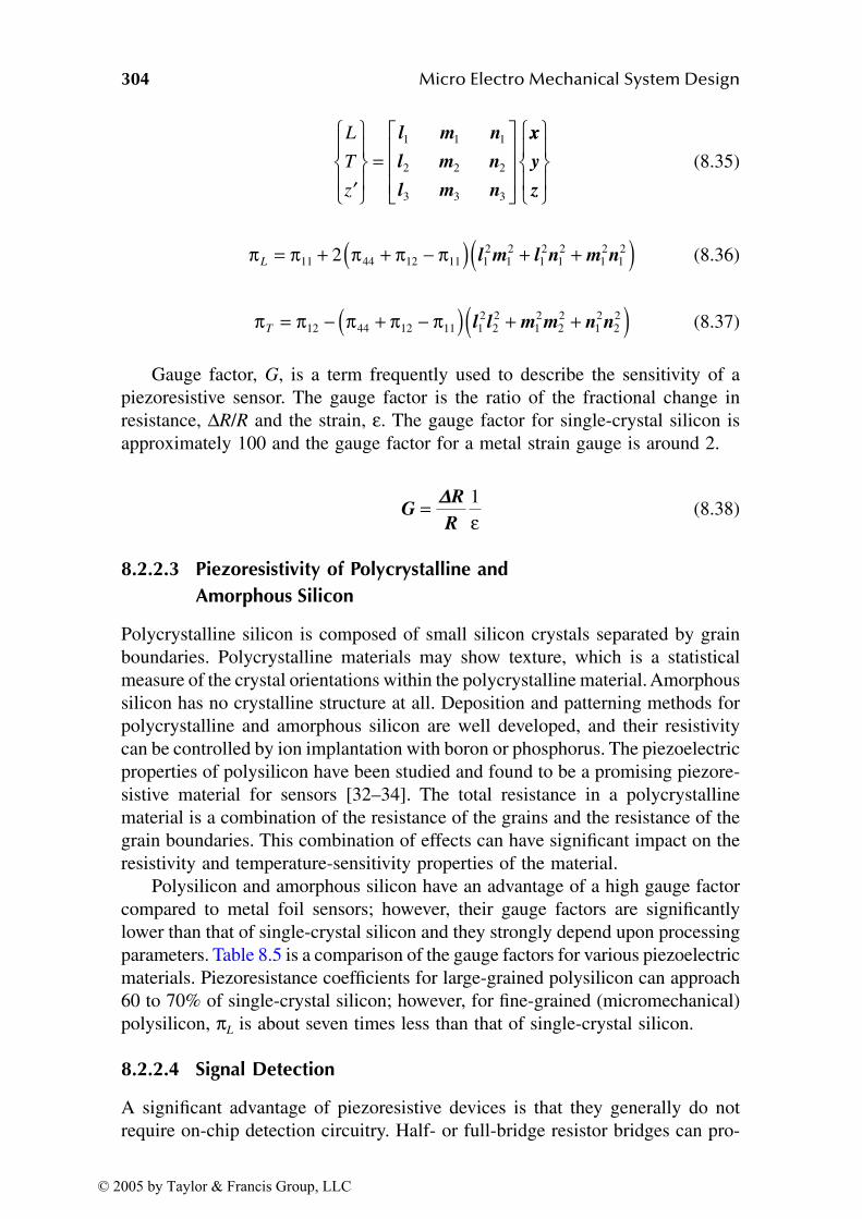
304 Micro Electro Mechanical System Design
(8.35)
(8.36)
(8.37)
Gauge factor, G, is a term frequently used to describe the sensitivity of apiezoresistive sensor. The gauge factor is the ratio of the fractional change inresistance, ∆R/R and the strain, ε. The gauge factor for single-crystal silicon isapproximately 100 and the gauge factor for a metal strain gauge is around 2.
(8.38)
8.2.2.3 Piezoresistivity of Polycrystalline and
Amorphous Silicon
Polycrystalline silicon is composed of small silicon crystals separated by grainboundaries. Polycrystalline materials may show texture, which is a statisticalmeasure of the crystal orientations within the polycrystalline material. Amorphoussilicon has no crystalline structure at all. Deposition and patterning methods forpolycrystalline and amorphous silicon are well developed, and their resistivitycan be controlled by ion implantation with boron or phosphorus. The piezoelectricproperties of polysilicon have been studied and found to be a promising piezore-sistive material for sensors [32–34]. The total resistance in a polycrystallinematerial is a combination of the resistance of the grains and the resistance of thegrain boundaries. This combination of effects can have significant impact on theresistivity and temperature-sensitivity properties of the material.
Polysilicon and amorphous silicon have an advantage of a high gauge factorcompared to metal foil sensors; however, their gauge factors are significantlylower than that of single-crystal silicon and they strongly depend upon processingparameters. Table 8.5 is a comparison of the gauge factors for various piezoelectricmaterials. Piezoresistance coefficients for large-grained polysilicon can approach60 to 70% of single-crystal silicon; however, for fine-grained (micromechanical)polysilicon, πL is about seven times less than that of single-crystal silicon.
8.2.2.4 Signal Detection
A significant advantage of piezoresistive devices is that they generally do notrequire on-chip detection circuitry. Half- or full-bridge resistor bridges can pro-
L
T
z′
=
l m n
l m n
l m n
1 1 1
2 2 2
3 3 3
xx
y
z
π π π π πL = + + −( ) + +( )11 44 12 11 12
12
12
12
12
122 l m l n m n
π π π π πT = − + −( ) + +( )12 44 12 11 12
22
12
22
12
22l l m m n n
GR
R= ∆∆ 1
ε
© 2005 by Taylor & Francis Group, LLC
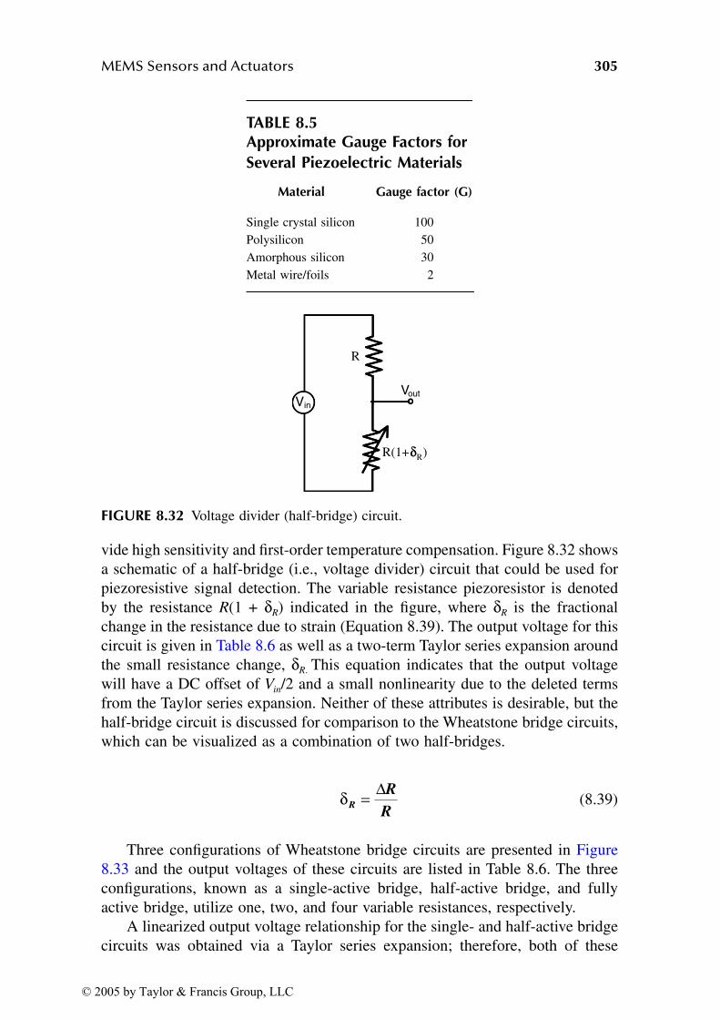
MEMS Sensors and Actuators 305
vide high sensitivity and first-order temperature compensation. Figure 8.32 showsa schematic of a half-bridge (i.e., voltage divider) circuit that could be used forpiezoresistive signal detection. The variable resistance piezoresistor is denotedby the resistance R(1 + δR) indicated in the figure, where δR is the fractionalchange in the resistance due to strain (Equation 8.39). The output voltage for thiscircuit is given in Table 8.6 as well as a two-term Taylor series expansion aroundthe small resistance change, δR. This equation indicates that the output voltagewill have a DC offset of Vin/2 and a small nonlinearity due to the deleted termsfrom the Taylor series expansion. Neither of these attributes is desirable, but thehalf-bridge circuit is discussed for comparison to the Wheatstone bridge circuits,which can be visualized as a combination of two half-bridges.
(8.39)
Three configurations of Wheatstone bridge circuits are presented in Figure8.33 and the output voltages of these circuits are listed in Table 8.6. The threeconfigurations, known as a single-active bridge, half-active bridge, and fullyactive bridge, utilize one, two, and four variable resistances, respectively.
A linearized output voltage relationship for the single- and half-active bridgecircuits was obtained via a Taylor series expansion; therefore, both of these
TABLE 8.5Approximate Gauge Factors for
Several Piezoelectric Materials
Material Gauge factor (G)
Single crystal silicon 100Polysilicon 50Amorphous silicon 30Metal wire/foils 2
FIGURE 8.32 Voltage divider (half-bridge) circuit.
VoutVin
R
R(1+δδR)
δ R
R
R= ∆
© 2005 by Taylor & Francis Group, LLC
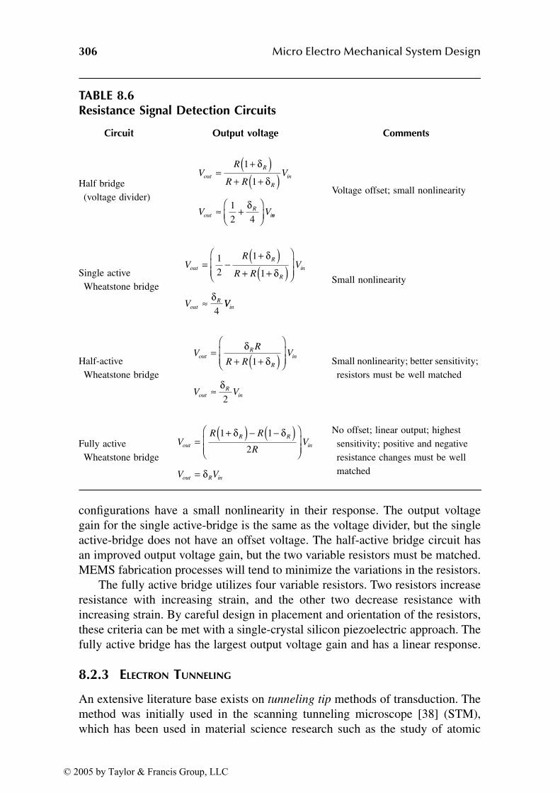
306 Micro Electro Mechanical System Design
configurations have a small nonlinearity in their response. The output voltagegain for the single active-bridge is the same as the voltage divider, but the singleactive-bridge does not have an offset voltage. The half-active bridge circuit hasan improved output voltage gain, but the two variable resistors must be matched.MEMS fabrication processes will tend to minimize the variations in the resistors.
The fully active bridge utilizes four variable resistors. Two resistors increaseresistance with increasing strain, and the other two decrease resistance withincreasing strain. By careful design in placement and orientation of the resistors,these criteria can be met with a single-crystal silicon piezoelectric approach. Thefully active bridge has the largest output voltage gain and has a linear response.
8.2.3 ELECTRON TUNNELING
An extensive literature base exists on tunneling tip methods of transduction. Themethod was initially used in the scanning tunneling microscope [38] (STM),which has been used in material science research such as the study of atomic
TABLE 8.6Resistance Signal Detection Circuits
Circuit Output voltage Comments
Half bridge(voltage divider)
Voltage offset; small nonlinearity
Single activeWheatstone bridge
Small nonlinearity
Half-active Wheatstone bridge
Small nonlinearity; better sensitivity; resistors must be well matched
Fully active Wheatstone bridge
No offset; linear output; highest sensitivity; positive and negative resistance changes must be well matched
VR
R RV
V V
out
R
R
in
outR
i
= +( )+ +( )
≈ +
1
1
1
2 4
δδ
δnn
VR
R RV
V
out
R
R
in
outR
= − +( )+ +( )
≈
1
2
1
1
4
δδ
δVVin
VR
R RV
V V
outR
R
in
outR
in
= + +( )
≈
δδ
δ1
2
VR R
RV
V V
out
R R
in
out R in
= +( ) − −( )
=
1 1
2
δ δ
δ
© 2005 by Taylor & Francis Group, LLC

MEMS Sensors and Actuators 307
scale surface structure. This method of transduction has also been used for infrared(IR) [39–41], magnetometer [42], and accelerometer [39,43] sensors. Electrontunneling can provide an extremely sensitive method of position transduction.
Electron tunneling is a phenomenon in which a current is passed across anarrow gap (Figure 8.34). Classically, a gap of finite size would pose a barrierto current flow. However, for sufficiently small gaps (~10Å), the probabilisticnature of quantum mechanics becomes apparent. In quantum mechanics, whena particle comes to a barrier that it does not have enough energy to penetrate,the wave function dies off exponentially. However, if the gap is small enough,the wave function will predict a significant probability of finding the particle onthe other side of the gap. Therefore, if the gap is small enough, a tunnelingcurrent will exist even though a break has occurred in the circuit. The electrontunneling current is described by:
(8.40)
FIGURE 8.33 Wheatstone bridge configurations.
Vin
Vout
Vin
Vout
Vin
Vout
R
R
R (1
+δ R
)
R (1
+δ R
)
R (1+
δR )
R (1
+δ R
)
R (1
+δ R
)
R (1−δR )
R (1−δR )
R
R
R
(a) Single active
(c) Fully active
(b) Half active
I V s∝ −( )exp α Φ
© 2005 by Taylor & Francis Group, LLC
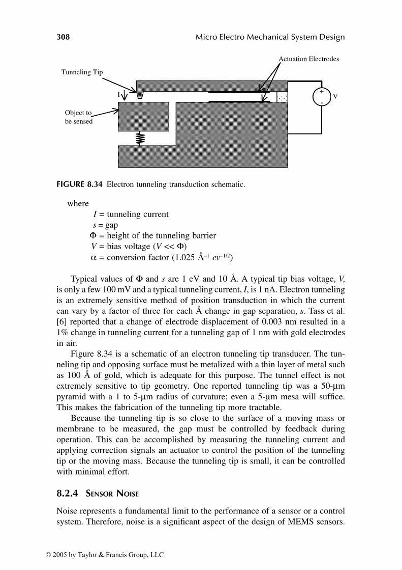
308 Micro Electro Mechanical System Design
whereI = tunneling currents = gap Φ = height of the tunneling barrierV = bias voltage (V << Φ)α = conversion factor (1.025 Å–1 ev–1/2)
Typical values of Φ and s are 1 eV and 10 Å. A typical tip bias voltage, V,is only a few 100 mV and a typical tunneling current, I, is 1 nA. Electron tunnelingis an extremely sensitive method of position transduction in which the currentcan vary by a factor of three for each Å change in gap separation, s. Tass et al.[6] reported that a change of electrode displacement of 0.003 nm resulted in a1% change in tunneling current for a tunneling gap of 1 nm with gold electrodesin air.
Figure 8.34 is a schematic of an electron tunneling tip transducer. The tun-neling tip and opposing surface must be metalized with a thin layer of metal suchas 100 Å of gold, which is adequate for this purpose. The tunnel effect is notextremely sensitive to tip geometry. One reported tunneling tip was a 50-µmpyramid with a 1 to 5-µm radius of curvature; even a 5-µm mesa will suffice.This makes the fabrication of the tunneling tip more tractable.
Because the tunneling tip is so close to the surface of a moving mass ormembrane to be measured, the gap must be controlled by feedback duringoperation. This can be accomplished by measuring the tunneling current andapplying correction signals an actuator to control the position of the tunnelingtip or the moving mass. Because the tunneling tip is small, it can be controlledwith minimal effort.
8.2.4 SENSOR NOISE
Noise represents a fundamental limit to the performance of a sensor or a controlsystem. Therefore, noise is a significant aspect of the design of MEMS sensors.
FIGURE 8.34 Electron tunneling transduction schematic.
Actuation Electrodes
Tunneling Tip
Object to be sensed
V+
-I
© 2005 by Taylor & Francis Group, LLC
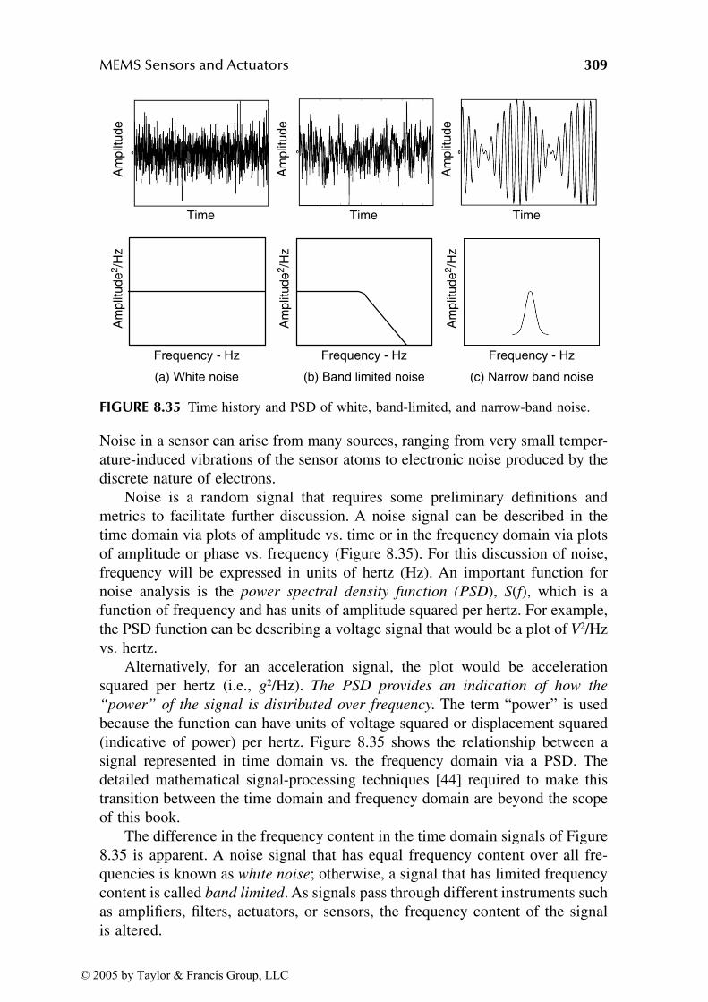
MEMS Sensors and Actuators 309
Noise in a sensor can arise from many sources, ranging from very small temper-ature-induced vibrations of the sensor atoms to electronic noise produced by thediscrete nature of electrons.
Noise is a random signal that requires some preliminary definitions andmetrics to facilitate further discussion. A noise signal can be described in thetime domain via plots of amplitude vs. time or in the frequency domain via plotsof amplitude or phase vs. frequency (Figure 8.35). For this discussion of noise,frequency will be expressed in units of hertz (Hz). An important function fornoise analysis is the power spectral density function (PSD), S(f), which is afunction of frequency and has units of amplitude squared per hertz. For example,the PSD function can be describing a voltage signal that would be a plot of V2/Hzvs. hertz.
Alternatively, for an acceleration signal, the plot would be accelerationsquared per hertz (i.e., g2/Hz). The PSD provides an indication of how the
“power” of the signal is distributed over frequency. The term “power” is usedbecause the function can have units of voltage squared or displacement squared(indicative of power) per hertz. Figure 8.35 shows the relationship between asignal represented in time domain vs. the frequency domain via a PSD. Thedetailed mathematical signal-processing techniques [44] required to make thistransition between the time domain and frequency domain are beyond the scopeof this book.
The difference in the frequency content in the time domain signals of Figure8.35 is apparent. A noise signal that has equal frequency content over all fre-quencies is known as white noise; otherwise, a signal that has limited frequencycontent is called band limited. As signals pass through different instruments suchas amplifiers, filters, actuators, or sensors, the frequency content of the signalis altered.
FIGURE 8.35 Time history and PSD of white, band-limited, and narrow-band noise.
Frequency - Hz Frequency - Hz Frequency - Hz
Am
plit
ude
2/H
z
Am
plit
ude
2/H
z
Am
plit
ude
2/H
z
Time Time Time
Am
plit
ude
Am
plit
ude
Am
plit
ude
(a) White noise (b) Band limited noise (c) Narrow band noise
© 2005 by Taylor & Francis Group, LLC

310 Micro Electro Mechanical System Design
The mean square of the signal, can be obtained from the PSD byintegrating over frequency (Equation 8.41). The mean square of a signal is ascalar, which is a useful metric indicative of the magnitude of the signal.
(8.41)
In noise analysis, it is often necessary to evaluate the magnitude of a noisesignal, which is a combination of several other signals. Noise signals are fre-quently uncorrelated; this allows the sum of the mean square amplitude of theuncorrelated signals to be added to obtain the mean square amplitude of the total:
(8.42)
In sensors, a desired sensor signal, vs, is proportional to a quantity to bemeasured, and sensor noise, vn, is an unwanted signal produced by the noisesources of the system. The signal to noise ratio (SNR) is a metric of the relativeamount of signal and noise present in a sensor output. SNR is defined as the ratioof the mean square signal, vs
2, to the mean square noise, vn
2 (Equation 8.43). Dueto the typical magnitude of SNR, the magnitude is often expressed in decibels(dB) as:
(8.43)
When signals and noises are applied to systems (Figure 8.36), it is frequentlydesired to calculate the response of the system. For linear systems, a frequencyresponse function, FRF, which can be calculated from the basic principles ormeasured, defines the response of the system vs. frequency due to inputs.
The PSD of the system output can be calculated by the product of themagnitude of the FRF squared and the PSD of the input (Equation 8.44). Becausethese are functions of frequency, the product is performed at each frequency. Themean square system response is calculated by integrating Equation 8.44 overfrequency similar to Equation 8.41.
(8.44)
v 2 ,
v S f df2
0= ( )∞∫
v vtotal i
i
n
2 2
1
==
∑
SNRv
v
SNRv
vdB
s
n
s
n
=
=
2
2
2
210 log
S f H f S fo i( ) = ( ) ( )2
© 2005 by Taylor & Francis Group, LLC
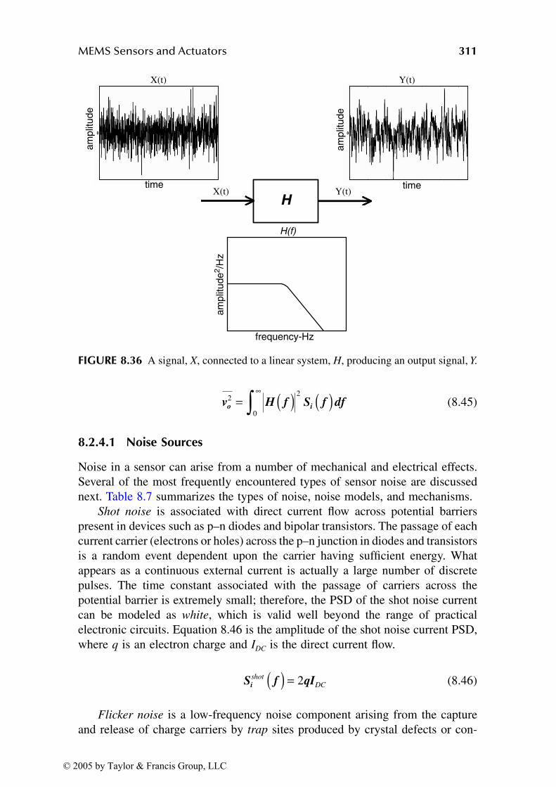
MEMS Sensors and Actuators 311
(8.45)
8.2.4.1 Noise Sources
Noise in a sensor can arise from a number of mechanical and electrical effects.Several of the most frequently encountered types of sensor noise are discussednext. Table 8.7 summarizes the types of noise, noise models, and mechanisms.
Shot noise is associated with direct current flow across potential barrierspresent in devices such as p–n diodes and bipolar transistors. The passage of eachcurrent carrier (electrons or holes) across the p–n junction in diodes and transistorsis a random event dependent upon the carrier having sufficient energy. Whatappears as a continuous external current is actually a large number of discretepulses. The time constant associated with the passage of carriers across thepotential barrier is extremely small; therefore, the PSD of the shot noise currentcan be modeled as white, which is valid well beyond the range of practicalelectronic circuits. Equation 8.46 is the amplitude of the shot noise current PSD,where q is an electron charge and IDC is the direct current flow.
(8.46)
Flicker noise is a low-frequency noise component arising from the captureand release of charge carriers by trap sites produced by crystal defects or con-
FIGURE 8.36 A signal, X, connected to a linear system, H, producing an output signal, Y.
time
am
plit
ude
X(t)
time
am
plit
ude
Y(t)
HX(t) Y(t)
frequency-Hz
am
plit
ude
2/H
zH(f)
v H f S f dfo i2
2
0= ( ) ( )∞∫
S f qIishot
DC( ) = 2
© 2005 by Taylor & Francis Group, LLC

312 Micro Electro Mechanical System Design
tamination in semiconductors. The trap sites capture and release carriers randomlywith time constants that are primarily low frequency. The flicker noise currentPSD is modeled by Equation 8.47, which shows a 1/f dependency in amplitudevs. frequency; this is why this type of noise is frequently called 1/f noise. Theconstants a, b, and K1 in Equation 8.47 are primarily fabrication process anddevice dependent. Once these parameters are determined for a particular processand type device, they may be used for prediction of noise in other similar devicesmade in that process.
TABLE 8.7Summary of Noise Models and Mechanisms
Model PSD Mechanism
Electrical and mechanical noise arising from the random motion of electrons and atoms that is directly related to absolute temperature, T
Direct current flow across potential barriers such as p–n diodes and bipolar transistors
Low-frequency (1/f) noise arising from the capture and release of charge carriers by trap sites in semiconductors
Low-frequency (1/f2) noise related to heavy metal contamination in semiconductors
S f kTRthermal ( ) = 42 /H
zi
eqfr
S f qIi DCshot ( ) = 2
2 /Hz
i
eqfr
S f KI
fi
a
b
flicker ( ) = 1
/Hz
2 i
eqfr
S f KI
f
f
i
c
c
burst ( ) =+
2 2
1
/Hz
2 i
eqfr
© 2005 by Taylor & Francis Group, LLC
MEMS Sensors and Actuators 313
(8.47)
whereI = direct current
K1 = constant for a particular device and processa = constant in the range 0.5 to 2b = constant typically about unity
Another type of low-frequency noise, termed burst or popcorn noise, issometimes found in integrated circuits and discrete transistors. The mechanismis not fully understood, but is believed to be related to heavy metal contamination.Equation 8.48 is a model of burst noise that contains constants that need to bedetermined for the specific application. Burst noise can also occur with multiplefrequency components (fc), which can be seen in an experimentally obtained PSDof the noise.
(8.48)
whereI = direct current
K2 = constant for a particular device and processc = constant in the range 0.5 to 2fc = a particular frequency for the noise process
Thermal noise is noise that can be generated in electrical and mechanicalcomponents; it arises from a completely unique mechanism — the randommotion of electrons and atoms, which is directly proportional to the absolutetemperature, T. Thermal noise is generated in these systems through their energydissipation mechanisms (i.e., resistance for electrical or damping for mechanical).Because dissipation mechanisms provide a way for energy to leave an electricalor mechanical system, they also provide a way for energy to enter. The energyentering the system is the thermal vibration of electrons and molecules. Theassociation linking the paths for energy dissipation and entrance is expressed bythe fluctuation–dissipation theorem [47,48]. Thermal noise is also known asJohnson noise in electrical systems and Brownian noise in mechanical systems.The PSD for thermal noise is white. This is the most fundamental noise limitationfor a sensor.
S f KI
fi
a
b
flicker ( ) = 1
S f KI
f
f
i
c
c
burst ( ) =+
2 2
1
© 2005 by Taylor & Francis Group, LLC

314 Micro Electro Mechanical System Design
(8.49)
whereI = direct currentk = Boltzmann’s constant (1.38 × 10⁻²³ J/K)T = absolute temperature (K)R = dissipation constant (electrical resistance or mechanical damping
coefficient)
8.2.5 MEMS PHYSICAL SENSORS
Physical sensors are one of the biggest application areas for MEMS technology.In this section, an overview of three of the most widely used types of physicalsensors and their implementation in MEMS technology will be presented.
Accelerometers and gyroscopes are inertial sensors that measure accelerationand rotation rate, respectively. The performance grades of these types of sensorsare found in Table 8.8 [50], which presents the bias stability and cost range forthe four performance grades. The performance ranges from strategic grade inertialinstruments used on strategic missiles and submarines to instrument grade instru-ments used in automotive and commercial applications. Currently, MEMS inertialsensors are available in the tactical and instrument grade inertial sensors.
One of the first commercial application areas of MEMS technology waspressure sensing. Today, pressure sensing is one the largest commercial applica-tions of MEMS technology. The implementation of pressure sensors with MEMStechnology for different pressure/vacuum regimes will be presented.
8.2.5.1 Accelerometer
Accelerometers are one of the most frequently utilized physical sensors for detect-ing and measuring motion. Accelerometers have found applications ranging frommeasurement and control to inertial navigation. MEMS implementations of accel-erometers have found a large commercial market in automotive airbag deployment
TABLE 8.8Inertial Instrument Performance Grades
Performancegrade
Accelerometerbias stability
Gyroscopebias stability Cost
Strategic <1 µg <0.0001°/h <$10,000,000/unitNavigation 10–50 µg 0.001–0.01°/h <$100,000/unitTactical 0.1–1 mg 1–10°/h <$30,000/unitInstrumentation 10–100 mg 30–100°/h $250–$2000/axis
Source: M.R. Daily, Defense Manufacturing Conference, DMC ’99, Nov. 1999.
S f kTRthermal ( ) = 4
© 2005 by Taylor & Francis Group, LLC
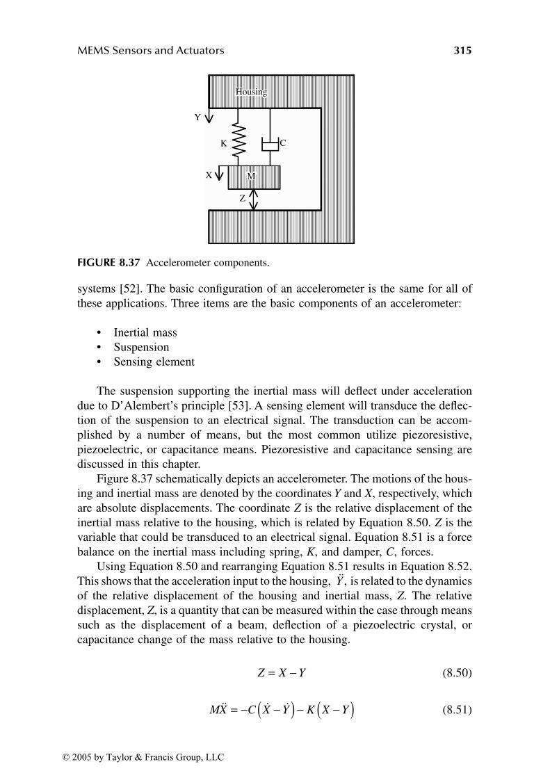
MEMS Sensors and Actuators 315
systems [52]. The basic configuration of an accelerometer is the same for all ofthese applications. Three items are the basic components of an accelerometer:
• Inertial mass• Suspension• Sensing element
The suspension supporting the inertial mass will deflect under accelerationdue to D’Alembert’s principle [53]. A sensing element will transduce the deflec-tion of the suspension to an electrical signal. The transduction can be accom-plished by a number of means, but the most common utilize piezoresistive,piezoelectric, or capacitance means. Piezoresistive and capacitance sensing arediscussed in this chapter.
Figure 8.37 schematically depicts an accelerometer. The motions of the hous-ing and inertial mass are denoted by the coordinates Y and X, respectively, whichare absolute displacements. The coordinate Z is the relative displacement of theinertial mass relative to the housing, which is related by Equation 8.50. Z is thevariable that could be transduced to an electrical signal. Equation 8.51 is a forcebalance on the inertial mass including spring, K, and damper, C, forces.
Using Equation 8.50 and rearranging Equation 8.51 results in Equation 8.52.This shows that the acceleration input to the housing, is related to the dynamicsof the relative displacement of the housing and inertial mass, Z. The relativedisplacement, Z, is a quantity that can be measured within the case through meanssuch as the displacement of a beam, deflection of a piezoelectric crystal, orcapacitance change of the mass relative to the housing.
(8.50)
(8.51)
FIGURE 8.37 Accelerometer components.
Y
X
Z
K C
MM
HousingHousing
ɺɺY ,
Z X Y= −MX C X Y K X Yɺɺ ɺ ɺ= − −( ) − −( )
© 2005 by Taylor & Francis Group, LLC
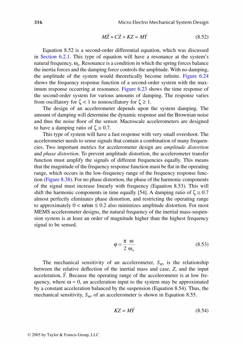
316 Micro Electro Mechanical System Design
(8.52)
Equation 8.52 is a second-order differential equation, which was discussedin Section 6.2.1. This type of equation will have a resonance at the system’snatural frequency, ωn. Resonance is a condition in which the spring forces balancethe inertia forces and the damping force controls the amplitude. With no damping,the amplitude of the system would theoretically become infinite. Figure 6.24shows the frequency response function of a second-order system with the max-imum response occurring at resonance. Figure 6.23 shows the time response ofthe second-order system for various amounts of damping. The response variesfrom oscillatory for ζ < 1 to nonoscillatory for ζ ≥ 1.
The design of an accelerometer depends upon the system damping. Theamount of damping will determine the dynamic response and the Brownian noiseand thus the noise floor of the sensor. Macroscale accelerometers are designedto have a damping ratio of ζ ≅ 0.7.
This type of system will have a fast response with very small overshoot. Theaccelerometer needs to sense signals that contain a combination of many frequen-cies. Two important metrics for accelerometer design are amplitude distortion
and phase distortion. To prevent amplitude distortion, the accelerometer transferfunction must amplify the signals of different frequencies equally. This meansthat the magnitude of the frequency response function must be flat in the operatingrange, which occurs in the low-frequency range of the frequency response func-tion (Figure 8.38). For no phase distortion, the phase of the harmonic componentsof the signal must increase linearly with frequency (Equation 8.53). This willshift the harmonic components in time equally [54]. A damping ratio of ζ ≅ 0.7almost perfectly eliminates phase distortion, and restricting the operating rangeto approximately 0 < ω/ωn ≤ 0.2 also minimizes amplitude distortion. For mostMEMS accelerometer designs, the natural frequency of the inertial mass-suspen-sion system is at least an order of magnitude higher than the highest frequencysignal to be sensed.
(8.53)
The mechanical sensitivity of an accelerometer, SM, is the relationshipbetween the relative deflection of the inertial mass and case, Z, and the inputacceleration, Because the operating range of the accelerometer is at low fre-quency, where ω ≈ 0, an acceleration input to the system may be approximatedby a constant acceleration balanced by the suspension (Equation 8.54). Thus, themechanical sensitivity, SM, of an accelerometer is shown in Equation 8.55.
(8.54)
MZ CZ KZ MYɺɺ ɺ ɺɺ+ + =
ϕ π ωω=
2 n
ɺɺY.
KZ MY= ɺɺ
© 2005 by Taylor & Francis Group, LLC
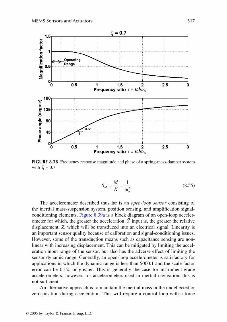
MEMS Sensors and Actuators 317
(8.55)
The accelerometer described thus far is an open-loop sensor consisting ofthe inertial mass-suspension system, position sensing, and amplification signal-conditioning elements. Figure 8.39a is a block diagram of an open-loop acceler-ometer for which, the greater the acceleration input is, the greater the relativedisplacement, Z, which will be transduced into an electrical signal. Linearity isan important sensor quality because of calibration and signal-conditioning issues.However, some of the transduction means such as capacitance sensing are non-linear with increasing displacement. This can be mitigated by limiting the accel-eration input range of the sensor, but also has the adverse effect of limiting thesensor dynamic range. Generally, an open-loop accelerometer is satisfactory forapplications in which the dynamic range is less than 5000:1 and the scale factorerror can be 0.1% or greater. This is generally the case for instrument-gradeaccelerometers; however, for accelerometers used in inertial navigation, this isnot sufficient.
An alternative approach is to maintain the inertial mass in the undeflected orzero position during acceleration. This will require a control loop with a force
FIGURE 8.38 Frequency response magnitude and phase of a spring-mass-damper systemwith ζ = 0.7.
SM
KM
n
= = 12ω
ɺɺY
© 2005 by Taylor & Francis Group, LLC
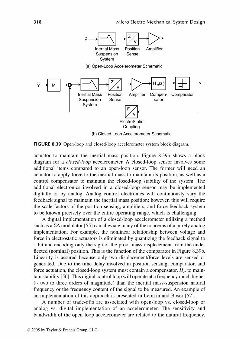
318 Micro Electro Mechanical System Design
actuator to maintain the inertial mass position. Figure 8.39b shows a blockdiagram for a closed-loop accelerometer. A closed-loop sensor involves someadditional items compared to an open-loop sensor. The former will need anactuator to apply force to the inertial mass to maintain its position, as well as acontrol compensator to maintain the closed-loop stability of the system. Theadditional electronics involved in a closed-loop sensor may be implementeddigitally or by analog. Analog control electronics will continuously vary thefeedback signal to maintain the inertial mass position; however, this will requirethe scale factors of the position sensing, amplifiers, and force feedback systemto be known precisely over the entire operating range, which is challenging.
A digital implementation of a closed-loop accelerometer utilizing a methodsuch as a Σ∆ modulator [55] can alleviate many of the concerns of a purely analogimplementation. For example, the nonlinear relationship between voltage andforce in electrostatic actuators is eliminated by quantizing the feedback signal to1 bit and encoding only the sign of the proof mass displacement from the unde-flected (nominal) position. This is the function of the comparator in Figure 8.39b.Linearity is assured because only two displacement/force levels are sensed orgenerated. Due to the time delay involved in position sensing, comparator, andforce actuation, the closed-loop system must contain a compensator, Hc, to main-tain stability [56]. This digital control loop will operate at a frequency much higher(~ two to three orders of magnitude) than the inertial mass-suspension naturalfrequency or the frequency content of the signal to be measured. An example ofan implementation of this approach is presented in Lemkin and Boser [57].
A number of trade-offs are associated with open-loop vs. closed-loop oranalog vs. digital implementation of an accelerometer. The sensitivity andbandwidth of the open-loop accelerometer are related to the natural frequency,
FIGURE 8.39 Open-loop and closed-loop accelerometer system block diagram.
Inertial Mass
Suspension
System
Comparator
H c(z )
Compen-
sator
AmplifierPosition
Sense
Inertial Mass
Suspension
System
AmplifierPosition
Sense
Z
V
ElectroStatic
Coupling
F
V
(b) Closed-Loop Accelerometer Schematic
MY
Z
V
(a) Open-Loop Accelerometer Schematic
··
Y··
© 2005 by Taylor & Francis Group, LLC
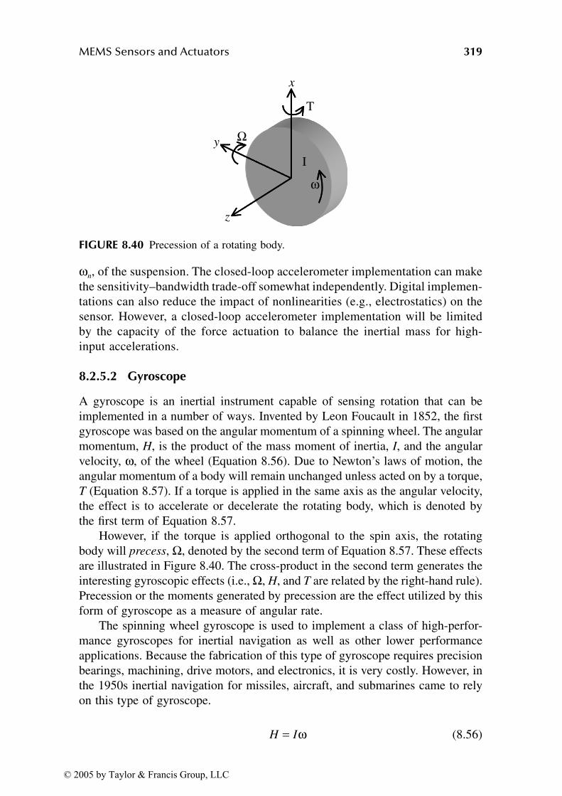
MEMS Sensors and Actuators 319
ωn, of the suspension. The closed-loop accelerometer implementation can makethe sensitivity–bandwidth trade-off somewhat independently. Digital implemen-tations can also reduce the impact of nonlinearities (e.g., electrostatics) on thesensor. However, a closed-loop accelerometer implementation will be limitedby the capacity of the force actuation to balance the inertial mass for high-input accelerations.
8.2.5.2 Gyroscope
A gyroscope is an inertial instrument capable of sensing rotation that can beimplemented in a number of ways. Invented by Leon Foucault in 1852, the firstgyroscope was based on the angular momentum of a spinning wheel. The angularmomentum, H, is the product of the mass moment of inertia, I, and the angularvelocity, ω, of the wheel (Equation 8.56). Due to Newton’s laws of motion, theangular momentum of a body will remain unchanged unless acted on by a torque,T (Equation 8.57). If a torque is applied in the same axis as the angular velocity,the effect is to accelerate or decelerate the rotating body, which is denoted bythe first term of Equation 8.57.
However, if the torque is applied orthogonal to the spin axis, the rotatingbody will precess, Ω, denoted by the second term of Equation 8.57. These effectsare illustrated in Figure 8.40. The cross-product in the second term generates theinteresting gyroscopic effects (i.e., Ω, H, and T are related by the right-hand rule).Precession or the moments generated by precession are the effect utilized by thisform of gyroscope as a measure of angular rate.
The spinning wheel gyroscope is used to implement a class of high-perfor-mance gyroscopes for inertial navigation as well as other lower performanceapplications. Because the fabrication of this type of gyroscope requires precisionbearings, machining, drive motors, and electronics, it is very costly. However, inthe 1950s inertial navigation for missiles, aircraft, and submarines came to relyon this type of gyroscope.
(8.56)
FIGURE 8.40 Precession of a rotating body.
z
y
x
Ω
ω
T
I
H I= ω
© 2005 by Taylor & Francis Group, LLC
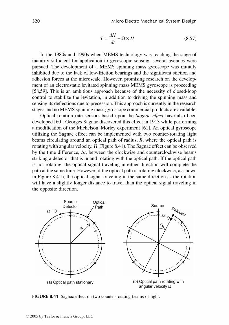
320 Micro Electro Mechanical System Design
(8.57)
In the 1980s and 1990s when MEMS technology was reaching the stage ofmaturity sufficient for application to gyroscopic sensing, several avenues werepursued. The development of a MEMS spinning mass gyroscope was initiallyinhibited due to the lack of low-friction bearings and the significant stiction andadhesion forces at the microscale. However, promising research on the develop-ment of an electrostatic levitated spinning mass MEMS gyroscope is proceeding[58,59]. This is an ambitious approach because of the necessity of closed-loopcontrol to stabilize the levitation, in addition to driving the spinning mass andsensing its deflections due to precession. This approach is currently in the researchstages and no MEMS spinning mass gyroscope commercial products are available.
Optical rotation rate sensors based upon the Sagnac effect have also beendeveloped [60]. Georges Sagnac discovered this effect in 1913 while performinga modification of the Michelson–Morley experiment [61]. An optical gyroscopeutilizing the Sagnac effect can be implemented with two counter-rotating lightbeams circulating around an optical path of radius, R, where the optical path isrotating with angular velocity, Ω (Figure 8.41). The Sagnac effect can be observedby the time difference, ∆t, between the clockwise and counterclockwise beamsstriking a detector that is in and rotating with the optical path. If the optical pathis not rotating, the optical signal traveling in either direction will complete thepath at the same time. However, if the optical path is rotating clockwise, as shownin Figure 8.41b, the optical signal traveling in the same direction as the rotationwill have a slightly longer distance to travel than the optical signal traveling inthe opposite direction.
FIGURE 8.41 Sagnac effect on two counter-rotating beams of light.
TdH
dtH= + ×Ω
SourceDetector
R
Ω = 0
OpticalPath
(a) Optical path stationary
Source
Ωt
Detector
(b) Optical path rotating with angular velocity Ω
© 2005 by Taylor & Francis Group, LLC
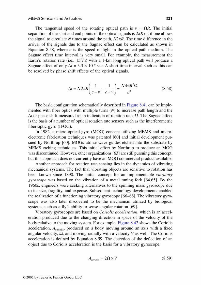
MEMS Sensors and Actuators 321
The tangential speed of the rotating optical path is v = ΩR. The initialseparation of the start and end points of the optical signals is 2πR or, if one allowsthe signal to circulate N times around the path, N2πR. The time difference in thearrival of the signals due to the Sagnac effect can be calculated as shown inEquation 8.58, where c is the speed of light in the optical path medium. TheSagnac effect time interval is very small. For example, the measurement theEarth’s rotation rate (i.e., 15°/h) with a 1-km long optical path will produce aSagnac effect of only ∆t = 3.3 × 10⁻⁹ sec. A short time interval such as this canbe resolved by phase shift effects of the optical signals.
(8.58)
The basic configuration schematically described in Figure 8.41 can be imple-mented with fiber optics with multiple turns (N) to increase path length and the∆t or phase shift measured as an indication of rotation rate, Ω. The Sagnac effectis the basis of a number of optical rotation rate sensors such as the interferometricfiber-optic gyro (IFOG).
In 1982, a micro-optical-gyro (MOG) concept utilizing MEMS and micro-electronic fabrication techniques was patented [60] and initial development pur-sued by Northrup [60]. MOGs utilize wave guides etched into the substrate byMEMS etching techniques. This initial effort by Northrup to produce an MOGwas discontinued. However, other organizations [63] are still pursuing this concept,but this approach does not currently have an MOG commercial product available.
Another approach for rotation rate sensing lies in the dynamics of vibratingmechanical systems. The fact that vibrating objects are sensitive to rotation hasbeen known since 1890. The initial concept for an implementable vibratory
gyroscope was based on the vibration of a metal tuning fork [64,65]. By the1960s, engineers were seeking alternatives to the spinning mass gyroscope dueto its size, fragility, and expense. Subsequent technology developments enabledthe realization of a functioning vibratory gyroscope [66–68]. The vibratory gyro-scope was also later discovered to be the mechanism utilized by biologicalsystems such as a fly’s ability to sense angular rotation [69].
Vibratory gyroscopes are based on Coriolis acceleration, which is an accel-eration produced due to the changing direction in space of the velocity of thebody relative to the moving system. For example, Figure 8.42 shows the Coriolisacceleration, Acoriolis, produced on a body moving around an axis with a fixedangular velocity, Ω, and moving radially with a velocity V as well. The Coriolisacceleration is defined by Equation 8.59. The detection of the deflection of anobject due to Coriolis acceleration is the basis for a vibratory gyroscope.
(8.59)
∆ Ωt N R
c v c v
N R
c= − − +
≈2
1 1 4 2
2π π
A Vcoriolis = ×2Ω
© 2005 by Taylor & Francis Group, LLC
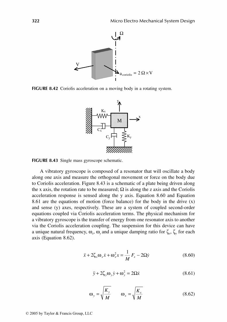
322 Micro Electro Mechanical System Design
A vibratory gyroscope is composed of a resonator that will oscillate a bodyalong one axis and measure the orthogonal movement or force on the body dueto Coriolis acceleration. Figure 8.43 is a schematic of a plate being driven alongthe x axis, the rotation rate to be measured; Ω is along the z axis and the Coriolisacceleration response is sensed along the y axis. Equation 8.60 and Equation8.61 are the equations of motion (force balance) for the body in the drive (x)and sense (y) axes, respectively. These are a system of coupled second-orderequations coupled via Coriolis acceleration terms. The physical mechanism fora vibratory gyroscope is the transfer of energy from one resonator axis to anothervia the Coriolis acceleration coupling. The suspension for this device can havea unique natural frequency, ωx, ωy and a unique damping ratio for ζx, ζy for eachaxis (Equation 8.62).
(8.60)
(8.61)
(8.62)
FIGURE 8.42 Coriolis acceleration on a moving body in a rotating system.
FIGURE 8.43 Single mass gyroscope schematic.
V2 Ωa coriolis ×=
Ω
V
M
Cx
Kx
y
x
KyCy
ɺɺ ɺ ɺx x xM
F yx x x x+ + = −21
22ζ ω ω Ω
ɺɺ ɺ ɺy y xy y y+ + =2 22ζ ω ω Ω
ω ωy
y
xx
K
M
K
M= =
© 2005 by Taylor & Francis Group, LLC
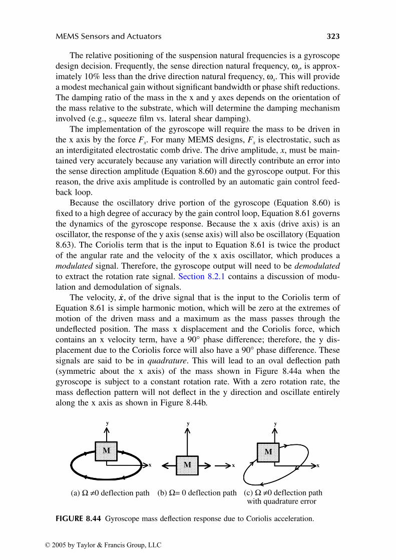
MEMS Sensors and Actuators 323
The relative positioning of the suspension natural frequencies is a gyroscopedesign decision. Frequently, the sense direction natural frequency, ωy, is approx-imately 10% less than the drive direction natural frequency, ωx. This will providea modest mechanical gain without significant bandwidth or phase shift reductions.The damping ratio of the mass in the x and y axes depends on the orientation ofthe mass relative to the substrate, which will determine the damping mechanisminvolved (e.g., squeeze film vs. lateral shear damping).
The implementation of the gyroscope will require the mass to be driven inthe x axis by the force Fx. For many MEMS designs, Fx is electrostatic, such asan interdigitated electrostatic comb drive. The drive amplitude, x, must be main-tained very accurately because any variation will directly contribute an error intothe sense direction amplitude (Equation 8.60) and the gyroscope output. For thisreason, the drive axis amplitude is controlled by an automatic gain control feed-back loop.
Because the oscillatory drive portion of the gyroscope (Equation 8.60) isfixed to a high degree of accuracy by the gain control loop, Equation 8.61 governsthe dynamics of the gyroscope response. Because the x axis (drive axis) is anoscillator, the response of the y axis (sense axis) will also be oscillatory (Equation8.63). The Coriolis term that is the input to Equation 8.61 is twice the productof the angular rate and the velocity of the x axis oscillator, which produces amodulated signal. Therefore, the gyroscope output will need to be demodulated
to extract the rotation rate signal. Section 8.2.1 contains a discussion of modu-lation and demodulation of signals.
The velocity, of the drive signal that is the input to the Coriolis term ofEquation 8.61 is simple harmonic motion, which will be zero at the extremes ofmotion of the driven mass and a maximum as the mass passes through theundeflected position. The mass x displacement and the Coriolis force, whichcontains an x velocity term, have a 90° phase difference; therefore, the y dis-placement due to the Coriolis force will also have a 90° phase difference. Thesesignals are said to be in quadrature. This will lead to an oval deflection path(symmetric about the x axis) of the mass shown in Figure 8.44a when thegyroscope is subject to a constant rotation rate. With a zero rotation rate, themass deflection pattern will not deflect in the y direction and oscillate entirelyalong the x axis as shown in Figure 8.44b.
FIGURE 8.44 Gyroscope mass deflection response due to Coriolis acceleration.
ɺx,
y
x
M
y
x
M
y
xM
(a) Ω ≠0 deflection path (b) Ω= 0 deflection path (c) Ω ≠0 deflection path with quadrature error
© 2005 by Taylor & Francis Group, LLC
324 Micro Electro Mechanical System Design
However, if mass or stiffness imbalances exist in the system dynamics asindicated in Equation 8.64, the mass deflection pattern will be as shown in Figure8.44c. These subtle imbalances in the vibration of the sense mass produce adeflection in the y direction known as quadrature error, which contaminates theCoriolis signal, which is the measure of rotation rate. The effects of quadratureerror can be negated by a quadrature error cancellation [70,71] scheme involvingthe use of electrostatic actuators with properly phased signals to cancel theimbalance, or by synchronous detection methods, which take advantage of thequadrature relationship to extract the Coriolis signal.
(8.63)
(8.64)
The first silicon integrated micromachined vibratory gyroscope was describedby O’Connor and Shupe in 1981 [72]. In the ensuing years, development of aMEMS gyroscope was spurred by the lure of a low-cost instrument that couldbe mass produced. Efforts to produce single resonator gyroscopes schematicallyare shown in Figure 8.43. However, the one configuration that has been employedfor macroscale and MEMS vibratory gyroscopes is the tuning fork gyro (TFG)(Figure 8.45). The TFG consists of two plates that are driven in an antiphasemanner (i.e., both plates move outward and inward relative to the center axis).The rotational field will cause the plates to move perpendicular to the substratein opposite directions. This configuration enables differential sensing, which willallow common mode signals such as external accelerations to be rejected. Theuse of two masses vibrating in antiphase also causes momenta to cancel locallyand make the gyroscope less sensitive to mounting. The two masses may havecoupled or separate suspensions.
Two MEMS TFGs have been successfully developed for commercial appli-cations by Draper Laboratories [73,74] and Analog Device [75]. These are exam-ples of tactical and instrument grade MEMS gyroscopes. The applications for agyroscope such as these include tactical grade navigation, platform stabilization,automobile skid control, and stabilization.
8.2.5.3 Pressure Sensors
The method of pressure sensor implementation differs depending on whether thepressure to be sensed is greater than atmospheric or less than atmospheric (vac-uum). Currently, the greatest commercial application for a MEMS pressure sensoris for the greater than atmospheric regime, which is the focus here. However,methods of implementing a vacuum sensor will first be briefly discussed.
The method of implementation of a vacuum sensor depends on the operatingrange. In the 1 to 2000 mtorr range, vacuum may be sensed by measuring the
x Xe y Yej t j t= = +( )ω ω ϕ
ɺɺ ɺɺ ɺ ɺy x y x xM y y y K+ + + + =δ ζ ω ω δ2 22 Ω
© 2005 by Taylor & Francis Group, LLC
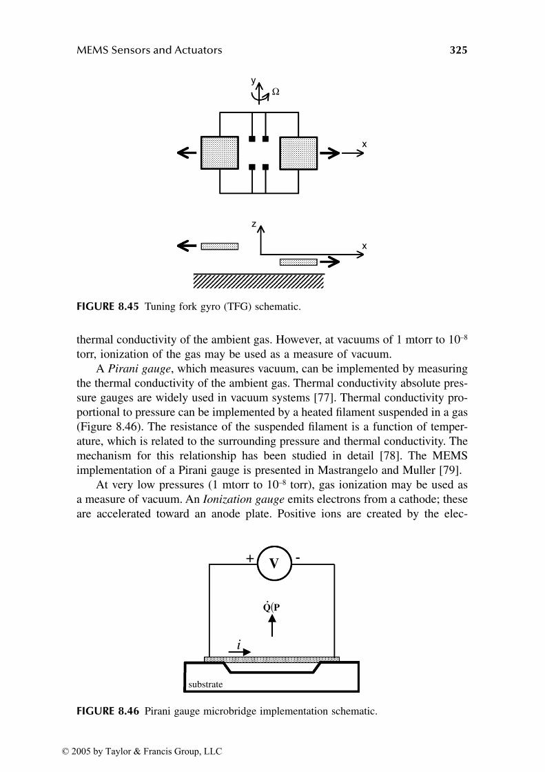
MEMS Sensors and Actuators 325
thermal conductivity of the ambient gas. However, at vacuums of 1 mtorr to 10–8
torr, ionization of the gas may be used as a measure of vacuum.A Pirani gauge, which measures vacuum, can be implemented by measuring
the thermal conductivity of the ambient gas. Thermal conductivity absolute pres-sure gauges are widely used in vacuum systems [77]. Thermal conductivity pro-portional to pressure can be implemented by a heated filament suspended in a gas(Figure 8.46). The resistance of the suspended filament is a function of temper-ature, which is related to the surrounding pressure and thermal conductivity. Themechanism for this relationship has been studied in detail [78]. The MEMSimplementation of a Pirani gauge is presented in Mastrangelo and Muller [79].
At very low pressures (1 mtorr to 10–8 torr), gas ionization may be used asa measure of vacuum. An Ionization gauge emits electrons from a cathode; theseare accelerated toward an anode plate. Positive ions are created by the elec-
FIGURE 8.45 Tuning fork gyro (TFG) schematic.
FIGURE 8.46 Pirani gauge microbridge implementation schematic.
y
x
Ω
z
x
V+ -
i
(PQ
substrate
·
© 2005 by Taylor & Francis Group, LLC

326 Micro Electro Mechanical System Design
tron–gas collisions. The current on the anode is proportional to the absolutepressure (vacuum) of the gas.
Most pressure sensors for greater than atmospheric pressure utilize a deform-able diaphragm. The deflection of the diaphragm is the measure of pressure,which can be sensed by capacitative, piezoresistive, or optical means. Figure 8.47is a schematic of typical pressure sensors. The pressure sensor may measureabsolute pressure that has a vacuum or a reference pressure on one side of thediaphragm. Alternatively, a gauge pressure or differential pressure sensor wouldhave one side of the diaphragm vented to atmosphere or to another pressure thatwould be a reference for the measurement.
The pressure diaphragm is generally rectangular or circular in shape. Pressuresensors fabricated with bulk micromachining methods are generally rectangular,due to the anisotropic etching techniques utilized. The fabrication sequence ofthe bulk micromachined Motorola MPX200 pressure sensor is shown in Figure8.48. This sensor has a square, single-crystal diaphragm that is 1448 µm in lengthand 26.5 µm thick. A four-terminal X-ducer [81] shear strain gauge technologyis used to read pressure.
The shape of surface micromachined pressure sensors is not restricted becausethey are photolithograhically defined. Figure 8.49 shows a surface micromachinedpressure sensor that has a 2-µm thick diaphragm and is 200 µm in diameter.Circular diaphragms may have an advantage over square or rectangular ones dueto the absence of stress concentrations at the corners.
The applied pressure for the diaphragm-based pressure sensors is determinedby the deflection of the diaphragm. Section 6.1.6 discusses the relationships forsmall deformations of a flat plate in bending with no initial built-in stresses dueto residual stress. Figure 6.15 and Figure 6.1.6 provide the maximum deflectionand stress for a rectangular and circular diaphragm with fixed boundary conditions(i.e., no deflection or rotation) at the boundary. The pressure on the diaphragmis directly proportional to the applied pressure for rectangular and circular dia-phragms. For the case of a diaphragm with large built-in stress or large deflections,the direct proportionality is no longer true. In general, it is desirable to use adiaphragm with a linear relationship with pressure because calibration and mea-surement are simpler. Deflection of the diaphragm may be sensed via capacitanceor piezoresistive sensing (discussed in this chapter).
FIGURE 8.47 Pressure sensor schematic for greater than atmospheric pressures.
P
Preference
(a) Absolute pressuregauge
P1
P2
(b) Differential pressuregauge
© 2005 by Taylor & Francis Group, LLC

MEMS Sensors and Actuators 327
FIGURE 8.48 A schematic of the fabrication sequence for the bulk micromachinedMotorola MPX200 pressure sensor. (After W.P. Eaton et al., Proc. SPIE, 3514, 431–438,Sept. 1998.)
FIGURE 8.49 Surface micromachined pressure sensor. (Courtesy of Sandia NationalLaboratories; W.P. Eaton et al., Proc. SPIE, 3514, 431–438, Sept. 1998.)
(a) Ion implant X-ducer™
(b) Deposit and pattern metal contacts, passivate with silicon nitride
(c) Backside etch wafer to form diaphragm
(d) Bond wafer to sensor to form reference cavity
© 2005 by Taylor & Francis Group, LLC
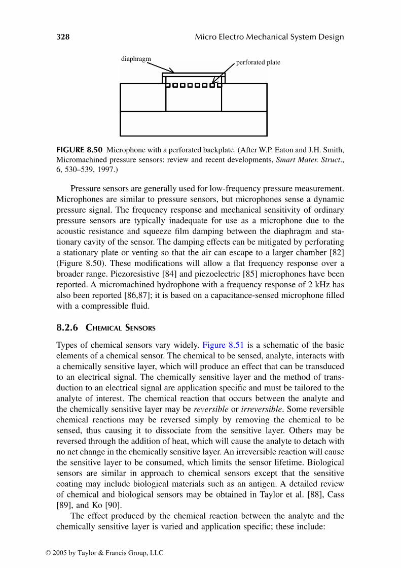
328 Micro Electro Mechanical System Design
Pressure sensors are generally used for low-frequency pressure measurement.Microphones are similar to pressure sensors, but microphones sense a dynamicpressure signal. The frequency response and mechanical sensitivity of ordinarypressure sensors are typically inadequate for use as a microphone due to theacoustic resistance and squeeze film damping between the diaphragm and sta-tionary cavity of the sensor. The damping effects can be mitigated by perforatinga stationary plate or venting so that the air can escape to a larger chamber [82](Figure 8.50). These modifications will allow a flat frequency response over abroader range. Piezoresistive [84] and piezoelectric [85] microphones have beenreported. A micromachined hydrophone with a frequency response of 2 kHz hasalso been reported [86,87]; it is based on a capacitance-sensed microphone filledwith a compressible fluid.
8.2.6 CHEMICAL SENSORS
Types of chemical sensors vary widely. Figure 8.51 is a schematic of the basicelements of a chemical sensor. The chemical to be sensed, analyte, interacts witha chemically sensitive layer, which will produce an effect that can be transducedto an electrical signal. The chemically sensitive layer and the method of trans-duction to an electrical signal are application specific and must be tailored to theanalyte of interest. The chemical reaction that occurs between the analyte andthe chemically sensitive layer may be reversible or irreversible. Some reversiblechemical reactions may be reversed simply by removing the chemical to besensed, thus causing it to dissociate from the sensitive layer. Others may bereversed through the addition of heat, which will cause the analyte to detach withno net change in the chemically sensitive layer. An irreversible reaction will causethe sensitive layer to be consumed, which limits the sensor lifetime. Biologicalsensors are similar in approach to chemical sensors except that the sensitivecoating may include biological materials such as an antigen. A detailed reviewof chemical and biological sensors may be obtained in Taylor et al. [88], Cass[89], and Ko [90].
The effect produced by the chemical reaction between the analyte and thechemically sensitive layer is varied and application specific; these include:
FIGURE 8.50 Microphone with a perforated backplate. (After W.P. Eaton and J.H. Smith,Micromachined pressure sensors: review and recent developments, Smart Mater. Struct.,6, 530–539, 1997.)
diaphragm perforated plate
© 2005 by Taylor & Francis Group, LLC
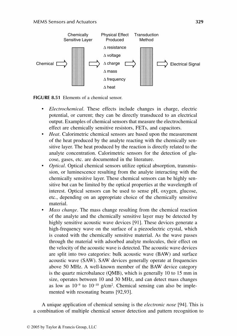
MEMS Sensors and Actuators 329
• Electrochemical. These effects include changes in charge, electricpotential, or current; they can be directly transduced to an electricaloutput. Examples of chemical sensors that measure the electrochemicaleffect are chemically sensitive resistors, FETs, and capacitors.
• Heat. Calorimetric chemical sensors are based upon the measurementof the heat produced by the analyte reacting with the chemically sen-sitive layer. The heat produced by the reaction is directly related to theanalyte concentration. Calorimetric sensors for the detection of glu-cose, gases, etc. are documented in the literature.
• Optical. Optical chemical sensors utilize optical absorption, transmis-sion, or luminescence resulting from the analyte interacting with thechemically sensitive layer. These chemical sensors can be highly sen-sitive but can be limited by the optical properties at the wavelength ofinterest. Optical sensors can be used to sense pH, oxygen, glucose,etc., depending on an appropriate choice of the chemically sensitivematerial.
• Mass change. The mass change resulting from the chemical reactionof the analyte and the chemically sensitive layer may be detected byhighly sensitive acoustic wave devices [91]. These devices generate ahigh-frequency wave on the surface of a piezoelectric crystal, whichis coated with the chemically sensitive material. As the wave passesthrough the material with adsorbed analyte molecules, their effect onthe velocity of the acoustic wave is detected. The acoustic wave devicesare split into two categories: bulk acoustic wave (BAW) and surfaceacoustic wave (SAW). SAW devices generally operate at frequenciesabove 50 MHz. A well-known member of the BAW device categoryis the quartz microbalance (QMB), which is generally 10 to 15 mm insize, operates between 10 and 30 MHz, and can detect mass changesas low as 10–9 to 10–10 g/cm2. Chemical sensing can also be imple-mented with resonating beams [92,93].
A unique application of chemical sensing is the electronic nose [94]. This isa combination of multiple chemical sensor detection and pattern recognition to
FIGURE 8.51 Elements of a chemical sensor.
Electrical SignalChemical
ChemicallySensitive Layer
TransductionMethod
∆ voltage
∆ resistance
∆ mass
∆ frequency
∆ heat
∆ charge
Physical Effect Produced
© 2005 by Taylor & Francis Group, LLC
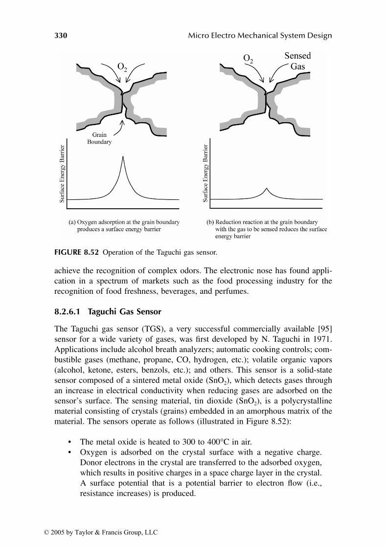
330 Micro Electro Mechanical System Design
achieve the recognition of complex odors. The electronic nose has found appli-cation in a spectrum of markets such as the food processing industry for therecognition of food freshness, beverages, and perfumes.
8.2.6.1 Taguchi Gas Sensor
The Taguchi gas sensor (TGS), a very successful commercially available [95]sensor for a wide variety of gases, was first developed by N. Taguchi in 1971.Applications include alcohol breath analyzers; automatic cooking controls; com-bustible gases (methane, propane, CO, hydrogen, etc.); volatile organic vapors(alcohol, ketone, esters, benzols, etc.); and others. This sensor is a solid-statesensor composed of a sintered metal oxide (SnO2), which detects gases throughan increase in electrical conductivity when reducing gases are adsorbed on thesensor’s surface. The sensing material, tin dioxide (SnO2), is a polycrystallinematerial consisting of crystals (grains) embedded in an amorphous matrix of thematerial. The sensors operate as follows (illustrated in Figure 8.52):
• The metal oxide is heated to 300 to 400°C in air.• Oxygen is adsorbed on the crystal surface with a negative charge.
Donor electrons in the crystal are transferred to the adsorbed oxygen,which results in positive charges in a space charge layer in the crystal.A surface potential that is a potential barrier to electron flow (i.e.,resistance increases) is produced.
FIGURE 8.52 Operation of the Taguchi gas sensor.
© 2005 by Taylor & Francis Group, LLC
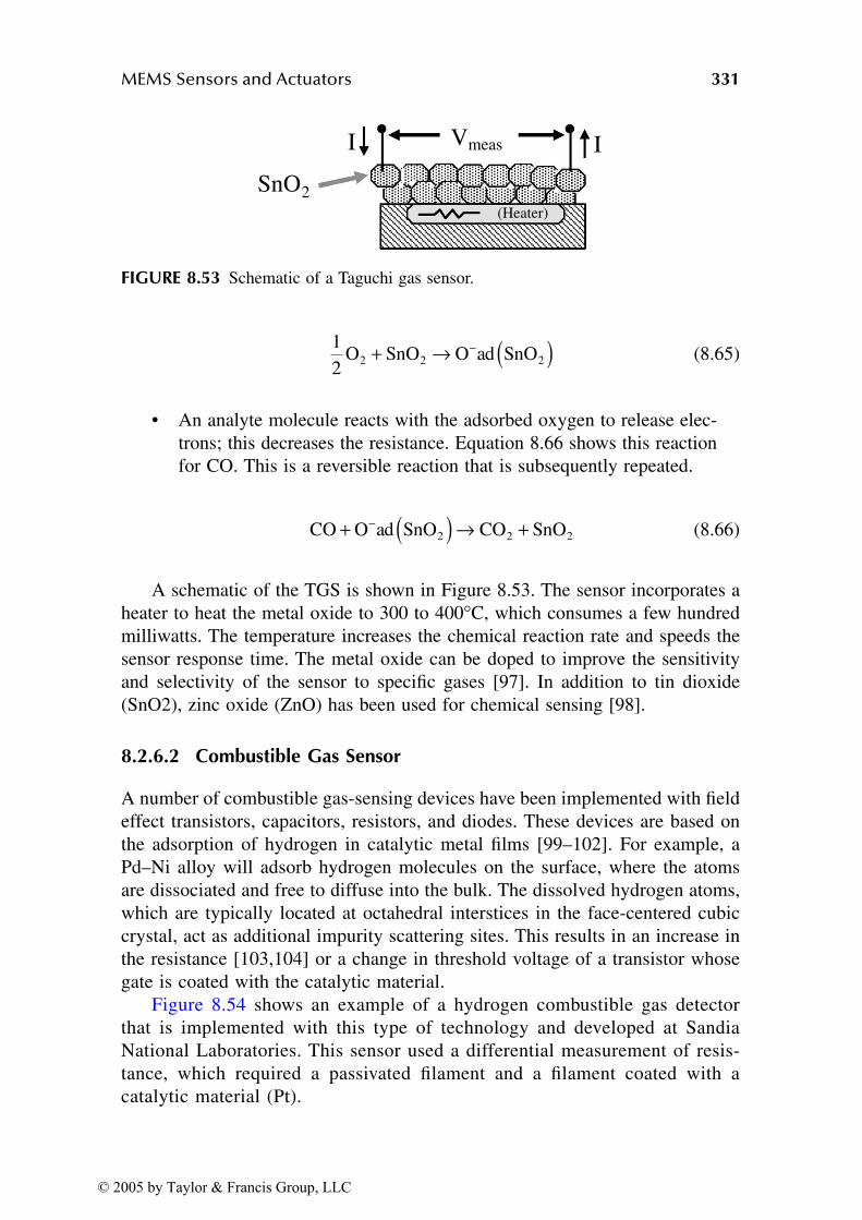
MEMS Sensors and Actuators 331
(8.65)
• An analyte molecule reacts with the adsorbed oxygen to release elec-trons; this decreases the resistance. Equation 8.66 shows this reactionfor CO. This is a reversible reaction that is subsequently repeated.
(8.66)
A schematic of the TGS is shown in Figure 8.53. The sensor incorporates aheater to heat the metal oxide to 300 to 400°C, which consumes a few hundredmilliwatts. The temperature increases the chemical reaction rate and speeds thesensor response time. The metal oxide can be doped to improve the sensitivityand selectivity of the sensor to specific gases [97]. In addition to tin dioxide(SnO2), zinc oxide (ZnO) has been used for chemical sensing [98].
8.2.6.2 Combustible Gas Sensor
A number of combustible gas-sensing devices have been implemented with fieldeffect transistors, capacitors, resistors, and diodes. These devices are based onthe adsorption of hydrogen in catalytic metal films [99–102]. For example, aPd–Ni alloy will adsorb hydrogen molecules on the surface, where the atomsare dissociated and free to diffuse into the bulk. The dissolved hydrogen atoms,which are typically located at octahedral interstices in the face-centered cubiccrystal, act as additional impurity scattering sites. This results in an increase inthe resistance [103,104] or a change in threshold voltage of a transistor whosegate is coated with the catalytic material.
Figure 8.54 shows an example of a hydrogen combustible gas detectorthat is implemented with this type of technology and developed at SandiaNational Laboratories. This sensor used a differential measurement of resis-tance, which required a passivated filament and a filament coated with acatalytic material (Pt).
FIGURE 8.53 Schematic of a Taguchi gas sensor.
SnO2(Heater)
VmeasI I
12 2 2 2O SnO O ad SnO+ → ( )−
CO O ad SnO CO SnO+ ( ) → +−2 2 2
© 2005 by Taylor & Francis Group, LLC
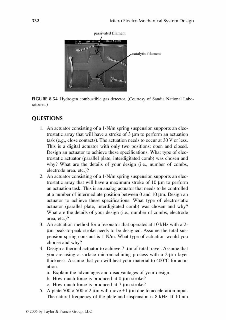
332 Micro Electro Mechanical System Design
QUESTIONS
1. An actuator consisting of a 1-N/m spring suspension supports an elec-trostatic array that will have a stroke of 3 µm to perform an actuationtask (e.g., close contacts). The actuation needs to occur at 30 V or less.This is a digital actuator with only two positions: open and closed.Design an actuator to achieve these specifications. What type of elec-trostatic actuator (parallel plate, interdigitated comb) was chosen andwhy? What are the details of your design (i.e., number of combs,electrode area. etc.)?
2. An actuator consisting of a 1-N/m spring suspension supports an elec-trostatic array that will have a maximum stroke of 10 µm to performan actuation task. This is an analog actuator that needs to be controlledat a number of intermediate position between 0 and 10 µm. Design anactuator to achieve these specifications. What type of electrostaticactuator (parallel plate, interdigitated comb) was chosen and why?What are the details of your design (i.e., number of combs, electrodearea, etc.)?
3. An actuation method for a resonator that operates at 10 kHz with a 2-µm peak-to-peak stroke needs to be designed. Assume the total sus-pension spring constant is 1 N/m. What type of actuation would youchoose and why?
4. Design a thermal actuator to achieve 7 µm of total travel. Assume thatyou are using a surface micromachining process with a 2-µm layerthickness. Assume that you will heat your material to 400°C for actu-ation.a. Explain the advantages and disadvantages of your design.b. How much force is produced at 0-µm stroke?c. How much force is produced at 7-µm stroke?
5. A plate 500 × 500 × 2 µm will move ±1 µm due to acceleration input.The natural frequency of the plate and suspension is 8 kHz. If 10 nm
FIGURE 8.54 Hydrogen combustible gas detector. (Courtesy of Sandia National Labo-ratories.)
passivated filament
catalytic filament
© 2005 by Taylor & Francis Group, LLC
MEMS Sensors and Actuators 333
of plate motion can be sensed, what is the corresponding accelerationinput? What is the nominal capacitance of the suspended plate? Whatis the change in capacitance corresponding to 10-nm motion? Choosea capacitance sense amplifier configuration and explain your reasons.
6. How many piezoresistive coefficients describe a piezoresistor in single-crystal silicon? How many piezoresistive coefficients describe apiezoresistor in polycrystalline silicon? If the number of coefficientsdiffers, explain.
REFERENCES
1. W.C. Tang, Electrostatic comb drive for resonant sensor and actuator applications,Ph.D. dissertation, University of California, Berkeley, November 1990.
2. W.C. Tang, M.G. Lim, R.T. Howe, Electrostatic comb drive levitation and controlmethod, JMEMS, 1(4), 170–178, December 1992.
3. J.J. Sniegowski, J.H. Smith, An application of mechanical leverage to microactu-ation, Int. Conf. Solid-State Sensors Actuators, TRANSDUCERS’95, 2, 364–367,1995.
4. S. Kota, J. Hetrick, L. Zhe, S. Rodgers, T. Krybowski, Synthesizing high-perfor-mance compliant stroke amplification systems for MEMS, IEEE Int. Conf. Micro
Electro Mechanical Syst., MEMS 2000, 164–169, January 2000, Miyazaki, Japan.5. L.L. Howell, Compliant Mechanisms, John Wiley & Sons, New York, 2001.6. N. Tas, I. Wissink, I. Sander, T. Larnmerink, M. Elwenspoek, Modeling, design
and testing of the electrostatic shuffle motor, Sensors Actuators, 70, 171, 1998.7. T. Akiyama, K. Shono, Controlled stepwise motion in polysilicon microstructures,
JMEMS, 2(3), 106–110, 1993.8. J.I. Seeger, S.B. Crary, Stabilization of electrostatically actuated mechanical
devices, Transducers ’97, 1133–1136, 1997.9. E.K. Chan, R.W. Dutton, Electrostatic micromechanical actuator with extended
range of travel, JMEMS, 9(3), 321–328, September 2000.10. J.M. Kyynarainen, A.S. Oja, H. Seppa, Increasing the dynamic range of a micro-
mechanical moving-plate capacitor, Analog IC Signal Proc., 29, 61–70, 2001.11. J.I. Seeger, B.E. Boser, Dynamics and control of parallel-plate actuators beyond
the electrostatic instability, Transducers ’99, 474–477, 1999.12. E.S. Hung, S.D. Senturia, Extending the travel range of analog-tuned electrostatic
actuators, JMEMS, Vol. 8, No. 4, 497–505, December 199913. G. Greitmann, R. A. Buser, Tactile Microgripper for Automated Handling of
Microparts, Sensors and Actuators A, 53, 410–415, 1996.14. J. Buhler, J. Funk, O. Paul, F.P. Steiner, H. Baltes, Thermally actuated CMOS
micromirrors, Sensors Actuators A, 46–47, 572–575, 1995.15. H.P. Trah, H. Baumann, C. Doring, H. Goebel, T. Grauer, M. Mettner, Microma-
chined valve with hydraulically actuated membrane subsequent to a thermoelec-trically controlled bimorph cantilever, Sensors Actuators A, 39, 169–176, 1993.
16. J.H. Comtois, V.M. Bright, Applications for surface-micromachined polysiliconthermal actuators, Sensors Actuators A, 58, 19–25, 1997.
17. L. Que, J. Park, Y. Gianchandani, Bent-beam electro-thermal actuators for highforce applications, Proc. IEEE MEMS ’99, 31–36, 1999.
© 2005 by Taylor & Francis Group, LLC
334 Micro Electro Mechanical System Design
18. Y.G. Gianchandani, K. Najafi, Bent-beam strain sensors, JMEMS, 5(1), 52–58,March 1996.
19. P.M. Zavracky, G.G. Adams, P.D. Aquilino, Strain analysis of silicon-on-insulatorfilms produced by zone melting recrystallization, JMEMS, 4(1), 42–48, March1995.
20. J.T. Butler, V.M. Bright, W.D. Cowan, Average power control and positioning ofpolysilicon thermal actuators, Sensor Actuators, 72, 88–97, 1999.
21. C.D. Lott, T.W. McLain, J.N. Harb, L.L. Howell, Modeling the thermal behaviorof a surface-micromachned linear-displacement thermomechanical microactuator,Sensor Actuators, 101, 239–250, 2002.
22. D. Bosch, B. Heimhofer, F. Muck, H. Seidel, U. Thumser, W. Welser, A siliconmicrovalve with combined electromagnetic/electrostatic actuation, Sensors Actu-
ators A, 37–38, 684–692, 1993.23. D.K. Wickenden, R.B. Givens, R. Osiander, J.L. Champion, D.A. Oursler, T.J.
Kistenmacher, MEMS-based resonating xylophone bar magnetometers, Proc.
SPIE, 3514, 350–358, 1998.24. M.A. Butler, S.J. Martin, J.J. Spates, and M.A. Mitchell, Magnetically excited
flexural plate wave devices, Transducers ’97, 1031–1034, 1997.25. J.T. Kung, H-S Lee, R.T. Howe, A digital readout technique for capacitive sensor
applications, IEEE J. Solid-State Circuits, 23(4), 972–977, August 1988.26. M.A. Lemkin, Micro accelerometer design with digital feedback control, disser-
tation, University of California, Berkeley, 1997.27. W. Thomson (Lord Kelvin), The electro-dynamic qualities of metals, Phil. Trans.
Royal Soc., 146, 733, London, 1856.28. C.S. Smith, Piezoresistive effect in germanium and silicon, Phys. Rev., 94, 42–49,
April, 1954.29. B. Kloeck, N.F. De Rooij, Mechanical sensors, in Semiconductor Sensors, S.M.
Sze, Ed., chapter 4, John Wiley & Sons, New York, 1994.30. S. Middelhoek, S.A. Audet, Silicon Sensors, Academic Press, New York, 1989.31. Y. Kanda, A graphical representation of the piezoresistance coefficients in silicon,
IEEE Trans. Electron Device, ED-29, 64–70, 1982.32. P.J. French, A.G.R. Evans, Polycrystalline silicon strain sensors, Sensors Actuator,
8, 219–225, 1985.33. P.J. French, A.G.R. Evans, Piezoresistance in polysilicon and its applications to
strain gauges, Solid-State Electron., 32(1), 1–10, 1989.34. V.A. Gridchin, V.M. Lubimsky, M.P. Sarina, Piezoresistive properties of polysil-
icon films, Sensors Actuators A, 49, 67–72, 1995.35. W.P. Eaton, Surface micromachined pressure sensors, Ph.D. dissertation, Univer-
sity of New Mexico, May, 1997.36. W.P. Eaton, J.H. Smith, Planar surface-micromachined pressure sensor with a
subsurface, embedded reference pressure cavity, Proc. SPIE, 2882, 259–265, 1996.37. H.L. Stalford, C. Apblett, S.S. Mani, W.K. Schubert, M. Jenkins, Sensitivity of
piezoresistive readout device for microfabricated acoustic spectrum analyzer,Proc. SPIE, 5344, 36–43, 2004.
38. G. Binnig, H. Rohrer, Scanning tunneling microscopy, IBM J. Res. Develop., 30,355, 1986
39. T.W. Kenny, W.J. Kaiser, J.K. Reynolds, J.A. Podosek, H.K. Rockstand, E.C. Vote,S.B. Waltman. Electron tunnel sensors, J. Vac. Sci. Technol. A 10(4), Jul/Aug,1992.
© 2005 by Taylor & Francis Group, LLC
MEMS Sensors and Actuators 335
40. T.W. Kenny, W.J. Kaiser, J.A. Podosek, H.K. Rockstand, J.K. Reynolds, E.C. Vote,Micromachined tunneling displacement transducers for physical sensors, J. Vac.
Sci. Technol. A, 11(4), July/August, 1993.41. T.W. Kenny, W.J. Kaiser, S.B. Waltman, J.K. Reynolds, Novel infrared detector
based on a tunneling displacement transducer, Appl. Phys. Lett. 59(15), 7 October1991.
42. D. DiLella, L.J. Whitman, J.J. Colton, T.W. Kenny, W.J. Kaiser, E.C. Vote, J.A.Podosek, L.M. Miller, A micromachined magnetic-field sensor based on an elec-tron tunneling displacement transducer, Sensors Actuators 86, 8–20, 2000.
43. P.M. Zavracky, B. McClelland, K. Warner, J. Wang, F. Harley, B. Dolgin, Designand process considerations for a tunneling tip accelerometer, J. Micromech.
Microengineering, 6(3), 352–358, September 1996.44. J.S. Bendat, Principles and Applications of Random Noise Theory, Krieger Pub-
lishing Company, Malabar, FL, 1977.45. A. van der Ziel, Noise: Sources, Characterization, Measurement, Prentice Hall,
Englewood Cliffs, NJ, 1970.46. P.R. Gray, R.G. Meyer, Analysis and Design of Analog Integrated Circuits, 3rd
ed., New York, Wiley, 1984.47. T.B. Gabrielson, Fundamental noise limits in miniature acoustic and vibration
sensors, NASC-91113–50, 31 December 1991. 48. T.B. Gabrielson, Mechanical-thermal noise in micromachined acoustic and vibra-
tion sensors, IEEE Trans. Elec. Dev., 40(5), 903–909, May 1993.49. H.B. Callen, T.A. Walton, Irreversibility and generalized noise, Phys. Rev. 83(1),
34–40, 1951.50. M.R. Daily, MEMS manufacturing challenges for inertial measurement unit appli-
cations, Defense Manufacturing Conference, DMC ’99, Miami, FL, November1999.
51. N. Yazdi, F. Ayazi, K. Najafi, Micromachined inertial sensors, Proc. IEEE, 86(8),1640–1659, August 1998.
52. Analog Devices Inc., http://www.analog.com/.53. D.T. Greenwood, Principles of Dynamics, Prentice Hall, Englewood Cliffs, NJ,
1965.54. W.T. Thomson, Theory of Vibration with Applications, Prentice Hall, Inc., Engle-
wood Cliffs, NJ, 1981. 55. R. van de Plassche, Integrated Analog to Digital and Digital to Analog Converters,
Kluwer Academic Publishers, Dordrecht, 1994.56. C. Lu, M. Lemkin, B.E. Boser, A monolithic surface micromachined accelerom-
eter with digital output, IEEE J. Solid State Circuits, 30(12), Dec. 1995.57. M. Lemkin, B.E. Boser, A micromachined fully differential lateral accelerometer,
IEEE Custom I.C. Conf., 315–318, 1996.58. C. Shearwood, C.B. Williams, P.H. Mellor, R.B. Yates, M.R.J. Gibbs, A.D. Mat-
tingley, Levitation of a micromachined rotor for application in a rotating gyro-scope, Electron. Lett., 31(21), 1845–1846, 1995.
59. C. Shearwood, K.Y. Ho, C.B. Williams, H. Gong, Development of a levitatedmicromotor for application as a gyroscope, Sensors Actuators, 83, 85–92, 2000.
60. A. Lawrence, Modern Inertial Technology, Springer-Verlag, Heidelberg, 1998.61. G. Sagnac, Sur la preuve de la réalité de l’éther lumineux par l’expérience de
l’interférographe tournant, C.R. Acad. Sci., 95, 1410–1413, 1913.62. A.W. Lawrence, Thin film laser gyro, U.S. Patent 4,326,803, issued 27 April 1982.
© 2005 by Taylor & Francis Group, LLC
336 Micro Electro Mechanical System Design
63. C. Monovoukas, A.K. Swiecki, F. Maseeh, Integrated optical gyroscopes offeringlow cost, small size and vibration immunity, Proc. SPIE, 3936, 293–300, 2000.
64. J. Lyman, E. Norden, Rate and attitude indicating instrument, U.S. Patent2,309,853, issued April 10, 1941.
65. J. Lyman, Angular velocity responsive apparatus, U.S. Patent, 2,513, 340, issuedOctober 17, 1945.
66. W.H. Quick, Theory of the vibrating string as an angular motion sensor, Trans.
ASME, J. Appl. Mech., 31, 523–534, September 1964. 67. D. Boocock, L. Maunder, Vibration of a symmetric tuning fork, J. Mech. Eng.
Sci., 11(4), 1969.68. G.W. Hunt, A.E.W. Hobbs, Development of an accurate tuning-fork gyroscope,
symposium on Gryos, Proc. Inst. Mech. Eng., 179(3E), 1964–1965. 69. W.P. Chan, F. Prete, M.H. Dickinson, Visual input to the efferent control of a fly’s
gyroscope, Science, Vol. 280, No. 5361, 289–292, April 10, 1998.70. W.A. Clark, Micromachined vibratory rate gyroscopes, Ph.D. dissertation, Uni-
versity of California, Berkeley, Fall 1997.71. W.A. Clark, R.T. Howe, R. Horowitz, Surface micromachined Z-axis vibratory
rate gyroscope, Tech. Dig. Solid-State Sensor Actuator Workshop, 83–287, June1996.
72. J.M. O’Connor, D.M. Shupe, Vibrating beam rotation sensor, U.S. Patent4,381,672, issued May 3, 1983.
73. B. Greiff, T. Boxenhorn, T. King, L. Niles, Silicon monolithic gyroscope, Trans-
ducers ’91, Dig. Tech. Papers, 966–969, 1991.74. A. Kourepenis, J. Borenstein, J. Connelly, R. Elliott, P. Ward, M. Weinberg, IEEE
1998 Position Location and Navigation Symposium, PLANS 98, 1–8, 1998.75. J.A. Green, S.J. Silverman, J.F. Chang, S.R. Lewis, Single-chip surface microma-
chined integrated gyroscope with 50°/h Allan deviation, IEEE J. Solid-State Cir-
cuits, 37(12), December 2002.76. T. Juneau, A.P. Pisano, Micromachined dual input axis angular rate sensor, Tech.
Dig. Solid-State Sensor Actuator Workshop, 299–302, June, 1996.77. J.H. Leck, Pressure Measurement in Vacuum Systems, Chapman & Hall, London,
1964.78. H.V. Ubisch, On the conduction of heat in rarefied gases and its manometric
application, Appl. Sci. Res., A2, 364–430, 1948,79. C.H. Mastrangelo, R.S. Muller, Microfabricated thermal absolute-pressure sensor
with on-chip digital front-end processor, IEEE J. Solid State Circuits, 26(12),1998–2007, December 1991.
80. W.P. Eaton, J.H. Smith, D.J. Monk, G. O’Brian, T.F. Miller, Comparison of bulkand surface micromachined pressure sensors, Proc. SPIE, 3514, 431–438, Sep-tember 1998.
81. Motorola, Inc., Motorola Pressure Sensors, Sensor Device Data/Handbook, 4.5,1997.
82. J. Bergqvist, F. Rudolf, J. Maisano, F. Parodi, M. Rossi, A silicon condensermicrophone with a highly perforated backplate, Transducers ’91, 266–269, 1991.
83. W.P. Eaton, J.H. Smith, Micromachined pressure sensors: review and recent devel-opments, Smart Mater. Struct., 6, 530–539, 1997.
84. R. Schellin, M. Strecker, U. Nothelfer, G. Schuster, Low pressure acoustic sensorsfor airborne sound with piezoresistive monocrystalline silicon and electrochemi-cally etched diaphragms, Sensors Actuators A, 46–47, 156–160, 1995.
© 2005 by Taylor & Francis Group, LLC
MEMS Sensors and Actuators 337
85. R.P. Pied, E.S. Kim, D.H. Hong, R.S. Muller, Piezoelectric microphone with on-chip CMOS circuits, JMEMS, 2(3), 111–120, September 1993.
86. J. Bernstein, A micromachined condenser hydrophone, IEEE Solid State Sensor
Actuator Workshop, Hilton Head ’92, 161–165, 1992.87. J. Bernstein, M. Weinberg, E. McLaughlin, J. Powers, F. Tito, Advanced micro-
machined condenser hydrophone, IEEE Solid State Sensor Actuator Workshop,Hilton Head ’94, 73–77, 1994.
88. R. Taylor, A.D. Little, J.S. Schultz, Handbook of Chemical and Biological Sensors,IOP Publishing, Bristol, 1996.
89. A.E.G. Cass, Biosensors: A Practical Approach, Oxford University Press, Oxford,1990.
90. W.H. Ko, Frontiers in solid state biomedical transducers, Proc. IEEE Int. Electron
Devices Meeting, 112–115, 1985. 91. D.S. Ballantine, R.M. White, S.J. Martin, Acoustic Wave Sensors, Academic Press,
New York, 1997.92. T. Ono, X. Li, H. Miyashita, M. Esashi, Mass sensing of adsorbed molecules in
sub-picogram sample with ultrathin silicon resonator, Rev. Sci. Instrum., 74(3),1240–1243, March 2003.
93. D. Lange, A. Koll, O. Brand, H. Baltes, CMOS chemical microsensors based onresonant cantilever beams, Proc. SPIE, 3328, 233–243, March 1998.
94. J.W. Garder, P.N. Barlett, Electronic Noses: Principles and Applications, OxfordUniversity Press, Oxford, 1999.
95. Figaro Engineering Inc.: http://www.figarosensor.com/.96. K.D. Schierbaum, U. Weimar, W. Gopel, U. Komalowski, Conductance, work
function and catalytic activity of SnO2 based gas sensors, Sensor Actuators, 3,205–214, 1991.
97. N. Yamazoe, Y. Kurokawa, T. Seiyama, Effects of additives on semiconductor gassensors, Sensors Actuators, 4, 283–289, 1983.
98. H. Nanto, T. Kobayaski, N. Dougami, M. Habara, H. Yamamoto, E. Kusano, A.Kinbara, Y. Douguchi, Smart chemical sensors using ZnO semiconducting thinfilms for freshness detection of foods and beverages, Proc. SPIE, 3328, 418–427,March 1998.
99. I. Lundstrom, S. Shivaraman, C. S. Svensson, L. Lundkvist, A hydrogen-sensitiveMOS field effect transistor, Appl. Phys. Lett., 26, 55, 1975.
100. M. Armgarth, C. Nylander, A stable hydrogen sensitive Pd gate metal oxidesemiconductor capacitor, Appl. Phys. Lett., 39, 91, 1981.
101. R.C. Hughes, W.K. Schubert, Thin films of Pd/Ni alloys for detection of highhycrogen concentrations, J. Appl. Phys., 71, 542, 1992.
102. P.F. Ruths, S. Askok, S.J. Fonash, J.M. Ruths, A study of Pd/Si MIS Schottkybarrier diode hydrogen detector, IEEE Trans. Electron Devices, ED-28, 1003,1981.
103. H. Conrad, G. Ertl, E. E. Latta, Adsorption of hydrogen on palladium single crystalsurfaces, Surface Sci., 41, 435, 1974.
104. P. Wright, The effect of occluded hydrogen on the electrical resistance of palla-dium, Proc. Phys. Soc., 63A, 727, 1950.
© 2005 by Taylor & Francis Group, LLC
339
9 Packaging
Once the fabrication of the MEMS device has been completed, parts are obtained
and assembled, protected, and tested. These parts can consist of one or more die
resulting from a surface micromachined or bulk micromachined process or, alter-
natively, an object such as a gear, rotor, or seismic mass resulting from a bulk
micromachined or LIGA process. The parts obtained from a MEMS fabrication
process are rarely the end product. A number of steps need to be accomplished
once the MEMS fabrication is done in order to produce a MEMS product such
as a sensing device (e.g., accelerometer, pressure sensor); an optical device (e.g.,
the TI DLP); or a switch. The major issues for packaging of MEMS devices
include handling, thermal budget, mechanical stress, encapsulation, and device
motion requirements.
9.1 PACKAGING PROCESS STEPS
The objective of packaging is multifaceted. Packaging operations may consist of
some postfabrication processes required for a device to function properly as well
as assembly of the MEMS device into a next level assembly or final product that
provides a function for the end user. The package containing the MEMS device
needs to provide the following functions:
• Mechanical support. The package must mechanically support or con-
tain the MEMS device so that it can function alone or within another
system. The package will physically protect the MEMS device.
• Interconnection. The package must provide for communication
between the microscale connection of a MEMS device and the mac-
roscale connection that will be used to function or interface with the
device. The connections may encompass a variety of physical phenom-
ena such as electrical, optical, fluidic, biologic, etc.
• Environment control. The package must control the environment nec-
essary for the MEMS device to function properly throughout its life-
time. The necessary environmental controls may include thermal
management, particulate contamination, or ambient atmosphere control
(i.e., humidity, atmosphere, and atmospheric pressure).
Similar to MEMS fabrication processing, packaging has its roots in and
leverages the microelectronics infrastructure; however, MEMS packaging fre-
© 2005 by Taylor & Francis Group, LLC
340 Micro Electro Mechanical System Design
quently has different requirements from those of microelectronics. The packaging
processing sequence will be broken down into the following steps, which will be
discussed in detail in this section:
• Postfabrication processing. Additional processing must occur to enable
the functionality of the basic MEMS device or part. These processes
may include dicing, releasing, and coating the device. Exactly which
of these postfabrication processes is performed and its sequence is very
application specific. This process sequence is frequently called the back
end of the line (BEOL).
• Package selection and design. The package provides the functions of
mechanical support, interconnection, and environmental control for the
MEMS device that it contains. Depending upon the application or the
point in the MEMS device development cycle (i.e., prototype, product
development, or product), the package that may be utilized could be a
simple IC package or a specifically designed package for the intended
product. Basic options and considerations will be discussed.
• Die attach. The MEMS die is fixed in the package to provide support
and interconnection.
• Wire bond and sealing. This section will discuss the connection from
the MEMS die to the package to provide interconnect between the
micro- and macrosize regimes. The package will be sealed to protect
the MEMS die from handling or contamination. The sealed package
can provide an inert environment for the MEMS die to prevent corro-
sion or humidity, which can affect device performance. Alternatively,
the package may also provide a vacuum that may be required for some
MEMS devices.
9.1.1 POSTFABRICATION PROCESSING
Postfabrication or back end of the line (BEOL) processing consists of a variety
of processes required to enable the MEMS device to be fully useful. The selection
of the processes to be used is very application specific and influenced by the
fabrication technology utilized (surface micromachining, bulk micromachining,
LIGA). The following processes will be discussed in this section:
• Release: the removal of the sacrificial layers at the end of fabrication
of a surface micromachined device.
• Drying: the removal of the etchant and rinsing solutions utilized in the
release process to yield a dry MEMS device.
• Coating: a coating applied to the MEMS device to further enable or
enhance its functionality — for example, a thin coating applied to
lubricate or reduce friction in the MEMS device. Alternatively, a bio-
logical coating could be applied to enable a biological sensor, or a
coating could be applied to enhance reflectivity of an optical device.
© 2005 by Taylor & Francis Group, LLC
Packaging 341
• Assembly: assembly of MEMS die or parts to form the next level of
assembly.
• Encapsulation: a MEMS die may be encapsulated to enhance its
protection.
9.1.1.1 Release Process
The release process of surface micromachining is discussed in Chapter 3. The
exact nature of the release process will depend upon the material system used in
the surface micromachine process. It is generally desired to have a release process
that will remove the sacrificial layer as quickly as possible with minimal impact
on the structural layer material that remains. For example, the SUMMiT process
utilizes polysilicon as the structural material and silicon dioxide as the sacrificial
material with hydrofluoric acid release chemistry. Alternatively, the Texas Instru-
ments DMD device utilizes aluminum as the structural material and photoresist
as the sacrificial material released with oxygen plasma etch. The release etch
would ideally produce no particles that would inhibit the MEMS device function
and produce a free-standing structure.
9.1.1.2 Drying Process
For release processes that involve liquid etchants, drying is a critical process in
the BEOL sequence. The drying of a MEMS device is crucial because the
fabrication processes typically involve thin layers (e.g., ~2 to 4 µm) and small
gaps, which give rise to a stiction phenomenon in which the layers can be adhered
to each other or to the substrate. Dyck et al. [1] provide a review and discussion
of the stiction literature. Stiction is chiefly due to the surface–volume ratio scaling
of MEMS devices (Chapter 4), which magnify the effects of surface forces [2,3]
such as surface tension in liquid–vapor interfaces. In the ordinary drying process
after the release etch, liquid evaporates and capillary forces due to surface tension
arise as a result of the liquid–vapor interface. The surface forces at this interface
can be avoided by using processes that avoid the liquid–vapor transition, such as
supercritical drying or freeze drying.
The supercritical drying process proposed by Mulhern [4] avoids the liq-
uid–vapor interface by transferring the liquid via the supercritical phase. Carbon
dioxide is used because of its low critical temperature and pressure (i.e., Tc =
31.1°C, pc = 72.8 atm). During the drying process, no liquid–vapor interface
exists, thus, no capillary forces are present.
Freeze drying removes the liquid by freezing it using evaporation cooling in
a vacuum chamber. The solid (frozen) material is then removed by sublimation.
Freeze drying was first applied by Guckel [5,6] in a surface micromachined device
released with a hydrofluoric (HF) acid etch. The wafer is immersed in a
water–methanol mixture after the liquid release etch. The liquid is then frozen
by evaporative cooling in a vacuum chamber. The methanol is added to avoid
supercooling the water and thus causing it to freeze too rapidly. Then the solid
water–methanol is removed by sublimation at 0.15 mbar.
© 2005 by Taylor & Francis Group, LLC
342 Micro Electro Mechanical System Design
9.1.1.3 Coating Processes
Coating a MEMS device may be required to enable its functionality for a partic-
ular application or to enhance the yield of the device. The types of coatings that
may be used are as wide ranging as applications for MEMS are. Examples of
coatings include surface passivation; antistiction coatings [7,8]; optical coatings
[9–12]; biocompatibility [13]; and biologically sensitive [14] or chemically sen-
sitive [15–17] coatings. Selected examples are discussed next.
• Antifriction/antistiction coatings. Self assembled monolayer (SAM)
coatings have been developed to aid in the reduction of stiction and
friction in MEMS devices. Stiction is the adhesion of compliant MEMS
surfaces when the restoring forces are unable to overcome the interface
forces (e.g., van der Waals, capillary forces, electrostatic forces). The
SAM coatings frequently consist of long chain molecules of various
chemistries that can produce oriented hydrophobic monolayers on a
MEMS surface; this aids stiction reduction.
• Optical coatings. MEMS optical devices frequently require a highly
reflective surface for the optical wavelength of interest. Gold (Au) is
a useful optical reflective coating in the infrared and visible spec-
trums. Depending upon the surface to be coated, an adhesion layer
may be required to ensure good adherence to the surface. For example,
Picard et al. [9] investigated the use of chromium (Cr) and titanium
(Ti) as an adhesion layer for gold deposition. However, for other
wavelengths, alternative coatings may be necessary. For example, a
molybdenum–polysilicon (Mo/Si) multilayer coating [10–12] is nec-
essary in the extreme ultraviolet (EUV) spectrum (λ = 13.4 nm). The
Au/Ti, Au/Cr, and Mo/Si coatings are generally deposited by evapo-
ration or sputtering.
• Biologically and chemically compatible coatings. MEMS-based fluid
systems may handle biological and chemical materials. For the MEMS
system to function properly, the surfaces of the MEMS devices must
not chemically or biologically react with the sample materials because
that would produce materials that may foul the system [13] with reacted
chemicals or biological elements.
• Biologically or chemically sensitive coatings. Biological and chemi-
cal sensors require portions of the MEMS device to be coated with
sensitive materials that are used to produce an effect that can be
measured. For example, the effect to be measured may be a mass
change on the treated portion of a vibrating beam. The biologically
sensitive coating may be an antigen applied to a vibrating sensor [14].
A chemically sensitive coating [15–17] may be applied to a structure,
which will adsorb a particular chemical that will change the resistance
of the material.
© 2005 by Taylor & Francis Group, LLC
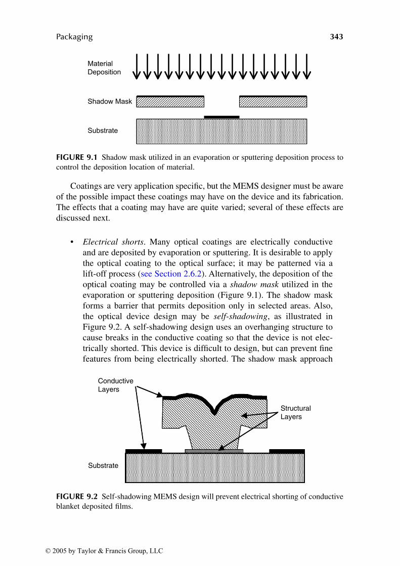
Packaging 343
Coatings are very application specific, but the MEMS designer must be aware
of the possible impact these coatings may have on the device and its fabrication.
The effects that a coating may have are quite varied; several of these effects are
discussed next.
• Electrical shorts. Many optical coatings are electrically conductive
and are deposited by evaporation or sputtering. It is desirable to apply
the optical coating to the optical surface; it may be patterned via a
lift-off process (see Section 2.6.2). Alternatively, the deposition of the
optical coating may be controlled via a shadow mask utilized in the
evaporation or sputtering deposition (Figure 9.1). The shadow mask
forms a barrier that permits deposition only in selected areas. Also,
the optical device design may be self-shadowing, as illustrated in
Figure 9.2. A self-shadowing design uses an overhanging structure to
cause breaks in the conductive coating so that the device is not elec-
trically shorted. This device is difficult to design, but can prevent fine
features from being electrically shorted. The shadow mask approach
FIGURE 9.1 Shadow mask utilized in an evaporation or sputtering deposition process to
control the deposition location of material.
FIGURE 9.2 Self-shadowing MEMS design will prevent electrical shorting of conductive
blanket deposited films.
Substrate
Shadow Mask
Material
Deposition
Substrate
ConductiveLayers
StructuralLayers
© 2005 by Taylor & Francis Group, LLC

344 Micro Electro Mechanical System Design
is limited by the precision with which the mask can be aligned, whereas
the self-shadowing approach is only limited by the precision of the
lithography process utilized and the amount of underspray in the
deposition process.
• Residual stress. The coating residual stress is a very important concern
especially for optical coatings. Significant engineering effort is involved
in the process development of a low-stress coating process [9]. A metric
for the performance of optical devices is flatness of the coated optical
surface. The process parameters of deposition rates and material alloys
are significant in engineering the coating processes. The MEMS optical
design and fabrication process is frequently influenced by the necessity
to produce mirror surfaces that can withstand the residual stresses
inherent in the MEMS fabrication process and the applied coatings.
Frequently, this pushes the MEMS design to have thicker, reinforced,
or smaller mirror surfaces to accommodate the residual stress effects.
• Particulate. Particles may be generated by a coating that may interfere
with the device operation by shorting or jamming. If this is a possibility,
the MEMS designer may be able to shield the critical portions of the
design from these effects.
• Coating out-gassing. Coatings may produce gases when exposed to an
elevated temperature. These gases may impede device operation by
adverse chemical reactions or changing the pressure or vacuum in the
package. These problems may be circumvented by a change of coating
material or use of chemical getters [18] to remove the offending gases.
The use of a chemical getter may be needed due to outgasing of the
applied coatings; also, package leakage and outgasing of the die attach
material may also be a significant source of undesirable internal pack-
age gases. Getters are selective chemical scavengers designed to cap-
ture undesirable substances. They are available for hydrogen, oxygen,
moisture, and particulate materials [19]. An early use of chemical
getters was the removal of oxygen from triode vacuum tubes, which
caused the filaments to oxidize and fail. A solution to this problem was
the use of active metals that reacted more quickly with the oxygen than
the tungsten filament of the triode.
• Coating thermal environment. The thermal environment involved in
the deposition of the coating may have an impact on the MEMS
material properties used if the temperature is sufficiently high. If the
coating is applied to a MEMS device that contains microelectronic
properties, the thermal environment may affect the electronic properties
or melt the interconnect layers.
• Coating stability. Some coatings may degrade at elevated temperature.
This could be the chemistry of the coating changes that makes a SAMS
coating for stiction ineffective or the corrosion of a mirror coating.
Many times these effects will impose a limit on subsequent temperature
processing that the MEMS device can withstand.
© 2005 by Taylor & Francis Group, LLC

Packaging 345
9.1.1.4 Assembly
A number of items fall under the umbrella of assembly. Assembly can include
assembly of MEMS or microelectronic die for a next level of assembly; assembly
of MEMS parts; or erection of MEMS structures. As with most things in the area
of MEMS, the technologies that will be discussed under this topic are in various
stages of development and maturity.
• Assembly of die. MEMS or microelectronic die can be assembled
together to form a greater assembly [20]. Interconnection between die
can be made via a number of methods, such as wire bonding between
die mounted on a common substrate; however, flip-chip bonding has
significant advantages (Figure 9.3). In flip-chip bonding, the die are
bonded together via small solder balls (<200 µm) without the use of
bond wires. This approach enables a small package with intimate
electrical contact, which mitigates the electrical parasitic of bond wire
resistance and capacitance. This method enables a multichip module
(MCM) in which multiple chips are stacked using flip-chip bonding
and connections through the wafer to enable the vertical connections
[21]. This approach allows improved system performance and small
geometric form factor.
The range of capabilities enabled by MEMS devices has prompted
research in techniques in which MEMS components fabricated in dif-
ferent technologies can be combined via a packaging method such as
flip-chip bonding to enable a viable solution or higher performance.
For example, Michalicek et. al. [22] demonstrated the transfer of a
surface micromachined device assembly to another substrate (Figure
9.4) to increase functionality; this allowed electronic control of the
MEMS devices. This approach could also be utilized to create RF
devices (e.g., switches, filters, variable capacitors) utilizing silicon
surface micromachined devices removed from the host silicon wafer;
that is not suited to RF applications to a better suited substrate.
FIGURE 9.3 Illustration of direct wire bonding of die and flip-chip bonding to form a
multichip module.
substrate
die
wire
bond
bond
pads
(a) wire bond connection of die
die
die
solder ball
(b) flip chip
© 2005 by Taylor & Francis Group, LLC
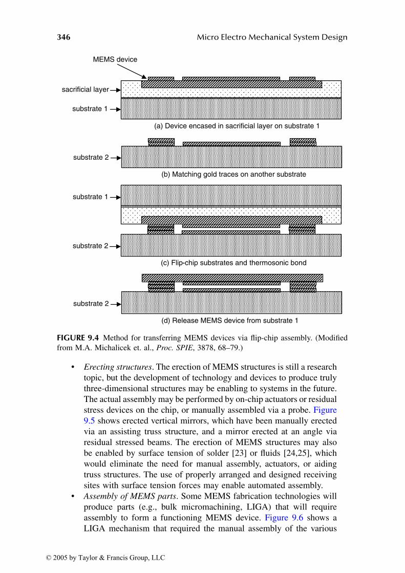
346 Micro Electro Mechanical System Design
• Erecting structures. The erection of MEMS structures is still a research
topic, but the development of technology and devices to produce truly
three-dimensional structures may be enabling to systems in the future.
The actual assembly may be performed by on-chip actuators or residual
stress devices on the chip, or manually assembled via a probe. Figure
9.5 shows erected vertical mirrors, which have been manually erected
via an assisting truss structure, and a mirror erected at an angle via
residual stressed beams. The erection of MEMS structures may also
be enabled by surface tension of solder [23] or fluids [24,25], which
would eliminate the need for manual assembly, actuators, or aiding
truss structures. The use of properly arranged and designed receiving
sites with surface tension forces may enable automated assembly.
• Assembly of MEMS parts. Some MEMS fabrication technologies will
produce parts (e.g., bulk micromachining, LIGA) that will require
assembly to form a functioning MEMS device. Figure 9.6 shows a
LIGA mechanism that required the manual assembly of the various
FIGURE 9.4 Method for transferring MEMS devices via flip-chip assembly. (Modified
from M.A. Michalicek et. al., Proc. SPIE, 3878, 68–79.)
substrate 1
sacrificial layer
MEMS device
(a) Device encased in sacrificial layer on substrate 1
substrate 2
(b) Matching gold traces on another substrate
substrate 2
(c) Flip-chip substrates and thermosonic bond
substrate 1
substrate 2
(d) Release MEMS device from substrate 1
© 2005 by Taylor & Francis Group, LLC
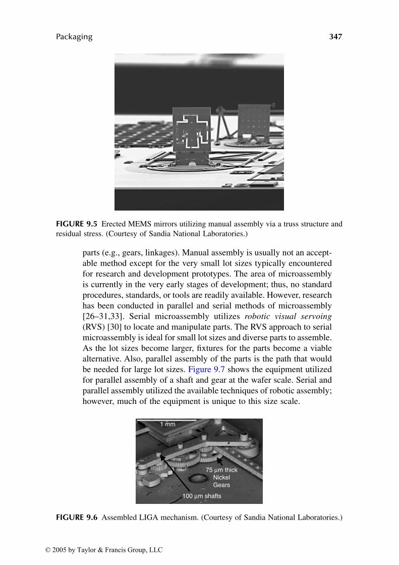
Packaging 347
parts (e.g., gears, linkages). Manual assembly is usually not an accept-
able method except for the very small lot sizes typically encountered
for research and development prototypes. The area of microassembly
is currently in the very early stages of development; thus, no standard
procedures, standards, or tools are readily available. However, research
has been conducted in parallel and serial methods of microassembly
[26–31,33]. Serial microassembly utilizes robotic visual servoing
(RVS) [30] to locate and manipulate parts. The RVS approach to serial
microassembly is ideal for small lot sizes and diverse parts to assemble.
As the lot sizes become larger, fixtures for the parts become a viable
alternative. Also, parallel assembly of the parts is the path that would
be needed for large lot sizes. Figure 9.7 shows the equipment utilized
for parallel assembly of a shaft and gear at the wafer scale. Serial and
parallel assembly utilized the available techniques of robotic assembly;
however, much of the equipment is unique to this size scale.
FIGURE 9.5 Erected MEMS mirrors utilizing manual assembly via a truss structure and
residual stress. (Courtesy of Sandia National Laboratories.)
FIGURE 9.6 Assembled LIGA mechanism. (Courtesy of Sandia National Laboratories.)
1 mm
100 µm shafts
75 µm thick
Nickel
Gears
© 2005 by Taylor & Francis Group, LLC

348 Micro Electro Mechanical System Design
9.1.1.5 Encapsulation
Packaging can represent as much as 70% of the cost of a MEMS product.
Manufacturability, which is the result of batch fabrication of hundreds to thou-
sands of devices at a time on a single wafer, is one of the reasons that integrated
circuits are so successful. One of the reasons that packaging can represent such
a significant fraction of the total cost is the need to handle individual die. MEMS
packaging can achieve greater manufacturability by avoiding the handling of
individual die in the release, dry, and coat processes; this can be achieved by
performing wafer level release, dry, and coat processes and encapsulation to
protect the MEMS device through the rest of the packaging process.
The encapsulation will provide a protective shell over the sensitive MEMS
parts while feed-throughs are passed through the package to connect to other
components or to pass an electrical signal (Figure 9.8). The feed-throughs are
needed to transfer signals to or from sensors, actuators, and circuitry. The feed-
throughs must have low parasitics (e.g., resistance, capacitance) and they must
be sealed to avoid any leakage. The encapsulation illustrated in Figure 9.8a is
achieved by bonding an encapsulating substrate to the MEMS wafer. A reliable
bonding process is essential to achieving a good seal. A variety of bonding
FIGURE 9.7 Parallel assembly of LIGA components. (a) The pin insertion tool is picking
up a 386-µm diameter pin. The pin is placed in the wafer in the background. (b) The
wafer of gears is being placed on the wafer of pins. (c) View of the wafer of gears before
being placed on the pins. (Courtesy of Intelligent Systems and Robotics, Sandia National
Laboratories.)
(a) (b)
(c)
© 2005 by Taylor & Francis Group, LLC
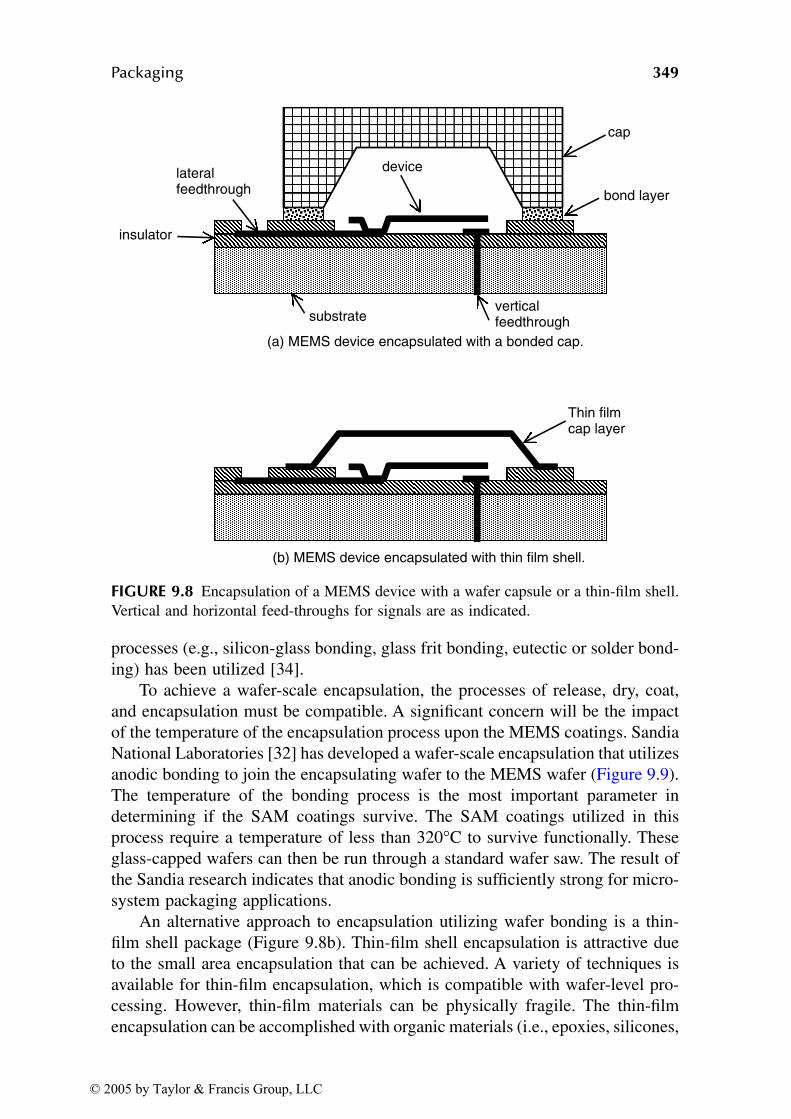
Packaging 349
processes (e.g., silicon-glass bonding, glass frit bonding, eutectic or solder bond-
ing) has been utilized [34].
To achieve a wafer-scale encapsulation, the processes of release, dry, coat,
and encapsulation must be compatible. A significant concern will be the impact
of the temperature of the encapsulation process upon the MEMS coatings. Sandia
National Laboratories [32] has developed a wafer-scale encapsulation that utilizes
anodic bonding to join the encapsulating wafer to the MEMS wafer (Figure 9.9).
The temperature of the bonding process is the most important parameter in
determining if the SAM coatings survive. The SAM coatings utilized in this
process require a temperature of less than 320°C to survive functionally. These
glass-capped wafers can then be run through a standard wafer saw. The result of
the Sandia research indicates that anodic bonding is sufficiently strong for micro-
system packaging applications.
An alternative approach to encapsulation utilizing wafer bonding is a thin-
film shell package (Figure 9.8b). Thin-film shell encapsulation is attractive due
to the small area encapsulation that can be achieved. A variety of techniques is
available for thin-film encapsulation, which is compatible with wafer-level pro-
cessing. However, thin-film materials can be physically fragile. The thin-film
encapsulation can be accomplished with organic materials (i.e., epoxies, silicones,
FIGURE 9.8 Encapsulation of a MEMS device with a wafer capsule or a thin-film shell.
Vertical and horizontal feed-throughs for signals are as indicated.
Thin film cap layer
(b) MEMS device encapsulated with thin film shell.
substrate
insulator
lateralfeedthrough
verticalfeedthrough
cap
bond layer
device
(a) MEMS device encapsulated with a bonded cap.
© 2005 by Taylor & Francis Group, LLC
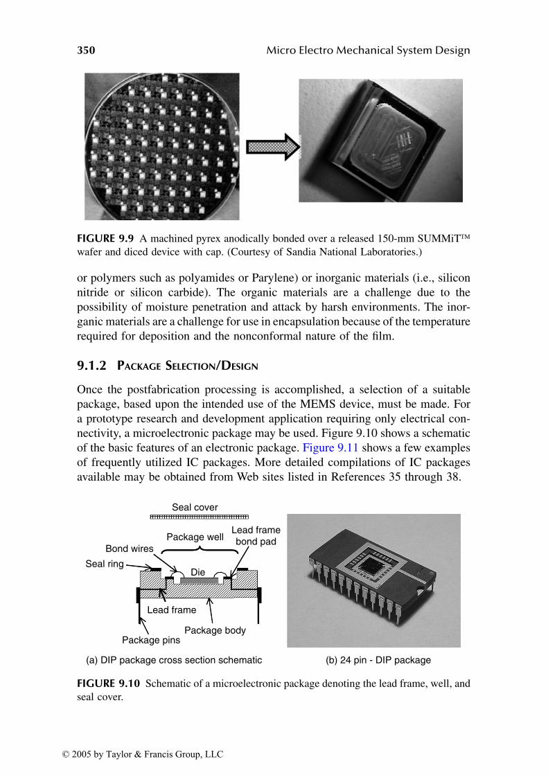
350 Micro Electro Mechanical System Design
or polymers such as polyamides or Parylene) or inorganic materials (i.e., silicon
nitride or silicon carbide). The organic materials are a challenge due to the
possibility of moisture penetration and attack by harsh environments. The inor-
ganic materials are a challenge for use in encapsulation because of the temperature
required for deposition and the nonconformal nature of the film.
9.1.2 PACKAGE SELECTION/DESIGN
Once the postfabrication processing is accomplished, a selection of a suitable
package, based upon the intended use of the MEMS device, must be made. For
a prototype research and development application requiring only electrical con-
nectivity, a microelectronic package may be used. Figure 9.10 shows a schematic
of the basic features of an electronic package. Figure 9.11 shows a few examples
of frequently utilized IC packages. More detailed compilations of IC packages
available may be obtained from Web sites listed in References 35 through 38.
FIGURE 9.9 A machined pyrex anodically bonded over a released 150-mm SUMMiTwafer and diced device with cap. (Courtesy of Sandia National Laboratories.)
FIGURE 9.10 Schematic of a microelectronic package denoting the lead frame, well, and
seal cover.
Seal cover
Package wellLead framebond pad
Die
Bond wires
Seal ring
Lead frame
Package bodyPackage pins
(a) DIP package cross section schematic (b) 24 pin - DIP package
© 2005 by Taylor & Francis Group, LLC
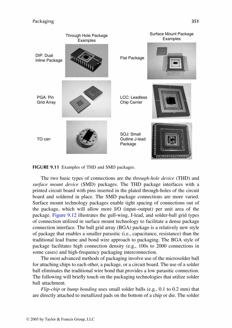
Packaging 351
The two basic types of connections are the through-hole device (THD) and
surface mount device (SMD) packages. The THD package interfaces with a
printed circuit board with pins inserted in the plated through-holes of the circuit
board and soldered in place. The SMD package connections are more varied.
Surface mount technology packages enable tight spacing of connections out of
the package, which will allow more I/O (input–output) per unit area of the
package. Figure 9.12 illustrates the gull-wing, J-lead, and solder-ball grid types
of connection utilized in surface mount technology to facilitate a dense package
connection interface. The ball grid array (BGA) package is a relatively new style
of package that enables a smaller parasitic (i.e., capacitance, resistance) than the
traditional lead frame and bond wire approach to packaging. The BGA style of
package facilitates high connection density (e.g., 100s to 2000 connections in
some cases) and high-frequency packaging interconnection.
The most advanced methods of packaging involve use of the microsolder ball
for attaching chips to each other, a package, or a circuit board. The use of a solder
ball eliminates the traditional wire bond that provides a low parasitic connection.
The following will briefly touch on the packaging technologies that utilize solder
ball attachment.
Flip-chip or bump bonding uses small solder balls (e.g., 0.1 to 0.2 mm) that
are directly attached to metallized pads on the bottom of a chip or die. The solder
FIGURE 9.11 Examples of THD and SMD packages.
Through Hole Package Examples
Surface Mount Package Examples
DIP: Dual Inline Package
PGA: Pin Grid Array
TO can
Flat Package
LCC: Leadless Chip Carrier
SOJ: Small Outline J-lead Package
© 2005 by Taylor & Francis Group, LLC
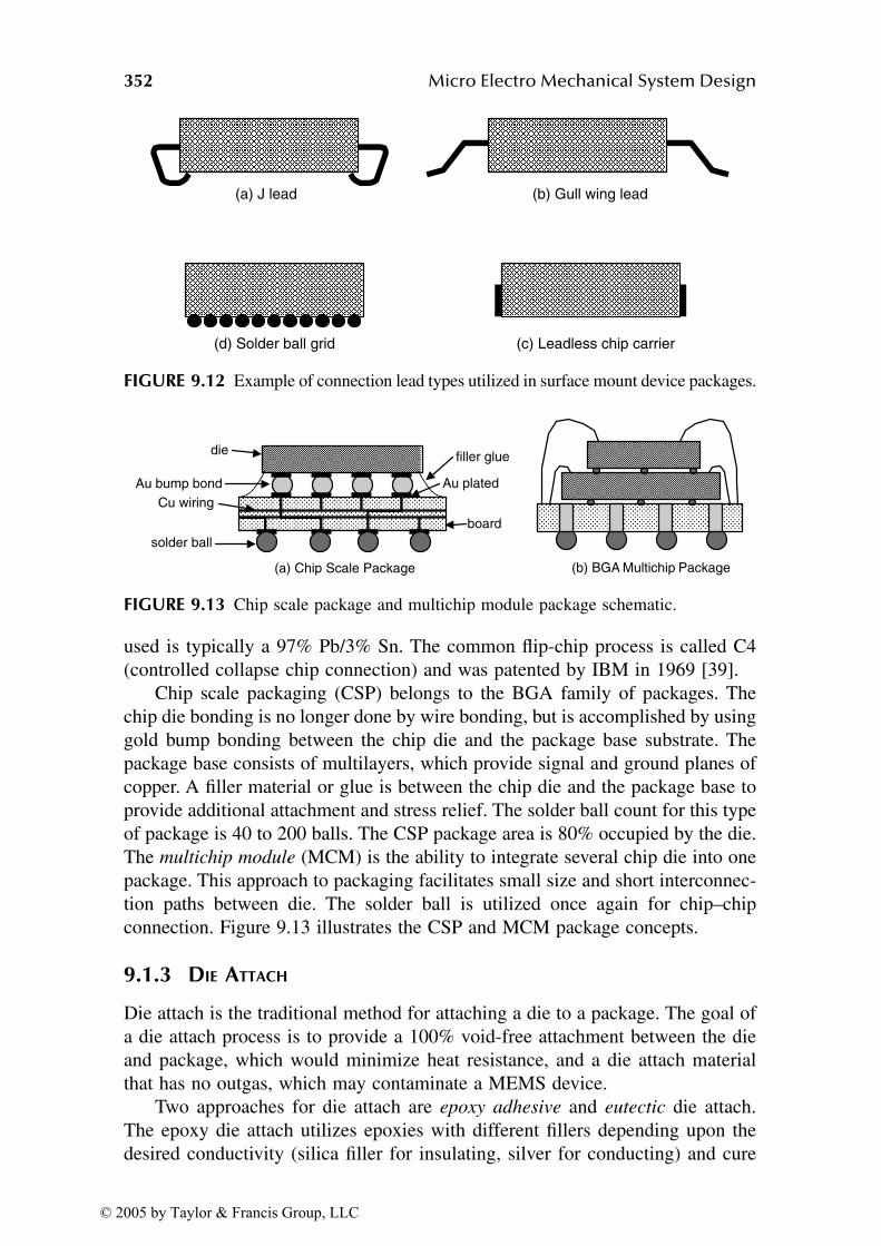
352 Micro Electro Mechanical System Design
used is typically a 97% Pb/3% Sn. The common flip-chip process is called C4
(controlled collapse chip connection) and was patented by IBM in 1969 [39].
Chip scale packaging (CSP) belongs to the BGA family of packages. The
chip die bonding is no longer done by wire bonding, but is accomplished by using
gold bump bonding between the chip die and the package base substrate. The
package base consists of multilayers, which provide signal and ground planes of
copper. A filler material or glue is between the chip die and the package base to
provide additional attachment and stress relief. The solder ball count for this type
of package is 40 to 200 balls. The CSP package area is 80% occupied by the die.
The multichip module (MCM) is the ability to integrate several chip die into one
package. This approach to packaging facilitates small size and short interconnec-
tion paths between die. The solder ball is utilized once again for chip–chip
connection. Figure 9.13 illustrates the CSP and MCM package concepts.
9.1.3 DIE ATTACH
Die attach is the traditional method for attaching a die to a package. The goal of
a die attach process is to provide a 100% void-free attachment between the die
and package, which would minimize heat resistance, and a die attach material
that has no outgas, which may contaminate a MEMS device.
Two approaches for die attach are epoxy adhesive and eutectic die attach.
The epoxy die attach utilizes epoxies with different fillers depending upon the
desired conductivity (silica filler for insulating, silver for conducting) and cure
FIGURE 9.12 Example of connection lead types utilized in surface mount device packages.
FIGURE 9.13 Chip scale package and multichip module package schematic.
(d) Solder ball grid (c) Leadless chip carrier
(a) J lead (b) Gull wing lead
die
Au bump bond
solder ball
Cu wiring
Au plated
board
filler glue
(a) Chip Scale Package (b) BGA Multichip Package
© 2005 by Taylor & Francis Group, LLC
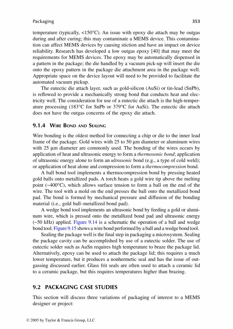
Packaging 353
temperature (typically, <150°C). An issue with epoxy die attach may be outgas
during and after curing; this may contaminate a MEMS device. This contamina-
tion can affect MEMS devices by causing stiction and have an impact on device
reliability. Research has developed a low outgas epoxy [40] that may meet the
requirements for MEMS devices. The epoxy may be automatically dispensed in
a pattern in the package; the die handled by a vacuum pick-up will insert the die
onto the epoxy pattern in the package die attachment area in the package well.
Appropriate space on the device layout will need to be provided to facilitate the
automated vacuum pickup.
The eutectic die attach layer, such as gold-silicon (AuSi) or tin-lead (SnPb),
is reflowed to provide a mechanically strong bond that conducts heat and elec-
tricity well. The consideration for use of a eutectic die attach is the high-temper-
ature processing (183°C for SnPb or 379°C for AuSi). The eutectic die attach
does not have the outgas concerns of the epoxy die attach.
9.1.4 WIRE BOND AND SEALING
Wire bonding is the oldest method for connecting a chip or die to the inner lead
frame of the package. Gold wires with 25 to 50 µm diameter or aluminum wires
with 25 µm diameter are commonly used. The bonding of the wires occurs by
application of heat and ultrasonic energy to form a thermosonic bond; application
of ultrasonic energy alone to form an ultrasonic bond (e.g., a type of cold weld);
or application of heat alone and compression to form a thermocompression bond.
A ball bond tool implements a thermocompression bond by pressing heated
gold balls onto metallized pads. A torch heats a gold wire tip above the melting
point (~400°C), which allows surface tension to form a ball on the end of the
wire. The tool with a mold on the end presses the ball onto the metallized bond
pad. The bond is formed by mechanical pressure and diffusion of the bonding
material (i.e., gold ball–metallized bond pad).
A wedge bond tool implements an ultrasonic bond by feeding a gold or alumi-
num wire, which is pressed onto the metallized bond pad and ultrasonic energy
(~50 kHz) applied. Figure 9.14 is a schematic the operation of a ball and wedge
bond tool. Figure 9.15 shows a wire bond performed by a ball and a wedge bond tool.
Sealing the package well is the final step in packaging a microsystem. Sealing
the package cavity can be accomplished by use of a eutectic solder. The use of
eutectic solder such as AuSn requires high temperature to braze the package lid.
Alternatively, epoxy can be used to attach the package lid; this requires a much
lower temperature, but it produces a nonhermetic seal and has the issue of out-
gassing discussed earlier. Glass frit seals are often used to attach a ceramic lid
to a ceramic package, but this requires temperatures higher than brazing.
9.2 PACKAGING CASE STUDIES
This section will discuss three variations of packaging of interest to a MEMS
designer or project:
© 2005 by Taylor & Francis Group, LLC
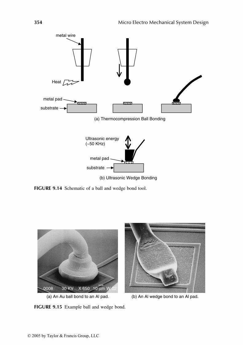
354 Micro Electro Mechanical System Design
FIGURE 9.14 Schematic of a ball and wedge bond tool.
FIGURE 9.15 Example ball and wedge bond.
Heat
metal pad
substrate
metal wire
(a) Thermocompression Ball Bonding
metal pad
substrate
(b) Ultrasonic Wedge Bonding
Ultrasonic energy (~50 KHz)
(a) An Au ball bond to an Al pad. (b) An Al wedge bond to an Al pad.
0008 30 KV W 02X 650 10 µm
© 2005 by Taylor & Francis Group, LLC
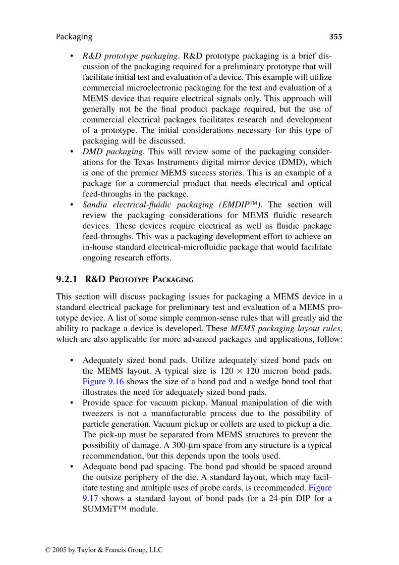
Packaging 355
• R&D prototype packaging. R&D prototype packaging is a brief dis-
cussion of the packaging required for a preliminary prototype that will
facilitate initial test and evaluation of a device. This example will utilize
commercial microelectronic packaging for the test and evaluation of a
MEMS device that require electrical signals only. This approach will
generally not be the final product package required, but the use of
commercial electrical packages facilitates research and development
of a prototype. The initial considerations necessary for this type of
packaging will be discussed.
• DMD packaging. This will review some of the packaging consider-
ations for the Texas Instruments digital mirror device (DMD), which
is one of the premier MEMS success stories. This is an example of a
package for a commercial product that needs electrical and optical
feed-throughs in the package.
• Sandia electrical-fluidic packaging (EMDIP). The section will
review the packaging considerations for MEMS fluidic research
devices. These devices require electrical as well as fluidic package
feed-throughs. This was a packaging development effort to achieve an
in-house standard electrical-microfluidic package that would facilitate
ongoing research efforts.
9.2.1 R&D PROTOTYPE PACKAGING
This section will discuss packaging issues for packaging a MEMS device in a
standard electrical package for preliminary test and evaluation of a MEMS pro-
totype device. A list of some simple common-sense rules that will greatly aid the
ability to package a device is developed. These MEMS packaging layout rules,
which are also applicable for more advanced packages and applications, follow:
• Adequately sized bond pads. Utilize adequately sized bond pads on
the MEMS layout. A typical size is 120 × 120 micron bond pads.
Figure 9.16 shows the size of a bond pad and a wedge bond tool that
illustrates the need for adequately sized bond pads.
• Provide space for vacuum pickup. Manual manipulation of die with
tweezers is not a manufacturable process due to the possibility of
particle generation. Vacuum pickup or collets are used to pickup a die.
The pick-up must be separated from MEMS structures to prevent the
possibility of damage. A 300-µm space from any structure is a typical
recommendation, but this depends upon the tools used.
• Adequate bond pad spacing. The bond pad should be spaced around
the outsize periphery of the die. A standard layout, which may facil-
itate testing and multiple uses of probe cards, is recommended. Figure
9.17 shows a standard layout of bond pads for a 24-pin DIP for a
SUMMiT™ module.
© 2005 by Taylor & Francis Group, LLC
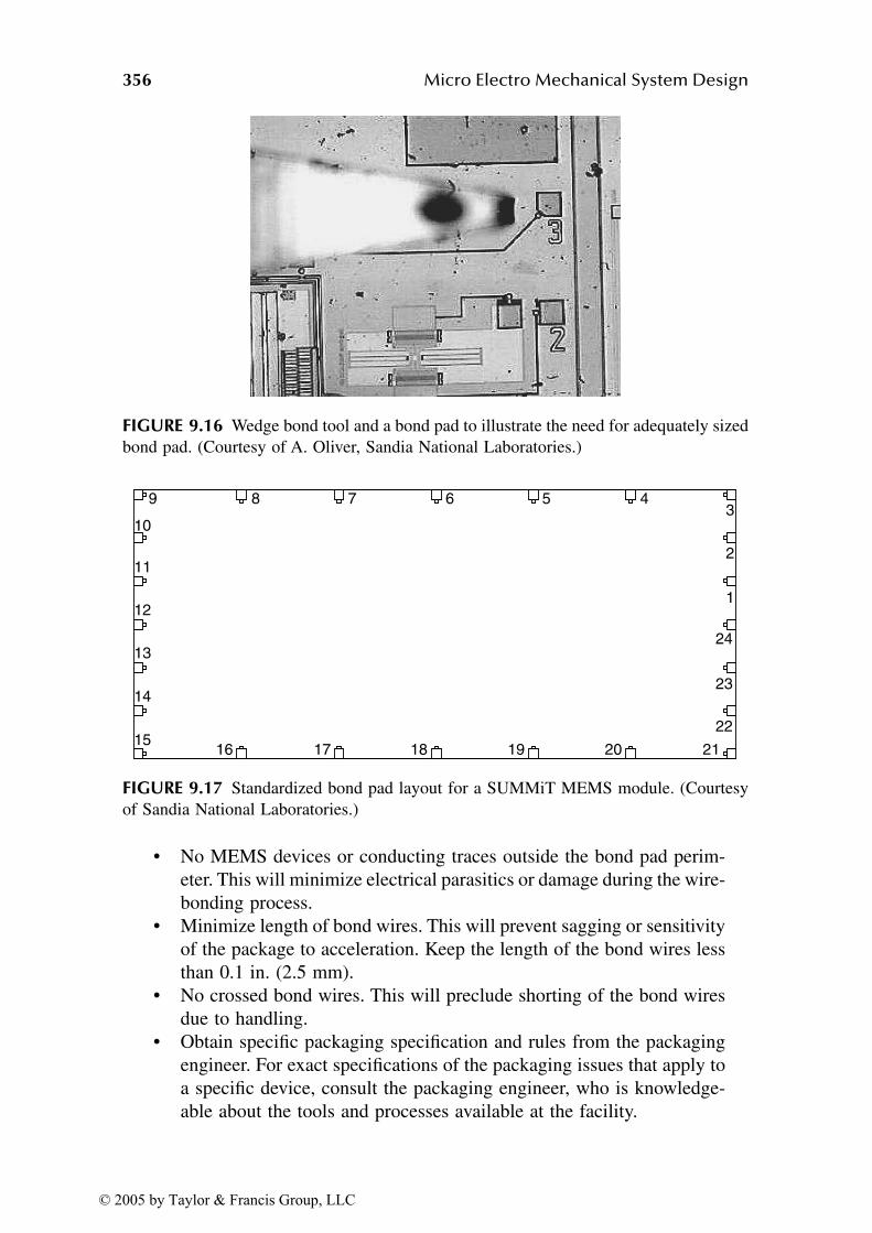
356 Micro Electro Mechanical System Design
• No MEMS devices or conducting traces outside the bond pad perim-
eter. This will minimize electrical parasitics or damage during the wire-
bonding process.
• Minimize length of bond wires. This will prevent sagging or sensitivity
of the package to acceleration. Keep the length of the bond wires less
than 0.1 in. (2.5 mm).
• No crossed bond wires. This will preclude shorting of the bond wires
due to handling.
• Obtain specific packaging specification and rules from the packaging
engineer. For exact specifications of the packaging issues that apply to
a specific device, consult the packaging engineer, who is knowledge-
able about the tools and processes available at the facility.
FIGURE 9.16 Wedge bond tool and a bond pad to illustrate the need for adequately sized
bond pad. (Courtesy of A. Oliver, Sandia National Laboratories.)
FIGURE 9.17 Standardized bond pad layout for a SUMMiT MEMS module. (Courtesy
of Sandia National Laboratories.)
1
2
3456789
10
11
12
13
14
1516 17 18 19 20 21
22
23
24
© 2005 by Taylor & Francis Group, LLC
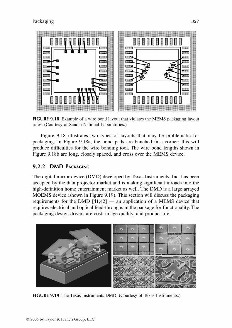
Packaging 357
Figure 9.18 illustrates two types of layouts that may be problematic for
packaging. In Figure 9.18a, the bond pads are bunched in a corner; this will
produce difficulties for the wire bonding tool. The wire bond lengths shown in
Figure 9.18b are long, closely spaced, and cross over the MEMS device.
9.2.2 DMD PACKAGING
The digital mirror device (DMD) developed by Texas Instruments, Inc. has been
accepted by the data projector market and is making significant inroads into the
high-definition home entertainment market as well. The DMD is a large arrayed
MOEMS device (shown in Figure 9.19). This section will discuss the packaging
requirements for the DMD [41,42] — an application of a MEMS device that
requires electrical and optical feed-throughs in the package for functionality. The
packaging design drivers are cost, image quality, and product life.
FIGURE 9.18 Example of a wire bond layout that violates the MEMS packaging layout
rules. (Courtesy of Sandia National Laboratories.)
FIGURE 9.19 The Texas Instruments DMD. (Courtesy of Texas Instruments.)
© 2005 by Taylor & Francis Group, LLC
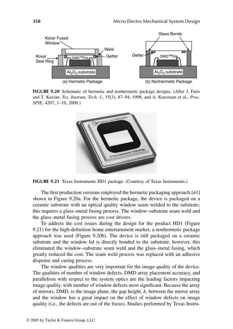
358 Micro Electro Mechanical System Design
The first production versions employed the hermetic packaging approach [41]
shown in Figure 9.20a. For the hermetic package, the device is packaged on a
ceramic substrate with an optical quality window seam welded to the substrate;
this requires a glass–metal fusing process. The window–substrate seam weld and
the glass–metal fusing process are cost drivers.
To address the cost issues during the design for the product HD1 (Figure
9.21) for the high-definition home entertainment market, a nonhermetic package
approach was used (Figure 9.20b). The device is still packaged on a ceramic
substrate and the window lid is directly bonded to the substrate; however, this
eliminated the window–substrate seam weld and the glass–metal fusing, which
greatly reduced the cost. The seam weld process was replaced with an adhesive
dispense and curing process.
The window qualities are very important for the image quality of the device.
The qualities of number of window defects, DMD array placement accuracy, and
parallelism with respect to the system optics are the leading factors impacting
image quality, with number of window defects most significant. Because the array
of mirrors, DMD, is the image plane, the gap height, h, between the mirror array
and the window has a great impact on the effect of window defects on image
quality (i.e., the defects are out of the focus). Studies performed by Texas Instru-
FIGURE 9.20 Schematic of hermetic and nonhermetic package designs. (After J. Faris
and T. Kocian, Tex. Instrum. Tech. J., 15(3), 87–94, 1998, and A. Kunzman et al., Proc.
SPIE, 4207, 1–10, 2000.)
FIGURE 9.21 Texas Instruments HD1 package. (Courtesy of Texas Instruments.)
Kovar
Seal Ring
Kovar Fused
Window
DMD™Die DMD™Die
Weld
(a) Hermetic Package
Getter
Glass Bonds
Getter
Al2O3 substrate
(b) Nonhermetic Package
Al2O3 substrate
© 2005 by Taylor & Francis Group, LLC
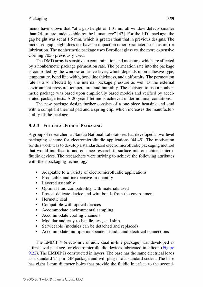
Packaging 359
ments have shown that “at a gap height of 1.0 mm, all window defects smaller
than 24 µm are undetectable by the human eye” [42]. For the HD1 package, the
gap height was set at 1.5 mm, which is greater than that in previous designs. The
increased gap height does not have an impact on other parameters such as mirror
lubrication. The nonhermetic package uses Borofloat glass vs. the more expensive
Corning 7056 previously used.
The DMD array is sensitive to contamination and moisture, which are affected
by a nonhermetic package permeation rate. The permeation rate into the package
is controlled by the window adhesive layer, which depends upon adhesive type,
temperature, bond line width, bond line thickness, and uniformity. The permeation
rate is also affected by the internal package pressure as well as the external
environment pressure, temperature, and humidity. The decision to use a nonher-
metic package was based upon empirically based models and verified by accel-
erated package tests. A 20-year lifetime is achieved under nominal conditions.
The new package design further consists of a one-piece heatsink and stud
with a compliant thermal pad and a spring clip, which increases the manufactur-
ability of the package.
9.2.3 ELECTRICAL-FLUIDIC PACKAGING
A group of researchers at Sandia National Laboratories has developed a two-level
packaging scheme for electromicrofluidic applications [44,45]. The motivation
for this work was to develop a standardized electromicrofluidic packaging method
that would interface to and enhance research in surface micromachined micro-
fluidic devices. The researchers were striving to achieve the following attributes
with their packaging technology:
• Adaptable to a variety of electromicrofluidic applications
• Producible and inexpensive in quantity
• Layered assembly
• Optimal fluid compatibility with materials used
• Protect delicate device and wire bonds from the environment
• Hermetic seal
• Compatible with optical devices
• Accommodate environmental sampling
• Accommodate cooling channels
• Modular and easy to handle, test, and ship
• Serviceable (modules can be detached and replaced)
• Accommodate multiple independent fluidic and electrical connections
The EMDIP (electromicrofluidic dual in-line package) was developed as
a first-level package for electromicrofluidic devices fabricated in silicon (Figure
9.22). The EMDIP is constructed in layers. The base has the same electrical leads
as a standard 24-pin DIP package and will plug into a standard socket. The base
has eight 1-mm diameter holes that provide the fluidic interface to the second-
© 2005 by Taylor & Francis Group, LLC
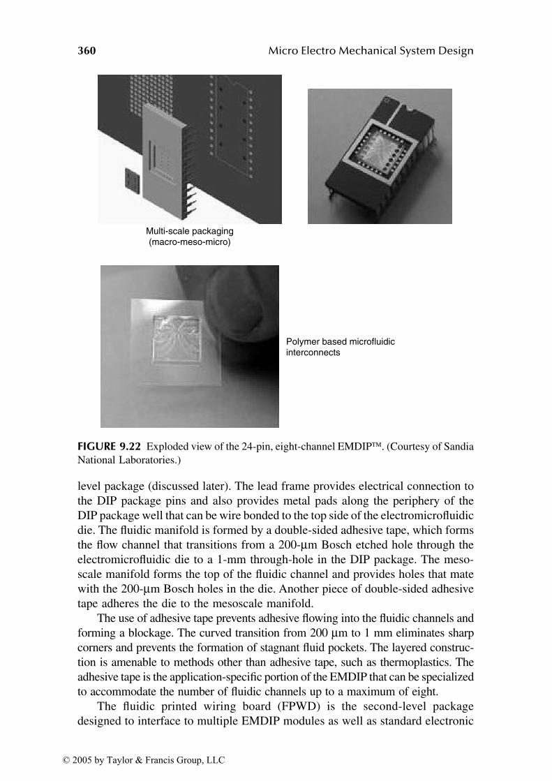
360 Micro Electro Mechanical System Design
level package (discussed later). The lead frame provides electrical connection to
the DIP package pins and also provides metal pads along the periphery of the
DIP package well that can be wire bonded to the top side of the electromicrofluidic
die. The fluidic manifold is formed by a double-sided adhesive tape, which forms
the flow channel that transitions from a 200-µm Bosch etched hole through the
electromicrofluidic die to a 1-mm through-hole in the DIP package. The meso-
scale manifold forms the top of the fluidic channel and provides holes that mate
with the 200-µm Bosch holes in the die. Another piece of double-sided adhesive
tape adheres the die to the mesoscale manifold.
The use of adhesive tape prevents adhesive flowing into the fluidic channels and
forming a blockage. The curved transition from 200 µm to 1 mm eliminates sharp
corners and prevents the formation of stagnant fluid pockets. The layered construc-
tion is amenable to methods other than adhesive tape, such as thermoplastics. The
adhesive tape is the application-specific portion of the EMDIP that can be specialized
to accommodate the number of fluidic channels up to a maximum of eight.
The fluidic printed wiring board (FPWD) is the second-level package
designed to interface to multiple EMDIP modules as well as standard electronic
FIGURE 9.22 Exploded view of the 24-pin, eight-channel EMDIP. (Courtesy of Sandia
National Laboratories.)
Multi-scale packaging (macro-meso-micro)
Polymer based microfluidic interconnects
© 2005 by Taylor & Francis Group, LLC

Packaging 361
components. Figure 9.23 is an exploded view of the FPWB, electrical connector,
and fluidic connector. The materials used to construct the FPWB are high-
temperature thermoplastics or glass. The FPWB consists of two parts: the channel
board and the cover board. The channel board contains the fluidic channel and
the cover board forms the channel lid. The fluidic connector, which was devel-
oped by Peter Krulevitch and Willam Benett [43] and patented by Lawrence
Livermore National Laboratories, connects to the channel board with a 3.4-mm
channel. The 1-mm holes in the cover board are designed to mate with the fluidic
connections of the EMDIP. The cover board also contains electrical traces, which
route electrical connections from the EMDIP to the electrical connector. The
interface between the EMDIP and FPWB make electrical as well as fluidic
connections.
9.3 SUMMARY
Packaging is a significant fraction of the cost of any MEMS product and requires
consideration concurrently with the device design and fabrication. Packaging
provides the basic functions of mechanical support, interconnection, and envi-
ronmental control for the MEMS device. Although the exact processes required
for packaging a device are application specific, they may span a wide range,
which may include any or all the following:
• Die separation
• Release
• Drying
• Coating
• Assembly
• Encapsulation
• Die attachment
• Wire bond and sealing
FIGURE 9.23 Exploded view of the fluidic printed wiring board with a standard 24-
conductor electrical connector and an eight-channel fluidic connector. (Courtesy of Sandia
National Laboratories.)
© 2005 by Taylor & Francis Group, LLC
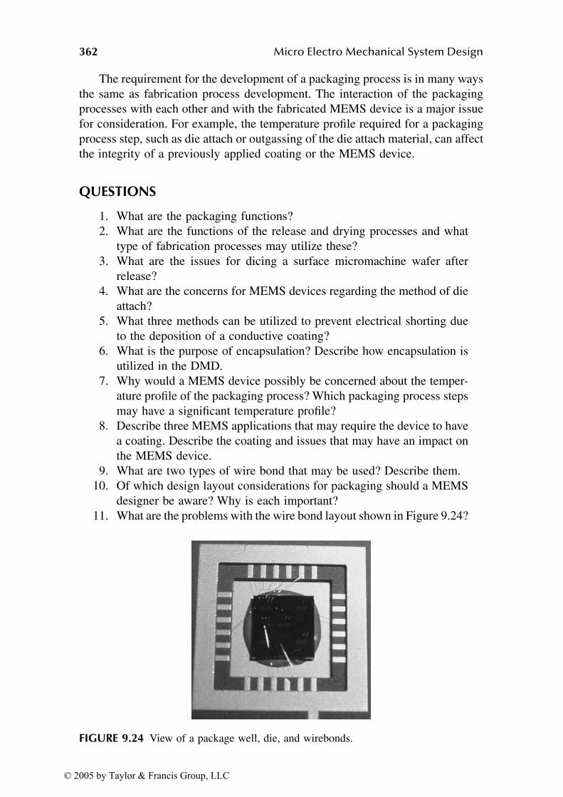
362 Micro Electro Mechanical System Design
The requirement for the development of a packaging process is in many ways
the same as fabrication process development. The interaction of the packaging
processes with each other and with the fabricated MEMS device is a major issue
for consideration. For example, the temperature profile required for a packaging
process step, such as die attach or outgassing of the die attach material, can affect
the integrity of a previously applied coating or the MEMS device.
QUESTIONS
1. What are the packaging functions?
2. What are the functions of the release and drying processes and what
type of fabrication processes may utilize these?
3. What are the issues for dicing a surface micromachine wafer after
release?
4. What are the concerns for MEMS devices regarding the method of die
attach?
5. What three methods can be utilized to prevent electrical shorting due
to the deposition of a conductive coating?
6. What is the purpose of encapsulation? Describe how encapsulation is
utilized in the DMD.
7. Why would a MEMS device possibly be concerned about the temper-
ature profile of the packaging process? Which packaging process steps
may have a significant temperature profile?
8. Describe three MEMS applications that may require the device to have
a coating. Describe the coating and issues that may have an impact on
the MEMS device.
9. What are two types of wire bond that may be used? Describe them.
10. Of which design layout considerations for packaging should a MEMS
designer be aware? Why is each important?
11. What are the problems with the wire bond layout shown in Figure 9.24?
FIGURE 9.24 View of a package well, die, and wirebonds.
© 2005 by Taylor & Francis Group, LLC
Packaging 363
12. Research the packaging of a commercial MEMS device and discuss
the issues that drove the package design.
REFERENCES
1. C.W. Dyck, J.H. Smith, S.L. Miller, C.L. Russick, C.L.J. Adkins, Supercritical
carbon dioxide solvent extraction from surface micromachined micromechanical
structures, Proc. SPIE Symp. Micromachining Microfabrication, 2879, 225–235,
Austin, TX, 1996.
2. J.N. Israelachvili, Intermolecular and Surface Forces, Academic Press, New York,
1992.
3. R. Legtenberg, A.C. Harrie, J.E. Tilmans, M. Elwenspoek, Stiction of surface
micromachined structures after rinsing and drying: model and investigation of
adhesion mechanisms, Sensors Actuators, 43, 230–238, 1994.
4. G.T. Mulhern, D.S. Soane, R.T. Howe, Supercritical carbon dioxide drying of
microstructures, Proc. 7th Int. Conf. Solid-State Sensors Actuators, Transducers
’93, Yokohama, 296–299, 1993.
5. H. Guckel, J.J. Sniegowski, T.R. Christenson, S. Mohney, S.F. Kelly, Fabrication
of micromechanical devices from polysilicon films with smooth surfaces, Sensors
Actuators, 20, 117–122, 1989.
6. H. Guckel, J.J. Sniegowski, T.R. Christenson, R. Raissi, The application of fine-
grained, tensile polysilicon to mechanically resonant transducers, Sensors Actua-
tors, 21, 346–351, 1990.
7. U. Srinivasan, M.R. Houston, R.T. Howe, Alkyltrichlorosilane-based self-assem-
bled monolayer films for stiction reduction in silicon micromachines, J. MEMS,
7(2), 252–260, June 1998.
8. X.Y. Zhu, J.E. Houston, Molecular lubricants for silicon-based microelectrome-
chanical systems (MEMS): a novel assembly strategy, Triboloby Lett., 7, 87–90,
1999.
9. Y.N. Picard, D.P. Adams, O.B. Spahn, S.M. Yalisove, D.J. Dagel, J. Sobczak,
Low-stress, high-reflectivity thin films for MEMS mirrors, Proc. Mater. Res. Soc.
Symp., San Francisco, CA, 729, 113–118, 2002.
10. S.S. Andreev, N.N. Salaschchenko, L.A. Suslov, A.N. Yablonsky, S.Y. Zuev, Stress
reduction of Mo/Si multilayer structures, Nuc. Inst. Methods Phys. Res., 470,
162–167, 2001.
11. P.B. Mirkarimi, E.A. Spiller, D.G. Stearns, V. Sperry, S.L. Baker, An ion-assisted
Mo-Si deposition process for planarizing reticle substrates for extreme ultraviolet
lithography, IEEE J. Quantum Electron., 37(12), 1514–1516, December 2001.
12. T. Chasse, H. Neumann, B. Ocker, M. Scherer, W. Frank, F. Frost, D. Hirsch, A.
Schindler, G. Wagner, M. Lorenz, G. Otto, Mo/Si multilayers for EUV lithography
by ion beam sputter deposition, Vacuum, 71, 407–415, 2003.
13. T.W. Schneider, L.E. Aloi, R.C. White, Control of protein adsorption for MEMs
and microfluidic applications on silicon surfaces using silane based self-assembled
monolayers of an oligo(ethylene oxide) derivative, Proc. SPIE, 4205, 128–134,
2001.
14. W.H. Ko, Frontiers in solid state biomedical transducers, Proc. IEEE Int. Electron
Devices Meeting, 112–115, 1985.
15. Figaro Engineering Inc., http://www.figarosensor.com/.
© 2005 by Taylor & Francis Group, LLC
364 Micro Electro Mechanical System Design
16. R.C. Hughes, W.K. Schubert, Thin films of Pd/Ni alloys for detection of high
hycrogen concentrations, J. Appl. Phys., 71, 542, 1992.
17. H. Nanto, T. Kobayaski, N. Dougami, M. Habara, H. Yamamoto, E. Kusano, A.
Kinbara, Y. Douguchi, Smart chemical sensors using ZnO semiconducting thin
films for freshness detection of foods and beverages, Proc. SPIE, 3328, 418–427,
March 1998.
18. K. Gilleo, M. Previti, Getters: molecular scavengers for packaging, International
Symposium on Advanced Packaging Material Properties and Interfaces, Braselton,
GA, March 2001; also www.hdi-online.com, January 2001.
19. STAYDRY, Cookson Semiconductor Packaging Materials, Alpharetta, GA.
20. J.T. Butler, V.M. Bright, J.H. Comtois, Multichip module packaging of microelec-
tromechanical systems, Sensors Actuators A, 70, 15–22, 1998.
21. S. Linder, H. Baltes, F. Gnaedinger, E. Doering, Fabrication technology for wafer
through-hole interconnections and three-dimensional stacks of chips and wafers,
Proc. IEEE Micro Electro Mech. Syst. (MEMS ’94), 349–354, January 1994, Japan.
22. M.A. Michalicek, W. Zhang, K.F. Harsh, V.M. Bright, Y.C. Lee, Micromirror
arrays fabricated by flip-chip assembly, Proc. SPIE, 3878, 68–79, 1999.
23. K.F. Harsh, V.M. Bright, Y.C. Lee, Solder self-assembly for three-dimensional
microelectromechanical systems, Sensors Actuators, 77, 237–244, 1999.
24. H.J. Yeh, J.S. Smith, Fluidic self assembly for the Integration of GaAs light-
emitting diodes on Si substrates, IEEE Photonics Technol. Lett., 6, 706–708, 1994.
25. U. Srinivasan, D. Liepmann, R.T. Howe, Microstructure to substrate self-assembly
using capillary forces, JMEMS, 10(1), March 2001.
26. J.T. Feddema, T. Christenson, Parallel assembly of high aspect ratio microstruc-
tures, Proc. SPIE, 3834, 153–164, September 1999.
27. A. Singh, D.A. Horsley, M.B. Cohen, A.P. Pisano, R.T. Howe, Batch transfer of
microstructures using flip chip bump bonding, Transducers ’97, Chicago.
28. J.T. Feddema, C.G. Keller, R.T. Howe, Experiments in micromanipulation and
CAD-driven microassembly, Proc. SPIE, 3202, 98–107, 1998.
29. J.T. Feddema, R.W. Simon, Visual servoing and CAD-driven microassembly, IEEE
Robotics Automation Mag., 5(4), 18–24, December 1998.
30. S. Hutchinson, G.D. Hagar, P.I. Corke, A tutorial on visual servo control, IEEE
Trans. Robotics and Automation, 12(5), 651–670, October 1996.
31. M.B. Cohn, R.T. Howe, Wafer to wafer transfer of microstructures using break
away tethers, U.S. Patent No. 6,142,358, issued November 7, 2000.
32. L.E.S. Rohwer, A.D. Oliver, M.V. Collins, Wafer level micropackaging of MEMS
devices using thin film anodic bonding, Mat. Res. Soc. Proc., 729, 229–234, 2002.
33. M.B. Cohn, K.F. Bohringer, J.M. Noworolski, A. Singh, C.G. Keller, K.Y. Gold-
berg, R.T. Howe, Microassembly technologies for MEMS, Proc. SPIE, 3514,
2–16, September, 1998.
34. K. Najafi, Micropackaging technologies for integrated microsystems: applications
to MEMS and MOEMS, Proc. SPIE, 4979, 1–19, 2003.
35. http://www.amkor.com — wafer bumping, MEMS.
36. http://www.necel.com — general packing information.
37. http://www.oki.com/semi/english — IC packages, materials.
38. http://www.intel.com — IC packaging, environmental conditions.
39. L.S. Goodman, Geometric optimization of controlled collapse interconnections,
IBM J. Res. Dev. 13(3), 251–265, 1969.
© 2005 by Taylor & Francis Group, LLC
Packaging 365
40. M.N. Nguyen, M.B. Grosse, Low moisture polymer adhesive for hermetic pack-
ages, IEEE Trans. Comp, Hybrids, Manf. Tech., 15, 964–971, 1992.
41. J. Faris, T. Kocian, DMD Packages — evolution and strategy, Tex. Instrum.
Tech. J., 15(3), 87–94, 1998.
42. A. Kunzman, J. O’Connor, D. Segler, T. Migl, K. Bell, Advancing the DMDdevice for high-definition home entertainment, Proc. SPIE, 4207, 1–10, 2000.
43. W. Benett, P. Krulevitch, A flexible packaging and interconnect scheme for microf-
luidic systems, Proc. SPIE, 3606, 111, 1999.
44. P. Galambos, G. Benavides, M. Okandan, M. Jenkins, D. Hetherington, Precision
alignment packaging for microsystems with multiple fluid connections, IMECE
2001 Proc., IMECE 2001/MEMS-23902, November 2001.
45. G.L. Benavides, P.C. Galambos, Electromicrofluidic packaging, Sandia National
Laboratories Report, SAND2002-1941, June, 2002.
46. G.L. Benavides, P.C. Galambos, J.A. Emerson, K.A. Peterson, R.K. Giunta, R.D.
Watson, Packaging of electromicrofluidic devices, U.S. Patent 6,443,179, issued
September 3, 2002.
47. G.L. Benavides, P.C. Galambos, J.A. Emerson, K.A. Peterson, R.K. Giunta, R.D.
Watson, Packaging of electromicrofluidic devices, U.S. Patent 6,548,895, issued
April 15, 2003.
© 2005 by Taylor & Francis Group, LLC
367
10 Reliability
10.1 RELIABILITY THEORY AND TERMINOLOGY
Reliability is the ability of a device or system to perform a required function for
a specified amount of time. The function and level of reliability required of a
device are obviously application specific. A sensor vital to an aircraft flight control
system whose failure can mean loss of life is an example of a high-reliability
application. Alternatively, a switch in a piece of commercial electronics may fail
and be an annoyance, but it is hardly a tragedy. Since World War II, reliability
techniques have been widely applied to military and commercial devices and
systems; this has led to the development of the field of reliability. Examples of
the reliability literature can be found in the journals listed in Table 10.1.
The reliability of a system may depend upon many things, such as the
subsystems (e.g., individual electrical, mechanical, or MEMS devices); packag-
ing; power supply; software; or cooling systems. The overall reliability of a
system is complex because the interrelations between the different subsystems
can combine in complex ways to cause a system failure. Alternatively, the system
could be designed so that subsystems can compensate for failures in other aspects
of the system. For example, software could be designed to monitor the system
and avoid a system failure by utilizing other subsystems to perform a function.
However, this chapter focuses on reliability at the device level — specifically,
the reliability of MEMS devices. Data to access the reliability of a device are
obtained by operating a large number of devices under normal operating condi-
tions and noting when failure occurs. Three items need to be defined unambig-
uously to formulate the reliability experiment properly:
• Method of operation: a detailed definition of the method of device
operation — for example, a switch is the device to be tested for
reliability. An application of voltage (10 V/0 V) to close or open a
switch at 100-Hz frequency using a square wave signal.
• Definition of failure: definition of what constitutes failure of this device
— for example, resistance of the switch contact > 1 kΩ when the 10-
V operate signal is applied or the resistance < 1 MΩ when the 0-V
signal to open the switch is applied. This statement of failure denotes
that contacts are fouled so that adequate continuity when closed is not
present or sufficient isolation is not present when the switch is open.
This condition may be present when the switch mechanism has failed
© 2005 by Taylor & Francis Group, LLC
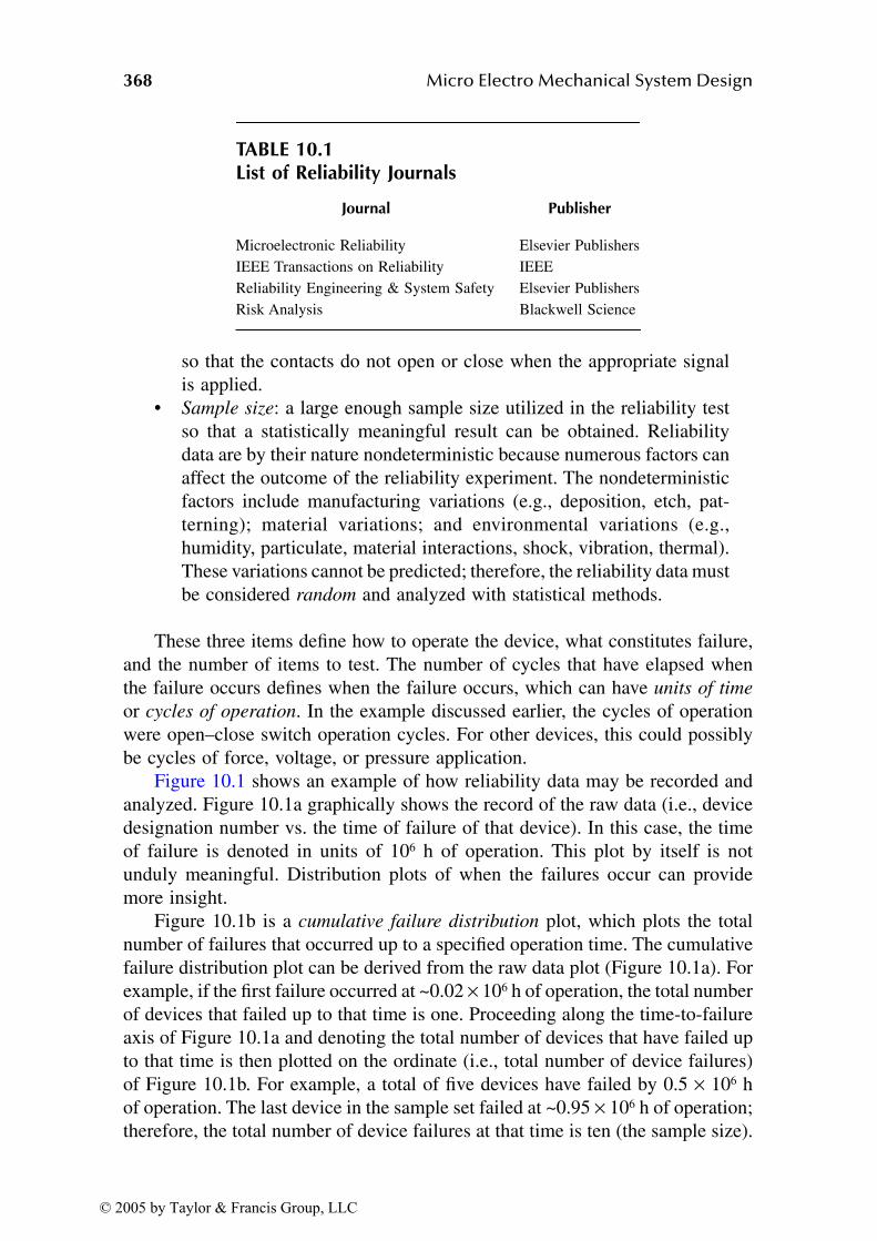
368 Micro Electro Mechanical System Design
so that the contacts do not open or close when the appropriate signal
is applied.
• Sample size: a large enough sample size utilized in the reliability test
so that a statistically meaningful result can be obtained. Reliability
data are by their nature nondeterministic because numerous factors can
affect the outcome of the reliability experiment. The nondeterministic
factors include manufacturing variations (e.g., deposition, etch, pat-
terning); material variations; and environmental variations (e.g.,
humidity, particulate, material interactions, shock, vibration, thermal).
These variations cannot be predicted; therefore, the reliability data must
be considered random and analyzed with statistical methods.
These three items define how to operate the device, what constitutes failure,
and the number of items to test. The number of cycles that have elapsed when
the failure occurs defines when the failure occurs, which can have units of time
or cycles of operation. In the example discussed earlier, the cycles of operation
were open–close switch operation cycles. For other devices, this could possibly
be cycles of force, voltage, or pressure application.
Figure 10.1 shows an example of how reliability data may be recorded and
analyzed. Figure 10.1a graphically shows the record of the raw data (i.e., device
designation number vs. the time of failure of that device). In this case, the time
of failure is denoted in units of 106 h of operation. This plot by itself is not
unduly meaningful. Distribution plots of when the failures occur can provide
more insight.
Figure 10.1b is a cumulative failure distribution plot, which plots the total
number of failures that occurred up to a specified operation time. The cumulative
failure distribution plot can be derived from the raw data plot (Figure 10.1a). For
example, if the first failure occurred at ~0.02 × 10⁶ h of operation, the total number
of devices that failed up to that time is one. Proceeding along the time-to-failure
axis of Figure 10.1a and denoting the total number of devices that have failed up
to that time is then plotted on the ordinate (i.e., total number of device failures)
of Figure 10.1b. For example, a total of five devices have failed by 0.5 × 10⁶ h
of operation. The last device in the sample set failed at ~0.95 × 10⁶ h of operation;
therefore, the total number of device failures at that time is ten (the sample size).
TABLE 10.1List of Reliability Journals
Journal Publisher
Microelectronic Reliability Elsevier Publishers
IEEE Transactions on Reliability IEEE
Reliability Engineering & System Safety Elsevier Publishers
Risk Analysis Blackwell Science
© 2005 by Taylor & Francis Group, LLC

Reliability 369
The total number of device failures in a cumulative distribution is always 0
at t = 0, and the cumulative distribution is equal to the sample size as t ⇒ ∞.
Instead of dealing with numbers of devices for the cumulative distribution, the
plot can be put on a probability basis by normalizing by the total number of
devices tested. In this case, the plots would be known as the cumulative probability
distribution function (CPDF). It is assumed that there are no inoperative devices
at t = 0 (i.e., no samples dead on arrival). For purposes of this discussion, the
initially inoperative devices would factor into the fabrication yield instead of the
reliability of the device. The cumulative failure distribution shows the minimum
time to failure of a device, the maximum time of failure of all the devices, and
how device failures were distributed between those limits. The slope of the
cumulative failure distribution shows the device failure rate over the duration of
the test data.
A frequently used unit in reliability test data is the FIT (failure in time). A
FIT is defined as one failure per billion (109) device hours or operations. This
definition of the FIT unit was chosen because failure rates are typically very small
for most devices in production.
FIGURE 10.1 Device failure and failure distribution plots utilizing a ten-device sample
set. (a) Individual device failure vs. time. (b) Cumulative failure distribution. (c) Failure
frequency distribution.
0 0.1 0.2 0.3 0.4 0.5 0.6 0.7 0.8 0.9 1
0 0.1 0.2 0.3 0.4 0.5 0.6 0.7 0.8 0.9 1
0
Tot
al N
umbe
r of
Dev
ice
Fai
lure
s
0.1Num
ber
of D
evic
e F
ailu
res/
(.1
× 10
6 ho
urs)
0.2 0.3 0.4 0.5 0.6 0.7 0.8 0.9 1
(b) Cumulative Failure Distribution
(c) Failure Frequency Distribution
Time to Failure (106 hours)
(a) Individual Devices Failure Time
Dev
ice
10
3
2.5
2
1.5
1
0.5
0
10
8
6
4
2
0
987654321
© 2005 by Taylor & Francis Group, LLC
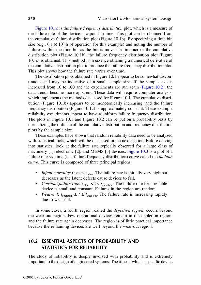
370 Micro Electro Mechanical System Design
Figure 10.1c is the failure frequency distribution plot, which is a measure of
the failure rate of the device at a point in time. This plot can be obtained from
the cumulative failure distribution plot (Figure 10.1b). By specifying a time bin
size (e.g., 0.1 × 10⁶ h of operation for this example) and noting the number of
failures within the time bin as the bin is moved in time across the cumulative
distribution plot (Figure 10.1b), the failure frequency distribution plot (Figure
10.1c) is obtained. This method is in essence obtaining a numerical derivative of
the cumulative distribution plot to produce the failure frequency distribution plot.
This plot shows how the failure rate varies over time.
The distribution plots obtained in Figure 10.1 appear to be somewhat discon-
tinuous and may be indicative of a small sample size. If the sample size is
increased from 10 to 100 and the experiments are run again (Figure 10.2), the
data trends become more apparent. These data will require computer analysis,
which implements the methods discussed for Figure 10.1. The cumulative distri-
bution (Figure 10.1b) appears to be monotonically increasing, and the failure
frequency distribution (Figure 10.1c) is approximately constant. These example
reliability experiments appear to have a uniform failure frequency distribution.
The plots in Figure 10.1 and Figure 10.2 can be put on a probability basis by
normalizing the ordinate of the cumulative distribution and frequency distribution
plots by the sample size.
These examples have shown that random reliability data need to be analyzed
with statistical tools, which will be discussed in the next section. Before delving
into statistics, look at the failure rate typically observed for a large class of
machinery [1], electronic [2], and MEMS [3] devices. Figure 10.3 is a plot of a
failure rate vs. time (i.e., failure frequency distribution) curve called the bathtub
curve. This curve is composed of three principal regions:
• Infant mortality: 0 < t ≤ tinfant. The failure rate is initially very high but
decreases as the latent defects cause devices to fail.
• Constant failure rate: tinfant < t < toperation. The failure rate for a reliable
device is small and constant. Failures in the region are random.
• Wear-out: toperation ≤ t ≤ twear-out. The failure rate is increasing rapidly
due to wear-out.
In some cases, a fourth region, called the depletion region, occurs beyond
the wear-out region. Few operational devices remain in the depletion region,
and the failure rate again decreases. The region is of little practical importance
because the remaining devices are well beyond the wear-out region.
10.2 ESSENTIAL ASPECTS OF PROBABILITY AND STATISTICS FOR RELIABILITY
The study of reliability is deeply involved with probability and is extremely
important to the design of engineered systems. The time at which a specific device
© 2005 by Taylor & Francis Group, LLC
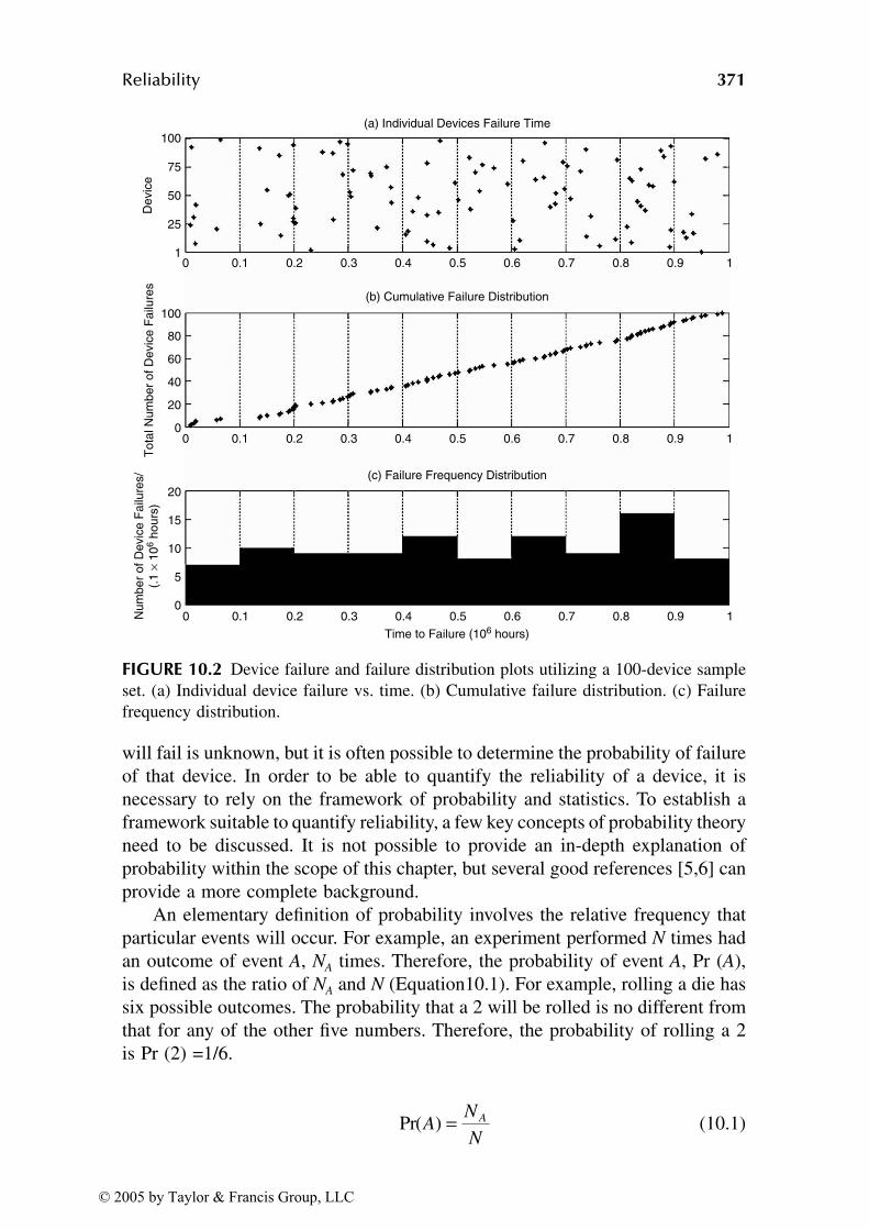
Reliability 371
will fail is unknown, but it is often possible to determine the probability of failure
of that device. In order to be able to quantify the reliability of a device, it is
necessary to rely on the framework of probability and statistics. To establish a
framework suitable to quantify reliability, a few key concepts of probability theory
need to be discussed. It is not possible to provide an in-depth explanation of
probability within the scope of this chapter, but several good references [5,6] can
provide a more complete background.
An elementary definition of probability involves the relative frequency that
particular events will occur. For example, an experiment performed N times had
an outcome of event A, NA times. Therefore, the probability of event A, Pr (A),
is defined as the ratio of NA and N (Equation10.1). For example, rolling a die has
six possible outcomes. The probability that a 2 will be rolled is no different from
that for any of the other five numbers. Therefore, the probability of rolling a 2
is Pr (2) =1/6.
(10.1)
FIGURE 10.2 Device failure and failure distribution plots utilizing a 100-device sample
set. (a) Individual device failure vs. time. (b) Cumulative failure distribution. (c) Failure
frequency distribution.
0 0.1 0.2 0.3 0.4 0.5 0.6 0.7 0.8 0.9 1
0 0.1 0.2 0.3 0.4 0.5 0.6 0.7 0.8 0.9 1
0 0.1 0.2 0.3 0.4 0.5 0.6 0.7 0.8 0.9 1
(b) Cumulative Failure Distribution
(c) Failure Frequency Distribution
Time to Failure (106 hours)
(a) Individual Devices Failure Time
Tot
al N
umbe
r of
Dev
ice
Fai
lure
sN
umbe
r of
Dev
ice
Fai
lure
s/(.
1×
106
hour
s)D
evic
e100
100
80
60
40
20
20
15
10
5
0
0
75
50
25
1
Pr( )AN
N
A=
© 2005 by Taylor & Francis Group, LLC

372 Micro Electro Mechanical System Design
Probability as stated here will have the following axioms:
• Probability is a number between 0 and 1:
0 ≤ Pr(A) ≤ 1 (10.2)
• The probability of a certain event, A, is 1:
Pr (A) = 1 (10.3)
• The probability of an impossible event, A, is 0:
Pr (A) = 0 (10.4)
• The probability of a complete set of mutually exclusive events is 1.
For example, the probability of a complete set of events A, B, C, D,
E, F is Pr(A) + Pr(B) + Pr(C) + Pr(D) + Pr(E) +Pr(F) = 1.
Probability can be used to describe finite events (e.g., rolling a die) or
continuous events (e.g., voltages that vary between 0 and 5 V). A finite event has
a countable number of possible outcomes, whereas a continuous event has an
infinite number of possible outcomes. In many tests or measurements, the number
FIGURE 10.3 A failure frequency distribution curve — the “bathtub” curve.
Fai
lure
Rat
e (
Fai
lure
s/tim
e)
Time
InfantMortality
Tinfant Toperate Twearout
Wear Out
Constant Failure Rate
depletionregion
Tuseful life
© 2005 by Taylor & Francis Group, LLC
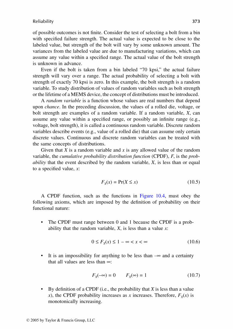
Reliability 373
of possible outcomes is not finite. Consider the test of selecting a bolt from a bin
with specified failure strength. The actual value is expected to be close to the
labeled value, but strength of the bolt will vary by some unknown amount. The
variances from the labeled value are due to manufacturing variations, which can
assume any value within a specified range. The actual value of the bolt strength
is unknown in advance.
Even if the bolt is taken from a bin labeled “70 kpsi,” the actual failure
strength will vary over a range. The actual probability of selecting a bolt with
strength of exactly 70 kpsi is zero. In this example, the bolt strength is a random
variable. To study distribution of values of random variables such as bolt strength
or the lifetime of a MEMS device, the concept of distributions must be introduced.
A random variable is a function whose values are real numbers that depend
upon chance. In the preceding discussion, the values of a rolled die, voltage, or
bolt strength are examples of a random variable. If a random variable, X, can
assume any value within a specified range, or possibly an infinite range (e.g.,
voltage, bolt strength), it is called a continuous random variable. Discrete random
variables describe events (e.g., value of a rolled die) that can assume only certain
discrete values. Continuous and discrete random variables can be treated with
the same concepts of distributions.
Given that X is a random variable and x is any allowed value of the random
variable, the cumulative probability distribution function (CPDF), F, is the prob-
ability that the event described by the random variable, X, is less than or equal
to a specified value, x:
FX(x) = Pr(X ≤ x) (10.5)
A CPDF function, such as the functions in Figure 10.4, must obey the
following axioms, which are imposed by the definition of probability on their
functional nature:
• The CPDF must range between 0 and 1 because the CPDF is a prob-
ability that the random variable, X, is less than a value x:
0 ≤ FX(x) ≤ 1 – ∞ < x < ∞ (10.6)
• It is an impossibility for anything to be less than –∞ and a certainty
that all values are less than ∞:
FX(–∞) = 0 FX(∞) = 1 (10.7)
• By definition of a CPDF (i.e., the probability that X is less than a value
x), the CPDF probability increases as x increases. Therefore, FX(x) is
monotonically increasing.
© 2005 by Taylor & Francis Group, LLC
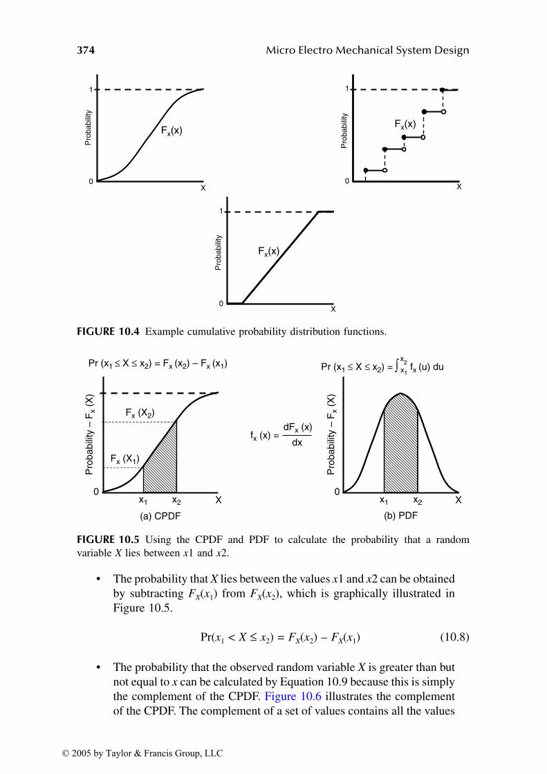
374 Micro Electro Mechanical System Design
• The probability that X lies between the values x1 and x2 can be obtained
by subtracting FX(x1) from FX(x2), which is graphically illustrated in
Figure 10.5.
Pr(x1 < X ≤ x2) = FX(x2) – FX(x1) (10.8)
• The probability that the observed random variable X is greater than but
not equal to x can be calculated by Equation 10.9 because this is simply
the complement of the CPDF. Figure 10.6 illustrates the complement
of the CPDF. The complement of a set of values contains all the values
FIGURE 10.4 Example cumulative probability distribution functions.
FIGURE 10.5 Using the CPDF and PDF to calculate the probability that a random
variable X lies between x1 and x2.
1
0X
Pro
babi
lity
Fx(x)
1
0X
Pro
babi
lity
Fx(x)
1
0X
Pro
babi
lity
Fx(x)
Pr (x1 ≤ X ≤ x2) = Fx (x2) – Fx (x1) Pr (x1 ≤ X ≤ x2) = x1 fx (u) du
x2
Pro
babi
lity
– F
x (X
)
Pro
babi
lity
– F
x (X
)
Fx (X2)
Fx (X1)
x1 x2 X x1 x2 X
fx (x) =dFx (x)
dx
00
(a) CPDF (b) PDF
∫
© 2005 by Taylor & Francis Group, LLC
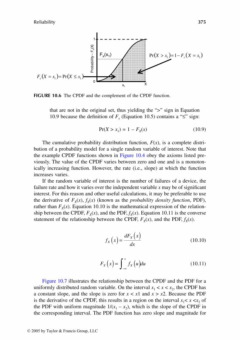
Reliability 375
that are not in the original set, thus yielding the “>” sign in Equation
10.9 because the definition of Fx (Equation 10.5) contains a “≤” sign:
Pr(X > x1) = 1 – FX(x) (10.9)
The cumulative probability distribution function, F(x), is a complete distri-
bution of a probability model for a single random variable of interest. Note that
the example CPDF functions shown in Figure 10.4 obey the axioms listed pre-
viously. The value of the CPDF varies between zero and one and is a monoton-
ically increasing function. However, the rate (i.e., slope) at which the function
increases varies.
If the random variable of interest is the number of failures of a device, the
failure rate and how it varies over the independent variable x may be of significant
interest. For this reason and other useful calculations, it may be preferable to use
the derivative of FX(x), fX(x) (known as the probability density function, PDF),
rather than FX(x). Equation 10.10 is the mathematical expression of the relation-
ship between the CPDF, FX(x), and the PDF, fX(x). Equation 10.11 is the converse
statement of the relationship between the CPDF, FX(x), and the PDF, fX(x).
(10.10)
(10.11)
Figure 10.7 illustrates the relationship between the CPDF and the PDF for a
uniformly distributed random variable. On the interval x1 < x < x2, the CPDF has
a constant slope, and the slope is zero for x < x1 and x > x2. Because the PDF
is the derivative of the CPDF, this results in a region on the interval x1< x <x2 of
the PDF with uniform magnitude 1/(x1 – x2), which is the slope of the CPDF in
the corresponding interval. The PDF function has zero slope and magnitude for
FIGURE 10.6 The CPDF and the complement of the CPDF function.
1
0Xx1
Pro
ba
bili
ty–
Fx(
X)
Fx(x1)
( ) ( )11 Pr xXxXFx ≤==
( ) ( )11 1Pr xXFxX x =−=>
f xdF x
dxX
X( ) = ( )F x f u duX X
x( ) = ( )−∞∫
© 2005 by Taylor & Francis Group, LLC
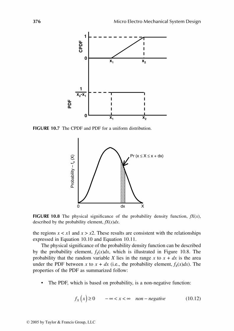
376 Micro Electro Mechanical System Design
the regions x < x1 and x > x2. These results are consistent with the relationships
expressed in Equation 10.10 and Equation 10.11.
The physical significance of the probability density function can be described
by the probability element, fX(x)dx, which is illustrated in Figure 10.8. The
probability that the random variable X lies in the range x to x + dx is the area
under the PDF between x to x + dx (i.e., the probability element, fX(x)dx). The
properties of the PDF as summarized follow:
• The PDF, which is based on probability, is a non-negative function:
(10.12)
FIGURE 10.7 The CPDF and PDF for a uniform distribution.
FIGURE 10.8 The physical significance of the probability density function, fX(x),
described by the probability element, fX(x)dx.
x1
x2
x2-x
1
1
1
0
0 x1
x2
CP
DF
PD
F
Pr (x ≤ X ≤ x + dx)
Pro
babi
lity
– f x
(X
)
0 dx X
f x x non negativeX ( ) ≥ − ∞ < < ∞ −0
© 2005 by Taylor & Francis Group, LLC
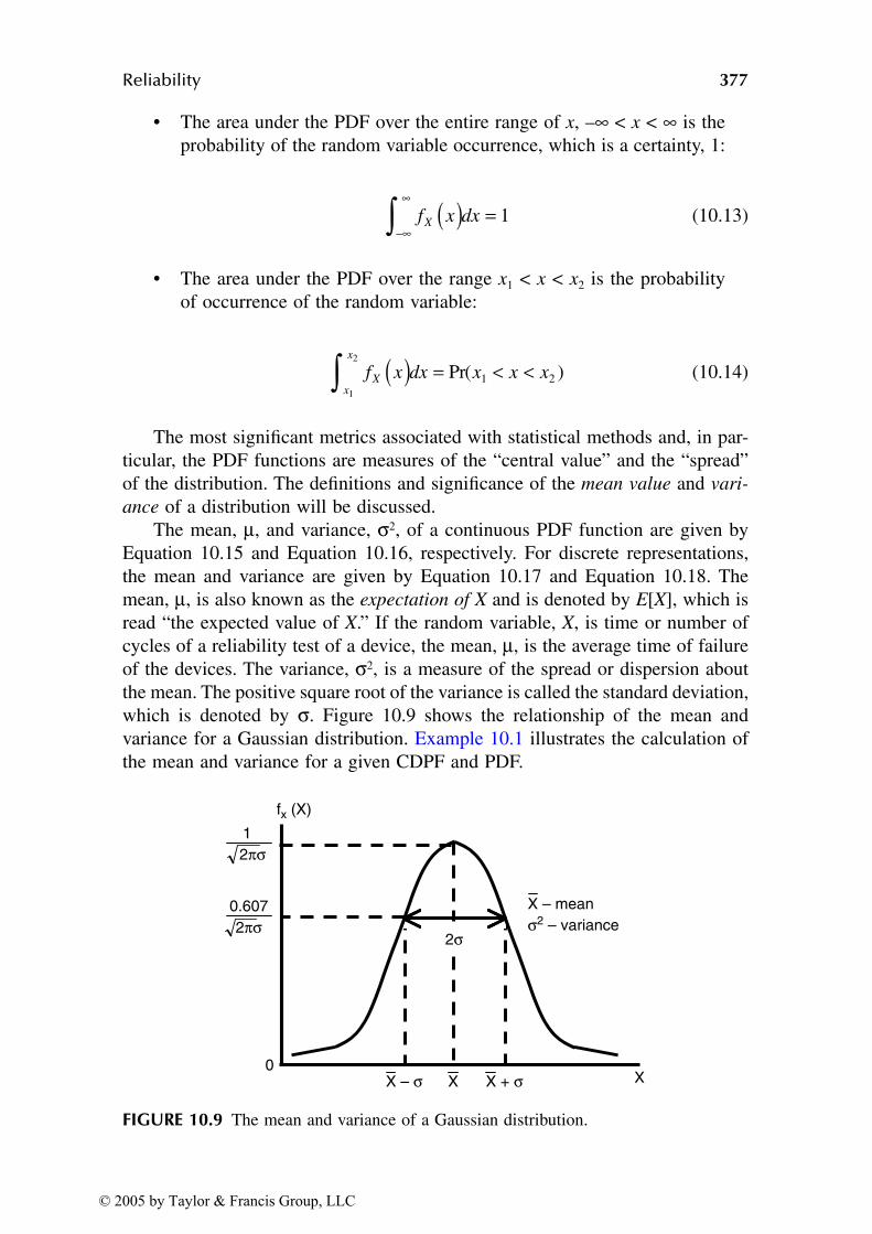
Reliability 377
• The area under the PDF over the entire range of x, –∞ < x < ∞ is the
probability of the random variable occurrence, which is a certainty, 1:
(10.13)
• The area under the PDF over the range x1 < x < x2 is the probability
of occurrence of the random variable:
(10.14)
The most significant metrics associated with statistical methods and, in par-
ticular, the PDF functions are measures of the “central value” and the “spread”
of the distribution. The definitions and significance of the mean value and vari-
ance of a distribution will be discussed.
The mean, µ, and variance, σ2, of a continuous PDF function are given by
Equation 10.15 and Equation 10.16, respectively. For discrete representations,
the mean and variance are given by Equation 10.17 and Equation 10.18. The
mean, µ, is also known as the expectation of X and is denoted by E[X], which is
read “the expected value of X.” If the random variable, X, is time or number of
cycles of a reliability test of a device, the mean, µ, is the average time of failure
of the devices. The variance, σ2, is a measure of the spread or dispersion about
the mean. The positive square root of the variance is called the standard deviation,
which is denoted by σ. Figure 10.9 shows the relationship of the mean and
variance for a Gaussian distribution. Example 10.1 illustrates the calculation of
the mean and variance for a given CDPF and PDF.
FIGURE 10.9 The mean and variance of a Gaussian distribution.
f x dxX ( ) =−∞∞∫ 1
f x dx x x xXx
x ( ) = < <∫1
2
1 2Pr( )
1
0.607
2πσ
2πσ
0
2σ
X – σ X + σX X
σ2 – varianceX – mean
fx (X)
© 2005 by Taylor & Francis Group, LLC

378 Micro Electro Mechanical System Design
(10.15)
(10.16)
(10.17)
(10.18)
Example 10.1
Problem: Figure 10.2 shows discrete data for a reliability test of a switch. Fre-
quently, for reliability test data, a functional fit to the test data is done using the
techniques of regression analysis [53]. Because the data in Figure 10.2 are
simulated, a uniform distribution model was used. A mathematical model provides
enhanced ability for analysis and exploration of the different types of models that
may be relevant. The next section will discuss several of the frequently used
reliability models. Given the functional formulation for the CPDF and PDF
function shown in Figure 10.10 calculate and plot the following: (a) mean; (b)
variance; and (c) standard deviation (Figure 10.10).
FIGURE 10.10 Functional fit of the CPDF and PDF data of Figure 10.2.
µ =−∞∞∫ xf x dxX ( )
σ µ2
2
= −( ) ( )−∞∞∫ x f x dx
µ =∑ x f xj
j
j( )
σ µ22= −( ) ( )∑ x f xj
j
j
1
0
0
CP
DF
PD
F
10−6
10−6
106Time – hr.
106Time – hr.
© 2005 by Taylor & Francis Group, LLC
Reliability 379
Solution: (a) X(t) is the random variable for the failures that is a function of
time. Utilizing Equation 10.15, the mean can be calculated as follows:
(b) Utilizing Equation 10.16, the variance is calculated as follows:
(c) Utilizing the definition of standard deviation,
Another important reliability measure is the instantaneous failure rate or
hazard rate, hX(t). In other words, the hazard rate is the failure rate of the survivors
at time t. The hazard rate is defined as the failure rate, fX(t) (i.e., PDF of failure),
normalized by the probability of devices surviving, RX(t). The probability of
devices surviving, RX(t), is the complement of the probability of device failures,
FX(t), occurring up to time t. This can be expressed as shown in Equation 10.19.
The hazard rate, hX(t), can be defined in terms of the CPDF and PDF functions
previously discussed, as shown in Equation 10.20. The hazard rate is expressed
in the FIT units (i.e., failures per billion cycles of operation) previously discussed.
The bathtub curve discussed in Section 10.1 is a plot of the hazard rate vs. time
or cycles of operation.
(10.19)
E X tf t dt
t dt
ho
X[ ] ( )
( )
= =
=
=
−∞∞
−
∫∫
µ
µ
µ
10
10
2
6
0
10
6
6
uurs
σ µ
σ µ
σ
2
2
2
0
102
6
2
6
10
1
= −( ) ( )= −( )=
−∞∞
−
∫∫
t f t dt
t dt
00
12
12
σ = ≈10
120 29 10
66. x
R t F tX X( ) = − ( )1
© 2005 by Taylor & Francis Group, LLC
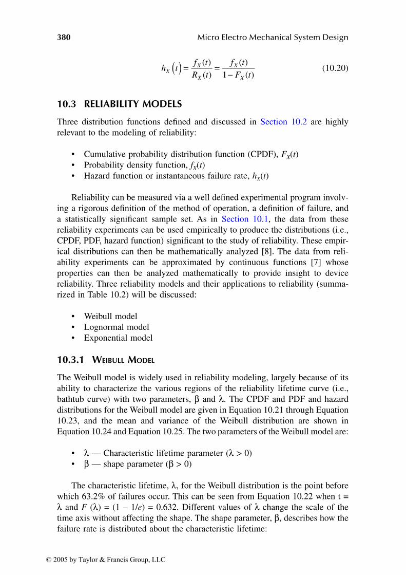
380 Micro Electro Mechanical System Design
(10.20)
10.3 RELIABILITY MODELS
Three distribution functions defined and discussed in Section 10.2 are highly
relevant to the modeling of reliability:
• Cumulative probability distribution function (CPDF), FX(t)
• Probability density function, fX(t)
• Hazard function or instantaneous failure rate, hX(t)
Reliability can be measured via a well defined experimental program involv-
ing a rigorous definition of the method of operation, a definition of failure, and
a statistically significant sample set. As in Section 10.1, the data from these
reliability experiments can be used empirically to produce the distributions (i.e.,
CPDF, PDF, hazard function) significant to the study of reliability. These empir-
ical distributions can then be mathematically analyzed [8]. The data from reli-
ability experiments can be approximated by continuous functions [7] whose
properties can then be analyzed mathematically to provide insight to device
reliability. Three reliability models and their applications to reliability (summa-
rized in Table 10.2) will be discussed:
• Weibull model
• Lognormal model
• Exponential model
10.3.1 WEIBULL MODEL
The Weibull model is widely used in reliability modeling, largely because of its
ability to characterize the various regions of the reliability lifetime curve (i.e.,
bathtub curve) with two parameters, β and λ. The CPDF and PDF and hazard
distributions for the Weibull model are given in Equation 10.21 through Equation
10.23, and the mean and variance of the Weibull distribution are shown in
Equation 10.24 and Equation 10.25. The two parameters of the Weibull model are:
• λ — Characteristic lifetime parameter (λ > 0)
• β — shape parameter (β > 0)
The characteristic lifetime, λ, for the Weibull distribution is the point before
which 63.2% of failures occur. This can be seen from Equation 10.22 when t =λ and F (λ) = (1 – 1/e) = 0.632. Different values of λ change the scale of the
time axis without affecting the shape. The shape parameter, β, describes how the
failure rate is distributed about the characteristic lifetime:
h tf t
R t
f t
F tX
X
X
X
X
( ) = = −( )
( )
( )
( )1
© 2005 by Taylor & Francis Group, LLC
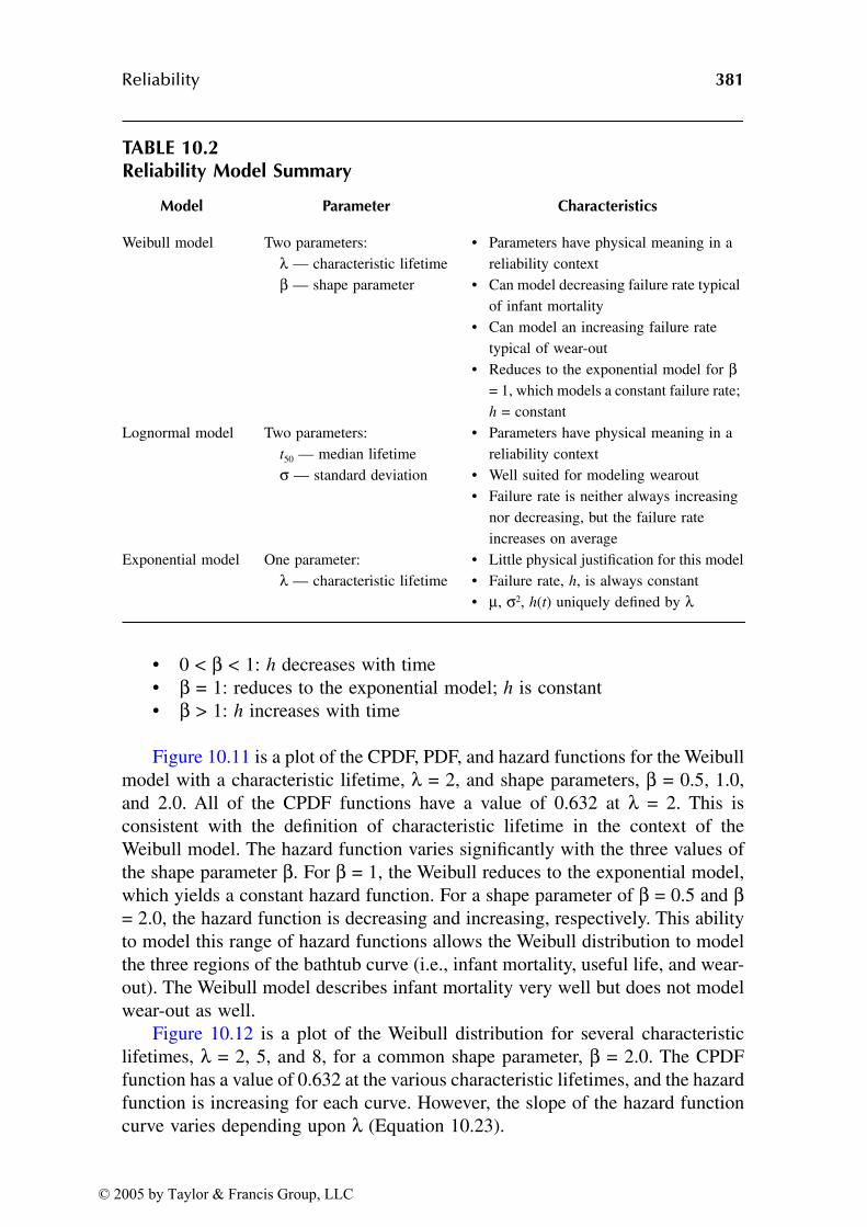
Reliability 381
• 0 < β < 1: h decreases with time
• β = 1: reduces to the exponential model; h is constant
• β > 1: h increases with time
Figure 10.11 is a plot of the CPDF, PDF, and hazard functions for the Weibull
model with a characteristic lifetime, λ = 2, and shape parameters, β = 0.5, 1.0,
and 2.0. All of the CPDF functions have a value of 0.632 at λ = 2. This is
consistent with the definition of characteristic lifetime in the context of the
Weibull model. The hazard function varies significantly with the three values of
the shape parameter β. For β = 1, the Weibull reduces to the exponential model,
which yields a constant hazard function. For a shape parameter of β = 0.5 and β= 2.0, the hazard function is decreasing and increasing, respectively. This ability
to model this range of hazard functions allows the Weibull distribution to model
the three regions of the bathtub curve (i.e., infant mortality, useful life, and wear-
out). The Weibull model describes infant mortality very well but does not model
wear-out as well.
Figure 10.12 is a plot of the Weibull distribution for several characteristic
lifetimes, λ = 2, 5, and 8, for a common shape parameter, β = 2.0. The CPDF
function has a value of 0.632 at the various characteristic lifetimes, and the hazard
function is increasing for each curve. However, the slope of the hazard function
curve varies depending upon λ (Equation 10.23).
TABLE 10.2Reliability Model Summary
Model Parameter Characteristics
Weibull model Two parameters:
λ — characteristic lifetime
β — shape parameter
• Parameters have physical meaning in a
reliability context
• Can model decreasing failure rate typical
of infant mortality
• Can model an increasing failure rate
typical of wear-out
• Reduces to the exponential model for β= 1, which models a constant failure rate;
h = constant
Lognormal model Two parameters:
t50 — median lifetime
σ — standard deviation
• Parameters have physical meaning in a
reliability context
• Well suited for modeling wearout
• Failure rate is neither always increasing
nor decreasing, but the failure rate
increases on average
Exponential model One parameter:
λ — characteristic lifetime
• Little physical justification for this model
• Failure rate, h, is always constant
• µ, σ2, h(t) uniquely defined by λ
© 2005 by Taylor & Francis Group, LLC
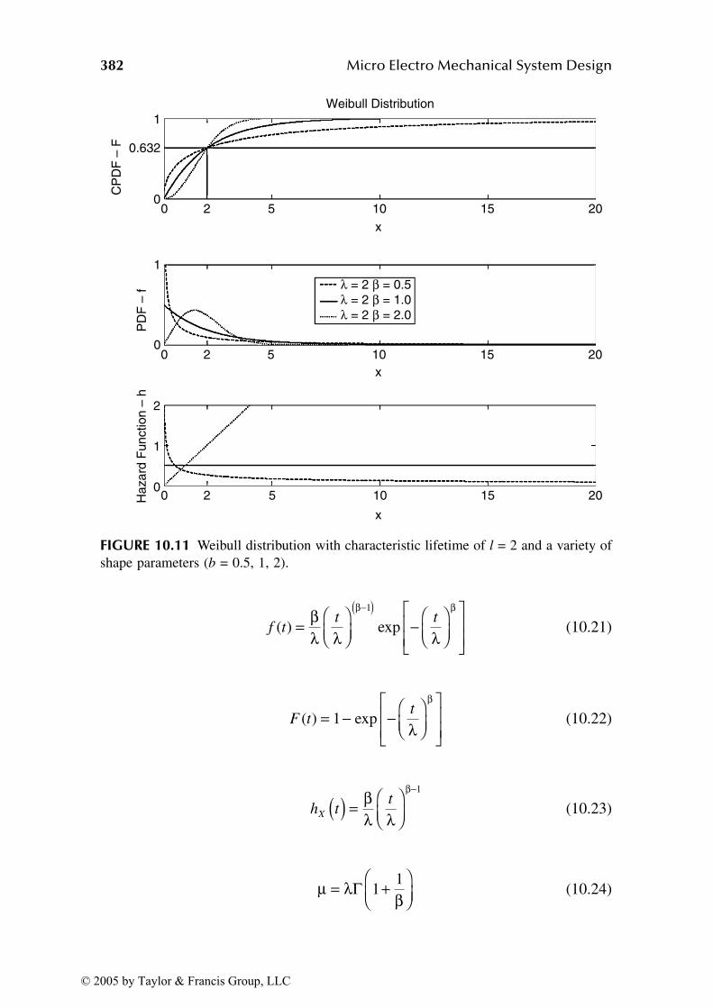
382 Micro Electro Mechanical System Design
(10.21)
(10.22)
(10.23)
(10.24)
FIGURE 10.11 Weibull distribution with characteristic lifetime of l = 2 and a variety of
shape parameters (b = 0.5, 1, 2).
Weibull Distribution
0 2 5 10 15 20
0 2 5 10 15 20
0 2Haz
ard
Fun
ctio
n –
h
5 10 15 20
λ = 2 β = 0.5λ = 2 β = 1.0λ = 2 β = 2.0
x
x
x
1
1
1
2
0
0
0
0.632
CP
DF
– F
PD
F –
f
f tt t
( ) exp=
−
−( )βλ λ λ
β β1
F tt
( ) exp= − −
1 λ
β
h tt
X ( ) =
−βλ λ
β 1
µ λ β= +
Γ 1
1
© 2005 by Taylor & Francis Group, LLC
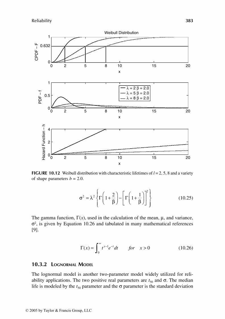
Reliability 383
(10.25)
The gamma function, Γ(x), used in the calculation of the mean, µ, and variance,σ2, is given by Equation 10.26 and tabulated in many mathematical references
[9].
(10.26)
10.3.2 LOGNORMAL MODEL
The lognormal model is another two-parameter model widely utilized for reli-
ability applications. The two positive real parameters are t50 and σ. The median
life is modeled by the t50 parameter and the σ parameter is the standard deviation
FIGURE 10.12 Weibull distribution with characteristic lifetimes of l = 2, 5, 8 and a variety
of shape parameters b = 2.0.
Weibull Distribution
0 2 5 8 10 15 20
Haz
ard
Fun
ctio
n –
h
λ = 2 β = 2.0λ = 5 β = 2.0λ = 8 β = 2.0
x
020 5 8 10 15 20
x
0 2 5 8 10 15 20
x
1
1
0.5
2
4
0
0
0.632
CP
DF
– F
PD
F –
f
σ λ β β2 2
2
12
11= +
− +
Γ Γ
Γ( )x t e dt for xx t= >−∞ −∫ 1
0
0
© 2005 by Taylor & Francis Group, LLC
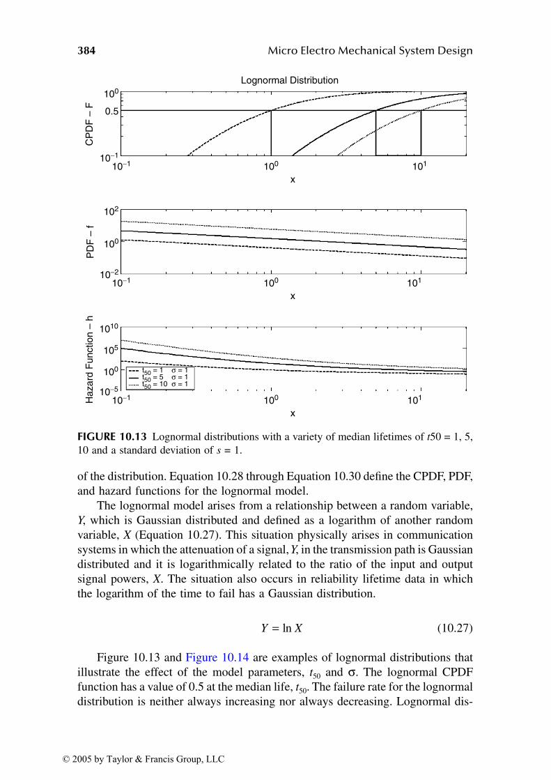
384 Micro Electro Mechanical System Design
of the distribution. Equation 10.28 through Equation 10.30 define the CPDF, PDF,
and hazard functions for the lognormal model.
The lognormal model arises from a relationship between a random variable,
Y, which is Gaussian distributed and defined as a logarithm of another random
variable, X (Equation 10.27). This situation physically arises in communication
systems in which the attenuation of a signal, Y, in the transmission path is Gaussian
distributed and it is logarithmically related to the ratio of the input and output
signal powers, X. The situation also occurs in reliability lifetime data in which
the logarithm of the time to fail has a Gaussian distribution.
(10.27)
Figure 10.13 and Figure 10.14 are examples of lognormal distributions that
illustrate the effect of the model parameters, t50 and σ. The lognormal CPDF
function has a value of 0.5 at the median life, t50. The failure rate for the lognormal
distribution is neither always increasing nor always decreasing. Lognormal dis-
FIGURE 10.13 Lognormal distributions with a variety of median lifetimes of t50 = 1, 5,
10 and a standard deviation of s = 1.
Lognormal Distribution
10−110−1
10−2
10−5
100
100
1010
105
100
100
102
0.5
101
x
10−1 100 101
x
10−1 100 101
x
Haz
ard
Fun
ctio
n –
hC
PD
F –
FP
DF
– f
t50 = 1 σ = 1t50 = 5 σ = 1t50 = 10 σ = 1
Y X= ln
© 2005 by Taylor & Francis Group, LLC
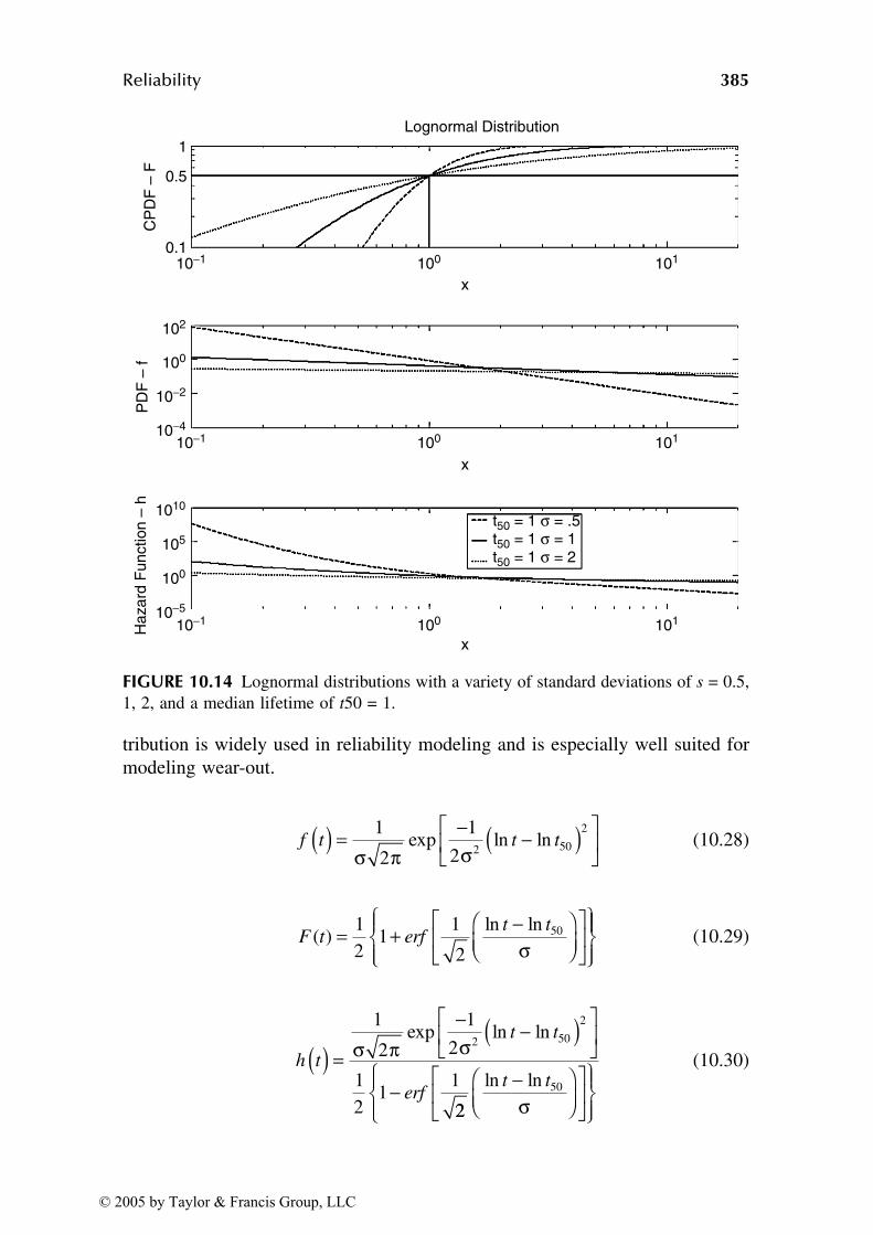
Reliability 385
tribution is widely used in reliability modeling and is especially well suited for
modeling wear-out.
(10.28)
(10.29)
(10.30)
FIGURE 10.14 Lognormal distributions with a variety of standard deviations of s = 0.5,
1, 2, and a median lifetime of t50 = 1.
Lognormal Distribution
10−1 100 101
10−1 100 101
10−1 100 101
x
x
x
1
0.5
0.1
102
1010
105
100
100
10−2
10−4
10−5
Haz
ard
Fun
ctio
n –
hC
PD
F –
FP
DF
– f
t50 = 1 σ = .5t50 = 1 σ = 1t50 = 1 σ = 2
f t t t( ) = − −( )
1
2
1
2 2 50
2
σ π σexp ln ln
F t erft t
( )ln ln= + −
1
21
1
2
50σ
h t
t t
erf
( ) =− −( )
−
1
2
1
2
1
21
1
2 50
2
σ π σexp ln ln
22
50ln lnt t−
σ
© 2005 by Taylor & Francis Group, LLC
386 Micro Electro Mechanical System Design
The error function, erf(x), used in the calculation of the preceding distribu-
tions is given by Equation 10.31 and tabulated in many mathematical refer-
ences [9].
(10.31)
10.3.3 EXPONENTIAL MODEL
The exponential model is a very simple, widely used one-parameter, λ, model;
however, there is little physical justification. The CPDF, PDF, and hazard func-
tions for the exponential model are defined in Equation 10.32 through Equation
10.34. Equation 10.35 and Equation 10.36 define the mean, µ, and variation, σ2,
of the distribution. Note that the mean, variance, and hazard function for the
exponential model are all uniquely defined by the parameter λ.
Because the hazard function for the exponential model is a constant, this
model is appropriate for systems involving truly random events such as occur in
the useful life portion of the bathtub curve. The model cannot model infant
mortality or wear-out. Figure 10.15 is a plot of the CPDF, PDF, and hazard
functions for the exponential model with λ = 1.0, 5.0, and 10.0. The CPDF
function has a value of 0.632 at the appropriate characteristic lifetime for each
curve plotted. Because this is a one-parameter model, the characteristic lifetime
parameter, λ, also defines the hazard function.
(10.32)
(10.33)
(10.34)
(10.35)
(10.36)
10.4 MEMS FAILURE MECHANISMS
Since World War II, reliability methodology has been increasingly applied to a
wide spectrum of devices and systems [10]. The reliability of microelectronic
erf x u dux
( ) exp= −( )∫2 2
0π
f t t( ) exp= −( )λ λ
F t t( ) exp= − −( )1 λ
h t( ) = λ
µ λ= 1
σ λ2
2
1=
© 2005 by Taylor & Francis Group, LLC

Reliability 387
devices has been extensively studied and their failure mechanisms are well under-
stood. Microelectronics share a common set of failure mechanisms, which include
hot carriers, oxide breakdown, stress voiding, and electromigration. These failure
mechanisms have been physically and statistically studied extensively, thus
enabling the prediction of performance in various environments.
MEMS applications cover a very wide spectrum and a large number of device
designs have been implemented to address these applications. As a result of the
breadth of application, the reliability of MEMS devices is not dominated by the
behavior of a “typical” device. The failure mechanisms that may be experienced
by MEMS devices are quite broad, especially in comparison to microelectronics.
As a result, these failure mechanisms are more varied than those of microelectronics.
Currently, MEMS failure mechanisms are not well characterized or under-
stood; it is not wise to use a macroscale failure mechanism or reliability data
directly for a MEMS device because this would require an assumption of simi-
larity that is generally not valid.
The area of understanding the failure mechanisms of MEMS devices in a
reliability context is just in its formative stages. However, some published works
have documented the first steps of understanding failure mechanisms of MEMS
FIGURE 10.15 Exponential distributions with a variety of characteristic lifetimes l = 1,
5, 10.
0 1 5 10 15 20x
0 1 5 10 15 20x
0 1 5 10 15 20x
1
1
0.5
1.5
1
0.50.2
0
0
0
0.632
Haz
ard
Fun
ctio
n –
hC
PD
F –
FP
DF
– f λ = 1
λ = 5λ = 10
Exponential Distribution
© 2005 by Taylor & Francis Group, LLC
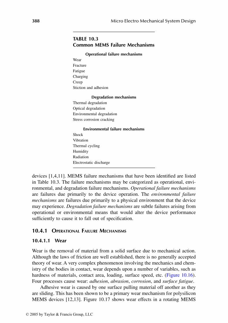
388 Micro Electro Mechanical System Design
devices [1,4,11]. MEMS failure mechanisms that have been identified are listed
in Table 10.3. The failure mechanisms may be categorized as operational, envi-
ronmental, and degradation failure mechanisms. Operational failure mechanisms
are failures due primarily to the device operation. The environmental failure
mechanisms are failures due primarily to a physical environment that the device
may experience. Degradation failure mechanisms are subtle failures arising from
operational or environmental means that would alter the device performance
sufficiently to cause it to fall out of specification.
10.4.1 OPERATIONAL FAILURE MECHANISMS
10.4.1.1 Wear
Wear is the removal of material from a solid surface due to mechanical action.
Although the laws of friction are well established, there is no generally accepted
theory of wear. A very complex phenomenon involving the mechanics and chem-
istry of the bodies in contact, wear depends upon a number of variables, such as
hardness of materials, contact area, loading, surface speed, etc. (Figure 10.16).
Four processes cause wear: adhesion, abrasion, corrosion, and surface fatigue.
Adhesive wear is caused by one surface pulling material off another as they
are sliding. This has been shown to be a primary wear mechanism for polysilicon
MEMS devices [12,13]. Figure 10.17 shows wear effects in a rotating MEMS
TABLE 10.3Common MEMS Failure Mechanisms
Operational failure mechanisms
Wear
Fracture
Fatigue
Charging
Creep
Stiction and adhesion
Degradation mechanisms
Thermal degradation
Optical degradation
Environmental degradation
Stress corrosion cracking
Environmental failure mechanisms
Shock
Vibration
Thermal cycling
Humidity
Radiation
Electrostatic discharge
© 2005 by Taylor & Francis Group, LLC
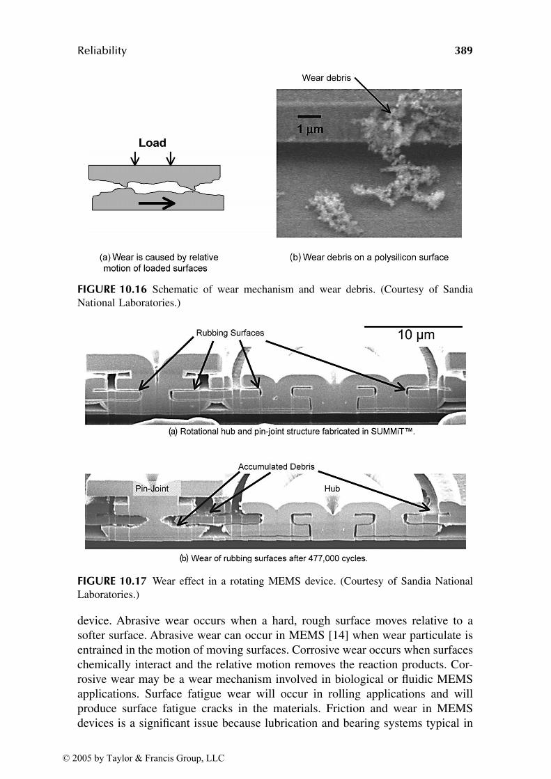
Reliability 389
device. Abrasive wear occurs when a hard, rough surface moves relative to a
softer surface. Abrasive wear can occur in MEMS [14] when wear particulate is
entrained in the motion of moving surfaces. Corrosive wear occurs when surfaces
chemically interact and the relative motion removes the reaction products. Cor-
rosive wear may be a wear mechanism involved in biological or fluidic MEMS
applications. Surface fatigue wear will occur in rolling applications and will
produce surface fatigue cracks in the materials. Friction and wear in MEMS
devices is a significant issue because lubrication and bearing systems typical in
FIGURE 10.16 Schematic of wear mechanism and wear debris. (Courtesy of Sandia
National Laboratories.)
FIGURE 10.17 Wear effect in a rotating MEMS device. (Courtesy of Sandia National
Laboratories.)
© 2005 by Taylor & Francis Group, LLC
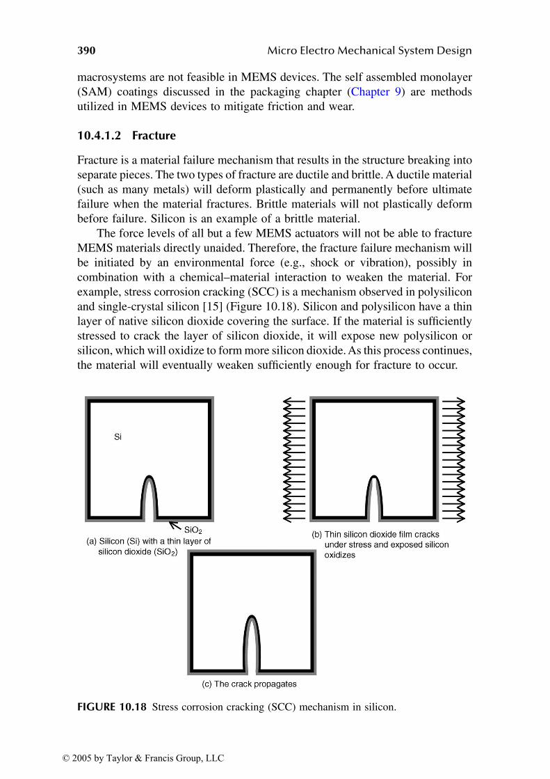
390 Micro Electro Mechanical System Design
macrosystems are not feasible in MEMS devices. The self assembled monolayer
(SAM) coatings discussed in the packaging chapter (Chapter 9) are methods
utilized in MEMS devices to mitigate friction and wear.
10.4.1.2 Fracture
Fracture is a material failure mechanism that results in the structure breaking into
separate pieces. The two types of fracture are ductile and brittle. A ductile material
(such as many metals) will deform plastically and permanently before ultimate
failure when the material fractures. Brittle materials will not plastically deform
before failure. Silicon is an example of a brittle material.
The force levels of all but a few MEMS actuators will not be able to fracture
MEMS materials directly unaided. Therefore, the fracture failure mechanism will
be initiated by an environmental force (e.g., shock or vibration), possibly in
combination with a chemical–material interaction to weaken the material. For
example, stress corrosion cracking (SCC) is a mechanism observed in polysilicon
and single-crystal silicon [15] (Figure 10.18). Silicon and polysilicon have a thin
layer of native silicon dioxide covering the surface. If the material is sufficiently
stressed to crack the layer of silicon dioxide, it will expose new polysilicon or
silicon, which will oxidize to form more silicon dioxide. As this process continues,
the material will eventually weaken sufficiently enough for fracture to occur.
FIGURE 10.18 Stress corrosion cracking (SCC) mechanism in silicon.
© 2005 by Taylor & Francis Group, LLC
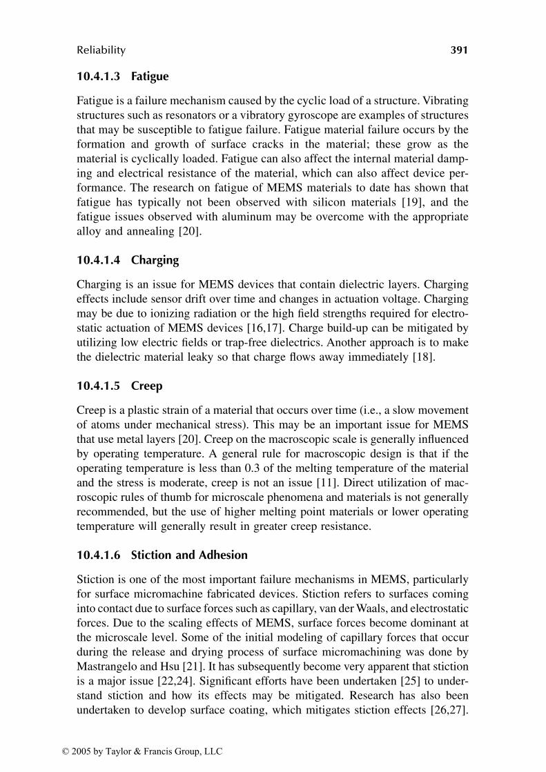
Reliability 391
10.4.1.3 Fatigue
Fatigue is a failure mechanism caused by the cyclic load of a structure. Vibrating
structures such as resonators or a vibratory gyroscope are examples of structures
that may be susceptible to fatigue failure. Fatigue material failure occurs by the
formation and growth of surface cracks in the material; these grow as the
material is cyclically loaded. Fatigue can also affect the internal material damp-
ing and electrical resistance of the material, which can also affect device per-
formance. The research on fatigue of MEMS materials to date has shown that
fatigue has typically not been observed with silicon materials [19], and the
fatigue issues observed with aluminum may be overcome with the appropriate
alloy and annealing [20].
10.4.1.4 Charging
Charging is an issue for MEMS devices that contain dielectric layers. Charging
effects include sensor drift over time and changes in actuation voltage. Charging
may be due to ionizing radiation or the high field strengths required for electro-
static actuation of MEMS devices [16,17]. Charge build-up can be mitigated by
utilizing low electric fields or trap-free dielectrics. Another approach is to make
the dielectric material leaky so that charge flows away immediately [18].
10.4.1.5 Creep
Creep is a plastic strain of a material that occurs over time (i.e., a slow movement
of atoms under mechanical stress). This may be an important issue for MEMS
that use metal layers [20]. Creep on the macroscopic scale is generally influenced
by operating temperature. A general rule for macroscopic design is that if the
operating temperature is less than 0.3 of the melting temperature of the material
and the stress is moderate, creep is not an issue [11]. Direct utilization of mac-
roscopic rules of thumb for microscale phenomena and materials is not generally
recommended, but the use of higher melting point materials or lower operating
temperature will generally result in greater creep resistance.
10.4.1.6 Stiction and Adhesion
Stiction is one of the most important failure mechanisms in MEMS, particularly
for surface micromachine fabricated devices. Stiction refers to surfaces coming
into contact due to surface forces such as capillary, van der Waals, and electrostatic
forces. Due to the scaling effects of MEMS, surface forces become dominant at
the microscale level. Some of the initial modeling of capillary forces that occur
during the release and drying process of surface micromachining was done by
Mastrangelo and Hsu [21]. It has subsequently become very apparent that stiction
is a major issue [22,24]. Significant efforts have been undertaken [25] to under-
stand stiction and how its effects may be mitigated. Research has also been
undertaken to develop surface coating, which mitigates stiction effects [26,27].
© 2005 by Taylor & Francis Group, LLC
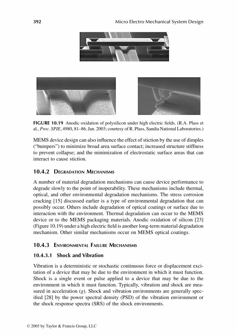
392 Micro Electro Mechanical System Design
MEMS device design can also influence the effect of stiction by the use of dimples
(“bumpers”) to minimize broad area surface contact; increased structure stiffness
to prevent collapse; and the minimization of electrostatic surface areas that can
interact to cause stiction.
10.4.2 DEGRADATION MECHANISMS
A number of material degradation mechanisms can cause device performance to
degrade slowly to the point of inoperability. These mechanisms include thermal,
optical, and other environmental degradation mechanisms. The stress corrosion
cracking [15] discussed earlier is a type of environmental degradation that can
possibly occur. Others include degradation of optical coatings or surface due to
interaction with the environment. Thermal degradation can occur to the MEMS
device or to the MEMS packaging materials. Anodic oxidation of silicon [23]
(Figure 10.19) under a high electric field is another long-term material degradation
mechanism. Other similar mechanisms occur on MEMS optical coatings.
10.4.3 ENVIRONMENTAL FAILURE MECHANISMS
10.4.3.1 Shock and Vibration
Vibration is a deterministic or stochastic continuous force or displacement exci-
tation of a device that may be due to the environment in which it must function.
Shock is a single event or pulse applied to a device that may be due to the
environment in which it must function. Typically, vibration and shock are mea-
sured in acceleration (g). Shock and vibration environments are generally spec-
ified [28] by the power spectral density (PSD) of the vibration environment or
the shock response spectra (SRS) of the shock environments.
FIGURE 10.19 Anodic oxidation of polysilicon under high electric fields. (R.A. Plass et
al., Proc. SPIE, 4980, 81–86, Jan. 2003; courtesy of R. Plass, Sandia National Laboratories.)
© 2005 by Taylor & Francis Group, LLC
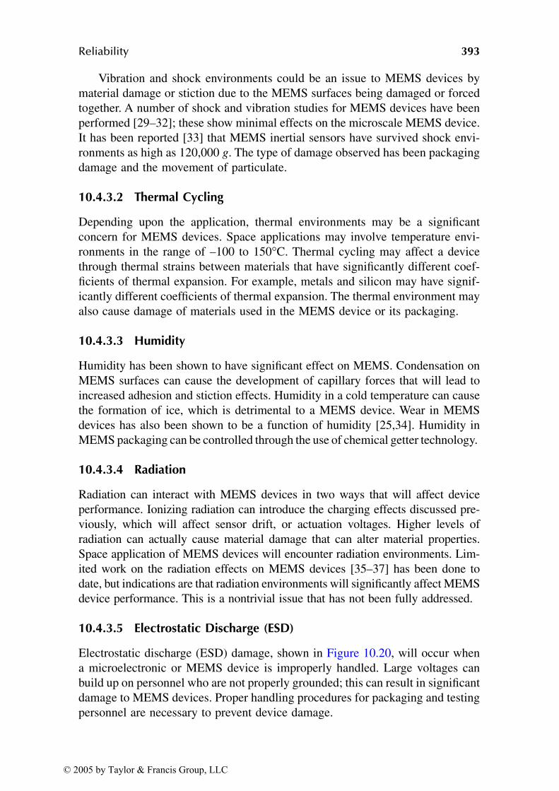
Reliability 393
Vibration and shock environments could be an issue to MEMS devices by
material damage or stiction due to the MEMS surfaces being damaged or forced
together. A number of shock and vibration studies for MEMS devices have been
performed [29–32]; these show minimal effects on the microscale MEMS device.
It has been reported [33] that MEMS inertial sensors have survived shock envi-
ronments as high as 120,000 g. The type of damage observed has been packaging
damage and the movement of particulate.
10.4.3.2 Thermal Cycling
Depending upon the application, thermal environments may be a significant
concern for MEMS devices. Space applications may involve temperature envi-
ronments in the range of –100 to 150°C. Thermal cycling may affect a device
through thermal strains between materials that have significantly different coef-
ficients of thermal expansion. For example, metals and silicon may have signif-
icantly different coefficients of thermal expansion. The thermal environment may
also cause damage of materials used in the MEMS device or its packaging.
10.4.3.3 Humidity
Humidity has been shown to have significant effect on MEMS. Condensation on
MEMS surfaces can cause the development of capillary forces that will lead to
increased adhesion and stiction effects. Humidity in a cold temperature can cause
the formation of ice, which is detrimental to a MEMS device. Wear in MEMS
devices has also been shown to be a function of humidity [25,34]. Humidity in
MEMS packaging can be controlled through the use of chemical getter technology.
10.4.3.4 Radiation
Radiation can interact with MEMS devices in two ways that will affect device
performance. Ionizing radiation can introduce the charging effects discussed pre-
viously, which will affect sensor drift, or actuation voltages. Higher levels of
radiation can actually cause material damage that can alter material properties.
Space application of MEMS devices will encounter radiation environments. Lim-
ited work on the radiation effects on MEMS devices [35–37] has been done to
date, but indications are that radiation environments will significantly affect MEMS
device performance. This is a nontrivial issue that has not been fully addressed.
10.4.3.5 Electrostatic Discharge (ESD)
Electrostatic discharge (ESD) damage, shown in Figure 10.20, will occur when
a microelectronic or MEMS device is improperly handled. Large voltages can
build up on personnel who are not properly grounded; this can result in significant
damage to MEMS devices. Proper handling procedures for packaging and testing
personnel are necessary to prevent device damage.
© 2005 by Taylor & Francis Group, LLC
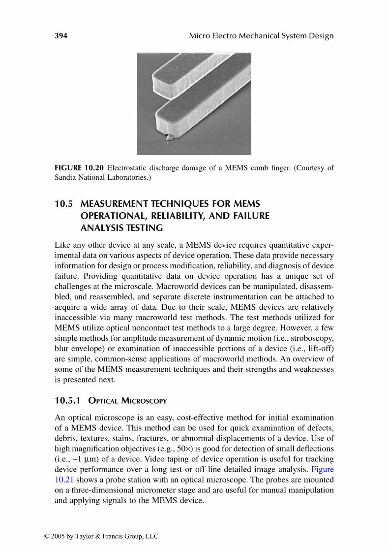
394 Micro Electro Mechanical System Design
10.5 MEASUREMENT TECHNIQUES FOR MEMS OPERATIONAL, RELIABILITY, AND FAILURE ANALYSIS TESTING
Like any other device at any scale, a MEMS device requires quantitative exper-
imental data on various aspects of device operation. These data provide necessary
information for design or process modification, reliability, and diagnosis of device
failure. Providing quantitative data on device operation has a unique set of
challenges at the microscale. Macroworld devices can be manipulated, disassem-
bled, and reassembled, and separate discrete instrumentation can be attached to
acquire a wide array of data. Due to their scale, MEMS devices are relatively
inaccessible via many macroworld test methods. The test methods utilized for
MEMS utilize optical noncontact test methods to a large degree. However, a few
simple methods for amplitude measurement of dynamic motion (i.e., stroboscopy,
blur envelope) or examination of inaccessible portions of a device (i.e., lift-off)
are simple, common-sense applications of macroworld methods. An overview of
some of the MEMS measurement techniques and their strengths and weaknesses
is presented next.
10.5.1 OPTICAL MICROSCOPY
An optical microscope is an easy, cost-effective method for initial examination
of a MEMS device. This method can be used for quick examination of defects,
debris, textures, stains, fractures, or abnormal displacements of a device. Use of
high magnification objectives (e.g., 50×) is good for detection of small deflections
(i.e., ~1 µm) of a device. Video taping of device operation is useful for tracking
device performance over a long test or off-line detailed image analysis. Figure
10.21 shows a probe station with an optical microscope. The probes are mounted
on a three-dimensional micrometer stage and are useful for manual manipulation
and applying signals to the MEMS device.
FIGURE 10.20 Electrostatic discharge damage of a MEMS comb finger. (Courtesy of
Sandia National Laboratories.)
© 2005 by Taylor & Francis Group, LLC
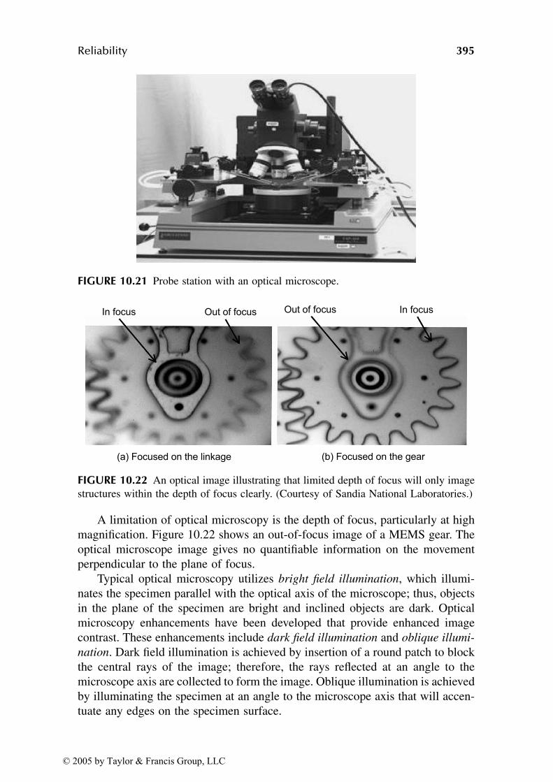
Reliability 395
A limitation of optical microscopy is the depth of focus, particularly at high
magnification. Figure 10.22 shows an out-of-focus image of a MEMS gear. The
optical microscope image gives no quantifiable information on the movement
perpendicular to the plane of focus.
Typical optical microscopy utilizes bright field illumination, which illumi-
nates the specimen parallel with the optical axis of the microscope; thus, objects
in the plane of the specimen are bright and inclined objects are dark. Optical
microscopy enhancements have been developed that provide enhanced image
contrast. These enhancements include dark field illumination and oblique illumi-
nation. Dark field illumination is achieved by insertion of a round patch to block
the central rays of the image; therefore, the rays reflected at an angle to the
microscope axis are collected to form the image. Oblique illumination is achieved
by illuminating the specimen at an angle to the microscope axis that will accen-
tuate any edges on the specimen surface.
FIGURE 10.21 Probe station with an optical microscope.
FIGURE 10.22 An optical image illustrating that limited depth of focus will only image
structures within the depth of focus clearly. (Courtesy of Sandia National Laboratories.)
In focus In focusOut of focus Out of focus
(a) Focused on the linkage (b) Focused on the gear
© 2005 by Taylor & Francis Group, LLC
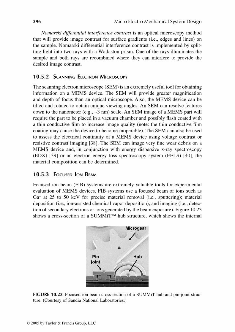
396 Micro Electro Mechanical System Design
Nomarski differential interference contrast is an optical microscopy method
that will provide image contrast for surface gradients (i.e., edges and lines) on
the sample. Nomarski differential interference contrast is implemented by split-
ting light into two rays with a Wollaston prism. One of the rays illuminates the
sample and both rays are recombined where they can interfere to provide the
desired image contrast.
10.5.2 SCANNING ELECTRON MICROSCOPY
The scanning electron microscope (SEM) is an extremely useful tool for obtaining
information on a MEMS device. The SEM will provide greater magnification
and depth of focus than an optical microscope. Also, the MEMS device can be
tilted and rotated to obtain unique viewing angles. An SEM can resolve features
down to the nanometer (e.g., ~3 nm) scale. An SEM image of a MEMS part will
require the part to be placed in a vacuum chamber and possibly flash coated with
a thin conductive film to increase image quality (note: the thin conductive film
coating may cause the device to become inoperable). The SEM can also be used
to assess the electrical continuity of a MEMS device using voltage contrast or
resistive contrast imaging [38]. The SEM can image very fine wear debris on a
MEMS device and, in conjunction with energy dispersive x-ray spectroscopy
(EDX) [39] or an electron energy loss spectroscopy system (EELS) [40], the
material composition can be determined.
10.5.3 FOCUSED ION BEAM
Focused ion beam (FIB) systems are extremely valuable tools for experimental
evaluation of MEMS devices. FIB systems use a focused beam of ions such as
Ga+ at 25 to 50 keV for precise material removal (i.e., sputtering); material
deposition (i.e., ion-assisted chemical vapor deposition); and imaging (i.e., detec-
tion of secondary electrons or ions generated by the beam exposure). Figure 10.23
shows a cross-section of a SUMMiT hub structure, which shows the internal
FIGURE 10.23 Focused ion beam cross-section of a SUMMiT hub and pin-joint struc-
ture. (Courtesy of Sandia National Laboratories.)
© 2005 by Taylor & Francis Group, LLC
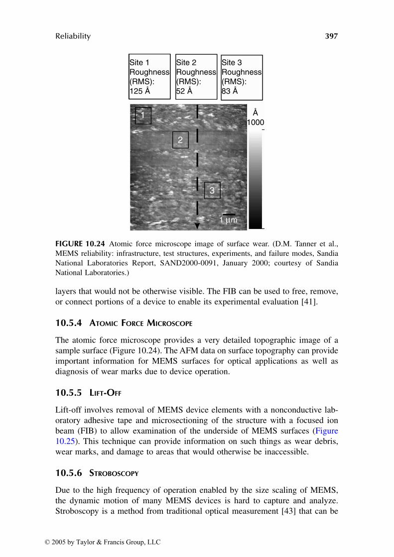
Reliability 397
layers that would not be otherwise visible. The FIB can be used to free, remove,
or connect portions of a device to enable its experimental evaluation [41].
10.5.4 ATOMIC FORCE MICROSCOPE
The atomic force microscope provides a very detailed topographic image of a
sample surface (Figure 10.24). The AFM data on surface topography can provide
important information for MEMS surfaces for optical applications as well as
diagnosis of wear marks due to device operation.
10.5.5 LIFT-OFF
Lift-off involves removal of MEMS device elements with a nonconductive lab-
oratory adhesive tape and microsectioning of the structure with a focused ion
beam (FIB) to allow examination of the underside of MEMS surfaces (Figure
10.25). This technique can provide information on such things as wear debris,
wear marks, and damage to areas that would otherwise be inaccessible.
10.5.6 STROBOSCOPY
Due to the high frequency of operation enabled by the size scaling of MEMS,
the dynamic motion of many MEMS devices is hard to capture and analyze.
Stroboscopy is a method from traditional optical measurement [43] that can be
FIGURE 10.24 Atomic force microscope image of surface wear. (D.M. Tanner et al.,
MEMS reliability: infrastructure, test structures, experiments, and failure modes, Sandia
National Laboratories Report, SAND2000-0091, January 2000; courtesy of Sandia
National Laboratories.)
Site 1Roughness(RMS):125 Å
Site 2Roughness(RMS):52 Å
Site 3Roughness(RMS):83 Å
Å1000
1
2
3
1 µm
© 2005 by Taylor & Francis Group, LLC
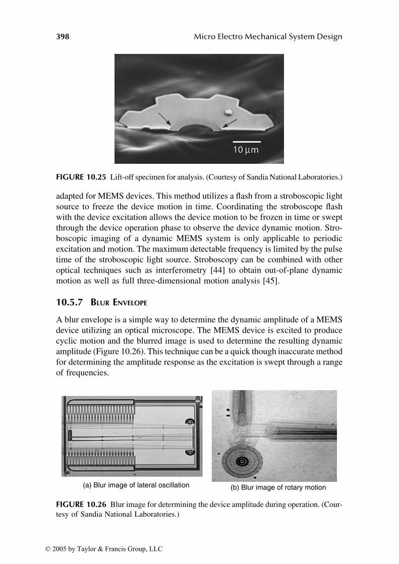
398 Micro Electro Mechanical System Design
adapted for MEMS devices. This method utilizes a flash from a stroboscopic light
source to freeze the device motion in time. Coordinating the stroboscope flash
with the device excitation allows the device motion to be frozen in time or swept
through the device operation phase to observe the device dynamic motion. Stro-
boscopic imaging of a dynamic MEMS system is only applicable to periodic
excitation and motion. The maximum detectable frequency is limited by the pulse
time of the stroboscopic light source. Stroboscopy can be combined with other
optical techniques such as interferometry [44] to obtain out-of-plane dynamic
motion as well as full three-dimensional motion analysis [45].
10.5.7 BLUR ENVELOPE
A blur envelope is a simple way to determine the dynamic amplitude of a MEMS
device utilizing an optical microscope. The MEMS device is excited to produce
cyclic motion and the blurred image is used to determine the resulting dynamic
amplitude (Figure 10.26). This technique can be a quick though inaccurate method
for determining the amplitude response as the excitation is swept through a range
of frequencies.
FIGURE 10.25 Lift-off specimen for analysis. (Courtesy of Sandia National Laboratories.)
FIGURE 10.26 Blur image for determining the device amplitude during operation. (Cour-
tesy of Sandia National Laboratories.)
(a) Blur image of lateral oscillation (b) Blur image of rotary motion
© 2005 by Taylor & Francis Group, LLC
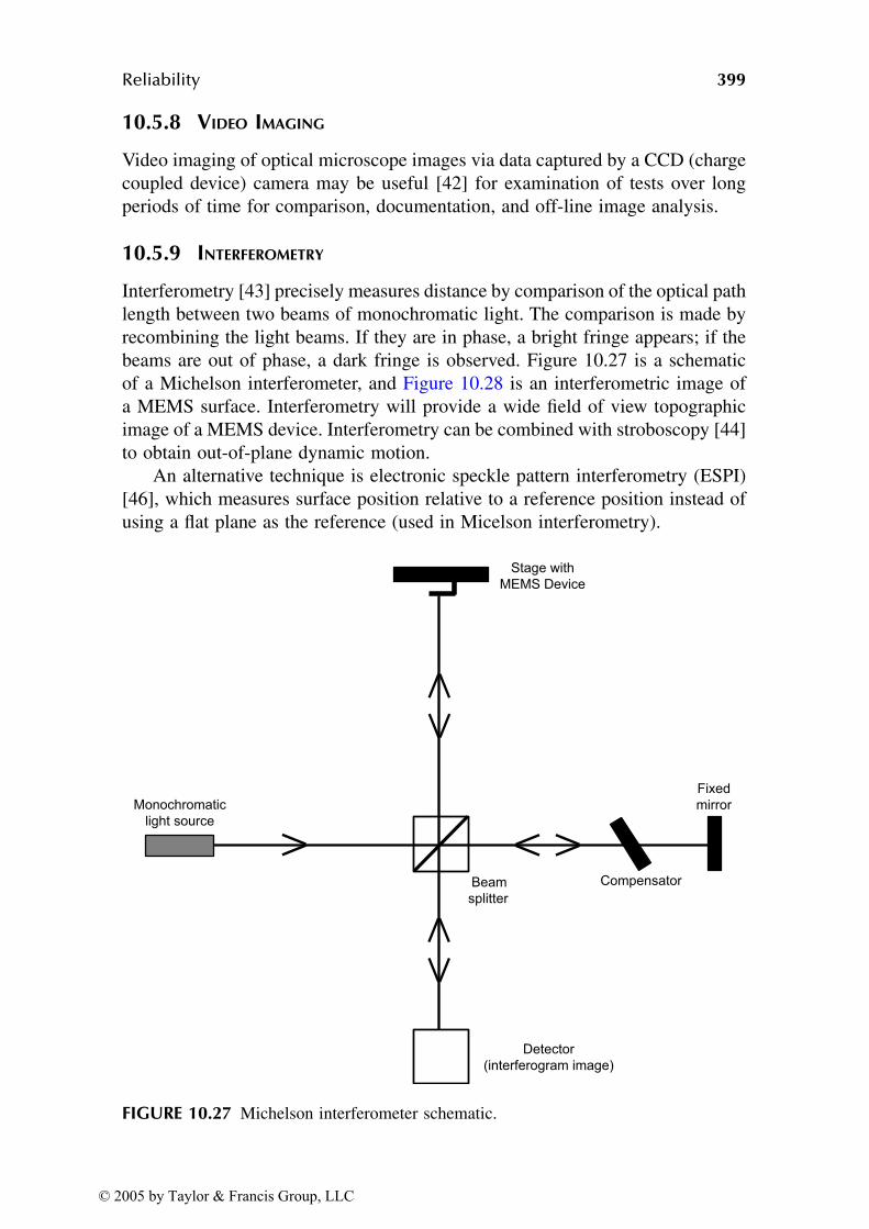
Reliability 399
10.5.8 VIDEO IMAGING
Video imaging of optical microscope images via data captured by a CCD (charge
coupled device) camera may be useful [42] for examination of tests over long
periods of time for comparison, documentation, and off-line image analysis.
10.5.9 INTERFEROMETRY
Interferometry [43] precisely measures distance by comparison of the optical path
length between two beams of monochromatic light. The comparison is made by
recombining the light beams. If they are in phase, a bright fringe appears; if the
beams are out of phase, a dark fringe is observed. Figure 10.27 is a schematic
of a Michelson interferometer, and Figure 10.28 is an interferometric image of
a MEMS surface. Interferometry will provide a wide field of view topographic
image of a MEMS device. Interferometry can be combined with stroboscopy [44]
to obtain out-of-plane dynamic motion.
An alternative technique is electronic speckle pattern interferometry (ESPI)
[46], which measures surface position relative to a reference position instead of
using a flat plane as the reference (used in Micelson interferometry).
FIGURE 10.27 Michelson interferometer schematic.
Monochromatic
light source
Beam
splitter
Stage with
MEMS Device
Detector
(interferogram image)
Fixed
mirror
Compensator
© 2005 by Taylor & Francis Group, LLC
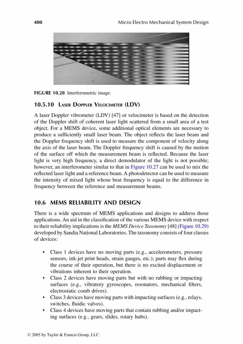
400 Micro Electro Mechanical System Design
10.5.10 LASER DOPPLER VELOCIMETER (LDV)
A laser Doppler vibrometer (LDV) [47] or velocimeter is based on the detection
of the Doppler shift of coherent laser light scattered from a small area of a test
object. For a MEMS device, some additional optical elements are necessary to
produce a sufficiently small laser beam. The object reflects the laser beam and
the Doppler frequency shift is used to measure the component of velocity along
the axis of the laser beam. The Doppler frequency shift is caused by the motion
of the surface off which the measurement beam is reflected. Because the laser
light is very high frequency, a direct demodulator of the light is not possible;
however, an interferometer similar to that in Figure 10.27 can be used to mix the
reflected laser light and a reference beam. A photodetector can be used to measure
the intensity of mixed light whose beat frequency is equal to the difference in
frequency between the reference and measurement beams.
10.6 MEMS RELIABILITY AND DESIGN
There is a wide spectrum of MEMS applications and designs to address those
applications. An aid in the classification of the various MEMS device with respect
to their reliability implications is the MEMS Device Taxonomy [48] (Figure 10.29)
developed by Sandia National Laboratories. The taxonomy consists of four classes
of devices:
• Class 1 devices have no moving parts (e.g., accelerometers, pressure
sensors, ink-jet print heads, strain gauges, etc.); parts may flex during
the course of their operation, but there is no excited displacement or
vibrations inherent to their operation.
• Class 2 devices have moving parts but with no rubbing or impacting
surfaces (e.g., vibratory gyroscopes, resonators, mechanical filters,
electrostatic comb drives).
• Class 3 devices have moving parts with impacting surfaces (e.g., relays,
switches, fluidic valves).
• Class 4 devices have moving parts that contain rubbing and/or impact-
ing surfaces (e.g., gears, slides, rotary hubs).
FIGURE 10.28 Interferometric image.
© 2005 by Taylor & Francis Group, LLC
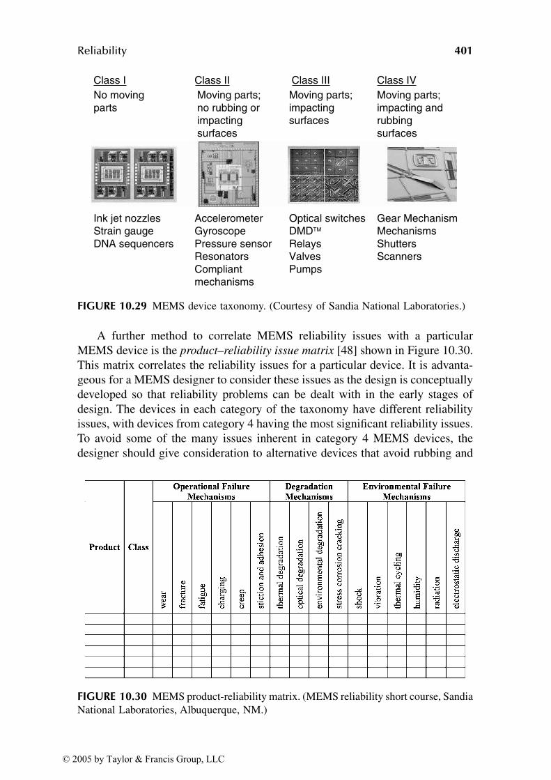
Reliability 401
A further method to correlate MEMS reliability issues with a particular
MEMS device is the product–reliability issue matrix [48] shown in Figure 10.30.
This matrix correlates the reliability issues for a particular device. It is advanta-
geous for a MEMS designer to consider these issues as the design is conceptually
developed so that reliability problems can be dealt with in the early stages of
design. The devices in each category of the taxonomy have different reliability
issues, with devices from category 4 having the most significant reliability issues.
To avoid some of the many issues inherent in category 4 MEMS devices, the
designer should give consideration to alternative devices that avoid rubbing and
FIGURE 10.29 MEMS device taxonomy. (Courtesy of Sandia National Laboratories.)
FIGURE 10.30 MEMS product-reliability matrix. (MEMS reliability short course, Sandia
National Laboratories, Albuquerque, NM.)
Class INo movingparts
Ink jet nozzlesStrain gaugeDNA sequencers
Class II Class IVClass IIIMoving parts;no rubbing orimpactingsurfaces
Moving parts;impacting andrubbingsurfaces
Moving parts;impactingsurfaces
AccelerometerGyroscopePressure sensorResonatorsCompliantmechanisms
Optical switchesDMDRelaysValvesPumps
Gear MechanismMechanismsShuttersScanners
© 2005 by Taylor & Francis Group, LLC
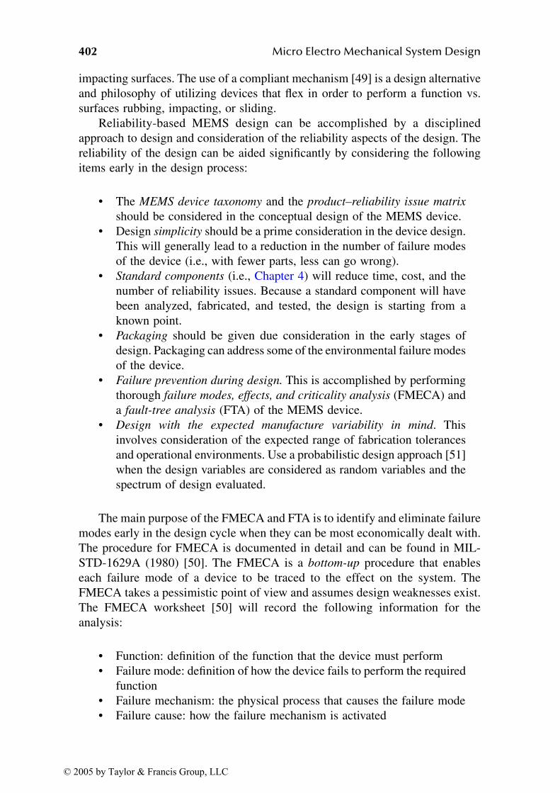
402 Micro Electro Mechanical System Design
impacting surfaces. The use of a compliant mechanism [49] is a design alternative
and philosophy of utilizing devices that flex in order to perform a function vs.
surfaces rubbing, impacting, or sliding.
Reliability-based MEMS design can be accomplished by a disciplined
approach to design and consideration of the reliability aspects of the design. The
reliability of the design can be aided significantly by considering the following
items early in the design process:
• The MEMS device taxonomy and the product–reliability issue matrix
should be considered in the conceptual design of the MEMS device.
• Design simplicity should be a prime consideration in the device design.
This will generally lead to a reduction in the number of failure modes
of the device (i.e., with fewer parts, less can go wrong).
• Standard components (i.e., Chapter 4) will reduce time, cost, and the
number of reliability issues. Because a standard component will have
been analyzed, fabricated, and tested, the design is starting from a
known point.
• Packaging should be given due consideration in the early stages of
design. Packaging can address some of the environmental failure modes
of the device.
• Failure prevention during design. This is accomplished by performing
thorough failure modes, effects, and criticality analysis (FMECA) and
a fault-tree analysis (FTA) of the MEMS device.
• Design with the expected manufacture variability in mind. This
involves consideration of the expected range of fabrication tolerances
and operational environments. Use a probabilistic design approach [51]
when the design variables are considered as random variables and the
spectrum of design evaluated.
The main purpose of the FMECA and FTA is to identify and eliminate failure
modes early in the design cycle when they can be most economically dealt with.
The procedure for FMECA is documented in detail and can be found in MIL-
STD-1629A (1980) [50]. The FMECA is a bottom-up procedure that enables
each failure mode of a device to be traced to the effect on the system. The
FMECA takes a pessimistic point of view and assumes design weaknesses exist.
The FMECA worksheet [50] will record the following information for the
analysis:
• Function: definition of the function that the device must perform
• Failure mode: definition of how the device fails to perform the required
function
• Failure mechanism: the physical process that causes the failure mode
• Failure cause: how the failure mechanism is activated
© 2005 by Taylor & Francis Group, LLC
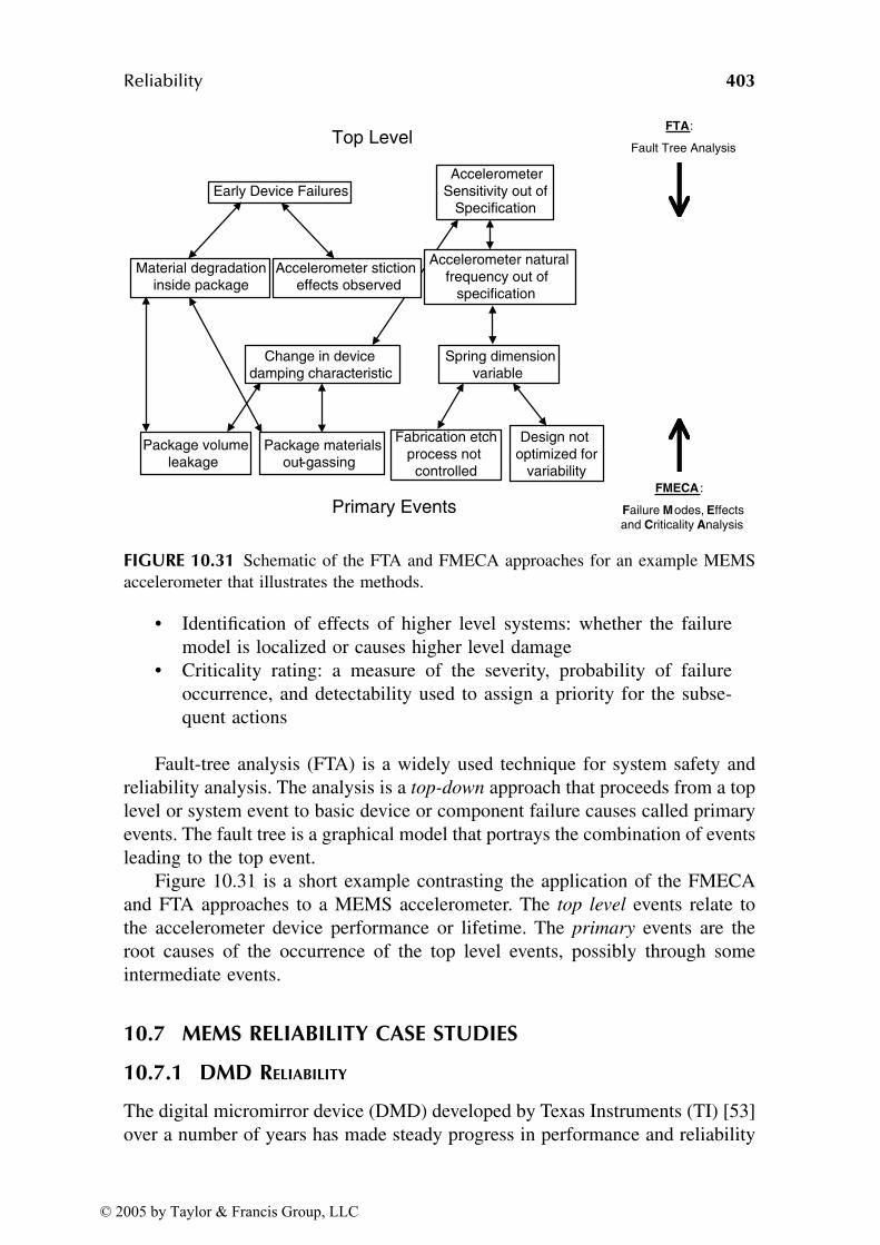
Reliability 403
• Identification of effects of higher level systems: whether the failure
model is localized or causes higher level damage
• Criticality rating: a measure of the severity, probability of failure
occurrence, and detectability used to assign a priority for the subse-
quent actions
Fault-tree analysis (FTA) is a widely used technique for system safety and
reliability analysis. The analysis is a top-down approach that proceeds from a top
level or system event to basic device or component failure causes called primary
events. The fault tree is a graphical model that portrays the combination of events
leading to the top event.
Figure 10.31 is a short example contrasting the application of the FMECA
and FTA approaches to a MEMS accelerometer. The top level events relate to
the accelerometer device performance or lifetime. The primary events are the
root causes of the occurrence of the top level events, possibly through some
intermediate events.
10.7 MEMS RELIABILITY CASE STUDIES
10.7.1 DMD RELIABILITY
The digital micromirror device (DMD) developed by Texas Instruments (TI) [53]
over a number of years has made steady progress in performance and reliability
FIGURE 10.31 Schematic of the FTA and FMECA approaches for an example MEMS
accelerometer that illustrates the methods.
FMECA :
Failure Modes, Effectsand Criticality Analysis
FTA:
Fault Tree Analysis
Package volume leakage
Package materials out-gassing
Fabrication etchprocess not
controlled
Design not optimized for
variability
Change in device damping characteristic
Spring dimension variable
Material degradation inside package
Accelerometer natural frequency out of
specification
Early Device FailuresAccelerometer
Sensitivity out of Specification
Accelerometer stictioneffects observed
Primary Events
Top Level
© 2005 by Taylor & Francis Group, LLC
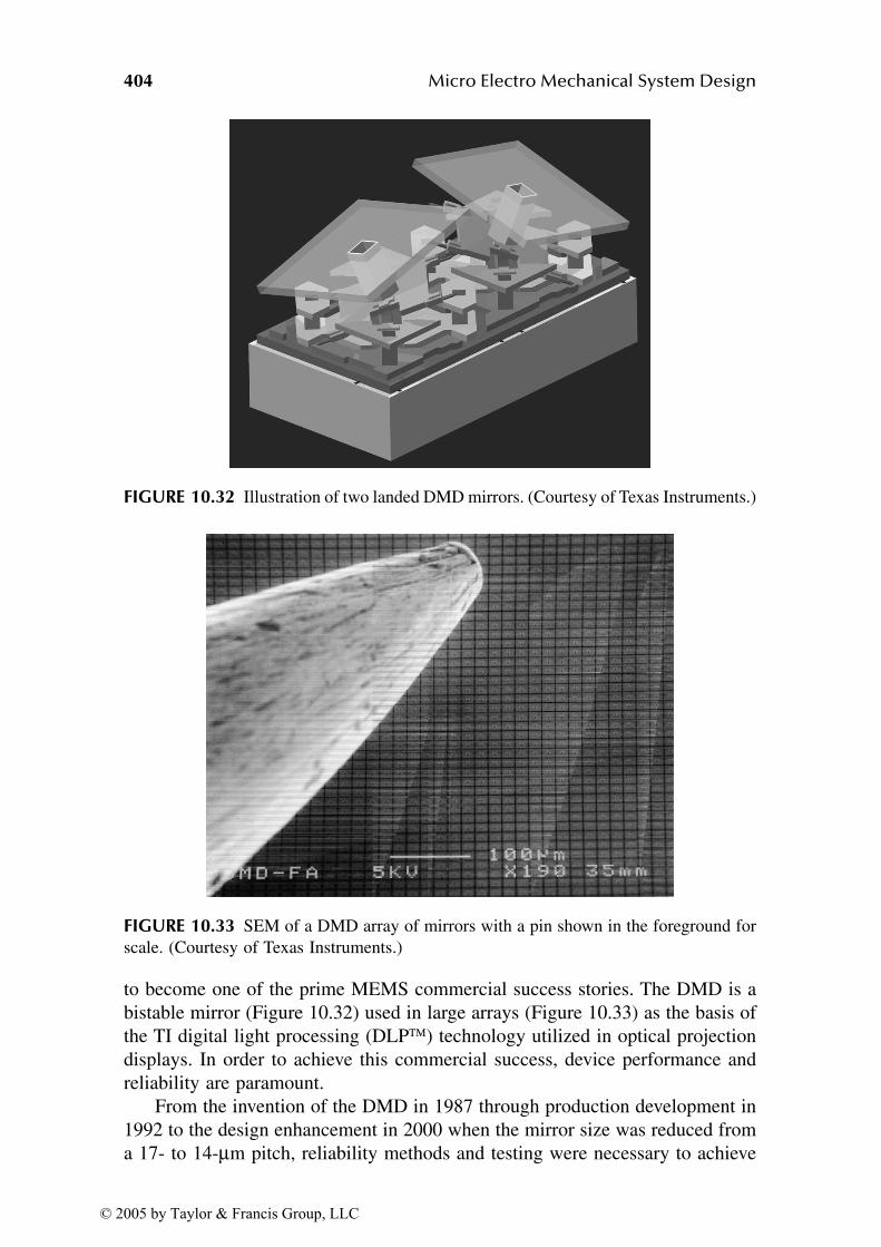
404 Micro Electro Mechanical System Design
to become one of the prime MEMS commercial success stories. The DMD is a
bistable mirror (Figure 10.32) used in large arrays (Figure 10.33) as the basis of
the TI digital light processing (DLP) technology utilized in optical projection
displays. In order to achieve this commercial success, device performance and
reliability are paramount.
From the invention of the DMD in 1987 through production development in
1992 to the design enhancement in 2000 when the mirror size was reduced from
a 17- to 14-µm pitch, reliability methods and testing were necessary to achieve
FIGURE 10.32 Illustration of two landed DMD mirrors. (Courtesy of Texas Instruments.)
FIGURE 10.33 SEM of a DMD array of mirrors with a pin shown in the foreground for
scale. (Courtesy of Texas Instruments.)
© 2005 by Taylor & Francis Group, LLC
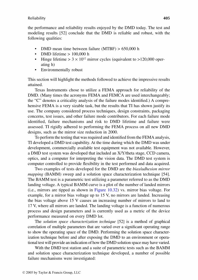
Reliability 405
the performance and reliability results enjoyed by the DMD today. The test and
modeling results [52] conclude that the DMD is reliable and robust, with the
following qualities:
• DMD mean time between failure (MTBF) > 650,000 h
• DMD lifetime > 100,000 h
• Hinge lifetime > 3 × 10¹² mirror cycles (equivalent to >120,000 oper-
ating h)
• Environmentally robust
This section will highlight the methods followed to achieve the impressive results
attained.
Texas Instruments chose to utilize a FEMA approach for reliability of the
DMD. (Many times the acronyms FEMA and FEMCA are used interchangeably;
the “C” denotes a criticality analysis of the failure modes identified.) A compre-
hensive FEMA is a very sizable task, but the results that TI has shown justify its
use. The company considered process techniques, design constraints, packaging
concerns, test issues, and other failure mode contributors. For each failure mode
identified, failure mechanisms and risk to DMD lifetime and failure were
assessed. TI rigidly adhered to performing the FEMA process on all new DMD
designs, such as the mirror size reduction in 2000.
To perform the testing that was required and identified from the FEMA analysis,
TI developed a DMD test capability. At the time during which the DMD was under
development, commercially available test equipment was not available. However,
a DMD test system was developed that included an X/Y/theta stage, CCD camera,
optics, and a computer for interpreting the vision data. The DMD test system is
computer controlled to provide flexibility in the test performed and data acquired.
Two examples of tests developed for the DMD are the bias/adhesion mirror
mapping (BAMM) sweep and a solution space characterization technique [54].
The BAMM test is a parametric test utilizing a parameter referred to as the DMD
landing voltage. A typical BAMM curve is a plot of the number of landed mirrors
(i.e., mirrors are tipped as shown in Figure 10.32) vs. mirror bias voltage. For
example, for a mirror bias voltage up to 15 V, no mirrors are landed. Increasing
the bias voltage above 15 V causes an increasing number of mirrors to land to
17 V, where all mirrors are landed. The landing voltage is a function of numerous
process and design parameters and is currently used as a metric of the device
performance measured on every DMD lot.
The solution space characterization technique [52] is a method of graphical
correlation of multiple parameters that are varied over a significant operating range
to show the operating space of the DMD. Performing the solution space character-
ization technique before and after exposing the DMD to an environment or opera-
tional test will provide an indication of how the DMD solution space may have varied.
With the DMD test station and a suite of parametric tests such as the BAMM
and solution space characterization technique developed, a number of possible
failure mechanisms were investigated:
© 2005 by Taylor & Francis Group, LLC
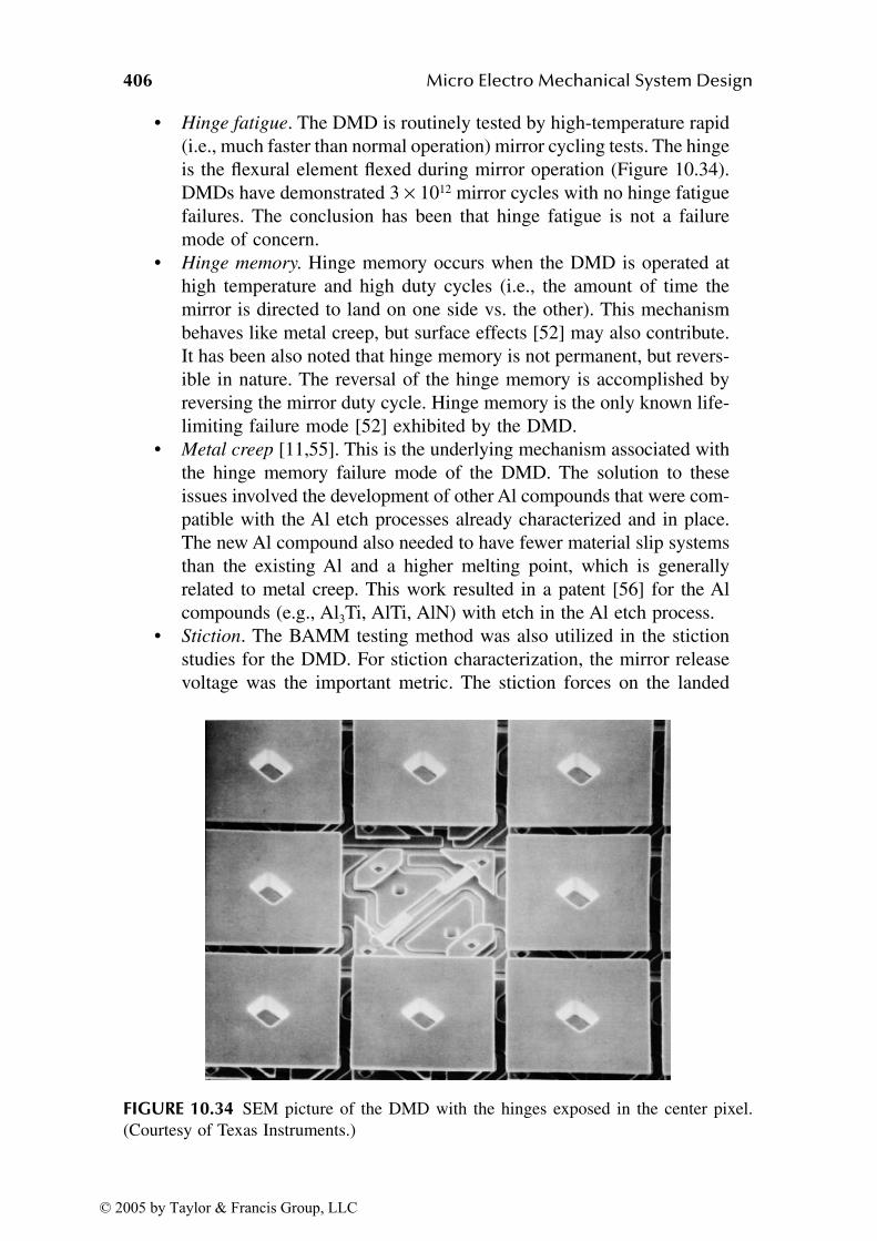
406 Micro Electro Mechanical System Design
• Hinge fatigue. The DMD is routinely tested by high-temperature rapid
(i.e., much faster than normal operation) mirror cycling tests. The hinge
is the flexural element flexed during mirror operation (Figure 10.34).
DMDs have demonstrated 3 × 10¹² mirror cycles with no hinge fatigue
failures. The conclusion has been that hinge fatigue is not a failure
mode of concern.
• Hinge memory. Hinge memory occurs when the DMD is operated at
high temperature and high duty cycles (i.e., the amount of time the
mirror is directed to land on one side vs. the other). This mechanism
behaves like metal creep, but surface effects [52] may also contribute.
It has been also noted that hinge memory is not permanent, but revers-
ible in nature. The reversal of the hinge memory is accomplished by
reversing the mirror duty cycle. Hinge memory is the only known life-
limiting failure mode [52] exhibited by the DMD.
• Metal creep [11,55]. This is the underlying mechanism associated with
the hinge memory failure mode of the DMD. The solution to these
issues involved the development of other Al compounds that were com-
patible with the Al etch processes already characterized and in place.
The new Al compound also needed to have fewer material slip systems
than the existing Al and a higher melting point, which is generally
related to metal creep. This work resulted in a patent [56] for the Al
compounds (e.g., Al3Ti, AlTi, AlN) with etch in the Al etch process.
• Stiction. The BAMM testing method was also utilized in the stiction
studies for the DMD. For stiction characterization, the mirror release
voltage was the important metric. The stiction forces on the landed
FIGURE 10.34 SEM picture of the DMD with the hinges exposed in the center pixel.
(Courtesy of Texas Instruments.)
© 2005 by Taylor & Francis Group, LLC
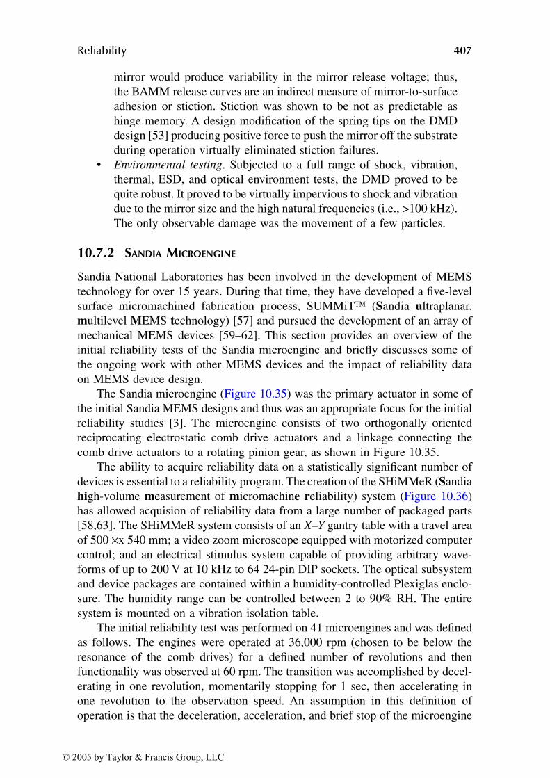
Reliability 407
mirror would produce variability in the mirror release voltage; thus,
the BAMM release curves are an indirect measure of mirror-to-surface
adhesion or stiction. Stiction was shown to be not as predictable as
hinge memory. A design modification of the spring tips on the DMD
design [53] producing positive force to push the mirror off the substrate
during operation virtually eliminated stiction failures.
• Environmental testing. Subjected to a full range of shock, vibration,
thermal, ESD, and optical environment tests, the DMD proved to be
quite robust. It proved to be virtually impervious to shock and vibration
due to the mirror size and the high natural frequencies (i.e., >100 kHz).
The only observable damage was the movement of a few particles.
10.7.2 SANDIA MICROENGINE
Sandia National Laboratories has been involved in the development of MEMS
technology for over 15 years. During that time, they have developed a five-level
surface micromachined fabrication process, SUMMiT (Sandia ultraplanar,
multilevel MEMS technology) [57] and pursued the development of an array of
mechanical MEMS devices [59–62]. This section provides an overview of the
initial reliability tests of the Sandia microengine and briefly discusses some of
the ongoing work with other MEMS devices and the impact of reliability data
on MEMS device design.
The Sandia microengine (Figure 10.35) was the primary actuator in some of
the initial Sandia MEMS designs and thus was an appropriate focus for the initial
reliability studies [3]. The microengine consists of two orthogonally oriented
reciprocating electrostatic comb drive actuators and a linkage connecting the
comb drive actuators to a rotating pinion gear, as shown in Figure 10.35.
The ability to acquire reliability data on a statistically significant number of
devices is essential to a reliability program. The creation of the SHiMMeR (Sandia
high-volume measurement of micromachine reliability) system (Figure 10.36)
has allowed acquision of reliability data from a large number of packaged parts
[58,63]. The SHiMMeR system consists of an X–Y gantry table with a travel area
of 500 ×x 540 mm; a video zoom microscope equipped with motorized computer
control; and an electrical stimulus system capable of providing arbitrary wave-
forms of up to 200 V at 10 kHz to 64 24-pin DIP sockets. The optical subsystem
and device packages are contained within a humidity-controlled Plexiglas enclo-
sure. The humidity range can be controlled between 2 to 90% RH. The entire
system is mounted on a vibration isolation table.
The initial reliability test was performed on 41 microengines and was defined
as follows. The engines were operated at 36,000 rpm (chosen to be below the
resonance of the comb drives) for a defined number of revolutions and then
functionality was observed at 60 rpm. The transition was accomplished by decel-
erating in one revolution, momentarily stopping for 1 sec, then accelerating in
one revolution to the observation speed. An assumption in this definition of
operation is that the deceleration, acceleration, and brief stop of the microengine
© 2005 by Taylor & Francis Group, LLC

408 Micro Electro Mechanical System Design
do not influence the ultimate failure and lifetime of the microengine. The failure
criteria were defined as the inability of the microengine to complete a revolution
during the observation period
During the observation period, a pass–fail decision was made; comments on
the motion of functioning engines were made; and video was recorded for post
test analysis. The test lasted for 28 days with a total of 32 separate stress periods.
FIGURE 10.35 Sandia microengine. (Courtesy of Sandia National Laboratories.)
FIGURE 10.36 SHiMMeR system with multiple packaged part, computer control, data
acquisition, vibration isolation, humidity enclosure, and video microscope. (Courtesy of
Sandia National Laboratories, Radiation and Reliability Physics Department.)
© 2005 by Taylor & Francis Group, LLC
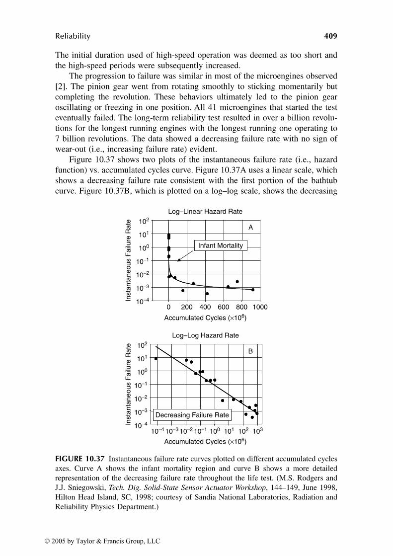
Reliability 409
The initial duration used of high-speed operation was deemed as too short and
the high-speed periods were subsequently increased.
The progression to failure was similar in most of the microengines observed
[2]. The pinion gear went from rotating smoothly to sticking momentarily but
completing the revolution. These behaviors ultimately led to the pinion gear
oscillating or freezing in one position. All 41 microengines that started the test
eventually failed. The long-term reliability test resulted in over a billion revolu-
tions for the longest running engines with the longest running one operating to
7 billion revolutions. The data showed a decreasing failure rate with no sign of
wear-out (i.e., increasing failure rate) evident.
Figure 10.37 shows two plots of the instantaneous failure rate (i.e., hazard
function) vs. accumulated cycles curve. Figure 10.37A uses a linear scale, which
shows a decreasing failure rate consistent with the first portion of the bathtub
curve. Figure 10.37B, which is plotted on a log–log scale, shows the decreasing
FIGURE 10.37 Instantaneous failure rate curves plotted on different accumulated cycles
axes. Curve A shows the infant mortality region and curve B shows a more detailed
representation of the decreasing failure rate throughout the life test. (M.S. Rodgers and
J.J. Sniegowski, Tech. Dig. Solid-State Sensor Actuator Workshop, 144–149, June 1998,
Hilton Head Island, SC, 1998; courtesy of Sandia National Laboratories, Radiation and
Reliability Physics Department.)
102
101
100
10−1
10−2
10−3
10−4
102
101
100
10−1
10−2
10−3
10−4
10−4 10−3 10−2 10−1 100 101 102 103
0 200 400
Accumulated Cycles (×106)
Accumulated Cycles (×106)
600 800 1000
Inst
anta
neou
s F
ailu
re R
ate
Inst
anta
neou
s F
ailu
re R
ate
Log–Linear Hazard Rate
Log–Log Hazard Rate
Infant Mortality
Decreasing Failure Rate
A
B
© 2005 by Taylor & Francis Group, LLC
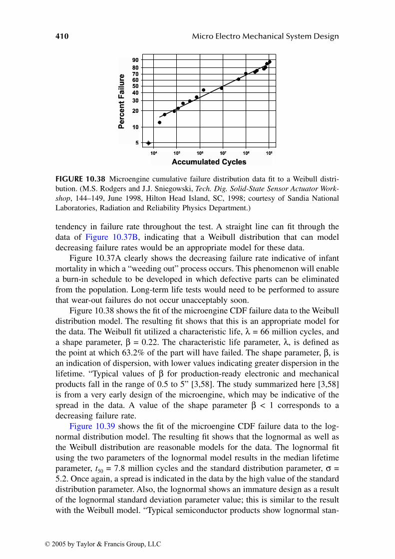
410 Micro Electro Mechanical System Design
tendency in failure rate throughout the test. A straight line can fit through the
data of Figure 10.37B, indicating that a Weibull distribution that can model
decreasing failure rates would be an appropriate model for these data.
Figure 10.37A clearly shows the decreasing failure rate indicative of infant
mortality in which a “weeding out” process occurs. This phenomenon will enable
a burn-in schedule to be developed in which defective parts can be eliminated
from the population. Long-term life tests would need to be performed to assure
that wear-out failures do not occur unacceptably soon.
Figure 10.38 shows the fit of the microengine CDF failure data to the Weibull
distribution model. The resulting fit shows that this is an appropriate model for
the data. The Weibull fit utilized a characteristic life, λ = 66 million cycles, and
a shape parameter, β = 0.22. The characteristic life parameter, λ, is defined as
the point at which 63.2% of the part will have failed. The shape parameter, β, is
an indication of dispersion, with lower values indicating greater dispersion in the
lifetime. “Typical values of β for production-ready electronic and mechanical
products fall in the range of 0.5 to 5” [3,58]. The study summarized here [3,58]
is from a very early design of the microengine, which may be indicative of the
spread in the data. A value of the shape parameter β < 1 corresponds to a
decreasing failure rate.
Figure 10.39 shows the fit of the microengine CDF failure data to the log-
normal distribution model. The resulting fit shows that the lognormal as well as
the Weibull distribution are reasonable models for the data. The lognormal fit
using the two parameters of the lognormal model results in the median lifetime
parameter, t50 = 7.8 million cycles and the standard distribution parameter, σ =
5.2. Once again, a spread is indicated in the data by the high value of the standard
distribution parameter. Also, the lognormal shows an immature design as a result
of the lognormal standard deviation parameter value; this is similar to the result
with the Weibull model. “Typical semiconductor products show lognormal stan-
FIGURE 10.38 Microengine cumulative failure distribution data fit to a Weibull distri-
bution. (M.S. Rodgers and J.J. Sniegowski, Tech. Dig. Solid-State Sensor Actuator Work-
shop, 144–149, June 1998, Hilton Head Island, SC, 1998; courtesy of Sandia National
Laboratories, Radiation and Reliability Physics Department.)
© 2005 by Taylor & Francis Group, LLC
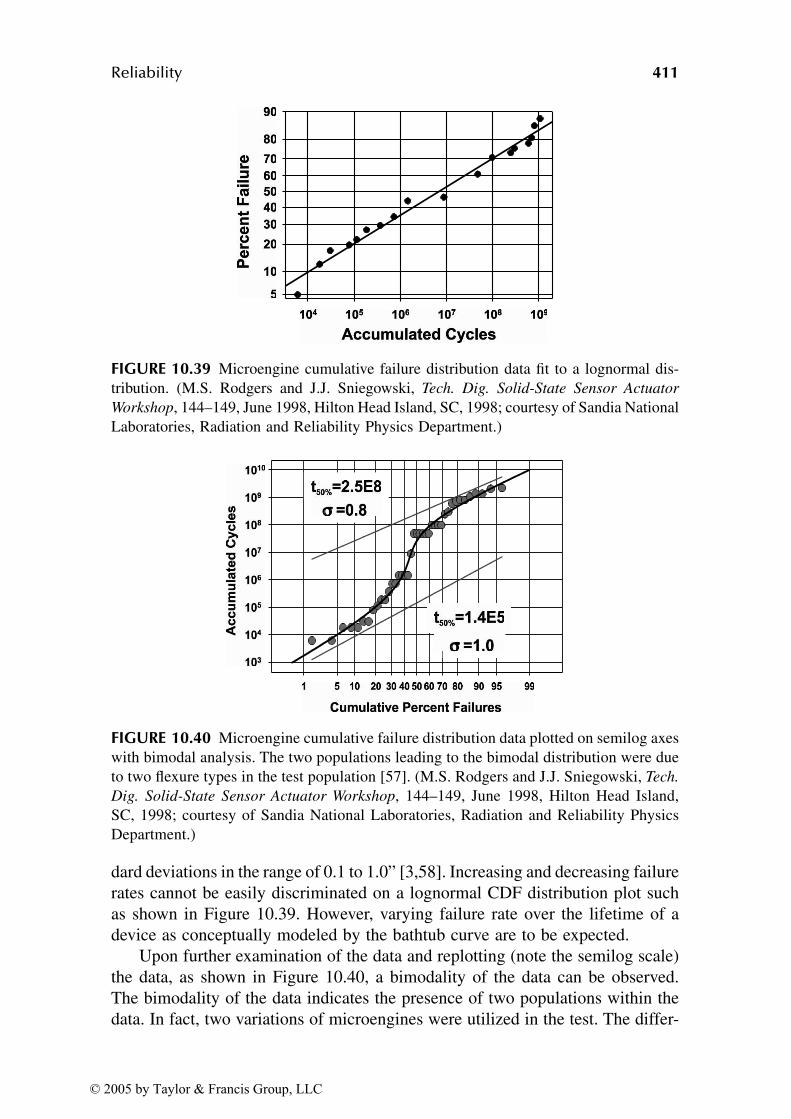
Reliability 411
dard deviations in the range of 0.1 to 1.0” [3,58]. Increasing and decreasing failure
rates cannot be easily discriminated on a lognormal CDF distribution plot such
as shown in Figure 10.39. However, varying failure rate over the lifetime of a
device as conceptually modeled by the bathtub curve are to be expected.
Upon further examination of the data and replotting (note the semilog scale)
the data, as shown in Figure 10.40, a bimodality of the data can be observed.
The bimodality of the data indicates the presence of two populations within the
data. In fact, two variations of microengines were utilized in the test. The differ-
FIGURE 10.39 Microengine cumulative failure distribution data fit to a lognormal dis-
tribution. (M.S. Rodgers and J.J. Sniegowski, Tech. Dig. Solid-State Sensor Actuator
Workshop, 144–149, June 1998, Hilton Head Island, SC, 1998; courtesy of Sandia National
Laboratories, Radiation and Reliability Physics Department.)
FIGURE 10.40 Microengine cumulative failure distribution data plotted on semilog axes
with bimodal analysis. The two populations leading to the bimodal distribution were due
to two flexure types in the test population [57]. (M.S. Rodgers and J.J. Sniegowski, Tech.
Dig. Solid-State Sensor Actuator Workshop, 144–149, June 1998, Hilton Head Island,
SC, 1998; courtesy of Sandia National Laboratories, Radiation and Reliability Physics
Department.)
© 2005 by Taylor & Francis Group, LLC
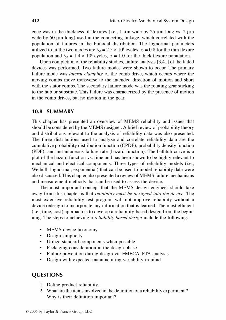
412 Micro Electro Mechanical System Design
ence was in the thickness of flexures (i.e., 1 µm wide by 25 µm long vs. 2 µm
wide by 50 µm long) used in the connecting linkage, which correlated with the
population of failures in the bimodal distribution. The lognormal parameters
utilized to fit the two modes are t50 = 2.5 × 10⁸ cycles, σ = 0.8 for the thin flexure
population and t50 = 1.4 × 10⁵ cycles, σ = 1.0 for the thick flexure population.
Upon completion of the reliability studies, failure analysis [3,41] of the failed
devices was performed. Two failure modes were shown to occur. The primary
failure mode was lateral clamping of the comb drive, which occurs where the
moving combs move transverse to the intended direction of motion and short
with the stator combs. The secondary failure mode was the rotating gear sticking
to the hub or substrate. This failure was characterized by the presence of motion
in the comb drives, but no motion in the gear.
10.8 SUMMARY
This chapter has presented an overview of MEMS reliability and issues that
should be considered by the MEMS designer. A brief review of probability theory
and distributions relevant to the analysis of reliability data was also presented.
The three distributions used to analyze and correlate reliability data are the
cumulative probability distribution function (CPDF); probability density function
(PDF); and instantaneous failure rate (hazard function). The bathtub curve is a
plot of the hazard function vs. time and has been shown to be highly relevant to
mechanical and electrical components. Three types of reliability models (i.e.,
Weibull, lognormal, exponential) that can be used to model reliability data were
also discussed. This chapter also presented a review of MEMS failure mechanisms
and measurement methods that can be used to assess the device.
The most important concept that the MEMS design engineer should take
away from this chapter is that reliability must be designed into the device. The
most extensive reliability test program will not improve reliability without a
device redesign to incorporate any information that is learned. The most efficient
(i.e., time, cost) approach is to develop a reliability-based design from the begin-
ning. The steps to achieving a reliability-based design include the following:
• MEMS device taxonomy
• Design simplicity
• Utilize standard components when possible
• Packaging consideration in the design phase
• Failure prevention during design via FMECA–FTA analysis
• Design with expected manufacturing variability in mind
QUESTIONS
1. Define product reliability.
2. What are the items involved in the definition of a reliability experiment?
Why is their definition important?
© 2005 by Taylor & Francis Group, LLC
Reliability 413
3. Choose a device (not necessarily a MEMS device) and define a mean-
ingful reliability experiment that could be performed. What three things
need to be defined to specify the reliability experiment?
4. What are three types of distributions frequently used in analyzing
reliability data? How are these distributions related?
5. What is the bathtub curve? Explain the various regions of the bathtub
curve.
6. Why are probability and statistics relevant and important to the study
of reliability?
7. Define probability. Given two fair die, what is the probability of rolling
a 12? What is the most probable number to be rolled?
8. What are reliability models and why are they used?
9. Discuss the Weibull model and its advantages for use in modeling
reliability data.
10. What are FMECA and FTA and what are they trying to accomplish?
Explain similarities and differences in the approach to FMECA and
FTA.
11. What is the reliability experiment as defined in the Sandia microengine
case study? Is the reliability experiment completely and unambiguously
defined?
12. What is the difference between a failure mode and a failure mechanism?
13. Why is it important to find the failure mode encountered in a reliability
experiment?
14. Why was reliability modeling of the data in the Sandia microengine
case study important and what did it reveal?
15. What are six things that should be considered to achieve a reliable
design?
16. Review recent articles in the MEMS literature (e.g., Journal of MEMS,
Sensors and Actuators) and choose a device of interest. Using the
taxonomy of MEMS devices, what class is your device? Does the
chosen device have any shortcomings or issues for concern when
compared to the steps for developing a reliability-based design (Section
10.6)? Perform FMECA and FTA analysis on the device.
REFERENCES
1. S.S. Rao, Reliability Based Design, McGraw-Hill, New York, 1992.
2. M.G. Pecht, F.R. Nash, Predicting the reliability of electronic equipment, Proc.
IEEE, 82(7), July 1994.
3. D.M. Tanner, N.F. Smith, L.W. Irwin, W.P. Eaton, K.S. Helgesen, J. J. Clement,
W.M. Miller, J.A. Walraven, K.A. Peterson, P. Tangyunyong, M.T. Dugger, S.L.
Miller, MEMS reliability: infrastructure, test structures, experiments, and failure
modes, Sandia National Laboratories Report, SAND2000-0091, January 2000.
4. B. Stark, MEMS reliability assurance guidelines for space applications, JPL
Publication 99-1, Jet Propulsion Laboratory, Pasadena, CA, January 1999.
© 2005 by Taylor & Francis Group, LLC
414 Micro Electro Mechanical System Design
5. A.W. Drake, Fundamentals of Applied Probability Theory, McGraw-Hill Inc., New
York, 1967.
6. P. Beckmann, Elements of Applied Probability Theory, Harcourt Brace and World
Inc., New York, 1968.
7. N. Draper, H. Smith, Applied Regression Analysis, 2nd ed., John Wiley & Sons,
New York, 1981.
8. P.A. Tobias, D.C. Trinidade, Applied Reliability, Van Nostrand Reinhold Co., New
York, 1986.
9. M. Abramowitz, I.A. Stegun, Handbook of Mathematical Functions with Formu-
las, Graphs, and Mathematical Table, National Bureau of Standards Applied
Mathematics Series 55, June 1964, 10th printing, December 1972.
10. M.G. Pecht, F.R. Nash, Predicting the reliability of electronic equipment, Proc.
IEEE, 82(7), July 1994.
11. W.M. van Spengen, MEMS reliability from a failure mechanisms perspective,
Microelectronics Reliability, 43, 1049–1060, 2003.
12. S.L. Miller, G. LaVigne, M.S. Rodgers, J.J. Sniegowski, J.P. Waters, and P.J.
McWhorter, Routes to failure in rotating MEMS devices experiencing sliding
friction, Proc. SPIE, 3324, 24–30, 1997.
13. S.L. Miller, M.S. Rodgers, G. LaVigne, J.J. Sniegowski, P. Clews, D.M. Tanner,
and K.A. Peterson, Failure modes in surface micromachined microelectromechan-
ical actuation systems, Microelectron. Reliability, 39, 1229–1237, 1999.
14. D.M. Tanner, M.T. Dugger, Wear mechanisms in a reliability methodology, Proc.
SPIE, 4980, 22–40, January 2003.
15. W.W. Van Arsdell, S.B. Brown, Subcritical crack growth in silicon MEMS, J.
MEMS, 8(3), 319, 1999.
16. J. Wibbeler, G. Pfeifer, M. Hietschold, Parasitic charging of dielectric surfaces in
capacitive microelectromechanical systems (MEMS), Sens Act A, 71(1–2), 74–80,
Nov. 1998.
17. G.M. Rebeitz, J.B. Muldavin, RF MEMS switches and switch circuits, IEEE
Microw. Mag., 59, 2000.
18. J.C. Ehmke, C.L. Goldsmith, Z.J. Yao, S.M. Eshelman, Method and apparatus for
switching high-frequency signals, U.S. Patent 6,391,675, issued 21 May 1999.
19. S.B. Brown, W. Van Arsdell, C. Muhlstein, Materials reliability in MEMs devices,
Transducers ‘97, 591–593, 1997.
20. M.R. Douglass, Lifetime estimates and unique failure mechanisms of the digitial
micromirror device, Proc. IEEE Int. Reliability Phys. Symp., 9–16, 1998.
21. C.H. Mastrangelo, C.H. Hsu, Mechanical stability and adhesion of microstructures
under capillary forces — part I: basic theory, JMEMS, 2(1), 33–43, March 1993.
22. R. Maboudian, R.T. Howe, Critical review: adhesion in surface micromechanical
structures, J. Vac. Sci. Tech. B., 15(1), 1–20, January 1997
23. R.A. Plass, J.A. Walraven, D.M. Tanner, F.W. Sexton, Anodic oxidation-induced
delamination of the SUMMiT poly 0 to silicon nitride interface, Proc. SPIE,
4980, 81–86, January 2003.
24. M. P. de Boer, J.A. Knapp, T.M. Mayer, T.A. Michalske, The role of interfacial
properties on MEMS performance and reliability, Proc. SPIE, 3825, 2–15, 1999.
25. M.P. de Boer, J.A. Knapp, J.M. Redmond, T.M. Mayer, J.J. Sniegowski, T.A.
Michalske, Fundamental mechanisms of micromachine reliability, Sandia
National Laboratories, Sandia Report SAND99-3100, January 2000.
© 2005 by Taylor & Francis Group, LLC

Reliability 415
26. P.F. Man, B.P. Gogoi, C.H. Mastrangelo, Elimination of post release adhesion in
microstructures using conformal fluorocarbon coatings, JMEMS, 6(1), 25–34,
March 1997.
27. U. Srinivasen, M.R. Houston, R.T. Howe, R. Maboudian, Alkyltrichlorosilane-
based self-assembled monolayer films for stiction reduction in silicon microma-
chines, JMEMS, 7(2), 252–260, June 1998.
28. C.M. Harris, C.E. Crede, Eds, Shock and Vibration Handbook, 2nd ed.,
McGraw–Hill Book Company, New York, 1976.
29. D.M. Tanner, J.A. Walraven, K.S. Helgesen, L.W. Irwin, D.L. Gregory, J.R. Stake,
N.F. Smith, MEMS reliability in a vibration environment, Proc. IRPS, 2000,
139–145.
30. D.M. Tanner, J.A. Walraven, K. Helgesen, L.W. Irwin, F. Brown, N.F. Smith, N.
Masters, MEMS reliability in shock environments, Proc. IRPS, 129–138, 2000.
31. V.T. Srikar, S.D. Senturia, The reliability of microelectromechanical systems
(MEMS) in shock environments, J. MEMS, 11(3), 206–214, 2002.
32. T.G. Brown, B.S. Davis, Dynamic high-G loading of MEMS sensors: ground and
flight testing, Proc. SPIE, 3512, 228–235, 1998.
33. A. Lawrence, Modern Inertial Technology, Navigation, Guidance, and Control,
Springer-Verlag, Heidelberg, 1992.
34. D.M. Tanner, J.A. Walraven, L.W. Irwin, M.T. Dugger, N.F. Smith, W.M. Miller,
S.L. Miller, The effect of humidity on the reliability of a surface micromachined
microengine, Proc. IEEE Int. Rel. Phys. Symp., 189–197, 1999.
35. L.P. Schanwald; J.R. Schwank; J.J. Sniegowski, M.R. Shaneyfelt, D.S. Walsh,
N.F. Smith, K.A. Peterson, P.S. Winokur, J.H. Smith, B.L. Doyle, High-fluence
x-ray and charged particle effects in microelectromechanical systems (MEMS)
comb-drive actuators, 1998 IEEE Nuclear and Space Radiation Effects Conference
(NSREC), July 20, 1998.
36. C.I. Lee, A.H. Johnson, W.C. Tang, C.E. Barnes, Total dose effects on microelec-
tromechanical systems (MEMS): accelerometers, IEEE Trans Nucl Sci, 43(6),
3127, 1996.
37. A.R. Knudson, S. Buchner, P. McDonald, W.J. Stapor, A.B. Campbell, K.S.
Grabowski, et al., The effects of radiation on MEMS accelerometers, IEEE Trans.
Nucl. Sci., 43(6), 3122, 1996.
38. E.I. Cole, J.M. Soden, Scanning electron microscopy techniques for IC failure
analysis, in Microelectronic Failure Analysis Desk Reference, 3rd ed., 1999.
39. D.B. Williams, J.L. Goldstein, D.E. Newbury, Eds., X-Ray Spectrometry in Elec-
tron Beam Instruments, Plenum Press, New York, 1995.
40. R.F. Egerton, Electron Energy-Loss Spectroscopy in the Electron Microscopy, 2nd
ed., Plenum Press, New York, 1996.
41. K.A. Peterson, P. Tangyunyong, A.A. Pimentel, Failure analysis of surface-micro-
machined microengines, Proc. SPIE, 3512, 190–200, 1998.
42. D.M. Freeman, C.Q. Davis, Using video microscopy to characterize microme-
chanics of biological and manmade micromachines, 1996 Solid State Sensor and
Actuator Workshop, Hilton Head, SC, 161–167, June 3–6, 1996.
43. G.L. Cloud, Optical Methods of Engineering Analysis, Cambridge University
Press, Cambridge, U.K., 1995.
44. M. Hart, R. Conant, K. Lau, R. Muller, Stroboscopic interferometer system for
dynamic MEMS characterization, JMEMS, 9, 409–418, December 2000.
© 2005 by Taylor & Francis Group, LLC
416 Micro Electro Mechanical System Design
45. C. Rembe, R. Muller, Measurement system for full three-dimensional motion
characterization of MEMS, JMEMS, 11(5), 479–488, October 2002.
46. P.Q. Zhang, Q.M. Wang, X.P. Wu, T.C. Huang, Experimental model analysis of
miniature objects by optical measurement technique, Int. J. Analytical Exp. Anal.,
7(4), 243–253, 1992.
47. K.L. Turner, P.G. Hartwell, N.C. MacDonald, Multidimensional MEMS motion
characterization using laser vibrometry, Transducers ’99, paper 4D1.2, 1999.
48. MEMS Reliability Short Course, Sandia National Laboratories, Albuquerque, NM.
49. L.L. Howell, Compliant Mechanisms, John Wiley & Sons, Inc., New York, 2001.
50. MIL-STD-1629A: U.S. Department of Defense, Military standard procedures for
performing a failure mode, effects and criticality analysis, November 24, 1980.
51. T.A. Cruse, Reliability Based Mechanical Design, Chapter 2, Marcel Dekker, New
York, 1997.
52. M.R. Douglass, DMD reliability, a MEMS success story, Proc. SPIE, 4980, 1–11,
2003.
53. P. van Kessel, L. Hornbeck, R. Meier, M. Douglass, A MEMS-based projection
display, Proc. IEEE, 86(8), 1687–1704, August 1998.
54. H. Chu, A. Gonzalez, T. Oudal, R. Aldridge, D. Dudasko, P. Barker, DMD
superstructure characterizations, TI Tech. J., 15(3), July–September 1998.
55. A.B. Sontheimer, Digital micromirror device (DMD) hinge memory lifetime reli-
ability modeling, IRPS 2002, 118–121.
56. J.H. Tregilgas, Micromechanical device having an improved beam, U.S. Patent
5,552,924, issued 3 September 1996.
57. M.S. Rodgers, J.J. Sniegowski, Five-level polysilicon surface micromachine tech-
nology: application to complex mechanical systems, Tech. Dig. Solid-State Sensor
Actuator Workshop, 144–149, June 1998, Hilton Head Island, SC, 1998.
58. D.M. Tanner, N.F. Smith, D.J. Bowman, W.P. Eaton, K.A. Peterson, First reliability
test of a surface micromachined microengine using SHiMMeR, Proc. SPIE, 3224,
14–23, 1997.
59. M.A. Polosky, E.J. Garcia, J.J. Allen, Surface micromachined counter-meshing
gears discrimination device, Proc. SPIE, 3328, 365–373, San Diego, CA, March
1998.
60. J.J. Allen, H.K. Schriner, Micromachine wedge stepping motor, Int. Mechanical
Eng. Congr. Exposition, DSC-, 66, 317–322, November, 1998.
61. M.S. Rodgers, S. Kota, J. Hetrick, Z. Li, B.D. Jensen, T.W. Krygowski, S.L. Miller,
S.M. Barnes, M.S. Burg, A new class of high force, low-voltage, compliant
actuation systems, presented at Solid-State Sensor Actuator Workshop, Hilton
Head Island, SC, June 4–8, 2000.
62. S.M. Barnes, S.L. Miller, M.S. Rodgers, F. Bitsie, Torsional ratcheting actuating
system, Proc. 3rd Int. Conf. Modeling Simulation Microsyst., San Diego, CA,
March 27–29, 2000, 273–276.
63. N.F. Smith, W.P. Eaton, D.M. Tanner, J.J. Allen, Development of characterization
tools for reliability testing of microelectromechanical system actuators, Proc.
SPIE, 3880, 156–164.
© 2005 by Taylor & Francis Group, LLC

417
Appendix A
Glossary
AFM atomic force microscope
AM amplitude modulation
CAD computer aided design
CIF Cal Tech intermediate format; an ASCII graphical data format employed
for mask plotting files
CMOS complementary metal oxide semiconductor
CMP chemical mechanical polishing
CPW coplanar waveguide
C-V capacitance voltage characteristic
CVD chemical vapor deposition
DARPA Defense Advanced Research Projects Agency
dB decibel
DCS dichlorosilane
DRC design rule checking
DRIE deep reactive ion etching
EDP ethylene diamine pyrocatecol; silicon etchant, highly toxic
epi epitaxial
EM electromagnetic
FIB focused ion beam
FET field effect transistor
FM frequency modulation
GaAs gallium arsenide
GDSII graphical data stream file format employed for mask plotting files;
originally developed and trademarked by CALMA/GE and implies use
on a CALMA graphics system http://www.cadence.com
HARM high aspect ratio micromachining
HF hydrofluoric acid; a silicon dioxide etchant
IC integrated circuit
IL insertion loss
IMEMS integrated microelectromechanical systems
KOH potassium hydroxide; an isotropic etchant that attacks silicon at differ-
ent rates in different directions
LIGA Lithographie Galvanic Abformung (German acronym)
© 2005 by Taylor & Francis Group, LLC
418 Micro Electro Mechanical System Design
LPCVD low-pressure chemical vapor deposition
MEMS microelectromechanical system
MOEMS micro-optoelectromechanical systems
MST microsystems technology
MIC microwave integrated circuit
MIG MEMS Industry Group (MIG); a trade association representing the
North American MEMS and microstructure industries with the purpose
of enabling the exchange of nonproprietary information and increasing
commercial development. http://www.memsindustrygroup.org/
MUMP multiuser MEMS process http://www.memsrus.com/
NEXUS Network of Excellence in Multifunctional Microsystems; a nonprofit
association to provide access to MEMS/MST information
http://www.nexus-emsto.com/
NMOS n-type metal oxide semiconductor
OPC optical proximity correction
PECVD plasma-enhanced chemical vapor deposition
PIC photonic integrated circuit
PM phase modulation
PMMA polymethyl methacrylate; photo resist commonly used in LIGA tech-
nology
PSG phosphosilicate glass
PZT lead zirconate titanate
RET resolution enhancement technology
RF radio frequency
RIE reactive ion etching
RTA rapid thermal annealing
SEM scanning electron microscope
SLIGA sacrificial LIGA
SMA shape memory alloy
STM scanning tunneling microscope
SOI silicon on Insulator
SUMMiT Sandia ultraplanar, multilevel MEMS technology http://www.
mems.sandia.gov
TEOS tetraethoxysilane
TMAH tetramethylammonium hydroxide; an anisotropic wet etchant
TEM transmission electron microscopy
VPE vapor phase etching
© 2005 by Taylor & Francis Group, LLC

419
Appendix B
Prefixes
Prefix Symbol Factor
tera T 1012 = 1 000 000 000 000
giga G 109 = 1 000 000 000
mega M 106 = 1 000 000
kilo k 103 = 1 000
hecto h 102 = 100
deka da 101 = 10
deci d 10–1 = 0.1
centi c 10–2 = 0.01
milli m 10–3 = 0.001
micro m 10–6 = 0.000 001
nano n 10–9 = 0.000 000 001
pico p 10–12 = 0.000 000 000 001
femto f 10–15 = 0.000 000 000 000 001
atto a 10–18 = 0.000 000 000 000 000 001
© 2005 by Taylor & Francis Group, LLC

421
Appendix C
Micro–MKS Conversions
Parameter MKS Multiply by µµµµMKS
Length M 106 µM
Force N 106 µN
Time s 1 s
Mass kg 1 kg
Pressure and stress Pa = N/M2 10–6 µN/µM2
Density kg/M3 10–18 kg/µM3
Current A 1012 pA
Voltage V 1 V
Charge C 1012 pC
Resistivity Ohm-M 10-6 TOhm-µM
Permittivity F/M 106 pF/µM
Energy J 1012 pJ
Capacitance F 1012 pF
Electric field V/M 10–6 V/ µM
Inductance H 1012 TH
Permeability H/M 10–18 TH/µM
Power W 1012 pW
Thermal conductivity W/(M °K) 106 pW/(µM °K)
Specific heat J/(kg °K) 1012 pJ/(kg °K)
© 2005 by Taylor & Francis Group, LLC

423
Appendix D
Physical Constants
Physical constant Symbol Value
Angstrom Å Å = 0.1 nm = 10,000 µmElectronic charge q q = 1.602 × 10⁻¹⁹ CElectron volt eV 1 eV = 1.60 2 × 10–19 JPermittivity of free space ε0 ε0 = 8.854 × 10⁻¹⁴ F/cmPermeability of free space µ0 µ0 = 1.2566 × 10⁻⁶ H/MThermal voltage (300 ºK) kT/q 0.0259 VBoltzmann’s constant kB k = 1.38 × 10⁻²³ J/KPlanck’s constant h h = 6.626 × 10⁻³⁴ J sStandard atmospheric pressure 1.013 × 10⁵ Pa
© 2005 by Taylor & Francis Group, LLC
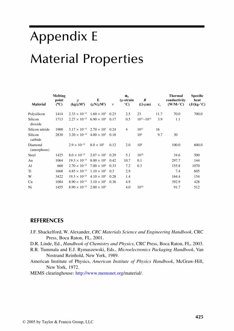
425
Appendix E
Material Properties
REFERENCES
J.F. Shackelford, W. Alexander, CRC Materials Science and Engineering Handbook, CRC
Press, Boca Raton, FL, 2001.
D.R. Linde, Ed., Handbook of Chemistry and Physics, CRC Press, Boca Raton, FL, 2003.
R.R. Tummala and E.J. Rymaszewski, Eds., Microelectronics Packaging Handbook, Van
Nostrand Reinhold, New York, 1989.
American Institute of Physics, American Institute of Physics Handbook, McGraw-Hill,
New York, 1972.
MEMS clearinghouse: http://www.memsnet.org/material/.
Material
Melting
point
(°°°°C)
ρ(kg/µM3)
E
(µN/µM2) ναααα
T
(µ-strain
°C)
R
(Ω-µm) εr
Thermal
conductivity
(W/M-°C)
Specific
heat
(J/(kg-°C)
Polysilicon 1414 2.33 × 10⁻¹⁵ 1.60 × 10⁵ 0.23 2.5 23 11.7 70.0 700.0
Silicon
dioxide
1713 2.27 × 10⁻¹⁵ 6.90 × 10⁴ 0.17 0.5 1011–1014 3.9 1.1
Silicon nitride 1900 3.17 × 10⁻¹⁵ 2.70 × 10⁵ 0.24 4 1011 16
Silicon
carbide
2830 3.20 × 10⁻¹⁵ 4.00 × 10⁵ 0.18 104 9.7 30
Diamond
(amorphous)
2.9 × 10⁻¹⁵ 8.0 × 10⁵ 0.12 2.0 108 100.0 600.0
Steel 1425 8.0 × 10⁻¹⁵ 2.07 × 10⁵ 0.29 5.1 1010 34.6 500
Au 1064 19.3 × 10⁻¹⁵ 8.00 × 10⁴ 0.42 10.7 0.1 297.7 144
Al 660 2.70 × 10⁻¹⁵ 7.00 × 10⁴ 0.33 7.2 0.3 155.8 1070
Ti 1668 4.85 × 10⁻¹⁵ 1.10 × 10⁵ 0.3 2.9 7.4 605
W 3422 19.3 × 10⁻¹⁵ 4.10 × 10⁵ 0.28 1.4 164.4 154
Cu 1084 8.90 × 10⁻¹⁵ 3.10 × 10⁵ 0.36 4.9 392.9 428
Ni 1455 8.90 × 10⁻¹⁵ 2.00 × 10⁵ 4.0 1018 91.7 512
© 2005 by Taylor & Francis Group, LLC
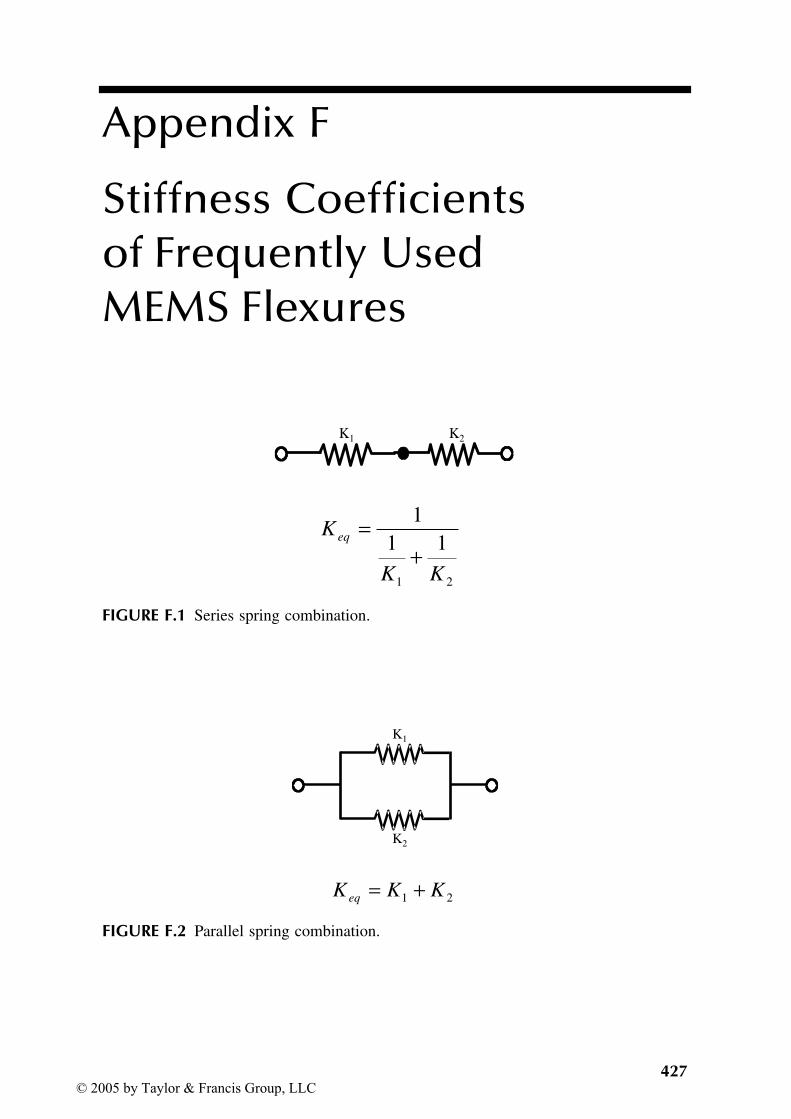
427
Appendix F
Stiffness Coefficientsof Frequently UsedMEMS Flexures
FIGURE F.1 Series spring combination.
FIGURE F.2 Parallel spring combination.
K1 K2
21
11
1
KK
K eq
+=
K1
K2
21 KKK eq +=
© 2005 by Taylor & Francis Group, LLC
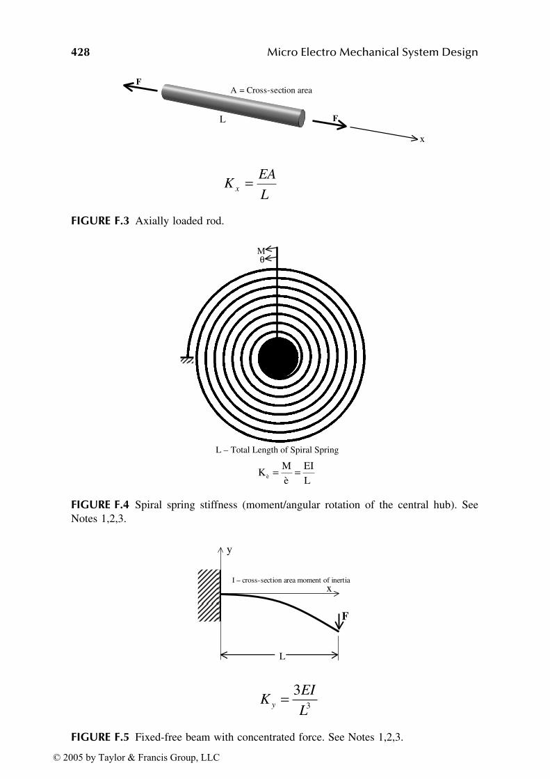
428 Micro Electro Mechanical System Design
FIGURE F.3 Axially loaded rod.
FIGURE F.4 Spiral spring stiffness (moment/angular rotation of the central hub). See
Notes 1,2,3.
FIGURE F.5 Fixed-free beam with concentrated force. See Notes 1,2,3.
x
F
F
A = Cross-section area
L
L
EAK x =
L
EI
è
MKè ==
θ
L – Total Length of Spiral Spring
M
=yKEI
L
33
iartne of intmemoareon aictses-rosI – c
L
F
x
y
© 2005 by Taylor & Francis Group, LLC
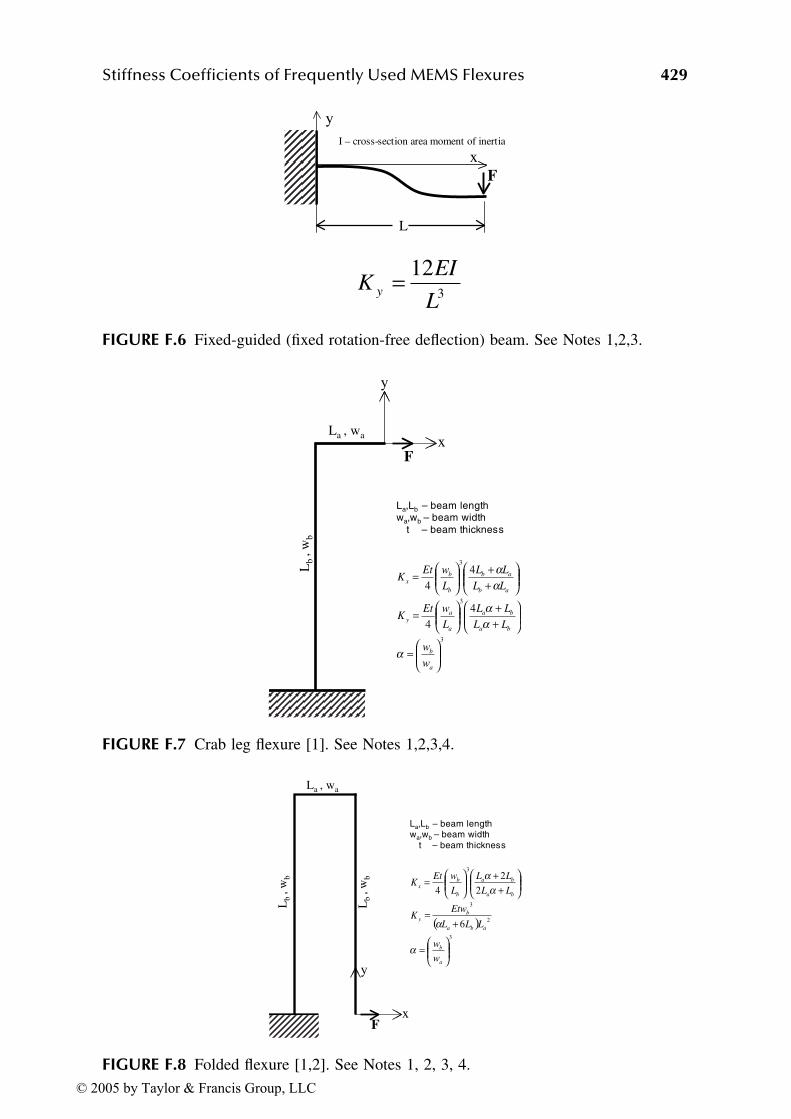
Stiffness Coefficients of Frequently Used MEMS Flexures 429
FIGURE F.6 Fixed-guided (fixed rotation-free deflection) beam. See Notes 1,2,3.
FIGURE F.7 Crab leg flexure [1]. See Notes 1,2,3,4.
FIGURE F.8 Folded flexure [1,2]. See Notes 1, 2, 3, 4.
y
x
F
I – cross-section area moment of inertia
L
3
12
L
EIK y =
y
xF
La , wa
Lb
,w
b
++
=
ab
ab
b
bx
LL
LL
L
wEtK
αα4
4
3
++
=
ba
ba
a
ay
LL
LL
L
wEtK
αα4
4
3
3
=
a
b
w
wα
La,Lb – beam length
wa,wb – beam width
t – beam thickness
y
xF
Lb
,w
b
La , wa
Lb
,w
b
+
+
=
ba
ba
b
bx
LL
LL
L
wEtK
αα
2
2
4
3
( ) 2
3
6 aba
by
LLL
EtwK
+=
α3
=
a
b
w
wα
La,Lb – beam length
wa,wb – beam width
t – beam thickness
© 2005 by Taylor & Francis Group, LLC
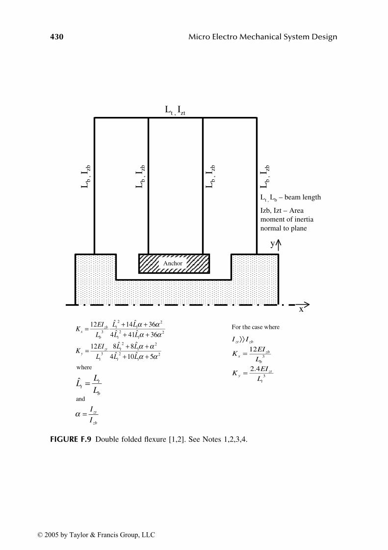
430 Micro Electro Mechanical System Design
FIGURE F.9 Double folded flexure [1,2]. See Notes 1,2,3,4.
⟩⟩I Izt zb
=KEI
Ly
zt
t
2.43
eplantonormal
inertiaofmoment
Areat –IzIzb,
lengtheam– bbLt ,L
zbI ,
b
L
zbI ,
b
L
zbI ,
b
L
ztI , tL
zbI ,
b
L
horcAn
x
y
dan
eerwh
α =I
I
zt
zb
ˆ =LL
Lt
t
b
KEI
L
L L
L Ly
zt
t
t t
t t
=+ +
+ +α αα α
12 8 ˆ 8 ˆ
4 ˆ 10 ˆ 53
2 2
2 2
KEI
L
L L
L Lx
zb
b
t t
t t
=+ ++ +
α αα α
12 ˆ 14 ˆ 36
4 ˆ 41 ˆ 363
2 2
2 2
eerwheas cheor tF
=KEI
Lx
zb
b
123
© 2005 by Taylor & Francis Group, LLC

Stiffness Coefficients of Frequently Used MEMS Flexures 431
NOTES
1. Youngs Modulus, E, should be obtained from the specific fabrication process
utilized. Appendix E and its references can provide approximate values.
2. The area moment of inertia, I, is calculated for the bending axis perpendicular to
the plane of the page.
3. Tables G.2 and G.3 provide methods to calculate I in terms of beam dimensions.
4. These equations were developed [1,2] with Castigliano’s Theorem which included
bending and torsion strain energy terms only. Due to the neglected axial strain
energy terms, the Ky stiffness may be significantly underestimated. This will occur
when bending is not the dominant contributor to deflection in some truss members.
REFERENCES
1. G.K. Fedder, Simulation of microelectromechanical systems, Ph.D. thesis, Dept.
of Electrical Engineering and Computer Sciences, University of California at
Berkeley, Berkeley, CA, 1994.
2. W.C. Tang, Electrostatic comb drive for resonant sensor and actuator applications,
Ph.D. thesis, Dept. of Electrical Engineering and Computer Sciences, University
of California at Berkeley, Berkeley, CA, 1990.
3. L. Saggere, S. Kota, and S.B. Crary, Int. Mechanical Eng. Congr. Exhibition,
ASME, DSC-55, 1994.
FIGURE F.10 Double V beam flexure [3]. See Notes 1,2,3.
Anchor
y
x
ϕ
ϕ
L L
+=
2
cos1
cos123
ϕϕL
EIK x
ϕcos
8
L
AEK y =
© 2005 by Taylor & Francis Group, LLC
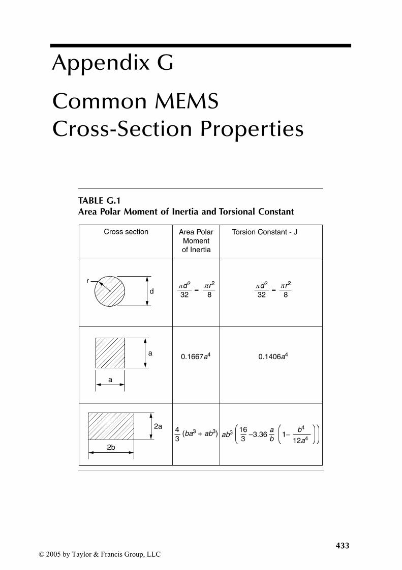
433
Appendix G
Common MEMS Cross-Section Properties
TABLE G.1Area Polar Moment of Inertia and Torsional Constant
Cross section Area Polar
Moment
of Inertia
Torsion Constant - J
πd2 πr2
32 8=
πd2 πr2
32 8=
0.1667a4 0.1406a4
4
3
a b4
b 12a4
16
3(ba3 + ab3) ab3 –3.36 1−
2b
2a
a
a
d
r
© 2005 by Taylor & Francis Group, LLC
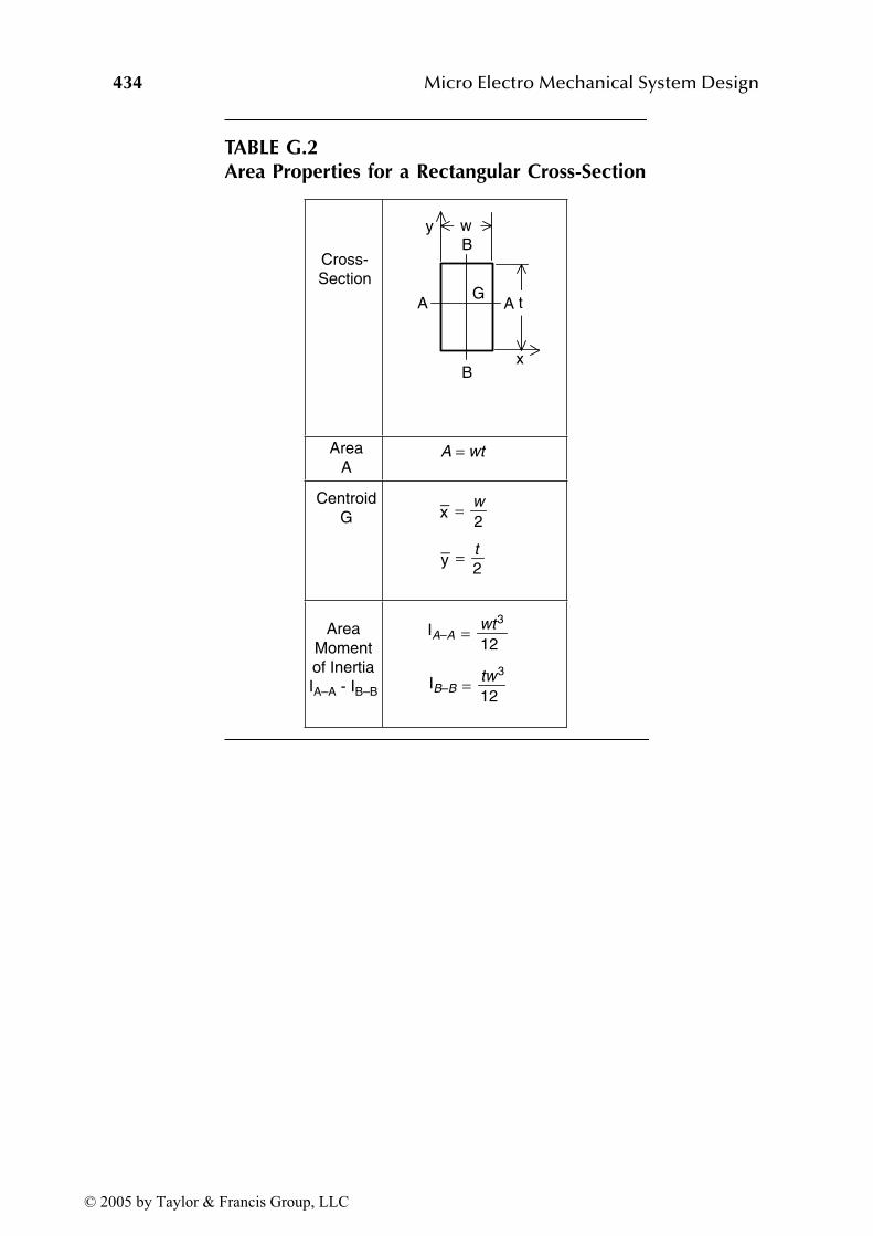
434 Micro Electro Mechanical System Design
TABLE G.2Area Properties for a Rectangular Cross-Section
t
x
y
A A
B
B
G
w
Area
A
Centroid
G
A = wt
2
2
ty
wx
=
=
12
=
=
Cross-
Section
Area
Moment
of Inertia
IA–A - IB–B
IA–A
IB–B
wt3
12
tw3
© 2005 by Taylor & Francis Group, LLC
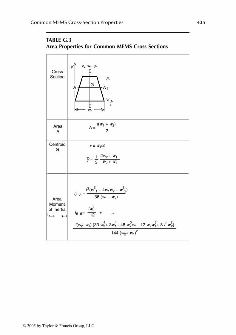
Common MEMS Cross-Section Properties 435
TABLE G.3Area Properties for Common MEMS Cross-Sections
Cross
Section
Area
A
Centroid
G
Area
Moment
of Inertia
IA–A − IB–B
y
A A
x
B
B
Gt
w2
w1
t(w1 + w2)
2
x = w1/2
y =t 2w2 + w1
w2 + w13
tw23
12IB–B= + ...
IA–A =t3(w
21 + 4w1w2 + w
22)
36 (w1 + w2)
t(w2–w1) (33 w24+ 3w1
4+ 48 w2
3w1– 12 w2w1
3+ 8 t
2w
22)
144 (w2+ w1)2
A =
© 2005 by Taylor & Francis Group, LLC

437
Appendix H
Appendix H shows the functions and files to perform Lagrange’s equation and
the SUGAR simulations discussed in Chapter 7. Appendix H.1 and H.2 are the
MATLAB functions that perform the computations for Lagrange’s equations
(Equation 7.13 and Equation 7.14). LagEqn.m (Appendix H.1) is the main func-
tion, which calls maxderiv.m (Appendix H.2) as necessary. These functions require
MATLAB and the Symbolic Math Toolbox. Appendix sections H.3 through H.7
are the MATLAB files used for Example 7.1 through Example 7.5. Sections H.8
through H.10 are files used for the SUGAR simulation in Example 7.6.
H.1 LAGEQN.M
function [eqns]=LagEqn(T,U,D,W,G,Gcoord,Tvar);
% [eqns]=LagEqn(T,U,D,W,G,Gcoord,Tvar)
% Lagrange‘s equation will be used to find the equations
of motion
% Equation #.11
%
% The equations of motion will be found using symbolic
% manipulation given the following input data:
% T-Kinetic Energy
% (e.g., T=1/2*m*Dx^2; or undefined if T=0;)
% U-Potential Energy
% (e.g., U=1/2*k*x^2; or undefined if U=0;)
% D-Raleigh Dissipation Function
% (e.g., D=1/2*c*Dx^2; or undefined if D=0)
% W-Virtual Work Vector
% (e.g., W=sym([f*x;f*y]); or W=[0;...] ncordx1;)
% G-Constraint Eqns
% (e.g., G=r-r0; or undefined if G is not relevant;)
% Gcoord-vector of Generalized Coordinates
% (e.g., Gcoord=sym([x; y]); required)
% Tvar-vector of time dependent variable symbols
© 2005 by Taylor & Francis Group, LLC
438 Micro Electro Mechanical System Design
% (e.g., Tvar=sym(‘[m;k]‘); or undefined if Tvar is
not relevant)
%
% Output Data:
% eqns- a vector of equations, where eqns=0
%
% Notes:
% 1. A capital D preceding a generalized coordinate
means derivative
% (e.g., Dx – first derivative of the generalized
coordinate x)
% (e.g., D2x – second derivative of the generalized
coordinate x)
%
% 2. LAM# (e.g., LAM1, LAM2) is a reserved variable
name associated with
% the Lagrange Multipliers for the constraint eqns.
%
% 2. IN ALL CASES, The following symbols must be
defined before a call
% to this function.
% syms T U D W G Gcoord Tvar
%
% 3. If any of the symbols are not used in a particular
problem, DO NOT set
% the symbol to a value. For example if T=0 -> Do not
set T to a value.
%
% ©J.J. Allen 2004
[nG,nc]=size(G); %nG= # constraint equations
[nGcoord,nc]=size(Gcoord); %nGcoord = # generalized
coordinates
if nc~=1
error(‘LagEqn: Gcoord should be a symbolic column
vector (nGcoord,1)‘);
end
[nTvar,nc]=size(Tvar); %# time dependent variables
[nVW,nc]=size(W);
if nVW~=nGcoord & nVW~=0
error(‘LagEqn: W vector should be a symbolic
vector(nGcoord,1’);
end
© 2005 by Taylor & Francis Group, LLC

Appendix H 439
eqns=sym(zeros(nGcoord,1)); %initialize equations
%fully expand Functionals
T=expand(T);
U=expand(U);
D=expand(D);
G=expand(G);
for ne=1:nGcoord
GC=Gcoord(ne); %symbol for generalized coordinate
eval([‘syms D’ char(GC)])
eval([‘Dx=D’ char(GC) ‘;’])
x=Gcoord(ne);
dTdx=diff(T,x);
dTdDx=diff(T,Dx);
dUdx=diff(U,x);
dFdDx=diff(D,Dx);
dWdx=diff(W(ne),x);
dGdx=diff(G,x);
Dmax=maxderiv(dTdDx);
dTdDxdt=‘0’;
%differentiate generalized coordinates,
%and all higher derivatives wrt time
for ig=1:nGcoord
GC=Gcoord(ig);
%order 0
eval([‘syms D’ char(GC)])
eval([‘dTdDxdt=dTdDxdt + expand(diff(dTdDx,GC)
* D’ …
char(GC) ‘);’ ])
%order1
eval([‘syms D2’ char(GC)])
eval([‘dTdDxdt=dTdDxdt + ‘...
‘expand(diff(dTdDx,D’ char(GC) ‘) * D2’
char(GC) ‘);’ ])
%derivative wrt to order 2 or greater
for id=2:Dmax
eval([‘dTdDxdt=dTdDxdt +
expand(diff(dTdDx,D’ …
© 2005 by Taylor & Francis Group, LLC

440 Micro Electro Mechanical System Design
int2str(id) char(GC) ‘) * D’
int2str(id+1) char(GC) ‘);’ ])
end
end
%differentiate time dependent variables,
%and all higher derivatives wrt time
for it=1:nTvar
Tv=Tvar(it);
%order 0
eval([‘syms D’ char(Tv)])
eval([‘dTdDxdt=dTdDxdt + expand(diff(dTdDx,Tv)
* D’ …
char(Tv) ‘);’ ])
%order1
eval([‘syms D2’ char(Tv)])
eval([‘dTdDxdt=dTdDxdt + expand(diff(dTdDx,D’
… char(Tv) ‘) * D2’ char(Tv) ‘);’ ])
%derivative wrt to order 2 or greater
for id=2:Dmax
eval([‘dTdDxdt=dTdDxdt +
expand(diff(dTdDx,D’...
int2str(id) char(Tv) ‘) * D’
int2str(id+1) char(Tv) ‘);’ ])
end
end
%Constraint force terms - Cforce
syms Cforce
Cforce=0;
for ic=1:nG
eval([‘syms LAM’ int2str(ic)])
eval([‘Cforce=Cforce+ LAM’ int2str(ic)
‘*dGdx(ic);’ ])
end
%Form Lagrange’s equation
eqns(ne)=dTdDxdt-dTdx +dUdx+dFdDx-dWdx-Cforce;
end
© 2005 by Taylor & Francis Group, LLC

Appendix H 441
H.2 MAXDERIV.M
function [Dmax]=maxderiv(expr);
%[Dmax]=maxderiv(expr)
%This function will find the maximum derivative for
any variable
% in the symbolic expression, expr.
expr=char(expr);
indx=find(expr==‘D’);
num=length(indx);
if num==0
Dmax=0;
else
Dmax=1;
for i=1:num
deg=str2num(expr(indx(i)+1));
if max(size(deg))~=0
Dmax=max([Dmax; deg]);
end
end
end
return
© 2005 by Taylor & Francis Group, LLC

442 Micro Electro Mechanical System Design
H.3 XCEL1.M
clear all
diary off
delete xcel1.dia
diary xcel1.dia
echo on
clc
syms T U D W G Gcoord Tvar %declare symbolic functionals
syms M C K F %declare symbolic constants in problem
syms x Dx %declare symbolic generalized coordinates &
derivatives
T=1/2*M*Dx^2;
U=1/2*K*x^2;
D=1/2*C*Dx^2;
W=[F*x];
Gcoord=[x];
[eqns]=LagEqn(T,U,D,W,G,Gcoord,Tvar);
%display results
disp(‘Generalized Coordinates’)
pretty(Gcoord)
disp(‘equations of motion’)
pretty(eqns)
echo off
diary off
© 2005 by Taylor & Francis Group, LLC
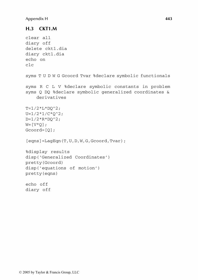
Appendix H 443
H.3 CKT1.M
clear all
diary off
delete ckt1.dia
diary ckt1.dia
echo on
clc
syms T U D W G Gcoord Tvar %declare symbolic functionals
syms R C L V %declare symbolic constants in problem
syms Q DQ %declare symbolic generalized coordinates &
derivatives
T=1/2*L*DQ^2;
U=1/2*1/C*Q^2;
D=1/2*R*DQ^2;
W=[V*Q];
Gcoord=[Q];
[eqns]=LagEqn(T,U,D,W,G,Gcoord,Tvar);
%display results
disp(‘Generalized Coordinates’)
pretty(Gcoord)
disp(‘equations of motion’)
pretty(eqns)
echo off
diary off
© 2005 by Taylor & Francis Group, LLC

444 Micro Electro Mechanical System Design
H.4 M2OSCL.M
diary m2oscl.dia
echo on
clc
syms T U D W G Gcoord Tvar %declare symbolic functionals
syms Mx My Kx Ky Cy g e0 A Er El %declare symbolic
constants in problem
syms x Dx y Dy %declare symbolic generalized coordinates
& derivatives
T=1/2*Mx*Dx^2 + 1/2*My*Dy^2;
U=1/2*(4*Kx)*x^2+1/2*(4*Ky)*(x-y)^2...
+1/2*e0*A*El^2/(g+x)+1/2*e0*A*Er^2/(g-x);
D=1/2*Cy*Dy^2;
W=[0; 0];
Gcoord=[x; y];
[eqns]=LagEqn(T,U,D,W,G,Gcoord,Tvar);
%display results
disp(‘Generalized Coordinates’)
pretty(Gcoord)
disp(‘equations of motion’)
pretty(eqns)
echo off
diary off
© 2005 by Taylor & Francis Group, LLC

Appendix H 445
H.5 RODWALL.M
clear all
diary off
delete RodWall.dia
diary RodWall.dia
echo on
clc
syms T U D W G Gcoord Tvar %declare symbolic functionals
syms LAM1 %declare Lagrange multipliers if there are
constraints
syms Lx Ly L M I K F %declare symbolic constants in
problem
syms x Dx y Dy %declare symbolic generalized coordinates
U=1/2*K*y^2;
W=[F*x; 0];
G=[(Lx-x)^2+(Ly+y)^2-L^2];
Gcoord=[x;y];
[eqns]=LagEqn(T,U,F,W,G,Gcoord,Tvar);
%display results
disp(‘Generalized Coordinates’)
pretty(Gcoord)
disp(‘equations of motion’)
pretty(eqns)
disp(‘constraint equations’)
pretty(G)
echo off
diary off
© 2005 by Taylor & Francis Group, LLC

446 Micro Electro Mechanical System Design
H.6 PARALLELRLC.M
clc
diary off
delete parallelRLC.dia
diary parallelRLC.dia
%Parallel RLC circuit
syms T U D W G Gcoord Tvar %declare symbolic functionals
syms R C L I %declare symbolic constants
in problem
syms lam Dlam %declare symbolic generalized
coordinates & derivatives
T=1/2*C*Dlam^2;
U=1/(2*L)*lam^2;
D=1/(2*R)*Dlam^2;
W=[I*lam];
Gcoord=[lam];
[eqns]=LagEqn(T,U,D,W,G,Gcoord,Tvar);
%display results
disp(‘Generalized Coordinates’)
pretty(Gcoord)
disp(‘equations of motion’)
pretty(eqns)
echo off
diary off
© 2005 by Taylor & Francis Group, LLC

Appendix H 447
H.7 SOLENOID.M
clear all
diary off
delete solenoid.dia
diary solenoid.dia
echo on
clc
syms T U D W G Gcoord Tvar %declare symbolic functionals
syms M K R C L E L0 x0 %declare symbolic constants
in problem
syms Q DQ x Dx %declare symbolic generalized
coordinates & derivatives
L=L0/(1+(x/x0)^2)
T=1/2*L*DQ^2+1/2*M*Dx^2;
U=1/2*K*x^2;
D=1/2*R*DQ^2+1/2*C*Dx^2;
W=[E*Q; 0];
Gcoord=[Q; x];
[eqns]=LagEqn(T,U,D,W,G,Gcoord,Tvar);
%display results
disp(‘Generalized Coordinates’)
pretty(Gcoord)
disp(‘equations of motion’)
pretty(eqns)
echo off
diary off
© 2005 by Taylor & Francis Group, LLC
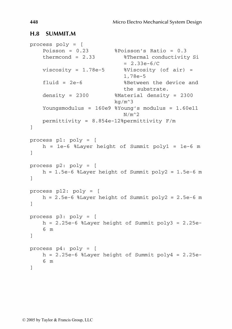
448 Micro Electro Mechanical System Design
H.8 SUMMIT.M
process poly = [
Poisson = 0.23 %Poisson’s Ratio = 0.3
thermcond = 2.33 %Thermal conductivity Si
= 2.33e-6/C
viscosity = 1.78e-5 %Viscosity (of air) =
1,78e-5
fluid = 2e-6 %Between the device and
the substrate.
density = 2300 %Material density = 2300
kg/m^3
Youngsmodulus = 160e9 %Young’s modulus = 1.60e11
N/m^2
permittivity = 8.854e-12%permittivity F/m
]
process p1: poly = [
h = 1e-6 %Layer height of Summit poly1 = 1e-6 m
]
process p2: poly = [
h = 1.5e-6 %Layer height of Summit poly2 = 1.5e-6 m
]
process p12: poly = [
h = 2.5e-6 %Layer height of Summit poly2 = 2.5e-6 m
]
process p3: poly = [
h = 2.25e-6 %Layer height of Summit poly3 = 2.25e-
6 m
]
process p4: poly = [
h = 2.25e-6 %Layer height of Summit poly4 = 2.25e-
6 m
]
© 2005 by Taylor & Francis Group, LLC

Appendix H 449
H.9 LEV_BEND.NET
uses summit.net
uses stdlib.net
param Lelec=0
param Lcenter=0
gap3de p12 [a b aa bb] [l=Lelec w1=2.5u w2=2.5u h=10u
gap=2u
R1=10 R2=10 ox=pi/2]
beam3de p12 [b c] [l=Lcenter w=10u R=10 ]
beam3de p12 [c d] [l=Lcenter w=10u R=10 ]
gap3de p12 [d e dd ee] [l=Lelec w1=2.5u w2=2.5u h=10u
gap=2u
R1=10 R2=10 ox=pi/2]
anchor p12 [a] [l=10u w=10u h=2.5u R=10 ]
anchor p12 [e] [l=10u w=10u h=2.5u R=10 ]
anchor p12 [aa] [l=10u w=10u R=10 ]
anchor p12 [bb] [l=10u w=10u R=10 ]
anchor p12 [dd] [l=10u w=10u R=10 ]
anchor p12 [ee] [l=10u w=10u R=10 ]
eground * [aa] []
eground * [bb] []
eground * [dd] []
eground * [ee] []
param Vactuate=0
Vsrc * [a gnd] [V=Vactuate sv=0.1 sph=0]
eground * [gnd] []
© 2005 by Taylor & Francis Group, LLC

450 Micro Electro Mechanical System Design
H.10 LEV_BEND.M
clear all
clc
Le=100;
Lc=300;
param.Lelec=Le*1e-6;
param.Lcenter=Lc*1e-6;
Vvec=[];
Zvec=[];
V=0;
for V=0:5:200
param.Vactuate=V;
net=cho_load(‘Lev_bend.net’,param);
[dq,conv]=cho_dc(net);
if conv==0
disp(‘did not converge -> break out of the
loop’)
break
end
cx=dq(lookup_coord(net,’c’,’x’));
cy=dq(lookup_coord(net,’c’,’y’));
cz=dq(lookup_coord(net,’c’,’z’));
Vvec=[Vvec; V];
Zvec=[Zvec; cz/1e-6];
disp([‘V = ‘ num2str(V) ‘ Z = ‘ num2str(cz/1e-6)])
end
cho_display(net,dq)
© 2005 by Taylor & Francis Group, LLC

Appendix H 451
H.11 RRITZ_FFBEAM.M
%Raliegh Ritz solution of a fixed-fixed beam with a
distributed load
%Lagranges equations are used to obtain the governing
equations.
%Using 10 terms in the solution.
clear all
clc
disp(‘Fixed Fixed Euler Beam a distributed load’)
syms T U D W G Gcoord Tvar
syms EI L Y phi a0 a1 a2 a3 a4 a5 a6 a7 a8 a9 x w
phi=[ cos(2*pi*x/L)-1 cos(2*2*pi*x/L)-1
cos(2*3*pi*x/L)-1...
cos(2*4*pi*x/L)-1 cos(2*5*pi*x/L)-1
cos(2*6*pi*x/L)-1...
cos(2*7*pi*x/L)-1 cos(2*8*pi*x/L)-1
cos(2*9*pi*x/L)-1...
cos(2*10*pi*x/L)-1];
D2phi=diff(phi,’x’,2);
a= [ a0; a1; a2; a3; a4; a5; a6; a7; a8; a9];
Y=phi * a;
%Strain Energy, U
U= EI/2*int((D2phi*a)^2,0,L);
%non-potential Energy, W
% w - distributed load
W=[int(w*phi(1),0,L)*a0; int(w*phi(2),0,L)*a1;...
int(w*phi(3),0,L)*a2; int(w*phi(4),0,L)*a3;...
int(w*phi(5),0,L)*a4; int(w*phi(6),0,L)*a5;...
int(w*phi(7),0,L)*a6; int(w*phi(8),0,L)*a7;...
int(w*phi(9),0,L)*a8; int(w*phi(10),0,L)*a9];
Gcoord=[a0; a1; a2; a3; a4; a5; a6; a7; a8; a9];
eqns=LagEqn(T,U,D,W,G,Gcoord,Tvar);
© 2005 by Taylor & Francis Group, LLC