Metal Oxide Nanowire and Thin-Film-Based Gas Sensors for Chemical Warfare Simulants Detection
8
IEEE SENSORS JOURNAL, VOL. 8, NO. 6, JUNE 2008 735 Metal Oxide Nanowire and Thin-Film-Based Gas Sensors for Chemical Warfare Simulants Detection Andrea Ponzoni, Camilla Baratto, Sebastiano Bianchi, Elisabetta Comini, Matteo Ferroni, Matteo Pardo, Marco Vezzoli, Alberto Vomiero, Guido Faglia, and Giorgio Sberveglieri Abstract—This work concerns with metal oxide (MOX) gas sensors based on nanowires and thin films. We focus on chemical warfare agents (CWAs) detection to compare these materials from the functional point-of-view. We work with different chemicals including simulants for Sarin nerve agents, vescicant gases, cyanide agents, and analytes such as ethanol, acetone, ammonia, and carbon monoxide that can be produced by everyday activities causing false alarms. Explorative data analysis has been used to demonstrate the different sensing performances of nanowires and thin films. Within the chosen application, our analysis reveal that the introduction of nanowires inside the array composed by thin films can improve its sensing capability. Cyanide simulants have been detected at con- centrations close to 1 ppm, lower than the Immediately Dangerous for Life and Health (IDLH) value of the respective warfare agent. Higher sensitivity has been obtained to simulants for Sarin and vescicant gases, which have been detected at concentrations close or even lower than 100 ppb. Results demonstrate the suitability of the proposed array to selectively detect CWA simulants with respect to some compounds produced by everyday activities. Index Terms—Chemical warfare agents (CWAs), DMMP, explo- rative data analysis, MOS devices, nanowires, thin films. I. INTRODUCTION M ONITORING HVAC systems (HVAC: heating, ventila- tion, and air conditioning) from chemical warfare agents (CWAs) attacks is of crucial importance in security field. These systems can be used to quickly diffuse toxic chemicals in closed environments such as, for example, metrostations or airports. Such an application is quite challenging because of the need to sense target gases at very low concentrations and to discriminate them from several interfering gases. In this work, we refer to the CWAs detection to compare metal oxide (MOX) nanowires and thin films from the func- tional point-of-view. MOX nanowires have been proposed as optimal materials for gas sensing [1]–[4] and their peculiar features, i.e., nano- Manuscript received Decdember 30, 2007; revised February 25, 2008; ac- cepted February 26, 2008. This work was supported in part by the European Strep Project 001528 “Nanostructured Solid-State Gas Sensors With Superior Performance” (NANOS4) and in part by the NATO Project 982166 “Chemical Threat Detectors Based on Multisensor Arrays and Selective Porous Concentra- tors.” The associate editor coordinating the review of this paper and approving it for publication was Dr. Janet Jensen. The authors are with the CNR-INFM SENSOR Laboratory, Department of Chemistry and Physics, Brescia University, I-25133 Brescia, Italy (e-mail: andrea. [email protected]; [email protected]; sebastiano. bianchi@ ing.unibs.it; [email protected]; [email protected]; pardo@ing. unibs.it; [email protected]; [email protected]; gfaglia@ing. unibs.it; [email protected]). Color versions of one or more of the figures in this paper are available online at http://ieeexplore.ieee.org. Digital Object Identifier 10.1109/JSEN.2008.923179 sized transverse dimension, high aspect-ratio and single-crystal structure, have been largely studied in literature [4]–[6]. Despite this, further work is still needed to have a reliable comparison between such an emerging technology and the traditional ones based on thin or thick polycrystalline films. We work with several chemicals to probe sensing perfor- mances of MOXs prepared as nanowires and thin films. We test CWA simulants for Sarin nerve agents, cyanide agents, or vescicant gases to visualize the capability of the array to respond to different CWA attacks; we use also compounds typical of indoor applications, chosen according to the HVAC system monitoring scenario, to test the sensor array capability to avoid false alarms. We use different explorative data analysis tools to visualize such results and address the contribution of nanowires within the sensor array. II. EXPERIMENTAL A. Sensor Preparation The sensing layers have been fabricated over mm mm mm alumina substrates. Thin films have been deposited by rheotaxial growth and thermal oxidation (RGTO) technique [7], [8], which allows obtaining a monolayer of oxidized droplets featuring a high surface to volume ratio. The RGTO technique consists of two deposition steps: first the preparation of a metallic thin film by DC magnetron sput- tering from a tin target on a substrate kept at a temperature higher than the melting point of the metal, then the thermal ox- idation cycle in order to get a stoichiometric composition for the MOX. The deposition of the metal on a substrate at a tem- perature higher than the melting point causes the formation of spherical clusters instead of flat film. The annealing treatment consists of two steps. The first step is performed at a temperature below the metal melting point in order to slightly oxidize the metallic droplets without fusing them in a continuous and compact layer. The slight oxidation strongly increases the melting temperature of the material, which can be further oxidized at higher temperature in the second step. During this second step, the material reaches a stable stoi- chiometry without losing the droplet-like morphology with high surface to volume ratio, suitable for gas sensing application. Shadow mask method has been adopted during the sputtering process to pattern the growth of the oxide layer according to the sensor layout structure. Nanowires have been synthesized via Vapor-Liquid-Solid (VLS) process in a tubular furnace where MOX powders are ther- mally evaporated. Vapors condense over Pt-catalyzed substrates 1530-437X/$25.00 © 2008 IEEE Authorized licensed use limited to: CNR AREA RICERCA DI BOLOGNA. Downloaded on October 8, 2008 at 05:36 from IEEE Xplore. Restrictions apply.
Transcript of Metal Oxide Nanowire and Thin-Film-Based Gas Sensors for Chemical Warfare Simulants Detection

IEEE SENSORS JOURNAL, VOL. 8, NO. 6, JUNE 2008 735
Metal Oxide Nanowire and Thin-Film-Based GasSensors for Chemical Warfare Simulants Detection
Andrea Ponzoni, Camilla Baratto, Sebastiano Bianchi, Elisabetta Comini, Matteo Ferroni, Matteo Pardo,Marco Vezzoli, Alberto Vomiero, Guido Faglia, and Giorgio Sberveglieri
Abstract—This work concerns with metal oxide (MOX) gassensors based on nanowires and thin films. We focus on chemicalwarfare agents (CWAs) detection to compare these materials fromthe functional point-of-view. We work with different chemicalsincluding simulants for Sarin nerve agents, vescicant gases, cyanideagents, and analytes such as ethanol, acetone, ammonia, and carbonmonoxide that can be produced by everyday activities causing falsealarms. Explorative data analysis has been used to demonstrate thedifferent sensing performances of nanowires and thin films. Withinthe chosen application, our analysis reveal that the introduction ofnanowires inside the array composed by thin films can improve itssensing capability. Cyanide simulants have been detected at con-centrations close to 1 ppm, lower than the Immediately Dangerousfor Life and Health (IDLH) value of the respective warfare agent.Higher sensitivity has been obtained to simulants for Sarin andvescicant gases, which have been detected at concentrations closeor even lower than 100 ppb. Results demonstrate the suitabilityof the proposed array to selectively detect CWA simulants withrespect to some compounds produced by everyday activities.
Index Terms—Chemical warfare agents (CWAs), DMMP, explo-rative data analysis, MOS devices, nanowires, thin films.
I. INTRODUCTION
MONITORING HVAC systems (HVAC: heating, ventila-tion, and air conditioning) from chemical warfare agents
(CWAs) attacks is of crucial importance in security field. Thesesystems can be used to quickly diffuse toxic chemicals in closedenvironments such as, for example, metrostations or airports.Such an application is quite challenging because of the need tosense target gases at very low concentrations and to discriminatethem from several interfering gases.
In this work, we refer to the CWAs detection to comparemetal oxide (MOX) nanowires and thin films from the func-tional point-of-view.
MOX nanowires have been proposed as optimal materialsfor gas sensing [1]–[4] and their peculiar features, i.e., nano-
Manuscript received Decdember 30, 2007; revised February 25, 2008; ac-cepted February 26, 2008. This work was supported in part by the EuropeanStrep Project 001528 “Nanostructured Solid-State Gas Sensors With SuperiorPerformance” (NANOS4) and in part by the NATO Project 982166 “ChemicalThreat Detectors Based on Multisensor Arrays and Selective Porous Concentra-tors.” The associate editor coordinating the review of this paper and approvingit for publication was Dr. Janet Jensen.
The authors are with the CNR-INFM SENSOR Laboratory, Departmentof Chemistry and Physics, Brescia University, I-25133 Brescia, Italy (e-mail:andrea. [email protected]; [email protected]; sebastiano. [email protected]; [email protected]; [email protected]; [email protected]; [email protected]; [email protected]; [email protected]; [email protected]).
Color versions of one or more of the figures in this paper are available onlineat http://ieeexplore.ieee.org.
Digital Object Identifier 10.1109/JSEN.2008.923179
sized transverse dimension, high aspect-ratio and single-crystalstructure, have been largely studied in literature [4]–[6]. Despitethis, further work is still needed to have a reliable comparisonbetween such an emerging technology and the traditional onesbased on thin or thick polycrystalline films.
We work with several chemicals to probe sensing perfor-mances of MOXs prepared as nanowires and thin films. Wetest CWA simulants for Sarin nerve agents, cyanide agents,or vescicant gases to visualize the capability of the array torespond to different CWA attacks; we use also compoundstypical of indoor applications, chosen according to the HVACsystem monitoring scenario, to test the sensor array capabilityto avoid false alarms.
We use different explorative data analysis tools to visualizesuch results and address the contribution of nanowires withinthe sensor array.
II. EXPERIMENTAL
A. Sensor Preparation
The sensing layers have been fabricated over mm mmmm alumina substrates.
Thin films have been deposited by rheotaxial growth andthermal oxidation (RGTO) technique [7], [8], which allowsobtaining a monolayer of oxidized droplets featuring a highsurface to volume ratio.
The RGTO technique consists of two deposition steps: firstthe preparation of a metallic thin film by DC magnetron sput-tering from a tin target on a substrate kept at a temperaturehigher than the melting point of the metal, then the thermal ox-idation cycle in order to get a stoichiometric composition forthe MOX. The deposition of the metal on a substrate at a tem-perature higher than the melting point causes the formation ofspherical clusters instead of flat film.
The annealing treatment consists of two steps. The first stepis performed at a temperature below the metal melting point inorder to slightly oxidize the metallic droplets without fusingthem in a continuous and compact layer. The slight oxidationstrongly increases the melting temperature of the material, whichcan be further oxidized at higher temperature in the secondstep. During this second step, the material reaches a stable stoi-chiometry without losing the droplet-like morphology with highsurface to volume ratio, suitable for gas sensing application.
Shadow mask method has been adopted during the sputteringprocess to pattern the growth of the oxide layer according to thesensor layout structure.
Nanowires have been synthesized via Vapor-Liquid-Solid(VLS) process in a tubular furnace where MOX powders are ther-mally evaporated. Vapors condense over Pt-catalyzed substrates
1530-437X/$25.00 © 2008 IEEE
Authorized licensed use limited to: CNR AREA RICERCA DI BOLOGNA. Downloaded on October 8, 2008 at 05:36 from IEEE Xplore. Restrictions apply.
736 IEEE SENSORS JOURNAL, VOL. 8, NO. 6, JUNE 2008
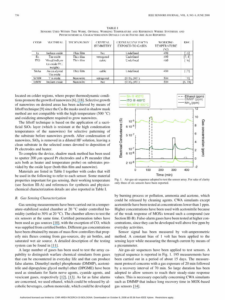
TABLE ISENSORS USED WITHIN THIS WORK. OPTIMAL WORKING TEMPERATURE AND REFERENCE WHERE SYNTHESIS AND
PHYSICOCHEMICAL CHARACTERIZATION DETAILS CAN BE FOUND ARE ALSO REPORTED
located on colder regions, where proper thermodynamic condi-tions promote the growth of nanowires [6], [18]. Selective growthof nanowires on desired areas has been achieved by means ofliftoff technique [9] since the Cu-Be masks used in shadow maskmethod are not compatible with the high temperature (500 C)and oxidizing atmosphere required to grow nanowires.
The liftoff technique is based on the application of a sacri-ficial SiO layer (which is resistant at the high condensationtemperatures of the nanowires) for selective patterning ofthe substrate before nanowires growth. After condensation ofnanowires, SiO is removed in a diluted HF solution, leaving aclean substrate in the selected zones devoted to deposition ofPt electrodes and heater.
To complete the device, shadow mask method has been usedto sputter 200 m spaced Pt electrodes and a Pt meander (thatacts both as heater and temperature probe) on substrates pro-vided by the oxide layer (both thin film and nanowire).
Materials are listed in Table I together with codes that willbe used in the following to refer to each sensor. Some materialproperties important for gas sensing, their working temperature(see Section III-A) and references for synthesis and physico-chemical characterization details are also reported in Table I.
B. Gas Sensing Characterization
Gas sensing measurements have been carried out in a temper-ature-stabilized sealed chamber at 20 C under controlled hu-midity (settled to 30% at 20 C). The chamber allows to test thesix sensors at the same time. Certified permeation tubes havebeen used as gas sources [10], with the exception of CO, whichwas supplied from certified bottles. Different gas concentrationshave been obtained by means of mass flow controllers that prop-erly mix fluxes coming from gas-sources, dry air bottles, andsaturated wet air source. A detailed description of the testingsystem can be found in [11].
A large number of gases has been used to test the array ca-pability to distinguish warfare chemical simulants from gasesthat can be encountered in everyday life and that can producefalse alarms. Dimethyl methyl phosphonate (DMMP), acetoni-trile and dipropylene glycol methyl ether (DPGME) have beenused as simulants for Sarin nerve agents, cyanide agents, andvescicant gases, respectively [12], [13]. As far as false alarmsare concerned, we used ethanol, which could be released by al-coholic beverages, carbon monoxide, which could be developed
Fig. 1. Air-gas-air sequence adopted to test the sensor array. For sake of clarityonly three of six sensors have been reported.
by burning process or pollution, ammonia and acetone, whichcould be released by cleaning agents. CWA simulants exceptacetonitrile have been tested at concentrations lower than 1 ppm.Higher concentrations have been used with acetonitrile becauseof the weak response of MOXs toward such a compound (seeSection III-B). False-alarm gases have been tested at higher con-centrations, since they can be developed well above few ppm byeveryday activities.
Sensor signal has been measured by volt-amperometricmethod. A constant bias of 1 volt has been applied to thesensing layer while measuring the through current by means ofa picoammeter.
Air-gas-air sequences have been applied to test sensors. Atypical sequence is reported in Fig. 1. 195 measurements havebeen carried out in a period of about 15 days. The measure-ment protocol concerns with a gas exposure of 20 min followedby a recovery interval of 70 min. So large duration has beenadopted to allow sensors to reach their steady-state responsevalues. This is necessary especially concerning CWA simulantssuch as DMMP that induce long recovery time in MOX-basedgas sensors [14].
Authorized licensed use limited to: CNR AREA RICERCA DI BOLOGNA. Downloaded on October 8, 2008 at 05:36 from IEEE Xplore. Restrictions apply.

PONZONI et al.: METAL OXIDE NANOWIRE AND THIN-FILM-BASED GAS SENSORS FOR CHEMICAL WARFARE SIMULANTS DETECTION 737
Fig. 2. (a) Secondary electron SEM image of tin oxide nanowires-based sensorand (b) tin oxide RGTO thin film. The different morphologies are expected tostrongly affect the conduction and sensing mechanism underlying the RGTOand nanowires-based devices: the former being dominated by grain boundariescontribution, while the latter is foreseen to be dominated by phenomena occur-ring over the nanowire surfaces.
C. Feature Selection and Explorative Data Analysis
Sensors’ responses have been calculated as theratio, where stands for the steady-state electrical conduc-tance when sensors are exposed to gases. stands for thesteady-state electrical conductance when sensors are exposedto the reference atmosphere (wet air with controlled humidity).
Explorative data analysis has been carried out by means ofpolar plots and Principal Component Analysis (PCA).
The first method has been used to compare sensors by meansof their response spectra. The second one has been used to com-pare the behavior of nanowires and thin films within a sensorarray, i.e., to visualize their capability to enhance variancebetween data and modify data clustering and cluster separation.Before, to apply the PCA algorithm, features extracted fromeach sensor have been preprocessed to zero mean and unitvariance.
We extracted four different static features other than :, , , or Log , but no ap-
preciable variations have been observed by using such featuresinstead of the first one we introduced. Results reported in thefollowing will, thus, be referred to the feature.
III. RESULTS AND DISCUSSION
A. Sensor Working Temperature
Scanning electron microscope (SEM) images of SnOnanowires and RGTO thin films are reported in Fig. 2(a) and (b),respectively.
Beside the evident high aspect ratio of nanowires, an impor-tant difference between the two structures is the crystalline de-gree. Nanowires are single crystals, featuring surfaces corre-sponding to well-defined crystalline planes [5], while RGTOfilms are composed by crystalline domains with rounded shapeand nanosized dimensions (5–50 nm), [19]. These differences
Fig. 3. Effect of working temperature on SnO and In O thin films andnanowires sensing performance to 2 ppm of acetonitrile. RH � ��� at 20 C.The common behavior observed with both SnO and In O , which exhibit ahigher optimal working temperature to the tested CWA simulants if prepared asnanowires instead of polycrystalline RGTO layers, suggest a different sensingmechanism occurring with nanowires and RGTO layers.
have strong effects on the sensing mechanism: surface termina-tion and defects deeply modifies the gas-solid interaction [20].
Metal oxides sense gases mainly via red-ox reactions occur-ring between gaseous molecules and oxygen ions chemisorbedover the MOX surface. This modulates the space charge layerdepth that, in turn, controls the layer conductivity. Concerningthin films exhibiting a granular morphology such as the RGTOones considered here, literature agrees that both the conductionand adsorption phenomena are dominated by grain boundaries[21], [22]. Concerning sensors based on nanowires meshes, fewboundaries between nanowires are also expected, but the maincontribution to their sensing mechanism is foreseen to comefrom the red-ox reaction occurring directly over the nanowiresurfaces [1].
The analysis of optimal sensor working temperature may re-veal some of these phenomena. Measurements carried out withCWA simulants revealed that nanowires used in this work (bothSnO and In O ) exhibit best performances at temperaturehigher than their thin-film counterparts. As an example, sensorresponse to 2 ppm of acetonitrile is reported in Fig. 3. Withinthe tested range of temperatures, nanowires performance isoptimized at 500 C, while the RGTO thin films optimizationoccurs around 400 C.
The common behavior of SnO and In O induces to arguethat phenomena underlying such effects may take origin fromthe material structure (nanowire versus polycrystalline) ratherthan from the material itself (SnO versus In O ).
B. Response Spectra
A key point to selectively identify diverse chemical com-pounds relies on different response spectra exhibited by eachsensor. Their preparation by different technologies may furtherenhance these differences improving the sensor array versatility.
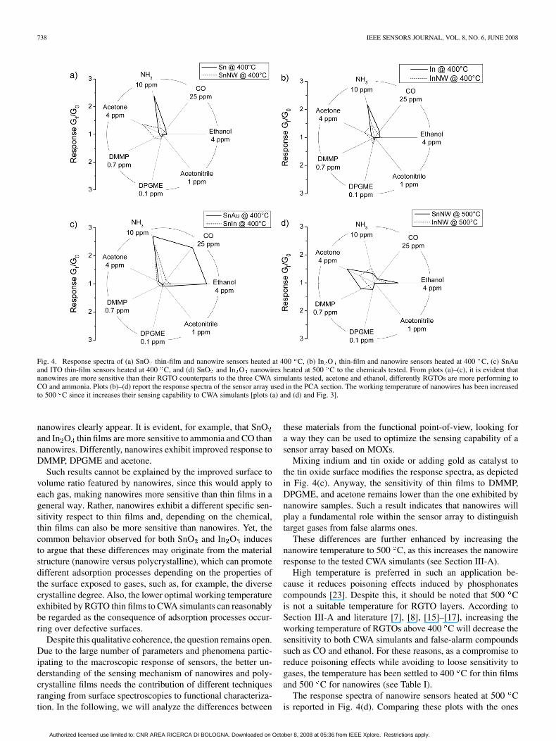
Responses exhibited by sensors heated at 400 C to the testedchemicals have been reported as polar plots in Fig. 4(a)–(c).From Fig. 4(a) and (b), some differences between thin films and
Authorized licensed use limited to: CNR AREA RICERCA DI BOLOGNA. Downloaded on October 8, 2008 at 05:36 from IEEE Xplore. Restrictions apply.
738 IEEE SENSORS JOURNAL, VOL. 8, NO. 6, JUNE 2008
Fig. 4. Response spectra of (a) SnO thin-film and nanowire sensors heated at 400 C, (b) In O thin-film and nanowire sensors heated at 400 C, (c) SnAuand ITO thin-film sensors heated at 400 C, and (d) SnO and In O nanowires heated at 500 C to the chemicals tested. From plots (a)–(c), it is evident thatnanowires are more sensitive than their RGTO counterparts to the three CWA simulants tested, acetone and ethanol, differently RGTOs are more performing toCO and ammonia. Plots (b)–(d) report the response spectra of the sensor array used in the PCA section. The working temperature of nanowires has been increasedto 500 C since it increases their sensing capability to CWA simulants [plots (a) and (d) and Fig. 3].
nanowires clearly appear. It is evident, for example, that SnOand In O thin films are more sensitive to ammonia and CO thannanowires. Differently, nanowires exhibit improved response toDMMP, DPGME and acetone.
Such results cannot be explained by the improved surface tovolume ratio featured by nanowires, since this would apply toeach gas, making nanowires more sensitive than thin films in ageneral way. Rather, nanowires exhibit a different specific sen-sitivity respect to thin films and, depending on the chemical,thin films can also be more sensitive than nanowires. Yet, thecommon behavior observed for both SnO and In O inducesto argue that these differences may originate from the materialstructure (nanowire versus polycrystalline), which can promotedifferent adsorption processes depending on the properties ofthe surface exposed to gases, such as, for example, the diversecrystalline degree. Also, the lower optimal working temperatureexhibited by RGTO thin films to CWA simulants can reasonablybe regarded as the consequence of adsorption processes occur-ring over defective surfaces.
Despite this qualitative coherence, the question remains open.Due to the large number of parameters and phenomena partic-ipating to the macroscopic response of sensors, the better un-derstanding of the sensing mechanism of nanowires and poly-crystalline films needs the contribution of different techniquesranging from surface spectroscopies to functional characteriza-tion. In the following, we will analyze the differences between
these materials from the functional point-of-view, looking fora way they can be used to optimize the sensing capability of asensor array based on MOXs.
Mixing indium and tin oxide or adding gold as catalyst tothe tin oxide surface modifies the response spectra, as depictedin Fig. 4(c). Anyway, the sensitivity of thin films to DMMP,DPGME, and acetone remains lower than the one exhibited bynanowire samples. Such a result indicates that nanowires willplay a fundamental role within the sensor array to distinguishtarget gases from false alarms ones.
These differences are further enhanced by increasing thenanowire temperature to 500 C, as this increases the nanowireresponse to the tested CWA simulants (see Section III-A).
High temperature is preferred in such an application be-cause it reduces poisoning effects induced by phosphonatescompounds [23]. Despite this, it should be noted that 500 Cis not a suitable temperature for RGTO layers. According toSection III-A and literature [7], [8], [15]–[17], increasing theworking temperature of RGTOs above 400 C will decrease thesensitivity to both CWA simulants and false-alarm compoundssuch as CO and ethanol. For these reasons, as a compromise toreduce poisoning effects while avoiding to loose sensitivity togases, the temperature has been settled to 400 C for thin filmsand 500 C for nanowires (see Table I).
The response spectra of nanowire sensors heated at 500 Cis reported in Fig. 4(d). Comparing these plots with the ones
Authorized licensed use limited to: CNR AREA RICERCA DI BOLOGNA. Downloaded on October 8, 2008 at 05:36 from IEEE Xplore. Restrictions apply.

PONZONI et al.: METAL OXIDE NANOWIRE AND THIN-FILM-BASED GAS SENSORS FOR CHEMICAL WARFARE SIMULANTS DETECTION 739
Fig. 5. PCA plot calculated from measurements carried out with the thin-film-based array, composed by Sn, In, ITO, and SnAu sensors. Colors identify gaseswhile symbols identify concentrations. In the legend, concentrations are ex-pressed in ppm. Non-Gaussian clustering of data can be observed, but this doesnot prevent to identify gases by proper vectors. Overlapping of some gas vectors(ex: acetone and DPGME) can be observed.
obtained by nanowires heated at 400 C [Fig. 4(a) and (b)], it isevident that also responses to acetone and ethanol are increasedby heating the nanowire at 500 C.
C. Principal Component Analysis (PCA)
The different response spectra of nanowires and thin films areuseful features for the development of electronic noses.
PCA is the widest used tool to reduce data dimensionality.It is an unsupervised pattern recognition technique that allowsto visualize data clustering and cluster separation according tomaximum variance.
In particular, testing gases at different concentrations allowsto visualize each chemical by its own direction within the PCAplot. By this, it is possible to identify concentrations at whichdifferent gases overlap one another and useful information con-cerning gases and concentrations critical for false alarms can beobtained.
PCA has been carried out considering separately data ac-quired by two subarrays of sensors. They are the subarray com-posed by Sn, In, SnAu. and ITO sensors, which we will call“thin-film array” and the subarray composed by SnNW, InNW,SnAu, and ITO sensors, which we will call “mixed array.”
In Fig. 5, the subspace composed by first and second prin-cipal components calculated from the thin-film array data isreported. In this plot, colors have been used to identify gases,while symbols have been adopted to distinguish different con-centrations. As a first approximation, gases can be characterizedby a proper vector, whose orientation and radius identify theanalyte and its concentration, respectively. Some gases such asDPGME, ethanol, acetone, CO, and ammonia are clearly visiblewithin this plot. For these compounds, the tested concentrationsare high enough to produce appreciable response in thin-filmsensors and gas-vectors can be easily tracked by visually con-
Fig. 6. PCA plot calculated from measurements carried out with thethin-film-based array, composed by Sn, In, ITO, and SnAu sensors, zoom overthe Fig. 5 “weak response region.” Colors identify gases while symbols identifyconcentrations. In the legend, concentrations are expressed in ppm. Acetonedata overlap with both DMMP and DPGME data.
necting data points over the PCA plot. Despite this, gas iden-tification is not free from ambiguity; for example, DPGME di-rection is almost superimposed to the ethanol one and visuallyextrapolating their vectors and the ammonia vector, further over-lapping is foreseen to occur.
Within the PCA plot, it can be also noted that data do notexhibit Gaussian clustering. This can be reasonably ascribed tosensor drift, which could arise both from intrinsic drift, knownto affect MOXs [24], and poisoning phenomena, induced byexposure to aggressive gases such as some CWA simulants[14], [25].
In principle, it is possible to model both kinds of drift, for ex-ample, models accounting for drift induced by ozone poisoning[25] and oxygen diffusion [24] have been reported in literature.These works indicate that model development should be ad-dressed in dedicated works, since model development requiresa detailed analysis of the application and models developed adhoc for each material may also be necessary.
So far, drift modeling is outside the aim of the present work.Despite this, with the knowledge of its effect on data clustering,it can be observed that sensor drift does not prevent identifyinganalytes according to their direction within the PCA plot. Thisis because data qualitatively spreads along such analyte direc-tions. Rather, non-Gaussian clustering will decrease the arraycapability to identify gas concentrations, since data identifyingdifferent concentrations of the same analyte can overlap as aconsequence of such a spread.
Focusing near the origin of gas-vectors identified withinFig. 5, we move toward the “weak-response region.” A zoomover this region is reported in Fig. 6. Here, we can clearlydistinguish acetonitrile, while data corresponding to other com-pounds (DMMP, DPGME, and acetone) are almost overlapped.
Considering the third and the fourth principal componentsdoes not improve data separability due to the high scores of
Authorized licensed use limited to: CNR AREA RICERCA DI BOLOGNA. Downloaded on October 8, 2008 at 05:36 from IEEE Xplore. Restrictions apply.

740 IEEE SENSORS JOURNAL, VOL. 8, NO. 6, JUNE 2008
Fig. 7. PCA plot calculated from measurements carried out by means of themixed array, composed by ITO, SnAu, SnNW, and InNW sensors. Colors iden-tify gas while symbols identify concentrations. In the legend, concentrationsare expressed in ppm. The non-Gaussain clustering of data already observed inFig. 5 is still present, but an improved gas-vectors separation can be noted. Forexample, Acetone and DPGME vectors do not overlap.
the first and second principal components (about 79% and 19%,respectively).
As far as nanowires are concerned, the same analysis hasbeen carried out with the mixed array, in which SnO and In Onanowires substitutes their thin-film counterparts.
The subspace constructed from the first and second principalcomponents is reported in Fig. 7. Looking first at data clustering,it exhibits the same behavior observed with the thin-film arrayin Figs. 5 and 6: clustering is non-Gaussian, yet data spreadsaccording to directions that can be used to distinguish differentgases.
Visually exploring Fig. 7 with the same criteria adopted withFig. 5, it is evident that the introduction of nanowires separatesthe DPGME direction from the ammonia and the acetone ones,at least at high gas concentrations. Looking at polar plots re-ported in Fig. 4, such a separation can be ascribed to the dif-ferent response spectra exhibited by nanowires and thin films.The former exhibit both an increased sensitivity to acetone andDPGME and a weak sensitivity to ammonia. So far, the mixedarray, composed by both nanowires and thin films, features abroader spectra respect to the thin-film array.
Exploring the PCA plot at low concentrations, the zoom overthe weak response region reported in Fig. 8 reveals that DPGMEand acetone data are still separated. Gas-vectors have been handtraced in Fig. 8 to help visualize it. As far as DMMP is con-cerned, it can be observed that overlapping with acetone andDPGME is partly solved. Data corresponding to 1 ppm of ace-tone do not overlap with DMMP and DPGME data. Anyway,there is the overlapping between DMMP data corresponding to0.35 ppm and the DPGME vector.
Concluding the comparison between Figs. 5–8, the reportedobservations concerning the nanowire-induced variance in-crease are qualitatively consistent with polar plots reported in
Fig. 8. PCA plot calculated from measurements carried out by means of themixed array (composed by SnIn, SnAu, SnNW, and InNW sensors); zoom overthe “weak response region.” Colors identify gas while symbols identify con-centrations. In the legend, concentrations are expressed in ppm. With respectto Fig. 6, the introduction of nanowires within the sensor array enhances theseparation between DMMP, DPGME and acetone data. As a first approximateexploitation, separated hand-traced gas-vectors can be identified.
Fig. 9. PCA plot calculated from measurements carried out by means of theSnAu, and ITO sensors. Colors identify gas while symbols identify concen-trations. In the legend, concentrations are expressed in ppm. The plot is verysimilar to the one reported in Fig. 5, calculated from data acquired by means ofthe thin-film array, indicating that the increased data separation observed com-paring Figs. 5 and 6 with Figs. 7 and 8, is due to nanowires instead of the corearray (SnAu and ITO).
Fig. 4, but a doubt still remains concerning the role playedby the SnAu and ITO sensors, which have been used in boththe mixed and thin-film arrays. To clarify this, the PCA plotobtained from these two sensors alone has been reported inFig. 9. Such a plot is quite similar to the one obtained by thethin-film array (Fig. 5), thus confirming that the differencesobserved between the PCA plots relative to the mixed and thethin-film arrays can be ascribed to nanowires rather than to theSnAu and ITO sensors.
Plotting the PCA plot obtained from nanowires sensors alone(data not shown) does not improve the results obtained with themixed array, indicating that these results come from the use ofboth technologies, while the two nanowire sensors alone ex-hibit response spectra not broad enough to separate the testedanalytes.
Authorized licensed use limited to: CNR AREA RICERCA DI BOLOGNA. Downloaded on October 8, 2008 at 05:36 from IEEE Xplore. Restrictions apply.

PONZONI et al.: METAL OXIDE NANOWIRE AND THIN-FILM-BASED GAS SENSORS FOR CHEMICAL WARFARE SIMULANTS DETECTION 741
IV. CONCLUDING REMARKS
In this work, we focused on functional characterizationof MOX gas sensors based on thin films and nanowires andcompare these technologies both sensor by sensor and withina sensor array, choosing CWA simulants detection as targetapplication. In particular, we observed some sensing featurescommon to nanowires (SnO and In O ), which differ if thesame oxides are prepared as thin films by RGTO method.
Nanowires exhibited optimal sensing capability to the testedCWA simulants at higher temperature with respect to theirthin-film counterparts (500 versus 400 C).
Some differences have also been observed concerning thesensor response spectra. For example, nanowires revealed moresensitive than thin films to DMMP, DPGME, and acetone; atthe same time they revealed less sensitive to other chemicalssuch as ammonia and CO. Nanowires exhibited appreciable re-sponse to DMMP and DPGME at concentrations close or evenlower than 100 ppb. More critical was the detection of acetoni-trile below the ppm threshold because of the weak response ofMOXs; anyway, it is worth it to note the IDLH value of cyanidecompounds is usually around a few tens of ppm [26].
The observed differences revealed useful to increase the se-lectivity of the sensor array composed by both nanowires andthin films (mixed array) with respect to the thin-film array (e.g.,to increase the separation between DMMP, DPGME, and ace-tone data).
Common to nanowires and thin films, sensor drift has beenobserved, both intrinsic and induced by exposure to aggressivegases. In PCA plots, it manifested as a deviation from Gaussiandata clustering, decreasing the array capability to recognize thegas concentration but not avoiding the possibility to identifygases according to specific directions.
Within the scenario of the development of sensing systemssuitable to reveal CWAs, we expect that the present results couldbe a reference to better address potentialities of MOXs and theirdrawbacks that should be compensated by integration with othertechnologies. For example, selectivity could be improved ac-counting for sensor drift by ad hoc developed models; precon-centrators can also be introduced to increase the capability todetect acetonitrile; properly designed test chambers would alsobe adopted to reduce sensor response time to a few seconds[27]. With the aim to further increase the versatility of the array,sensors based on materials other than MOXs would also be in-troduced, such as, for example, carbon nanotubes or polymers;each material contributing with its proper sensing mechanism tocompensate drawbacks intrinsic of the other ones.
REFERENCES
[1] E. Comini, G. Faglia, G. Sberveglieri, Z. W. Pan, and Z. L. Wang,“Stable and highly sensitive gas sensors based on semiconductingoxide nanobelts,” Appl. Phys. Lett., vol. 81, pp. 1869–1871, 2002.
[2] A. Kolmakov, D. O. Klenov, Y. Lilach, S. Stemmer, and M. Moskovits,“Enhanced gas sensing by individual ��� nanowires and nanobeltsfunctionalized with Pd catalyst particles,” Nano Lett., vol. 5, no. 4, pp.667–673, 2005.
[3] Q. Wan, Q. H. Li, Y. J. Chen, T. H. Wang, X. L. He, J. P. Li,and C. L. Lin, “Fabrication and ethanol sensing characteristics ofZnO nanowire gas sensors,” Appl. Phys. Lett., vol. 84, no. 18, pp.3654–3656, 2004.
[4] F. H. Ramirez, A. Tarancon, O. Casals, J. Rodriguez, A. R. Rodriguez,J. R. Morante, S. Barth, S. Mathur, T. Y. Choi, D. Poulikakos, V. Cal-legari, and P. M. Nellen, “Fabrication and electrical characterizationof circuits based on individual tin oxide nanowires,” Nanotechnology,vol. 17, pp. 5577–5583, 2006.
[5] Z. L. Wang, “Functional oxide nanobelts: Materials, properties andpotential applications in nanosystems and biotechnology,” Annu. Rev.Phys. Chem., vol. 55, pp. 159–196, 2004.
[6] A. Vomiero, S. Bianchi, E. Comini, G. Faglia, M. Ferroni, and G.Sberveglieri, “Controlled growth and sensing properties of �� �
nanowires,” Cryst. Growth Des., vol. 7, pp. 2500–2504, 2007.[7] G. Sberveglieri, “Recent developments in semiconducting film gas sen-
sors,” Sens. Actuator B-Chem., vol. 23, pp. 103–109, 1995.[8] G. Sberveglieri, G. Faglia, S. Groppelli, and P. Nelli, “A new technique
for growing large surface-area ��� thin-film (RGTO technique),”Semicond. Sci. Technol., vol. 5, pp. 1231–1233, 1990.
[9] A. Vomiero, S. Bianchi, E. Comini, G. Faglia, M. Ferroni, N. Poli, andG. Sberveglieri, “High temperature lift off: A new tool for design ofeffective nanowires-based gas sensor,” in Proc. IS-TCO 1st Int. Symp.Transparent Conducting Oxides, Crete, Greece, Oct. 23–25, 2006.
[10] J. J. McKinley and R. E. Majors, “The preparation of calibrationstandards for volatile organic compounds—A question of traceability,”LC-GC, vol. 10, pp. 1024–1033, 2000.
[11] H. E. Endres, H. D. Jander, and W. Gottler, “A test system for gassensors,” Sens. Actuator B-Chemical, vol. 23, pp. 163–172, 1995.
[12] N. J. Choi, J. H. Kwak, Y. T. Lim, T. H. Bahn, K. Y. Yun, J. C. Kim,J. S. Huh, and D. D. Lee, “Classification of chemical warfare agentsusing thick film gas sensor array,” Sens. Actuator B-Chem., vol. 108,pp. 298–304, 2005.
[13] S. M. Kanan and C. P. Tripp, “An infrared study of adsorbedorganophosphonates on silica: A prefiltering strategy for the detectionof nerve agents on metal oxide sensors,” Langmuir, vol. 17, pp.2213–2218, 2001.
[14] A. A. Tomchenko, G. P. Harmer, and B. T. Marquis, “Detection ofchemical warfare agents using nanostructured metal oxide sensors,”Sens. Actuator B-Chem., vol. 108, p. 41, 2005.
[15] E. Comini, A. Cristalli, G. Faglia, and G. Sberveglieri, “Light enhancedgas sensing properties of indium oxide and tin dioxide sensors,” Sens.Actuator B-Chem., vol. 65, no. 1–3, pp. 260–263, 2000.
[16] G. Sberveglieri, P. Benussi, G. Coccoli, S. Gropelli, and P. Nelli, “Reac-tively sputtered Indium Tin Oxide polycrystalline thin-films as NO and�� gas sensors,” Thin Solid Films, vol. 186, no. 2, pp. 349–360, 1990.
[17] P. Nelli, G. Faglia, G. Sberveglieri, E. Cereda, G. Gabetta, A. Dieguez,A. Romano-Rodriguez, and J. R. Morante, “The aging effect on��� -Au thin film sensors: Electrical and structural characterization,”Thin Solid Films, vol. 371, no. 1–2, pp. 249–253, 2000.
[18] G. Sberveglieri, C. Baratto, E. Comini, G. Faglia, M. Ferroni, A. Pon-zoni, and A. Vomiero, “Synthesis and characterization of semicon-ducting nanowires for gas sensing,” Sens. Actuator B-Chem., vol. 121,p. 208, 2007.
[19] A. Dieguez, A. Romano-Rodriguez, J. R. Morante, L. Sangaletti, L. E.Deperob, E. Comini, G. Faglia, and G. Sberveglieri, “Influence of thecompletion of oxidation on the long-term response of RGTO ��� gassensors,” Sens. Actuator B-Chem., vol. 66, pp. 40–42, 2000.
[20] S. R. Morrison, The Chemical Physics of Surfaces, 2nd ed. NewYork: Plenum Press, 1977, ch. 4 and 5.
[21] L. Ottaviano, E. Maccallini, and S. Santucci, “Visualization of the pref-erential adsorption sites of oxygen onto �� nano-particles,” Surf.Sci., vol. 492, pp. L700–L704, 2001.
[22] N. Barsan, M. Schweizer-Berberich, and W. Gopel, “Fundamental andpractical aspects in the design of nanoscaled SnO2 gas sensors: A statusreport,” Fresenius J Anal Chem, vol. 365, pp. 287–304, 1999.
[23] L. Cao, S. R. Segal, S. L. Suib, X. Tang, and S. Satyapaly, “Thermo-catalytic oxidation of dimethyl methylphosphonate on supported metaloxides,” J. Catal., vol. 194, pp. 61–70, 2000.
[24] B. Kamp, R. Merkle, and J. Maier, “Chemical diffusion of oxygen intin dioxide,” Sens. Actuator B-Chem, vol. 77, pp. 534–542, 2001.
[25] S. R. Aliwell, J. F. Halsall, K. F. E. Pratt, J. O’Sullivan, R. L. Jones, R.A. Cox, S. R. Utembe, G. M. Hansford, and D. E. Williams, “Ozonesensors based on �� : A model for sensor drift and a measurementcorrection method,” Meas. Sci. Technol., vol. 12, pp. 684–690, 2001.
[26] M. Utriainen, “Cyanide detection by metal oxide gas sensor integratedinto the handheld chemical detector,” in Proc. 11th Int. Meeting onChem. Sens., Brescia, Italy, Jul. 2006.
[27] G. Korotcenkov, V. Brinzari, V. Golovanov, A. Cerneavschi, V. Ma-tolin, and A. Tadd, “Acceptor-like behavior of reducing gases on thesurface of n-type �� � ,” Appl. Surf. Sci., vol. 227, pp. 122–131, 2004.
Authorized licensed use limited to: CNR AREA RICERCA DI BOLOGNA. Downloaded on October 8, 2008 at 05:36 from IEEE Xplore. Restrictions apply.

742 IEEE SENSORS JOURNAL, VOL. 8, NO. 6, JUNE 2008
Andrea Ponzoni was born in 1976. He received the Degree in physics from theUniversity of Parma, Parma, Italy, in 2000 and the Ph.D. degree in materialsengineering from the University of Brescia, Brescia, Italy, in 2006.
His main activity concerns synthesis and electrical characterization of metaloxides for gas sensing applications. Presently, he is Researcher at the CNR-INFM Sensor Laboratory, Brescia, Italy.
Camilla Baratto received a Degree in applied physics and the Ph.D. degreefrom the University of Parma, Parma, Italy, in 1997 and 2002, respectively.
Currently, she is a Researcher at the Sensor Laboratory, Brescia University,Brescia, Italy. Research topics are: optical characterization of gas sensors basedon quenching of photoluminescence of MOX nanowires; electrical characteriza-tion of gas sensors; thin-film deposition by magnetron sputtering; developmentof label-free MOX based biosensors.
Sebastiano Bianchi received the M.S. degree in electronic engineering fromBrescia University, Brescia, Italy, in 2005. He is currently working towards thePh.D. degree at the Sensor Laboratory , University of Brescia. He is studyingthe growth of nanowires of different MOX and their application.
Elisabetta Comini was born on November 21, 1972. She received the Degreein physics from Pisa University, Pisa, Italy, in 1996 and the Ph.D. degree inmaterial science from the University of Brescia, Brescia, Italy.
She is presently working on chemical sensors. She is now an Assistant Pro-fessor at the University of Brescia.
Matteo Ferroni received the Ph.D. degree in physics from the University ofFerrara, Ferrara, Italy, in 1998.
He became a Researcher at the University of Brescia, Brescia, Italy, in 2004.His main research activity concerns the characterization of nanostructured metaloxides by means of transmission and scanning electron microscopy. Presently,he is in charge of the high-resolution scanning electron microscopy facility atthe CNR-INFM SENSOR Laboratory, University of Brescia.
Matteo Pardo received the Degree in theoretical physics from the Universityof Milan, Milan, Italy, in 1996 and the Ph.D. degree in computer engineeringfrom the University of Brescia, Brescia, Italy, in 2000.
Since 2002, he has been a Researcher at the National Institute for MatterPhysics (CNR-INFM), University of Brescia, working on data analysis for arti-ficial olfaction and, recently, high-throughput molecular biology.
Marco Vezzoli received the Degree in material science in 2002 from the Uni-versity of Milan, Milan, Italy, and the Ph.D. degree in materials engineeringfrom the University of Brescia, Brescia, Italy, in 2007, with a dissertation onexploratory data analysis for gas sensors arrays.
His research interests include statistical data analysis and pattern recognitionfor chemical sensors.
Alberto Vomiero received the Degree in physics from the University of Padova,Padova, Italy, in 1999 and the Ph.D. degree in electronic engineering from theUniversity of Trento, Trento, Italy, in 2003.
His main activities deal with the synthesis of thin films and nanostructuredmaterials by the means of PVD techniques and the application of low-energynuclear techniques to materials science. Presently, he is Researcher at the CNR-INFM SENSOR Laboratory, University of Brescia, Brescia, Italy.
Guido Faglia received the M.S. degree from the Polytechnic of Milan, Milan,Italy, in 1991, with a thesis on gas sensors, and the Ph.D. degree from the Univer-sity of Brescia, Brescia, Italy, in 1996 by discussing a thesis on semiconductorgas sensors.
In 1992, was a Researcher at the Thin-Film Laboratory, University of Brescia,Brescia, Italy. He is involved in the study of the interactions between gases andsemiconductor surfaces and in gas sensors electrical characterization. In 2000,he was appointed Associate Professor of Experimental Physics at the Universityof Brescia. During his career, he has published more than 80 articles in Interna-tional Journals with referee.
Giorgio Sberveglieri received the Degree in physics (cum laude) from the Uni-versity of Parma, Parma, Italy,
In 1971, he started his research activities at University of Parma on the prepa-ration of semiconductor thin film solar cells. In 1994, he was appointed FullProfessor of Physics. At present, he is Director of the CNR-INFM Sensor Labo-ratory, University of Brescia, Brescia, Italy, established in 1988. Sensor Labora-tory is devoted to the preparation and characterization of chemical sensors basedon nanostrucured metal oxide semiconductors and to development of electronicnoses. During his carrier, he published more than 250 papers in internationaljournals and presented more than 250 Oral Communications to InternationalCongresses (12 plenary and 45 invited talks).
Dr. Sberveglieri was the General Chairman of the Eleventh InternationalMeeting on Chemical Sensors in 2006. He is the Chair of the Steering Com-mittee of the IMCS Series Conference. He is Evaluator of the European Union,in the area of Nanoscience and Nanomaterials, and the Coordinator of theEU Project NANOS4 (Nanostructured Solid-State Gas Sensors With SuperiorPerformance) and several Italian projects on gas sensors.
Authorized licensed use limited to: CNR AREA RICERCA DI BOLOGNA. Downloaded on October 8, 2008 at 05:36 from IEEE Xplore. Restrictions apply.