MCP6H04 Evaluation Board User's Guide
30
© 2011 Microchip Technology Inc. DS52005A MCP6H04 Evaluation Board User’s Guide
-
Upload
khangminh22 -
Category
Documents
-
view
3 -
download
0
Transcript of MCP6H04 Evaluation Board User's Guide

© 2011 Microchip Technology Inc. DS52005A
MCP6H04Evaluation Board
User’s Guide

Note the following details of the code protection feature on Microchip devices:• Microchip products meet the specification contained in their particular Microchip Data Sheet.
• Microchip believes that its family of products is one of the most secure families of its kind on the market today, when used in the intended manner and under normal conditions.
• There are dishonest and possibly illegal methods used to breach the code protection feature. All of these methods, to our knowledge, require using the Microchip products in a manner outside the operating specifications contained in Microchip’s Data Sheets. Most likely, the person doing so is engaged in theft of intellectual property.
• Microchip is willing to work with the customer who is concerned about the integrity of their code.
• Neither Microchip nor any other semiconductor manufacturer can guarantee the security of their code. Code protection does not mean that we are guaranteeing the product as “unbreakable.”
Code protection is constantly evolving. We at Microchip are committed to continuously improving the code protection features of ourproducts. Attempts to break Microchip’s code protection feature may be a violation of the Digital Millennium Copyright Act. If such actsallow unauthorized access to your software or other copyrighted work, you may have a right to sue for relief under that Act.
Information contained in this publication regarding deviceapplications and the like is provided only for your convenienceand may be superseded by updates. It is your responsibility toensure that your application meets with your specifications.MICROCHIP MAKES NO REPRESENTATIONS ORWARRANTIES OF ANY KIND WHETHER EXPRESS ORIMPLIED, WRITTEN OR ORAL, STATUTORY OROTHERWISE, RELATED TO THE INFORMATION,INCLUDING BUT NOT LIMITED TO ITS CONDITION,QUALITY, PERFORMANCE, MERCHANTABILITY ORFITNESS FOR PURPOSE. Microchip disclaims all liabilityarising from this information and its use. Use of Microchipdevices in life support and/or safety applications is entirely atthe buyer’s risk, and the buyer agrees to defend, indemnify andhold harmless Microchip from any and all damages, claims,suits, or expenses resulting from such use. No licenses areconveyed, implicitly or otherwise, under any Microchipintellectual property rights.
DS52005A-page 2
Trademarks
The Microchip name and logo, the Microchip logo, dsPIC, KEELOQ, KEELOQ logo, MPLAB, PIC, PICmicro, PICSTART, PIC32 logo, rfPIC and UNI/O are registered trademarks of Microchip Technology Incorporated in the U.S.A. and other countries.
FilterLab, Hampshire, HI-TECH C, Linear Active Thermistor, MXDEV, MXLAB, SEEVAL and The Embedded Control Solutions Company are registered trademarks of Microchip Technology Incorporated in the U.S.A.
Analog-for-the-Digital Age, Application Maestro, chipKIT, chipKIT logo, CodeGuard, dsPICDEM, dsPICDEM.net, dsPICworks, dsSPEAK, ECAN, ECONOMONITOR, FanSense, HI-TIDE, In-Circuit Serial Programming, ICSP, Mindi, MiWi, MPASM, MPLAB Certified logo, MPLIB, MPLINK, mTouch, Omniscient Code Generation, PICC, PICC-18, PICDEM, PICDEM.net, PICkit, PICtail, REAL ICE, rfLAB, Select Mode, Total Endurance, TSHARC, UniWinDriver, WiperLock and ZENA are trademarks of Microchip Technology Incorporated in the U.S.A. and other countries.
SQTP is a service mark of Microchip Technology Incorporated in the U.S.A.
All other trademarks mentioned herein are property of their respective companies.
© 2011, Microchip Technology Incorporated, Printed in the U.S.A., All Rights Reserved.
Printed on recycled paper.
ISBN: 978-1-61341-737-9
© 2011 Microchip Technology Inc.
Microchip received ISO/TS-16949:2009 certification for its worldwide headquarters, design and wafer fabrication facilities in Chandler and Tempe, Arizona; Gresham, Oregon and design centers in California and India. The Company’s quality system processes and procedures are for its PIC® MCUs and dsPIC® DSCs, KEELOQ® code hopping devices, Serial EEPROMs, microperipherals, nonvolatile memory and analog products. In addition, Microchip’s quality system for the design and manufacture of development systems is ISO 9001:2000 certified.

MCP6H04 EVALUATION BOARDUSER’S GUIDE
Table of Contents
Preface ........................................................................................................................... 5Introduction............................................................................................................ 5Document Layout .................................................................................................. 5Conventions Used in this Guide ............................................................................ 6Recommended Reading........................................................................................ 7The Microchip Web Site ........................................................................................ 7Customer Support ................................................................................................. 7Document Revision History ................................................................................... 7
Chapter 1. Product Overview1.1 Introduction ..................................................................................................... 91.2 Board Description ........................................................................................... 91.3 What the MCP6H04 Evaluation Board Kit Includes ..................................... 10
Chapter 2. Installation and Operation2.1 Introduction ................................................................................................... 112.2 Required Tools ............................................................................................. 112.3 MCP6H04 Evaluation Board Set-Up ............................................................ 11
2.3.1 Top Level Amplifier Circuit Diagram .......................................................... 13
2.4 MCP6H04 Evaluation Board Operation ........................................................ 152.4.1 Building the Amplifier ................................................................................. 152.4.2 Testing the Amplifier .................................................................................. 18
Appendix A. Schematic and LayoutsA.1 Introduction .................................................................................................. 25A.2 Board – Schematic ....................................................................................... 26A.3 Board – Silk and Solder Mask ...................................................................... 27A.4 Board – Top Metal Layer ............................................................................. 27A.5 Board – Bottom Metal Layer (Bottom View) ................................................. 28
Appendix B. Bill of MaterialsWorldwide Sales and Service .................................................................................... 30
© 2011 Microchip Technology Inc. DS52005A-page 3

MCP6H04 Evaluation Board User’s Guide
NOTES:
DS52005A-page 4 © 2011 Microchip Technology Inc.

MCP6H04 EVALUATION BOARDUSER’S GUIDE
Preface
INTRODUCTIONThis chapter contains general information that will be useful to know before using the MCP6H04 Evaluation Board. Items discussed in this chapter include:• Document Layout• Conventions Used in this Guide• Recommended Reading• The Microchip Web Site• Customer Support• Document Revision History
DOCUMENT LAYOUTThis document describes how to use the MCP6H04 Evaluation Board. The manual layout is as follows:• Chapter 1. “Product Overview” – Important information about the MCP6H04
Evaluation Board.• Chapter 2. “Installation and Operation” – Includes instructions on how to set up
and operate the MCP6H04 Evaluation Board. • Appendix A. “Schematic and Layouts” – Shows the schematic and layout
diagrams for the MCP6H04 Evaluation Board.• Appendix B. “Bill of Materials” – Lists the parts used to build the MCP6H04
Evaluation Board.
NOTICE TO CUSTOMERS
All documentation becomes dated, and this manual is no exception. Microchip tools and documentation are constantly evolving to meet customer needs, so some actual dialogs and/or tool descriptions may differ from those in this document. Please refer to our web site (www.microchip.com) to obtain the latest documentation available.
Documents are identified with a “DS” number. This number is located on the bottom of each page, in front of the page number. The numbering convention for the DS number is “DSXXXXXA”, where “XXXXX” is the document number and “A” is the revision level of the document.
For the most up-to-date information on development tools, see the MPLAB® IDE online help. Select the Help menu, and then Topics to open a list of available online help files.
© 2011 Microchip Technology Inc. DS52005A-page 5

MCP6H04 Evaluation Board User’s Guide
CONVENTIONS USED IN THIS GUIDEThis manual uses the following documentation conventions:
DOCUMENTATION CONVENTIONSDescription Represents Examples
Arial font:Italic characters Referenced books MPLAB® IDE User’s Guide
Emphasized text ...is the only compiler...Initial caps A window the Output window
A dialog the Settings dialogA menu selection select Enable Programmer
Quotes A field name in a window or dialog
“Save project before build”
Underlined, italic text with right angle bracket
A menu path File>Save
Bold characters A dialog button Click OKA tab Click the Power tab
N‘Rnnnn A number in verilog format, where N is the total number of digits, R is the radix and n is a digit.
4‘b0010, 2‘hF1
Text in angle brackets < > A key on the keyboard Press <Enter>, <F1>Courier New font:Plain Courier New Sample source code #define START
Filenames autoexec.bat
File paths c:\mcc18\hKeywords _asm, _endasm, staticCommand-line options -Opa+, -Opa-
Bit values 0, 1Constants 0xFF, ‘A’
Italic Courier New A variable argument file.o, where file can be any valid filename
Square brackets [ ] Optional arguments mcc18 [options] file [options]
Curly brackets and pipe character: { | }
Choice of mutually exclusive arguments; an OR selection
errorlevel {0|1}
Ellipses... Replaces repeated text var_name [, var_name...]
Represents code supplied by user
void main (void){ ...}
DS52005A-page 6 © 2011 Microchip Technology Inc.

Preface
RECOMMENDED READINGThis user's guide describes how to use the MCP6H04 Evaluation Board. Other useful documents are listed below. The following Microchip document is available and recommended as a supplemental reference resource.• MCP6H01/2/4 - “1.2 MHz, 16V Op Amps” (DS22243)
THE MICROCHIP WEB SITEMicrochip provides online support via our web site at www.microchip.com. This web site is used as a means to make files and information easily available to customers. Accessible by using your favorite Internet browser, the web site contains the following information:• Product Support – Data sheets and errata, application notes and sample
programs, design resources, user’s guides and hardware support documents, latest software releases and archived software
• General Technical Support – Frequently Asked Questions (FAQs), technical support requests, online discussion groups, Microchip consultant program member listing
• Business of Microchip – Product selector and ordering guides, latest Microchip press releases, listing of seminars and events, listings of Microchip sales offices, distributors and factory representatives
CUSTOMER SUPPORTUsers of Microchip products can receive assistance through several channels:• Distributor or Representative• Local Sales Office• Field Application Engineer (FAE)• Technical SupportCustomers should contact their distributor, representative or field application engineer (FAE) for support. Local sales offices are also available to help customers. A listing of sales offices and locations is included in the back of this document.Technical support is available through the web site at: http://www.microchip.com/support.
DOCUMENT REVISION HISTORY
Revision A (October 2011)• Initial Release of this Document.
© 2011 Microchip Technology Inc. DS52005A-page 7

MCP6H04 Evaluation Board User’s Guide
NOTES:
DS52005A-page 8 © 2011 Microchip Technology Inc.
MCP6H04 EVALUATION BOARDUSER’S GUIDE
Chapter 1. Product Overview
1.1 INTRODUCTIONThe MCP6H04 Evaluation Board is described as follows:• Assembly #:114-00375-R2• Order#: MCP6H04EV• Name: MCP6H04 Evaluation Board
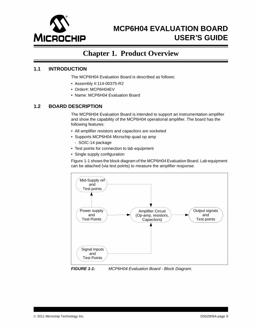
1.2 BOARD DESCRIPTIONThe MCP6H04 Evaluation Board is intended to support an instrumentation amplifier and show the capability of the MCP6H04 operational amplifier. The board has the following features:• All amplifier resistors and capacitors are socketed • Supports MCP6H04 Microchip quad op amp
- SOIC-14 package • Test points for connection to lab equipment• Single supply configurationFigure 1-1 shows the block diagram of the MCP6H04 Evaluation Board. Lab equipment can be attached (via test points) to measure the amplifier response.
FIGURE 1-1: MCP6H04 Evaluation Board - Block Diagram.
Mid-Supply refand
Test points
Power supplyand
Test Points
Signal Inputs and
Test Points
Amplifier Circuit(Op-amp, resistors,
Capacitors)
Output signalsand
Test points
© 2011 Microchip Technology Inc. DS52005A-page 9

MCP6H04 Evaluation Board User’s Guide
1.3 WHAT THE MCP6H04 EVALUATION BOARD KIT INCLUDES• MCP6H04 Evaluation Board, 102-00375• Important Information Sheet• Accessories Bag – contains loose parts for populating sockets on board, such as
resistors and capacitors
FIGURE 1-2: MCP6H04 Evaluation Board View.
DS52005A-page 10 © 2011 Microchip Technology Inc.

MCP6H04 EVALUATION BOARDUSER’S GUIDE
Chapter 2. Installation and Operation
2.1 INTRODUCTIONThis chapter describes how to set up the MCP6H04 Evaluation Board. Topics discussed in this chapter include:• Required Tools• MCP6H04 Evaluation Board Set-Up• MCP6H04 Evaluation Board Operation
2.2 REQUIRED TOOLSThe following tools are required for testing the functionality of the board:• Lab power supply• Lab dual signal source (e.g., dual function generator)• Lab measurement equipment (e.g., oscilloscope)
2.3 MCP6H04 EVALUATION BOARD SET-UPThe MCP6H04 Evaluation Board uses a quad op amp in difference amplifier configuration with input buffers and voltage reference. Figure 2-1 shows the circuit diagram of the board.
FIGURE 2-1: MCP6H04 Evaluation Board Circuit Diagram.
VOUT
+-
R1 R2
R1* R2*
RGRL CL
VDD
VOUT1
VOUT2
+-
+- VDD
VDD
RFRF* U1A
U1B
U1C
VIN(-)
VIN(+)
VDD
VDD
C2DP1
VDD
C2 R4
R3
+-
VDD
VREFU1D
© 2011 Microchip Technology Inc. DS52005A-page 11

MCP6H04 Evaluation Board User’s Guide
The power supply voltage needs to be in the allowed range for the op amp. The MCP6H04 device supports a maximum of 16V power supply. The power supply is protected by a Zener diode with a nominal voltage of 16V and bypassed by a 1 µF capacitor (see Figure 2-3).The mid-supply reference voltage consists of a voltage divider and a buffer amplifier (see Figure 2-4).The resistors that are part of the amplifier are placed in pin sockets, which are labeled.All component labels on board are consistent with those on the schematic. The op amp on board is a 14-lead SOIC package, and is bypassed by a 0.1 µF capacitor.The test points for the power supply, ground, input signals, output signals, and voltage reference allow lab equipment to be connected to the board. The MCP6H04 Evaluation Board top view is shown in Figure 2-2.
FIGURE 2-2: MCP6H04 Evaluation Board Top View.
DS52005A-page 12 © 2011 Microchip Technology Inc.

Installation and Operation
2.3.1 Top Level Amplifier Circuit Diagram
2.3.1.1 POWER SUPPLY BLOCK
The power supply is protected by a Zener diode and bypassed by a capacitor. Figure 2-3 shows the circuit diagram for the power supply (C2 = 1 µF). DP1 is a Zener diode with a nominal voltage of 16V.
FIGURE 2-3: Circuit Diagram for Power Supply.
2.3.1.2 MID-SUPPLY REFERENCE BLOCK
The mid-supply reference consists of a voltage divider and a buffer amplifier. Figure 2-4 shows the circuit diagram for the mid-supply reference (R3 = R4 = 100K, C3 =0.1 µF).
FIGURE 2-4: Mid-Supply Reference Block.
2.3.1.3 OUTPUT LOAD BLOCK
The output load consists of a capacitor and a resistor. Figure 2-5 shows the circuit diagram of the output load (RL = 10K, CL = 56 pF).
FIGURE 2-5: Output Load Block.
VDD
VDD
C2DP1
VDD
C2 R4
R3
+-
VDD
VREFU1D
VOUT
RL CL
VC
© 2011 Microchip Technology Inc. DS52005A-page 13

MCP6H04 Evaluation Board User’s Guide
2.3.1.4 INPUT STAGE
The input stage consists of two resistors and three capacitors. All three capacitors are forming a noise filter. Figure 2-6 shows the circuit diagram of the input stage (C5 = C6 = 10 nF, C4 = 100 nF and R5 =R6 = 1K).
FIGURE 2-6: Input Stage Block.
2.3.1.5 INPUT BUFFER BLOCK
The input buffer block consists of two op amps in buffer configuration with outputs tied together through one resistor. Figure 2-7 shows the circuit diagram of the input buffer block (RF = RF* = 50K, RG = 1K).
FIGURE 2-7: Input Buffer Block.
R5
R6
C4C5
C6
VIN(-)
VIN(+)
VA
VB
+-
VDD
VOUT1
VOUT2+-
VDD
RG
RF
RF*
VA
VB
DS52005A-page 14 © 2011 Microchip Technology Inc.

Installation and Operation
2.3.1.6 DIFFERENCE AMPLIFIER
This circuit amplifies the difference between two voltages, while rejecting the Common mode input voltage. Output voltage can be shifted by a reference voltage for single supply operation. Fill the sockets with the recommended resistors and capacitors (see the circuit diagram shown in Figure 2-8).
FIGURE 2-8: Difference Amplifier Block.
The jumper positions have the following effect:• JP1 connected to ground: the output voltage will be centered on 0V.• JP1 connected to VREF: the output voltage will be centered on 8V.
2.4 MCP6H04 EVALUATION BOARD OPERATIONThis section covers the following topics:• Building the Amplifier• Testing the Amplifier
2.4.1 Building the AmplifierThe accessory bag that comes with this kit facilitates the evaluation of the amplifier described below. The amplifier characteristics are:• Instrumentation amplifier (Single supply operation)• Power supply voltage = 16V• Desired Gain = 101 V/V• Load Capacitance = 56 pF
+-
R1 R2
R2*
RL
VDD
VOUT1
VOUT2
VREF
R1*
VC
JP1
© 2011 Microchip Technology Inc. DS52005A-page 15

MCP6H04 Evaluation Board User’s Guide
FIGURE 2-9: Schematic of the Instrumentation Amplifier Designed for Simulation.
VREF
VOUT2VIN+
VIN(+)
16VV2
10kR12
100nC6
1K
R10
10n
C3
100nC1
100kR6
10k
R8
10kR4
1kR2
X3
MCP6H01
X1
MCP6H04
X2
MCP6H04
X4
MCP6H04
50kR1
50kR3
10k
R5
10k
R7
100kR9
100nC2
10n
C4
1K
R11
100nC5
100nC7
56pC9
16VV1
VIN(-)
VIN-VOUT1
VOUT
DS52005A-page 16 © 2011 Microchip Technology Inc.

Installation and Operation
Figure 2-10 shows the same circuit redrawn to emphasize the instrumentation amplifier.
FIGURE 2-10: Instrumentation Amplifier Diagram Block.
Each of the components in Figure 2-10 that need to be inserted in a socket on the MCP6H04 Evaluation Board is listed in Table 2-1 and Table 2-2. The op amp is soldered on the PCB.
TABLE 2-1: AMPLIFIER COMPONENTS LISTPCB Labels Component Value
RF 50KRF* 50KRG 1KR1 10KR1* 10KR2 10KR2* 10KRL 10KCL 56 pF
TABLE 2-2: JUMPER POSITIONSJumper Position
JP1 VDD/2GND
VOUT
+-
R1 R2
Voltage reference
R1* R2*
RGRL CL
VDD
VOUT1
VOUT2VREF
+-
+- VDD
VDD
RFRF*
PowerSupply VDD
U1A
U1B
U1C
VIN(-)
VIN(+)
© 2011 Microchip Technology Inc. DS52005A-page 17
MCP6H04 Evaluation Board User’s Guide
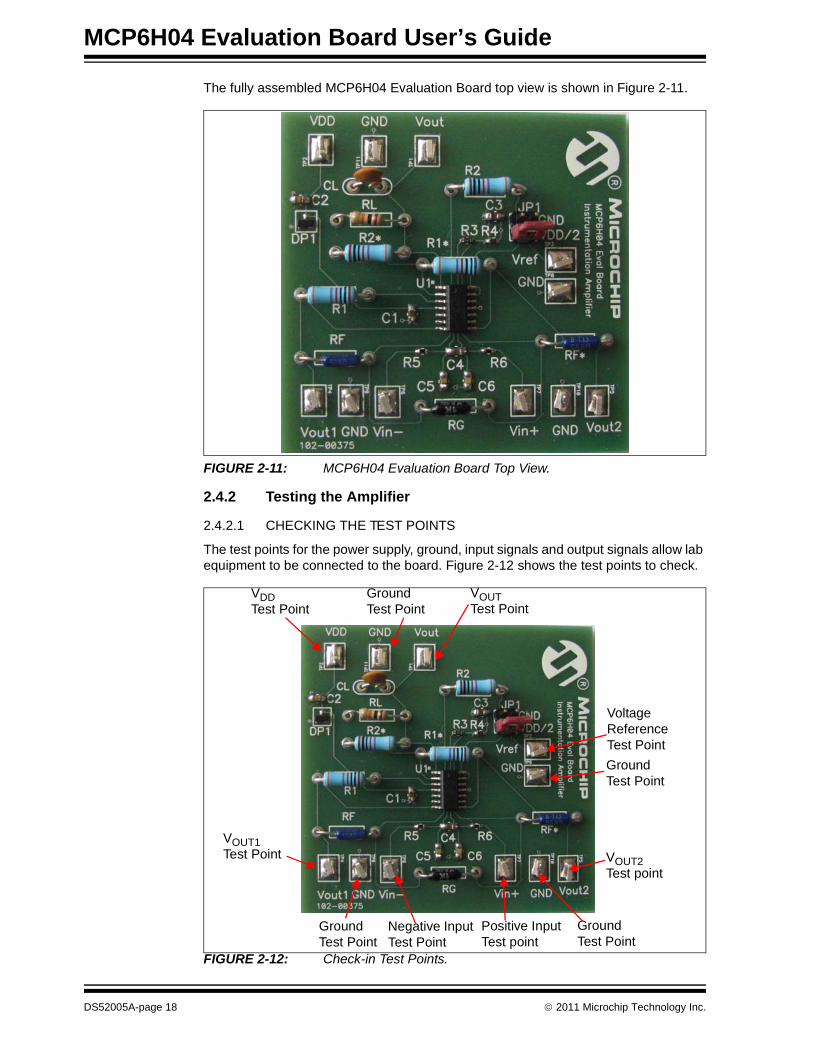
The fully assembled MCP6H04 Evaluation Board top view is shown in Figure 2-11.
FIGURE 2-11: MCP6H04 Evaluation Board Top View.
2.4.2 Testing the Amplifier
2.4.2.1 CHECKING THE TEST POINTS
The test points for the power supply, ground, input signals and output signals allow lab equipment to be connected to the board. Figure 2-12 shows the test points to check.
FIGURE 2-12: Check-in Test Points.
Ground Test Point
VOUT Test Point
VDD Test Point
Ground Test Point
VOUT1 Test Point
Negative Input Test Point
Ground Test Point
Voltage Reference Test PointGround Test Point
VOUT2 Test point
Positive Input Test point
DS52005A-page 18 © 2011 Microchip Technology Inc.

Installation and Operation
2.4.2.2 BOARD VALIDATION
All resistors in sockets have 0.1% tolerance and all soldered resistors have 1% tolerance. The capacitors have 20% tolerance.
2.4.2.2.1 Sine Wave ResponseSettings in bench measurement:• Set VIN for Source(–) at 10 mV, 10 Hz, 0° phase and a Common mode voltage
of 4V• Set VIN for Source(+) at 10 mV,10 Hz,180° phase and a Common mode voltage
of 4V• VREF = VDD/2• VDD = 16V• The output signal is centered on 8V• The amplifier’s Gain is 101 V/VFigure 2-13 shows the result of this measurement.
FIGURE 2-13: Sine Wave Response.
Simulation settings:• Set VIN for Source(-) at 10 mV, 10 Hz, 0° phase and Common mode voltage 4V• Set VIN for Source(+) at 10 mV,10 Hz,180° phase and Common mode voltage 4V• VREF = VDD/2• VDD=16V• The output signal is centered on 8V• The amplifier’s Gain is 101 V/VFigure 2-14 shows the results.
VOUT
VOUT2
VREF
VOUT1
© 2011 Microchip Technology Inc. DS52005A-page 19

MCP6H04 Evaluation Board User’s Guide
FIGURE 2-14: Simulation of the Sine Wave Response.
2.4.2.2.2 Square Wave ResponseSettings in bench measurement:• Set VIN for Source(-) at 50 mV,10 Hz, 0° phase and Common mode voltage 4V• Set VIN for Source(+) at 50 mV,10 Hz, 180° phase and Common mode voltage 4V• VREF = VDD/2• VDD=16V• The output signal is centered on 8V• The amplifier’s Gain is 101V/VFigure 2-15 shows the result of this measurement.
FIGURE 2-15: Square Wave Response.
0.000m 50.00m 100.0m 150.0m 200.0m 250.0m 300.0m 350.0m 400.0m 450.0m 500.0mTime (s)
(V
)
5.500
6.000
6.500
7.000
7.500
8.000
8.500
9.000
9.500
10.00
10.50 OUTVREF
0.000m 50.00m 100.0m 150.0m 200.0m 250.0m 300.0m 350.0m 400.0m 450.0m 500.0mTime (s)
(V
)
3.990
3.993
3.995
3.998
4.000
4.003
4.005
4.008
4.010 VIN+VIN-
0.000m 50.00m 100.0m 150.0m 200.0m 250.0m 300.0m 350.0m 400.0m 450.0m 500.0mTime (s)
(V
)
2.750
3.000
3.250
3.500
3.750
4.000
4.250
4.500
4.750
5.000
5.250 VOUT2VOUT1
VOUT2
VREF
VOUT1
VOUT
DS52005A-page 20 © 2011 Microchip Technology Inc.

Installation and Operation
Simulation settings:• Set VIN for Source(-) at 50 mV,10 Hz, 0° phase and common mode voltage 4V• Set VIN for Source(+) at 50 mV,10 Hz, 180° phase and common mode voltage 4V• VREF = VDD/2• VDD=16V• The output signal is centered on 8V• The amplifier’s Gain is 101V/VFigure 2-16 shows the result of this simulation.
FIGURE 2-16: Simulation of the Square Wave Response.
0.000m 100.0m 200.0m 300.0m 400.0m 500.0mTime (s)
(V
)
6.750
7.000
7.250
7.500
7.750
8.000
8.250
8.500
8.750
9.000
9.250 OUTVREF
0.000m 100.0m 200.0m 300.0m 400.0m 500.0mTime (s)
(V
)
3.995
3.996
3.997
3.998
3.999
4.000
4.001
4.002
4.003
4.004
4.005 VIN+
0.000m 100.0m 200.0m 300.0m 400.0m 500.0mTime (s)
(V
)
3.995
3.996
3.997
3.998
3.999
4.000
4.001
4.002
4.003
4.004
4.005 VIN-
0.000m 100.0m 200.0m 300.0m 400.0m 500.0mTime (s)
(V
)
3.250
3.500
3.750
4.000
4.250
4.500
4.750 VOUT1VOUT2
© 2011 Microchip Technology Inc. DS52005A-page 21

MCP6H04 Evaluation Board User’s Guide
2.4.2.2.3 DC ResponseSettings in bench measurement:• Set VIN for Source(-) at 80 mV DC signal• Set VIN for Source(+) at 30 mV DC signal• VREF = VDD/2• VDD = 16VFigure 2-17 shows the result of this measurement.
FIGURE 2-17: DC Response.
Simulation settings:• Set VIN for Source(-) at 80 mV DC signal• Set VIN for Source(+) at 30 mV DC signal• VREF = VDD/2• VDD = 16VFigure 2-18 shows the result of this measurement.
VOUT1
VOUT2
VOUT
VREF
DS52005A-page 22 © 2011 Microchip Technology Inc.

Installation and Operation
FIGURE 2-18: Simulation of the DC Response.
0.000u 0.500u 1.000u 1.500u 2.000u 2.500u 3.000u 3.500u 4.000u 4.500u 5.000uTime (s)
(V
)
7.975
8.000
8.025
8.050
8.075
8.100
8.125 OUTVREF
0.000u 0.500u 1.000u 1.500u 2.000u 2.500u 3.000u 3.500u 4.000u 4.500u 5.000uTime (s)
(V
)
0.000m
25.00m
50.00m
75.00m
100.0m
125.0m
150.0m VIN+VIN-VOUT1VOUT2
© 2011 Microchip Technology Inc. DS52005A-page 23

MCP6H04 Evaluation Board User’s Guide
NOTES:
DS52005A-page 24 © 2011 Microchip Technology Inc.

MCP6H04 EVALUATION BOARDUSER’S GUIDE
Appendix A. Schematic and Layouts
A.1 INTRODUCTIONThis appendix contains the following schematics and layouts of the MCP6H04 Evaluation Board:• Board – Schematic• Board – Silk and Solder Mask• Board – Top Metal Layer• Board – Bottom Metal Layer (bottom View)
© 2011 Microchip Technology Inc. DS52005A-page 25

MCP6H04 Evaluation Board User’s Guide
A.2 BOARD – SCHEMATIC
+A3
-A2
OU
TA
1V
SS
VD
D11 4
�������
U1A
+B5
-B6
OU
TB
7V
SS
VD
D11 4
�������
U1B
+C10
-C11
OU
TC
8
VSS
VD
D 114
�������
U1C
+D12
-D13
OU
TD
14
VS
S
VD
D
114
�������
U1D
R5 R
6
��RF RG ��
RF
*
�
R1
�
R2
�
R1*
�
R2*
1212
JP1
GN
D
��
R4��
R3
GN
D
�� �
C3
GN
D
�
RL
GN
D
����
CL
GN
D
����
C4
���
C5
���
C6
GN
D
GN
D
TP
6
TP
7
TP
3
TP
1
TP
9
TP
11
TP
8
TP
10
GN
D
GN
D
GN
D
GN
D
D1 G
ND
�
C2
GN
D
TP
2V
CC
VC
C
VC
C
GN
D
GN
D
GN
D
VC
C
GN
D
VC
C
VC
C
�� ������
�� ������
���
TP
5
TP
4 �� ��
�� �
����
�� �
� �
� �
� �
� �
����
C1
GN
D
��
����
� �
DS52005A-page 26 © 2011 Microchip Technology Inc.

Schematic and Layouts
A.3 BOARD – SILK AND SOLDER MASK
A.4 BOARD – TOP METAL LAYER
© 2011 Microchip Technology Inc. DS52005A-page 27

MCP6H04 Evaluation Board User’s Guide
A.5 BOARD – BOTTOM METAL LAYER (BOTTOM VIEW)
DS52005A-page 28 © 2011 Microchip Technology Inc.

MCP6H04 EVALUATION BOARDUSER’S GUIDE
Appendix B. Bill of Materials
TABLE B-1: BILL OF MATERIALS (BOM)Qty Reference Description Manufacturer Part Number
3 C1,C3,C4 CAPACITOR, 0805, X7R, 100V, 100NF
AVX Corporation 08051C104K4T2A
1 C2 CAPACITOR, 0805, X7R, 25V, 1UF AVX Corporation 08053C105K4Z2A2 C5,C6 CAPACITOR, 0805, X7R, 100V, 10NF AVX Corporation 08051C103K4Z2A1 DP1 ZENER, 16V, 350MW, SOT-23 Micro Commercial
Components CorporationBZX84C16-TP
1 JP1 CONN HEADR BRKWAY .100 02POS STR
TE Connectivity Ltd. 9-146258-0-02
1 PCB RoHS Compliant Bare PCB, MCP6H04 Evaluation Board
Microchip Technology Inc. 104-00375
18 Pin Socket PIN RECPT .015/.025 DIA 0667 SER Mill-Max Mfg. Corporation 0667-0-15-01-30-27-10-02 R3,R4 RESISTOR, 100K, 0603 1% 0.1W Vishay Intertechnology, Inc. MCT06030C1003FP5002 R5,R6 RESISTOR, 0603, 1K ,0.1% TE Connectivity Ltd. CPF0603B1K0E111 Test Points PC TEST POINT COMPACT SMT Keystone Electronics
Corporation5016
1 U1 MCP6H04 Microchip Technology Inc. MCP6H04Note 1: The components listed in this Bill of Materials are representative of the PCB assembly. The
released BOM used in manufacturing uses all RoHS-compliant components.
TABLE B-2: BILL OF MATERIALS – ACCESSORIES BAG PARTSQty Reference Description Manufacturer Part Number
1 CL CAPACITOR, DISC, 100V, 56PF AVX Corporation 5KK560KOAAM4 R1,R2,R1*, R2* 10K, 0.125W, 0.1%, 15PPM Vishay Intertechnology,
Inc.PTF5610K000BXEB
1 RG RESISTOR, 0.25W, 0.1%, 1K0 TE Connectivity Ltd. H81K0BYA2 RF, RF* RES 50.0K OHM 1/4W 0.1% AXIAL TE Connectivity Ltd. H850KBCA1 RL 0.5W 5% 10K Vishay Intertechnology,
Inc.NFR25H0001002JR500
Note 1: The components listed in this Bill of Materials are representative of the loose components found in the accessories bag. The released BOM used in manufacturing uses all RoHS-com-pliant components.
© 2011 Microchip Technology Inc. DS52005A-page 29

DS52005A-page 30 © 2011 Microchip Technology Inc.
AMERICASCorporate Office2355 West Chandler Blvd.Chandler, AZ 85224-6199Tel: 480-792-7200 Fax: 480-792-7277Technical Support: http://www.microchip.com/supportWeb Address: www.microchip.comAtlantaDuluth, GA Tel: 678-957-9614 Fax: 678-957-1455BostonWestborough, MA Tel: 774-760-0087 Fax: 774-760-0088ChicagoItasca, IL Tel: 630-285-0071 Fax: 630-285-0075ClevelandIndependence, OH Tel: 216-447-0464 Fax: 216-447-0643DallasAddison, TX Tel: 972-818-7423 Fax: 972-818-2924DetroitFarmington Hills, MI Tel: 248-538-2250Fax: 248-538-2260IndianapolisNoblesville, IN Tel: 317-773-8323Fax: 317-773-5453Los AngelesMission Viejo, CA Tel: 949-462-9523 Fax: 949-462-9608Santa ClaraSanta Clara, CA Tel: 408-961-6444Fax: 408-961-6445TorontoMississauga, Ontario, CanadaTel: 905-673-0699 Fax: 905-673-6509
ASIA/PACIFICAsia Pacific OfficeSuites 3707-14, 37th FloorTower 6, The GatewayHarbour City, KowloonHong KongTel: 852-2401-1200Fax: 852-2401-3431Australia - SydneyTel: 61-2-9868-6733Fax: 61-2-9868-6755China - BeijingTel: 86-10-8569-7000 Fax: 86-10-8528-2104China - ChengduTel: 86-28-8665-5511Fax: 86-28-8665-7889China - ChongqingTel: 86-23-8980-9588Fax: 86-23-8980-9500China - HangzhouTel: 86-571-2819-3187 Fax: 86-571-2819-3189China - Hong Kong SARTel: 852-2401-1200 Fax: 852-2401-3431China - NanjingTel: 86-25-8473-2460Fax: 86-25-8473-2470China - QingdaoTel: 86-532-8502-7355Fax: 86-532-8502-7205China - ShanghaiTel: 86-21-5407-5533 Fax: 86-21-5407-5066China - ShenyangTel: 86-24-2334-2829Fax: 86-24-2334-2393China - ShenzhenTel: 86-755-8203-2660 Fax: 86-755-8203-1760China - WuhanTel: 86-27-5980-5300Fax: 86-27-5980-5118China - XianTel: 86-29-8833-7252Fax: 86-29-8833-7256China - XiamenTel: 86-592-2388138 Fax: 86-592-2388130China - ZhuhaiTel: 86-756-3210040 Fax: 86-756-3210049
ASIA/PACIFICIndia - BangaloreTel: 91-80-3090-4444 Fax: 91-80-3090-4123India - New DelhiTel: 91-11-4160-8631Fax: 91-11-4160-8632India - PuneTel: 91-20-2566-1512Fax: 91-20-2566-1513Japan - YokohamaTel: 81-45-471- 6166 Fax: 81-45-471-6122Korea - DaeguTel: 82-53-744-4301Fax: 82-53-744-4302Korea - SeoulTel: 82-2-554-7200Fax: 82-2-558-5932 or 82-2-558-5934Malaysia - Kuala LumpurTel: 60-3-6201-9857Fax: 60-3-6201-9859Malaysia - PenangTel: 60-4-227-8870Fax: 60-4-227-4068Philippines - ManilaTel: 63-2-634-9065Fax: 63-2-634-9069SingaporeTel: 65-6334-8870Fax: 65-6334-8850Taiwan - Hsin ChuTel: 886-3-5778-366Fax: 886-3-5770-955Taiwan - KaohsiungTel: 886-7-536-4818Fax: 886-7-330-9305Taiwan - TaipeiTel: 886-2-2500-6610 Fax: 886-2-2508-0102Thailand - BangkokTel: 66-2-694-1351Fax: 66-2-694-1350
EUROPEAustria - WelsTel: 43-7242-2244-39Fax: 43-7242-2244-393Denmark - CopenhagenTel: 45-4450-2828 Fax: 45-4485-2829France - ParisTel: 33-1-69-53-63-20 Fax: 33-1-69-30-90-79Germany - MunichTel: 49-89-627-144-0 Fax: 49-89-627-144-44Italy - Milan Tel: 39-0331-742611 Fax: 39-0331-466781Netherlands - DrunenTel: 31-416-690399 Fax: 31-416-690340Spain - MadridTel: 34-91-708-08-90Fax: 34-91-708-08-91UK - WokinghamTel: 44-118-921-5869Fax: 44-118-921-5820
Worldwide Sales and Service
08/02/11