
MC9S12HY64 Reference Manual Covers MC9S12HY/HA ...
796
S12 Microcontrollers freescale.com MC9S12HY64 Reference Manual Covers MC9S12HY/HA Family MC9S12HY64RMV1 Rev. 1.05 09/2012
-
Upload
khangminh22 -
Category
Documents
-
view
0 -
download
0
Transcript of MC9S12HY64 Reference Manual Covers MC9S12HY/HA ...

S12Microcontrollers
freescale.com
MC9S12HY64Reference ManualCovers MC9S12HY/HA Family
MC9S12HY64RMV1
Rev. 1.05
09/2012

To provide the most up-to-date information, the revision of our documents on the World Wide Web will bethe most current. Your printed copy may be an earlier revision. To verify you have the latest informationavailable, refer to:
freescale.com
A full list of family members and options is included in the appendices.
The following revision history table summarizes changes contained in this document.
This document contains information for all constituent modules, with the exception of the CPU. For CPUinformation please refer to CPU12-1 in the CPU12 & CPU12X Reference Manual.
Revision History
Date RevisionLevel Description
July, 2009 1.00 initial v1.00 version
Aug, 2009 1.01 update SCI block guide, update motor pad input leakage in Appendix A
Nov, 2009 1.02 update FTMRC block guide, update MC10B8C block guide, minor update in
chapter 1, minor typo correction in Appendix F
May, 2010 1.03 update PIM block guide, update CPMU block guide, update TIM block guide
Nov, 2010 1.04 update SCI block guide, update typo in device overview
Sep, 2012 1.05 update Device overview, PIM, BDM, DBG, CPMU, INT, PWM and Appendix
for Bandgap and Motor/LCD pad maximum value update

Chapter 1 Device Overview MC9S12HY/HA-Family . . . . . . . . . . . . . . . . .11
Chapter 2 Port Integration Module (S12HYPIMV1) . . . . . . . . . . . . . . . . . .53
Chapter 3 S12P Memory Map Control (S12PMMCV1). . . . . . . . . . . . . . .135
Chapter 4 Interrupt Module (S12SINTV1). . . . . . . . . . . . . . . . . . . . . . . . .151
Chapter 5 Background Debug Module (S12SBDMV1) . . . . . . . . . . . . . .159
Chapter 6 S12S Debug Module (S12SDBGV2) . . . . . . . . . . . . . . . . . . . .183
Chapter 7 S12 Clock, Reset and Power Management Unit (S12CPMU) . . .227
Chapter 8 Analog-to-Digital Converter (ADC12B8CV1) . . . . . . . . . . . . .285
Chapter 9 Freescale’s Scalable Controller Area Network (S12MSCANV3).311
Chapter 10 Inter-Integrated Circuit (IICV3) . . . . . . . . . . . . . . . . . . . . . . . .365
Chapter 11 Pulse-Width Modulator (S12PWM8B8CV1) . . . . . . . . . . . . . .393
Chapter 12 Serial Communication Interface (S12SCIV5) . . . . . . . . . . . . .425
Chapter 13 Serial Peripheral Interface (S12SPIV5) . . . . . . . . . . . . . . . . . .463
Chapter 14 Timer Module (TIM16B8CV2) . . . . . . . . . . . . . . . . . . . . . . . . .489
Chapter 15 32 KByte Flash Module (S12FTMRC32K1V1). . . . . . . . . . . . .517
Chapter 16 48 KByte Flash Module (S12FTMRC48K1V1). . . . . . . . . . . . .567
Chapter 17 64 KByte Flash Module (S12FTMRC64K1V1). . . . . . . . . . . . .617
Chapter 18 Liquid Crystal Display (LCD40F4BV1) . . . . . . . . . . . . . . . . . .667
Chapter 19 Motor Controller (MC10B8CV1). . . . . . . . . . . . . . . . . . . . . . . .689
Appendix A Electrical Characteristics. . . . . . . . . . . . . . . . . . . . . . . . . . . . .721
Appendix B Ordering Information . . . . . . . . . . . . . . . . . . . . . . . . . . . . . . . .756
Appendix C Package Information . . . . . . . . . . . . . . . . . . . . . . . . . . . . . . . .757
Appendix D PCB Layout Guidelines . . . . . . . . . . . . . . . . . . . . . . . . . . . . . .763
MC9S12HY/HA-Family Reference Manual, Rev. 1.05
Freescale Semiconductor 3

Appendix E Derivative Differences . . . . . . . . . . . . . . . . . . . . . . . . . . . . . . .767
Appendix F Detailed Register Address Map. . . . . . . . . . . . . . . . . . . . . . . .768
MC9S12HY/HA-Family Reference Manual, Rev. 1.05
4 Freescale Semiconductor

Chapter 1Device Overview MC9S12HY/HA-Family
1.1 Introduction . . . . . . . . . . . . . . . . . . . . . . . . . . . . . . . . . . . . . . . . . . . . . . . . . . . . . . . . . . . . . . . . . . 111.2 Features . . . . . . . . . . . . . . . . . . . . . . . . . . . . . . . . . . . . . . . . . . . . . . . . . . . . . . . . . . . . . . . . . . . . . 111.3 Module Features . . . . . . . . . . . . . . . . . . . . . . . . . . . . . . . . . . . . . . . . . . . . . . . . . . . . . . . . . . . . . . . 131.4 Block Diagram . . . . . . . . . . . . . . . . . . . . . . . . . . . . . . . . . . . . . . . . . . . . . . . . . . . . . . . . . . . . . . . . 191.5 Device Memory Map . . . . . . . . . . . . . . . . . . . . . . . . . . . . . . . . . . . . . . . . . . . . . . . . . . . . . . . . . . . 201.6 Part ID Assignments . . . . . . . . . . . . . . . . . . . . . . . . . . . . . . . . . . . . . . . . . . . . . . . . . . . . . . . . . . . . 251.7 Signal Description . . . . . . . . . . . . . . . . . . . . . . . . . . . . . . . . . . . . . . . . . . . . . . . . . . . . . . . . . . . . . 251.8 System Clock Description . . . . . . . . . . . . . . . . . . . . . . . . . . . . . . . . . . . . . . . . . . . . . . . . . . . . . . . 451.9 Modes of Operation . . . . . . . . . . . . . . . . . . . . . . . . . . . . . . . . . . . . . . . . . . . . . . . . . . . . . . . . . . . . 461.10 Security . . . . . . . . . . . . . . . . . . . . . . . . . . . . . . . . . . . . . . . . . . . . . . . . . . . . . . . . . . . . . . . . . . . . . . 461.11 Resets and Interrupts . . . . . . . . . . . . . . . . . . . . . . . . . . . . . . . . . . . . . . . . . . . . . . . . . . . . . . . . . . . 471.12 COP Configuration . . . . . . . . . . . . . . . . . . . . . . . . . . . . . . . . . . . . . . . . . . . . . . . . . . . . . . . . . . . . . 501.13 ATD External Trigger Input Connection . . . . . . . . . . . . . . . . . . . . . . . . . . . . . . . . . . . . . . . . . . . . 501.14 S12CPMU Configuration . . . . . . . . . . . . . . . . . . . . . . . . . . . . . . . . . . . . . . . . . . . . . . . . . . . . . . . . 511.15 Documentation Note . . . . . . . . . . . . . . . . . . . . . . . . . . . . . . . . . . . . . . . . . . . . . . . . . . . . . . . . . . . 51
Chapter 2Port Integration Module (S12HYPIMV1)
2.1 Introduction . . . . . . . . . . . . . . . . . . . . . . . . . . . . . . . . . . . . . . . . . . . . . . . . . . . . . . . . . . . . . . . . . . 532.2 External Signal Description . . . . . . . . . . . . . . . . . . . . . . . . . . . . . . . . . . . . . . . . . . . . . . . . . . . . . . 542.3 Memory Map and Register Definition . . . . . . . . . . . . . . . . . . . . . . . . . . . . . . . . . . . . . . . . . . . . . . 592.4 Functional Description . . . . . . . . . . . . . . . . . . . . . . . . . . . . . . . . . . . . . . . . . . . . . . . . . . . . . . . . . 1272.5 Initialization Information . . . . . . . . . . . . . . . . . . . . . . . . . . . . . . . . . . . . . . . . . . . . . . . . . . . . . . . 133
Chapter 3S12P Memory Map Control (S12PMMCV1)3.1 Introduction . . . . . . . . . . . . . . . . . . . . . . . . . . . . . . . . . . . . . . . . . . . . . . . . . . . . . . . . . . . . . . . . . 1353.2 External Signal Description . . . . . . . . . . . . . . . . . . . . . . . . . . . . . . . . . . . . . . . . . . . . . . . . . . . . . 1373.3 Memory Map and Registers . . . . . . . . . . . . . . . . . . . . . . . . . . . . . . . . . . . . . . . . . . . . . . . . . . . . . 1373.4 Functional Description . . . . . . . . . . . . . . . . . . . . . . . . . . . . . . . . . . . . . . . . . . . . . . . . . . . . . . . . . 1413.5 Implemented Memory in the System Memory Architecture . . . . . . . . . . . . . . . . . . . . . . . . . . . . 1453.6 Initialization/Application Information . . . . . . . . . . . . . . . . . . . . . . . . . . . . . . . . . . . . . . . . . . . . . 148
Chapter 4Interrupt Module (S12SINTV1)
4.1 Introduction . . . . . . . . . . . . . . . . . . . . . . . . . . . . . . . . . . . . . . . . . . . . . . . . . . . . . . . . . . . . . . . . . 1514.2 External Signal Description . . . . . . . . . . . . . . . . . . . . . . . . . . . . . . . . . . . . . . . . . . . . . . . . . . . . . 1534.3 Memory Map and Register Definition . . . . . . . . . . . . . . . . . . . . . . . . . . . . . . . . . . . . . . . . . . . . . 1534.4 Functional Description . . . . . . . . . . . . . . . . . . . . . . . . . . . . . . . . . . . . . . . . . . . . . . . . . . . . . . . . . 154
MC9S12HY/HA-Family Reference Manual, Rev. 1.05
Freescale Semiconductor 5

4.5 Initialization/Application Information . . . . . . . . . . . . . . . . . . . . . . . . . . . . . . . . . . . . . . . . . . . . . 156
Chapter 5Background Debug Module (S12SBDMV1)
5.1 Introduction . . . . . . . . . . . . . . . . . . . . . . . . . . . . . . . . . . . . . . . . . . . . . . . . . . . . . . . . . . . . . . . . . 1595.2 External Signal Description . . . . . . . . . . . . . . . . . . . . . . . . . . . . . . . . . . . . . . . . . . . . . . . . . . . . . 1615.3 Memory Map and Register Definition . . . . . . . . . . . . . . . . . . . . . . . . . . . . . . . . . . . . . . . . . . . . . 1615.4 Functional Description . . . . . . . . . . . . . . . . . . . . . . . . . . . . . . . . . . . . . . . . . . . . . . . . . . . . . . . . . 165
Chapter 6S12S Debug Module (S12SDBGV2)
6.1 Introduction . . . . . . . . . . . . . . . . . . . . . . . . . . . . . . . . . . . . . . . . . . . . . . . . . . . . . . . . . . . . . . . . . 1836.2 External Signal Description . . . . . . . . . . . . . . . . . . . . . . . . . . . . . . . . . . . . . . . . . . . . . . . . . . . . . 1856.3 Memory Map and Registers . . . . . . . . . . . . . . . . . . . . . . . . . . . . . . . . . . . . . . . . . . . . . . . . . . . . . 1866.4 Functional Description . . . . . . . . . . . . . . . . . . . . . . . . . . . . . . . . . . . . . . . . . . . . . . . . . . . . . . . . . 2046.5 Application Information . . . . . . . . . . . . . . . . . . . . . . . . . . . . . . . . . . . . . . . . . . . . . . . . . . . . . . . . 220
Chapter 7S12 Clock, Reset and Power Management Unit (S12CPMU) Block Description7.1 Introduction . . . . . . . . . . . . . . . . . . . . . . . . . . . . . . . . . . . . . . . . . . . . . . . . . . . . . . . . . . . . . . . . . 2287.2 Signal Description . . . . . . . . . . . . . . . . . . . . . . . . . . . . . . . . . . . . . . . . . . . . . . . . . . . . . . . . . . . . 2347.3 Memory Map and Registers . . . . . . . . . . . . . . . . . . . . . . . . . . . . . . . . . . . . . . . . . . . . . . . . . . . . . 2367.4 Functional Description . . . . . . . . . . . . . . . . . . . . . . . . . . . . . . . . . . . . . . . . . . . . . . . . . . . . . . . . . 2717.5 Resets . . . . . . . . . . . . . . . . . . . . . . . . . . . . . . . . . . . . . . . . . . . . . . . . . . . . . . . . . . . . . . . . . . . . . . 2807.6 Interrupts . . . . . . . . . . . . . . . . . . . . . . . . . . . . . . . . . . . . . . . . . . . . . . . . . . . . . . . . . . . . . . . . . . . 2827.7 Initialization/Application Information . . . . . . . . . . . . . . . . . . . . . . . . . . . . . . . . . . . . . . . . . . . . . 284
Chapter 8Analog-to-Digital Converter (ADC12B8CV1)
Block Description8.1 Introduction . . . . . . . . . . . . . . . . . . . . . . . . . . . . . . . . . . . . . . . . . . . . . . . . . . . . . . . . . . . . . . . . . 2858.2 Signal Description . . . . . . . . . . . . . . . . . . . . . . . . . . . . . . . . . . . . . . . . . . . . . . . . . . . . . . . . . . . . 2898.3 Memory Map and Register Definition . . . . . . . . . . . . . . . . . . . . . . . . . . . . . . . . . . . . . . . . . . . . . 2898.4 Functional Description . . . . . . . . . . . . . . . . . . . . . . . . . . . . . . . . . . . . . . . . . . . . . . . . . . . . . . . . . 3078.5 Resets . . . . . . . . . . . . . . . . . . . . . . . . . . . . . . . . . . . . . . . . . . . . . . . . . . . . . . . . . . . . . . . . . . . . . . 3088.6 Interrupts . . . . . . . . . . . . . . . . . . . . . . . . . . . . . . . . . . . . . . . . . . . . . . . . . . . . . . . . . . . . . . . . . . . 309
Chapter 9Freescale’s Scalable Controller Area Network (S12MSCANV3)
9.1 Introduction . . . . . . . . . . . . . . . . . . . . . . . . . . . . . . . . . . . . . . . . . . . . . . . . . . . . . . . . . . . . . . . . . 3119.2 External Signal Description . . . . . . . . . . . . . . . . . . . . . . . . . . . . . . . . . . . . . . . . . . . . . . . . . . . . . 3149.3 Memory Map and Register Definition . . . . . . . . . . . . . . . . . . . . . . . . . . . . . . . . . . . . . . . . . . . . . 3159.4 Functional Description . . . . . . . . . . . . . . . . . . . . . . . . . . . . . . . . . . . . . . . . . . . . . . . . . . . . . . . . . 347
MC9S12HY/HA-Family Reference Manual, Rev. 1.05
6 Freescale Semiconductor

9.5 Initialization/Application Information . . . . . . . . . . . . . . . . . . . . . . . . . . . . . . . . . . . . . . . . . . . . . 364
Chapter 10Inter-Integrated Circuit (IICV3) Block Description
10.1 Introduction . . . . . . . . . . . . . . . . . . . . . . . . . . . . . . . . . . . . . . . . . . . . . . . . . . . . . . . . . . . . . . . . . 36510.2 External Signal Description . . . . . . . . . . . . . . . . . . . . . . . . . . . . . . . . . . . . . . . . . . . . . . . . . . . . . 36810.3 Memory Map and Register Definition . . . . . . . . . . . . . . . . . . . . . . . . . . . . . . . . . . . . . . . . . . . . . 36810.4 Functional Description . . . . . . . . . . . . . . . . . . . . . . . . . . . . . . . . . . . . . . . . . . . . . . . . . . . . . . . . . 38010.5 Resets . . . . . . . . . . . . . . . . . . . . . . . . . . . . . . . . . . . . . . . . . . . . . . . . . . . . . . . . . . . . . . . . . . . . . . 38510.6 Interrupts . . . . . . . . . . . . . . . . . . . . . . . . . . . . . . . . . . . . . . . . . . . . . . . . . . . . . . . . . . . . . . . . . . . 38510.7 Application Information . . . . . . . . . . . . . . . . . . . . . . . . . . . . . . . . . . . . . . . . . . . . . . . . . . . . . . . . 386
Chapter 11Pulse-Width Modulator (S12PWM8B8CV1)
11.1 Introduction . . . . . . . . . . . . . . . . . . . . . . . . . . . . . . . . . . . . . . . . . . . . . . . . . . . . . . . . . . . . . . . . . 39311.2 External Signal Description . . . . . . . . . . . . . . . . . . . . . . . . . . . . . . . . . . . . . . . . . . . . . . . . . . . . . 39411.3 Memory Map and Register Definition . . . . . . . . . . . . . . . . . . . . . . . . . . . . . . . . . . . . . . . . . . . . . 39511.4 Functional Description . . . . . . . . . . . . . . . . . . . . . . . . . . . . . . . . . . . . . . . . . . . . . . . . . . . . . . . . . 41111.5 Resets . . . . . . . . . . . . . . . . . . . . . . . . . . . . . . . . . . . . . . . . . . . . . . . . . . . . . . . . . . . . . . . . . . . . . . 42211.6 Interrupts . . . . . . . . . . . . . . . . . . . . . . . . . . . . . . . . . . . . . . . . . . . . . . . . . . . . . . . . . . . . . . . . . . . 423
Chapter 12Serial Communication Interface (S12SCIV5)
12.1 Introduction . . . . . . . . . . . . . . . . . . . . . . . . . . . . . . . . . . . . . . . . . . . . . . . . . . . . . . . . . . . . . . . . . 42512.2 External Signal Description . . . . . . . . . . . . . . . . . . . . . . . . . . . . . . . . . . . . . . . . . . . . . . . . . . . . . 42812.3 Memory Map and Register Definition . . . . . . . . . . . . . . . . . . . . . . . . . . . . . . . . . . . . . . . . . . . . . 42812.4 Functional Description . . . . . . . . . . . . . . . . . . . . . . . . . . . . . . . . . . . . . . . . . . . . . . . . . . . . . . . . . 44112.5 Initialization/Application Information . . . . . . . . . . . . . . . . . . . . . . . . . . . . . . . . . . . . . . . . . . . . . 459
Chapter 13Serial Peripheral Interface (S12SPIV5)
13.1 Introduction . . . . . . . . . . . . . . . . . . . . . . . . . . . . . . . . . . . . . . . . . . . . . . . . . . . . . . . . . . . . . . . . . 46313.2 External Signal Description . . . . . . . . . . . . . . . . . . . . . . . . . . . . . . . . . . . . . . . . . . . . . . . . . . . . . 46513.3 Memory Map and Register Definition . . . . . . . . . . . . . . . . . . . . . . . . . . . . . . . . . . . . . . . . . . . . . 46613.4 Functional Description . . . . . . . . . . . . . . . . . . . . . . . . . . . . . . . . . . . . . . . . . . . . . . . . . . . . . . . . . 475
Chapter 14Timer Module (TIM16B8CV2) Block Description
14.1 Introduction . . . . . . . . . . . . . . . . . . . . . . . . . . . . . . . . . . . . . . . . . . . . . . . . . . . . . . . . . . . . . . . . . 48914.2 External Signal Description . . . . . . . . . . . . . . . . . . . . . . . . . . . . . . . . . . . . . . . . . . . . . . . . . . . . . 49314.3 Memory Map and Register Definition . . . . . . . . . . . . . . . . . . . . . . . . . . . . . . . . . . . . . . . . . . . . . 49414.4 Functional Description . . . . . . . . . . . . . . . . . . . . . . . . . . . . . . . . . . . . . . . . . . . . . . . . . . . . . . . . . 51114.5 Resets . . . . . . . . . . . . . . . . . . . . . . . . . . . . . . . . . . . . . . . . . . . . . . . . . . . . . . . . . . . . . . . . . . . . . . 51514.6 Interrupts . . . . . . . . . . . . . . . . . . . . . . . . . . . . . . . . . . . . . . . . . . . . . . . . . . . . . . . . . . . . . . . . . . . 515
MC9S12HY/HA-Family Reference Manual, Rev. 1.05
Freescale Semiconductor 7

Chapter 1532 KByte Flash Module (S12FTMRC32K1V1)
15.1 Introduction . . . . . . . . . . . . . . . . . . . . . . . . . . . . . . . . . . . . . . . . . . . . . . . . . . . . . . . . . . . . . . . . . 51715.2 External Signal Description . . . . . . . . . . . . . . . . . . . . . . . . . . . . . . . . . . . . . . . . . . . . . . . . . . . . . 52015.3 Memory Map and Registers . . . . . . . . . . . . . . . . . . . . . . . . . . . . . . . . . . . . . . . . . . . . . . . . . . . . . 52115.4 Functional Description . . . . . . . . . . . . . . . . . . . . . . . . . . . . . . . . . . . . . . . . . . . . . . . . . . . . . . . . . 54315.5 Security . . . . . . . . . . . . . . . . . . . . . . . . . . . . . . . . . . . . . . . . . . . . . . . . . . . . . . . . . . . . . . . . . . . . . 56415.6 Initialization . . . . . . . . . . . . . . . . . . . . . . . . . . . . . . . . . . . . . . . . . . . . . . . . . . . . . . . . . . . . . . . . . 566
Chapter 1648 KByte Flash Module (S12FTMRC48K1V1)
16.1 Introduction . . . . . . . . . . . . . . . . . . . . . . . . . . . . . . . . . . . . . . . . . . . . . . . . . . . . . . . . . . . . . . . . . 56716.2 External Signal Description . . . . . . . . . . . . . . . . . . . . . . . . . . . . . . . . . . . . . . . . . . . . . . . . . . . . . 57016.3 Memory Map and Registers . . . . . . . . . . . . . . . . . . . . . . . . . . . . . . . . . . . . . . . . . . . . . . . . . . . . . 57116.4 Functional Description . . . . . . . . . . . . . . . . . . . . . . . . . . . . . . . . . . . . . . . . . . . . . . . . . . . . . . . . . 59216.5 Security . . . . . . . . . . . . . . . . . . . . . . . . . . . . . . . . . . . . . . . . . . . . . . . . . . . . . . . . . . . . . . . . . . . . . 61316.6 Initialization . . . . . . . . . . . . . . . . . . . . . . . . . . . . . . . . . . . . . . . . . . . . . . . . . . . . . . . . . . . . . . . . . 615
Chapter 1764 KByte Flash Module (S12FTMRC64K1V1)
17.1 Introduction . . . . . . . . . . . . . . . . . . . . . . . . . . . . . . . . . . . . . . . . . . . . . . . . . . . . . . . . . . . . . . . . . 61717.2 External Signal Description . . . . . . . . . . . . . . . . . . . . . . . . . . . . . . . . . . . . . . . . . . . . . . . . . . . . . 62017.3 Memory Map and Registers . . . . . . . . . . . . . . . . . . . . . . . . . . . . . . . . . . . . . . . . . . . . . . . . . . . . . 62117.4 Functional Description . . . . . . . . . . . . . . . . . . . . . . . . . . . . . . . . . . . . . . . . . . . . . . . . . . . . . . . . . 64317.5 Security . . . . . . . . . . . . . . . . . . . . . . . . . . . . . . . . . . . . . . . . . . . . . . . . . . . . . . . . . . . . . . . . . . . . . 66417.6 Initialization . . . . . . . . . . . . . . . . . . . . . . . . . . . . . . . . . . . . . . . . . . . . . . . . . . . . . . . . . . . . . . . . . 666
Chapter 18Liquid Crystal Display (LCD40F4BV1) Block Description
18.1 Introduction . . . . . . . . . . . . . . . . . . . . . . . . . . . . . . . . . . . . . . . . . . . . . . . . . . . . . . . . . . . . . . . . . 66718.2 External Signal Description . . . . . . . . . . . . . . . . . . . . . . . . . . . . . . . . . . . . . . . . . . . . . . . . . . . . . 67018.3 Memory Map and Register Definition . . . . . . . . . . . . . . . . . . . . . . . . . . . . . . . . . . . . . . . . . . . . . 67018.4 Functional Description . . . . . . . . . . . . . . . . . . . . . . . . . . . . . . . . . . . . . . . . . . . . . . . . . . . . . . . . . 67718.5 Resets . . . . . . . . . . . . . . . . . . . . . . . . . . . . . . . . . . . . . . . . . . . . . . . . . . . . . . . . . . . . . . . . . . . . . . 68718.6 Interrupts . . . . . . . . . . . . . . . . . . . . . . . . . . . . . . . . . . . . . . . . . . . . . . . . . . . . . . . . . . . . . . . . . . . 687
Chapter 19Motor Controller (MC10B8CV1)
19.1 Introduction . . . . . . . . . . . . . . . . . . . . . . . . . . . . . . . . . . . . . . . . . . . . . . . . . . . . . . . . . . . . . . . . . 68919.2 External Signal Description . . . . . . . . . . . . . . . . . . . . . . . . . . . . . . . . . . . . . . . . . . . . . . . . . . . . . 69219.3 Memory Map and Register Definition . . . . . . . . . . . . . . . . . . . . . . . . . . . . . . . . . . . . . . . . . . . . . 69319.4 Functional Description . . . . . . . . . . . . . . . . . . . . . . . . . . . . . . . . . . . . . . . . . . . . . . . . . . . . . . . . . 70119.5 Reset . . . . . . . . . . . . . . . . . . . . . . . . . . . . . . . . . . . . . . . . . . . . . . . . . . . . . . . . . . . . . . . . . . . . . . . 715
MC9S12HY/HA-Family Reference Manual, Rev. 1.05
8 Freescale Semiconductor

19.6 Interrupts . . . . . . . . . . . . . . . . . . . . . . . . . . . . . . . . . . . . . . . . . . . . . . . . . . . . . . . . . . . . . . . . . . . 71519.7 Initialization/Application Information . . . . . . . . . . . . . . . . . . . . . . . . . . . . . . . . . . . . . . . . . . . . . 716
Appendix AElectrical Characteristics
A.1 General . . . . . . . . . . . . . . . . . . . . . . . . . . . . . . . . . . . . . . . . . . . . . . . . . . . . . . . . . . . . . . . . . . . . . 721A.1.1 Parameter Classification . . . . . . . . . . . . . . . . . . . . . . . . . . . . . . . . . . . . . . . . . . . . . . . . . 721A.1.2 Power Supply . . . . . . . . . . . . . . . . . . . . . . . . . . . . . . . . . . . . . . . . . . . . . . . . . . . . . . . . . 721A.1.3 Pins . . . . . . . . . . . . . . . . . . . . . . . . . . . . . . . . . . . . . . . . . . . . . . . . . . . . . . . . . . . . . . . . . 722A.1.4 Current Injection . . . . . . . . . . . . . . . . . . . . . . . . . . . . . . . . . . . . . . . . . . . . . . . . . . . . . . . 722A.1.5 Absolute Maximum Ratings . . . . . . . . . . . . . . . . . . . . . . . . . . . . . . . . . . . . . . . . . . . . . . 723A.1.6 ESD Protection and Latch-up Immunity. . . . . . . . . . . . . . . . . . . . . . . . . . . . . . . . . . . . . 723A.1.7 Operating Conditions . . . . . . . . . . . . . . . . . . . . . . . . . . . . . . . . . . . . . . . . . . . . . . . . . . . 724A.1.8 Power Dissipation and Thermal Characteristics . . . . . . . . . . . . . . . . . . . . . . . . . . . . . . . 725A.1.9 I/O Characteristics . . . . . . . . . . . . . . . . . . . . . . . . . . . . . . . . . . . . . . . . . . . . . . . . . . . . . 727A.1.10 Supply Currents . . . . . . . . . . . . . . . . . . . . . . . . . . . . . . . . . . . . . . . . . . . . . . . . . . . . . . . 729
A.2 ATD Characteristics . . . . . . . . . . . . . . . . . . . . . . . . . . . . . . . . . . . . . . . . . . . . . . . . . . . . . . . . . . . 732A.2.1 ATD Operating Characteristics. . . . . . . . . . . . . . . . . . . . . . . . . . . . . . . . . . . . . . . . . . . . 732A.2.2 Factors Influencing Accuracy . . . . . . . . . . . . . . . . . . . . . . . . . . . . . . . . . . . . . . . . . . . . . 732A.2.3 ATD Accuracy . . . . . . . . . . . . . . . . . . . . . . . . . . . . . . . . . . . . . . . . . . . . . . . . . . . . . . . . 734
A.3 NVM . . . . . . . . . . . . . . . . . . . . . . . . . . . . . . . . . . . . . . . . . . . . . . . . . . . . . . . . . . . . . . . . . . . . . . . 738A.3.1 Timing Parameters . . . . . . . . . . . . . . . . . . . . . . . . . . . . . . . . . . . . . . . . . . . . . . . . . . . . . 738A.3.2 NVM Reliability Parameters. . . . . . . . . . . . . . . . . . . . . . . . . . . . . . . . . . . . . . . . . . . . . . 742
A.4 Reset, Oscillator,IRC,IVREG,IPLL . . . . . . . . . . . . . . . . . . . . . . . . . . . . . . . . . . . . . . . . . . . . . . . 744A.5 Phase Locked Loop . . . . . . . . . . . . . . . . . . . . . . . . . . . . . . . . . . . . . . . . . . . . . . . . . . . . . . . . . . . . 744
A.5.1 Jitter Definitions . . . . . . . . . . . . . . . . . . . . . . . . . . . . . . . . . . . . . . . . . . . . . . . . . . . . . . . 744A.6 Electrical Characteristics for the PLL . . . . . . . . . . . . . . . . . . . . . . . . . . . . . . . . . . . . . . . . . . . . . . 745A.7 Electrical Characteristics for the IRC1M . . . . . . . . . . . . . . . . . . . . . . . . . . . . . . . . . . . . . . . . . . . 745A.8 Electrical Characteristics for the Oscillator (OSCLCP) . . . . . . . . . . . . . . . . . . . . . . . . . . . . . . . . 746A.9 Reset Characteristics . . . . . . . . . . . . . . . . . . . . . . . . . . . . . . . . . . . . . . . . . . . . . . . . . . . . . . . . . . . 746A.10 Electrical Specification for Voltage Regulator . . . . . . . . . . . . . . . . . . . . . . . . . . . . . . . . . . . . . . . 747A.11 Chip Power-up and Voltage Drops . . . . . . . . . . . . . . . . . . . . . . . . . . . . . . . . . . . . . . . . . . . . . . . . 747A.12 LCD Driver . . . . . . . . . . . . . . . . . . . . . . . . . . . . . . . . . . . . . . . . . . . . . . . . . . . . . . . . . . . . . . . . . . 748A.13 MSCAN. . . . . . . . . . . . . . . . . . . . . . . . . . . . . . . . . . . . . . . . . . . . . . . . . . . . . . . . . . . . . . . . . . . . . 751A.14 SPI Timing . . . . . . . . . . . . . . . . . . . . . . . . . . . . . . . . . . . . . . . . . . . . . . . . . . . . . . . . . . . . . . . . . . 751
A.14.1 Master Mode . . . . . . . . . . . . . . . . . . . . . . . . . . . . . . . . . . . . . . . . . . . . . . . . . . . . . . . . . . 752A.14.2 Slave Mode . . . . . . . . . . . . . . . . . . . . . . . . . . . . . . . . . . . . . . . . . . . . . . . . . . . . . . . . . . . 754
Appendix BOrdering Information
Appendix CPackage Information
C.1 100-Pin LQFP Mechanical Dimensions . . . . . . . . . . . . . . . . . . . . . . . . . . . . . . . . . . . . . . . . . . . . 757
MC9S12HY/HA-Family Reference Manual, Rev. 1.05
Freescale Semiconductor 9
C.2 64-Pin LQFP Mechanical Dimensions . . . . . . . . . . . . . . . . . . . . . . . . . . . . . . . . . . . . . . . . . . . . . 760
Appendix DPCB Layout Guidelines
Appendix EDerivative Differences
E.1 Memory Sizes and Package Options S12HY/S12HA - Family . . . . . . . . . . . . . . . . . . . . . . . . . . 767
Appendix FDetailed Register Address Map
MC9S12HY/HA-Family Reference Manual, Rev. 1.05
10 Freescale Semiconductor
Chapter 1Device Overview MC9S12HY/HA-Family
1.1 IntroductionThe MC9S12HY/HA family is an automotive, 16-bit microcontroller product line that is specificallydesigned for entry level instrument clusters. This family also services generic automotive applicationsrequiring CAN, LCD, Motor driver control or LIN/J2602. Typical examples of these applications includeinstrument clusters for automobiles and 2 or 3 wheelers, HVAC displays, general purpose motor controland body controllers.
The MC9S12HY/HA family uses many of the same features found on the MC9S12P family, includingerror correction code (ECC) on flash memory, a separate data-flash module for diagnostic or data storage,a fast analog-to-digital converter (ATD) and a frequency modulated phase locked loop (IPLL) thatimproves the EMC performance. The MC9S12HY/HA family features a 40x4 liquid crystal display (LCD)controller/driver and a motor pulse width modulator (MC) consisting of up to 16 high current outputs. Itis capable of stepper motor stall detection (SSD), please contact a Freescale sales office for detailedinformation.
The MC9S12HY/HA family delivers all the advantages and efficiencies of a 16-bit MCU while retainingthe low cost, power consumption, EMC, and code-size efficiency advantages currently enjoyed by usersof Freescale’s existing 8-bit and 16-bit MCU families. Like the MC9S12HZ family, the MC9S12HY/HAfamily run 16-bit wide accesses without wait states for all peripherals and memories. The MC9S12HY/HAfamily is available in 100-pin LQFP and 64-pin LQFP package options. In addition to the I/O portsavailable in each module, further I/O ports are available with interrupt capability allowing wake-up fromstop or wait modes.
1.2 FeaturesThis section describes the key features of the MC9S12HY/HA family.
MC9S12HY/HA-Family Reference Manual, Rev. 1.05
Freescale Semiconductor 11

Device Overview MC9S12HY/HA-Family
1.2.1 MC9S12HY/HA Family Comparison
Table 1 provides a summary of different members of the MC9S12HY/HA family and their proposedfeatures. This information is intended to provide an understanding of the range of functionality offered bythis microcontroller family.
Table 1. MC9S12HY/MC9S12HA Family
Feature MC9S12HY32
MC9S12HY48
MC9S12HY64
MC9S12HA32
MC9S12HA48
MC9S12HA64
CPU HCS12 V1
Flash memory(ECC) 32 KB 48 KB 64 KB 32 KB 48 KB 64 KB
Data flash (ECC) 4 KB
RAM 2 KB 4 KB 4 KB 2 KB 4 KB 4 KB
Pin Quantity 64 100 64 100 64 100 64 100 64 100 64 100
CAN 1 -
SCI 1
SPI 1
IIC 1
Timer 0 8 ch x 16-bit
Timer 1 8 ch x 16-bit
PWM 8 ch x 8-bit or 4 ch x16-bit
ADC (10-bit) 6 ch 8 ch 6 ch 8 ch 6 ch 8 ch 6 ch 8 ch 6 ch 8 ch 6 ch 8 ch
Stepper Motor
Controller(1)
1. the third stepper motor controller (M2) has a restricted output current on the 64 pin version, which is half of normal motorpad driving current
3 4 3 4 3 4 3 4 3 4 3 4
LCD Driver(FPxBP) 20x4 40x4 20x4 40x4 20x4 40x4 20x4 40x4 20x4 40x4 20x4 40x4
Key Wakeup Pins 18 22 18 22 18 22 18 22 18 22 18 22
Frequency Modu-lated PLL Yes
External osc(4–16 MHz Piercewith loop control)
Yes
Internal 1 MHz RCosc Yes
Supply voltage 4.5 V – 5.5 V
RTI, LVI, CPMU,RST, COP, DBG,POR, API
Yes
MC9S12HY/HA-Family Reference Manual, Rev. 1.05
12 Freescale Semiconductor

Device Overview MC9S12HY/HA-Family
1.2.2 Chip-Level Features
On-chip modules available within the family include the following features:
• S12 CPU core
• Maximum 64 MHz core freqency, 32 MHz bus frequency
• Up to 64 KB on-chip flash with ECC
• 4 KB data flash with ECC
• Up to 4 KB on-chip SRAM
• Phase locked loop (IPLL) frequency multiplier with internal filter
• 4–16 MHz amplitude controlled Pierce oscillator
• 1 MHz internal RC oscillator
• Two timer modules (TIM0 and TIM1) supporting input/output channels that provide a range of 16-bit input capture, output compare, counter and pulse accumulator functions
• Pulse width modulation (PWM) module with up to 8 x 8-bit channels
• Up to 8-channel, 10-bit resolution successive approximation analog-to-digital converter (ATD)
• Up to 40x4 LCD driver
• PWM motor controller (MC) with up to 16 high current drivers
• Output slew rate control on Motor driver pad
• One serial peripheral interface (SPI) module
• One Inter-IC bus interface (IIC) module
• One serial communication interface (SCI) module supporting LIN communications
• One multi-scalable controller area network (MSCAN) module (supporting CAN protocol 2.0A/B)
• On-chip voltage regulator (VREG) for regulation of input supply and all internal voltages
• Autonomous periodic interrupt (API)
• Up to 22 key wakeup inputs
1.3 Module FeaturesThe following sections provide more details of the modules implemented on the MC9S12HY/HA family.
1.3.1 S12 16-Bit Central Processor Unit (CPU)
The S12 CPU is a high-speed, 16-bit processing unit that has a programming model identical to that of theindustry standard M68HC11 central processor unit (CPU).
• Full 16-bit data paths support efficient arithmetic operation and high-speed math execution
• Supports instructions with odd byte counts, including many single-byte instructions. This allowsmuch more efficient use of ROM space.
• Extensive set of indexed addressing capabilities, including:
— Using the stack pointer as an indexing register in all indexed operations
— Using the program counter as an indexing register in all but auto increment/decrement mode
MC9S12HY/HA-Family Reference Manual, Rev. 1.05
Freescale Semiconductor 13

Device Overview MC9S12HY/HA-Family
— Accumulator offsets using A, B, or D accumulators
— Automatic index predecrement, preincrement, postdecrement, and postincrement (by –8 to +8)
1.3.2 On-Chip Flash with ECC
On-chip flash memory on the MC9S12HY/HA features the following:
• Up to 64 KB of program flash memory— 32 data bits plus 7 syndrome ECC (error correction code) bits allow single bit error correction
and double fault detection— Erase sector size 512 bytes— Automated program and erase algorithm— User margin level setting for reads— Protection scheme to prevent accidental program or erase
• 4 KB data flash space— 16 data bits plus 6 syndrome ECC (error correction code) bits allow single bit error correction
and double fault detection— Erase sector size 256 bytes— Automated program and erase algorithm— User margin level setting for reads
1.3.3 On-Chip SRAM• Up to 4 KB of general-purpose RAM, no single cycle misaligned access
1.3.4 Main External Oscillator (XOSC)• Loop control Pierce oscillator using a 4 MHz to 16 MHz crystal
— Current gain control on amplitude output
— Signal with low harmonic distortion
— Low power
— Good noise immunity
— Eliminates need for external current limiting resistor
— Transconductance sized for optimum start-up margin for typical crystals
1.3.5 Internal RC Oscillator (IRC)• Trimmable internal reference clock.
— Frequency: 1 MHz
— Trimmed accuracy over –40˚C to +125˚C ambient temperature range: ±2.0%
— Trimmed accuracy over –40˚C to +85˚C ambient temperature range: ±1.5%
MC9S12HY/HA-Family Reference Manual, Rev. 1.05
14 Freescale Semiconductor
Device Overview MC9S12HY/HA-Family
1.3.6 Internal Phase-Locked Loop (IPLL)• Phase-locked-loop clock frequency multiplier
— No external components required
— Reference divider and multiplier allow large variety of clock rates
— Automatic bandwidth control mode for low-jitter operation
— Automatic frequency lock detector
— Configurable option to spread spectrum for reduced EMC radiation (frequency modulation)
— Reference clock sources:
– External 4–16 MHz resonator/crystal (XOSC)
– Internal 1 MHz RC oscillator (IRC)
1.3.7 System Integrity Support• Power-on reset (POR)
• System reset generation
• Illegal address detection with reset
• Low-voltage detection with interrupt or reset
• Real time interrupt (RTI)
• Computer operating properly (COP) watchdog
— Configurable as window COP for enhanced failure detection
— Initialized out of reset using option bits located in flash memory
• Clock monitor supervising the correct function of the oscillator
• Temperature sensor
1.3.8 Timer (TIM0)• 8 x 16-bit channels for input capture
• 8 x 16-bit channels for output compare
• 16-bit free-running counter with 7-bit precision prescaler
• 1 x 16-bit pulse accumulator
1.3.9 Timer (TIM1)• 8 x 16-bit channels for input capture
• 8 x 16-bit channels for output compare
• 16-bit free-running counter with 7-bit precision prescaler
• 1 x 16-bit pulse accumulator
MC9S12HY/HA-Family Reference Manual, Rev. 1.05
Freescale Semiconductor 15
Device Overview MC9S12HY/HA-Family
1.3.10 Liquid Crystal Display Driver (LCD)• Configurable for up to 40 frontplanes and 4 backplanes or general-purpose input or output
• 5 modes of operation allow for different display sizes to meet application requirements
• Unused frontplane and backplane pins can be used as general-purpose I/O
1.3.11 Motor Controller (MC)• PWM motor controller (MC) with up to 16 high current drivers
• Each PWM channel switchable between two drivers in an H-bridge configuration
• Left, right and center aligned outputs
• Support for sine and cosine drive
• Dithering
• Output slew rate control
1.3.12 Pulse Width Modulation Module (PWM)• 8 channel x 8-bit or 4 channel x 16-bit pulse width modulator
— Programmable period and duty cycle per channel
— Center-aligned or left-aligned outputs
— Programmable clock select logic with a wide range of frequencies
1.3.13 Inter-IC Bus Module (IIC)• 1 Inter-IC (IIC) bus module
— Multi-master operation— Soft programming for one of 256 different serial clock frequencies— General Call (Broadcast) mode support— 10-bit address support
1.3.14 Controller Area Network Module (MSCAN)• 1 Mbit per second, CAN 2.0 A, B software compatible
— Standard and extended data frames
— 0–8 bytes data length
— Programmable bit rate up to 1 Mbps
• Five receive buffers with FIFO storage scheme
• Three transmit buffers with internal prioritization
• Flexible identifier acceptance filter programmable as:
— 2 x 32-bit
— 4 x 16-bit
MC9S12HY/HA-Family Reference Manual, Rev. 1.05
16 Freescale Semiconductor

Device Overview MC9S12HY/HA-Family
— 8 x 8-bit
• Wakeup with integrated low pass filter option
• Loop back for self test
• Listen-only mode to monitor CAN bus
• Bus-off recovery by software intervention or automatically
• 16-bit time stamp of transmitted/received messages
1.3.15 Serial Communication Interface Module (SCI)• Full-duplex or single-wire operation
• Standard mark/space non-return-to-zero (NRZ) format
• Selectable IrDA 1.4 return-to-zero-inverted (RZI) format with programmable pulse widths
• 13-bit baud rate selection
• Programmable character length
• Programmable polarity for transmitter and receiver
• Active edge receive wakeup
• Break detect and transmit collision detect supporting LIN
1.3.16 Serial Peripheral Interface Module (SPI)• Configurable 8- or 16-bit data size
• Full-duplex or single-wire bidirectional
• Double-buffered transmit and receive
• Master or slave mode
• MSB-first or LSB-first shifting
• Serial clock phase and polarity options
1.3.17 Analog-to-Digital Converter Module (ATD)• Up to 8-channel, 10-bit analog-to-digital converter
— 3 µs single conversion time— 8-/10 bit resolution— Left or right justified result data
— Internal oscillator for conversion in stop modes
— Wakeup from low power modes on analog comparison > or <= match
— Continuous conversion mode
— Multiple channel scans
• Pins can also be used as digital I/O
MC9S12HY/HA-Family Reference Manual, Rev. 1.05
Freescale Semiconductor 17
Device Overview MC9S12HY/HA-Family
1.3.18 On-Chip Voltage Regulator (VREG)• Linear voltage regulator with bandgap reference
• Low-voltage detect (LVD) with low-voltage interrupt (LVI)
• Power-on reset (POR) circuit
• Low-voltage reset (LVR)
• High temperature sensor
1.3.19 Background Debug (BDM)• Non-intrusive memory access commands
• Supports in-circuit programming of on-chip nonvolatile memory
1.3.20 Debugger (DBG)• Trace buffer with depth of 64 entries
• Three comparators (A, B and C)— Comparators A compares the full address bus and full 16-bit data bus— Exact address or address range comparisons
• Two types of comparator matches— Tagged This matches just before a specific instruction begins execution— Force This is valid on the first instruction boundary after a match occurs
• Four trace modes
• Four stage state sequencer
MC9S12HY/HA-Family Reference Manual, Rev. 1.05
18 Freescale Semiconductor

Device Overview MC9S12HY/HA-Family
1.4 Block DiagramFigure 1-1 shows a block diagram of the MC9S12HY/HA-Family devices
Figure 1-1. MC9S12HY/HA-Family 100 LQFP Block Diagram
2K/4K bytes RAM
RESET
EXTAL
XTAL
4K bytes Data Flash
BKGD
VDDR
Periodic Interrupt
Clock Monitor
Single-wire Background
TEST
Voltage Regulator
Debug Module
ATD
MultilevelInterrupt Module
PT
AD
(KW
U)
SCI
SSSCK
MOSIMISOSPI
AN[7:0]PAD[7:0]
10-bit 8-channelAnalog-Digital Converter
TIM1
Asynchronous Serial IF
8-bit 8channel Pulse Width Modulator
PWM
IRQXIRQ
ECLK
PA4PA3PA2PA1PA0
PA7PA6PA5
PT
A
32K/48K/64K bytes Flash
CPU12-V1
Amplitude ControlledLow Power Pierce or
Full drive PierceOscillator
COP Watchdog
PLL with FrequencyModulation option
Debug Module3 address breakpoints
1 data breakpoints64 Byte Trace Buffer
Reset Generationand Test Entry
RXDTXD
CAN(HY family only)
PR3
PR0PR1PR2
PT
R(K
WU
)
msCAN 2.0BRXCANTXCAN
PR4PR5
Synchronous Serial IF
Auto. Periodic Int.
PT3
PT0PT1PT2
PT
T(K
WU
)
PT7
PT4PT5PT6
PP3
PP0PP1PP2
PT
P
PP7
PP4PP5
PWM3
PWM0PWM1PWM2
PWM4PWM5PWM6
IOC1_3
IOC1_0IOC1_1IOC1_2
IOC1_7
IOC1_4IOC1_5IOC1_6
VDDA/VRHVSSA/VRL
VDDX/VSSX
VDDM2/VSSM2
5V IO Supply
VSS3
VSSPLL
PP6PWM7
VDDM1/VSSM1
PU4PU3PU2PU1PU0
PU7PU6PU5
PT
U
Motor Driver0
PV4PV3PV2PV1PV0
PV7PV6PV5
PT
V
Motor Driver1
Motor Driver2
Motor Driver3
PB3
PB0PB1PB2
PT
B
PB4PB5
PH3
PH0PH1PH2
40 X
4 LC
D dis
play PH4
PH5
IIC SDASCL
PH6PH7
VLCD
PR6PR7
PS3
PS0PS1PS2
PT
S(K
WU
)
PS4PS5PS6PS7
PB6PB7
PT
H
TIM0
IOC0_3
IOC0_0IOC0_1IOC0_2
IOC0_7
IOC0_4IOC0_5IOC0_6
VDDA/VSSA
MC9S12HY/HA-Family Reference Manual, Rev. 1.05
Freescale Semiconductor 19
Device Overview MC9S12HY/HA-Family
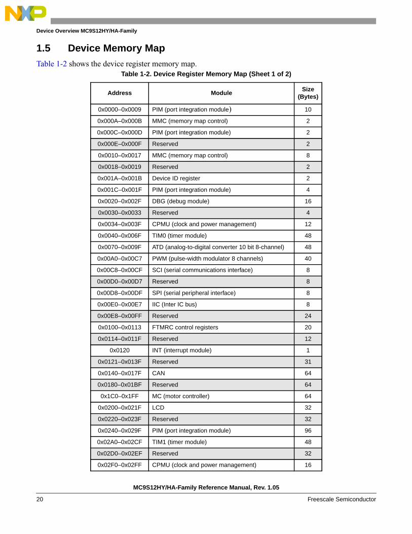
1.5 Device Memory MapTable 1-2 shows the device register memory map.
Table 1-2. Device Register Memory Map (Sheet 1 of 2)
Address ModuleSize
(Bytes)
0x0000–0x0009 PIM (port integration module) 10
0x000A–0x000B MMC (memory map control) 2
0x000C–0x000D PIM (port integration module) 2
0x000E–0x000F Reserved 2
0x0010–0x0017 MMC (memory map control) 8
0x0018–0x0019 Reserved 2
0x001A–0x001B Device ID register 2
0x001C–0x001F PIM (port integration module) 4
0x0020–0x002F DBG (debug module) 16
0x0030–0x0033 Reserved 4
0x0034–0x003F CPMU (clock and power management) 12
0x0040–0x006F TIM0 (timer module) 48
0x0070–0x009F ATD (analog-to-digital converter 10 bit 8-channel) 48
0x00A0–0x00C7 PWM (pulse-width modulator 8 channels) 40
0x00C8–0x00CF SCI (serial communications interface) 8
0x00D0–0x00D7 Reserved 8
0x00D8–0x00DF SPI (serial peripheral interface) 8
0x00E0–0x00E7 IIC (Inter IC bus) 8
0x00E8–0x00FF Reserved 24
0x0100–0x0113 FTMRC control registers 20
0x0114–0x011F Reserved 12
0x0120 INT (interrupt module) 1
0x0121–0x013F Reserved 31
0x0140–0x017F CAN 64
0x0180–0x01BF Reserved 64
0x1C0–0x1FF MC (motor controller) 64
0x0200–0x021F LCD 32
0x0220–0x023F Reserved 32
0x0240–0x029F PIM (port integration module) 96
0x02A0–0x02CF TIM1 (timer module) 48
0x02D0–0x02EF Reserved 32
0x02F0–0x02FF CPMU (clock and power management) 16
MC9S12HY/HA-Family Reference Manual, Rev. 1.05
20 Freescale Semiconductor

Device Overview MC9S12HY/HA-Family
NOTEReserved register space shown in Table 1-2 is not allocated to any module.This register space is reserved for future use. Writing to these locations hasno effect. Read access to these locations returns zero.
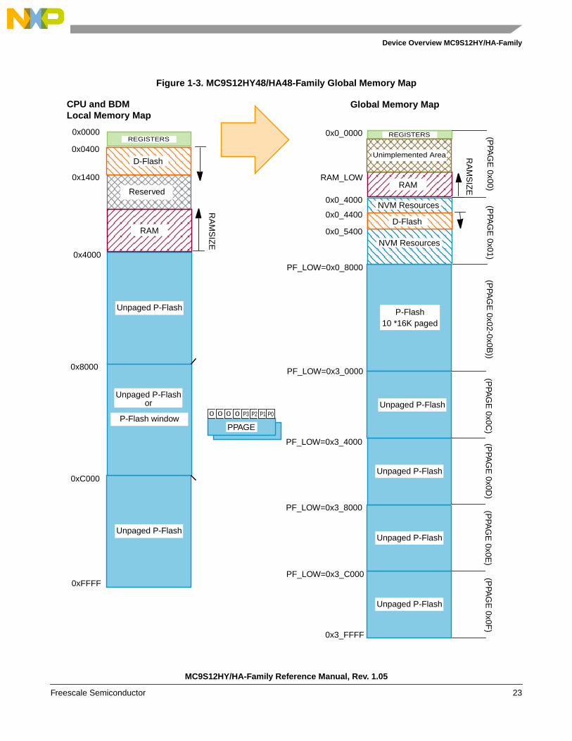
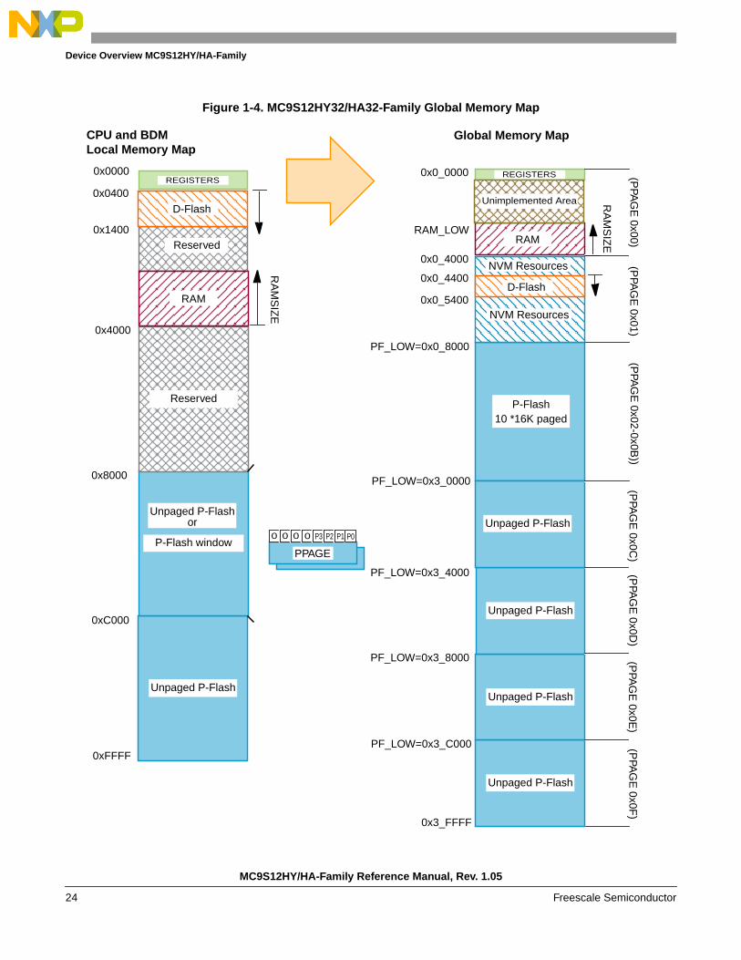
Figure 1-2, Figure 1-3 and Figure 1-4 shows S12HY/HA family CPU and BDM local address translationto the global memory map. It indicates also the location of the internal resources in the memory map.Table 1-3 shows the mapping of D-Flash and unpaged P-Flash memory. The whole 256K global memoryspace is visible through the P-Flash window located in the 64K local memory map located at 0x8000 −0xBFFF using the PPAGE register.
Table 1-4. MC9S12HY/MC9S12HA Derivatives
0x0300–0x03FF Reserved 256
Table 1-3. MC9S12HY/MC9S12HA -Family mapping for D-Flash and unpaged P-Flash
Local 64K memory map Global 256K memory map
D-Flash 0x0400 - 0x13FF 0x0_4400 - 0x0_53FF
P-Flash
0x1400 - 0x2FFF(1)
1. 0x2FFF for MC9S12HY64 because of 4K RAM size
0x3_1400 -0x3_2FFF(2)
2. 0x3_2FFF for MC9S12HY64 because of 4K RAM size
0x4000 - 0x7FFF 0x3_4000 - 0x3_7FFF
0xC000 - 0xFFFF 0x3_C000 - 0x3_FFFF
Feature MC9S12HY32MC9S12HA32
MC9S12HY48MC9S12HA48
MC9S12HY64MC9S12HA64
P-Flash size 32KB 48KB 64KB
PF_LOWPPAGES
0x3_80000x0E - 0x0F
0x3_40000x0D - 0x0F
0x3_00000x0C - 0x0F
RAMSIZE 2KB 4KB 4KB
RAM_LOW 0x0_3800 0x0_3000 0x0_3000
Table 1-2. Device Register Memory Map (Sheet 2 of 2)
Address ModuleSize
(Bytes)
MC9S12HY/HA-Family Reference Manual, Rev. 1.05
Freescale Semiconductor 21

Device Overview MC9S12HY/HA-Family
Figure 1-2. MC9S12HY64/HA64-Family Global Memory Map
0x3_FFFF
PPAGE
CPU and BDMLocal Memory Map
Global Memory Map
0xFFFF
0xC000
0x8000
P-Flash window
PF_LOW=0x3_4000
PF_LOW=0x3_8000
PF_LOW=0x3_C000
0x0_4000
0x0000
0x4000
0x0400D-Flash
RAM
Unpaged P-Flash
REGISTERS
Unpaged P-Flash
Unpaged P-Flash
0 P0P1P2P3000
0x1400
RA
MS
IZE
0x0_0000
RAM
RA
MS
IZE
10 *16K pagedP-Flash
PF_LOW=0x0_8000
NVM Resources
REGISTERS
RAM_LOW
Unpaged P-Flash
PF_LOW=0x3_0000
Unimplemented Area
Unpaged P-Flash
Unpaged P-Flash
(PPA
GE
0x0C)
(PPA
GE
0x0D)
(PPA
GE
0x0E)
(PPA
GE
0x0F)
Unpaged P-Flashor
(PPA
GE
0x02-0x0B))
(PPA
GE
0x01)(P
PAG
E 0x00)
Unpaged P-Flash
0x0_4400D-Flash
0x0_5400NVM Resources
MC9S12HY/HA-Family Reference Manual, Rev. 1.05
22 Freescale Semiconductor
Device Overview MC9S12HY/HA-Family
Figure 1-3. MC9S12HY48/HA48-Family Global Memory Map
0x3_FFFF
PPAGE
CPU and BDMLocal Memory Map
Global Memory Map
0xFFFF
0xC000
0x8000
P-Flash window
PF_LOW=0x3_4000
PF_LOW=0x3_8000
PF_LOW=0x3_C000
0x0_4000
0x0000
0x4000
0x0400D-Flash
RAM
REGISTERS
Unpaged P-Flash
Unpaged P-Flash
0 P0P1P2P3000
0x1400
RA
MS
IZE
0x0_0000
RAM
RA
MS
IZE
10 *16K pagedP-Flash
PF_LOW=0x0_8000
NVM Resources
REGISTERS
RAM_LOW
Unpaged P-Flash
PF_LOW=0x3_0000
Unimplemented Area
Unpaged P-Flash
Unpaged P-Flash
(PPA
GE
0x0C)
(PPA
GE
0x0D)
(PPA
GE
0x0E)
(PPA
GE
0x0F)
Unpaged P-Flashor
(PPA
GE
0x02-0x0B))
(PPA
GE
0x01)(P
PAG
E 0x00)
0x0_4400D-Flash
0x0_5400NVM Resources
Reserved
Unpaged P-Flash
MC9S12HY/HA-Family Reference Manual, Rev. 1.05
Freescale Semiconductor 23
Device Overview MC9S12HY/HA-Family
Figure 1-4. MC9S12HY32/HA32-Family Global Memory Map
0x3_FFFF
PPAGE
CPU and BDMLocal Memory Map
Global Memory Map
0xFFFF
0xC000
0x8000
P-Flash window
PF_LOW=0x3_4000
PF_LOW=0x3_8000
PF_LOW=0x3_C000
0x0_4000
0x0000
0x4000
0x0400D-Flash
RAM
REGISTERS
Reserved
Unpaged P-Flash
0 P0P1P2P3000
0x1400
RA
MS
IZE
0x0_0000
RAM
RA
MS
IZE
10 *16K pagedP-Flash
PF_LOW=0x0_8000
NVM Resources
REGISTERS
RAM_LOW
Unpaged P-Flash
PF_LOW=0x3_0000
Unimplemented Area
Unpaged P-Flash
Unpaged P-Flash
(PPA
GE
0x0C)
(PPA
GE
0x0D)
(PPA
GE
0x0E)
(PPA
GE
0x0F)
Unpaged P-Flashor
(PPA
GE
0x02-0x0B))
(PPA
GE
0x01)(P
PAG
E 0x00)
0x0_4400D-Flash
0x0_5400NVM Resources
Reserved
Unpaged P-Flash
MC9S12HY/HA-Family Reference Manual, Rev. 1.05
24 Freescale Semiconductor
Device Overview MC9S12HY/HA-Family
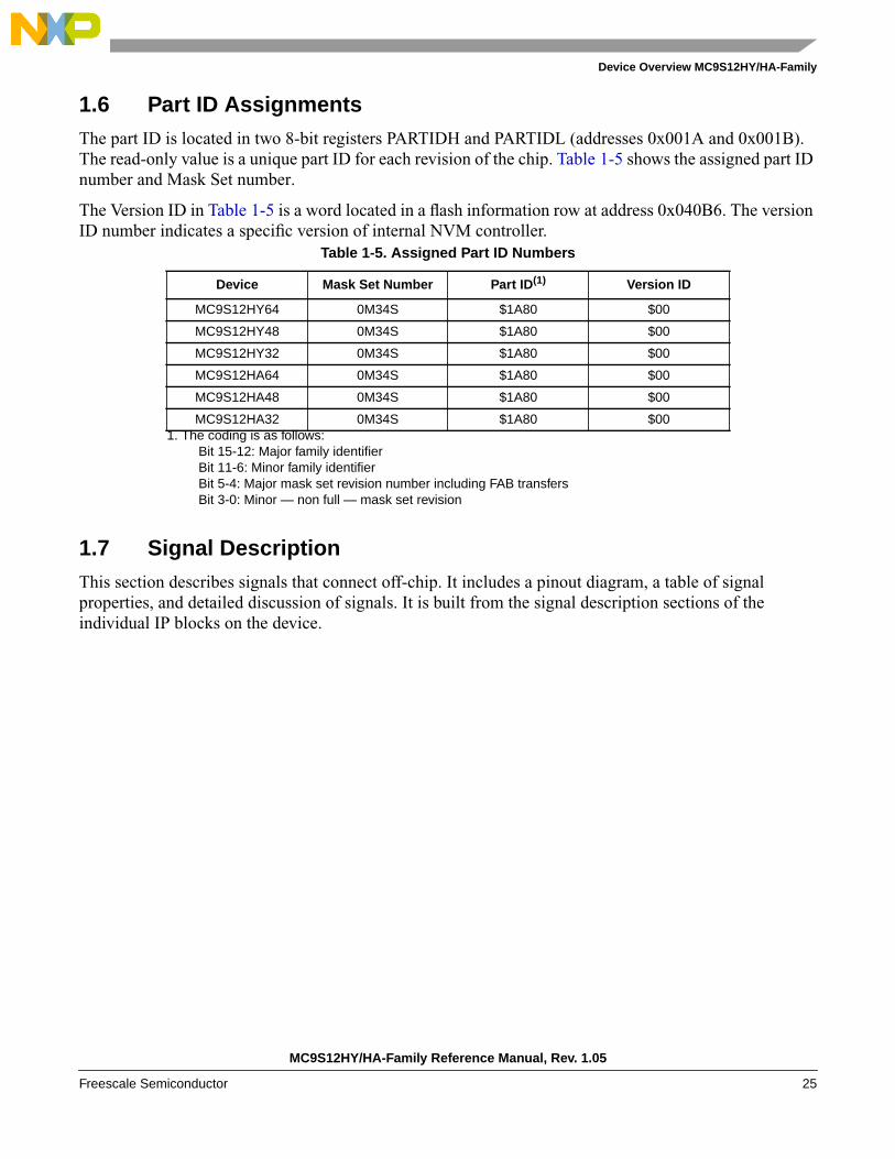
1.6 Part ID AssignmentsThe part ID is located in two 8-bit registers PARTIDH and PARTIDL (addresses 0x001A and 0x001B).The read-only value is a unique part ID for each revision of the chip. Table 1-5 shows the assigned part IDnumber and Mask Set number.
The Version ID in Table 1-5 is a word located in a flash information row at address 0x040B6. The versionID number indicates a specific version of internal NVM controller.
1.7 Signal DescriptionThis section describes signals that connect off-chip. It includes a pinout diagram, a table of signalproperties, and detailed discussion of signals. It is built from the signal description sections of theindividual IP blocks on the device.
Table 1-5. Assigned Part ID Numbers
Device Mask Set Number Part ID(1)
1. The coding is as follows:Bit 15-12: Major family identifierBit 11-6: Minor family identifierBit 5-4: Major mask set revision number including FAB transfersBit 3-0: Minor — non full — mask set revision
Version ID
MC9S12HY64 0M34S $1A80 $00
MC9S12HY48 0M34S $1A80 $00
MC9S12HY32 0M34S $1A80 $00
MC9S12HA64 0M34S $1A80 $00
MC9S12HA48 0M34S $1A80 $00
MC9S12HA32 0M34S $1A80 $00
MC9S12HY/HA-Family Reference Manual, Rev. 1.05
Freescale Semiconductor 25

Device Overview MC9S12HY/HA-Family
1.7.1 Device Pinout
Figure 1-5. MC9S12HY/HA-Family 100 LQFP pinout
123456789
10111213141516171819202122232425
26 27 28 29 30 31 32 33 34 35 36 37 38 39 40 41 42 43 44 45 46 47 48 49 50
PA1 / XIRQ / FP30PA0 / IRQ / FP29XTALEXTALVSSPLLVSS3VDDRPB0 / FP28PR7 / FP27PH7 / FP26PH6 / FP25PH5 / FP24PH4 / FP23VDDXVSSXPH3 / SS / SDA / FP22PH2 / ECLK / SCK / FP21PH1 / MOSI / FP20PH0 / MISO / SCL / FP19PR6 / SCL / FP18PR5 / SDA / FP17PT7 / IOC0_7 / KWT7 / FP16PT6 / IOC0_6 / KWT6 / FP15PT5 / IOC0_5 / KWT5 / FP14PT4 / IOC0_4 / KWT4 / FP13
TX
D /
PW
M7
/ PS
1
RX
CA
N /
PS
2
TX
CA
N /
PS
3M
ISO
/ S
CL
/ P
WM
0 / P
S4
KW
S5
/ MO
SI /
PW
M1
/ PS
5 K
WS
6 / S
CK
/ P
WM
2 / P
S6
SS
/ S
DA
/ P
WM
3 / P
S7
KW
R0
/ IO
C0_
6 / P
R0
KW
R1
/ IO
C0_
7 / P
R1
KW
R2
/ IO
C1_
6 / P
R2
KW
R3
/ IO
C1_
7 / P
R3
FP
0 / P
WM
0 / P
P0
FP
1 / P
WM
1 / P
P1
FP
2 / P
WM
2 / P
P2
FP
3 / P
WM
3 / P
P3
FP
4 / P
WM
4 / P
P4
FP
5 / P
WM
5 / P
P5
FP
6 / P
WM
6 / P
P6
FP
7 / P
WM
7 / P
P7
FP
8 / K
WT
0 / I
OC
1_4
/ PT
0 F
P9
/ KW
T1
/ IO
C1_
5 / P
T1
FP
10 /
KW
T2
/ IO
C1_
6 / P
T2
FP
11 /
KW
T3
/ IO
C1_
7 / P
T3
FP
12 /
PR
4
RE
SE
T
75747372717069686766656463626160595857565554535251
100 99 98 97 96 95 94 93 92 91 90 89 88 87 86 85 84 83 82 81 80 79 78 77 76
MC9S12HY/HA-Family100 LQFP
TEST NC
M0C0M / IOC0_0 / PU0 M0C0P / PU1
M0C1M / IOC0_1 / PU2 M0C1P / PU3
VDDM1 VSSM1
M1C0M / IOC0_2 / PU4 M1C0P / PU5
M1C1M / IOC0_3 / PU6 M1C1P / PU7
M2C0M / IOC1_0 / SCL / PWM4 / MISO / PV0 M2C0P / MOSI / PWM5 / PV1
M2C1M / IOC1_1 / SCK / PWM6 / PV2M2C1P / SDA / PWM7 / SS / PV3
VDDM2 VSSM2
M3C0M / IOC1_2 / PV4 M3C0P / PV5
M3C1M / IOC1_3 / PV6 M3C1P / PV7
NC NC
RXD / PWM6 / PS0
PAD
07 /
AN
07 /
KW
AD
7PA
D06
/ A
N06
/ K
WA
D6
PAD
05 /
AN
05 /
KW
AD
5PA
D04
/ A
N04
/ K
WA
D4
PAD
03 /
AN
03 /
KW
AD
3PA
D02
/ A
N02
/ K
WA
D2
PAD
01 /
AN
01 /
KW
AD
1PA
D00
/ A
N00
/ K
WA
D0
VD
DA
/ V
RH
VS
SA
/ V
RL
BK
GD
/ M
OD
CV
LCD
PB
7 / B
P3
PB
6 / B
P2
PB
5 / B
P1
PB
4 / B
P0
PB
3 / F
P39
PB
2 / F
P38
PB
1 / F
P37
PA7
/ FP
36PA
6 / F
P35
PA5
/ FP
34PA
4 / F
P33
PA3
/ AP
I_E
XT
CLK
/ F
P32
PA2
/ FP
31
Pins shown in BOLD arenot available on the64 LQFP package
MC9S12HY/HA-Family Reference Manual, Rev. 1.05
26 Freescale Semiconductor

Device Overview MC9S12HY/HA-Family
Figure 1-6. MC9S12HY/HA-Family 64 LQFP pinout
123456789
10111213141516
17 18 19 20 21 22 23 24 25 26 27 28 29 30 31 32
48474645444342414039383736353433
64 63 62 61 60 59 58 57 56 55 54 53 52 51 50 49
MC9S12HY/HA-Family
64 LQFP
TX
D /
PW
M7
/ PS
1
RX
CA
N /
PS
2
TX
CA
N /
PS
3 K
WR
0 / I
OC
0_6
/ PR
0 K
WR
1 / I
OC
0_7
/ PR
1 K
WR
2 / I
OC
1_6
/ PR
2 K
WR
3 / I
OC
1_7
/ PR
3 F
P0
/ PW
M0
/ PP
0 F
P1
/ PW
M1
/ PP
1 F
P2
/ PW
M2
/ PP
2 F
P3
/ PW
M3
/ PP
3 F
P8
/ KW
T0
/ IO
C1_
4 / P
T0
FP
9 / K
WT
1 / I
OC
1_5
/ PT
1 F
P10
/ K
WT
2 / I
OC
1_6
/ PT
2 F
P11
/ K
WT
3 / I
OC
1_7
/ PT
3
RE
SE
T
TEST M0C0M / IOC0_0 / PU0
M0C0P / PU1 M0C1M / IOC0_1 / PU2
M0C1P / PU3 VDDM1 VSSM1
M1C0M / IOC0_2 / PU4 M1C0P / PU5
M1C1M / IOC0_3 / PU6 M1C1P / PU7
M2C0M / IOC1_0 / SCL / PWM4 / MISO / PV0 M2C0P / MOSI / PWM5 / PV1
M2C1M / IOC1_1 / SCK / PWM6 / PV2M2C1P / SDA / PWM7 / SS / PV3
RXD / PWM6 / PS0
PAD
05 /
AN
05 /
KW
AD
5PA
D04
/ A
N04
/ K
WA
D4
PAD
03 /
AN
03 /
KW
AD
3PA
D02
/ A
N02
/ K
WA
D2
PAD
01 /
AN
01 /
KW
AD
1PA
D00
/ A
N00
/ K
WA
D0
VD
DA
/ V
RH
VS
SA
/ V
RL
BK
GD
/ M
OD
CV
LCD
PB
7 / B
P3
PB
6 / B
P2
PB
5 / B
P1
PB
4 / B
P0
PA3
/ AP
I_E
XT
CLK
/ F
P32
PA2
/ FP
31
PA1 / XIRQ / FP30PA0 / IRQ / FP29XTALEXTALVSS3 / VSSPLLVDDRVDDXVSSXPH3 / SS / SDA / FP22PH2 / ECLK / SCK / FP21PH1 / MOSI / FP20PH0 / MISO / SCL / FP19PT7 / IOC0_7 / KWT7 / FP16PT6 / IOC0_6 / KWT6 / FP15PT5 / IOC0_5 / KWT5 / FP14PT4 / IOC0_4 / KWT4 / FP13
MC9S12HY/HA-Family Reference Manual, Rev. 1.05
Freescale Semiconductor 27

Device Overview MC9S12HY/HA-Family
1.7.2 Pin Assignment Overview
Table 1-6 provides a summary of which ports are available for each package option. Routing of pinfunctions is summarized in Table 1-7.
Table 1-6. Port Availability by Package Option
Port 100 LQFP 64 LQFP
Port AD/ADC Channels 8/8 6/6
Port A 8 4
Port B 8 4
Port H 8 4
Port P 8 4
Port R 8 4
Port S 8 4
Port T 8 8
Port U 8 8
Port V 8 4
Sum of Ports 80 50
I/O Power Pairs VDDM/VSSM 2/2 1/1
I/O Power Pairs VDDX/VSSX 1/1 1/1
I/O Power Pairs VDDA/VSSA(1)
1. VRH/VRL are sharing with VDDA/VSSA pins
1/1 1/1
VREG Power Pairs VDDR/VSS3 1/1 1/1
I/O Power Pair VSSPLL 1 0(2)
2. Double bond with VSS3 on 64LQFP package
VLCD power 1 1
MC9S12HY/HA-Family Reference Manual, Rev. 1.05
28 Freescale Semiconductor

Device Overview MC9S12HY/HA-Family
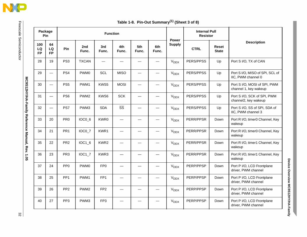
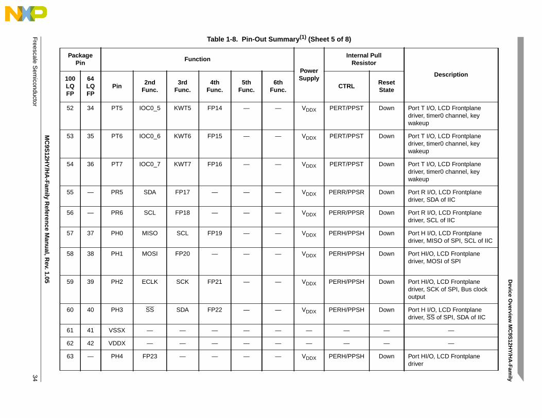
Table 1-8 provides a pin out summary listing the availability and functionality of individual pins for eachpackage option.
Table 1-7. Peripheral - Port Routing Options(1)
IICTIM0(IO
C7/6)TIM1(IO
C7/6)SPI
PWM[7:6]
PWM[5:4]
PWM[3:2]
PWM[1:0]
PR[6:5] O
PH[3,0] O
PV[3,0] O
PS[7,4] X
PT[7:6] X
PR[1:0] O
PT[3:2] X
PR[3:2] O
PS[7:4] X
PV[3:0] O
PH[3:0] O
PP[7:6] X
PS[1:0] O
PV[3:2] O
PP[5:4] X
PV[1:0] O
PP[3:2] X
PS[7:6] O
PP[1:0] X
PS[5:4] O1. “O” denotes a possible rerouting under software control, “X” denotes as default routing option
MC9S12HY/HA-Family Reference Manual, Rev. 1.05
Freescale Semiconductor 29
Device O
verview M
C9S
12HY
/HA
-Family
F
Descriptionette
N Test input
—
led Port U I/O, Motor0 coil nodes ofMC, timer0 channel
led Port U I/O, Motor0 coil nodes ofMC
led Port U I/O, Motor0 coil nodes ofMC, timer0 channel
led Port U I/O, Motor0 coil nodes ofMC
—
—
led Port U I/O, Motor1 coil nodes ofMC, timer0 channel
led Port U I/O, Motor1 coil nodes ofMC
led Port U I/O, Motor1 coil nodes ofMC, timer0 channel
led Port U I/O, Motor1 coil nodes ofMC
led Port V I/O, Motor2 coil nodes ofMC, MISO of SPI, SCL of IIC,PWM channel 4, timer1 channel
MC
9S12H
Y/H
A-Fam
ily Referen
ce Man
ual, R
ev. 1.05
reescale Sem
iconductor30
Table 1-8. Pin-Out Summary(1) (Sheet 1 of 8)
PackagePin
Function
PowerSupply
Internal PullResistor
100LQFP
64LQFP
Pin2nd
Func.3rd
Func.4th
Func.5th
Func.6th
Func.CTRL
ResSta
1 1 TEST — — — — — VDDA RESET pin DOW
2 — NC — — — — — — — —
3 2 PU0 IOC0_0 M0C0M — — — VDDM PERU/PPSU Disab
4 3 PU1 M0C0P — — — — VDDM PERU/PPSU Disab
5 4 PU2 IOC0_1 M0C1M — — — VDDM PERU/PPSU Disab
6 5 PU3 M0C1P — — — VDDM PERU/PPSU Disab
7 6 VDDM1 — — — — — — — —
8 7 VSSM1 — — — — — — — —
9 8 PU4 IOC0_2 M1C0M — — — VDDM PERU/PPSU Disab
10 9 PU5 M1C0P — — — — VDDM PERU/PPSU Disab
11 10 PU6 IOC0_3 M1C1M — — — VDDM PERU/PPSU Disab
12 11 PU7 M1C1P — — — — VDDM PERU/PPSU Disab
13 12 PV0 MISO PWM4 SCL IOC1_0 M2C0M VDDM PERV/PPSV Disab

Device O
verview M
C9S
12HY
/HA
-Family
F
led Port V I/O, Motor2 coil nodes ofMC, MOSI of SPI, PWMchannel 5
led Port V I/O, Motor2 coil nodes ofMC, SCK of SPI, PWM channel6
led Port V I/O, Motor2 coil nodes ofMC, SS of SPI, SDA of IIC,PWM channel 7
—
—
led Port V I/O, Motor3 coil nodes ofMC, timer1 channel
led Port V I/O, Motor3 coil nodes ofMC
led Port V I/O, Motor3 coil nodes ofMC, timer1 channel
led Port V I/O, Motor3 coil nodes ofMC
—
—
Port S I/O, RXD of SCI, PWMchannel6
Port S I/O, TXD of SCI, PWMchannel 7
Port S I/O, RX of CAN
(1)
Descriptionette
MC
9S12H
Y/H
A-Fam
ily Referen
ce Man
ual, R
ev. 1.05
reescale Sem
iconductor31
14 13 PV1 MOSI PWM5 M2C0P — — VDDM PERV/PPSV Disab
15 14 PV2 SCK PWM6 IOC1_1 M2C1M — VDDM PERV/PPSV Disab
16 15 PV3 SS PWM7 SDA M2C1P — VDDM PERV/PPSV Disab
17 — VDDM2 — — — — — — — —
18 — VSSM2 — — — — — — — —
19 — PV4 IOC1_2 M3C0M — — — VDDM PERV/PPSV Disab
20 — PV5 M3C0P — — — — VDDM PERV/PPSV Disab
21 — PV6 IOC1_3 M3C1M — — — VDDM PERV/PPSV Disab
22 — PV7 M3C1P — — — — VDDM PERV/PPSV Disab
23 — NC — — — — — — — —
24 — NC — — — — — — — —
25 16 PS0 PWM6 RXD — — — VDDX PERS/PPSS Up
26 17 PS1 PWM7 TXD — — — VDDX PERS/PPSS Up
27 18 PS2 RXCAN — — — — VDDX PERS/PPSS Up
Table 1-8. Pin-Out Summary (Sheet 2 of 8)
PackagePin
Function
PowerSupply
Internal PullResistor
100LQFP
64LQFP
Pin2nd
Func.3rd
Func.4th
Func.5th
Func.6th
Func.CTRL
ResSta
Device O
verview M
C9S
12HY
/HA
-Family
F
Port S I/O, TX of CAN
Port S I/O, MISO of SPI, SCL ofIIC, PWM channel 0
Port S I/O, MOSI of SPI, PWMchannel 1, key wakeup
Port S I/O, SCK of SPI, PWMchannel2, key wakeup
Port S I/O, SS of SPI, SDA ofIIC, PWM channel 3
n Port R I/O, timer0 Channel, Keywakeup
n Port R I/O, timer0 Channel, Keywakeup
n Port R I/O, timer1 Channel, Keywakeup
n Port R I/O, timer1 Channel, Keywakeup
n Port P I/O, LCD Frontplanedriver, PWM channel
n Port P I/O, LCD Frontplanedriver, PWM channel
n Port P I/O, LCD Frontplanedriver, PWM channel
n Port P I/O, LCD Frontplanedriver, PWM channel
(1)
Descriptionette
MC
9S12H
Y/H
A-Fam
ily Referen
ce Man
ual, R
ev. 1.05
reescale Sem
iconductor32
28 19 PS3 TXCAN — — — — VDDX PERS/PPSS Up
29 — PS4 PWM0 SCL MISO — — VDDX PERS/PPSS Up
30 — PS5 PWM1 KWS5 MOSI — — VDDX PERS/PPSS Up
31 — PS6 PWM2 KWS6 SCK — — VDDX PERS/PPSS Up
32 — PS7 PWM3 SDA SS — — VDDX PERS/PPSS Up
33 20 PR0 IOC0_6 KWR0 — — — VDDX PERR/PPSR Dow
34 21 PR1 IOC0_7 KWR1 — — — VDDX PERR/PPSR Dow
35 22 PR2 IOC1_6 KWR2 — — — VDDX PERR/PPSR Dow
36 23 PR3 IOC1_7 KWR3 — — — VDDX PERR/PPSR Dow
37 24 PP0 PWM0 FP0 — — — VDDX PERP/PPSP Dow
38 25 PP1 PWM1 FP1 — — — VDDX PERP/PPSP Dow
39 26 PP2 PWM2 FP2 — — — VDDX PERP/PPSP Dow
40 27 PP3 PWM3 FP3 — — — VDDX PERP/PPSP Dow
Table 1-8. Pin-Out Summary (Sheet 3 of 8)
PackagePin
Function
PowerSupply
Internal PullResistor
100LQFP
64LQFP
Pin2nd
Func.3rd
Func.4th
Func.5th
Func.6th
Func.CTRL
ResSta

Device O
verview M
C9S
12HY
/HA
-Family
F
n Port P I/O, LCD Frontplanedriver, PWM channel
n Port P I/O, LCD Frontplanedriver, PWM channel
n Port P I/O, LCD Frontplanedriver, PWM channel
n Port P I/O, LCD Frontplanedriver, PWM channel
n Port T I/O, LCD Frontplanedriver, timer1 channel, keywakeup
n Port T I/O, LCD Frontplanedriver, timer1 channel, keywakeup
n Port T I/O, LCD Frontplanedriver, timer1 channel, keywakeup
n Port T I/O, LCD Frontplanedriver, timer1 channel, keywakeup
n Port R I/O, LCD Frontplanedriver
External reset
n Port T I/O, LCD Frontplanedriver, timer0 channel, keywakeup
(1)
Descriptionette
MC
9S12H
Y/H
A-Fam
ily Referen
ce Man
ual, R
ev. 1.05
reescale Sem
iconductor33
41 — PP4 PWM4 FP4 — — — VDDX PERP/PPSP Dow
42 — PP5 PWM5 FP5 — — — VDDX PERP/PPSP Dow
43 — PP6 PWM6 FP6 — — — VDDX PERP/PPSP Dow
44 — PP7 PWM7 FP7 — — — VDDX PERP/PPSP Dow
45 28 PT0 IOC1_4 KWT0 FP8 — — VDDX PERT/PPST Dow
46 29 PT1 IOC1_5 KWT1 FP9 — — VDDX PERT/PPST Dow
47 30 PT2 IOC1_6 KWT2 FP10 — — VDDX PERT/PPST Dow
48 31 PT3 IOC1_7 KWT3 FP11 — — VDDX PERT/PPST Dow
49 — PR4 FP12 — — — — VDDX PERR/PPSR Dow
50 32 RESET — — — — — VDDX PULLUP
51 33 PT4 IOC0_4 KWT4 FP13 — — VDDX PERT/PPST Dow
Table 1-8. Pin-Out Summary (Sheet 4 of 8)
PackagePin
Function
PowerSupply
Internal PullResistor
100LQFP
64LQFP
Pin2nd
Func.3rd
Func.4th
Func.5th
Func.6th
Func.CTRL
ResSta
Device O
verview M
C9S
12HY
/HA
-Family
F
n Port T I/O, LCD Frontplanedriver, timer0 channel, keywakeup
n Port T I/O, LCD Frontplanedriver, timer0 channel, keywakeup
n Port T I/O, LCD Frontplanedriver, timer0 channel, keywakeup
n Port R I/O, LCD Frontplanedriver, SDA of IIC
n Port R I/O, LCD Frontplanedriver, SCL of IIC
n Port H I/O, LCD Frontplanedriver, MISO of SPI, SCL of IIC
n Port HI/O, LCD Frontplanedriver, MOSI of SPI
n Port HI/O, LCD Frontplanedriver, SCK of SPI, Bus clockoutput
n Port H I/O, LCD Frontplanedriver, SS of SPI, SDA of IIC
—
—
n Port HI/O, LCD Frontplanedriver
(1)
Descriptionette
MC
9S12H
Y/H
A-Fam
ily Referen
ce Man
ual, R
ev. 1.05
reescale Sem
iconductor34
52 34 PT5 IOC0_5 KWT5 FP14 — — VDDX PERT/PPST Dow
53 35 PT6 IOC0_6 KWT6 FP15 — — VDDX PERT/PPST Dow
54 36 PT7 IOC0_7 KWT7 FP16 — — VDDX PERT/PPST Dow
55 — PR5 SDA FP17 — — — VDDX PERR/PPSR Dow
56 — PR6 SCL FP18 — — — VDDX PERR/PPSR Dow
57 37 PH0 MISO SCL FP19 — — VDDX PERH/PPSH Dow
58 38 PH1 MOSI FP20 — — — VDDX PERH/PPSH Dow
59 39 PH2 ECLK SCK FP21 — — VDDX PERH/PPSH Dow
60 40 PH3 SS SDA FP22 — — VDDX PERH/PPSH Dow
61 41 VSSX — — — — — — — —
62 42 VDDX — — — — — — — —
63 — PH4 FP23 — — — — VDDX PERH/PPSH Dow
Table 1-8. Pin-Out Summary (Sheet 5 of 8)
PackagePin
Function
PowerSupply
Internal PullResistor
100LQFP
64LQFP
Pin2nd
Func.3rd
Func.4th
Func.5th
Func.6th
Func.CTRL
ResSta

Device O
verview M
C9S
12HY
/HA
-Family
F
n Port H I/O, LCD Frontplanedriver
n Port H I/O, LCD Frontplanedriver
n Port H I/O, LCD Frontplanedriver
n Port R I/O, LCD Frontplanedriver
n Port B I/O, LCD Frontplanedriver
—
—
—
Oscillator pin
Oscillator pin
n Port A I/O, LCD Frontplanedriver, IRQ input
n Port A I/O, LCD Frontplanedriver, XIRQ input
n Port A I/O, LCD Frontplanedriver
n Port A I/O, LCD Frontplanedriver, API clock output
(1)
Descriptionette
MC
9S12H
Y/H
A-Fam
ily Referen
ce Man
ual, R
ev. 1.05
reescale Sem
iconductor35
64 — PH5 FP24 — — — — VDDX PERH/PPSH Dow
65 — PH6 FP25 — — — — VDDX PERH/PPSH Dow
66 — PH7 FP26 — — — — VDDX PERH/PPSH Dow
67 — PR7 FP27 — — — — VDDX PERR/PPSR Dow
68 — PB0 FP28 — — — — VDDX PUCR Dow
69 43 VDDR — — — — — — — —
70 44 VSS3 — — — — — — — —
71 44 VSSPLL — — — — — — — —
72 45 EXTAL — — — — — VDDPLL
— —
73 46 XTAL — — — — — VDDPLL
— —
74 47 PA0 IRQ FP29 — — — VDDX PUCR Dow
75 48 PA1 XIRQ FP30 — — — VDDX PUCR Dow
76 49 PA2 FP31 — — — — VDDX PUCR Dow
77 50 PA3 API_EXTCLK
FP32 — — — VDDX PUCR Dow
Table 1-8. Pin-Out Summary (Sheet 6 of 8)
PackagePin
Function
PowerSupply
Internal PullResistor
100LQFP
64LQFP
Pin2nd
Func.3rd
Func.4th
Func.5th
Func.6th
Func.CTRL
ResSta
Device O
verview M
C9S
12HY
/HA
-Family
F
n Port A I/O, LCD Frontplanedriver
n Port A I/O, LCD Frontplanedriver
n Port A I/O, LCD Frontplanedriver
n Port A I/O, LCD Frontplanedriver
n Port B I/O, LCD Frontplanedriver
n Port B I/O, LCD Frontplanedriver
n Port B I/O, LCD Frontplanedriver
n Port B I/O, LCD Backplanedriver
n Port B I/O, LCD Backplanedriver
n Port B I/O, LCD Backplanedriver
n Port B I/O, LCD Backplanedriver
Voltage reference pin for theLCD driver.
Background debug, Modeselection pin
—
(1)
Descriptionette
MC
9S12H
Y/H
A-Fam
ily Referen
ce Man
ual, R
ev. 1.05
reescale Sem
iconductor36
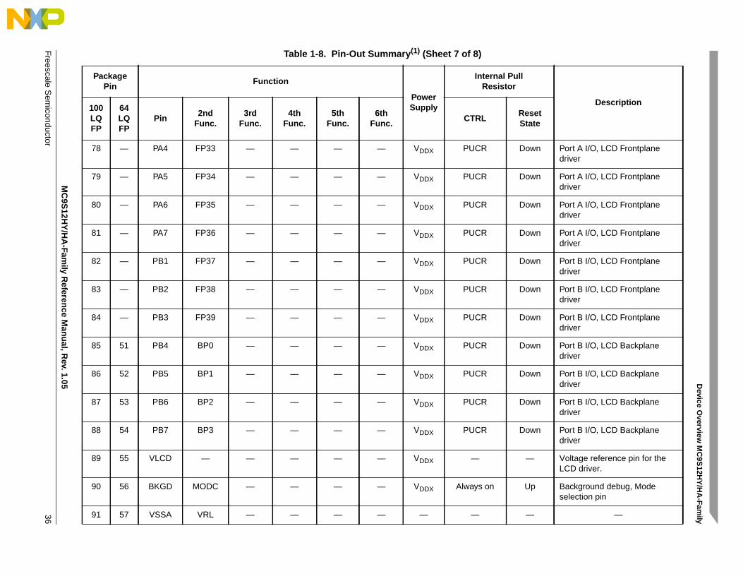
78 — PA4 FP33 — — — — VDDX PUCR Dow
79 — PA5 FP34 — — — — VDDX PUCR Dow
80 — PA6 FP35 — — — — VDDX PUCR Dow
81 — PA7 FP36 — — — — VDDX PUCR Dow
82 — PB1 FP37 — — — — VDDX PUCR Dow
83 — PB2 FP38 — — — — VDDX PUCR Dow
84 — PB3 FP39 — — — — VDDX PUCR Dow
85 51 PB4 BP0 — — — — VDDX PUCR Dow
86 52 PB5 BP1 — — — — VDDX PUCR Dow
87 53 PB6 BP2 — — — — VDDX PUCR Dow
88 54 PB7 BP3 — — — — VDDX PUCR Dow
89 55 VLCD — — — — — VDDX — —
90 56 BKGD MODC — — — — VDDX Always on Up
91 57 VSSA VRL — — — — — — —
Table 1-8. Pin-Out Summary (Sheet 7 of 8)
PackagePin
Function
PowerSupply
Internal PullResistor
100LQFP
64LQFP
Pin2nd
Func.3rd
Func.4th
Func.5th
Func.6th
Func.CTRL
ResSta
Device O
verview M
C9S
12HY
/HA
-Family
F
d as outputs afterted pins.
—
led Port AD I/O, analog input ofATD, key wakeup
led Port AD I/O, analog input ofATD, key wakeup
led Port AD I/O, analog input ofATD, key wakeup
led Port AD I/O, analog input ofATD, key wakeup
led Port AD I/O, analog input ofATD, key wakeup
led Port AD I/O, analog input ofATD, key wakeup
led Port AD I/O, analog input ofATD, key wakeup
led Port AD I/O, analog input ofATD, key wakeup
sistor should be < =4.7K
(1)
Descriptionette
MC
9S12H
Y/H
A-Fam
ily Referen
ce Man
ual, R
ev. 1.05
reescale Sem
iconductor37
NOTEFor devices assembled in 64-pin package all non-bonded out pins should be configurereset in order to avoid current drawn from floating inputs. Refer to Table 1-8 for affec
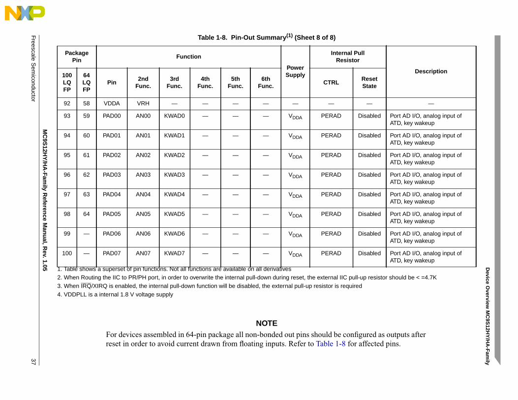
92 58 VDDA VRH — — — — — — —
93 59 PAD00 AN00 KWAD0 — — — VDDA PERAD Disab
94 60 PAD01 AN01 KWAD1 — — — VDDA PERAD Disab
95 61 PAD02 AN02 KWAD2 — — — VDDA PERAD Disab
96 62 PAD03 AN03 KWAD3 — — — VDDA PERAD Disab
97 63 PAD04 AN04 KWAD4 — — — VDDA PERAD Disab
98 64 PAD05 AN05 KWAD5 — — — VDDA PERAD Disab
99 — PAD06 AN06 KWAD6 — — — VDDA PERAD Disab
100 — PAD07 AN07 KWAD7 — — — VDDA PERAD Disab
1. Table shows a superset of pin functions. Not all functions are available on all derivatives2. When Routing the IIC to PR/PH port, in order to overwrite the internal pull-down during reset, the external IIC pull-up re3. When IRQ/XIRQ is enabled, the internal pull-down function will be disabled, the external pull-up resistor is required4. VDDPLL is a internal 1.8 V voltage supply
Table 1-8. Pin-Out Summary (Sheet 8 of 8)
PackagePin
Function
PowerSupply
Internal PullResistor
100LQFP
64LQFP
Pin2nd
Func.3rd
Func.4th
Func.5th
Func.6th
Func.CTRL
ResSta

Device Overview MC9S12HY/HA-Family
1.7.3 Detailed Signal Descriptions
1.7.3.1 EXTAL, XTAL — Oscillator Pins
EXTAL and XTAL are the crystal driver and external clock pins. On reset all the device clocks are derivedfrom the internal reference clock. XTAL is the oscillator output.
1.7.3.2 RESET — External Reset Pin
The RESET pin is an active low bidirectional control signal. It acts as an input to initialize the MCU to aknown start-up state, and an output when an internal MCU function causes a reset. The RESET pin has aninternal pull-up device.
1.7.3.3 TEST — Test Pin
This input only pin is reserved for factory test. This pin has an internal pull-down device.
NOTEThe TEST pin must be tied to VSSA in all applications.
1.7.3.4 BKGD / MODC — Background Debug and Mode Pin
The BKGD/MODC pin is used as a pseudo-open-drain pin for the background debug communication. Itis used as a MCU operating mode select pin during reset. The state of this pin is latched to the MODC bitat the rising edge of RESET. The BKGD pin has an internal pull-up device.
1.7.3.5 PAD[7:0] / AN[7:0] / KWAD[7:0]— Port AD Input Pins of ATD [7:0]
PAD[7:0] are a general-purpose input or output pins and analog inputs AN[7:0] of the analog-to-digitalconverter ATD. They can be configured as keypad wakeup inputs.
1.7.3.6 PA[7:4] / FP[36:33]— Port A I/O Pins [7:4]
PA[7:4] are a general-purpose input or output pins. They can be configured as frontplane segment driveroutputs FP[36:33].
1.7.3.7 PA[3:2] / API_EXTCLK / FP[32:31]— Port A I/O Pins [3:2]
PA[3:2] are a general-purpose input or output pins. They can be configured as frontplane segment driveroutputs FP[32:31]. PA3 can also be configure as API_EXTCLK.
1.7.3.8 PA1 / XIRQ / FP[30]— Port A I/O Pin 1
PA1 is a general-purpose input or output pin. It can be configured as frontplane segment driver outputsFP[30]. It also provide the non-maskable interrupt request input that provides a means of applyingasynchronous interrupt requests. This will wake up the MCU from stop or wait mode. The XIRQ interrupt
MC9S12HY/HA-Family Reference Manual, Rev. 1.05
38 Freescale Semiconductor

Device Overview MC9S12HY/HA-Family
is level sensitive and active low. As XIRQ is level sensitive, while this pin is low the MCU will not enterSTOP mode. After Reset, the XIRQ default is not enabled.
1.7.3.9 PA0 / IRQ / FP[29]— Port A I/O Pin 0
PA0 is a general-purpose input or output pin. It can be configured as frontplane segment driver outputsFP[29].Tthe maskable interrupt request input that provides a means of applying asynchronous interruptrequests.
1.7.3.10 PB[7:4] / BP[3:0] — Port B I/O Pins [7:4]
PB[7:4] are a general-purpose input or output pins. They can be configured as backplane segment driveroutputs BP[3:0].
1.7.3.11 PB[3:0] / FP[39:37,28] — Port B I/O Pins [3:0]
PB[3:0] are a general-purpose input or output pins. They can be configured as frontplane segment driveroutputs FP[39:37,28].
1.7.3.12 PS7 / PWM3 / SDA / SS — Port S I/O Pin 7
PS7 is a general-purpose input or output pin. It can be configured as the slave selection pin SS for the serialperipheral interface (SPI). It can be configured as the serial data pin SDA as IIC module. It can beconfigured as PWM channel 3.
1.7.3.13 PS6 / PWM2 / SCK / KWS6 — Port S I/O Pin 6
PS6 is a general-purpose input or output pin. It can be configured as the serial clock SCK of the serialperipheral interface (SPI). It can be configured as PWM channel 2. It can be configured as keypad wakeupinput.
1.7.3.14 PS5 / PWM1 / MOSI / KWS5 — Port S I/O Pin 5
PS5 is a general-purpose input or output pin. It can be configured as the master output (during mastermode) or slave input pin (during slave mode) MOSI of the serial peripheral interface (SPI). It can beconfigured as PWM channel1. It can configured as keypad wakeup input.
1.7.3.15 PS4 / PWM0 / SCL / MISO — Port S I/O Pin 4
PS4 is a general-purpose input or output pin. It can be configured as the master input (during master mode)or slave output pin (during slave mode) MISO for the serial peripheral interface (SPI).It can be configuredas the serial clock pin SCL as IIC module.It can be configured as PWM channel0
1.7.3.16 PS3 / TXCAN — Port S I/O Pin 3
PS3 is a general-purpose input or output pin. It can be configured as the transmit pin TXCAN of thescalable controller area network controller (CAN).
MC9S12HY/HA-Family Reference Manual, Rev. 1.05
Freescale Semiconductor 39
Device Overview MC9S12HY/HA-Family
1.7.3.17 PS2 / RXCAN — Port S I/O Pin 2
PS3 is a general-purpose input or output pin. It can be configured as the receive pin RXCAN of the scalablecontroller area network controller (CAN).
1.7.3.18 PS1 / PWM7 / TXD — Port S I/O Pin 1
PS1 is a general-purpose input or output pin. It can be configured as the transmit pin TXD of serialcommunication interface(SCI). It can be configured as PWM channel 7.
1.7.3.19 PS0 / PWM6 / RXD — Port S I/O Pin 0
PS0 is a general-purpose input or output pin. It can be configured as the receive pin RXD of serialcommunication interface(SCI). It can be configured as PWM channel 6.
1.7.3.20 PR7 / FP[27] — Port R I/O Pin 7
PR7 is a general-purpose input or output pin. It can be configured as frontplane segment driver outputFP[27].
1.7.3.21 PR6 / SCL / FP[18]— Port R I/O Pin 6
PR6 is a general-purpose input or output pin. It can be configured as frontplane segment driver outputFP[18]. It can be configured as the serial clock pin SCL of IIC.
1.7.3.22 PR5 / SDA / FP[17]— Port R I/O Pin 5
PR5 is a general-purpose input or output pin. It can be configured as frontplane segment driver outputFP[17]. It can be configured as the serial data pin SDA of IIC.
1.7.3.23 PR4 / FP[12] — Port R I/O Pin 4
PR4 is a general-purpose input or output pin. It can be configured as frontplane segment driver outputFP[12].
1.7.3.24 PR[3:2] / IOC1[7:6] / KWR[3:2] — Port R I/O Pins [3:2]
PR[3:2] are a general-purpose input or output pins. They can be configured as timer (TIM1) channels 7-6.The can be configured as keypad wakeup inputs.
1.7.3.25 PR[1:0] / IOC0[7:6] / KWR[1:0] — Port R I/O Pins [1:0]
PR[1:0] are a general-purpose input or output pins. They can be configured as timer (TIM0) channels 7-6.They can be configured as keypad wakeup inputs.
MC9S12HY/HA-Family Reference Manual, Rev. 1.05
40 Freescale Semiconductor
Device Overview MC9S12HY/HA-Family
1.7.3.26 PP[7:0] / PWM[7:0] / FP[7:0] — Port P I/O Pins [7:0]
PP[7:0] are a general-purpose input or output pins. They can be configured as frontplane segment driveroutputs FP[7:0]. They can be configured as pulse width modulator (PWM) channels 7-0 output.
1.7.3.27 PH[7:4] / FP[26:23] — Port H I/O Pins [7:4]
PH[7:4] are a general-purpose input or output pins. They can be configured as frontplane segment driveroutputs FP[26:23].
1.7.3.28 PH3 / SS / SDA / FP[22]— Port H I/O Pin 3
PH3 is a general-purpose input or output pin. It can be configured as frontplane segment driver outputFP[22]. It can be configured as the slave selection pin SS for the serial peripheral interface (SPI). It can beconfigured as the serial data pin SDA as IIC module.
1.7.3.29 PH2 / ECLK / SCK / FP[21] — Port H I/O Pin 2
PH2 is a general-purpose input or output pin. It can be configured as frontplane segment driver outputFP[21]. It can be configured as the serial clock SCK of the serial peripheral interface (SPI). It can beconfigured to drive the internal bus clock ECLK. ECLK can be used as a timing reference. The ECLKoutput has a programmable prescaler.
1.7.3.30 PH1 / MOSI / FP[20] — Port H I/O Pin 1
PH1 is a general-purpose input or output pin. It can be configured as frontplane segment driver outputFP[20]. It can be configured as the master output (during master mode) or slave input pin (during slavemode) MOSI of the serial peripheral interface (SPI).
1.7.3.31 PH0 / MISO / SCL / FP[19] — Port H I/O Pin 0
PH0 is a general-purpose input or output pin. It can be configured as frontplane segment driver outputFP[19]. It can be configured as the master input (during master mode) or slave output pin (during slavemode) MISO for the serial peripheral interface (SPI).It can be configured as the serial clock pin SCL asIIC module.
1.7.3.32 PT[7:4] / IOC0[7:4] / KWT[7:4] / FP[16:13] — Port T I/O Pins [7:4]
PT[7:4] are a general-purpose input or output pins. They can be configured as frontplane segment driveroutputs FP[16:13]. They can be configured as timer (TIM0) channels 7-4. They can be configured as keywakeup inputs.
MC9S12HY/HA-Family Reference Manual, Rev. 1.05
Freescale Semiconductor 41

Device Overview MC9S12HY/HA-Family
1.7.3.33 PT[3:0] / IOC1[7:4] /KWT [3:0] / FP[11:8] — Port T I/O Pin [3:0]
PT[3:0] are a general-purpose input or output pins. They can be configured as frontplane segment driveroutputs FP[11:8]. They can be configured as timer (TIM1) channels 7-4. They can be configured as keywakeup inputs.
1.7.3.34 PU[7] / M1C1P— Port U I/O Pin [7]
PU[7] is a general-purpose input or output pin. It can be configured as high current PWM output pin whichcan be used for motor drive. The pin interfaces to the coils of motor 1.
1.7.3.35 PU[6] / IOC0_3 / M1C1M— Port U I/O Pin [6]
PU[6] is a general-purpose input or output pin. It can be configured as high current PWM output pin whichcan be used for motor drive. The pin interfaces to the coils of motor 1. It can aslo be configured as timer(TIM0) channel 3
1.7.3.36 PU[5] / M1C0P— Port U I/O Pin [5]
PU[5] is a general-purpose input or output pin. It can be configured as high current PWM output pin whichcan be used for motor drive. The pin interfaces to the coils of motor 1.
1.7.3.37 PU[4] / IOC0_2 / M1C0M— Port U I/O Pin [4]
PU[4] is a general-purpose input or output pin. It can be configured as high current PWM output pin whichcan be used for motor drive. The pin interfaces to the coils of motor 1. It can aslo be configured as timer(TIM0) channel 2
1.7.3.38 PU[3] / M0C1P— Port U I/O Pin [3]
PU[3] is a general-purpose input or output pin. It can be configured as high current PWM output pin whichcan be used for motor drive. The pin interfaces to the coils of motor 0.
1.7.3.39 PU[2] / IOC0_1 / M0C1M— Port U I/O Pin [2]
PU[2] is a general-purpose input or output pin. It can be configured as high current PWM output pin whichcan be used for motor drive. The pin interfaces to the coils of motor 0. It can aslo be configured astimer(TIM0) channel 1
1.7.3.40 PU[1] / M0C0P— Port U I/O Pin [1]
PU[1] is a general-purpose input or output pin. It can be configured as high current PWM output pin whichcan be used for motor drive. The pin interfaces to the coils of motor 0.
MC9S12HY/HA-Family Reference Manual, Rev. 1.05
42 Freescale Semiconductor
Device Overview MC9S12HY/HA-Family
1.7.3.41 PU[0] / IOC0_0 / M0C0M— Port U I/O Pin [0]
PU[0] is a general-purpose input or output pin. It can be configured as high current PWM output pin whichcan be used for motor drive. The pin interfaces to the coils of motor 0. It can aslo be configured astimer(TIM0) channel 0
1.7.3.42 PV[7] / M3C1P— Port V I/O Pin [7]
PV[7] is a general-purpose input or output pin. It can be configured as high current PWM output pin whichcan be used for motor drive. The pin interfaces to the coils of motor 3.
1.7.3.43 PV[6] / IOC1_3 / M3C1M— Port V I/O Pin [6]
PV[6] is a general-purpose input or output pin. It can be configured as high current PWM output pin whichcan be used for motor drive. The pin interfaces to the coils of motor 3. It can aslo be configured as timer(TIM1) channel 3
1.7.3.44 PV[5] / M3C0P— Port V I/O Pin [5]
PV[5] is a general-purpose input or output pin. It can be configured as high current PWM output pin whichcan be used for motor drive. The pin interfaces to the coils of motor 3.
1.7.3.45 PV[4] / IOC1_2 / M3C0M— Port V I/O Pin [4]
PV[4] is a general-purpose input or output pin. It can be configured as high current PWM output pin whichcan be used for motor drive. The pin interfaces to the coils of motor 3. It can aslo be configured as timer(TIM1) channel 2
1.7.3.46 PV3 / SS / PWM7 / SDA / M2C1P — Port V I/O Pin 3
PV3 is a general-purpose input or output pin. It can be configured as high current PWM output pin whichcan be used for motor driver. It interface to the coil of motor 2. It can be configured as the slave selectionpin SS for the serial peripheral interface (SPI). It can be configured as the serial data pin SDA as IICmodule. It can be configured as PWM channel 7.
1.7.3.47 PV2 / PWM6 / SCK / IOC1_1 / M2C1M— Port V I/O Pin 2
PV2 is a general-purpose input or output pin. It can be configured as high current PWM output pin whichcan be used for motor driver. It interface to the coil of motor 2. It can be configured as timer(TIM1) channel1. It can be configured as the serial clock SCK of the serial peripheral interface (SPI). It can be configuredas PWM channel 6.
1.7.3.48 PV1 / PWM5 / MOSI / M2C0P — Port V I/O Pin 1
PV1 is a general-purpose input or output pin. It can be configured as high current PWM output pin whichcan be used for motor driver. It interface to the coil of motor 2. It can be configured as the master output
MC9S12HY/HA-Family Reference Manual, Rev. 1.05
Freescale Semiconductor 43

Device Overview MC9S12HY/HA-Family
(during master mode) or slave input pin (during slave mode) MOSI of the serial peripheral interface (SPI).It can be configured as PWM channel 5.
1.7.3.49 PV0 / MISO / PWM4 / SCL / IOC1_0 / M2C0M — Port V I/O Pin 0
PV0 is a general-purpose input or output pin. It can be configured as high current PWM output pin whichcan be used for motor driver. It interface to the coil of motor 2. It can be configured as timer (TIM1)channel 0. It can be configured as the master input (during master mode) or slave output pin (during slavemode) MISO for the serial peripheral interface (SPI). It can be configured as the serial clock pin SCL ofIIC module. It can be configured as PWM channel 4.
1.7.4 Power Supply Pins
MC9S12HY/HA-Family power and ground pins are described below. Because fast signal transitions placehigh, short-duration current demands on the power supply, use bypass capacitors with high-frequencycharacteristics and place them as close to the MCU as possible.
NOTEAll VSS pins must be connected together in the application.
1.7.4.1 VDDX / VSSX — Power and Ground Pins for I/O Drivers
External power and ground for I/O drivers. Bypass requirements depend on how heavily the MCU pins areloaded.
1.7.4.2 VDDR — Power Pin for Internal Voltage Regulator
Power supply input to the internal voltage regulator.
1.7.4.3 VSS3 — Core Ground Pin
The voltage supply of nominally 1.8 V is derived from the internal voltage regulator. The return currentpath is through the VSS3 pin. No static external loading of these pins is permitted.
1.7.4.4 VSSPLL — Ground Pin for PLL
This pin provides ground for the oscillator and the phased-locked loop. The voltage supply of nominally1.8 V is derived from the internal voltage regulator. On 64LQFP, it will be bonded together with VSS3.
1.7.4.5 VDDA/VRH / VSSA/VRL — Power Supply Pins for ATD and VoltageRegulator and ATD Reference Voltage inputs
These are the power supply and ground input pins for Port AD IO, the analog-to-digital converter and thevoltage regulator. And also server as the reference voltage input pins for the analog-to-digital converter.
MC9S12HY/HA-Family Reference Manual, Rev. 1.05
44 Freescale Semiconductor

Device Overview MC9S12HY/HA-Family
1.7.4.6 VDDM[2:1] / VSSM[2:1]— Power Supply Pins for Motor 0 to 3
External power supply pins for the Port U and Port V. VDDM2 and VDDM1 as well as VSSM2 andVSSM1 are internal connected together.
1.7.4.7 VLCD— Power Supply Reference Pin for LCD driver
VLCD is the voltage reference pin for the LCD driver. Adjusting the voltage on this pin will change thedisplay contrast.
1.7.4.8 Power and Ground Connection SummaryTable 1-9. Power and Ground Connection Summary
1.8 System Clock DescriptionFor the system clock description please refer to Chapter 7, “S12 Clock, Reset and Power Management Unit(S12CPMU) Block Description. For the LCD IRCCLK in Table 18-8. LCD Clock and Frame Frequency,it is always connected to the internal 1 MHz RC output.
MnemonicNominalVoltage
Description
VDDR 5.0 V External power supply to internal voltageregulator
VDDX 5.0 V External power and ground, supply to pindrivers
VSSX 0 V
VDDA/VRH 5.0 V Operating voltage and ground for theanalog-to-digital converters and thereference for the internal voltage regulator,allows the supply voltage to the A/D to bebypassed independently.AlsorReferencevoltages for the analog-to-digital converter.
VSSA/VRL 0 V
VSS3 0 V Internal power and ground generated byinternal regulator for the internal core.
VSSPLL 0 V Provides operating voltage and ground forthe phased-locked loop. This allows thesupply voltage to the PLL to be bypassedindependently. Internal power and groundgenerated by internal regulator.
VDDM[2:1] 5.0 V External power and ground, supply to PortU/V motor drivers
VSSM[2:1] 0 V
VLCD 5.0 V External voltage reference for the LCDdriver
MC9S12HY/HA-Family Reference Manual, Rev. 1.05
Freescale Semiconductor 45
Device Overview MC9S12HY/HA-Family
1.9 Modes of OperationThe MCU can operate in different modes. These are described in 1.9.1 Chip Configuration Summary.
The MCU can operate in different power modes to facilitate power saving when full system performanceis not required. These are described in 1.9.2 Low Power Operation.
Some modules feature a software programmable option to freeze the module status whilst the backgrounddebug module is active to facilitate debugging.
1.9.1 Chip Configuration Summary
The different modes and the security state of the MCU affect the debug features (enabled or disabled). Theoperating mode out of reset is determined by the state of the MODC signal during reset (see Table 1-10).The MODC bit in the MODE register shows the current operating mode and provides limited modeswitching during operation. The state of the MODC signal is latched into this bit on the rising edge ofRESET.
1.9.1.1 Normal Single-Chip Mode
This mode is intended for normal device operation. The opcode from the on-chip memory is beingexecuted after reset (requires the reset vector to be programmed correctly). The processor program isexecuted from internal memory.
1.9.1.2 Special Single-Chip Mode
This mode is used for debugging single-chip operation, boot-strapping, or security related operations. Thebackground debug module BDM is active in this mode. The CPU executes a monitor program located inan on-chip ROM. BDM firmware waits for additional serial commands through the BKGD pin.
1.9.2 Low Power Operation
The MC9S12HY/HA has two static low-power modes Pseudo Stop and Stop Mode. For a detaileddescription refer to Section 7.1.2, “Modes of Operation.
1.10 SecurityThe MCU security mechanism prevents unauthorized access to the Flash memory. Refer to Section 5.4.1,“Security and Section 17.5, “Security
Table 1-10. Chip Modes
Chip Modes MODC
Normal single chip 1
Special single chip 0
MC9S12HY/HA-Family Reference Manual, Rev. 1.05
46 Freescale Semiconductor

Device Overview MC9S12HY/HA-Family
1.11 Resets and InterruptsConsult the Chapter 7, “S12 Clock, Reset and Power Management Unit (S12CPMU) Block Descriptionand the Chapter 4, “Interrupt Module (S12SINTV1) for information on exception processing.
1.11.1 Resets
Table 1-11 lists all Reset sources and the vector locations. Resets are explained in detail in the Chapter 7,“S12 Clock, Reset and Power Management Unit (S12CPMU) Block Description
Table 1-11. Reset Sources and Vector Locations
1.11.2 Vectors
Table 1-12 lists all interrupt sources and vectors in the default order of priority. The interrupt module (seeChapter 4, “Interrupt Module (S12SINTV1)) provides an interrupt vector base register (IVBR) to relocatethe vectors.
Vector Address Reset SourceCCRMask
Local Enable
0xFFFE Power-On Reset (POR) None None
0xFFFE Low Voltage Reset (LVR) None None
0xFFFE External pin RESET None None
0xFFFE Illegal Address Reset None None
0xFFFC Clock monitor reset None OSCE Bit in CPMUOSC register
0xFFFA COP watchdog reset None CR[2:0] in CPMUCOP register
Table 1-12. Interrupt Vector Locations (Sheet 1 of 3)
Vector Address(1) Interrupt SourceCCRMask
Local Enable
Vector base + 0xF8 Unimplemented instruction trap None None
Vector base+ 0xF6 SWI None None
Vector base+ 0xF4 XIRQ X Bit IRQCR (XIRQEN)
Vector base+ 0xF2 IRQ I bit IRQCR (IRQEN)
Vector base+ 0xF0 Real time interrupt I bit CPMUINT (RTIE)
Vector base+ 0xEE TIM0 timer channel 0 I bit TIM0TIE (C0I)
Vector base + 0xEC TIM0 timer channel 1 I bit TIM0TIE (C1I)
Vector base+ 0xEA TIM0 timer channel 2 I bit TIM0TIE (C2I)
Vector base+ 0xE8 TIM0 timer channel 3 I bit TIM0TIE (C3I)
Vector base+ 0xE6 TIM0 timer channel 4 I bit TIM0TIE (C4I)
Vector base + 0xE4 TIM0 timer channel 5 I bit TIM0TIE (C5I)
Vector base+ 0xE2 TIM0 timer channel 6 I bit TIM0TIE (C6I)
MC9S12HY/HA-Family Reference Manual, Rev. 1.05
Freescale Semiconductor 47

Device Overview MC9S12HY/HA-Family
Vector base+ 0xE0 TIM0 timer channel 7 I bit TIM0TIE (C7I)
Vector base+ 0xDE TIM0 timer overflow I bit TIM0TSRC2 (TOI)
Vector base+ 0xDC TIM0 Pulse accumulator A overflow I bit TIM0PACTL (PAOVI)
Vector base + 0xDA TIM0 Pulse accumulator input edge I bit TIM0PACTL (PAI)
Vector base + 0xD8 SPI I bit SPICR1 (SPIE, SPTIE)
Vector base+ 0xD6 SCI I bit SCICR2(TIE, TCIE, RIE, ILIE)
Vector base + 0xD4 Reserved
Vector base + 0xD2 ATD I bit ATDCTL2 (ASCIE)
Vector base + 0xD0 Reserved
Vector base + 0xCE Port AD I bit PIEAD (PIEAD7-PIEAD0)
Vector base + 0xCC Port R I bit PIER (PIER3-PIER0)
Vector base + 0xCA Port S I bit PIES (PIES6-PIES5)
Vector base + 0xC8 CPMU Oscillator Noise I bit CPMUINT(OSCIE)
Vector base + 0xC6 CPMU PLL lock I bit CPMUINT(LOCKIE)
Vector base + 0xC4to
Vector base + 0xC2
Reserved
Vector base + 0xC0 IIC bus I bit IBCR(IBIE)
Vector base + 0xBEto
Vector base + 0xBCReserved
Vector base + 0xBA FLASH Fault Detect I bit FCNFG2 (SFDIE, DFDIE)
Vector base + 0xB8 FLASH I bit FCNFG (CCIE)
Vector base + 0xB6 CAN wake-up I bit CANRIER (WUPIE)
Vector base + 0xB4 CAN errors I bit CANRIER (CSCIE, OVRIE)
Vector base + 0xB2 CAN receive I bit CANRIER (RXFIE)
Vector base + 0xB0 CAN transmit I bit CANTIER (TXEIE[2:0])
Vector base+ 0xAE TIM1 timer channel 0 I bit TIM1TIE (C0I)
Vector base + 0xAC TIM1 timer channel 1 I bit TIM1TIE (C1I)
Vector base+ 0xAA TIM1 timer channel 2 I bit TIM1TIE (C2I)
Vector base+ 0xA8 TIM1 timer channel 3 I bit TIM1TIE (C3I)
Vector base+ 0xA6 TIM1 timer channel 4 I bit TIM1TIE (C4I)
Vector base + 0xA4 TIM1 timer channel 5 I bit TIM1TIE (C5I)
Vector base+ 0xA2 TIM1 timer channel 6 I bit TIM1TIE (C6I)
Vector base+ 0xA0 TIM1 timer channel 7 I bit TIM1TIE (C7I)
Table 1-12. Interrupt Vector Locations (Sheet 2 of 3)
Vector Address(1) Interrupt SourceCCRMask
Local Enable
MC9S12HY/HA-Family Reference Manual, Rev. 1.05
48 Freescale Semiconductor
Device Overview MC9S12HY/HA-Family
1.11.3 Effects of Reset
When a reset occurs, MCU registers and control bits are initialized. Refer to the respective block sectionsfor register reset states.
On each reset, the Flash module executes a reset sequence to load Flash configuration registers.
1.11.3.1 Flash Configuration Reset Sequence Phase
On each reset, the Flash module will hold CPU activity while loading Flash module registers from theFlash memory. If double faults are detected in the reset phase, Flash module protection and security maybe active on leaving reset. This is explained in more detail in the Section 17.6, “Initialization.
1.11.3.2 Reset While Flash Command Active
If a reset occurs while any Flash command is in progress, that command will be immediately aborted. Thestate of the word being programmed or the sector/block being erased is not guaranteed.
1.11.3.3 I/O Pins
Refer to the Chapter 2, “Port Integration Module (S12HYPIMV1) for reset configurations of all peripheralmodule ports.
Vector base+ 0x9E TIM1 timer overflow I bit TIM1TSRC2 (TOI)
Vector base+ 0x9C TIM1 Pulse accumulator A overflow I bit TIM1PACTL (PAOVI)
Vector base + 0x9A TIM1 Pulse accumulator input edge I bit TIM1PACTL (PAI)
Vector base+ 0x98 Reserved
Vector base + 0x96 Motor Control Timer Overflow I-Bit MCCTL1 (MCOCIE)
Vector base + 0x94to
Vector base + 0x90Reserved
Vector base + 0x8E Port T I bit PIET (PIET7-PIET0)
Vector base+ 0x8C PWM emergency shutdown I bit PWMSDN (PWMIE)
Vector base + 0x8A Low-voltage interrupt (LVI) I bit CPMUCTRL (LVIE)
Vector base + 0x88 Autonomous periodical interrupt (API) I bit CPMUAPICTRL (APIE)
Vector base + 0x86 High Temperature Interrupt I bit CPMUHTCL (HTIE)
Vector base + 0x84 ATD Compare Interrupt I bit ATDCTL2 (ACMPIE)
Vector base + 0x82 Reserved
Vector base + 0x80 Spurious interrupt — None1. 16 bits vector address based
Table 1-12. Interrupt Vector Locations (Sheet 3 of 3)
Vector Address(1) Interrupt SourceCCRMask
Local Enable
MC9S12HY/HA-Family Reference Manual, Rev. 1.05
Freescale Semiconductor 49
Device Overview MC9S12HY/HA-Family
1.11.3.4 Memory
The RAM arrays are not initialized out of reset.
1.12 COP ConfigurationThe COP time-out rate bits CR[2:0] and the WCOP bit in the CPMUCOP register at address 0x003C areloaded from the Flash register FOPT. See Table 1-13 and Table 1-14 for coding. The FOPT register isloaded from the Flash configuration field byte at global address 0x3_FF0E during the reset sequence.
1.13 ATD External Trigger Input ConnectionThe ATD module includes external trigger inputs ETRIG[3:0]. The external trigger allows the user tosynchronize ATD conversion to external trigger events. Table 1-15 shows the connection of the externaltrigger inputs.
Table 1-13. Initial COP Rate Configuration
NV[2:0] inFOPT Register
CR[2:0] inCOPCTL Register
000 111
001 110
010 101
011 100
100 011
101 010
110 001
111 000
Table 1-14. Initial WCOP Configuration
NV[3] inFOPT Register
WCOP inCOPCTL Register
1 0
0 1
Table 1-15. ATD External Trigger Sources
External TriggerInput
Connectivity
ETRIG0 PP1(1)
1. When LCD segment output driver is enabled on PP1/PP3, the ATDexternal trigger function will be unavailable
ETRIG1 PP31
ETRIG2 TIM0 Channel output 2(2)
2. Independent of the TIM0OCPD3/2 bit setting
ETRIG3 TIM0 Channel output 32
MC9S12HY/HA-Family Reference Manual, Rev. 1.05
50 Freescale Semiconductor

Device Overview MC9S12HY/HA-Family
Consult the ATD section for information about the analog-to-digital converter module. References tofreeze mode are equivalent to active BDM mode.
1.14 S12CPMU ConfigurationThe bandgap reference voltage VBG and the output voltage of the temperature sensor VHT can beconnected to the ATD channel SPECIAL17 (see Table 8-15) using the VSEL (Voltage Access Select Bit)in CPMUHTCTL register (see Table 7-13)
1.15 Documentation NoteThe terms S12P, S12X and S12S which appear in some of the following chapters refer to the originalarchitecture which those modules were designed to work with. Please do not confuse them with theS12HY/S12HA product families.
S12HY/S12HA will support only 10-bit ATD resolution, although in ATD12B8C block it still has the 12-bit descriptions.
MC9S12HY/HA-Family Reference Manual, Rev. 1.05
Freescale Semiconductor 51

Device Overview MC9S12HY/HA-Family
MC9S12HY/HA-Family Reference Manual, Rev. 1.05
52 Freescale Semiconductor
Chapter 2Port Integration Module (S12HYPIMV1)Revision History
2.1 Introduction
2.1.1 Overview
The S12HY Family Port Integration Module establishes the interface between the peripheral modules andthe I/O pins for all ports. It controls the electrical pin properties as well as the signal prioritization andmultiplexing on shared pins.
This document covers:
• Port A associated with the IRQ, XIRQ interrupt inputs and API_EXTCLK. Also associated withthe LCD driver output
• Port B used as general purpose I/O and LCD driver output
• Port R associated with 2 timer module - port 7-4 inputs can be used as an external interrupt source.Also associated with the LCD driver output. PR also associated with the IIC
• Port T associated with 2 timer module. Also associated with the LCD driver output. It can be usedas external interrupt source
• Port S associated with 1 SCI module, 1 IIC module and 1 MSCAN, and PWM. Port 7-6 can be usedas an external interrupt source
• Port P connected to the PWM, also associated with LCD driver output
• Port H associated with 1 SPI, 1 IIC. Also associated with LCD driver output
• Port AD associated with one 8-channel ATD module. It an be used as an external interrupt source
• Port U/V associated with the Motor driver output. Also PV3-0 associated with 1 SPI, 1 IIC and 4PWM channels. PU0/PU2/PU4/PU6 and PV0/PV2/PV4/PV6 associated with TIM0 channels 0 -3and TIM1 channels 0 -3
VersionNumber
RevisionDate
EffectiveDate
Author Description of Changes
01.00 12 April 2008 Initial version
01.05 18 Dec 2008 update typo for PER1AD register description
01.06 07 May 2010 correct PPSH, PPSR, PIET, PIFT, PIF1AD register description
01.07 28 Sep 2010 format/typo etc correction
MC9S12HY/HA-Family Reference Manual, Rev. 1.05
Freescale Semiconductor 53

Port Integration Module (S12HYPIMV1)
Most I/O pins can be configured by register bits to select data direction and drive strength, to enable andselect pull-up or pull-down devices. Port U/V have register bits to select the slew rate control.
NOTEThis document assumes the availability of all features (100-pin packageoption). Some functions are not available on lower pin count packageoptions. Refer to the Section 1.7.1, “Device Pinout
2.1.2 Features
The Port Integration Module includes these distinctive registers:
• Data registers and data direction registers for Ports A, B, H, T, S, P, R, U, V and AD when used asgeneral purpose I/O
• Control registers to enable/disable pull devices and select pull-ups/pull-downs on Ports H, T, S, P,R, U and V on per-pin basis
• Control registers to enable/disable pull-up devices on Port AD on per-pin basis
• Single control register to enable/disable pull-down on Ports A and B, on per-port basis and
• Single control register to enable/disable pull-up on BKGD pin
• Control registers to enable/disable reduced output drive on Ports H, T, S, P, R, U, V and AD onper-pin basis
• Single control register to enable/disable reduced output drive on Ports A and B on per-port basis
• Control registers to enable/disable open-drain (wired-or) mode on Ports H, R and S. Controlregister to enable/disable slew rate control on Port U and Port V
• Interrupt flag register for pin interrupts on Ports R, Port S, Port T and AD
• Control register to configure IRQ/XIRQ pin operation
• Routing register to support module port relocation
• Free-running clock outputs
A standard port pin has the following minimum features:
• Input/output selection
• 5 V output drive with two selectable drive strengths
• 5 V digital and analog input
• Input with selectable pull-up or pull-down device
Optional features supported on dedicated pins:
• Open drain for wired-or connections
• Interrupt inputs with glitch filtering
• The output slew rate control
2.2 External Signal DescriptionThis section lists and describes the signals that do connect off-chip.
MC9S12HY/HA-Family Reference Manual, Rev. 1.05
54 Freescale Semiconductor

Port Integration Module (S12HYPIMV1)
Table 2-1 shows all the pins and their functions that are controlled by the Port Integration Module.
NOTEIf there is more than one function associated with a pin, the priority isindicated by the position in the table from top (highest priority) to bottom(lowest priority).
Table 2-1. Pin Functions and Priorities
Port Pin NamePin Function& Priority1 I/O Description
Pin Functionafter Reset
- BKGD MODC 2 I MODC input during RESET BKGD
BKGD I/O BDM communication pin
AD PAD[7:0] AN[7:0] I ATD analog GPIO
KWAD[7:0] I Key Wakeup
GPIO I/O General purpose
A PA[7:4] FP[36:33] O LCD frontplane segment driver output GPIO
GPIO I/O General purpose
PA[3] FP[32] O LCD frontplane segment driver output
API_EXTCLK O API output
GPIO I/O General purpose
PA[2] FP[31] O LCD frontplane segment driver output
GPIO I/O General purpose
PA[1] FP[30] O LCD frontplane segment driver output
XIRQ I Non-maskable level-sensitive interrupt
GPIO I/O General purpose
PA[0] FP[29] O LCD frontplane segment driver output
IRQ I Maskable level or falling edge-sensitive interrupt
GPIO I/O General purpose
B PB[7:4] BP[3:0] O LCD backplane segment driver output GPIO
GPIO I/O General purpose
PB[3:0] FP[39:37,28] O LCD frontplane segment driver output
GPIO I/O General purpose
MC9S12HY/HA-Family Reference Manual, Rev. 1.05
Freescale Semiconductor 55

Port Integration Module (S12HYPIMV1)
H PH[7:4] FP[26:23] O LCD frontplane segment driver output GPIO
GPIO I/O General purpose
PH[3] FP[22] O LCD frontplane segment driver output
SDA I/O SDA of IIC, mappable through software
SS I/O SS of SPI, mappable through software
GPIO I/O General purpose
PH[2]
FP[21] O LCD frontplane segment driver output
SCK I/O SCK of SPI, mappable through software
ECLK O Free-running clock at bus clock rate or programmabledown-scaled bus clock
GPIO I/O General purpose
PH[1] FP[20] O LCD frontplane segment driver output
MOSI I/O MOSI of SPI, mappable through software
GPIO I/O General purpose
PH[0] FP[19] O LCD frontplane segment driver output
SCL I/O SCL of IIC, mappable through software
MISO I/O MISO of SPI, mappable through software
GPIO I/O General purpose
P
PP[7:0] FP[7:0] O LCD frontplane segment driver output
GPIOPWM[7:0] I/O Pulse Width Modulator channel 7 - 0
GPIO I/O General purpose
R PR[7] FP[27] I LCD frontplane segment driver output GPIO
GPIO I/O General purpose
PR[6] FP[18] I LCD frontplane segment driver output
SCL I/O SCL of IIC, mappable through software
GPIO I/O General purpose
PR[5] FP[17] I LCD frontplane segment driver output
SDA I/O SDA of IIC, mappable through software
GPIO I/O General purpose
PR[4] FP[12] I LCD frontplane segment driver output
GPIO I/O General purpose
PR[3:2] KWR[3:2] I Key Wakeup
IOC1[7:6] I/O TIM1 channel, mappable through software
GPIO I/O General purpose
PR[1:0] KWR[1:0] I Key Wakeup
IOC0[7:6] I/O TIM0 channel, mappable through software
GPIO I/O General purpose
Port Pin NamePin Function& Priority1 I/O Description
Pin Functionafter Reset
MC9S12HY/HA-Family Reference Manual, Rev. 1.05
56 Freescale Semiconductor

Port Integration Module (S12HYPIMV1)
S
PS7
SS I/O SS of SPI GPIO
SDA I/O SDA of IIC
PWM3 O PWM channel 3, mappable through software
GPIO I/O General purpose
PS6 KWS[6] I Key Wakeup
SCK I/O SCK of SPI
PWM2 O PWM channel 2, mappable through software
GPIO I/O General purpose
PS5
KWS[5] I Key Wakeup
MOSI I/O MOSI of SPI
PWM1 O PWM channel 1, mappable through software
GPIO I/O General purpose
PS4
MISO I/O MISO of SPI
SCL I/O SCL of IIC
PWM0 O PWM channel 0, mappable through software
GPIO I/O General purpose
PS3TXCAN O TX of CAN
GPIO I/O General purpose
PS2RXCAN I RX of CAN
GPIO I/O General purpose
PS1
TXD I/O Serial Communication Interface transmit pin
PWM7 I/O PWM channel 7, mappable through software
GPIO I/O General purpose
PS0
RXD I/O Serial Communication Interface receive pin
PWM6 O PWM channel 6, mappable through software
GPIO I/O General purpose
T PT[7:4] FP[16:13] O LCD segment driver output GPIO
KWT[7:4] I Key Wakeup
IOC0[7:4] I/O Timer0 Channels 7-4
GPIO I/O General purpose
PT[3:0] FP[11:8] O LCD segment driver output
KWT[3:0] I Key Wakeup
IOC1[7:4] I/O Timer1 Channels 7-4
GPIO I/O General purpose
Port Pin NamePin Function& Priority1 I/O Description
Pin Functionafter Reset
MC9S12HY/HA-Family Reference Manual, Rev. 1.05
Freescale Semiconductor 57

Port Integration Module (S12HYPIMV1)
U PU[7] M1C1P O Motor control output for motor 1 GPIO
GPIO I/O General purpose
PU[6] M1C1M O Motor control output for motor 1
IOC0_3 I/O TIM0 channel 3
GPIO I/O General purpose
PU[5] M1C0P O Motor control output for motor 1
GPIO I/O General purpose
PU[4] M1C0M O Motor control output for motor 1
IOC0_2 I/O TIM0 channel2
GPIO I/O General purpose
PU[3] M0C1P O Motor control output for motor 0
GPIO I/O General purpose
PU[2] M0C1M O Motor control output for motor 0
IOC0_1 I/O TIM0 channel 1
GPIO I/O General purpose
PU[1] M0C0P O Motor control output for motor 0
GPIO I/O General purpose
PU[0] M0C0M O Motor control output for motor 0
IOC0_0 I/O TIM0 channel 0
GPIO I/O General purpose
Port Pin NamePin Function& Priority1 I/O Description
Pin Functionafter Reset
MC9S12HY/HA-Family Reference Manual, Rev. 1.05
58 Freescale Semiconductor

Port Integration Module (S12HYPIMV1)
2.3 Memory Map and Register DefinitionThis section provides a detailed description of all Port Integration Module registers.
V
PV[7] M3C1P O Motor control output for motor 3 GPIO
GPIO I/O General purpose
PV[6] M3C1M O Motor control output for motor 3
IOC1_3 I/O TIM1 channel 3
GPIO I/O General purpose
PV[5] M3C0P O Motor control output for motor 3
GPIO I/O General purpose
PV[4] M3C0M O Motor control output for motor 3
IOC1_2 I/O TIM1 channel 2
GPIO I/O General purpose
PV3 M2C1P O Motor control output for Motor 2
SDA I/O SDA of IIC, mappable through software
PWM7 I/O PWM channel 7, mappable through software
SS I/O SS of SPI, mappable through software
GPIO I/O General purpose
PV2 M2C1M O Motor control output for Motor 2
IOC1_1 I/O TIM1 channel 1
SCK I/O SCK of SPI, mappable through software
PWM6 I/O PWM channel 6, mappable through software
GPIO I/O General purpose
PV1 M2C0P O Motor control output for Motor 2
MOSI I/O MOSI of SPI, mappable through software
PWM5 O PWM channel 5, mappable through software
GPIO I/O General purpose
PV0 M2C0M O Motor control output for Motor 2
IOC1_0 I/O TIM1 channel 0
SCL I/O SCL of IIC, mappable through software
PWM4 O PWM channel 4, mappable through software
MISO I/O MISO of SPI, mappable through software
GPIO I/O General purpose1 Signals in brackets denote alternative module routing pins.2 Function active when RESET asserted.
Port Pin NamePin Function& Priority1 I/O Description
Pin Functionafter Reset
MC9S12HY/HA-Family Reference Manual, Rev. 1.05
Freescale Semiconductor 59

Port Integration Module (S12HYPIMV1)
2.3.1 Memory Map
Table 2-2 shows the register map of the Port Integration Module.Table 2-2. Block Memory Map
PortOffset orAddress
Register Access Reset Value Section/Page
AB
0x0000 PORTA—Port A Data Register R/W 0x00 2.3.3/2-71
0x0001 PORTB—Port B Data Register R/W 0x00 2.3.4/2-72
0x0002 DDRA—Port A Data Direction Register R/W 0x00 2.3.5/2-72
0x0003 DDRB—Port B Data Direction Register R/W 0x00 2.3.6/2-73
0x0004::
0x0009
PIM Reserved R 0x00 2.3.7/2-74
0x000A:
0x000B
Non-PIM address range1 - - -
AB
0x000C PUCR—Pull-up Up Control Register R/W2 0x43 2.3.8/2-74
0x000D RDRIV—Reduced Drive Register R/W 0x00 2.3.9/2-75
0x000E:
0x001B
Non-PIM address range1 - - -
0x001C ECLKCTL—ECLK Control Register R/W 0x80 2.3.10/2-77
0x001D PIM Reserved R 0x00 2.3.11/2-77
0x001E IRQCR—IRQ Control Register R/W2 0x00 2.3.12/2-78
0x001F PIM Reserved R 0x00 2.3.13/2-78
0x0020:
0x023F
Non-PIM address range1 - - -
T 0x0240 PTT—Port T Data Register R/W 0x00 2.3.14/2-79
0x0241 PTIT—Port T Input Register R 3 2.3.15/2-80
0x0242 DDRT—Port T Data Direction Register R/W 0x00 2.3.16/2-81
0x0243 RDRT—Port T Reduced Drive Register R/W 0x00 2.3.17/2-81
0x0244 PERT—Port T Pull Device Enable Register R/W 0xFF 2.3.18/2-82
0x0245 PPST—Port T Polarity Select Register R/W 0xFF 2.3.19/2-82
0x0246 PIM Reserved R 0x00 2.3.20/2-83
0x0247 PTTRR Port T Routing Register R/W 0x00 2.3.21/2-83
MC9S12HY/HA-Family Reference Manual, Rev. 1.05
60 Freescale Semiconductor

Port Integration Module (S12HYPIMV1)
S 0x0248 PTS—Port S Data Register R/W 0x00 2.3.22/2-84
0x0249 PTIS—Port S Input Register R 3 2.3.23/2-86
0x024A DDRS—Port S Data Direction Register R/W 0x00 2.3.24/2-87
0x024B RDRS—Port S Reduced Drive Register R/W 0x00 2.3.25/2-88
0x024C PERS—Port S Pull Device Enable Register R/W 0xFF 2.3.26/2-89
0x024D PPSS—Port S Polarity Select Register R/W 0x00 2.3.27/2-89
0x024E WOMS—Port S Wired-Or Mode Register R/W 0x00 2.3.28/2-90
0x024F PTSRR Port S Routing Register R/W 0x00 2.3.29/2-90
0x0250:
0x0257
PIM Reserved R 0x00 2.3.30/2-91
P 0x0258 PTP—Port P Data Register R/W 0x00 2.3.31/2-91
0x0259 PTIP—Port P Input Register R 3 2.3.32/2-92
0x025A DDRP—Port P Data Direction Register R/W 0x00 2.3.33/2-92
0x025B RDRP—Port P Reduced Drive Register R/W 0x00 2.3.34/2-93
0x025C PERP—Port P Pull Device Enable Register R/W 0xFF 2.3.35/2-94
0x025D PPSP—Port P Polarity Select Register R/W 0xFF 2.3.36/2-94
0x025E PTPRRH Port P Routing Register High R/W 0x00 2.3.37/2-95
0x025F PTPRRL Port P Routing Register Low R/W 0x00 2.3.38/2-95
H 0x0260 PTH—Port H Data Register R/W 0x00 2.3.39/2-96
0x0261 PTIH—Port H Input Register R 3 2.3.40/2-98
0x0262 DDRH—Port H Data Direction Register R/W 0x00 2.3.41/2-98
0x0263 RDRH—Port H Reduced Drive Register R/W 0x00 2.3.42/2-100
0x0264 PERH—Port H Pull Device Enable Register R/W 0xFF 2.3.43/2-100
0x0265 PPSH—Port H Polarity Select Register R/W 0xFF 2.3.44/2-101
0x0266 WOMH—Port H Wired-Or Mode Register R/W 0x00 2.3.45/2-101
0x0267 PIM Reserved R 0x00 2.3.46/2-102
0x0268:
0x026F
PIM Reserved R 0x00 2.3.47/2-102
Table 2-2. Block Memory Map (continued)
PortOffset orAddress
Register Access Reset Value Section/Page
MC9S12HY/HA-Family Reference Manual, Rev. 1.05
Freescale Semiconductor 61

Port Integration Module (S12HYPIMV1)
AD 0x0270 PIM Reserved R 0x00 2.3.48/2-102
0x0271 PT1AD—Port AD Data Register R/W 0x00 2.3.49/2-103
0x0272 PIM Reserved R 0x00 2.3.50/2-103
0x0273 DDR1AD - Port AD Data Direction Register R/W 0x00 2.3.51/2-104
0x0274 PIM Reserved R 0x00 2.3.52/2-104
0x0275 RDR1AD—Port AD Reduced Drive Register R/W 0x00 2.3.53/2-105
0x0276 PIM Reserved R 0x00 2.3.54/2-105
0x0277 PER1AD—Port AD Pull Up Enable Register R/W 0x00 2.3.55/2-105
0x0278:
0x027F
PIM Reserved R 0x00 2.3.56/2-106
R 0x0280 PTR—Port R Data Register R/W 0x00 2.3.57/2-106
0x0281 PTIR—Port R Input Register R 3 2.3.58/2-108
0x0282 DDRR—Port R Data Direction Register R/W 0x00 2.3.59/2-108
0x0283 RDRR—Port R Reduced Drive Register R/W 0x00 2.3.60/2-110
0x0284 PERR—Port R Pull Device Enable Register R/W 0xFF 2.3.61/2-110
0x0285 PPSR—Port R Polarity Select Register R/W 0xFF 2.3.62/2-111
0x0286 WOMR—Port R Wired-Or Mode Register R/W 0x00 2.3.63/2-111
0x0287 PIM Reserved R 0x00 2.3.64/2-112
KeyWakeup
0x0288 PIET—Port T Interrupt Enable Register R/W 0x00 2.3.65/2-112
0x0289 PIFT—Port T Interrupt Flag Register R/W 0x00 2.3.66/2-112
0x028A PIES—Port S Interrupt Enable Register R/W 0x00 2.3.67/2-113
0x028B PIFS—Port S Interrupt Flag Register R/W 0x00 2.3.68/2-113
0x028C PIE1AD—Port AD Interrupt Enable Register R/W 0x00 2.3.69/2-114
0x028D PIF1AD—Port AD Interrupt Flag Register R/W 0x00 2.3.70/2-114
0x028E PIER—Port R Interrupt Enable Register R/W 0x00 2.3.71/2-115
0x028F PIFR—Port R Interrupt Flag Register R/W 0x00 2.3.72/2-115
Table 2-2. Block Memory Map (continued)
PortOffset orAddress
Register Access Reset Value Section/Page
MC9S12HY/HA-Family Reference Manual, Rev. 1.05
62 Freescale Semiconductor

Port Integration Module (S12HYPIMV1)
U 0x0290 PTU—Port U Data Register R/W 0x00 2.3.73/2-116
0x0291 PTIU—Port U input Register R 3 2.3.74/2-117
0x0292 DDRU—Port U Data Direction Register R/W 0x00 2.3.75/2-117
0x0293 PIM Reserved R 0x00 2.3.76/2-118
0x0294 PERU—Port U Pull Device Enable Register R/W 0x00 2.3.77/2-118
0x0295 PPSU—Port U Polarity Select Register R/W 0x00 2.3.78/2-119
0x0296 SRRU—Port U Slew Rate Register R/W 0x00 2.3.79/2-119
0x0297 PIM Reserved R 0x00 2.3.80/2-120
V 0x0298 PTV—Port V Data Register R/W 0x00 2.3.81/2-121
0x0299 PTIV—Port V Input Register R 3 2.3.82/2-123
0x029A DDRV—Port V Data Direction Register R/W 0x00 2.3.83/2-123
0x029B PIM Reserved R 0x00 2.3.84/2-125
0x029C PERV—Port V Pull Device Enable Register R/W 0x00 2.3.85/2-126
0x029D PPSV—Port V Polarity Select Register R/W 0x00 2.3.86/2-126
0x029E SRRV—Port V Slew Rate Register R/W 0x00 2.3.87/2-127
0x029F PIM Reserved R 0x00 2.3.88/2-127
1 Refer to memory map in SoC Guide to determine related module2 Write access not applicable for one or more register bits. Refer to register description3 Read always returns logic level on pins.
RegisterName
Bit 7 6 5 4 3 2 1 Bit 0
0x0000PORTA
RPA7 PA6 PA5 PA4 PA3 PA2 PA1 PA0
W
0x0001PORTB
RPB7 PB6 PB5 PB4 PB3 PB2 PB1 PB0
W
0x0002DDRA
RDDRA7 DDRA6 DDRA5 DDRA4 DDRA3 DDRA2 DDRA1 DDRA0
W
0x0003DDRB
RDDRB7 DDRB6 DDRB5 DDRB4 DDRB3 DDRB2 DDRB1 DDRB0
W
0x0004-0x0009
Reserved
R 0 0 0 0 0 0 0 0
W
= Unimplemented or Reserved
Table 2-2. Block Memory Map (continued)
PortOffset orAddress
Register Access Reset Value Section/Page
MC9S12HY/HA-Family Reference Manual, Rev. 1.05
Freescale Semiconductor 63

Port Integration Module (S12HYPIMV1)
0x000A0x000BNon-PIMAddressRange
R
Non-PIM Address RangeW
0x000CPUCR
R 0BKPUE
0 0 0 0PUPBE PUPAE
W
0x000DRDRIV
R 0 0 0 0 0 0RDPB RDPA
W
0x000E–0x001BNon-PIMAddressRange
R
Non-PIM Address RangeW
0x001CECLKCTL
RNECLK
0DIV16 EDIV4 EDIV3 EDIV2 EDIV1 EDIV0
W
0x001DReserved
R 0 0 0 0 0 0 0 0
W
0x001EIRQCR
RIRQE IRQEN XIRQEN
0 0 0 0 0
W
0x001F
Reserved
R 0 0 0 0 0 0 0 0
W
0x0020–0x023F
Non-PIMAddressRange
R
Non-PIM Address RangeW
0x0240PTT
RPTT7 PTT6 PTT5 PTT4 PTT3 PTT2 PTT1 PTT0
W
0x0241PTIT
R PTIT7 PTIT6 PTIT5 PTIT4 PTIT3 PTIT2 PTIT1 PTIT0
W
0x0242DDRT
RDDRT7 DDRT6 DDRT5 DDRT4 DDRT3 DDRT2 DDRT1 DDRT0
W
0x0243RDRT
RRDRT7 RDRT6 RDRT5 RDRT4 RDRT3 RDRT2 RDRT1 RDRT0
W
RegisterName
Bit 7 6 5 4 3 2 1 Bit 0
= Unimplemented or Reserved
MC9S12HY/HA-Family Reference Manual, Rev. 1.05
64 Freescale Semiconductor
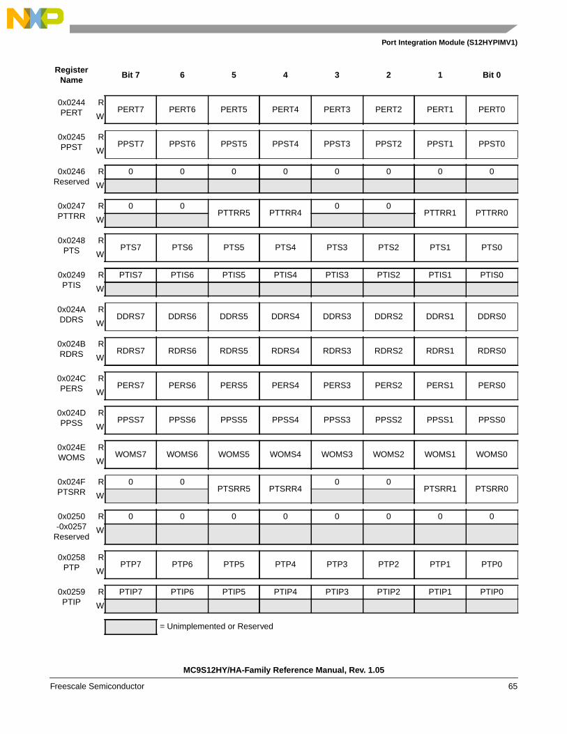
Port Integration Module (S12HYPIMV1)
0x0244PERT
RPERT7 PERT6 PERT5 PERT4 PERT3 PERT2 PERT1 PERT0
W
0x0245PPST
RPPST7 PPST6 PPST5 PPST4 PPST3 PPST2 PPST1 PPST0
W
0x0246Reserved
R 0 0 0 0 0 0 0 0
W
0x0247PTTRR
R 0 0PTTRR5 PTTRR4
0 0PTTRR1 PTTRR0
W
0x0248PTS
RPTS7 PTS6 PTS5 PTS4 PTS3 PTS2 PTS1 PTS0
W
0x0249PTIS
R PTIS7 PTIS6 PTIS5 PTIS4 PTIS3 PTIS2 PTIS1 PTIS0
W
0x024ADDRS
RDDRS7 DDRS6 DDRS5 DDRS4 DDRS3 DDRS2 DDRS1 DDRS0
W
0x024BRDRS
RRDRS7 RDRS6 RDRS5 RDRS4 RDRS3 RDRS2 RDRS1 RDRS0
W
0x024CPERS
RPERS7 PERS6 PERS5 PERS4 PERS3 PERS2 PERS1 PERS0
W
0x024DPPSS
RPPSS7 PPSS6 PPSS5 PPSS4 PPSS3 PPSS2 PPSS1 PPSS0
W
0x024EWOMS
RWOMS7 WOMS6 WOMS5 WOMS4 WOMS3 WOMS2 WOMS1 WOMS0
W
0x024FPTSRR
R 0 0PTSRR5 PTSRR4
0 0PTSRR1 PTSRR0
W
0x0250-0x0257
Reserved
R 0 0 0 0 0 0 0 0
W
0x0258PTP
RPTP7 PTP6 PTP5 PTP4 PTP3 PTP2 PTP1 PTP0
W
0x0259PTIP
R PTIP7 PTIP6 PTIP5 PTIP4 PTIP3 PTIP2 PTIP1 PTIP0
W
RegisterName
Bit 7 6 5 4 3 2 1 Bit 0
= Unimplemented or Reserved
MC9S12HY/HA-Family Reference Manual, Rev. 1.05
Freescale Semiconductor 65

Port Integration Module (S12HYPIMV1)
0x025ADDRP
RDDRP7 DDRP6 DDRP5 DDRP4 DDRP3 DDRP2 DDRP1 DDRP0
W
0x025BRDRP
RRDRP7 RDRP6 RDRP5 RDRP4 RDRP3 RDRP2 RDRP1 RDRP0
W
0x025CPERP
RPERP7 PERP6 PERP5 PERP4 PERP3 PERP2 PERP1 PERP0
W
0x025DPPSP
RPPSP7 PPSP6 PPSP5 PPSP4 PPSP3 PPSP2 PPSP1 PPSP0
W
0x025EPTPRRH
R 0 0 0 0 0 0PTPRRH1 PTPRRH0
W
0x025FPTPRRL
RPTPRRL7 PTPRRL6 PTPRRL5 PTPRRL4 PTPRRL3 PTPRRL2 PTPRRL1 PTPRRL0
W
0x0260PTH
RPTH7 PTH6 PTH5 PTH4 PTH3 PTH2 PTH1 PTH0
W
0x0261PTIH
R PTIH7 PTIH6 PTIH5 PTIH4 PTIH3 PTIH2 PTIH1 PTIH0
W
0x0262DDRH
RDDRH7 DDRH6 DDRH5 DDRH4 DDRH3 DDRH2 DDRH1 DDRH0
W
0x0263RDRH
RRDRH7 RDRH6 RDRH5 RDRH4 RDRH3 RDRH2 RDRH1 RDRH0
W
0x0264PERH
RPERH7 PERH6 PERH5 PERH4 PERH3 PERH2 PERH1 PERH0
W
0x0265PPSH
RPPSH7 PPSH6 PPSH5 PPSH4 PPSH3 PPSH2 PPSH1 PPSH0
0x0266WOMH
RWOMH7 WOMH6 WOMH5 WOMH4 WOMH3 WOMH2 WOMH1 WOMH0
W
0x0267-0x026F
Reserved
R 0 0 0 0 0 0 0 0
W
0x0270Reserved
R 0 0 0 0 0 0 0 0
W
RegisterName
Bit 7 6 5 4 3 2 1 Bit 0
= Unimplemented or Reserved
MC9S12HY/HA-Family Reference Manual, Rev. 1.05
66 Freescale Semiconductor

Port Integration Module (S12HYPIMV1)
0x0271PT1AD
RPT1AD7 PT1AD6 PT1AD5 PT1AD4 PT1AD3 PT1AD2 PT1AD1 PT1AD0
W
0x0272Reserved
R 0 0 0 0 0 0 0 0
W
0x0273DDR1AD
RDDR1AD7 DDR1AD6 DDR1AD5 DDR1AD4 DDR1AD3 DDR1AD2 DDR1AD1 DDR1AD0
W
0x0274Reserved
R 0 0 0 0 0 0 0 0
W
0x0275RDR1AD
RRDR1AD7 RDR1AD6 RDR1AD5 RDR1AD4 RDR1AD3 RDR1AD2 RDR1AD1 RDR1AD0
W
0x0276Reserved
R 0 0 0 0 0 0 0 0
W
0x0277PER1AD
RPER1AD7 PER1AD6 PER1AD5 PER1AD4 PER1AD3 PER1AD2 PER1AD1 PER1AD0
W
0x0278-0x027F
Reserved
R 0 0 0 0 0 0 0 0
W
0x0280PTR
RPTR7 PTR6 PTR5 PTR4 PTR3 PTR2 PTR1 PTR0
W
0x0281PTIR
R PTIR7 PTIR6 PTIR5 PTIR4 PTIR3 PTIR2 PTIR1 PTIR0
W
0x0282DDRR
RDDRR7 DDRR6 DDRR5 DDRR4 DDRR3 DDRR2 DDRR1 DDRR0
W
0x0283RDRR
RRDRR7 RDRR6 RDRR5 RDRR4 RDRR3 RDRR2 RDRR1 RDRR0
W
0x0284PERR
RPERR7 PERR6 PERR5 PERR4 PERR3 PERR2 PERR1 PERR0
W
0x0285PPSR
RPPSR7 PPSR6 PPSR5 PPSR4 PPSR3 PPSR2 PPSR1 PPSR0
W
0x0286WOMR
RWOMR7 WOMR6 WOMR5 WOMR4 WOMR3 WOMR2 WOMR1 WOMR0
W
RegisterName
Bit 7 6 5 4 3 2 1 Bit 0
= Unimplemented or Reserved
MC9S12HY/HA-Family Reference Manual, Rev. 1.05
Freescale Semiconductor 67

Port Integration Module (S12HYPIMV1)
0x0287Reserved
R 0 0 0 0 0 0 0 0
W
0x0288PIET
RPIET7 PIET6 PIET5 PIET4 PIET3 PIET2 PIET1 PIET0
W
0x0289PIFT
RPIFT7 PIFT6 PIFT5 PIFT4 PIFT3 PIFT2 PIFT1 PIFT0
W
0x028APIES
R 0PIES6 PIES5
0 0 0 0 0
W
0x028BPIFS
R 0PIFS6 PIFS5
0 0 0 0 0
W
0x028CPIE1AD
RPIE1AD7 PIE1AD6 PIE1AD5 PIE1AD4 PIE1AD3 PIE1AD2 PIE1AD1 PIE1AD0
W
0x028DPIF1AD
RPIF1AD7 PIF1AD6 PIF1AD5 PIF1AD4 PIF1AD3 PIF1AD2 PIF1AD1 PIF1AD0
W
0x028EPIER
R 0 0 0 0PIER3 PIER2 PIER1 PIER0
W
0x028FPIFR
R 0 0 0 0PIFR3 PIFR2 PIFR1 PIFR0
W
0x0290PTU
RPTU7 PTU6 PTU5 PTU4 PTU3 PTU2 PTU1 PTU0
W
0x0291PTIU
R PTIU7 PTIU6 PTIU5 PTIU4 PTIU3 PTIU2 PTIU1 PTIU0
W
0x0292DDRU
RDDRU7 DDRU6 DDRU5 DDRU4 DDRU3 DDRU2 DDRU1 DDRU0
W
0x0293Reserved
R 0 0 0 0 0 0 0 0
W
0x0294PERU
RPERU7 PERU6 PERU5 PERU4 PERU3 PERU2 PERU1 PERU0
W
0x0295PPSU
RPPSU7 PPSU6 PPSU5 PPSU4 PPSU3 PPSU2 PPSU1 PPSU0
0x0296SRRU
RSRRU7 SRRU6 SRRU5 SRRU4 SRRU3 SRRU2 SRRU1 SRRU0
W
RegisterName
Bit 7 6 5 4 3 2 1 Bit 0
= Unimplemented or Reserved
MC9S12HY/HA-Family Reference Manual, Rev. 1.05
68 Freescale Semiconductor
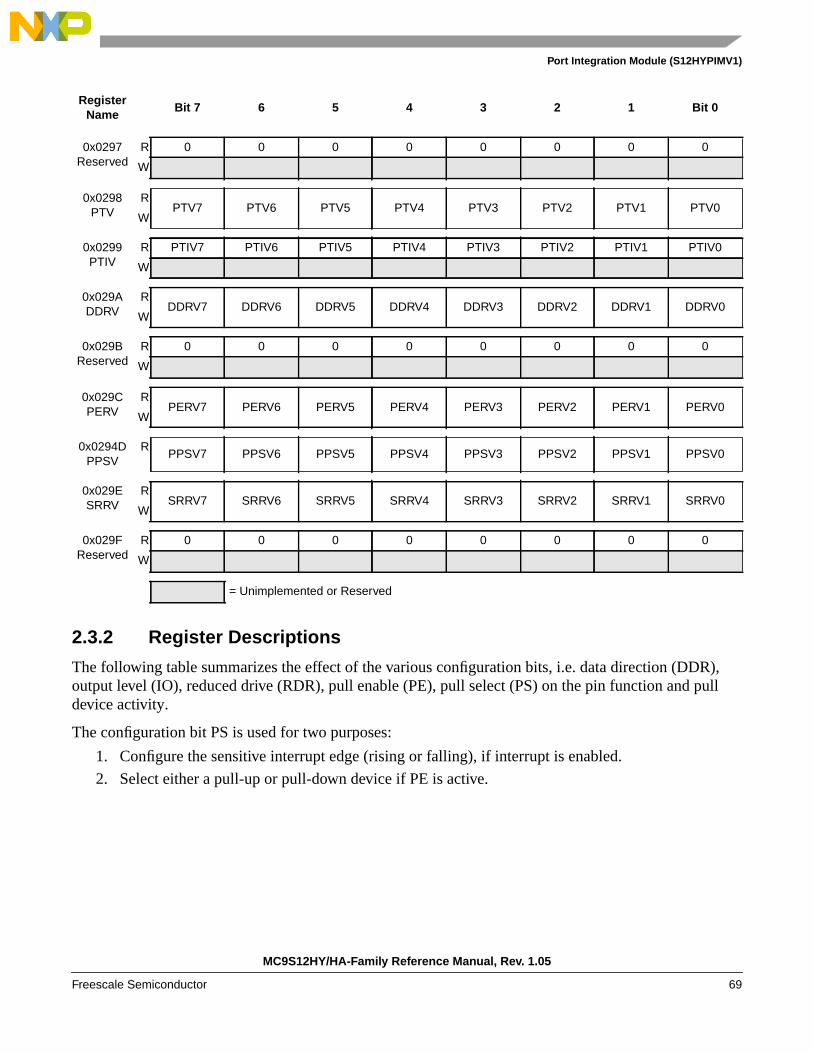
Port Integration Module (S12HYPIMV1)
2.3.2 Register Descriptions
The following table summarizes the effect of the various configuration bits, i.e. data direction (DDR),output level (IO), reduced drive (RDR), pull enable (PE), pull select (PS) on the pin function and pulldevice activity.
The configuration bit PS is used for two purposes:
1. Configure the sensitive interrupt edge (rising or falling), if interrupt is enabled.
2. Select either a pull-up or pull-down device if PE is active.
0x0297Reserved
R 0 0 0 0 0 0 0 0
W
0x0298PTV
RPTV7 PTV6 PTV5 PTV4 PTV3 PTV2 PTV1 PTV0
W
0x0299PTIV
R PTIV7 PTIV6 PTIV5 PTIV4 PTIV3 PTIV2 PTIV1 PTIV0
W
0x029ADDRV
RDDRV7 DDRV6 DDRV5 DDRV4 DDRV3 DDRV2 DDRV1 DDRV0
W
0x029BReserved
R 0 0 0 0 0 0 0 0
W
0x029CPERV
RPERV7 PERV6 PERV5 PERV4 PERV3 PERV2 PERV1 PERV0
W
0x0294DPPSV
RPPSV7 PPSV6 PPSV5 PPSV4 PPSV3 PPSV2 PPSV1 PPSV0
0x029ESRRV
RSRRV7 SRRV6 SRRV5 SRRV4 SRRV3 SRRV2 SRRV1 SRRV0
W
0x029FReserved
R 0 0 0 0 0 0 0 0
W
RegisterName
Bit 7 6 5 4 3 2 1 Bit 0
= Unimplemented or Reserved
MC9S12HY/HA-Family Reference Manual, Rev. 1.05
Freescale Semiconductor 69

Port Integration Module (S12HYPIMV1)
Table 2-3. Pin Configuration Summary
NOTEAll register bits in this module are completely synchronous to internalclocks during a register read.
NOTEFigure of port data registers also display the alternative functions ifapplicable on the related pin as defined in Table 2-1. Names in bracketsdenote the availability of the function when using a specific routing option.
NOTEFigures of module routing registers also display the module instance ormodule channel associated with the related routing bit.
DDR IO RDR PE PS1
1 Always “1” on Port A, B, and always “0” on AD.
IE2
2 Applicable only on Port T, S, R and AD.
Function Pull Device Interrupt
0 x x 0 x 0 Input Disabled Disabled
0 x x 1 0 0 Input Pull Up Disabled
0 x x 1 1 0 Input Pull Down Disabled
0 x x 0 0 1 Input Disabled Falling edge
0 x x 0 1 1 Input Disabled Rising edge
0 x x 1 0 1 Input Pull Up Falling edge
0 x x 1 1 1 Input Pull Down Rising edge
1 0 0 x x 0 Output, full drive to 0 Disabled Disabled
1 1 0 x x 0 Output, full drive to 1 Disabled Disabled
1 0 1 x x 0 Output, reduced drive to 0 Disabled Disabled
1 1 1 x x 0 Output, reduced drive to 1 Disabled Disabled
1 0 0 x 0 1 Output, full drive to 0 Disabled Falling edge
1 1 0 x 1 1 Output, full drive to 1 Disabled Rising edge
1 0 1 x 0 1 Output, reduced drive to 0 Disabled Falling edge
1 1 1 x 1 1 Output, reduced drive to 1 Disabled Rising edge
MC9S12HY/HA-Family Reference Manual, Rev. 1.05
70 Freescale Semiconductor

Port Integration Module (S12HYPIMV1)
2.3.3 Port A Data Register (PORTA)
Address 0x0000 (PRR) Access: User read/write1
1 Read: Anytime. The data source is depending on the data direction value.Write: Anytime
7 6 5 4 3 2 1 0
RPA7 PA6 PA5 PA4 PA3 PA2 PA1 PA7
W
— — — — API_EXTCLK — XIRQ IRQ
Altern.Function
FP36 FP35 FP34 FP33 FP32 FP31 FP30 FP29
Reset 0 0 0 0 0 0 0 0
Figure 2-1. Port A Data Register (PORTA)
Table 2-4. PORTA Register Field Descriptions
Field Description
7-4,2PA
Port A general purpose input/output data—Data Register, LCD segment driver outputThe associated pin can be used as general purpose I/O when not used as alternative function. In general purposeoutput mode the register bit value is driven to the pin. If the associated data direction bit is set to 1, a read returnsthe value of the port register bit, otherwise the buffered pin input state is read. • The LCD segment driver output takes precedence over the general purpose I/O function if the related LCD
segment is enabled.
3PA
Port A general purpose input/output data—Data Register, LCD segment driver output, API_EXTCLKThe associated pin can be used as general purpose I/O when not used as alternative function. In general purposeoutput mode the register bit value is driven to the pin. If the associated data direction bit is set to 1, a read returnsthe value of the port register bit, otherwise the buffered pin input state is read. • The LCD segment driver output takes precedence over the API_EXTCLK and general purpose I/O function if the
related LCD segment is enabled. • The API_EXTCLK takes precedence over the general purpose I/O function if the API_EXTCLK function is enabled
1PA
Port A general purpose input/output data—Data Register, LCD segment driver output, XIRQThe associated pin can be used as general purpose I/O when not used as alternative function. In general purposeoutput mode the register bit value is driven to the pin. If the associated data direction bit is set to 1, a read returnsthe value of the port register bit, otherwise the buffered pin input state is read. • The LCD segment driver output takes precedence over the XIRQ and general purpose I/O function if the related
LCD segment is enabled. • The XIRQ takes precedence over the general purpose I/O function if the XIRQ function is enabled
0PA
Port A general purpose input/output data—Data Register, LCD segment driver output, IRQThe associated pin can be used as general purpose I/O when not used as alternative function. In general purposeoutput mode the register bit value is driven to the pin. If the associated data direction bit is set to 1, a read returnsthe value of the port register bit, otherwise the buffered pin input state is read. • The LCD segment driver output takes precedence over the IRQ and general purpose I/O function if the related
LCD segment is enabled. • The IRQ takes precedence over the general purpose I/O function if the IRQ function is enabled
MC9S12HY/HA-Family Reference Manual, Rev. 1.05
Freescale Semiconductor 71

Port Integration Module (S12HYPIMV1)
2.3.4 Port B Data Register (PORTB)
2.3.5 Port A Data Direction Register (DDRA)
Address 0x0001 (PRR) Access: User read/write1
1 Read: Anytime. The data source is depending on the data direction value.Write: Anytime
7 6 5 4 3 2 1 0
RPB7 PB6 PB5 PB4 PB3 PB2 PB1 PB7
W
Altern.Function
BP3 BP2 BP1 BP0 FP39 FP38 FP37 FP28
Reset 0 0 0 0 0 0 0 0
Figure 2-2. Port B Data Register (PORTB)
Table 2-5. PORTB Register Field Descriptions
Field Description
7-0PB
Port B general purpose input/output data—Data Register, LCD segment driver outputThe associated pin can be used as general purpose I/O when not used as alternative function. In general purposeoutput mode the register bit value is driven to the pin. If the associated data direction bit is set to 1, a read returnsthe value of the port register bit, otherwise the buffered pin input state is read. • The LCD segment driver output takes precedence over the general purpose I/O function if the related LCD
segment is enabled.
Address 0x0002 (PRR) Access: User read/write1
1 Read: AnytimeWrite: Anytime
7 6 5 4 3 2 1 0
RDDRA7 DDRA6 DDRA5 DDRA4 DDRA3 DDRA2 DDRA1 DDRA0
W
Reset 0 0 0 0 0 0 0 0
Figure 2-3. Port A Data Direction Register (DDRA)
MC9S12HY/HA-Family Reference Manual, Rev. 1.05
72 Freescale Semiconductor

Port Integration Module (S12HYPIMV1)
2.3.6 Port B Data Direction Register (DDRB)
Table 2-6. DDRA Register Field Descriptions
Field Description
7-4,2DDRA
Port A Data Direction—This bit determines whether the associated pin is an input or output.If corresponding LCD segment is enabled, it will be forced as input/output disable
1 Associated pin is configured as output0 Associated pin is configured as input
3DDRA
Port A Data Direction—This bit determines whether the associated pin is an input or output.If corresponding LCD segment is enabled, it will be forced as input/output disabledElse if API_EXTCLK is enabled, it will be forced as output
1 Associated pin is configured as output0 Associated pin is configured as input
1DDRA
Port A Data Direction—This bit determines whether the associated pin is an input or output.If corresponding LCD segment is enabled, it will be forced as input/output disabledElse if XIRQ is enabled, it will be forced as input
1 Associated pin is configured as output0 Associated pin is configured as input
0DDRA
Port A Data Direction—This bit determines whether the associated pin is an input or output.If corresponding LCD segment is enabled, it will be forced as input/output disabledElse if /IRQ is enabled, it will be forced as input
1 Associated pin is configured as output0 Associated pin is configured as input
Address 0x0003 (PRR) Access: User read/write1
1 Read: AnytimeWrite: Anytime
7 6 5 4 3 2 1 0
RDDRB7 DDRB6 DDRB5 DDRB4 DDRB3 DDRB2 DDRB1 DDRB0
W
Reset 0 0 0 0 0 0 0 0
Figure 2-4. Port B Data Direction Register (DDRB)
MC9S12HY/HA-Family Reference Manual, Rev. 1.05
Freescale Semiconductor 73

Port Integration Module (S12HYPIMV1)
NOTEDue to internal synchronization circuits, it can take up to 2 bus clock cyclesuntil the correct value is read on PTA, PTB registers, when changing theDDRA,DDRB register.
2.3.7 PIM Reserved Register
2.3.8 Ports A, B, BKGD pin Pull Control Register (PUCR)
Table 2-7. DDRB Register Field Descriptions
Field Description
7-0DDRB
Port B Data Direction—This bit determines whether the associated pin is an input or output.If corresponding LCD segment is enabled, it will be forced as input/output disabled
1 Associated pin is configured as output0 Associated pin is configured as input
Address 0x0004 (PRR) to 0x0007 (PRR) Access: User read1
1 Read: Always reads 0x00Write: Unimplemented
7 6 5 4 3 2 1 0
R 0 0 0 0 0 0 0 0
W
Reset 0 0 0 0 0 0 0 0
= Unimplemented or Reserved
Figure 2-5. PIM Reserved Register
Address 0x000C (PRR) Access: User read/write1
1 Read:Anytime in single-chip modes.Write:Anytime, except BKPUE which is writable in Special Single-Chip Mode only.
7 6 5 4 3 2 1 0
R 0BKPUE
0 0 0 0PUPBE PUPAE
W
Reset 0 1 0 0 0 0 1 1
= Unimplemented or Reserved
Figure 2-6. Ports AB, BKGD pin Pull Control Register (PUCR)
MC9S12HY/HA-Family Reference Manual, Rev. 1.05
74 Freescale Semiconductor

Port Integration Module (S12HYPIMV1)
2.3.9 Ports A, B Reduced Drive Register (RDRIV)
Table 2-8. PUCR Register Field Descriptions
Field Description
6BKPUE
BKGD pin pull-up Enable—Enable pull-up device on pinThis bit configures whether a pull-up device is activated, if the pin is used as input. If a pin is used as output this bithas no effect.
1 Pull-up device enabled0 Pull-up device disabled
1PUPBE
Port B Pull-down Enable—Enable pull-down devices on all port input pinsThis bit configures whether a pull-down device is activated on all associated port input pins. If a pin is used as outputthis bit has no effect.
1 pull-down device enabled0 pull-down device disabled
0PUPAE
Port A Pull-down Enable—Enable pull-down devices on all port input pinsThis bit configures whether a pull-down device is activated on all associated port input pins. If a pin is used as outputthis bit has no effect.
1 pull-down device enabled0 pull-down device disabled
Address 0x000D (PRR) Access: User read/write1
1 Read: AnytimeWrite: Anytime
7 6 5 4 3 2 1 0
R 0 0 0 0 0 0RDPB RDPA
W
Reset 0 0 0 0 0 0 0 0
= Unimplemented or Reserved
Figure 2-7. Ports ABEK Reduced Drive Register (RDRIV)
MC9S12HY/HA-Family Reference Manual, Rev. 1.05
Freescale Semiconductor 75

Port Integration Module (S12HYPIMV1)
Table 2-9. RDRIV Register Field Descriptions
Field Description
1RDPB
Port B reduced drive—Select reduced drive for output portThis bit configures the drive strength of all associated port output pins as either full or reduced. If a pin is used asinput this bit has no effect. The reduced drive function is independent of which function is being used on a particularpin.
1 Reduced drive selected (1/6 of the full drive strength)0 Full drive strength enabled
0RDPA
Port A reduced drive—Select reduced drive for output portThis bit configures the drive strength of all associated port output pins as either full or reduced. If a pin is used asinput this bit has no effect. The reduced drive function is independent of which function is being used on a particularpin.
1 Reduced drive selected (1/6 of the full drive strength)0 Full drive strength enabled
MC9S12HY/HA-Family Reference Manual, Rev. 1.05
76 Freescale Semiconductor

Port Integration Module (S12HYPIMV1)
2.3.10 ECLK Control Register (ECLKCTL)
2.3.11 PIM Reserved Register
Address 0x001C (PRR) Access: User read/write1
1 Read: AnytimeWrite: Anytime
7 6 5 4 3 2 1 0
RNECLK
0DIV16 EDIV4 EDIV3 EDIV2 EDIV1 EDIV0
W
Reset: 1 0 0 0 0 0 0 0
= Unimplemented or Reserved
Figure 2-8. ECLK Control Register (ECLKCTL)
Table 2-10. ECLKCTL Register Field Descriptions
Field Description
7NECLK
No ECLK—Disable ECLK outputThis bit controls the availability of a free-running clock on the ECLK pin. This clock has a fixed rate of equivalent tothe internal bus clock.
1 ECLK disabled0 ECLK enabled
5DIV16
Free-running ECLK predivider—Divide by 16This bit enables a divide-by-16 stage on the selected EDIV rate.
1 Divider enabled: ECLK rate = EDIV rate divided by 160 Divider disabled: ECLK rate = EDIV rate
4-0EDIV
Free-running ECLK Divider—Configure ECLK rateThese bits determine the rate of the free-running clock on the ECLK pin.
00000 ECLK rate = bus clock rate00001 ECLK rate = bus clock rate divided by 200010 ECLK rate = bus clock rate divided by 3,...11111 ECLK rate = bus clock rate divided by 32
Address 0x001D (PRR) Access: User read1
7 6 5 4 3 2 1 0
R 0 0 0 0 0 0 0 0
W
Reset 0 0 0 0 0 0 0 0
= Unimplemented or Reserved
Figure 2-9. PIM Reserved Register
MC9S12HY/HA-Family Reference Manual, Rev. 1.05
Freescale Semiconductor 77

Port Integration Module (S12HYPIMV1)
2.3.12 IRQ Control Register (IRQCR)
2.3.13 PIM Reserved Register
This register is reserved for factory testing of the PIM module and is not available in normal operation.
1 Read: Always reads 0x00Write: Unimplemented
Address 0x001E Access: User read/write1
1 Read: See individual bit descriptions below.Write: See individual bit descriptions below.
7 6 5 4 3 2 1 0
RIRQE IRQEN XIRQEN
0 0 0 0 0
W
Reset 0 0 0 0 0 0 0 0
= Unimplemented or Reserved
Figure 2-10. IRQ Control Register (IRQCR)
Table 2-11. IRQCR Register Field Descriptions
Field Description
7IRQE
IRQ select edge sensitive only—Special mode: Read or write anytime.Normal mode: Read anytime, write once.
1 IRQ pin configured to respond only to falling edges. Falling edges on the IRQ pin will be detected anytime IRQE=1and will be cleared only upon a reset or the servicing of the IRQ interrupt.
0 IRQ pin configured for low level recognition
6IRQEN
IRQ enable—Read or write anytime.
1 IRQ pin is connected to interrupt logic0 IRQ pin is disconnected from interrupt logic
5XIRQEN
XIRQ enable—Special mode: Read or write anytime.Normal mode: Read anytime, write once.
1 XIRQ pin is connected to interrupt logic0 XIRQ pin is disconnected from interrupt logic
MC9S12HY/HA-Family Reference Manual, Rev. 1.05
78 Freescale Semiconductor

Port Integration Module (S12HYPIMV1)
2.3.14 Port T Data Register (PTT)
Address 0x001F Access: User read1
1 Read: Always reads 0x00Write: Unimplemented
Writing to this register when in special modes can alter the pin functionality.
7 6 5 4 3 2 1 0
R 0 0 0 0 0 0 0 0
W
Reset 0 0 0 0 0 0 0 0
= Unimplemented or Reserved
Figure 2-11. PIM Reserved Register
Address 0x0240 Access: User read/write1
1 Read: Anytime. The data source is depending on the data direction value.Write: Anytime
7 6 5 4 3 2 1 0
RPTT7 PTT6 PTT5 PTT4 PTT3 PTT2 PTT1 PTT0
W
IOC0_7 IOC0_6 IOC0_5 IOC0_4 IOC1_7 IOC1_6 IOC1_5 IOC1_4
Altern.Function
FP16 FP15 FP14 FP13 FP11 FP10 FP9 FP8
Reset 0 0 0 0 0 0 0 0
Figure 2-12. Port T Data Register (PTT)
MC9S12HY/HA-Family Reference Manual, Rev. 1.05
Freescale Semiconductor 79

Port Integration Module (S12HYPIMV1)
2.3.15 Port T Input Register (PTIT)
Table 2-12. PTT Register Field Descriptions
Field Description
7-4PTT
Port T general purpose input/output data—Data Register, LCD segment driver output, TIM0 outputWhen not used with the alternative function, the associated pin can be used as general purpose I/O. In generalpurpose output mode the register bit value is driven to the pin. If the associated data direction bit is set to 1, a readreturns the value of the port register bit, otherwise the buffered pin input state is read. • The LCD segment driver output takes precedence over the TIM0 and general purpose I/O function if related LCD
segment is enabled • The TIM0 output function takes precedence over the general purpose I/O function if the related channel is
enabled.1
1 For the TIM input capture to be function correctly, the corresponding DDRT bit should be set to 0
3-0PTT
Port T general purpose input/output data—Data Register, LCD segment driver output, TIM1 outputWhen not used with the alternative function, the associated pin can be used as general purpose I/O. In generalpurpose output mode the register bit value is driven to the pin. If the associated data direction bit is set to 1, a readreturns the value of the port register bit, otherwise the buffered pin input state is read. • The LCD segment driver output takes precedence over the TIM1 and general purpose I/O function if related LCD
segment is enabled • The TIM1 output function takes precedence over the general purpose I/O function if the related channel is
enabled.1
Address 0x0241 Access: User read1
1 Read: AnytimeWrite:Never, writes to this register have no effect.
7 6 5 4 3 2 1 0
R PTIT7 PTIT6 PTIT5 PTIT4 PTIT3 PTIT2 PTIT1 PTIT0
W
Reset u u u u u u u u
= Unimplemented or Reserved u = Unaffected by reset
Figure 2-13. Port T Input Register (PTIT)
Table 2-13. PTIT Register Field Descriptions
Field Description
7-0PTIT
Port T input data—A read always returns the buffered input state of the associated pin. It can be used to detect overload or short circuitconditions on output pins.
MC9S12HY/HA-Family Reference Manual, Rev. 1.05
80 Freescale Semiconductor

Port Integration Module (S12HYPIMV1)
2.3.16 Port T Data Direction Register (DDRT)
NOTEDue to internal synchronization circuits, it can take up to 2 bus clock cyclesuntil the correct value is read on PTT or PTIT registers, when changing theDDRT register.
2.3.17 Port T Reduced Drive Register (RDRT)
Address 0x0242 Access: User read/write1
1 Read: AnytimeWrite: Anytime
7 6 5 4 3 2 1 0
RDDRT7 DDRT6 DDRT5 DDRT4 DDRT3 DDRT2 DDRT1 DDRT0
W
Reset 0 0 0 0 0 0 0 0
Figure 2-14. Port T Data Direction Register (DDRT)
Table 2-14. DDRT Register Field Descriptions
Field Description
7-4DDRT
Port T data direction—This bit determines whether the pin is an input or output.If corresponding LCD segment is enabled, it will be forced as input/output disabledElse If corresponding TIM0 output compare channel is enabled, it will be forced as output.
1 Associated pin is configured as output0 Associated pin is configured as input
3-0DDRT
Port T data direction—This bit determines whether the pin is an input or output.If corresponding LCD segment is enabled, it will be forced as input/output disabledElse If corresponding TIM1 output compare channel is enabled, it will be forced as output.
1 Associated pin is configured as output0 Associated pin is configured as input
Address 0x0243 Access: User read/write1
7 6 5 4 3 2 1 0
RRDRT7 RDRT6 RDRT5 RDRT4 RDRT3 RDRT2 RDRT1 RDRT0
W
Reset 0 0 0 0 0 0 0 0
Figure 2-15. Port T Reduced Drive Register (RDRT)
MC9S12HY/HA-Family Reference Manual, Rev. 1.05
Freescale Semiconductor 81

Port Integration Module (S12HYPIMV1)
2.3.18 Port T Pull Device Enable Register (PERT)
2.3.19 Port T Polarity Select Register (PPST)
1 Read: AnytimeWrite: Anytime
Table 2-15. RDRT Register Field Descriptions
Field Description
7-0RDRT
Port T reduced drive—Select reduced drive for output pinThis bit configures the drive strength of the associated output pin as either full or reduced. If a pin is used as inputthis bit has no effect. The reduced drive function is independent of which function is being used on a particular pin.
1 Reduced drive selected (1/6 of the full drive strength)0 Full drive strength enabled
Address 0x0244 Access: User read/write1
1 Read: AnytimeWrite: Anytime
7 6 5 4 3 2 1 0
RPERT7 PERT6 PERT5 PERT4 PERT3 PERT2 PERT1 PERT0
W
Reset 1 1 1 1 1 1 1 1
Figure 2-16. Port T Pull Device Enable Register (PERT)
Table 2-16. PERT Register Field Descriptions
Field Description
7-0PERT
Port T pull device enable—Enable pull device on input pinThis bit controls whether a pull device on the associated port input pin is active. If a pin is used as output this bit hasno effect. The polarity is selected by the related polarity select register bit.
1 Pull device enabled0 Pull device disabled
Address 0x0245 Access: User read/write1
1 Read: AnytimeWrite: Anytime
7 6 5 4 3 2 1 0
RPPST7 PPST6 PPST5 PPST4 PPST3 PPST2 PPST1 PPST0
W
Reset 1 1 1 1 1 1 1 1
Figure 2-17. Port T Polarity Select Register (PPST)
MC9S12HY/HA-Family Reference Manual, Rev. 1.05
82 Freescale Semiconductor

Port Integration Module (S12HYPIMV1)
2.3.20 PIM Reserved Register
2.3.21 Port T Routing Register (PTTRR)
This register configures the re-routing of TIM0/1 channels on alternative pins on Port R/T.
Table 2-17. PPST Register Field Descriptions
Field Description
7-0PPST
Port T pull device select—Configure pull device polarity on input pinThis bit selects a pull-up or a pull-down device if enabled on the associated port input pin.
1 A pull-down device is selected0 A pull-up device is selected
Address 0x0246 Access: User read1
1 Read: Always reads 0x00Write: Unimplemented
7 6 5 4 3 2 1 0
R 0 0 0 0 0 0 0 0
W
Reset 0 0 0 0 0 0 0 0
= Unimplemented or Reserved
Figure 2-18. PIM Reserved Register
Address 0x0247 Access: User read1
1 Read: AnytimeWrite: Anytime
7 6 5 4 3 2 1 0
R 0 0PTTRR5 PTTRR4
0 0PTTRR1 PTTRR0
W
RoutingOption
— — IOC0_7 IOC0_6 — — IOC1_7 IOC1_6
Reset 0 0 0 0 0 0 0 0
= Unimplemented or Reserved
Figure 2-19. Port T Routing Register (PTTRR)
MC9S12HY/HA-Family Reference Manual, Rev. 1.05
Freescale Semiconductor 83

Port Integration Module (S12HYPIMV1)
2.3.22 Port S Data Register (PTS)
Table 2-18. Port T Routing Register Field Descriptions
Field Description
5PTTRR
Port T data direction—This register controls the routing of IOC0_7.
0 IOC0_7 routed to PT71 IOC0_7 routed to PR1
4PTTRR
Port T data direction—This register controls the routing of IOC0_6.
0 IOC0_6 routed to PT61 IOC0_6 routed to PR0
1PTTRR
Port T data direction—This register controls the routing of IOC1_7.
0 IOC1_7routed to PT31 IOC1_7 routed to PR3
0PTTRR
Port T data direction—This register controls the routing of IOC1_6.
0 IOC1_6 routed to PT21 IOC1_6 routed to PR2
Address 0x0248 Access: User read/write1
1 Read: Anytime The data source is depending on the data direction value.Write: Anytime
7 6 5 4 3 2 1 0
RPTS7 PTS6 PTS5 PTS4 PTS3 PTS2 PTS1 PTS0
W
PWM3 PWM2 PWM1 PWM0 — — PWM7 PWM6
SDA — — SCL — — — —
Altern.Function
SS SCK MOSI MISO TXCAN RXCAN TXD RXD
Reset 0 0 0 0 0 0 0 0
Figure 2-20. Port S Data Register (PTS)
MC9S12HY/HA-Family Reference Manual, Rev. 1.05
84 Freescale Semiconductor

Port Integration Module (S12HYPIMV1)
Table 2-19. PTS Register Field Descriptions
Field Description
7PTS
Port S general purpose input/output data—Data Register, SPI SS inout, IIC SDA inout, PWM channel3When not used with the alternative function, the associated pin can be used as general purpose I/O. In generalpurpose output mode the register bit value is driven to the pin.If the associated data direction bit is set to 1, a read returns the value of the port register bit, otherwise the bufferedpin input state is read.
• The SPI takes precedence over the IIC, PWM3 and the general purpose I/O function if enabled • The IIC takes precedence over the PWM3 and the general purpose I/O function if enabled • The PWM3 takes precedence over the general purpose I/O function if enabled
6PTS
Port S general purpose input/output data—Data Register, SPI SCK inout, PWM channel2When not used with the alternative function, the associated pin can be used as general purpose I/O. In generalpurpose output mode the register bit value is driven to the pin.If the associated data direction bit is set to 1, a read returns the value of the port register bit, otherwise the bufferedpin input state is read.
• The SPI takes precedence over the PWM2 and the general purpose I/O function if enabled • The PWM2 takes precedence over the general purpose I/O function if enabled
5PTS
Port S general purpose input/output data—Data Register, SPI MOSI inout, PWM channel1When not used with the alternative function, the associated pin can be used as general purpose I/O. In generalpurpose output mode the register bit value is driven to the pin.If the associated data direction bit is set to 1, a read returns the value of the port register bit, otherwise the bufferedpin input state is read.
• The SPI takes precedence over the PWM1 and the general purpose I/O function if enabled • The PWM1 takes precedence over the general purpose I/O function if enabled
4PTS
Port S general purpose input/output data—Data Register, SPI MISO inout, IIC SCL inout, PWM channel0When not used with the alternative function, the associated pin can be used as general purpose I/O. In generalpurpose output mode the register bit value is driven to the pin.If the associated data direction bit is set to 1, a read returns the value of the port register bit, otherwise the bufferedpin input state is read.
• The SPI takes precedence over the IIC, PWM0 and the general purpose I/O function if enabled • The IIC takes precedence over the PWM0 and the general purpose I/O function if enabled • The PWM0 takes precedence over the general purpose I/O function if enabled
3PTS
Port S general purpose input/output data—Data Register, CAN TXWhen not used with the alternative function, the associated pin can be used as general purpose I/O. In generalpurpose output mode the register bit value is driven to the pin.If the associated data direction bit is set to 1, a read returns the value of the port register bit, otherwise the bufferedpin input state is read.
• The CAN takes precedence over the general purpose I/O function if enabled
2PTS
Port S general purpose input/output data—Data Register, CAN RXWhen not used with the alternative function, the associated pin can be used as general purpose I/O. In generalpurpose output mode the register bit value is driven to the pin.If the associated data direction bit is set to 1, a read returns the value of the port register bit, otherwise the bufferedpin input state is read.
• The CAN takes precedence over the general purpose I/O function if enabled
MC9S12HY/HA-Family Reference Manual, Rev. 1.05
Freescale Semiconductor 85
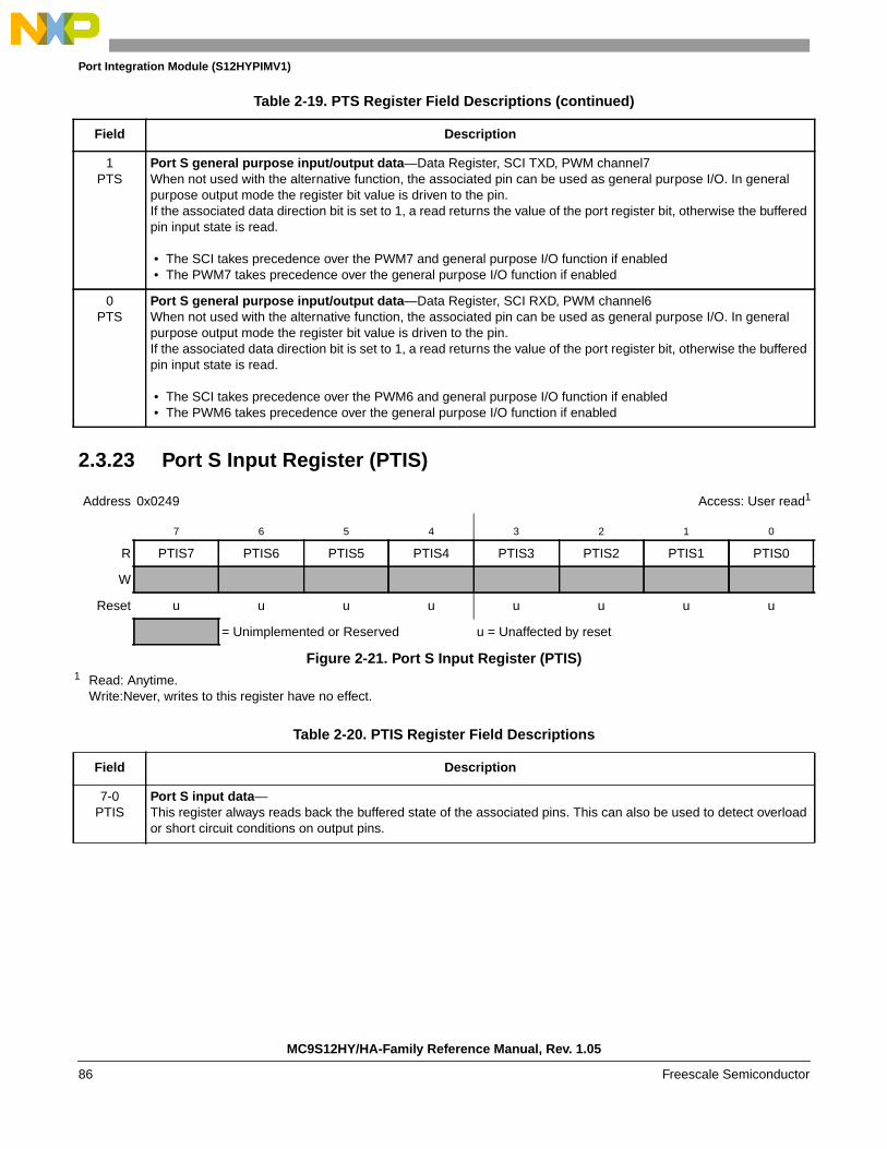
Port Integration Module (S12HYPIMV1)
2.3.23 Port S Input Register (PTIS)
1PTS
Port S general purpose input/output data—Data Register, SCI TXD, PWM channel7When not used with the alternative function, the associated pin can be used as general purpose I/O. In generalpurpose output mode the register bit value is driven to the pin.If the associated data direction bit is set to 1, a read returns the value of the port register bit, otherwise the bufferedpin input state is read.
• The SCI takes precedence over the PWM7 and general purpose I/O function if enabled • The PWM7 takes precedence over the general purpose I/O function if enabled
0PTS
Port S general purpose input/output data—Data Register, SCI RXD, PWM channel6When not used with the alternative function, the associated pin can be used as general purpose I/O. In generalpurpose output mode the register bit value is driven to the pin.If the associated data direction bit is set to 1, a read returns the value of the port register bit, otherwise the bufferedpin input state is read.
• The SCI takes precedence over the PWM6 and general purpose I/O function if enabled • The PWM6 takes precedence over the general purpose I/O function if enabled
Address 0x0249 Access: User read1
1 Read: Anytime.Write:Never, writes to this register have no effect.
7 6 5 4 3 2 1 0
R PTIS7 PTIS6 PTIS5 PTIS4 PTIS3 PTIS2 PTIS1 PTIS0
W
Reset u u u u u u u u
= Unimplemented or Reserved u = Unaffected by reset
Figure 2-21. Port S Input Register (PTIS)
Table 2-20. PTIS Register Field Descriptions
Field Description
7-0PTIS
Port S input data—This register always reads back the buffered state of the associated pins. This can also be used to detect overloador short circuit conditions on output pins.
Table 2-19. PTS Register Field Descriptions (continued)
Field Description
MC9S12HY/HA-Family Reference Manual, Rev. 1.05
86 Freescale Semiconductor

Port Integration Module (S12HYPIMV1)
2.3.24 Port S Data Direction Register (DDRS)
Address 0x024A Access: User read/write1
1 Read: Anytime.Write: Anytime.
7 6 5 4 3 2 1 0
RDDRS7 DDRS6 DDRS5 DDRS4 DDRS3 DDRS2 DDRS1 DDRS0
W
Reset 0 0 0 0 0 0 0 0
Figure 2-22. Port S Data Direction Register (DDRS)
Table 2-21. DDRS Register Field Descriptions
Field Description
7DDRS
Port S data direction—This register controls the data direction of pin 7.This register configures pin as either input or output.If SPI is routing to PS and SPI is enabled, the SPI determines the pin directionElse If IIC is routing to PS and IIC is enabled, the IIC determines the pin direction, it will force as open-drain outputElse if PWM3 is routing to PS and PWM3 is enabled it will force as output.
1 Associated pin is configured as output.0 Associated pin is configured as input.
6DDRS
Port S data direction—This register controls the data direction of pin 6.This register configures pin as either input or output.If SPI is routing to PS and SPI is enabled, the SPI determines the pin directionElse if PWM2 is routing to PS and PWM2 is enabled it will force as output.
1 Associated pin is configured as output.0 Associated pin is configured as input.
5DDRS
Port S data direction—This register controls the data direction of pin 5.This register configures pin as either input or output.If SPI is routing to PS and SPI is enabled, the SPI determines the pin directionElse if PWM1 is routing to PS and PWM1 is enabled it will force as output.
1 Associated pin is configured as output.0 Associated pin is configured as input.
4DDRS
Port S data direction—This register controls the data direction of pin 4.This register configures pin as either input or output.If SPI is routing to PS and SPI is enabled, the SPI determines the pin directionElse If IIC is routing to PS and IIC is enabled, it will force as open-drain outputElse if PWM0 is routing to PS and PWM0 is enabled it will force as output.
1 Associated pin is configured as output.0 Associated pin is configured as input.
MC9S12HY/HA-Family Reference Manual, Rev. 1.05
Freescale Semiconductor 87

Port Integration Module (S12HYPIMV1)
NOTEDue to internal synchronization circuits, it can take up to 2 bus clock cyclesuntil the correct value is read on PTS or PTIS registers, when changing theDDRS register.
2.3.25 Port S Reduced Drive Register (RDRS)
3DDRS
Port S data direction—This register controls the data direction of pin 3.This register configures pin as either input or output.If CAN is enabled, it will force the pin as output.
1 Associated pin is configured as output.0 Associated pin is configured as input.
2DDRS
Port S data direction—This register controls the data direction of pin 2.This register configures pin as either input or output.If CAN is enabled, it will force the pin as input.
1 Associated pin is configured as output.0 Associated pin is configured as input.
1DDRS
Port S data direction—This register controls the data direction of pin 1.This register configures pin as either input or output.If SCI is enabled, it will force the pin as outputElse if PWM7 is routing to PS1 and use as PWM channel output, it will force pin as output. If use as PWM emergencyshut down, it will force pin as input.
1 Associated pin is configured as output.0 Associated pin is configured as input.
0DDRS
Port S data direction—This register controls the data direction of pin 0.This register configures pin as either input or output.If SCI is enabled, it will force the pin as inputElse if PWM6 is routing to PS0 and PWM6 is enabled, it will force pin as output.
1 Associated pin is configured as output.0 Associated pin is configured as input.
Address 0x024B Access: User read/write1
1 Read: Anytime.Write: Anytime.
7 6 5 4 3 2 1 0
RRDRS7 RDRS6 RDRS5 RDRS4 RDRS3 RDRS2 RDRS1 RDRS0
W
Reset 0 0 0 0 0 0 0 0
Figure 2-23. Port S Reduced Drive Register (RDRS)
Table 2-21. DDRS Register Field Descriptions (continued)
Field Description
MC9S12HY/HA-Family Reference Manual, Rev. 1.05
88 Freescale Semiconductor
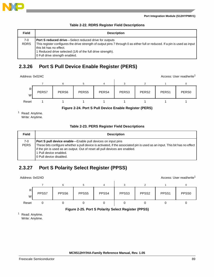
Port Integration Module (S12HYPIMV1)
2.3.26 Port S Pull Device Enable Register (PERS)
2.3.27 Port S Polarity Select Register (PPSS)
Table 2-22. RDRS Register Field Descriptions
Field Description
7-0RDRS
Port S reduced drive—Select reduced drive for outputsThis register configures the drive strength of output pins 7 through 0 as either full or reduced. If a pin is used as inputthis bit has no effect.1 Reduced drive selected (1/6 of the full drive strength).0 Full drive strength enabled.
Address 0x024C Access: User read/write1
1 Read: Anytime.Write: Anytime.
7 6 5 4 3 2 1 0
RPERS7 PERS6 PERS5 PERS4 PERS3 PERS2 PERS1 PERS0
W
Reset 1 1 1 1 1 1 1 1
Figure 2-24. Port S Pull Device Enable Register (PERS)
Table 2-23. PERS Register Field Descriptions
Field Description
7-0PERS
Port S pull device enable—Enable pull devices on input pinsThese bits configure whether a pull device is activated, if the associated pin is used as an input. This bit has no effectif the pin is used as an output. Out of reset all pull devices are enabled.1 Pull device enabled.0 Pull device disabled.
Address 0x024D Access: User read/write1
1 Read: Anytime.Write: Anytime.
7 6 5 4 3 2 1 0
RPPSS7 PPSS6 PPSS5 PPSS4 PPSS3 PPSS2 PPSS1 PPSS0
W
Reset 0 0 0 0 0 0 0 0
Figure 2-25. Port S Polarity Select Register (PPSS)
MC9S12HY/HA-Family Reference Manual, Rev. 1.05
Freescale Semiconductor 89
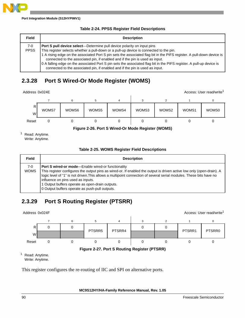
Port Integration Module (S12HYPIMV1)
2.3.28 Port S Wired-Or Mode Register (WOMS)
2.3.29 Port S Routing Register (PTSRR)
This register configures the re-routing of IIC and SPI on alternative ports.
Table 2-24. PPSS Register Field Descriptions
Field Description
7-0PPSS
Port S pull device select—Determine pull device polarity on input pinsThis register selects whether a pull-down or a pull-up device is connected to the pin.1 A rising edge on the associated Port S pin sets the associated flag bit in the PIFS register. A pull-down device is
connected to the associated pin, if enabled and if the pin is used as input.0 A falling edge on the associated Port S pin sets the associated flag bit in the PIFS register. A pull-up device is
connected to the associated pin, if enabled and if the pin is used as input.
Address 0x024E Access: User read/write1
1 Read: Anytime.Write: Anytime.
7 6 5 4 3 2 1 0
RWOMS7 WOMS6 WOMS5 WOMS4 WOMS3 WOMS2 WOMS1 WOMS0
W
Reset 0 0 0 0 0 0 0 0
Figure 2-26. Port S Wired-Or Mode Register (WOMS)
Table 2-25. WOMS Register Field Descriptions
Field Description
7-0WOMS
Port S wired-or mode—Enable wired-or functionalityThis register configures the output pins as wired-or. If enabled the output is driven active low only (open-drain). Alogic level of “1” is not driven.This allows a multipoint connection of several serial modules. These bits have noinfluence on pins used as inputs.1 Output buffers operate as open-drain outputs.0 Output buffers operate as push-pull outputs.
Address 0x024F Access: User read/write1
1 Read: Anytime.Write: Anytime.
7 6 5 4 3 2 1 0
R 0 0PTSRR5 PTSRR4
0 0PTSRR1 PTSRR0
W
Reset 0 0 0 0 0 0 0 0
Figure 2-27. Port S Routing Register (PTSRR)
MC9S12HY/HA-Family Reference Manual, Rev. 1.05
90 Freescale Semiconductor

Port Integration Module (S12HYPIMV1)
2.3.30 PIM Reserved Register
2.3.31 Port P Data Register (PTP)
Table 2-26. Module Routing Summary
ModulePTSRR
Related Pins
5 4 1 0
SCL SDA
IIC x x 0 0 PS4 PS7
x x 0 1 PH0 PH3
x x 1 0 PR6 PR5
x x 1 1 PV0 PV3
MISO MOSI SCK SS
SPI 0 0 x x PS4 PS5 PS6 PS7
0 1 x x PH0 PH1 PH2 PH3
1 0 x x PV0 PV1 PV2 PV3
1 1 x x Reserved
Address 0x0250-0x257 Access: User read1
1 Read: Always reads 0x00Write: Unimplemented
7 6 5 4 3 2 1 0
R 0 0 0 0 0 0 0 0
W
Reset 0 0 0 0 0 0 0 0
= Unimplemented or Reserved
Figure 2-28. PIM Reserved Register
Address 0x0258 Access: User read/write1
7 6 5 4 3 2 1 0
RPTP7 PTP6 PTP5 PTP4 PTP3 PTP2 PTP1 PTP0
W
PWM7 PWM6 PWM5 PWM4 PWM3 PWM2 PWM1 PWM0
Altern.Function
FP7 FP6 FP5 FP4 FP3 FP2 FP1 FP0
Reset 0 0 0 0 0 0 0 0
Figure 2-29. Port P Data Register (PTP)
MC9S12HY/HA-Family Reference Manual, Rev. 1.05
Freescale Semiconductor 91
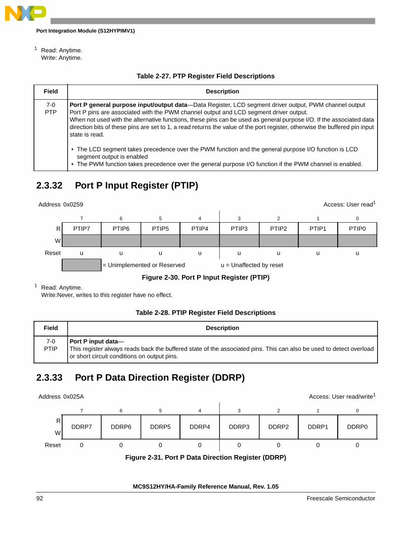
Port Integration Module (S12HYPIMV1)
2.3.32 Port P Input Register (PTIP)
2.3.33 Port P Data Direction Register (DDRP)
1 Read: Anytime.Write: Anytime.
Table 2-27. PTP Register Field Descriptions
Field Description
7-0PTP
Port P general purpose input/output data—Data Register, LCD segment driver output, PWM channel outputPort P pins are associated with the PWM channel output and LCD segment driver output.When not used with the alternative functions, these pins can be used as general purpose I/O. If the associated datadirection bits of these pins are set to 1, a read returns the value of the port register, otherwise the buffered pin inputstate is read.
• The LCD segment takes precedence over the PWM function and the general purpose I/O function is LCDsegment output is enabled
• The PWM function takes precedence over the general purpose I/O function if the PWM channel is enabled.
Address 0x0259 Access: User read1
1 Read: Anytime.Write:Never, writes to this register have no effect.
7 6 5 4 3 2 1 0
R PTIP7 PTIP6 PTIP5 PTIP4 PTIP3 PTIP2 PTIP1 PTIP0
W
Reset u u u u u u u u
= Unimplemented or Reserved u = Unaffected by reset
Figure 2-30. Port P Input Register (PTIP)
Table 2-28. PTIP Register Field Descriptions
Field Description
7-0PTIP
Port P input data—This register always reads back the buffered state of the associated pins. This can also be used to detect overloador short circuit conditions on output pins.
Address 0x025A Access: User read/write1
7 6 5 4 3 2 1 0
RDDRP7 DDRP6 DDRP5 DDRP4 DDRP3 DDRP2 DDRP1 DDRP0
W
Reset 0 0 0 0 0 0 0 0
Figure 2-31. Port P Data Direction Register (DDRP)
MC9S12HY/HA-Family Reference Manual, Rev. 1.05
92 Freescale Semiconductor

Port Integration Module (S12HYPIMV1)
NOTEDue to internal synchronization circuits, it can take up to 2 bus clock cyclesuntil the correct value is read on PTP or PTIP registers, when changing theDDRP register.
2.3.34 Port P Reduced Drive Register (RDRP)
1 Read: Anytime.Write: Anytime.
Table 2-29. DDRP Register Field Descriptions
Field Description
7DDRP
Port P data direction—This register controls the data direction of pin 7.If the LCD segment output is enabled, it will force the I/O state to be a input/output disabledElse if the enabled PWM channel 7 forces the I/O state to be an output. If the PWM shutdown feature is enabled thispin is forced to be an input. In these cases the data direction bit will not change.
1 Associated pin is configured as output.0 Associated pin is configured as input.
6-0DDRP
Port P data direction—If the LCD segment output is enabled, it will force the I/O state to be a input/output disabledElse if the PWM forces the I/O state to be an output for each port line associated with an enabled PWM6-0 channel.In this case the data direction bit will not change.
1 Associated pin is configured as output.0 Associated pin is configured as input.
Address 0x025B Access: User read/write1
1 Read: Anytime.Write: Anytime.
7 6 5 4 3 2 1 0
RRDRP7 RDRP6 RDRP5 RDRP4 RDRP3 RDRP2 RDRP1 RDRP0
W
Reset 0 0 0 0 0 0 0 0
Figure 2-32. Port P Reduced Drive Register (RDRP)
Table 2-30. RDRP Register Field Descriptions
Field Description
7-0RDRP
Port P reduced drive—Select reduced drive for outputsThis register configures the drive strength of output pins 7 through 0 as either full or reduced. If a pin is used as inputthis bit has no effect.1 Reduced drive selected (1/6 of the full drive strength).0 Full drive strength enabled.
MC9S12HY/HA-Family Reference Manual, Rev. 1.05
Freescale Semiconductor 93

Port Integration Module (S12HYPIMV1)
2.3.35 Port P Pull Device Enable Register (PERP)
2.3.36 Port P Polarity Select Register (PPSP)
Address 0x025C Access: User read/write1
1 Read: Anytime.Write: Anytime.
7 6 5 4 3 2 1 0
RPERP7 PERP6 PERP5 PERP4 PERP3 PERP2 PERP1 PERP0
W
Reset 1 1 1 1 1 1 1 1
Figure 2-33. Port P Pull Device Enable Register (PERP)
Table 2-31. PERP Register Field Descriptions
Field Description
7-0PERP
Port P pull device enable—Enable pull devices on input pinsThese bits configure whether a pull device is activated, if the associated pin is used as an input. This bit has no effectif the pin is used as an output. Out of reset all pull device is enabled.1 Pull device enabled.0 Pull device disabled.
Address 0x025D Access: User read/write1
1 Read: Anytime.Write: Anytime.
7 6 5 4 3 2 1 0
RPPSP7 PPSP6 PPSP5 PPSP4 PPSP3 PPSP2 PPSP1 PPSP0
W
Reset 1 1 1 1 1 1 1 1
Figure 2-34. Port P Polarity Select Register (PPSP)
Table 2-32. PPSP Register Field Descriptions
Field Description
7-0PPSP
Port P pull device select—Determine pull device polarity on input pinsThis register serves a dual purpose by selecting the polarity of the active interrupt edge as well as selecting a pull-upor pull-down device if enabled.1 A pull-down device is connected to the associated Port P pin, if enabled by the associated bit in register PERP and
if the port is used as input.0 A pull-up device is connected to the associated Port P pin, if enabled by the associated bit in register PERP and
if the port is used as input.
MC9S12HY/HA-Family Reference Manual, Rev. 1.05
94 Freescale Semiconductor

Port Integration Module (S12HYPIMV1)
2.3.37 Port P Routing Register High (PTPRRH)Read: Anytime.
2.3.38 Port P Routing Register Low(PTPRRL)
The PTPRRH/PTPRRL register configures the re-routing of PWM on alternative ports.
Address 0x025E Access: User read/write1
1 Read: Anytime.Write: Anytime.
7 6 5 4 3 2 1 0
RPTPRRH1 PTPRRH0
W
Reset 0 0 0 0 0 0 0 0
Figure 2-35. Port P Routing Register High (PTPRRH)
Table 2-33. Port Routing Register High Field Descriptions
Field Description
1-0PTPRRH
Port P Routing Register High—The registers enable the PWM7 routing the Port S/V/P
Address 0x025F Access: User read/write1
1 Read: Anytime.Write: Anytime.
7 6 5 4 3 2 1 0
RPTPRRL7 PTPRRL6 PTPRRL5 PTPRRL4 PTPRRL3 PTPRRL2 PTPRRL1 PTPRRL0
W
Reset 0 0 0 0 0 0 0 0
Figure 2-36. Port P Routing Register Low(PTPRRL)
Table 2-34. PTPRRL Register Field Descriptions
Field Description
7-0PTPRRL
Port P Routing Register Low—The register decide the PWM channel routing on the Port S/P/V
MC9S12HY/HA-Family Reference Manual, Rev. 1.05
Freescale Semiconductor 95

Port Integration Module (S12HYPIMV1)
2.3.39 Port H Data Register (PTH)
Table 2-35. Module Routing Summary
Module
PTPRRH PTPRRL Related Pins
1 0 7 6 5 4 3 2 1 0 PWM7 PWM6 PWM5 PWM4 PWM3 PWM2 PWM1 PWM0
PWM7
0 0 x x x x x x x x PP7
0 1 x x x x x x x x PS1
1 0 x x x x x x x x PV3
1 1 x x x x x x x x PP7
PWM6
x x 0 0 x x x x x x PP6
x x 0 1 x x x x x x PS0
x x 1 0 x x x x x x PV2
x x 1 1 x x x x x x PP6
PWM5
x x x x 0 x x x x x PP5
x x x x 1 x x x x x PV1
PWM4
x x x x x 0 x x x x PP4
x x x x x 1 x x x x PV0
PWM3
x x x x x x 0 x x x PP3
x x x x x x 1 x x x PS7
PWM2
x x x x x x x 0 x x PP2
x x x x x x x 1 x x PS6
PWM1
x x x x x x x x 0 x PP1
x x x x x x x x 1 x PS5
PWM0
x x x x x x x x x 0 PP0
x x x x x x x x x 1 PS4
Address 0x0260 Access: User read/write1
1 Read: Anytime.Write: Anytime.
7 6 5 4 3 2 1 0
RPTH7 PTH6 PTH5 PTH4 PTH3 PTH2 PTH1 PTH0
W
— — — — SS ECLK — MISO2
— — — SDA SCK MOSI SCL
Altern.Function
FP26 FP25 FP24 FP23 FP22 FP21 FP20 FP19
Reset 0 0 0 0 0 0 0 0
Figure 2-37. Port H Data Register (PTH)
MC9S12HY/HA-Family Reference Manual, Rev. 1.05
96 Freescale Semiconductor
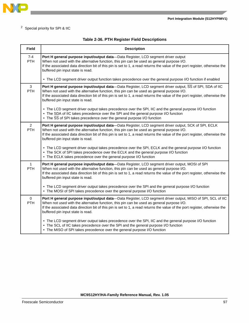
Port Integration Module (S12HYPIMV1)
2 Special priority for SPI & IIC
Table 2-36. PTH Register Field Descriptions
Field Description
7-4PTH
Port H general purpose input/output data—Data Register, LCD segment driver outputWhen not used with the alternative function, this pin can be used as general purpose I/O.If the associated data direction bit of this pin is set to 1, a read returns the value of the port register, otherwise thebuffered pin input state is read.
• The LCD segment driver output function takes precedence over the general purpose I/O function if enabled
3PTH
Port H general purpose input/output data—Data Register, LCD segment driver output, SS of SPI, SDA of IICWhen not used with the alternative function, this pin can be used as general purpose I/O.If the associated data direction bit of this pin is set to 1, a read returns the value of the port register, otherwise thebuffered pin input state is read.
• The LCD segment driver output takes precedence over the SPI, IIC and the general purpose I/O function • The SDA of IIC takes precedence over the SPI and the general purpose I/O function • The SS of SPI takes precedence over the general purpose I/O function
2PTH
Port H general purpose input/output data—Data Register, LCD segment driver output, SCK of SPI, ECLKWhen not used with the alternative function, this pin can be used as general purpose I/O.If the associated data direction bit of this pin is set to 1, a read returns the value of the port register, otherwise thebuffered pin input state is read.
• The LCD segment driver output takes precedence over the SPI, ECLK and the general purpose I/O function • The SCK of SPI takes precedence over the ECLK and the general purpose I/O function • The ECLK takes precedence over the general purpose I/O function
1PTH
Port H general purpose input/output data—Data Register, LCD segment driver output, MOSI of SPIWhen not used with the alternative function, this pin can be used as general purpose I/O.If the associated data direction bit of this pin is set to 1, a read returns the value of the port register, otherwise thebuffered pin input state is read.
• The LCD segment driver output takes precedence over the SPI and the general purpose I/O function • The MOSI of SPI takes precedence over the general purpose I/O function
0PTH
Port H general purpose input/output data—Data Register, LCD segment driver output, MISO of SPI, SCL of IICWhen not used with the alternative function, this pin can be used as general purpose I/O.If the associated data direction bit of this pin is set to 1, a read returns the value of the port register, otherwise thebuffered pin input state is read.
• The LCD segment driver output takes precedence over the SPI, IIC and the general purpose I/O function • The SCL of IIC takes precedence over the SPI and the general purpose I/O function • The MISO of SPI takes precedence over the general purpose I/O function
MC9S12HY/HA-Family Reference Manual, Rev. 1.05
Freescale Semiconductor 97

Port Integration Module (S12HYPIMV1)
2.3.40 Port H Input Register (PTIH)
2.3.41 Port H Data Direction Register (DDRH)
Address 0x0261 Access: User read1
1 Read: Anytime.Write:Never, writes to this register have no effect.
7 6 5 4 3 2 1 0
R PTIH7 PTIH6 PTIH5 PTIH4 PTIH3 PTIH2 PTIH1 PTIH0
W
Reset u u u u u u u u
= Unimplemented or Reserved u = Unaffected by reset
Figure 2-38. Port H Input Register (PTIH)
Table 2-37. PTIH Register Field Descriptions
Field Description
7-0PTIH
Port H input data—This register always reads back the buffered state of the associated pins. This can also be used to detect overloador short circuit conditions on output pins.
Address 0x0262 Access: User read/write1
1 Read: Anytime.Write: Anytime.
7 6 5 4 3 2 1 0
RDDRH7 DDRH6 DDRH5 DDRH4 DDRH3 DDRH2 DDRH1 DDRH0
W
Reset 0 0 0 0 0 0 0 0
Figure 2-39. Port H Data Direction Register (DDRH)
MC9S12HY/HA-Family Reference Manual, Rev. 1.05
98 Freescale Semiconductor
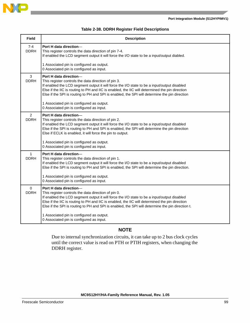
Port Integration Module (S12HYPIMV1)
NOTEDue to internal synchronization circuits, it can take up to 2 bus clock cyclesuntil the correct value is read on PTH or PTIH registers, when changing theDDRH register.
Table 2-38. DDRH Register Field Descriptions
Field Description
7-4DDRH
Port H data direction—This register controls the data direction of pin 7-4.If enabled the LCD segment output it will force the I/O state to be a input/output diabled.
1 Associated pin is configured as output.0 Associated pin is configured as input.
3DDRH
Port H data direction—This register controls the data direction of pin 3.If enabled the LCD segment output it will force the I/O state to be a input/output disabledElse if the IIC is routing to PH and IIC is enabled, the IIC will determined the pin directionElse if the SPI is routing to PH and SPI is enabled, the SPI will determine the pin direction
1 Associated pin is configured as output.0 Associated pin is configured as input.
2DDRH
Port H data direction—This register controls the data direction of pin 2.If enabled the LCD segment output it will force the I/O state to be a input/output disabledElse if the SPI is routing to PH and SPI is enabled, the SPI will determine the pin directionElse if ECLK is enabled, it will force the pin to output.
1 Associated pin is configured as output.0 Associated pin is configured as input.
1DDRH
Port H data direction—This register controls the data direction of pin 1.If enabled the LCD segment output it will force the I/O state to be a input/output disabledElse if the SPI is routing to PH and SPI is enabled, the SPI will determine the pin direction.
1 Associated pin is configured as output.0 Associated pin is configured as input.
0DDRH
Port H data direction—This register controls the data direction of pin 0.If enabled the LCD segment output it will force the I/O state to be a input/output disabledElse if the IIC is routing to PH and IIC is enabled, the IIC will determined the pin directionElse if the SPI is routing to PH and SPI is enabled, the SPI will determine the pin direction t.
1 Associated pin is configured as output.0 Associated pin is configured as input.
MC9S12HY/HA-Family Reference Manual, Rev. 1.05
Freescale Semiconductor 99

Port Integration Module (S12HYPIMV1)
2.3.42 Port H Reduced Drive Register (RDRH)
2.3.43 Port H Pull Device Enable Register (PERH)
Address 0x0263 Access: User read/write1
1 Read: Anytime.Write: Anytime.
7 6 5 4 3 2 1 0
RRDRH7 RDRH6 RDRH5 RDRH4 RDRH3 RDRH2 RDRH1 RDRH0
W
Reset 0 0 0 0 0 0 0 0
Figure 2-40. Port H Reduced Drive Register (RDRH)
Table 2-39. RDRH Register Field Descriptions
Field Description
7-0RDRH
Port H reduced drive—Select reduced drive for outputsThis register configures the drive strength of output pins 7 through 0 as either full or reduced. If a pin is used as inputthis bit has no effect.1 Reduced drive selected (1/6 of the full drive strength).0 Full drive strength enabled.
Address 0x0264 Access: User read/write1
1 Read: Anytime.Write: Anytime.
7 6 5 4 3 2 1 0
RPERH7 PERH6 PERH5 PERH4 PERH3 PERH2 PERH1 PERH0
W
Reset 1 1 1 1 1 1 1 1
Figure 2-41. Port H Pull Device Enable Register (PERH)
Table 2-40. PERH Register Field Descriptions
Field Description
7-0PERH
Port H pull device enable—Enable pull devices on input pinsThese bits configure whether a pull device is activated, if the associated pin is used as an input. This bit has no effectif the pin is used as an output. Out of reset all pull device is enabled.1 Pull device enabled.0 Pull device disabled.
MC9S12HY/HA-Family Reference Manual, Rev. 1.05
100 Freescale Semiconductor
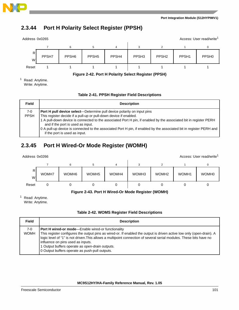
Port Integration Module (S12HYPIMV1)
2.3.44 Port H Polarity Select Register (PPSH)
2.3.45 Port H Wired-Or Mode Register (WOMH)
Address 0x0265 Access: User read/write1
1 Read: Anytime.Write: Anytime.
7 6 5 4 3 2 1 0
RPPSH7 PPSH6 PPSH5 PPSH4 PPSH3 PPSH2 PPSH1 PPSH0
W
Reset 1 1 1 1 1 1 1 1
Figure 2-42. Port H Polarity Select Register (PPSH)
Table 2-41. PPSH Register Field Descriptions
Field Description
7-0PPSH
Port H pull device select—Determine pull device polarity on input pinsThis register decide if a pull-up or pull-down device if enabled.1 A pull-down device is connected to the associated Port H pin, if enabled by the associated bit in register PERH
and if the port is used as input.0 A pull-up device is connected to the associated Port H pin, if enabled by the associated bit in register PERH and
if the port is used as input.
Address 0x0266 Access: User read/write1
1 Read: Anytime.Write: Anytime.
7 6 5 4 3 2 1 0
RWOMH7 WOMH6 WOMH5 WOMH4 WOMH3 WOMH2 WOMH1 WOMH0
W
Reset 0 0 0 0 0 0 0 0
Figure 2-43. Port H Wired-Or Mode Register (WOMH)
Table 2-42. WOMS Register Field Descriptions
Field Description
7-0WOMH
Port H wired-or mode—Enable wired-or functionalityThis register configures the output pins as wired-or. If enabled the output is driven active low only (open-drain). Alogic level of “1” is not driven.This allows a multipoint connection of several serial modules. These bits have noinfluence on pins used as inputs.1 Output buffers operate as open-drain outputs.0 Output buffers operate as push-pull outputs.
MC9S12HY/HA-Family Reference Manual, Rev. 1.05
Freescale Semiconductor 101

Port Integration Module (S12HYPIMV1)
2.3.46 PIM Reserved Register
2.3.47 PIM Reserved Register
2.3.48 PIM Reserved Register
Address 0x0267 Access: User read1
1 Read: Always reads 0x00Write: Unimplemented
7 6 5 4 3 2 1 0
R 0 0 0 0 0 0 0 0
W
Reset 0 0 0 0 0 0 0 0
= Unimplemented or Reserved
Figure 2-44. PIM Reserved Register
Address 0x0268-0x26F Access: User read1
1 Read: Always reads 0x00Write: Unimplemented
7 6 5 4 3 2 1 0
R 0 0 0 0 0 0 0 0
W
Reset 0 0 0 0 0 0 0 0
= Unimplemented or Reserved
Figure 2-45. PIM Reserved Register
Address 0x0270 Access: User read1
1 Read: Always reads 0x00Write: Unimplemented
7 6 5 4 3 2 1 0
R 0 0 0 0 0 0 0 0
W
Reset 0 0 0 0 0 0 0 0
= Unimplemented or Reserved
Figure 2-46. PIM Reserved Register
MC9S12HY/HA-Family Reference Manual, Rev. 1.05
102 Freescale Semiconductor

Port Integration Module (S12HYPIMV1)
2.3.49 Port AD Data Register (PT1AD)
2.3.50 PIM Reserved Register
Address 0x0271 Access: User read/write1
1 Read: Anytime. The data source is depending on the data direction value.Write: Anytime
7 6 5 4 3 2 1 0
RPT1AD7 PT1AD6 PT1AD5 PT1AD4 PT1AD3 PT1AD2 PT1AD1 PT1AD0
W
KWAD7 KWAD6 KWAD5 KWAD4 KWAD3 KWAD2 KWAD1 KWAD0
Altern.Function
AN7 AN6 AN5 AN4 AN3 AN2 AN1 AN0
Reset 0 0 0 0 0 0 0 0
Figure 2-47. Port AD Data Register (PT1AD)
Table 2-43. PT1AD Register Field Descriptions
Field Description
7-0PT1AD
Port AD general purpose input/output data—Data Register, ATD AN analog inputWhen not used with the alternative function, the associated pin can be used as general purpose I/O. In generalpurpose output mode the register bit value is driven to the pin.If the associated data direction bit is set to 1, a read returns the value of the port register bit, otherwise the bufferedpin input state is read.
Address 0x0272 Access: User read1
1 Read: Always reads 0x00Write: Unimplemented
7 6 5 4 3 2 1 0
R 0 0 0 0 0 0 0 0
W
Reset 0 0 0 0 0 0 0 0
= Unimplemented or Reserved
Figure 2-48. PIM Reserved Register
MC9S12HY/HA-Family Reference Manual, Rev. 1.05
Freescale Semiconductor 103

Port Integration Module (S12HYPIMV1)
2.3.51 Port AD Data Direction Register (DDR1AD)
NOTEDue to internal synchronization circuits, it can take up to 2 bus clock cyclesuntil the correct value is read on PT1AD registers, when changing theDDR1AD register.
2.3.52 PIM Reserved Register
Address 0x0273 Access: User read/write1
1 Read: AnytimeWrite: Anytime
7 6 5 4 3 2 1 0
RDDR1AD7 DDR1AD6 DDR1AD5 DDR1AD4 DDR1AD3 DDR1AD2 DDR1AD1 DDR1AD0
W
Reset 0 0 0 0 0 0 0 0
Figure 2-49. Port AD Data Direction Register (DDR1AD)
Table 2-44. DDR1AD Register Field Descriptions
Field Description
7-0DDR1AD
Port AD data direction—This bit determines whether the associated pin is an input or output.To use the digital input function the ATD Digital Input Enable Register (ATDDIEN) has to be set to logic level “1”.
1 Associated pin is configured as output0 Associated pin is configured as input
Address 0x0274 Access: User read1
1 Read: Always reads 0x00Write: Unimplemented
7 6 5 4 3 2 1 0
R 0 0 0 0 0 0 0 0
W
Reset 0 0 0 0 0 0 0 0
= Unimplemented or Reserved
Figure 2-50. PIM Reserved Register
MC9S12HY/HA-Family Reference Manual, Rev. 1.05
104 Freescale Semiconductor

Port Integration Module (S12HYPIMV1)
2.3.53 Port AD Reduced Drive Register (RDR1AD)
2.3.54 PIM Reserved Register
2.3.55 Port AD Pull Up Enable Register (PER1AD)
Address 0x0275 Access: User read/write1
1 Read: AnytimeWrite: Anytime
7 6 5 4 3 2 1 0
RRDR1AD7 RDR1AD6 RDR1AD5 RDR1AD4 RDR1AD3 RDR1AD2 RDR1AD1 RDR1AD0
W
Reset 0 0 0 0 0 0 0 0
Figure 2-51. Port AD Reduced Drive Register (RDR1AD)
Table 2-45. RDR1AD Register Field Descriptions
Field Description
7-0RDR1AD
Port AD reduced drive—Select reduced drive for output pinThis bit configures the drive strength of the associated output pin as either full or reduced. If a pin is used as inputthis bit has no effect. The reduced drive function is independent of which function is being used on a particular pin.
1 Reduced drive selected (1/6 of the full drive strength)0 Full drive strength enabled
Address 0x0276 Access: User read1
1 Read: Always reads 0x00Write: Unimplemented
7 6 5 4 3 2 1 0
R 0 0 0 0 0 0 0 0
W
Reset 0 0 0 0 0 0 0 0
= Unimplemented or Reserved
Figure 2-52. PIM Reserved Register
Address 0x0277 Access: User read/write1
7 6 5 4 3 2 1 0
RPER1AD7 PER1AD6 PER1AD5 PER1AD4 PER1AD3 PER1AD2 PER1AD1 PER1AD0
W
Reset 0 0 0 0 0 0 0 0
Figure 2-53. Port AD Pull Up Enable Register (PER1AD)
MC9S12HY/HA-Family Reference Manual, Rev. 1.05
Freescale Semiconductor 105

Port Integration Module (S12HYPIMV1)
2.3.56 PIM Reserved Registers
2.3.57 Port R Data Register (PTR)
1 Read: AnytimeWrite: Anytime
Table 2-46. PER1AD Register Field Descriptions
Field Description
7-0PER1AD
Port AD pull-up enable—Enable pull-up device on input pinThis bit controls whether a pull up device on the associated port input pin is active. If a pin is used as output this bithas no effect.
1 Pull device enabled0 Pull device disabled
Address 0x0278-0x27F Access: User read1
1 Read: Always reads 0x00Write: Unimplemented
7 6 5 4 3 2 1 0
R 0 0 0 0 0 0 0 0
W
Reset 0 0 0 0 0 0 0 0
= Unimplemented or Reserved u = Unaffected by reset
Figure 2-54. PIM Reserved Registers
Address 0x0280 Access: User read/write1
1 Read: Anytime The data source is depending on the data direction value.Write: Anytime
7 6 5 4 3 2 1 0
RPTR7 PTR6 PTR5 PTR4 PTR3 PTR2 PTR1 PTR0
W
— SCL SDA — — — — —
Altern.Function
FP27 FP18 FP17 FP112 IOC1_7 IOC1_6 IOC0_7 IOC0_6
Reset 0 0 0 0 0 0 0 0
Figure 2-55. Port R Data Register (PTR)
MC9S12HY/HA-Family Reference Manual, Rev. 1.05
106 Freescale Semiconductor

Port Integration Module (S12HYPIMV1)
Table 2-47. PTR Register Field Descriptions
Field Description
7PTR
Port R general purpose input/output data—Data Register, LCD segment driver outputWhen not used with the alternative function, the associated pin can be used as general purpose I/O. In generalpurpose output mode the register bit value is driven to the pin.If the associated data direction bit is set to 1, a read returns the value of the port register bit, otherwise the bufferedpin input state is read.
• The LCD segment driver output takes precedence over the general purpose I/O function
6PTR
Port R general purpose input/output data—Data Register, LCD segment driver output, SCL of IICWhen not used with the alternative function, the associated pin can be used as general purpose I/O. In generalpurpose output mode the register bit value is driven to the pin.If the associated data direction bit is set to 1, a read returns the value of the port register bit, otherwise the bufferedpin input state is read.
• The LCD segment driver output takes precedence over the IIC and general purpose I/O function • The IIC function takes over the general purpose I/O function
5PTR
Port R general purpose input/output data—Data Register, LCD segment driver output, SDA of IICWhen not used with the alternative function, the associated pin can be used as general purpose I/O. In generalpurpose output mode the register bit value is driven to the pin.If the associated data direction bit is set to 1, a read returns the value of the port register bit, otherwise the bufferedpin input state is read.
• The LCD segment driver output takes precedence over the IIC and general purpose I/O function • The IIC function takes over the general purpose I/O function
4PTR
Port R general purpose input/output data—Data Register, LCD segment driver outputWhen not used with the alternative function, the associated pin can be used as general purpose I/O. In generalpurpose output mode the register bit value is driven to the pin.If the associated data direction bit is set to 1, a read returns the value of the port register bit, otherwise the bufferedpin input state is read.
• The LCD segment driver output takes precedence over the general purpose I/O function
3-0PTR
Port R general purpose input/output data—Data Register, TIM1/TIM0 channelsWhen not used with the alternative function, the associated pin can be used as general purpose I/O. In generalpurpose output mode the register bit value is driven to the pin.If the associated data direction bit is set to 1, a read returns the value of the port register bit, otherwise the bufferedpin input state is read.
• The TIM1/TIM0 output compare function takes precedence over the general purpose I/O function1
1 For the TIM input capture to be function correctly, the corresponding DDRR bit should be set as input state
MC9S12HY/HA-Family Reference Manual, Rev. 1.05
Freescale Semiconductor 107

Port Integration Module (S12HYPIMV1)
2.3.58 Port R Input Register (PTIR)
2.3.59 Port R Data Direction Register (DDRR)
Address 0x0281 Access: User read1
1 Read: Anytime.Write:Never, writes to this register have no effect.
7 6 5 4 3 2 1 0
R PTIR7 PTIR6 PTIR5 PTIR4 PTIR3 PTIR2 PTIR1 PTIR0
W
Reset u u u u u u u u
= Unimplemented or Reserved u = Unaffected by reset
Figure 2-56. Port R Input Register (PTIR)
Table 2-48. PTIR Register Field Descriptions
Field Description
7-0PTIR
Port R input data—This register always reads back the buffered state of the associated pins. This can also be used to detect overloador short circuit conditions on output pins.
Address 0x0282 Access: User read/write1
1 Read: Anytime.Write: Anytime.
7 6 5 4 3 2 1 0
RDDRR7 DDRR6 DDRR5 DDRR4 DDRR3 DDRR2 DDRR1 DDRR0
W
Reset 0 0 0 0 0 0 0 0
Figure 2-57. Port R Data Direction Register (DDRR)
MC9S12HY/HA-Family Reference Manual, Rev. 1.05
108 Freescale Semiconductor

Port Integration Module (S12HYPIMV1)
NOTEDue to internal synchronization circuits, it can take up to 2 bus clock cyclesuntil the correct value is read on PTR or PTIR registers, when changing theDDRR register.
Table 2-49. DDRR Register Field Descriptions
Field Description
7DDRR
Port R data direction—This register controls the data direction of pin 7.This register configures pin as either input or output.If LCD segment driver output is enabled, it will force as input/output disabled.
1 Associated pin is configured as output.0 Associated pin is configured as input.
6DDRR
Port R data direction—This register controls the data direction of pin 6.This register configures pin as either input or output.If LCD segment driver output is enabled, it will force as input/output disabledElse If IIC is routing to PR and IIC is enabled, it will force as open-drain output.
1 Associated pin is configured as output.0 Associated pin is configured as input.
5DDRR
Port R data direction—This register controls the data direction of pin 5.This register configures pin as either input or output.If LCD segment driver output is enabled, it will force as input/output disabledElse If IIC is routing to PR and IIC is enabled, it will force as open-drain output.
1 Associated pin is configured as output.0 Associated pin is configured as input.
4DDRR
Port R data direction—This register controls the data direction of pin 4.This register configures pin as either input or output.If LCD segment driver output is enabled, it will force as input/output disabled.
1 Associated pin is configured as output.0 Associated pin is configured as input.
3-0DDRR
Port R data direction—This register controls the data direction of pin 3-0.This register configures pin as either input or output.If TIM1/TIM0 are routing to the PR and TIM1/TIM0 output compare functions are enabled, it will force as output.
1 Associated pin is configured as output.0 Associated pin is configured as input.
MC9S12HY/HA-Family Reference Manual, Rev. 1.05
Freescale Semiconductor 109

Port Integration Module (S12HYPIMV1)
2.3.60 Port R Reduced Drive Register (RDRR)
2.3.61 Port R Pull Device Enable Register (PERR)
Address 0x0283 Access: User read/write1
1 Read: Anytime.Write: Anytime.
7 6 5 4 3 2 1 0
RRDRR7 RDRR6 RDRR5 RDRR4 RDRR3 RDRR2 RDRR1 RDRR0
W
Reset 0 0 0 0 0 0 0 0
Figure 2-58. Port R Reduced Drive Register (RDRR)
Table 2-50. RDRR Register Field Descriptions
Field Description
7-0RDRR
Port R reduced drive—Select reduced drive for outputsThis register configures the drive strength of output pins 7 through 0 as either full or reduced. If a pin is used as inputthis bit has no effect.1 Reduced drive selected (1/6 of the full drive strength).0 Full drive strength enabled.
Address 0x0284 Access: User read/write1
1 Read: Anytime.Write: Anytime.
7 6 5 4 3 2 1 0
RPERR7 PERR6 PERR5 PERR4 PERR3 PERR2 PERR1 PERR0
W
Reset 1 1 1 1 1 1 1 1
Figure 2-59. Port R Pull Device Enable Register (PERR)
Table 2-51. PERR Register Field Descriptions
Field Description
7-0PERR
Port R pull device enable—Enable pull devices on input pinsThese bits configure whether a pull device is activated, if the associated pin is used as an input. This bit has no effectif the pin is used as an output. Out of reset all pull devices are enabled.1 Pull device enabled.0 Pull device disabled.
MC9S12HY/HA-Family Reference Manual, Rev. 1.05
110 Freescale Semiconductor
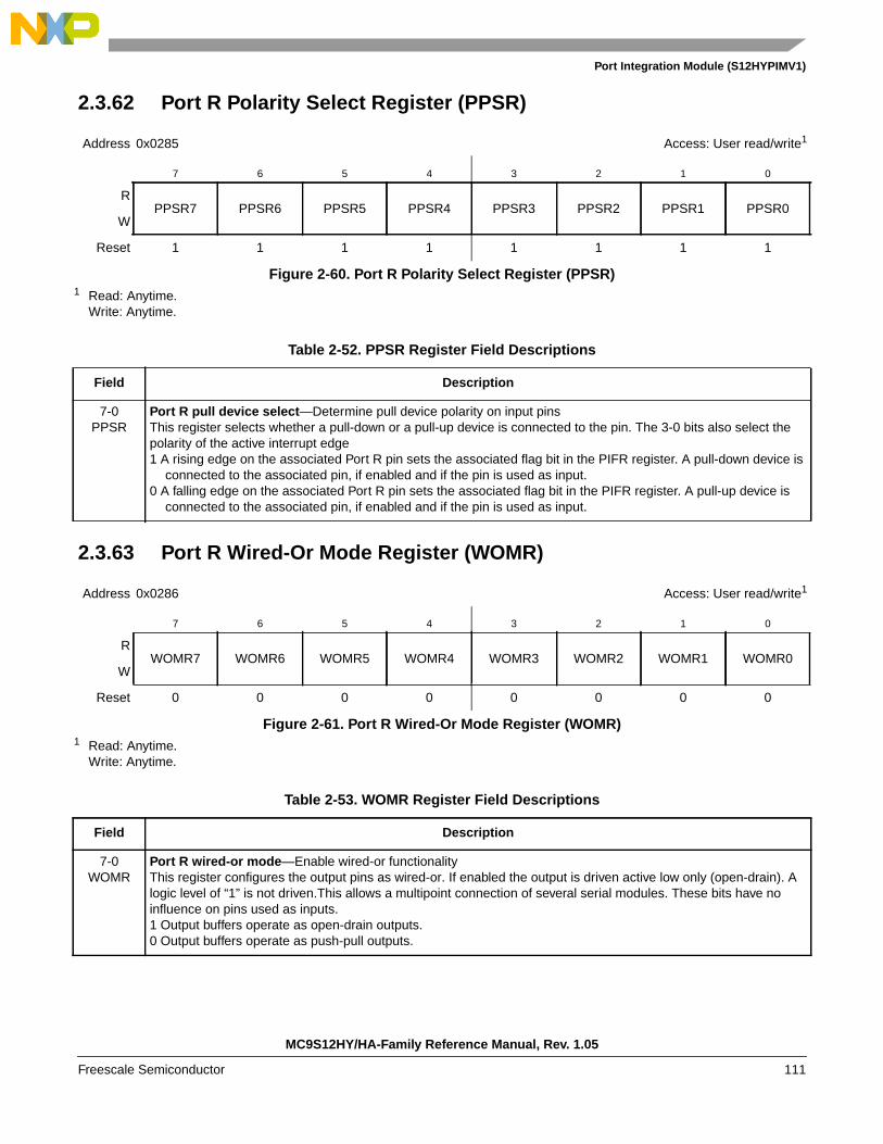
Port Integration Module (S12HYPIMV1)
2.3.62 Port R Polarity Select Register (PPSR)
2.3.63 Port R Wired-Or Mode Register (WOMR)
Address 0x0285 Access: User read/write1
1 Read: Anytime.Write: Anytime.
7 6 5 4 3 2 1 0
RPPSR7 PPSR6 PPSR5 PPSR4 PPSR3 PPSR2 PPSR1 PPSR0
W
Reset 1 1 1 1 1 1 1 1
Figure 2-60. Port R Polarity Select Register (PPSR)
Table 2-52. PPSR Register Field Descriptions
Field Description
7-0PPSR
Port R pull device select—Determine pull device polarity on input pinsThis register selects whether a pull-down or a pull-up device is connected to the pin. The 3-0 bits also select thepolarity of the active interrupt edge1 A rising edge on the associated Port R pin sets the associated flag bit in the PIFR register. A pull-down device is
connected to the associated pin, if enabled and if the pin is used as input.0 A falling edge on the associated Port R pin sets the associated flag bit in the PIFR register. A pull-up device is
connected to the associated pin, if enabled and if the pin is used as input.
Address 0x0286 Access: User read/write1
1 Read: Anytime.Write: Anytime.
7 6 5 4 3 2 1 0
RWOMR7 WOMR6 WOMR5 WOMR4 WOMR3 WOMR2 WOMR1 WOMR0
W
Reset 0 0 0 0 0 0 0 0
Figure 2-61. Port R Wired-Or Mode Register (WOMR)
Table 2-53. WOMR Register Field Descriptions
Field Description
7-0WOMR
Port R wired-or mode—Enable wired-or functionalityThis register configures the output pins as wired-or. If enabled the output is driven active low only (open-drain). Alogic level of “1” is not driven.This allows a multipoint connection of several serial modules. These bits have noinfluence on pins used as inputs.1 Output buffers operate as open-drain outputs.0 Output buffers operate as push-pull outputs.
MC9S12HY/HA-Family Reference Manual, Rev. 1.05
Freescale Semiconductor 111

Port Integration Module (S12HYPIMV1)
2.3.64 PIM Reserved Registers
2.3.65 Port T Interrupt Enable Register (PIET)Read: Anytime.
2.3.66 Port T Interrupt Flag Register (PIFT)
Address 0x0287 Access: User read1
1 Read: Always reads 0x00Write: Unimplemented
7 6 5 4 3 2 1 0
R 0 0 0 0 0 0 0 0
W
Reset 0 0 0 0 0 0 0 0
= Unimplemented or Reserved u = Unaffected by reset
Figure 2-62. PIM Reserved Registers
Address 0x0288 Access: User read/write1
1 Read: Anytime.Write: Anytime.
7 6 5 4 3 2 1 0
RPIET7 PIET6 PIET5 PIET4 PIET3 PIET2 PIET1 PIET0
W
Reset 0 0 0 0 0 0 0 0
Figure 2-63. Port T Interrupt Enable Register (PIET)
Table 2-54. PIET Register Field Descriptions
Field Description
7-0PIET
Port T interrupt enable—This register disables or enables on a per-pin basis the edge sensitive external interrupt associated with Port T.1 Interrupt is enabled.0 Interrupt is disabled (interrupt flag masked).
Address 0x0289 Access: User read/write1
1 Read: Anytime.Write: Anytime.
7 6 5 4 3 2 1 0
RPIFT7 PIFT6 PIFT5 PIFT4 PIFT3 PIFT2 PIFT1 PIFT0
W
Reset 0 0 0 0 0 0 0 0
Figure 2-64. Port T Interrupt Flag Register (PIFT)
MC9S12HY/HA-Family Reference Manual, Rev. 1.05
112 Freescale Semiconductor
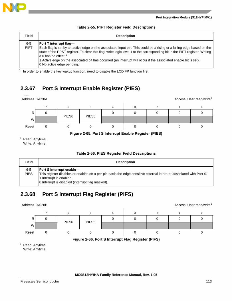
Port Integration Module (S12HYPIMV1)
2.3.67 Port S Interrupt Enable Register (PIES)Read: Anytime.
2.3.68 Port S Interrupt Flag Register (PIFS)
Table 2-55. PIFT Register Field Descriptions
Field Description
6-5PIFT
Port T interrupt flag—Each flag is set by an active edge on the associated input pin. This could be a rising or a falling edge based on thestate of the PPST register. To clear this flag, write logic level 1 to the corresponding bit in the PIFT register. Writinga 0 has no effect.1
1 Active edge on the associated bit has occurred (an interrupt will occur if the associated enable bit is set).0 No active edge pending.
1 In order to enable the key wakup function, need to disable the LCD FP function first
Address 0x028A Access: User read/write1
1 Read: Anytime.Write: Anytime.
7 6 5 4 3 2 1 0
R 0PIES6 PIES5
0 0 0 0 0
W
Reset 0 0 0 0 0 0 0 0
Figure 2-65. Port S Interrupt Enable Register (PIES)
Table 2-56. PIES Register Field Descriptions
Field Description
6-5PIES
Port S interrupt enable—This register disables or enables on a per-pin basis the edge sensitive external interrupt associated with Port S.1 Interrupt is enabled.0 Interrupt is disabled (interrupt flag masked).
Address 0x028B Access: User read/write1
1 Read: Anytime.Write: Anytime.
7 6 5 4 3 2 1 0
R 0PIFS6 PIFS5
0 0 0 0 0
W
Reset 0 0 0 0 0 0 0 0
Figure 2-66. Port S Interrupt Flag Register (PIFS)
MC9S12HY/HA-Family Reference Manual, Rev. 1.05
Freescale Semiconductor 113

Port Integration Module (S12HYPIMV1)
2.3.69 Port AD Interrupt Enable Register (PIE1AD)Read: Anytime.
2.3.70 Port AD Interrupt Flag Register (PIF1AD)
Table 2-57. PIFS Register Field Descriptions
Field Description
6-5PIFS
Port S interrupt flag—Each flag is set by an active edge on the associated input pin. This could be a rising or a falling edge based on thestate of the PPSS register. To clear this flag, write logic level 1 to the corresponding bit in the PIFS register. Writinga 0 has no effect.1 Active edge on the associated bit has occurred (an interrupt will occur if the associated enable bit is set).0 No active edge pending.
Address 0x028C Access: User read/write1
1 Read: Anytime.Write: Anytime.
7 6 5 4 3 2 1 0
RPIE1AD7 PIE1AD6 PIE1AD5 PIE1AD4 PIE1AD3 PIE1AD2 PIE1AD1 PIE1AD0
W
Reset 0 0 0 0 0 0 0 0
Figure 2-67. Port AD Interrupt Enable Register (PIE1AD)
Table 2-58. PIE1AD Register Field Descriptions
Field Description
7-0PIE1AD
Port AD interrupt enable—This register disables or enables on a per-pin basis the edge sensitive external interrupt associated with Port AD.1 Interrupt is enabled.0 Interrupt is disabled (interrupt flag masked).
Address 0x028D Access: User read/write1
1 Read: Anytime.Write: Anytime.
7 6 5 4 3 2 1 0
RPIF1AD7 PIF1AD6 PIF1AD5 PIF1AD4 PIF1AD3 PIF1AD2 PIF1AD1 PIF1AD0
W
Reset 0 0 0 0 0 0 0 0
Figure 2-68. Port AD Interrupt Flag Register (PIF1AD)
MC9S12HY/HA-Family Reference Manual, Rev. 1.05
114 Freescale Semiconductor

Port Integration Module (S12HYPIMV1)
2.3.71 Port R Interrupt Enable Register (PIER)Read: Anytime.
2.3.72 Port R Interrupt Flag Register (PIFR)
Table 2-59. PIF1AD Register Field Descriptions
Field Description
7-0PIF1AD
Port AD interrupt flag—Each flag is set by an active edge on the associated input pin. To clear this flag, write logic level 1 to thecorresponding bit in the PIF1AD register. Writing a 0 has no effect. 1
1 Active falling edge on the associated bit has occurred (an interrupt will occur if the associated enable bit is set).0 No active edge pending.
1 In order to enable the Key Wakeup function, need to set the ATDIENL first.
Address 0x028E Access: User read/write1
1 Read: Anytime.Write: Anytime.
7 6 5 4 3 2 1 0
R 0 0 0 0PIER3 PIER2 PIER1 PIER0
W
Reset 0 0 0 0 0 0 0 0
Figure 2-69. Port R Interrupt Enable Register (PIER)
Table 2-60. PIER Register Field Descriptions
Field Description
3-0PIER
Port R interrupt enable—This register disables or enables on a per-pin basis the edge sensitive external interrupt associated with Port R.1 Interrupt is enabled.0 Interrupt is disabled (interrupt flag masked).
Address 0x028F Access: User read/write1
1 Read: Anytime.Write: Anytime.
7 6 5 4 3 2 1 0
R 0 0 0 0PIFR3 PIFR2 PIFR1 PIFR0
W
Reset 0 0 0 0 0 0 0 0
Figure 2-70. Port R Interrupt Flag Register (PIFR)
MC9S12HY/HA-Family Reference Manual, Rev. 1.05
Freescale Semiconductor 115
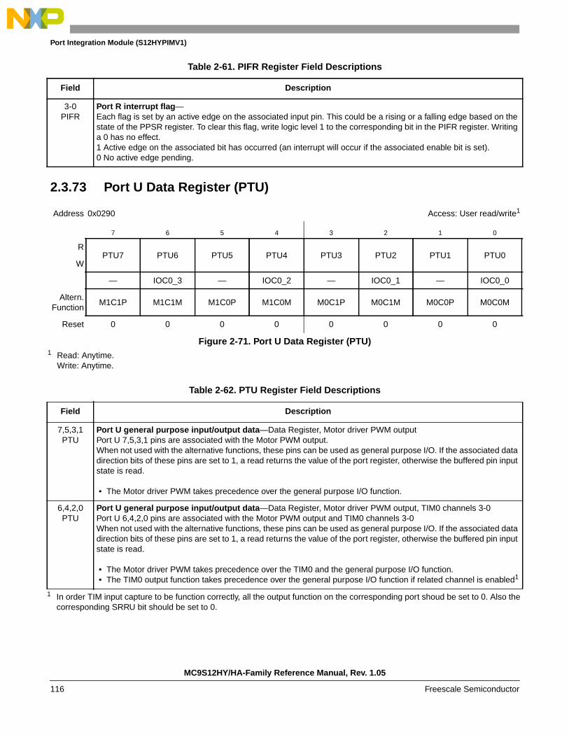
Port Integration Module (S12HYPIMV1)
2.3.73 Port U Data Register (PTU)
Table 2-61. PIFR Register Field Descriptions
Field Description
3-0PIFR
Port R interrupt flag—Each flag is set by an active edge on the associated input pin. This could be a rising or a falling edge based on thestate of the PPSR register. To clear this flag, write logic level 1 to the corresponding bit in the PIFR register. Writinga 0 has no effect.1 Active edge on the associated bit has occurred (an interrupt will occur if the associated enable bit is set).0 No active edge pending.
Address 0x0290 Access: User read/write1
1 Read: Anytime.Write: Anytime.
7 6 5 4 3 2 1 0
RPTU7 PTU6 PTU5 PTU4 PTU3 PTU2 PTU1 PTU0
W
— IOC0_3 — IOC0_2 — IOC0_1 — IOC0_0
Altern.Function
M1C1P M1C1M M1C0P M1C0M M0C1P M0C1M M0C0P M0C0M
Reset 0 0 0 0 0 0 0 0
Figure 2-71. Port U Data Register (PTU)
Table 2-62. PTU Register Field Descriptions
Field Description
7,5,3,1PTU
Port U general purpose input/output data—Data Register, Motor driver PWM outputPort U 7,5,3,1 pins are associated with the Motor PWM output.When not used with the alternative functions, these pins can be used as general purpose I/O. If the associated datadirection bits of these pins are set to 1, a read returns the value of the port register, otherwise the buffered pin inputstate is read.
• The Motor driver PWM takes precedence over the general purpose I/O function.
6,4,2,0PTU
Port U general purpose input/output data—Data Register, Motor driver PWM output, TIM0 channels 3-0Port U 6,4,2,0 pins are associated with the Motor PWM output and TIM0 channels 3-0When not used with the alternative functions, these pins can be used as general purpose I/O. If the associated datadirection bits of these pins are set to 1, a read returns the value of the port register, otherwise the buffered pin inputstate is read.
• The Motor driver PWM takes precedence over the TIM0 and the general purpose I/O function. • The TIM0 output function takes precedence over the general purpose I/O function if related channel is enabled1
1 In order TIM input capture to be function correctly, all the output function on the corresponding port shoud be set to 0. Also thecorresponding SRRU bit should be set to 0.
MC9S12HY/HA-Family Reference Manual, Rev. 1.05
116 Freescale Semiconductor

Port Integration Module (S12HYPIMV1)
2.3.74 Port U Input Register (PTIU)
2.3.75 Port U Data Direction Register (DDRU)
Address 0x0291 Access: User read1
1 Read: Anytime.Write:Never, writes to this register have no effect.
7 6 5 4 3 2 1 0
R PTIU7 PTIU6 PTIU5 PTIU4 PTIU3 PTIU2 PTIU1 PTIU0
W
Reset u u u u u u u u
= Unimplemented or Reserved u = Unaffected by reset
Figure 2-72. Port U Input Register (PTIU)
Table 2-63. PTIU Register Field Descriptions
Field Description
7-0PTIU
Port U input data—This register always reads back the buffered state of the associated pins. This can also be used to detect overloador short circuit conditions on output pins.
Address 0x0292 Access: User read/write1
1 Read: Anytime.Write: Anytime.
7 6 5 4 3 2 1 0
RDDRU7 DDRU6 DDRU5 DDRU4 DDRU3 DDRU2 DDRU1 DDRU0
W
Reset 0 0 0 0 0 0 0 0
Figure 2-73. Port U Data Direction Register (DDRU)
Table 2-64. DDRU Register Field Descriptions
Field Description
7,5,3,1DDRU
Port U data direction—If enabled the Motor driver PWM output it will force the I/O state to be output.
1 Associated pin is configured as output.0 Associated pin is configured as input.
6,4,2,0DDRU
Port U data direction—If enabled the Motor driver PWM output it will force the I/O state to be output.Else if corresponding TIM0 output compare channel is enabled, it will be force as output
1 Associated pin is configured as output.0 Associated pin is configured as input.
MC9S12HY/HA-Family Reference Manual, Rev. 1.05
Freescale Semiconductor 117

Port Integration Module (S12HYPIMV1)
NOTEDue to internal synchronization circuits, it can take up to 2 bus clock cyclesuntil the correct value is read on PTU or PTIU registers, when changing theDDRU register.
2.3.76 PIM Reserved Registers
2.3.77 Port U Pull Device Enable Register (PERU)
Address 0x0293 Access: User read1
1 Read: Always reads 0x00Write: Unimplemented
7 6 5 4 3 2 1 0
R 0 0 0 0 0 0 0 0
W
Reset 0 0 0 0 0 0 0 0
= Unimplemented or Reserved u = Unaffected by reset
Figure 2-74. PIM Reserved Registers
Address 0x0294 Access: User read/write1
1 Read: Anytime.Write: Anytime.
7 6 5 4 3 2 1 0
RPERU7 PERU6 PERU5 PERU4 PERU3 PERU2 PERU1 PERU0
W
Reset 0 0 0 0 0 0 0 0
Figure 2-75. Port U Pull Device Enable Register (PERU)
Table 2-65. PERU Register Field Descriptions
Field Description
7-0PERU
Port U pull device enable—Enable pull devices on input pinsThese bits configure whether a pull device is activated, if the associated pin is used as an input. This bit has no effectif the pin is used as an output. Out of reset no pull device is enabled.1 Pull device enabled.0 Pull device disabled.
MC9S12HY/HA-Family Reference Manual, Rev. 1.05
118 Freescale Semiconductor

Port Integration Module (S12HYPIMV1)
2.3.78 Port U Polarity Select Register (PPSU)
2.3.79 Port U Slew Rate Register(SRRU)
Address 0x0295 Access: User read/write1
1 Read: Anytime.Write: Anytime.
7 6 5 4 3 2 1 0
RPPSU7 PPSU6 PPSU5 PPSU4 PPSU3 PPSU2 PPSU1 PPSU0
W
Reset 0 0 0 0 0 0 0 0
Figure 2-76. Port U Polarity Select Register (PPSU)
Table 2-66. PPSU Register Field Descriptions
Field Description
7-0PPSU
Port U pull device select—Determine pull device polarity on input pinsThis register serves a dual purpose by selecting the polarity of the active interrupt edge as well as selecting a pull-upor pull-down device if enabled.1 A pull-down device is connected to the associated Port U pin, if enabled by the associated bit in register PERU and
if the port is used as input.0 A pull-up device is connected to the associated Port U pin, if enabled by the associated bit in register PERU and
if the port is used as input.
Address 0x0296 Access: User read/write1
1 Read: Anytime.Write: Anytime.
7 6 5 4 3 2 1 0
RSRRU7 SRRU6 SRRU5 SRRU4 SRRU3 SRRU2 SRRU1 SRRU0
W
Reset 0 0 0 0 0 0 0 0
Figure 2-77. Port U Polarity Select Register (SRRU)
Table 2-67. SRRU Register Field Descriptions
Field Description
7-0SRRU
Port U Slew Rate Register—Determine the slew rate on the pins1
1 Enable the slew rate control and disables the digital input buffer0 Disable the slew rate control and enable the digital input buffer
1 When the values of SRRU changes from non-zero to zero or vice versa, It will need to wait for about 300 ns delay before theslew rate control to be real function as setting. When entering STOP mode, to save the power, the slew rate control will be forcedto off state. After wakeup from STOP, it will also need to wait for about 300 ns before slew rate control to be functional as setting.
MC9S12HY/HA-Family Reference Manual, Rev. 1.05
Freescale Semiconductor 119

Port Integration Module (S12HYPIMV1)
2.3.80 PIM Reserved Registers
Address 0x0297 Access: User read1
1 Read: Always reads 0x00Write: Unimplemented
7 6 5 4 3 2 1 0
R 0 0 0 0 0 0 0 0
W
Reset 0 0 0 0 0 0 0 0
= Unimplemented or Reserved u = Unaffected by reset
Figure 2-78. PIM Reserved Registers
MC9S12HY/HA-Family Reference Manual, Rev. 1.05
120 Freescale Semiconductor
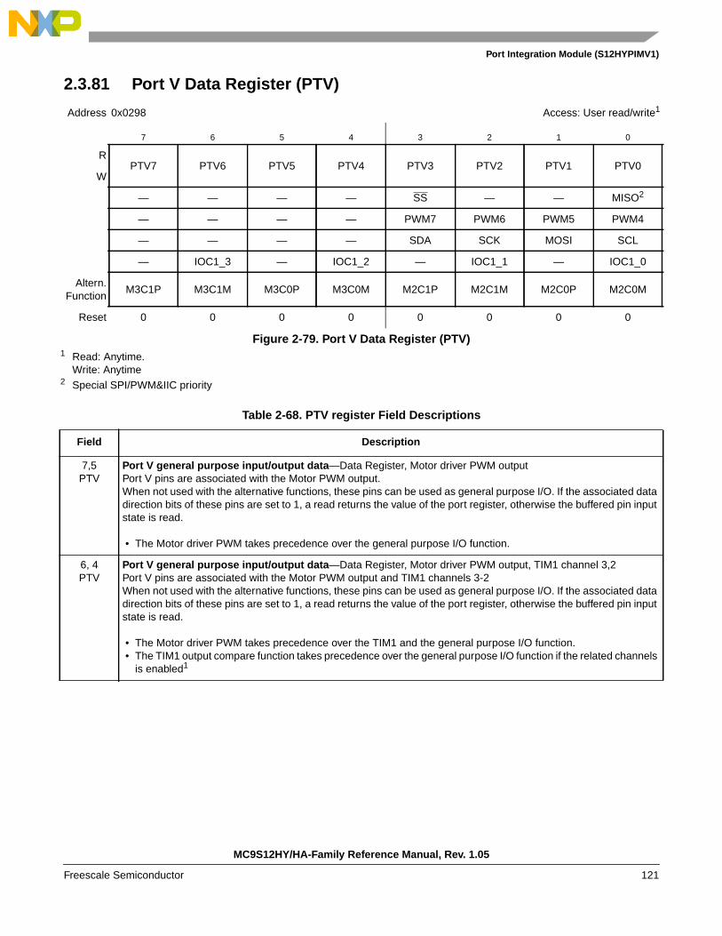
Port Integration Module (S12HYPIMV1)
2.3.81 Port V Data Register (PTV)
Address 0x0298 Access: User read/write1
1 Read: Anytime.Write: Anytime
7 6 5 4 3 2 1 0
RPTV7 PTV6 PTV5 PTV4 PTV3 PTV2 PTV1 PTV0
W
— — — — SS — — MISO2
2 Special SPI/PWM&IIC priority
— — — — PWM7 PWM6 PWM5 PWM4
— — — — SDA SCK MOSI SCL
— IOC1_3 — IOC1_2 — IOC1_1 — IOC1_0
Altern.Function
M3C1P M3C1M M3C0P M3C0M M2C1P M2C1M M2C0P M2C0M
Reset 0 0 0 0 0 0 0 0
Figure 2-79. Port V Data Register (PTV)
Table 2-68. PTV register Field Descriptions
Field Description
7,5PTV
Port V general purpose input/output data—Data Register, Motor driver PWM outputPort V pins are associated with the Motor PWM output.When not used with the alternative functions, these pins can be used as general purpose I/O. If the associated datadirection bits of these pins are set to 1, a read returns the value of the port register, otherwise the buffered pin inputstate is read.
• The Motor driver PWM takes precedence over the general purpose I/O function.
6, 4PTV
Port V general purpose input/output data—Data Register, Motor driver PWM output, TIM1 channel 3,2Port V pins are associated with the Motor PWM output and TIM1 channels 3-2When not used with the alternative functions, these pins can be used as general purpose I/O. If the associated datadirection bits of these pins are set to 1, a read returns the value of the port register, otherwise the buffered pin inputstate is read.
• The Motor driver PWM takes precedence over the TIM1 and the general purpose I/O function. • The TIM1 output compare function takes precedence over the general purpose I/O function if the related channels
is enabled1
MC9S12HY/HA-Family Reference Manual, Rev. 1.05
Freescale Semiconductor 121
Port Integration Module (S12HYPIMV1)
3PTV
Port V general purpose input/output data—Data Register, Motor driver PWM output, SS of SPI, PWM channel 7,SDA of IICPort V pin 3 is associated with the Motor PWM output, SPI and PWM channel 7 and IIC.When not used with the alternative functions, this pin can be used as general purpose I/O. If the associated datadirection bit of this pins is set to 1, a read returns the value of the port register, otherwise the buffered pin input stateis read.
• The Motor driver PWM takes precedence over the SPI, PWM channel 7, IIC and general purpose I/O function. • The SDA of IIC takes precedence over the PWM channel 7, SPI and general purpose I/O function • The PWM channel 7 takes precedence over the SPI and general purpose I/O function • The SS of SPI takes precedence over the general purpose I/O function
2PTV
Port V general purpose input/output data—Data Register, Motor driver PWM output, TIM1 channel 1, SCK of SPI,PWM channel 6Port V pin 2 is associated with the Motor PWM output, SPI and PWM channel 6.When not used with the alternative functions, this pin can be used as general purpose I/O. If the associated datadirection bit of this pins is set to 1, a read returns the value of the port register, otherwise the buffered pin input stateis read.
• The Motor driver PWM takes precedence over the TIM1, SPI, PWM channel 6 and general purpose I/O function. • The TIM1 channel 1 output function takes precedence over the SPI, PWM channels 6 and the general purpose
I/O function if related channel is enabled1
• The SCK of SPI takes precedence over the PWM channel 6 and the general purpose I/O function • The PWM channel 6 takes precedence over the general purpose I/O function
1PTV
Port V general purpose input/output data—Data Register, Motor driver PWM output, MOSI of SPI, PWM channel5Port V pin 1 is associated with the Motor PWM output, SPI and PWM channel 5.When not used with the alternative functions, this pin can be used as general purpose I/O. If the associated datadirection bit of this pins is set to 1, a read returns the value of the port register, otherwise the buffered pin input stateis read.
• The Motor driver PWM takes precedence over the SPI, PWM channel 5 and general purpose I/O function. • The MOSI of SPI takes precedence over the PWM channel 5 and the general purpose I/O function • The PWM channel 5 takes precedence over the general purpose I/O function
0PTV
Port V general purpose input/output data—Data Register, Motor driver PWM output, TIM1 channel 0, MISO ofSPI, PWM channel 4, SCL of IICPort V pin 0 is associated with the Motor PWM output, TIM1 channel 0, SPI and PWM channel 4 and IIC.When not used with the alternative functions, this pin can be used as general purpose I/O. If the associated datadirection bit of this pins is set to 1, a read returns the value of the port register, otherwise the buffered pin input stateis read.
• The Motor driver PWM takes precedence over the TIM1, SPI, PWM channel 4, IIC and general purpose I/Ofunction.
• The TIM1 output compare function take precedence over the SPI, PWM channel4, IIC and general purpose I/O1
• The SCL of IIC takes presentees over the PWM channel 4, SPI and general purpose I/O function • The PWM channel 4 takes precedence over the SPI and the general purpose I/O function • The MISO of SPI takes precedence over the general purpose I/O function
1 For the TIM1 input capture to be function correctly, need to disable all the output functions on the corresponding channel. Alsothe corresponding SRRV bit should be set to 0.
Table 2-68. PTV register Field Descriptions
Field Description
MC9S12HY/HA-Family Reference Manual, Rev. 1.05
122 Freescale Semiconductor

Port Integration Module (S12HYPIMV1)
2.3.82 Port V Input Register (PTIV)
2.3.83 Port V Data Direction Register (DDRV)
Address 0x0299 Access: User read1
1 Read: Anytime.Write:Never, writes to this register have no effect.
7 6 5 4 3 2 1 0
R PTIV7 PTIV6 PTIV5 PTIV4 PTIV3 PTIV2 PTIV1 PTIV0
W
Reset u u u u u u u u
= Unimplemented or Reserved u = Unaffected by reset
Figure 2-80. Port V Input Register (PTIV)
Table 2-69. PTIV Register Field Descriptions
Field Description
7-0PTIV
Port V input data—This register always reads back the buffered state of the associated pins. This can also be used to detect overloador short circuit conditions on output pins.
Address 0x029A Access: User read/write1
1 Read: Anytime.Write: Anytime.
7 6 5 4 3 2 1 0
RDDRV7 DDRV6 DDRV5 DDRV4 DDRV3 DDRV2 DDRV1 DDRV0
W
Reset 0 0 0 0 0 0 0 0
Figure 2-81. Port V Data Direction Register (DDRV)
MC9S12HY/HA-Family Reference Manual, Rev. 1.05
Freescale Semiconductor 123

Port Integration Module (S12HYPIMV1)
Table 2-70. DDRV Register Field Descriptions
Field Description
7DDRV
Port V data direction—If the Motor driver PWM output is enabled, it will force the I/O state to be output.
1 Associated pin is configured as output.0 Associated pin is configured as input.
6DDRV
Port V data direction—If the Motor driver PWM output or the TIM1 channel 3 output compare function is enabled, it will force the I/O stateto be output.
1 Associated pin is configured as output.0 Associated pin is configured as input.
5DDRV
Port V data direction—If the Motor driver PWM output is enabled, it will force the I/O state to be output.
1 Associated pin is configured as output.0 Associated pin is configured as input.
4DDRV
Port V data direction—If the Motor driver PWM output or the TIM1 channel 2 output compare function is enabled, it will force the I/O stateto be output.
1 Associated pin is configured as output.0 Associated pin is configured as input.
3DDRV
Port V data direction—If the Motor driver PWM output is enabled, it will force the I/O state to be outputElse if IIC is routing to PV and IIC is enabled, it will force the I/O state to be open drain output, also the input bufferis enabledElse if PWM7 is routing to PV and PWM 7 is configured as PWM channel output, it will force the I/O state to be outputElse if PWM7 is routing to PV and PWM7 is configured as PWM emergency shutdown, it will force the I/O state tobe inputElse if SPI is routing to PV and SPI is enabled, SPI will determine the I/O state.
1 Associated pin is configured as output.0 Associated pin is configured as input.
2DDRV
Port V data direction—If the Motor driver PWM output is enabled, it will force the I/O state to be outputElse if corresponding TIM1 output compare channle is enabled, it will be force as outputElse if SPI is routing to PV and SPI is enabled, SPI will determine the I/O stateElse if PWM6 is routing to PV, it will force the I/O state to be output.
1 Associated pin is configured as output.0 Associated pin is configured as input.
MC9S12HY/HA-Family Reference Manual, Rev. 1.05
124 Freescale Semiconductor

Port Integration Module (S12HYPIMV1)
NOTEDue to internal synchronization circuits, it can take up to 2 bus clock cyclesuntil the correct value is read on PTV or PTIV registers, when changing theDDRV register.
2.3.84 PIM Reserved Registers
1DDRV
Port V data direction—If the Motor driver PWM output is enabled, it will force the I/O state to be outputElse if SPI is routing to PV and SPI is enabled, SPI will determine the I/O stateElse if PWM5 is routing to PV, it will force I/O state to be outputElse if SPI is routing to PV and SPI is enabled, SPI will determine the I/O state.
1 Associated pin is configured as output.0 Associated pin is configured as input.
0DDRV
Port V data direction—If the Motor driver PWM output is enabled, it will force the I/O state to be outputElse if corresponding TIM1 output compare channel is enabled, it will be forced as outputElse if IIC is routing to PV and IIC is enabled, it will force the I/O state to be open drain output, also the input bufferis enabledElse if PWM4 is routing to PV, it will force I/O state to be outputElse if SPI is routing to PV and SPI is enabled, SPI will determine the I/O state.
1 Associated pin is configured as output.0 Associated pin is configured as input.
Address 0x029B Access: User read1
1 Read: Always reads 0x00Write: Unimplemented
7 6 5 4 3 2 1 0
R 0 0 0 0 0 0 0 0
W
Reset 0 0 0 0 0 0 0 0
= Unimplemented or Reserved u = Unaffected by reset
Figure 2-82. PIM Reserved Registers
Table 2-70. DDRV Register Field Descriptions (continued)
Field Description
MC9S12HY/HA-Family Reference Manual, Rev. 1.05
Freescale Semiconductor 125

Port Integration Module (S12HYPIMV1)
2.3.85 Port V Pull Device Enable Register (PERV)
2.3.86 Port V Polarity Select Register (PPSV)
Address 0x029C Access: User read/write1
1 Read: Anytime.Write: Anytime.
7 6 5 4 3 2 1 0
RPERV7 PERV6 PERV5 PERV4 PERV3 PERV2 PERV1 PERV0
W
Reset 0 0 0 0 0 0 0 0
Figure 2-83. Port V Pull Device Enable Register (PERV)
Table 2-71. PERV Register Field Descriptions
Field Description
7-0PERV
Port V pull device enable—Enable pull devices on input pinsThese bits configure whether a pull device is activated, if the associated pin is used as an input. This bit has no effectif the pin is used as an output. Out of reset no pull device is enabled.
1 Pull device enabled.0 Pull device disabled.
Address 0x029D Access: User read/write1
1 Read: Anytime.Write: Anytime.
7 6 5 4 3 2 1 0
RPPSV7 PPSV6 PPSV5 PPSV4 PPSV3 PPSV2 PPSV1 PPSV0
W
Reset 0 0 0 0 0 0 0 0
Figure 2-84. Port V Polarity Select Register (PPSV)
Table 2-72. PPSV Register Field Descriptions
Field Description
7-0PPSV
Port V pull device select—Determine pull device polarity on input pinsThis register serves a dual purpose by selecting the polarity of the active interrupt edge as well as selecting a pull-upor pull-down device if enabled.1 A pull-down device is connected to the associated Port V pin, if enabled by the associated bit in register PERV and
if the port is used as input.0 A pull-up device is connected to the associated Port V pin, if enabled by the associated bit in register PERV and if
the port is used as input.
MC9S12HY/HA-Family Reference Manual, Rev. 1.05
126 Freescale Semiconductor
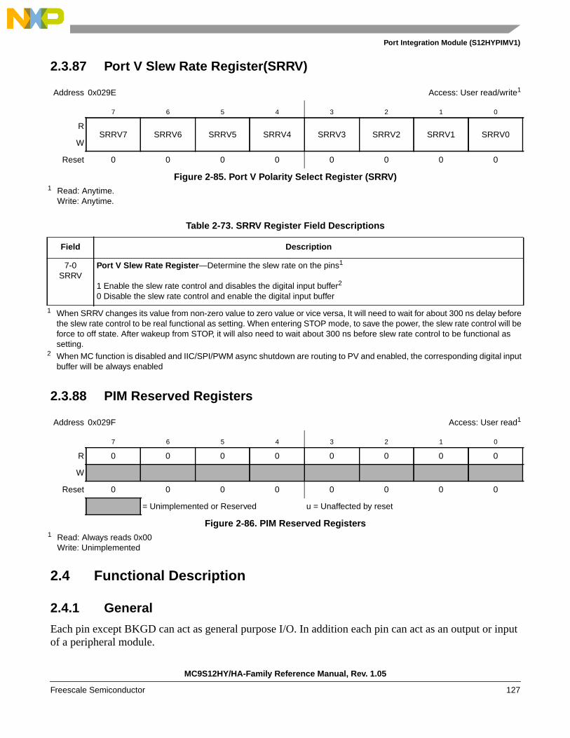
Port Integration Module (S12HYPIMV1)
2.3.87 Port V Slew Rate Register(SRRV)
2.3.88 PIM Reserved Registers
2.4 Functional Description
2.4.1 General
Each pin except BKGD can act as general purpose I/O. In addition each pin can act as an output or inputof a peripheral module.
Address 0x029E Access: User read/write1
1 Read: Anytime.Write: Anytime.
7 6 5 4 3 2 1 0
RSRRV7 SRRV6 SRRV5 SRRV4 SRRV3 SRRV2 SRRV1 SRRV0
W
Reset 0 0 0 0 0 0 0 0
Figure 2-85. Port V Polarity Select Register (SRRV)
Table 2-73. SRRV Register Field Descriptions
Field Description
7-0SRRV
Port V Slew Rate Register—Determine the slew rate on the pins1
1 Enable the slew rate control and disables the digital input buffer2
0 Disable the slew rate control and enable the digital input buffer
1 When SRRV changes its value from non-zero value to zero value or vice versa, It will need to wait for about 300 ns delay beforethe slew rate control to be real functional as setting. When entering STOP mode, to save the power, the slew rate control will beforce to off state. After wakeup from STOP, it will also need to wait about 300 ns before slew rate control to be functional assetting.
2 When MC function is disabled and IIC/SPI/PWM async shutdown are routing to PV and enabled, the corresponding digital inputbuffer will be always enabled
Address 0x029F Access: User read1
1 Read: Always reads 0x00Write: Unimplemented
7 6 5 4 3 2 1 0
R 0 0 0 0 0 0 0 0
W
Reset 0 0 0 0 0 0 0 0
= Unimplemented or Reserved u = Unaffected by reset
Figure 2-86. PIM Reserved Registers
MC9S12HY/HA-Family Reference Manual, Rev. 1.05
Freescale Semiconductor 127

Port Integration Module (S12HYPIMV1)
1 E
P g
A
2.4.2 Registers
A set of configuration registers is common to all ports with exception of the ATD port (Table 2-74). Allregisters can be written at any time, however a specific configuration might not become active.
For example selecting a pull-up device: This device does not become active while the port is used as apush-pull output.
2.4.2.1 Data register (PORTx, PTx)
This register holds the value driven out to the pin if the pin is used as a general purpose I/O.
Writing to this register has only an effect on the pin if the pin is used as general purpose output. Whenreading this address, the buffered state of the pin is returned if the associated data direction register bit isset to “0”.
If the data direction register bits are set to logic level “1”, the contents of the data register is returned. Thisis independent of any other configuration (Figure 2-87).
2.4.2.2 Input register (PTIx)
This register is read-only and always returns the buffered state of the pin (Figure 2-87).
2.4.2.3 Data direction register (DDRx)
This register defines whether the pin is used as an general purpose input or an output.
If a peripheral module controls the pin the contents of the data direction register is ignored (Figure 2-87).
Independent of the pin usage with a peripheral module this register determines the source of data whenreading the associated data register address (2.4.2.1/2-128).
Table 2-74. Register availability per port1
ach cell represents one register with individual configuration bits
ort Data InputData
DirectionReduced
DrivePull
EnablePolaritySelect
Wired-Or Mode
SlewRate
InterruptEnable
InterruptFlag
Routin
A yes - yes yes yes - - - - - -
B yes - yes - - - - - -
T yes yes yes yes yes yes - - yes yes yes
S yes yes yes yes yes yes yes - yes yes yes
R yes yes yes yes yes yes yes - yes yes yes
P yes yes yes yes yes yes - - - - yes
H yes yes yes yes yes yes yes - - - -
D yes - yes yes yes - - - yes yes -
U yes yes yes yes yes yes - yes - - -
V yes yes yes yes yes yes - yes - - -
MC9S12HY/HA-Family Reference Manual, Rev. 1.05
128 Freescale Semiconductor

Port Integration Module (S12HYPIMV1)
NOTEDue to internal synchronization circuits, it can take up to 2 bus clock cyclesuntil the correct value is read on port data or port input registers, whenchanging the data direction register.
Figure 2-87. Illustration of I/O pin functionality
2.4.2.4 Reduced drive register (RDRx)
If the pin is used as an output this register allows the configuration of the drive strength independent of theuse with a peripheral module.
2.4.2.5 Pull device enable register (PERx)
This register turns on a pull-up or pull-down device on the related pins determined by the associatedpolarity select register (2.4.2.6/2-129).
The pull device becomes active only if the pin is used as an input or as a wired-or output. Some peripheralmodule only allow certain configurations of pull devices to become active. Refer to the respective bitdescriptions.
2.4.2.6 Polarity select register (PPSx)
This register selects either a pull-up or pull-down device if enabled.
It becomes only active if the pin is used as an input. A pull-up device can be activated if the pin is used asa wired-or output.
PT
DDR
output enable
module enable
1
0
1
1
0
0
PIN
PTI
data out
Module
MC9S12HY/HA-Family Reference Manual, Rev. 1.05
Freescale Semiconductor 129

Port Integration Module (S12HYPIMV1)
2.4.2.7 Wired-or mode register (WOMx)
If the pin is used as an output this register turns off the active high drive. This allows wired-or typeconnections of outputs.
2.4.2.8 Interrupt enable register (PIEx)
If the pin is used as an interrupt input this register serves as a mask to the interrupt flag to enable/disablethe interrupt.
2.4.2.9 Interrupt flag register (PIFx)
If the pin is used as an interrupt input this register holds the interrupt flag after a valid pin event.
2.4.2.10 Slew Rate Register(SRRx)
This register select the either slew rate enable or slew rate disable on the Motor dirverpad.
2.4.2.11 Module routing register (PTxRRx)
This register allows software re-configuration of the pinouts of the different package options for specificperipherals:
• PTxRRx supports the re-routing of the PWM channels to alternative ports
2.4.3 Pins and Ports
NOTEPlease refer to the device pinout section to determine the pin availability inthe different package options.
2.4.3.1 BKGD pin
The BKGD pin is associated with the BDM module.
During reset, the BKGD pin is used as MODC input.
2.4.3.2 Port AD
This port is associated with the ATD.
2.4.3.3 Port A, B
These ports are associated with LCD, IRQ, XIRQ and API_EXTCLK
2.4.3.4 Port H
This port is associated with LCD/SPI/IIC.
MC9S12HY/HA-Family Reference Manual, Rev. 1.05
130 Freescale Semiconductor

Port Integration Module (S12HYPIMV1)
2.4.3.5 Port P
This port is associated with the PWM.
2.4.3.6 Port R
This port is associated with LCD/IIC.
2.4.3.7 Port S
This port is associated with SPI/SCI/IIC/PWM/CAN.
2.4.3.8 Port T
This port is associated with LCD and TIM.
2.4.3.9 Port U
This port is associated with the Motor Driver/TIM0.
2.4.3.10 Port V
This port is associated with the Motor Driver/TIM1/SPI/IIC/PWM.
2.4.4 Pin interrupts
Ports T, S, R, AD offer pin interrupt capability. The interrupt enable as well as the sensitivity to rising orfalling edges can be individually configured on per-pin basis. All bits/pins in a port share the same interruptvector. Interrupts can be used with the pins configured as inputs or outputs.
An interrupt is generated when a bit in the port interrupt flag register and its corresponding port interruptenable bit are both set. The pin interrupt feature is also capable to wake up the CPU when it is in STOP orWAIT mode.
A digital filter on each pin prevents pulses (Figure 2-89) shorter than a specified time from generating aninterrupt. The minimum time varies over process conditions, temperature and voltage (Figure 2-88 andTable 2-75).
MC9S12HY/HA-Family Reference Manual, Rev. 1.05
Freescale Semiconductor 131

Port Integration Module (S12HYPIMV1)
Figure 2-88. Interrupt Glitch Filter on Port P and J (PPS=0)
Table 2-75. Pulse Detection Criteria
Figure 2-89. Pulse Illustration
A valid edge on an input is detected if 4 consecutive samples of a passive level are followed by 4consecutive samples of an active level directly or indirectly.
The filters are continuously clocked by the bus clock in RUN and WAIT mode. In STOP mode the clockis generated by an RC-oscillator in the Port Integration Module. To maximize current saving the RCoscillator runs only if the following condition is true on any pin individually:
Sample count <= 4 and interrupt enabled (PIE=1) and interrupt flag not set (PIF=0).
Pulse
Mode
STOP STOP1
1These values include the spread of the oscillator frequency over tempera-ture, voltage and process.
Unit
Ignored tpulse ≤ 3 bus clocks tpulse ≤ tpign
Uncertain 3 < tpulse < 4 bus clocks tpign < tpulse < tpval
Valid tpulse ≥ 4 bus clocks tpulse ≥ tpval
Glitch, filtered out, no interrupt flag set
Valid pulse, interrupt flag set
tpign
tpval
uncertain
tpulse
MC9S12HY/HA-Family Reference Manual, Rev. 1.05
132 Freescale Semiconductor
Port Integration Module (S12HYPIMV1)
2.5 Initialization Information
2.5.1 Port Data and Data Direction Register writes
It is not recommended to write PORTx/PTx and DDRx in a word access. When changing the register pinsfrom inputs to outputs, the data may have extra transitions during the write access. Initialize the port dataregister before enabling the outputs.
MC9S12HY/HA-Family Reference Manual, Rev. 1.05
Freescale Semiconductor 133

Port Integration Module (S12HYPIMV1)
MC9S12HY/HA-Family Reference Manual, Rev. 1.05
134 Freescale Semiconductor

Chapter 3 S12P Memory Map Control (S12PMMCV1)Table 3-1. Revision History Table
3.1 IntroductionThe S12PMMC module controls the access to all internal memories and peripherals for the CPU12 andS12SBDM module. It regulates access priorities and determines the address mapping of the on-chipressources. Figure 3-1 shows a block diagram of the S12PMMC module.
3.1.1 Glossary
Rev. No.(Item No.)
Date(Submitted By)
SectionsAffected
Substantial Change(s)
01.03 18.APR.2008
Section 3.3.2.3,“Program PageIndex Register
(PPAGE)”
Corrected the address offset of the PPAGE register (on page 3-140)
01.04 27.Jun.2008Section 3.5.1,“ImplementedMemory Map”
Removed “Table 1-9. MC9S12P Derivatives”
01.04 11.Jul.2008 Removed references to the MMCCTL1 register
Table 3-2. Glossary Of Terms
Term Definition
Local Addresses Address within the CPU12’s Local Address Map (Figure 3-10)
Global Addresse Address within the Global Address Map (Figure 3-10)
Aligned Bus Access Bus access to an even address.
Misaligned Bus Access Bus access to an odd address.
NS Normal Single-Chip Mode
SS Special Single-Chip Mode
Unimplemented Address Ranges Address ranges which are not mapped to any on-chip ressource.
P-Flash Program Flash
D-Plash Data Flash
NVM Non-volatile Memory; P-Flash or D-Flash
IFR NVM Information Row. Refer to FTMRC Block Guide
MC9S12HY/HA-Family Reference Manual, Rev. 1.05
Freescale Semiconductor 135

S12P Memory Map Control (S12PMMCV1)
3.1.2 Overview
The S12PMMC connects the CPU12’s and the S12SBDM’s bus interfaces to the MCU’s on-chipressources (memories and peripherals). It arbitrates the bus accesses and detemines all of the MCU’smemory maps. Furthermore, the S12PMMC is responsible for constraining memory accesses on secureddevices and for selecting the MCU’s functional mode.
3.1.3 Features
The main features of this block are:
• Paging capability to support a global 256 KByte memory address space
• Bus arbitration between the masters CPU12, S12SBDM to different resources.
• MCU operation mode control
• MCU security control
• Separate memory map schemes for each master CPU12, S12SBDM
• Generation of system reset when CPU12 accesses an unimplemented address (i.e., an addresswhich does not belong to any of the on-chip modules) in single-chip modes
3.1.4 Modes of Operation
The S12PMMC selects the MCU’s functional mode. It also determines the devices behavior in secured andunsecured state.
3.1.4.1 Functional Modes
Two funtional modes are implementes on devices of the S12P product family:
• Normal Single Chip (NS)The mode used for running applications.
• Special Single Chip Mode (SS)A debug mode which causes the device to enter BDM Active Mode after each reset. Peripheralsmay also provide special debug features in this mode.
3.1.4.2 Security
S12P devives can be secured to prohibit external access to the on-chip P-Flash. The S12PMMC moduledetermines the access permissions to the on-chip memories in secured and unsecured state.
3.1.5 Block Diagram
Figure 3-1 shows a block diagram of the S12PMMC.
MC9S12HY/HA-Family Reference Manual, Rev. 1.05
136 Freescale Semiconductor

S12P Memory Map Control (S12PMMCV1)
Figure 3-1. S12PMMC Block Diagram
3.2 External Signal DescriptionThe S12PMMC uses two external pins to determine the devices operating mode: RESET and MODC(Figure 3-3) See Device User Guide (DUG) for the mapping of these signals to device pins.
3.3 Memory Map and Registers
3.3.1 Module Memory Map
A summary of the registers associated with the S12PMMC block is shown in Figure 3-2. Detaileddescriptions of the registers and bits are given in the subsections that follow.
Table 3-3. External System Pins Associated With S12PMMC
Pin Name Pin Functions Description
RESET(See DUG)
RESETThe RESET pin is used the select the MCU’s operating mode.
MODC(See DUG)
MODC The MODC pin is captured at the rising edge of the RESET pin. The capturedvalue determines the MCU’s operating mode.
CPUBDM
Target Bus Controller
DBG
MMC
Address Decoder & Priority
PeripheralsP-FlashD-Flash RAM
MC9S12HY/HA-Family Reference Manual, Rev. 1.05
Freescale Semiconductor 137

S12P Memory Map Control (S12PMMCV1)
3.3.2 Register Descriptions
This section consists of the S12PMMC control register descriptions in address order.
3.3.2.1 Mode Register (MODE)
Read: Anytime.
Write: Only if a transition is allowed (see Figure 3-4).
The MODC bit of the MODE register is used to select the MCU’s operating mode.
AddressRegister
NameBit 7 6 5 4 3 2 1 Bit 0
0x000B MODE RMODC
0 0 0 0 0 0 0
W
0x0011 DIRECT RDP15 DP14 DP13 DP12 DP11 DP10 DP9 DP8
W
0x0015 PPAGE R 0 0 0 0PIX3 PIX2 PIX1 PIX0
W
= Unimplemented or Reserved
Figure 3-2. MMC Register Summary
Address: 0x000B
7 6 5 4 3 2 1 0
RMODC
0 0 0 0 0 0 0
W
Reset MODC1 0 0 0 0 0 0 0
1. External signal (see Table 3-3).
= Unimplemented or Reserved
Figure 3-3. Mode Register (MODE)
Table 3-4. MODE Field Descriptions
Field Description
7MODC
Mode Select Bit — This bit controls the current operating mode during RESET high (inactive). The externalmode pin MODC determines the operating mode during RESET low (active). The state of the pin is registeredinto the respective register bit after the RESET signal goes inactive (see Figure 3-4).
Write restrictions exist to disallow transitions between certain modes. Figure 3-4 illustrates all allowed modechanges. Attempting non authorized transitions will not change the MODE bit, but it will block further writes tothe register bit except in special modes.
Write accesses to the MODE register are blocked when the device is secured.
MC9S12HY/HA-Family Reference Manual, Rev. 1.05
138 Freescale Semiconductor

S12P Memory Map Control (S12PMMCV1)
Figure 3-4. Mode Transition Diagram when MCU is Unsecured
3.3.2.2 Direct Page Register (DIRECT)
Read: Anytime
Write: anytime in special SS, writr-one in NS.
This register determines the position of the 256 Byte direct page within the memory map.It is valid for bothglobal and local mapping scheme.
Figure 3-6. DIRECT Address Mapping
Address: 0x0011
7 6 5 4 3 2 1 0
RDP15 DP14 DP13 DP12 DP11 DP10 DP9 DP8
W
Reset 0 0 0 0 0 0 0 0
Figure 3-5. Direct Register (DIRECT)
Table 3-5. DIRECT Field Descriptions
Field Description
7–0DP[15:8]
Direct Page Index Bits 15–8 — These bits are used by the CPU when performing accesses using the directaddressing mode. These register bits form bits [15:8] of the local address (see Figure 3-6).
NormalSingle-Chip
1
SpecialSingle-Chip
0
(SS)
RESET
(NS)
1
01
Bit15 Bit0Bit7
CPU Address [15:0]
Bit8
DP [15:8]
Bit16Bit17
Global Address [17:0]
MC9S12HY/HA-Family Reference Manual, Rev. 1.05
Freescale Semiconductor 139
S12P Memory Map Control (S12PMMCV1)
Example 3-1. This example demonstrates usage of the Direct Addressing Mode
MOVB #0x80,DIRECT ;Set DIRECT register to 0x80. Write once only.;Global data accesses to the range 0xXX_80XX can be direct.;Logical data accesses to the range 0x80XX are direct.
LDY <00 ;Load the Y index register from 0x8000 (direct access).;< operator forces direct access on some assemblers but in;many cases assemblers are “direct page aware” and can;automatically select direct mode.
3.3.2.3 Program Page Index Register (PPAGE)
Read: Anytime
Write: Anytime
These four index bits are used to map 16KB blocks into the Flash page window located in the local (CPUor BDM) memory map from address 0x8000 to address 0xBFFF (see Figure 3-8). This supports accessingup to 256 KB of Flash (in the Global map) within the 64KB Local map. The PPAGE index register iseffectively used to construct paged Flash addresses in the Local map format. The CPU has special accessto read and write this register directly during execution of CALL and RTC instructions.
Figure 3-8. PPAGE Address Mapping
NOTEWrites to this register using the special access of the CALL and RTCinstructions will be complete before the end of the instruction execution.
Address: 0x0015
7 6 5 4 3 2 1 0
R 0 0 0 0PIX3 PIX2 PIX1 PIX0
W
Reset 0 0 0 0 1 1 1 0
Figure 3-7. Program Page Index Register (PPAGE)
Bit14 Bit0
Address [13:0]PPAGE Register [3:0]
Global Address [17:0]
Bit13Bit17
Address: CPU Local Addressor BDM Local Address
MC9S12HY/HA-Family Reference Manual, Rev. 1.05
140 Freescale Semiconductor

S12P Memory Map Control (S12PMMCV1)
The fixed 16KB page from 0x0000 to 0x3FFF is the page number 0x0C. Parts of this page are covered byRegisters, D-Flash and RAM space. See SoC Guide for details.
The fixed 16KB page from 0x4000–0x7FFF is the page number 0x0D.
The reset value of 0x0E ensures that there is linear Flash space available between addresses 0x0000 and0xFFFF out of reset.
The fixed 16KB page from 0xC000-0xFFFF is the page number 0x0F.
3.4 Functional DescriptionThe S12PMMC block performs several basic functions of the S12P sub-system operation: MCU operationmodes, priority control, address mapping, select signal generation and access limitations for the system.Each aspect is described in the following subsections.
3.4.1 MCU Operating Modes• Normal single chip mode
This is the operation mode for running application codeThere is no external bus in this mode.
• Special single chip mode
This mode is generally used for debugging operation, boot-strapping or security relatedoperations. The active background debug mode is in control of the CPU code execution and theBDM firmware is waiting for serial commands sent through the BKGD pin.
3.4.2 Memory Map Scheme
3.4.2.1 CPU and BDM Memory Map Scheme
The BDM firmware lookup tables and BDM register memory locations share addresses with othermodules; however they are not visible in the memory map during user’s code execution. The BDMmemory resources are enabled only during the READ_BD and WRITE_BD access cycles to distinguishbetween accesses to the BDM memory area and accesses to the other modules. (Refer to BDM BlockGuide for further details).
When the MCU enters active BDM mode, the BDM firmware lookup tables and the BDM registersbecome visible in the local memory map in the range 0xFF00-0xFFFF (global address 0x3_FF00 -0x3_FFFF) and the CPU begins execution of firmware commands or the BDM begins execution ofhardware commands. The resources which share memory space with the BDM module will not be visiblein the memory map during active BDM mode.
Table 3-6. PPAGE Field Descriptions
Field Description
3–0PIX[3:0]
Program Page Index Bits 3–0 — These page index bits are used to select which of the 256 P-Flash or ROMarray pages is to be accessed in the Program Page Window.
MC9S12HY/HA-Family Reference Manual, Rev. 1.05
Freescale Semiconductor 141

S12P Memory Map Control (S12PMMCV1)
Please note that after the MCU enters active BDM mode the BDM firmware lookup tables and the BDMregisters will also be visible between addresses 0xBF00 and 0xBFFF if the PPAGE register contains valueof 0x0F.
3.4.2.1.1 Expansion of the Local Address Map
Expansion of the CPU Local Address Map
The program page index register in S12PMMC allows accessing up to 256KB of P-Flash in the globalmemory map by using the four index bits (PPAGE[3:0]) to page 16x16 KB blocks into the program pagewindow located from address 0x8000 to address 0xBFFF in the local CPU memory map.
The page value for the program page window is stored in the PPAGE register. The value of the PPAGEregister can be read or written by normal memory accesses as well as by the CALL and RTC instructions(see Section 3.6.1, “CALL and RTC Instructions).
Control registers, vector space and parts of the on-chip memories are located in unpaged portions of the64KB local CPU address space.
The starting address of an interrupt service routine must be located in unpaged memory unless the user iscertain that the PPAGE register will be set to the appropriate value when the service routine is called.However an interrupt service routine can call other routines that are in paged memory. The upper 16KBblock of the local CPU memory space (0xC000–0xFFFF) is unpaged. It is recommended that all reset andinterrupt vectors point to locations in this area or to the other unmapped pages sections of the local CPUmemory map.
Expansion of the BDM Local Address Map
PPAGE and BDMPPR register is also used for the expansion of the BDM local address to the globaladdress. These registers can be read and written by the BDM.
The BDM expansion scheme is the same as the CPU expansion scheme.
The four BDMPPR Program Page index bits allow access to the full 256KB address map that can beaccessed with 18 address bits.
The BDM program page index register (BDMPPR) is used only when the feature is enabled in BDM and,in the case the CPU is executing a firmware command which uses CPU instructions, or by a BDMhardware commands. See the BDM Block Guide for further details. (see Figure 3-9).
MC9S12HY/HA-Family Reference Manual, Rev. 1.05
142 Freescale Semiconductor
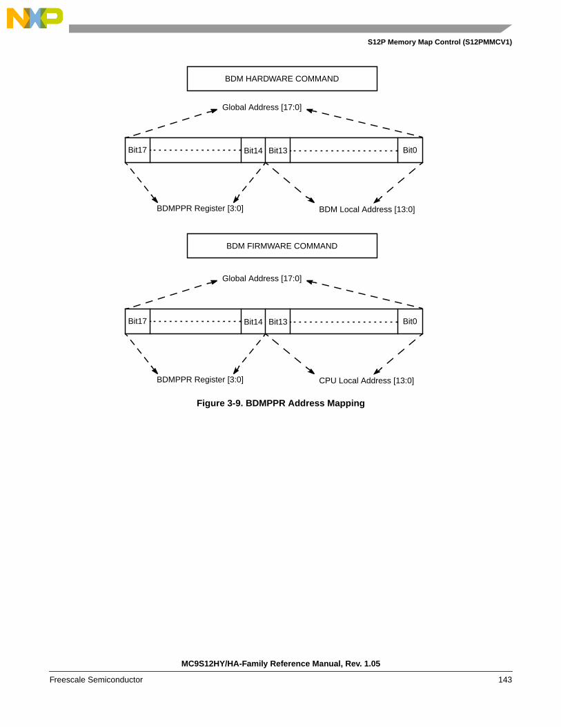
S12P Memory Map Control (S12PMMCV1)
Figure 3-9. BDMPPR Address Mapping
BDM HARDWARE COMMAND
BDM FIRMWARE COMMAND
Bit14 Bit0
BDM Local Address [13:0]BDMPPR Register [3:0]
Global Address [17:0]
Bit13Bit17
Bit14 Bit0
CPU Local Address [13:0]BDMPPR Register [3:0]
Global Address [17:0]
Bit13Bit17
MC9S12HY/HA-Family Reference Manual, Rev. 1.05
Freescale Semiconductor 143

S12P Memory Map Control (S12PMMCV1)
Figure 3-10. Local to Global Address Mapping
0x3_FFFF
PPAGE
CPU and BDMLocal Memory Map
Global Memory Map
0xFFFF
0xC000
0x8000
P-Flash window
0x3_4000
0x3_8000
0x3_C000
0x0_4000
0x0000
0x4000
0x0400D-Flash
RAM
Unpaged P-Flash
REGISTERS
Unpaged P-Flash
Unpaged P-Flash
0 P0P1P2P3000
0x1400
RA
MS
IZE
0x0_0000
RAM
RA
MS
IZE
10 *16K pagedP-Flash
0x0_8000
NVM Resources
REGISTERS
RAM_LOW
Unpaged P-Flash
0x3_0000
Unimplemented Area
Unpaged P-Flash
Unpaged P-Flash
(PPA
GE
0x0C)
(PPA
GE
0x0D)
(PPA
GE
0x0E)
(PPA
GE
0x0F)
Unpaged P-Flashor
(PPA
GE
0x02-0x0B))
(PPA
GE
0x01)(P
PAG
E 0x00)
Unpaged P-Flash
0x0_4400D-Flash
0x0_5400NVM Resources
MC9S12HY/HA-Family Reference Manual, Rev. 1.05
144 Freescale Semiconductor

S12P Memory Map Control (S12PMMCV1)
3.5 Implemented Memory in the System Memory ArchitectureEach memory can be implemented in its maximum allowed size. But some devices have been defined forsmaller sizes, which means less implemented pages. All non implemented pages are called unimplementedareas.
• Registers has a fixed size of 1KB, accessible via xbus0.
• SRAM has a maximum size of 11KB, accessible via xbus0.
• D-Flash has a fixed size of 4KB accessible via xbus0.
• P-Flash has a maximum size of 224KB, accessible via xbus0.
3.5.1 Implemented Memory Map
The global memory spaces reserved for the internal resources (RAM, D-Flash, and P-Flash) are notdetermined by the MMC module. Size of the individual internal resources are however fixed in the designof the device cannot be changed by the user. Please refer to the SoC Guide for further details. Figure 3-11and Table 3-7 show the memory spaces occupied by the on-chip resources. Please note that the memoryspaces have fixed top addresses.
In single-chip modes accesses by the CPU12 (except for firmware commands) to any of theunimplemented areas (see Figure 3-11) will result in an illegal access reset (system reset). BDM accessesto the unimplemented areas are allowed but the data will be undefined.
No misaligned word access from the BDM module will occur; these accesses are blocked in the BDMmodule (Refer to BDM Block Guide).
Table 3-7. Global Implemented Memory Space
Internal Resource Bottom Address Top Address
Registers 0x0_0000 0x0_03FF
System RAM RAM_LOW =0x0_4000 minus RAMSIZE1
1 RAMSIZE is the hexadecimal value of RAM SIZE in bytes
0x0_3FFF
D-Flash 0x0_4400 0x0_53FF
P-Flash PF_LOW =0x4_0000 minus FLASHSIZE2
2 FLASHSIZE is the hexadecimal value of FLASH SIZE in bytes
0x3_FFFF
MC9S12HY/HA-Family Reference Manual, Rev. 1.05
Freescale Semiconductor 145

S12P Memory Map Control (S12PMMCV1)
Figure 3-11. Implemented Global Address Mapping
0x3_FFFF
PPAGE
CPU and BDMLocal Memory Map
Global Memory Map
0xFFFF
0xC000
0x8000
P-Flash window
PF_LOW
Unpaged P-Flash
Unpaged P-Flash
0 P0P1P2P3000
PF
SIZ
E
Unimplemented area
P-Flash
0x0000
0x4000
0x0400D-Flash
RAM
Unpaged P-Flash
REGISTERS
0x1400
RA
MS
IZE
0x0_4000
0x0_0000
RAM
RA
MS
IZE
0x0_8000
NVM Resources
REGISTERS
RAM_LOW
Unimplemented Area
(PPA
GE
0x01)(P
PAG
E 0x00)
0x0_4400D-Flash
0x0_5400NVM Resources
MC9S12HY/HA-Family Reference Manual, Rev. 1.05
146 Freescale Semiconductor
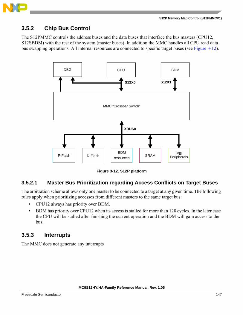
S12P Memory Map Control (S12PMMCV1)
3.5.2 Chip Bus Control
The S12PMMC controls the address buses and the data buses that interface the bus masters (CPU12,S12SBDM) with the rest of the system (master buses). In addition the MMC handles all CPU read databus swapping operations. All internal resources are connected to specific target buses (see Figure 3-12).
Figure 3-12. S12P platform
3.5.2.1 Master Bus Prioritization regarding Access Conflicts on Target Buses
The arbitration scheme allows only one master to be connected to a target at any given time. The followingrules apply when prioritizing accesses from different masters to the same target bus:
• CPU12 always has priority over BDM.
• BDM has priority over CPU12 when its access is stalled for more than 128 cycles. In the later casethe CPU will be stalled after finishing the current operation and the BDM will gain access to thebus.
3.5.3 Interrupts
The MMC does not generate any interrupts
CPU BDM
MMC “Crossbar Switch”
S12X0
XBUS0
DBG
S12X1
IPBIP-Flash D-Flash SRAM
BDM
resources Peripherals
MC9S12HY/HA-Family Reference Manual, Rev. 1.05
Freescale Semiconductor 147
S12P Memory Map Control (S12PMMCV1)
3.6 Initialization/Application Information
3.6.1 CALL and RTC Instructions
CALL and RTC instructions are uninterruptable CPU instructions that automate page switching in theprogram page window. The CALL instruction is similar to the JSR instruction, but the subroutine that iscalled can be located anywhere in the local address space or in any Flash or ROM page visible through theprogram page window. The CALL instruction calculates and stacks a return address, stacks the currentPPAGE value and writes a new instruction-supplied value to the PPAGE register. The PPAGE valuecontrols which of the 256 possible pages is visible through the 16 Kbyte program page window in the64 Kbyte local CPU memory map. Execution then begins at the address of the called subroutine.
During the execution of the CALL instruction, the CPU performs the following steps:
1. Writes the current PPAGE value into an internal temporary register and writes the newinstruction-supplied PPAGE value into the PPAGE register
2. Calculates the address of the next instruction after the CALL instruction (the return address) andpushes this 16-bit value onto the stack
3. Pushes the temporarily stored PPAGE value onto the stack
4. Calculates the effective address of the subroutine, refills the queue and begins execution at the newaddress
This sequence is uninterruptable. There is no need to inhibit interrupts during the CALL instructionexecution. A CALL instruction can be performed from any address to any other address in the local CPUmemory space.
The PPAGE value supplied by the instruction is part of the effective address of the CPU. For all addressingmode variations (except indexed-indirect modes) the new page value is provided by an immediate operandin the instruction. In indexed-indirect variations of the CALL instruction a pointer specifies memorylocations where the new page value and the address of the called subroutine are stored. Using indirectaddressing for both the new page value and the address within the page allows usage of values calculatedat run time rather than immediate values that must be known at the time of assembly.
The RTC instruction terminates subroutines invoked by a CALL instruction. The RTC instruction unstacksthe PPAGE value and the return address and refills the queue. Execution resumes with the next instructionafter the CALL instruction.
During the execution of an RTC instruction the CPU performs the following steps:
1. Pulls the previously stored PPAGE value from the stack
2. Pulls the 16-bit return address from the stack and loads it into the PC
3. Writes the PPAGE value into the PPAGE register
4. Refills the queue and resumes execution at the return address
This sequence is uninterruptable. The RTC can be executed from anywhere in the local CPU memoryspace.
The CALL and RTC instructions behave like JSR and RTS instruction, they however require moreexecution cycles. Usage of JSR/RTS instructions is therefore recommended when possible and
MC9S12HY/HA-Family Reference Manual, Rev. 1.05
148 Freescale Semiconductor

S12P Memory Map Control (S12PMMCV1)
CALL/RTC instructions should only be used when needed. The JSR and RTS instructions can be used toaccess subroutines that are already present in the local CPU memory map (i.e. in the same page in theprogram memory page window for example). However calling a function located in a different pagerequires usage of the CALL instruction. The function must be terminated by the RTC instruction. Becausethe RTC instruction restores contents of the PPAGE register from the stack, functions terminated with theRTC instruction must be called using the CALL instruction even when the correct page is already presentin the memory map. This is to make sure that the correct PPAGE value will be present on stack at the timeof the RTC instruction execution.
MC9S12HY/HA-Family Reference Manual, Rev. 1.05
Freescale Semiconductor 149

S12P Memory Map Control (S12PMMCV1)
MC9S12HY/HA-Family Reference Manual, Rev. 1.05
150 Freescale Semiconductor
Chapter 4Interrupt Module (S12SINTV1)
4.1 IntroductionThe INT module decodes the priority of all system exception requests and provides the applicable vectorfor processing the exception to the CPU. The INT module supports:
• I bit and X bit maskable interrupt requests
• A non-maskable unimplemented op-code trap
• A non-maskable software interrupt (SWI) or background debug mode request
• Three system reset vector requests
• A spurious interrupt vector
Each of the I bit maskable interrupt requests is assigned to a fixed priority level.
4.1.1 Glossary
Table 4-2 contains terms and abbreviations used in the document.
4.1.2 Features• Interrupt vector base register (IVBR)
• One spurious interrupt vector (at address vector base1 + 0x0080).
VersionNumber
RevisionDate
EffectiveDate
Author Description of Changes
01.02 13 Sep2007
updates for S12P family devices:- re-added XIRQ and IRQ references since this functionality is usedon devices without D2D- added low voltage reset as possible source to the pin reset vector
01.04 20 May2009
added footnote about availability of “Wake-up from STOP or WAITby XIRQ with X bit set” feature
01.05 14 Dec2011
Re-worded for difference of Wake-up feature between STOP andWAIT modes.
Table 4-2. Terminology
Term Meaning
CCR Condition Code Register (in the CPU)
ISR Interrupt Service Routine
MCU Micro-Controller Unit
MC9S12HY/HA-Family Reference Manual, Rev. 1.05
Freescale Semiconductor 151

Interrupt Module (S12SINTV1)
• 2–58 I bit maskable interrupt vector requests (at addresses vector base + 0x0082–0x00F2).
• I bit maskable interrupts can be nested.
• One X bit maskable interrupt vector request (at address vector base + 0x00F4).
• One non-maskable software interrupt request (SWI) or background debug mode vector request (ataddress vector base + 0x00F6).
• One non-maskable unimplemented op-code trap (TRAP) vector (at address vector base + 0x00F8).
• Three system reset vectors (at addresses 0xFFFA–0xFFFE).
• Determines the highest priority interrupt vector requests, drives the vector to the bus on CPUrequest
• Wakes up the system from stop or wait mode when an appropriate interrupt request occurs.
4.1.3 Modes of Operation• Run mode
This is the basic mode of operation.
• Wait mode
In wait mode, the clock to the INT module is disabled. The INT module is however capable ofwaking-up the CPU from wait mode if an interrupt occurs. Please refer to Section 4.5.3, “Wake Upfrom Stop or Wait Mode” for details.
• Stop Mode
In stop mode, the clock to the INT module is disabled. The INT module is however capable ofwaking-up the CPU from stop mode if an interrupt occurs. Please refer to Section 4.5.3, “Wake Upfrom Stop or Wait Mode” for details.
• Freeze mode (BDM active)
In freeze mode (BDM active), the interrupt vector base register is overridden internally. Pleaserefer to Section 4.3.1.1, “Interrupt Vector Base Register (IVBR)” for details.
4.1.4 Block Diagram
Figure 4-1 shows a block diagram of the INT module.
1. The vector base is a 16-bit address which is accumulated from the contents of the interrupt vector base register (IVBR, usedas upper byte) and 0x00 (used as lower byte).
MC9S12HY/HA-Family Reference Manual, Rev. 1.05
152 Freescale Semiconductor

Interrupt Module (S12SINTV1)
Figure 4-1. INT Block Diagram
4.2 External Signal DescriptionThe INT module has no external signals.
4.3 Memory Map and Register DefinitionThis section provides a detailed description of all registers accessible in the INT module.
4.3.1 Register Descriptions
This section describes in address order all the INT registers and their individual bits.
4.3.1.1 Interrupt Vector Base Register (IVBR)
Read: Anytime
Write: Anytime
Address: 0x0120
7 6 5 4 3 2 1 0
RIVB_ADDR[7:0]
W
Reset 1 1 1 1 1 1 1 1
Figure 4-2. Interrupt Vector Base Register (IVBR)
Wake Up
IVBR
InterruptRequests
Interrupt Requests CPU
VectorAddress
Peripheral
To C
PU
Prio
rity
Dec
oder
Non I bit Maskable Channels
I bit Maskable Channels
MC9S12HY/HA-Family Reference Manual, Rev. 1.05
Freescale Semiconductor 153

Interrupt Module (S12SINTV1)
4.4 Functional DescriptionThe INT module processes all exception requests to be serviced by the CPU module. These exceptionsinclude interrupt vector requests and reset vector requests. Each of these exception types and their overallpriority level is discussed in the subsections below.
4.4.1 S12S Exception Requests
The CPU handles both reset requests and interrupt requests. A priority decoder is used to evaluate thepriority of pending interrupt requests.
4.4.2 Interrupt Prioritization
The INT module contains a priority decoder to determine the priority for all interrupt requests pending forthe CPU. If more than one interrupt request is pending, the interrupt request with the higher vector addresswins the prioritization.
The following conditions must be met for an I bit maskable interrupt request to be processed.
1. The local interrupt enabled bit in the peripheral module must be set.
2. The I bit in the condition code register (CCR) of the CPU must be cleared.
3. There is no SWI, TRAP, or X bit maskable request pending.
NOTEAll non I bit maskable interrupt requests always have higher priority thanthe I bit maskable interrupt requests. If the X bit in the CCR is cleared, it ispossible to interrupt an I bit maskable interrupt by an X bit maskableinterrupt. It is possible to nest non maskable interrupt requests, for exampleby nesting SWI or TRAP calls.
Since an interrupt vector is only supplied at the time when the CPU requests it, it is possible that a higherpriority interrupt request could override the original interrupt request that caused the CPU to request thevector. In this case, the CPU will receive the highest priority vector and the system will process thisinterrupt request first, before the original interrupt request is processed.
Table 4-3. IVBR Field Descriptions
Field Description
7–0IVB_ADDR[7:0]
Interrupt Vector Base Address Bits — These bits represent the upper byte of all vector addresses. Out ofreset these bits are set to 0xFF (that means vectors are located at 0xFF80–0xFFFE) to ensure compatibilityto HCS12.Note: A system reset will initialize the interrupt vector base register with “0xFF” before it is used to determine
the reset vector address. Therefore, changing the IVBR has no effect on the location of the three resetvectors (0xFFFA–0xFFFE).
Note: If the BDM is active (that means the CPU is in the process of executing BDM firmware code), thecontents of IVBR are ignored and the upper byte of the vector address is fixed as “0xFF”. This is doneto enable handling of all non-maskable interrupts in the BDM firmware.
MC9S12HY/HA-Family Reference Manual, Rev. 1.05
154 Freescale Semiconductor

Interrupt Module (S12SINTV1)
If the interrupt source is unknown (for example, in the case where an interrupt request becomes inactiveafter the interrupt has been recognized, but prior to the CPU vector request), the vector address suppliedto the CPU will default to that of the spurious interrupt vector.
NOTECare must be taken to ensure that all interrupt requests remain active untilthe system begins execution of the applicable service routine; otherwise, theexception request may not get processed at all or the result may be aspurious interrupt request (vector at address (vector base + 0x0080)).
4.4.3 Reset Exception Requests
The INT module supports three system reset exception request types (please refer to the Clock and Resetgenerator module for details):
1. Pin reset, power-on reset or illegal address reset, low voltage reset (if applicable)
2. Clock monitor reset request
3. COP watchdog reset request
4.4.4 Exception Priority
The priority (from highest to lowest) and address of all exception vectors issued by the INT module uponrequest by the CPU is shown in Table 4-4.
Table 4-4. Exception Vector Map and Priority
Vector Address1
1 16 bits vector address based
Source
0xFFFE Pin reset, power-on reset, illegal address reset, low voltage reset (if applicable)
0xFFFC Clock monitor reset
0xFFFA COP watchdog reset
(Vector base + 0x00F8) Unimplemented opcode trap
(Vector base + 0x00F6) Software interrupt instruction (SWI) or BDM vector request
(Vector base + 0x00F4) X bit maskable interrupt request (XIRQ or D2D error interrupt)2
2 D2D error interrupt on MCUs featuring a D2D initiator module, otherwise XIRQ pin interrupt
(Vector base + 0x00F2) IRQ or D2D interrupt request3
3 D2D interrupt on MCUs featuring a D2D initiator module, otherwise IRQ pin interrupt
(Vector base + 0x00F0–0x0082) Device specific I bit maskable interrupt sources (priority determined by the low byte of thevector address, in descending order)
(Vector base + 0x0080) Spurious interrupt
MC9S12HY/HA-Family Reference Manual, Rev. 1.05
Freescale Semiconductor 155

Interrupt Module (S12SINTV1)
4.5 Initialization/Application Information
4.5.1 Initialization
After system reset, software should:
1. Initialize the interrupt vector base register if the interrupt vector table is not located at the defaultlocation (0xFF80–0xFFF9).
2. Enable I bit maskable interrupts by clearing the I bit in the CCR.
3. Enable the X bit maskable interrupt by clearing the X bit in the CCR.
4.5.2 Interrupt Nesting
The interrupt request scheme makes it possible to nest I bit maskable interrupt requests handled by theCPU.
• I bit maskable interrupt requests can be interrupted by an interrupt request with a higher priority.
I bit maskable interrupt requests cannot be interrupted by other I bit maskable interrupt requests perdefault. In order to make an interrupt service routine (ISR) interruptible, the ISR must explicitly clear theI bit in the CCR (CLI). After clearing the I bit, other I bit maskable interrupt requests can interrupt thecurrent ISR.
An ISR of an interruptible I bit maskable interrupt request could basically look like this:
1. Service interrupt, that is clear interrupt flags, copy data, etc.
2. Clear I bit in the CCR by executing the instruction CLI (thus allowing other I bit maskable interruptrequests)
3. Process data
4. Return from interrupt by executing the instruction RTI
4.5.3 Wake Up from Stop or Wait Mode
4.5.3.1 CPU Wake Up from Stop or Wait Mode
Every I bit maskable interrupt request is capable of waking the MCU from wait mode.
Since bus and core clocks are disabled in stop mode, only interrupt requests that can be generated withoutthese clocks can wake the MCU from stop mode. These are listed in the device overview interrupt vectortable.
To determine whether an I bit maskable interrupts is qualified to wake-up the CPU or not, the sameconditions as in normal run mode are applied during stop or wait mode:
• If the I bit in the CCR is set, all I bit maskable interrupts are masked from waking-up the MCU.
The X bit maskable interrupt request can wake up the MCU from stop or wait mode at anytime, even if theX bit in CCR is set1.
MC9S12HY/HA-Family Reference Manual, Rev. 1.05
156 Freescale Semiconductor

Interrupt Module (S12SINTV1)
If the X bit maskable interrupt request is used to wake-up the MCU with the X bit in the CCR set, theassociated ISR is not called. The CPU then resumes program execution with the instruction following theWAI or STOP instruction. This features works following the same rules like any interrupt request, that iscare must be taken that the X interrupt request used for wake-up remains active at least until the systembegins execution of the instruction following the WAI or STOP instruction; otherwise, wake-up may notoccur.
1. The capability of the XIRQ pin to wake-up the MCU with the X bit set may not be available if, for example, the XIRQ pin isshared with other peripheral modules on the device. Please refer to the Device section of the MCU reference manual for details.
MC9S12HY/HA-Family Reference Manual, Rev. 1.05
Freescale Semiconductor 157

Interrupt Module (S12SINTV1)
MC9S12HY/HA-Family Reference Manual, Rev. 1.05
158 Freescale Semiconductor

Chapter 5Background Debug Module (S12SBDMV1)
Table 5-1. Revision History
5.1 IntroductionThis section describes the functionality of the background debug module (BDM) sub-block of the HCS12Score platform.
The background debug module (BDM) sub-block is a single-wire, background debug system implementedin on-chip hardware for minimal CPU intervention. All interfacing with the BDM is done via the BKGDpin.
The BDM has enhanced capability for maintaining synchronization between the target and host whileallowing more flexibility in clock rates. This includes a sync signal to determine the communication rateand a handshake signal to indicate when an operation is complete. The system is backwards compatible tothe BDM of the S12 family with the following exceptions:
• TAGGO command not supported by S12SBDM
• External instruction tagging feature is part of the DBG module
• S12SBDM register map and register content modified
• Family ID readable from BDM ROM at global address 0x3_FF0F in active BDM(value for devices with HCS12S core is 0xC2)
• Clock switch removed from BDM (CLKSW bit removed from BDMSTS register)
5.1.1 Features
The BDM includes these distinctive features:
• Single-wire communication with host development system
• Enhanced capability for allowing more flexibility in clock rates
• SYNC command to determine communication rate
• GO_UNTIL command
Revision Number Date SectionsAffected Summary of Changes
1.05 07.Dec.2010 Table 5-1 Standardized format of revision history table header.
1.06 02.Mar.2011 5.3.2.2/5-1655.2/5-161
Corrected BPAE bit description.Removed references to fixed VCO frequencies
1.07 27.Sep.2012 General Changed references to device level.
Rev. 1.05
Freescale Semiconductor 159
Background Debug Module (S12SBDMV1)
• Hardware handshake protocol to increase the performance of the serial communication
• Active out of reset in special single chip mode
• Nine hardware commands using free cycles, if available, for minimal CPU intervention
• Hardware commands not requiring active BDM
• 14 firmware commands execute from the standard BDM firmware lookup table
• Software control of BDM operation during wait mode
• When secured, hardware commands are allowed to access the register space in special single chipmode, if the Flash erase tests fail.
• Family ID readable from BDM ROM at global address 0x3_FF0F in active BDM(value for devices with HCS12S core is 0xC2)
• BDM hardware commands are operational until system stop mode is entered
5.1.2 Modes of Operation
BDM is available in all operating modes but must be enabled before firmware commands are executed.Some systems may have a control bit that allows suspending the function during background debug mode.
5.1.2.1 Regular Run Modes
All of these operations refer to the part in run mode and not being secured. The BDM does not providecontrols to conserve power during run mode.
• Normal modes
General operation of the BDM is available and operates the same in all normal modes.
• Special single chip mode
In special single chip mode, background operation is enabled and active out of reset. This allowsprogramming a system with blank memory.
5.1.2.2 Secure Mode Operation
If the device is in secure mode, the operation of the BDM is reduced to a small subset of its regular runmode operation. Secure operation prevents access to Flash other than allowing erasure. For moreinformation please see Section 5.4.1, “Security”.
5.1.2.3 Low-Power Modes
The BDM can be used until stop mode is entered. When CPU is in wait mode all BDM firmwarecommands as well as the hardware BACKGROUND command cannot be used and are ignored. In this casethe CPU can not enter BDM active mode, and only hardware read and write commands are available. Alsothe CPU can not enter a low power mode (stop or wait) during BDM active mode.
In stop mode the BDM clocks are stopped. When BDM clocks are disabled and stop mode is exited, theBDM clocks will restart and BDM will have a soft reset (clearing the instruction register, any command inprogress and disable the ACK function). The BDM is now ready to receive a new command.
Rev. 1.05
160 Freescale Semiconductor

Background Debug Module (S12SBDMV1)
5.1.3 Block Diagram
A block diagram of the BDM is shown in Figure 5-1.
Figure 5-1. BDM Block Diagram
5.2 External Signal DescriptionA single-wire interface pin called the background debug interface (BKGD) pin is used to communicatewith the BDM system. During reset, this pin is a mode select input which selects between normal andspecial modes of operation. After reset, this pin becomes the dedicated serial interface pin for thebackground debug mode.
5.3 Memory Map and Register Definition
5.3.1 Module Memory Map
Table 5-2 shows the BDM memory map when BDM is active.
Table 5-2. BDM Memory Map
Global Address ModuleSize
(Bytes)
0x3_FF00–0x3_FF0B BDM registers 12
16-Bit Shift RegisterBKGDHost
System SerialInterface
Data
Control
Register Block
RegisterBDMSTS
Instruction Codeand
Execution
Standard BDM FirmwareLOOKUP TABLE
Secured BDM FirmwareLOOKUP TABLE
Bus Interfaceand
Control Logic
Address
Data
Control
ClocksBDMACT
TRACE
ENBDM
SDV
UNSEC
Rev. 1.05
Freescale Semiconductor 161

Background Debug Module (S12SBDMV1)
5.3.2 Register Descriptions
A summary of the registers associated with the BDM is shown in Figure 5-2. Registers are accessed byhost-driven communications to the BDM hardware using READ_BD and WRITE_BD commands.
0x3_FF0C–0x3_FF0E BDM firmware ROM 3
0x3_FF0F Family ID (part of BDM firmware ROM) 1
0x3_FF10–0x3_FFFF BDM firmware ROM 240
GlobalAddress
RegisterName
Bit 7 6 5 4 3 2 1 Bit 0
0x3_FF00 Reserved R X X X X X X 0 0
W
0x3_FF01 BDMSTS RENBDM
BDMACT 0 SDV TRACE 0 UNSEC 0
W
0x3_FF02 Reserved R X X X X X X X X
W
0x3_FF03 Reserved R X X X X X X X X
W
0x3_FF04 Reserved R X X X X X X X X
W
0x3_FF05 Reserved R X X X X X X X X
W
0x3_FF06 BDMCCR RCCR7 CCR6 CCR5 CCR4 CCR3 CCR2 CCR1 CCR0
W
0x3_FF07 Reserved R 0 0 0 0 0 0 0 0
W
0x3_FF08 BDMPPR RBPAE
0 0 0BPP3 BPP2 BPP1 BPP0
W
= Unimplemented, Reserved = Implemented (do not alter)
X = Indeterminate 0 = Always read zero
Figure 5-2. BDM Register Summary
Table 5-2. BDM Memory Map
Global Address ModuleSize
(Bytes)
Rev. 1.05
162 Freescale Semiconductor
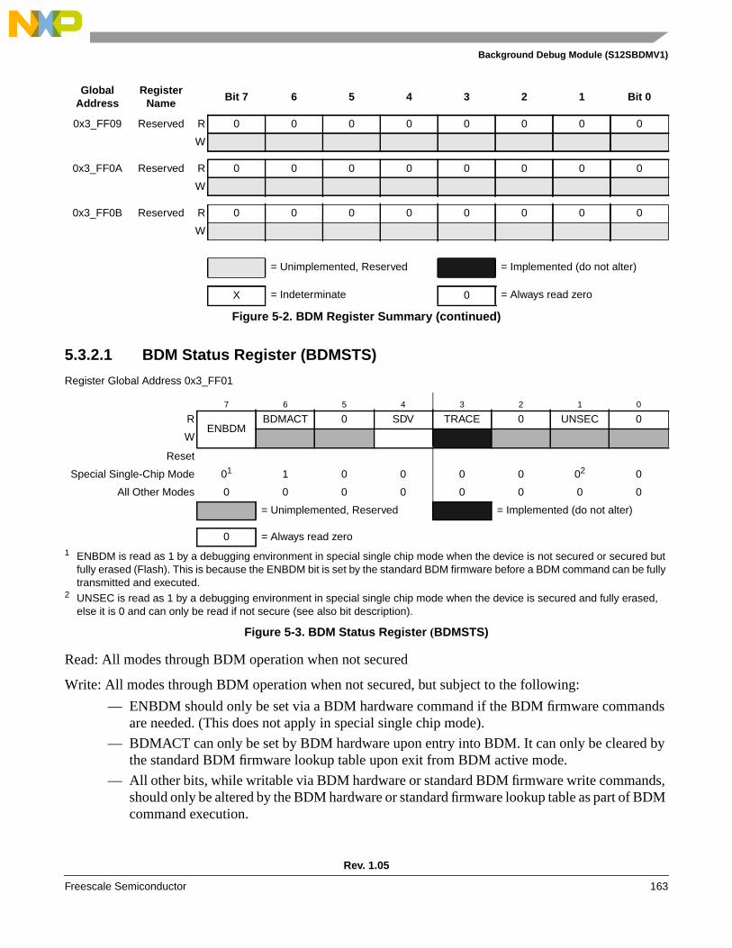
Background Debug Module (S12SBDMV1)
5.3.2.1 BDM Status Register (BDMSTS)
Figure 5-3. BDM Status Register (BDMSTS)
Read: All modes through BDM operation when not secured
Write: All modes through BDM operation when not secured, but subject to the following:
— ENBDM should only be set via a BDM hardware command if the BDM firmware commandsare needed. (This does not apply in special single chip mode).
— BDMACT can only be set by BDM hardware upon entry into BDM. It can only be cleared bythe standard BDM firmware lookup table upon exit from BDM active mode.
— All other bits, while writable via BDM hardware or standard BDM firmware write commands,should only be altered by the BDM hardware or standard firmware lookup table as part of BDMcommand execution.
0x3_FF09 Reserved R 0 0 0 0 0 0 0 0
W
0x3_FF0A Reserved R 0 0 0 0 0 0 0 0
W
0x3_FF0B Reserved R 0 0 0 0 0 0 0 0
W
Register Global Address 0x3_FF01
7 6 5 4 3 2 1 0
RENBDM
BDMACT 0 SDV TRACE 0 UNSEC 0
W
Reset
Special Single-Chip Mode 01
1 ENBDM is read as 1 by a debugging environment in special single chip mode when the device is not secured or secured butfully erased (Flash). This is because the ENBDM bit is set by the standard BDM firmware before a BDM command can be fullytransmitted and executed.
1 0 0 0 0 02
2 UNSEC is read as 1 by a debugging environment in special single chip mode when the device is secured and fully erased,else it is 0 and can only be read if not secure (see also bit description).
0
All Other Modes 0 0 0 0 0 0 0 0
= Unimplemented, Reserved = Implemented (do not alter)
0 = Always read zero
GlobalAddress
RegisterName
Bit 7 6 5 4 3 2 1 Bit 0
= Unimplemented, Reserved = Implemented (do not alter)
X = Indeterminate 0 = Always read zero
Figure 5-2. BDM Register Summary (continued)
Rev. 1.05
Freescale Semiconductor 163

Background Debug Module (S12SBDMV1)
Figure 5-4. BDM CCR Holding Register (BDMCCR)
Read: All modes through BDM operation when not secured
Table 5-3. BDMSTS Field Descriptions
Field Description
7ENBDM
Enable BDM — This bit controls whether the BDM is enabled or disabled. When enabled, BDM can be madeactive to allow firmware commands to be executed. When disabled, BDM cannot be made active but BDMhardware commands are still allowed.0 BDM disabled1 BDM enabledNote: ENBDM is set out of reset in special single chip mode. In special single chip mode with the device
secured, this bit will not be set until after the Flash erase verify tests are complete.
6BDMACT
BDM Active Status — This bit becomes set upon entering BDM. The standard BDM firmware lookup table isthen enabled and put into the memory map. BDMACT is cleared by a carefully timed store instruction in thestandard BDM firmware as part of the exit sequence to return to user code and remove the BDM memory fromthe map.0 BDM not active1 BDM active
4SDV
Shift Data Valid — This bit is set and cleared by the BDM hardware. It is set after data has been transmitted aspart of a BDM firmware or hardware read command or after data has been received as part of a BDM firmwareor hardware write command. It is cleared when the next BDM command has been received or BDM is exited.SDV is used by the standard BDM firmware to control program flow execution.0 Data phase of command not complete1 Data phase of command is complete
3TRACE
TRACE1 BDM Firmware Command is Being Executed — This bit gets set when a BDM TRACE1 firmwarecommand is first recognized. It will stay set until BDM firmware is exited by one of the following BDM commands:GO or GO_UNTIL.0 TRACE1 command is not being executed1 TRACE1 command is being executed
1UNSEC
Unsecure — If the device is secured this bit is only writable in special single chip mode from the BDM securefirmware. It is in a zero state as secure mode is entered so that the secure BDM firmware lookup table is enabledand put into the memory map overlapping the standard BDM firmware lookup table.The secure BDM firmware lookup table verifies that the on-chip Flash is erased. This being the case, the UNSECbit is set and the BDM program jumps to the start of the standard BDM firmware lookup table and the secureBDM firmware lookup table is turned off. If the erase test fails, the UNSEC bit will not be asserted.0 System is in a secured mode.1 System is in a unsecured mode.Note: When UNSEC is set, security is off and the user can change the state of the secure bits in the on-chip
Flash EEPROM. Note that if the user does not change the state of the bits to “unsecured” mode, thesystem will be secured again when it is next taken out of reset.After reset this bit has no meaning or effectwhen the security byte in the Flash EEPROM is configured for unsecure mode.
Register Global Address 0x3_FF06
7 6 5 4 3 2 1 0
RCCR7 CCR6 CCR5 CCR4 CCR3 CCR2 CCR1 CCR0
W
Reset
Special Single-Chip Mode 1 1 0 0 1 0 0 0
All Other Modes 0 0 0 0 0 0 0 0
Rev. 1.05
164 Freescale Semiconductor
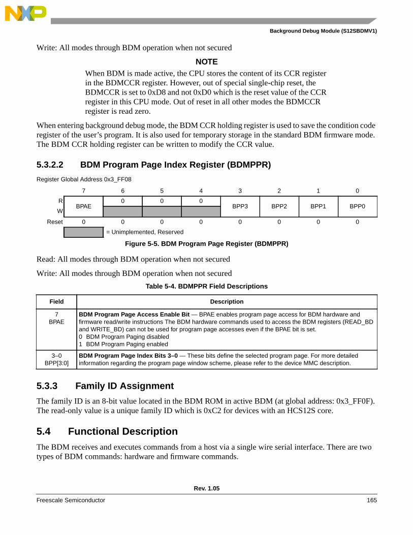
Background Debug Module (S12SBDMV1)
Write: All modes through BDM operation when not secured
NOTEWhen BDM is made active, the CPU stores the content of its CCR registerin the BDMCCR register. However, out of special single-chip reset, theBDMCCR is set to 0xD8 and not 0xD0 which is the reset value of the CCRregister in this CPU mode. Out of reset in all other modes the BDMCCRregister is read zero.
When entering background debug mode, the BDM CCR holding register is used to save the condition coderegister of the user’s program. It is also used for temporary storage in the standard BDM firmware mode.The BDM CCR holding register can be written to modify the CCR value.
5.3.2.2 BDM Program Page Index Register (BDMPPR)
Figure 5-5. BDM Program Page Register (BDMPPR)
Read: All modes through BDM operation when not secured
Write: All modes through BDM operation when not secured
5.3.3 Family ID Assignment
The family ID is an 8-bit value located in the BDM ROM in active BDM (at global address: 0x3_FF0F).The read-only value is a unique family ID which is 0xC2 for devices with an HCS12S core.
5.4 Functional DescriptionThe BDM receives and executes commands from a host via a single wire serial interface. There are twotypes of BDM commands: hardware and firmware commands.
Register Global Address 0x3_FF08
7 6 5 4 3 2 1 0
RBPAE
0 0 0BPP3 BPP2 BPP1 BPP0
W
Reset 0 0 0 0 0 0 0 0
= Unimplemented, Reserved
Table 5-4. BDMPPR Field Descriptions
Field Description
7BPAE
BDM Program Page Access Enable Bit — BPAE enables program page access for BDM hardware andfirmware read/write instructions The BDM hardware commands used to access the BDM registers (READ_BDand WRITE_BD) can not be used for program page accesses even if the BPAE bit is set.0 BDM Program Paging disabled1 BDM Program Paging enabled
3–0BPP[3:0]
BDM Program Page Index Bits 3–0 — These bits define the selected program page. For more detailedinformation regarding the program page window scheme, please refer to the device MMC description.
Rev. 1.05
Freescale Semiconductor 165
Background Debug Module (S12SBDMV1)
Hardware commands are used to read and write target system memory locations and to enter activebackground debug mode, see Section 5.4.3, “BDM Hardware Commands”. Target system memoryincludes all memory that is accessible by the CPU.
Firmware commands are used to read and write CPU resources and to exit from active background debugmode, see Section 5.4.4, “Standard BDM Firmware Commands”. The CPU resources referred to are theaccumulator (D), X index register (X), Y index register (Y), stack pointer (SP), and program counter (PC).
Hardware commands can be executed at any time and in any mode excluding a few exceptions ashighlighted (see Section 5.4.3, “BDM Hardware Commands”) and in secure mode (see Section 5.4.1,“Security”). BDM firmware commands can only be executed when the system is not secure and is in activebackground debug mode (BDM).
5.4.1 Security
If the user resets into special single chip mode with the system secured, a secured mode BDM firmwarelookup table is brought into the map overlapping a portion of the standard BDM firmware lookup table.The secure BDM firmware verifies that the on-chip Flash EEPROM are erased. This being the case, theUNSEC and ENBDM bit will get set. The BDM program jumps to the start of the standard BDM firmwareand the secured mode BDM firmware is turned off and all BDM commands are allowed. If the Flash donot verify as erased, the BDM firmware sets the ENBDM bit, without asserting UNSEC, and the firmwareenters a loop. This causes the BDM hardware commands to become enabled, but does not enable thefirmware commands. This allows the BDM hardware to be used to erase the Flash.
BDM operation is not possible in any other mode than special single chip mode when the device is secured.The device can only be unsecured via BDM serial interface in special single chip mode. More informationregarding security is provided in the security section of the device documentation.
5.4.2 Enabling and Activating BDM
The system must be in active BDM to execute standard BDM firmware commands. BDM can be activatedonly after being enabled. BDM is enabled by setting the ENBDM bit in the BDM status (BDMSTS)register. The ENBDM bit is set by writing to the BDM status (BDMSTS) register, via the single-wireinterface, using a hardware command such as WRITE_BD_BYTE.
After being enabled, BDM is activated by one of the following1:
• Hardware BACKGROUND command
• CPU BGND instruction
• Breakpoint force or tag mechanism2
When BDM is activated, the CPU finishes executing the current instruction and then begins executing thefirmware in the standard BDM firmware lookup table. When BDM is activated by a breakpoint, the typeof breakpoint used determines if BDM becomes active before or after execution of the next instruction.
1. BDM is enabled and active immediately out of special single-chip reset.2. This method is provided by the S12S_DBG module.
Rev. 1.05
166 Freescale Semiconductor

Background Debug Module (S12SBDMV1)
NOTEIf an attempt is made to activate BDM before being enabled, the CPUresumes normal instruction execution after a brief delay. If BDM is notenabled, any hardware BACKGROUND commands issued are ignored bythe BDM and the CPU is not delayed.
In active BDM, the BDM registers and standard BDM firmware lookup table are mapped to addresses0x3_FF00 to 0x3_FFFF. BDM registers are mapped to addresses 0x3_FF00 to 0x3_FF0B. The BDM usesthese registers which are readable anytime by the BDM. However, these registers are not readable by userprograms.
When BDM is activated while CPU executes code overlapping with BDM firmware space the savedprogram counter (PC) will be auto incremented by one from the BDM firmware, no matter what causedthe entry into BDM active mode (BGND instruction, BACKGROUND command or breakpoints). In sucha case the PC must be set to the next valid address via a WRITE_PC command before executing the GOcommand.
5.4.3 BDM Hardware Commands
Hardware commands are used to read and write target system memory locations and to enter activebackground debug mode. Target system memory includes all memory that is accessible by the CPU suchas on-chip RAM, Flash, I/O and control registers.
Hardware commands are executed with minimal or no CPU intervention and do not require the system tobe in active BDM for execution, although, they can still be executed in this mode. When executing ahardware command, the BDM sub-block waits for a free bus cycle so that the background access does notdisturb the running application program. If a free cycle is not found within 128 clock cycles, the CPU ismomentarily frozen so that the BDM can steal a cycle. When the BDM finds a free cycle, the operationdoes not intrude on normal CPU operation provided that it can be completed in a single cycle. However,if an operation requires multiple cycles the CPU is frozen until the operation is complete, even though theBDM found a free cycle.
The BDM hardware commands are listed in Table 5-5.
The READ_BD and WRITE_BD commands allow access to the BDM register locations. These locationsare not normally in the system memory map but share addresses with the application in memory. Todistinguish between physical memory locations that share the same address, BDM memory resources areenabled just for the READ_BD and WRITE_BD access cycle. This allows the BDM to access BDMlocations unobtrusively, even if the addresses conflict with the application memory map.
Table 5-5. Hardware Commands
CommandOpcode (hex)
Data Description
BACKGROUND 90 None Enter background mode if BDM is enabled. If enabled, an ACK will be issuedwhen the part enters active background mode.
ACK_ENABLE D5 None Enable Handshake. Issues an ACK pulse after the command is executed.
ACK_DISABLE D6 None Disable Handshake. This command does not issue an ACK pulse.
Rev. 1.05
Freescale Semiconductor 167

Background Debug Module (S12SBDMV1)
5.4.4 Standard BDM Firmware Commands
BDM firmware commands are used to access and manipulate CPU resources. The system must be in activeBDM to execute standard BDM firmware commands, see Section 5.4.2, “Enabling and Activating BDM”.Normal instruction execution is suspended while the CPU executes the firmware located in the standardBDM firmware lookup table. The hardware command BACKGROUND is the usual way to activate BDM.
As the system enters active BDM, the standard BDM firmware lookup table and BDM registers becomevisible in the on-chip memory map at 0x3_FF00–0x3_FFFF, and the CPU begins executing the standardBDM firmware. The standard BDM firmware watches for serial commands and executes them as they arereceived.
The firmware commands are shown in Table 5-6.
READ_BD_BYTE E4 16-bit address16-bit data out
Read from memory with standard BDM firmware lookup table in map.Odd address data on low byte; even address data on high byte.
READ_BD_WORD EC 16-bit address16-bit data out
Read from memory with standard BDM firmware lookup table in map.Must be aligned access.
READ_BYTE E0 16-bit address16-bit data out
Read from memory with standard BDM firmware lookup table out of map.Odd address data on low byte; even address data on high byte.
READ_WORD E8 16-bit address16-bit data out
Read from memory with standard BDM firmware lookup table out of map.Must be aligned access.
WRITE_BD_BYTE C4 16-bit address16-bit data in
Write to memory with standard BDM firmware lookup table in map.Odd address data on low byte; even address data on high byte.
WRITE_BD_WORD CC 16-bit address16-bit data in
Write to memory with standard BDM firmware lookup table in map.Must be aligned access.
WRITE_BYTE C0 16-bit address16-bit data in
Write to memory with standard BDM firmware lookup table out of map.Odd address data on low byte; even address data on high byte.
WRITE_WORD C8 16-bit address16-bit data in
Write to memory with standard BDM firmware lookup table out of map.Must be aligned access.
NOTE:If enabled, ACK will occur when data is ready for transmission for all BDM READ commands and will occur after the write iscomplete for all BDM WRITE commands.
Table 5-5. Hardware Commands (continued)
CommandOpcode (hex)
Data Description
Rev. 1.05
168 Freescale Semiconductor

Background Debug Module (S12SBDMV1)
5.4.5 BDM Command Structure
Hardware and firmware BDM commands start with an 8-bit opcode followed by a 16-bit address and/or a16-bit data word, depending on the command. All the read commands return 16 bits of data despite thebyte or word implication in the command name.
8-bit reads return 16-bits of data, only one byte of which contains valid data.If reading an even address, the valid data will appear in the MSB. If readingan odd address, the valid data will appear in the LSB.
Table 5-6. Firmware Commands
Command1
1 If enabled, ACK will occur when data is ready for transmission for all BDM READ commands and will occur after the write iscomplete for all BDM WRITE commands.
Opcode(hex)
Data Description
READ_NEXT2
2 When the firmware command READ_NEXT or WRITE_NEXT is used to access the BDM address space the BDM resourcesare accessed rather than user code. Writing BDM firmware is not possible.
62 16-bit data out Increment X index register by 2 (X = X + 2), then read word X points to.
READ_PC 63 16-bit data out Read program counter.
READ_D 64 16-bit data out Read D accumulator.
READ_X 65 16-bit data out Read X index register.
READ_Y 66 16-bit data out Read Y index register.
READ_SP 67 16-bit data out Read stack pointer.
WRITE_NEXT2 42 16-bit data in Increment X index register by 2 (X = X + 2), then write word to locationpointed to by X.
WRITE_PC 43 16-bit data in Write program counter.
WRITE_D 44 16-bit data in Write D accumulator.
WRITE_X 45 16-bit data in Write X index register.
WRITE_Y 46 16-bit data in Write Y index register.
WRITE_SP 47 16-bit data in Write stack pointer.
GO 08 none Go to user program. If enabled, ACK will occur when leaving activebackground mode.
GO_UNTIL3
3 System stop disables the ACK function and ignored commands will not have an ACK-pulse (e.g., CPU in stop or wait mode).The GO_UNTIL command will not get an Acknowledge if CPU executes the wait or stop instruction before the “UNTIL”condition (BDM active again) is reached (see Section 5.4.7, “Serial Interface Hardware Handshake Protocol” last note).
0C none Go to user program. If enabled, ACK will occur upon returning to activebackground mode.
TRACE1 10 none Execute one user instruction then return to active BDM. If enabled,ACK will occur upon returning to active background mode.
TAGGO -> GO 18 none (Previous enable tagging and go to user program.)This command will be deprecated and should not be used anymore.Opcode will be executed as a GO command.
Rev. 1.05
Freescale Semiconductor 169

Background Debug Module (S12SBDMV1)
16-bit misaligned reads and writes are generally not allowed. If attemptedby BDM hardware command, the BDM ignores the least significant bit ofthe address and assumes an even address from the remaining bits.
For hardware data read commands, the external host must wait at least 150 bus clock cycles after sendingthe address before attempting to obtain the read data. This is to be certain that valid data is available in theBDM shift register, ready to be shifted out. For hardware write commands, the external host must wait150 bus clock cycles after sending the data to be written before attempting to send a new command. Thisis to avoid disturbing the BDM shift register before the write has been completed. The 150 bus clock cycledelay in both cases includes the maximum 128 cycle delay that can be incurred as the BDM waits for afree cycle before stealing a cycle.
For BDM firmware read commands, the external host should wait at least 48 bus clock cycles after sendingthe command opcode and before attempting to obtain the read data. The 48 cycle wait allows enough timefor the requested data to be made available in the BDM shift register, ready to be shifted out.
For BDM firmware write commands, the external host must wait 36 bus clock cycles after sending the datato be written before attempting to send a new command. This is to avoid disturbing the BDM shift registerbefore the write has been completed.
The external host should wait for at least for 76 bus clock cycles after a TRACE1 or GO command beforestarting any new serial command. This is to allow the CPU to exit gracefully from the standard BDMfirmware lookup table and resume execution of the user code. Disturbing the BDM shift registerprematurely may adversely affect the exit from the standard BDM firmware lookup table.
NOTEIf the bus rate of the target processor is unknown or could be changing, it isrecommended that the ACK (acknowledge function) is used to indicatewhen an operation is complete. When using ACK, the delay times areautomated.
Figure 5-6 represents the BDM command structure. The command blocks illustrate a series of eight bittimes starting with a falling edge. The bar across the top of the blocks indicates that the BKGD line idlesin the high state. The time for an 8-bit command is 8 × 16 target clock cycles.1
1. Target clock cycles are cycles measured using the target MCU’s serial clock rate. See Section 5.4.6, “BDM Serial Interface”and Section 5.3.2.1, “BDM Status Register (BDMSTS)” for information on how serial clock rate is selected.
Rev. 1.05
170 Freescale Semiconductor

Background Debug Module (S12SBDMV1)
Figure 5-6. BDM Command Structure
5.4.6 BDM Serial Interface
The BDM communicates with external devices serially via the BKGD pin. During reset, this pin is a modeselect input which selects between normal and special modes of operation. After reset, this pin becomesthe dedicated serial interface pin for the BDM.
This clock will be referred to as the target clock in the following explanation.
The BDM serial interface uses a clocking scheme in which the external host generates a falling edge onthe BKGD pin to indicate the start of each bit time. This falling edge is sent for every bit whether data istransmitted or received. Data is transferred most significant bit (MSB) first at 16 target clock cycles perbit. The interface times out if 512 clock cycles occur between falling edges from the host.
The BKGD pin is a pseudo open-drain pin and has an weak on-chip active pull-up that is enabled at alltimes. It is assumed that there is an external pull-up and that drivers connected to BKGD do not typicallydrive the high level. Since R-C rise time could be unacceptably long, the target system and host providebrief driven-high (speedup) pulses to drive BKGD to a logic 1. The source of this speedup pulse is the hostfor transmit cases and the target for receive cases.
The timing for host-to-target is shown in Figure 5-7 and that of target-to-host in Figure 5-8 andFigure 5-9. All four cases begin when the host drives the BKGD pin low to generate a falling edge. Sincethe host and target are operating from separate clocks, it can take the target system up to one full clockcycle to recognize this edge. The target measures delays from this perceived start of the bit time while thehost measures delays from the point it actually drove BKGD low to start the bit up to one target clock cycleearlier. Synchronization between the host and target is established in this manner at the start of every bittime.
Hardware
Hardware
Firmware
Firmware
GO,
48-BC
BC = Bus Clock Cycles
Command Address
150-BCDelay
Next
DELAY
8 BitsAT ~16 TC/Bit
16 BitsAT ~16 TC/Bit
16 BitsAT ~16 TC/Bit
Command Address Data Next
DataRead
Write
Read
Write
TRACE
Command Next
Command Data
76-BCDelay
Next
Command
150-BCDelay
36-BCDELAY
Command
Command
Command
CommandData
NextCommand
TC = Target Clock Cycles
Rev. 1.05
Freescale Semiconductor 171

Background Debug Module (S12SBDMV1)
Figure 5-7 shows an external host transmitting a logic 1 and transmitting a logic 0 to the BKGD pin of atarget system. The host is asynchronous to the target, so there is up to a one clock-cycle delay from thehost-generated falling edge to where the target recognizes this edge as the beginning of the bit time. Tentarget clock cycles later, the target senses the bit level on the BKGD pin. Internal glitch detect logicrequires the pin be driven high no later that eight target clock cycles after the falling edge for a logic 1transmission.
Since the host drives the high speedup pulses in these two cases, the rising edges look like digitally drivensignals.
Figure 5-7. BDM Host-to-Target Serial Bit Timing
The receive cases are more complicated. Figure 5-8 shows the host receiving a logic 1 from the targetsystem. Since the host is asynchronous to the target, there is up to one clock-cycle delay from thehost-generated falling edge on BKGD to the perceived start of the bit time in the target. The host holds theBKGD pin low long enough for the target to recognize it (at least two target clock cycles). The host mustrelease the low drive before the target drives a brief high speedup pulse seven target clock cycles after theperceived start of the bit time. The host should sample the bit level about 10 target clock cycles after itstarted the bit time.
Target Senses Bit
10 Cycles
SynchronizationUncertainty
BDM Clock(Target MCU)
HostTransmit 1
HostTransmit 0
PerceivedStart of Bit Time
EarliestStart ofNext Bit
Rev. 1.05
172 Freescale Semiconductor

Background Debug Module (S12SBDMV1)
Figure 5-8. BDM Target-to-Host Serial Bit Timing (Logic 1)
Figure 5-9 shows the host receiving a logic 0 from the target. Since the host is asynchronous to the target,there is up to a one clock-cycle delay from the host-generated falling edge on BKGD to the start of the bittime as perceived by the target. The host initiates the bit time but the target finishes it. Since the targetwants the host to receive a logic 0, it drives the BKGD pin low for 13 target clock cycles then briefly drivesit high to speed up the rising edge. The host samples the bit level about 10 target clock cycles after startingthe bit time.
Figure 5-9. BDM Target-to-Host Serial Bit Timing (Logic 0)
High-Impedance
EarliestStart ofNext Bit
R-C Rise
10 Cycles10 Cycles
Host SamplesBKGD Pin
PerceivedStart of Bit Time
BKGD Pin
BDM Clock(Target MCU)
HostDrive to
BKGD Pin
Target SystemSpeedup
Pulse
High-Impedance
High-Impedance
EarliestStart ofNext Bit
BDM Clock(Target MCU)
HostDrive to
BKGD Pin
BKGD Pin
PerceivedStart of Bit Time
10 Cycles10 Cycles
Host SamplesBKGD Pin
Target SystemDrive and
Speedup Pulse
Speedup Pulse
High-Impedance
Rev. 1.05
Freescale Semiconductor 173

Background Debug Module (S12SBDMV1)
5.4.7 Serial Interface Hardware Handshake Protocol
BDM commands that require CPU execution are ultimately treated at the MCU bus rate. Since the BDMclock source can be modified , it is very helpful to provide a handshake protocol in which the host coulddetermine when an issued command is executed by the CPU. . The alternative is to always wait the amountof time equal to the appropriate number of cycles at the slowest possible rate the clock could be running.This sub-section will describe the hardware handshake protocol.
The hardware handshake protocol signals to the host controller when an issued command was successfullyexecuted by the target. This protocol is implemented by a 16 serial clock cycle low pulse followed by abrief speedup pulse in the BKGD pin. This pulse is generated by the target MCU when a command, issuedby the host, has been successfully executed (see Figure 5-10). This pulse is referred to as the ACK pulse.After the ACK pulse has finished: the host can start the bit retrieval if the last issued command was a readcommand, or start a new command if the last command was a write command or a control command(BACKGROUND, GO, GO_UNTIL or TRACE1). The ACK pulse is not issued earlier than 32 serial clockcycles after the BDM command was issued. The end of the BDM command is assumed to be the 16th tickof the last bit. This minimum delay assures enough time for the host to perceive the ACK pulse. Note alsothat, there is no upper limit for the delay between the command and the related ACK pulse, since thecommand execution depends upon the CPU bus, which in some cases could be very slow due to longaccesses taking place.This protocol allows a great flexibility for the POD designers, since it does not relyon any accurate time measurement or short response time to any event in the serial communication.
Figure 5-10. Target Acknowledge Pulse (ACK)
NOTEIf the ACK pulse was issued by the target, the host assumes the previouscommand was executed. If the CPU enters wait or stop prior to executing ahardware command, the ACK pulse will not be issued meaning that theBDM command was not executed. After entering wait or stop mode, theBDM command is no longer pending.
Figure 5-11 shows the ACK handshake protocol in a command level timing diagram. The READ_BYTEinstruction is used as an example. First, the 8-bit instruction opcode is sent by the host, followed by the
16 Cycles
BDM Clock(Target MCU)
TargetTransmits
ACK Pulse
High-Impedance
BKGD Pin
Minimum DelayFrom the BDM Command
32 Cycles
EarliestStart ofNext Bit
Speedup Pulse
16th Tick of theLast Command Bit
High-Impedance
Rev. 1.05
174 Freescale Semiconductor

Background Debug Module (S12SBDMV1)
address of the memory location to be read. The target BDM decodes the instruction. A bus cycle is grabbed(free or stolen) by the BDM and it executes the READ_BYTE operation. Having retrieved the data, theBDM issues an ACK pulse to the host controller, indicating that the addressed byte is ready to be retrieved.After detecting the ACK pulse, the host initiates the byte retrieval process. Note that data is sent in the formof a word and the host needs to determine which is the appropriate byte based on whether the address wasodd or even.
Figure 5-11. Handshake Protocol at Command Level
Differently from the normal bit transfer (where the host initiates the transmission), the serial interface ACKhandshake pulse is initiated by the target MCU by issuing a negative edge in the BKGD pin. The hardwarehandshake protocol in Figure 5-10 specifies the timing when the BKGD pin is being driven, so the hostshould follow this timing constraint in order to avoid the risk of an electrical conflict in the BKGD pin.
NOTEThe only place the BKGD pin can have an electrical conflict is when oneside is driving low and the other side is issuing a speedup pulse (high). Other“highs” are pulled rather than driven. However, at low rates the time of thespeedup pulse can become lengthy and so the potential conflict timebecomes longer as well.
The ACK handshake protocol does not support nested ACK pulses. If a BDM command is notacknowledge by an ACK pulse, the host needs to abort the pending command first in order to be able toissue a new BDM command. When the CPU enters wait or stop while the host issues a hardware command(e.g., WRITE_BYTE), the target discards the incoming command due to the wait or stop being detected.Therefore, the command is not acknowledged by the target, which means that the ACK pulse will not beissued in this case. After a certain time the host (not aware of stop or wait) should decide to abort anypossible pending ACK pulse in order to be sure a new command can be issued. Therefore, the protocolprovides a mechanism in which a command, and its corresponding ACK, can be aborted.
READ_BYTE
BDM Issues the
BKGD Pin Byte Address
BDM Executes theREAD_BYTE Command
Host Target
HostTarget
BDM Decodesthe Command
ACK Pulse (out of scale)
Host Target
(2) Bytes areRetrieved
New BDMCommand
Rev. 1.05
Freescale Semiconductor 175

Background Debug Module (S12SBDMV1)
NOTEThe ACK pulse does not provide a time out. This means for the GO_UNTILcommand that it can not be distinguished if a stop or wait has been executed(command discarded and ACK not issued) or if the “UNTIL” condition(BDM active) is just not reached yet. Hence in any case where the ACKpulse of a command is not issued the possible pending command should beaborted before issuing a new command. See the handshake abort proceduredescribed in Section 5.4.8, “Hardware Handshake Abort Procedure”.
5.4.8 Hardware Handshake Abort Procedure
The abort procedure is based on the SYNC command. In order to abort a command, which had not issuedthe corresponding ACK pulse, the host controller should generate a low pulse in the BKGD pin by drivingit low for at least 128 serial clock cycles and then driving it high for one serial clock cycle, providing aspeedup pulse. By detecting this long low pulse in the BKGD pin, the target executes the SYNC protocol,see Section 5.4.9, “SYNC — Request Timed Reference Pulse”, and assumes that the pending commandand therefore the related ACK pulse, are being aborted. Therefore, after the SYNC protocol has beencompleted the host is free to issue new BDM commands. For BDM firmware READ or WRITE commandsit can not be guaranteed that the pending command is aborted when issuing a SYNC before thecorresponding ACK pulse. There is a short latency time from the time the READ or WRITE access beginsuntil it is finished and the corresponding ACK pulse is issued. The latency time depends on the firmwareREAD or WRITE command that is issued and on the selected bus clock rate. When the SYNC commandstarts during this latency time the READ or WRITE command will not be aborted, but the correspondingACK pulse will be aborted. A pending GO, TRACE1 or GO_UNTIL command can not be aborted. Onlythe corresponding ACK pulse can be aborted by the SYNC command.
Although it is not recommended, the host could abort a pending BDM command by issuing a low pulse inthe BKGD pin shorter than 128 serial clock cycles, which will not be interpreted as the SYNC command.The ACK is actually aborted when a negative edge is perceived by the target in the BKGD pin. The shortabort pulse should have at least 4 clock cycles keeping the BKGD pin low, in order to allow the negativeedge to be detected by the target. In this case, the target will not execute the SYNC protocol but the pendingcommand will be aborted along with the ACK pulse. The potential problem with this abort procedure iswhen there is a conflict between the ACK pulse and the short abort pulse. In this case, the target may notperceive the abort pulse. The worst case is when the pending command is a read command (i.e.,READ_BYTE). If the abort pulse is not perceived by the target the host will attempt to send a newcommand after the abort pulse was issued, while the target expects the host to retrieve the accessedmemory byte. In this case, host and target will run out of synchronism. However, if the command to beaborted is not a read command the short abort pulse could be used. After a command is aborted the targetassumes the next negative edge, after the abort pulse, is the first bit of a new BDM command.
NOTEThe details about the short abort pulse are being provided only as a referencefor the reader to better understand the BDM internal behavior. It is notrecommended that this procedure be used in a real application.
Rev. 1.05
176 Freescale Semiconductor

Background Debug Module (S12SBDMV1)
Since the host knows the target serial clock frequency, the SYNC command (used to abort a command)does not need to consider the lower possible target frequency. In this case, the host could issue a SYNCvery close to the 128 serial clock cycles length. Providing a small overhead on the pulse length in order toassure the SYNC pulse will not be misinterpreted by the target. See Section 5.4.9, “SYNC — RequestTimed Reference Pulse”.
Figure 5-12 shows a SYNC command being issued after a READ_BYTE, which aborts the READ_BYTEcommand. Note that, after the command is aborted a new command could be issued by the host computer.
Figure 5-12. ACK Abort Procedure at the Command Level
NOTEFigure 5-12 does not represent the signals in a true timing scale
Figure 5-13 shows a conflict between the ACK pulse and the SYNC request pulse. This conflict couldoccur if a POD device is connected to the target BKGD pin and the target is already in debug active mode.Consider that the target CPU is executing a pending BDM command at the exact moment the POD is beingconnected to the BKGD pin. In this case, an ACK pulse is issued along with the SYNC command. In thiscase, there is an electrical conflict between the ACK speedup pulse and the SYNC pulse. Since this is nota probable situation, the protocol does not prevent this conflict from happening.
Figure 5-13. ACK Pulse and SYNC Request Conflict
READ_BYTE READ_STATUSBKGD Pin Memory Address New BDM Command
New BDM Command
Host Target Host Target Host Target
SYNC ResponseFrom the Target(Out of Scale)
BDM Decodeand Starts to Execute
the READ_BYTE Command
READ_BYTE CMD is Abortedby the SYNC Request
(Out of Scale)
BDM Clock(Target MCU)
Target MCUDrives to
BKGD Pin
BKGD Pin
16 Cycles
Speedup Pulse
High-Impedance
HostDrives SYNCTo BKGD Pin
ACK Pulse
Host SYNC Request Pulse
At Least 128 Cycles
Electrical ConflictHost andTarget Driveto BKGD Pin
Rev. 1.05
Freescale Semiconductor 177

Background Debug Module (S12SBDMV1)
NOTEThis information is being provided so that the MCU integrator will be awarethat such a conflict could occur.
The hardware handshake protocol is enabled by the ACK_ENABLE and disabled by the ACK_DISABLEBDM commands. This provides backwards compatibility with the existing POD devices which are notable to execute the hardware handshake protocol. It also allows for new POD devices, that support thehardware handshake protocol, to freely communicate with the target device. If desired, without the needfor waiting for the ACK pulse.
The commands are described as follows:
• ACK_ENABLE — enables the hardware handshake protocol. The target will issue the ACK pulsewhen a CPU command is executed by the CPU. The ACK_ENABLE command itself also has theACK pulse as a response.
• ACK_DISABLE — disables the ACK pulse protocol. In this case, the host needs to use the worstcase delay time at the appropriate places in the protocol.
The default state of the BDM after reset is hardware handshake protocol disabled.
All the read commands will ACK (if enabled) when the data bus cycle has completed and the data is thenready for reading out by the BKGD serial pin. All the write commands will ACK (if enabled) after the datahas been received by the BDM through the BKGD serial pin and when the data bus cycle is complete. SeeSection 5.4.3, “BDM Hardware Commands” and Section 5.4.4, “Standard BDM Firmware Commands”for more information on the BDM commands.
The ACK_ENABLE sends an ACK pulse when the command has been completed. This feature could beused by the host to evaluate if the target supports the hardware handshake protocol. If an ACK pulse isissued in response to this command, the host knows that the target supports the hardware handshakeprotocol. If the target does not support the hardware handshake protocol the ACK pulse is not issued. Inthis case, the ACK_ENABLE command is ignored by the target since it is not recognized as a validcommand.
The BACKGROUND command will issue an ACK pulse when the CPU changes from normal tobackground mode. The ACK pulse related to this command could be aborted using the SYNC command.
The GO command will issue an ACK pulse when the CPU exits from background mode. The ACK pulserelated to this command could be aborted using the SYNC command.
The GO_UNTIL command is equivalent to a GO command with exception that the ACK pulse, in thiscase, is issued when the CPU enters into background mode. This command is an alternative to the GOcommand and should be used when the host wants to trace if a breakpoint match occurs and causes theCPU to enter active background mode. Note that the ACK is issued whenever the CPU enters BDM, whichcould be caused by a breakpoint match or by a BGND instruction being executed. The ACK pulse relatedto this command could be aborted using the SYNC command.
The TRACE1 command has the related ACK pulse issued when the CPU enters background active modeafter one instruction of the application program is executed. The ACK pulse related to this command couldbe aborted using the SYNC command.
Rev. 1.05
178 Freescale Semiconductor

Background Debug Module (S12SBDMV1)
5.4.9 SYNC — Request Timed Reference Pulse
The SYNC command is unlike other BDM commands because the host does not necessarily know thecorrect communication speed to use for BDM communications until after it has analyzed the response tothe SYNC command. To issue a SYNC command, the host should perform the following steps:
1. Drive the BKGD pin low for at least 128 cycles at the lowest possible BDM serial communicationfrequency
2. Drive BKGD high for a brief speedup pulse to get a fast rise time (this speedup pulse is typicallyone cycle of the host clock.)
3. Remove all drive to the BKGD pin so it reverts to high impedance.
4. Listen to the BKGD pin for the sync response pulse.
Upon detecting the SYNC request from the host, the target performs the following steps:
1. Discards any incomplete command received or bit retrieved.
2. Waits for BKGD to return to a logic one.
3. Delays 16 cycles to allow the host to stop driving the high speedup pulse.
4. Drives BKGD low for 128 cycles at the current BDM serial communication frequency.
5. Drives a one-cycle high speedup pulse to force a fast rise time on BKGD.
6. Removes all drive to the BKGD pin so it reverts to high impedance.
The host measures the low time of this 128 cycle SYNC response pulse and determines the correct speedfor subsequent BDM communications. Typically, the host can determine the correct communication speedwithin a few percent of the actual target speed and the communication protocol can easily tolerate speederrors of several percent.
As soon as the SYNC request is detected by the target, any partially received command or bit retrieved isdiscarded. This is referred to as a soft-reset, equivalent to a time-out in the serial communication. After theSYNC response, the target will consider the next negative edge (issued by the host) as the start of a newBDM command or the start of new SYNC request.
Another use of the SYNC command pulse is to abort a pending ACK pulse. The behavior is exactly thesame as in a regular SYNC command. Note that one of the possible causes for a command to not beacknowledged by the target is a host-target synchronization problem. In this case, the command may nothave been understood by the target and so an ACK response pulse will not be issued.
5.4.10 Instruction Tracing
When a TRACE1 command is issued to the BDM in active BDM, the CPU exits the standard BDMfirmware and executes a single instruction in the user code. Once this has occurred, the CPU is forced toreturn to the standard BDM firmware and the BDM is active and ready to receive a new command. If theTRACE1 command is issued again, the next user instruction will be executed. This facilitates stepping ortracing through the user code one instruction at a time.
If an interrupt is pending when a TRACE1 command is issued, the interrupt stacking operation occurs butno user instruction is executed. Once back in standard BDM firmware execution, the program counterpoints to the first instruction in the interrupt service routine.
Rev. 1.05
Freescale Semiconductor 179
Background Debug Module (S12SBDMV1)
Be aware when tracing through the user code that the execution of the user code is done step by step butall peripherals are free running. Hence possible timing relations between CPU code execution andoccurrence of events of other peripherals no longer exist.
Do not trace the CPU instruction BGND used for soft breakpoints. Tracing over the BGND instruction willresult in a return address pointing to BDM firmware address space.
When tracing through user code which contains stop or wait instructions the following will happen whenthe stop or wait instruction is traced:
The CPU enters stop or wait mode and the TRACE1 command can not be finished before leavingthe low power mode. This is the case because BDM active mode can not be entered after CPUexecuted the stop instruction. However all BDM hardware commands except the BACKGROUNDcommand are operational after tracing a stop or wait instruction and still being in stop or waitmode. If system stop mode is entered (all bus masters are in stop mode) no BDM command isoperational.
As soon as stop or wait mode is exited the CPU enters BDM active mode and the saved PC valuepoints to the entry of the corresponding interrupt service routine.
In case the handshake feature is enabled the corresponding ACK pulse of the TRACE1 commandwill be discarded when tracing a stop or wait instruction. Hence there is no ACK pulse when BDMactive mode is entered as part of the TRACE1 command after CPU exited from stop or wait mode.All valid commands sent during CPU being in stop or wait mode or after CPU exited from stop orwait mode will have an ACK pulse. The handshake feature becomes disabled only when systemstop mode has been reached. Hence after a system stop mode the handshake feature must beenabled again by sending the ACK_ENABLE command.
5.4.11 Serial Communication Time Out
The host initiates a host-to-target serial transmission by generating a falling edge on the BKGD pin. IfBKGD is kept low for more than 128 target clock cycles, the target understands that a SYNC commandwas issued. In this case, the target will keep waiting for a rising edge on BKGD in order to answer theSYNC request pulse. If the rising edge is not detected, the target will keep waiting forever without anytime-out limit.
Consider now the case where the host returns BKGD to logic one before 128 cycles. This is interpreted asa valid bit transmission, and not as a SYNC request. The target will keep waiting for another falling edgemarking the start of a new bit. If, however, a new falling edge is not detected by the target within 512 clockcycles since the last falling edge, a time-out occurs and the current command is discarded without affectingmemory or the operating mode of the MCU. This is referred to as a soft-reset.
If a read command is issued but the data is not retrieved within 512 serial clock cycles, a soft-reset willoccur causing the command to be disregarded. The data is not available for retrieval after the time-out hasoccurred. This is the expected behavior if the handshake protocol is not enabled. In order to allow the datato be retrieved even with a large clock frequency mismatch (between BDM and CPU) when the hardwarehandshake protocol is enabled, the time out between a read command and the data retrieval is disabled.Therefore, the host could wait for more then 512 serial clock cycles and still be able to retrieve the datafrom an issued read command. However, once the handshake pulse (ACK pulse) is issued, the time-out
Rev. 1.05
180 Freescale Semiconductor

Background Debug Module (S12SBDMV1)
feature is re-activated, meaning that the target will time out after 512 clock cycles. Therefore, the hostneeds to retrieve the data within a 512 serial clock cycles time frame after the ACK pulse had been issued.After that period, the read command is discarded and the data is no longer available for retrieval. Anynegative edge in the BKGD pin after the time-out period is considered to be a new command or a SYNCrequest.
Note that whenever a partially issued command, or partially retrieved data, has occurred the time out in theserial communication is active. This means that if a time frame higher than 512 serial clock cycles isobserved between two consecutive negative edges and the command being issued or data being retrievedis not complete, a soft-reset will occur causing the partially received command or data retrieved to bedisregarded. The next negative edge in the BKGD pin, after a soft-reset has occurred, is considered by thetarget as the start of a new BDM command, or the start of a SYNC request pulse.
Rev. 1.05
Freescale Semiconductor 181

Background Debug Module (S12SBDMV1)
Rev. 1.05
182 Freescale Semiconductor

Chapter 6S12S Debug Module (S12SDBGV2)
Table 6-1. Revision History
6.1 IntroductionThe S12SDBG module provides an on-chip trace buffer with flexible triggering capability to allownon-intrusive debug of application software. The S12SDBG module is optimized for S12SCPUdebugging.
Typically the S12SDBG module is used in conjunction with the S12SBDM module, whereby the userconfigures the S12SDBG module for a debugging session over the BDM interface. Once configured theS12SDBG module is armed and the device leaves BDM returning control to the user program, which isthen monitored by the S12SDBG module. Alternatively the S12SDBG module can be configured over aserial interface using SWI routines.
6.1.1 Glossary Of Terms
COF: Change Of Flow. Change in the program flow due to a conditional branch, indexed jump or interrupt
BDM: Background Debug Mode
S12SBDM: Background Debug Module
DUG: Device User Guide, describing the features of the device into which the DBG is integrated
WORD: 16-bit data entity
Data Line: 20-bit data entity
CPU: S12SCPU module
DBG: S12SDBG module
POR: Power On Reset
Revision Number RevisionDate
SectionsAffected Summary of Changes
02.08 09.MAY.2008 General Spelling corrections. Revision history format changed.
02.09 29.MAY.2008 6.4.5.4 Added note for end aligned, PurePC, rollover case.
02.10 27.SEP.2012 General Changed cross reference formats
MC9S12HY/HA-Family Reference Manual, Rev. 1.05
Freescale Semiconductor

S12S Debug Module (S12SDBGV2)
Tag: Tags can be attached to CPU opcodes as they enter the instruction pipe. If the tagged opcode reachesthe execution stage a tag hit occurs.
6.1.2 Overview
The comparators monitor the bus activity of the CPU module. A match can initiate a state sequencertransition. On a transition to the Final State, bus tracing is triggered and/or a breakpoint can be generated.
Independent of comparator matches a transition to Final State with associated tracing and breakpoint canbe triggered immediately by writing to the TRIG control bit.
The trace buffer is visible through a 2-byte window in the register address map and can be read out usingstandard 16-bit word reads. Tracing is disabled when the MCU system is secured.
6.1.3 Features• Three comparators (A, B and C)
— Comparators A compares the full address bus and full 16-bit data bus— Comparator A features a data bus mask register— Comparators B and C compare the full address bus only— Each comparator features selection of read or write access cycles— Comparator B allows selection of byte or word access cycles— Comparator matches can initiate state sequencer transitions
• Three comparator modes— Simple address/data comparator match mode— Inside address range mode, Addmin ≤ Address ≤ Addmax— Outside address range match mode, Address < Addmin or Address > Addmax
• Two types of matches— Tagged — This matches just before a specific instruction begins execution— Force — This is valid on the first instruction boundary after a match occurs
• Two types of breakpoints— CPU breakpoint entering BDM on breakpoint (BDM)— CPU breakpoint executing SWI on breakpoint (SWI)
• Trigger mode independent of comparators— TRIG Immediate software trigger
• Four trace modes— Normal: change of flow (COF) PC information is stored (see 6.4.5.2.1, "Normal Mode") for
change of flow definition.— Loop1: same as Normal but inhibits consecutive duplicate source address entries— Detail: address and data for all cycles except free cycles and opcode fetches are stored— Compressed Pure PC: all program counter addresses are stored
• 4-stage state sequencer for trace buffer control— Tracing session trigger linked to Final State of state sequencer
MC9S12HY/HA-Family Reference Manual, Rev. 1.05
184 Freescale Semiconductor
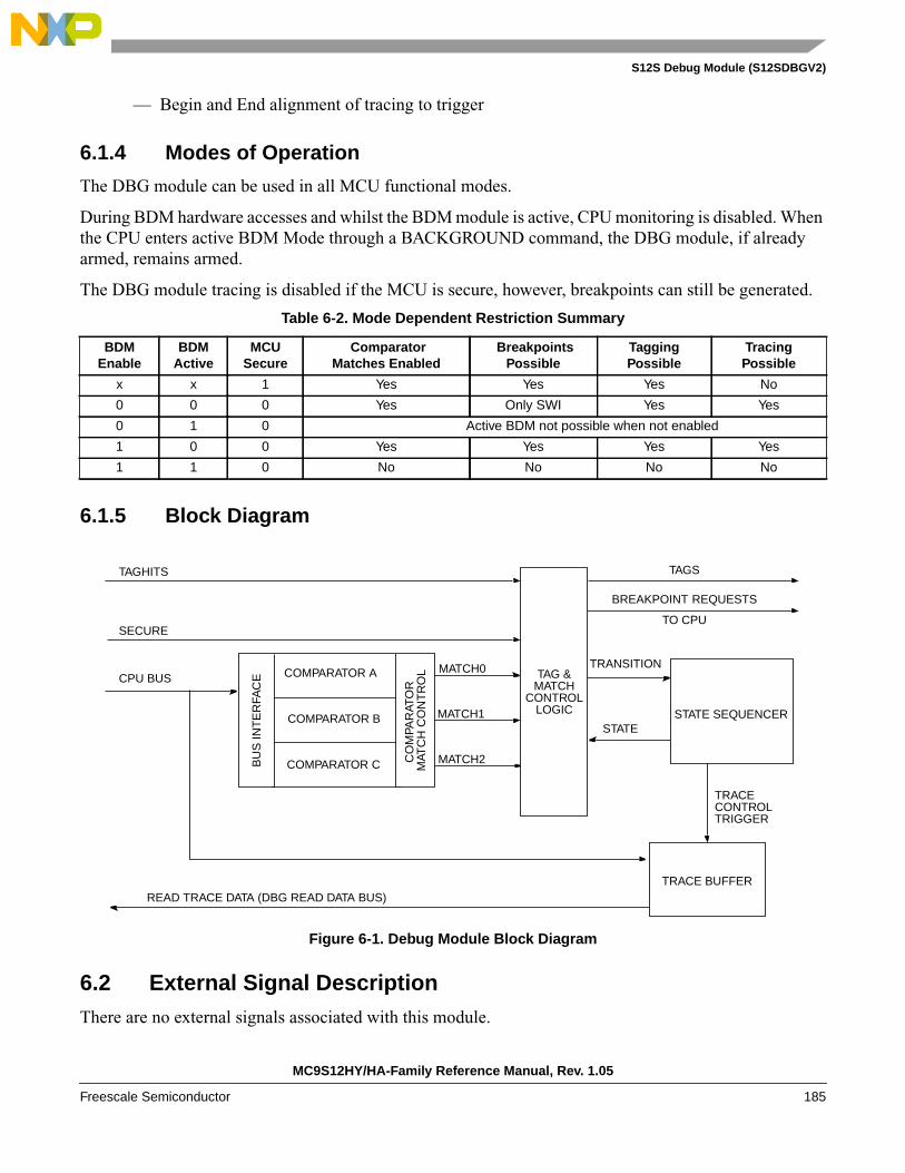
S12S Debug Module (S12SDBGV2)
— Begin and End alignment of tracing to trigger
6.1.4 Modes of Operation
The DBG module can be used in all MCU functional modes.
During BDM hardware accesses and whilst the BDM module is active, CPU monitoring is disabled. Whenthe CPU enters active BDM Mode through a BACKGROUND command, the DBG module, if alreadyarmed, remains armed.
The DBG module tracing is disabled if the MCU is secure, however, breakpoints can still be generated.
6.1.5 Block Diagram
Figure 6-1. Debug Module Block Diagram
6.2 External Signal DescriptionThere are no external signals associated with this module.
Table 6-2. Mode Dependent Restriction Summary
BDMEnable
BDMActive
MCUSecure
ComparatorMatches Enabled
BreakpointsPossible
TaggingPossible
TracingPossible
x x 1 Yes Yes Yes No
0 0 0 Yes Only SWI Yes Yes
0 1 0 Active BDM not possible when not enabled
1 0 0 Yes Yes Yes Yes
1 1 0 No No No No
CPU BUS
TRACE BUFFER
BU
S IN
TE
RFA
CE
TRANSITIONMATCH0
STATE
COMPARATOR B
COMPARATOR C
COMPARATOR A
STATE SEQUENCERMATCH1
MATCH2
TRACE
READ TRACE DATA (DBG READ DATA BUS)
CONTROL
SECURE
BREAKPOINT REQUESTS
CO
MPA
RAT
OR
MAT
CH
CO
NT
RO
L
TRIGGER
TAG &MATCH
CONTROLLOGIC
TAGSTAGHITS
STATE
TO CPU
MC9S12HY/HA-Family Reference Manual, Rev. 1.05
Freescale Semiconductor 185

S12S Debug Module (S12SDBGV2)
6.3 Memory Map and Registers
6.3.1 Module Memory Map
A summary of the registers associated with the DBG sub-block is shown in Figure 6-2. Detaileddescriptions of the registers and bits are given in the subsections that follow.
Address Name Bit 7 6 5 4 3 2 1 Bit 0
0x0020 DBGC1R
ARM0 0
BDM DBGBRK0
COMRVW TRIG
0x0021 DBGSRR 1TBF 0 0 0 0 SSF2 SSF1 SSF0W
0x0022 DBGTCRR 0
TSOURCE0 0
TRCMOD0
TALIGNW
0x0023 DBGC2R 0 0 0 0 0 0
ABCMW
0x0024 DBGTBHR Bit 15 Bit 14 Bit 13 Bit 12 Bit 11 Bit 10 Bit 9 Bit 8W
0x0025 DBGTBLR Bit 7 Bit 6 Bit 5 Bit 4 Bit 3 Bit 2 Bit 1 Bit 0W
0x0026 DBGCNTR 1 TBF 0 CNTW
0x0027 DBGSCRXR 0 0 0 0
SC3 SC2 SC1 SC0W
0x0027 DBGMFRR 0 0 0 0 0 MC2 MC1 MC0W
2 0x0028DBGACTL
RSZE SZ TAG BRK RW RWE NDB COMPE
W3 0x0028
DBGBCTLR
SZE SZ TAG BRK RW RWE0
COMPEW
4 0x0028DBGCCTL
R 0 0TAG BRK RW RWE
0COMPE
W
0x0029 DBGXAHR 0 0 0 0 0 0
Bit 17 Bit 16W
0x002A DBGXAMR
Bit 15 14 13 12 11 10 9 Bit 8W
0x002B DBGXALR
Bit 7 6 5 4 3 2 1 Bit 0W
0x002C DBGADHR
Bit 15 14 13 12 11 10 9 Bit 8W
0x002D DBGADLR
Bit 7 6 5 4 3 2 1 Bit 0W
Figure 6-2. Quick Reference to DBG Registers
MC9S12HY/HA-Family Reference Manual, Rev. 1.05
186 Freescale Semiconductor

S12S Debug Module (S12SDBGV2)
6.3.2 Register Descriptions
This section consists of the DBG control and trace buffer register descriptions in address order. Eachcomparator has a bank of registers that are visible through an 8-byte window between 0x0028 and 0x002Fin the DBG module register address map. When ARM is set in DBGC1, the only bits in the DBG moduleregisters that can be written are ARM, TRIG, and COMRV[1:0].
6.3.2.1 Debug Control Register 1 (DBGC1)
Read: Anytime
Write: Bits 7, 1, 0 anytimeBit 6 can be written anytime but always reads back as 0.Bits 4:3 anytime DBG is not armed.
NOTEWhen disarming the DBG by clearing ARM with software, the contents ofbits[4:3] are not affected by the write, since up until the write operation,ARM = 1 preventing these bits from being written. These bits must becleared using a second write if required.
0x002E DBGADHMR
Bit 15 14 13 12 11 10 9 Bit 8W
0x002F DBGADLMR
Bit 7 6 5 4 3 2 1 Bit 0W
1 This bit is visible at DBGCNT[7] and DBGSR[7]2 This represents the contents if the Comparator A control register is blended into this address.3 This represents the contents if the Comparator B control register is blended into this address4 This represents the contents if the Comparator C control register is blended into this address
Address: 0x0020
7 6 5 4 3 2 1 0
RARM
0 0BDM DBGBRK
0COMRV
W TRIG
Reset 0 0 0 0 0 0 0 0
= Unimplemented or Reserved
Figure 6-3. Debug Control Register (DBGC1)
Address Name Bit 7 6 5 4 3 2 1 Bit 0
Figure 6-2. Quick Reference to DBG Registers
MC9S12HY/HA-Family Reference Manual, Rev. 1.05
Freescale Semiconductor 187

S12S Debug Module (S12SDBGV2)
6.3.2.2 Debug Status Register (DBGSR)
Table 6-3. DBGC1 Field Descriptions
Field Description
7ARM
Arm Bit — The ARM bit controls whether the DBG module is armed. This bit can be set and cleared by usersoftware and is automatically cleared on completion of a debug session, or if a breakpoint is generated withtracing not enabled. On setting this bit the state sequencer enters State1.0 Debugger disarmed1 Debugger armed
6TRIG
Immediate Trigger Request Bit — This bit when written to 1 requests an immediate trigger independent of statesequencer status. When tracing is complete a forced breakpoint may be generated depending upon DBGBRKand BDM bit settings. This bit always reads back a 0. Writing a 0 to this bit has no effect. If theDBGTCR_TSOURCE bit is clear no tracing is carried out. If tracing has already commenced using BEGIN triggeralignment, it continues until the end of the tracing session as defined by the TALIGN bit, thus TRIG has no affect.In secure mode tracing is disabled and writing to this bit cannot initiate a tracing session.The session is ended by setting TRIG and ARM simultaneously.0 Do not trigger until the state sequencer enters the Final State.1 Trigger immediately
4BDM
Background Debug Mode Enable — This bit determines if a breakpoint causes the system to enter BackgroundDebug Mode (BDM) or initiate a Software Interrupt (SWI). If this bit is set but the BDM is not enabled by theENBDM bit in the BDM module, then breakpoints default to SWI.0 Breakpoint to Software Interrupt if BDM inactive. Otherwise no breakpoint.1 Breakpoint to BDM, if BDM enabled. Otherwise breakpoint to SWI
3DBGBRK
S12SDBG Breakpoint Enable Bit — The DBGBRK bit controls whether the debugger will request a breakpointon reaching the state sequencer Final State. If tracing is enabled, the breakpoint is generated on completionof the tracing session. If tracing is not enabled, the breakpoint is generated immediately.
0 No Breakpoint generated1 Breakpoint generated
1–0COMRV
Comparator Register Visibility Bits — These bits determine which bank of comparator register is visible in the8-byte window of the S12SDBG module address map, located between 0x0028 to 0x002F. Furthermore thesebits determine which register is visible at the address 0x0027. See Table 6-4.
Table 6-4. COMRV Encoding
COMRV Visible Comparator Visible Register at 0x0027
00 Comparator A DBGSCR1
01 Comparator B DBGSCR2
10 Comparator C DBGSCR3
11 None DBGMFR
Address: 0x0021
7 6 5 4 3 2 1 0
R TBF 0 0 0 0 SSF2 SSF1 SSF0
W
ResetPOR
—0
00
00
00
00
00
00
00
= Unimplemented or Reserved
Figure 6-4. Debug Status Register (DBGSR)
MC9S12HY/HA-Family Reference Manual, Rev. 1.05
188 Freescale Semiconductor

S12S Debug Module (S12SDBGV2)
Read: Anytime
Write: Never
Table 6-5. DBGSR Field Descriptions
Field Description
7TBF
Trace Buffer Full — The TBF bit indicates that the trace buffer has stored 64 or more lines of data since it waslast armed. If this bit is set, then all 64 lines will be valid data, regardless of the value of DBGCNT bits. The TBFbit is cleared when ARM in DBGC1 is written to a one. The TBF is cleared by the power on reset initialization.Other system generated resets have no affect on this bitThis bit is also visible at DBGCNT[7]
2–0SSF[2:0]
State Sequencer Flag Bits — The SSF bits indicate in which state the State Sequencer is currently in. Duringa debug session on each transition to a new state these bits are updated. If the debug session is ended bysoftware clearing the ARM bit, then these bits retain their value to reflect the last state of the state sequencerbefore disarming. If a debug session is ended by an internal event, then the state sequencer returns to state0and these bits are cleared to indicate that state0 was entered during the session. On arming the module the statesequencer enters state1 and these bits are forced to SSF[2:0] = 001. See Table 6-6.
Table 6-6. SSF[2:0] — State Sequence Flag Bit Encoding
SSF[2:0] Current State
000 State0 (disarmed)
001 State1
010 State2
011 State3
100 Final State
101,110,111 Reserved
MC9S12HY/HA-Family Reference Manual, Rev. 1.05
Freescale Semiconductor 189

S12S Debug Module (S12SDBGV2)
6.3.2.3 Debug Trace Control Register (DBGTCR)
Read: Anytime
Write: Bit 6 only when DBG is neither secure nor armed.Bits 3,2,0 anytime the module is disarmed.
Address: 0x0022
7 6 5 4 3 2 1 0
R 0TSOURCE
0 0TRCMOD
0TALIGN
W
Reset 0 0 0 0 0 0 0 0
Figure 6-5. Debug Trace Control Register (DBGTCR)
Table 6-7. DBGTCR Field Descriptions
Field Description
6TSOURCE
Trace Source Control Bit — The TSOURCE bit enables a tracing session given a trigger condition. If the MCUsystem is secured, this bit cannot be set and tracing is inhibited.This bit must be set to read the trace buffer.0 Debug session without tracing requested1 Debug session with tracing requested
3–2TRCMOD
Trace Mode Bits — See 6.4.5.2, "Trace Modes" for detailed Trace Mode descriptions. In Normal Mode, changeof flow information is stored. In Loop1 Mode, change of flow information is stored but redundant entries into tracememory are inhibited. In Detail Mode, address and data for all memory and register accesses is stored. InCompressed Pure PC mode the program counter value for each instruction executed is stored. See Table 6-8.
0TALIGN
Trigger Align Bit — This bit controls whether the trigger is aligned to the beginning or end of a tracing session.0 Trigger at end of stored data1 Trigger before storing data
Table 6-8. TRCMOD Trace Mode Bit Encoding
TRCMOD Description
00 Normal
01 Loop1
10 Detail
11 Compressed Pure PC
MC9S12HY/HA-Family Reference Manual, Rev. 1.05
190 Freescale Semiconductor

S12S Debug Module (S12SDBGV2)
6.3.2.4 Debug Control Register2 (DBGC2)
Read: Anytime
Write: Anytime the module is disarmed.
This register configures the comparators for range matching.
6.3.2.5 Debug Trace Buffer Register (DBGTBH:DBGTBL)
Read: Only when unlocked AND unsecured AND not armed AND TSOURCE set.
Write: Aligned word writes when disarmed unlock the trace buffer for reading but do not affect trace buffercontents.
Address: 0x0023
7 6 5 4 3 2 1 0
R 0 0 0 0 0 0ABCM
W
Reset 0 0 0 0 0 0 0 0
= Unimplemented or Reserved
Figure 6-6. Debug Control Register2 (DBGC2)
Table 6-9. DBGC2 Field Descriptions
Field Description
1–0ABCM[1:0]
A and B Comparator Match Control — These bits determine the A and B comparator match mapping asdescribed in Table 6-10.
Table 6-10. ABCM Encoding
ABCM Description
00 Match0 mapped to comparator A match: Match1 mapped to comparator B match.
01 Match 0 mapped to comparator A/B inside range: Match1 disabled.
10 Match 0 mapped to comparator A/B outside range: Match1 disabled.
11 Reserved1
1 Currently defaults to Comparator A, Comparator B disabled
Address: 0x0024, 0x0025
15 14 13 12 11 10 9 8 7 6 5 4 3 2 1 0
RBit 15 Bit 14 Bit 13 Bit 12 Bit 11 Bit 10 Bit 9 Bit 8 Bit 7 Bit 6 Bit 5 Bit 4 Bit 3 Bit 2 Bit 1 Bit 0
W
POR X X X X X X X X X X X X X X X X
OtherResets
— — — — — — — — — — — — — — — —
Figure 6-7. Debug Trace Buffer Register (DBGTB)
MC9S12HY/HA-Family Reference Manual, Rev. 1.05
Freescale Semiconductor 191
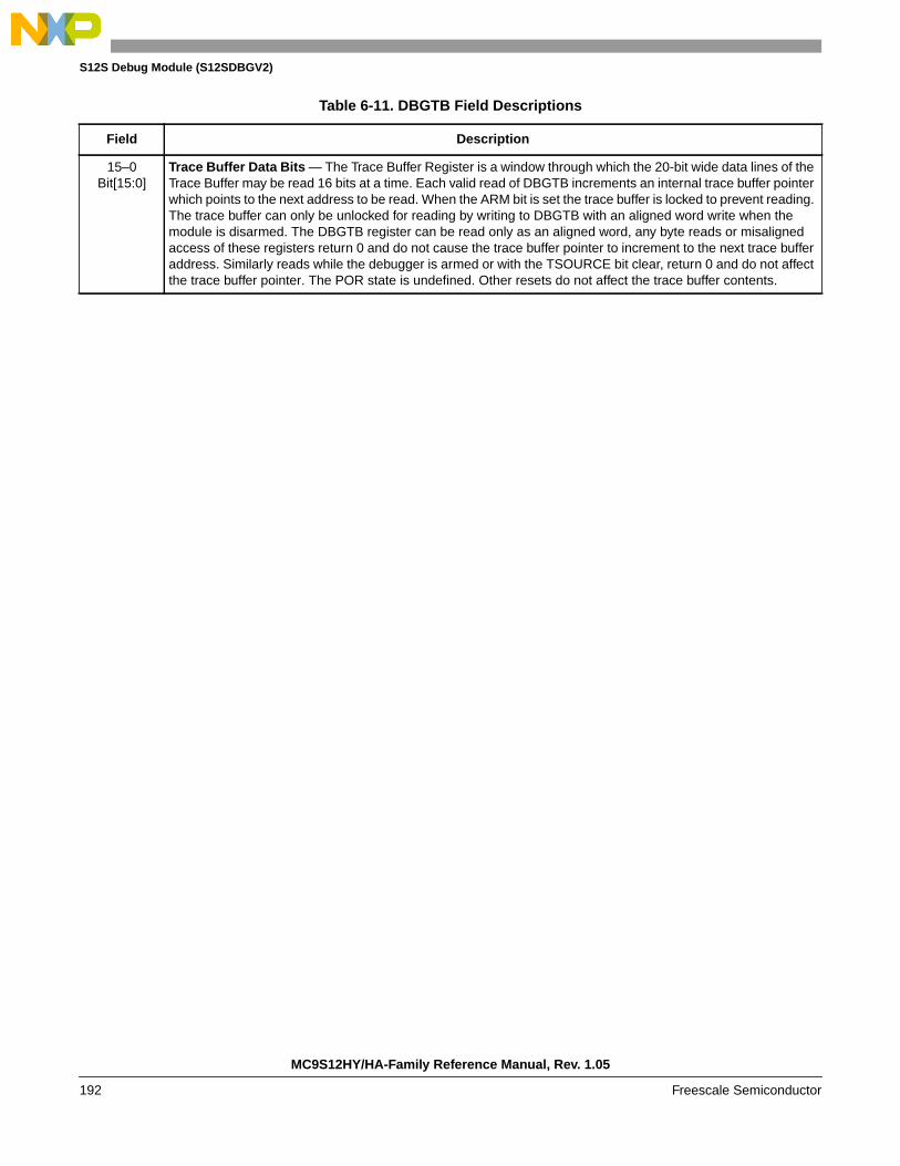
S12S Debug Module (S12SDBGV2)
Table 6-11. DBGTB Field Descriptions
Field Description
15–0Bit[15:0]
Trace Buffer Data Bits — The Trace Buffer Register is a window through which the 20-bit wide data lines of theTrace Buffer may be read 16 bits at a time. Each valid read of DBGTB increments an internal trace buffer pointerwhich points to the next address to be read. When the ARM bit is set the trace buffer is locked to prevent reading.The trace buffer can only be unlocked for reading by writing to DBGTB with an aligned word write when themodule is disarmed. The DBGTB register can be read only as an aligned word, any byte reads or misalignedaccess of these registers return 0 and do not cause the trace buffer pointer to increment to the next trace bufferaddress. Similarly reads while the debugger is armed or with the TSOURCE bit clear, return 0 and do not affectthe trace buffer pointer. The POR state is undefined. Other resets do not affect the trace buffer contents.
MC9S12HY/HA-Family Reference Manual, Rev. 1.05
192 Freescale Semiconductor

S12S Debug Module (S12SDBGV2)
6.3.2.6 Debug Count Register (DBGCNT)
Read: Anytime
Write: Never
Address: 0x0026
7 6 5 4 3 2 1 0
R TBF 0 CNT
W
ResetPOR
—0
—0
—0
—0
—0
—0
—0
—0
= Unimplemented or Reserved
Figure 6-8. Debug Count Register (DBGCNT)
Table 6-12. DBGCNT Field Descriptions
Field Description
7TBF
Trace Buffer Full — The TBF bit indicates that the trace buffer has stored 64 or more lines of data since it waslast armed. If this bit is set, then all 64 lines will be valid data, regardless of the value of DBGCNT bits. The TBFbit is cleared when ARM in DBGC1 is written to a one. The TBF is cleared by the power on reset initialization.Other system generated resets have no affect on this bitThis bit is also visible at DBGSR[7]
5–0CNT[5:0]
Count Value — The CNT bits indicate the number of valid data 20-bit data lines stored in the Trace Buffer.Table 6-13 shows the correlation between the CNT bits and the number of valid data lines in the Trace Buffer.When the CNT rolls over to zero, the TBF bit in DBGSR is set and incrementing of CNT will continue inend-trigger mode. The DBGCNT register is cleared when ARM in DBGC1 is written to a one. The DBGCNTregister is cleared by power-on-reset initialization but is not cleared by other system resets. Thus should a resetoccur during a debug session, the DBGCNT register still indicates after the reset, the number of valid trace bufferentries stored before the reset occurred. The DBGCNT register is not decremented when reading from the tracebuffer.
Table 6-13. CNT Decoding Table
TBF CNT[5:0] Description
0 000000 No data valid
0 000001000010000100000110
..111111
1 line valid2 lines valid4 lines valid6 lines valid
..63 lines valid
1 000000 64 lines valid; if using Begin trigger alignment,ARM bit will be cleared and the tracing session ends.
1 000001....
111110
64 lines valid,oldest data has been overwritten by most recent data
MC9S12HY/HA-Family Reference Manual, Rev. 1.05
Freescale Semiconductor 193

S12S Debug Module (S12SDBGV2)
6.3.2.7 Debug State Control Registers
There is a dedicated control register for each of the state sequencer states 1 to 3 that determines iftransitions from that state are allowed, depending upon comparator matches or tag hits, and defines thenext state for the state sequencer following a match. The three debug state control registers are located atthe same address in the register address map (0x0027). Each register can be accessed using the COMRVbits in DBGC1 to blend in the required register. The COMRV = 11 value blends in the match flag register(DBGMFR).
Table 6-14. State Control Register Access Encoding
COMRV Visible State Control Register
00 DBGSCR1
01 DBGSCR2
10 DBGSCR3
11 DBGMFR
MC9S12HY/HA-Family Reference Manual, Rev. 1.05
194 Freescale Semiconductor

S12S Debug Module (S12SDBGV2)
6.3.2.7.1 Debug State Control Register 1 (DBGSCR1)
Read: If COMRV[1:0] = 00
Write: If COMRV[1:0] = 00 and DBG is not armed.
This register is visible at 0x0027 only with COMRV[1:0] = 00. The state control register 1 selects thetargeted next state whilst in State1. The matches refer to the match channels of the comparator matchcontrol logic as depicted in Figure 6-1 and described in 6.3.2.8.1, "Debug Comparator Control Register(DBGXCTL)". Comparators must be enabled by setting the comparator enable bit in the associatedDBGXCTL control register.
The priorities described in Table 6-36 dictate that in the case of simultaneous matches, a match leading tofinal state has priority followed by the match on the lower channel number (0,1,2). Thus withSC[3:0]=1101 a simultaneous match0/match1 transitions to final state.
Address: 0x0027
7 6 5 4 3 2 1 0
R 0 0 0 0SC3 SC2 SC1 SC0
W
Reset 0 0 0 0 0 0 0 0
= Unimplemented or Reserved
Figure 6-9. Debug State Control Register 1 (DBGSCR1)
Table 6-15. DBGSCR1 Field Descriptions
Field Description
3–0SC[3:0]
These bits select the targeted next state whilst in State1, based upon the match event.
Table 6-16. State1 Sequencer Next State Selection
SC[3:0] Description (Unspecified matches have no effect)0000 Any match to Final State0001 Match1 to State30010 Match2 to State20011 Match1 to State20100 Match0 to State2....... Match1 to State30101 Match1 to State3.........Match0 to Final State0110 Match0 to State2....... Match2 to State30111 Either Match0 or Match1 to State21000 Reserved1001 Match0 to State31010 Reserved1011 Reserved1100 Reserved1101 Either Match0 or Match2 to Final State........Match1 to State21110 Reserved1111 Reserved
MC9S12HY/HA-Family Reference Manual, Rev. 1.05
Freescale Semiconductor 195

S12S Debug Module (S12SDBGV2)
6.3.2.7.2 Debug State Control Register 2 (DBGSCR2)
Read: If COMRV[1:0] = 01
Write: If COMRV[1:0] = 01 and DBG is not armed.
This register is visible at 0x0027 only with COMRV[1:0] = 01. The state control register 2 selects thetargeted next state whilst in State2. The matches refer to the match channels of the comparator matchcontrol logic as depicted in Figure 6-1 and described in 6.3.2.8.1, "Debug Comparator Control Register(DBGXCTL)". Comparators must be enabled by setting the comparator enable bit in the associatedDBGXCTL control register.
The priorities described in Table 6-36 dictate that in the case of simultaneous matches, a match leading tofinal state has priority followed by the match on the lower channel number (0,1,2).
Address: 0x0027
7 6 5 4 3 2 1 0
R 0 0 0 0SC3 SC2 SC1 SC0
W
Reset 0 0 0 0 0 0 0 0
= Unimplemented or Reserved
Figure 6-10. Debug State Control Register 2 (DBGSCR2)
Table 6-17. DBGSCR2 Field Descriptions
Field Description
3–0SC[3:0]
These bits select the targeted next state whilst in State2, based upon the match event.
Table 6-18. State2 —Sequencer Next State Selection
SC[3:0] Description (Unspecified matches have no effect)0000 Match0 to State1....... Match2 to State3.0001 Match1 to State30010 Match2 to State30011 Match1 to State3....... Match0 Final State0100 Match1 to State1....... Match2 to State3.0101 Match2 to Final State0110 Match2 to State1..... Match0 to Final State0111 Either Match0 or Match1 to Final State1000 Reserved1001 Reserved1010 Reserved1011 Reserved1100 Either Match0 or Match1 to Final State........Match2 to State31101 Reserved1110 Reserved1111 Either Match0 or Match1 to Final State........Match2 to State1
MC9S12HY/HA-Family Reference Manual, Rev. 1.05
196 Freescale Semiconductor

S12S Debug Module (S12SDBGV2)
6.3.2.7.3 Debug State Control Register 3 (DBGSCR3)
Read: If COMRV[1:0] = 10
Write: If COMRV[1:0] = 10 and DBG is not armed.
This register is visible at 0x0027 only with COMRV[1:0] = 10. The state control register three selects thetargeted next state whilst in State3. The matches refer to the match channels of the comparator matchcontrol logic as depicted in Figure 6-1 and described in 6.3.2.8.1, "Debug Comparator Control Register(DBGXCTL)". Comparators must be enabled by setting the comparator enable bit in the associatedDBGXCTL control register.
The priorities described in Table 6-36 dictate that in the case of simultaneous matches, a match leading tofinal state has priority followed by the match on the lower channel number (0,1,2).
Address: 0x0027
7 6 5 4 3 2 1 0
R 0 0 0 0SC3 SC2 SC1 SC0
W
Reset 0 0 0 0 0 0 0 0
= Unimplemented or Reserved
Figure 6-11. Debug State Control Register 3 (DBGSCR3)
Table 6-19. DBGSCR3 Field Descriptions
Field Description
3–0SC[3:0]
These bits select the targeted next state whilst in State3, based upon the match event.
Table 6-20. State3 — Sequencer Next State Selection
SC[3:0] Description (Unspecified matches have no effect)0000 Match0 to State10001 Match2 to State2........ Match1 to Final State0010 Match0 to Final State....... Match1 to State10011 Match1 to Final State....... Match2 to State10100 Match1 to State20101 Match1 to Final State0110 Match2 to State2........ Match0 to Final State0111 Match0 to Final State1000 Reserved1001 Reserved1010 Either Match1 or Match2 to State1....... Match0 to Final State1011 Reserved1100 Reserved1101 Either Match1 or Match2 to Final State....... Match0 to State11110 Match0 to State2....... Match2 to Final State1111 Reserved
MC9S12HY/HA-Family Reference Manual, Rev. 1.05
Freescale Semiconductor 197

S12S Debug Module (S12SDBGV2)
6.3.2.7.4 Debug Match Flag Register (DBGMFR)
Read: If COMRV[1:0] = 11
Write: Never
DBGMFR is visible at 0x0027 only with COMRV[1:0] = 11. It features 3 flag bits each mapped directlyto a channel. Should a match occur on the channel during the debug session, then the corresponding flagis set and remains set until the next time the module is armed by writing to the ARM bit. Thus the contentsare retained after a debug session for evaluation purposes. These flags cannot be cleared by software, theyare cleared only when arming the module. A set flag does not inhibit the setting of other flags. Once a flagis set, further comparator matches on the same channel in the same session have no affect on that flag.
6.3.2.8 Comparator Register Descriptions
Each comparator has a bank of registers that are visible through an 8-byte window in the DBG moduleregister address map. Comparator A consists of 8 register bytes (3 address bus compare registers, two databus compare registers, two data bus mask registers and a control register). Comparator B consists of fourregister bytes (three address bus compare registers and a control register). Comparator C consists of fourregister bytes (three address bus compare registers and a control register).
Each set of comparator registers can be accessed using the COMRV bits in the DBGC1 register.Unimplemented registers (e.g. Comparator B data bus and data bus masking) read as zero and cannot bewritten. The control register for comparator B differs from those of comparators A and C.
6.3.2.8.1 Debug Comparator Control Register (DBGXCTL)
The contents of this register bits 7 and 6 differ depending upon which comparator registers are visible inthe 8-byte window of the DBG module register address map.
Address: 0x0027
7 6 5 4 3 2 1 0
R 0 0 0 0 0 MC2 MC1 MC0
W
Reset 0 0 0 0 0 0 0 0
= Unimplemented or Reserved
Figure 6-12. Debug Match Flag Register (DBGMFR)
Table 6-21. Comparator Register Layout
0x0028 CONTROL Read/Write Comparators A,B and C
0x0029 ADDRESS HIGH Read/Write Comparators A,B and C
0x002A ADDRESS MEDIUM Read/Write Comparators A,B and C
0x002B ADDRESS LOW Read/Write Comparators A,B and C
0x002C DATA HIGH COMPARATOR Read/Write Comparator A only
0x002D DATA LOW COMPARATOR Read/Write Comparator A only
0x002E DATA HIGH MASK Read/Write Comparator A only
0x002F DATA LOW MASK Read/Write Comparator A only
MC9S12HY/HA-Family Reference Manual, Rev. 1.05
198 Freescale Semiconductor

S12S Debug Module (S12SDBGV2)
Read: DBGACTL if COMRV[1:0] = 00DBGBCTL if COMRV[1:0] = 01DBGCCTL if COMRV[1:0] = 10
Write: DBGACTL if COMRV[1:0] = 00 and DBG not armedDBGBCTL if COMRV[1:0] = 01 and DBG not armedDBGCCTL if COMRV[1:0] = 10 and DBG not armed
Address: 0x0028
7 6 5 4 3 2 1 0
RSZE SZ TAG BRK RW RWE NDB COMPE
W
Reset 0 0 0 0 0 0 0 0
= Unimplemented or Reserved
Figure 6-13. Debug Comparator Control Register DBGACTL (Comparator A)
Address: 0x0028
7 6 5 4 3 2 1 0
RSZE SZ TAG BRK RW RWE
0COMPE
W
Reset 0 0 0 0 0 0 0 0
= Unimplemented or Reserved
Figure 6-14. Debug Comparator Control Register DBGBCTL (Comparator B)
Address: 0x0028
7 6 5 4 3 2 1 0
R 0 0TAG BRK RW RWE
0COMPE
W
Reset 0 0 0 0 0 0 0 0
= Unimplemented or Reserved
Figure 6-15. Debug Comparator Control Register DBGCCTL (Comparator C)
Table 6-22. DBGXCTL Field Descriptions
Field Description
7SZE
(ComparatorsA and B)
Size Comparator Enable Bit — The SZE bit controls whether access size comparison is enabled for theassociated comparator. This bit is ignored if the TAG bit in the same register is set.0 Word/Byte access size is not used in comparison1 Word/Byte access size is used in comparison
6SZ
(ComparatorsA and B)
Size Comparator Value Bit — The SZ bit selects either word or byte access size in comparison for theassociated comparator. This bit is ignored if the SZE bit is cleared or if the TAG bit in the same register is set.0 Word access size is compared1 Byte access size is compared
MC9S12HY/HA-Family Reference Manual, Rev. 1.05
Freescale Semiconductor 199

S12S Debug Module (S12SDBGV2)
Table 6-23 shows the effect for RWE and RW on the comparison conditions. These bits are ignored if thecorresponding TAG bit is set since the match occurs based on the tagged opcode reaching the executionstage of the instruction queue.
5TAG
Tag Select— This bit controls whether the comparator match has immediate effect, causing an immediatestate sequencer transition or tag the opcode at the matched address. Tagged opcodes trigger only if theyreach the execution stage of the instruction queue.0 Allow state sequencer transition immediately on match1 On match, tag the opcode. If the opcode is about to be executed allow a state sequencer transition
4BRK
Break— This bit controls whether a comparator match terminates a debug session immediately, independentof state sequencer state. To generate an immediate breakpoint the module breakpoints must be enabledusing the DBGC1 bit DBGBRK.0 The debug session termination is dependent upon the state sequencer and trigger conditions.1 A match on this channel terminates the debug session immediately; breakpoints if active are generated,
tracing, if active, is terminated and the module disarmed.
3RW
Read/Write Comparator Value Bit — The RW bit controls whether read or write is used in compare for theassociated comparator. The RW bit is not used if RWE = 0. This bit is ignored if the TAG bit in the sameregister is set.0 Write cycle is matched1Read cycle is matched
2RWE
Read/Write Enable Bit — The RWE bit controls whether read or write comparison is enabled for theassociated comparator.This bit is ignored if the TAG bit in the same register is set0 Read/Write is not used in comparison1 Read/Write is used in comparison
1NDB
(Comparator A)
Not Data Bus — The NDB bit controls whether the match occurs when the data bus matches the comparatorregister value or when the data bus differs from the register value. This bit is ignored if the TAG bit in the sameregister is set. This bit is only available for comparator A.0 Match on data bus equivalence to comparator register contents1 Match on data bus difference to comparator register contents
0COMPE
Determines if comparator is enabled0 The comparator is not enabled1 The comparator is enabled
Table 6-23. Read or Write Comparison Logic Table
RWE Bit RW Bit RW Signal Comment
0 x 0 RW not used in comparison
0 x 1 RW not used in comparison
1 0 0 Write data bus
1 0 1 No match
1 1 0 No match
1 1 1 Read data bus
Table 6-22. DBGXCTL Field Descriptions (continued)
Field Description
MC9S12HY/HA-Family Reference Manual, Rev. 1.05
200 Freescale Semiconductor

S12S Debug Module (S12SDBGV2)
6.3.2.8.2 Debug Comparator Address High Register (DBGXAH)
The DBGC1_COMRV bits determine which comparator address registers are visible in the 8-byte windowfrom 0x0028 to 0x002F as shown in Table 6-24., "Comparator Address Register Visibility"
Table 6-24. Comparator Address Register Visibility
Read: Anytime. See Table 6-24 for visible register encoding.
Write: If DBG not armed. See Table 6-24 for visible register encoding.
6.3.2.8.3 Debug Comparator Address Mid Register (DBGXAM)
Read: Anytime. See Table 6-24 for visible register encoding.
Write: If DBG not armed. See Table 6-24 for visible register encoding.
Address: 0x0029
7 6 5 4 3 2 1 0
R 0 0 0 0 0 0Bit 17 Bit 16
W
Reset 0 0 0 0 0 0 0 0
= Unimplemented or Reserved
Figure 6-16. Debug Comparator Address High Register (DBGXAH)
COMRV Visible Comparator
00 DBGAAH, DBGAAM, DBGAAL
01 DBGBAH, DBGBAM, DBGBAL
10 DBGCAH, DBGCAM, DBGCAL
11 None
Table 6-25. DBGXAH Field Descriptions
Field Description
1–0Bit[17:16]
Comparator Address High Compare Bits — The Comparator address high compare bits control whether theselected comparator compares the address bus bits [17:16] to a logic one or logic zero.0 Compare corresponding address bit to a logic zero1 Compare corresponding address bit to a logic one
Address: 0x002A
7 6 5 4 3 2 1 0
RBit 15 Bit 14 Bit 13 Bit 12 Bit 11 Bit 10 Bit 9 Bit 8
W
Reset 0 0 0 0 0 0 0 0
Figure 6-17. Debug Comparator Address Mid Register (DBGXAM)
MC9S12HY/HA-Family Reference Manual, Rev. 1.05
Freescale Semiconductor 201

S12S Debug Module (S12SDBGV2)
6.3.2.8.4 Debug Comparator Address Low Register (DBGXAL)
Read: Anytime. See Table 6-24 for visible register encoding.
Write: If DBG not armed. See Table 6-24 for visible register encoding.
6.3.2.8.5 Debug Comparator Data High Register (DBGADH)
Read: If COMRV[1:0] = 00
Write: If COMRV[1:0] = 00 and DBG not armed.
Table 6-26. DBGXAM Field Descriptions
Field Description
7–0Bit[15:8]
Comparator Address Mid Compare Bits — The Comparator address mid compare bits control whether theselected comparator compares the address bus bits [15:8] to a logic one or logic zero.0 Compare corresponding address bit to a logic zero1 Compare corresponding address bit to a logic one
Address: 0x002B
7 6 5 4 3 2 1 0
RBit 7 Bit 6 Bit 5 Bit 4 Bit 3 Bit 2 Bit 1 Bit 0
W
Reset 0 0 0 0 0 0 0 0
Figure 6-18. Debug Comparator Address Low Register (DBGXAL)
Table 6-27. DBGXAL Field Descriptions
Field Description
7–0Bits[7:0]
Comparator Address Low Compare Bits — The Comparator address low compare bits control whether theselected comparator compares the address bus bits [7:0] to a logic one or logic zero.0 Compare corresponding address bit to a logic zero1 Compare corresponding address bit to a logic one
Address: 0x002C
7 6 5 4 3 2 1 0
RBit 15 Bit 14 Bit 13 Bit 12 Bit 11 Bit 10 Bit 9 Bit 8
W
Reset 0 0 0 0 0 0 0 0
Figure 6-19. Debug Comparator Data High Register (DBGADH)
MC9S12HY/HA-Family Reference Manual, Rev. 1.05
202 Freescale Semiconductor

S12S Debug Module (S12SDBGV2)
6.3.2.8.6 Debug Comparator Data Low Register (DBGADL)
Read: If COMRV[1:0] = 00
Write: If COMRV[1:0] = 00 and DBG not armed.
6.3.2.8.7 Debug Comparator Data High Mask Register (DBGADHM)
Read: If COMRV[1:0] = 00
Write: If COMRV[1:0] = 00 and DBG not armed.
Table 6-28. DBGADH Field Descriptions
Field Description
7–0Bits[15:8]
Comparator Data High Compare Bits— The Comparator data high compare bits control whether the selectedcomparator compares the data bus bits [15:8] to a logic one or logic zero. The comparator data compare bits areonly used in comparison if the corresponding data mask bit is logic 1. This register is available only forcomparator A. Data bus comparisons are only performed if the TAG bit in DBGACTL is clear.0 Compare corresponding data bit to a logic zero1 Compare corresponding data bit to a logic one
Address: 0x002D
7 6 5 4 3 2 1 0
RBit 7 Bit 6 Bit 5 Bit 4 Bit 3 Bit 2 Bit 1 Bit 0
W
Reset 0 0 0 0 0 0 0 0
Figure 6-20. Debug Comparator Data Low Register (DBGADL)
Table 6-29. DBGADL Field Descriptions
Field Description
7–0Bits[7:0]
Comparator Data Low Compare Bits — The Comparator data low compare bits control whether the selectedcomparator compares the data bus bits [7:0] to a logic one or logic zero. The comparator data compare bits areonly used in comparison if the corresponding data mask bit is logic 1. This register is available only forcomparator A. Data bus comparisons are only performed if the TAG bit in DBGACTL is clear0 Compare corresponding data bit to a logic zero1 Compare corresponding data bit to a logic one
Address: 0x002E
7 6 5 4 3 2 1 0
RBit 15 Bit 14 Bit 13 Bit 12 Bit 11 Bit 10 Bit 9 Bit 8
W
Reset 0 0 0 0 0 0 0 0
Figure 6-21. Debug Comparator Data High Mask Register (DBGADHM)
MC9S12HY/HA-Family Reference Manual, Rev. 1.05
Freescale Semiconductor 203
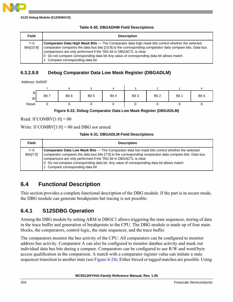
S12S Debug Module (S12SDBGV2)
6.3.2.8.8 Debug Comparator Data Low Mask Register (DBGADLM)
Read: If COMRV[1:0] = 00
Write: If COMRV[1:0] = 00 and DBG not armed.
6.4 Functional DescriptionThis section provides a complete functional description of the DBG module. If the part is in secure mode,the DBG module can generate breakpoints but tracing is not possible.
6.4.1 S12SDBG Operation
Arming the DBG module by setting ARM in DBGC1 allows triggering the state sequencer, storing of datain the trace buffer and generation of breakpoints to the CPU. The DBG module is made up of four mainblocks, the comparators, control logic, the state sequencer, and the trace buffer.
The comparators monitor the bus activity of the CPU. All comparators can be configured to monitoraddress bus activity. Comparator A can also be configured to monitor databus activity and mask outindividual data bus bits during a compare. Comparators can be configured to use R/W and word/byteaccess qualification in the comparison. A match with a comparator register value can initiate a statesequencer transition to another state (see Figure 6-24). Either forced or tagged matches are possible. Using
Table 6-30. DBGADHM Field Descriptions
Field Description
7–0Bits[15:8]
Comparator Data High Mask Bits — The Comparator data high mask bits control whether the selectedcomparator compares the data bus bits [15:8] to the corresponding comparator data compare bits. Data buscomparisons are only performed if the TAG bit in DBGACTL is clear0 Do not compare corresponding data bit Any value of corresponding data bit allows match.1 Compare corresponding data bit
Address: 0x002F
7 6 5 4 3 2 1 0
RBit 7 Bit 6 Bit 5 Bit 4 Bit 3 Bit 2 Bit 1 Bit 0
W
Reset 0 0 0 0 0 0 0 0
Figure 6-22. Debug Comparator Data Low Mask Register (DBGADLM)
Table 6-31. DBGADLM Field Descriptions
Field Description
7–0Bits[7:0]
Comparator Data Low Mask Bits — The Comparator data low mask bits control whether the selectedcomparator compares the data bus bits [7:0] to the corresponding comparator data compare bits. Data buscomparisons are only performed if the TAG bit in DBGACTL is clear0 Do not compare corresponding data bit. Any value of corresponding data bit allows match1 Compare corresponding data bit
MC9S12HY/HA-Family Reference Manual, Rev. 1.05
204 Freescale Semiconductor
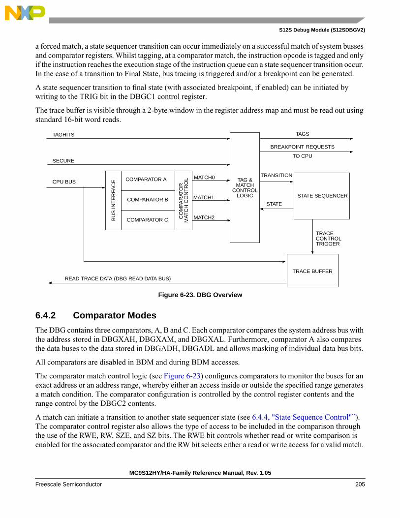
S12S Debug Module (S12SDBGV2)
a forced match, a state sequencer transition can occur immediately on a successful match of system bussesand comparator registers. Whilst tagging, at a comparator match, the instruction opcode is tagged and onlyif the instruction reaches the execution stage of the instruction queue can a state sequencer transition occur.In the case of a transition to Final State, bus tracing is triggered and/or a breakpoint can be generated.
A state sequencer transition to final state (with associated breakpoint, if enabled) can be initiated bywriting to the TRIG bit in the DBGC1 control register.
The trace buffer is visible through a 2-byte window in the register address map and must be read out usingstandard 16-bit word reads.
Figure 6-23. DBG Overview
6.4.2 Comparator Modes
The DBG contains three comparators, A, B and C. Each comparator compares the system address bus withthe address stored in DBGXAH, DBGXAM, and DBGXAL. Furthermore, comparator A also comparesthe data buses to the data stored in DBGADH, DBGADL and allows masking of individual data bus bits.
All comparators are disabled in BDM and during BDM accesses.
The comparator match control logic (see Figure 6-23) configures comparators to monitor the buses for anexact address or an address range, whereby either an access inside or outside the specified range generatesa match condition. The comparator configuration is controlled by the control register contents and therange control by the DBGC2 contents.
A match can initiate a transition to another state sequencer state (see 6.4.4, "State Sequence Control"”).The comparator control register also allows the type of access to be included in the comparison throughthe use of the RWE, RW, SZE, and SZ bits. The RWE bit controls whether read or write comparison isenabled for the associated comparator and the RW bit selects either a read or write access for a valid match.
CPU BUS
TRACE BUFFER
BU
S IN
TE
RFA
CE
TRANSITIONMATCH0
STATE
COMPARATOR B
COMPARATOR C
COMPARATOR A
STATE SEQUENCERMATCH1
MATCH2
TRACE
READ TRACE DATA (DBG READ DATA BUS)
CONTROL
SECURE
BREAKPOINT REQUESTS
CO
MPA
RAT
OR
MAT
CH
CO
NT
RO
L
TRIGGER
TAG &MATCH
CONTROLLOGIC
TAGSTAGHITS
STATE
TO CPU
MC9S12HY/HA-Family Reference Manual, Rev. 1.05
Freescale Semiconductor 205
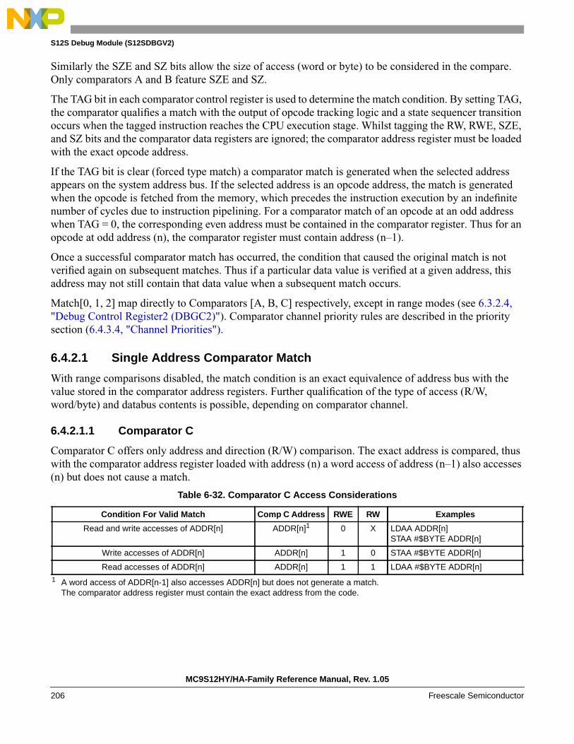
S12S Debug Module (S12SDBGV2)
Similarly the SZE and SZ bits allow the size of access (word or byte) to be considered in the compare.Only comparators A and B feature SZE and SZ.
The TAG bit in each comparator control register is used to determine the match condition. By setting TAG,the comparator qualifies a match with the output of opcode tracking logic and a state sequencer transitionoccurs when the tagged instruction reaches the CPU execution stage. Whilst tagging the RW, RWE, SZE,and SZ bits and the comparator data registers are ignored; the comparator address register must be loadedwith the exact opcode address.
If the TAG bit is clear (forced type match) a comparator match is generated when the selected addressappears on the system address bus. If the selected address is an opcode address, the match is generatedwhen the opcode is fetched from the memory, which precedes the instruction execution by an indefinitenumber of cycles due to instruction pipelining. For a comparator match of an opcode at an odd addresswhen TAG = 0, the corresponding even address must be contained in the comparator register. Thus for anopcode at odd address (n), the comparator register must contain address (n–1).
Once a successful comparator match has occurred, the condition that caused the original match is notverified again on subsequent matches. Thus if a particular data value is verified at a given address, thisaddress may not still contain that data value when a subsequent match occurs.
Match[0, 1, 2] map directly to Comparators [A, B, C] respectively, except in range modes (see 6.3.2.4,"Debug Control Register2 (DBGC2)"). Comparator channel priority rules are described in the prioritysection (6.4.3.4, "Channel Priorities").
6.4.2.1 Single Address Comparator Match
With range comparisons disabled, the match condition is an exact equivalence of address bus with thevalue stored in the comparator address registers. Further qualification of the type of access (R/W,word/byte) and databus contents is possible, depending on comparator channel.
6.4.2.1.1 Comparator C
Comparator C offers only address and direction (R/W) comparison. The exact address is compared, thuswith the comparator address register loaded with address (n) a word access of address (n–1) also accesses(n) but does not cause a match.
Table 6-32. Comparator C Access Considerations
Condition For Valid Match Comp C Address RWE RW Examples
Read and write accesses of ADDR[n] ADDR[n]1
1 A word access of ADDR[n-1] also accesses ADDR[n] but does not generate a match.The comparator address register must contain the exact address from the code.
0 X LDAA ADDR[n]STAA #$BYTE ADDR[n]
Write accesses of ADDR[n] ADDR[n] 1 0 STAA #$BYTE ADDR[n]
Read accesses of ADDR[n] ADDR[n] 1 1 LDAA #$BYTE ADDR[n]
MC9S12HY/HA-Family Reference Manual, Rev. 1.05
206 Freescale Semiconductor
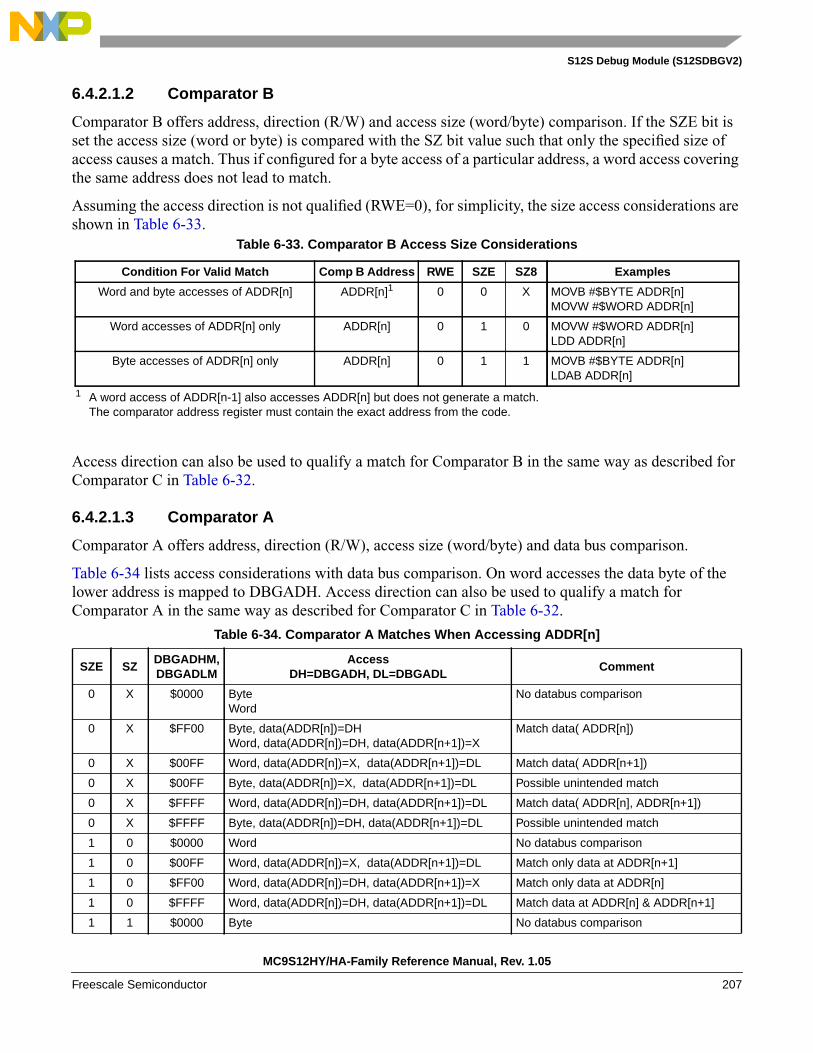
S12S Debug Module (S12SDBGV2)
6.4.2.1.2 Comparator B
Comparator B offers address, direction (R/W) and access size (word/byte) comparison. If the SZE bit isset the access size (word or byte) is compared with the SZ bit value such that only the specified size ofaccess causes a match. Thus if configured for a byte access of a particular address, a word access coveringthe same address does not lead to match.
Assuming the access direction is not qualified (RWE=0), for simplicity, the size access considerations areshown in Table 6-33.
Access direction can also be used to qualify a match for Comparator B in the same way as described forComparator C in Table 6-32.
6.4.2.1.3 Comparator A
Comparator A offers address, direction (R/W), access size (word/byte) and data bus comparison.
Table 6-34 lists access considerations with data bus comparison. On word accesses the data byte of thelower address is mapped to DBGADH. Access direction can also be used to qualify a match forComparator A in the same way as described for Comparator C in Table 6-32.
Table 6-34. Comparator A Matches When Accessing ADDR[n]
Table 6-33. Comparator B Access Size Considerations
Condition For Valid Match Comp B Address RWE SZE SZ8 Examples
Word and byte accesses of ADDR[n] ADDR[n]1
1 A word access of ADDR[n-1] also accesses ADDR[n] but does not generate a match.The comparator address register must contain the exact address from the code.
0 0 X MOVB #$BYTE ADDR[n]MOVW #$WORD ADDR[n]
Word accesses of ADDR[n] only ADDR[n] 0 1 0 MOVW #$WORD ADDR[n]LDD ADDR[n]
Byte accesses of ADDR[n] only ADDR[n] 0 1 1 MOVB #$BYTE ADDR[n]LDAB ADDR[n]
SZE SZDBGADHM,DBGADLM
AccessDH=DBGADH, DL=DBGADL
Comment
0 X $0000 ByteWord
No databus comparison
0 X $FF00 Byte, data(ADDR[n])=DHWord, data(ADDR[n])=DH, data(ADDR[n+1])=X
Match data( ADDR[n])
0 X $00FF Word, data(ADDR[n])=X, data(ADDR[n+1])=DL Match data( ADDR[n+1])
0 X $00FF Byte, data(ADDR[n])=X, data(ADDR[n+1])=DL Possible unintended match
0 X $FFFF Word, data(ADDR[n])=DH, data(ADDR[n+1])=DL Match data( ADDR[n], ADDR[n+1])
0 X $FFFF Byte, data(ADDR[n])=DH, data(ADDR[n+1])=DL Possible unintended match
1 0 $0000 Word No databus comparison
1 0 $00FF Word, data(ADDR[n])=X, data(ADDR[n+1])=DL Match only data at ADDR[n+1]
1 0 $FF00 Word, data(ADDR[n])=DH, data(ADDR[n+1])=X Match only data at ADDR[n]
1 0 $FFFF Word, data(ADDR[n])=DH, data(ADDR[n+1])=DL Match data at ADDR[n] & ADDR[n+1]
1 1 $0000 Byte No databus comparison
MC9S12HY/HA-Family Reference Manual, Rev. 1.05
Freescale Semiconductor 207
S12S Debug Module (S12SDBGV2)
6.4.2.1.4 Comparator A Data Bus Comparison NDB Dependency
Comparator A features an NDB control bit, which allows data bus comparators to be configured to eithertrigger on equivalence or trigger on difference. This allows monitoring of a difference in the contents ofan address location from an expected value.
When matching on an equivalence (NDB=0), each individual data bus bit position can be masked out byclearing the corresponding mask bit (DBGADHM/DBGADLM) so that it is ignored in the comparison. Amatch occurs when all data bus bits with corresponding mask bits set are equivalent. If all mask registerbits are clear, then a match is based on the address bus only, the data bus is ignored.
When matching on a difference, mask bits can be cleared to ignore bit positions. A match occurs when anydata bus bit with corresponding mask bit set is different. Clearing all mask bits, causes all bits to be ignoredand prevents a match because no difference can be detected. In this case address bus equivalence does notcause a match.
6.4.2.2 Range Comparisons
Using the AB comparator pair for a range comparison, the data bus can also be used for qualification byusing the comparator A data registers. Furthermore the DBGACTL RW and RWE bits can be used toqualify the range comparison on either a read or a write access. The corresponding DBGBCTL bits areignored. The SZE and SZ control bits are ignored in range mode. The comparator A TAG bit is used to tagrange comparisons. The comparator B TAG bit is ignored in range modes. In order for a range comparisonusing comparators A and B, both COMPEA and COMPEB must be set; to disable range comparisons bothmust be cleared. The comparator A BRK bit is used to for the AB range, the comparator B BRK bit isignored in range mode.
When configured for range comparisons and tagging, the ranges are accurate only to word boundaries.
6.4.2.2.1 Inside Range (CompA_Addr ≤ address ≤ CompB_Addr)
In the Inside Range comparator mode, comparator pair A and B can be configured for range comparisons.This configuration depends upon the control register (DBGC2). The match condition requires that a validmatch for both comparators happens on the same bus cycle. A match condition on only one comparator is
1 1 $FF00 Byte, data(ADDR[n])=DH Match data at ADDR[n]
Table 6-35. NDB and MASK bit dependency
NDBDBGADHM[n] /DBGADLM[n]
Comment
0 0 Do not compare data bus bit.
0 1 Compare data bus bit. Match on equivalence.
1 0 Do not compare data bus bit.
1 1 Compare data bus bit. Match on difference.
SZE SZDBGADHM,DBGADLM
AccessDH=DBGADH, DL=DBGADL
Comment
MC9S12HY/HA-Family Reference Manual, Rev. 1.05
208 Freescale Semiconductor
S12S Debug Module (S12SDBGV2)
not valid. An aligned word access which straddles the range boundary is valid only if the aligned addressis inside the range.
6.4.2.2.2 Outside Range (address < CompA_Addr or address > CompB_Addr)
In the Outside Range comparator mode, comparator pair A and B can be configured for range comparisons.A single match condition on either of the comparators is recognized as valid. An aligned word accesswhich straddles the range boundary is valid only if the aligned address is outside the range.
Outside range mode in combination with tagging can be used to detect if the opcode fetches are from anunexpected range. In forced match mode the outside range match would typically be activated at anyinterrupt vector fetch or register access. This can be avoided by setting the upper range limit to $3FFFF orlower range limit to $00000 respectively.
6.4.3 Match Modes (Forced or Tagged)
Match modes are used as qualifiers for a state sequencer change of state. The Comparator control registerTAG bits select the match mode. The modes are described in the following sections.
6.4.3.1 Forced Match
When configured for forced matching, a comparator channel match can immediately initiate a transitionto the next state sequencer state whereby the corresponding flags in DBGSR are set. The state controlregister for the current state determines the next state. Forced matches are typically generated 2-3 buscycles after the final matching address bus cycle, independent of comparator RWE/RW settings.Furthermore since opcode fetches occur several cycles before the opcode execution a forced match of anopcode address typically precedes a tagged match at the same address.
6.4.3.2 Tagged Match
If a CPU taghit occurs a transition to another state sequencer state is initiated and the correspondingDBGSR flags are set. For a comparator related taghit to occur, the DBG must first attach tags toinstructions as they are fetched from memory. When the tagged instruction reaches the execution stage ofthe instruction queue a taghit is generated by the CPU. This can initiate a state sequencer transition.
6.4.3.3 Immediate Trigger
Independent of comparator matches it is possible to initiate a tracing session and/or breakpoint by writingto the TRIG bit in DBGC1. If configured for begin aligned tracing, this triggers the state sequencer intothe Final State, if configured for end alignment, setting the TRIG bit disarms the module, ending thesession and issues a forced breakpoint request to the CPU.
It is possible to set both TRIG and ARM simultaneously to generate an immediate trigger, independent ofthe current state of ARM.
MC9S12HY/HA-Family Reference Manual, Rev. 1.05
Freescale Semiconductor 209

S12S Debug Module (S12SDBGV2)
6.4.3.4 Channel Priorities
In case of simultaneous matches the priority is resolved according to Table 6-36. The lower priority issuppressed. It is thus possible to miss a lower priority match if it occurs simultaneously with a higherpriority. The priorities described in Table 6-36 dictate that in the case of simultaneous matches, the matchpointing to final state has highest priority followed by the lower channel number (0,1,2).
6.4.4 State Sequence Control
Figure 6-24. State Sequencer Diagram
The state sequencer allows a defined sequence of events to provide a trigger point for tracing of data in thetrace buffer. Once the DBG module has been armed by setting the ARM bit in the DBGC1 register, thenstate1 of the state sequencer is entered. Further transitions between the states are then controlled by thestate control registers and channel matches. From Final State the only permitted transition is back to thedisarmed state0. Transition between any of the states 1 to 3 is not restricted. Each transition updates theSSF[2:0] flags in DBGSR accordingly to indicate the current state.
Alternatively writing to the TRIG bit in DBGSC1, provides an immediate trigger independent ofcomparator matches.
Independent of the state sequencer, each comparator channel can be individually configured to generate animmediate breakpoint when a match occurs through the use of the BRK bits in the DBGxCTL registers.Thus it is possible to generate an immediate breakpoint on selected channels, whilst a state sequencertransition can be initiated by a match on other channels. If a debug session is ended by a match on a channelthe state sequencer transitions through Final State for a clock cycle to state0. This is independent of tracing
Table 6-36. Channel Priorities
Priority Source Action
Highest TRIG Enter Final State
Channel pointing to Final State Transition to next state as defined by state control registers
Match0 (force or tag hit) Transition to next state as defined by state control registers
Match1 (force or tag hit) Transition to next state as defined by state control registers
Lowest Match2 (force or tag hit) Transition to next state as defined by state control registers
State1
Final State State3
ARM = 1
Session Complete(Disarm)
State2 State 0
(Disarmed)ARM = 0
ARM = 0
ARM = 0
MC9S12HY/HA-Family Reference Manual, Rev. 1.05
210 Freescale Semiconductor

S12S Debug Module (S12SDBGV2)
and breakpoint activity, thus with tracing and breakpoints disabled, the state sequencer enters state0 andthe debug module is disarmed.
6.4.4.1 Final State
On entering Final State a trigger may be issued to the trace buffer according to the trace alignment controlas defined by the TALIGN bit (see 6.3.2.3, "Debug Trace Control Register (DBGTCR)"”). If theTSOURCE bit in DBGTCR is clear then the trace buffer is disabled and the transition to Final State canonly generate a breakpoint request. In this case or upon completion of a tracing session when tracing isenabled, the ARM bit in the DBGC1 register is cleared, returning the module to the disarmed state0. Iftracing is enabled a breakpoint request can occur at the end of the tracing session. If neither tracing norbreakpoints are enabled then when the final state is reached it returns automatically to state0 and the debugmodule is disarmed.
6.4.5 Trace Buffer Operation
The trace buffer is a 64 lines deep by 20-bits wide RAM array. The DBG module stores trace informationin the RAM array in a circular buffer format. The system accesses the RAM array through a registerwindow (DBGTBH:DBGTBL) using 16-bit wide word accesses. After each complete 20-bit trace bufferline is read, an internal pointer into the RAM increments so that the next read receives fresh information.Data is stored in the format shown in Table 6-37 and Table 6-40. After each store the counter registerDBGCNT is incremented. Tracing of CPU activity is disabled when the BDM is active. Reading the tracebuffer whilst the DBG is armed returns invalid data and the trace buffer pointer is not incremented.
6.4.5.1 Trace Trigger Alignment
Using the TALIGN bit (see 6.3.2.3, "Debug Trace Control Register (DBGTCR)") it is possible to align thetrigger with the end or the beginning of a tracing session.
If end alignment is selected, tracing begins when the ARM bit in DBGC1 is set and State1 is entered; thetransition to Final State signals the end of the tracing session. Tracing with Begin-Trigger starts at theopcode of the trigger. Using end alignment or when the tracing is initiated by writing to the TRIG bit whilstconfigured for begin alignment, tracing starts in the second cycle after the DBGC1 write cycle.
6.4.5.1.1 Storing with Begin Trigger Alignment
Storing with begin alignment, data is not stored in the Trace Buffer until the Final State is entered. Oncethe trigger condition is met the DBG module remains armed until 64 lines are stored in the Trace Buffer.If the trigger is at the address of the change-of-flow instruction the change of flow associated with thetrigger is stored in the Trace Buffer. Using begin alignment together with tagging, if the tagged instructionis about to be executed then the trace is started. Upon completion of the tracing session the breakpoint isgenerated, thus the breakpoint does not occur at the tagged instruction boundary.
6.4.5.1.2 Storing with End Trigger Alignment
Storing with end alignment, data is stored in the Trace Buffer until the Final State is entered, at which pointthe DBG module becomes disarmed and no more data is stored. If the trigger is at the address of a change
MC9S12HY/HA-Family Reference Manual, Rev. 1.05
Freescale Semiconductor 211
S12S Debug Module (S12SDBGV2)
of flow instruction, the trigger event is not stored in the Trace Buffer. If all trace buffer lines have beenused before a trigger event occurrs then the trace continues at the first line, overwriting the oldest entries.
6.4.5.2 Trace Modes
Four trace modes are available. The mode is selected using the TRCMOD bits in the DBGTCR register.Tracing is enabled using the TSOURCE bit in the DBGTCR register. The modes are described in thefollowing subsections.
6.4.5.2.1 Normal Mode
In Normal Mode, change of flow (COF) program counter (PC) addresses are stored.
COF addresses are defined as follows:
• Source address of taken conditional branches (long, short, bit-conditional, and loop primitives)
• Destination address of indexed JMP, JSR, and CALL instruction
• Destination address of RTI, RTS, and RTC instructions
• Vector address of interrupts, except for BDM vectors
LBRA, BRA, BSR, BGND as well as non-indexed JMP, JSR, and CALL instructions are not classified aschange of flow and are not stored in the trace buffer.
Stored information includes the full 18-bit address bus and information bits, which contains asource/destination bit to indicate whether the stored address was a source address or destination address.
NOTEWhen a COF instruction with destination address is executed, thedestination address is stored to the trace buffer on instruction completion,indicating the COF has taken place. If an interrupt occurs simultaneouslythen the next instruction carried out is actually from the interrupt serviceroutine. The instruction at the destination address of the original programflow gets executed after the interrupt service routine.
In the following example an IRQ interrupt occurs during execution of theindexed JMP at address MARK1. The BRN at the destination (SUB_1) isnot executed until after the IRQ service routine but the destination addressis entered into the trace buffer to indicate that the indexed JMP COF hastaken place.
LDX #SUB_1MARK1 JMP 0,X ; IRQ interrupt occurs during execution of thisMARK2 NOP ;
SUB_1 BRN * ; JMP Destination address TRACE BUFFER ENTRY 1; RTI Destination address TRACE BUFFER ENTRY 3
NOP ;ADDR1 DBNE A,PART5 ; Source address TRACE BUFFER ENTRY 4
IRQ_ISR LDAB #$F0 ; IRQ Vector $FFF2 = TRACE BUFFER ENTRY 2STAB VAR_C1
MC9S12HY/HA-Family Reference Manual, Rev. 1.05
212 Freescale Semiconductor

S12S Debug Module (S12SDBGV2)
RTI ;
The execution flow taking into account the IRQ is as follows
LDX #SUB_1MARK1 JMP 0,X ;IRQ_ISR LDAB #$F0 ;
STAB VAR_C1RTI ;
SUB_1 BRN *NOP ;
ADDR1 DBNE A,PART5 ;
6.4.5.2.2 Loop1 Mode
Loop1 Mode, similarly to Normal Mode also stores only COF address information to the trace buffer, ithowever allows the filtering out of redundant information.
The intent of Loop1 Mode is to prevent the Trace Buffer from being filled entirely with duplicateinformation from a looping construct such as delays using the DBNE instruction or polling loops usingBRSET/BRCLR instructions. Immediately after address information is placed in the Trace Buffer, theDBG module writes this value into a background register. This prevents consecutive duplicate addressentries in the Trace Buffer resulting from repeated branches.
Loop1 Mode only inhibits consecutive duplicate source address entries that would typically be stored inmost tight looping constructs. It does not inhibit repeated entries of destination addresses or vectoraddresses, since repeated entries of these would most likely indicate a bug in the user’s code that the DBGmodule is designed to help find.
6.4.5.2.3 Detail Mode
In Detail Mode, address and data for all memory and register accesses is stored in the trace buffer. Thismode is intended to supply additional information on indexed, indirect addressing modes where storingonly the destination address would not provide all information required for a user to determine where thecode is in error. This mode also features information bit storage to the trace buffer, for each address bytestorage. The information bits indicate the size of access (word or byte) and the type of access (read orwrite).
When tracing in Detail Mode, all cycles are traced except those when the CPU is either in a free or opcodefetch cycle.
6.4.5.2.4 Compressed Pure PC Mode
In Compressed Pure PC Mode, the PC addresses of all executed opcodes, including illegal opcodes arestored. A compressed storage format is used to increase the effective depth of the trace buffer. This isachieved by storing the lower order bits each time and using 2 information bits to indicate if a 64 byteboundary has been crossed, in which case the full PC is stored.
Each Trace Buffer row consists of 2 information bits and 18 PC address bits
MC9S12HY/HA-Family Reference Manual, Rev. 1.05
Freescale Semiconductor 213

S12S Debug Module (S12SDBGV2)
NOTE:When tracing is terminated using forced breakpoints, latency in breakpointgeneration means that opcodes following the opcode causing the breakpointcan be stored to the trace buffer. The number of opcodes is dependent onprogram flow. This can be avoided by using tagged breakpoints.
6.4.5.3 Trace Buffer Organization (Normal, Loop1, Detail modes)
ADRH, ADRM, ADRL denote address high, middle and low byte respectively. The numerical suffix refersto the tracing count. The information format for Loop1 and Normal modes is identical. In Detail mode, theaddress and data for each entry are stored on consecutive lines, thus the maximum number of entries is 32.In this case DBGCNT bits are incremented twice, once for the address line and once for the data line, oneach trace buffer entry. In Detail mode CINF comprises of R/W and size access information (CRW andCSZ respectively).
Single byte data accesses in Detail Mode are always stored to the low byte of the trace buffer (DATAL)and the high byte is cleared. When tracing word accesses, the byte at the lower address is always stored totrace buffer byte1 and the byte at the higher address is stored to byte0.
6.4.5.3.1 Information Bit Organization
The format of the bits is dependent upon the active trace mode as described below.
Field2 Bits in Detail Mode
In Detail Mode the CSZ and CRW bits indicate the type of access being made by the CPU.
Table 6-37. Trace Buffer Organization (Normal,Loop1,Detail modes)
ModeEntry
Number
4-bits 8-bits 8-bits
Field 2 Field 1 Field 0
Detail Mode
Entry 1CINF1,ADRH1 ADRM1 ADRL1
0 DATAH1 DATAL1
Entry 2CINF2,ADRH2 ADRM2 ADRL2
0 DATAH2 DATAL2
Normal/Loop1Modes
Entry 1 PCH1 PCM1 PCL1
Entry 2 PCH2 PCM2 PCL2
Bit 3 Bit 2 Bit 1 Bit 0
CSZ CRW ADDR[17] ADDR[16]
Figure 6-25. Field2 Bits in Detail Mode
MC9S12HY/HA-Family Reference Manual, Rev. 1.05
214 Freescale Semiconductor
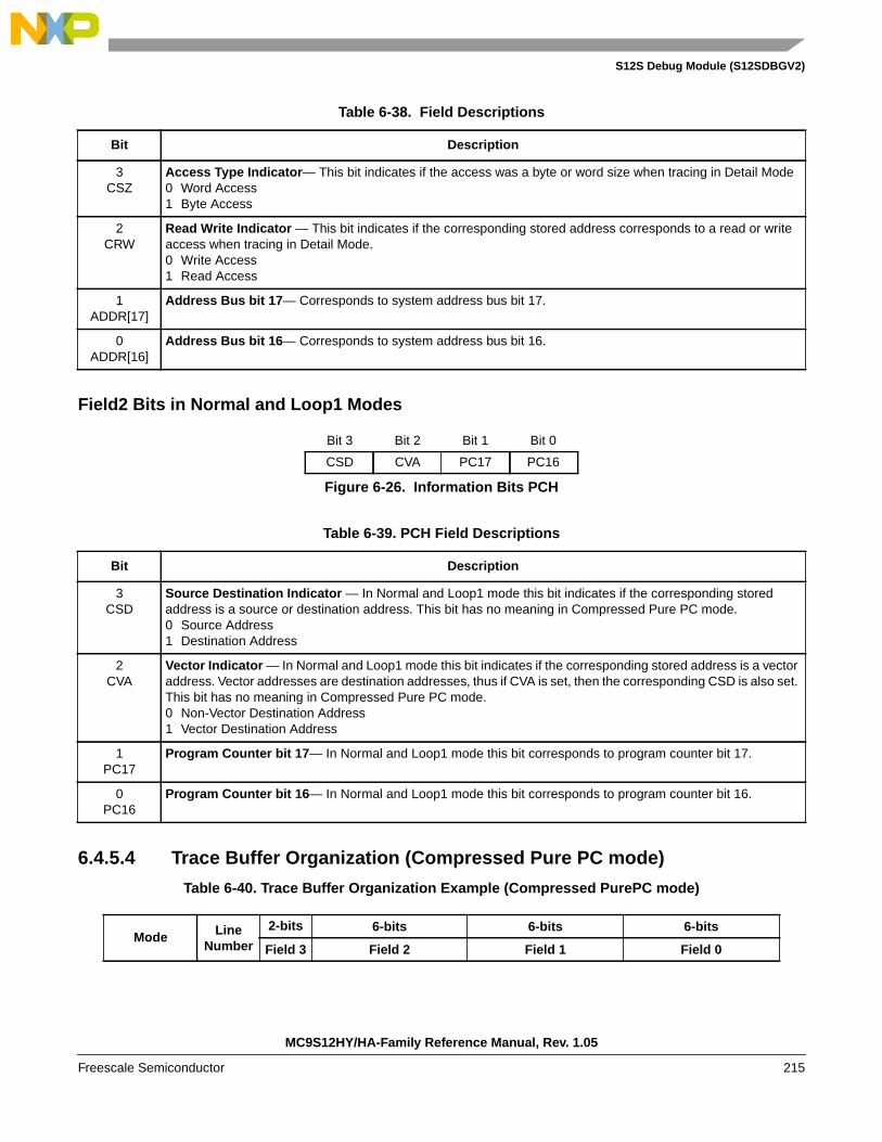
S12S Debug Module (S12SDBGV2)
Field2 Bits in Normal and Loop1 Modes
6.4.5.4 Trace Buffer Organization (Compressed Pure PC mode)
Table 6-40. Trace Buffer Organization Example (Compressed PurePC mode)
Table 6-38. Field Descriptions
Bit Description
3CSZ
Access Type Indicator— This bit indicates if the access was a byte or word size when tracing in Detail Mode0 Word Access1 Byte Access
2CRW
Read Write Indicator — This bit indicates if the corresponding stored address corresponds to a read or writeaccess when tracing in Detail Mode.0 Write Access1 Read Access
1ADDR[17]
Address Bus bit 17— Corresponds to system address bus bit 17.
0ADDR[16]
Address Bus bit 16— Corresponds to system address bus bit 16.
Bit 3 Bit 2 Bit 1 Bit 0
CSD CVA PC17 PC16
Figure 6-26. Information Bits PCH
Table 6-39. PCH Field Descriptions
Bit Description
3CSD
Source Destination Indicator — In Normal and Loop1 mode this bit indicates if the corresponding storedaddress is a source or destination address. This bit has no meaning in Compressed Pure PC mode.0 Source Address1 Destination Address
2CVA
Vector Indicator — In Normal and Loop1 mode this bit indicates if the corresponding stored address is a vectoraddress. Vector addresses are destination addresses, thus if CVA is set, then the corresponding CSD is also set.This bit has no meaning in Compressed Pure PC mode.0 Non-Vector Destination Address1 Vector Destination Address
1PC17
Program Counter bit 17— In Normal and Loop1 mode this bit corresponds to program counter bit 17.
0PC16
Program Counter bit 16— In Normal and Loop1 mode this bit corresponds to program counter bit 16.
Mode LineNumber
2-bits 6-bits 6-bits 6-bits
Field 3 Field 2 Field 1 Field 0
MC9S12HY/HA-Family Reference Manual, Rev. 1.05
Freescale Semiconductor 215
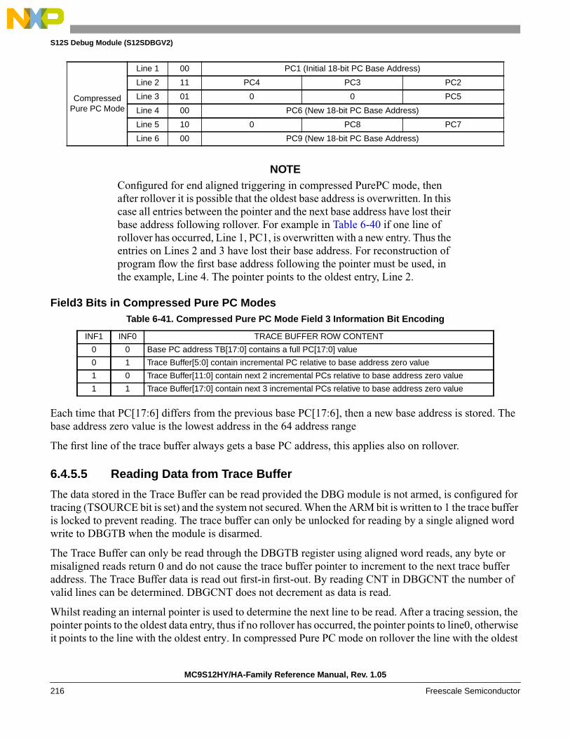
S12S Debug Module (S12SDBGV2)
NOTEConfigured for end aligned triggering in compressed PurePC mode, thenafter rollover it is possible that the oldest base address is overwritten. In thiscase all entries between the pointer and the next base address have lost theirbase address following rollover. For example in Table 6-40 if one line ofrollover has occurred, Line 1, PC1, is overwritten with a new entry. Thus theentries on Lines 2 and 3 have lost their base address. For reconstruction ofprogram flow the first base address following the pointer must be used, inthe example, Line 4. The pointer points to the oldest entry, Line 2.
Field3 Bits in Compressed Pure PC Modes
Each time that PC[17:6] differs from the previous base PC[17:6], then a new base address is stored. Thebase address zero value is the lowest address in the 64 address range
The first line of the trace buffer always gets a base PC address, this applies also on rollover.
6.4.5.5 Reading Data from Trace Buffer
The data stored in the Trace Buffer can be read provided the DBG module is not armed, is configured fortracing (TSOURCE bit is set) and the system not secured. When the ARM bit is written to 1 the trace bufferis locked to prevent reading. The trace buffer can only be unlocked for reading by a single aligned wordwrite to DBGTB when the module is disarmed.
The Trace Buffer can only be read through the DBGTB register using aligned word reads, any byte ormisaligned reads return 0 and do not cause the trace buffer pointer to increment to the next trace bufferaddress. The Trace Buffer data is read out first-in first-out. By reading CNT in DBGCNT the number ofvalid lines can be determined. DBGCNT does not decrement as data is read.
Whilst reading an internal pointer is used to determine the next line to be read. After a tracing session, thepointer points to the oldest data entry, thus if no rollover has occurred, the pointer points to line0, otherwiseit points to the line with the oldest entry. In compressed Pure PC mode on rollover the line with the oldest
CompressedPure PC Mode
Line 1 00 PC1 (Initial 18-bit PC Base Address)
Line 2 11 PC4 PC3 PC2
Line 3 01 0 0 PC5
Line 4 00 PC6 (New 18-bit PC Base Address)
Line 5 10 0 PC8 PC7
Line 6 00 PC9 (New 18-bit PC Base Address)
Table 6-41. Compressed Pure PC Mode Field 3 Information Bit Encoding
INF1 INF0 TRACE BUFFER ROW CONTENT
0 0 Base PC address TB[17:0] contains a full PC[17:0] value
0 1 Trace Buffer[5:0] contain incremental PC relative to base address zero value
1 0 Trace Buffer[11:0] contain next 2 incremental PCs relative to base address zero value
1 1 Trace Buffer[17:0] contain next 3 incremental PCs relative to base address zero value
MC9S12HY/HA-Family Reference Manual, Rev. 1.05
216 Freescale Semiconductor

S12S Debug Module (S12SDBGV2)
data entry may also contain newer data entries in fields 0 and 1. Thus if rollover is indicated by the TBFbit, the line status must be decoded using the INF bits in field3 of that line. If both INF bits are clear thenthe line contains only entries from before the last rollover.If INF0=1 then field 0 contains post rollover data but fields 1 and 2 contain pre rollover data.If INF1=1 then fields 0 and 1 contain post rollover data but field 2 contains pre rollover data.
The pointer is initialized by each aligned write to DBGTBH to point to the oldest data again. This enablesan interrupted trace buffer read sequence to be easily restarted from the oldest data entry.
The least significant word of line is read out first. This corresponds to the fields 1 and 0 of Table 6-37. Thenext word read returns field 2 in the least significant bits [3:0] and “0” for bits [15:4].
Reading the Trace Buffer while the DBG module is armed returns invalid data and no shifting of the RAMpointer occurs.
6.4.5.6 Trace Buffer Reset State
The Trace Buffer contents and DBGCNT bits are not initialized by a system reset. Thus should a systemreset occur, the trace session information from immediately before the reset occurred can be read out andthe number of valid lines in the trace buffer is indicated by DBGCNT. The internal pointer to the currenttrace buffer address is initialized by unlocking the trace buffer and points to the oldest valid data even if areset occurred during the tracing session. To read the trace buffer after a reset, TSOURCE must be set,otherwise the trace buffer reads as all zeroes. Generally debugging occurrences of system resets is besthandled using end trigger alignment since the reset may occur before the trace trigger, which in the begintrigger alignment case means no information would be stored in the trace buffer.
The Trace Buffer contents and DBGCNT bits are undefined following a POR.
NOTEAn external pin RESET that occurs simultaneous to a trace buffer entry can,in very seldom cases, lead to either that entry being corrupted or the firstentry of the session being corrupted. In such cases the other contents of thetrace buffer still contain valid tracing information. The case occurs when thereset assertion coincides with the trace buffer entry clock edge.
6.4.6 Tagging
A tag follows program information as it advances through the instruction queue. When a tagged instructionreaches the head of the queue a tag hit occurs and can initiate a state sequencer transition.
Each comparator control register features a TAG bit, which controls whether the comparator match causesa state sequencer transition immediately or tags the opcode at the matched address. If a comparator isenabled for tagged comparisons, the address stored in the comparator match address registers must be anopcode address.
Using Begin trigger together with tagging, if the tagged instruction is about to be executed then thetransition to the next state sequencer state occurs. If the transition is to the Final State, tracing is started.Only upon completion of the tracing session can a breakpoint be generated. Using End alignment, when
MC9S12HY/HA-Family Reference Manual, Rev. 1.05
Freescale Semiconductor 217

S12S Debug Module (S12SDBGV2)
the tagged instruction is about to be executed and the next transition is to Final State then a breakpoint isgenerated immediately, before the tagged instruction is carried out.
R/W monitoring, access size (SZ) monitoring and data bus monitoring are not useful if tagging is selected,since the tag is attached to the opcode at the matched address and is not dependent on the data bus nor onthe type of access. Thus these bits are ignored if tagging is selected.
When configured for range comparisons and tagging, the ranges are accurate only to word boundaries.
Tagging is disabled when the BDM becomes active.
6.4.7 Breakpoints
It is possible to generate breakpoints from channel transitions to final state or using software to write tothe TRIG bit in the DBGC1 register.
6.4.7.1 Breakpoints From Comparator Channels
Breakpoints can be generated when the state sequencer transitions to the Final State. If configured fortagging, then the breakpoint is generated when the tagged opcode reaches the execution stage of theinstruction queue.
If a tracing session is selected by the TSOURCE bit, breakpoints are requested when the tracing sessionhas completed, thus if Begin aligned triggering is selected, the breakpoint is requested only on completionof the subsequent trace (see Table 6-42). If no tracing session is selected, breakpoints are requestedimmediately.
If the BRK bit is set, then the associated breakpoint is generated immediately independent of tracingtrigger alignment.
6.4.7.2 Breakpoints Generated Via The TRIG Bit
If a TRIG triggers occur, the Final State is entered whereby tracing trigger alignment is defined by theTALIGN bit. If a tracing session is selected by the TSOURCE bit, breakpoints are requested when thetracing session has completed, thus if Begin aligned triggering is selected, the breakpoint is requested onlyon completion of the subsequent trace (see Table 6-42). If no tracing session is selected, breakpoints are
Table 6-42. Breakpoint Setup For CPU Breakpoints
BRK TALIGN DBGBRK Breakpoint Alignment
0 0 0 Fill Trace Buffer until trigger then disarm (no breakpoints)
0 0 1 Fill Trace Buffer until trigger, then breakpoint request occurs
0 1 0 Start Trace Buffer at trigger (no breakpoints)
0 1 1 Start Trace Buffer at triggerA breakpoint request occurs when Trace Buffer is full
1 x 1 Terminate tracing and generate breakpoint immediately on trigger
1 x 0 Terminate tracing immediately on trigger
MC9S12HY/HA-Family Reference Manual, Rev. 1.05
218 Freescale Semiconductor

S12S Debug Module (S12SDBGV2)
requested immediately. TRIG breakpoints are possible with a single write to DBGC1, setting ARM andTRIG simultaneously.
6.4.7.3 Breakpoint Priorities
If a TRIG trigger occurs after Begin aligned tracing has already started, then the TRIG no longer has aneffect. When the associated tracing session is complete, the breakpoint occurs. Similarly if a TRIG isfollowed by a subsequent comparator channel match, it has no effect, since tracing has already started.
If a forced SWI breakpoint coincides with a BGND in user code with BDM enabled, then the BDM isactivated by the BGND and the breakpoint to SWI is suppressed.
6.4.7.3.1 DBG Breakpoint Priorities And BDM Interfacing
Breakpoint operation is dependent on the state of the BDM module. If the BDM module is active, the CPUis executing out of BDM firmware, thus comparator matches and associated breakpoints are disabled. Inaddition, while executing a BDM TRACE command, tagging into BDM is disabled. If BDM is not active,the breakpoint gives priority to BDM requests over SWI requests if the breakpoint happens to coincidewith a SWI instruction in user code. On returning from BDM, the SWI from user code gets executed.
BDM cannot be entered from a breakpoint unless the ENABLE bit is set in the BDM. If entry to BDM viaa BGND instruction is attempted and the ENABLE bit in the BDM is cleared, the CPU actually executesthe BDM firmware code, checks the ENABLE and returns if ENABLE is not set. If not serviced by themonitor then the breakpoint is re-asserted when the BDM returns to normal CPU flow.
If the comparator register contents coincide with the SWI/BDM vector address then an SWI in user codecould coincide with a DBG breakpoint. The CPU ensures that BDM requests have a higher priority thanSWI requests. Returning from the BDM/SWI service routine care must be taken to avoid a repeatedbreakpoint at the same address.
Should a tagged or forced breakpoint coincide with a BGND in user code, then the instruction that followsthe BGND instruction is the first instruction executed when normal program execution resumes.
Table 6-43. Breakpoint Mapping Summary
DBGBRKBDM Bit
(DBGC1[4])BDM
EnabledBDM
Active Breakpoint
Mapping
0 X X X No Breakpoint
1 0 X 0 Breakpoint to SWI
X X 1 1 No Breakpoint
1 1 0 X Breakpoint to SWI
1 1 1 0 Breakpoint to BDM
MC9S12HY/HA-Family Reference Manual, Rev. 1.05
Freescale Semiconductor 219
S12S Debug Module (S12SDBGV2)
NOTEWhen program control returns from a tagged breakpoint using an RTI orBDM GO command without program counter modification it returns to theinstruction whose tag generated the breakpoint. To avoid a repeatedbreakpoint at the same location reconfigure the DBG module in the SWIroutine, if configured for an SWI breakpoint, or over the BDM interface byexecuting a TRACE command before the GO to increment the program flowpast the tagged instruction.
6.5 Application Information
6.5.1 State Machine scenarios
Defining the state control registers as SCR1,SCR2, SCR3 and M0,M1,M2 as matches on channels 0,1,2respectively. SCR encoding supported by S12SDBGV1 are shown in black. SCR encoding supported onlyin S12SDBGV2 are shown in red. For backwards compatibility the new scenarios use a 4th bit in each SCRregister. Thus the existing encoding for SCRx[2:0] is not changed.
6.5.2 Scenario 1
A trigger is generated if a given sequence of 3 code events is executed.
Figure 6-27. Scenario 1
Scenario 1 is possible with S12SDBGV1 SCR encoding
6.5.3 Scenario 2
A trigger is generated if a given sequence of 2 code events is executed.
Figure 6-28. Scenario 2a
State1 Final StateState3State2
SCR1=0011 SCR2=0010 SCR3=0111M1 M2 M0
State1 Final StateState2
SCR1=0011 SCR2=0101M1 M2
MC9S12HY/HA-Family Reference Manual, Rev. 1.05
220 Freescale Semiconductor

S12S Debug Module (S12SDBGV2)
A trigger is generated if a given sequence of 2 code events is executed, whereby the first event is entry intoa range (COMPA,COMPB configured for range mode). M1 is disabled in range modes.
Figure 6-29. Scenario 2b
A trigger is generated if a given sequence of 2 code events is executed, whereby the second event is entryinto a range (COMPA,COMPB configured for range mode)
Figure 6-30. Scenario 2c
All 3 scenarios 2a,2b,2c are possible with the S12SDBGV1 SCR encoding
6.5.4 Scenario 3
A trigger is generated immediately when one of up to 3 given events occurs
Figure 6-31. Scenario 3
Scenario 3 is possible with S12SDBGV1 SCR encoding
6.5.5 Scenario 4
Trigger if a sequence of 2 events is carried out in an incorrect order. Event A must be followed by event Band event B must be followed by event A. 2 consecutive occurrences of event A without an intermediate
State1 Final StateState2
SCR1=0111 SCR2=0101M01 M2
State1 Final StateState2
SCR1=0010 SCR2=0011M2 M0
State1 Final State
SCR1=0000M012
MC9S12HY/HA-Family Reference Manual, Rev. 1.05
Freescale Semiconductor 221

S12S Debug Module (S12SDBGV2)
event B cause a trigger. Similarly 2 consecutive occurrences of event B without an intermediate event Acause a trigger. This is possible by using CompA and CompC to match on the same address as shown.
Figure 6-32. Scenario 4a
This scenario is currently not possible using 2 comparators only. S12SDBGV2 makes it possible with 2comparators, State 3 allowing a M0 to return to state 2, whilst a M2 leads to final state as shown.
Figure 6-33. Scenario 4b (with 2 comparators)
The advantage of using only 2 channels is that now range comparisons can be included (channel0)
This however violates the S12SDBGV1 specification, which states that a match leading to final statealways has priority in case of a simultaneous match, whilst priority is also given to the lowest channelnumber. For S12SDBG the corresponding CPU priority decoder is removed to support this, such that onsimultaneous taghits, taghits pointing to final state have highest priority. If no taghit points to final statethen the lowest channel number has priority. Thus with the above encoding from State3, the CPU and DBGwould break on a simultaneous M0/M2.
State1
State 3 Final State
State2M0
M0M2M1
M1
M1
SCR1=0100 SCR2=0011
SCR3=0001
State1
State 3 Final State
State2M0
M01M0M2
M2
M2
SCR1=0110 SCR2=1100
SCR3=1110
M1 disabled inrange mode
MC9S12HY/HA-Family Reference Manual, Rev. 1.05
222 Freescale Semiconductor
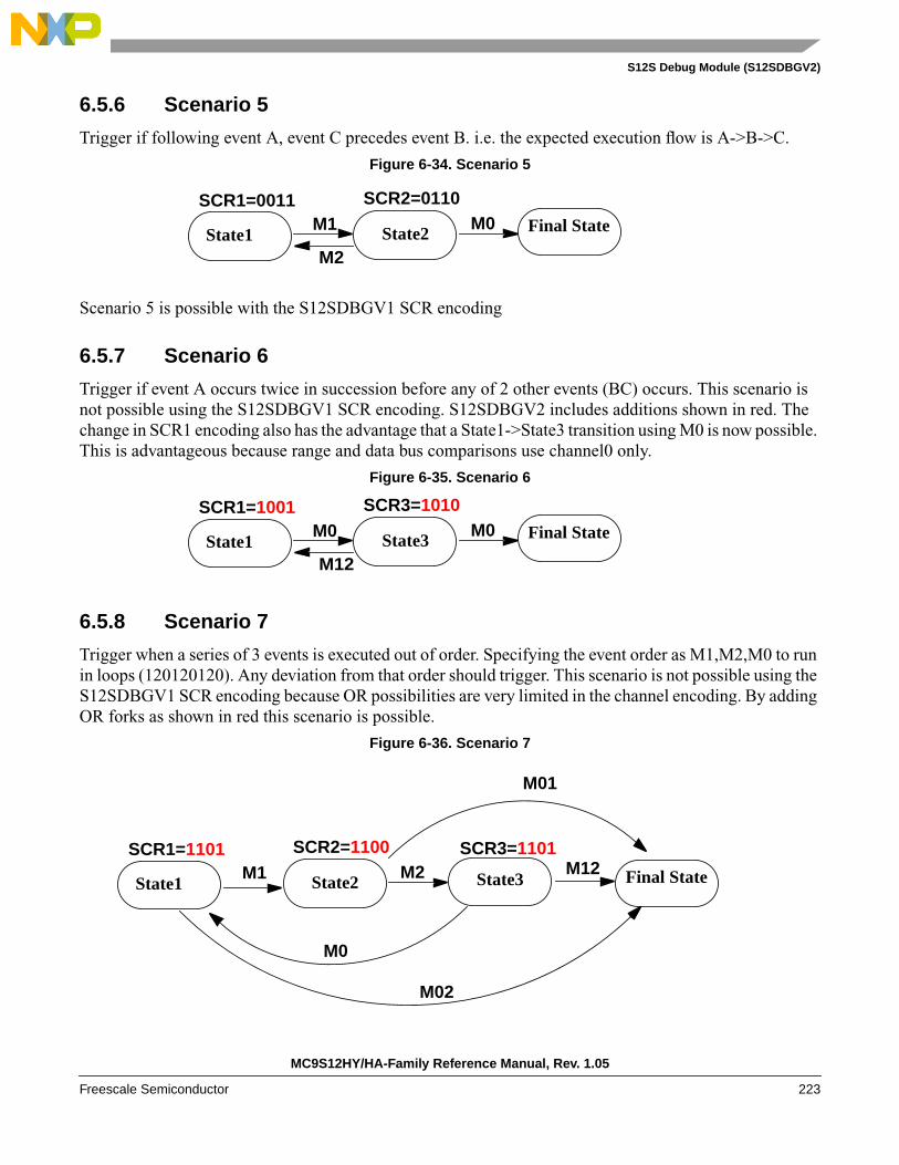
S12S Debug Module (S12SDBGV2)
6.5.6 Scenario 5
Trigger if following event A, event C precedes event B. i.e. the expected execution flow is A->B->C.
Figure 6-34. Scenario 5
Scenario 5 is possible with the S12SDBGV1 SCR encoding
6.5.7 Scenario 6
Trigger if event A occurs twice in succession before any of 2 other events (BC) occurs. This scenario isnot possible using the S12SDBGV1 SCR encoding. S12SDBGV2 includes additions shown in red. Thechange in SCR1 encoding also has the advantage that a State1->State3 transition using M0 is now possible.This is advantageous because range and data bus comparisons use channel0 only.
Figure 6-35. Scenario 6
6.5.8 Scenario 7
Trigger when a series of 3 events is executed out of order. Specifying the event order as M1,M2,M0 to runin loops (120120120). Any deviation from that order should trigger. This scenario is not possible using theS12SDBGV1 SCR encoding because OR possibilities are very limited in the channel encoding. By addingOR forks as shown in red this scenario is possible.
Figure 6-36. Scenario 7
State1 Final StateState2
SCR1=0011 SCR2=0110M1 M0
M2
State1 Final StateState3
SCR1=1001 SCR3=1010M0 M0
M12
State1 Final StateState3State2
SCR1=1101 SCR2=1100 SCR3=1101M1 M2 M12
M0
M02
M01
MC9S12HY/HA-Family Reference Manual, Rev. 1.05
Freescale Semiconductor 223

S12S Debug Module (S12SDBGV2)
On simultaneous matches the lowest channel number has priority so with this configuration the forkingfrom State1 has the peculiar effect that a simultaneous match0/match1 transitions to final state but asimultaneous match2/match1transitions to state2.
6.5.9 Scenario 8
Trigger when a routine/event at M2 follows either M1 or M0.
Figure 6-37. Scenario 8a
Trigger when an event M2 is followed by either event M0 or event M1
Figure 6-38. Scenario 8b
Scenario 8a and 8b are possible with the S12SDBGV1 and S12SDBGV2 SCR encoding
6.5.10 Scenario 9
Trigger when a routine/event at A (M2) does not follow either B or C (M1 or M0) before they are executedagain. This cannot be realized with theS12SDBGV1 SCR encoding due to OR limitations. By changingthe SCR2 encoding as shown in red this scenario becomes possible.
Figure 6-39. Scenario 9
6.5.11 Scenario 10
Trigger if an event M0 occurs following up to two successive M2 events without the resetting event M1.As shown up to 2 consecutive M2 events are allowed, whereby a reset to State1 is possible after either oneor two M2 events. If an event M0 occurs following the second M2, before M1 resets to State1 then a trigger
State1 Final StateState2
SCR1=0111 SCR2=0101M01 M2
State1 Final StateState2
SCR1=0010 SCR2=0111M2 M01
State1 Final StateState2
SCR1=0111 SCR2=1111M01 M01
M2
MC9S12HY/HA-Family Reference Manual, Rev. 1.05
224 Freescale Semiconductor
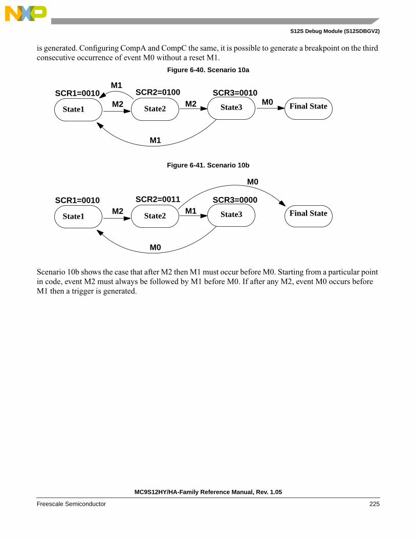
S12S Debug Module (S12SDBGV2)
is generated. Configuring CompA and CompC the same, it is possible to generate a breakpoint on the thirdconsecutive occurrence of event M0 without a reset M1.
Figure 6-40. Scenario 10a
Figure 6-41. Scenario 10b
Scenario 10b shows the case that after M2 then M1 must occur before M0. Starting from a particular pointin code, event M2 must always be followed by M1 before M0. If after any M2, event M0 occurs beforeM1 then a trigger is generated.
State1 Final StateState3State2
SCR1=0010 SCR2=0100 SCR3=0010M2 M2 M0
M1
M1
State1 Final StateState3State2
SCR1=0010 SCR2=0011 SCR3=0000M2 M1
M0
M0
MC9S12HY/HA-Family Reference Manual, Rev. 1.05
Freescale Semiconductor 225

S12S Debug Module (S12SDBGV2)
MC9S12HY/HA-Family Reference Manual, Rev. 1.05
226 Freescale Semiconductor

Chapter 7S12 Clock, Reset and Power Management Unit (S12CPMU)Block Description
Revision History
VersionNumber
RevisionDate
EffectiveDate Author Description of Changes
V01.00 16 Jan.07 16 Jan. 07 Initial release
V01.01 9 July 08 9 July 08 added IRCLK to Block Diagram
V01.02 7 Oct. 08 7 Oct. 08 clarified and detailed oscillator filter functionality
V01.03 11 Dec. 08 11 Dec. 08added note, that startup time of external oscillator tUPOSC must beconsidered, especially when entering Pseudo Stop Mode
V01.04 17 Jun. 09 17 Jun. 09Modified reset phase descriptions to reference fVCORST instead offPLLRST and correct typo of RESET pin sample point from 64 to 256cycles in section: Description of Reset Operation
V01.05 27 Apr. 10 27 Apr. 10Major rework fixing typos, figures and tables and improveddescription of Adaptive Oscillator Filter.
V01.06 03 Mai 10 03 Mai 10
Improved pin description in Section 7.2, “Signal Description.Improved description of bit write access conditions for CPMUCLKregister bits in Section 7.3.2.6, “S12CPMU Clock Select Register(CPMUCLKS).Improved description of bit write access conditions for CPMUCOPregister bits in Section 7.3.2.9, “S12CPMU COP Control Register(CPMUCOP).Updated bit description OSCFILT[4:0] to get one common wordingthroughout the document.Updated register description CPMUPROT to have list of protectedregisters only once in the document which gets referenced.Wording corrections throughout document.
V01.06 06 Mai 10 06 Mai 10Changed feature name “adaptive spike filter” to “Adaptive OscillatorFilter” in Figure 7-2.Added a node to the description of the CPMUOSC register.
V01.07 25 July 12 25 July 12Enhanced VSEL bit description that setting HTE bit before isrequired.
MC9S12HY/HA-Family Reference Manual, Rev. 1.05
Freescale Semiconductor 227

S12 Clock, Reset and Power Management Unit (S12CPMU) Block Description
7.1 IntroductionThis specification describes the function of the Clock, Reset and Power Management Unit (S12CPMU).
• The Pierce oscillator (OSCLCP) provides a robust, low-noise and low-power external clock source.It is designed for optimal start-up margin with typical crystal oscillators.
• The Voltage regulator (IVREG) operates from the range 3.13V to 5.5V. It provides all the requiredchip internal voltages and voltage monitors.
• The Phase Locked Loop (PLL) provides a highly accurate frequency multiplier with internal filter.
• The Internal Reference Clock (IRC1M) provides a1MHz clock.
7.1.1 Features
The Pierce Oscillator (OSCLCP) contains circuitry to dynamically control current gain in the outputamplitude. This ensures a signal with low harmonic distortion, low power and good noise immunity.
• Supports crystals or resonators from 4MHz to 16MHz.
• High noise immunity due to input hysteresis and spike filtering.
• Low RF emissions with peak-to-peak swing limited dynamically
• Transconductance (gm) sized for optimum start-up margin for typical crystals
• Dynamic gain control eliminates the need for external current limiting resistor
• Integrated resistor eliminates the need for external bias resistor.
• Low power consumption: Operates from internal 1.8V (nominal) supply, Amplitude control limitspower
The Voltage Regulator (IVREG) has the following features:
• Input voltage range from 3.13V to 5.5V
• Low-voltage detect (LVD) with low-voltage interrupt (LVI)
• Power-on reset (POR)
• Low-voltage reset (LVR)
The Phase Locked Loop (PLL) has the following features:
• highly accurate and phase locked frequency multiplier
• Configurable internal filter for best stability and lock time.
• Frequency modulation for defined jitter and reduced emission
• Automatic frequency lock detector
• Interrupt request on entry or exit from locked condition
• Reference clock either external (crystal) or internal square wave (1MHz IRC1M) based.
• PLL stability is sufficient for LIN communication, even if using IRC1M as reference clock
The Internal Reference Clock (IRC1M) has the following features:
• Trimmable in frequency
• Factory trimmed value for 1MHz in Flash Memory, can be overwritten by application if required
MC9S12HY/HA-Family Reference Manual, Rev. 1.05
228 Freescale Semiconductor

S12 Clock, Reset and Power Management Unit (S12CPMU) Block Description
Other features of the S12CPMU include
• Clock monitor to detect loss of crystal
• Autonomous periodical interrupt (API)
• Bus Clock Generator
— Clock switch to select either PLLCLK or external crystal/resonator based Bus Clock
— PLLCLK divider to adjust system speed
• System Reset generation from the following possible sources:
— Power-on reset (POR)
— Low-voltage reset (LVR)
— Illegal address access
— COP time out
— Loss of oscillation (clock monitor fail)
— External pin RESET
MC9S12HY/HA-Family Reference Manual, Rev. 1.05
Freescale Semiconductor 229

S12 Clock, Reset and Power Management Unit (S12CPMU) Block Description
7.1.2 Modes of Operation
This subsection lists and briefly describes all operating modes supported by the S12CPMU.
7.1.2.1 Run Mode
The voltage regulator is in Full Performance Mode (FPM).
The Phase Locked Loop (PLL) is on.
The Internal Reference Clock (IRC1M) is on.
The API is available.
• PLL Engaged Internal (PEI)— This is the default mode after System Reset and Power-On Reset.
— The Bus Clock is based on the PLLCLK.
— After reset the PLL is configured for 64MHz VCOCLK operationPost divider is 0x03, so PLLCLK is VCOCLK divided by 4, that is 16MHz and Bus Clock is8MHz.The PLL can be re-configured for other bus frequencies.
— The reference clock for the PLL (REFCLK) is based on internal reference clock IRC1M
• PLL Engaged External (PEE)— The Bus Clock is based on the PLLCLK.
— This mode can be entered from default mode PEI by performing the following steps:
– Configure the PLL for desired bus frequency.
– Program the reference divider (REFDIV[3:0] bits) to divide down oscillator frequency ifnecessary.
– Enable the external oscillator (OSCE bit)
• PLL Bypassed External (PBE)— The Bus Clock is based on the Oscillator Clock (OSCCLK).
— This mode can be entered from default mode PEI by performing the following steps:
– Enable the external oscillator (OSCE bit)
– Wait for oscillator to start up (UPOSC=1)
– Select the Oscillator Clock (OSCCLK) as Bus Clock (PLLSEL=0).
— The PLLCLK is still on to filter possible spikes of the external oscillator clock.
7.1.2.2 Wait Mode
For S12CPMU Wait Mode is the same as Run Mode.
MC9S12HY/HA-Family Reference Manual, Rev. 1.05
230 Freescale Semiconductor

S12 Clock, Reset and Power Management Unit (S12CPMU) Block Description
7.1.2.3 Stop Mode
This mode is entered by executing the CPU STOP instruction.
The voltage regulator is in Reduced Power Mode (RPM).
The API is available.
The Phase Locked Loop (PLL) is off.
The Internal Reference Clock (IRC1M) is off.
Core Clock, Bus Clock and BDM Clock are stopped.
Depending on the setting of the PSTP and the OSCE bit, Stop Mode can be differentiated between FullStop Mode (PSTP = 0 or OSCE=0) and Pseudo Stop Mode (PSTP = 1 and OSCE=1).
• Full Stop Mode (PSTP=0 or OSCE=0)The external oscillator (OSCLCP) is disabled.After wake-up from Full Stop Mode the Core Clock and Bus Clock are running on PLLCLK(PLLSEL=1). After wake-up from Full Stop Mode COP and RTI are running on IRCCLK(COPOSCSEL=0, RTIOSCSEL=0).
• Pseudo Stop Mode (PSTP=1 and OSCE=1)The external oscillator (OSCLCP) continues torun. If the respective enable bits are set the COP andRTI will continue to run.The clock configuration bits PLLSEL, COPOSCSEL, RTIOSCSEL are unchanged.
NOTEWhen starting up the external oscillator (either by programming OSCE bitto 1 or on exit from Full Stop Mode with OSCE bit already 1) the softwaremust wait for a minimum time equivalent to the startup-time of the externaloscillator tUPOSC before entering Pseudo Stop Mode.
MC9S12HY/HA-Family Reference Manual, Rev. 1.05
Freescale Semiconductor 231

S12 Clock, Reset and Power Management Unit (S12CPMU) Block Description
7.1.3 S12CPMU Block Diagram
Figure 7-1. Block diagram of S12CPMU
S12CPMU
EXTAL
XTAL
System Reset
Power-On Detect
PLL Lock Interrupt
MMC Illegal Address Access
COP time out
Loop
ReferenceDivider
COPWatchdog
Voltage
VDDR
Internal
ResetGenerator
Divide by
Phase
PostDivider1 to 32
VCOCLK
ECLK2X
LOCKIE
IRCTRIM[9:0]
SYNDIV[5:0]
LOCK
REFDIV[3:0]
2*(SYNDIV+1)
PierceOscillator
4MHz-16MHz
OSCE
ILAF
PORF
divideby 2
ECLK
POSTDIV[4:0]
Power-On Reset
Controlled
lockedLoop withinternalFilter (PLL)
REFCLK
FBCLK
REFFRQ[1:0]
VCOFRQ[1:0]
Lockdetect
Regulator3.13 to 5.5V
AutonomousPeriodicInterrupt (API)
API Interrupt
VDDAVSSA
AdaptiveOscillatorFilter PLLSEL
OSCFILT[4:0](to MSCAN)
VDDXVSSX
VSSPLLVSS
Low Voltage Detect VDDX
LVRF
PLLCLKReference
divideby 8
BDM Clock
Clock(IRC1M)
ClockMonitor
monitor fail
Real TimeInterrupt (RTI)
RTI Interrupt
PSTP
CPMURTI
oscillator status Interrupt
(OSCLCP)
CAN_OSCCLK
HighTemperatureSense
HT Interrupt
Low Voltage Interrupt
ACLK
APICLK
RTICLKIRCCLK
OSCCLK
RTIOSCSELCPMUCOP
COPCLKIRCCLK
OSCCLK
COPOSCSEL
to ResetGenerator
COP time out
PCE PRE
UPOSC=0 sets PLLSEL bit
API_EXTCLKRCOsc.
VDD, VDDPLL, VDDF(core supplies)
UPOSC
RESET
OSCIE
APIE
RTIE
HTDS HTIE
LVDS LVIELow Voltage Detect VDDA
UPOSC
UPOSC=0 clears
&OSCCLK
divideby 4
Bus Clock
IRCCLK(to LCD)
OSCBW
(Core Clock)
(Bus Clock)
MC9S12HY/HA-Family Reference Manual, Rev. 1.05
232 Freescale Semiconductor

S12 Clock, Reset and Power Management Unit (S12CPMU) Block Description
Figure 7-2 shows a block diagram of the OSCLCP.
Figure 7-2. OSCLCP Block Diagram
EXTAL XTAL
Gain Control
VDDPLL = 1.8 V
Rf
OSCCLK
PeakDetector
VSSPLL
MC9S12HY/HA-Family Reference Manual, Rev. 1.05
Freescale Semiconductor 233

S12 Clock, Reset and Power Management Unit (S12CPMU) Block Description
7.2 Signal DescriptionThis section lists and describes the signals that connect off chip and internal supply nodes.
7.2.1 RESET
Pin RESET is an active-low bidirectional pin. As an input it initializes the MCU asynchronously to aknown start-up state. As an open-drain output it indicates that an MCU-internal reset has been triggered.
7.2.2 EXTAL and XTAL
These pins provide the interface for a crystal to control the internal clock generator circuitry. EXTAL isthe external clock input or the input to the crystal oscillator amplifier. XTAL is the output of the crystaloscillator amplifier. The MCU internal OSCCLK is derived from the EXTAL input frequency. If OSCE=0,the EXTAL pin is pulled down by an internal resistor of approximately 200 kΩ and the XTAL pin is pulleddown by an internal resistor of approximately 700 kΩ.
NOTEFreescale recommends an evaluation of the application board and chosenresonator or crystal by the resonator or crystal supplier.Loop controlled circuit is not suited for overtone resonators and crystals.
7.2.3 TEMPSENSE — temperature sensor output voltage
Depending on the VSEL value either the voltage level generated by the temperature sensor or the VREGbandgap voltage is driven to a special channel of the ATD Converter. See device level specification forconnectivity.
7.2.4 VDDR — Regulator Power Input Pin
Pin VDDR is the power input of IVREG. All currents sourced into the regulator loads flow through thispin.
An off-chip decoupling capacitor (100 nF...220 nF, X7R ceramic) between VDDR and VSS can smoothripple on VDDR.
7.2.5 VSS, VSSPLL— Ground Pins
VSS and VSSPLL must be grounded.
7.2.6 VDDA, VSSA — Regulator Reference Supply Pins
Pins VDDA and VSSA, are used to supply the analog parts of the regulator.Internal precision reference circuits are supplied from these signals.
An off-chip external decoupling capacitor (100 nF...220 nF, X7R ceramic) between VDDA and VSSA canimprove the quality of this supply.
MC9S12HY/HA-Family Reference Manual, Rev. 1.05
234 Freescale Semiconductor

S12 Clock, Reset and Power Management Unit (S12CPMU) Block Description
7.2.7 VDDX, VSSX— Pad Supply Pins
This supply domain is monitored by the Low Voltage Reset circuit.
An off-chip decoupling capacitor (100 nF...220 nF, X7R ceramic) between VDDX and VSSX can improvethe quality of this supply.
NOTEDepending on the device package following device supply pins are maybecombined into one pin: VDDR, VDDX and VDDA.Depending on the device package following device supply pins are maybecombined into one pin: VSS, VSSX and VSSA.Please refer to the device Reference Manual for information if device supplypins are combined into one supply pin for certain packages and whichsupply pins are combined together.An off-chip decoupling capacitor (100 nF...220 nF, X7R ceramic) betweenthe combined supply pin pair can improve the quality of this supply.
7.2.8 API_EXTCLK — API external clock output pin
This pin provides the signal selected via APIES and is enabled with APIEA bit. See device specificationto which pin it connects.
7.2.9 VDD — Internal Regulator Output Supply (Core Logic)
Node VDD is a device internal supply output of the voltage regulator that provides the power supply forthe core logic.This supply domain is monitored by the Low Voltage Reset circuit.
7.2.10 VDDF — Internal Regulator Output Supply (NVM Logic)
Node VDDF is a device internal supply output of the voltage regulator that provides the power supply forthe NVM logic.This supply domain is monitored by the Low Voltage Reset circuit
7.2.11 VDDPLL — Internal Regulator Output Supply (PLL)
Node VDDPLL is a device internal supply output of the voltage regulator that provides the power supplyfor the PLL.
MC9S12HY/HA-Family Reference Manual, Rev. 1.05
Freescale Semiconductor 235

S12 Clock, Reset and Power Management Unit (S12CPMU) Block Description
7.3 Memory Map and RegistersThis section provides a detailed description of all registers accessible in the S12CPMU.
7.3.1 Module Memory Map
The S12CPMU registers are shown in Figure 7-3.
Address
Name Bit 7 6 5 4 3 2 1 Bit 0
0x0034CPMUSYNR
RVCOFRQ[1:0] SYNDIV[5:0]
W
0x0035CPMU
REFDIVR
REFFRQ[1:0]0 0
REFDIV[3:0]W
0x0036CPMU
POSTDIVR 0 0 0
POSTDIV[4:0]W
0x0037 CPMUFLGR
RTIF PORF LVRF LOCKIFLOCK
ILAF OSCIFUPOSC
W
0x0038 CPMUINTR
RTIE0 0
LOCKIE0 0
OSCIE0
W
0x0039 CPMUCLKSR
PLLSEL PSTP0 0
PRE PCERTI
OSCSELCOP
OSCSELW
0x003A CPMUPLLR 0 0
FM1 FM00 0 0 0
W
0x003B CPMURTIR
RTDEC RTR6 RTR5 RTR4 RTR3 RTR2 RTR1 RTR0W
0x003C CPMUCOPR
WCOP RSBCK0 0 0
CR2 CR1 CR0W WRTMASK
0x003DRESERVED
CPMUTEST0R 0 0 0 0 0 0 0 0
W
0x003ERESERVED
CPMUTEST1R 0 0 0 0 0 0 0 0
W
0x003FCPMU
ARMCOPR 0 0 0 0 0 0 0 0
W Bit 7 Bit 6 Bit 5 Bit 4 Bit 3 Bit 2 Bit 1 Bit 0
0x02F0CPMUHTCTL
R 0 0VSEL
0HTE
HTDSHTIE HTIF
W
0x02F1CPMULVCTL
R 0 0 0 0 0 LVDSLVIE LVIF
W
0x02F2CPMU
APICTLR
APICLK0 0
APIES APIEA APIFE APIE APIFW
= Unimplemented or Reserved
Figure 7-3. CPMU Register Summary
MC9S12HY/HA-Family Reference Manual, Rev. 1.05
236 Freescale Semiconductor

S12 Clock, Reset and Power Management Unit (S12CPMU) Block Description
0x02F3 CPMUAPITRR
APITR5 APITR4 APITR3 APITR2 APITR1 APITR00 0
W
0x02F4 CPMUAPIRHR
APIR15 APIR14 APIR13 APIR12 APIR11 APIR10 APIR9 APIR8W
0x02F5 CPMUAPIRLR
APIR7 APIR6 APIR5 APIR4 APIR3 APIR2 APIR1 APIR0W
0x02F6RESERVED
CPMUTEST3R 0 0 0 0 0 0 0 0
W
0x02F7 CPMUHTTRR
HTOE0 0 0
HTTR3 HTTR2 HTTR1 HTTR0W
0x02F8CPMU
IRCTRIMHR
TCTRIM[3:0]0 0
IRCTRIM[9:8]W
0x02F9CPMU
IRCTRIMLR
IRCTRIM[7:0]W
0x02FA CPMUOSCR
OSCE OSCBW0
OSCFILT[4:0]W
0x02FB CPMUPROTR 0 0 0 0 0 0 0
PROTW
0x02FCRESERVED
CPMUTEST2R 0 0 0 0 0 0 0 0
W
Address
Name Bit 7 6 5 4 3 2 1 Bit 0
= Unimplemented or Reserved
Figure 7-3. CPMU Register Summary
MC9S12HY/HA-Family Reference Manual, Rev. 1.05
Freescale Semiconductor 237
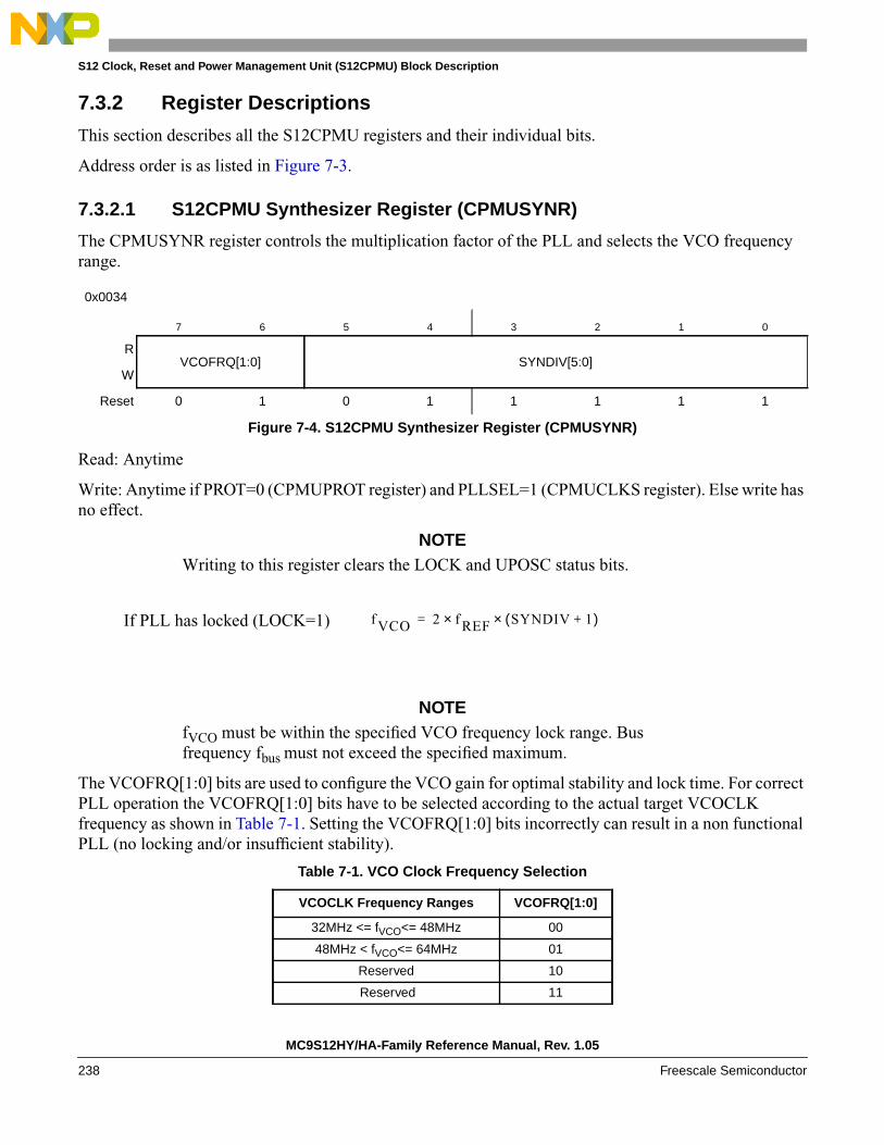
S12 Clock, Reset and Power Management Unit (S12CPMU) Block Description
7.3.2 Register Descriptions
This section describes all the S12CPMU registers and their individual bits.
Address order is as listed in Figure 7-3.
7.3.2.1 S12CPMU Synthesizer Register (CPMUSYNR)
The CPMUSYNR register controls the multiplication factor of the PLL and selects the VCO frequencyrange.
Read: Anytime
Write: Anytime if PROT=0 (CPMUPROT register) and PLLSEL=1 (CPMUCLKS register). Else write hasno effect.
NOTEWriting to this register clears the LOCK and UPOSC status bits.
NOTEfVCO must be within the specified VCO frequency lock range. Busfrequency fbus must not exceed the specified maximum.
The VCOFRQ[1:0] bits are used to configure the VCO gain for optimal stability and lock time. For correctPLL operation the VCOFRQ[1:0] bits have to be selected according to the actual target VCOCLKfrequency as shown in Table 7-1. Setting the VCOFRQ[1:0] bits incorrectly can result in a non functionalPLL (no locking and/or insufficient stability).
0x0034
7 6 5 4 3 2 1 0
RVCOFRQ[1:0] SYNDIV[5:0]
W
Reset 0 1 0 1 1 1 1 1
Figure 7-4. S12CPMU Synthesizer Register (CPMUSYNR)
Table 7-1. VCO Clock Frequency Selection
VCOCLK Frequency Ranges VCOFRQ[1:0]
32MHz <= fVCO<= 48MHz 00
48MHz < fVCO<= 64MHz 01
Reserved 10
Reserved 11
f VCO 2 f REF× SYNDIV 1+( )×=If PLL has locked (LOCK=1)
MC9S12HY/HA-Family Reference Manual, Rev. 1.05
238 Freescale Semiconductor

S12 Clock, Reset and Power Management Unit (S12CPMU) Block Description
7.3.2.2 S12CPMU Reference Divider Register (CPMUREFDIV)
The CPMUREFDIV register provides a finer granularity for the PLL multiplier steps when using theexternal oscillator as reference.
Read: Anytime
Write: Anytime if PROT=0 (CPMUPROT register) and PLLSEL=1 (CPMUCLKS register). Else write hasno effect.
NOTEWrite to this register clears the LOCK and UPOSC status bits.
The REFFRQ[1:0] bits are used to configure the internal PLL filter for optimal stability and lock time. Forcorrect PLL operation the REFFRQ[1:0] bits have to be selected according to the actual REFCLKfrequency as shown in Table 7-2.
If IRC1M is selected as REFCLK (OSCE=0) the PLL filter is fixed configured for the 1MHz <= fREF <=2MHz range. The bits can still be written but will have no effect on the PLL filter configuration.
For OSCE=1, setting the REFFRQ[1:0] bits incorrectly can result in a non functional PLL (no lockingand/or insufficient stability).
0x0035
7 6 5 4 3 2 1 0
RREFFRQ[1:0]
0 0REFDIV[3:0]
W
Reset 0 0 0 0 1 1 1 1
Figure 7-5. S12CPMU Reference Divider Register (CPMUREFDIV)
Table 7-2. Reference Clock Frequency Selection if OSC_LCP is enabled
REFCLK Frequency Ranges(OSCE=1)
REFFRQ[1:0]
1MHz <= fREF <= 2MHz 00
2MHz < fREF <= 6MHz 01
6MHz < fREF <= 12MHz 10
fREF >12MHz 11
f REF
f OSCREFDIV 1+( )-------------------------------------=If OSCLCP is enabled (OSCE=1)
If OSCLCP is disabled (OSCE=0) f REF f IRC1M=
MC9S12HY/HA-Family Reference Manual, Rev. 1.05
Freescale Semiconductor 239

S12 Clock, Reset and Power Management Unit (S12CPMU) Block Description
7.3.2.3 S12CPMU Post Divider Register (CPMUPOSTDIV)
The POSTDIV register controls the frequency ratio between the VCOCLK and the PLLCLK.
Read: Anytime
Write: Anytime if PLLSEL=1, else write has no effect.
7.3.2.4 S12CPMU Flags Register (CPMUFLG)
This register provides S12CPMU status bits and flags.
Read: Anytime
0x0036
7 6 5 4 3 2 1 0
R 0 0 0POSTDIV[4:0]
W
Reset 0 0 0 0 0 0 1 1
= Unimplemented or Reserved
Figure 7-6. S12CPMU Post Divider Register (CPMUPOSTDIV)
0x0037
7 6 5 4 3 2 1 0
RRTIF PORF LVRF LOCKIF
LOCKILAF OSCIF
UPOSC
W
Reset 0 Note 1 Note 2 0 0 Note 3 0 0
1. PORF is set to 1 when a power on reset occurs. Unaffected by System Reset.2. LVRF is set to 1 when a low voltage reset occurs. Unaffected by System Reset. Set by power on reset.3. ILAF is set to 1 when an illegal address reset occurs. Unaffected by System Reset. Cleared by power on reset.
= Unimplemented or Reserved
Figure 7-7. S12CPMU Flags Register (CPMUFLG)
f PLL
f VCOPOSTDIV 1+( )-----------------------------------------=If PLL is locked (LOCK=1)
If PLL is not locked (LOCK=0) f PLL
f VCO4
----------------=
f bus
f PLL2
--------------=If PLL is selected (PLLSEL=1)
MC9S12HY/HA-Family Reference Manual, Rev. 1.05
240 Freescale Semiconductor

S12 Clock, Reset and Power Management Unit (S12CPMU) Block Description
Write: Refer to each bit for individual write conditions
Table 7-3. CPMUFLG Field Descriptions
Field Description
7RTIF
Real Time Interrupt Flag — RTIF is set to 1 at the end of the RTI period. This flag can only be cleared by writinga 1. Writing a 0 has no effect. If enabled (RTIE=1), RTIF causes an interrupt request.0 RTI time-out has not yet occurred.1 RTI time-out has occurred.
6PORF
Power on Reset Flag — PORF is set to 1 when a power on reset occurs. This flag can only be cleared by writinga 1. Writing a 0 has no effect.0 Power on reset has not occurred.1 Power on reset has occurred.
5LVRF
Low Voltage Reset Flag — LVRF is set to 1 when a low voltage reset occurs. This flag can only be cleared bywriting a 1. Writing a 0 has no effect.0 Low voltage reset has not occurred.1 Low voltage reset has occurred.
4LOCKIF
PLL Lock Interrupt Flag — LOCKIF is set to 1 when LOCK status bit changes. This flag can only be cleared bywriting a 1. Writing a 0 has no effect.If enabled (LOCKIE=1), LOCKIF causes an interrupt request.0 No change in LOCK bit.1 LOCK bit has changed.
3LOCK
Lock Status Bit — LOCK reflects the current state of PLL lock condition. Writes have no effect. While PLL isunlocked (LOCK=0) fPLL is fVCO / 4 to protect the system from high core clock frequencies during the PLLstabilization time tlock.0 VCOCLK is not within the desired tolerance of the target frequency.
fPLL = fVCO/4.1 VCOCLK is within the desired tolerance of the target frequency.
fPLL = fVCO/(POSTDIV+1).
2ILAF
Illegal Address Reset Flag — ILAF is set to 1 when an illegal address reset occurs. Refer to MMC chapter fordetails. This flag can only be cleared by writing a 1. Writing a 0 has no effect.0 Illegal address reset has not occurred.1 Illegal address reset has occurred.
1OSCIF
Oscillator Interrupt Flag — OSCIF is set to 1 when UPOSC status bit changes. This flag can only be clearedby writing a 1. Writing a 0 has no effect.If enabled (OSCIE=1), OSCIF causes an interrupt request.0 No change in UPOSC bit.1 UPOSC bit has changed.
0UPOSC
Oscillator Status Bit — UPOSC reflects the status of the oscillator. Writes have no effect. While UPOSC=0 theOSCCLK going to the MSCAN module is off. Entering Full Stop Mode UPOSC is cleared.0 The oscillator is off or oscillation is not qualified by the PLL.1 The oscillator is qualified by the PLL.
MC9S12HY/HA-Family Reference Manual, Rev. 1.05
Freescale Semiconductor 241

S12 Clock, Reset and Power Management Unit (S12CPMU) Block Description
NOTEThe Adaptive Oscillator Filter uses the VCO clock as a reference to
continuously qualify the external oscillator clock. Because of this, the PLL isalways active and a valid PLL configuration is required for the system to workproperly. Furthermore, the Adaptive Oscillator Filter is used to determine thestatus of the external oscillator (reflected in the UPOSC bit). Since this functionalso relies on the VCO clock, loosing PLL lock status (LOCK=0, except forentering Pseudo Stop Mode) means loosing the oscillator status information aswell (UPOSC=0).
MC9S12HY/HA-Family Reference Manual, Rev. 1.05
242 Freescale Semiconductor

S12 Clock, Reset and Power Management Unit (S12CPMU) Block Description
7.3.2.5 S12CPMU Interrupt Enable Register (CPMUINT)
This register enables S12CPMU interrupt requests.
Read: Anytime
Write: Anytime
0x0038
7 6 5 4 3 2 1 0
RRTIE
0 0LOCKIE
0 0OSCIE
0
W
Reset 0 0 0 0 0 0 0 0
= Unimplemented or Reserved
Figure 7-8. S12CPMU Interrupt Enable Register (CPMUINT)
Table 7-4. CRGINT Field Descriptions
Field Description
7RTIE
Real Time Interrupt Enable Bit0 Interrupt requests from RTI are disabled.1 Interrupt will be requested whenever RTIF is set.
4LOCKIE
PLL Lock Interrupt Enable Bit0 PLL LOCK interrupt requests are disabled.1 Interrupt will be requested whenever LOCKIF is set.
1OSCIE
Oscillator Corrupt Interrupt Enable Bit0 Oscillator Corrupt interrupt requests are disabled.1 Interrupt will be requested whenever OSCIF is set.
MC9S12HY/HA-Family Reference Manual, Rev. 1.05
Freescale Semiconductor 243

S12 Clock, Reset and Power Management Unit (S12CPMU) Block Description
7.3.2.6 S12CPMU Clock Select Register (CPMUCLKS)
This register controls S12CPMU clock selection.
Read: Anytime
Write:
1. Only possible if PROT=0 (CPMUPROT register) in all MCU Modes (Normal and Special Mode).
2. All bits in Special Mode (if PROT=0).
3. PLLSEL, PSTP, PRE, PCE, RTIOSCSEL: In Normal Mode (if PROT=0).
4. COPOSCSEL: In Normal Mode (if PROT=0) until CPMUCOP write once has taken place.If COPOSCSEL was cleared by UPOSC=0 (entering Full Stop Mode with COPOSCSEL=1or insufficient OSCCLK quality), then COPOSCSEL can be set once again.
NOTEAfter writing CPMUCLKS register, it is strongly recommended to readback CPMUCLKS register to make sure that write of PLLSEL,RTIOSCSEL and COPOSCSEL was successful.
0x0039
7 6 5 4 3 2 1 0
RPLLSEL PSTP
0 0PRE PCE
RTIOSCSEL
COPOSCSELW
Reset 1 0 0 0 0 0 0 0
= Unimplemented or Reserved
Figure 7-9. S12CPMU Clock Select Register (CPMUCLKS)
MC9S12HY/HA-Family Reference Manual, Rev. 1.05
244 Freescale Semiconductor

S12 Clock, Reset and Power Management Unit (S12CPMU) Block Description
Table 7-5. CPMUCLKS Descriptions
Field Description
7PLLSEL
PLL Select BitThis bit selects the PLLCLK as source of the System Clocks (Core Clock and Bus Clock).PLLSEL can only be set to 0, if UPOSC=1.UPOSC= 0 sets the PLLSEL bit.Entering Full Stop Mode sets the PLLSEL bit.0 System clocks are derived from OSCCLK if oscillator is up (UPOSC=1, fbus = fosc / 2.1 System clocks are derived from PLLCLK, fbus = fPLL / 2.
6PSTP
Pseudo Stop BitThis bit controls the functionality of the oscillator during Stop Mode.0 Oscillator is disabled in Stop Mode (Full Stop Mode).1 Oscillator continues to run in Stop Mode (Pseudo Stop Mode), option to run RTI and COP.Note: Pseudo Stop Mode allows for faster STOP recovery and reduces the mechanical stress and aging of the
resonator in case of frequent STOP conditions at the expense of a slightly increased power consumption.Note: When starting up the external oscillator (either by programming OSCE bit to 1 or on exit from Full Stop
Mode with OSCE bit is already 1) the software must wait for a minimum time equivalent to the startup-timeof the external oscillator tUPOSC before entering Pseudo Stop Mode.
3PRE
RTI Enable During Pseudo Stop Bit — PRE enables the RTI during Pseudo Stop Mode.0 RTI stops running during Pseudo Stop Mode.1 RTI continues running during Pseudo Stop Mode if RTIOSCSEL=1.Note: If PRE=0 or RTIOSCSEL=0 then the RTI will go static while Stop Mode is active. The RTI counter will not
be reset.
2PCE
COP Enable During Pseudo Stop Bit — PCE enables the COP during Pseudo Stop Mode.0 COP stops running during Pseudo Stop Mode1 COP continues running during Pseudo Stop Mode if COPOSCSEL=1Note: If PCE=0 or COPOSCSEL=0 then the COP will go static while Stop Mode is active. The COP counter will
not be reset.
1RTIOSCSEL
RTI Clock Select— RTIOSCSEL selects the clock source to the RTI. Either IRCCLK or OSCCLK. Changing theRTIOSCSEL bit re-starts the RTI time-out period.RTIOSCSEL can only be set to 1, if UPOSC=1.UPOSC= 0 clears the RTIOSCSEL bit.0 RTI clock source is IRCCLK.1 RTI clock source is OSCCLK.
0COPOSCSE
L
COP Clock Select— COPOSCSEL selects the clock source to the COP. Either IRCCLK or OSCCLK. Changingthe COPOSCSEL bit re-starts the COP time-out period.COPOSCSEL can only be set to 1, if UPOSC=1.UPOSC= 0 clears the COPOSCSEL bit.0 COP clock source is IRCCLK.1 COP clock source is OSCCLK
MC9S12HY/HA-Family Reference Manual, Rev. 1.05
Freescale Semiconductor 245

S12 Clock, Reset and Power Management Unit (S12CPMU) Block Description
7.3.2.7 S12CPMU PLL Control Register (CPMUPLL)
This register controls the PLL functionality.
Read: Anytime
Write: Anytime if PROT=0 (CPMUPROT register) and PLLSEL=1 (CPMUCLKS register). Else write hasno effect.
NOTEWrite to this register clears the LOCK and UPOSC status bits.
NOTECare should be taken to ensure that the bus frequency does not exceed thespecified maximum when frequency modulation is enabled.
NOTEThe frequency modulation (FM1 and FM0) can not be used if the AdaptiveOscillator Filter is enabled.
0x003A
7 6 5 4 3 2 1 0
R 0 0FM1 FM0
0 0 0 0
W
Reset 0 0 0 0 0 0 0 0
Figure 7-10. S12CPMU PLL Control Register (CPMUPLL)
Table 7-6. CPMUPLL Field Descriptions
Field Description
5, 4FM1, FM0
PLL Frequency Modulation Enable Bits — FM1 and FM0 enable frequency modulation on the VCOCLK. Thisis to reduce noise emission. The modulation frequency is fref divided by 16. See Table 7-7 for coding.
Table 7-7. FM Amplitude selection
FM1 FM0FM Amplitude /fVCO Variation
0 0 FM off
0 1 ±1%
1 0 ±2%
1 1 ±4%
MC9S12HY/HA-Family Reference Manual, Rev. 1.05
246 Freescale Semiconductor

S12 Clock, Reset and Power Management Unit (S12CPMU) Block Description
7.3.2.8 S12CPMU RTI Control Register (CPMURTI)
This register selects the time-out period for the Real Time Interrupt.
The clock source for the RTI is either IRCCLK or OSCCLK depending on the setting of the RTIOSCSELbit. In Stop Mode with PSTP=1 (Pseudo Stop Mode) and RTIOSCSEL=1 the RTI continues to run, elsethe RTI counter halts in Stop Mode.
Read: Anytime
Write: Anytime
NOTEA write to this register starts the RTI time-out period. A change of theRTIOSCSEL bit (writing a different value or loosing UPOSC status)re-starts the RTI time-out period.
0x003B
7 6 5 4 3 2 1 0
RRTDEC RTR6 RTR5 RTR4 RTR3 RTR2 RTR1 RTR0
W
Reset 0 0 0 0 0 0 0 0
Figure 7-11. S12CPMU RTI Control Register (CPMURTI)
Table 7-8. CPMURTI Field Descriptions
Field Description
7RTDEC
Decimal or Binary Divider Select Bit — RTDEC selects decimal or binary based prescaler values.0 Binary based divider value. See Table 7-91 Decimal based divider value. See Table 7-10
6–4RTR[6:4]
Real Time Interrupt Prescale Rate Select Bits — These bits select the prescale rate for the RTI. See Table 7-9and Table 7-10.
3–0RTR[3:0]
Real Time Interrupt Modulus Counter Select Bits — These bits select the modulus counter target value toprovide additional granularity.Table 7-9 and Table 7-10 show all possible divide values selectable by theCPMURTI register.
MC9S12HY/HA-Family Reference Manual, Rev. 1.05
Freescale Semiconductor 247

S12 Clock, Reset and Power Management Unit (S12CPMU) Block Description
Table 7-9. RTI Frequency Divide Rates for RTDEC = 0
RTR[3:0]
RTR[6:4] =
000(OFF)
001(210)
010(211)
011(212)
100(213)
101(214)
110(215)
111(216)
0000 (÷1) OFF1
1 Denotes the default value out of reset.This value should be used to disable the RTI to ensure future backwards compatibility.
210 211 212 213 214 215 216
0001 (÷2) OFF 2x210 2x211 2x212 2x213 2x214 2x215 2x216
0010 (÷3) OFF 3x210 3x211 3x212 3x213 3x214 3x215 3x216
0011 (÷4) OFF 4x210 4x211 4x212 4x213 4x214 4x215 4x216
0100 (÷5) OFF 5x210 5x211 5x212 5x213 5x214 5x215 5x216
0101 (÷6) OFF 6x210 6x211 6x212 6x213 6x214 6x215 6x216
0110 (÷7) OFF 7x210 7x211 7x212 7x213 7x214 7x215 7x216
0111 (÷8) OFF 8x210 8x211 8x212 8x213 8x214 8x215 8x216
1000 (÷9) OFF 9x210 9x211 9x212 9x213 9x214 9x215 9x216
1001 (÷10) OFF 10x210 10x211 10x212 10x213 10x214 10x215 10x216
1010 (÷11) OFF 11x210 11x211 11x212 11x213 11x214 11x215 11x216
1011 (÷12) OFF 12x210 12x211 12x212 12x213 12x214 12x215 12x216
1100 (÷13) OFF 13x210 13x211 13x212 13x213 13x214 13x215 13x216
1101 (÷14) OFF 14x210 14x211 14x212 14x213 14x214 14x215 14x216
1110 (÷15) OFF 15x210 15x211 15x212 15x213 15x214 15x215 15x216
1111 (÷16) OFF 16x210 16x211 16x212 16x213 16x214 16x215 16x216
MC9S12HY/HA-Family Reference Manual, Rev. 1.05
248 Freescale Semiconductor
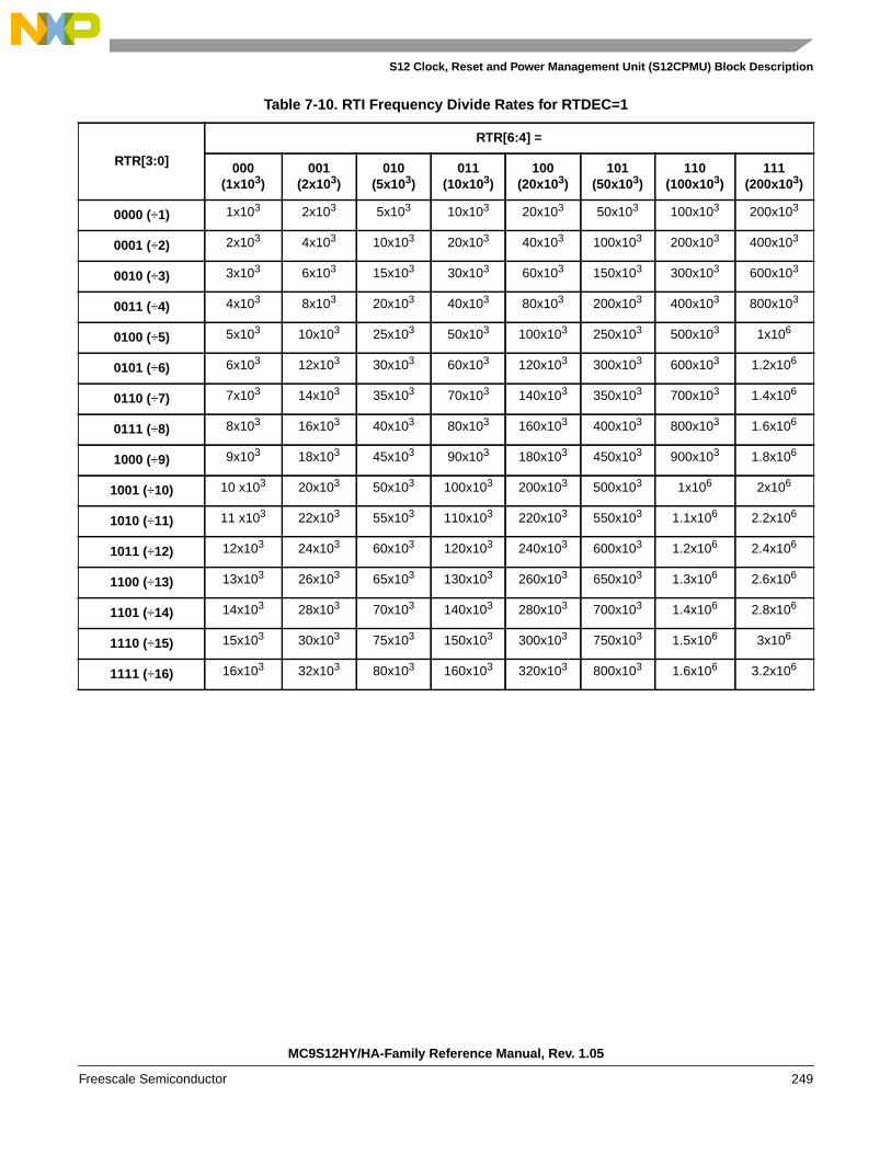
S12 Clock, Reset and Power Management Unit (S12CPMU) Block Description
Table 7-10. RTI Frequency Divide Rates for RTDEC=1
RTR[3:0]
RTR[6:4] =
000(1x10³)
001(2x10³)
010(5x10³)
011(10x103)
100(20x103)
101(50x103)
110(100x103)
111(200x103)
0000 (÷1) 1x10³ 2x10³ 5x10³ 10x103 20x103 50x103 100x103 200x103
0001 (÷2) 2x10³ 4x10³ 10x103 20x103 40x103 100x103 200x103 400x103
0010 (÷3) 3x10³ 6x10³ 15x103 30x103 60x103 150x103 300x103 600x103
0011 (÷4) 4x10³ 8x10³ 20x103 40x103 80x103 200x103 400x103 800x103
0100 (÷5) 5x10³ 10x103 25x103 50x103 100x103 250x103 500x103 1x10⁶
0101 (÷6) 6x10³ 12x103 30x103 60x103 120x103 300x103 600x103 1.2x10⁶
0110 (÷7) 7x10³ 14x103 35x103 70x103 140x103 350x103 700x103 1.4x10⁶
0111 (÷8) 8x10³ 16x103 40x103 80x103 160x103 400x103 800x103 1.6x10⁶
1000 (÷9) 9x10³ 18x103 45x103 90x103 180x103 450x103 900x103 1.8x10⁶
1001 (÷10) 10 x103 20x103 50x103 100x103 200x103 500x103 1x10⁶ 2x10⁶
1010 (÷11) 11 x103 22x103 55x103 110x103 220x103 550x103 1.1x10⁶ 2.2x10⁶
1011 (÷12) 12x103 24x103 60x103 120x103 240x103 600x103 1.2x10⁶ 2.4x10⁶
1100 (÷13) 13x103 26x103 65x103 130x103 260x103 650x103 1.3x10⁶ 2.6x10⁶
1101 (÷14) 14x103 28x103 70x103 140x103 280x103 700x103 1.4x10⁶ 2.8x10⁶
1110 (÷15) 15x103 30x103 75x103 150x103 300x103 750x103 1.5x10⁶ 3x10⁶
1111 (÷16) 16x103 32x103 80x103 160x103 320x103 800x103 1.6x10⁶ 3.2x10⁶
MC9S12HY/HA-Family Reference Manual, Rev. 1.05
Freescale Semiconductor 249

S12 Clock, Reset and Power Management Unit (S12CPMU) Block Description
7.3.2.9 S12CPMU COP Control Register (CPMUCOP)
This register controls the COP (Computer Operating Properly) watchdog.
The clock source for the COP is either IRCCLK or OSCCLK depending on the setting of theCOPOSCSEL bit. In Stop Mode with PSTP=1 (Pseudo Stop Mode), COPOSCSEL=1 and PCE=1 the COPcontinues to run, else the COP counter halts in Stop Mode.
Read: Anytime
Write:
1. RSBCK: Anytime in Special Mode; write to “1” but not to “0” in Normal Mode
2. WCOP, CR2, CR1, CR0:
— Anytime in Special Mode, when WRTMASK is 0, otherwise it has no effect
— Write once in Normal Mode, when WRTMASK is 0, otherwise it has no effect.
– Writing CR[2:0] to “000” has no effect, but counts for the “write once” condition.
– Writing WCOP to “0” has no effect, but counts for the “write once” condition.
When a non-zero value is loaded from Flash to CR[2:0] the COP time-out period is started.
A change of the COPOSCSEL bit (writing a different value or loosing UPOSC status) re-starts the COPtime-out period.
In Normal Mode the COP time-out period is restarted if either of these conditions is true:
1. Writing a non-zero value to CR[2:0] (anytime in Special Mode, once in Normal Mode) withWRTMASK = 0.
2. Writing WCOP bit (anytime in Special Mode, once in Normal Mode) with WRTMASK = 0.
3. Changing RSBCK bit from “0” to “1”.
In Special Mode, any write access to CPMUCOP register restarts the COP time-out period.
0x003C
7 6 5 4 3 2 1 0
RWCOP RSBCK
0 0 0CR2 CR1 CR0
W WRTMASK
Reset F 0 0 0 0 F F F
After de-assert of System Reset the values are automatically loaded from the Flash memory. See Device specification fordetails.
= Unimplemented or Reserved
Figure 7-12. S12CPMU COP Control Register (CPMUCOP)
MC9S12HY/HA-Family Reference Manual, Rev. 1.05
250 Freescale Semiconductor

S12 Clock, Reset and Power Management Unit (S12CPMU) Block Description
Table 7-11. CPMUCOP Field Descriptions
Field Description
7WCOP
Window COP Mode Bit — When set, a write to the CPMUARMCOP register must occur in the last 25% of theselected period. A write during the first 75% of the selected period generates a COP reset. As long as all writesoccur during this window, $55 can be written as often as desired. Once $AA is written after the $55, the time-outlogic restarts and the user must wait until the next window before writing to CPMUARMCOP. Table 7-12 showsthe duration of this window for the seven available COP rates.0 Normal COP operation1 Window COP operation
6RSBCK
COP and RTI Stop in Active BDM Mode Bit0 Allows the COP and RTI to keep running in Active BDM mode.1 Stops the COP and RTI counters whenever the part is in Active BDM mode.
5WRTMASK
Write Mask for WCOP and CR[2:0] Bit — This write-only bit serves as a mask for the WCOP and CR[2:0] bitswhile writing the CPMUCOP register. It is intended for BDM writing the RSBCK without changing the content ofWCOP and CR[2:0].0 Write of WCOP and CR[2:0] has an effect with this write of CPMUCOP1 Write of WCOP and CR[2:0] has no effect with this write of CPMUCOP.
(Does not count for “write once”.)
2–0CR[2:0]
COP Watchdog Timer Rate Select — These bits select the COP time-out rate (see Table 7-12). Writing anonzero value to CR[2:0] enables the COP counter and starts the time-out period. A COP counter time-outcauses a System Reset. This can be avoided by periodically (before time-out) initializing the COP counter viathe CPMUARMCOP register.While all of the following four conditions are true the CR[2:0], WCOP bits are ignored and the COP operates athighest time-out period (2 24 cycles) in normal COP mode (Window COP mode disabled):
1) COP is enabled (CR[2:0] is not 000)2) BDM mode active3) RSBCK = 04) Operation in Special Mode
Table 7-12. COP Watchdog Rates
CR2 CR1 CR0
COPCLKCycles to time-out
(COPCLK is either IRCCLK orOSCCLK depending on the
COPOSCSEL bit)
0 0 0 COP disabled
0 0 1 2 14
0 1 0 2 16
0 1 1 2 18
1 0 0 2 20
1 0 1 2 22
1 1 0 2 23
1 1 1 2 24
MC9S12HY/HA-Family Reference Manual, Rev. 1.05
Freescale Semiconductor 251
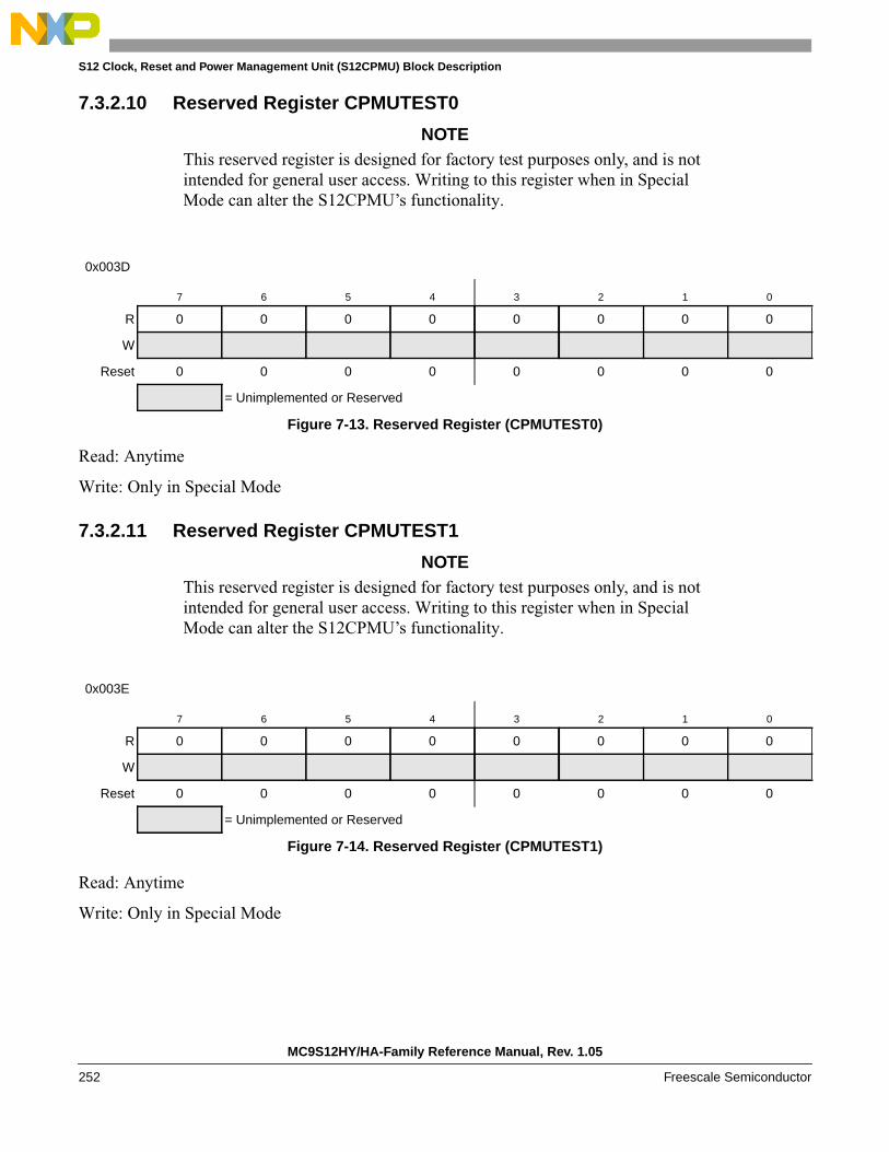
S12 Clock, Reset and Power Management Unit (S12CPMU) Block Description
7.3.2.10 Reserved Register CPMUTEST0
NOTEThis reserved register is designed for factory test purposes only, and is notintended for general user access. Writing to this register when in SpecialMode can alter the S12CPMU’s functionality.
Read: Anytime
Write: Only in Special Mode
7.3.2.11 Reserved Register CPMUTEST1
NOTEThis reserved register is designed for factory test purposes only, and is notintended for general user access. Writing to this register when in SpecialMode can alter the S12CPMU’s functionality.
Read: Anytime
Write: Only in Special Mode
0x003D
7 6 5 4 3 2 1 0
R 0 0 0 0 0 0 0 0
W
Reset 0 0 0 0 0 0 0 0
= Unimplemented or Reserved
Figure 7-13. Reserved Register (CPMUTEST0)
0x003E
7 6 5 4 3 2 1 0
R 0 0 0 0 0 0 0 0
W
Reset 0 0 0 0 0 0 0 0
= Unimplemented or Reserved
Figure 7-14. Reserved Register (CPMUTEST1)
MC9S12HY/HA-Family Reference Manual, Rev. 1.05
252 Freescale Semiconductor

S12 Clock, Reset and Power Management Unit (S12CPMU) Block Description
7.3.2.12 S12CPMU COP Timer Arm/Reset Register (CPMUARMCOP)
This register is used to restart the COP time-out period.
Read: Always reads $00
Write: Anytime
When the COP is disabled (CR[2:0] = “000”) writing to this register has no effect.
When the COP is enabled by setting CR[2:0] nonzero, the following applies:
Writing any value other than $55 or $AA causes a COP reset. To restart the COP time-out periodwrite $55 followed by a write of $AA. These writes do not need to occur back-to-back, but thesequence ($55, $AA) must be completed prior to COP end of time-out period to avoid a COP reset.Sequences of $55 writes are allowed. When the WCOP bit is set, $55 and $AA writes must be donein the last 25% of the selected time-out period; writing any value in the first 75% of the selectedperiod will cause a COP reset.
7.3.2.13 High Temperature Control Register (CPMUHTCTL)
The CPMUHTCTL register configures the temperature sense features.
Read: Anytime
Write: VSEL, HTE, HTIE and HTIF are write anytime, HTDS is read only
0x003F
7 6 5 4 3 2 1 0
R 0 0 0 0 0 0 0 0
W Bit 7 Bit 6 Bit 5 Bit 4 Bit 3 Bit 2 Bit 1 Bit 0
Reset 0 0 0 0 0 0 0 0
Figure 7-15. S12CPMU CPMUARMCOP Register
0x02F0
7 6 5 4 3 2 1 0
R 0 0VSEL
0HTE
HTDSHTIE HTIF
W
Reset 0 0 0 0 0 0 0 0
= Unimplemented or Reserved
MC9S12HY/HA-Family Reference Manual, Rev. 1.05
Freescale Semiconductor 253

S12 Clock, Reset and Power Management Unit (S12CPMU) Block Description
Figure 7-16. Voltage Access Select
Table 7-13. CPMUHTCTL Field Descriptions
Field Description
5VSEL
Voltage Access Select Bit — If set, the bandgap reference voltage VBG can be accessed internally (i.e.multiplexed to an internal Analog to Digital Converter channel). If not set, the die temperature proportionalvoltage VHT of the temperature sense can be accessed internally. See device level specification for connectivity.It is required for both VHT and VBG to be accessed internally, that the HTE bit must be set to 1 before,even if you only want to access VBG.0 An internal temperature proportional voltage VHT can be accessed internally.1 Bandgap reference voltage VBG can be accessed internally.
3HTE
High Temperature Enable Bit — This bit enables the high temperature sensor.This bit needs to be set to 1 before using the VSEL feature, even if you only want to access VBG.0 The temperature sense is disabled.1 The temperature sense is enabled.
2HTDS
High Temperature Detect Status Bit — This read-only status bit reflects the temperature. status. Writes haveno effect.0 Junction Temperature is below level THTID or RPM.1 Junction Temperature is above level THTIA and FPM.
1HTIE
High Temperature Interrupt Enable Bit0 Interrupt request is disabled.1 Interrupt will be requested whenever HTIF is set.
0HTIF
High Temperature Interrupt Flag — HTIF — High Temperature Interrupt FlagHTIF is set to 1 when HTDS status bit changes. This flag can only be cleared by writing a 1.Writing a 0 has no effect. If enabled (HTIE=1), HTIF causes an interrupt request.0 No change in HTDS bit.1 HTDS bit has changed.
C
HTD
VBG
ATD
Ref
ChannelVSELTEMPSENSE
MC9S12HY/HA-Family Reference Manual, Rev. 1.05
254 Freescale Semiconductor

S12 Clock, Reset and Power Management Unit (S12CPMU) Block Description
7.3.2.14 Low Voltage Control Register (CPMULVCTL)
The CPMULVCTL register allows the configuration of the low-voltage detect features.
Read: Anytime
Write: LVIE and LVIF are write anytime, LVDS is read only
0x02F1
7 6 5 4 3 2 1 0
R 0 0 0 0 0 LVDSLVIE LVIF
W
Reset 0 0 0 0 0 U 0 U
The Reset state of LVDS and LVIF depends on the external supplied VDDA level
= Unimplemented or Reserved
Figure 7-17. Low Voltage Control Register (CPMULVCTL)
Table 7-14. CPMULVCTL Field Descriptions
Field Description
2LVDS
Low-Voltage Detect Status Bit — This read-only status bit reflects the voltage level on VDDA. Writes have noeffect.0 Input voltage VDDA is above level VLVID or RPM.1 Input voltage VDDA is below level VLVIA and FPM.
1LVIE
Low-Voltage Interrupt Enable Bit0 Interrupt request is disabled.1 Interrupt will be requested whenever LVIF is set.
0LVIF
Low-Voltage Interrupt Flag — LVIF is set to 1 when LVDS status bit changes. This flag can only be cleared bywriting a 1. Writing a 0 has no effect. If enabled (LVIE = 1), LVIF causes an interrupt request.0 No change in LVDS bit.1 LVDS bit has changed.
MC9S12HY/HA-Family Reference Manual, Rev. 1.05
Freescale Semiconductor 255

S12 Clock, Reset and Power Management Unit (S12CPMU) Block Description
7.3.2.15 Autonomous Periodical Interrupt Control Register (CPMUAPICTL)
The CPMUAPICTL register allows the configuration of the autonomous periodical interrupt features.
Read: Anytime
Write: Anytime
0x02F2
7 6 5 4 3 2 1 0
RAPICLK
0 0APIES APIEA APIFE APIE APIF
W
Reset 0 0 0 0 0 0 0 0
= Unimplemented or Reserved
Figure 7-18. Autonomous Periodical Interrupt Control Register (CPMUAPICTL)
Table 7-15. CPMUAPICTL Field Descriptions
Field Description
7APICLK
Autonomous Periodical Interrupt Clock Select Bit — Selects the clock source for the API. Writable only ifAPIFE = 0. APICLK cannot be changed if APIFE is set by the same write operation.0 Autonomous periodical interrupt clock used as source.1 Bus Clock used as source.
4APIES
Autonomous Periodical Interrupt External Select Bit — Selects the waveform at the external pinAPI_EXTCLK as shown in Figure 7-19. See device level specification for connectivity of API_EXTCLK pin.0 If APIEA and APIFE are set, at the external pin API_EXTCLK periodic high pulses are visible at the end of
every selected period with the size of half of the minimum period (APIR=0x0000 in Table 7-19).1 If APIEA and APIFE are set, at the external pin API_EXTCLK a clock is visible with 2 times the selected API
Period.
3APIEA
Autonomous Periodical Interrupt External Access Enable Bit — If set, the waveform selected by bit APIEScan be accessed externally. See device level specification for connectivity.0 Waveform selected by APIES can not be accessed externally.1 Waveform selected by APIES can be accessed externally, if APIFE is set.
2APIFE
Autonomous Periodical Interrupt Feature Enable Bit — Enables the API feature and starts the API timerwhen set.0 Autonomous periodical interrupt is disabled.1 Autonomous periodical interrupt is enabled and timer starts running.
1APIE
Autonomous Periodical Interrupt Enable Bit0 API interrupt request is disabled.1 API interrupt will be requested whenever APIF is set.
0APIF
Autonomous Periodical Interrupt Flag — APIF is set to 1 when the in the API configured time has elapsed.This flag can only be cleared by writing a 1. Writing a 0 has no effect. If enabled (APIE = 1), APIF causes aninterrupt request.0 API time-out has not yet occurred.1 API time-out has occurred.
MC9S12HY/HA-Family Reference Manual, Rev. 1.05
256 Freescale Semiconductor

S12 Clock, Reset and Power Management Unit (S12CPMU) Block Description
Figure 7-19. Waveform selected on API_EXTCLK pin (APIEA=1, APIFE=1)
APIES=0
APIES=1
API period
API min period / 2
MC9S12HY/HA-Family Reference Manual, Rev. 1.05
Freescale Semiconductor 257
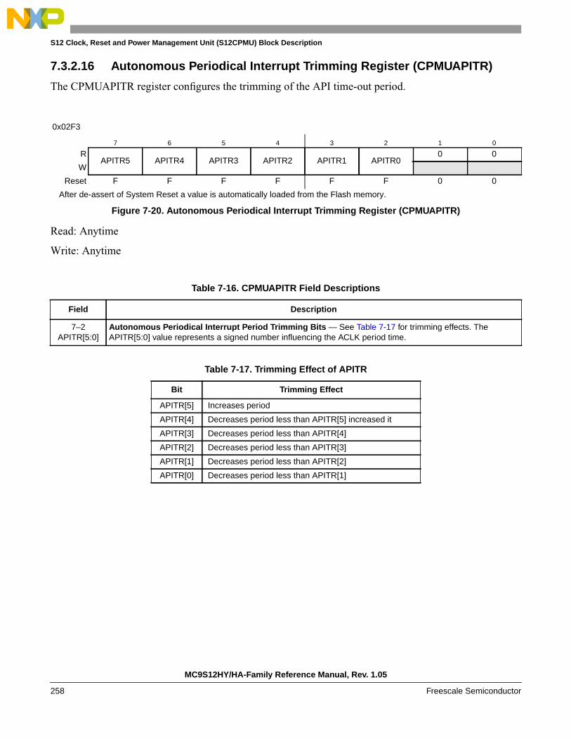
S12 Clock, Reset and Power Management Unit (S12CPMU) Block Description
7.3.2.16 Autonomous Periodical Interrupt Trimming Register (CPMUAPITR)
The CPMUAPITR register configures the trimming of the API time-out period.
Read: Anytime
Write: Anytime
0x02F3
7 6 5 4 3 2 1 0
RAPITR5 APITR4 APITR3 APITR2 APITR1 APITR0
0 0
W
Reset F F F F F F 0 0
After de-assert of System Reset a value is automatically loaded from the Flash memory.
Figure 7-20. Autonomous Periodical Interrupt Trimming Register (CPMUAPITR)
Table 7-16. CPMUAPITR Field Descriptions
Field Description
7–2APITR[5:0]
Autonomous Periodical Interrupt Period Trimming Bits — See Table 7-17 for trimming effects. TheAPITR[5:0] value represents a signed number influencing the ACLK period time.
Table 7-17. Trimming Effect of APITR
Bit Trimming Effect
APITR[5] Increases period
APITR[4] Decreases period less than APITR[5] increased it
APITR[3] Decreases period less than APITR[4]
APITR[2] Decreases period less than APITR[3]
APITR[1] Decreases period less than APITR[2]
APITR[0] Decreases period less than APITR[1]
MC9S12HY/HA-Family Reference Manual, Rev. 1.05
258 Freescale Semiconductor

S12 Clock, Reset and Power Management Unit (S12CPMU) Block Description
7.3.2.17 Autonomous Periodical Interrupt Rate High and Low Register(CPMUAPIRH / CPMUAPIRL)
The CPMUAPIRH and CPMUAPIRL registers allow the configuration of the autonomous periodicalinterrupt rate.
Read: Anytime
Write: Anytime if APIFE=0, else writes have no effect.
The period can be calculated as follows depending on logical value of the APICLK bit:
APICLK=0: Period = 2*(APIR[15:0] + 1) * fACLKAPICLK=1: Period = 2*(APIR[15:0] + 1) * Bus Clock period
0x02F4
7 6 5 4 3 2 1 0
RAPIR15 APIR14 APIR13 APIR12 APIR11 APIR10 APIR9 APIR8
W
Reset 0 0 0 0 0 0 0 0
= Unimplemented or Reserved
Figure 7-21. Autonomous Periodical Interrupt Rate High Register (CPMUAPIRH)
0x02F5
7 6 5 4 3 2 1 0
RAPIR7 APIR6 APIR5 APIR4 APIR3 APIR2 APIR1 APIR0
W
Reset 0 0 0 0 0 0 0 0
Figure 7-22. Autonomous Periodical Interrupt Rate Low Register (CPMUAPIRL)
Table 7-18. CPMUAPIRH / CPMUAPIRL Field Descriptions
Field Description
15-0APIR[15:0]
Autonomous Periodical Interrupt Rate Bits — These bits define the time-out period of the API. SeeTable 7-19 for details of the effect of the autonomous periodical interrupt rate bits.
MC9S12HY/HA-Family Reference Manual, Rev. 1.05
Freescale Semiconductor 259

S12 Clock, Reset and Power Management Unit (S12CPMU) Block Description
Table 7-19. Selectable Autonomous Periodical Interrupt Periods
APICLK APIR[15:0] Selected Period
0 0000 0.2 ms1
1 When fACLK is trimmed to 10KHz.
0 0001 0.4 ms1
0 0002 0.6 ms1
0 0003 0.8 ms1
0 0004 1.0 ms1
0 0005 1.2 ms1
0 ..... .....
0 FFFD 13106.8 ms1
0 FFFE 13107.0 ms1
0 FFFF 13107.2 ms1
1 0000 2 * Bus Clock period
1 0001 4 * Bus Clock period
1 0002 6 * Bus Clock period
1 0003 8 * Bus Clock period
1 0004 10 * Bus Clock period
1 0005 12 * Bus Clock period
1 ..... .....
1 FFFD 131068 * Bus Clock period
1 FFFE 131070 * Bus Clock period
1 FFFF 131072 * Bus Clock period
MC9S12HY/HA-Family Reference Manual, Rev. 1.05
260 Freescale Semiconductor

S12 Clock, Reset and Power Management Unit (S12CPMU) Block Description
7.3.2.18 Reserved Register CPMUTEST3
NOTEThis reserved register is designed for factory test purposes only, and is notintended for general user access. Writing to this register when in SpecialMode can alter the S12CPMU’s functionality.
Read: Anytime
Write: Only in Special Mode
0x02F6
7 6 5 4 3 2 1 0
R 0 0 0 0 0 0 0 0
W
Reset 0 0 0 0 0 0 0 0
= Unimplemented or Reserved
Figure 7-23. Reserved Register (CPMUTEST3)
MC9S12HY/HA-Family Reference Manual, Rev. 1.05
Freescale Semiconductor 261

S12 Clock, Reset and Power Management Unit (S12CPMU) Block Description
7.3.2.19 High Temperature Trimming Register (CPMUHTTR)
The CPMUHTTR register configures the trimming of the S12CPMU temperature sense.
Read: Anytime
Write: Anytime
0x02F7
7 6 5 4 3 2 1 0
RHTOE
0 0 0HTTR3 HTTR2 HTTR1 HTTR0
W
Reset 0 0 0 0 F F F F
After de-assert of System Reset a trim value is automatically loaded from the Flash memory. See Device specification fordetails.
= Unimplemented or Reserved
Field Description
7HTOE
High Temperature Offset Enable Bit — If set the temperature sense offset is enabled.0 The temperature sense offset is disabled. HTTR[3:0] bits don’t care.1 The temperature sense offset is enabled. HTTR[3:0] select the temperature offset.
3–0HTTR[3:0]
High Temperature Trimming Bits — See Table 1-27 for trimming effects.
Bit Trimming Effect
HTTR[3] Increases VHT twice of HTTR[2]
HTTR[2] Increases VHT twice of HTTR[1]
HTTR[1] Increases VHT twice of HTTR[0]
HTTR[0] Increases VHT (to compensate Temperature Offset)
MC9S12HY/HA-Family Reference Manual, Rev. 1.05
262 Freescale Semiconductor

S12 Clock, Reset and Power Management Unit (S12CPMU) Block Description
7.3.2.20 S12CPMU IRC1M Trim Registers (CPMUIRCTRIMH / CPMUIRCTRIML)
Read: Anytime
Write: Anytime if PROT=0 (CPMUPROT register). Else write has no effect
NOTEWrites to these registers while PLLSEL=1 clears the LOCK and UPOSCstatus bits.
0x02F8
15 14 13 12 11 10 9 8
RTCTRIM[3:0]
0 0IRCTRIM[9:8]
W
Reset F F F F 0 0 F F
After de-assert of System Reset a factory programmed trim value is automatically loaded from the Flash memory toprovide trimmed Internal Reference Frequency fIRC1M_TRIM.
Figure 7-24. S12CPMU IRC1M Trim High Register (CPMUIRCTRIMH)
0x02F9
7 6 5 4 3 2 1 0
RIRCTRIM[7:0]
W
Reset F F F F F F F F
After de-assert of System Reset a factory programmed trim value is automatically loaded from the Flash memory toprovide trimmed Internal Reference Frequency fIRC1M_TRIM.
Figure 7-25. S12CPMU IRC1M Trim Low Register (CPMUIRCTRIML)
Table 7-20. CPMUIRCTRIMH/L Field Descriptions
Field Description
15-12TCTRIM[3:0]
IRC1M temperature coefficient Trim BitsTrim bits for the Temperature Coefficient (TC) of the IRC1M frequency.Table 7-21 shows the influence of the bits TCTRIM3:0] on the relationship between frequency and temperature.Figure 7-27 shows an approximate TC variation, relative to the nominal TC of the IRC1M (i.e. forTCTRIM[3:0]=0x0000 or 0x1000).
9-0IRCTRIM[9:0]
IRC1M Frequency Trim Bits — Trim bits for Internal Reference ClockAfter System Reset the factory programmed trim value is automatically loaded into these registers, resulting in aInternal Reference Frequency fIRC1M_TRIM. See device electrical characteristics for value of fIRC1M_TRIM.The frequency trimming consists of two different trimming methods:A rough trimming controlled by bits IRCTRIM[9:6] can be done with frequency leaps of about 6% in average.A fine trimming controlled by the bits IRCTRIM[5:0] can be doe with frequency leaps of about 0.3% (this trimmingdetermines the precision of the frequency setting of 0.15%, i.e. 0.3% is the distance between two trimmingvalues).Figure 7-26 shows the relationship between the trim bits and the resulting IRC1M frequency.
MC9S12HY/HA-Family Reference Manual, Rev. 1.05
Freescale Semiconductor 263

S12 Clock, Reset and Power Management Unit (S12CPMU) Block Description
Figure 7-26. IRC1M Frequency Trimming Diagram
IRCTRIM[9:0]
$000
IRCTRIM[9:6]
IRCTRIM[5:0]
IRC1M frequency (IRCCLK)
600KHz
1.5MHz
1MHz
$3FF
......
MC9S12HY/HA-Family Reference Manual, Rev. 1.05
264 Freescale Semiconductor

S12 Clock, Reset and Power Management Unit (S12CPMU) Block Description
Figure 7-27. Influence of TCTRIM[3:0] on the Temperature Coefficient
NOTEThe frequency is not necessarily linear with the temperature (in most casesit will not be). The above diagram is meant only to give the direction(positive or negative) of the variation of the TC, relative to the nominal TC.
Setting TCTRIM[3:0] to 0x0000 or 0x1000 does not mean that thetemperature coefficient will be zero. These two combinations basicallyswitch off the TC compensation module, which results in the nominal TC ofthe IRC1M.
frequency
temperature
TCTRIM[3:0]=0x1111
TCTRIM[3:0]=0x0111
- 40C 150C
TCTRIM[3:0]=0x1000 or 0x0000 (nominal TC)
0x00010x00100x00110x01000x01010x01100x0111
0x11110x11100x11010x11000x10110x10100x1001
TC increases
TC decreases
MC9S12HY/HA-Family Reference Manual, Rev. 1.05
Freescale Semiconductor 265

S12 Clock, Reset and Power Management Unit (S12CPMU) Block Description
Table 7-21. TC trimming of the IRC1M frequency at ambient temperature
NOTESince the IRC1M frequency is not a linear function of the temperature, butmore like a parabola, the above relative TC variation is only an indicationand should be considered with care.
Be aware that the output frequency vary with TC trimming, A frequencytrimming correction is therefore necessary. The values provided inTable 7-21 are typical values at ambient temperature which can vary fromdevice to device.
TCTRIM[3:0] IRC1M indicativerelative TC variation
IRC1M indicative frequency drift forrelative TC variation
0000 0 (nominal TC of the IRC1M) 0%
0001 -0.54% -0.8%
0010 -1.08% -1.6%
0011 -1.63% -2.4%
0100 -2.20% -3.2%
0101 -2.77% -4.0%
0110 -3.33% -4.8%
0111 -3.91% -5.5%
1000 0 (nominal TC of the IRC1M) 0%
1001 +0.54% +0.8%
1010 +1.07% +1.6%
1011 +1.59% +2.4%
1100 +2.11% +3.2%
1101 +2.62% +4.0%
1110 +3.12% +4.8%
1111 +3.62% +5.5%
MC9S12HY/HA-Family Reference Manual, Rev. 1.05
266 Freescale Semiconductor

S12 Clock, Reset and Power Management Unit (S12CPMU) Block Description
7.3.2.21 S12CPMU Oscillator Register (CPMUOSC)
This registers configures the external oscillator (OSCLCP).
Read: Anytime
Write: Anytime if PROT=0 (CPMUPROT register) and PLLSEL=1 (CPMUCLKS register). Else write hasno effect.
NOTE.
Write to this register clears the LOCK and UPOSC status bits.
NOTE.
If the chosen VCOCLK-to-OSCCLK ratio divided by two ((fVCO / fOSC)/2)is not an integer number, then the filter can not be used and theOSCFILT[4:0] bits must be set to 0.
NOTEThe frequency modulation (FM1 and FM0) can not be used if the AdaptiveOscillator Filter is enabled.
0x02FA
7 6 5 4 3 2 1 0
ROSCE OSCBW
0OSCFILT[4:0]
W
Reset 0 0 0 0 0 0 0 0
Figure 7-28. S12CPMU Oscillator Register (CPMUOSC)
MC9S12HY/HA-Family Reference Manual, Rev. 1.05
Freescale Semiconductor 267
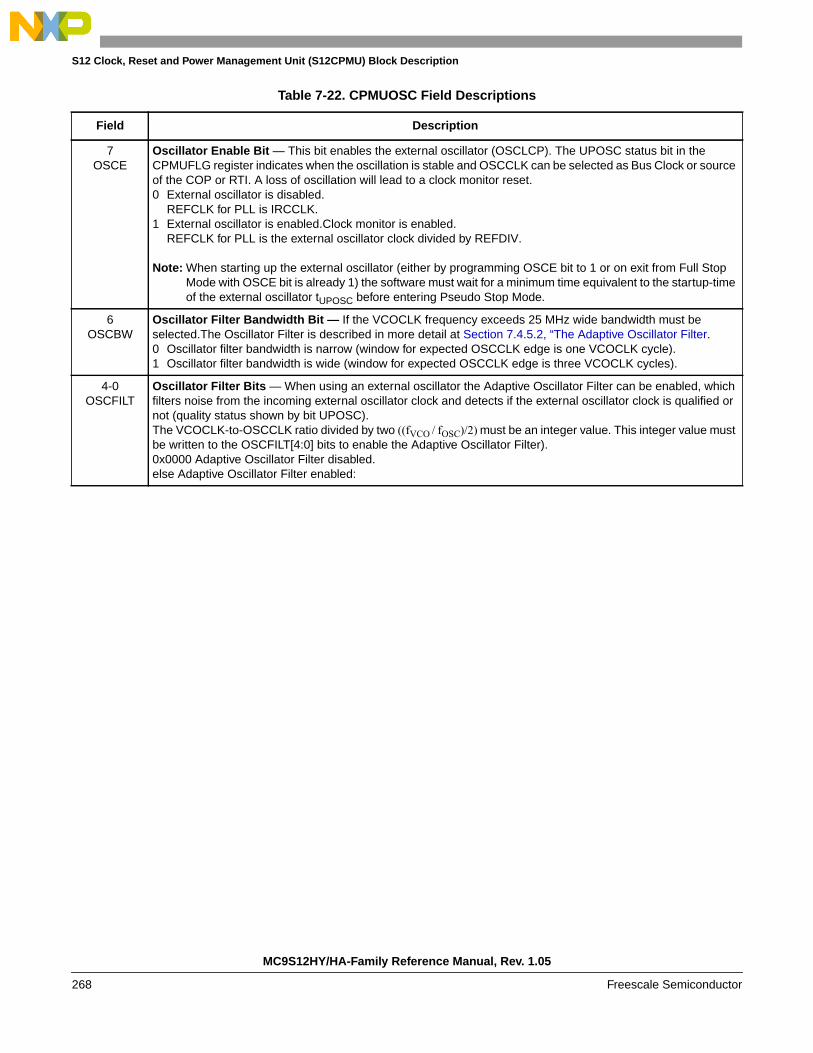
S12 Clock, Reset and Power Management Unit (S12CPMU) Block Description
Table 7-22. CPMUOSC Field Descriptions
Field Description
7OSCE
Oscillator Enable Bit — This bit enables the external oscillator (OSCLCP). The UPOSC status bit in theCPMUFLG register indicates when the oscillation is stable and OSCCLK can be selected as Bus Clock or sourceof the COP or RTI. A loss of oscillation will lead to a clock monitor reset.0 External oscillator is disabled.
REFCLK for PLL is IRCCLK.1 External oscillator is enabled.Clock monitor is enabled.
REFCLK for PLL is the external oscillator clock divided by REFDIV.
Note: When starting up the external oscillator (either by programming OSCE bit to 1 or on exit from Full StopMode with OSCE bit is already 1) the software must wait for a minimum time equivalent to the startup-timeof the external oscillator tUPOSC before entering Pseudo Stop Mode.
6OSCBW
Oscillator Filter Bandwidth Bit — If the VCOCLK frequency exceeds 25 MHz wide bandwidth must beselected.The Oscillator Filter is described in more detail at Section 7.4.5.2, “The Adaptive Oscillator Filter.0 Oscillator filter bandwidth is narrow (window for expected OSCCLK edge is one VCOCLK cycle).1 Oscillator filter bandwidth is wide (window for expected OSCCLK edge is three VCOCLK cycles).
4-0OSCFILT
Oscillator Filter Bits — When using an external oscillator the Adaptive Oscillator Filter can be enabled, whichfilters noise from the incoming external oscillator clock and detects if the external oscillator clock is qualified ornot (quality status shown by bit UPOSC).The VCOCLK-to-OSCCLK ratio divided by two ((fVCO / fOSC)/2) must be an integer value. This integer value mustbe written to the OSCFILT[4:0] bits to enable the Adaptive Oscillator Filter).0x0000 Adaptive Oscillator Filter disabled.else Adaptive Oscillator Filter enabled:
MC9S12HY/HA-Family Reference Manual, Rev. 1.05
268 Freescale Semiconductor

S12 Clock, Reset and Power Management Unit (S12CPMU) Block Description
7.3.2.22 S12CPMU Protection Register (CPMUPROT)
This register protects the clock configuration registers from accidental overwrite:
CPMUSYNR, CPMUREFDIV, CPMUCLKS, CPMUPLL, CPMUIRCTRIMH/L and CPMUOSC
Read: Anytime
Write: Anytime
0x02FB
7 6 5 4 3 2 1 0
R 0 0 0 0 0 0 0PROT
W
Reset 0 0 0 0 0 0 0 0
Figure 7-29. S12CPMU Protection Register (CPMUPROT)
Field Description
0PROT
Clock Configuration Registers Protection Bit — This bit protects the clock configuration registers fromaccidental overwrite (see list of affected registers above).Writing 0x26 to the CPMUPROT register clears the PROT bit, other write accesses set the PROT bit.0 Protection of clock configuration registers is disabled.1 Protection of clock configuration registers is enabled. (see list of protected registers above).
MC9S12HY/HA-Family Reference Manual, Rev. 1.05
Freescale Semiconductor 269

S12 Clock, Reset and Power Management Unit (S12CPMU) Block Description
7.3.2.23 Reserved Register CPMUTEST2
NOTEThis reserved register is designed for factory test purposes only, and is notintended for general user access. Writing to this register when in SpecialMode can alter the S12CPMU’s functionality.
Read: Anytime
Write: Only in Special Mode
0x02FC
7 6 5 4 3 2 1 0
R 0 0 0 0 0 0 0 0
W
Reset 0 0 0 0 0 0 0 0
= Unimplemented or Reserved
Figure 7-30. Reserved Register CPMUTEST2
MC9S12HY/HA-Family Reference Manual, Rev. 1.05
270 Freescale Semiconductor

S12 Clock, Reset and Power Management Unit (S12CPMU) Block Description
7.4 Functional Description
7.4.1 Phase Locked Loop with Internal Filter (PLL)
The PLL is used to generate a high speed PLLCLK based on a low frequency REFCLK.
The REFCLK is by default the IRCCLK which is trimmed to fIRC1M_TRIM=1MHz.
If using the oscillator (OSCE=1) REFCLK will be based on OSCCLK. For increased flexibility, OSCCLKcan be divided in a range of 1 to 16 to generate the reference frequency REFCLK using the REFDIV[3:0]bits. Based on the SYNDIV[5:0] bits the PLL generates the VCOCLK by multiplying the reference clockby a 2, 4, 6,... 126, 128. Based on the POSTDIV[4:0] bits the VCOCLK can be divided in a range of 1,2,3, 4, 5, 6,... to 32 to generate the PLLCLK.
.
NOTEAlthough it is possible to set the dividers to command a very high clockfrequency, do not exceed the specified bus frequency limit for the MCU.
f VCO 2 f REF× SYNDIV 1+( )×=
f REF
f OSCREFDIV 1+( )-------------------------------------=If oscillator is enabled (OSCE=1)
If oscillator is disabled (OSCE=0) f REF f IRC1M=
f PLL
f VCOPOSTDIV 1+( )-----------------------------------------=If PLL is locked (LOCK=1)
If PLL is not locked (LOCK=0) f PLL
f VCO4
----------------=
f bus
f PLL2
--------------=If PLL is selected (PLLSEL=1)
MC9S12HY/HA-Family Reference Manual, Rev. 1.05
Freescale Semiconductor 271
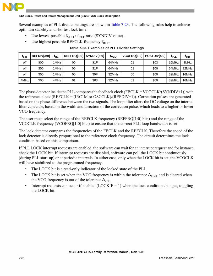
S12 Clock, Reset and Power Management Unit (S12CPMU) Block Description
Several examples of PLL divider settings are shown in Table 7-23. The following rules help to achieveoptimum stability and shortest lock time:
• Use lowest possible fVCO / fREF ratio (SYNDIV value).
• Use highest possible REFCLK frequency fREF.
The phase detector inside the PLL compares the feedback clock (FBCLK = VCOCLK/(SYNDIV+1)) withthe reference clock (REFCLK = (IRC1M or OSCCLK)/(REFDIV+1)). Correction pulses are generatedbased on the phase difference between the two signals. The loop filter alters the DC voltage on the internalfilter capacitor, based on the width and direction of the correction pulse, which leads to a higher or lowerVCO frequency.
The user must select the range of the REFCLK frequency (REFFRQ[1:0] bits) and the range of theVCOCLK frequency (VCOFRQ[1:0] bits) to ensure that the correct PLL loop bandwidth is set.
The lock detector compares the frequencies of the FBCLK and the REFCLK. Therefore the speed of thelock detector is directly proportional to the reference clock frequency. The circuit determines the lockcondition based on this comparison.
If PLL LOCK interrupt requests are enabled, the software can wait for an interrupt request and for instancecheck the LOCK bit. If interrupt requests are disabled, software can poll the LOCK bit continuously(during PLL start-up) or at periodic intervals. In either case, only when the LOCK bit is set, the VCOCLKwill have stabilized to the programmed frequency.
• The LOCK bit is a read-only indicator of the locked state of the PLL.
• The LOCK bit is set when the VCO frequency is within the tolerance ∆Lock and is cleared whenthe VCO frequency is out of the tolerance ∆unl.
• Interrupt requests can occur if enabled (LOCKIE = 1) when the lock condition changes, togglingthe LOCK bit.
Table 7-23. Examples of PLL Divider Settings
fosc REFDIV[3:0] fREF REFFRQ[1:0] SYNDIV[5:0] fVCO VCOFRQ[1:0] POSTDIV[4:0] fPLL fbus
off $00 1MHz 00 $1F 64MHz 01 $03 16MHz 8MHz
off $00 1MHz 00 $1F 64MHz 01 $00 64MHz 32MHz
off $00 1MHz 00 $0F 32MHz 00 $00 32MHz 16MHz
4MHz $00 4MHz 01 $03 32MHz 01 $00 32MHz 16MHz
MC9S12HY/HA-Family Reference Manual, Rev. 1.05
272 Freescale Semiconductor

S12 Clock, Reset and Power Management Unit (S12CPMU) Block Description
7.4.2 Startup from Reset
An example of startup of clock system from Reset is given in Figure 7-31.
Figure 7-31. Startup of clock system after Reset
7.4.3 Stop Mode using PLLCLK as Bus Clock
An example of what happens going into Stop Mode and exiting Stop Mode after an interrupt is shown inFigure 7-32. Disable PLL Lock interrupt (LOCKIE=0) before going into Stop Mode.
Figure 7-32. Stop Mode using PLLCLK as Bus Clock
System
PLLCLK
Reset
fVCORST
CPU reset state vector fetch, program execution
LOCK
POSTDIV $03 (default target fPLL=fVCO/4 = 16MHz)
fPLL increasing fPLL=16MHz
tlock
SYNDIV $1F (default target fVCO=64MHz)
$01
fPLL=32 MHz
example changeof POSTDIV
768 cycles
) (
PLLCLK
CPU
LOCKtlock
STOP instructionexecution interrupt continue execution
wakeup
tSTP_REC
MC9S12HY/HA-Family Reference Manual, Rev. 1.05
Freescale Semiconductor 273

S12 Clock, Reset and Power Management Unit (S12CPMU) Block Description
7.4.4 Full Stop Mode using Oscillator Clock as Bus Clock
An example of what happens going into Full Stop Mode and exiting Full Stop Mode after an interrupt isshown in Figure 7-33.
Disable PLL Lock interrupt (LOCKIE=0) and oscillator status change interrupt (OSCIE=0) before goinginto Full Stop Mode.
Figure 7-33. Full Stop Mode using Oscillator Clock as Bus Clock
CPU
UPOSC
tlock
STOP instructionexecution interrupt continue execution
wakeup
tSTP_RECCoreClock
select OSCCLK as Core/Bus Clock by writing PLLSEL to “0”
PLLSEL
automatically set when going into Full Stop Mode
OSCCLK
PLLCLK
MC9S12HY/HA-Family Reference Manual, Rev. 1.05
274 Freescale Semiconductor

S12 Clock, Reset and Power Management Unit (S12CPMU) Block Description
7.4.5 External Oscillator
7.4.5.1 Enabling the External Oscillator
An example of how to use the oscillator as Bus Clock is shown in Figure 7-34.
Figure 7-34. Enabling the External Oscillator
PLLSEL
OSCE
EXTAL
OSCCLK
Core
enable external oscillator by writing OSCE bit to one.
crystal/resonator starts oscillating
UPOSC
UPOSC flag is set upon successful start of oscillation
select OSCCLK as Core/Bus Clock by writing PLLSEL to zero
Clockbased on PLLCLK based on OSCCLK
MC9S12HY/HA-Family Reference Manual, Rev. 1.05
Freescale Semiconductor 275

S12 Clock, Reset and Power Management Unit (S12CPMU) Block Description
7.4.5.2 The Adaptive Oscillator Filter
A spike in the oscillator clock can disturb the function of the modules driven by this clock.
The Adaptive Oscillator Filter includes two features:
1. Filter noise (spikes) from the incoming external oscillator clock. The filter function is illustrated inFigure 7-35.
Figure 7-35. Noise filtered by the Adaptive Oscillator Filter
2. Detect severe noise disturbances on the external oscillator clock, which can not be filtered andindicate the critical situation to the software by clearing the UPOSC and LOCK status bit andsetting the OSCIF and LOCKIF flag. An example for the detection of critical noise is illustrated inFigure 7-36.
Figure 7-36. Critical noise detected by the Adaptive Oscillator Filter
NOTEIf the LOCK bit is clear due to severe noise disturbance on the externaloscillator clock the PLLCLK is derived from the VCO clock (with its actualfrequency) divided by four (see also Section 7.3.2.3, “S12CPMU PostDivider Register (CPMUPOSTDIV))
OSCE
EXTAL
OSCCLK
enable external oscillator
crystal/resonator starts oscillating
UPOSC
OSCconfigure the Adaptive Oscillator Filter
FILT 0 > 0
LOCK
filtered filtered
(filtered)
OSCE
EXTAL
OSCCLK
enable external oscillator
crystal/resonator starts oscillating
UPOSC
OSCconfigure the Adaptive Oscillator Filter
FILT 0 > 0
LOCK
(filtered)
phase shift can not be filtered but detected
MC9S12HY/HA-Family Reference Manual, Rev. 1.05
276 Freescale Semiconductor
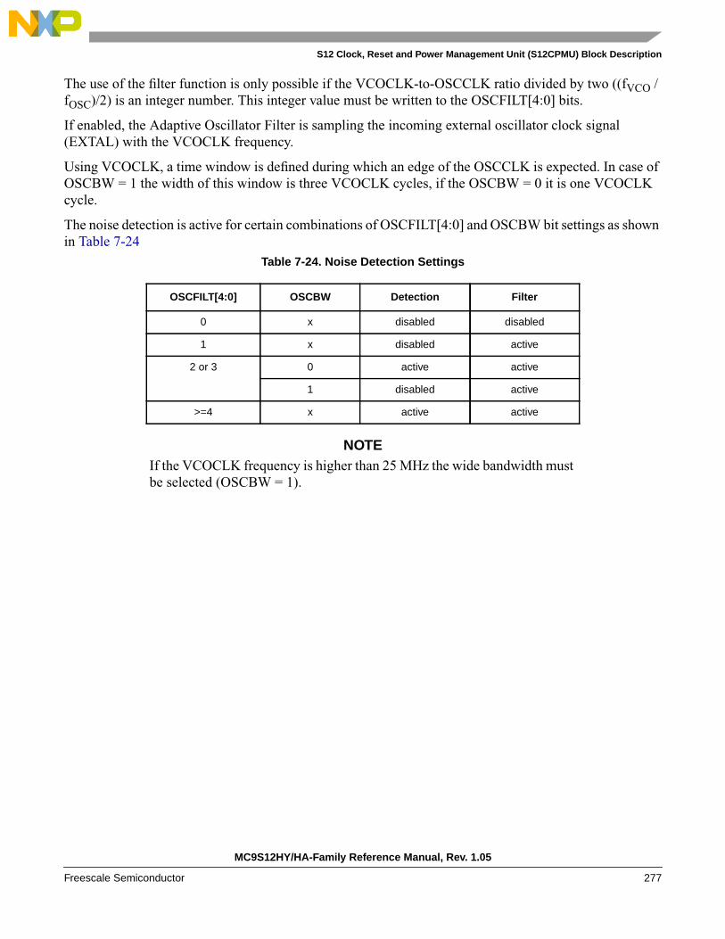
S12 Clock, Reset and Power Management Unit (S12CPMU) Block Description
The use of the filter function is only possible if the VCOCLK-to-OSCCLK ratio divided by two ((fVCO /fOSC)/2) is an integer number. This integer value must be written to the OSCFILT[4:0] bits.
If enabled, the Adaptive Oscillator Filter is sampling the incoming external oscillator clock signal(EXTAL) with the VCOCLK frequency.
Using VCOCLK, a time window is defined during which an edge of the OSCCLK is expected. In case ofOSCBW = 1 the width of this window is three VCOCLK cycles, if the OSCBW = 0 it is one VCOCLKcycle.
The noise detection is active for certain combinations of OSCFILT[4:0] and OSCBW bit settings as shownin Table 7-24
Table 7-24. Noise Detection Settings
NOTEIf the VCOCLK frequency is higher than 25 MHz the wide bandwidth mustbe selected (OSCBW = 1).
OSCFILT[4:0] OSCBW Detection Filter
0 x disabled disabled
1 x disabled active
2 or 3 0 active active
1 disabled active
>=4 x active active
MC9S12HY/HA-Family Reference Manual, Rev. 1.05
Freescale Semiconductor 277

S12 Clock, Reset and Power Management Unit (S12CPMU) Block Description
7.4.6 System Clock Configurations
7.4.6.1 PLL Engaged Internal Mode (PEI)
This mode is the default mode after System Reset or Power-On Reset.
The Bus Clock is based on the PLLCLK, the reference clock for the PLL is internally generated (IRC1M).The PLL is configured to 64 MHz VCOCLK with POSTDIV set to 0x03. If locked (LOCK=1) this resultsin a PLLCLK of 16 MHz and a Bus Clock of 8 MHz. The PLL can be re-configured to other busfrequencies.
The clock sources for COP and RTI are based on the internal reference clock generator (IRC1M).
7.4.6.2 PLL Engaged External Mode (PEE)
In this mode, the Bus Clock is based on the PLLCLK as well (like PEI). The reference clock for the PLLis based on the external oscillator. The adaptive spike filter and detection logic which uses the VCOCLKto filter and qualify the external oscillator clock can be enabled.
The clock sources for COP and RTI can be based on the internal reference clock generator or on theexternal oscillator clock.
This mode can be entered from default mode PEI by performing the following steps:
1. Configure the PLL for desired bus frequency.
2. Optionally the adaptive spike filter and detection logic can be enabled by calculating the integervalue for the OSCFIL[4:0] bits and setting the bandwidth (OSCBW) accordingly.
3. Enable the external oscillator (OSCE bit).
4. Wait for the PLL being locked (LOCK = 1) and the oscillator to start-up and additionally beingqualified if the adaptive spike filter is enabled (UPOSC =1).
5. Clear all flags in the CPMUFLG register to be able to detect any future status bit change.
6. Optionally status interrupts can be enabled (CPMUINT register).
Since the Adaptive Oscillator Filter (adaptive spike filter and detection logic) uses the VCOCLK tocontinuously filter and qualify the external oscillator clock, loosing PLL lock status (LOCK=0) meansloosing the oscillator status information as well (UPOSC=0).
The impact of loosing the oscillator status in PEE mode is as follows:
• The PLLCLK is derived from the VCO clock (with its actual frequency) divided by four until thePLL locks again.
Application software needs to be prepared to deal with the impact of loosing the oscillator status at anytime.
MC9S12HY/HA-Family Reference Manual, Rev. 1.05
278 Freescale Semiconductor
S12 Clock, Reset and Power Management Unit (S12CPMU) Block Description
7.4.6.3 PLL Bypassed External Mode (PBE)
In this mode, the Bus Clock is based on the external oscillator clock. The reference clock for the PLL isbased on the external oscillator. The adaptive spike filter and detection logic can be enabled which usesthe VCOCLK to filter and qualify the external oscillator clock.
The clock sources for COP and RTI can be based on the internal reference clock generator or on theexternal oscillator clock.
This mode can be entered from default mode PEI by performing the following steps:
1. Make sure the PLL configuration is valid
2. Optionally the adaptive spike filter and detection logic can be enabled by calculating the integervalue for the OSCFIL[4:0] bits and setting the bandwidth (OSCBW) accordingly.
3. Enable the external oscillator (OSCE bit)
4. Wait for the PLL being locked (LOCK = 1) and the oscillator to start-up and additionally beingqualified if the adaptive spike filter is enabled (UPOSC =1).
5. Clear all flags in the CPMUFLG register to be able to detect any status bit change.
6. Optionally status interrupts can be enabled (CPMUINT register).
7. Select the Oscillator Clock (OSCCLK) as Bus Clock (PLLSEL=0)
Since the Adaptive Oscillator Filter (adaptive spike filter and detection logic) uses VCOCLK (from PLL)to continuously filter and qualify the external oscillator clock, loosing PLL lock status (LOCK=0) meansloosing the oscillator status information as well (UPOSC=0).
The impact of loosing the oscillator status in PBE mode is as follows:
• PLLSEL is set automatically and the Bus Clock is switched back to the PLLCLK.
• The PLLCLK is derived from the VCO clock (with its actual frequency) divided by four until thePLL locks again.
Application software needs to be prepared to deal with the impact of loosing the oscillator status at anytime.
In the PBE mode, not every noise disturbance can be indicated by bits LOCK and UPOSC (both bits arebased on the Bus Clock domain). There are clock disturbances possible, after which UPOSC and LOCKboth stay asserted while occasional pauses on the filtered OSCCLK and resulting Bus Clock occur. Theadaptive spike filter is still functional and protects the Bus Clock from frequency overshoot due to spikeson the external oscillator clock. The filtered OSCCLK and resulting Bus Clock will pause until the PLLhas stabilized again.
MC9S12HY/HA-Family Reference Manual, Rev. 1.05
Freescale Semiconductor 279

S12 Clock, Reset and Power Management Unit (S12CPMU) Block Description
7.5 Resets
7.5.1 General
All reset sources are listed in Table 7-25. Refer to MCU specification for related vector addresses andpriorities.
7.5.2 Description of Reset Operation
Upon detection of any reset of Table 7-25, an internal circuit drives the RESET pin low for 512 PLLCLKcycles. After 512 PLLCLK cycles the RESET pin is released. The reset generator of the S12CPMU waitsfor additional 256 PLLCLK cycles and then samples the RESET pin to determine the originating source.Table 7-26 shows which vector will be fetched.
NOTEWhile System Reset is asserted the PLLCLK runs with the frequencyfVCORST.
Table 7-25. Reset Summary
Reset Source Local Enable
Power-On Reset (POR) None
Low Voltage Reset (LVR) None
External pin RESET None
Illegal Address Reset None
Clock Monitor Reset OSCE Bit in CPMUOSC register
COP Reset CR[2:0] in CPMUCOP register
Table 7-26. Reset Vector Selection
Sampled RESET Pin(256 cycles after
release)
Oscillator monitorfail pending
COPtime outpending
Vector Fetch
1 0 0 PORLVR
Illegal Address ResetExternal pin RESET
1 1 X Clock Monitor Reset
1 0 1 COP Reset
0 X X PORLVR
Illegal Address ResetExternal pin RESET
MC9S12HY/HA-Family Reference Manual, Rev. 1.05
280 Freescale Semiconductor

S12 Clock, Reset and Power Management Unit (S12CPMU) Block Description
The internal reset of the MCU remains asserted while the reset generator completes the 768 PLLCLKcycles long reset sequence. In case the RESET pin is externally driven low for more than these 768PLLCLK cycles (External Reset), the internal reset remains asserted longer.
Figure 7-37. RESET Timing
7.5.2.1 Clock Monitor Reset
If the external oscillator is enabled (OSCE=1) in case of loss of oscillation or the oscillator frequency isbelow the failure assert frequency fCMFA (see device electrical characteristics for values), the S12CPMUgenerates a Clock Monitor Reset.In Full Stop Mode the external oscillator and the clock monitor aredisabled.
7.5.2.2 Computer Operating Properly Watchdog (COP) Reset
The COP (free running watchdog timer) enables the user to check that a program is running andsequencing properly. When the COP is being used, software is responsible for keeping the COP fromtiming out. If the COP times out it is an indication that the software is no longer being executed in theintended sequence; thus COP reset is generated.
The clock source for the COP is either IRCCLK or OSCCLK depending on the setting of theCOPOSCSEL bit. In Stop Mode with PSTP=1 (Pseudo Stop Mode), COPOSCSEL=1 and PCE=1 the COPcontinues to run, else the COP counter halts in Stop Mode.
Three control bits in the CPMUCOP register allow selection of seven COP time-out periods.
When COP is enabled, the program must write $55 and $AA (in this order) to the CPMUARMCOPregister during the selected time-out period. Once this is done, the COP time-out period is restarted. If theprogram fails to do this and the COP times out, a COP reset is generated. Also, if any value other than $55or $AA is written, a COP reset generated.
)
(
)PLLCLK
512 cycles 256 cycles
S12_CPMU drives
possiblyRESETdriven lowexternally
)((
RESET
S12_CPMU releases
fVCORST
RESET pin low RESET pinfVCORST
MC9S12HY/HA-Family Reference Manual, Rev. 1.05
Freescale Semiconductor 281
S12 Clock, Reset and Power Management Unit (S12CPMU) Block Description
Windowed COP operation is enabled by setting WCOP in the CPMUCOP register. In this mode, writes tothe CPMUARMCOP register to clear the COP timer must occur in the last 25% of the selected time-outperiod. A premature write will immediately reset the part.
7.5.3 Power-On Reset (POR)
The on-chip POR circuitry detects when the internal supply VDD drops below an appropriate voltagelevel. The POR is deasserted, if the internal supply VDD exceeds an appropriate voltage level (voltagelevels not specified in this document because this internal supply is not visible on device pins).
7.5.4 Low-Voltage Reset (LVR)
The on-chip LVR circuitry detects when one of the supply voltages VDD, VDDF or VDDX drops belowan appropriate voltage level. If LVR is deasserted the MCU is fully operational at the specified maximumspeed.The LVR assert and deassert levels for the supply voltage VDDX are VLVRXA and VLVRXD and arespecified in the device Reference Manual.
7.6 InterruptsThe interrupt/reset vectors requested by the S12CPMU are listed in Table 7-27. Refer to MCUspecification for related vector addresses and priorities.
7.6.1 Description of Interrupt Operation
7.6.1.1 Real Time Interrupt (RTI)
The clock source for the RTI is either IRCCLK or OSCCLK depending on the setting of the RTIOSCSELbit. In Stop Mode with PSTP=1 (Pseudo Stop Mode), RTIOSCSEL=1 and PRE=1 the RTI continues torun, else the RTI counter halts in Stop Mode.
Table 7-27. S12CPMU Interrupt Vectors
Interrupt Source CCRMask Local Enable
RTI time-out interrupt I bit CPMUINT (RTIE)
PLL lock interrupt I bit CPMUINT (LOCKIE)
Oscillator statusinterrupt
I bit CPMUINT (OSCIE)
Low voltage interrupt I bit CPMULVCTL (LVIE)
High temperatureinterrupt
I bit CPMUHTCTL (HTIE)
AutonomousPeriodical Interrupt
I bit CPMUAPICTL (APIE)
MC9S12HY/HA-Family Reference Manual, Rev. 1.05
282 Freescale Semiconductor

S12 Clock, Reset and Power Management Unit (S12CPMU) Block Description
The RTI can be used to generate hardware interrupts at a fixed periodic rate. If enabled (by settingRTIE=1), this interrupt will occur at the rate selected by the CPMURTI register. At the end of the RTItime-out period the RTIF flag is set to one and a new RTI time-out period starts immediately.
A write to the CPMURTI register restarts the RTI time-out period.
7.6.1.2 PLL Lock Interrupt
The S12CPMU generates a PLL Lock interrupt when the lock condition (LOCK status bit) of the PLLchanges, either from a locked state to an unlocked state or vice versa. Lock interrupts are locally disabledby setting the LOCKIE bit to zero. The PLL Lock interrupt flag (LOCKIF) is set to 1 when the lockcondition has changed, and is cleared to 0 by writing a 1 to the LOCKIF bit.
7.6.1.3 Oscillator Status Interrupt
The Adaptive Oscillator Filter contains two different features:
1. Filter spikes of the external oscillator clock.
2. Qualify the external oscillator clock (detect and flag severe noise disturbances on the external oscillatorclock which can not be filtered).
When the OSCE bit is 0, then UPOSC stays 0. When OSCE = 1 and OSCFILT = 0, then the filter istransparent and no spikes are filtered. The UPOSC bit is then set after the LOCK bit is set.
Upon detection of a status change (UPOSC), that is an unqualified oscillation becomes qualified or viceversa, the OSCIF flag is set. Going into Full Stop Mode or disabling the oscillator can also cause a statuschange of UPOSC.
Also, since the Adaptive Oscillator Filter is based on the PLLCLK, any change in PLL configuration orany other event which causes the PLL lock status to be cleared leads to a loss of the oscillator statusinformation as well (UPOSC=0).
Oscillator status change interrupts are locally enabled with the OSCIE bit.
NOTELoosing the oscillator status (UPOSC=0) affects the clock configuration ofthe system1. This needs to be dealt with in application software.
7.6.1.4 Low-Voltage Interrupt (LVI)
In FPM the input voltage VDDA is monitored. Whenever VDDA drops below level VLVIA, the status bitLVDS is set to 1. When VDDA rises above level VLVID the status bit LVDS is cleared to 0. An interrupt,indicated by flag LVIF = 1, is triggered by any change of the status bit LVDS if interrupt enable bit LVIE= 1.
1. For details please refer to “7.4.6 System Clock Configurations”
MC9S12HY/HA-Family Reference Manual, Rev. 1.05
Freescale Semiconductor 283

S12 Clock, Reset and Power Management Unit (S12CPMU) Block Description
7.6.1.5 HTI - High Temperature Interrupt
In FPM the junction temperature TJ is monitored. Whenever TJ exceeds level THTIA the status bit HTDSis set to 1. Vice versa, HTDS is reset to 0 when TJ get below level THTID. An interrupt, indicated by flagHTIF = 1, is triggered by any change of the status bit HTDS, if interrupt enable bit HTIE = 1.
7.6.1.6 Autonomous Periodical Interrupt (API)
The API sub-block can generate periodical interrupts independent of the clock source of the MCU. Toenable the timer, the bit APIFE needs to be set.
The API timer is either clocked by a trimmable internal RC oscillator (ACLK) or the Bus Clock. Timeroperation will freeze when MCU clock source is selected and Bus Clock is turned off. The clock sourcecan be selected with bit APICLK. APICLK can only be written when APIFE is not set.
The APIR[15:0] bits determine the interrupt period. APIR[15:0] can only be written when APIFE iscleared. As soon as APIFE is set, the timer starts running for the period selected by APIR[15:0] bits. Whenthe configured time has elapsed, the flag APIF is set. An interrupt, indicated by flag APIF = 1, is triggeredif interrupt enable bit APIE = 1. The timer is re-started automatically again after it has set APIF.
The procedure to change APICLK or APIR[15:0] is first to clear APIFE, then write to APICLK orAPIR[15:0], and afterwards set APIFE.
The API Trimming bits APITR[5:0] must be set so the minimum period equals 0.2 ms if stable frequencyis desired.
See Table 7-17 for the trimming effect of APITR.
NOTEThe first period after enabling the counter by APIFE might be reduced byAPI start up delay tsdel.
It is possible to generate with the API a waveform at the external pin API_EXTCLK by setting APIFE andenabling the external access with setting APIEA.
7.7 Initialization/Application Information
MC9S12HY/HA-Family Reference Manual, Rev. 1.05
284 Freescale Semiconductor

Chapter 8Analog-to-Digital Converter (ADC12B8CV1)Block Description
Revision History
8.1 IntroductionThe ADC12B8C is a 8-channel, 12-bit, multiplexed input successive approximation analog-to-digitalconverter. Refer to device electrical specifications for ATD accuracy.
8.1.1 Features• 8-, 10-, or 12-bit resolution.
• Conversion in Stop Mode using internally generated clock
• Automatic return to low power after conversion sequence
• Automatic compare with interrupt for higher than or less/equal than programmable value
• Programmable sample time.
• Left/right justified result data.
• External trigger control.
• Sequence complete interrupt.
• Analog input multiplexer for 8 analog input channels.
• Special conversions for VRH, VRL, (VRL+VRH)/2.
• 1-to-8 conversion sequence lengths.
VersionNumber
RevisionDate
EffectiveDate Author Description of Changes
V01.00 25 July 2007 25 July 2007 Initial version
V01.01 14 Sept 2007 14 Sept 2007 Added reserved registers at the end the memory map.
V01.02 1 Oct 2007 1 Oct 2007Added following mention where applies:(n conversion number, NOT channel number!)
V01.03 9 Oct 2007 9 Oct 2007Modified table “Analog Input Channel Select Coding” due tonew customer feature (SPECIAL17).
V01.04 30 Apr 2008 30 Apr 2008 Updated document for 8 channels.
MC9S12HY/HA-Family Reference Manual, Rev. 1.05
Freescale Semiconductor 285

Analog-to-Digital Converter (ADC12B8CV1) Block Description
• Continuous conversion mode.
• Multiple channel scans.
• Configurable external trigger functionality on any AD channel or any of four additional triggerinputs. The four additional trigger inputs can be chip external or internal. Refer to devicespecification for availability and connectivity.
• Configurable location for channel wrap around (when converting multiple channels in a sequence).
MC9S12HY/HA-Family Reference Manual, Rev. 1.05
286 Freescale Semiconductor

Analog-to-Digital Converter (ADC12B8CV1) Block Description
8.1.2 Modes of Operation
8.1.2.1 Conversion Modes
There is software programmable selection between performing single or continuous conversion on asingle channel or multiple channels.
8.1.2.2 MCU Operating Modes
• Stop Mode— ICLKSTP=0 (in ATDCTL2 register)
Entering Stop Mode aborts any conversion sequence in progress and if a sequence was abortedrestarts it after exiting stop mode. This has the same effect/consequences as starting aconversion sequence with write to ATDCTL5. So after exiting from stop mode with apreviously aborted sequence all flags are cleared etc.
— ICLKSTP=1 (in ATDCTL2 register)A/D conversion sequence seamless continues in Stop Mode based on the internally generatedclock ICLK as ATD clock. For conversions during transition from Run to Stop Mode or viceversa the result is not written to the results register, no CCF flag is set and no compare is done.When converting in Stop Mode (ICLKSTP=1) an ATD Stop Recovery time tATDSTPRCV isrequired to switch back to bus clock based ATDCLK when leaving Stop Mode. Do not accessATD registers during this time.
• Wait ModeADC12B8C behaves same in Run and Wait Mode. For reduced power consumption continuousconversions should be aborted before entering Wait mode.
• Freeze ModeIn Freeze Mode the ADC12B8C will either continue or finish or stop converting according to theFRZ1 and FRZ0 bits. This is useful for debugging and emulation.
MC9S12HY/HA-Family Reference Manual, Rev. 1.05
Freescale Semiconductor 287

Analog-to-Digital Converter (ADC12B8CV1) Block Description
8.1.3 Block Diagram
Figure 8-1. ADC12B8C Block Diagram
VSSA
AN6
ATD_12B8C
AnalogMUX
Mode and
SuccessiveApproximationRegister (SAR)
ResultsATD 0ATD 1ATD 2ATD 3ATD 4ATD 5ATD 6ATD 7
and DAC
Sample & Hold
VDDA
VRL
VRH
Sequence Complete
+
-
Comparator
ClockPrescaler
Bus Clock
ATD Clock
AN5
AN4
AN3
AN1
AN0
AN7
ETRIG0
(See device specifi-cation for availability
ETRIG1
ETRIG2
ETRIG3
and connectivity)
Timing Control
ATDDIENATDCTL1
TriggerMux
Internal
Clock
Interrupt
Compare Interrupt
ICLK
AN2
MC9S12HY/HA-Family Reference Manual, Rev. 1.05
288 Freescale Semiconductor

Analog-to-Digital Converter (ADC12B8CV1) Block Description
8.2 Signal DescriptionThis section lists all inputs to the ADC12B8C block.
8.2.1 Detailed Signal Descriptions
8.2.1.1 ANx (x = 7, 6, 5, 4, 3, 2, 1, 0)
This pin serves as the analog input Channel x. It can also be configured as digital port or external triggerfor the ATD conversion.
8.2.1.2 ETRIG3, ETRIG2, ETRIG1, ETRIG0
These inputs can be configured to serve as an external trigger for the ATD conversion.
Refer to device specification for availability and connection of these inputs!
8.2.1.3 VRH, VRL
VRH is the high reference voltage, VRL is the low reference voltage for ATD conversion.
8.2.1.4 VDDA, VSSA
These pins are the power supplies for the analog circuitry of the ADC12B8C block.
8.3 Memory Map and Register DefinitionThis section provides a detailed description of all registers accessible in the ADC12B8C.
8.3.1 Module Memory Map
Figure 8-2 gives an overview on all ADC12B8C registers.
NOTERegister Address = Base Address + Address Offset, where the Base Addressis defined at the MCU level and the Address Offset is defined at the modulelevel.
Address Name Bit 7 6 5 4 3 2 1 Bit 0
0x0000 ATDCTL0R
Reserved0 0 0
WRAP3 WRAP2 WRAP1 WRAP0W
0x0001 ATDCTL1R
ETRIGSEL SRES1 SRES0 SMP_DIS ETRIGCH3 ETRIGCH2 ETRIGCH1 ETRIGCH0W
0x0002 ATDCTL2R 0
AFFC ICLKSTP ETRIGLE ETRIGP ETRIGE ASCIE ACMPIEW
= Unimplemented or Reserved
Figure 8-2. ADC12B8C Register Summary (Sheet 1 of 2)
MC9S12HY/HA-Family Reference Manual, Rev. 1.05
Freescale Semiconductor 289
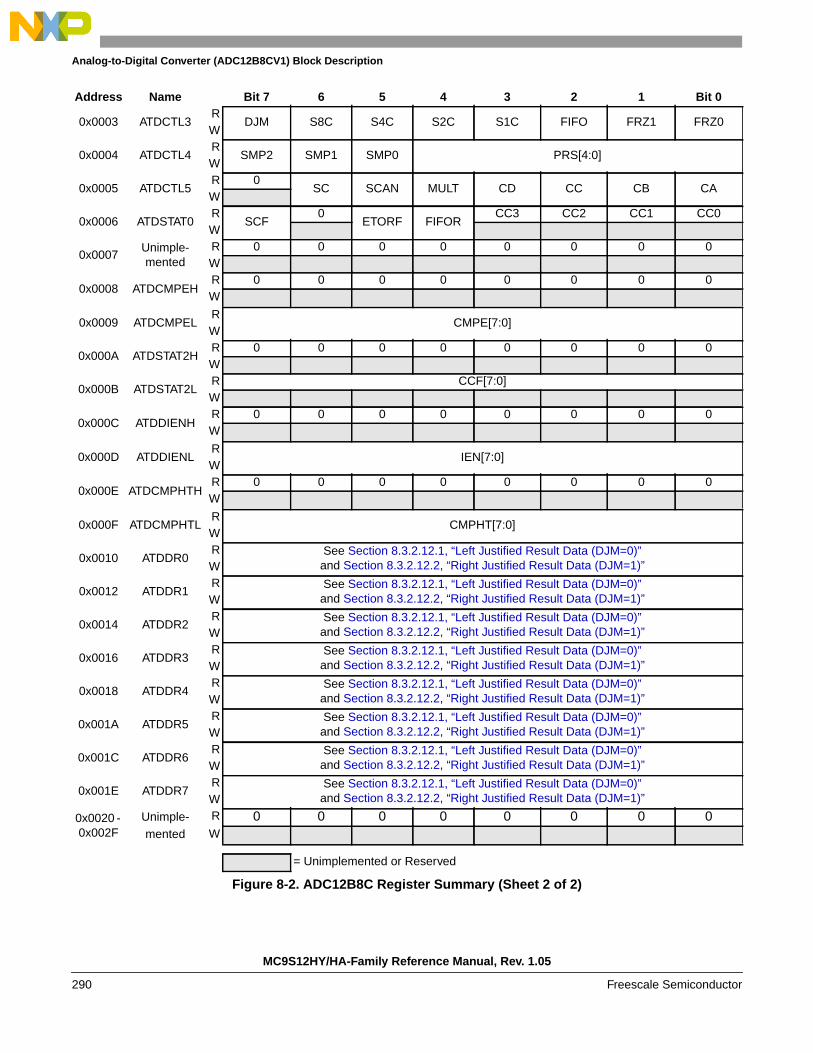
Analog-to-Digital Converter (ADC12B8CV1) Block Description
0x0003 ATDCTL3R
DJM S8C S4C S2C S1C FIFO FRZ1 FRZ0W
0x0004 ATDCTL4R
SMP2 SMP1 SMP0 PRS[4:0]W
0x0005 ATDCTL5R 0
SC SCAN MULT CD CC CB CAW
0x0006 ATDSTAT0R
SCF0
ETORF FIFORCC3 CC2 CC1 CC0
W
0x0007Unimple-mented
R 0 0 0 0 0 0 0 0W
0x0008 ATDCMPEHR 0 0 0 0 0 0 0 0W
0x0009 ATDCMPELR
CMPE[7:0]W
0x000A ATDSTAT2HR 0 0 0 0 0 0 0 0W
0x000B ATDSTAT2LR CCF[7:0]W
0x000C ATDDIENHR 0 0 0 0 0 0 0 0W
0x000D ATDDIENLR
IEN[7:0]W
0x000E ATDCMPHTHR 0 0 0 0 0 0 0 0W
0x000F ATDCMPHTLR
CMPHT[7:0]W
0x0010 ATDDR0R See Section 8.3.2.12.1, “Left Justified Result Data (DJM=0)”
and Section 8.3.2.12.2, “Right Justified Result Data (DJM=1)”W
0x0012 ATDDR1R See Section 8.3.2.12.1, “Left Justified Result Data (DJM=0)”
and Section 8.3.2.12.2, “Right Justified Result Data (DJM=1)”W
0x0014 ATDDR2R See Section 8.3.2.12.1, “Left Justified Result Data (DJM=0)”
and Section 8.3.2.12.2, “Right Justified Result Data (DJM=1)”W
0x0016 ATDDR3R See Section 8.3.2.12.1, “Left Justified Result Data (DJM=0)”
and Section 8.3.2.12.2, “Right Justified Result Data (DJM=1)”W
0x0018 ATDDR4R See Section 8.3.2.12.1, “Left Justified Result Data (DJM=0)”
and Section 8.3.2.12.2, “Right Justified Result Data (DJM=1)”W
0x001A ATDDR5R See Section 8.3.2.12.1, “Left Justified Result Data (DJM=0)”
and Section 8.3.2.12.2, “Right Justified Result Data (DJM=1)”W
0x001C ATDDR6R See Section 8.3.2.12.1, “Left Justified Result Data (DJM=0)”
and Section 8.3.2.12.2, “Right Justified Result Data (DJM=1)”W
0x001E ATDDR7R See Section 8.3.2.12.1, “Left Justified Result Data (DJM=0)”
and Section 8.3.2.12.2, “Right Justified Result Data (DJM=1)”W
0x0020 -0x002F
Unimple-mented
R 0 0 0 0 0 0 0 0W
Address Name Bit 7 6 5 4 3 2 1 Bit 0
= Unimplemented or Reserved
Figure 8-2. ADC12B8C Register Summary (Sheet 2 of 2)
MC9S12HY/HA-Family Reference Manual, Rev. 1.05
290 Freescale Semiconductor

Analog-to-Digital Converter (ADC12B8CV1) Block Description
8.3.2 Register Descriptions
This section describes in address order all the ADC12B8C registers and their individual bits.
8.3.2.1 ATD Control Register 0 (ATDCTL0)
Writes to this register will abort current conversion sequence.
Read: Anytime
Write: Anytime, in special modes always write 0 to Reserved Bit 7.
Module Base + 0x0000
7 6 5 4 3 2 1 0
RReserved
0 0 0WRAP3 WRAP2 WRAP1 WRAP0
W
Reset 0 0 0 0 1 1 1 1
= Unimplemented or Reserved
Figure 8-3. ATD Control Register 0 (ATDCTL0)
Table 8-1. ATDCTL0 Field Descriptions
Field Description
3-0WRAP[3-0]
Wrap Around Channel Select Bits — These bits determine the channel for wrap around when doingmulti-channel conversions. The coding is summarized in Table 8-2.
Table 8-2. Multi-Channel Wrap Around Coding
WRAP3 WRAP2 WRAP1 WRAP0Multiple Channel Conversions (MULT = 1)
Wraparound to AN0 after Converting
0 0 0 0 Reserved1
0 0 0 1 AN1
0 0 1 0 AN2
0 0 1 1 AN3
0 1 0 0 AN4
0 1 0 1 AN5
0 1 1 0 AN6
0 1 1 1 AN7
1 0 0 0 AN7
1 0 0 1 AN7
1 0 1 0 AN7
1 0 1 1 AN7
1 1 0 0 AN7
1 1 0 1 AN7
1 1 1 0 AN7
1 1 1 1 AN7
MC9S12HY/HA-Family Reference Manual, Rev. 1.05
Freescale Semiconductor 291

Analog-to-Digital Converter (ADC12B8CV1) Block Description
8.3.2.2 ATD Control Register 1 (ATDCTL1)
Writes to this register will abort current conversion sequence.
Read: Anytime
Write: Anytime
1If only AN0 should be converted use MULT=0.
Module Base + 0x0001
7 6 5 4 3 2 1 0
RETRIGSEL SRES1 SRES0 SMP_DIS ETRIGCH3 ETRIGCH2 ETRIGCH1 ETRIGCH0
W
Reset 0 0 1 0 1 1 1 1
Figure 8-4. ATD Control Register 1 (ATDCTL1)
Table 8-3. ATDCTL1 Field Descriptions
Field Description
7ETRIGSEL
External Trigger Source Select — This bit selects the external trigger source to be either one of the ADchannels or one of the ETRIG3-0 inputs. See device specification for availability and connectivity of ETRIG3-0inputs. If a particular ETRIG3-0 input option is not available, writing a 1 to ETRISEL only sets the bit but hasnot effect, this means that one of the AD channels (selected by ETRIGCH3-0) is configured as the source forexternal trigger. The coding is summarized in Table 8-5.
6–5SRES[1:0]
A/D Resolution Select — These bits select the resolution of A/D conversion results. See Table 8-4 for coding.
4SMP_DIS
Discharge Before Sampling Bit0 No discharge before sampling.1 The internal sample capacitor is discharged before sampling the channel. This adds 2 ATD clock cycles to
the sampling time. This can help to detect an open circuit instead of measuring the previous sampledchannel.
3–0ETRIGCH[3:0]
External Trigger Channel Select — These bits select one of the AD channels or one of the ETRIG3-0 inputsas source for the external trigger. The coding is summarized in Table 8-5.
Table 8-4. A/D Resolution Coding
SRES1 SRES0 A/D Resolution
0 0 8-bit data
0 1 10-bit data
1 0 12-bit data
1 1 Reserved
MC9S12HY/HA-Family Reference Manual, Rev. 1.05
292 Freescale Semiconductor

Analog-to-Digital Converter (ADC12B8CV1) Block Description
8.3.2.3 ATD Control Register 2 (ATDCTL2)
Writes to this register will abort current conversion sequence.
Read: Anytime
Write: Anytime
Table 8-5. External Trigger Channel Select Coding
ETRIGSEL ETRIGCH3 ETRIGCH2 ETRIGCH1 ETRIGCH0 External trigger source is
0 0 0 0 0 AN0
0 0 0 0 1 AN1
0 0 0 1 0 AN2
0 0 0 1 1 AN3
0 0 1 0 0 AN4
0 0 1 0 1 AN5
0 0 1 1 0 AN6
0 0 1 1 1 AN7
0 1 0 0 0 AN7
0 1 0 0 1 AN7
0 1 0 1 0 AN7
0 1 0 1 1 AN7
0 1 1 0 0 AN7
0 1 1 0 1 AN7
0 1 1 1 0 AN7
0 1 1 1 1 AN7
1 0 0 0 0 ETRIG01
1 Only if ETRIG3-0 input option is available (see device specification), else ETRISEL is ignored, that meansexternal trigger source is still on one of the AD channels selected by ETRIGCH3-0
1 0 0 0 1 ETRIG11
1 0 0 1 0 ETRIG21
1 0 0 1 1 ETRIG31
1 0 1 X X Reserved
1 1 X X X Reserved
Module Base + 0x0002
7 6 5 4 3 2 1 0
R 0AFFC ICLKSTP ETRIGLE ETRIGP ETRIGE ASCIE ACMPIE
W
Reset 0 0 0 0 0 0 0 0
= Unimplemented or Reserved
Figure 8-5. ATD Control Register 2 (ATDCTL2)
MC9S12HY/HA-Family Reference Manual, Rev. 1.05
Freescale Semiconductor 293

Analog-to-Digital Converter (ADC12B8CV1) Block Description
Table 8-6. ATDCTL2 Field Descriptions
Field Description
6AFFC
ATD Fast Flag Clear All0 ATD flag clearing done by write 1 to respective CCF[n] flag.1 Changes all ATD conversion complete flags to a fast clear sequence.
For compare disabled (CMPE[n]=0) a read access to the result register will cause the associated CCF[n] flagto clear automatically.For compare enabled (CMPE[n]=1) a write access to the result register will cause the associated CCF[n] flagto clear automatically.
5ICLKSTP
Internal Clock in Stop Mode Bit — This bit enables A/D conversions in stop mode. When going into stop modeand ICLKSTP=1 the ATD conversion clock is automatically switched to the internally generated clock ICLK.Current conversion sequence will seamless continue. Conversion speed will change from prescaled busfrequency to the ICLK frequency (see ATD Electrical Characteristics in device description). The prescaler bitsPRS4-0 in ATDCTL4 have no effect on the ICLK frequency. For conversions during stop mode the automaticcompare interrupt or the sequence complete interrupt can be used to inform software handler about changingA/D values. External trigger will not work while converting in stop mode. For conversions during transition fromRun to Stop Mode or vice versa the result is not written to the results register, no CCF flag is set and no compareis done. When converting in Stop Mode (ICLKSTP=1) an ATD Stop Recovery time tATDSTPRCV is required toswitch back to bus clock based ATDCLK when leaving Stop Mode. Do not access ATD registers during this time.0 If A/D conversion sequence is ongoing when going into stop mode, the actual conversion sequence will be
aborted and automatically restarted when exiting stop mode.1 A/D continues to convert in stop mode using internally generated clock (ICLK)
4ETRIGLE
External Trigger Level/Edge Control — This bit controls the sensitivity of the external trigger signal. SeeTable 8-7 for details.
3ETRIGP
External Trigger Polarity — This bit controls the polarity of the external trigger signal. See Table 8-7 for details.
2ETRIGE
External Trigger Mode Enable — This bit enables the external trigger on one of the AD channels or one of theETRIG3-0 inputs as described in Table 8-5. If external trigger source is one of the AD channels, the digital inputbuffer of this channel is enabled. The external trigger allows to synchronize the start of conversion with externalevents. External trigger will not work while converting in stop mode.0 Disable external trigger1 Enable external trigger
1ASCIE
ATD Sequence Complete Interrupt Enable0 ATD Sequence Complete interrupt requests are disabled.1 ATD Sequence Complete interrupt will be requested whenever SCF=1 is set.
0ACMPIE
ATD Compare Interrupt Enable — If automatic compare is enabled for conversion n (CMPE[n]=1 in ATDCMPEregister) this bit enables the compare interrupt. If the CCF[n] flag is set (showing a successful compare forconversion n), the compare interrupt is triggered.0 ATD Compare interrupt requests are disabled.1 For the conversions in a sequence for which automatic compare is enabled (CMPE[n]=1), ATD Compare
Interrupt will be requested whenever any of the respective CCF flags is set.
Table 8-7. External Trigger Configurations
ETRIGLE ETRIGP External Trigger Sensitivity
0 0 Falling edge
0 1 Rising edge
1 0 Low level
1 1 High level
MC9S12HY/HA-Family Reference Manual, Rev. 1.05
294 Freescale Semiconductor

Analog-to-Digital Converter (ADC12B8CV1) Block Description
8.3.2.4 ATD Control Register 3 (ATDCTL3)
Writes to this register will abort current conversion sequence.
Read: Anytime
Write: Anytime
Module Base + 0x0003
7 6 5 4 3 2 1 0
RDJM S8C S4C S2C S1C FIFO FRZ1 FRZ0
W
Reset 0 0 1 0 0 0 0 0
= Unimplemented or Reserved
Figure 8-6. ATD Control Register 3 (ATDCTL3)
Table 8-8. ATDCTL3 Field Descriptions
Field Description
7DJM
Result Register Data Justification — Result data format is always unsigned. This bit controls justification ofconversion data in the result registers.0 Left justified data in the result registers.1 Right justified data in the result registers.Table 8-9 gives examples ATD results for an input signal range between 0 and 5.12 Volts.
6–3S8C, S4C,S2C, S1C
Conversion Sequence Length — These bits control the number of conversions per sequence. Table 8-10shows all combinations. At reset, S4C is set to 1 (sequence length is 4). This is to maintain software continuityto HC12 family.
2FIFO
Result Register FIFO Mode — If this bit is zero (non-FIFO mode), the A/D conversion results map into the resultregisters based on the conversion sequence; the result of the first conversion appears in the first result register(ATDDR0), the second result in the second result register (ATDDR1), and so on.
If this bit is one (FIFO mode) the conversion counter is not reset at the beginning or ending of a conversionsequence; sequential conversion results are placed in consecutive result registers. In a continuously scanningconversion sequence, the result register counter will wrap around when it reaches the end of the result registerfile. The conversion counter value (CC3-0 in ATDSTAT0) can be used to determine where in the result registerfile, the current conversion result will be placed.
Aborting a conversion or starting a new conversion clears the conversion counter even if FIFO=1. So the firstresult of a new conversion sequence, started by writing to ATDCTL5, will always be place in the first result register(ATDDDR0). Intended usage of FIFO mode is continuos conversion (SCAN=1) or triggered conversion(ETRIG=1).
Which result registers hold valid data can be tracked using the conversion complete flags. Fast flag clear modemay or may not be useful in a particular application to track valid data.
If this bit is one, automatic compare of result registers is always disabled, that is ADC12B8C will behave as ifACMPIE and all CPME[n] were zero.0 Conversion results are placed in the corresponding result register up to the selected sequence length.1 Conversion results are placed in consecutive result registers (wrap around at end).
1–0FRZ[1:0]
Background Debug Freeze Enable — When debugging an application, it is useful in many cases to have theATD pause when a breakpoint (Freeze Mode) is encountered. These 2 bits determine how the ATD will respondto a breakpoint as shown in Table 8-11. Leakage onto the storage node and comparator reference capacitorsmay compromise the accuracy of an immediately frozen conversion depending on the length of the freeze period.
MC9S12HY/HA-Family Reference Manual, Rev. 1.05
Freescale Semiconductor 295
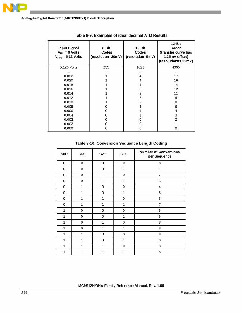
Analog-to-Digital Converter (ADC12B8CV1) Block Description
Table 8-9. Examples of ideal decimal ATD Results
Input SignalVRL = 0 Volts
VRH = 5.12 Volts
8-Bit Codes
(resolution=20mV)
10-BitCodes
(resolution=5mV)
12-BitCodes
(transfer curve has1.25mV offset)
(resolution=1.25mV)
5.120 Volts...
0.0220.0200.0180.0160.0140.0120.0100.0080.0060.0040.0030.0020.000
255...1111111000000
1023...4443322211000
4095...171614121198643210
Table 8-10. Conversion Sequence Length Coding
S8C S4C S2C S1CNumber of Conversions
per Sequence
0 0 0 0 8
0 0 0 1 1
0 0 1 0 2
0 0 1 1 3
0 1 0 0 4
0 1 0 1 5
0 1 1 0 6
0 1 1 1 7
1 0 0 0 8
1 0 0 1 8
1 0 1 0 8
1 0 1 1 8
1 1 0 0 8
1 1 0 1 8
1 1 1 0 8
1 1 1 1 8
MC9S12HY/HA-Family Reference Manual, Rev. 1.05
296 Freescale Semiconductor

Analog-to-Digital Converter (ADC12B8CV1) Block Description
8.3.2.5 ATD Control Register 4 (ATDCTL4)
Writes to this register will abort current conversion sequence.
Read: Anytime
Write: Anytime
Table 8-11. ATD Behavior in Freeze Mode (Breakpoint)
FRZ1 FRZ0 Behavior in Freeze Mode
0 0 Continue conversion
0 1 Reserved
1 0 Finish current conversion, then freeze
1 1 Freeze Immediately
Module Base + 0x0004
7 6 5 4 3 2 1 0
RSMP2 SMP1 SMP0 PRS[4:0]
W
Reset 0 0 0 0 0 1 0 1
Figure 8-7. ATD Control Register 4 (ATDCTL4)
Table 8-12. ATDCTL4 Field Descriptions
Field Description
7–5SMP[2:0]
Sample Time Select — These three bits select the length of the sample time in units of ATD conversion clockcycles. Note that the ATD conversion clock period is itself a function of the prescaler value (bits PRS4-0).Table 8-13 lists the available sample time lengths.
4–0PRS[4:0]
ATD Clock Prescaler — These 5 bits are the binary prescaler value PRS. The ATD conversion clock frequencyis calculated as follows:
Refer to Device Specification for allowed frequency range of fATDCLK.
Table 8-13. Sample Time Select
SMP2 SMP1 SMP0Sample Timein Number of
ATD Clock Cycles
0 0 0 4
0 0 1 6
0 1 0 8
0 1 1 10
1 0 0 12
1 0 1 16
1 1 0 20
fATDCLK
fBUS2 PRS 1+( )×-------------------------------------=
MC9S12HY/HA-Family Reference Manual, Rev. 1.05
Freescale Semiconductor 297

Analog-to-Digital Converter (ADC12B8CV1) Block Description
8.3.2.6 ATD Control Register 5 (ATDCTL5)
Writes to this register will abort current conversion sequence and start a new conversion sequence. Ifexternal trigger is enabled (ETRIGE=1) an initial write to ATDCTL5 is required to allow starting of aconversion sequence which will then occur on each trigger event. Start of conversion means the beginningof the sampling phase.
Read: Anytime
Write: Anytime
1 1 1 24
Module Base + 0x0005
7 6 5 4 3 2 1 0
R 0SC SCAN MULT CD CC CB CA
W
Reset 0 0 0 0 0 0 0 0
= Unimplemented or Reserved
Figure 8-8. ATD Control Register 5 (ATDCTL5)
Table 8-14. ATDCTL5 Field Descriptions
Field Description
6SC
Special Channel Conversion Bit — If this bit is set, then special channel conversion can be selected using CD,CC, CB and CA of ATDCTL5. Table 8-15 lists the coding.0 Special channel conversions disabled1 Special channel conversions enabled
5SCAN
Continuous Conversion Sequence Mode — This bit selects whether conversion sequences are performedcontinuously or only once. If external trigger is enabled (ETRIGE=1) setting this bit has no effect, that meansexternal trigger always starts a single conversion sequence.0 Single conversion sequence1 Continuous conversion sequences (scan mode)
Table 8-13. Sample Time Select
SMP2 SMP1 SMP0Sample Timein Number of
ATD Clock Cycles
MC9S12HY/HA-Family Reference Manual, Rev. 1.05
298 Freescale Semiconductor
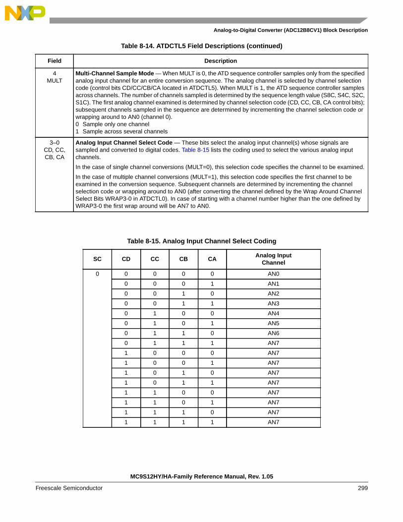
Analog-to-Digital Converter (ADC12B8CV1) Block Description
4MULT
Multi-Channel Sample Mode — When MULT is 0, the ATD sequence controller samples only from the specifiedanalog input channel for an entire conversion sequence. The analog channel is selected by channel selectioncode (control bits CD/CC/CB/CA located in ATDCTL5). When MULT is 1, the ATD sequence controller samplesacross channels. The number of channels sampled is determined by the sequence length value (S8C, S4C, S2C,S1C). The first analog channel examined is determined by channel selection code (CD, CC, CB, CA control bits);subsequent channels sampled in the sequence are determined by incrementing the channel selection code orwrapping around to AN0 (channel 0).0 Sample only one channel1 Sample across several channels
3–0CD, CC,CB, CA
Analog Input Channel Select Code — These bits select the analog input channel(s) whose signals aresampled and converted to digital codes. Table 8-15 lists the coding used to select the various analog inputchannels.
In the case of single channel conversions (MULT=0), this selection code specifies the channel to be examined.
In the case of multiple channel conversions (MULT=1), this selection code specifies the first channel to beexamined in the conversion sequence. Subsequent channels are determined by incrementing the channelselection code or wrapping around to AN0 (after converting the channel defined by the Wrap Around ChannelSelect Bits WRAP3-0 in ATDCTL0). In case of starting with a channel number higher than the one defined byWRAP3-0 the first wrap around will be AN7 to AN0.
Table 8-15. Analog Input Channel Select Coding
SC CD CC CB CAAnalog Input
Channel
0 0 0 0 0 AN0
0 0 0 1 AN1
0 0 1 0 AN2
0 0 1 1 AN3
0 1 0 0 AN4
0 1 0 1 AN5
0 1 1 0 AN6
0 1 1 1 AN7
1 0 0 0 AN7
1 0 0 1 AN7
1 0 1 0 AN7
1 0 1 1 AN7
1 1 0 0 AN7
1 1 0 1 AN7
1 1 1 0 AN7
1 1 1 1 AN7
Table 8-14. ATDCTL5 Field Descriptions (continued)
Field Description
MC9S12HY/HA-Family Reference Manual, Rev. 1.05
Freescale Semiconductor 299

Analog-to-Digital Converter (ADC12B8CV1) Block Description
1 0 0 0 0 Reserved
0 0 0 1 SPECIAL17
0 0 1 X Reserved
0 1 0 0 VRH
0 1 0 1 VRL
0 1 1 0 (VRH+VRL) / 2
0 1 1 1 Reserved
1 X X X Reserved
Table 8-15. Analog Input Channel Select Coding
SC CD CC CB CAAnalog Input
Channel
MC9S12HY/HA-Family Reference Manual, Rev. 1.05
300 Freescale Semiconductor

Analog-to-Digital Converter (ADC12B8CV1) Block Description
8.3.2.7 ATD Status Register 0 (ATDSTAT0)
This register contains the Sequence Complete Flag, overrun flags for external trigger and FIFO mode, andthe conversion counter.
Read: Anytime
Write: Anytime (No effect on (CC3, CC2, CC1, CC0))
Module Base + 0x0006
7 6 5 4 3 2 1 0
RSCF
0ETORF FIFOR
CC3 CC2 CC1 CC0
W
Reset 0 0 0 0 0 0 0 0
= Unimplemented or Reserved
Figure 8-9. ATD Status Register 0 (ATDSTAT0)
Table 8-16. ATDSTAT0 Field Descriptions
Field Description
7SCF
Sequence Complete Flag — This flag is set upon completion of a conversion sequence. If conversionsequences are continuously performed (SCAN=1), the flag is set after each one is completed. This flag is clearedwhen one of the following occurs:
A) Write “1” to SCFB) Write to ATDCTL5 (a new conversion sequence is started)C) If AFFC=1 and read of a result register
0 Conversion sequence not completed1 Conversion sequence has completed
5ETORF
External Trigger Overrun Flag — While in edge trigger mode (ETRIGLE=0), if additional active edges aredetected while a conversion sequence is in process the overrun flag is set. This flag is cleared when one of thefollowing occurs:
A) Write “1” to ETORFB) Write to ATDCTL0,1,2,3,4, ATDCMPE or ATDCMPHT (a conversion sequence is aborted)C) Write to ATDCTL5 (a new conversion sequence is started)
0 No External trigger over run error has occurred1 External trigger over run error has occurred
4FIFOR
Result Register Over Run Flag — This bit indicates that a result register has been written to before itsassociated conversion complete flag (CCF) has been cleared. This flag is most useful when using the FIFO modebecause the flag potentially indicates that result registers are out of sync with the input channels. However, it isalso practical for non-FIFO modes, and indicates that a result register has been over written before it has beenread (i.e. the old data has been lost). This flag is cleared when one of the following occurs:
A) Write “1” to FIFORB) Write to ATDCTL0,1,2,3,4, ATDCMPE or ATDCMPHT (a conversion sequence is aborted)C) Write to ATDCTL5 (a new conversion sequence is started)
0 No over run has occurred1 Overrun condition exists (result register has been written while associated CCFx flag was still set)
MC9S12HY/HA-Family Reference Manual, Rev. 1.05
Freescale Semiconductor 301

Analog-to-Digital Converter (ADC12B8CV1) Block Description
8.3.2.8 ATD Compare Enable Register (ATDCMPE)
Writes to this register will abort current conversion sequence.
Read: Anytime
Write: Anytime
3–0CC[3:0]
Conversion Counter — These 4 read-only bits are the binary value of the conversion counter. The conversioncounter points to the result register that will receive the result of the current conversion. E.g. CC3=0, CC2=1,CC1=1, CC0=0 indicates that the result of the current conversion will be in ATD Result Register 6. If in non-FIFOmode (FIFO=0) the conversion counter is initialized to zero at the begin and end of the conversion sequence. Ifin FIFO mode (FIFO=1) the register counter is not initialized. The conversion counters wraps around when itsmaximum value is reached.
Aborting a conversion or starting a new conversion clears the conversion counter even if FIFO=1.
Module Base + 0x0008
15 14 13 12 11 10 9 8 7 6 5 4 3 2 1 0
R 0 0 0 0 0 0 0 0CMPE[7:0]
W
Reset 0 0 0 0 0 0 0 0 0 0 0 0 0 0 0 0
= Unimplemented or Reserved
Figure 8-10. ATD Compare Enable Register (ATDCMPE)
Table 8-17. ATDCMPE Field Descriptions
Field Description
7–0CMPE[7:0]
Compare Enable for Conversion Number n (n= 7, 6, 5, 4, 3, 2, 1, 0) of a Sequence (n conversion number,NOT channel number!) — These bits enable automatic compare of conversion results individually forconversions of a sequence. The sense of each comparison is determined by the CMPHT[n] bit in the ATDCMPHTregister.
For each conversion number with CMPE[n]=1 do the following:1) Write compare value to ATDDRn result register2) Write compare operator with CMPHT[n] in ATDCPMHT register
CCF[n] in ATDSTAT2 register will flag individual success of any comparison.0 No automatic compare1 Automatic compare of results for conversion n of a sequence is enabled.
Table 8-16. ATDSTAT0 Field Descriptions (continued)
Field Description
MC9S12HY/HA-Family Reference Manual, Rev. 1.05
302 Freescale Semiconductor

Analog-to-Digital Converter (ADC12B8CV1) Block Description
8.3.2.9 ATD Status Register 2 (ATDSTAT2)
This read-only register contains the Conversion Complete Flags CCF[7:0].
Read: Anytime
Write: Anytime, no effect
Module Base + 0x000A
15 14 13 12 11 10 9 8 7 6 5 4 3 2 1 0
R 0 0 0 0 0 0 0 0 CCF[7:0]
W
Reset 0 0 0 0 0 0 0 0 0 0 0 0 0 0 0 0
= Unimplemented or Reserved
Figure 8-11. ATD Status Register 2 (ATDSTAT2)
Table 8-18. ATDSTAT2 Field Descriptions
Field Description
7–0CCF[7:0]
Conversion Complete Flag n (n= 7, 6, 5, 4, 3, 2, 1, 0) (n conversion number, NOT channel number!)— Aconversion complete flag is set at the end of each conversion in a sequence. The flags are associated with theconversion position in a sequence (and also the result register number). Therefore in non-fifo mode, CCF[4] isset when the fifth conversion in a sequence is complete and the result is available in result register ATDDR4;CCF[5] is set when the sixth conversion in a sequence is complete and the result is available in ATDDR5, andso forth.
If automatic compare of conversion results is enabled (CMPE[n]=1 in ATDCMPE), the conversion complete flagis only set if comparison with ATDDRn is true and if ACMPIE=1 a compare interrupt will be requested. In thiscase, as the ATDDRn result register is used to hold the compare value, the result will not be stored there at theend of the conversion but is lost.
A flag CCF[n] is cleared when one of the following occurs:A) Write to ATDCTL5 (a new conversion sequence is started)B) If AFFC=0, write “1” to CCF[n]C) If AFFC=1 and CMPE[n]=0, read of result register ATDDRnD) If AFFC=1 and CMPE[n]=1, write to result register ATDDRn
In case of a concurrent set and clear on CCF[n]: The clearing by method A) will overwrite the set. The clearingby methods B) or C) or D) will be overwritten by the set.0 Conversion number n not completed or successfully compared1 If (CMPE[n]=0): Conversion number n has completed. Result is ready in ATDDRn.
If (CMPE[n]=1): Compare for conversion result number n with compare value in ATDDRn, using compareoperator CMPGT[n] is true. (No result available in ATDDRn)
MC9S12HY/HA-Family Reference Manual, Rev. 1.05
Freescale Semiconductor 303

Analog-to-Digital Converter (ADC12B8CV1) Block Description
8.3.2.10 ATD Input Enable Register (ATDDIEN)
Read: Anytime
Write: Anytime
8.3.2.11 ATD Compare Higher Than Register (ATDCMPHT)
Writes to this register will abort current conversion sequence.
Read: Anytime
Write: Anytime
Module Base + 0x000C
15 14 13 12 11 10 9 8 7 6 5 4 3 2 1 0
R 0 0 0 0 0 0 0 0IEN[7:0]
W
Reset 0 0 0 0 0 0 0 0 0 0 0 0 0 0 0 0
= Unimplemented or Reserved
Figure 8-12. ATD Input Enable Register (ATDDIEN)
Table 8-19. ATDDIEN Field Descriptions
Field Description
7–0IEN[7:0]
ATD Digital Input Enable on channel x (x= 7, 6, 5, 4, 3, 2, 1, 0) — This bit controls the digital input buffer fromthe analog input pin (ANx) to the digital data register.0 Disable digital input buffer to ANx pin1 Enable digital input buffer on ANx pin.Note: Setting this bit will enable the corresponding digital input buffer continuously. If this bit is set while
simultaneously using it as an analog port, there is potentially increased power consumption because thedigital input buffer maybe in the linear region.
Module Base + 0x000E
15 14 13 12 11 10 9 8 7 6 5 4 3 2 1 0
R 0 0 0 0 0 0 0 0CMPHT[7:0]
W
Reset 0 0 0 0 0 0 0 0 0 0 0 0 0 0 0 0
= Unimplemented or Reserved
Figure 8-13. ATD Compare Higher Than Register (ATDCMPHT)
Table 8-20. ATDCMPHT Field Descriptions
Field Description
7–0CMPHT[7:0]
Compare Operation Higher Than Enable for conversion number n (n= 7, 6, 5, 4, 3, 2, 1, 0) of a Sequence(n conversion number, NOT channel number!) — This bit selects the operator for comparison of conversionresults.0 If result of conversion n is lower or same than compare value in ATDDRn, this is flagged in ATDSTAT21 If result of conversion n is higher than compare value in ATDDRn, this is flagged in ATDSTAT2
MC9S12HY/HA-Family Reference Manual, Rev. 1.05
304 Freescale Semiconductor
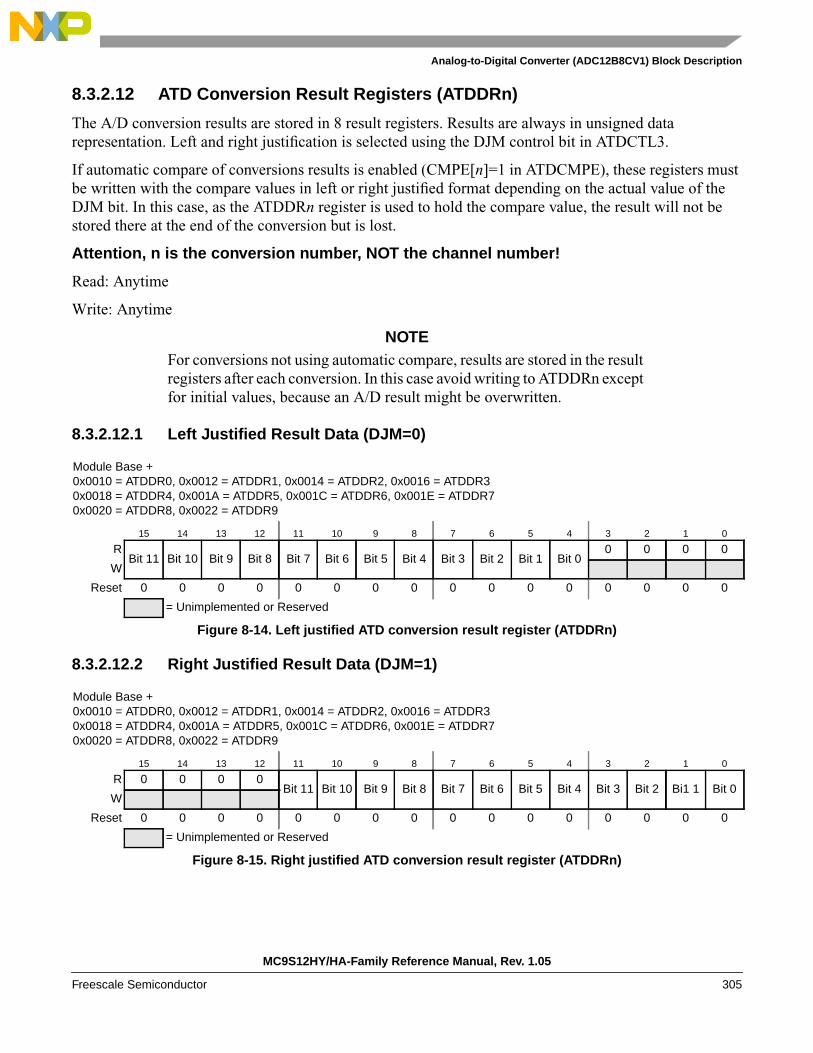
Analog-to-Digital Converter (ADC12B8CV1) Block Description
8.3.2.12 ATD Conversion Result Registers (ATDDRn)
The A/D conversion results are stored in 8 result registers. Results are always in unsigned datarepresentation. Left and right justification is selected using the DJM control bit in ATDCTL3.
If automatic compare of conversions results is enabled (CMPE[n]=1 in ATDCMPE), these registers mustbe written with the compare values in left or right justified format depending on the actual value of theDJM bit. In this case, as the ATDDRn register is used to hold the compare value, the result will not bestored there at the end of the conversion but is lost.
Attention, n is the conversion number, NOT the channel number!
Read: Anytime
Write: Anytime
NOTEFor conversions not using automatic compare, results are stored in the resultregisters after each conversion. In this case avoid writing to ATDDRn exceptfor initial values, because an A/D result might be overwritten.
8.3.2.12.1 Left Justified Result Data (DJM=0)
8.3.2.12.2 Right Justified Result Data (DJM=1)
Module Base +0x0010 = ATDDR0, 0x0012 = ATDDR1, 0x0014 = ATDDR2, 0x0016 = ATDDR30x0018 = ATDDR4, 0x001A = ATDDR5, 0x001C = ATDDR6, 0x001E = ATDDR70x0020 = ATDDR8, 0x0022 = ATDDR9
15 14 13 12 11 10 9 8 7 6 5 4 3 2 1 0
RBit 11 Bit 10 Bit 9 Bit 8 Bit 7 Bit 6 Bit 5 Bit 4 Bit 3 Bit 2 Bit 1 Bit 0
0 0 0 0
W
Reset 0 0 0 0 0 0 0 0 0 0 0 0 0 0 0 0
= Unimplemented or Reserved
Figure 8-14. Left justified ATD conversion result register (ATDDRn)
Module Base +0x0010 = ATDDR0, 0x0012 = ATDDR1, 0x0014 = ATDDR2, 0x0016 = ATDDR30x0018 = ATDDR4, 0x001A = ATDDR5, 0x001C = ATDDR6, 0x001E = ATDDR70x0020 = ATDDR8, 0x0022 = ATDDR9
15 14 13 12 11 10 9 8 7 6 5 4 3 2 1 0
R 0 0 0 0Bit 11 Bit 10 Bit 9 Bit 8 Bit 7 Bit 6 Bit 5 Bit 4 Bit 3 Bit 2 Bi1 1 Bit 0
W
Reset 0 0 0 0 0 0 0 0 0 0 0 0 0 0 0 0
= Unimplemented or Reserved
Figure 8-15. Right justified ATD conversion result register (ATDDRn)
MC9S12HY/HA-Family Reference Manual, Rev. 1.05
Freescale Semiconductor 305

Analog-to-Digital Converter (ADC12B8CV1) Block Description
Table 8-21 shows how depending on the A/D resolution the conversion result is transferred to the ATDresult registers. Compare is always done using all 12 bits of both the conversion result and the comparevalue in ATDDRn.
Table 8-21. Conversion result mapping to ATDDRn
A/Dresolution
DJMconversion result mapping to
ATDDRn
8-bit data 0 Bit[11:4] = result, Bit[3:0]=0000
8-bit data 1 Bit[7:0] = result, Bit[11:8]=0000
10-bit data 0 Bit[11:2] = result, Bit[1:0]=00
10-bit data 1 Bit[9:0] = result, Bit[11:10]=00
12-bit data X Bit[11:0] = result
MC9S12HY/HA-Family Reference Manual, Rev. 1.05
306 Freescale Semiconductor

Analog-to-Digital Converter (ADC12B8CV1) Block Description
8.4 Functional DescriptionThe ADC12B8C is structured into an analog sub-block and a digital sub-block.
8.4.1 Analog Sub-Block
The analog sub-block contains all analog electronics required to perform a single conversion. Separatepower supplies VDDA and VSSA allow to isolate noise of other MCU circuitry from the analog sub-block.
8.4.1.1 Sample and Hold Machine
The Sample and Hold (S/H) Machine accepts analog signals from the external world and stores them ascapacitor charge on a storage node.
During the sample process the analog input connects directly to the storage node.
The input analog signals are unipolar and must fall within the potential range of VSSA to VDDA.
During the hold process the analog input is disconnected from the storage node.
8.4.1.2 Analog Input Multiplexer
The analog input multiplexer connects one of the 8 external analog input channels to the sample and holdmachine.
8.4.1.3 Analog-to-Digital (A/D) Machine
The A/D Machine performs analog to digital conversions. The resolution is program selectable at either 8or 10 or 12 bits. The A/D machine uses a successive approximation architecture. It functions by comparingthe stored analog sample potential with a series of digitally generated analog potentials. By following abinary search algorithm, the A/D machine locates the approximating potential that is nearest to thesampled potential.
When not converting the A/D machine is automatically powered down.
Only analog input signals within the potential range of VRL to VRH (A/D reference potentials) will resultin a non-railed digital output code.
8.4.2 Digital Sub-Block
This subsection explains some of the digital features in more detail. See Section 8.3.2, “RegisterDescriptions” for all details.
8.4.2.1 External Trigger Input
The external trigger feature allows the user to synchronize ATD conversions to the external environmentevents rather than relying on software to signal the ATD module when ATD conversions are to take place.The external trigger signal (out of reset ATD channel 7, configurable in ATDCTL1) is programmable to
MC9S12HY/HA-Family Reference Manual, Rev. 1.05
Freescale Semiconductor 307

Analog-to-Digital Converter (ADC12B8CV1) Block Description
be edge or level sensitive with polarity control. Table 8-22 gives a brief description of the differentcombinations of control bits and their effect on the external trigger function.
During a conversion, if additional active edges are detected the overrun error flag ETORF is set.
In either level or edge triggered modes, the first conversion begins when the trigger is received.
Once ETRIGE is enabled, conversions cannot be started by a write to ATDCTL5, but rather must betriggered externally.
If the level mode is active and the external trigger both de-asserts and re-asserts itself during a conversionsequence, this does not constitute an overrun. Therefore, the flag is not set. If the trigger is left asserted inlevel mode while a sequence is completing, another sequence will be triggered immediately.
8.4.2.2 General-Purpose Digital Port Operation
The input channel pins can be multiplexed between analog and digital data. As analog inputs, they aremultiplexed and sampled as analog channels to the A/D converter. The analog/digital multiplex operationis performed in the input pads. The input pad is always connected to the analog input channels of theADC12B8C. The input pad signal is buffered to the digital port registers. This buffer can be turned on oroff with the ATDDIEN register. This is important so that the buffer does not draw excess current whenanalog potentials are presented at its input.
8.5 ResetsAt reset the ADC12B8C is in a power down state. The reset state of each individual bit is listed within theRegister Description section (see Section 8.3.2, “Register Descriptions”) which details the registers andtheir bit-field.
Table 8-22. External Trigger Control Bits
ETRIGLE ETRIGP ETRIGE SCAN Description
X X 0 0 Ignores external trigger. Performs oneconversion sequence and stops.
X X 0 1 Ignores external trigger. Performscontinuous conversion sequences.
0 0 1 X Falling edge triggered. Performs oneconversion sequence per trigger.
0 1 1 X Rising edge triggered. Performs oneconversion sequence per trigger.
1 0 1 X Trigger active low. Performs continuousconversions while trigger is active.
1 1 1 X Trigger active high. Performs continuousconversions while trigger is active.
MC9S12HY/HA-Family Reference Manual, Rev. 1.05
308 Freescale Semiconductor

Analog-to-Digital Converter (ADC12B8CV1) Block Description
8.6 InterruptsThe interrupts requested by the ADC12B8C are listed in Table 8-23. Refer to MCU specification forrelated vector address and priority.
See Section 8.3.2, “Register Descriptions” for further details.
Table 8-23. ATD Interrupt Vectors
Interrupt SourceCCRMask
Local Enable
Sequence Complete Interrupt I bit ASCIE in ATDCTL2
Compare Interrupt I bit ACMPIE in ATDCTL2
MC9S12HY/HA-Family Reference Manual, Rev. 1.05
Freescale Semiconductor 309

Analog-to-Digital Converter (ADC12B8CV1) Block Description
MC9S12HY/HA-Family Reference Manual, Rev. 1.05
310 Freescale Semiconductor
Chapter 9Freescale’s Scalable Controller Area Network(S12MSCANV3)
9.1 IntroductionFreescale’s scalable controller area network (S12MSCANV3) definition is based on the MSCAN12definition, which is the specific implementation of the MSCAN concept targeted for the M68HC12microcontroller family.
The module is a communication controller implementing the CAN 2.0A/B protocol as defined in theBosch specification dated September 1991. For users to fully understand the MSCAN specification, it isrecommended that the Bosch specification be read first to familiarize the reader with the terms andconcepts contained within this document.
Though not exclusively intended for automotive applications, CAN protocol is designed to meet thespecific requirements of a vehicle serial data bus: real-time processing, reliable operation in the EMIenvironment of a vehicle, cost-effectiveness, and required bandwidth.
MSCAN uses an advanced buffer arrangement resulting in predictable real-time behavior and simplifiedapplication software.
Table 9-1. Revision History
RevisionNumber
Revision DateSectionsAffected
Description of Changes
V03.08 07 Mar 2006 - Internal updates only.
V03.09 04 May 2007 9.3.2.11/9-329 - Corrected mnemonics of code example in CANTBSEL register description
V03.10 19 Aug 2008 9.4.7.4/9-3639.4.4.5/9-357
9.2/9-314
- Corrected wake-up description- Relocated initialization section- Added note to external pin descriptions for use with integrated physical layer- Minor corrections
MC9S12HY/HA-Family Reference Manual, Rev. 1.05
Freescale Semiconductor 311

Freescale’s Scalable Controller Area Network (S12MSCANV3)
9.1.1 Glossary
9.1.2 Block Diagram
Figure 9-1. MSCAN Block Diagram
Table 9-2. Terminology
ACK Acknowledge of CAN message
CAN Controller Area Network
CRC Cyclic Redundancy Code
EOF End of Frame
FIFO First-In-First-Out Memory
IFS Inter-Frame Sequence
SOF Start of Frame
CPU bus CPU related read/write data bus
CAN bus CAN protocol related serial bus
oscillator clock Direct clock from external oscillator
bus clock CPU bus realated clock
CAN clock CAN protocol related clock
RXCAN
TXCAN
Receive/TransmitEngine
MessageFiltering
andBuffering
Controland
StatusWake-Up Interrupt Req.
Errors Interrupt Req.
Receive Interrupt Req.
Transmit Interrupt Req.
CANCLK
Bus Clock
Configuration
Oscillator ClockMUX Presc.
Tq Clk
MSCAN
Low Pass FilterWake-UpRegisters
MC9S12HY/HA-Family Reference Manual, Rev. 1.05
312 Freescale Semiconductor
Freescale’s Scalable Controller Area Network (S12MSCANV3)
9.1.3 Features
The basic features of the MSCAN are as follows:
• Implementation of the CAN protocol — Version 2.0A/B
— Standard and extended data frames
— Zero to eight bytes data length
— Programmable bit rate up to 1 Mbps1
— Support for remote frames
• Five receive buffers with FIFO storage scheme
• Three transmit buffers with internal prioritization using a “local priority” concept
• Flexible maskable identifier filter supports two full-size (32-bit) extended identifier filters, or four16-bit filters, or eight 8-bit filters
• Programmable wakeup functionality with integrated low-pass filter
• Programmable loopback mode supports self-test operation
• Programmable listen-only mode for monitoring of CAN bus
• Programmable bus-off recovery functionality
• Separate signalling and interrupt capabilities for all CAN receiver and transmitter error states(warning, error passive, bus-off)
• Programmable MSCAN clock source either bus clock or oscillator clock
• Internal timer for time-stamping of received and transmitted messages
• Three low-power modes: sleep, power down, and MSCAN enable
• Global initialization of configuration registers
9.1.4 Modes of Operation
For a description of the specific MSCAN modes and the module operation related to the system operatingmodes refer to Section 9.4.4, “Modes of Operation”.
1. Depending on the actual bit timing and the clock jitter of the PLL.
MC9S12HY/HA-Family Reference Manual Rev. 1.05
Freescale Semiconductor 313
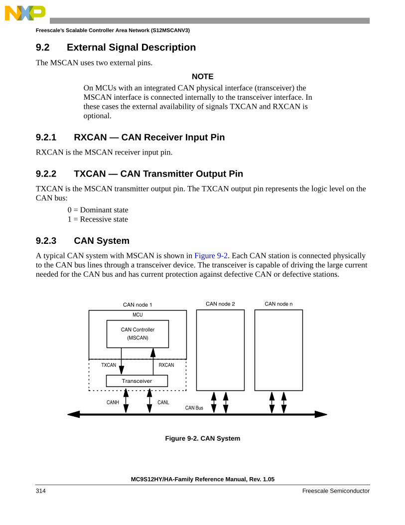
Freescale’s Scalable Controller Area Network (S12MSCANV3)
9.2 External Signal DescriptionThe MSCAN uses two external pins.
NOTEOn MCUs with an integrated CAN physical interface (transceiver) theMSCAN interface is connected internally to the transceiver interface. Inthese cases the external availability of signals TXCAN and RXCAN isoptional.
9.2.1 RXCAN — CAN Receiver Input Pin
RXCAN is the MSCAN receiver input pin.
9.2.2 TXCAN — CAN Transmitter Output Pin
TXCAN is the MSCAN transmitter output pin. The TXCAN output pin represents the logic level on theCAN bus:
0 = Dominant state1 = Recessive state
9.2.3 CAN System
A typical CAN system with MSCAN is shown in Figure 9-2. Each CAN station is connected physicallyto the CAN bus lines through a transceiver device. The transceiver is capable of driving the large currentneeded for the CAN bus and has current protection against defective CAN or defective stations.
Figure 9-2. CAN System
CAN Bus
CAN Controller
(MSCAN)
Transceiver
CAN node 1 CAN node 2 CAN node n
CANLCANH
MCU
TXCAN RXCAN
MC9S12HY/HA-Family Reference Manual, Rev. 1.05
314 Freescale Semiconductor

Freescale’s Scalable Controller Area Network (S12MSCANV3)
9.3 Memory Map and Register DefinitionThis section provides a detailed description of all registers accessible in the MSCAN.
9.3.1 Module Memory Map
Figure 9-3 gives an overview on all registers and their individual bits in the MSCAN memory map. Theregister address results from the addition of base address and address offset. The base address isdetermined at the MCU level and can be found in the MCU memory map description. The address offsetis defined at the module level.
The MSCAN occupies 64 bytes in the memory space. The base address of the MSCAN module isdetermined at the MCU level when the MCU is defined. The register decode map is fixed and begins at thefirst address of the module address offset.
The detailed register descriptions follow in the order they appear in the register map.
MC9S12HY/HA-Family Reference Manual Rev. 1.05
Freescale Semiconductor 315

Freescale’s Scalable Controller Area Network (S12MSCANV3)
MC9S12HY/HA-Family Reference Manual, Rev. 1.05
RegisterName
Bit 7 6 5 4 3 2 1 Bit 0
0x0000CANCTL0
RRXFRM
RXACTCSWAI
SYNCHTIME WUPE SLPRQ INITRQ
W
0x0001CANCTL1
RCANE CLKSRC LOOPB LISTEN BORM WUPM
SLPAK INITAK
W
0x0002CANBTR0
RSJW1 SJW0 BRP5 BRP4 BRP3 BRP2 BRP1 BRP0
W
0x0003CANBTR1
RSAMP TSEG22 TSEG21 TSEG20 TSEG13 TSEG12 TSEG11 TSEG10
W
0x0004CANRFLG
RWUPIF CSCIF
RSTAT1 RSTAT0 TSTAT1 TSTAT0OVRIF RXF
W
0x0005CANRIER
RWUPIE CSCIE RSTATE1 RSTATE0 TSTATE1 TSTATE0 OVRIE RXFIE
W
0x0006CANTFLG
R 0 0 0 0 0TXE2 TXE1 TXE0
W
0x0007CANTIER
R 0 0 0 0 0TXEIE2 TXEIE1 TXEIE0
W
0x0008CANTARQ
R 0 0 0 0 0ABTRQ2 ABTRQ1 ABTRQ0
W
0x0009CANTAAK
R 0 0 0 0 0 ABTAK2 ABTAK1 ABTAK0
W
0x000ACANTBSEL
R 0 0 0 0 0TX2 TX1 TX0
W
0x000BCANIDAC
R 0 0IDAM1 IDAM0
0 IDHIT2 IDHIT1 IDHIT0
W
0x000CReserved
R 0 0 0 0 0 0 0 0
W
0x000DCANMISC
R 0 0 0 0 0 0 0BOHOLD
W
0x000ECANRXERR
R RXERR7 RXERR6 RXERR5 RXERR4 RXERR3 RXERR2 RXERR1 RXERR0
W
= Unimplemented or Reserved
Figure 9-3. MSCAN Register Summary
316 Freescale Semiconductor

Freescale’s Scalable Controller Area Network (S12MSCANV3)
9.3.2 Register Descriptions
This section describes in detail all the registers and register bits in the MSCAN module. Each descriptionincludes a standard register diagram with an associated figure number. Details of register bit and fieldfunction follow the register diagrams, in bit order. All bits of all registers in this module are completelysynchronous to internal clocks during a register read.
9.3.2.1 MSCAN Control Register 0 (CANCTL0)
The CANCTL0 register provides various control bits of the MSCAN module as described below.
0x000FCANTXERR
R TXERR7 TXERR6 TXERR5 TXERR4 TXERR3 TXERR2 TXERR1 TXERR0
W
0x0010–0x0013CANIDAR0–3
RAC7 AC6 AC5 AC4 AC3 AC2 AC1 AC0
W
0x0014–0x0017CANIDMRx
RAM7 AM6 AM5 AM4 AM3 AM2 AM1 AM0
W
0x0018–0x001BCANIDAR4–7
RAC7 AC6 AC5 AC4 AC3 AC2 AC1 AC0
W
0x001C–0x001FCANIDMR4–7
RAM7 AM6 AM5 AM4 AM3 AM2 AM1 AM0
W
0x0020–0x002FCANRXFG
RSee Section 9.3.3, “Programmer’s Model of Message Storage”
W
0x0030–0x003FCANTXFG
RSee Section 9.3.3, “Programmer’s Model of Message Storage”
W
Module Base + 0x0000 Access: User read/write(1)
7 6 5 4 3 2 1 0
RRXFRM
RXACTCSWAI
SYNCHTIME WUPE SLPRQ INITRQ
W
Reset: 0 0 0 0 0 0 0 1
= Unimplemented
Figure 9-4. MSCAN Control Register 0 (CANCTL0)
RegisterName
Bit 7 6 5 4 3 2 1 Bit 0
= Unimplemented or Reserved
Figure 9-3. MSCAN Register Summary (continued)
MC9S12HY/HA-Family Reference Manual Rev. 1.05
Freescale Semiconductor 317
Freescale’s Scalable Controller Area Network (S12MSCANV3)
NOTEThe CANCTL0 register, except WUPE, INITRQ, and SLPRQ, is held in thereset state when the initialization mode is active (INITRQ = 1 andINITAK = 1). This register is writable again as soon as the initializationmode is exited (INITRQ = 0 and INITAK = 0).
1. Read: AnytimeWrite: Anytime when out of initialization mode; exceptions are read-only RXACT and SYNCH, RXFRM (which is set by themodule only), and INITRQ (which is also writable in initialization mode)
Table 9-3. CANCTL0 Register Field Descriptions
Field Description
7RXFRM(1)
Received Frame Flag — This bit is read and clear only. It is set when a receiver has received a valid messagecorrectly, independently of the filter configuration. After it is set, it remains set until cleared by software or reset.Clearing is done by writing a 1. Writing a 0 is ignored. This bit is not valid in loopback mode.0 No valid message was received since last clearing this flag1 A valid message was received since last clearing of this flag
6RXACT
Receiver Active Status — This read-only flag indicates the MSCAN is receiving a message. The flag iscontrolled by the receiver front end. This bit is not valid in loopback mode.0 MSCAN is transmitting or idle2
1 MSCAN is receiving a message (including when arbitration is lost)(2)
5CSWAI(3)
CAN Stops in Wait Mode — Enabling this bit allows for lower power consumption in wait mode by disabling allthe clocks at the CPU bus interface to the MSCAN module.0 The module is not affected during wait mode1 The module ceases to be clocked during wait mode
4SYNCH
Synchronized Status — This read-only flag indicates whether the MSCAN is synchronized to the CAN bus andable to participate in the communication process. It is set and cleared by the MSCAN.0 MSCAN is not synchronized to the CAN bus1 MSCAN is synchronized to the CAN bus
3TIME
Timer Enable — This bit activates an internal 16-bit wide free running timer which is clocked by the bit clock rate.If the timer is enabled, a 16-bit time stamp will be assigned to each transmitted/received message within theactive TX/RX buffer. Right after the EOF of a valid message on the CAN bus, the time stamp is written to thehighest bytes (0x000E, 0x000F) in the appropriate buffer (see Section 9.3.3, “Programmer’s Model of MessageStorage”). The internal timer is reset (all bits set to 0) when disabled. This bit is held low in initialization mode.0 Disable internal MSCAN timer1 Enable internal MSCAN timer
2WUPE(4)
Wake-Up Enable — This configuration bit allows the MSCAN to restart from sleep mode or from power downmode (entered from sleep) when traffic on CAN is detected (see Section 9.4.5.5, “MSCAN Sleep Mode”). Thisbit must be configured before sleep mode entry for the selected function to take effect.0 Wake-up disabled — The MSCAN ignores traffic on CAN1 Wake-up enabled — The MSCAN is able to restart
MC9S12HY/HA-Family Reference Manual, Rev. 1.05
318 Freescale Semiconductor

Freescale’s Scalable Controller Area Network (S12MSCANV3)
9.3.2.2 MSCAN Control Register 1 (CANCTL1)
The CANCTL1 register provides various control bits and handshake status information of the MSCANmodule as described below.
1SLPRQ(5)
Sleep Mode Request — This bit requests the MSCAN to enter sleep mode, which is an internal power savingmode (see Section 9.4.5.5, “MSCAN Sleep Mode”). The sleep mode request is serviced when the CAN bus isidle, i.e., the module is not receiving a message and all transmit buffers are empty. The module indicates entryto sleep mode by setting SLPAK = 1 (see Section 9.3.2.2, “MSCAN Control Register 1 (CANCTL1)”). SLPRQcannot be set while the WUPIF flag is set (see Section 9.3.2.5, “MSCAN Receiver Flag Register (CANRFLG)”).Sleep mode will be active until SLPRQ is cleared by the CPU or, depending on the setting of WUPE, the MSCANdetects activity on the CAN bus and clears SLPRQ itself.0 Running — The MSCAN functions normally1 Sleep mode request — The MSCAN enters sleep mode when CAN bus idle
0INITRQ(6),(7)
Initialization Mode Request — When this bit is set by the CPU, the MSCAN skips to initialization mode (seeSection 9.4.4.5, “MSCAN Initialization Mode”). Any ongoing transmission or reception is aborted andsynchronization to the CAN bus is lost. The module indicates entry to initialization mode by setting INITAK = 1(Section 9.3.2.2, “MSCAN Control Register 1 (CANCTL1)”).The following registers enter their hard reset state and restore their default values: CANCTL0(8), CANRFLG(9),CANRIER(10), CANTFLG, CANTIER, CANTARQ, CANTAAK, and CANTBSEL.The registers CANCTL1, CANBTR0, CANBTR1, CANIDAC, CANIDAR0-7, and CANIDMR0-7 can only bewritten by the CPU when the MSCAN is in initialization mode (INITRQ = 1 and INITAK = 1). The values of theerror counters are not affected by initialization mode.When this bit is cleared by the CPU, the MSCAN restarts and then tries to synchronize to the CAN bus. If theMSCAN is not in bus-off state, it synchronizes after 11 consecutive recessive bits on the CAN bus; if the MSCANis in bus-off state, it continues to wait for 128 occurrences of 11 consecutive recessive bits.Writing to other bits in CANCTL0, CANRFLG, CANRIER, CANTFLG, or CANTIER must be done only afterinitialization mode is exited, which is INITRQ = 0 and INITAK = 0.0 Normal operation1 MSCAN in initialization mode
1. The MSCAN must be in normal mode for this bit to become set.2. See the Bosch CAN 2.0A/B specification for a detailed definition of transmitter and receiver states.3. In order to protect from accidentally violating the CAN protocol, TXCAN is immediately forced to a recessive state when the
CPU enters wait (CSWAI = 1) or stop mode (see Section 9.4.5.2, “Operation in Wait Mode” and Section 9.4.5.3, “Operation inStop Mode”).
4. The CPU has to make sure that the WUPE register and the WUPIE wake-up interrupt enable register (see Section 9.3.2.6,“MSCAN Receiver Interrupt Enable Register (CANRIER)) is enabled, if the recovery mechanism from stop or wait is required.
5. The CPU cannot clear SLPRQ before the MSCAN has entered sleep mode (SLPRQ = 1 and SLPAK = 1).6. The CPU cannot clear INITRQ before the MSCAN has entered initialization mode (INITRQ = 1 and INITAK = 1).7. In order to protect from accidentally violating the CAN protocol, TXCAN is immediately forced to a recessive state when the
initialization mode is requested by the CPU. Thus, the recommended procedure is to bring the MSCAN into sleep mode(SLPRQ = 1 and SLPAK = 1) before requesting initialization mode.
8. Not including WUPE, INITRQ, and SLPRQ.9. TSTAT1 and TSTAT0 are not affected by initialization mode.10. RSTAT1 and RSTAT0 are not affected by initialization mode.
Table 9-3. CANCTL0 Register Field Descriptions (continued)
Field Description
MC9S12HY/HA-Family Reference Manual Rev. 1.05
Freescale Semiconductor 319

Freescale’s Scalable Controller Area Network (S12MSCANV3)
Module Base + 0x0001 Access: User read/write(1)
1. Read: AnytimeWrite: Anytime in initialization mode (INITRQ = 1 and INITAK = 1); CANE is write once
7 6 5 4 3 2 1 0
RCANE CLKSRC LOOPB LISTEN BORM WUPM
SLPAK INITAK
W
Reset: 0 0 0 1 0 0 0 1
= Unimplemented
Figure 9-5. MSCAN Control Register 1 (CANCTL1)
Table 9-4. CANCTL1 Register Field Descriptions
Field Description
7CANE
MSCAN Enable0 MSCAN module is disabled1 MSCAN module is enabled
6CLKSRC
MSCAN Clock Source — This bit defines the clock source for the MSCAN module (only for systems with a clockgeneration module; Section 9.4.3.2, “Clock System,” and Section Figure 9-43., “MSCAN Clocking Scheme,”).0 MSCAN clock source is the oscillator clock1 MSCAN clock source is the bus clock
5LOOPB
Loopback Self Test Mode — When this bit is set, the MSCAN performs an internal loopback which can be usedfor self test operation. The bit stream output of the transmitter is fed back to the receiver internally. The RXCANinput is ignored and the TXCAN output goes to the recessive state (logic 1). The MSCAN behaves as it doesnormally when transmitting and treats its own transmitted message as a message received from a remote node.In this state, the MSCAN ignores the bit sent during the ACK slot in the CAN frame acknowledge field to ensureproper reception of its own message. Both transmit and receive interrupts are generated.0 Loopback self test disabled1 Loopback self test enabled
4LISTEN
Listen Only Mode — This bit configures the MSCAN as a CAN bus monitor. When LISTEN is set, all valid CANmessages with matching ID are received, but no acknowledgement or error frames are sent out (seeSection 9.4.4.4, “Listen-Only Mode”). In addition, the error counters are frozen. Listen only mode supportsapplications which require “hot plugging” or throughput analysis. The MSCAN is unable to transmit anymessages when listen only mode is active.0 Normal operation1 Listen only mode activated
3BORM
Bus-Off Recovery Mode — This bits configures the bus-off state recovery mode of the MSCAN. Refer toSection 9.5.2, “Bus-Off Recovery,” for details.0 Automatic bus-off recovery (see Bosch CAN 2.0A/B protocol specification)1 Bus-off recovery upon user request
2WUPM
Wake-Up Mode — If WUPE in CANCTL0 is enabled, this bit defines whether the integrated low-pass filter isapplied to protect the MSCAN from spurious wake-up (see Section 9.4.5.5, “MSCAN Sleep Mode”).0 MSCAN wakes up on any dominant level on the CAN bus1 MSCAN wakes up only in case of a dominant pulse on the CAN bus that has a length of Twup
MC9S12HY/HA-Family Reference Manual, Rev. 1.05
320 Freescale Semiconductor

Freescale’s Scalable Controller Area Network (S12MSCANV3)
9.3.2.3 MSCAN Bus Timing Register 0 (CANBTR0)
The CANBTR0 register configures various CAN bus timing parameters of the MSCAN module.
1SLPAK
Sleep Mode Acknowledge — This flag indicates whether the MSCAN module has entered sleep mode (seeSection 9.4.5.5, “MSCAN Sleep Mode”). It is used as a handshake flag for the SLPRQ sleep mode request.Sleep mode is active when SLPRQ = 1 and SLPAK = 1. Depending on the setting of WUPE, the MSCAN willclear the flag if it detects activity on the CAN bus while in sleep mode.0 Running — The MSCAN operates normally1 Sleep mode active — The MSCAN has entered sleep mode
0INITAK
Initialization Mode Acknowledge — This flag indicates whether the MSCAN module is in initialization mode(see Section 9.4.4.5, “MSCAN Initialization Mode”). It is used as a handshake flag for the INITRQ initializationmode request. Initialization mode is active when INITRQ = 1 and INITAK = 1. The registers CANCTL1,CANBTR0, CANBTR1, CANIDAC, CANIDAR0–CANIDAR7, and CANIDMR0–CANIDMR7 can be written only bythe CPU when the MSCAN is in initialization mode.0 Running — The MSCAN operates normally1 Initialization mode active — The MSCAN has entered initialization mode
Module Base + 0x0002 Access: User read/write(1)
1. Read: AnytimeWrite: Anytime in initialization mode (INITRQ = 1 and INITAK = 1)
7 6 5 4 3 2 1 0
RSJW1 SJW0 BRP5 BRP4 BRP3 BRP2 BRP1 BRP0
W
Reset: 0 0 0 0 0 0 0 0
Figure 9-6. MSCAN Bus Timing Register 0 (CANBTR0)
Table 9-5. CANBTR0 Register Field Descriptions
Field Description
7-6SJW[1:0]
Synchronization Jump Width — The synchronization jump width defines the maximum number of time quanta(Tq) clock cycles a bit can be shortened or lengthened to achieve resynchronization to data transitions on theCAN bus (see Table 9-6).
5-0BRP[5:0]
Baud Rate Prescaler — These bits determine the time quanta (Tq) clock which is used to build up the bit timing(see Table 9-7).
Table 9-6. Synchronization Jump Width
SJW1 SJW0 Synchronization Jump Width
0 0 1 Tq clock cycle
0 1 2 Tq clock cycles
1 0 3 Tq clock cycles
1 1 4 Tq clock cycles
Table 9-4. CANCTL1 Register Field Descriptions (continued)
Field Description
MC9S12HY/HA-Family Reference Manual Rev. 1.05
Freescale Semiconductor 321

Freescale’s Scalable Controller Area Network (S12MSCANV3)
9.3.2.4 MSCAN Bus Timing Register 1 (CANBTR1)
The CANBTR1 register configures various CAN bus timing parameters of the MSCAN module.
Table 9-7. Baud Rate Prescaler
BRP5 BRP4 BRP3 BRP2 BRP1 BRP0 Prescaler value (P)
0 0 0 0 0 0 1
0 0 0 0 0 1 2
0 0 0 0 1 0 3
0 0 0 0 1 1 4
: : : : : : :
1 1 1 1 1 1 64
Module Base + 0x0003 Access: User read/write(1)
1. Read: AnytimeWrite: Anytime in initialization mode (INITRQ = 1 and INITAK = 1)
7 6 5 4 3 2 1 0
RSAMP TSEG22 TSEG21 TSEG20 TSEG13 TSEG12 TSEG11 TSEG10
W
Reset: 0 0 0 0 0 0 0 0
Figure 9-7. MSCAN Bus Timing Register 1 (CANBTR1)
Table 9-8. CANBTR1 Register Field Descriptions
Field Description
7SAMP
Sampling — This bit determines the number of CAN bus samples taken per bit time.0 One sample per bit.1 Three samples per bit(1).If SAMP = 0, the resulting bit value is equal to the value of the single bit positioned at the sample point. IfSAMP = 1, the resulting bit value is determined by using majority rule on the three total samples. For higher bitrates, it is recommended that only one sample is taken per bit time (SAMP = 0).
1. In this case, PHASE_SEG1 must be at least 2 time quanta (Tq).
6-4TSEG2[2:0]
Time Segment 2 — Time segments within the bit time fix the number of clock cycles per bit time and the locationof the sample point (see Figure 9-44). Time segment 2 (TSEG2) values are programmable as shown in Table 9-9.
3-0TSEG1[3:0]
Time Segment 1 — Time segments within the bit time fix the number of clock cycles per bit time and the locationof the sample point (see Figure 9-44). Time segment 1 (TSEG1) values are programmable as shown in Table 9-10.
MC9S12HY/HA-Family Reference Manual, Rev. 1.05
322 Freescale Semiconductor

Freescale’s Scalable Controller Area Network (S12MSCANV3)
The bit time is determined by the oscillator frequency, the baud rate prescaler, and the number of timequanta (Tq) clock cycles per bit (as shown in Table 9-9 and Table 9-10).
Eqn. 9-1
9.3.2.5 MSCAN Receiver Flag Register (CANRFLG)
A flag can be cleared only by software (writing a 1 to the corresponding bit position) when the conditionwhich caused the setting is no longer valid. Every flag has an associated interrupt enable bit in theCANRIER register.
Table 9-9. Time Segment 2 Values
TSEG22 TSEG21 TSEG20 Time Segment 2
0 0 0 1 Tq clock cycle(1)
1. This setting is not valid. Please refer to Table 9-37 for valid settings.
0 0 1 2 Tq clock cycles
: : : :
1 1 0 7 Tq clock cycles
1 1 1 8 Tq clock cycles
Table 9-10. Time Segment 1 Values
TSEG13 TSEG12 TSEG11 TSEG10 Time segment 1
0 0 0 0 1 Tq clock cycle(1)
1. This setting is not valid. Please refer to Table 9-37 for valid settings.
0 0 0 1 2 Tq clock cycles1
0 0 1 0 3 Tq clock cycles1
0 0 1 1 4 Tq clock cycles
: : : : :
1 1 1 0 15 Tq clock cycles
1 1 1 1 16 Tq clock cycles
Module Base + 0x0004 Access: User read/write(1)
7 6 5 4 3 2 1 0
RWUPIF CSCIF
RSTAT1 RSTAT0 TSTAT1 TSTAT0OVRIF RXF
W
Reset: 0 0 0 0 0 0 0 0
= Unimplemented
Figure 9-8. MSCAN Receiver Flag Register (CANRFLG)
Bit Time Prescaler value( )fCANCLK
------------------------------------------------------ 1 TimeSegment1 TimeSegment2+ +( )•=
MC9S12HY/HA-Family Reference Manual Rev. 1.05
Freescale Semiconductor 323
Freescale’s Scalable Controller Area Network (S12MSCANV3)
NOTEThe CANRFLG register is held in the reset state1 when the initializationmode is active (INITRQ = 1 and INITAK = 1). This register is writable againas soon as the initialization mode is exited (INITRQ = 0 and INITAK = 0).
1. Read: AnytimeWrite: Anytime when not in initialization mode, except RSTAT[1:0] and TSTAT[1:0] flags which are read-only; write of 1 clearsflag; write of 0 is ignored
1. The RSTAT[1:0], TSTAT[1:0] bits are not affected by initialization mode.
Table 9-11. CANRFLG Register Field Descriptions
Field Description
7WUPIF
Wake-Up Interrupt Flag — If the MSCAN detects CAN bus activity while in sleep mode (see Section 9.4.5.5,“MSCAN Sleep Mode,”) and WUPE = 1 in CANTCTL0 (see Section 9.3.2.1, “MSCAN Control Register 0(CANCTL0)”), the module will set WUPIF. If not masked, a wake-up interrupt is pending while this flag is set.0 No wake-up activity observed while in sleep mode1 MSCAN detected activity on the CAN bus and requested wake-up
6CSCIF
CAN Status Change Interrupt Flag — This flag is set when the MSCAN changes its current CAN bus statusdue to the actual value of the transmit error counter (TEC) and the receive error counter (REC). An additional 4-bit (RSTAT[1:0], TSTAT[1:0]) status register, which is split into separate sections for TEC/REC, informs thesystem on the actual CAN bus status (see Section 9.3.2.6, “MSCAN Receiver Interrupt Enable Register(CANRIER)”). If not masked, an error interrupt is pending while this flag is set. CSCIF provides a blockinginterrupt. That guarantees that the receiver/transmitter status bits (RSTAT/TSTAT) are only updated when noCAN status change interrupt is pending. If the TECs/RECs change their current value after the CSCIF isasserted, which would cause an additional state change in the RSTAT/TSTAT bits, these bits keep their statusuntil the current CSCIF interrupt is cleared again.0 No change in CAN bus status occurred since last interrupt1 MSCAN changed current CAN bus status
5-4RSTAT[1:0]
Receiver Status Bits — The values of the error counters control the actual CAN bus status of the MSCAN. Assoon as the status change interrupt flag (CSCIF) is set, these bits indicate the appropriate receiver related CANbus status of the MSCAN. The coding for the bits RSTAT1, RSTAT0 is:00 RxOK: 0 ≤ receive error counter ≤ 9601 RxWRN: 96 < receive error counter ≤ 12710 RxERR: 127 < receive error counter11 Bus-off(1): transmit error counter > 255
3-2TSTAT[1:0]
Transmitter Status Bits — The values of the error counters control the actual CAN bus status of the MSCAN.As soon as the status change interrupt flag (CSCIF) is set, these bits indicate the appropriate transmitter relatedCAN bus status of the MSCAN. The coding for the bits TSTAT1, TSTAT0 is:00 TxOK: 0 ≤ transmit error counter ≤ 9601 TxWRN: 96 < transmit error counter ≤ 12710 TxERR: 127 < transmit error counter ≤ 25511 Bus-Off: transmit error counter > 255
MC9S12HY/HA-Family Reference Manual, Rev. 1.05
324 Freescale Semiconductor
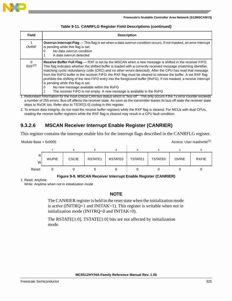
Freescale’s Scalable Controller Area Network (S12MSCANV3)
9.3.2.6 MSCAN Receiver Interrupt Enable Register (CANRIER)
This register contains the interrupt enable bits for the interrupt flags described in the CANRFLG register.
NOTEThe CANRIER register is held in the reset state when the initialization modeis active (INITRQ=1 and INITAK=1). This register is writable when not ininitialization mode (INITRQ=0 and INITAK=0).
The RSTATE[1:0], TSTATE[1:0] bits are not affected by initializationmode.
1OVRIF
Overrun Interrupt Flag — This flag is set when a data overrun condition occurs. If not masked, an error interruptis pending while this flag is set.0 No data overrun condition1 A data overrun detected
0RXF(2)
Receive Buffer Full Flag — RXF is set by the MSCAN when a new message is shifted in the receiver FIFO.This flag indicates whether the shifted buffer is loaded with a correctly received message (matching identifier,matching cyclic redundancy code (CRC) and no other errors detected). After the CPU has read that messagefrom the RxFG buffer in the receiver FIFO, the RXF flag must be cleared to release the buffer. A set RXF flagprohibits the shifting of the next FIFO entry into the foreground buffer (RxFG). If not masked, a receive interruptis pending while this flag is set.0 No new message available within the RxFG1 The receiver FIFO is not empty. A new message is available in the RxFG
1. Redundant Information for the most critical CAN bus status which is “bus-off”. This only occurs if the Tx error counter exceedsa number of 255 errors. Bus-off affects the receiver state. As soon as the transmitter leaves its bus-off state the receiver stateskips to RxOK too. Refer also to TSTAT[1:0] coding in this register.
2. To ensure data integrity, do not read the receive buffer registers while the RXF flag is cleared. For MCUs with dual CPUs,reading the receive buffer registers while the RXF flag is cleared may result in a CPU fault condition.
Module Base + 0x0005 Access: User read/write(1)
1. Read: AnytimeWrite: Anytime when not in initialization mode
7 6 5 4 3 2 1 0
RWUPIE CSCIE RSTATE1 RSTATE0 TSTATE1 TSTATE0 OVRIE RXFIE
W
Reset: 0 0 0 0 0 0 0 0
Figure 9-9. MSCAN Receiver Interrupt Enable Register (CANRIER)
Table 9-11. CANRFLG Register Field Descriptions (continued)
Field Description
MC9S12HY/HA-Family Reference Manual Rev. 1.05
Freescale Semiconductor 325
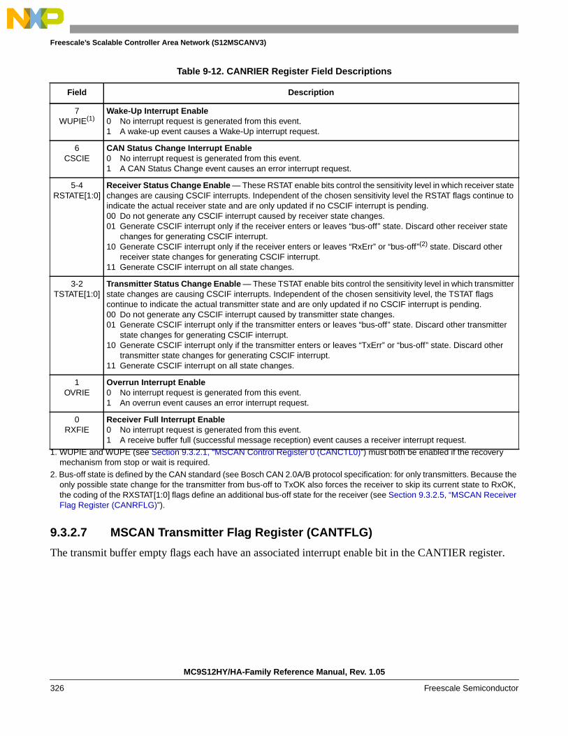
Freescale’s Scalable Controller Area Network (S12MSCANV3)
9.3.2.7 MSCAN Transmitter Flag Register (CANTFLG)
The transmit buffer empty flags each have an associated interrupt enable bit in the CANTIER register.
Table 9-12. CANRIER Register Field Descriptions
Field Description
7WUPIE(1)
1. WUPIE and WUPE (see Section 9.3.2.1, “MSCAN Control Register 0 (CANCTL0)”) must both be enabled if the recoverymechanism from stop or wait is required.
Wake-Up Interrupt Enable0 No interrupt request is generated from this event.1 A wake-up event causes a Wake-Up interrupt request.
6CSCIE
CAN Status Change Interrupt Enable0 No interrupt request is generated from this event.1 A CAN Status Change event causes an error interrupt request.
5-4RSTATE[1:0]
Receiver Status Change Enable — These RSTAT enable bits control the sensitivity level in which receiver statechanges are causing CSCIF interrupts. Independent of the chosen sensitivity level the RSTAT flags continue toindicate the actual receiver state and are only updated if no CSCIF interrupt is pending.00 Do not generate any CSCIF interrupt caused by receiver state changes.01 Generate CSCIF interrupt only if the receiver enters or leaves “bus-off” state. Discard other receiver state
changes for generating CSCIF interrupt.10 Generate CSCIF interrupt only if the receiver enters or leaves “RxErr” or “bus-off”(2) state. Discard other
receiver state changes for generating CSCIF interrupt.11 Generate CSCIF interrupt on all state changes.
2. Bus-off state is defined by the CAN standard (see Bosch CAN 2.0A/B protocol specification: for only transmitters. Because theonly possible state change for the transmitter from bus-off to TxOK also forces the receiver to skip its current state to RxOK,the coding of the RXSTAT[1:0] flags define an additional bus-off state for the receiver (see Section 9.3.2.5, “MSCAN ReceiverFlag Register (CANRFLG)”).
3-2TSTATE[1:0]
Transmitter Status Change Enable — These TSTAT enable bits control the sensitivity level in which transmitterstate changes are causing CSCIF interrupts. Independent of the chosen sensitivity level, the TSTAT flagscontinue to indicate the actual transmitter state and are only updated if no CSCIF interrupt is pending.00 Do not generate any CSCIF interrupt caused by transmitter state changes.01 Generate CSCIF interrupt only if the transmitter enters or leaves “bus-off” state. Discard other transmitter
state changes for generating CSCIF interrupt.10 Generate CSCIF interrupt only if the transmitter enters or leaves “TxErr” or “bus-off” state. Discard other
transmitter state changes for generating CSCIF interrupt.11 Generate CSCIF interrupt on all state changes.
1OVRIE
Overrun Interrupt Enable0 No interrupt request is generated from this event.1 An overrun event causes an error interrupt request.
0RXFIE
Receiver Full Interrupt Enable0 No interrupt request is generated from this event.1 A receive buffer full (successful message reception) event causes a receiver interrupt request.
MC9S12HY/HA-Family Reference Manual, Rev. 1.05
326 Freescale Semiconductor

Freescale’s Scalable Controller Area Network (S12MSCANV3)
NOTEThe CANTFLG register is held in the reset state when the initializationmode is active (INITRQ = 1 and INITAK = 1). This register is writable whennot in initialization mode (INITRQ = 0 and INITAK = 0).
9.3.2.8 MSCAN Transmitter Interrupt Enable Register (CANTIER)
This register contains the interrupt enable bits for the transmit buffer empty interrupt flags.
Module Base + 0x0006 Access: User read/write(1)
1. Read: AnytimeWrite: Anytime when not in initialization mode; write of 1 clears flag, write of 0 is ignored
7 6 5 4 3 2 1 0
R 0 0 0 0 0TXE2 TXE1 TXE0
W
Reset: 0 0 0 0 0 1 1 1
= Unimplemented
Figure 9-10. MSCAN Transmitter Flag Register (CANTFLG)
Table 9-13. CANTFLG Register Field Descriptions
Field Description
2-0TXE[2:0]
Transmitter Buffer Empty — This flag indicates that the associated transmit message buffer is empty, and thusnot scheduled for transmission. The CPU must clear the flag after a message is set up in the transmit buffer andis due for transmission. The MSCAN sets the flag after the message is sent successfully. The flag is also set bythe MSCAN when the transmission request is successfully aborted due to a pending abort request (seeSection 9.3.2.9, “MSCAN Transmitter Message Abort Request Register (CANTARQ)”). If not masked, a transmitinterrupt is pending while this flag is set.Clearing a TXEx flag also clears the corresponding ABTAKx (see Section 9.3.2.10, “MSCAN TransmitterMessage Abort Acknowledge Register (CANTAAK)”). When a TXEx flag is set, the corresponding ABTRQx bitis cleared (see Section 9.3.2.9, “MSCAN Transmitter Message Abort Request Register (CANTARQ)”).When listen-mode is active (see Section 9.3.2.2, “MSCAN Control Register 1 (CANCTL1)”) the TXEx flagscannot be cleared and no transmission is started.Read and write accesses to the transmit buffer will be blocked, if the corresponding TXEx bit is cleared(TXEx = 0) and the buffer is scheduled for transmission.0 The associated message buffer is full (loaded with a message due for transmission)1 The associated message buffer is empty (not scheduled)
Module Base + 0x0007 Access: User read/write(1)
7 6 5 4 3 2 1 0
R 0 0 0 0 0TXEIE2 TXEIE1 TXEIE0
W
Reset: 0 0 0 0 0 0 0 0
= Unimplemented
Figure 9-11. MSCAN Transmitter Interrupt Enable Register (CANTIER)
MC9S12HY/HA-Family Reference Manual Rev. 1.05
Freescale Semiconductor 327
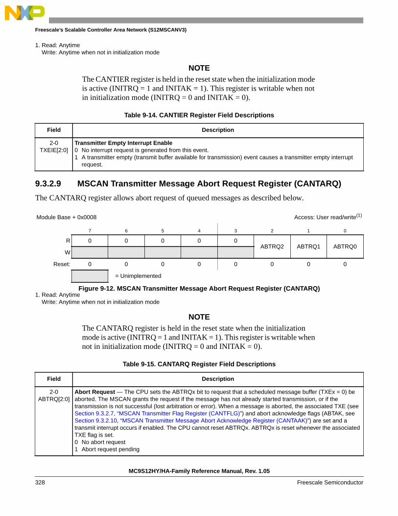
Freescale’s Scalable Controller Area Network (S12MSCANV3)
NOTEThe CANTIER register is held in the reset state when the initialization modeis active (INITRQ = 1 and INITAK = 1). This register is writable when notin initialization mode (INITRQ = 0 and INITAK = 0).
9.3.2.9 MSCAN Transmitter Message Abort Request Register (CANTARQ)
The CANTARQ register allows abort request of queued messages as described below.
NOTEThe CANTARQ register is held in the reset state when the initializationmode is active (INITRQ = 1 and INITAK = 1). This register is writable whennot in initialization mode (INITRQ = 0 and INITAK = 0).
1. Read: AnytimeWrite: Anytime when not in initialization mode
Table 9-14. CANTIER Register Field Descriptions
Field Description
2-0TXEIE[2:0]
Transmitter Empty Interrupt Enable0 No interrupt request is generated from this event.1 A transmitter empty (transmit buffer available for transmission) event causes a transmitter empty interrupt
request.
Module Base + 0x0008 Access: User read/write(1)
1. Read: AnytimeWrite: Anytime when not in initialization mode
7 6 5 4 3 2 1 0
R 0 0 0 0 0ABTRQ2 ABTRQ1 ABTRQ0
W
Reset: 0 0 0 0 0 0 0 0
= Unimplemented
Figure 9-12. MSCAN Transmitter Message Abort Request Register (CANTARQ)
Table 9-15. CANTARQ Register Field Descriptions
Field Description
2-0ABTRQ[2:0]
Abort Request — The CPU sets the ABTRQx bit to request that a scheduled message buffer (TXEx = 0) beaborted. The MSCAN grants the request if the message has not already started transmission, or if thetransmission is not successful (lost arbitration or error). When a message is aborted, the associated TXE (seeSection 9.3.2.7, “MSCAN Transmitter Flag Register (CANTFLG)”) and abort acknowledge flags (ABTAK, seeSection 9.3.2.10, “MSCAN Transmitter Message Abort Acknowledge Register (CANTAAK)”) are set and atransmit interrupt occurs if enabled. The CPU cannot reset ABTRQx. ABTRQx is reset whenever the associatedTXE flag is set.0 No abort request1 Abort request pending
MC9S12HY/HA-Family Reference Manual, Rev. 1.05
328 Freescale Semiconductor

Freescale’s Scalable Controller Area Network (S12MSCANV3)
9.3.2.10 MSCAN Transmitter Message Abort Acknowledge Register (CANTAAK)
The CANTAAK register indicates the successful abort of a queued message, if requested by theappropriate bits in the CANTARQ register.
NOTEThe CANTAAK register is held in the reset state when the initializationmode is active (INITRQ = 1 and INITAK = 1).
9.3.2.11 MSCAN Transmit Buffer Selection Register (CANTBSEL)
The CANTBSEL register allows the selection of the actual transmit message buffer, which then will beaccessible in the CANTXFG register space.
Module Base + 0x0009 Access: User read/write(1)
1. Read: AnytimeWrite: Unimplemented
7 6 5 4 3 2 1 0
R 0 0 0 0 0 ABTAK2 ABTAK1 ABTAK0
W
Reset: 0 0 0 0 0 0 0 0
= Unimplemented
Figure 9-13. MSCAN Transmitter Message Abort Acknowledge Register (CANTAAK)
Table 9-16. CANTAAK Register Field Descriptions
Field Description
2-0ABTAK[2:0]
Abort Acknowledge — This flag acknowledges that a message was aborted due to a pending abort requestfrom the CPU. After a particular message buffer is flagged empty, this flag can be used by the applicationsoftware to identify whether the message was aborted successfully or was sent anyway. The ABTAKx flag iscleared whenever the corresponding TXE flag is cleared.0 The message was not aborted.1 The message was aborted.
Module Base + 0x000A Access: User read/write(1)
1. Read: Find the lowest ordered bit set to 1, all other bits will be read as 0Write: Anytime when not in initialization mode
7 6 5 4 3 2 1 0
R 0 0 0 0 0TX2 TX1 TX0
W
Reset: 0 0 0 0 0 0 0 0
= Unimplemented
Figure 9-14. MSCAN Transmit Buffer Selection Register (CANTBSEL)
MC9S12HY/HA-Family Reference Manual Rev. 1.05
Freescale Semiconductor 329

Freescale’s Scalable Controller Area Network (S12MSCANV3)
NOTEThe CANTBSEL register is held in the reset state when the initializationmode is active (INITRQ = 1 and INITAK=1). This register is writable whennot in initialization mode (INITRQ = 0 and INITAK = 0).
The following gives a short programming example of the usage of the CANTBSEL register:
To get the next available transmit buffer, application software must read the CANTFLG register and writethis value back into the CANTBSEL register. In this example Tx buffers TX1 and TX2 are available. Thevalue read from CANTFLG is therefore 0b0000_0110. When writing this value back to CANTBSEL, theTx buffer TX1 is selected in the CANTXFG because the lowest numbered bit set to 1 is at bit position 1.Reading back this value out of CANTBSEL results in 0b0000_0010, because only the lowest numberedbit position set to 1 is presented. This mechanism eases the application software the selection of the nextavailable Tx buffer.
• LDAA CANTFLG; value read is 0b0000_0110
• STAA CANTBSEL; value written is 0b0000_0110
• LDAA CANTBSEL; value read is 0b0000_0010
If all transmit message buffers are deselected, no accesses are allowed to the CANTXFG registers.
9.3.2.12 MSCAN Identifier Acceptance Control Register (CANIDAC)
The CANIDAC register is used for identifier acceptance control as described below.
Table 9-17. CANTBSEL Register Field Descriptions
Field Description
2-0TX[2:0]
Transmit Buffer Select — The lowest numbered bit places the respective transmit buffer in the CANTXFGregister space (e.g., TX1 = 1 and TX0 = 1 selects transmit buffer TX0; TX1 = 1 and TX0 = 0 selects transmitbuffer TX1). Read and write accesses to the selected transmit buffer will be blocked, if the corresponding TXExbit is cleared and the buffer is scheduled for transmission (see Section 9.3.2.7, “MSCAN Transmitter FlagRegister (CANTFLG)”).0 The associated message buffer is deselected1 The associated message buffer is selected, if lowest numbered bit
Module Base + 0x000B Access: User read/write(1)
1. Read: AnytimeWrite: Anytime in initialization mode (INITRQ = 1 and INITAK = 1), except bits IDHITx, which are read-only
7 6 5 4 3 2 1 0
R 0 0IDAM1 IDAM0
0 IDHIT2 IDHIT1 IDHIT0
W
Reset: 0 0 0 0 0 0 0 0
= Unimplemented
Figure 9-15. MSCAN Identifier Acceptance Control Register (CANIDAC)
MC9S12HY/HA-Family Reference Manual, Rev. 1.05
330 Freescale Semiconductor
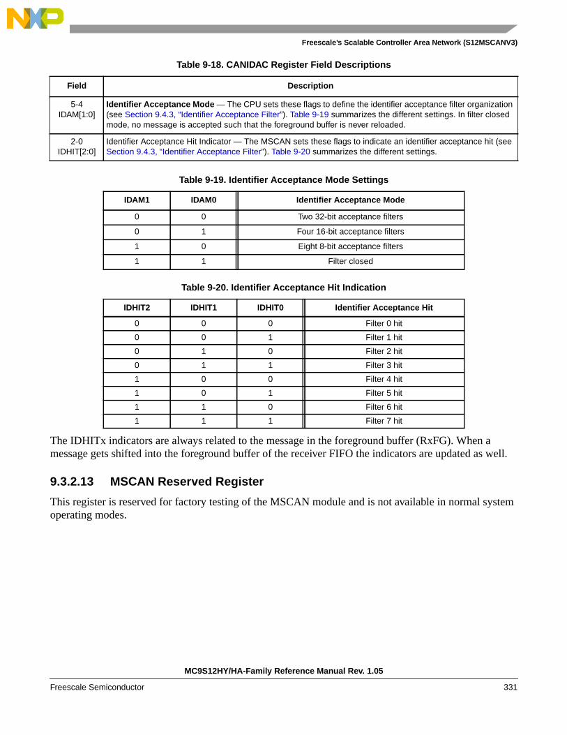
Freescale’s Scalable Controller Area Network (S12MSCANV3)
The IDHITx indicators are always related to the message in the foreground buffer (RxFG). When amessage gets shifted into the foreground buffer of the receiver FIFO the indicators are updated as well.
9.3.2.13 MSCAN Reserved Register
This register is reserved for factory testing of the MSCAN module and is not available in normal systemoperating modes.
Table 9-18. CANIDAC Register Field Descriptions
Field Description
5-4IDAM[1:0]
Identifier Acceptance Mode — The CPU sets these flags to define the identifier acceptance filter organization(see Section 9.4.3, “Identifier Acceptance Filter”). Table 9-19 summarizes the different settings. In filter closedmode, no message is accepted such that the foreground buffer is never reloaded.
2-0IDHIT[2:0]
Identifier Acceptance Hit Indicator — The MSCAN sets these flags to indicate an identifier acceptance hit (seeSection 9.4.3, “Identifier Acceptance Filter”). Table 9-20 summarizes the different settings.
Table 9-19. Identifier Acceptance Mode Settings
IDAM1 IDAM0 Identifier Acceptance Mode
0 0 Two 32-bit acceptance filters
0 1 Four 16-bit acceptance filters
1 0 Eight 8-bit acceptance filters
1 1 Filter closed
Table 9-20. Identifier Acceptance Hit Indication
IDHIT2 IDHIT1 IDHIT0 Identifier Acceptance Hit
0 0 0 Filter 0 hit
0 0 1 Filter 1 hit
0 1 0 Filter 2 hit
0 1 1 Filter 3 hit
1 0 0 Filter 4 hit
1 0 1 Filter 5 hit
1 1 0 Filter 6 hit
1 1 1 Filter 7 hit
MC9S12HY/HA-Family Reference Manual Rev. 1.05
Freescale Semiconductor 331

Freescale’s Scalable Controller Area Network (S12MSCANV3)
NOTEWriting to this register when in special systm operating modes can alter theMSCAN functionality.
9.3.2.14 MSCAN Miscellaneous Register (CANMISC)
This register provides additional features.
9.3.2.15 MSCAN Receive Error Counter (CANRXERR)
This register reflects the status of the MSCAN receive error counter.
Module Base + 0x000C to Module Base + 0x000D Access: User read/write(1)
1. Read: Always reads zero in normal system operation modesWrite: Unimplemented in normal system operation modes
7 6 5 4 3 2 1 0
R 0 0 0 0 0 0 0 0
W
Reset: 0 0 0 0 0 0 0 0
= Unimplemented
Figure 9-16. MSCAN Reserved Register
Module Base + 0x000D Access: User read/write(1)
1. Read: AnytimeWrite: Anytime; write of ‘1’ clears flag; write of ‘0’ ignored
7 6 5 4 3 2 1 0
R 0 0 0 0 0 0 0BOHOLD
W
Reset: 0 0 0 0 0 0 0 0
= Unimplemented
Figure 9-17. MSCAN Miscellaneous Register (CANMISC)
Table 9-21. CANMISC Register Field Descriptions
Field Description
0BOHOLD
Bus-off State Hold Until User Request — If BORM is set in MSCAN Control Register 1 (CANCTL1), this bitindicates whether the module has entered the bus-off state. Clearing this bit requests the recovery from bus-off.Refer to Section 9.5.2, “Bus-Off Recovery,” for details.0 Module is not bus-off or recovery has been requested by user in bus-off state1 Module is bus-off and holds this state until user request
MC9S12HY/HA-Family Reference Manual, Rev. 1.05
332 Freescale Semiconductor

Freescale’s Scalable Controller Area Network (S12MSCANV3)
NOTEReading this register when in any other mode other than sleep orinitialization mode may return an incorrect value. For MCUs with dualCPUs, this may result in a CPU fault condition.
Writing to this register when in special modes can alter the MSCANfunctionality.
9.3.2.16 MSCAN Transmit Error Counter (CANTXERR)
This register reflects the status of the MSCAN transmit error counter.
NOTEReading this register when in any other mode other than sleep orinitialization mode, may return an incorrect value. For MCUs with dualCPUs, this may result in a CPU fault condition.
Writing to this register when in special modes can alter the MSCANfunctionality.
Module Base + 0x000E Access: User read/write(1)
1. Read: Only when in sleep mode (SLPRQ = 1 and SLPAK = 1) or initialization mode (INITRQ = 1 and INITAK = 1)Write: Unimplemented
7 6 5 4 3 2 1 0
R RXERR7 RXERR6 RXERR5 RXERR4 RXERR3 RXERR2 RXERR1 RXERR0
W
Reset: 0 0 0 0 0 0 0 0
= Unimplemented
Figure 9-18. MSCAN Receive Error Counter (CANRXERR)
Module Base + 0x000F Access: User read/write(1)
1. Read: Only when in sleep mode (SLPRQ = 1 and SLPAK = 1) or initialization mode (INITRQ = 1 and INITAK = 1)Write: Unimplemented
7 6 5 4 3 2 1 0
R TXERR7 TXERR6 TXERR5 TXERR4 TXERR3 TXERR2 TXERR1 TXERR0
W
Reset: 0 0 0 0 0 0 0 0
= Unimplemented
Figure 9-19. MSCAN Transmit Error Counter (CANTXERR)
MC9S12HY/HA-Family Reference Manual Rev. 1.05
Freescale Semiconductor 333

Freescale’s Scalable Controller Area Network (S12MSCANV3)
1
9.3.2.17 MSCAN Identifier Acceptance Registers (CANIDAR0-7)
On reception, each message is written into the background receive buffer. The CPU is only signalled toread the message if it passes the criteria in the identifier acceptance and identifier mask registers(accepted); otherwise, the message is overwritten by the next message (dropped).
The acceptance registers of the MSCAN are applied on the IDR0–IDR3 registers (see Section 9.3.3.1,“Identifier Registers (IDR0–IDR3)”) of incoming messages in a bit by bit manner (see Section 9.4.3,“Identifier Acceptance Filter”).
For extended identifiers, all four acceptance and mask registers are applied. For standard identifiers, onlythe first two (CANIDAR0/1, CANIDMR0/1) are applied.
Module Base + 0x0010 to Module Base + 0x0013 Access: User read/write(1)
1. Read: AnytimeWrite: Anytime in initialization mode (INITRQ = 1 and INITAK = 1)
7 6 5 4 3 2 1 0
RAC7 AC6 AC5 AC4 AC3 AC2 AC1 AC0
W
Reset 0 0 0 0 0 0 0 0
Figure 9-20. MSCAN Identifier Acceptance Registers (First Bank) — CANIDAR0–CANIDAR3
Table 9-22. CANIDAR0–CANIDAR3 Register Field Descriptions
Field Description
7-0AC[7:0]
Acceptance Code Bits — AC[7:0] comprise a user-defined sequence of bits with which the corresponding bitsof the related identifier register (IDRn) of the receive message buffer are compared. The result of this comparisonis then masked with the corresponding identifier mask register.
Module Base + 0x0018 to Module Base + 0x001B Access: User read/write(1)
. Read: AnytimeWrite: Anytime in initialization mode (INITRQ = 1 and INITAK = 1)
7 6 5 4 3 2 1 0
RAC7 AC6 AC5 AC4 AC3 AC2 AC1 AC0
W
Reset 0 0 0 0 0 0 0 0
Figure 9-21. MSCAN Identifier Acceptance Registers (Second Bank) — CANIDAR4–CANIDAR7
MC9S12HY/HA-Family Reference Manual, Rev. 1.05
334 Freescale Semiconductor

Freescale’s Scalable Controller Area Network (S12MSCANV3)
9.3.2.18 MSCAN Identifier Mask Registers (CANIDMR0–CANIDMR7)
The identifier mask register specifies which of the corresponding bits in the identifier acceptance registerare relevant for acceptance filtering. To receive standard identifiers in 32 bit filter mode, it is required toprogram the last three bits (AM[2:0]) in the mask registers CANIDMR1 and CANIDMR5 to “don’t care.”To receive standard identifiers in 16 bit filter mode, it is required to program the last three bits (AM[2:0])in the mask registers CANIDMR1, CANIDMR3, CANIDMR5, and CANIDMR7 to “don’t care.”
Table 9-23. CANIDAR4–CANIDAR7 Register Field Descriptions
Field Description
7-0AC[7:0]
Acceptance Code Bits — AC[7:0] comprise a user-defined sequence of bits with which the corresponding bitsof the related identifier register (IDRn) of the receive message buffer are compared. The result of this comparisonis then masked with the corresponding identifier mask register.
Module Base + 0x0014 to Module Base + 0x0017 Access: User read/write(1)
1. Read: AnytimeWrite: Anytime in initialization mode (INITRQ = 1 and INITAK = 1)
7 6 5 4 3 2 1 0
RAM7 AM6 AM5 AM4 AM3 AM2 AM1 AM0
W
Reset 0 0 0 0 0 0 0 0
Figure 9-22. MSCAN Identifier Mask Registers (First Bank) — CANIDMR0–CANIDMR3
Table 9-24. CANIDMR0–CANIDMR3 Register Field Descriptions
Field Description
7-0AM[7:0]
Acceptance Mask Bits — If a particular bit in this register is cleared, this indicates that the corresponding bit inthe identifier acceptance register must be the same as its identifier bit before a match is detected. The messageis accepted if all such bits match. If a bit is set, it indicates that the state of the corresponding bit in the identifieracceptance register does not affect whether or not the message is accepted.0 Match corresponding acceptance code register and identifier bits1 Ignore corresponding acceptance code register bit
Module Base + 0x001C to Module Base + 0x001F Access: User read/write(1)
7 6 5 4 3 2 1 0
RAM7 AM6 AM5 AM4 AM3 AM2 AM1 AM0
W
Reset 0 0 0 0 0 0 0 0
Figure 9-23. MSCAN Identifier Mask Registers (Second Bank) — CANIDMR4–CANIDMR7
MC9S12HY/HA-Family Reference Manual Rev. 1.05
Freescale Semiconductor 335

Freescale’s Scalable Controller Area Network (S12MSCANV3)
9.3.3 Programmer’s Model of Message Storage
The following section details the organization of the receive and transmit message buffers and theassociated control registers.
To simplify the programmer interface, the receive and transmit message buffers have the same outline.Each message buffer allocates 16 bytes in the memory map containing a 13 byte data structure.
An additional transmit buffer priority register (TBPR) is defined for the transmit buffers. Within the lasttwo bytes of this memory map, the MSCAN stores a special 16-bit time stamp, which is sampled from aninternal timer after successful transmission or reception of a message. This feature is only available fortransmit and receiver buffers, if the TIME bit is set (see Section 9.3.2.1, “MSCAN Control Register 0(CANCTL0)”).
The time stamp register is written by the MSCAN. The CPU can only read these registers.
1. Read: AnytimeWrite: Anytime in initialization mode (INITRQ = 1 and INITAK = 1)
Table 9-25. CANIDMR4–CANIDMR7 Register Field Descriptions
Field Description
7-0AM[7:0]
Acceptance Mask Bits — If a particular bit in this register is cleared, this indicates that the corresponding bit inthe identifier acceptance register must be the same as its identifier bit before a match is detected. The messageis accepted if all such bits match. If a bit is set, it indicates that the state of the corresponding bit in the identifieracceptance register does not affect whether or not the message is accepted.0 Match corresponding acceptance code register and identifier bits1 Ignore corresponding acceptance code register bit
MC9S12HY/HA-Family Reference Manual, Rev. 1.05
336 Freescale Semiconductor
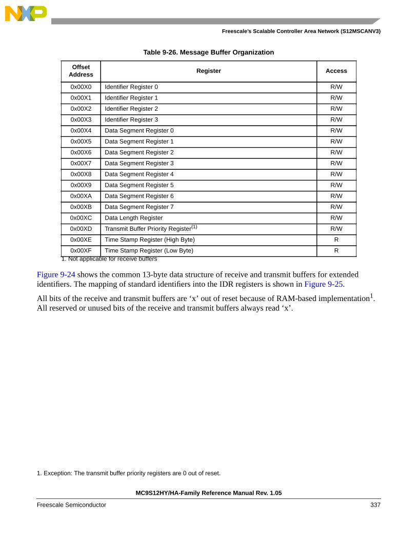
Freescale’s Scalable Controller Area Network (S12MSCANV3)
Figure 9-24 shows the common 13-byte data structure of receive and transmit buffers for extendedidentifiers. The mapping of standard identifiers into the IDR registers is shown in Figure 9-25.
All bits of the receive and transmit buffers are ‘x’ out of reset because of RAM-based implementation1.All reserved or unused bits of the receive and transmit buffers always read ‘x’.
Table 9-26. Message Buffer Organization
OffsetAddress
Register Access
0x00X0 Identifier Register 0 R/W
0x00X1 Identifier Register 1 R/W
0x00X2 Identifier Register 2 R/W
0x00X3 Identifier Register 3 R/W
0x00X4 Data Segment Register 0 R/W
0x00X5 Data Segment Register 1 R/W
0x00X6 Data Segment Register 2 R/W
0x00X7 Data Segment Register 3 R/W
0x00X8 Data Segment Register 4 R/W
0x00X9 Data Segment Register 5 R/W
0x00XA Data Segment Register 6 R/W
0x00XB Data Segment Register 7 R/W
0x00XC Data Length Register R/W
0x00XD Transmit Buffer Priority Register(1)
1. Not applicable for receive buffers
R/W
0x00XE Time Stamp Register (High Byte) R
0x00XF Time Stamp Register (Low Byte) R
1. Exception: The transmit buffer priority registers are 0 out of reset.
MC9S12HY/HA-Family Reference Manual Rev. 1.05
Freescale Semiconductor 337

Freescale’s Scalable Controller Area Network (S12MSCANV3)
Figure 9-24. Receive/Transmit Message Buffer — Extended Identifier Mapping
RegisterName
Bit 7 6 5 4 3 2 1 Bit0
0x00X0IDR0
RID28 ID27 ID26 ID25 ID24 ID23 ID22 ID21
W
0x00X1IDR1
RID20 ID19 ID18 SRR (=1) IDE (=1) ID17 ID16 ID15
W
0x00X2IDR2
RID14 ID13 ID12 ID11 ID10 ID9 ID8 ID7
W
0x00X3IDR3
RID6 ID5 ID4 ID3 ID2 ID1 ID0 RTR
W
0x00X4DSR0
RDB7 DB6 DB5 DB4 DB3 DB2 DB1 DB0
W
0x00X5DSR1
RDB7 DB6 DB5 DB4 DB3 DB2 DB1 DB0
W
0x00X6DSR2
RDB7 DB6 DB5 DB4 DB3 DB2 DB1 DB0
W
0x00X7DSR3
RDB7 DB6 DB5 DB4 DB3 DB2 DB1 DB0
W
0x00X8DSR4
RDB7 DB6 DB5 DB4 DB3 DB2 DB1 DB0
W
0x00X9DSR5
RDB7 DB6 DB5 DB4 DB3 DB2 DB1 DB0
W
0x00XADSR6
RDB7 DB6 DB5 DB4 DB3 DB2 DB1 DB0
W
0x00XBDSR7
RDB7 DB6 DB5 DB4 DB3 DB2 DB1 DB0
W
0x00XCDLR
RDLC3 DLC2 DLC1 DLC0
W
MC9S12HY/HA-Family Reference Manual, Rev. 1.05
338 Freescale Semiconductor

Freescale’s Scalable Controller Area Network (S12MSCANV3)
Read:
• For transmit buffers, anytime when TXEx flag is set (see Section 9.3.2.7, “MSCAN TransmitterFlag Register (CANTFLG)”) and the corresponding transmit buffer is selected in CANTBSEL (seeSection 9.3.2.11, “MSCAN Transmit Buffer Selection Register (CANTBSEL)”).
• For receive buffers, only when RXF flag is set (see Section 9.3.2.5, “MSCAN Receiver FlagRegister (CANRFLG)”).
Write:
• For transmit buffers, anytime when TXEx flag is set (see Section 9.3.2.7, “MSCAN TransmitterFlag Register (CANTFLG)”) and the corresponding transmit buffer is selected in CANTBSEL (seeSection 9.3.2.11, “MSCAN Transmit Buffer Selection Register (CANTBSEL)”).
• Unimplemented for receive buffers.
Reset: Undefined because of RAM-based implementation
9.3.3.1 Identifier Registers (IDR0–IDR3)
The identifier registers for an extended format identifier consist of a total of 32 bits; ID[28:0], SRR, IDE,and RTR bits. The identifier registers for a standard format identifier consist of a total of 13 bits; ID[10:0],RTR, and IDE bits.
= Unused, always read ‘x’
Figure 9-25. Receive/Transmit Message Buffer — Standard Identifier Mapping
RegisterName
Bit 7 6 5 4 3 2 1 Bit 0
IDR00x00X0
RID10 ID9 ID8 ID7 ID6 ID5 ID4 ID3
W
IDR10x00X1
RID2 ID1 ID0 RTR IDE (=0)
W
IDR20x00X2
R
W
IDR30x00X3
R
W
= Unused, always read ‘x’
Figure 9-24. Receive/Transmit Message Buffer — Extended Identifier Mapping (continued)
RegisterName
Bit 7 6 5 4 3 2 1 Bit0
MC9S12HY/HA-Family Reference Manual Rev. 1.05
Freescale Semiconductor 339

Freescale’s Scalable Controller Area Network (S12MSCANV3)
9.3.3.1.1 IDR0–IDR3 for Extended Identifier Mapping
Module Base + 0x00X0
7 6 5 4 3 2 1 0
RID28 ID27 ID26 ID25 ID24 ID23 ID22 ID21
W
Reset: x x x x x x x x
Figure 9-26. Identifier Register 0 (IDR0) — Extended Identifier Mapping
Table 9-27. IDR0 Register Field Descriptions — Extended
Field Description
7-0ID[28:21]
Extended Format Identifier — The identifiers consist of 29 bits (ID[28:0]) for the extended format. ID28 is themost significant bit and is transmitted first on the CAN bus during the arbitration procedure. The priority of anidentifier is defined to be highest for the smallest binary number.
Module Base + 0x00X1
7 6 5 4 3 2 1 0
RID20 ID19 ID18 SRR (=1) IDE (=1) ID17 ID16 ID15
W
Reset: x x x x x x x x
Figure 9-27. Identifier Register 1 (IDR1) — Extended Identifier Mapping
Table 9-28. IDR1 Register Field Descriptions — Extended
Field Description
7-5ID[20:18]
Extended Format Identifier — The identifiers consist of 29 bits (ID[28:0]) for the extended format. ID28 is themost significant bit and is transmitted first on the CAN bus during the arbitration procedure. The priority of anidentifier is defined to be highest for the smallest binary number.
4SRR
Substitute Remote Request — This fixed recessive bit is used only in extended format. It must be set to 1 bythe user for transmission buffers and is stored as received on the CAN bus for receive buffers.
3IDE
ID Extended — This flag indicates whether the extended or standard identifier format is applied in this buffer. Inthe case of a receive buffer, the flag is set as received and indicates to the CPU how to process the bufferidentifier registers. In the case of a transmit buffer, the flag indicates to the MSCAN what type of identifier to send.0 Standard format (11 bit)1 Extended format (29 bit)
2-0ID[17:15]
Extended Format Identifier — The identifiers consist of 29 bits (ID[28:0]) for the extended format. ID28 is themost significant bit and is transmitted first on the CAN bus during the arbitration procedure. The priority of anidentifier is defined to be highest for the smallest binary number.
MC9S12HY/HA-Family Reference Manual, Rev. 1.05
340 Freescale Semiconductor
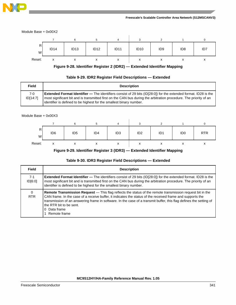
Freescale’s Scalable Controller Area Network (S12MSCANV3)
Module Base + 0x00X2
7 6 5 4 3 2 1 0
RID14 ID13 ID12 ID11 ID10 ID9 ID8 ID7
W
Reset: x x x x x x x x
Figure 9-28. Identifier Register 2 (IDR2) — Extended Identifier Mapping
Table 9-29. IDR2 Register Field Descriptions — Extended
Field Description
7-0ID[14:7]
Extended Format Identifier — The identifiers consist of 29 bits (ID[28:0]) for the extended format. ID28 is themost significant bit and is transmitted first on the CAN bus during the arbitration procedure. The priority of anidentifier is defined to be highest for the smallest binary number.
Module Base + 0x00X3
7 6 5 4 3 2 1 0
RID6 ID5 ID4 ID3 ID2 ID1 ID0 RTR
W
Reset: x x x x x x x x
Figure 9-29. Identifier Register 3 (IDR3) — Extended Identifier Mapping
Table 9-30. IDR3 Register Field Descriptions — Extended
Field Description
7-1ID[6:0]
Extended Format Identifier — The identifiers consist of 29 bits (ID[28:0]) for the extended format. ID28 is themost significant bit and is transmitted first on the CAN bus during the arbitration procedure. The priority of anidentifier is defined to be highest for the smallest binary number.
0RTR
Remote Transmission Request — This flag reflects the status of the remote transmission request bit in theCAN frame. In the case of a receive buffer, it indicates the status of the received frame and supports thetransmission of an answering frame in software. In the case of a transmit buffer, this flag defines the setting ofthe RTR bit to be sent.0 Data frame1 Remote frame
MC9S12HY/HA-Family Reference Manual Rev. 1.05
Freescale Semiconductor 341

Freescale’s Scalable Controller Area Network (S12MSCANV3)
9.3.3.1.2 IDR0–IDR3 for Standard Identifier Mapping
Module Base + 0x00X0
7 6 5 4 3 2 1 0
RID10 ID9 ID8 ID7 ID6 ID5 ID4 ID3
W
Reset: x x x x x x x x
Figure 9-30. Identifier Register 0 — Standard Mapping
Table 9-31. IDR0 Register Field Descriptions — Standard
Field Description
7-0ID[10:3]
Standard Format Identifier — The identifiers consist of 11 bits (ID[10:0]) for the standard format. ID10 is themost significant bit and is transmitted first on the CAN bus during the arbitration procedure. The priority of anidentifier is defined to be highest for the smallest binary number. See also ID bits in Table 9-32.
Module Base + 0x00X1
7 6 5 4 3 2 1 0
RID2 ID1 ID0 RTR IDE (=0)
W
Reset: x x x x x x x x
= Unused; always read ‘x’
Figure 9-31. Identifier Register 1 — Standard Mapping
Table 9-32. IDR1 Register Field Descriptions
Field Description
7-5ID[2:0]
Standard Format Identifier — The identifiers consist of 11 bits (ID[10:0]) for the standard format. ID10 is themost significant bit and is transmitted first on the CAN bus during the arbitration procedure. The priority of anidentifier is defined to be highest for the smallest binary number. See also ID bits in Table 9-31.
4RTR
Remote Transmission Request — This flag reflects the status of the Remote Transmission Request bit in theCAN frame. In the case of a receive buffer, it indicates the status of the received frame and supports thetransmission of an answering frame in software. In the case of a transmit buffer, this flag defines the setting ofthe RTR bit to be sent.0 Data frame1 Remote frame
3IDE
ID Extended — This flag indicates whether the extended or standard identifier format is applied in this buffer. Inthe case of a receive buffer, the flag is set as received and indicates to the CPU how to process the bufferidentifier registers. In the case of a transmit buffer, the flag indicates to the MSCAN what type of identifier to send.0 Standard format (11 bit)1 Extended format (29 bit)
MC9S12HY/HA-Family Reference Manual, Rev. 1.05
342 Freescale Semiconductor
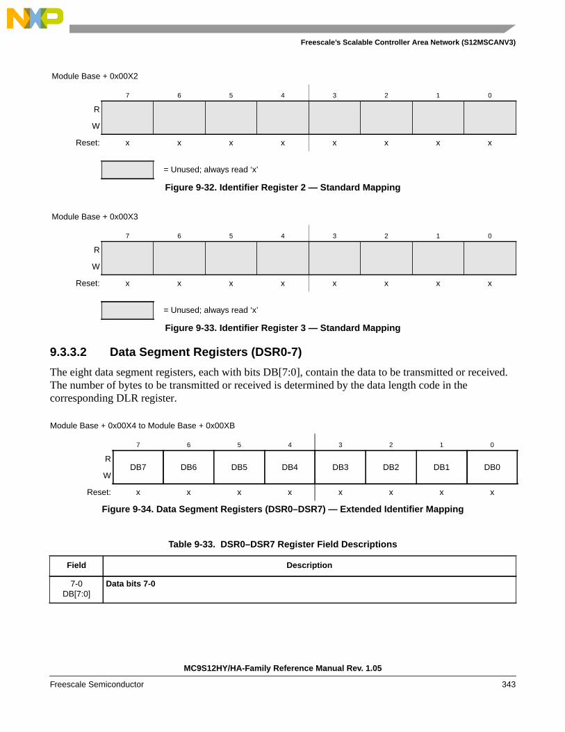
Freescale’s Scalable Controller Area Network (S12MSCANV3)
9.3.3.2 Data Segment Registers (DSR0-7)
The eight data segment registers, each with bits DB[7:0], contain the data to be transmitted or received.The number of bytes to be transmitted or received is determined by the data length code in thecorresponding DLR register.
Module Base + 0x00X2
7 6 5 4 3 2 1 0
R
W
Reset: x x x x x x x x
= Unused; always read ‘x’
Figure 9-32. Identifier Register 2 — Standard Mapping
Module Base + 0x00X3
7 6 5 4 3 2 1 0
R
W
Reset: x x x x x x x x
= Unused; always read ‘x’
Figure 9-33. Identifier Register 3 — Standard Mapping
Module Base + 0x00X4 to Module Base + 0x00XB
7 6 5 4 3 2 1 0
RDB7 DB6 DB5 DB4 DB3 DB2 DB1 DB0
W
Reset: x x x x x x x x
Figure 9-34. Data Segment Registers (DSR0–DSR7) — Extended Identifier Mapping
Table 9-33. DSR0–DSR7 Register Field Descriptions
Field Description
7-0DB[7:0]
Data bits 7-0
MC9S12HY/HA-Family Reference Manual Rev. 1.05
Freescale Semiconductor 343

Freescale’s Scalable Controller Area Network (S12MSCANV3)
9.3.3.3 Data Length Register (DLR)
This register keeps the data length field of the CAN frame.
9.3.3.4 Transmit Buffer Priority Register (TBPR)
This register defines the local priority of the associated message buffer. The local priority is used for theinternal prioritization process of the MSCAN and is defined to be highest for the smallest binary number.The MSCAN implements the following internal prioritization mechanisms:
• All transmission buffers with a cleared TXEx flag participate in the prioritization immediatelybefore the SOF (start of frame) is sent.
Module Base + 0x00XC
7 6 5 4 3 2 1 0
RDLC3 DLC2 DLC1 DLC0
W
Reset: x x x x x x x x
= Unused; always read “x”
Figure 9-35. Data Length Register (DLR) — Extended Identifier Mapping
Table 9-34. DLR Register Field Descriptions
Field Description
3-0DLC[3:0]
Data Length Code Bits — The data length code contains the number of bytes (data byte count) of the respectivemessage. During the transmission of a remote frame, the data length code is transmitted as programmed whilethe number of transmitted data bytes is always 0. The data byte count ranges from 0 to 8 for a data frame.Table 9-35 shows the effect of setting the DLC bits.
Table 9-35. Data Length Codes
Data Length Code Data ByteCountDLC3 DLC2 DLC1 DLC0
0 0 0 0 0
0 0 0 1 1
0 0 1 0 2
0 0 1 1 3
0 1 0 0 4
0 1 0 1 5
0 1 1 0 6
0 1 1 1 7
1 0 0 0 8
MC9S12HY/HA-Family Reference Manual, Rev. 1.05
344 Freescale Semiconductor
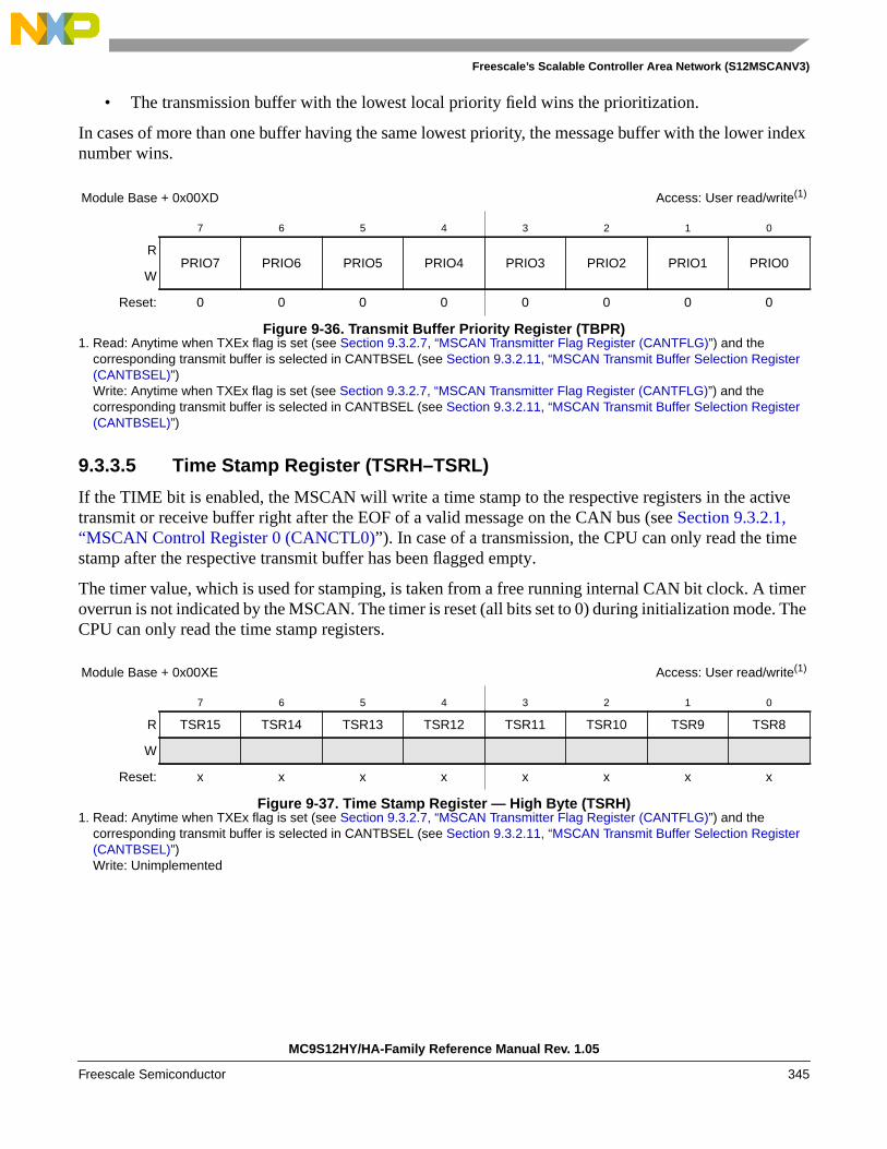
Freescale’s Scalable Controller Area Network (S12MSCANV3)
• The transmission buffer with the lowest local priority field wins the prioritization.
In cases of more than one buffer having the same lowest priority, the message buffer with the lower indexnumber wins.
9.3.3.5 Time Stamp Register (TSRH–TSRL)
If the TIME bit is enabled, the MSCAN will write a time stamp to the respective registers in the activetransmit or receive buffer right after the EOF of a valid message on the CAN bus (see Section 9.3.2.1,“MSCAN Control Register 0 (CANCTL0)”). In case of a transmission, the CPU can only read the timestamp after the respective transmit buffer has been flagged empty.
The timer value, which is used for stamping, is taken from a free running internal CAN bit clock. A timeroverrun is not indicated by the MSCAN. The timer is reset (all bits set to 0) during initialization mode. TheCPU can only read the time stamp registers.
Module Base + 0x00XD Access: User read/write(1)
1. Read: Anytime when TXEx flag is set (see Section 9.3.2.7, “MSCAN Transmitter Flag Register (CANTFLG)”) and thecorresponding transmit buffer is selected in CANTBSEL (see Section 9.3.2.11, “MSCAN Transmit Buffer Selection Register(CANTBSEL)”)Write: Anytime when TXEx flag is set (see Section 9.3.2.7, “MSCAN Transmitter Flag Register (CANTFLG)”) and thecorresponding transmit buffer is selected in CANTBSEL (see Section 9.3.2.11, “MSCAN Transmit Buffer Selection Register(CANTBSEL)”)
7 6 5 4 3 2 1 0
RPRIO7 PRIO6 PRIO5 PRIO4 PRIO3 PRIO2 PRIO1 PRIO0
W
Reset: 0 0 0 0 0 0 0 0
Figure 9-36. Transmit Buffer Priority Register (TBPR)
Module Base + 0x00XE Access: User read/write(1)
1. Read: Anytime when TXEx flag is set (see Section 9.3.2.7, “MSCAN Transmitter Flag Register (CANTFLG)”) and thecorresponding transmit buffer is selected in CANTBSEL (see Section 9.3.2.11, “MSCAN Transmit Buffer Selection Register(CANTBSEL)”)Write: Unimplemented
7 6 5 4 3 2 1 0
R TSR15 TSR14 TSR13 TSR12 TSR11 TSR10 TSR9 TSR8
W
Reset: x x x x x x x x
Figure 9-37. Time Stamp Register — High Byte (TSRH)
MC9S12HY/HA-Family Reference Manual Rev. 1.05
Freescale Semiconductor 345
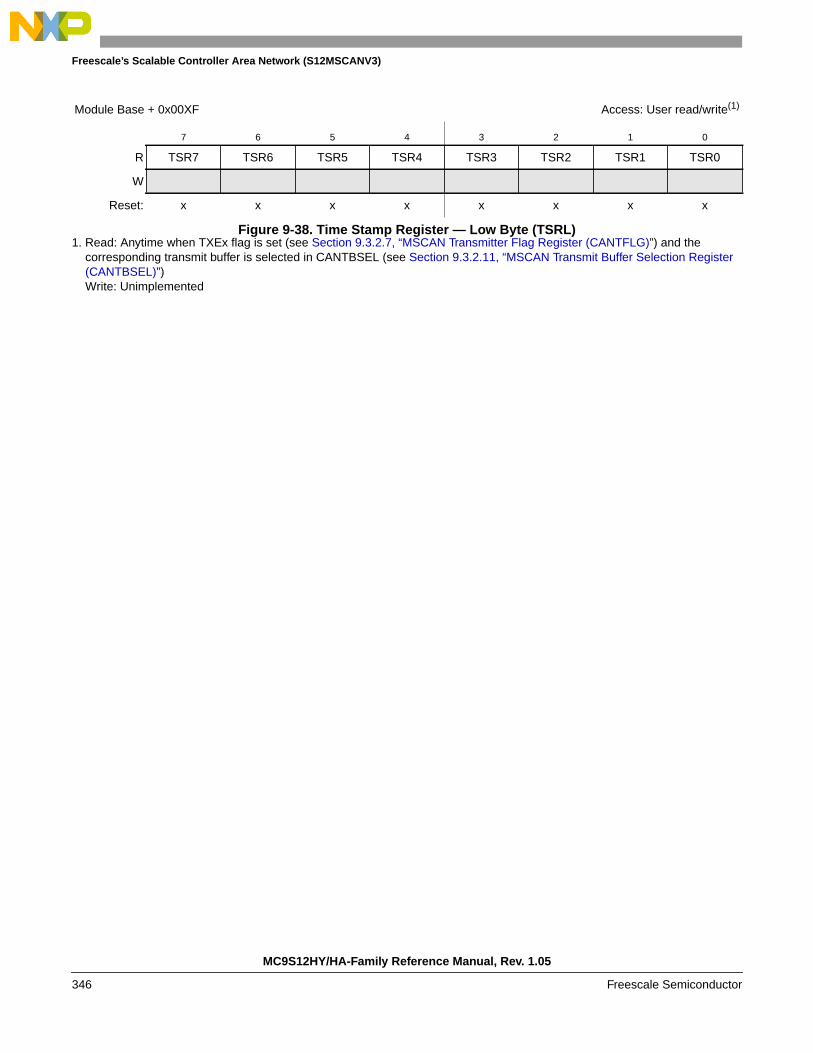
Freescale’s Scalable Controller Area Network (S12MSCANV3)
Module Base + 0x00XF Access: User read/write(1)
1. Read: Anytime when TXEx flag is set (see Section 9.3.2.7, “MSCAN Transmitter Flag Register (CANTFLG)”) and thecorresponding transmit buffer is selected in CANTBSEL (see Section 9.3.2.11, “MSCAN Transmit Buffer Selection Register(CANTBSEL)”)Write: Unimplemented
7 6 5 4 3 2 1 0
R TSR7 TSR6 TSR5 TSR4 TSR3 TSR2 TSR1 TSR0
W
Reset: x x x x x x x x
Figure 9-38. Time Stamp Register — Low Byte (TSRL)
MC9S12HY/HA-Family Reference Manual, Rev. 1.05
346 Freescale Semiconductor

Freescale’s Scalable Controller Area Network (S12MSCANV3)
9.4 Functional Description
9.4.1 General
This section provides a complete functional description of the MSCAN.
9.4.2 Message Storage
Figure 9-39. User Model for Message Buffer Organization
MSCAN
Rx0Rx1
CAN Receive / Transmit Engine Memory Mapped I/O
CPU bus
MSCAN
Tx2 TXE2
PRIO
Receiver
Transmitter
RxB
G
TxB
G
Tx0 TXE0
PRIOTxB
G
Tx1
PRIO
TXE1
TxF
G
CPU bus
Rx2Rx3
Rx4RXF
RxF
G
MC9S12HY/HA-Family Reference Manual Rev. 1.05
Freescale Semiconductor 347

Freescale’s Scalable Controller Area Network (S12MSCANV3)
The MSCAN facilitates a sophisticated message storage system which addresses the requirements of abroad range of network applications.
9.4.2.1 Message Transmit Background
Modern application layer software is built upon two fundamental assumptions:
• Any CAN node is able to send out a stream of scheduled messages without releasing the CAN busbetween the two messages. Such nodes arbitrate for the CAN bus immediately after sending theprevious message and only release the CAN bus in case of lost arbitration.
• The internal message queue within any CAN node is organized such that the highest prioritymessage is sent out first, if more than one message is ready to be sent.
The behavior described in the bullets above cannot be achieved with a single transmit buffer. That buffermust be reloaded immediately after the previous message is sent. This loading process lasts a finite amountof time and must be completed within the inter-frame sequence (IFS) to be able to send an uninterruptedstream of messages. Even if this is feasible for limited CAN bus speeds, it requires that the CPU reactswith short latencies to the transmit interrupt.
A double buffer scheme de-couples the reloading of the transmit buffer from the actual message sendingand, therefore, reduces the reactiveness requirements of the CPU. Problems can arise if the sending of amessage is finished while the CPU re-loads the second buffer. No buffer would then be ready fortransmission, and the CAN bus would be released.
At least three transmit buffers are required to meet the first of the above requirements under allcircumstances. The MSCAN has three transmit buffers.
The second requirement calls for some sort of internal prioritization which the MSCAN implements withthe “local priority” concept described in Section 9.4.2.2, “Transmit Structures.”
9.4.2.2 Transmit Structures
The MSCAN triple transmit buffer scheme optimizes real-time performance by allowing multiplemessages to be set up in advance. The three buffers are arranged as shown in Figure 9-39.
All three buffers have a 13-byte data structure similar to the outline of the receive buffers (seeSection 9.3.3, “Programmer’s Model of Message Storage”). An additional Transmit Buffer PriorityRegister (TBPR) contains an 8-bit local priority field (PRIO) (see Section 9.3.3.4, “Transmit BufferPriority Register (TBPR)”). The remaining two bytes are used for time stamping of a message, if required(see Section 9.3.3.5, “Time Stamp Register (TSRH–TSRL)”).
To transmit a message, the CPU must identify an available transmit buffer, which is indicated by a settransmitter buffer empty (TXEx) flag (see Section 9.3.2.7, “MSCAN Transmitter Flag Register(CANTFLG)”). If a transmit buffer is available, the CPU must set a pointer to this buffer by writing to theCANTBSEL register (see Section 9.3.2.11, “MSCAN Transmit Buffer Selection Register(CANTBSEL)”). This makes the respective buffer accessible within the CANTXFG address space (seeSection 9.3.3, “Programmer’s Model of Message Storage”). The algorithmic feature associated with theCANTBSEL register simplifies the transmit buffer selection. In addition, this scheme makes the handler
MC9S12HY/HA-Family Reference Manual, Rev. 1.05
348 Freescale Semiconductor
Freescale’s Scalable Controller Area Network (S12MSCANV3)
software simpler because only one address area is applicable for the transmit process, and the requiredaddress space is minimized.
The CPU then stores the identifier, the control bits, and the data content into one of the transmit buffers.Finally, the buffer is flagged as ready for transmission by clearing the associated TXE flag.
The MSCAN then schedules the message for transmission and signals the successful transmission of thebuffer by setting the associated TXE flag. A transmit interrupt (see Section 9.4.7.2, “Transmit Interrupt”)is generated1 when TXEx is set and can be used to drive the application software to re-load the buffer.
If more than one buffer is scheduled for transmission when the CAN bus becomes available for arbitration,the MSCAN uses the local priority setting of the three buffers to determine the prioritization. For thispurpose, every transmit buffer has an 8-bit local priority field (PRIO). The application software programsthis field when the message is set up. The local priority reflects the priority of this particular messagerelative to the set of messages being transmitted from this node. The lowest binary value of the PRIO fieldis defined to be the highest priority. The internal scheduling process takes place whenever the MSCANarbitrates for the CAN bus. This is also the case after the occurrence of a transmission error.
When a high priority message is scheduled by the application software, it may become necessary to aborta lower priority message in one of the three transmit buffers. Because messages that are already intransmission cannot be aborted, the user must request the abort by setting the corresponding abort requestbit (ABTRQ) (see Section 9.3.2.9, “MSCAN Transmitter Message Abort Request Register(CANTARQ)”.) The MSCAN then grants the request, if possible, by:
1. Setting the corresponding abort acknowledge flag (ABTAK) in the CANTAAK register.
2. Setting the associated TXE flag to release the buffer.
3. Generating a transmit interrupt. The transmit interrupt handler software can determine from thesetting of the ABTAK flag whether the message was aborted (ABTAK = 1) or sent (ABTAK = 0).
9.4.2.3 Receive Structures
The received messages are stored in a five stage input FIFO. The five message buffers are alternatelymapped into a single memory area (see Figure 9-39). The background receive buffer (RxBG) is exclusivelyassociated with the MSCAN, but the foreground receive buffer (RxFG) is addressable by the CPU (seeFigure 9-39). This scheme simplifies the handler software because only one address area is applicable forthe receive process.
All receive buffers have a size of 15 bytes to store the CAN control bits, the identifier (standard orextended), the data contents, and a time stamp, if enabled (see Section 9.3.3, “Programmer’s Model ofMessage Storage”).
The receiver full flag (RXF) (see Section 9.3.2.5, “MSCAN Receiver Flag Register (CANRFLG)”) signalsthe status of the foreground receive buffer. When the buffer contains a correctly received message with amatching identifier, this flag is set.
On reception, each message is checked to see whether it passes the filter (see Section 9.4.3, “IdentifierAcceptance Filter”) and simultaneously is written into the active RxBG. After successful reception of avalid message, the MSCAN shifts the content of RxBG into the receiver FIFO2, sets the RXF flag, and
1. The transmit interrupt occurs only if not masked. A polling scheme can be applied on TXEx also.
MC9S12HY/HA-Family Reference Manual Rev. 1.05
Freescale Semiconductor 349

Freescale’s Scalable Controller Area Network (S12MSCANV3)
generates a receive interrupt (see Section 9.4.7.3, “Receive Interrupt”) to the CPU1. The user’s receivehandler must read the received message from the RxFG and then reset the RXF flag to acknowledge theinterrupt and to release the foreground buffer. A new message, which can follow immediately after the IFSfield of the CAN frame, is received into the next available RxBG. If the MSCAN receives an invalidmessage in its RxBG (wrong identifier, transmission errors, etc.) the actual contents of the buffer will beover-written by the next message. The buffer will then not be shifted into the FIFO.
When the MSCAN module is transmitting, the MSCAN receives its own transmitted messages into thebackground receive buffer, RxBG, but does not shift it into the receiver FIFO, generate a receive interrupt,or acknowledge its own messages on the CAN bus. The exception to this rule is in loopback mode (seeSection 9.3.2.2, “MSCAN Control Register 1 (CANCTL1)”) where the MSCAN treats its own messagesexactly like all other incoming messages. The MSCAN receives its own transmitted messages in the eventthat it loses arbitration. If arbitration is lost, the MSCAN must be prepared to become a receiver.
An overrun condition occurs when all receive message buffers in the FIFO are filled with correctlyreceived messages with accepted identifiers and another message is correctly received from the CAN buswith an accepted identifier. The latter message is discarded and an error interrupt with overrun indicationis generated if enabled (see Section 9.4.7.5, “Error Interrupt”). The MSCAN remains able to transmitmessages while the receiver FIFO being filled, but all incoming messages are discarded. As soon as areceive buffer in the FIFO is available again, new valid messages will be accepted.
9.4.3 Identifier Acceptance Filter
The MSCAN identifier acceptance registers (see Section 9.3.2.12, “MSCAN Identifier AcceptanceControl Register (CANIDAC)”) define the acceptable patterns of the standard or extended identifier(ID[10:0] or ID[28:0]). Any of these bits can be marked ‘don’t care’ in the MSCAN identifier maskregisters (see Section 9.3.2.18, “MSCAN Identifier Mask Registers (CANIDMR0–CANIDMR7)”).
A filter hit is indicated to the application software by a set receive buffer full flag (RXF = 1) and three bitsin the CANIDAC register (see Section 9.3.2.12, “MSCAN Identifier Acceptance Control Register(CANIDAC)”). These identifier hit flags (IDHIT[2:0]) clearly identify the filter section that caused theacceptance. They simplify the application software’s task to identify the cause of the receiver interrupt. Ifmore than one hit occurs (two or more filters match), the lower hit has priority.
A very flexible programmable generic identifier acceptance filter has been introduced to reduce the CPUinterrupt loading. The filter is programmable to operate in four different modes (see Bosch CAN 2.0A/Bprotocol specification):
• Two identifier acceptance filters, each to be applied to:
— The full 29 bits of the extended identifier and to the following bits of the CAN 2.0B frame:
– Remote transmission request (RTR)
– Identifier extension (IDE)
– Substitute remote request (SRR)
2. Only if the RXF flag is not set.1. The receive interrupt occurs only if not masked. A polling scheme can be applied on RXF also.
MC9S12HY/HA-Family Reference Manual, Rev. 1.05
350 Freescale Semiconductor
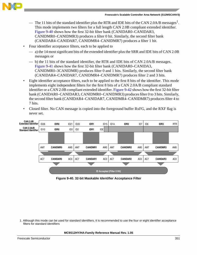
Freescale’s Scalable Controller Area Network (S12MSCANV3)
— The 11 bits of the standard identifier plus the RTR and IDE bits of the CAN 2.0A/B messages1.This mode implements two filters for a full length CAN 2.0B compliant extended identifier.Figure 9-40 shows how the first 32-bit filter bank (CANIDAR0–CANIDAR3,CANIDMR0–CANIDMR3) produces a filter 0 hit. Similarly, the second filter bank(CANIDAR4–CANIDAR7, CANIDMR4–CANIDMR7) produces a filter 1 hit.
• Four identifier acceptance filters, each to be applied to
— a) the 14 most significant bits of the extended identifier plus the SRR and IDE bits of CAN 2.0Bmessages or
— b) the 11 bits of the standard identifier, the RTR and IDE bits of CAN 2.0A/B messages.Figure 9-41 shows how the first 32-bit filter bank (CANIDAR0–CANIDA3,CANIDMR0–3CANIDMR) produces filter 0 and 1 hits. Similarly, the second filter bank(CANIDAR4–CANIDAR7, CANIDMR4–CANIDMR7) produces filter 2 and 3 hits.
• Eight identifier acceptance filters, each to be applied to the first 8 bits of the identifier. This modeimplements eight independent filters for the first 8 bits of a CAN 2.0A/B compliant standardidentifier or a CAN 2.0B compliant extended identifier. Figure 9-42 shows how the first 32-bit filterbank (CANIDAR0–CANIDAR3, CANIDMR0–CANIDMR3) produces filter 0 to 3 hits. Similarly,the second filter bank (CANIDAR4–CANIDAR7, CANIDMR4–CANIDMR7) produces filter 4 to7 hits.
• Closed filter. No CAN message is copied into the foreground buffer RxFG, and the RXF flag isnever set.
Figure 9-40. 32-bit Maskable Identifier Acceptance Filter
1. Although this mode can be used for standard identifiers, it is recommended to use the four or eight identifier acceptancefilters for standard identifiers
ID28 ID21IDR0
ID10 ID3IDR0
ID20 ID15IDR1
ID2 IDEIDR1
ID14 ID7IDR2
ID10 ID3IDR2
ID6 RTRIDR3
ID10 ID3IDR3
AC7 AC0CANIDAR0
AM7 AM0CANIDMR0
AC7 AC0CANIDAR1
AM7 AM0CANIDMR1
AC7 AC0CANIDAR2
AM7 AM0CANIDMR2
AC7 AC0CANIDAR3
AM7 AM0CANIDMR3
ID Accepted (Filter 0 Hit)
CAN 2.0BExtended Identifier
CAN 2.0A/BStandard Identifier
MC9S12HY/HA-Family Reference Manual Rev. 1.05
Freescale Semiconductor 351

Freescale’s Scalable Controller Area Network (S12MSCANV3)
Figure 9-41. 16-bit Maskable Identifier Acceptance Filters
ID28 ID21IDR0
ID10 ID3IDR0
ID20 ID15IDR1
ID2 IDEIDR1
ID14 ID7IDR2
ID10 ID3IDR2
ID6 RTRIDR3
ID10 ID3IDR3
AC7 AC0CANIDAR0
AM7 AM0CANIDMR0
AC7 AC0CANIDAR1
AM7 AM0CANIDMR1
ID Accepted (Filter 0 Hit)
AC7 AC0CANIDAR2
AM7 AM0CANIDMR2
AC7 AC0CANIDAR3
AM7 AM0CANIDMR3
ID Accepted (Filter 1 Hit)
CAN 2.0BExtended Identifier
CAN 2.0A/BStandard Identifier
MC9S12HY/HA-Family Reference Manual, Rev. 1.05
352 Freescale Semiconductor

Freescale’s Scalable Controller Area Network (S12MSCANV3)
Figure 9-42. 8-bit Maskable Identifier Acceptance Filters
CAN 2.0BExtended Identifier
CAN 2.0A/BStandard Identifier
AC7 AC0CIDAR3
AM7 AM0CIDMR3
ID Accepted (Filter 3 Hit)
AC7 AC0CIDAR2
AM7 AM0CIDMR2
ID Accepted (Filter 2 Hit)
AC7 AC0CIDAR1
AM7 AM0CIDMR1
ID Accepted (Filter 1 Hit)
ID28 ID21IDR0
ID10 ID3IDR0
ID20 ID15IDR1
ID2 IDEIDR1
ID14 ID7IDR2
ID10 ID3IDR2
ID6 RTRIDR3
ID10 ID3IDR3
AC7 AC0CIDAR0
AM7 AM0CIDMR0
ID Accepted (Filter 0 Hit)
MC9S12HY/HA-Family Reference Manual Rev. 1.05
Freescale Semiconductor 353

Freescale’s Scalable Controller Area Network (S12MSCANV3)
9.4.3.1 Protocol Violation Protection
The MSCAN protects the user from accidentally violating the CAN protocol through programming errors.The protection logic implements the following features:
• The receive and transmit error counters cannot be written or otherwise manipulated.
• All registers which control the configuration of the MSCAN cannot be modified while the MSCANis on-line. The MSCAN has to be in Initialization Mode. The corresponding INITRQ/INITAKhandshake bits in the CANCTL0/CANCTL1 registers (see Section 9.3.2.1, “MSCAN ControlRegister 0 (CANCTL0)”) serve as a lock to protect the following registers:
— MSCAN control 1 register (CANCTL1)
— MSCAN bus timing registers 0 and 1 (CANBTR0, CANBTR1)
— MSCAN identifier acceptance control register (CANIDAC)
— MSCAN identifier acceptance registers (CANIDAR0–CANIDAR7)
— MSCAN identifier mask registers (CANIDMR0–CANIDMR7)
• The TXCAN is immediately forced to a recessive state when the MSCAN goes into the powerdown mode or initialization mode (see Section 9.4.5.6, “MSCAN Power Down Mode,” andSection 9.4.4.5, “MSCAN Initialization Mode”).
• The MSCAN enable bit (CANE) is writable only once in normal system operation modes, whichprovides further protection against inadvertently disabling the MSCAN.
9.4.3.2 Clock System
Figure 9-43 shows the structure of the MSCAN clock generation circuitry.
Figure 9-43. MSCAN Clocking Scheme
The clock source bit (CLKSRC) in the CANCTL1 register (9.3.2.2/9-319) defines whether the internalCANCLK is connected to the output of a crystal oscillator (oscillator clock) or to the bus clock.
The clock source has to be chosen such that the tight oscillator tolerance requirements (up to 0.4%) of theCAN protocol are met. Additionally, for high CAN bus rates (1 Mbps), a 45% to 55% duty cycle of theclock is required.
If the bus clock is generated from a PLL, it is recommended to select the oscillator clock rather than thebus clock due to jitter considerations, especially at the faster CAN bus rates.
Bus Clock
Oscillator Clock
MSCAN
CANCLK
CLKSRC
CLKSRC
Prescaler(1 .. 64)
Time quanta clock (Tq)
MC9S12HY/HA-Family Reference Manual, Rev. 1.05
354 Freescale Semiconductor
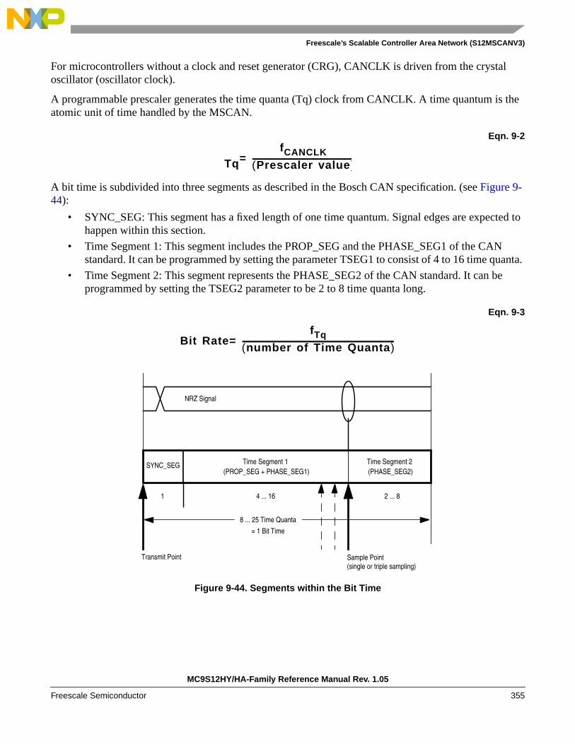
Freescale’s Scalable Controller Area Network (S12MSCANV3)
For microcontrollers without a clock and reset generator (CRG), CANCLK is driven from the crystaloscillator (oscillator clock).
A programmable prescaler generates the time quanta (Tq) clock from CANCLK. A time quantum is theatomic unit of time handled by the MSCAN.
Eqn. 9-2
A bit time is subdivided into three segments as described in the Bosch CAN specification. (see Figure 9-44):
• SYNC_SEG: This segment has a fixed length of one time quantum. Signal edges are expected tohappen within this section.
• Time Segment 1: This segment includes the PROP_SEG and the PHASE_SEG1 of the CANstandard. It can be programmed by setting the parameter TSEG1 to consist of 4 to 16 time quanta.
• Time Segment 2: This segment represents the PHASE_SEG2 of the CAN standard. It can beprogrammed by setting the TSEG2 parameter to be 2 to 8 time quanta long.
Eqn. 9-3
Figure 9-44. Segments within the Bit Time
TqfCANCLK
Prescaler value( )------------------------------------------------------=
Bit RatefTq
number of Time Quanta( )---------------------------------------------------------------------------------=
SYNC_SEG Time Segment 1 Time Segment 2
1 4 ... 16 2 ... 8
8 ... 25 Time Quanta
= 1 Bit Time
NRZ Signal
Sample Point(single or triple sampling)
(PROP_SEG + PHASE_SEG1) (PHASE_SEG2)
Transmit Point
MC9S12HY/HA-Family Reference Manual Rev. 1.05
Freescale Semiconductor 355

Freescale’s Scalable Controller Area Network (S12MSCANV3)
The synchronization jump width (see the Bosch CAN specification for details) can be programmed in arange of 1 to 4 time quanta by setting the SJW parameter.
The SYNC_SEG, TSEG1, TSEG2, and SJW parameters are set by programming the MSCAN bus timingregisters (CANBTR0, CANBTR1) (see Section 9.3.2.3, “MSCAN Bus Timing Register 0 (CANBTR0)”and Section 9.3.2.4, “MSCAN Bus Timing Register 1 (CANBTR1)”).
Table 9-37 gives an overview of the CAN compliant segment settings and the related parameter values.
NOTEIt is the user’s responsibility to ensure the bit time settings are in compliancewith the CAN standard.
9.4.4 Modes of Operation
9.4.4.1 Normal System Operating Modes
The MSCAN module behaves as described within this specification in all normal system operating modes.Write restrictions exist for some registers.
Table 9-36. Time Segment Syntax
Syntax Description
SYNC_SEGSystem expects transitions to occur on the CAN bus during thisperiod.
Transmit PointA node in transmit mode transfers a new value to the CAN bus atthis point.
Sample PointA node in receive mode samples the CAN bus at this point. If thethree samples per bit option is selected, then this point marks theposition of the third sample.
Table 9-37. CAN Standard Compliant Bit Time Segment Settings
Time Segment 1 TSEG1 Time Segment 2 TSEG2 Synchronization
Jump WidthSJW
5 .. 10 4 .. 9 2 1 1 .. 2 0 .. 1
4 .. 11 3 .. 10 3 2 1 .. 3 0 .. 2
5 .. 12 4 .. 11 4 3 1 .. 4 0 .. 3
6 .. 13 5 .. 12 5 4 1 .. 4 0 .. 3
7 .. 14 6 .. 13 6 5 1 .. 4 0 .. 3
8 .. 15 7 .. 14 7 6 1 .. 4 0 .. 3
9 .. 16 8 .. 15 8 7 1 .. 4 0 .. 3
MC9S12HY/HA-Family Reference Manual, Rev. 1.05
356 Freescale Semiconductor

Freescale’s Scalable Controller Area Network (S12MSCANV3)
9.4.4.2 Special System Operating Modes
The MSCAN module behaves as described within this specification in all special system operating modes.Write restrictions which exist on specific registers in normal modes are lifted for test purposes in specialmodes.
9.4.4.3 Emulation Modes
In all emulation modes, the MSCAN module behaves just like in normal system operating modes asdescribed within this specification.
9.4.4.4 Listen-Only Mode
In an optional CAN bus monitoring mode (listen-only), the CAN node is able to receive valid data framesand valid remote frames, but it sends only “recessive” bits on the CAN bus. In addition, it cannot start atransmission.
If the MAC sub-layer is required to send a “dominant” bit (ACK bit, overload flag, or active error flag), thebit is rerouted internally so that the MAC sub-layer monitors this “dominant” bit, although the CAN busmay remain in recessive state externally.
9.4.4.5 MSCAN Initialization Mode
The MSCAN enters initialization mode when it is enabled (CANE=1).
When entering initialization mode during operation, any on-going transmission or reception isimmediately aborted and synchronization to the CAN bus is lost, potentially causing CAN protocolviolations. To protect the CAN bus system from fatal consequences of violations, the MSCANimmediately drives TXCAN into a recessive state.
NOTEThe user is responsible for ensuring that the MSCAN is not active wheninitialization mode is entered. The recommended procedure is to bring theMSCAN into sleep mode (SLPRQ = 1 and SLPAK = 1) before setting theINITRQ bit in the CANCTL0 register. Otherwise, the abort of an on-goingmessage can cause an error condition and can impact other CAN busdevices.
In initialization mode, the MSCAN is stopped. However, interface registers remain accessible. This modeis used to reset the CANCTL0, CANRFLG, CANRIER, CANTFLG, CANTIER, CANTARQ,CANTAAK, and CANTBSEL registers to their default values. In addition, the MSCAN enables theconfiguration of the CANBTR0, CANBTR1 bit timing registers; CANIDAC; and the CANIDAR,CANIDMR message filters. See Section 9.3.2.1, “MSCAN Control Register 0 (CANCTL0),” for adetailed description of the initialization mode.
MC9S12HY/HA-Family Reference Manual Rev. 1.05
Freescale Semiconductor 357

Freescale’s Scalable Controller Area Network (S12MSCANV3)
Figure 9-45. Initialization Request/Acknowledge Cycle
Due to independent clock domains within the MSCAN, INITRQ must be synchronized to all domains byusing a special handshake mechanism. This handshake causes additional synchronization delay (seeSection Figure 9-45., “Initialization Request/Acknowledge Cycle”).
If there is no message transfer ongoing on the CAN bus, the minimum delay will be two additional busclocks and three additional CAN clocks. When all parts of the MSCAN are in initialization mode, theINITAK flag is set. The application software must use INITAK as a handshake indication for the request(INITRQ) to go into initialization mode.
NOTEThe CPU cannot clear INITRQ before initialization mode (INITRQ = 1 andINITAK = 1) is active.
9.4.5 Low-Power Options
If the MSCAN is disabled (CANE = 0), the MSCAN clocks are stopped for power saving.
If the MSCAN is enabled (CANE = 1), the MSCAN has two additional modes with reduced powerconsumption, compared to normal mode: sleep and power down mode. In sleep mode, power consumptionis reduced by stopping all clocks except those to access the registers from the CPU side. In power downmode, all clocks are stopped and no power is consumed.
Table 9-38 summarizes the combinations of MSCAN and CPU modes. A particular combination of modesis entered by the given settings on the CSWAI and SLPRQ/SLPAK bits.
SYNC
SYNC
Bus Clock Domain CAN Clock Domain
CPUInit Request
INITFlag
INITAKFlag
INITRQ
sync.INITAK
sync.INITRQ
INITAK
MC9S12HY/HA-Family Reference Manual, Rev. 1.05
358 Freescale Semiconductor

Freescale’s Scalable Controller Area Network (S12MSCANV3)
9.4.5.1 Operation in Run Mode
As shown in Table 9-38, only MSCAN sleep mode is available as low power option when the CPU is inrun mode.
9.4.5.2 Operation in Wait Mode
The WAI instruction puts the MCU in a low power consumption stand-by mode. If the CSWAI bit is set,additional power can be saved in power down mode because the CPU clocks are stopped. After leavingthis power down mode, the MSCAN restarts and enters normal mode again.
While the CPU is in wait mode, the MSCAN can be operated in normal mode and generate interrupts(registers can be accessed via background debug mode).
9.4.5.3 Operation in Stop Mode
The STOP instruction puts the MCU in a low power consumption stand-by mode. In stop mode, theMSCAN is set in power down mode regardless of the value of the SLPRQ/SLPAK and CSWAI bits(Table 9-38).
9.4.5.4 MSCAN Normal Mode
This is a non-power-saving mode. Enabling the MSCAN puts the module from disabled mode into normalmode. In this mode the module can either be in initialization mode or out of initialization mode. SeeSection 9.4.4.5, “MSCAN Initialization Mode”.
Table 9-38. CPU vs. MSCAN Operating Modes
CPU Mode
MSCAN Mode
Normal
Reduced Power Consumption
Sleep Power DownDisabled(CANE=0)
RUNCSWAI = X(1)
SLPRQ = 0SLPAK = 0
1. ‘X’ means don’t care.
CSWAI = XSLPRQ = 1SLPAK = 1
CSWAI = XSLPRQ = XSLPAK = X
WAITCSWAI = 0SLPRQ = 0SLPAK = 0
CSWAI = 0SLPRQ = 1SLPAK = 1
CSWAI = 1SLPRQ = XSLPAK = X
CSWAI = XSLPRQ = XSLPAK = X
STOPCSWAI = XSLPRQ = XSLPAK = X
CSWAI = XSLPRQ = XSLPAK = X
MC9S12HY/HA-Family Reference Manual Rev. 1.05
Freescale Semiconductor 359
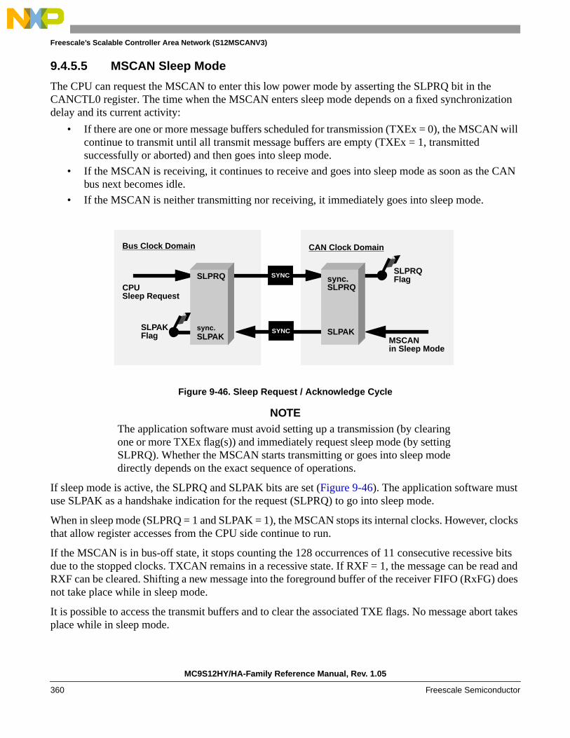
Freescale’s Scalable Controller Area Network (S12MSCANV3)
9.4.5.5 MSCAN Sleep Mode
The CPU can request the MSCAN to enter this low power mode by asserting the SLPRQ bit in theCANCTL0 register. The time when the MSCAN enters sleep mode depends on a fixed synchronizationdelay and its current activity:
• If there are one or more message buffers scheduled for transmission (TXEx = 0), the MSCAN willcontinue to transmit until all transmit message buffers are empty (TXEx = 1, transmittedsuccessfully or aborted) and then goes into sleep mode.
• If the MSCAN is receiving, it continues to receive and goes into sleep mode as soon as the CANbus next becomes idle.
• If the MSCAN is neither transmitting nor receiving, it immediately goes into sleep mode.
Figure 9-46. Sleep Request / Acknowledge Cycle
NOTEThe application software must avoid setting up a transmission (by clearingone or more TXEx flag(s)) and immediately request sleep mode (by settingSLPRQ). Whether the MSCAN starts transmitting or goes into sleep modedirectly depends on the exact sequence of operations.
If sleep mode is active, the SLPRQ and SLPAK bits are set (Figure 9-46). The application software mustuse SLPAK as a handshake indication for the request (SLPRQ) to go into sleep mode.
When in sleep mode (SLPRQ = 1 and SLPAK = 1), the MSCAN stops its internal clocks. However, clocksthat allow register accesses from the CPU side continue to run.
If the MSCAN is in bus-off state, it stops counting the 128 occurrences of 11 consecutive recessive bitsdue to the stopped clocks. TXCAN remains in a recessive state. If RXF = 1, the message can be read andRXF can be cleared. Shifting a new message into the foreground buffer of the receiver FIFO (RxFG) doesnot take place while in sleep mode.
It is possible to access the transmit buffers and to clear the associated TXE flags. No message abort takesplace while in sleep mode.
SYNC
SYNC
Bus Clock Domain CAN Clock Domain
MSCANin Sleep Mode
CPUSleep Request
SLPRQFlag
SLPAKFlag
SLPRQ
sync.SLPAK
sync.SLPRQ
SLPAK
MC9S12HY/HA-Family Reference Manual, Rev. 1.05
360 Freescale Semiconductor

Freescale’s Scalable Controller Area Network (S12MSCANV3)
If the WUPE bit in CANCTL0 is not asserted, the MSCAN will mask any activity it detects on CAN.RXCAN is therefore held internally in a recessive state. This locks the MSCAN in sleep mode. WUPEmust be set before entering sleep mode to take effect.
The MSCAN is able to leave sleep mode (wake up) only when:
• CAN bus activity occurs and WUPE = 1
or
• the CPU clears the SLPRQ bit
NOTEThe CPU cannot clear the SLPRQ bit before sleep mode (SLPRQ = 1 andSLPAK = 1) is active.
After wake-up, the MSCAN waits for 11 consecutive recessive bits to synchronize to the CAN bus. As aconsequence, if the MSCAN is woken-up by a CAN frame, this frame is not received.
The receive message buffers (RxFG and RxBG) contain messages if they were received before sleep modewas entered. All pending actions will be executed upon wake-up; copying of RxBG into RxFG, messageaborts and message transmissions. If the MSCAN remains in bus-off state after sleep mode was exited, itcontinues counting the 128 occurrences of 11 consecutive recessive bits.
9.4.5.6 MSCAN Power Down Mode
The MSCAN is in power down mode (Table 9-38) when
• CPU is in stop mode
or
• CPU is in wait mode and the CSWAI bit is set
When entering the power down mode, the MSCAN immediately stops all ongoing transmissions andreceptions, potentially causing CAN protocol violations. To protect the CAN bus system from fatalconsequences of violations to the above rule, the MSCAN immediately drives TXCAN into a recessivestate.
NOTEThe user is responsible for ensuring that the MSCAN is not active whenpower down mode is entered. The recommended procedure is to bring theMSCAN into Sleep mode before the STOP or WAI instruction (if CSWAIis set) is executed. Otherwise, the abort of an ongoing message can cause anerror condition and impact other CAN bus devices.
In power down mode, all clocks are stopped and no registers can be accessed. If the MSCAN was not insleep mode before power down mode became active, the module performs an internal recovery cycle afterpowering up. This causes some fixed delay before the module enters normal mode again.
MC9S12HY/HA-Family Reference Manual Rev. 1.05
Freescale Semiconductor 361

Freescale’s Scalable Controller Area Network (S12MSCANV3)
9.4.5.7 Disabled Mode
The MSCAN is in disabled mode out of reset (CANE=0). All module clocks are stopped for power saving,however the register map can still be accessed as specified.
9.4.5.8 Programmable Wake-Up Function
The MSCAN can be programmed to wake up from sleep or power down mode as soon as CAN bus activityis detected (see control bit WUPE in MSCAN Control Register 0 (CANCTL0). The sensitivity to existingCAN bus action can be modified by applying a low-pass filter function to the RXCAN input line (seecontrol bit WUPM in Section 9.3.2.2, “MSCAN Control Register 1 (CANCTL1)”).
This feature can be used to protect the MSCAN from wake-up due to short glitches on the CAN bus lines.Such glitches can result from—for example—electromagnetic interference within noisy environments.
9.4.6 Reset Initialization
The reset state of each individual bit is listed in Section 9.3.2, “Register Descriptions,” which details allthe registers and their bit-fields.
9.4.7 Interrupts
This section describes all interrupts originated by the MSCAN. It documents the enable bits and generatedflags. Each interrupt is listed and described separately.
9.4.7.1 Description of Interrupt Operation
The MSCAN supports four interrupt vectors (see Table 9-39), any of which can be individually masked(for details see Section 9.3.2.6, “MSCAN Receiver Interrupt Enable Register (CANRIER)” toSection 9.3.2.8, “MSCAN Transmitter Interrupt Enable Register (CANTIER)”).
NOTEThe dedicated interrupt vector addresses are defined in the Resets andInterrupts chapter.
9.4.7.2 Transmit Interrupt
At least one of the three transmit buffers is empty (not scheduled) and can be loaded to schedule a messagefor transmission. The TXEx flag of the empty message buffer is set.
Table 9-39. Interrupt Vectors
Interrupt Source CCR Mask Local Enable
Wake-Up Interrupt (WUPIF) I bit CANRIER (WUPIE)
Error Interrupts Interrupt (CSCIF, OVRIF) I bit CANRIER (CSCIE, OVRIE)
Receive Interrupt (RXF) I bit CANRIER (RXFIE)
Transmit Interrupts (TXE[2:0]) I bit CANTIER (TXEIE[2:0])
MC9S12HY/HA-Family Reference Manual, Rev. 1.05
362 Freescale Semiconductor

Freescale’s Scalable Controller Area Network (S12MSCANV3)
9.4.7.3 Receive Interrupt
A message is successfully received and shifted into the foreground buffer (RxFG) of the receiver FIFO.This interrupt is generated immediately after receiving the EOF symbol. The RXF flag is set. If there aremultiple messages in the receiver FIFO, the RXF flag is set as soon as the next message is shifted to theforeground buffer.
9.4.7.4 Wake-Up Interrupt
A wake-up interrupt is generated if activity on the CAN bus occurs during MSCAN sleep or power-downmode.
NOTEThis interrupt can only occur if the MSCAN was in sleep mode (SLPRQ =1 and SLPAK = 1) before entering power down mode, the wake-up optionis enabled (WUPE = 1), and the wake-up interrupt is enabled (WUPIE = 1).
9.4.7.5 Error Interrupt
An error interrupt is generated if an overrun of the receiver FIFO, error, warning, or bus-off conditionoccurrs. MSCAN Receiver Flag Register (CANRFLG) indicates one of the following conditions:
• Overrun — An overrun condition of the receiver FIFO as described in Section 9.4.2.3, “ReceiveStructures,” occurred.
• CAN Status Change — The actual value of the transmit and receive error counters control theCAN bus state of the MSCAN. As soon as the error counters skip into a critical range (Tx/Rx-warning, Tx/Rx-error, bus-off) the MSCAN flags an error condition. The status change, whichcaused the error condition, is indicated by the TSTAT and RSTAT flags (see Section 9.3.2.5,“MSCAN Receiver Flag Register (CANRFLG)” and Section 9.3.2.6, “MSCAN Receiver InterruptEnable Register (CANRIER)”).
9.4.7.6 Interrupt Acknowledge
Interrupts are directly associated with one or more status flags in either the MSCAN Receiver Flag Register(CANRFLG) or the MSCAN Transmitter Flag Register (CANTFLG). Interrupts are pending as long asone of the corresponding flags is set. The flags in CANRFLG and CANTFLG must be reset within theinterrupt handler to handshake the interrupt. The flags are reset by writing a 1 to the corresponding bitposition. A flag cannot be cleared if the respective condition prevails.
NOTEIt must be guaranteed that the CPU clears only the bit causing the currentinterrupt. For this reason, bit manipulation instructions (BSET) must not beused to clear interrupt flags. These instructions may cause accidentalclearing of interrupt flags which are set after entering the current interruptservice routine.
MC9S12HY/HA-Family Reference Manual Rev. 1.05
Freescale Semiconductor 363

Freescale’s Scalable Controller Area Network (S12MSCANV3)
9.5 Initialization/Application Information
9.5.1 MSCAN initialization
The procedure to initially start up the MSCAN module out of reset is as follows:
1. Assert CANE
2. Write to the configuration registers in initialization mode
3. Clear INITRQ to leave initialization mode
If the configuration of registers which are only writable in initialization mode shall be changed:
1. Bring the module into sleep mode by setting SLPRQ and awaiting SLPAK to assert after the CANbus becomes idle.
2. Enter initialization mode: assert INITRQ and await INITAK
3. Write to the configuration registers in initialization mode
4. Clear INITRQ to leave initialization mode and continue
9.5.2 Bus-Off Recovery
The bus-off recovery is user configurable. The bus-off state can either be left automatically or on userrequest.
For reasons of backwards compatibility, the MSCAN defaults to automatic recovery after reset. In thiscase, the MSCAN will become error active again after counting 128 occurrences of 11 consecutiverecessive bits on the CAN bus (see the Bosch CAN specification for details).
If the MSCAN is configured for user request (BORM set in MSCAN Control Register 1 (CANCTL1)), therecovery from bus-off starts after both independent events have become true:
• 128 occurrences of 11 consecutive recessive bits on the CAN bus have been monitored
• BOHOLD in MSCAN Miscellaneous Register (CANMISC) has been cleared by the user
These two events may occur in any order.
MC9S12HY/HA-Family Reference Manual, Rev. 1.05
364 Freescale Semiconductor

Chapter 10Inter-Integrated Circuit (IICV3) Block Description
Table 10-1. Revision History
10.1 IntroductionThe inter-IC bus (IIC) is a two-wire, bidirectional serial bus that provides a simple, efficient method of dataexchange between devices. Being a two-wire device, the IIC bus minimizes the need for large numbers ofconnections between devices, and eliminates the need for an address decoder.
This bus is suitable for applications requiring occasional communications over a short distance between anumber of devices. It also provides flexibility, allowing additional devices to be connected to the bus forfurther expansion and system development.
The interface is designed to operate up to 100 kbps with maximum bus loading and timing. The device iscapable of operating at higher baud rates, up to a maximum of clock/20, with reduced bus loading. Themaximum communication length and the number of devices that can be connected are limited by amaximum bus capacitance of 400 pF.
10.1.1 Features
The IIC module has the following key features:
• Compatible with I2C bus standard
• Multi-master operation
• Software programmable for one of 256 different serial clock frequencies
• Software selectable acknowledge bit
• Interrupt driven byte-by-byte data transfer
• Arbitration lost interrupt with automatic mode switching from master to slave
• Calling address identification interrupt
• Start and stop signal generation/detection
• Repeated start signal generation
RevisionNumber
Revision DateSectionsAffected
Description of Changes
V01.03 28 Jul 2006 10.7.1.7/10-389 - Update flow-chart of interrupt routine for 10-bit address
V01.04 17 Nov 2006 10.3.1.2/10-369 - Revise Table1-5
Rev. 1.05 14 Aug 2007 10.3.1.1/10-369 - Backward compatible for IBAD bit name
MC9S12HY/HA-Family Reference Manual, Rev. 1.05
Freescale Semiconductor 365

Inter-Integrated Circuit (IICV3) Block Description
• Acknowledge bit generation/detection
• Bus busy detection
• General Call Address detection
• Compliant to ten-bit address
MC9S12HY/HA-Family Reference Manual, Rev. 1.05
366 Freescale Semiconductor

Inter-Integrated Circuit (IICV3) Block Description
10.1.2 Modes of Operation
The IIC functions the same in normal, special, and emulation modes. It has two low power modes: waitand stop modes.
10.1.3 Block Diagram
The block diagram of the IIC module is shown in Figure 10-1.
Figure 10-1. IIC Block Diagram
In/OutDataShiftRegister
AddressCompare
SDA
Interrupt
ClockControl
StartStopArbitrationControl
SCL
bus_clock
IIC
Registers
MC9S12HY/HA-Family Reference Manual, Rev. 1.05
Freescale Semiconductor 367

Inter-Integrated Circuit (IICV3) Block Description
10.2 External Signal DescriptionThe IICV3 module has two external pins.
10.2.1 IIC_SCL — Serial Clock Line Pin
This is the bidirectional serial clock line (SCL) of the module, compatible to the IIC bus specification.
10.2.2 IIC_SDA — Serial Data Line Pin
This is the bidirectional serial data line (SDA) of the module, compatible to the IIC bus specification.
10.3 Memory Map and Register DefinitionThis section provides a detailed description of all memory and registers for the IIC module.
10.3.1 Register Descriptions
This section consists of register descriptions in address order. Each description includes a standard registerdiagram with an associated figure number. Details of register bit and field function follow the registerdiagrams, in bit order.
RegisterName
Bit 7 6 5 4 3 2 1 Bit 0
0x0000IBAD
RADR7 ADR6 ADR5 ADR4 ADR3 ADR2 ADR1
0
W
0x0001IBFD
RIBC7 IBC6 IBC5 IBC4 IBC3 IBC2 IBC1 IBC0
W
0x0002IBCR
RIBEN IBIE MS/SL Tx/Rx TXAK
0 0IBSWAI
W RSTA
0x0003IBSR
R TCF IAAS IBBIBAL
0 SRWIBIF
RXAK
W
0x0004IBDR
RD7 D6 D5 D4 D3 D2 D1 D0
W
0x0005IBCR2
RGCEN ADTYPE
0 0 0ADR10 ADR9 ADR8
W
= Unimplemented or Reserved
Figure 10-2. IIC Register Summary
MC9S12HY/HA-Family Reference Manual, Rev. 1.05
368 Freescale Semiconductor
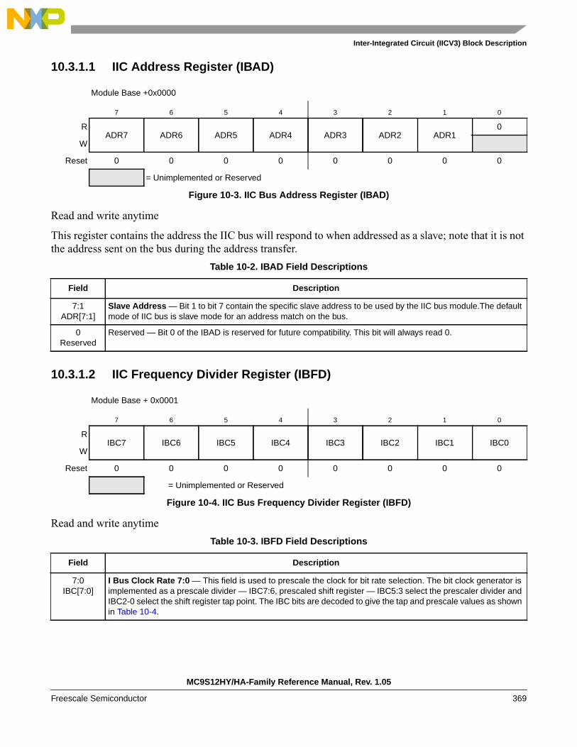
Inter-Integrated Circuit (IICV3) Block Description
10.3.1.1 IIC Address Register (IBAD)
Read and write anytime
This register contains the address the IIC bus will respond to when addressed as a slave; note that it is notthe address sent on the bus during the address transfer.
10.3.1.2 IIC Frequency Divider Register (IBFD)
Read and write anytime
Module Base +0x0000
7 6 5 4 3 2 1 0
RADR7 ADR6 ADR5 ADR4 ADR3 ADR2 ADR1
0
W
Reset 0 0 0 0 0 0 0 0
= Unimplemented or Reserved
Figure 10-3. IIC Bus Address Register (IBAD)
Table 10-2. IBAD Field Descriptions
Field Description
7:1ADR[7:1]
Slave Address — Bit 1 to bit 7 contain the specific slave address to be used by the IIC bus module.The defaultmode of IIC bus is slave mode for an address match on the bus.
0Reserved
Reserved — Bit 0 of the IBAD is reserved for future compatibility. This bit will always read 0.
Module Base + 0x0001
7 6 5 4 3 2 1 0
RIBC7 IBC6 IBC5 IBC4 IBC3 IBC2 IBC1 IBC0
W
Reset 0 0 0 0 0 0 0 0
= Unimplemented or Reserved
Figure 10-4. IIC Bus Frequency Divider Register (IBFD)
Table 10-3. IBFD Field Descriptions
Field Description
7:0IBC[7:0]
I Bus Clock Rate 7:0 — This field is used to prescale the clock for bit rate selection. The bit clock generator isimplemented as a prescale divider — IBC7:6, prescaled shift register — IBC5:3 select the prescaler divider andIBC2-0 select the shift register tap point. The IBC bits are decoded to give the tap and prescale values as shownin Table 10-4.
MC9S12HY/HA-Family Reference Manual, Rev. 1.05
Freescale Semiconductor 369
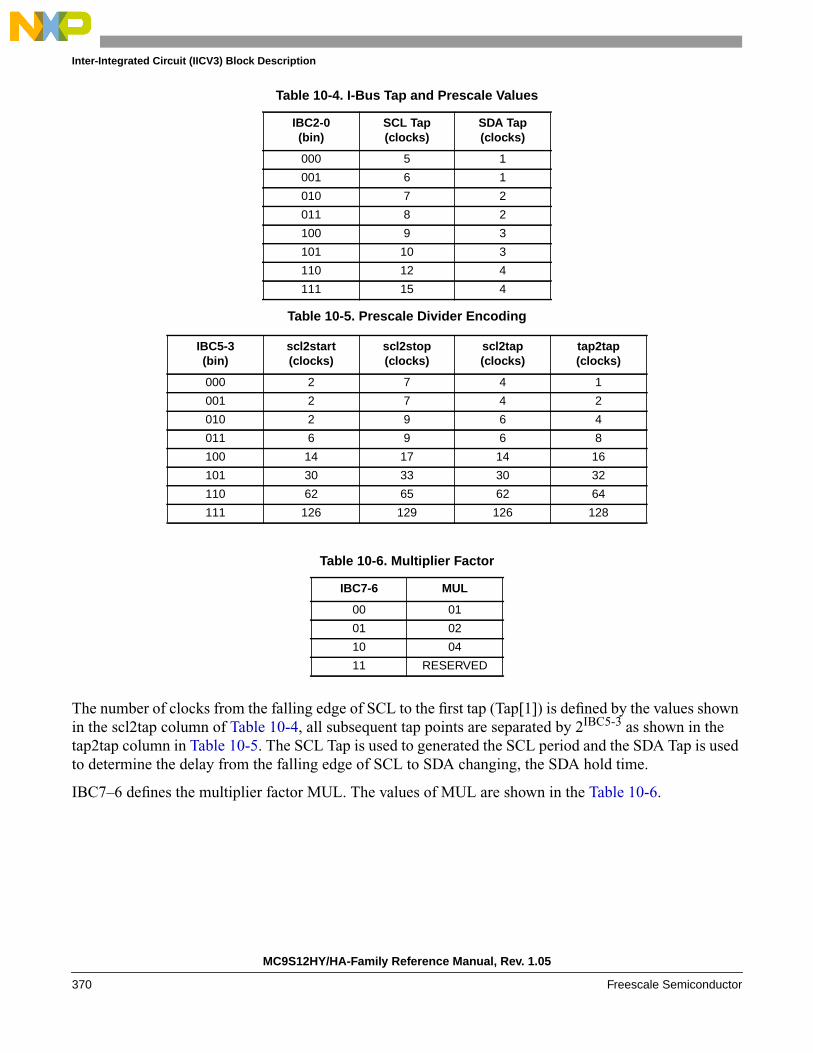
Inter-Integrated Circuit (IICV3) Block Description
Table 10-5. Prescale Divider Encoding
The number of clocks from the falling edge of SCL to the first tap (Tap[1]) is defined by the values shownin the scl2tap column of Table 10-4, all subsequent tap points are separated by 2IBC5-3 as shown in thetap2tap column in Table 10-5. The SCL Tap is used to generated the SCL period and the SDA Tap is usedto determine the delay from the falling edge of SCL to SDA changing, the SDA hold time.
IBC7–6 defines the multiplier factor MUL. The values of MUL are shown in the Table 10-6.
Table 10-4. I-Bus Tap and Prescale Values
IBC2-0(bin)
SCL Tap(clocks)
SDA Tap(clocks)
000 5 1
001 6 1
010 7 2
011 8 2
100 9 3
101 10 3
110 12 4
111 15 4
IBC5-3(bin)
scl2start(clocks)
scl2stop(clocks)
scl2tap(clocks)
tap2tap(clocks)
000 2 7 4 1
001 2 7 4 2
010 2 9 6 4
011 6 9 6 8
100 14 17 14 16
101 30 33 30 32
110 62 65 62 64
111 126 129 126 128
Table 10-6. Multiplier Factor
IBC7-6 MUL
00 01
01 02
10 04
11 RESERVED
MC9S12HY/HA-Family Reference Manual, Rev. 1.05
370 Freescale Semiconductor

Inter-Integrated Circuit (IICV3) Block Description
Figure 10-5. SCL Divider and SDA Hold
The equation used to generate the divider values from the IBFD bits is:
SCL Divider = MUL x 2 x (scl2tap + [(SCL_Tap -1) x tap2tap] + 2)
The SDA hold delay is equal to the CPU clock period multiplied by the SDA Hold value shown inTable 10-7. The equation used to generate the SDA Hold value from the IBFD bits is:
SDA Hold = MUL x scl2tap + [(SDA_Tap - 1) x tap2tap] + 3
The equation for SCL Hold values to generate the start and stop conditions from the IBFD bits is:
SCL Hold(start) = MUL x [scl2start + (SCL_Tap - 1) x tap2tap]SCL Hold(stop) = MUL x [scl2stop + (SCL_Tap - 1) x tap2tap]
Table 10-7. IIC Divider and Hold Values (Sheet 1 of 6)
IBC[7:0](hex)
SCL Divider(clocks)
SDA Hold(clocks)
SCL Hold(start)
SCL Hold(stop)
MUL=1
SCL Divider
SDA Hold
SCL
SDA
SDA
SCL
START condition STOP condition
SCL Hold(start) SCL Hold(stop)
MC9S12HY/HA-Family Reference Manual, Rev. 1.05
Freescale Semiconductor 371
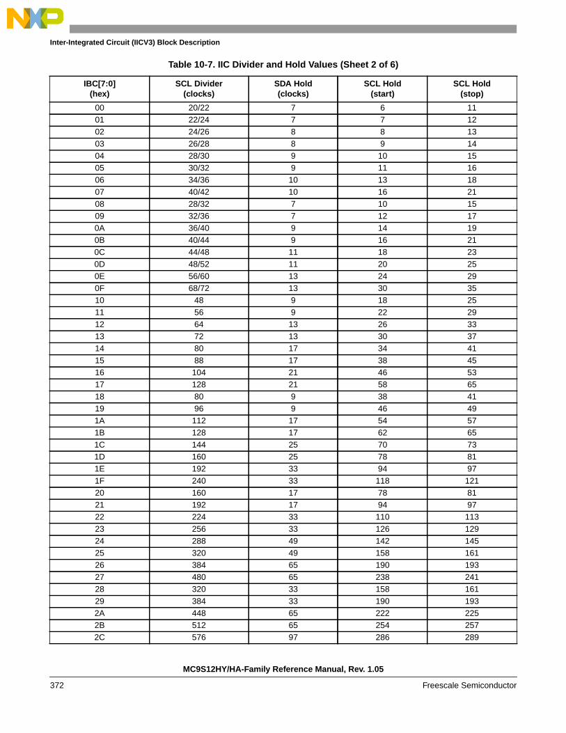
Inter-Integrated Circuit (IICV3) Block Description
00 20/22 7 6 1101 22/24 7 7 1202 24/26 8 8 1303 26/28 8 9 1404 28/30 9 10 1505 30/32 9 11 1606 34/36 10 13 1807 40/42 10 16 2108 28/32 7 10 1509 32/36 7 12 170A 36/40 9 14 190B 40/44 9 16 210C 44/48 11 18 230D 48/52 11 20 250E 56/60 13 24 290F 68/72 13 30 3510 48 9 18 2511 56 9 22 2912 64 13 26 3313 72 13 30 3714 80 17 34 4115 88 17 38 4516 104 21 46 5317 128 21 58 6518 80 9 38 4119 96 9 46 491A 112 17 54 571B 128 17 62 651C 144 25 70 731D 160 25 78 811E 192 33 94 971F 240 33 118 12120 160 17 78 8121 192 17 94 9722 224 33 110 11323 256 33 126 12924 288 49 142 14525 320 49 158 16126 384 65 190 19327 480 65 238 24128 320 33 158 16129 384 33 190 1932A 448 65 222 2252B 512 65 254 2572C 576 97 286 289
Table 10-7. IIC Divider and Hold Values (Sheet 2 of 6)
IBC[7:0](hex)
SCL Divider(clocks)
SDA Hold(clocks)
SCL Hold(start)
SCL Hold(stop)
MC9S12HY/HA-Family Reference Manual, Rev. 1.05
372 Freescale Semiconductor

Inter-Integrated Circuit (IICV3) Block Description
2D 640 97 318 3212E 768 129 382 3852F 960 129 478 48130 640 65 318 32131 768 65 382 38532 896 129 446 44933 1024 129 510 51334 1152 193 574 57735 1280 193 638 64136 1536 257 766 76937 1920 257 958 96138 1280 129 638 64139 1536 129 766 7693A 1792 257 894 8973B 2048 257 1022 10253C 2304 385 1150 11533D 2560 385 1278 12813E 3072 513 1534 15373F 3840 513 1918 1921
MUL=240 40 14 12 2241 44 14 14 2442 48 16 16 2643 52 16 18 2844 56 18 20 3045 60 18 22 3246 68 20 26 3647 80 20 32 4248 56 14 20 3049 64 14 24 344A 72 18 28 384B 80 18 32 424C 88 22 36 464D 96 22 40 504E 112 26 48 584F 136 26 60 7050 96 18 36 5051 112 18 44 5852 128 26 52 6653 144 26 60 7454 160 34 68 8255 176 34 76 9056 208 42 92 10657 256 42 116 13058 160 18 76 82
Table 10-7. IIC Divider and Hold Values (Sheet 3 of 6)
IBC[7:0](hex)
SCL Divider(clocks)
SDA Hold(clocks)
SCL Hold(start)
SCL Hold(stop)
MC9S12HY/HA-Family Reference Manual, Rev. 1.05
Freescale Semiconductor 373

Inter-Integrated Circuit (IICV3) Block Description
59 192 18 92 985A 224 34 108 1145B 256 34 124 1305C 288 50 140 1465D 320 50 156 1625E 384 66 188 1945F 480 66 236 24260 320 34 156 16261 384 34 188 19462 448 66 220 22663 512 66 252 25864 576 98 284 29065 640 98 316 32266 768 130 380 38667 960 130 476 48268 640 66 316 32269 768 66 380 3866A 896 130 444 4506B 1024 130 508 5146C 1152 194 572 5786D 1280 194 636 6426E 1536 258 764 7706F 1920 258 956 96270 1280 130 636 64271 1536 130 764 77072 1792 258 892 89873 2048 258 1020 102674 2304 386 1148 115475 2560 386 1276 128276 3072 514 1532 153877 3840 514 1916 192278 2560 258 1276 128279 3072 258 1532 15387A 3584 514 1788 17947B 4096 514 2044 20507C 4608 770 2300 23067D 5120 770 2556 25627E 6144 1026 3068 30747F 7680 1026 3836 3842
MUL=480 72 28 24 4481 80 28 28 4882 88 32 32 5283 96 32 36 5684 104 36 40 60
Table 10-7. IIC Divider and Hold Values (Sheet 4 of 6)
IBC[7:0](hex)
SCL Divider(clocks)
SDA Hold(clocks)
SCL Hold(start)
SCL Hold(stop)
MC9S12HY/HA-Family Reference Manual, Rev. 1.05
374 Freescale Semiconductor

Inter-Integrated Circuit (IICV3) Block Description
85 112 36 44 6486 128 40 52 7287 152 40 64 8488 112 28 40 6089 128 28 48 688A 144 36 56 768B 160 36 64 848C 176 44 72 928D 192 44 80 1008E 224 52 96 1168F 272 52 120 14090 192 36 72 10091 224 36 88 11692 256 52 104 13293 288 52 120 14894 320 68 136 16495 352 68 152 18096 416 84 184 21297 512 84 232 26098 320 36 152 16499 384 36 184 1969A 448 68 216 2289B 512 68 248 2609C 576 100 280 2929D 640 100 312 3249E 768 132 376 3889F 960 132 472 484A0 640 68 312 324A1 768 68 376 388A2 896 132 440 452A3 1024 132 504 516A4 1152 196 568 580A5 1280 196 632 644A6 1536 260 760 772A7 1920 260 952 964A8 1280 132 632 644A9 1536 132 760 772AA 1792 260 888 900AB 2048 260 1016 1028AC 2304 388 1144 1156AD 2560 388 1272 1284AE 3072 516 1528 1540AF 3840 516 1912 1924B0 2560 260 1272 1284B1 3072 260 1528 1540
Table 10-7. IIC Divider and Hold Values (Sheet 5 of 6)
IBC[7:0](hex)
SCL Divider(clocks)
SDA Hold(clocks)
SCL Hold(start)
SCL Hold(stop)
MC9S12HY/HA-Family Reference Manual, Rev. 1.05
Freescale Semiconductor 375

Inter-Integrated Circuit (IICV3) Block Description
Note:Since the bus frequency is speeding up,the SCL Divider could be expanded by it.Therefore,in thetable,when IBC[7:0] is from $00 to $0F,the SCL Divider is revised by the format value1/value2.Value1 isthe divider under the low frequency.Value2 is the divider under the high frequency.How to select thedivider depends on the bus frequency.When IBC[7:0] is from $10 to $BF,the divider is not changed.
10.3.1.3 IIC Control Register (IBCR)
Read and write anytime
B2 3584 516 1784 1796B3 4096 516 2040 2052B4 4608 772 2296 2308B5 5120 772 2552 2564B6 6144 1028 3064 3076B7 7680 1028 3832 3844B8 5120 516 2552 2564B9 6144 516 3064 3076BA 7168 1028 3576 3588BB 8192 1028 4088 4100BC 9216 1540 4600 4612BD 10240 1540 5112 5124BE 12288 2052 6136 6148BF 15360 2052 7672 7684
Module Base + 0x0002
7 6 5 4 3 2 1 0
RIBEN IBIE MS/SL Tx/Rx TXAK
0 0IBSWAI
W RSTA
Reset 0 0 0 0 0 0 0 0
= Unimplemented or Reserved
Figure 10-6. IIC Bus Control Register (IBCR)
Table 10-7. IIC Divider and Hold Values (Sheet 6 of 6)
IBC[7:0](hex)
SCL Divider(clocks)
SDA Hold(clocks)
SCL Hold(start)
SCL Hold(stop)
MC9S12HY/HA-Family Reference Manual, Rev. 1.05
376 Freescale Semiconductor

Inter-Integrated Circuit (IICV3) Block Description
Wait mode is entered via execution of a CPU WAI instruction. In the event that the IBSWAI bit is set, allclocks internal to the IIC will be stopped and any transmission currently in progress will halt.If the CPUwere woken up by a source other than the IIC module, then clocks would restart and the IIC would resume
Table 10-8. IBCR Field Descriptions
Field Description
7IBEN
I-Bus Enable — This bit controls the software reset of the entire IIC bus module.0 The module is reset and disabled. This is the power-on reset situation. When low the interface is held in reset
but registers can be accessed1 The IIC bus module is enabled.This bit must be set before any other IBCR bits have any effectIf the IIC bus module is enabled in the middle of a byte transfer the interface behaves as follows: slave modeignores the current transfer on the bus and starts operating whenever a subsequent start condition is detected.Master mode will not be aware that the bus is busy, hence if a start cycle is initiated then the current bus cyclemay become corrupt. This would ultimately result in either the current bus master or the IIC bus module losingarbitration, after which bus operation would return to normal.
6IBIE
I-Bus Interrupt Enable0 Interrupts from the IIC bus module are disabled. Note that this does not clear any currently pending interrupt
condition1 Interrupts from the IIC bus module are enabled. An IIC bus interrupt occurs provided the IBIF bit in the status
register is also set.
5MS/SL
Master/Slave Mode Select Bit — Upon reset, this bit is cleared. When this bit is changed from 0 to 1, a STARTsignal is generated on the bus, and the master mode is selected. When this bit is changed from 1 to 0, a STOPsignal is generated and the operation mode changes from master to slave.A STOP signal should only begenerated if the IBIF flag is set. MS/SL is cleared without generating a STOP signal when the master losesarbitration.0 Slave Mode1 Master Mode
4Tx/Rx
Transmit/Receive Mode Select Bit — This bit selects the direction of master and slave transfers. Whenaddressed as a slave this bit should be set by software according to the SRW bit in the status register. In mastermode this bit should be set according to the type of transfer required. Therefore, for address cycles, this bit willalways be high.0 Receive1 Transmit
3TXAK
Transmit Acknowledge Enable — This bit specifies the value driven onto SDA during data acknowledge cyclesfor both master and slave receivers. The IIC module will always acknowledge address matches, provided it isenabled, regardless of the value of TXAK. Note that values written to this bit are only used when the IIC bus is areceiver, not a transmitter.0 An acknowledge signal will be sent out to the bus at the 9th clock bit after receiving one byte data1 No acknowledge signal response is sent (i.e., acknowledge bit = 1)
2RSTA
Repeat Start — Writing a 1 to this bit will generate a repeated START condition on the bus, provided it is thecurrent bus master. This bit will always be read as a low. Attempting a repeated start at the wrong time, if the busis owned by another master, will result in loss of arbitration.1 Generate repeat start cycle
1RESERVED
Reserved — Bit 1 of the IBCR is reserved for future compatibility. This bit will always read 0.
0IBSWAI
I Bus Interface Stop in Wait Mode0 IIC bus module clock operates normally1 Halt IIC bus module clock generation in wait mode
MC9S12HY/HA-Family Reference Manual, Rev. 1.05
Freescale Semiconductor 377

Inter-Integrated Circuit (IICV3) Block Description
from where was during the previous transmission. It is not possible for the IIC to wake up the CPU whenits internal clocks are stopped.
If it were the case that the IBSWAI bit was cleared when the WAI instruction was executed, the IIC internalclocks and interface would remain alive, continuing the operation which was currently underway. It is alsopossible to configure the IIC such that it will wake up the CPU via an interrupt at the conclusion of thecurrent operation. See the discussion on the IBIF and IBIE bits in the IBSR and IBCR, respectively.
10.3.1.4 IIC Status Register (IBSR)
This status register is read-only with exception of bit 1 (IBIF) and bit 4 (IBAL), which are softwareclearable.
Module Base + 0x0003
7 6 5 4 3 2 1 0
R TCF IAAS IBBIBAL
0 SRWIBIF
RXAK
W
Reset 1 0 0 0 0 0 0 0
= Unimplemented or Reserved
Figure 10-7. IIC Bus Status Register (IBSR)
Table 10-9. IBSR Field Descriptions
Field Description
7TCF
Data Transferring Bit — While one byte of data is being transferred, this bit is cleared. It is set by the fallingedge of the 9th clock of a byte transfer. Note that this bit is only valid during or immediately following a transferto the IIC module or from the IIC module.0 Transfer in progress1 Transfer complete
6IAAS
Addressed as a Slave Bit — When its own specific address (I-bus address register) is matched with the callingaddress or it receives the general call address with GCEN== 1,this bit is set.The CPU is interrupted provided theIBIE is set.Then the CPU needs to check the SRW bit and set its Tx/Rx mode accordingly.Writing to the I-buscontrol register clears this bit.0 Not addressed1 Addressed as a slave
5IBB
Bus Busy Bit0 This bit indicates the status of the bus. When a START signal is detected, the IBB is set. If a STOP signal is
detected, IBB is cleared and the bus enters idle state.1 Bus is busy
4IBAL
Arbitration Lost — The arbitration lost bit (IBAL) is set by hardware when the arbitration procedure is lost.Arbitration is lost in the following circumstances:
1. SDA sampled low when the master drives a high during an address or data transmit cycle.2. SDA sampled low when the master drives a high during the acknowledge bit of a data receive cycle.3. A start cycle is attempted when the bus is busy.4. A repeated start cycle is requested in slave mode.5. A stop condition is detected when the master did not request it.
This bit must be cleared by software, by writing a one to it. A write of 0 has no effect on this bit.
MC9S12HY/HA-Family Reference Manual, Rev. 1.05
378 Freescale Semiconductor

Inter-Integrated Circuit (IICV3) Block Description
10.3.1.5 IIC Data I/O Register (IBDR)
In master transmit mode, when data is written to the IBDR a data transfer is initiated. The most significantbit is sent first. In master receive mode, reading this register initiates next byte data receiving. In slavemode, the same functions are available after an address match has occurred.Note that the Tx/Rx bit in theIBCR must correctly reflect the desired direction of transfer in master and slave modes for the transmissionto begin. For instance, if the IIC is configured for master transmit but a master receive is desired, thenreading the IBDR will not initiate the receive.
Reading the IBDR will return the last byte received while the IIC is configured in either master receive orslave receive modes. The IBDR does not reflect every byte that is transmitted on the IIC bus, nor cansoftware verify that a byte has been written to the IBDR correctly by reading it back.
In master transmit mode, the first byte of data written to IBDR following assertion of MS/SL is used forthe address transfer and should com.prise of the calling address (in position D7:D1) concatenated with therequired R/W bit (in position D0).
3RESERVED
Reserved — Bit 3 of IBSR is reserved for future use. A read operation on this bit will return 0.
2SRW
Slave Read/Write — When IAAS is set this bit indicates the value of the R/W command bit of the calling addresssent from the masterThis bit is only valid when the I-bus is in slave mode, a complete address transfer has occurred with an addressmatch and no other transfers have been initiated.Checking this bit, the CPU can select slave transmit/receive mode according to the command of the master.0 Slave receive, master writing to slave1 Slave transmit, master reading from slave
1IBIF
I-Bus Interrupt — The IBIF bit is set when one of the following conditions occurs:— Arbitration lost (IBAL bit set)— Data transfer complete (TCF bit set)— Addressed as slave (IAAS bit set)
It will cause a processor interrupt request if the IBIE bit is set. This bit must be cleared by software, writing a oneto it. A write of 0 has no effect on this bit.
0RXAK
Received Acknowledge — The value of SDA during the acknowledge bit of a bus cycle. If the receivedacknowledge bit (RXAK) is low, it indicates an acknowledge signal has been received after the completion of 8bits data transmission on the bus. If RXAK is high, it means no acknowledge signal is detected at the 9th clock.0 Acknowledge received1 No acknowledge received
Module Base + 0x0004
7 6 5 4 3 2 1 0
RD7 D6 D5 D4 D3 D2 D1 D0
W
Reset 0 0 0 0 0 0 0 0
Figure 10-8. IIC Bus Data I/O Register (IBDR)
Table 10-9. IBSR Field Descriptions (continued)
Field Description
MC9S12HY/HA-Family Reference Manual, Rev. 1.05
Freescale Semiconductor 379

Inter-Integrated Circuit (IICV3) Block Description
10.3.1.6 IIC Control Register 2(IBCR2)
Figure 10-9. IIC Bus Control Register 2(IBCR2)
This register contains the variables used in general call and in ten-bit address.
Read and write anytime
10.4 Functional DescriptionThis section provides a complete functional description of the IICV3.
10.4.1 I-Bus Protocol
The IIC bus system uses a serial data line (SDA) and a serial clock line (SCL) for data transfer. All devicesconnected to it must have open drain or open collector outputs. Logic AND function is exercised on bothlines with external pull-up resistors. The value of these resistors is system dependent.
Normally, a standard communication is composed of four parts: START signal, slave address transmission,data transfer and STOP signal. They are described briefly in the following sections and illustrated inFigure 10-10.
Module Base + 0x0005
7 6 5 4 3 2 1 0
RGCEN ADTYPE
0 0 0ADR10 ADR9 ADR8
W
Reset 0 0 0 0 0 0 0 0
Table 10-10. IBCR2 Field Descriptions
Field Description
7GCEN
General Call Enable.0 General call is disabled. The module dont receive any general call data and address.1 enable general call. It indicates that the module can receive address and any data.
6ADTYPE
Address Type— This bit selects the address length. The variable must be configured correctly before IIC entersslave mode.0 7-bit address1 10-bit address
5,4,3RESERVED
Reserved — Bit 5,4 and 3 of the IBCR2 are reserved for future compatibility. These bits will always read 0.
2:0ADR[10:8]
Slave Address [10:8] —These 3 bits represent the MSB of the 10-bit address when address type is asserted(ADTYPE = 1).
MC9S12HY/HA-Family Reference Manual, Rev. 1.05
380 Freescale Semiconductor
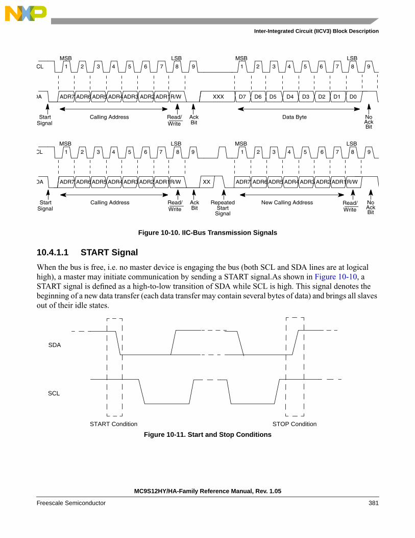
Inter-Integrated Circuit (IICV3) Block Description
Figure 10-10. IIC-Bus Transmission Signals
10.4.1.1 START Signal
When the bus is free, i.e. no master device is engaging the bus (both SCL and SDA lines are at logicalhigh), a master may initiate communication by sending a START signal.As shown in Figure 10-10, aSTART signal is defined as a high-to-low transition of SDA while SCL is high. This signal denotes thebeginning of a new data transfer (each data transfer may contain several bytes of data) and brings all slavesout of their idle states.
Figure 10-11. Start and Stop Conditions
CL
DA
StartSignal
AckBit
1 2 3 4 5 6 7 8
MSB LSB
1 2 3 4 5 6 7 8
MSB LSB
No
CL
DA
1 2 3 4 5 6 7 8
MSB LSB
1 2 5 6 7 8
MSB LSB
Repeated
3 4
9 9
ADR7 ADR6 ADR5 ADR4ADR3 ADR2 ADR1R/W XXX D7 D6 D5 D4 D3 D2 D1 D0
Calling Address Read/ Data Byte
ADR7 ADR6 ADR5 ADR4 ADR3 ADR2 ADR1R/W ADR7 ADR6 ADR5 ADR4 ADR3 ADR2 ADR1R/W
New Calling Address
9 9
XX
AckBitWrite
StartSignal
StartSignal
AckBit
Calling Address Read/Write
NoAckBit
Read/Write
SDA
SCL
START Condition STOP Condition
MC9S12HY/HA-Family Reference Manual, Rev. 1.05
Freescale Semiconductor 381

Inter-Integrated Circuit (IICV3) Block Description
10.4.1.2 Slave Address Transmission
The first byte of data transfer immediately after the START signal is the slave address transmitted by themaster. This is a seven-bit calling address followed by a R/W bit. The R/W bit tells the slave the desireddirection of data transfer.
1 = Read transfer, the slave transmits data to the master.0 = Write transfer, the master transmits data to the slave.
If the calling address is 10-bit, another byte is followed by the first byte.Only the slave with a callingaddress that matches the one transmitted by the master will respond by sending back an acknowledge bit.This is done by pulling the SDA low at the 9th clock (see Figure 10-10).
No two slaves in the system may have the same address. If the IIC bus is master, it must not transmit anaddress that is equal to its own slave address. The IIC bus cannot be master and slave at the sametime.However, if arbitration is lost during an address cycle the IIC bus will revert to slave mode and operatecorrectly even if it is being addressed by another master.
10.4.1.3 Data Transfer
As soon as successful slave addressing is achieved, the data transfer can proceed byte-by-byte in adirection specified by the R/W bit sent by the calling master
All transfers that come after an address cycle are referred to as data transfers, even if they carry sub-addressinformation for the slave device.
Each data byte is 8 bits long. Data may be changed only while SCL is low and must be held stable whileSCL is high as shown in Figure 10-10. There is one clock pulse on SCL for each data bit, the MSB beingtransferred first. Each data byte has to be followed by an acknowledge bit, which is signalled from thereceiving device by pulling the SDA low at the ninth clock. So one complete data byte transfer needs nineclock pulses.
If the slave receiver does not acknowledge the master, the SDA line must be left high by the slave. Themaster can then generate a stop signal to abort the data transfer or a start signal (repeated start) tocommence a new calling.
If the master receiver does not acknowledge the slave transmitter after a byte transmission, it means 'endof data' to the slave, so the slave releases the SDA line for the master to generate STOP or STARTsignal.Note in order to release the bus correctly,after no-acknowledge to the master,the slave must beimmediately switched to receiver and a following dummy reading of the IBDR is necessary.
10.4.1.4 STOP Signal
The master can terminate the communication by generating a STOP signal to free the bus. However, themaster may generate a START signal followed by a calling command without generating a STOP signalfirst. This is called repeated START. A STOP signal is defined as a low-to-high transition of SDA whileSCL at logical 1 (see Figure 10-10).
The master can generate a STOP even if the slave has generated an acknowledge at which point the slavemust release the bus.
MC9S12HY/HA-Family Reference Manual, Rev. 1.05
382 Freescale Semiconductor

Inter-Integrated Circuit (IICV3) Block Description
10.4.1.5 Repeated START Signal
As shown in Figure 10-10, a repeated START signal is a START signal generated without first generatinga STOP signal to terminate the communication. This is used by the master to communicate with anotherslave or with the same slave in different mode (transmit/receive mode) without releasing the bus.
10.4.1.6 Arbitration Procedure
The Inter-IC bus is a true multi-master bus that allows more than one master to be connected on it. If twoor more masters try to control the bus at the same time, a clock synchronization procedure determines thebus clock, for which the low period is equal to the longest clock low period and the high is equal to theshortest one among the masters. The relative priority of the contending masters is determined by a dataarbitration procedure, a bus master loses arbitration if it transmits logic 1 while another master transmitslogic 0. The losing masters immediately switch over to slave receive mode and stop driving SDA output.In this case the transition from master to slave mode does not generate a STOP condition. Meanwhile, astatus bit is set by hardware to indicate loss of arbitration.
10.4.1.7 Clock Synchronization
Because wire-AND logic is performed on SCL line, a high-to-low transition on SCL line affects all thedevices connected on the bus. The devices start counting their low period and as soon as a device's clockhas gone low, it holds the SCL line low until the clock high state is reached.However, the change of low tohigh in this device clock may not change the state of the SCL line if another device clock is within its lowperiod. Therefore, synchronized clock SCL is held low by the device with the longest low period. Deviceswith shorter low periods enter a high wait state during this time (see Figure 10-11). When all devicesconcerned have counted off their low period, the synchronized clock SCL line is released and pulled high.There is then no difference between the device clocks and the state of the SCL line and all the devices startcounting their high periods.The first device to complete its high period pulls the SCL line low again.
Figure 10-12. IIC-Bus Clock Synchronization
SCL1
SCL2
SCL
Internal Counter Reset
WAIT Start Counting High Period
MC9S12HY/HA-Family Reference Manual, Rev. 1.05
Freescale Semiconductor 383

Inter-Integrated Circuit (IICV3) Block Description
S1
A4
10.4.1.8 Handshaking
The clock synchronization mechanism can be used as a handshake in data transfer. Slave devices may holdthe SCL low after completion of one byte transfer (9 bits). In such case, it halts the bus clock and forcesthe master clock into wait states until the slave releases the SCL line.
10.4.1.9 Clock Stretching
The clock synchronization mechanism can be used by slaves to slow down the bit rate of a transfer. Afterthe master has driven SCL low the slave can drive SCL low for the required period and then release it.Ifthe slave SCL low period is greater than the master SCL low period then the resulting SCL bus signal lowperiod is stretched.
10.4.1.10 Ten-bit Address
A ten-bit address is indicated if the first 5 bits of the first address byte are 0x11110. The following rulesapply to the first address byte.
Figure 10-13. Definition of bits in the first byte.
The address type is identified by ADTYPE. When ADTYPE is 0, 7-bit address is applied. Reversely, theaddress is 10-bit address.Generally, there are two cases of 10-bit address.See the Fig.1-14 and 1-15.
Figure 10-14. A master-transmitter addresses a slave-receiver with a 10-bit address
Figure 10-15. A master-receiver addresses a slave-transmitter with a 10-bit address.
In the figure 1-15,the first two bytes are the similar to figure1-14.After the repeated START(Sr),the firstslave address is transmitted again, but the R/W is 1, meaning that the slave is acted as a transmitter.
SLAVEADDRESS R/W BIT DESCRIPTION
0000000 0 General call address
0000010 xReserved for different bus
format
0000011 x Reserved for future purposes
11111XX x Reserved for future purposes
11110XX x 10-bit slave addressing
SSlave Add1st 7bits
11110+ADR10+ADR9R/W
0A1
Slave Add 2nd byteADR[8:1]
A2 Data A3
Slave Add1st 7bits1110+ADR10+ADR9
R/W0
A1Slave Add 2nd byte
ADR[8:1]A2 Sr
Slave Add 1st 7bits11110+ADR10+ADR9
R/W1
A3 Data
MC9S12HY/HA-Family Reference Manual, Rev. 1.05
384 Freescale Semiconductor

Inter-Integrated Circuit (IICV3) Block Description
10.4.1.11 General Call Address
To broadcast using a general call, a device must first generate the general call address($00), then afterreceiving acknowledge, it must transmit data.
In communication, as a slave device, provided the GCEN is asserted, a device acknowledges the broadcastand receives data until the GCEN is disabled or the master device releases the bus or generates a newtransfer. In the broadcast, slaves always act as receivers. In general call, IAAS is also used to indicate theaddress match.
In order to distinguish whether the address match is the normal address match or the general call addressmatch, IBDR should be read after the address byte has been received. If the data is $00, the match isgeneral call address match. The meaning of the general call address is always specified in the first data byteand must be dealt with by S/W, the IIC hardware does not decode and process the first data byte.
When one byte transfer is done, the received data can be read from IBDR. The user can control theprocedure by enabling or disabling GCEN.
10.4.2 Operation in Run Mode
This is the basic mode of operation.
10.4.3 Operation in Wait Mode
IIC operation in wait mode can be configured. Depending on the state of internal bits, the IIC can operatenormally when the CPU is in wait mode or the IIC clock generation can be turned off and the IIC moduleenters a power conservation state during wait mode. In the later case, any transmission or reception inprogress stops at wait mode entry.
10.4.4 Operation in Stop Mode
The IIC is inactive in stop mode for reduced power consumption. The STOP instruction does not affect IICregister states.
10.5 ResetsThe reset state of each individual bit is listed in Section 10.3, “Memory Map and Register Definition,”which details the registers and their bit-fields.
10.6 InterruptsIICV3 uses only one interrupt vector.
Table 10-11. Interrupt Summary
Interrupt Offset Vector Priority Source Description
MC9S12HY/HA-Family Reference Manual, Rev. 1.05
Freescale Semiconductor 385

Inter-Integrated Circuit (IICV3) Block Description
Internally there are three types of interrupts in IIC. The interrupt service routine can determine the interrupttype by reading the status register.
IIC Interrupt can be generated on
1. Arbitration lost condition (IBAL bit set)
2. Byte transfer condition (TCF bit set)
3. Address detect condition (IAAS bit set)
The IIC interrupt is enabled by the IBIE bit in the IIC control register. It must be cleared by writing 0 tothe IBF bit in the interrupt service routine.
10.7 Application Information
10.7.1 IIC Programming Examples
10.7.1.1 Initialization Sequence
Reset will put the IIC bus control register to its default status. Before the interface can be used to transferserial data, an initialization procedure must be carried out, as follows:
1. Update the frequency divider register (IBFD) and select the required division ratio to obtain SCLfrequency from system clock.
2. Update the ADTYPE of IBCR2 to define the address length, 7 bits or 10 bits.
3. Update the IIC bus address register (IBAD) to define its slave address. If 10-bit address is appliedIBCR2 should be updated to define the rest bits of address.
4. Set the IBEN bit of the IIC bus control register (IBCR) to enable the IIC interface system.
5. Modify the bits of the IIC bus control register (IBCR) to select master/slave mode, transmit/receivemode and interrupt enable or not.
6. If supported general call, the GCEN in IBCR2 should be asserted.
10.7.1.2 Generation of START
After completion of the initialization procedure, serial data can be transmitted by selecting the 'mastertransmitter' mode. If the device is connected to a multi-master bus system, the state of the IIC bus busy bit(IBB) must be tested to check whether the serial bus is free.
If the bus is free (IBB=0), the start condition and the first byte (the slave address) can be sent. The datawritten to the data register comprises the slave calling address and the LSB set to indicate the direction oftransfer required from the slave.
The bus free time (i.e., the time between a STOP condition and the following START condition) is builtinto the hardware that generates the START cycle. Depending on the relative frequencies of the system
IICInterrupt
— — — IBAL, TCF, IAASbits in IBSR
register
When either of IBAL, TCF or IAAS bits is setmay cause an interrupt based on arbitrationlost, transfer complete or address detectconditions
MC9S12HY/HA-Family Reference Manual, Rev. 1.05
386 Freescale Semiconductor

Inter-Integrated Circuit (IICV3) Block Description
clock and the SCL period it may be necessary to wait until the IIC is busy after writing the calling addressto the IBDR before proceeding with the following instructions. This is illustrated in the following example.
An example of a program which generates the START signal and transmits the first byte of data (slaveaddress) is shown below:
10.7.1.3 Post-Transfer Software Response
Transmission or reception of a byte will set the data transferring bit (TCF) to 1, which indicates one bytecommunication is finished. The IIC bus interrupt bit (IBIF) is set also; an interrupt will be generated if theinterrupt function is enabled during initialization by setting the IBIE bit. Software must clear the IBIF bitin the interrupt routine first. The TCF bit will be cleared by reading from the IIC bus data I/O register(IBDR) in receive mode or writing to IBDR in transmit mode.
Software may service the IIC I/O in the main program by monitoring the IBIF bit if the interrupt functionis disabled. Note that polling should monitor the IBIF bit rather than the TCF bit because their operationis different when arbitration is lost.
Note that when an interrupt occurs at the end of the address cycle the master will always be in transmitmode, i.e. the address is transmitted. If master receive mode is required, indicated by R/W bit in IBDR,then the Tx/Rx bit should be toggled at this stage.
During slave mode address cycles (IAAS=1), the SRW bit in the status register is read to determine thedirection of the subsequent transfer and the Tx/Rx bit is programmed accordingly.For slave mode datacycles (IAAS=0) the SRW bit is not valid, the Tx/Rx bit in the control register should be read to determinethe direction of the current transfer.
The following is an example of a software response by a 'master transmitter' in the interrupt routine.
10.7.1.4 Generation of STOP
A data transfer ends with a STOP signal generated by the 'master' device. A master transmitter can simplygenerate a STOP signal after all the data has been transmitted. The following is an example showing howa stop condition is generated by a master transmitter.
CHFLAG BRSET IBSR,#$20,* ;WAIT FOR IBB FLAG TO CLEAR
TXSTART BSET IBCR,#$30 ;SET TRANSMIT AND MASTER MODE;i.e. GENERATE START CONDITION
MOVB CALLING,IBDR ;TRANSMIT THE CALLING ADDRESS, D0=R/W
IBFREE BRCLR IBSR,#$20,* ;WAIT FOR IBB FLAG TO SET
ISR BCLR IBSR,#$02 ;CLEAR THE IBIF FLAGBRCLR IBCR,#$20,SLAVE ;BRANCH IF IN SLAVE MODEBRCLR IBCR,#$10,RECEIVE ;BRANCH IF IN RECEIVE MODEBRSET IBSR,#$01,END ;IF NO ACK, END OF TRANSMISSION
TRANSMIT MOVB DATABUF,IBDR ;TRANSMIT NEXT BYTE OF DATA
MC9S12HY/HA-Family Reference Manual, Rev. 1.05
Freescale Semiconductor 387

Inter-Integrated Circuit (IICV3) Block Description
If a master receiver wants to terminate a data transfer, it must inform the slave transmitter by notacknowledging the last byte of data which can be done by setting the transmit acknowledge bit (TXAK)before reading the 2nd last byte of data. Before reading the last byte of data, a STOP signal must begenerated first. The following is an example showing how a STOP signal is generated by a master receiver.
10.7.1.5 Generation of Repeated START
At the end of data transfer, if the master continues to want to communicate on the bus, it can generateanother START signal followed by another slave address without first generating a STOP signal. Aprogram example is as shown.
10.7.1.6 Slave Mode
In the slave interrupt service routine, the module addressed as slave bit (IAAS) should be tested to checkif a calling of its own address has just been received. If IAAS is set, software should set the transmit/receivemode select bit (Tx/Rx bit of IBCR) according to the R/W command bit (SRW). Writing to the IBCRclears the IAAS automatically. Note that the only time IAAS is read as set is from the interrupt at the endof the address cycle where an address match occurred, interrupts resulting from subsequent data transferswill have IAAS cleared. A data transfer may now be initiated by writing information to IBDR, for slavetransmits, or dummy reading from IBDR, in slave receive mode. The slave will drive SCL low in-betweenbyte transfers, SCL is released when the IBDR is accessed in the required mode.
In slave transmitter routine, the received acknowledge bit (RXAK) must be tested before transmitting thenext byte of data. Setting RXAK means an 'end of data' signal from the master receiver, after which it mustbe switched from transmitter mode to receiver mode by software. A dummy read then releases the SCLline so that the master can generate a STOP signal.
MASTX TST TXCNT ;GET VALUE FROM THE TRANSMITING COUNTERBEQ END ;END IF NO MORE DATABRSET IBSR,#$01,END ;END IF NO ACKMOVB DATABUF,IBDR ;TRANSMIT NEXT BYTE OF DATADEC TXCNT ;DECREASE THE TXCNTBRA EMASTX ;EXIT
END BCLR IBCR,#$20 ;GENERATE A STOP CONDITIONEMASTX RTI ;RETURN FROM INTERRUPT
MASR DEC RXCNT ;DECREASE THE RXCNTBEQ ENMASR ;LAST BYTE TO BE READMOVB RXCNT,D1 ;CHECK SECOND LAST BYTEDEC D1 ;TO BE READBNE NXMAR ;NOT LAST OR SECOND LAST
LAMAR BSET IBCR,#$08 ;SECOND LAST, DISABLE ACK;TRANSMITTING
BRA NXMARENMASR BCLR IBCR,#$20 ;LAST ONE, GENERATE ‘STOP’ SIGNALNXMAR MOVB IBDR,RXBUF ;READ DATA AND STORE
RTI
RESTART BSET IBCR,#$04 ;ANOTHER START (RESTART)MOVB CALLING,IBDR ;TRANSMIT THE CALLING ADDRESS;D0=R/W
MC9S12HY/HA-Family Reference Manual, Rev. 1.05
388 Freescale Semiconductor

Inter-Integrated Circuit (IICV3) Block Description
10.7.1.7 Arbitration Lost
If several masters try to engage the bus simultaneously, only one master wins and the others losearbitration. The devices which lost arbitration are immediately switched to slave receive mode by thehardware. Their data output to the SDA line is stopped, but SCL continues to be generated until the end ofthe byte during which arbitration was lost. An interrupt occurs at the falling edge of the ninth clock of thistransfer with IBAL=1 and MS/SL=0. If one master attempts to start transmission while the bus is beingengaged by another master, the hardware will inhibit the transmission; switch the MS/SL bit from 1 to 0without generating STOP condition; generate an interrupt to CPU and set the IBAL to indicate that theattempt to engage the bus is failed. When considering these cases, the slave service routine should test theIBAL first and the software should clear the IBAL bit if it is set.
MC9S12HY/HA-Family Reference Manual, Rev. 1.05
Freescale Semiconductor 389

Inter-Integrated Circuit (IICV3) Block Description
Figure 10-16. Flow-Chart of Typical IIC Interrupt Routine
Clear
MasterMode
?
Tx/Rx?
Last ByteTransmitted
?
RXAK=0?
End OfAddr Cycle(Master Rx)
?
Write NextByte To IBDR
Switch ToRx Mode
Dummy ReadFrom IBDR
GenerateStop Signal
Read DataFrom IBDRAnd Store
Set TXAK =1 GenerateStop Signal
2nd LastByte To Be Read
?
LastByte To Be Read
?
ArbitrationLost
?
Clear IBAL
IAAS=1?
IAAS=1?
SRW=1?
TX/RX?
Set TXMode
Write DataTo IBDR
Set RXMode
Dummy ReadFrom IBDR
ACK FromReceiver
?
Tx NextByte
Read DataFrom IBDRAnd Store
Switch ToRx Mode
Dummy ReadFrom IBDR
RTI
Y N
Y
Y Y
Y
Y
Y
Y
N
N
N
N
N
N
N
N
Y
TX RX
RX
TX
(Write)
(Read)
N
IBIF
Data Transfer
Y Y
10-bitaddress?
NN
7-bit address transfer
Y
10-bit address transfer
Modeset RX
Dummy ReadFrom IBDR
N
set TXMode
Write DataTo IBDR
Y
IBDR==11110xx1?
MC9S12HY/HA-Family Reference Manual, Rev. 1.05
390 Freescale Semiconductor

Inter-Integrated Circuit (IICV3) Block Description
Caution:When IIC is configured as 10-bit address,the point of the data array in interrupt routine must bereset after it’s addressed.
MC9S12HY/HA-Family Reference Manual, Rev. 1.05
Freescale Semiconductor 391

Inter-Integrated Circuit (IICV3) Block Description
MC9S12HY/HA-Family Reference Manual, Rev. 1.05
392 Freescale Semiconductor

Chapter 11Pulse-Width Modulator (S12PWM8B8CV1)
11.1 IntroductionThe PWM definition is based on the HC12 PWM definitions. It contains the basic features from the HC11with some of the enhancements incorporated on the HC12: center aligned output mode and four availableclock sources.The PWM module has eight channels with independent control of left and center alignedoutputs on each channel.
Each of the eight channels has a programmable period and duty cycle as well as a dedicated counter. Aflexible clock select scheme allows a total of four different clock sources to be used with the counters. Eachof the modulators can create independent continuous waveforms with software-selectable duty rates from0% to 100%. The PWM outputs can be programmed as left aligned outputs or center aligned outputs.
11.1.1 Features
The PWM block includes these distinctive features:
• Eight independent PWM channels with programmable period and duty cycle
• Dedicated counter for each PWM channel
• Programmable PWM enable/disable for each channel
• Software selection of PWM duty pulse polarity for each channel
• Period and duty cycle are double buffered. Change takes effect when the end of the effective periodis reached (PWM counter reaches zero) or when the channel is disabled.
• Programmable center or left aligned outputs on individual channels
• Eight 8-bit channel or four 16-bit channel PWM resolution
• Four clock sources (A, B, SA, and SB) provide for a wide range of frequencies
• Programmable clock select logic
• Emergency shutdown
11.1.2 Modes of Operation
There is a software programmable option for low power consumption in wait mode that disables the inputclock to the prescaler.
In freeze mode there is a software programmable option to disable the input clock to the prescaler. This isuseful for emulation.
MC9S12HY/HA-Family Reference Manual, Rev. 1.05
Freescale Semiconductor 393

Pulse-Width Modulator (S12PWM8B8CV1)
11.1.3 Block Diagram
Figure 11-1 shows the block diagram for the 8-bit 8-channel PWM block.
Figure 11-1. PWM Block Diagram
11.2 External Signal DescriptionThe PWM module has a total of 8 external pins.
11.2.1 PWM7 — PWM Channel 7
This pin serves as waveform output of PWM channel 7 and as an input for the emergency shutdownfeature.
11.2.2 PWM6 — PWM Channel 6
This pin serves as waveform output of PWM channel 6.
Period and Duty Counter
Channel 6
Clock Select PWM Clock
Period and Duty Counter
Channel 5
Period and Duty Counter
Channel 4
Period and Duty Counter
Channel 3
Period and Duty Counter
Channel 2
Period and Duty Counter
Channel 1Alignment
Polarity
Control
PWM8B8C
PWM6
PWM5
PWM4
PWM3
PWM2
PWM1
Enable
PWM Channels
Period and Duty Counter
Channel 7
Period and Duty Counter
Channel 0PWM0
PWM7
Bus Clock
MC9S12HY/HA-Family Reference Manual, Rev. 1.05
394 Freescale Semiconductor
Pulse-Width Modulator (S12PWM8B8CV1)
11.2.3 PWM5 — PWM Channel 5
This pin serves as waveform output of PWM channel 5.
11.2.4 PWM4 — PWM Channel 4
This pin serves as waveform output of PWM channel 4.
11.2.5 PWM3 — PWM Channel 3
This pin serves as waveform output of PWM channel 3.
11.2.6 PWM3 — PWM Channel 2
This pin serves as waveform output of PWM channel 2.
11.2.7 PWM3 — PWM Channel 1
This pin serves as waveform output of PWM channel 1.
11.2.8 PWM3 — PWM Channel 0
This pin serves as waveform output of PWM channel 0.
11.3 Memory Map and Register DefinitionThis section describes in detail all the registers and register bits in the PWM module.
The special-purpose registers and register bit functions that are not normally available to device end users,such as factory test control registers and reserved registers, are clearly identified by means of shading theappropriate portions of address maps and register diagrams. Notes explaining the reasons for restrictingaccess to the registers and functions are also explained in the individual register descriptions.
11.3.1 Module Memory Map
This section describes the content of the registers in the PWM module. The base address of the PWMmodule is determined at the MCU level when the MCU is defined. The register decode map is fixed andbegins at the first address of the module address offset. The figure below shows the registers associatedwith the PWM and their relative offset from the base address. The register detail description follows theorder they appear in the register map.
Reserved bits within a register will always read as 0 and the write will be unimplemented. Unimplementedfunctions are indicated by shading the bit. .
MC9S12HY/HA-Family Reference Manual, Rev. 1.05
Freescale Semiconductor 395
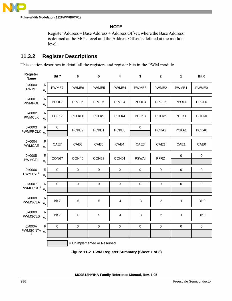
Pulse-Width Modulator (S12PWM8B8CV1)
NOTERegister Address = Base Address + Address Offset, where the Base Addressis defined at the MCU level and the Address Offset is defined at the modulelevel.
11.3.2 Register Descriptions
This section describes in detail all the registers and register bits in the PWM module.
RegisterName
Bit 7 6 5 4 3 2 1 Bit 0
0x0000PWME
RPWME7 PWME6 PWME5 PWME4 PWME3 PWME2 PWME1 PWME0
W
0x0001PWMPOL
RPPOL7 PPOL6 PPOL5 PPOL4 PPOL3 PPOL2 PPOL1 PPOL0
W
0x0002PWMCLK
RPCLK7 PCLKL6 PCLK5 PCLK4 PCLK3 PCLK2 PCLK1 PCLK0
W
0x0003PWMPRCLK
R 0PCKB2 PCKB1 PCKB0
0PCKA2 PCKA1 PCKA0
W
0x0004PWMCAE
RCAE7 CAE6 CAE5 CAE4 CAE3 CAE2 CAE1 CAE0
W
0x0005PWMCTL
RCON67 CON45 CON23 CON01 PSWAI PFRZ
0 0
W
0x0006PWMTST1
R 0 0 0 0 0 0 0 0
W
0x0007PWMPRSC1
R 0 0 0 0 0 0 0 0
W
0x0008PWMSCLA
RBit 7 6 5 4 3 2 1 Bit 0
W
0x0009PWMSCLB
RBit 7 6 5 4 3 2 1 Bit 0
W
0x000APWMSCNTA
1
R 0 0 0 0 0 0 0 0
W
= Unimplemented or Reserved
Figure 11-2. PWM Register Summary (Sheet 1 of 3)
MC9S12HY/HA-Family Reference Manual, Rev. 1.05
396 Freescale Semiconductor
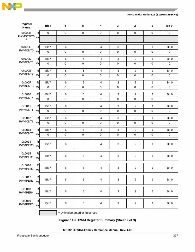
Pulse-Width Modulator (S12PWM8B8CV1)
0x000BPWMSCNTB
1
R 0 0 0 0 0 0 0 0
W
0x000CPWMCNT0
R Bit 7 6 5 4 3 2 1 Bit 0
W 0 0 0 0 0 0 0 0
0x000DPWMCNT1
R Bit 7 6 5 4 3 2 1 Bit 0
W 0 0 0 0 0 0 0 0
0x000EPWMCNT2
R Bit 7 6 5 4 3 2 1 Bit 0
W 0 0 0 0 0 0 0 0
0x000FPWMCNT3
R Bit 7 6 5 4 3 2 1 Bit 0
W 0 0 0 0 0 0 0 0
0x0010PWMCNT4
R Bit 7 6 5 4 3 2 1 Bit 0
W 0 0 0 0 0 0 0 0
0x0011PWMCNT5
R Bit 7 6 5 4 3 2 1 Bit 0
W 0 0 0 0 0 0 0 0
0x0012PWMCNT6
R Bit 7 6 5 4 3 2 1 Bit 0
W 0 0 0 0 0 0 0 0
0x0013PWMCNT7
R Bit 7 6 5 4 3 2 1 Bit 0
W 0 0 0 0 0 0 0 0
0x0014PWMPER0
RBit 7 6 5 4 3 2 1 Bit 0
W
0x0015PWMPER1
RBit 7 6 5 4 3 2 1 Bit 0
W
0x0016PWMPER2
RBit 7 6 5 4 3 2 1 Bit 0
W
0x0017PWMPER3
RBit 7 6 5 4 3 2 1 Bit 0
W
0x0018PWMPER4
RBit 7 6 5 4 3 2 1 Bit 0
W
0x0019PWMPER5
RBit 7 6 5 4 3 2 1 Bit 0
W
RegisterName
Bit 7 6 5 4 3 2 1 Bit 0
= Unimplemented or Reserved
Figure 11-2. PWM Register Summary (Sheet 2 of 3)
MC9S12HY/HA-Family Reference Manual, Rev. 1.05
Freescale Semiconductor 397

Pulse-Width Modulator (S12PWM8B8CV1)
11.3.2.1 PWM Enable Register (PWME)
Each PWM channel has an enable bit (PWMEx) to start its waveform output. When any of the PWMExbits are set (PWMEx = 1), the associated PWM output is enabled immediately. However, the actual PWMwaveform is not available on the associated PWM output until its clock source begins its next cycle due tothe synchronization of PWMEx and the clock source.
NOTEThe first PWM cycle after enabling the channel can be irregular.
0x001APWMPER6
RBit 7 6 5 4 3 2 1 Bit 0
W
0x001BPWMPER7
RBit 7 6 5 4 3 2 1 Bit 0
W
0x001CPWMDTY0
RBit 7 6 5 4 3 2 1 Bit 0
W
0x001DPWMDTY1
RBit 7 6 5 4 3 2 1 Bit 0
W
0x001EPWMDTY2
RBit 7 6 5 4 3 2 1 Bit 0
W
0x001FPWMDTY3
RBit 7 6 5 4 3 2 1 Bit 0
W
0x0010PWMDTY4
RBit 7 6 5 4 3 2 1 Bit 0
W
0x0021PWMDTY5
RBit 7 6 5 4 3 2 1 Bit 0
W
0x0022PWMDTY6
RBit 7 6 5 4 3 2 1 Bit 0
W
0x0023PWMDTY7
RBit 7 6 5 4 3 2 1 Bit 0
W
0x0024PWMSDN
RPWMIF PWMIE
0PWMLVL
0 PWM7INPWM7INL PWM7ENA
W PWMRSTRT
1 Intended for factory test purposes only.
RegisterName
Bit 7 6 5 4 3 2 1 Bit 0
= Unimplemented or Reserved
Figure 11-2. PWM Register Summary (Sheet 3 of 3)
MC9S12HY/HA-Family Reference Manual, Rev. 1.05
398 Freescale Semiconductor

Pulse-Width Modulator (S12PWM8B8CV1)
An exception to this is when channels are concatenated. Once concatenated mode is enabled (CONxx bitsset in PWMCTL register), enabling/disabling the corresponding 16-bit PWM channel is controlled by thelow order PWMEx bit.In this case, the high order bytes PWMEx bits have no effect and theircorresponding PWM output lines are disabled.
While in run mode, if all eight PWM channels are disabled (PWME7–0 = 0), the prescaler counter shutsoff for power savings.
Read: Anytime
Write: Anytime
Module Base + 0x0000
7 6 5 4 3 2 1 0
RPWME7 PWME6 PWME5 PWME4 PWME3 PWME2 PWME1 PWME0
W
Reset 0 0 0 0 0 0 0 0
Figure 11-3. PWM Enable Register (PWME)
Table 11-1. PWME Field Descriptions
Field Description
7PWME7
Pulse Width Channel 7 Enable0 Pulse width channel 7 is disabled.1 Pulse width channel 7 is enabled. The pulse modulated signal becomes available at PWM output bit 7 when
its clock source begins its next cycle.
6PWME6
Pulse Width Channel 6 Enable0 Pulse width channel 6 is disabled.1 Pulse width channel 6 is enabled. The pulse modulated signal becomes available at PWM output bit6 when
its clock source begins its next cycle. If CON67=1, then bit has no effect and PWM output line 6 is disabled.
5PWME5
Pulse Width Channel 5 Enable0 Pulse width channel 5 is disabled.1 Pulse width channel 5 is enabled. The pulse modulated signal becomes available at PWM output bit 5 when
its clock source begins its next cycle.
4PWME4
Pulse Width Channel 4 Enable0 Pulse width channel 4 is disabled.1 Pulse width channel 4 is enabled. The pulse modulated signal becomes available at PWM, output bit 4 when
its clock source begins its next cycle. If CON45 = 1, then bit has no effect and PWM output bit4 is disabled.
3PWME3
Pulse Width Channel 3 Enable0 Pulse width channel 3 is disabled.1 Pulse width channel 3 is enabled. The pulse modulated signal becomes available at PWM, output bit 3 when
its clock source begins its next cycle.
2PWME2
Pulse Width Channel 2 Enable0 Pulse width channel 2 is disabled.1 Pulse width channel 2 is enabled. The pulse modulated signal becomes available at PWM, output bit 2 when
its clock source begins its next cycle. If CON23 = 1, then bit has no effect and PWM output bit2 is disabled.
MC9S12HY/HA-Family Reference Manual, Rev. 1.05
Freescale Semiconductor 399
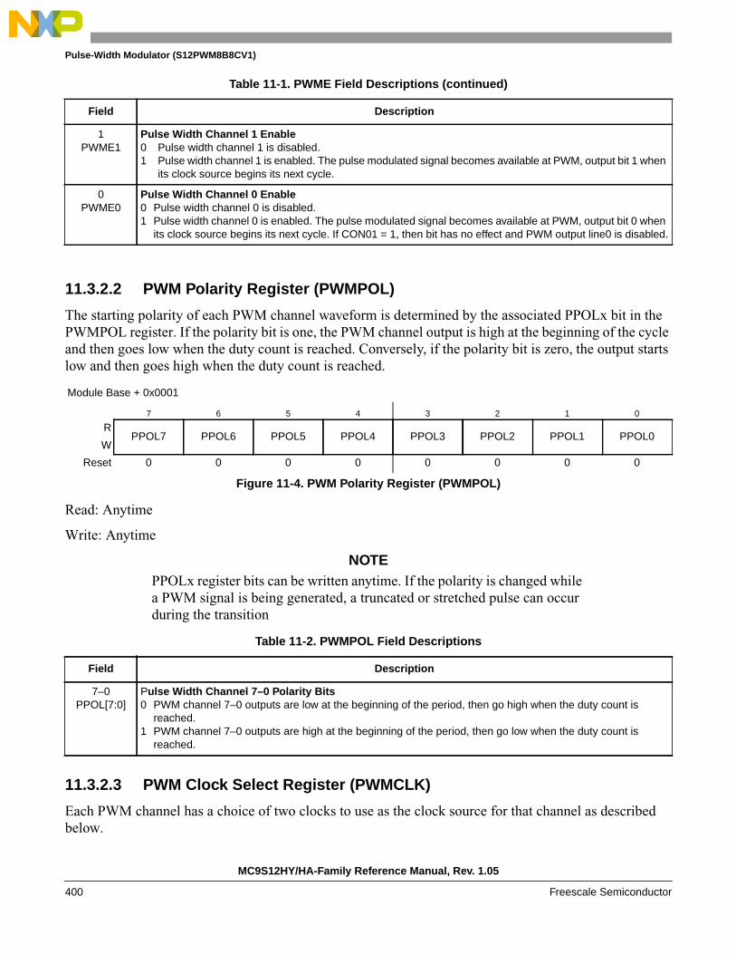
Pulse-Width Modulator (S12PWM8B8CV1)
11.3.2.2 PWM Polarity Register (PWMPOL)
The starting polarity of each PWM channel waveform is determined by the associated PPOLx bit in thePWMPOL register. If the polarity bit is one, the PWM channel output is high at the beginning of the cycleand then goes low when the duty count is reached. Conversely, if the polarity bit is zero, the output startslow and then goes high when the duty count is reached.
Read: Anytime
Write: Anytime
NOTEPPOLx register bits can be written anytime. If the polarity is changed whilea PWM signal is being generated, a truncated or stretched pulse can occurduring the transition
11.3.2.3 PWM Clock Select Register (PWMCLK)
Each PWM channel has a choice of two clocks to use as the clock source for that channel as describedbelow.
1PWME1
Pulse Width Channel 1 Enable0 Pulse width channel 1 is disabled.1 Pulse width channel 1 is enabled. The pulse modulated signal becomes available at PWM, output bit 1 when
its clock source begins its next cycle.
0PWME0
Pulse Width Channel 0 Enable0 Pulse width channel 0 is disabled.1 Pulse width channel 0 is enabled. The pulse modulated signal becomes available at PWM, output bit 0 when
its clock source begins its next cycle. If CON01 = 1, then bit has no effect and PWM output line0 is disabled.
Module Base + 0x0001
7 6 5 4 3 2 1 0
RPPOL7 PPOL6 PPOL5 PPOL4 PPOL3 PPOL2 PPOL1 PPOL0
W
Reset 0 0 0 0 0 0 0 0
Figure 11-4. PWM Polarity Register (PWMPOL)
Table 11-2. PWMPOL Field Descriptions
Field Description
7–0PPOL[7:0]
Pulse Width Channel 7–0 Polarity Bits0 PWM channel 7–0 outputs are low at the beginning of the period, then go high when the duty count is
reached.1 PWM channel 7–0 outputs are high at the beginning of the period, then go low when the duty count is
reached.
Table 11-1. PWME Field Descriptions (continued)
Field Description
MC9S12HY/HA-Family Reference Manual, Rev. 1.05
400 Freescale Semiconductor
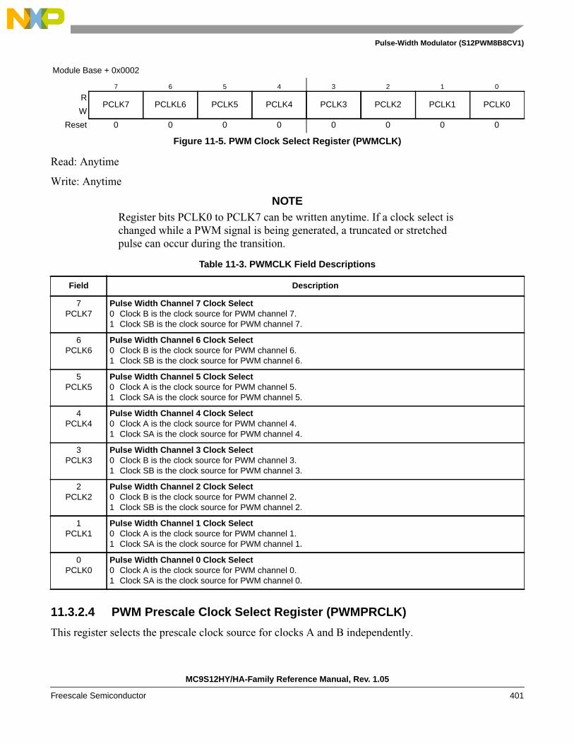
Pulse-Width Modulator (S12PWM8B8CV1)
Read: Anytime
Write: Anytime
NOTERegister bits PCLK0 to PCLK7 can be written anytime. If a clock select ischanged while a PWM signal is being generated, a truncated or stretchedpulse can occur during the transition.
11.3.2.4 PWM Prescale Clock Select Register (PWMPRCLK)
This register selects the prescale clock source for clocks A and B independently.
Module Base + 0x0002
7 6 5 4 3 2 1 0
RPCLK7 PCLKL6 PCLK5 PCLK4 PCLK3 PCLK2 PCLK1 PCLK0
W
Reset 0 0 0 0 0 0 0 0
Figure 11-5. PWM Clock Select Register (PWMCLK)
Table 11-3. PWMCLK Field Descriptions
Field Description
7PCLK7
Pulse Width Channel 7 Clock Select0 Clock B is the clock source for PWM channel 7.1 Clock SB is the clock source for PWM channel 7.
6PCLK6
Pulse Width Channel 6 Clock Select0 Clock B is the clock source for PWM channel 6.1 Clock SB is the clock source for PWM channel 6.
5PCLK5
Pulse Width Channel 5 Clock Select0 Clock A is the clock source for PWM channel 5.1 Clock SA is the clock source for PWM channel 5.
4PCLK4
Pulse Width Channel 4 Clock Select0 Clock A is the clock source for PWM channel 4.1 Clock SA is the clock source for PWM channel 4.
3PCLK3
Pulse Width Channel 3 Clock Select0 Clock B is the clock source for PWM channel 3.1 Clock SB is the clock source for PWM channel 3.
2PCLK2
Pulse Width Channel 2 Clock Select0 Clock B is the clock source for PWM channel 2.1 Clock SB is the clock source for PWM channel 2.
1PCLK1
Pulse Width Channel 1 Clock Select0 Clock A is the clock source for PWM channel 1.1 Clock SA is the clock source for PWM channel 1.
0PCLK0
Pulse Width Channel 0 Clock Select0 Clock A is the clock source for PWM channel 0.1 Clock SA is the clock source for PWM channel 0.
MC9S12HY/HA-Family Reference Manual, Rev. 1.05
Freescale Semiconductor 401

Pulse-Width Modulator (S12PWM8B8CV1)
Read: Anytime
Write: Anytime
NOTEPCKB2–0 and PCKA2–0 register bits can be written anytime. If the clockpre-scale is changed while a PWM signal is being generated, a truncated orstretched pulse can occur during the transition.
s
Module Base + 0x0003
7 6 5 4 3 2 1 0
R 0PCKB2 PCKB1 PCKB0
0PCKA2 PCKA1 PCKA0
W
Reset 0 0 0 0 0 0 0 0
= Unimplemented or Reserved
Figure 11-6. PWM Prescale Clock Select Register (PWMPRCLK)
Table 11-4. PWMPRCLK Field Descriptions
Field Description
6–4PCKB[2:0]
Prescaler Select for Clock B — Clock B is one of two clock sources which can be used for channels 2, 3, 6, or7. These three bits determine the rate of clock B, as shown in Table 11-5.
2–0PCKA[2:0]
Prescaler Select for Clock A — Clock A is one of two clock sources which can be used for channels 0, 1, 4 or5. These three bits determine the rate of clock A, as shown in Table 11-6.
Table 11-5. Clock B Prescaler Selects
PCKB2 PCKB1 PCKB0 Value of Clock B
0 0 0 Bus clock0 0 1 Bus clock / 20 1 0 Bus clock / 40 1 1 Bus clock / 81 0 0 Bus clock / 161 0 1 Bus clock / 321 1 0 Bus clock / 641 1 1 Bus clock / 128
Table 11-6. Clock A Prescaler Selects
PCKA2 PCKA1 PCKA0 Value of Clock A
0 0 0 Bus clock0 0 1 Bus clock / 20 1 0 Bus clock / 40 1 1 Bus clock / 81 0 0 Bus clock / 161 0 1 Bus clock / 321 1 0 Bus clock / 641 1 1 Bus clock / 128
MC9S12HY/HA-Family Reference Manual, Rev. 1.05
402 Freescale Semiconductor

Pulse-Width Modulator (S12PWM8B8CV1)
11.3.2.5 PWM Center Align Enable Register (PWMCAE)
The PWMCAE register contains eight control bits for the selection of center aligned outputs or left alignedoutputs for each PWM channel. If the CAEx bit is set to a one, the corresponding PWM output will becenter aligned. If the CAEx bit is cleared, the corresponding PWM output will be left aligned. SeeSection 11.4.2.5, “Left Aligned Outputs” and Section 11.4.2.6, “Center Aligned Outputs” for a moredetailed description of the PWM output modes.
Read: Anytime
Write: Anytime
NOTEWrite these bits only when the corresponding channel is disabled.
11.3.2.6 PWM Control Register (PWMCTL)
The PWMCTL register provides for various control of the PWM module.
Read: Anytime
Write: Anytime
There are three control bits for concatenation, each of which is used to concatenate a pair of PWMchannels into one 16-bit channel. When channels 6 and 7are concatenated, channel 6 registers become thehigh order bytes of the double byte channel. When channels 4 and 5 are concatenated, channel 4 registersbecome the high order bytes of the double byte channel. When channels 2 and 3 are concatenated, channel
Module Base + 0x0004
7 6 5 4 3 2 1 0
RCAE7 CAE6 CAE5 CAE4 CAE3 CAE2 CAE1 CAE0
W
Reset 0 0 0 0 0 0 0 0
Figure 11-7. PWM Center Align Enable Register (PWMCAE)
Table 11-7. PWMCAE Field Descriptions
Field Description
7–0CAE[7:0]
Center Aligned Output Modes on Channels 7–00 Channels 7–0 operate in left aligned output mode.1 Channels 7–0 operate in center aligned output mode.
Module Base + 0x0005
7 6 5 4 3 2 1 0
RCON67 CON45 CON23 CON01 PSWAI PFRZ
0 0
W
Reset 0 0 0 0 0 0 0 0
= Unimplemented or Reserved
Figure 11-8. PWM Control Register (PWMCTL)
MC9S12HY/HA-Family Reference Manual, Rev. 1.05
Freescale Semiconductor 403

Pulse-Width Modulator (S12PWM8B8CV1)
2 registers become the high order bytes of the double byte channel. When channels 0 and 1 areconcatenated, channel 0 registers become the high order bytes of the double byte channel.
See Section 11.4.2.7, “PWM 16-Bit Functions” for a more detailed description of the concatenation PWMFunction.
NOTEChange these bits only when both corresponding channels are disabled.
Table 11-8. PWMCTL Field Descriptions
Field Description
7CON67
Concatenate Channels 6 and 70 Channels 6 and 7 are separate 8-bit PWMs.1 Channels 6 and 7 are concatenated to create one 16-bit PWM channel. Channel 6 becomes the high order
byte and channel 7 becomes the low order byte. Channel 7 output pin is used as the output for this 16-bitPWM (bit 7 of port PWMP). Channel 7 clock select control-bit determines the clock source, channel 7 polaritybit determines the polarity, channel 7 enable bit enables the output and channel 7 center aligned enable bitdetermines the output mode.
6CON45
Concatenate Channels 4 and 50 Channels 4 and 5 are separate 8-bit PWMs.1 Channels 4 and 5 are concatenated to create one 16-bit PWM channel. Channel 4 becomes the high order
byte and channel 5 becomes the low order byte. Channel 5 output pin is used as the output for this 16-bitPWM (bit 5 of port PWMP). Channel 5 clock select control-bit determines the clock source, channel 5 polaritybit determines the polarity, channel 5 enable bit enables the output and channel 5 center aligned enable bitdetermines the output mode.
5CON23
Concatenate Channels 2 and 30 Channels 2 and 3 are separate 8-bit PWMs.1 Channels 2 and 3 are concatenated to create one 16-bit PWM channel. Channel 2 becomes the high order
byte and channel 3 becomes the low order byte. Channel 3 output pin is used as the output for this 16-bitPWM (bit 3 of port PWMP). Channel 3 clock select control-bit determines the clock source, channel 3 polaritybit determines the polarity, channel 3 enable bit enables the output and channel 3 center aligned enable bitdetermines the output mode.
4CON01
Concatenate Channels 0 and 10 Channels 0 and 1 are separate 8-bit PWMs.1 Channels 0 and 1 are concatenated to create one 16-bit PWM channel. Channel 0 becomes the high order
byte and channel 1 becomes the low order byte. Channel 1 output pin is used as the output for this 16-bitPWM (bit 1 of port PWMP). Channel 1 clock select control-bit determines the clock source, channel 1 polaritybit determines the polarity, channel 1 enable bit enables the output and channel 1 center aligned enable bitdetermines the output mode.
3PSWAI
PWM Stops in Wait Mode — Enabling this bit allows for lower power consumption in wait mode by disablingthe input clock to the prescaler.0 Allow the clock to the prescaler to continue while in wait mode.1 Stop the input clock to the prescaler whenever the MCU is in wait mode.
2PFREZ
PWM Counters Stop in Freeze Mode — In freeze mode, there is an option to disable the input clock to theprescaler by setting the PFRZ bit in the PWMCTL register. If this bit is set, whenever the MCU is in freeze mode,the input clock to the prescaler is disabled. This feature is useful during emulation as it allows the PWM functionto be suspended. In this way, the counters of the PWM can be stopped while in freeze mode so that once normalprogram flow is continued, the counters are re-enabled to simulate real-time operations. Since the registers canstill be accessed in this mode, to re-enable the prescaler clock, either disable the PFRZ bit or exit freeze mode.0 Allow PWM to continue while in freeze mode.1 Disable PWM input clock to the prescaler whenever the part is in freeze mode. This is useful for emulation.
MC9S12HY/HA-Family Reference Manual, Rev. 1.05
404 Freescale Semiconductor

Pulse-Width Modulator (S12PWM8B8CV1)
11.3.2.7 Reserved Register (PWMTST)
This register is reserved for factory testing of the PWM module and is not available in normal modes.
Read: Always read $00 in normal modes
Write: Unimplemented in normal modes
NOTEWriting to this register when in special modes can alter the PWMfunctionality.
11.3.2.8 Reserved Register (PWMPRSC)
This register is reserved for factory testing of the PWM module and is not available in normal modes.
Read: Always read $00 in normal modes
Write: Unimplemented in normal modes
NOTEWriting to this register when in special modes can alter the PWMfunctionality.
11.3.2.9 PWM Scale A Register (PWMSCLA)
PWMSCLA is the programmable scale value used in scaling clock A to generate clock SA. Clock SA isgenerated by taking clock A, dividing it by the value in the PWMSCLA register and dividing that by two.
Clock SA = Clock A / (2 * PWMSCLA)
Module Base + 0x0006
7 6 5 4 3 2 1 0
R 0 0 0 0 0 0 0 0
W
Reset 0 0 0 0 0 0 0 0
= Unimplemented or Reserved
Figure 11-9. Reserved Register (PWMTST)
Module Base + 0x0007
7 6 5 4 3 2 1 0
R 0 0 0 0 0 0 0 0
W
Reset 0 0 0 0 0 0 0 0
= Unimplemented or Reserved
Figure 11-10. Reserved Register (PWMPRSC)
MC9S12HY/HA-Family Reference Manual, Rev. 1.05
Freescale Semiconductor 405
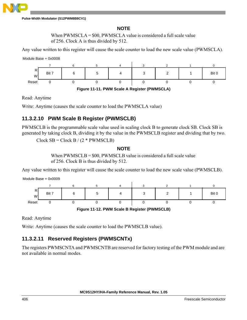
Pulse-Width Modulator (S12PWM8B8CV1)
NOTEWhen PWMSCLA = $00, PWMSCLA value is considered a full scale valueof 256. Clock A is thus divided by 512.
Any value written to this register will cause the scale counter to load the new scale value (PWMSCLA).
Read: Anytime
Write: Anytime (causes the scale counter to load the PWMSCLA value)
11.3.2.10 PWM Scale B Register (PWMSCLB)
PWMSCLB is the programmable scale value used in scaling clock B to generate clock SB. Clock SB isgenerated by taking clock B, dividing it by the value in the PWMSCLB register and dividing that by two.
Clock SB = Clock B / (2 * PWMSCLB)
NOTEWhen PWMSCLB = $00, PWMSCLB value is considered a full scale valueof 256. Clock B is thus divided by 512.
Any value written to this register will cause the scale counter to load the new scale value (PWMSCLB).
Read: Anytime
Write: Anytime (causes the scale counter to load the PWMSCLB value).
11.3.2.11 Reserved Registers (PWMSCNTx)
The registers PWMSCNTA and PWMSCNTB are reserved for factory testing of the PWM module and arenot available in normal modes.
Module Base + 0x0008
7 6 5 4 3 2 1 0
RBit 7 6 5 4 3 2 1 Bit 0
W
Reset 0 0 0 0 0 0 0 0
Figure 11-11. PWM Scale A Register (PWMSCLA)
Module Base + 0x0009
7 6 5 4 3 2 1 0
RBit 7 6 5 4 3 2 1 Bit 0
W
Reset 0 0 0 0 0 0 0 0
Figure 11-12. PWM Scale B Register (PWMSCLB)
MC9S12HY/HA-Family Reference Manual, Rev. 1.05
406 Freescale Semiconductor

Pulse-Width Modulator (S12PWM8B8CV1)
Read: Always read $00 in normal modes
Write: Unimplemented in normal modes
NOTEWriting to these registers when in special modes can alter the PWMfunctionality.
11.3.2.12 PWM Channel Counter Registers (PWMCNTx)
Each channel has a dedicated 8-bit up/down counter which runs at the rate of the selected clock source.The counter can be read at any time without affecting the count or the operation of the PWM channel. Inleft aligned output mode, the counter counts from 0 to the value in the period register - 1. In center alignedoutput mode, the counter counts from 0 up to the value in the period register and then back down to 0.
Any value written to the counter causes the counter to reset to $00, the counter direction to be set to up,the immediate load of both duty and period registers with values from the buffers, and the output to changeaccording to the polarity bit. The counter is also cleared at the end of the effective period (seeSection 11.4.2.5, “Left Aligned Outputs” and Section 11.4.2.6, “Center Aligned Outputs” for moredetails). When the channel is disabled (PWMEx = 0), the PWMCNTx register does not count. When achannel becomes enabled (PWMEx = 1), the associated PWM counter starts at the count in thePWMCNTx register. For more detailed information on the operation of the counters, see Section 11.4.2.4,“PWM Timer Counters”.
In concatenated mode, writes to the 16-bit counter by using a 16-bit access or writes to either the low orhigh order byte of the counter will reset the 16-bit counter. Reads of the 16-bit counter must be made by16-bit access to maintain data coherency.
NOTEWriting to the counter while the channel is enabled can cause an irregular PWM cycle to occur.
Read: Anytime
Module Base + 0x000A, 0x000B
7 6 5 4 3 2 1 0
R 0 0 0 0 0 0 0 0
W
Reset 0 0 0 0 0 0 0 0
= Unimplemented or Reserved
Figure 11-13. Reserved Registers (PWMSCNTx)
Module Base + 0x000C = PWMCNT0, 0x000D = PWMCNT1, 0x000E = PWMCNT2, 0x000F = PWMCNT3Module Base + 0x0010 = PWMCNT4, 0x0011 = PWMCNT5, 0x0012 = PWMCNT6, 0x0013 = PWMCNT7
7 6 5 4 3 2 1 0
R Bit 7 6 5 4 3 2 1 Bit 0
W 0 0 0 0 0 0 0 0
Reset 0 0 0 0 0 0 0 0
Figure 11-14. PWM Channel Counter Registers (PWMCNTx)
MC9S12HY/HA-Family Reference Manual, Rev. 1.05
Freescale Semiconductor 407

Pulse-Width Modulator (S12PWM8B8CV1)
Write: Anytime (any value written causes PWM counter to be reset to $00).
11.3.2.13 PWM Channel Period Registers (PWMPERx)
There is a dedicated period register for each channel. The value in this register determines the period ofthe associated PWM channel.
The period registers for each channel are double buffered so that if they change while the channel isenabled, the change will NOT take effect until one of the following occurs:
• The effective period ends
• The counter is written (counter resets to $00)
• The channel is disabled
In this way, the output of the PWM will always be either the old waveform or the new waveform, not somevariation in between. If the channel is not enabled, then writes to the period register will go directly to thelatches as well as the buffer.
NOTEReads of this register return the most recent value written. Reads do notnecessarily return the value of the currently active period due to the doublebuffering scheme.
See Section 11.4.2.3, “PWM Period and Duty” for more information.
To calculate the output period, take the selected clock source period for the channel of interest (A, B, SA,or SB) and multiply it by the value in the period register for that channel:
• Left aligned output (CAEx = 0)
• PWMxPeriod=ChannelClockPeriod*PWMPERxCenterAlignedOutput(CAEx=1)
PWMx Period = Channel Clock Period * (2 * PWMPERx)
For boundary case programming values, please refer to Section 11.4.2.8, “PWM Boundary Cases”.
Read: Anytime
Write: Anytime
Module Base + 0x0014 = PWMPER0, 0x0015 = PWMPER1, 0x0016 = PWMPER2, 0x0017 = PWMPER3Module Base + 0x0018 = PWMPER4, 0x0019 = PWMPER5, 0x001A = PWMPER6, 0x001B = PWMPER7
7 6 5 4 3 2 1 0
RBit 7 6 5 4 3 2 1 Bit 0
W
Reset 1 1 1 1 1 1 1 1
Figure 11-15. PWM Channel Period Registers (PWMPERx)
MC9S12HY/HA-Family Reference Manual, Rev. 1.05
408 Freescale Semiconductor

Pulse-Width Modulator (S12PWM8B8CV1)
11.3.2.14 PWM Channel Duty Registers (PWMDTYx)
There is a dedicated duty register for each channel. The value in this register determines the duty of theassociated PWM channel. The duty value is compared to the counter and if it is equal to the counter valuea match occurs and the output changes state.
The duty registers for each channel are double buffered so that if they change while the channel is enabled,the change will NOT take effect until one of the following occurs:
• The effective period ends
• The counter is written (counter resets to $00)
• The channel is disabled
In this way, the output of the PWM will always be either the old duty waveform or the new duty waveform,not some variation in between. If the channel is not enabled, then writes to the duty register will go directlyto the latches as well as the buffer.
NOTEReads of this register return the most recent value written. Reads do notnecessarily return the value of the currently active duty due to the doublebuffering scheme.
See Section 11.4.2.3, “PWM Period and Duty” for more information.
NOTEDepending on the polarity bit, the duty registers will contain the count ofeither the high time or the low time. If the polarity bit is one, the output startshigh and then goes low when the duty count is reached, so the duty registerscontain a count of the high time. If the polarity bit is zero, the output startslow and then goes high when the duty count is reached, so the duty registerscontain a count of the low time.
To calculate the output duty cycle (high time as a% of period) for a particular channel:
• Polarity = 0 (PPOL x =0)
Duty Cycle = [(PWMPERx-PWMDTYx)/PWMPERx] * 100%
• Polarity = 1 (PPOLx = 1)
Duty Cycle = [PWMDTYx / PWMPERx] * 100%
For boundary case programming values, please refer to Section 11.4.2.8, “PWM Boundary Cases”.
Read: Anytime
Module Base + 0x001C = PWMDTY0, 0x001D = PWMDTY1, 0x001E = PWMDTY2, 0x001F = PWMDTY3Module Base + 0x0020 = PWMDTY4, 0x0021 = PWMDTY5, 0x0022 = PWMDTY6, 0x0023 = PWMDTY7
7 6 5 4 3 2 1 0
RBit 7 6 5 4 3 2 1 Bit 0
W
Reset 1 1 1 1 1 1 1 1
Figure 11-16. PWM Channel Duty Registers (PWMDTYx)
MC9S12HY/HA-Family Reference Manual, Rev. 1.05
Freescale Semiconductor 409

Pulse-Width Modulator (S12PWM8B8CV1)
Write: Anytime
11.3.2.15 PWM Shutdown Register (PWMSDN)
The PWMSDN register provides for the shutdown functionality of the PWM module in the emergencycases. For proper operation, channel 7 must be driven to the active level for a minimum of two bus clocks.
Read: Anytime
Write: Anytime
Module Base + 0x0024
7 6 5 4 3 2 1 0
RPWMIF PWMIE
0PWMLVL
0 PWM7INPWM7INL PWM7ENA
W PWMRSTRT
Reset 0 0 0 0 0 0 0 0
= Unimplemented or Reserved
Figure 11-17. PWM Shutdown Register (PWMSDN)
Table 11-9. PWMSDN Field Descriptions
Field Description
7PWMIF
PWM Interrupt Flag — Any change from passive to asserted (active) state or from active to passive state willbe flagged by setting the PWMIF flag = 1. The flag is cleared by writing a logic 1 to it. Writing a 0 has no effect.0 No change on PWM7IN input.1 Change on PWM7IN input
6PWMIE
PWM Interrupt Enable — If interrupt is enabled an interrupt to the CPU is asserted.0 PWM interrupt is disabled.1 PWM interrupt is enabled.
5PWMRSTRT
PWM Restart — The PWM can only be restarted if the PWM channel input 7 is de-asserted. After writing a logic1 to the PWMRSTRT bit (trigger event) the PWM channels start running after the corresponding counter passesnext “counter == 0” phase. Also, if the PWM7ENA bit is reset to 0, the PWM do not start before the counterpasses $00. The bit is always read as “0”.
4PWMLVL
PWM Shutdown Output Level If active level as defined by the PWM7IN input, gets asserted all enabled PWMchannels are immediately driven to the level defined by PWMLVL.0 PWM outputs are forced to 01 Outputs are forced to 1.
2PWM7IN
PWM Channel 7 Input Status — This reflects the current status of the PWM7 pin.
1PWM7INL
PWM Shutdown Active Input Level for Channel 7 — If the emergency shutdown feature is enabled(PWM7ENA = 1), this bit determines the active level of the PWM7channel.0 Active level is low1 Active level is high
0PWM7ENA
PWM Emergency Shutdown Enable — If this bit is logic 1, the pin associated with channel 7 is forced to inputand the emergency shutdown feature is enabled. All the other bits in this register are meaningful only ifPWM7ENA = 1.0 PWM emergency feature disabled.1 PWM emergency feature is enabled.
MC9S12HY/HA-Family Reference Manual, Rev. 1.05
410 Freescale Semiconductor

Pulse-Width Modulator (S12PWM8B8CV1)
11.4 Functional Description
11.4.1 PWM Clock Select
There are four available clocks: clock A, clock B, clock SA (scaled A), and clock SB (scaled B). Thesefour clocks are based on the bus clock.
Clock A and B can be software selected to be 1, 1/2, 1/4, 1/8,..., 1/64, 1/128 times the bus clock. Clock SAuses clock A as an input and divides it further with a reloadable counter. Similarly, clock SB uses clock Bas an input and divides it further with a reloadable counter. The rates available for clock SA are softwareselectable to be clock A divided by 2, 4, 6, 8,..., or 512 in increments of divide by 2. Similar rates areavailable for clock SB. Each PWM channel has the capability of selecting one of two clocks, either thepre-scaled clock (clock A or B) or the scaled clock (clock SA or SB).
The block diagram in Figure 11-18 shows the four different clocks and how the scaled clocks are created.
11.4.1.1 Prescale
The input clock to the PWM prescaler is the bus clock. It can be disabled whenever the part is in freezemode by setting the PFRZ bit in the PWMCTL register. If this bit is set, whenever the MCU is in freezemode (freeze mode signal active) the input clock to the prescaler is disabled. This is useful for emulationin order to freeze the PWM. The input clock can also be disabled when all eight PWM channels aredisabled (PWME7-0 = 0). This is useful for reducing power by disabling the prescale counter.
Clock A and clock B are scaled values of the input clock. The value is software selectable for both clockA and clock B and has options of 1, 1/2, 1/4, 1/8, 1/16, 1/32, 1/64, or 1/128 times the bus clock. The valueselected for clock A is determined by the PCKA2, PCKA1, PCKA0 bits in the PWMPRCLK register. Thevalue selected for clock B is determined by the PCKB2, PCKB1, PCKB0 bits also in the PWMPRCLKregister.
11.4.1.2 Clock Scale
The scaled A clock uses clock A as an input and divides it further with a user programmable value andthen divides this by 2. The scaled B clock uses clock B as an input and divides it further with a userprogrammable value and then divides this by 2. The rates available for clock SA are software selectable tobe clock A divided by 2, 4, 6, 8,..., or 512 in increments of divide by 2. Similar rates are available for clockSB.
MC9S12HY/HA-Family Reference Manual, Rev. 1.05
Freescale Semiconductor 411

Pulse-Width Modulator (S12PWM8B8CV1)
Figure 11-18. PWM Clock Select Block Diagram
128
24
816
3264
PC
KB
2P
CK
B1
PC
KB
0
M
U
X
Clock A
Clock B
Clock SA
Clock A/2, A/4, A/6,....A/512
Prescale Scale
Div
ide
byP
FR
ZFr
eeze
Mod
e S
igna
l
Bus
Clo
ck
Clock Select
MUX
PCLK0
Clock toPWM Ch 0
MUX
PCLK2
Clock toPWM Ch 2
MUX
PCLK1
Clock toPWM Ch 1
MUX
PCLK4
Clock toPWM Ch 4
MUX
PCLK5
Clock toPWM Ch 5
MUX
PCLK6
Clock toPWM Ch 6
MUX
PCLK7
Clock toPWM Ch 7
MUX
PCLK3
Clock toPWM Ch 3
Load
DIV 2PWMSCLBClock SB
Clock B/2, B/4, B/6,....B/512
M
U
X
PC
KA
2P
CK
A1
PC
KA
0
PW
ME
7-0
Count = 1
Load
DIV 2PWMSCLA
Count = 18-Bit DownCounter
8-Bit DownCounter
Pre
scal
er T
aps:
MC9S12HY/HA-Family Reference Manual, Rev. 1.05
412 Freescale Semiconductor

Pulse-Width Modulator (S12PWM8B8CV1)
Clock A is used as an input to an 8-bit down counter. This down counter loads a user programmable scalevalue from the scale register (PWMSCLA). When the down counter reaches one, a pulse is output and the8-bit counter is re-loaded. The output signal from this circuit is further divided by two. This gives a greaterrange with only a slight reduction in granularity. Clock SA equals clock A divided by two times the valuein the PWMSCLA register.
NOTEClock SA = Clock A / (2 * PWMSCLA)
When PWMSCLA = $00, PWMSCLA value is considered a full scale valueof 256. Clock A is thus divided by 512.
Similarly, clock B is used as an input to an 8-bit down counter followed by a divide by two producing clockSB. Thus, clock SB equals clock B divided by two times the value in the PWMSCLB register.
NOTEClock SB = Clock B / (2 * PWMSCLB)
When PWMSCLB = $00, PWMSCLB value is considered a full scale valueof 256. Clock B is thus divided by 512.
As an example, consider the case in which the user writes $FF into the PWMSCLA register. Clock A forthis case will be E divided by 4. A pulse will occur at a rate of once every 255x4 E cycles. Passing thisthrough the divide by two circuit produces a clock signal at an E divided by 2040 rate. Similarly, a valueof $01 in the PWMSCLA register when clock A is E divided by 4 will produce a clock at an E divided by8 rate.
Writing to PWMSCLA or PWMSCLB causes the associated 8-bit down counter to be re-loaded.Otherwise, when changing rates the counter would have to count down to $01 before counting at the properrate. Forcing the associated counter to re-load the scale register value every time PWMSCLA orPWMSCLB is written prevents this.
NOTEWriting to the scale registers while channels are operating can causeirregularities in the PWM outputs.
11.4.1.3 Clock Select
Each PWM channel has the capability of selecting one of two clocks. For channels 0, 1, 4, and 5 the clockchoices are clock A or clock SA. For channels 2, 3, 6, and 7 the choices are clock B or clock SB. The clockselection is done with the PCLKx control bits in the PWMCLK register.
NOTEChanging clock control bits while channels are operating can causeirregularities in the PWM outputs.
MC9S12HY/HA-Family Reference Manual, Rev. 1.05
Freescale Semiconductor 413

Pulse-Width Modulator (S12PWM8B8CV1)
11.4.2 PWM Channel Timers
The main part of the PWM module are the actual timers. Each of the timer channels has a counter, a periodregister and a duty register (each are 8-bit). The waveform output period is controlled by a match betweenthe period register and the value in the counter. The duty is controlled by a match between the duty registerand the counter value and causes the state of the output to change during the period. The starting polarityof the output is also selectable on a per channel basis. Shown below in Figure 11-19 is the block diagramfor the PWM timer.
Figure 11-19. PWM Timer Channel Block Diagram
11.4.2.1 PWM Enable
Each PWM channel has an enable bit (PWMEx) to start its waveform output. When any of the PWMExbits are set (PWMEx = 1), the associated PWM output signal is enabled immediately. However, the actualPWM waveform is not available on the associated PWM output until its clock source begins its next cycledue to the synchronization of PWMEx and the clock source. An exception to this is when channels areconcatenated. Refer to Section 11.4.2.7, “PWM 16-Bit Functions” for more detail.
NOTEThe first PWM cycle after enabling the channel can be irregular.
Clock Source
T
R
Q
Q
PPOLx
From Port PWMPData Register
PWMEx
To PinDriver
Gate
8-bit Compare =
PWMDTYx
8-bit Compare =
PWMPERx
CAExT
R
Q
Q
8-Bit Counter
PWMCNTx
MUX
MUX
(Clock EdgeSync)
Up/Down Reset
MC9S12HY/HA-Family Reference Manual, Rev. 1.05
414 Freescale Semiconductor

Pulse-Width Modulator (S12PWM8B8CV1)
On the front end of the PWM timer, the clock is enabled to the PWM circuit by the PWMEx bit being high.There is an edge-synchronizing circuit to guarantee that the clock will only be enabled or disabled at anedge. When the channel is disabled (PWMEx = 0), the counter for the channel does not count.
11.4.2.2 PWM Polarity
Each channel has a polarity bit to allow starting a waveform cycle with a high or low signal. This is shownon the block diagram as a mux select of either the Q output or the Q output of the PWM output flip flop.When one of the bits in the PWMPOL register is set, the associated PWM channel output is high at thebeginning of the waveform, then goes low when the duty count is reached. Conversely, if the polarity bitis zero, the output starts low and then goes high when the duty count is reached.
11.4.2.3 PWM Period and Duty
Dedicated period and duty registers exist for each channel and are double buffered so that if they changewhile the channel is enabled, the change will NOT take effect until one of the following occurs:
• The effective period ends
• The counter is written (counter resets to $00)
• The channel is disabled
In this way, the output of the PWM will always be either the old waveform or the new waveform, not somevariation in between. If the channel is not enabled, then writes to the period and duty registers will godirectly to the latches as well as the buffer.
A change in duty or period can be forced into effect “immediately” by writing the new value to the dutyand/or period registers and then writing to the counter. This forces the counter to reset and the new dutyand/or period values to be latched. In addition, since the counter is readable, it is possible to know wherethe count is with respect to the duty value and software can be used to make adjustments
NOTEWhen forcing a new period or duty into effect immediately, an irregularPWM cycle can occur.
Depending on the polarity bit, the duty registers will contain the count ofeither the high time or the low time.
11.4.2.4 PWM Timer Counters
Each channel has a dedicated 8-bit up/down counter which runs at the rate of the selected clock source (seeSection 11.4.1, “PWM Clock Select” for the available clock sources and rates). The counter compares totwo registers, a duty register and a period register as shown in Figure 11-19. When the PWM countermatches the duty register, the output flip-flop changes state, causing the PWM waveform to also changestate. A match between the PWM counter and the period register behaves differently depending on whatoutput mode is selected as shown in Figure 11-19 and described in Section 11.4.2.5, “Left AlignedOutputs” and Section 11.4.2.6, “Center Aligned Outputs”.
MC9S12HY/HA-Family Reference Manual, Rev. 1.05
Freescale Semiconductor 415

Pulse-Width Modulator (S12PWM8B8CV1)
Each channel counter can be read at anytime without affecting the count or the operation of the PWMchannel.
Any value written to the counter causes the counter to reset to $00, the counter direction to be set to up,the immediate load of both duty and period registers with values from the buffers, and the output to changeaccording to the polarity bit. When the channel is disabled (PWMEx = 0), the counter stops. When achannel becomes enabled (PWMEx = 1), the associated PWM counter continues from the count in thePWMCNTx register. This allows the waveform to continue where it left off when the channel isre-enabled. When the channel is disabled, writing “0” to the period register will cause the counter to reseton the next selected clock.
NOTEIf the user wants to start a new “clean” PWM waveform without any“history” from the old waveform, the user must write to channel counter(PWMCNTx) prior to enabling the PWM channel (PWMEx = 1).
Generally, writes to the counter are done prior to enabling a channel in order to start from a known state.However, writing a counter can also be done while the PWM channel is enabled (counting). The effect issimilar to writing the counter when the channel is disabled, except that the new period is startedimmediately with the output set according to the polarity bit.
NOTEWriting to the counter while the channel is enabled can cause an irregularPWM cycle to occur.
The counter is cleared at the end of the effective period (see Section 11.4.2.5, “Left Aligned Outputs” andSection 11.4.2.6, “Center Aligned Outputs” for more details).
11.4.2.5 Left Aligned Outputs
The PWM timer provides the choice of two types of outputs, left aligned or center aligned. They areselected with the CAEx bits in the PWMCAE register. If the CAEx bit is cleared (CAEx = 0), thecorresponding PWM output will be left aligned.
In left aligned output mode, the 8-bit counter is configured as an up counter only. It compares to tworegisters, a duty register and a period register as shown in the block diagram in Figure 11-19. When thePWM counter matches the duty register the output flip-flop changes state causing the PWM waveform toalso change state. A match between the PWM counter and the period register resets the counter and theoutput flip-flop, as shown in Figure 11-19, as well as performing a load from the double buffer period andduty register to the associated registers, as described in Section 11.4.2.3, “PWM Period and Duty”. Thecounter counts from 0 to the value in the period register – 1.
Table 11-10. PWM Timer Counter Conditions
Counter Clears ($00) Counter Counts Counter Stops
When PWMCNTx register written toany value
When PWM channel is enabled(PWMEx = 1). Counts from last value in
PWMCNTx.
When PWM channel is disabled(PWMEx = 0)
Effective period ends
MC9S12HY/HA-Family Reference Manual, Rev. 1.05
416 Freescale Semiconductor

Pulse-Width Modulator (S12PWM8B8CV1)
NOTEChanging the PWM output mode from left aligned to center aligned output(or vice versa) while channels are operating can cause irregularities in thePWM output. It is recommended to program the output mode beforeenabling the PWM channel.
Figure 11-20. PWM Left Aligned Output Waveform
To calculate the output frequency in left aligned output mode for a particular channel, take the selectedclock source frequency for the channel (A, B, SA, or SB) and divide it by the value in the period registerfor that channel.
• PWMx Frequency = Clock (A, B, SA, or SB) / PWMPERx
• PWMx Duty Cycle (high time as a% of period):
— Polarity = 0 (PPOLx = 0)
• Duty Cycle = [(PWMPERx-PWMDTYx)/PWMPERx] * 100%
— Polarity = 1 (PPOLx = 1)
Duty Cycle = [PWMDTYx / PWMPERx] * 100%
As an example of a left aligned output, consider the following case:
Clock Source = E, where E = 10 MHz (100 ns period)
PPOLx = 0
PWMPERx = 4
PWMDTYx = 1
PWMx Frequency = 10 MHz/4 = 2.5 MHz
PWMx Period = 400 ns
PWMx Duty Cycle = 3/4 *100% = 75%
The output waveform generated is shown in Figure 11-21.
PWMDTYx
Period = PWMPERx
PPOLx = 0
PPOLx = 1
MC9S12HY/HA-Family Reference Manual, Rev. 1.05
Freescale Semiconductor 417
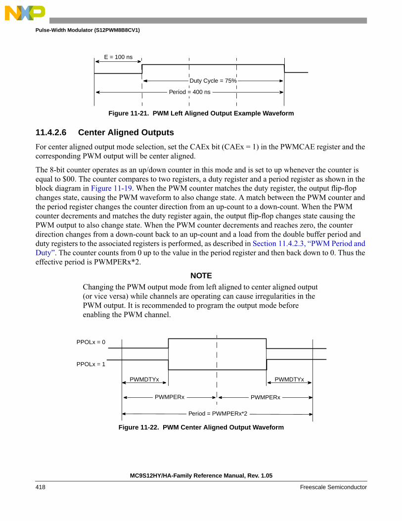
Pulse-Width Modulator (S12PWM8B8CV1)
Figure 11-21. PWM Left Aligned Output Example Waveform
11.4.2.6 Center Aligned Outputs
For center aligned output mode selection, set the CAEx bit (CAEx = 1) in the PWMCAE register and thecorresponding PWM output will be center aligned.
The 8-bit counter operates as an up/down counter in this mode and is set to up whenever the counter isequal to $00. The counter compares to two registers, a duty register and a period register as shown in theblock diagram in Figure 11-19. When the PWM counter matches the duty register, the output flip-flopchanges state, causing the PWM waveform to also change state. A match between the PWM counter andthe period register changes the counter direction from an up-count to a down-count. When the PWMcounter decrements and matches the duty register again, the output flip-flop changes state causing thePWM output to also change state. When the PWM counter decrements and reaches zero, the counterdirection changes from a down-count back to an up-count and a load from the double buffer period andduty registers to the associated registers is performed, as described in Section 11.4.2.3, “PWM Period andDuty”. The counter counts from 0 up to the value in the period register and then back down to 0. Thus theeffective period is PWMPERx*2.
NOTEChanging the PWM output mode from left aligned to center aligned output(or vice versa) while channels are operating can cause irregularities in thePWM output. It is recommended to program the output mode beforeenabling the PWM channel.
Figure 11-22. PWM Center Aligned Output Waveform
Period = 400 ns
E = 100 ns
Duty Cycle = 75%
PPOLx = 0
PPOLx = 1
PWMDTYx PWMDTYx
Period = PWMPERx*2
PWMPERxPWMPERx
MC9S12HY/HA-Family Reference Manual, Rev. 1.05
418 Freescale Semiconductor

Pulse-Width Modulator (S12PWM8B8CV1)
To calculate the output frequency in center aligned output mode for a particular channel, take the selectedclock source frequency for the channel (A, B, SA, or SB) and divide it by twice the value in the periodregister for that channel.
• PWMx Frequency = Clock (A, B, SA, or SB) / (2*PWMPERx)
• PWMx Duty Cycle (high time as a% of period):
— Polarity = 0 (PPOLx = 0)
Duty Cycle = [(PWMPERx-PWMDTYx)/PWMPERx] * 100%
— Polarity = 1 (PPOLx = 1)
Duty Cycle = [PWMDTYx / PWMPERx] * 100%
As an example of a center aligned output, consider the following case:
Clock Source = E, where E = 10 MHz (100 ns period)
PPOLx = 0
PWMPERx = 4
PWMDTYx = 1
PWMx Frequency = 10 MHz/8 = 1.25 MHz
PWMx Period = 800 ns
PWMx Duty Cycle = 3/4 *100% = 75%
Shown in Figure 11-23 is the output waveform generated.
Figure 11-23. PWM Center Aligned Output Example Waveform
11.4.2.7 PWM 16-Bit Functions
The PWM timer also has the option of generating 8-channels of 8-bits or 4-channels of 16-bits for greaterPWM resolution. This 16-bit channel option is achieved through the concatenation of two 8-bit channels.
The PWMCTL register contains four control bits, each of which is used to concatenate a pair of PWMchannels into one 16-bit channel. Channels 6 and 7 are concatenated with the CON67 bit, channels 4 and5 are concatenated with the CON45 bit, channels 2 and 3 are concatenated with the CON23 bit, andchannels 0 and 1 are concatenated with the CON01 bit.
NOTEChange these bits only when both corresponding channels are disabled.
When channels 6 and 7 are concatenated, channel 6 registers become the high order bytes of the doublebyte channel, as shown in Figure 11-24. Similarly, when channels 4 and 5 are concatenated, channel 4registers become the high order bytes of the double byte channel. When channels 2 and 3 are concatenated,
E = 100 ns
DUTY CYCLE = 75%
E = 100 ns
PERIOD = 800 ns
MC9S12HY/HA-Family Reference Manual, Rev. 1.05
Freescale Semiconductor 419

Pulse-Width Modulator (S12PWM8B8CV1)
channel 2 registers become the high order bytes of the double byte channel. When channels 0 and 1 areconcatenated, channel 0 registers become the high order bytes of the double byte channel.
When using the 16-bit concatenated mode, the clock source is determined by the low order 8-bit channelclock select control bits. That is channel 7 when channels 6 and 7 are concatenated, channel 5 whenchannels 4 and 5 are concatenated, channel 3 when channels 2 and 3 are concatenated, and channel 1 whenchannels 0 and 1 are concatenated. The resulting PWM is output to the pins of the corresponding low order8-bit channel as also shown in Figure 11-24. The polarity of the resulting PWM output is controlled by thePPOLx bit of the corresponding low order 8-bit channel as well.
MC9S12HY/HA-Family Reference Manual, Rev. 1.05
420 Freescale Semiconductor

Pulse-Width Modulator (S12PWM8B8CV1)
Figure 11-24. PWM 16-Bit Mode
Once concatenated mode is enabled (CONxx bits set in PWMCTL register), enabling/disabling thecorresponding 16-bit PWM channel is controlled by the low order PWMEx bit. In this case, the high orderbytes PWMEx bits have no effect and their corresponding PWM output is disabled.
In concatenated mode, writes to the 16-bit counter by using a 16-bit access or writes to either the low orhigh order byte of the counter will reset the 16-bit counter. Reads of the 16-bit counter must be made by16-bit access to maintain data coherency.
PWMCNT6 PWCNT7
PWM7
Clock Source 7High Low
Period/Duty Compare
PWMCNT4 PWCNT5
PWM5
Clock Source 5High Low
Period/Duty Compare
PWMCNT2 PWCNT3
PWM3
Clock Source 3High Low
Period/Duty Compare
PWMCNT0 PWCNT1
PWM1
Clock Source 1High Low
Period/Duty Compare
MC9S12HY/HA-Family Reference Manual, Rev. 1.05
Freescale Semiconductor 421
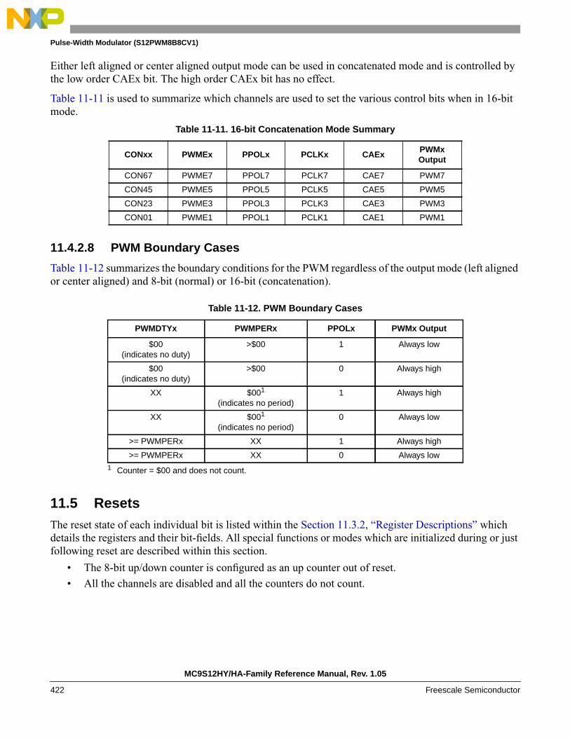
Pulse-Width Modulator (S12PWM8B8CV1)
Either left aligned or center aligned output mode can be used in concatenated mode and is controlled bythe low order CAEx bit. The high order CAEx bit has no effect.
Table 11-11 is used to summarize which channels are used to set the various control bits when in 16-bitmode.
11.4.2.8 PWM Boundary Cases
Table 11-12 summarizes the boundary conditions for the PWM regardless of the output mode (left alignedor center aligned) and 8-bit (normal) or 16-bit (concatenation).
11.5 ResetsThe reset state of each individual bit is listed within the Section 11.3.2, “Register Descriptions” whichdetails the registers and their bit-fields. All special functions or modes which are initialized during or justfollowing reset are described within this section.
• The 8-bit up/down counter is configured as an up counter out of reset.
• All the channels are disabled and all the counters do not count.
Table 11-11. 16-bit Concatenation Mode Summary
CONxx PWMEx PPOLx PCLKx CAExPWMxOutput
CON67 PWME7 PPOL7 PCLK7 CAE7 PWM7
CON45 PWME5 PPOL5 PCLK5 CAE5 PWM5
CON23 PWME3 PPOL3 PCLK3 CAE3 PWM3
CON01 PWME1 PPOL1 PCLK1 CAE1 PWM1
Table 11-12. PWM Boundary Cases
PWMDTYx PWMPERx PPOLx PWMx Output
$00(indicates no duty)
>$00 1 Always low
$00(indicates no duty)
>$00 0 Always high
XX $001
(indicates no period)
1 Counter = $00 and does not count.
1 Always high
XX $001
(indicates no period)0 Always low
>= PWMPERx XX 1 Always high
>= PWMPERx XX 0 Always low
MC9S12HY/HA-Family Reference Manual, Rev. 1.05
422 Freescale Semiconductor

Pulse-Width Modulator (S12PWM8B8CV1)
11.6 InterruptsThe PWM module has only one interrupt which is generated at the time of emergency shutdown, if thecorresponding enable bit (PWMIE) is set. This bit is the enable for the interrupt. The interrupt flag PWMIFis set whenever the input level of the PWM7 channel changes while PWM7ENA = 1 or when PWMENAis being asserted while the level at PWM7 is active.
In stop mode or wait mode (with the PSWAI bit set), the emergency shutdown feature will drive the PWMoutputs to their shutdown output levels but the PWMIF flag will not be set.
A description of the registers involved and affected due to this interrupt is explained in Section 11.3.2.15,“PWM Shutdown Register (PWMSDN)”.
The PWM block only generates the interrupt and does not service it. The interrupt signal name is PWMinterrupt signal.
MC9S12HY/HA-Family Reference Manual, Rev. 1.05
Freescale Semiconductor 423

Pulse-Width Modulator (S12PWM8B8CV1)
MC9S12HY/HA-Family Reference Manual, Rev. 1.05
424 Freescale Semiconductor

Chapter 12Serial Communication Interface (S12SCIV5)
12.1 IntroductionThis block guide provides an overview of the serial communication interface (SCI) module.
The SCI allows asynchronous serial communications with peripheral devices and other CPUs.
12.1.1 Glossary
IR: InfraRed
IrDA: Infrared Design Associate
IRQ: Interrupt Request
LIN: Local Interconnect Network
LSB: Least Significant Bit
MSB: Most Significant Bit
NRZ: Non-Return-to-Zero
RZI: Return-to-Zero-Inverted
RXD: Receive Pin
SCI : Serial Communication Interface
TXD: Transmit Pin
Table 12-1. Revision History
VersionNumber
RevisionDate
EffectiveDate Author Description of Changes
05.03 12/25/2008 remove redundancy comments in Figure1-2
05.04 08/05/2009 fix typo, SCIBDL reset value be 0x04, not 0x00
05.05 06/03/2010 fix typo, Table 12-4,SCICR1 Even parity should be PT=0fix typo, on page 12-447,should be BKDIF,not BLDIF
MC9S12HY/HA-Family Reference Manual, Rev. 1.05
Freescale Semiconductor 425
Serial Communication Interface (S12SCIV5)
12.1.2 Features
The SCI includes these distinctive features:
• Full-duplex or single-wire operation
• Standard mark/space non-return-to-zero (NRZ) format
• Selectable IrDA 1.4 return-to-zero-inverted (RZI) format with programmable pulse widths
• 13-bit baud rate selection
• Programmable 8-bit or 9-bit data format
• Separately enabled transmitter and receiver
• Programmable polarity for transmitter and receiver
• Programmable transmitter output parity
• Two receiver wakeup methods:
— Idle line wakeup— Address mark wakeup
• Interrupt-driven operation with eight flags:
— Transmitter empty— Transmission complete— Receiver full— Idle receiver input— Receiver overrun— Noise error— Framing error— Parity error— Receive wakeup on active edge— Transmit collision detect supporting LIN— Break Detect supporting LIN
• Receiver framing error detection
• Hardware parity checking
• 1/16 bit-time noise detection
12.1.3 Modes of Operation
The SCI functions the same in normal, special, and emulation modes. It has two low power modes, waitand stop modes.
• Run mode
• Wait mode
• Stop mode
MC9S12HY/HA-Family Reference Manual, Rev. 1.05
426 Freescale Semiconductor

Serial Communication Interface (S12SCIV5)
12.1.4 Block Diagram
Figure 12-1 is a high level block diagram of the SCI module, showing the interaction of various functionblocks.
Figure 12-1. SCI Block Diagram
SCI Data Register
RXD Data In
Data Out TXD
Receive Shift RegisterInfraredDecoder
Receive & WakeupControl
Data Format Control
Transmit Control
Baud RateGenerator
Bus Clock
1/16
Transmit Shift Register
SCI Data Register
ReceiveInterrupt
Generation
TransmitInterrupt
Generation
InfraredEncoder
IDLE
RDRF/OR
TC
TDRE
BRKD
BERRRXEDG
SCIInterruptRequest
MC9S12HY/HA-Family Reference Manual, Rev. 1.05
Freescale Semiconductor 427

Serial Communication Interface (S12SCIV5)
12.2 External Signal DescriptionThe SCI module has a total of two external pins.
12.2.1 TXD — Transmit Pin
The TXD pin transmits SCI (standard or infrared) data. It will idle high in either mode and is highimpedance anytime the transmitter is disabled.
12.2.2 RXD — Receive Pin
The RXD pin receives SCI (standard or infrared) data. An idle line is detected as a line high. This input isignored when the receiver is disabled and should be terminated to a known voltage.
12.3 Memory Map and Register DefinitionThis section provides a detailed description of all the SCI registers.
12.3.1 Module Memory Map and Register Definition
The memory map for the SCI module is given below in Figure 12-2. The address listed for each register isthe address offset. The total address for each register is the sum of the base address for the SCI module andthe address offset for each register.
MC9S12HY/HA-Family Reference Manual, Rev. 1.05
428 Freescale Semiconductor

Serial Communication Interface (S12SCIV5)
12.3.2 Register Descriptions
This section consists of register descriptions in address order. Each description includes a standard registerdiagram with an associated figure number. Writes to a reserved register locations do not have any effectand reads of these locations return a zero. Details of register bit and field function follow the registerdiagrams, in bit order.
RegisterName
Bit 7 6 5 4 3 2 1 Bit 0
0x0000SCIBDH1
RIREN TNP1 TNP0 SBR12 SBR11 SBR10 SBR9 SBR8
W
0x0001SCIBDL1
RSBR7 SBR6 SBR5 SBR4 SBR3 SBR2 SBR1 SBR0
W
0x0002SCICR11
RLOOPS SCISWAI RSRC M WAKE ILT PE PT
W
0x0000SCIASR12
RRXEDGIF
0 0 0 0BERRV BERRIF BKDIF
W
0x0001SCIACR12
RRXEDGIE
0 0 0 0 0BERRIE BKDIE
W
0x0002SCIACR22
R 0 0 0 0 0BERRM1 BERRM0 BKDFE
W
0x0003SCICR2
RTIE TCIE RIE ILIE TE RE RWU SBK
W
0x0004SCISR1
R TDRE TC RDRF IDLE OR NF FE PF
W
0x0005SCISR2
RAMAP
0 0TXPOL RXPOL BRK13 TXDIR
RAF
W
0x0006SCIDRH
R R8T8
0 0 0 0 0 0
W
0x0007SCIDRL
R R7 R6 R5 R4 R3 R2 R1 R0
W T7 T6 T5 T4 T3 T2 T1 T0
1.These registers are accessible if the AMAP bit in the SCISR2 register is set to zero.2,These registers are accessible if the AMAP bit in the SCISR2 register is set to one.
= Unimplemented or Reserved
Figure 12-2. SCI Register Summary
MC9S12HY/HA-Family Reference Manual, Rev. 1.05
Freescale Semiconductor 429

Serial Communication Interface (S12SCIV5)
12.3.2.1 SCI Baud Rate Registers (SCIBDH, SCIBDL)
Read: Anytime, if AMAP = 0. If only SCIBDH is written to, a read will not return the correct data untilSCIBDL is written to as well, following a write to SCIBDH.
Write: Anytime, if AMAP = 0.
NOTEThose two registers are only visible in the memory map if AMAP = 0 (resetcondition).
The SCI baud rate register is used by to determine the baud rate of the SCI, and to control the infraredmodulation/demodulation submodule.
Module Base + 0x0000
7 6 5 4 3 2 1 0
RIREN TNP1 TNP0 SBR12 SBR11 SBR10 SBR9 SBR8
W
Reset 0 0 0 0 0 0 0 0
Figure 12-3. SCI Baud Rate Register (SCIBDH)
Module Base + 0x0001
7 6 5 4 3 2 1 0
RSBR7 SBR6 SBR5 SBR4 SBR3 SBR2 SBR1 SBR0
W
Reset 0 0 0 0 0 1 0 0
Figure 12-4. SCI Baud Rate Register (SCIBDL)
Table 12-2. SCIBDH and SCIBDL Field Descriptions
Field Description
7IREN
Infrared Enable Bit — This bit enables/disables the infrared modulation/demodulation submodule.0 IR disabled1 IR enabled
6:5TNP[1:0]
Transmitter Narrow Pulse Bits — These bits enable whether the SCI transmits a 1/16, 3/16, 1/32 or 1/4 narrowpulse. See Table 12-3.
4:07:0
SBR[12:0]
SCI Baud Rate Bits — The baud rate for the SCI is determined by the bits in this register. The baud rate iscalculated two different ways depending on the state of the IREN bit.The formulas for calculating the baud rate are:
When IREN = 0 then,SCI baud rate = SCI bus clock / (16 x SBR[12:0])
When IREN = 1 then,SCI baud rate = SCI bus clock / (32 x SBR[12:1])
Note: The baud rate generator is disabled after reset and not started until the TE bit or the RE bit is set for thefirst time. The baud rate generator is disabled when (SBR[12:0] = 0 and IREN = 0) or (SBR[12:1] = 0 andIREN = 1).
Note: Writing to SCIBDH has no effect without writing to SCIBDL, because writing to SCIBDH puts the data ina temporary location until SCIBDL is written to.
MC9S12HY/HA-Family Reference Manual, Rev. 1.05
430 Freescale Semiconductor

Serial Communication Interface (S12SCIV5)
12.3.2.2 SCI Control Register 1 (SCICR1)
Read: Anytime, if AMAP = 0.
Write: Anytime, if AMAP = 0.
NOTEThis register is only visible in the memory map if AMAP = 0 (resetcondition).
Table 12-3. IRSCI Transmit Pulse Width
TNP[1:0] Narrow Pulse Width
11 1/4
10 1/32
01 1/16
00 3/16
Module Base + 0x0002
7 6 5 4 3 2 1 0
RLOOPS SCISWAI RSRC M WAKE ILT PE PT
W
Reset 0 0 0 0 0 0 0 0
Figure 12-5. SCI Control Register 1 (SCICR1)
Table 12-4. SCICR1 Field Descriptions
Field Description
7LOOPS
Loop Select Bit — LOOPS enables loop operation. In loop operation, the RXD pin is disconnected from the SCIand the transmitter output is internally connected to the receiver input. Both the transmitter and the receiver mustbe enabled to use the loop function.0 Normal operation enabled1 Loop operation enabledThe receiver input is determined by the RSRC bit.
6SCISWAI
SCI Stop in Wait Mode Bit — SCISWAI disables the SCI in wait mode.0 SCI enabled in wait mode1 SCI disabled in wait mode
5RSRC
Receiver Source Bit — When LOOPS = 1, the RSRC bit determines the source for the receiver shift registerinput. See Table 12-5.0 Receiver input internally connected to transmitter output1 Receiver input connected externally to transmitter
4M
Data Format Mode Bit — MODE determines whether data characters are eight or nine bits long.0 One start bit, eight data bits, one stop bit1 One start bit, nine data bits, one stop bit
3WAKE
Wakeup Condition Bit — WAKE determines which condition wakes up the SCI: a logic 1 (address mark) in themost significant bit position of a received data character or an idle condition on the RXD pin.0 Idle line wakeup1 Address mark wakeup
MC9S12HY/HA-Family Reference Manual, Rev. 1.05
Freescale Semiconductor 431

Serial Communication Interface (S12SCIV5)
2ILT
Idle Line Type Bit — ILT determines when the receiver starts counting logic 1s as idle character bits. Thecounting begins either after the start bit or after the stop bit. If the count begins after the start bit, then a string oflogic 1s preceding the stop bit may cause false recognition of an idle character. Beginning the count after thestop bit avoids false idle character recognition, but requires properly synchronized transmissions.0 Idle character bit count begins after start bit1 Idle character bit count begins after stop bit
1PE
Parity Enable Bit — PE enables the parity function. When enabled, the parity function inserts a parity bit in themost significant bit position.0 Parity function disabled1 Parity function enabled
0PT
Parity Type Bit — PT determines whether the SCI generates and checks for even parity or odd parity. With evenparity, an even number of 1s clears the parity bit and an odd number of 1s sets the parity bit. With odd parity, anodd number of 1s clears the parity bit and an even number of 1s sets the parity bit.0 Even parity1 Odd parity
Table 12-5. Loop Functions
LOOPS RSRC Function
0 x Normal operation
1 0 Loop mode with transmitter output internally connected to receiver input
1 1 Single-wire mode with TXD pin connected to receiver input
Table 12-4. SCICR1 Field Descriptions (continued)
Field Description
MC9S12HY/HA-Family Reference Manual, Rev. 1.05
432 Freescale Semiconductor
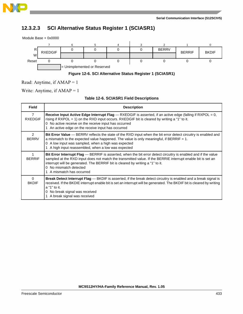
Serial Communication Interface (S12SCIV5)
12.3.2.3 SCI Alternative Status Register 1 (SCIASR1)
Read: Anytime, if AMAP = 1
Write: Anytime, if AMAP = 1
Module Base + 0x0000
7 6 5 4 3 2 1 0
RRXEDGIF
0 0 0 0 BERRVBERRIF BKDIF
W
Reset 0 0 0 0 0 0 0 0
= Unimplemented or Reserved
Figure 12-6. SCI Alternative Status Register 1 (SCIASR1)
Table 12-6. SCIASR1 Field Descriptions
Field Description
7RXEDGIF
Receive Input Active Edge Interrupt Flag — RXEDGIF is asserted, if an active edge (falling if RXPOL = 0,rising if RXPOL = 1) on the RXD input occurs. RXEDGIF bit is cleared by writing a “1” to it.0 No active receive on the receive input has occurred1 An active edge on the receive input has occurred
2BERRV
Bit Error Value — BERRV reflects the state of the RXD input when the bit error detect circuitry is enabled anda mismatch to the expected value happened. The value is only meaningful, if BERRIF = 1.0 A low input was sampled, when a high was expected1 A high input reassembled, when a low was expected
1BERRIF
Bit Error Interrupt Flag — BERRIF is asserted, when the bit error detect circuitry is enabled and if the valuesampled at the RXD input does not match the transmitted value. If the BERRIE interrupt enable bit is set aninterrupt will be generated. The BERRIF bit is cleared by writing a “1” to it.0 No mismatch detected1 A mismatch has occurred
0BKDIF
Break Detect Interrupt Flag — BKDIF is asserted, if the break detect circuitry is enabled and a break signal isreceived. If the BKDIE interrupt enable bit is set an interrupt will be generated. The BKDIF bit is cleared by writinga “1” to it.0 No break signal was received1 A break signal was received
MC9S12HY/HA-Family Reference Manual, Rev. 1.05
Freescale Semiconductor 433

Serial Communication Interface (S12SCIV5)
12.3.2.4 SCI Alternative Control Register 1 (SCIACR1)
Read: Anytime, if AMAP = 1
Write: Anytime, if AMAP = 1
Module Base + 0x0001
7 6 5 4 3 2 1 0
RRXEDGIE
0 0 0 0 0BERRIE BKDIE
W
Reset 0 0 0 0 0 0 0 0
= Unimplemented or Reserved
Figure 12-7. SCI Alternative Control Register 1 (SCIACR1)
Table 12-7. SCIACR1 Field Descriptions
Field Description
7RSEDGIE
Receive Input Active Edge Interrupt Enable — RXEDGIE enables the receive input active edge interrupt flag,RXEDGIF, to generate interrupt requests.0 RXEDGIF interrupt requests disabled1 RXEDGIF interrupt requests enabled
1BERRIE
Bit Error Interrupt Enable — BERRIE enables the bit error interrupt flag, BERRIF, to generate interruptrequests.0 BERRIF interrupt requests disabled1 BERRIF interrupt requests enabled
0BKDIE
Break Detect Interrupt Enable — BKDIE enables the break detect interrupt flag, BKDIF, to generate interruptrequests.0 BKDIF interrupt requests disabled1 BKDIF interrupt requests enabled
MC9S12HY/HA-Family Reference Manual, Rev. 1.05
434 Freescale Semiconductor
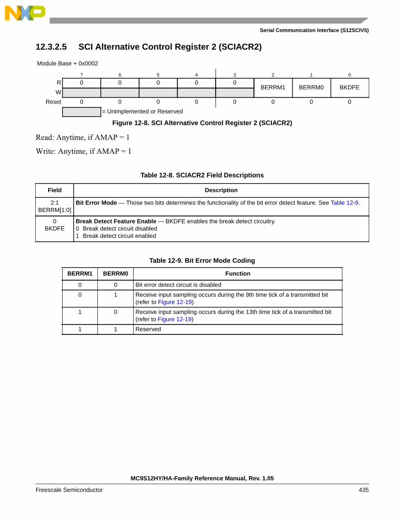
Serial Communication Interface (S12SCIV5)
12.3.2.5 SCI Alternative Control Register 2 (SCIACR2)
Read: Anytime, if AMAP = 1
Write: Anytime, if AMAP = 1
Module Base + 0x0002
7 6 5 4 3 2 1 0
R 0 0 0 0 0BERRM1 BERRM0 BKDFE
W
Reset 0 0 0 0 0 0 0 0
= Unimplemented or Reserved
Figure 12-8. SCI Alternative Control Register 2 (SCIACR2)
Table 12-8. SCIACR2 Field Descriptions
Field Description
2:1BERRM[1:0]
Bit Error Mode — Those two bits determines the functionality of the bit error detect feature. See Table 12-9.
0BKDFE
Break Detect Feature Enable — BKDFE enables the break detect circuitry.0 Break detect circuit disabled1 Break detect circuit enabled
Table 12-9. Bit Error Mode Coding
BERRM1 BERRM0 Function
0 0 Bit error detect circuit is disabled
0 1 Receive input sampling occurs during the 9th time tick of a transmitted bit(refer to Figure 12-19)
1 0 Receive input sampling occurs during the 13th time tick of a transmitted bit(refer to Figure 12-19)
1 1 Reserved
MC9S12HY/HA-Family Reference Manual, Rev. 1.05
Freescale Semiconductor 435
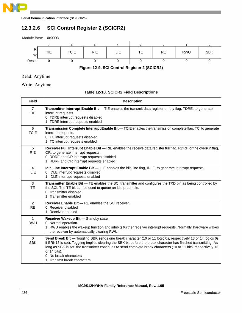
Serial Communication Interface (S12SCIV5)
12.3.2.6 SCI Control Register 2 (SCICR2)
Read: Anytime
Write: Anytime
Module Base + 0x0003
7 6 5 4 3 2 1 0
RTIE TCIE RIE ILIE TE RE RWU SBK
W
Reset 0 0 0 0 0 0 0 0
Figure 12-9. SCI Control Register 2 (SCICR2)
Table 12-10. SCICR2 Field Descriptions
Field Description
7TIE
Transmitter Interrupt Enable Bit — TIE enables the transmit data register empty flag, TDRE, to generateinterrupt requests.0 TDRE interrupt requests disabled1 TDRE interrupt requests enabled
6TCIE
Transmission Complete Interrupt Enable Bit — TCIE enables the transmission complete flag, TC, to generateinterrupt requests.0 TC interrupt requests disabled1 TC interrupt requests enabled
5RIE
Receiver Full Interrupt Enable Bit — RIE enables the receive data register full flag, RDRF, or the overrun flag,OR, to generate interrupt requests.0 RDRF and OR interrupt requests disabled1 RDRF and OR interrupt requests enabled
4ILIE
Idle Line Interrupt Enable Bit — ILIE enables the idle line flag, IDLE, to generate interrupt requests.0 IDLE interrupt requests disabled1 IDLE interrupt requests enabled
3TE
Transmitter Enable Bit — TE enables the SCI transmitter and configures the TXD pin as being controlled bythe SCI. The TE bit can be used to queue an idle preamble.0 Transmitter disabled1 Transmitter enabled
2RE
Receiver Enable Bit — RE enables the SCI receiver.0 Receiver disabled1 Receiver enabled
1RWU
Receiver Wakeup Bit — Standby state0 Normal operation.1 RWU enables the wakeup function and inhibits further receiver interrupt requests. Normally, hardware wakes
the receiver by automatically clearing RWU.
0SBK
Send Break Bit — Toggling SBK sends one break character (10 or 11 logic 0s, respectively 13 or 14 logics 0sif BRK13 is set). Toggling implies clearing the SBK bit before the break character has finished transmitting. Aslong as SBK is set, the transmitter continues to send complete break characters (10 or 11 bits, respectively 13or 14 bits).0 No break characters1 Transmit break characters
MC9S12HY/HA-Family Reference Manual, Rev. 1.05
436 Freescale Semiconductor

Serial Communication Interface (S12SCIV5)
12.3.2.7 SCI Status Register 1 (SCISR1)
The SCISR1 and SCISR2 registers provides inputs to the MCU for generation of SCI interrupts. Also,these registers can be polled by the MCU to check the status of these bits. The flag-clearing proceduresrequire that the status register be read followed by a read or write to the SCI data register.It is permissibleto execute other instructions between the two steps as long as it does not compromise the handling of I/O,but the order of operations is important for flag clearing.
Read: Anytime
Write: Has no meaning or effect
Module Base + 0x0004
7 6 5 4 3 2 1 0
R TDRE TC RDRF IDLE OR NF FE PF
W
Reset 1 1 0 0 0 0 0 0
= Unimplemented or Reserved
Figure 12-10. SCI Status Register 1 (SCISR1)
Table 12-11. SCISR1 Field Descriptions
Field Description
7TDRE
Transmit Data Register Empty Flag — TDRE is set when the transmit shift register receives a byte from theSCI data register. When TDRE is 1, the transmit data register (SCIDRH/L) is empty and can receive a new valueto transmit.Clear TDRE by reading SCI status register 1 (SCISR1), with TDRE set and then writing to SCI dataregister low (SCIDRL).0 No byte transferred to transmit shift register1 Byte transferred to transmit shift register; transmit data register empty
6TC
Transmit Complete Flag — TC is set low when there is a transmission in progress or when a preamble or breakcharacter is loaded. TC is set high when the TDRE flag is set and no data, preamble, or break character is beingtransmitted.When TC is set, the TXD pin becomes idle (logic 1). Clear TC by reading SCI status register 1(SCISR1) with TC set and then writing to SCI data register low (SCIDRL). TC is cleared automatically when data,preamble, or break is queued and ready to be sent. TC is cleared in the event of a simultaneous set and clear ofthe TC flag (transmission not complete).0 Transmission in progress1 No transmission in progress
5RDRF
Receive Data Register Full Flag — RDRF is set when the data in the receive shift register transfers to the SCIdata register. Clear RDRF by reading SCI status register 1 (SCISR1) with RDRF set and then reading SCI dataregister low (SCIDRL).0 Data not available in SCI data register1 Received data available in SCI data register
4IDLE
Idle Line Flag — IDLE is set when 10 consecutive logic 1s (if M = 0) or 11 consecutive logic 1s (if M =1) appearon the receiver input. Once the IDLE flag is cleared, a valid frame must again set the RDRF flag before an idlecondition can set the IDLE flag.Clear IDLE by reading SCI status register 1 (SCISR1) with IDLE set and thenreading SCI data register low (SCIDRL).0 Receiver input is either active now or has never become active since the IDLE flag was last cleared1 Receiver input has become idleNote: When the receiver wakeup bit (RWU) is set, an idle line condition does not set the IDLE flag.
MC9S12HY/HA-Family Reference Manual, Rev. 1.05
Freescale Semiconductor 437

Serial Communication Interface (S12SCIV5)
3OR
Overrun Flag — OR is set when software fails to read the SCI data register before the receive shift registerreceives the next frame. The OR bit is set immediately after the stop bit has been completely received for thesecond frame. The data in the shift register is lost, but the data already in the SCI data registers is not affected.Clear OR by reading SCI status register 1 (SCISR1) with OR set and then reading SCI data register low(SCIDRL).0 No overrun1 OverrunNote: OR flag may read back as set when RDRF flag is clear. This may happen if the following sequence of
events occurs:1. After the first frame is received, read status register SCISR1 (returns RDRF set and OR flag clear);2. Receive second frame without reading the first frame in the data register (the second frame is not
received and OR flag is set);3. Read data register SCIDRL (returns first frame and clears RDRF flag in the status register);4. Read status register SCISR1 (returns RDRF clear and OR set).
Event 3 may be at exactly the same time as event 2 or any time after. When this happens, a dummySCIDRL read following event 4 will be required to clear the OR flag if further frames are to be received.
2NF
Noise Flag — NF is set when the SCI detects noise on the receiver input. NF bit is set during the same cycle asthe RDRF flag but does not get set in the case of an overrun. Clear NF by reading SCI status register 1(SCISR1),and then reading SCI data register low (SCIDRL).0 No noise1 Noise
1FE
Framing Error Flag — FE is set when a logic 0 is accepted as the stop bit. FE bit is set during the same cycleas the RDRF flag but does not get set in the case of an overrun. FE inhibits further data reception until it iscleared. Clear FE by reading SCI status register 1 (SCISR1) with FE set and then reading the SCI data registerlow (SCIDRL).0 No framing error1 Framing error
0PF
Parity Error Flag — PF is set when the parity enable bit (PE) is set and the parity of the received data does notmatch the parity type bit (PT). PF bit is set during the same cycle as the RDRF flag but does not get set in thecase of an overrun. Clear PF by reading SCI status register 1 (SCISR1), and then reading SCI data register low(SCIDRL).0 No parity error1 Parity error
Table 12-11. SCISR1 Field Descriptions (continued)
Field Description
MC9S12HY/HA-Family Reference Manual, Rev. 1.05
438 Freescale Semiconductor

Serial Communication Interface (S12SCIV5)
12.3.2.8 SCI Status Register 2 (SCISR2)
Read: Anytime
Write: Anytime
Module Base + 0x0005
7 6 5 4 3 2 1 0
RAMAP
0 0TXPOL RXPOL BRK13 TXDIR
RAF
W
Reset 0 0 0 0 0 0 0 0
= Unimplemented or Reserved
Figure 12-11. SCI Status Register 2 (SCISR2)
Table 12-12. SCISR2 Field Descriptions
Field Description
7AMAP
Alternative Map — This bit controls which registers sharing the same address space are accessible. In the resetcondition the SCI behaves as previous versions. Setting AMAP=1 allows the access to another set of control andstatus registers and hides the baud rate and SCI control Register 1.0 The registers labelled SCIBDH (0x0000),SCIBDL (0x0001), SCICR1 (0x0002) are accessible1 The registers labelled SCIASR1 (0x0000),SCIACR1 (0x0001), SCIACR2 (0x00002) are accessible
4TXPOL
Transmit Polarity — This bit control the polarity of the transmitted data. In NRZ format, a one is represented bya mark and a zero is represented by a space for normal polarity, and the opposite for inverted polarity. In IrDAformat, a zero is represented by short high pulse in the middle of a bit time remaining idle low for a one for normalpolarity, and a zero is represented by short low pulse in the middle of a bit time remaining idle high for a one forinverted polarity.0 Normal polarity1 Inverted polarity
3RXPOL
Receive Polarity — This bit control the polarity of the received data. In NRZ format, a one is represented by amark and a zero is represented by a space for normal polarity, and the opposite for inverted polarity. In IrDAformat, a zero is represented by short high pulse in the middle of a bit time remaining idle low for a one for normalpolarity, and a zero is represented by short low pulse in the middle of a bit time remaining idle high for a one forinverted polarity.0 Normal polarity1 Inverted polarity
2BRK13
Break Transmit Character Length — This bit determines whether the transmit break character is 10 or 11 bitrespectively 13 or 14 bits long. The detection of a framing error is not affected by this bit.0 Break character is 10 or 11 bit long1 Break character is 13 or 14 bit long
1TXDIR
Transmitter Pin Data Direction in Single-Wire Mode — This bit determines whether the TXD pin is going tobe used as an input or output, in the single-wire mode of operation. This bit is only relevant in the single-wiremode of operation.0 TXD pin to be used as an input in single-wire mode1 TXD pin to be used as an output in single-wire mode
0RAF
Receiver Active Flag — RAF is set when the receiver detects a logic 0 during the RT1 time period of the startbit search. RAF is cleared when the receiver detects an idle character.0 No reception in progress1 Reception in progress
MC9S12HY/HA-Family Reference Manual, Rev. 1.05
Freescale Semiconductor 439

Serial Communication Interface (S12SCIV5)
12.3.2.9 SCI Data Registers (SCIDRH, SCIDRL)
Read: Anytime; reading accesses SCI receive data register
Write: Anytime; writing accesses SCI transmit data register; writing to R8 has no effect
NOTEIf the value of T8 is the same as in the previous transmission, T8 does nothave to be rewritten.The same value is transmitted until T8 is rewritten
In 8-bit data format, only SCI data register low (SCIDRL) needs to beaccessed.
When transmitting in 9-bit data format and using 8-bit write instructions,write first to SCI data register high (SCIDRH), then SCIDRL.
Module Base + 0x0006
7 6 5 4 3 2 1 0
R R8T8
0 0 0 0 0 0
W
Reset 0 0 0 0 0 0 0 0
= Unimplemented or Reserved
Figure 12-12. SCI Data Registers (SCIDRH)
Module Base + 0x0007
7 6 5 4 3 2 1 0
R R7 R6 R5 R4 R3 R2 R1 R0
W T7 T6 T5 T4 T3 T2 T1 T0
Reset 0 0 0 0 0 0 0 0
Figure 12-13. SCI Data Registers (SCIDRL)
Table 12-13. SCIDRH and SCIDRL Field Descriptions
Field Description
SCIDRH7
R8
Received Bit 8 — R8 is the ninth data bit received when the SCI is configured for 9-bit data format (M = 1).
SCIDRH6
T8
Transmit Bit 8 — T8 is the ninth data bit transmitted when the SCI is configured for 9-bit data format (M = 1).
SCIDRL7:0
R[7:0]T[7:0]
R7:R0 — Received bits seven through zero for 9-bit or 8-bit data formatsT7:T0 — Transmit bits seven through zero for 9-bit or 8-bit formats
MC9S12HY/HA-Family Reference Manual, Rev. 1.05
440 Freescale Semiconductor

Serial Communication Interface (S12SCIV5)
12.4 Functional DescriptionThis section provides a complete functional description of the SCI block, detailing the operation of thedesign from the end user perspective in a number of subsections.
Figure 12-14 shows the structure of the SCI module. The SCI allows full duplex, asynchronous, serialcommunication between the CPU and remote devices, including other CPUs. The SCI transmitter andreceiver operate independently, although they use the same baud rate generator. The CPU monitors thestatus of the SCI, writes the data to be transmitted, and processes received data.
Figure 12-14. Detailed SCI Block Diagram
SCI Data
ReceiveShift Register
SCI DataRegister
TransmitShift Register
Register
Baud RateGenerator
SBR12:SBR0
Bus
TransmitControl÷16
Receiveand Wakeup
Data FormatControl
Control
T8
PF
FE
NF
RDRF
IDLE
TIE
OR
TCIE
TDRE
TC
R8
RAF
LOOPS
RWU
RE
PE
ILT
PT
WAKE
MClock
ILIE
RIE
RXD
RSRC
SBK
LOOPS
TE
RSRC
IREN
R16
XC
LK
Ir_RXD
TXDIr_TXD
R16XCLK
R32XCLK
TNP[1:0] IREN
TransmitEncoder
ReceiveDecoder
SCRXD
SCTXD
Infrared
Infrared
TC
TDRE
RD
RF
/OR
IDLE
Active EdgeDetect
Break DetectRXD
BKDFE
BERRM[1:0]
BKDIE
BKDIF
RXEDGIE
RXEDGIF
BERRIE
BERRIF
SCIInterruptRequest
LIN TransmitCollisionDetect
MC9S12HY/HA-Family Reference Manual, Rev. 1.05
Freescale Semiconductor 441
Serial Communication Interface (S12SCIV5)
12.4.1 Infrared Interface Submodule
This module provides the capability of transmitting narrow pulses to an IR LED and receiving narrowpulses and transforming them to serial bits, which are sent to the SCI. The IrDA physical layerspecification defines a half-duplex infrared communication link for exchange data. The full standardincludes data rates up to 16 Mbits/s. This design covers only data rates between 2.4 Kbits/s and 115.2Kbits/s.
The infrared submodule consists of two major blocks: the transmit encoder and the receive decoder. TheSCI transmits serial bits of data which are encoded by the infrared submodule to transmit a narrow pulsefor every zero bit. No pulse is transmitted for every one bit. When receiving data, the IR pulses should bedetected using an IR photo diode and transformed to CMOS levels by the IR receive decoder (externalfrom the MCU). The narrow pulses are then stretched by the infrared submodule to get back to a serial bitstream to be received by the SCI.The polarity of transmitted pulses and expected receive pulses can beinverted so that a direct connection can be made to external IrDA transceiver modules that uses active lowpulses.
The infrared submodule receives its clock sources from the SCI. One of these two clocks are selected inthe infrared submodule in order to generate either 3/16, 1/16, 1/32 or 1/4 narrow pulses duringtransmission. The infrared block receives two clock sources from the SCI, R16XCLK and R32XCLK,which are configured to generate the narrow pulse width during transmission. The R16XCLK andR32XCLK are internal clocks with frequencies 16 and 32 times the baud rate respectively. BothR16XCLK and R32XCLK clocks are used for transmitting data. The receive decoder uses only theR16XCLK clock.
12.4.1.1 Infrared Transmit Encoder
The infrared transmit encoder converts serial bits of data from transmit shift register to the TXD pin. Anarrow pulse is transmitted for a zero bit and no pulse for a one bit. The narrow pulse is sent in the middleof the bit with a duration of 1/32, 1/16, 3/16 or 1/4 of a bit time. A narrow high pulse is transmitted for azero bit when TXPOL is cleared, while a narrow low pulse is transmitted for a zero bit when TXPOL is set.
12.4.1.2 Infrared Receive Decoder
The infrared receive block converts data from the RXD pin to the receive shift register. A narrow pulse isexpected for each zero received and no pulse is expected for each one received. A narrow high pulse isexpected for a zero bit when RXPOL is cleared, while a narrow low pulse is expected for a zero bit whenRXPOL is set. This receive decoder meets the edge jitter requirement as defined by the IrDA serial infraredphysical layer specification.
12.4.2 LIN Support
This module provides some basic support for the LIN protocol. At first this is a break detect circuitrymaking it easier for the LIN software to distinguish a break character from an incoming data stream. As afurther addition is supports a collision detection at the bit level as well as cancelling pending transmissions.
MC9S12HY/HA-Family Reference Manual, Rev. 1.05
442 Freescale Semiconductor

Serial Communication Interface (S12SCIV5)
12.4.3 Data Format
The SCI uses the standard NRZ mark/space data format. When Infrared is enabled, the SCI uses RZI dataformat where zeroes are represented by light pulses and ones remain low. See Figure 12-15 below.
Figure 12-15. SCI Data Formats
Each data character is contained in a frame that includes a start bit, eight or nine data bits, and a stop bit.Clearing the M bit in SCI control register 1 configures the SCI for 8-bit data characters. A frame with eightdata bits has a total of 10 bits. Setting the M bit configures the SCI for nine-bit data characters. A framewith nine data bits has a total of 11 bits.
When the SCI is configured for 9-bit data characters, the ninth data bit is the T8 bit in SCI data registerhigh (SCIDRH). It remains unchanged after transmission and can be used repeatedly without rewriting it.A frame with nine data bits has a total of 11 bits.
Table 12-14. Example of 8-Bit Data Formats
StartBit
DataBits
AddressBits
ParityBits
StopBit
1 8 0 0 1
1 7 0 1 1
1 7 11
1 The address bit identifies the frame as an addresscharacter. See Section 12.4.6.6, “Receiver Wakeup”.
0 1
Table 12-15. Example of 9-Bit Data Formats
StartBit
DataBits
AddressBits
ParityBits
StopBit
1 9 0 0 1
1 8 0 1 1
1 8 11 0 1
Bit 5StartBit Bit 0 Bit 1
Next
STOPBit
StartBit
8-Bit Data Format(Bit M in SCICR1 Clear)
StartBit Bit 0
NEXT
STOPBit
STARTBit
9-Bit Data Format(Bit M in SCICR1 Set)
Bit 1 Bit 2 Bit 3 Bit 4 Bit 5 Bit 6 Bit 7 Bit 8
Bit 2 Bit 3 Bit 4 Bit 6 Bit 7
POSSIBLEPARITY
Bit
PossibleParity
BitStandardSCI Data
InfraredSCI Data
StandardSCI Data
InfraredSCI Data
MC9S12HY/HA-Family Reference Manual, Rev. 1.05
Freescale Semiconductor 443

Serial Communication Interface (S12SCIV5)
12.4.4 Baud Rate Generation
A 13-bit modulus counter in the baud rate generator derives the baud rate for both the receiver and thetransmitter. The value from 0 to 8191 written to the SBR12:SBR0 bits determines the bus clock divisor.The SBR bits are in the SCI baud rate registers (SCIBDH and SCIBDL). The baud rate clock issynchronized with the bus clock and drives the receiver. The baud rate clock divided by 16 drives thetransmitter. The receiver has an acquisition rate of 16 samples per bit time.
Baud rate generation is subject to one source of error:
• Integer division of the bus clock may not give the exact target frequency.
Table 12-16 lists some examples of achieving target baud rates with a bus clock frequency of 25 MHz.
When IREN = 0 then,
SCI baud rate = SCI bus clock / (16 * SCIBR[12:0])
1 The address bit identifies the frame as an addresscharacter. See Section 12.4.6.6, “Receiver Wakeup”.
Table 12-16. Baud Rates (Example: Bus Clock = 25 MHz)
BitsSBR[12:0]
ReceiverClock (Hz)
TransmitterClock (Hz)
TargetBaud Rate
Error(%)
41 609,756.1 38,109.8 38,400 .76
81 308,642.0 19,290.1 19,200 .47
163 153,374.2 9585.9 9,600 .16
326 76,687.1 4792.9 4,800 .15
651 38,402.5 2400.2 2,400 .01
1302 19,201.2 1200.1 1,200 .01
2604 9600.6 600.0 600 .00
5208 4800.0 300.0 300 .00
MC9S12HY/HA-Family Reference Manual, Rev. 1.05
444 Freescale Semiconductor

Serial Communication Interface (S12SCIV5)
12.4.5 Transmitter
Figure 12-16. Transmitter Block Diagram
12.4.5.1 Transmitter Character Length
The SCI transmitter can accommodate either 8-bit or 9-bit data characters. The state of the M bit in SCIcontrol register 1 (SCICR1) determines the length of data characters. When transmitting 9-bit data, bit T8in SCI data register high (SCIDRH) is the ninth bit (bit 8).
12.4.5.2 Character Transmission
To transmit data, the MCU writes the data bits to the SCI data registers (SCIDRH/SCIDRL), which in turnare transferred to the transmitter shift register. The transmit shift register then shifts a frame out throughthe TXD pin, after it has prefaced them with a start bit and appended them with a stop bit. The SCI dataregisters (SCIDRH and SCIDRL) are the write-only buffers between the internal data bus and the transmitshift register.
PE
PT
H 8 7 6 5 4 3 2 1 0 L
11-Bit Transmit RegisterSto
p
Sta
rt
T8
TIE
TDRE
TCIE
SBK
TC
ParityGeneration
MS
B
SCI Data Registers
Load
from
SC
IDR
Shi
ft E
nabl
e
Pre
ambl
e (A
ll 1s
)
Bre
ak (
All
0s)
Transmitter Control
M
Internal Bus
SBR12:SBR0
Baud Divider ÷ 16BusClock
TE
SCTXDTXPOL
LOOPS
LOOP
RSRC
CONTROLTo Receiver
Transmit Collision Detect
TDRE IRQ
TC IRQ
SCTXD
SCRXD(From Receiver)TCIE
BERRIFBER IRQ
BERRM[1:0]
MC9S12HY/HA-Family Reference Manual, Rev. 1.05
Freescale Semiconductor 445

Serial Communication Interface (S12SCIV5)
The SCI also sets a flag, the transmit data register empty flag (TDRE), every time it transfers data from thebuffer (SCIDRH/L) to the transmitter shift register.The transmit driver routine may respond to this flag bywriting another byte to the Transmitter buffer (SCIDRH/SCIDRL), while the shift register is still shiftingout the first byte.
To initiate an SCI transmission:
1. Configure the SCI:
a) Select a baud rate. Write this value to the SCI baud registers (SCIBDH/L) to begin the baudrate generator. Remember that the baud rate generator is disabled when the baud rate is zero.Writing to the SCIBDH has no effect without also writing to SCIBDL.
b) Write to SCICR1 to configure word length, parity, and other configuration bits(LOOPS,RSRC,M,WAKE,ILT,PE,PT).
c) Enable the transmitter, interrupts, receive, and wake up as required, by writing to the SCICR2register bits (TIE,TCIE,RIE,ILIE,TE,RE,RWU,SBK). A preamble or idle character will nowbe shifted out of the transmitter shift register.
2. Transmit Procedure for each byte:
a) Poll the TDRE flag by reading the SCISR1 or responding to the TDRE interrupt. Keep in mindthat the TDRE bit resets to one.
b) If the TDRE flag is set, write the data to be transmitted to SCIDRH/L, where the ninth bit iswritten to the T8 bit in SCIDRH if the SCI is in 9-bit data format. A new transmission will notresult until the TDRE flag has been cleared.
3. Repeat step 2 for each subsequent transmission.
NOTEThe TDRE flag is set when the shift register is loaded with the next data tobe transmitted from SCIDRH/L, which happens, generally speaking, a littleover half-way through the stop bit of the previous frame. Specifically, thistransfer occurs 9/16ths of a bit time AFTER the start of the stop bit of theprevious frame.
Writing the TE bit from 0 to a 1 automatically loads the transmit shift register with a preamble of 10 logic1s (if M = 0) or 11 logic 1s (if M = 1). After the preamble shifts out, control logic transfers the data fromthe SCI data register into the transmit shift register. A logic 0 start bit automatically goes into the leastsignificant bit position of the transmit shift register. A logic 1 stop bit goes into the most significant bitposition.
Hardware supports odd or even parity. When parity is enabled, the most significant bit (MSB) of the datacharacter is the parity bit.
The transmit data register empty flag, TDRE, in SCI status register 1 (SCISR1) becomes set when the SCIdata register transfers a byte to the transmit shift register. The TDRE flag indicates that the SCI dataregister can accept new data from the internal data bus. If the transmit interrupt enable bit, TIE, in SCIcontrol register 2 (SCICR2) is also set, the TDRE flag generates a transmitter interrupt request.
MC9S12HY/HA-Family Reference Manual, Rev. 1.05
446 Freescale Semiconductor
Serial Communication Interface (S12SCIV5)
When the transmit shift register is not transmitting a frame, the TXD pin goes to the idle condition, logic1. If at any time software clears the TE bit in SCI control register 2 (SCICR2), the transmitter enable signalgoes low and the transmit signal goes idle.
If software clears TE while a transmission is in progress (TC = 0), the frame in the transmit shift registercontinues to shift out. To avoid accidentally cutting off the last frame in a message, always wait for TDREto go high after the last frame before clearing TE.
To separate messages with preambles with minimum idle line time, use this sequence between messages:
1. Write the last byte of the first message to SCIDRH/L.
2. Wait for the TDRE flag to go high, indicating the transfer of the last frame to the transmit shiftregister.
3. Queue a preamble by clearing and then setting the TE bit.
4. Write the first byte of the second message to SCIDRH/L.
12.4.5.3 Break Characters
Writing a logic 1 to the send break bit, SBK, in SCI control register 2 (SCICR2) loads the transmit shiftregister with a break character. A break character contains all logic 0s and has no start, stop, or parity bit.Break character length depends on the M bit in SCI control register 1 (SCICR1). As long as SBK is at logic1, transmitter logic continuously loads break characters into the transmit shift register. After softwareclears the SBK bit, the shift register finishes transmitting the last break character and then transmits at leastone logic 1. The automatic logic 1 at the end of a break character guarantees the recognition of the start bitof the next frame.
The SCI recognizes a break character when there are 10 or 11(M = 0 or M = 1) consecutive zero received.Depending if the break detect feature is enabled or not receiving a break character has these effects on SCIregisters.
If the break detect feature is disabled (BKDFE = 0):
• Sets the framing error flag, FE
• Sets the receive data register full flag, RDRF
• Clears the SCI data registers (SCIDRH/L)
• May set the overrun flag, OR, noise flag, NF, parity error flag, PE, or the receiver active flag, RAF(see 3.4.4 and 3.4.5 SCI Status Register 1 and 2)
If the break detect feature is enabled (BKDFE = 1) there are two scenarios1
The break is detected right from a start bit or is detected during a byte reception.
• Sets the break detect interrupt flag, BKDIF
• Does not change the data register full flag, RDRF or overrun flag OR
• Does not change the framing error flag FE, parity error flag PE.
• Does not clear the SCI data registers (SCIDRH/L)
• May set noise flag NF, or receiver active flag RAF.
1. A Break character in this context are either 10 or 11 consecutive zero received bits
MC9S12HY/HA-Family Reference Manual, Rev. 1.05
Freescale Semiconductor 447

Serial Communication Interface (S12SCIV5)
Figure 12-17 shows two cases of break detect. In trace RXD_1 the break symbol starts with the start bit,while in RXD_2 the break starts in the middle of a transmission. If BRKDFE = 1, in RXD_1 case therewill be no byte transferred to the receive buffer and the RDRF flag will not be modified. Also no framingerror or parity error will be flagged from this transfer. In RXD_2 case, however the break signal starts laterduring the transmission. At the expected stop bit position the byte received so far will be transferred to thereceive buffer, the receive data register full flag will be set, a framing error and if enabled and appropriatea parity error will be set. Once the break is detected the BRKDIF flag will be set.
Figure 12-17. Break Detection if BRKDFE = 1 (M = 0)
12.4.5.4 Idle Characters
An idle character (or preamble) contains all logic 1s and has no start, stop, or parity bit. Idle characterlength depends on the M bit in SCI control register 1 (SCICR1). The preamble is a synchronizing idlecharacter that begins the first transmission initiated after writing the TE bit from 0 to 1.
If the TE bit is cleared during a transmission, the TXD pin becomes idle after completion of thetransmission in progress. Clearing and then setting the TE bit during a transmission queues an idlecharacter to be sent after the frame currently being transmitted.
NOTEWhen queueing an idle character, return the TE bit to logic 1 before the stopbit of the current frame shifts out through the TXD pin. Setting TE after thestop bit appears on TXD causes data previously written to the SCI dataregister to be lost. Toggle the TE bit for a queued idle character while theTDRE flag is set and immediately before writing the next byte to the SCIdata register.
If the TE bit is clear and the transmission is complete, the SCI is not themaster of the TXD pin
Start Bit Position Stop Bit Position
BRKDIF = 1
FE = 1 BRKDIF = 1
RXD_1
RXD_2
1 2 3 4 5 6 7 8 9 10
1 2 3 4 5 6 7 8 9 10
Zero Bit Counter
Zero Bit Counter . . .
. . .
MC9S12HY/HA-Family Reference Manual, Rev. 1.05
448 Freescale Semiconductor

Serial Communication Interface (S12SCIV5)
12.4.5.5 LIN Transmit Collision Detection
This module allows to check for collisions on the LIN bus.
Figure 12-18. Collision Detect Principle
If the bit error circuit is enabled (BERRM[1:0] = 0:1 or = 1:0]), the error detect circuit will compare thetransmitted and the received data stream at a point in time and flag any mismatch. The timing checks runwhen transmitter is active (not idle). As soon as a mismatch between the transmitted data and the receiveddata is detected the following happens:
• The next bit transmitted will have a high level (TXPOL = 0) or low level (TXPOL = 1)
• The transmission is aborted and the byte in transmit buffer is discarded.
• the transmit data register empty and the transmission complete flag will be set
• The bit error interrupt flag, BERRIF, will be set.
• No further transmissions will take place until the BERRIF is cleared.
Figure 12-19. Timing Diagram Bit Error Detection
If the bit error detect feature is disabled, the bit error interrupt flag is cleared.
NOTEThe RXPOL and TXPOL bit should be set the same when transmissioncollision detect feature is enabled, otherwise the bit error interrupt flag maybe set incorrectly.
TXD Pin
RXD Pin
LIN Physical InterfaceSynchronizer Stage
Bus Clock
Receive ShiftRegister
Transmit ShiftRegister
LIN Bus
Compare
Sample
Bit Error
Point
Output TransmitShift Register
0 1 2 3 4 5 6 7 8 9 10 11 12 13 14 15 0
Input ReceiveShift Register
BERRM[1:0] = 0:1 BERRM[1:0] = 1:1
Compare Sample Points
Sam
plin
g B
egin
Sam
plin
g B
egin
Sam
plin
g E
nd
Sam
plin
g E
nd
MC9S12HY/HA-Family Reference Manual, Rev. 1.05
Freescale Semiconductor 449

Serial Communication Interface (S12SCIV5)
12.4.6 Receiver
Figure 12-20. SCI Receiver Block Diagram
12.4.6.1 Receiver Character Length
The SCI receiver can accommodate either 8-bit or 9-bit data characters. The state of the M bit in SCIcontrol register 1 (SCICR1) determines the length of data characters. When receiving 9-bit data, bit R8 inSCI data register high (SCIDRH) is the ninth bit (bit 8).
12.4.6.2 Character Reception
During an SCI reception, the receive shift register shifts a frame in from the RXD pin. The SCI data registeris the read-only buffer between the internal data bus and the receive shift register.
After a complete frame shifts into the receive shift register, the data portion of the frame transfers to theSCI data register. The receive data register full flag, RDRF, in SCI status register 1 (SCISR1) becomes set,
All
1s
M
WAKE
ILT
PE
PT
RE
H 8 7 6 5 4 3 2 1 0 L
11-Bit Receive Shift RegisterSto
p
Sta
rt
Data
Wakeup
ParityChecking
MS
B
SCI Data Register
R8
ILIE
RWU
RDRF
OR
NF
FE
PE
Internal Bus
Bus
SBR12:SBR0
Baud DividerClock
IDLE
RAF
Recovery
Logic
RXPOL
LOOPS
Loop
RSRC
Control
SCRXD
From TXD Pinor Transmitter
Idle IRQ
RDRF/OR IRQ
BreakDetect Logic
Active EdgeDetect Logic
BRKDFE
BRKDIE
BRKDIF
RXEDGIE
RXEDGIF
Break IRQ
RX Active Edge IRQ
RIE
MC9S12HY/HA-Family Reference Manual, Rev. 1.05
450 Freescale Semiconductor
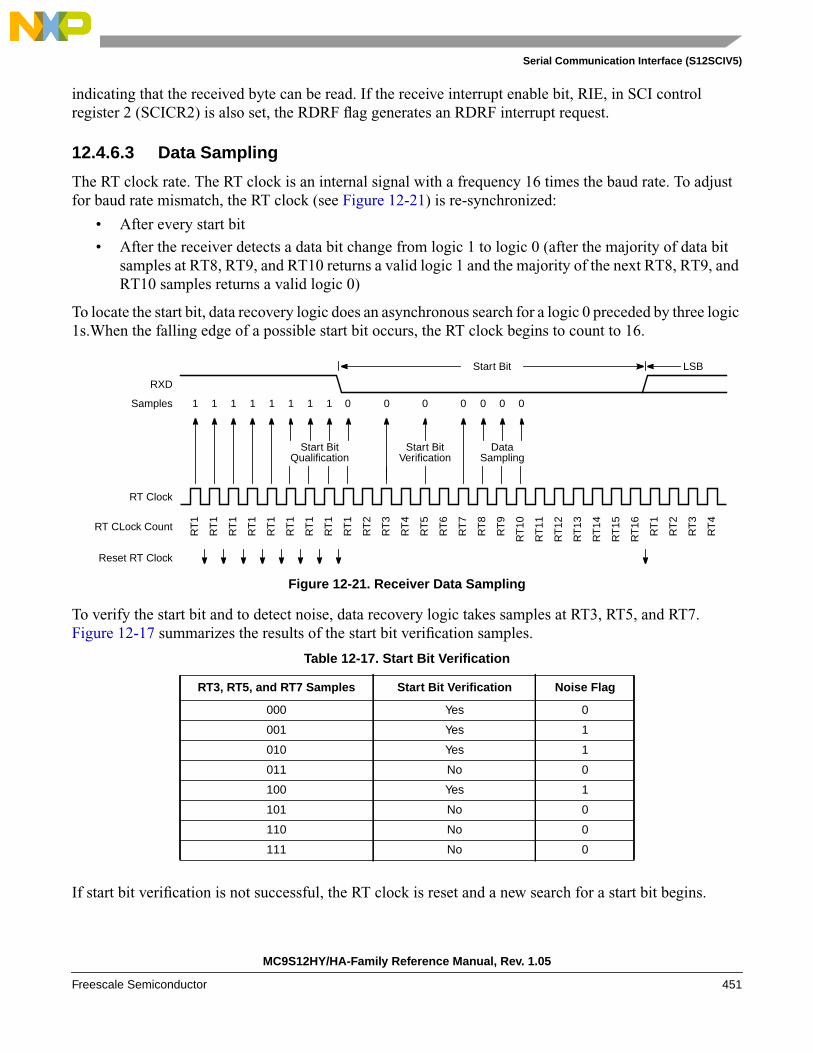
Serial Communication Interface (S12SCIV5)
indicating that the received byte can be read. If the receive interrupt enable bit, RIE, in SCI controlregister 2 (SCICR2) is also set, the RDRF flag generates an RDRF interrupt request.
12.4.6.3 Data Sampling
The RT clock rate. The RT clock is an internal signal with a frequency 16 times the baud rate. To adjustfor baud rate mismatch, the RT clock (see Figure 12-21) is re-synchronized:
• After every start bit
• After the receiver detects a data bit change from logic 1 to logic 0 (after the majority of data bitsamples at RT8, RT9, and RT10 returns a valid logic 1 and the majority of the next RT8, RT9, andRT10 samples returns a valid logic 0)
To locate the start bit, data recovery logic does an asynchronous search for a logic 0 preceded by three logic1s.When the falling edge of a possible start bit occurs, the RT clock begins to count to 16.
Figure 12-21. Receiver Data Sampling
To verify the start bit and to detect noise, data recovery logic takes samples at RT3, RT5, and RT7.Figure 12-17 summarizes the results of the start bit verification samples.
If start bit verification is not successful, the RT clock is reset and a new search for a start bit begins.
Table 12-17. Start Bit Verification
RT3, RT5, and RT7 Samples Start Bit Verification Noise Flag
000 Yes 0
001 Yes 1
010 Yes 1
011 No 0
100 Yes 1
101 No 0
110 No 0
111 No 0
Reset RT Clock
RT
1
RT
1
RT
1
RT
1
RT
1
RT
1
RT
1
RT
1
RT
1
RT
2
RT
3
RT
4
RT
5
RT
8
RT
7
RT
6
RT
11
RT
10
RT
9
RT
15
RT
14
RT
13
RT
12
RT
16
RT
1
RT
2
RT
3
RT
4
Samples
RT Clock
RT CLock Count
Start Bit
RXD
Start BitQualification
Start Bit DataSampling
1 111111 1 0 0 0 000 0
LSB
Verification
MC9S12HY/HA-Family Reference Manual, Rev. 1.05
Freescale Semiconductor 451

Serial Communication Interface (S12SCIV5)
To determine the value of a data bit and to detect noise, recovery logic takes samples at RT8, RT9, andRT10. Table 12-18 summarizes the results of the data bit samples.
NOTEThe RT8, RT9, and RT10 samples do not affect start bit verification. If anyor all of the RT8, RT9, and RT10 start bit samples are logic 1s following asuccessful start bit verification, the noise flag (NF) is set and the receiverassumes that the bit is a start bit (logic 0).
To verify a stop bit and to detect noise, recovery logic takes samples at RT8, RT9, and RT10. Table 12-19summarizes the results of the stop bit samples.
Table 12-18. Data Bit Recovery
RT8, RT9, and RT10 Samples Data Bit Determination Noise Flag
000 0 0
001 0 1
010 0 1
011 1 1
100 0 1
101 1 1
110 1 1
111 1 0
Table 12-19. Stop Bit Recovery
RT8, RT9, and RT10 Samples Framing Error Flag Noise Flag
000 1 0
001 1 1
010 1 1
011 0 1
100 1 1
101 0 1
110 0 1
111 0 0
MC9S12HY/HA-Family Reference Manual, Rev. 1.05
452 Freescale Semiconductor
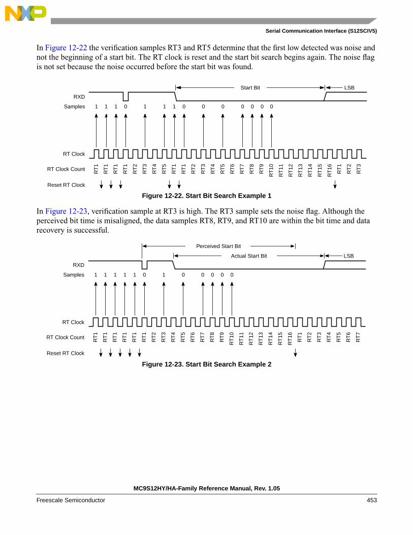
Serial Communication Interface (S12SCIV5)
In Figure 12-22 the verification samples RT3 and RT5 determine that the first low detected was noise andnot the beginning of a start bit. The RT clock is reset and the start bit search begins again. The noise flagis not set because the noise occurred before the start bit was found.
Figure 12-22. Start Bit Search Example 1
In Figure 12-23, verification sample at RT3 is high. The RT3 sample sets the noise flag. Although theperceived bit time is misaligned, the data samples RT8, RT9, and RT10 are within the bit time and datarecovery is successful.
Figure 12-23. Start Bit Search Example 2
Reset RT Clock
RT
1
RT
1
RT
1
RT
1
RT
2
RT
3
RT
4
RT
5
RT
1
RT
1
RT
2
RT
3
RT
4
RT
7
RT
6
RT
5
RT
10
RT
9
RT
8
RT
14
RT
13
RT
12
RT
11
RT
15
RT
16
RT
1
RT
2
RT
3
Samples
RT Clock
RT Clock Count
Start Bit
RXD
1 1011 1 1 0 0 00 0
LSB
0 0
Reset RT Clock
RT
1
RT
1
RT
1
RT
1
RT
1
RT
1
RT
2
RT
3
RT
4
RT
5
RT
6
RT
7
RT
8
RT
11
RT
10
RT
9
RT
14
RT
13
RT
12
RT
2
RT
1
RT
16
RT
15
RT
3
RT
4
RT
5
RT
6
RT
7
Samples
RT Clock
RT Clock Count
Actual Start Bit
RXD
1 1111 1 0 0 00
LSB
00
Perceived Start Bit
MC9S12HY/HA-Family Reference Manual, Rev. 1.05
Freescale Semiconductor 453

Serial Communication Interface (S12SCIV5)
In Figure 12-24, a large burst of noise is perceived as the beginning of a start bit, although the test sampleat RT5 is high. The RT5 sample sets the noise flag. Although this is a worst-case misalignment of perceivedbit time, the data samples RT8, RT9, and RT10 are within the bit time and data recovery is successful.
Figure 12-24. Start Bit Search Example 3
Figure 12-25 shows the effect of noise early in the start bit time. Although this noise does not affect propersynchronization with the start bit time, it does set the noise flag.
Figure 12-25. Start Bit Search Example 4
Reset RT Clock
RT
1
RT
1
RT
1
RT
1
RT
2
RT
3
RT
4
RT
5
RT
6
RT
7
RT
8
RT
9
RT
10
RT
13
RT
12
RT
11
RT
16
RT
15
RT
14
RT
4
RT
3
RT
2
RT
1
RT
5
RT
6
RT
7
RT
8
RT
9
Samples
RT Clock
RT Clock Count
Actual Start Bit
RXD
1 011 1 0 0 00
LSB
0
Perceived Start Bit
Reset RT Clock
RT
1
RT
1
RT
1
RT
1
RT
1
RT
1
RT
1
RT
1
RT
1
RT
1
RT
2
RT
3
RT
4
RT
7
RT
6
RT
5
RT
10
RT
9
RT
8
RT
14
RT
13
RT
12
RT
11
RT
15
RT
16
RT
1
RT
2
RT
3
Samples
RT Clock
RT Clock Count
Perceived and Actual Start Bit
RXD
1 111 1 0 01
LSB
11 1 1
MC9S12HY/HA-Family Reference Manual, Rev. 1.05
454 Freescale Semiconductor

Serial Communication Interface (S12SCIV5)
Figure 12-26 shows a burst of noise near the beginning of the start bit that resets the RT clock. The sampleafter the reset is low but is not preceded by three high samples that would qualify as a falling edge.Depending on the timing of the start bit search and on the data, the frame may be missed entirely or it mayset the framing error flag.
Figure 12-26. Start Bit Search Example 5
In Figure 12-27, a noise burst makes the majority of data samples RT8, RT9, and RT10 high. This sets thenoise flag but does not reset the RT clock. In start bits only, the RT8, RT9, and RT10 data samples areignored.
Figure 12-27. Start Bit Search Example 6
12.4.6.4 Framing Errors
If the data recovery logic does not detect a logic 1 where the stop bit should be in an incoming frame, itsets the framing error flag, FE, in SCI status register 1 (SCISR1). A break character also sets the FE flagbecause a break character has no stop bit. The FE flag is set at the same time that the RDRF flag is set.
Reset RT Clock
RT
1
RT
1
RT
1
RT
1
RT
1
RT
1
RT
1
RT
1
RT
1
RT
1
RT
2
RT
3
RT
4
RT
7
RT
6
RT
5
RT
1
RT
1
RT
1
RT
1
RT
1
RT
1
RT
1
RT
1
RT
1
RT
1
RT
1
RT
1
Samples
RT Clock
RT Clock Count
Start Bit
RXD
1 111 1 0 10
LSB
11 1 1 1 0 000 000 0
No Start Bit Found
Reset RT Clock
RT
1
RT
1
RT
1
RT
1
RT
1
RT
1
RT
1
RT
1
RT
1
RT
1
RT
2
RT
3
RT
4
RT
7
RT
6
RT
5
RT
10
RT
9
RT
8
RT
14
RT
13
RT
12
RT
11
RT
15
RT
16
RT
1
RT
2
RT
3
Samples
RT Clock
RT Clock Count
Start Bit
RXD
1 111 1 0 00
LSB
11 1 1 0 1 10
MC9S12HY/HA-Family Reference Manual, Rev. 1.05
Freescale Semiconductor 455
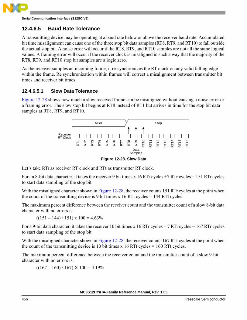
Serial Communication Interface (S12SCIV5)
12.4.6.5 Baud Rate Tolerance
A transmitting device may be operating at a baud rate below or above the receiver baud rate. Accumulatedbit time misalignment can cause one of the three stop bit data samples (RT8, RT9, and RT10) to fall outsidethe actual stop bit. A noise error will occur if the RT8, RT9, and RT10 samples are not all the same logicalvalues. A framing error will occur if the receiver clock is misaligned in such a way that the majority of theRT8, RT9, and RT10 stop bit samples are a logic zero.
As the receiver samples an incoming frame, it re-synchronizes the RT clock on any valid falling edgewithin the frame. Re synchronization within frames will correct a misalignment between transmitter bittimes and receiver bit times.
12.4.6.5.1 Slow Data Tolerance
Figure 12-28 shows how much a slow received frame can be misaligned without causing a noise error ora framing error. The slow stop bit begins at RT8 instead of RT1 but arrives in time for the stop bit datasamples at RT8, RT9, and RT10.
Figure 12-28. Slow Data
Let’s take RTr as receiver RT clock and RTt as transmitter RT clock.
For an 8-bit data character, it takes the receiver 9 bit times x 16 RTr cycles +7 RTr cycles = 151 RTr cyclesto start data sampling of the stop bit.
With the misaligned character shown in Figure 12-28, the receiver counts 151 RTr cycles at the point whenthe count of the transmitting device is 9 bit times x 16 RTt cycles = 144 RTt cycles.
The maximum percent difference between the receiver count and the transmitter count of a slow 8-bit datacharacter with no errors is:
((151 – 144) / 151) x 100 = 4.63%
For a 9-bit data character, it takes the receiver 10 bit times x 16 RTr cycles + 7 RTr cycles = 167 RTr cyclesto start data sampling of the stop bit.
With the misaligned character shown in Figure 12-28, the receiver counts 167 RTr cycles at the point whenthe count of the transmitting device is 10 bit times x 16 RTt cycles = 160 RTt cycles.
The maximum percent difference between the receiver count and the transmitter count of a slow 9-bitcharacter with no errors is:
((167 – 160) / 167) X 100 = 4.19%
MSB Stop
RT
1
RT
2
RT
3
RT
4
RT
5
RT
6
RT
7
RT
8
RT
9
RT
10
RT
11
RT
12
RT
13
RT
14
RT
15
RT
16
DataSamples
ReceiverRT Clock
MC9S12HY/HA-Family Reference Manual, Rev. 1.05
456 Freescale Semiconductor

Serial Communication Interface (S12SCIV5)
12.4.6.5.2 Fast Data Tolerance
Figure 12-29 shows how much a fast received frame can be misaligned. The fast stop bit ends at RT10instead of RT16 but is still sampled at RT8, RT9, and RT10.
Figure 12-29. Fast Data
For an 8-bit data character, it takes the receiver 9 bit times x 16 RTr cycles + 10 RTr cycles = 154 RTr cyclesto finish data sampling of the stop bit.
With the misaligned character shown in Figure 12-29, the receiver counts 154 RTr cycles at the point whenthe count of the transmitting device is 10 bit times x 16 RTt cycles = 160 RTt cycles.
The maximum percent difference between the receiver count and the transmitter count of a fast 8-bitcharacter with no errors is:
((160 – 154) / 160) x 100 = 3.75%
For a 9-bit data character, it takes the receiver 10 bit times x 16 RTr cycles + 10 RTr cycles = 170 RTr cyclesto finish data sampling of the stop bit.
With the misaligned character shown in Figure 12-29, the receiver counts 170 RTr cycles at the point whenthe count of the transmitting device is 11 bit times x 16 RTt cycles = 176 RTt cycles.
The maximum percent difference between the receiver count and the transmitter count of a fast 9-bitcharacter with no errors is:
((176 – 170) /176) x 100 = 3.40%
12.4.6.6 Receiver Wakeup
To enable the SCI to ignore transmissions intended only for other receivers in multiple-receiver systems,the receiver can be put into a standby state. Setting the receiver wakeup bit, RWU, in SCI control register 2(SCICR2) puts the receiver into standby state during which receiver interrupts are disabled.The SCI willstill load the receive data into the SCIDRH/L registers, but it will not set the RDRF flag.
The transmitting device can address messages to selected receivers by including addressing information inthe initial frame or frames of each message.
The WAKE bit in SCI control register 1 (SCICR1) determines how the SCI is brought out of the standbystate to process an incoming message. The WAKE bit enables either idle line wakeup or address markwakeup.
Idle or Next FrameStop
RT
1
RT
2
RT
3
RT
4
RT
5
RT
6
RT
7
RT
8
RT
9
RT
10
RT
11
RT
12
RT
13
RT
14
RT
15
RT
16
DataSamples
ReceiverRT Clock
MC9S12HY/HA-Family Reference Manual, Rev. 1.05
Freescale Semiconductor 457

Serial Communication Interface (S12SCIV5)
12.4.6.6.1 Idle Input line Wakeup (WAKE = 0)
In this wakeup method, an idle condition on the RXD pin clears the RWU bit and wakes up the SCI. Theinitial frame or frames of every message contain addressing information. All receivers evaluate theaddressing information, and receivers for which the message is addressed process the frames that follow.Any receiver for which a message is not addressed can set its RWU bit and return to the standby state. TheRWU bit remains set and the receiver remains on standby until another idle character appears on the RXDpin.
Idle line wakeup requires that messages be separated by at least one idle character and that no messagecontains idle characters.
The idle character that wakes a receiver does not set the receiver idle bit, IDLE, or the receive data registerfull flag, RDRF.
The idle line type bit, ILT, determines whether the receiver begins counting logic 1s as idle character bitsafter the start bit or after the stop bit. ILT is in SCI control register 1 (SCICR1).
12.4.6.6.2 Address Mark Wakeup (WAKE = 1)
In this wakeup method, a logic 1 in the most significant bit (MSB) position of a frame clears the RWU bitand wakes up the SCI. The logic 1 in the MSB position marks a frame as an address frame that containsaddressing information. All receivers evaluate the addressing information, and the receivers for which themessage is addressed process the frames that follow.Any receiver for which a message is not addressed canset its RWU bit and return to the standby state. The RWU bit remains set and the receiver remains onstandby until another address frame appears on the RXD pin.
The logic 1 MSB of an address frame clears the receiver’s RWU bit before the stop bit is received and setsthe RDRF flag.
Address mark wakeup allows messages to contain idle characters but requires that the MSB be reservedfor use in address frames.
NOTEWith the WAKE bit clear, setting the RWU bit after the RXD pin has beenidle can cause the receiver to wake up immediately.
12.4.7 Single-Wire Operation
Normally, the SCI uses two pins for transmitting and receiving. In single-wire operation, the RXD pin isdisconnected from the SCI. The SCI uses the TXD pin for both receiving and transmitting.
Figure 12-30. Single-Wire Operation (LOOPS = 1, RSRC = 1)
RXD
Transmitter
Receiver
TXD
MC9S12HY/HA-Family Reference Manual, Rev. 1.05
458 Freescale Semiconductor

Serial Communication Interface (S12SCIV5)
Enable single-wire operation by setting the LOOPS bit and the receiver source bit, RSRC, in SCI controlregister 1 (SCICR1). Setting the LOOPS bit disables the path from the RXD pin to the receiver. Settingthe RSRC bit connects the TXD pin to the receiver. Both the transmitter and receiver must be enabled(TE = 1 and RE = 1).The TXDIR bit (SCISR2[1]) determines whether the TXD pin is going to be used asan input (TXDIR = 0) or an output (TXDIR = 1) in this mode of operation.
NOTEIn single-wire operation data from the TXD pin is inverted if RXPOL is set.
12.4.8 Loop Operation
In loop operation the transmitter output goes to the receiver input. The RXD pin is disconnected from theSCI.
Figure 12-31. Loop Operation (LOOPS = 1, RSRC = 0)
Enable loop operation by setting the LOOPS bit and clearing the RSRC bit in SCI control register 1(SCICR1). Setting the LOOPS bit disables the path from the RXD pin to the receiver. Clearing the RSRCbit connects the transmitter output to the receiver input. Both the transmitter and receiver must be enabled(TE = 1 and RE = 1).
NOTEIn loop operation data from the transmitter is not recognized by the receiverif RXPOL and TXPOL are not the same.
12.5 Initialization/Application Information
12.5.1 Reset Initialization
See Section 12.3.2, “Register Descriptions”.
12.5.2 Modes of Operation
12.5.2.1 Run Mode
Normal mode of operation.
To initialize a SCI transmission, see Section 12.4.5.2, “Character Transmission”.
RXD
Transmitter
Receiver
TXD
MC9S12HY/HA-Family Reference Manual, Rev. 1.05
Freescale Semiconductor 459

Serial Communication Interface (S12SCIV5)
12.5.2.2 Wait Mode
SCI operation in wait mode depends on the state of the SCISWAI bit in the SCI control register 1(SCICR1).
• If SCISWAI is clear, the SCI operates normally when the CPU is in wait mode.
• If SCISWAI is set, SCI clock generation ceases and the SCI module enters a power-conservationstate when the CPU is in wait mode. Setting SCISWAI does not affect the state of the receiverenable bit, RE, or the transmitter enable bit, TE.
If SCISWAI is set, any transmission or reception in progress stops at wait mode entry. Thetransmission or reception resumes when either an internal or external interrupt brings the CPU outof wait mode. Exiting wait mode by reset aborts any transmission or reception in progress andresets the SCI.
12.5.2.3 Stop Mode
The SCI is inactive during stop mode for reduced power consumption. The STOP instruction does notaffect the SCI register states, but the SCI bus clock will be disabled. The SCI operation resumes fromwhere it left off after an external interrupt brings the CPU out of stop mode. Exiting stop mode by resetaborts any transmission or reception in progress and resets the SCI.
The receive input active edge detect circuit is still active in stop mode. An active edge on the receive inputcan be used to bring the CPU out of stop mode.
12.5.3 Interrupt Operation
This section describes the interrupt originated by the SCI block.The MCU must service the interruptrequests. Table 12-20 lists the eight interrupt sources of the SCI.
Table 12-20. SCI Interrupt Sources
Interrupt Source Local Enable Description
TDRE SCISR1[7] TIE Active high level. Indicates that a byte was transferred from SCIDRH/L to thetransmit shift register.
TC SCISR1[6] TCIE Active high level. Indicates that a transmit is complete.
RDRF SCISR1[5] RIE Active high level. The RDRF interrupt indicates that received data is availablein the SCI data register.
OR SCISR1[3] Active high level. This interrupt indicates that an overrun condition has occurred.
IDLE SCISR1[4] ILIE Active high level. Indicates that receiver input has become idle.
RXEDGIF SCIASR1[7] RXEDGIE Active high level. Indicates that an active edge (falling for RXPOL = 0, rising forRXPOL = 1) was detected.
BERRIF SCIASR1[1] BERRIE Active high level. Indicates that a mismatch between transmitted and received datain a single wire application has happened.
BKDIF SCIASR1[0] BRKDIE Active high level. Indicates that a break character has been received.
MC9S12HY/HA-Family Reference Manual, Rev. 1.05
460 Freescale Semiconductor

Serial Communication Interface (S12SCIV5)
12.5.3.1 Description of Interrupt Operation
The SCI only originates interrupt requests. The following is a description of how the SCI makes a requestand how the MCU should acknowledge that request. The interrupt vector offset and interrupt number arechip dependent. The SCI only has a single interrupt line (SCI Interrupt Signal, active high operation) andall the following interrupts, when generated, are ORed together and issued through that port.
12.5.3.1.1 TDRE Description
The TDRE interrupt is set high by the SCI when the transmit shift register receives a byte from the SCIdata register. A TDRE interrupt indicates that the transmit data register (SCIDRH/L) is empty and that anew byte can be written to the SCIDRH/L for transmission.Clear TDRE by reading SCI status register 1with TDRE set and then writing to SCI data register low (SCIDRL).
12.5.3.1.2 TC Description
The TC interrupt is set by the SCI when a transmission has been completed. Transmission is completedwhen all bits including the stop bit (if transmitted) have been shifted out and no data is queued to betransmitted. No stop bit is transmitted when sending a break character and the TC flag is set (providingthere is no more data queued for transmission) when the break character has been shifted out. A TCinterrupt indicates that there is no transmission in progress. TC is set high when the TDRE flag is set andno data, preamble, or break character is being transmitted. When TC is set, the TXD pin becomes idle(logic 1). Clear TC by reading SCI status register 1 (SCISR1) with TC set and then writing to SCI dataregister low (SCIDRL).TC is cleared automatically when data, preamble, or break is queued and ready tobe sent.
12.5.3.1.3 RDRF Description
The RDRF interrupt is set when the data in the receive shift register transfers to the SCI data register. ARDRF interrupt indicates that the received data has been transferred to the SCI data register and that thebyte can now be read by the MCU. The RDRF interrupt is cleared by reading the SCI status register one(SCISR1) and then reading SCI data register low (SCIDRL).
12.5.3.1.4 OR Description
The OR interrupt is set when software fails to read the SCI data register before the receive shift registerreceives the next frame. The newly acquired data in the shift register will be lost in this case, but the dataalready in the SCI data registers is not affected. The OR interrupt is cleared by reading the SCI statusregister one (SCISR1) and then reading SCI data register low (SCIDRL).
12.5.3.1.5 IDLE Description
The IDLE interrupt is set when 10 consecutive logic 1s (if M = 0) or 11 consecutive logic 1s (if M = 1)appear on the receiver input. Once the IDLE is cleared, a valid frame must again set the RDRF flag beforean idle condition can set the IDLE flag. Clear IDLE by reading SCI status register 1 (SCISR1) with IDLEset and then reading SCI data register low (SCIDRL).
MC9S12HY/HA-Family Reference Manual, Rev. 1.05
Freescale Semiconductor 461

Serial Communication Interface (S12SCIV5)
12.5.3.1.6 RXEDGIF Description
The RXEDGIF interrupt is set when an active edge (falling if RXPOL = 0, rising if RXPOL = 1) on theRXD pin is detected. Clear RXEDGIF by writing a “1” to the SCIASR1 SCI alternative status register 1.
12.5.3.1.7 BERRIF Description
The BERRIF interrupt is set when a mismatch between the transmitted and the received data in a singlewire application like LIN was detected. Clear BERRIF by writing a “1” to the SCIASR1 SCI alternativestatus register 1. This flag is also cleared if the bit error detect feature is disabled.
12.5.3.1.8 BKDIF Description
The BKDIF interrupt is set when a break signal was received. Clear BKDIF by writing a “1” to theSCIASR1 SCI alternative status register 1. This flag is also cleared if break detect feature is disabled.
12.5.4 Recovery from Wait Mode
The SCI interrupt request can be used to bring the CPU out of wait mode.
12.5.5 Recovery from Stop Mode
An active edge on the receive input can be used to bring the CPU out of stop mode.
MC9S12HY/HA-Family Reference Manual, Rev. 1.05
462 Freescale Semiconductor

Chapter 13Serial Peripheral Interface (S12SPIV5)
13.1 IntroductionThe SPI module allows a duplex, synchronous, serial communication between the MCU and peripheraldevices. Software can poll the SPI status flags or the SPI operation can be interrupt driven.
13.1.1 Glossary of Terms
13.1.2 Features
The SPI includes these distinctive features:
• Master mode and slave mode
• Selectable 8 or 16-bit transfer width
• Bidirectional mode
• Slave select output
• Mode fault error flag with CPU interrupt capability
• Double-buffered data register
• Serial clock with programmable polarity and phase
• Control of SPI operation during wait mode
13.1.3 Modes of Operation
The SPI functions in three modes: run, wait, and stop.
Table 13-1. Revision History
RevisionNumber
Revision DateSectionsAffected
Description of Changes
V05.00 24 Mar 2005 13.3.2/13-467 - Added 16-bit transfer width feature.
SPI Serial Peripheral Interface
SS Slave Select
SCK Serial Clock
MOSI Master Output, Slave Input
MISO Master Input, Slave Output
MOMI Master Output, Master Input
SISO Slave Input, Slave Output
MC9S12HY/HA-Family Reference Manual, Rev. 1.05
Freescale Semiconductor 463

Serial Peripheral Interface (S12SPIV5)
• Run mode
This is the basic mode of operation.
• Wait mode
SPI operation in wait mode is a configurable low power mode, controlled by the SPISWAI bitlocated in the SPICR2 register. In wait mode, if the SPISWAI bit is clear, the SPI operates like inrun mode. If the SPISWAI bit is set, the SPI goes into a power conservative state, with the SPI clockgeneration turned off. If the SPI is configured as a master, any transmission in progress stops, butis resumed after CPU goes into run mode. If the SPI is configured as a slave, reception andtransmission of data continues, so that the slave stays synchronized to the master.
• Stop mode
The SPI is inactive in stop mode for reduced power consumption. If the SPI is configured as amaster, any transmission in progress stops, but is resumed after CPU goes into run mode. If the SPIis configured as a slave, reception and transmission of data continues, so that the slave stayssynchronized to the master.
For a detailed description of operating modes, please refer to Section 13.4.7, “Low Power Mode Options”.
13.1.4 Block Diagram
Figure 13-1 gives an overview on the SPI architecture. The main parts of the SPI are status, control anddata registers, shifter logic, baud rate generator, master/slave control logic, and port control logic.
MC9S12HY/HA-Family Reference Manual, Rev. 1.05
464 Freescale Semiconductor

Serial Peripheral Interface (S12SPIV5)
Figure 13-1. SPI Block Diagram
13.2 External Signal DescriptionThis section lists the name and description of all ports including inputs and outputs that do, or may, connectoff chip. The SPI module has a total of four external pins.
13.2.1 MOSI — Master Out/Slave In Pin
This pin is used to transmit data out of the SPI module when it is configured as a master and receive datawhen it is configured as slave.
13.2.2 MISO — Master In/Slave Out Pin
This pin is used to transmit data out of the SPI module when it is configured as a slave and receive datawhen it is configured as master.
SPI Control Register 1
SPI Control Register 2
SPI Baud Rate Register
SPI Status Register
SPI Data Register
Shifter
PortControlLogic
MOSI
SCK
Interrupt Control
SPI
MSB LSB
LSBFE=1 LSBFE=0
LSBFE=0 LSBFE=1
Data In
LSBFE=1
LSBFE=0
Data Out
Baud Rate Generator
PrescalerBus Clock
Counter
Clock Select
SPPR 3 3SPR
Baud Rate
Phase +PolarityControl
Master
Slave
SCK In
SCK OutMaster Baud Rate
Slave Baud Rate
Phase +PolarityControl
Control
ControlCPOL CPHA
2
BIDIROE
SPC0
2
Shift SampleClockClock
MODFSPIF SPTEF
SPI
RequestInterrupt
SS
MC9S12HY/HA-Family Reference Manual Rev. 1.05
Freescale Semiconductor 465

Serial Peripheral Interface (S12SPIV5)
13.2.3 SS — Slave Select Pin
This pin is used to output the select signal from the SPI module to another peripheral with which a datatransfer is to take place when it is configured as a master and it is used as an input to receive the slave selectsignal when the SPI is configured as slave.
13.2.4 SCK — Serial Clock Pin
In master mode, this is the synchronous output clock. In slave mode, this is the synchronous input clock.
13.3 Memory Map and Register DefinitionThis section provides a detailed description of address space and registers used by the SPI.
13.3.1 Module Memory Map
The memory map for the SPI is given in Figure 13-2. The address listed for each register is the sum of abase address and an address offset. The base address is defined at the SoC level and the address offset isdefined at the module level. Reads from the reserved bits return zeros and writes to the reserved bits haveno effect.
RegisterName
Bit 7 6 5 4 3 2 1 Bit 0
0x0000SPICR1
RSPIE SPE SPTIE MSTR CPOL CPHA SSOE LSBFE
W
0x0001SPICR2
R 0XFRW
0MODFEN BIDIROE
0SPISWAI SPC0
W
0x0002SPIBR
R 0SPPR2 SPPR1 SPPR0
0SPR2 SPR1 SPR0
W
0x0003SPISR
R SPIF 0 SPTEF MODF 0 0 0 0W
0x0004SPIDRH
R R15 R14 R13 R12 R11 R10 R9 R8T15 T14 T13 T12 T11 T10 T9 T8W
0x0005SPIDRL
R R7 R6 R5 R4 R3 R2 R1 R0T7 T6 T5 T4 T3 T2 T1 T0W
0x0006Reserved
RW
0x0007Reserved
RW
= Unimplemented or Reserved
Figure 13-2. SPI Register Summary
MC9S12HY/HA-Family Reference Manual, Rev. 1.05
466 Freescale Semiconductor

Serial Peripheral Interface (S12SPIV5)
13.3.2 Register Descriptions
This section consists of register descriptions in address order. Each description includes a standard registerdiagram with an associated figure number. Details of register bit and field function follow the registerdiagrams, in bit order.
13.3.2.1 SPI Control Register 1 (SPICR1)
Read: Anytime
Write: Anytime
Module Base +0x0000
7 6 5 4 3 2 1 0
RSPIE SPE SPTIE MSTR CPOL CPHA SSOE LSBFE
W
Reset 0 0 0 0 0 1 0 0
Figure 13-3. SPI Control Register 1 (SPICR1)
Table 13-2. SPICR1 Field Descriptions
Field Description
7SPIE
SPI Interrupt Enable Bit — This bit enables SPI interrupt requests, if SPIF or MODF status flag is set.0 SPI interrupts disabled.1 SPI interrupts enabled.
6SPE
SPI System Enable Bit — This bit enables the SPI system and dedicates the SPI port pins to SPI systemfunctions. If SPE is cleared, SPI is disabled and forced into idle state, status bits in SPISR register are reset.0 SPI disabled (lower power consumption).1 SPI enabled, port pins are dedicated to SPI functions.
5SPTIE
SPI Transmit Interrupt Enable — This bit enables SPI interrupt requests, if SPTEF flag is set.0 SPTEF interrupt disabled.1 SPTEF interrupt enabled.
4MSTR
SPI Master/Slave Mode Select Bit — This bit selects whether the SPI operates in master or slave mode.Switching the SPI from master to slave or vice versa forces the SPI system into idle state.0 SPI is in slave mode.1 SPI is in master mode.
3CPOL
SPI Clock Polarity Bit — This bit selects an inverted or non-inverted SPI clock. To transmit data between SPImodules, the SPI modules must have identical CPOL values. In master mode, a change of this bit will abort atransmission in progress and force the SPI system into idle state.0 Active-high clocks selected. In idle state SCK is low.1 Active-low clocks selected. In idle state SCK is high.
2CPHA
SPI Clock Phase Bit — This bit is used to select the SPI clock format. In master mode, a change of this bit willabort a transmission in progress and force the SPI system into idle state.0 Sampling of data occurs at odd edges (1,3,5,...) of the SCK clock.1 Sampling of data occurs at even edges (2,4,6,...) of the SCK clock.
MC9S12HY/HA-Family Reference Manual Rev. 1.05
Freescale Semiconductor 467

Serial Peripheral Interface (S12SPIV5)
13.3.2.2 SPI Control Register 2 (SPICR2)
Read: Anytime
Write: Anytime; writes to the reserved bits have no effect
1SSOE
Slave Select Output Enable — The SS output feature is enabled only in master mode, if MODFEN is set, byasserting the SSOE as shown in Table 13-3. In master mode, a change of this bit will abort a transmission inprogress and force the SPI system into idle state.
0LSBFE
LSB-First Enable — This bit does not affect the position of the MSB and LSB in the data register. Reads andwrites of the data register always have the MSB in the highest bit position. In master mode, a change of this bitwill abort a transmission in progress and force the SPI system into idle state.0 Data is transferred most significant bit first.1 Data is transferred least significant bit first.
Table 13-3. SS Input / Output Selection
MODFEN SSOE Master Mode Slave Mode
0 0 SS not used by SPI SS input
0 1 SS not used by SPI SS input
1 0 SS input with MODF feature SS input
1 1 SS is slave select output SS input
Module Base +0x0001
7 6 5 4 3 2 1 0
R 0XFRW
0MODFEN BIDIROE
0SPISWAI SPC0
W
Reset 0 0 0 0 0 0 0 0
= Unimplemented or Reserved
Figure 13-4. SPI Control Register 2 (SPICR2)
Table 13-2. SPICR1 Field Descriptions (continued)
Field Description
MC9S12HY/HA-Family Reference Manual, Rev. 1.05
468 Freescale Semiconductor
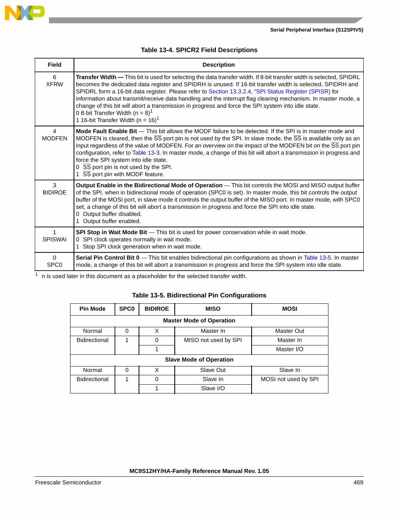
Serial Peripheral Interface (S12SPIV5)
Table 13-4. SPICR2 Field Descriptions
Field Description
6XFRW
Transfer Width — This bit is used for selecting the data transfer width. If 8-bit transfer width is selected, SPIDRLbecomes the dedicated data register and SPIDRH is unused. If 16-bit transfer width is selected, SPIDRH andSPIDRL form a 16-bit data register. Please refer to Section 13.3.2.4, “SPI Status Register (SPISR) forinformation about transmit/receive data handling and the interrupt flag clearing mechanism. In master mode, achange of this bit will abort a transmission in progress and force the SPI system into idle state.0 8-bit Transfer Width (n = 8)1
1 16-bit Transfer Width (n = 16)1
1 n is used later in this document as a placeholder for the selected transfer width.
4MODFEN
Mode Fault Enable Bit — This bit allows the MODF failure to be detected. If the SPI is in master mode andMODFEN is cleared, then the SS port pin is not used by the SPI. In slave mode, the SS is available only as aninput regardless of the value of MODFEN. For an overview on the impact of the MODFEN bit on the SS port pinconfiguration, refer to Table 13-3. In master mode, a change of this bit will abort a transmission in progress andforce the SPI system into idle state.0 SS port pin is not used by the SPI.1 SS port pin with MODF feature.
3BIDIROE
Output Enable in the Bidirectional Mode of Operation — This bit controls the MOSI and MISO output bufferof the SPI, when in bidirectional mode of operation (SPC0 is set). In master mode, this bit controls the outputbuffer of the MOSI port, in slave mode it controls the output buffer of the MISO port. In master mode, with SPC0set, a change of this bit will abort a transmission in progress and force the SPI into idle state.0 Output buffer disabled.1 Output buffer enabled.
1SPISWAI
SPI Stop in Wait Mode Bit — This bit is used for power conservation while in wait mode.0 SPI clock operates normally in wait mode.1 Stop SPI clock generation when in wait mode.
0SPC0
Serial Pin Control Bit 0 — This bit enables bidirectional pin configurations as shown in Table 13-5. In mastermode, a change of this bit will abort a transmission in progress and force the SPI system into idle state.
Table 13-5. Bidirectional Pin Configurations
Pin Mode SPC0 BIDIROE MISO MOSI
Master Mode of Operation
Normal 0 X Master In Master Out
Bidirectional 1 0 MISO not used by SPI Master In
1 Master I/O
Slave Mode of Operation
Normal 0 X Slave Out Slave In
Bidirectional 1 0 Slave In MOSI not used by SPI
1 Slave I/O
MC9S12HY/HA-Family Reference Manual Rev. 1.05
Freescale Semiconductor 469

Serial Peripheral Interface (S12SPIV5)
13.3.2.3 SPI Baud Rate Register (SPIBR)
Read: Anytime
Write: Anytime; writes to the reserved bits have no effect
The baud rate divisor equation is as follows:BaudRateDivisor = (SPPR + 1) • 2(SPR + 1) Eqn. 13-1
The baud rate can be calculated with the following equation:Baud Rate = BusClock / BaudRateDivisor Eqn. 13-2
NOTEFor maximum allowed baud rates, please refer to the SPI ElectricalSpecification in the Electricals chapter of this data sheet.
Module Base +0x0002
7 6 5 4 3 2 1 0
R 0SPPR2 SPPR1 SPPR0
0SPR2 SPR1 SPR0
W
Reset 0 0 0 0 0 0 0 0
= Unimplemented or Reserved
Figure 13-5. SPI Baud Rate Register (SPIBR)
Table 13-6. SPIBR Field Descriptions
Field Description
6–4SPPR[2:0]
SPI Baud Rate Preselection Bits — These bits specify the SPI baud rates as shown in Table 13-7. In mastermode, a change of these bits will abort a transmission in progress and force the SPI system into idle state.
2–0SPR[2:0]
SPI Baud Rate Selection Bits — These bits specify the SPI baud rates as shown in Table 13-7. In master mode,a change of these bits will abort a transmission in progress and force the SPI system into idle state.
Table 13-7. Example SPI Baud Rate Selection (25 MHz Bus Clock) (Sheet 1 of 3)
SPPR2 SPPR1 SPPR0 SPR2 SPR1 SPR0Baud Rate
DivisorBaud Rate
0 0 0 0 0 0 2 12.5 Mbit/s
0 0 0 0 0 1 4 6.25 Mbit/s
0 0 0 0 1 0 8 3.125 Mbit/s
0 0 0 0 1 1 16 1.5625 Mbit/s
0 0 0 1 0 0 32 781.25 kbit/s
0 0 0 1 0 1 64 390.63 kbit/s
0 0 0 1 1 0 128 195.31 kbit/s
0 0 0 1 1 1 256 97.66 kbit/s
0 0 1 0 0 0 4 6.25 Mbit/s
0 0 1 0 0 1 8 3.125 Mbit/s
0 0 1 0 1 0 16 1.5625 Mbit/s
0 0 1 0 1 1 32 781.25 kbit/s
MC9S12HY/HA-Family Reference Manual, Rev. 1.05
470 Freescale Semiconductor

Serial Peripheral Interface (S12SPIV5)
0 0 1 1 0 0 64 390.63 kbit/s
0 0 1 1 0 1 128 195.31 kbit/s
0 0 1 1 1 0 256 97.66 kbit/s
0 0 1 1 1 1 512 48.83 kbit/s
0 1 0 0 0 0 6 4.16667 Mbit/s
0 1 0 0 0 1 12 2.08333 Mbit/s
0 1 0 0 1 0 24 1.04167 Mbit/s
0 1 0 0 1 1 48 520.83 kbit/s
0 1 0 1 0 0 96 260.42 kbit/s
0 1 0 1 0 1 192 130.21 kbit/s
0 1 0 1 1 0 384 65.10 kbit/s
0 1 0 1 1 1 768 32.55 kbit/s
0 1 1 0 0 0 8 3.125 Mbit/s
0 1 1 0 0 1 16 1.5625 Mbit/s
0 1 1 0 1 0 32 781.25 kbit/s
0 1 1 0 1 1 64 390.63 kbit/s
0 1 1 1 0 0 128 195.31 kbit/s
0 1 1 1 0 1 256 97.66 kbit/s
0 1 1 1 1 0 512 48.83 kbit/s
0 1 1 1 1 1 1024 24.41 kbit/s
1 0 0 0 0 0 10 2.5 Mbit/s
1 0 0 0 0 1 20 1.25 Mbit/s
1 0 0 0 1 0 40 625 kbit/s
1 0 0 0 1 1 80 312.5 kbit/s
1 0 0 1 0 0 160 156.25 kbit/s
1 0 0 1 0 1 320 78.13 kbit/s
1 0 0 1 1 0 640 39.06 kbit/s
1 0 0 1 1 1 1280 19.53 kbit/s
1 0 1 0 0 0 12 2.08333 Mbit/s
1 0 1 0 0 1 24 1.04167 Mbit/s
1 0 1 0 1 0 48 520.83 kbit/s
1 0 1 0 1 1 96 260.42 kbit/s
1 0 1 1 0 0 192 130.21 kbit/s
1 0 1 1 0 1 384 65.10 kbit/s
1 0 1 1 1 0 768 32.55 kbit/s
1 0 1 1 1 1 1536 16.28 kbit/s
1 1 0 0 0 0 14 1.78571 Mbit/s
1 1 0 0 0 1 28 892.86 kbit/s
1 1 0 0 1 0 56 446.43 kbit/s
1 1 0 0 1 1 112 223.21 kbit/s
1 1 0 1 0 0 224 111.61 kbit/s
1 1 0 1 0 1 448 55.80 kbit/s
Table 13-7. Example SPI Baud Rate Selection (25 MHz Bus Clock) (Sheet 2 of 3)
SPPR2 SPPR1 SPPR0 SPR2 SPR1 SPR0Baud Rate
DivisorBaud Rate
MC9S12HY/HA-Family Reference Manual Rev. 1.05
Freescale Semiconductor 471

Serial Peripheral Interface (S12SPIV5)
13.3.2.4 SPI Status Register (SPISR)
Read: Anytime
Write: Has no effect
1 1 0 1 1 0 896 27.90 kbit/s
1 1 0 1 1 1 1792 13.95 kbit/s
1 1 1 0 0 0 16 1.5625 Mbit/s
1 1 1 0 0 1 32 781.25 kbit/s
1 1 1 0 1 0 64 390.63 kbit/s
1 1 1 0 1 1 128 195.31 kbit/s
1 1 1 1 0 0 256 97.66 kbit/s
1 1 1 1 0 1 512 48.83 kbit/s
1 1 1 1 1 0 1024 24.41 kbit/s
1 1 1 1 1 1 2048 12.21 kbit/s
Module Base +0x0003
7 6 5 4 3 2 1 0
R SPIF 0 SPTEF MODF 0 0 0 0
W
Reset 0 0 1 0 0 0 0 0
= Unimplemented or Reserved
Figure 13-6. SPI Status Register (SPISR)
Table 13-8. SPISR Field Descriptions
Field Description
7SPIF
SPIF Interrupt Flag — This bit is set after received data has been transferred into the SPI data register. Forinformation about clearing SPIF Flag, please refer to Table 13-9.0 Transfer not yet complete.1 New data copied to SPIDR.
5SPTEF
SPI Transmit Empty Interrupt Flag — If set, this bit indicates that the transmit data register is empty. Forinformation about clearing this bit and placing data into the transmit data register, please refer to Table 13-10.0 SPI data register not empty.1 SPI data register empty.
4MODF
Mode Fault Flag — This bit is set if the SS input becomes low while the SPI is configured as a master and modefault detection is enabled, MODFEN bit of SPICR2 register is set. Refer to MODFEN bit description inSection 13.3.2.2, “SPI Control Register 2 (SPICR2)”. The flag is cleared automatically by a read of the SPI statusregister (with MODF set) followed by a write to the SPI control register 1.0 Mode fault has not occurred.1 Mode fault has occurred.
Table 13-7. Example SPI Baud Rate Selection (25 MHz Bus Clock) (Sheet 3 of 3)
SPPR2 SPPR1 SPPR0 SPR2 SPR1 SPR0Baud Rate
DivisorBaud Rate
MC9S12HY/HA-Family Reference Manual, Rev. 1.05
472 Freescale Semiconductor

Serial Peripheral Interface (S12SPIV5)
Table 13-9. SPIF Interrupt Flag Clearing Sequence
Table 13-10. SPTEF Interrupt Flag Clearing Sequence
XFRW Bit SPIF Interrupt Flag Clearing Sequence
0 Read SPISR with SPIF == 1 then Read SPIDRL
1 Read SPISR with SPIF == 1
then
Byte Read SPIDRL 1
1 Data in SPIDRH is lost in this case.
or
Byte Read SPIDRH 2
2 SPIDRH can be read repeatedly without any effect on SPIF. SPIF Flag is cleared only by the readof SPIDRL after reading SPISR with SPIF == 1.
Byte Read SPIDRL
or
Word Read (SPIDRH:SPIDRL)
XFRW Bit SPTEF Interrupt Flag Clearing Sequence
0 Read SPISR with SPTEF == 1 then Write to SPIDRL 1
1 Any write to SPIDRH or SPIDRL with SPTEF == 0 is effectively ignored.
1 Read SPISR with SPTEF == 1
then
Byte Write to SPIDRL 12
2 Data in SPIDRH is undefined in this case.
or
Byte Write to SPIDRH 13
3 SPIDRH can be written repeatedly without any effect on SPTEF. SPTEF Flag is cleared only bywriting to SPIDRL after reading SPISR with SPTEF == 1.
Byte Write to SPIDRL 1
or
Word Write to (SPIDRH:SPIDRL) 1
MC9S12HY/HA-Family Reference Manual Rev. 1.05
Freescale Semiconductor 473

Serial Peripheral Interface (S12SPIV5)
13.3.2.5 SPI Data Register (SPIDR = SPIDRH:SPIDRL)
Read: Anytime; read data only valid when SPIF is set
Write: Anytime
The SPI data register is both the input and output register for SPI data. A write to this registerallows data to be queued and transmitted. For an SPI configured as a master, queued data istransmitted immediately after the previous transmission has completed. The SPI transmitter emptyflag SPTEF in the SPISR register indicates when the SPI data register is ready to accept new data.
Received data in the SPIDR is valid when SPIF is set.
If SPIF is cleared and data has been received, the received data is transferred from the receive shiftregister to the SPIDR and SPIF is set.
If SPIF is set and not serviced, and a second data value has been received, the second received datais kept as valid data in the receive shift register until the start of another transmission. The data inthe SPIDR does not change.
If SPIF is set and valid data is in the receive shift register, and SPIF is serviced before the start ofa third transmission, the data in the receive shift register is transferred into the SPIDR and SPIFremains set (see Figure 13-9).
If SPIF is set and valid data is in the receive shift register, and SPIF is serviced after the start of athird transmission, the data in the receive shift register has become invalid and is not transferredinto the SPIDR (see Figure 13-10).
Module Base +0x0004
7 6 5 4 3 2 1 0
R R15 R14 R13 R12 R11 R10 R9 R8
W T15 T14 T13 T12 T11 T10 T9 T8
Reset 0 0 0 0 0 0 0 0
Figure 13-7. SPI Data Register High (SPIDRH)
Module Base +0x0005
7 6 5 4 3 2 1 0
R R7 R6 R5 R4 R3 R2 R1 R0
W T7 T6 T5 T4 T3 T2 T1 T0
Reset 0 0 0 0 0 0 0 0
Figure 13-8. SPI Data Register Low (SPIDRL)
MC9S12HY/HA-Family Reference Manual, Rev. 1.05
474 Freescale Semiconductor
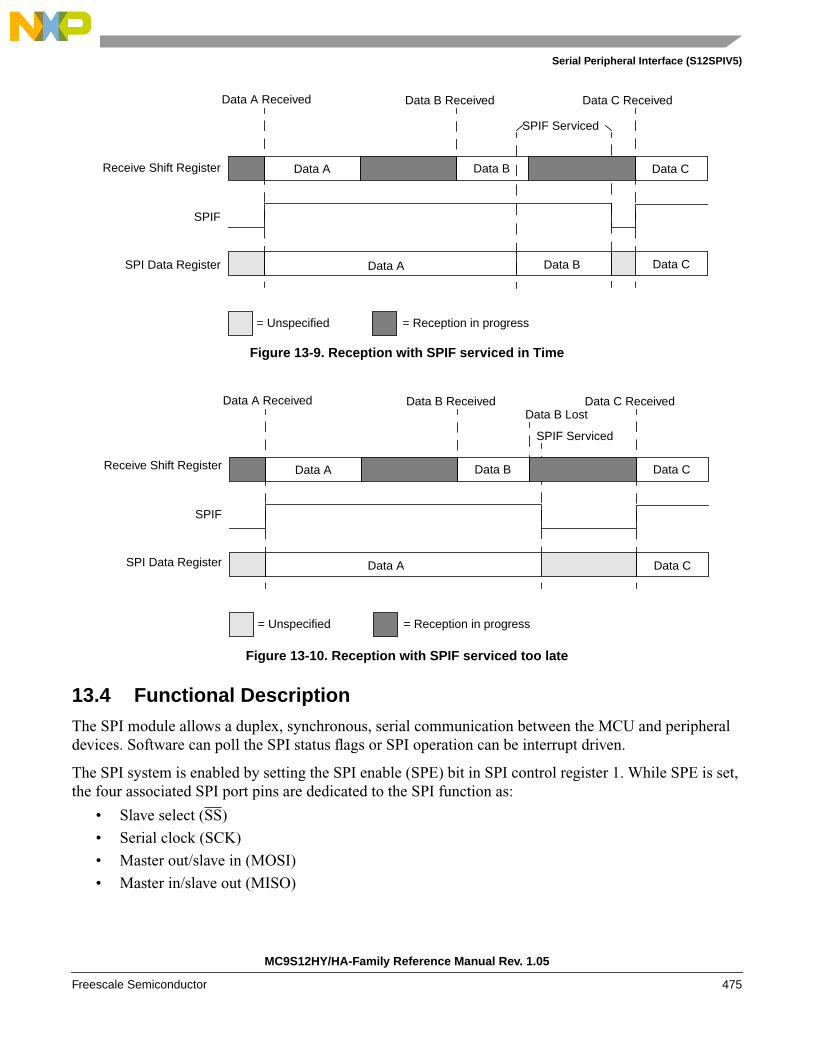
Serial Peripheral Interface (S12SPIV5)
Figure 13-9. Reception with SPIF serviced in Time
Figure 13-10. Reception with SPIF serviced too late
13.4 Functional DescriptionThe SPI module allows a duplex, synchronous, serial communication between the MCU and peripheraldevices. Software can poll the SPI status flags or SPI operation can be interrupt driven.
The SPI system is enabled by setting the SPI enable (SPE) bit in SPI control register 1. While SPE is set,the four associated SPI port pins are dedicated to the SPI function as:
• Slave select (SS)
• Serial clock (SCK)
• Master out/slave in (MOSI)
• Master in/slave out (MISO)
Receive Shift Register
SPIF
SPI Data Register
Data A Data B
Data A
Data A Received Data B Received
Data C
Data C
SPIF Serviced
Data C Received
Data B
= Unspecified = Reception in progress
Receive Shift Register
SPIF
SPI Data Register
Data A Data B
Data A
Data A Received Data B Received
Data C
Data C
SPIF Serviced
Data C ReceivedData B Lost
= Unspecified = Reception in progress
MC9S12HY/HA-Family Reference Manual Rev. 1.05
Freescale Semiconductor 475

Serial Peripheral Interface (S12SPIV5)
The main element of the SPI system is the SPI data register. The n-bit1 data register in the master and then-bit1 data register in the slave are linked by the MOSI and MISO pins to form a distributed 2n-bit1
register. When a data transfer operation is performed, this 2n-bit1 register is serially shifted n1 bit positionsby the S-clock from the master, so data is exchanged between the master and the slave. Data written to themaster SPI data register becomes the output data for the slave, and data read from the master SPI dataregister after a transfer operation is the input data from the slave.
A read of SPISR with SPTEF = 1 followed by a write to SPIDR puts data into the transmit data register.When a transfer is complete and SPIF is cleared, received data is moved into the receive data register. Thisdata register acts as the SPI receive data register for reads and as the SPI transmit data register for writes.A common SPI data register address is shared for reading data from the read data buffer and for writingdata to the transmit data register.
The clock phase control bit (CPHA) and a clock polarity control bit (CPOL) in the SPI control register 1(SPICR1) select one of four possible clock formats to be used by the SPI system. The CPOL bit simplyselects a non-inverted or inverted clock. The CPHA bit is used to accommodate two fundamentallydifferent protocols by sampling data on odd numbered SCK edges or on even numbered SCK edges (seeSection 13.4.3, “Transmission Formats”).
The SPI can be configured to operate as a master or as a slave. When the MSTR bit in SPI control register1is set, master mode is selected, when the MSTR bit is clear, slave mode is selected.
NOTEA change of CPOL or MSTR bit while there is a received byte pending inthe receive shift register will destroy the received byte and must be avoided.
13.4.1 Master Mode
The SPI operates in master mode when the MSTR bit is set. Only a master SPI module can initiatetransmissions. A transmission begins by writing to the master SPI data register. If the shift register isempty, data immediately transfers to the shift register. Data begins shifting out on the MOSI pin under thecontrol of the serial clock.
• Serial clock
The SPR2, SPR1, and SPR0 baud rate selection bits, in conjunction with the SPPR2, SPPR1, andSPPR0 baud rate preselection bits in the SPI baud rate register, control the baud rate generator anddetermine the speed of the transmission. The SCK pin is the SPI clock output. Through the SCKpin, the baud rate generator of the master controls the shift register of the slave peripheral.
• MOSI, MISO pin
In master mode, the function of the serial data output pin (MOSI) and the serial data input pin(MISO) is determined by the SPC0 and BIDIROE control bits.
• SS pin
If MODFEN and SSOE are set, the SS pin is configured as slave select output. The SS outputbecomes low during each transmission and is high when the SPI is in idle state.
1. n depends on the selected transfer width, please refer to Section 13.3.2.2, “SPI Control Register 2 (SPICR2)
MC9S12HY/HA-Family Reference Manual, Rev. 1.05
476 Freescale Semiconductor

Serial Peripheral Interface (S12SPIV5)
If MODFEN is set and SSOE is cleared, the SS pin is configured as input for detecting mode faulterror. If the SS input becomes low this indicates a mode fault error where another master tries todrive the MOSI and SCK lines. In this case, the SPI immediately switches to slave mode, byclearing the MSTR bit and also disables the slave output buffer MISO (or SISO in bidirectionalmode). So the result is that all outputs are disabled and SCK, MOSI, and MISO are inputs. If atransmission is in progress when the mode fault occurs, the transmission is aborted and the SPI isforced into idle state.
This mode fault error also sets the mode fault (MODF) flag in the SPI status register (SPISR). Ifthe SPI interrupt enable bit (SPIE) is set when the MODF flag becomes set, then an SPI interruptsequence is also requested.
When a write to the SPI data register in the master occurs, there is a half SCK-cycle delay. Afterthe delay, SCK is started within the master. The rest of the transfer operation differs slightly,depending on the clock format specified by the SPI clock phase bit, CPHA, in SPI control register 1(see Section 13.4.3, “Transmission Formats”).
NOTEA change of the bits CPOL, CPHA, SSOE, LSBFE, XFRW, MODFEN,SPC0, or BIDIROE with SPC0 set, SPPR2-SPPR0 and SPR2-SPR0 inmaster mode will abort a transmission in progress and force the SPI into idlestate. The remote slave cannot detect this, therefore the master must ensurethat the remote slave is returned to idle state.
13.4.2 Slave Mode
The SPI operates in slave mode when the MSTR bit in SPI control register 1 is clear.
• Serial clock
In slave mode, SCK is the SPI clock input from the master.
• MISO, MOSI pin
In slave mode, the function of the serial data output pin (MISO) and serial data input pin (MOSI)is determined by the SPC0 bit and BIDIROE bit in SPI control register 2.
• SS pin
The SS pin is the slave select input. Before a data transmission occurs, the SS pin of the slave SPImust be low. SS must remain low until the transmission is complete. If SS goes high, the SPI isforced into idle state.
The SS input also controls the serial data output pin, if SS is high (not selected), the serial dataoutput pin is high impedance, and, if SS is low, the first bit in the SPI data register is driven out ofthe serial data output pin. Also, if the slave is not selected (SS is high), then the SCK input isignored and no internal shifting of the SPI shift register occurs.
Although the SPI is capable of duplex operation, some SPI peripherals are capable of onlyreceiving SPI data in a slave mode. For these simpler devices, there is no serial data out pin.
MC9S12HY/HA-Family Reference Manual Rev. 1.05
Freescale Semiconductor 477

Serial Peripheral Interface (S12SPIV5)
NOTEWhen peripherals with duplex capability are used, take care not tosimultaneously enable two receivers whose serial outputs drive the samesystem slave’s serial data output line.
As long as no more than one slave device drives the system slave’s serial data output line, it is possible forseveral slaves to receive the same transmission from a master, although the master would not receive returninformation from all of the receiving slaves.
If the CPHA bit in SPI control register 1 is clear, odd numbered edges on the SCK input cause the data atthe serial data input pin to be latched. Even numbered edges cause the value previously latched from theserial data input pin to shift into the LSB or MSB of the SPI shift register, depending on the LSBFE bit.
If the CPHA bit is set, even numbered edges on the SCK input cause the data at the serial data input pin tobe latched. Odd numbered edges cause the value previously latched from the serial data input pin to shiftinto the LSB or MSB of the SPI shift register, depending on the LSBFE bit.
When CPHA is set, the first edge is used to get the first data bit onto the serial data output pin. When CPHAis clear and the SS input is low (slave selected), the first bit of the SPI data is driven out of the serial dataoutput pin. After the nth1 shift, the transfer is considered complete and the received data is transferred intothe SPI data register. To indicate transfer is complete, the SPIF flag in the SPI status register is set.
NOTEA change of the bits CPOL, CPHA, SSOE, LSBFE, MODFEN, SPC0, orBIDIROE with SPC0 set in slave mode will corrupt a transmission inprogress and must be avoided.
13.4.3 Transmission Formats
During an SPI transmission, data is transmitted (shifted out serially) and received (shifted in serially)simultaneously. The serial clock (SCK) synchronizes shifting and sampling of the information on the twoserial data lines. A slave select line allows selection of an individual slave SPI device; slave devices thatare not selected do not interfere with SPI bus activities. Optionally, on a master SPI device, the slave selectline can be used to indicate multiple-master bus contention.
Figure 13-11. Master/Slave Transfer Block Diagram
1. n depends on the selected transfer width, please refer to Section 13.3.2.2, “SPI Control Register 2 (SPICR2)
SHIFT REGISTER
SHIFT REGISTER
BAUD RATEGENERATOR
MASTER SPI SLAVE SPI
MOSI MOSI
MISO MISO
SCK SCK
SS SSVDD
MC9S12HY/HA-Family Reference Manual, Rev. 1.05
478 Freescale Semiconductor

Serial Peripheral Interface (S12SPIV5)
13.4.3.1 Clock Phase and Polarity Controls
Using two bits in the SPI control register 1, software selects one of four combinations of serial clock phaseand polarity.
The CPOL clock polarity control bit specifies an active high or low clock and has no significant effect onthe transmission format.
The CPHA clock phase control bit selects one of two fundamentally different transmission formats.
Clock phase and polarity should be identical for the master SPI device and the communicating slavedevice. In some cases, the phase and polarity are changed between transmissions to allow a master deviceto communicate with peripheral slaves having different requirements.
13.4.3.2 CPHA = 0 Transfer Format
The first edge on the SCK line is used to clock the first data bit of the slave into the master and the firstdata bit of the master into the slave. In some peripherals, the first bit of the slave’s data is available at theslave’s data out pin as soon as the slave is selected. In this format, the first SCK edge is issued a half cycleafter SS has become low.
A half SCK cycle later, the second edge appears on the SCK line. When this second edge occurs, the valuepreviously latched from the serial data input pin is shifted into the LSB or MSB of the shift register,depending on LSBFE bit.
After this second edge, the next bit of the SPI master data is transmitted out of the serial data output pin ofthe master to the serial input pin on the slave. This process continues for a total of 16 edges on the SCKline, with data being latched on odd numbered edges and shifted on even numbered edges.
Data reception is double buffered. Data is shifted serially into the SPI shift register during the transfer andis transferred to the parallel SPI data register after the last bit is shifted in.
After 2n1 (last) SCK edges:
• Data that was previously in the master SPI data register should now be in the slave data register andthe data that was in the slave data register should be in the master.
• The SPIF flag in the SPI status register is set, indicating that the transfer is complete.
Figure 13-12 is a timing diagram of an SPI transfer where CPHA = 0. SCK waveforms are shown forCPOL = 0 and CPOL = 1. The diagram may be interpreted as a master or slave timing diagram becausethe SCK, MISO, and MOSI pins are connected directly between the master and the slave. The MISO signalis the output from the slave and the MOSI signal is the output from the master. The SS pin of the mastermust be either high or reconfigured as a general-purpose output not affecting the SPI.
1. n depends on the selected transfer width, please refer to Section 13.3.2.2, “SPI Control Register 2 (SPICR2)
MC9S12HY/HA-Family Reference Manual Rev. 1.05
Freescale Semiconductor 479

Serial Peripheral Interface (S12SPIV5)
Figure 13-12. SPI Clock Format 0 (CPHA = 0), with 8-bit Transfer Width selected (XFRW = 0)
tL
Begin End
SCK (CPOL = 0)
SAMPLE I
CHANGE O
SEL SS (O)
Transfer
SCK (CPOL = 1)
MSB first (LSBFE = 0): LSB first (LSBFE = 1):
MSBLSB
LSBMSB
Bit 5Bit 2
Bit 6Bit 1
Bit 4Bit 3
Bit 3Bit 4
Bit 2Bit 5
Bit 1Bit 6
CHANGE O
SEL SS (I)
MOSI pin
MISO pin
Master only
MOSI/MISO
tT
If ne
xt tr
ansf
er b
egin
s he
re
for tT, tl, tLMinimum 1/2 SCK
tI tL
tL = Minimum leading time before the first SCK edgetT = Minimum trailing time after the last SCK edgetI = Minimum idling time between transfers (minimum SS high time)tL, tT, and tI are guaranteed for the master mode and required for the slave mode.
1 2 3 4 5 6 7 8 9 10 11 12 13 14 15 16SCK Edge Number
End of Idle State Begin of Idle State
MC9S12HY/HA-Family Reference Manual, Rev. 1.05
480 Freescale Semiconductor
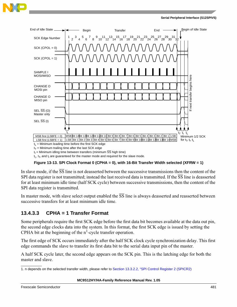
Serial Peripheral Interface (S12SPIV5)
Figure 13-13. SPI Clock Format 0 (CPHA = 0), with 16-Bit Transfer Width selected (XFRW = 1)
In slave mode, if the SS line is not deasserted between the successive transmissions then the content of theSPI data register is not transmitted; instead the last received data is transmitted. If the SS line is deassertedfor at least minimum idle time (half SCK cycle) between successive transmissions, then the content of theSPI data register is transmitted.
In master mode, with slave select output enabled the SS line is always deasserted and reasserted betweensuccessive transfers for at least minimum idle time.
13.4.3.3 CPHA = 1 Transfer Format
Some peripherals require the first SCK edge before the first data bit becomes available at the data out pin,the second edge clocks data into the system. In this format, the first SCK edge is issued by setting theCPHA bit at the beginning of the n1-cycle transfer operation.
The first edge of SCK occurs immediately after the half SCK clock cycle synchronization delay. This firstedge commands the slave to transfer its first data bit to the serial data input pin of the master.
A half SCK cycle later, the second edge appears on the SCK pin. This is the latching edge for both themaster and slave.
1. n depends on the selected transfer width, please refer to Section 13.3.2.2, “SPI Control Register 2 (SPICR2)
tL
Begin End
SCK (CPOL = 0)
SAMPLE I
CHANGE O
SEL SS (O)
Transfer
SCK (CPOL = 1)
MSB first (LSBFE = 0)LSB first (LSBFE = 1)
MSBLSB
LSBMSB
Bit 13Bit 2
Bit 14Bit 1
Bit 12Bit 3
Bit 11Bit 4
Bit 5
CHANGE O
SEL SS (I)
MOSI pin
MISO pin
Master only
MOSI/MISO
tT
If ne
xt tr
ansf
er b
egin
s he
re
for tT, tl, tLMinimum 1/2 SCKtI tL
tL = Minimum leading time before the first SCK edgetT = Minimum trailing time after the last SCK edgetI = Minimum idling time between transfers (minimum SS high time)tL, tT, and tI are guaranteed for the master mode and required for the slave mode.
12
34
56
78
910
1112
1314
1516SCK Edge Number
End of Idle State Begin of Idle State
1718
1920
2122
2324
2526
2728
2930
3132
Bit 10 Bit 9 Bit 8 Bit 7 Bit 6 Bit 4 Bit 3 Bit 2 Bit 1Bit 6Bit 5 Bit 7 Bit 8 Bit 9 Bit 10Bit 11Bit 12Bit 13Bit 14
MC9S12HY/HA-Family Reference Manual Rev. 1.05
Freescale Semiconductor 481
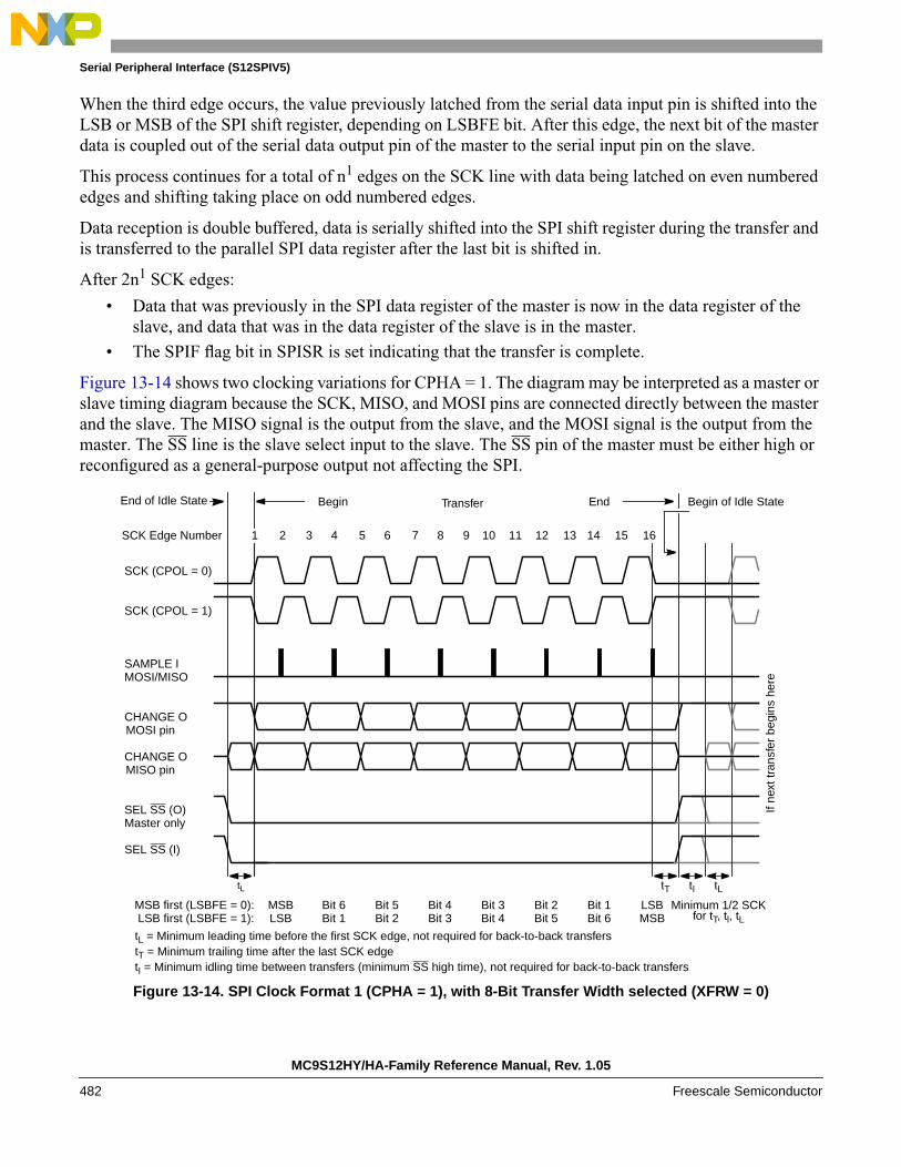
Serial Peripheral Interface (S12SPIV5)
When the third edge occurs, the value previously latched from the serial data input pin is shifted into theLSB or MSB of the SPI shift register, depending on LSBFE bit. After this edge, the next bit of the masterdata is coupled out of the serial data output pin of the master to the serial input pin on the slave.
This process continues for a total of n1 edges on the SCK line with data being latched on even numberededges and shifting taking place on odd numbered edges.
Data reception is double buffered, data is serially shifted into the SPI shift register during the transfer andis transferred to the parallel SPI data register after the last bit is shifted in.
After 2n1 SCK edges:
• Data that was previously in the SPI data register of the master is now in the data register of theslave, and data that was in the data register of the slave is in the master.
• The SPIF flag bit in SPISR is set indicating that the transfer is complete.
Figure 13-14 shows two clocking variations for CPHA = 1. The diagram may be interpreted as a master orslave timing diagram because the SCK, MISO, and MOSI pins are connected directly between the masterand the slave. The MISO signal is the output from the slave, and the MOSI signal is the output from themaster. The SS line is the slave select input to the slave. The SS pin of the master must be either high orreconfigured as a general-purpose output not affecting the SPI.
Figure 13-14. SPI Clock Format 1 (CPHA = 1), with 8-Bit Transfer Width selected (XFRW = 0)
tL tT
for tT, tl, tLMinimum 1/2 SCK
tI tL
If ne
xt tr
ansf
er b
egin
s he
re
Begin End
SCK (CPOL = 0)
SAMPLE I
CHANGE O
SEL SS (O)
Transfer
SCK (CPOL = 1)
MSB first (LSBFE = 0): LSB first (LSBFE = 1):
MSBLSB
LSBMSB
Bit 5Bit 2
Bit 6Bit 1
Bit 4Bit 3
Bit 3Bit 4
Bit 2Bit 5
Bit 1Bit 6
CHANGE O
SEL SS (I)
MOSI pin
MISO pin
Master only
MOSI/MISO
tL = Minimum leading time before the first SCK edge, not required for back-to-back transferstT = Minimum trailing time after the last SCK edgetI = Minimum idling time between transfers (minimum SS high time), not required for back-to-back transfers
1 2 3 4 5 6 7 8 9 10 11 12 13 14 15 16SCK Edge Number
End of Idle State Begin of Idle State
MC9S12HY/HA-Family Reference Manual, Rev. 1.05
482 Freescale Semiconductor
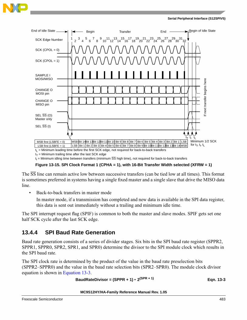
Serial Peripheral Interface (S12SPIV5)
Figure 13-15. SPI Clock Format 1 (CPHA = 1), with 16-Bit Transfer Width selected (XFRW = 1)
The SS line can remain active low between successive transfers (can be tied low at all times). This formatis sometimes preferred in systems having a single fixed master and a single slave that drive the MISO dataline.
• Back-to-back transfers in master mode
In master mode, if a transmission has completed and new data is available in the SPI data register,this data is sent out immediately without a trailing and minimum idle time.
The SPI interrupt request flag (SPIF) is common to both the master and slave modes. SPIF gets set onehalf SCK cycle after the last SCK edge.
13.4.4 SPI Baud Rate Generation
Baud rate generation consists of a series of divider stages. Six bits in the SPI baud rate register (SPPR2,SPPR1, SPPR0, SPR2, SPR1, and SPR0) determine the divisor to the SPI module clock which results inthe SPI baud rate.
The SPI clock rate is determined by the product of the value in the baud rate preselection bits(SPPR2–SPPR0) and the value in the baud rate selection bits (SPR2–SPR0). The module clock divisorequation is shown in Equation 13-3.
BaudRateDivisor = (SPPR + 1) • 2(SPR + 1) Eqn. 13-3
tL
Begin End
SCK (CPOL = 0)
SAMPLE I
CHANGE O
SEL SS (O)
Transfer
SCK (CPOL = 1)
MSB first (LSBFE = 0)LSB first (LSBFE = 1)
MSBLSB
LSBMSB
Bit 13Bit 2
Bit 14Bit 1
Bit 12Bit 3
Bit 11Bit 4
Bit 5
CHANGE O
SEL SS (I)
MOSI pin
MISO pin
Master only
MOSI/MISO
tT
If ne
xt tr
ansf
er b
egin
s he
re
for tT, tl, tLMinimum 1/2 SCKtI tL
tL = Minimum leading time before the first SCK edge, not required for back-to-back transferstT = Minimum trailing time after the last SCK edgetI = Minimum idling time between transfers (minimum SS high time), not required for back-to-back transfers
12
34
56
78
910
1112
1314
1516SCK Edge Number
End of Idle State Begin of Idle State
1718
1920
2122
2324
2526
2728
2930
3132
Bit 10 Bit 9 Bit 8 Bit 7 Bit 6 Bit 4 Bit 3 Bit 2 Bit 1Bit 6Bit 5 Bit 7 Bit 8 Bit 9 Bit 10Bit 11Bit 12Bit 13Bit 14
MC9S12HY/HA-Family Reference Manual Rev. 1.05
Freescale Semiconductor 483

Serial Peripheral Interface (S12SPIV5)
When all bits are clear (the default condition), the SPI module clock is divided by 2. When the selectionbits (SPR2–SPR0) are 001 and the preselection bits (SPPR2–SPPR0) are 000, the module clock divisorbecomes 4. When the selection bits are 010, the module clock divisor becomes 8, etc.
When the preselection bits are 001, the divisor determined by the selection bits is multiplied by 2. Whenthe preselection bits are 010, the divisor is multiplied by 3, etc. See Table 13-7 for baud rate calculationsfor all bit conditions, based on a 25 MHz bus clock. The two sets of selects allows the clock to be dividedby a non-power of two to achieve other baud rates such as divide by 6, divide by 10, etc.
The baud rate generator is activated only when the SPI is in master mode and a serial transfer is takingplace. In the other cases, the divider is disabled to decrease IDD current.
NOTEFor maximum allowed baud rates, please refer to the SPI ElectricalSpecification in the Electricals chapter of this data sheet.
13.4.5 Special Features
13.4.5.1 SS Output
The SS output feature automatically drives the SS pin low during transmission to select external devicesand drives it high during idle to deselect external devices. When SS output is selected, the SS output pinis connected to the SS input pin of the external device.
The SS output is available only in master mode during normal SPI operation by asserting SSOE andMODFEN bit as shown in Table 13-3.
The mode fault feature is disabled while SS output is enabled.
NOTECare must be taken when using the SS output feature in a multimastersystem because the mode fault feature is not available for detecting systemerrors between masters.
13.4.5.2 Bidirectional Mode (MOMI or SISO)
The bidirectional mode is selected when the SPC0 bit is set in SPI control register 2 (see Table 13-11). Inthis mode, the SPI uses only one serial data pin for the interface with external device(s). The MSTR bitdecides which pin to use. The MOSI pin becomes the serial data I/O (MOMI) pin for the master mode, andthe MISO pin becomes serial data I/O (SISO) pin for the slave mode. The MISO pin in master mode andMOSI pin in slave mode are not used by the SPI.
MC9S12HY/HA-Family Reference Manual, Rev. 1.05
484 Freescale Semiconductor

Serial Peripheral Interface (S12SPIV5)
The direction of each serial I/O pin depends on the BIDIROE bit. If the pin is configured as an output,serial data from the shift register is driven out on the pin. The same pin is also the serial input to the shiftregister.
• The SCK is output for the master mode and input for the slave mode.
• The SS is the input or output for the master mode, and it is always the input for the slave mode.
• The bidirectional mode does not affect SCK and SS functions.
NOTEIn bidirectional master mode, with mode fault enabled, both data pins MISOand MOSI can be occupied by the SPI, though MOSI is normally used fortransmissions in bidirectional mode and MISO is not used by the SPI. If amode fault occurs, the SPI is automatically switched to slave mode. In thiscase MISO becomes occupied by the SPI and MOSI is not used. This mustbe considered, if the MISO pin is used for another purpose.
13.4.6 Error Conditions
The SPI has one error condition:
• Mode fault error
13.4.6.1 Mode Fault Error
If the SS input becomes low while the SPI is configured as a master, it indicates a system error where morethan one master may be trying to drive the MOSI and SCK lines simultaneously. This condition is notpermitted in normal operation, the MODF bit in the SPI status register is set automatically, provided theMODFEN bit is set.
In the special case where the SPI is in master mode and MODFEN bit is cleared, the SS pin is not used bythe SPI. In this special case, the mode fault error function is inhibited and MODF remains cleared. In case
Table 13-11. Normal Mode and Bidirectional Mode
When SPE = 1 Master Mode MSTR = 1 Slave Mode MSTR = 0
Normal ModeSPC0 = 0
Bidirectional ModeSPC0 = 1
SPI
MOSI
MISO
Serial Out
Serial In
SPI
MOSI
MISO
Serial In
Serial Out
SPI
MOMISerial Out
Serial In
BIDIROESPI
SISO
Serial In
Serial Out
BIDIROE
MC9S12HY/HA-Family Reference Manual Rev. 1.05
Freescale Semiconductor 485

Serial Peripheral Interface (S12SPIV5)
the SPI system is configured as a slave, the SS pin is a dedicated input pin. Mode fault error doesn’t occurin slave mode.
If a mode fault error occurs, the SPI is switched to slave mode, with the exception that the slave outputbuffer is disabled. So SCK, MISO, and MOSI pins are forced to be high impedance inputs to avoid anypossibility of conflict with another output driver. A transmission in progress is aborted and the SPI isforced into idle state.
If the mode fault error occurs in the bidirectional mode for a SPI system configured in master mode, outputenable of the MOMI (MOSI in bidirectional mode) is cleared if it was set. No mode fault error occurs inthe bidirectional mode for SPI system configured in slave mode.
The mode fault flag is cleared automatically by a read of the SPI status register (with MODF set) followedby a write to SPI control register 1. If the mode fault flag is cleared, the SPI becomes a normal master orslave again.
NOTEIf a mode fault error occurs and a received data byte is pending in the receiveshift register, this data byte will be lost.
13.4.7 Low Power Mode Options
13.4.7.1 SPI in Run Mode
In run mode with the SPI system enable (SPE) bit in the SPI control register clear, the SPI system is in alow-power, disabled state. SPI registers remain accessible, but clocks to the core of this module aredisabled.
13.4.7.2 SPI in Wait Mode
SPI operation in wait mode depends upon the state of the SPISWAI bit in SPI control register 2.
• If SPISWAI is clear, the SPI operates normally when the CPU is in wait mode
• If SPISWAI is set, SPI clock generation ceases and the SPI module enters a power conservationstate when the CPU is in wait mode.
– If SPISWAI is set and the SPI is configured for master, any transmission and reception inprogress stops at wait mode entry. The transmission and reception resumes when the SPI exitswait mode.
– If SPISWAI is set and the SPI is configured as a slave, any transmission and reception inprogress continues if the SCK continues to be driven from the master. This keeps the slavesynchronized to the master and the SCK.
If the master transmits several bytes while the slave is in wait mode, the slave will continue tosend out bytes consistent with the operation mode at the start of wait mode (i.e., if the slave iscurrently sending its SPIDR to the master, it will continue to send the same byte. Else if theslave is currently sending the last received byte from the master, it will continue to send eachprevious master byte).
MC9S12HY/HA-Family Reference Manual, Rev. 1.05
486 Freescale Semiconductor

Serial Peripheral Interface (S12SPIV5)
NOTECare must be taken when expecting data from a master while the slave is inwait or stop mode. Even though the shift register will continue to operate,the rest of the SPI is shut down (i.e., a SPIF interrupt will not be generateduntil exiting stop or wait mode). Also, the byte from the shift register willnot be copied into the SPIDR register until after the slave SPI has exited waitor stop mode. In slave mode, a received byte pending in the receive shiftregister will be lost when entering wait or stop mode. An SPIF flag andSPIDR copy is generated only if wait mode is entered or exited during atranmission. If the slave enters wait mode in idle mode and exits wait modein idle mode, neither a SPIF nor a SPIDR copy will occur.
13.4.7.3 SPI in Stop Mode
Stop mode is dependent on the system. The SPI enters stop mode when the module clock is disabled (heldhigh or low). If the SPI is in master mode and exchanging data when the CPU enters stop mode, thetransmission is frozen until the CPU exits stop mode. After stop, data to and from the external SPI isexchanged correctly. In slave mode, the SPI will stay synchronized with the master.
The stop mode is not dependent on the SPISWAI bit.
13.4.7.4 Reset
The reset values of registers and signals are described in Section 13.3, “Memory Map and RegisterDefinition”, which details the registers and their bit fields.
• If a data transmission occurs in slave mode after reset without a write to SPIDR, it will transmitgarbage, or the data last received from the master before the reset.
• Reading from the SPIDR after reset will always read zeros.
13.4.7.5 Interrupts
The SPI only originates interrupt requests when SPI is enabled (SPE bit in SPICR1 set). The following isa description of how the SPI makes a request and how the MCU should acknowledge that request. Theinterrupt vector offset and interrupt priority are chip dependent.
The interrupt flags MODF, SPIF, and SPTEF are logically ORed to generate an interrupt request.
13.4.7.5.1 MODF
MODF occurs when the master detects an error on the SS pin. The master SPI must be configured for theMODF feature (see Table 13-3). After MODF is set, the current transfer is aborted and the following bit ischanged:
• MSTR = 0, The master bit in SPICR1 resets.
The MODF interrupt is reflected in the status register MODF flag. Clearing the flag will also clear theinterrupt. This interrupt will stay active while the MODF flag is set. MODF has an automatic clearingprocess which is described in Section 13.3.2.4, “SPI Status Register (SPISR)”.
MC9S12HY/HA-Family Reference Manual Rev. 1.05
Freescale Semiconductor 487

Serial Peripheral Interface (S12SPIV5)
13.4.7.5.2 SPIF
SPIF occurs when new data has been received and copied to the SPI data register. After SPIF is set, it doesnot clear until it is serviced. SPIF has an automatic clearing process, which is described inSection 13.3.2.4, “SPI Status Register (SPISR)”.
13.4.7.5.3 SPTEF
SPTEF occurs when the SPI data register is ready to accept new data. After SPTEF is set, it does not clearuntil it is serviced. SPTEF has an automatic clearing process, which is described in Section 13.3.2.4, “SPIStatus Register (SPISR)”.
MC9S12HY/HA-Family Reference Manual, Rev. 1.05
488 Freescale Semiconductor
Chapter 14Timer Module (TIM16B8CV2) Block Description
14.1 IntroductionThe basic timer consists of a 16-bit, software-programmable counter driven by a enhanced programmableprescaler.
Table 14-1. Revision History
RevisionNumber
Revision DateSectionsAffected
Description of Changes
V02.04 1 Jul 2008 14.3.2.12/14-505
14.3.2.13/14-505
14.3.2.16/14-508
14.4.2/14-51314.4.3/14-513
- Revised flag clearing procedure, whereby TEN bit must be set when clearingflags.
V02.05 9 Jul 2009 14.3.2.12/14-505
14.3.2.13/14-505
14.3.2.15/14-507
14.3.2.16/14-508
14.3.2.19/14-510
14.4.2/14-51314.4.3/14-513
- Revised flag clearing procedure, whereby TEN or PAEN bit must be setwhen clearing flags.- Add fomula to describe prescaler
V02.06 26 Aug 2009 14.1.2/14-49014.3.2.15/14-50
714.3.2.2/14-49614.3.2.3/14-49714.3.2.4/14-49814.4.3/14-513
- Correct typo: TSCR ->TSCR1- Correct reference: Figure 1-25 -> Figure 1-31- Add description, “a counter overflow when TTOV[7] is set”, to be thecondition of channel 7 override event.- Phrase the description of OC7M to make it more explicit
V02.07 04 May 2010 14.3.2.8/14-50114.3.2.11/14-50
414.4.3/14-513
- Add Table 14-10- in TCRE bit description part,add Note- Add Figure 14-31
MC9S12HY/HA-Family Reference Manual, Rev. 1.05
Freescale Semiconductor 489
Timer Module (TIM16B8CV2) Block Description
This timer can be used for many purposes, including input waveform measurements while simultaneouslygenerating an output waveform. Pulse widths can vary from microseconds to many seconds.
This timer contains 8 complete input capture/output compare channels and one pulse accumulator. Theinput capture function is used to detect a selected transition edge and record the time. The output comparefunction is used for generating output signals or for timer software delays. The 16-bit pulse accumulatoris used to operate as a simple event counter or a gated time accumulator. The pulse accumulator sharestimer channel 7 when in event mode.
A full access for the counter registers or the input capture/output compare registers should take place inone clock cycle. Accessing high byte and low byte separately for all of these registers may not yield thesame result as accessing them in one word.
14.1.1 Features
The TIM16B8CV2 includes these distinctive features:
• Eight input capture/output compare channels.
• Clock prescaling.
• 16-bit counter.
• 16-bit pulse accumulator.
14.1.2 Modes of Operation
Stop: Timer is off because clocks are stopped.
Freeze: Timer counter keep on running, unless TSFRZ in TSCR1 (0x0006) is set to 1.
Wait: Counters keep on running, unless TSWAI in TSCR1 (0x0006) is set to 1.
Normal: Timer counter keep on running, unless TEN in TSCR1 (0x0006) is cleared to 0.
MC9S12HY/HA-Family Reference Manual, Rev. 1.05
490 Freescale Semiconductor
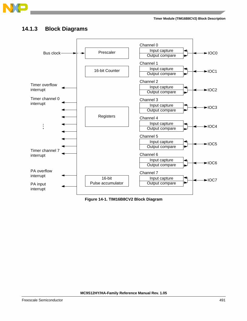
Timer Module (TIM16B8CV2) Block Description
14.1.3 Block Diagrams
Figure 14-1. TIM16B8CV2 Block Diagram
Prescaler
16-bit Counter
Input captureOutput compare
16-bitPulse accumulator
IOC0
IOC2
IOC1
IOC5
IOC3
IOC4
IOC6
IOC7PA inputinterrupt
PA overflowinterrupt
Timer overflowinterrupt
Timer channel 0interrupt
Timer channel 7interrupt
Registers
Bus clock
Input captureOutput compare
Input captureOutput compare
Input captureOutput compare
Input captureOutput compare
Input captureOutput compare
Input captureOutput compare
Input captureOutput compare
Channel 0
Channel 1
Channel 2
Channel 3
Channel 4
Channel 5
Channel 6
Channel 7
MC9S12HY/HA-Family Reference Manual Rev. 1.05
Freescale Semiconductor 491

Timer Module (TIM16B8CV2) Block Description
Figure 14-2. 16-Bit Pulse Accumulator Block Diagram
Figure 14-3. Interrupt Flag Setting
Edge detector
Inte
rmod
ule
Bus
PT7
M clockDivide by 64
Clock select
CLK0CLK1 4:1 MUX
TIMCLK
PAC
LK
PAC
LK /
256
PAC
LK /
6553
6Prescaled clock(PCLK)
(Timer clock)
Interrupt
MUX
(PAMOD)
PACNT
PTn Edge detector
16-bit Main Timer
TCn Input Capture Reg.Set CnF Interrupt
MC9S12HY/HA-Family Reference Manual, Rev. 1.05
492 Freescale Semiconductor

Timer Module (TIM16B8CV2) Block Description
Figure 14-4. Channel 7 Output Compare/Pulse Accumulator Logic
14.2 External Signal DescriptionThe TIM16B8CV2 module has a total of eight external pins.
14.2.1 IOC7 — Input Capture and Output Compare Channel 7 Pin
This pin serves as input capture or output compare for channel 7. This can also be configured as pulseaccumulator input.
14.2.2 IOC6 — Input Capture and Output Compare Channel 6 Pin
This pin serves as input capture or output compare for channel 6.
14.2.3 IOC5 — Input Capture and Output Compare Channel 5 Pin
This pin serves as input capture or output compare for channel 5.
14.2.4 IOC4 — Input Capture and Output Compare Channel 4 Pin
This pin serves as input capture or output compare for channel 4. Pin
14.2.5 IOC3 — Input Capture and Output Compare Channel 3 Pin
This pin serves as input capture or output compare for channel 3.
14.2.6 IOC2 — Input Capture and Output Compare Channel 2 Pin
This pin serves as input capture or output compare for channel 2.
PULSEACCUMULATOR PAD
TEN
CHANNEL 7 OUTPUT COMPARE
OCPD
TIOS7
MC9S12HY/HA-Family Reference Manual Rev. 1.05
Freescale Semiconductor 493
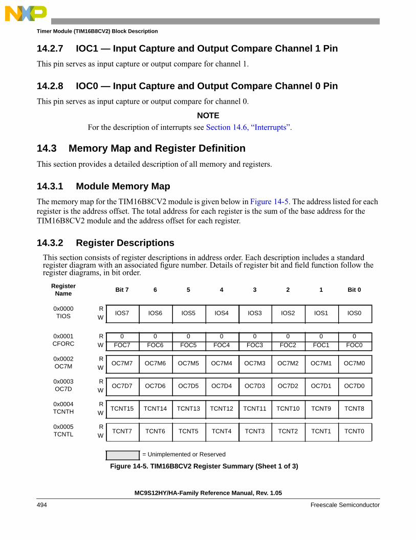
Timer Module (TIM16B8CV2) Block Description
14.2.7 IOC1 — Input Capture and Output Compare Channel 1 Pin
This pin serves as input capture or output compare for channel 1.
14.2.8 IOC0 — Input Capture and Output Compare Channel 0 Pin
This pin serves as input capture or output compare for channel 0.
NOTE For the description of interrupts see Section 14.6, “Interrupts”.
14.3 Memory Map and Register DefinitionThis section provides a detailed description of all memory and registers.
14.3.1 Module Memory Map
The memory map for the TIM16B8CV2 module is given below in Figure 14-5. The address listed for eachregister is the address offset. The total address for each register is the sum of the base address for theTIM16B8CV2 module and the address offset for each register.
14.3.2 Register DescriptionsThis section consists of register descriptions in address order. Each description includes a standardregister diagram with an associated figure number. Details of register bit and field function follow theregister diagrams, in bit order.
RegisterName
Bit 7 6 5 4 3 2 1 Bit 0
0x0000TIOS
RIOS7 IOS6 IOS5 IOS4 IOS3 IOS2 IOS1 IOS0
W
0x0001CFORC
R 0 0 0 0 0 0 0 0W FOC7 FOC6 FOC5 FOC4 FOC3 FOC2 FOC1 FOC0
0x0002OC7M
ROC7M7 OC7M6 OC7M5 OC7M4 OC7M3 OC7M2 OC7M1 OC7M0
W
0x0003OC7D
ROC7D7 OC7D6 OC7D5 OC7D4 OC7D3 OC7D2 OC7D1 OC7D0
W
0x0004TCNTH
RTCNT15 TCNT14 TCNT13 TCNT12 TCNT11 TCNT10 TCNT9 TCNT8
W
0x0005TCNTL
RTCNT7 TCNT6 TCNT5 TCNT4 TCNT3 TCNT2 TCNT1 TCNT0
W
= Unimplemented or Reserved
Figure 14-5. TIM16B8CV2 Register Summary (Sheet 1 of 3)
MC9S12HY/HA-Family Reference Manual, Rev. 1.05
494 Freescale Semiconductor

Timer Module (TIM16B8CV2) Block Description
0x0006TSCR1
RTEN TSWAI TSFRZ TFFCA PRNT
0 0 0W
0x0007TTOV
RTOV7 TOV6 TOV5 TOV4 TOV3 TOV2 TOV1 TOV0
W
0x0008TCTL1
ROM7 OL7 OM6 OL6 OM5 OL5 OM4 OL4
W
0x0009TCTL2
ROM3 OL3 OM2 OL2 OM1 OL1 OM0 OL0
W
0x000ATCTL3
REDG7B EDG7A EDG6B EDG6A EDG5B EDG5A EDG4B EDG4A
W
0x000BTCTL4
REDG3B EDG3A EDG2B EDG2A EDG1B EDG1A EDG0B EDG0A
W
0x000CTIE
RC7I C6I C5I C4I C3I C2I C1I C0I
W
0x000DTSCR2
RTOI
0 0 0TCRE PR2 PR1 PR0
W
0x000ETFLG1
RC7F C6F C5F C4F C3F C2F C1F C0F
W
0x000FTFLG2
RTOF
0 0 0 0 0 0 0W
0x0010–0x001FTCxH–TCxL
RBit 15 Bit 14 Bit 13 Bit 12 Bit 11 Bit 10 Bit 9 Bit 8
W
RBit 7 Bit 6 Bit 5 Bit 4 Bit 3 Bit 2 Bit 1 Bit 0
W
0x0020PACTL
R 0PAEN PAMOD PEDGE CLK1 CLK0 PAOVI PAI
W
0x0021PAFLG
R 0 0 0 0 0 0PAOVF PAIF
W
0x0022PACNTH
RPACNT15 PACNT14 PACNT13 PACNT12 PACNT11 PACNT10 PACNT9 PACNT8
W
0x0023PACNTL
RPACNT7 PACNT6 PACNT5 PACNT4 PACNT3 PACNT2 PACNT1 PACNT0
W
0x0024–0x002BReserved
RW
RegisterName
Bit 7 6 5 4 3 2 1 Bit 0
= Unimplemented or Reserved
Figure 14-5. TIM16B8CV2 Register Summary (Sheet 2 of 3)
MC9S12HY/HA-Family Reference Manual Rev. 1.05
Freescale Semiconductor 495
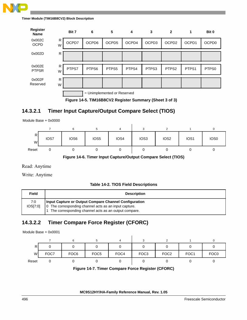
Timer Module (TIM16B8CV2) Block Description
14.3.2.1 Timer Input Capture/Output Compare Select (TIOS)
Read: Anytime
Write: Anytime
14.3.2.2 Timer Compare Force Register (CFORC)
0x002COCPD
ROCPD7 OCPD6 OCPD5 OCPD4 OCPD3 OCPD2 OCPD1 OCPD0
W
0x002D R
0x002EPTPSR
RPTPS7 PTPS6 PTPS5 PTPS4 PTPS3 PTPS2 PTPS1 PTPS0
W
0x002FReserved
RW
Module Base + 0x0000
7 6 5 4 3 2 1 0
RIOS7 IOS6 IOS5 IOS4 IOS3 IOS2 IOS1 IOS0
W
Reset 0 0 0 0 0 0 0 0
Figure 14-6. Timer Input Capture/Output Compare Select (TIOS)
Table 14-2. TIOS Field Descriptions
Field Description
7:0IOS[7:0]
Input Capture or Output Compare Channel Configuration0 The corresponding channel acts as an input capture.1 The corresponding channel acts as an output compare.
Module Base + 0x0001
7 6 5 4 3 2 1 0
R 0 0 0 0 0 0 0 0
W FOC7 FOC6 FOC5 FOC4 FOC3 FOC2 FOC1 FOC0
Reset 0 0 0 0 0 0 0 0
Figure 14-7. Timer Compare Force Register (CFORC)
RegisterName
Bit 7 6 5 4 3 2 1 Bit 0
= Unimplemented or Reserved
Figure 14-5. TIM16B8CV2 Register Summary (Sheet 3 of 3)
MC9S12HY/HA-Family Reference Manual, Rev. 1.05
496 Freescale Semiconductor

Timer Module (TIM16B8CV2) Block Description
Read: Anytime but will always return 0x0000 (1 state is transient)
Write: Anytime
14.3.2.3 Output Compare 7 Mask Register (OC7M)
Read: Anytime
Write: Anytime
Table 14-3. CFORC Field Descriptions
Field Description
7:0FOC[7:0]
Force Output Compare Action for Channel 7:0 — A write to this register with the corresponding data bit(s) setcauses the action which is programmed for output compare “x” to occur immediately. The action taken is thesame as if a successful comparison had just taken place with the TCx register except the interrupt flag does notget set.Note: A channel 7 event, which can be a counter overflow when TTOV[7] is set or a successful output compare
on channel 7, overrides any channel 6:0 compares. If forced output compare on any channel occurs at thesame time as the successful output compare then forced output compare action will take precedence andinterrupt flag won’t get set.
Module Base + 0x0002
7 6 5 4 3 2 1 0
ROC7M7 OC7M6 OC7M5 OC7M4 OC7M3 OC7M2 OC7M1 OC7M0
W
Reset 0 0 0 0 0 0 0 0
Figure 14-8. Output Compare 7 Mask Register (OC7M)
Table 14-4. OC7M Field Descriptions
Field Description
7:0OC7M[7:0]
Output Compare 7 Mask — A channel 7 event, which can be a counter overflow when TTOV[7] is set or asuccessful output compare on channel 7, overrides any channel 6:0 compares. For each OC7M bit that is set,the output compare action reflects the corresponding OC7D bit.0 The corresponding OC7Dx bit in the output compare 7 data register will not be transferred to the timer port on
a channel 7 event, even if the corresponding pin is setup for output compare.1 The corresponding OC7Dx bit in the output compare 7 data register will be transferred to the timer port on a
channel 7 event.Note: The corresponding channel must also be setup for output compare (IOSx = 1 and OCPDx = 0) for data to
be transferred from the output compare 7 data register to the timer port.
MC9S12HY/HA-Family Reference Manual Rev. 1.05
Freescale Semiconductor 497
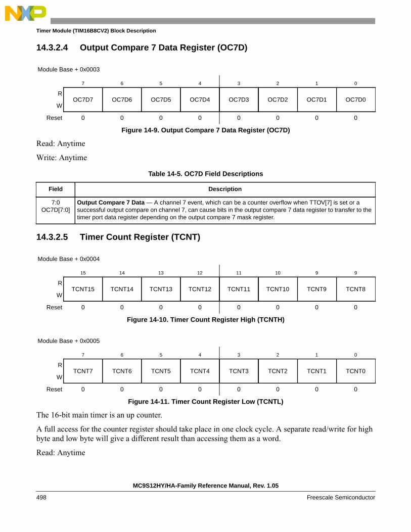
Timer Module (TIM16B8CV2) Block Description
14.3.2.4 Output Compare 7 Data Register (OC7D)
Read: Anytime
Write: Anytime
14.3.2.5 Timer Count Register (TCNT)
The 16-bit main timer is an up counter.
A full access for the counter register should take place in one clock cycle. A separate read/write for highbyte and low byte will give a different result than accessing them as a word.
Read: Anytime
Module Base + 0x0003
7 6 5 4 3 2 1 0
ROC7D7 OC7D6 OC7D5 OC7D4 OC7D3 OC7D2 OC7D1 OC7D0
W
Reset 0 0 0 0 0 0 0 0
Figure 14-9. Output Compare 7 Data Register (OC7D)
Table 14-5. OC7D Field Descriptions
Field Description
7:0OC7D[7:0]
Output Compare 7 Data — A channel 7 event, which can be a counter overflow when TTOV[7] is set or asuccessful output compare on channel 7, can cause bits in the output compare 7 data register to transfer to thetimer port data register depending on the output compare 7 mask register.
Module Base + 0x0004
15 14 13 12 11 10 9 9
RTCNT15 TCNT14 TCNT13 TCNT12 TCNT11 TCNT10 TCNT9 TCNT8
W
Reset 0 0 0 0 0 0 0 0
Figure 14-10. Timer Count Register High (TCNTH)
Module Base + 0x0005
7 6 5 4 3 2 1 0
RTCNT7 TCNT6 TCNT5 TCNT4 TCNT3 TCNT2 TCNT1 TCNT0
W
Reset 0 0 0 0 0 0 0 0
Figure 14-11. Timer Count Register Low (TCNTL)
MC9S12HY/HA-Family Reference Manual, Rev. 1.05
498 Freescale Semiconductor

Timer Module (TIM16B8CV2) Block Description
Write: Has no meaning or effect in the normal mode; only writable in special modes (test_mode = 1).
The period of the first count after a write to the TCNT registers may be a different size because the writeis not synchronized with the prescaler clock.
14.3.2.6 Timer System Control Register 1 (TSCR1)
Read: Anytime
Write: Anytime
Module Base + 0x0006
7 6 5 4 3 2 1 0
RTEN TSWAI TSFRZ TFFCA PRNT
0 0 0
W
Reset 0 0 0 0 0 0 0 0
= Unimplemented or Reserved
Figure 14-12. Timer System Control Register 1 (TSCR1)
Table 14-6. TSCR1 Field Descriptions
Field Description
7TEN
Timer Enable0 Disables the main timer, including the counter. Can be used for reducing power consumption.1 Allows the timer to function normally.If for any reason the timer is not active, there is no ÷64 clock for the pulse accumulator because the ÷64 isgenerated by the timer prescaler.
6TSWAI
Timer Module Stops While in Wait0 Allows the timer module to continue running during wait.1 Disables the timer module when the MCU is in the wait mode. Timer interrupts cannot be used to get the MCU
out of wait.TSWAI also affects pulse accumulator.
5TSFRZ
Timer Stops While in Freeze Mode0 Allows the timer counter to continue running while in freeze mode.1 Disables the timer counter whenever the MCU is in freeze mode. This is useful for emulation.TSFRZ does not stop the pulse accumulator.
MC9S12HY/HA-Family Reference Manual Rev. 1.05
Freescale Semiconductor 499

Timer Module (TIM16B8CV2) Block Description
14.3.2.7 Timer Toggle On Overflow Register 1 (TTOV)
Read: Anytime
Write: Anytime
4TFFCA
Timer Fast Flag Clear All0 Allows the timer flag clearing to function normally.1 For TFLG1(0x000E), a read from an input capture or a write to the output compare channel (0x0010–0x001F)
causes the corresponding channel flag, CnF, to be cleared. For TFLG2 (0x000F), any access to the TCNTregister (0x0004, 0x0005) clears the TOF flag. Any access to the PACNT registers (0x0022, 0x0023) clearsthe PAOVF and PAIF flags in the PAFLG register (0x0021). This has the advantage of eliminating softwareoverhead in a separate clear sequence. Extra care is required to avoid accidental flag clearing due tounintended accesses.
3PRNT
Precision Timer0 Enables legacy timer. PR0, PR1, and PR2 bits of the TSCR2 register are used for timer counter prescaler
selection.1 Enables precision timer. All bits of the PTPSR register are used for Precision Timer Prescaler Selection, and
all bits.This bit is writable only once out of reset.
Module Base + 0x0007
7 6 5 4 3 2 1 0
RTOV7 TOV6 TOV5 TOV4 TOV3 TOV2 TOV1 TOV0
W
Reset 0 0 0 0 0 0 0 0
Figure 14-13. Timer Toggle On Overflow Register 1 (TTOV)
Table 14-7. TTOV Field Descriptions
Field Description
7:0TOV[7:0]
Toggle On Overflow Bits — TOVx toggles output compare pin on overflow. This feature only takes effect whenin output compare mode. When set, it takes precedence over forced output compare but not channel 7 overrideevents.0 Toggle output compare pin on overflow feature disabled.1 Toggle output compare pin on overflow feature enabled.
Table 14-6. TSCR1 Field Descriptions (continued)
Field Description
MC9S12HY/HA-Family Reference Manual, Rev. 1.05
500 Freescale Semiconductor

Timer Module (TIM16B8CV2) Block Description
14.3.2.8 Timer Control Register 1/Timer Control Register 2 (TCTL1/TCTL2)
Read: Anytime
Write: Anytime
Module Base + 0x0008
7 6 5 4 3 2 1 0
ROM7 OL7 OM6 OL6 OM5 OL5 OM4 OL4
W
Reset 0 0 0 0 0 0 0 0
Figure 14-14. Timer Control Register 1 (TCTL1)
Module Base + 0x0009
7 6 5 4 3 2 1 0
ROM3 OL3 OM2 OL2 OM1 OL1 OM0 OL0
W
Reset 0 0 0 0 0 0 0 0
Figure 14-15. Timer Control Register 2 (TCTL2)
Table 14-8. TCTL1/TCTL2 Field Descriptions
Field Description
7:0OMx
Output Mode — These eight pairs of control bits are encoded to specify the output action to be taken as a resultof a successful OCx compare. When either OMx or OLx is 1, the pin associated with OCx becomes an outputtied to OCx.Note: To enable output action by OMx bits on timer port, the corresponding bit in OC7M should be cleared. For
an output line to be driven by an OCx the OCPDx must be cleared.
7:0OLx
Output Level — These eight pairs of control bits are encoded to specify the output action to be taken as a resultof a successful OCx compare. When either OMx or OLx is 1, the pin associated with OCx becomes an outputtied to OCx.Note: To enable output action by OLx bits on timer port, the corresponding bit in OC7M should be cleared. For
an output line to be driven by an OCx the OCPDx must be cleared.
Table 14-9. Compare Result Output Action
OMx OLx Action
0 0 No output compareaction on the timer output signal
0 1 Toggle OCx output line
1 0 Clear OCx output line to zero
1 1 Set OCx output line to one
MC9S12HY/HA-Family Reference Manual Rev. 1.05
Freescale Semiconductor 501

Timer Module (TIM16B8CV2) Block Description
To operate the 16-bit pulse accumulator independently of input capture or output compare 7 and 0respectively the user must set the corresponding bits IOSx = 1, OMx = 0 and OLx = 0. OC7M7 in theOC7M register must also be cleared.
To enable output action using the OM7 and OL7 bits on the timer port,the corresponding bit OC7M7 inthe OC7M register must also be cleared. The settings for these bits can be seen in Table 14-10
Table 14-10. The OC7 and OCx event priority
Note: in Table 14-10, the IOS7 and IOSx should be set to 1
IOSx is the register TIOS bit x,
OC7Mx is the register OC7M bit x,
TCx is timer Input Capture/Output Compare register,
IOCx is channel x,
OMx/OLx is the register TCTL1/TCTL2,
OC7Dx is the register OC7D bit x.
IOCx = OC7Dx+ OMx/OLx, means that both OC7 event and OCx event will change channel x value.
14.3.2.9 Timer Control Register 3/Timer Control Register 4 (TCTL3 and TCTL4)
OC7M7=0 OC7M7=1
OC7Mx=1 OC7Mx=0 OC7Mx=1 OC7Mx=0
TC7=TCx TC7>TCx TC7=TCx TC7>TCx TC7=TCx TC7>TCx TC7=TCx TC7>TCx
IOCx=OC7DxIOC7=OM7/O
L7
IOCx=OC7Dx+OMx/OLx
IOC7=OM7/OL7
IOCx=OMx/OLxIOC7=OM7/OL7
IOCx=OC7DxIOC7=OC7D7
IOCx=OC7Dx+OMx/OLx
IOC7=OC7D7
IOCx=OMx/OLxIOC7=OC7D7
Module Base + 0x000A
7 6 5 4 3 2 1 0
REDG7B EDG7A EDG6B EDG6A EDG5B EDG5A EDG4B EDG4A
W
Reset 0 0 0 0 0 0 0 0
Figure 14-16. Timer Control Register 3 (TCTL3)
Module Base + 0x000B
7 6 5 4 3 2 1 0
REDG3B EDG3A EDG2B EDG2A EDG1B EDG1A EDG0B EDG0A
W
Reset 0 0 0 0 0 0 0 0
Figure 14-17. Timer Control Register 4 (TCTL4)
MC9S12HY/HA-Family Reference Manual, Rev. 1.05
502 Freescale Semiconductor

Timer Module (TIM16B8CV2) Block Description
Read: Anytime
Write: Anytime.
14.3.2.10 Timer Interrupt Enable Register (TIE)
Read: Anytime
Write: Anytime.
Table 14-11. TCTL3/TCTL4 Field Descriptions
Field Description
7:0EDGnBEDGnA
Input Capture Edge Control — These eight pairs of control bits configure the input capture edge detectorcircuits.
Table 14-12. Edge Detector Circuit Configuration
EDGnB EDGnA Configuration
0 0 Capture disabled
0 1 Capture on rising edges only
1 0 Capture on falling edges only
1 1 Capture on any edge (rising or falling)
Module Base + 0x000C
7 6 5 4 3 2 1 0
RC7I C6I C5I C4I C3I C2I C1I C0I
W
Reset 0 0 0 0 0 0 0 0
Figure 14-18. Timer Interrupt Enable Register (TIE)
Table 14-13. TIE Field Descriptions
Field Description
7:0C7I:C0I
Input Capture/Output Compare “x” Interrupt Enable — The bits in TIE correspond bit-for-bit with the bits inthe TFLG1 status register. If cleared, the corresponding flag is disabled from causing a hardware interrupt. If set,the corresponding flag is enabled to cause a interrupt.
MC9S12HY/HA-Family Reference Manual Rev. 1.05
Freescale Semiconductor 503
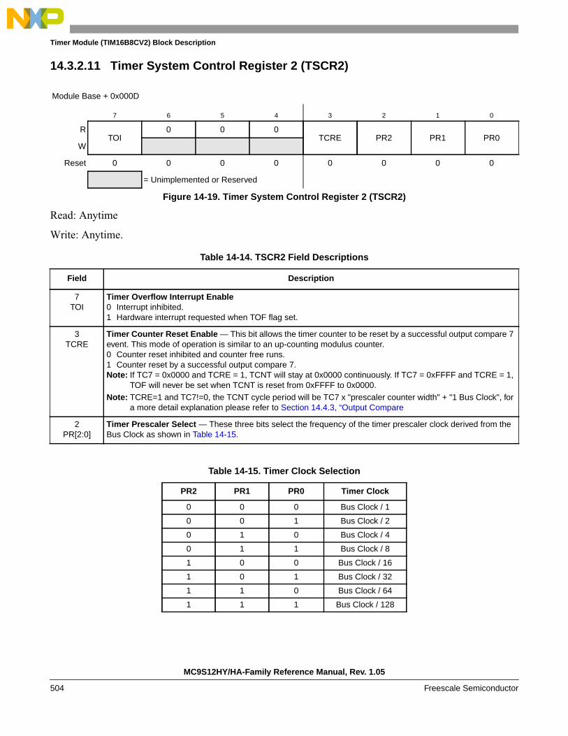
Timer Module (TIM16B8CV2) Block Description
14.3.2.11 Timer System Control Register 2 (TSCR2)
Read: Anytime
Write: Anytime.
Module Base + 0x000D
7 6 5 4 3 2 1 0
RTOI
0 0 0TCRE PR2 PR1 PR0
W
Reset 0 0 0 0 0 0 0 0
= Unimplemented or Reserved
Figure 14-19. Timer System Control Register 2 (TSCR2)
Table 14-14. TSCR2 Field Descriptions
Field Description
7TOI
Timer Overflow Interrupt Enable0 Interrupt inhibited.1 Hardware interrupt requested when TOF flag set.
3TCRE
Timer Counter Reset Enable — This bit allows the timer counter to be reset by a successful output compare 7event. This mode of operation is similar to an up-counting modulus counter.0 Counter reset inhibited and counter free runs.1 Counter reset by a successful output compare 7.Note: If TC7 = 0x0000 and TCRE = 1, TCNT will stay at 0x0000 continuously. If TC7 = 0xFFFF and TCRE = 1,
TOF will never be set when TCNT is reset from 0xFFFF to 0x0000.Note: TCRE=1 and TC7!=0, the TCNT cycle period will be TC7 x "prescaler counter width" + "1 Bus Clock", for
a more detail explanation please refer to Section 14.4.3, “Output Compare
2PR[2:0]
Timer Prescaler Select — These three bits select the frequency of the timer prescaler clock derived from theBus Clock as shown in Table 14-15.
Table 14-15. Timer Clock Selection
PR2 PR1 PR0 Timer Clock
0 0 0 Bus Clock / 1
0 0 1 Bus Clock / 2
0 1 0 Bus Clock / 4
0 1 1 Bus Clock / 8
1 0 0 Bus Clock / 16
1 0 1 Bus Clock / 32
1 1 0 Bus Clock / 64
1 1 1 Bus Clock / 128
MC9S12HY/HA-Family Reference Manual, Rev. 1.05
504 Freescale Semiconductor

Timer Module (TIM16B8CV2) Block Description
NOTEThe newly selected prescale factor will not take effect until the nextsynchronized edge where all prescale counter stages equal zero.
14.3.2.12 Main Timer Interrupt Flag 1 (TFLG1)
Read: Anytime
Write: Used in the clearing mechanism (set bits cause corresponding bits to be cleared). Writing a zerowill not affect current status of the bit.
14.3.2.13 Main Timer Interrupt Flag 2 (TFLG2)
TFLG2 indicates when interrupt conditions have occurred. To clear a bit in the flag register, write the bitto one while TEN bit of TSCR1 or PAEN bit of PACTL is set to one.
Read: Anytime
Write: Used in clearing mechanism (set bits cause corresponding bits to be cleared).
Any access to TCNT will clear TFLG2 register if the TFFCA bit in TSCR register is set.
Module Base + 0x000E
7 6 5 4 3 2 1 0
RC7F C6F C5F C4F C3F C2F C1F C0F
W
Reset 0 0 0 0 0 0 0 0
Figure 14-20. Main Timer Interrupt Flag 1 (TFLG1)
Table 14-16. TRLG1 Field Descriptions
Field Description
7:0C[7:0]F
Input Capture/Output Compare Channel “x” Flag — These flags are set when an input capture or outputcompare event occurs. Clearing requires writing a one to the corresponding flag bit while TEN or PAEN is set toone.
When TFFCA bit in TSCR register is set, a read from an input capture or a write into an output compare channel(0x0010–0x001F) will cause the corresponding channel flag CxF to be cleared.
Module Base + 0x000F
7 6 5 4 3 2 1 0
RTOF
0 0 0 0 0 0 0
W
Reset 0 0 0 0 0 0 0 0
Unimplemented or Reserved
Figure 14-21. Main Timer Interrupt Flag 2 (TFLG2)
MC9S12HY/HA-Family Reference Manual Rev. 1.05
Freescale Semiconductor 505
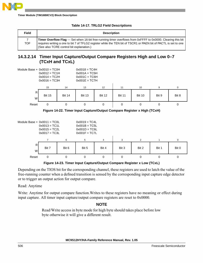
Timer Module (TIM16B8CV2) Block Description
14.3.2.14 Timer Input Capture/Output Compare Registers High and Low 0–7(TCxH and TCxL)
Depending on the TIOS bit for the corresponding channel, these registers are used to latch the value of thefree-running counter when a defined transition is sensed by the corresponding input capture edge detectoror to trigger an output action for output compare.
Read: Anytime
Write: Anytime for output compare function.Writes to these registers have no meaning or effect duringinput capture. All timer input capture/output compare registers are reset to 0x0000.
NOTERead/Write access in byte mode for high byte should takes place before lowbyte otherwise it will give a different result.
Table 14-17. TRLG2 Field Descriptions
Field Description
7TOF
Timer Overflow Flag — Set when 16-bit free-running timer overflows from 0xFFFF to 0x0000. Clearing this bitrequires writing a one to bit 7 of TFLG2 register while the TEN bit of TSCR1 or PAEN bit of PACTL is set to one(See also TCRE control bit explanation.)
Module Base + 0x0010 = TC0H0x0012 = TC1H0x0014 = TC2H0x0016 = TC3H
0x0018 = TC4H0x001A = TC5H0x001C = TC6H0x001E = TC7H
15 14 13 12 11 10 9 0
RBit 15 Bit 14 Bit 13 Bit 12 Bit 11 Bit 10 Bit 9 Bit 8
W
Reset 0 0 0 0 0 0 0 0
Figure 14-22. Timer Input Capture/Output Compare Register x High (TCxH)
Module Base + 0x0011 = TC0L0x0013 = TC1L0x0015 = TC2L0x0017 = TC3L
0x0019 = TC4L0x001B = TC5L0x001D = TC6L0x001F = TC7L
7 6 5 4 3 2 1 0
RBit 7 Bit 6 Bit 5 Bit 4 Bit 3 Bit 2 Bit 1 Bit 0
W
Reset 0 0 0 0 0 0 0 0
Figure 14-23. Timer Input Capture/Output Compare Register x Low (TCxL)
MC9S12HY/HA-Family Reference Manual, Rev. 1.05
506 Freescale Semiconductor

Timer Module (TIM16B8CV2) Block Description
14.3.2.15 16-Bit Pulse Accumulator Control Register (PACTL)
When PAEN is set, the PACT is enabled.The PACT shares the input pin with IOC7.
Read: Any time
Write: Any time
Module Base + 0x0020
7 6 5 4 3 2 1 0
R 0PAEN PAMOD PEDGE CLK1 CLK0 PAOVI PAI
W
Reset 0 0 0 0 0 0 0 0
Unimplemented or Reserved
Figure 14-24. 16-Bit Pulse Accumulator Control Register (PACTL)
Table 14-18. PACTL Field Descriptions
Field Description
6PAEN
Pulse Accumulator System Enable — PAEN is independent from TEN. With timer disabled, the pulseaccumulator can function unless pulse accumulator is disabled.0 16-Bit Pulse Accumulator system disabled.1 Pulse Accumulator system enabled.
5PAMOD
Pulse Accumulator Mode — This bit is active only when the Pulse Accumulator is enabled (PAEN = 1). SeeTable 14-19.0 Event counter mode.1 Gated time accumulation mode.
4PEDGE
Pulse Accumulator Edge Control — This bit is active only when the Pulse Accumulator is enabled (PAEN = 1).For PAMOD bit = 0 (event counter mode). See Table 14-19.0 Falling edges on IOC7 pin cause the count to be incremented.1 Rising edges on IOC7 pin cause the count to be incremented.For PAMOD bit = 1 (gated time accumulation mode).0 IOC7 input pin high enables M (bus clock) divided by 64 clock to Pulse Accumulator and the trailing falling
edge on IOC7 sets the PAIF flag.1 IOC7 input pin low enables M (bus clock) divided by 64 clock to Pulse Accumulator and the trailing rising edge
on IOC7 sets the PAIF flag.
3:2CLK[1:0]
Clock Select Bits — Refer to Table 14-20.
1PAOVI
Pulse Accumulator Overflow Interrupt Enable0 Interrupt inhibited.1 Interrupt requested if PAOVF is set.
0PAI
Pulse Accumulator Input Interrupt Enable0 Interrupt inhibited.1 Interrupt requested if PAIF is set.
MC9S12HY/HA-Family Reference Manual Rev. 1.05
Freescale Semiconductor 507

Timer Module (TIM16B8CV2) Block Description
NOTEIf the timer is not active (TEN = 0 in TSCR), there is no divide-by-64because the ÷64 clock is generated by the timer prescaler.
For the description of PACLK please refer Figure 14-30.
If the pulse accumulator is disabled (PAEN = 0), the prescaler clock from the timer is always used as aninput clock to the timer counter. The change from one selected clock to the other happens immediatelyafter these bits are written.
14.3.2.16 Pulse Accumulator Flag Register (PAFLG)
Read: Anytime
Write: Anytime
When the TFFCA bit in the TSCR register is set, any access to the PACNT register will clear all the flagsin the PAFLG register. Timer module or Pulse Accumulator must stay enabled (TEN=1 or PAEN=1) whileclearing these bits.
Table 14-19. Pin Action
PAMOD PEDGE Pin Action
0 0 Falling edge
0 1 Rising edge
1 0 Div. by 64 clock enabled with pin high level
1 1 Div. by 64 clock enabled with pin low level
Table 14-20. Timer Clock Selection
CLK1 CLK0 Timer Clock
0 0 Use timer prescaler clock as timer counter clock
0 1 Use PACLK as input to timer counter clock
1 0 Use PACLK/256 as timer counter clock frequency
1 1 Use PACLK/65536 as timer counter clock frequency
Module Base + 0x0021
7 6 5 4 3 2 1 0
R 0 0 0 0 0 0PAOVF PAIF
W
Reset 0 0 0 0 0 0 0 0
Unimplemented or Reserved
Figure 14-25. Pulse Accumulator Flag Register (PAFLG)
MC9S12HY/HA-Family Reference Manual, Rev. 1.05
508 Freescale Semiconductor

Timer Module (TIM16B8CV2) Block Description
14.3.2.17 Pulse Accumulators Count Registers (PACNT)
Read: Anytime
Write: Anytime
These registers contain the number of active input edges on its input pin since the last reset.
When PACNT overflows from 0xFFFF to 0x0000, the Interrupt flag PAOVF in PAFLG (0x0021) is set.
Full count register access should take place in one clock cycle. A separate read/write for high byte and lowbyte will give a different result than accessing them as a word.
NOTE Reading the pulse accumulator counter registers immediately after anactive edge on the pulse accumulator input pin may miss the last countbecause the input has to be synchronized with the bus clock first.
Table 14-21. PAFLG Field Descriptions
Field Description
1PAOVF
Pulse Accumulator Overflow Flag — Set when the 16-bit pulse accumulator overflows from 0xFFFF to 0x0000.Clearing this bit requires writing a one to this bit in the PAFLG register while TEN bit of TSCR1 or PAEN bit ofPACTL register is set to one.
0PAIF
Pulse Accumulator Input edge Flag — Set when the selected edge is detected at the IOC7 input pin.In eventmode the event edge triggers PAIF and in gated time accumulation mode the trailing edge of the gate signal atthe IOC7 input pin triggers PAIF.Clearing this bit requires writing a one to this bit in the PAFLG register while TEN bit of TSCR1 or PAEN bit ofPACTL register is set to one. Any access to the PACNT register will clear all the flags in this register when TFFCAbit in register TSCR(0x0006) is set.
Module Base + 0x0022
15 14 13 12 11 10 9 0
RPACNT15 PACNT14 PACNT13 PACNT12 PACNT11 PACNT10 PACNT9 PACNT8
W
Reset 0 0 0 0 0 0 0 0
Figure 14-26. Pulse Accumulator Count Register High (PACNTH)
Module Base + 0x0023
7 6 5 4 3 2 1 0
RPACNT7 PACNT6 PACNT5 PACNT4 PACNT3 PACNT2 PACNT1 PACNT0
W
Reset 0 0 0 0 0 0 0 0
Figure 14-27. Pulse Accumulator Count Register Low (PACNTL)
MC9S12HY/HA-Family Reference Manual Rev. 1.05
Freescale Semiconductor 509
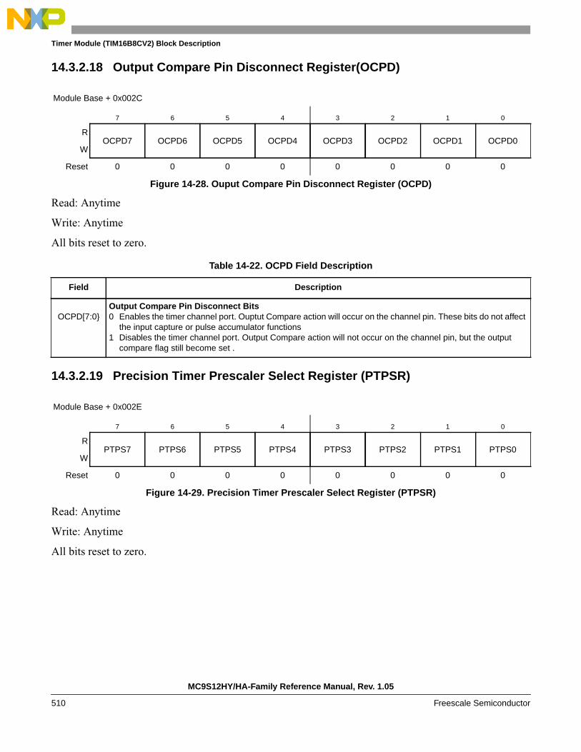
Timer Module (TIM16B8CV2) Block Description
14.3.2.18 Output Compare Pin Disconnect Register(OCPD)
Read: Anytime
Write: Anytime
All bits reset to zero.
14.3.2.19 Precision Timer Prescaler Select Register (PTPSR)
Read: Anytime
Write: Anytime
All bits reset to zero.
Module Base + 0x002C
7 6 5 4 3 2 1 0
ROCPD7 OCPD6 OCPD5 OCPD4 OCPD3 OCPD2 OCPD1 OCPD0
W
Reset 0 0 0 0 0 0 0 0
Figure 14-28. Ouput Compare Pin Disconnect Register (OCPD)
Table 14-22. OCPD Field Description
Field Description
OCPD[7:0Output Compare Pin Disconnect Bits0 Enables the timer channel port. Ouptut Compare action will occur on the channel pin. These bits do not affect
the input capture or pulse accumulator functions1 Disables the timer channel port. Output Compare action will not occur on the channel pin, but the output
compare flag still become set .
Module Base + 0x002E
7 6 5 4 3 2 1 0
RPTPS7 PTPS6 PTPS5 PTPS4 PTPS3 PTPS2 PTPS1 PTPS0
W
Reset 0 0 0 0 0 0 0 0
Figure 14-29. Precision Timer Prescaler Select Register (PTPSR)
MC9S12HY/HA-Family Reference Manual, Rev. 1.05
510 Freescale Semiconductor
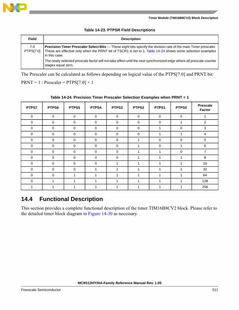
Timer Module (TIM16B8CV2) Block Description
The Prescaler can be calculated as follows depending on logical value of the PTPS[7:0] and PRNT bit:
PRNT = 1 : Prescaler = PTPS[7:0] + 1
Table 14-24. Precision Timer Prescaler Selection Examples when PRNT = 1
14.4 Functional DescriptionThis section provides a complete functional description of the timer TIM16B8CV2 block. Please refer tothe detailed timer block diagram in Figure 14-30 as necessary.
Table 14-23. PTPSR Field Descriptions
Field Description
7:0PTPS[7:0]
Precision Timer Prescaler Select Bits — These eight bits specify the division rate of the main Timer prescaler.These are effective only when the PRNT bit of TSCR1 is set to 1. Table 14-24 shows some selection examplesin this case.
The newly selected prescale factor will not take effect until the next synchronized edge where all prescale counterstages equal zero.
PTPS7 PTPS6 PTPS5 PTPS4 PTPS3 PTPS2 PTPS1 PTPS0PrescaleFactor
0 0 0 0 0 0 0 0 1
0 0 0 0 0 0 0 1 2
0 0 0 0 0 0 1 0 3
0 0 0 0 0 0 1 1 4
0 0 0 0 0 1 0 0 5
0 0 0 0 0 1 0 1 6
0 0 0 0 0 1 1 0 7
0 0 0 0 0 1 1 1 8
0 0 0 0 1 1 1 1 16
0 0 0 1 1 1 1 1 32
0 0 1 1 1 1 1 1 64
0 1 1 1 1 1 1 1 128
1 1 1 1 1 1 1 1 256
MC9S12HY/HA-Family Reference Manual Rev. 1.05
Freescale Semiconductor 511

Timer Module (TIM16B8CV2) Block Description
Figure 14-30. Detailed Timer Block Diagram
14.4.1 Prescaler
The prescaler divides the bus clock by 1,2,4,8,16,32,64 or 128. The prescaler select bits, PR[2:0], selectthe prescaler divisor. PR[2:0] are in timer system control register 2 (TSCR2).
PRESCALER
CHANNEL 0
IOC0 PIN
16-BIT COUNTER
LOGIC
PR[2:1:0]
DIVIDE-BY-64
TC0
EDGEDETECT
PACNT(hi):PACNT(lo)PAOVFPEDGE
PAOVI
TEN
PAE
16-BIT COMPARATOR
TCNT(hi):TCNT(lo)
CHANNEL 1
TC1
16-BIT COMPARATOR
16-BIT COUNTER
INTERRUPTLOGIC
TOF
TOI
C0F
C1F
EDGEDETECT
IOC1 PINLOGIC
EDGEDETECT
CxF
CHANNEL7
TC7
16-BIT COMPARATOR C7F
IOC7 PINLOGIC
EDGEDETECT
OM:OL0
TOV0
OM:OL1
TOV1
OM:OL7
TOV7
EDG1A EDG1B
EDG7A
EDG7B
EDG0B
TCRE
PAIF
CLEAR COUNTER
PAIF
PAI
INTERRUPTLOGIC
CxI
INTERRUPTREQUEST
PAOVF
CH. 7 COMPARE
CH.7 CAPTURE
CH. 1 CAPTURE
MUX
CLK[1:0]
PACLKPACLK/256
PACLK/65536
IOC1 PIN
IOC0 PIN
IOC7 PIN
PACLKPACLK/256
PACLK/65536
TE
CH. 1 COMPARE
CH. 0COMPARE
CH. 0 CAPTURE
PA INPUT
CHANNEL2
EDG0A
channel 7 outputcompare
IOC0
IOC1
IOC7
Bus Clock
Bus Clock
PAOVF
PAOVI
TOF
C0F
C1F
C7F
MC9S12HY/HA-Family Reference Manual, Rev. 1.05
512 Freescale Semiconductor

Timer Module (TIM16B8CV2) Block Description
The prescaler divides the bus clock by a prescalar value. Prescaler select bits PR[2:0] of in timer systemcontrol register 2 (TSCR2) are set to define a prescalar value that generates a divide by 1, 2, 4, 8, 16, 32,64 and 128 when the PRNT bit in TSCR1 is disabled.
By enabling the PRNT bit of the TSCR1 register, the performance of the timer can be enhanced. In thiscase, it is possible to set additional prescaler settings for the main timer counter in the present timer byusing PTPSR[7:0] bits of PTPSR register.
14.4.2 Input Capture
Clearing the I/O (input/output) select bit, IOSx, configures channel x as an input capture channel. Theinput capture function captures the time at which an external event occurs. When an active edge occurs onthe pin of an input capture channel, the timer transfers the value in the timer counter into the timer channelregisters, TCx.
The minimum pulse width for the input capture input is greater than two bus clocks.
An input capture on channel x sets the CxF flag. The CxI bit enables the CxF flag to generate interruptrequests. Timer module or Pulse Accumulator must stay enabled (TEN bit of TSCR1 or PAEN bit ofPACTL regsiter must be set to one) while clearing CxF (writing one to CxF).
14.4.3 Output Compare
Setting the I/O select bit, IOSx, configures channel x as an output compare channel. The output comparefunction can generate a periodic pulse with a programmable polarity, duration, and frequency. When thetimer counter reaches the value in the channel registers of an output compare channel, the timer can set,clear, or toggle the channel pin if the corresponding OCPDx bit is set to zero. An output compare onchannel x sets the CxF flag. The CxI bit enables the CxF flag to generate interrupt requests. Timer moduleor Pulse Accumulator must stay enabled (TEN bit of TSCR1 or PAEN bit of PACTL regsiter must be setto one) while clearing CxF (writing one to CxF).
The output mode and level bits, OMx and OLx, select set, clear, toggle on output compare. Clearing bothOMx and OLx results in no output compare action on the output compare channel pin.
Setting a force output compare bit, FOCx, causes an output compare on channel x. A forced outputcompare does not set the channel flag.
A channel 7 event, which can be a counter overflow when TTOV[7] is set or a successful output compareon channel 7, overrides output compares on all other output compare channels. The output compare 7 maskregister masks the bits in the output compare 7 data register. The timer counter reset enable bit, TCRE,enables channel 7 output compares to reset the timer counter. A channel 7 output compare can reset thetimer counter even if the IOC7 pin is being used as the pulse accumulator input.
Writing to the timer port bit of an output compare pin does not affect the pin state. The value written isstored in an internal latch. When the pin becomes available for general-purpose output, the last valuewritten to the bit appears at the pin.
When TCRE is set and TC7 is not equal to 0, then TCNT will cycle from 0 to TC7. When TCNT reachesTC7 value, it will last only one bus cycle then reset to 0.
MC9S12HY/HA-Family Reference Manual Rev. 1.05
Freescale Semiconductor 513
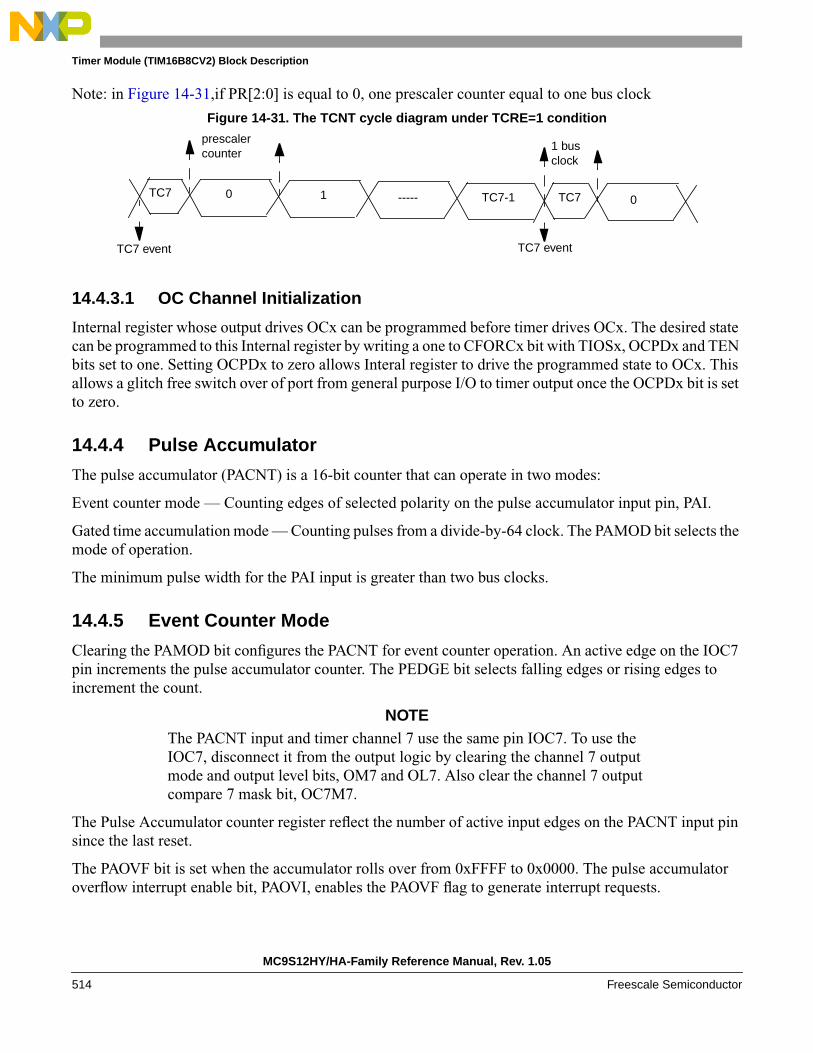
Timer Module (TIM16B8CV2) Block Description
Note: in Figure 14-31,if PR[2:0] is equal to 0, one prescaler counter equal to one bus clock
Figure 14-31. The TCNT cycle diagram under TCRE=1 condition
14.4.3.1 OC Channel Initialization
Internal register whose output drives OCx can be programmed before timer drives OCx. The desired statecan be programmed to this Internal register by writing a one to CFORCx bit with TIOSx, OCPDx and TENbits set to one. Setting OCPDx to zero allows Interal register to drive the programmed state to OCx. Thisallows a glitch free switch over of port from general purpose I/O to timer output once the OCPDx bit is setto zero.
14.4.4 Pulse Accumulator
The pulse accumulator (PACNT) is a 16-bit counter that can operate in two modes:
Event counter mode — Counting edges of selected polarity on the pulse accumulator input pin, PAI.
Gated time accumulation mode — Counting pulses from a divide-by-64 clock. The PAMOD bit selects themode of operation.
The minimum pulse width for the PAI input is greater than two bus clocks.
14.4.5 Event Counter Mode
Clearing the PAMOD bit configures the PACNT for event counter operation. An active edge on the IOC7pin increments the pulse accumulator counter. The PEDGE bit selects falling edges or rising edges toincrement the count.
NOTEThe PACNT input and timer channel 7 use the same pin IOC7. To use theIOC7, disconnect it from the output logic by clearing the channel 7 outputmode and output level bits, OM7 and OL7. Also clear the channel 7 outputcompare 7 mask bit, OC7M7.
The Pulse Accumulator counter register reflect the number of active input edges on the PACNT input pinsince the last reset.
The PAOVF bit is set when the accumulator rolls over from 0xFFFF to 0x0000. The pulse accumulatoroverflow interrupt enable bit, PAOVI, enables the PAOVF flag to generate interrupt requests.
TC7 0 1 ----- TC7-1 TC7 0
TC7 event TC7 event
prescalercounter
1 busclock
MC9S12HY/HA-Family Reference Manual, Rev. 1.05
514 Freescale Semiconductor

Timer Module (TIM16B8CV2) Block Description
NOTEThe pulse accumulator counter can operate in event counter mode evenwhen the timer enable bit, TEN, is clear.
14.4.6 Gated Time Accumulation Mode
Setting the PAMOD bit configures the pulse accumulator for gated time accumulation operation. An activelevel on the PACNT input pin enables a divided-by-64 clock to drive the pulse accumulator. The PEDGEbit selects low levels or high levels to enable the divided-by-64 clock.
The trailing edge of the active level at the IOC7 pin sets the PAIF. The PAI bit enables the PAIF flag togenerate interrupt requests.
The pulse accumulator counter register reflect the number of pulses from the divided-by-64 clock since thelast reset.
NOTEThe timer prescaler generates the divided-by-64 clock. If the timer is notactive, there is no divided-by-64 clock.
14.5 ResetsThe reset state of each individual bit is listed within Section 14.3, “Memory Map and Register Definition”which details the registers and their bit fields.
14.6 InterruptsThis section describes interrupts originated by the TIM16B8CV2 block. Table 14-25 lists the interruptsgenerated by the TIM16B8CV2 to communicate with the MCU.
The TIM16B8CV2 uses a total of 11 interrupt vectors. The interrupt vector offsets and interrupt numbersare chip dependent.
Table 14-25. TIM16B8CV1 Interrupts
Interrupt Offset1
1 Chip Dependent.
Vector1 Priority1 Source Description
C[7:0]F — — — Timer Channel 7–0 Active high timer channel interrupts 7–0
PAOVI — — — Pulse AccumulatorInput
Active high pulse accumulator input interrupt
PAOVF — — — Pulse AccumulatorOverflow
Pulse accumulator overflow interrupt
TOF — — — Timer Overflow Timer Overflow interrupt
MC9S12HY/HA-Family Reference Manual Rev. 1.05
Freescale Semiconductor 515

Timer Module (TIM16B8CV2) Block Description
14.6.1 Channel [7:0] Interrupt (C[7:0]F)
This active high outputs will be asserted by the module to request a timer channel 7 – 0 interrupt to beserviced by the system controller.
14.6.2 Pulse Accumulator Input Interrupt (PAOVI)
This active high output will be asserted by the module to request a timer pulse accumulator input interruptto be serviced by the system controller.
14.6.3 Pulse Accumulator Overflow Interrupt (PAOVF)
This active high output will be asserted by the module to request a timer pulse accumulator overflowinterrupt to be serviced by the system controller.
14.6.4 Timer Overflow Interrupt (TOF)
This active high output will be asserted by the module to request a timer overflow interrupt to be servicedby the system controller.
MC9S12HY/HA-Family Reference Manual, Rev. 1.05
516 Freescale Semiconductor
Chapter 1532 KByte Flash Module (S12FTMRC32K1V1)
15.1 IntroductionThe FTMRC32K1 module implements the following:
• 32 Kbytes of P-Flash (Program Flash) memory
• 4 Kbytes of D-Flash (Data Flash) memory
The Flash memory is ideal for single-supply applications allowing for field reprogramming withoutrequiring external high voltage sources for program or erase operations. The Flash module includes amemory controller that executes commands to modify Flash memory contents. The user interface to thememory controller consists of the indexed Flash Common Command Object (FCCOB) register which iswritten to with the command, global address, data, and any required command parameters. The memorycontroller must complete the execution of a command before the FCCOB register can be written to with anew command.
Table 15-1. Revision History
RevisionNumber
RevisionDate
SectionsAffected
Description of Changes
V01.11 28 Jul 2008 15.1.1/15-51815.3.1/15-521
- Remove reference to IFRON in Program IFR definition- Remove reference to IFRON in Table 15-4 and Figure 15-3
V01.12 19 Dec 2008 15.1/15-51715.4.5.4/15-55215.4.5.6/15-55315.4.5.11/15-55
715.4.5.11/15-55
715.4.5.11/15-55
715.5.2/15-565
- Clarify single bit fault correction for P-Flash phrase- Add statement concerning code runaway when executing Read Once,Program Once, and Verify Backdoor Access Key commands from Flash blockcontaining associated fields- Relate Key 0 to associated Backdoor Comparison Key address- Change “power down reset” to “reset”- Reformat section on unsecuring MCU using BDM
V01.13 25 Sep 2009
15.3.2/15-52415.3.2.1/15-52615.4.3.2/15-544
15.6/15-566
The following changes were made to clarify module behavior related to Flashregister access during reset sequence and while Flash commands are active:- Add caution concerning register writes while command is active- Writes to FCLKDIV are allowed during reset sequence while CCIF is clear- Add caution concerning register writes while command is active- Writes to FCCOBIX, FCCOBHI, FCCOBLO registers are ignored duringreset sequence
MC9S12HY/HA-Family Reference Manual, Rev. 1.05
Freescale Semiconductor 517

CAUTIONA Flash word or phrase must be in the erased state before beingprogrammed. Cumulative programming of bits within a Flash word orphrase is not allowed.
The Flash memory may be read as bytes, aligned words, or misaligned words. Read access time is one buscycle for bytes and aligned words, and two bus cycles for misaligned words. For Flash memory, an erasedbit reads 1 and a programmed bit reads 0.
It is possible to read from P-Flash memory while some commands are executing on D-Flash memory. Itis not possible to read from D-Flash memory while a command is executing on P-Flash memory.Simultaneous P-Flash and D-Flash operations are discussed in Section 15.4.4.
Both P-Flash and D-Flash memories are implemented with Error Correction Codes (ECC) that can resolvesingle bit faults and detect double bit faults. For P-Flash memory, the ECC implementation requires thatprogramming be done on an aligned 8 byte basis (a Flash phrase). Since P-Flash memory is always readby half-phrase, only one single bit fault in an aligned 4 byte half-phrase containing the byte or wordaccessed will be corrected.
15.1.1 Glossary
Command Write Sequence — An MCU instruction sequence to execute built-in algorithms (includingprogram and erase) on the Flash memory.
D-Flash Memory — The D-Flash memory constitutes the nonvolatile memory store for data.
D-Flash Sector — The D-Flash sector is the smallest portion of the D-Flash memory that can be erased.The D-Flash sector consists of four 64 byte rows for a total of 256 bytes.
NVM Command Mode — An NVM mode using the CPU to setup the FCCOB register to pass parametersrequired for Flash command execution.
Phrase — An aligned group of four 16-bit words within the P-Flash memory. Each phrase includes twosets of aligned double words with each set including 7 ECC bits for single bit fault correction and doublebit fault detection within each double word.
P-Flash Memory — The P-Flash memory constitutes the main nonvolatile memory store for applications.
P-Flash Sector — The P-Flash sector is the smallest portion of the P-Flash memory that can be erased.Each P-Flash sector contains 512 bytes.
Program IFR — Nonvolatile information register located in the P-Flash block that contains the DeviceID, Version ID, and the Program Once field.
MC9S12HY/HA-Family Reference Manual, Rev. 1.05
Freescale Semiconductor 518

32 KByte Flash Module (S12FTMRC32K1V1)
15.1.2 Features
15.1.2.1 P-Flash Features
• 32 Kbytes of P-Flash memory composed of one 32 Kbyte Flash block divided into 64 sectors of512 bytes
• Single bit fault correction and double bit fault detection within a 32-bit double word during readoperations
• Automated program and erase algorithm with verify and generation of ECC parity bits
• Fast sector erase and phrase program operation
• Ability to read the P-Flash memory while programming a word in the D-Flash memory
• Flexible protection scheme to prevent accidental program or erase of P-Flash memory
15.1.2.2 D-Flash Features
• 4 Kbytes of D-Flash memory composed of one 4 Kbyte Flash block divided into 16 sectors of 256bytes
• Single bit fault correction and double bit fault detection within a word during read operations
• Automated program and erase algorithm with verify and generation of ECC parity bits
• Fast sector erase and word program operation
• Protection scheme to prevent accidental program or erase of D-Flash memory
• Ability to program up to four words in a burst sequence
15.1.2.3 Other Flash Module Features
• No external high-voltage power supply required for Flash memory program and erase operations
• Interrupt generation on Flash command completion and Flash error detection
• Security mechanism to prevent unauthorized access to the Flash memory
15.1.3 Block Diagram
The block diagram of the Flash module is shown in Figure 15-1.
MC9S12HY/HA-Family Reference Manual, Rev. 1.05
Freescale Semiconductor 519

32 KByte Flash Module (S12FTMRC32K1V1)
Figure 15-1. FTMRC32K1 Block Diagram
15.2 External Signal DescriptionThe Flash module contains no signals that connect off-chip.
BusClockDivider
Clock
CommandInterruptRequest
FCLK
Protection
Security
Registers
FlashInterface
16bitinternalbus
sector 0sector 1
sector 63
8Kx39P-Flash
ErrorInterruptRequest
CPU
D-Flash2Kx22
sector 0sector 1
sector 15
Scratch RAM384x16
MemoryController
MC9S12HY/HA-Family Reference Manual, Rev. 1.05
520 Freescale Semiconductor

32 KByte Flash Module (S12FTMRC32K1V1)
15.3 Memory Map and RegistersThis section describes the memory map and registers for the Flash module. Read data from unimplementedmemory space in the Flash module is undefined. Write access to unimplemented or reserved memory spacein the Flash module will be ignored by the Flash module.
15.3.1 Module Memory Map
The S12 architecture places the P-Flash memory between global addresses 0x3_8000 and 0x3_FFFF asshown in Table 15-2.The P-Flash memory map is shown in Figure 15-2.
The FPROT register, described in Section 15.3.2.9, can be set to protect regions in the Flash memory fromaccidental program or erase. Three separate memory regions, one growing upward from global address0x3_8000 in the Flash memory (called the lower region), one growing downward from global address0x3_FFFF in the Flash memory (called the higher region), and the remaining addresses in the Flashmemory, can be activated for protection. The Flash memory addresses covered by these protectable regionsare shown in the P-Flash memory map. The higher address region is mainly targeted to hold the boot loadercode since it covers the vector space. Default protection settings as well as security information that allowsthe MCU to restrict access to the Flash module are stored in the Flash configuration field as described inTable 15-3.
Table 15-2. P-Flash Memory Addressing
Global AddressSize
(Bytes)Description
0x3_8000 – 0x3_FFFF 32 KP-Flash BlockContains Flash Configuration Field(see Table 15-3)
Table 15-3. Flash Configuration Field
Global AddressSize
(Bytes)Description
0x3_FF00-0x3_FF07 8Backdoor Comparison KeyRefer to Section 15.4.5.11, “Verify Backdoor Access Key Command,” andSection 15.5.1, “Unsecuring the MCU using Backdoor Key Access”
0x3_FF08-0x3_FF0B1
1 0x3FF08-0x3_FF0F form a Flash phrase and must be programmed in a single command write sequence. Each byte inthe 0x3_FF08 - 0x3_FF0B reserved field should be programmed to 0xFF.
4 Reserved
0x3_FF0C1 1P-Flash Protection byte.Refer to Section 15.3.2.9, “P-Flash Protection Register (FPROT)”
0x3_FF0D1 1D-Flash Protection byte.Refer to Section 15.3.2.10, “D-Flash Protection Register (DFPROT)”
0x3_FF0E1 1Flash Nonvolatile byteRefer to Section 15.3.2.16, “Flash Option Register (FOPT)”
0x3_FF0F1 1Flash Security byteRefer to Section 15.3.2.2, “Flash Security Register (FSEC)”
MC9S12HY/HA-Family Reference Manual, Rev. 1.05
Freescale Semiconductor 521

32 KByte Flash Module (S12FTMRC32K1V1)
Figure 15-2. P-Flash Memory Map
Flash Configuration Field
0x3_C000
Flash Protected/Unprotected Lower Region1, 2, 4, 8 Kbytes
P-Flash START = 0x3_8000
0x3_9000
0x3_84000x3_8800
0x3_A000
P-Flash END = 0x3_FFFF
0x3_F800
0x3_F000
0x3_E000 Flash Protected/Unprotected Higher Region2, 4, 8, 16 Kbytes
Flash Protected/Unprotected Region8 Kbytes (up to 29 Kbytes)
16 bytes (0x3_FF00 - 0x3_FF0F)
Protection
Protection
Protection
Movable End
Fixed End
Fixed End
MC9S12HY/HA-Family Reference Manual, Rev. 1.05
522 Freescale Semiconductor

32 KByte Flash Module (S12FTMRC32K1V1)
Table 15-4. Program IFR Fields
Global AddressSize
(Bytes)Field Description
0x0_4000 – 0x0_4007 8 Reserved
0x0_4008 – 0x0_40B5 174 Reserved
0x0_40B6 – 0x0_40B7 2 Version ID1
1 Used to track firmware patch versions, see Section 15.4.2
0x0_40B8 – 0x0_40BF 8 Reserved
0x0_40C0 – 0x0_40FF 64Program Once FieldRefer to Section 15.4.5.6, “Program Once Command”
Table 15-5. D-Flash and Memory Controller Resource Fields
Global AddressSize
(Bytes)Description
0x0_4000 – 0x0_43FF 1,024 Reserved
0x0_4400 – 0x0_53FF 4,096 D-Flash Memory
0x0_5400 – 0x0_57FF 1,024 Reserved
0x0_5800 – 0x0_5AFF 768 Memory Controller Scratch RAM (RAMON1 = 1)
1 MMCCTL1 register bit
0x0_5B00 – 0x0_5FFF 1,280 Reserved
0x0_6000 – 0x0_67FF 2,048 Reserved
0x0_6800 – 0x0_7FFF 6,144 Reserved
MC9S12HY/HA-Family Reference Manual, Rev. 1.05
Freescale Semiconductor 523

32 KByte Flash Module (S12FTMRC32K1V1)
Figure 15-3. D-Flash and Memory Controller Resource Memory Map
15.3.2 Register Descriptions
The Flash module contains a set of 20 control and status registers located between Flash module base +0x0000 and 0x0013. A summary of the Flash module registers is given in Figure 15-4 with detaileddescriptions in the following subsections.
CAUTIONWrites to any Flash register must be avoided while a Flash command isactive (CCIF=0) to prevent corruption of Flash register contents andadversely affect Memory Controller behavior.
Address& Name
7 6 5 4 3 2 1 0
0x0000FCLKDIV
R FDIVLDFDIVLCK FDIV5 FDIV4 FDIV3 FDIV2 FDIV1 FDIV0
W
0x0001FSEC
R KEYEN1 KEYEN0 RNV5 RNV4 RNV3 RNV2 SEC1 SEC0
W
0x0002FCCOBIX
R 0 0 0 0 0CCOBIX2 CCOBIX1 CCOBIX0
W
Figure 15-4. FTMRC32K1 Register Summary
D-Flash Memory4 Kbytes
D-Flash Start = 0x0_4400
0x0_6000
D-Flash End = 0x0_53FF
P-Flash IFR 1 Kbyte
0x0_4000
Reserved 1 Kbyte
Scratch Ram 768 bytes (RAMON)RAM End = 0x0_5AFFRAM Start = 0x0_5800
Reserved 6 Kbytes
Reserved 2 Kbytes
Reserved 1280 bytes
0x0_6800
0x0_7FFF
0x0_40FF
MC9S12HY/HA-Family Reference Manual, Rev. 1.05
524 Freescale Semiconductor

32 KByte Flash Module (S12FTMRC32K1V1)
0x0003FRSV0
R 0 0 0 0 0 0 0 0
W
0x0004FCNFG
RCCIE
0 0IGNSF
0 0FDFD FSFD
W
0x0005FERCNFG
R 0 0 0 0 0 0DFDIE SFDIE
W
0x0006FSTAT
RCCIF
0ACCERR FPVIOL
MGBUSY RSVD MGSTAT1 MGSTAT0
W
0x0007FERSTAT
R 0 0 0 0 0 0DFDIF SFDIF
W
0x0008FPROT
RFPOPEN
RNV6FPHDIS FPHS1 FPHS0 FPLDIS FPLS1 FPLS0
W
0x0009DFPROT
RDPOPEN
0 0 0DPS3 DPS2 DPS1 DPS0
W
0x000AFCCOBHI
RCCOB15 CCOB14 CCOB13 CCOB12 CCOB11 CCOB10 CCOB9 CCOB8
W
0x000BFCCOBLO
RCCOB7 CCOB6 CCOB5 CCOB4 CCOB3 CCOB2 CCOB1 CCOB0
W
0x000CFRSV1
R 0 0 0 0 0 0 0 0
W
0x000DFRSV2
R 0 0 0 0 0 0 0 0
W
0x000EFRSV3
R 0 0 0 0 0 0 0 0
W
0x000FFRSV4
R 0 0 0 0 0 0 0 0
W
0x0010FOPT
R NV7 NV6 NV5 NV4 NV3 NV2 NV1 NV0
W
Address& Name
7 6 5 4 3 2 1 0
Figure 15-4. FTMRC32K1 Register Summary (continued)
MC9S12HY/HA-Family Reference Manual, Rev. 1.05
Freescale Semiconductor 525

32 KByte Flash Module (S12FTMRC32K1V1)
15.3.2.1 Flash Clock Divider Register (FCLKDIV)
The FCLKDIV register is used to control timed events in program and erase algorithms.
All bits in the FCLKDIV register are readable, bit 7 is not writable, bit 6 is write-once-hi and controls thewritability of the FDIV field.
CAUTIONThe FCLKDIV register must never be written to while a Flash command isexecuting (CCIF=0). The FCLKDIV register is writable during the Flashreset sequence even though CCIF is clear.
0x0011FRSV5
R 0 0 0 0 0 0 0 0
W
0x0012FRSV6
R 0 0 0 0 0 0 0 0
W
0x0013FRSV7
R 0 0 0 0 0 0 0 0
W
= Unimplemented or Reserved
Offset Module Base + 0x0000
7 6 5 4 3 2 1 0
R FDIVLDFDIVLCK FDIV[5:0]
W
Reset 0 0 0 0 0 0 0 0
= Unimplemented or Reserved
Figure 15-5. Flash Clock Divider Register (FCLKDIV)
Table 15-6. FCLKDIV Field Descriptions
Field Description
7FDIVLD
Clock Divider Loaded0 FCLKDIV register has not been written since the last reset1 FCLKDIV register has been written since the last reset
Address& Name
7 6 5 4 3 2 1 0
Figure 15-4. FTMRC32K1 Register Summary (continued)
MC9S12HY/HA-Family Reference Manual, Rev. 1.05
526 Freescale Semiconductor

32 KByte Flash Module (S12FTMRC32K1V1)
15.3.2.2 Flash Security Register (FSEC)
The FSEC register holds all bits associated with the security of the MCU and Flash module.
6FDIVLCK
Clock Divider Locked0 FDIV field is open for writing1 FDIV value is locked and cannot be changed. Once the lock bit is set high, only reset can clear this bit and
restore writability to the FDIV field.
5–0FDIV[5:0]
Clock Divider Bits — FDIV[5:0] must be set to effectively divide BUSCLK down to 1 MHz to control timed eventsduring Flash program and erase algorithms. Table 15-7 shows recommended values for FDIV[5:0] based on theBUSCLK frequency. Please refer to Section 15.4.3, “Flash Command Operations,” for more information.
Table 15-7. FDIV values for various BUSCLK Frequencies
BUSCLK Frequency(MHz) FDIV[5:0]
BUSCLK Frequency(MHz) FDIV[5:0]
MIN1
1 BUSCLK is Greater Than this value.
MAX2
2 BUSCLK is Less Than or Equal to this value.
MIN1 MAX2
1.0 1.6 0x00 16.6 17.6 0x10
1.6 2.6 0x01 17.6 18.6 0x11
2.6 3.6 0x02 18.6 19.6 0x12
3.6 4.6 0x03 19.6 20.6 0x13
4.6 5.6 0x04 20.6 21.6 0x14
5.6 6.6 0x05 21.6 22.6 0x15
6.6 7.6 0x06 22.6 23.6 0x16
7.6 8.6 0x07 23.6 24.6 0x17
8.6 9.6 0x08 24.6 25.6 0x18
9.6 10.6 0x09 25.6 26.6 0x19
10.6 11.6 0x0A 26.6 27.6 0x1A
11.6 12.6 0x0B 27.6 28.6 0x1B
12.6 13.6 0x0C 28.6 29.6 0x1C
13.6 14.6 0x0D 29.6 30.6 0x1D
14.6 15.6 0x0E 30.6 31.6 0x1E
15.6 16.6 0x0F 31.6 32.6 0x1F
Table 15-6. FCLKDIV Field Descriptions (continued)
Field Description
MC9S12HY/HA-Family Reference Manual, Rev. 1.05
Freescale Semiconductor 527
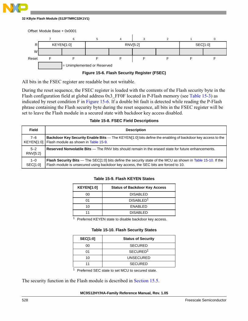
32 KByte Flash Module (S12FTMRC32K1V1)
All bits in the FSEC register are readable but not writable.
During the reset sequence, the FSEC register is loaded with the contents of the Flash security byte in theFlash configuration field at global address 0x3_FF0F located in P-Flash memory (see Table 15-3) asindicated by reset condition F in Figure 15-6. If a double bit fault is detected while reading the P-Flashphrase containing the Flash security byte during the reset sequence, all bits in the FSEC register will beset to leave the Flash module in a secured state with backdoor key access disabled.
The security function in the Flash module is described in Section 15.5.
Offset Module Base + 0x0001
7 6 5 4 3 2 1 0
R KEYEN[1:0] RNV[5:2] SEC[1:0]
W
Reset F F F F F F F F
= Unimplemented or Reserved
Figure 15-6. Flash Security Register (FSEC)
Table 15-8. FSEC Field Descriptions
Field Description
7–6KEYEN[1:0]
Backdoor Key Security Enable Bits — The KEYEN[1:0] bits define the enabling of backdoor key access to theFlash module as shown in Table 15-9.
5–2RNV[5:2
Reserved Nonvolatile Bits — The RNV bits should remain in the erased state for future enhancements.
1–0SEC[1:0]
Flash Security Bits — The SEC[1:0] bits define the security state of the MCU as shown in Table 15-10. If theFlash module is unsecured using backdoor key access, the SEC bits are forced to 10.
Table 15-9. Flash KEYEN States
KEYEN[1:0] Status of Backdoor Key Access
00 DISABLED
01 DISABLED1
1 Preferred KEYEN state to disable backdoor key access.
10 ENABLED
11 DISABLED
Table 15-10. Flash Security States
SEC[1:0] Status of Security
00 SECURED
01 SECURED1
1 Preferred SEC state to set MCU to secured state.
10 UNSECURED
11 SECURED
MC9S12HY/HA-Family Reference Manual, Rev. 1.05
528 Freescale Semiconductor

32 KByte Flash Module (S12FTMRC32K1V1)
15.3.2.3 Flash CCOB Index Register (FCCOBIX)
The FCCOBIX register is used to index the FCCOB register for Flash memory operations.
CCOBIX bits are readable and writable while remaining bits read 0 and are not writable.
15.3.2.4 Flash Reserved0 Register (FRSV0)
This Flash register is reserved for factory testing.
All bits in the FRSV0 register read 0 and are not writable.
15.3.2.5 Flash Configuration Register (FCNFG)
The FCNFG register enables the Flash command complete interrupt and forces ECC faults on Flash arrayread access from the CPU.
Offset Module Base + 0x0002
7 6 5 4 3 2 1 0
R 0 0 0 0 0CCOBIX[2:0]
W
Reset 0 0 0 0 0 0 0 0
= Unimplemented or Reserved
Figure 15-7. FCCOB Index Register (FCCOBIX)
Table 15-11. FCCOBIX Field Descriptions
Field Description
2–0CCOBIX[1:0]
Common Command Register Index— The CCOBIX bits are used to select which word of the FCCOB registerarray is being read or written to. See Section 15.3.2.11, “Flash Common Command Object Register (FCCOB),”for more details.
Offset Module Base + 0x000C
7 6 5 4 3 2 1 0
R 0 0 0 0 0 0 0 0
W
Reset 0 0 0 0 0 0 0 0
= Unimplemented or Reserved
Figure 15-8. Flash Reserved0 Register (FRSV0)
MC9S12HY/HA-Family Reference Manual, Rev. 1.05
Freescale Semiconductor 529

32 KByte Flash Module (S12FTMRC32K1V1)
CCIE, IGNSF, FDFD, and FSFD bits are readable and writable while remaining bits read 0 and are notwritable.
15.3.2.6 Flash Error Configuration Register (FERCNFG)
The FERCNFG register enables the Flash error interrupts for the FERSTAT flags.
Offset Module Base + 0x0004
7 6 5 4 3 2 1 0
RCCIE
0 0IGNSF
0 0FDFD FSFD
W
Reset 0 0 0 0 0 0 0 0
= Unimplemented or Reserved
Figure 15-9. Flash Configuration Register (FCNFG)
Table 15-12. FCNFG Field Descriptions
Field Description
7CCIE
Command Complete Interrupt Enable — The CCIE bit controls interrupt generation when a Flash commandhas completed.0 Command complete interrupt disabled1 An interrupt will be requested whenever the CCIF flag in the FSTAT register is set (see Section 15.3.2.7)
4IGNSF
Ignore Single Bit Fault — The IGNSF controls single bit fault reporting in the FERSTAT register (seeSection 15.3.2.8).0 All single bit faults detected during array reads are reported1 Single bit faults detected during array reads are not reported and the single bit fault interrupt will not be
generated
1FDFD
Force Double Bit Fault Detect — The FDFD bit allows the user to simulate a double bit fault during Flash arrayread operations and check the associated interrupt routine. The FDFD bit is cleared by writing a 0 to FDFD. TheFECCR registers will not be updated during the Flash array read operation with FDFD set unless an actualdouble bit fault is detected.0 Flash array read operations will set the DFDIF flag in the FERSTAT register only if a double bit fault is detected1 Any Flash array read operation will force the DFDIF flag in the FERSTAT register to be set (see
Section 15.3.2.7) and an interrupt will be generated as long as the DFDIE interrupt enable in the FERCNFGregister is set (see Section 15.3.2.6)
0FSFD
Force Single Bit Fault Detect — The FSFD bit allows the user to simulate a single bit fault during Flash arrayread operations and check the associated interrupt routine. The FSFD bit is cleared by writing a 0 to FSFD. TheFECCR registers will not be updated during the Flash array read operation with FSFD set unless an actual singlebit fault is detected.0 Flash array read operations will set the SFDIF flag in the FERSTAT register only if a single bit fault is detected1 Flash array read operation will force the SFDIF flag in the FERSTAT register to be set (see Section 15.3.2.7)
and an interrupt will be generated as long as the SFDIE interrupt enable in the FERCNFG register is set (seeSection 15.3.2.6)
MC9S12HY/HA-Family Reference Manual, Rev. 1.05
530 Freescale Semiconductor

32 KByte Flash Module (S12FTMRC32K1V1)
All assigned bits in the FERCNFG register are readable and writable.
15.3.2.7 Flash Status Register (FSTAT)
The FSTAT register reports the operational status of the Flash module.
CCIF, ACCERR, and FPVIOL bits are readable and writable, MGBUSY and MGSTAT bits are readablebut not writable, while remaining bits read 0 and are not writable.
Offset Module Base + 0x0005
7 6 5 4 3 2 1 0
R 0 0 0 0 0 0DFDIE SFDIE
W
Reset 0 0 0 0 0 0 0 0
= Unimplemented or Reserved
Figure 15-10. Flash Error Configuration Register (FERCNFG)
Table 15-13. FERCNFG Field Descriptions
Field Description
1DFDIE
Double Bit Fault Detect Interrupt Enable — The DFDIE bit controls interrupt generation when a double bit faultis detected during a Flash block read operation.0 DFDIF interrupt disabled1 An interrupt will be requested whenever the DFDIF flag is set (see Section 15.3.2.8)
0SFDIE
Single Bit Fault Detect Interrupt Enable — The SFDIE bit controls interrupt generation when a single bit faultis detected during a Flash block read operation.0 SFDIF interrupt disabled whenever the SFDIF flag is set (see Section 15.3.2.8)1 An interrupt will be requested whenever the SFDIF flag is set (see Section 15.3.2.8)
Offset Module Base + 0x0006
7 6 5 4 3 2 1 0
RCCIF
0ACCERR FPVIOL
MGBUSY RSVD MGSTAT[1:0]
W
Reset 1 0 0 0 0 0 01
1 Reset value can deviate from the value shown if a double bit fault is detected during the reset sequence (see Section 15.6).
01
= Unimplemented or Reserved
Figure 15-11. Flash Status Register (FSTAT)
MC9S12HY/HA-Family Reference Manual, Rev. 1.05
Freescale Semiconductor 531
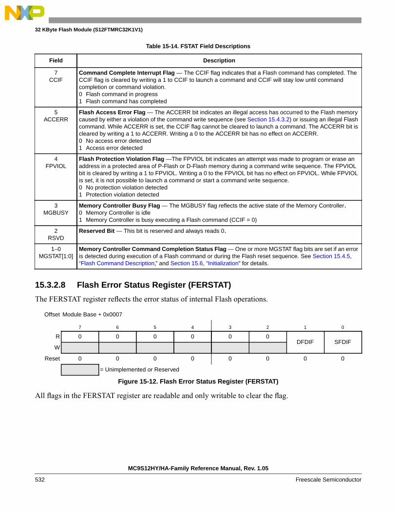
32 KByte Flash Module (S12FTMRC32K1V1)
15.3.2.8 Flash Error Status Register (FERSTAT)
The FERSTAT register reflects the error status of internal Flash operations.
All flags in the FERSTAT register are readable and only writable to clear the flag.
Table 15-14. FSTAT Field Descriptions
Field Description
7CCIF
Command Complete Interrupt Flag — The CCIF flag indicates that a Flash command has completed. TheCCIF flag is cleared by writing a 1 to CCIF to launch a command and CCIF will stay low until commandcompletion or command violation.0 Flash command in progress1 Flash command has completed
5ACCERR
Flash Access Error Flag — The ACCERR bit indicates an illegal access has occurred to the Flash memorycaused by either a violation of the command write sequence (see Section 15.4.3.2) or issuing an illegal Flashcommand. While ACCERR is set, the CCIF flag cannot be cleared to launch a command. The ACCERR bit iscleared by writing a 1 to ACCERR. Writing a 0 to the ACCERR bit has no effect on ACCERR.0 No access error detected1 Access error detected
4FPVIOL
Flash Protection Violation Flag —The FPVIOL bit indicates an attempt was made to program or erase anaddress in a protected area of P-Flash or D-Flash memory during a command write sequence. The FPVIOLbit is cleared by writing a 1 to FPVIOL. Writing a 0 to the FPVIOL bit has no effect on FPVIOL. While FPVIOLis set, it is not possible to launch a command or start a command write sequence.0 No protection violation detected1 Protection violation detected
3MGBUSY
Memory Controller Busy Flag — The MGBUSY flag reflects the active state of the Memory Controller.0 Memory Controller is idle1 Memory Controller is busy executing a Flash command (CCIF = 0)
2RSVD
Reserved Bit — This bit is reserved and always reads 0.
1–0MGSTAT[1:0]
Memory Controller Command Completion Status Flag — One or more MGSTAT flag bits are set if an erroris detected during execution of a Flash command or during the Flash reset sequence. See Section 15.4.5,“Flash Command Description,” and Section 15.6, “Initialization” for details.
Offset Module Base + 0x0007
7 6 5 4 3 2 1 0
R 0 0 0 0 0 0DFDIF SFDIF
W
Reset 0 0 0 0 0 0 0 0
= Unimplemented or Reserved
Figure 15-12. Flash Error Status Register (FERSTAT)
MC9S12HY/HA-Family Reference Manual, Rev. 1.05
532 Freescale Semiconductor

32 KByte Flash Module (S12FTMRC32K1V1)
15.3.2.9 P-Flash Protection Register (FPROT)
The FPROT register defines which P-Flash sectors are protected against program and erase operations.
The (unreserved) bits of the FPROT register are writable with the restriction that the size of the protectedregion can only be increased (see Section 15.3.2.9.1, “P-Flash Protection Restrictions,” and Table 15-20).
During the reset sequence, the FPROT register is loaded with the contents of the P-Flash protection bytein the Flash configuration field at global address 0x3_FF0C located in P-Flash memory (see Table 15-3)as indicated by reset condition ‘F’ in Figure 15-13. To change the P-Flash protection that will be loadedduring the reset sequence, the upper sector of the P-Flash memory must be unprotected, then the P-Flashprotection byte must be reprogrammed. If a double bit fault is detected while reading the P-Flash phrasecontaining the P-Flash protection byte during the reset sequence, the FPOPEN bit will be cleared andremaining bits in the FPROT register will be set to leave the P-Flash memory fully protected.
Trying to alter data in any protected area in the P-Flash memory will result in a protection violation errorand the FPVIOL bit will be set in the FSTAT register. The block erase of a P-Flash block is not possibleif any of the P-Flash sectors contained in the same P-Flash block are protected.
Table 15-15. FERSTAT Field Descriptions
Field Description
1DFDIF
Double Bit Fault Detect Interrupt Flag — The setting of the DFDIF flag indicates that a double bit fault wasdetected in the stored parity and data bits during a Flash array read operation or that a Flash array read operationwas attempted on a Flash block that was under a Flash command operation.1 The DFDIF flag is cleared bywriting a 1 to DFDIF. Writing a 0 to DFDIF has no effect on DFDIF.0 No double bit fault detected1 Double bit fault detected or an invalid Flash array read operation attempted
1 The single bit fault and double bit fault flags are mutually exclusive for parity errors (an ECC fault occurrence can be eithersingle fault or double fault but never both). A simultaneous access collision (read attempted while command running) isindicated when both SFDIF and DFDIF flags are high.
0SFDIF
Single Bit Fault Detect Interrupt Flag — With the IGNSF bit in the FCNFG register clear, the SFDIF flagindicates that a single bit fault was detected in the stored parity and data bits during a Flash array read operationor that a Flash array read operation was attempted on a Flash block that was under a Flash command operation.1
The SFDIF flag is cleared by writing a 1 to SFDIF. Writing a 0 to SFDIF has no effect on SFDIF.0 No single bit fault detected1 Single bit fault detected and corrected or an invalid Flash array read operation attempted
Offset Module Base + 0x0008
7 6 5 4 3 2 1 0
RFPOPEN
RNV6FPHDIS FPHS[1:0] FPLDIS FPLS[1:0]
W
Reset F F F F F F F F
= Unimplemented or Reserved
Figure 15-13. Flash Protection Register (FPROT)
MC9S12HY/HA-Family Reference Manual, Rev. 1.05
Freescale Semiconductor 533
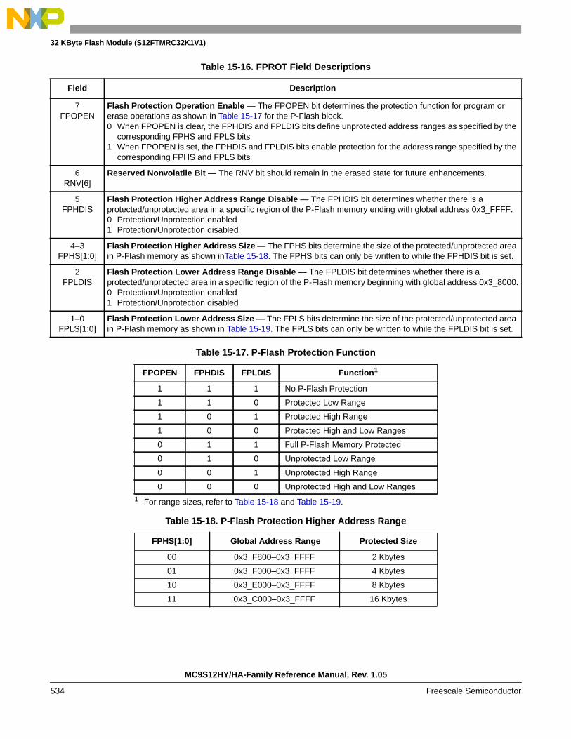
32 KByte Flash Module (S12FTMRC32K1V1)
Table 15-16. FPROT Field Descriptions
Field Description
7FPOPEN
Flash Protection Operation Enable — The FPOPEN bit determines the protection function for program orerase operations as shown in Table 15-17 for the P-Flash block.0 When FPOPEN is clear, the FPHDIS and FPLDIS bits define unprotected address ranges as specified by the
corresponding FPHS and FPLS bits1 When FPOPEN is set, the FPHDIS and FPLDIS bits enable protection for the address range specified by the
corresponding FPHS and FPLS bits
6RNV[6]
Reserved Nonvolatile Bit — The RNV bit should remain in the erased state for future enhancements.
5FPHDIS
Flash Protection Higher Address Range Disable — The FPHDIS bit determines whether there is aprotected/unprotected area in a specific region of the P-Flash memory ending with global address 0x3_FFFF.0 Protection/Unprotection enabled1 Protection/Unprotection disabled
4–3FPHS[1:0]
Flash Protection Higher Address Size — The FPHS bits determine the size of the protected/unprotected areain P-Flash memory as shown inTable 15-18. The FPHS bits can only be written to while the FPHDIS bit is set.
2FPLDIS
Flash Protection Lower Address Range Disable — The FPLDIS bit determines whether there is aprotected/unprotected area in a specific region of the P-Flash memory beginning with global address 0x3_8000.0 Protection/Unprotection enabled1 Protection/Unprotection disabled
1–0FPLS[1:0]
Flash Protection Lower Address Size — The FPLS bits determine the size of the protected/unprotected areain P-Flash memory as shown in Table 15-19. The FPLS bits can only be written to while the FPLDIS bit is set.
Table 15-17. P-Flash Protection Function
FPOPEN FPHDIS FPLDIS Function1
1 For range sizes, refer to Table 15-18 and Table 15-19.
1 1 1 No P-Flash Protection
1 1 0 Protected Low Range
1 0 1 Protected High Range
1 0 0 Protected High and Low Ranges
0 1 1 Full P-Flash Memory Protected
0 1 0 Unprotected Low Range
0 0 1 Unprotected High Range
0 0 0 Unprotected High and Low Ranges
Table 15-18. P-Flash Protection Higher Address Range
FPHS[1:0] Global Address Range Protected Size
00 0x3_F800–0x3_FFFF 2 Kbytes
01 0x3_F000–0x3_FFFF 4 Kbytes
10 0x3_E000–0x3_FFFF 8 Kbytes
11 0x3_C000–0x3_FFFF 16 Kbytes
MC9S12HY/HA-Family Reference Manual, Rev. 1.05
534 Freescale Semiconductor

32 KByte Flash Module (S12FTMRC32K1V1)
All possible P-Flash protection scenarios are shown in Figure 15-14. Although the protection scheme isloaded from the Flash memory at global address 0x3_FF0C during the reset sequence, it can be changedby the user. The P-Flash protection scheme can be used by applications requiring reprogramming in singlechip mode while providing as much protection as possible if reprogramming is not required.
Table 15-19. P-Flash Protection Lower Address Range
FPLS[1:0] Global Address Range Protected Size
00 0x3_8000–0x3_83FF 1 Kbyte
01 0x3_8000–0x3_87FF 2 Kbytes
10 0x3_8000–0x3_8FFF 4 Kbytes
11 0x3_8000–0x3_9FFF 8 Kbytes
MC9S12HY/HA-Family Reference Manual, Rev. 1.05
Freescale Semiconductor 535

32 KByte Flash Module (S12FTMRC32K1V1)
Figure 15-14. P-Flash Protection Scenarios
7 6 5 4
FP
HS
[1:0
]F
PLS
[1:0
]
3 2 1 0
FP
HS
[1:0
]F
PLS
[1:0
]
FPHDIS = 1FPLDIS = 1
FPHDIS = 1FPLDIS = 0
FPHDIS = 0FPLDIS = 1
FPHDIS = 0FPLDIS = 0
Scenario
Scenario
Unprotected region Protected region with size
Protected region Protected region with size
defined by FPLS
defined by FPHSnot defined by FPLS, FPHS
0x3_8000
0x3_FFFF
0x3_8000
0x3_FFFF
FLASH START
FLASH START
FP
OP
EN
= 1
FP
OP
EN
= 0
MC9S12HY/HA-Family Reference Manual, Rev. 1.05
536 Freescale Semiconductor

32 KByte Flash Module (S12FTMRC32K1V1)
15.3.2.9.1 P-Flash Protection Restrictions
The general guideline is that P-Flash protection can only be added and not removed. Table 15-20 specifiesall valid transitions between P-Flash protection scenarios. Any attempt to write an invalid scenario to theFPROT register will be ignored. The contents of the FPROT register reflect the active protection scenario.See the FPHS and FPLS bit descriptions for additional restrictions.
15.3.2.10 D-Flash Protection Register (DFPROT)
The DFPROT register defines which D-Flash sectors are protected against program and erase operations.
The (unreserved) bits of the DFPROT register are writable with the restriction that protection can be addedbut not removed. Writes must increase the DPS value and the DPOPEN bit can only be written from 1(protection disabled) to 0 (protection enabled). If the DPOPEN bit is set, the state of the DPS bits isirrelevant.
During the reset sequence, the DFPROT register is loaded with the contents of the D-Flash protection bytein the Flash configuration field at global address 0x3_FF0D located in P-Flash memory (see Table 15-3)as indicated by reset condition F in Figure 15-15. To change the D-Flash protection that will be loadedduring the reset sequence, the P-Flash sector containing the D-Flash protection byte must be unprotected,then the D-Flash protection byte must be programmed. If a double bit fault is detected while reading the
Table 15-20. P-Flash Protection Scenario Transitions
FromProtectionScenario
To Protection Scenario1
1 Allowed transitions marked with X, see Figure 15-14 for a definition of the scenarios.
0 1 2 3 4 5 6 7
0 X X X X
1 X X
2 X X
3 X
4 X X
5 X X X X
6 X X X X
7 X X X X X X X X
Offset Module Base + 0x0009
7 6 5 4 3 2 1 0
RDPOPEN
0 0 0DPS[3:0]
W
Reset F 0 0 0 F F F F
= Unimplemented or Reserved
Figure 15-15. D-Flash Protection Register (DFPROT)
MC9S12HY/HA-Family Reference Manual, Rev. 1.05
Freescale Semiconductor 537
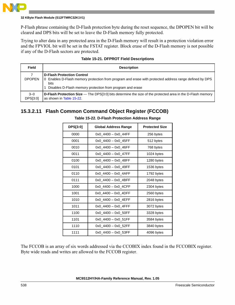
32 KByte Flash Module (S12FTMRC32K1V1)
P-Flash phrase containing the D-Flash protection byte during the reset sequence, the DPOPEN bit will becleared and DPS bits will be set to leave the D-Flash memory fully protected.
Trying to alter data in any protected area in the D-Flash memory will result in a protection violation errorand the FPVIOL bit will be set in the FSTAT register. Block erase of the D-Flash memory is not possibleif any of the D-Flash sectors are protected.
15.3.2.11 Flash Common Command Object Register (FCCOB)
The FCCOB is an array of six words addressed via the CCOBIX index found in the FCCOBIX register.Byte wide reads and writes are allowed to the FCCOB register.
Table 15-21. DFPROT Field Descriptions
Field Description
7DPOPEN
D-Flash Protection Control0 Enables D-Flash memory protection from program and erase with protected address range defined by DPS
bits1 Disables D-Flash memory protection from program and erase
3–0DPS[3:0]
D-Flash Protection Size — The DPS[3:0] bits determine the size of the protected area in the D-Flash memoryas shown in Table 15-22.
Table 15-22. D-Flash Protection Address Range
DPS[3:0] Global Address Range Protected Size
0000 0x0_4400 – 0x0_44FF 256 bytes
0001 0x0_4400 – 0x0_45FF 512 bytes
0010 0x0_4400 – 0x0_46FF 768 bytes
0011 0x0_4400 – 0x0_47FF 1024 bytes
0100 0x0_4400 – 0x0_48FF 1280 bytes
0101 0x0_4400 – 0x0_49FF 1536 bytes
0110 0x0_4400 – 0x0_4AFF 1792 bytes
0111 0x0_4400 – 0x0_4BFF 2048 bytes
1000 0x0_4400 – 0x0_4CFF 2304 bytes
1001 0x0_4400 – 0x0_4DFF 2560 bytes
1010 0x0_4400 – 0x0_4EFF 2816 bytes
1011 0x0_4400 – 0x0_4FFF 3072 bytes
1100 0x0_4400 – 0x0_50FF 3328 bytes
1101 0x0_4400 – 0x0_51FF 3584 bytes
1110 0x0_4400 – 0x0_52FF 3840 bytes
1111 0x0_4400 – 0x0_53FF 4096 bytes
MC9S12HY/HA-Family Reference Manual, Rev. 1.05
538 Freescale Semiconductor

32 KByte Flash Module (S12FTMRC32K1V1)
15.3.2.11.1 FCCOB - NVM Command Mode
NVM command mode uses the indexed FCCOB register to provide a command code and its relevantparameters to the Memory Controller. The user first sets up all required FCCOB fields and then initiatesthe command’s execution by writing a 1 to the CCIF bit in the FSTAT register (a 1 written by the userclears the CCIF command completion flag to 0). When the user clears the CCIF bit in the FSTAT registerall FCCOB parameter fields are locked and cannot be changed by the user until the command completes(as evidenced by the Memory Controller returning CCIF to 1). Some commands return information to theFCCOB register array.
The generic format for the FCCOB parameter fields in NVM command mode is shown in Table 15-23.The return values are available for reading after the CCIF flag in the FSTAT register has been returned to1 by the Memory Controller. Writes to the unimplemented parameter fields (CCOBIX = 110 and CCOBIX= 111) are ignored with reads from these fields returning 0x0000.
Table 15-23 shows the generic Flash command format. The high byte of the first word in the CCOB arraycontains the command code, followed by the parameters for this specific Flash command. For details onthe FCCOB settings required by each command, see the Flash command descriptions in Section 15.4.5.
Offset Module Base + 0x000A
7 6 5 4 3 2 1 0
RCCOB[15:8]
W
Reset 0 0 0 0 0 0 0 0
Figure 15-16. Flash Common Command Object High Register (FCCOBHI)
Offset Module Base + 0x000B
7 6 5 4 3 2 1 0
RCCOB[7:0]
W
Reset 0 0 0 0 0 0 0 0
Figure 15-17. Flash Common Command Object Low Register (FCCOBLO)
Table 15-23. FCCOB - NVM Command Mode (Typical Usage)
CCOBIX[2:0] Byte FCCOB Parameter Fields (NVM Command Mode)
000HI FCMD[7:0] defining Flash command
LO 6’h0, Global address [17:16]
001HI Global address [15:8]
LO Global address [7:0]
010HI Data 0 [15:8]
LO Data 0 [7:0]
MC9S12HY/HA-Family Reference Manual, Rev. 1.05
Freescale Semiconductor 539

32 KByte Flash Module (S12FTMRC32K1V1)
15.3.2.12 Flash Reserved1 Register (FRSV1)
This Flash register is reserved for factory testing.
All bits in the FRSV1 register read 0 and are not writable.
15.3.2.13 Flash Reserved2 Register (FRSV2)
This Flash register is reserved for factory testing.
All bits in the FRSV2 register read 0 and are not writable.
15.3.2.14 Flash Reserved3 Register (FRSV3)
This Flash register is reserved for factory testing.
011HI Data 1 [15:8]
LO Data 1 [7:0]
100HI Data 2 [15:8]
LO Data 2 [7:0]
101HI Data 3 [15:8]
LO Data 3 [7:0]
Offset Module Base + 0x000C
7 6 5 4 3 2 1 0
R 0 0 0 0 0 0 0 0
W
Reset 0 0 0 0 0 0 0 0
= Unimplemented or Reserved
Figure 15-18. Flash Reserved1 Register (FRSV1)
Offset Module Base + 0x000D
7 6 5 4 3 2 1 0
R 0 0 0 0 0 0 0 0
W
Reset 0 0 0 0 0 0 0 0
= Unimplemented or Reserved
Figure 15-19. Flash Reserved2 Register (FRSV2)
Table 15-23. FCCOB - NVM Command Mode (Typical Usage)
CCOBIX[2:0] Byte FCCOB Parameter Fields (NVM Command Mode)
MC9S12HY/HA-Family Reference Manual, Rev. 1.05
540 Freescale Semiconductor

32 KByte Flash Module (S12FTMRC32K1V1)
All bits in the FRSV3 register read 0 and are not writable.
15.3.2.15 Flash Reserved4 Register (FRSV4)
This Flash register is reserved for factory testing.
All bits in the FRSV4 register read 0 and are not writable.
15.3.2.16 Flash Option Register (FOPT)
The FOPT register is the Flash option register.
All bits in the FOPT register are readable but are not writable.
During the reset sequence, the FOPT register is loaded from the Flash nonvolatile byte in the Flashconfiguration field at global address 0x3_FF0E located in P-Flash memory (see Table 15-3) as indicatedby reset condition F in Figure 15-22. If a double bit fault is detected while reading the P-Flash phrasecontaining the Flash nonvolatile byte during the reset sequence, all bits in the FOPT register will be set.
Offset Module Base + 0x000E
7 6 5 4 3 2 1 0
R 0 0 0 0 0 0 0 0
W
Reset 0 0 0 0 0 0 0 0
= Unimplemented or Reserved
Figure 15-20. Flash Reserved3 Register (FRSV3)
Offset Module Base + 0x000F
7 6 5 4 3 2 1 0
R 0 0 0 0 0 0 0 0
W
Reset 0 0 0 0 0 0 0 0
= Unimplemented or Reserved
Figure 15-21. Flash Reserved4 Register (FRSV4)
Offset Module Base + 0x0010
7 6 5 4 3 2 1 0
R NV[7:0]
W
Reset F F F F F F F F
= Unimplemented or Reserved
Figure 15-22. Flash Option Register (FOPT)
MC9S12HY/HA-Family Reference Manual, Rev. 1.05
Freescale Semiconductor 541

32 KByte Flash Module (S12FTMRC32K1V1)
15.3.2.17 Flash Reserved5 Register (FRSV5)
This Flash register is reserved for factory testing.
All bits in the FRSV5 register read 0 and are not writable.
15.3.2.18 Flash Reserved6 Register (FRSV6)
This Flash register is reserved for factory testing.
All bits in the FRSV6 register read 0 and are not writable.
15.3.2.19 Flash Reserved7 Register (FRSV7)
This Flash register is reserved for factory testing.
Table 15-24. FOPT Field Descriptions
Field Description
7–0NV[7:0]
Nonvolatile Bits — The NV[7:0] bits are available as nonvolatile bits. Refer to the device user guide for properuse of the NV bits.
Offset Module Base + 0x0011
7 6 5 4 3 2 1 0
R 0 0 0 0 0 0 0 0
W
Reset 0 0 0 0 0 0 0 0
= Unimplemented or Reserved
Figure 15-23. Flash Reserved5 Register (FRSV5)
Offset Module Base + 0x0012
7 6 5 4 3 2 1 0
R 0 0 0 0 0 0 0 0
W
Reset 0 0 0 0 0 0 0 0
= Unimplemented or Reserved
Figure 15-24. Flash Reserved6 Register (FRSV6)
MC9S12HY/HA-Family Reference Manual, Rev. 1.05
542 Freescale Semiconductor
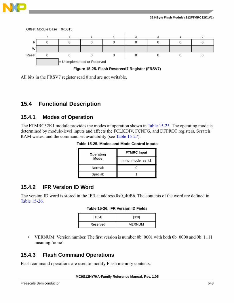
32 KByte Flash Module (S12FTMRC32K1V1)
All bits in the FRSV7 register read 0 and are not writable.
15.4 Functional Description
15.4.1 Modes of Operation
The FTMRC32K1 module provides the modes of operation shown in Table 15-25. The operating mode isdetermined by module-level inputs and affects the FCLKDIV, FCNFG, and DFPROT registers, ScratchRAM writes, and the command set availability (see Table 15-27).
15.4.2 IFR Version ID Word
The version ID word is stored in the IFR at address 0x0_40B6. The contents of the word are defined inTable 15-26.
• VERNUM: Version number. The first version is number 0b_0001 with both 0b_0000 and 0b_1111meaning ‘none’.
15.4.3 Flash Command Operations
Flash command operations are used to modify Flash memory contents.
Offset Module Base + 0x0013
7 6 5 4 3 2 1 0
R 0 0 0 0 0 0 0 0
W
Reset 0 0 0 0 0 0 0 0
= Unimplemented or Reserved
Figure 15-25. Flash Reserved7 Register (FRSV7)
Table 15-25. Modes and Mode Control Inputs
OperatingMode
FTMRC Input
mmc_mode_ss_t2
Normal: 0
Special: 1
Table 15-26. IFR Version ID Fields
[15:4] [3:0]
Reserved VERNUM
MC9S12HY/HA-Family Reference Manual, Rev. 1.05
Freescale Semiconductor 543

32 KByte Flash Module (S12FTMRC32K1V1)
The next sections describe:
• How to write the FCLKDIV register that is used to generate a time base (FCLK) derived fromBUSCLK for Flash program and erase command operations
• The command write sequence used to set Flash command parameters and launch execution
• Valid Flash commands available for execution
15.4.3.1 Writing the FCLKDIV Register
Prior to issuing any Flash program or erase command after a reset, the user is required to write theFCLKDIV register to divide BUSCLK down to a target FCLK of 1 MHz. Table 15-7 shows recommendedvalues for the FDIV field based on BUSCLK frequency.
NOTEProgramming or erasing the Flash memory cannot be performed if the busclock runs at less than 0.8 MHz. Setting FDIV too high can destroy the Flashmemory due to overstress. Setting FDIV too low can result in incompleteprogramming or erasure of the Flash memory cells.
When the FCLKDIV register is written, the FDIVLD bit is set automatically. If the FDIVLD bit is 0, theFCLKDIV register has not been written since the last reset. If the FCLKDIV register has not been written,any Flash program or erase command loaded during a command write sequence will not execute and theACCERR bit in the FSTAT register will set.
15.4.3.2 Command Write Sequence
The Memory Controller will launch all valid Flash commands entered using a command write sequence.
Before launching a command, the ACCERR and FPVIOL bits in the FSTAT register must be clear (seeSection 15.3.2.7) and the CCIF flag should be tested to determine the status of the current command writesequence. If CCIF is 0, the previous command write sequence is still active, a new command writesequence cannot be started, and all writes to the FCCOB register are ignored.
CAUTIONWrites to any Flash register must be avoided while a Flash command isactive (CCIF=0) to prevent corruption of Flash register contents andMemory Controller behavior.
15.4.3.2.1 Define FCCOB Contents
The FCCOB parameter fields must be loaded with all required parameters for the Flash command beingexecuted. Access to the FCCOB parameter fields is controlled via the CCOBIX bits in the FCCOBIXregister (see Section 15.3.2.3).
The contents of the FCCOB parameter fields are transferred to the Memory Controller when the user clearsthe CCIF command completion flag in the FSTAT register (writing 1 clears the CCIF to 0). The CCIF flagwill remain clear until the Flash command has completed. Upon completion, the Memory Controller will
MC9S12HY/HA-Family Reference Manual, Rev. 1.05
544 Freescale Semiconductor

32 KByte Flash Module (S12FTMRC32K1V1)
return CCIF to 1 and the FCCOB register will be used to communicate any results. The flow for a genericcommand write sequence is shown in Figure 15-26.
MC9S12HY/HA-Family Reference Manual, Rev. 1.05
Freescale Semiconductor 545
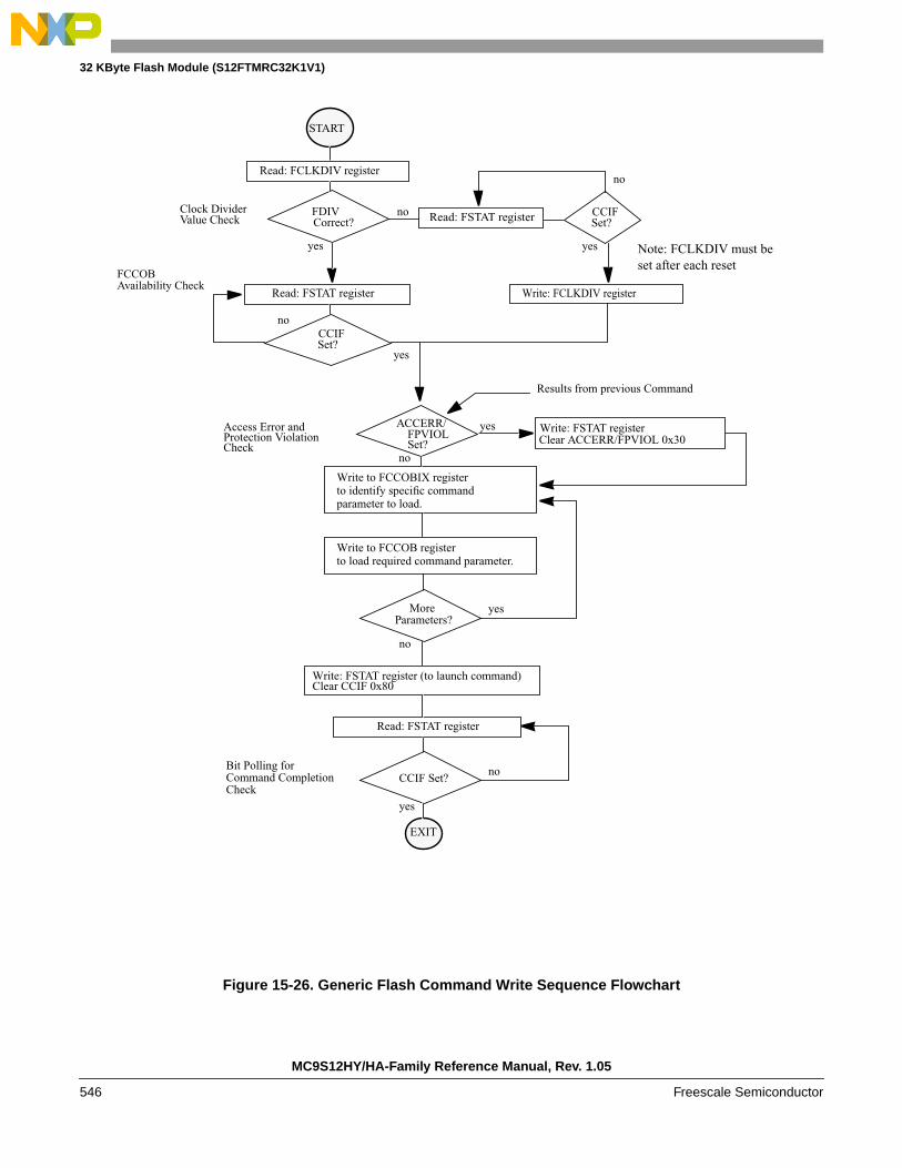
32 KByte Flash Module (S12FTMRC32K1V1)
Figure 15-26. Generic Flash Command Write Sequence Flowchart
Write to FCCOBIX register
Write: FSTAT register (to launch command)Clear CCIF 0x80
Clear ACCERR/FPVIOL 0x30Write: FSTAT registeryes
no
Access Error andProtection Violation
Read: FSTAT register
START
Check
FCCOB
ACCERR/FPVIOLSet?
EXIT
Write: FCLKDIV register
Read: FCLKDIV register
yes
noFDIVCorrect?
noBit Polling forCommand CompletionCheck
yes
CCIF Set?
to identify specific commandparameter to load.
Write to FCCOB registerto load required command parameter.
yes
no
MoreParameters?
Availability Check
Results from previous Command
Note: FCLKDIV must beset after each reset
Read: FSTAT register
no
yes
CCIFSet?
no
yes
CCIFSet?
Clock DividerValue Check Read: FSTAT register
MC9S12HY/HA-Family Reference Manual, Rev. 1.05
546 Freescale Semiconductor
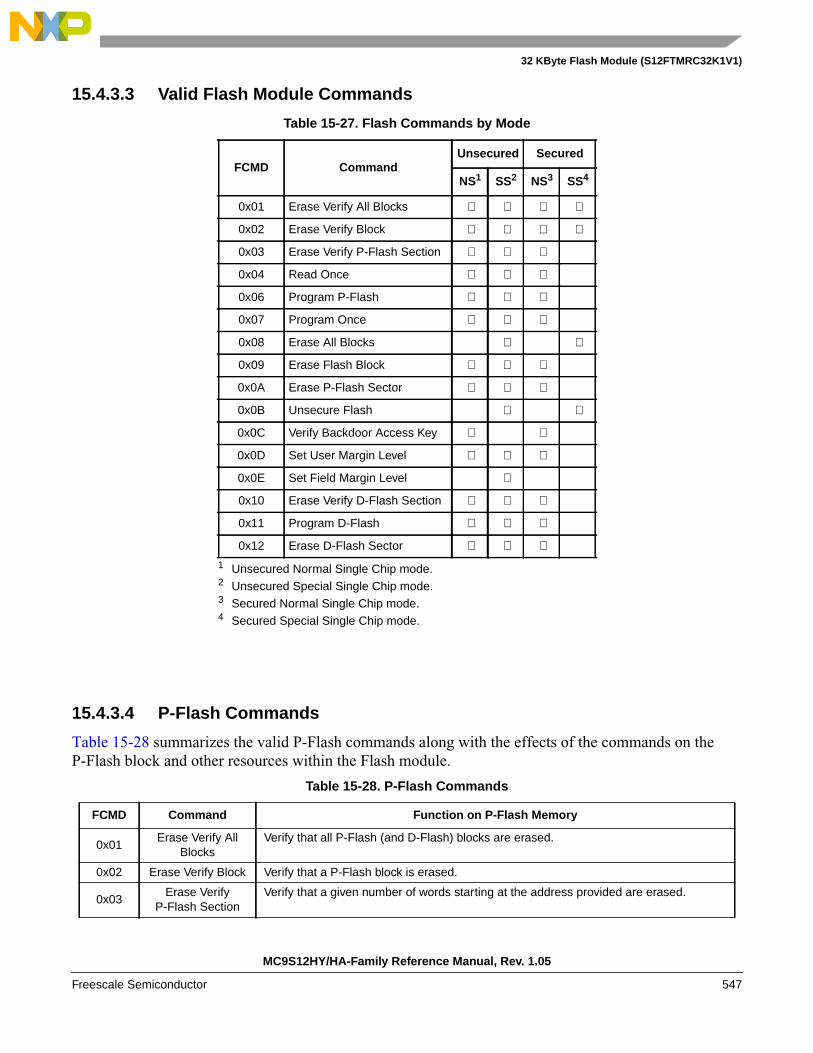
32 KByte Flash Module (S12FTMRC32K1V1)
15.4.3.3 Valid Flash Module Commands
15.4.3.4 P-Flash Commands
Table 15-28 summarizes the valid P-Flash commands along with the effects of the commands on theP-Flash block and other resources within the Flash module.
Table 15-27. Flash Commands by Mode
FCMD CommandUnsecured Secured
NS1
1 Unsecured Normal Single Chip mode.
SS2
2 Unsecured Special Single Chip mode.
NS3
3 Secured Normal Single Chip mode.
SS4
4 Secured Special Single Chip mode.
0x01 Erase Verify All Blocks ∗ ∗ ∗ ∗
0x02 Erase Verify Block ∗ ∗ ∗ ∗
0x03 Erase Verify P-Flash Section ∗ ∗ ∗
0x04 Read Once ∗ ∗ ∗
0x06 Program P-Flash ∗ ∗ ∗
0x07 Program Once ∗ ∗ ∗
0x08 Erase All Blocks ∗ ∗
0x09 Erase Flash Block ∗ ∗ ∗
0x0A Erase P-Flash Sector ∗ ∗ ∗
0x0B Unsecure Flash ∗ ∗
0x0C Verify Backdoor Access Key ∗ ∗
0x0D Set User Margin Level ∗ ∗ ∗
0x0E Set Field Margin Level ∗
0x10 Erase Verify D-Flash Section ∗ ∗ ∗
0x11 Program D-Flash ∗ ∗ ∗
0x12 Erase D-Flash Sector ∗ ∗ ∗
Table 15-28. P-Flash Commands
FCMD Command Function on P-Flash Memory
0x01Erase Verify All
BlocksVerify that all P-Flash (and D-Flash) blocks are erased.
0x02 Erase Verify Block Verify that a P-Flash block is erased.
0x03Erase Verify
P-Flash SectionVerify that a given number of words starting at the address provided are erased.
MC9S12HY/HA-Family Reference Manual, Rev. 1.05
Freescale Semiconductor 547

32 KByte Flash Module (S12FTMRC32K1V1)
15.4.3.5 D-Flash Commands
Table 15-29 summarizes the valid D-Flash commands along with the effects of the commands on theD-Flash block.
0x04 Read OnceRead a dedicated 64 byte field in the nonvolatile information register in P-Flash block thatwas previously programmed using the Program Once command.
0x06 Program P-Flash Program a phrase in a P-Flash block.
0x07 Program OnceProgram a dedicated 64 byte field in the nonvolatile information register in P-Flash blockthat is allowed to be programmed only once.
0x08 Erase All Blocks
Erase all P-Flash (and D-Flash) blocks.An erase of all Flash blocks is only possible when the FPLDIS, FPHDIS, and FPOPENbits in the FPROT register and the DPOPEN bit in the DFPROT register are set prior tolaunching the command.
0x09 Erase Flash BlockErase a P-Flash (or D-Flash) block.An erase of the full P-Flash block is only possible when FPLDIS, FPHDIS and FPOPENbits in the FPROT register are set prior to launching the command.
0x0AErase P-Flash
SectorErase all bytes in a P-Flash sector.
0x0B Unsecure FlashSupports a method of releasing MCU security by erasing all P-Flash (and D-Flash) blocksand verifying that all P-Flash (and D-Flash) blocks are erased.
0x0CVerify Backdoor
Access KeySupports a method of releasing MCU security by verifying a set of security keys.
0x0DSet User Margin
LevelSpecifies a user margin read level for all P-Flash blocks.
0x0ESet Field Margin
LevelSpecifies a field margin read level for all P-Flash blocks (special modes only).
Table 15-29. D-Flash Commands
FCMD Command Function on D-Flash Memory
0x01Erase Verify All
BlocksVerify that all D-Flash (and P-Flash) blocks are erased.
0x02 Erase Verify Block Verify that the D-Flash block is erased.
0x08 Erase All Blocks
Erase all D-Flash (and P-Flash) blocks.An erase of all Flash blocks is only possible when the FPLDIS, FPHDIS, and FPOPENbits in the FPROT register and the DPOPEN bit in the DFPROT register are set prior tolaunching the command.
0x09 Erase Flash BlockErase a D-Flash (or P-Flash) block.An erase of the full D-Flash block is only possible when DPOPEN bit in the DFPROTregister is set prior to launching the command.
0x0B Unsecure FlashSupports a method of releasing MCU security by erasing all D-Flash (and P-Flash) blocksand verifying that all D-Flash (and P-Flash) blocks are erased.
0x0DSet User Margin
LevelSpecifies a user margin read level for the D-Flash block.
0x0ESet Field Margin
LevelSpecifies a field margin read level for the D-Flash block (special modes only).
Table 15-28. P-Flash Commands
FCMD Command Function on P-Flash Memory
MC9S12HY/HA-Family Reference Manual, Rev. 1.05
548 Freescale Semiconductor

32 KByte Flash Module (S12FTMRC32K1V1)
15.4.4 Allowed Simultaneous P-Flash and D-Flash Operations
Only the operations marked ‘OK’ in Table 15-30 are permitted to be run simultaneously on the ProgramFlash and Data Flash blocks. Some operations cannot be executed simultaneously because certainhardware resources are shared by the two memories. The priority has been placed on permitting ProgramFlash reads while program and erase operations execute on the Data Flash, providing read (P-Flash) whilewrite (D-Flash) functionality.
15.4.5 Flash Command Description
This section provides details of all available Flash commands launched by a command write sequence. TheACCERR bit in the FSTAT register will be set during the command write sequence if any of the followingillegal steps are performed, causing the command not to be processed by the Memory Controller:
• Starting any command write sequence that programs or erases Flash memory before initializing theFCLKDIV register
• Writing an invalid command as part of the command write sequence
• For additional possible errors, refer to the error handling table provided for each command
0x10Erase Verify
D-Flash SectionVerify that a given number of words starting at the address provided are erased.
0x11 Program D-Flash Program up to four words in the D-Flash block.
0x12Erase D-Flash
SectorErase all bytes in a sector of the D-Flash block.
Table 15-30. Allowed P-Flash and D-Flash Simultaneous Operations
Data Flash
Program Flash ReadMarginRead1 Program
SectorErase
MassErase3
Read OK OK OK
Margin Read1
1 A ‘Margin Read’ is any read after executing the margin setting commands‘Set User Margin Level’ or ‘Set Field Margin Level’ with anything but the‘normal’ level specified.
OK2
2 See the Note on margin settings in Section 15.4.5.12 and Section 15.4.5.13.
Program
Sector Erase OK
Mass Erase3
3 The ‘Mass Erase’ operations are commands ‘Erase All Blocks’ and ‘EraseFlash Block’
OK
Table 15-29. D-Flash Commands
FCMD Command Function on D-Flash Memory
MC9S12HY/HA-Family Reference Manual, Rev. 1.05
Freescale Semiconductor 549
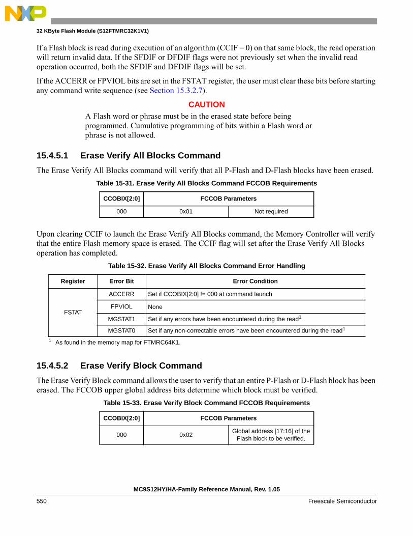
32 KByte Flash Module (S12FTMRC32K1V1)
If a Flash block is read during execution of an algorithm (CCIF = 0) on that same block, the read operationwill return invalid data. If the SFDIF or DFDIF flags were not previously set when the invalid readoperation occurred, both the SFDIF and DFDIF flags will be set.
If the ACCERR or FPVIOL bits are set in the FSTAT register, the user must clear these bits before startingany command write sequence (see Section 15.3.2.7).
CAUTIONA Flash word or phrase must be in the erased state before beingprogrammed. Cumulative programming of bits within a Flash word orphrase is not allowed.
15.4.5.1 Erase Verify All Blocks Command
The Erase Verify All Blocks command will verify that all P-Flash and D-Flash blocks have been erased.
Upon clearing CCIF to launch the Erase Verify All Blocks command, the Memory Controller will verifythat the entire Flash memory space is erased. The CCIF flag will set after the Erase Verify All Blocksoperation has completed.
15.4.5.2 Erase Verify Block Command
The Erase Verify Block command allows the user to verify that an entire P-Flash or D-Flash block has beenerased. The FCCOB upper global address bits determine which block must be verified.
Table 15-31. Erase Verify All Blocks Command FCCOB Requirements
CCOBIX[2:0] FCCOB Parameters
000 0x01 Not required
Table 15-32. Erase Verify All Blocks Command Error Handling
Register Error Bit Error Condition
FSTAT
ACCERR Set if CCOBIX[2:0] != 000 at command launch
FPVIOL None
MGSTAT1 Set if any errors have been encountered during the read1
1 As found in the memory map for FTMRC64K1.
MGSTAT0 Set if any non-correctable errors have been encountered during the read1
Table 15-33. Erase Verify Block Command FCCOB Requirements
CCOBIX[2:0] FCCOB Parameters
000 0x02Global address [17:16] of the
Flash block to be verified.
MC9S12HY/HA-Family Reference Manual, Rev. 1.05
550 Freescale Semiconductor
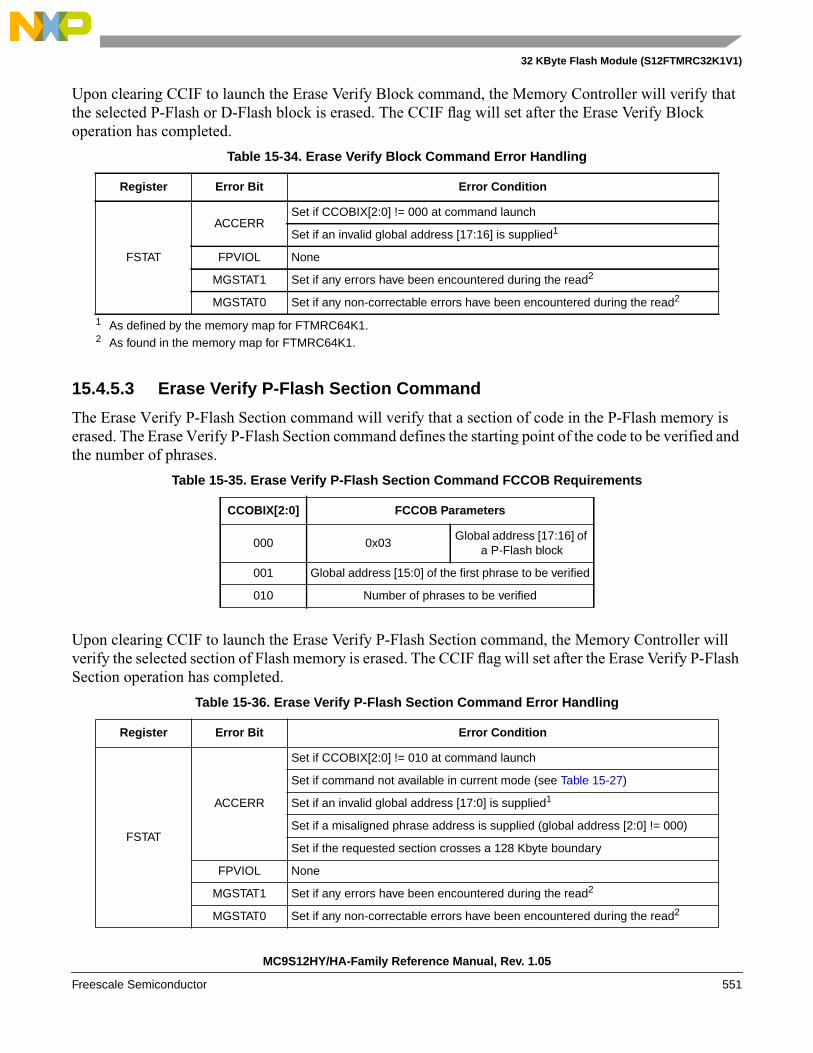
32 KByte Flash Module (S12FTMRC32K1V1)
Upon clearing CCIF to launch the Erase Verify Block command, the Memory Controller will verify thatthe selected P-Flash or D-Flash block is erased. The CCIF flag will set after the Erase Verify Blockoperation has completed.
15.4.5.3 Erase Verify P-Flash Section Command
The Erase Verify P-Flash Section command will verify that a section of code in the P-Flash memory iserased. The Erase Verify P-Flash Section command defines the starting point of the code to be verified andthe number of phrases.
Upon clearing CCIF to launch the Erase Verify P-Flash Section command, the Memory Controller willverify the selected section of Flash memory is erased. The CCIF flag will set after the Erase Verify P-FlashSection operation has completed.
Table 15-34. Erase Verify Block Command Error Handling
Register Error Bit Error Condition
FSTAT
ACCERRSet if CCOBIX[2:0] != 000 at command launch
Set if an invalid global address [17:16] is supplied1
1 As defined by the memory map for FTMRC64K1.
FPVIOL None
MGSTAT1 Set if any errors have been encountered during the read2
2 As found in the memory map for FTMRC64K1.
MGSTAT0 Set if any non-correctable errors have been encountered during the read2
Table 15-35. Erase Verify P-Flash Section Command FCCOB Requirements
CCOBIX[2:0] FCCOB Parameters
000 0x03Global address [17:16] of
a P-Flash block
001 Global address [15:0] of the first phrase to be verified
010 Number of phrases to be verified
Table 15-36. Erase Verify P-Flash Section Command Error Handling
Register Error Bit Error Condition
FSTAT
ACCERR
Set if CCOBIX[2:0] != 010 at command launch
Set if command not available in current mode (see Table 15-27)
Set if an invalid global address [17:0] is supplied1
Set if a misaligned phrase address is supplied (global address [2:0] != 000)
Set if the requested section crosses a 128 Kbyte boundary
FPVIOL None
MGSTAT1 Set if any errors have been encountered during the read2
MGSTAT0 Set if any non-correctable errors have been encountered during the read2
MC9S12HY/HA-Family Reference Manual, Rev. 1.05
Freescale Semiconductor 551

32 KByte Flash Module (S12FTMRC32K1V1)
15.4.5.4 Read Once Command
The Read Once command provides read access to a reserved 64 byte field (8 phrases) located in thenonvolatile information register of P-Flash. The Read Once field is programmed using the Program Oncecommand described in Section 15.4.5.6. The Read Once command must not be executed from the Flashblock containing the Program Once reserved field to avoid code runaway.
Upon clearing CCIF to launch the Read Once command, a Read Once phrase is fetched and stored in theFCCOB indexed register. The CCIF flag will set after the Read Once operation has completed. Validphrase index values for the Read Once command range from 0x0000 to 0x0007. During execution of theRead Once command, any attempt to read addresses within P-Flash block will return invalid data.
8
15.4.5.5 Program P-Flash Command
The Program P-Flash operation will program a previously erased phrase in the P-Flash memory using anembedded algorithm.
CAUTIONA P-Flash phrase must be in the erased state before being programmed.Cumulative programming of bits within a Flash phrase is not allowed.
1 As defined by the memory map for FTMRC64K1.2 As found in the memory map for FTMRC64K1.
Table 15-37. Read Once Command FCCOB Requirements
CCOBIX[2:0] FCCOB Parameters
000 0x04 Not Required
001 Read Once phrase index (0x0000 - 0x0007)
010 Read Once word 0 value
011 Read Once word 1 value
100 Read Once word 2 value
101 Read Once word 3 value
Table 15-38. Read Once Command Error Handling
Register Error Bit Error Condition
FSTAT
ACCERR
Set if CCOBIX[2:0] != 001 at command launch
Set if command not available in current mode (see Table 15-27)
Set if an invalid phrase index is supplied
FPVIOL None
MGSTAT1 Set if any errors have been encountered during the read
MGSTAT0 Set if any non-correctable errors have been encountered during the read
MC9S12HY/HA-Family Reference Manual, Rev. 1.05
552 Freescale Semiconductor
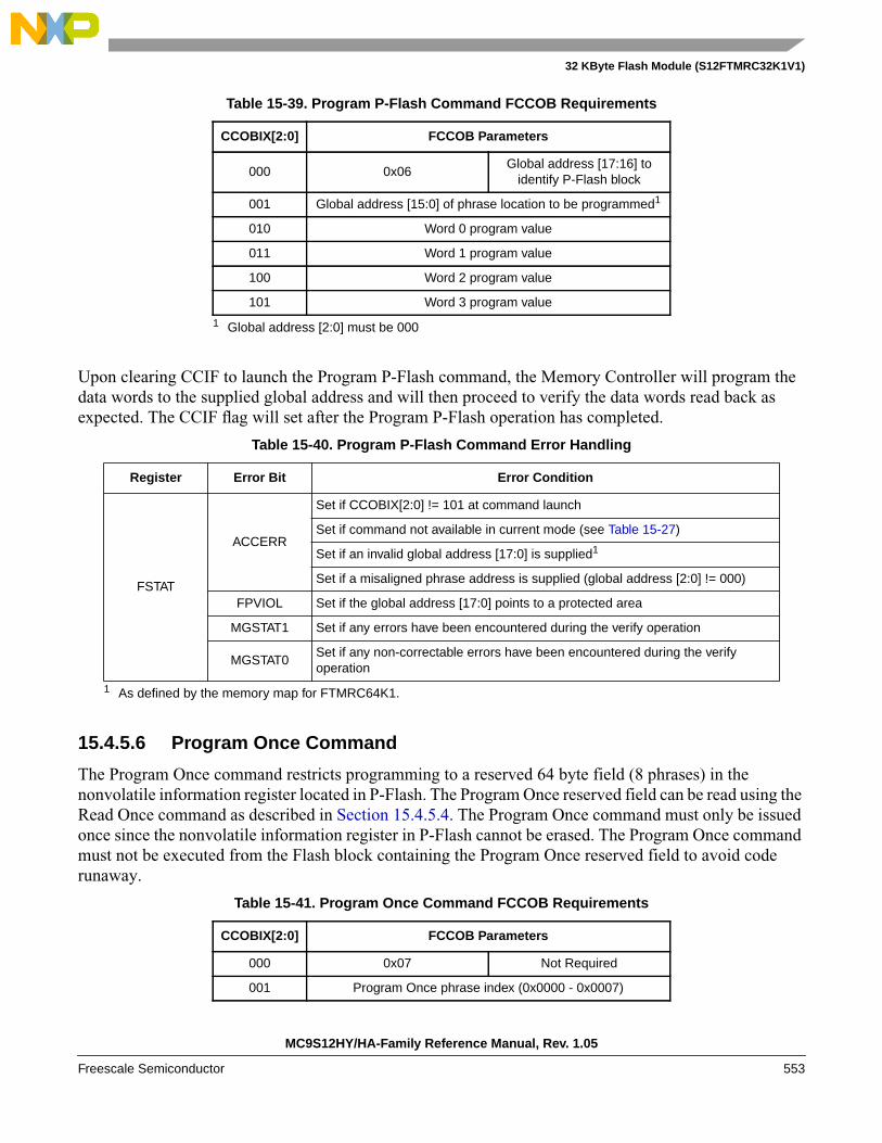
32 KByte Flash Module (S12FTMRC32K1V1)
Upon clearing CCIF to launch the Program P-Flash command, the Memory Controller will program thedata words to the supplied global address and will then proceed to verify the data words read back asexpected. The CCIF flag will set after the Program P-Flash operation has completed.
15.4.5.6 Program Once Command
The Program Once command restricts programming to a reserved 64 byte field (8 phrases) in thenonvolatile information register located in P-Flash. The Program Once reserved field can be read using theRead Once command as described in Section 15.4.5.4. The Program Once command must only be issuedonce since the nonvolatile information register in P-Flash cannot be erased. The Program Once commandmust not be executed from the Flash block containing the Program Once reserved field to avoid coderunaway.
Table 15-39. Program P-Flash Command FCCOB Requirements
CCOBIX[2:0] FCCOB Parameters
000 0x06Global address [17:16] to
identify P-Flash block
001 Global address [15:0] of phrase location to be programmed1
1 Global address [2:0] must be 000
010 Word 0 program value
011 Word 1 program value
100 Word 2 program value
101 Word 3 program value
Table 15-40. Program P-Flash Command Error Handling
Register Error Bit Error Condition
FSTAT
ACCERR
Set if CCOBIX[2:0] != 101 at command launch
Set if command not available in current mode (see Table 15-27)
Set if an invalid global address [17:0] is supplied1
1 As defined by the memory map for FTMRC64K1.
Set if a misaligned phrase address is supplied (global address [2:0] != 000)
FPVIOL Set if the global address [17:0] points to a protected area
MGSTAT1 Set if any errors have been encountered during the verify operation
MGSTAT0Set if any non-correctable errors have been encountered during the verifyoperation
Table 15-41. Program Once Command FCCOB Requirements
CCOBIX[2:0] FCCOB Parameters
000 0x07 Not Required
001 Program Once phrase index (0x0000 - 0x0007)
MC9S12HY/HA-Family Reference Manual, Rev. 1.05
Freescale Semiconductor 553

32 KByte Flash Module (S12FTMRC32K1V1)
Upon clearing CCIF to launch the Program Once command, the Memory Controller first verifies that theselected phrase is erased. If erased, then the selected phrase will be programmed and then verified withread back. The CCIF flag will remain clear, setting only after the Program Once operation has completed.
The reserved nonvolatile information register accessed by the Program Once command cannot be erasedand any attempt to program one of these phrases a second time will not be allowed. Valid phrase indexvalues for the Program Once command range from 0x0000 to 0x0007. During execution of the ProgramOnce command, any attempt to read addresses within P-Flash will return invalid data.
15.4.5.7 Erase All Blocks Command
The Erase All Blocks operation will erase the entire P-Flash and D-Flash memory space.
Upon clearing CCIF to launch the Erase All Blocks command, the Memory Controller will erase the entireFlash memory space and verify that it is erased. If the Memory Controller verifies that the entire Flashmemory space was properly erased, security will be released. During the execution of this command
010 Program Once word 0 value
011 Program Once word 1 value
100 Program Once word 2 value
101 Program Once word 3 value
Table 15-42. Program Once Command Error Handling
Register Error Bit Error Condition
FSTAT
ACCERR
Set if CCOBIX[2:0] != 101 at command launch
Set if command not available in current mode (see Table 15-27)
Set if an invalid phrase index is supplied
Set if the requested phrase has already been programmed1
1 If a Program Once phrase is initially programmed to 0xFFFF_FFFF_FFFF_FFFF, the Program Once command willbe allowed to execute again on that same phrase.
FPVIOL None
MGSTAT1 Set if any errors have been encountered during the verify operation
MGSTAT0Set if any non-correctable errors have been encountered during the verifyoperation
Table 15-43. Erase All Blocks Command FCCOB Requirements
CCOBIX[2:0] FCCOB Parameters
000 0x08 Not required
Table 15-41. Program Once Command FCCOB Requirements
CCOBIX[2:0] FCCOB Parameters
MC9S12HY/HA-Family Reference Manual, Rev. 1.05
554 Freescale Semiconductor

32 KByte Flash Module (S12FTMRC32K1V1)
(CCIF=0) the user must not write to any Flash module register. The CCIF flag will set after the Erase AllBlocks operation has completed.
15.4.5.8 Erase Flash Block Command
The Erase Flash Block operation will erase all addresses in a P-Flash or D-Flash block.
Upon clearing CCIF to launch the Erase Flash Block command, the Memory Controller will erase theselected Flash block and verify that it is erased. The CCIF flag will set after the Erase Flash Blockoperation has completed.
Table 15-44. Erase All Blocks Command Error Handling
Register Error Bit Error Condition
FSTAT
ACCERRSet if CCOBIX[2:0] != 000 at command launch
Set if command not available in current mode (see Table 15-27)
FPVIOL Set if any area of the P-Flash or D-Flash memory is protected
MGSTAT1 Set if any errors have been encountered during the verify operation1
1 As found in the memory map for FTMRC64K1.
MGSTAT0Set if any non-correctable errors have been encountered during the verifyoperation1
Table 15-45. Erase Flash Block Command FCCOB Requirements
CCOBIX[2:0] FCCOB Parameters
000 0x09Global address [17:16] to
identify Flash block
001 Global address [15:0] in Flash block to be erased
Table 15-46. Erase Flash Block Command Error Handling
Register Error Bit Error Condition
FSTAT
ACCERR
Set if CCOBIX[2:0] != 001 at command launch
Set if command not available in current mode (see Table 15-27)
Set if an invalid global address [17:16] is supplied1
1 As defined by the memory map for FTMRC64K1.
Set if the supplied P-Flash address is not phrase-aligned or if the D-Flashaddress is not word-aligned
FPVIOL Set if an area of the selected Flash block is protected
MGSTAT1 Set if any errors have been encountered during the verify operation2
2 As found in the memory map for FTMRC64K1.
MGSTAT0Set if any non-correctable errors have been encountered during the verifyoperation2
MC9S12HY/HA-Family Reference Manual, Rev. 1.05
Freescale Semiconductor 555

32 KByte Flash Module (S12FTMRC32K1V1)
15.4.5.9 Erase P-Flash Sector Command
The Erase P-Flash Sector operation will erase all addresses in a P-Flash sector.
Upon clearing CCIF to launch the Erase P-Flash Sector command, the Memory Controller will erase theselected Flash sector and then verify that it is erased. The CCIF flag will be set after the Erase P-FlashSector operation has completed.
15.4.5.10 Unsecure Flash Command
The Unsecure Flash command will erase the entire P-Flash and D-Flash memory space and, if the erase issuccessful, will release security.
Upon clearing CCIF to launch the Unsecure Flash command, the Memory Controller will erase the entireP-Flash and D-Flash memory space and verify that it is erased. If the Memory Controller verifies that theentire Flash memory space was properly erased, security will be released. If the erase verify is notsuccessful, the Unsecure Flash operation sets MGSTAT1 and terminates without changing the securitystate. During the execution of this command (CCIF=0) the user must not write to any Flash moduleregister. The CCIF flag is set after the Unsecure Flash operation has completed.
Table 15-47. Erase P-Flash Sector Command FCCOB Requirements
CCOBIX[2:0] FCCOB Parameters
000 0x0AGlobal address [17:16] to identify
P-Flash block to be erased
001Global address [15:0] anywhere within the sector to be erased.
Refer to Section 15.1.2.1 for the P-Flash sector size.
Table 15-48. Erase P-Flash Sector Command Error Handling
Register Error Bit Error Condition
FSTAT
ACCERR
Set if CCOBIX[2:0] != 001 at command launch
Set if command not available in current mode (see Table 15-27)
Set if an invalid global address [17:16] is supplied1
1 As defined by the memory map for FTMRC64K1.
Set if a misaligned phrase address is supplied (global address [2:0] != 000)
FPVIOL Set if the selected P-Flash sector is protected
MGSTAT1 Set if any errors have been encountered during the verify operation
MGSTAT0Set if any non-correctable errors have been encountered during the verifyoperation
Table 15-49. Unsecure Flash Command FCCOB Requirements
CCOBIX[2:0] FCCOB Parameters
000 0x0B Not required
MC9S12HY/HA-Family Reference Manual, Rev. 1.05
556 Freescale Semiconductor

32 KByte Flash Module (S12FTMRC32K1V1)
15.4.5.11 Verify Backdoor Access Key Command
The Verify Backdoor Access Key command will only execute if it is enabled by the KEYEN bits in theFSEC register (see Table 15-9). The Verify Backdoor Access Key command releases security ifuser-supplied keys match those stored in the Flash security bytes of the Flash configuration field (seeTable 15-3). The Verify Backdoor Access Key command must not be executed from the Flash blockcontaining the backdoor comparison key to avoid code runaway.
Upon clearing CCIF to launch the Verify Backdoor Access Key command, the Memory Controller willcheck the FSEC KEYEN bits to verify that this command is enabled. If not enabled, the MemoryController sets the ACCERR bit in the FSTAT register and terminates. If the command is enabled, theMemory Controller compares the key provided in FCCOB to the backdoor comparison key in the Flashconfiguration field with Key 0 compared to 0x3_FF00, etc. If the backdoor keys match, security will bereleased. If the backdoor keys do not match, security is not released and all future attempts to execute theVerify Backdoor Access Key command are aborted (set ACCERR) until a reset occurs. The CCIF flag isset after the Verify Backdoor Access Key operation has completed.
Table 15-50. Unsecure Flash Command Error Handling
Register Error Bit Error Condition
FSTAT
ACCERRSet if CCOBIX[2:0] != 000 at command launch
Set if command not available in current mode (see Table 15-27)
FPVIOL Set if any area of the P-Flash or D-Flash memory is protected
MGSTAT1 Set if any errors have been encountered during the verify operation1
1 As found in the memory map for FTMRC64K1.
MGSTAT0Set if any non-correctable errors have been encountered during the verifyoperation1
Table 15-51. Verify Backdoor Access Key Command FCCOB Requirements
CCOBIX[2:0] FCCOB Parameters
000 0x0C Not required
001 Key 0
010 Key 1
011 Key 2
100 Key 3
MC9S12HY/HA-Family Reference Manual, Rev. 1.05
Freescale Semiconductor 557
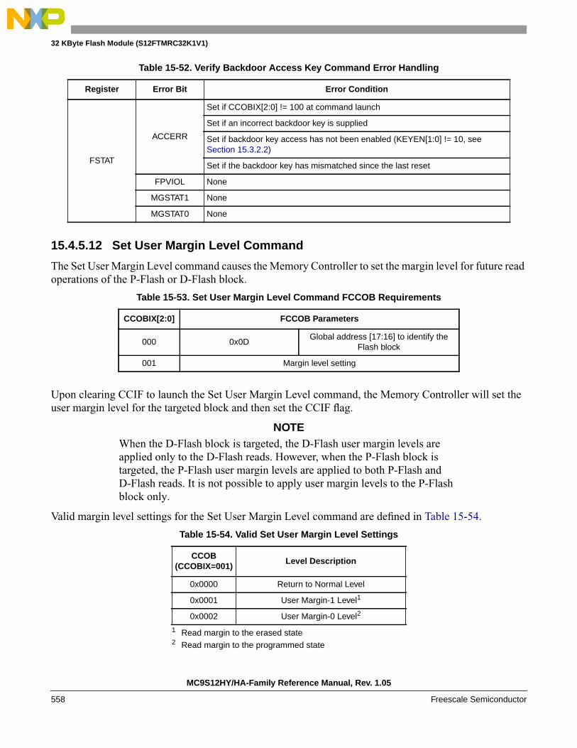
32 KByte Flash Module (S12FTMRC32K1V1)
15.4.5.12 Set User Margin Level Command
The Set User Margin Level command causes the Memory Controller to set the margin level for future readoperations of the P-Flash or D-Flash block.
Upon clearing CCIF to launch the Set User Margin Level command, the Memory Controller will set theuser margin level for the targeted block and then set the CCIF flag.
NOTEWhen the D-Flash block is targeted, the D-Flash user margin levels areapplied only to the D-Flash reads. However, when the P-Flash block istargeted, the P-Flash user margin levels are applied to both P-Flash andD-Flash reads. It is not possible to apply user margin levels to the P-Flashblock only.
Valid margin level settings for the Set User Margin Level command are defined in Table 15-54.
Table 15-52. Verify Backdoor Access Key Command Error Handling
Register Error Bit Error Condition
FSTAT
ACCERR
Set if CCOBIX[2:0] != 100 at command launch
Set if an incorrect backdoor key is supplied
Set if backdoor key access has not been enabled (KEYEN[1:0] != 10, seeSection 15.3.2.2)
Set if the backdoor key has mismatched since the last reset
FPVIOL None
MGSTAT1 None
MGSTAT0 None
Table 15-53. Set User Margin Level Command FCCOB Requirements
CCOBIX[2:0] FCCOB Parameters
000 0x0DGlobal address [17:16] to identify the
Flash block
001 Margin level setting
Table 15-54. Valid Set User Margin Level Settings
CCOB(CCOBIX=001)
Level Description
0x0000 Return to Normal Level
0x0001 User Margin-1 Level1
1 Read margin to the erased state
0x0002 User Margin-0 Level2
2 Read margin to the programmed state
MC9S12HY/HA-Family Reference Manual, Rev. 1.05
558 Freescale Semiconductor

32 KByte Flash Module (S12FTMRC32K1V1)
NOTEUser margin levels can be used to check that Flash memory contents haveadequate margin for normal level read operations. If unexpected results areencountered when checking Flash memory contents at user margin levels, apotential loss of information has been detected.
15.4.5.13 Set Field Margin Level Command
The Set Field Margin Level command, valid in special modes only, causes the Memory Controller to setthe margin level specified for future read operations of the P-Flash or D-Flash block.
Upon clearing CCIF to launch the Set Field Margin Level command, the Memory Controller will set thefield margin level for the targeted block and then set the CCIF flag.
NOTEWhen the D-Flash block is targeted, the D-Flash field margin levels areapplied only to the D-Flash reads. However, when the P-Flash block istargeted, the P-Flash field margin levels are applied to both P-Flash andD-Flash reads. It is not possible to apply field margin levels to the P-Flashblock only.
Valid margin level settings for the Set Field Margin Level command are defined in Table 15-57.
Table 15-55. Set User Margin Level Command Error Handling
Register Error Bit Error Condition
FSTAT
ACCERR
Set if CCOBIX[2:0] != 001 at command launch
Set if command not available in current mode (see Table 15-27)
Set if an invalid global address [17:16] is supplied1
1 As defined by the memory map for FTMRC64K1.
Set if an invalid margin level setting is supplied
FPVIOL None
MGSTAT1 None
MGSTAT0 None
Table 15-56. Set Field Margin Level Command FCCOB Requirements
CCOBIX[2:0] FCCOB Parameters
000 0x0EGlobal address [17:16] to identify the Flash
block
001 Margin level setting
MC9S12HY/HA-Family Reference Manual, Rev. 1.05
Freescale Semiconductor 559
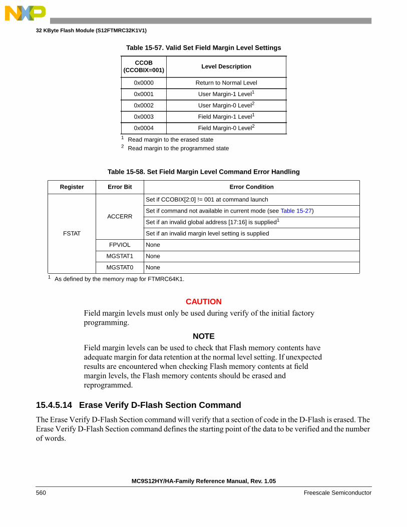
32 KByte Flash Module (S12FTMRC32K1V1)
CAUTIONField margin levels must only be used during verify of the initial factoryprogramming.
NOTEField margin levels can be used to check that Flash memory contents haveadequate margin for data retention at the normal level setting. If unexpectedresults are encountered when checking Flash memory contents at fieldmargin levels, the Flash memory contents should be erased andreprogrammed.
15.4.5.14 Erase Verify D-Flash Section Command
The Erase Verify D-Flash Section command will verify that a section of code in the D-Flash is erased. TheErase Verify D-Flash Section command defines the starting point of the data to be verified and the numberof words.
Table 15-57. Valid Set Field Margin Level Settings
CCOB(CCOBIX=001)
Level Description
0x0000 Return to Normal Level
0x0001 User Margin-1 Level1
1 Read margin to the erased state
0x0002 User Margin-0 Level2
2 Read margin to the programmed state
0x0003 Field Margin-1 Level1
0x0004 Field Margin-0 Level2
Table 15-58. Set Field Margin Level Command Error Handling
Register Error Bit Error Condition
FSTAT
ACCERR
Set if CCOBIX[2:0] != 001 at command launch
Set if command not available in current mode (see Table 15-27)
Set if an invalid global address [17:16] is supplied1
1 As defined by the memory map for FTMRC64K1.
Set if an invalid margin level setting is supplied
FPVIOL None
MGSTAT1 None
MGSTAT0 None
MC9S12HY/HA-Family Reference Manual, Rev. 1.05
560 Freescale Semiconductor

32 KByte Flash Module (S12FTMRC32K1V1)
Upon clearing CCIF to launch the Erase Verify D-Flash Section command, the Memory Controller willverify the selected section of D-Flash memory is erased. The CCIF flag will set after the Erase VerifyD-Flash Section operation has completed.
15.4.5.15 Program D-Flash Command
The Program D-Flash operation programs one to four previously erased words in the D-Flash block. TheProgram D-Flash operation will confirm that the targeted location(s) were successfully programmed uponcompletion.
CAUTIONA Flash word must be in the erased state before being programmed.Cumulative programming of bits within a Flash word is not allowed.
Table 15-59. Erase Verify D-Flash Section Command FCCOB Requirements
CCOBIX[2:0] FCCOB Parameters
000 0x10Global address [17:16] toidentify the D-Flash block
001 Global address [15:0] of the first word to be verified
010 Number of words to be verified
Table 15-60. Erase Verify D-Flash Section Command Error Handling
Register Error Bit Error Condition
FSTAT
ACCERR
Set if CCOBIX[2:0] != 010 at command launch
Set if command not available in current mode (see Table 15-27)
Set if an invalid global address [17:0] is supplied
Set if a misaligned word address is supplied (global address [0] != 0)
Set if the requested section breaches the end of the D-Flash block
FPVIOL None
MGSTAT1 Set if any errors have been encountered during the read
MGSTAT0 Set if any non-correctable errors have been encountered during the read
Table 15-61. Program D-Flash Command FCCOB Requirements
CCOBIX[2:0] FCCOB Parameters
000 0x11Global address [17:16] toidentify the D-Flash block
001 Global address [15:0] of word to be programmed
010 Word 0 program value
011 Word 1 program value, if desired
100 Word 2 program value, if desired
MC9S12HY/HA-Family Reference Manual, Rev. 1.05
Freescale Semiconductor 561
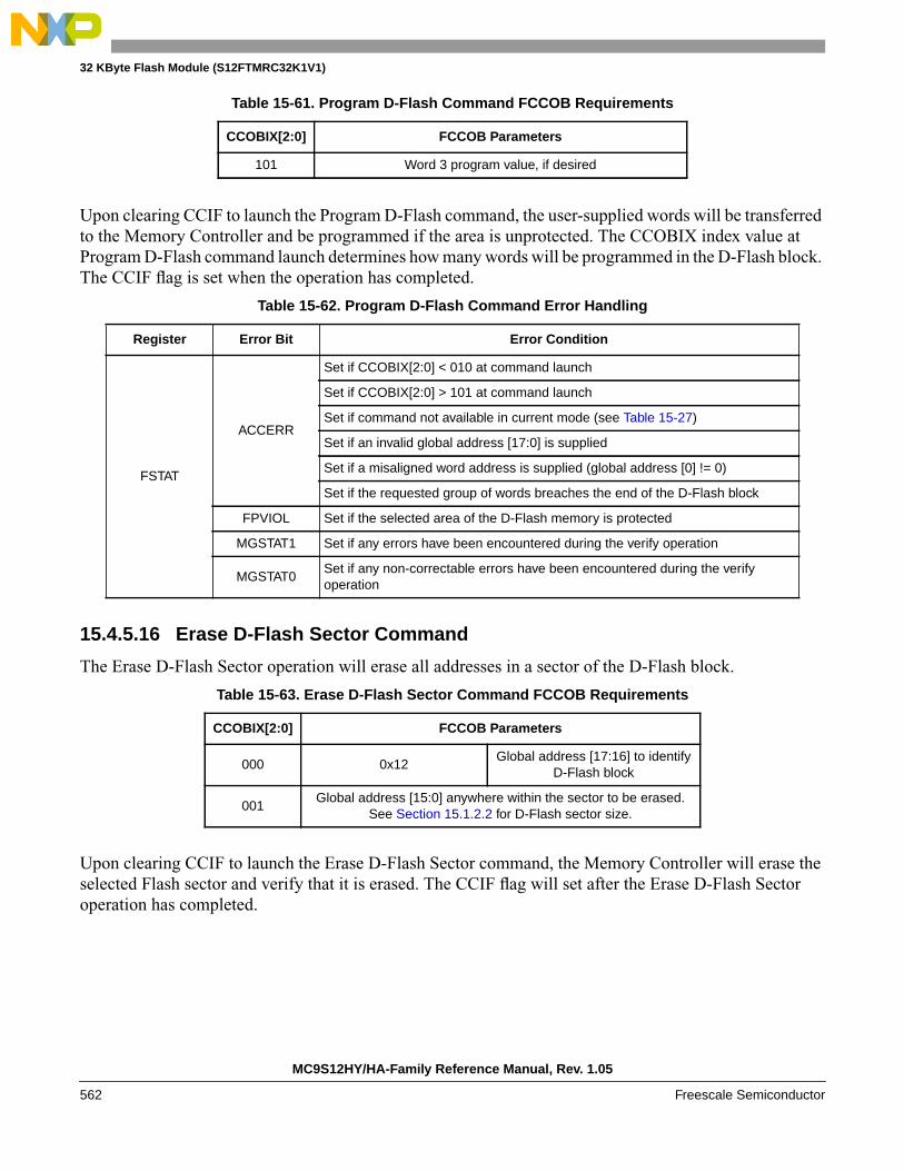
32 KByte Flash Module (S12FTMRC32K1V1)
Upon clearing CCIF to launch the Program D-Flash command, the user-supplied words will be transferredto the Memory Controller and be programmed if the area is unprotected. The CCOBIX index value atProgram D-Flash command launch determines how many words will be programmed in the D-Flash block.The CCIF flag is set when the operation has completed.
15.4.5.16 Erase D-Flash Sector Command
The Erase D-Flash Sector operation will erase all addresses in a sector of the D-Flash block.
Upon clearing CCIF to launch the Erase D-Flash Sector command, the Memory Controller will erase theselected Flash sector and verify that it is erased. The CCIF flag will set after the Erase D-Flash Sectoroperation has completed.
101 Word 3 program value, if desired
Table 15-62. Program D-Flash Command Error Handling
Register Error Bit Error Condition
FSTAT
ACCERR
Set if CCOBIX[2:0] < 010 at command launch
Set if CCOBIX[2:0] > 101 at command launch
Set if command not available in current mode (see Table 15-27)
Set if an invalid global address [17:0] is supplied
Set if a misaligned word address is supplied (global address [0] != 0)
Set if the requested group of words breaches the end of the D-Flash block
FPVIOL Set if the selected area of the D-Flash memory is protected
MGSTAT1 Set if any errors have been encountered during the verify operation
MGSTAT0Set if any non-correctable errors have been encountered during the verifyoperation
Table 15-63. Erase D-Flash Sector Command FCCOB Requirements
CCOBIX[2:0] FCCOB Parameters
000 0x12Global address [17:16] to identify
D-Flash block
001Global address [15:0] anywhere within the sector to be erased.
See Section 15.1.2.2 for D-Flash sector size.
Table 15-61. Program D-Flash Command FCCOB Requirements
CCOBIX[2:0] FCCOB Parameters
MC9S12HY/HA-Family Reference Manual, Rev. 1.05
562 Freescale Semiconductor

32 KByte Flash Module (S12FTMRC32K1V1)
15.4.6 Interrupts
The Flash module can generate an interrupt when a Flash command operation has completed or when aFlash command operation has detected an ECC fault.
NOTEVector addresses and their relative interrupt priority are determined at theMCU level.
15.4.6.1 Description of Flash Interrupt Operation
The Flash module uses the CCIF flag in combination with the CCIE interrupt enable bit to generate theFlash command interrupt request. The Flash module uses the DFDIF and SFDIF flags in combination withthe DFDIE and SFDIE interrupt enable bits to generate the Flash error interrupt request. For a detaileddescription of the register bits involved, refer to Section 15.3.2.5, “Flash Configuration Register(FCNFG)”, Section 15.3.2.6, “Flash Error Configuration Register (FERCNFG)”, Section 15.3.2.7, “FlashStatus Register (FSTAT)”, and Section 15.3.2.8, “Flash Error Status Register (FERSTAT)”.
The logic used for generating the Flash module interrupts is shown in Figure 15-27.
Table 15-64. Erase D-Flash Sector Command Error Handling
Register Error Bit Error Condition
FSTAT
ACCERR
Set if CCOBIX[2:0] != 001 at command launch
Set if command not available in current mode (see Table 15-27)
Set if an invalid global address [17:0] is supplied
Set if a misaligned word address is supplied (global address [0] != 0)
FPVIOL Set if the selected area of the D-Flash memory is protected
MGSTAT1 Set if any errors have been encountered during the verify operation
MGSTAT0Set if any non-correctable errors have been encountered during the verifyoperation
Table 15-65. Flash Interrupt Sources
Interrupt Source Interrupt Flag Local EnableGlobal (CCR)
Mask
Flash Command Complete CCIF(FSTAT register)
CCIE(FCNFG register)
I Bit
ECC Double Bit Fault on Flash Read DFDIF(FERSTAT register)
DFDIE(FERCNFG register)
I Bit
ECC Single Bit Fault on Flash Read SFDIF(FERSTAT register)
SFDIE(FERCNFG register)
I Bit
MC9S12HY/HA-Family Reference Manual, Rev. 1.05
Freescale Semiconductor 563
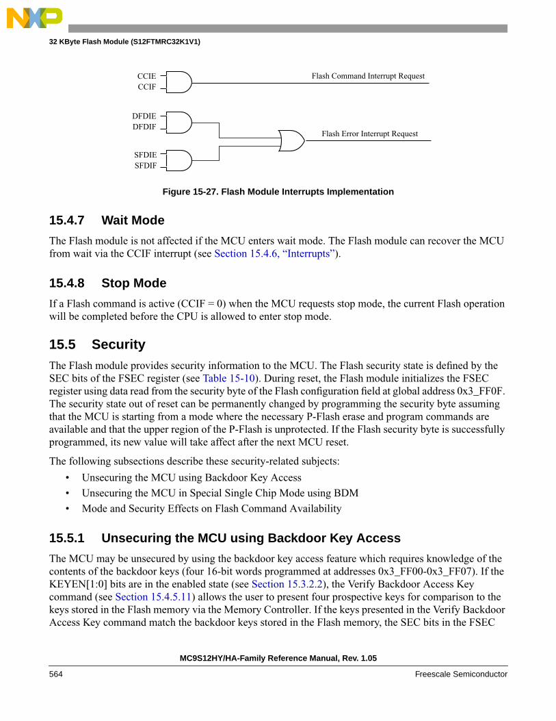
32 KByte Flash Module (S12FTMRC32K1V1)
Figure 15-27. Flash Module Interrupts Implementation
15.4.7 Wait Mode
The Flash module is not affected if the MCU enters wait mode. The Flash module can recover the MCUfrom wait via the CCIF interrupt (see Section 15.4.6, “Interrupts”).
15.4.8 Stop Mode
If a Flash command is active (CCIF = 0) when the MCU requests stop mode, the current Flash operationwill be completed before the CPU is allowed to enter stop mode.
15.5 SecurityThe Flash module provides security information to the MCU. The Flash security state is defined by theSEC bits of the FSEC register (see Table 15-10). During reset, the Flash module initializes the FSECregister using data read from the security byte of the Flash configuration field at global address 0x3_FF0F.The security state out of reset can be permanently changed by programming the security byte assumingthat the MCU is starting from a mode where the necessary P-Flash erase and program commands areavailable and that the upper region of the P-Flash is unprotected. If the Flash security byte is successfullyprogrammed, its new value will take affect after the next MCU reset.
The following subsections describe these security-related subjects:
• Unsecuring the MCU using Backdoor Key Access
• Unsecuring the MCU in Special Single Chip Mode using BDM
• Mode and Security Effects on Flash Command Availability
15.5.1 Unsecuring the MCU using Backdoor Key Access
The MCU may be unsecured by using the backdoor key access feature which requires knowledge of thecontents of the backdoor keys (four 16-bit words programmed at addresses 0x3_FF00-0x3_FF07). If theKEYEN[1:0] bits are in the enabled state (see Section 15.3.2.2), the Verify Backdoor Access Keycommand (see Section 15.4.5.11) allows the user to present four prospective keys for comparison to thekeys stored in the Flash memory via the Memory Controller. If the keys presented in the Verify BackdoorAccess Key command match the backdoor keys stored in the Flash memory, the SEC bits in the FSEC
Flash Error Interrupt Request
CCIFCCIE
DFDIFDFDIE
SFDIFSFDIE
Flash Command Interrupt Request
MC9S12HY/HA-Family Reference Manual, Rev. 1.05
564 Freescale Semiconductor

32 KByte Flash Module (S12FTMRC32K1V1)
register (see Table 15-10) will be changed to unsecure the MCU. Key values of 0x0000 and 0xFFFF arenot permitted as backdoor keys. While the Verify Backdoor Access Key command is active, P-Flashmemory and D-Flash memory will not be available for read access and will return invalid data.
The user code stored in the P-Flash memory must have a method of receiving the backdoor keys from anexternal stimulus. This external stimulus would typically be through one of the on-chip serial ports.
If the KEYEN[1:0] bits are in the enabled state (see Section 15.3.2.2), the MCU can be unsecured by thebackdoor key access sequence described below:
1. Follow the command sequence for the Verify Backdoor Access Key command as explained inSection 15.4.5.11
2. If the Verify Backdoor Access Key command is successful, the MCU is unsecured and theSEC[1:0] bits in the FSEC register are forced to the unsecure state of 10
The Verify Backdoor Access Key command is monitored by the Memory Controller and an illegal key willprohibit future use of the Verify Backdoor Access Key command. A reset of the MCU is the only methodto re-enable the Verify Backdoor Access Key command. The security as defined in the Flash security byte(0x3_FF0F) is not changed by using the Verify Backdoor Access Key command sequence. The backdoorkeys stored in addresses 0x3_FF00-0x3_FF07 are unaffected by the Verify Backdoor Access Keycommand sequence. The Verify Backdoor Access Key command sequence has no effect on the programand erase protections defined in the Flash protection register, FPROT.
After the backdoor keys have been correctly matched, the MCU will be unsecured. After the MCU isunsecured, the sector containing the Flash security byte can be erased and the Flash security byte can bereprogrammed to the unsecure state, if desired. In the unsecure state, the user has full control of thecontents of the backdoor keys by programming addresses 0x3_FF00-0x3_FF07 in the Flash configurationfield.
15.5.2 Unsecuring the MCU in Special Single Chip Mode using BDM
A secured MCU can be unsecured in special single chip mode by using the following method to erase theP-Flash and D-Flash memory:
1. Reset the MCU into special single chip mode
2. Delay while the BDM executes the Erase Verify All Blocks command write sequence to check ifthe P-Flash and D-Flash memories are erased
3. Send BDM commands to disable protection in the P-Flash and D-Flash memory
4. Execute the Erase All Blocks command write sequence to erase the P-Flash and D-Flash memory
5. After the CCIF flag sets to indicate that the Erase All Blocks operation has completed, reset theMCU into special single chip mode
6. Delay while the BDM executes the Erase Verify All Blocks command write sequence to verify thatthe P-Flash and D-Flash memory are erased
If the P-Flash and D-Flash memory are verified as erased, the MCU will be unsecured. All BDMcommands will now be enabled and the Flash security byte may be programmed to the unsecure state bycontinuing with the following steps:
MC9S12HY/HA-Family Reference Manual, Rev. 1.05
Freescale Semiconductor 565

32 KByte Flash Module (S12FTMRC32K1V1)
7. Send BDM commands to execute the Program P-Flash command write sequence to program theFlash security byte to the unsecured state
8. Reset the MCU
15.5.3 Mode and Security Effects on Flash Command Availability
The availability of Flash module commands depends on the MCU operating mode and security state asshown in Table 15-27.
15.6 InitializationOn each system reset the Flash module executes a reset sequence which establishes initial values for theFlash Block Configuration Parameters, the FPROT and DFPROT protection registers, and the FOPT andFSEC registers. The Flash module reverts to using built-in default values that leave the module in a fullyprotected and secured state if errors are encountered during execution of the reset sequence. If a double bitfault is detected during the reset sequence, both MGSTAT bits in the FSTAT register will be set.
CCIF remains clear throughout the reset sequence. The Flash module holds off all CPU access for theinitial portion of the reset sequence. While Flash memory reads and access to most Flash registers arepossible when the hold is removed, writes to the FCCOBIX, FCCOBHI, and FCCOBLO registers areignored. Completion of the reset sequence is marked by setting CCIF high which enables writes to theFCCOBIX, FCCOBHI, and FCCOBLO registers to launch any available Flash command.
If a reset occurs while any Flash command is in progress, that command will be immediately aborted. Thestate of the word being programmed or the sector/block being erased is not guaranteed.
MC9S12HY/HA-Family Reference Manual, Rev. 1.05
566 Freescale Semiconductor

Chapter 1648 KByte Flash Module (S12FTMRC48K1V1)
16.1 IntroductionThe FTMRC48K1 module implements the following:
• 48 Kbytes of P-Flash (Program Flash) memory
• 4 Kbytes of D-Flash (Data Flash) memory
The Flash memory is ideal for single-supply applications allowing for field reprogramming withoutrequiring external high voltage sources for program or erase operations. The Flash module includes amemory controller that executes commands to modify Flash memory contents. The user interface to thememory controller consists of the indexed Flash Common Command Object (FCCOB) register which iswritten to with the command, global address, data, and any required command parameters. The memorycontroller must complete the execution of a command before the FCCOB register can be written to with anew command.
CAUTIONA Flash word or phrase must be in the erased state before beingprogrammed. Cumulative programming of bits within a Flash word orphrase is not allowed.
The Flash memory may be read as bytes, aligned words, or misaligned words. Read access time is one buscycle for bytes and aligned words, and two bus cycles for misaligned words. For Flash memory, an erasedbit reads 1 and a programmed bit reads 0.
It is possible to read from P-Flash memory while some commands are executing on D-Flash memory. Itis not possible to read from D-Flash memory while a command is executing on P-Flash memory.Simultaneous P-Flash and D-Flash operations are discussed in Section 16.4.4.
Table 16-1. Revision History
RevisionNumber
RevisionDate
SectionsAffected
Description of Changes
V01.12 25 May 2009 - Initial version
V01.13 25 Sep 2009
16.3.2/16-57416.3.2.1/16-57616.4.3.2/16-593
16.6/16-615
The following changes were made to clarify module behavior related to Flashregister access during reset sequence and while Flash commands are active:- Add caution concerning register writes while command is active- Writes to FCLKDIV are allowed during reset sequence while CCIF is clear- Add caution concerning register writes while command is active- Writes to FCCOBIX, FCCOBHI, FCCOBLO registers are ignored duringreset sequence
MC9S12HY/HA-Family Reference Manual, Rev. 1.05
Freescale Semiconductor 567
Both P-Flash and D-Flash memories are implemented with Error Correction Codes (ECC) that can resolvesingle bit faults and detect double bit faults. For P-Flash memory, the ECC implementation requires thatprogramming be done on an aligned 8 byte basis (a Flash phrase). Since P-Flash memory is always readby half-phrase, only one single bit fault in an aligned 4 byte half-phrase containing the byte or wordaccessed will be corrected.
16.1.1 Glossary
Command Write Sequence — An MCU instruction sequence to execute built-in algorithms (includingprogram and erase) on the Flash memory.
D-Flash Memory — The D-Flash memory constitutes the nonvolatile memory store for data.
D-Flash Sector — The D-Flash sector is the smallest portion of the D-Flash memory that can be erased.The D-Flash sector consists of four 64 byte rows for a total of 256 bytes.
NVM Command Mode — An NVM mode using the CPU to setup the FCCOB register to pass parametersrequired for Flash command execution.
Phrase — An aligned group of four 16-bit words within the P-Flash memory. Each phrase includes twosets of aligned double words with each set including 7 ECC bits for single bit fault correction and doublebit fault detection within each double word.
P-Flash Memory — The P-Flash memory constitutes the main nonvolatile memory store for applications.
P-Flash Sector — The P-Flash sector is the smallest portion of the P-Flash memory that can be erased.Each P-Flash sector contains 512 bytes.
Program IFR — Nonvolatile information register located in the P-Flash block that contains the DeviceID, Version ID, and the Program Once field.
16.1.2 Features
16.1.2.1 P-Flash Features
• 48 Kbytes of P-Flash memory composed of one 48 Kbyte Flash block divided into 96 sectors of512 bytes
• Single bit fault correction and double bit fault detection within a 32-bit double word during readoperations
• Automated program and erase algorithm with verify and generation of ECC parity bits
• Fast sector erase and phrase program operation
• Ability to read the P-Flash memory while programming a word in the D-Flash memory
• Flexible protection scheme to prevent accidental program or erase of P-Flash memory
MC9S12HY/HA-Family Reference Manual, Rev. 1.05
Freescale Semiconductor 568

48 KByte Flash Module (S12FTMRC48K1V1)
16.1.2.2 D-Flash Features
• 4 Kbytes of D-Flash memory composed of one 4 Kbyte Flash block divided into 16 sectors of 256bytes
• Single bit fault correction and double bit fault detection within a word during read operations
• Automated program and erase algorithm with verify and generation of ECC parity bits
• Fast sector erase and word program operation
• Protection scheme to prevent accidental program or erase of D-Flash memory
• Ability to program up to four words in a burst sequence
16.1.2.3 Other Flash Module Features
• No external high-voltage power supply required for Flash memory program and erase operations
• Interrupt generation on Flash command completion and Flash error detection
• Security mechanism to prevent unauthorized access to the Flash memory
16.1.3 Block Diagram
The block diagram of the Flash module is shown in Figure 16-1.
MC9S12HY/HA-Family Reference Manual, Rev. 1.05
Freescale Semiconductor 569

48 KByte Flash Module (S12FTMRC48K1V1)
Figure 16-1. FTMRC48K1 Block Diagram
16.2 External Signal DescriptionThe Flash module contains no signals that connect off-chip.
BusClockDivider
Clock
CommandInterruptRequest
FCLK
Protection
Security
Registers
FlashInterface
16bitinternalbus
sector 0sector 1
sector 95
12Kx39P-Flash
ErrorInterruptRequest
CPU
D-Flash2Kx22
sector 0sector 1
sector 15
Scratch RAM384x16
MemoryController
MC9S12HY/HA-Family Reference Manual, Rev. 1.05
570 Freescale Semiconductor

48 KByte Flash Module (S12FTMRC48K1V1)
16.3 Memory Map and RegistersThis section describes the memory map and registers for the Flash module. Read data from unimplementedmemory space in the Flash module is undefined. Write access to unimplemented or reserved memory spacein the Flash module will be ignored by the Flash module.
16.3.1 Module Memory Map
The S12 architecture places the P-Flash memory between global addresses 0x3_4000 and 0x3_FFFF asshown in Table 16-2.The P-Flash memory map is shown in Figure 16-2.
The FPROT register, described in Section 16.3.2.9, can be set to protect regions in the Flash memory from
accidental program or erase. Three separate memory regions, one growing upward from global address0x3_8000 in the Flash memory (called the lower region), one growing downward from global address0x3_FFFF in the Flash memory (called the higher region), and the remaining addresses in the Flashmemory, can be activated for protection. The Flash memory addresses covered by these protectable regionsare shown in the P-Flash memory map. The higher address region is mainly targeted to hold the boot loadercode since it covers the vector space. Default protection settings as well as security information that allowsthe MCU to restrict access to the Flash module are stored in the Flash configuration field as described inTable 16-3.
Table 16-2. P-Flash Memory Addressing
Global AddressSize
(Bytes)Description
0x3_4000 – 0x3_FFFF 48 KP-Flash BlockContains Flash Configuration Field(see Table 16-3)
Table 16-3. Flash Configuration Field
Global AddressSize
(Bytes)Description
0x3_FF00-0x3_FF07 8Backdoor Comparison KeyRefer to Section 16.4.5.11, “Verify Backdoor Access Key Command,” andSection 16.5.1, “Unsecuring the MCU using Backdoor Key Access”
0x3_FF08-0x3_FF0B1 4 Reserved
0x3_FF0C1 1P-Flash Protection byte.Refer to Section 16.3.2.9, “P-Flash Protection Register (FPROT)”
0x3_FF0D1 1D-Flash Protection byte.Refer to Section 16.3.2.10, “D-Flash Protection Register (DFPROT)”
0x3_FF0E1 1Flash Nonvolatile byteRefer to Section 16.3.2.16, “Flash Option Register (FOPT)”
0x3_FF0F1 1Flash Security byteRefer to Section 16.3.2.2, “Flash Security Register (FSEC)”
MC9S12HY/HA-Family Reference Manual, Rev. 1.05
Freescale Semiconductor 571

48 KByte Flash Module (S12FTMRC48K1V1)
Figure 16-2. P-Flash Memory Map
1 0x3FF08-0x3_FF0F form a Flash phrase and must be programmed in a single command write sequence. Each byte inthe 0x3_FF08 - 0x3_FF0B reserved field should be programmed to 0xFF.
Flash Configuration Field
0x3_C000
Flash Protected/Unprotected Lower Region1, 2, 4, 8 Kbytes
0x3_8000
0x3_9000
0x3_84000x3_8800
0x3_A000
P-Flash END = 0x3_FFFF
0x3_F800
0x3_F000
0x3_E000 Flash Protected/Unprotected Higher Region2, 4, 8, 16 Kbytes
Flash Protected/Unprotected Region8 Kbytes (up to 29 Kbytes)
16 bytes (0x3_FF00 - 0x3_FF0F)
Flash Protected/Unprotected Region16 Kbytes
P-Flash START = 0x3_4000
Protection
Protection
Protection
Movable End
Fixed End
Fixed End
MC9S12HY/HA-Family Reference Manual, Rev. 1.05
572 Freescale Semiconductor

48 KByte Flash Module (S12FTMRC48K1V1)
Table 16-4. Program IFR Fields
Global AddressSize
(Bytes)Field Description
0x0_4000 – 0x0_4007 8 Reserved
0x0_4008 – 0x0_40B5 174 Reserved
0x0_40B6 – 0x0_40B7 2 Version ID1
1 Used to track firmware patch versions, see Section 16.4.2
0x0_40B8 – 0x0_40BF 8 Reserved
0x0_40C0 – 0x0_40FF 64Program Once FieldRefer to Section 16.4.5.6, “Program Once Command”
Table 16-5. D-Flash and Memory Controller Resource Fields
Global AddressSize
(Bytes)Description
0x0_4000 – 0x0_43FF 1,024 Reserved
0x0_4400 – 0x0_53FF 4,096 D-Flash Memory
0x0_5400 – 0x0_57FF 1,024 Reserved
0x0_5800 – 0x0_5AFF 768 Memory Controller Scratch RAM (RAMON1 = 1)
1 MMCCTL1 register bit
0x0_5B00 – 0x0_5FFF 1,280 Reserved
0x0_6000 – 0x0_67FF 2,048 Reserved
0x0_6800 – 0x0_7FFF 6,144 Reserved
MC9S12HY/HA-Family Reference Manual, Rev. 1.05
Freescale Semiconductor 573

48 KByte Flash Module (S12FTMRC48K1V1)
Figure 16-3. D-Flash and Memory Controller Resource Memory Map
16.3.2 Register Descriptions
The Flash module contains a set of 20 control and status registers located between Flash module base +0x0000 and 0x0013. A summary of the Flash module registers is given in Figure 16-4 with detaileddescriptions in the following subsections.
CAUTIONWrites to any Flash register must be avoided while a Flash command isactive (CCIF=0) to prevent corruption of Flash register contents andadversely affect Memory Controller behavior.
Address& Name
7 6 5 4 3 2 1 0
0x0000FCLKDIV
R FDIVLDFDIVLCK FDIV5 FDIV4 FDIV3 FDIV2 FDIV1 FDIV0
W
0x0001FSEC
R KEYEN1 KEYEN0 RNV5 RNV4 RNV3 RNV2 SEC1 SEC0
W
0x0002FCCOBIX
R 0 0 0 0 0CCOBIX2 CCOBIX1 CCOBIX0
W
Figure 16-4. FTMRC48K1 Register Summary
D-Flash Memory4 Kbytes
D-Flash Start = 0x0_4400
0x0_6000
D-Flash End = 0x0_53FF
P-Flash IFR 1 Kbyte
0x0_4000
Reserved 1 Kbyte
Scratch Ram 768 bytes (RAMON)RAM End = 0x0_5AFFRAM Start = 0x0_5800
Reserved 6 Kbytes
Reserved 2 Kbytes
Reserved 1280 bytes
0x0_6800
0x0_7FFF
0x0_40FF
MC9S12HY/HA-Family Reference Manual, Rev. 1.05
574 Freescale Semiconductor

48 KByte Flash Module (S12FTMRC48K1V1)
0x0003FRSV0
R 0 0 0 0 0 0 0 0
W
0x0004FCNFG
RCCIE
0 0IGNSF
0 0FDFD FSFD
W
0x0005FERCNFG
R 0 0 0 0 0 0DFDIE SFDIE
W
0x0006FSTAT
RCCIF
0ACCERR FPVIOL
MGBUSY RSVD MGSTAT1 MGSTAT0
W
0x0007FERSTAT
R 0 0 0 0 0 0DFDIF SFDIF
W
0x0009DFPROT
RDPOPEN
0 0 0DPS3 DPS2 DPS1 DPS0
W
0x000AFCCOBHI
RCCOB15 CCOB14 CCOB13 CCOB12 CCOB11 CCOB10 CCOB9 CCOB8
W
0x000BFCCOBLO
RCCOB7 CCOB6 CCOB5 CCOB4 CCOB3 CCOB2 CCOB1 CCOB0
W
0x000CFRSV1
R 0 0 0 0 0 0 0 0
W
0x000DFRSV2
R 0 0 0 0 0 0 0 0
W
0x000EFRSV3
R 0 0 0 0 0 0 0 0
W
0x000FFRSV4
R 0 0 0 0 0 0 0 0
W
0x0010FOPT
R NV7 NV6 NV5 NV4 NV3 NV2 NV1 NV0
W
0x0011FRSV5
R 0 0 0 0 0 0 0 0
W
Address& Name
7 6 5 4 3 2 1 0
Figure 16-4. FTMRC48K1 Register Summary (continued)
MC9S12HY/HA-Family Reference Manual, Rev. 1.05
Freescale Semiconductor 575

48 KByte Flash Module (S12FTMRC48K1V1)
16.3.2.1 Flash Clock Divider Register (FCLKDIV)
The FCLKDIV register is used to control timed events in program and erase algorithms.
All bits in the FCLKDIV register are readable, bit 7 is not writable, bit 6 is write-once-hi and controls thewritability of the FDIV field.
CAUTIONThe FCLKDIV register must never be written to while a Flash command isexecuting (CCIF=0). The FCLKDIV register is writable during the Flashreset sequence even though CCIF is clear.
0x0012FRSV6
R 0 0 0 0 0 0 0 0
W
0x0013FRSV7
R 0 0 0 0 0 0 0 0
W
= Unimplemented or Reserved
Offset Module Base + 0x0000
7 6 5 4 3 2 1 0
R FDIVLDFDIVLCK FDIV[5:0]
W
Reset 0 0 0 0 0 0 0 0
= Unimplemented or Reserved
Figure 16-5. Flash Clock Divider Register (FCLKDIV)
Table 16-6. FCLKDIV Field Descriptions
Field Description
7FDIVLD
Clock Divider Loaded0 FCLKDIV register has not been written since the last reset1 FCLKDIV register has been written since the last reset
6FDIVLCK
Clock Divider Locked0 FDIV field is open for writing1 FDIV value is locked and cannot be changed. Once the lock bit is set high, only reset can clear this bit and
restore writability to the FDIV field.
5–0FDIV[5:0]
Clock Divider Bits — FDIV[5:0] must be set to effectively divide BUSCLK down to 1 MHz to control timed eventsduring Flash program and erase algorithms. Table 16-7 shows recommended values for FDIV[5:0] based on theBUSCLK frequency. Please refer to Section 16.4.3, “Flash Command Operations,” for more information.
Address& Name
7 6 5 4 3 2 1 0
Figure 16-4. FTMRC48K1 Register Summary (continued)
MC9S12HY/HA-Family Reference Manual, Rev. 1.05
576 Freescale Semiconductor

48 KByte Flash Module (S12FTMRC48K1V1)
16.3.2.2 Flash Security Register (FSEC)
The FSEC register holds all bits associated with the security of the MCU and Flash module.
All bits in the FSEC register are readable but not writable.
During the reset sequence, the FSEC register is loaded with the contents of the Flash security byte in theFlash configuration field at global address 0x3_FF0F located in P-Flash memory (see Table 16-3) as
Table 16-7. FDIV values for various BUSCLK Frequencies
BUSCLK Frequency(MHz) FDIV[5:0]
BUSCLK Frequency(MHz) FDIV[5:0]
MIN1
1 BUSCLK is Greater Than this value.
MAX2
2 BUSCLK is Less Than or Equal to this value.
MIN1 MAX2
1.0 1.6 0x00 16.6 17.6 0x10
1.6 2.6 0x01 17.6 18.6 0x11
2.6 3.6 0x02 18.6 19.6 0x12
3.6 4.6 0x03 19.6 20.6 0x13
4.6 5.6 0x04 20.6 21.6 0x14
5.6 6.6 0x05 21.6 22.6 0x15
6.6 7.6 0x06 22.6 23.6 0x16
7.6 8.6 0x07 23.6 24.6 0x17
8.6 9.6 0x08 24.6 25.6 0x18
9.6 10.6 0x09 25.6 26.6 0x19
10.6 11.6 0x0A 26.6 27.6 0x1A
11.6 12.6 0x0B 27.6 28.6 0x1B
12.6 13.6 0x0C 28.6 29.6 0x1C
13.6 14.6 0x0D 29.6 30.6 0x1D
14.6 15.6 0x0E 30.6 31.6 0x1E
15.6 16.6 0x0F 31.6 32.6 0x1F
Offset Module Base + 0x0001
7 6 5 4 3 2 1 0
R KEYEN[1:0] RNV[5:2] SEC[1:0]
W
Reset F F F F F F F F
= Unimplemented or Reserved
Figure 16-6. Flash Security Register (FSEC)
MC9S12HY/HA-Family Reference Manual, Rev. 1.05
Freescale Semiconductor 577
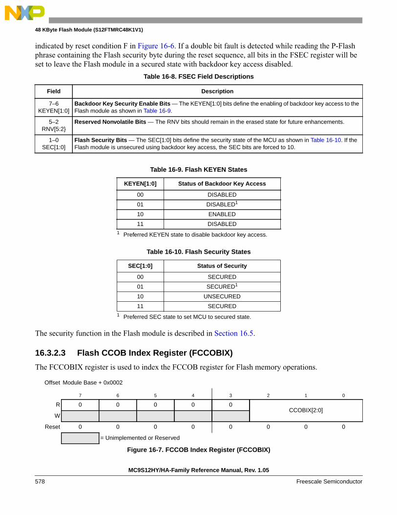
48 KByte Flash Module (S12FTMRC48K1V1)
indicated by reset condition F in Figure 16-6. If a double bit fault is detected while reading the P-Flashphrase containing the Flash security byte during the reset sequence, all bits in the FSEC register will beset to leave the Flash module in a secured state with backdoor key access disabled.
The security function in the Flash module is described in Section 16.5.
16.3.2.3 Flash CCOB Index Register (FCCOBIX)
The FCCOBIX register is used to index the FCCOB register for Flash memory operations.
Table 16-8. FSEC Field Descriptions
Field Description
7–6KEYEN[1:0]
Backdoor Key Security Enable Bits — The KEYEN[1:0] bits define the enabling of backdoor key access to theFlash module as shown in Table 16-9.
5–2RNV[5:2
Reserved Nonvolatile Bits — The RNV bits should remain in the erased state for future enhancements.
1–0SEC[1:0]
Flash Security Bits — The SEC[1:0] bits define the security state of the MCU as shown in Table 16-10. If theFlash module is unsecured using backdoor key access, the SEC bits are forced to 10.
Table 16-9. Flash KEYEN States
KEYEN[1:0] Status of Backdoor Key Access
00 DISABLED
01 DISABLED1
1 Preferred KEYEN state to disable backdoor key access.
10 ENABLED
11 DISABLED
Table 16-10. Flash Security States
SEC[1:0] Status of Security
00 SECURED
01 SECURED1
1 Preferred SEC state to set MCU to secured state.
10 UNSECURED
11 SECURED
Offset Module Base + 0x0002
7 6 5 4 3 2 1 0
R 0 0 0 0 0CCOBIX[2:0]
W
Reset 0 0 0 0 0 0 0 0
= Unimplemented or Reserved
Figure 16-7. FCCOB Index Register (FCCOBIX)
MC9S12HY/HA-Family Reference Manual, Rev. 1.05
578 Freescale Semiconductor

48 KByte Flash Module (S12FTMRC48K1V1)
CCOBIX bits are readable and writable while remaining bits read 0 and are not writable.
16.3.2.4 Flash Reserved0 Register (FRSV0)
This Flash register is reserved for factory testing.
All bits in the FRSV0 register read 0 and are not writable.
16.3.2.5 Flash Configuration Register (FCNFG)
The FCNFG register enables the Flash command complete interrupt and forces ECC faults on Flash arrayread access from the CPU.
CCIE, IGNSF, FDFD, and FSFD bits are readable and writable while remaining bits read 0 and are notwritable.
Table 16-11. FCCOBIX Field Descriptions
Field Description
2–0CCOBIX[1:0]
Common Command Register Index— The CCOBIX bits are used to select which word of the FCCOB registerarray is being read or written to. See Section 16.3.2.11, “Flash Common Command Object Register (FCCOB),”for more details.
Offset Module Base + 0x000C
7 6 5 4 3 2 1 0
R 0 0 0 0 0 0 0 0
W
Reset 0 0 0 0 0 0 0 0
= Unimplemented or Reserved
Figure 16-8. Flash Reserved0 Register (FRSV0)
Offset Module Base + 0x0004
7 6 5 4 3 2 1 0
RCCIE
0 0IGNSF
0 0FDFD FSFD
W
Reset 0 0 0 0 0 0 0 0
= Unimplemented or Reserved
Figure 16-9. Flash Configuration Register (FCNFG)
MC9S12HY/HA-Family Reference Manual, Rev. 1.05
Freescale Semiconductor 579

48 KByte Flash Module (S12FTMRC48K1V1)
16.3.2.6 Flash Error Configuration Register (FERCNFG)
The FERCNFG register enables the Flash error interrupts for the FERSTAT flags.
All assigned bits in the FERCNFG register are readable and writable.
Table 16-12. FCNFG Field Descriptions
Field Description
7CCIE
Command Complete Interrupt Enable — The CCIE bit controls interrupt generation when a Flash commandhas completed.0 Command complete interrupt disabled1 An interrupt will be requested whenever the CCIF flag in the FSTAT register is set (see Section 16.3.2.7)
4IGNSF
Ignore Single Bit Fault — The IGNSF controls single bit fault reporting in the FERSTAT register (seeSection 16.3.2.8).0 All single bit faults detected during array reads are reported1 Single bit faults detected during array reads are not reported and the single bit fault interrupt will not be
generated
1FDFD
Force Double Bit Fault Detect — The FDFD bit allows the user to simulate a double bit fault during Flash arrayread operations and check the associated interrupt routine. The FDFD bit is cleared by writing a 0 to FDFD. TheFECCR registers will not be updated during the Flash array read operation with FDFD set unless an actualdouble bit fault is detected.0 Flash array read operations will set the DFDIF flag in the FERSTAT register only if a double bit fault is detected1 Any Flash array read operation will force the DFDIF flag in the FERSTAT register to be set (see
Section 16.3.2.7) and an interrupt will be generated as long as the DFDIE interrupt enable in the FERCNFGregister is set (see Section 16.3.2.6)
0FSFD
Force Single Bit Fault Detect — The FSFD bit allows the user to simulate a single bit fault during Flash arrayread operations and check the associated interrupt routine. The FSFD bit is cleared by writing a 0 to FSFD. TheFECCR registers will not be updated during the Flash array read operation with FSFD set unless an actual singlebit fault is detected.0 Flash array read operations will set the SFDIF flag in the FERSTAT register only if a single bit fault is detected1 Flash array read operation will force the SFDIF flag in the FERSTAT register to be set (see Section 16.3.2.7)
and an interrupt will be generated as long as the SFDIE interrupt enable in the FERCNFG register is set (seeSection 16.3.2.6)
Offset Module Base + 0x0005
7 6 5 4 3 2 1 0
R 0 0 0 0 0 0DFDIE SFDIE
W
Reset 0 0 0 0 0 0 0 0
= Unimplemented or Reserved
Figure 16-10. Flash Error Configuration Register (FERCNFG)
MC9S12HY/HA-Family Reference Manual, Rev. 1.05
580 Freescale Semiconductor
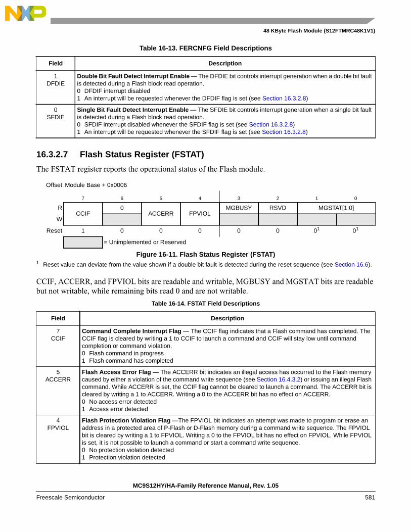
48 KByte Flash Module (S12FTMRC48K1V1)
16.3.2.7 Flash Status Register (FSTAT)
The FSTAT register reports the operational status of the Flash module.
CCIF, ACCERR, and FPVIOL bits are readable and writable, MGBUSY and MGSTAT bits are readablebut not writable, while remaining bits read 0 and are not writable.
Table 16-13. FERCNFG Field Descriptions
Field Description
1DFDIE
Double Bit Fault Detect Interrupt Enable — The DFDIE bit controls interrupt generation when a double bit faultis detected during a Flash block read operation.0 DFDIF interrupt disabled1 An interrupt will be requested whenever the DFDIF flag is set (see Section 16.3.2.8)
0SFDIE
Single Bit Fault Detect Interrupt Enable — The SFDIE bit controls interrupt generation when a single bit faultis detected during a Flash block read operation.0 SFDIF interrupt disabled whenever the SFDIF flag is set (see Section 16.3.2.8)1 An interrupt will be requested whenever the SFDIF flag is set (see Section 16.3.2.8)
Offset Module Base + 0x0006
7 6 5 4 3 2 1 0
RCCIF
0ACCERR FPVIOL
MGBUSY RSVD MGSTAT[1:0]
W
Reset 1 0 0 0 0 0 01
1 Reset value can deviate from the value shown if a double bit fault is detected during the reset sequence (see Section 16.6).
01
= Unimplemented or Reserved
Figure 16-11. Flash Status Register (FSTAT)
Table 16-14. FSTAT Field Descriptions
Field Description
7CCIF
Command Complete Interrupt Flag — The CCIF flag indicates that a Flash command has completed. TheCCIF flag is cleared by writing a 1 to CCIF to launch a command and CCIF will stay low until commandcompletion or command violation.0 Flash command in progress1 Flash command has completed
5ACCERR
Flash Access Error Flag — The ACCERR bit indicates an illegal access has occurred to the Flash memorycaused by either a violation of the command write sequence (see Section 16.4.3.2) or issuing an illegal Flashcommand. While ACCERR is set, the CCIF flag cannot be cleared to launch a command. The ACCERR bit iscleared by writing a 1 to ACCERR. Writing a 0 to the ACCERR bit has no effect on ACCERR.0 No access error detected1 Access error detected
4FPVIOL
Flash Protection Violation Flag —The FPVIOL bit indicates an attempt was made to program or erase anaddress in a protected area of P-Flash or D-Flash memory during a command write sequence. The FPVIOLbit is cleared by writing a 1 to FPVIOL. Writing a 0 to the FPVIOL bit has no effect on FPVIOL. While FPVIOLis set, it is not possible to launch a command or start a command write sequence.0 No protection violation detected1 Protection violation detected
MC9S12HY/HA-Family Reference Manual, Rev. 1.05
Freescale Semiconductor 581
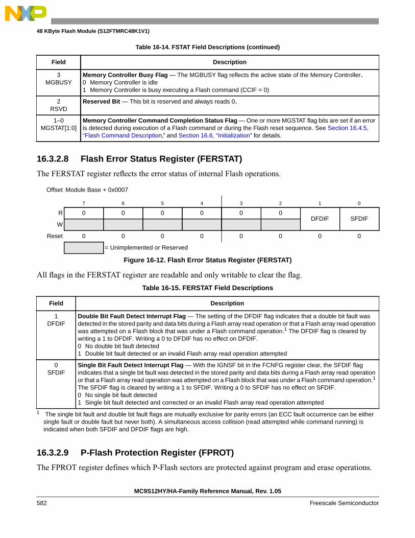
48 KByte Flash Module (S12FTMRC48K1V1)
16.3.2.8 Flash Error Status Register (FERSTAT)
The FERSTAT register reflects the error status of internal Flash operations.
All flags in the FERSTAT register are readable and only writable to clear the flag.
16.3.2.9 P-Flash Protection Register (FPROT)
The FPROT register defines which P-Flash sectors are protected against program and erase operations.
3MGBUSY
Memory Controller Busy Flag — The MGBUSY flag reflects the active state of the Memory Controller.0 Memory Controller is idle1 Memory Controller is busy executing a Flash command (CCIF = 0)
2RSVD
Reserved Bit — This bit is reserved and always reads 0.
1–0MGSTAT[1:0]
Memory Controller Command Completion Status Flag — One or more MGSTAT flag bits are set if an erroris detected during execution of a Flash command or during the Flash reset sequence. See Section 16.4.5,“Flash Command Description,” and Section 16.6, “Initialization” for details.
Offset Module Base + 0x0007
7 6 5 4 3 2 1 0
R 0 0 0 0 0 0DFDIF SFDIF
W
Reset 0 0 0 0 0 0 0 0
= Unimplemented or Reserved
Figure 16-12. Flash Error Status Register (FERSTAT)
Table 16-15. FERSTAT Field Descriptions
Field Description
1DFDIF
Double Bit Fault Detect Interrupt Flag — The setting of the DFDIF flag indicates that a double bit fault wasdetected in the stored parity and data bits during a Flash array read operation or that a Flash array read operationwas attempted on a Flash block that was under a Flash command operation.1 The DFDIF flag is cleared bywriting a 1 to DFDIF. Writing a 0 to DFDIF has no effect on DFDIF.0 No double bit fault detected1 Double bit fault detected or an invalid Flash array read operation attempted
1 The single bit fault and double bit fault flags are mutually exclusive for parity errors (an ECC fault occurrence can be eithersingle fault or double fault but never both). A simultaneous access collision (read attempted while command running) isindicated when both SFDIF and DFDIF flags are high.
0SFDIF
Single Bit Fault Detect Interrupt Flag — With the IGNSF bit in the FCNFG register clear, the SFDIF flagindicates that a single bit fault was detected in the stored parity and data bits during a Flash array read operationor that a Flash array read operation was attempted on a Flash block that was under a Flash command operation.1
The SFDIF flag is cleared by writing a 1 to SFDIF. Writing a 0 to SFDIF has no effect on SFDIF.0 No single bit fault detected1 Single bit fault detected and corrected or an invalid Flash array read operation attempted
Table 16-14. FSTAT Field Descriptions (continued)
Field Description
MC9S12HY/HA-Family Reference Manual, Rev. 1.05
582 Freescale Semiconductor

48 KByte Flash Module (S12FTMRC48K1V1)
The (unreserved) bits of the FPROT register are writable with the restriction that the size of the protectedregion can only be increased (see Section 16.3.2.9.1, “P-Flash Protection Restrictions,” and Table 16-20).
During the reset sequence, the FPROT register is loaded with the contents of the P-Flash protection bytein the Flash configuration field at global address 0x3_FF0C located in P-Flash memory (see Table 16-3)as indicated by reset condition ‘F’ in Figure 16-13. To change the P-Flash protection that will be loadedduring the reset sequence, the upper sector of the P-Flash memory must be unprotected, then the P-Flashprotection byte must be reprogrammed. If a double bit fault is detected while reading the P-Flash phrasecontaining the P-Flash protection byte during the reset sequence, the FPOPEN bit will be cleared andremaining bits in the FPROT register will be set to leave the P-Flash memory fully protected.
Trying to alter data in any protected area in the P-Flash memory will result in a protection violation errorand the FPVIOL bit will be set in the FSTAT register. The block erase of a P-Flash block is not possibleif any of the P-Flash sectors contained in the same P-Flash block are protected.
Offset Module Base + 0x0008
7 6 5 4 3 2 1 0
RFPOPEN
RNV6FPHDIS FPHS[1:0] FPLDIS FPLS[1:0]
W
Reset F F F F F F F F
= Unimplemented or Reserved
Figure 16-13. Flash Protection Register (FPROT)
Table 16-16. FPROT Field Descriptions
Field Description
6RNV[6]
Reserved Nonvolatile Bit — The RNV bit should remain in the erased state for future enhancements.
5FPHDIS
Flash Protection Higher Address Range Disable — The FPHDIS bit determines whether there is aprotected/unprotected area in a specific region of the P-Flash memory ending with global address 0x3_FFFF.0 Protection/Unprotection enabled1 Protection/Unprotection disabled
4–3FPHS[1:0]
Flash Protection Higher Address Size — The FPHS bits determine the size of the protected/unprotected areain P-Flash memory as shown inTable 16-18. The FPHS bits can only be written to while the FPHDIS bit is set.
Table 16-17. P-Flash Protection Function
FPOPEN FPHDIS FPLDIS Function1
1 1 1 No P-Flash Protection
1 1 0 Protected Low Range
1 0 1 Protected High Range
1 0 0 Protected High and Low Ranges
0 1 1 Full P-Flash Memory Protected
0 1 0 Unprotected Low Range
0 0 1 Unprotected High Range
0 0 0 Unprotected High and Low Ranges
MC9S12HY/HA-Family Reference Manual, Rev. 1.05
Freescale Semiconductor 583

48 KByte Flash Module (S12FTMRC48K1V1)
All possible P-Flash protection scenarios are shown in Figure 16-14. Although the protection scheme isloaded from the Flash memory at global address 0x3_FF0C during the reset sequence, it can be changedby the user. The P-Flash protection scheme can be used by applications requiring reprogramming in singlechip mode while providing as much protection as possible if reprogramming is not required.
1 For range sizes, refer to Table 16-18 and Table 16-19.
Table 16-18. P-Flash Protection Higher Address Range
FPHS[1:0] Global Address Range Protected Size
00 0x3_F800–0x3_FFFF 2 Kbytes
01 0x3_F000–0x3_FFFF 4 Kbytes
10 0x3_E000–0x3_FFFF 8 Kbytes
11 0x3_C000–0x3_FFFF 16 Kbytes
Table 16-19. P-Flash Protection Lower Address Range
FPLS[1:0] Global Address Range Protected Size
00 0x3_8000–0x3_83FF 1 Kbyte
01 0x3_8000–0x3_87FF 2 Kbytes
10 0x3_8000–0x3_8FFF 4 Kbytes
11 0x3_8000–0x3_9FFF 8 Kbytes
MC9S12HY/HA-Family Reference Manual, Rev. 1.05
584 Freescale Semiconductor

48 KByte Flash Module (S12FTMRC48K1V1)
Figure 16-14. P-Flash Protection Scenarios
7 6 5 4
FP
HS
[1:0
]F
PLS
[1:0
]
3 2 1 0
FP
HS
[1:0
]F
PLS
[1:0
]
FPHDIS = 1FPLDIS = 1
FPHDIS = 1FPLDIS = 0
FPHDIS = 0FPLDIS = 1
FPHDIS = 0FPLDIS = 0
Scenario
Scenario
Unprotected region Protected region with size
Protected region Protected region with size
defined by FPLS
defined by FPHSnot defined by FPLS, FPHS
0x3_8000
0x3_FFFF
0x3_8000
0x3_FFFF
FLASH START
FLASH START
FP
OP
EN
= 1
FP
OP
EN
= 0
MC9S12HY/HA-Family Reference Manual, Rev. 1.05
Freescale Semiconductor 585
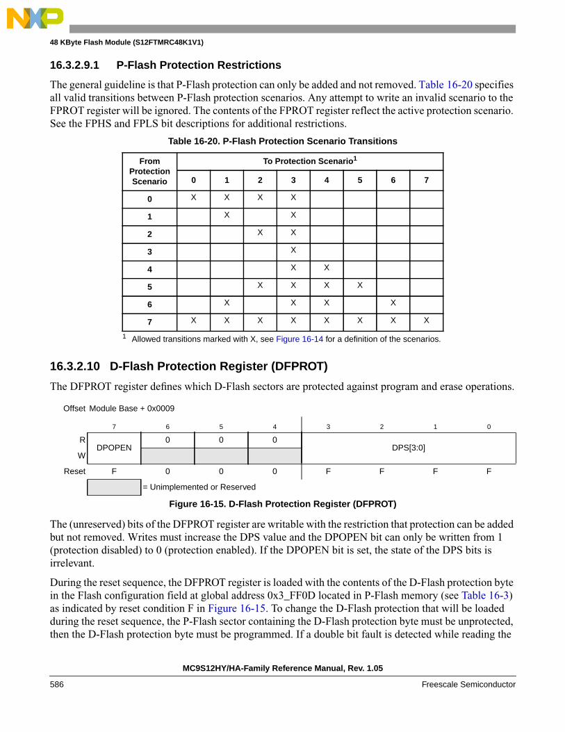
48 KByte Flash Module (S12FTMRC48K1V1)
16.3.2.9.1 P-Flash Protection Restrictions
The general guideline is that P-Flash protection can only be added and not removed. Table 16-20 specifiesall valid transitions between P-Flash protection scenarios. Any attempt to write an invalid scenario to theFPROT register will be ignored. The contents of the FPROT register reflect the active protection scenario.See the FPHS and FPLS bit descriptions for additional restrictions.
16.3.2.10 D-Flash Protection Register (DFPROT)
The DFPROT register defines which D-Flash sectors are protected against program and erase operations.
The (unreserved) bits of the DFPROT register are writable with the restriction that protection can be addedbut not removed. Writes must increase the DPS value and the DPOPEN bit can only be written from 1(protection disabled) to 0 (protection enabled). If the DPOPEN bit is set, the state of the DPS bits isirrelevant.
During the reset sequence, the DFPROT register is loaded with the contents of the D-Flash protection bytein the Flash configuration field at global address 0x3_FF0D located in P-Flash memory (see Table 16-3)as indicated by reset condition F in Figure 16-15. To change the D-Flash protection that will be loadedduring the reset sequence, the P-Flash sector containing the D-Flash protection byte must be unprotected,then the D-Flash protection byte must be programmed. If a double bit fault is detected while reading the
Table 16-20. P-Flash Protection Scenario Transitions
FromProtectionScenario
To Protection Scenario1
1 Allowed transitions marked with X, see Figure 16-14 for a definition of the scenarios.
0 1 2 3 4 5 6 7
0 X X X X
1 X X
2 X X
3 X
4 X X
5 X X X X
6 X X X X
7 X X X X X X X X
Offset Module Base + 0x0009
7 6 5 4 3 2 1 0
RDPOPEN
0 0 0DPS[3:0]
W
Reset F 0 0 0 F F F F
= Unimplemented or Reserved
Figure 16-15. D-Flash Protection Register (DFPROT)
MC9S12HY/HA-Family Reference Manual, Rev. 1.05
586 Freescale Semiconductor

48 KByte Flash Module (S12FTMRC48K1V1)
P-Flash phrase containing the D-Flash protection byte during the reset sequence, the DPOPEN bit will becleared and DPS bits will be set to leave the D-Flash memory fully protected.
Trying to alter data in any protected area in the D-Flash memory will result in a protection violation errorand the FPVIOL bit will be set in the FSTAT register. Block erase of the D-Flash memory is not possibleif any of the D-Flash sectors are protected.
16.3.2.11 Flash Common Command Object Register (FCCOB)
The FCCOB is an array of six words addressed via the CCOBIX index found in the FCCOBIX register.Byte wide reads and writes are allowed to the FCCOB register.
Table 16-21. DFPROT Field Descriptions
Field Description
7DPOPEN
D-Flash Protection Control0 Enables D-Flash memory protection from program and erase with protected address range defined by DPS
bits1 Disables D-Flash memory protection from program and erase
3–0DPS[3:0]
D-Flash Protection Size — The DPS[3:0] bits determine the size of the protected area in the D-Flash memoryas shown in Table 16-22.
Table 16-22. D-Flash Protection Address Range
DPS[3:0] Global Address Range Protected Size
0000 0x0_4400 – 0x0_44FF 256 bytes
0001 0x0_4400 – 0x0_45FF 512 bytes
0010 0x0_4400 – 0x0_46FF 768 bytes
0011 0x0_4400 – 0x0_47FF 1024 bytes
0100 0x0_4400 – 0x0_48FF 1280 bytes
0101 0x0_4400 – 0x0_49FF 1536 bytes
0110 0x0_4400 – 0x0_4AFF 1792 bytes
0111 0x0_4400 – 0x0_4BFF 2048 bytes
1000 0x0_4400 – 0x0_4CFF 2304 bytes
1001 0x0_4400 – 0x0_4DFF 2560 bytes
1010 0x0_4400 – 0x0_4EFF 2816 bytes
1011 0x0_4400 – 0x0_4FFF 3072 bytes
1100 0x0_4400 – 0x0_50FF 3328 bytes
1101 0x0_4400 – 0x0_51FF 3584 bytes
1110 0x0_4400 – 0x0_52FF 3840 bytes
1111 0x0_4400 – 0x0_53FF 4096 bytes
MC9S12HY/HA-Family Reference Manual, Rev. 1.05
Freescale Semiconductor 587
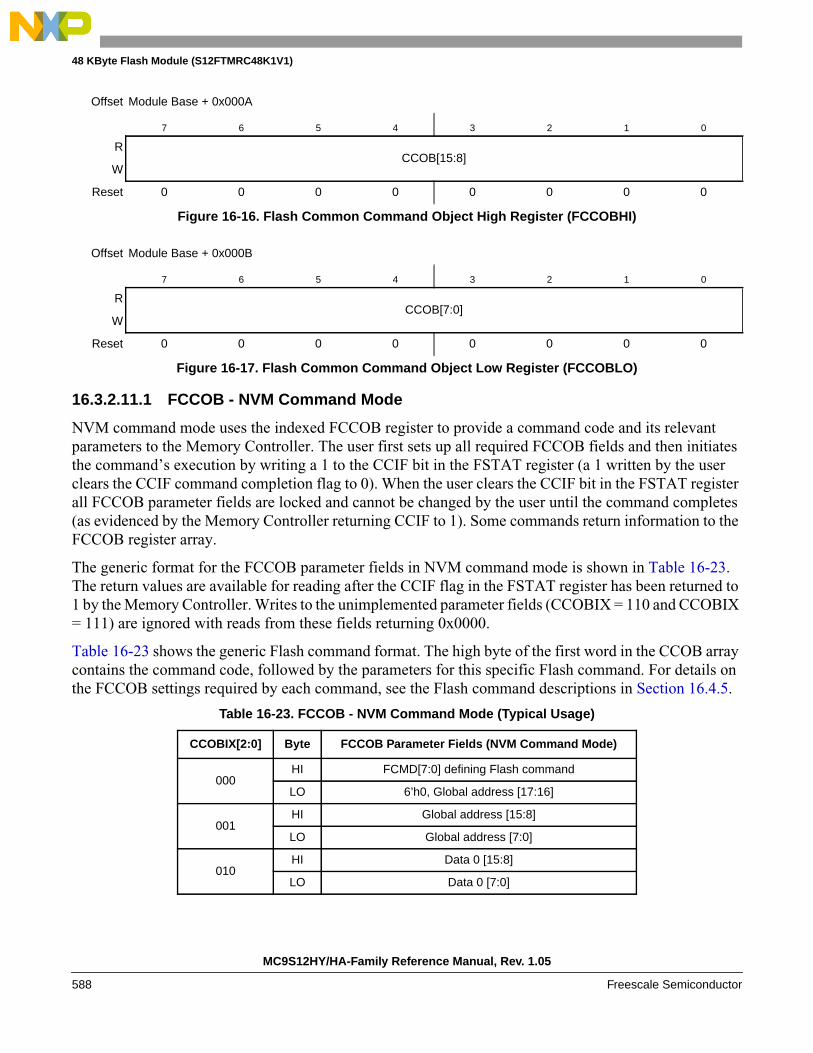
48 KByte Flash Module (S12FTMRC48K1V1)
16.3.2.11.1 FCCOB - NVM Command Mode
NVM command mode uses the indexed FCCOB register to provide a command code and its relevantparameters to the Memory Controller. The user first sets up all required FCCOB fields and then initiatesthe command’s execution by writing a 1 to the CCIF bit in the FSTAT register (a 1 written by the userclears the CCIF command completion flag to 0). When the user clears the CCIF bit in the FSTAT registerall FCCOB parameter fields are locked and cannot be changed by the user until the command completes(as evidenced by the Memory Controller returning CCIF to 1). Some commands return information to theFCCOB register array.
The generic format for the FCCOB parameter fields in NVM command mode is shown in Table 16-23.The return values are available for reading after the CCIF flag in the FSTAT register has been returned to1 by the Memory Controller. Writes to the unimplemented parameter fields (CCOBIX = 110 and CCOBIX= 111) are ignored with reads from these fields returning 0x0000.
Table 16-23 shows the generic Flash command format. The high byte of the first word in the CCOB arraycontains the command code, followed by the parameters for this specific Flash command. For details onthe FCCOB settings required by each command, see the Flash command descriptions in Section 16.4.5.
Offset Module Base + 0x000A
7 6 5 4 3 2 1 0
RCCOB[15:8]
W
Reset 0 0 0 0 0 0 0 0
Figure 16-16. Flash Common Command Object High Register (FCCOBHI)
Offset Module Base + 0x000B
7 6 5 4 3 2 1 0
RCCOB[7:0]
W
Reset 0 0 0 0 0 0 0 0
Figure 16-17. Flash Common Command Object Low Register (FCCOBLO)
Table 16-23. FCCOB - NVM Command Mode (Typical Usage)
CCOBIX[2:0] Byte FCCOB Parameter Fields (NVM Command Mode)
000HI FCMD[7:0] defining Flash command
LO 6’h0, Global address [17:16]
001HI Global address [15:8]
LO Global address [7:0]
010HI Data 0 [15:8]
LO Data 0 [7:0]
MC9S12HY/HA-Family Reference Manual, Rev. 1.05
588 Freescale Semiconductor
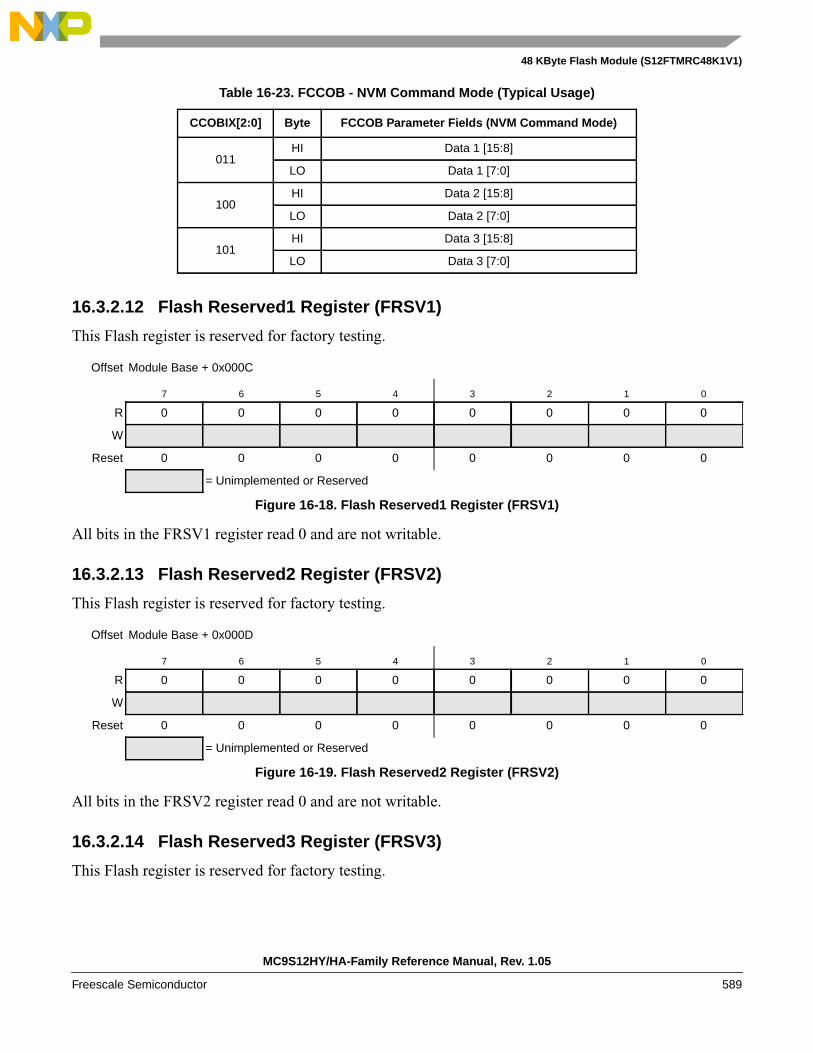
48 KByte Flash Module (S12FTMRC48K1V1)
16.3.2.12 Flash Reserved1 Register (FRSV1)
This Flash register is reserved for factory testing.
All bits in the FRSV1 register read 0 and are not writable.
16.3.2.13 Flash Reserved2 Register (FRSV2)
This Flash register is reserved for factory testing.
All bits in the FRSV2 register read 0 and are not writable.
16.3.2.14 Flash Reserved3 Register (FRSV3)
This Flash register is reserved for factory testing.
011HI Data 1 [15:8]
LO Data 1 [7:0]
100HI Data 2 [15:8]
LO Data 2 [7:0]
101HI Data 3 [15:8]
LO Data 3 [7:0]
Offset Module Base + 0x000C
7 6 5 4 3 2 1 0
R 0 0 0 0 0 0 0 0
W
Reset 0 0 0 0 0 0 0 0
= Unimplemented or Reserved
Figure 16-18. Flash Reserved1 Register (FRSV1)
Offset Module Base + 0x000D
7 6 5 4 3 2 1 0
R 0 0 0 0 0 0 0 0
W
Reset 0 0 0 0 0 0 0 0
= Unimplemented or Reserved
Figure 16-19. Flash Reserved2 Register (FRSV2)
Table 16-23. FCCOB - NVM Command Mode (Typical Usage)
CCOBIX[2:0] Byte FCCOB Parameter Fields (NVM Command Mode)
MC9S12HY/HA-Family Reference Manual, Rev. 1.05
Freescale Semiconductor 589

48 KByte Flash Module (S12FTMRC48K1V1)
All bits in the FRSV3 register read 0 and are not writable.
16.3.2.15 Flash Reserved4 Register (FRSV4)
This Flash register is reserved for factory testing.
All bits in the FRSV4 register read 0 and are not writable.
16.3.2.16 Flash Option Register (FOPT)
The FOPT register is the Flash option register.
All bits in the FOPT register are readable but are not writable.
During the reset sequence, the FOPT register is loaded from the Flash nonvolatile byte in the Flashconfiguration field at global address 0x3_FF0E located in P-Flash memory (see Table 16-3) as indicatedby reset condition F in Figure 16-22. If a double bit fault is detected while reading the P-Flash phrasecontaining the Flash nonvolatile byte during the reset sequence, all bits in the FOPT register will be set.
Offset Module Base + 0x000E
7 6 5 4 3 2 1 0
R 0 0 0 0 0 0 0 0
W
Reset 0 0 0 0 0 0 0 0
= Unimplemented or Reserved
Figure 16-20. Flash Reserved3 Register (FRSV3)
Offset Module Base + 0x000F
7 6 5 4 3 2 1 0
R 0 0 0 0 0 0 0 0
W
Reset 0 0 0 0 0 0 0 0
= Unimplemented or Reserved
Figure 16-21. Flash Reserved4 Register (FRSV4)
Offset Module Base + 0x0010
7 6 5 4 3 2 1 0
R NV[7:0]
W
Reset F F F F F F F F
= Unimplemented or Reserved
Figure 16-22. Flash Option Register (FOPT)
MC9S12HY/HA-Family Reference Manual, Rev. 1.05
590 Freescale Semiconductor
48 KByte Flash Module (S12FTMRC48K1V1)
16.3.2.17 Flash Reserved5 Register (FRSV5)
This Flash register is reserved for factory testing.
All bits in the FRSV5 register read 0 and are not writable.
16.3.2.18 Flash Reserved6 Register (FRSV6)
This Flash register is reserved for factory testing.
All bits in the FRSV6 register read 0 and are not writable.
16.3.2.19 Flash Reserved7 Register (FRSV7)
This Flash register is reserved for factory testing.
Table 16-24. FOPT Field Descriptions
Field Description
7–0NV[7:0]
Nonvolatile Bits — The NV[7:0] bits are available as nonvolatile bits. Refer to the device user guide for properuse of the NV bits.
Offset Module Base + 0x0011
7 6 5 4 3 2 1 0
R 0 0 0 0 0 0 0 0
W
Reset 0 0 0 0 0 0 0 0
= Unimplemented or Reserved
Figure 16-23. Flash Reserved5 Register (FRSV5)
Offset Module Base + 0x0012
7 6 5 4 3 2 1 0
R 0 0 0 0 0 0 0 0
W
Reset 0 0 0 0 0 0 0 0
= Unimplemented or Reserved
Figure 16-24. Flash Reserved6 Register (FRSV6)
MC9S12HY/HA-Family Reference Manual, Rev. 1.05
Freescale Semiconductor 591

48 KByte Flash Module (S12FTMRC48K1V1)
All bits in the FRSV7 register read 0 and are not writable.
16.4 Functional Description
16.4.1 Modes of Operation
The FTMRC48K1 module provides the modes of operation shown in Table 16-25. The operating mode isdetermined by module-level inputs and affects the FCLKDIV, FCNFG, and DFPROT registers, ScratchRAM writes, and the command set availability (see Table 16-27).
16.4.2 IFR Version ID Word
The version ID word is stored in the IFR at address 0x0_40B6. The contents of the word are defined inTable 16-26.
• VERNUM: Version number. The first version is number 0b_0001 with both 0b_0000 and 0b_1111meaning ‘none’.
16.4.3 Flash Command Operations
Flash command operations are used to modify Flash memory contents.
Offset Module Base + 0x0013
7 6 5 4 3 2 1 0
R 0 0 0 0 0 0 0 0
W
Reset 0 0 0 0 0 0 0 0
= Unimplemented or Reserved
Figure 16-25. Flash Reserved7 Register (FRSV7)
Table 16-25. Modes and Mode Control Inputs
OperatingMode
FTMRC Input
mmc_mode_ss_t2
Normal: 0
Special: 1
Table 16-26. IFR Version ID Fields
[15:4] [3:0]
Reserved VERNUM
MC9S12HY/HA-Family Reference Manual, Rev. 1.05
592 Freescale Semiconductor

48 KByte Flash Module (S12FTMRC48K1V1)
The next sections describe:
• How to write the FCLKDIV register that is used to generate a time base (FCLK) derived fromBUSCLK for Flash program and erase command operations
• The command write sequence used to set Flash command parameters and launch execution
• Valid Flash commands available for execution
16.4.3.1 Writing the FCLKDIV Register
Prior to issuing any Flash program or erase command after a reset, the user is required to write theFCLKDIV register to divide BUSCLK down to a target FCLK of 1 MHz. Table 16-7 shows recommendedvalues for the FDIV field based on BUSCLK frequency.
NOTEProgramming or erasing the Flash memory cannot be performed if the busclock runs at less than 0.8 MHz. Setting FDIV too high can destroy the Flashmemory due to overstress. Setting FDIV too low can result in incompleteprogramming or erasure of the Flash memory cells.
When the FCLKDIV register is written, the FDIVLD bit is set automatically. If the FDIVLD bit is 0, theFCLKDIV register has not been written since the last reset. If the FCLKDIV register has not been written,any Flash program or erase command loaded during a command write sequence will not execute and theACCERR bit in the FSTAT register will set.
16.4.3.2 Command Write Sequence
The Memory Controller will launch all valid Flash commands entered using a command write sequence.
Before launching a command, the ACCERR and FPVIOL bits in the FSTAT register must be clear (seeSection 16.3.2.7) and the CCIF flag should be tested to determine the status of the current command writesequence. If CCIF is 0, the previous command write sequence is still active, a new command writesequence cannot be started, and all writes to the FCCOB register are ignored.
CAUTIONWrites to any Flash register must be avoided while a Flash command isactive (CCIF=0) to prevent corruption of Flash register contents andMemory Controller behavior.
16.4.3.2.1 Define FCCOB Contents
The FCCOB parameter fields must be loaded with all required parameters for the Flash command beingexecuted. Access to the FCCOB parameter fields is controlled via the CCOBIX bits in the FCCOBIXregister (see Section 16.3.2.3).
The contents of the FCCOB parameter fields are transferred to the Memory Controller when the user clearsthe CCIF command completion flag in the FSTAT register (writing 1 clears the CCIF to 0). The CCIF flagwill remain clear until the Flash command has completed. Upon completion, the Memory Controller will
MC9S12HY/HA-Family Reference Manual, Rev. 1.05
Freescale Semiconductor 593

48 KByte Flash Module (S12FTMRC48K1V1)
return CCIF to 1 and the FCCOB register will be used to communicate any results. The flow for a genericcommand write sequence is shown in Figure 16-26.
MC9S12HY/HA-Family Reference Manual, Rev. 1.05
594 Freescale Semiconductor
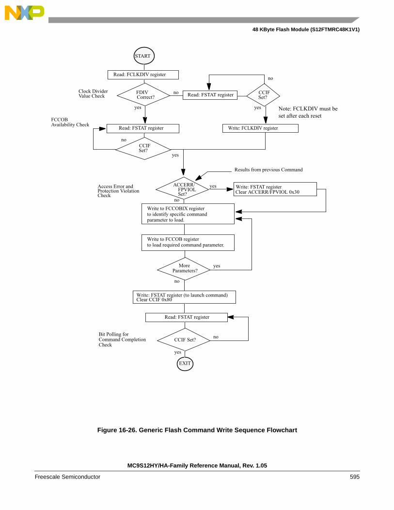
48 KByte Flash Module (S12FTMRC48K1V1)
Figure 16-26. Generic Flash Command Write Sequence Flowchart
Write to FCCOBIX register
Write: FSTAT register (to launch command)Clear CCIF 0x80
Clear ACCERR/FPVIOL 0x30Write: FSTAT registeryes
no
Access Error andProtection Violation
Read: FSTAT register
START
Check
FCCOB
ACCERR/FPVIOLSet?
EXIT
Write: FCLKDIV register
Read: FCLKDIV register
yes
noFDIVCorrect?
noBit Polling forCommand CompletionCheck
yes
CCIF Set?
to identify specific commandparameter to load.
Write to FCCOB registerto load required command parameter.
yes
no
MoreParameters?
Availability Check
Results from previous Command
Note: FCLKDIV must beset after each reset
Read: FSTAT register
no
yes
CCIFSet?
no
yes
CCIFSet?
Clock DividerValue Check Read: FSTAT register
MC9S12HY/HA-Family Reference Manual, Rev. 1.05
Freescale Semiconductor 595

48 KByte Flash Module (S12FTMRC48K1V1)
16.4.3.3 Valid Flash Module Commands
16.4.3.4 P-Flash Commands
Table 16-28 summarizes the valid P-Flash commands along with the effects of the commands on theP-Flash block and other resources within the Flash module.
Table 16-27. Flash Commands by Mode
FCMD CommandUnsecured Secured
NS1
1 Unsecured Normal Single Chip mode.
SS2
2 Unsecured Special Single Chip mode.
NS3
3 Secured Normal Single Chip mode.
SS4
4 Secured Special Single Chip mode.
0x01 Erase Verify All Blocks ∗ ∗ ∗ ∗
0x02 Erase Verify Block ∗ ∗ ∗ ∗
0x03 Erase Verify P-Flash Section ∗ ∗ ∗
0x04 Read Once ∗ ∗ ∗
0x06 Program P-Flash ∗ ∗ ∗
0x07 Program Once ∗ ∗ ∗
0x08 Erase All Blocks ∗ ∗
0x09 Erase Flash Block ∗ ∗ ∗
0x0A Erase P-Flash Sector ∗ ∗ ∗
0x0B Unsecure Flash ∗ ∗
0x0C Verify Backdoor Access Key ∗ ∗
0x0D Set User Margin Level ∗ ∗ ∗
0x0E Set Field Margin Level ∗
0x10 Erase Verify D-Flash Section ∗ ∗ ∗
0x11 Program D-Flash ∗ ∗ ∗
0x12 Erase D-Flash Sector ∗ ∗ ∗
Table 16-28. P-Flash Commands
FCMD Command Function on P-Flash Memory
0x01Erase Verify All
BlocksVerify that all P-Flash (and D-Flash) blocks are erased.
0x02 Erase Verify Block Verify that a P-Flash block is erased.
0x03Erase Verify
P-Flash SectionVerify that a given number of words starting at the address provided are erased.
MC9S12HY/HA-Family Reference Manual, Rev. 1.05
596 Freescale Semiconductor

48 KByte Flash Module (S12FTMRC48K1V1)
16.4.3.5 D-Flash Commands
Table 16-29 summarizes the valid D-Flash commands along with the effects of the commands on theD-Flash block.
0x04 Read OnceRead a dedicated 64 byte field in the nonvolatile information register in P-Flash block thatwas previously programmed using the Program Once command.
0x06 Program P-Flash Program a phrase in a P-Flash block.
0x07 Program OnceProgram a dedicated 64 byte field in the nonvolatile information register in P-Flash blockthat is allowed to be programmed only once.
0x08 Erase All Blocks
Erase all P-Flash (and D-Flash) blocks.An erase of all Flash blocks is only possible when the FPLDIS, FPHDIS, and FPOPENbits in the FPROT register and the DPOPEN bit in the DFPROT register are set prior tolaunching the command.
0x09 Erase Flash BlockErase a P-Flash (or D-Flash) block.An erase of the full P-Flash block is only possible when FPLDIS, FPHDIS and FPOPENbits in the FPROT register are set prior to launching the command.
0x0AErase P-Flash
SectorErase all bytes in a P-Flash sector.
0x0B Unsecure FlashSupports a method of releasing MCU security by erasing all P-Flash (and D-Flash) blocksand verifying that all P-Flash (and D-Flash) blocks are erased.
0x0CVerify Backdoor
Access KeySupports a method of releasing MCU security by verifying a set of security keys.
0x0DSet User Margin
LevelSpecifies a user margin read level for all P-Flash blocks.
0x0ESet Field Margin
LevelSpecifies a field margin read level for all P-Flash blocks (special modes only).
Table 16-29. D-Flash Commands
FCMD Command Function on D-Flash Memory
0x01Erase Verify All
BlocksVerify that all D-Flash (and P-Flash) blocks are erased.
0x02 Erase Verify Block Verify that the D-Flash block is erased.
0x08 Erase All Blocks
Erase all D-Flash (and P-Flash) blocks.An erase of all Flash blocks is only possible when the FPLDIS, FPHDIS, and FPOPENbits in the FPROT register and the DPOPEN bit in the DFPROT register are set prior tolaunching the command.
0x09 Erase Flash BlockErase a D-Flash (or P-Flash) block.An erase of the full D-Flash block is only possible when DPOPEN bit in the DFPROTregister is set prior to launching the command.
0x0B Unsecure FlashSupports a method of releasing MCU security by erasing all D-Flash (and P-Flash) blocksand verifying that all D-Flash (and P-Flash) blocks are erased.
0x0DSet User Margin
LevelSpecifies a user margin read level for the D-Flash block.
0x0ESet Field Margin
LevelSpecifies a field margin read level for the D-Flash block (special modes only).
Table 16-28. P-Flash Commands
FCMD Command Function on P-Flash Memory
MC9S12HY/HA-Family Reference Manual, Rev. 1.05
Freescale Semiconductor 597
48 KByte Flash Module (S12FTMRC48K1V1)
16.4.4 Allowed Simultaneous P-Flash and D-Flash Operations
Only the operations marked ‘OK’ in Table 16-30 are permitted to be run simultaneously on the ProgramFlash and Data Flash blocks. Some operations cannot be executed simultaneously because certainhardware resources are shared by the two memories. The priority has been placed on permitting ProgramFlash reads while program and erase operations execute on the Data Flash, providing read (P-Flash) whilewrite (D-Flash) functionality.
16.4.5 Flash Command Description
This section provides details of all available Flash commands launched by a command write sequence. TheACCERR bit in the FSTAT register will be set during the command write sequence if any of the followingillegal steps are performed, causing the command not to be processed by the Memory Controller:
• Starting any command write sequence that programs or erases Flash memory before initializing theFCLKDIV register
• Writing an invalid command as part of the command write sequence
• For additional possible errors, refer to the error handling table provided for each command
0x10Erase Verify
D-Flash SectionVerify that a given number of words starting at the address provided are erased.
0x11 Program D-Flash Program up to four words in the D-Flash block.
0x12Erase D-Flash
SectorErase all bytes in a sector of the D-Flash block.
Table 16-30. Allowed P-Flash and D-Flash Simultaneous Operations
Data Flash
Program Flash ReadMarginRead1 Program
SectorErase
MassErase3
Read OK OK OK
Margin Read1
1 A ‘Margin Read’ is any read after executing the margin setting commands‘Set User Margin Level’ or ‘Set Field Margin Level’ with anything but the‘normal’ level specified.
OK2
2 See the Note on margin settings in Section 16.4.5.12 and Section 16.4.5.13.
Program
Sector Erase OK
Mass Erase3
3 The ‘Mass Erase’ operations are commands ‘Erase All Blocks’ and ‘EraseFlash Block’
OK
Table 16-29. D-Flash Commands
FCMD Command Function on D-Flash Memory
MC9S12HY/HA-Family Reference Manual, Rev. 1.05
598 Freescale Semiconductor
48 KByte Flash Module (S12FTMRC48K1V1)
If a Flash block is read during execution of an algorithm (CCIF = 0) on that same block, the read operationwill return invalid data. If the SFDIF or DFDIF flags were not previously set when the invalid readoperation occurred, both the SFDIF and DFDIF flags will be set.
If the ACCERR or FPVIOL bits are set in the FSTAT register, the user must clear these bits before startingany command write sequence (see Section 16.3.2.7).
CAUTIONA Flash word or phrase must be in the erased state before beingprogrammed. Cumulative programming of bits within a Flash word orphrase is not allowed.
16.4.5.1 Erase Verify All Blocks Command
The Erase Verify All Blocks command will verify that all P-Flash and D-Flash blocks have been erased.
Upon clearing CCIF to launch the Erase Verify All Blocks command, the Memory Controller will verifythat the entire Flash memory space is erased. The CCIF flag will set after the Erase Verify All Blocksoperation has completed.
16.4.5.2 Erase Verify Block Command
The Erase Verify Block command allows the user to verify that an entire P-Flash or D-Flash block has beenerased. The FCCOB upper global address bits determine which block must be verified.
Table 16-31. Erase Verify All Blocks Command FCCOB Requirements
CCOBIX[2:0] FCCOB Parameters
000 0x01 Not required
Table 16-32. Erase Verify All Blocks Command Error Handling
Register Error Bit Error Condition
FSTAT
ACCERR Set if CCOBIX[2:0] != 000 at command launch
FPVIOL None
MGSTAT1 Set if any errors have been encountered during the read1
1 As found in the memory map for FTMRC64K1.
MGSTAT0 Set if any non-correctable errors have been encountered during the read1
Table 16-33. Erase Verify Block Command FCCOB Requirements
CCOBIX[2:0] FCCOB Parameters
000 0x02Global address [17:16] of the
Flash block to be verified.
MC9S12HY/HA-Family Reference Manual, Rev. 1.05
Freescale Semiconductor 599
48 KByte Flash Module (S12FTMRC48K1V1)
Upon clearing CCIF to launch the Erase Verify Block command, the Memory Controller will verify thatthe selected P-Flash or D-Flash block is erased. The CCIF flag will set after the Erase Verify Blockoperation has completed.
16.4.5.3 Erase Verify P-Flash Section Command
The Erase Verify P-Flash Section command will verify that a section of code in the P-Flash memory iserased. The Erase Verify P-Flash Section command defines the starting point of the code to be verified andthe number of phrases.
Upon clearing CCIF to launch the Erase Verify P-Flash Section command, the Memory Controller willverify the selected section of Flash memory is erased. The CCIF flag will set after the Erase Verify P-FlashSection operation has completed.
Table 16-34. Erase Verify Block Command Error Handling
Register Error Bit Error Condition
FSTAT
ACCERRSet if CCOBIX[2:0] != 000 at command launch
Set if an invalid global address [17:16] is supplied1
1 As defined by the memory map for FTMRC64K1.
FPVIOL None
MGSTAT1 Set if any errors have been encountered during the read2
2 As found in the memory map for FTMRC64K1.
MGSTAT0 Set if any non-correctable errors have been encountered during the read2
Table 16-35. Erase Verify P-Flash Section Command FCCOB Requirements
CCOBIX[2:0] FCCOB Parameters
000 0x03Global address [17:16] of
a P-Flash block
001 Global address [15:0] of the first phrase to be verified
010 Number of phrases to be verified
Table 16-36. Erase Verify P-Flash Section Command Error Handling
Register Error Bit Error Condition
FSTAT
ACCERR
Set if CCOBIX[2:0] != 010 at command launch
Set if command not available in current mode (see Table 16-27)
Set if an invalid global address [17:0] is supplied1
Set if a misaligned phrase address is supplied (global address [2:0] != 000)
Set if the requested section crosses a 128 Kbyte boundary
FPVIOL None
MGSTAT1 Set if any errors have been encountered during the read2
MGSTAT0 Set if any non-correctable errors have been encountered during the read2
MC9S12HY/HA-Family Reference Manual, Rev. 1.05
600 Freescale Semiconductor

48 KByte Flash Module (S12FTMRC48K1V1)
16.4.5.4 Read Once Command
The Read Once command provides read access to a reserved 64 byte field (8 phrases) located in thenonvolatile information register of P-Flash. The Read Once field is programmed using the Program Oncecommand described in Section 16.4.5.6. The Read Once command must not be executed from the Flashblock containing the Program Once reserved field to avoid code runaway.
Upon clearing CCIF to launch the Read Once command, a Read Once phrase is fetched and stored in theFCCOB indexed register. The CCIF flag will set after the Read Once operation has completed. Validphrase index values for the Read Once command range from 0x0000 to 0x0007. During execution of theRead Once command, any attempt to read addresses within P-Flash block will return invalid data.
8
16.4.5.5 Program P-Flash Command
The Program P-Flash operation will program a previously erased phrase in the P-Flash memory using anembedded algorithm.
CAUTIONA P-Flash phrase must be in the erased state before being programmed.Cumulative programming of bits within a Flash phrase is not allowed.
1 As defined by the memory map for FTMRC64K1.2 As found in the memory map for FTMRC64K1.
Table 16-37. Read Once Command FCCOB Requirements
CCOBIX[2:0] FCCOB Parameters
000 0x04 Not Required
001 Read Once phrase index (0x0000 - 0x0007)
010 Read Once word 0 value
011 Read Once word 1 value
100 Read Once word 2 value
101 Read Once word 3 value
Table 16-38. Read Once Command Error Handling
Register Error Bit Error Condition
FSTAT
ACCERR
Set if CCOBIX[2:0] != 001 at command launch
Set if command not available in current mode (see Table 16-27)
Set if an invalid phrase index is supplied
FPVIOL None
MGSTAT1 Set if any errors have been encountered during the read
MGSTAT0 Set if any non-correctable errors have been encountered during the read
MC9S12HY/HA-Family Reference Manual, Rev. 1.05
Freescale Semiconductor 601

48 KByte Flash Module (S12FTMRC48K1V1)
Upon clearing CCIF to launch the Program P-Flash command, the Memory Controller will program thedata words to the supplied global address and will then proceed to verify the data words read back asexpected. The CCIF flag will set after the Program P-Flash operation has completed.
16.4.5.6 Program Once Command
The Program Once command restricts programming to a reserved 64 byte field (8 phrases) in thenonvolatile information register located in P-Flash. The Program Once reserved field can be read using theRead Once command as described in Section 16.4.5.4. The Program Once command must only be issuedonce since the nonvolatile information register in P-Flash cannot be erased. The Program Once commandmust not be executed from the Flash block containing the Program Once reserved field to avoid coderunaway.
Table 16-39. Program P-Flash Command FCCOB Requirements
CCOBIX[2:0] FCCOB Parameters
000 0x06Global address [17:16] to
identify P-Flash block
001 Global address [15:0] of phrase location to be programmed1
1 Global address [2:0] must be 000
010 Word 0 program value
011 Word 1 program value
100 Word 2 program value
101 Word 3 program value
Table 16-40. Program P-Flash Command Error Handling
Register Error Bit Error Condition
FSTAT
ACCERR
Set if CCOBIX[2:0] != 101 at command launch
Set if command not available in current mode (see Table 16-27)
Set if an invalid global address [17:0] is supplied1
1 As defined by the memory map for FTMRC64K1.
Set if a misaligned phrase address is supplied (global address [2:0] != 000)
FPVIOL Set if the global address [17:0] points to a protected area
MGSTAT1 Set if any errors have been encountered during the verify operation
MGSTAT0Set if any non-correctable errors have been encountered during the verifyoperation
Table 16-41. Program Once Command FCCOB Requirements
CCOBIX[2:0] FCCOB Parameters
000 0x07 Not Required
001 Program Once phrase index (0x0000 - 0x0007)
MC9S12HY/HA-Family Reference Manual, Rev. 1.05
602 Freescale Semiconductor

48 KByte Flash Module (S12FTMRC48K1V1)
Upon clearing CCIF to launch the Program Once command, the Memory Controller first verifies that theselected phrase is erased. If erased, then the selected phrase will be programmed and then verified withread back. The CCIF flag will remain clear, setting only after the Program Once operation has completed.
The reserved nonvolatile information register accessed by the Program Once command cannot be erasedand any attempt to program one of these phrases a second time will not be allowed. Valid phrase indexvalues for the Program Once command range from 0x0000 to 0x0007. During execution of the ProgramOnce command, any attempt to read addresses within P-Flash will return invalid data.
16.4.5.7 Erase All Blocks Command
The Erase All Blocks operation will erase the entire P-Flash and D-Flash memory space.
Upon clearing CCIF to launch the Erase All Blocks command, the Memory Controller will erase the entireFlash memory space and verify that it is erased. If the Memory Controller verifies that the entire Flashmemory space was properly erased, security will be released. During the execution of this command
010 Program Once word 0 value
011 Program Once word 1 value
100 Program Once word 2 value
101 Program Once word 3 value
Table 16-42. Program Once Command Error Handling
Register Error Bit Error Condition
FSTAT
ACCERR
Set if CCOBIX[2:0] != 101 at command launch
Set if command not available in current mode (see Table 16-27)
Set if an invalid phrase index is supplied
Set if the requested phrase has already been programmed1
1 If a Program Once phrase is initially programmed to 0xFFFF_FFFF_FFFF_FFFF, the Program Once command willbe allowed to execute again on that same phrase.
FPVIOL None
MGSTAT1 Set if any errors have been encountered during the verify operation
MGSTAT0Set if any non-correctable errors have been encountered during the verifyoperation
Table 16-43. Erase All Blocks Command FCCOB Requirements
CCOBIX[2:0] FCCOB Parameters
000 0x08 Not required
Table 16-41. Program Once Command FCCOB Requirements
CCOBIX[2:0] FCCOB Parameters
MC9S12HY/HA-Family Reference Manual, Rev. 1.05
Freescale Semiconductor 603

48 KByte Flash Module (S12FTMRC48K1V1)
(CCIF=0) the user must not write to any Flash module register. The CCIF flag will set after the Erase AllBlocks operation has completed.
16.4.5.8 Erase Flash Block Command
The Erase Flash Block operation will erase all addresses in a P-Flash or D-Flash block.
Upon clearing CCIF to launch the Erase Flash Block command, the Memory Controller will erase theselected Flash block and verify that it is erased. The CCIF flag will set after the Erase Flash Blockoperation has completed.
Table 16-44. Erase All Blocks Command Error Handling
Register Error Bit Error Condition
FSTAT
ACCERRSet if CCOBIX[2:0] != 000 at command launch
Set if command not available in current mode (see Table 16-27)
FPVIOL Set if any area of the P-Flash or D-Flash memory is protected
MGSTAT1 Set if any errors have been encountered during the verify operation1
1 As found in the memory map for FTMRC64K1.
MGSTAT0Set if any non-correctable errors have been encountered during the verifyoperation1
Table 16-45. Erase Flash Block Command FCCOB Requirements
CCOBIX[2:0] FCCOB Parameters
000 0x09Global address [17:16] to
identify Flash block
001 Global address [15:0] in Flash block to be erased
Table 16-46. Erase Flash Block Command Error Handling
Register Error Bit Error Condition
FSTAT
ACCERR
Set if CCOBIX[2:0] != 001 at command launch
Set if command not available in current mode (see Table 16-27)
Set if an invalid global address [17:16] is supplied1
1 As defined by the memory map for FTMRC64K1.
Set if the supplied P-Flash address is not phrase-aligned or if the D-Flashaddress is not word-aligned
FPVIOL Set if an area of the selected Flash block is protected
MGSTAT1 Set if any errors have been encountered during the verify operation2
2 As found in the memory map for FTMRC64K1.
MGSTAT0Set if any non-correctable errors have been encountered during the verifyoperation2
MC9S12HY/HA-Family Reference Manual, Rev. 1.05
604 Freescale Semiconductor

48 KByte Flash Module (S12FTMRC48K1V1)
16.4.5.9 Erase P-Flash Sector Command
The Erase P-Flash Sector operation will erase all addresses in a P-Flash sector.
Upon clearing CCIF to launch the Erase P-Flash Sector command, the Memory Controller will erase theselected Flash sector and then verify that it is erased. The CCIF flag will be set after the Erase P-FlashSector operation has completed.
16.4.5.10 Unsecure Flash Command
The Unsecure Flash command will erase the entire P-Flash and D-Flash memory space and, if the erase issuccessful, will release security.
Upon clearing CCIF to launch the Unsecure Flash command, the Memory Controller will erase the entireP-Flash and D-Flash memory space and verify that it is erased. If the Memory Controller verifies that theentire Flash memory space was properly erased, security will be released. If the erase verify is notsuccessful, the Unsecure Flash operation sets MGSTAT1 and terminates without changing the securitystate. During the execution of this command (CCIF=0) the user must not write to any Flash moduleregister. The CCIF flag is set after the Unsecure Flash operation has completed.
Table 16-47. Erase P-Flash Sector Command FCCOB Requirements
CCOBIX[2:0] FCCOB Parameters
000 0x0AGlobal address [17:16] to identify
P-Flash block to be erased
001Global address [15:0] anywhere within the sector to be erased.
Refer to Section 16.1.2.1 for the P-Flash sector size.
Table 16-48. Erase P-Flash Sector Command Error Handling
Register Error Bit Error Condition
FSTAT
ACCERR
Set if CCOBIX[2:0] != 001 at command launch
Set if command not available in current mode (see Table 16-27)
Set if an invalid global address [17:16] is supplied1
1 As defined by the memory map for FTMRC64K1.
Set if a misaligned phrase address is supplied (global address [2:0] != 000)
FPVIOL Set if the selected P-Flash sector is protected
MGSTAT1 Set if any errors have been encountered during the verify operation
MGSTAT0Set if any non-correctable errors have been encountered during the verifyoperation
Table 16-49. Unsecure Flash Command FCCOB Requirements
CCOBIX[2:0] FCCOB Parameters
000 0x0B Not required
MC9S12HY/HA-Family Reference Manual, Rev. 1.05
Freescale Semiconductor 605

48 KByte Flash Module (S12FTMRC48K1V1)
16.4.5.11 Verify Backdoor Access Key Command
The Verify Backdoor Access Key command will only execute if it is enabled by the KEYEN bits in theFSEC register (see Table 16-9). The Verify Backdoor Access Key command releases security ifuser-supplied keys match those stored in the Flash security bytes of the Flash configuration field (seeTable 16-3). The Verify Backdoor Access Key command must not be executed from the Flash blockcontaining the backdoor comparison key to avoid code runaway.
Upon clearing CCIF to launch the Verify Backdoor Access Key command, the Memory Controller willcheck the FSEC KEYEN bits to verify that this command is enabled. If not enabled, the MemoryController sets the ACCERR bit in the FSTAT register and terminates. If the command is enabled, theMemory Controller compares the key provided in FCCOB to the backdoor comparison key in the Flashconfiguration field with Key 0 compared to 0x3_FF00, etc. If the backdoor keys match, security will bereleased. If the backdoor keys do not match, security is not released and all future attempts to execute theVerify Backdoor Access Key command are aborted (set ACCERR) until a reset occurs. The CCIF flag isset after the Verify Backdoor Access Key operation has completed.
Table 16-50. Unsecure Flash Command Error Handling
Register Error Bit Error Condition
FSTAT
ACCERRSet if CCOBIX[2:0] != 000 at command launch
Set if command not available in current mode (see Table 16-27)
FPVIOL Set if any area of the P-Flash or D-Flash memory is protected
MGSTAT1 Set if any errors have been encountered during the verify operation1
1 As found in the memory map for FTMRC64K1.
MGSTAT0Set if any non-correctable errors have been encountered during the verifyoperation1
Table 16-51. Verify Backdoor Access Key Command FCCOB Requirements
CCOBIX[2:0] FCCOB Parameters
000 0x0C Not required
001 Key 0
010 Key 1
011 Key 2
100 Key 3
MC9S12HY/HA-Family Reference Manual, Rev. 1.05
606 Freescale Semiconductor

48 KByte Flash Module (S12FTMRC48K1V1)
16.4.5.12 Set User Margin Level Command
The Set User Margin Level command causes the Memory Controller to set the margin level for future readoperations of the P-Flash or D-Flash block.
Upon clearing CCIF to launch the Set User Margin Level command, the Memory Controller will set theuser margin level for the targeted block and then set the CCIF flag.
NOTEWhen the D-Flash block is targeted, the D-Flash user margin levels areapplied only to the D-Flash reads. However, when the P-Flash block istargeted, the P-Flash user margin levels are applied to both P-Flash andD-Flash reads. It is not possible to apply user margin levels to the P-Flashblock only.
Valid margin level settings for the Set User Margin Level command are defined in Table 16-54.
Table 16-52. Verify Backdoor Access Key Command Error Handling
Register Error Bit Error Condition
FSTAT
ACCERR
Set if CCOBIX[2:0] != 100 at command launch
Set if an incorrect backdoor key is supplied
Set if backdoor key access has not been enabled (KEYEN[1:0] != 10, seeSection 16.3.2.2)
Set if the backdoor key has mismatched since the last reset
FPVIOL None
MGSTAT1 None
MGSTAT0 None
Table 16-53. Set User Margin Level Command FCCOB Requirements
CCOBIX[2:0] FCCOB Parameters
000 0x0DGlobal address [17:16] to identify the
Flash block
001 Margin level setting
Table 16-54. Valid Set User Margin Level Settings
CCOB(CCOBIX=001)
Level Description
0x0000 Return to Normal Level
0x0001 User Margin-1 Level1
1 Read margin to the erased state
0x0002 User Margin-0 Level2
2 Read margin to the programmed state
MC9S12HY/HA-Family Reference Manual, Rev. 1.05
Freescale Semiconductor 607

48 KByte Flash Module (S12FTMRC48K1V1)
NOTEUser margin levels can be used to check that Flash memory contents haveadequate margin for normal level read operations. If unexpected results areencountered when checking Flash memory contents at user margin levels, apotential loss of information has been detected.
16.4.5.13 Set Field Margin Level Command
The Set Field Margin Level command, valid in special modes only, causes the Memory Controller to setthe margin level specified for future read operations of the P-Flash or D-Flash block.
Upon clearing CCIF to launch the Set Field Margin Level command, the Memory Controller will set thefield margin level for the targeted block and then set the CCIF flag.
NOTEWhen the D-Flash block is targeted, the D-Flash field margin levels areapplied only to the D-Flash reads. However, when the P-Flash block istargeted, the P-Flash field margin levels are applied to both P-Flash andD-Flash reads. It is not possible to apply field margin levels to the P-Flashblock only.
Valid margin level settings for the Set Field Margin Level command are defined in Table 16-57.
Table 16-55. Set User Margin Level Command Error Handling
Register Error Bit Error Condition
FSTAT
ACCERR
Set if CCOBIX[2:0] != 001 at command launch
Set if command not available in current mode (see Table 16-27)
Set if an invalid global address [17:16] is supplied1
1 As defined by the memory map for FTMRC64K1.
Set if an invalid margin level setting is supplied
FPVIOL None
MGSTAT1 None
MGSTAT0 None
Table 16-56. Set Field Margin Level Command FCCOB Requirements
CCOBIX[2:0] FCCOB Parameters
000 0x0EGlobal address [17:16] to identify the Flash
block
001 Margin level setting
MC9S12HY/HA-Family Reference Manual, Rev. 1.05
608 Freescale Semiconductor

48 KByte Flash Module (S12FTMRC48K1V1)
CAUTIONField margin levels must only be used during verify of the initial factoryprogramming.
NOTEField margin levels can be used to check that Flash memory contents haveadequate margin for data retention at the normal level setting. If unexpectedresults are encountered when checking Flash memory contents at fieldmargin levels, the Flash memory contents should be erased andreprogrammed.
16.4.5.14 Erase Verify D-Flash Section Command
The Erase Verify D-Flash Section command will verify that a section of code in the D-Flash is erased. TheErase Verify D-Flash Section command defines the starting point of the data to be verified and the numberof words.
Table 16-57. Valid Set Field Margin Level Settings
CCOB(CCOBIX=001)
Level Description
0x0000 Return to Normal Level
0x0001 User Margin-1 Level1
1 Read margin to the erased state
0x0002 User Margin-0 Level2
2 Read margin to the programmed state
0x0003 Field Margin-1 Level1
0x0004 Field Margin-0 Level2
Table 16-58. Set Field Margin Level Command Error Handling
Register Error Bit Error Condition
FSTAT
ACCERR
Set if CCOBIX[2:0] != 001 at command launch
Set if command not available in current mode (see Table 16-27)
Set if an invalid global address [17:16] is supplied1
1 As defined by the memory map for FTMRC64K1.
Set if an invalid margin level setting is supplied
FPVIOL None
MGSTAT1 None
MGSTAT0 None
MC9S12HY/HA-Family Reference Manual, Rev. 1.05
Freescale Semiconductor 609
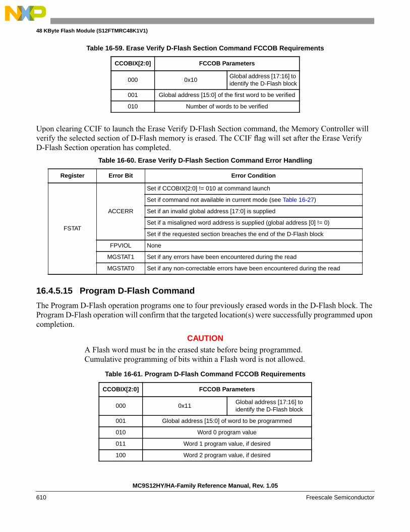
48 KByte Flash Module (S12FTMRC48K1V1)
Upon clearing CCIF to launch the Erase Verify D-Flash Section command, the Memory Controller willverify the selected section of D-Flash memory is erased. The CCIF flag will set after the Erase VerifyD-Flash Section operation has completed.
16.4.5.15 Program D-Flash Command
The Program D-Flash operation programs one to four previously erased words in the D-Flash block. TheProgram D-Flash operation will confirm that the targeted location(s) were successfully programmed uponcompletion.
CAUTIONA Flash word must be in the erased state before being programmed.Cumulative programming of bits within a Flash word is not allowed.
Table 16-59. Erase Verify D-Flash Section Command FCCOB Requirements
CCOBIX[2:0] FCCOB Parameters
000 0x10Global address [17:16] toidentify the D-Flash block
001 Global address [15:0] of the first word to be verified
010 Number of words to be verified
Table 16-60. Erase Verify D-Flash Section Command Error Handling
Register Error Bit Error Condition
FSTAT
ACCERR
Set if CCOBIX[2:0] != 010 at command launch
Set if command not available in current mode (see Table 16-27)
Set if an invalid global address [17:0] is supplied
Set if a misaligned word address is supplied (global address [0] != 0)
Set if the requested section breaches the end of the D-Flash block
FPVIOL None
MGSTAT1 Set if any errors have been encountered during the read
MGSTAT0 Set if any non-correctable errors have been encountered during the read
Table 16-61. Program D-Flash Command FCCOB Requirements
CCOBIX[2:0] FCCOB Parameters
000 0x11Global address [17:16] toidentify the D-Flash block
001 Global address [15:0] of word to be programmed
010 Word 0 program value
011 Word 1 program value, if desired
100 Word 2 program value, if desired
MC9S12HY/HA-Family Reference Manual, Rev. 1.05
610 Freescale Semiconductor

48 KByte Flash Module (S12FTMRC48K1V1)
Upon clearing CCIF to launch the Program D-Flash command, the user-supplied words will be transferredto the Memory Controller and be programmed if the area is unprotected. The CCOBIX index value atProgram D-Flash command launch determines how many words will be programmed in the D-Flash block.The CCIF flag is set when the operation has completed.
16.4.5.16 Erase D-Flash Sector Command
The Erase D-Flash Sector operation will erase all addresses in a sector of the D-Flash block.
Upon clearing CCIF to launch the Erase D-Flash Sector command, the Memory Controller will erase theselected Flash sector and verify that it is erased. The CCIF flag will set after the Erase D-Flash Sectoroperation has completed.
101 Word 3 program value, if desired
Table 16-62. Program D-Flash Command Error Handling
Register Error Bit Error Condition
FSTAT
ACCERR
Set if CCOBIX[2:0] < 010 at command launch
Set if CCOBIX[2:0] > 101 at command launch
Set if command not available in current mode (see Table 16-27)
Set if an invalid global address [17:0] is supplied
Set if a misaligned word address is supplied (global address [0] != 0)
Set if the requested group of words breaches the end of the D-Flash block
FPVIOL Set if the selected area of the D-Flash memory is protected
MGSTAT1 Set if any errors have been encountered during the verify operation
MGSTAT0Set if any non-correctable errors have been encountered during the verifyoperation
Table 16-63. Erase D-Flash Sector Command FCCOB Requirements
CCOBIX[2:0] FCCOB Parameters
000 0x12Global address [17:16] to identify
D-Flash block
001Global address [15:0] anywhere within the sector to be erased.
See Section 16.1.2.2 for D-Flash sector size.
Table 16-61. Program D-Flash Command FCCOB Requirements
CCOBIX[2:0] FCCOB Parameters
MC9S12HY/HA-Family Reference Manual, Rev. 1.05
Freescale Semiconductor 611

48 KByte Flash Module (S12FTMRC48K1V1)
16.4.6 Interrupts
The Flash module can generate an interrupt when a Flash command operation has completed or when aFlash command operation has detected an ECC fault.
NOTEVector addresses and their relative interrupt priority are determined at theMCU level.
16.4.6.1 Description of Flash Interrupt Operation
The Flash module uses the CCIF flag in combination with the CCIE interrupt enable bit to generate theFlash command interrupt request. The Flash module uses the DFDIF and SFDIF flags in combination withthe DFDIE and SFDIE interrupt enable bits to generate the Flash error interrupt request. For a detaileddescription of the register bits involved, refer to Section 16.3.2.5, “Flash Configuration Register(FCNFG)”, Section 16.3.2.6, “Flash Error Configuration Register (FERCNFG)”, Section 16.3.2.7, “FlashStatus Register (FSTAT)”, and Section 16.3.2.8, “Flash Error Status Register (FERSTAT)”.
The logic used for generating the Flash module interrupts is shown in Figure 16-27.
Table 16-64. Erase D-Flash Sector Command Error Handling
Register Error Bit Error Condition
FSTAT
ACCERR
Set if CCOBIX[2:0] != 001 at command launch
Set if command not available in current mode (see Table 16-27)
Set if an invalid global address [17:0] is supplied
Set if a misaligned word address is supplied (global address [0] != 0)
FPVIOL Set if the selected area of the D-Flash memory is protected
MGSTAT1 Set if any errors have been encountered during the verify operation
MGSTAT0Set if any non-correctable errors have been encountered during the verifyoperation
Table 16-65. Flash Interrupt Sources
Interrupt Source Interrupt Flag Local EnableGlobal (CCR)
Mask
Flash Command Complete CCIF(FSTAT register)
CCIE(FCNFG register)
I Bit
ECC Double Bit Fault on Flash Read DFDIF(FERSTAT register)
DFDIE(FERCNFG register)
I Bit
ECC Single Bit Fault on Flash Read SFDIF(FERSTAT register)
SFDIE(FERCNFG register)
I Bit
MC9S12HY/HA-Family Reference Manual, Rev. 1.05
612 Freescale Semiconductor
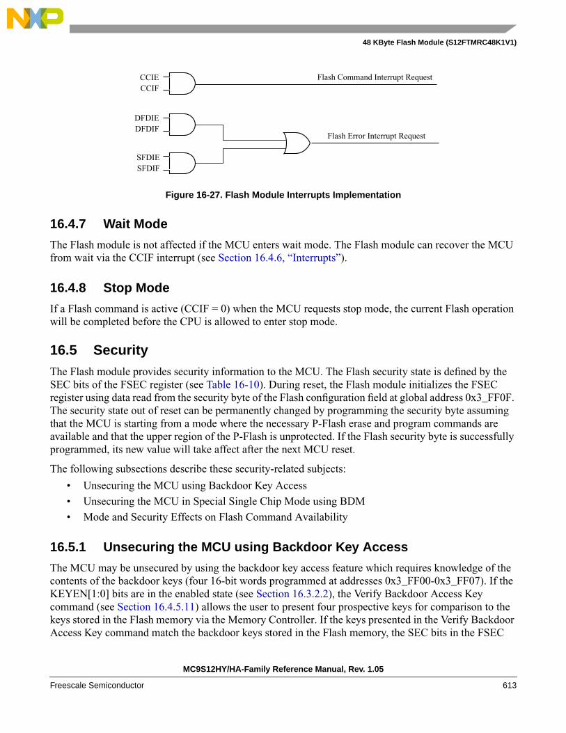
48 KByte Flash Module (S12FTMRC48K1V1)
Figure 16-27. Flash Module Interrupts Implementation
16.4.7 Wait Mode
The Flash module is not affected if the MCU enters wait mode. The Flash module can recover the MCUfrom wait via the CCIF interrupt (see Section 16.4.6, “Interrupts”).
16.4.8 Stop Mode
If a Flash command is active (CCIF = 0) when the MCU requests stop mode, the current Flash operationwill be completed before the CPU is allowed to enter stop mode.
16.5 SecurityThe Flash module provides security information to the MCU. The Flash security state is defined by theSEC bits of the FSEC register (see Table 16-10). During reset, the Flash module initializes the FSECregister using data read from the security byte of the Flash configuration field at global address 0x3_FF0F.The security state out of reset can be permanently changed by programming the security byte assumingthat the MCU is starting from a mode where the necessary P-Flash erase and program commands areavailable and that the upper region of the P-Flash is unprotected. If the Flash security byte is successfullyprogrammed, its new value will take affect after the next MCU reset.
The following subsections describe these security-related subjects:
• Unsecuring the MCU using Backdoor Key Access
• Unsecuring the MCU in Special Single Chip Mode using BDM
• Mode and Security Effects on Flash Command Availability
16.5.1 Unsecuring the MCU using Backdoor Key Access
The MCU may be unsecured by using the backdoor key access feature which requires knowledge of thecontents of the backdoor keys (four 16-bit words programmed at addresses 0x3_FF00-0x3_FF07). If theKEYEN[1:0] bits are in the enabled state (see Section 16.3.2.2), the Verify Backdoor Access Keycommand (see Section 16.4.5.11) allows the user to present four prospective keys for comparison to thekeys stored in the Flash memory via the Memory Controller. If the keys presented in the Verify BackdoorAccess Key command match the backdoor keys stored in the Flash memory, the SEC bits in the FSEC
Flash Error Interrupt Request
CCIFCCIE
DFDIFDFDIE
SFDIFSFDIE
Flash Command Interrupt Request
MC9S12HY/HA-Family Reference Manual, Rev. 1.05
Freescale Semiconductor 613

48 KByte Flash Module (S12FTMRC48K1V1)
register (see Table 16-10) will be changed to unsecure the MCU. Key values of 0x0000 and 0xFFFF arenot permitted as backdoor keys. While the Verify Backdoor Access Key command is active, P-Flashmemory and D-Flash memory will not be available for read access and will return invalid data.
The user code stored in the P-Flash memory must have a method of receiving the backdoor keys from anexternal stimulus. This external stimulus would typically be through one of the on-chip serial ports.
If the KEYEN[1:0] bits are in the enabled state (see Section 16.3.2.2), the MCU can be unsecured by thebackdoor key access sequence described below:
1. Follow the command sequence for the Verify Backdoor Access Key command as explained inSection 16.4.5.11
2. If the Verify Backdoor Access Key command is successful, the MCU is unsecured and theSEC[1:0] bits in the FSEC register are forced to the unsecure state of 10
The Verify Backdoor Access Key command is monitored by the Memory Controller and an illegal key willprohibit future use of the Verify Backdoor Access Key command. A reset of the MCU is the only methodto re-enable the Verify Backdoor Access Key command. The security as defined in the Flash security byte(0x3_FF0F) is not changed by using the Verify Backdoor Access Key command sequence. The backdoorkeys stored in addresses 0x3_FF00-0x3_FF07 are unaffected by the Verify Backdoor Access Keycommand sequence. The Verify Backdoor Access Key command sequence has no effect on the programand erase protections defined in the Flash protection register, FPROT.
After the backdoor keys have been correctly matched, the MCU will be unsecured. After the MCU isunsecured, the sector containing the Flash security byte can be erased and the Flash security byte can bereprogrammed to the unsecure state, if desired. In the unsecure state, the user has full control of thecontents of the backdoor keys by programming addresses 0x3_FF00-0x3_FF07 in the Flash configurationfield.
16.5.2 Unsecuring the MCU in Special Single Chip Mode using BDM
A secured MCU can be unsecured in special single chip mode by using the following method to erase theP-Flash and D-Flash memory:
1. Reset the MCU into special single chip mode
2. Delay while the BDM executes the Erase Verify All Blocks command write sequence to check ifthe P-Flash and D-Flash memories are erased
3. Send BDM commands to disable protection in the P-Flash and D-Flash memory
4. Execute the Erase All Blocks command write sequence to erase the P-Flash and D-Flash memory
5. After the CCIF flag sets to indicate that the Erase All Blocks operation has completed, reset theMCU into special single chip mode
6. Delay while the BDM executes the Erase Verify All Blocks command write sequence to verify thatthe P-Flash and D-Flash memory are erased
If the P-Flash and D-Flash memory are verified as erased, the MCU will be unsecured. All BDMcommands will now be enabled and the Flash security byte may be programmed to the unsecure state bycontinuing with the following steps:
MC9S12HY/HA-Family Reference Manual, Rev. 1.05
614 Freescale Semiconductor
48 KByte Flash Module (S12FTMRC48K1V1)
7. Send BDM commands to execute the Program P-Flash command write sequence to program theFlash security byte to the unsecured state
8. Reset the MCU
16.5.3 Mode and Security Effects on Flash Command Availability
The availability of Flash module commands depends on the MCU operating mode and security state asshown in Table 16-27.
16.6 InitializationOn each system reset the Flash module executes a reset sequence which establishes initial values for theFlash Block Configuration Parameters, the FPROT and DFPROT protection registers, and the FOPT andFSEC registers. The Flash module reverts to using built-in default values that leave the module in a fullyprotected and secured state if errors are encountered during execution of the reset sequence. If a double bitfault is detected during the reset sequence, both MGSTAT bits in the FSTAT register will be set.
CCIF remains clear throughout the reset sequence. The Flash module holds off all CPU access for theinitial portion of the reset sequence. While Flash memory reads and access to most Flash registers arepossible when the hold is removed, writes to the FCCOBIX, FCCOBHI, and FCCOBLO registers areignored. Completion of the reset sequence is marked by setting CCIF high which enables writes to theFCCOBIX, FCCOBHI, and FCCOBLO registers to launch any available Flash command.
If a reset occurs while any Flash command is in progress, that command will be immediately aborted. Thestate of the word being programmed or the sector/block being erased is not guaranteed.
MC9S12HY/HA-Family Reference Manual, Rev. 1.05
Freescale Semiconductor 615

48 KByte Flash Module (S12FTMRC48K1V1)
MC9S12HY/HA-Family Reference Manual, Rev. 1.05
616 Freescale Semiconductor

Chapter 1764 KByte Flash Module (S12FTMRC64K1V1)
17.1 IntroductionThe FTMRC64K1 module implements the following:
• 64 Kbytes of P-Flash (Program Flash) memory
• 4 Kbytes of D-Flash (Data Flash) memory
The Flash memory is ideal for single-supply applications allowing for field reprogramming withoutrequiring external high voltage sources for program or erase operations. The Flash module includes amemory controller that executes commands to modify Flash memory contents. The user interface to thememory controller consists of the indexed Flash Common Command Object (FCCOB) register which iswritten to with the command, global address, data, and any required command parameters. The memorycontroller must complete the execution of a command before the FCCOB register can be written to with anew command.
Table 17-1. Revision History
RevisionNumber
RevisionDate
SectionsAffected
Description of Changes
V01.11 28 Jul 2008 17.1.1/17-61817.3.1/17-621
- Remove reference to IFRON in Program IFR definition- Remove reference to IFRON in Table 17-4 and Figure 17-3
V01.12 19 Dec 2008 17.1/17-61717.4.5.4/17-65117.4.5.6/17-65317.4.5.11/17-65
717.4.5.11/17-65
717.4.5.11/17-65
717.5.2/17-665
- Clarify single bit fault correction for P-Flash phrase- Add statement concerning code runaway when executing Read Once,Program Once, and Verify Backdoor Access Key commands from Flash blockcontaining associated fields- Relate Key 0 to associated Backdoor Comparison Key address- Change “power down reset” to “reset”- Reformat section on unsecuring MCU using BDM
V01.13 25 Sep 2009
17.3.2/17-62417.3.2.1/17-62617.4.3.2/17-644
17.6/17-666
The following changes were made to clarify module behavior related to Flashregister access during reset sequence and while Flash commands are active:- Add caution concerning register writes while command is active- Writes to FCLKDIV are allowed during reset sequence while CCIF is clear- Add caution concerning register writes while command is active- Writes to FCCOBIX, FCCOBHI, FCCOBLO registers are ignored duringreset sequence
MC9S12HY/HA-Family Reference Manual, Rev. 1.05
Freescale Semiconductor 617

CAUTIONA Flash word or phrase must be in the erased state before beingprogrammed. Cumulative programming of bits within a Flash word orphrase is not allowed.
The Flash memory may be read as bytes, aligned words, or misaligned words. Read access time is one buscycle for bytes and aligned words, and two bus cycles for misaligned words. For Flash memory, an erasedbit reads 1 and a programmed bit reads 0.
It is possible to read from P-Flash memory while some commands are executing on D-Flash memory. Itis not possible to read from D-Flash memory while a command is executing on P-Flash memory.Simultaneous P-Flash and D-Flash operations are discussed in Section 17.4.4.
Both P-Flash and D-Flash memories are implemented with Error Correction Codes (ECC) that can resolvesingle bit faults and detect double bit faults. For P-Flash memory, the ECC implementation requires thatprogramming be done on an aligned 8 byte basis (a Flash phrase). Since P-Flash memory is always readby half-phrase, only one single bit fault in an aligned 4 byte half-phrase containing the byte or wordaccessed will be corrected.
17.1.1 Glossary
Command Write Sequence — An MCU instruction sequence to execute built-in algorithms (includingprogram and erase) on the Flash memory.
D-Flash Memory — The D-Flash memory constitutes the nonvolatile memory store for data.
D-Flash Sector — The D-Flash sector is the smallest portion of the D-Flash memory that can be erased.The D-Flash sector consists of four 64 byte rows for a total of 256 bytes.
NVM Command Mode — An NVM mode using the CPU to setup the FCCOB register to pass parametersrequired for Flash command execution.
Phrase — An aligned group of four 16-bit words within the P-Flash memory. Each phrase includes twosets of aligned double words with each set including 7 ECC bits for single bit fault correction and doublebit fault detection within each double word.
P-Flash Memory — The P-Flash memory constitutes the main nonvolatile memory store for applications.
P-Flash Sector — The P-Flash sector is the smallest portion of the P-Flash memory that can be erased.Each P-Flash sector contains 512 bytes.
Program IFR — Nonvolatile information register located in the P-Flash block that contains the DeviceID, Version ID, and the Program Once field.
MC9S12HY/HA-Family Reference Manual, Rev. 1.05
Freescale Semiconductor 618

64 KByte Flash Module (S12FTMRC64K1V1)
17.1.2 Features
17.1.2.1 P-Flash Features
• 64 Kbytes of P-Flash memory composed of one 64 Kbyte Flash block divided into 128 sectors of512 bytes
• Single bit fault correction and double bit fault detection within a 32-bit double word during readoperations
• Automated program and erase algorithm with verify and generation of ECC parity bits
• Fast sector erase and phrase program operation
• Ability to read the P-Flash memory while programming a word in the D-Flash memory
• Flexible protection scheme to prevent accidental program or erase of P-Flash memory
17.1.2.2 D-Flash Features
• 4 Kbytes of D-Flash memory composed of one 4 Kbyte Flash block divided into 16 sectors of 256bytes
• Single bit fault correction and double bit fault detection within a word during read operations
• Automated program and erase algorithm with verify and generation of ECC parity bits
• Fast sector erase and word program operation
• Protection scheme to prevent accidental program or erase of D-Flash memory
• Ability to program up to four words in a burst sequence
17.1.2.3 Other Flash Module Features
• No external high-voltage power supply required for Flash memory program and erase operations
• Interrupt generation on Flash command completion and Flash error detection
• Security mechanism to prevent unauthorized access to the Flash memory
17.1.3 Block Diagram
The block diagram of the Flash module is shown in Figure 17-1.
MC9S12HY/HA-Family Reference Manual, Rev. 1.05
Freescale Semiconductor 619

64 KByte Flash Module (S12FTMRC64K1V1)
Figure 17-1. FTMRC64K1 Block Diagram
17.2 External Signal DescriptionThe Flash module contains no signals that connect off-chip.
BusClockDivider
Clock
CommandInterruptRequest
FCLK
Protection
Security
Registers
FlashInterface
16bitinternalbus
sector 0sector 1
sector 127
16Kx39P-Flash
ErrorInterruptRequest
CPU
D-Flash2Kx22
sector 0sector 1
sector 15
Scratch RAM384x16
MemoryController
MC9S12HY/HA-Family Reference Manual, Rev. 1.05
620 Freescale Semiconductor

64 KByte Flash Module (S12FTMRC64K1V1)
17.3 Memory Map and RegistersThis section describes the memory map and registers for the Flash module. Read data from unimplementedmemory space in the Flash module is undefined. Write access to unimplemented or reserved memory spacein the Flash module will be ignored by the Flash module.
17.3.1 Module Memory Map
The S12 architecture places the P-Flash memory between global addresses 0x3_0000 and 0x3_FFFF asshown in Table 17-2.The P-Flash memory map is shown in Figure 17-2.
The FPROT register, described in Section 17.3.2.9, can be set to protect regions in the Flash memory fromaccidental program or erase. Three separate memory regions, one growing upward from global address0x3_8000 in the Flash memory (called the lower region), one growing downward from global address0x3_FFFF in the Flash memory (called the higher region), and the remaining addresses in the Flashmemory, can be activated for protection. The Flash memory addresses covered by these protectable regionsare shown in the P-Flash memory map. The higher address region is mainly targeted to hold the boot loadercode since it covers the vector space. Default protection settings as well as security information that allowsthe MCU to restrict access to the Flash module are stored in the Flash configuration field as described inTable 17-3.
Table 17-2. P-Flash Memory Addressing
Global AddressSize
(Bytes)Description
0x3_0000 – 0x3_FFFF 64 KP-Flash BlockContains Flash Configuration Field(see Table 17-3)
Table 17-3. Flash Configuration Field
Global AddressSize
(Bytes)Description
0x3_FF00-0x3_FF07 8Backdoor Comparison KeyRefer to Section 17.4.5.11, “Verify Backdoor Access Key Command,” andSection 17.5.1, “Unsecuring the MCU using Backdoor Key Access”
0x3_FF08-0x3_FF0B1
1 0x3FF08-0x3_FF0F form a Flash phrase and must be programmed in a single command write sequence. Each byte inthe 0x3_FF08 - 0x3_FF0B reserved field should be programmed to 0xFF.
4 Reserved
0x3_FF0C1 1P-Flash Protection byte.Refer to Section 17.3.2.9, “P-Flash Protection Register (FPROT)”
0x3_FF0D1 1D-Flash Protection byte.Refer to Section 17.3.2.10, “D-Flash Protection Register (DFPROT)”
0x3_FF0E1 1Flash Nonvolatile byteRefer to Section 17.3.2.16, “Flash Option Register (FOPT)”
0x3_FF0F1 1Flash Security byteRefer to Section 17.3.2.2, “Flash Security Register (FSEC)”
MC9S12HY/HA-Family Reference Manual, Rev. 1.05
Freescale Semiconductor 621

64 KByte Flash Module (S12FTMRC64K1V1)
Figure 17-2. P-Flash Memory Map
Flash Configuration Field
0x3_C000
Flash Protected/Unprotected Lower Region1, 2, 4, 8 Kbytes
0x3_8000
0x3_9000
0x3_84000x3_8800
0x3_A000
P-Flash END = 0x3_FFFF
0x3_F800
0x3_F000
0x3_E000 Flash Protected/Unprotected Higher Region2, 4, 8, 16 Kbytes
Flash Protected/Unprotected Region8 Kbytes (up to 29 Kbytes)
16 bytes (0x3_FF00 - 0x3_FF0F)
Flash Protected/Unprotected Region32 Kbytes
P-Flash START = 0x3_0000
Protection
Protection
Protection
Movable End
Fixed End
Fixed End
MC9S12HY/HA-Family Reference Manual, Rev. 1.05
622 Freescale Semiconductor
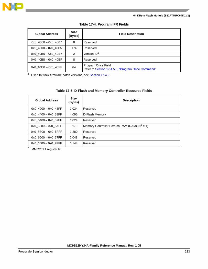
64 KByte Flash Module (S12FTMRC64K1V1)
Table 17-4. Program IFR Fields
Global AddressSize
(Bytes)Field Description
0x0_4000 – 0x0_4007 8 Reserved
0x0_4008 – 0x0_40B5 174 Reserved
0x0_40B6 – 0x0_40B7 2 Version ID1
1 Used to track firmware patch versions, see Section 17.4.2
0x0_40B8 – 0x0_40BF 8 Reserved
0x0_40C0 – 0x0_40FF 64Program Once FieldRefer to Section 17.4.5.6, “Program Once Command”
Table 17-5. D-Flash and Memory Controller Resource Fields
Global AddressSize
(Bytes)Description
0x0_4000 – 0x0_43FF 1,024 Reserved
0x0_4400 – 0x0_53FF 4,096 D-Flash Memory
0x0_5400 – 0x0_57FF 1,024 Reserved
0x0_5800 – 0x0_5AFF 768 Memory Controller Scratch RAM (RAMON1 = 1)
1 MMCCTL1 register bit
0x0_5B00 – 0x0_5FFF 1,280 Reserved
0x0_6000 – 0x0_67FF 2,048 Reserved
0x0_6800 – 0x0_7FFF 6,144 Reserved
MC9S12HY/HA-Family Reference Manual, Rev. 1.05
Freescale Semiconductor 623

64 KByte Flash Module (S12FTMRC64K1V1)
Figure 17-3. D-Flash and Memory Controller Resource Memory Map
17.3.2 Register Descriptions
The Flash module contains a set of 20 control and status registers located between Flash module base +0x0000 and 0x0013. A summary of the Flash module registers is given in Figure 17-4 with detaileddescriptions in the following subsections.
CAUTIONWrites to any Flash register must be avoided while a Flash command isactive (CCIF=0) to prevent corruption of Flash register contents andadversely affect Memory Controller behavior.
Address& Name
7 6 5 4 3 2 1 0
0x0000FCLKDIV
R FDIVLDFDIVLCK FDIV5 FDIV4 FDIV3 FDIV2 FDIV1 FDIV0
W
0x0001FSEC
R KEYEN1 KEYEN0 RNV5 RNV4 RNV3 RNV2 SEC1 SEC0
W
0x0002FCCOBIX
R 0 0 0 0 0CCOBIX2 CCOBIX1 CCOBIX0
W
Figure 17-4. FTMRC64K1 Register Summary
D-Flash Memory4 Kbytes
D-Flash Start = 0x0_4400
0x0_6000
D-Flash End = 0x0_53FF
P-Flash IFR 1 Kbyte
0x0_4000
Reserved 1 Kbyte
Scratch Ram 768 bytes (RAMON)RAM End = 0x0_5AFFRAM Start = 0x0_5800
Reserved 6 Kbytes
Reserved 2 Kbytes
Reserved 1280 bytes
0x0_6800
0x0_7FFF
0x0_40FF
MC9S12HY/HA-Family Reference Manual, Rev. 1.05
624 Freescale Semiconductor
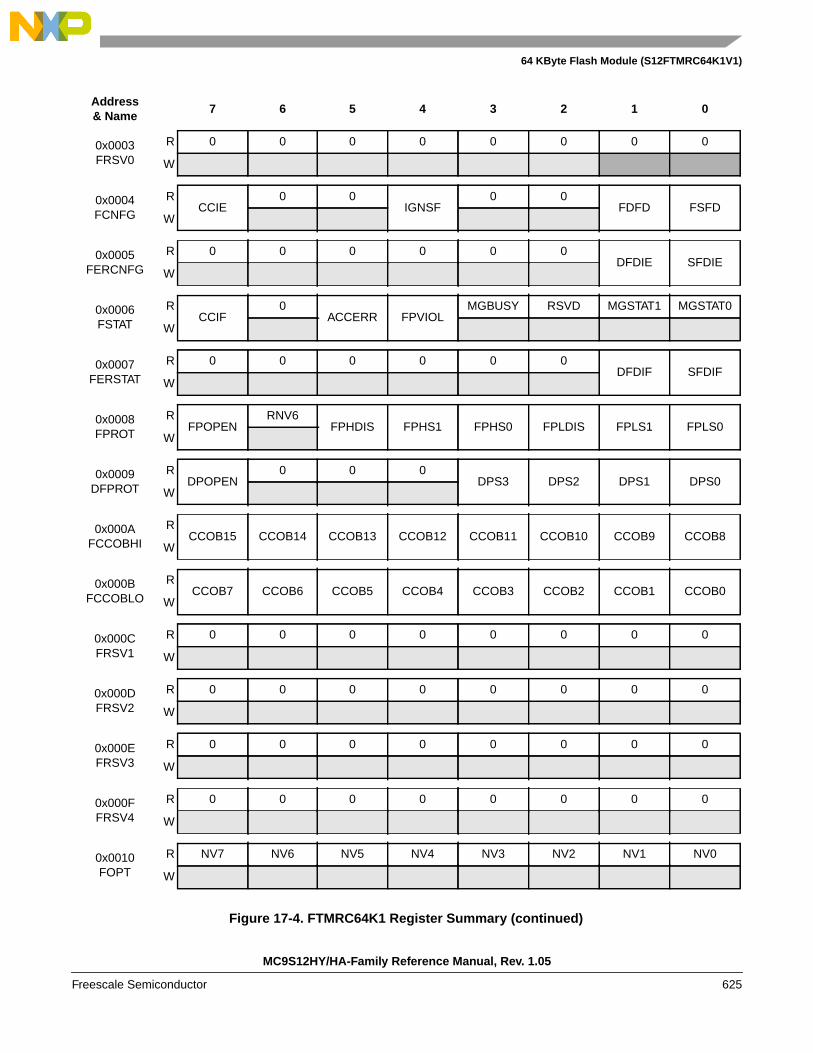
64 KByte Flash Module (S12FTMRC64K1V1)
0x0003FRSV0
R 0 0 0 0 0 0 0 0
W
0x0004FCNFG
RCCIE
0 0IGNSF
0 0FDFD FSFD
W
0x0005FERCNFG
R 0 0 0 0 0 0DFDIE SFDIE
W
0x0006FSTAT
RCCIF
0ACCERR FPVIOL
MGBUSY RSVD MGSTAT1 MGSTAT0
W
0x0007FERSTAT
R 0 0 0 0 0 0DFDIF SFDIF
W
0x0008FPROT
RFPOPEN
RNV6FPHDIS FPHS1 FPHS0 FPLDIS FPLS1 FPLS0
W
0x0009DFPROT
RDPOPEN
0 0 0DPS3 DPS2 DPS1 DPS0
W
0x000AFCCOBHI
RCCOB15 CCOB14 CCOB13 CCOB12 CCOB11 CCOB10 CCOB9 CCOB8
W
0x000BFCCOBLO
RCCOB7 CCOB6 CCOB5 CCOB4 CCOB3 CCOB2 CCOB1 CCOB0
W
0x000CFRSV1
R 0 0 0 0 0 0 0 0
W
0x000DFRSV2
R 0 0 0 0 0 0 0 0
W
0x000EFRSV3
R 0 0 0 0 0 0 0 0
W
0x000FFRSV4
R 0 0 0 0 0 0 0 0
W
0x0010FOPT
R NV7 NV6 NV5 NV4 NV3 NV2 NV1 NV0
W
Address& Name
7 6 5 4 3 2 1 0
Figure 17-4. FTMRC64K1 Register Summary (continued)
MC9S12HY/HA-Family Reference Manual, Rev. 1.05
Freescale Semiconductor 625
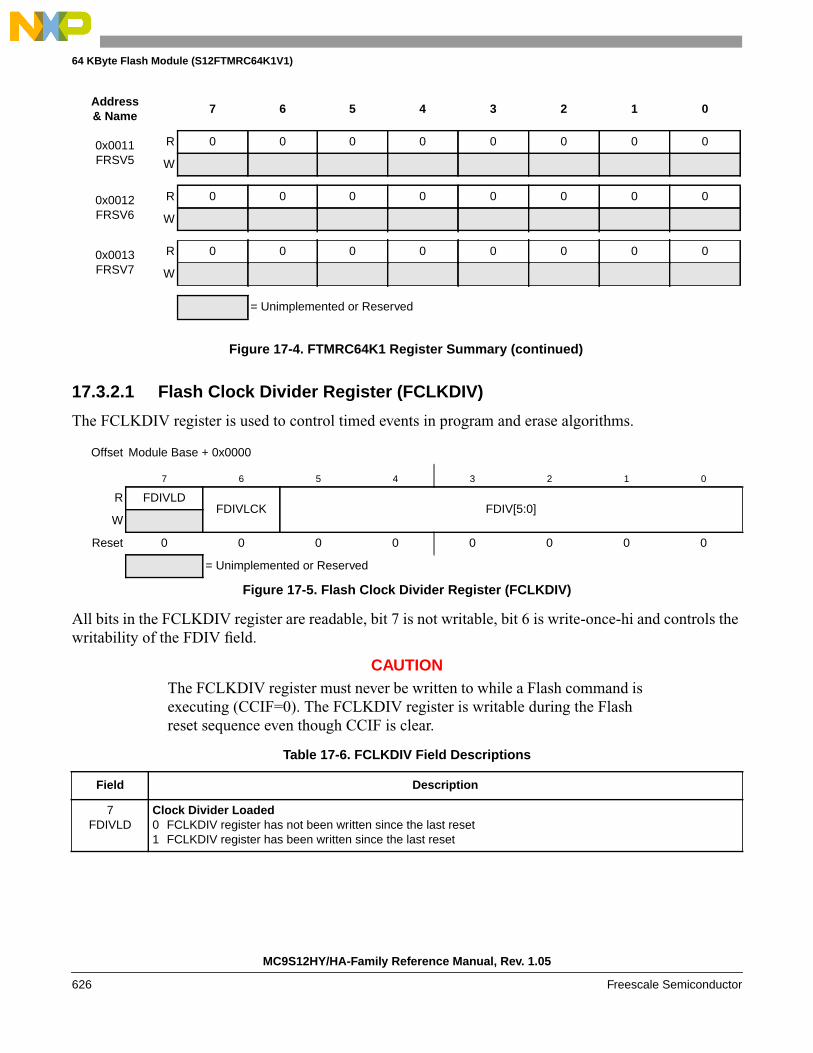
64 KByte Flash Module (S12FTMRC64K1V1)
17.3.2.1 Flash Clock Divider Register (FCLKDIV)
The FCLKDIV register is used to control timed events in program and erase algorithms.
All bits in the FCLKDIV register are readable, bit 7 is not writable, bit 6 is write-once-hi and controls thewritability of the FDIV field.
CAUTIONThe FCLKDIV register must never be written to while a Flash command isexecuting (CCIF=0). The FCLKDIV register is writable during the Flashreset sequence even though CCIF is clear.
0x0011FRSV5
R 0 0 0 0 0 0 0 0
W
0x0012FRSV6
R 0 0 0 0 0 0 0 0
W
0x0013FRSV7
R 0 0 0 0 0 0 0 0
W
= Unimplemented or Reserved
Offset Module Base + 0x0000
7 6 5 4 3 2 1 0
R FDIVLDFDIVLCK FDIV[5:0]
W
Reset 0 0 0 0 0 0 0 0
= Unimplemented or Reserved
Figure 17-5. Flash Clock Divider Register (FCLKDIV)
Table 17-6. FCLKDIV Field Descriptions
Field Description
7FDIVLD
Clock Divider Loaded0 FCLKDIV register has not been written since the last reset1 FCLKDIV register has been written since the last reset
Address& Name
7 6 5 4 3 2 1 0
Figure 17-4. FTMRC64K1 Register Summary (continued)
MC9S12HY/HA-Family Reference Manual, Rev. 1.05
626 Freescale Semiconductor

64 KByte Flash Module (S12FTMRC64K1V1)
17.3.2.2 Flash Security Register (FSEC)
The FSEC register holds all bits associated with the security of the MCU and Flash module.
6FDIVLCK
Clock Divider Locked0 FDIV field is open for writing1 FDIV value is locked and cannot be changed. Once the lock bit is set high, only reset can clear this bit and
restore writability to the FDIV field.
5–0FDIV[5:0]
Clock Divider Bits — FDIV[5:0] must be set to effectively divide BUSCLK down to 1 MHz to control timed eventsduring Flash program and erase algorithms. Table 17-7 shows recommended values for FDIV[5:0] based on theBUSCLK frequency. Please refer to Section 17.4.3, “Flash Command Operations,” for more information.
Table 17-7. FDIV values for various BUSCLK Frequencies
BUSCLK Frequency(MHz) FDIV[5:0]
BUSCLK Frequency(MHz) FDIV[5:0]
MIN1
1 BUSCLK is Greater Than this value.
MAX2
2 BUSCLK is Less Than or Equal to this value.
MIN1 MAX2
1.0 1.6 0x00 16.6 17.6 0x10
1.6 2.6 0x01 17.6 18.6 0x11
2.6 3.6 0x02 18.6 19.6 0x12
3.6 4.6 0x03 19.6 20.6 0x13
4.6 5.6 0x04 20.6 21.6 0x14
5.6 6.6 0x05 21.6 22.6 0x15
6.6 7.6 0x06 22.6 23.6 0x16
7.6 8.6 0x07 23.6 24.6 0x17
8.6 9.6 0x08 24.6 25.6 0x18
9.6 10.6 0x09 25.6 26.6 0x19
10.6 11.6 0x0A 26.6 27.6 0x1A
11.6 12.6 0x0B 27.6 28.6 0x1B
12.6 13.6 0x0C 28.6 29.6 0x1C
13.6 14.6 0x0D 29.6 30.6 0x1D
14.6 15.6 0x0E 30.6 31.6 0x1E
15.6 16.6 0x0F 31.6 32.6 0x1F
Table 17-6. FCLKDIV Field Descriptions (continued)
Field Description
MC9S12HY/HA-Family Reference Manual, Rev. 1.05
Freescale Semiconductor 627

64 KByte Flash Module (S12FTMRC64K1V1)
All bits in the FSEC register are readable but not writable.
During the reset sequence, the FSEC register is loaded with the contents of the Flash security byte in theFlash configuration field at global address 0x3_FF0F located in P-Flash memory (see Table 17-3) asindicated by reset condition F in Figure 17-6. If a double bit fault is detected while reading the P-Flashphrase containing the Flash security byte during the reset sequence, all bits in the FSEC register will beset to leave the Flash module in a secured state with backdoor key access disabled.
The security function in the Flash module is described in Section 17.5.
Offset Module Base + 0x0001
7 6 5 4 3 2 1 0
R KEYEN[1:0] RNV[5:2] SEC[1:0]
W
Reset F F F F F F F F
= Unimplemented or Reserved
Figure 17-6. Flash Security Register (FSEC)
Table 17-8. FSEC Field Descriptions
Field Description
7–6KEYEN[1:0]
Backdoor Key Security Enable Bits — The KEYEN[1:0] bits define the enabling of backdoor key access to theFlash module as shown in Table 17-9.
5–2RNV[5:2
Reserved Nonvolatile Bits — The RNV bits should remain in the erased state for future enhancements.
1–0SEC[1:0]
Flash Security Bits — The SEC[1:0] bits define the security state of the MCU as shown in Table 17-10. If theFlash module is unsecured using backdoor key access, the SEC bits are forced to 10.
Table 17-9. Flash KEYEN States
KEYEN[1:0] Status of Backdoor Key Access
00 DISABLED
01 DISABLED1
1 Preferred KEYEN state to disable backdoor key access.
10 ENABLED
11 DISABLED
Table 17-10. Flash Security States
SEC[1:0] Status of Security
00 SECURED
01 SECURED1
1 Preferred SEC state to set MCU to secured state.
10 UNSECURED
11 SECURED
MC9S12HY/HA-Family Reference Manual, Rev. 1.05
628 Freescale Semiconductor

64 KByte Flash Module (S12FTMRC64K1V1)
17.3.2.3 Flash CCOB Index Register (FCCOBIX)
The FCCOBIX register is used to index the FCCOB register for Flash memory operations.
CCOBIX bits are readable and writable while remaining bits read 0 and are not writable.
17.3.2.4 Flash Reserved0 Register (FRSV0)
This Flash register is reserved for factory testing.
All bits in the FRSV0 register read 0 and are not writable.
17.3.2.5 Flash Configuration Register (FCNFG)
The FCNFG register enables the Flash command complete interrupt and forces ECC faults on Flash arrayread access from the CPU.
Offset Module Base + 0x0002
7 6 5 4 3 2 1 0
R 0 0 0 0 0CCOBIX[2:0]
W
Reset 0 0 0 0 0 0 0 0
= Unimplemented or Reserved
Figure 17-7. FCCOB Index Register (FCCOBIX)
Table 17-11. FCCOBIX Field Descriptions
Field Description
2–0CCOBIX[1:0]
Common Command Register Index— The CCOBIX bits are used to select which word of the FCCOB registerarray is being read or written to. See Section 17.3.2.11, “Flash Common Command Object Register (FCCOB),”for more details.
Offset Module Base + 0x000C
7 6 5 4 3 2 1 0
R 0 0 0 0 0 0 0 0
W
Reset 0 0 0 0 0 0 0 0
= Unimplemented or Reserved
Figure 17-8. Flash Reserved0 Register (FRSV0)
MC9S12HY/HA-Family Reference Manual, Rev. 1.05
Freescale Semiconductor 629
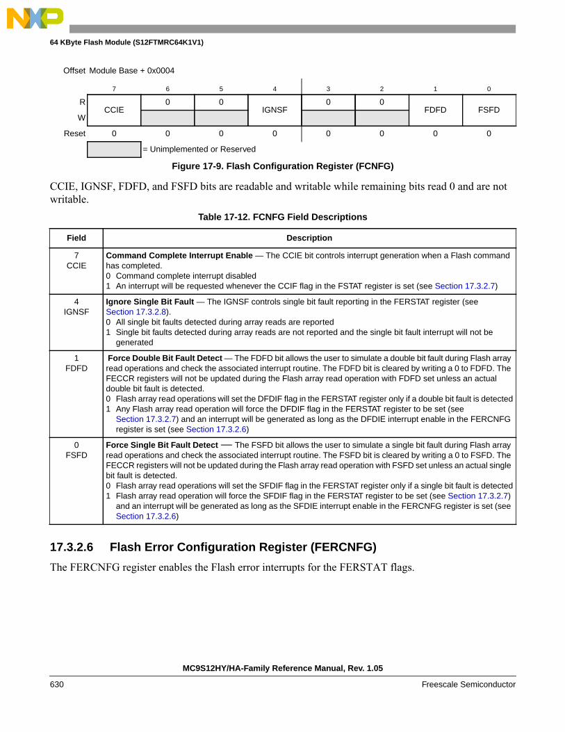
64 KByte Flash Module (S12FTMRC64K1V1)
CCIE, IGNSF, FDFD, and FSFD bits are readable and writable while remaining bits read 0 and are notwritable.
17.3.2.6 Flash Error Configuration Register (FERCNFG)
The FERCNFG register enables the Flash error interrupts for the FERSTAT flags.
Offset Module Base + 0x0004
7 6 5 4 3 2 1 0
RCCIE
0 0IGNSF
0 0FDFD FSFD
W
Reset 0 0 0 0 0 0 0 0
= Unimplemented or Reserved
Figure 17-9. Flash Configuration Register (FCNFG)
Table 17-12. FCNFG Field Descriptions
Field Description
7CCIE
Command Complete Interrupt Enable — The CCIE bit controls interrupt generation when a Flash commandhas completed.0 Command complete interrupt disabled1 An interrupt will be requested whenever the CCIF flag in the FSTAT register is set (see Section 17.3.2.7)
4IGNSF
Ignore Single Bit Fault — The IGNSF controls single bit fault reporting in the FERSTAT register (seeSection 17.3.2.8).0 All single bit faults detected during array reads are reported1 Single bit faults detected during array reads are not reported and the single bit fault interrupt will not be
generated
1FDFD
Force Double Bit Fault Detect — The FDFD bit allows the user to simulate a double bit fault during Flash arrayread operations and check the associated interrupt routine. The FDFD bit is cleared by writing a 0 to FDFD. TheFECCR registers will not be updated during the Flash array read operation with FDFD set unless an actualdouble bit fault is detected.0 Flash array read operations will set the DFDIF flag in the FERSTAT register only if a double bit fault is detected1 Any Flash array read operation will force the DFDIF flag in the FERSTAT register to be set (see
Section 17.3.2.7) and an interrupt will be generated as long as the DFDIE interrupt enable in the FERCNFGregister is set (see Section 17.3.2.6)
0FSFD
Force Single Bit Fault Detect — The FSFD bit allows the user to simulate a single bit fault during Flash arrayread operations and check the associated interrupt routine. The FSFD bit is cleared by writing a 0 to FSFD. TheFECCR registers will not be updated during the Flash array read operation with FSFD set unless an actual singlebit fault is detected.0 Flash array read operations will set the SFDIF flag in the FERSTAT register only if a single bit fault is detected1 Flash array read operation will force the SFDIF flag in the FERSTAT register to be set (see Section 17.3.2.7)
and an interrupt will be generated as long as the SFDIE interrupt enable in the FERCNFG register is set (seeSection 17.3.2.6)
MC9S12HY/HA-Family Reference Manual, Rev. 1.05
630 Freescale Semiconductor

64 KByte Flash Module (S12FTMRC64K1V1)
All assigned bits in the FERCNFG register are readable and writable.
17.3.2.7 Flash Status Register (FSTAT)
The FSTAT register reports the operational status of the Flash module.
CCIF, ACCERR, and FPVIOL bits are readable and writable, MGBUSY and MGSTAT bits are readablebut not writable, while remaining bits read 0 and are not writable.
Offset Module Base + 0x0005
7 6 5 4 3 2 1 0
R 0 0 0 0 0 0DFDIE SFDIE
W
Reset 0 0 0 0 0 0 0 0
= Unimplemented or Reserved
Figure 17-10. Flash Error Configuration Register (FERCNFG)
Table 17-13. FERCNFG Field Descriptions
Field Description
1DFDIE
Double Bit Fault Detect Interrupt Enable — The DFDIE bit controls interrupt generation when a double bit faultis detected during a Flash block read operation.0 DFDIF interrupt disabled1 An interrupt will be requested whenever the DFDIF flag is set (see Section 17.3.2.8)
0SFDIE
Single Bit Fault Detect Interrupt Enable — The SFDIE bit controls interrupt generation when a single bit faultis detected during a Flash block read operation.0 SFDIF interrupt disabled whenever the SFDIF flag is set (see Section 17.3.2.8)1 An interrupt will be requested whenever the SFDIF flag is set (see Section 17.3.2.8)
Offset Module Base + 0x0006
7 6 5 4 3 2 1 0
RCCIF
0ACCERR FPVIOL
MGBUSY RSVD MGSTAT[1:0]
W
Reset 1 0 0 0 0 0 01
1 Reset value can deviate from the value shown if a double bit fault is detected during the reset sequence (see Section 17.6).
01
= Unimplemented or Reserved
Figure 17-11. Flash Status Register (FSTAT)
MC9S12HY/HA-Family Reference Manual, Rev. 1.05
Freescale Semiconductor 631

64 KByte Flash Module (S12FTMRC64K1V1)
17.3.2.8 Flash Error Status Register (FERSTAT)
The FERSTAT register reflects the error status of internal Flash operations.
All flags in the FERSTAT register are readable and only writable to clear the flag.
Table 17-14. FSTAT Field Descriptions
Field Description
7CCIF
Command Complete Interrupt Flag — The CCIF flag indicates that a Flash command has completed. TheCCIF flag is cleared by writing a 1 to CCIF to launch a command and CCIF will stay low until commandcompletion or command violation.0 Flash command in progress1 Flash command has completed
5ACCERR
Flash Access Error Flag — The ACCERR bit indicates an illegal access has occurred to the Flash memorycaused by either a violation of the command write sequence (see Section 17.4.3.2) or issuing an illegal Flashcommand. While ACCERR is set, the CCIF flag cannot be cleared to launch a command. The ACCERR bit iscleared by writing a 1 to ACCERR. Writing a 0 to the ACCERR bit has no effect on ACCERR.0 No access error detected1 Access error detected
4FPVIOL
Flash Protection Violation Flag —The FPVIOL bit indicates an attempt was made to program or erase anaddress in a protected area of P-Flash or D-Flash memory during a command write sequence. The FPVIOLbit is cleared by writing a 1 to FPVIOL. Writing a 0 to the FPVIOL bit has no effect on FPVIOL. While FPVIOLis set, it is not possible to launch a command or start a command write sequence.0 No protection violation detected1 Protection violation detected
3MGBUSY
Memory Controller Busy Flag — The MGBUSY flag reflects the active state of the Memory Controller.0 Memory Controller is idle1 Memory Controller is busy executing a Flash command (CCIF = 0)
2RSVD
Reserved Bit — This bit is reserved and always reads 0.
1–0MGSTAT[1:0]
Memory Controller Command Completion Status Flag — One or more MGSTAT flag bits are set if an erroris detected during execution of a Flash command or during the Flash reset sequence. See Section 17.4.5,“Flash Command Description,” and Section 17.6, “Initialization” for details.
Offset Module Base + 0x0007
7 6 5 4 3 2 1 0
R 0 0 0 0 0 0DFDIF SFDIF
W
Reset 0 0 0 0 0 0 0 0
= Unimplemented or Reserved
Figure 17-12. Flash Error Status Register (FERSTAT)
MC9S12HY/HA-Family Reference Manual, Rev. 1.05
632 Freescale Semiconductor

64 KByte Flash Module (S12FTMRC64K1V1)
17.3.2.9 P-Flash Protection Register (FPROT)
The FPROT register defines which P-Flash sectors are protected against program and erase operations.
The (unreserved) bits of the FPROT register are writable with the restriction that the size of the protectedregion can only be increased (see Section 17.3.2.9.1, “P-Flash Protection Restrictions,” and Table 17-20).
During the reset sequence, the FPROT register is loaded with the contents of the P-Flash protection bytein the Flash configuration field at global address 0x3_FF0C located in P-Flash memory (see Table 17-3)as indicated by reset condition ‘F’ in Figure 17-13. To change the P-Flash protection that will be loadedduring the reset sequence, the upper sector of the P-Flash memory must be unprotected, then the P-Flashprotection byte must be reprogrammed. If a double bit fault is detected while reading the P-Flash phrasecontaining the P-Flash protection byte during the reset sequence, the FPOPEN bit will be cleared andremaining bits in the FPROT register will be set to leave the P-Flash memory fully protected.
Trying to alter data in any protected area in the P-Flash memory will result in a protection violation errorand the FPVIOL bit will be set in the FSTAT register. The block erase of a P-Flash block is not possibleif any of the P-Flash sectors contained in the same P-Flash block are protected.
Table 17-15. FERSTAT Field Descriptions
Field Description
1DFDIF
Double Bit Fault Detect Interrupt Flag — The setting of the DFDIF flag indicates that a double bit fault wasdetected in the stored parity and data bits during a Flash array read operation or that a Flash array read operationwas attempted on a Flash block that was under a Flash command operation.1 The DFDIF flag is cleared bywriting a 1 to DFDIF. Writing a 0 to DFDIF has no effect on DFDIF.0 No double bit fault detected1 Double bit fault detected or an invalid Flash array read operation attempted
1 The single bit fault and double bit fault flags are mutually exclusive for parity errors (an ECC fault occurrence can be eithersingle fault or double fault but never both). A simultaneous access collision (read attempted while command running) isindicated when both SFDIF and DFDIF flags are high.
0SFDIF
Single Bit Fault Detect Interrupt Flag — With the IGNSF bit in the FCNFG register clear, the SFDIF flagindicates that a single bit fault was detected in the stored parity and data bits during a Flash array read operationor that a Flash array read operation was attempted on a Flash block that was under a Flash command operation.1
The SFDIF flag is cleared by writing a 1 to SFDIF. Writing a 0 to SFDIF has no effect on SFDIF.0 No single bit fault detected1 Single bit fault detected and corrected or an invalid Flash array read operation attempted
Offset Module Base + 0x0008
7 6 5 4 3 2 1 0
RFPOPEN
RNV6FPHDIS FPHS[1:0] FPLDIS FPLS[1:0]
W
Reset F F F F F F F F
= Unimplemented or Reserved
Figure 17-13. Flash Protection Register (FPROT)
MC9S12HY/HA-Family Reference Manual, Rev. 1.05
Freescale Semiconductor 633
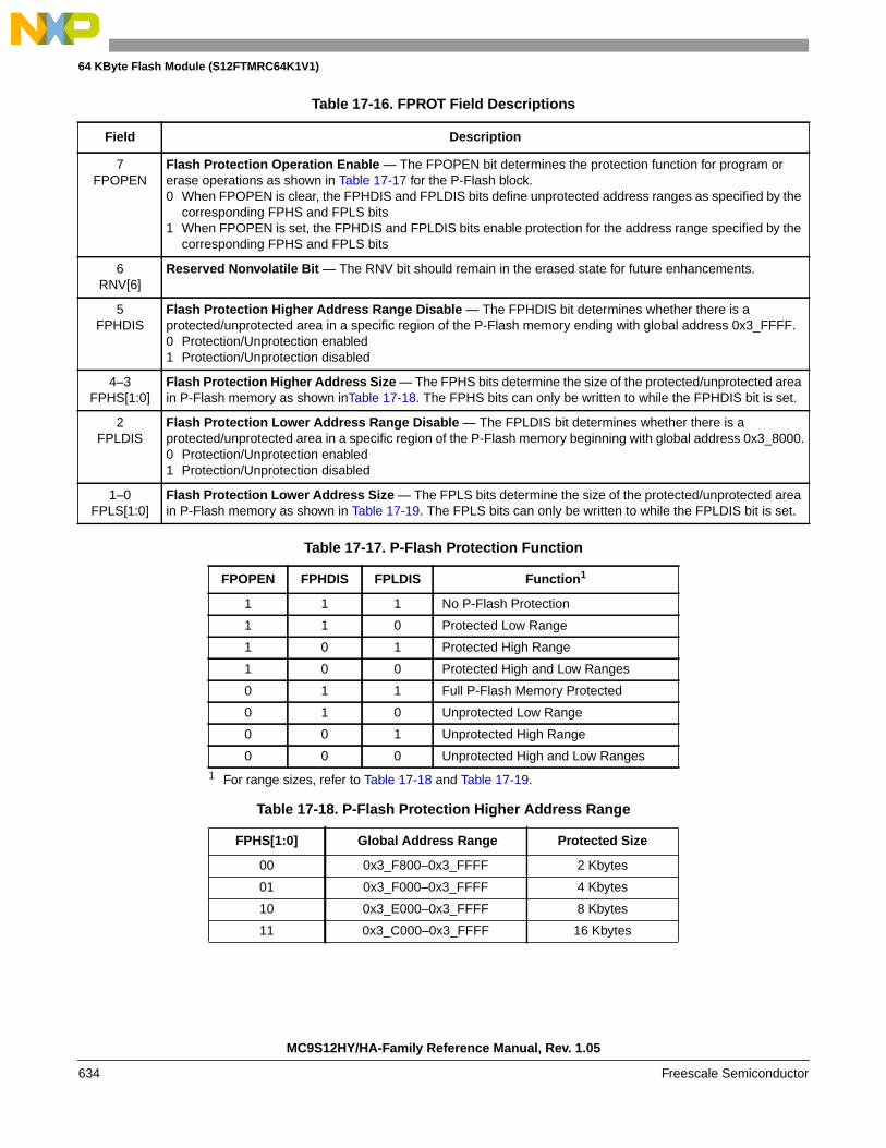
64 KByte Flash Module (S12FTMRC64K1V1)
Table 17-16. FPROT Field Descriptions
Field Description
7FPOPEN
Flash Protection Operation Enable — The FPOPEN bit determines the protection function for program orerase operations as shown in Table 17-17 for the P-Flash block.0 When FPOPEN is clear, the FPHDIS and FPLDIS bits define unprotected address ranges as specified by the
corresponding FPHS and FPLS bits1 When FPOPEN is set, the FPHDIS and FPLDIS bits enable protection for the address range specified by the
corresponding FPHS and FPLS bits
6RNV[6]
Reserved Nonvolatile Bit — The RNV bit should remain in the erased state for future enhancements.
5FPHDIS
Flash Protection Higher Address Range Disable — The FPHDIS bit determines whether there is aprotected/unprotected area in a specific region of the P-Flash memory ending with global address 0x3_FFFF.0 Protection/Unprotection enabled1 Protection/Unprotection disabled
4–3FPHS[1:0]
Flash Protection Higher Address Size — The FPHS bits determine the size of the protected/unprotected areain P-Flash memory as shown inTable 17-18. The FPHS bits can only be written to while the FPHDIS bit is set.
2FPLDIS
Flash Protection Lower Address Range Disable — The FPLDIS bit determines whether there is aprotected/unprotected area in a specific region of the P-Flash memory beginning with global address 0x3_8000.0 Protection/Unprotection enabled1 Protection/Unprotection disabled
1–0FPLS[1:0]
Flash Protection Lower Address Size — The FPLS bits determine the size of the protected/unprotected areain P-Flash memory as shown in Table 17-19. The FPLS bits can only be written to while the FPLDIS bit is set.
Table 17-17. P-Flash Protection Function
FPOPEN FPHDIS FPLDIS Function1
1 For range sizes, refer to Table 17-18 and Table 17-19.
1 1 1 No P-Flash Protection
1 1 0 Protected Low Range
1 0 1 Protected High Range
1 0 0 Protected High and Low Ranges
0 1 1 Full P-Flash Memory Protected
0 1 0 Unprotected Low Range
0 0 1 Unprotected High Range
0 0 0 Unprotected High and Low Ranges
Table 17-18. P-Flash Protection Higher Address Range
FPHS[1:0] Global Address Range Protected Size
00 0x3_F800–0x3_FFFF 2 Kbytes
01 0x3_F000–0x3_FFFF 4 Kbytes
10 0x3_E000–0x3_FFFF 8 Kbytes
11 0x3_C000–0x3_FFFF 16 Kbytes
MC9S12HY/HA-Family Reference Manual, Rev. 1.05
634 Freescale Semiconductor

64 KByte Flash Module (S12FTMRC64K1V1)
All possible P-Flash protection scenarios are shown in Figure 17-14. Although the protection scheme isloaded from the Flash memory at global address 0x3_FF0C during the reset sequence, it can be changedby the user. The P-Flash protection scheme can be used by applications requiring reprogramming in singlechip mode while providing as much protection as possible if reprogramming is not required.
Table 17-19. P-Flash Protection Lower Address Range
FPLS[1:0] Global Address Range Protected Size
00 0x3_8000–0x3_83FF 1 Kbyte
01 0x3_8000–0x3_87FF 2 Kbytes
10 0x3_8000–0x3_8FFF 4 Kbytes
11 0x3_8000–0x3_9FFF 8 Kbytes
MC9S12HY/HA-Family Reference Manual, Rev. 1.05
Freescale Semiconductor 635

64 KByte Flash Module (S12FTMRC64K1V1)
Figure 17-14. P-Flash Protection Scenarios
7 6 5 4
FP
HS
[1:0
]F
PLS
[1:0
]
3 2 1 0
FP
HS
[1:0
]F
PLS
[1:0
]
FPHDIS = 1FPLDIS = 1
FPHDIS = 1FPLDIS = 0
FPHDIS = 0FPLDIS = 1
FPHDIS = 0FPLDIS = 0
Scenario
Scenario
Unprotected region Protected region with size
Protected region Protected region with size
defined by FPLS
defined by FPHSnot defined by FPLS, FPHS
0x3_8000
0x3_FFFF
0x3_8000
0x3_FFFF
FLASH START
FLASH START
FP
OP
EN
= 1
FP
OP
EN
= 0
MC9S12HY/HA-Family Reference Manual, Rev. 1.05
636 Freescale Semiconductor
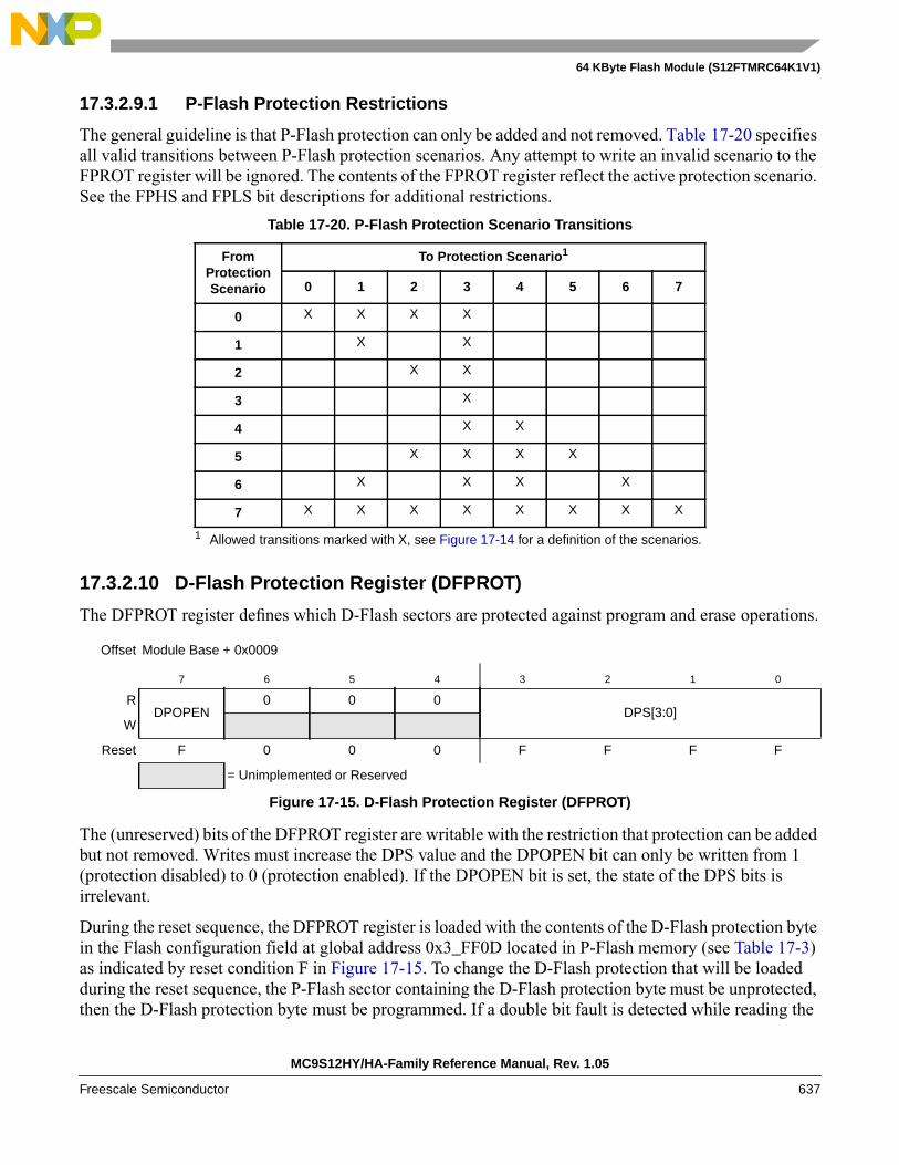
64 KByte Flash Module (S12FTMRC64K1V1)
17.3.2.9.1 P-Flash Protection Restrictions
The general guideline is that P-Flash protection can only be added and not removed. Table 17-20 specifiesall valid transitions between P-Flash protection scenarios. Any attempt to write an invalid scenario to theFPROT register will be ignored. The contents of the FPROT register reflect the active protection scenario.See the FPHS and FPLS bit descriptions for additional restrictions.
17.3.2.10 D-Flash Protection Register (DFPROT)
The DFPROT register defines which D-Flash sectors are protected against program and erase operations.
The (unreserved) bits of the DFPROT register are writable with the restriction that protection can be addedbut not removed. Writes must increase the DPS value and the DPOPEN bit can only be written from 1(protection disabled) to 0 (protection enabled). If the DPOPEN bit is set, the state of the DPS bits isirrelevant.
During the reset sequence, the DFPROT register is loaded with the contents of the D-Flash protection bytein the Flash configuration field at global address 0x3_FF0D located in P-Flash memory (see Table 17-3)as indicated by reset condition F in Figure 17-15. To change the D-Flash protection that will be loadedduring the reset sequence, the P-Flash sector containing the D-Flash protection byte must be unprotected,then the D-Flash protection byte must be programmed. If a double bit fault is detected while reading the
Table 17-20. P-Flash Protection Scenario Transitions
FromProtectionScenario
To Protection Scenario1
1 Allowed transitions marked with X, see Figure 17-14 for a definition of the scenarios.
0 1 2 3 4 5 6 7
0 X X X X
1 X X
2 X X
3 X
4 X X
5 X X X X
6 X X X X
7 X X X X X X X X
Offset Module Base + 0x0009
7 6 5 4 3 2 1 0
RDPOPEN
0 0 0DPS[3:0]
W
Reset F 0 0 0 F F F F
= Unimplemented or Reserved
Figure 17-15. D-Flash Protection Register (DFPROT)
MC9S12HY/HA-Family Reference Manual, Rev. 1.05
Freescale Semiconductor 637

64 KByte Flash Module (S12FTMRC64K1V1)
P-Flash phrase containing the D-Flash protection byte during the reset sequence, the DPOPEN bit will becleared and DPS bits will be set to leave the D-Flash memory fully protected.
Trying to alter data in any protected area in the D-Flash memory will result in a protection violation errorand the FPVIOL bit will be set in the FSTAT register. Block erase of the D-Flash memory is not possibleif any of the D-Flash sectors are protected.
17.3.2.11 Flash Common Command Object Register (FCCOB)
The FCCOB is an array of six words addressed via the CCOBIX index found in the FCCOBIX register.Byte wide reads and writes are allowed to the FCCOB register.
Table 17-21. DFPROT Field Descriptions
Field Description
7DPOPEN
D-Flash Protection Control0 Enables D-Flash memory protection from program and erase with protected address range defined by DPS
bits1 Disables D-Flash memory protection from program and erase
3–0DPS[3:0]
D-Flash Protection Size — The DPS[3:0] bits determine the size of the protected area in the D-Flash memoryas shown in Table 17-22.
Table 17-22. D-Flash Protection Address Range
DPS[3:0] Global Address Range Protected Size
0000 0x0_4400 – 0x0_44FF 256 bytes
0001 0x0_4400 – 0x0_45FF 512 bytes
0010 0x0_4400 – 0x0_46FF 768 bytes
0011 0x0_4400 – 0x0_47FF 1024 bytes
0100 0x0_4400 – 0x0_48FF 1280 bytes
0101 0x0_4400 – 0x0_49FF 1536 bytes
0110 0x0_4400 – 0x0_4AFF 1792 bytes
0111 0x0_4400 – 0x0_4BFF 2048 bytes
1000 0x0_4400 – 0x0_4CFF 2304 bytes
1001 0x0_4400 – 0x0_4DFF 2560 bytes
1010 0x0_4400 – 0x0_4EFF 2816 bytes
1011 0x0_4400 – 0x0_4FFF 3072 bytes
1100 0x0_4400 – 0x0_50FF 3328 bytes
1101 0x0_4400 – 0x0_51FF 3584 bytes
1110 0x0_4400 – 0x0_52FF 3840 bytes
1111 0x0_4400 – 0x0_53FF 4096 bytes
MC9S12HY/HA-Family Reference Manual, Rev. 1.05
638 Freescale Semiconductor

64 KByte Flash Module (S12FTMRC64K1V1)
17.3.2.11.1 FCCOB - NVM Command Mode
NVM command mode uses the indexed FCCOB register to provide a command code and its relevantparameters to the Memory Controller. The user first sets up all required FCCOB fields and then initiatesthe command’s execution by writing a 1 to the CCIF bit in the FSTAT register (a 1 written by the userclears the CCIF command completion flag to 0). When the user clears the CCIF bit in the FSTAT registerall FCCOB parameter fields are locked and cannot be changed by the user until the command completes(as evidenced by the Memory Controller returning CCIF to 1). Some commands return information to theFCCOB register array.
The generic format for the FCCOB parameter fields in NVM command mode is shown in Table 17-23.The return values are available for reading after the CCIF flag in the FSTAT register has been returned to1 by the Memory Controller. Writes to the unimplemented parameter fields (CCOBIX = 110 and CCOBIX= 111) are ignored with reads from these fields returning 0x0000.
Table 17-23 shows the generic Flash command format. The high byte of the first word in the CCOB arraycontains the command code, followed by the parameters for this specific Flash command. For details onthe FCCOB settings required by each command, see the Flash command descriptions in Section 17.4.5.
Offset Module Base + 0x000A
7 6 5 4 3 2 1 0
RCCOB[15:8]
W
Reset 0 0 0 0 0 0 0 0
Figure 17-16. Flash Common Command Object High Register (FCCOBHI)
Offset Module Base + 0x000B
7 6 5 4 3 2 1 0
RCCOB[7:0]
W
Reset 0 0 0 0 0 0 0 0
Figure 17-17. Flash Common Command Object Low Register (FCCOBLO)
Table 17-23. FCCOB - NVM Command Mode (Typical Usage)
CCOBIX[2:0] Byte FCCOB Parameter Fields (NVM Command Mode)
000HI FCMD[7:0] defining Flash command
LO 6’h0, Global address [17:16]
001HI Global address [15:8]
LO Global address [7:0]
010HI Data 0 [15:8]
LO Data 0 [7:0]
MC9S12HY/HA-Family Reference Manual, Rev. 1.05
Freescale Semiconductor 639

64 KByte Flash Module (S12FTMRC64K1V1)
17.3.2.12 Flash Reserved1 Register (FRSV1)
This Flash register is reserved for factory testing.
All bits in the FRSV1 register read 0 and are not writable.
17.3.2.13 Flash Reserved2 Register (FRSV2)
This Flash register is reserved for factory testing.
All bits in the FRSV2 register read 0 and are not writable.
17.3.2.14 Flash Reserved3 Register (FRSV3)
This Flash register is reserved for factory testing.
011HI Data 1 [15:8]
LO Data 1 [7:0]
100HI Data 2 [15:8]
LO Data 2 [7:0]
101HI Data 3 [15:8]
LO Data 3 [7:0]
Offset Module Base + 0x000C
7 6 5 4 3 2 1 0
R 0 0 0 0 0 0 0 0
W
Reset 0 0 0 0 0 0 0 0
= Unimplemented or Reserved
Figure 17-18. Flash Reserved1 Register (FRSV1)
Offset Module Base + 0x000D
7 6 5 4 3 2 1 0
R 0 0 0 0 0 0 0 0
W
Reset 0 0 0 0 0 0 0 0
= Unimplemented or Reserved
Figure 17-19. Flash Reserved2 Register (FRSV2)
Table 17-23. FCCOB - NVM Command Mode (Typical Usage)
CCOBIX[2:0] Byte FCCOB Parameter Fields (NVM Command Mode)
MC9S12HY/HA-Family Reference Manual, Rev. 1.05
640 Freescale Semiconductor

64 KByte Flash Module (S12FTMRC64K1V1)
All bits in the FRSV3 register read 0 and are not writable.
17.3.2.15 Flash Reserved4 Register (FRSV4)
This Flash register is reserved for factory testing.
All bits in the FRSV4 register read 0 and are not writable.
17.3.2.16 Flash Option Register (FOPT)
The FOPT register is the Flash option register.
All bits in the FOPT register are readable but are not writable.
During the reset sequence, the FOPT register is loaded from the Flash nonvolatile byte in the Flashconfiguration field at global address 0x3_FF0E located in P-Flash memory (see Table 17-3) as indicatedby reset condition F in Figure 17-22. If a double bit fault is detected while reading the P-Flash phrasecontaining the Flash nonvolatile byte during the reset sequence, all bits in the FOPT register will be set.
Offset Module Base + 0x000E
7 6 5 4 3 2 1 0
R 0 0 0 0 0 0 0 0
W
Reset 0 0 0 0 0 0 0 0
= Unimplemented or Reserved
Figure 17-20. Flash Reserved3 Register (FRSV3)
Offset Module Base + 0x000F
7 6 5 4 3 2 1 0
R 0 0 0 0 0 0 0 0
W
Reset 0 0 0 0 0 0 0 0
= Unimplemented or Reserved
Figure 17-21. Flash Reserved4 Register (FRSV4)
Offset Module Base + 0x0010
7 6 5 4 3 2 1 0
R NV[7:0]
W
Reset F F F F F F F F
= Unimplemented or Reserved
Figure 17-22. Flash Option Register (FOPT)
MC9S12HY/HA-Family Reference Manual, Rev. 1.05
Freescale Semiconductor 641
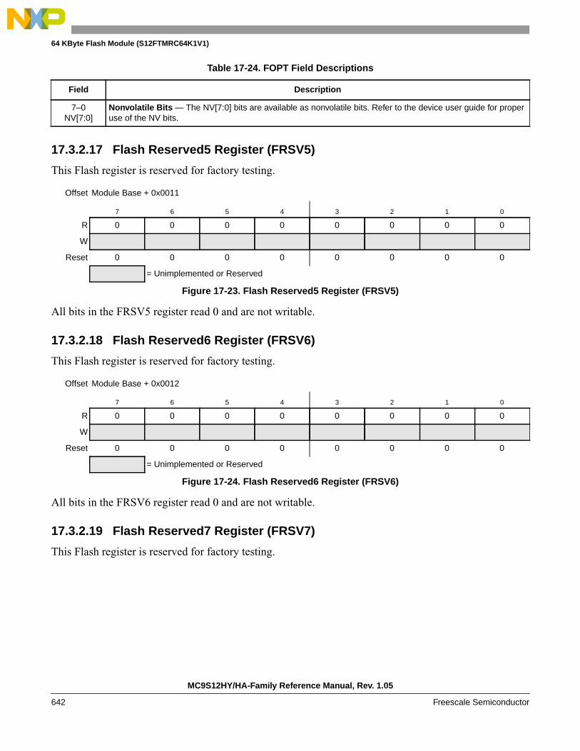
64 KByte Flash Module (S12FTMRC64K1V1)
17.3.2.17 Flash Reserved5 Register (FRSV5)
This Flash register is reserved for factory testing.
All bits in the FRSV5 register read 0 and are not writable.
17.3.2.18 Flash Reserved6 Register (FRSV6)
This Flash register is reserved for factory testing.
All bits in the FRSV6 register read 0 and are not writable.
17.3.2.19 Flash Reserved7 Register (FRSV7)
This Flash register is reserved for factory testing.
Table 17-24. FOPT Field Descriptions
Field Description
7–0NV[7:0]
Nonvolatile Bits — The NV[7:0] bits are available as nonvolatile bits. Refer to the device user guide for properuse of the NV bits.
Offset Module Base + 0x0011
7 6 5 4 3 2 1 0
R 0 0 0 0 0 0 0 0
W
Reset 0 0 0 0 0 0 0 0
= Unimplemented or Reserved
Figure 17-23. Flash Reserved5 Register (FRSV5)
Offset Module Base + 0x0012
7 6 5 4 3 2 1 0
R 0 0 0 0 0 0 0 0
W
Reset 0 0 0 0 0 0 0 0
= Unimplemented or Reserved
Figure 17-24. Flash Reserved6 Register (FRSV6)
MC9S12HY/HA-Family Reference Manual, Rev. 1.05
642 Freescale Semiconductor

64 KByte Flash Module (S12FTMRC64K1V1)
All bits in the FRSV7 register read 0 and are not writable.
17.4 Functional Description
17.4.1 Modes of Operation
The FTMRC64K1 module provides the modes of operation shown in Table 17-25. The operating mode isdetermined by module-level inputs and affects the FCLKDIV, FCNFG, and DFPROT registers, ScratchRAM writes, and the command set availability (see Table 17-27).
17.4.2 IFR Version ID Word
The version ID word is stored in the IFR at address 0x0_40B6. The contents of the word are defined inTable 17-26.
• VERNUM: Version number. The first version is number 0b_0001 with both 0b_0000 and 0b_1111meaning ‘none’.
17.4.3 Flash Command Operations
Flash command operations are used to modify Flash memory contents.
Offset Module Base + 0x0013
7 6 5 4 3 2 1 0
R 0 0 0 0 0 0 0 0
W
Reset 0 0 0 0 0 0 0 0
= Unimplemented or Reserved
Figure 17-25. Flash Reserved7 Register (FRSV7)
Table 17-25. Modes and Mode Control Inputs
OperatingMode
FTMRC Input
mmc_mode_ss_t2
Normal: 0
Special: 1
Table 17-26. IFR Version ID Fields
[15:4] [3:0]
Reserved VERNUM
MC9S12HY/HA-Family Reference Manual, Rev. 1.05
Freescale Semiconductor 643

64 KByte Flash Module (S12FTMRC64K1V1)
The next sections describe:
• How to write the FCLKDIV register that is used to generate a time base (FCLK) derived fromBUSCLK for Flash program and erase command operations
• The command write sequence used to set Flash command parameters and launch execution
• Valid Flash commands available for execution
17.4.3.1 Writing the FCLKDIV Register
Prior to issuing any Flash program or erase command after a reset, the user is required to write theFCLKDIV register to divide BUSCLK down to a target FCLK of 1 MHz. Table 17-7 shows recommendedvalues for the FDIV field based on BUSCLK frequency.
NOTEProgramming or erasing the Flash memory cannot be performed if the busclock runs at less than 0.8 MHz. Setting FDIV too high can destroy the Flashmemory due to overstress. Setting FDIV too low can result in incompleteprogramming or erasure of the Flash memory cells.
When the FCLKDIV register is written, the FDIVLD bit is set automatically. If the FDIVLD bit is 0, theFCLKDIV register has not been written since the last reset. If the FCLKDIV register has not been written,any Flash program or erase command loaded during a command write sequence will not execute and theACCERR bit in the FSTAT register will set.
17.4.3.2 Command Write Sequence
The Memory Controller will launch all valid Flash commands entered using a command write sequence.
Before launching a command, the ACCERR and FPVIOL bits in the FSTAT register must be clear (seeSection 17.3.2.7) and the CCIF flag should be tested to determine the status of the current command writesequence. If CCIF is 0, the previous command write sequence is still active, a new command writesequence cannot be started, and all writes to the FCCOB register are ignored.
CAUTIONWrites to any Flash register must be avoided while a Flash command isactive (CCIF=0) to prevent corruption of Flash register contents andMemory Controller behavior.
17.4.3.2.1 Define FCCOB Contents
The FCCOB parameter fields must be loaded with all required parameters for the Flash command beingexecuted. Access to the FCCOB parameter fields is controlled via the CCOBIX bits in the FCCOBIXregister (see Section 17.3.2.3).
The contents of the FCCOB parameter fields are transferred to the Memory Controller when the user clearsthe CCIF command completion flag in the FSTAT register (writing 1 clears the CCIF to 0). The CCIF flagwill remain clear until the Flash command has completed. Upon completion, the Memory Controller will
MC9S12HY/HA-Family Reference Manual, Rev. 1.05
644 Freescale Semiconductor

64 KByte Flash Module (S12FTMRC64K1V1)
return CCIF to 1 and the FCCOB register will be used to communicate any results. The flow for a genericcommand write sequence is shown in Figure 17-26.
MC9S12HY/HA-Family Reference Manual, Rev. 1.05
Freescale Semiconductor 645

64 KByte Flash Module (S12FTMRC64K1V1)
Figure 17-26. Generic Flash Command Write Sequence Flowchart
Write to FCCOBIX register
Write: FSTAT register (to launch command)Clear CCIF 0x80
Clear ACCERR/FPVIOL 0x30Write: FSTAT registeryes
no
Access Error andProtection Violation
Read: FSTAT register
START
Check
FCCOB
ACCERR/FPVIOLSet?
EXIT
Write: FCLKDIV register
Read: FCLKDIV register
yes
noFDIVCorrect?
noBit Polling forCommand CompletionCheck
yes
CCIF Set?
to identify specific commandparameter to load.
Write to FCCOB registerto load required command parameter.
yes
no
MoreParameters?
Availability Check
Results from previous Command
Note: FCLKDIV must beset after each reset
Read: FSTAT register
no
yes
CCIFSet?
no
yes
CCIFSet?
Clock DividerValue Check Read: FSTAT register
MC9S12HY/HA-Family Reference Manual, Rev. 1.05
646 Freescale Semiconductor

64 KByte Flash Module (S12FTMRC64K1V1)
17.4.3.3 Valid Flash Module Commands
17.4.3.4 P-Flash Commands
Table 17-28 summarizes the valid P-Flash commands along with the effects of the commands on theP-Flash block and other resources within the Flash module.
Table 17-27. Flash Commands by Mode
FCMD CommandUnsecured Secured
NS1
1 Unsecured Normal Single Chip mode.
SS2
2 Unsecured Special Single Chip mode.
NS3
3 Secured Normal Single Chip mode.
SS4
4 Secured Special Single Chip mode.
0x01 Erase Verify All Blocks ∗ ∗ ∗ ∗
0x02 Erase Verify Block ∗ ∗ ∗ ∗
0x03 Erase Verify P-Flash Section ∗ ∗ ∗
0x04 Read Once ∗ ∗ ∗
0x06 Program P-Flash ∗ ∗ ∗
0x07 Program Once ∗ ∗ ∗
0x08 Erase All Blocks ∗ ∗
0x09 Erase Flash Block ∗ ∗ ∗
0x0A Erase P-Flash Sector ∗ ∗ ∗
0x0B Unsecure Flash ∗ ∗
0x0C Verify Backdoor Access Key ∗ ∗
0x0D Set User Margin Level ∗ ∗ ∗
0x0E Set Field Margin Level ∗
0x10 Erase Verify D-Flash Section ∗ ∗ ∗
0x11 Program D-Flash ∗ ∗ ∗
0x12 Erase D-Flash Sector ∗ ∗ ∗
Table 17-28. P-Flash Commands
FCMD Command Function on P-Flash Memory
0x01Erase Verify All
BlocksVerify that all P-Flash (and D-Flash) blocks are erased.
0x02 Erase Verify Block Verify that a P-Flash block is erased.
0x03Erase Verify
P-Flash SectionVerify that a given number of words starting at the address provided are erased.
MC9S12HY/HA-Family Reference Manual, Rev. 1.05
Freescale Semiconductor 647

64 KByte Flash Module (S12FTMRC64K1V1)
17.4.3.5 D-Flash Commands
Table 17-29 summarizes the valid D-Flash commands along with the effects of the commands on theD-Flash block.
0x04 Read OnceRead a dedicated 64 byte field in the nonvolatile information register in P-Flash block thatwas previously programmed using the Program Once command.
0x06 Program P-Flash Program a phrase in a P-Flash block.
0x07 Program OnceProgram a dedicated 64 byte field in the nonvolatile information register in P-Flash blockthat is allowed to be programmed only once.
0x08 Erase All Blocks
Erase all P-Flash (and D-Flash) blocks.An erase of all Flash blocks is only possible when the FPLDIS, FPHDIS, and FPOPENbits in the FPROT register and the DPOPEN bit in the DFPROT register are set prior tolaunching the command.
0x09 Erase Flash BlockErase a P-Flash (or D-Flash) block.An erase of the full P-Flash block is only possible when FPLDIS, FPHDIS and FPOPENbits in the FPROT register are set prior to launching the command.
0x0AErase P-Flash
SectorErase all bytes in a P-Flash sector.
0x0B Unsecure FlashSupports a method of releasing MCU security by erasing all P-Flash (and D-Flash) blocksand verifying that all P-Flash (and D-Flash) blocks are erased.
0x0CVerify Backdoor
Access KeySupports a method of releasing MCU security by verifying a set of security keys.
0x0DSet User Margin
LevelSpecifies a user margin read level for all P-Flash blocks.
0x0ESet Field Margin
LevelSpecifies a field margin read level for all P-Flash blocks (special modes only).
Table 17-29. D-Flash Commands
FCMD Command Function on D-Flash Memory
0x01Erase Verify All
BlocksVerify that all D-Flash (and P-Flash) blocks are erased.
0x02 Erase Verify Block Verify that the D-Flash block is erased.
0x08 Erase All Blocks
Erase all D-Flash (and P-Flash) blocks.An erase of all Flash blocks is only possible when the FPLDIS, FPHDIS, and FPOPENbits in the FPROT register and the DPOPEN bit in the DFPROT register are set prior tolaunching the command.
0x09 Erase Flash BlockErase a D-Flash (or P-Flash) block.An erase of the full D-Flash block is only possible when DPOPEN bit in the DFPROTregister is set prior to launching the command.
0x0B Unsecure FlashSupports a method of releasing MCU security by erasing all D-Flash (and P-Flash) blocksand verifying that all D-Flash (and P-Flash) blocks are erased.
0x0DSet User Margin
LevelSpecifies a user margin read level for the D-Flash block.
0x0ESet Field Margin
LevelSpecifies a field margin read level for the D-Flash block (special modes only).
Table 17-28. P-Flash Commands
FCMD Command Function on P-Flash Memory
MC9S12HY/HA-Family Reference Manual, Rev. 1.05
648 Freescale Semiconductor

64 KByte Flash Module (S12FTMRC64K1V1)
17.4.4 Allowed Simultaneous P-Flash and D-Flash Operations
Only the operations marked ‘OK’ in Table 17-30 are permitted to be run simultaneously on the ProgramFlash and Data Flash blocks. Some operations cannot be executed simultaneously because certainhardware resources are shared by the two memories. The priority has been placed on permitting ProgramFlash reads while program and erase operations execute on the Data Flash, providing read (P-Flash) whilewrite (D-Flash) functionality.
17.4.5 Flash Command Description
This section provides details of all available Flash commands launched by a command write sequence. TheACCERR bit in the FSTAT register will be set during the command write sequence if any of the followingillegal steps are performed, causing the command not to be processed by the Memory Controller:
• Starting any command write sequence that programs or erases Flash memory before initializing theFCLKDIV register
• Writing an invalid command as part of the command write sequence
• For additional possible errors, refer to the error handling table provided for each command
0x10Erase Verify
D-Flash SectionVerify that a given number of words starting at the address provided are erased.
0x11 Program D-Flash Program up to four words in the D-Flash block.
0x12Erase D-Flash
SectorErase all bytes in a sector of the D-Flash block.
Table 17-30. Allowed P-Flash and D-Flash Simultaneous Operations
Data Flash
Program Flash ReadMarginRead1 Program
SectorErase
MassErase3
Read OK OK OK
Margin Read1
1 A ‘Margin Read’ is any read after executing the margin setting commands‘Set User Margin Level’ or ‘Set Field Margin Level’ with anything but the‘normal’ level specified.
OK2
2 See the Note on margin settings in Section 17.4.5.12 and Section 17.4.5.13.
Program
Sector Erase OK
Mass Erase3
3 The ‘Mass Erase’ operations are commands ‘Erase All Blocks’ and ‘EraseFlash Block’
OK
Table 17-29. D-Flash Commands
FCMD Command Function on D-Flash Memory
MC9S12HY/HA-Family Reference Manual, Rev. 1.05
Freescale Semiconductor 649

64 KByte Flash Module (S12FTMRC64K1V1)
If a Flash block is read during execution of an algorithm (CCIF = 0) on that same block, the read operationwill return invalid data. If the SFDIF or DFDIF flags were not previously set when the invalid readoperation occurred, both the SFDIF and DFDIF flags will be set.
If the ACCERR or FPVIOL bits are set in the FSTAT register, the user must clear these bits before startingany command write sequence (see Section 17.3.2.7).
CAUTIONA Flash word or phrase must be in the erased state before beingprogrammed. Cumulative programming of bits within a Flash word orphrase is not allowed.
17.4.5.1 Erase Verify All Blocks Command
The Erase Verify All Blocks command will verify that all P-Flash and D-Flash blocks have been erased.
Upon clearing CCIF to launch the Erase Verify All Blocks command, the Memory Controller will verifythat the entire Flash memory space is erased. The CCIF flag will set after the Erase Verify All Blocksoperation has completed.
17.4.5.2 Erase Verify Block Command
The Erase Verify Block command allows the user to verify that an entire P-Flash or D-Flash block has beenerased. The FCCOB upper global address bits determine which block must be verified.
Upon clearing CCIF to launch the Erase Verify Block command, the Memory Controller will verify thatthe selected P-Flash or D-Flash block is erased. The CCIF flag will set after the Erase Verify Blockoperation has completed.
Table 17-31. Erase Verify All Blocks Command FCCOB Requirements
CCOBIX[2:0] FCCOB Parameters
000 0x01 Not required
Table 17-32. Erase Verify All Blocks Command Error Handling
Register Error Bit Error Condition
FSTAT
ACCERR Set if CCOBIX[2:0] != 000 at command launch
FPVIOL None
MGSTAT1 Set if any errors have been encountered during the read
MGSTAT0 Set if any non-correctable errors have been encountered during the read
Table 17-33. Erase Verify Block Command FCCOB Requirements
CCOBIX[2:0] FCCOB Parameters
000 0x02Global address [17:16] of the
Flash block to be verified.
MC9S12HY/HA-Family Reference Manual, Rev. 1.05
650 Freescale Semiconductor
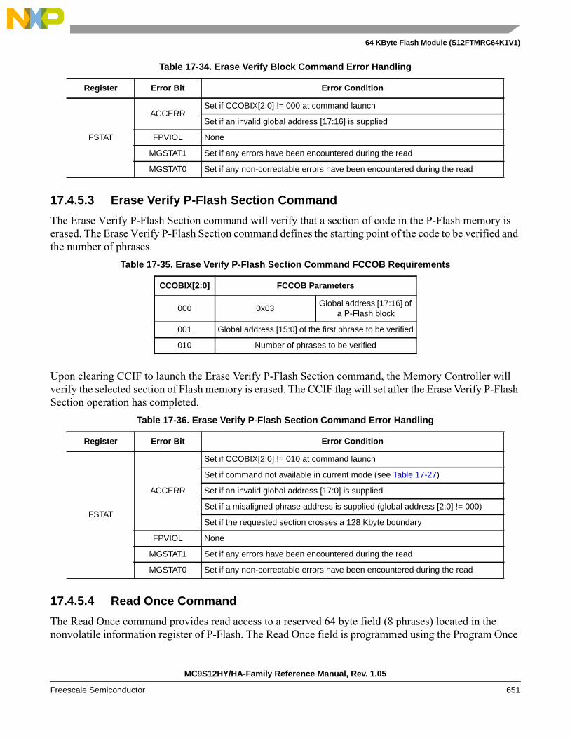
64 KByte Flash Module (S12FTMRC64K1V1)
17.4.5.3 Erase Verify P-Flash Section Command
The Erase Verify P-Flash Section command will verify that a section of code in the P-Flash memory iserased. The Erase Verify P-Flash Section command defines the starting point of the code to be verified andthe number of phrases.
Upon clearing CCIF to launch the Erase Verify P-Flash Section command, the Memory Controller willverify the selected section of Flash memory is erased. The CCIF flag will set after the Erase Verify P-FlashSection operation has completed.
17.4.5.4 Read Once Command
The Read Once command provides read access to a reserved 64 byte field (8 phrases) located in thenonvolatile information register of P-Flash. The Read Once field is programmed using the Program Once
Table 17-34. Erase Verify Block Command Error Handling
Register Error Bit Error Condition
FSTAT
ACCERRSet if CCOBIX[2:0] != 000 at command launch
Set if an invalid global address [17:16] is supplied
FPVIOL None
MGSTAT1 Set if any errors have been encountered during the read
MGSTAT0 Set if any non-correctable errors have been encountered during the read
Table 17-35. Erase Verify P-Flash Section Command FCCOB Requirements
CCOBIX[2:0] FCCOB Parameters
000 0x03Global address [17:16] of
a P-Flash block
001 Global address [15:0] of the first phrase to be verified
010 Number of phrases to be verified
Table 17-36. Erase Verify P-Flash Section Command Error Handling
Register Error Bit Error Condition
FSTAT
ACCERR
Set if CCOBIX[2:0] != 010 at command launch
Set if command not available in current mode (see Table 17-27)
Set if an invalid global address [17:0] is supplied
Set if a misaligned phrase address is supplied (global address [2:0] != 000)
Set if the requested section crosses a 128 Kbyte boundary
FPVIOL None
MGSTAT1 Set if any errors have been encountered during the read
MGSTAT0 Set if any non-correctable errors have been encountered during the read
MC9S12HY/HA-Family Reference Manual, Rev. 1.05
Freescale Semiconductor 651

64 KByte Flash Module (S12FTMRC64K1V1)
command described in Section 17.4.5.6. The Read Once command must not be executed from the Flashblock containing the Program Once reserved field to avoid code runaway.
Upon clearing CCIF to launch the Read Once command, a Read Once phrase is fetched and stored in theFCCOB indexed register. The CCIF flag will set after the Read Once operation has completed. Validphrase index values for the Read Once command range from 0x0000 to 0x0007. During execution of theRead Once command, any attempt to read addresses within P-Flash block will return invalid data.
8
17.4.5.5 Program P-Flash Command
The Program P-Flash operation will program a previously erased phrase in the P-Flash memory using anembedded algorithm.
CAUTIONA P-Flash phrase must be in the erased state before being programmed.Cumulative programming of bits within a Flash phrase is not allowed.
Table 17-37. Read Once Command FCCOB Requirements
CCOBIX[2:0] FCCOB Parameters
000 0x04 Not Required
001 Read Once phrase index (0x0000 - 0x0007)
010 Read Once word 0 value
011 Read Once word 1 value
100 Read Once word 2 value
101 Read Once word 3 value
Table 17-38. Read Once Command Error Handling
Register Error Bit Error Condition
FSTAT
ACCERR
Set if CCOBIX[2:0] != 001 at command launch
Set if command not available in current mode (see Table 17-27)
Set if an invalid phrase index is supplied
FPVIOL None
MGSTAT1 Set if any errors have been encountered during the read
MGSTAT0 Set if any non-correctable errors have been encountered during the read
Table 17-39. Program P-Flash Command FCCOB Requirements
CCOBIX[2:0] FCCOB Parameters
000 0x06Global address [17:16] to
identify P-Flash block
001 Global address [15:0] of phrase location to be programmed1
010 Word 0 program value
MC9S12HY/HA-Family Reference Manual, Rev. 1.05
652 Freescale Semiconductor

64 KByte Flash Module (S12FTMRC64K1V1)
Upon clearing CCIF to launch the Program P-Flash command, the Memory Controller will program thedata words to the supplied global address and will then proceed to verify the data words read back asexpected. The CCIF flag will set after the Program P-Flash operation has completed.
17.4.5.6 Program Once Command
The Program Once command restricts programming to a reserved 64 byte field (8 phrases) in thenonvolatile information register located in P-Flash. The Program Once reserved field can be read using theRead Once command as described in Section 17.4.5.4. The Program Once command must only be issuedonce since the nonvolatile information register in P-Flash cannot be erased. The Program Once commandmust not be executed from the Flash block containing the Program Once reserved field to avoid coderunaway.
011 Word 1 program value
100 Word 2 program value
101 Word 3 program value
1 Global address [2:0] must be 000
Table 17-40. Program P-Flash Command Error Handling
Register Error Bit Error Condition
FSTAT
ACCERR
Set if CCOBIX[2:0] != 101 at command launch
Set if command not available in current mode (see Table 17-27)
Set if an invalid global address [17:0] is supplied
Set if a misaligned phrase address is supplied (global address [2:0] != 000)
FPVIOL Set if the global address [17:0] points to a protected area
MGSTAT1 Set if any errors have been encountered during the verify operation
MGSTAT0Set if any non-correctable errors have been encountered during the verifyoperation
Table 17-41. Program Once Command FCCOB Requirements
CCOBIX[2:0] FCCOB Parameters
000 0x07 Not Required
001 Program Once phrase index (0x0000 - 0x0007)
010 Program Once word 0 value
011 Program Once word 1 value
100 Program Once word 2 value
101 Program Once word 3 value
Table 17-39. Program P-Flash Command FCCOB Requirements
CCOBIX[2:0] FCCOB Parameters
MC9S12HY/HA-Family Reference Manual, Rev. 1.05
Freescale Semiconductor 653
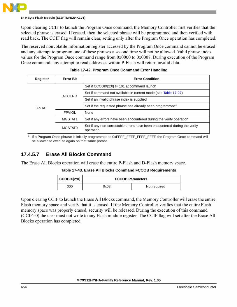
64 KByte Flash Module (S12FTMRC64K1V1)
Upon clearing CCIF to launch the Program Once command, the Memory Controller first verifies that theselected phrase is erased. If erased, then the selected phrase will be programmed and then verified withread back. The CCIF flag will remain clear, setting only after the Program Once operation has completed.
The reserved nonvolatile information register accessed by the Program Once command cannot be erasedand any attempt to program one of these phrases a second time will not be allowed. Valid phrase indexvalues for the Program Once command range from 0x0000 to 0x0007. During execution of the ProgramOnce command, any attempt to read addresses within P-Flash will return invalid data.
17.4.5.7 Erase All Blocks Command
The Erase All Blocks operation will erase the entire P-Flash and D-Flash memory space.
Upon clearing CCIF to launch the Erase All Blocks command, the Memory Controller will erase the entireFlash memory space and verify that it is erased. If the Memory Controller verifies that the entire Flashmemory space was properly erased, security will be released. During the execution of this command(CCIF=0) the user must not write to any Flash module register. The CCIF flag will set after the Erase AllBlocks operation has completed.
Table 17-42. Program Once Command Error Handling
Register Error Bit Error Condition
FSTAT
ACCERR
Set if CCOBIX[2:0] != 101 at command launch
Set if command not available in current mode (see Table 17-27)
Set if an invalid phrase index is supplied
Set if the requested phrase has already been programmed1
1 If a Program Once phrase is initially programmed to 0xFFFF_FFFF_FFFF_FFFF, the Program Once command willbe allowed to execute again on that same phrase.
FPVIOL None
MGSTAT1 Set if any errors have been encountered during the verify operation
MGSTAT0Set if any non-correctable errors have been encountered during the verifyoperation
Table 17-43. Erase All Blocks Command FCCOB Requirements
CCOBIX[2:0] FCCOB Parameters
000 0x08 Not required
MC9S12HY/HA-Family Reference Manual, Rev. 1.05
654 Freescale Semiconductor

64 KByte Flash Module (S12FTMRC64K1V1)
17.4.5.8 Erase Flash Block Command
The Erase Flash Block operation will erase all addresses in a P-Flash or D-Flash block.
Upon clearing CCIF to launch the Erase Flash Block command, the Memory Controller will erase theselected Flash block and verify that it is erased. The CCIF flag will set after the Erase Flash Blockoperation has completed.
17.4.5.9 Erase P-Flash Sector Command
The Erase P-Flash Sector operation will erase all addresses in a P-Flash sector.
Table 17-44. Erase All Blocks Command Error Handling
Register Error Bit Error Condition
FSTAT
ACCERRSet if CCOBIX[2:0] != 000 at command launch
Set if command not available in current mode (see Table 17-27)
FPVIOL Set if any area of the P-Flash or D-Flash memory is protected
MGSTAT1 Set if any errors have been encountered during the verify operation
MGSTAT0Set if any non-correctable errors have been encountered during the verifyoperation
Table 17-45. Erase Flash Block Command FCCOB Requirements
CCOBIX[2:0] FCCOB Parameters
000 0x09Global address [17:16] to
identify Flash block
001 Global address [15:0] in Flash block to be erased
Table 17-46. Erase Flash Block Command Error Handling
Register Error Bit Error Condition
FSTAT
ACCERR
Set if CCOBIX[2:0] != 001 at command launch
Set if command not available in current mode (see Table 17-27)
Set if an invalid global address [17:16] is supplied
Set if the supplied P-Flash address is not phrase-aligned or if the D-Flashaddress is not word-aligned
FPVIOL Set if an area of the selected Flash block is protected
MGSTAT1 Set if any errors have been encountered during the verify operation
MGSTAT0Set if any non-correctable errors have been encountered during the verifyoperation
MC9S12HY/HA-Family Reference Manual, Rev. 1.05
Freescale Semiconductor 655

64 KByte Flash Module (S12FTMRC64K1V1)
Upon clearing CCIF to launch the Erase P-Flash Sector command, the Memory Controller will erase theselected Flash sector and then verify that it is erased. The CCIF flag will be set after the Erase P-FlashSector operation has completed.
17.4.5.10 Unsecure Flash Command
The Unsecure Flash command will erase the entire P-Flash and D-Flash memory space and, if the erase issuccessful, will release security.
Upon clearing CCIF to launch the Unsecure Flash command, the Memory Controller will erase the entireP-Flash and D-Flash memory space and verify that it is erased. If the Memory Controller verifies that theentire Flash memory space was properly erased, security will be released. If the erase verify is notsuccessful, the Unsecure Flash operation sets MGSTAT1 and terminates without changing the securitystate. During the execution of this command (CCIF=0) the user must not write to any Flash moduleregister. The CCIF flag is set after the Unsecure Flash operation has completed.
Table 17-47. Erase P-Flash Sector Command FCCOB Requirements
CCOBIX[2:0] FCCOB Parameters
000 0x0AGlobal address [17:16] to identify
P-Flash block to be erased
001Global address [15:0] anywhere within the sector to be erased.
Refer to Section 17.1.2.1 for the P-Flash sector size.
Table 17-48. Erase P-Flash Sector Command Error Handling
Register Error Bit Error Condition
FSTAT
ACCERR
Set if CCOBIX[2:0] != 001 at command launch
Set if command not available in current mode (see Table 17-27)
Set if an invalid global address [17:16] is supplied
Set if a misaligned phrase address is supplied (global address [2:0] != 000)
FPVIOL Set if the selected P-Flash sector is protected
MGSTAT1 Set if any errors have been encountered during the verify operation
MGSTAT0Set if any non-correctable errors have been encountered during the verifyoperation
Table 17-49. Unsecure Flash Command FCCOB Requirements
CCOBIX[2:0] FCCOB Parameters
000 0x0B Not required
MC9S12HY/HA-Family Reference Manual, Rev. 1.05
656 Freescale Semiconductor

64 KByte Flash Module (S12FTMRC64K1V1)
17.4.5.11 Verify Backdoor Access Key Command
The Verify Backdoor Access Key command will only execute if it is enabled by the KEYEN bits in theFSEC register (see Table 17-9). The Verify Backdoor Access Key command releases security ifuser-supplied keys match those stored in the Flash security bytes of the Flash configuration field (seeTable 17-3). The Verify Backdoor Access Key command must not be executed from the Flash blockcontaining the backdoor comparison key to avoid code runaway.
Upon clearing CCIF to launch the Verify Backdoor Access Key command, the Memory Controller willcheck the FSEC KEYEN bits to verify that this command is enabled. If not enabled, the MemoryController sets the ACCERR bit in the FSTAT register and terminates. If the command is enabled, theMemory Controller compares the key provided in FCCOB to the backdoor comparison key in the Flashconfiguration field with Key 0 compared to 0x3_FF00, etc. If the backdoor keys match, security will bereleased. If the backdoor keys do not match, security is not released and all future attempts to execute theVerify Backdoor Access Key command are aborted (set ACCERR) until a reset occurs. The CCIF flag isset after the Verify Backdoor Access Key operation has completed.
Table 17-50. Unsecure Flash Command Error Handling
Register Error Bit Error Condition
FSTAT
ACCERRSet if CCOBIX[2:0] != 000 at command launch
Set if command not available in current mode (see Table 17-27)
FPVIOL Set if any area of the P-Flash or D-Flash memory is protected
MGSTAT1 Set if any errors have been encountered during the verify operation
MGSTAT0Set if any non-correctable errors have been encountered during the verifyoperation
Table 17-51. Verify Backdoor Access Key Command FCCOB Requirements
CCOBIX[2:0] FCCOB Parameters
000 0x0C Not required
001 Key 0
010 Key 1
011 Key 2
100 Key 3
MC9S12HY/HA-Family Reference Manual, Rev. 1.05
Freescale Semiconductor 657
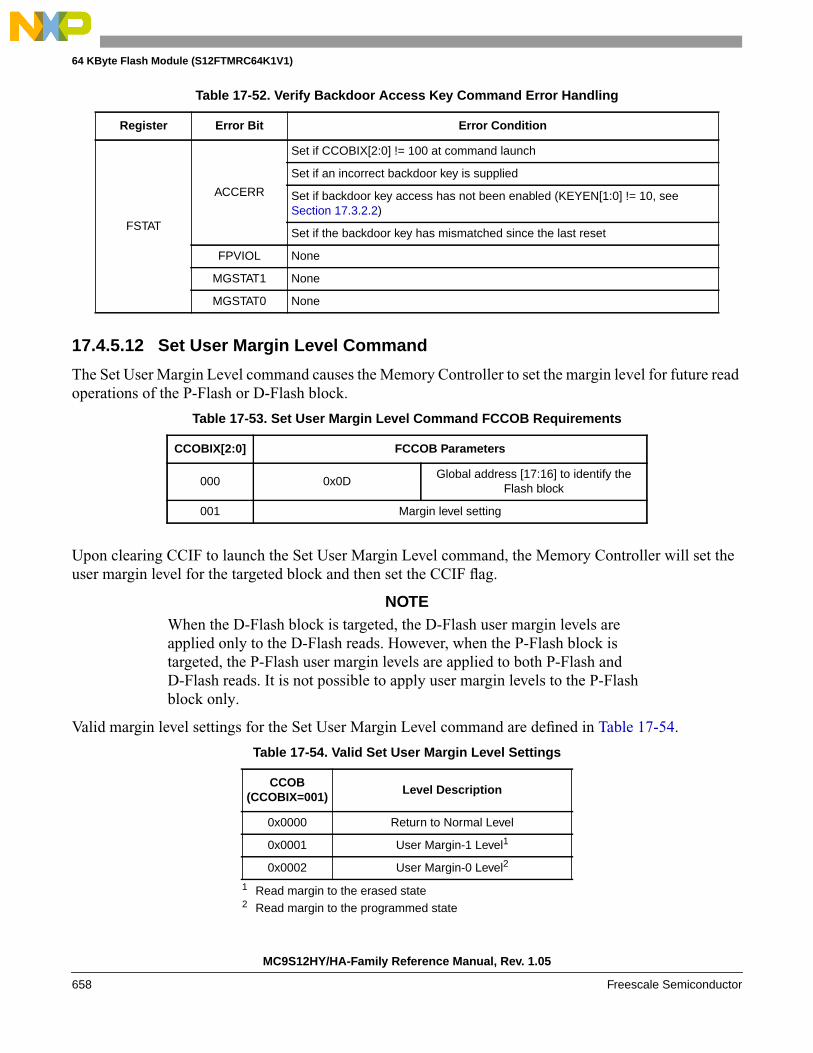
64 KByte Flash Module (S12FTMRC64K1V1)
17.4.5.12 Set User Margin Level Command
The Set User Margin Level command causes the Memory Controller to set the margin level for future readoperations of the P-Flash or D-Flash block.
Upon clearing CCIF to launch the Set User Margin Level command, the Memory Controller will set theuser margin level for the targeted block and then set the CCIF flag.
NOTEWhen the D-Flash block is targeted, the D-Flash user margin levels areapplied only to the D-Flash reads. However, when the P-Flash block istargeted, the P-Flash user margin levels are applied to both P-Flash andD-Flash reads. It is not possible to apply user margin levels to the P-Flashblock only.
Valid margin level settings for the Set User Margin Level command are defined in Table 17-54.
Table 17-52. Verify Backdoor Access Key Command Error Handling
Register Error Bit Error Condition
FSTAT
ACCERR
Set if CCOBIX[2:0] != 100 at command launch
Set if an incorrect backdoor key is supplied
Set if backdoor key access has not been enabled (KEYEN[1:0] != 10, seeSection 17.3.2.2)
Set if the backdoor key has mismatched since the last reset
FPVIOL None
MGSTAT1 None
MGSTAT0 None
Table 17-53. Set User Margin Level Command FCCOB Requirements
CCOBIX[2:0] FCCOB Parameters
000 0x0DGlobal address [17:16] to identify the
Flash block
001 Margin level setting
Table 17-54. Valid Set User Margin Level Settings
CCOB(CCOBIX=001)
Level Description
0x0000 Return to Normal Level
0x0001 User Margin-1 Level1
1 Read margin to the erased state
0x0002 User Margin-0 Level2
2 Read margin to the programmed state
MC9S12HY/HA-Family Reference Manual, Rev. 1.05
658 Freescale Semiconductor
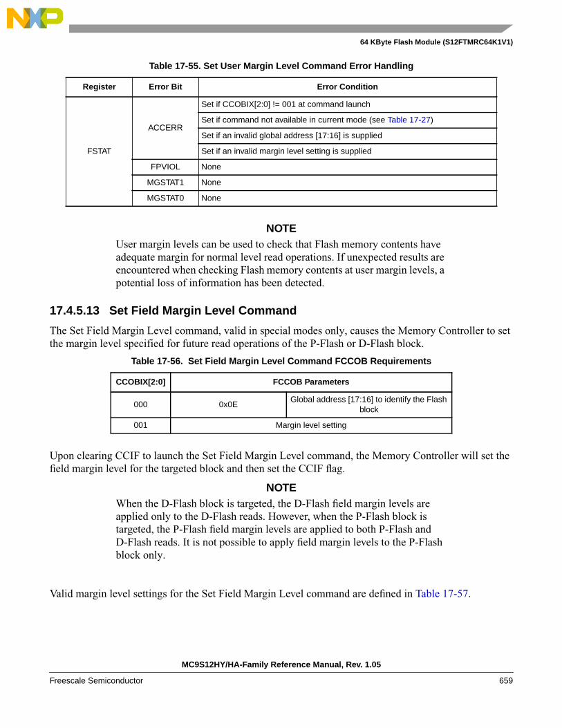
64 KByte Flash Module (S12FTMRC64K1V1)
NOTEUser margin levels can be used to check that Flash memory contents haveadequate margin for normal level read operations. If unexpected results areencountered when checking Flash memory contents at user margin levels, apotential loss of information has been detected.
17.4.5.13 Set Field Margin Level Command
The Set Field Margin Level command, valid in special modes only, causes the Memory Controller to setthe margin level specified for future read operations of the P-Flash or D-Flash block.
Upon clearing CCIF to launch the Set Field Margin Level command, the Memory Controller will set thefield margin level for the targeted block and then set the CCIF flag.
NOTEWhen the D-Flash block is targeted, the D-Flash field margin levels areapplied only to the D-Flash reads. However, when the P-Flash block istargeted, the P-Flash field margin levels are applied to both P-Flash andD-Flash reads. It is not possible to apply field margin levels to the P-Flashblock only.
Valid margin level settings for the Set Field Margin Level command are defined in Table 17-57.
Table 17-55. Set User Margin Level Command Error Handling
Register Error Bit Error Condition
FSTAT
ACCERR
Set if CCOBIX[2:0] != 001 at command launch
Set if command not available in current mode (see Table 17-27)
Set if an invalid global address [17:16] is supplied
Set if an invalid margin level setting is supplied
FPVIOL None
MGSTAT1 None
MGSTAT0 None
Table 17-56. Set Field Margin Level Command FCCOB Requirements
CCOBIX[2:0] FCCOB Parameters
000 0x0EGlobal address [17:16] to identify the Flash
block
001 Margin level setting
MC9S12HY/HA-Family Reference Manual, Rev. 1.05
Freescale Semiconductor 659

64 KByte Flash Module (S12FTMRC64K1V1)
CAUTIONField margin levels must only be used during verify of the initial factoryprogramming.
NOTEField margin levels can be used to check that Flash memory contents haveadequate margin for data retention at the normal level setting. If unexpectedresults are encountered when checking Flash memory contents at fieldmargin levels, the Flash memory contents should be erased andreprogrammed.
17.4.5.14 Erase Verify D-Flash Section Command
The Erase Verify D-Flash Section command will verify that a section of code in the D-Flash is erased. TheErase Verify D-Flash Section command defines the starting point of the data to be verified and the numberof words.
Table 17-57. Valid Set Field Margin Level Settings
CCOB(CCOBIX=001)
Level Description
0x0000 Return to Normal Level
0x0001 User Margin-1 Level1
1 Read margin to the erased state
0x0002 User Margin-0 Level2
2 Read margin to the programmed state
0x0003 Field Margin-1 Level1
0x0004 Field Margin-0 Level2
Table 17-58. Set Field Margin Level Command Error Handling
Register Error Bit Error Condition
FSTAT
ACCERR
Set if CCOBIX[2:0] != 001 at command launch
Set if command not available in current mode (see Table 17-27)
Set if an invalid global address [17:16] is supplied
Set if an invalid margin level setting is supplied
FPVIOL None
MGSTAT1 None
MGSTAT0 None
MC9S12HY/HA-Family Reference Manual, Rev. 1.05
660 Freescale Semiconductor

64 KByte Flash Module (S12FTMRC64K1V1)
Upon clearing CCIF to launch the Erase Verify D-Flash Section command, the Memory Controller willverify the selected section of D-Flash memory is erased. The CCIF flag will set after the Erase VerifyD-Flash Section operation has completed.
17.4.5.15 Program D-Flash Command
The Program D-Flash operation programs one to four previously erased words in the D-Flash block. TheProgram D-Flash operation will confirm that the targeted location(s) were successfully programmed uponcompletion.
CAUTIONA Flash word must be in the erased state before being programmed.Cumulative programming of bits within a Flash word is not allowed.
Table 17-59. Erase Verify D-Flash Section Command FCCOB Requirements
CCOBIX[2:0] FCCOB Parameters
000 0x10Global address [17:16] toidentify the D-Flash block
001 Global address [15:0] of the first word to be verified
010 Number of words to be verified
Table 17-60. Erase Verify D-Flash Section Command Error Handling
Register Error Bit Error Condition
FSTAT
ACCERR
Set if CCOBIX[2:0] != 010 at command launch
Set if command not available in current mode (see Table 17-27)
Set if an invalid global address [17:0] is supplied
Set if a misaligned word address is supplied (global address [0] != 0)
Set if the requested section breaches the end of the D-Flash block
FPVIOL None
MGSTAT1 Set if any errors have been encountered during the read
MGSTAT0 Set if any non-correctable errors have been encountered during the read
Table 17-61. Program D-Flash Command FCCOB Requirements
CCOBIX[2:0] FCCOB Parameters
000 0x11Global address [17:16] toidentify the D-Flash block
001 Global address [15:0] of word to be programmed
010 Word 0 program value
011 Word 1 program value, if desired
100 Word 2 program value, if desired
MC9S12HY/HA-Family Reference Manual, Rev. 1.05
Freescale Semiconductor 661

64 KByte Flash Module (S12FTMRC64K1V1)
Upon clearing CCIF to launch the Program D-Flash command, the user-supplied words will be transferredto the Memory Controller and be programmed if the area is unprotected. The CCOBIX index value atProgram D-Flash command launch determines how many words will be programmed in the D-Flash block.The CCIF flag is set when the operation has completed.
17.4.5.16 Erase D-Flash Sector Command
The Erase D-Flash Sector operation will erase all addresses in a sector of the D-Flash block.
Upon clearing CCIF to launch the Erase D-Flash Sector command, the Memory Controller will erase theselected Flash sector and verify that it is erased. The CCIF flag will set after the Erase D-Flash Sectoroperation has completed.
101 Word 3 program value, if desired
Table 17-62. Program D-Flash Command Error Handling
Register Error Bit Error Condition
FSTAT
ACCERR
Set if CCOBIX[2:0] < 010 at command launch
Set if CCOBIX[2:0] > 101 at command launch
Set if command not available in current mode (see Table 17-27)
Set if an invalid global address [17:0] is supplied
Set if a misaligned word address is supplied (global address [0] != 0)
Set if the requested group of words breaches the end of the D-Flash block
FPVIOL Set if the selected area of the D-Flash memory is protected
MGSTAT1 Set if any errors have been encountered during the verify operation
MGSTAT0Set if any non-correctable errors have been encountered during the verifyoperation
Table 17-63. Erase D-Flash Sector Command FCCOB Requirements
CCOBIX[2:0] FCCOB Parameters
000 0x12Global address [17:16] to identify
D-Flash block
001Global address [15:0] anywhere within the sector to be erased.
See Section 17.1.2.2 for D-Flash sector size.
Table 17-61. Program D-Flash Command FCCOB Requirements
CCOBIX[2:0] FCCOB Parameters
MC9S12HY/HA-Family Reference Manual, Rev. 1.05
662 Freescale Semiconductor

64 KByte Flash Module (S12FTMRC64K1V1)
17.4.6 Interrupts
The Flash module can generate an interrupt when a Flash command operation has completed or when aFlash command operation has detected an ECC fault.
NOTEVector addresses and their relative interrupt priority are determined at theMCU level.
17.4.6.1 Description of Flash Interrupt Operation
The Flash module uses the CCIF flag in combination with the CCIE interrupt enable bit to generate theFlash command interrupt request. The Flash module uses the DFDIF and SFDIF flags in combination withthe DFDIE and SFDIE interrupt enable bits to generate the Flash error interrupt request. For a detaileddescription of the register bits involved, refer to Section 17.3.2.5, “Flash Configuration Register(FCNFG)”, Section 17.3.2.6, “Flash Error Configuration Register (FERCNFG)”, Section 17.3.2.7, “FlashStatus Register (FSTAT)”, and Section 17.3.2.8, “Flash Error Status Register (FERSTAT)”.
The logic used for generating the Flash module interrupts is shown in Figure 17-27.
Table 17-64. Erase D-Flash Sector Command Error Handling
Register Error Bit Error Condition
FSTAT
ACCERR
Set if CCOBIX[2:0] != 001 at command launch
Set if command not available in current mode (see Table 17-27)
Set if an invalid global address [17:0] is supplied
Set if a misaligned word address is supplied (global address [0] != 0)
FPVIOL Set if the selected area of the D-Flash memory is protected
MGSTAT1 Set if any errors have been encountered during the verify operation
MGSTAT0Set if any non-correctable errors have been encountered during the verifyoperation
Table 17-65. Flash Interrupt Sources
Interrupt Source Interrupt Flag Local EnableGlobal (CCR)
Mask
Flash Command Complete CCIF(FSTAT register)
CCIE(FCNFG register)
I Bit
ECC Double Bit Fault on Flash Read DFDIF(FERSTAT register)
DFDIE(FERCNFG register)
I Bit
ECC Single Bit Fault on Flash Read SFDIF(FERSTAT register)
SFDIE(FERCNFG register)
I Bit
MC9S12HY/HA-Family Reference Manual, Rev. 1.05
Freescale Semiconductor 663

64 KByte Flash Module (S12FTMRC64K1V1)
Figure 17-27. Flash Module Interrupts Implementation
17.4.7 Wait Mode
The Flash module is not affected if the MCU enters wait mode. The Flash module can recover the MCUfrom wait via the CCIF interrupt (see Section 17.4.6, “Interrupts”).
17.4.8 Stop Mode
If a Flash command is active (CCIF = 0) when the MCU requests stop mode, the current Flash operationwill be completed before the CPU is allowed to enter stop mode.
17.5 SecurityThe Flash module provides security information to the MCU. The Flash security state is defined by theSEC bits of the FSEC register (see Table 17-10). During reset, the Flash module initializes the FSECregister using data read from the security byte of the Flash configuration field at global address 0x3_FF0F.The security state out of reset can be permanently changed by programming the security byte assumingthat the MCU is starting from a mode where the necessary P-Flash erase and program commands areavailable and that the upper region of the P-Flash is unprotected. If the Flash security byte is successfullyprogrammed, its new value will take affect after the next MCU reset.
The following subsections describe these security-related subjects:
• Unsecuring the MCU using Backdoor Key Access
• Unsecuring the MCU in Special Single Chip Mode using BDM
• Mode and Security Effects on Flash Command Availability
17.5.1 Unsecuring the MCU using Backdoor Key Access
The MCU may be unsecured by using the backdoor key access feature which requires knowledge of thecontents of the backdoor keys (four 16-bit words programmed at addresses 0x3_FF00-0x3_FF07). If theKEYEN[1:0] bits are in the enabled state (see Section 17.3.2.2), the Verify Backdoor Access Keycommand (see Section 17.4.5.11) allows the user to present four prospective keys for comparison to thekeys stored in the Flash memory via the Memory Controller. If the keys presented in the Verify BackdoorAccess Key command match the backdoor keys stored in the Flash memory, the SEC bits in the FSEC
Flash Error Interrupt Request
CCIFCCIE
DFDIFDFDIE
SFDIFSFDIE
Flash Command Interrupt Request
MC9S12HY/HA-Family Reference Manual, Rev. 1.05
664 Freescale Semiconductor
64 KByte Flash Module (S12FTMRC64K1V1)
register (see Table 17-10) will be changed to unsecure the MCU. Key values of 0x0000 and 0xFFFF arenot permitted as backdoor keys. While the Verify Backdoor Access Key command is active, P-Flashmemory and D-Flash memory will not be available for read access and will return invalid data.
The user code stored in the P-Flash memory must have a method of receiving the backdoor keys from anexternal stimulus. This external stimulus would typically be through one of the on-chip serial ports.
If the KEYEN[1:0] bits are in the enabled state (see Section 17.3.2.2), the MCU can be unsecured by thebackdoor key access sequence described below:
1. Follow the command sequence for the Verify Backdoor Access Key command as explained inSection 17.4.5.11
2. If the Verify Backdoor Access Key command is successful, the MCU is unsecured and theSEC[1:0] bits in the FSEC register are forced to the unsecure state of 10
The Verify Backdoor Access Key command is monitored by the Memory Controller and an illegal key willprohibit future use of the Verify Backdoor Access Key command. A reset of the MCU is the only methodto re-enable the Verify Backdoor Access Key command. The security as defined in the Flash security byte(0x3_FF0F) is not changed by using the Verify Backdoor Access Key command sequence. The backdoorkeys stored in addresses 0x3_FF00-0x3_FF07 are unaffected by the Verify Backdoor Access Keycommand sequence. The Verify Backdoor Access Key command sequence has no effect on the programand erase protections defined in the Flash protection register, FPROT.
After the backdoor keys have been correctly matched, the MCU will be unsecured. After the MCU isunsecured, the sector containing the Flash security byte can be erased and the Flash security byte can bereprogrammed to the unsecure state, if desired. In the unsecure state, the user has full control of thecontents of the backdoor keys by programming addresses 0x3_FF00-0x3_FF07 in the Flash configurationfield.
17.5.2 Unsecuring the MCU in Special Single Chip Mode using BDM
A secured MCU can be unsecured in special single chip mode by using the following method to erase theP-Flash and D-Flash memory:
1. Reset the MCU into special single chip mode
2. Delay while the BDM executes the Erase Verify All Blocks command write sequence to check ifthe P-Flash and D-Flash memories are erased
3. Send BDM commands to disable protection in the P-Flash and D-Flash memory
4. Execute the Erase All Blocks command write sequence to erase the P-Flash and D-Flash memory
5. After the CCIF flag sets to indicate that the Erase All Blocks operation has completed, reset theMCU into special single chip mode
6. Delay while the BDM executes the Erase Verify All Blocks command write sequence to verify thatthe P-Flash and D-Flash memory are erased
If the P-Flash and D-Flash memory are verified as erased, the MCU will be unsecured. All BDMcommands will now be enabled and the Flash security byte may be programmed to the unsecure state bycontinuing with the following steps:
MC9S12HY/HA-Family Reference Manual, Rev. 1.05
Freescale Semiconductor 665

64 KByte Flash Module (S12FTMRC64K1V1)
7. Send BDM commands to execute the Program P-Flash command write sequence to program theFlash security byte to the unsecured state
8. Reset the MCU
17.5.3 Mode and Security Effects on Flash Command Availability
The availability of Flash module commands depends on the MCU operating mode and security state asshown in Table 17-27.
17.6 InitializationOn each system reset the Flash module executes a reset sequence which establishes initial values for theFlash Block Configuration Parameters, the FPROT and DFPROT protection registers, and the FOPT andFSEC registers. The Flash module reverts to using built-in default values that leave the module in a fullyprotected and secured state if errors are encountered during execution of the reset sequence. If a double bitfault is detected during the reset sequence, both MGSTAT bits in the FSTAT register will be set.
CCIF remains clear throughout the reset sequence. The Flash module holds off all CPU access for theinitial portion of the reset sequence. While Flash memory reads and access to most Flash registers arepossible when the hold is removed, writes to the FCCOBIX, FCCOBHI, and FCCOBLO registers areignored. Completion of the reset sequence is marked by setting CCIF high which enables writes to theFCCOBIX, FCCOBHI, and FCCOBLO registers to launch any available Flash command.
If a reset occurs while any Flash command is in progress, that command will be immediately aborted. Thestate of the word being programmed or the sector/block being erased is not guaranteed.
MC9S12HY/HA-Family Reference Manual, Rev. 1.05
666 Freescale Semiconductor
Chapter 18Liquid Crystal Display (LCD40F4BV1) Block Description
Revision History
18.1 IntroductionThe LCD40F4BV1 driver module has 40 frontplane drivers and 4 backplane drivers so that a maximum of160 LCD segments are controllable. Each segment is controlled by a corresponding bit in the LCD RAM.Four multiplex modes (1/1, 1/2, 1/3, 1/4 duty), and three bias (1/1, 1/2, 1/3) methods are available. The V0voltage is the lowest level of the output waveform and V3 becomes the highest level. All frontplane andbackplane pins can be multiplexed with other port functions.
The LCD40F4BV1 driver system consists of five major sub-modules:
• Timing and Control – consists of registers and control logic for frame clock generation, biasvoltage level select, frame duty select, backplane select, and frontplane select/enable to producethe required frame frequency and voltage waveforms.
• LCD RAM – contains the data to be displayed on the LCD. Data can be read from or written to thedisplay RAM at any time.
• Frontplane Drivers – consists of 40 frontplane drivers.
• Backplane Drivers – consists of 4 backplane drivers.
• Voltage Generator – Based on voltage applied to VLCD, it generates the voltage levels for thetiming and control logic to produce the frontplane and backplane waveforms.
18.1.1 Features
The LCD40F4BV1 includes these distinctive features:
Table 18-1. LCD40F4BV1 Revision History
VersionNumber
RevisionDate
EffectiveDate
Author Description of Changes
01.00 26-Jul-00 initial LCD module spec
01.08 27-Mar-08 New specification for 9S12HY family based on 9S12H family specification
01.09 25-Apr-08 Update for 9S12HY defining last registers as unimplemented
MC9S12HY/HA-Family Reference Manual, Rev. 1.05
Freescale Semiconductor 667

Liquid Crystal Display (LCD40F4BV1) Block Description
• Supports five LCD operation modes
• 40 frontplane drivers
• 4 backplane drivers
— Each frontplane has an enable bit respectively
• Programmable frame clock generator
• Programmable bias voltage level selector
• On-chip generation of 4 different output voltage levels
18.1.2 Modes of Operation
The LCD40F4BV1 module supports five operation modes with different numbers of backplanes anddifferent biasing levels. During wait mode the LCD operation can be suspended under software control.Depending on the state of internal bits, the LCD can operate normally or the LCD clock generation can beturned off and the LCD40F4BV1 module enters a power conservation state.
This is a high level description only, detailed descriptions of operating modes are contained inSection 18.4.2, “Operation in Wait Mode”, and Section 18.4.3, “Operation in Stop Mode”.
18.1.3 Block Diagram
Figure 18-1 is a block diagram of the LCD40F4BV1 module.
MC9S12HY/HA-Family Reference Manual, Rev. 1.05
668 Freescale Semiconductor
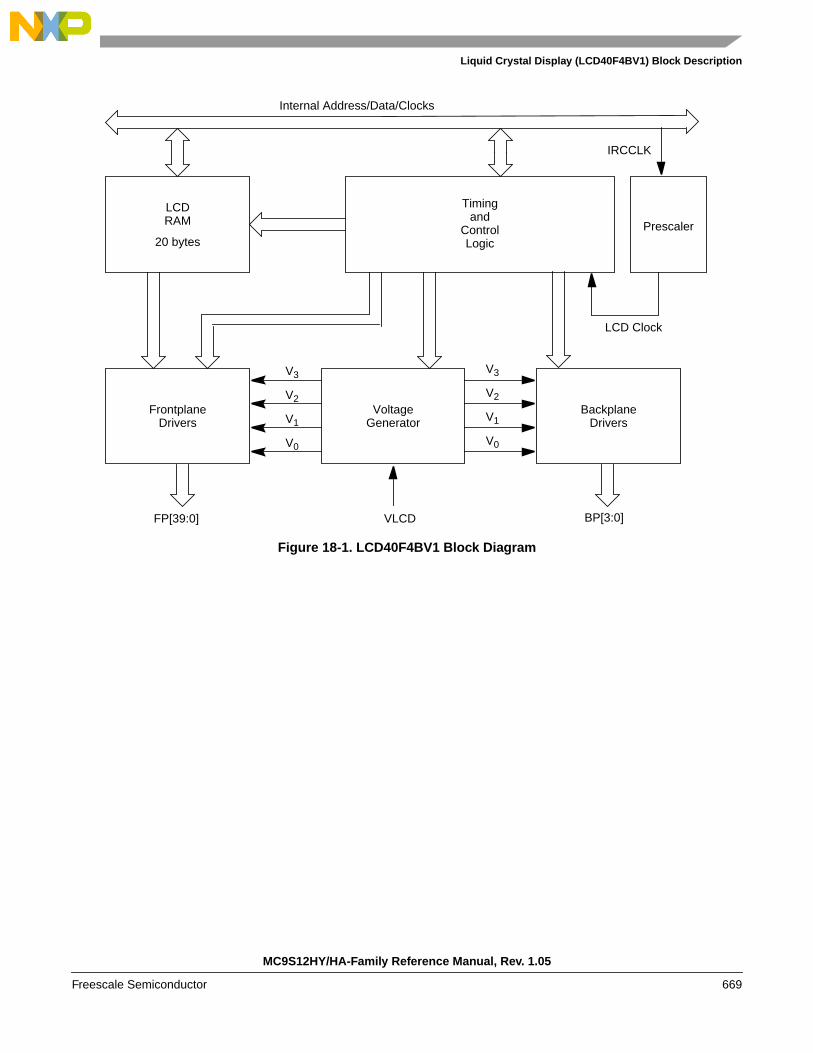
Liquid Crystal Display (LCD40F4BV1) Block Description
Figure 18-1. LCD40F4BV1 Block Diagram
LCDRAM
20 bytes
Timingand
ControlLogic
FrontplaneDrivers
VoltageGenerator
BackplaneDrivers
Internal Address/Data/Clocks
V3
V2
V1
V0
V3
V2
V1
V0
FP[39:0] VLCD BP[3:0]
Prescaler
IRCCLK
LCD Clock
MC9S12HY/HA-Family Reference Manual, Rev. 1.05
Freescale Semiconductor 669

Liquid Crystal Display (LCD40F4BV1) Block Description
18.2 External Signal DescriptionThe LCD40F4BV1 module has a total of 45 external pins.
18.2.1 BP[3:0] — Analog Backplane Pins
This output signal vector represents the analog backplane waveforms of the LCD40F4BV1 module and isconnected directly to the corresponding pads.
18.2.2 FP[39:0] — Analog Frontplane Pins
This output signal vector represents the analog frontplane waveforms of the LCD40F4BV1 module and isconnected directly to the corresponding pads.
18.2.3 VLCD — LCD Supply Voltage Pin
Positive supply voltage for the LCD waveform generation.
18.3 Memory Map and Register DefinitionThis section provides a detailed description of all memory and registers.
18.3.1 Module Memory Map
The memory map for the LCD40F4BV1 module is given in Table 18-3. The address listed for each registeris the address offset. The total address for each register is the sum of the base address for theLCD40F4BV1 module and the address offset for each register.
Table 18-2. Signal Properties
Name Port Function Reset State
4 backplane waveforms BP[3:0] Backplane waveform signalsthat connect directly to the pads
High impedance
40 frontplane waveforms FP[39:0] Frontplane waveform signalsthat connect directly to the pads
High impedance
LCD voltage VLCD LCD supply voltage —
MC9S12HY/HA-Family Reference Manual, Rev. 1.05
670 Freescale Semiconductor

Liquid Crystal Display (LCD40F4BV1) Block Description
Table 18-3. LCD40F4BV1 Memory Map
AddressOffset
Use Access
0x0000 LCD Control Register 0 (LCDCR0) Read/Write
0x0001 LCD Control Register 1 (LCDCR1) Read/Write
0x0002 LCD Frontplane Enable Register 0 (FPENR0) Read/Write
0x0003 LCD Frontplane Enable Register 1 (FPENR1) Read/Write
0x0004 LCD Frontplane Enable Register 2 (FPENR2) Read/Write
0x0005 LCD Frontplane Enable Register 3 (FPENR3) Read/Write
0x0006 LCD Frontplane Enable Register 4 (FPENR4) Read/Write
0x0007 Unimplemented
0x0008 LCDRAM (Location 0) Read/Write
0x0009 LCDRAM (Location 1) Read/Write
0x000A LCDRAM (Location 2) Read/Write
0x000B LCDRAM (Location 3) Read/Write
0x000C LCDRAM (Location 4) Read/Write
0x000D LCDRAM (Location 5) Read/Write
0x000E LCDRAM (Location 6) Read/Write
0x000F LCDRAM (Location 7) Read/Write
0x0010 LCDRAM (Location 8) Read/Write
0x0011 LCDRAM (Location 9) Read/Write
0x0012 LCDRAM (Location 10) Read/Write
0x0013 LCDRAM (Location 11) Read/Write
0x0014 LCDRAM (Location 12) Read/Write
0x0015 LCDRAM (Location 13) Read/Write
0x0016 LCDRAM (Location 14) Read/Write
0x0017 LCDRAM (Location 15) Read/Write
0x0018 LCDRAM (Location 16) Read/Write
0x0019 LCDRAM (Location 17) Read/Write
0x001A LCDRAM (Location 18) Read/Write
0x001B LCDRAM (Location 19) Read/Write
0x001C-0x001F
Unimplemented
MC9S12HY/HA-Family Reference Manual, Rev. 1.05
Freescale Semiconductor 671

Liquid Crystal Display (LCD40F4BV1) Block Description
18.3.2 Register Descriptions
This section consists of register descriptions. Each description includes a standard register diagram.Details of register bit and field function follow the register diagrams, in bit order.
18.3.2.1 LCD Control Register 0 (LCDCR0)
Read: anytime
Write: LCDEN anytime. To avoid segment flicker the clock prescaler bits, the bias select bit and the dutyselect bits must not be changed when the LCD is enabled.
Module Base + 0x0000
7 6 5 4 3 2 1 0
RLCDEN
0LCLK2 LCLK1 LCLK0 BIAS DUTY1 DUTY0
W
Reset 0 0 0 0 0 0 0 0
= Unimplemented or Reserved
Figure 18-2. LCD Control Register 0 (LCDCR0)
Table 18-4. LCDCR0 Field Descriptions
Field Description
7LCDEN
LCD40F4BV1 Driver System Enable — The LCDEN bit starts the LCD waveform generator.0 All frontplane and backplane pins are disabled. In addition, the LCD40F4BV1 system is disabled
and all LCD waveform generation clocks are stopped.1 LCD driver system is enabled. All FP[39:0] pins with FP[39:0]EN set, will output an LCD driver
waveform The BP[3:0] pins will output an LCD40F4BV1 driver waveform based on the settings of DUTY0and DUTY1.
5:3LCLK[2:0]
LCD Clock Prescaler — The LCD clock prescaler bits determine the IRCCLK divider value to produce the LCDclock frequency. For detailed description of the correlation between LCD clock prescaler bits and the dividervalue please refer to Table 18-8.
2BIAS
BIAS Voltage Level Select — This bit selects the bias voltage levels during various LCD operating modes, asshown in Table 18-9.
1:0DUTY[1:0]
LCD Duty Select — The DUTY1 and DUTY0 bits select the duty (multiplex mode) of the LCD40F4BV1 driversystem, as shown in Table 18-9.
MC9S12HY/HA-Family Reference Manual, Rev. 1.05
672 Freescale Semiconductor

Liquid Crystal Display (LCD40F4BV1) Block Description
18.3.2.2 LCD Control Register 1 (LCDCR1)
Read: anytime
Write: anytime
Module Base + 0x0001
7 6 5 4 3 2 1 0
R 0 0 0 0 0 0LCDSWAI
0
W
Reset 0 0 0 0 0 0 0 0
Unimplemented or Reserved
Figure 18-3. LCD Control Register 1 (LCDCR1)
Table 18-5. LCDCR1 Field Descriptions
Field Description
1LCDSWAI
LCD Stop in Wait Mode — This bit controls the LCD operation while in wait mode.0 LCD operates normally in wait mode.1 Stop LCD40F4BV1 driver system when in wait mode.
MC9S12HY/HA-Family Reference Manual, Rev. 1.05
Freescale Semiconductor 673

Liquid Crystal Display (LCD40F4BV1) Block Description
18.3.2.3 LCD Frontplane Enable Register 0–3 (FPENR0–FPENR4)
These bits enable the frontplane output waveform on the corresponding frontplane pin when LCDEN = 1.
Read: anytime
Write: anytime
Module Base + 0x0002
7 6 5 4 3 2 1 0
RFP7EN FP6EN FP5EN FP4EN FP3EN FP2EN FP1EN FP0EN
W
Reset 0 0 0 0 0 0 0 0
Figure 18-4. LCD Frontplane Enable Register 0 (FPENR0)
Module Base + 0x0003
7 6 5 4 3 2 1 0
RFP15EN FP14EN FP13EN FP12EN FP11EN FP10EN FP9EN FP8EN
W
Reset 0 0 0 0 0 0 0 0
Figure 18-5. LCD Frontplane Enable Register 1 (FPENR1)
Module Base + 0x0004
7 6 5 4 3 2 1 0
RFP23EN FP22EN FP21EN FP20EN FP19EN FP18EN FP17EN FP16EN
W
Reset 0 0 0 0 0 0 0 0
Figure 18-6. LCD Frontplane Enable Register 2 (FPENR2)
Module Base + 0x0005
7 6 5 4 3 2 1 0
RFP31EN FP30EN FP29EN FP28EN FP27EN FP26EN FP25EN FP24EN
W
Reset 0 0 0 0 0 0 0 0
Figure 18-7. LCD Frontplane Enable Register 3 (FPENR3)
Module Base + 0x0005
7 6 5 4 3 2 1 0
RFP39EN FP38EN FP37EN FP36EN FP35EN FP34EN FP33EN FP32EN
W
Reset 0 0 0 0 0 0 0 0
Figure 18-8. LCD Frontplane Enable Register 4 (FPENR4)
MC9S12HY/HA-Family Reference Manual, Rev. 1.05
674 Freescale Semiconductor

Liquid Crystal Display (LCD40F4BV1) Block Description
18.3.2.4 LCD RAM (LCDRAM)
The LCD RAM consists of 20 bytes. After reset the LCD RAM contents will be indeterminate (I), asindicated by Figure 18-9.
Table 18-6. FPENR0–FPENR4 Field Descriptions
Field Description
39:0FP[39:0]EN
Frontplane Output Enable — The FP[39:0]EN bit enables the frontplane driver outputs. If LCDEN = 0, thesebits have no effect on the state of the I/O pins. It is recommended to set FP[39:0]EN bits before LCDEN is set.0 Frontplane driver output disabled on FP[39:0].1 Frontplane driver output enabled on FP[39:0].
7 6 5 4 3 2 1 0
0x0008 RFP1BP3 FP1BP2 FP1BP1 FP1BP0 FP0BP3 FP0BP2 FP0BP1 FP0BP0
LCDRAM W
Reset I I I I I I I I
0x0009 RFP3BP3 FP3BP2 FP3BP1 FP3BP0 FP2BP3 FP2BP2 FP2BP1 FP2BP0
LCDRAM W
Reset I I I I I I I I
0x000A RFP5BP3 FP5BP2 FP5BP1 FP5BP0 FP4BP3 FP4BP2 FP4BP1 FP4BP0
LCDRAM W
Reset I I I I I I I I
0x000B RFP7BP3 FP7BP2 FP7BP1 FP7BP0 FP6BP3 FP6BP2 FP6BP1 FP6BP0
LCDRAM W
Reset I I I I I I I I
0x000C RFP9BP3 FP9BP2 FP9BP1 FP9BP0 FP8BP3 FP8BP2 FP8BP1 FP8BP0
LCDRAM W
Reset I I I I I I I I
0x000D RFP11BP3 FP11BP2 FP11BP1 FP11BP0 FP10BP3 FP10BP2 FP10BP1 FP10BP0
LCDRAM W
Reset I I I I I I I I
0x000E RFP13BP3 FP13BP2 FP13BP1 FP13BP0 FP12BP3 FP12BP2 FP12BP1 FP12BP0
LCDRAM W
Reset I I I I I I I I
0x000F RFP15BP3 FP15BP2 FP15BP1 FP15BP0 FP14BP3 FP14BP2 FP14BP1 FP14BP0
LCDRAM W
Reset I I I I I I I I
0x0010 RFP17BP3 FP17BP2 FP17BP1 FP17BP0 FP16BP3 FP16BP2 FP16BP1 FP16BP0
LCDRAM W
Reset I I I I I I I I
I = Value is indeterminate
Figure 18-9. LCD RAM (LCDRAM)
MC9S12HY/HA-Family Reference Manual, Rev. 1.05
Freescale Semiconductor 675
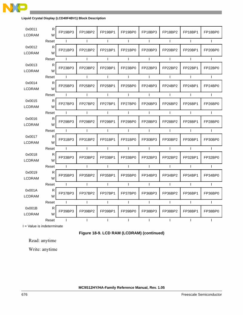
Liquid Crystal Display (LCD40F4BV1) Block Description
Read: anytime
Write: anytime
0x0011 RFP19BP3 FP19BP2 FP19BP1 FP19BP0 FP18BP3 FP18BP2 FP18BP1 FP18BP0
LCDRAM W
Reset I I I I I I I I
0x0012 RFP21BP3 FP21BP2 FP21BP1 FP21BP0 FP20BP3 FP20BP2 FP20BP1 FP20BP0
LCDRAM W
Reset I I I I I I I I
0x0013 RFP23BP3 FP23BP2 FP23BP1 FP23BP0 FP22BP3 FP22BP2 FP22BP1 FP22BP0
LCDRAM W
Reset I I I I I I I I
0x0014 RFP25BP3 FP25BP2 FP25BP1 FP25BP0 FP24BP3 FP24BP2 FP24BP1 FP24BP0
LCDRAM W
Reset I I I I I I I I
0x0015 RFP27BP3 FP27BP2 FP27BP1 FP27BP0 FP26BP3 FP26BP2 FP26BP1 FP26BP0
LCDRAM W
Reset I I I I I I I I
0x0016 RFP29BP3 FP29BP2 FP29BP1 FP29BP0 FP28BP3 FP28BP2 FP28BP1 FP28BP0
LCDRAM W
Reset I I I I I I I I
0x0017 RFP31BP3 FP31BP2 FP31BP1 FP31BP0 FP30BP3 FP30BP2 FP30BP1 FP30BP0
LCDRAM W
Reset I I I I I I I I
0x0018 RFP33BP3 FP33BP2 FP33BP1 FP33BP0 FP32BP3 FP32BP2 FP32BP1 FP32BP0
LCDRAM W
Reset I I I I I I I I
0x0019 RFP35BP3 FP35BP2 FP35BP1 FP35BP0 FP34BP3 FP34BP2 FP34BP1 FP34BP0
LCDRAM W
Reset I I I I I I I I
0x001A RFP37BP3 FP37BP2 FP37BP1 FP37BP0 FP36BP3 FP36BP2 FP36BP1 FP36BP0
LCDRAM W
Reset I I I I I I I I
0x001B RFP39BP3 FP39BP2 FP39BP1 FP39BP0 FP38BP3 FP38BP2 FP38BP1 FP38BP0
LCDRAM W
Reset I I I I I I I I
I = Value is indeterminate
Figure 18-9. LCD RAM (LCDRAM) (continued)
MC9S12HY/HA-Family Reference Manual, Rev. 1.05
676 Freescale Semiconductor

Liquid Crystal Display (LCD40F4BV1) Block Description
18.4 Functional DescriptionThis section provides a complete functional description of the LCD40F4BV1 block, detailing theoperation of the design from the end user perspective in a number of subsections.
18.4.1 LCD Driver Description
18.4.1.1 Frontplane, Backplane, and LCD System During Reset
During a reset the following conditions exist:
• The LCD40F4BV1 system is configured in the default mode, 1/4 duty and 1/3 bias, that means allbackplanes are used.
• All frontplane enable bits, FP[39:0]EN are cleared and the ON/OFF control for the display, theLCDEN bit is cleared, thereby forcing all frontplane and backplane driver outputs to the highimpedance state. The MCU pin state during reset is defined by the port integration module (PIM).
18.4.1.2 LCD Clock and Frame Frequency
The frequency of the source clock (IRCCLK) and divider determine the LCD clock frequency. The divideris set by the LCD clock prescaler bits, LCLK[2:0], in the LCD control register 0 (LCDCR0). Table 18-8shows the LCD clock and frame frequency for some multiplexed mode at IRCCLK = 16 MHz, 8 MHz, 4MHz, 2 MHz, 1 MHz, and 0.5 MHz.
Table 18-7. LCD RAM Field Descriptions
Field Description
39:03:0
FP[39:0]BP[3:0]
LCD Segment ON — The FP[39:0]BP[3:0] bit displays (turns on) the LCD segment connected between FP[39:0]and BP[3:0].0 LCD segment OFF1 LCD segment ON
Table 18-8. LCD Clock and Frame Frequency
Source clockFrequency in
MHz
LCD Clock PrescalerDivider
LCD ClockFrequency [Hz]
Frame Frequency [Hz]
LCLK2 LCLK1 LCLK0 1/1 Duty 1/2 Duty 1/3 Duty 1/4 Duty
IRCCLK = 0.500
00
01
10242048
488244
488244
244122
16381
12261
IRCCLK = 1.000
01
10
20484096
488244
488244
244122
16381
12261
IRCCLK = 2.000
11
01
40968192
488244
488244
244122
16381
12261
IRCCLK = 4.001
10
10
819216384
488244
488244
244122
16381
12261
IRCCLK = 8.011
00
01
1638432768
488244
488244
244122
16381
12261
MC9S12HY/HA-Family Reference Manual, Rev. 1.05
Freescale Semiconductor 677

Liquid Crystal Display (LCD40F4BV1) Block Description
For other combinations of IRCCLK and divider not shown in Table 18-8, the following formula may beused to calculate the LCD frame frequency for each multiplex mode:
The possible divider values are shown in Table 18-8.
18.4.1.3 LCD RAM
For a segment on the LCD to be displayed, data must be written to the LCD RAM which is shown inSection 18.3, “Memory Map and Register Definition”. The 160 bits in the LCD RAM correspond to the160 segments that are driven by the frontplane and backplane drivers. Writing a 1 to a given location willresult in the corresponding display segment being driven with a differential RMS voltage necessary to turnthe segment ON when the LCDEN bit is set and the corresponding FP[39:0]EN bit is set. Writing a 0 to agiven location will result in the corresponding display segment being driven with a differential RMSvoltage necessary to turn the segment OFF. The LCD RAM is a dual port RAM that interfaces with theinternal address and data buses of the MCU. It is possible to read from LCD RAM locations for scrollingpurposes. When LCDEN = 0, the LCD RAM can be used as on-chip RAM. Writing or reading of theLCDEN bit does not change the contents of the LCD RAM. After a reset, the LCD RAM contents will beindeterminate.
18.4.1.4 LCD Driver System Enable and Frontplane Enable Sequencing
If LCDEN = 0 (LCD40F4BV1 driver system disabled) and the frontplane enable bit, FP[39:0]EN, is set,the frontplane driver waveform will not appear on the output until LCDEN is set. If LCDEN = 1(LCD40F4BV1 driver system enabled), the frontplane driver waveform will appear on the output as soonas the corresponding frontplane enable bit, FP[39:0]EN, in the registers FPENR0–FPENR4 is set.
18.4.1.5 LCD Bias and Modes of Operation
The LCD40F4BV1 driver has five modes of operation:
• 1/1 duty (1 backplane), 1/1 bias (2 voltage levels)
• 1/2 duty (2 backplanes), 1/2 bias (3 voltage levels)
• 1/2 duty (2 backplanes), 1/3 bias (4 voltage levels)
• 1/3 duty (3 backplanes), 1/3 bias (4 voltage levels)
• 1/4 duty (4 backplanes), 1/3 bias (4 voltage levels)
IRCCLK = 16.011
11
01
65536131072
244122
244122
12261
8140
6131
Table 18-8. LCD Clock and Frame Frequency
Source clockFrequency in
MHz
LCD Clock PrescalerDivider
LCD ClockFrequency [Hz]
Frame Frequency [Hz]
LCLK2 LCLK1 LCLK0 1/1 Duty 1/2 Duty 1/3 Duty 1/4 Duty
LCD Frame Frequency (Hz)IRCCLK (Hz)( )
Divider--------------------------------------- Duty⋅=
MC9S12HY/HA-Family Reference Manual, Rev. 1.05
678 Freescale Semiconductor

Liquid Crystal Display (LCD40F4BV1) Block Description
The voltage levels required for the different operating modes are generated internally based on VLCD.Changing VLCD alters the differential RMS voltage across the segments in the ON and OFF states,thereby setting the display contrast.
The backplane waveforms are continuous and repetitive every frame. They are fixed within each operatingmode and are not affected by the data in the LCD RAM.
The frontplane waveforms generated are dependent on the state (ON or OFF) of the LCD segments asdefined in the LCD RAM. The LCD40F4BV1 driver hardware uses the data in the LCD RAM to constructthe frontplane waveform to create a differential RMS voltage necessary to turn the segment ON or OFF.
The LCD duty is decided by the DUTY1 and DUTY0 bits in the LCD control register 0 (LCDCR0). Thenumber of bias voltage levels is determined by the BIAS bit in LCDCR0. Table 18-9 summarizes themultiplex modes (duties) and the bias voltage levels that can be selected for each multiplex mode (duty).The backplane pins have their corresponding backplane waveform output BP[3:0] in high impedance statewhen in the OFF state as indicated in Table 18-9. In the OFF state the corresponding pins BP[3:0]can beused for other functionality, for example as general purpose I/O ports.
18.4.2 Operation in Wait Mode
The LCD40F4BV1 driver system operation during wait mode is controlled by the LCD stop in wait(LCDSWAI) bit in the LCD control register 1 (LCDCR1). If LCDSWAI is reset, the LCD40F4BV1 driversystem continues to operate during wait mode. If LCDSWAI is set, the LCD40F4BV1 driver system isturned off during wait mode. In this case, the LCD waveform generation clocks are stopped and theLCD40F4BV1 drivers pull down to VSSX those frontplane and backplane pins that were enabled beforeentering wait mode. The contents of the LCD RAM and the LCD registers retain the values they had priorto entering wait mode.
18.4.3 Operation in Stop Mode
All LCD40F4BV1 driver system clocks are stopped, the LCD40F4BV1 driver system pulls down to VSSXthose frontplane and backplane pins that were enabled before entering stop mode. Also, during stop mode,the contents of the LCD RAM and the LCD registers retain the values they had prior to entering stop mode.As a result, after exiting from stop mode, the LCD40F4BV1 driver system clocks will run (if LCDEN =1) and the frontplane and backplane pins retain the functionality they had prior to entering stop mode.
Table 18-9. LCD Duty and Bias
DutyLCDCR0 Register Backplanes Bias (BIAS = 0) Bias (BIAS = 1)
DUTY1 DUTY0 BP3 BP2 BP1 BP0 1/1 1/2 1/3 1/1 1/2 1/3
1/1
1/2
1/3
1/4
0
1
1
0
1
0
1
0
OFF
OFF
OFF
BP3
OFF
OFF
BP2
BP2
OFF
BP1
BP1
BP1
BP0
BP0
BP0
BP0
YES
NA
NA
NA
NA
YES
NA
NA
NA
NA
YES
YES
YES
NA
NA
NA
NA
NA
NA
NA
NA
YES
YES
YES
MC9S12HY/HA-Family Reference Manual, Rev. 1.05
Freescale Semiconductor 679

Liquid Crystal Display (LCD40F4BV1) Block Description
18.4.4 LCD Waveform Examples
Figure 18-10 through Figure 18-14 show the timing examples of the LCD output waveforms for theavailable modes of operation.
MC9S12HY/HA-Family Reference Manual, Rev. 1.05
680 Freescale Semiconductor
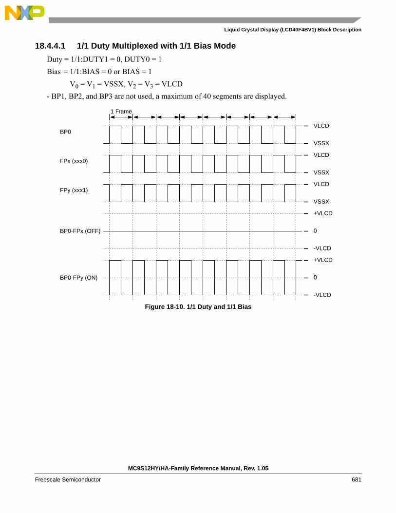
Liquid Crystal Display (LCD40F4BV1) Block Description
18.4.4.1 1/1 Duty Multiplexed with 1/1 Bias Mode
Duty = 1/1:DUTY1 = 0, DUTY0 = 1
Bias = 1/1:BIAS = 0 or BIAS = 1
V0 = V1 = VSSX, V2 = V3 = VLCD
- BP1, BP2, and BP3 are not used, a maximum of 40 segments are displayed.
Figure 18-10. 1/1 Duty and 1/1 Bias
0
0
VLCD
VSSX
BP0
+VLCD
-VLCD
BP0-FPx (OFF)
+VLCD
-VLCD
BP0-FPy (ON)
VLCD
VSSX
FPx (xxx0)
VLCD
VSSX
FPy (xxx1)
1 Frame
MC9S12HY/HA-Family Reference Manual, Rev. 1.05
Freescale Semiconductor 681

Liquid Crystal Display (LCD40F4BV1) Block Description
18.4.4.2 1/2 Duty Multiplexed with 1/2 Bias Mode
Duty = 1/2:DUTY1 = 1, DUTY0 = 0
Bias = 1/2:BIAS = 0
V0 = VSSX, V1 = V2 = VLCD * 1/2, V3 = VLCD
- BP2 and BP3 are not used, a maximum of 80 segments are displayed.
Figure 18-11. 1/2 Duty and 1/2 Bias
0
VLCD
VSSXBP0
+VLCD
-VLCD
BP0-FPx (OFF)
1 Frame
VLCD × 1/2
VLCD
VSSXBP1
VLCD
VSSXFPx (xx10)
VLCD
VSSXFPy (xx00)
VLCD
VSSXFPz (xx11)
+VLCD × 1/2
-VLCD × 1/2
0
+VLCD
-VLCD
BP1-FPx (ON)+VLCD × 1/2
-VLCD × 1/2
0
+VLCD
-VLCD
BP0-FPy (OFF)+VLCD × 1/2
-VLCD × 1/2
0
+VLCD
-VLCD
BP0-FPz (ON)+VLCD × 1/2
-VLCD × 1/2
VLCD × 1/2
VLCD × 1/2
VLCD × 1/2
VLCD × 1/2
MC9S12HY/HA-Family Reference Manual, Rev. 1.05
682 Freescale Semiconductor

Liquid Crystal Display (LCD40F4BV1) Block Description
18.4.4.3 1/2 Duty Multiplexed with 1/3 Bias Mode
Duty = 1/2:DUTY1 = 1, DUTY0 = 0Bias = 1/3:BIAS = 1
V0 = VSSX, V1 = VLCD * 1/3, V2 = VLCD * 2/3, V3 = VLCD- BP2 and BP3 are not used, a maximum of 80 segments are displayed.
MC9S12HY/HA-Family Reference Manual, Rev. 1.05
Freescale Semiconductor 683
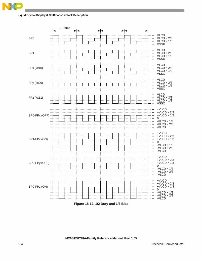
Liquid Crystal Display (LCD40F4BV1) Block Description
Figure 18-12. 1/2 Duty and 1/3 Bias
-VLCD × 1/3
+VLCD × 1/3
-VLCD × 1/3
+VLCD × 1/3
-VLCD × 1/3
VLCD × 1/3
0
VLCD
VSSX
BP0
-VLCD
BP0-FPx (OFF)
1 Frame
VLCD × 2/3
+VLCD × 2/3
-VLCD × 2/3
VLCD
VSSX
BP1 VLCD × 2/3
VLCD
VSSX
FPx (xx10) VLCD × 2/3
VLCD
VSSX
FPy (xx00) VLCD × 2/3
VLCD
VSSX
FPz (xx11) VLCD × 2/3
+VLCD × 1/3
-VLCD × 1/3
0
+VLCD
-VLCD
BP1-FPx (ON)+VLCD × 2/3
-VLCD × 2/3
+VLCD × 1/3
0
+VLCD
-VLCD
BP0-FPy (OFF)+VLCD × 2/3
-VLCD × 2/3
0
+VLCD
-VLCD
BP0-FPz (ON)+VLCD × 2/3
-VLCD × 2/3
VLCD × 1/3
VLCD × 1/3
VLCD × 1/3
VLCD × 1/3
+VLCD
MC9S12HY/HA-Family Reference Manual, Rev. 1.05
684 Freescale Semiconductor

Liquid Crystal Display (LCD40F4BV1) Block Description
18.4.4.4 1/3 Duty Multiplexed with 1/3 Bias Mode
Duty = 1/3:DUTY1 = 1, DUTY0 = 1
Bias = 1/3:BIAS = 0 or BIAS = 1
V0 = VSSX, V1 = VLCD * 1/3, V2 = VLCD * 2/3, V3 = VLCD
- BP3 is not used, a maximum of 120 segments are displayed.
Figure 18-13. 1/3 Duty and 1/3 Bias
+VLCD × 1/3
-VLCD × 1/3
+VLCD × 1/3
-VLCD × 1/3
VLCD × 1/3
VLCD × 1/3
VLCD × 1/3
VLCD × 1/3
0
VLCD
VSSX
BP0
+VLCD
-VLCD
BP0-FPx (OFF)
1 Frame
VLCD × 2/3
+VLCD × 2/3
-VLCD × 2/3
VLCD
VSSX
BP1 VLCD × 2/3
VLCD
VSSX
BP2 VLCD × 2/3
0
+VLCD
-VLCD
BP1-FPx (ON)+VLCD × 2/3
-VLCD × 2/3
VLCD
VSSX
FPx (x010) VLCD × 2/3
MC9S12HY/HA-Family Reference Manual, Rev. 1.05
Freescale Semiconductor 685

Liquid Crystal Display (LCD40F4BV1) Block Description
18.4.4.5 1/4 Duty Multiplexed with 1/3 Bias Mode
Duty = 1/4:DUTY1 = 0, DUTY0 = 0
Bias = 1/3:BIAS = 0 or BIAS = 1
V0 = VSSX, V1 = VLCD * 1/3, V2 = VLCD * 2/3, V3 = VLCD
- A maximum of 160 segments are displayed.
Figure 18-14. 1/4 Duty and 1/3 Bias
+VLCD × 1/3
-VLCD × 1/3
+VLCD × 1/3
-VLCD × 1/3
VLCD × 1/3
VLCD × 1/3
VLCD × 1/3
VLCD × 1/3
VLCD × 1/3
0
VLCD
VSSX
BP0
+VLCD
-VLCD
BP0-FPx (ON)
1 Frame
VLCD × 2/3
+VLCD × 2/3
-VLCD × 2/3
VLCD
VSSX
BP1 VLCD × 2/3
VLCD
VSSX
BP2 VLCD × 2/3
0
+VLCD
-VLCD
BP1-FPx (OFF)+VLCD × 2/3
-VLCD × 2/3
VLCD
VSSX
FPx (1001) VLCD × 2/3
VLCD
VSSX
BP3 VLCD × 2/3
MC9S12HY/HA-Family Reference Manual, Rev. 1.05
686 Freescale Semiconductor

Liquid Crystal Display (LCD40F4BV1) Block Description
18.5 ResetsThe reset values of registers and signals are described in Section 18.3, “Memory Map and RegisterDefinition”. The behavior of the LCD40F4BV1 system during reset is described in Section 18.4.1, “LCDDriver Description”.
18.6 InterruptsThis module does not generate any interrupts.
MC9S12HY/HA-Family Reference Manual, Rev. 1.05
Freescale Semiconductor 687

Liquid Crystal Display (LCD40F4BV1) Block Description
MC9S12HY/HA-Family Reference Manual, Rev. 1.05
688 Freescale Semiconductor

Chapter 19Motor Controller (MC10B8CV1)
Table 19-1. Revision History
19.1 IntroductionThe block MC10B8C is a PWM motor controller suitable to drive instruments in a cluster configurationor any other loads requiring a PWM signal. The motor controller has eight PWM channels associated withtwo pins each (16 pins in total).
19.1.1 Features
The MC10B8C includes the following features:
• 10/11-bit PWM counter
• 11-bit resolution with selectable PWM dithering function
• 7-bit resolution mode (fast mode): duty cycle can be changed by accessing only 1 byte/output
• Left, right, or center aligned PWM
• Output slew rate control
• This module is suited for, but not limited to, driving small stepper and air core motors used ininstrumentation applications. This module can be used for other motor control or PWMapplications that match the frequency, resolution, and output drive capabilities of the module.
19.1.2 Modes of Operation
19.1.2.1 Functional Modes
19.1.2.1.1 PWM Resolution
The motor controller can be configured to either 11- or 7-bits resolution mode by clearing or setting theFAST bit. This bit influences all PWM channels. For details, please refer to Section 19.3.2.5, “MotorController Duty Cycle Registers”.
VersionNumber
RevisionDate Author Description of Changes
V01.01 6-OCT-2009 Table 19-12- fixed 2nd content row : MnCyP := PWM- fixed 4th content row : MnCyP := 0
MC9S12HY/HA-Family Reference Manual, Rev. 1.05
Freescale Semiconductor 689

Motor Controller (MC10B8CV1)
19.1.2.1.2 Dither Function
Dither function can be selected or deselected by setting or clearing the DITH bit. This bit influences allPWM channels. For details, please refer to Section 19.4.1.3.5, “Dither Bit (DITH)”.
19.1.2.2 PWM Channel Configuration Modes
The eight PWM channels can operate in three functional modes. Those modes are, with some restrictions,selectable for each channel independently.
19.1.2.2.1 Dual Full H-Bridge Mode
This mode is suitable to drive a stepper motor or a 360o air gauge instrument. For details, please refer toSection 19.4.1.1.1, “Dual Full H-Bridge Mode (MCOM = 11)”. In this mode two adjacent PWM channelsare combined, and two PWM channels drive four pins.
19.1.2.2.2 Full H-Bridge Mode
This mode is suitable to drive any load requiring a PWM signal in a H-bridge configuration using two pins.For details please refer to Section 19.4.1.1.2, “Full H-Bridge Mode (MCOM = 10)”.
19.1.2.2.3 Half H-Bridge Mode
This mode is suitable to drive a 90o instrument driven by one pin. For details, please refer toSection 19.4.1.1.3, “Half H-Bridge Mode (MCOM = 00 or 01)”.
19.1.2.3 PWM Alignment Modes
Each PWM channel can operate independently in three different alignment modes. For details, please referto Section 19.4.1.3.1, “PWM Alignment Modes”.
19.1.2.4 Low-Power Modes
The behavior of the motor controller in low-power modes is programmable. For details, please refer toSection 19.4.5, “Operation in Wait Mode” and Section 19.4.6, “Operation in Stop and Pseudo-StopModes”.
MC9S12HY/HA-Family Reference Manual, Rev. 1.05
690 Freescale Semiconductor

Motor Controller (MC10B8CV1)
19.1.3 Block Diagram
Figure 19-1. MC10B8C Block Diagram
Period Register
11-Bit Timer/Counter
Duty Register 0 ComparatorM0C0M
M0C0P
Duty Register 1 ComparatorM0C1M
M0C1P
Duty Register 2 ComparatorM1C0M
M1C0P
Duty Register 3 ComparatorM1C1M
M1C1P
Duty Register 4 ComparatorM2C0M
M2C0P
Duty Register 5 ComparatorM2C1M
M2C1P
Duty Register 6 ComparatorM3C0M
M3C0P
Duty Register 7 ComparatorM3C1M
M3C1P
Control Registers
FASTDITH
11
PWM Channel Pair
PWM Channel
MC9S12HY/HA-Family Reference Manual, Rev. 1.05
Freescale Semiconductor 691
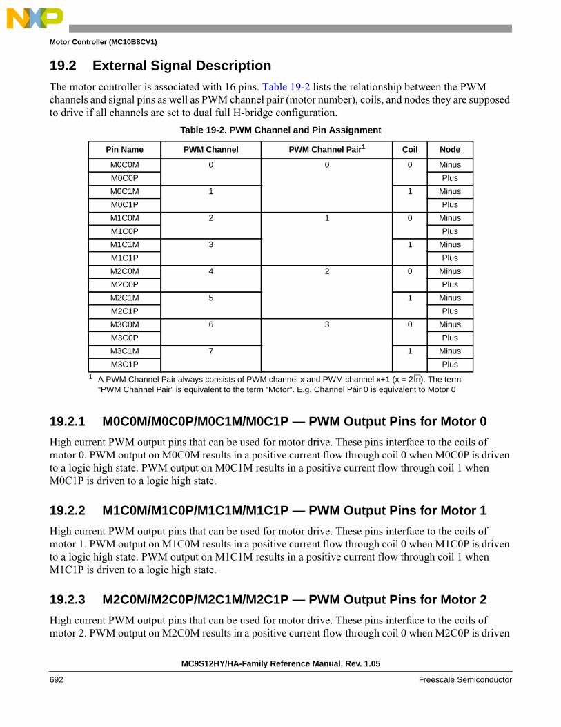
Motor Controller (MC10B8CV1)
19.2 External Signal DescriptionThe motor controller is associated with 16 pins. Table 19-2 lists the relationship between the PWMchannels and signal pins as well as PWM channel pair (motor number), coils, and nodes they are supposedto drive if all channels are set to dual full H-bridge configuration.
19.2.1 M0C0M/M0C0P/M0C1M/M0C1P — PWM Output Pins for Motor 0
High current PWM output pins that can be used for motor drive. These pins interface to the coils ofmotor 0. PWM output on M0C0M results in a positive current flow through coil 0 when M0C0P is drivento a logic high state. PWM output on M0C1M results in a positive current flow through coil 1 whenM0C1P is driven to a logic high state.
19.2.2 M1C0M/M1C0P/M1C1M/M1C1P — PWM Output Pins for Motor 1
High current PWM output pins that can be used for motor drive. These pins interface to the coils ofmotor 1. PWM output on M1C0M results in a positive current flow through coil 0 when M1C0P is drivento a logic high state. PWM output on M1C1M results in a positive current flow through coil 1 whenM1C1P is driven to a logic high state.
19.2.3 M2C0M/M2C0P/M2C1M/M2C1P — PWM Output Pins for Motor 2
High current PWM output pins that can be used for motor drive. These pins interface to the coils ofmotor 2. PWM output on M2C0M results in a positive current flow through coil 0 when M2C0P is driven
Table 19-2. PWM Channel and Pin Assignment
Pin Name PWM Channel PWM Channel Pair1
1 A PWM Channel Pair always consists of PWM channel x and PWM channel x+1 (x = 2⋅n). The term“PWM Channel Pair” is equivalent to the term “Motor”. E.g. Channel Pair 0 is equivalent to Motor 0
Coil Node
M0C0M 0 0 0 Minus
M0C0P Plus
M0C1M 1 1 Minus
M0C1P Plus
M1C0M 2 1 0 Minus
M1C0P Plus
M1C1M 3 1 Minus
M1C1P Plus
M2C0M 4 2 0 Minus
M2C0P Plus
M2C1M 5 1 Minus
M2C1P Plus
M3C0M 6 3 0 Minus
M3C0P Plus
M3C1M 7 1 Minus
M3C1P Plus
MC9S12HY/HA-Family Reference Manual, Rev. 1.05
692 Freescale Semiconductor

Motor Controller (MC10B8CV1)
to a logic high state. PWM output on M2C1M results in a positive current flow through coil 1 whenM2C1P is driven to a logic high state.
19.2.4 M3C0M/M3C0P/M3C1M/M3C1P — PWM Output Pins for Motor 3
High current PWM output pins that can be used for motor drive. These pins interface to the coils ofmotor 3. PWM output on M3C0M results in a positive current flow through coil 0 when M3C0P is drivento a logic high state. PWM output on M3C1M results in a positive current flow through coil 1 whenM3C1P is driven to a logic high state.
19.3 Memory Map and Register DefinitionThis section provides a detailed description of all registers of the 10-bit 8-channel motor controllermodule.
19.3.1 Module Memory Map
Figure 19-2 shows the memory map of the 10-bit 8-channel motor controller module.
Figure 19-2. MC10B8C Memory Map
Offset Register Access
0x0000 Motor Controller Control Register 0 (MCCTL0) RW
0x0001 Motor Controller Control Register 1 (MCCTL1) RW
0x0002 Motor Controller Period Register (High Byte) RW
0x0003 Motor Controller Period Register (Low Byte) RW
0x0004 Reserved1 —
0x0005 Reserved —
0x0006 Reserved —
0x0007 Reserved —
0x0008 Reserved —
0x0009 Reserved —
0x000A Reserved —
0x000B Reserved —
0x000C Reserved —
0x000D Reserved —
0x000E Reserved —
0x000F Reserved —
0x0010 Motor Controller Channel Control Register 0 (MCCC0) RW
0x0011 Motor Controller Channel Control Register 1 (MCCC1) RW
0x0012 Motor Controller Channel Control Register 2 (MCCC2) RW
0x0013 Motor Controller Channel Control Register 3 (MCCC3) RW
0x0014 Motor Controller Channel Control Register 4 (MCCC4) RW
0x0015 Motor Controller Channel Control Register 5 (MCCC5) RW
MC9S12HY/HA-Family Reference Manual, Rev. 1.05
Freescale Semiconductor 693
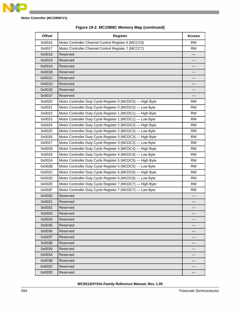
Motor Controller (MC10B8CV1)
0x0016 Motor Controller Channel Control Register 6 (MCCC6) RW
0x0017 Motor Controller Channel Control Register 7 (MCCC7) RW
0x0018 Reserved —
0x0019 Reserved —
0x001A Reserved —
0x001B Reserved —
0x001C Reserved —
0x001D Reserved —
0x001E Reserved —
0x001F Reserved —
0x0020 Motor Controller Duty Cycle Register 0 (MCDC0) — High Byte RW
0x0021 Motor Controller Duty Cycle Register 0 (MCDC0) — Low Byte RW
0x0022 Motor Controller Duty Cycle Register 1 (MCDC1) — High Byte RW
0x0023 Motor Controller Duty Cycle Register 1 (MCDC1) — Low Byte RW
0x0024 Motor Controller Duty Cycle Register 2 (MCDC2) — High Byte RW
0x0025 Motor Controller Duty Cycle Register 2 (MCDC2) — Low Byte RW
0x0026 Motor Controller Duty Cycle Register 3 (MCDC3) — High Byte RW
0x0027 Motor Controller Duty Cycle Register 3 (MCDC3) — Low Byte RW
0x0028 Motor Controller Duty Cycle Register 4 (MCDC4) — High Byte RW
0x0029 Motor Controller Duty Cycle Register 4 (MCDC4) — Low Byte RW
0x002A Motor Controller Duty Cycle Register 5 (MCDC5) — High Byte RW
0x002B Motor Controller Duty Cycle Register 5 (MCDC5) — Low Byte RW
0x002C Motor Controller Duty Cycle Register 6 (MCDC6) — High Byte RW
0x002D Motor Controller Duty Cycle Register 6 (MCDC6) — Low Byte RW
0x002E Motor Controller Duty Cycle Register 7 (MCDC7) — High Byte RW
0x002F Motor Controller Duty Cycle Register 7 (MCDC7) — Low Byte RW
0x0030 Reserved —
0x0031 Reserved —
0x0032 Reserved —
0x0033 Reserved —
0x0034 Reserved —
0x0035 Reserved —
0x0036 Reserved —
0x0037 Reserved —
0x0038 Reserved —
0x0039 Reserved —
0x003A Reserved —
0x003B Reserved —
0x003C Reserved —
0x003D Reserved —
Figure 19-2. MC10B8C Memory Map (continued)
Offset Register Access
MC9S12HY/HA-Family Reference Manual, Rev. 1.05
694 Freescale Semiconductor
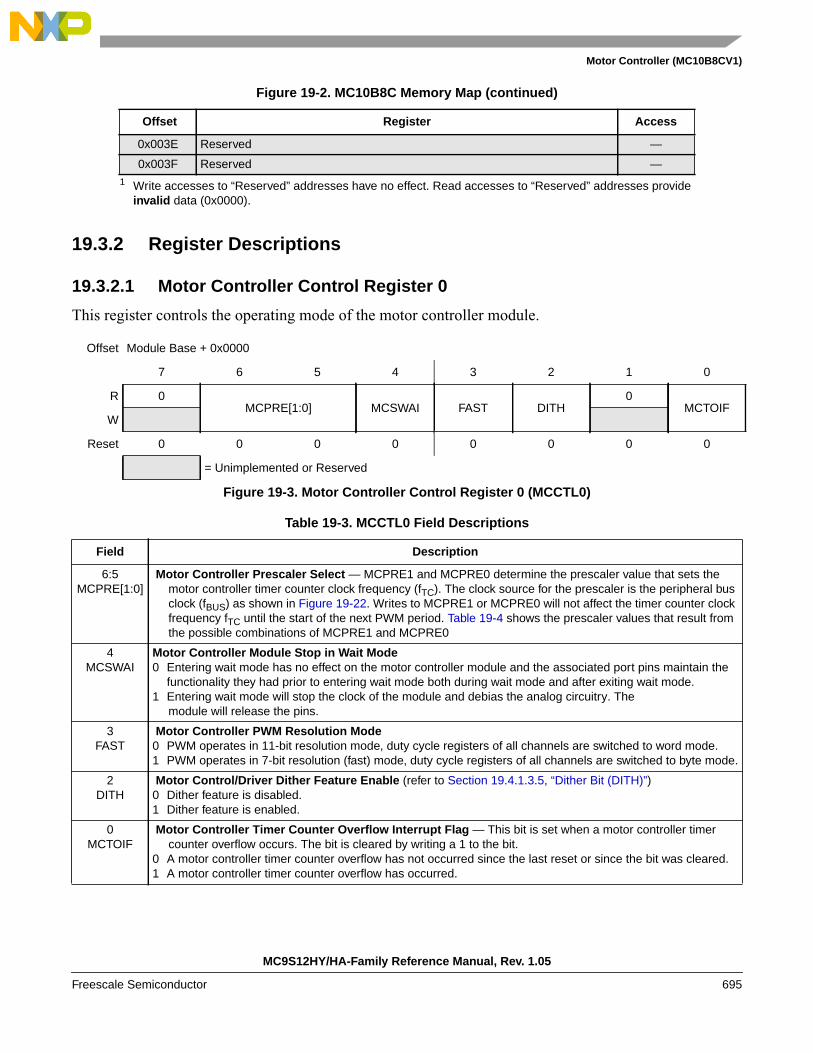
Motor Controller (MC10B8CV1)
19.3.2 Register Descriptions
19.3.2.1 Motor Controller Control Register 0
This register controls the operating mode of the motor controller module.
0x003E Reserved —
0x003F Reserved —1 Write accesses to “Reserved” addresses have no effect. Read accesses to “Reserved” addresses provide
invalid data (0x0000).
Offset Module Base + 0x0000
7 6 5 4 3 2 1 0
R 0MCPRE[1:0] MCSWAI FAST DITH
0MCTOIF
W
Reset 0 0 0 0 0 0 0 0
= Unimplemented or Reserved
Figure 19-3. Motor Controller Control Register 0 (MCCTL0)
Table 19-3. MCCTL0 Field Descriptions
Field Description
6:5MCPRE[1:0]
Motor Controller Prescaler Select — MCPRE1 and MCPRE0 determine the prescaler value that sets themotor controller timer counter clock frequency (fTC). The clock source for the prescaler is the peripheral busclock (fBUS) as shown in Figure 19-22. Writes to MCPRE1 or MCPRE0 will not affect the timer counter clockfrequency fTC until the start of the next PWM period. Table 19-4 shows the prescaler values that result fromthe possible combinations of MCPRE1 and MCPRE0
4MCSWAI
Motor Controller Module Stop in Wait Mode0 Entering wait mode has no effect on the motor controller module and the associated port pins maintain the
functionality they had prior to entering wait mode both during wait mode and after exiting wait mode.1 Entering wait mode will stop the clock of the module and debias the analog circuitry. The
module will release the pins.
3FAST
Motor Controller PWM Resolution Mode0 PWM operates in 11-bit resolution mode, duty cycle registers of all channels are switched to word mode.1 PWM operates in 7-bit resolution (fast) mode, duty cycle registers of all channels are switched to byte mode.
2DITH
Motor Control/Driver Dither Feature Enable (refer to Section 19.4.1.3.5, “Dither Bit (DITH)”)0 Dither feature is disabled.1 Dither feature is enabled.
0MCTOIF
Motor Controller Timer Counter Overflow Interrupt Flag — This bit is set when a motor controller timercounter overflow occurs. The bit is cleared by writing a 1 to the bit.
0 A motor controller timer counter overflow has not occurred since the last reset or since the bit was cleared.1 A motor controller timer counter overflow has occurred.
Figure 19-2. MC10B8C Memory Map (continued)
Offset Register Access
MC9S12HY/HA-Family Reference Manual, Rev. 1.05
Freescale Semiconductor 695

Motor Controller (MC10B8CV1)
.
19.3.2.2 Motor Controller Control Register 1
This register controls the behavior of the analog section of the motor controller as well as the interruptenables.
Table 19-4. Prescaler Values
MCPRE[1:0] fTC
00 fBus
01 fBus/2
10 fBus/4
11 fBus/8
Offset Module Base + 0x0001
7 6 5 4 3 2 1 0
RRECIRC
0 0 0 0 0 0MCTOIE
W
Reset 0 0 0 0 0 0 0 0
= Unimplemented or Reserved
Figure 19-4. Motor Controller Control Register 1 (MCCTL1)
Table 19-5. MCCTL1 Field Descriptions
Field Description
7RECIRC
Recirculation in (Dual) Full H-Bridge Mode (refer to Section 19.4.1.3.3, “RECIRC Bit”)— RECIRC onlyaffects the outputs in (dual) full H-bridge modes. In half H-bridge mode, the PWM output is always active low.RECIRC = 1 will also invert the effect of the S bits (refer to Section 19.4.1.3.2, “Sign Bit (S)”) in (dual) fullH-bridge modes. RECIRC must be changed only while no PWM channel is operating in (dual) full H-bridgemode; otherwise, erroneous output pattern may occur.
0 Recirculation on the high side transistors. Active state for PWM output is logic low, the static channel willoutput logic high.
1 Recirculation on the low side transistors. Active state for PWM output is logic high, the static channel willoutput logic low.
0MCTOIE
Motor Controller Timer Counter Overflow Interrupt Enable0 Interrupt disabled.1 Interrupt enabled. An interrupt will be generated when the motor controller timer counter overflow interrupt flag
(MCTOIF) is set.
MC9S12HY/HA-Family Reference Manual, Rev. 1.05
696 Freescale Semiconductor
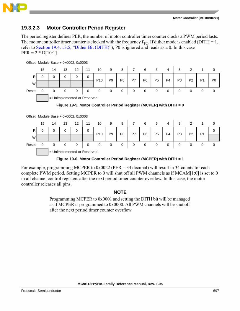
Motor Controller (MC10B8CV1)
19.3.2.3 Motor Controller Period Register
The period register defines PER, the number of motor controller timer counter clocks a PWM period lasts.The motor controller timer counter is clocked with the frequency fTC. If dither mode is enabled (DITH = 1,refer to Section 19.4.1.3.5, “Dither Bit (DITH)”), P0 is ignored and reads as a 0. In this casePER = 2 * D[10:1].
For example, programming MCPER to 0x0022 (PER = 34 decimal) will result in 34 counts for eachcomplete PWM period. Setting MCPER to 0 will shut off all PWM channels as if MCAM[1:0] is set to 0in all channel control registers after the next period timer counter overflow. In this case, the motorcontroller releases all pins.
NOTEProgramming MCPER to 0x0001 and setting the DITH bit will be managedas if MCPER is programmed to 0x0000. All PWM channels will be shut offafter the next period timer counter overflow.
Offset Module Base + 0x0002, 0x0003
15 14 13 12 11 10 9 8 7 6 5 4 3 2 1 0
R 0 0 0 0 0P10 P9 P8 P7 P6 P5 P4 P3 P2 P1 P0
W
Reset 0 0 0 0 0 0 0 0 0 0 0 0 0 0 0 0
= Unimplemented or Reserved
Figure 19-5. Motor Controller Period Register (MCPER) with DITH = 0
Offset Module Base + 0x0002, 0x0003
15 14 13 12 11 10 9 8 7 6 5 4 3 2 1 0
R 0 0 0 0 0P10 P9 P8 P7 P6 P5 P4 P3 P2 P1
0
W
Reset 0 0 0 0 0 0 0 0 0 0 0 0 0 0 0 0
= Unimplemented or Reserved
Figure 19-6. Motor Controller Period Register (MCPER) with DITH = 1
MC9S12HY/HA-Family Reference Manual, Rev. 1.05
Freescale Semiconductor 697
Motor Controller (MC10B8CV1)
19.3.2.4 Motor Controller Channel Control Registers
Each PWM channel has one associated control register to control output delay, PWM alignment, andoutput mode. The registers are named MCCC0... MCCC7. In the following, MCCC0 is described as areference for all eight registers.
Offset Module Base + 0x0010 . . . 0x0017
7 6 5 4 3 2 1 0
RMCOM1 MCOM0 MCAM1 MCAM0
0 0CD1 CD0
W
Reset 0 0 0 0 0 0 0 0
= Unimplemented or Reserved
Figure 19-7. Motor Controller Control Register Channel 0–7 (MCCC0–MCCC7)
Table 19-6. MCCC0–MCCC7 Field Descriptions
Field Description
7:6MCOM[1:0]
Output Mode — MCOM1, MCOM0 control the PWM channel’s output mode. See Table 19-7.
5:4MCAM[1:0]
PWM Channel Alignment Mode — MCAM1, MCAM0 control the PWM channel’s PWM alignment mode andoperation. See Table 19-8.
MCAM[1:0] and MCOM[1:0] are double buffered. The values used for the generation of the output waveformwill be copied to the working registers either at once (if all PWM channels are disabled or MCPER is set to 0)or if a timer counter overflow occurs. Reads of the register return the most recent written value, which are notnecessarily the currently active values.
1:0CD[1:0]
PWM Channel Delay — Each PWM channel can be individually delayed by a programmable number of PWMtimer counter clocks. The delay will be n/fTC. See Table 19-9.
Table 19-7. Output Mode
MCOM[1:0] Output Mode
00 Half H-bridge mode, PWM on MnCxM, MnCxP is released
01 Half H-bridge mode, PWM on MnCxP, MnCxM is released
10 Full H-bridge mode
11 Dual full H-bridge mode
Table 19-8. PWM Alignment Mode
MCAM[1:0] PWM Alignment Mode
00 Channel disabled
01 Left aligned
10 Right aligned
11 Center aligned
MC9S12HY/HA-Family Reference Manual, Rev. 1.05
698 Freescale Semiconductor

Motor Controller (MC10B8CV1)
NOTEThe PWM motor controller will release the pins after the next PWM timercounter overflow without accommodating any channel delay if a singlechannel has been disabled or if the period register has been cleared or allchannels have been disabled. Program one or more inactive PWM frames(duty cycle = 0) before writing a configuration that disables a single channelor the entire PWM motor controller.
19.3.2.5 Motor Controller Duty Cycle Registers
Each duty cycle register sets the sign and duty functionality for the respective PWM channel.
The contents of the duty cycle registers define DUTY, the number of motor controller timer counter clocksthe corresponding output is driven low (RECIRC = 0) or is driven high (RECIRC = 1). Setting all bits to 0will give a static high output in case of RECIRC = 0; otherwise, a static low output. Values greater thanor equal to the contents of the period register will generate a static low output in case of RECIRC = 0, ora static high output if RECIRC = 1. The layout of the duty cycle registers differ dependent upon the stateof the FAST bit in the control register 0.
Table 19-9. Channel Delay
CD[1:0] n [# of PWM Clocks]
00 0
01 1
10 2
11 3
Offset Module Base + 0x0020 . . . 0x002F Access: User read/write
15 14 13 12 11 10 9 8 7 6 5 4 3 2 1 0
RS
S S S SD10 D9 D8 D7 D6 D5 D4 D3 D2 D1 D0
W
Reset 0 0 0 0 0 0 0 0 0 0 0 0 0 0 0 0
= Unimplemented or Reserved
Figure 19-8. Motor Controller Duty Cycle Register x (MCDCx) with FAST = 0
MC9S12HY/HA-Family Reference Manual, Rev. 1.05
Freescale Semiconductor 699

Motor Controller (MC10B8CV1)
Whenever FAST = 1, the bits D10, D9, D1, and D0 will be set to 0 if the duty cycle register is written.
For example setting MCDCx = 0x0158 with FAST = 0 gives the same output waveform as settingMCDCx = 0x5600 with FAST = 1 (with FAST = 1, the low byte of MCDCx needs not to be written).
The state of the FAST bit has impact only during write and read operations. A change of the FAST bit (setor clear) without writing a new value does not impact the internal interpretation of the duty cycle values.
To prevent the output from inconsistent signals, the duty cycle registers are double buffered. The motorcontroller module will use working registers to generate the output signals. The working registers arecopied from the bus accessible registers at the following conditions:
• MCPER is set to 0 (all channels are disabled in this case)
• MCAM[1:0] of the respective channel is set to 0 (channel is disabled)
• A PWM timer counter overflow occurs while in half H-bridge or full H-bridge mode
• A PWM channel pair is configured to work in Dual Full H-Bridge mode and a PWM timer counteroverflow occurs after the odd1 duty cycle register of the channel pair has been written.
In this way, the output of the PWM will always be either the old PWM waveform or the new PWMwaveform, not some variation in between.
Reads of this register return the most recent value written. Reads do not necessarily return the value of thecurrently active sign, duty cycle, and dither functionality due to the double buffering scheme.
Offset Module Base + 0x0020 . . . 0x002F Access: User read/write
15 14 13 12 11 10 9 8 7 6 5 4 3 2 1 0
RS D8 D7 D6 D5 D4 D3 D2
0 0 0 0 0 0 0 0
W
Reset 0 0 0 0 0 0 0 0 0 0 0 0 0 0 0 0
= Unimplemented or Reserved
Figure 19-9. Motor Controller Duty Cycle Register x (MCDCx) with FAST = 1
Table 19-10. MCDCx Field Descriptions
Field Description
0S
SIGN — The SIGN bit is used to define which output will drive the PWM signal in (dual) full-H-bridge modes. TheSIGN bit has no effect in half-bridge modes. See Section 19.4.1.3.2, “Sign Bit (S)”, and table Table 19-12 fordetailed information about the impact of RECIRC and SIGN bit on the PWM output.
1. Odd duty cycle register: MCDCx+1, x = 2⋅n
MC9S12HY/HA-Family Reference Manual, Rev. 1.05
700 Freescale Semiconductor

Motor Controller (MC10B8CV1)
19.4 Functional Description
19.4.1 Modes of Operation
19.4.1.1 PWM Output Modes
The motor controller is configurable between three output modes.
• Dual full H-bridge mode can be used to control either a stepper motor or a 360° air core instrument.In this case two PWM channels are combined.
• In full H-bridge mode, each PWM channel is updated independently.
• In half H-bridge mode, one pin of the PWM channel can generate a PWM signal to control a 90°air core instrument (or other load requiring a PWM signal) and the other pin is unused.
The mode of operation for each PWM channel is determined by the corresponding MCOM[1:0] bits inchannel control registers. After a reset occurs, each PWM channel will be disabled, the corresponding pinsare released.
Each PWM channel consists of two pins. One output pin will generate a PWM signal. The other willoperate as logic high or low output depending on the state of the RECIRC bit (refer to Section 19.4.1.3.3,“RECIRC Bit”), while in (dual) full H-bridge mode, or will be released, while in half H-bridge mode. Thestate of the S bit in the duty cycle register determines the pin where the PWM signal is driven in fullH-bridge mode. While in half H-bridge mode, the state of the released pin is determined by other modulesassociated with this pin.
Associated with each PWM channel pair n are two PWM channels, x and x + 1, where x = 2 * n and n(0, 1, 2, 3) is the PWM channel pair number. Duty cycle register x controls the sign of the PWM signal(which pin drives the PWM signal) and the duty cycle of the PWM signal for motor controller channel x.The pins associated with PWM channel x are MnC0P and MnC0M. Similarly, duty cycle register x + 1controls the sign of the PWM signal and the duty cycle of the PWM signal for channel x + 1. The pinsassociated with PWM channel x + 1 are MnC1P and MnC1M. This is summarized in Table 19-11.
Table 19-11. Corresponding Registers and Pin Names for Each PWM Channel Pair
PWMChannel
Pair Number
PWMChannel Control
Register
Duty CycleRegister
ChannelNumber
PinNames
n MCMCx MCDCx PWM Channel x, x = 2⋅n MnC0M
MnC0P
MCMCx + 1 MCDCx + 1 PWM Channel x + 1, x = 2⋅n MnC1M
MnC1P
0 MCMC0 MCDC0 PWM Channel 0 M0C0M
M0C0P
MCMC1 MCDC1 PWM Channel 1 M0C1M
M0C1P
MC9S12HY/HA-Family Reference Manual, Rev. 1.05
Freescale Semiconductor 701
Motor Controller (MC10B8CV1)
19.4.1.1.1 Dual Full H-Bridge Mode (MCOM = 11)
PWM channel pairs x and x + 1 operate in dual full H-bridge mode if both channels have been enabled(MCAM[1:0]=01, 10, or 11) and both of the corresponding output mode bits MCOM[1:0] in both PWMchannel control registers are set.
A typical configuration in dual full H-bridge mode is shown in Figure 19-10. PWM channel x drives thePWM output signal on either MnC0P or MnC0M. If MnC0P drives the PWM signal, MnC0M will beoutput either high or low depending on the RECIRC bit. If MnC0M drives the PWM signal, MnC0P willbe an output high or low. PWM channel x + 1 drives the PWM output signal on either MnC1P or MnC1M.If MnC1P drives the PWM signal, MnC1M will be an output high or low. If MnC1M drives the PWMsignal, MnC1P will be an output high or low. This results in motor recirculation currents on the high sidedrivers (RECIRC = 0) while the PWM signal is at a logic high level, or motor recirculation currents on thelow side drivers (RECIRC = 1) while the PWM signal is at a logic low level. The pin driving the PWMsignal is determined by the S (sign) bit in the corresponding duty cycle register and the state of theRECIRC bit. The value of the PWM duty cycle is determined by the value of the D[10:0] or D[8:2] bitsrespectively in the duty cycle register depending on the state of the FAST bit.
1 MCMC2 MCDC2 PWM Channel 2 M1C0M
M1C0P
MCMC3 MCDC3 PWM Channel 3 M1C1M
M1C1P
2 MCMC4 MCDC4 PWM Channel 4 M2C0M
M2C0P
MCMC5 MCDC5 PWM Channel 5 M2C1M
M2C1P
3 MCMC6 MCDC6 PWM Channel 6 M3C0M
M3C0P
MCMC7 MCDC7 PWM Channel 7 M3C1M
M3C1P
Table 19-11. Corresponding Registers and Pin Names for Each PWM Channel Pair (continued)
PWMChannel
Pair Number
PWMChannel Control
Register
Duty CycleRegister
ChannelNumber
PinNames
MC9S12HY/HA-Family Reference Manual, Rev. 1.05
702 Freescale Semiconductor
Motor Controller (MC10B8CV1)
Figure 19-10. Typical Dual Full H-Bridge Mode Configuration
Whenever FAST = 0 only 16-bit write accesses to the duty cycle registers are allowed, 8-bit write accessescan lead to unpredictable duty cycles.
While fast mode is enabled (FAST = 1), 8-bit write accesses to the high byte of the duty cycle registers areallowed, because only the high byte of the duty cycle register is used to determine the duty cycle.
The following sequence should be used to update the current magnitude and direction for coil 0 and coil1 of the motor to achieve consistent PWM output:
1. Write to duty cycle register x
2. Write to duty cycle register x + 1.
At the next timer counter overflow, the duty cycle registers will be copied to the working duty cycleregisters. Sequential writes to the duty cycle register x will result in the previous data being overwritten.
19.4.1.1.2 Full H-Bridge Mode (MCOM = 10)
In full H-bridge mode, the PWM channels x and x + 1 operate independently. The duty cycle workingregisters are updated whenever a timer counter overflow occurs.
19.4.1.1.3 Half H-Bridge Mode (MCOM = 00 or 01)
In half H-bridge mode, the PWM channels x and x + 1 operate independently. In this mode, each PWMchannel can be configured such that one pin is released and the other pin is a PWM output. Figure 19-11shows a typical configuration in half H-bridge mode.
The two pins associated with each channel are switchable between released mode and PWM outputdependent upon the state of the MCOM[1:0] bits in the MCCCx (channel control) register. See registerdescription in Section 19.3.2.4, “Motor Controller Channel Control Registers”. In half H-bridge mode, thestate of the S bit has no effect.
PWM Channel x
PWM Channel x + 1
MnC0PMnC0M
MnC1PMnC1M
Motor n, Coil 0
Motor n, Coil 1
MC9S12HY/HA-Family Reference Manual, Rev. 1.05
Freescale Semiconductor 703
Motor Controller (MC10B8CV1)
Figure 19-11. Typical Quad Half H-Bridge Mode Configuration
19.4.1.2 Relationship Between PWM Mode and PWM Channel Enable
The pair of motor controller channels cannot be placed into dual full H-bridge mode unless both motorcontroller channels have been enabled (MCAM[1:0] not equal to 00) and dual full H-bridge mode isselected for both PWM channels (MCOM[1:0] = 11). If only one channel is set to dual full H-bridge mode,this channel will operate in full H-bridge mode, the other as programmed.
19.4.1.3 Relationship Between Sign, Duty, Dither, RECIRC, Period,and PWM Mode Functions
19.4.1.3.1 PWM Alignment Modes
Each PWM channel can be programmed individually to three different alignment modes. The mode isdetermined by the MCAM[1:0] bits in the corresponding channel control register.
Left aligned (MCAM[1:0] = 01): The output will start active (low if RECIRC = 0 or high if RECIRC = 1)and will turn inactive (high if RECIRC = 0 or low if RECIRC = 1) after the number of counts specified bythe corresponding duty cycle register.
PWM Channel x
PWM Channel x + 1
MnC0PMnC0M
MnC1PMnC1M
Released
PWM Output
VSSM
VDDM
VSSM
VDDM
Released
PWM Output
MC9S12HY/HA-Family Reference Manual, Rev. 1.05
704 Freescale Semiconductor
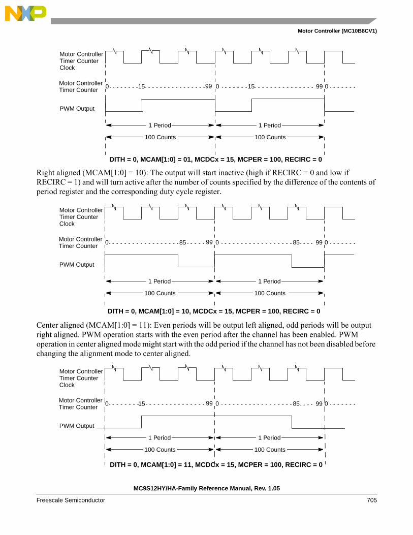
Motor Controller (MC10B8CV1)
Right aligned (MCAM[1:0] = 10): The output will start inactive (high if RECIRC = 0 and low ifRECIRC = 1) and will turn active after the number of counts specified by the difference of the contents ofperiod register and the corresponding duty cycle register.
Center aligned (MCAM[1:0] = 11): Even periods will be output left aligned, odd periods will be outputright aligned. PWM operation starts with the even period after the channel has been enabled. PWMoperation in center aligned mode might start with the odd period if the channel has not been disabled beforechanging the alignment mode to center aligned.
0 15
PWM Output
0
1 Period
100 Counts
Motor ControllerTimer Counter
Motor ControllerTimer Counter
Clock
0
1 Period
100 Counts
15 9999
DITH = 0, MCAM[1:0] = 01, MCDCx = 15, MCPER = 100, RECIRC = 0
0 85
PWM Output
0
1 Period
100 Counts
Motor ControllerTimer Counter
Motor ControllerTimer Counter
Clock
0
1 Period
100 Counts
85 9999
DITH = 0, MCAM[1:0] = 10, MCDCx = 15, MCPER = 100, RECIRC = 0
0 85
PWM Output
0
1 Period
100 Counts
Motor ControllerTimer Counter
Motor ControllerTimer Counter
Clock
0
1 Period
100 Counts
15 9999
DITH = 0, MCAM[1:0] = 11, MCDCx = 15, MCPER = 100, RECIRC = 0
MC9S12HY/HA-Family Reference Manual, Rev. 1.05
Freescale Semiconductor 705
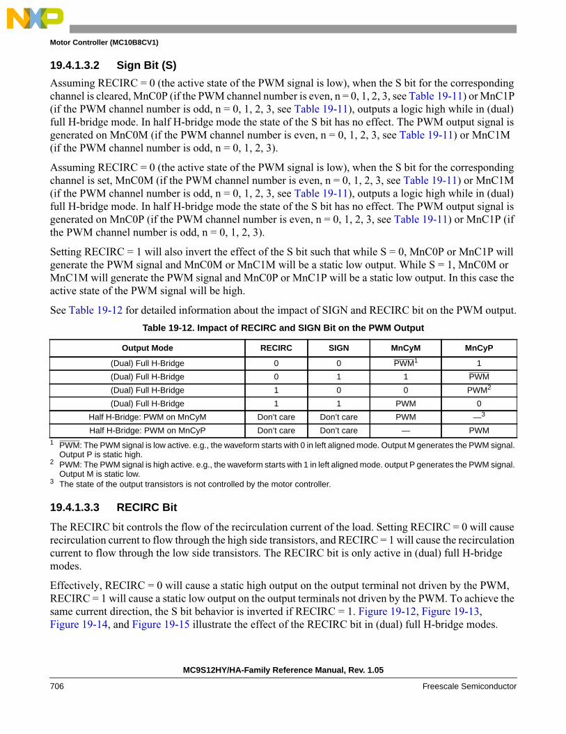
Motor Controller (MC10B8CV1)
19.4.1.3.2 Sign Bit (S)
Assuming RECIRC = 0 (the active state of the PWM signal is low), when the S bit for the correspondingchannel is cleared, MnC0P (if the PWM channel number is even, n = 0, 1, 2, 3, see Table 19-11) or MnC1P(if the PWM channel number is odd, n = 0, 1, 2, 3, see Table 19-11), outputs a logic high while in (dual)full H-bridge mode. In half H-bridge mode the state of the S bit has no effect. The PWM output signal isgenerated on MnC0M (if the PWM channel number is even, n = 0, 1, 2, 3, see Table 19-11) or MnC1M(if the PWM channel number is odd, n = 0, 1, 2, 3).
Assuming RECIRC = 0 (the active state of the PWM signal is low), when the S bit for the correspondingchannel is set, MnC0M (if the PWM channel number is even, n = 0, 1, 2, 3, see Table 19-11) or MnC1M(if the PWM channel number is odd, n = 0, 1, 2, 3, see Table 19-11), outputs a logic high while in (dual)full H-bridge mode. In half H-bridge mode the state of the S bit has no effect. The PWM output signal isgenerated on MnC0P (if the PWM channel number is even, n = 0, 1, 2, 3, see Table 19-11) or MnC1P (ifthe PWM channel number is odd, n = 0, 1, 2, 3).
Setting RECIRC = 1 will also invert the effect of the S bit such that while S = 0, MnC0P or MnC1P willgenerate the PWM signal and MnC0M or MnC1M will be a static low output. While S = 1, MnC0M orMnC1M will generate the PWM signal and MnC0P or MnC1P will be a static low output. In this case theactive state of the PWM signal will be high.
See Table 19-12 for detailed information about the impact of SIGN and RECIRC bit on the PWM output.
19.4.1.3.3 RECIRC Bit
The RECIRC bit controls the flow of the recirculation current of the load. Setting RECIRC = 0 will causerecirculation current to flow through the high side transistors, and RECIRC = 1 will cause the recirculationcurrent to flow through the low side transistors. The RECIRC bit is only active in (dual) full H-bridgemodes.
Effectively, RECIRC = 0 will cause a static high output on the output terminal not driven by the PWM,RECIRC = 1 will cause a static low output on the output terminals not driven by the PWM. To achieve thesame current direction, the S bit behavior is inverted if RECIRC = 1. Figure 19-12, Figure 19-13,Figure 19-14, and Figure 19-15 illustrate the effect of the RECIRC bit in (dual) full H-bridge modes.
Table 19-12. Impact of RECIRC and SIGN Bit on the PWM Output
Output Mode RECIRC SIGN MnCyM MnCyP
(Dual) Full H-Bridge 0 0 PWM1
1 PWM: The PWM signal is low active. e.g., the waveform starts with 0 in left aligned mode. Output M generates the PWM signal.Output P is static high.
1
(Dual) Full H-Bridge 0 1 1 PWM
(Dual) Full H-Bridge 1 0 0 PWM2
2 PWM: The PWM signal is high active. e.g., the waveform starts with 1 in left aligned mode. output P generates the PWM signal.Output M is static low.
(Dual) Full H-Bridge 1 1 PWM 0
Half H-Bridge: PWM on MnCyM Don’t care Don’t care PWM —3
3 The state of the output transistors is not controlled by the motor controller.
Half H-Bridge: PWM on MnCyP Don’t care Don’t care — PWM
MC9S12HY/HA-Family Reference Manual, Rev. 1.05
706 Freescale Semiconductor

Motor Controller (MC10B8CV1)
RECIRC bit must be changed only while no PWM channel is operated in (dual) full H-bridge mode.
Figure 19-12. PWM Active Phase, RECIRC = 0, S = 0
Figure 19-13. PWM Passive Phase, RECIRC = 0, S = 0
VDDM
VSSM
MnC0P MnC0M
Static 0 PWM 1
PWM 1Static 0
VDDM
VSSM
MnC0P MnC0M
Static 0 PWM 0
Static 0 PWM 0
MC9S12HY/HA-Family Reference Manual, Rev. 1.05
Freescale Semiconductor 707

Motor Controller (MC10B8CV1)
Figure 19-14. PWM Active Phase, RECIRC = 1, S = 0
Figure 19-15. PWM Passive Phase, RECIRC = 1, S = 0
VSSM
MnC0P MnC0M
VDDM
Static 1
Static 1
PWM 0
PWM 0
VDDM
VSSM
MnC0P MnC0M
Static 1
Static 1
PWM 1
PWM 1
MC9S12HY/HA-Family Reference Manual, Rev. 1.05
708 Freescale Semiconductor

Motor Controller (MC10B8CV1)
19.4.1.3.4 Relationship Between RECIRC Bit, S Bit, MCOM Bits, PWM State, and OutputTransistors
Please refer to Figure 19-16 for the output transistor assignment.
Figure 19-16. Output Transistor Assignment
Table 19-13 illustrates the state of the output transistors in different states of the PWM motor controllermodule. ‘—’ means that the state of the output transistor is not controlled by the motor controller.
Table 19-13. State of Output Transistors in Various Modes
Mode MCOM[1:0] PWM Duty RECIRC S T1 T2 T3 T4
Off Don’t care — Don’t care Don’t care — — — —
Half H-Bridge 00 Active Don’t care Don’t care — — OFF ON
Half H-Bridge 00 Passive Don’t care Don’t care — — ON OFF
Half H-Bridge 01 Active Don’t care Don’t care OFF ON — —
Half H-Bridge 01 Passive Don’t care Don’t care ON OFF — —
(Dual) Full 10 or 11 Active 0 0 ON OFF OFF ON
(Dual) Full 10 or 11 Passive 0 0 ON OFF ON OFF
(Dual) Full 10 or 11 Active 0 1 OFF ON ON OFF
(Dual) Full 10 or 11 Passive 0 1 ON OFF ON OFF
(Dual) Full 10 or 11 Active 1 0 ON OFF OFF ON
(Dual) Full 10 or 11 Passive 1 0 OFF ON OFF ON
(Dual) Full 10 or 11 Active 1 1 OFF ON ON OFF
(Dual) Full 10 or 11 Passive 1 1 OFF ON OFF ON
VDDM
VSSM
MnCyP MnCyM
T1
T2
T3
T4
MC9S12HY/HA-Family Reference Manual, Rev. 1.05
Freescale Semiconductor 709

Motor Controller (MC10B8CV1)
19.4.1.3.5 Dither Bit (DITH)
The purpose of the dither mode is to increase the minimum length of output pulses without decreasing thePWM resolution, in order to limit the pulse distortion introduced by the slew rate control of the outputs. Ifdither mode is selected the output pattern will repeat after two timer counter overflows. For the sameoutput frequency, the shortest output pulse will have twice the length while dither feature is selected. Toachieve the same output frame frequency, the prescaler of the MC10B8C module has to be set to twice thedivision rate if dither mode is selected; e.g., with the same prescaler division rate the repeat rate of theoutput pattern is the same as well as the shortest output pulse with or without dither mode selected.
The DITH bit in control register 0 enables or disables the dither function.
DITH = 0: dither function is disabled.
When DITH is cleared and assuming left aligned operation and RECIRC = 0, the PWM output will startat a logic low level at the beginning of the PWM period (motor controller timer counter = 0x000). ThePWM output remains low until the motor controller timer counter matches the 11-bit PWM duty cyclevalue, DUTY, contained in D[10:0] in MCDCx. When a match (output compare between motor controllertimer counter and DUTY) occurs, the PWM output will toggle to a logic high level and will remain at alogic high level until the motor controller timer counter overflows (reaches the contents of MCPER – 1).After the motor controller timer counter resets to 0x000, the PWM output will return to a logic low level.This completes one PWM period. The PWM period repeats every P counts (as defined by the bits P[10:0]in the motor controller period register) of the motor controller timer counter. If DUTY >= P, the outputwill be static low. If DUTY = 0x0000, the output will be continuously at a logic high level. Therelationship between the motor controller timer counter clock, motor controller timer counter value, andPWM output while DITH = 0 is shown in Figure 19-17.
Figure 19-17. PWM Output: DITH = 0, MCAM[1:0] = 01, MCDC = 100,MCPER = 200, RECIRC = 0
DITH = 1: dither function is enabled
Please note if DITH = 1, the bit P0 in the motor controller period register will be internally forced to 0 andread always as 0.
When DITH is set and assuming left aligned operation and RECIRC = 0, the PWM output will start at alogic low level at the beginning of the PWM period (when the motor controller timer counter = 0x000).The PWM output remains low until the motor controller timer counter matches the 10-bit PWM duty cycle
0 100 0 100 0
PWM Output
1 Period
200 Counts 200 Counts
1 Period
Motor ControllerTimer Counter Clock
Motor ControllerTimer Counter 199199
MC9S12HY/HA-Family Reference Manual, Rev. 1.05
710 Freescale Semiconductor

Motor Controller (MC10B8CV1)
value, DUTY, contained in D[10:1] in MCDCx. When a match (output compare between motor controllertimer counter and DUTY) occurs, the PWM output will toggle to a logic high level and will remain at alogic high level until the motor controller timer counter overflows (reaches the value defined byP[10:1] – 1 in MCPER). After the motor controller timer counter resets to 0x000, the PWM output willreturn to a logic low level. This completes the first half of the PWM period. During the second half of thePWM period, the PWM output will remain at a logic low level until either the motor controller timercounter matches the 10-bit PWM duty cycle value, DUTY, contained in D[10:1] in MCDCx if D0 = 0, orthe motor controller timer counter matches the 10-bit PWM duty cycle value + 1 (the value of D[10:1] inMCDCx is increment by 1 and is compared with the motor controller timer counter value) if D0 = 1 in thecorresponding duty cycle register. When a match occurs, the PWM output will toggle to a logic high leveland will remain at a logic high level until the motor controller timer counter overflows (reaches the valuedefined by P[10:1] – 1 in MCPER). After the motor controller timer counter resets to 0x000, the PWMoutput will return to a logic low level.
This process will repeat every number of counts of the motor controller timer counter defined by the periodregister contents (P[10:0]). If the output is neither set to 0% nor to 100% there will be four edges on thePWM output per PWM period in this case. Therefore, the PWM output compare function will alternatebetween DUTY and DUTY + 1 every half PWM period if D0 in the corresponding duty cycle register isset to 1. The relationship between the motor controller timer counter clock (fTC), motor controller timercounter value, and left aligned PWM output if DITH = 1 is shown in Figure 19-18 and Figure 19-19.Figure 19-20 and Figure 19-21 show right aligned and center aligned PWM operation respectively, withdither feature enabled and D0 = 1. Please note: In the following examples, the MCPER value is definedby the bits P[10:0], which is, if DITH = 1, always an even number.
NOTEThe DITH bit must be changed only if the motor controller is disabled (allchannels disabled or period register cleared) to avoid erroneous waveforms.
Figure 19-18. PWM Output: DITH = 1, MCAM[1:0] = 01, MCDC = 31, MCPER = 200, RECIRC = 0
0 15
PWM Output
16 0
100 Counts
Motor ControllerTimer Counter
Motor ControllerTimer Counter
Clock
0 16
1 Period
100 Counts
15 9999
MC9S12HY/HA-Family Reference Manual, Rev. 1.05
Freescale Semiconductor 711

Motor Controller (MC10B8CV1)
Figure 19-19. PWM Output: DITH = 1, MCAM[1:0] = 01, MCDC = 30, MCPER = 200, RECIRC = 0
.
Figure 19-20. PWM Output: DITH = 1, MCAM[1:0] = 10, MCDC = 31, MCPER = 200, RECIRC = 0
Figure 19-21. PWM Output: DITH = 1, MCAM[1:0] = 11, MCDC = 31, MCPER = 200, RECIRC = 0
PWM Output
1 Period
100 Counts
Motor ControllerTimer Counter
Motor ControllerTimer Counter
Clock
100 Counts
0 15 16 00 1615 9999
0 84
PWM Output
85 0
1 Period
100 Counts
Motor ControllerTimer Counter
Motor ControllerTimer Counter
Clock
0 85
100 Counts
84 9999
0 84
PWM Output
0
1 Period
100 Counts
Motor ControllerTimer Counter
Motor ControllerTimer Counter
Clock
0
100 Counts
15 9999
MC9S12HY/HA-Family Reference Manual, Rev. 1.05
712 Freescale Semiconductor

Motor Controller (MC10B8CV1)
19.4.2 PWM Duty Cycle
The PWM duty cycle for the motor controller channel x can be determined by dividing the decimalrepresentation of bits D[10:0] in MCDCx by the decimal representation of the bits P[10:0] in MCPER andmultiplying the result by 100% as shown in the equation below:
NOTEx = PWM Channel Number = 0, 1, 2, 3 ... 8. This equation is only valid ifDUTY <= MCPER and MCPER is not equal to 0.
Whenever D[10:0] >= P[10:0], a constant low level (RECIRC = 0) or high level (RECIRC = 1) will beoutput.
19.4.3 Motor Controller Counter Clock Source
Figure 19-22 shows how the PWM motor controller timer counter clock source is selected.
Figure 19-22. Motor Controller Counter Clock Selection
The peripheral bus clock is the source for the motor controller counter prescaler. The motor controllercounter clock rate, fTC, is set by selecting the appropriate prescaler value. The prescaler is selected withthe MCPRE[1:0] bits in motor controller control register 0 (MCCTL0). The motor controller channelfrequency of operation can be calculated using the following formula if DITH = 0:
Effective PWM Channel X % Duty CycleDUTY
MCPER--------------------- 100%⋅=
11/21/41/8
Motor Controller TimerCounter Prescaler
Motor ControllerTimer
Counter ClockPrescaler Select
MPPRE0, MPPRE1
11-Bit Motor ControllerTimer Counter
PeripheralBus
Clock fBUS
ClockGenerator
CLK
Clocks andResetGeneratorModule
Motor Controller TimerCounter Clock fTC
Motor Channel Frequency (Hz)fTC
MCPER M⋅-------------------------------=
MC9S12HY/HA-Family Reference Manual, Rev. 1.05
Freescale Semiconductor 713
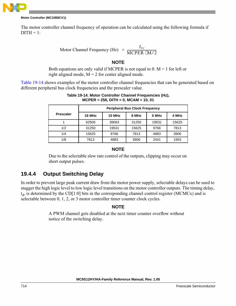
Motor Controller (MC10B8CV1)
The motor controller channel frequency of operation can be calculated using the following formula ifDITH = 1:
NOTEBoth equations are only valid if MCPER is not equal to 0. M = 1 for left orright aligned mode, M = 2 for center aligned mode.
Table 19-14 shows examples of the motor controller channel frequencies that can be generated based ondifferent peripheral bus clock frequencies and the prescaler value.
NOTEDue to the selectable slew rate control of the outputs, clipping may occur onshort output pulses.
19.4.4 Output Switching Delay
In order to prevent large peak current draw from the motor power supply, selectable delays can be used tostagger the high logic level to low logic level transitions on the motor controller outputs. The timing delay,td, is determined by the CD[1:0] bits in the corresponding channel control register (MCMCx) and isselectable between 0, 1, 2, or 3 motor controller timer counter clock cycles.
NOTEA PWM channel gets disabled at the next timer counter overflow withoutnotice of the switching delay.
Table 19-14. Motor Controller Channel Frequencies (Hz),MCPER = 256, DITH = 0, MCAM = 10, 01
Prescaler
Peripheral Bus Clock Frequency
16 MHz 10 MHz 8 MHz 5 MHz 4 MHz
1 62500 39063 31250 19531 15625
1/2 31250 19531 15625 9766 7813
1/4 15625 9766 7813 4883 3906
1/8 7813 4883 3906 2441 1953
Motor Channel Frequency (Hz)fTC
MCPER M 2⁄⋅--------------------------------------=
MC9S12HY/HA-Family Reference Manual, Rev. 1.05
714 Freescale Semiconductor

Motor Controller (MC10B8CV1)
19.4.5 Operation in Wait Mode
During wait mode, the operation of the motor controller pins are selectable between the following twooptions:
1. MCSWAI = 1: All module clocks are stopped and the associated port pins are set to their inactivestate, which is defined by the state of the RECIRC bit during wait mode. The motor controllermodule registers stay the same as they were prior to entering wait mode. Therefore, after exitingfrom wait mode, the associated port pins will resume to the same functionality they had prior toentering wait mode.
2. MCSWAI = 0: The PWM clocks continue to run and the associated port pins maintain thefunctionality they had prior to entering wait mode both during wait mode and after exiting waitmode.
19.4.6 Operation in Stop and Pseudo-Stop Modes
All module clocks are stopped and the associated port pins are set to their inactive state, which is definedby the state of the RECIRC bit. The motor controller module registers stay the same as they were prior toentering stop or pseudo-stop modes. Therefore, after exiting from stop or pseudo-stop modes, theassociated port pins will resume to the same functionality they had prior to entering stop or pseudo-stopmodes.
19.5 ResetThe motor controller is reset by system reset. All associated ports are released, all registers of the motorcontroller module will switch to their reset state as defined in Section 19.3.2, “Register Descriptions”.
19.6 InterruptsThe motor controller has one interrupt source.
19.6.1 Timer Counter Overflow Interrupt
An interrupt will be requested when the MCTOIE bit in the motor controller control register 1 is set andthe running PWM frame is finished. The interrupt is cleared by either setting the MCTOIE bit to 0 or towrite a 1 to the MCTOIF bit in the motor controller control register 0.
MC9S12HY/HA-Family Reference Manual, Rev. 1.05
Freescale Semiconductor 715
Motor Controller (MC10B8CV1)
19.7 Initialization/Application InformationThis section provides an example of how the PWM motor controller can be initialized and used byapplication software. The configuration parameters (e.g., timer settings, duty cycle values, etc.) are notguaranteed to be adequate for any real application.
The example software is implemented in assembly language.
19.7.1 Code Example
One way to use the motor controller is:
1. Perform global initialization
a) Set the motor controller control registers MCCTL0 and MCCTL1 to appropriate values.
i) Prescaler disabled (MCPRE1 = 0, MCPRE0 = 0).
ii) Fast mode and dither disabled (FAST = 0, DITH = 0).
iii) Recirculation feature in dual full H-bridge mode disabled (RECIRC = 0).
All other bits in MCCTL0 and MCCTL1 are set to 0.
b) Configure the channel control registers for the desired mode.
i) Dual full H-bridge mode (MCOM[1:0] = 11).
ii) Left aligned PWM (MCAM[1:0] = 01).
iii) No channel delay (MCCD[1:0] = 00).
2. Perform the startup phase
a) Clear the duty cycle registers MCDC0 and MCDC1
b) Initialize the period register MCPER, which is equivalent to enabling the motor controller.
c) Enable the timer which generates the timebase for the updates of the duty cycle registers.
3. Main program
a) Check if pin PB0 is set to “1” and execute the sub program if a timer interrupt is pending.
b) Initiate the shutdown procedure if pin PB0 is set to “0”.
4. Sub program
a) Update the duty cycle registers
Load the duty cycle registers MCDC0 and MCDC1 with new values from the table and clearthe timer interrupt flag.
The sub program will initiate the shutdown procedure if pin PB0 is set to “0”.
b) Shutdown procedure
The timer is disabled and the duty cycle registers are cleared to drive an inactive value on the PWM outputas long as the motor controller is enabled. The period register is cleared after a certain time, which disablesthe motor controller. The table address is restored and the timer interrupt flag is cleared.
MC9S12HY/HA-Family Reference Manual, Rev. 1.05
716 Freescale Semiconductor
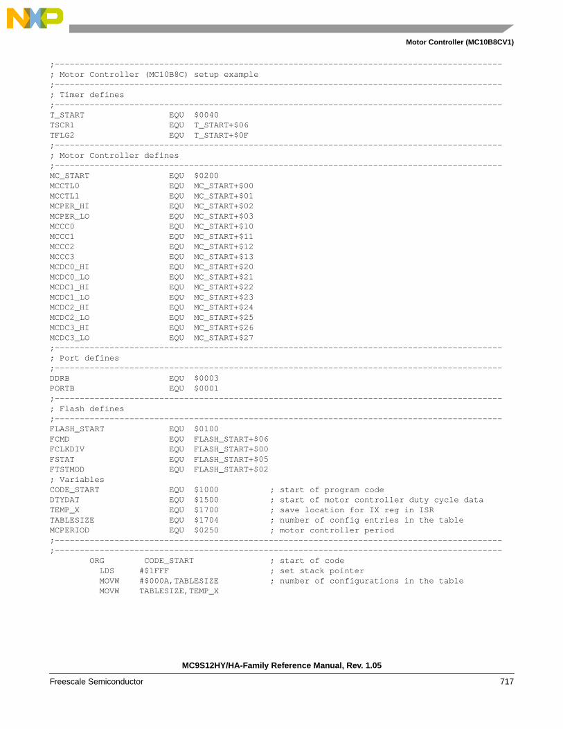
Motor Controller (MC10B8CV1)
;------------------------------------------------------------------------------------------; Motor Controller (MC10B8C) setup example;------------------------------------------------------------------------------------------; Timer defines;------------------------------------------------------------------------------------------T_START EQU $0040TSCR1 EQU T_START+$06TFLG2 EQU T_START+$0F;------------------------------------------------------------------------------------------; Motor Controller defines;------------------------------------------------------------------------------------------MC_START EQU $0200MCCTL0 EQU MC_START+$00MCCTL1 EQU MC_START+$01MCPER_HI EQU MC_START+$02MCPER_LO EQU MC_START+$03MCCC0 EQU MC_START+$10MCCC1 EQU MC_START+$11MCCC2 EQU MC_START+$12MCCC3 EQU MC_START+$13MCDC0_HI EQU MC_START+$20MCDC0_LO EQU MC_START+$21MCDC1_HI EQU MC_START+$22MCDC1_LO EQU MC_START+$23MCDC2_HI EQU MC_START+$24MCDC2_LO EQU MC_START+$25MCDC3_HI EQU MC_START+$26MCDC3_LO EQU MC_START+$27;------------------------------------------------------------------------------------------; Port defines;------------------------------------------------------------------------------------------DDRB EQU $0003PORTB EQU $0001;------------------------------------------------------------------------------------------; Flash defines;------------------------------------------------------------------------------------------FLASH_START EQU $0100FCMD EQU FLASH_START+$06FCLKDIV EQU FLASH_START+$00FSTAT EQU FLASH_START+$05FTSTMOD EQU FLASH_START+$02; VariablesCODE_START EQU $1000 ; start of program codeDTYDAT EQU $1500 ; start of motor controller duty cycle dataTEMP_X EQU $1700 ; save location for IX reg in ISRTABLESIZE EQU $1704 ; number of config entries in the tableMCPERIOD EQU $0250 ; motor controller period;------------------------------------------------------------------------------------------;------------------------------------------------------------------------------------------ ORG CODE_START ; start of code LDS #$1FFF ; set stack pointer MOVW #$000A,TABLESIZE ; number of configurations in the table MOVW TABLESIZE,TEMP_X
MC9S12HY/HA-Family Reference Manual, Rev. 1.05
Freescale Semiconductor 717

Motor Controller (MC10B8CV1)
;------------------------------------------------------------------------------------------;global motor controller init;------------------------------------------------------------------------------------------GLB_INIT: MOVB #$0000,MCCTL0 ; fMC = fBUS, FAST=0, DITH=0 MOVB #$0000,MCCTL1 ; RECIRC=0, MCTOIE=0 MOVW #$D0D0,MCCC0 ; dual full h-bridge mode, left aligned,
; no channel delay MOVW #$0000,MCPER_HI ; disable motor controller;------------------------------------------------------------------------------------------;motor controller startup;------------------------------------------------------------------------------------------STARTUP: MOVW #$0000,MCDC0_HI ; define startup duty cycles MOVW #$0000,MCDC1_HI MOVW #MCPERIOD,MCPER_HI ; define PWM period MOVB #$80,TSCR1 ; enable timerMAIN: LDAA PORTB ; if PB=0, activate shutdown ANDA #$01 BEQ MN0 JSR TIM_SRMN0: TST TFLG2 ; poll for timer counter overflow flag BEQ MAIN ; TOF set? JSR TIM_SR ; yes, go to TIM_SR BRA MAINTIM_SR: LDX TEMP_X ; restore index register X LDAA PORTB ; if PB=0, enter shutdown routine ANDA #$01 BNE SHUTDOWN LDX TEMP_X ; restore index register X BEQ NEW_SEQ ; all mc configurations done?NEW_CFG: LDD DTYDAT,X ; load new config’s STD MCDC0_HI DEX DEX LDD DTYDAT,X STD MCDC1_HI BRA END_SR ; leave sub-routineSHUTDOWN: MOVB #$00,TSCR1 ; disable timer MOVW #$0000,MCDC0_HI ; define startup duty cycle MOVW #$0000,MCDC1_HI ; define startup duty cycle LDAA #$0000 ; ensure that duty cycle registers are
; cleared for some time before disabling; the motor controller
LOOP DECA BNE LOOP MOVW #$0000,MCPER_HI ; define pwm periodNEW_SEQ: MOVW TABLESIZE,TEMP_X ; start new tx loop LDX TEMP_XEND_SR: STX TEMP_X ; save byte counter MOVB #$80,TFLG2 ; clear TOF RTS ; wait for new timer overflow
MC9S12HY/HA-Family Reference Manual, Rev. 1.05
718 Freescale Semiconductor

Motor Controller (MC10B8CV1)
;------------------------------------------------------------------------------------------; motor controller duty cycles;------------------------------------------------------------------------------------------ org DTYDAT DC.B $02, $FF1; MCDC1_HI, MCDC1_LO DC.B $02, $D0 ; MCDC0_HI, MCDC0_LO DC.B $02, $A0 ; MCDC1_HI, MCDC1_LO DC.B $02, $90 ; MCDC0_HI, MCDC0_LO DC.B $02, $60 ; MCDC1_HI, MCDC1_LO DC.B $02, $25 ; MCDC0_HI, MCDC0_LO
1. The values for the duty cycle table have to be defined for the needs of the target application.
MC9S12HY/HA-Family Reference Manual, Rev. 1.05
Freescale Semiconductor 719

Motor Controller (MC10B8CV1)
MC9S12HY/HA-Family Reference Manual, Rev. 1.05
720 Freescale Semiconductor

Appendix AElectrical Characteristics
A.1 GeneralNOTE
The electrical characteristics given in this section should be used as aguideonly. Values cannot be guaranteed by Freescale and are subject tochange without notice.
This supplement contains the most accurate electrical information for the MC9S12HY/HA-Familymicrocontroller available at the time of publication.
This introduction is intended to give an overview on several common topics like power supply, currentinjection etc.
A.1.1 Parameter Classification
The electrical parameters shown in this supplement are guaranteed by various methods. To give thecustomer a better understanding the following classification is used and the parameters are taggedaccordingly in the tables where appropriate.
NOTEThis classification is shown in the column labeled “C” in the parametertables where appropriate.
P: Those parameters are guaranteed during production testing on each individual device.
C: Those parameters are achieved by the design characterization by measuring a statistically relevantsample size across process variations.
T: Those parameters are achieved by design characterization on a small sample size from typicaldevices under typical conditions unless otherwise noted. All values shown in the typical columnare within this category.
D: Those parameters are derived mainly from simulations.
A.1.2 Power Supply
The VDDA, VSSA pin pairs supply the A/D converter , PAD[7:0] IO pins, parts of the internal voltageregulator, also the A/D covnvert reference voltage input
The VDDX, VSSX pin pairs supply the I/O pins except PU/PV and PAD[7:0].
The VDDM, VSSM pin pairs [2:1] supply the PU/PV I/O pins.
MC9S12HY/HA-Family Reference Manual, Rev. 1.05
Freescale Semiconductor 721

Electrical Characteristics
VDDR supplies the internal voltage regulator.
All VDDM pins are internally connected by metal.
All VSSM pins are internally connected by metal.
VDDA, VDDX, VDDM and VSSA, VSSX, VSSM are connected by diodes for ESD protection.
NOTEIn the following context VDD35 is used for either VDDA, VDDR, VDDMand VDDX; VSS35 is used for either VSSA, VSSM and VSSX unlessotherwise noted.
IDD35 denotes the sum of the currents flowing into the VDDAand VDDRpins. The run mode current in VDDM and VDDX is external load dependent
A.1.3 Pins
There are four groups of functional pins.
A.1.3.1 I/O Pins
The I/O pins have a level in the range of 4.5V to 5.5V. This class of pins is comprised of all port I/O pins,the analog inputs, BKGD and the RESET pins. Some functionality may be disabled.
A.1.3.2 Analog Reference
This group is made up by the VDDA and VSSA pins.
A.1.3.3 Oscillator
The pins EXTAL, XTAL dedicated to the oscillator have a nominal 1.8V level.
A.1.3.4 TEST
This pin is used for production testing only. The TEST pin must be tied to ground in all applications.
A.1.4 Current Injection
Power supply must maintain regulation within operating VDD35 or VDD range during instantaneous andoperating maximum current conditions. If positive injection current (Vin > VDD35) is greater than IDD35,the injection current may flow out of VDD35 and could result in external power supply going out ofregulation. Ensure external VDD35 load will shunt current greater than maximum injection current. Thiswill be the greatest risk when the MCU is not consuming power; e.g., if no system clock is present, or ifclock rate is very low which would reduce overall power consumption.
MC9S12HY/HA-Family Reference Manual, Rev. 1.05
722 Freescale Semiconductor

Electrical Characteristics
A.1.5 Absolute Maximum Ratings
Absolute maximum ratings are stress ratings only. A functional operation under or outside those maximais not guaranteed. Stress beyond those limits may affect the reliability or cause permanent damage of thedevice.
This device contains circuitry protecting against damage due to high static voltage or electrical fields;however, it is advised that normal precautions be taken to avoid application of any voltages higher thanmaximum-rated voltages to this high-impedance circuit. Reliability of operation is enhanced if unusedinputs are tied to an appropriate logic voltage level (e.g., either VSS35 or VDD35).
A.1.6 ESD Protection and Latch-up Immunity
All ESD testing is in conformity with CDF-AEC-Q100 stress test qualification for automotive gradeintegrated circuits. During the device qualification ESD stresses were performed for the Human BodyModel (HBM) and the Charge Device Model.
Table A-1. Absolute Maximum Ratings(1)
1. Beyond absolute maximum ratings device might be damaged.
Num Rating Symbol Min Max Unit
1 I/O, regulator and analog supply voltage VDD35 –0.3 6.0 V
2 Voltage difference VDDX to VDDA ∆VDDXA –0.3 0.3 V
3 Voltage difference VSSX to VSSA ∆VSSXA –0.3 0.3 V
4 Voltage difference VDDX to VDDM1,2 ∆VDDXM –0.3 0.3 V
5 Voltage difference VSSX to VSSM1,2 ∆VSSXM –0.3 0.3 V
6 Voltage difference VDDM1,2 to VDDA ∆VDDMA –0.3 0.3 V
7 Voltage difference VSSM1,2 to VSSA ∆VSSMA –0.3 0.3 V
8 Digital I/O input voltage VIN –0.3 6.0 V
9 EXTAL, XTAL VILV –0.3 2.16 V
10 Instantaneous maximum currentSingle pin limit for all digital I/O pins except Port U and Port V(2)
2. All digital I/O pins are internally clamped to VSSX and VDDX, or VSSA and VDDA or VSSM and VDDM
ID
–25 +25 mA
11 Instantaneous maximum currentSingle pin limit for Port U and Port V
ID
–55 +55 mA
12 Instantaneous maximum currentSingle pin limit for all pads which are used as LCD function
ID
–2.5 +2.5 mA
13 Instantaneous maximum currentSingle pin limit for all the power pins except VDDM
IDL
-50 +50 mA
14 Instantaneous maximum current on VDDM IDL
-220 +220 mA
15 Instantaneous maximum currentSingle pin limit for EXTAL, XTAL
IDL
–25 +25 mA
16 Storage temperature range Tstg –65 155 °C
MC9S12HY/HA-Family Reference Manual, Rev. 1.05
Freescale Semiconductor 723

Electrical Characteristics
A device will be defined as a failure if after exposure to ESD pulses the device no longer meets the devicespecification. Complete DC parametric and functional testing is performed per the applicable devicespecification at room temperature followed by hot temperature, unless specified otherwise in the devicespecification.
A.1.7 Operating Conditions
This section describes the operating conditions of the device. Unless otherwise noted those conditionsapply to all the following data.
NOTEPlease refer to the temperature rating of the device (C, V, M) with regards tothe ambient temperature TA and the junction temperature TJ. For powerdissipation calculations refer to Section A.1.8, “Power Dissipation andThermal Characteristics”.
Table A-2. ESD and Latch-up Test Conditions
Model Description Symbol Value Unit
Human Body Series resistance R1 1500 Ohm
Storage capacitance C 100 pF
Number of pulse per pinPositiveNegative
——
33
Latch-up Minimum input voltage limit — –2.5 V
Maximum input voltage limit — 7.5 V
Table A-3. ESD and Latch-Up Protection Characteristics
Num C Rating Symbol Min Max Unit
1 C Human Body Model (HBM) VHBM 2000 — V
2 C Charge Device Model (CDM) VCDM 500 — V
3 C Latch-up current at TA = 125°CPositiveNegative
ILAT+100–100
——
mA
4 C Latch-up current at TA = 27°CPositiveNegative
ILAT+200–200
——
mA
Table A-4. Operating Conditions
Rating Symbol Min Typ Max Unit
I/O, regulator and analog supply voltage VDD35 3.13(1) 5 5.5 V
Voltage difference VDDX to VDDA to VDDM ∆VDDX refer to Table A-1
MC9S12HY/HA-Family Reference Manual, Rev. 1.05
724 Freescale Semiconductor

Electrical Characteristics
NOTEOperation is guaranteed when powering down until low voltage resetassertion.
A.1.8 Power Dissipation and Thermal Characteristics
Power dissipation and thermal characteristics are closely related. The user must assure that the maximumoperating junction temperature is not exceeded. The average chip-junction temperature (TJ) in °C can beobtained from:
Voltage difference VDDR to VDDX ∆VDDR -0.1 0 0.1 V
Voltage difference VLCD to VDDX ∆VLCDVDDX — — 0.25 V
Voltage difference VLCD to VSSX ∆VLCDVSSX -0.25 — — V
Voltage difference VSSX to VSSA to VSSM ∆VSSX refer to Table A-1
Voltage difference VSS3 , VSSPLL to VSSX ∆VSS -0.1 0 0.1 V
Digital logic supply voltage VDD 1.72 1.8 1.98 V
Oscillator fosc 4 — 16 MHz
Bus frequency fbus 0.5 — 32 MHz
Temperature Option COperating junction temperature rangeOperating ambient temperature range(2)
TJTA
–40–40
—27
10585
°C
Temperature Option VOperating junction temperature rangeOperating ambient temperature range2
TJTA
–40–40
—27
125105
°C
Temperature Option MOperating junction temperature rangeOperating ambient temperature range2
TJTA
–40–40
—27
150125
°C
1. LCD/Motor Dirver pad can only be work under >4.5V2. Please refer to Section A.1.8, “Power Dissipation and Thermal Characteristics” for more details about the relation between
ambient temperature TA and device junction temperature TJ.
Table A-4. Operating Conditions
TJ TA PD ΘJA•( )+=
TJ Junction Temperature, [°C ]=
TA Ambient Temperature, [°C ]=
PD Total Chip Power Dissipation, [W]=
ΘJA Package Thermal Resistance, [°C/W]=
MC9S12HY/HA-Family Reference Manual, Rev. 1.05
Freescale Semiconductor 725

Electrical Characteristics
The total power dissipation can be calculated from:
PIO is the sum of all output currents on I/O ports associated with VDDX, whereby
PD PINT PIO+=
PINT Chip Internal Power Dissipation, [W]=
PIO RDSONi
∑ IIOi
2⋅=
RDSON
VOLIOL------------ for outputs driven low;=
RDSON
VDD35 VOH–
IOH--------------------------------------- for outputs driven high;=
PINT IDDR VDDR⋅ IDDA VDDA⋅+=
MC9S12HY/HA-Family Reference Manual, Rev. 1.05
726 Freescale Semiconductor

Electrical Characteristics
A.1.9 I/O Characteristics
This section describes the characteristics of all I/O pins except EXTAL, XTAL, TEST and supply pins
Table A-5. Thermal Package Characteristics(1)
1. The values for thermal resistance are achieved by package simulations
Num C Rating Symbol Min Typ Max Unit
LQFP100
1 D Thermal resistance LQFP 100, single sided PCB2 θJA — — 61 °C/W
2 D Thermal resistance LQFP 100, double sided PCBwith 2 internal planes3
θJA — — 48 °C/W
3 D Junction to Board LQFP 100 θJB — — 34 °C/W
4 D Junction to Case LQFP 100(2)
2. Junction to case thermal resistance was simulated to be equivalent to the measured values using the cold plate technique withthe cold plate temperature used as the “case” temperature. This basic cold plate measurement technique is described by MIL-STD 883D, Method 1012.1. This is the correct thermal metric to use to calculate thermal performance when the package isbeing used with a heat sink.
θJC — — 14 °C/W
5 D Junction to Package Top LQFP 100(3)
3. Thermal characterization parameter ΨJT is the “resistance” from junction to reference point thermocouple on top center of thecase as defined in JESD51-2. ΨJT is a useful value to use to estimate junction temperature in a steady state customerenviroment.
ΨJT — — 2 °C/W
LQFP 64
6 D Thermal resistance LQFP 64, single sided PCB2 θJA — — 70 °C/W
7 D Thermal resistance LQFP 64, double sided PCBwith 2 internal planes3
θJA — — 52 °C/W
8 D Junction to Board LQFP 64 θJB — — 35 °C/W
9 D Junction to Case LQFP 642 θJC — — 17 °C/W
10 D Junction to Package Top LQFP 643 ΨJT — — 3 °C/W
Table A-6. 5-V I/O Characteristics
Conditions are 4.5 V < VDD35 < 5.5 V junction temperature from –40°C to +150°C, unless otherwise notedI/O Characteristics for all I/O pins except EXTAL, XTAL,TEST and supply pins.
Num C Rating Symbol Min Typ Max Unit
1 P Input high voltage VIH
0.65*VDD35 — — V
T Input high voltage VIH — — VDD35 + 0.3 V
2 P Input low voltage VIL — — 0.35*VDD35 V
T Input low voltage VIL VSS35 – 0.3 — — V
3 C Input hysteresis VHYS 250 — mV
4 P Input leakage current (pins in high impedance inputmode)(1), all io pins except PU/PV
Vin = VDD35 or VSS35
Iin
–1 — 1 µA
MC9S12HY/HA-Family Reference Manual, Rev. 1.05
Freescale Semiconductor 727

Electrical Characteristics
P Input leakage current (pins in high impedance inputmode)1, PU, PV
Vin = VDD35 or VSS35
Iin
–2.5 — 2.5 µA
5 C Output high voltage (pins in output mode)Partial drive IOH = –2 mA
VOH
VDD35 – 0.8 — — V
6 P Output high voltage (pins in output mode), all io pinsexcept PU/PV
Full drive IOH = –10 mA
VOH VDD35 – 0.8 — — V
P Output high voltage (pins in output mode), PU, PVFull drive IOH = –20 mA
VOH VDDM-0.4 — — V
7 C Output low voltage (pins in output mode)Partial drive IOL = +2 mA
VOL — — 0.8 V
8 P Output low voltage (pins in output mode), all io pinsexcept PU/PV
Full drive IOL = +10 mA
VOL
— — 0.8 V
P Output low voltage (pins in output mode), PU, PVFull drive IOL = +20 mA
VOL
— — 0.4 V
9 C Port U, V Output Rise TimeVDD5=5V, 10% to 90% of VOH
Cload 47pF connected to GND, slew disabledRload=1KΩ connected to GND, slew enabled
Rload=1KΩ connected to VDD, slew enabled
tr
— 9.987
107
—
ns
10 C Port U, V Output Fall TimeVDD5=5V, 10% to 90% of VOH
Cload 47pF connected to GND, slew disabledRload=1KΩ connected to GND, slew enabled
Rload=1KΩ connected to VDD,, slew enabled
tf
— 9.910587
— nsns
11 P Internal pull up resistance all io pins except PU/PVVIH min > input voltage > VIL max
RPUL 25 — 50 KΩ
P Internal pull up device current, PU, PVVIH min > input voltage > VIL max
Ipu -10 — -130 uA
12 P Internal pull down resistance, all io pins exceptPU/PVVIH min > input voltage > VIL max
RPDH 25 — 50 KΩ
P Internal pull down device current, PU, PVVIH min > input voltage > VIL max
Ipd 10 — 130 uA
13 D Input capacitance Cin — 6 — pF
14 T Injection current(2)
Single pin limitTotal device Limit, sum of all injected currents
IICSIICP
–2.5–25
—2.525
mA
15 P Port T, S, R, AD interrupt input pulse filtered(STOP)(3)
tPULSE — — 3 µs
16 P Port T, S, R, AD interrupt input pulse passed (STOP)3 tPULSE 10 — — µs
17 D Port T, S, R, AD interrupt input pulse filtered (STOP) tPULSE — — 3 tcyc
Table A-6. 5-V I/O Characteristics
MC9S12HY/HA-Family Reference Manual, Rev. 1.05
728 Freescale Semiconductor
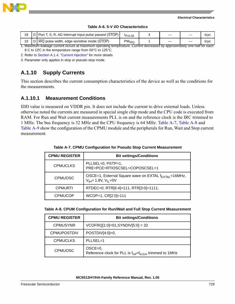
Electrical Characteristics
A.1.10 Supply Currents
This section describes the current consumption characteristics of the device as well as the conditions forthe measurements.
A.1.10.1 Measurement Conditions
IDD value is measured on VDDR pin. It does not include the current to drive external loads. Unlessotherwise noted the currents are measured in special single chip mode and the CPU code is executed fromRAM. For Run and Wait current measurements PLL is on and the reference clock is the IRC trimmed to1 MHz. The bus frequency is 32 MHz and the CPU frequency is 64 MHz. Table A-7, Table A-8 andTable A-9 show the configuration of the CPMU module and the peripherals for Run, Wait and Stop currentmeasurement.
18 D Port T, S, R, AD interrupt input pulse passed (STOP) tPULSE 4 — — tcyc
19 D IRQ pulse width, edge-sensitive mode (STOP) PWIRQ 1 — — tcyc1. Maximum leakage current occurs at maximum operating temperature. Current decreases by approximately one-half for each
8 C to 12°C in the temperature range from 50°C to 125°C.2. Refer to Section A.1.4, “Current Injection” for more details3. Parameter only applies in stop or pseudo stop mode.
Table A-7. CPMU Configuration for Pseudo Stop Current Measurement
CPMU REGISTER Bit settings/Conditions
CPMUCLKSPLLSEL=0, PSTP=1,PRE=PCE=RTIOSCSEL=COPOSCSEL=1
CPMUOSCOSCE=1, External Square wave on EXTAL fEXTAL=16MHz,VIH= 1.8V, VIL=0V
CPMURTI RTDEC=0, RTR[6:4]=111, RTR[3:0]=1111;
CPMUCOP WCOP=1, CR[2:0]=111
Table A-8. CPUM Configuration for Run/Wait and Full Stop Current Measurement
CPMU REGISTER Bit settings/Conditions
CPMUSYNR VCOFRQ[1:0]=01,SYNDIV[5:0] = 32
CPMUPOSTDIV POSTDIV[4:0]=0,
CPMUCLKS PLLSEL=1
CPMUOSCOSCE=0,Reference clock for PLL is fref=firc1m trimmed to 1MHz
Table A-6. 5-V I/O Characteristics
MC9S12HY/HA-Family Reference Manual, Rev. 1.05
Freescale Semiconductor 729

Electrical Characteristics
Table A-10. Run and Wait Current Characteristics
Table A-9. Peripheral Configurations for Run & Wait Current Measurement
Peripheral Configuration
MSCAN configured to loop-back mode using a bit rate of 1 Mbit/s
SPIconfigured to master mode, continously transmit data (0x55 or 0xAA) at 1Mbit/s
SCIconfigured into loop mode, continously transmit data (0x55) at speed of57600 baud
PWM configured to toggle its pins at the rate of 40 kHz
IICoperate in master mode and continuously transimit data(0x55 or 0xAA) at100Kbits/s
LCDconfigured to 244Hz frame frequency, 1/4 Duty, 1/3 Bias with all FP/BPenabled and all segment on
MCconfigured to full H-bridge mode MCPER=0x3FF, 1/2fbus motor controllertimer counter clock, MCDC=0x20
ATDthe peripheral is configured to operate at its maximum specified fre-quency and to continuously convert voltages on all input channels insequence.
DBGthe module is enabled and the comparators are configured to trigger inoutside range.The range covers all the code executed by the core.
TIM0, TIM1the peripheral shall be configured to output compare mode, pulse accu-mulator and modulus counter enabled.
COP & RTI enabled
Conditions are shown in Table A-8 and Table A-9 unless otherwise noted, VDD35=5.5v, 150°C
Num C Rating Symbol Min Typ Max Unit
1 P IDD Run Current IDDR 17 20 mA
2 P IDD Wait Current IDDW 9.5 12 mA
MC9S12HY/HA-Family Reference Manual, Rev. 1.05
730 Freescale Semiconductor

Electrical Characteristics
Table A-11. Pseudo Stop and Full Stop Current
Conditions are shown in Table A-7 and Table A-8 unless otherwise noted, VDD35=5.5v,
Num C Rating Symbol Min Typ Max Unit
1 P Pseudo Stop Current, 150°C IDDPS 400 600 µA
2 P Pseudo Stop Current, -40°C IDDPS 290 400 µA
3 P Pseudo Stop Current, 25°C IDDPS 320 500 µA
4 P Full Stop Current , API disabled,150°C IDDS 90 200 µA
5 P Full Stop Current , API disabled,-40°C IDDS 3 20 µA
6 P Full Stop Current , API disabled,25°C IDDS 4 20 µA
7 C Full Stop Current , API enabled,150°C IDDS 90 µA
8 C Full Stop Current , API enabled,-40°C IDDS 4 µA
9 C Full Stop Current , API enabled,25°C IDDS 5 µA
MC9S12HY/HA-Family Reference Manual, Rev. 1.05
Freescale Semiconductor 731
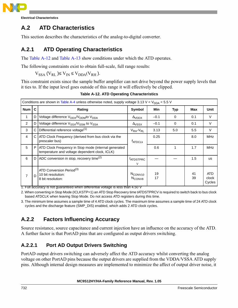
Electrical Characteristics
A.2 ATD CharacteristicsThis section describes the characteristics of the analog-to-digital converter.
A.2.1 ATD Operating Characteristics
The Table A-12 and Table A-13 show conditions under which the ATD operates.
The following constraints exist to obtain full-scale, full range results:
VSSA (VRL )≤ VIN ≤ VDDA(VRH ).
This constraint exists since the sample buffer amplifier can not drive beyond the power supply levels thatit ties to. If the input level goes outside of this range it will effectively be clipped.
Table A-12. ATD Operating Characteristics
A.2.2 Factors Influencing Accuracy
Source resistance, source capacitance and current injection have an influence on the accuracy of the ATD.A further factor is that PortAD pins that are configured as output drivers switching.
A.2.2.1 Port AD Output Drivers Switching
PortAD output drivers switching can adversely affect the ATD accuracy whilst converting the analogvoltage on other PortAD pins because the output drivers are supplied from the VDDA/VSSA ATD supplypins. Although internal design measures are implemented to minimize the affect of output driver noise, it
Conditions are shown in Table A-4 unless otherwise noted, supply voltage 3.13 V < VDDA < 5.5 V
Num C Rating Symbol Min Typ Max Unit
1 D Voltage difference VDDX/VDDMto VDDA ∆VDDX –0.1 0 0.1 V
2 D Voltage difference VSSX/VSSM to VSSA ∆VSSX –0.1 0 0.1 V
3 C Differential reference voltage(1)
1. Full accuracy is not guaranteed when differential voltage is less than 4.50 V
VRH-VRL 3.13 5.0 5.5 V
4 C ATD Clock Frequency (derived from bus clock via theprescaler bus) fATDCLk
0.25 8.0 MHz
5 P ATD Clock Frequency in Stop mode (internal generatedtemperature and voltage dependent clock, ICLK)
0.6 1 1.7 MHz
6 D ADC conversion in stop, recovery time(2)
2. When converting in Stop Mode (ICLKSTP=1) an ATD Stop Recovery time tATDSTPRCV is required to switch back to bus clockbased ATDCLK when leaving Stop Mode. Do not access ATD registers during this time.
tATDSTPRC
V
— — 1.5 us
7 D
ATD Conversion Period(3)
10 bit resolution:8 bit resolution:
3. The minimum time assumes a sample time of 4 ATD clock cycles. The maximum time assumes a sample time of 24 ATD clockcycles and the discharge feature (SMP_DIS) enabled, which adds 2 ATD clock cycles.
NCONV10NCONV8
1917
4139
ATDclock
Cycles
MC9S12HY/HA-Family Reference Manual, Rev. 1.05
732 Freescale Semiconductor

Electrical Characteristics
is recommended to configure PortAD pins as outputs only for low frequency, low load outputs. The impacton ATD accuracy is load dependent and not specified. The values specified are valid under condition thatno PortAD output drivers switch during conversion.
A.2.2.2 Source Resistance
Due to the input pin leakage current as specified in Table A-6 in conjunction with the source resistancethere will be a voltage drop from the signal source to the ATD input. The maximum source resistance RSspecifies results in an error (10-bit resolution) of less than 1/2 LSB (2.5 mV) at the maximum leakagecurrent. If device or operating conditions are less than worst case or leakage-induced error is acceptable,larger values of source resistance of up to 10 kΩ are allowed.
A.2.2.3 Source Capacitance
When sampling an additional internal capacitor is switched to the input. This can cause a voltage drop dueto charge sharing with the external and the pin capacitance. For a maximum sampling error of the inputvoltage ≤ 1LSB (10-bit resilution), then the external filter capacitor, Cf ≥ 1024 * (CINS–CINN).
A.2.2.4 Current Injection
There are two cases to consider.
1. A current is injected into the channel being converted. The channel being stressed has conversionvalues of $3FF (in 10-bit mode) for analog inputs greater than VRH and $000 for values less thanVRL unless the current is higher than specified as disruptive condition.
2. Current is injected into pins in the neighborhood of the channel being converted. A portion of thiscurrent is picked up by the channel (coupling ratio K), This additional current impacts the accuracyof the conversion depending on the source resistance.
The additional input voltage error on the converted channel can be calculated as:VERR = K * RS * IINJ
with IINJ being the sum of the currents injected into the two pins adjacent to the converted channel.
MC9S12HY/HA-Family Reference Manual, Rev. 1.05
Freescale Semiconductor 733

Electrical Characteristics
A.2.3 ATD Accuracy
Table A-14. and Table A-15. specifies the ATD conversion performance excluding any errors due tocurrent injection, input capacitance and source resistance.
Table A-13. ATD Electrical Characteristics
Conditions are shown in Table A-4 unless otherwise noted
Num C Rating Symbol Min Typ Max Unit
1 C Max input source resistance(1)
1. Refer to A.2.2.2 for further information concerning source resistance
RS — — 1 kΩ
2 D Total input capacitance Non samplingTotal input capacitance Sampling
CINNCINS
——
——
1016
pF
3 D Input internal Resistance RINA — 5 15 kΩ
4 C Disruptive analog input current INA -2.5 — 2.5 mA
5 C Coupling ratio positive current injection Kp — — 1E-4 A/A
6 C Coupling ratio negative current injection Kn — — 5E-3 A/A
MC9S12HY/HA-Family Reference Manual, Rev. 1.05
734 Freescale Semiconductor
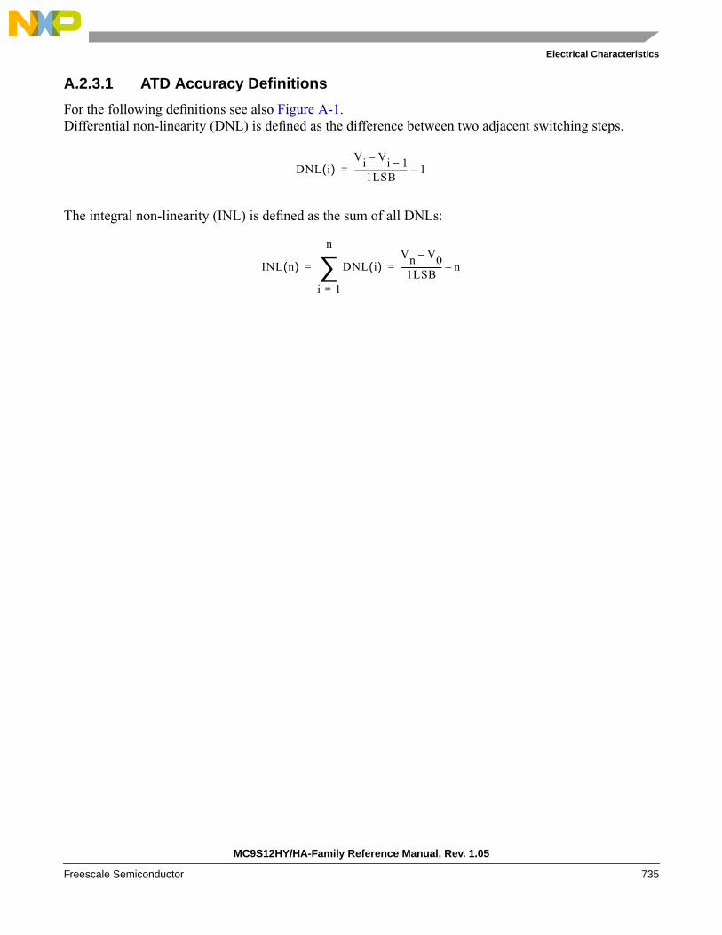
Electrical Characteristics
A.2.3.1 ATD Accuracy Definitions
For the following definitions see also Figure A-1.Differential non-linearity (DNL) is defined as the difference between two adjacent switching steps.
The integral non-linearity (INL) is defined as the sum of all DNLs:
DNL i( )Vi Vi 1––
1LSB--------------------------- 1–=
INL n( ) DNL i( )
i 1=
n
∑ Vn V0–
1LSB--------------------- n–= =
MC9S12HY/HA-Family Reference Manual, Rev. 1.05
Freescale Semiconductor 735
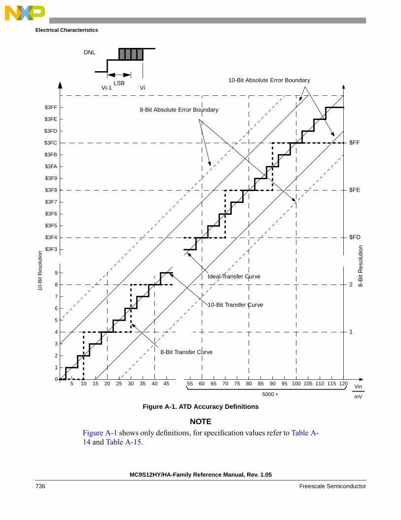
Electrical Characteristics
Figure A-1. ATD Accuracy Definitions
NOTEFigure A-1 shows only definitions, for specification values refer to Table A-14 and Table A-15.
1
5 Vin
mV
10 15 20 25 30 35 40 85 90 95 100 105 110 115 12065 70 75 80600
3
2
5
4
7
6
45
$3F7
$3F9
$3F8
$3FB
$3FA
$3FD
$3FC
$3FE
$3FF
$3F4
$3F6
$3F5
8
9
1
2
$FF
$FE
$FD
$3F3
10-B
it R
esol
utio
n
8-B
it R
esol
utio
n
Ideal Transfer Curve
10-Bit Transfer Curve
8-Bit Transfer Curve
55
10-Bit Absolute Error Boundary
8-Bit Absolute Error Boundary
LSBVi-1 Vi
DNL
5000 +
MC9S12HY/HA-Family Reference Manual, Rev. 1.05
736 Freescale Semiconductor

Electrical Characteristics
Table A-14. ATD Conversion Performance 5V range
Table A-15. ATD Conversion Performance 3.3V range
Conditions are shown in Table A-4. unless otherwise noted. VREF = VRH - VRL = 5.12V. fATDCLK = 8.0MHzThe values are tested to be valid with no PortAD output drivers switching simultaneous with conversions.
Num C Rating(1)
1. The 8-bit mode operation is structurally tested in production test..2. These values include the quantization error which is inherently 1/2 count for any A/D converter
Symbol Min Typ Max Unit
5 P Resolution 10-Bit LSB 5 mV
6 P Differential Nonlinearity 10-Bit DNL -1 ±0.5 1 counts
7 P Integral Nonlinearity 10-Bit INL -2.5 ±1 2.5 counts
8 P Absolute Error1. 10-Bit AE -3 ±2 3 counts
9 C Resolution 8-Bit LSB 20 mV
10 C Differential Nonlinearity 8-Bit DNL ±0.3 counts
11 C Integral Nonlinearity 8-Bit INL ±0.5 counts
12 C Absolute Error1. 8-Bit AE ±1 counts
Conditions are shown in Table A-4. unless otherwise noted. VREF = VRH - VRL = 3.3V. fATDCLK = 8.0MHzThe values are tested to be valid with no PortAD output drivers switching simultaneous with conversions.
Num C Rating Symbol Min Typ Max Unit
5 C Resolution 10-Bit LSB 3.22 mV
6 C Differential Nonlinearity 10-Bit DNL ±1 counts
7 C Integral Nonlinearity 10-Bit INL ±1 counts
8 C Absolute Error(1)
1. These values include the quantization error which is inherently 1/2 count for any A/D converter
10-Bit AE ±2 counts
9 C Resolution 8-Bit LSB 12.89 mV
10 C Differential Nonlinearity 8-Bit DNL ±0.3 counts
11 C Integral Nonlinearity 8-Bit INL ±0.5 counts
12 C Absolute Error1. 8-Bit AE ±1 counts
MC9S12HY/HA-Family Reference Manual, Rev. 1.05
Freescale Semiconductor 737

Electrical Characteristics
A.3 NVM
A.3.1 Timing Parameters
The time base for all NVM program or erase operations is derived from the bus clock using the FCLKDIVregister. The frequency of this derived clock must be set within the limits specified as fNVMOP. The NVMmodule does not have any means to monitor the frequency and will not prevent program or erase operationat frequencies above or below the specified minimum. When attempting to program or erase the NVMmodule at a lower frequency, a full program or erase transition is not assured.
The following sections provide equations which can be used to determine the time required to executespecific flash commands. All timing parameters are a function of the bus clock frequency, fNVMBUS. Allprogram and erase times are also a function of the NVM operating frequency, fNVMOP. A summary of keytiming parameters can be found in Table A-16.
A.3.1.1 Erase Verify All Blocks (Blank Check) (FCMD=0x01)
The time required to perform a blank check on all blocks is dependent on the location of the first non-blankword starting at relative address zero. It takes one bus cycle per phrase to verify plus a setup of thecommand. Assuming that no non-blank location is found, then the time to erase verify all blocks is givenby:
for 64 KB P-Flash and 4 KB D-Flash
A.3.1.2 Erase Verify Block (Blank Check) (FCMD=0x02)
The time required to perform a blank check is dependent on the location of the first non-blank word startingat relative address zero. It takes one bus cycle per phrase to verify plus a setup of the command.
Assuming that no non-blank location is found, then the time to erase verify a P-Flash block is given by:
for 64 KB P-Flash
Assuming that no non-blank location is found, then the time to erase verify a D-Flash block is given by:
tcheck 192001
f NVMBUS----------------------⋅=
tpcheck 172001
f NVMBUS----------------------⋅=
tdcheck 28001
f NVMBUS----------------------⋅=
MC9S12HY/HA-Family Reference Manual, Rev. 1.05
738 Freescale Semiconductor

Electrical Characteristics
A.3.1.3 Erase Verify P-Flash Section (FCMD=0x03)
The maximum time to erase verify a section of P-Flash depends on the number of phrases being verified(NVP) and is given by:
A.3.1.4 Read Once (FCMD=0x04)
The maximum read once time is given by:
A.3.1.5 Program P-Flash (FCMD=0x06)
The programming time for a single phrase of four P-Flash words and the two seven-bit ECC fields isdependent on the bus frequency, fNVMBUS, as well as on the NVM operating frequency, fNVMOP.
The typical phrase programming time is given by:
The maximum phrase programming time is given by:
A.3.1.6 Program Once (FCMD=0x07)
The maximum time required to program a P-Flash Program Once field is given by:
A.3.1.7 Erase All Blocks (FCMD=0x08)
The time required to erase all blocks is given by:
for 64 KB P-Flash and 4 KB D-Flash
t 450 NVP+( ) 1f NVMBUS----------------------⋅≈
t 4001
f NVMBUS----------------------⋅=
tppgm 164 1f NVMOP------------------- 2000
1f NVMBUS----------------------⋅+⋅≈
tppgm 164 1f NVMOP------------------- 2500
1f NVMBUS----------------------⋅+⋅≈
t 164 1f NVMOP------------------- 2150
1f NVMBUS----------------------⋅+⋅≈
tmass 100100 1f NVMOP------------------- 38000
1f NVMBUS----------------------⋅+⋅≈
MC9S12HY/HA-Family Reference Manual, Rev. 1.05
Freescale Semiconductor 739
Electrical Characteristics
A.3.1.8 Erase P-Flash Block (FCMD=0x09)
The time required to erase the P-Flash block is given by:
for 64 KB P-Flash
A.3.1.9 Erase P-Flash Sector (FCMD=0x0A)
The typical time to erase a 512-byte P-Flash sector is given by:
The maximum time to erase a 512-byte P-Flash sector is given by:
A.3.1.10 Unsecure Flash (FCMD=0x0B)
The maximum time required to erase and unsecure the Flash is given by:
for 64 KB P-Flash and 4 KB D-Flash
A.3.1.11 Verify Backdoor Access Key (FCMD=0x0C)
The maximum verify backdoor access key time is given by:
A.3.1.12 Set User Margin Level (FCMD=0x0D)
The maximum set user margin level time is given by:
tpmass 100100 1f NVMOP------------------- 35000
1f NVMBUS----------------------⋅+⋅≈
tpera 200201
f NVMOP-------------------⋅ 700
1f NVMBUS----------------------⋅+≈
tpera 200201
f NVMOP-------------------⋅ 1400
1f NVMBUS----------------------⋅+≈
tuns 100100 1f NVMOP------------------- 38000
1f NVMBUS----------------------⋅+⋅≈
t 4001
f NVMBUS----------------------⋅=
t 3501
f NVMBUS----------------------⋅=
MC9S12HY/HA-Family Reference Manual, Rev. 1.05
740 Freescale Semiconductor

Electrical Characteristics
A.3.1.13 Set Field Margin Level (FCMD=0x0E)
The maximum set field margin level time is given by:
A.3.1.14 Erase Verify D-Flash Section (FCMD=0x10)
The time required to Erase Verify D-Flash for a given number of words NW is given by:
A.3.1.15 Program D-Flash (FCMD=0x11)
D-Flash programming time is dependent on the number of words being programmed and their locationwith respect to a row boundary since programming across a row boundary requires extra steps. The D-Flash programming time is specified for different cases: 1,2,3,4 words and 4 words across a row boundary.
The typical D-Flash programming time is given by the following equation, where NW denotes the numberof words; BC=0 if no row boundary is crossed and BC=1 if a row boundary is crossed:
The maximum D-Flash programming time is given by:
A.3.1.16 Erase D-Flash Sector (FCMD=0x12)
Typical D-Flash sector erase times, expected on a new device where no margin verify fails occur, is givenby:
Maximum D-Flash sector erase times is given by:
The D-Flash sector erase time is ~ 5 ms on a new device and can extend to ~ 20 ms as the flash is cycled.
t 3501
f NVMBUS----------------------⋅=
tdcheck 450 NW+( ) 1f NVMBUS----------------------⋅≈
tdpgm 14 54 NW⋅( )+( 14 BC⋅( ) )+1
f NVMOP-------------------⋅
500 525 NW⋅( ) 100 BC⋅( )+ +( ) 1
f NVMBUS----------------------⋅
+≈
tdpgm 14 54 NW⋅( )+( 14 BC⋅( ) )+1
f NVMOP-------------------⋅
500 750( NW )⋅ 100 BC⋅( )+ +( ) 1
f NVMBUS----------------------⋅
+≈
tdera 5025 1f NVMOP------------------- 700
1f NVMBUS----------------------⋅+⋅≈
tdera 20100 1f NVMOP------------------- 3400
1f NVMBUS----------------------⋅+⋅≈
MC9S12HY/HA-Family Reference Manual, Rev. 1.05
Freescale Semiconductor 741

Electrical Characteristics
Table A-16. NVM Timing Characteristics
A.3.2 NVM Reliability Parameters
The reliability of the NVM blocks is guaranteed by stress test during qualification, constant processmonitors and burn-in to screen early life failures.
The data retention and program/erase cycling failure rates are specified at the operating conditions noted.The program/erase cycle count on the sector is incremented every time a sector or mass erase event isexecuted.
Num C Rating Symbol Min Typ(1)
1. Typical program and erase times are based on typical fNVMOP and maximum fNVMBUS
Max(2)
2. Maximum program and erase times are based on minimum fNVMOP and maximum fNVMBUS
Unit(3)
3. tcyc = 1 / fNVMBUS
1 Bus frequency fNVMBUS 1 — 32 MHz
2 Operating frequency fNVMOP 0.8 1.0 1.05 MHz
3 D Erase all blocks (mass erase) time tmass — 100 130 ms
5 D Unsecure Flash time tuns — 100 130 ms
6 D P-Flash block erase time tpmass — 100 130 ms
8 D P-Flash sector erase time tpera — 20 26 ms
9 D P-Flash phrase programming time tppgm — 226 285 µs
10 D D-Flash sector erase time tdera — 5(4)
4. Typical value for a new device
26 ms
11 D D-Flash erase verify (blank check) time tdcheck — — 2800 tcyc
12a D D-Flash one word programming time tdpgm1 — 100 107 µs
12b D D-Flash two word programming time tdpgm2 — 170 185 µs
12c D D-Flash three word programming time tdpgm3 — 241 262 µs
12d D D-Flash four word programming time tdpgm4 — 311 339 µs
12e D D-Flash four word programming time crossing rowboundary
tdpgm4c — 328 357 µs
MC9S12HY/HA-Family Reference Manual, Rev. 1.05
742 Freescale Semiconductor

Electrical Characteristics
NOTEAll values shown in Table A-17 are preliminary and subject to furthercharacterization.
Table A-17. NVM Reliability Characteristics
Conditions are shown in Table A-4 unless otherwise noted
Num C Rating Symbol Min Typ Max Unit
Program Flash Arrays
1 C Data retention at an average junction temperature of TJavg =85°C(1) after up to 10,000 program/erase cycles
1. TJavg does not exceed 85°C in a typical temperature profile over the lifetime of a consumer, industrial or automotiveapplication.
tNVMRET 20 100(2)
2. Typical data retention values are based on intrinsic capability of the technology measured at high temperature and de-ratedto 25°C using the Arrhenius equation. For additional information on how Freescale defines Typical Data Retention, pleaserefer to Engineering Bulletin EB618
— Years
2 C Program Flash number of program/erase cycles(-40°C ≤ tj ≤ 150°C)
nFLPE 10K 100K(3)
3. Spec table quotes typical endurance evaluated at 25°C for this product family. For additional information on how Freescaledefines Typical Endurance, please refer to EB619: Typical Endurance for Nonvolatile Memory, avaiable on freescale.comhttp://cache.freescale.com/files/microcontrollers/doc/eng_bulletin/EB619.pdf?fsrch=1&sr=1.
— Cycles
Data Flash Array
3 C Data retention at an average junction temperature of TJavg =85°C1 after up to 50,000 program/erase cycles
tNVMRET 5 1002 — Years
4 C Data retention at an average junction temperature of TJavg =85°C1 after up to 10,000 program/erase cycles
tNVMRET 10 1002 — Years
5 C Data retention at an average junction temperature of TJavg =85°C1 after less than 100 program/erase cycles
tNVMRET 20 1002 — Years
6 C Data Flash number of program/erase cycles (-40°C ≤ tj ≤ 150°C) nFLPE 50K 500K3 — Cycles
MC9S12HY/HA-Family Reference Manual, Rev. 1.05
Freescale Semiconductor 743

Electrical Characteristics
A.4 Reset, Oscillator,IRC,IVREG,IPLL
A.5 Phase Locked Loop
A.5.1 Jitter Definitions
With each transition of the feedback clock, the deviation from the reference clock is measured and inputvoltage to the VCO is adjusted accordingly.The adjustment is done continuously with no abrupt changesin the VCOCLK frequency. Noise, voltage, temperature and other factors cause slight variations in thecontrol loop resulting in a clock jitter. This jitter affects the real minimum and maximum clock periods asillustrated in Figure A-2.
Figure A-2. Jitter Definitions
The relative deviation of tnom is at its maximum for one clock period, and decreases towards zero for largernumber of clock periods (N).
Defining the jitter as:
For N < 100, the following equation is a good fit for the maximum jitter:
2 3 N-1 N10
tnom
tmax1
tmin1
tmaxN
tminN
J N( ) max 1tmax N( )
N tnom⋅-----------------------– 1tmin N( )
N tnom⋅-----------------------–,
=
J N( )j1
N--------=
MC9S12HY/HA-Family Reference Manual, Rev. 1.05
744 Freescale Semiconductor
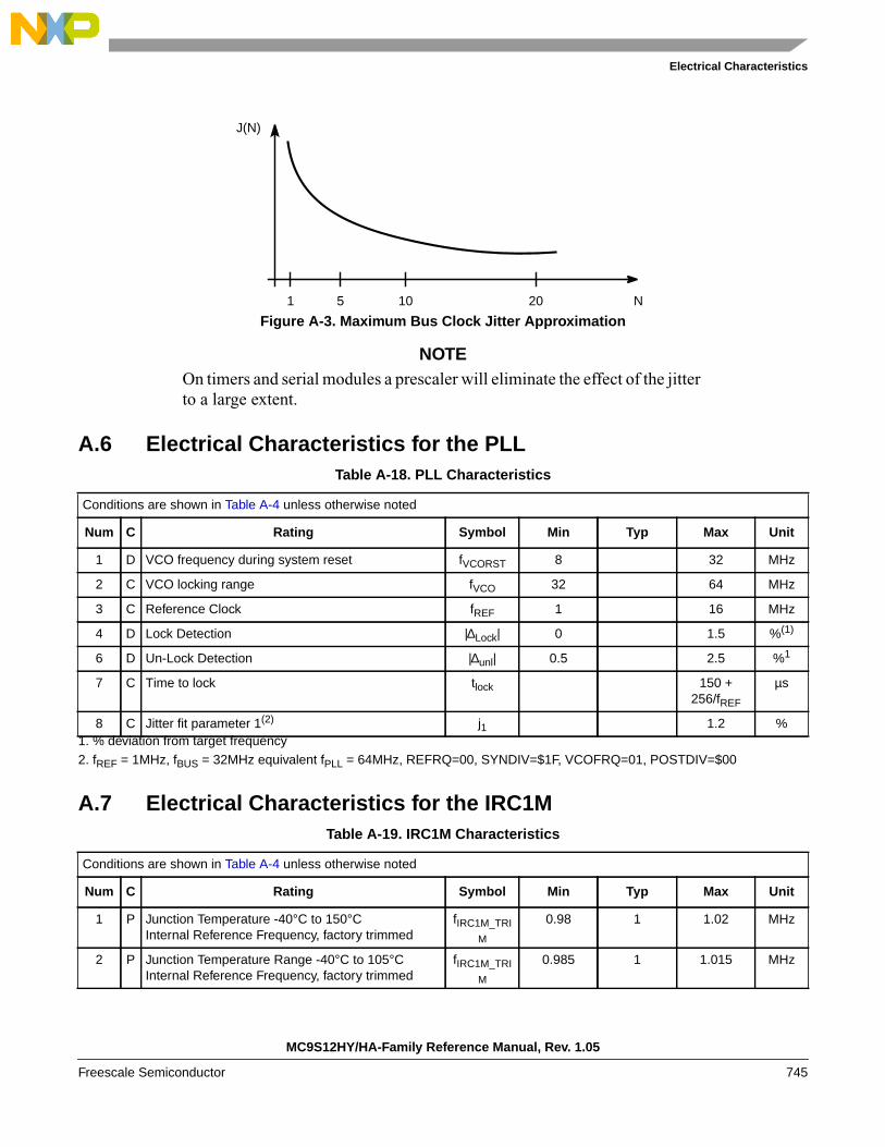
Electrical Characteristics
Figure A-3. Maximum Bus Clock Jitter Approximation
NOTEOn timers and serial modules a prescaler will eliminate the effect of the jitterto a large extent.
A.6 Electrical Characteristics for the PLL
A.7 Electrical Characteristics for the IRC1M
Table A-18. PLL Characteristics
Conditions are shown in Table A-4 unless otherwise noted
Num C Rating Symbol Min Typ Max Unit
1 D VCO frequency during system reset fVCORST 8 32 MHz
2 C VCO locking range fVCO 32 64 MHz
3 C Reference Clock fREF 1 16 MHz
4 D Lock Detection |∆Lock| 0 1.5 %(1)
1. % deviation from target frequency
6 D Un-Lock Detection |∆unl| 0.5 2.5 %1
7 C Time to lock tlock 150 +256/fREF
µs
8 C Jitter fit parameter 1(2)
2. fREF = 1MHz, fBUS = 32MHz equivalent fPLL = 64MHz, REFRQ=00, SYNDIV=$1F, VCOFRQ=01, POSTDIV=$00
j1 1.2 %
Table A-19. IRC1M Characteristics
Conditions are shown in Table A-4 unless otherwise noted
Num C Rating Symbol Min Typ Max Unit
1 P Junction Temperature -40°C to 150°CInternal Reference Frequency, factory trimmed
fIRC1M_TRI
M
0.98 1 1.02 MHz
2 P Junction Temperature Range -40°C to 105°CInternal Reference Frequency, factory trimmed
fIRC1M_TRI
M
0.985 1 1.015 MHz
1 5 10 20 N
J(N)
MC9S12HY/HA-Family Reference Manual, Rev. 1.05
Freescale Semiconductor 745
Electrical Characteristics
A.8 Electrical Characteristics for the Oscillator (OSCLCP)
A.9 Reset Characteristics
Table A-20. OSCLCP Characteristics
Conditions are shown in Table A-4 unless otherwise noted
Num C Rating Symbol Min Typ Max Unit
1 C Crystal oscillator range fOSC 4.0 16 MHz
2 P Startup Current iOSC 100 µA
3a C Oscillator start-up time (LCP, 4MHz)(1)
1. These values apply for carefully designed PCB layouts with capacitors that match the crystal/resonator requirements.
tUPOSC — 2 10 ms
3b C Oscillator start-up time (LCP, 8MHz)1 tUPOSC — 1.6 8 ms
3c C Oscillator start-up time (LCP, 16MHz)1 tUPOSC — 1 5 ms
4 P Clock Monitor Failure Assert Frequency fCMFA 200 400 1000 kHz
5 D Input Capacitance (EXTAL, XTAL pins) CIN 7 pF
6 C EXTAL Pin Input Hysteresis VHYS,EXTAL — 180 — mV
7 CEXTAL Pin oscillation amplitude (loopcontrolled Pierce)
VPP,EXTAL—
0.9—
V
Table A-21. Reset and Stop Characteristics
Conditions are shown in Table A-4 unless otherwise noted
Num C Rating Symbol Min Typ Max Unit
1 C Reset input pulse width, minimum input time PWRSTL 2 tVCORS
T
2 C Startup from Reset nRST 768 tVCORS
T
3 C STOP recovery time tSTP_REC 50 µs
MC9S12HY/HA-Family Reference Manual, Rev. 1.05
746 Freescale Semiconductor

Electrical Characteristics
A.10 Electrical Specification for Voltage Regulator
NOTEThe LVR monitors the voltages VDD, VDDF and VDDX. As soon as voltagedrops on these supplies which would prohibit the correct function of themicrocontroller, the LVR is triggering a reset.
A.11 Chip Power-up and Voltage DropsLVI (low voltage interrupt), POR (power-on reset) and LVRs (low voltage reset) handle chip power-up ordrops of the supply voltage.
Table A-22. IVREG Characteristics
Num C Characteristic Symbol Min Typical Max Unit
1 P Input Voltages VVDDR,A 3.13 — 5.5 V
2 P VDDA Low Voltage Interrupt Assert Level (1)
VDDA Low Voltage Interrupt Deassert Level
1. Monitors VDDA, active only in Full Performance Mode. Indicates I/O & ADC performance degradation due to low supplyvoltage.
VLVIAVLVID
4.044.19
4.234.38
4.404.49
VV
3 P VDDX Low Voltage Reset Deassert (2) (3)
2. Device functionality is guaranteed on power down to the LVR assert level3. Monitors VDDX, active only in Full Performance Mode. MCU is monitored by the POR in RPM (see Figure A-4)
VLVRXD — — 3.13 V
4 TAPI ACLK frequency(APITR[5:0] = %000000)
fACLK — 10 — kHz
5 C Trimmed API internal clock(4) ∆f / fnominal
4. The API Trimming APITR[5:0] bits must be set so that fACLK=10KHz.
dfACLK - 5% — + 5% —
6 DThe first period after enabling the counterby APIFE might be reduced by API start updelay
tsdel — — 100 us
7 T Temperature Sensor Slope dVTS 5.05 5.25 5.45mV/oC
8 T
High Temperature Interrupt Assert
(VREGHTTR=$88)(5)
High Temperature Interrupt Deassert(VREGHTTR=$88)
5. A hysteresis is guaranteed by design
THTIATHTID
120110
132122
144134
oC
9 T Bandgap Reference Voltage VBG 1.13 1.21 1.32 V
MC9S12HY/HA-Family Reference Manual, Rev. 1.05
Freescale Semiconductor 747
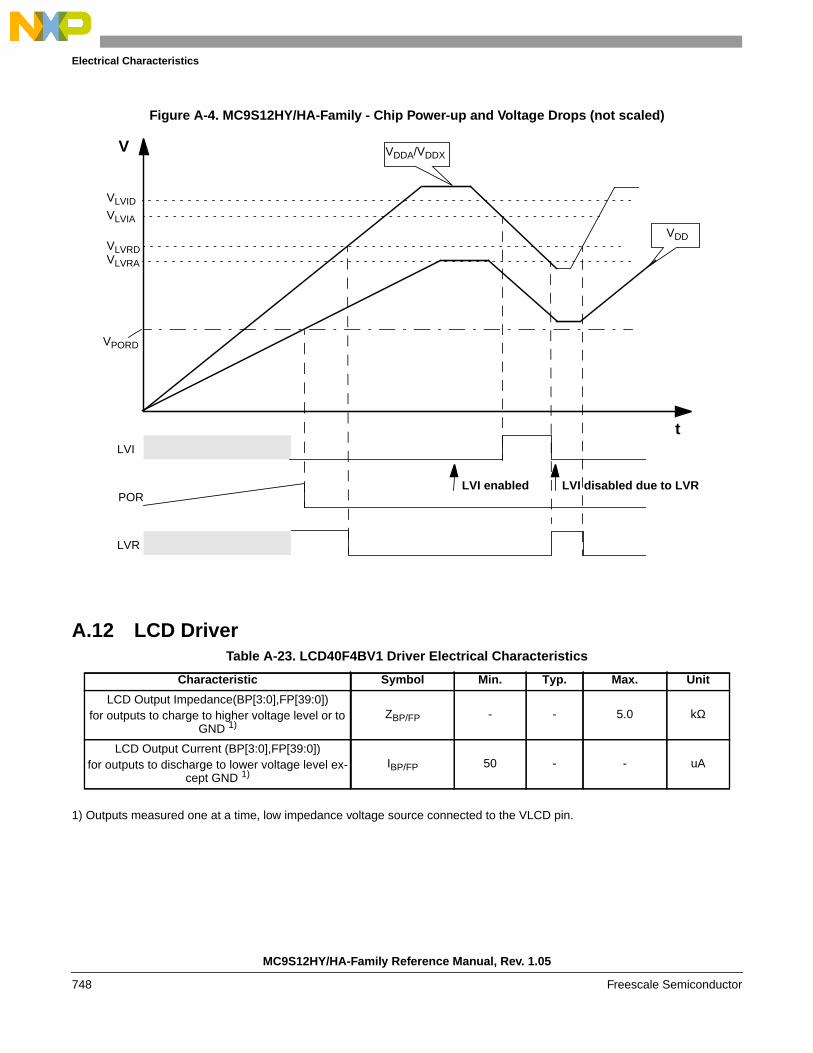
Electrical Characteristics
Figure A-4. MC9S12HY/HA-Family - Chip Power-up and Voltage Drops (not scaled)
A.12 LCD DriverTable A-23. LCD40F4BV1 Driver Electrical Characteristics
1) Outputs measured one at a time, low impedance voltage source connected to the VLCD pin.
Characteristic Symbol Min. Typ. Max. Unit
LCD Output Impedance(BP[3:0],FP[39:0])for outputs to charge to higher voltage level or to
GND 1)ZBP/FP - - 5.0 kΩ
LCD Output Current (BP[3:0],FP[39:0])for outputs to discharge to lower voltage level ex-
cept GND 1)IBP/FP 50 - - uA
VLVID
VLVIA
VLVRDVLVRA
VPORD
LVI
POR
LVR
t
V VDDA/VDDX
VDD
LVI enabled LVI disabled due to LVR
MC9S12HY/HA-Family Reference Manual, Rev. 1.05
748 Freescale Semiconductor

Electrical Characteristics
The 1/3, 1/2 and 2/3 VLCD voltage levels are buffered internally with an asymmetric output stage, asshown in Figure A-5.
Figure A-5. Buffer configuration (left) and buffer output stage (right)
The switching matrix applies a capacitive load (LCD elements) to the buffer output. The charge excites thebuffer output voltage VBuf from the target output voltage which can be 1/3, 1/2 or 2/3 VLCD. After apositive spike on VBuf a frontplane or backplane is discharged by an active load with a constant current.After a negative spike on VBuf the output is charged through a transistor which is switched on and whichbehaves like a resistor. Simplified output voltage transients are shown in Figure A-6.. The showntransients emphasize the spikes and the voltage recovery. They are not to scale. The buffer outputcharacteristic is shown in Figure A-7.. The resistive output characteristic is also valid if an output isforced to GND or VLCD.
switchmatrixto LCDVBuf
VBuf
VLCD VDDX
output MOSFET
active load
Iout
MC9S12HY/HA-Family Reference Manual, Rev. 1.05
Freescale Semiconductor 749

Electrical Characteristics
.
Figure A-6. VBuf transients (not to scale)
Figure A-7. buffer output characteristic
VBuf
t
2/3VLCD
1/2VLCD
1/3VLCD
constant currentresistive
IOUT
VOUT
1/3, 1/2 or2/3 VLCD
resistive
current source
region
region
IBP/FP
ZBP/FP
MC9S12HY/HA-Family Reference Manual, Rev. 1.05
750 Freescale Semiconductor

Electrical Characteristics
A.13 MSCAN
A.14 SPI TimingThis section provides electrical parametrics and ratings for the SPI. In Table A-25 the measurementconditions are listed.
Table A-24. MSCAN Wake-up Pulse Characteristics
Conditions are shown in Table A-4 unless otherwise noted
Num C Rating Symbol Min Typ Max Unit
1 P MSCAN wakeup dominant pulse filtered tWUP — — 1.5 µs
2 P MSCAN wakeup dominant pulse pass tWUP 5 — — µs
Table A-25. Measurement Conditions
Description Value Unit
Drive mode Full drive mode —
Load capacitance CLOAD(1)
, on all outputs
1. Timing specified for equal load on all SPI output pins. Avoid asymmetric load.
50 pF
Thresholds for delay measurement points (20% / 80%) VDDX V
Thresholds for delay measurement points on Motor pad (20% / 80%) VDDM V
MC9S12HY/HA-Family Reference Manual, Rev. 1.05
Freescale Semiconductor 751

Electrical Characteristics
A.14.1 Master Mode
In Figure A-8 the timing diagram for master mode with transmission format CPHA = 0 is depicted.
Figure A-8. SPI Master Timing (CPHA = 0)
In Figure A-9 the timing diagram for master mode with transmission format CPHA=1 is depicted.
Figure A-9. SPI Master Timing (CPHA = 1)
SCK
(Output)
SCK
(Output)
MISO(Input)
MOSI(Output)
SS(Output)
1
9
5 6
MSB IN2
Bit MSB-1. . . 1
LSB IN
MSB OUT2 LSB OUT
Bit MSB-1. . . 1
11
4
4
2
10
(CPOL = 0)
(CPOL = 1)
313
13
1. If configured as an output.2. LSBF = 0. For LSBF = 1, bit order is LSB, bit 1, bit 2... MSB.
12
12
SCK
(Output)
SCK
(Output)
MISO(Input)
MOSI(Output)
1
5 6
MSB IN2
Bit MSB-1. . . 1
LSB IN
Master MSB OUT2 Master LSB OUT
Bit MSB-1. . . 1
44
9
12 13
11
Port Data
(CPOL = 0)
(CPOL = 1)
Port Data
SS(Output)
2 12 13 3
1.If configured as output2. LSBF = 0. For LSBF = 1, bit order is LSB, bit 1,bit 2... MSB.
MC9S12HY/HA-Family Reference Manual, Rev. 1.05
752 Freescale Semiconductor

Electrical Characteristics
In Table A-26 the timing characteristics for master mode are listed.
Table A-26. SPI Master Mode Timing Characteristics
Num C Characteristic Symbol Min Typ Max Unit
1 D SCK frequency fsck fbus/2048 —
MIN(16, fbus/2)(1)
1. SPI on non-motor pad ports (Port S or Por t H)
MHZMIN(10,fbus/2) (2)
2. SPI on Port V with slew rate control disable. All the SPI pins slew rate control should be disabled.
MIN(0.8,fbus/2)(3)
3. SPI on Port V with slew rate control enabled. All the SPI pins slew rate control should be enabled.4. MIN(16, fbus/2) means select minimum frequency value from 16MHZ and fbus/2MHZ. same for the other MIN(X,Y)5. MAX(62.5, 2*tbus) means select the maximum period value from 62.5ns and 2*tbus ns. same for the other MAX(X,Y)
1 D SCK period tsck
MAX(62.5, 2*tbus)1
— 2048 ∗ tbus nsMAX(100, 2*tbus)2
MAX(1250, 2*tbus)3
2 D Enable lead time tlead — 1/2 — tsck
3 D Enable lag time tlag — 1/2 — tsck
4 DClock (SCK) high or lowtime
twsck — 1/2 — tsck
5 D Data setup time (inputs) tsu81,2 — — ns
2203 — — ns
6 D Data hold time (inputs) thi81,2 — — ns
2203 — — ns
9 D Data valid after SCK edge tvsck — —151,2 ns
2203 ns
10 DData valid after SS fall(CPHA = 0)
tvss — — 15 ns
11 D Data hold time (outputs) tho 20 — — ns
12 D Rise and fall time inputs trfi — —81,2 ns
853 ns
13 D Rise and fall time outputs trfo — —81,2 ns
853 ns
MC9S12HY/HA-Family Reference Manual, Rev. 1.05
Freescale Semiconductor 753

Electrical Characteristics
A.14.2 Slave Mode
In Figure A-10 the timing diagram for slave mode with transmission format CPHA = 0 is depicted.
Figure A-10. SPI Slave Timing (CPHA = 0)
In Figure A-11 the timing diagram for slave mode with transmission format CPHA = 1 is depicted.
Figure A-11. SPI Slave Timing (CPHA = 1)
SCK
(Input)
SCK
(Input)
MOSI(Input)
MISO(Output)
SS(Input)
1
9
5 6
MSB IN
Bit MSB-1 . . . 1
LSB IN
Slave MSB Slave LSB OUT
Bit MSB-1. . . 1
11
442
7
(CPOL = 0)
(CPOL = 1)
3
13
NOTE: Not defined
12
12
11
See
13
Note
810
SeeNote
SCK
(Input)
SCK
(Input)
MOSI(Input)
MISO(Output)
1
5 6
MSB IN
Bit MSB-1 . . . 1
LSB IN
MSB OUT Slave LSB OUT
Bit MSB-1 . . . 1
44
9
12 13
11
(CPOL = 0)
(CPOL = 1)
SS(Input)
2 12 13
3
NOTE: Not defined
Slave
7
8
SeeNote
MC9S12HY/HA-Family Reference Manual, Rev. 1.05
754 Freescale Semiconductor

Electrical Characteristics
In Table A-27 the timing characteristics for slave mode are listed.Table A-27. SPI Slave Mode Timing Characteristics
Num C Characteristic Symbol Min Typ Max Unit
1 D SCK frequency fsck DC —MIN(8,fbus/4)(1)
1. SPI on non-motor pad ports (Port S or Por t H), or SPI on motor pad ports with all Slew Rate control disable
MHZ
MIN(0.8,fbus/4)(2)
2. SPI on Port V with slew rate control enabled. All the SPI pins slew rate control should be enabled
1 D SCK period tsck
4*tbus1
— ∞ns
MAX(1250, 4*tbus)2
2 D Enable lead time tlead 4 — — tbus
3 D Enable lag time tlag 4 — — tbus
4 D Clock (SCK) high or low time twsck 4 — — tbus
5 D Data setup time (inputs) tsu 8 — — ns
6 D Data hold time (inputs) thi 8 — — ns
7 DSlave access time (time to dataactive)
ta — — 20ns
8 D Slave MISO disable time tdis
— — 22 ns
— — 2202 ns
9 D Data valid after SCK edge tvsck — —29 + 0.5 ⋅ tbus
(3),
3. 0.5 tbus added due to internal synchronization delay
ns
220 + 0.5 ⋅ tbus(4)
4. 0.5 tbus added due to internal synchronization delay, SPI on Port V with slew rate control enabled. All the SPI pins slewrate control should be enabled
4. MIN(8, fbus/4) means select minimum frequency value from 8MHZ and fbus/4MHZ. same for the other MIN(X,Y)5. MAX(1250, 4*tbus) means select the maximum period value from 1250ns and 4*tbus ns.
10 D Data valid after SS fall tvss — — 29 + 0.5 ⋅ tbus3 ns
11 D Data hold time (outputs) tho 17 — — ns
12 D Rise and fall time inputs trfi — — 8 ns
13 D Rise and fall time outputs trfo — —8 ns
852
MC9S12HY/HA-Family Reference Manual, Rev. 1.05
Freescale Semiconductor 755

Ordering Information
Appendix BOrdering InformationThe following figure provides an ordering partnumber example for the devices covered by this data book.There are two options when ordering a device. Customers must choose between ordering either the mask-specific partnumber or the generic / mask-independent partnumber. Ordering the mask-specificpartnumber enables the customer to specify which particular maskset they will receive whereas orderingthe generic maskset means that FSL will ship the currently preferred maskset (which may change overtime).
In either case, the marking on the device will always show the generic / mask-independent partnumber andthe mask set number.
NOTEThe mask identifier suffix and the Tape & Reel suffix are always both omitted from the
partnumber which is actually marked on the device.
For specific partnumbers to order, please contact your local sales office. The below figure illustrates thestructure of a typical mask-specific ordering number for the MC9S12HY/HA-Family devices
Figure B-1. Order Part Number Example
S 9 S12 HY64 J0 M LH R
Package Option:
Temperature Option:
Device Title
Controller Family
C = -40˚C to 85˚CV = -40˚C to 105˚CM = -40˚C to 125˚C
LH = 64 LQFPLL = 100 LQFP
Status / Partnumber type:S or SC = Maskset specific partnumberMC = Generic / mask-independent partnumberP or PC = prototype status (pre qualification)
Main Memory Type:9 = Flash3 = ROM (if available)
Maskset identifier Suffix:First digit usually references wafer fabSecond digit usually differentiates mask rev(This suffix is omitted in generic partnumbers)
Tape & Reel:R = Tape & ReelNo R = No Tape & Reel
MC9S12HY/HA-Family Reference Manual, Rev. 1.05
756 Freescale Semiconductor

Package Information
Appendix CPackage Information
C.1 100-Pin LQFP Mechanical Dimensions
Figure C-1. 100-pin LQFP (case no. 983) - page 1
MC9S12HY/HA-Family Reference Manual, Rev. 1.05
Freescale Semiconductor 757

Package Information
Figure C-2. 100-pin LQFP (case no. 983) - page 2
MC9S12HY/HA-Family Reference Manual, Rev. 1.05
758 Freescale Semiconductor

Package Information
Figure C-3. 100-pin LQFP (case no. 983) - page 3
MC9S12HY/HA-Family Reference Manual, Rev. 1.05
Freescale Semiconductor 759

Package Information
C.2 64-Pin LQFP Mechanical Dimensions
Figure C-4. 64-pin LQFP (case no. 840F) - page 1
MC9S12HY/HA-Family Reference Manual, Rev. 1.05
760 Freescale Semiconductor
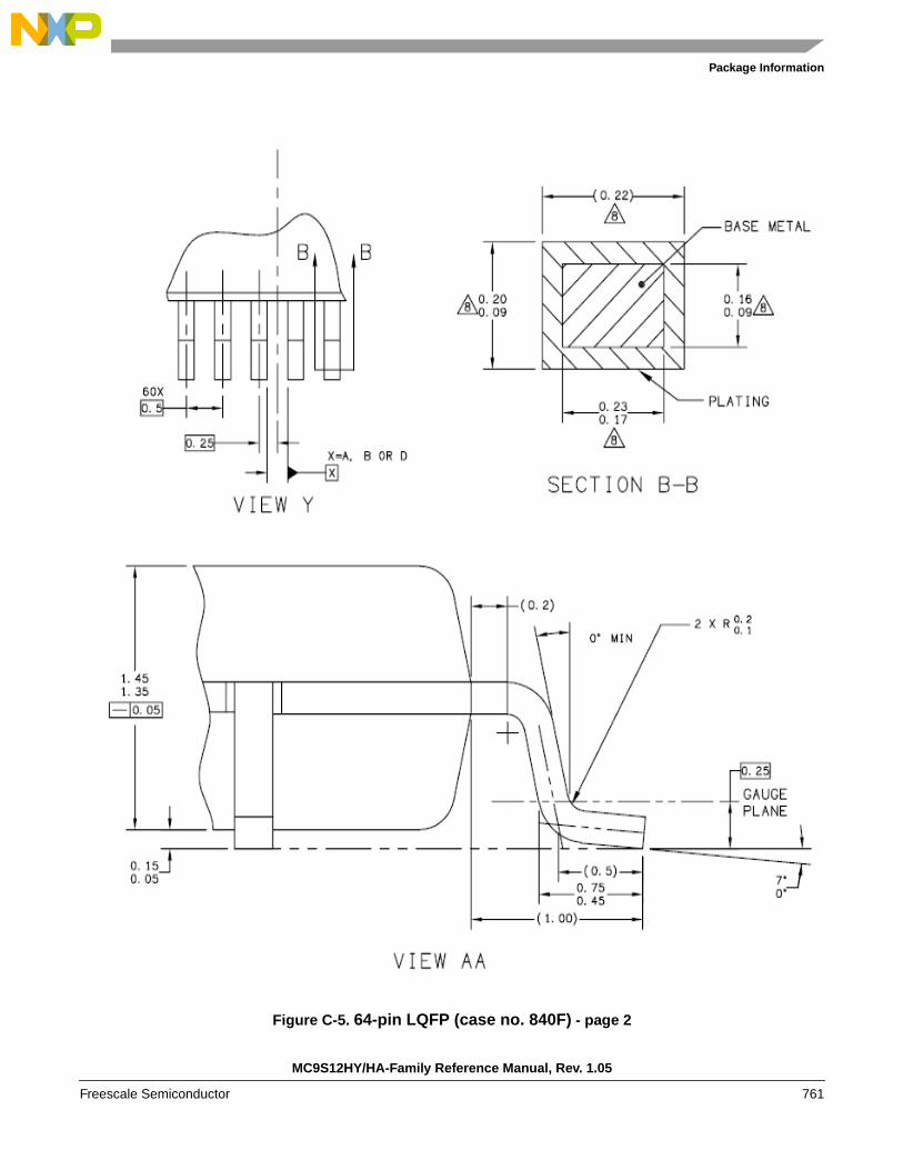
Package Information
Figure C-5. 64-pin LQFP (case no. 840F) - page 2
MC9S12HY/HA-Family Reference Manual, Rev. 1.05
Freescale Semiconductor 761
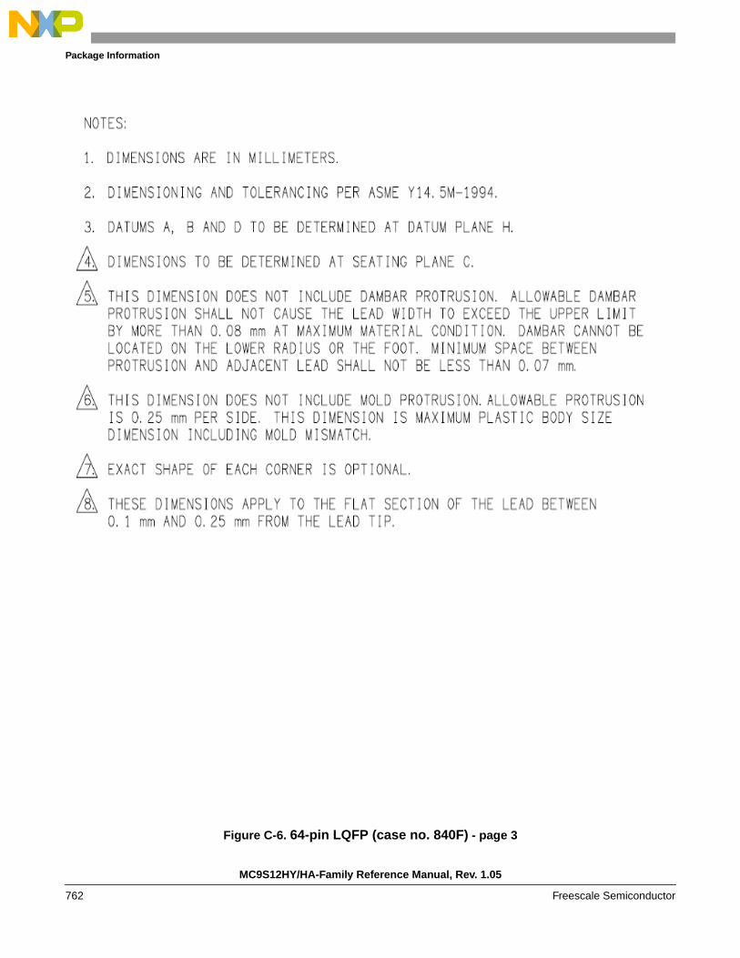
Package Information
Figure C-6. 64-pin LQFP (case no. 840F) - page 3
MC9S12HY/HA-Family Reference Manual, Rev. 1.05
762 Freescale Semiconductor

PCB Layout Guidelines
Appendix DPCB Layout GuidelinesThe PCB must be carefully laid out to ensure proper operation of the voltage regulator as well as of theMCU itself. The following rules must be observed:
• Every supply pair must be decoupled by a ceramic capacitor connected as near as possible to thecorresponding pins .
• Central point of the ground star should be the VSS3 pin.
• VSSPLL must be directly connected to VSS3.
• Keep traces of VSSPLL, EXTAL, and XTAL as short as possible and occupied board area for C1,C2, and Q1 as small as possible.
• Do not place other signals or supplies underneath area occupied by C1, C2, and Q1 and theconnection area to the MCU.
• Central power input should be fed in at the VDDA/VSSA pins.
Example layouts are illustrated on the following pages.
MC9S12HY/HA-Family Reference Manual, Rev. 1.05
Freescale Semiconductor 763

PCB Layout Guidelines
Table D-1. Recommended Decoupling Capacitor Choice
Component Purpose Type Value
C1 OSC load capacitor From crystal manufacturer
C2 OSC load capacitor
C3 VDDA filter capacitor X7R/tantalum >=100 nF
C4 VDDM1 filter capacitor Ceramic/X7R >=47uF
C5 VDDR filter capacitor X7R/tantalum >=100 nF
C6 VLCD filter capacitor X7R/tantalum >=100 nF
C7 VDDM2 filter capacitor Ceramic/X7R >=47uF
C8 VDDX filter capacitor X7R/tantalum >=100 nF
Q1 Quartz — —
MC9S12HY/HA-Family Reference Manual, Rev. 1.05
764 Freescale Semiconductor
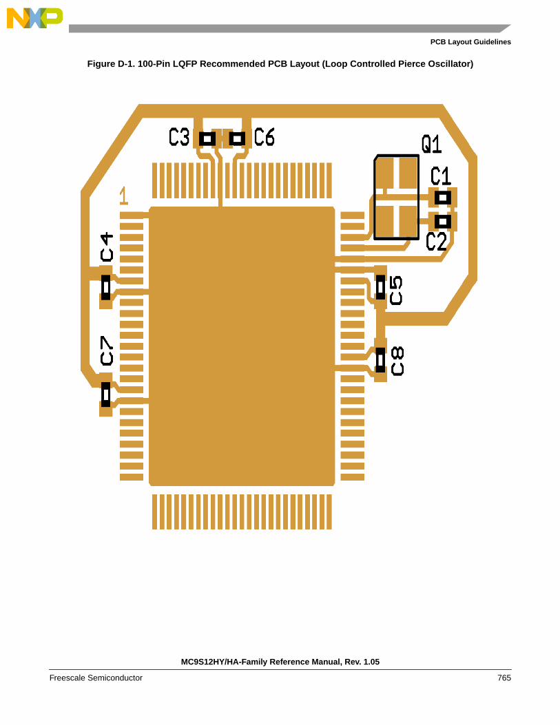
PCB Layout Guidelines
Figure D-1. 100-Pin LQFP Recommended PCB Layout (Loop Controlled Pierce Oscillator)
MC9S12HY/HA-Family Reference Manual, Rev. 1.05
Freescale Semiconductor 765

PCB Layout Guidelines
Figure D-2. 64-Pin LQFP Recommended PCB Layout (Loop Controlled Pierce Oscillator)
MC9S12HY/HA-Family Reference Manual, Rev. 1.05
766 Freescale Semiconductor

Derivative Differences
Appendix EDerivative Differences
E.1 Memory Sizes and Package Options S12HY/S12HA - FamilyTable E-1. Package and Memory Options of MC9S12HY/S12HA-Family
Table E-2. Peripheral Options of MC9S12HY/HA Family Members
Device Package Flash RAM D-Flash
9S12HY64100 LQFP
64K 4K 4K64 LQFP
9S12HY48100 LQFP
48K 4K 4K64 LQFP
9S12HY32100 LQFP
32K 2K 4K64 LQFP
9S12HA64100 LQFP
64K 4K 4K64 LQFP
9S12HA48100 LQFP
48K 4K 4K64 LQFP
9S12HA32100 LQFP
32K 2K 4K64 LQFP
Device Package CAN SCI SPI IIC TIM0 TIM1 PWM LCD A/D MC I/O
9S12HY64100 LQFP
1 1 1 1
8ch 8ch 8ch 40x4 1/8 4 80
64 LQFP 8ch 8ch 8ch 20x4 1/6 3(1)
1. M2 can have only reduced drive capability, which is half of normal motor pad driving current
50
9S12HY48100 LQFP 8ch 8ch 8ch 40x4 1/8 4 80
64 LQFP 8ch 8ch 8ch 20x4 1/6 31 50
9S12HY32100 LQFP 8ch 8ch 8ch 40x4 1/8 4 80
64 LQFP 8ch 8ch 8ch 20x4 1/6 31 50
9S12HA64100 LQFP
0 1 1 1
8ch 8ch 8ch 40x4 1/8 4 80
64 LQFP 8ch 8ch 8ch 20x4 1/6 31 50
9S12HA48100 LQFP 8ch 8ch 8ch 40x4 1/8 4 80
64 LQFP 8ch 8ch 8ch 20x4 1/6 31 50
9S12HA32100 LQFP 8ch 8ch 8ch 40x4 1/8 4 80
64 LQFP 8ch 8ch 8ch 20x4 1/6 31 50
MC9S12HY/HA-Family Reference Manual, Rev. 1.05
Freescale Semiconductor 767

Detailed Register Address Map
Appendix FDetailed Register Address MapThe following tables show the detailed register map of the MC9S12HY/HA.
NOTESmaller derivatives within the MC9S12HY/HA feature a subset of the listedmodules. Refer to Appendix E Derivative Differences for more informationabout derivative device module subsets.
0x0000–0x0009 Port Integration Module (PIM) Map 1 of 4
0x000A–0x000B Module Mapping Control (MMC) Map 1 of 2
0x000C–0x000D Port Integration Module (PIM) Map 2 of 4
0x000E–0x000F Reserved
Address Name Bit 7 Bit 6 Bit 5 Bit 4 Bit 3 Bit 2 Bit 1 Bit 0
0x0000 PORTAR
PA7 PA6 PA5 PA4 PA3 PA2 PA1 PA 0W
0x0001 PORTBR
PB7 PB6 PB5 PB4 PB3 PB2 PB1 PB0W
0x0002 DDRAR
DDRA7 DDRA6 DDRA5 DDRA4 DDRA3 DDRA2 DDRA1 DDRA0W
0x0003 DDRBR
DDRB7 DDRB6 DDRB5 DDRB4 DDRB3 DDRB2 DDRB1 DDRB0W
0x0004-0x0009
ReservedR 0 0 0 0 0 0 0 0
W
Address Name Bit 7 Bit 6 Bit 5 Bit 4 Bit 3 Bit 2 Bit 1 Bit 0
0x000A ReservedR 0 0 0 0 0 0 0 0
W
0x000B MODER
MODC0 0 0 0 0 0 0
W
Address Name Bit 7 Bit 6 Bit 5 Bit 4 Bit 3 Bit 2 Bit 1 Bit 0
0x000C PUCRR 0
BKPUE0 0 0 0
PUPBE PUPAEW
0x000D RDRIVR 0 0 0 0 0 0
RDPB RDPAW
Address Name Bit 7 Bit 6 Bit 5 Bit 4 Bit 3 Bit 2 Bit 1 Bit 0
0x000E-0x000F
ReservedR 0 0 0 0 0 0 0 0
W
MC9S12HY/HA-Family Reference Manual, Rev. 1.05
768 Freescale Semiconductor

Detailed Register Address Map
0x0010–0x0017 Module Mapping Control (MMC) Map 2 of 2
0x0018–0x001B Miscellaneous Peripheral
0x001C–0x001F Port Integration Module (PIM) Map 3 of 6
AddressRegister
NameBit 7 6 5 4 3 2 1 Bit 0
0x00010 ReservedR 0 0 0 0 0 0 0 0
W
0x0011 DIRECT RDP15 DP14 DP13 DP12 DP11 DP10 DP9 DP8
W
0x0012 ReservedR 0 0 0 0 0 0 0 0
W
0x0013 Reserved R 0 0 0 0 0 0 0 0
W
0x0014 ReservedR 0 0 0 0 0 0 0 0
W
0x0015 PPAGE R 0 0 0 0PIX3 PIX2 PIX1 PIX0
W
0x0016-0x0017
ReservedR 0 0 0 0 0 0 0 0
W
Address Name Bit 7 Bit 6 Bit 5 Bit 4 Bit 3 Bit 2 Bit 1 Bit 0
0x0018 ReservedR 0 0 0 0 0 0 0 0
W
0x0019 ReservedR 0 0 0 0 0 0 0 0
W
0x001A PARTIDH(1)
1. Refer to Part ID assignments in the device description section for a full list of MC9S12HY/HAPart ID values.
R 0 0 0 1 1 0 1 0
W
0x001B PARTIDL1 R 1 0 0 0 0 0 0 0
W
Address Name Bit 7 Bit 6 Bit 5 Bit 4 Bit 3 Bit 2 Bit 1 Bit 0
0x001C ECLKCTLR
NECLK0
DIV16 EDIV4 EDIV3 EDIV2 EDIV1 EDIV0W
0x001D ReservedR 0 0 0 0 0 0 0 0
W
0x001E IRQCRR
IRQE IRQEN XIRQEN0 0 0 0 0
W
0x001F ReservedR 0 0 0 0 0 0 0 0
W
MC9S12HY/HA-Family Reference Manual, Rev. 1.05
Freescale Semiconductor 769

Detailed Register Address Map
0x0020–0x002F Debug Module (DBG) Map
Address Name Bit 7 6 5 4 3 2 1 Bit 0
0x0020 DBGC1R
ARM0 0
BDM DBGBRK0
COMRVW TRIG
0x0021 DBGSRR 1TBF 0 0 0 0 SSF2 SSF1 SSF0
W
0x0022 DBGTCRR 0
TSOURCE0 0
TRCMOD0
TALIGNW
0x0023 DBGC2R 0 0 0 0 0 0
ABCMW
0x0024 DBGTBHR Bit 15 Bit 14 Bit 13 Bit 12 Bit 11 Bit 10 Bit 9 Bit 8
W
0x0025 DBGTBLR Bit 7 Bit 6 Bit 5 Bit 4 Bit 3 Bit 2 Bit 1 Bit 0
W
0x0026 DBGCNTR 5 TBF 0 CNT
W
0x0027 DBGSCRXR 0 0 0 0
SC3 SC2 SC1 SC0W
0x0027 DBGMFRR 0 0 0 0 0 MC2 MC1 MC0
W6 0x0028
DBGACTLR
SZE SZ TAG BRK RW RWE NDB COMPEW
7 0x0028DBGBCTL
RSZE SZ TAG BRK RW RWE
0COMPE
W8 0x0028
DBGCCTLR 0 0
TAG BRK RW RWE0
COMPEW
0x0029 DBGXAHR 0 0 0 0 0 0
Bit 17 Bit 16W
0x002A DBGXAMR
Bit 15 14 13 12 11 10 9 Bit 8W
0x002B DBGXALR
Bit 7 6 5 4 3 2 1 Bit 0W
0x002C DBGADHR
Bit 15 14 13 12 11 10 9 Bit 8W
0x002D DBGADLR
Bit 7 6 5 4 3 2 1 Bit 0W
0x002E DBGADHMR
Bit 15 14 13 12 11 10 9 Bit 8W
MC9S12HY/HA-Family Reference Manual, Rev. 1.05
770 Freescale Semiconductor

Detailed Register Address Map
0x0030–0x0033 Reserved
0x0034–0x003F Clock and Power Management (CPMU) 1 of 2
0x002F DBGADLMR
Bit 7 6 5 4 3 2 1 Bit 0W
1 This bit is visible at DBGCNT[7] and DBGSR[7]2 This represents the contents if the Comparator A control register is blended into this address.3 This represents the contents if the Comparator B control register is blended into this address4 This represents the contents if the Comparator C control register is blended into this address
Address Name Bit 7 Bit 6 Bit 5 Bit 4 Bit 3 Bit 2 Bit 1 Bit 0
0x0030-0x0033
ReservedR 0 0 0 0 0 0 0 0
W
Address Name Bit 7 Bit 6 Bit 5 Bit 4 Bit 3 Bit 2 Bit 1 Bit 0
0x0034CPMUSYNR
RVCOFRQ[1:0] SYNDIV[5:0]
W
0x0035CPMU
REFDIVR
REFFRQ[1:0]0 0
REFDIV[3:0]W
0x0036CPMU
POSTDIVR 0 0 0
POSTDIV[4:0]W
0x0037 CPMUFLGR
RTIF PORF LVRF LOCKIFLOCK
ILAF OSCIFUPOSC
W
0x0038 CPMUINTR
RTIE0 0
LOCKIE0 0
OSCIE0
W
0x0039 CPMUCLKSR
PLLSEL PSTP0 0
PRE PCERTI
OSCSELCOP
OSCSELW
0x003A CPMUPLLR 0 0
FM1 FM00 0 0 0
W
0x003B CPMURTIR
RTDEC RTR6 RTR5 RTR4 RTR3 RTR2 RTR1 RTR0W
0x003C CPMUCOPR
WCOP RSBCK0 0 0
CR2 CR1 CR0W WRTMASK
0x003D RESERVEDR 0 0 0 0 0 0 0 0
W
0x003E RESERVEDR 0 0 0 0 0 0 0 0
W
0x003FCPMU
ARMCOPR 0 0 0 0 0 0 0 0
W Bit 7 Bit 6 Bit 5 Bit 4 Bit 3 Bit 2 Bit 1 Bit 0
Address Name Bit 7 6 5 4 3 2 1 Bit 0
MC9S12HY/HA-Family Reference Manual, Rev. 1.05
Freescale Semiconductor 771

Detailed Register Address Map
0x0040–0x006F Timer Module (TIM0) MapAddress Name Bit 7 Bit 6 Bit 5 Bit 4 Bit 3 Bit 2 Bit 1 Bit 0
0x0040 TIOSR
IOS7 IOS6 IOS5 IOS4 IOS3 IOS2 IOS1 IOS0W
0x0041 CFORCR 0 0 0 0 0 0 0 0
W FOC7 FOC6 FOC5 FOC4 FOC3 FOC2 FOC1 FOC0
0x0042 OC7MR
OC7M7 OC7M6 OC7M5 OC7M4 OC7M3 OC7M2 OC7M1 OC7M0W
0x0043 OC7DR
OC7D7 OC7D6 OC7D5 OC7D4 OC7D3 OC7D2 OC7D1 OC7D0W
0x0044 TCNTHR
TCNT15 TCNT14 TCNT13 TCNT12 TCNT11 TCNT10 TCNT9 TCNT8W
0x0045 TCNTLR
TCNT7 TCNT6 TCNT5 TCNT4 TCNT3 TCNT2 TCNT1 TCNT0W
0x0046 TSCR1R
TEN TSWAI TSFRZ TFFCA PRNT0 0 0
W
0x0047 TTOVR
TOV7 TOV6 TOV5 TOV4 TOV3 TOV2 TOV1 TOV0W
0x0048 TCTL1R
OM7 OL7 OM6 OL6 OM5 OL5 OM4 OL4W
0x0049 TCTL2R
OM3 OL3 OM2 OL2 OM1 OL1 OM0 OL0W
0x004A TCTL3R
EDG7B EDG7A EDG6B EDG6A EDG5B EDG5A EDG4B EDG4AW
0x004B TCTL4R
EDG3B EDG3A EDG2B EDG2A EDG1B EDG1A EDG0B EDG0AW
0x004C TIER
C7I C6I C5I C4I C3I C2I C1I C0IW
0x004D TSCR2R
TOI0 0 0
TCRE PR2 PR1 PR0W
0x004E TFLG1R
C7F C6F C5F C4F C3F C2F C1F C0FW
0x004F TFLG2R
TOF0 0 0 0 0 0 0
W
0x0050 TC0HR
Bit 15 Bit 14 Bit 13 Bit 12 Bit 11 Bit 10 Bit 9 Bit 8W
0x0051 TC0LR
Bit 7 Bit 6 Bit 5 Bit 4 Bit 3 Bit 2 Bit 1 Bit 0W
0x0052 TC1HR
Bit 15 Bit 14 Bit 13 Bit 12 Bit 11 Bit 10 Bit 9 Bit 8W
0x0053 TC1LR
Bit 7 Bit 6 Bit 5 Bit 4 Bit 3 Bit 2 Bit 1 Bit 0W
MC9S12HY/HA-Family Reference Manual, Rev. 1.05
772 Freescale Semiconductor
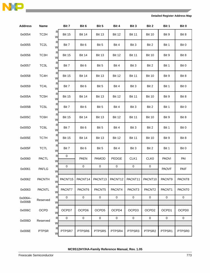
Detailed Register Address Map
0x0054 TC2HR
Bit 15 Bit 14 Bit 13 Bit 12 Bit 11 Bit 10 Bit 9 Bit 8W
0x0055 TC2LR
Bit 7 Bit 6 Bit 5 Bit 4 Bit 3 Bit 2 Bit 1 Bit 0W
0x0056 TC3HR
Bit 15 Bit 14 Bit 13 Bit 12 Bit 11 Bit 10 Bit 9 Bit 8W
0x0057 TC3LR
Bit 7 Bit 6 Bit 5 Bit 4 Bit 3 Bit 2 Bit 1 Bit 0W
0x0058 TC4HR
Bit 15 Bit 14 Bit 13 Bit 12 Bit 11 Bit 10 Bit 9 Bit 8W
0x0059 TC4LR
Bit 7 Bit 6 Bit 5 Bit 4 Bit 3 Bit 2 Bit 1 Bit 0W
0x005A TC5HR
Bit 15 Bit 14 Bit 13 Bit 12 Bit 11 Bit 10 Bit 9 Bit 8W
0x005B TC5LR
Bit 7 Bit 6 Bit 5 Bit 4 Bit 3 Bit 2 Bit 1 Bit 0W
0x005C TC6HR
Bit 15 Bit 14 Bit 13 Bit 12 Bit 11 Bit 10 Bit 9 Bit 8W
0x005D TC6LR
Bit 7 Bit 6 Bit 5 Bit 4 Bit 3 Bit 2 Bit 1 Bit 0W
0x005E TC7HR
Bit 15 Bit 14 Bit 13 Bit 12 Bit 11 Bit 10 Bit 9 Bit 8W
0x005F TC7LR
Bit 7 Bit 6 Bit 5 Bit 4 Bit 3 Bit 2 Bit 1 Bit 0W
0x0060 PACTLR 0
PAEN PAMOD PEDGE CLK1 CLK0 PAOVI PAIW
0x0061 PAFLGR 0 0 0 0 0 0
PAOVF PAIFW
0x0062 PACNTHR
PACNT15 PACNT14 PACNT13 PACNT12 PACNT11 PACNT10 PACNT9 PACNT8W
0x0063 PACNTLR
PACNT7 PACNT6 PACNT5 PACNT4 PACNT3 PACNT2 PACNT1 PACNT0W
0x0064–0x006B
ReservedR 0 0 0 0 0 0 0 0
W
0x006C OCPDR
OCPD7 OCPD6 OCPD5 OCPD4 OCPD3 OCPD2 OCPD1 OCPD0W
0x006D ReservedR 0 0 0 0 0 0 0 0
W
0x006E PTPSRR
PTPSR7 PTPSR6 PTPSR5 PTPSR4 PTPSR3 PTPSR2 PTPSR1 PTPSR0W
Address Name Bit 7 Bit 6 Bit 5 Bit 4 Bit 3 Bit 2 Bit 1 Bit 0
MC9S12HY/HA-Family Reference Manual, Rev. 1.05
Freescale Semiconductor 773
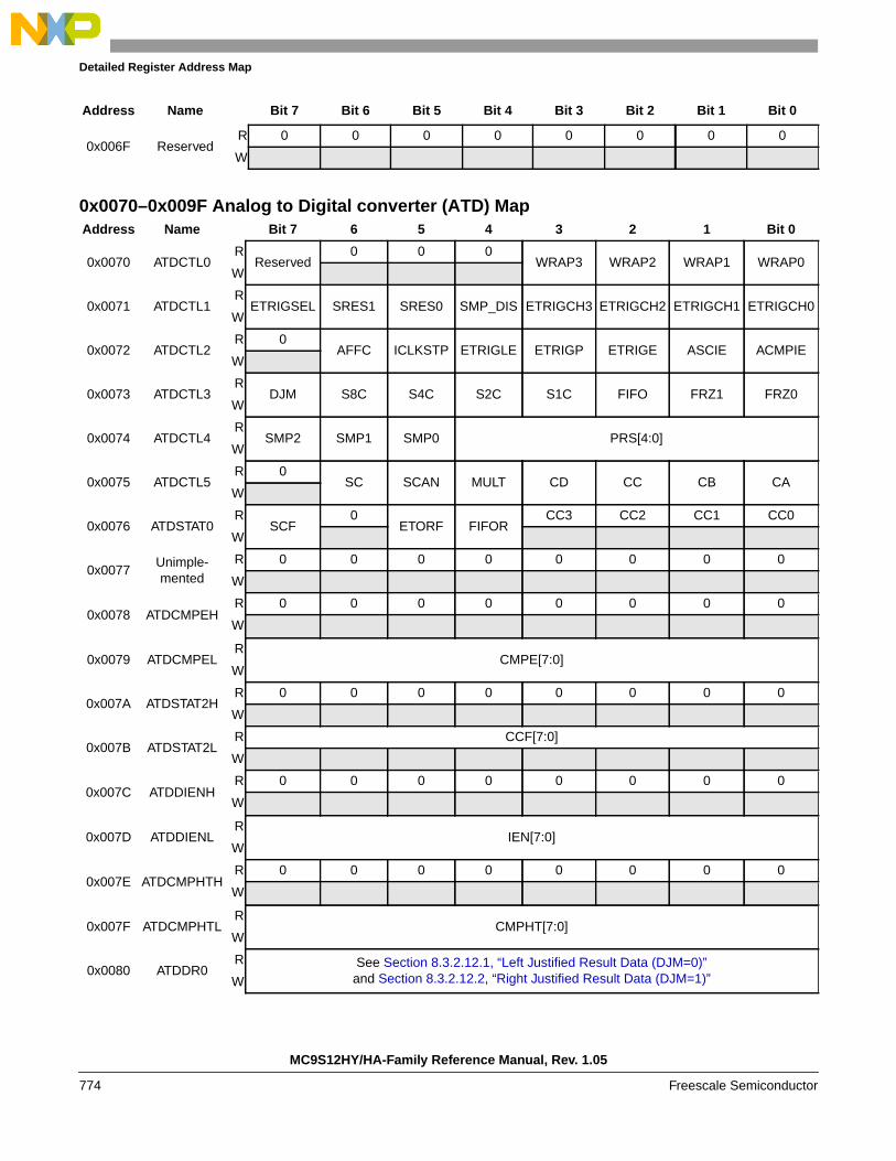
Detailed Register Address Map
0x0070–0x009F Analog to Digital converter (ATD) Map
0x006F ReservedR 0 0 0 0 0 0 0 0
W
Address Name Bit 7 6 5 4 3 2 1 Bit 0
0x0070 ATDCTL0R
Reserved0 0 0
WRAP3 WRAP2 WRAP1 WRAP0W
0x0071 ATDCTL1R
ETRIGSEL SRES1 SRES0 SMP_DIS ETRIGCH3 ETRIGCH2 ETRIGCH1 ETRIGCH0W
0x0072 ATDCTL2R 0
AFFC ICLKSTP ETRIGLE ETRIGP ETRIGE ASCIE ACMPIEW
0x0073 ATDCTL3R
DJM S8C S4C S2C S1C FIFO FRZ1 FRZ0W
0x0074 ATDCTL4R
SMP2 SMP1 SMP0 PRS[4:0]W
0x0075 ATDCTL5R 0
SC SCAN MULT CD CC CB CAW
0x0076 ATDSTAT0R
SCF0
ETORF FIFORCC3 CC2 CC1 CC0
W
0x0077Unimple-mented
R 0 0 0 0 0 0 0 0
W
0x0078 ATDCMPEHR 0 0 0 0 0 0 0 0
W
0x0079 ATDCMPELR
CMPE[7:0]W
0x007A ATDSTAT2HR 0 0 0 0 0 0 0 0
W
0x007B ATDSTAT2LR CCF[7:0]
W
0x007C ATDDIENHR 0 0 0 0 0 0 0 0
W
0x007D ATDDIENLR
IEN[7:0]W
0x007E ATDCMPHTHR 0 0 0 0 0 0 0 0
W
0x007F ATDCMPHTLR
CMPHT[7:0]W
0x0080 ATDDR0R See Section 8.3.2.12.1, “Left Justified Result Data (DJM=0)”
and Section 8.3.2.12.2, “Right Justified Result Data (DJM=1)”W
Address Name Bit 7 Bit 6 Bit 5 Bit 4 Bit 3 Bit 2 Bit 1 Bit 0
MC9S12HY/HA-Family Reference Manual, Rev. 1.05
774 Freescale Semiconductor
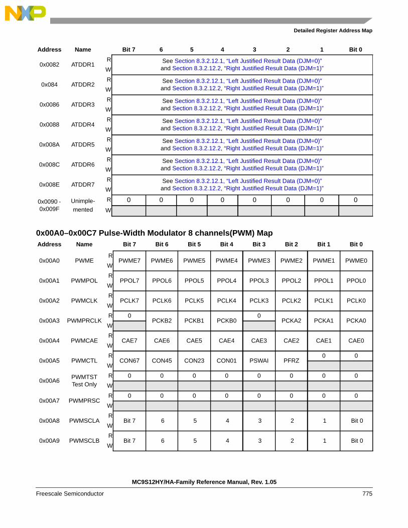
Detailed Register Address Map
0x00A0–0x00C7 Pulse-Width Modulator 8 channels(PWM) Map
0x0082 ATDDR1R See Section 8.3.2.12.1, “Left Justified Result Data (DJM=0)”
and Section 8.3.2.12.2, “Right Justified Result Data (DJM=1)”W
0x084 ATDDR2R See Section 8.3.2.12.1, “Left Justified Result Data (DJM=0)”
and Section 8.3.2.12.2, “Right Justified Result Data (DJM=1)”W
0x0086 ATDDR3R See Section 8.3.2.12.1, “Left Justified Result Data (DJM=0)”
and Section 8.3.2.12.2, “Right Justified Result Data (DJM=1)”W
0x0088 ATDDR4R See Section 8.3.2.12.1, “Left Justified Result Data (DJM=0)”
and Section 8.3.2.12.2, “Right Justified Result Data (DJM=1)”W
0x008A ATDDR5R See Section 8.3.2.12.1, “Left Justified Result Data (DJM=0)”
and Section 8.3.2.12.2, “Right Justified Result Data (DJM=1)”W
0x008C ATDDR6R See Section 8.3.2.12.1, “Left Justified Result Data (DJM=0)”
and Section 8.3.2.12.2, “Right Justified Result Data (DJM=1)”W
0x008E ATDDR7R See Section 8.3.2.12.1, “Left Justified Result Data (DJM=0)”
and Section 8.3.2.12.2, “Right Justified Result Data (DJM=1)”W
0x0090 -0x009F
Unimple-mented
R 0 0 0 0 0 0 0 0
W
Address Name Bit 7 Bit 6 Bit 5 Bit 4 Bit 3 Bit 2 Bit 1 Bit 0
0x00A0 PWMER
PWME7 PWME6 PWME5 PWME4 PWME3 PWME2 PWME1 PWME0W
0x00A1 PWMPOLR
PPOL7 PPOL6 PPOL5 PPOL4 PPOL3 PPOL2 PPOL1 PPOL0W
0x00A2 PWMCLKR
PCLK7 PCLK6 PCLK5 PCLK4 PCLK3 PCLK2 PCLK1 PCLK0W
0x00A3 PWMPRCLKR 0
PCKB2 PCKB1 PCKB00
PCKA2 PCKA1 PCKA0W
0x00A4 PWMCAER
CAE7 CAE6 CAE5 CAE4 CAE3 CAE2 CAE1 CAE0W
0x00A5 PWMCTLR
CON67 CON45 CON23 CON01 PSWAI PFRZ0 0
W
0x00A6PWMTSTTest Only
R 0 0 0 0 0 0 0 0
W
0x00A7 PWMPRSCR 0 0 0 0 0 0 0 0
W
0x00A8 PWMSCLAR
Bit 7 6 5 4 3 2 1 Bit 0W
0x00A9 PWMSCLBR
Bit 7 6 5 4 3 2 1 Bit 0W
Address Name Bit 7 6 5 4 3 2 1 Bit 0
MC9S12HY/HA-Family Reference Manual, Rev. 1.05
Freescale Semiconductor 775

Detailed Register Address Map
0x00AA PWMSCNTAR 0 0 0 0 0 0 0 0
W
0x00AB PWMSCNTBR 0 0 0 0 0 0 0 0
W
0x00AC PWMCNT0R Bit 7 6 5 4 3 2 1 Bit 0
W 0 0 0 0 0 0 0 0
0x00AD PWMCNT1R Bit 7 6 5 4 3 2 1 Bit 0
W 0 0 0 0 0 0 0 0
0x00AE PWMCNT2R Bit 7 6 5 4 3 2 1 Bit 0
W 0 0 0 0 0 0 0 0
0x00AF PWMCNT3R Bit 7 6 5 4 3 2 1 Bit 0
W 0 0 0 0 0 0 0 0
0x00B0 PWMCNT4R Bit 7 6 5 4 3 2 1 Bit 0
W 0 0 0 0 0 0 0 0
0x00B1 PWMCNT5R Bit 7 6 5 4 3 2 1 Bit 0
W 0 0 0 0 0 0 0 0
0x00B2 PWMCNT6R Bit 7 6 5 4 3 2 1 Bit 0
W 0 0 0 0 0 0 0 0
0x00B3 PWMCNT7R Bit 7 6 5 4 3 2 1 Bit 0
W 0 0 0 0 0 0 0 0
0x00B4 PWMPER0R
Bit 7 6 5 4 3 2 1 Bit 0W
0x00B5 PWMPER1R
Bit 7 6 5 4 3 2 1 Bit 0W
0x00B6 PWMPER2R
Bit 7 6 5 4 3 2 1 Bit 0W
0x00B7 PWMPER3R
Bit 7 6 5 4 3 2 1 Bit 0W
0x00B8 PWMPER4R
Bit 7 6 5 4 3 2 1 Bit 0W
0x00B9 PWMPER5R
Bit 7 6 5 4 3 2 1 Bit 0W
0x00BA PWMPER6R
Bit 7 6 5 4 3 2 1 Bit 0W
0x00BB PWMPER7R
Bit 7 6 5 4 3 2 1 Bit 0W
0x00BC PWMDTY0R
Bit 7 6 5 4 3 2 1 Bit 0W
0x00BD PWMDTY1R
Bit 7 6 5 4 3 2 1 Bit 0W
Address Name Bit 7 Bit 6 Bit 5 Bit 4 Bit 3 Bit 2 Bit 1 Bit 0
MC9S12HY/HA-Family Reference Manual, Rev. 1.05
776 Freescale Semiconductor

Detailed Register Address Map
0x00C8–0x00CF Asynchronous Serial Interface (SCI) Map
0x00BE PWMDTY2R
Bit 7 6 5 4 3 2 1 Bit 0W
0x00BF PWMDTY3R
Bit 7 6 5 4 3 2 1 Bit 0W
0x00C0 PWMDTY4R
Bit 7 6 5 4 3 2 1 Bit 0W
0x00C1 PWMDTY5R
Bit 7 6 5 4 3 2 1 Bit 0W
0x00C2 PWMDTY6R
Bit 7 6 5 4 3 2 1 Bit 0W
0x00C3 PWMDTY7R
Bit 7 6 5 4 3 2 1 Bit 0W
0x00C4 PWMSDNR
PWMIF PWMIE0
PWMLVL0 PWM7IN
PWM7INLPWM7ENAW PWM
RSTRT
0x00C5 ReservedR 0 0 0 0 0 0 0 0
W
0x00C6 ReservedR 0 0 0 0 0 0 0 0
W
0x00C7 ReservedR 0 0 0 0 0 0 0 0
W
Address Name Bit 7 Bit 6 Bit 5 Bit 4 Bit 3 Bit 2 Bit 1 Bit 0
0x00C8 SCIBDH(1) RIREN TNP1 TNP0 SBR12 SBR11 SBR10 SBR9 SBR8
W
0x00C9 SCIBDL1 RSBR7 SBR6 SBR5 SBR4 SBR3 SBR2 SBR1 SBR0
W
0x00CA SCICR11 RLOOPS SCISWAI RSRC M WAKE ILT PE PT
W
0x00C8 SCIASR1(2) RRXEDGIF
0 0 0 0BERRV BERRIF BKDIF
W
0x00C9 SCIACR12 RRXEDGIE
0 0 0 0 0BERRIE BKDIE
W
0x00CA SCIACR22 R 0 0 0 0 0BERRM1 BERRM0 BKDFE
W
0x00CB SCICR2R
TIE TCIE RIE ILIE TE RE RWU SBKW
0x00CC SCISR1R TDRE TC RDRF IDLE OR NF FE PF
W
Address Name Bit 7 Bit 6 Bit 5 Bit 4 Bit 3 Bit 2 Bit 1 Bit 0
MC9S12HY/HA-Family Reference Manual, Rev. 1.05
Freescale Semiconductor 777

Detailed Register Address Map
0x00D0–0x00D7 Reserved
x00D8–0x00DF Serial Peripheral Interface (SPI) Map
0x00E0–0x00E7 Inter IC Bus (IIC) Map
0x00CD SCISR2R
AMAP0 0
TXPOL RXPOL BRK13 TXDIRRAF
W
0x00CE SCIDRHR R8
T80 0 0 0 0 0
W
0x00CF SCIDRLR R7 R6 R5 R4 R3 R2 R1 R0
W T7 T6 T5 T4 T3 T2 T1 T01. Those registers are accessible if the AMAP bit in the SCISR2 register is set to zero2. Those registers are accessible if the AMAP bit in the SCISR2 register is set to one
Address Name Bit 7 Bit 6 Bit 5 Bit 4 Bit 3 Bit 2 Bit 1 Bit 0
0x00D0-0x00D7
ReservedR 0 0 0 0 0 0 0 0
W
Address Name Bit 7 Bit 6 Bit 5 Bit 4 Bit 3 Bit 2 Bit 1 Bit 0
0x00D8 SPICR1R
SPIE SPE SPTIE MSTR CPOL CPHA SSOE LSBFEW
0x00D9 SPICR2R 0
XFRW0
MODFEN BIDIROE0
SPISWAI SPC0W
0x00DA SPIBRR 0
SPPR2 SPPR1 SPPR00
SPR2 SPR1 SPR0W
0x00DB SPISRR SPIF 0 SPTEF MODF 0 0 0 0
W
0x00DC SPIDRHR R15 R14 R13 R12 R11 R10 R9 R8
W T15 T14 T13 T12 T11 T10 T9 T8
0x00DD SPIDRLR R7 R6 R5 R4 R3 R2 R1 R0
W T7 T6 T5 T4 T3 T2 T1 T0
0x00DE ReservedR 0 0 0 0 0 0 0 0
W
0x00DF ReservedR 0 0 0 0 0 0 0 0
W
Address Name Bit 7 Bit 6 Bit 5 Bit 4 Bit 3 Bit 2 Bit 1 Bit 0
0x00E0 IBADR
ADR7 ADR6 ADR5 ADR4 ADR3 ADR2 ADR10
W
0x00E1 IBFDR
IBC7 IBC6 IBC5 IBC4 IBC3 IBC2 IBC1 IBC0W
Address Name Bit 7 Bit 6 Bit 5 Bit 4 Bit 3 Bit 2 Bit 1 Bit 0
MC9S12HY/HA-Family Reference Manual, Rev. 1.05
778 Freescale Semiconductor

Detailed Register Address Map
0x00E8–0x00FF Reserved
0x0100–0x0113 FTMRC control registers (FTMRC) Map
0x00E2 IBCRR
IBEN IBIE MS/SL TX/RX TXAK0 0
IBSWAIW RSTA
0x00E3 IBSRR TCF IAAS IBB
IBAL0 SRW
IBIFRXAK
W
0x00E4 IBDRR
D7 D6 D5 D4 D3 D2 D1 D 0W
0x00E5 IBCR2R
GCEN ADTYPE0 0 0
ADR10 ADR9 ADR8W
0x00E6 ReservedR 0 0 0 0 0 0 0 0
W
0x00E7 ReservedR 0 0 0 0 0 0 0 0
W
Address Name Bit 7 Bit 6 Bit 5 Bit 4 Bit 3 Bit 2 Bit 1 Bit 0
0x00E8-0x00FF
ReservedR 0 0 0 0 0 0 0 0
W
Address Name Bit 7 Bit 6 Bit 5 Bit 4 Bit 3 Bit 2 Bit 1 Bit 0
0x0100 FCLKDIVR FDIVLD
FDIVLCK FDIV5 FDIV4 FDIV3 FDIV2 FDIV1 FDIV0W
0x0101 FSECR KEYEN1 KEYEN0 RNV5 RNV4 RNV3 RNV2 SEC1 SEC0
W
0x0102 FCCOBIXR 0 0 0 0 0
CCOBIX2 CCOBIX1 CCOBIX0W
0x0103 FRSV0R 0 0 0 0 0 0 0 0
W
0x0104 FCNFGR
CCIE0 0
IGNSF0 0
FDFD FSFDW
0x0105 FERCNFGR 0 0 0 0 0 0
DFDIE SFDIEW
0x0106 FSTATR
CCIF0
ACCERR FPVIOLMGBUSY RSVD MGSTAT1 MGSTAT0
W
0x0107 FERSTATR 0 0 0 0 0 0
DFDIF SFDIFW
0x0108 FPROTR
FPOPENRNV6
FPHDIS FPHS1 FPHS0 FPLDIS FPLS1 FPLS0W
0x0109 DFPROTR
DPOPEN0 0 0
DPS3 DPS2 DPS1 DPS0W
Address Name Bit 7 Bit 6 Bit 5 Bit 4 Bit 3 Bit 2 Bit 1 Bit 0
MC9S12HY/HA-Family Reference Manual, Rev. 1.05
Freescale Semiconductor 779

Detailed Register Address Map
0x0114–0x011F Reserved
0x0120 Interrupt Module(INT) Map
0x0121-0x013F Reserved
0x140-0x017F MSCAN(CAN) Map
0x010A FCCOBHIR
CCOB15 CCOB14 CCOB13 CCOB12 CCOB11 CCOB10 CCOB9 CCOB8W
0x010B FCCOBLOR
CCOB7 CCOB6 CCOB5 CCOB4 CCOB3 CCOB2 CCOB1 CCOB0W
0x010C-0x010F
ReservedR 0 0 0 0 0 0 0 0
W
0x0110 FOPTR NV7 NV6 NV5 NV4 NV3 NV2 NV1 NV0
W
0x0111-0x0113
ReservedR 0 0 0 0 0 0 0 0
W
Address Name Bit 7 Bit 6 Bit 5 Bit 4 Bit 3 Bit 2 Bit 1 Bit 0
0x0114-0x011F
ReservedR 0 0 0 0 0 0 0 0
W
Address Name Bit 7 Bit 6 Bit 5 Bit 4 Bit 3 Bit 2 Bit 1 Bit 0
0x0120 IVBRR
IVB_ADDR[7:0]W
Address Name Bit 7 Bit 6 Bit 5 Bit 4 Bit 3 Bit 2 Bit 1 Bit 0
0x0121-0x013F
ReservedR 0 0 0 0 0 0 0 0
W
Address Name Bit 7 Bit 6 Bit 5 Bit 4 Bit 3 Bit 2 Bit 1 Bit 0
0x0140 CANCTL0R
RXFRMRXACT
CSWAISYNCH
TIME WUPE SLPRQ INITRQW
0x0141 CANCTL1R
CANE CLKSRC LOOPB LISTEN BORM WUPMSLPAK INITAK
W
0x0142 CANBTR0R
SJW1 SJW0 BRP5 BRP4 BRP3 BRP2 BRP1 BRP0W
0x0143 CANBTR1R
SAMP TSEG22 TSEG21 TSEG20 TSEG13 TSEG12 TSEG11 TSEG10W
0x0144 CANRFLGR
WUPIF CSCIFRSTAT1 RSTAT0 TSTAT1 TSTAT0
OVRIF RXFW
Address Name Bit 7 Bit 6 Bit 5 Bit 4 Bit 3 Bit 2 Bit 1 Bit 0
MC9S12HY/HA-Family Reference Manual, Rev. 1.05
780 Freescale Semiconductor

Detailed Register Address Map
Detailed MSCAN Foreground Receive and Transmit Buffer Layout (continued)
0x0145 CANRIERR
WUPIE CSCIE RSTATE1 RSTATE0 TSTATE1 TSTATE0 OVRIE RXFIEW
0x0146 CANTFLGR 0 0 0 0 0
TXE2 TXE1 TXE0W
0x0147 CANTIERR 0 0 0 0 0
TXEIE2 TXEIE1 TXEIE0W
0x0148 CANTARQR 0 0 0 0 0
ABTRQ2 ABTRQ1 ABTRQ0W
0x0149 CANTAAKR 0 0 0 0 0 ABTAK2 ABTAK1 ABTAK0
W
0x014A CANTBSELR 0 0 0 0 0
TX2 TX1 TX0W
0x014B CANIDACR 0 0
IDAM1 IDAM00 IDHIT2 IDHIT1 IDHIT0
W
0x014C ReservedR 0 0 0 0 0 0 0 0
W
0x014D CANMISCR 0 0 0 0 0 0 0
BOHOLDW
0x014E CANRXERRR RXERR7 RXERR6 RXERR5 RXERR4 RXERR3 RXERR2 RXERR1 RXERR0
W
0x014F CANTXERRR TXERR7 TXERR6 TXERR5 TXERR4 TXERR3 TXERR2 TXERR1 TXERR0
W
0x0150–0x0153
CANIDAR0–CANIDAR3
RAC7 AC6 AC5 AC4 AC3 AC2 AC1 AC0
W
0x0154–0x0157
CANIDMR0–CANIDMR3
RAM7 AM6 AM5 AM4 AM3 AM2 AM1 AM0
W
0x0158–0x015B
CANIDAR4–CANIDAR7
RAC7 AC6 AC5 AC4 AC3 AC2 AC1 AC0
W
0x015C–0x015F
CANIDMR4–CANIDMR7
RAM7 AM6 AM5 AM4 AM3 AM2 AM1 AM0
W
0x0160–0x016F
CANRXFGR FOREGROUND RECEIVE BUFFER
(See Detailed MSCAN Foreground Receive and Transmit Buffer Layout)
W
0x0170–0x017F
CANTXFGR FOREGROUND TRANSMIT BUFFER
(See Detailed MSCAN Foreground Receive and Transmit Buffer Layout)W
Address Name Bit 7 Bit 6 Bit 5 Bit 4 Bit 3 Bit 2 Bit 1 Bit 0
0xXXX0Extended ID R ID28 ID27 ID26 ID25 ID24 ID23 ID22 ID21Standard ID R ID10 ID9 ID8 ID7 ID6 ID5 ID4 ID3CANxRIDR0 W
Address Name Bit 7 Bit 6 Bit 5 Bit 4 Bit 3 Bit 2 Bit 1 Bit 0
MC9S12HY/HA-Family Reference Manual, Rev. 1.05
Freescale Semiconductor 781
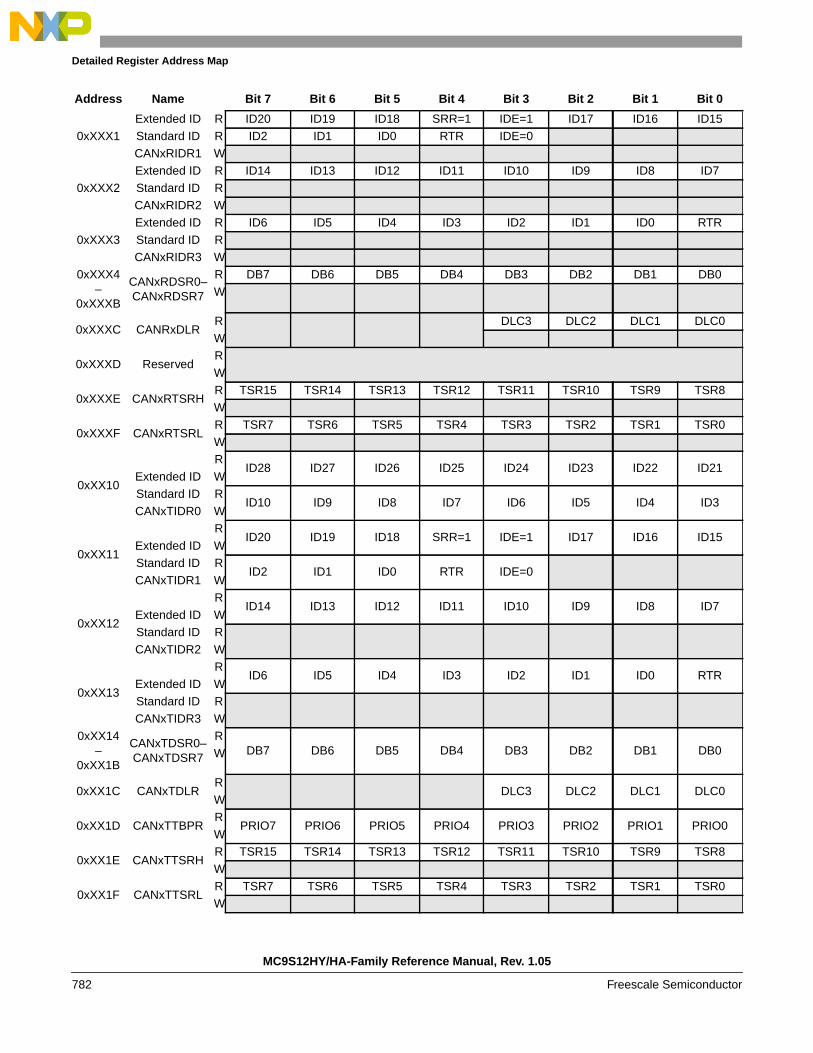
Detailed Register Address Map
0xXXX1Extended ID R ID20 ID19 ID18 SRR=1 IDE=1 ID17 ID16 ID15Standard ID R ID2 ID1 ID0 RTR IDE=0CANxRIDR1 W
0xXXX2Extended ID R ID14 ID13 ID12 ID11 ID10 ID9 ID8 ID7Standard ID RCANxRIDR2 W
0xXXX3Extended ID R ID6 ID5 ID4 ID3 ID2 ID1 ID0 RTRStandard ID RCANxRIDR3 W
0xXXX4–
0xXXXB
CANxRDSR0–CANxRDSR7
R DB7 DB6 DB5 DB4 DB3 DB2 DB1 DB0W
0xXXXC CANRxDLRR DLC3 DLC2 DLC1 DLC0W
0xXXXD ReservedRW
0xXXXE CANxRTSRHR TSR15 TSR14 TSR13 TSR12 TSR11 TSR10 TSR9 TSR8W
0xXXXF CANxRTSRLR TSR7 TSR6 TSR5 TSR4 TSR3 TSR2 TSR1 TSR0W
0xXX10
RID28 ID27 ID26 ID25 ID24 ID23 ID22 ID21
Extended ID WStandard ID R
ID10 ID9 ID8 ID7 ID6 ID5 ID4 ID3CANxTIDR0 W
0xXX11
RID20 ID19 ID18 SRR=1 IDE=1 ID17 ID16 ID15
Extended ID WStandard ID R
ID2 ID1 ID0 RTR IDE=0CANxTIDR1 W
0xXX12
RID14 ID13 ID12 ID11 ID10 ID9 ID8 ID7
Extended ID WStandard ID RCANxTIDR2 W
0xXX13
RID6 ID5 ID4 ID3 ID2 ID1 ID0 RTR
Extended ID WStandard ID RCANxTIDR3 W
0xXX14–
0xXX1B
CANxTDSR0–CANxTDSR7
RDB7 DB6 DB5 DB4 DB3 DB2 DB1 DB0W
0xXX1C CANxTDLRR
DLC3 DLC2 DLC1 DLC0W
0xXX1D CANxTTBPRR
PRIO7 PRIO6 PRIO5 PRIO4 PRIO3 PRIO2 PRIO1 PRIO0W
0xXX1E CANxTTSRHR TSR15 TSR14 TSR13 TSR12 TSR11 TSR10 TSR9 TSR8W
0xXX1F CANxTTSRLR TSR7 TSR6 TSR5 TSR4 TSR3 TSR2 TSR1 TSR0W
Address Name Bit 7 Bit 6 Bit 5 Bit 4 Bit 3 Bit 2 Bit 1 Bit 0
MC9S12HY/HA-Family Reference Manual, Rev. 1.05
782 Freescale Semiconductor

Detailed Register Address Map
0x0180-0x01BF Reserved
0x01C0-0x01FF Motor Controller 10-bit 8-channels(MC) Map
Address Name Bit 7 Bit 6 Bit 5 Bit 4 Bit 3 Bit 2 Bit 1 Bit 0
0x0180-0x01BF
ReservedR 0 0 0 0 0 0 0 0
W
Address Name Bit 7 Bit 6 Bit 5 Bit 4 Bit 3 Bit 2 Bit 1 Bit 0
0x01C0 MCCTL0R 0
MCPRE1 MCPRE0 MCSWAI FAST DITH0
MCTOIFW
0x01C1 MCCTL1R
RECIRC0 0 0 0 0 0
MCTOIEW
0x01C2 MCPER (hi)R 0 0 0 0 0
P10 P9 P8W
0x01C3 MCPER (lo)R
P7 P6 P5 P4 P3 P2 P1 P0W
0x01C4–0x01CF
ReservedR 0 0 0 0 0 0 0 0
W
0x01D0 MCCC0R
MCOM1 MCOM0 MCAM1 MCAM00 0
CD1 CD0W
0x01D1 MCCC1R
MCOM1 MCOM0 MCAM1 MCAM00 0
CD1 CD0W
0x01D2 MCCC2R
MCOM1 MCOM0 MCAM1 MCAM00 0
CD1 CD0W
0x01D3 MCCC3R
MCOM1 MCOM0 MCAM1 MCAM00 0
CD1 CD0W
0x01D4 MCCC4R
MCOM1 MCOM0 MCAM1 MCAM00 0
CD1 CD0W
0x01D5 MCCC5R
MCOM1 MCOM0 MCAM1 MCAM00 0
CD1 CD0W
0x01D6 MCCC6R
MCOM1 MCOM0 MCAM1 MCAM00 0
CD1 CD0W
0x01D7 MCCC7R
MCOM1 MCOM0 MCAM1 MCAM00 0
CD1 CD0W
0x01D8–0x01DF
ReservedR 0 0 0 0 0 0 0 0
W
0x01E0 MCDC0 (hi)R
SS S S S
D10 D9 D8W
0x01E1 MCDC0 (lo)R
D7 D6 D5 D4 D3 D2 D1 D0W
0x01E2 MCDC1 (hi)R
SS S S S
D10 D9 D8W
MC9S12HY/HA-Family Reference Manual, Rev. 1.05
Freescale Semiconductor 783
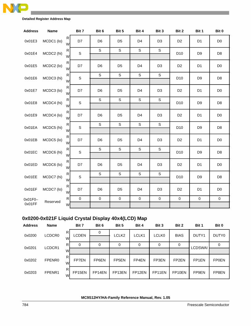
Detailed Register Address Map
0x0200-0x021F Liquid Crystal Display 40x4(LCD) Map
0x01E3 MCDC1 (lo)R
D7 D6 D5 D4 D3 D2 D1 D0W
0x01E4 MCDC2 (hi)R
SS S S S
D10 D9 D8W
0x01E5 MCDC2 (lo)R
D7 D6 D5 D4 D3 D2 D1 D0W
0x01E6 MCDC3 (hi)R
SS S S S
D10 D9 D8W
0x01E7 MCDC3 (lo)R
D7 D6 D5 D4 D3 D2 D1 D0W
0x01E8 MCDC4 (hi)R
SS S S S
D10 D9 D8W
0x01E9 MCDC4 (lo)R
D7 D6 D5 D4 D3 D2 D1 D0W
0x01EA MCDC5 (hi)R
SS S S S
D10 D9 D8W
0x01EB MCDC5 (lo)R
D7 D6 D5 D4 D3 D2 D1 D0W
0x01EC MCDC6 (hi)R
SS S S S
D10 D9 D8W
0x01ED MCDC6 (lo)R
D7 D6 D5 D4 D3 D2 D1 D0W
0x01EE MCDC7 (hi)R
SS S S S
D10 D9 D8W
0x01EF MCDC7 (lo)R
D7 D6 D5 D4 D3 D2 D1 D0W
0x01F0–0x01FF
ReservedR 0 0 0 0 0 0 0 0
W
Address Name Bit 7 Bit 6 Bit 5 Bit 4 Bit 3 Bit 2 Bit 1 Bit 0
0x0200 LCDCR0R
LCDEN0
LCLK2 LCLK1 LCLK0 BIAS DUTY1 DUTY0W
0x0201 LCDCR1R 0 0 0 0 0 0
LCDSWAI0
W
0x0202 FPENR0R
FP7EN FP6EN FP5EN FP4EN FP3EN FP2EN FP1EN FP0ENW
0x0203 FPENR1R
FP15EN FP14EN FP13EN FP12EN FP11EN FP10EN FP9EN FP8ENW
Address Name Bit 7 Bit 6 Bit 5 Bit 4 Bit 3 Bit 2 Bit 1 Bit 0
MC9S12HY/HA-Family Reference Manual, Rev. 1.05
784 Freescale Semiconductor
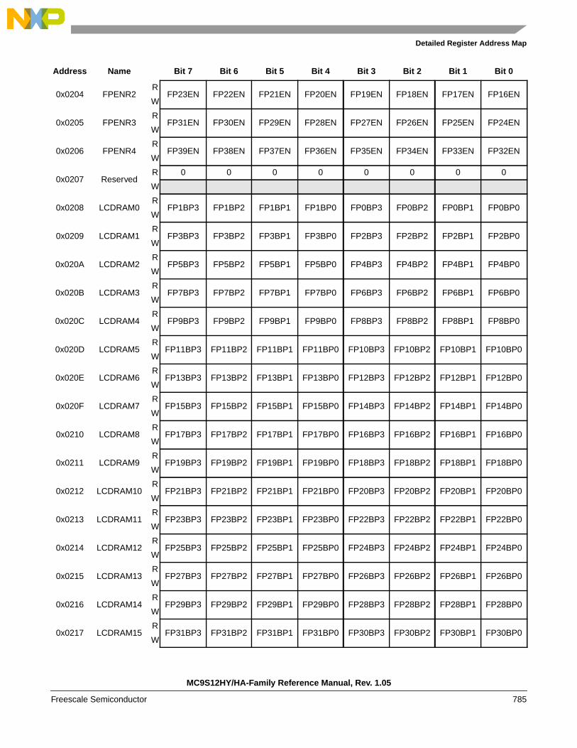
Detailed Register Address Map
0x0204 FPENR2R
FP23EN FP22EN FP21EN FP20EN FP19EN FP18EN FP17EN FP16ENW
0x0205 FPENR3R
FP31EN FP30EN FP29EN FP28EN FP27EN FP26EN FP25EN FP24ENW
0x0206 FPENR4R
FP39EN FP38EN FP37EN FP36EN FP35EN FP34EN FP33EN FP32ENW
0x0207 ReservedR 0 0 0 0 0 0 0 0
W
0x0208 LCDRAM0R
FP1BP3 FP1BP2 FP1BP1 FP1BP0 FP0BP3 FP0BP2 FP0BP1 FP0BP0W
0x0209 LCDRAM1R
FP3BP3 FP3BP2 FP3BP1 FP3BP0 FP2BP3 FP2BP2 FP2BP1 FP2BP0W
0x020A LCDRAM2R
FP5BP3 FP5BP2 FP5BP1 FP5BP0 FP4BP3 FP4BP2 FP4BP1 FP4BP0W
0x020B LCDRAM3R
FP7BP3 FP7BP2 FP7BP1 FP7BP0 FP6BP3 FP6BP2 FP6BP1 FP6BP0W
0x020C LCDRAM4R
FP9BP3 FP9BP2 FP9BP1 FP9BP0 FP8BP3 FP8BP2 FP8BP1 FP8BP0W
0x020D LCDRAM5R
FP11BP3 FP11BP2 FP11BP1 FP11BP0 FP10BP3 FP10BP2 FP10BP1 FP10BP0W
0x020E LCDRAM6R
FP13BP3 FP13BP2 FP13BP1 FP13BP0 FP12BP3 FP12BP2 FP12BP1 FP12BP0W
0x020F LCDRAM7R
FP15BP3 FP15BP2 FP15BP1 FP15BP0 FP14BP3 FP14BP2 FP14BP1 FP14BP0W
0x0210 LCDRAM8R
FP17BP3 FP17BP2 FP17BP1 FP17BP0 FP16BP3 FP16BP2 FP16BP1 FP16BP0W
0x0211 LCDRAM9R
FP19BP3 FP19BP2 FP19BP1 FP19BP0 FP18BP3 FP18BP2 FP18BP1 FP18BP0W
0x0212 LCDRAM10R
FP21BP3 FP21BP2 FP21BP1 FP21BP0 FP20BP3 FP20BP2 FP20BP1 FP20BP0W
0x0213 LCDRAM11R
FP23BP3 FP23BP2 FP23BP1 FP23BP0 FP22BP3 FP22BP2 FP22BP1 FP22BP0W
0x0214 LCDRAM12R
FP25BP3 FP25BP2 FP25BP1 FP25BP0 FP24BP3 FP24BP2 FP24BP1 FP24BP0W
0x0215 LCDRAM13R
FP27BP3 FP27BP2 FP27BP1 FP27BP0 FP26BP3 FP26BP2 FP26BP1 FP26BP0W
0x0216 LCDRAM14R
FP29BP3 FP29BP2 FP29BP1 FP29BP0 FP28BP3 FP28BP2 FP28BP1 FP28BP0W
0x0217 LCDRAM15R
FP31BP3 FP31BP2 FP31BP1 FP31BP0 FP30BP3 FP30BP2 FP30BP1 FP30BP0W
Address Name Bit 7 Bit 6 Bit 5 Bit 4 Bit 3 Bit 2 Bit 1 Bit 0
MC9S12HY/HA-Family Reference Manual, Rev. 1.05
Freescale Semiconductor 785

Detailed Register Address Map
0x0220-0x023F Reserved
0x0240-0x029F Port Integration Module (PIM) Map 4 of 4
0x0218 LCDRAM16R
FP33BP3 FP33BP2 FP33BP1 FP33BP0 FP32BP3 FP32BP2 FP32BP1 FP32BP0W
0x0219 LCDRAM17R
FP35BP3 FP35BP2 FP35BP1 FP35BP0 FP34BP3 FP34BP2 FP34BP1 FP34BP0W
0x021A LCDRAM18R
FP37BP3 FP37BP2 FP37BP1 FP37BP0 FP36BP3 FP36BP2 FP36BP1 FP36BP0W
0x021B LCDRAM19R
FP39BP3 FP39BP2 FP39BP1 FP39BP0 FP38BP3 FP38BP2 FP38BP1 FP38BP0W
0x021C-0x021F
ReservedR 0 0 0 0 0 0 0 0
W
Address Name Bit 7 Bit 6 Bit 5 Bit 4 Bit 3 Bit 2 Bit 1 Bit 0
0x0220-0x023F
ReservedR 0 0 0 0 0 0 0 0
W
Address Name Bit 7 Bit 6 Bit 5 Bit 4 Bit 3 Bit 2 Bit 1 Bit 0
0x0240 PTTR
PTT7 PTT6 PTT5 PTT4 PTT3 PTT2 PTT1 PTT0W
0x0241 PTITR PTIT7 PTIT6 PTIT5 PTIT4 PTIT3 PTIT2 PTIT1 PTIT0
W
0x0242 DDRTR
DDRT7 DDRT6 DDRT5 DDRT4 DDRT3 DDRT2 DDRT1 DDRT0W
0x0243 RDRTR
RDRT7 RDRT6 RDRT5 RDRT4 RDRT3 RDRT2 RDRT1 RDRT0W
0x0244 PERTR
PERT7 PERT6 PERT5 PERT4 PERT3 PERT2 PERT1 PERT0W
0x0245 PPSTR
PPST7 PPST6 PPST5 PPST4 PPST3 PPST2 PPST1 PPST0W
0x0246 ReservedR 0 0 0 0 0 0 0 0
W
0x0247 PTTRRR 0 0
PTTRR5 PTTRR40 0
PTTRR1 PTTRR0W
0x0248 PTSR
PTS7 PTS6 PTS5 PTS4 PTS3 PTS2 PTS1 PTS0W
0x0249 PTISR PTIS7 PTIS6 PTIS5 PTIS4 PTIS3 PTIS2 PTIS1 PTIS0
W
0x024A DDRSR
DDRS7 DDRS6 DDRS5 DDRS4 DDRS3 DDRS2 DDRS1 DDRS0W
Address Name Bit 7 Bit 6 Bit 5 Bit 4 Bit 3 Bit 2 Bit 1 Bit 0
MC9S12HY/HA-Family Reference Manual, Rev. 1.05
786 Freescale Semiconductor
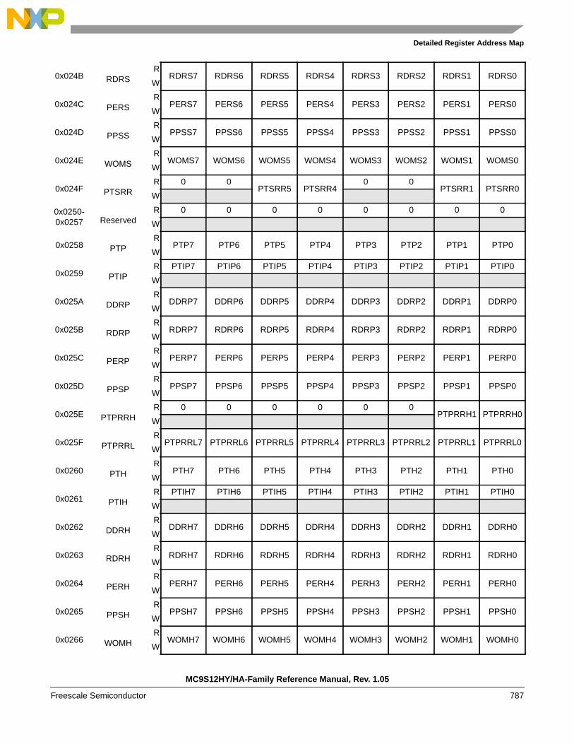
Detailed Register Address Map
0x024B RDRSR
RDRS7 RDRS6 RDRS5 RDRS4 RDRS3 RDRS2 RDRS1 RDRS0W
0x024C PERSR
PERS7 PERS6 PERS5 PERS4 PERS3 PERS2 PERS1 PERS0W
0x024D PPSSR
PPSS7 PPSS6 PPSS5 PPSS4 PPSS3 PPSS2 PPSS1 PPSS0W
0x024E WOMSR
WOMS7 WOMS6 WOMS5 WOMS4 WOMS3 WOMS2 WOMS1 WOMS0W
0x024F PTSRRR 0 0
PTSRR5 PTSRR40 0
PTSRR1 PTSRR0W
0x0250-0x0257 Reserved
R 0 0 0 0 0 0 0 0
W
0x0258 PTPR
PTP7 PTP6 PTP5 PTP4 PTP3 PTP2 PTP1 PTP0W
0x0259 PTIPR PTIP7 PTIP6 PTIP5 PTIP4 PTIP3 PTIP2 PTIP1 PTIP0
W
0x025A DDRPR
DDRP7 DDRP6 DDRP5 DDRP4 DDRP3 DDRP2 DDRP1 DDRP0W
0x025B RDRPR
RDRP7 RDRP6 RDRP5 RDRP4 RDRP3 RDRP2 RDRP1 RDRP0W
0x025C PERPR
PERP7 PERP6 PERP5 PERP4 PERP3 PERP2 PERP1 PERP0W
0x025D PPSPR
PPSP7 PPSP6 PPSP5 PPSP4 PPSP3 PPSP2 PPSP1 PPSP0W
0x025E PTPRRHR 0 0 0 0 0 0
PTPRRH1 PTPRRH0W
0x025F PTPRRLR
PTPRRL7 PTPRRL6 PTPRRL5 PTPRRL4 PTPRRL3 PTPRRL2 PTPRRL1 PTPRRL0W
0x0260 PTHR
PTH7 PTH6 PTH5 PTH4 PTH3 PTH2 PTH1 PTH0W
0x0261 PTIHR PTIH7 PTIH6 PTIH5 PTIH4 PTIH3 PTIH2 PTIH1 PTIH0
W
0x0262 DDRHR
DDRH7 DDRH6 DDRH5 DDRH4 DDRH3 DDRH2 DDRH1 DDRH0W
0x0263 RDRHR
RDRH7 RDRH6 RDRH5 RDRH4 RDRH3 RDRH2 RDRH1 RDRH0W
0x0264 PERHR
PERH7 PERH6 PERH5 PERH4 PERH3 PERH2 PERH1 PERH0W
0x0265 PPSHR
PPSH7 PPSH6 PPSH5 PPSH4 PPSH3 PPSH2 PPSH1 PPSH0W
0x0266 WOMHR
WOMH7 WOMH6 WOMH5 WOMH4 WOMH3 WOMH2 WOMH1 WOMH0W
MC9S12HY/HA-Family Reference Manual, Rev. 1.05
Freescale Semiconductor 787
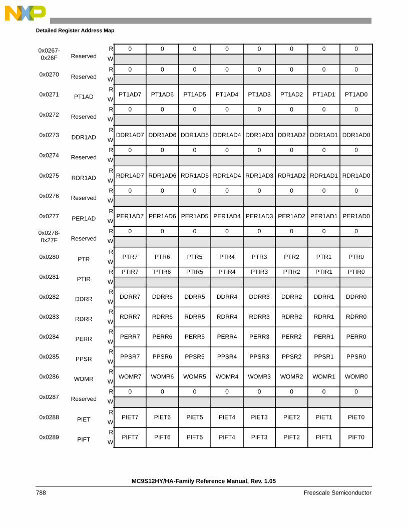
Detailed Register Address Map
0x0267-0x26F Reserved
R 0 0 0 0 0 0 0 0
W
0x0270 ReservedR 0 0 0 0 0 0 0 0
W
0x0271 PT1ADR
PT1AD7 PT1AD6 PT1AD5 PT1AD4 PT1AD3 PT1AD2 PT1AD1 PT1AD0W
0x0272 ReservedR 0 0 0 0 0 0 0 0
W
0x0273 DDR1ADR
DDR1AD7 DDR1AD6 DDR1AD5 DDR1AD4 DDR1AD3 DDR1AD2 DDR1AD1 DDR1AD0W
0x0274 ReservedR 0 0 0 0 0 0 0 0
W
0x0275 RDR1ADR
RDR1AD7 RDR1AD6 RDR1AD5 RDR1AD4 RDR1AD3 RDR1AD2 RDR1AD1 RDR1AD0W
0x0276 ReservedR 0 0 0 0 0 0 0 0
W
0x0277 PER1ADR
PER1AD7 PER1AD6 PER1AD5 PER1AD4 PER1AD3 PER1AD2 PER1AD1 PER1AD0W
0x0278-0x27F Reserved
R 0 0 0 0 0 0 0 0
W
0x0280 PTRR
PTR7 PTR6 PTR5 PTR4 PTR3 PTR2 PTR1 PTR0W
0x0281 PTIRR PTIR7 PTIR6 PTIR5 PTIR4 PTIR3 PTIR2 PTIR1 PTIR0
W
0x0282 DDRRR
DDRR7 DDRR6 DDRR5 DDRR4 DDRR3 DDRR2 DDRR1 DDRR0W
0x0283 RDRRR
RDRR7 RDRR6 RDRR5 RDRR4 RDRR3 RDRR2 RDRR1 RDRR0W
0x0284 PERRR
PERR7 PERR6 PERR5 PERR4 PERR3 PERR2 PERR1 PERR0W
0x0285 PPSRR
PPSR7 PPSR6 PPSR5 PPSR4 PPSR3 PPSR2 PPSR1 PPSR0W
0x0286 WOMRR
WOMR7 WOMR6 WOMR5 WOMR4 WOMR3 WOMR2 WOMR1 WOMR0W
0x0287 ReservedR 0 0 0 0 0 0 0 0
W
0x0288 PIETR
PIET7 PIET6 PIET5 PIET4 PIET3 PIET2 PIET1 PIET0W
0x0289 PIFTR
PIFT7 PIFT6 PIFT5 PIFT4 PIFT3 PIFT2 PIFT1 PIFT0W
MC9S12HY/HA-Family Reference Manual, Rev. 1.05
788 Freescale Semiconductor

Detailed Register Address Map
0x028A PIESR 0
PIES6 PIES50 0 0 0 0
W
0x028B PIFSR 0
PIFS6 PIFS50 0 0 0 0
W
0x028C PIE1ADR
PIE1AD7 PIE1AD6 PIE1AD5 PIE1AD4 PIE1AD3 PIE1AD2 PIE1AD1 PIE1AD0W
0x028D PIF1ADR
PIF1AD7 PIF1AD6 PIF1AD5 PIF1AD4 PIF1AD3 PIF1AD2 PIF1AD1 PIF1AD0W
0x028E PIERR 0 0 0 0
PIER3 PIER2 PIER1 PIER0W
0x028F PIFRR 0 0 0 0
PIFR3 PIFR2 PIFR1 PIFR0W
0x0290 PTUR
PTU7 PTU6 PTU5 PTU4 PTU3 PTU2 PTU1 PTU0W
0x0291 PTIUR PTIU7 PTIU6 PTIU5 PTIU4 PTIU3 PTIU2 PTIU1 PTIU0
W
0x0292 DDRUR
DDRU7 DDRU6 DDRU5 DDRU4 DDRU3 DDRU2 DDRU1 DDRU0W
0x0293 ReservedR 0 0 0 0 0 0 0 0
W
0x0294 PERUR
PERU7 PERU6 PERU5 PERU4 PERU3 PERU2 PERU1 PERU0W
0x0295 PPSUR
PPSU7 PPSU6 PPSU5 PPSU4 PPSU3 PPSU2 PPSU1 PPSU0W
0x0296 SRRUR
SRRU7 SRRU6 SRRU5 SRRU4 SRRU3 SRRU2 SRRU1 SRRU0W
0x0297 ReservedR 0 0 0 0 0 0 0 0
W
0x0298 PTVR
PTV7 PTV6 PTV5 PTV4 PTV3 PTV2 PTV1 PTV0W
0x0299 PTIVR PTIV7 PTIV6 PTIV5 PTIV4 PTIV3 PTIV2 PTIV1 PTIV0
W
0x029A DDRVR
DDRV7 DDRV6 DDRV5 DDRV4 DDRV3 DDRV2 DDRV1 DDRV0W
0x029B ReservedR 0 0 0 0 0 0 0 0
W
0x029C PERVR
PERV7 PERV6 PERV5 PERV4 PERV3 PERV2 PERV1 PERV0W
0x029D PPSVR
PPSV7 PPSV6 PPSV5 PPSV4 PPSV3 PPSV2 PPSV1 PPSV0W
0x029E SRRVR
SRRV7 SRRV6 SRRV5 SRRV4 SRRV3 SRRV2 SRRV1 SRRV0W
MC9S12HY/HA-Family Reference Manual, Rev. 1.05
Freescale Semiconductor 789
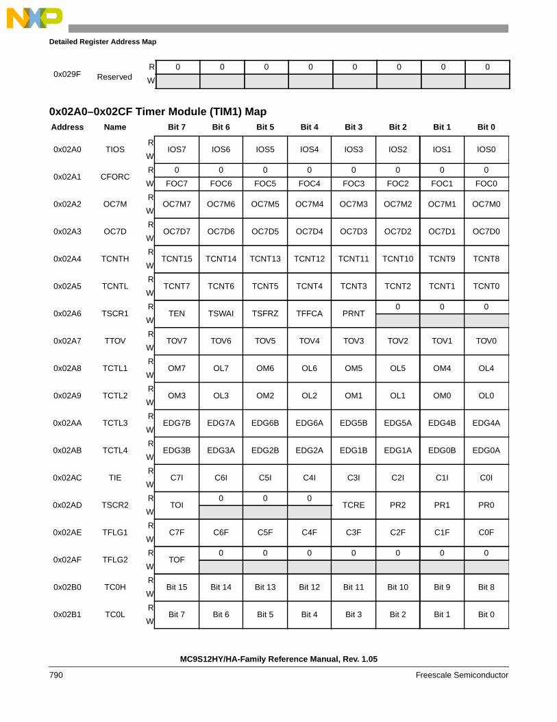
Detailed Register Address Map
0x02A0–0x02CF Timer Module (TIM1) Map
0x029F ReservedR 0 0 0 0 0 0 0 0
W
Address Name Bit 7 Bit 6 Bit 5 Bit 4 Bit 3 Bit 2 Bit 1 Bit 0
0x02A0 TIOSR
IOS7 IOS6 IOS5 IOS4 IOS3 IOS2 IOS1 IOS0W
0x02A1 CFORCR 0 0 0 0 0 0 0 0
W FOC7 FOC6 FOC5 FOC4 FOC3 FOC2 FOC1 FOC0
0x02A2 OC7MR
OC7M7 OC7M6 OC7M5 OC7M4 OC7M3 OC7M2 OC7M1 OC7M0W
0x02A3 OC7DR
OC7D7 OC7D6 OC7D5 OC7D4 OC7D3 OC7D2 OC7D1 OC7D0W
0x02A4 TCNTHR
TCNT15 TCNT14 TCNT13 TCNT12 TCNT11 TCNT10 TCNT9 TCNT8W
0x02A5 TCNTLR
TCNT7 TCNT6 TCNT5 TCNT4 TCNT3 TCNT2 TCNT1 TCNT0W
0x02A6 TSCR1R
TEN TSWAI TSFRZ TFFCA PRNT0 0 0
W
0x02A7 TTOVR
TOV7 TOV6 TOV5 TOV4 TOV3 TOV2 TOV1 TOV0W
0x02A8 TCTL1R
OM7 OL7 OM6 OL6 OM5 OL5 OM4 OL4W
0x02A9 TCTL2R
OM3 OL3 OM2 OL2 OM1 OL1 OM0 OL0W
0x02AA TCTL3R
EDG7B EDG7A EDG6B EDG6A EDG5B EDG5A EDG4B EDG4AW
0x02AB TCTL4R
EDG3B EDG3A EDG2B EDG2A EDG1B EDG1A EDG0B EDG0AW
0x02AC TIER
C7I C6I C5I C4I C3I C2I C1I C0IW
0x02AD TSCR2R
TOI0 0 0
TCRE PR2 PR1 PR0W
0x02AE TFLG1R
C7F C6F C5F C4F C3F C2F C1F C0FW
0x02AF TFLG2R
TOF0 0 0 0 0 0 0
W
0x02B0 TC0HR
Bit 15 Bit 14 Bit 13 Bit 12 Bit 11 Bit 10 Bit 9 Bit 8W
0x02B1 TC0LR
Bit 7 Bit 6 Bit 5 Bit 4 Bit 3 Bit 2 Bit 1 Bit 0W
MC9S12HY/HA-Family Reference Manual, Rev. 1.05
790 Freescale Semiconductor

Detailed Register Address Map
0x02B2 TC1HR
Bit 15 Bit 14 Bit 13 Bit 12 Bit 11 Bit 10 Bit 9 Bit 8W
0x02B3 TC1LR
Bit 7 Bit 6 Bit 5 Bit 4 Bit 3 Bit 2 Bit 1 Bit 0W
0x02B4 TC2HR
Bit 15 Bit 14 Bit 13 Bit 12 Bit 11 Bit 10 Bit 9 Bit 8W
0x02B5 TC2LR
Bit 7 Bit 6 Bit 5 Bit 4 Bit 3 Bit 2 Bit 1 Bit 0W
0x02B6 TC3HR
Bit 15 Bit 14 Bit 13 Bit 12 Bit 11 Bit 10 Bit 9 Bit 8W
0x02B7 TC3LR
Bit 7 Bit 6 Bit 5 Bit 4 Bit 3 Bit 2 Bit 1 Bit 0W
0x02B8 TC4HR
Bit 15 Bit 14 Bit 13 Bit 12 Bit 11 Bit 10 Bit 9 Bit 8W
0x02B9 TC4LR
Bit 7 Bit 6 Bit 5 Bit 4 Bit 3 Bit 2 Bit 1 Bit 0W
0x02BA TC5HR
Bit 15 Bit 14 Bit 13 Bit 12 Bit 11 Bit 10 Bit 9 Bit 8W
0x02BB TC5LR
Bit 7 Bit 6 Bit 5 Bit 4 Bit 3 Bit 2 Bit 1 Bit 0W
0x02BC TC6HR
Bit 15 Bit 14 Bit 13 Bit 12 Bit 11 Bit 10 Bit 9 Bit 8W
0x02BD TC6LR
Bit 7 Bit 6 Bit 5 Bit 4 Bit 3 Bit 2 Bit 1 Bit 0W
0x02BE TC7HR
Bit 15 Bit 14 Bit 13 Bit 12 Bit 11 Bit 10 Bit 9 Bit 8W
0x02BF TC7LR
Bit 7 Bit 6 Bit 5 Bit 4 Bit 3 Bit 2 Bit 1 Bit 0W
0x02C0 PACTLR 0
PAEN PAMOD PEDGE CLK1 CLK0 PAOVI PAIW
0x02C1 PAFLGR 0 0 0 0 0 0
PAOVF PAIFW
0x02C2 PACNTHR
PACNT15 PACNT14 PACNT13 PACNT12 PACNT11 PACNT10 PACNT9 PACNT8W
0x02C3 PACNTLR
PACNT7 PACNT6 PACNT5 PACNT4 PACNT3 PACNT2 PACNT1 PACNT0W
0x02C4–0x02CB
ReservedR 0 0 0 0 0 0 0 0
W
0x02CC OCPDR
OCPD7 OCPD6 OCPD5 OCPD4 OCPD3 OCPD2 OCPD1 OCPD0W
Address Name Bit 7 Bit 6 Bit 5 Bit 4 Bit 3 Bit 2 Bit 1 Bit 0
MC9S12HY/HA-Family Reference Manual, Rev. 1.05
Freescale Semiconductor 791

Detailed Register Address Map
0x02D0-0x02EF Reserved
0x02F0–0x02FF Clock and Power Management (CPMU) 2 of 2
0x02CD ReservedR 0 0 0 0 0 0 0 0
W
0x02CE PTPSRR
PTPSR7 PTPSR6 PTPSR5 PTPSR4 PTPSR3 PTPSR2 PTPSR1 PTPSR0W
0x02CF ReservedR 0 0 0 0 0 0 0 0
W
Address Name Bit 7 Bit 6 Bit 5 Bit 4 Bit 3 Bit 2 Bit 1 Bit 0
0x02D0-0x02EF
ReservedR 0 0 0 0 0 0 0 0
W
Address Name Bit 7 Bit 6 Bit 5 Bit 4 Bit 3 Bit 2 Bit 1 Bit 0
0x02F0CPMUHTCTL
R 0 0VSEL
0HTE
HTDSHTIE HTIF
W
0x02F1CPMULVCTL
R 0 0 0 0 0 LVDSLVIE LVIF
W
0x02F2CPMUAPICTL
RAPICLK
0 0APIES APIEA APIFE APIE APIF
W
0x02F3 CPMUAPITRR
APITR5 APITR4 APITR3 APITR2 APITR1 APITR00 0
W
0x02F4 CPMUAPIRHR
APIR15 APIR14 APIR13 APIR12 APIR11 APIR10 APIR9 APIR8W
0x02F5 CPMUAPIRLR
APIR7 APIR6 APIR5 APIR4 APIR3 APIR2 APIR1 APIR0W
0x02F6 RESERVEDR 0 0 0 0 0 0 0 0
W
0x02F7 CPMUHTTRR
HTOE0 0 0
HTTR3 HTTR2 HTTR1 HTTR0W
0x02F8CPMU
IRCTRIMHR
TCTRIM[3:0]0 0
IRCTRIM[9:8]W
0x02F9CPMU
IRCTRIMLR
IRCTRIM[7:0]W
0x02FA CPMUOSCR
OSCE OSCBW0
OSCFILT[4:0]W
0x02FB CPMUPROTR 0 0 0 0 0 0 0
PROTW
0x02FC RESERVEDR 0 0 0 0 0 0 0 0
W
Address Name Bit 7 Bit 6 Bit 5 Bit 4 Bit 3 Bit 2 Bit 1 Bit 0
MC9S12HY/HA-Family Reference Manual, Rev. 1.05
792 Freescale Semiconductor

Detailed Register Address Map
0x0300-0x03FF Reserved
0x02FD-0x02FF
ReservedR 0 0 0 0 0 0 0 0
W
Address Name Bit 7 Bit 6 Bit 5 Bit 4 Bit 3 Bit 2 Bit 1 Bit 0
0x0300-0x03FF
ReservedR 0 0 0 0 0 0 0 0
W
MC9S12HY/HA-Family Reference Manual, Rev. 1.05
Freescale Semiconductor 793

Detailed Register Address Map
MC9S12HY/HA-Family Reference Manual, Rev. 1.05
794 Freescale Semiconductor


How to Reach Us:
USA/Europe/Locations not listed:Freescale Semiconductor Literature DistributionP.O. Box 5405, Denver, Colorado 802171-800-521-6274 or 480-768-2130
Japan:Freescale Semiconductor Japan Ltd.SPS, Technical Information Center3-20-1, Minami-AzabuMinato-kuTokyo 106-8573, Japan81-3-3440-3569
Asia/Pacific:Freescale Semiconductor H.K. Ltd.2 Dai King StreetTai Po Industrial EstateTai Po, N.T. Hong Kong852-26668334
Learn More:For more information about FreescaleSemiconductor products, please visithttp://www.freescale.com
Information in this document is provided solely to enable system and software implementers to use
Freescale Semiconductor products. There are no express or implied copyright licenses granted
hereunder to design or fabricate any integrated circuits or integrated circuits based on the information
in this document.
Freescale Semiconductor reserves the right to make changes without further notice to any products
herein. Freescale Semiconductor makes no warranty, representation or guarantee regarding the
suitability of its products for any particular purpose, nor does Freescale Semiconductor assume any
liability arising out of the application or use of any product or circuit, and specifically disclaims any
and all liability, including without limitation consequential or incidental damages. “Typical” parameters
which may be provided in Freescale Semiconductor data sheets and/or specifications can and do
vary in different applications and actual performance may vary over time. All operating parameters,
including “Typicals” must be validated for each customer application by customer’s technical experts.
Freescale Semiconductor does not convey any license under its patent rights nor the rights of others.
Freescale Semiconductor products are not designed, intended, or authorized for use as components
in systems intended for surgical implant into the body, or other applications intended to support or
sustain life, or for any other application in which the failure of the Freescale Semiconductor product
could create a situation where personal injury or death may occur. Should Buyer purchase or use
Freescale Semiconductor products for any such unintended or unauthorized application, Buyer shall
indemnify and hold Freescale Semiconductor and its officers, employees, subsidiaries, affiliates, and
distributors harmless against all claims, costs, damages, and expenses, and reasonable attorney
fees arising out of, directly or indirectly, any claim of personal injury or death associated with such
unintended or unauthorized use, even if such claim alleges that Freescale Semiconductor was
negligent regarding the design or manufacture of the part.
Freescale™ and the Freescale logo are trademarks of Freescale Semiconductor, Inc. All otherproduct or service names are the property of their respective owners.© Freescale Semiconductor, Inc. 2006