The onset of convection in a binary nanofluid saturated porous layer
Upload
independentCategory
view
2download
0
ARTIC
LECopyright © 2013 by American Scientific Publishers
All rights reserved.
Printed in the United States of America
Journal of NanofluidsVol. 2, pp. 165–174, 2013(www.aspbs.com/jon)
Magnetic Nanofluid Based Approach forImaging DefectsV. Mahendran, R. Ancy Beautlin†, and John Philip∗
SMARTS, Metallurgy and Materials Group, Indira Gandhi Centre for Atomic Research, Kalpakkam 603102,Tamilnadu, India
Magnetic flux leakage is one of the most widely used electromagnetic nondestructive techniques to locate andassess discontinuities such as fatigue, cracks, corrosion, erosion, non metallic inclusion and abrasive wear inmagnetic components. Here, we report a new optical technique for imaging internal defects in materials usinga magnetically polarizable nanofluid (ferrofluid). The gradient in the magnetic flux lines around the defectiveregion induces the formation of one-dimensional array of nanoparticles along the field direction in the nanofluid,which produces a discernible gray level contrast in the ferrofluid. The grey level contrast produced by the leakedmagnetic flux is exploited to detect defects buried inside the sample. The normal and tangential components ofleakage magnetic fluxes have been modeled using a dipole approach for rectangular and cylindrical defects ofdifferent dimensions. The simulated results are validated experimentally. Various image processing techniquessuch as contrast stretching, image gradient, contrast limited adaptive histogram equalization and image profilingare used to obtain better detection sensitivity.
KEYWORDS: Nanofluids, Ferrofluid, Nondestructive Testing, Magnetic Flux Leakage, Sensor.
1. INTRODUCTION
Magnetic nanofluids are colloidal suspensions of super-
paramagnetic particles in a suitable carrier fluid.1 Mag-
netic nanofluids have attracted enormous interest in recent
years because of their field driven self-assembly and
tunable physical properties.2�3 The unique field driven
properties of magnetic nanofluids have been exploited
for several interesting applications such as electronics
cooling,4�5 sealant, dampers,1 optical filter,2 defect6�7 and
ion sensors8�9 etc. They have also been used as a
model system for fundamental studies such as struc-
tural transition under external stimuli,10–15 magneto rheo-
logical properties,16–26 tunable thermal conductivity4�27–34
etc. Using the magnetically tunable optical properties
of nanoemulsions, we have developed an optical probe
for defect detection in ferromagnetic materials.6�7 In this
work, we report a methodology to image defects in
ferromagnetic materials and components using magnetic
∗Author to whom correspondence should be addressed.
Email: [email protected]†Present address: Department of Electronics and Communication
Engineering, Ponjesly College of Engineering, Nagercoil 629003,
Tamilnadu, India.
Received: 13 April 2013
Accepted: 25 April 2013
nanofluids and the defect feature extraction and its quan-
tification using image enhancing methods.
Magnetic flux leakage (MFL) is one of the most
commonly used electromagnetic nondestructive techniques
(NDT).35–55 This technique has been extensively used as
an inspection technique in the petrochemical engineer-
ing, transportation, and energy industries.56 It has been
employed in on-line inspection of various components
such as inspection of rail tracks, pipelines, tubes, etc in
oil, gas transportation industries, nuclear power plants and
metal industries, to locate and assess the discontinuities
such as fatigue, cracks, corrosion, erosion, non metallic
inclusion and abrasive wear in ferro magnetic structures.
MFL technique is found to have a high degree of cer-
tainty in the detection of defects with better sensitivity.57
In MFL, the leakage magnetic field from a disconti-
nuity, due to magnetic permeability variations, is mea-
sured by various techniques such as Hall probes, flux
gate sensors, magnetodiodes, search coils, magnetic par-
ticles and Forester micro probes. New magnetic sensors
like SQUID, Giant magneto resistance (GMR), anisotropic
magneto resistance (AMR) etc. can detect even very weak
leakage flux resulting from the magnetic inhomogene-
ity, with high sensitivity.58�59 Laborious data processing
and complicated operating procedures are the major draw-
backs of conventional MFL techniques. Here, we demon-
strate a simple flux leakage sensor, using a magnetic
J. Nanofluids 2013, Vol. 2, No. 3 2169-432X/2013/2/165/010 doi:10.1166/jon.2013.1060 165

Magnetic Nanofluid Based Approach for Imaging Defects Mahendran et al.
ARTIC
LEfluid, to map the defects in ferromagnetic materials and
components. Further, we demonstrate some image pro-
cessing techniques that can provide better defect detection
sensitivity from the images.
2. MATERIALS AND METHODS
2.1. Magnetic Nanofluid Based Sensor
A fatty acid coated super paramagnetic magnetite (Fe3O4�nanoparticles of ∼10 nm dispersed in kerosene is used.
The magnetite nanoparticles used in our study are
synthesized by a simple co-precipitation technique.60–64
Without applied magnetic field, the particles are randomly
dispersed in the basefluid due to excess thermal energy.
Under applied field, the particles tend to align along the
field direction and form linear chains due to dipole–dipole
interaction attraction.
In a typical sensor head, magnetic nanofluid is sand-
wiched between two microscopic glass slides. A spacer
of 0.3 mm is used to maintain a uniform gap between
the slides. All the measurements were done at ambient
temperature. A mild steel plate of thickness 10 mm, with
rectangular and cylindrical slots of different dimensions
were used in this study. The specimens are magnetized by
an electromagnetic DC yoke. The thin film sensor head
is placed at a lift off distance and scanned on the sam-
ple surface. When the sensor head is over the defect-free
region, due to the uniform magnetic field, no magnetic flux
leakage occurs.
3. THEORETICAL CALCULATION OF MFLPROFILES FOR DIFFERENT DEFECTGEOMETRIES
Theoretical modeling of magnetic flux leakage signal
from various objects is essential for accurate detection
and sizing of defects. Zatsepin and Scherbinin65 mod-
eled the leakage fields of surface-breaking cracks by an
infinitely long strip of dipoles.42 Compared with the ana-
lytical approaches, the finite element method (FEM) is
a powerful tool for evaluating MFL signal because of
its flexibility in the simulations of defects with irregu-
lar geometrical shapes. The 2D and 3D FEM have been
widely used along with algorithms of wavelets, neutral net-
works and genetic algorithm to determine the defects from
MFL signals.56�66�67 The numerical models provide precise
results but are computationally expensive. On the contrary,
the analytical models and neutral networks are fast but less
precise due to various approximations used.68
In this work we have used analytical dipole model to
evaluate the experimental data. Zatsepin and Shcherbinin65
derived an expression for the leakage field of rectangu-
lar slots by assuming constant surface magnetic charge
density on the faces of the slot. The tangential (Hx� and
normal (Hy� components of leakage filed from rectangular
defect with depth Y0, width lg given by,6�65
Hx =Hg
�
(tan−1
�x+ lg/2�Y0
�x+ lg/2�2+y�y+Y0�
− tan−1�x− lg/2�Y0
�x− lg/2�2+y�y+Y0�
)(5)
Hy =Hg
2�ln
(�x+ lg/2�
2+ �y+Y0�2
�x− lg/2�2+ �y+Y0�
2
)(�x− lg/2�
2+y2
�x+ lg/2�2+y2
)
(6)
Where Hg is the field inside the defect for an applied field
Ha and is given by,
Hg =2Y0/lg +1
�1/��2Y0/lg +1Ha (7)
Here � is the permeability. Calculated tangential and nor-
mal components of leakage field by using Eqs. (5) and (6)
for a rectangular defect with 3 mm width, depth of 4 mm
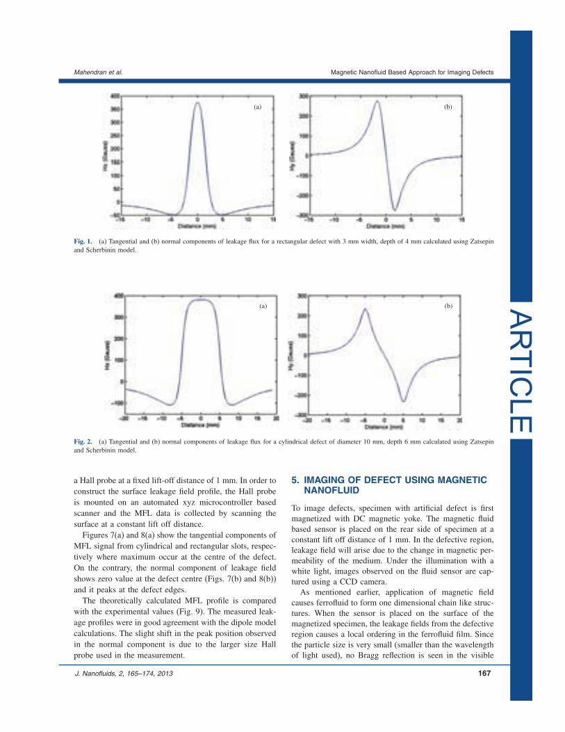
is shown in Figure 1.
Figure 2 show the calculated tangential (Hx� and normal(Hy� components of leakage magnetic flux, for a cylindri-cal defect of diameter 10 mm and depth 6 mm. It can be
seen that the maximum leakage flux occurs at the center
of the defect for the tangential component and at the edges
for the normal component.
Figure 3 shows the tangential and normal components
of magnetic flux leakage for a rectangular defect with a
constant width of 3 mm and varying depths of 4, 8 and
12 mm. Figure 4 shows the tangential and normal compo-
nents of magnetic flux leakage for the rectangular defect
with a constant depth of 4 mm and varying widths 3, 6 and
8 mm. As the defect depth or width increases, the max-
imum value of the leakage magnetic flux (Hx, Hy� also
increases. Also, the peak position shifts with the defect
dimension. To map the leakage field along the specimen
surface, we have calculated the surface profiles of leakage
flux. The surface plots of leakage flux for a rectangular
(3×4 mm) and cylindrical defects are shown in Figures 5
and 6, respectively.
Figures 5 and 6 show the distinct MFL profiles for
defects of different morphologies and dimensions. Using
the surface plots, it is possible to locate the defects and
quantify the defect features and morphologies.
4. EXPERIMENTAL MEASUREMENT OF MFLPROFILES FROM DIFFERENT DEFECTGEOMETRIES
Two different Hall probes have been used for measuring
the tangential and normal components. For validation, a
mild steel plate, with cylindrical and rectangular slots of
different dimensions, is fabricated. After magnetizing the
sample, with a DC yoke, the MFL signal is measured using
166 J. Nanofluids, 2, 165–174, 2013
Mahendran et al. Magnetic Nanofluid Based Approach for Imaging Defects
ARTIC
LE
(b)(a)
Fig. 1. (a) Tangential and (b) normal components of leakage flux for a rectangular defect with 3 mm width, depth of 4 mm calculated using Zatsepin
and Scherbinin model.
(a) (b)
Fig. 2. (a) Tangential and (b) normal components of leakage flux for a cylindrical defect of diameter 10 mm, depth 6 mm calculated using Zatsepin
and Scherbinin model.
a Hall probe at a fixed lift-off distance of 1 mm. In order to
construct the surface leakage field profile, the Hall probe
is mounted on an automated xyz microcontroller based
scanner and the MFL data is collected by scanning the
surface at a constant lift off distance.
Figures 7(a) and 8(a) show the tangential components of
MFL signal from cylindrical and rectangular slots, respec-
tively where maximum occur at the centre of the defect.
On the contrary, the normal component of leakage field
shows zero value at the defect centre (Figs. 7(b) and 8(b))
and it peaks at the defect edges.
The theoretically calculated MFL profile is compared
with the experimental values (Fig. 9). The measured leak-
age profiles were in good agreement with the dipole model
calculations. The slight shift in the peak position observed
in the normal component is due to the larger size Hall
probe used in the measurement.
5. IMAGING OF DEFECT USING MAGNETICNANOFLUID
To image defects, specimen with artificial defect is first
magnetized with DC magnetic yoke. The magnetic fluid
based sensor is placed on the rear side of specimen at a
constant lift off distance of 1 mm. In the defective region,
leakage field will arise due to the change in magnetic per-
meability of the medium. Under the illumination with a
white light, images observed on the fluid sensor are cap-
tured using a CCD camera.
As mentioned earlier, application of magnetic field
causes ferrofluid to form one dimensional chain like struc-
tures. When the sensor is placed on the surface of the
magnetized specimen, the leakage fields from the defective
region causes a local ordering in the ferrofluid film. Since
the particle size is very small (smaller than the wavelength
of light used), no Bragg reflection is seen in the visible
J. Nanofluids, 2, 165–174, 2013 167

Magnetic Nanofluid Based Approach for Imaging Defects Mahendran et al.
ARTIC
LE
(a) (b)
Fig. 3. (a) Tangential and (b) normal components of magnetic flux leakage for a rectangular defect with a constant width of 3 mm and varying depths
of 4, 8 and 12 mm.
(a) (b)
Fig. 4. The (a) tangential and (b) normal components of magnetic flux leakage for the rectangular defects with a constant depth of 4 mm and varying
widths 3, 6 and 8 mm.
168 J. Nanofluids, 2, 165–174, 2013

Mahendran et al. Magnetic Nanofluid Based Approach for Imaging Defects
ARTIC
LE(a) (b)
Fig. 5. The surface profiles of (a) tangential and (b) normal components of magnetic flux leakage from the rectangular defect of dimensions 3×4 mm
(W×D).
(a) (b)
Fig. 6. The surface profiles of (a) tangential and (b) normal components of magnetic flux leakage from the cylindrical defect 10×6 mm (W×D).
–20 –10 0 10 200
100
200
300
400
Position (mm)
Hx
(Gau
ss)
Hy
(Gau
ss)
–20 –10 0 10 20–300
–200
–100
0
100
200
300
Position (mm)
(a) (b)
Fig. 7. Measured values of (a) tangential and (b) normal components of MFL from a cylindrical defect of 10 mm diameter and 6 mm depth.
region like the one seen in nanoemulsion based sensor.6�7
However, the local ordering leads to changes in the number
density distribution within the sensor area, which causes
a grey level variation in the nanofluid. Figure 10 shows
the photographic images of the sensor for three specimens
with different defect geometries i.e., rectangular defects of
3 mm width and 4 mm depth, 5 mm width 3 mm depth
and a cylindrical defect of 10 mm diameter, 6 mm depth.
Dotted lines in the photographic images show the defect
locations.
6. IMAGE PROCESSING APPROACHES FORBETTER VISUALIZATION OF DEFECTS
Though the defects are faintly visible on the photographic
images on the sensor, it was not possible to obtain the
J. Nanofluids, 2, 165–174, 2013 169

Magnetic Nanofluid Based Approach for Imaging Defects Mahendran et al.
ARTIC
LE
–20 –15 –10 –5 0 5 10 15 20–100
0
100
200
300
400H
x (G
auss
)
Hy
(Gau
ss)
Position (mm)
–20 –15 –10 –5 0 5 10 15 20
–300
–200
–100
0
100
200
300
Position (mm)
(a) (b)
Fig. 8. Measured values of (a) tangential and (b) normal components of MFL for a rectangular defect of 3 mm width and 4 mm depth.
Fig. 9. (a) Tangential and (b) normal component of leakage field for rectangular crack of (3×4) mm. Scattered points correspond to experimentally
measured values and solid line represent calculated values.
(a) (b) (c)
Fig. 10. Sensor output image of a rectangular defect of (Width x Depth) (a) 3×4 mm (b) 5×3 mm and (c) a cylindrical defect of depth 6 mm and
diameter 10 mm.
170 J. Nanofluids, 2, 165–174, 2013

Mahendran et al. Magnetic Nanofluid Based Approach for Imaging Defects
ARTIC
LE
(d)(c)
(b)(a)
Fig. 11. (a) Original sensor output image of rectangular defect of 3×4 mm and (b) contrast enhanced image of a, (c) original sensor out-
put image of a cylindrical defect of 10× 6 mm (d) contrast enhanced
image of (c).
defect morphology and orientation precisely because of
poor resolution. For quantitative defect features, different
image processing tools are attempted.
6.1. Contrast Stretching (Full-Scale HistogramStretch)
The contrast stretch, which is often called as full scale his-togram stretch (FSHS), is a simple linear point operation
that expands the image histogram to fill the entire available
grayscale range.69�70 The definition of the multiplicative
scaling (P) and additive offset factors (L) in the full-scale
histogram stretch depend on the image f . For f that has acompressed histogram with maximum gray level value Band minimum value A,
A=minn�f �n�� and B =max
n�f �n�� (8)
A linear operation of the form g�n� = Pf �n�+L, whereg�n� is the modified image and f �n� is the original image,maps gray levels A and B in the original image to a gray
levels 0 and K− 1 in the transformed image.69 This can
be expressed in following two linear equations:
PA+L= 0 (9)
PB+L= K−1 (10)
The two unknowns (P , L), are given by
P =(K−1
B−A
)(11)
L=−A
(K−1
B−A
)(12)
The overall full-scale histogram stretch is given by
g�n�=(K−1
B−A
)f �n�−A (13)
Figure 11(a) shows the original sensor output image of
rectangular defect of 3×4 mm and (b) contrast enhanced
image of a. Figure 11(c) shows the original sensor output
image of a cylindrical defect of 10× 6 mm and (d) the
contrast enhanced image of c. It is clear that the contrast
stretching operation can produce dramatic improvements
in the quality of an image suffering from a poor grayscale
distribution.
6.2. Contrast Limited Adaptive HistogramEqualization (CLAHE)
In Contrast Limited Adaptive Histogram Equalization
(CLAHE) procedure, the image is first divided into sev-
eral non-overlapping regions of almost equal sizes and
then the histogram of each region is calculated. Based on
the contrast expansion requirement, a limit for clipping
histograms is obtained. Each histogram is redistributed in
such a way that its height does not exceed the clip limit
‘�’ given by71
�= MN
L
(1+ �
100�Smax−1�
)(14)
Where ‘�’ is a clip factor, which is equal to zero the clip
limit becomes exactly equal to ‘�MN/L�’ and for �= 100,
the maximum allowable slope is ‘Smax’. Finally, cumulativedistribution functions (CDF) of the resultant contrast lim-
ited histograms are determined for grayscale images. The
pixels are mapped by linearly combining the results from
the mappings of the four nearest regions.71 The results
obtained on the raw image, after applying CLAHE and
contrast stretching to the histogram equalized image is
shown in Figure 12.
The Matlab function “adapthisteq()” enhances the con-
trast of the grayscale image by transforming the values
using CLAHE. CLAHE operates on small regions in the
image, called tiles, rather than the entire image. Each
tile’s contrast is enhanced and the neighboring tiles are
then combined by using bilinear interpolation to eliminate
artificially induced boundaries. The contrast can be lim-
ited to avoid amplification of inherent noise in the image.
The Figure 12, (a) shows the photographic image of the
raw sensor output from a rectangular defect and (b) the
grayscale image of a. The adaptive histogram equalized
J. Nanofluids, 2, 165–174, 2013 171

Magnetic Nanofluid Based Approach for Imaging Defects Mahendran et al.
ARTIC
LE
(a) (b) (c) (d)
Fig. 12. CLAHE processed images for rectangular defect of 3×4 (width×depth) mm.
0 50 100 150 200 2500
10
20
30
40
50
Distance (Pixel)
Inte
nsity
(a.
u)
(a)
(b)
Fig. 13. (a) sensor output image of a rectangular defect of 3 mm
width and 4 mm depth (b) RGB Intensity Profile along the line segment
shown in (a).
and contrast stretched image are shown in (c) and (d),
respectively. The processed images show the defect bound-
aries very clearly.
For quantitative estimation of defect width, we have
used line profiling on the images. The intensity profile of
an image is the set of intensity values taken from regularly
spaced points along a line segment shown on the image.
It gives the intensity of Red, Green, Blue (RGB) profiles
corresponding to each pixel along a line segment. From
the contrast in the grey level values, the defect width is
measured precisely.
Figure 13(a) shows the raw sensor output image of a
rectangular specimen with a defect of width and depth 3
and 4 mm, respectively (b) RGB Intensity Profile along
0 50 100 150 200 2500
20
40
60
80
100
Inte
nsity
(a.
u)
Distance (Pixel)
(a)
(b)
Fig. 14. (a) Sensor output image of a rectangular defect of width 5 mm
and depth 3 mm (b) RGB Intensity profile along the line segment
shown in (a).
the line segment shown in a. Figure 14(a) shows the image
seen on the sensor from a specimen with a rectangular slot
of width and depth 4 and 3 mm, respectively and (b) the
RGB intensity profiles across the image is shown by the
dotted line.
In all the cases, the defect dimensions were distinguish-
able from the contrast in the intensity values. Though
the raw sensor output images show poor boundaries, the
RGB profiles enable estimation of the defect location,
morphology and its dimensions precisely. The measured
dimensions from the images were within 10% of its actual
values, which could be improved further. These results
show that the quantification of defect dimensions and the
172 J. Nanofluids, 2, 165–174, 2013
Mahendran et al. Magnetic Nanofluid Based Approach for Imaging Defects
ARTIC
LE
morphologies are possible using suitable image processing
tools.
7. CONCLUSION
In conclusion, a new MFL sensing methodology has been
developed to detect defects in ferromagnetic components
using magnetic nanofluids. The leakage field from defects
induces nanochain formation and a gradient in the par-
ticle distribution within the sensor. The redistribution of
nanochains across the defect location facilitates the identi-
fication of defect location and morphology. For quantitative
estimation of defect features, different image processing
tools have been employed. Extracted defect dimensions
were within 10% of the actual value. The advantage of the
nanofluid sensor is that it is simple, in-expensive and covers
large area inspection in a short period of time.
Acknowledgments: Authors thank Dr. T. Jayakumar,
Dr. Baldev Raj, Shri. S. C. Chetal and Dr. P. R. Vasudeva
Rao for support and encouragements. J. P thanks Board
of Research Nuclear Sciences (BRNS) for a perspec-
tive research grant for advanced nanofluid development
program.
References and Notes
1. R. E. Rosensweig, Ferrohydrodynamics, 1st edn., Dover, New York
(1997).2. J. Philip, T. Jaykumar, P. Kalyanasundaram, and B. Raj, Meas. Sci.
Technol. 14, 1289 (2003).3. S. Odenbach, Colloidal Magneitc Fluids, Basics, Development and
Application of Ferrofluids, Springer-Verlag, Berlin (2009).4. J. Philip, P. D. Shima, and B. Raj, Appl. Phys. Lett. 92, 043108
(2008).5. J. Philip and P. D. Shima, Adv. Colloids and Interface Science
183, 30 (2012).6. J. Philip, C. B. Rao, T. Jayakumar, and B. Raj, NDT and E Int.
33, 289 (2000).7. V. Mahendran and J. Philip, Appl. Phys. Lett. 100, 073104 (2012).8. V. Mahendran and J. Philip, Langmuir 29, 4252 (2013).9. V. Mahendran and J. Philip, Appl. Phys. Lett. 102, 063107 (2013).10. J. Philip and J. M. Laskar, J. Nanofluids 1, 3 (2012).11. J. M. Laskar, J. Philip, and B. Raj, Phys. Rev. E 78, 031404 (2008).12. J. M. Laskar, S. Brojabasi, B. Raj, and J. Philip, Opt. Commun.
285, 1242 (2012).13. J. M. Laskar, J. Philip, and B. Raj, Phys. Rev. E 80, 041401 (2009).14. J. M. Laskar, J. Philip, and B. Raj, Phys. Rev. E 82, 021402 (2010).15. S. Brojabasi and J. Philip, J. Appl. Phys. 113, 054902 (2013).16. L. J. Felicia and J. Philip, Langmuir 29, 110 (2013).17. D. Borin, A. Zubarev, D. Chirikov, R. Muller, and S. Odenbach,
J. Magn. Magn. Mater. 323 (2011).18. D. N. Chirikov, S. P. Fedotov, L. Y. Iskakova, and A. Y. Zubarev,
Phys. Rev. E 82, 051405 (2010).19. J. Embs, H. W. Müller, C. Wagner, K. Knorr, and M. Lücke, Phys.
Rev. E 61, R2196 (2000).20. B. U. Felderhof, Phys. Rev. E 62, 3848 (2000).21. Y. Gao, J. P. Huang, Y. M. Liu, L. Gao, K. W. Yu, and X. Zhang,
Phys. Rev. Lett. 104, 034501 (2010).22. R. Y. Hong, Z. Q. Ren, Y. P. Han, H. Z. Li, Y. Zheng, and J. Ding,
Chem. Eng. Sci. 62, 5912 (2007).
23. S. Odenbach, Int. J. Mod. Phys. B 14, 1615 (2000).24. D. Soto-Aquino and C. Rinaldi, Phys. Rev. E 82, 046310 (2010).25. A. Y. Zubarev and L. Y. Iskakova, J. Phys. Condens. Matter
18, S2771 (2006).26. A. Y. Zubarev, S. Odenbach, and J. Fleischer, J. Magn. Magn. Mater.
252, 241 (2002).27. P. D. Shima, J. Philip, and B. Raj, J. Phys. Chem. C 114, 18825
(2010).28. P. D. Shima, J. Philip, and B. Raj, Appl. Phys. Lett. 95, 133112
(2009).29. P. D. Shima and J. Philip, J. Phys. Chem. C 115, 20097 (2011).30. J. Philip, P. D. Shima, and B. Raj, Appl. Phys. Lett. 91, 203108
(2007).31. J. Philip, P. D. Shima, and B. Raj, Nanotechnology 19, 305706
(2008).32. P. D. Shima, J. Philip, and B. Raj, Appl. Phys. Lett. 94, 223101
(2009).33. P. D. Shima, J. Philip, and B. Raj, Appl. Phys. Lett. 97, 153113
(2010).34. P. D. Shima, J. Philip, and B. Raj, J. Phys. Chem. C 114, 18825
(2010).35. V. Babbar, J. Bryne, and L. Clapham, NDT and E Int. 38, 471 (2005).36. Y. Li, J. Wilson, and G. Y. Tian, NDT and E Int. 40, 197 (2007).37. D. Mukherjee, S. Saha, and S. Mukhopadhyay, NDT and E Int.
(2013), In press.38. R. Schifini and A. C. Bruno, J. Phys. D: Appl. Phys. 38, 1875 (2005).39. A. Sophian, G. Y. Tian, and S. Zairi, Sens. Actuators A 125, 186
(2006).40. K. Tsukada, M. Yoshioka, T. Kiwa, and Y. Hirano, NDT and E Int.
44, 101 (2011).41. Y. Zhang, Z. Ye, and C. Wang, NDT and E Int. 42, 369 (2009).42. W. Lord and J. H. Hwang, Brit. J. NDT 19, 14 (1977).43. L. Clapham and D. L. Atherton, J. Non Dest. Eval. 20, 40 (2000).44. A. Montgomerya, P. Wildb, and L. Clapham, Res. Nondestr. Eval.
7, 85 (2011).45. M. Ravan, R. K. Amineh, S. Koziel, N. K. Nikolova, and J. P. Reilly,
IEEE Trans. Magn. 46, 1024 (2010).46. R. K. Amineh, S. Koziel, N. K. Nikolova, J. W. Bandler, and J. P.
Reilly, IEEE Trans. Magn. 44, 2058 (2008).47. S. Ando, T. Nara, N. Ono, and T. Kurihara, IEEE Trans. Magn.
43, 1044 (2007).48. J. Lee, J. Hwang, K. Lee, and S. Choi, Key Eng. Mater. 306, 235
(2006).49. C. Mandache and L. Clapham, J. Phys. D: Appl. Phys. 36, 2427
(2003).50. S. O’Connor, L. Clapham, and P. Wild, Meas. Sci. Technol. 13, 157
(2002).51. M. Afzal and S. Udpa, NDT and E Int. 35, 449 (2002).52. D. Minkov, T. Shoji, NDT and E Int. 31, 317 (1998).53. I. Uetake and T. Saito, NDT and E Int. 30, 371 (1997).54. E. Altschuler and A. Pignotti, NDT and E Int. 28, 35 (1995).55. D. L. Atherton and M. G. Daly, NDT Int. 20, 235 (1987).56. Z. D. Wang, Y. Gu, and Y. S. Wang, J. Magn. Magn. Mater. 324, 382
(2012).57. J. Blitz, Electrical and Magnetic methodes of Nodestructive Testing,
Adam Hilger, New York (1991), p. 42.58. K. Allweins, M. V. Kreutzbruck, and G. Gierelt, J. Appl. Phys.
97, 10Q102 (2005).59. H. J. Krause and M. V. Kreutzbruck, Physica C 368, 70 (2002).60. G. Gnanaprakash, J. Philip, T. Jayakumar, and B. Raj, J. Phys. Chem.
B 111, 7978 (2007).61. T. Muthukumaran, G. Gnanaprakash, and J. Philip, J. Nanofluids
1, 85 (2012).62. S. Ayyappan, S. Kalyani, and J. Philip, J. Nanofluids 1, 128 (2012).63. K. Parekh and R. V. Upadhyay, J. Nanofluids 1, 93 (2012).64. R. Patel, J. Nanofluids 1, 71 (2012).
J. Nanofluids, 2, 165–174, 2013 173

Magnetic Nanofluid Based Approach for Imaging Defects Mahendran et al.
ARTIC
LE65. N. N. Zatsepin and V. E. Shcherbinin, Soviet J. Nondestruct. Test.
5, 385 (1966).66. Y. Li, G. Y. Tian, and S. Ward, NDT and E Int. 39, 367 (2006).67. H. Zuoying, Q. Peiwen, and C. Liang, NDT and E Int. 39, 61 (2006).68. M. Ravan, R. K. Amineh, S. Koziel, N. K. Nikolova, and J. P. Reilly,
IET Sci. Meas. Technol. 4, 1 (2010).
69. A. Bovik, The Essential Guide to Image Processing, Academic Press,
New York, USA (2009), p. 835.70. W. K. Pratt, Digital Image Processing, 3rd edn., Wiley-Interscience,
New York, USA (2001), p. 723.71. E. D. Pisano, S. Zong, B. M. H. DeLuca, R. E. Johnston, K. Muller,
M. P. Braeuning, and S. M. Pozer, J. Digit. Imaging 11, 193 (1998).
174 J. Nanofluids, 2, 165–174, 2013
Copyright © 2022 FDOKUMEN