Low Power Wearable Wireless ECG System for Long-Term ...
138
Low Power Wearable Wireless ECG System for Long-Term Homecare Von der Fakultät für Elektrotechnik und Informationstechnik der Rheinisch-Westfälischen Technischen Hochschule Aachen zur Erlangung des akademischen Grades eines Doktors der Ingenieurwissenschaften (Dr.-Ing.) genehmigte Dissertation vorgelegt von Master of Science Yishan Wang aus Zhuji, China Berichter: Universitätsprofessor Dr.-Ing. Stefan Heinen Universitätsprofessor Dr.-Ing. Dr. med. Steffen Leonhardt Tag der müdlichen Prüfung: 06.Dezember 2016 Diese Dissertation ist auf den Internetseiten der Universitätsbibliothek online verfügbar
-
Upload
khangminh22 -
Category
Documents
-
view
2 -
download
0
Transcript of Low Power Wearable Wireless ECG System for Long-Term ...
Low Power Wearable Wireless ECGSystem for Long-Term Homecare
Von der Fakultät für Elektrotechnik und Informationstechnikder Rheinisch-Westfälischen Technischen Hochschule Aachen
zur Erlangung des akademischen Grades einesDoktors der Ingenieurwissenschaften (Dr.-Ing.) genehmigte Dissertation
vorgelegt von
Master of ScienceYishan Wang
aus Zhuji, China
Berichter: Universitätsprofessor Dr.-Ing. Stefan HeinenUniversitätsprofessor Dr.-Ing. Dr. med. Steffen Leonhardt
Tag der müdlichen Prüfung: 06.Dezember 2016Diese Dissertation ist auf den Internetseiten der Universitätsbibliothek online verfügbar

Low Power Wearable Wireless ECGSystem for Long-Term Homecare
PhD Thesis
Yishan Wang

Abstract
This thesis has proposed a novel wearable wireless ECG system. With the considerationof long-term homecare application, it strives to control the size and power consumptionof the sensor node. As a result, this thesis is devoted in three aspects: new electrodeplacements design, wireless ECG system design and multiple power control technologies.
In the new electrode placements investigation, an experiment was designed to in-vestigate the best limb electrode placements. The experiment compared 14 differentplacements for limb electrodes. The detected signals of different placements werecompared with the standard lead system. The best placements for four limb electrodeswere selected according to the correlation coefficients between the standard and newplacements.
In the wireless ECG system design, a low noise analog frontend was implementedfor the ECG signals, considering practical issues like dc offset caused by body motion,EMI coupled from the power line and electrode impedance mismatch. The measure-ment result showed excellent performance even under body motion. With the newelectrode placements and the low noise analog front end, two wireless ECG systemswere implemented with ZigBee and BLE. The sizes of both sensor nodes were controlledin 5.5 cm × 2.5 cm, with which the sensor node was able to be conveniently worn onthe body without affecting user’s mobility. The ECG signals were displayed on PCor smartphone in real time. This work applied multiple power control technologiesin both analog and digital ways to extend the battery life. Firstly, adjustable powermode control was operated in the ZigBee and BLE sensor nodes with battery livesof 52 hours and 55 hours respectively. Secondly, dynamic transmission power controlin ZigBee system was utilized to adjust the Tx output power dynamically according
v
to the received signal strength indicator. It saved 20%-30% power during regularmovements. Thirdly, Compressed Sensing (CS) was applied to reduce the size of thetransmitted data. Digital CS was firstly implemented in the BLE system. ECG signalswere successfully reconstructed in real time with little distortion under compressionratio of 2. The battery life was extended by 12 hours. Analog CS was also implementedby an integrated encoder using 0.13µm CMOS technology. Instead of using 64 parallelSAR-ADCs, only one SAR-ADC was employed. The total average power consumptionwas 23.5µW. Finally, an integrated analog front end was designed and implementedin 0.13µm CMOS technology. The offset and 1/f noise of the first Gm were noted.Ac coupling circuit and chopped current coupled instrumentation amplifier were thesolutions to reduce the noises appeared in ECG signals. The measurement resultsshowed that, the chip only consumed 5µA current and supplied 46.3 dB gain and0.56Hz–90Hz bandwidth. Furthermore, high range dc-electrode offset (500mV) andcommon-mode voltage (0.2V-1.0V) were achieved to provide high tolerance for bodymotion and electrode mismatch.
vi

Acknowledgment
I would like to express my sincere gratitude to Prof. Dr.-Ing. Stefan Heinen for givingme the opportunity to this thesis at the Chair of Integrated Analog Circuits andRF-Systems. Without his experience on integrate analog circuits and guidance thiswork would have never been possible. Meanwhile, I also would like to express my deepsense of gratitude to Dr.-Ing. Ralf Wunderlich for all of his continuous support,covering all fields from circuit design to administration. Their guidance helped me inall the time of research in this thesis.
My sincere thank also goes to my IAS colleagues for the pleasant work and spare timetogether. Special thanks go to Jan Henning Mueller, Bastian Mohr, Iyappan Subbiah,Arun Ashok, Gabor Varga, Moritz Schrey for for their support both on the large andsmall scale. I would like to thank Vahid Bonehi, Lei Liao, Aytac Atac, Ye Zhang,Markus Scholl, Durgham Al-Shebanee for their tremendous contribution to our jointtapeouts.
Last but not the least, I would like to thank my family for supporting me throughoutmy life.
Wang, Yishan
RWTH AachenJuly. 2016
vii

viii

Contents
List of Figures xiii
List of Tables xvii
List of Abbreviations xix
1 Introduction 11.1 Wireless Body Area Networks: In the Era of Big Data . . . . . . . . . 11.2 Wireless ECG System . . . . . . . . . . . . . . . . . . . . . . . . . . . 3
1.2.1 Overview of Wireless ECG System Development . . . . . . . . . 31.2.2 Low-Power Radio Technologies . . . . . . . . . . . . . . . . . . 8
1.3 Motivation . . . . . . . . . . . . . . . . . . . . . . . . . . . . . . . . . . 91.4 Goal of the Work . . . . . . . . . . . . . . . . . . . . . . . . . . . . . . 101.5 Structure of the Thesis . . . . . . . . . . . . . . . . . . . . . . . . . . . 10
2 Investigation of Electrode Placements 132.1 Fundamentals of ECG . . . . . . . . . . . . . . . . . . . . . . . . . . . 13
2.1.1 Interpretation of ECG . . . . . . . . . . . . . . . . . . . . . . . 132.1.2 ECG Leads . . . . . . . . . . . . . . . . . . . . . . . . . . . . . 17
2.2 Development of the ECG Electrode Placements . . . . . . . . . . . . . 182.3 New Electrode Placements Experiment Design . . . . . . . . . . . . . . 202.4 Experiments Results . . . . . . . . . . . . . . . . . . . . . . . . . . . . 212.5 Conclusion . . . . . . . . . . . . . . . . . . . . . . . . . . . . . . . . . . 23
ix

3 Wireless ECG System Design and Implementation 253.1 Analog Front End . . . . . . . . . . . . . . . . . . . . . . . . . . . . . . 25
3.1.1 Circuit Design . . . . . . . . . . . . . . . . . . . . . . . . . . . . 253.1.2 Measurement Platform . . . . . . . . . . . . . . . . . . . . . . . 283.1.3 Measurement Results . . . . . . . . . . . . . . . . . . . . . . . . 29
3.2 Wireless ECG System with ZigBee . . . . . . . . . . . . . . . . . . . . 343.2.1 System Design . . . . . . . . . . . . . . . . . . . . . . . . . . . 343.2.2 Implementation . . . . . . . . . . . . . . . . . . . . . . . . . . . 35
3.3 Wireless ECG System with BLE . . . . . . . . . . . . . . . . . . . . . . 363.3.1 System Design . . . . . . . . . . . . . . . . . . . . . . . . . . . 363.3.2 Implementation . . . . . . . . . . . . . . . . . . . . . . . . . . . 36
3.4 Conclusion . . . . . . . . . . . . . . . . . . . . . . . . . . . . . . . . . . 38
4 Digital Power Control Technologies 414.1 Power Mode Control . . . . . . . . . . . . . . . . . . . . . . . . . . . . 41
4.1.1 Background . . . . . . . . . . . . . . . . . . . . . . . . . . . . . 414.1.2 Control Method . . . . . . . . . . . . . . . . . . . . . . . . . . . 424.1.3 Measurement Results . . . . . . . . . . . . . . . . . . . . . . . . 444.1.4 Discussion . . . . . . . . . . . . . . . . . . . . . . . . . . . . . . 45
4.2 Dynamic Transmission Power Control . . . . . . . . . . . . . . . . . . . 454.2.1 Background . . . . . . . . . . . . . . . . . . . . . . . . . . . . . 454.2.2 Adjustment Method . . . . . . . . . . . . . . . . . . . . . . . . 454.2.3 Measurement Results . . . . . . . . . . . . . . . . . . . . . . . . 494.2.4 Discussion . . . . . . . . . . . . . . . . . . . . . . . . . . . . . . 50
4.3 Digital Compressed Sensing . . . . . . . . . . . . . . . . . . . . . . . . 504.3.1 Background . . . . . . . . . . . . . . . . . . . . . . . . . . . . . 504.3.2 Compressed Sensing . . . . . . . . . . . . . . . . . . . . . . . . 514.3.3 Reconstruction . . . . . . . . . . . . . . . . . . . . . . . . . . . 534.3.4 Simulation of Compressed Sensing . . . . . . . . . . . . . . . . . 554.3.5 Implementation on Wireless ECG System with BLE . . . . . . . 584.3.6 Discussion . . . . . . . . . . . . . . . . . . . . . . . . . . . . . . 58
4.4 Conclusion . . . . . . . . . . . . . . . . . . . . . . . . . . . . . . . . . . 62
5 Analog Power Control Technologies 635.1 Micro-Power Integrated Analog Front End . . . . . . . . . . . . . . . . 63
5.1.1 Backgroud . . . . . . . . . . . . . . . . . . . . . . . . . . . . . . 635.1.2 Analog Front End Architecture Overview . . . . . . . . . . . . . 645.1.3 Capacitively-Coupled Chopper Instrumentation Amplifier . . . . 645.1.4 Chopper Spike Filter . . . . . . . . . . . . . . . . . . . . . . . . 695.1.5 Band-Pass Filter . . . . . . . . . . . . . . . . . . . . . . . . . . 715.1.6 Clock Generator . . . . . . . . . . . . . . . . . . . . . . . . . . 735.1.7 Measurement Results . . . . . . . . . . . . . . . . . . . . . . . . 73
x
5.1.8 Discussion . . . . . . . . . . . . . . . . . . . . . . . . . . . . . . 765.2 Analog Compressed Sensing Encoder . . . . . . . . . . . . . . . . . . . 77
5.2.1 Background . . . . . . . . . . . . . . . . . . . . . . . . . . . . . 775.2.2 Compressed Sensing Encoder Architecture Overview . . . . . . 785.2.3 Random Matrix Generator . . . . . . . . . . . . . . . . . . . . . 795.2.4 Multiplying Digital-to-Analog Converter/Integrator . . . . . . . 795.2.5 Current Leakage . . . . . . . . . . . . . . . . . . . . . . . . . . 805.2.6 Sub-Nyquist ADC . . . . . . . . . . . . . . . . . . . . . . . . . 865.2.7 Simulation Results . . . . . . . . . . . . . . . . . . . . . . . . . 885.2.8 Discussion . . . . . . . . . . . . . . . . . . . . . . . . . . . . . . 91
5.3 Conclusion . . . . . . . . . . . . . . . . . . . . . . . . . . . . . . . . . . 94
6 Conclusion and Outlooks 956.1 Conclusion . . . . . . . . . . . . . . . . . . . . . . . . . . . . . . . . . . 956.2 Outlooks . . . . . . . . . . . . . . . . . . . . . . . . . . . . . . . . . . . 97
6.2.1 Integrated Analog Front End with analog CS encoder . . . . . . 986.2.2 Wireless Body Area Network for Patients with Heart Disease . . 986.2.3 Diagnosis and Treatment System using Big Data Technology . . 99
References 101
List of Publications 115
xi

xii

List of Figures
1.1 Architecture of WBAN [7]. . . . . . . . . . . . . . . . . . . . . . . . . 21.2 Non-continuous wireless ECG system. . . . . . . . . . . . . . . . . . . . 41.3 Commercial wireless ECG system. . . . . . . . . . . . . . . . . . . . . . 51.4 Wireless ECG system with non-contact electrode. . . . . . . . . . . . . 61.5 Multi-lead wireless ECG system. . . . . . . . . . . . . . . . . . . . . . . 71.6 Single lead wireless ECG system. . . . . . . . . . . . . . . . . . . . . . 7
2.1 Electrophysiology of the heart. The different waveforms for each of thespecialized cells [39]. . . . . . . . . . . . . . . . . . . . . . . . . . . . . 15
2.2 Schematic representation of normal ECG. . . . . . . . . . . . . . . . . 152.3 Directions of ECG leads in 3 dimensions [43, 44]. . . . . . . . . . . . . 172.4 The development of the leads system. . . . . . . . . . . . . . . . . . . . 192.5 The placements of RA and LA electrodes [51, 53]. . . . . . . . . . . . . 202.6 The new placements of this paper for LL electrode [51]. . . . . . . . . . 212.7 The comparison of signals between standard placement and new placements. 24
3.1 A classic model for power line interference in ECG system. . . . . . . . 263.2 First stage of ECG front end [60]. . . . . . . . . . . . . . . . . . . . . . 273.3 DRL circuit. . . . . . . . . . . . . . . . . . . . . . . . . . . . . . . . . . 273.4 The proposed analog front end circuit. . . . . . . . . . . . . . . . . . . 283.5 Ac transfer characteristic of the whole circuit. . . . . . . . . . . . . . . 293.6 Photograph of the system components. . . . . . . . . . . . . . . . . . . 303.7 Comparison of the signals with and without DRL circuit. . . . . . . . . 313.8 Comparison of the signals of [62] and this work during walking and
running. . . . . . . . . . . . . . . . . . . . . . . . . . . . . . . . . . . . 32
xiii

3.9 QRS detection during running. . . . . . . . . . . . . . . . . . . . . . . 333.10 System diagram. . . . . . . . . . . . . . . . . . . . . . . . . . . . . . . 343.11 The design of the sensor node. . . . . . . . . . . . . . . . . . . . . . . . 353.12 Photograph of the system. . . . . . . . . . . . . . . . . . . . . . . . . . 363.13 GUI data acquisition host. . . . . . . . . . . . . . . . . . . . . . . . . . 373.14 The window of UART parameters setting. . . . . . . . . . . . . . . . . 373.15 Android App. . . . . . . . . . . . . . . . . . . . . . . . . . . . . . . . . 38
4.1 Timing sequences of different Timers. . . . . . . . . . . . . . . . . . . . 424.2 Flow chart of communication in wireless ECG system with ZigBee. . . 434.3 Flow chart of communication in wireless ECG system with BLE. . . . . 434.4 Current consumption of ZigBee and BLE sensor node in different status. 444.5 Transmission power changes according to distance. . . . . . . . . . . . 474.6 Flow chart of communication in wireless ECG system with ZigBee
applying dynamic transmission power control. . . . . . . . . . . . . . . 484.7 Diagram of the measurement process. . . . . . . . . . . . . . . . . . . . 494.8 Power level adjustment and RSSI during body motion and resting. . . . 504.9 Two tone sinusoid signal as an sparse in frequency domain. . . . . . . . 534.10 Three level tree structure for decomposed wavelet coefficients. . . . . . 544.11 Wavelet functions of different Daubechies wavelets. . . . . . . . . . . . 544.12 Reconstruction SNR as a function of the filter length. CR = 2 and the
wavelet decomposition of 3 levels are utilized. . . . . . . . . . . . . . . 564.13 Reconstruction SNR as a function of the wavelet decomposition level.
CR = 2 and the orthogonal Daubechies wavelets (db4) are utilized. . . 574.14 Reconstruction SNR as a function of the CR. The wavelet decomposition
of 3 levels and the orthogonal Daubechies wavelets (db4) are utilized. . 574.15 Simulated reconstruction of an ECG signal when the volunteer is in peace.
From the top: raw ECG; Compressed measurements [Y ]; Reconstructedsignal: Reconstruction error. . . . . . . . . . . . . . . . . . . . . . . . . 59
4.16 Simulated reconstruction of an ECG signal when the volunteer is running.From the top: raw ECG; Compressed measurements [Y ]; Reconstructedsignal; Reconstruction error. . . . . . . . . . . . . . . . . . . . . . . . . 60
4.17 System diagram of digital CS. . . . . . . . . . . . . . . . . . . . . . . . 604.18 Reconstructed ECG signals plotted on App. . . . . . . . . . . . . . . . 614.19 Current consumption of sensor node with BLE when the compressed
data with CR = 2 is sent. . . . . . . . . . . . . . . . . . . . . . . . . . 61
5.1 Four topologies for traditional INAs. . . . . . . . . . . . . . . . . . . . 655.2 Architecture of the proposed integrated analog front end. . . . . . . . . 675.3 The process of chopping technology. . . . . . . . . . . . . . . . . . . . . 685.4 Schematic of the opamp. . . . . . . . . . . . . . . . . . . . . . . . . . . 685.5 Simulated differential and common mode gain of CCIA. . . . . . . . . . 69
xiv
5.6 Schematic of traditional chopper. . . . . . . . . . . . . . . . . . . . . . 705.7 NMOS chopper with booststrapped clock drivers. . . . . . . . . . . . . 705.8 CSF. . . . . . . . . . . . . . . . . . . . . . . . . . . . . . . . . . . . . . 715.9 Schematic of OTA. . . . . . . . . . . . . . . . . . . . . . . . . . . . . . 725.10 Input referred noise spectrum. . . . . . . . . . . . . . . . . . . . . . . . 725.11 Logic diagram of clock divider and non-overlapped clock generator. . . 735.12 Logic diagram of the clock generator for fCSF . . . . . . . . . . . . . . . 735.13 Timing diagram of clock generator for fCSF . From the top: input clock;
output of six biased inverters; fCSF . . . . . . . . . . . . . . . . . . . . . 745.14 The micrograph of the analog front end implemented in 0.13µm CMOS
process. . . . . . . . . . . . . . . . . . . . . . . . . . . . . . . . . . . . 745.15 The measured and simulated bandpass response of the analog front end. 755.16 The measured input offset voltage and input common-mode range. . . . 755.17 The measured ECG signal from human subject. . . . . . . . . . . . . . 765.18 Block diagram of digital and analog CS. . . . . . . . . . . . . . . . . . 785.19 Analog CS with one channel ADC. . . . . . . . . . . . . . . . . . . . . 785.20 Block diagram of the proposed analog CS encoder. . . . . . . . . . . . . 795.21 Block diagram of the random matrix generator. . . . . . . . . . . . . . 805.22 The architecture and timing diagram of MDAC/I. . . . . . . . . . . . . 815.23 The schematic of the subthreshold opamp. . . . . . . . . . . . . . . . . 815.24 Compare the VGS difference in normal switch. . . . . . . . . . . . . . . 835.25 AT-switch with different input voltage during OFF phase. . . . . . . . 835.26 CMOS transmission gate switch. . . . . . . . . . . . . . . . . . . . . . . 845.27 Low leakage switch with input voltage settled. . . . . . . . . . . . . . . 845.28 The effect of VDS in subthreshold leakage current IDS. . . . . . . . . . 855.29 Subthreshold leakage suppression by adjusting VDS to zero during OFF
phase. . . . . . . . . . . . . . . . . . . . . . . . . . . . . . . . . . . . . 855.30 The architecture of MDAC/I with leakage suppression switches. . . . . 865.31 The architecture of SAR-ADC. . . . . . . . . . . . . . . . . . . . . . . 875.32 The architecture of output offset strorage. . . . . . . . . . . . . . . . . 885.33 Implemented comparator with output offset storage. . . . . . . . . . . . 895.34 The performance of leakage suppression switches compared to normal
switches. . . . . . . . . . . . . . . . . . . . . . . . . . . . . . . . . . . . 905.35 The timing diagram of the system. . . . . . . . . . . . . . . . . . . . . 905.36 The distribution of the power consumption. . . . . . . . . . . . . . . . 915.37 Reconstruction result of ECG signals with CR = 2. . . . . . . . . . . . 925.38 Reconstruction result of ECG signals with CR = 4. . . . . . . . . . . . 93
6.1 The structure of the new analog front end. . . . . . . . . . . . . . . . . 986.2 The architecture of PPG sensor. . . . . . . . . . . . . . . . . . . . . . . 99
xv

xvi

List of Tables
1.1 The specification summery of ZigBee and BLE [31] . . . . . . . . . . . 9
2.1 The description and pathology of the waves . . . . . . . . . . . . . . . 162.2 The particular orientation of 12 leads . . . . . . . . . . . . . . . . . . 172.3 The correlation coefficients of Lead I signals between standard and new
placement for RA and LA . . . . . . . . . . . . . . . . . . . . . . . . . 222.4 The correlation coefficients of Lead II and Lead III signals between
standard and new placements for LL electrodes . . . . . . . . . . . . . 22
4.1 Current consumption in different power modes for CC2530 and CC2541 424.2 Current consumptions of CC2530 and CC2541 at every Tx output power
[63, 66] . . . . . . . . . . . . . . . . . . . . . . . . . . . . . . . . . . . 464.3 Tx output power level settings . . . . . . . . . . . . . . . . . . . . . . 474.4 Reconstruction algorithms . . . . . . . . . . . . . . . . . . . . . . . . . 56
5.1 Performance summary and comparison . . . . . . . . . . . . . . . . . . 775.2 Comparison of leakage current . . . . . . . . . . . . . . . . . . . . . . . 885.3 Performance comparison with other designs under CR = 2 . . . . . . . 94
xvii

xviii

List of Abbreviations
ADC Analog-to-Digital Converter . . . . . . . . . . . . . . . . . . . . . . . . . . . . . . . . . . . . . . . . 29AIHT Accelerated Iterative Hard Thresholding . . . . . . . . . . . . . . . . . . . . . . . . . . . . 55App Application . . . . . . . . . . . . . . . . . . . . . . . . . . . . . . . . . . . . . . . . . . . . . . . . . . . . . . . . 36AT-switch Analog T-switch. . . . . . . . . . . . . . . . . . . . . . . . . . . . . . . . . . . . . . . . . . . . . . . . . . . .83AV Atrioventricular . . . . . . . . . . . . . . . . . . . . . . . . . . . . . . . . . . . . . . . . . . . . . . . . . . . . 14BLE Bluetooth Low Energy. . . . . . . . . . . . . . . . . . . . . . . . . . . . . . . . . . . . . . . . . . . . . . .8BP Basis Pursuit . . . . . . . . . . . . . . . . . . . . . . . . . . . . . . . . . . . . . . . . . . . . . . . . . . . . . . . 55BPDN Basis Pursuit Denoise . . . . . . . . . . . . . . . . . . . . . . . . . . . . . . . . . . . . . . . . . . . . . . 55CCIA Capacitively-Coupled Chopper Instrumentation Amplifier . . . . . . . . . . .64CFIA Current Feedback Instrumentation Amplifier. . . . . . . . . . . . . . . . . . . . . . . .64CMFB Common Mode Feed Back . . . . . . . . . . . . . . . . . . . . . . . . . . . . . . . . . . . . . . . . . . 68CMOS Complementary Metal–Oxide–Semiconductor . . . . . . . . . . . . . . . . . . . . . . . 69CMRR Common Mode Rejection Ratio . . . . . . . . . . . . . . . . . . . . . . . . . . . . . . . . . . . . 26CoSaMP Compressive Sampling Matching Pursuit . . . . . . . . . . . . . . . . . . . . . . . . . . . 55CR Compression Ratio . . . . . . . . . . . . . . . . . . . . . . . . . . . . . . . . . . . . . . . . . . . . . . . . . 51CS Compressive Sampling . . . . . . . . . . . . . . . . . . . . . . . . . . . . . . . . . . . . . . . . . . . . . . 51CSF Chopper Spike Filter . . . . . . . . . . . . . . . . . . . . . . . . . . . . . . . . . . . . . . . . . . . . . . . 71DEO dc-Electrode Offset . . . . . . . . . . . . . . . . . . . . . . . . . . . . . . . . . . . . . . . . . . . . . . . . . 64DAC Digital-to-Analog Converter . . . . . . . . . . . . . . . . . . . . . . . . . . . . . . . . . . . . . . . . 86
xix
DRL Driven Right Leg . . . . . . . . . . . . . . . . . . . . . . . . . . . . . . . . . . . . . . . . . . . . . . . . . . . 27ECG Electrocardiography . . . . . . . . . . . . . . . . . . . . . . . . . . . . . . . . . . . . . . . . . . . . . . . . . 2EEG Electroencephalography . . . . . . . . . . . . . . . . . . . . . . . . . . . . . . . . . . . . . . . . . . . . . 2EMG Electromyography . . . . . . . . . . . . . . . . . . . . . . . . . . . . . . . . . . . . . . . . . . . . . . . . . . . 2EMI Electromagnetic Interference. . . . . . . . . . . . . . . . . . . . . . . . . . . . . . . . . . . . . . . .25ENOB Effective Number of Bits . . . . . . . . . . . . . . . . . . . . . . . . . . . . . . . . . . . . . . . . . . . 86GUI Graphical User Interface. . . . . . . . . . . . . . . . . . . . . . . . . . . . . . . . . . . . . . . . . . . .29IHT Iterative Hard Thresholding . . . . . . . . . . . . . . . . . . . . . . . . . . . . . . . . . . . . . . . . 55INA Instrumentation Amplifier . . . . . . . . . . . . . . . . . . . . . . . . . . . . . . . . . . . . . . . . . . 25LA Left Arm. . . . . . . . . . . . . . . . . . . . . . . . . . . . . . . . . . . . . . . . . . . . . . . . . . . . . . . . . . . 20LED Light Emitting Diode. . . . . . . . . . . . . . . . . . . . . . . . . . . . . . . . . . . . . . . . . . . . . . .99LFSR Linear Feedback Shift Register . . . . . . . . . . . . . . . . . . . . . . . . . . . . . . . . . . . . . 79LL Left Leg . . . . . . . . . . . . . . . . . . . . . . . . . . . . . . . . . . . . . . . . . . . . . . . . . . . . . . . . . . . . 20LVH left ventricular hypertrophy . . . . . . . . . . . . . . . . . . . . . . . . . . . . . . . . . . . . . . . . 16MDAC/I Multiplying Digital-to-Analog Converter/Integrator . . . . . . . . . . . . . . . . .78MOS Metal–Oxide–Semiconductor . . . . . . . . . . . . . . . . . . . . . . . . . . . . . . . . . . . . . . . 82MOSFET Metal–Oxide–Semiconductor Field-Effect Transistor . . . . . . . . . . . . . . . . 69NAND negative-AND . . . . . . . . . . . . . . . . . . . . . . . . . . . . . . . . . . . . . . . . . . . . . . . . . . . . . . 73NMOS n-channel Metal–Oxide–Semiconductor . . . . . . . . . . . . . . . . . . . . . . . . . . . . . 69OMP Orthogonal Matching Pursuit. . . . . . . . . . . . . . . . . . . . . . . . . . . . . . . . . . . . . . .55OOS Output Offset Storage . . . . . . . . . . . . . . . . . . . . . . . . . . . . . . . . . . . . . . . . . . . . . . 86opamp Operational Amplifier . . . . . . . . . . . . . . . . . . . . . . . . . . . . . . . . . . . . . . . . . . . . . . 28OTA Operational Transconductance Amplifier . . . . . . . . . . . . . . . . . . . . . . . . . . . . 71PC Personal Computer . . . . . . . . . . . . . . . . . . . . . . . . . . . . . . . . . . . . . . . . . . . . . . . . . . 3PCB Printed Circuit Board . . . . . . . . . . . . . . . . . . . . . . . . . . . . . . . . . . . . . . . . . . . . . . 34PMOS p-channel Metal–Oxide–Semiconductor . . . . . . . . . . . . . . . . . . . . . . . . . . . . . 68PPG Photoplethysmography . . . . . . . . . . . . . . . . . . . . . . . . . . . . . . . . . . . . . . . . . . . . . 98PSRR Power Supply Rejection Ratio . . . . . . . . . . . . . . . . . . . . . . . . . . . . . . . . . . . . . . 75RA Right Arm . . . . . . . . . . . . . . . . . . . . . . . . . . . . . . . . . . . . . . . . . . . . . . . . . . . . . . . . . 20RF Radio Frequency . . . . . . . . . . . . . . . . . . . . . . . . . . . . . . . . . . . . . . . . . . . . . . . . . . . 28RL Right Leg . . . . . . . . . . . . . . . . . . . . . . . . . . . . . . . . . . . . . . . . . . . . . . . . . . . . . . . . . . 18
xx

RSSI Received Signal Strength Indicator . . . . . . . . . . . . . . . . . . . . . . . . . . . . . . . . . 45Rx Receiver . . . . . . . . . . . . . . . . . . . . . . . . . . . . . . . . . . . . . . . . . . . . . . . . . . . . . . . . . . . .42SA Sinus or Sinoatrial . . . . . . . . . . . . . . . . . . . . . . . . . . . . . . . . . . . . . . . . . . . . . . . . . .14SAR-ADC Successive Approximation Register Analog-to-Digital Converter . . . . .78SNR Signal-to-Noise Ratio . . . . . . . . . . . . . . . . . . . . . . . . . . . . . . . . . . . . . . . . . . . . . . . 33SPI Serial Peripheral Interface . . . . . . . . . . . . . . . . . . . . . . . . . . . . . . . . . . . . . . . . . . 35SW Serial Wire . . . . . . . . . . . . . . . . . . . . . . . . . . . . . . . . . . . . . . . . . . . . . . . . . . . . . . . . . 29Tx Transmitter . . . . . . . . . . . . . . . . . . . . . . . . . . . . . . . . . . . . . . . . . . . . . . . . . . . . . . . . 42UART Universal Asynchronous Receiver/Transmitter . . . . . . . . . . . . . . . . . . . . . . 29USB Universal Serial Bus . . . . . . . . . . . . . . . . . . . . . . . . . . . . . . . . . . . . . . . . . . . . . . . . 29UWB Ultra-Wideband . . . . . . . . . . . . . . . . . . . . . . . . . . . . . . . . . . . . . . . . . . . . . . . . . . . . . 8VCG Vector-Cardiogram . . . . . . . . . . . . . . . . . . . . . . . . . . . . . . . . . . . . . . . . . . . . . . . . . 18WBAN Wireless Body Area Network . . . . . . . . . . . . . . . . . . . . . . . . . . . . . . . . . . . . . . . . 2XOR Exclusive-OR . . . . . . . . . . . . . . . . . . . . . . . . . . . . . . . . . . . . . . . . . . . . . . . . . . . . . . 79ZNP ZigBee Network Processor . . . . . . . . . . . . . . . . . . . . . . . . . . . . . . . . . . . . . . . . . . 28
xxi

xxii
Chapter 1Introduction
1.1 Wireless Body Area Networks: In the Era of BigData
Big data is data that is very large or complex, doesn’t fit the strictures of databasearchitectures and exceeds the traditional processing capacity of conventional databasesystems. To gain value from this data, an alternative way is needed to process it.Challenges include analysis, capture, data curation, search, sharing, storage, transfer,visualization, querying and information privacy. Since 2012, the hot buzzword word’big data’ has become viable as cost-effective approaches which have emerged to tamethese challenges. It often refers simply to the use of predictive analytics or certain otheradvanced methods to extract value from data, and seldom to a particular size of dataset. As a result, new correlations to spot business trends, prevent diseases, combatcrime and so on can be found from the data set [1, 2].
The healthcare industry historically has generated large amounts of data, driven byrecord keeping, compliance and regulatory requirements, and patient care [3]. Since thecurrent trend is toward rapid digitization of these large amounts of data, it is difficultto manage with traditional or common data management tools and methods. Bigdata in healthcare is overwhelming not only because of its volume, but also becauseof the diversity of data types and the speed at which it must be managed [4]. With
1

1 Introduction
the contribution of big data in healthcare, an excellent platform become possible tobe built for collecting and analyzing vast amounts of personal health data betweennetworked personal appliances and medical database in hospital [5]. Useful informationis extracted immediately.
Nowadays, the health data is not limited to get from the hospital. Wireless Body AreaNetwork (WBAN) is an another popular platform to collect personal health data. AWBAN typically consists of body sensors, personal devices, extra-body communicationand devices in medical serve. Figure 1.1 describes the architecture of WBAN. Thebody sensors are usually low-power, miniaturized, invasive or non-invasive, lightweightdevices with wireless communication capabilities. These sensors can be placed in,on, or around the body, and can monitor the human body functions [6]. WBANshave been applied for various purposes, for example to monitor various biopotentialsignals (Electrocardiography (ECG), Electroencephalography (EEG), Electromyography(EMG) and so on), daily activities, balance and fall. The data from networked sensorsare wirelessly transmitted to medical server through personal devices and internet.Using the big data technology, correlations between these data are extracted. WBANwith bid data makes telemedicine, with which diagnosis and treatment are givenremotely, become possible. It not only supplies the convenience for patients, but alsoreduces the cost and time of diagnosis and treatment.
by the specific absorption rate (SAR). Since the device may
be in close proximity to, or inside, a human body, the
localized SAR could be quite large. The localized SAR into
the body must be minimized and needs to comply with
international and local SAR regulations. The regulation for
transmitting near the human body is similar to the one for
mobile phones, with strict transmit power requirements
[11, 30].
3.4 Quality of service and reliability
Proper QoS handling is an important part in the framework
of risk management of medical applications. A crucial
issue is the reliability of the transmission in order to
guarantee that the monitored data is received correctly by
the health care professionals. The reliability can be con-
sidered either end-to-end or on a per link base. Examples of
reliability include the guaranteed delivery of data (i.e.
packet delivery ratio), in-order-delivery, … Moreover,
messages should be delivered in reasonable time. The
reliability of the network directly affects the quality of
patient monitoring and in a worst case scenario it can be
fatal when a life threatening event has gone undetected
[31].
3.5 Usability
In most cases, a WBAN will be set up in a hospital by
medical staff, not by ICT-engineers. Consequently, the
network should be capable of configuring and maintaining
itself automatically, i.e. self-organization an self-mainte-
nance should be supported. Whenever a node is put on the
body and turned on, it should be able to join the network
and set up routes without any external intervention. The
self-organizing aspect also includes the problem of
addressing the nodes. An address can be configured at
manufacturing time (e.g. the MAC-address) or at setup
time by the network itself. Further, the network should be
quickly reconfigurable, for adding new services. When a
route fails, a back up path should be set up.
The devices may be scattered over and in the whole
body. The exact location of a device will depend on the
application, e.g. a heart sensor obviously must be placed in
the neighborhood of the heart, a temperature sensor can be
placed almost anywhere. Researchers seem to disagree on
the ideal body location for some sensor nodes, i.e. motion
sensors, as the interpretation of the measured data is not
always the same [32]. The network should not be regarded
as a static one. The body may be in motion (e.g. walking,
running, twisting, etc.) which induces channel fading and
shadowing effects.
The nodes should have a small form factor consistent
with wearable and implanted applications. This will make
WBANs invisible and unobtrusive.
3.6 Security and privacy
The communication of health related information between
sensors in a WBAN and over the Internet to servers is
strictly private and confidential [33] and should be
encrypted to protect the patient’s privacy. The medical
staff collecting the data needs to be confident that the data
is not tampered with and indeed originates from that
patient. Further, it can not be expected that an average
person or the medical staff is capable of setting up and
managing authentication and authorization processes.
Moreover the network should be accessible when the user
is not capable of giving the password (e.g. to guarantee
accessibility by paramedics in trauma situations). Security
and privacy protection mechanisms use a significant part of
the available energy and should therefor be energy efficient
and lightweight.
4 Positioning WBANs
The development and research in the domain of WBANs is
only at an early stage. As a consequence, the terminology is
not always clearly defined. In literature, protocols devel-
oped for WBANs can span from communication between
the sensors on the body to communication from a body
node to a data center connected to the Internet. In order to
have clear understanding, we propose the following defi-
nitions: intra-body communication and extra-body com-
munication. An example is shown on Fig. 2. The former
controls the information handling on the body between the
sensors or actuators and the personal device [34–37], the
Fig. 2 Example of intra-body and extra-body communication in a
WBAN
Wireless Netw (2011) 17:1–18 5
123
Figure 1.1: Architecture of WBAN [7].
2

1.2 Wireless ECG System
1.2 Wireless ECG SystemECG, which was firstly recorded by Alexander Muirhead in 1872 at St Bartholomew’sHospital [8], is one of the most important indicators for diagnosing many cardiacdiseases. By measuring and amplifying body surface potentials at electrodes, potentialdifferences at time series across these electrode placements are presented [9]. Thesepotential differences are called ECG lead signals. Any deviation from the normal signal,which is potentially pathological and therefore of clinical significance, is the indicatorto diagnose cardiac disease. In order to detect cardiac diseases earlier and reduce thehospitalization needs, the demand for long-term, continuous and real time monitoringusing a body wearable wireless system is increasing. Wireless ECG systems, whichbelongs to WBANs, are proposed and widely researched in this century. A wirelessECG system typically consists of a sensor node and a data acquisition on smart phone orPersonal Computer (PC). Because of its wearable and long-term homecare application,sensor node with requirements of low power, miniaturized and lightweight is always themain focus of these researches.
1.2.1 Overview of Wireless ECG System DevelopmentDifferent kinds of wireless ECG system are burgeoning in this century. All of thesedesigns tend to make the system more compact and functional. This section willintroduce typical designs published in this century.
Non-continuous Wireless ECG System
Non-continuous wireless ECG system normally uses dry-contact electrodes to sense theECG signals from skin [10]. In 2001, a wireless ECG monitoring system (as shown inFigure 1.2(a)), which recorded the signal by pressing the electrodes, was published [11].And the system allows up to 2-min recording. Since 2004, Hadzievski’s group did a lotof researches on CardioBip remote ECG monitoring system [12, 13, 14] (as shown inFigure 1.2(c)). Two electrodes (A and B) placed on the top of the device are contactedby the patient’s left and right index fingers. The other three electrodes (C, D and E)are on the bottom of the device to contact specific points on the patient’s precordium.With electrode E as ground and electrode B as the common reference, the potentials ofA, C and D with respect to the reference electrode define three base leads [14]. Thestandard lead signals have to be reconstructed from the base leads, which means themonitoring is not in real time. In 2012, a wireless steering wheel for ECG monitoringwas proposed [15] (as shown in Figure 1.2(b)). This wheel detects single lead ECGsignal when both hands hold the wheel, and is only applied in short-term application.
These systems obviously avoid the cables between electrodes and sensor node by usingdry-contact electrodes. However, one notable disadvantage of non-continuous wirelessECG system is that they can not monitor ECG signals for long-term. Additionally,
3

1 Introduction
they will disturb the patients’ daily life because their hands or fingers should be kepton the electrodes.
(a) Orlov’s wireless ECG system [11]. Top left:Lead I recording; Bottom left: Lead II recording;Right: Lead VR5 recording.
(b) Wireless steering wheel [15].
(c) CardioBip remote ECG monitoring system [14].
Figure 1.2: Non-continuous wireless ECG system.
Wireless ECG System with Electrode Cables
Several commercial products have been presented in this decade (as shown in Figure1.3). In these products, additional lead cables are used to connect the electrodes andthe sensor node, which is tied on the chest or arm. Although they can continuouslymonitor more than 3 lead signals for long-term, the cables between electrodes andsensor node limit the physical mobility of patients.
4
1.2 Wireless ECG System
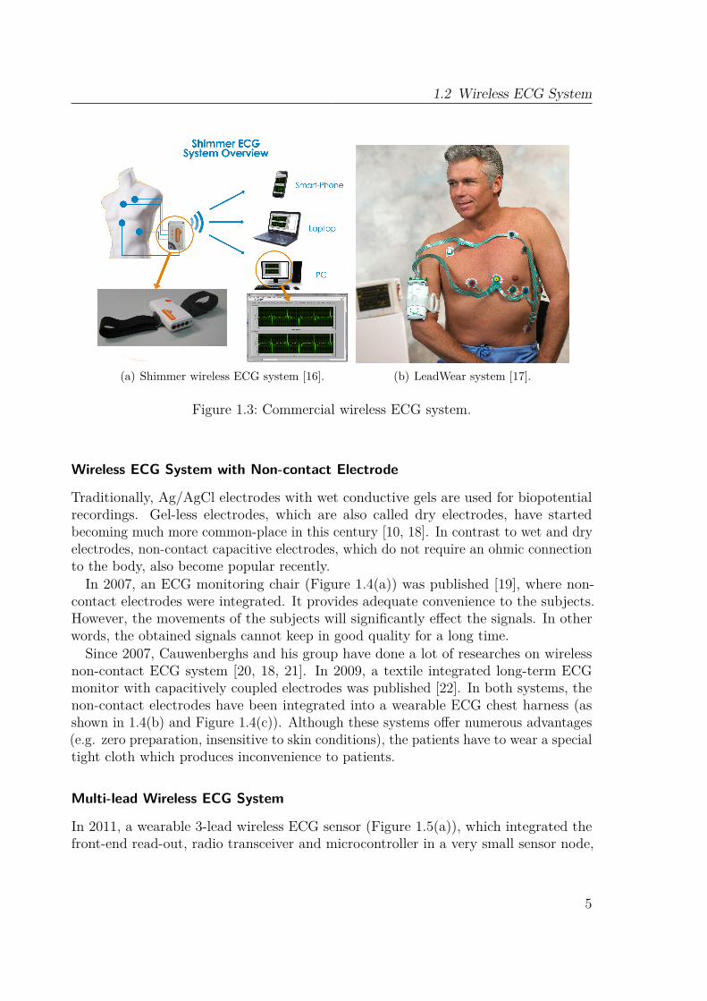
(a) Shimmer wireless ECG system [16]. (b) LeadWear system [17].
Figure 1.3: Commercial wireless ECG system.
Wireless ECG System with Non-contact Electrode
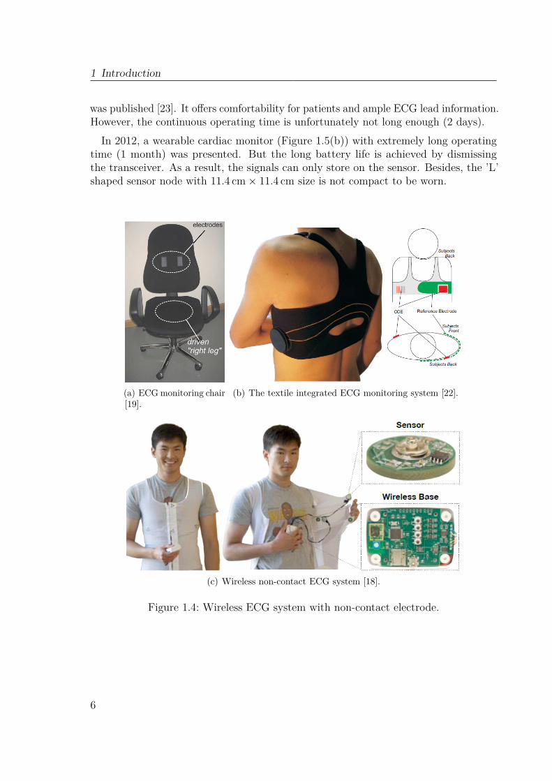
Traditionally, Ag/AgCl electrodes with wet conductive gels are used for biopotentialrecordings. Gel-less electrodes, which are also called dry electrodes, have startedbecoming much more common-place in this century [10, 18]. In contrast to wet and dryelectrodes, non-contact capacitive electrodes, which do not require an ohmic connectionto the body, also become popular recently.In 2007, an ECG monitoring chair (Figure 1.4(a)) was published [19], where non-
contact electrodes were integrated. It provides adequate convenience to the subjects.However, the movements of the subjects will significantly effect the signals. In otherwords, the obtained signals cannot keep in good quality for a long time.
Since 2007, Cauwenberghs and his group have done a lot of researches on wirelessnon-contact ECG system [20, 18, 21]. In 2009, a textile integrated long-term ECGmonitor with capacitively coupled electrodes was published [22]. In both systems, thenon-contact electrodes have been integrated into a wearable ECG chest harness (asshown in 1.4(b) and Figure 1.4(c)). Although these systems offer numerous advantages(e.g. zero preparation, insensitive to skin conditions), the patients have to wear a specialtight cloth which produces inconvenience to patients.
Multi-lead Wireless ECG System
In 2011, a wearable 3-lead wireless ECG sensor (Figure 1.5(a)), which integrated thefront-end read-out, radio transceiver and microcontroller in a very small sensor node,
5
1 Introduction
was published [23]. It offers comfortability for patients and ample ECG lead information.However, the continuous operating time is unfortunately not long enough (2 days).In 2012, a wearable cardiac monitor (Figure 1.5(b)) with extremely long operating
time (1 month) was presented. But the long battery life is achieved by dismissingthe transceiver. As a result, the signals can only store on the sensor. Besides, the ’L’shaped sensor node with 11.4 cm× 11.4 cm size is not compact to be worn.
(a) ECGmonitoring chair[19].
(b) The textile integrated ECG monitoring system [22].
(c) Wireless non-contact ECG system [18].
Figure 1.4: Wireless ECG system with non-contact electrode.
6

1.2 Wireless ECG System
(a) Imec’s 3-lead wireless ECG sensor [23]. (b) ’L’-shaped cardiac monitor [24].
Figure 1.5: Multi-lead wireless ECG system.
Single lead Wireless ECG System
Three single pad wireless ECG systems were proposed in 2010 and 2011 [25, 26, 27](Figure 1.6). Obviously, these systems provide sufficient physical mobility to patients.However, the conspicuous defect is that the single lead is not adequate to exhaustivelymonitor the heart activity.
(a) Valchinov’s ECG sensor [25]. (b) Imec’s ECG patch [28]. (c) Fensli’s ECG BAN [27].
Figure 1.6: Single lead wireless ECG system.
The systems introduced before always have certain disadvantages. Commercialsystems [17, 16] which detect 3 leads or 12 leads ECG signals but do not avoid thecables between the electrodes and sensor node. Non-contact ECG systems [19, 22, 18]
7
1 Introduction
do not satisfy convenience and comfortability simultaneously. Single-pad systems [26,29, 30] which provide the possibility to make ECG system wearable and compact butare impossible to comprehensively monitor the cardiac activity and clinically diagnoseheart diseases. Multi-lead systems either are not compact to be worn or have short lifetime. All these systems are not sufficient for nowadays long-term homecare application.
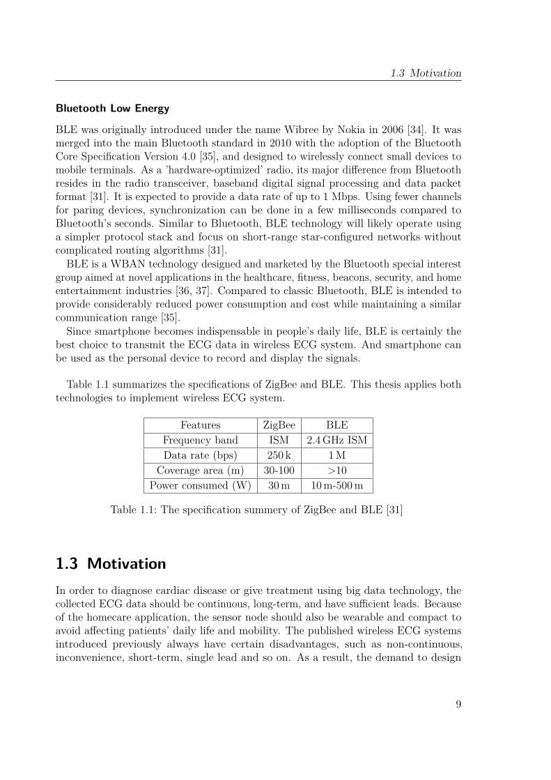
1.2.2 Low-Power Radio TechnologiesIn the past few years, researchers have made considerable progress in characterizing thebody area propagation environment through both measurement-based and simulation-based studies. These works have been conducted in both the ISM (industrial, scientificand medical) bands between 400MHz and 2.45GHz (ZigBee and Bluetooth Low Energy(BLE)) and the Ultra-Wideband (UWB) frequency allocation between 3.1GHz and10.6GHz [31]. In contrast to ZigBee and BLE, UWB provides extremely high datarate (up to 480Mbps) and a relatively low power spectral density emission, whichleads to the suitability of applications in environments which is short-range, indoorand sensitive to RF emissions, e.g., in a hospital. But in the wireless ECG systemsfor homecare application, UWB is limited by its coverage area (< 10 m). As a result,ZigBee and BLE are the most two popular low power radio technologies in the wirelessECG systems introduced before, because of their low power specification, acceptablecoverage area and sufficient data rate.
ZigBee
ZigBee is based on an IEEE 802.15.4 standard [32]. Low data rate and low powerconsumption are two main features of ZigBee, which targets at wide development of longbattery life devices in wireless control and monitoring applications [31]. Therefore, it issuitable for high-level communication protocols used to create personal area networksbuilt from small, low-power digital radios [32]. The recently completed ZigBee HealthCare public application profile provides a flexible framework to meet Continua HealthAlliance requirements for remote health and fitness monitoring. These solutions bettersuit WBAN deployment scenarios in a limited area, e.g. a house [31].ZigBee can operate in three ISM bands, with data rates from 20Kbps to 250Kbps.
The ZigBee network layer natively supports three types of topologies: star, clustertree and mesh. Every network must have one coordinator device, tasked with itscreation, the control of its parameters and basic maintenance. Within star networks,the coordinator must be the central node which initiates and controls the network.Both trees and meshes allow the use of multi-hop routing to extend communication toa WBAN area using the same radio [32, 31].
There have been many published wireless ECG systems [33, 25, 29] utilizing ZigBeefor transporting ECG signals. Owing to its low power specification, ZigBee is a goodchoice to wireless ECG systems for long-term homecare.
8
1.3 Motivation
Bluetooth Low Energy
BLE was originally introduced under the name Wibree by Nokia in 2006 [34]. It wasmerged into the main Bluetooth standard in 2010 with the adoption of the BluetoothCore Specification Version 4.0 [35], and designed to wirelessly connect small devices tomobile terminals. As a ’hardware-optimized’ radio, its major difference from Bluetoothresides in the radio transceiver, baseband digital signal processing and data packetformat [31]. It is expected to provide a data rate of up to 1 Mbps. Using fewer channelsfor paring devices, synchronization can be done in a few milliseconds compared toBluetooth’s seconds. Similar to Bluetooth, BLE technology will likely operate usinga simpler protocol stack and focus on short-range star-configured networks withoutcomplicated routing algorithms [31].BLE is a WBAN technology designed and marketed by the Bluetooth special interest
group aimed at novel applications in the healthcare, fitness, beacons, security, and homeentertainment industries [36, 37]. Compared to classic Bluetooth, BLE is intended toprovide considerably reduced power consumption and cost while maintaining a similarcommunication range [35].
Since smartphone becomes indispensable in people’s daily life, BLE is certainly thebest choice to transmit the ECG data in wireless ECG system. And smartphone canbe used as the personal device to record and display the signals.
Table 1.1 summarizes the specifications of ZigBee and BLE. This thesis applies bothtechnologies to implement wireless ECG system.
Features ZigBee BLEFrequency band ISM 2.4GHz ISMData rate (bps) 250 k 1M
Coverage area (m) 30-100 >10Power consumed (W) 30m 10m-500m
Table 1.1: The specification summery of ZigBee and BLE [31]
1.3 MotivationIn order to diagnose cardiac disease or give treatment using big data technology, thecollected ECG data should be continuous, long-term, and have sufficient leads. Becauseof the homecare application, the sensor node should also be wearable and compact toavoid affecting patients’ daily life and mobility. The published wireless ECG systemsintroduced previously always have certain disadvantages, such as non-continuous,inconvenience, short-term, single lead and so on. As a result, the demand to design
9

1 Introduction
a wireless ECG system, which meets all the requirements of low power, long-term,wireless, wearable and compact, is increasing.
1.4 Goal of the WorkThe goal of this work is to design a low power wearable wireless ECG system whichcan be applied in long-term real time homecare. The possible solutions are introducedbelow.
The traditional electrode placements do not fulfill the nowadays demands for wirelessECG system. The published new placements do not avoid the cables or can only detectone lead ECG signal. To achieve wearable and compact demands and meanwhile detectenough leads, new electrode placements should be experimented. The best placementshould be selected based on the experiment results.Wireless and real time demand can be achieved by miniaturized low noise sensor
node and data acquisition design using ZigBee and BLE. Body motion cancellationshould be considered in the design of low noise analog front end. Wireless ECG systemswith ZigBee and BLE need to be developed respectively. Base on the new electrodeplacement, the sensor node for both systems should be controlled in miniaturized size.And the cables between electrodes and sensor node need to be avoided.
As a wireless sensor node powered by battery, low power is always the most importantconsideration. This work aims to control the power consumption not only in analogbut also in digital. Three ways need to be employed to control the power consumptionin digital: power mode control of microcontroller, dynamic transmission power controland compressed sensing. The best way to control the power consumption in analog isto integrate the discrete circuit. As a result, a micro-power integrated analog front endneed to be designed and manufactured. Besides, analog compressed sensing encoder isanother method to reduce the power in analog further.
1.5 Structure of the ThesisThe whole thesis is organized as follows:
Chapter 2 gives the general background of the fundamentals of ECG and the develop-ment of both traditional electrode placements and new electrode placements for wirelessECG system. Base on the evolution, the experiment for discovering novel electrodeplacements and the evaluation method are introduced. The results are compared anddiscussed. The best electrode placement is selected. This chapter was published inIEEE Biomedical Circuits and System (BioCAS) Conference 2013.In Chapter 3, two wireless ECG systems are designed and implemented. Firstly, a
low noise analog front end with body motion cancellation is presented. This section waspublished in International Conference of E-Health Networking, Application & Services
10

1.5 Structure of the Thesis
(2013). Secondly, a wireless ECG system with ZigBee is introduced. This section waspublished in Journal of Medical Systems, 2015. Finally, a wireless ECG system withBLE is presented.Chapter 4 outlines several digital and analog technologies for power control. In
the digital section, power mode control of microcontroller and dynamic transmissionpower control are firstly presented. Digital compressed sensing is introduced afterward.In the analog power control section, a micro-power integrated analog front end andan analog compressed sensing encoder are presented respectively. The digital andanalog compressed sensing were published in Journal of Medical Systems 2016 andMicroelectronics Journal 2016 respectively.
Chapter 5 concludes the thesis and summarizes the implementation. In the end, anoutlook containing the further research of the wireless ECG system is provided.
11

12
Chapter 2Investigation of Electrode Placements
2.1 Fundamentals of ECGECG is the graph of recording the electrical activity of the heart over a period of timeusing electrodes placed on a body. These electrodes detect the tiny electrical changeson the skin which arise from the heart muscle depolarizing during each heartbeat. Thissection introduces the detailed interpretation of ECG signals and leads.
2.1.1 Interpretation of ECGElectric Activation of the Heart
In the heart muscle cell, electric activation takes place from the inflow of sodium ionsacross the cell membrane. The action potential amplitudes of both nerve and muscle areabout 100mV. The duration of the cardiac muscle impulse is two orders of magnitudelonger than that in either nerve cell or skeletal muscle. Cardiac depolarization isfollowed after a plateau phase, and thereafter repolarization takes place [38].Mechanical contraction of cardiac muscle cell occurs a little later after the electric
activation. The activation wavefronts are in complex shape, as activation can propagatefrom one cell to another in any direction. The boundary between the atria and ventricles,which the activation wave normally cannot cross except along a special conduction
13
2 Investigation of Electrode Placements
system, is the only exception, since a nonconducting barrier of fibrous tissue is present[39].The Sinus or Sinoatrial (SA) node, which consists of specialized muscle cells and
locates in the right atrium at the superior vena cava, are self-excitatory, pacemakercells. An action potential is generated by them with the rate of about 70 per minute.Activation propagates from the SA node and throughout the atria, but cannot propagatedirectly across the boundary between atria and ventricles [40].The Atrioventricular (AV) node located at the boundary between the atria and
ventricles has an intrinsic frequency of about 50 pulses/min. However, if the AV nodeis triggered with a higher pulse frequency, it follows this higher frequency. In a normalheart, the only conducting path is provided from the atria to the ventricles. Thus, undernormal conditions, the latter can be excited only by pulses that propagate through it[41].
A specialized conduction system provides the propagation from the AV node to theventricles. Once propagation along the conduction system is within the ventricularregion, it takes place at a relatively high speed, but prior to this (through the AV node)the velocity is extremely slow [42].
The formation of a wavefront which propagates through the ventricular mass towardthe outer wall is caused by many activation sites from the inner side of the ventricularwall. Repolarization, which occurs after each ventricular muscle region has depolarized,is not a propagating phenomenon. Because the duration of the action impulse atthe epicardium (the outer side of the cardiac muscle) is much shorter than at theendocardium (the inner side of the cardiac muscle), the termination of activity appearsas if it was propagating from epicardium toward the endocardium [40].Because the intrinsic rate of the SA node is the greatest, it sets the activation
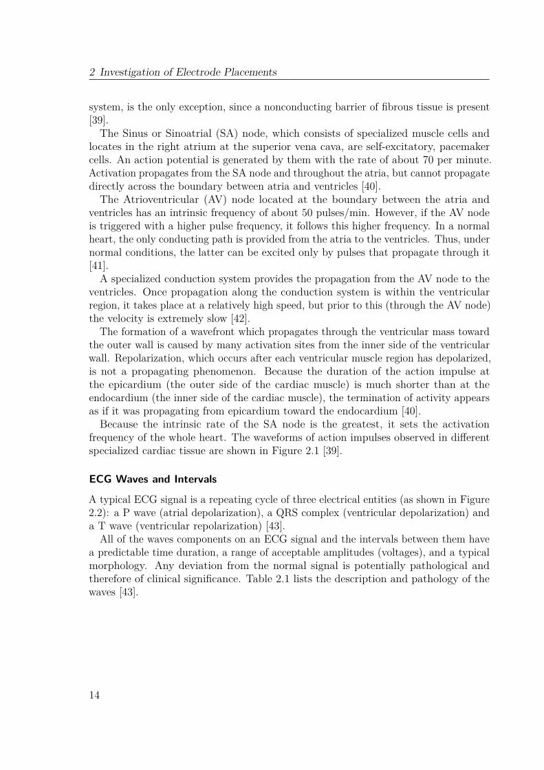
frequency of the whole heart. The waveforms of action impulses observed in differentspecialized cardiac tissue are shown in Figure 2.1 [39].
ECG Waves and Intervals
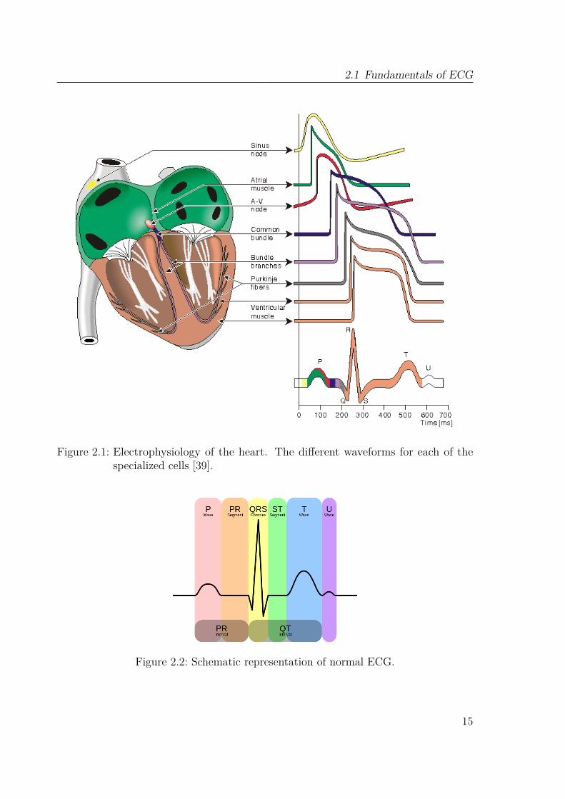
A typical ECG signal is a repeating cycle of three electrical entities (as shown in Figure2.2): a P wave (atrial depolarization), a QRS complex (ventricular depolarization) anda T wave (ventricular repolarization) [43].
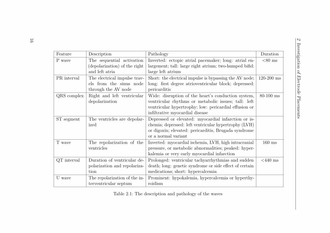
All of the waves components on an ECG signal and the intervals between them havea predictable time duration, a range of acceptable amplitudes (voltages), and a typicalmorphology. Any deviation from the normal signal is potentially pathological andtherefore of clinical significance. Table 2.1 lists the description and pathology of thewaves [43].
14
2.1 Fundamentals of ECG
Figure 2.1: Electrophysiology of the heart. The different waveforms for each of thespecialized cells [39].
Figure 2.2: Schematic representation of normal ECG.
15
2Investigation
ofElectrodePlacem
ents
Feature Description Pathology DurationP wave The sequential activation
(depolarization) of the rightand left atria
Inverted: ectopic atrial pacemaker; long: atrial en-largement; tall: large right atrium; two-humped bifid:large left atrium
<80 ms
PR interval The electrical impulse trav-els from the sinus nodethrough the AV node
Short: the electrical impulse is bypassing the AV node;long: first degree atrioventricular block; depressed:pericarditis
120-200 ms
QRS complex Right and left ventriculardepolarization
Wide: disruption of the heart’s conduction system,ventricular rhythms or metabolic issues; tall: leftventricular hypertrophy; low: pericardial effusion orinfiltrative myocardial disease
80-100 ms
ST segment The ventricles are depolar-ized
Depressed or elevated: myocardial infarction or is-chemia; depressed: left ventricular hypertrophy (LVH)or digoxin; elevated: pericarditis, Brugada syndromeor a normal variant
T wave The repolarization of theventricles
Inverted: myocardial ischemia, LVH, high intracranialpressure, or metabolic abnormalities; peaked: hyper-kalemia or very early myocardial infarction
160 ms
QT interval Duration of ventricular de-polarization and repolariza-tion
Prolonged: ventricular tachyarrhythmias and suddendeath; long: genetic syndrome or side effect of certainmedications; short: hypercalcemia
<440 ms
U wave The repolarization of the in-terventricular septum
Prominent: hypokalemia, hypercalcemia or hyperthy-roidism
Table 2.1: The description and pathology of the waves
16

2.1 Fundamentals of ECG
2.1.2 ECG LeadsThe ECG signal is detected by the electrodes placed on the body. Traditionally, 10electrodes are placed on the patient’s limbs and on the surface of the chest to build theconventional 12 lead ECG. The standard 12-lead ECG provides spatial informationabout the heart’s electrical activity in 3 approximately orthogonal directions: right ⇔left; superior ⇔ inferior; anterior ⇔ posterior [44]. Each of the 12 leads represents aparticular orientation in space, as indicated in Table 2.2 and Figure 2.3 [43, 44].
Leads Description
Limb leads(frontal plane)
Right ⇔ left: Lead I = Vleft arm − Vright armSuperior ⇔ inferior: Lead II = Vleft leg − Vright armSuperior ⇔ inferior: Lead III = Vleft leg − Vleft arm
Augmented limbleads (frontalplane)
Rightward: Lead aV R = Vright arm − 12(Vleft arm + Vleft leg)
Leftward: Lead aV L = Vleft arm − 12(Vright arm + Vleft leg)
Inferior: Lead aV F = Vleft leg − 12(Vleft arm + Vright arm)
Precordial leads(horizontal plane)
Posterior ⇔ anterior: LeadsV1, V2, V3
Right ⇔ left: LeadsV4, V5, V6
Table 2.2: The particular orientation of 12 leads
Figure 2.3: Directions of ECG leads in 3 dimensions [43, 44].
17
2 Investigation of Electrode Placements
2.2 Development of the ECG Electrode PlacementsThe electrode placement has been developed for more than one century. There is noconsensus on either the optimal quantity or placement positions of an ECG system’selectrodes. They largely depend on a particular application [45].In the last century, many electrode placements were proposed. And they became
more and more convenience. The first limb leads were defined by Einthoven in 1908 [46](Figure 2.4(a)). With these 3 electrodes on limb, 3 primary leads (Lead I, Lead II, LeadIII) ECG signals can be detected. In 1944, Wilson proposed 6 precordial leads with6 electrodes on chest [47] (Figure 2.4(b)). Combining with the 3 electrodes proposedby Einthoven and 1 ground electrode on Right Leg (RL), 12 leads ECG system, whichis already introduced in the last section, was established then. These 10 electrodeplacements were also accepted as the traditional and standard electrode placements,and popular for the ECG monitoring in the hospital.
So as to provide more physical mobility for the patient, Mason and Likar publisheda new 12-lead ECG system in 1966 to detect the 12 leads signals during exercise [48](Figure 2.4(c)). They moved the limb electrodes to shoulder and abdomen. But thissystem still needs 10 electrodes on body. For the purpose of simplified lead system, in1988, Dower developed a EASI system which utilized 5 electrodes to detect 3 EASIsignals (AI, AS, ES) [49] (Figure 2.4(d)). The 12-lead ECG signals can be reconstructedfrom these 3 EASI signals.However, with the electrode placements aforementioned, cables are still essential
to connect the electrodes with the sensor. Therefore, these electrode placements cannot satisfy the demands of modern wearable wireless ECG system. In this century,several completely wireless ECG systems were published. Cao developed a three-padECG system. Three sensor nodes were worn around the heart to detect the signalsfrom 3 dimensions, which were transmitted respectively to PC applying ZigBee [9](Figure 2.4(e)). 12-lead signals were reconstructed from the 3 dimension signals. Thissystem is completely wireless. However, lots of efforts need to be payed on the timesynchronization and reconstruction. Single-lead ECG systems were also published by[26, 30, 29] (Figure 2.4(f)). But they can only detect one lead ECG signal.The electrode placements introduced before can fall into three classes, namely
conventional 12-lead ECG system (limb leads, precordial leads and Mason-Likar leads),Vector-Cardiogram (VCG) systems (EASI system and three pad system), and wirelesssingle-pad ECG systems. The deployment complexity of conventional 12-lead ECGsystem hinder its wide employment in the wireless ECG system. The VCG systemregisters electrical heart activity in three orthogonal leads. However, wires are stillrequired to connect them [9]. Meanwhile, reconstruction produce significant timedelay. The single-pad ECG system gives the possibility to make ECG system wearable,wireless and comfortable to patients. Nevertheless, using such a single-pad approach, itis impossible to comprehensively monitor the cardiac activity and clinically diagnoseheart diseases [51].
18

2.2 Development of the ECG Electrode Placements
(a) Limb leads [39]. (b) Precodial leads [44].
(c) Mason-Likar leads [50]. (d) EASI system [50]
(e) Three lead system [9]. (f) Single lead system [28].
Figure 2.4: The development of the leads system.
19
2 Investigation of Electrode Placements
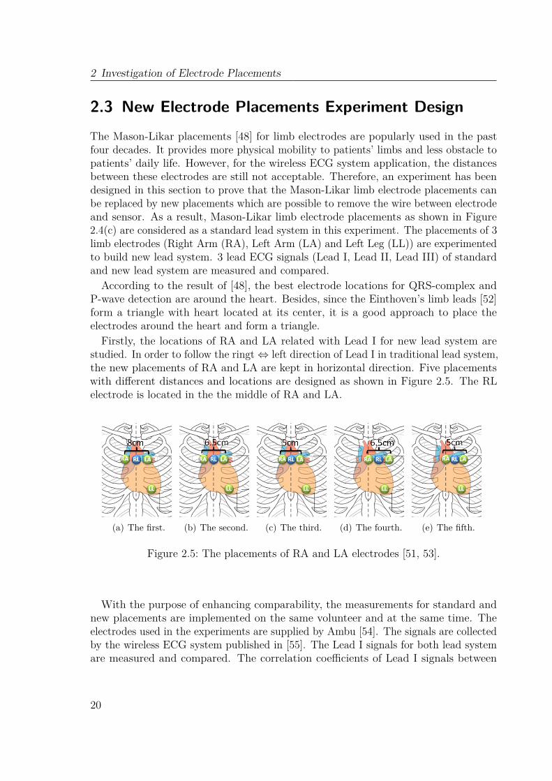
2.3 New Electrode Placements Experiment Design
The Mason-Likar placements [48] for limb electrodes are popularly used in the pastfour decades. It provides more physical mobility to patients’ limbs and less obstacle topatients’ daily life. However, for the wireless ECG system application, the distancesbetween these electrodes are still not acceptable. Therefore, an experiment has beendesigned in this section to prove that the Mason-Likar limb electrode placements canbe replaced by new placements which are possible to remove the wire between electrodeand sensor. As a result, Mason-Likar limb electrode placements as shown in Figure2.4(c) are considered as a standard lead system in this experiment. The placements of 3limb electrodes (Right Arm (RA), Left Arm (LA) and Left Leg (LL)) are experimentedto build new lead system. 3 lead ECG signals (Lead I, Lead II, Lead III) of standardand new lead system are measured and compared.According to the result of [48], the best electrode locations for QRS-complex and
P-wave detection are around the heart. Besides, since the Einthoven’s limb leads [52]form a triangle with heart located at its center, it is a good approach to place theelectrodes around the heart and form a triangle.Firstly, the locations of RA and LA related with Lead I for new lead system are
studied. In order to follow the ringt⇔ left direction of Lead I in traditional lead system,the new placements of RA and LA are kept in horizontal direction. Five placementswith different distances and locations are designed as shown in Figure 2.5. The RLelectrode is located in the the middle of RA and LA.
(a) The first. (b) The second. (c) The third. (d) The fourth. (e) The fifth.
Figure 2.5: The placements of RA and LA electrodes [51, 53].
With the purpose of enhancing comparability, the measurements for standard andnew placements are implemented on the same volunteer and at the same time. Theelectrodes used in the experiments are supplied by Ambu [54]. The signals are collectedby the wireless ECG system published in [55]. The Lead I signals for both lead systemare measured and compared. The correlation coefficients of Lead I signals between
20

2.4 Experiments Results
them are calculated as:
r =∑ni=1
(Xi −X
) (Yi − Y
)√∑n
i=1
(Xi −X
)2√∑n
i=1
(Yi − Y
)2, (2.1)
where r is the correlation coefficient, X is the signal of new lead system and Y is thesignal of standard lead system. The best placements for RA and LA, which have thehighest correlation coefficient with standard placements, are selected out.Afterward the new placement for LL has also been studied. 9 placements for LL
electrode are investigated in both horizontal and vertical direction (as shown in Figure2.6). The Lead II and Lead III signals of these 9 placements are measured andcompared with these two lead signals of standard lead system. With the same method,the correlation coefficients between them are also calculated.
(a) 4 cm in vertical. (b) 5 cm in vertical. (c) 6 cm in vertical.
Figure 2.6: The new placements of this paper for LL electrode [51].
2.4 Experiments ResultsAccording to the experiment for the placements of RA and LA, the Lead I signals ofstandard and new lead system are measured and compared. The correlation coefficientsbetween them are calculated (as listed in Table 2.3). Although the third placement hasthe highest correlation coefficient with standard placement, the result shows that thefirst three placements have similar correlation coefficients, but much larger than theother two placements. It indicates that, if the placements of RA and LA electrodesare kept on the both sides of middle line respectively, the signal is less dependent onthe distance between them. This result gives a significant foundation to reduce thedistance between electrodes and make the ECG sensor much smaller. As a result, thethird placement with 5 cm distance between RA and LA electrodes is selected as thebest placement for RA and LA.
21
2 Investigation of Electrode Placements
Standard placementThe first placement 0.93The second placement 0.91The third placement 0.95The fourth placement 0.89The fifth placement 0.83
Table 2.3: The correlation coefficients of Lead I signals between standard and newplacement for RA and LA
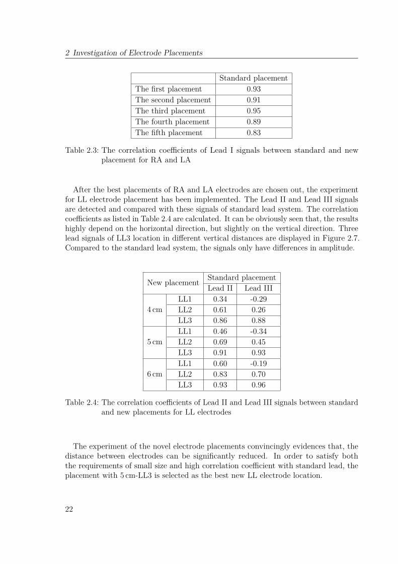
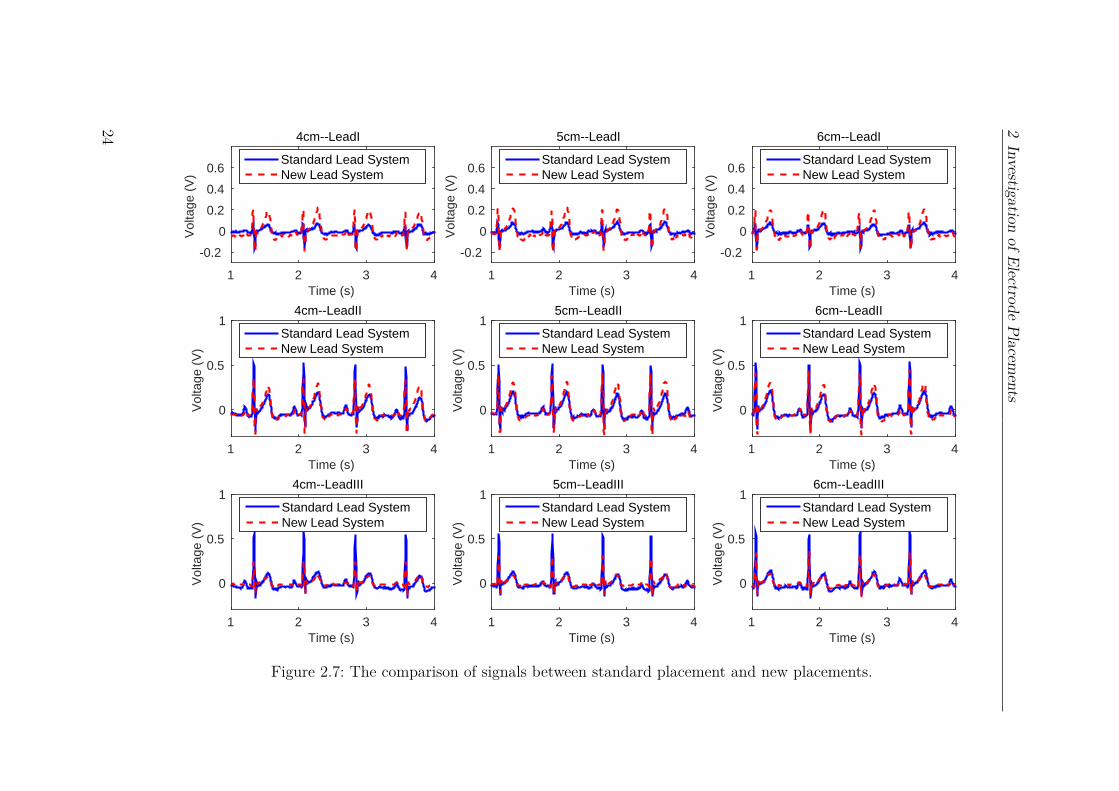
After the best placements of RA and LA electrodes are chosen out, the experimentfor LL electrode placement has been implemented. The Lead II and Lead III signalsare detected and compared with these signals of standard lead system. The correlationcoefficients as listed in Table 2.4 are calculated. It can be obviously seen that, the resultshighly depend on the horizontal direction, but slightly on the vertical direction. Threelead signals of LL3 location in different vertical distances are displayed in Figure 2.7.Compared to the standard lead system, the signals only have differences in amplitude.
New placement Standard placementLead II Lead III
4 cmLL1 0.34 -0.29LL2 0.61 0.26LL3 0.86 0.88
5 cmLL1 0.46 -0.34LL2 0.69 0.45LL3 0.91 0.93
6 cmLL1 0.60 -0.19LL2 0.83 0.70LL3 0.93 0.96
Table 2.4: The correlation coefficients of Lead II and Lead III signals between standardand new placements for LL electrodes
The experiment of the novel electrode placements convincingly evidences that, thedistance between electrodes can be significantly reduced. In order to satisfy boththe requirements of small size and high correlation coefficient with standard lead, theplacement with 5 cm-LL3 is selected as the best new LL electrode location.
22
2.5 Conclusion
2.5 ConclusionA new lead system is proposed in this chapter to make the sensor much more convenientand provide more physical mobility to patients. Mason-Likar limb electrode placementwhich has often been used in the last four decades is considered as standard leadsystem. Five new placements for RA and LA were firstly discussed. Lead I signals ofthese placements were measured and compared with standard lead system. The bestplacements for RA and LA have been selected according to the correlation coefficient.Afterwards, Nine new placements for LL have also been studied and Lead II and LeadIII signals were measured. Using the same method as before, the best placement of LLis determined. This study proves that it is possible to replace the standard lead systemwith new lead system. Comparing with the three pad system [9], the new lead systemproposed in this chapter only needs one sensor node and doesn’t need to consider abouttime synchronization. Besides, it can also provide more lead signals to the monitoringsystem than the single pad system.
23
2Investigation
ofElectrodePlacem
ents
Time (s)1 2 3 4
Vol
tage
(V
)
-0.2
0
0.2
0.4
0.6
4cm--LeadI
Standard Lead SystemNew Lead System
Time (s)1 2 3 4
Vol
tage
(V
)
0
0.5
14cm--LeadII
Standard Lead SystemNew Lead System
Time (s)1 2 3 4
Vol
tage
(V
)
0
0.5
14cm--LeadIII
Standard Lead SystemNew Lead System
Time (s)1 2 3 4
Vol
tage
(V
)
-0.2
0
0.2
0.4
0.6
5cm--LeadI
Standard Lead SystemNew Lead System
Time (s)1 2 3 4
Vol
tage
(V
)
0
0.5
15cm--LeadII
Standard Lead SystemNew Lead System
Time (s)1 2 3 4
Vol
tage
(V
)
0
0.5
15cm--LeadIII
Standard Lead SystemNew Lead System
Time (s)1 2 3 4
Vol
tage
(V
)
-0.2
0
0.2
0.4
0.6
6cm--LeadI
Standard Lead SystemNew Lead System
Time (s)1 2 3 4
Vol
tage
(V
)
0
0.5
16cm--LeadII
Standard Lead SystemNew Lead System
Time (s)1 2 3 4
Vol
tage
(V
)
0
0.5
16cm--LeadIII
Standard Lead SystemNew Lead System
Figure 2.7: The comparison of signals between standard placement and new placements.
24
Chapter 3Wireless ECG System Design and
Implementation
3.1 Analog Front EndInstrumentation Amplifier (INA)s and band-pass filter are two essential componentsfor the analog front end of ECG system. The performance of the analog front enddetermines the quality of the signal detected by the monitoring system. Low noise,body motion cancellation, electrode mismatch tolerance and narrow bandwidth are themain challenges for analog front end. With these considerations in mind, this sectionintroduces the circuit design and performance evaluation of the analog front end.
3.1.1 Circuit DesignFirst Stage
The first stage of ECG front end contributes a lot for the performance of the ECG system.The common mode noise, especially the 50/60Hz Electromagnetic Interference (EMI)from the power line, should be rejected in this stage. Figure 3.1 shows the classic modelof EMI in ECG system [56, 57]. EMI can couple to the ECG system through couplingcapacitor CP and CB. Capacitance CISO is coupled between ac ground and the ground
25

3 Wireless ECG System Design and Implementation
of the ECG system.
Isolated ECG Sensor
Power Line
CE
RE
CE
RE
CISO
CB
CP
120 V/240 V50 Hz/60 Hz
Electrode
Electrode
Figure 3.1: A classic model for power line interference in ECG system.
Besides, CE and RE are the basic circuit model of electrode. They compose theelectrode impedance Ze. Different electrodes will have impedance mismatch, althoughthey are from the same factory. Furthermore, the dc offset voltage caused by bodymotion should also be considered in the first stage of analog front end.The dc offset component vs and an EMI va compose the common mode voltage vc
[58]. vc will be transformed into an interfering differential voltage vi as provided thefollowing equation [59]:
vi = (va + vs)(1/CMRR + Zd/Zc), (3.1)
where Zd is the difference between two electrode impedance (Ze and Z ′e as shown inFigure 3.2) and Zc is the common mode impedance.
An ac coupled INA is a common front end in ECG measurements. A high CommonMode Rejection Ratio (CMRR) can be achieved without any trimmings, when theinput stage achieves large gain [60]. However, due to the dc offset, the overall gain islimited to avoid the saturation of INA. The ac coupling circuit in Figure 3.2 [60] isapplied in this work before the INA to remove the vs and protect the signal from thesaturation phenomenon of INA. Ideally, Zc in this circuit is infinite, which makes theterm Zd/Zc become zero. If R2C = R
′2C = τ , the transfer function of the ac-coupling
network isG(s) = sτ
1 + sτ, (3.2)
which corresponds to a high pass filter. 500mHz cutoff frequency is achieved by settingR2 and R′2 as 330KΩ and C as 1µF. To avoid the decay of the input signal, the inputimpedance should be as high as possible. R1 and R′1 are hence chosen as 10MΩ.
26

3.1 Analog Front End
The INA after the ac coupling circuit is employed to amplify the difference of signalsfrom the two electrodes and also to reject va. It is implemented with a micro-power(50µA), zero-drift and high CMRR (100 dB) instrumentation amplifier TI INA333 withthe gain set to 200.
C
R1 R2
R1´ R2´
Ze
Ze´
INA333
C
Figure 3.2: First stage of ECG front end [60].
Driven Right Leg Circuit
EMI va always plays a critical role in biopotential system. The Driven Right Leg (DRL)circuit shown in Figure 3.3 is a common way to cancel this va interference from thebody. It inversely amplifies the common mode signal and feeds back to the right legelectrode. As a result, the overall EMI noise seen at the other electrodes (RA, LA andLL) is reduced. High gain of this feedback can increase the CMRR in the first stage.The value of the closed loop gain ADRL at a given frequency f is equal to:
ADRL = 2× Zf
RCM
, (3.3)
where:Zf = Rf
1 + sRfCf. (3.4)
To refrain from any oscillations, the phase margin of the feedback should be largerthan 45. By setting R1 = 100 kΩ, R2 = 10MΩ and C = 100 pF , the phase margin isachieved to be 85.93.
Vcm R1
Rf
Rp
Cf
Vref
Figure 3.3: DRL circuit.
27

3 Wireless ECG System Design and Implementation
Low Pass Filter
A second order Sallen-Key low pass filter with low-power Operational Amplifier (opamp)(TI OPA333) is following the INA. The cutoff frequency of this stage is set to 40Hzand the gain is set to 3.
The ac coupling circuit, instrumentation amplifier, DRL and the filter build the ECGanalog front end which is shown in Figure 3.4. The common mode point of the inputac coupling circuit is connected to the DRL. The overall bandwidth is 0.4Hz to 40Hzand the total gain is 56 dB as depicted in Figure 3.5. Here, the interfering differentialvoltage vi is minimized. The front end can detect two lead signals (Lead II and LeadIII). The Lead I signal can be calculated as
Lead I = Lead II − Lead III. (3.5)
C1´
R1´ R2´
R1´´ R2´´
Ze´
Ze´´ INA333C1´´
C1
R1 R2Ze
R3
Vref
RpRL
Rf
Cf
Vref
Vref
Vref
RA
LL
LA
RL
R4
R5R6
R7INA333
Vref
Vref
Vref
R8
R9
R10
R11
C2C3
C4C5
Lead II
Lead III
Ze´´´
RpRA
RpLL
RpLA
C6
C7
Figure 3.4: The proposed analog front end circuit.
3.1.2 Measurement PlatformIn order to evaluate the performance of the analog front end, a radio transmitter unitis applied to sample the ECG signals from analog front end and transmit them to thereceiver unit. The signals are finally displayed on the PC.
TI CC2530 ZigBee Network Processor (ZNP) Mini Development Kit is employed asthe signal sampling and radio communication units. The kit includes an End-Deviceand a coordinator.The End-Device is composed of a low power microcontroller MSP430F2274, and
an Radio Frequency (RF) transceiver CC2530. Two AAA 1.5V alkaline batteries are
28
3.1 Analog Front End
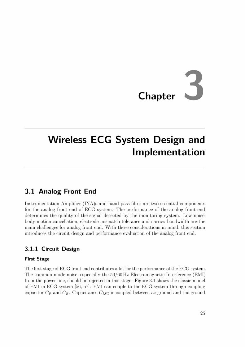
Figure 3.5: Ac transfer characteristic of the whole circuit.
used to power the End-Device and the analog front end. The microcontroller, whichincludes a 10 bit Analog-to-Digital Converter (ADC), is used to sample the two LeadsECG signals coming from the analog front end with 200Hz sampling frequency. Theprogram sends the data packet every 100ms. Each packet contains 20 samples.The coordinator consists of Universal Serial Bus (USB) stick for Serial Wire (SW)
debugging, USB Universal Asynchronous Receiver/Transmitter (UART) interface,microcontroller MSP430F2274 and RF transceiver CC2530. It receives the data fromEnd-Device and transmits to PC using USB UART interface.A Matlab Graphical User Interface (GUI) Data Acquisition Host is built to set the
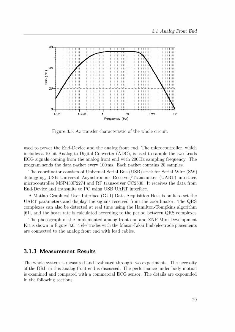
UART parameters and display the signals received from the coordinator. The QRScomplexes can also be detected at real time using the Hamilton-Tompkins algorithm[61], and the heart rate is calculated according to the period between QRS complexes.The photograph of the implemented analog front end and ZNP Mini Development
Kit is shown in Figure 3.6. 4 electrodes with the Mason-Likar limb electrode placementsare connected to the analog front end with lead cables.
3.1.3 Measurement Results
The whole system is measured and evaluated through two experiments. The necessityof the DRL in this analog front end is discussed. The performance under body motionis examined and compared with a commercial ECG sensor. The details are expoundedin the following sections.
29
3 Wireless ECG System Design and Implementation
Figure 3.6: Photograph of the system components.
Comparison of the Signals with and without DRL
DRL circuit and high CMRR INA are applied in this work to reduce va. In orderto minimize the components used in the system, the necessity of DRL is evaluated.Figure 3.7(b) shows the signals when the DRL circuit is connected to the right legelectrode. The signals when the right leg electrode is directly connected to referencevoltage and without the DRL circuit are also measured and shown in Figure 3.7(a).The measurement is done on the same volunteer and with the same electrode placement.According to the comparison, it is obvious that the interference expresses little differencebetween the two situations. The level of it is 10mV in average in both conditions. As aconclusion, a high CMRR INA is enough to cancel the electromagnetic interference va.
The Signals under Body Motion
The dc component vs will change along with the body motion. And as a result of theelectrode impedance mismatch, it will be transformed into a differential voltage. Thisresults in the fluctuation of the signal base lines at the output of ECG front end, whicheven causes the saturation of amplifier. We employed ac coupling circuit to remove vs.An experiment is designed to evaluate the capability of this work to cancel the bodymotion effect. A commercial ECG sensor produced by SHIMMER [62] which does nothave the ac coupling circuit and has a gain of 170 is used here as a reference sensor.Both of the sensors from this work and [62] are connected to the same electrodes on theMason-Likar placements [48]. The experiment is implemented on the same volunteer,at the same time, in the same electrode placements and with the same electrodes.
Figure 3.8(a) and Figure 3.8(c) are the measured Lead III signals of this work whenthe body is walking and running. The Lead III signals of [62] during walking andrunning are also measured (see Figure 3.8(b) and Figure 3.8(d)). The comparisonresults indicate that the ac coupling circuit contributes a lot to cancel vs and keep the
30

3.1 Analog Front End
10 10.5 11 11.5 12 12.5 13−0.5
0
0.5
Time (s)
Vol
tage
(V
)Lead I
10 10.5 11 11.5 12 12.5 131.5
2
2.5
Time (s)
Vol
tage
(V
)
Lead II
10 10.5 11 11.5 12 12.5 131.5
2
2.5
Time (s)
Vol
tage
(V
)
Lead III
(a) Without DRL circuit.
10 10.5 11 11.5 12 12.5 13−0.5
0
0.5
Time (s)
Vol
tage
(V
)
Lead I
10 10.5 11 11.5 12 12.5 131.5
2
2.5
Time (s)
Vol
tage
(V
)
Lead II
10 10.5 11 11.5 12 12.5 131.5
2
2.5
Time (s)
Vol
tage
(V
)
Lead III
(b) With DRL circuit.
Figure 3.7: Comparison of the signals with and without DRL circuit.
31
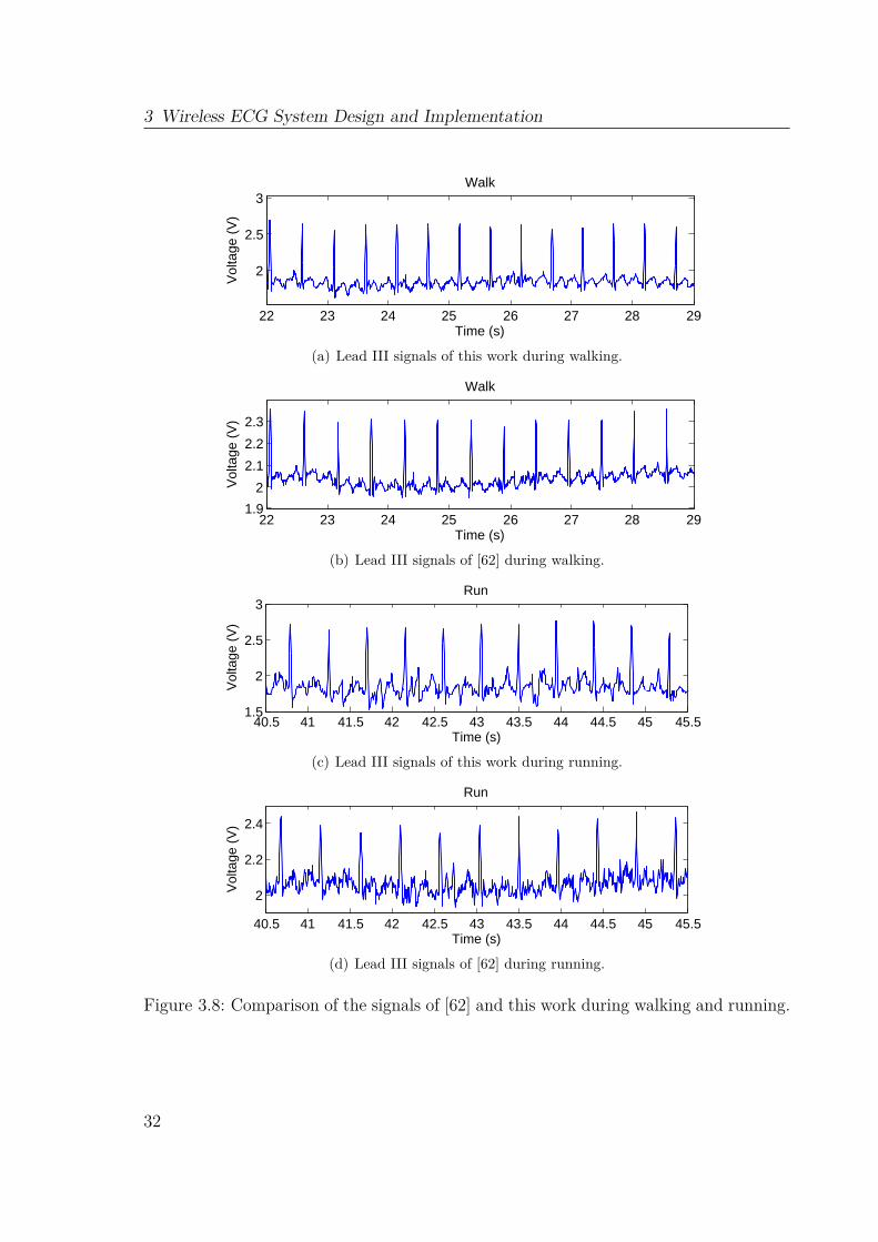
3 Wireless ECG System Design and Implementation
22 23 24 25 26 27 28 29
2
2.5
3Walk
Time (s)
Vol
tage
(V
)
(a) Lead III signals of this work during walking.
22 23 24 25 26 27 28 291.9
2
2.1
2.2
2.3
Walk
Time (s)
Vol
tage
(V
)
(b) Lead III signals of [62] during walking.
40.5 41 41.5 42 42.5 43 43.5 44 44.5 45 45.51.5
2
2.5
3Run
Time (s)
Vol
tage
(V
)
(c) Lead III signals of this work during running.
40.5 41 41.5 42 42.5 43 43.5 44 44.5 45 45.5
2
2.2
2.4
Run
Time (s)
Vol
tage
(V
)
(d) Lead III signals of [62] during running.
Figure 3.8: Comparison of the signals of [62] and this work during walking and running.
32
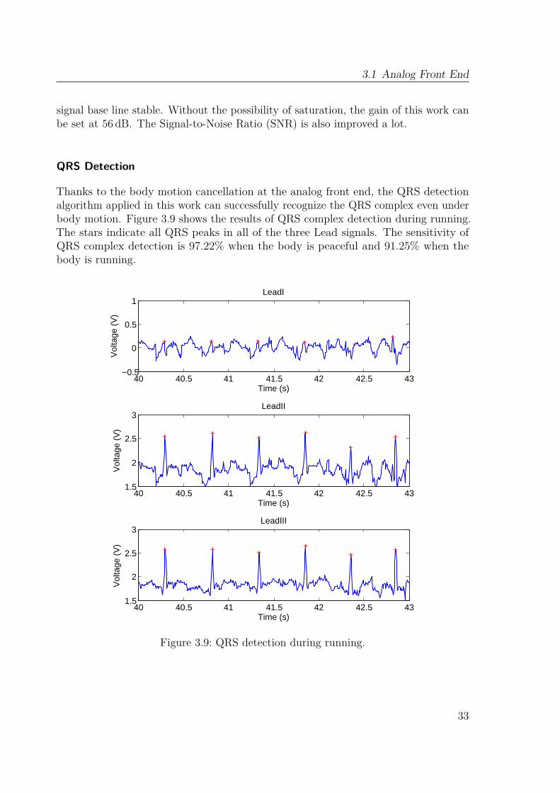
3.1 Analog Front End
signal base line stable. Without the possibility of saturation, the gain of this work canbe set at 56 dB. The Signal-to-Noise Ratio (SNR) is also improved a lot.
QRS Detection
Thanks to the body motion cancellation at the analog front end, the QRS detectionalgorithm applied in this work can successfully recognize the QRS complex even underbody motion. Figure 3.9 shows the results of QRS complex detection during running.The stars indicate all QRS peaks in all of the three Lead signals. The sensitivity ofQRS complex detection is 97.22% when the body is peaceful and 91.25% when thebody is running.
40 40.5 41 41.5 42 42.5 43−0.5
0
0.5
1LeadI
Time (s)
Vol
tage
(V
)
40 40.5 41 41.5 42 42.5 431.5
2
2.5
3LeadII
Time (s)
Vol
tage
(V
)
40 40.5 41 41.5 42 42.5 431.5
2
2.5
3LeadIII
Time (s)
Vol
tage
(V
)
Figure 3.9: QRS detection during running.
33

3 Wireless ECG System Design and Implementation
3.2 Wireless ECG System with ZigBeeAlthough the ZNP Mini Development Kit functionally fulfill the requirements forwireless ECG system, the total size of the the analog front end and the end-device cannot reach the wearable target. Furthermore, the cables between the analog front endand the electrodes are still not avoided. Therefore, this section and the next section aimto combine the analog front end and the transmitter, and control the sensor node inacceptable size. This section employs ZigBee as the protocol of the radio communicationand PC as the signal record and display terminal.
3.2.1 System DesignThe considered wireless ECG monitoring system with ZigBee constitutes a sensor node,a coordinator and a GUI. The signals detected by the sensor are transmitted to thecoordinator and finally displayed and analyzed on a PC. The diagram of the wholesystem is shown in Figure 3.10.
INA
INA
RA
LA
LL
MCURX
TX
AD
RX
TXMCU
BPF
BPF
Figure 3.10: System diagram.
Sensor Node
According to the results of the electrode placements in Chapter 2, the final arrangementof the electrodes and the size of sensor node are shown in Fig 3.11. The size of thesensor node can be kept below 5.5 cm× 2.5 cm.The sensor node includes the analog front end described in Section 3.1, the micro-
controller and the RF transceiver that samples and transmits the signals. The wholesensor node is powered by a rechargeable 600mAh battery. A recharging circuit hasalso been designed in the sensor node.A TI CC2530 System-on-Chip with ZigBee protocol [63], which features very low
power consumption due to its fast speed from sleep to active mode, has been appliedin this work. It includes the microcontroller which samples the signals from frontend with 200Hz sampling frequency, and the transceiver which transmits the data tocoordinator. An 50Ω Inverted F Printed Circuit Board (PCB) antenna [64] has alsobeen designed. In order to reduce the power consumption, the data is sent every 100mswith 20 samples in every packet.
34

3.2 Wireless ECG System with ZigBee
Figure 3.11: The design of the sensor node.
Coordinator
The coordinator consists of USB stick for debugging, USB Serial Peripheral Interface(SPI) (FT220X) [65], system on chip CC2530 [63] and 50Ω Inverted F PCB antenna.It receives the data from the sensor node and sends back the acknowledgment message.The received data is transmitted to the FT220X and then sent to PC.
GUI
A GUI Data Acquisition Host is built to set the UART parameters and display thesignals received from the coordinator. The QRS detection and the heart rate calculationare employed with the same approach introduced in the last section.
3.2.2 ImplementationFigure 3.12(a) shows the photograph of the sensor node, the size of which is 5.5 cm×2.5 cm. Bottom view presents the analog front end and the connectors to electrodes.Top view shows the rechargeable battery and the charging port. The transceiver andthe antenna are implanted below the battery. Figure 3.12(b) shows the photographof the coordinator. The coordinator is always connected to PC and power on towait for the connection request from sensor node. When the sensor node is poweredon, it will first search for the available coordinator and send the connection request.After the connection is built, they communicate between each other. The maximumcommunication distance between sensor node and coordinator is 30m, which can easilyfulfill home usage applications.
The GUI data acquisition host is shown in Figure 3.13. Figure 3.14 shows the windowto set the UART parameters. After the setting, the coordinator is connected to theGUI. If the sensor node is also connected to the coordinator, two lead ECG signalsare firstly transmitted to the coordinator and finally received by the GUI. Lead I ECGsignal is calculated on the GUI by equation 3.5. Three lead signals are finally displayedin the GUI. The QRS complex and heart rate is successfully detected in real time.
35

3 Wireless ECG System Design and Implementation
(a) Sensor node. (b) Coordina-tor.
Figure 3.12: Photograph of the system.
When the heart rate is abnormal (too high or too low), the color of the heart rate textwill turn red as an alarm for user.
3.3 Wireless ECG System with BLEAs smartphones have become the essential device for everyone in nowadays’ daily life,this section introduce a wireless ECG system which employs BLE as the protocol ofradio communication and smartphone as the record and display terminal. This systemprovide more activity space for the patients. The monitoring can continue even duringoutdoor activities.
3.3.1 System DesignBased on the system design in Section 3.2, this design applies the same analog front endin Section 3.2 and TI CC2541 System-on-Chip with BLE [66]. The whole sensor nodeis also powered by a rechargeable 600mAh battery. The sensor node communicateswith smartphone by BLE. An android Application (App) has been designed to receiveand display the data.
3.3.2 ImplementationThe photograph of sensor node is the same as in Figure 3.12. The android App is shownin Figure 3.15(a). Unlike in the wireless ECG system with ZigBee, when the sensornode is powered on, it will broadcast itself every 1 s. When the user open the App, it
36
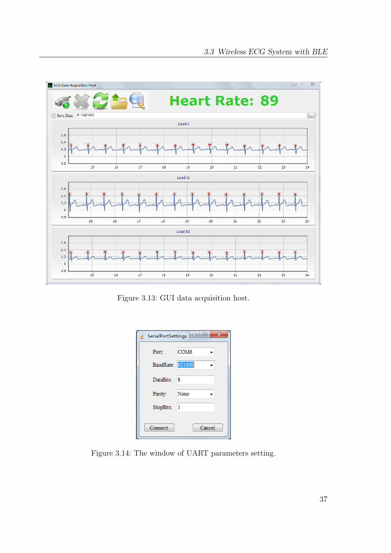
3.3 Wireless ECG System with BLE
Figure 3.13: GUI data acquisition host.
Figure 3.14: The window of UART parameters setting.
37
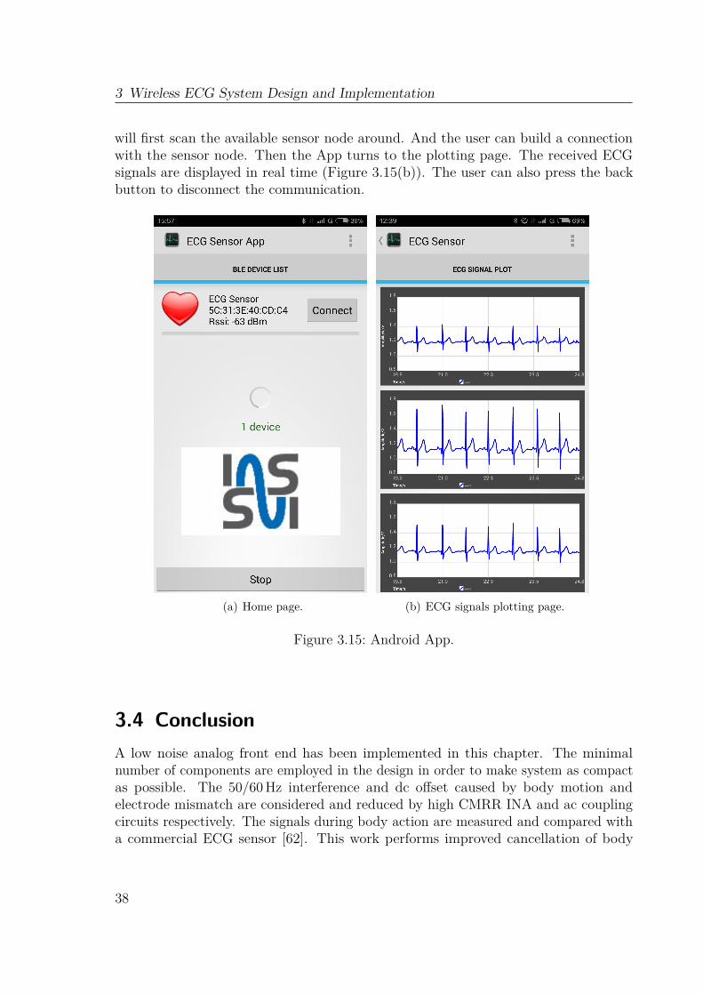
3 Wireless ECG System Design and Implementation
will first scan the available sensor node around. And the user can build a connectionwith the sensor node. Then the App turns to the plotting page. The received ECGsignals are displayed in real time (Figure 3.15(b)). The user can also press the backbutton to disconnect the communication.
(a) Home page. (b) ECG signals plotting page.
Figure 3.15: Android App.
3.4 ConclusionA low noise analog front end has been implemented in this chapter. The minimalnumber of components are employed in the design in order to make system as compactas possible. The 50/60Hz interference and dc offset caused by body motion andelectrode mismatch are considered and reduced by high CMRR INA and ac couplingcircuits respectively. The signals during body action are measured and compared witha commercial ECG sensor [62]. This work performs improved cancellation of body
38

3.4 Conclusion
motion effects. Furthermore, a high accuracy of QRS complex detection and heart ratecalculation is achieved even when the body is running.
Wireless wearable ECG systems with ZigBee and BLE have both been implemented.The size of the two systems can be kept at 5.5 cm × 2.5 cm with the new electrodeplacements. The system with ZigBee can fulfill the homecare usage, while the systemwith BLE also allows monitoring during outdoor activities. These two systems satisfyreal time application and provide more physical mobility to patients.
39

40

Chapter 4Digital Power Control Technologies
For a wireless body sensor, battery life time is always an important specification. Forthe purpose of long term homecare, a series of power mode control techniques havebeen investigated in this work. The components in sensor node can be separated intoanalog and digital parts. Therefore, the power control can be realized in both parts.The digital parts of the ZigBee and BLE sensor node are implemented by the TI
CC2530 and CC2541 respectively. According to the structure of these two chips, thepower reduction on them can be realized both by microcontroller (8051 CPU Core)and transceiver. Therefore, digital power control is implemented by three technologies:power mode control, dynamic transmission power control and digital compressed sensing.This chapter introduces these 3 power control approaches in the following sections.
4.1 Power Mode Control
4.1.1 BackgroundAccording to the datasheet of CC2530 and CC2541 [63, 66], the chips can operate in 5power modes (Table 4.1). In both wireless ECG systems, 20 samples are sent every100ms, which means there are a lot time interval during absence of transmitting task.Hence, adjustable power mode can be applied in both ZigBee and BLE sensor node.
41
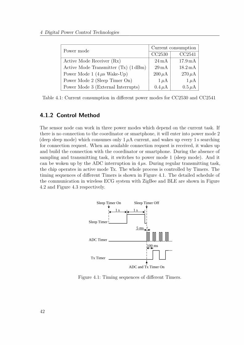
4 Digital Power Control Technologies
Power mode Current consumptionCC2530 CC2541
Active Mode Receiver (Rx) 24mA 17.9mAActive Mode Transmitter (Tx) (1 dBm) 29mA 18.2mAPower Mode 1 (4µs Wake-Up) 200µA 270µAPower Mode 2 (Sleep Timer On) 1µA 1µAPower Mode 3 (External Interrupts) 0.4µA 0.5µA
Table 4.1: Current consumption in different power modes for CC2530 and CC2541
4.1.2 Control Method
The sensor node can work in three power modes which depend on the current task. Ifthere is no connection to the coordinator or smartphone, it will enter into power mode 2(deep sleep mode) which consumes only 1µA current, and wakes up every 1 s searchingfor connection request. When an available connection request is received, it wakes upand build the connection with the coordinator or smartphone. During the absence ofsampling and transmitting task, it switches to power mode 1 (sleep mode). And itcan be woken up by the ADC interruption in 4µs. During regular transmitting task,the chip operates in active mode Tx. The whole process is controlled by Timers. Thetiming sequences of different Timers is shown in Figure 4.1. The detailed schedule ofthe communication in wireless ECG system with ZigBee and BLE are shown in Figure4.2 and Figure 4.3 respectively.
Sleep Timer
ADC Timer
Tx Timer
1 s 1 s
Sleep Timer On Sleep Timer Off
5 ms
100 ms
ADC and Tx Timer On
Figure 4.1: Timing sequences of different Timers.
42
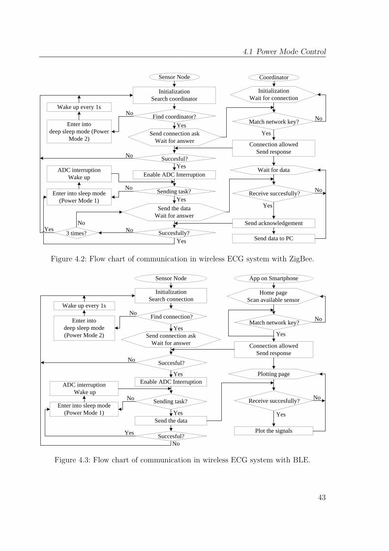
4.1 Power Mode Control
InitializationSearch coordinator
Find coordinator?
Succesful?
Enable ADC Interruption
Sending task?
Succesfully?
Sensor Node
No
Yes
No
Yes
No
3 times? NoNo
Yes
Coordinator
Wait for data
Receive succesfully?
Yes
No
Send data to PC
Enter intodeep sleep mode (Power
Mode 2)
Wake up every 1s
Enter into sleep mode (Power Mode 1)
ADC interruptionWake up
Yes
Match network key? No
Connection allowedSend response
Send acknowledgement
YesSend connection askWait for answer
Yes
Send the dataWait for answer
InitializationWait for connection
Figure 4.2: Flow chart of communication in wireless ECG system with ZigBee.
InitializationSearch connection
Find connection?
Succesful?
Enable ADC Interruption
Sending task?
Sensor Node
No
Yes
No
No
App on Smartphone
Plotting page
Receive succesfully?
Yes
No
Plot the signals
Enter intodeep sleep mode (Power Mode 2)
Wake up every 1s
Enter into sleep mode (Power Mode 1)
ADC interruptionWake up
Yes
Match network key?No
Connection allowedSend response
YesSend connection askWait for answer
Yes
Home pageScan available sensor
Send the data
No
YesSuccesful?
Figure 4.3: Flow chart of communication in wireless ECG system with BLE.
43
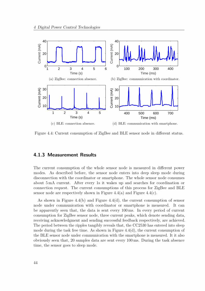
4 Digital Power Control Technologies
1 2 3 4 5 60
20
40
Time (s)
Cur
rent
(m
A)
(a) ZigBee: connection absence.
100 200 300 4000
20
40
Time (ms)
Cur
rent
(m
A)
(b) ZigBee: communication with coordinator.
400 500 600 700
10
20
30
Time (ms)
Cur
rent
(m
A)
1 2 3 4 5
10
20
30
Time (s)
Cur
rent
(m
A)
0 0.5 1 1.5 2
10
20
30
Time (s)
Cur
rent
(m
A)
(c) BLE: connection absence.
400 500 600 700
10
20
30
Time (ms)
Cur
rent
(m
A)
1 2 3 4 5
10
20
30
Time (s)
Cur
rent
(m
A)
0 0.5 1 1.5 2
10
20
30
Time (s)
Cur
rent
(m
A)(d) BLE: communication with smartphone.
Figure 4.4: Current consumption of ZigBee and BLE sensor node in different status.
4.1.3 Measurement Results
The current consumption of the whole sensor node is measured in different powermodes. As described before, the sensor node enters into deep sleep mode duringdisconnection with the coordinator or smartphone. The whole sensor node consumesabout 5mA current. After every 1s it wakes up and searches for coordination orconnection request. The current consumptions of this process for ZigBee and BLEsensor node are respectively shown in Figure 4.4(a) and Figure 4.4(c).
As shown in Figure 4.4(b) and Figure 4.4(d), the current consumption of sensornode under communication with coordinator or smartphone is measured. It canbe apparently seen that, the data is sent every 100ms. In every period of currentconsumption for ZigBee sensor node, three current peaks, which denote sending data,receiving acknowledgment and sending successful feedback respectively, are achieved.The period between the ripples tangibly reveals that, the CC2530 has entered into sleepmode during the task free time. As shown in Figure 4.4(d), the current consumption ofthe BLE sensor node under communication with the smartphone is measured. It it alsoobviously seen that, 20 samples data are sent every 100 ms. During the task absencetime, the sensor goes to sleep mode.
44
4.2 Dynamic Transmission Power Control
4.1.4 DiscussionOwing to the power mode control, the sensor node saves plenty of power, especiallywhen there is no connection with the coordinator or smartphone. Even if the sensorworks continuously, the battery life times of ZigBee and BLE sensor node can be morethan 52 hours and 55 h respectively.
4.2 Dynamic Transmission Power Control
4.2.1 BackgroundTransmission is the most energy consuming operation in a sensor node. The radiotransceiver’s transmission strength depends on its transmission power. Although a hightransmission power level provides a good link quality, it raises the power consumptionin sensor node. On the other side, low transmission power can degrade the energyconsumption with the expense of diminished link quality. Accordingly, a tradeoffbetween link reliability and energy consumption must be obtained [67].
The relationship between Tx output power and current consumption of transceiversfor CC2530 and CC2541 are listed in Table 4.2. It states that, in CC2530, it can save11mA in lowest level compared with the highest level. However, in CC2541, the currentconsumption is not sensitive to Tx output power. As a result, the dynamic transmissionpower control was only applied in wireless ECG system with ZigBee.
In the body sensor application, the patient who is carrying the sensor will move in acertain range. To successfully perform over a long term and monitor the ECG signalscontinuously, the Tx output power should not be set to a fixed level, but be adjustableaccording to the received signal strength. At night, the patient would stay at the sameplace. If the coordinator is put close to the sensor, and the Tx output power of thesensor is adjusted to a lower level, the power consumption can be significantly reduced.This section establishes a dynamic adjustment rule for Tx output power base on a
sequence of measurements between the Received Signal Strength Indicator (RSSI) andpower levels.
4.2.2 Adjustment MethodEvery data packet the coordinator receives includes the RSSI. RSSI, which rangesfrom 0dBm to −100 dBm, is computed internally in the radio by averaging the signalpower over eight symbol periods of the incoming packet. It is related to the link state(distance and obstacle) between sensor node and coordinator. Therefore, it is a goodindicator to adjust the Tx output power of the sensor node.With the purpose to find a suitable method to adjust the Tx output power, an
experiment is designed. Because the distance between sensor node and coordinatoris an important factor to affect the RSSI value, the Tx output power is recorded at
45

4 Digital Power Control Technologies
CC2530Tx Output Power (dBm) Current Consumption (mA)
4.5 342.5 311 29
-0.5 28-1.5 27-3 27-4 26-6 26-8 25-10 25-12 25-14 25-16 25-18 24-20 24-22 23
CC2541Tx Output Power (dBm) Current Consumption (mA)
0 18.2-20 16.8
Table 4.2: Current consumptions of CC2530 and CC2541 at every Tx output power [63,66]
46
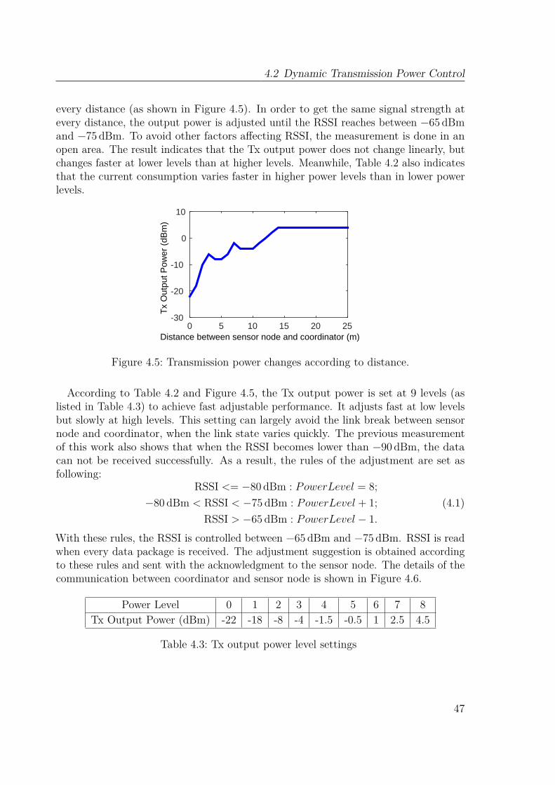
4.2 Dynamic Transmission Power Control
every distance (as shown in Figure 4.5). In order to get the same signal strength atevery distance, the output power is adjusted until the RSSI reaches between −65 dBmand −75 dBm. To avoid other factors affecting RSSI, the measurement is done in anopen area. The result indicates that the Tx output power does not change linearly, butchanges faster at lower levels than at higher levels. Meanwhile, Table 4.2 also indicatesthat the current consumption varies faster in higher power levels than in lower powerlevels.
Distance between sensor node and coordinator (m)0 5 10 15 20 25
Tx
Out
put P
ower
(dB
m)
-30
-20
-10
0
10
Figure 4.5: Transmission power changes according to distance.
According to Table 4.2 and Figure 4.5, the Tx output power is set at 9 levels (aslisted in Table 4.3) to achieve fast adjustable performance. It adjusts fast at low levelsbut slowly at high levels. This setting can largely avoid the link break between sensornode and coordinator, when the link state varies quickly. The previous measurementof this work also shows that when the RSSI becomes lower than −90 dBm, the datacan not be received successfully. As a result, the rules of the adjustment are set asfollowing:
RSSI <= −80 dBm : PowerLevel = 8;−80 dBm < RSSI < −75 dBm : PowerLevel + 1;
RSSI > −65 dBm : PowerLevel − 1.(4.1)
With these rules, the RSSI is controlled between −65 dBm and −75 dBm. RSSI is readwhen every data package is received. The adjustment suggestion is obtained accordingto these rules and sent with the acknowledgment to the sensor node. The details of thecommunication between coordinator and sensor node is shown in Figure 4.6.
Power Level 0 1 2 3 4 5 6 7 8Tx Output Power (dBm) -22 -18 -8 -4 -1.5 -0.5 1 2.5 4.5
Table 4.3: Tx output power level settings
47

4 Digital Power Control Technologies
InitializationSearch coordinator
Find coordinator?
Succesful?
Enable ADC Interruption
Sending task?
Succesfully?
Sensor Node
No
Yes
No
Yes
No
3 times? NoNo
Yes
Coordinator
Wait for data
Receive succesfully?No
Send data to PC
Enter intodeep sleep mode(Power Mode 2)
Wake up every 1s
Enter into sleep mode (Power Mode 1)
ADC interruptionWake up
Yes
Match network key? No
Connection allowedSend response
YesSend connection ask
Wait for answer
Yes
Send the dataWait for answer
InitializationWait for connection
Send acknowledgement with Tx power adjustment suggestion
Read RSSI
Adjust the Tx power
Yes
RSSI<-80 -80<RSSI<-70 RSSI>-60
PowerLevel = 8
PowerLevel + 1
PowerLevel - 1
Figure 4.6: Flow chart of communication in wireless ECG system with ZigBee applyingdynamic transmission power control.
48
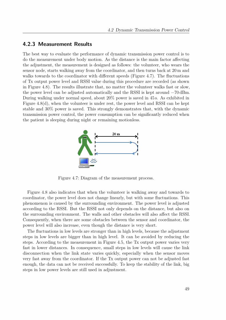
4.2 Dynamic Transmission Power Control
4.2.3 Measurement Results
The best way to evaluate the performance of dynamic transmission power control is todo the measurement under body motion. As the distance is the main factor affectingthe adjustment, the measurement is designed as follows: the volunteer, who wears thesensor node, starts walking away from the coordinator, and then turns back at 20m andwalks towards to the coordinator with different speeds (Figure 4.7). The fluctuationsof Tx output power level and RSSI value during this procedure are recorded (as shownin Figure 4.8). The results illustrate that, no matter the volunteer walks fast or slow,the power level can be adjusted automatically and the RSSI is kept around −70 dBm.During walking under normal speed, about 20% power is saved in 45 s. As exhibited inFigure 4.8(d), when the volunteer is under rest, the power level and RSSI can be keptstable and 30% power is saved. This strongly demonstrates that, with the dynamictransmission power control, the power consumption can be significantly reduced whenthe patient is sleeping during night or remaining motionless.
Figure 4.7: Diagram of the measurement process.
Figure 4.8 also indicates that when the volunteer is walking away and towards tocoordinator, the power level does not change linearly, but with some fluctuations. Thisphenomenon is caused by the surrounding environment. The power level is adjustedaccording to the RSSI. But the RSSI not only depends on the distance, but also onthe surrounding environment. The walls and other obstacles will also affect the RSSI.Consequently, when there are some obstacles between the sensor and coordinator, thepower level will also increase, even though the distance is very short.
The fluctuations in low levels are stronger than in high levels, because the adjustmentsteps in low levels are bigger than in high level. It can be avoided by reducing thesteps. According to the measurement in Figure 4.5, the Tx output power varies veryfast in lower distances. In consequence, small steps in low levels will cause the linkdisconnection when the link state varies quickly, especially when the sensor movesvery fast away from the coordinator. If the Tx output power can not be adjusted fastenough, the data can not be received successfully. To keep the stability of the link, bigsteps in low power levels are still used in adjustment.
49
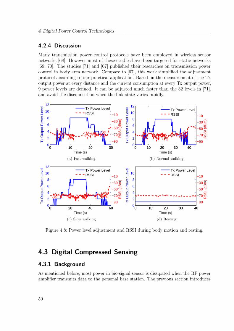
4 Digital Power Control Technologies
4.2.4 DiscussionMany transmission power control protocols have been employed in wireless sensornetworks [68]. However most of these studies have been targeted for static networks[69, 70]. The studies [71] and [67] published their researches on transmission powercontrol in body area network. Compare to [67], this work simplified the adjustmentprotocol according to our practical application. Based on the measurement of the Txoutput power at every distance and the current consumption at every Tx output power,9 power levels are defined. It can be adjusted much faster than the 32 levels in [71],and avoid the disconnection when the link state varies rapidly.
0 10 20 300
2
4
6
8
10
12
Time (s)
Tx
Out
put P
ower
Lev
el
0 10 20 30
−90
−70
−50
−30
−10R
SS
I (dB
m)
Tx Power LevelRSSI
(a) Fast walking.
0 10 20 30 400
2
4
6
8
10
12
Time (s)
Tx
Out
put P
ower
Lev
el
0 10 20 30 40
−90
−70
−50
−30
−10
RS
SI (
dBm
)
Tx Power LevelRSSI
(b) Normal walking.
0 20 40 600
2
4
6
8
10
12
Time (s)
Tx
Out
put P
ower
Lev
el
0 20 40 60
−90
−70
−50
−30
−10
RS
SI (
dBm
)
Tx Power LevelRSSI
(c) Slow walking.
0 10 20 30 400
2
4
6
8
10
Time (s)
Tx
Out
put P
ower
Lev
el
0 10 20 30 40
−90
−70
−50
−30
−10
RS
SI (
dBm
)
Tx Power LevelRSSI
(d) Resting.
Figure 4.8: Power level adjustment and RSSI during body motion and resting.
4.3 Digital Compressed Sensing
4.3.1 BackgroundAs mentioned before, most power in bio-signal sensor is dissipated when the RF poweramplifier transmits data to the personal base station. The previous section introduces
50

4.3 Digital Compressed Sensing
dynamic transmission power control to increase the energy efficiency. In this section,another technology is introduced to reduce the power consumption of transmissionby decreasing the amount of data to be transmitted and reduce the duty cycle of thetransmitter. This energy efficient paradigm is enabled using compressed sensing orCompressive Sampling (CS) in analog or digital domain wherein a compressible signalis acquired using only a few incoherent measurements [72]. Prior research has shownthat CS can be used successfully to exploit the sparsity of ECG bio-signals [73, 74, 75].Digital CS technology is tested and evaluated in this section to increase the energyefficiency of wireless ECG system with BLE.
4.3.2 Compressed SensingA Nyquist-rate ADC samples the signal from the analog front end and gets N samples[X]. [X] with size of N is multiplied by a measurement matrix [Φ] of size M ×N andcompressed into a measurement vector [Y ] of size M < N . CS can be defined by thesimple matrix equation:
y1
y2
.
.
.
yM
=
φ11 φ12 . . . . . φ1N
φ21 φ22 . . . . . φ2N
. . . .
. . . .
. . . .
φM1 φM2 . . . . . φMN
×
x1
x2
.
.
.
.
.
xN
, (4.2)
wherein an uncompressed input vector [X] of size N multiplied by a measurementmatrix [Φ] of size M ×N produces a measurement vector [Y ] of size M < N [73, 76,77]. Compression Ratio (CR) can be calculated as:
CR = N/M. (4.3)
For a signal sparse in an arbitrary domain,
x1
x2
.
.
.
xN
=
ψ11 ψ12 . . . ψ1N
ψ21 ψ22 . . . ψ2N
. . . .
. . . .
. . . .
ψN1 ψN2 . . . ψNN
×
α1
α2
.
.
.
αN
, (4.4)
51

4 Digital Power Control Technologies
where [Ψ] is anN×N sparsifying basis and [α] is the corresponding sparse representationof [X] in the basis [Ψ] [78]. Then [Y ] can be finally defined by:
y1
y2
.
.
.
yM
=
φ11 φ12 . . . . φ1N
φ21 φ22 . . . . φ2N
. . . .
. . . .
. . . .
φM1 φM2 . . . . φMN
×
ψ11 ψ12 . . . . . ψ1N
ψ21 ψ22 . . . . . ψ2N
. . .
. . . .
. . . .
. . . .
. . .
ψN1 ψN2 . . . . . ψNN
×
α1
α2
.
.
.
.
.
αN
.
(4.5)
Two factors ensure accurate reconstruction: 1) [X] is sparse in [Ψ]; 2) [Ψ] and [Φ]are incoherent [73, 72, 76]. [X] is sparse when only a few elements in [α] are significantand [Ψ] determines the domain of sparsity. For time-domain sparse signals ([Ψ] = [I]),if K elements of [X] are greater than the other N −K elements, only the K largestelements are kept in [XK ]; i.e., the signal is thresholded. A definition of sparsity is
Sparsity(%) = (1−K/N)× (100%).
Sparsity control by thresholding is advantageous when [X] is well approximated by[XK ], which means the L2 − norm of the residue ‖X −XK‖2 is small. For accurateand stable compression and reconstruction, [72] recommends
M > CkKlog(NK
), (4.6)
where Ck is an empirical constant. Equation 4.6 limits the maximum achievablecompression for a given sparsity level.For signal sparse in frequency domain, [Ψ] is an inverse Fourier transform matrix.
Make a two-tone sinusoid (Figure 4.9) as an example. [α] only has two non-zerosignificant coefficients (two frequencies: 50Hz and 100Hz) when using inverse Fouriertransform matrix as the signal’s sparsifying basis [Ψ].
For ECG signals, an inverse wavelet transform matrix is widely used as [Ψ]. Waveletcoefficients are typically generated hierarchically using scale dependent low pass (h(n))and high pass (g(n)) quadrature mirror filters that correspond to the type of mother
52
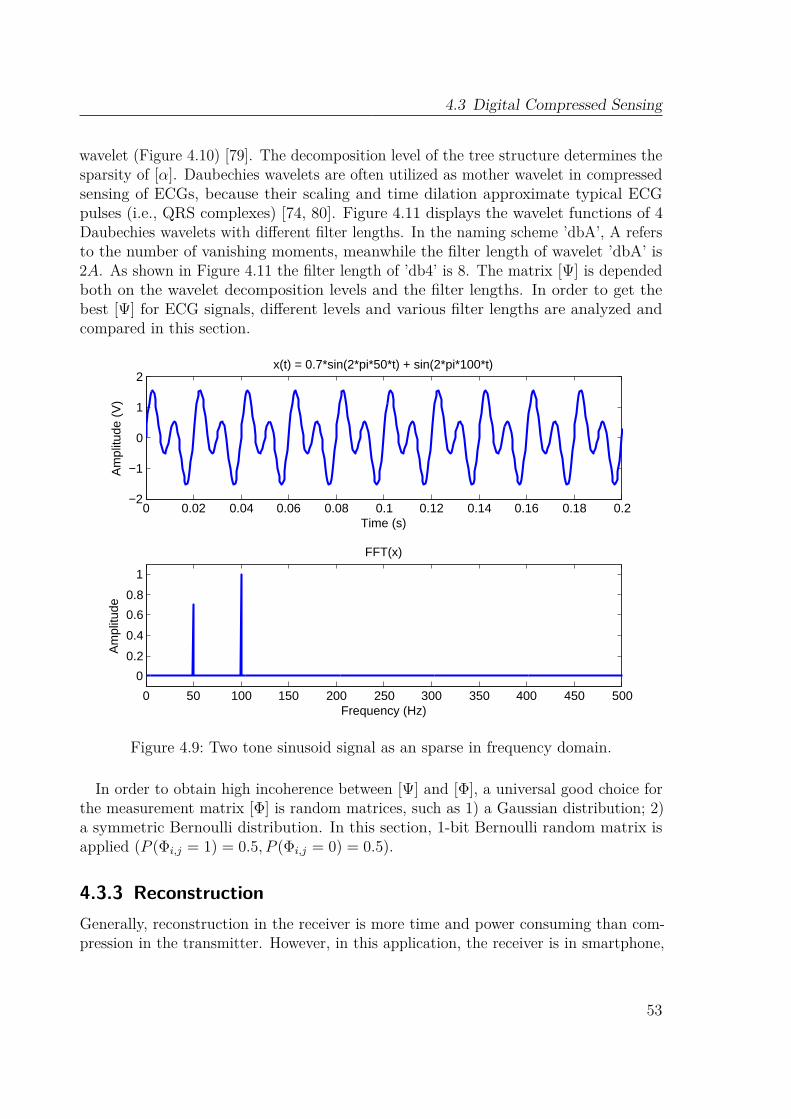
4.3 Digital Compressed Sensing
wavelet (Figure 4.10) [79]. The decomposition level of the tree structure determines thesparsity of [α]. Daubechies wavelets are often utilized as mother wavelet in compressedsensing of ECGs, because their scaling and time dilation approximate typical ECGpulses (i.e., QRS complexes) [74, 80]. Figure 4.11 displays the wavelet functions of 4Daubechies wavelets with different filter lengths. In the naming scheme ’dbA’, A refersto the number of vanishing moments, meanwhile the filter length of wavelet ’dbA’ is2A. As shown in Figure 4.11 the filter length of ’db4’ is 8. The matrix [Ψ] is dependedboth on the wavelet decomposition levels and the filter lengths. In order to get thebest [Ψ] for ECG signals, different levels and various filter lengths are analyzed andcompared in this section.
0 0.02 0.04 0.06 0.08 0.1 0.12 0.14 0.16 0.18 0.2−2
−1
0
1
2
Time (s)
Am
plitu
de (
V)
x(t) = 0.7*sin(2*pi*50*t) + sin(2*pi*100*t)
0 50 100 150 200 250 300 350 400 450 500
0
0.2
0.4
0.6
0.8
1
Frequency (Hz)
Am
plitu
de
FFT(x)
Figure 4.9: Two tone sinusoid signal as an sparse in frequency domain.
In order to obtain high incoherence between [Ψ] and [Φ], a universal good choice forthe measurement matrix [Φ] is random matrices, such as 1) a Gaussian distribution; 2)a symmetric Bernoulli distribution. In this section, 1-bit Bernoulli random matrix isapplied (P (Φi,j = 1) = 0.5, P (Φi,j = 0) = 0.5).
4.3.3 ReconstructionGenerally, reconstruction in the receiver is more time and power consuming than com-pression in the transmitter. However, in this application, the receiver is in smartphone,
53
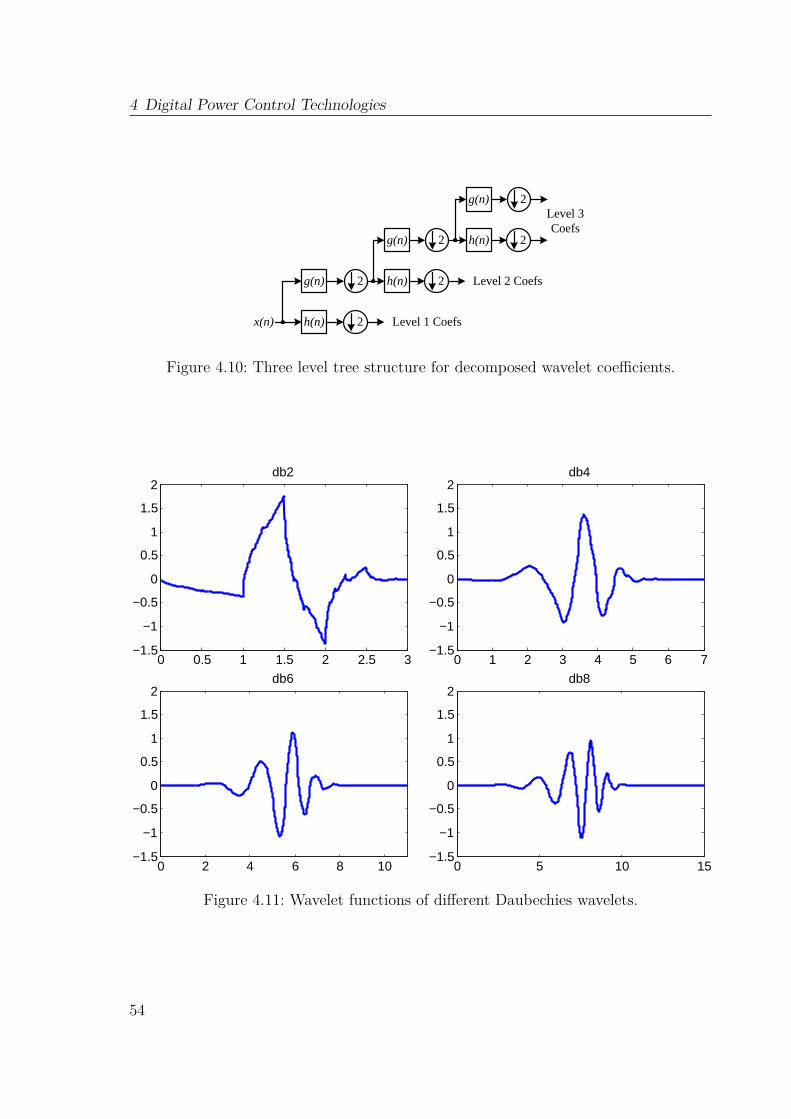
4 Digital Power Control Technologies
x(n)
g(n)
h(n)
2
2
g(n)
h(n)
2
2
g(n)
h(n)
2
2
Level 1 Coefs
Level 2 Coefs
Level 3 Coefs
Figure 4.10: Three level tree structure for decomposed wavelet coefficients.
0 0.5 1 1.5 2 2.5 3−1.5
−1
−0.5
0
0.5
1
1.5
2db2
0 1 2 3 4 5 6 7−1.5
−1
−0.5
0
0.5
1
1.5
2db4
0 2 4 6 8 10−1.5
−1
−0.5
0
0.5
1
1.5
2db6
0 5 10 15−1.5
−1
−0.5
0
0.5
1
1.5
2db8
Figure 4.11: Wavelet functions of different Daubechies wavelets.
54

4.3 Digital Compressed Sensing
where has much greater computational and energy resources than the sensor.Ideally,
[X]
= [Φ]−1 [Y ], where[X]is the reconstructed vector. However, as
[X]
has N unknowns and [Y ] has only M knowns, [Φ] is non-square and non-invertible [74].As a result, optimization methodologies are needed for reconstruction. Table 4.4 listsall the reconstruction algorithms used in this paper.
Two main methods are mostly used in optimization: Iterative Greedy Optimizationand Convex Optimization. The former optimization falls in two categories: variationson Matching pursuit techniques and thresholding algorithms. Matching pursuit, whichwas first introduced in [81], decomposes a signal into a linear expansion of functions froma dictionary. At each iteration of the algorithm, matching pursuit chooses dictionaryelements in a greedy fashion that best approximate the signal [82]. Orthogonal MatchingPursuit (OMP) is an improvement on matching pursuit. It has been successfully usedfor signal recovery [83]. An extension to OMP is the Compressive Sampling MatchingPursuit (CoSaMP), which has tighter bounds on its convergence and performancethan OMP [84]. Thresholding algorithms perform some thresholding function on eachiteration. Iterative Hard Thresholding (IHT) is a class of thresholding algorithms. It setsall but the s-largest component of a vector [α] to 0 and leaves the remaining componentsuntouched. The Accelerated Iterative Hard Thresholding (AIHT) algorithm includesan additional double over relaxation step that significantly improves convergence speedwithout destroying any of the theoretical guarantees of the IHT algorithm.
Basis Pursuit (BP) algorithm is a class of Convex Optimization. It solves the problemby the following generalization:
minimize ‖α‖1 subject to Aα = Y, (4.7)
where A = ΦΨ [85, 86]. In sparsity-minimizing formulations, the same can be achievedby finding the sparsest x satisfying a given misfit:
minimize ‖α‖1 subject to ‖Aα− Y ‖2 ≤ σ, (4.8)
where σ is the maximum permissible misfit [85, 86]. This method is called Basis PursuitDenoise (BPDN).This work simulates all 6 methods mentioned before. The best reconstruction
algorithm is selected by comparing the reconstruction results from different algorithms.
4.3.4 Simulation of Compressed SensingSeveral minutes ECG signals are sampled from the sensor node. [Φ] was obtained by1-bit Bernoulli random matrix. All the simulations were done in Matlab. To obtain thebest [Ψ], the filter length has first been analyzed. 9 wavelet functions (db2 to db10),which have 9 different filter lengths, were simulated with CR = 2, decomposition level
55

4 Digital Power Control Technologies
Iterative Greedy OptimizationMatching pursuit OMP
CoSaMP
Thresholding algorithms IHTAIHT
Convex Optimization BPBPDN
Table 4.4: Reconstruction algorithms
3 and different reconstruction algorithms. SNR was calculated by
SNR = 20log10
(‖x‖2‖x− x‖2
). (4.9)
The results are shown in Figure 4.12. Obviously db4 with filter length 8 has thehighest SNR for most of the reconstruction algorithms. As a result, it was used in thefollowing analysis. With the same method, Reconstruction SNR as a function of thewavelet decomposition levels is depicted in Figure 4.13. Most of the algorithms havethe highest SNR in decomposition 3-level. According to the above results, the bestmatrix [Ψ] is built by 3-level decomposed db4 wavelet coefficients.
Decomposition Levels1 2 3 4 5 6
SN
R (
dB)
10
15
20
25
30
35
OMPCoSaMPBPDNBPHITAHIT
Filter Length5 10 15 20
SN
R (
dB)
10
15
20
25
30
35
OMPCoSaMPBPDNBPHITAHIT
Compression Ratio (CR)2 2.5 3 3.5 4 4.5 5
SN
R (
dB)
0
5
10
15
20
25
30
35
OMPCoSaMPBPDNBPHITAHIT
Figure 4.12: Reconstruction SNR as a function of the filter length. CR = 2 and thewavelet decomposition of 3 levels are utilized.
Another simulation was performed with different CRs (Figure 4.14). The SNRdecreases greatly when the CR increases. In order to keep the main feature of ECG
56
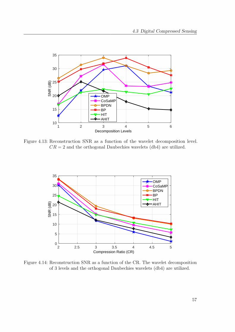
4.3 Digital Compressed Sensing
Decomposition Levels1 2 3 4 5 6
SN
R (
dB)
10
15
20
25
30
35
OMPCoSaMPBPDNBPHITAHIT
Filter Length5 10 15 20
SN
R (
dB)
10
15
20
25
30
35
OMPCoSaMPBPDNBPHITAHIT
Compression Ratio (CR)2 2.5 3 3.5 4 4.5 5
SN
R (
dB)
0
5
10
15
20
25
30
35
OMPCoSaMPBPDNBPHITAHIT
Figure 4.13: Reconstruction SNR as a function of the wavelet decomposition level.CR = 2 and the orthogonal Daubechies wavelets (db4) are utilized.
Decomposition Levels1 2 3 4 5 6
SN
R (
dB)
10
15
20
25
30
35
OMPCoSaMPBPDNBPHITAHIT
Filter Length5 10 15 20
SN
R (
dB)
10
15
20
25
30
35
OMPCoSaMPBPDNBPHITAHIT
Compression Ratio (CR)2 2.5 3 3.5 4 4.5 5
SN
R (
dB)
0
5
10
15
20
25
30
35
OMPCoSaMPBPDNBPHITAHIT
Figure 4.14: Reconstruction SNR as a function of the CR. The wavelet decompositionof 3 levels and the orthogonal Daubechies wavelets (db4) are utilized.
57
4 Digital Power Control Technologies
signals (i.e. T-wave, S-wave, QRS complex wave), SNR > 20dB. Therefore CR isbetter to set at 2.From all the results illustrating before, reconstruction algorithm BPDN always has
the best SNR. Thence it is employed as a reconstruction algorithm on smartphone.Figure 4.15 and Figure 4.16 shows the reconstruction results for Lead III signals whenthe volunteer is in peace and running with the parameters and algorithm selected before.The raw ECG signal, which sparse in the 3-level decomposed db4 wavelet domain, ismeasured by 1-bit Bernoulli random matrix with CR = 2 and reconstructed by BPDNalgorithm. The SNRs for both simulations are 33.14 dB and 25.04 dB respectively. Asa result, the selected parameters and algorithm are able to be applied to the wearablewireless ECG system for homecare.
4.3.5 Implementation on Wireless ECG System with BLEAccording to the simulation results before, CS is implemented on the wireless ECGsystem with BLE. The system diagram in Figure 4.17 explains that, CS is done onsensor node in digital way. With the consideration of memory size of CC2541 andCR = 2, [Φ] obtained by 1-bit Bernoulli random matrix is sized as 50× 100 and storedin the memory of CC2541. Every 100 samples is compressed to the measurement matrix[Y ] with size of 50× 1 by multiplication with [Φ]. [Y ] is transmitted to the smartphone.
On the smartphone, the App reconstructs the ECG signals from [Y ]. The bestmatrix [Ψ], which is selected by simulation and built by 3-level decomposed db4 waveletcoefficients, and the same [Φ] as on the sensor node are stored on the smartphone. TheBPDN algorithm was implemented to reconstruct the ECG signals from the received[Y ]. Finally the reconstructed signals are displayed on the App (Figure 4.18).
The main purpose of CS is to reduce the power consumption of sensor node. Therefore,the current consumption of the sensor node with CS is measured and demonstrated inFigure 4.19. Compare to the current consumption without CS (Figure 4.4(d)), sensornode sends 50 data every 500 ms, which means it sends half less data than without CS.With CS, the battery life time can be extended by 12 h.
4.3.6 DiscussionCompared to the researches in [87, 88], this work not only simulated the process ofCS in digital way with various wavelets, CRs and reconstruction algorithms, but alsoimplemented it on the sensor node and App of a smartphone. The wireless ECG systemwith CS has been evaluated by current consumption measurements. The result showsthat, in order to keep high SNR, the CR can not be bigger than 2. And further more,the reconstruction on the App of smartphone also has much time cost. Based on theseconsiderations, the CS research in analog domain will be continued. An analog CSfront end is designed, evaluated and compared with the digital CS in section 5.2.
58

4.3 Digital Compressed Sensing
10 10.5 11 11.5 12 12.5 131
1.2
1.4
1.6
Time (s)
Vol
tage
(V
)
Original signal
500 550 600 650 700 750 800
0
1
2
Compressed samples
Vol
tage
(V
)
Compressed measurments
10 10.5 11 11.5 12 12.5 131
1.2
1.4
1.6
Time (s)
Vol
tage
(V
)
Reconstructed signal
10 10.5 11 11.5 12 12.5 13
−0.2
0
0.2
Time (s)
Vol
tage
(V
)
Reconstruction error
Figure 4.15: Simulated reconstruction of an ECG signal when the volunteer is in peace.From the top: raw ECG; Compressed measurements [Y ]; Reconstructedsignal: Reconstruction error.
59
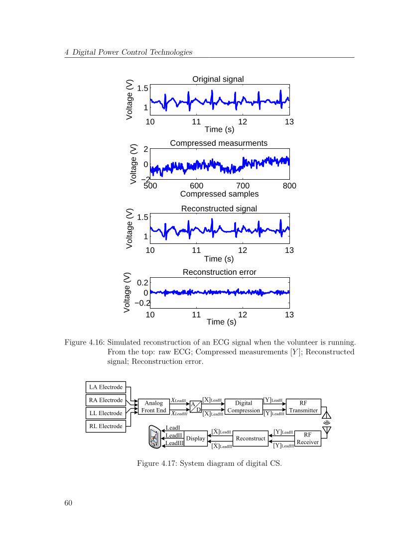
4 Digital Power Control Technologies
10 11 12 13
1
1.5
Time (s)V
olta
ge (
V) Original signal
500 600 700 800−2
0
2
Compressed samples
Vol
tage
(V
) Compressed measurments
10 11 12 13
1
1.5
Time (s)
Vol
tage
(V
) Reconstructed signal
10 11 12 13−0.2
00.2
Time (s)
Vol
tage
(V
) Reconstruction error
Figure 4.16: Simulated reconstruction of an ECG signal when the volunteer is running.From the top: raw ECG; Compressed measurements [Y ]; Reconstructedsignal; Reconstruction error.
LA Electrode
AD
RFTransmitter
RFReceiver
Reconstruct
Analog Front End
Digital Compression
[X]LeadIIXLeadII [Y]LeadII
LeadI
RA Electrode
LL Electrode
RL Electrode
XLeadIII [X]LeadIII [Y]LeadIII
[Y]LeadII
[Y]LeadIII
[Ẋ]LeadII
[Ẋ]LeadIII
DisplayLeadIILeadIII
Figure 4.17: System diagram of digital CS.
60
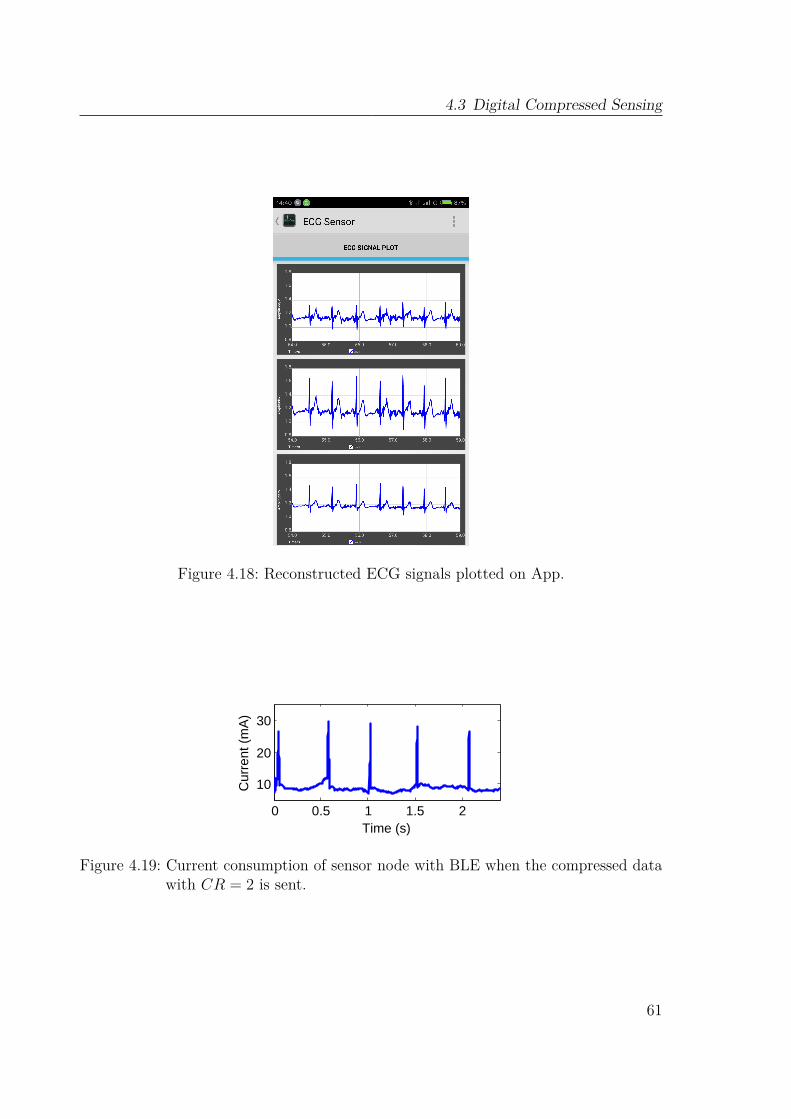
4.3 Digital Compressed Sensing
Figure 4.18: Reconstructed ECG signals plotted on App.
400 500 600 700
10
20
30
Time (ms)
Cur
rent
(m
A)
1 2 3 4 5
10
20
30
Time (s)
Cur
rent
(m
A)
0 0.5 1 1.5 2
10
20
30
Time (s)
Cur
rent
(m
A)
Figure 4.19: Current consumption of sensor node with BLE when the compressed datawith CR = 2 is sent.
61
4 Digital Power Control Technologies
4.4 ConclusionThis chapter proposes several approaches of power reduction. Different power modesare implemented on the microcontroller of CC2530 and CC2541. Specific timers aredefined to control the processes of different tasks. Meanwhile, specific power modes areapplied to the different tasks. With the contribution of power mode control, the batterylife of ZigBee and BLE sensor node can be more than two day even under continuouscommunication.With the consideration of homecare application, the dynamic transmission power
control is applied on the ZigBee sensor node. Because the link quality of the communi-cation between sensor node and coordinator is variable due to the user’s movement indaily life, the transmission power of the sensor node is not necessary kept in the highestlevel. It can be adjustable according to the received RSSI on coordinator. As a resultthis chapter proposed a method to adjust the Tx power level of the sensor node. Theresult of the measurement under different body motion shows that, although the Txpower level is dynamically adjusted, the RSSI is still stable. It also indicates that, thedynamic adjustment will not affect the link quality. With this power control, 20%-30%power of the sensor node is saved.In order to reduce the transmission power further, compressed sensing is applied
after the ADC sampling. The digital data is compressed before transmitting. If thecompression ratio is 2, only half data is transmitted. Therefore, the transmission poweris reduced. The battery life of the sensor node is extended to 67 hours. Becausethe received data on the smartphone is compressed, the original signals should bereconstructed with optimization algorithms.
62

Chapter 5Analog Power Control Technologies
The best way to reduce the power consumption in analog circuit is to integrate thediscrete circuits. As a result, a micro-power integrated analog front end is designedand implemented in this work to integrate the instrumentation amplifier and band passfilter. Further more, an analog compressed sensing encoder is also designed to furtherdecrease the power consumption on the analog side.
5.1 Micro-Power Integrated Analog Front End
5.1.1 BackgroudIntegrated analog front end design for bio-signals has increasingly focused on lowerpower consumption, lower noise and miniaturized size INA, which are still a challengenowadays [89, 90]. Due to the low frequency and mV level amplitude of ECG signals,in band noise is dominated by flick noise (1/f) and offset of the INA. Moreover,common-mode interference from the power line correlate the biopotential signals andthere is the problem of dc offset generated by the body motion and electrode mismatch[55]. Therefore, to amplify weak and noisy biopotentials without loss, a front end withhigh CMRR, low noise, stable gain, band pass bandwidth and high input impedance isneeded[91, 92].Chopping and auto-zeroing have been popularly used to reduce the 1/f noise and
63

5 Analog Power Control Technologies
offset caused by INA. The first chopper modulates the base band signal to a choppingfrequency (fchop). The second chopper modulates the offset and 1/f noise of theINA! (INA!) to fchop. But the signal is demodulated back to the base band. After alow pass filter with 3 dB corner frequency lower than fchop, the offset and 1/f noiseare filtered out. But the signal remains. However, the up-modulation causes rippleat the INA’s output. Auto-zeroing samples the offset and low frequency 1/f noiseon an auto-zero capacitor and then uses this information to cancel the offset and lowfrequency 1/f noise. However, the noise folding associated with sampling results inincreased baseband noise. In general, chopping is the better choice to achieve highpower efficiency [93].
Traditional INAs have four topologies (as shown in Figure 5.1). The resistive feedbacktopology [94] is a popular solution for INAs. However, the input resistor not only causesthe noise but also decreases the input impedance. The classic three-opamp topology[95] has excellent linearity and high input impedance. However, the two low-noise inputamplifiers limit the power efficiency. Furthermore, the CMRR is limited by the mismatchof the resistors. Although Current Feedback Instrumentation Amplifier (CFIA) [96, 91]has rail sensing capability, the gain accuracy is reduced by the mismatch between theirinput and feedback transconductors, which also limits the power efficiency. Compare tothe former three traditional topologies, capacitively-coupled chopper topology can notonly supply high input impedance, but also increase the power efficiency by minimizingthe current consumption in the feedback network [97, 98]. As a result, the analog frontend proposed in this work is designed based on this topology.
5.1.2 Analog Front End Architecture OverviewFigure 5.2 shows the architecture of the proposed integrated analog front end. Theexternal ac coupling circuit, which is already proved in Section 3.1 that it can successfullyreduce the differential dc-Electrode Offset (DEO) caused by the body motion andelectrode mismatch, is applied before the analog front end. The Capacitively-CoupledChopper Instrumentation Amplifier (CCIA) is employed to realize the main gain. Thefollowing two stages are designed to filter the chopper spike and to settle the bandwidthof the whole front end.
5.1.3 Capacitively-Coupled Chopper Instrumentation AmplifierThe offset and 1/f noise are always the important considerations in bio-signal amplifier.As described in the background, chopping technology is a good choice to reduce theoffset and 1/f noise. In the proposed CCIA, the offset and 1/f noise of Gm areup-modulated by the output chopper. Meanwhile, the signal is up-modulated by theinput chopper and demodulated by the output chopper. At the output of CCIA, thesignal remains in the baseband, while the offset and 1/f noise are filtered by the output
64
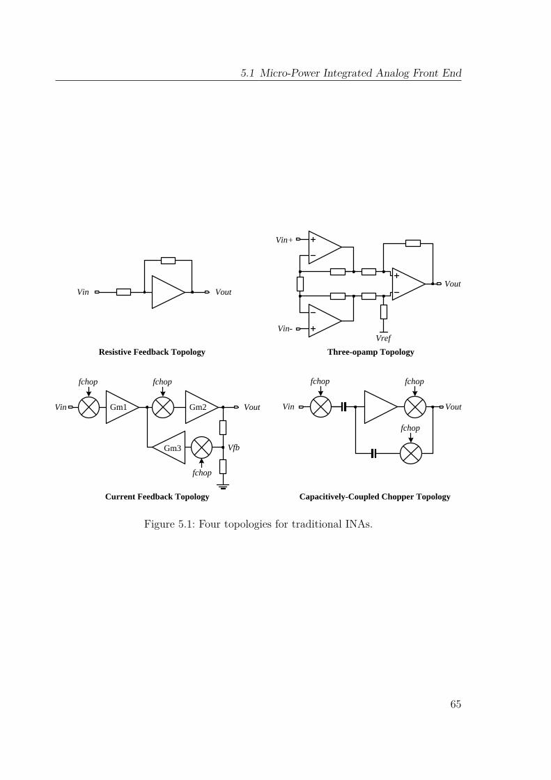
5.1 Micro-Power Integrated Analog Front End
Vin Vout
Vref
Vin+
Vin-
Vout
Gm1 Gm2
Gm3
fchop fchop
fchop
Vin Vout
fchop
Vin Vout
fchop
Vfb
Resistive Feedback Topology Three-opamp Topology
Current Feedback Topology Capacitively-Coupled Chopper Topology
fchop
Figure 5.1: Four topologies for traditional INAs.
65

5 Analog Power Control Technologies
capacitor. Fig. 5.3 shows the process of the chopping technology. fchop is chosen tobe 4 kHz, which is higher than the 1/f noise corner of Gm.
66
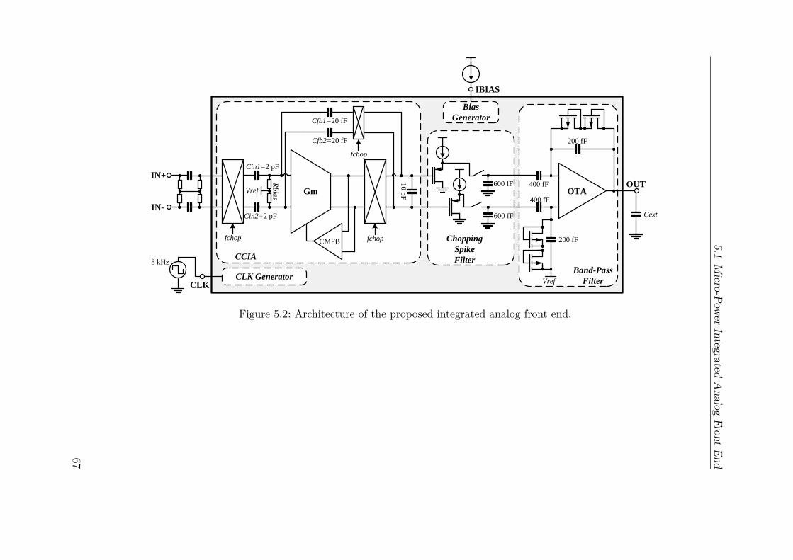
5.1M
icro-PowerIntegrated
Analog
FrontEnd
IN+
IN-
Gm
CMFB
OTA
Vref
200 fF
200 fF
OUT
CLK GeneratorCLK
Bias
Generator
IBIAS
Chopping
Spike
FilterCCIA
600 fF
600 fF
10
pF
Rbia
s
Vref
Cin1=2 pF
Cin2=2 pF
Cfb2=20 fF
Cfb1=20 fF
400 fF
400 fF
Cext
Band-Pass
Filter
fchop fchop
fchop
8 kHz
Figure 5.2: Architecture of the proposed integrated analog front end.
67

5 Analog Power Control Technologies
fchop
Vin Vout
fchop
fchop
Signal
f
VSignal
f
V VfnVthn
Gm
Cout
Cin
Cfb
fchop f
V
fchop
Signal
ModulatedVfn, Voff
Vfn: 1/f noise Vthn: thermal noise Voff: dc offset
Vthn
Figure 5.3: The process of chopping technology.
The gain of the CCIA is dominated by:
G = A0
1 + A0Cfb1,2/Cin1,2, (5.1)
where A0 is the open-loop gain of Gm. According to the capacitance of Cfb1,2 andCin1,2, the gain of the CCIA is set to 100. To ensure a gain accuracy better than99.9%, A0 is designed to 100 dB. As a result, Gm is implemented as a folded-cascodeamplifier, which is shown in Figure 5.4. To achieve high power efficiency and high gainat the same time, the input p-channel Metal–Oxide–Semiconductor (PMOS) transistorsoperate in weak inversion. The Common Mode Feed Back (CMFB) circuit is used todecrease common mode gain. The differential and common mode gains of the CCIAare shown in Figure 5.5.
160 μ/4 μ
Vb1
1 uA
200 nAVb2
Vb3Vcm+
-Vin
+ -Vout
Figure 5.4: Schematic of the opamp.
68

5.1 Micro-Power Integrated Analog Front End
10−2
10−1
100
101
102
103
104
105
−250
−200
−150
−100
Frequency (Hz)
Com
mon
Mod
e G
ain
(dB
)
10−2
10−1
100
101
102
103
104
105
0
20
40
Frequency (Hz)
Diff
eren
tial G
ain
(dB
)
Figure 5.5: Simulated differential and common mode gain of CCIA.
According to our experiment in Section 3.1, the input common mode range shouldbe extremely large due to the body motion. Figure 5.6 shows the basic design forn-channel Metal–Oxide–Semiconductor (NMOS) chopper. However, it can not beemployed as the input chopper. When the input common mode voltage reach thesupply voltage V DD, the switches in the chopper can not be switched on anymore. Thesimplest method to solve this problem is to apply a complementary ComplementaryMetal–Oxide–Semiconductor (CMOS) chopper (Figure 5.6). Although this design canincrease the input common mode range, the total amount of charge injection andcurrent noise is increased by the additional Metal–Oxide–Semiconductor Field-EffectTransistor (MOSFET). As a result, the NMOS chopper with booststrapped clockdrivers (Figure 5.7) [99] is employed as the input chopper. This design boosts the clockfor chopper to V cm + V DD. With this design, the chopper can be switched on atany input common mode voltage. As a result, the input common mode range can beextended to 0− V DD. Meanwhile, its charge injection and current noise is reduced bythe low-swing clock. In order to ensure the high input impedance, a pseudo resistor isapplied as RCM which can supply GΩ resistance [100]. The same resistor design is alsoapplied to the Rbias at the input of Gm to set input dc level of Gm.
5.1.4 Chopper Spike FilterA well-known problem of chopping circuit is the chopper spike caused by chargeinjection from the input chopping switches [91]. The frequency spectrum results of themeasurements in [101] also shows a strong spike at the chopper frequency. This paper
69
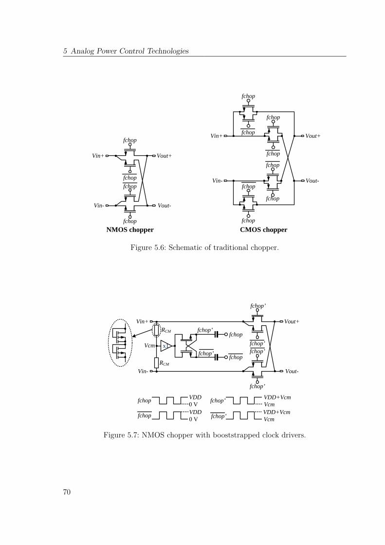
5 Analog Power Control Technologies
fchop
fchop
fchop
fchop
Vin+
Vin-
Vout+
Vout-
fchop
fchop
fchop
fchop
Vin+
Vin-
Vout+
Vout-
fchop
fchop
fchop
fchop
NMOS chopper CMOS chopper
Figure 5.6: Schematic of traditional chopper.
fchop’
fchop’fchop’
fchop’
Vin+
Vin-
Vout+
Vout-
RCM
RCM
x1
fchop
fchop
fchop’
fchop’
VDD0 V
fchop
fchopVDD0 V
VDD+VcmVcm
fchop’
fchop’VDD+VcmVcm
Vcm
Figure 5.7: NMOS chopper with booststrapped clock drivers.
70

5.1 Micro-Power Integrated Analog Front End
apply the Chopper Spike Filter (CSF) (Figure 5.8) which utilizes switched capacitor tofilter the spikes. Before the appearance of the spike, the output of the CCIA is directlysampled to the capacitor, while during the presence of spike, switch is opened andoutput is held on the capacitor. According to the noise transfer function of a trace andhold (T&H) stage in [91, 102], the output noise of the CSF can be written as
vout,CSF 2 (f) = vout,CCIA2 (f)×2BWnm
2
fCSFsinc2
(πmf
fCSF
)
+ (1−m)2(
1 + 2BWn/fCSF∑
n=1sinc2 (πn (1−m))
),(5.2)
where fCSF is the frequency of CSF which is 2 times of fchop, BWn is the noisebandwidth of the input, m is the duty cycle of the hold time of the switch. Firstand second terms represent the noise contributions of hold and sampling operationsrespectively. In order to reduce the distortion, m should be as small as possible. Inthis design, m is set to 5.2% which is sufficient to filter the spikes.
50 nA
Vin
Vout
f_CSF
600 fF
fchop4 kHz
spike
f_CSF8 kHz
Figure 5.8: CSF.
5.1.5 Band-Pass Filter
In order to directly obtain the ECG lead signal from two electrode (LeadI = Vleft arm−Vright arm, LeadII = Vleft leg−Vright arm, LeadIII = Vleft leg−Vleft arm), the band-passfilter consists of a single-end current mirror Operational Transconductance Amplifier(OTA) (Figure 5.9) with a capacitive gain feedback and pseudo resistors made fromPMOS transistors. The gain of this stage is designed to be 2, with which the total gainof the front end is 200. 0.5 Hz− 100 Hz bandwidth is gained together with the externalload capacitor. With the contributions of chopper technology and band-pass filter, theanalog front end gains an input referred noise of 118 nV/
√Hz @ 10Hz (as shown in
Figure 5.10). Figure 5.10 also indicates that chopper spike filter successfully filters thespikes at 4 kHz.
71
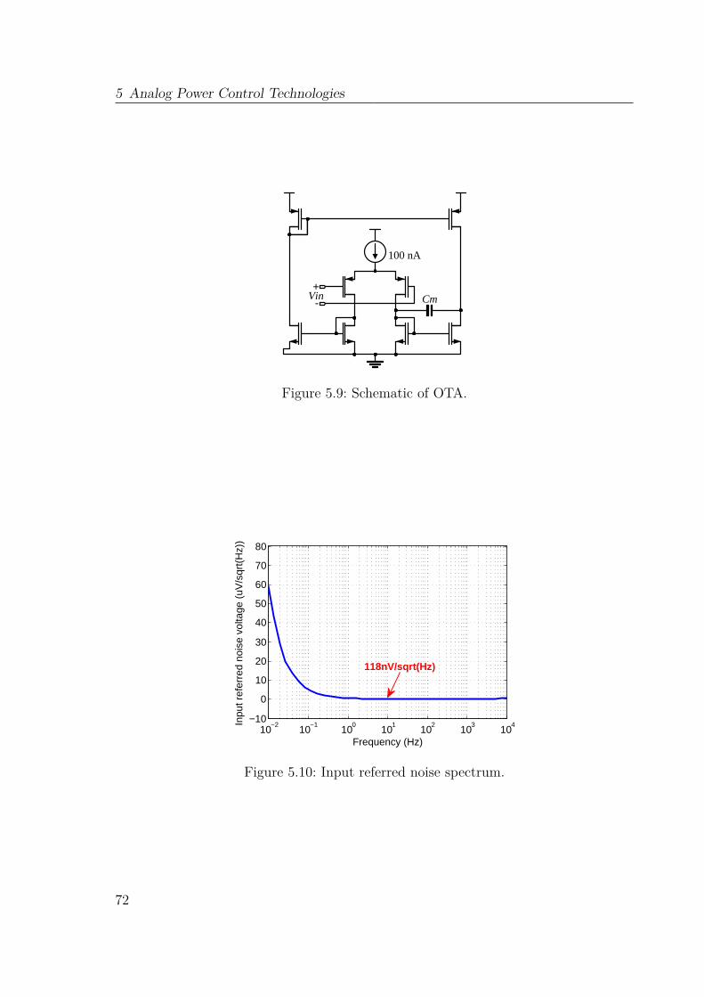
5 Analog Power Control Technologies
100 nA
Cm+
-Vin
Figure 5.9: Schematic of OTA.
10−2
10−1
100
101
102
103
104
−10
0
10
20
30
40
50
60
70
80
Frequency (Hz)
Inpu
t ref
erre
d no
ise
volta
ge (
uV/s
qrt(
Hz)
)
118nV/sqrt(Hz)
Figure 5.10: Input referred noise spectrum.
72
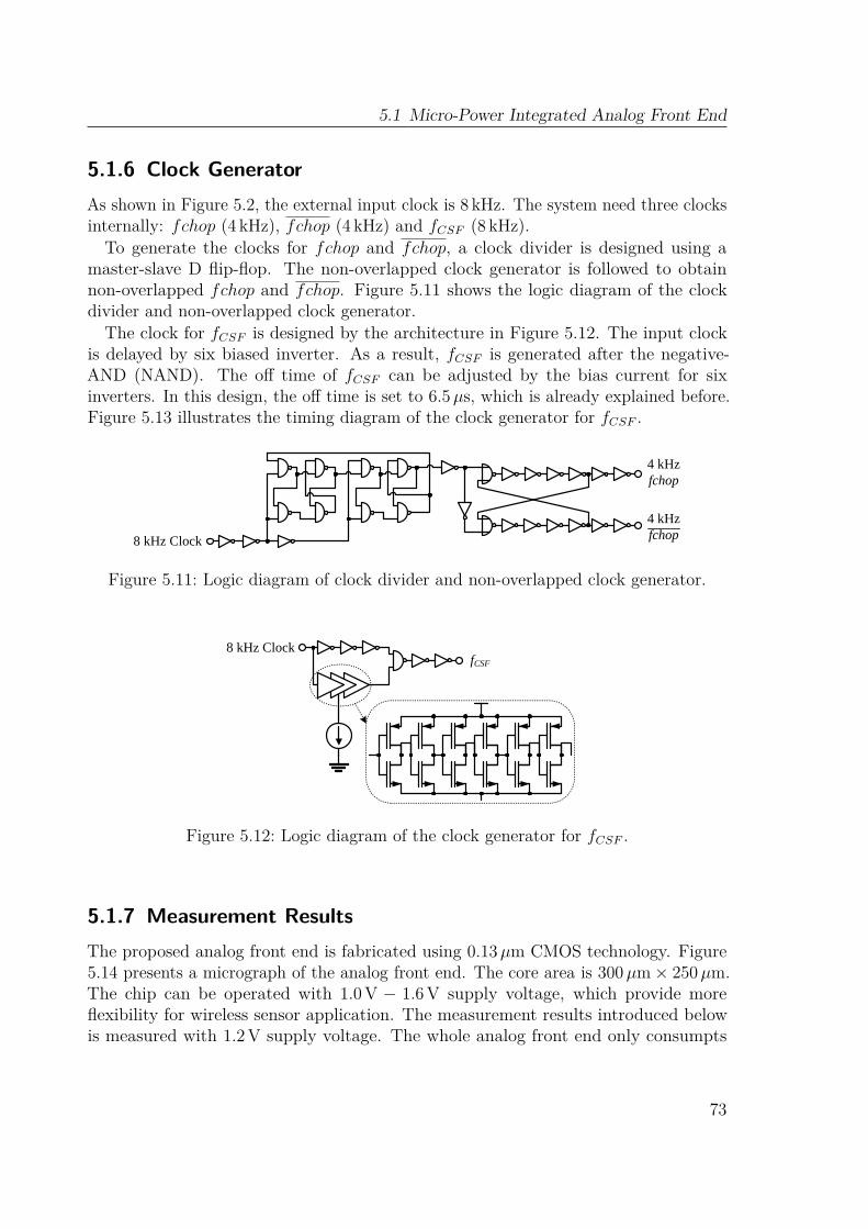
5.1 Micro-Power Integrated Analog Front End
5.1.6 Clock GeneratorAs shown in Figure 5.2, the external input clock is 8 kHz. The system need three clocksinternally: fchop (4 kHz), fchop (4 kHz) and fCSF (8 kHz).To generate the clocks for fchop and fchop, a clock divider is designed using a
master-slave D flip-flop. The non-overlapped clock generator is followed to obtainnon-overlapped fchop and fchop. Figure 5.11 shows the logic diagram of the clockdivider and non-overlapped clock generator.The clock for fCSF is designed by the architecture in Figure 5.12. The input clock
is delayed by six biased inverter. As a result, fCSF is generated after the negative-AND (NAND). The off time of fCSF can be adjusted by the bias current for sixinverters. In this design, the off time is set to 6.5µs, which is already explained before.Figure 5.13 illustrates the timing diagram of the clock generator for fCSF .
8 kHz Clock
4 kHzfchop
4 kHzfchop
Figure 5.11: Logic diagram of clock divider and non-overlapped clock generator.
8 kHz ClockfCSF
Figure 5.12: Logic diagram of the clock generator for fCSF .
5.1.7 Measurement ResultsThe proposed analog front end is fabricated using 0.13µm CMOS technology. Figure5.14 presents a micrograph of the analog front end. The core area is 300µm× 250µm.The chip can be operated with 1.0 V − 1.6 V supply voltage, which provide moreflexibility for wireless sensor application. The measurement results introduced belowis measured with 1.2V supply voltage. The whole analog front end only consumpts
73

5 Analog Power Control Technologies
Time (ms)4.5 4.6 4.7 4.8 4.9 5
Vol
tage
(V
)
0
1.20
1.20
1.2
Figure 5.13: Timing diagram of clock generator for fCSF . From the top: input clock;output of six biased inverters; fCSF .
Figure 5.14: The micrograph of the analog front end implemented in 0.13µm CMOSprocess.
74
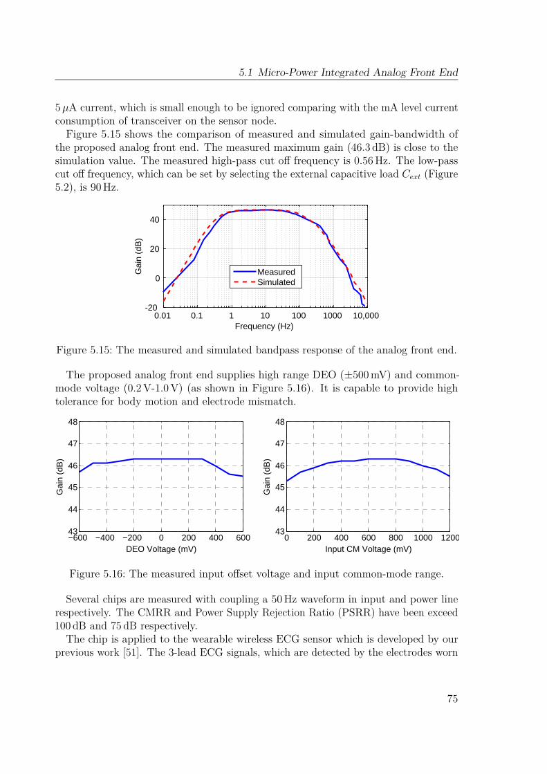
5.1 Micro-Power Integrated Analog Front End
5µA current, which is small enough to be ignored comparing with the mA level currentconsumption of transceiver on the sensor node.Figure 5.15 shows the comparison of measured and simulated gain-bandwidth of
the proposed analog front end. The measured maximum gain (46.3 dB) is close to thesimulation value. The measured high-pass cut off frequency is 0.56Hz. The low-passcut off frequency, which can be set by selecting the external capacitive load Cext (Figure5.2), is 90Hz.
Frequency (Hz)0.01 0.1 1 10 100 1000 10,000
Gai
n (d
B)
-20
0
20
40
MeasuredSimulated
Figure 5.15: The measured and simulated bandpass response of the analog front end.
The proposed analog front end supplies high range DEO (±500mV) and common-mode voltage (0.2V-1.0V) (as shown in Figure 5.16). It is capable to provide hightolerance for body motion and electrode mismatch.
−600 −400 −200 0 200 400 60043
44
45
46
47
48
DEO Voltage (mV)
Gai
n (d
B)
0 200 400 600 800 1000 120043
44
45
46
47
48
Input CM Voltage (mV)
Gai
n (d
B)
Figure 5.16: The measured input offset voltage and input common-mode range.
Several chips are measured with coupling a 50Hz waveform in input and power linerespectively. The CMRR and Power Supply Rejection Ratio (PSRR) have been exceed100 dB and 75 dB respectively.
The chip is applied to the wearable wireless ECG sensor which is developed by ourprevious work [51]. The 3-lead ECG signals, which are detected by the electrodes worn
75
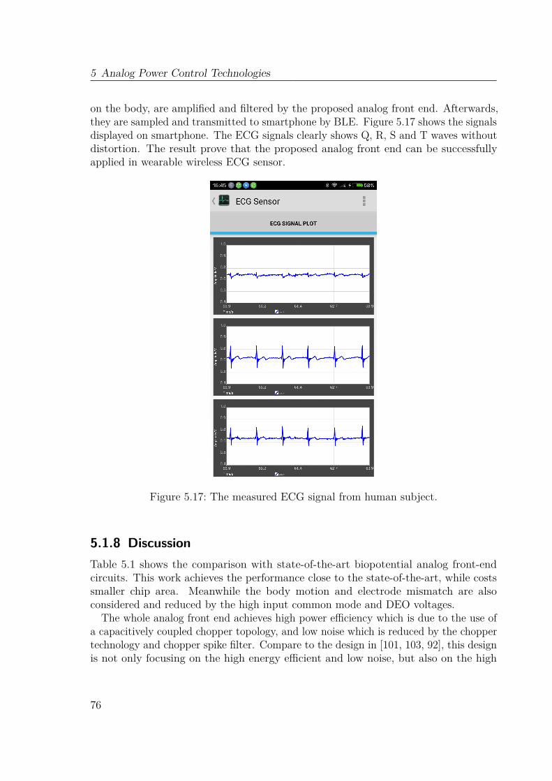
5 Analog Power Control Technologies
on the body, are amplified and filtered by the proposed analog front end. Afterwards,they are sampled and transmitted to smartphone by BLE. Figure 5.17 shows the signalsdisplayed on smartphone. The ECG signals clearly shows Q, R, S and T waves withoutdistortion. The result prove that the proposed analog front end can be successfullyapplied in wearable wireless ECG sensor.
Figure 5.17: The measured ECG signal from human subject.
5.1.8 DiscussionTable 5.1 shows the comparison with state-of-the-art biopotential analog front-endcircuits. This work achieves the performance close to the state-of-the-art, while costssmaller chip area. Meanwhile the body motion and electrode mismatch are alsoconsidered and reduced by the high input common mode and DEO voltages.
The whole analog front end achieves high power efficiency which is due to the use ofa capacitively coupled chopper topology, and low noise which is reduced by the choppertechnology and chopper spike filter. Compare to the design in [101, 103, 92], this designis not only focusing on the high energy efficient and low noise, but also on the high
76
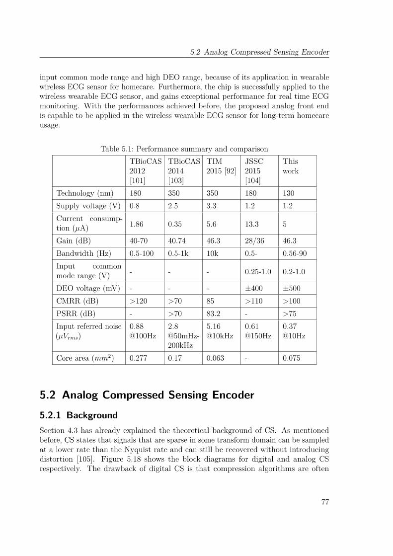
5.2 Analog Compressed Sensing Encoder
input common mode range and high DEO range, because of its application in wearablewireless ECG sensor for homecare. Furthermore, the chip is successfully applied to thewireless wearable ECG sensor, and gains exceptional performance for real time ECGmonitoring. With the performances achieved before, the proposed analog front endis capable to be applied in the wireless wearable ECG sensor for long-term homecareusage.
Table 5.1: Performance summary and comparisonTBioCAS2012[101]
TBioCAS2014[103]
TIM2015 [92]
JSSC2015[104]
Thiswork
Technology (nm) 180 350 350 180 130Supply voltage (V) 0.8 2.5 3.3 1.2 1.2Current consump-tion (µA) 1.86 0.35 5.6 13.3 5
Gain (dB) 40-70 40.74 46.3 28/36 46.3Bandwidth (Hz) 0.5-100 0.5-1k 10k 0.5- 0.56-90Input commonmode range (V) - - - 0.25-1.0 0.2-1.0
DEO voltage (mV) - - - ±400 ±500CMRR (dB) >120 >70 85 >110 >100PSRR (dB) - >70 83.2 - >75Input referred noise(µVrms)
0.88@100Hz
2.8@50mHz-200kHz
5.16@10kHz
0.61@150Hz
0.37@10Hz
Core area (mm2) 0.277 0.17 0.063 - 0.075
5.2 Analog Compressed Sensing Encoder5.2.1 BackgroundSection 4.3 has already explained the theoretical background of CS. As mentionedbefore, CS states that signals that are sparse in some transform domain can be sampledat a lower rate than the Nyquist rate and can still be recovered without introducingdistortion [105]. Figure 5.18 shows the block diagrams for digital and analog CSrespectively. The drawback of digital CS is that compression algorithms are often
77
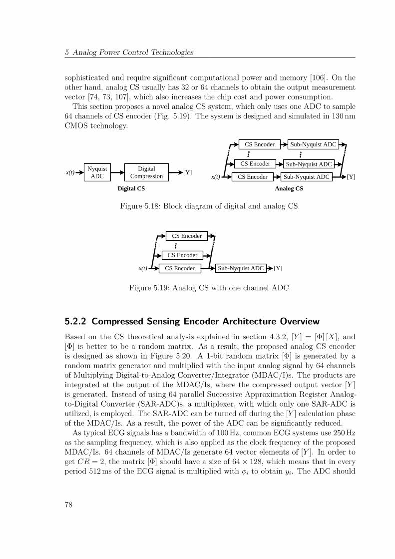
5 Analog Power Control Technologies
sophisticated and require significant computational power and memory [106]. On theother hand, analog CS usually has 32 or 64 channels to obtain the output measurementvector [74, 73, 107], which also increases the chip cost and power consumption.
This section proposes a novel analog CS system, which only uses one ADC to sample64 channels of CS encoder (Fig. 5.19). The system is designed and simulated in 130 nmCMOS technology.
x(t) [Y]Sub-Nyquist ADCCS Encoder
Sub-Nyquist ADCCS Encoder
Sub-Nyquist ADCCS Encoder
NyquistADC
x(t)Digital
Compression[Y]
Digital CS Analog CS
Figure 5.18: Block diagram of digital and analog CS.
x(t) Sub-Nyquist ADCCS Encoder
CS Encoder
CS Encoder
[Y]
Figure 5.19: Analog CS with one channel ADC.
5.2.2 Compressed Sensing Encoder Architecture OverviewBased on the CS theoretical analysis explained in section 4.3.2, [Y ] = [Φ] [X], and[Φ] is better to be a random matrix. As a result, the proposed analog CS encoderis designed as shown in Figure 5.20. A 1-bit random matrix [Φ] is generated by arandom matrix generator and multiplied with the input analog signal by 64 channelsof Multiplying Digital-to-Analog Converter/Integrator (MDAC/I)s. The products areintegrated at the output of the MDAC/Is, where the compressed output vector [Y ]is generated. Instead of using 64 parallel Successive Approximation Register Analog-to-Digital Converter (SAR-ADC)s, a multiplexer, with which only one SAR-ADC isutilized, is employed. The SAR-ADC can be turned off during the [Y ] calculation phaseof the MDAC/Is. As a result, the power of the ADC can be significantly reduced.
As typical ECG signals has a bandwidth of 100Hz, common ECG systems use 250Hzas the sampling frequency, which is also applied as the clock frequency of the proposedMDAC/Is. 64 channels of MDAC/Is generate 64 vector elements of [Y ]. In order toget CR = 2, the matrix [Φ] should have a size of 64× 128, which means that in everyperiod 512ms of the ECG signal is multiplied with φi to obtain yi. The ADC should
78
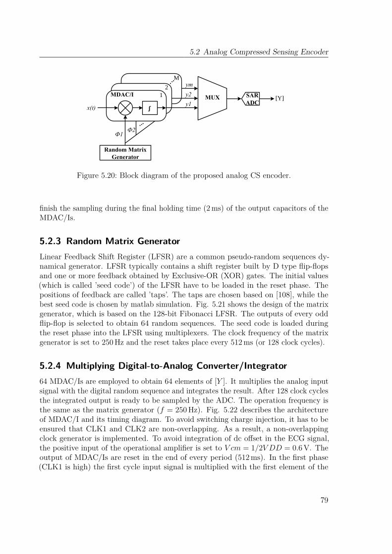
5.2 Analog Compressed Sensing Encoder
x(t)y1
Random Matrix Generator
y2
ym
Ф1Ф2
...
SARADC
MUX [Y]
ʃ
.
MDAC/I 12
. .M
Figure 5.20: Block diagram of the proposed analog CS encoder.
finish the sampling during the final holding time (2ms) of the output capacitors of theMDAC/Is.
5.2.3 Random Matrix GeneratorLinear Feedback Shift Register (LFSR) are a common pseudo-random sequences dy-namical generator. LFSR typically contains a shift register built by D type flip-flopsand one or more feedback obtained by Exclusive-OR (XOR) gates. The initial values(which is called ’seed code’) of the LFSR have to be loaded in the reset phase. Thepositions of feedback are called ’taps’. The taps are chosen based on [108], while thebest seed code is chosen by matlab simulation. Fig. 5.21 shows the design of the matrixgenerator, which is based on the 128-bit Fibonacci LFSR. The outputs of every oddflip-flop is selected to obtain 64 random sequences. The seed code is loaded duringthe reset phase into the LFSR using multiplexers. The clock frequency of the matrixgenerator is set to 250Hz and the reset takes place every 512ms (or 128 clock cycles).
5.2.4 Multiplying Digital-to-Analog Converter/Integrator64 MDAC/Is are employed to obtain 64 elements of [Y ]. It multiplies the analog inputsignal with the digital random sequence and integrates the result. After 128 clock cyclesthe integrated output is ready to be sampled by the ADC. The operation frequency isthe same as the matrix generator (f = 250 Hz). Fig. 5.22 describes the architectureof MDAC/I and its timing diagram. To avoid switching charge injection, it has to beensured that CLK1 and CLK2 are non-overlapping. As a result, a non-overlappingclock generator is implemented. To avoid integration of dc offset in the ECG signal,the positive input of the operational amplifier is set to V cm = 1/2V DD = 0.6 V. Theoutput of MDAC/Is are reset in the end of every period (512ms). In the first phase(CLK1 is high) the first cycle input signal is multiplied with the first element of the
79
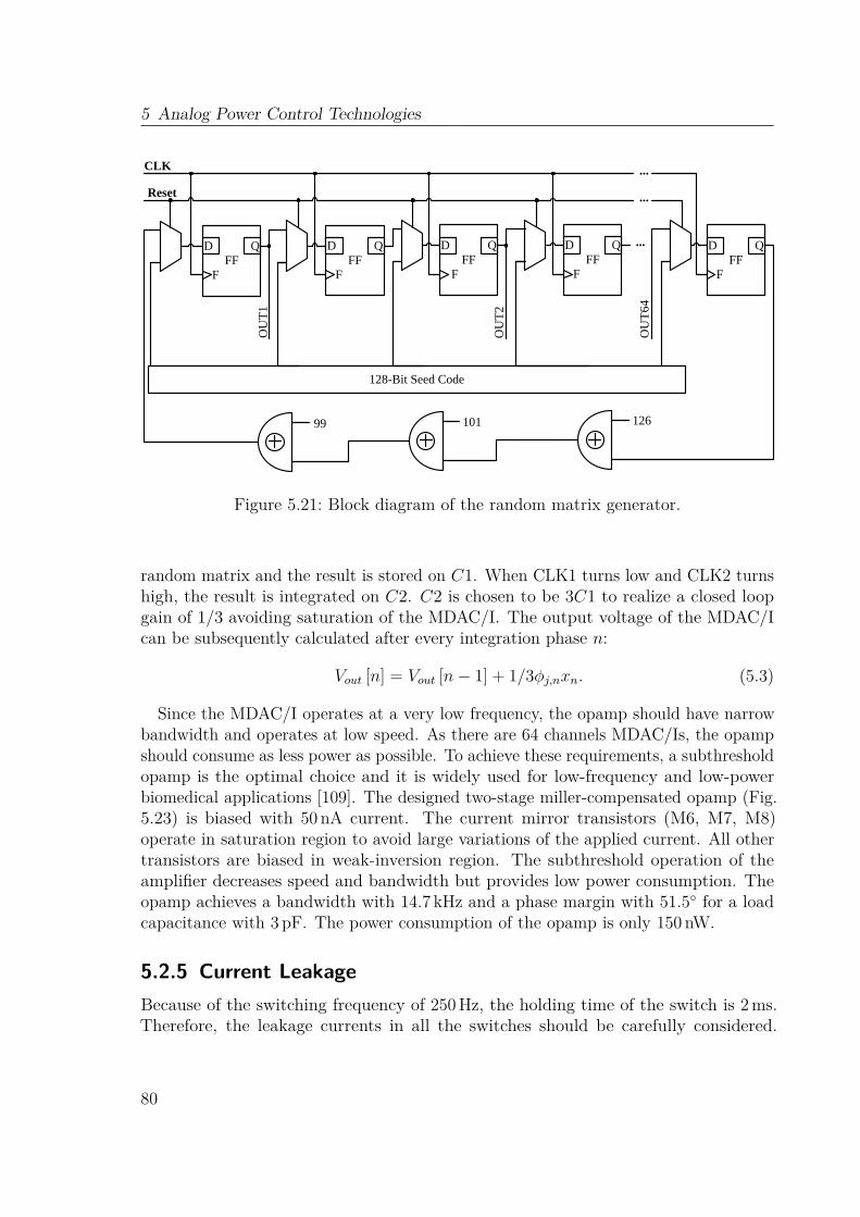
5 Analog Power Control Technologies
FFD Q
F
Reset
FFD Q
FFF
D Q
FFF
D Q
FO
UT1
OU
T2
...
...
FFD Q
F
OU
T64
128-Bit Seed Code
12610199
CLK ...
Figure 5.21: Block diagram of the random matrix generator.
random matrix and the result is stored on C1. When CLK1 turns low and CLK2 turnshigh, the result is integrated on C2. C2 is chosen to be 3C1 to realize a closed loopgain of 1/3 avoiding saturation of the MDAC/I. The output voltage of the MDAC/Ican be subsequently calculated after every integration phase n:
Vout [n] = Vout [n− 1] + 1/3φj,nxn. (5.3)
Since the MDAC/I operates at a very low frequency, the opamp should have narrowbandwidth and operates at low speed. As there are 64 channels MDAC/Is, the opampshould consume as less power as possible. To achieve these requirements, a subthresholdopamp is the optimal choice and it is widely used for low-frequency and low-powerbiomedical applications [109]. The designed two-stage miller-compensated opamp (Fig.5.23) is biased with 50 nA current. The current mirror transistors (M6, M7, M8)operate in saturation region to avoid large variations of the applied current. All othertransistors are biased in weak-inversion region. The subthreshold operation of theamplifier decreases speed and bandwidth but provides low power consumption. Theopamp achieves a bandwidth with 14.7 kHz and a phase margin with 51.5 for a loadcapacitance with 3 pF. The power consumption of the opamp is only 150 nW.
5.2.5 Current LeakageBecause of the switching frequency of 250Hz, the holding time of the switch is 2ms.Therefore, the leakage currents in all the switches should be carefully considered.
80
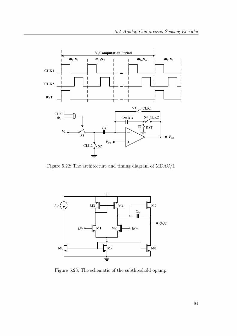
5.2 Analog Compressed Sensing Encoder
CLK1
CLK2
RST
...
...
...
Φ11X1 Φ12X2 Φ1nXn Φ21X1
Y1 Computation Period
C2=3C1
C1 RST
CLK1
CLK2
Vin
Vout
CLK2CLK1Φij
Vcm
S1
S2
S3
S4
S5
Figure 5.22: The architecture and timing diagram of MDAC/I.
Iref
IN- IN+OUT
CM
M1 M2
M3 M4 M5
M6 M7 M8
Figure 5.23: The schematic of the subthreshold opamp.
81

5 Analog Power Control Technologies
There are two main leakage sources in a Metal–Oxide–Semiconductor (MOS) switch:subthreshold conduction (or drain-source leakage current) and drain-to-bulk diodeleakage. As shown in Figure 5.22, the storage performance is appreciably depended onthe leakages of the three switches (S3, S4, S5) surrounding the storage capacitor C2.Both subthreshold and drain-to-bulk diode leakages present in all of these switches.
Subthreshold conduction
Subthreshold current in an NMOS transistor is accurately modeled by the followingrelation (valid for VGS << VTS) [110, 111]
IDS = IOSW
Leκ(VGS−VT S)/Vt(1− e−VDS/Vt), (5.4)
where IOS is a process-dependent current scaling constant, Vt is the thermal voltage,VTS is the transistor’s threshold voltage, W/L is its width over length ratio, and κ is aparameter that depends on the applied source-to-bulk voltage and has a magnitudeless than one. The threshold voltage VTS can be modulated through the body effect,and is given by
VTS = VTO + γ(√φo + VSB −
√φo). (5.5)
VTS is a function of the nominal process-defined threshold voltage VTO, the appliedsource-to-bulk voltage VSB, and γ and φo, which are process-dependent parameters[110]. As a result, IDS is dominated by VGS, VSB and VDS.
Drain-to-Bulk Diode Leakage
The first order model of drain-to-bulk diode leakage in an NMOS transistor is given by
IDB = −IS + [e−VDB
Vt − 1], (5.6)
where IDB is the diode current, VDB is the applied voltage, and Is is the diode saturationcurrent and is a constant proportional to a linear combination of its junction area andperimeter [110]. VDB is the main factor to dominate the value of IDB.
Leakage Suppression: Analog T-Switch
According to the equation (5.4), IDS can be easily reduced by decreasing VGS. When anormal NMOS switch is off (Figure 5.24), VGS = 0. But if the source voltage of theswitch is given with V DD/2 (as shown in Figure 5.24), VGS = −V DD/2 during OFFphase. Then the transistor’s operating region moves toward the deep inside cutoff regionto reduce the leakage current. Meanwhile VSB is increased, which reduces IDS further.However, when the drain voltage of the switch is from V SS to V DD/2, accordingto equation (5.4), the inversed VDS will also cause leakage. In Figure 5.25, a PMOS
82
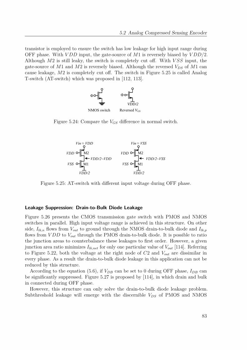
5.2 Analog Compressed Sensing Encoder
transistor is employed to ensure the switch has low leakage for high input range duringOFF phase. With V DD input, the gate-source of M1 is reversely biased by V DD/2.Although M2 is still leaky, the switch is completely cut off. With V SS input, thegate-source of M1 and M2 is reversely biased. Although the reversed VDS of M1 cancause leakage, M2 is completely cut off. The switch in Figure 5.25 is called AnalogT-switch (AT-switch) which was proposed in [112, 113].
Ф
VDD/2
Ф
NMOS switch Reversed VGS
Figure 5.24: Compare the VGS difference in normal switch.
VDD/2
Vin ≈ VDD
VSS
VDD
M1
M2
VDD/2~VDD
VDD/2
Vin ≈ VSS
VSS
VDD
M1
M2
VDD/2~VSS
Figure 5.25: AT-switch with different input voltage during OFF phase.
Leakage Suppression: Drain-to-Bulk Diode Leakage
Figure 5.26 presents the CMOS transmission gate switch with PMOS and NMOSswitches in parallel. High input voltage range is achieved in this structure. On otherside, Ilk,n flows from Vout to ground through the NMOS drain-to-bulk diode and Ilk,pflows from V DD to Vout through the PMOS drain-to-bulk diode. It is possible to ratiothe junction areas to counterbalance these leakages to first order. However, a givenjunction area ratio minimizes Ilk,net for only one particular value of Vout [114]. Referringto Figure 5.22, both the voltage at the right node of C2 and Vout are dissimilar inevery phase. As a result the drain-to-bulk diode leakage in this application can not bereduced by this structure.
According to the equation (5.6), if VDB can be set to 0 during OFF phase, IDB canbe significantly suppressed. Figure 5.27 is proposed by [114], in which drain and bulkin connected during OFF phase.However, this structure can only solve the drain-to-bulk diode leakage problem.
Subthreshold leakage will emerge with the discernible VDS of PMOS and NMOS
83

5 Analog Power Control Technologies
Ilk,n
Ilk,p
Ilk,net ~ 0Vin Vout
Ф
Ф
Figure 5.26: CMOS transmission gate switch.
Vref
Vin VoutM1 M2
M3
Ф
Ф Ф
Figure 5.27: Low leakage switch with input voltage settled.
(equation (5.4)). Consequently, it can only be applied to the switches with same andstatic drain and source voltage (i.e. S3 in Figure 5.22). Because the input voltage isintegrated and stored at the right node of C2, the potential at this node is varied inevery period. With the design in Figure 5.27, subthreshold leakage in S4 and S5 cannot be suppressed.
Leakage Suppression: Subthreshold Leakage Caused by VDSAs mentioned before, VDS is also an important factor for leakage. Figure 5.28 charac-terizes the factor (1− e−VDS/Vt), which is included in the NMOS model of IDS, versusVDS/Vt. The subthreshold leakage current is substantially increased with reversed VDS.The minimum subthreshold leakage current can be achieved if VDS is zero.
In order to equal the drain and source voltage during OFF phase, this thesis proposeda switch design which can suppress the subthreshold leakage by making VDS = 0, (asshown in Figure 5.29). Source, bulk and drain are adjusted to the same voltage duringOFF phase, which makes sure that both drain-to-bulk diode leakage and subthresholdleakage are suppressed.
MDAC/I with Leakage Suppression Switches
In order to reduce all of the leakages, the switches in MDAC/I are designed as shownin Fig. 5.30. In order to get high input range, the CMOS transmission switches areemployed to the switch S1 and S4. An AT-switch is employed in S2 to completelycut off the switch with any input voltage during OFF phase. The structure in Figure
84
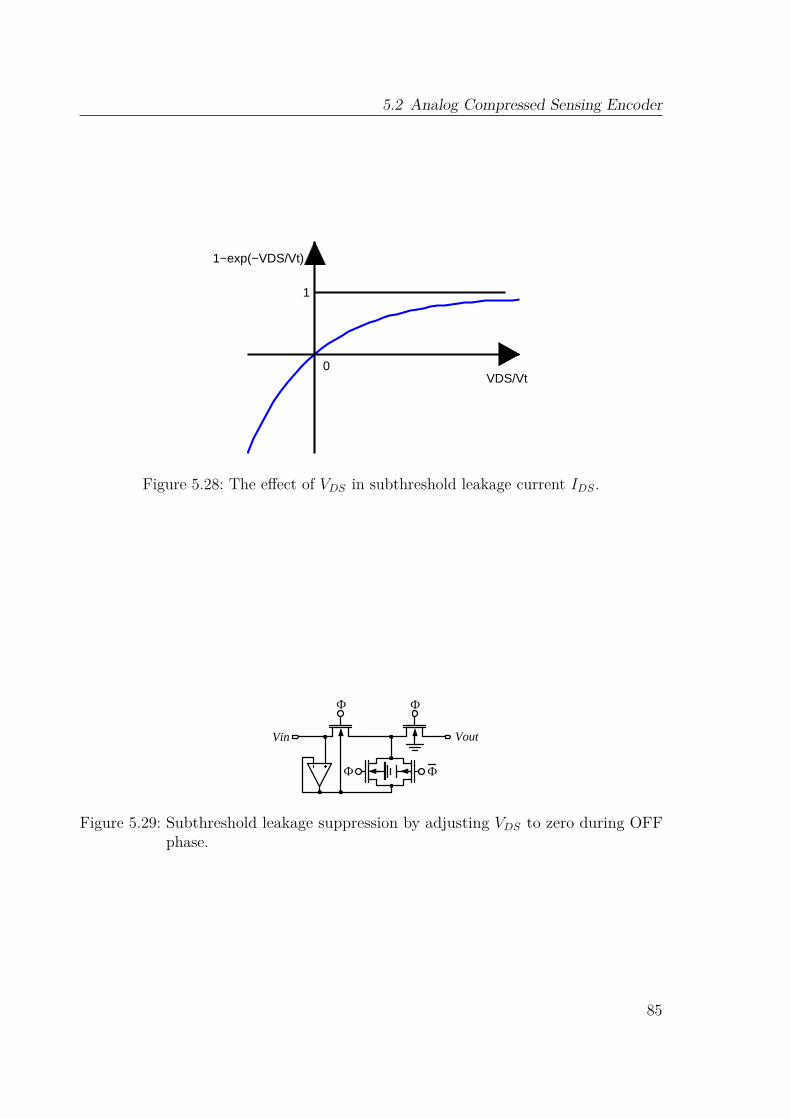
5.2 Analog Compressed Sensing Encoder
1
VDS/Vt0
1−exp(−VDS/Vt)
Figure 5.28: The effect of VDS in subthreshold leakage current IDS.
Ф Ф
ФФ
Vin Vout
Figure 5.29: Subthreshold leakage suppression by adjusting VDS to zero during OFFphase.
85

5 Analog Power Control Technologies
5.27 is applied to S3 to reduce the drain-to-bulk and subthreshold leakage. S4 and S5employ the switch in Figure 5.29 to suppress the subthreshold leakage caused by VDS.
Vref
M1 M2
M3
C2
C1
CLK1
CLK1
CLK2
Vin
Vout
S4S5
S3
S2S1
CLK1
CLK2
VrefVref
CLK1
CLK1
Vref
RST
RST
RST
RST
V1
CLK2CLK2CLK2CLK2
CL
K2
CL
K2
CL
K2
CL
K2
V2
V2
V2
V1 V2
Figure 5.30: The architecture of MDAC/I with leakage suppression switches.
5.2.6 Sub-Nyquist ADCThe clock frequency of the proposed SAR-ADC is 2MHz resulting in a samplingrate of 166.6 kS/s. Every conversion process costs 6µs including the sampling time1µs. Therefore, 64 channels can be sampled in 384µs. As typically 8 EffectiveNumber of Bits (ENOB) is required in biomedical systems, a 9-bit Digital-to-AnalogConverter (DAC) is implemented taking possible non-linearity into account. A separatedhold stage is not required because the voltages generated by the MDAC/Is are alreadyconstant. Consequently, the design employs only a one-stage voltage follower biasedby 20µA to be able to load the DAC capacitors during 1µs sampling time. A systemoverview of the implemented SAR-ADC is shown in Fig. 5.31.Since comparator offset is a well known problem for CS system [115], this design
utilizes Output Offset Storage (OOS) to cancel the comparator offset. Generally, OOSconsists of preamplifier, offset storage capacitors and a latch (as shown in Figure 5.32).
86
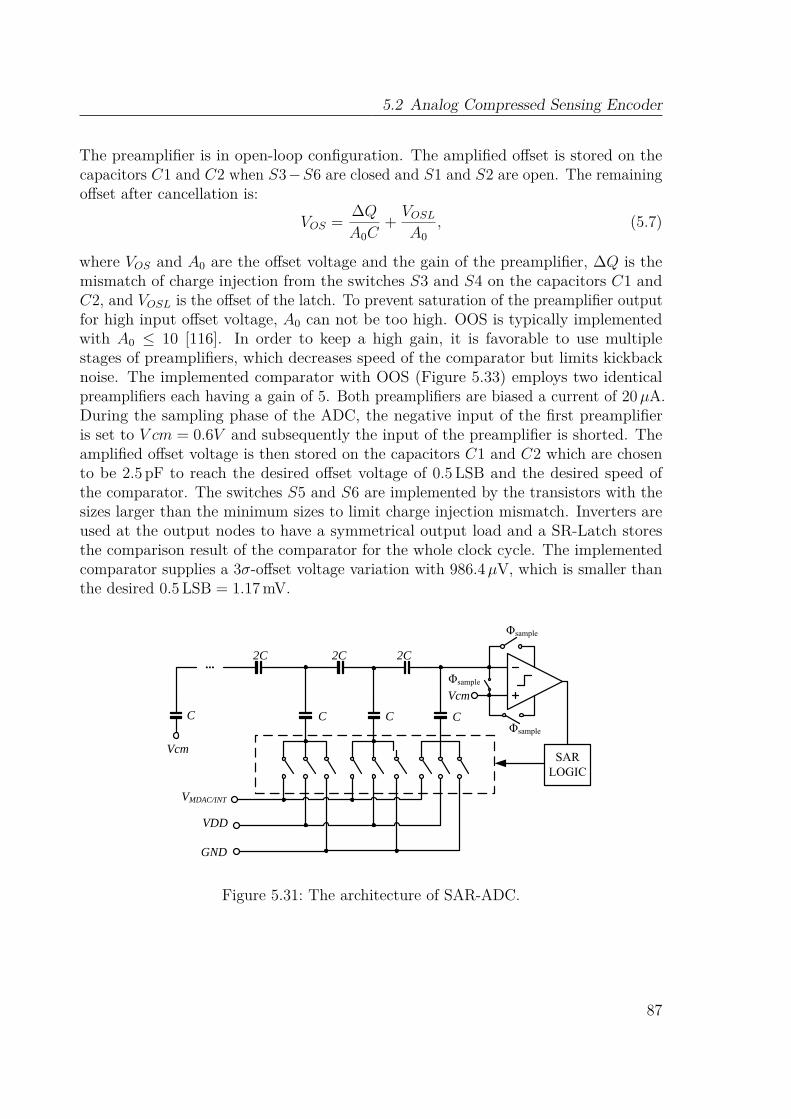
5.2 Analog Compressed Sensing Encoder
The preamplifier is in open-loop configuration. The amplified offset is stored on thecapacitors C1 and C2 when S3−S6 are closed and S1 and S2 are open. The remainingoffset after cancellation is:
VOS = ∆QA0C
+ VOSLA0
, (5.7)
where VOS and A0 are the offset voltage and the gain of the preamplifier, ∆Q is themismatch of charge injection from the switches S3 and S4 on the capacitors C1 andC2, and VOSL is the offset of the latch. To prevent saturation of the preamplifier outputfor high input offset voltage, A0 can not be too high. OOS is typically implementedwith A0 ≤ 10 [116]. In order to keep a high gain, it is favorable to use multiplestages of preamplifiers, which decreases speed of the comparator but limits kickbacknoise. The implemented comparator with OOS (Figure 5.33) employs two identicalpreamplifiers each having a gain of 5. Both preamplifiers are biased a current of 20µA.During the sampling phase of the ADC, the negative input of the first preamplifieris set to V cm = 0.6V and subsequently the input of the preamplifier is shorted. Theamplified offset voltage is then stored on the capacitors C1 and C2 which are chosento be 2.5 pF to reach the desired offset voltage of 0.5 LSB and the desired speed ofthe comparator. The switches S5 and S6 are implemented by the transistors with thesizes larger than the minimum sizes to limit charge injection mismatch. Inverters areused at the output nodes to have a symmetrical output load and a SR-Latch storesthe comparison result of the comparator for the whole clock cycle. The implementedcomparator supplies a 3σ-offset voltage variation with 986.4µV, which is smaller thanthe desired 0.5 LSB = 1.17 mV.
2C 2C 2C
C C C
...
C
VMDAC/INT
VDD
GND
VcmSAR
LOGIC
Φsample
Φsample
Φsample
Vcm
Figure 5.31: The architecture of SAR-ADC.
87
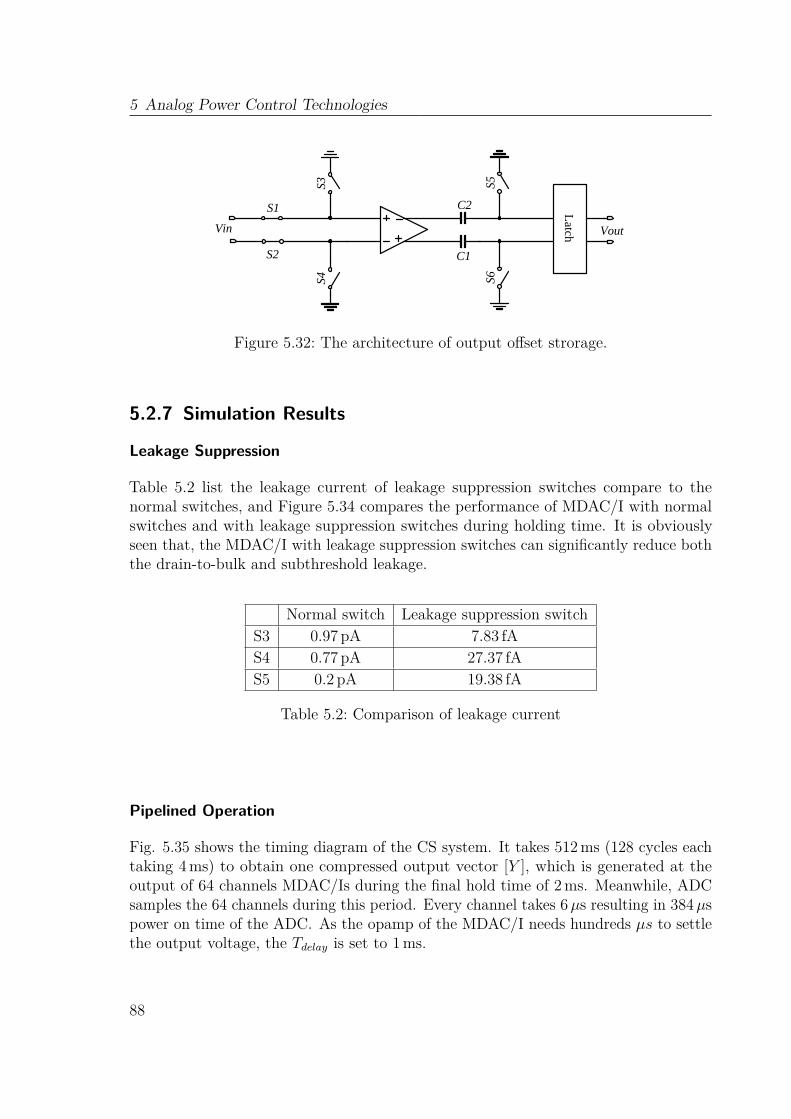
5 Analog Power Control Technologies
Latch VoutVin
S1
S2
S5S6
C1
C2
S3S4
Figure 5.32: The architecture of output offset strorage.
5.2.7 Simulation Results
Leakage Suppression
Table 5.2 list the leakage current of leakage suppression switches compare to thenormal switches, and Figure 5.34 compares the performance of MDAC/I with normalswitches and with leakage suppression switches during holding time. It is obviouslyseen that, the MDAC/I with leakage suppression switches can significantly reduce boththe drain-to-bulk and subthreshold leakage.
Normal switch Leakage suppression switchS3 0.97 pA 7.83 fAS4 0.77 pA 27.37 fAS5 0.2 pA 19.38 fA
Table 5.2: Comparison of leakage current
Pipelined Operation
Fig. 5.35 shows the timing diagram of the CS system. It takes 512ms (128 cycles eachtaking 4ms) to obtain one compressed output vector [Y ], which is generated at theoutput of 64 channels MDAC/Is during the final hold time of 2ms. Meanwhile, ADCsamples the 64 channels during this period. Every channel takes 6µs resulting in 384µspower on time of the ADC. As the opamp of the MDAC/I needs hundreds µs to settlethe output voltage, the Tdelay is set to 1ms.
88
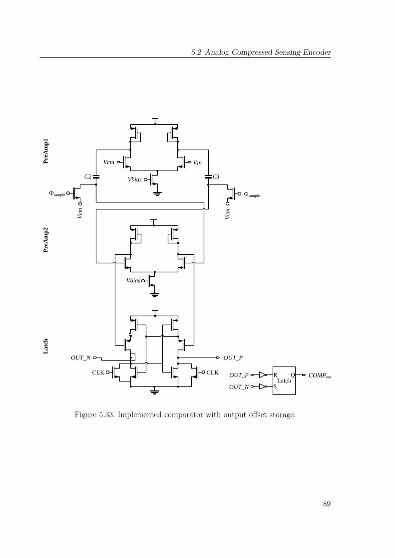
5.2 Analog Compressed Sensing Encoder
Vbias
Vbias
C1C2
VinVcm
Vcm
Фsample
Vcm
CLKCLK
Pre
Am
p1
Pre
Am
p2
Lat
ch
OUT_POUT_N
LatchR
S
QOUT_P
OUT_N
COMPout
Фsample
Figure 5.33: Implemented comparator with output offset storage.
89
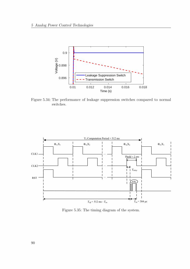
5 Analog Power Control Technologies
Time (s)0.01 0.012 0.014 0.016 0.018
Vol
tage
(V
)
0.896
0.898
0.9
Leakage Suppression SwitchTransmission Switch
Figure 5.34: The performance of leakage suppression switches compared to normalswitches.
CLK1
CLK2
RST
...
...
...
Φ11X1 Φ12X2 Φ1nXn Φ21X1
Y1 Computation Period = 512 ms
64x
Toff = 512 ms - Ton Ton = 384 μs
..
Tdelay
Thold = 2 ms
Figure 5.35: The timing diagram of the system.
90

5.2 Analog Compressed Sensing Encoder
Power Consumption
To determine the power consumption, the CS system is simulated for 2.56 s. Thedistribution of the average power consumption of the various components of the systemis shown in Fig. 5.36. The total average power consumption over 2.56 s equals 23.5µWand the largest amount of power is consumed by the 64 MDAC/Is. The ADC consumes81.1µW during the sampling phase and the largest amount of power is consumed bythe comparator since it uses two preamplifier stages each biased by 20µA.
Figure 5.36: The distribution of the power consumption.
Signal Reconstruction
Because [Φ] is non-square and non-invertible, original signal can not be obtained directlyfrom
[X]
= [Φ]−1 [Y ]. As described in section 4.3, optimization methodologies areneeded to first reconstruct [α], because [Y ] = [Φ] [Ψ] [α], while [α] is the correspondingsparse representation of [X] in the sparsifying basis [Ψ]. Then the reconstructed signalcan be obtain from
[X]
= [Ψ] [α]. According to the description and simulation insection 4.3, the best [Ψ] for ECG signals is built by the 3-level decomposed orthogonalDaubechies wavelets (db4) transform matrix. In section 4.3, different optimizationmethodologies were also simulated, and BPDN are selected as the best reconstructionalgorithm.As a result, the same [Ψ] and BPDN are applied to reconstruct the ECG signals
on matlab from the measurement matrix [Y ] which is obtained from the proposedanalog CS encoder. Fig. 5.37 and Fig. 5.38 shows the reconstruction results withSNR = 48.3 dB and SNR = 28.1 dB for CR = 2 and CR = 4 respectively. Theaccuracy is mainly limited due to the quantization noise of ADC.
5.2.8 DiscussionTable 5.3 lists the comparison of the performances with CR = 2 in recent publishedworks. Obviously, this work has higher power efficiency and SNR than [117]. Analog CSencoder power model in [118] applied M channels of amplifiers before the mixer, which
91
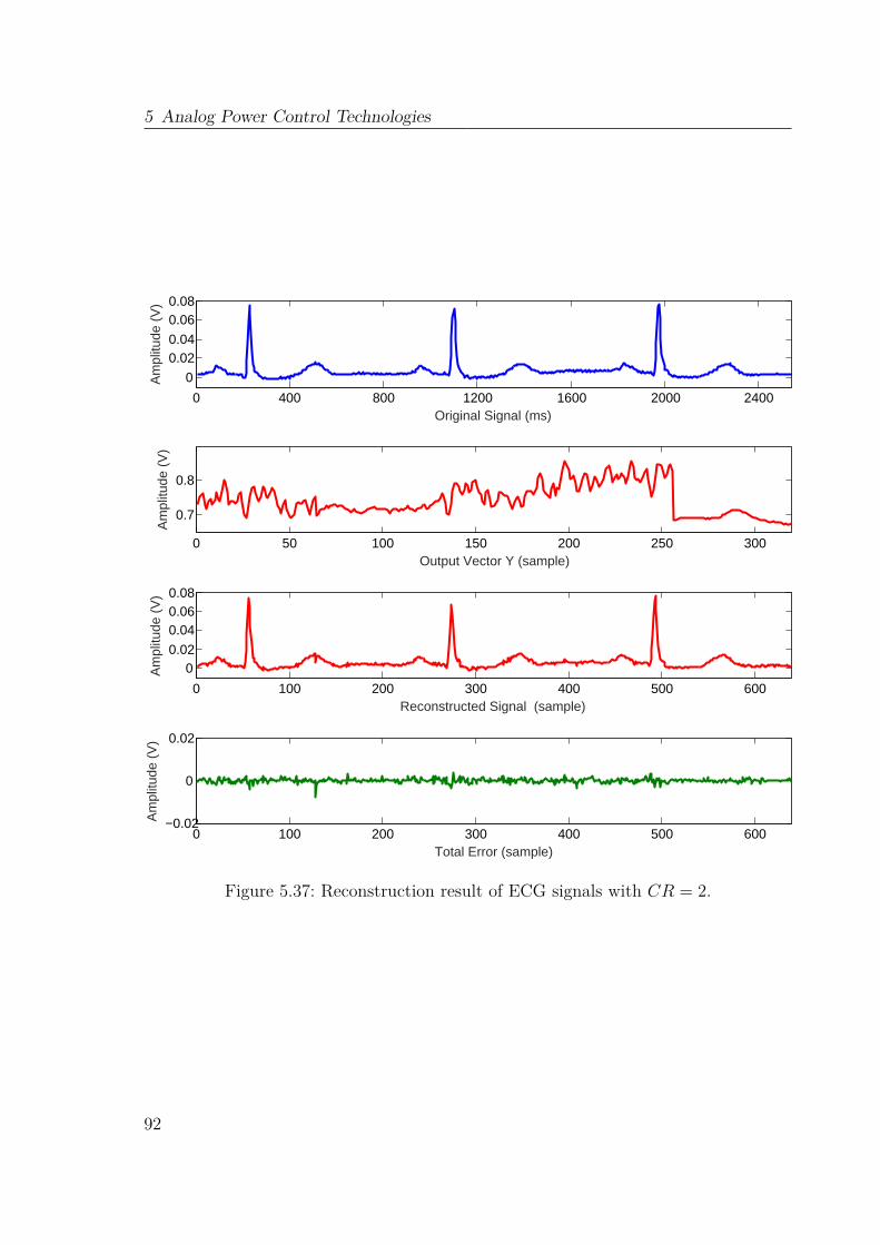
5 Analog Power Control Technologies
0 400 800 1200 1600 2000 2400
0
0.020.04
0.060.08
Original Signal (ms)
Am
plitu
de (
V)
0 50 100 150 200 250 300
0.7
0.8
Output Vector Y (sample)
Am
plitu
de (
V)
0 100 200 300 400 500 600
00.02
0.040.060.08
Reconstructed Signal (sample)
Am
plitu
de (
V)
0 100 200 300 400 500 600−0.02
0
0.02
Total Error (sample)
Am
plitu
de (
V)
Figure 5.37: Reconstruction result of ECG signals with CR = 2.
92

5.2 Analog Compressed Sensing Encoder
0 400 800 1200 1600 2000 2400
0
0.020.04
0.060.08
Original Signal (ms)
Am
plitu
de (
V)
0 20 40 60 80 100 120 140 160
0.7
0.8
Output Vector Y (sample)
Am
plitu
de (
V)
0 100 200 300 400 500 600
00.02
0.040.060.08
Reconstructed Signal (sample)
Am
plitu
de (
V)
0 100 200 300 400 500 600−0.02
0
0.02
Total Error (sample)
Am
plitu
de (
V)
Figure 5.38: Reconstruction result of ECG signals with CR = 4.
93
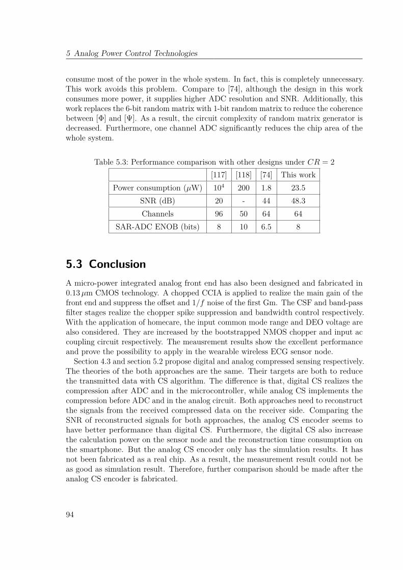
5 Analog Power Control Technologies
consume most of the power in the whole system. In fact, this is completely unnecessary.This work avoids this problem. Compare to [74], although the design in this workconsumes more power, it supplies higher ADC resolution and SNR. Additionally, thiswork replaces the 6-bit random matrix with 1-bit random matrix to reduce the coherencebetween [Φ] and [Ψ]. As a result, the circuit complexity of random matrix generator isdecreased. Furthermore, one channel ADC significantly reduces the chip area of thewhole system.
Table 5.3: Performance comparison with other designs under CR = 2[117] [118] [74] This work
Power consumption (µW) 104 200 1.8 23.5SNR (dB) 20 - 44 48.3Channels 96 50 64 64
SAR-ADC ENOB (bits) 8 10 6.5 8
5.3 ConclusionA micro-power integrated analog front end has also been designed and fabricated in0.13µm CMOS technology. A chopped CCIA is applied to realize the main gain of thefront end and suppress the offset and 1/f noise of the first Gm. The CSF and band-passfilter stages realize the chopper spike suppression and bandwidth control respectively.With the application of homecare, the input common mode range and DEO voltage arealso considered. They are increased by the bootstrapped NMOS chopper and input accoupling circuit respectively. The meausrement results show the excellent performanceand prove the possibility to apply in the wearable wireless ECG sensor node.
Section 4.3 and section 5.2 propose digital and analog compressed sensing respectively.The theories of the both approaches are the same. Their targets are both to reducethe transmitted data with CS algorithm. The difference is that, digital CS realizes thecompression after ADC and in the microcontroller, while analog CS implements thecompression before ADC and in the analog circuit. Both approaches need to reconstructthe signals from the received compressed data on the receiver side. Comparing theSNR of reconstructed signals for both approaches, the analog CS encoder seems tohave better performance than digital CS. Furthermore, the digital CS also increasethe calculation power on the sensor node and the reconstruction time consumption onthe smartphone. But the analog CS encoder only has the simulation results. It hasnot been fabricated as a real chip. As a result, the measurement result could not beas good as simulation result. Therefore, further comparison should be made after theanalog CS encoder is fabricated.
94
Chapter 6Conclusion and Outlooks
6.1 ConclusionThis thesis has proposed a novel wearable wireless ECG system. With the considerationof its application in long-term homecare, it strives to control the size and powerconsumption of the sensor node. The main targets of the design are to make the sensornode wearable without affecting the user’s daily life and extend the battery life. Asa result, this thesis devotes in three aspects to achieve these targets: new electrodeplacements design, wireless ECG system design with new electrode placements andmultiple power control technologies.With the purpose of wearable and compact sensor node design, the traditional
electrode placements, which need additional cables to connect the sensor and electrodes,are not suitable for today’s homecare application. Furthermore, the novel electrodeplacements proposed in recent researches either need additional effort to reconstruct12-lead ECG signals [9], or can only detect single lead signal [28]. As a result, anexperiment was designed to find the best limb electrode placements. With four limbelectrodes, three limb leads were detected. The experiment compared 14 differentplacements for limb electrodes. The detected signals of different placements werecompared with the standard lead system (Mason-Likar leads [50]). The correlationcoefficients between the standard and new placements were utilized as the index tojudge if the new placements had the close performance to the standard placements.
95
6 Conclusion and Outlooks
With this experiment, the best placements for four limb electrodes were selected.Analog front ends have always been the important part of ECG sensor node, because
they determine the quality of the signal. A low noise analog front end was designed inChapter 3. The design considered all the noises appeared in the ECG signals: dc offsetcaused by body motion, EMI coupled from the power line and electrode impedancemismatch. In order to minimize the components used in the analog front end, thenecessity of DRL circuit was evaluated. The result showed that high CMRR INAwas enough to reduce the EMI noise. Therefore, the DRL circuit was not necessaryanymore in this analog front end. The measurement result of the analog front endshowed excellent performance even under body motion, which was proved that it issufficient to be applied in the sensor node for homecare.
With the new electrode placements and the low noise analog front end, two wirelessECG systems were implemented. ZigBee and BLE are known as the two popular lowpower radio technologies for body area networks. They were respectively employed intotwo wireless ECG systems. Based on the new electrode placements, the sizes of bothsensor nodes were controlled in 5.5 cm× 2.5 cm, with which the sensor node was able tobe conveniently worn on the body without affecting user’s mobility. The ECG signalswere displayed on PC (ZigBee system) or smartphone (BLE system) in real time.
Because the sensor node is powered by battery, power consumption is an importantparameter in sensor node design. This thesis applied multiple power control technologiesin both analog and digital ways to extend the battery life. Firstly, adjustable powermode control was operated in the ZigBee and BLE sensor nodes. With adjustablepower mode control, the battery lives of ZigBee and BLE sensor nodes were morethan 52 hours and 55hours respectively, even under continuous communication withcoordinator or smartphone.Transmission is always the most energy consuming operation in a sensor node.
Because of the user’s daily movements, the link quality between transmitter andreceiver is not kept in static state, which means the Tx output power is not necessaryto be kept in the highest level. This thesis proposed dynamic transmission powercontrol in wireless ECG system with ZigBee to adjust the Tx output power dynamicallyaccording to the received RSSI. With defined adjustment rules, the RSSI was keptbetween −65 dBm and −75 dBm, which means the link quality was still kept stableunder dynamic transmission power control. The measurement results showed that 20%- 30% power was saved during regular movements.
To reduce the transmission power further, another technology was proposed in thisthesis: compressed sensing. Digital CS was firstly implemented in the wireless ECGsystem with BLE. The amount of the data to be transmitted was reduced by thismethod. With CR = 2, only half data needed to be transmitted. In result, thetransmission power was simultaneously decreased. The result showed that the ECGsignals were successfully reconstructed in real time with little distortion under CR = 2.Although the calculation on microcontroller also caused additional current consumption,the battery life was extended by 12 hours.
96
6.2 Outlooks
The previous three technologies (power mode control, dynamic transmission powercontrol and digital CS) were all implemented in digital part. This thesis also providedtechnologies to reduce the power consumption in analog circuit. Because the analogfront end introduced before was implemented in discrete circuit and it consumed 1mAcurrent in total, to reduce its power consumption, an integrated analog front end wasdesigned and implemented in 0.13µm CMOS technology. General noises (dc offsetcaused by body motion, EMI from power line and electrode mismatch) appeared inthe ECG signals were still considered in integrated circuit design. Additionally, theoffset and 1/f noise of the first Gm were also noted. Ac coupling circuit and chopperedCCIA were the solutions to reduce these noises. The CSF and band-pass filter werefollowed to suppress the chopper spikes and determine the main bandwidth of the frontend. The measurement results showed that, the chip only consumed 5µA current whichcan be totally ignored compared with the transmission current. Meanwhile, the chipsupplied 46.3 dB gain and 0.56Hz - 90Hz bandwidth. Furthermore, high range DEO(±500mV) and common-mode voltage (0.2V - 1.0V) were achieved to provide hightolerance for body motion and electrode mismatch.With the same theory as digital CS, analog CS was implemented by an integrated
encoder using 0.13µm CMOS technology. Instead of using 64 parallel SAR-ADCs, onlyone SAR-ADC was employed to sample the products during the final holding time ofthe output capacitors of the MDAC/Is. Because of ECG’s low frequency, the switchingfrequency of MDAC/I was only 250Hz which caused the long holding time (2ms) ofthe switches. Therefore, multiple leakage current suppression solutions were employedin this thesis. The simulation results revealed that the leakage current suppressionsolutions contributed a lot to suppress the leakage current. The power on time of theADC was only 384µs in every period (512ms), which saved plenty of power for ADC.The total average power consumption was 23.5µW. With the same reconstructionalgorithm as in digital CS, the signal was successfully reconstructed from the obtainedoutput vector.In general, this thesis provided various solutions to satisfy the long-term homecare
application. It not only redesigned the location of the electrodes to remove thecables between electrodes and sensor node, but also proposed multiple power controltechnologies to extend the battery life. With the proposed solutions and technologies,the wireless ECG system is sufficient to be applied in the homecare without decline inquality of user’s life.
6.2 Outlooks
Several improvements and innovative techniques for wireless ECG system are worthyto be investigated in the future.
97

6 Conclusion and Outlooks
6.2.1 Integrated Analog Front End with analog CS encoderAs mentioned before, although the simulation performance of analog CS encoder isbetter than the digital CS, the encoder was not fabricated. In addition, the analogfront end and the analog CS can be combined together and integrated on the samechip. Therefore, the new analog front end including the analog CS encoder need tobe implemented and fabricated. The possible structure of the new analog front end isshown in Figure 6.1. According to the measurement result in section 5.1, the CMRRof the analog front end needs to be improved. As a result, more attentions on CMRRshould be payed in the new design. Furthermore, the simulation result in section 5.2.7shows that, most of the power in analog CS encoder is consumed by the 64 channelsMDAC/I. Thence, lower power opamp for MDAC/I need to be designed. During themeasurement, the power efficiency of the analog CS encoder with different CR needs tobe evaluated and compared with digital CS. Besides, the SNRs of the reconstructedsignals also need to be recalculated and compared with digital CS. Additionally, varietyof ECGs especially various heart beat frequencies and non-healthy ECGs need to betested with the new analog front end.
Chopped
CCIACSF
Band-Pass
Filter
Analog CS
Encoder
RF
Transceiver
Analog Front End
SAR
ADC
Figure 6.1: The structure of the new analog front end.
6.2.2 Wireless Body Area Network for Patients with Heart DiseaseECG is the most important but not the only indicator for heart disease. In order tomonitor the status of patients with heart disease better, more physiological indexes ofthe patient should be monitored. In result, a WBAN with multiple body sensors couldbe built to monitor the patient status.Blood pressure, which is the pressure exerted by circulating blood upon the walls
of blood vessels, gives information about state of whole blood delivery system. As aresult, it is also an indicator to diagnose or treat heart disease. The most popularblood pressure measuring system is using cuff. It is inflated until the pressure on thearm is big enough to cut the pulse propagation off. Then the pressure in cuff decreasesslowly. When blood flow starts again in the artery, a sound began to be noted. Thepressure at this moment is called systolic blood pressure. The cuff pressure is furtherreleased until the sound can no longer be heard. This is recorded as the diastolic bloodpressure [119]. The obvious disadvantage of this method is that, neither manual nordigital sphygmomanometers monitor the blood pressure continuously. As a result, awearable wireless continuous blood pressure monitoring sensor is demanded.
98

Photoplethysmography (PPG) is an optically obtained plethysmogram, a volumetricmeasurement of an organ. Recently, it is applied to monitor the blood volume changes inarteries. The change in volume caused by the pressure pulse is detected by illuminatingthe skin with the light from a Light Emitting Diode (LED) and then measuring theamount of light either transmitted or reflected to a photo-diode [120]. The systolicand diastolic blood pressure can be calculated from the PPG signal. The possiblearchitecture of the sensor node is shown in Figure 6.2. The biggest challenge of thesensor node design is the power control because of the continuous power on LED.Besides, accurate calculation of blood pressure from PPG signal doesn’t have finalconclusion. The best two published methods are using pulse arrive time with ECGsignal or an additional PPG signal [121]. As a result, experiments are needed to evaluatethe best calculation method.
Filter AD
Amp μC Tx
Finger
Figure 6.2: The architecture of PPG sensor.
Other general parameters, e.g. temperature and body motion, are also necessaryfor monitoring the patients’ status. Body motion monitoring is used to analyze therelationships between body motion and variation of ECG or PPG signals. Therefore,temperature sensor and accelerometer should also be integrated into the ECG sensornode or PPG sensor node.All of these signals are transmitted to PC or smartphone, and finally to medical
serve through internet for further analysis. Then a WBAN to monitor patients withheart disease is built.
6.2.3 Diagnosis and Treatment System using Big Data TechnologyBecause of the vast amount of the data fromWBANs, it is difficult to analyze them usingtraditional tools. In result, big data technology should be applied to help the doctorsgive diagnosis or treatment. The analysis should extract information by comparingnot only with the patient’s previous data, but also with the data of other patientsand healthy people. Furthermore, the big data system should also have self-learningcapability according to the received real-time data. Potential benefits of this systeminclude detecting diseases at earlier stages when they can be treated more easily andeffectively, managing specific individual and population health, detecting health carefraud more quickly and efficiently and giving diagnosis and treatment remotely [3].
99

100
References
[1] What is big data. 2012. url: https://www.oreilly.com/ideas/what-is-big-data.[2] Big data. 2016. url: https://en.wikipedia.org/wiki/Big_data.[3] W. Raghupathi. Healthcare informatics: improving efficiency and productivity.
Boca Raton: Taylor and Francis Group, 2010, pp. 211–223.[4] Frost and Sullivan. Drowning in big data? reducing information technology
complexities and costs for healthcare organizations. Tech. rep. Silicon Valley, US.[5] C. Poon, B. Lo, M. Yuce, A. Alomainy, and Y. Hao. „Body sensor networks: in
the era of big data and beyond“. In: Biomedical Engineering, IEEE Reviews inPP.99 (2015), pp. 1–1.
[6] R. Cavallari, F. Martelli, R. Rosini, C. Buratti, and R. Verdone. „A survey onwireless body area networks: technologies and design challenges“. In: Communi-cations Surveys Tutorials, IEEE 16.3 (2014), pp. 1635–1657.
[7] B. Latré, B. Braem, I. Moerman, C. Blondia, and P. Demeester. „A survey onwireless body area networks“. In: Wireless Network 17.1 (2011), pp. 1–18.
[8] R. M. Birse. „Muirhead, Alexander (1848–1920)“. In: Oxford Dictionary ofNational Biography (2004).
[9] H. Cao, H. Li, L. Stocco, and V. C. M. Leung. „Wireless three-pad ECG system:challenges, design, and evaluations“. In: Communications and Networks, Journalof 13.2 (2011), pp. 113–124.
[10] Y. Chi, T.-P. Jung, and G. Cauwenberghs. „Dry-contact and noncontact biopo-tential electrodes: methodological review“. In: Biomedical Engineering, IEEEReviews in 3 (2010), pp. 106–119.
[11] O. Orlov, D. Drozdov, C. Doarn, and R. Merrell. „Wireless ECG monitoring bytelephone“. In: Telemedicine and e-Health 7.1 (2001), pp. 33–38.
101

References
[12] L. Hadzievski, B. Bojovic, V. Vukcevic, P. Belicev, S. Pavlovic, Z. Vasiljevic-Pokrajcic, and M. Ostojic. „A novel mobile transtelephonic system with synthe-sized 12-lead ECG“. In: Information Technology in Biomedicine, IEEE Transac-tions on 8.4 (2004), pp. 428–438.
[13] D. Vukajlovic, B. Bojovic, L. Hadzievski, S. George, I. Gussak, and D. Panescu.„Wireless remote monitoring of atrial fibrillation using reconstructed 12-leadECGs“. In: Engineering in Medicine and Biology Society (EMBC), 2010 AnnualInternational Conference of the IEEE. 2010, pp. 1113–1118.
[14] D. Vukajlovic, I. Gussak, S. George, G. Simic, B. Bojovic, L. Hadzievski, B.Stojanovic, L. Angelkov, and D. Panescu. „Wireless monitoring of reconstructed12-lead ECG in atrial fibrillation patients enables differential diagnosis of re-current arrhythmias“. In: Engineering in Medicine and Biology Society, EMBC,2011 Annual International Conference of the IEEE. 2011, pp. 4741–4744.
[15] J. Gomez-Clapers and R. Casanella. „A fast and easy-to-use ECG acquisitionand heart rate monitoring system using a wireless steering wheel“. In: SensorsJournal, IEEE 12.3 (2012), pp. 610–616.
[16] Shimmer3 ECG unit. 2012. url: http://www.shimmersensing.com/shop/shimmer3-ecg-unit.
[17] LeadWear disposable product specifications sheet. Florida, USA: LifeSync Corpo-ration.
[18] Y. M. Chi, P. Ng, E. Kang, J. Kang, J. Fang, and G. Cauwenberghs. „Wirelessnon-contact cardiac and neural monitoring“. In: Wireless Health 2010. 2010,pp. 15–23.
[19] M. Steffen, A. Aleksandrowicz, and S. Leonhardt. „Mobile noncontact moni-toring of heart and lung activity“. In: Biomedical Circuits and Systems, IEEETransactions on 1.4 (2007), pp. 250–257.
[20] T. Sullivan, S. Deiss, and G. Cauwenberghs. „A low-noise, non-contact EEG/ECGsensor“. In: Biomedical Circuits and Systems Conference (BioCAS), 2007 IEEE.2007, pp. 154–157.
[21] N. Gandhi, C. Khe, D. Chung, Y. Chi, and G. Cauwenberghs. „Properties of dryand non-contact electrodes for wearable physiological sensors“. In: Body SensorNetworks (BSN), 2011 International Conference on. 2011, pp. 107–112.
[22] S. Fuhrhop, S. Lamparth, and S. Heuer. „A textile integrated long-term ECGmonitor with capacitively coupled electrodes“. In: Biomedical Circuits andSystems Conference (BioCAS), 2009 IEEE. 2009, pp. 21–24.
102

[23] I. Romero, T. Berset, D. Buxi, L. Brown, J. Penders, S. Kim, N. Van Helleputte,H. Kim, C. Van Hoof, and F. Yazicioglu. „Motion artifact reduction in ambulatoryECG monitoring: an integrated system approach“. In: Proceedings of the 2ndConference on Wireless Health. 2011, 11:1–11:8.
[24] E. Winokur, M. Delano, and C. Sodini. „A wearable cardiac monitor for long-termdata acquisition and analysis“. In: Biomedical Engineering, IEEE Transactionson 60.1 (2013), pp. 189–192.
[25] N. E. P. E. S. Valchinov. „A wearable wireless ECG sensor: a design witha minimal number of parts“. In: XII Mediterranean Conference on Medicaland Biological Engineering and Computing 2010, IFMBE Proceedings 29. 2010,pp. 288–291.
[26] M. Altini, S. Polito, J. Penders, H. Kim, N. Van Helleputte, S. Kim, and F.Yazicioglu. „An ECG patch combining a customized ultra-low-power ECG SoCwith bluetooth low energy for long term ambulatory monitoring“. In: Proceedingsof the 2nd Conference on Wireless Health. 2011, pp. 1–2.
[27] R. Fensli, J. Dale, P. O’Reilly, J. O’Donoghue, D. Sammon, and T. Gundersen.„Towards improved healthcare performance: examining technological possibilitiesand patient satisfaction with wireless body area networks“. In: Journal of MedicalSystems 34.4 (2010), pp. 767–775.
[28] Imec unveils innovative technology for an ECG patch, combining an ultralow-power ECG SoC with bluetooth low energy. 2011. url: http://www2.imec.be/be_en/press/imec-news/ecgpatch.html.
[29] M. Munshi, X. Xu, X. Zou, E. Soetiono, C. S. Teo, and Y. Lian. „Wireless ECGplaster for body sensor network“. In: Proceedings of ISSS-MDBS 2008. 2008,pp. 310–313.
[30] F. Massé, J. Penders, A. Serteyn, M. van Bussel, and J. Arends. „Miniatur-ized wireless ECG-monitor for real-time detection of epileptic seizures“. In:Proceedings of Wireless Health 2010. 2010, pp. 111–117.
[31] H. Cao. „A novel wireless three-pad ECG system for generating conventional12-lead signals“. MA thesis. The University of British Columbia, 2010.
[32] ZigBee. 2015. url: http://en.wikipedia.org/wiki/ZigBee.[33] H. Kobayashi. „Intelligent wireless EMG/ECG electrode employing ZigBee
technology“. In: SICE Annual Conference (SICE), 2011 Proceedings of. 2011,pp. 2856–2861.
[34] Is wibree going to rival bluetooth? 2006. url: http://www.howstuffworks.com/
wibree.htm.[35] Bluetooth low energy. 2015. url: http://en.wikipedia.org/wiki/Bluetooth_low_
energy.
103

References
[36] Bluetooth smart technology: powering the internet of things. 2015. url: http://www.bluetooth.com/Pages/Bluetooth-Smart.aspx.
[37] Bluetooth smart beacons in retail. 2015. url: http://www.bluetooth.com/Pages/
beacons-retail-location.aspx.[38] F. H. Netter. The heart. Tech. rep. 7602748A. United States, 1969.[39] J. Malmivuo and R. Plonsey. Bioelectromagnetism: principles and applications
of bioelectric and biomagnetic rields. New York: Oxford University Press, 1995.[40] A. Kapela. „Mathematical models and simulation studies of effects of hetero-
geneity and loss of channel function on ECG signal and cardiac vulnerability“.PhD thesis. University of Patras, School of Medicine, Department of MedicalPhysics, 2004.
[41] R. H. Naik, K. M. Reddy, B. Polaiah, and A. Chakravarthi. „A PC basedbiological signal monitor using NI-ELIVIS and Lab VIEW“. In: InternationalJournal of Advanced and Innovative Research 1 (2012), pp. 161–165.
[42] V. Tuyisenge. „Prediction of cardiac electrophysiology signal characteristics fromimage features“. MA thesis. Polytech’ Nice Sophia Antipolis-University of NiceSophia Antipolis, 2011.
[43] Electrocardiography. 2015. url: http://en.wikipedia.org/wiki/Electrocardiography.[44] F. G. Yanowitz. Introduction to ECG interpretation V8.0. Salt Lake City, Utah:
Eccles Health Sciences Library University of Utah, 2012.[45] R. Hoekema, G. Uijen, and A. van Oosterom. „On selecting a body surface
mapping procedure“. In: Journal of Electrocardiology 32.2 (1999), pp. 93–101.[46] W. Einthoven. „Weiteres üeber das elektrokardiogram“. In: Pflüger Archiv für
gesamte Physiologie 122 (1908), pp. 517–584.[47] F. N. Wilson, F. D. Johnston, F. F. Rosenbaum, H. Erlanger, C. E. Kossmann, H.
Hecht, N. Cotrim, R. M. de Oliveira, R. Scarsi, and P. S. Barker. „The precordialelectrocardiogram“. In: American Heart Journal 27.1 (1944), pp. 19–85.
[48] R. E. Mason and I. Likar. „A new system of multiple-lead exercise electrocar-diography“. In: American Heart Journal 71.2 (1966), pp. 196–205.
[49] G. E. Dower, A. Yakush, S. B. Nazzal, R. V. Jutzy, and C. E. Ruiz. „Deriv-ing the 12-lead electrocardiogram from four EASI electrodes“. In: Journal ofElectrocardiology 21 (1988), pp. 182–187.
[50] A. Welinder, L. Sörnmo, D. Q. Feild, C. L. Feldman, J. Pettersson, G. S. Wagner,and O. Pahlm. „Comparison of signal quality between easy and Mason-Likar12-lead electrocardiograms during physical activity“. In: American Journal ofCritical Care 13.3 (2004), pp. 228–234.
104

[51] Y. Wang, S. Doleschel, R. Wunderlich, and S. Heinen. „A wearable wirelessECG monitoring system with dynamic transmission power control for long-termhomecare“. In: Journal of Medical Systems 39.3 (2015), pp. 1–10.
[52] M. Puurtinen, J. Viik, and J. Hyttinen. „Best electrode locations for a smallbipolar ECG device: signal strength analysis of clinical data“. In: Annals ofBiomedical Engineering 37.2 (2009), pp. 331–336.
[53] Y. Wang, R. Wunderlich, and S. Heinen. „Design and evaluation of a novelwireless reconstructed 3-lead ECG monitoring system“. In: Proceedings of IEEEBioCAS 2013 Conference. 2013, pp. 362–365.
[54] Ambu bluesensor M. Ambu Inc. Ballerup , Denmark, 2013.[55] Y. Wang, R. Wunderlich, and S. Heinen. „A low noise wearable wireless ECG
system with body motion cancellation for long term homecare“. In: Proceedingsof IEEE Healthcom 2013 Conference. 2013, pp. 507–511.
[56] E. Spinelli and M. Mayosky. „Two-electrode biopotential measurements: powerline interference analysis“. In: Biomedical Engineering, IEEE Transactions on52.8 (2005), pp. 1436–1442.
[57] V. Acharya. Improving common-mode rejection using the right-leg drive amplifier.Tech. rep. SBAA188. Texas, USA: Texas Instruments Incorporated, 2011.
[58] B. B. Winter and J. Webster. „Reduction of interference due to common modevoltage in biopotential amplifiers“. In: Biomedical Engineering, IEEE Transac-tions on BME-30.1 (1983), pp. 58–62.
[59] J. C. Huhta and J. Webster. „60 Hz interference in electrocardiography“. In:Biomedical Engineering, IEEE Transactions on BME-20.2 (1973), pp. 91–101.
[60] R. Pallas-Areny and J. Webster. „Common mode rejection ratio in differentialamplifiers“. In: Instrumentation and Measurement, IEEE Transactions on 40.4(1991), pp. 669–676.
[61] J. Pan and W. J. Tompkins. „A real-time QRS detection algorithm“. In: Biomed-ical Engineering, IEEE Transaction on BME-32.3 (1985), pp. 230–236.
[62] A. Burns, E. Doheny, B. Greene, T. Foran, D. Leahy, K. Donovan, and M.McGrath. „Shimmer: an extensible platform for physiological signal capture“.In: Engineering in Medicine and Biology Society (EMBC), 2010 Annual Inter-national Conference of the IEEE. 2010, pp. 3759–3762.
[63] A true system-on-chip solution for 2.4 GHz IEEE 802.15.4 and ZigBee applica-tions. Texas Instruments Inc. Dallas, Texas, 2011.
[64] A. Andersen. 2.4 GHz inverted F antenna. Design Note DN0007. Texas Instru-ments Inc., 2008.
105
References
[65] USB 4-bit SPI/FT1248 IC FT220X. Future Technology Devices InternationalLtd. 2014.
[66] 2.4 GHz bluetooth low energy and proprietary system-on-chip. Texas InstrumentsInc. Dallas, Texas, 201.
[67] S. KIM and D. Eom. „Link-state-estimation-based transmission power controlin wireless body area networks“. In: Biomedical and Health Informatics, IEEEJournal of 18.4 (2014), pp. 1294–1302.
[68] N. Pantazis and D. Vergados. „A survey on power control issues in wireless sensornetworks“. In: IEEE Communications Surveys Tutorials 9.4 (2007), pp. 86–107.
[69] G. Zhou, T. He, S. Krishnamurthy, and J. A. Stankovic. „Impact of radioirregularity on wireless sensor networks“. In: Proceedings of MobiSys 2004. 2004,pp. 125–138.
[70] J. Zhao and R. Govindan. „Understanding packet delivery performance in densewireless sensor networks“. In: Proceedings of the 1st International Conferenceon Embedded Networked Sensor Systems. 2003, pp. 1–13.
[71] S. Xiao, A. Dhamdhere, V. Sivaraman, and A. Burdett. „Transmission powercontrol in body area sensor networks for healthcare monitoring“. In: SelectedAreas in Communications, IEEE Journal on 27.1 (2009), pp. 37–48.
[72] E. Candes and M. Wakin. „An introduction to compressive sampling“. In: SignalProcessing Magazine, IEEE 25.2 (2008), pp. 21–30.
[73] A. Dixon, E. Allstot, D. Gangopadhyay, and D. Allstot. „Compressed sensingsystem considerations for ECG and EMG wireless bio-sensors“. In: BiomedicalCircuits and Systems, IEEE Transactions on 6.2 (2012), pp. 156–166.
[74] D. Gangopadhyay, E. Allstot, A. Dixon, K. Natarajan, S. Gupta, and D. Allstot.„Compressed sensing analog front-end for bio-sensor applications“. In: Solid-StateCircuits, IEEE Journal of 49.2 (2014), pp. 426–438.
[75] E. Allstot, A. Chen, A. Dixon, D. Gangopadhyay, H. Mitsuda, and D. Allstot.„Compressed sensing of ECG bio-signals using one-bit measurement matrices“. In:New Circuits and Systems Conference (NEWCAS), 2011 IEEE 9th International.2011, pp. 213–216.
[76] E. J. Candes, J. K. Romberg, and T. Tao. „Stable signal recovery from incompleteand inaccurate mMeasurements“. In: Communications on Pure and AppliedMathematics 59.8 (2006), pp. 1207–1223.
[77] D. Donoho. „Compressed sensing“. In: Information Theory, IEEE Transactionson 52.4 (2006), pp. 1289–1306.
[78] W. Zou and X. Pan. „Compressed sensing based fluorescence molecular tomo-graphic image reconstruction with grouped sources“. In: BioMedical EngineeringOnLine 13.119 (2014), pp. 1–15.
106
[79] S. Mallat. A wavelet tour of signal processing: the sparse way. Boston: AcademicPress, 2009.
[80] R. Baraniuk, V. Cevher, M. Duarte, and C. Hegde. „Model-based compressivesensing“. In: Information Theory, IEEE Transactions on 56.4 (2010), pp. 1982–2001.
[81] S. Mallat and Z. Zhang. „Matching pursuits with time-frequency dictionaries“.In: Signal Processing, IEEE Transactions on 41.12 (1993), pp. 3397–3415.
[82] G. Pope. „Compressive sensing: a summary of reconstruction algorithms“. MAthesis. Eidgenössische Technische Hochschule, Zürich, Department of ComputerScience, 2009.
[83] J. Tropp and A. Gilbert. „Signal recovery from random measurements viaorthogonal matching pursuit“. In: Information Theory, IEEE Transactions on53.12 (2007), pp. 4655–4666.
[84] D. Needell and J. Tropp. „CoSaMP: iterative signal recovery from incompleteand inaccurate samples“. In: Applied and Computational Harmonic Analysis26.3 (2009), pp. 301–321.
[85] E. van den Berg. „Convex optimization for generalized sparse recovery“. PhDthesis. The University of British Columbia, Department of Computer Science,2009.
[86] X. Li and S. Luo. „A compressed sensing-based iterative algorithm for CTreconstruction and its possible application to phase contrast imaging“. In:BioMedical Engineering OnLine 10.73 (2011), pp. 1–14.
[87] L. Polania, R. Carrillo, M. Blanco-Velasco, and K. Barner. „Exploiting priorknowledge in compressed sensing wireless ECG systems“. In: Biomedical andHealth Informatics, IEEE Journal of 19.2 (2015), pp. 508–519.
[88] H. Mamaghanian, N. Khaled, D. Atienza, and P. Vandergheynst. „Compressedsensing for real-time energy-efficient ECG compression on wireless body sensornodes“. In: Biomedical Engineering, IEEE Transactions on 58.9 (2011), pp. 2456–2466.
[89] E. Greenwald, M. Mollazadeh, C. Hu, W. Tang, E. Culurciello, and V. Thakor.„A VLSI neural monitoring system with ultra-wide-band telemetry for awakebehaving subjects“. In: Biomedical Circuits and Systems, IEEE Transactions on5.2 (2011), pp. 112–119.
[90] N. Van Helleputte, M. Konijnenburg, J. Pettine, D.-W. Jee, H. Kim, A. Morgado,R. Van Wegberg, T. Torfs, R. Mohan, A. Breeschoten, H. de Groot, C. Van Hoof,and R. Yazicioglu. „A 345 µW multi-sensor biomedical SoC with bio-impedance,3-channel ECG, motion artifact reduction, and integrated DSP“. In: Solid-StateCircuits, IEEE Journal of 50.1 (2015), pp. 230–244.
107
References
[91] R. Yazicioglu, P. Merken, R. Puers, and C. Van Hoof. „A 60 µW 60 nV/√Hz
readout front-end for portable biopotential acquisition systems“. In: Solid-StateCircuits, IEEE Journal of 42.5 (2007), pp. 1100–1110.
[92] M. Hasan and K.-S. Lee. „A wide linear output range biopotential amplifier forphysiological measurement frontend“. In: Instrumentation and Measurement,IEEE Transactions on 64.1 (2015), pp. 120–131.
[93] Q. Fan, J. Huijsing, and K. Makinwa. „A 21 nV/√Hz chopper-stabilized multi-
path current-feedback instrumentation amplifier with 2 µV offset“. In: Solid-StateCircuits, IEEE Journal of 47.2 (2012), pp. 464–475.
[94] J. H. Huijsing. Operational amplifiers: theory and design. The Netherlands:Springer Publishing Company, Incorporated, 2011.
[95] Micro-power (50 µA),zero-drift,rail-to-rail out instrumentation amplifier. TexasInstruments Incorporated. 2008.
[96] R. Wu, K. Makinwa, and J. Huijsing. „A chopper current-feedback instrumenta-tion amplifier with a 1 mHz 1/f noise corner and an AC-coupled ripple reductionloop“. In: Solid-State Circuits, IEEE Journal of 44.12 (2009), pp. 3232–3243.
[97] D. Yeager, F. Zhang, A. Zarrasvand, N. George, T. Daniel, and B. Otis. „A9 µA, addressable Gen2 sensor tag for biosignal acquisition“. In: Solid-StateCircuits, IEEE Journal of 45.10 (2010), pp. 2198–2209.
[98] Q. Fan, F. Sebastiano, J. Huijsing, and K. Makinwa. „A 1.8 µW 60 nV/√Hz
capacitively-coupled chopper instrumentation amplifier in 65 nm CMOS forwireless sensor nodes“. In: Solid-State Circuits, IEEE Journal of 46.7 (2011),pp. 1534–1543.
[99] J. Xu, Q. Fan, J. Huijsing, C. Van Hoof, R. Yazicioglu, and K. Makinwa.„Measurement and analysis of current noise in chopper amplifiers“. In: Solid-State Circuits, IEEE Journal of 48.7 (2013), pp. 1575–1584.
[100] H. Kassiri, K. Abdelhalim, and R. Genov. „Low-distortion super-GOhm subthreshold-MOS resistors for CMOS neural amplifiers“. In: Biomedical Circuits and SystemsConference (BioCAS), 2013 IEEE. 2013, pp. 270–273.
[101] Y. Tseng, Y. Ho, S. Kao, and C. Su. „A 0.09 µW low power front-end biopotentialamplifier for biosignal rRecording“. In: Biomedical Circuits and Systems, IEEETransactions on 6.5 (2012), pp. 508–516.
[102] J. Fischer. „Noise sources and calculation techniques for switched capacitorfilters“. In: Solid-State Circuits, IEEE Journal of 17.4 (1982), pp. 742–752.
[103] T.-Y. Wang, M.-R. Lai, C. Twigg, and S.-Y. Peng. „A fully reconfigurablelow-noise biopotential sensing amplifier with 1.96 noise efficiency factor“. In:Biomedical Circuits and Systems, IEEE Transactions on 8.3 (2014), pp. 411–422.
108
[104] N. Van Helleputte, M. Konijnenburg, J. Pettine, D.-W. Jee, H. Kim, A. Morgado,R. Van Wegberg, T. Torfs, R. Mohan, A. Breeschoten, H. de Groot, C. Van Hoof,and R. Yazicioglu. „A 345 µW multi-sensor biomedical SoC with bio-impedance,3-channel ECG, motion artifact reduction, and integrated DSP“. In: Solid-StateCircuits, IEEE Journal of 50.1 (2015), pp. 230–244.
[105] H.-T. Wang and W. Leon-Salas. „An incremental sigma delta converter forcompressive sensing applications“. In: Circuits and Systems (ISCAS), 2011IEEE International Symposium on. 2011, pp. 522–525.
[106] A. Ravelomanantsoa, H. Rabah, and A. Rouane. „Simple and efficient com-pressed sensing encoder for wireless body area network“. In: Instrumentationand Measurement, IEEE Transactions on 63.12 (2014), pp. 2973–2982.
[107] J. Yoo, S. Becker, M. Loh, M. Monge, E. Candes, and A. Emami-Neyestanak.„A 100 MHz - 2 GHz 12.5x sub-Nyquist rate receiver in 90nm CMOS“. In: RadioFrequency Integrated Circuits Symposium (RFIC), 2012 IEEE. 2012, pp. 31–34.
[108] P. Alfke. Efficient shift registers, LFSR counters, and long pseudo-randomsequence generators. Tech. rep. XAPP 052. San Jose, USA: Xilinx, Inc., 1996.
[109] R. Harrison and C. Charles. „A low-power low-noise CMOS amplifier for neuralrecording applications“. In: Solid-State Circuits, IEEE Journal of 38.6 (2003),pp. 958–965.
[110] M. O’Halloran and R. Sarpeshkar. „An analog storage cell with 5e−/sec leak-age“. In: Circuits and Systems, 2006. ISCAS 2006. Proceedings. 2006 IEEEInternational Symposium on. 2006, pp. 557–560.
[111] M. Abhari and A. Abrishamifar. „A novel ultra low-leakage switch for switchedcapacitor circuits“. In: GCC Conference Exhibition, 2009 5th IEEE. 2009, pp. 1–4.
[112] H. Roh, H. Kim, Y. Choi, J. Roh, Y.-G. Kim, and J.-K. Kwon. „A 0.6 V delta-sigma modulator with subthreshold-leakage suppression switches“. In: Circuitsand Systems II: Express Briefs, IEEE Transactions on 56.11 (2009), pp. 825–829.
[113] K. Ishida, K. Kanda, A. Tamtrakarn, H. Kawaguchi, and T. Sakurai. „Managingsubthreshold leakage in charge-based analog circuits with low-VTH transistorsby analog T-switch (AT-Switch) and super cut-off CMOS (SCCMOS)“. In:Solid-State Circuits, IEEE Journal of 41.4 (2006), pp. 859–867.
[114] M. O’Halloran and R. Sarpeshkar. „A 10 nW 12-bit accurate analog storage cellwith 10 aA leakage“. In: Solid-State Circuits, IEEE Journal of 39.11 (2004),pp. 1985–1996.
[115] A. M. R. Dixon. „Understanding the practical limitations of applying analog com-pressed sensing systems to ECG signals“. PhD thesis. University of Washington,2012.
109
References
[116] B. Razavi and B. Wooley. „Design techniques for high-speed, high-resolutioncomparators“. In: Solid-State Circuits, IEEE Journal of 27.12 (1992), pp. 1916–1926.
[117] H. Mamaghanian and P. Vandergheynst. „Ultra-low-power ECG front-end designbased on compressed sensing“. In: Design, Automation Test in Europe ConferenceExhibition (DATE), 2015. 2015, pp. 671–676.
[118] F. Chen, A. Chandrakasan, and V. Stojanovic. „Design and analysis of ahardware-efficient compressed sensing architecture for data compression inwireless sensors“. In: Solid-State Circuits, IEEE Journal of 47.3 (2012), pp. 744–756.
[119] Blood pressure. 2016. url: https://en.wikipedia.org/wiki/Blood_pressure.[120] Photoplethysmogram. 2015. url: https://en.wikipedia.org/wiki/Photoplethysmogram.[121] W. Chen, T. Kobayashi, S. Ichikawa, Y. Takeuchi, and T. Togawa. „Continuous
estimation of systolic blood pressure using the pulse arrival time and intermittentcalibration“. In: Medical and Biological Engineering and Computing 38.5 (2000),pp. 569–574.
[122] Y. Wang, S. Doleschel, R. Wunderlich, and S. Heinen. „High energy efficientanalog compressed sensing encoder for wireless ECG system“. In:MicroelectronicsJournal 56 (2016), pp. 10–16.
[123] Y. Wang, S. Doleschel, R. Wunderlich, and S. Heinen. „Evaluation of DigitalCompressed Sensing for Real-Time Wireless ECG System with Bluetooth lowEnergy“. In: Journal of Medical Systems 40.7 (2016), pp. 1–9.
[124] Y. Wang, Y. Hu, D. Wang, K. Yu, L. Wang, Y. Zou, C. Zhao, X. Zhang, P.Wang, and K. Ying. „The analysis of volatile organic compounds biomarkers forlung cancer in exhaled breath, tissues and cell lines“. In: Cancer Biomarkers11.4 (2012), pp. 129–137.
[125] Y. Wang, D. Wang, K. Yu, L. Wang, C. Zhao, Y. Zhou, P. Wang, Y. Hu, andK. Ying. „Research on hybrid recognition algorithms of lung cancer breathdiagnosis based on MOS and SAW sensors“. In: Chinese Journal of BiomedicalEngineering 31.1 (2012), pp. 110–116.
[126] D. Wang, K. Yu, Y. Wang, Y. Hu, C. Zhao, L. Wang, K. Ying, and P. Wang.„A hybrid electronic nose system based on MOS-SAW detection units intendedfor lung cancer diagnosis“. In: Journal of Innovative Optical Health Sciences 5.1(2012).
[127] K. Yu, Y. Wang, J. Yu, and P. Wang. „A portable electronic nose intendedfor home healthcare based on a mixed sensor array and multiple desorptionmethods“. In: Sensor Letters 9.2 (2011).
110
References
[128] Y. Wang, K. Yu, D. Wang, C. Zhao, L. Wang, and P. Wang. „Multi-modeldiagnosis method for lung cancer based on MOS-SAW breath detecting e-Nose“.In: Proceedings of The 14th International Symposium on Olfaction and ElectronicNose. New York City, NY (USA), 2011, pp. 163–164.
111

112

Curriculum Vitae
Name Yishan WangAcademic Degree Master of Science (M.Sc.)Birthday October 28, 1985Place of Birth Zhuji, ChinaNationality P.R. of ChinaFamily Status Married
Professional Experience
11/2016-present Fraunhofer Institute for Microelectronic Circuits and SystemsDuisburg, GermanyResearcher
04/2012-03/2016 Integrated Analog Circuits and RF SystemsRWTH Aachen UniversityAachen, GermanyResearch Assistant
09/2009-03/2012 Biosensor National Special LaboratoryDepartment of Biomedical EngineeringZhejiang University, ChinaStudent Research Assistant
113

References
Education04/2012-03/2016 RWTH Aachen University
Aachen, GermanyElectrical Engineering and Information TechnologiesPh.D. Student
09/2009-03/2012 Zhejiang UniversityHangzhou, ChinaBiomedical EngineeringMaster
09/2004-06/2009 Zhejiang UniversityHangzhou, ChinaBiomedical EngineeringBachelor
Awards2012-2016 Chinese Scholarship for Ph.D. study in Germany
2011 The best prize of Extracurricular academic and technology workZhejiang University
2009 The best creative design (only one team)Asian-Pacific Creative Electronic Design ContestFounded by NXP Semiconductor
2004 Outstanding Student Honor of Zhejiang Province
114
List of Publications
JournalsY. Wang, S. Doleschel, R. Wunderlich, and S. Heinen. „High energy efficient analogcompressed sensing encoder for wireless ECG system“. In: Microelectronics Journal 56(2016), pp. 10–16
Y. Wang, S. Doleschel, R. Wunderlich, and S. Heinen. „Evaluation of DigitalCompressed Sensing for Real-Time Wireless ECG System with Bluetooth low Energy“.In: Journal of Medical Systems 40.7 (2016), pp. 1–9
Y. Wang, S. Doleschel, R. Wunderlich, and S. Heinen. „A wearable wireless ECGmonitoring system with dynamic transmission power control for long-term homecare“.In: Journal of Medical Systems 39.3 (2015), pp. 1–10
Y. Wang, Y. Hu, D. Wang, K. Yu, L. Wang, Y. Zou, C. Zhao, X. Zhang, P. Wang, andK. Ying. „The analysis of volatile organic compounds biomarkers for lung cancer inexhaled breath, tissues and cell lines“. In: Cancer Biomarkers 11.4 (2012), pp. 129–137
Y. Wang, D. Wang, K. Yu, L. Wang, C. Zhao, Y. Zhou, P. Wang, Y. Hu, and K. Ying.„Research on hybrid recognition algorithms of lung cancer breath diagnosis based onMOS and SAW sensors“. In: Chinese Journal of Biomedical Engineering 31.1 (2012),pp. 110–116
D. Wang, K. Yu, Y. Wang, Y. Hu, C. Zhao, L. Wang, K. Ying, and P. Wang. „Ahybrid electronic nose system based on MOS-SAW detection units intended for lungcancer diagnosis“. In: Journal of Innovative Optical Health Sciences 5.1 (2012)
K. Yu, Y. Wang, J. Yu, and P. Wang. „A portable electronic nose intended for home
115
List of Publications
healthcare based on a mixed sensor array and multiple desorption methods“. In:Sensor Letters 9.2 (2011)
ConferencesY. Wang, R. Wunderlich, and S. Heinen. „Design and evaluation of a novel wirelessreconstructed 3-lead ECG monitoring system“. In: Proceedings of IEEE BioCAS 2013Conference. 2013, pp. 362–365Y. Wang, R. Wunderlich, and S. Heinen. „A low noise wearable wireless ECG systemwith body motion cancellation for long term homecare“. In: Proceedings of IEEEHealthcom 2013 Conference. 2013, pp. 507–511Y. Wang, K. Yu, D. Wang, C. Zhao, L. Wang, and P. Wang. „Multi-model diagnosismethod for lung cancer based on MOS-SAW breath detecting e-Nose“. In: Proceedingsof The 14th International Symposium on Olfaction and Electronic Nose. New YorkCity, NY (USA), 2011, pp. 163–164
116