
low harmonic content three-phase-to-dc-conversion using ac ...
204
LOW HARMONIC CONTENT THREE-PHASE-TO-DC-CONVERSION USING AC-SIDE SWITCHES AND DISCONTINUOUS CONDUCTION MODE by DAN CARLTON M.Sc, The Polytechnic Institute, Jassy, Romania, 1986 A THESIS SUBMITTED LN PARTIAL FULFILLMENT OF THE REQUIREMENTS FOR THE DEGREE OF DOCTOR OF PHILOSOPHY in THE FACULTY OF GRADUATE STUDIES Department of Electrical and Computer Engineering We accept this thesis as conforming to the required standard A THE UNIVERSITY OF BRITISH COLUMBIA March 1999 ©Dan Carlton, 1999
-
Upload
khangminh22 -
Category
Documents
-
view
3 -
download
0
Transcript of low harmonic content three-phase-to-dc-conversion using ac ...
LOW HARMONIC CONTENT THREE-PHASE-TO-DC-CONVERSION
USING AC-SIDE SWITCHES AND DISCONTINUOUS CONDUCTION MODE
by
DAN CARLTON
M.Sc, The Polytechnic Institute, Jassy, Romania, 1986
A THESIS SUBMITTED LN PARTIAL FULFILLMENT OF THE REQUIREMENTS FOR THE DEGREE OF
DOCTOR OF PHILOSOPHY
in
THE FACULTY OF GRADUATE STUDIES
Department of Electrical and Computer Engineering
We accept this thesis as conforming to the required standard
A
THE UNIVERSITY OF BRITISH COLUMBIA
March 1999
©Dan Carlton, 1999
In presenting this thesis in partial fulfilment of the requirements for an advanced
degree at the University of British Columbia, I agree that the Library shall make it
freely available for reference and study. I further agree that permission for extensive
copying of this thesis for scholarly purposes may be granted by the head of my
department or by his or her representatives. It is understood that copying or
publication of this thesis for financial gain shall not be allowed without my written
permission.
Department of F i e C T T ^ ' O r l <V^k CO^pv>TllZ- ^ C ' H t T P ^ M 6 .
The University of British Columbia Vancouver, Canada
Date 'IIS
DE-6 (2/88)

ABSTRACT
The quality of A C power is affected by the large number of nonlinear loads, particularly power converter
systems. One way of improving the power factor of A C - D C converters in the 3-100 kW power range is by
using Pulse Width Modulation rectifiers with low effects on the mains. The three-phase Power Factor
Correction circuits process the whole amount of power transferred, using inductors whose current is
controlled at switching frequencies above 20 kHz. Based on the inductor energy being fully or partially
transferred to the output within a switching cycle, the operation is called Discontinuous or Continuous
Conduction Mode. The definition comes from the shape of the inductor current, whether or not it reaches
zero every switching cycle.
The present work brings a contribution to the knowledge about three-phase Power Factor Correction in the
Discontinuous Conduction Mode. These circuits are characterized by the small size of the inductors and
simple voltage follower control with the downside of higher component stress and large input filters.
The thesis investigates the performance features of circuits with AC-side switches. Two new circuits, the
boost-delta and boost-star, with very competitive features emerge. The possibility of using bi-directional
and quasi tri-directional switches is explored.
New analytical tools are developed for the study of circuits operating in Discontinuous Conduction Mode.
The average current space vector method brings a new insight into the operation of the circuits. Thus, the
development of modulation techniques which improve the Total Harmonic Distortion down to zero
becomes possible. Moreover, a sinusoidal current waveform in lightly unbalanced voltage systems is
achievable.
New circuits using two boost stages, series connected, are proposed. Advantageous features are derived
without any compromise. The SEPIC converter with AC-side switches is also analyzed. A comparison is
drawn among the investigated circuits. The possibility of staggered operation of several stages, which
reduces the amount of ripple on the input is analyzed in this context.
ii

The contribution of the thesis consists in finding theoretically viable options for achieving high power
factors with very low harmonic content in Discontinuous Conduction Mode.
iii

T A B L E OF CONTENTS
A B S T R A C T n
T A B L E OF C O N T E N T S iv
LIST OF T A B L E S vi
LIST OF FIGURES vii
A C K N O W L E D G E M E N T xvi
DEDICATION xvii
C H A P T E R 1 INTRODUCTION 1
1.1. Harmonics - Historical Context 2 1.2. Classification and Related Issues 4 1.3. Contribution 16 1.4 Assumptions 19
C H A P T E R 2 N E W ANALYSIS T O O L S 20
2.1. Average current space vector technique 21 2.1.1. Introduction 21 2.1.2. Space vector technique 22 2.1.3. Space vector technique using average currents 24
2.2. Current calculation method for D C M circuits 29 2.2.1. Determination of the RMS currents in D C M 29
C H A P T E R 3 BOOST, SINGLE-STAGE CIRCUITS 33
3.1. Boost-star with AC-side switches 34 3.1.1. Introduction 34 3.1.2. Modulation at the beginning of the ON-interval 36 3.1.3. Modulation at the end of the ON-interval 42 3.1.4. The Quasi Tri-Directional Switch 46
3.2. Boost-delta circuit 48 3.2.1. Introduction 48 3.2.2. Analysis of the boost-delta PFC 48 3.2.3. Component ratings 51 3.2.4. Harmonic injection 52 3.2.5. Average current space vector analysis 57 3.2.6. Current calculations 58
C H A P T E R 4 BOOST, T W O - S T A G E CIRCUITS 60
4.1. 'Starfly' circuit 61 4.1.1. Introduction 61 4.1.2. Analysis of the 'Starfly' Three-Phase PFC circuit 62 4.1.3. Design related issues 68 4.1.4. Average current space vector analysis 69
4.2. 'Deltafly' circuit 70 4.2.1. Introduction 70 4.2.2. Analysis of the 'Deltafly' three-phase PFC circuit 71 4.2.3. Design related issues 73
iv

4.2.4. Average current space vector analysis 4.3. 'Star-delta' Circuit
4.3.1. Introduction 4.3.2. Analysis of the 'Star-delta' three-phase PFC circuit 4.3.3. Design related issues
4.4. 'Delta-delta' circuit 4.4.1. Introduction 4.4.2. Analysis of the proposed circuit 4.4.3. Design related issues
4.5. N-level circuits 4.5.1. Harmonic reduction techniques for D C M operation 4.5.2. Features of the N-level circuits
C H A P T E R 5 SEPIC-DERIVED CIRCUITS
5.1. Star-SEPIC 5.1.1. Introduction 5.1.2. Circuit analysis 5.1.3. Analytical determination of circuit parameters 5.1.4. Design notes and time domain simulation 5.1.5. Conclusions
5.2. Delta-SEPIC 5.2.1. Introduction 5.2.2. Circuit analysis 5.2.3. Analytical determination of circuit parameters 5.2.4. Design notes and time domain simulations 5.2.5. Conclusions
C H A P T E R 6 E X P E R I M E N T A L RESULTS 6.1. Circuit Description 6.2. Theoretical and Experimental Results 6.3. Experimental Set-up Pictures
C H A P T E R 7 CONCLUSIONS
7.1. Comparison and Recommendations
7.2. Conclusions and Future Work
BIBLIOGRAPHY
APPENDIX A
APPENDIX B
APPENDIX C
APPENDIX D
APPENDIX E
APPENDIX F
APPENDIX G

LIST OF TABLES
3.1 Performance of the boost-star circuit without harmonic injection. 56
3.2 Performance of the boost-star circuit with harmonic injection. 56
3.3 Performance of the boost-delta circuit without harmonic injection. 56
3.4 Performance of the boost-delta circuit with harmonic injection. 56
5.1 Comparison between Delta-SEPIC and Star-SEPIC PFC circuits. 112
6.1 Harmonics comparison of theoretical and experimental results. 127
6.2 Experimental measurements for the boost-delta PFC circuit. 128
7.1 Comparison of performance parameters of Three-Phase Power Factor Correction Circuits 139 operating in Discontinuous Conduction Mode.
E. 1 Sign of the current in the phase and diode bridges for the Star-delta circuit. Interval (0, n 13). 160
E.2 Coordination Table Star-Delta. 164
E.3 Inductor di/ dt for the possible conducting diode combinations for the star-delta circuit. 166
Interval (0,TT/6).
E. 4 Inductor di I dt for the possible conducting diode combinations for the star-delta circuit. 167
Interval (;r/6,;r/3).E4
F. 1 Sign of the current in the phase and diode bridges for the Delta-delta circuit. Interval (0, n 13). 170
F.2 Coordination Table Delta-Delta. 171
F.3 Inductor dildt for the possible conducting diode combinations for the delta-delta circuit. 179
Interval (0,/r/6).
F.4 Inductor di I dt for the possible conducting diode combinations for the delta-delta circuit. 182
Interval (;r/6,;r/3).F4
vi

LIST OF FIGURES
1.1 Basic approaches to obtaining power factor correction. 5
1.2 Classification of three-phase rectifier systems for low and medium power. 6
1.3 Three single-phase boost rectifiers circuit. 8
1.4 Boost rectifier circuit in C C M . 9
1.5 Single switch boost circuit with DC-side switch. 10
1.6 PFC circuit with DC-side SEPIC network. 11
1.7 Inductively loaded buck rectifier circuit. 12
1.8 Basic circuit for active filtering. 13
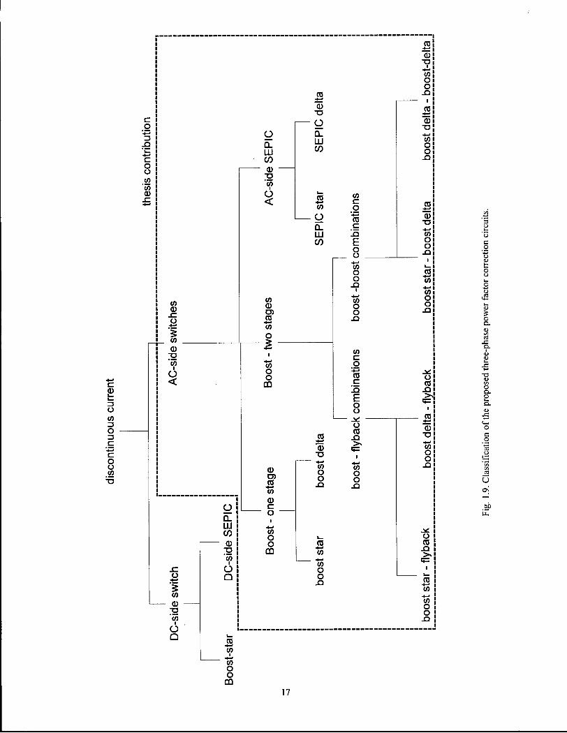
1.9 Classification of the proposed three-phase power factor correction circuits. 17
2.1 Normalized current waveforms vs. phase angle for the boost-star circuit, at various voltage 21 transfer ratios M .
2.2 Space vector technique: decomposition of the vector into its three-phase components. 22
2.3 Space vector technique: decomposition of the vector into its fundamental and harmonics. 22
2.4 Phase current waveforms for the boost-star PFC circuit with DC-side switch. 25
2.5 a) Average current space vector and its components, b) Trajectory of the instantaneous 25 current space vector and its resultant average current space vector
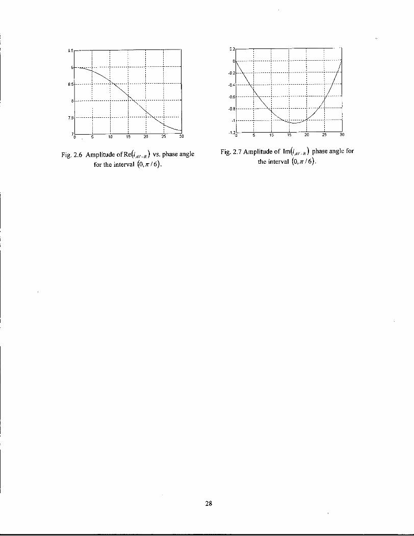
2.6 Amplitude of R e ^ , ^ ) vs. phase angle for the interval (0,x/6). 28
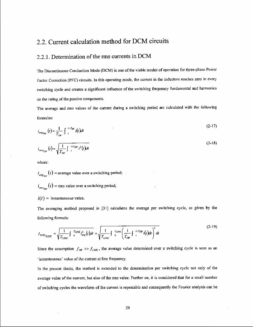
2.7 Amplitude of I m ^ ^ ) vs. phase angle for the interval (fJ,;r/6). 28
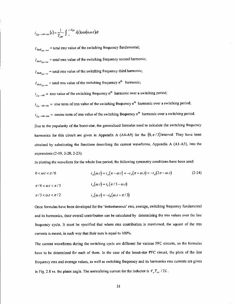
2.8 Normalized inductor currents vs. phase angle for the boost-star circuit. M=1.5 32
2.9 Total rms contribution (%) vs. duty cycle D for inductor currents in the boost-star circuit. 32 M=1.5
2.10 Total rms contribution (%) vs. voltage transfer ratio M for inductor currents. Boost-star 32 circuit. Max. D.
3.1 Boost-star PFC circuit with AC-side switch. 35
3.2 Modulation at the end of the ON-interval. 35
3.3 Modulation at the beginning of the ON-interval. 35
vii

3.4 Space vector components for modulation at the beginning of the ON-interval. 38
3.5 a) Phase current waveforms for the boost-star PFC circuit with AC-side switches and 110 38 modulation, b) Average current space vector, c) Instantaneous current space vector trajectory.
3.6 The positive and negative roots of ta vs. phase angle. Interval 16). 40
3.7 Diagram showing phase A goes out of conduction before phase C. (o, n 16) interval. 40
3.8 The positive root of ta vs. phase angle. Interval (0 ,W6). 40
3.9 Times Tlal and Tsw normalized to T0N vs. phase angle. Interval (o,;r/6). 40
3.10 Maximum ta_R vs. voltage transfer ratio. 40
3.11 Maximum and minimum TSW_R vs. voltage transfer ratio. 40
3.12 Ratio maximum/minimum Tsw vs. voltage transfer ratio. 41
3.13 Current waveform with approximating modulation vs. phase angle. 41
3.14 Sequence of switches with duty cycle modulation during a line period. 41
3.15 Space vector components for modulation at the end of the ON-interval. 43
3.16 The positive and negative roots of ta vs. phase angle. (0, n 16) interval. 44
3.17 Check phase A goes out of conduction before phase C over (o, n 16) interval. 44
3.18 The positive root of ta vs. phase angle. (o,;z76) interval. 45
3.19 Times Tlol and Tsw normalized to T0N vs. phase angle. (0,;r/6) interval. 45
3.20 Maximum ta_R vs. voltage transfer ratio. 45
3.21 Maximum and minimum TSW_R vs. voltage transfer ratio. 45
3.22 Ratio maximum/minimum Tsw vs. voltage transfer ratio. 45
3.23 Current waveform with approximating modulation vs. phase angle. (0,2;r) interval. 45
3.24 a) Bi-directional switch , b) IGBT implementation of the bi-directional switch, c) M O S F E T 47 implementation of the bi-directional switch, d) IGBT with anti-parallel diode seen as a 'quasi bi-directional switch'.
viii

3.25 a) Delta implementation of the bi-directional switch, b) Star implementation of the bi- 47 directional switch, c) Quasi tri-directional switch.
3.26 Boost-delta 3-phase 3-switch PFC circuit. 48
3.27 Proposed circuit. Switches closed. 49
3.28 Proposed circuit for the interval (0,^/3) when current flows in three inductor.
3.29 Proposed circuit for the interval (0,^/3), when current reaches zero first in inductor Lx.
49
49
3.30 Proposed circuit for the interval (0,^/3), when current reaches zero first in inductor L3. 49
3.31 Phase current vs. phase angle over one period, at various voltage transfer ratios M . Boost- 49 delta circuit.
3.32 Average inductor current vs. phase angle over one period, at various voltage transfer ratios 49 M . Boost-delta circuit.
3.33 Plot showing the times (normalized to T0N) at which the current through the inductors 50
reaches zero vs. phase angle. (0,/z76) interval. Voltage transfer ratio M=3.
3.34 Phase current waveforms during a switching cycle. 50
3.35 5 t h and 7 th harmonics (%) vs. voltage transfer ratio M . 52
3.36 Leading angle of phase current vs. voltage transfer ratio M . Boost-delta circuit. 52
3.37 Normalized phase current vs. phase angle over one period. Boost-delta circuit. M=1.5 53
3.38 Injected harmonic amplitude vs. voltage transfer ratio, M for the boost-star and boost delta 55 circuits.
3.39 5 t h harmonic vs. voltage transfer ratio, a- boost-star without harmonic injection, b- boost-star 55 with harmonic injection, c - boost-delta without harmonic injection, d - boost-delta with harmonic injection.
3.40 Total Harmonic Distortion vs. voltage transfer ratio M . a- boost-star without harmonic 55 injection, b- boost-star with harmonic injection, c - boost-delta without harmonic injection, d - boost-delta with harmonic injection.
55 3.41 Maximum power based on harmonic content required by IEC 1000-3-2 vs. voltage transfer
ratio M . a- boost-star without harmonic injection, b- boost-star with harmonic injection, c -boost-delta without harmonic injection, d - boost-delta with harmonic injection.
3.42 Average current space vectors for boost-delta circuit. 59
3.43 Average current space vectors. 59
3.44 Boost-delta. One stage vs. two reverse connected. 5 th and 7 th harmonics (%) vs. voltage 59 transfer ratio M .
ix

3.45 Normalized inductor currents vs. phase angle for the boost-delta circuit. M=l .5 59
3.46 Total rms contribution (%) vs. duty cycle D for capacitor currents in the boost-delta circuit. 59
M=1.5
3.47 Total rms contribution vs. voltage transfer ratio M for the inductor currents. Boost-delta 59 circuit. Max. duty cycle.
4.1 Starfly PFC circuit. 61
4.2 Equivalent circuit diagram of the proposed circuit when all switches are closed. 65
4.3 Equivalent circuit diagram of the proposed circuit when all switches are opened. 65
4.4 Inductor L, currents during a switching cycle. 65
4.5 Inductor L2 currents during a switching cycle. 65
4.6 Normalized average phase current for boost circuit (T - 0) over one period. 66
4.7 Normalized average phase current for flyback circuit (T = oo) over one period. 66
4.8 Normalized average phase current for starfly circuit (7" = 6) over one period. 66
4.9 Normalized fifth harmonic (%) vs. voltage transfer ratio M . 66
4.10 Normalized seventh harmonic (%) vs. voltage transfer ratio M . 66
4.11 Total Harmonic Distortion (percentage) vs. voltage transfer ratio M . 66
4.12 Current ratio /',: I, global peak /peak of the phase fundamental vs. voltage transfer ratio M . 67
4.13 Current ratio i2: L2 global peak /peak of the phase fundamental vs. voltage transfer ratio M . 67
4.14 Normalized active power vs. voltage transfer ratio M . 67
4.15 Ratio inductors/transmitted energy vs. voltage transfer ratio M . 67
4.16 Line current. Time domain simulation. 67
4.17 Voltage transfer ratio M vs. inductor ratio T for meeting IEC 1000-3-2 requirements at 67 various power levels.
4.18 Proposed 'deltafly' three-phase, three-switch Power Factor Correction circuit. 71
4.19 Equivalent circuit diagram of the proposed circuit when all switches are closed. 75
4.20 Line currents during a switching cycle. 75
4.21 Inductor I, currents during a switching cycle. 75
x

4.22 Inductor L2 currents during a switching cycle. / D
4.23 Line current vs. time, for various voltage transfer ratios, M and inductance ratios. 76
4.24 5 th harmonic (%) vs. voltage transfer ratio M , for various inductance ratios. 76
4.25 7 lh harmonic (%) vs. voltage transfer ratio M , for various inductance ratios. 76
4.26 Current leading angle vs. voltage transfer ratio, M for various inductance ratios. 76
4.27 Average line current vs. time. 76
4.28 Average inductor currents vs. time. 76
4.29 Average semiconductor currents vs. time. 76
4.30 Space vector representation of the averaged phase current for the boost-delta circuit, a) 77
a = -n/6,b) a = 0, c) <X = K 16.
4.31 'Star-delta' three-phase, three-switch Power Factor Correction circuit. 78
4.32 Time-domain simulation showing the currents for the inductor sets L, and L2 during a 79
switching cycle.
4.33 Line current vs. time, for various voltage transfer ratios, M and inductance ratios. 80
4.34 Maximum duty cycle vs. voltage transfer ratio, M for various inductance ratios. 80
4.35 Total Harmonic Distortion vs. voltage transfer ratio M , for various inductance ratios. 80
4.36 Current leading angle vs. voltage transfer ratio, M for various inductance ratios. 80
4.37 Diode set l/(Diode set 1 + Diode set 2) average current vs. inductance ratio for various 80 voltage transfer ratios, M .
4.38 Average inductor currents vs. time. 81
4.39 Average semiconductor currents vs. time. 81
4.40 Proposed delta-delta three-phase, three-switch Power Factor Correction circuit. 83
4.41 5* harmonic (%) vs. inductance ratio T. 85
4.42 7 th harmonic (%) vs. inductance ratio T. 85
4.43 Current leading angle vs. inductance ratio T for various voltage transfer ratios M . 85
4.44 5 lh harmonic (%) vs. voltage transfer ratio M for various inductance ratios T. 85
4.45 7 th harmonic (%) vs. voltage transfer ratio M for various inductance ratios T. 85
4.46 Current leading angle vs. voltage transfer ratio M . 85
xi

4.47 Average line current vs. time. 5 0
4.48 Average inductor currents vs. time. 86
4.49 Average semiconductor currents vs. time. 86
4.50 Generic line current during a switching cycle. 88
4.51 Boost-star input stage. 90 90
4.52 Boost-delta input stage.
4.53 Flyback stage. 90
4.54 Boost-delta stage. 90
5.1 Proposed SEPIC 3-phase 3-switch power factor correction circuit. 93
5.2 Proposed circuit. Switches closed (111). 95
5.3 Proposed circuit. Switches opened (000). Current flowing in three diodes. 95
5.4 Proposed circuit. Switches opened (000). Current flowing in two diodes. 95
5.5 Inductor I, current waveforms during a switching period. 95
5.6 Inductor L2 current waveforms during a switching period. 95
5.7 Rectifying diodes current waveforms during a switching period. 95
5.8 Switch current waveforms during a switching period. 96
5.9 Capacitor C, current waveforms during a switching period. 96
5.10 Normalized average phase current vs. phase angle during a line period. 98
5.11 Normalized inductor Lx rms current vs. phase angle during a line period. 98
5.12 Normalized inductor L2 rms current vs. phase angle during a line period. 98
5.13 Normalized capacitor C, rms current vs. phase angle during a line period. 98
5.14 Normalized 5 th , 7 t h harmonics and T H D (%) of the average inductor I, current vs. voltage 98
transfer ratio M .
5.15 Ratio (%) of the high frequency/total inductor I, rms current vs. voltage transfer ratio M . 98
5.16 Phase current at the input of the high frequency filter vs. time. 101
5.17 Capacitor C , voltage vs. time. 101
xii

5.18 Proposed Delta-SEPIC 3-phase 3-switch power factor correction circuit. 102
5.19 Proposed circuit. Switches closed (111). 105
5.20 Proposed circuit. Switches opened (000). Current flowing in three rectifier diodes. 105
5.21 Proposed circuit. Switches opened (000). Current flowing in two rectifier diodes. 105
5.22 Inductor L, current waveforms during a switching period. 105
5.23 Inductor L2 current waveforms during a switching period. 105
5.24 Capacitor C, current waveforms during a switching period. 105
5.25 Rectifying diodes current waveforms during a switching period. 106
5.26 Switch current waveforms during a switching period. 106
5.27 Phase current waveforms during a switching period. 106
5.28 Normalized average phase current vs. phase angle over one period. 109
5.29 Normalized inductor L, rms current vs. phase angle over one period. 109
5.30 Normalized inductor L2 rms current vs. phase angle over one period. 109
5.31 Normalized capacitor C, rms current vs. phase angle over one period. 109
5.32 Normalized 5 t h , 7* harmonics, and T H D (%) of the average phase current vs. voltage 109 transfer ratio M .
5.33 Ratio (%) of the high frequency/total rms currents in inductor Z,, vs. voltage transfer ratio M . 109
5.34 Phase current at the input of the high frequency filter vs. time. I l l
5.35 Capacitor C. voltage vs. time. 111
6.1 Boost-delta PFC circuit. 114
6.2 Boost-delta PFC. Two circuits running in parallel, with reverse input phase connections. 115
6.3 Practical implementation of a bi-directional switch. 117
6.4 Gate driving circuit. 117
6.5 P W M and drivers circuit. 118
6.6 Boost-delta PFC circuit, a) Line current vs. phase-angle. M A T L A B simulation, b) Line 120 current and voltage vs. time. PSIM simulation.
xiii

6.7 Boost-delta PFC circuit with reversed phase sequence, a) Line current vs. phase-angle. 120 M A T L A B simulation, b) Line current and voltage vs. time. PSIM simulation.
6.8 Boost-delta PFC circuit with two stages, a) Line current vs. phase-angle. M A T L A B 120 simulation, b) Line current and voltage vs. time. PSIM simulation.
6.9 Line current vs. time for the boost-delta PFC with input filter: a) PSIM, b) experimental, 121
2A/10mV scale.
6.10 Line current vs. time for the boost-delta PFC with reversed phase sequence and input filter: 121 a) PSIM, b) experimental, 2A/10mV scale.
6.11 Line current vs. time for the boost-delta PFC with two stages and input filter: a) PSIM b) 121 experimental, 5A/10mV scale.
6.12 Inductor current vs. time at line frequency a) PSIM, b) experimental, 5A/10mV scale. 122
6.13 Inductor current vs. time at switching frequency a) PSIM, b) experimental, 5A/10mV scale. 122
6.14 Bi-directional switch current vs. time at line frequency: a) PSIM, b) experimental, 122 5A/10mV scale.
6.15 Bi-directional switch current vs. time at switching frequency: a) PSIM, b) experimental, 123 5A/10mV scale.
6.16 Diode current vs. time at line frequency: a) PSIM, b) experimental, 5A/10mV scale. 123
6.17 Diode current vs. time at switching frequency: a) PSIM, b) experimental, 5A/10mV scale. 123
6.18 Filter capacitor current vs. time at line frequency: a) PSIM, b) experimental, 5A/10mV 123 scale.
6.19 Filter capacitor current vs. time at switching frequency: a) PSIM, b) experimental, 123 5A/10mV.
6.20 Bi-directional switch voltage vs. time at line frequency: a) PSIM, b) experimental (inverted 123 waveform).
6.21 Bi-directional switch voltage vs. time at switching frequency: a) PSIM, b) experimental. 125
6.22 Filter capacitor voltage vs. time at line frequency: a) PSIM, b) experimental. 125
6.23 Filter capacitor ripple voltage vs. time at switching frequency: a) PSIM, b) experimental. 125
6.24 Output capacitor ripple voltage vs. time at line frequency: a) PSIM, b) experimental. 126
6.25 Input phase voltage and current of three-phase rectifying bridge vs. time: a)PSIM, b) 126 experimental.
6.26 Output voltage ripple of three-phase rectifying bridge vs. time: a)PSIM, b) experimental. 126
Photo 6.1 Bench set-up for testing the PFC circuit. 129
xiv

Photo 6.2 Measurement equipment with test readings.
Photo 6.3 PFC Circuit layout.
Photo 6.4 Bi-directional switches and rectifying diodes.
Photo 6.5 PWM circuit.
Photo 6.6 Boost inductor and input filtering stage.
xv

ACKNOWLEDGEMENT
I like to take this opportunity to offer my sincerest gratitude to the sum of the many people who helped
make this thesis possible.
First, I'd like to thank my supervisor, Dr. William G. Dunford, whose perspicacity, energy, warm support,
and critical thinking were central to making this thesis come to life. His comments and suggestions were
nothing short of brilliant and, I shall be forever grateful for his creative guidance in shaping my ideas into
the big picture of this thesis. He has been an incredible mentor helping me to develop my 'voice' in the
field of power electronics. His deep intelligence and creative inspiration may be felt throughout my work.
Dr. Hua Jin has been essential to making this thesis happen and I am deeply grateful for his example of the
highest standard of professionalism and excellence.
Xantrex has also been generously supportive of my work. I must express my gratitude to the management,
who have created a wonderful environment in which I have been able to discuss new ideas and hear about
the experiences of others.
Researching and writing this thesis would have been impossible without the patience, love and
understanding of my family. I am deeply indebted to my wife, Ewa, for her unwavering love and support.
She has shared her heart and soul with me in this years long toil. Her dedication, tenacity, creativity and
sensibility have inspired me to a great extent, much more than she is ever willing to take credit for. In his
turn, my son Oliver, has done his share in boosting up my efforts, by providing me with a daily dose of
cheerfulness and joy.
Not the least I would like to thank all the researchers around the world who are tackling this subject, and
have written valuable papers, bringing a fresh insight or an overall mature view of the state of the art.
While the list is a long one, names like Dr. J.W. Kolar, Dr. A.R. Prasad, Dr. M . Sedighy come to mind as
people who have had a profound influence on my work, and generally on the development trend in the
field.
xvi

To my father, who has taught me to seek out knowledge,
and to share it for the benefit of all.

CHAPTER 1
INTRODUCTION
In this chapter the historical background and available topologies for three-phase power factor correction
are described. A general classification and the advantages and disadvantages of various types of circuits are
discussed. The contribution of this thesis is presented in the context of the previous work. The assumptions
underlying the calculations are given.
1

1.1. Harmonics - Historical Context
Power system harmonic distortion is not a new phenomenon - efforts to limit it to acceptable proportions
have been a concern of power engineers from the early days of utility systems. At that time, the distortion
was typically caused by the magnetic saturation of transformers or by certain industrial loads, such as arc
furnaces or arc welders. The major concerns were the effects of harmonics on synchronous and induction
machines, telephone interference, and power capacitor failures. In the past, harmonic problems could often
be tolerated because equipment was of conservative design and grounded wye-delta transformer
connections were used judiciously.
Power system problems that were associated with harmonics began to be of general concern in the 1970s,
when two independent developments took place. The first was the oil embargo, which led to price increases
in electricity and the move to save energy. Industrial consumers and utilities began to apply power factor
improvement capacitors. Capacitors reduce M V A demand from the utility grid systems by supplying the
reactive power portion of the load locally. As a result, losses are reduced in the industrial plant and the
utility network. The move to power factor improvement resulted in a significant increase in the number of
capacitors connected to power systems. As a consequence, there has been an equally significant increase in
the number of tuned circuits in plant and utility networks.
The second involved the coming of age of low voltage thyristor technology. In the 1960s, thyristors were
developed for dc motor drives and then extended to include adjustable-speed ac motor drives in the 1970s.
This resulted in a proliferation of small, independently operated converters usually without mitigation
techniques employed.
The increase in the use of static converters both in industrial control equipment and in domestic
applications, combined with the increase in use of power factor improvement capacitors, created
widespread problems.
The quality of distributed electrical power has become a critical concern in recent years. This concern has
grown with the advent of positive industry trends to improve electrical product efficiency as well due to the
proliferation of electronic equipment in households and commercial environments. Interestingly enough,
the very technology that allows for more efficient use of electrical energy, switch-mode power conversion
technology, is also a culprit that can negatively impact power quality. Switch-mode power supplies can
2

draw high harmonic currents from the A C mains, which can cause a variety of undesirable effects in the ac
power distribution system. The end result for electronic products connected to the ac mains can be
improper operation, over-stressed ac input components and product failure. There are a number of areas of
new and continuing concern related to the effect of harmonics:
• sensitivity of computers, computer-controlled machine tools, and various types of digital controllers;
• damaging dielectric heating in underground cables;
• insulation stress in capacitors, fuse blowing in capacitor banks;
• metering errors;
• rotating machines and transformers heating problems;
• communication systems interference;
• thyristor firing errors, false tripping of protective devices.
The presence of harmonic distortion on the utility system results in incremental costs in the operation of the
system. The most important cost component is likely to be the costs associated with applying mitigation
measures, such as harmonic filtering, to reduce harmonic levels. Based on the incremental costs alone,
substantial investment in mitigating harmonic generation in the end use equipment could be justified. This
philosophy of controlling harmonic distortion levels by applying limits at the end use equipment level has
been adopted in IEC 1000-3-2.
On the other hand the North American approach is emphasized in the recommendations given in IEEE Std
519-1992, where the harmonic limits are given at the point of common coupling, i.e. the electrical
connecting point between utility and customers distribution systems.
3

1.2 Classification and related issues
Classification
Power Factor Correction (PFC) has been an active research topic in power electronics, motivated by
forthcoming stringent power quality regulations. The single-phase PFC is already a common practice, and
the industrial application of three-phase PFC techniques has also emerged.
Up to this point the research of three-phase converter techniques has been heavily focused on inverter
applications. Although most techniques developed in the inverter area can be used in PFC applications, a
PFC circuit has its unique characteristics, and therefore deserves some special treatment. The primary
differences between PFC and inverter applications include the following aspects:
• Special attention has to be paid to the quality of input current and electromagnetic interference (EMI)
emissions in PFC, which makes control design more difficult;
• Very high switching frequencies are desirable to reduce the size and weight of reactive components
(especially inductors), and to improve current control performance. The effect of soft-switching
techniques is therefore very prominent in PFC applications;
• The input currents are generally in phase with input voltages, and bi-directional power flow is usually
not required in PFC circuits. These aspects provide some flexibility to develop soft-switching and
control techniques specific for PFC converters.
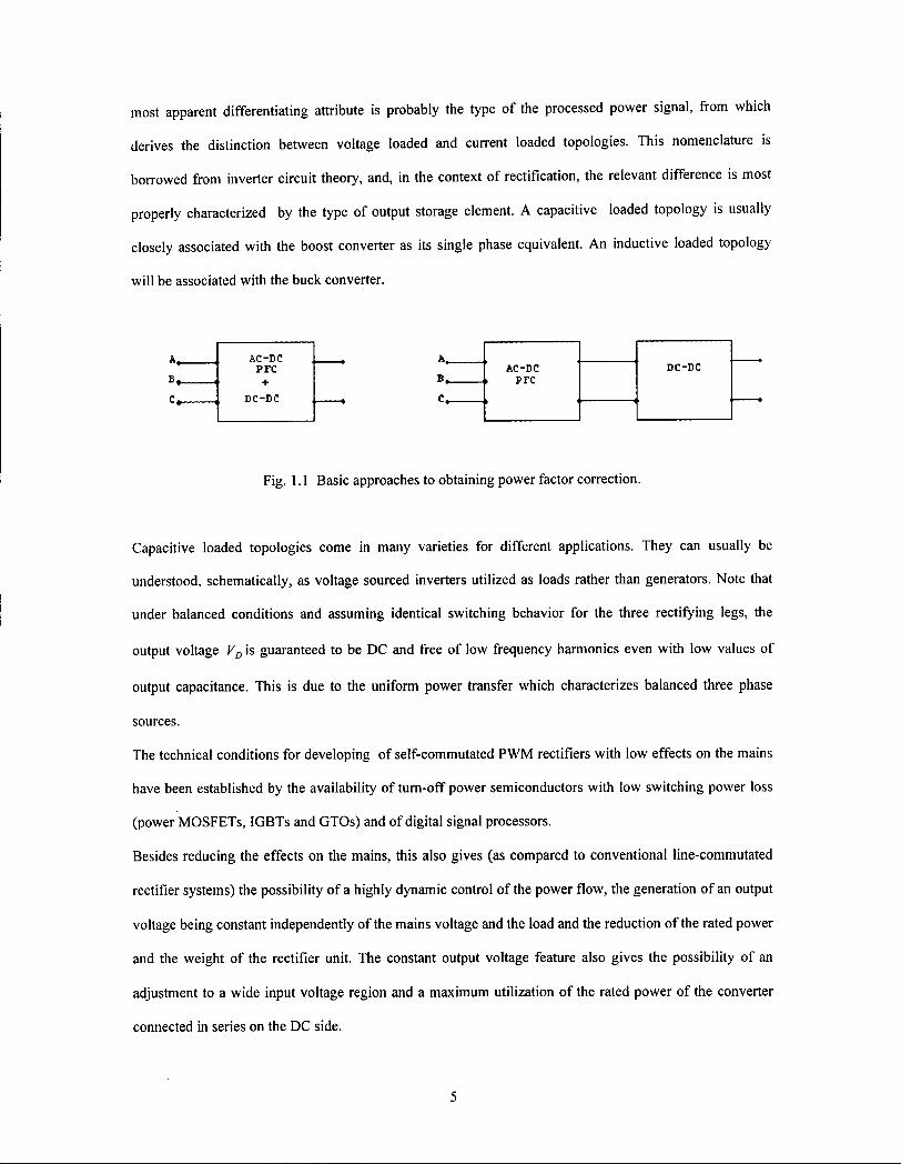
There are two basic approaches to controlling power in a power conditioning system, as shown in Fig. 1.1.
The first approach is a single stage conversion, which integrates input current control, load voltage
regulation, and possibly input/output isolation into one power stage. The second approach is the traditional
two-stage scheme, where the input stage (i.e. a PFC converter) controls the input currents and provides a
coarsely regulated output voltage, while the load regulation is performed by the second stage.
Active conditioning circuits are the only practical option available to the design engineer. Passive circuits
are characterized by poor performance in addition to their notable size and weight. Conversely, so many
different active methods have been described that it becomes a task to simply attempt a classification. The
4
most apparent differentiating attribute is probably the type of the processed power signal, from which
derives the distinction between voltage loaded and current loaded topologies. This nomenclature is
borrowed from inverter circuit theory, and, in the context of rectification, the relevant difference is most
properly characterized by the type of output storage element. A capacitive loaded topology is usually
closely associated with the boost converter as its single phase equivalent. An inductive loaded topology
will be associated with the buck converter.
C .
AC-DC pre +
DC-DC
K
C .
AC-DC
> pre DC-DC
•
Fig. 1.1 Basic approaches to obtaining power factor correction.
Capacitive loaded topologies come in many varieties for different applications. They can usually be
understood, schematically, as voltage sourced inverters utilized as loads rather than generators. Note that
under balanced conditions and assuming identical switching behavior for the three rectifying legs, the
output voltage VD is guaranteed to be DC and free of low frequency harmonics even with low values of
output capacitance. This is due to the uniform power transfer which characterizes balanced three phase
sources.
The technical conditions for developing of self-commutated P W M rectifiers with low effects on the mains
have been established by the availability of turn-off power semiconductors with low switching power loss
(power MOSFETs, IGBTs and GTOs) and of digital signal processors.
Besides reducing the effects on the mains, this also gives (as compared to conventional line-commutated
rectifier systems) the possibility of a highly dynamic control of the power flow, the generation of an output
voltage being constant independently of the mains voltage and the load and the reduction of the rated power
and the weight of the rectifier unit. The constant output voltage feature also gives the possibility of an
adjustment to a wide input voltage region and a maximum utilization of the rated power of the converter
connected in series on the DC side.
5
i= to
Vi o CD c
o •
2 J Q. i t
i CD
3
11 ro Q . o. o
3 £<§
._ § — CL .£ CD
CD
CD CO c o
CD
CD >
f2 4)
.0
O O
O
cu
£ CD .£=>>-£ c gi a — -C
* "O CD <D C > O) CO C T3 •_ O C CD O •° t C CD >
>, ° o. J I Q. CD
*r ? « CL CD
£ o i - CD
3 a) -6
s § f -g Q- °
(0
CD
CD >
CD O) CO
O
o
CD 0 L -10 CD CD ^
1 *
in =>
0 c
•I e-1 3
. s i in tj co
co c o o c
V) o „
.15
• g
3 „ o c
! 3
S I
<->
' <D „ —h to 9) in t ro 3 CL o
3 o
CD CD
11 CO CL Q . CD
CL CO
CO CD
CP in
co c g
is | g
3
"2 ^
CD S — CL
C
8: Ct) 10
co
O c
13 o
o 3 c
c o
(0 _ „ • c , £ CO
2 oo -5 o
— >
o
CD
ST .O
3 ,2 co € cb t3 CD CD
3 5 f E «> to CD Ct) C co
CD > CD
3 E
CD > CD
3 u •? E
O ) CD c • -
, (D C
u. -a o CD ^ : g i
*r > T3 O ) ° >- 5 2 tn *z ro ==
x c 2
u E « a
CD v. t: c CD
o c ° - o ro °
3 CD CD CL <= E ' JS
o
~ CD
3 <E
2 ts
p
CD
>
o
P
CD
.2> >. ^ x
S t 3 o o o
3 2 CO « =
" CD t) CD CD
i CD <=
g ) x : f £
^ -s 5 CD *r > T3 O )
° >> £ i5 S X * P => a) 5 > o E i? o. • o o - g
o .<o =
O a .
T3
o
C3
a .
c o
O
U
op

The aim of this chapter is to give a classification of the circuit concepts of three-phase P W M rectifier
systems as given in literature and to give an overview over the technical possibilities and the most
important trends of the presently very dynamic developments in the area of self commutated rectifier
systems. The main attention will be paid to P W M converters (with low and medium power) to be operated
from the public low-voltage mains. This means that area which seems to be most likely affected (due to its
high application diversity) by future stricter standards concerning effects on the mains of power converter
systems.
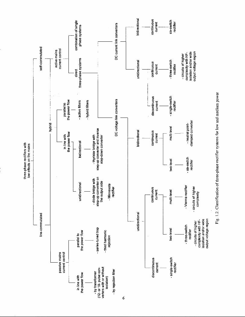
Fig. 1.2 shows a classification developed in [1] for low and medium power three-phase rectifier systems.
For a detailed reference list of the circuits mentioned, [1] represents a source of information rigorously and
exhaustively developed. Based on the number of pertinent publications the main focus of the development
is now in the area of self commutated and hybrid circuit concepts. ( The latter denotes the series and/or
parallel connection of a line-commutated and a self-commutated converter). In connection with hybrid
systems we also have to point out the future high importance of active filters (besides the concepts
discussed here) in the area of energy distribution. Due to the much broader application of pulse rectifier
systems with impressed output voltage (voltage DC link pulse rectifier systems) as compared to current DC
link pulse converters (e.g. for electrical drive systems) also current D C link pulse rectifiers are omitted
from the considerations here. In the following several examples of three-phase PFC will be given, based on
presentations such as [1-3].
Three single-phase boost rectifiers
A simple way to implement a three-phase PFC converter is to combine three single-phase boost rectifiers at
the input side, one for each phase and each followed by a dc-dc converter, as shown in Fig. 1.3. This
configuration is simplified in [4] by directly coupling the outputs of the three PFC converters, so only one
dc-dc converter is required. The advantage of the configuration is that well-known single-phase PFC
techniques can be used directly, so little development effort is required. In addition, certain redundancy is
inherent in this arrangement, since the three converters operate independently. The disadvantages are that
more components are added in the main power path, and that the interference among the single-phase PFC
converters cannot be avoided completely [4]. Due to its relatively low efficiency, this topology is
7
not recommended for high power applications.
A
B
DC B u s
B
C
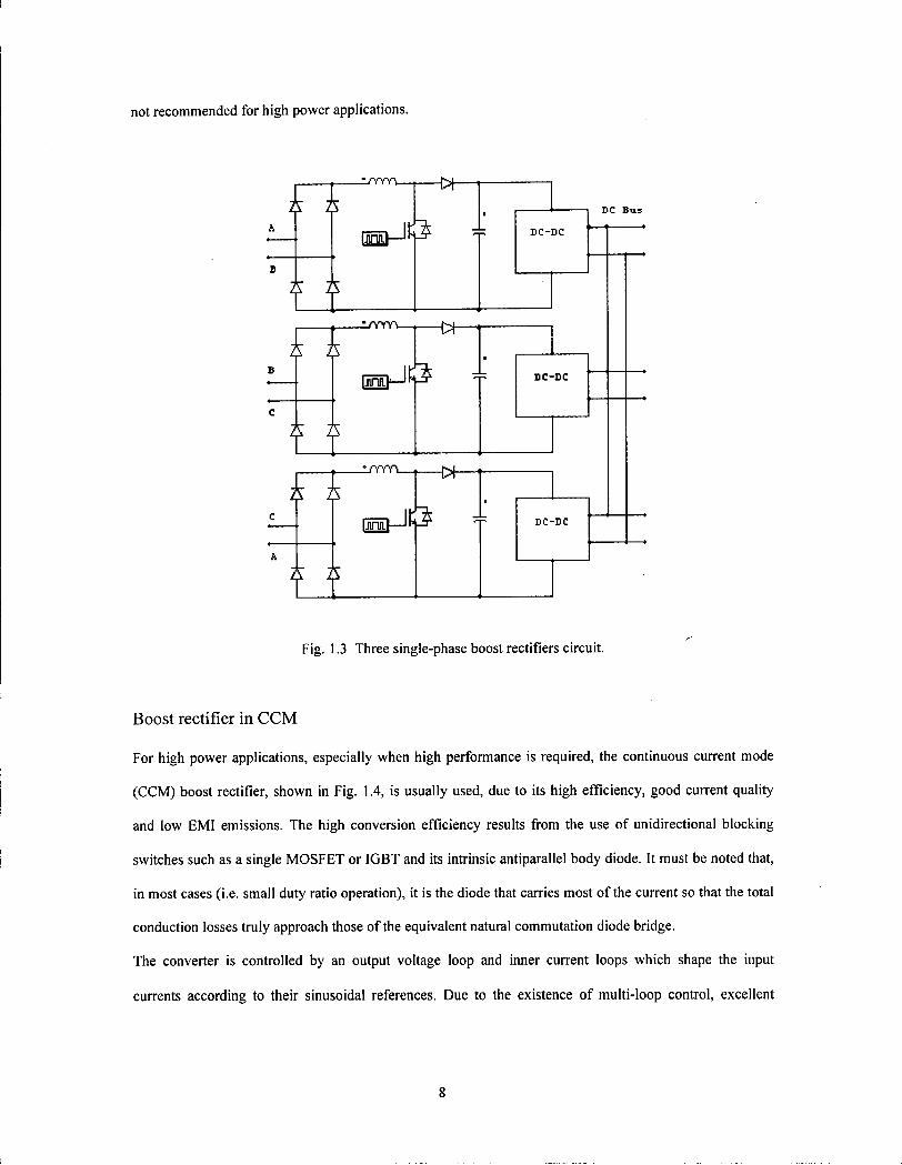
Fig. 1.3 Three single-phase boost rectifiers circuit.
Boost rectifier in CCM
For high power applications, especially when high performance is required, the continuous current mode
(CCM) boost rectifier, shown in Fig. 1.4, is usually used, due to its high efficiency, good current quality
and low EMI emissions. The high conversion efficiency results from the use of unidirectional blocking
switches such as a single MOSFET or IGBT and its intrinsic antiparallel body diode. It must be noted that,
in most cases (i.e. small duty ratio operation), it is the diode that carries most of the current so that the total
conduction losses truly approach those of the equivalent natural commutation diode bridge.
The converter is controlled by an output voltage loop and inner current loops which shape the input
currents according to their sinusoidal references. Due to the existence of multi-loop control, excellent
8

current characteristics can be achieved if output voltage is higher that the input line voltage amplitude. EMI
emissions and switch conduction loss are also kept low due to the continuous input current. Due to severe
diode reverse recovery problem, the major part of the switching loss in a C C M boost converter is the turn-
on loss. Several zero-voltage switching techniques have been proposed to reduce or eliminate the switch
turn-on loss while alleviating the turn-off loss indirectly by the use of snubber capacitors. Great simplicity
can be achieved of the soft switching mechanism is applied to the dc link instead of applying it on the ac
side, as in the resonant dc-link (RDCL) [5,6] and other dc link commutated converters [7-10]. Although
device switching losses are significantly reduced, the conduction loss in the auxiliary circuit is quite high.
R D C L converters also suffer from high voltage stress, high circulating energy and complex but not very
effective discrete pulse modulation.
The control section design presents additional difficulties since it must provide for the evaluation of the
proper duty cycle, and the suitable power angle simultaneously in order to regulate the output. This
increases the controller's complexity and difficulty of analysis. Furthermore, the small signal behavior is
characterized by a RHP zero, if used in continuous mode, complicating further the realization of a stable
system within large operating ranges. All of the above reasons would certainly restrain most power
engineers from adopting such a topology if it were not for the notable benefits it provides.
DC Bus
J _ L T Y T Y \
Fig. 1.4 Boost rectifier circuit in C C M .
9
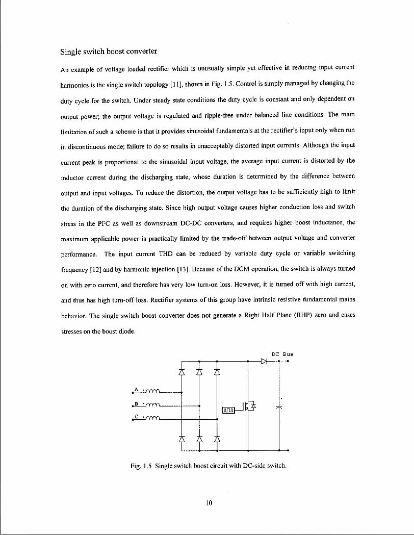
Single switch boost converter
An example of voltage loaded rectifier which is unusually simple yet effective in reducing input current
harmonics is the single switch topology [11], shown in Fig. 1.5. Control is simply managed by changing the
duty cycle for the switch. Under steady state conditions the duty cycle is constant and only dependent on
output power; the output voltage is regulated and ripple-free under balanced line conditions. The main
limitation of such a scheme is that it provides sinusoidal fundamentals at the rectifier's input only when run
in discontinuous mode; failure to do so results in unacceptably distorted input currents. Although the input
current peak is proportional to the sinusoidal input voltage, the average input current is distorted by the
inductor current during the discharging state, whose duration is determined by the difference between
output and input voltages. To reduce the distortion, the output voltage has to be sufficiently high to limit
the duration of the discharging state. Since high output voltage causes higher conduction loss and switch
stress in the PFC as well as downstream D C - D C converters, and requires higher boost inductance, the
maximum applicable power is practically limited by the trade-off between output voltage and converter
performance. The input current T H D can be reduced by variable duty cycle or variable switching
frequency [12] and by harmonic injection [13]. Because of the D C M operation, the switch is always turned
on with zero current, and therefore has very low turn-on loss. However, it is turned off with high current,
and thus has high turn-off loss. Rectifier systems of this group have intrinsic resistive fundamental mains
behavior. The single switch boost converter does not generate a Right Half Plane (RHP) zero and eases
stresses on the boost diode.
DC BUS
l/YYYY.
JL_1/~VTYY.
C •fYYin flnJLl—
H i Fig. 1.5 Single switch boost circuit with DC-side switch.
10
SEPIC and Cuk circuits
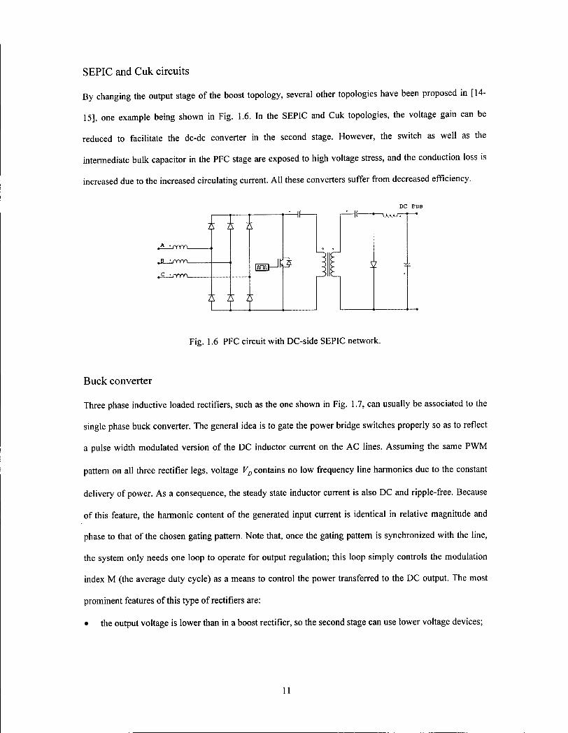
By changing the output stage of the boost topology, several other topologies have been proposed in [14-
15], one example being shown in Fig. 1.6. In the SEPIC and Cuk topologies, the voltage gain can be
reduced to facilitate the dc-dc converter in the second stage. However, the switch as well as the
intermediate bulk capacitor in the PFC stage are exposed to high voltage stress, and the conduction loss is
increased due to the increased circulating current. All these converters suffer from decreased efficiency.
um—1^
i l l
Fig. 1.6 PFC circuit with DC-side SEPIC network.
Buck converter
Three phase inductive loaded rectifiers, such as the one shown in Fig. 1.7, can usually be associated to the
single phase buck converter. The general idea is to gate the power bridge switches properly so as to reflect
a pulse width modulated version of the D C inductor current on the A C lines. Assuming the same P W M
partem on all three rectifier legs, voltage VD contains no low frequency line harmonics due to the constant
delivery of power. As a consequence, the steady state inductor current is also D C and ripple-free. Because
of this feature, the harmonic content of the generated input current is identical in relative magnitude and
phase to that of the chosen gating pattern. Note that, once the gating pattern is synchronized with the line,
the system only needs one loop to operate for output regulation; this loop simply controls the modulation
index M (the average duty cycle) as a means to control the power transferred to the D C output. The most
prominent features of this type of rectifiers are:
• the output voltage is lower than in a boost rectifier, so the second stage can use lower voltage devices;
11

• the input currents can be controlled in open loop and much wider voltage loop bandwidth can be
achieved.
• more resilient to switch "misfiring" problems. Momentary "shoot-throughs" result in no damage; they
are actually often utilized as part of the gating technique implementation.
• the inrush current at start up can be easily controlled by limiting switch duty cycles;
• less efficient then the voltage loaded type due to the series blocking diodes;
• a freewheeling diode can be used on the dc side to reduce the conduction loss.
Generally, a buck rectifier has similar switching loss, but higher conduction loss than its boost counterpart.
Due to the series diodes and consequently its lower efficiency, the buck rectifier is not used as widely as
the boost rectifier.
A ' B ,
B B J B B D J B B J
Qoij—Jk poTl—^ rJruCl—l^
r\ ! : i
Fig. 1.7 Inductively loaded buck rectifier circuit
Active filters
The active filter concept uses power electronics to produce harmonic components which cancel the
harmonic components from the nonlinear loads. These active filters are relatively new and a number of
different topologies are being proposed. Within each topology, there are issues of required component
ratings and methods of rating the overall filter for the loads to be compensated. The most common active
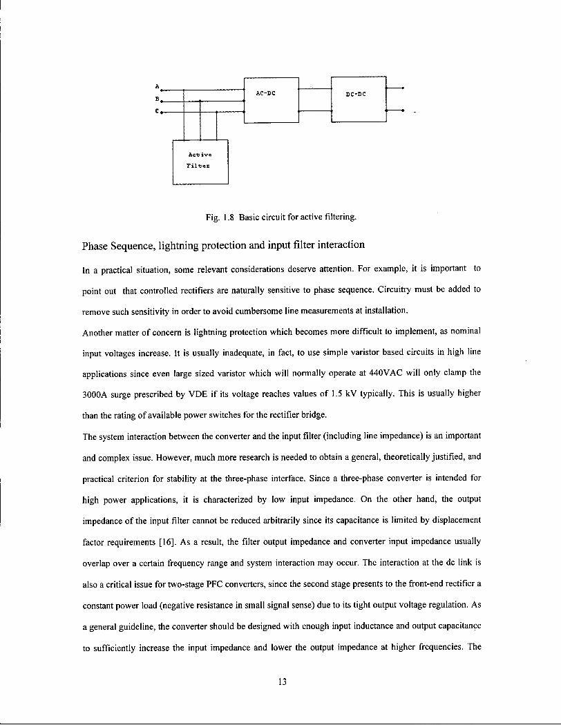
filter configuration is shown in Fig. 1.8 and is based on a PWM voltage source inverter that interfaces to
the system through a system interface filter. In this configuration, the filter is connected in parallel with the
load being compensated. Therefore, the configuration is often referred to as an active parallel filter.
12
A C - D C D C - D C
A c t i v e
Fig. 1.8 Basic circuit for active filtering.
Phase Sequence, lightning protection and input filter interaction
In a practical situation, some relevant considerations deserve attention. For example, it is important to
point out that controlled rectifiers are naturally sensitive to phase sequence. Circuitry must be added to
remove such sensitivity in order to avoid cumbersome line measurements at installation.
Another matter of concern is lightning protection which becomes more difficult to implement, as nominal
input voltages increase. It is usually inadequate, in fact, to use simple varistor based circuits in high line
applications since even large sized varistor which will normally operate at 440VAC will only clamp the
3000A surge prescribed by V D E if its voltage reaches values of 1.5 kV typically. This is usually higher
than the rating of available power switches for the rectifier bridge.
The system interaction between the converter and the input filter (including line impedance) is an important
and complex issue. However, much more research is needed to obtain a general, theoretically justified, and
practical criterion for stability at the three-phase interface. Since a three-phase converter is intended for
high power applications, it is characterized by low input impedance. On the other hand, the output
impedance of the input filter cannot be reduced arbitrarily since its capacitance is limited by displacement
factor requirements [16]. As a result, the filter output impedance and converter input impedance usually
overlap over a certain frequency range and system interaction may occur. The interaction at the dc link is
also a critical issue for two-stage PFC converters, since the second stage presents to the front-end rectifier a
constant power load (negative resistance in small signal sense) due to its tight output voltage regulation. As
a general guideline, the converter should be designed with enough input inductance and output capacitance
to sufficiently increase the input impedance and lower the output impedance at higher frequencies. The
13

pulse frequency ofthe rectifier system has to be set sufficiently above the resonance frequency ofthe filter
in order to obtain sufficient damping of the current harmonics with switching frequency. However, also in
this case a resonance condition can result if periodic load changes occur.
Soft-switching
Soft-switching techniques are very important for increasing the power density and reducing the EMI
emissions of a PFC circuit. They reduce the switching loss and switch stresses of power devices, and thus
makes high switching frequency operation feasible. Most soft-switching techniques originate in dc-dc
converters, and have evolved from quasi-resonant converters (QRC), multi-resonant converters (MRC),
quasi square-wave P W M converters and soft transition PWM techniques, which include zero-voltage-
transition (ZVT) and zero-current-transition (ZCT). The soft transition techniques combine the advantages
of soft-switching and P W M control with a low power auxiliary circuit, which is actuated only for a short
time prior to switch transition. For most PFC applications, soft transition techniques are more efficient than
other soft-switching techniques.
Control
The control of power converters usually can be divided into three functions: modulation, current control,
and regulation of an output variable (the output voltage in rectifiers). In the three phase inverter
applications, the system dynamics is usually dominated by the slow electromechanical and/or large reactive
components, so that the inverter dynamic performance is not very critical. Additionally, accurate ac current
control is not very important in many inverter applications (except for field-oriented drives). On the
contrary, high quality current control, without the use of large reactive components, is the major objective
in PFC applications. With high switching frequencies, which is made possible through the use of soft
switching techniques, high performance and very wide bandwidth control now can be designed.
Al l standard modulation techniques developed for inverters could be used in rectifier applications. An
excellent survey of these techniques can be found in [17]. Sinusoidal P W M (SPWM) is well suited for
analog implementation [18] but causes higher switching losses and current ripple [19]. In boost rectifiers,
SPWM can be used with third harmonic injection to decrease the minimum output voltage by 15%. The
14

same effect is automatically achieved with space vector modulation (SVM) [35] which also significantly
reduces switching loss and high frequency current ripple. Many of the soft switching techniques often
require the use of completely different modulation strategies [20] or modifications of the standard P W M
schemes [19,21,22].
The simplest analog current control for boost rectifiers is the hysteresis control [18] which combines the
modulation and current control in a single function. It also provides the widest current loop bandwidth of
all schemes. The major problems with the hysteresis control are the load dependence of the switching
frequency, and the interference among phases resulting in irregular converter operation and uneven current
waveforms. These problems can be remedied by controlling two line-to-line currents (differences between
phase currents). [23-24]
Average current control is widely used in three-phase rectifiers and can be implemented either with analog
or digital hardware. The S V M sequence is often adjusted such that the switches in the phase carrying the
highest current are disabled, so the switching loss is reduced to 50%. In digital implementations, two
current compensators in rotating coordinates are used [25]. The advantage of the digital implementation is
that all control variables are constant in steady state for a balanced system. Conversely, in the analog
current control, the control variables are time-varying, and the ideal control voltages may be even
discontinuous at the current zero-crossing. Therefore, very fast analog controllers have to be used to
achieve good current control, and the current distortion is usually higher than with the digital controllers
due to finite controller gains at line frequency [26]. Similarly as in dc-dc converters, the output voltage loop
bandwidth for boost rectifiers is severely limited by the presence of the RHP zero in the control-to-output-
transfer function [25, 27]. For digital control implementations, the bandwidth is limited even more by the
computational and sampling delays.
In the buck rectifiers, due to topological restrictions, three phases cannot operate independently. This
prevents the use of hysteresis input current controllers. Instead, S V M or modified SPWM techniques are
usually used [28-29]. Excellent input current quality can be easily achieved with open loop control [30].
15

Future trends
Concerning the effects on the mains with the switching frequency caused by pulse rectifier systems,
attempts are being made to obtain a wider distribution of harmonic power and/or a reduction of the
amplitudes of single frequency components by varying the pulse frequency (e.g. random pulse width
modulation). In this area, a clarification would be advantageous in connection with the standards being
prepared for the frequency region 2 ... 9 kHz regarding the admissible harmonic stress on the mains; this
should make clear that an even distribution of the harmonic power within a frequency band (and, therefore
minimum harmonic stress on the mains for discrete frequencies) should be preferred as compared to a
concentration of the harmonic power around multiples of the mains frequency.
Assuming a wider application in the future of pulse converter systems with low effects on the mains and/or
of power electronic energy converters, in general, we have to point out the deterioration of the damping
conditions to be expected due to the constant power characteristic of these systems. Therefore, under
further consideration of the efficiency reduction (2...3% as compared to simple diode rectification)
resulting typically for connecting a power factor correction stage in front of each single power electronic
load, one has to pose the question in general how a technically and economically optimal solution of the
problem area of effects on the mains can be achieved (e.g. by a combined application of "mains-friendly"
pulse rectifier systems and centrally located active or hybrid filters).
1.3 C o n t r i b u t i o n
The thesis proposes a new family of PFC circuits operating in DCM. The distinctive feature is the presence
of switches on the AC side of the rectifying bridge unlike the circuits presented in the literature, where they
are on the DC-side.
One important consequence is the fact that the switches have to be bi-directional or as it will further be
proposed, quasi tri-directional. While this can be seen as an increase of the semiconductors number, the
sharing of the dissipated heat can be a reasonable trade-off. New areas of research will evolve by the use of
bi-directional switches, both in semiconductor fabrication as well as in soft-switching circuitry.
16
c o
'•*-» wz J2 *L_ -•—' c o o co CO CD
c 0) L-o CO o
c '
c o o co
(/> o> o
CO (1)
• g co • O <
O Q_ LU CO <D
• g CO i
O <
OS -*—*
•o O Q_ LU CO
05 -«—<
O Q_ LU CO
5 </> - g co • O Q
O Q_ LU CO CO
• g 'co i O Q
co <D CD (0
-•—< CO
CO O o 00
CD ns » CD c o
(A O o CD
ro a5
T 3 -•—< co o o
as CO CO o o
SI
(0 c o ro c
!o E o o
-*—< CO o o .a
^—< CO o o
CO c g
'-»—» as c
l a E o o
^ o as
5=
CO O O
-Q
as ^—* CO
I *-> CO o o
CO
as »
0 T 3 i
< CO O o
as d)
T3 -•—< CO o o
ro a) CO o o
as -*—» CO
• 4 - *
CO o o .a
o as
•
ro a) •a to o o .a
o as
>» Cf=
as -•—» CO
- 4 — '
CO o o
17

The single-switch boost circuit operating in DCM has the disadvantage of poor performance at low voltage
transfer ratios. The circuits proposed reduce the THD significantly while maintaining a simple voltage
follower control. As a continuation of the general classification given in Fig. 1.2, Fig. 1.9 shows the circuits
operating in DCM and includes in the dotted area the contribution of the present thesis. A short description
of the circuits will be given here while the schematics and analysis of features will be dealt with in further
chapters.
The introduction of three bi-directional switches on the ac-side will give a new degree of freedom to the
single-switch boost circuit. The circuit still has a single voltage follower loop, however a phase dependent
modulation will reduce in this case the harmonics down to zero. The degree of reduction is dependent on
the level of approximation of theoretically determined curves.
By connecting the switches in delta rather than in star as in the previously described circuit, a new set of
features is obtained. The boost delta will be phase sequence sensitive and its harmonic content will be
comparable to the single switch circuit. However two parallel circuits with the switches connected reverse
sequence and staggered operation will achieve both a dramatic reduction of the harmonics as well as an
improved ripple on the input. While the staggered operation of the DC-side switch PFC will improve the
ripple to an equal extent, the harmonics will stay the same due to phase sequence insensitivity.
Both circuits described so far, will be dealt with in Chapter 3 and are characterized by a single set of
boosting inductors. In contrast, Chapter 4 is dedicated to the analysis of circuits having two sets of boosting
inductors and AC-side switches. A variety of properties will characterize the boost star - flyback, boost
delta - flyback, boost star - boost delta and boost delta - boost delta circuits. The degree of reduction of the
harmonics is a trade-off with the displacement angle, switches stress and number.
In Chapter 5, SEPIC derived circuits are studied. They are a natural consequence of the presence of the
switches on the AC-side, and are characterized by shifting the L-C-L networks on the AC-side as well. The
well known trade-offs of high switch stress and the need for capacitors vs. low harmonics, simple voltage
follower control and very good transient performance are present here as in all other SEPIC circuits.
However a better power sharing and the quasi tri-directional switch become available options.
18

1.4 A s s u m p t i o n s
The following assumptions have been used in the determination of the properties ofthe proposed circuits:
• the utility source is ideal with a zero internal impedance;
• the requirement on power flow is unidirectional;
• the components are ideal, unless specified otherwise;
• variations in the utility source voltage are ignored;
• the switching frequency is constant;
• the switching frequency is much higher than the line frequency;
• the ripple in the output voltage is neglected in comparison to its average value.
The diodes and the output dc capacitors are not included in the evaluation of component ratings, since the
diodes are relatively inexpensive and the output dc capacitors are needed in all schemes.
19

CHAPTER 2
NEW ANALYSIS TOOLS
In this chapter an average current space vector technique is proposed which makes possible a complete
analysis of the three-phase power factor correction circuit in the discontinuous conduction mode. The
theoretical analysis of various switching combinations allows the determination of the modulation needed
for very low Total Harmonic Distortion, down to zero. A technique previously applied for determining the
harmonics of the line current is further extended for the calculation of the switching frequency component
of the boost inductor currents.
20

2.1. Average Current Space Vector Technique
2 .1 .1 . Introduction
The boost three-phase Power Factor Correction (PFC) circuit operating in Discontinuous Conduction Mode
(DCM), shown in Fig. 1.5, is a popular topology. The input current waveforms have been determined for
various voltage transfer ratios, M in [31] and are reproduced here in Fig. 2.1 where M , the voltage transfer
ratio is defined as follows:
M = VD/SVLN
where :
VD = output D C voltage,
V!N = phase peak voltage.
The main limitation of the circuit is that a high output voltage or reduced output power are needed in order
to meet the requirements of IEC 1000-3-2 in regards to the harmonic content.
A space vector analysis method which uses averaged currents over a switching cycle is proposed. The
method will be used in order to analyze the harmonic content of the line current for the PFC circuit with
DC-side switch, shown in Fig. 1.5. The new method will demonstrate that no possible modulation can
reduce the T H D substantially for the particular circuit studied.
ii i i "» • * 1
0 100 200 300 400
Fig. 2.1 Normalized current waveforms vs. phase angle for the boost-star circuit, at various voltage transfer ratios M .
21
The method will be applied in further chapters to the proposed family of PFC circuits with switches on the
AC side. A theoretical determination becomes therefore possible for the modulation of various schemes, in
order to obtain very low, down to zero, harmonic content in the input current.
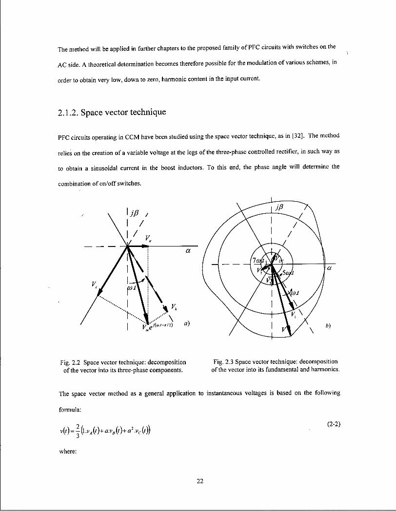
2.1.2. Space vector technique
PFC circuits operating in CCM have been studied using the space vector technique, as in [32]. The method
relies on the creation of a variable voltage at the legs of the three-phase controlled rectifier, in such way as
to obtain a sinusoidal current in the boost inductors. To this end, the phase angle will determine the
combination of on/off switches.
Fig. 2.2 Space vector technique: decomposition Fig. 2.3 Space vector technique: decomposition of the vector into its three-phase components. of the vector into its fundamental and harmonics.
The space vector method as a general application to instantaneous voltages is based on the following
formula:
v(t)=l(\.vA{t)+a.vB{t)+a2.vc(t)) ( ? ' 2 )
where:
22
1 = e10 = (cos(0)+ j sin(0)) = 1 V>
a = ej2"n = (cos(2;r/3)+ ysin(2W3))=-l/2 + jfi/2
a1 =e-J2!rn =(cos(-2«/3)+ y'sin(- 2*73)) = - 1 / 2 - yVJ/2
An example of the application of formula (2-2) to phase and line three phase voltage systems is given in
the following:
y (t)=y eX—*/i) (2-4)
r phase V/ m e
where:
Va=Vm.sm(atj), V„ =Vm.sm{co.t-2JT/3), Vc =Vm.Sm{a>J+ 2.K 12,)
VrmM=Svme^ (2-5)
and
vab = va -vh = Svm sm(cot + 7i 16)
vhc = vh -K = Svm sin((i»r - TZ7 2)
vcu = vc -K, = Svm sin(oj/ + 5^-/6)
The interpretation of formula (2-2) can be seen in Fig. 2.2, where the projections of the space vector onto
the three axes gives the instantaneous values of the phase voltages. When the space vector is of constant
amplitude, its trajectory describes a circle, and consequently its projections onto the axes A,B,C are three
sinusoidal components, phase shifted by 120° electric. In Fig. 2.3 an exemplification of the situation
where V is the space vector for a signal where harmonics are present, shows that the trajectory is distorted
from its circular shape. A Fourier decomposition yields harmonics which can be represented by vectors of
constant amplitude, a given phase angle and a rotation speed of nxol. While the space vector technique
has been exemplified for voltages, it can be equally applied to currents.
23

2.1.3. Space vector technique using average currents
An averaging technique which determines analytically the properties of the circuit in Fig. 1.5 has been
proposed in [31]. Here this method is extended to a space vector representation of the averaged current
over a switching cycle. An analytical determination carried out in [31] has shown that the waveforms of the
three phase instantaneous currents, look like those in Fig. 2.3 during a switching cycle. The expressions
describing this waveforms for each phase are given in Appendix A and are functions of x, the time
parameter. The time points where change occurs in the functions are determined in [31] and given below:
t 3V" T l-yD-3v/0N
(2-6)
TON '2 {vD-wAXvD + vB-vc)
1 aw ~ , . , 1 ON M -1
An attempt to apply the space vector method to instantaneous currents, has resulted in [12] in the
determination of the trajectory of the instantaneous current space vectors, such as shown in Fig. 2.5b. The
trajectory is based on the formulas given in Appendix A. This method will not give a visual representation
of the features of the circuit and consequently little insight is brought.
The space vector method using instantaneous currents is based on the formula (2-7). Its application for
average currents will be described by (2-8) which was derived for the boost-star PFC circuit in [31].
'"(0 = J( l JA(')+ aJB(t)+a2.ic(t)) ( 2 ? )
1 " W0N K +(TM >,+/(r0A, +tl)tl+i{T0N+tX] (2"8)
271
The average current for each time point where dil dt changes occur, as well as the average over the
switching cycle have been calculated and the results are shown in (2-9) and (2-10).
i(T \- V" T „•>(<»•'-»/2) ^ 2 9 ^ lVONl~ ^ 'ONc
24
L> 3L
i{TOK+t,+tl) = 0
iAV = JjLeJ(*-->-*'2) (Tm +tx\T0N +/, +t2) + 2Vo_ej2„/3 /,(/, +t2) L 2TSW 3L 2TSW
0 \ \ 7»'
'A •vD(vA-vc)
1 ^ B T
/ L m
Fig. 2.4 Phase current waveforms for the boost-star PFC circuit with DC-side switch.
Fig. 2.5 a) Average current space vector and its components, b) Trajectory of the instantaneous current space vector and its resultant average current space vector.
25

As can be seen by analyzing formula (2-10) and its visual representation in Fig. 2.5, except at the
extremities of the studied interval [0,;z76], the resultant vector is always behind the voltage vector, and has
a variable amplitude. That can be also assessed by looking at the plots of the average current as determined
in [31] and reproduced in Fig. 2.1 where for the interval (0,/z76) the current amplitude is always smaller
than that corresponding to a sinusoidal wave.
The non-circular trajectory implies that the resultant vector is composed of a fundamental and harmonic
vectors. A space vector which describes a circle with the speed of CO.t has a constant amplitude and its
projection onto the three axes gives the instantaneous amplitude of the three phases.
When a vector has a non-circular trajectory, it is equivalent to a three-phase system with fundamental and
harmonics. Consequently this trajectory is the summation of the vectors representing the fundamental and
its harmonics which have particular amplitudes and phase shifts. The vector corresponding to the n-th
harmonic rotates n-times faster, i.e. with a speed n.co.t .The simplest way to determine their amplitude and
phase is by using an analytical rather than graphical method, based on the formulas presented in [31].
It is now easy to show how larger voltage transfer ratios reduce the harmonic component by comparing the
overall contribution of the two component vectors from (2-10):
2VD / . fr .+Q (2-H) 3£ 2TSir _2VA{Vc-VB)_sin(2a>j)
ym {Tps+tjT^+t.+t,) VmVD M L 2TSW
The formula proves that the relative size of the vector eJ2"n becomes smaller with higher voltage transfer
ratio and consequently the resultant vector is more aligned with the voltage vector, i.e. the harmonics will
be smaller.
The vector diagram shown in Fig. 2.5 lets us draw an important conclusion, that it is impossible to obtain
zero THD regardless of the modulation scheme used due to the fact that the vector eJ2"n will always have
some distorting effect.
Let us now analyze the variation of the resultant vector over the (0,;r/6) interval.
The average current vector can be written as:
26

, - fa , - , /2 ) , r . / 2 . / 3 sin(2^i) ( 2- 1 2>
where:
For a simpler calculation the system of axes can be rotated as follows:
/ - y , VcX*'*-») sin(2^) (2"14)
LAV-R . , M
In order that no harmonics be present the following should hold true:
HiAv-n)=ct. (2-15)
As mentioned before meeting the conditions in (2-15) is not possible for this circuit, however it is
interesting to study the variation of these components in order to see what duty cycle modulation would
reduce the harmonic content.
Re(/V R)=V 1 + — i '-cos(7?r/6-a.t) [ M l
T /. \ T r sin(2<»i) . /_ , , \ \m(iAV_R)=V—i Lsm\j7cl6-a)X)
M
The plots are given in Figs. 2.6 and 2.7 for M = 1.5 and a normalizing factor VmTON I2L . It can be seen
that a significant variation of the amplitude of the two components occurs/
Since Re(/^_ f i ) must be brought closer to a constant value and I m ^ ^ ) closer to zero, several papers
[33-35] have proposed a modulation T0N(l + ms\n(6coJ + 3z/2)) in order to achieve just that.
27
28
2.2. Current calculation method for DCM circuits
2.2.1. Determination of the rms currents in DCM
The Discontinuous Conduction Mode (DCM) is one of the viable modes of operation for three-phase Power
Factor Correction (PFC) circuits. In this operating mode, the current in the inductors reaches zero in every
switching cycle and creates a significant influence of the switching frequency fundamental and harmonics
on the rating of the passive components.
The average and rms values of the current during a switching period are calculated with the following
formulas:
/ \ l r I+TS„- (2-17)
n (2-18)
where:
h,v<, (t) — average value over a switching period;
KmsT W = ™5 value over a switching period;
i(t) = instantaneous value.
The averaging method proposed in [31] calculates the average per switching cycle, as given by the
following formula:
lRMSfUNE 1 r TUNE-2 (t\,t
1 f TUNE( _ j _ r l+Tsw;(t\,t
V 1L1NE \IUNE \ L S I V
^2 (2-19)
dt )
Since the assumption fsw » fLINE, the average value determined over a switching cycle is seen as an
'instantaneous' value of the current at line frequency.
In the present thesis, the method is extended to the determination per switching cycle not only of the
average value of the current, but also of the rms value. Further on, it is considered that for a small number
of switching cycles the waveform of the current is repeatable and consequently the Fourier analysis can be
29

applied. Consequently, the switching frequency fundamental and its harmonics can be analytically
determined for every phase angle. Normalized currents are used in the calculations.
The total rms current can be determined over a period at the line frequency by integrating the instantaneous
rms currents as shown in the following :
IRMSTOT V 'UNE \'UNE \JSW J
where:
irms{t) = rms value over a switching period;
;'(/) = instantaneous value.
1'RMS = total rms value.
The rms contribution of the switching frequency component is determined as follows:
/„,><• - ^ RMSr,„ 1 RMS
where:
iavg(t) = average value over a switching period;
I RMS, = t o t a l r m s value of the line frequency fundamental and its harmonics ;
I RMS, ~ t o t a l m s value of the switching frequency fundamental and its harmonics .
On the other hand we can write:
where:
~\T 1 0 ' / s i r - » ' * ( ' ) * V 1 LINE
' / s „ . -nth (0 _ lj'/s„- -»«A-sin ( ' ) + ' /» , . -nrt-cos (')
ifm.-,„A-Si„ (0=^T—J iif)sm(n.co.t)dt * CIV
(2-20)
(2-21)
(2-22)
(2-23)
30
-,„*-cos(')= ^ - J "TS" i(t)cos{n.a>.t)dt 'sir
IKMS, IML
= t o t a ' T M S v a m e ° f t n e switching frequency fundamental;
I RMS, 2 „ = t o t a i M S v a ' u e ° f t h e switching frequency second harmonic;
1RMS, , = t o t a ' R M S v a ' u e of the switching frequency third harmonic;
IRMS, T ~total11113 v a ' u e ° f the switching frequency n* harmonic;
'/ar-nth ~ r m s value of the switching frequency n"1 harmonic over a switching period;
>fs„-,,ih-sm = sine term of rms value of the switching frequency n , h harmonic over a switching period;
'fs„.-,nh-cos = cosine term of rms value of the switching frequency n* harmonic over a switching period.
Due to the popularity of the boost-star, the generalized formulas used to calculate the switching frequency
harmonics for this circuit are given in Appendix A (A4-A9) for the (0,nl3)interval. They have been
obtained by substituting the functions describing the current waveforms, Appendix A (A1-A3), into the
expressions (2-19, 2-20, 2-23).
In plotting the waveform for the whole line period, the following symmetry conditions have been used:
0<co.t<7tl6 iA(coj) = iA(x-aj) = -iA(K + (o.t) = -iA(2x-co.t) (2-24)
it 16 < co.t < it 13 iA(o>.t) = ic(rt/3-G).t)
7tl3 <o).t <nll 'A^-1) = -iB(<o.t-xli)
Once formulas have been developed for the 'instantaneous' rms, average, switching frequency fundamental
and its harmonics, their overall contribution can be calculated by determining the rms values over the line
frequency cycle. It must be specified that where rms contribution is mentioned, the square of the rms
currents is meant, in such way that their sum is equal to 100%.
The current waveforms during the switching cycle are different for various PFC circuits, so the formulas
have to be determined for each of them. In the case of the boost-star PFC circuit, the plots of the line
frequency rms and average values, as well as switching frequency and its harmonics rms currents are given
in Fig. 2.8 vs. the phase angle. The normalizing current for the inductor is VmTm, 12L .
31
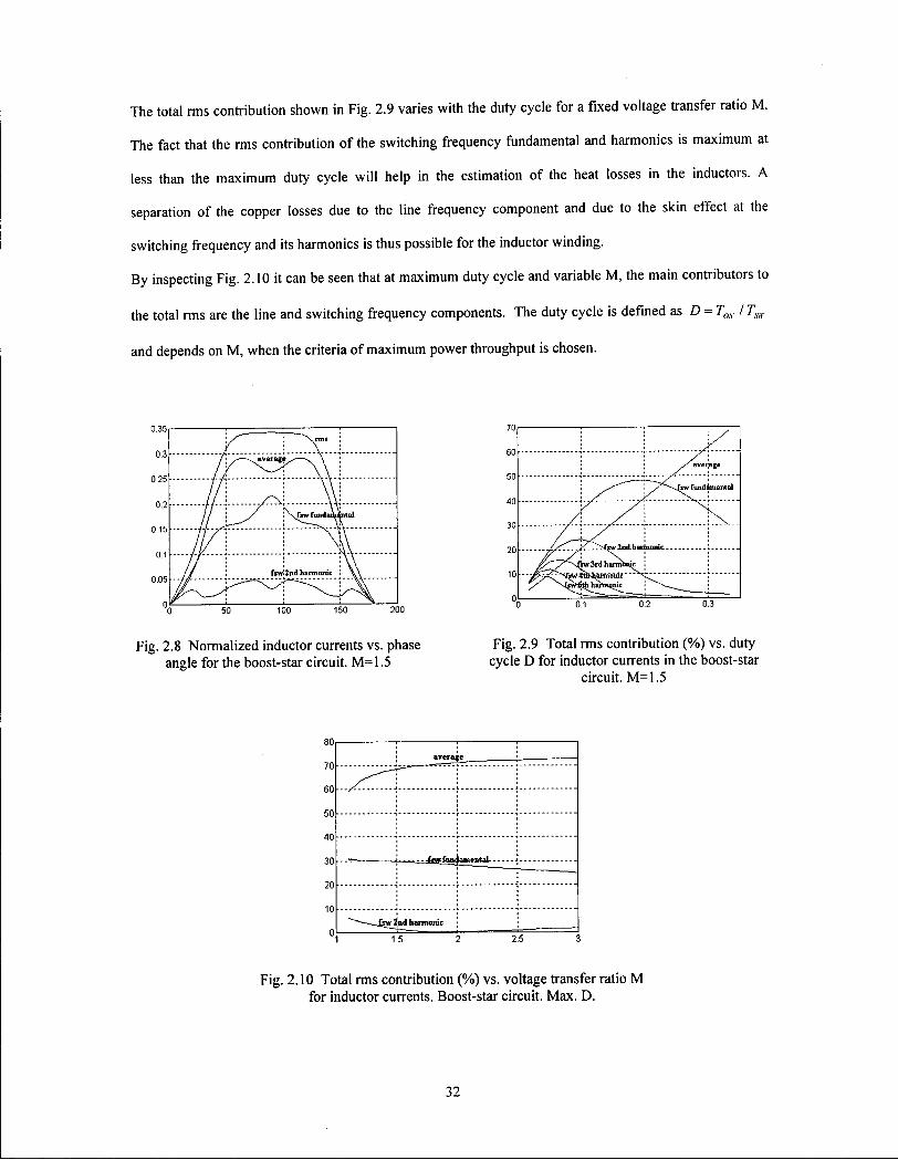
The total rms contribution shown in Fig. 2.9 varies with the duty cycle for a fixed voltage transfer ratio M .
The fact that the rms contribution of the switching frequency fundamental and harmonics is maximum at
less than the maximum duty cycle will help in the estimation of the heat losses in the inductors. A
separation of the copper losses due to the line frequency component and due to the skin effect at the
switching frequency and its harmonics is thus possible for the inductor winding.
By inspecting Fig. 2.10 it can be seen that at maximum duty cycle and variable M, the main contributors to
the total rms are the line and switching frequency components. The duty cycle is defined as D = Tos I Ts„.
and depends on M , when the criteria of maximum power throughput is chosen.
0.351
oaj
0.25'
0.2
0.15
.01
0.05
0.
P\ /*—-^average s — \
/ / ! y \ \TJW fundam ntal
/ / f«w!2nd harmonic
\ y
; average
/ " i ! "
w3rdhantumjc !
• - - '/pyKj fVW 4«N)&rm"oMf N ; " 7
50 150 0.1
Fig. 2.8 Normalized inductor currents vs. phase angle for the boost-star circuit. M=1.5
Fig. 2.9 Total rms contribution (%) vs. duty cycle D for inductor currents in the boost-star
circuit. M=1.5
1 averase
: |
; ;
j .
*~*^---^Jswit id harmonic j
1.5 2.5
Fig. 2.10 Total rms contribution (%) vs. voltage transfer ratio M for inductor currents. Boost-star circuit. Max. D.
32
CHAPTER 3
BOOST, SINGLE-STAGE CIRCUITS
Two circuits, the boost-star and boost-delta PFC are proposed in the present chapter. The location of the
switches on the AC-side allows a superior performance when compared with the circuits previously
available in D C M . A complete analysis of the circuit properties is carried out using the tools developed in
the previous chapter. For the boost-delta, the improvement of the performance is investigated for the case
of sixth harmonic injected into the duty cycle.
33

3.1. Boost-star circuit with AC side switches
3.1.1. Introduction
The limitations of the boost-star circuit with DC-side switch have been shown in Section 2.1. The
possibility for the individual control of the current waveform in each phase is not available due to the
existence of a single switch. If switches are placed on the AC rather than the DC side, the circuit in Fig. 3.1
is obtained and different modulation possibilities are achieved. Such a circuit can be implemented with
three delta-connected bi-directional switches or a 'quasi tri-directional switch' as will be shown in Section
3.1.4.
By introducing modulation, i.e. switch ON-times starting at different time points and/or of different
lengths, it becomes possible to influence the evolution of the current waveform for each phase. The
independent control of the component switches gives a much wider flexibility of operation and leading or
lagging current can be obtained.
As it can be seen in Fig. 3.1 the voltage follower control loop is present like in all other PFC circuits
operating in DCM. The voltage compensator block adjusts Tw based on the voltage transfer ratio, M,
which in turn depends on the amount of power processed. The control addition consists in the phase
detector block. Its output, the phase angle co.t, will determine the modulation parameters ta and Tsn., as it
will be shown in this chapter.
There are many modulation possibilities, some of which are shown in Figs. 3.2-3.3: at the beginning of the
on interval and at the end of the on interval. Another possibility is to keep the on-time and duty cycle
constant for all three switches and have every few cycles only two switches turned on. Since the switching
frequency is considered much higher than the line frequency, the average current over a few cycles can be
considered as an instantaneous value at the line frequency. Here the first two modulation types mentioned
will be analyzed. It will be shown that zero THD and unity power factor are possible with a certain
analytically determined modulation of the ON-time and switching period. A simpler practical
implementation could use an approximation of the analytical results and obtain very good performance.
34
V a
L l 1 / Y Y Y Y .
L l j r m .
L l m r r r \ _
Phase Detector
m r 1
UiruiH
SW3
Swl Sw2 Sw3(Fig
t_±i 3.2,3 14)
Logic
Tsw flon Calculator
(Eq. 3-12.3-13)
Voltage Compensator
M Vref
Fig. 3.1 Boost-star PFC circuit with AC-side switch.
J J
SW1
T T +t 'ON 'ON t 'a
T 'sw
SW2
T T +1 'ON 'ON
t la
SW3
TON Ton + ta T 'sw
Fig. 3.2 Modulation at the end of the ON-interval.
J 0 r„
J 0 L
SW1
ToN+ta T 'sw
SW2
T0N+ta T 'sw
SW3
0 U TON + ta Tsw
Fig. 3.3 Modulation at the beginning of the ON-interval.
35

3.1.2. Modulation at the beginning of the ON-interval
The equations describing the current evolution in each phase are given in the Appendix B in formulas
(B11-B16) for various combinations of switch turn-offs at the beginning of the ON-interval. A simple
strategy for obtaining a low harmonic current is to modulate during one switching cycle only one set of the
available space vectors.
Applying the formula (2-13) for the case of the boost circuit with AC-side switches, we obtain:
= -^r- [»'('. >. +''('. Kv + it. + Tm )T0, + ,\t. + Tm >, + it. + Tos + r, >, + /(/. + Tox +/,),] (3-1) sir
equivalent to:
/„• = K O ^ + * . + T j ^ + i(t,+T0N (3-2) Z V V „ , sir ^'sw
We obtain:
110 (SWl=on SW2=on SW3=off)
= ^ A - y B ) e . M 6 ta{ta+2TON+2t,+t2) + V^eMl_„l2) ( ^ + r , ) ( r w + r , + f 2 ) + 2 ^ , ^ h{t,+t2) 3L 2TSW L 2TSW 3L 2TSW
(3-3)
000, 101 ( SWl=off SW2=off SW3=of0, ( SWl=on SW2=off SW3=on)
. _ V3fc - VA) _„,„/6 ta{ta +2T0N +2r, +t2) [ Vm
3L 2TSW L 2TSW 3L 2TSW
(3-4)
011 (SWl=off SW2=on SW3=on)
. _ S{VB-VC) ta{ta+2TON+2tl+t2) Vm i(al_x/2) {TON+t)(TON+tl+t2) . .12x11 W» +^2)
3L 2TSW L 2TSW 3L 2TSW
(3-5)
By inspecting the formulas it becomes clear that for the interval (0,;z76) the only modulation possible for
obtaining a sinusoidal current in phase with the voltage is 110. As can be noticed, in this case a leading
power factor could be obtained by modulating 110 and a lagging power factor by adjusting the 101 or 011
vectors.
36

A space vector diagram can be drawn in order to give a graphical representation ofthe reason why the 110
modulation is useful. The amplitude of the component vectors from (3-3), represented in Fig. 3.5, is given
below:
(3-6)
(3-7)
+ 'JT0N + 'l +h) L 2TSW
VB)ta{ta + 2TON+2t + t2)
3L 2TSW
vA)ta{ta + 2TON+2t, + t2)
3L 2TSW
S{vB- vc)tX + 2TON+2t, + t2) 3L 2TSW
2VD r,(,
(3-8)
(3-9)
(3-10)
l 5 ~ 3L 2TSW
In Fig. 3.5 the alignment of the average current vector to the input voltage vector is detailed. In Fig. 3.5b it
can be seen how by using the 110 modulation the vector components give a resultant average current in
phase with the voltage. In order to have a more visual representation, Fig. 3.5a shows how the current
flows initially only in phases A and B until time ta. The trajectory of the instantaneous current space
vector during a switching cycle is shown in Fig. 3.5c with dotted lines.
Let us rotate the reference axis by (n 12- co.t) for simplicity of calculation:
, . # r > i l > M ^ ( ^ + 27'oy+2<i+f2), vm (r0Ar+t,Xr0A,+f,+<2), ivD , , 7 , ( 6 _ W ) ? I ( < I + / 2 ) G _ j n
The contribution ofthe eJ2"n and e'J"16 must cancel each other.
Re(z^)=cr. I m ^ )= 0.
This system of equations can be solved by varying ta'm order to obtain \m(iAV)=Q and Tsw
for Re^,,-) = ct. From Im(/^) = 0 we obtain:
2V ta(ta +2TON+2t] + t2)s'm(n/3-coj) = tl(tl + t2)-=-—- -sin(^/6-<y.r) (3-12)
JWA-VB)
From Re{iAy) = ct. we obtain:
37
Fig. 3.5 a) Phase current waveforms for the boost-star PFC circuit with AC-side switches and 110 modulation, b) Average current space vector, c) Instantaneous current space vector trajectory.
38

A V 3L V ; 2Tslr L 1THW 3L 2TSW
(3-13)
Given a fixed T0N and ?0_r to meet Im(/^) = 0,now TSIV can be determined for Re(iAV) = ct.
The average current can be written as:
, VJQN / M : t ( 3" 1 4 )
AV 2L Tsw_r{<o.t)
where:
T„{a,j) (3-15) lsw\
TON
Tlo,{co.t)=TON+ta(coj)+t](coj)+t2(o}.t) (3-16)
It has been proven through MATLAB simulations that:
Tsw (o>.i) > Tlo, (cox) for 0 < coX < n16 and, (3-17)
Tsw(eot)=Tlol{pj) for co.t = {fJ,/r/6} .
This makes it possible to choose:
Tsw_r(cox) = f(a>j) resulting in:
2z, rw_ r(^)
One important consequence of choosing Tsw_r (cox) in this way is a maximization of the power throughput
of the rectifier.
The solutions to the equation in (3-32) are given in Appendix B in formulas (B17-B21). The results for ta
and Tsw have been determined using MATLAB and are shown in Figs. 3.6-3.12. The plots given in the
following are an illustration for M=l .4 .
39
Fig. 3.8 The positive root of ta vs. phase angle. Fig. 3.9 Times Tm and Tw normalized to T0N vs. Interval (0, n 16). phase angle. Interval (0, n 16).
Fig. 3.10 Maximum ta_R\s. Fig. 3.11 Maximum and minimum vs. voltage transfer ratio. voltage transfer ratio.
40
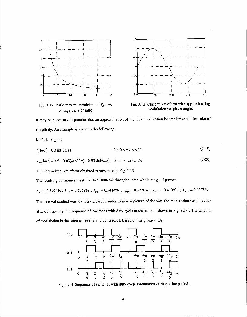
3.5
3
2.5
2
1.5
1.2 1.4 1.6
Fig. 3.12 Ratio maximum/minimum Tsw vs. voltage transfer ratio.
Fig. 3.13 Current waveform with approximating modulation vs. phase angle.
It may be necessary in practice that an approximation of the ideal modulation be implemented, for sake of
simplicity. An example is given in the following:
M=1.4, T0N =1
r a(^i)=0.3sin(6«.0 for 0<<y.f <ft/6 (3-19)
Tsw(cox)=3.5-0m(cojtl2ft) + 0.95sm(6a>.t) for 0 <co.t <ft/6 (3-20)
The normalized waveform obtained is presented in Fig. 3.13.
The resulting harmonics meet the IEC 1000-3-2 throughout the whole range of power:
iar5 = 0.3929%, / , 7 =0.7278% , iarU =0.5444% , iar]2 =0.3276% , / u r l 7 =0.4199% , iarl9 = 0.0375%.
The interval studied was 0 < co.t < ft 16. In order to give a picture of the way the modulation would occur
at line frequency, the sequence of switches with duty cycle modulation is shown in Fig. 3.14 . The amount
of modulation is the same as for the interval studied, based on the phase angle.
110
011
101
4n 3ft 5 T ~1
0 ft ^ )f~ 2ft 5n K 4ft 3ft 5ft \tfi 2n 6 I 2 T T 6 T ~2~ T ~6~
_ _ _ a 5 _
0 ft ft ft jt % % Hjf 2
0 n it ft ^rt ^ft *5f ^ % « = 2 6 3 2 3 6 6 3 2 3 6
Fig. 3.14 Sequence of switches with duty cycle modulation during a line period.
41

3.1.3. Modulation at the end of the ON-interval
The equations describing the current evolution in each phase are given in the Appendix B in formulas (B l -
B6) for various combinations of switch turn-offs at the end of the ON-interval. A simple strategy for
obtaining a low harmonic current is to modulate during one switching cycle only one set of the available
space vectors.
Applying formula (2-13) for the case of the boost circuit with AC-side switches, we obtain:
V =Tf-\i{Tm)Tm + fc +/(/„), + '(',>,+ <(', >2 ] ( 3 " 2 1 )
< 3 ' 2 2 )
We obtain:
110 (SWl=on SW2=on SW3=off)
, _ V* -Ma-mi) (ToN+ta+^lTON+ta+t,+t2) 2VD / < r / 3 ta{ta+2tt +t2) 2VD j 2 K n /,(/, +t2)
L 2TSW 3L 2TSW 3L 2TSW
(3-23)
000, 101 (SWl=off SW2=off SW3=off), ( SWl=on SW2=off SW3=on)
/ = l i c > ( « - W 2 ) {ToN+tg+tlXTov+tc+tl+'l) + ^0.^2*13 t . Q . + 2 / , + f J + ^ S _ e J 2 X , 3 'ifrl+O ( 3 . 2 4 )
£j "jfT^iy 3tL 27 / 3Z* 27"*^
011 ( SWl=off SW2=on SW3=on)
f _ ym c,U,-«n) {T0N +t. +t]){T0N +t„ + /, + f 2 ) | 2VD c , K ta(ta+2tt +t2) t 2VD
eJ2nii t\(fi +ti) (3-25)
By inspecting the formulas it becomes clear that for the interval (0,;r/6) the only modulation possible for
obtaining a sinusoidal current in phase with the voltage is 110. As can be seen, in this case a leading power
factor could be obtained by modulating 110 and a lagging power factor by adjusting 101 or 011 vectors. A
space vector diagram can be drawn in order to give a graphical representation of the reason why the 110
modulation pattern is useful. The amplitude ofthe vectors shown in Fig. 3.15 is given below:
42

Vm (T0N +ta+t,\T0N+ta+tx+t2)
2T„
j _2VD ta(ta+2tl+t2)
3L Q.Tcur
j _2VD h{h+t2)
3L *2.Tcur
(000,10 1
j ^ j b o l - r t l l )
(3-26)
(3-27)
(3-28)
Fig. 3.15 Space vector components for modulation at the end of the ON-interval.
Let us rotate the reference axis by (x/2-co.t) for simplicity of calculation:
. Vm (T0N+ta +h\T0N +<„+/,+/,) 2VD ' a t +t2) 2VD JO^J) +h) ( 3.29) ' Al/ — ' • rtm
I 2 7 ^ 3Z, " 27-^ z-1 sw
The contribution of the en"n and e-'*'3 must cancel each other.
Re(/^)=cr. Im(^,,) = 0 (3-30)
This system of equations can be solved by varying ta in order to obtain I m ^ ) = 0 and Tsw for
Re(;^) = cr.
With I m ^ ) = 0 yields:
ta{'a+ 2 t\ +t2)sm{irl6 + G)i) = t\{t\ +r2)sin(^/6-o>i) (3-31)
Therefore with Re(iAV) = ct. we obtain:
_ VON fVON (3-32)
2TSW
43
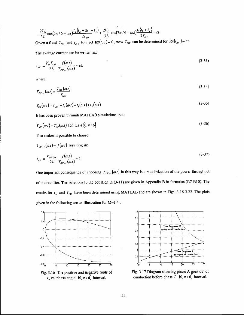
+ 2 ^ c o s ( 5 , r / 6 - « i ) i * ^ ^ 3L ITw 3L 2TSW
Given a fixed T0N and ta_r to meet I m ^ ) = 0 , now Tsw can be determined for Re(iAy) = ct.
The average current can be written as: (3-33)
where:
71 7 V , M ' • ct.
Tlo, (co.t) = T0N + ta (a>j) + /, (t»j) +12 M
It has been proven through MATLAB simulations that:
Tsiy(coj)= Tlol(a)j) for co.t e [o,x/6]
That makes it possible to choose:
Tsw-r if0*)= fif°A resulting in:
(3-34)
(3-35)
(3-36)
VJoN / M (3-37)
One important consequence of choosing Tsw_r(coj) in this way is a maximization of the power throughput
of the rectifier. The solutions to the equation in (3-11) are given in Appendix B in formulas (B7-B10). The
results for ta and Tsw have been determined using MATLAB and are shown in Figs. 3.16-3.22. The plots
given in the following are an illustration for M=1.4 .
30 "0 5 10 15 20 25
Fig. 3.16 The positive and negative roots of ta vs. phase angle. (0, it 16) interval.
4
3.5
3
2.5;
2
1.5
1
0.5
0l
i \ I i : \ : :
Time for-phase C ; \ ; going out ]of conductions ',
'< I •
I i i J>
^ ^ ^ - - ^ X i m e for phase A -""""'^ \ going o^t of conduction
; i I 10 15 20 25 30
Fig. 3.17 Diagram showing phase A goes out of conduction before phase C. (0, n 16) interval.
44
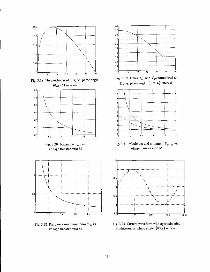
0.25
0.2
0.15
0.1
0.05
10 15 20 25 30
Fig. 3.18 The positive root of ta vs. phase angle.
(0,n/6) interval. 0.7r
Fig. 3.20 Maximum ta_R\s. voltage transfer ratio M .
Fig. 3.19 Times Tlol and Tsw normalized to
T0N vs. phase angle. (0, n 16) interval.
Fig. 3.21 Maximum and minimum TSW_R vs.
voltage transfer ratio M .
-0.5
400
Fig. 3.22 Ratio maximum/minimum T ^ v s .
voltage transfer ratio M .
Fig. 3.23 Current waveform with approximating modulation vs. phase angle. (0,2;r) interval.
45
Maximum ratio Iav I Tsw = 1.
It may be necessary in practice that an approximation of the ideal modulation be implemented with analog
circuitry. An example is given in the following:
M=1.4, T0N=l
ta{o).t)= 0 . 2 s i n ( 6 « . / ) + 0 . 1 6 7 s i n ( l 2 o > i ) for 0 < col < nIXl (3"38)
fQ(<y;)=0.2sin(6<y./) for nl\2 < coJ < nl6 (3-39)
Tslv(a)j) = 3.7 -0.035(a>j/2x) for 0<a>i<7r/6 (3-40)
The normalized waveform obtained is presented in Fig. 3.23.
The resulting harmonics meet the IEC 1000-3-2 throughout the whole range of power:
iar5 =3.1078% , i , 7 = 0.5637% , / „ „ =1.4032% , / , „ = 1.2751% , i , 1 7 =0.7924% , iar]9 = 0.4006% .
The sequence of switches with duty cycle modulation is the same as presented in Fig. 3.14.
3.1.4. The Quasi Tri-directional Switch
A new 'quasi tri-directional switch' is proposed for application in three-phase Power Factor Correction
(PFC) circuits. In regards to the implementation, a 'quasi tri-directional' switch can be used as an AC-side
switch. The term 'quasi' comes from the fact that the current flow can be controlled in one direction, of the
IGBT, but it is independent of the gating in the opposite direction, of the diode.
The 'quasi tri-directional' switch consists of three IGBTs with anti-parallel diodes and common-emitter
connected. The gating signals have thus a common point for all three IGBTs. A reduction of the number of
transistors is obtained by implementation in circuits formerly using three bi-directional switches, without
any compromise on the performance.
The bi-directional switch shown in Fig. 3.24a has been applied in various three-phase PFC circuits [37,38].
The practical implementation of this switch can be done with today's components as in Figs. 3.24b and
3.24c. On the other hand an Insulated Gate Bipolar Transistor (IGBT) with anti-parallel diode, shown in
Figure 3.24d, can be seen as a 'quasi bi-directional switch'.
46
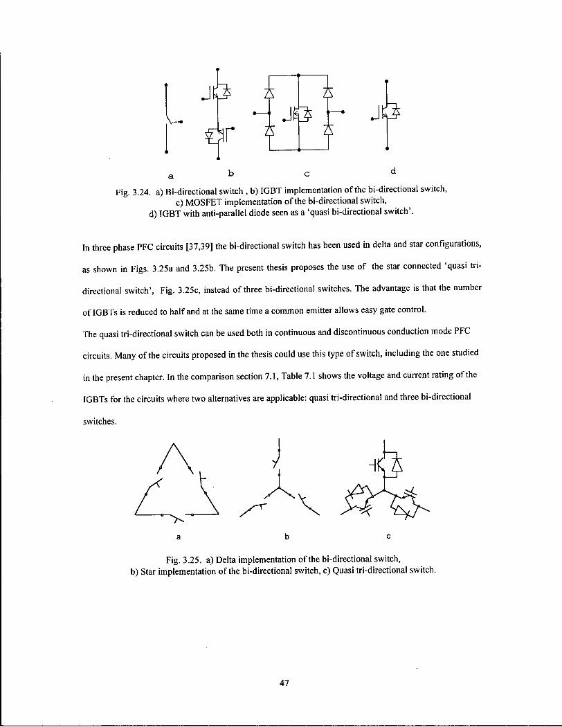
Ji3
b c d a
Fig. 3.24. a) Bi-directional switch , b) IGBT implementation of the bi-directional switch, c) MOSFET implementation of the bi-directional switch,
d) IGBT with anti-parallel diode seen as a 'quasi bi-directional switch'.
In three phase PFC circuits [37,39] the bi-directional switch has been used in delta and star configurations,
as shown in Figs. 3.25a and 3.25b. The present thesis proposes the use of the star connected 'quasi tri-
directional switch', Fig. 3.25c, instead of three bi-directional switches. The advantage is that the number
of IGBTs is reduced to half and at the same time a common emitter allows easy gate control.
The quasi tri-directional switch can be used both in continuous and discontinuous conduction mode PFC
circuits. Many of the circuits proposed in the thesis could use this type of switch, including the one studied
in the present chapter. In the comparison section 7.1, Table 7.1 shows the voltage and current rating of the
IGBTs for the circuits where two alternatives are applicable: quasi tri-directional and three bi-directional
switches.
a b c
Fig. 3.25. a) Delta implementation of the bi-directional switch, b) Star implementation of the bi-directional switch, c) Quasi tri-directional switch.
47
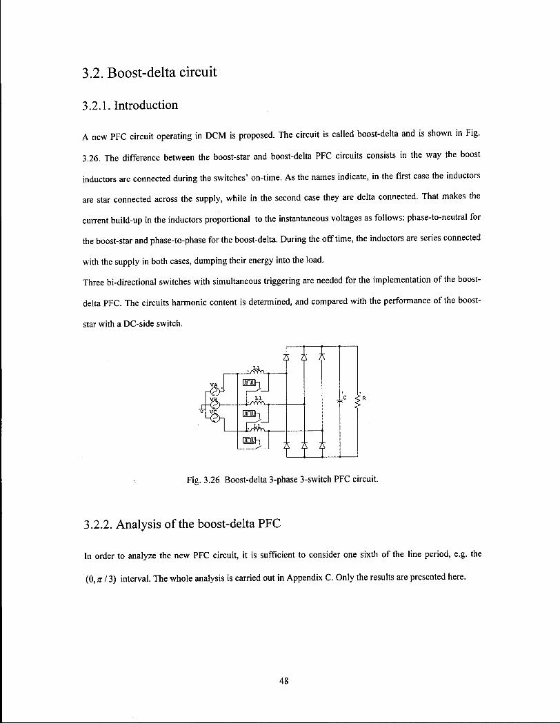
3.2. Boost-delta circuit
3.2.1. Introduction
A new PFC circuit operating in D C M is proposed. The circuit is called boost-delta and is shown in Fig.
3.26. The difference between the boost-star and boost-delta PFC circuits consists in the way the boost
inductors are connected during the switches' on-time. As the names indicate, in the first case the inductors
are star connected across the supply, while in the second case they are delta connected. That makes the
current build-up in the inductors proportional to the instantaneous voltages as follows: phase-to-neutral for
the boost-star and phase-to-phase for the boost-delta. During the off time, the inductors are series connected
with the supply in both cases, dumping their energy into the load.
Three bi-directional switches with simultaneous triggering are needed for the implementation of the boost-
delta PFC. The circuits harmonic content is determined, and compared with the performance of the boost-
star with a DC-side switch.
In order to analyze the new PFC circuit, it is sufficient to consider one sixth of the line period, e.g. the
(0, n 13) interval. The whole analysis is carried out in Appendix C. Only the results are presented here.
VA
Fig. 3.26 Boost-delta 3-phase 3-switch PFC circuit.
3.2.2. Analysis of the boost-delta PFC
4 8
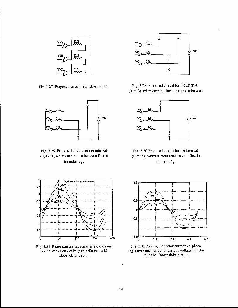
V B L 2
f V Q I—-(g)' | - r W Y \
L 3
Fig. 3.27 Proposed circuit. Switches closed.
V A L l
0
Fig. 3.29 Proposed circuit for the interval
(0,^/3), when current reaches zero first in
inductor L,.
V A L l
KrR L 2
L_(2> vwv_
Fig. 3.28 Proposed circuit for the interval
(0,^/3) when current flows in three inductors.
V A L l
v c L 3
Fig. 3.30 Proposed circuit for the interval
(0,^/3), when current reaches zero first in
inductor L , .
49
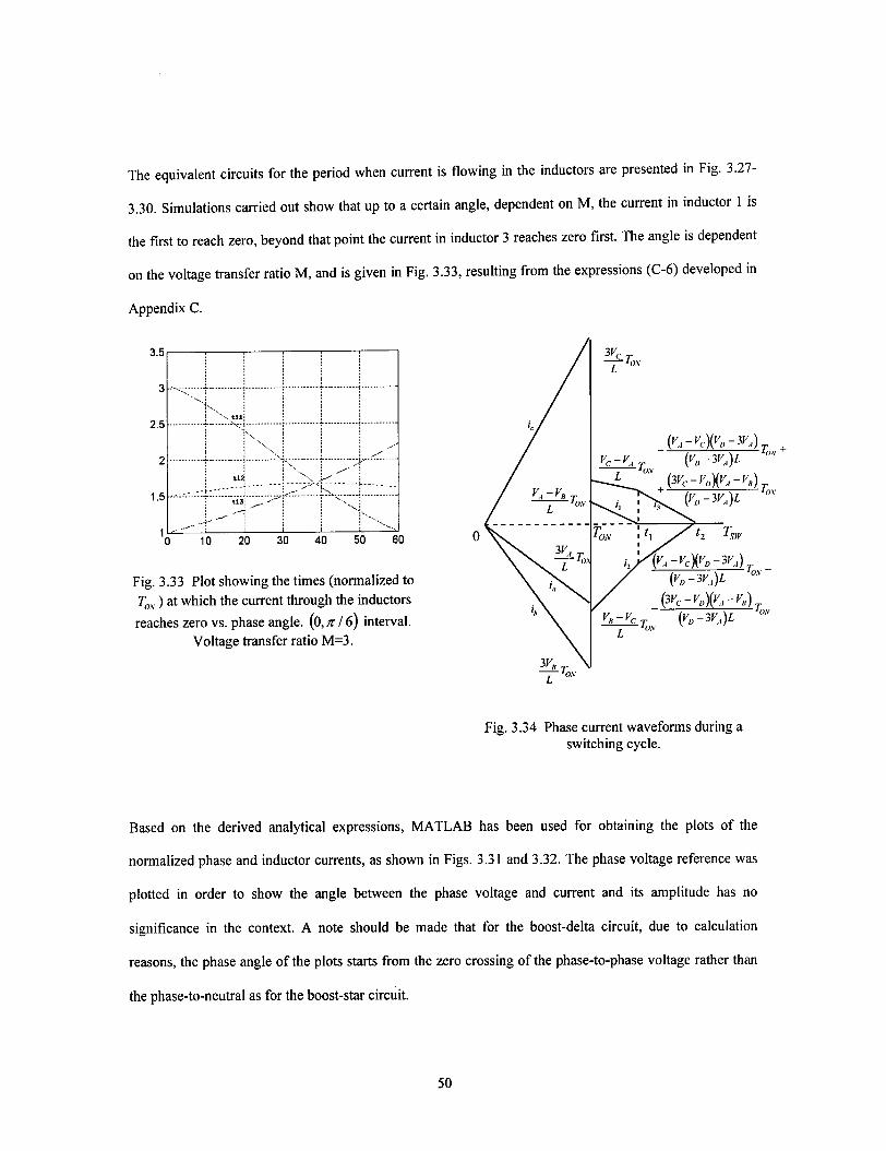
The equivalent circuits for the period when current is flowing in the inductors are presented in Fig. 3.27-
3.30. Simulations carried out show that up to a certain angle, dependent on M, the current in inductor 1 is
the first to reach zero, beyond that point the current in inductor 3 reaches zero first. The angle is dependent
on the voltage transfer ratio M , and is given in Fig. 3.33, resulting from the expressions (C-6) developed in
Appendix C.
3.5
3
2.5
2
1.5
1
VN t i l
v t ! 2
t ! 3 ^
10 20 30 40 50 60
Fig. 3.33 Plot showing the times (normalized to Tm) at which the current through the inductors reaches zero vs. phase angle. (0, n 16) interval.
Voltage transfer ratio M=3.
(VD-WA)L ' M
2 Tsw
{yD-jvA)L AV"
; ^ ln\
Fig. 3.34 Phase current waveforms during a switching cycle.
Based on the derived analytical expressions, MATLAB has been used for obtaining the plots of the
normalized phase and inductor currents, as shown in Figs. 3.31 and 3.32. The phase voltage reference was
plotted in order to show the angle between the phase voltage and current and its amplitude has no
significance in the context. A note should be made that for the boost-delta circuit, due to calculation
reasons, the phase angle of the plots starts from the zero crossing of the phase-to-phase voltage rather than
the phase-to-neutral as for the boost-star circuit.
50

The displacement angle can be determined by making the phase A average current equal to zero. Solving
numerically for various M , it has been determined that the phase current is leading the phase voltage by an
angle as shown in Fig. 3.36.
3.2.3. Component ratings
The study of the interval (0,^/6) is sufficient for the determination of the maximum voltage across the
switch. For the period when all three inductors have a current flow:
V (3-41) V =K - — ' SW I B ^
V V =v - — ' Sll'3 A ^ It has been determined that the maximum voltage happens across switch 2:
max(Fs,2) = F M ( l + ^ | ^ ) (3-42)
For the period when only two inductors have a current flow, it can be shown that the voltage is less than the
value determined above. This result is confirmed by time-domain simulation results.
The peak inductor current is given by the expression:
V T J3V T (3-43) max(/t_,A.) = maxH^) = ^ "
The peak switch current is given by the expression:
max(iar.„) = max(- - ) (3-44)
L L
The average instantaneous switch current is:
" { t ) - ~ L ~ 2 t ~ 2 D ~ 2LU K )
The time-domain simulation of the circuit has been done using PSIM. A comparison of the theoretical
calculations, time-domains simulations and experimental measurements has been carried out in Chapter 6.
51
3.2.4. Harmonic Injection
The boost-star circuit [11], has been extensively studied. Inherently, the circuit has a high 5 t h harmonic
component and a high Total Harmonic Distortion (THD) at low voltage transfer ratios M and fixed duty-
cycle operation. Consequently, in [13,33-35], various harmonic injection techniques which modulate the
duty cycle have been proposed.
The properties of the boost-delta circuit are further investigated in regards to harmonic reduction. The 5 t h
and 7 t h harmonics are determined for various voltage transfer ratios and so is the phase angle by which the
current leads the voltage. A harmonic injection technique is proposed in order to reduce the THD.
A comparison is made between the boost-delta and the boost-star circuits, with and without harmonic
injection. The criterion is the maximum power handling capability in light of the requirements of the IEC
1000-3-2 standard.
The 5 t h and 7 t h harmonics of the phase currents for the two circuits are presented in Fig. 3.35. The boost-
delta shows a slightly better performance than the boost-star circuit.
Fig. 3.35 5 t h and 7 t h harmonics (%) vs. Fig. 3.36 Leading angle of phase current vs. voltage transfer ratio M . voltage transfer ratio M . Boost-delta circuit.
An interesting property of the boost-delta is that, unlike the boost-star where the current fundamental is in
phase with the voltage, here the current is leading the voltage (for a certain phase sequence). The leading
52
angle is dependent on the voltage transfer ratio M as shown in Fig. 3.36. The same plot shows the current
zero crossing angle which is different from the leading angle mentioned above due to the asymmetry of the
waveform.
Analyzing Fig. 3.35 it can be seen that the 5 l h harmonic, in particular, is quite large at low voltage transfer
ratios. This limits the power capability of the circuits which have to meet the absolute harmonic values
stipulated by the IEC 1000-3-2 standard. The various harmonic injection techniques proposed in [13,33-35]
revolve around the idea of introducing a 6 t h harmonic component in the duty cycle, one example being the
formula in [34]:
d = dmm - m{\ + cos(6ft>. i)) (3'46)
where: m = injected harmonic amplitude.
A harmonic injection technique which improves the performance of the boost-delta circuit is proposed in
the following. It is also based on the modulation of the duty cycle with a 6 l h harmonic of the line frequency.
However, the modulation is done with a sine term rather than a cosine as in the boost-star circuit:
rf = rfm„-i»(l + sin(6fl>./)) ( 3 " 4 ? )
MATLAB has been used for the determination of the optimum amplitude of the injected harmonic in order
to maximize the power capability. As an example of the improvement possibility, the shape of the phase
current is shown in Fig. 3.37 for a voltage transfer ratio M=l .5 with and without harmonic injection.
53

A comparison is drawn between the boost-star and boost-delta circuits, with and without harmonic
injection. The optimization criterion is maximum power throughput while satisfying the IEC 1000-3-2
requirements.
A short presentation of the IEC 1000-3-2 will be made in the following:
- the voltage at which the measurements are made is 3 phase 400V, 50Hz;
- the absolute rms value of the line current and its harmonics are given: fundamental current, 16 A; 5 t h
harmonic, 1.14 A; 7 t h harmonic, 0.77 A; 11th harmonic, 0.33 A; 13th harmonic, 0.21 A.
- the maximum power to which the standard applies is:
Pmm = 4l>x40Wx\6A = 11,072W ( 3" 4 8)
- the relative values of the harmonics are:
5 t h harmonic —x\00 = 7.125% ; 7 t h harmonic — * 1 0 0 = 4.812% (3-49) 16 16
Inharmonic — xlOO = 2.062% ; 13,h harmonic — *100 = 1.312% 16 16
the harmonics ratio:
S'h 114 5'* 114 ^ - = — = 1.481, -?— = — = 3.455 l'h 0.77 11'* 0.33
(3-50)
The maximum power handled by the PFC circuits analyzed is determined based on the following
optimization criteria:
a - for high voltage transfer ratios, the maximum power can be handled without harmonic injection, since
the relative values of the harmonics are below the standard limits;
b - at lower voltage transfer ratios, harmonic injection is used in such way that the relative values of the
harmonics are still below the standard limits and maximum power can be processed;
c - at very low voltage transfer ratios, the harmonic injection amplitude can be chosen in such a way that
the harmonics ratios 5*/7th and 5 t h/l 1th are close to the standard limit. In this way, the power transferred is
below the standard limit but it is maximized with respect to the absolute harmonic components acceptable.
The application of these criteria will be illustrated in Tables 3.1-3.4, which show the performance of the
boost-star and boost-delta PFC circuits with and without harmonic injection.
54
Based on the results presented in Tables 3.2 and 3.4, the plots of the optimized amplitude of the injected
sixth harmonic are shown in Fig. 3.38. Further on, the information in the tables is shown in a chart type
comparison of the 5 t h harmonic, T H D and maximum power in Figs. 3.39-3.41.
The overall result is that the boost-delta has slightly better performance than the boost-star in terms of
harmonics. By introducing harmonic injection, a significant reduction of the harmonics occurs for both
circuits, while the boost-delta still preserves its small advantage.
0016
0014
0.012
0.01
0.008
0.006
0.004
0.002
0 1
j
/ ! \ injected fiarmonic amplitude / ! ' \ for booit-star rircjiit
i i \ j
• - — 4 — . : \ •
/ • \ injected harmonic amplitude \
for boost-d^lta circuit; \ \ j
\ \ i
: : : 1.2 1 4 1.6 2.2
Fig. 3.38 Injected harmonic amplitude vs. voltage transfer ratio, M for the boost-star and
boost delta circuits
I u 1
• a nb
c Bd
1 1 1 1 1 I t 1.2 1^ 14 15 15 1.7 Ifl 15 2
Voltage transfer ratio M
Fig. 3.39 5 t h harmonic vs. voltage transfer ratio, a- boost-star without harmonic injection,
b- boost-star with harmonic injection, c - boost-delta without harmonic injection, d - boost-delta with harmonic injection.
E C 1000-3-2 limit |
1J 1.7 1.8
VoRafle trarofof r rtk, M
Fig. 3.40 Total Harmonic Distortion vs. voltage transfer ratio M .
a - boost-star without harmonic injection, b- boost-star with harmonic injection,
c - boost-delta without harmonic injection, d - boost-delta with harmonic injection.
Fig. 3.41 Maximum power based on harmonic content required by IEC 1000-3-2 vs. voltage
transfer ratio M . a- boost-star without harmonic injection,
b- boost-star with harmonic injection, c - boost-delta without harmonic injection,
d - boost-delta with harmonic injection.
55

Table 3.1 Performance of the boost-star circuit without harmonic injection
M it (normalized
value)
itr5 %
itr7 %
itrl 1 % itrl 3 %
THD %
Power (W)
1.1 0.068 29.08 8.48 0.29 0.86 31.80 2,713
1.2 0.138 21.10 2.68 1.31 0.41 21.81 3,739
1.3 0.200 16.88 0.60 1.22 0.34 17.18 4,674
1.4 0.255 14.18 0.34 1.03 0.29 14.37 5,564
1.5 0.302 12.27 0.81 0.85 0.25 12.42 6,429
1.6 0.345 10.84 1.06 0.70 0.22 10.98 7,277
1.7 0.382 9.72 1.19 0.58 0.19 9.86 8,114
1.8 0.416 8.82 1.26 0.49 0.16 8.96 8,943
1.9 0.446 8.08 1.28 0.42 0.14 8.22 9,767 2.0 0.473 7.45 1.29 0.36 0.12 7.59 10,584 2.1 0.498 6.92 1.28 0.31 0.11 7.04 11,072
Table 3 .2 Performance of the boost-star circuit with harmonic injectio n
M it (normalized
value)
itr5 %
itr7 %
itrll %
itrl3 %
THD %
m Power (W)
Optimization Criteria
1.1 0.047 16.29 6.37 4.65 0.17 18.40 0.0120 4,843 a
1.2 0.110 11.71 7.56 3.39 0.43 14.50 0.0155 6,738 a
1.3 0.171 9.99 6.71 2.40 0.45 12.37 0.0157 7,898 a
1.4 0.226 8.82 5.93 1.78 0.40 10.85 0.0151 8,939 a
1.5 0.275 7.90 5.33 1.37 0.35 9.68 0.0144 9,990 a
1.6 0.319 7.17 4.83 1.09 0.30 8.75 0.0136 11,002 a
1.7 0.361 7.11 3.86 0.84 0.24 8.16 0.0107 11,072 b
1.8 0.401 7.11 3.00 0.64 0.19 7.77 0.0076 11,072 b
1.9 0.437 7.11 2.26 0.50 0.16 7.50 0.0046 11,072 b
2.0 0.470 7.12 1.63 0.38 0.13 7.33 0.0017 11,072 b
2.1 0.498 6.92 1.28 0.31 0.11 7.04 0 11,072 c
Table 3.3 Performance of the boost-delta circuit without harmonic injection
M it (normalized
value)
itr5 %
itr7 %
itrll %
itrl 3 %
THD %
Power (W)
l . l 0.079 25.78 9.72 2.42 0.17 26.58 3,060 1.2 0.170 18.33 4.75 2.01 0.61 18.70 4,303 1.3 0.263 14.65 3.12 1.74 0.63 14.92 5,384 1.4 0.348 12.38 2.44 1.49 0.60 12.62 6,372
1.5 0.430 10.80 2.11 1.28 0.54 11.02 7,304
1.6 0.509 9.62 1.91 1.10 0.49 9.83 8,200 1.7 0.584 8.70 1.77 0.97 0.44 8.91 9,067 1.8 0.650 7.95 1.67 0.86 0.40 8.15 9,923
1.9 0.718 7.33 1.60 0.76 0.36 7.53 10,762 2.0 0.781 6.80 1.52 0.68 0.33 7.01 11,072
Table 3.4 Performance of the boost-delta circuit with harmonic injection
M it (normalized
value)
itr5 %
itr7 %
itrll %
itrl3 %
THD %
m Power (W)
Optimization Criteria
1.1 0.061 19.47 13.12 5.21 0.91 24.81 0.0063 3,954 a 1.2 0.145 12.02 8.09 3.36 0.81 15.09 0.0081 6,562 a
1.3 0.232 9.27 6.25 2.53 0.77 11.59 0.0088 8,511 a
1.4 0.315 7.85 5.29 2.03 0.70 9.77 0.0091 10.045 a
1.5 0.396 7.12 4.50 1.67 0.63 8.65 0.0089 11,072 b
1.6 0.481 7.12 3.42 1.36 0.54 8.07 0.0071 11,072 b 1.7 0.564 7.12 2.60 1.12 0.47 7.70 0.0052 11,072 b
1.8 0.638 7.11 2.00 0.93 0.41 7.48 0.0030 11,072 b
1.9 0.714 7.11 1.63 0.78 0.37 7.37 0.0008 11,072 b
2.0 0.781 6.80 1.52 0.68 0.33 7.01 0 11,072 c
56

3.2.5. Average current space vector analysis
Individual modulation of the switches is not possible due to the fact that after turn-off the three phase
currents don't add up to zero.
The averaged current space vector for the boost-delta circuit is calculated based on the method in Section
2.1. The resulting formulas, given below for the regular phase sequence, are visually represented in Fig.
3.42.
[>&,._ )TOS + i(rov+)/, + /(/,)/, + /(/, )/2 ] ( }
3 g v + f ^ . , - , , , ) V 3 7 ' w ( 2 / , + r 2 ) | 2VD _J2kI3 ( 3 _ 5 2 )
271
m i(toJ-nI2)
y2Tsll, 2TS„. ) L 2TSW 3L 2TSW
When two phases are reversed or the switches are connected in reverse sequence, the formula becomes (3-
53) and the vectorial representation is as shown in Fig. 3.43 .
j{(o.t-xll) ',('.+0 27" 2T
1 .vif ' .sir
+ V. jbj-2,,3) ^TON{2t] +t2)t 2VD c j K l i tt(tl+t2) ( 3
271 3L 2TSW
•53)
For the case where two boost-delta circuits, one non-reversed and one reversed are run in parallel, the
formula is:
m_ j(a>.t-7tl2)
r6T^+t]n(t]n+t2n)+tw{tlr+t2r)' 271
(3-54)
+
V-^^(e^\2tUl +t2l,)+e^-^\2K + /„))+ L 2T,
3L 2T< sw
After rotating the axes of coordinates by (coJ -KI2) the vector becomes:
271, sw j L 2TSW
3L 21 s w
The indexes n and r are used for the non-reversed and reversed phase sequence boost-delta circuits.
(3-55)
57

As it was mentioned in previous sections of this chapter the performance of a boost-delta PFC is
comparable with the boost-star. However, when connecting two boost-delta circuits in parallel and their
phase connections are reversed, the performance is significantly improved. The explanation is that the
vectorial components not in phase tend to cancel each other, as can be seen by comparing Figs. 3.42 and
3.43.
The effect is presented in Fig. 3.44 where a dramatic reduction of the 5 t h harmonic occurs, particularly for
M=1.4. This is the area of most interest due to the practical applicability: Vin = 208K, VIM =420V for
North America and Vm = 3801 /, Vml =750K for Europe. Where perfectly sinusoidal current waveform
must be obtained, two boost-delta circuits must be connected in parallel, with reversed phase sequence. An
individual modulation of the duty cycle of each stage will make the circuit behave more inductively or
capacitively , as needed. Then a sinusoidal current can be achieved, even if the input voltage has some
distortion, by meeting the conditions given in formula (3-10).
3.2.6.Current calculations
Since the current waveforms during the switching cycle are different when compared with the boost-star
circuit, the formulas are determined for the boost-delta as well. The formulas (2-19, 2-20, 2-23) are applied.
The resulting plots are drawn in Figs. 3.45-3.47 for the inductor currents, at various voltage transfer ratios
M and maximum duty cycle, as well as for fixed M and variable duty cycle. The total rms contribution
shown in Fig. 3.46 varies with the duty cycle for a fixed voltage transfer ratio M . The fact that the rms
contribution of the switching frequency fundamental and harmonics is maximum at less than the maximum
duty cycle will help in the estimation of the heat losses in the inductors. A separation of the copper losses
due to the line frequency component and due to the skin effect at the switching frequency and its harmonics
is thus possible for the inductor winding.
By comparing the plots in Figs. 2.10 and 3.47, showing the rms contribution of the various harmonics at
maximum duty cycle and variable M, it can be seen that the difference between the boost-star and boost-
delta is small.
58
Fig. 3.42 Average current space vectors for boost-delta circuit.
: i i
l \ • ^ i
1 h a r m o n i c 1 •
\ \ 2 s t a g e s i "^"
. 7 t h h a i i m o n i c
/ 1 / 2 s t a g e s
n l i ' • • 1
1 . 1.5 2 2.5 3 3.5 A
Fig. 3.44 Boost-delta. One stage vs. two reverse connected. 5 lh and 7th harmonics (%) vs. voltage
transfer ratio M.
Fig. 3.43 Average current space vectors.
: :
/ I \ n n i
f / N a y e r a g e \ ;
/ t f s w f u n d a m e n t a l V\
-vl n l K : i • ^ ' 0 50 100 150 200
Fig. 3.45 Normalized inductor currents vs. phase angle for the boost-delta circuit. M=1.5
59
CHAPTER 4
BOOST, TWO-STAGE CIRCUITS
In this chapter PFC circuits with two boost stages are studied. Since the first stage can be a boost-star or a
boost-delta, and the second stage a flyback or a boost-delta, four combinations become possible. The
resulting circuits are analyzed using the average current space vector technique where possible, and a
sequence of diode conducting stages in the other cases. The principles underlying the improvement of
harmonic content in D C M are exposed. The advantages and disadvantages of n-stage PFC circuits are
investigated.
60
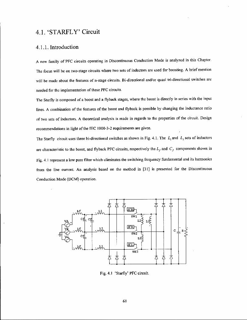
4.1. 'STARFLY' Circuit
4.1.1. Introduction
A new family of PFC circuits operating in Discontinuous Conduction Mode is analyzed in this Chapter.
The focus will be on two-stage circuits where two sets of inductors are used for boosting. A brief mention
will be made about the features of n-stage circuits. Bi-directional and/or quasi tri-directional switches are
needed for the implementation of these PFC circuits.
The Starfly is composed of a boost and a flyback stages, where the boost is directly in series with the input
lines. A combination of the features of the boost and flyback is possible by changing the inductance ratio
of two sets of inductors. A theoretical analysis is made in regards to the properties of the circuit. Design
recommendations in light of the IEC 1000-3-2 requirements are given.
The Starfly circuit uses three bi-directional switches as shown in Fig. 4.1. The I, and L2 sets of inductors
are characteristic to the boost, and flyback PFC circuits, respectively the Lf and Cf components shown in
Fig. 4.1 represent a low pass filter which eliminates the switching frequency fundamental and its harmonics
from the line current. An analysis based on the method in [31] is presented for the Discontinuous
Conduction Mode (DCM) operation.
L f ,1/YYYX
VA , c i cfi
VB L f
li/YYY\.
L l
L l
L l
swi L23 L 2
|JU~UL|—j
SW2
SRJ3
i l l Fig. 4.1 'Starfly' PFC circuit.
61

4.1.2. Analysis ofthe 'Starfly' Three-Phase PFC Circuit
The circuit proposed is analyzed with respect to its D C M operation. The three switches are simultaneously
either on or off. The switching period is chosen in such way that the currents in both the boost and flyback
parts of the circuit reach zero before the next turn-on of the switches. A voltage follower control is used
for the switches, where the on time and switching period are fixed.
In order to analyze the circuit, it is sufficient to consider one twelfth of the line period, e.g. the
interval (0,/z7 6).
The inductance ratio is:
T = LJL, (4-1)
The proposed starfly PFC stage has as particular cases the boost-star circuit with DC-side switch when
T = 0 , respectively flyback when T = °o .
While the boost circuit has a high Total Harmonic Distortion (THD) at low voltage transfer ratios, the
flyback with zero T H D suffers from high switch currents. The Starfly circuit alleviates these problems by
compromising on the characteristics of the boost and flyback. That makes the circuit particularly
interesting for the cases where low fifth and seventh harmonics, as well as T H D are desirable at low
voltage transfer ratios, i.e. M= 1.3-1.5.
In practical applications that would allow the use of 1200V semiconductor devices for the European 380 V
input voltage and 600V devices for the North American 208V , without the need for modulation of the duty
cycle [13,33-35].
Other benefits are the reduced switch current as well as the smaller size of the inductors. This is achieved
at the expense of the introduction of a second three-phase bridge of ultrafast recovery diodes.
With the assumption: fsw » fllm, the analysis method given in [1] can be applied. The equivalent circuit
looks like Fig. 4.2 during the switch on time and like Fig. 4.3 during the off time.
The equations for the interval (0,nib) are given in Appendix D. The current waveforms during a
switching cycle are shown in Figs. 4.4 and 4.5 for the inductor sets Z,, respectively L2.
62

The line current is obtained by averaging the inductor current over each switching cycle and plotting these
values for the entire line period.
The following formulas have been used in the analysis:
- the normalizing current:
2KL 3Z,, + L2
i LN T
the normalizing power:
9V} P - '•" T ^ " 2 ( 3 I 1 + Z 2 ) 0 N
where:
T0N = switch on time,
Tsw = switching period.
- the normalized value of the fifth harmonic:
^ - J C I O O l \
- the normalized value of the seventh harmonic:
^2-JC100
A - the Total Harmonic Distortion:
77/£>(%) =
19
xlOO
(4-2)
(4-3)
(4-4)
(4-5)
(4-6)
where:
/„ = the n , h harmonic of the line current obtained by Fourier series decomposition.
The parameters which give a qualitative description on the performance of the circuit are defined as
follows:
- the current ratio : Lx global peak /peak of the phase fundamental:
63

WLNT0N 3Z, + L2 = T0N (4"7)
3Z,, + L2 3VLNTsiyiiN Tswi\N
- the current ratio i2: L2 global peak /peak of the phase fundamental:
^yLNT0N 3LI+L2 = T0N
3LX+L2 2>VLNTswiyN -j3.Tswi[N
- the active power:
p - L n T i 2 ( 3 £ 1 + I 2 )
- the ratio inductors energy/transmitted energy:
max (L2i2
2) + max I 2 J l 2 J r 2
(4-9)
(4-10)
where:
z, = instantaneous current through inductor L , ,
/ 2 = instantaneous current through inductor L2,
iSN = peak of the fundamental of the average phase current,
Pav = average active power.
By looking at Figs. 4.6-4.8 it can be seen how by increasing T the line current waveforms are closer to
sinusoids. The plots of the fifth and seventh normalized harmonics as well as the T H D shown in Figs. 4.9-
4.11 indicate an improvement with the increase of the inductance ratio T.
On the other hand higher T increases the switch current and deteriorates the performance indicators of the
circuit, presented in Figs. 4.12-4.15.
64
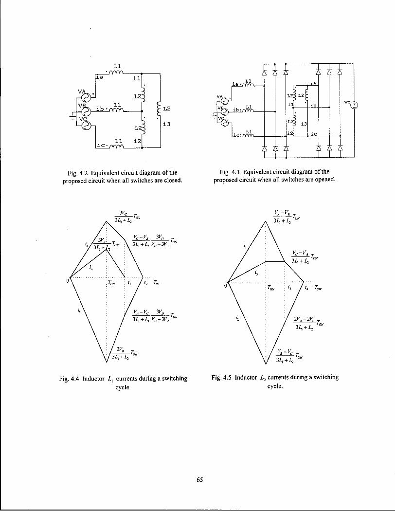
L I _/YYY\_
i l
L2:
- V C
L 2 -
L I i 2
L 2
i 3
Fig. 4.2 Equivalent circuit diagram of the proposed circuit when all switches are closed.
m m L l
L 1
U . c - - . / r Y Y V -
L23 L2^
i3
i2
m m Fig. 4.3 Equivalent circuit diagram of the
proposed circuit when all switches are opened.
Fig. 4.4 Inductor Lx currents during a switching
cycle.
Fig. 4.5 Inductor L2 currents during a switching
cycle.
65
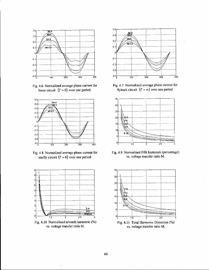
Fig. 4.8 Normalized average phase current for Fig. 4.9 Normalized fifth harmonic (percentage) starfly circuit (T = 6) over one period. vs. voltage transfer ratio M .
Fig. 4.10 Normalized seventh harmonic (%) Fig. 4.11 Total Harmonic Distortion (%) vs. voltage transfer ratio M . vs. voltage transfer ratio M .
66
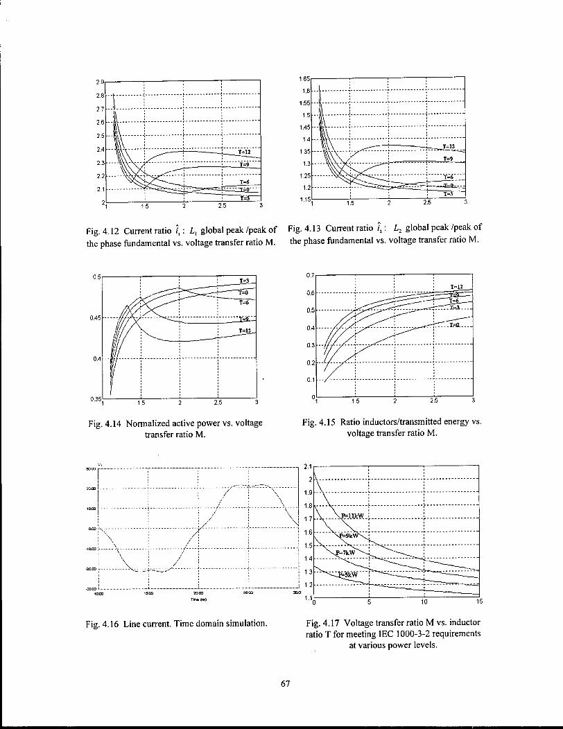
0.7,
0.6
0.5
04
0.3
0.2
0.1
0
1=12
— •—l£7...
1=12
— •—l£7...
i i
1.5 2.5
Fig. 4.15 Ratio inductors/transmitted energy vs. voltage transfer ratio M .
2.1
2
1.9
1.8
1.7
1.6
1.5
1.4
1.3
1.2
1.1
\ \p=iikw :
^<^5kW —
! " " —' '
10 15
Fig. 4.17 Voltage transfer ratio M vs. inductor ratio T for meeting IEC 1000-3-2 requirements
at various power levels.
0.5
0.45
0.4
0.35
~~T=O
T=6
T=n_
1.5 2.5
Fig. 4.14 Normalized active power vs. voltage transfer ratio M.
Fig. 4.16 Line current. Time domain simulation.
67

4.1.3. Design Related Issues
The component ratings are determined theoretically and they are matched by the results of the time-domain
simulation using PSIM. By inspection of the circuit the following component ratings can be determined:
- peak voltage across the switches and diodes:
max{Vsw)=VD (4-11)
- peak current through the switches and diodes:
max;™ = — L N U N
K s w ' 31, + L2
- peak inductor Lx current:
fc)-3*"7'" ( 4 " 1 3 )
31, + L2
peak inductor L2 current
(0 max 3i , + L2
The time domain simulation was done with the following values:
F s i n = 400K / 50Hz, VD = 800F, R = 59Q., Poul = 10,850JF I, = 35//// , L2 = 270/^/ , Ts„, = 40/zs,
Tm = 22.11//*, TMp =0.1/0, Tmal = 0.035 .
For the sake of brevity only the line current, with the switching frequency and its harmonics filtered out, is
shown in Fig. 4.16.
The requirements of IEC 1000-3-2 refer to absolute limits for the line frequency harmonics, for currents up
to 16 A per phase.
By inspection of Figs. 4.9 and 4.10 it can be seen that only the 5 ,h harmonic has a significant value. Based
on the standard, the limit for the 5 lh harmonics relative value can be calculated as follows:
/ 1 14 (4-15) jtlOO = — xlOO = 7.125%
/, 16
at maximum power throughput, i.e.:
4l>xmVx\(>A = 1 l,0721f ( 4 _ 1 6 )
68

Fig. 4.17 shows the inductance ratio T which allows various power throughput levels, while meeting the
standard requirements. It can be seen that for the same M and lower powers T will be smaller. These plots
can be a very helpful tool in the design, where after establishing the maximum throughput power, the
output voltage and the voltage transfer ratio range, the minimum inductance ratio T allowable can be
determined. In this way the peak current stress on the switches will be reduced most.
The features of the circuit can be seen in an overall comparison with other two-stages PFCs in Section 7.1.
4.1.4. Average current space vector analysis
The method developed in Section 2.1 can be applied for the analysis of the properties of the Starfly PFC
circuit. The circuit represents in fact a boost-star PFC with AC-side switches interconnected with a flyback
stage. For this reason the analysis is similar to the one carried out in Section 3.1 and the final equations are
given in Appendix D. As expected, the modulation options are similar with those in Section 3.1
The average current space vector for the line is given by the following formula:
+ *iXT0N +/, +Q | VmL2 /,(/, +f2)"L(»..-«/2) | 2VD /,(/, +t2)_J2Ml3 ( 4 1 ? )
3Z,, + L2 2TSW L\{iLx + L2) 2TSW _ 3L, 2Tslr
The inductance L2 appears this time in the expressions, and it is quite easy to prove that the ratio of the
vector component out of phase to the one in phase is decreasing with the increase of the inductors ratio T.
As it was already shown in Section 4.1.2 , and proven here by formula (4-17) the inductance of L2 plays a
harmonic reduction role. For sake of completeness the space vector formulas are given for modulation in
the case of the Starfly. However, the relative complexity of the circuit would encourage a mitigation of the
harmonic content based on the inductance ratio alone, and preservation of a fixed duty cycle, rather than on
modulation.
69

4.2. 'DELTAFLY' Circuit
4.2.1. Introduction
A new three-phase three-switch Power Factor Correction (PFC) circuit operating in Discontinuous
Conduction Mode (DCM), shown in Fig. 4.18, is proposed. The 'Deltafly' circuit consists of two stages, a
boost-delta and a flyback, where the boost-delta is directly in series with the input line. The boost-delta
circuit has a relatively high harmonic content and a leading/lagging current based on the phase sequence
and voltage transfer ratio. While the flyback has zero Total Harmonic Distortion (THD) and in-phase
current, high current/voltage stress on the switches limits its application. Just like in the case of the
'Starfly', a proportional combination of the features of the two stages is possible by changing the
inductance ratio of the two sets of inductors.
The following analysis refers to the boost-delta operating with a leading current. The results for the lagging
current situation, occurring for a reversed phase sequence, are determined in a similar way, based on the
results in Section 3.2.
The 'Deltafly' circuit uses six bi-directional switches. The quasi tri-directional switches presented in
Section 3.1.4 could replace two adjacent bi-directional switches by simply connecting the three
independent nodes of the circuit. The gating becomes easier due to the common emitter point. There are
two levels of complexity with regards to the operation of the switches. In the simplest, the switches are
turned simultaneously on/off, and a proportional combination of the features of the boost-delta and flyback
is obtained based on the inductance ratio. The possibility of cycle-by-cycle, interleaved boost-delta and
boost-star connection, by triggering the appropriate switches, could be implemented. In this way a
reduction of the harmonic content is possible, at the cost of power reduction throughput and slightly higher
control complexity. The latter implementation is a variation of the basic scheme, and will not be further
investigated here.
The high conduction losses and switching losses associated with the high number of semiconductors is a
trade-off for the simple voltage follower control and low Total Harmonic Distortion (THD).
70
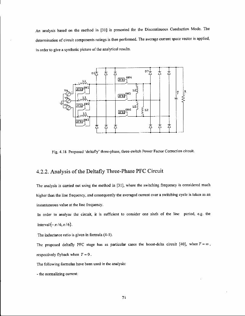
An analysis based on the method in [31] is presented for the Discontinuous Conduction Mode. The
determination of circuit components ratings is then performed. The average current space vector is applied,
in order to give a synthetic picture of the analytical results.
Va ,
L l
S W 2 |
L l JYYYX.
i 1 SW3
iJinaH S W 4
L 2 2 , , S W 5
iJinal—•
L2-. . S K I 6 DJrOfl-1
: L2
ill i l l
Fig. 4.18 Proposed 'deltafly' three-phase, three-switch Power Factor Correction circuit.
4.2.2. Analysis ofthe Deltafly Three-Phase PFC Circuit
The analysis is carried out using the method in [31], where the switching frequency is considered much
higher than the line frequency, and consequently the averaged current over a switching cycle is taken as an
instantaneous value at the line frequency.
In order to analyze the circuit, it is sufficient to consider one sixth of the line period, e.g. the
interval (- n 16, n 16).
The inductance ratio is given in formula (4-1).
The proposed deltafly PFC stage has as particular cases the boost-delta circuit [40], when T = oo ,
respectively flyback when T = 0 .
The following formulas have been used in the analysis:
- the normalizing current:
71

(4-18)
l» = LN T • " - I L , l s w
the normalizing power:
^LN T
(4-19)
where:
T0N = switches on time,
Tsw = switching period.
The parameters which give a qualitative description on the performance of the circuit are defined as
follows:
- the current ratio /',: Z,, global peak /peak of the phase fundamental:
Sv^Tp, 21, _ 2ST0N
A ^LN^SWHN TiWiw
- the current ratio i2: L2 global peak /peak of the phase fundamental:
SvLNTON 2L, 2ST0N I, ^ 2 ^LN^SW'IN TswiXN L2
- the active power:
3V P = ~2LTswixN C°S(Pl
(4-20)
(4-21)
(4-22)
the ratio inductors energy/transmitted energy:
U/2) max + max 1 2 J I 2 J T2
'ON
TSANC0S<PI
f L N
(4-23)
where:
= instantaneous current through inductor L,,
/', = instantaneous current through inductor L2,
ilN =peak of the fundamental of the average phase current,
72

Pm = average active power.
The equivalent circuits during the switches on-time and off-time are shown in Figs. 4.19 and 4.3. The
equations resulting from the analysis of the circuit are based on Appendix C for the boost-delta stage and
Appendix D for the flyback stage. The current waveforms during a switching duty cycle are presented in
Figs. 4.20-4.22 for the line, inductor L{ and L2 currents. Based on those results, the plots defining the
performance of the circuit are given below. In Fig. 4.23 the shape of the line currents shows clearly how
the inductance ratio makes the circuit look more like a flyback (T close to zero) or boost-delta (T large).
The same idea is reflected by the plots in Figs. 4.24 and 4.25 where the relative value of the 5 , h and 7 th
harmonics are given vs. the voltage transfer ratio M . While the boost-delta presents a current
leading/lagging phase-angle, the proposed circuit makes possible a reduction of this angle, as shown in Fig.
4.26.
4.2.3. Design related issues
The voltage, current and power rating utilization factor of the components will be given. The component
ratings are determined theoretically and they are matched by the results of the time-domain simulation
using PSIM.
By inspection of the circuit the following component ratings can be determined:
- peak voltage across the diodes:
max l :(FD1) = max(K 0 7 )=K z D (4-24)
- peak voltage across the switches:
•(*Wi)=^ + = VD, max(K, D (4-25)
max I SW-i-IGBT
- peak current through the diodes:
(4-26)
maxl ,maxl
- peak current through the switches:
73

max{ism) = max fv -V 3V„ N
l0N T 'ON y L\ L2 J
, max(/A.H,J=—— T(
max(/w_ 3. / C f l n)=max fy y \ 3V„ A RB T ZIJLT
''ON , 'ON Li
(• \ ^VLNT M A X V W - 3 - / G B 7 2 / - j 'ON
m a x{'sw-i-iGBn ) _
3^ 'ON
(4-27)
(4-28)
- peak inductor 7,, current:
SvLNTON
max
peak inductor L2 current:
max
(4-29)
(4-30)
A comparison will be drawn with the boost-delta and flyback circuits. A practical example is simulated
with the values given below:
Vsin = 400V/50Hz, VD=800V, R = 59C1, c = 4,700^ P(ml = 10,850 7, =135//.//, L2 = 135/ .7/,
Tsw = AQ/IJI , T0N = i.Ufij, Tslep = 0.2M.s , Tlolal = 0.04* .
The time-domain plots are shown to match the analytical results. In Fig. 4.27 the average line current is
given for an inductance ratio T=l. The inductors and semiconductors averaged currents are presented in
Figs. 4.28 and 4.29.
4.2.4. Average current space vector analysis
The space vector method presented in Section 2.1 is applied to the expressions given in Appendix E . As a
result the following expression is obtained for the line current:
'AV 37", ON 271
1 + ^L V L2 J
r , (? ,+f 2 )
2n, J3TON{2tl+t2) | 2VD c J 2 x l i f , ( r , + r 2 )
37, 27", 2Tt sw sw
(4-31)
74
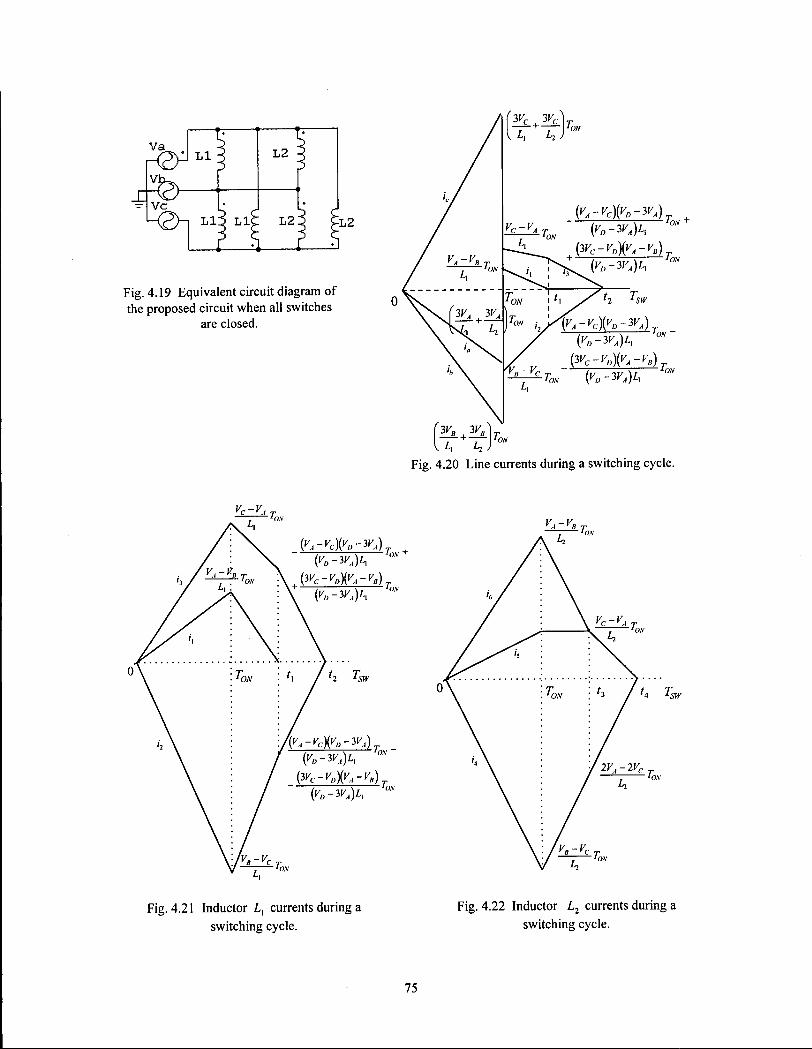
Va
- Vc L-0-n L l 3 L 1 C
L 2
L 2 : ~ L 2
Fig. 4.19 Equivalent circuit diagram of the proposed circuit when all switches
are closed.
; ; InN +
{wc-vD\vA-vB),
(Wc-^){VA-VB)T
T„N {VD-WA)L\ °N
Fig. 4.20 Line currents during a switching cycle.
75
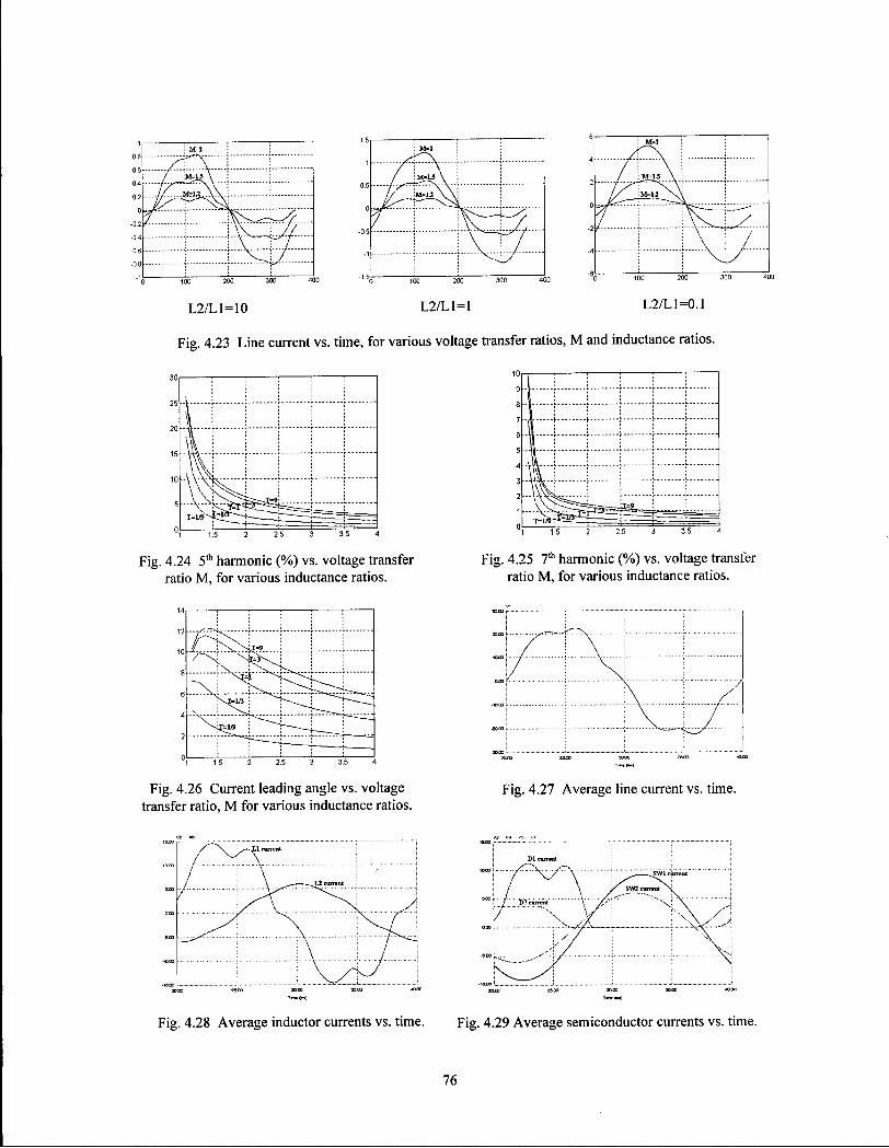
\
M«2
M=1.2 \ \ M=1.2 \ \
L2/L1=10 L2/L1=1 L2/L1=0.1
Fig. 4.23 Line current vs. time, for various voltage transfer ratios, M and inductance ratios.
Fig. 4.24 5 th harmonic (%) vs. voltage transfer ratio M , for various inductance ratios.
Fig. 4.25 7 th harmonic (%) vs. voltage transfer ratio M , for various inductance ratios.
Fig. 4.28 Average inductor currents vs. time. Fig. 4.29 Average semiconductor currents vs. time.
76
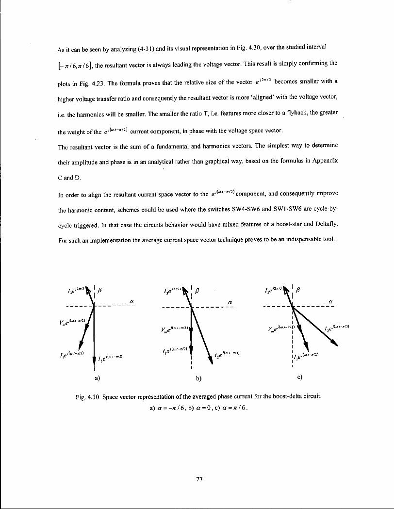
As it can be seen by analyzing (4-31) and its visual representation in Fig. 4.30, over the studied interval
[- nI'6,nI'6], the resultant vector is always leading the voltage vector. This result is simply confirming the
plots in Fig. 4.23. The formula proves that the relative size of the vector eA"n becomes smaller with a
higher voltage transfer ratio and consequently the resultant vector is more 'aligned' with the voltage vector,
i.e. the harmonics will be smaller. The smaller the ratio T, i.e. features more closer to a flyback, the greater
the weight of the EJ(AJ-*,2'> current component, in phase with the voltage space vector.
The resultant vector is the sum of a fundamental and harmonics vectors. The simplest way to determine
their amplitude and phase is in an analytical rather than graphical way, based on the formulas in Appendix
C and D.
In order to align the resultant current space vector to the e''""-*7^ component, and consequently improve
the harmonic content, schemes could be used where the switches SW4-SW6 and SW1-SW6 are cycle-by-
cycle triggered. In that case the circuits behavior would have mixed features of a boost-star and Deltafly.
For such an implementation the average current space vector technique proves to be an indispensable tool.
Fig. 4.30 Space vector representation of the averaged phase current for the boost-delta circuit.
a) a = -x / 6 ,b) a = 0, c) a = Kl6.
11
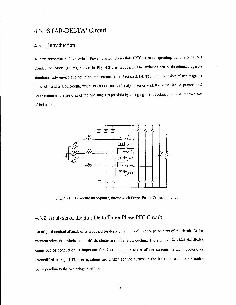
4 . 3 . 'STAR-DELTA' Circuit
4.3.1. Introduction
A new three-phase three-switch Power Factor Correction (PFC) circuit operating in Discontinuous
Conduction Mode (DCM), shown in Fig. 4.31, is proposed. The switches are bi-directional, operate
simultaneously on/off, and could be implemented as in Section 3.1.4. The circuit consists of two stages, a
boost-star and a boost-delta, where the boost-star is directly in series with the input line. A proportional
combination of the features of the two stages is possible by changing the inductance ratio of the two sets
of inductors.
L l irrrrv.
V A
VB J : - © — 1 / Y Y Y V -
L l
L 2
iJinitt-pBi
GnD-isKJ2
,L2 , rmrx
m m Fig. 4.31 'Star-delta' three-phase, three-switch Power Factor Correction circuit.
4.3.2. Analysis ofthe Star-Delta Three-Phase PFC Circuit
An original method of analysis is proposed for describing the performance parameters of the circuit. At the
moment when the switches turn off, six diodes are initially conducting. The sequence in which the diodes
come out of conduction is important for determining the shape of the currents in the inductors, as
exemplified in Fig. 4.32. The equations are written for the current in the inductors and the six nodes
corresponding to the two bridge rectifiers.
78
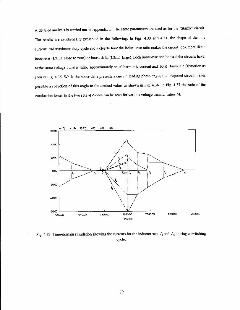
A detailed analysis is carried out in Appendix E. The same parameters are used as for the 'Starfly' circuit.
The results are synthetically presented in the following. In Figs. 4.33 and 4.34, the shape of the line
currents and maximum duty cycle show clearly how the inductance ratio makes the circuit look more like a'
boost-star (L2/L1 close to zero) or boost-delta (L2/L1 large). Both boost-star and boost-delta circuits have,
at the same voltage transfer ratio, approximately equal harmonic content and Total Harmonic Distortion as
seen in Fig. 4.35. While the boost-delta presents a current leading phase-angle, the proposed circuit makes
possible a reduction of this angle to the desired value, as shown in Fig. 4.36. In Fig. 4.37 the ratio of the
conduction losses in the two sets of diodes can be seen for various voltage transfer ratios M .
i(U20) i(Liq> Kj-21) i(j-7) ifljqi \Qja> eo.oo i
73CO.OO 7310.00 7320.00 7330.00 7340.00 7350.00 7360.00
Time (u*)
Fig. 4.32 Time-domain simulation showing the currents for the inductor sets Lx and L2 during a switching cycle.
79
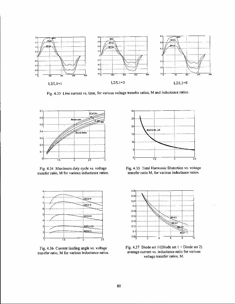
400
L2/L1=1 L2/L1=3 L2/L1=9
Fig. 4.33 Line current vs. time, for various voltage transfer ratios, M and inductance ratios.
— • — ^ L J i i = i ^ ^ ^
;
1— -—^j£irL£i___^^
_J I I 1.5 2 2.5
Fig. 4.36 Current leading angle vs. voltage transfer ratio, M for various inductance ratios.
i
I
Fig. 4.37 Diode set l/(Diode set 1 + Diode set 2) average current vs. inductance ratio for various
voltage transfer ratios, M .
80
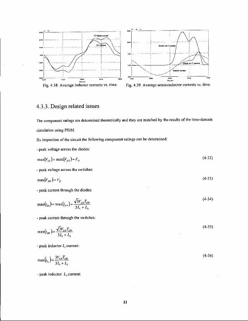
Fig. 4.38 Average inductor currents vs. time. Fig. 4.39 Average semiconductor currents vs. time.
4.3.3. Design related issues
The component ratings are determined theoretically and they are matched by the results of the time-domain
simulation using PSIM.
By inspection of the circuit the following component ratings can be determined:
- peak voltage across the diodes:
maxfo,) = max(Vm ) = VD (4-32)
- peak voltage across the switches:
m?Lx(Vstv)=VD (4-33)
- peak current through the diodes:
max(iD1) = max(/ f l 7) = L N ° N
jL/y "f"
- peak current through the switches:
max!; w j = L N U N
- peak inductor Lx current:
maxu, )= —
peak inductor L2 current:
81

SvwTm
3Z,, + L2
(4-37)
max I
A comparison will be drawn in Section 7.1 with the other PFC circuits proposed. A practical example is
simulated with the values given below:
ys.n = 400F/50//Z , VD = 800F , R = 59Q , C„„, = 500//F, PM = 10,850^ Z,, = 25.5//.// ,
L2 = 76.5//.// , fsw = 25kHz , D = 0.2445 , Tslep = 0.3//.* , Tlolal = 0.03* .
The time-domain plots are shown to match the analytical results. The inductors and semiconductors
averaged currents are presented in Figs. 4.38 and 4.39.
82
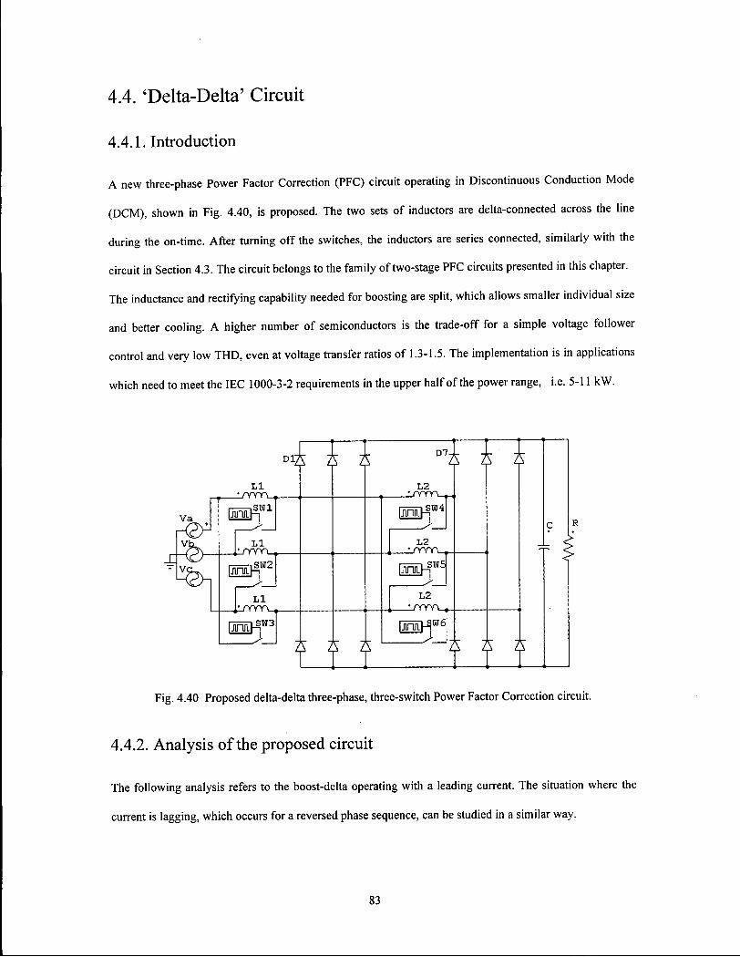
4.4. 'Delta-Delta' Circuit
4.4.1. Introduction
A new three-phase Power Factor Correction (PFC) circuit operating in Discontinuous Conduction Mode
(DCM), shown in Fig. 4.40, is proposed. The two sets of inductors are delta-connected across the line
during the on-time. After turning off the switches, the inductors are series connected, similarly with the
circuit in Section 4.3. The circuit belongs to the family of two-stage PFC circuits presented in this chapter.
The inductance and rectifying capability needed for boosting are split, which allows smaller individual size
and better cooling. A higher number of semiconductors is the trade-off for a simple voltage follower
control and very low THD, even at voltage transfer ratios of 1.3-1.5. The implementation is in applications
which need to meet the IEC 1000-3-2 requirements in the upper half of the power range, i.e. 5-11 kW.
Va
D i A A L l
L / Y Y Y V
iJiniLi—i
L l
L l ,1/TYYYH
S W 3 iJlfUhn
i l l
°7i A' A L 2
SW4
L 2 JJTYYY
SW5l rjQJLp?
L 2 L/YYYV
W6
Fig. 4.40 Proposed delta-delta three-phase, three-switch Power Factor Correction circuit.
4.4.2. Analysis of the proposed circuit
The following analysis refers to the boost-delta operating with a leading current. The situation where the
current is lagging, which occurs for a reversed phase sequence, can be studied in a similar way.
83

The analysis is carried out using the method in Section 4.3. The assumption is made that the switching
frequency is much higher than the line frequency, and consequently the averaged current over a switching
cycle is taken as an instantaneous value at the line frequency. During off-time there are initially six diodes
conducting. They come consecutively out of conduction pending on the node currents at the legs of the
three-phase rectifiers. The phase angle, voltage transfer ratio and inductance ratio are factors which will
influence the switching period and the averaged phase and inductor currents. A chart of all the possible
combinations has been devised and M A T L A B has been used for solving the system.
The normalizing current used in the analysis is:
. V (4-38)
'N ~ 2L{
s w
where;
Tsw = switching period.
The analysis is carried out in Appendix F and some of the results are given in the following. The plots in
Figs. 4.41-4.43 show the variation of the 5 th , 7 th harmonics (percent of the fundamental) and current
fundamental leading angle vs. the inductance ratio, T for various M . The same plots are then presented vs.
voltage transfer ratio M , for various T, in Figs. 4.44-4.45.
4.4.3. Design related issues
The component ratings are determined theoretically and they are matched by the results of the time-domain
simulation using PSIM.
By inspection of the circuit the following component ratings can be determined:
- peak voltage across the diodes:
max{vD]) = max(vD1)=VD (4-39)
84
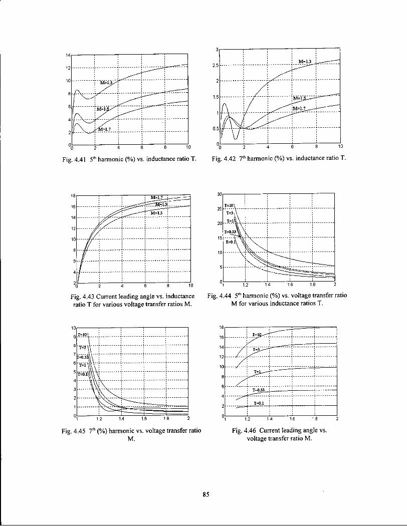
85
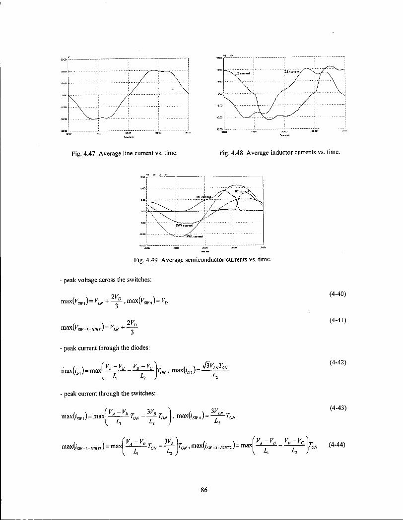
Fig. 4.47 Average line current vs. time. Fig. 4.48 Average inductor currents vs. time.
Fig. 4.49 Average semiconductor currents vs. time.
- peak voltage across the switches:
7M max{Vsm) = VLN+—^-, max(VSIV4)= VD
(4-40)
m a x(^sw-3-IGBT)~ 2Vn
(4-41)
- peak current through the diodes:
<('DI) = maxwm ; = max T0N, max(iD7) = SVLNT0I
J 2 J
(4-42)
- peak current through the switches:
(• \ ( V A ~ V B r r WBT 1
max(ism) = max T0N - — T0N
V A L 2 J
(. \ 3F/JV » n>ax(iW4)=—— Ta
(4-43)
maxu SW-l-IGBTI ) = max| I 0 N I
T0N . max(iSH,_3.K;flr2)= max VA VB Vg VC TON (4-44)
u 2 J
86

m a x\'siv-3-iGBn!~ . 'ON L2
- peak inductor Lx current:
(. \ SVu,Tw
(4"45)
- peak inductor L2 current:
(. ) SVINT0N
( 4 " 4 6 )
L2
A comparison will be drawn in Section 7.1 with the other PFC circuits proposed. A practical example is
simulated with the values given below:
Vsin = 400V/50Hz , K o = 8 0 0 F , fl = 62.5Q, C = 500//F, Pm,= 10,240^ , L,=162/tf/, L2=54juH,
r v, = 40/JS , Tm = 6.55/tf, TMp = 0.2/zs , Ttolal = 0.03s .
PSIM has been used for the plots in Figs. 4.47-4.49. In Fig. 4.47 the average line current is given for an
inductance ratio T=0.33. The harmonic values as determined using PSIM correspond to those expected
from Figs. 4.44 and 4.45. The improvement of the phase current harmonic content can also be easily seen
by comparing Fig. 4.47 with Fig. 2.1 for an M=1.4. The inductors and semiconductors averaged currents
are presented in Figs. 4.48 and 4.49.
87

4.5. N-level circuits
4.5.1. Harmonic reduction techniques for DCM operation
A generic drawing of the shape of the line current in a PFC circuit operating in DCM is given in Fig. 4.50.
The waveform does not have continuity due to the possible change of the amplitude based on the
configuration of the switches.
An inspection ofthe waveform results in the conclusion that, when TON, Tsw are constant, there are three
sets of variables which could make the current more sinusoidal. By keeping two criteria constant and
varying the third one, a direct influence on the harmonic content can be achieved, as shown below:
0 sw
Fig. 4.50 Generic line current during a switching cycle.
- for /(: %N-)=i{ToN+) a n d Li =Li • (4-47)
Ph
- for i{T0N_)= i{T0N+) and VD « Vph
(4-48)
- for VD « Vph and Z, = L2
(4-49)
i{TON-)»i(ToN+)
In the drawing k is a sub-unitary coefficient.
88

VD » Vph is equivalent to M »1.
Another way of reducing the harmonics is when :
'(TON- ) = '(TON+ ) > A = A > VD * ^ph > ^
and a variable T0N, TSW are used, such as it was the case with the boost-star with AC-side switch.
4.5.2. Features of the N-level circuits
The PFC circuits studied in the present chapter have as a common characteristic the use of two boost stages
connected in series during the ON-time and in series/parallel during the OFF-time. These circuits take
advantage of the harmonic reduction criteria presented in Section 4.5.1. The building blocks for the
development of these circuits are boost-star, boost-delta for the input, and flyback and boost-delta for the
second stage, as shown in Figs. 4.51-4.54. One more variation is possible in the phase sequence for the
boost-delta stages, as explained in Section 3.2. In the alternative of N-connected stages various
combinations could be made with one input and (N-l) follow-up boosting stages.
Besides this type of connection, several networks of parallel running circuits could also be connected to the
same DC output rail. An example can be given in the two boost-delta with reverse connection sequence, as
presented in Section 3.2.5. Also the interconnection of several parallel and series networks can be made on
the AC-side with the use of bi-, tri- or N-directional switches.
As a general rule little benefit is seen in connecting more than two stages. This is due to the added
complexity, reduced improvement over two stages, and particularly difficult layout with largely sized
inductors. In order that such circuits receive more interest, layouts must be developed where the ratio of
inductor size and interconnection length is large.
Some of the problems specific to N-series connected circuits are underlined below:
Interleaved switching pattern of the stages for a reduction of the EMI/filtering requirements is not
possible; a parallel structure must be available for that purpose;
switch's current is highest close to the supply and decreasing toward the D C side. The same trend is
valid for the first set of line inductors depending on the number of switches series connected.
8 9
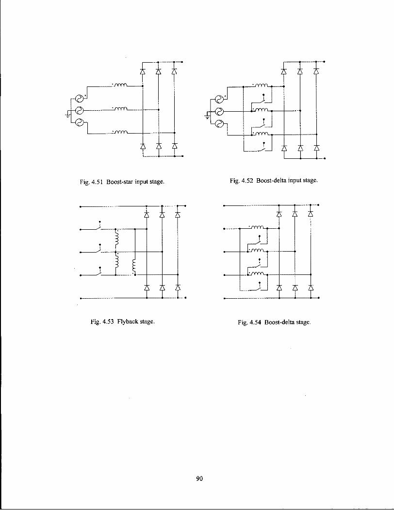
l/YYYV.
K 2 h _1/YYY\_
F T ?
J:-<2>-^<2h
t
1/YYYV
t
irrrrv.
ill Fig. 4.51 Boost-star input stage. Fig. 4.52 Boost-delta input stage.
. ] t t M s A
t p M s A s A
z u i f.
i
irrm.
t
UTYYV
H i Fig. 4.53 Flyback stage. Fig. 4.54 Boost-delta stage.
90
CHAPTER 5
SEPIC-DERIVED CIRCUITS
The location of the switches on the AC-side, allows the development of SEPIC (Single-Ended-Primary-
Inductor-Circuit) networks across the three phases. Due to the star-delta nature of three-phase, two new
circuit topologies become possible: the star-SEPIC and delta-SEPIC. It is shown that the general properties
of the SEPIC are carried over, while the power distribution across three sets of components allows a more
manageable size.
91
5.1.Star-SEPIC
5.1.1. Introduction
The present chapter extends the SEPIC topology, first developed in [41] to a three-phase three-switches
power factor correction (PFC) stage operating in DCM. Unlike previous work [42,43] where the SEPIC
topology is placed on the DC side, in the proposed circuit it is placed on the AC side, i.e. before the
rectifying bridge. The circuit consists of three bi-directional switches and three SEPIC characteristic L-C
networks as shown in Fig. 5.1.
For DCM operation a possible implementation of the three bidirectional switches is by using three IGBTs
with antiparallel diodes, star-connected with a common emitter. This way the gating signals for all the
controllable switches of the circuit have a common reference.
It is known that in the case of the SEPIC converter the DCM can occur with inductor current reaching zero
every switching period or following a base line at the supply frequency. In the present work the mode in
which the current of the inductors always reaches zero is studied. As documented in [44] in this case the
energy stored in the inductors is the smallest.
The results reported here are the outcome of an analytical investigation of the circuit's steady state
behavior. The theoretical analysis has its roots in the previous work developed for single-phase PFC [45-
48] and the averaging method proposed in [31]. The normalized current waveforms, harmonics, THD and
design optimization criteria are determined. Time domain simulations which confirm the analytical results
are shown.
Several disadvantages present in the popular DCM boost topology, like:
• difficult implementation of input-output isolation;
• difficult to control overload and start-up overcurrents;
• need of a high voltage transfer ratio or duty cycle modulation for the reduction of the 5 t h and 7 th
harmonics;
can be easily eliminated due to the intrinsic properties of the SEPIC converter. In addition, for the same
power level the inductor volume for the SEPIC and boost DCM PFC stages stays approximately the same
with the advantage of having split inductors in the first case.
92
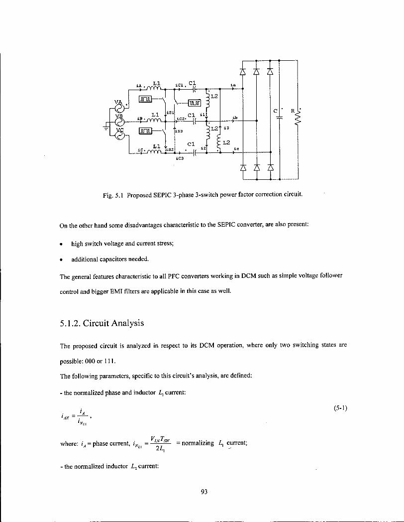
1A L l i C l c l
V A ,
L l
>L2
L l +.
iC2- Cl i i .
*-|iS3 ! L 2
l a —>—
->—
Cl ->— iC3
L2
ill Fig. 5.1 Proposed SEPIC 3-phase 3-switch power factor correction circuit.
On the other hand some disadvantages characteristic to the SEPIC converter, are also present:
• high switch voltage and current stress;
• additional capacitors needed.
The general features characteristic to all PFC converters working in DCM such as simple voltage follower
control and bigger EMI filters are applicable in this case as well.
5.1.2. Circuit Analysis
The proposed circuit is analyzed in respect to its DCM operation, where only two switching states are
possible: 000 or 111.
The following parameters, specific to this circuit's analysis, are defined:
- the normalized phase and inductor Lx current:
iA (5-1) AN ~ . '
V T where: iA = phase current, iN = w s w = normalizing I, current;
- the normalized inductor L2 current:
93

(5-2)
'\N 1NLI
V T where: /, = inductor L2 current, iNii = " s w = normalizing L2 current;
- the normalized capacitor C, current:
(5-3)
where: icl = capacitor C, current, iNci = F ^ T ^
the inductors ratio:
31,
A ^ 2 ,
= normalizing C, current;
(5-4)
In order to analyze the new PFC circuit, it is sufficient to consider one twelfth of the line period, e.g.
(0, TV 16) interval, due to symmetry.
For the time interval (0,7^) all the switches are closed (111) and the equivalent circuit looks like in Fig.
5.2. During the off time of the switches (000), the current flow is dependent on the instantaneous values of
the currents (proportional to the instantaneous voltages). There are two time intervals: if0N,tx) when
current flows in three diodes and (tx,t2) when current flows in two diodes, as shown in Fig. 5.3 and 5.4.
The shape of the currents in the inductors, capacitors, diodes and switches during a switching cycle is
presented in Fig. 5.5-5.9, where absolute values are given for the times T0N , /, and t2.
The total time in which current flows through the £, inductors can be determined as:
LSW -'ON +M +'2 - 1ON\ 1 + jr
+ v \ 1CM
y n y n (5-5)
For fixed frequency operation the switching period and duty-cycle are determined as:
(T )-T V ° + ^ » T (5-6) VsW) ~ LON V, ON V U J
Tw = max(
DJON . Vp _ M
TSw VD+SVLN M + l
94
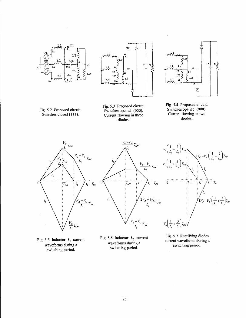
VA
L l
rep VB L l
L l fc/YYYY
I C I C l
L 2 -
C l
L 2 -C l L2
T L l
3L2
L l i l l
L2-L l L2
T_
L l isrrr\ >JA.
3L2
L l i l l l i r r m _ ,
L2 • L l
L l / Y Y Y V i
: L2
Fig. 5.2 Proposed circuit. Switches closed (111).
Fig. 5.3 Proposed circuit. Switches opened (000). Current flowing in three
diodes.
Fig. 5.4 Proposed circuit. Switches opened (000). Current flowing in two
diodes.
Fig. 5.5 Inductor Lx current waveforms during a
switching period.
Fig. 5.6 Inductor L2 current waveforms during a
switching period.
Fig. 5.7 Rectifying diodes current waveforms during a
switching period.
95
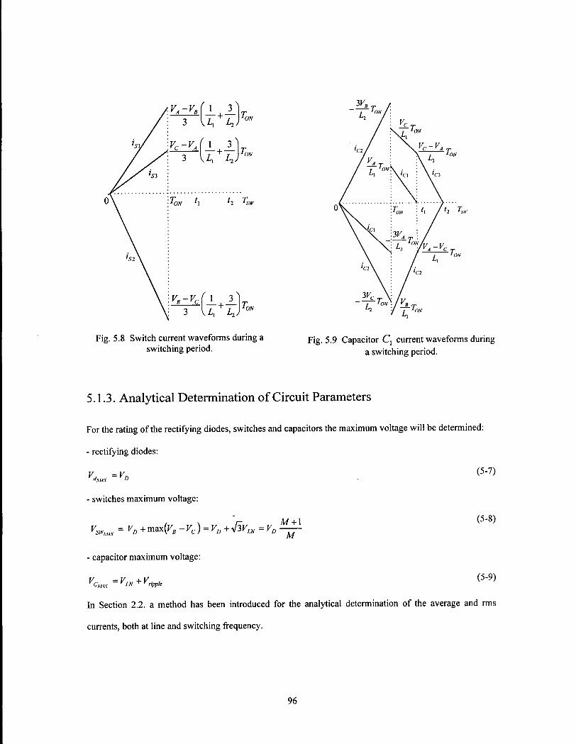
5.1.3. Analytical Determination of Circuit Parameters
For the rating of the rectifying diodes, switches and capacitors the maximum voltage will be determined:
- rectifying diodes:
(5-7)
- switches maximum voltage:
/ \ r M + l (5-8)
- capacitor maximum voltage:
Vc^=Vw+Vrlppk (5-9)
In Section 2.2. a method has been introduced for the analytical determination of the average and rms
currents, both at line and switching frequency.
96

By applying the formulas (2-19, 2-20, 2-23) to the current shapes given in Fig. 5.5, the closed form
expressions for the inductor I, rms currents are determined for each phase as follows:
(5-10) TON TON y2 | yi
The average current space vector method, developed in Section 2.1.3. can also be applied to the input phase
currents. Using formulas (2-7, 2-8) and Fig. 5.5 the space vector and its components are determined as:
/ x V , (5-H) LVON)~ j 'ONC
i { t ^ V - ^ T 0 N e ^
;. _ ym TON{TON +Q c , k , - , / 2) , 2V3 vc-vA TON(TL + t 2 ) c _ j n n
L\ 2TSW 3 Z,, 27 .,,,
Since in the case of the SEPIC converter no modulation is needed, due to the intrinsic low harmonic
content, the average current space vector will not be further used.
Using the general formulas (2-24, 2-25, 2-28), plots have been drawn for the normalized rms and average
inductor 7, currents in Fig. 5.10 and 5.11 and the rms normalized inductor L2 and capacitor C, currents,
in Fig. 5.12 respectively 5.13.
By studying Fig. 5.14 it can be seen an important advantage of the SEPIC converter, that good 5th, 7th
harmonics and THD can be achieved even at low voltage transfer ratios M. In Fig. 5.15 the contribution of
the high frequency rms component to the total rms for inductor Lt is shown to be dependent on M .
97
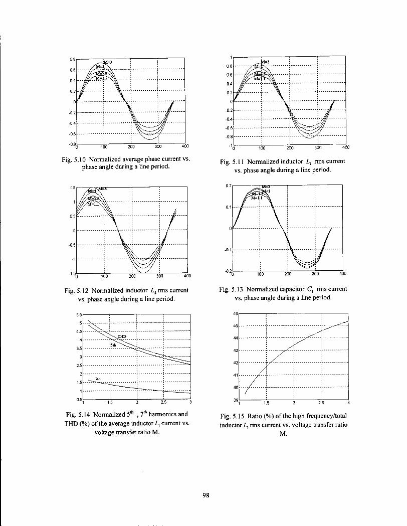
\ ':
"uo0 100 200 300 400
Fig. 5.10 Normalized average phase current vs. phase angle during a line period.
o
-1 'o 100 200 300 400
Fig. 5.11 Normalized inductor Z,, rms current vs. phase angle during a line period.
-1
-1-5, 0 100 200 300 400
Fig. 5.12 Normalized inductor Z,2rms current vs. phase angle during a line period.
• \ T H D
0 5l i i i 1
1 1.5 2 2.5 3
Fig. 5.14 Normalized 5 , 7 harmonics and THD (%) of the average inductor Lx current vs.
voltage transfer ratio M.
0.1
0
-0.1
M=3 3d?2
0 100 200 300 400
Fig. 5.13 Normalized capacitor C, rms current vs. phase angle during a line period.
1 1.5 2 2.5 3
Fig. 5.15 Ratio (%) of the high frequency/total inductor Z., rms current vs. voltage transfer ratio
M .
98

5.1.4. Design Notes and Time Domain Simulations
As it has been shown in [48] the SEPIC converter used as a single-phase power factor correction stage has
to meet a certain condition for the inductors ratio X, / L2 so that the base line of the current in Z,, will
have the same sign with the phase voltage during the whole period .
For three-phase the same condition will be determined in the following. The energy drawn by the circuit
during one switching period is:
1 2 1 2
'W/2 i o *\
' 1 ON 1 3
— + — M L2j
-VnV 2
Dr LN 2
Since the above inequality should hold for any angle in the interval (0,^/6) we obtain:
(5-12)
4
where:
I^, IBA, ICA = currents in the inductors at the beginning of the switching period;
7,o, I2 , IIN = currents in the L2 inductors at the beginning of the switching period;
hPK JBPK . 7 c r e = currents in the Z-, inductors at TON ;
!APK > !BPK > 7c>K = currents in the L2 inductors at TON .
At the same time the energy can be written as:
E = (VAIAAI. + VBlBv. + VCICm. )rsw (5-13)
Making the two expressions (17) and (18) equal and taking into consideration:
^ A + ^ + ^ C o ^ O (5-14)
we obtain:
L\ ^^A+2VAV2-4VBV2-VCV2 (5-15)
U~ 9
(5-16)
L2 3M
99

In terms of the load, the boundary condition for having discontinuous conduction mode is based on the
method in [48] and results in the following:
R> " D V2 2T,
(5-17) sw
(2Vc
2
+2V2
+2VAVc^j- + j-T2
'ON
The discontinuous conduction mode is guaranteed for the whole period when:
1 . 1 (5-18)
' l 4(M + l) 2
— + 7~ KJsw V L i L i )
The capacitor voltage has two constraints: to have a nearly constant value during a switching period and to
follow the input voltage in a line period. Its value has a great influence on the input current waveform. The
resonant frequency of C, , Z,, and Z-2 must be much greater than the line frequency, to avoid input current
oscillations each half-cycle. Besides, if the resonant frequency is near the switching frequency, the
characteristic of good power factor is lost and distorted waveforms are generated. As a general rule, based
on the recommendation in [48], we can use:
1 _ , ( 5- 1 9> I , u 2
V 3 j
The energy transfer between the inductor and capacitor networks during each switching cycle must keep
the capacitor voltage ripple within reasonable limits.
Therefore, the following design rules can be derived, based on energy considerations:
3 2 1 2 (5-20) C, > — T0N and C, >—T0N
As an example a 3-phase 3-switches PFC stage was designed and simulated using PSIM. The following
values have been chosen:
VUNE = 208F , f u m = 60/TZ , I, = 90////, L2 = 540//// , C, = 9.4//F , COUR = 4,700/zF,
R = 58.5ft, Vom = 600F , fsw = 25KHz , D = 0.64, TSTEP = 1// sec., TT0T = 0.3 sec., P0UT = 6.15KW .
The phase current at the input of the high frequency filter and the capacitor C, voltage are given in Fig.
5.16 and 5.17.
100
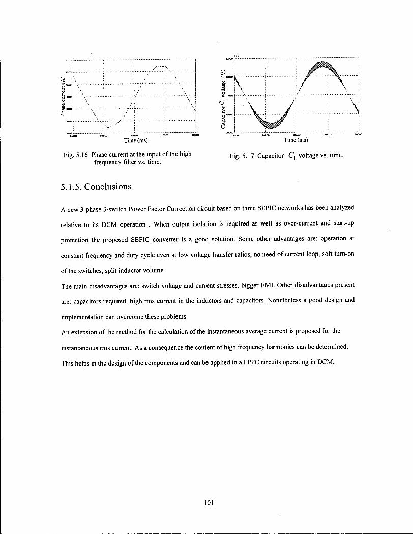
<
PH
\ ; 1 / - • 1 v v • y
30303 WBJDO
Time (ms)
IOO.00
2*5X1) 290GO 255 CD
Time (ms)
Fig. 5.16 Phase current at the input of the high F i g 5 1 7 capacitor C, voltage vs. time, frequency filter vs. time.
5.1.5. Conclusions
A new 3-phase 3-switch Power Factor Correction circuit based on three SEPIC networks has been analyzed
relative to its DCM operation . When output isolation is required as well as over-current and start-up
protection the proposed SEPIC converter is a good solution. Some other advantages are: operation at
constant frequency and duty cycle even at low voltage transfer ratios, no need of current loop, soft turn-on
of the switches, split inductor volume.
The main disadvantages are: switch voltage and current stresses, bigger EMI. Other disadvantages present
are: capacitors required, high rms current in the inductors and capacitors. Nonetheless a good design and
implementation can overcome these problems.
An extension of the method for the calculation of the instantaneous average current is proposed for the
instantaneous rms current. As a consequence the content of high frequency harmonics can be determined.
This helps in the design of the components and can be applied to all PFC circuits operating in DCM.
101
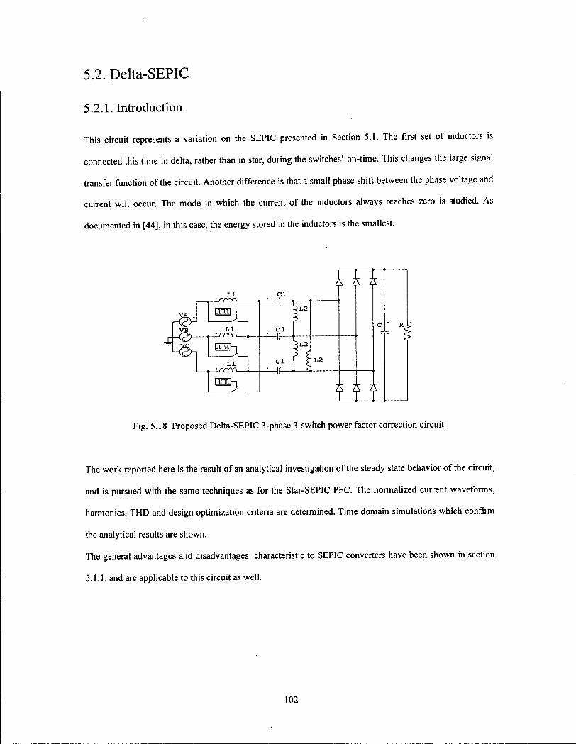
5.2. Delta-SEPIC
5.2.1. Introduction
This circuit represents a variation on the SEPIC presented in Section 5.1. The first set of inductors is
connected this time in delta, rather than in star, during the switches' on-time. This changes the large signal
transfer function of the circuit. Another difference is that a small phase shift between the phase voltage and
current will occur. The mode in which the current of the inductors always reaches zero is studied. As
documented in [44], in this case, the energy stored in the inductors is the smallest.
QQLJ-I
L l UYYY\
L l IL
c i
c i H f -
3L2
!L2
: L 2
t i l Fig. 5.18 Proposed Delta-SEPIC 3-phase 3-switch power factor correction circuit.
The work reported here is the result of an analytical investigation of the steady state behavior of the circuit,
and is pursued with the same techniques as for the Star-SEPIC PFC. The normalized current waveforms,
harmonics, THD and design optimization criteria are determined. Time domain simulations which confirm
the analytical results are shown.
The general advantages and disadvantages characteristic to SEPIC converters have been shown in section
5.1.1. and are applicable to this circuit as well.
102

5.2.2. Circuit Analysis
The proposed circuit is analyzed in respect to its DCM operation, where only two switching states are
possible: 000 or 111.
The following parameters, specific to this circuit's analysis, are defined:
- the normalized phase current:
lAaN
where iAa = phase current, iNph =VLNTSW
the normalized inductor L. current:
= normalizing phase current;
'AN
where: / '= inductor L, current, iNi< = LN s w = normalizing Z,, current; " 2Z-,
the normalized inductor Z,, current:
V T'. where: /', = inductor L2 current, iNii = LN^W = normalizing L2 current;
- the normalized capacitor C, current:
'C\N ~ .
1 3^ where: ici = capacitor C, current, iNci = VLNTSW\ — +
M L2 J
- the inductors ratio:
= normalizing C, current;
V3Z,
The following assumption is made:
(5-21)
(5-22)
(5-23)
(5-24)
(5-25)
103

f »f (5-26)
J SW J LINE
where: fsw = switching frequency, fUNE = line frequency.
This makes it possible to consider the average, rms, and high frequency components of the current over a
switching cycle as 'instantaneous' values seen at the line frequency. In the following, where plots or
formulas refer to line frequency, the 'instantaneous' values are used.
In order to analyze the new PFC circuit, it is sufficient to consider one twelfth of the line period, e.g.,
{n16,n 13) interval, due to symmetry , as shown below: iA(a)j)=iA(jr -co.i)=-iA{7i + (ox)=-iA{2x -co.t) (5-27)
iA (w.t) = ic {7113 - cox) for 0 < coX < n 13 ;
/A(cox)= -iB{2n73-cax) for nil <coX <a 12.
For the time interval (0,7^) all the switches are closed (111) and the equivalent circuit looks like in Fig.
5.19. During the off time of the switches (000), the current flow is dependent on the instantaneous values of
the currents (proportional to the instantaneous voltages). There are two time intervals: (T0N,tx) when
current flows in three diodes and (tx,t2) when current flows in two diodes, as shown in Fig. 5.20 and 5.21.
The shape of the currents in the line, inductors, capacitors, diodes, and switches during a switching cycle is
presented in Figs. 5.22-5.27.
The total time in which current flows through the Z,, inductors can be determined as:
hw ~ TON +t\ +t2 — T0
1 | 3 ( ^ - ^ ) , 6 ^ c yD
v D j ^ v - 3 K
TON ° . B (5-28) 'ON y
' D
For fixed frequency operation, the switching period and duty-cycle are determined as:
1 s w -maxu^)-IQN y ~1ON ^
D_ T0N _ VD _ M
(5-29)
TSW VD+WLN M + fi
104
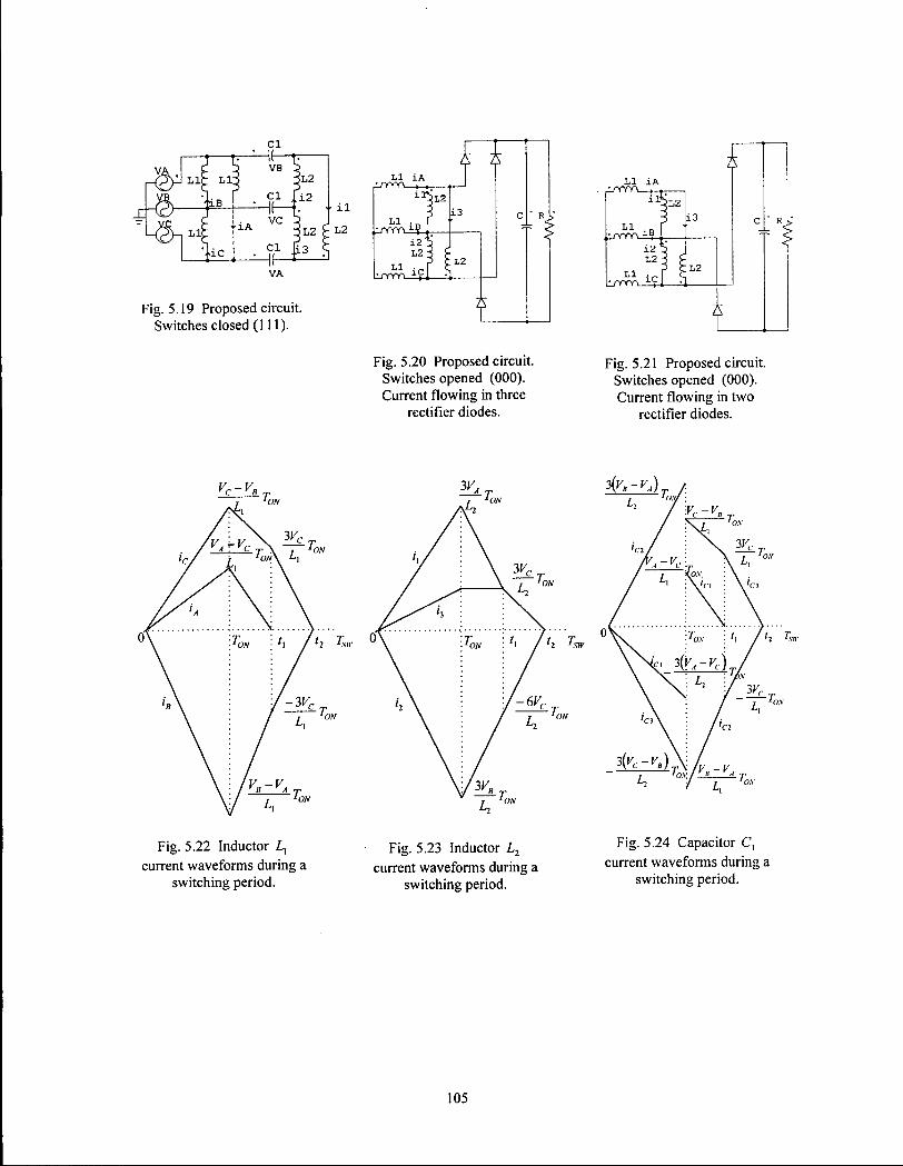
Fig. 5.19 Proposed circuit. Switches closed (111).
L l i A
±rrrr\ L l i A
i3
i2 : L2 •
L l : L2
i c
Fig. 5.20 Proposed circuit. Switches opened (000). Current flowing in three
rectifier diodes.
Fig. 5.21 Proposed circuit. Switches opened (000). Current flowing in two
rectifier diodes.
' 1 • \
TON ; 'i A
•3VC rr. — T
/v„-vA
/ A T 'ON
3 ( K C VB)t\ y _y , 'os: / LA LA. T
L7 I ^ 'n>
Fig. 5.22 Inductor Lx
current waveforms during a switching period.
Fig. 5.23 Inductor L2
current waveforms during a switching period.
Fig. 5.24 Capacitor C, current waveforms during a
switching period.
105
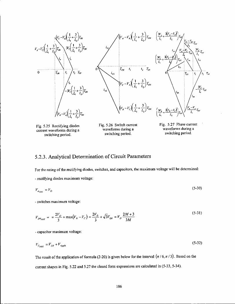
Fig 5 25 Rectifying diodes Fig. 5.26 Switch current Fig. 5.27 Phase current current waveforms during a waveforms during a waveforms during a
switching period. switching period. switching period.
5.2.3. Analytical Determination of Circuit Parameters
For the rating ofthe rectifying diodes, switches, and capacitors, the maximum voltage will be determined:
- rectifying diodes maximum voltage:
- switches maximum voltage:
v w „ . ^ ^ . - v ^ & v - Y . y g - ( 5 - 3 , )
- capacitor maximum voltage:
V -V +V , (5-32) K C ; U 1 V
yLN^rripple
The result ofthe application of formula (2-20) is given below for the interval {n 16, n 13). Based on the
current shapes in Fig. 5.22 and 5.27 the closed form expressions are calculated in (5-33, 5-34).
106
Phase 'instantaneous' average currents:
'ON 'j.w 2f
sw
>BbM. ' 27\,
2Ta
J_ _L\
l_
h
3V< +
3V„ D J " D
(VC-VB+3VC)+^3VC
V D J
Inductor L. 'instantaneous'rms currents:
ARJKE
(5-33)
(5-34)
= T-f- J^J(VB-VAY +^^lv.-Vj A-WCXVB-VM-*VCY("3Y
CRMS
The average current space vector method, developed in Section 2.1.3. can also be applied to the input phase
currents. Using formulas (2-7, 2-8) and Fig. 5.27 the space vector and its components are determined as:
;iT \-L\V2LT r.l("-l-"li) . 3 V m T ](a>.t-xll) . 3 V m T j(a>.l-xll) Jxll ( 5 3 5 ) 1VON-)-~r—IONE + ~ , JONE + j 'ONE E
AT \ - M T 0 A a ' - " n ) x "' T 0A<^i-xii)-)ni3 L\ION+)--y~1ONE +~1ONE E
-jx/2
2T„ 37* I _L + i ^ •"owl t
+ j TONU / ( a > . / - t f / 2 ) +
27-,, 37/2
,jxn , TON'\ c - f j(a.l-nll) +
2SVC T0N(tl+t2)^fn
2T„
Since in the case of the SEPIC converter no modulation is needed, due to the intrinsic low harmonic
content, the average current space vector will not be further used.
107
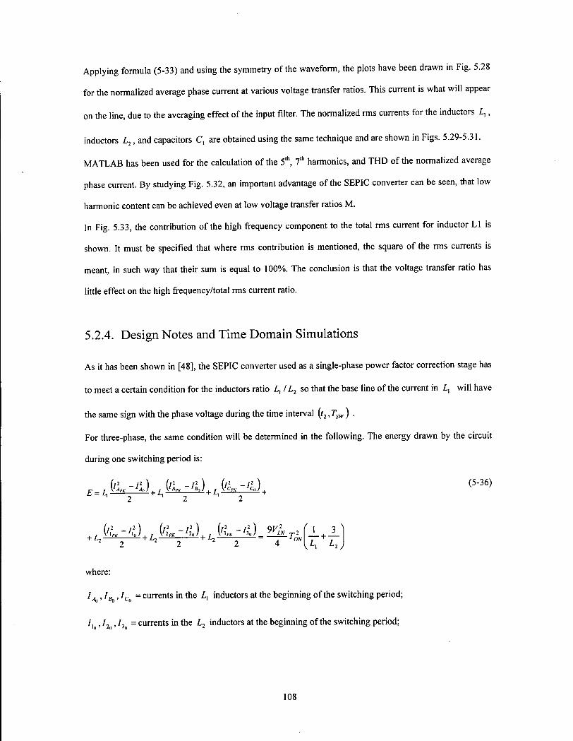
Applying formula (5-33) and using the symmetry of the waveform, the plots have been drawn in Fig. 5.28
for the normalized average phase current at various voltage transfer ratios. This current is what will appear
on the line, due to the averaging effect of the input filter. The normalized rms currents for the inductors 7,,
inductors L2, and capacitors C, are obtained using the same technique and are shown in Figs. 5.29-5.31.
MATLAB has been used for the calculation of the 5 t h, 7 th harmonics, and THD of the normalized average
phase current. By studying Fig. 5.32, an important advantage of the SEPIC converter can be seen, that low
harmonic content can be achieved even at low voltage transfer ratios M .
In Fig. 5.33, the contribution of the high frequency component to the total rms current for inductor L l is
shown. It must be specified that where rms contribution is mentioned, the square of the rms currents is
meant, in such way that their sum is equal to 100%. The conclusion is that the voltage transfer ratio has
little effect on the high frequency/total rms current ratio.
5.2.4. Design Notes and Time Domain Simulations
As it has been shown in [48], the SEPIC converter used as a single-phase power factor correction stage has
to meet a certain condition for the inductors ratio L, I7,2 so that the base line of the current in 7,, will have
the same sign with the phase voltage during the time interval (/2, Tsw) .
For three-phase, the same condition will be determined in the following. The energy drawn by the circuit
during one switching period is:
E = L\
+ L
(5-36)
where:
7^, IBo, 7Q i = currents in the 7, inductors at the beginning of the switching period;
7, , 72 , Ih = currents in the L2 inductors at the beginning of the switching period;
108
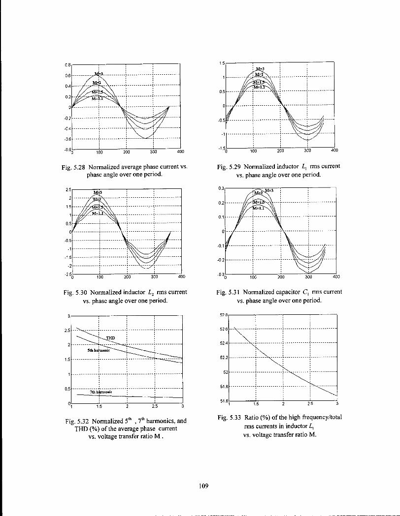
i
i
j
\\r~—*jf/
50 100 200 300 400
Fig. 5.28 Normalized average phase current vs. phase angle over one period.
M=>3
'0 100 200 300 400
J
' 5 0 100 200 300 400
Fig. 5.29 Normalized inductor /_, rms current vs. phase angle over one period.
0 100 200 300 400
Fig. 5.30 Normalized inductor 7_2 rms current vs. phase angle over one period.
5th h a h n o n i c - ~ ^ ! ^ ~
i i
i | 7th h k r m o n i c !
0I i : i 1 1 1.5 2 2.5 3
Fig. 5.32 Normalized 5* , 7* harmonics, and THD (%) ofthe average phase current
vs. voltage transfer ratio M .
Fig. 5.31 Normalized capacitor C, rms current vs. phase angle over one period.
52.8, . , : 1
Fig. 5.33 Ratio (%) of the high frequency/total rms currents in inductor Lx
vs. voltage transfer ratio M .
109

^m- » 7 / W ' lcPK = currents in the I, inductors at T0N ;
7, ,7, ,7, = currents in the 7, inductors at Tnu . tFK ' *PK ' JPK 2 UN
At the same time, the energy can be written as:
E = (vAiAaM.+vBiBbAy+vciCCAy)rw
where:
IAa„. > 7 f l* j r ' 7 cc I, = 'instantaneous' average phase currents at line frequency;
Making the two expressions (5-36) and (5-37) equal and taking into consideration:
vAU+vBiBt)+vciCo >o
we obtain:
(5-37)
(5-38)
27VDVL
2
N
WAWA-VCWA-VC)}*
+ VB[3(VA -VCWB -Va-3VC)-\SVC
2]+VC[3(VA -VC){VC —VB+ 3VC) +1SV2]]
Since the above inequality should hold for any angle in the interval {nI6,nl3), we obtain:
7.2 y/3M
(5-39)
(5-40)
In terms of the load, the boundary condition for having discontinuous conduction mode is based on the
method in [48] and results in the following:
7?> 27V, (5-41)
{vB-vA-3vcWA-vc)-m 1 3
— + — 7-, L2 j
The discontinuous conduction mode is guaranteed for the whole period when:
(5-42)
\L\ Li j
The capacitor voltage has two constraints: to have a nearly constant value in a switching period and to
follow the input voltage in a line period. Its value has a great influence on the input current waveform.
110
The resonant frequency of C,, Z,,, and L2 must be much greater than the line frequency, to avoid input
current oscillations each half-cycle. Besides, if the resonant frequency is near the switching frequency, the
characteristic of good power factor is lost and the waveforms are distorted. As a general rule, based on the
recommendation in [48], we can use:
i . (5-43) a>,a, »
» CO
C, L, + LINE
The energy transfer between the inductor and capacitor networks during each switching cycle must keep
the capacitor voltage ripple within reasonable limits. Therefore, the following design rules can be derived,
based on energy considerations:
(5-44) C, >-j-T^ and C, > i - 7 ^
As an example, a 3-phase 3-switches PFC stage was designed and simulated using PSIM. The following
values have been chosen:
LINE 208F, fLINE = 607/z, Vom = 600F , P0UT = \2.\5KW, Z, = 90>/Y, L2 =310////
C, =14. \nF,C o m =4,700//F, /? = 29.6fi, fm = 25KHz ,D = 0.47, TSTEP = l//sec., TTOT = 0.3sec.
The phase current at the input ofthe high frequency filter and the capacitor C, voltage are given in Figs.
5.34 and 5.35. By inspection, it can be seen that the time domain simulation confirms the analytical results.
^ ^ ^ ^ ^ ^
Fig. 5.34 Phase current at the input of the high frequency filter vs. time.
Fig. 5.35 Capacitor C, voltage vs. time.
I l l
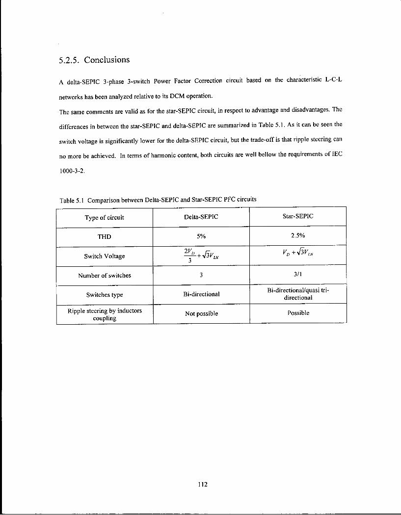
5.2.5. Conclusions
A delta-SEPIC 3-phase 3-switch Power Factor Correction circuit based on the characteristic L-C-L
networks has been analyzed relative to its DCM operation.
The same comments are valid as for the star-SEPIC circuit, in respect to advantage and disadvantages. The
differences in between the star-SEPIC and delta-SEPIC are summarized in Table 5.1. As it can be seen the
switch voltage is significantly lower for the delta-SEPIC circuit, but the trade-off is that ripple steering can
no more be achieved. In terms of harmonic content, both circuits are well bellow the requirements of IEC
1000-3-2.
Table 5.1 Comparison between Delta-SEPIC and Star-SEPIC PFC circuits
Type of circuit Delta-SEPIC Star-SEPIC
THD 5% 2.5%
Switch Voltage
Number of switches 3 3/1
Switches type Bi-directional Bi-directional/quasi bidirectional
Ripple steering by inductors coupling
Not possible Possible
112

CHAPTER 6
EXPERIMENTAL RESULTS
A proof of concept circuit has been built for the boost-delta PFC. Since the boost-delta is a phase sequence
sensitive circuit. The circuit features for both phase sequence cases, ABC and ACB, are investigated. The
properties of two parallel running boost-delta circuits with reverse phase sequence are studied. The results
obtained analytically and in time-domain simulations are found to be in good agreement with the
experimental data. Photos of the experimental set-up are presented.
113
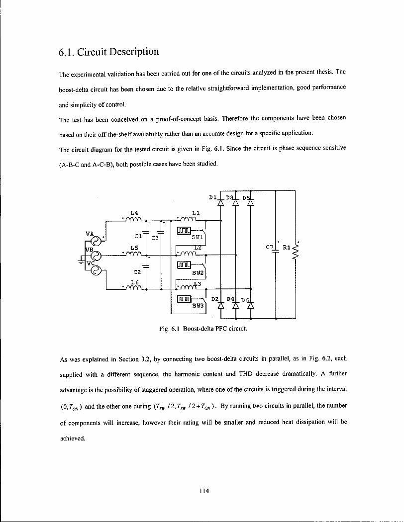
6.1. Circuit Description
The experimental validation has been carried out for one of the circuits analyzed in the present thesis. The
boost-delta circuit has been chosen due to the relative straightforward implementation, good performance
and simplicity of control.
The test has been conceived on a proof-of-concept basis. Therefore the components have been chosen
based on their off-the-shelf availability rather than an accurate design for a specific application.
The circuit diagram for the tested circuit is given in Fig. 6.1. Since the circuit is phase sequence sensitive
(A-B-C and A-C-B), both possible cases have been studied.
VA
- vc
L4 i r r m .
ci L5
__/TYT\_
C2 L6
L/YYYV
C3
L l -L/YVYY-
Dunrll— SUl L"2~
1/YYY\ DOTCr—A r
SW2
IJITIILI—A' D2 SW3
D4
Fig. 6.1 Boost-delta PFC circuit.
C7 Rl .
As was explained in Section 3.2, by connecting two boost-delta circuits in parallel, as in Fig. 6.2, each
supplied with a different sequence, the harmonic content and THD decrease dramatically. A further
advantage is the possibility of staggered operation, where one of the circuits is triggered during the interval
(0, T0N) and the other one during (TSfV 12, Tsw 12 + T0N). By running two circuits in parallel, the number
of components will increase, however their rating will be smaller and reduced heat dissipation will be
achieved.
114
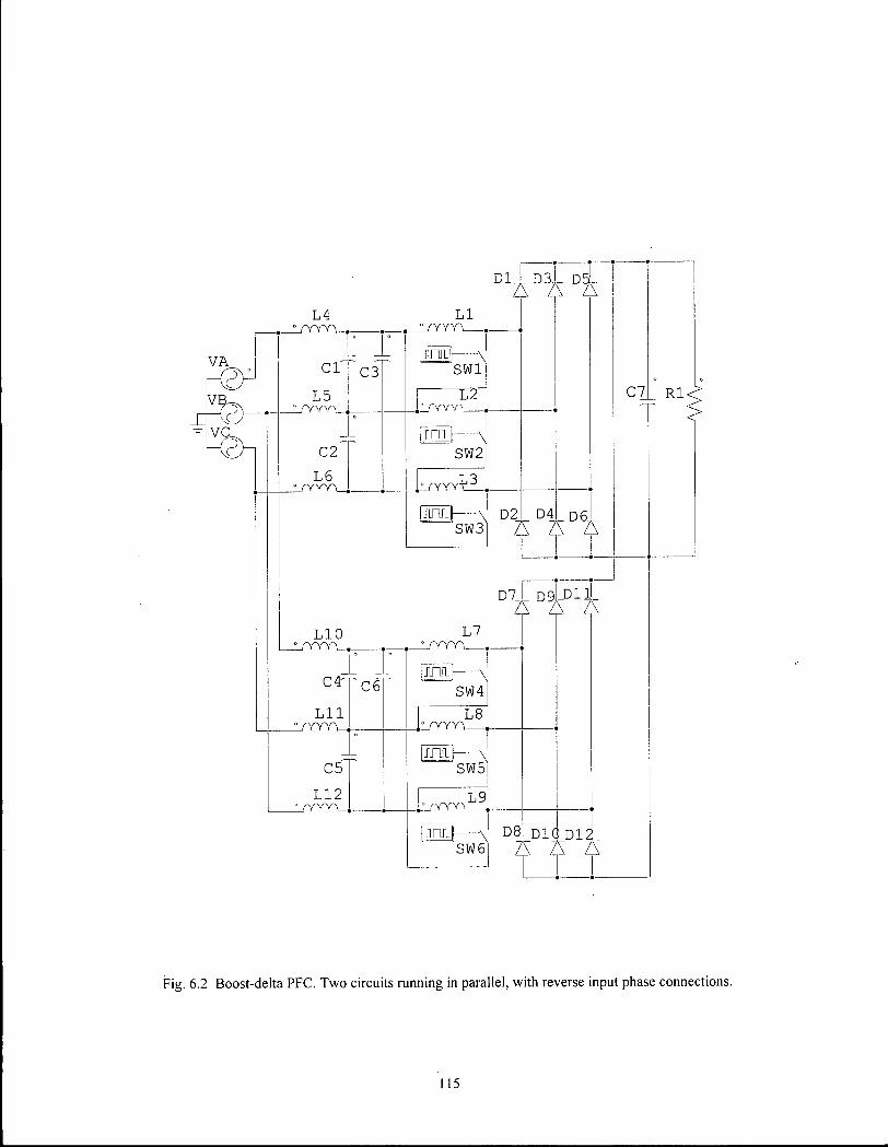
V A
V C
L4 1 / Y Y Y V ,
C l
L 5
C2
L6 L / Y Y Y V
C3
L l
swi
T2 _ / Y Y V \ _
- T O
SW2
. r o n
[Fu l l—\ D2 SW3I
D4 D6J
C7
L 1 0
C4 '
L l l L / Y Y Y V .
C5
L 1 2
C 6
L7 : / Y Y Y \ _
Jinn.1 SW4
_ / Y Y Y \ _ L8
D7_
B r — A SW5
L 9
f j i rml—A D8 SW6|
D10 D12
. 6.2 Boost-delta PFC. Two circuits running in parallel, with reverse input phase connections.
115

Fig. 6.3 shows a possible way of implementing a bi-directional switch. The gate driving and PWM circuits
have been implemented with circuits readily available in Xantrex and their schematics are shown in Figs.
6.4 and 6.5. The gating signals generated by the circuit in Fig. 6.5 are sent to the input of the circuit in Fig.
6.4. Isolation is then achieved and the output signals from the circuit in Fig. 6.4 are connected to gates of
the bi-directional switches, as represented in detail in Fig. 6.3. The lists of components and other equipment
used in the experimental part are given in Appendix G.
6.2. Theoretical and experimental results
The approach taken is to use MATLAB to determine analytically the current waveforms, the harmonic
content and THD for a voltage transfer ratio M=l .4 .
PSIM is then used for time-domain simulations. The experimental values are given in the following:
One stage (Fig. 6.1)
yPHASE = , fum = 60/*, i , = L2 = L} = 87.5//// ,L4=L,=L6=l 80//// , C, = C 2 = C 3 = 8//F,
C 7 = 4.480//F , R = 47.7Q, V0UT = 15IV, fsw = 2AKHz , D = 0.2, TSTEP = 1// sec., TT0T = 0.1 sec.,
Pour** WW .
Two stages running in parallel (Fig. 6.2)
The values are the same as above, but R = 24.4Q, P0UT = 934W . The following additions are made:
Z 7 = Lg = L9 = 87.5//// , ! , „ = / , „ = Ln = 180///7 , C 4 = C 5 = C6 = 8//F
A practical implementation with the values used in the simulation is the final way of proving the concept.
In order to illustrate the bench setup and circuit layout, several pictures have been taken and are presented
in Section 6.4.
116
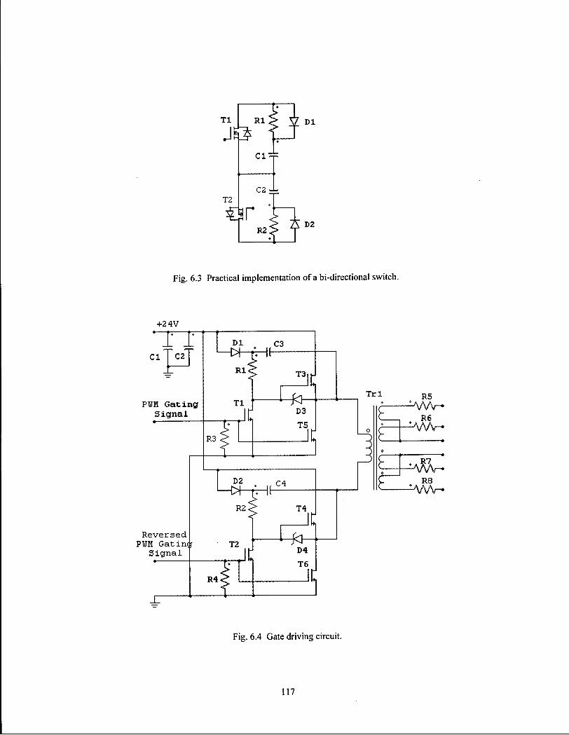
TI I Rl DI
C l ^
C2 T2
R2. D2
Fig. 6.3 Practical implementation of a bi-directional switch.
+24V
Cl C2
PWM Gating Signal
Reversed PUM Gating
Signal
LH>r-rHI— Rl< T3
TI
1
R3
J D3 T5
D2 C 4
R2- T4
T2
J
J D4 T6
R4<
T r l R 5
R6
£ 0
R8 LVvV-
Fig. 6.4 Gate driving circuit.
117
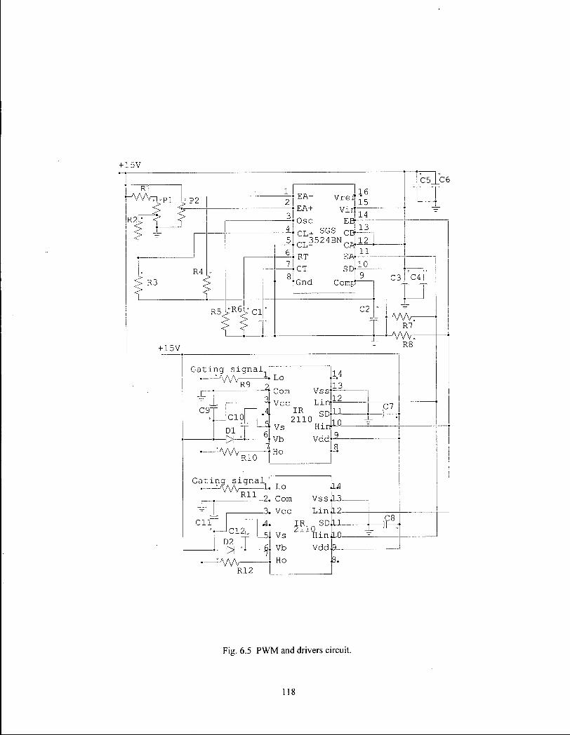
+ 15V
j C 5 R l
-AAA / 71 , pi : P2 EA- v r e f EA+ virt Osc EBt CL+ S G S CBf CL- 3 5 2 4 B NCA^
16 15
JjC6
T 14
13
12 n
9
R12
Fig. 6.5 P W M and drivers circuit.
118
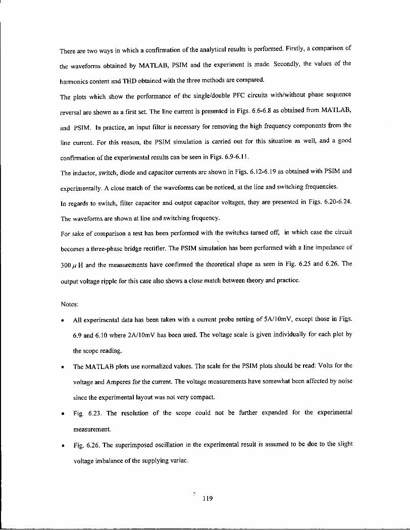
There are two ways in which a confirmation of the analytical results is performed. Firstly, a comparison of
the waveforms obtained by MATLAB, PSIM and the experiment is made. Secondly, the values of the
harmonics content and THD obtained with the three methods are compared.
The plots which show the performance of the single/double PFC circuits with/without phase sequence
reversal are shown as a first set. The line current is presented in Figs. 6.6-6.8 as obtained from MATLAB,
and PSIM. In practice, an input filter is necessary for removing the high frequency components from the
line current. For this reason, the PSIM simulation is carried out for this situation as well, and a good
confirmation ofthe experimental results can be seen in Figs. 6.9-6.11.
The inductor, switch, diode and capacitor currents are shown in Figs. 6.12-6.19 as obtained with PSIM and
experimentally. A close match of the waveforms can be noticed, at the line and switching frequencies.
In regards to switch, filter capacitor and output capacitor voltages, they are presented in Figs. 6.20-6.24.
The waveforms are shown at line and switching frequency.
For sake of comparison a test has been performed with the switches turned off, in which case the circuit
becomes a three-phase bridge rectifier. The PSIM simulation has been performed with a line impedance of
300 n H and the measurements have confirmed the theoretical shape as seen in Fig. 6.25 and 6.26. The
output voltage ripple for this case also shows a close match between theory and practice.
Notes:
• All experimental data has been taken with a current probe setting of 5A/10mV, except those in Figs.
6.9 and 6.10 where 2A/10mV has been used. The voltage scale is given individually for each plot by
the scope reading.
• The MATLAB plots use normalized values. The scale for the PSIM plots should be read: Volts for the
voltage and Amperes for the current. The voltage measurements have somewhat been affected by noise
since the experimental layout was not very compact.
• Fig. 6.23. The resolution of the scope could not be further expanded for the experimental
measurement.
• Fig. 6.26. The superimposed oscillation in the experimental result is assumed to be due to the slight
voltage imbalance of the supplying variac.
119
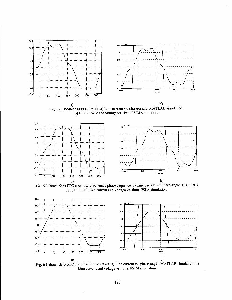
0.4 r 0.3-
0.2-
0.1 •
0 •
-0.1 -
-0.2-
-0.3-
-0.4- 50 100 150 200 250 300
a) b) Fig. 6.6 Boost-delta PFC circuit, a) Line current vs. phase-angle. M A T L A B simulation,
b) Line current and voltage vs. time. PSIM simulation.
100 150 200 250 300 a) b)
Fig. 6.7 Boost-delta PFC circuit with reversed phase sequence, a) Line current vs. phase-angle. M A T L A B simulation, b) Line current and voltage vs. time. PSIM simulation.
100 150 200 250 300
a) b) Fig. 6.8 Boost-delta PFC circuit with two stages, a) Line current vs. phase-angle. M A T L A B simulation, b)
Line current and voltage vs. time. PSIM simulation.
120
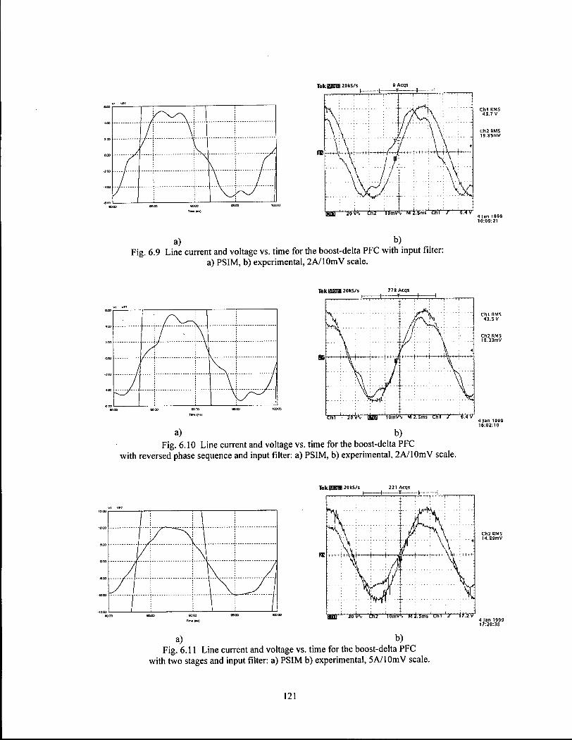
TekBHffl 20ks/s
' ' ' ' ; ' 1 1 1 1 1— 1- T j 1
t t „;.,,, [ t i i i j -,-rV-t—
4
--r-r-r-f-j-V +-+-+f
mn a\2 i o m v \ M 2.5ms c m 1 0.1 v
Chl RMS 43.7 V
Ch2 RMS 19.85mV
4 ]an 1999 16:09:21
a) b) Fig. 6.9 Line current and voltage vs. time for the boost-delta PFC with input filter:
a) PSIM, b) experimental, 2A/10mV scale.
TekaHffl 20kS/s
Chl RMS 43.S V
Chl ' ' '26 BUS 'lO'mVV 'M'i.5ms' Chi ' / ' ' '<.4 V
a) b) Fig. 6.10 Line current and voltage vs. time for the boost-delta PFC
with reversed phase sequence and input filter: a) PSIM, b) experimental, 2A/10mV scale.
121
Tilt man 2 0 k s / s 1 2 8 Acqs I ; _ , T ) -
Chi RMS 44.27 V
BBI ihl UmV\ M i S m s Chi / if.lV
a) b)
Fig. 6.12 Inductor current vs. time at line frequency a) PSIM, b) experimental, 5A/10mV scale.
4 Jan 1999 17:46:38
BI
eaaz Bos* eo.30 taza « « «o.«a
. . .
X I
/ + \ .
/ t M " I M " ... 4.... I
i . . . t J 1
1 o m V ^ M L f O u s Ch'J 2'3'mV
a ) b) Fig. 6.13 Inductor current vs. time at switching frequency a) PSIM, b) experimental, 5A/10mV scale.
31 Dec 19! 16:14:58
TekQQlll 20kS/s 148 Acqs
oaco
*
llll. 'ill Li 11 1 I f f " ' i n ] \\f f Ifl 1 \\f
. . . . .
1 W • j
a) b) Fig. 6.14 Bi-directional switch current vs. time at line frequency:
a) PSIM, b) experimental, 5A/10mV scale.
31 Dec 19! 16:07:01
122
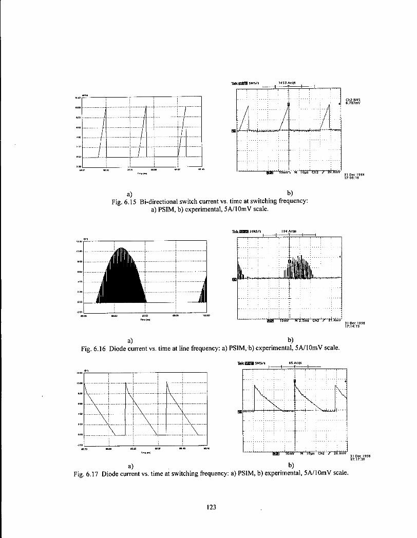
Ch2 RMS 6.787mV
a) b) Fig. 6.15 Bi-directional switch current vs. time at switching frequency:
a) PSIM, b) experimental, 5A/10mV scale.
TekBDID 20kS/s
a) b) Fig. 6.16 Diode current vs. time at line frequency: a) PSIM, b) experimental, 5A/10mV scale.
a) b) Fig. 6.17 Diode current vs. time at switching frequency: a) PSIM, b) experimental, 5A/10mV scale.
123
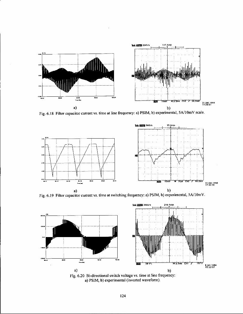
i B ' ' 'l'oW ' 'M'2 . '5ms" CUi "f '28.'6m» 31 Dec 1998 17:28:51
a) b) Fig. 6.18 Filter capacitor current vs. time at line frequency: a) PSIM, b) experimental, 5A/10mV scale.
h- .—[_ n - } — — i • 1 1 1 1
: /f:
1 i i r i " "I 1'ft'nW tout . '2m« 31 Dec 1998 17:32:39
a) b) Fig. 6.19 Filter capacitor current vs. time at switching frequency: a) PSIM, b) experimental, 5A/10mV.
a) b) Fig. 6.20 Bi-directional switch voltage vs. time at line frequency:
a) PSIM, b) experimental (inverted waveform).
124
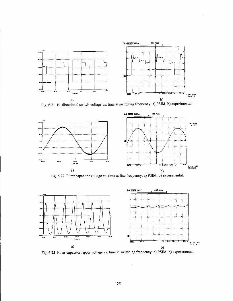
Tekanns 5 M s / s
L— IN I 1 IN - — - —
"war / 1 ' Vflfl'V
a) b) Fig. 6.21 Bi-directional switch voltage vs. time at switching frequency: a) PSIM, b) experimental.
a) b) Fig. 6.22 Filter capacitor voltage vs. time at line frequency: a) PSIM, b) experimental.
TekBDIIS 2 M " s 4 3 5 A c q s
- z L 1 1 1 1 ] 1 , 1 1
U i f 'f'
151b: a ) b)
Fig. 6.23 Filter capacitor ripple voltage vs. time at switching frequency: a) PSIM, b) experimental.
125
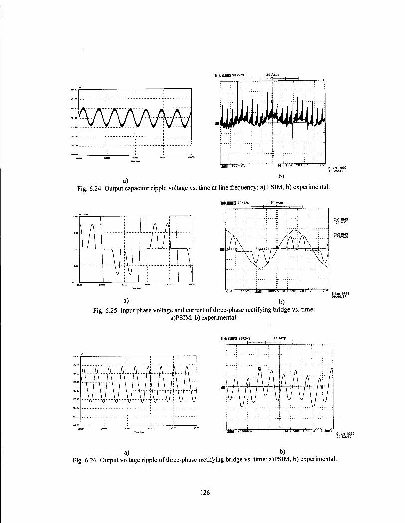
a)
+
+
T T T m s
b)
C h i ' / i.iV 8 J a n 1 9 9 9 1 3 : 2 5 : 4 0
Fig. 6.24 Output capacitor ripple voltage vs. time at line frequency: a) PSIM, b) experimental.
T e k tUHIS 2 0 k s / s 4 6 1 A c q s I 1 T -
T V " 4
T V "
i n » — \j to 5ms irv
Chi RMS 64.4 V
a) b) Fig. 6.25 Input phase voltage and current of three-phase rectifying bridge vs. time:
a)PSIM, b) experimental.
a) b) Fig. 6.26 Output voltage ripple of three-phase rectifying bridge vs. time: a)PSIM, b) experimental.
126
Table 6.1 shows a comparison of the harmonic contents and THD for the single and double stage PFC
circuits as given by MATLAB and PSIM. As can be seen a very good match occurs between the two types
of theoretical determinations.
Table 6.1 Harmonics comparison of MATLAB and PSIM results
Boost-delta circuit Two boost-delta circuits
Simulation MATLAB PSIM MATLAB PSIM
Input filter No Yes No No Yes
Phase sequence ABC or ACB ABC ACB ABC & ACB ABC & ACB ABC & ACB
5 t h (%) 12.49 11.66 12.73 2.54 2.54 1.96
7 t h (%) 2.47 2.41 2.42 2.47 2.44 2.45
11th (%) 1.50 1.67 1.3 1.50 1.22 1.47
13th (%) 0.59 0.56 0.61 0.59 0.51 0.49
THD (%) 12.85 12.04 13.00 3.84 3.70 3.50
The experimental results are shown in Table 6.2 and have been determined using a three-phase power
analyzer. The experimental THD value of the PFC circuits is presented in Table 6.2, and when compared
with the theoretical values given in Table 6.1 shows a close match. The influence of the input filter is
shown by the difference in the harmonic content of the PSIM simulations and the theoretical MATLAB
calculations. By inspecting the results it can also be seen that two stages running in parallel is the best
solution in terms of power factor and harmonic content. For sake of comparison, the results are given also
for the case where only a three phase bridge is used. The measurement can be performed very easily, by
turning off the gating signal from the bi-directional switches. It can be seen how much better the
performance of the power factor stage is, for a penalty in efficiency of about 3%. Generally speaking the
efficiency of the PFC stage can be improved by using a soft- rather than hard-switching method, and
designing the boost inductors for a lower ac resistance.
127
Table 6.2 Experimental measurements for the boost-delta PFC circuit
Boost-delta circuit
ABC sequence
Boost-delta circuit
ACB sequence
Two boost-delta circuits
ABC and ACB sequence
Three-phase rectifying bridge
Output Voltage (V) 151.1 151.5 152.3 150.3
AC Phase Voltage (V) 43.80 43.88 43.45 64.40
AC Input Current (A) 3.98 4.30 7.94 3.47
Power Factor 0.984 0.926 0.994 0.740
Output Power (W) 478.6 481.2 1028.8 473.6
Input Power (W) 514.6 524.2 950.2 496.8
Efficiency (%) 93.0 91.8 92.4 95.3
Output Load (ft) 47.7 47.7 24.4 47.4
Voltage Transfer Ratio 1.41 1.41 1.44 0.95
THD (%) 11.45 11.57 5.70 79.97
128
6.3. E x p e r i m e n t a l Se t -up P i c t u r e s
Photo 6.3 PFC Circuit layout
Photo 6.4 Bi-directional switches and rectifying diodes
130
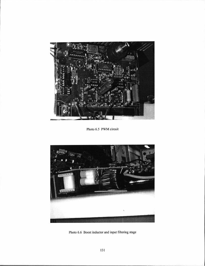
Photo 6.5 PWM circuit

C H A P T E R 7
C O N C L U S I O N S
A comparison is carried out for all the circuits proposed in the present thesis. Conclusions are drawn as to
their suitability for various applications. Recommendations are given and future work directions are
outlined.
132

7.1. Comparison and Recommendations
The work covered in this thesis has dealt so far with the in-depth analysis of the properties of proposed
PFC circuits. In order to have an overall view, whereby a comparison becomes more straightforward, the
main features of the circuits are presented in Table 7.1 at page 139.
The switches column shows the voltage and current stress. Switches could be one of three types: uni
directional, bi-directional or quasi tri-directional. Al l of them, even if composed of several transistors, have
a common emitter and consequently gating point. The triggering can be of two types: simultaneous, or
modulation, where slight deviations from a simultaneous signal are used for individual switches. Where
simultaneous-staggered appears in the Table, two parallel running boost stages, each one with
simultaneous switching but staggered triggering in between circuits is meant.
The diodes column shows the number of three-phase bridges needed for the operation of the circuit. A
common characteristic to all circuits is that the diodes see as maximum reverse voltage VD. The peak
current is given for each three-phase diode bridge, and is characteristically high due to the operation in
DCM. A / m o d represents the amount of extra current due to the modulation and is proportional to the time
tmoi and the current slope VIL.
All the circuits studied in the present thesis are operating in boost mode. The number of passive
components varies, being a characteristic which defines the type of circuit. The boost-star and boost-delta
use only one set of inductors for obtaining PFC. Two sets of inductors are needed for the star-flyback,
delta-flyback, star-delta and delta-delta PFCs. The SEPIC circuits are characterized by L-C-L networks,
just like their single phase or DC-DC implementations. Table 7.1 shows the peak current in the inductors
and the peak voltage across the capacitors, which are important parameters for the design.
In order to obtain a consistent comparison, the harmonics and THD of the analyzed circuits are given for a
voltage transfer ratio M=1.4. Since some of the circuits are phase sequence sensitive and characterized by a
displacement factor, this parameter is also shown. For circuits with two sets of inductors, their ratio
influences the harmonic content. The comments column shows the ratios chosen, and they are based on the
principle of equal amounts of stored energy and consequently equal physical size of the two inductors.
133

It can be seen in general that a complex trade-off of the performance parameters occurs. There is no
universal solution and different approaches can be used for various applications. A short description of the
advantages and limitations are given below for each of the proposed circuits:
- Boost-Star DC side switch
The simplicity of the circuit makes it a favorite in many practical applications. While the uni-directional
switch and rectifying diode are operating under DC conditions, which simplifies the implementation of
soft-switching, their power stress is very high and often several components must be paralleled. The
content of harmonics cannot be reduced substantially for M=1.4 which limits the application to 5 KW for
meeting IEC 1000-3-2, unless harmonic injection schemes are implemented. Several circuits running in
parallel can have staggered operation, which will reduce the EMI requirements for the input filter, but no
improvement will be achieved in regards to the harmonic content.
- Boost-Star AC side switch
The circuit can be implemented with either three bi-directional or a single quasi tri-directional switch.
Since three independent triggering signals are now available, a certain amount of modulation can reduce
the harmonics down to zero. The degree of approximation of the analytically determined modulation will
determine the amount of harmonic reduction in practice. The modulation is dependent on M , the output
power as well as the phase angle. Consequently the control will be somewhat more complicated than in the
case of the boost-star with DC side switch. For this circuit as well as for all the other ones further
described, the soft switching./snubbering of bi-directional switches under AC conditions has been little
developed and presents new opportunities for research.
- Boost-Delta
By connecting the switches in a delta rather than a star configuration, a new set of properties is obtained.
The circuit will bring a small benefit when compared with the Boost-Star DC-side switch. However, the
situation changes when two circuits with reverse switch connection sequence are running in parallel. The
134

amount of reduction of harmonics is dramatic and practically the requirements for the whole range covered
by IEC 1000-3-2 are met. In addition staggering is possible, relieving the EMI/RFI filter of some of the
performance requirements. The fact that the transistor's emitters are at different potentials is one of the
drawbacks, but it is compensated by the simultaneous operation and possibility of having a single pulse
transformer with three isolated secondaries for driving. Another disadvantage is the relatively high number
of semiconductors of the circuit, but in fact this is just a redistribution of the semiconductor area in more
components. If the properties of the circuit seem to justify it, the semiconductor manufacturers could
assemble the three bi-directional switches in a compact package.
- Starfly
This circuit has two sets of boosting inductors, series connected during the on-time and parallel running
during the off-time. It is a combination of a Boost-Star and a Flyback, whereby a trade-off between the
characteristics of the two circuits is achieved, pending on the inductors ratio. Three bi-directional switches
with the emitter at various potentials and simultaneous triggering are used. The advantages are split
inductors and switching bridges, improved harmonic content. Due to the topological similarity to the
Boost-Star with AC-side switch, in this case too, zero harmonic content can be achieved by modulation.
The main disadvantages are higher component number and a moderately high switching stress for a
significant harmonic reduction.
- Deltafly
A similar combination as the circuit previously described, this time a Boost-Delta and a Flyback are
connected together. A characteristic common to all circuits with two inductor sets is the relative large
number of components which makes staggered operation with another similar circuit a complex
implementation. Since the boost-delta is phase sequence sensitive, this feature is conveyed to the new
circuit. The harmonic content and displacement angle are alleviated as compared to the original boost delta,
depending on the inductance ratio, just like in the case of the Star-Flyback. However, while the mentioned
135
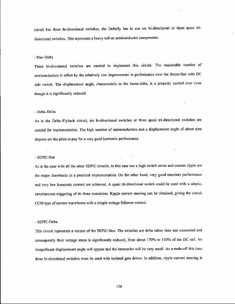
circuit has three bi-directional switches, the Deltafly has to use six bi-directional or three quasi tri-
directional switches. This represents a heavy toll on semiconductor components.
- Star-Delta
Three bi-directional switches are needed to implement this circuit. The reasonable number of
semiconductors is offset by the relatively low improvement in performance over the Boost-Star with DC
side switch. The displacement angle, characteristic to the boost-delta, is a property carried over even
though it is significantly reduced.
- Delta-Delta
As in the Delta-Flyback circuit, six bi-directional switches or three quasi tri-directional switches are
needed for implementation. The high number of semiconductors and a displacement angle of about nine
degrees are the price to pay for a very good harmonic performance.
- SEPIC-Star
As is the case with all the other SEPIC circuits, in this case too a high switch stress and current ripple are
the major drawbacks in a practical implementation. On the other hand, very good transient performance
and very low harmonic content are achieved. A quasi tri-directional switch could be used with a simple,
simultaneous triggering of its three transistors. Ripple current steering can be obtained, giving the circuit
CCM type of current waveforms with a simple voltage follower control.
- SEPIC-Delta
This circuit represents a variant of the SEPIC-Star. The switches are delta rather then star connected and
consequently their voltage stress is significantly reduced, from about 170% to 130% of the DC rail. An
insignificant displacement angle will appear and the harmonics will be very small. As a trade-off this time
three bi-directional switches must be used with isolated gate drives. In addition, ripple current steering is
136

no more possible. In general the SEPIC-derived circuits will not be interesting for a practical
implementation, unless some particular features of the SEPIC are required by the application.
It is expected that the proposed circuits using a single set of inductors will be the most attractive in
practice. The circuits using two sets of inductors could be interesting for particular applications where
splitting the inductors and rectifying bridges becomes a layout advantage or the power level requires it.
Except of the Star-Flyback, all the circuits in the two inductors category would have to be used where a
small displacement angle is acceptable, and/or can be offset to some extent by the EMI/RFI input filter.
7.2. Conclusions and Future Work
The work done in the present thesis lays the theoretical basis for obtaining power factor correction with
lower harmonic content than any other circuits operating in Discontinuous Conduction Mode. The practical
implementation in successful applications is based on further research in the technological aspects, such as
high efficiency bi-directional switches and good techniques for soft-switching in AC.
A wide selection of new circuits has been proposed, allowing the flexibility of choice based on specific
application requirements. Experimental results have shown a close match with the expected performance,
as determined analytically with MATLAB and in time domain simulations with PSIM.
The PFC circuits presented bring a significant contribution in regards to new schematic and control
solutions. While the general properties have been covered in the thesis, the author deems further research
necessary, particularly in the following areas:
• Small Signal Modeling,
• Operation with other loads then a voltage source,
• Operation under unbalanced/distorted voltage condition ,
• Influence of the unequal value of the inductors,
• Noise Reduction with Random Pulse Width Modulation,
137

• Interaction between EMI filter and PFC stage,
• Soft-switching of bi-directional switches in AC.
In regards to the future prospects, it can be expected that the use of three-phase PFC circuits will grow
substantially. The growth will be most prominent in applications such as telecommunications, autonomous
ac power systems (e.g. aircraft and ships) and other applications where performance and/or power density
are critical. In the consumer and industrial markets, the growth will be mainly conditioned by new power
quality regulations due to the significant add-on cost of active PFC when compared to diode rectification
and bulky passive filter. For the low power applications, the simple three-phase PFC circuits may provide a
cost effective solution with satisfactory performances. At the high power end, the trade-off between passive
harmonic filtering and the active PFC tends to be in favor of the active circuits.
The issues of high frequency operation, input current quality, EMI filtering, high efficiency and power
density remain the driving force in the development of PFC circuits. Because the performance
requirements in the PFC applications are much less diversified and complicated than that in the motor drive
applications, development of standardized, low cost, single-chip digital controllers could be expected soon.
Many of these results will also benefit three-phase inverter design, especially in applications such as three-
phase distributed power systems and uninterruptible power supplies.
138
o CD
C 3
G 3
CD O 5 ' 3 ED
a i & 3,'
II CO
CD o 5 ' 3 Cfl
rO c to
3/
O c
CL C5-
CD O 5 ' 3 f a
5s
00
00 00 CD
00
e
CD O c
2 o CL
2 o
o 3
00
00
00
c
CD O c y 00
00 00 CD ^ CD CL O T3 <D o 3 o oo T3
to o CD 3 CD 3 g era. HT CL CD 00
CD g O CL CD
00
D m CD_ hS
00
3!
*1
oo oo W
3.o CL £
00
X
.. 3
CD a
3.o CL 3.' or.
00
to
+ *1
1
1 o
00
+ *1
t5n
to
s1
*1
5 ^
D oo
00
^ a. o ?
3.o CL p 3 ' 0 1
to
+
8s
to
+
3
3:
o
+
+
+
00
u> + s
3!
2. o & S5-
oo oo oo
to
+ *1
<
1
u>
<
a: 1
to
+
8s
5
in & O CL CD
S o CL p
u> I to
t5n
s + a; +
a.
+ +
% O oo O CO oo o
* §• ? a
CL C =i' 3
5 "
> oo n,
CD a; CD pi
8- s-CL 0 '
CL CD
O C «
o
H <-< 13 CD
3 Oo
•13 CD
<;
00 CD
T3 CD
n c =1 CD 3
2! o
2.
*0 CD
o c =1
ha CD
O c =1 CD 3 to
H T3 CD
CD
—' c CD 3
13 CD
to e CD 3
o O 3 •a o 3 CD 3 5?
=3"
G < o
a -
^ X
2 2 , • II o . O 3 3 CD 3

BIBLIOGRAPHY
1. Kolar J.W., Ertl H., Zach F.C., "Status of the Techniques of Three-Phase Rectifier Systems with Low Effects on the Mains", 'Leistungselektronik Aktoren und intelligente Bewegungssteuerungen' 1996, pp. 75-83;
2. Carli G., "Elimination of Input Harmonic Currents in 3 Phase AC to DC Converters: A Practical Approach", IEEE, pp. 399-406;
3. Mao H., Lee F.C., Boroyevich D., Hiti S., "High Performance Three-Phase Power Factor Correction Circuits", IEEE 1995, pp.8-14;
4. Spiazzi G., Lee F.C., "Implementation of single-phase boost power factor correction circuits in three-phase applications", IECON 1994, pp. 250-255;
5. Divan D.M., "The resonant dc-link converter - a new concept in power conversion", IECON 1986, pp. 648-656;
6. Divan D.M., Skibinski G., "Zero switching loss inverters for high power applications", IAS Transactions 1987, pp. 627-634;
7. Lai J.S., Bose B.K., "A high frequency quasi-resonant dc voltage inverter for ac motor drive", IAS Transactions 1990, pp. 1202-1207;
8. Malesani L., Tenti P., Tomasin P., Toigo V., "High efficiency quasi resonant dc-link converter for full-range PWM", APEC 1992, pp. 472-478;
9. Cho J.G., Kim H.S., Cho G.H., "Novel soft-switching PWM converter using a parallel resonant dc-link", PESC 1991, pp. 241-247;
10. He J., Mohan N., "Parallel resonant dc-link circuit - a novel zero switching loss topology with minimum voltage stresses", PESC 1989, pp. 1006-1012;
11. Prasad A.R., Ziogas P.D., Manias S., 'An Active Power Factor Correction Technique for Three-Phase Diode Rectifiers', IEEE Transactions on Power Electronics 1991, pp.83-92;
12. Kolar J.W., Ertl H., Zach F.C., " Space Vector-Based Analytical Analysis of the Input Current Distortion of a Three-Phase Discontinuous-Mode Boost Rectifier System", IEEE Transactions on Power Electronics, 1995, pp. 733-745;
13. Huang Q., Lee F.C., "Harmonic Reduction in a Single-Switch, Three-Phase Boost Rectifier with High Order Harmonic Injected PWM", IEEE PESC 1996, pp. 1266-1271;
14. Pforr J., Hobson L., "Power Factor Correction Using Quasi-Resonant SEPIC Converter with Three-Phase Input", IEE Colloq. No. 203, Static Power Conversion, 1992, pp. 9/1-9/4;
15. Oishi H., Okada H., Ishizaka K., Itoh R., "SEPIC-derived three-phase sinusoidal rectifier operating in discontinuous current conduction mode", IEE Proceedings Electr. Power Appl., 1995, pp. 239-245;
16. Vlatkovic V., Borojevic D., Lee F.C., "Input filter design for power factor correction circuits", IECON 1993, pp. 954-958;
17. Holtz J., "Pulsewidth modulation - a survey", IEEE Trans. Ind. Electr., vol. 39, no. 5, 1992, pp. 410-420;
140
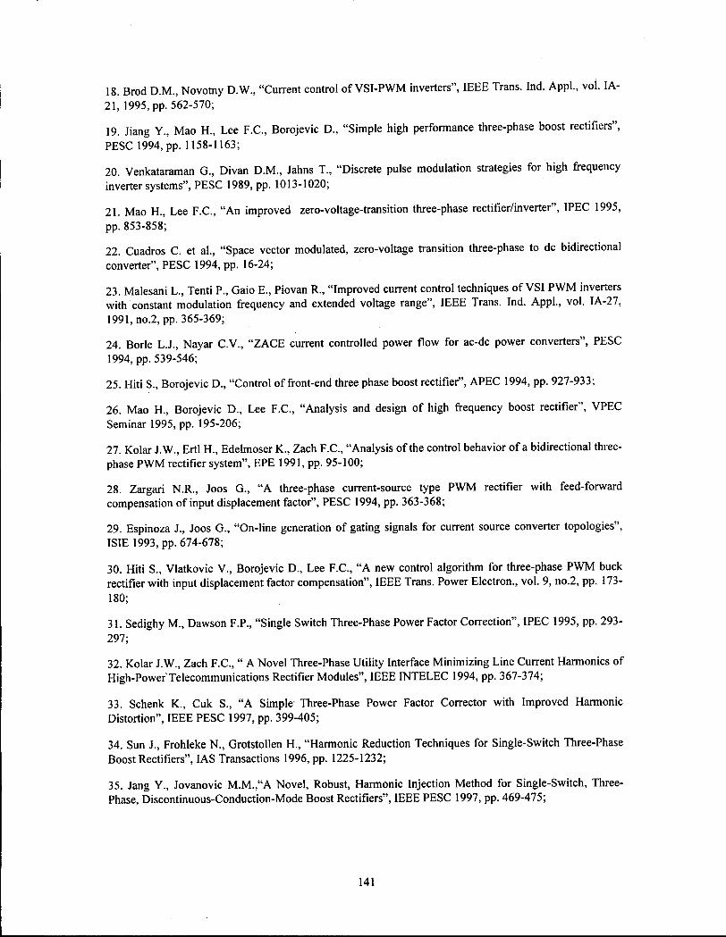
18. Brod D.M., Novotny D.W., "Current control of VSI-PWM inverters", IEEE Trans. Ind. Appl., vol. IA-21, 1995, pp. 562-570;
19. Jiang Y., Mao H., Lee F.C., Borojevic D., "Simple high performance three-phase boost rectifiers", PESC 1994,pp.1158-1163;
20. Venkataraman G., Divan D.M., Jahns T., "Discrete pulse modulation strategies for high frequency inverter systems", PESC 1989, pp. 1013-1020;
21. Mao H., Lee F.C., "An improved zero-voltage-transition three-phase rectifier/inverter", IPEC 1995, pp. 853-858;
22. Cuadros C. et al., "Space vector modulated, zero-voltage transition three-phase to dc bidirectional converter", PESC 1994, pp. 16-24;
23. Malesani L., Tenti P., Gaio E., Piovan R., "Improved current control techniques of VSI PWM inverters with constant modulation frequency and extended voltage range", IEEE Trans. Ind. Appl., vol. IA-27, 1991, no.2, pp. 365-369;
24. Borle L.J., Nayar C.V., "ZACE current controlled power flow for ac-dc power converters", PESC 1994, pp. 539-546;
25. Hiti S., Borojevic D., "Control of front-end three phase boost rectifier", APEC 1994, pp. 927-933;
26. Mao H., Borojevic D., Lee F.C., "Analysis and design of high frequency boost rectifier", VPEC Seminar 1995, pp. 195-206;
27. Kolar J.W., Ertl H., Edelmoser K., Zach F.C., "Analysis of the control behavior of a bidirectional three-phase PWM rectifier system", EPE 1991, pp. 95-100;
28. Zargari N.R., Joos G., "A three-phase current-source type PWM rectifier with feed-forward compensation of input displacement factor", PESC 1994, pp. 363-368;
29. Espinoza J., Joos G., "On-line generation of gating signals for current source converter topologies", ISIE 1993, pp. 674-678;
30. Hiti S., Vlatkovic V., Borojevic D., Lee F.C., "A new control algorithm for three-phase PWM buck rectifier with input displacement factor compensation", IEEE Trans. Power Electron., vol. 9, no.2, pp. 173-180;
31. Sedighy M., Dawson F.P., "Single Switch Three-Phase Power Factor Correction", IPEC 1995, pp. 293-297;
32. Kolar J.W., Zach F.C., " A Novel Three-Phase Utility Interface Minimizing Line Current Harmonics of High-Power Telecommunications Rectifier Modules", IEEE INTELEC 1994, pp. 367-374;
33. Schenk K., Cuk S., "A Simple Three-Phase Power Factor Corrector with Improved Harmonic Distortion", IEEE PESC 1997, pp. 399-405;
34. Sun J., Frohleke N. , Grotstollen H., "Harmonic Reduction Techniques for Single-Switch Three-Phase Boost Rectifiers", IAS Transactions 1996, pp. 1225-1232;
35. Jang Y., Jovanovic M.M.,"A Novel, Robust, Harmonic Injection Method for Single-Switch, Three-Phase, Discontinuous-Conduction-Mode Boost Rectifiers", IEEE PESC 1997, pp. 469-475;
141

36. Kolar J.W, Ertl H., Zach F.C., 'Design and Experimental Investigation of a Three-Phase High Power Density High Efficiency Unity Power Factor (VIENNA) Rectifier Employing a Novel Integrated Power Semiconductor Module", IEEE 1996, pp. 514-523;
37. Kolar J.W., Zach F.C., 'A Novel Three-Phase Three-Switch Three-Level PWM Rectifier', Power Conversion Conference 1994, pp. 125-138;
38. Prestifilippo P., Scibilia R., Baggione G., Caramazza G., 'A Switched-Mode Three-Phase 200A/48V Rectifier with Input Unity Power Factor', IEEE 1996, pp.543-547;
39. Bialoskorski P., Koczara W., 'Unity Power Factor Three Phase Rectifiers', IEEE 1993, pp. 669-674;
40. Cretu D., Dunford W.G., Edmunds M., "Universal Input 3-Phase 3-Switches Power Factor Correction Circuit Operating in Discontinuous Conduction Mode", IEEE INTELEC 1997, pp. 475-482;
41. Massey R.P., Snyder E.C., "High Voltage Single-Ended DC-DC Converter", IEEE PESC 1977, pp. 156-159;
42. Pforr J., Hobson L., "Power Factor Correction Using Quasi-Resonant SEPICConverter with Three-Phase Input", IEE Colloq. No. 203, Static Power Conversion, 1992, pp. 9/1-9/4;
43. Oishi H., Okada H., Ishizaka K., Itoh R., "SEPIC-derived three-phase sinusoidal rectifier operating in discontinuous current conduction mode", IEE Proceedings Electr. Power Appl., 1995, pp. 239-245;
44. Dos Reis F.S., Sebastian J., Uceda J., "Minimizing PFP Converters" , IEEE INTELEC, 1997, pp. 723-728;
45. de Vicuna L.G., Guinjoan F., Majo J., Martinez L., "Discontinuous Conduction Mode in the SEPIC Converter", IEEE MELECON, 1989, pp. 38-42;
46. Sebastian J., Uceda J., Cobos J.A., Arau J., Aldana F., "Improving Power Factor Correction in Distributed Power Supply Systems Using PWM and ZCS-QRC SEPIC Topologies", IEEE PESC, 1991, pp. 780-791;
47. Simonetti D.S.L., Sebastian J., dos Reis F.S., Uceda J., "Design Criteria for Sepic and Cuk Converters as Power Factor Preregulators in Discontinuous Conduction Mode", IECON 1992, pp. 283-288;
48. Sebastian J., Cobos J.A., Gil P., Uceda J., "The Determination of the Boundaries between Continuous and Discontinuous Conduction Modes in PWM DC-to-DC Converters used as Power Factor Preregulators" IEEE PESC 1992, pp. 1061-1070.
142
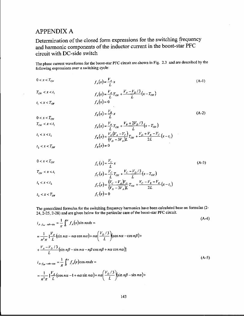
APPENDIX A Determination of the closed form expressions for the switching frequency and harmonic components of the inductor current in the boost-star PFC circuit with DC-side switch
The phase current waveforms for the boost-star PFC circuit are shown in Fig. 2.3 and are described by the following expressions over a switching cycle:
0 < X < Tn, (A-l)
T0N<x< r,
f, < x < Tsw
0<x<TON
T0N <x<tx
f, <x<t2
t2<x< Tsw
0<x<Tn,
T0N<x< r,
r, < x < t2
t2 < x < Tsw
/,(-
/ , (*
/*(*.
/*(*.
/*(*
/„(*
fc(x
fc(x
fc(x
fc(x
= 0
L
-TON + VB+2VD/3
(X~TON)
f^"V^ + ^ + K ' - K c (x-/ , ) {VD-WA)L 0 N 2L
= 0
= —x
-V-±T L ° r v
x T0N)
{VC-VA)VD
{VD-WA)L
Vr-VR- V, 2L
(A-2)
(A-3)
The generalized formulas for the switching frequency harmonics have been calculated base on formulas (2-24, 2-25, 2-28) and are given below for the particular case of the boost-star PFC circuit.
1 «. , . (A-4) A-/sir-n,H-^ = - I" /A ( * ) S M M D X =
1 V \ — [— (sin na - na cos na)+ na\ n n
VJ2>\ (cos«a-cos/j/?)+
y -v 12, , x
+ — - — (sin n/3 - sin na - nJ3 cos «/? + na cos na)] L
IA f ,u = — f fj(x)cosnxdx-A-/sw-"'"-cos Jj JTA\ /
(A-5)
= —!— [— (cos na -1 + na sin na)+ na\ n2K L
(VDJ2_
I ) (sin nfl -sin na)+
143

V -V 13 / \ + —i S.— (cos nP + nP sin n/3 - cos na - na sin na) L
i •B-fm-nth- .-«» = - f*//,(*)sinnr£fa =
[—— (sin na — na cos na)+ na — (cos na- cos n/J)+ 2VDI3
n27t L
+ V b + 2 ^ c / 3 (sin nP - sin na - nP cos nP + na cos na)+ L
+ n {VA-VC)VD „ VD+VB-Vc
{{VD~3VA)L
VD+VB-VC
2L
-a 2L P |(cos«/J-cos ny)+
(sin ny - sin nP - ny cos ny + nP cos «/?)]
/• , ,. = — f" fR(x)cos nxdx = 'B-far-nth-cm J, •/fi W
= - i — [- - (cos na-l + na sin « a f - ^y^2l( s j n np - sin war) 2 1 r n TI L
+ n \ ^ - V c ) V ° a - V ° + V B - V c P (sinny-sinnp)+
{(VD-3VA)L 2L f
+ _2 i £- (cos ny - cos nP + ny sin ny - nP sin nP)] 2L
C-fw-nlh-s\n = — f* fc(x)sin nxdx •• 71 k
-[—— (sin na — na cos na)+ na —— (cos/ia-cosn/9)+ ' 1 L ) n2K L
y —Y /3 . x + — — — (sin np - sin na- nP cos nP + na cos na)+
+ n {Vc-VAy„ VC-VB-VO
a-{(VD-3VA)L 2L P (cos w/?-cos ny)-
+ ——^—~ (sm nY ~ s m nP ~ n7 cos ny + np cos np)\
ic-/s,-n,h-cos = f" fc(^)cos nxdx =
I V (V /3^ = ——[—(cos w a - l + na sin/?a)+/ia — - — (sin nP - sin na)
n n L \ L )
VC-VDI3, n „ . „ . x (cos np - cos na + np sin np - na sin na)+
+ n {VC-VAYD „ VC-VB-VD
(VD-3VA)La 2L P (sin ny -sin«/?)+
y —Y —V . < - 2 2 2. (cos Wv _ cos nP + ny sin ny - np sin «/?)], where:
a = $ ^ 2 ; r ; P = T - ^ 2 n ; ^ ^ ^ 2* ^.W ^5(f 7 S W
(A-6)
(A-7)
(A-8)
(A-9)
(A-10)
144

APPENDIX B Formulas for the determination of the optimum modulation of boost-star PFC circuits with AC-side switches
Modulation at the end of the ON-interval
The equations for various combinations of switch turn-offs at the end of the ON-interval are determined as
follows:
i n ^ L = ^ L *h-=X*. *L=Y<L ' dt L ' dt L' dt L
y — m cA">l-"/2) LABC L
110
dig _ VA+VD'I dih = VB+VD/3 dic _ VC-2VDI3
dt L ' dt L ' dt L
y _ K*_ j(aJ-n/2) 2VD -J2nl3
L a b c L 3L
101
Vl»* " L 3L
O i l
dU = VA-2VDI3 dib _VB+VDI3 dic = Vc+VD/3
dt L ' dt L ' dt L
y = YjrLeA^>-"i2) , 2 V D CJQ L a b c L 3L
000
The operation in this interval can be split into two:
- current flowing in three rectifying diodes:
dig = VA-Vp /3 ^ di„ = VB +2VD 13 ^ dic _ Vc-VD 13
dt L ' dt L ' dt L
(B-l)
(B-2)
dig _VA-yp^ di„ _VB+2VDI3 dic _ VC-VDI3 (B"3)
dt L ' dt L ' dt L
(B-4)
(B-5)
145

y _ Ym_ej(vt-*n) , 2VD
L a b c L 3L
- current flowing in two rectifying diodes:
dia = Q dib =VB-VC + VD dic = Vc -VB-VD (B-6) dt ' dt 2L ' dt 2L
y V3fo-r c ) , , / 2 | fivD l s l 2
L a b c 3L 3L
This equation is valid under the condition: ic (tt) > iA (r,) = 0 .
Determination of ta for modulation at the end of the ON-interval
From Im(/^) = 0 it results:
ta(ta+2tt +t2)sm(7r/6 + o)j) = ti(tl +t2)sm(x/6-a>j:) (B'7)
where:
VA „ Vnl3 + VA
t, = 1 VDI3-VA
0 N VD/3-VA
2VB , 2VA(VB+\2VD/3) VC-VB-VD {VC-VB-VD\VDI3-VA)
By writing:
T +LRJjLLLLt
(B-8)
A
/, = A + Bta_r
t2=C + Dta
_ sin(;r 16-co.t) s'm(x / 6 + <o.t)
F = \ + 2B + D-BE(B + D)
G = 2A + C - E ( B A + B C + A B + A D )
H = - A E ( A + C )
t =M a-r rp
we obtain the following equation:
T0s + 2(VB +VD/3)] 2{VB + 2VD I3\VD 13 + VA) Vc-VB-VD {VC-VB-VD\VDI3-VA)\
(B-9)
146

Ftlr+Gta_r+H=0 (B"10>
Simulations using MATLAB show that the equation has only one positive root over the (0,x/6) interval.
Also through simulation it is checked that the resulting ta_r maintains ic (r,) > iA (/,) = 0 .
Modulation at the beginning of the ON-interval
The equations for various combinations of switch turn-ons at the beginning of the ON-interval are
determined as follows:
111
d h j ^ d h j ^ d ^ j ^ J_^eA^n) (B - l l ) l lO , dt L dt L dt L L a b c L
110
di„ _VA-VB di„ _ VA — VB diSL = 0 _J}(VA-VB)C-J*,*
dt 21 ' dt 2L ' dt ' L a b c 31 (B-12)
101
dig = VC-VA ^* . = 0 di, = VA -VB = S { v c - y A ) ( B l 3 )
dt 2L ' dt ' dt 2L ' L a b c 3L
Oil
^ = 0
di» = V » ~ V c di< - VB~yC Y = S { V B - V C ) j,n ( B l 4 )
dt ' dt 2L ' dt 2L ' L a b c 3L
000
The operation in this interval can be split into two:
- current flowing in three rectifying diodes:
dig VA-VD'* di„ VB +2VDI3 dic ^Vc-VD/3 = Vm - ( ( 0 . , . W 2 ) 2VD J t l 3
dt L ' dt L ' dt L L a b c L 31
- current flowing in two rectifying diodes:
d i « - 0 DI" _VB-yc+yD dic _ Vc-Vg-VD _S(VB-Vc)cj,n , SVncj«n dt ' dt 2L dt 2L ' L a b c 31. 3L
This equation is valid under the condition: ic (r,) > iA(r,) = 0 .
(B-16)
147
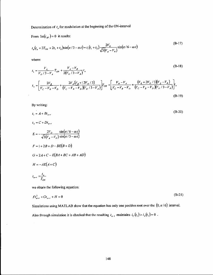
Determination of ta for modulation at the beginning of the ON-interval
From \m(iAV) = 0 it results:
2V ta{ta+2T0N +2', +/2)sin( /3-fi>i) = /,(/, + t2) r
D -sm(n16-w.t) S{vA-vB)
(B-17)
where:
t, = -7V,„ + V. — VR
(B-18) i-VD/3-VA
1°N2(VD/3-VA)a
2V„ 2VA{VB + \2VD/3) VC-VB-VD
+{VC-VB-VD\VD I3-VA) T0N +
„ „ , (vB+2VDl3r{VA-VB) ' VC-VB-VD (vc-VB-VDXvD/3-VA\
vB-vA
By writing:
t,=A + Bta
t2 = C + Dta_r
(B-19)
(B-20)
E = 2VD sin(;r/6-tu/)
Ji~{VA-VB)sm{nl3-a>.t)
F = \ + 2B + D - B E ( B + D )
G = 2A + C - E(BA + B C + A B + A D )
H = - A E ( A + C )
'ON
we obtain the following equation:
FtLr+GtA_,+H = 0 (B-21)
Simulations using MATLAB show that the equation has only one positive root over the (fJ,;r/6) interval.
Also through simulation it is checked that the resulting ta_r maintains ic ) > iA (?,) = 0 .
148

APPENDIX C Formulas for the determination of the current waveforms for the boost-delta PFC circuit
The following parameters have been used for describing the performance of the circuits:
(C-l) - the normalized phase current: iM =
where: iA = phase current,
normalizing L current.
There are two possible states of the three switches: 000 or 111. When all the switches are closed (111) the
circuit looks like in Fig. 3.27 and the following equations can be written:
v T V T V T • , T v _ AB ON ; (T \ _ r BC1 ON j (f \ _ CA* ON
l i \ l O N > - • 'lVoN/— £ ' h\'ON> ^
(C-2)
; I T \ — ^ A B VCA)TOn . /f \ _ (VBC VAB)TQN . (T \ — ^CA ac) o.v /p -21 lph\\1ON>~ 2 ' pl<l"0N>— £ » 1 phA1 ON > — ^ V^-->)
where «', (TM), z2 (TQFL (TM) are the currents through the inductors and v,(7;,v), v2(ro A,),/„„(rO T) are the
phase currents at the end of the ON interval.
During the off time of the switches (000) the current flow is dependent on the instantaneous values of the
currents (proportional to the instantaneous voltage). For the equivalent circuit presented in Fig. 3.28 the
following equations can be written:
y 4 - L « - y c - L ^ v . - L * L + y D
( C " 4 )
dt c dt dt D
vA + vB + v c = o
i, + /j + z3 =0
Solving the system the following solution is obtained:
1 (C-5) V --V
V T A i D
/ I ( / ) = L » £ « L + — i — ( / - r 0 , v )
149

V + — V y f B ^ D
i (/) = LJsiss. + 3— (t - Tw)
V --V / j (0 = i 2 i ^ + f—(t-T0N)
Li Li
The time at which the current would reach zero in the three inductors is determined as:
(C-6) t = T 11 1 ON
t = T
vD- WA
2VD + 3VC
2VD + 3VB
vD- wA
vD- 3VC
t = T '13 ON
Since the beginning of the interval studied is taken as the zero crossing of VAB the phase voltages are
written as: (C-7)
VA=VL„sm{w.t--)
^ = K „ s i n ( a » i - y )
Vc =K„sin(ty.? + y )
VD = VLVMy[3
After the time point where one of the currents becomes zero, the analysis must be carried out for two
intervals:
Interval (0,a)
(C-8)
V --V V T "x V -3V
Wii)- hCu)- £ + ^ V 'ON y 'ON)
150

After tn the current in inductors 2 and 3 is equal and of opposite sign. The equivalent circuit is shown in
Fig. 3.29 and the following equations describe the circuit:
V ^ L ^ = VB-L^- + VD
dt ' dt
By solving:
\iVc-vB-vD) h (0 = h Cu)+ j ('-'..)
The time t2 at which the current through inductors 2 and 3 will become 0 is determined as:
-{VC-VB-VD)
= 0
The instantaneous currents in the three phases and inductors are shown in Fig. 3.34.
The average current in the inductors over a switching period can be calculated as follows:
hi = ~Z~ 'i (TON )'i i
k.2=^{h(ToN)ToN+(tn-ToN)['2(ToN) + i2(tn)) + (t2 -'nH('n)} zt2
'i.3 = ih (TON )T0N + CI I " T0N )[i3 (TON ) +1, (/,,)] + (t2 - /,, )i, (/,,)} zr 2
The average current in the phases over a switching period can be calculated as follows:
'PH., = -Z-{'PHA(TON )TON + On ~ TON)'I(^.V)}
'PH2 = ^-{iph2(ToN)TON +(tn-T0N)['2(ToN) + '2(tJ] + (t2 ~ 1 >*2 C'] 1 » zf2
Ws = - { ^ . 3 ( ^ ) 7 ^ + (',, -T0„)[h(TON) + i3(tu)) + (t2-t„)h(*n)) lt2
(C-9)
(C-10)
(C-ll)
(C-12)
(C-13)
151

Interval (a,7r/3)
./,(!„) = 0 (C-14)
v-l-v V T "x V -3V
After tn the currents in inductors 1 and 2 are equal and of opposite sign. The equivalent circuit is shown in
Fig. 3.30 and the following equations describe the circuit:
dL di, (C- 1 5 ) V t— L —- — VB—L —- + VD , /,+/, =0
dt dt
By solving:
1 (C-16) -(VA-vB-vD)
',(0 = ',('.,) + - - ('-',,)
The time / 2 at which the current through inductors 1 and 2 will become 0 is determined as:
~(yA-vB-vD)
»",(',) = o
The average of the current in the inductors over a switching period can be calculated as follows:
1 (C-18) Lx = T- {'. ) r w + On " 7^)[/, (rOT) +1, ( / „ ) ] + (r2 - / 1 3 )i, (/l3)}
zt2
Li = ih VON WON + Cn ~ T O N )VI (TON ) + '2 ('n )1 + ('2 " 'n )'2 ('13)) zt2
L>=-£-h(To#yt»
The average of the current in the phases over a switching period can be calculated as follows:
1 (C-19) 'PHI = — {'PhAT0N)T0N +(/13 -7 ,
OAf)[/ l(rOA,) + /1(r13)] + (/2 -/13M(r13)}
' W 2 = 7 - { ' ^ ( ^ F O Y + ('13 - T0N)[h(TON) + / , ( / „ ) ] + (r2 - tn)i2{tu)} 2t2
152

APPENDIX D
Determination of the currents in the 'Starfly' PFC circuit operating in DCM
State 111
During this state all the switches are on, the inductors are building up energy and no power transfer occurs
to the DC side. As it can be seen in the Fig. 4.2 we have the two sets of inductors, Lx and L2, in a star -
delta configuration across the input three-phase voltage system.
While 0 < t < T0N the inductor currents, as shown in Figs. 4.2, 4.4 and 4.5, have the following expressions:
• i\ 3 V A • ( \ 3Kg . / \ 3VC (D-l) a\n = —-—' > bin = —-—(> An = — —' "V ' 3LX + L2 "K ' 3LX+L2
c K ' 3LX+L2
hin = ———t.hin = ———t, hin = ———t I W 3LX+L2
2 W 3LX+L2
3 W 3LX+L2
At the end of the interval the following currents have been reached in the inductors:
j(T ) - W « T i(T ) W b T tlT ) W c T ( D " 3 )
a [ m > 3LX + L2
0 N ' cw j - + ^ ION , >AJON) ~ ^ + ^ ION
I ( T ) VA~yB T i ( T x V.-VCT i { T ) Vc-VAT (D-4) A o n ) 31., + L2
O N ' h { o N > ~ 3LX + L2
O N ' h [ o N > ~ 3Z, + L2
O N
State 000
During this state all the switches are off and the inductors are transferring energy to the DC side. As it can
be seen in Fig. 4.3 the boost and the flyback stages are running independently.
Boost stage.
While T0N <r<r,the Lx inductor currents, as shown in Figs. 4.3, 4.4 and 4.5, have the following
expressions:
y _ ^ <D-5> 3V A i
^ - K t L i T ~ * - L ^ -
153

V + ^
It can be shown that the current in phase A reaches first zero, at a time /, as given by the following
expression:
3L, 3VA
3Li+L2 VD-3VA
The currents in the L, set of inductors reach the following values:
• ( t \ 3To» V ° ( V ' - V c ) h ^ ' - 3 L x + L 2 VD-3VA '
, , 3TON VD(VC-VA) cKV 3Ll+L2 VD-3VA
The current equations after r,, i.e. r, <t <t2 become:
'.(') = °
,,(,) = _;,(,) = 37-w M ^ - ^ ) + K c - K , - K c W * w 3L,+Z,2 F D — 3VA 2L,
The current reaches zero in all three phases at t2:
t 3T0N VD{Vc-VA) 21, 2 3LX+L2 VD-3VA VD+VB-VC
In the interval t2<t < Tsw no current flows in the inductors:
The total time in which current flows through inductors of the boost star stage is:
(D-6)
(D-7)
(D-8)
(D-9)
(D-10)
154

T — T 1 tot-star ON
+ ' l + t2 = T0N 1 + 3L]{VC-VB)
(3Ll+L2){VD+VB Vc))
(D-l l )
Flyback stage.
While Tnrl<t< r, the currents, as shown in Figures 3,4 and 5, have the following expressions:
' .( ')=-3 ^
' .( ')=- 31, + Z-j
<«(')=-3VB
<«(')=- 31, + i 2
<c(') = -3^c T
*2 <c(') = - 3L, + Z-j *ON
*2
31, + L 2
31, + L2
-vA
3Z, + L2
IV) - IT , I l O N + r 1 > ^ 2
^) = i r - 7 r T 0 N .
It can be shown that the current in phase A reaches first zero. Consequently:
3T0N(VA-VC)
'c(0=-'fl('3) :
31, - L2
• L \ 2 V A ~ 2 V c T
h[-tn>~ 3LX+L2
l o N
The current equations after r3 become:
(D-12)
(D-13)
3VA L2 (D-14) t = -T h 3Ll+L2 VD •
(D-15)
(A (A ^ - r ( D " 1 6 )
155

(D-l 7)
. M . ( A 1T0N{VA-VC) 3V
3Z-, - 1 2 2 I 2
3Lt+L2
0 N 2L2
2VA~2VC Vn_ '2V>~ 3Ll+L2
O N
The current reaches zero in all three phases at tA:
L2 J V C - V A ) T
The total time in which current flows through inductors of the flyback stage is:
T,ol-flyb ~ TQN + U ~ TQN 1 + (3L1+L2)VD)
(D-l 8)
(D-l 9)
(D-20)
(D-21)
Phase currents
The instantaneous switching period is chosen as:
T - (T T \ ( D " 2 2 )
*SW ~ m a * \ * lot-slar ' 'lol-Jlyb )
The averaged instantaneous phase currents for the interval (0,n/6) are given by the following formulas:
ia(T0N)(T0N+tl) (D-23)
2Tsiy
. =U{TQN){Ton +tl) + h{tl){t,+t2)
. =ic{ToN){TON+t,) + ic(t[)(tl+t2)
'c-av - rp
In phase A the current can be expressed for the interval (n 16,7112) as:
156

ia'mj) = i\^L-(o.t^ , for 7tl6<a.t <nl2>
ia(co.t) = -ih[a.t - - j j , for n13 < col < K12
(D-24)
(D-25)
Once the current in phase A has been determined for the interval (0,^/2), the current for the whole
period can be written as:
ia(co.t)=ia(n-co.t), for n12 < col < n (D-26)
ia [co. t) = -ia (co. t - TI) , for n < col < 2n (D-27)
Average current space vectors determination for the 'Starfly' PFC circuit
For the modulation at the beginning of the ON-interval, the space vectors are given in formulas (D-28/D-
30) and the diagram of Fig. 3-15 is valid with the values given by (D-31/D-35).
110
di_ dt
101
O i l
ABC
ABC
di^ dt) ABC
3Z, + L2
3L + L,
S ( v B - v c ) t
3Z, + L,
-jx/6
-j5ir/6
jttll
3A TON(TON+2ti+t2) | tx(tx+t2)
3L, + L2 271 sw
I T sw
S ( V A - F J , ) f . ( f < t + 2 r Q y + 2 f 1 + / 2 ) ! l 31, + L2 IT.
(D-28)
(D-29)
(D-30)
(D-31)
(D-32)
sw
157

j 3 fc -Kj f g ( / f l +2r w +2f ,+ f 2 ) (D-33)
/ s 31, + I 2
V3fc-rc)f.(f.+2rw+2f,+f2) (D-34)
7 ' 31, + Z2 2 7 ;
2 F D f,(f,+/2) (D-35)
5 3Z, 27;,
For the modulation at the end of the ON-interval, the space vectors are given in formulas (D-36/D-38) and
the diagram of Fig. 3.5 is valid with the values given by (D-39/D-41).
110
ABC 3Z, + Z2
3K, ^ iO,,.,-*/!) + 2 V D eJ*U
3Z, + L2
(D-36)
101
ABC 3Ll + L2 3Li+L2
(D-37)
Oil
di 3V„.
ABC 31, + Z2
2VD
+ —eJ
31, +L2
(D-38)
1=^ 1 A
3Z, {TON +ta\TON +ta + 2(, +t2) t tfa+tj
31, + Z2 2 7 ; sw 2T
(D-39)
2VD ta{ta+2tx+t2) (D-40)
2KDf,(f,+/ 2) 3 3/ 271
J l j \ ^Lsw
(D-41)
158
APPENDIX E
Determination of the currents in the Star-Delta PFC circuit operating in Discontinuous Conduction Mode
The general equations describing the evolution of the current in the boost inductors and the rectifying
bridges legs are given below:
dial dia dix dib±_^_di2_ dic3 ^ dic di
dt dt dt ' dt dt dt ' dt dt dt
di, di, . di, i - = - i T ° N ' ^ < > + ^ ' ' ^ + ^ ' s '
(E-l)
(E-2)
di. di, di, / * = / - * + d " ' 4 ' / ' > = ' ^ + : ^ ' 3 ' v , = ( / , + ^ dt dt
—- varies with the interval. dt
je{a,b,c,\,2,3,al,b2,c3}
Tlol=TON+ti+ti+t,+tJ+t2
Tw =max(rto,)
ljAv T
0 + i i, +i, i, +i,
(E-3)
(E-4)
(E-5) 2 "°™ ' 2 ° 2 ' 2 " 2 ' 2
Immediately after turning off the switches, there are six diodes conducting, three in each bridge. They
eventually come out of conduction, one by one, changing the current slope of the inductors. The inductance
and voltage transfer ratios are determining the set of equations that can be written, and consequently the
current evolution. A visual representation of the current in the input inductors is given in Fig. 4.32, based
on a time domain simulation with the values given in Section 4.3.
The analysis starts by determining which diodes are conducting at the end of the ON-interval. Table E-l
shows that information for the analyzed interval. As an example of the current evolution, when an inductor
of the L2 set has diodes at both ends conducting onto the same bus, the voltage across it is zero, and its
current maintains a constant value. It is identified which possible sequence of diodes coming out of
159

conduction can occur. This is based on the calculation of the times in which the current in the rectifier
bridges legs would reach zero, for a given set of equations. Then the minimum time is determined, and the
new set of equations, characteristic to the new current flow is written. The possible states are identified
with letters and figures, where the latter shows the number of diodes in conduction. In Table E-2 the times
which lead to the occurrence of each state are given. The complete set of equations for each particular state
is given in Tables E-3 and E-4.
Currents Phase Angle Phase Diode Diode (0,JT/6) (a-/6,w/3)
bridge 1 bridge 2 A6 B6
iJToN+) 'ai (TON+ ) >X(TON+) + - + + + +
h(TON+) hi (TON+) '2(TON+) - - - - - -
'ATON+) 'c3 {TQN+ ) h(TON+) + + + + + -
In the following, based on the application of the general equations , the time length for each interval is
given.
Interval (0,7^)
^ = lL^L2
T o n ' '* (ToK)" 3vfZ7T°N ' i e ( 7 ™ ) " 31, + L2
T °
•IT \ V A ~ V B T ; (T \ - V B ~ V C T : ( T \ - Vc ~ V A T
Lx (TON ) = L (TON ) ~ 'x (TON ) = ^ T "
LAToN)=ic(T0N)-h(ToN)--
3£, + L2
vB -vA
31, + L2
Vc -vB
31, + L2
'ON
(E-6)
(E-7)
(E-8)
Interval (T0N,T0N +0 ia([)=ia(T0N)+^t ,ih(t) = i b ( T m ) + ^ t ,ic(t)=ic(ToN)^t
(E-9)
160

I
' ,1 (') = '« ( ' )" 'I (0 = ' a ) " fcw )+
hi ( ' ) = '* (0- '2 (0 = '* v cw ) - '2 (TON )+1
dL di.
(, «# dt
Uih di2^
hi (0 = h if)~ h if) = h (TON )~ h (TON )+
dt dt
die d h
dt dt )
(E-10)
(E- l l )
It is mathematically shown that:
t, = 2VA+VB
3L, +L2
3£ , L2 )
for which:
'„,(', )=°
Interval (TON +tx,TON + f, +t2)
ibATON +0 >a{T0N + 0
bl dt
dh
dt J
Interval {T0N +/, +r2,7-OA, +/, +f2 +r3)
If: di b2 dt
dia
dt
iaiT0N + ' i + ' 2 ) ' » f c w + ' 1 * * 2 )
di cl
dt dh
dt
If: di bi dt
dig
dt
(E-12)
(E-l 3)
(E-14)
(E-l 5)
161
di„ ' di
dt
'ci dt
Interval (T0N + t,+t2 +t3,T0N +r, + t2 +/3 +/4)
'c3 fo* + ^ ifcw+'i+O If:
di ci dt
(E-16)
di. c3 dt
I f . ^ f c w + ' i + O < ifcw+'i+O di cl dt dt
(E-17)
ig\TON+t,+t2+t3) 'c(ToN+tl+t2+h)
dia ' dic
dt dt
Tf. K ic&QN+t.+ti)
di bl dt
di. ci dt
(E-18)
di. ci dt
If: hi (tON + '.+0 ^ hi\T0N+t,+t2)
di bl dt
di. ci dt
(E-19)
ta = mm' hi{TON + ' . + ' 2 + 0
di bl dt
162

Interval (T0N +r, + t2 + f3 + t4,T0N +r, +t2 + / 3 +r4 +0
hJToN+h+h+h+U)
dt
(E-20)
Interval (TON +tx +t2 +t3 +t4 +t5, Tsw)
The current in all inductors is zero.
163
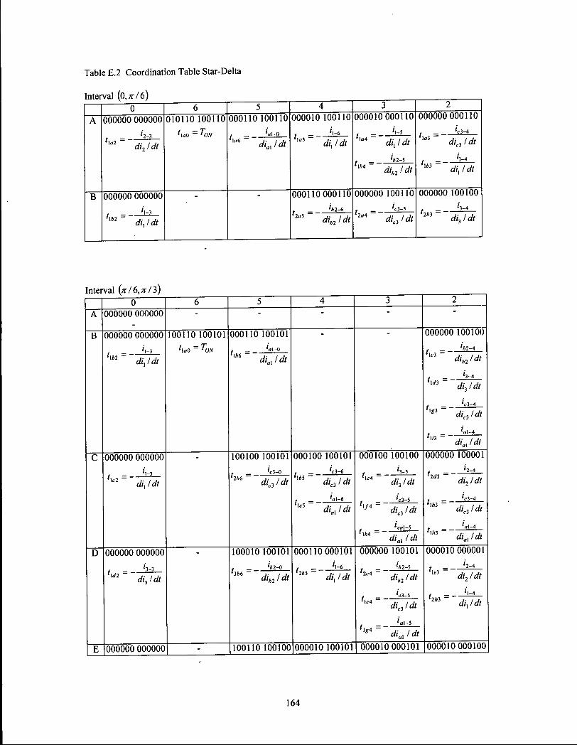
Table E.2 Coordination Table Star-Delta
Interval (0,;r/6) 0
B
000000 000000 i
u, '2-3
010110 100110
di2ldt
000110 100110 t _ 'al-0 , a 6
000010 100110 000010 000110 000000 000110
'1-6 dijdt dijdt
his t , M dLjdt
dic3ldt
dix Idt
000000 000000 000110 000110
dijdt 'bl-6
dih2ldt
000000 100110
/ — 'c3-5 2 a 4 ~
000000 100100
'263 = - '3-4
Interval (n 16,rr I'3) 0
000000 000000
000000 000000
' lM = - '1-3
100110 100101 ?iao = TQN
000110 100101 _ 'ql-0
000000 100100
dix Idt diaJdt 'M-4
dih2ldt
t,^ = — di3ldt
000000 000000 'l-3
dijdt
100100 100101 t _ *c3-0
000100 100101
dijdt dic3ldt
000100 100100 000000 100001
dijdt t\ fA —
'3-5 '2-4 di3ldt di2ldt
'c3-5 _ 'c3-4 dic3ldt
'cal-5 'm 'al-4 di„Jdt 'm
D 000000 000000 o _ '3-3
dij/dt
100010 100101 t _ '*2-0
000110 000101 000000 100101
din Idt dijdt
t\gi, -
hi -5 dhi Idt
'c3 -5 di* Idt
ia\ -5 dial
000010 000001 , h=*
di2ldt
t =- ''-4
2 M d,-/dr
000000 000000 100110 100100 000010 100101 000010 000101 000010 000100
164

'2-3 t - t
lh2-6 . '»2-5 f, , - '3-4
h e 2 ~ di2/dt Ah6 dijdt 3 M " dih2/dt
f 'al-6 U i ~ dijdt
t - ''-5
2 e 4
2 e 3 dijdt
j '*2-4 1 / 3 dijdt
t - ''-4
2*3 dijdt
F 000110 100100
t = '3-6
4>5 dijdt
. 'al-6 l e 5 dijdt
000110 000100
t
2 d A dijdt
' 3 / 4 dijdt G 100000 100101
t _ '*2-6
, 'c3-6 2 J 5 _
000010 100100
t - '3-5
3 8 4 dijdt
( '42-5 2 / 4 " dib2 Idt
( 'al-5 "4 dijdt
H 100100 100100
t = ''3-6
3cS rf/j/dr ., 'c3-6
2 < 5
000010 100001
f - ''2-5
4 " 4 dl"2/<*
, 'al-5 2 J 4 ~ dijdt
I 100010 100100
' W 5 dijdt
t '*2-6 3 e 5
100000 100100
2*4 rfij/dr-, his
2 M ~ dijdt
f 'c3-5 2 i 4 ~ dijdt
J 100010 100001
= '2-6 4rfs dijdt
100000 100001
r - '2-5
3 * 4 « f i 2 / t f
f 'c3-5 1 7 4 </«;,/<*
165

to > i to > u>
CO 4^
> i > I
> i > i O
+ +
+
+ . M
+ I
+ c-
I
+
OS
l i - l +
. M +
+
1 1 +
+ +
+
+
I
+
+
+ .c- I
+
+
+
I
+
j - - I I
l > l
+
+
•1 +
+
t- I
+ +
I
+ >5- I
S I
i i
+ B-LSr
+
+
i 7"?
+ . M
+ . M
+
+
+ . M

X I
| i -+ tx
i-l + + tx
jx +
[i-+ tx
•
x
i-l + Jx I
y l I to F'l +
D O I
1 + tx
_?x + tx
|i~" + tx
l i -+ fx
li-+ tx
| i -+ fx h i -+ fx
F l + .tx I
i - l +
Os xj
i -
+ tx
l i -+ tx
I i - l +
. M
to F l +
Jx I y l I
li-+ tx
li-+ tx h + tx
I bx
F l + jx I y l I
F l + tx I y l + i - I + .tx I
li-+ tx
.tx
^1 I
I i -Jx +
I F I b^
I tx
+ F I y l I
F l
+
+ i-l + .tx I
+ .tx I
F I
F l + .tx I
Jr-
ix +
1 tx 1 ix +
tx
i -
F
i - | + .tx I
i -i-l + .tx|
i -+ tX i -
i-l +
i -
i-l ' + .?x I I
1 I to ^ I
K> ix I + tx
ix 'l^i + to I
| i -+ tx
> b.
•
4
ix +
otx
+ F l + Jx I
i-l + Jx I y l + "io" i - I + tx I
+ F | + .tx I
71
i - l + tx I
y l +
i -+ tx
+ i - I + .fx I
I F | + .tx|
i-l + |x I
ix + tx
li-+ tx
•
4
+ .tx I
i -+ fx i -+ t>
i x
i - | + jx I
I l > + jx
+ fo~ i-l + .tx I
i " +
tx Jx + tx
i-l +
+ 'tos
+ .fx|
I jx i-l + .tx I + to"
F l +
i F | + .tx I
+ „tx| I
F i +
Mtx I
i-l + Jx I y i
I | F | + tx I
li-+ tx
| i -+ tx
I F I
i F I
i - l + .tx I 1
I > ' l + t- I
y l + i-l + .tx I
I "ix
.tx
4
0 | I
i-l + tx I
li-+ tx
| i -+
o I
4^
i-l +
y l
i F | + .tx I
i •i-1
i -
i i -
i - l .tx I
I i -+ tx
| i -+ fx
F l + tx I yl +
F l + tx I
i -
li-+ tx
li-+ tx
l i -+ fx
l i-+ tx
I I ^ I
|F | Jx I
+
i-l + -fx I
+ i-l
i - l + Jx I y i I
| F l +
ix
+ .fx I
l i-+ tX
l i-+ tx
I F 10* I I
F l +
Mtx I
+ To" i-l + tx| + -f-1
O I
i-l +
i i -i
I'i-+ .tx I
i - l +
o •
i-1 + Jx I
i F | + .tx I
03 • Os
> i o
li-+
i-l + .tx I i -
t^l +
_tx
, i -
i - l + .fx I
I F l +
J-1
+ 1o-_fx + tx
S I I
i - I 7"
i -+ tx
ix
I tx I + F l + .tx I
I i -
i - I + tx I y l I
i-l + tx I y l +
i - l + .fx I
a ^ l + B.LB:
i-l +
i-l +
I F I
li-+ i - l + .tx I
ix
I F
i F | + tx I
y l + i - l +
.t- I
jx + tx
i - l + .tx I
li-+
F
tx l i -
+ tx &. Br
i -+ to t -
F Jx + tx
tx + _tx
li-+ tx
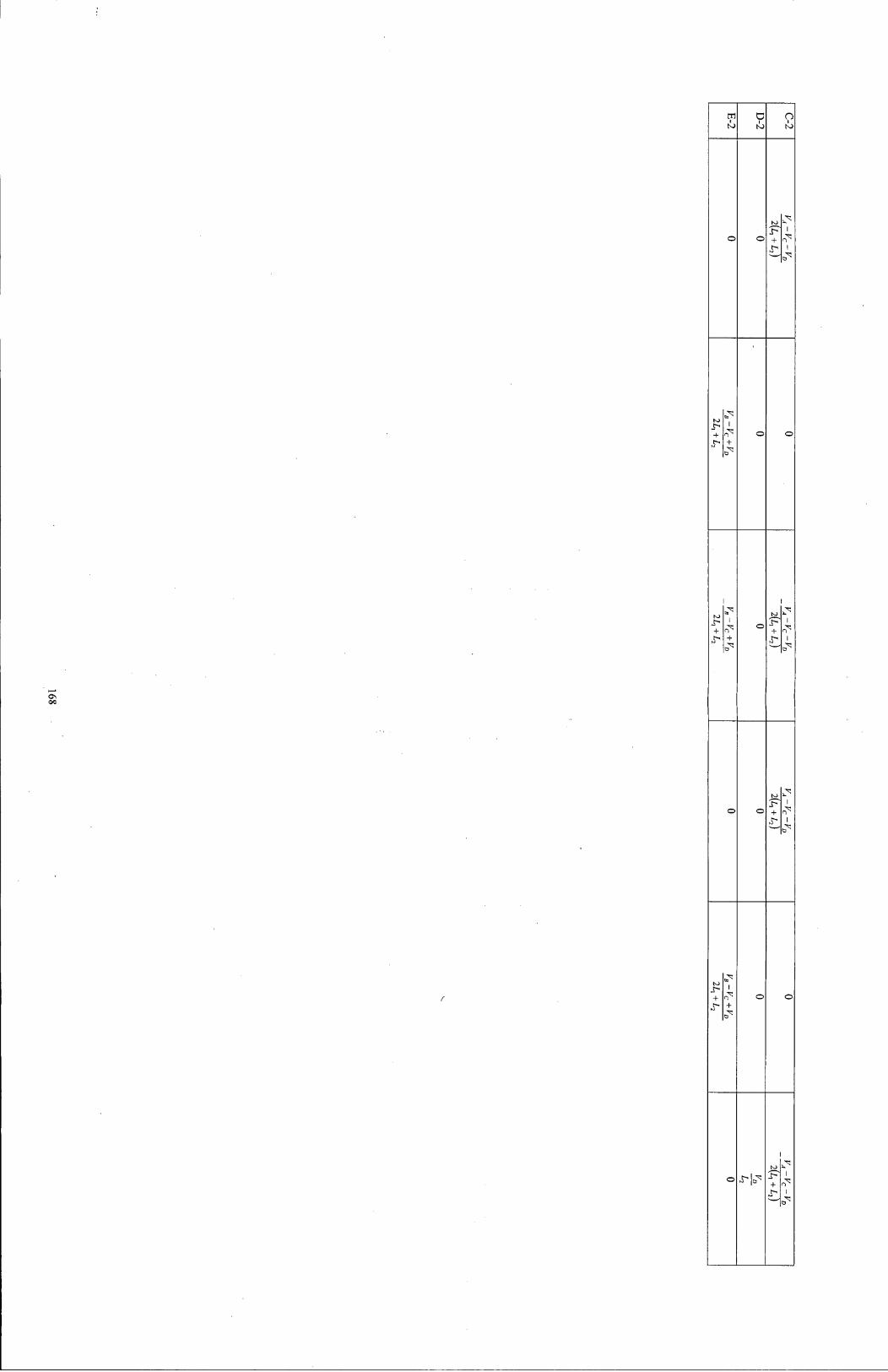
r
E-2
D-2
C-2
o o
to
+ i
1
to
+ 1
+ © o
to
+ 1
+ o
to
+ 1
1
o o
to
+ 1
1
to
+ 1
+ o O
o to
+ 1
1

APPENDIX F
Determination of the currents in the Delta-Delta PFC circuit operating in Discontinuous Conduction Mode
The general equations describing the evolution of the current in the boost inductors and the rectifying
bridges legs are given below:
dilA di^=di^_djs_ di36 = di3 di6
~dT~ dt dt dt dt dt dt dt dt
di, di, di,
(F-l)
(F-2)
L = - i T o N ij.-'jo+it'' '^+-dfh
di, di, . di,
' * = W « ^ + ^ r ' 3
d2i. dt
varies with the interval.
j e {1,2,3,4,5,6,14,25,36}
The analysis is carried out in a similar way as for the Star-Delta circuit in Appendix E. For this reason only
the equations are given here, while the procedure remains the same.
The currents immediately after turn-off of the switches are given by the following formulas:
h froN ) _ — ~ T0N > h (TON ) ~ B
T ° T0N > h froN ) _
jL, Li,
VC-VAT
T 'ON • (F-3)
i(T \ - V B ~ V C T i(T \ - V C ~ V A T ilT ) = V ' - V B T WON)-—j 'ON > WON)- , ' O N * WON) , 'o,
L - , L0 L , 2
ia{T0N)=W
HXTON) =
yLt L2 j TON 'h {TON ) - 3 VB
TON > '25 {TQN ) =
V A L2 j \Lt L2j
T M . ic(T0N)=WC
TQN-> ht,^ToN) =
TQN • (F-4)
^ Vg VC VC V A
U1 J
VC-VA VA-VB
J 2 J
(F-5)
The analysis starts by determining which diodes are conducting at the end of the ON-interval. Table E.5
shows that information for the analyzed interval.
169
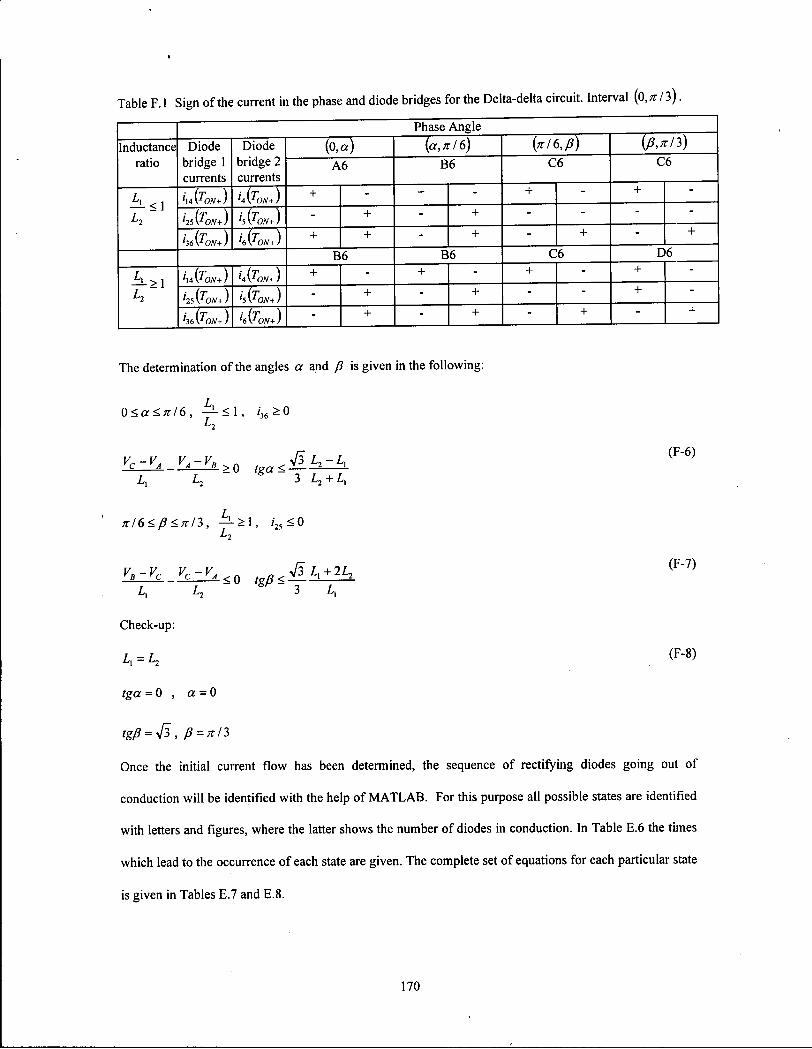
Table F.l Sign ofthe current in the phase and diode bridges for the Delta-delta circuit. Interval (0,^/3).
Phase Angle Inductance
ratio Diode
bridge 1 currents
Diode bridge 2 currents
( o , « ) (/?,*/3) Inductance ratio
Diode bridge 1 currents
Diode bridge 2 currents
A6 B6 C6 C 6
L2
'14( 0 +) U(TON+) + - + - + - + -
L2 '25 (^CW+ ) h froN+ ) - + - + - - - -L2
ijToN+) + + - + - + - +
B6 B6 C6 D 6
L2
'A{TON+) + - + - + - + -
L2 '25 {TON+ ) - + - + - - + -L2
'36 (7ew+ ) >6{TON+) - + - + - + - +
The determination of the angles a and P is given in the following:
Q<a<nl6, — <1, / 3 6 >0
Z,, L2 3 L2+LT
x/6<fi<7r/3, ^ ->1 , / 2 5 <0
L\ L2 3 L.
(F-6)
(F-7)
(F-8)
Check-up:
LT=L2
tga = 0 , a = 0
tgp = S , P = nl3
Once the initial current flow has been determined, the sequence of rectifying diodes going out of
conduction will be identified with the help of MATLAB. For this purpose all possible states are identified
with letters and figures, where the latter shows the number of diodes in conduction. In Table E.6 the times
which lead to the occurrence of each state are given. The complete set of equations for each particular state
is given in Tables E.7 and E.8.
170

Table F.2 Coordination Table Delta-Delta.
Interval (0,;r/6) 0 j
000000 011010 * - *36-5 'lo4 ,. /
000000 000000 i '4-3
100110011010
dijdt
000110011010 / = '14-0
u'6 dijdt
000010 011010
/ = '25-6 '"5 dijdt
000000 011000
t — 14-6 ,M dijdt
'l*4
Me4
*lj4
^36 Idt
'25 -5 di25
'14 -5
'36 -5 di^ldt
di6/dt
dijdt
di2S Idt
dixJdt
'36-4 *2n3
000000 010010 dhJdt
B 000000 000000 100101 011010 100010 011010 , _ '25-0
000100 011010 000010 010010
dijdt di2Jdt '36-6 t — '5-5
di}61 dt '2a4 — di5 Idt
'14-6 / — '25-5
di.Jdt Mc4 di25 Idt
'36-6 t _ 'l4-5
diKldt '1/4 _ diX4 Idt
'5-4 '2«3
l2d3
dijdt
dijdt
di251 dt
t = '14-4 *' dixJdt
di3Jdt
di51 dt
/ = 2 5 ' 4
000000 000000 100101 010110 100100 011010
'36-0
000110 010010 , _ '5-6
000100 001010 000100 001000
dijdt 3o6
'4*6
di361 dt dijdt
di}Jdt di,Jdt
dijdt
'36-5 di\61 dt
>.c3=-dijdt
'2*3 — '
dijdt
dixJdt
di3Jdt
' . , 3 = - '36-4 di}61 dt
D 000000 000000 i,
101001 010110 100110 010010
'6-3
000110 001010
dijdt dis I dt UaS — ' '4-6
000100 010010
dijdt '3*4 ~ ' '5-5
000100 000010
'5-4 dijdt '2c3 dijdt
171

f '36-5
2 C 4 C ^ / c i f
t '36-5 W 4 ~ ««,./«*
_ 'M-3 ]g4 dijdt
t '36-5 f2"4" dijdt
t '4-4 WJ dijdt
f _ '36-4
1 / 3 ~ db./df j , ' l4-4
273 dijdt
E 000000 000000 '4-3
000101 011010 , '14-0
100000 011010 t '36-6
000100 011000 t _ '6-5
100000 010000
t = '6-4
E
u2~ dijdt t m dijdt dijdt
t '25-6 2 c 5 <//M/dr
J '36-6 2/5 dijdt
444" dijdt
f ' l4-5 , M ~ dl-14/«*
f '36-5 2"4 dijdt
2 g i dijdt
t = ''5-< 2"3 <v«*
J, '25-4 2/3 dijdt
I _ '36-4 253 dijdt
t = *5-4
f '25-4 l a e 3 rfi^/rfr
F 000000 000000
t ' l4-3
100001 011010
t — '25~°
100010 010010 t - '5-6
000110 000010
/ - ' 4 - 5
100100 000000 , = '4-4
F
1/2 dijdt 2 * 6 <*Z 2 5/CA 3 4 5 " <*V<*7
J, '25-6 lrf5 dijdt
3c4~ dijdt
t - *5-5
2 1 / 4 < t f 5 / < f t
, '14-5 U4~ dijdt
"3 dijdt
t = 1/3 dijdt
t - ''5-4
U 3 <VCY/
G 000000 000000
t '5-3
100101 010010 , _ '5-0
100100 010010 , _ '5-6
100000 010010
/ - ' s - 5
000001 001000
t, = '6-4
G
]g2~ dijdt 3 4 6 "
, '36-6 3 J 5 _ dijdt
t _ '36-6 3 s 5 dijdt
2£4~ dijdt
f '36-5 2/4" dijdt
f '25-5 2*4 dijdt
t '36-5 2« dijdt
t = h-5
3"4 dijdt
f '25-5 W 4 dijdt
1 , 3 ^ / J ?
t = '4-4
" ' 3 rf/4/<*
f _ '25-4 2" 3 di-jj/aV
f '25-4 2 " 3 di^/aV
f _ '14-4 2 r 3 rfi14/dr
H 000000 000000
t '«-'
100001 010110 J '25-0
100100 011000
t '6-6
100000 011000
/ - ' 6 - 5
000001 000010
t = '5-4
H
m ~ dijdt k 6 dijdt 4c5~ dijdt 3e4~ dijdt 2,3 dijdt
172

/ — '25-0 4rf6 dLjdt
*2p4 ~ '
dijdt
dijdt
dijdt
dijdt
di51 dt
dijdt
000000 000000
Ml diXAldt
100100 010110
2c6 dijdt
100100 010000
t =- <6-s
h g A dijdt
100001 000000
'2,3
dijdt
dijdt
di61 dt
dijdt
dijdt
di2S /dt
t = 13,3 dijdt
tlart ~ di25 /dt
000000 000000
t = *H-3 172 dijdt
100101 000110
'4-0 di41 dt
000001 011010
t — l25-6
di2Jdt
100100 000010
^ dijdt
100100 000000
' l ,3=" '36-4 dii61 dt
1/5 dijdt dijdt
f3r4 _
dijdt
K 000000 000000
i '5-3
U2 dijdt
000101 010110 100110 000010
dijdt '4-6
100100 001000
dijdt '3*4 - '4-5
000000 000110
dijdt hill ~ ' dijdt
dht'dt
dijdt
di2Jdt
'25-4 di2S I dt
000000 000000
* _ f 14-3 dijdt
101000010110
'36-0
000101 001010
, <4-6 ]<J6 di161 dt dijdt
000001 001010
t =- <4-5
2 7 4 dijdt
100000 000100
fl/4 _
dijdt
dijdt
173

f,„4 = — diXAldt he -4
Idt
hi -4
di25 Idt
'25 -4
di2s Idt
M 000000 000000
t =~^-""2 rf«5/^
101001 010010
t =-2"6 «*V<*
000101 010010 000001 010010 001000 000100
' l g 5 -
'5-6 hj4 =
'5-5 '20*3 =
'6-4
dijdt hj4 =
dijdt '20*3 =
dijdt
'l4-6 t\m4 =
'25-5 '201/3
'4-4
diXAldt t\m4 =
di25ldt '201/3 dijdt
h<j4 ~ '(4-5
- =
'14-4 h<j4 ~ diXAldt
- =
<#]4 / dt
^214 =
'5-5 'lq/3 =
'36-4 ^214 =
dijdt 'lq/3 =
rf/J6/cfr
hag4 =
'25-5 hag4 =
efr2s /
N 000000 000000
diAldt
o 000000 000000
'25-3
di2S Idt
001001 010110
'14-0
000101 011000 000001 011000 001000 010000
3</6 diXA Idt dijdt ^4)4 ~
hp4 — '
'6-5 *2ac3
'6-4
dijdt *2ac3 dijdt
'25-5 'lo</3
_ 's-4
di2Jdt 'lo</3 dijdt
'14-5 ^2ae3
_ . '14-4
rf/'i4 Idt ^2ae3 diXAldt
hahT, _ '36-4
efr36 /
100001 001010
3 / 5 A / d i f
000101 001000
i. hi4 ~'
'6-5
001001 000000
dijdt
dijdt
'2ag3 dijdt
diAldt
t,..„ = — diXAldt
dijdt
000000 000000 100001 011000
/ — '6-6 4 / 5 " dijdt
000101 000010
'4/4 - " '5-5
dis I dt
'4-5 dijdt
'14-5
diXAldt
000000 000000 100001 010010
t =--!**-5 / 5 dijdt
100001 000010
, _ '5-5
dijdt
174

'25-6 hq4 =
'4-5 di2Jdt hq4 =
dijdt
'5-6 hr4 =
'25-5
dijdt hr4 =
d/25 Idt '25-6 t4v4 = '5-5
dijdt t4v4 = dijdt
'2a/i4 = '25-5
di2Jdt
R 000000 000000 100101 000010
4 * 5 A / A
100001 001000
t}o4 —
'ip4
dijdt
dijdt 000000 000000 100101 010000
/ = '6-6 5g5 dijdt
100001 010000
'4^4 _
dijdt
di6/dt
f,,4 = — di2Jdt
dijdt
di2Jdt 000000 000000 000001 010110 100101 000000
'.4 -6 diu Idt
'25 -6
din Idt
'25 -6
di2S /rf/
dijdt
dijdt
dijdt U 000000 000000 100000 010110 000000 010110
'2A5
'1/5
'36-6 '.,4 =
'36-5 dijdt '.,4 = dijdt
'25-6 'li/4 = 'l4-5
di2Jdt 'li/4 =
dii4/dt
'25-6 hx4 = '25-5
di2Jdt hx4 =
di2Jdt
hac4 ~ '25-5
di2Jdt 000000 000000 100001 000110 000001 000110
»3/r5 di4ldt dijdt
t — 25-6 2 7 5 rf/„/<ft
/,.,4 = — du.ldt
175

t '25-5 ]aaA dijdt
t '25-5 ]aJ4 dijdt
w 000000 000000 100001 010100
t h-6 51,5 ~ dijdt
100000 000110
2"4 <v</f J '36-5
2v4 <#36 / dt
t '25-5 2 ' 4 d/ 2 5 /df
t '25-5 2 " £ 4 <//25/<fc
X 000000 000000 000100 010110
j _ 'l4-6 '" dixJdt
t '36-6 2k5~ dijdt
100000 010100
t '6-5
4 " 4 d / 6 / ^
f '36-5
'"4 d ^ / A
f '25-5 M dijdt
f '25-5 2a/4~ dijdt
Y 000000 000000 100100 000110
/ _ '<-' 3,5 dijdt
f _ '36-6 i p dijdt
100001 000100
/ - ' 6- 5
3"4 dijdt
t '4-5
3 w 4 rfl4/rff
f '25-5 'la«4 — ,. ,
di25/dt z 000000 000000 100100 010100
, '6-6 4,5 _ dijdt
000100 000110
/ - ' 4- 5
2*4 dijdt
t '14-5 " 4 d/ 1 4/df
t '36-5
dhJdt A A 000000 000000 000101 000110
. 'l4-6 U5 dijdt
= '4-6 h k i dijdt
100100 000100
3'4 <v<fc / - ' 4- 5
M dijdt
, '36-5 2aM~ dijdt
A B 000000 000000 - - 100101 000100 001000 000110 -
176

- '6-6 4/5 dijdt
t - '4-5
2 a c 4 d/4/rff
t 'l4-5 <tf I 4/£»
f '36-5 2074 dijdt
A C 000000 000000 001000 010110
t 'l4-6 2,5 ~ dijdt
, '36-6 2"5 dijdt
001000 010010
t - h-5
3ac4 dijdt
t 'l4-5 di,4/dt
t '36-5 2"* 4 dI-36/tf
A D 000000 000000 101000 010010
, '5-6 3/5 dijdt
f '36-6 3m5 dijdt
001000 010100
'6-5 4ac4 <v<#
f 'l4-5 l a / 4 «fi 1 4/<*
, '36-5 'la* 4 — ,. , j .
a<36 / at A E 000000 000000 101000 000110
, _ '4-6 4,5 dijdt
101000 010000
'6-5 W 4 £ f i 6 / A
40/4 dijdt
t '36-5 3"'4 dijdt
A F 000000 000000 101000 010100
f '6-6 h l s ~ dijdt
101000 000100
f ' 6 - 5
3ae4 dijdt
t - '4-5
3a/4 dijdt A G 000000 000000 001001 010010
. 'l4-6 ,ra5 dijdt
t = is-6
4"5 dijdt
001001 000010
f - ' 4 - 5
*ag4 dijdt
t 'l4-5 M 4 ' dijdt
t ~ ''5-5
dijdt A H 000000 000000 101001 000010
t = 4 m 5 rf/4/aV
001001 010000
/ - ' 6 - 5
4flg4 dijdt
t 'l4-5 l a / 4 dl 1 4 /df
177

t '5-5
3 a M d,- 5 /d
A l 000000 000000 101001 010000
. l6-6 5m$ dijdt
101001 000000
'6-5 3 a M «fi 6/«#
'4-5 4 a ' 4 di 4 /df
AJ 000000 000000 001001 000110
t = '4-6
3"5 dijdt
001001 000100
t - '6-5
4 a - / 4 rfl6/rff
'4-5 2 a M <fi4/<*
A K 000000 000000 001001 010100
t '6-6 '5"5~ dijdt
A 000000 000000
t - ' M
102 dijdt
010110 100110 000110 00110 000010 100110 000010 000110 000000 000110
178

c I
H i I
li-+ .tx i - i
i IO*
| i -ix + to
i
i-l +
05 I
S I I
F +
I i -+
i i -+ tx
+ Ox I
i -li-+ I
F I 05
I +
i-
l -M + .fx I
i -i
lo* I
x +
to
xj xO
+ i-1 o*
l i-+ .fx
l> + tx
ix ix +
s ix Ox
+ 1.5-
O i *0\ O •
ix
li-+ fx %?
li-+
i - i -
li-+ tx
li-+ .tx
i-1 + Ox I I
1-5- I ^ I I
I>1 +
+
Ox
ix OS
li-l +
i ]F + jx I
i k i I
i - I + till 0>
I
I lOxl
i -
l i -+ fx
ix +
+
+ F i + F J ox
i> + tx
li-+
i -+
ix + i-
li-l + ^ I
i 1
OjX I I
ix + + Ox
i ix Ox
i-l I + fx i
FI
i-l + .fx I
Ox I
r
ix +
, tx> i -
li-+ i -
to _fx
to ix
1 + 1 + tx 1
6*
ix +
ix + fx
li-+ fx
I I-S-
I ix + Ox
ix + i-orl
i - i -
i -
i -
ix
ix
fx Ox
o I w I
li-+ I F
l i -
ix +
D I
F l + l£l 1 i F l + , fx y l I
+ Ox
ix
li-+ fx h ix +
i -+ .tx
ix |
F + •
i -+ fx
+ 1o~ ix ix +
+ fx Jx ^ 1
ix +
o I
Cd • > •
+ .fx I
5-15 .
i -+ fx
li-+ .fx
to
+ . M
l i-+ 1-
i -+ fx
S- £x
li-+ tx g. IS:
+ .fx
i-l + 1
l i-+ .tx S.IJM
H
Lo t—i a o . c o o
or T3 O
o o 3
3 era o . o' a . o o 3 c r 3' o
3
a*
D. n> & o o c
3 ft

1
H-2
G-2
F-2
E-2
D-2
o 1
B-2
A-2
AJ-3
AI-3
AH
-3
AG
-3
AF-3
AE-3
AD
-3
AC
-3
AB
-3
AA
-3
Z-3
Y-3
X-3
W-3
V-3
to i> 1 1
o o to >
1 1
o o ©
to
+ 1 + b
to
+ 1 + b
© Jr 1 b"
Jr jr +' to
+ b"
© to
J - i to 1 to
+ 1 + b"
> +
+ £ 2
fo"
+
1
+
1
+ Io" + b
© to o-
1 1
b
o
>
+ to
£2,
+
1
i +
1 fo~
+
b
to
+ i i
b"
+
+ £2,
+
1
+
, ©
O o to ir-+ Jr
1 1
to 1 1
o to ir-+
i + b
o ©
to jr +
1 +
to >
1 1
b
LO jr 1
b + to
£2,
i
+ Io" J -
+
1 Jr + Jr 1
fo" > +
b"
to J>
1 1
b"r
to J - i to -1 .
to > +: 1 + b"
+
+ £2,
w
+
i
+ b
to
+ 1 to 1 1
b
to
+ 1 + bN
>•
+ to
O + b"
to
+ i i
b
+
*f +
£ 2
1
+
+ Io" > + 1
+ Io"
+
to
+ i
to i r 1 1
o to i r + jr
1 1
O o to jr +
1 +
©
to i r +
1 +
© to 1 1
b"
i r + to b
Jr tH"
+ to
1 jr 1
jp + Jr +
J -+ Jr
+ jr +
to J -
1 1
b
© 1 ©
i
: ©
+
+
£
i
i
+
+ fo~ + 1
X -b
to
+ 1 o to
+ 1 + b
> + to
£ 2
1
+
i +
Io" > +
+ +
b
©
+
+ £22
1
+
1 > +
fo"
+
1 b"
to
+ (t-"
i
O o O O J-lb^ O ©
to ir +
1 +
to jr +
£ 2
1 +
© ©
ir .<r + to J>
j -+ b
© ©
I
to
+' 1 + b
+
+ £ 2
Io"
+
1
+
i +
Io* +
b
© © © © © ©
o o to
+ Jr
1 1
O o © ©
to
+ 1 +
J-lb^ © © 1 © .r-|b~ ^ |b o ^lb^ © ©
>
+ to
+ b"
to
+ i
i
b"5
+
+
1 >
+
+ Io" > + Jr 1 +
Io" Jr + jr b
to jr + 1
o o O o to > + jr
1 + b"
©
to jr +
£2,
1 +
© © • © © ; © © '. ©
+
+ £ 2
1 > 1
> +
£2,
+ Io"
+ 1
J> b
to
+ 1 © to
+ 1 + b"
© ©
+
+ £ 2
i i r +
i
+ fo"
+ Jr « i i r b"
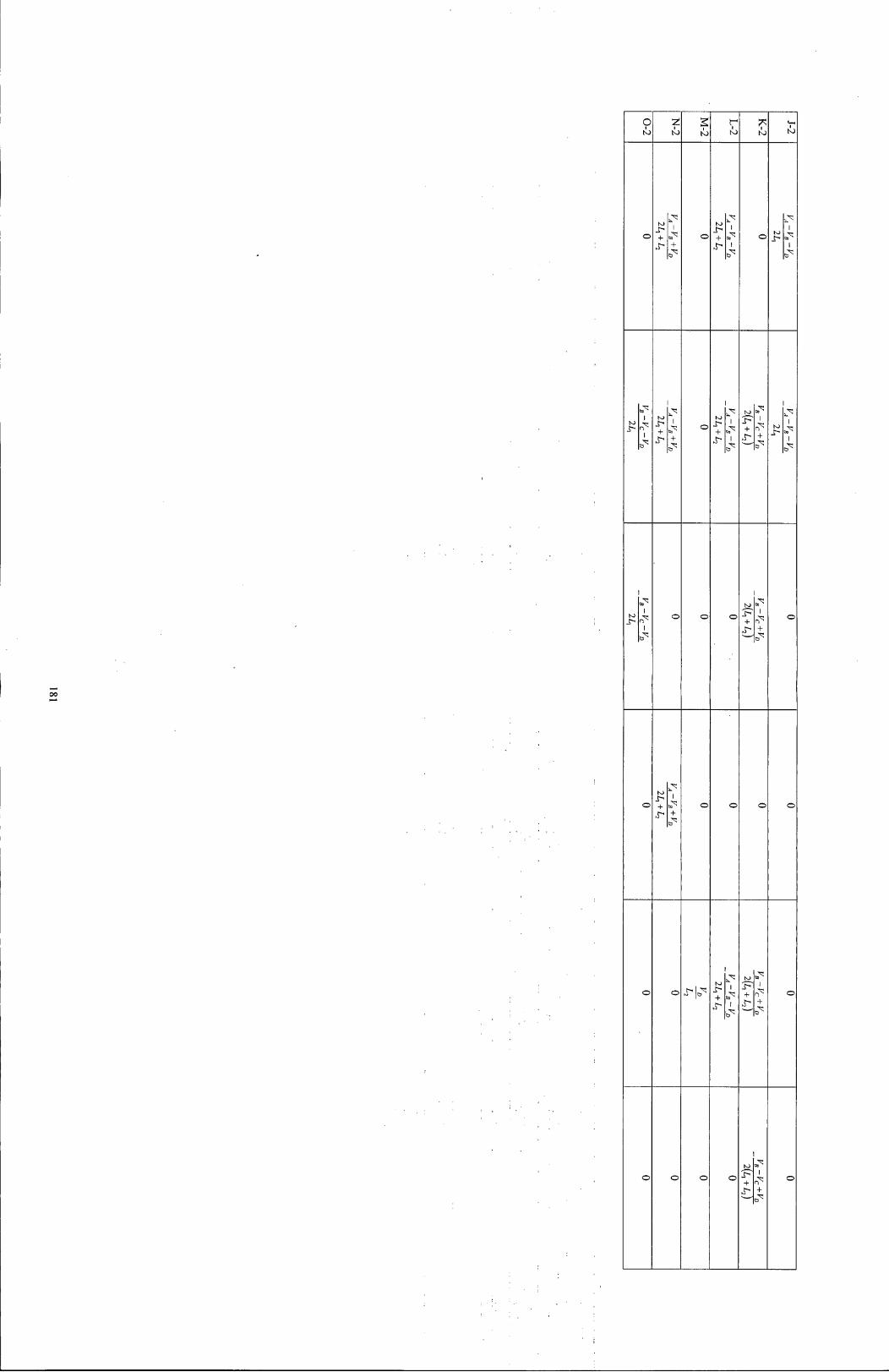
o 1
NJ
N-2
M-2
L-2
K-2
J-2
o to > +
i + o
to JT-+ 1 1 o to
i> 1 1
to 1 1
to
+ i +
o to
+ Jr-
1 1
to J-+ Jp
i +
to
> 1 1
to
> 1 1
O o o to
+ £ 2
1 +
O
O to Jr-+ jr-
i + o o o O
O o to
+ 1 1
to
+ Jp 1 +
O
o o o o to
+ jp 1 +
O

+ a- &
Jx +
i -
+
Jx
tx L" + tx •Mb"
tx x
Jx

1 ^ +
h +
x • 4
+
i i F l + .tr1
'JT-
+
lir-+ h +
+ jp
+ | F +
j> I
i I ^ I
i F i +
1
+ + |Jr +
jp
i ^ , J- I + Jp1
+
jp + tp
jp + tp I
+
IJT
+
I
I F + I lo
ir + £2
j -+ jp
i
+ |J-+
JP
+ jp +
£ 2 ^ 5
J -+
Jr. i
| J r J r |
JP +
jr
j -
Jp +
jp
i
+ |J-+
+ I F +
+ t-h J r +
Jp +
•5-
=£? Jr +
Jr
i Jr +
jp
+ 'to" Ijp +
Ijr ^ i Jp r-5
Jr +
Jp +
.P
Jp + Jr Jr + J-
Jr
J r l +
tp 1^
1 +
1
LO +
1
o
jp +
J r
Jr +
i F + t-
i l-t"
Jr +
jp
+ "to J -+ tp
J - l
Jp +
i Jp r -
J-'Co" Jp +
JN
jp +
J r
i
+ Jr
, i
i [ F I +
+ ?o Jp +
£2
Jr
i Jr
J P
J r
I +
+ J r +
£2
Jr
J> +
jp
i
|J>
i IJr +
+ j r
Jr +
£2
J> Jr
Jr +
jp
i
+
i
JT I
Jr +
£2
i Jr +
jp
+ Jr +
i£:
J -+ £2
Jr r^
Jr
Jr
|J> +
J5 i
| F + jp
+ Jr +
j r
Jr
Jp +
jp
+ fo* !JT>
+
I To" Jr +
Jr
Jr +
£2
i Jr + £2
' J r
+ Jr J«5
I
JP Jp + Jp
+ | J r
+
Jp +
£2,
IJ-+
Jp Jp
JP Jr Jp
JP + + +
Jp to > « ^ Jp
Jr +
Jr
Jr +
j>
J-" Jp 'Cos Jp +
Jp
1
Jp 'Cos Jp + 1
> to Jp Jp
+ J r
J T
Jr
Jr
+ t -
Jp i + j p
J r +
J - TIT + JP
j p + J r
' f J p
Jp
jr
J_ j -+ Jr
> +
J-+
j p + + Jr
i
Jr + J-5^

> i
> > i 4s-
> X I 4s-
>
i -'tZT + to f x
-f-+
SI i - i -
i -
+ Lfx [ os
| i -+
i w
i x
os
+ 05
I
I F + .fx I
i -I
I
I0S I
ix i -+
I tN>
^1 +
+
y l i F I + .tx i
l i -+
i - l +
OS
t O - l I
F | +
y l +
+ j-1 y l +
F | +
0>
to 1 + . f x I
I
F I
IO> I
ix
ix OS i - l +
y l +
'txi", i - l + f x I
y l +
F | + £1-1 ON
ix ix +
ix ix +
l i -
+ Ii- I
0 5
.Mos
Ox I Ox I
i x
+ S I
ii-+ tx
ix ON
f x ON
ix ix > i - > >
+ OS + to o to Jx Ntx
• * '
ix ON
i -
i -+ tx
i -+ tx
l i -+
l£l OS
I
I F + Jx y
I
l i -
"to ix + tx
ix +
ix +
OS
i -+
i -
+ . f x
l i -+
o> +
io" ix +
i 05
i x
+ ,5-0>
i x
+ i -
i x
+
i -
i -+ i -X I
fx ON
> 05 1 F
i x + t x
i -
+ i x *to* + i -
t t x + i -
i x
> w I
4s-
> > i 4s-
N i 4N.
ix i -i
ON I
losl
i - i os I
i
i losl
i 4i.
i - l + Jx I
y i
i | F | +
i F l i
F ' l +
N f x I
osl
i - l + J x I
y l +
fo~ i - 1 + fx I
i - l +
. f x I
i - ix l i -
+ fx
OS
os
51
t x
1 I
_ f x I
OS
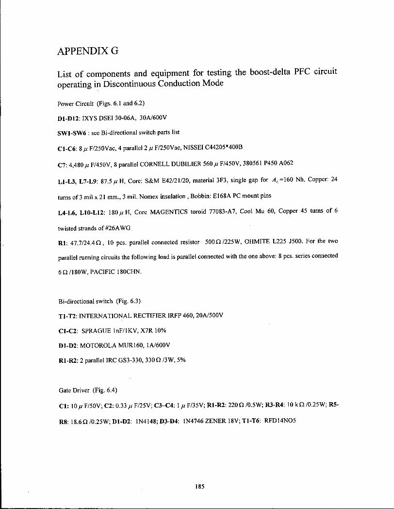
APPENDIX G
List of components and equipment for testing the boost-delta PFC circuit operating in Discontinuous Conduction Mode
Power Circuit (Figs. 6.1 and 6.2)
D1-D12: IXYS DSEI 30-06A, 30A/600V
SW1-SW6 : see Bi-directional switch parts list
C1-C6: 8 n F/250Vac, 4 parallel 2 /j F/250Vac, NISSEI C44205*400B
C7: 4,480 // F/450V, 8 parallel CORNELL DUB1LIER 560 // F/450V, 380561 P450 A062
L1-L3, L7-L9: 87.5 n H, Core: S&M E42/21/20, material 3F3, single gap for ^=160 Nh, Copper: 24
turns of 3 mil x 21 mm., 3 mil. Nomex insulation , Bobbin: E168A PC mount pins
L4-L6, L10-L12: 180//H, Core MAGENTICS toroid 77083-A7, Cool Mu 60, Copper 45 turns of 6
twisted strands of #26AWG
R l : 47.7/24.4Q, 10 pes. parallel connected resistor 500Q/225W, OHMITE L225 J500. For the two
parallel running circuits the following load is parallel connected with the one above: 8 pes. series connected
6Q/180W, PACIFIC 180CHN.
Bi-directional switch (Fig. 6.3)
T1-T2: INTERNATIONAL RECTIFIER IRFP 460, 20A/500V
C1-C2: SPRAGUE InF/lKV, X7R 10%
D1-D2: MOTOROLA MUR160, 1A/600V
R1-R2: 2 parallel IRC GS3-330, 330 fi /3W, 5%
Gate Driver (Fig. 6.4)
C l : 10// F/50V; C2: 0.33 ju F/25V; C3-C4: 1 /j F/35V; R1-R2: 220Q /0.5W; R3-R4: 10 kQ /0.25W; R5-
R8: 18.6Q/0.25W;D1-D2: 1N4148; D3-D4: 1N4746 ZENER 18V; T1-T6: RFD14N05
185

Trl: Gating transformer, Core:E2425, Material 3C8, MAGNETICS P42510-EC,, Copper: Primary 30 turns
#26 AWG, 4 Secondaries 18 turns #26 AWG, Bobbin: E2425 Bobbin PC Mount, MAGNETICS PC-
B2510-T1
PWM Circuit (Fig. 6.5)
Rl, R5: 10kQ/0.25W; R2: 2 kfi/0.25W; R3-R4: 100kQ/0.25W; R6: 38kQ/0.25W ;R7-R8:
392Q/0.25W;R9-R12: 3.32Q/0.25W; PI: lkQ;P2: 10 k Q ;
Cl: 680 pF/25V; C2,C3,C5,C7,C8,C10,C12: 0.33 // F/25V; C4-,C6,C9,C11: 10/u F/50V
D1-D2: MUR160; ICI: THOMPSON SGS 3524A; IC2-IC3: INTERNATIONAL RECTIFIER IR 2110.
Instruments and equipment used for the measurements:
Scope: TEKTRONIX Two Channel, Digital Real-Time Oscilloscope, 100 MHz.
Power Analyzer: YOKOGAWA WT130, Digital Power Meter, Measuring Range 600V/20A, 3 phase
Meter: METEX M-4650
Current Probe: AM503 TEKTRONIX Probe Amplifier
Step-down isolation transformer: 600V/480V, REX MANUFACTURING 45 K V A
Variable auto transformer: 480V/0-560V, SUPERIOR ELECTRIC 30 K V A
186