LOC IC HV Generation and On-Chip Electronic Systems ...
239
LOC IC HV Generation and On-Chip Electronic Systems Integration by David L. Sloan A thesis submitted in partial fulfillment of the requirements for the degree of Doctor of Philosophy in Integrated Circuits and Systems Department of Electrical and Computer Engineering University of Alberta c David L. Sloan, 2018
-
Upload
khangminh22 -
Category
Documents
-
view
0 -
download
0
Transcript of LOC IC HV Generation and On-Chip Electronic Systems ...

LOC IC HV Generation and On-Chip Electronic Systems Integration
by
David L. Sloan
A thesis submitted in partial fulfillment of the requirements for the degree of
Doctor of Philosophy
in
Integrated Circuits and Systems
Department of Electrical and Computer Engineering
University of Alberta
c© David L. Sloan, 2018

Abstract
The BIOMEMS interdisciplinary research group has been working to produce single-
chip Lab-on-Chip systems for genetic diagnostic applications. By bringing a genetic
diagnostic platform down to the size of a single Lab-on-Chip integrated circuit
we can enable fast testing at the point of care. One significant impediment to
single-chip operation is the requirement of high-voltage supplies for driving capillary
electrophoresis experiments and actuating electrostatic systems. My research focuses
on on-chip high voltage generation and control systems, improvements on analog
circuits involved in heater control, and optical detection, as well as digital logic and
synthesis. The high voltage systems are described as they relate to Lab-on-Chip genetic
diagnostic platforms requiring high voltage signaling to drive capillary electrophoresis
experiments, and enable future Lab-on-Chip systems to use electrostatic valving. In this
work I present a fully integrated 300V charge pump capable of producing a 3mW ,
300V signal from a 5V USB port. In order to accommodate future Lab-on-Chip
devices with high valve counts, the high voltage switches used in previous generations
of Lab-on-Chip integrated circuits have been redesigned using novel control signal
level-shifting circuits. The new high voltage switching devices occupy one half the
silicon area of previous designs, and consume less power from the high voltage supply
when switching. High voltage sensing was also considered, in order to produce
programmable high-voltage regulation. I propose and demonstrate novel high voltage
sensing device is proposed and has been fabricated which occupies only 1.2% of the
ii

layout area of previous generations of high voltage sensing circuits and contains no
DC current path from the high voltage sense line to ground. The heating and sensing
circuits, use for PCR amplification, built into previous generations of Lab-on-Chip
integrated circuits had limited current driving capabilities and were sensitive to contact
resistance between the microfluidic and CMOS chips. In my work I have increased
the current driving capabilities, increased the control logic power resolution, and added
4-point sensing to reduce the impact of heater contact resistance on heater temperature
readings. These changes increase the current drive capabilities from 300mA to 1A,
and driver resolution from 8-bits to 10-bits, to allow for a larger range of microfluidic
heater designs. The improvements made in heater element resistance sensing, in
addition to providing 4-point direct element sensing, allow for the use of dedicated
thermistor sensing elements, should direct element sensing prove insufficient. Circuit
redesigns are discussed for the on-chip optical sensing devices in order to simplify chip
illumination requirements for optical tests. The circuits proposed demonstrated the
feasibility of alternate designs, but will need further work to obtain similar noise floors
to earlier work. Finally, improvements have been made to the digital logic and digital
synthesis process used in our Lab-on-Chip integrated circuit designs.
iii

Dedication
To all the wonderful distractions that inspired my meandering path to completion, be
they research tangents or killer robots. To Luke Sloan, Andrew Maier, and Graham
Jordan for helping make one of my childhood dreams come true by competing in
Battlebots while finishing my research.
iv

Acknowledgments
I would like to acknowledge my PhD supervisor: Dr. Duncan Elliott for his advice and
support throughout this project and his understanding and tolerance of the many side
projects along the way. I would like to thank Dr. Christopher Backhouse and Dr. Dan
Sameoto who contributed their knowledge and support to further both this project and
my own research.
I would also like to thank the students who have helped me throughout my degree. I
would like to thank Benjamin Martin and Andrew Hakman who brought me up to speed
with the rest of the lab, and shared the late-night tape-out deadlines we collaborated on.
I would like to thank Jinghang Liang for allowing me to bounce ideas off him and for
helping to solve problems throughout my degree.
I must also acknowledge the work of all those who began the work I have continued
and expanded upon. Saul Caverhill-Godkewitsch, Matthew Reynolds, Philip Marshall,
Karl Jensen, Shane Groendahl, Wesam Al-Haddad, Maziyar Khorasani, Mohammad
Behnam Dehkordi, and Leendert van den Burg, thank you for your contributions, help,
and documentation, without which I would have spent many nights staring blankly at
code and device layouts.
Thank you to Teledyne DALSA Semiconductor, NSERC, and CMC Microsystems
for their funding and support.
Thank you to my family for their love, support, and patience.
v

Contents
1 Introduction 1
1.1 Group History in Brief . . . . . . . . . . . . . . . . . . . . . . . . . . 3
1.2 Target Experiments . . . . . . . . . . . . . . . . . . . . . . . . . . . . 6
1.2.1 Sample Preparation . . . . . . . . . . . . . . . . . . . . . . . . 6
1.2.2 Amplification . . . . . . . . . . . . . . . . . . . . . . . . . . . 6
1.2.3 Detection . . . . . . . . . . . . . . . . . . . . . . . . . . . . . 7
1.3 Future Proofing . . . . . . . . . . . . . . . . . . . . . . . . . . . . . . 9
1.4 System Summary . . . . . . . . . . . . . . . . . . . . . . . . . . . . . 10
2 On-Chip High Voltage Generation 13
2.0.1 Applications . . . . . . . . . . . . . . . . . . . . . . . . . . . 14
2.0.2 Our focus . . . . . . . . . . . . . . . . . . . . . . . . . . . . . 15
2.1 Background . . . . . . . . . . . . . . . . . . . . . . . . . . . . . . . . 15
2.1.1 Boost Conversion . . . . . . . . . . . . . . . . . . . . . . . . . 15
2.1.2 Integrated Charge Pump . . . . . . . . . . . . . . . . . . . . . 17
2.2 Charge Pump Design . . . . . . . . . . . . . . . . . . . . . . . . . . . 19
2.2.1 Architecture . . . . . . . . . . . . . . . . . . . . . . . . . . . . 19
2.2.2 Component Considerations . . . . . . . . . . . . . . . . . . . . 21
2.3 Implementation . . . . . . . . . . . . . . . . . . . . . . . . . . . . . . 25
2.3.1 Charge Pump Design and Layout . . . . . . . . . . . . . . . . 25
vi

2.3.2 Area Utilization . . . . . . . . . . . . . . . . . . . . . . . . . . 25
2.4 Fabricated Circuits . . . . . . . . . . . . . . . . . . . . . . . . . . . . 28
2.4.1 Power Supply Variation . . . . . . . . . . . . . . . . . . . . . 29
2.4.2 Service Life . . . . . . . . . . . . . . . . . . . . . . . . . . . . 29
2.5 Regulation Strategies . . . . . . . . . . . . . . . . . . . . . . . . . . . 30
2.5.1 Zener . . . . . . . . . . . . . . . . . . . . . . . . . . . . . . . 31
2.5.2 Gated Clock . . . . . . . . . . . . . . . . . . . . . . . . . . . 32
2.6 Summary . . . . . . . . . . . . . . . . . . . . . . . . . . . . . . . . . 33
3 High Voltage Sensing Structures 35
3.1 Resistive Divider . . . . . . . . . . . . . . . . . . . . . . . . . . . . . 35
3.2 High Voltage Sense Transistor . . . . . . . . . . . . . . . . . . . . . . 37
4 High Voltage Switching Circuits 41
4.0.1 Application . . . . . . . . . . . . . . . . . . . . . . . . . . . . 42
4.0.2 Previous Generation . . . . . . . . . . . . . . . . . . . . . . . 43
4.1 Capacitively Coupled Level-Shifting . . . . . . . . . . . . . . . . . . . 46
4.1.1 Dynamic resistor-capacitor (RC) Level-Shifter . . . . . . . . . 46
4.1.2 Capacitively-Coupled-Buffer Level-Shifter . . . . . . . . . . . 49
4.1.3 High-Side Bias Voltage Generation . . . . . . . . . . . . . . . 53
4.2 Fabricated Circuits . . . . . . . . . . . . . . . . . . . . . . . . . . . . 54
4.3 Summary . . . . . . . . . . . . . . . . . . . . . . . . . . . . . . . . . 56
5 On-Chip Heater Control 58
5.1 Automated Heater Generation - Implementation . . . . . . . . . . . . . 59
5.1.1 Heat Flux Extraction . . . . . . . . . . . . . . . . . . . . . . . 59
5.1.2 Automatic Heater Layout Generation . . . . . . . . . . . . . . 61
5.1.3 Layout Export . . . . . . . . . . . . . . . . . . . . . . . . . . 62
5.2 PCR Chamber Temperature Sensing . . . . . . . . . . . . . . . . . . . 63
vii

5.2.1 Dedicated Thermistor Sensing . . . . . . . . . . . . . . . . . . 65
5.2.2 Direct Heater Element Sensing . . . . . . . . . . . . . . . . . . 68
5.3 Die Temperature Sensing . . . . . . . . . . . . . . . . . . . . . . . . . 75
5.4 Summary . . . . . . . . . . . . . . . . . . . . . . . . . . . . . . . . . 78
6 Optics 80
6.1 Photo-Diode Integrator . . . . . . . . . . . . . . . . . . . . . . . . . . 81
6.1.1 High Gain Integrator . . . . . . . . . . . . . . . . . . . . . . . 83
6.1.2 Reduced Gain Integrator . . . . . . . . . . . . . . . . . . . . . 84
6.1.3 Direct Integrator . . . . . . . . . . . . . . . . . . . . . . . . . 86
6.2 Summary . . . . . . . . . . . . . . . . . . . . . . . . . . . . . . . . . 89
7 Digital Logic 90
7.1 SPI Interface . . . . . . . . . . . . . . . . . . . . . . . . . . . . . . . 90
7.1.1 3.3 V IO . . . . . . . . . . . . . . . . . . . . . . . . . . . . . 91
7.1.2 Controller Changes . . . . . . . . . . . . . . . . . . . . . . . . 93
7.2 Constrained Digital Place and Route . . . . . . . . . . . . . . . . . . . 94
7.3 Summary . . . . . . . . . . . . . . . . . . . . . . . . . . . . . . . . . 96
8 Lab-on-Chip Integrated Circuits 97
8.1 Lab-on-Chip 11 . . . . . . . . . . . . . . . . . . . . . . . . . . . . . . 97
8.1.1 Overview . . . . . . . . . . . . . . . . . . . . . . . . . . . . . 97
8.1.2 Microfluidic Interface . . . . . . . . . . . . . . . . . . . . . . 99
8.1.3 HV . . . . . . . . . . . . . . . . . . . . . . . . . . . . . . . . 100
8.1.4 Optics . . . . . . . . . . . . . . . . . . . . . . . . . . . . . . . 101
8.1.5 Heater Control . . . . . . . . . . . . . . . . . . . . . . . . . . 102
8.1.6 External Electronics . . . . . . . . . . . . . . . . . . . . . . . 102
8.1.7 Experimental Verification . . . . . . . . . . . . . . . . . . . . 103
8.2 Lab-on-Chip 12 . . . . . . . . . . . . . . . . . . . . . . . . . . . . . . 105
viii

8.2.1 Overview . . . . . . . . . . . . . . . . . . . . . . . . . . . . . 105
8.2.2 Microfluidic Interface . . . . . . . . . . . . . . . . . . . . . . 107
8.2.3 HV Channels . . . . . . . . . . . . . . . . . . . . . . . . . . . 108
8.2.4 HV Generation . . . . . . . . . . . . . . . . . . . . . . . . . . 109
8.2.5 HV Regulation . . . . . . . . . . . . . . . . . . . . . . . . . . 110
8.2.6 HV Sensing . . . . . . . . . . . . . . . . . . . . . . . . . . . . 110
8.2.7 Heater Control . . . . . . . . . . . . . . . . . . . . . . . . . . 110
8.2.8 Analog to digital converter . . . . . . . . . . . . . . . . . . . . 111
8.3 Lab-on-Chip Stable 1 . . . . . . . . . . . . . . . . . . . . . . . . . . . 112
8.3.1 Overview . . . . . . . . . . . . . . . . . . . . . . . . . . . . . 112
8.3.2 Microfluidic Interface . . . . . . . . . . . . . . . . . . . . . . 113
8.3.3 Optics . . . . . . . . . . . . . . . . . . . . . . . . . . . . . . . 114
8.3.4 HV . . . . . . . . . . . . . . . . . . . . . . . . . . . . . . . . 114
8.3.5 Heater Control . . . . . . . . . . . . . . . . . . . . . . . . . . 114
8.4 Lab-on-Chip 13 . . . . . . . . . . . . . . . . . . . . . . . . . . . . . . 115
8.4.1 Overview . . . . . . . . . . . . . . . . . . . . . . . . . . . . . 115
8.4.2 Microfluidic Interface . . . . . . . . . . . . . . . . . . . . . . 116
8.4.3 Optics . . . . . . . . . . . . . . . . . . . . . . . . . . . . . . . 117
8.4.4 HV - Switching . . . . . . . . . . . . . . . . . . . . . . . . . . 117
8.4.5 HV - Generation . . . . . . . . . . . . . . . . . . . . . . . . . 118
8.4.6 Heater Control . . . . . . . . . . . . . . . . . . . . . . . . . . 118
9 Conclusions 119
9.1 HV Systems . . . . . . . . . . . . . . . . . . . . . . . . . . . . . . . . 119
9.2 Meeting Evolving Design Targets . . . . . . . . . . . . . . . . . . . . 120
9.3 Serial Interface . . . . . . . . . . . . . . . . . . . . . . . . . . . . . . 121
9.4 Digital Synthesis . . . . . . . . . . . . . . . . . . . . . . . . . . . . . 121
9.5 Future Work . . . . . . . . . . . . . . . . . . . . . . . . . . . . . . . . 122
ix

9.5.1 PCR Demonstration . . . . . . . . . . . . . . . . . . . . . . . 122
9.5.2 Electrostatic Valves . . . . . . . . . . . . . . . . . . . . . . . . 122
9.5.3 Magnetic Bead Capture . . . . . . . . . . . . . . . . . . . . . . 123
9.5.4 On-Chip Microfluidic Structures . . . . . . . . . . . . . . . . . 123
Bibliography 124
A Heater Design and Visualization Code 131
B Reading Photodiodes in ST1 and L13 136
C System PCBs 144
C.1 Lab-on-Chip 11 System Board . . . . . . . . . . . . . . . . . . . . . . 144
C.1.1 Power Configurations . . . . . . . . . . . . . . . . . . . . . . . 145
C.1.2 High Voltage Source Configurations . . . . . . . . . . . . . . . 146
C.1.3 3.5 mm HV Connection Usage . . . . . . . . . . . . . . . . . . 147
C.1.4 Expansion Header . . . . . . . . . . . . . . . . . . . . . . . . 147
C.1.5 Status Indicators . . . . . . . . . . . . . . . . . . . . . . . . . 148
C.1.6 Command Interface . . . . . . . . . . . . . . . . . . . . . . . . 149
C.2 Lab-on-Chip 12 System Board . . . . . . . . . . . . . . . . . . . . . . 155
C.2.1 Power . . . . . . . . . . . . . . . . . . . . . . . . . . . . . . . 155
C.2.2 Status LEDs . . . . . . . . . . . . . . . . . . . . . . . . . . . 158
C.2.3 External Heater Connections . . . . . . . . . . . . . . . . . . . 159
C.2.4 External temperature sensors . . . . . . . . . . . . . . . . . . . 159
C.2.5 HV regulation . . . . . . . . . . . . . . . . . . . . . . . . . . . 160
C.2.6 Command Interface . . . . . . . . . . . . . . . . . . . . . . . . 160
D Chip Pinouts 165
D.1 Lab-on-Chip 11 Pinouts . . . . . . . . . . . . . . . . . . . . . . . . . . 165
D.1.1 L11-DIP . . . . . . . . . . . . . . . . . . . . . . . . . . . . . 165
x

D.1.2 L11-PGA . . . . . . . . . . . . . . . . . . . . . . . . . . . . . 167
D.2 Lab-on-Chip 12 Pinouts . . . . . . . . . . . . . . . . . . . . . . . . . . 169
D.2.1 L12-A . . . . . . . . . . . . . . . . . . . . . . . . . . . . . . . 169
D.2.2 L12-B . . . . . . . . . . . . . . . . . . . . . . . . . . . . . . . 170
D.3 Lab-on-Chip 13 Pinout . . . . . . . . . . . . . . . . . . . . . . . . . . 172
D.3.1 L13-A . . . . . . . . . . . . . . . . . . . . . . . . . . . . . . . 172
D.3.2 L13-B . . . . . . . . . . . . . . . . . . . . . . . . . . . . . . . 173
D.4 Lab-on-Chip Stable 1 Pinout . . . . . . . . . . . . . . . . . . . . . . . 175
D.4.1 ST1-A . . . . . . . . . . . . . . . . . . . . . . . . . . . . . . . 175
D.4.2 ST1-B . . . . . . . . . . . . . . . . . . . . . . . . . . . . . . . 176
D.5 Test Chip 22 Pinout . . . . . . . . . . . . . . . . . . . . . . . . . . . . 178
E Device Register Layouts 179
E.1 Lab-on-Chip 11 . . . . . . . . . . . . . . . . . . . . . . . . . . . . . . 179
E.1.1 System Configuration Register . . . . . . . . . . . . . . . . . . 179
E.1.2 Level Shifter States . . . . . . . . . . . . . . . . . . . . . . . . 180
E.1.3 ADC configuration . . . . . . . . . . . . . . . . . . . . . . . . 181
E.1.4 PD Integrator . . . . . . . . . . . . . . . . . . . . . . . . . . . 183
E.1.5 Interrupt Status Register . . . . . . . . . . . . . . . . . . . . . 183
E.1.6 Heater Control . . . . . . . . . . . . . . . . . . . . . . . . . . 183
E.1.7 HV Generation . . . . . . . . . . . . . . . . . . . . . . . . . . 184
E.1.8 GP Output State . . . . . . . . . . . . . . . . . . . . . . . . . 185
E.2 Lab-on-Chip 12 . . . . . . . . . . . . . . . . . . . . . . . . . . . . . . 186
E.2.1 System Configuration . . . . . . . . . . . . . . . . . . . . . . 186
E.2.2 Magnet Configuration . . . . . . . . . . . . . . . . . . . . . . 188
E.2.3 Level Shifter States . . . . . . . . . . . . . . . . . . . . . . . . 188
E.2.4 HV Generation . . . . . . . . . . . . . . . . . . . . . . . . . . 190
E.2.5 GP Output . . . . . . . . . . . . . . . . . . . . . . . . . . . . 192
xi

E.2.6 PD Configuration . . . . . . . . . . . . . . . . . . . . . . . . . 193
E.2.7 Heater System . . . . . . . . . . . . . . . . . . . . . . . . . . 194
E.2.8 Interrupt Status . . . . . . . . . . . . . . . . . . . . . . . . . . 196
E.2.9 ADC Heater, PD, HV I, and HV V . . . . . . . . . . . . . . . . 196
E.3 Lab-on-Chip 13 . . . . . . . . . . . . . . . . . . . . . . . . . . . . . . 197
E.3.1 System Configuration . . . . . . . . . . . . . . . . . . . . . . 197
E.3.2 HV Generation . . . . . . . . . . . . . . . . . . . . . . . . . . 199
E.3.3 CE Level Shifters . . . . . . . . . . . . . . . . . . . . . . . . . 201
E.3.4 CE Configuration . . . . . . . . . . . . . . . . . . . . . . . . . 201
E.3.5 Valve Level Shifter States . . . . . . . . . . . . . . . . . . . . 202
E.3.6 MGT Status . . . . . . . . . . . . . . . . . . . . . . . . . . . . 202
E.3.7 GP Output . . . . . . . . . . . . . . . . . . . . . . . . . . . . 203
E.3.8 PD Configuration . . . . . . . . . . . . . . . . . . . . . . . . . 203
E.3.9 Heater System . . . . . . . . . . . . . . . . . . . . . . . . . . 204
E.3.10 Interrupt Status . . . . . . . . . . . . . . . . . . . . . . . . . . 206
E.3.11 ADC HV, Heater, PD . . . . . . . . . . . . . . . . . . . . . . . 206
E.4 Lab-on-Chip Stable 1 . . . . . . . . . . . . . . . . . . . . . . . . . . . 207
E.4.1 System Configuration . . . . . . . . . . . . . . . . . . . . . . 207
E.4.2 HV Generation . . . . . . . . . . . . . . . . . . . . . . . . . . 208
E.4.3 CE Level Shifters . . . . . . . . . . . . . . . . . . . . . . . . . 210
E.4.4 CE Configuration . . . . . . . . . . . . . . . . . . . . . . . . . 211
E.4.5 Valve Level Shifter States . . . . . . . . . . . . . . . . . . . . 211
E.4.6 MGT Status . . . . . . . . . . . . . . . . . . . . . . . . . . . . 212
E.4.7 GP Output . . . . . . . . . . . . . . . . . . . . . . . . . . . . 212
E.4.8 PD Configuration . . . . . . . . . . . . . . . . . . . . . . . . . 213
E.4.9 Heater System . . . . . . . . . . . . . . . . . . . . . . . . . . 214
E.4.10 Interrupt Status . . . . . . . . . . . . . . . . . . . . . . . . . . 215
xii

E.4.11 ADC HV, Heater, PD . . . . . . . . . . . . . . . . . . . . . . . 216
E.5 Test Chip 22 . . . . . . . . . . . . . . . . . . . . . . . . . . . . . . . . 216
xiii

List of Figures
1.1 Standard PCR thermal cycle . . . . . . . . . . . . . . . . . . . . . . . 7
1.2 Practical microfluidic layout increasing channel length . . . . . . . . . 8
1.3 CE injection and separation phases . . . . . . . . . . . . . . . . . . . . 9
1.4 Electrostatic valve cross section . . . . . . . . . . . . . . . . . . . . . 10
1.5 CE injection and separation phases . . . . . . . . . . . . . . . . . . . . 11
2.1 Comparison of CP and boost converter IV curves . . . . . . . . . . . . 16
2.2 Comparison of CP and Boost converter efficiencies . . . . . . . . . . . 17
2.3 LOC IC next to boost converter inductor . . . . . . . . . . . . . . . . . 18
2.4 Pelliconi and Dickson charge pump single stage comparison . . . . . . 20
2.5 PMOS transistor diode parasitic devices . . . . . . . . . . . . . . . . . 21
2.6 Dickson charge pump forward bulk biasing . . . . . . . . . . . . . . . 22
2.7 Floating body charge pump configuration . . . . . . . . . . . . . . . . 23
2.8 Charge pump transient load performance . . . . . . . . . . . . . . . . . 24
2.9 HV capacitor stack . . . . . . . . . . . . . . . . . . . . . . . . . . . . 25
2.10 Dickson charge pump block diagram . . . . . . . . . . . . . . . . . . . 26
2.11 Charge pump load sweep comparison of simulated and tested devices . 27
2.12 Fabricated charge pump start-up curve . . . . . . . . . . . . . . . . . . 27
2.13 Effect of process corners on charge pump I-V characteristics in simulation 28
2.14 Die image of charge pump test integrated circuit (IC) . . . . . . . . . . 29
2.15 127 stage charge pump I-V curve . . . . . . . . . . . . . . . . . . . . . 31
xiv

3.1 Resistive divider network with distributed capacitance shown . . . . . . 36
3.2 Simulated transient response of resistive voltage divider . . . . . . . . . 36
3.3 HV-sense transistor sensing circuit profile view . . . . . . . . . . . . . 37
3.4 HV sweep of HV-sense transistor Sensor. Vds = 5V . . . . . . . . . . 38
3.5 HV-sense transistor HV sensor temperature dependence . . . . . . . . . 39
4.1 Constant control current HV switch . . . . . . . . . . . . . . . . . . . 42
4.2 Static HV switch . . . . . . . . . . . . . . . . . . . . . . . . . . . . . 44
4.3 Dynamic HV switch . . . . . . . . . . . . . . . . . . . . . . . . . . . 45
4.4 Dynamic RC HV switch . . . . . . . . . . . . . . . . . . . . . . . . . 47
4.5 Drive strength of dynamic RC switches . . . . . . . . . . . . . . . . . 48
4.6 RC HV switch drive strength duty cycle dependence . . . . . . . . . . 49
4.7 Capacitively-coupled-buffer based HV switch . . . . . . . . . . . . . . 50
4.8 RC HV switch control signals at steady state . . . . . . . . . . . . . . . 51
4.9 Switch layout area comparison . . . . . . . . . . . . . . . . . . . . . . 52
4.10 Comparison of drive strengths of fabricated switches . . . . . . . . . . 52
4.11 HV bias generator . . . . . . . . . . . . . . . . . . . . . . . . . . . . . 53
4.12 HV bias generation circuit size comparison . . . . . . . . . . . . . . . 54
4.13 Buffed RC gate protection structure showing parasitic BJT . . . . . . . 55
5.1 Example Q filed used for heater design . . . . . . . . . . . . . . . . . . 60
5.2 Screen capture of heater design software implementation . . . . . . . . 61
5.3 PCR thermal cycle example . . . . . . . . . . . . . . . . . . . . . . . . 63
5.4 Thermistor temperature sensing circuit . . . . . . . . . . . . . . . . . . 65
5.5 External resistive sensing DAC current sweep . . . . . . . . . . . . . . 66
5.6 Heater ADC + Amplifier Error . . . . . . . . . . . . . . . . . . . . . . 67
5.7 PCR reaction chamber cross-section . . . . . . . . . . . . . . . . . . . 68
5.8 Direct element temperature sensing circuit . . . . . . . . . . . . . . . . 69
xv

5.9 Direct element temperature sensing die temperature dependence . . . . 70
5.10 Direct element temperature sensing voltage dependence . . . . . . . . . 71
5.11 Direct element sensing error test . . . . . . . . . . . . . . . . . . . . . 73
5.12 On-chip temperature sensor and amplification circuit . . . . . . . . . . 75
5.13 Die temperature sensor sweep in Lab-on-Chip (LOC) stable 1 . . . . . 76
5.14 Temperature sensor deviation from linear calibration parameters . . . . 77
6.1 Photo-diode sites for CE and qPCR florescent readings. . . . . . . . . . 81
6.2 Photo-diode instability at low light intensities . . . . . . . . . . . . . . 82
6.3 Op-amp based integration circuit used in our LOC ICs . . . . . . . . . 83
6.4 Non-linear distortion of high-gain integrator . . . . . . . . . . . . . . . 83
6.5 High gain vs low gain op-amp circuits . . . . . . . . . . . . . . . . . . 84
6.6 Medium-gain op-amp non-linear distortion . . . . . . . . . . . . . . . . 85
6.7 Internal gain-enhancing op-amps using in high-gain integrator . . . . . 86
6.8 Medium gain op-amp based integrator optical response . . . . . . . . . 87
6.9 Direct Integrator circuit . . . . . . . . . . . . . . . . . . . . . . . . . . 88
6.10 Direct integrator optical response . . . . . . . . . . . . . . . . . . . . . 88
7.1 3.3V IO well isolation . . . . . . . . . . . . . . . . . . . . . . . . . . 92
7.2 LOC single register SPI command . . . . . . . . . . . . . . . . . . . . 93
7.3 LOC multiple register SPI command . . . . . . . . . . . . . . . . . . . 94
7.4 Increased silicon utilization by digital place and route tools . . . . . . . 95
8.1 LOC 11 die photo . . . . . . . . . . . . . . . . . . . . . . . . . . . . . 98
8.2 LOC 11 block diagram. External interfaces denoted by dotted lines . . . 99
8.3 LOC 11 system-level block diagram . . . . . . . . . . . . . . . . . . . 100
8.4 LOC 11 electrical connections . . . . . . . . . . . . . . . . . . . . . . 100
8.5 LOC 11 proposed on-chip CE microfluidic layout . . . . . . . . . . . . 101
8.6 LOC 11 proposed on-chip PCR/qPCR microfluidic layout . . . . . . . . 101
xvi

8.7 USB powered test system . . . . . . . . . . . . . . . . . . . . . . . . . 102
8.8 Electropherogram experiment LOC 11 . . . . . . . . . . . . . . . . . . 104
8.9 Electropherogram produced using LOC 11 . . . . . . . . . . . . . . . . 104
8.10 LOC 12 die photo . . . . . . . . . . . . . . . . . . . . . . . . . . . . . 105
8.11 LOC 12 microfluidic design for sample prep + PCR + CE tests . . . . . 105
8.12 LOC 12 electrical connection interface . . . . . . . . . . . . . . . . . . 106
8.13 LOC 12 microfluidic design for CE-only experiments . . . . . . . . . . 107
8.14 LOC 12 microfluidic design for qPCR/PCR + CE tests . . . . . . . . . 107
8.15 LOC Stable 1 die photo . . . . . . . . . . . . . . . . . . . . . . . . . . 112
8.16 LOC stable 1 proposed on-chip PCR + CE microfluidic layout . . . . . 112
8.17 LOC stable 1 electrical connections . . . . . . . . . . . . . . . . . . . 113
8.18 LOC 13 die photo . . . . . . . . . . . . . . . . . . . . . . . . . . . . . 115
B.1 LOC stable 1 photo-diode digital signalling error . . . . . . . . . . . . 137
B.2 LOC stable 1 photo-diode analog signal routing . . . . . . . . . . . . . 137
B.3 Signalling used by external ADC in photo-diode value conversion . . . 138
B.4 Propeller-chip core synchronization during photo-diode read . . . . . . 139
C.1 LOC 11 system-board connectors . . . . . . . . . . . . . . . . . . . . 144
C.2 LOC 11 system-board power select . . . . . . . . . . . . . . . . . . . . 145
C.3 LOC 11 system-board DC barrel jack . . . . . . . . . . . . . . . . . . 146
C.4 LOC 11 system-board HV configuration . . . . . . . . . . . . . . . . . 146
C.5 LOC 11 system-board HV insertion method . . . . . . . . . . . . . . . 148
C.6 LOC 11 system-board expansion header pinout . . . . . . . . . . . . . 149
C.7 LOC 11 system-board status LEDs . . . . . . . . . . . . . . . . . . . . 149
C.8 ARM SPI modes . . . . . . . . . . . . . . . . . . . . . . . . . . . . . 154
C.9 LOC 12 system-board connectors . . . . . . . . . . . . . . . . . . . . 155
C.10 LOC 12 system-board screw terminals . . . . . . . . . . . . . . . . . . 156
xvii
C.11 LOC 12 system-board low voltage headers . . . . . . . . . . . . . . . . 157
C.12 LOC 12 system-board ARM status LEDs . . . . . . . . . . . . . . . . 158
C.13 LOC 12 system-board LOC LEDs . . . . . . . . . . . . . . . . . . . . 159
C.14 LOC 12 system-board high voltage headers . . . . . . . . . . . . . . . 160
C.15 LOC 12 system-board serial interface header . . . . . . . . . . . . . . 160
D.1 64 DIP package used for L11 bonding . . . . . . . . . . . . . . . . . . 165
D.2 68 PGA package used for L11 bonding . . . . . . . . . . . . . . . . . . 167
D.3 84 PGA package used for L12 bonding . . . . . . . . . . . . . . . . . . 169
D.4 68 PGA package used for L13 bonding . . . . . . . . . . . . . . . . . . 172
D.5 68 PGA package used for ST1 bonding . . . . . . . . . . . . . . . . . 175
D.6 40 DIP package used for T22 bonding . . . . . . . . . . . . . . . . . . 178
E.1 Heater PWM/Current mirror switch signalling . . . . . . . . . . . . . . 195
xviii

List of Tables
2.1 HV drive capabilities charge pump and boost converter circuits . . . . . 19
3.1 Temperature sensitivity of HV-sense transistor HV sensing devices . . . 38
4.1 Static HV switch control signaling . . . . . . . . . . . . . . . . . . . . 43
4.2 Dynamic RC switch control signalling . . . . . . . . . . . . . . . . . . 46
4.3 Capacitively-coupled-buffer control signalling . . . . . . . . . . . . . . 49
4.4 high-voltage (HV) switch level-shifter power consumption at 70 V
supply voltage . . . . . . . . . . . . . . . . . . . . . . . . . . . . . . . 54
4.5 HV switch layout area . . . . . . . . . . . . . . . . . . . . . . . . . . 56
5.1 Die Temperature Effects on Sense Current . . . . . . . . . . . . . . . . 69
5.2 Drain-Source Voltage Effects on Sense Current . . . . . . . . . . . . . 70
5.3 Simulation Absolute Error After Linear Correction . . . . . . . . . . . 72
5.4 Error in Direct Element Sensing Test Device . . . . . . . . . . . . . . . 73
D.1 L11 DIP pinout . . . . . . . . . . . . . . . . . . . . . . . . . . . . . . 165
D.2 L11 PGA pinout . . . . . . . . . . . . . . . . . . . . . . . . . . . . . . 167
D.3 L12 pinout with bonding option A . . . . . . . . . . . . . . . . . . . . 169
D.4 L12 pinout with bonding option B . . . . . . . . . . . . . . . . . . . . 170
D.5 L13-A pinout . . . . . . . . . . . . . . . . . . . . . . . . . . . . . . . 172
D.6 L13-B pinout . . . . . . . . . . . . . . . . . . . . . . . . . . . . . . . 173
D.7 ST1-A pinout . . . . . . . . . . . . . . . . . . . . . . . . . . . . . . . 175
xix

D.8 ST1-B pinout . . . . . . . . . . . . . . . . . . . . . . . . . . . . . . . 176
D.9 T22 pinout . . . . . . . . . . . . . . . . . . . . . . . . . . . . . . . . . 178
xx

List of Acronyms
AC alternating current
ADC analog to digital converter
BJT bipolar junction transistor
CE capillary electrophoresis
CMOS complementary metal-oxide-semiconductor
DAC digital to analog converter
DC direct current
DIP dual in-line pin
DNA deoxyribonucleic acid
ESD electrostatic discharge
EP electrophoresis
GPIO general purpose input-output
HV high-voltage
IC integrated circuit
IO input-output
xxi

LDMOS laterally-diffused metal-oxide-semiconductor
LED light emitting diode
LOC Lab-on-Chip
MEMS microelectromechanical systems
MGT metal-gate-transistor
MOSFET metal-oxide-semiconductor field-effect transistor
NC no-connection
NMOS n-channel MOSFET
NRE non-recurring engineering
PCB printed circuit board
PCR polymerase chain reaction
PGA pin grid array
PMOS p-channel MOSFET
PWM pulse width modulation
qPCR quantitative polymerase chain reaction
RC resistor-capacitor
RESURF reduced surface field
RTOS real-time operating-system
Rs sheet resistance
SCR silicon-controlled rectifier
xxii

SPI serial peripheral interface
SOI silicon-on-insulator
TB Tris base and boric acid
TCR temperature coefficient of resistance
TDSI Teledyne DALSA Semiconductor
USB universal serial bus
ZIF zero-insertion-force
xxiii

Chapter 1
Introduction
Portable miniaturized medical devices, capable of providing immediate diagnostic
results, have the potential to decrease costs and delays associated with diagnosing
illnesses. By designing targeted medical test instruments and bringing them to the point
of care such systems could also provide rapid response to infectious disease screening,
allowing for fast screening in any location. In order to reach these goals, these point of
care devices must be portable, easy to use, and require little in the way of supporting
infrastructure. Lab-on-Chip (LOC) devices have been pursued as an attractive solution
to this problem by combining both chemical and electrical instrumentation onto a single
device, compatible with existing mass manufacturing techniques. Due to the selectivity
of genetic testing and the applicability to detection of infectious diseases a large amount
of effort has been put towards creating DNA sensitive LOC devices for the purposes of
medical diagnostics. Some of the most promising novel techniques involve activated
trapping sites coupled with electronic sensors either directly attached to these sites
[1] or through optical detection [2]. While these methods show promise in becoming
reliable solutions to direct sensing of selective genetic material, our group has chosen
to focus on the miniaturization of existing genetic diagnostic techniques. Detection
can be done by directly reading the optical signal of a sample while it is thermocycled
1

in a polymerase chain reaction (PCR) chamber [3], but runs the risk of false positives
in the event that a near match occurs, and requires the use of fluorophores which are
inactive when not bound to a genetic target. Our group has focused on a miniaturizing
a combined PCR capillary electrophoresis (CE) device which used PCR for selective
amplification of a genetic sample, and CE to detect and separate a target specimen from
erroneous products and remaining florescent primers.
Our research group has successfully demonstrated many experiments using printed
circuit board (PCB) stacks and pneumatic pumping housed in a shoe box sized
enclosure [4]. These systems used glass slides with deposited metal films and epoxy
bonded integrated circuits (ICs), requiring careful hand placement of specimens and
external sample preparation. The focus of my research has been to demonstrate all
of the separate electronic pieces used to run individual experiments in silicon, and
create a toolbox allowing for the design of single IC LOC devices. In this process
several subsystems needed to be improved to reach design requirements of the latest
configurations used in our group. Also, a new high-voltage (HV) subsystem needed to
be developed to break the 50V barrier set by our first successful fully integrated supply.
A large portion of this document will focus on the development of HV generation,
regulation, and control circuits, as I have had a significant role in this development. The
remainder of this document will focus on design implementations and system-level
assembly of LOC ICs. Here I combine my HV systems work with that of previous
students who have worked on this project, [5, 6, 7, 8], into a LOC instrumentation
platform for use in microfluidic experiments. I will be discussing: challenges faced and
corrections made to facilitate system integration; work done on digital control systems;
and a brief discussion of advancements in digital place and route tools used to place
digital subsystems within densely packed hand routed analog circuits. Microfluidic
placement considerations and experiments were a major consideration for all LOC
IC designs, and played a major roll in subsystem placement and IC dimensions. A
2

discussion of microfluidic interface considerations and future goals will be included.
1.1 Group History in Brief
The BIOMEMS research group has been working to produce single-chip LOC devices,
compatible with high-volume wafer-fabrication equiptment, designed to do genetic
diagnostic testing at the point of care. Point of care diagnostic tests allow for immediate
diagnosis of illnesses caused by a virus, bacteria, or genetic disorder based on detection
of the disease itself rather than prevailing symptoms without the need to wait for a
response from a lab. This rapid analysis is especially helpful in the case of infectious
diseases, where delays caused by centralized lab wait-times could lead to further spread
of the disease. To this end, progress was made towards device miniaturization in the
work of Mohammad Dehkordi [9] and Maziyar Khorasani [10], who demonstrated the
first compact diagnostics platform, combining both custom LOC integrated circuits and
custom microfluidics in a shoebox-sized device[4]. This system incorporated a 300V
boost converter and an on-chip high voltage switching devices in a custom integrated
circuit which was used to drive CE experiments in a microfluidic chip excited by a
small laser and read using a CCD image sensor, optical filter, and photomultiplier tube.
These early LOC ICs also incorporated optical detection using photodiodes in photo-
conductive mode, using correlated double sampling to remove the dark current from the
signal. In these early chips an 8-bit successive approximation ADC was used to sample
analog signals. Noise coupling between the HV systems and analog systems, through
shared power pins, prevented simultaneous single-chip HV and optical detection in
these devices.
Following this initial work there have been focused attempts to improve upon indi-
vidual systems within our LOC ICs. These improvements have targeted improvements
to: HV switching circuits; full integration of HV generation systems; integration of a
3

source and measurement unit for embedded microfluidic heaters; increased range and
resolution of optical detection circuits; automation of microfluidic heater design; and
novel circuits for pre-amplification concentration of genetic samples on chip.
Wesam Al-Haddad [7] focused on the improvement and miniaturization of HV
devices and circuits in our LOC ICs. In his work new static level shifters where
designed, which did not require a high-side referenced bias signal to operate. This work
was successful in producing novel 5-terminal HV devices capable of protecting the
high-side low voltage control logic transistors from an HV supply of up to 40V . Early
work into fully integrated 300V charge pumps was started using a Pelliconi architecture
charge pump. This charge pump architecture was successfully demonstrated using low
voltage transistors in deep N-wells, producing the maximum voltage of 50V allowed
by these devices. When migrating this architecture to HV-floating transistors, however,
increased FET thresholds eliminated this biasing advantage, causing parasitic devices
to dump all charge pump current to the substrate rather than the output.
In order to support on-chip PCR experiments, a dedicated source and measurement
unit (SMU) is required. While early designs did incorporate 300 mA switches for use
in heater signal driving, thermal feedback and regulation was left to external circuitry.
Our group has worked to characterize our heating elements thermal properties [11] and
rely on the tight coupling between microfluidic camber and heating element for thermal
regulation. Philip Marshall and Sunny Ho [8] created one of our first integrated SMU
designs for this purpose. In these devices a high current switch can be switched into
current mirror mode, where heater current is mirrored from the element onto an on-
chip resistor. By sensing both this heater current and the voltage across the heater, the
temperature can be calculated using the heating element’s temperature coefficient of
resistance. This circuit was designed for 0.45 ◦C resolution, however, was only able to
achieve 13 ◦C resolution in testing.
Early optical detection techniques suffered two significant drawbacks. The first is
4

signal noise caused by the use of a photodiode in photo-conductive mode. The second is
low resolution of the SAR ADC. In order to improve upon these limitations two optical
detection methods where pursued. Andrew Hakman [5] investigated the use of single
photon, geiger mode, avalanche photo-diodes. Using this method, optical signals can be
converted directly to digital signals by counting pulses from an avalanche photodiode
corresponding to photon hits. Benjamin Martin tackled this problem by redesigning
both the integration circuitry and ADC circuits. The integration circuitry was designed
to operate the photodiode in zero-biased photovoltaic mode using an op-amp based
integrator. A Delta sigma ADC was designed to increase the resolution of all of the
analog readings on-chip including the new photodiode integration circuitry. Benjamin
Martin’s solution is the system which was pursued for current LOC implementation, as
the reduction in dark current allows for much greater range of low-intensity signals, and
the improved resolution of the 16-bit sigma-delta (13 ENOB) ADC allows for greater
resolution within a selected signal range.
Novel sample preparation techniques where pursued by Saul Caverhill-
Godkewitsch [12] , who designed and tested PCB level magnetic bead trapping coils
for use in initial sample concentration. This research was then applied to IC level
magnetic coils for on-chip magnetic bead capture. Due to the potential advantages of
concentrating samples trapped on magnetic beads in IC scale microfluidic chambers,
these designs have been included in current on-chip devices, adding additional routing
constraints to digital logic.
More recent work on microfluidic heater designs has involved the automated design
of uniform heater layouts by Jose Martinez-Quijada, Saul Caverhill-Godkewitsch, and
Matthew Reynolds [13, 12, 14]. A heater which is designed to operate at a uniform
temperature accros the heating surface helps to both eliminate hot spots, and reduce
sensing errors cause by variation accros heaters surface. By automating this design
process, we can both allow for rapid iteration of microfluidic designs, and the use
5

of complex structures to isolate the heating surface from driving electronics, while
maintaining close proximity between microfluidic channels and a LOC IC.
1.2 Target Experiments
The goal of our group has been to create low-cost miniaturized genetic diagnostic
platforms. The target has been broken down into three steps.
1.2.1 Sample Preparation
DNA extraction or sample preparation. This is the process of removing DNA from
biological specimens found in blood or water by either chemical or mechanical means.
My focus in the project includes a supporting role for sample preparation electronics.
Specifically ensuring serial interfacing exposes LOC IC general purpose input-output
(GPIO) and contains magnetic bead trapping coils for future students’ use. This
includes the design a fabrication of medium current, 300 mA, switches used to drive
on-chip coils. On-chip magnetic bead capture has been proposed by Saul Caverhill-
Godkewitsch [12] for sample concentration before running PCR amplification. On-chip
high-current switches and magnetic coils have been added to recent LOC ICs and space
has been reserved for support structures such as valves and channels.
1.2.2 Amplification
By bringing genetic amplification and detection onto a single LOC IC with microfluidic
devices bonded directly to the IC surface, we will be able to both reduce the amount
of required reagents needed to fill the miniaturized chamber, and reduce the amount of
amplified sample required for detection. In our designs we use selective amplification to
both amplify a sample and as a first stage filter for a genetic code of interest. In standard
processes we must allow for losses when moving samples by micro-pipette or even
6

Figure 1.1: Standard PCR thermal cycle used for amplification of genetic samples.
piping between microfluidic chips. Our group has produced several novel techniques
for thermal design [15], and is working together with Teledyne DALSA Semiconductor
(TDSI) on wafer-level microfluidic patterning with embedded conductors. My work, as
it relates to this portion of the project, is to design the interfacing electronics required to
both: source the currents used to heat on-chip PCR reaction chambers; and accurately
measure the temperature based on in-circuit heater characterization [11].
Additionally, due to the placement constraints and physically large size of on-
chip contacts between heater electronics and the upper microfluidic layers, I have
developed tools to aid in automated digital place and route as pertaining to placement
and routing blockages and non-rectangular power ring extraction and synthesis. In
some configurations, detection can be done during the amplification state, using a
photo-detector and light source. The florescence can be measured during amplification
as in quantitative polymerase chain reaction (qPCR), negating the need to move on to a
separate detection stage. Our group has an interest in both qPCR and PCR followed by
CE, and has yet to determine the most sensitive and reliable approach to use in a final
system.
1.2.3 Detection
CE support systems are the focus of the majority of my novel research. In CE, high
voltage generation and switching is required to move DNA along a micro-channel.
7

Figure 1.2: When miniturizing CE microfluidic structures chip edge and fluid connec-tion interface restrictions lead to increased lengths of energized channels
This voltage is used to separate genetic samples by length as they approach the end
of a channel containing optical detection mechanisms. In CE, voltages on the order
of 150 - 75V/cm [4] are required, resulting in a minimum drive voltage requirement
of 37.5V on a 5mm channel. This minimum design goal has been met in previous
LOC IC designs, however, the most recent microfluidic designs have required voltages
nearer the upper end of this design goal, or 70V applied along the length of a 5 mm CE
channel. In final microfluidic designs, placement constraints of microfluidic channels
will require significant non-active lengths of energized microfluidic channels, further
increasing the required minimum design voltage, Fig. 1.2. Practical considerations for
electrode placement and future proofing bring this minimum specification upwards of
150V . In CE, two stages are required, Fig. 1.3. An initial injection stage is used to
place a small plug of sample material in one end of the channel. This process can be
achieved through either pressure-driven flow, or electrophoretic forces. Our current
microfluidic designs use the latter. The second stage runs the actual genetic separation.
In this process, genetic material is pulled through a sieving matrix using CE, separating
genetic samples by length as they travel to the sensing electronics at the end of the
micro-channel. At the far end of the channel there is a light source and optical detector,
8

Figure 1.3: CE is run by first energizing the lhs and rhs fluidic wells (left) to injecta sample in to the sepparaiont channel. Energizing from top to bottom (right) thensepparates the sample by DNA length.
which picks out the peaks of separated material as it passes the detector from shortest
strand to longest. Our group is using CE for both injection and separation, requiring
high voltage switching capable of outputting a HV signal, ground signal, or entering
a high impedance state. The primary focus of my research has been in developing
high voltage generation circuits requiring no off-chip components, and developing high
voltage switches with reduced silicon area usage and power consumption on the HV
supply. A limited amount of work has been invested in producing DC isolated HV
sensing circuits, with successful designs requiring significant per-IC calibration.
1.3 Future Proofing
Future designs in microfluidic valves, Fig 1.4, have directed some design goals of our
high voltage generation structures and switches. In particular, a proposed electrostatic
valve design has pushed the upper generation output goal to 300V to achieve maximum
force, allowing for thicker microfluidic layers and smaller valve plate diameters. Initial
testing on electrostatic test structures has yielded charge trapping issues, resulting in
9

Figure 1.4: Cross section of the proposed ES valves. These devices are normally closed(top) and are opened by applying an HV signal accross the top and bottom electrodes(bottom).
dual switch driver requirements to alternate plate polarities, compensating for charge
injected. This doubling of the required number of HV switches has resulted in an
increased need for both HV power load reduction for biasing and switching circuits, and
a reduction in silicon area used by each HV switch. These devices remain a topic for
future designs, as functional electrostatic valves have yet to be produced. The fabricated
devices used to test valve deflection an electrical actuation consist of the bottom two
microfluidic layers + electrical microfluidic layer. This partial design was used to verify
proper device deflection at target device sizes. Selective bonding of microfluidic layers
required to create the valve seal remains an open area of research.
1.4 System Summary
In summary, the system requirements of our LOC IC, Fig. 1.5, include: integrated
HV generation and regulation; multi-channel HV control; optical signal detection;
and micro-heater control and actuation. An integrated high voltage supply generator
is required to boost the input 5V from a USB connection up to 300V max while
10

Digital Interface(SPI)
High VoltageGeneration (0 - 300 V)
HV Switching
Optical Detection
Analog to DigitalConvertion
High Voltage Sensing
High VoltageRegulation
28+
Serial Comms
Heater Control andRegulation
uC/PC
Surface bondedmicrofluidic chip
Light source
Lab on Chip IC
Figure 1.5: Simplified LOC IC block diagram.
providing 4.5mW of HV power. This HV supply must be capable of being regulated
down to 70V to support lower voltage CE experiments. High voltage switches are
required to drive both microfluidic channels and electrostatic valves. These switches
must be controllable through a low voltage serial interface and able to switch up-to
300V with a maximum current drive of 60μA. Optical detection is required for sensing
fluorescently labeled genetic samples during CE separation and detection runs. This
subsystem, designed by Benjamin Martin [6], is designed to detect optical fluorescence
signals as low as 17 pW from within an optical signal with a baseline optical power of
80nW . Thermal control requires careful design of the micro heater to insure thermal
uniformity, and tight regulation of PCR mixture temperature. This circuit has the
11

target regulation accuracy of ±1 ◦C, while using the heating element its self as the
temperature sensor.
12

Chapter 2
On-Chip High Voltage Generation
This chapter describes the design and implementation of fully integrated charge pump
circuits capable of producing low-current HV outputs from a single low-voltage supply.
My work follows that of Philip Marshall, later picked up by Wesam Al-Haddad [7],
who produced a functional 50V Pellinconi architecture charge pump in the TDSI IC
process which did not scale to 300 V operation. My contribution to this work has been
to switch to a simplified charge pump architecture in order to reduce the HV component
count and parasitic leakage modes of operation, allowing for fully integrated 300V
generation in our LOC ICs.
HV generation is required to run genetic detection using on-chip CE channels,
and to drive future electrostatic valves for flow control and reagent mixing. The
implementation presented produces 300V at 10μA or 75V at 60μA output, from a
5V source compatible with USB power specifications. This integrated charge pump
allows for the creation of miniaturized diagnostic platforms, compatible with existing
consumer electronics. This circuit is built using the TDSI 0.8μm HV CMOS process.
Choosing this process with a larger minimum feature size has allowed for thicker oxide
layers, capable of withstanding our 300V requirements across adjacent metal layers.
Reducing the need for external components to support HV systems when working
13

with LOC devices has the potential to drastically reduce device sizes and manufacturing
costs. A review by Blanes et al. [16] surveyed HV power subsystems composed of
discrete components (e.g. as in [17, 18]). As yet there has been very little development
of fully integrated CMOS HV power supplies. We have demonstrated a CMOS-based
HV power supply based on an inductive boost converter architecture [19] capable of
producing 150 V. However, to the best of my knowledge there has yet to be CMOS-
based demonstration of a fully integrated HV generator greater than 120V [20]. The
use of a charge pump approach, rather than a boost converter, is important in that it
enables a compact integration that can be fit onto a single die.
2.0.1 Applications
CE is a common technology for DNA and protein analysis and separation. The central
requirements of CE are for a HV subsystem (generation and switching, for actuation),
as well as optical detection (for sensing). CE is of particular importance in the field of
molecular biology in application to LOC point of care testing, where a central challenge
is to cost-effectively integrate all of the needed functionality [21], ideally onto a single
IC.
Electrostatic valve actuation is also possible with access to a low current HV source.
This addition has the potential to reduce, or eliminate, the need for costly pneumatic
pumping, and valve systems typically used to either actuate microfluidic valves, or to
directly control fluid flow in a microfluidic device. These devices have an inversely
proportional relationship between diameter and actuation potential, when the dominant
forces are due to membrane deflection.
Other potential applications include electrostatic microelectromechanical systems
(MEMS) mirror, and micro-positioner actuation. This design is suitable for low
power HV microfluidic and MEMS applications, where maximum system integration
is required.
14

2.0.2 Our focus
Our research group has been focusing on CE, and has shown promising results in
miniaturization of currently accepted test protocols [22]. These systems require 75 -
300V at 60 - 10μA respectively, to separate DNA using CE in short channels. As the
micro-channels shrink, it is becoming feasible to integrate all diagnostic devices onto
a single IC, incorporating both CMOS circuits and microfluidic structures. Our group
has been making steady progress in reducing the size and component count required
to run full genetic diagnostics in a single instrument [23]. Proposed electro-statically
actuated valves will also require this HV charge pump. The long term goal is to bring
all aspects down to a single IC solution, which could be plugged into any USB port to
enable low-cost point of care genetic diagnostics.
2.1 Background
Two methods of HV supply generation were pursued. Early work [4] focused on boost
converter designs, incorporating the HV switching and logic on-chip, and relying on
two external components, an inductor and a diode. This was seen as the fastest path to
initial system miniaturization, however would not be capable of reaching the final goal
of a completely self contained LOC. Work following this has focused on developing a
fully integrated charge pump capable of producing the 300V at 10μA required for our
microfluidic experiments.
2.1.1 Boost Conversion
Boost converter designs were the primary focus of our early research [19] as a quick
path to miniaturized LOC devices, requiring significantly less silicon area than their
charge pump counterparts. These designs have been kept in many of our most recent
LOC ICs, due to their higher current drive capabilities at output voltages below 100V ,
15

Figure 2.1: Comparison of loading characteristics of both HV generation systems inLOC 11
Fig. 2.1. Internal circuitry required to drive this boost converter is a 300V tolerant low-
side switch with a fixed duty pulse width modulation (PWM) signal generator. Due to
the large voltage gain required, low power requirements, and relatively high resistance
of our low-side switches (2.6 kΩ), a discontinuous-mode boost converter was designed
for voltages in the range 55 - 300V . A switching frequency of 9.77 kHz with fixed duty
of 93.75% results in an output current of 36.9μA at 300V , while consuming 35.5mW
from a 5V supply. In a typical 100V CE separation, a current of 179μA is available.
This boost converter circuit is significantly more efficient, Fig. 2.2, than its charge pump
replacement, however, at a maximum power consumption of 80mW , the charge pump
power draw is not a concern for USB compatible power supplies.
On-chip boost conversion is limited by the parasitic capacitance of on-chip induc-
tors. This LC tank, coupled with the maximum current carrying capacity of an IC trace,
limits the maximum boost voltage of on-chip coil trace inductors to 20V for coil ge-
ometries under 2 mm x 2 mm. A quick sweep through the square coil inductor equation
L = μn2davg1.27
2(ln(2.07/ρ)+0.18ρ+0.13ρ2) [24] using an outer to inner diameter ratio
16

Figure 2.2: Comparison of efficiencies of both HV generation systems in LOC 11
of 2.4, spacing of 1.2μm, and trace width of 20μm produces a required outer diameter
of 0.48m. This large design, results in a coil with sufficient inductance that, at the
maximum current rating of the TDSI IC process, 1/2 of the coils parasitic capacitance
can be charged to 300V . While it may be possible to improve on a square inductor de-
sign, and this equation was not intended to be used at these scales, the devices involved
are 3 orders of magnitude larger than anything that could be considered for on-chip
design. Due to this fact on-chip boost conversion without the addition of any ferrite
core material at the IC surface has been discarded for further consideration.
2.1.2 Integrated Charge Pump
In an effort to increase system integration and reduce external component count and
size, integrated charge pumps have been a main focus of my research. Charge pumps
occupy significantly more silicon area when compared to the switching and control
logic of our previous boost converter designs. The designed charge pump circuits
occupy 2.9mm2 compared to 0.15mm2 for the boost converter switches. However,
17

Figure 2.3: LOC Stable 1 die next to inductor used by transitional boost convertercircuit. This inductor and a small external diode are used in the LOC 11’s boostconverter subsystem
the elimination of all external devices required to generate on-chip HV supplies makes
these ICs compatible with significantly smaller form factors, Fig. 2.3. On-chip HV
charge pumps are suitable for low current applications, such as CE at 100μm2 scale
cross sectional areas, or electrostatic devices with current requirements in the 10μA
range.
My integrated charge pump [25] is based on a floating-body Dickson architecture.
This design uses a chain of low-voltage-p-channel MOSFET (PMOS) devices in a
diode connected configuration. Each PMOS device sits in a separate reduced surface
field (RESURF) protected HV-N-well, allowing the transistor gate, drain, and source
to float up to 300V above substrate potential. The transistor bodies are left floating, to
prevent leakage and charge pump start-up issues associated with forward conduction of
body-drain and body-source contacts, which would turn on parasitic bipolar junction
transistors (BJTs) to substrate. This floating-body design, adds additional back-gating
considerations which can significantly effect regulated output operation, particularly
when decreasing the output voltage. This backgating will temporarily increase Vdb,
and thus the threshold voltages of diode-connected transistors in later stages of the
charge pump. Additionally, high voltage capacitors were implemented using thick
oxide between routing layers. This is required, as the Dickson architecture charge
18

pump exposes drive capacitors near the output stage to full operational voltage. This is
incompatible with the standard library double-poly 15V capacitors provided by TDSI.
The design goals of this integrated charge pump were 300V output at 3mW , or
10μA. These goals were reached using 127 stages and 1.2 pF pump capacitors, driven
from the 5V Logic supply at a pump frequency of 20MHz. This charge pump has
a maximum low voltage power consumption of 80.5mW when the output is shorted
to ground, and has a power consumption of 52mW when regulated to 300V (19μA)
with an external Zener diode.
Output Voltage (V) HV Current (μA) HV Power (mW) LV Power (mW)Charge Pump (Measured)
292 19.7 5.75 51.8184 37.3 6.86 61.3103 52.0 5.36 69.40.13 70.4 0.009 80.5
Boost Converter (Calculated)300 36.9 11.1 31.3185 84.6 15.7 31.3100 179 17.9 31.350 391 19.6 31.3
Table 2.1: HV specifications based on IC chip running from 20MHz externalclock(CP), and boost converter with external diode and inductor
2.2 Charge Pump Design
2.2.1 Architecture
For this low-power HV LOC application, avoiding external passive components,
like inductors and transformers helps minimize the size of a diagnostic device, thus
favouring fully integrated CMOS charge pumps over transformer or inductive boost
DC-DC converters.
We have successfully built Pelliconi architecture charge pumps in deep N-wells,
producing up to 45V [7]. However, using the same circuit in HV-N-wells, which
19

are much more shallow than deep N-wells, to build a 300V charge pump resulted in
excessive leakage in manufactured Pellinconi charge pumps, due to higher beta values
of the parasitic BJTs. In my research the charge pump’s design implementation was
restricted to architectures in which components could be implemented using proven
on-chip components. Since the low voltage N-MOS devices with HV tolerant body
wells had not yet proven themselves in a physical chip, the Peliconi architecture was
discarded in favour of designs compatible with PMOS-only implementation.
Figure 2.4: Left: Single stage of a Pelliconi charge pump; Right: Single stage of aDickson charge pump
Dickson [26] and Cockroft-Walton [27] charge pumps were considered as design
candidates for their conceptual simplicity. While a Cockroft-Walton charge pump,
which uses series capacitors to reduce the maximum voltage across any single device’s
terminals, would allow the use of low voltage higher capacitance per unit area integrated
capacitors it was quickly discarded. This is due to low drive strengths and the
susceptibility to parasitics of capacitive ladder networks. In this design, 127 charge
pump stages are required. If a Cockroft-Walton charge pump was used in the TDSI
process there would be a parasitic capacitance to substrate that is 6% that of the pump
capacitance for low voltage capacitors. Such a design would result in a reduction in
output drive strength of over 99%. The Dickson charge pump is much more resilient to
the parasitic capacitances seen in IC designs, and was chosen as the final architecture
to be pursued in my research as seen in Fig. 2.4. In a Dickson charge pump, pump
20

capacitors can be designed such that the majority of the parasitic substrate capacitance
effects the low voltage pump signals rather than the HV lines, resulting in much lower
reductions in drive strength when compared to Cockroft-Walton charge pumps.
2.2.2 Component Considerations
Diodes
Without silicon-on-insulator (SOI) technologies two terminal diodes cannot be built on
the same wafer without sharing one of these terminals. When built inside separate
wells, diode junctions become BJTs or silicon-controlled rectifiers (SCRs) with a
common terminal allowing leakage to substrate. NMOS only designs, with body tied to
Vss, cannot work for such high output voltages. Due to high gate-body and source-body
voltages, the drive strength of each transistor quickly reaches unreasonably low levels,
and transistors simply cannot withstand source-body voltages of 300V .
Figure 2.5: Left: Naive PMOS transistor biasing leading to excessive substrate leakage.Right: Floating body configuration with parasitic devices shown
In the TDSI HV CMOS process, we have access to low-voltage-PMOS devices
capable of floating 300V above substrate potential. These PMOS devices have a
relatively high threshold voltage of 1.5V , so when used as diode-connected metal-
oxide-semiconductor field-effect transistors (MOSFETs), they have this high forward
voltage drop, thus requiring more charge pump stages to produce a given voltage. These
PMOS devices are built in a RESURF-protected HV-N-well, which must typically be
21

held at a potential greater than, or equal to, that of either the drain or source contacts.
This prevents unwanted leakage through parasitic BJTs formed across both the drain-
body-substrate regions and the source-body-substrate regions Fig. 2.5.
Figure 2.6: Dickson charge pump forward bulk biasing. This biasing scheme does notsolve the biasing problem for the last two stages of a charge pump.
These BJTs can be kept in cut-off at steady state using two methods. The transistor
body can be connected to a charge pump stage further along in the chain, Fig. 2.6.
This configuration requires that charge pump output must be sufficiently high so as to
guarantee that the body potential (output of stage i + 2) is always greater than both
the input and output potential at the current stage. This restriction does not affect the
charge pump during normal operation, but may delay the power-up sequence. The
parasitic source to body diode, and corresponding BJT, will be used to charge later
stages of the charge pump during start-up, leaking most current to substrate in this
phase of operation. Additionally, the final two stages do not have an appropriate bias
voltage to connect to. These connections could be left floating, or could be connected
to the output potential. If the body was connected to the output of the charge pump,
this would result in significant current loss to substrate on the final two stages, reducing
charge pump efficiency and output drive strength significantly.
The second solution to body biasing is to leave the body of each transistor floating
[28, 29] as shown in Fig. 2.7. In this method, the parasitic BJTs need only charge
their own parasitic base-collector capacitance, resulting in very small leakages during
start-up. During discharge, the reverse-bias breakdown of source-body and drain-body
regions are relied upon to protect the gate oxide from catastrophic failure. In the TDSI
22

Figure 2.7: Floating body charge pump configuration used in our Dickson charge pumpimplementations.
HV CMOS process, this gives us a a P+ / HV-N-well breakdown voltage which is 60%
that of the absolute maximum gate oxide voltage. Allowing the body potential to float
adds a second performance consideration when actively regulating a charge pump’s
output voltage. In this configuration, the body potential can be held at any voltage
between max(Vs, Vd) and min(Vs, Vd) + Vbreakdown. This well back-bias can lead to
significant fluctuations in PMOS thresholds, causing drops in output drive strength
when reducing output voltage from a previous state. Charge pump tests have shown that
there is enough body-substrate leakage to recover full drive strength without additional
measures, however, this process may take several seconds, Fig. 2.8. An alternative
is to intentionally undershoot the desired regulation voltage when reducing the target
voltage, in order to discharge body potentials before attempting to regulate the output
voltage. Using this method, only the early charge pump stages will rely on body-
substrate leakage to regain full drive-strength.
A floating body connection model was chosen, which allows for low Vth shifts,
as compared to common body architectures [26], while presenting additional design
considerations during output charge and discharge events. During start-up, body
voltages must increase to that of the drain and source potentials, to prevent leakage
current during normal operation. The leakage current during start-up is negligible, due
to very small body-substrate capacitance, inherent to the reverse-biased body-substrate
diode. This leakage can be assumed to be zero for all practical considerations. On
charge pump discharge, the reverse-bias breakdown voltage of the source/drain body
23

Figure 2.8: Charge transient performance when switching from 10MΩ load to 3.3MΩload and back again. After a reduction in output voltage several seconds of recoverytime are required to regain full drive strength.
diodes is relied upon for gate over-voltage protection. This created hysteresis caused
by output voltage overshoots, and reductions in regulated voltage. In fabricated charge
pumps, this hysteresis can be accounted for by permitting undershoots, and by adding
delays between the time the regulation voltage is set and the time in which the charge
pump is expected to perform at full drive strength Fig. 2.8.
Capacitors
Building on previous work in our group, the (N-well)-poly-metal-metal-metal stacked
plate capacitors have been used, Fig. 2.9. These capacitors rely on inherent parasitic
capacitances through thick oxide layers. These oxide layers are capable of withstanding
300 V from terminal to terminal. The low-side terminal sits in an HV-N-well
without RESURF protection, resulting in a 40V maximum pump signal voltage. This
optimization does not affect the charge pump’s operation at 5V , and saves 58% of the
silicon area required per capacitor or 1.9 mm2 in a 127 stage charge pump.
24

Figure 2.9: Cross section of HV capacitor stack used to drive charge pump diode chain.Due to the lack of HV protection structures on the HV-NWell this device can onlywithstand 40 V on its low side terminal.
2.3 Implementation
2.3.1 Charge Pump Design and Layout
Stage Count
In my design, targeting 300V output from a 5V USB supply, the ΔV per stage is
limited to 5V , giving a minimum stage count of (300 - 5) / 5 = 59. However, the
floating PMOS transistors have relatively high threshold voltages of 2.3V , resulting
in a maximum ΔV/stage of 2.7V , leading to a minimum stage count of 295 / 2.7 =
110. A final stage count of 127 was selected to allow room for a 10% drop in supply
voltage, as per USB 2.0 power specifications. This allows for variations in capacitor
values expected when using thick-oxide dielectric capacitors, that while characterized,
do not have IC process controlled minimum values.
2.3.2 Area Utilization
A Dickson charge pump can be seen to be comprised of two key subsystems: signal
drivers providing pumping signals and power to the pumping capacitors; and the charge
pump chain itself Fig. 2.10. Here the final rectifying stage can be viewed as an extra
pumping stage with the driver connection grounded. In the TDSI HV CMOS process
25

Figure 2.10: Dickson charge pump system overview. In addition to the diode chainand pumping capacitors, high current pump drivers and an output rectifying diode arerequired for a complete implementation.
the MOS-diodes and capacitors comprising the charge pump dominate device area
utilization at 95.0% of the total device area, or 2.6mm2. At the design current of
10μA, a large portion of this area is used by protection structures and high voltage
component spacing. This results in nearly 50% area usage by protection structures for
a 300V , 10μA charge pump. Drawing from these observations, future area estimations
based on this design can be attained from:
DeviceArea[mm2] ≈Vout[V ]
300× (0.145× Iout[μA] + 1.35)
Output voltage is directly proportional to stage count, and individual capacitor and
transistor area are directly proportional to output current.
This design is capable of producing 350V under a load of 30MΩ in simulation,
while consuming 60mW of supply power and 121V at 55μA current draw. Fig. 2.11
This exceeds the HV specification of 300V at 10μA. The charge pump will reach full
output voltage in 3 milliseconds Fig. 2.12 which is sufficiently fast for our intended
applications.
26

Figure 2.11: Charge pump load sweep comparison of simulated and tested devices.Both the reduced power consumption and reduced output voltage fall withing expectedopperating conditions accross process corners.
Figure 2.12: Tested transient start-up of fabricated charge pump. Device under test isconnected to a 100 MΩ sensing network and regulated using an external zener diode.
27

2.4 Fabricated Circuits
These charge pump circuits have been fabricated by TDSI, and the test ICs have been
run through a series of load tests, to be compared with simulation results obtained
during the design phase. These tests were conducted using a custom PCB, containing a
100:1 voltage divider for HV monitoring and power supply current sensing circuit for
low voltage power monitoring. These signals were then fed in to two 100 kHz, 16-bit
analog to digital converters (ADCs) for high-speed data capture. The reader should
note that the values captured during these tests are calculated based on nominal values
of 1% tolerance resistors.
Figure 2.13: Effect of process corners on charge pump I-V characteristics in simulation.Input pump drive signal is a 5V pk-pk, 20MHz square wave.
The output voltage obtained from ICs running at 20MHz under a 30MΩ load is
40V below what would be expected through nominal process parameters in simulation,
Fig. 2.11. However, this lies within the operational envelope found when running
through process corners, Fig. 2.13.
28

Figure 2.14: Die image of charge pump test IC. This chip contains a single 127 stagedickson charge pump including pump signal drivers and output rectification stage.
2.4.1 Power Supply Variation
Power supply voltage has a significant impact on output voltage. In order to generate
300V from a 5V power supply, a minimum gain of 60 is needed, which would
correspond to a 59 stage charge pump in an ideal device. In fabricated devices,
transistor thresholds required the use of 127 active stages, resulting in a power supply to
output voltage gain of 127− c where c is roughly equal to Vth × 127. As a result, every
100mV reduction from the ideal 5V supply results in a 12.7V decrease in maximum
output voltage. While our test boards have well regulated supplies, the target USB
power specification allows for minimum voltages of 4.5V , as seen by the charge pump.
In future devices a drop or increase in maximum output voltage of up to ±63.5V will
be expected.
2.4.2 Service Life
The 10 year design guidelines have not been followed for all components used in this
design. In order to verify useful working life of our ICs a 2 week test was run switching
between three load states and power cycling the IC 1500 times. The guidelines not
29

followed are for the the gate-oxide voltages on the PMOS devices. My designs rely
on source and drain breakdown voltages to protect the gate oxide during charge pump
discharge. This breakdown voltage is 6V higher than the recommended maximum
voltage, to meet TDSI’s reliability guidelines. However, this is well below the oxide
breakdown voltage. The application of these charge pumps is LOC systems, which will
be single use or limited use, running for a few minutes to an hour at a time. In order to
verify useful working life for the intended application, a LOC IC containing this charge
pump was used to run simulated diagnostic tests continuously over a 2 week period.
The LOC IC was connected to a set of 2.2MΩ and 6.8MΩ resistive loads, which were
switched at set intervals, followed by a power cycle of the charge pump system. One
cycle comprised of the charge pump being: switched on with loads left disconnected for
9 seconds; 2.2MΩ load connected and held for 3.3 minutes; 2.2MΩ load disconnected,
6.8MΩ load connected and held for 8.2 minutes; all loads disconnected and charge
pump turned off for 2 minutes. This test was regulated to 75V using an external Zener
diode, and saw no degradation in performance over the two week period.
2.5 Regulation Strategies
Due to the floating body connections used by the PMOS transistors used, the charge
pumps fabricated have constraints on the acceptable output load variation. Large spikes
in output voltage could potentially result in significant drops in expected drive strength,
if precautions are not followed. The most effective regulation solution is to use a fixed
Zener diode. This will result in the most stable load on the charge pump, reducing
the risk of overshoots and voltage dips, provided the working load current is kept
below the maximum at a given operating point. In cases where output voltage must
be programmable, single fixed diodes are unacceptable. A gated clock may be used
to drive the charge pump intermittently to maintain proper regulation voltage. In this
30

configuration, time must be allowed for drive strength to recover after output voltage
has either significantly overshot its target or the regulation voltage has been reduced.
Figure 2.15: 127 Stage charge pump loading caracteristics. Values measured fromcharge pump test chip with swept constant current load.
2.5.1 Zener
The simplest and most reliable method of regulation is to connect an external Zener
diode as a shunt regulator to the HV power supply. The low-power nature of our
charge pump circuit prevents excessive heating of the zener diode used here, since
current is limited to 100μA. A free-running charge pump will operate continuously at
a fixed operating point in this configuration regardless of the load resistance, provided
maximum output current is respected. This method of regulation results in lower ripple
currents than active regulation techniques, but will always run the charge pump at
its maximum power consumption for a given target voltage, and may not lend itself
well to arbitrarily voltage regulation. One potential solution to this, if only a small
number of predetermined fixed voltages are required, is to attach Zener diodes from
31

ground to an unused HV switch to be set high, enabling the Zener load, when specific
voltages are required. Due to back-gating issues in the charge pump, any changes from
a higher output voltage to a lower output voltage will require a grace period of several
seconds before loading the HV supply. This is required to allow the internal floating
bulk connections to discharge and the charge pump to regain full drive-strength.
Vripple = Vout(1− ePeriodpump2RloadCload ) (2.1)
Supply power consumption is determined by the maximum current output at a given
output voltage due to zener diode operation.
Psupply = Vsupply(Imax(Vout))Nstage+
Vsupply(Cstray + Cgs)Fpump
(2.2)
2.5.2 Gated Clock
In active regulation, the charge pump’s pumping frequency can be regulated or
simply enabled or disabled to maintain a fixed voltage from feedback, from either a
resistive divider network or HV-sense transistor. This has the advantage of allowing
programmable control of desired output voltage, and reducing power consumption of
the high voltage generation circuitry. One potential pitfall of active regulation which
must be considered is the charge pump’s susceptibility to transient output voltage drops.
If the output is near the maximum current, small transient voltage drops in output
voltage may be slow to recover, as back-gating potentials are discharged.
Output voltage ripple is dependent on the maximum period of inactivity of the pump
signal.
Vripple = Vout(1− eTsteadymaxRloadCload ) (2.3)
32

Psupply = VsupplyIoutNstage+
Vsupply(Cstray + Cgs)Fpump
(2.4)
2.6 Summary
A fully integrated charge pump implementation was presented for use in both genetic
amplification and future electrostatic device amplifications. This circuit replaces the
boost converter design previously used by our research group which relied on an
external inductor, diode and capacitor for operation. The charge pump presented meets
and exceeds the target 10μA, 300V output at a conversion efficiency of 11%. To the
best of my knowledge this is the highest output voltage of a fully integrated charge
pump to-date, with the next highest producing 120V [20]. A floating body, Dickson
charge pump architecture was chosen for implementation simplicity and good parasitic
capacitance immunity. The charge pump has been tested under load and draws a
maximum power supply current of 16mA with its output shorted to ground and 10mA
at maximum output voltage. These are both well within the 500mA USB power limit,
leaving a 484mA power budget for support systems and heater control. Due to the
floating body design considerations for output regulation were presented and tested.
When driving a switched resistive load with no active regulation, a 4 second recovery
time was found when switching from a higher to lower resistance load. This effect is
attributed to back-gating effects when diode-connected-PMOS devices drop to a lower
drain and source potential relative to substrate. The slow recovery time is due to the
small leakage current present in all body-substrate diodes. While the recommended
operating points of the transistors used cannot be followed in floating body designs, the
reversed-bias breakdown voltage of P+/HV-NWell drain and source contacts serves to
protect the gate oxide of these devices from catastrophic failure. In order to test the
reliability of these devices, a test chip was run continuously over a two week period
running a simulated CE experiment repetitively. At the end of this period there was no
33

apparent degradation in performance.
34

Chapter 3
High Voltage Sensing Structures
HV sensing is used to ensure the internal HV supply is not overloaded or running
beyond the safe limits of either internal components or the attached load. Active
regulation is based on feedback from on chip HV sensing circuits, allowing for a fully
integrated programmable HV supply for genetic tests and electrostatic actuation. My
work in the area has been the development of novel HV sensing transistors capable of
withstanding gate-source voltages greater than 300V . This work is intended to replace
our group’s previous generation of HV sensing systems which relied upon large valued
on-chip resistors. These previous circuits have been shown to be too slow for regulation
of on-chip charge pumps and occupy significantly more silicon area then the proposed
sensing transistor circuits.
3.1 Resistive Divider
The simplest form of voltage sensing circuitry present on our LOC ICs is a resistive
divider network. Due to the low current drive capabilities of our integrated charge
pump, this must be a very large-valued resistor, so as not to disturb the output voltage,
and not significantly effect the output drive strength of our charge pump. A target
resistance of 10x the nominal charge pump resistive load, or 1/10th of the supply
35
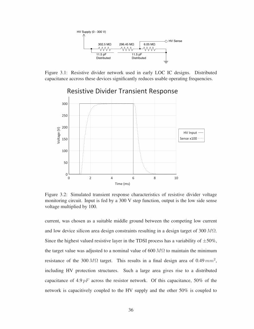
Figure 3.1: Resistive divider network used in early LOC IC designs. Distributedcapacitance accross these devices significantly reduces usable operating frequencies.
Figure 3.2: Simulated transient response characteristics of resistive divider voltagemonitoring circuit. Input is fed by a 300 V step function, output is the low side sensevoltage multiplied by 100.
current, was chosen as a suitable middle ground between the competing low current
and low device silicon area design constraints resulting in a design target of 300MΩ.
Since the highest valued resistive layer in the TDSI process has a variability of ±50%,
the target value was adjusted to a nominal value of 600MΩ to maintain the minimum
resistance of the 300MΩ target. This results in a final design area of 0.49mm2,
including HV protection structures. Such a large area gives rise to a distributed
capacitance of 4.9 pF across the resistor network. Of this capacitance, 50% of the
network is capacitively coupled to the HV supply and the other 50% is coupled to
36

ground. This leads to poor AC performance and significant inaccuracies when dealing
with transients below the 1ms time-scale, taking 2ms to settle to within 1 % of the
nominal sense voltage after a stepped input swing. The integrated charge pump can
charge from 0 to 300V in 3ms making this sensing method only marginally acceptable
for output voltage regulation.
3.2 High Voltage Sense Transistor
Figure 3.3: HV-sense transistor sensing circuit cross section. The HV-sensing deviceis formed by running a routing layer across two adjecent HV-N-wells.
Due to the large silicon area used by resistive sensing devices and the slow response
times, an alternate HV sensing technique was pursued. To the best of my knowledge
very little work has been done on the integration of ultra low-current high-voltage
sensing electronics. There are optical based approaches [30], [31] which could lend
them selves to MEMS implementation, however, CMOS compatible implementations
tend to rely on either capacitor networks [32], or external components. An interesting
alternative to dealing with high voltage signals is to use parasitic transistors, formed
using routing layers over field oxide ("thick oxide"), as active elements capable of
withstanding very high gate voltages [33]. By intentionally building transistors using
N-wells, substrate, and signal layers insulated by thick oxide layers, we can build DC
isolated HV sensing devices which are both faster and significantly smaller than their
resistive counterparts, Fig. 3.3. My work on these devices is similar to work done
37

Figure 3.4: Sweep of HV-sense transistor sensor gate voltage vs drain-source current.Vds = 5V
by Udatha et al. [34], who have produced flexible, thin film, high Vgs transistors for
DC voltage sensing of copper wires. In order to read these devices, a fixed voltage is
applied across the N-wells which form the drain and source of a HV-sense transistor,
and the current is read indicating the HV potential on the signal line. Since these devices
are transistors, and design efforts have been made at the process level to keep these
transistors turned off during normal operation, they suffer from several limitations.
Temperature Sensitivity (V/◦C)Voltage Temperature Regions (◦C)
Range (V ) 90 - 66 66 - 47 47 - 34 34 - 27250 - 200 3.3 3.7 4.0 4.4200 - 150 2.2 2.6 2.6 3.0150 - 100 1.3 1.2 1.3 1.7
Table 3.1: Temperature sensitivity of HV-sense transistor devices. This roughlycoresponds to voltage resolution when die temperature is known to 1 circC.
The first of these limitations is a very high gate threshold voltage. This voltage
varies between signal layers due to differences in oxide thickness, but in testing has
38

Figure 3.5: Temperature effects on active regulation of charge pump output voltage.The device under test is connected to a single 270V zener doide for output protectionand is otherwise unloaded.
an operational lower bound of 30V when using the capacitor poly sensors, and 50V
when using metal layer 1 based devices. This limitation restricts use of tested devices to
regulation voltages in the range of 30 - 300V , as sub-threshold operation has not been
examined for these devices.
The second issue with these devices, as with all MOSFETs, is non-linearity. This
requires additional design effort to produce circuits which can handle signal range at
the extremes, and maintain the resolution required to sense/regulate and the lower end.
Unlike the resistive network which is not affected by temperature changes provided
they are uniform across the whole network, the output of the HV-sense transistor
devices has a significant and non-linear temperature dependence, which can shift sensed
voltage by as much as 4.4 V◦C , Table 3.1. This temperature dependence necessitates
the addition of temperature sensing circuitry to allow for accurate voltage regulation
over a range of temperatures. In our plans for future research we have on-chip heater
designs which would further add to this problem. A simple temperature sensing circuit
39

was implemented and tested to counteract this limitation, by providing feedback to
microcontroller firmware, and is described in section 5.3.
In the current generation of LOC devices, due to a design error in digital to analog
converter (DAC) range we are limited to a regulation resolution of 10 V/step at IC
temperatures below 50 ◦C and 15 V/step when approaching 100 ◦C operation. This
limits regulation accuracy to either ±8.4 V or ±11.9V when operating in the ranges
20 - 50 ◦C or 50 - 100 ◦C respectively, for an individually calibrated die.
These devices occupy 5800μm2 which is only 1.2% of original resistive divider
network. And reduced power consumption of on-chip high voltage supplies by enabling
gated-clock voltage regulation. When running 300V , 10μA CE experiments the power
consumption of the charge pump system drops to 26mW from 52mW using this
regulation method rather than shunt regulation.
In practical applications, these sensors require per-chip calibration and die temper-
ature sensing for use. This calibration procedure requires that an external HV signal be
applied to the sensor while the die is brought to multiple controlled temperatures. A
sweep over both die temperature and HV supply voltage is used to generate a lookup
table to be flashed to an external micro controller. During operation this microcon-
troller will continuously sample the die temperature and adjust the HV set point to
compensate.
40

Chapter 4
High Voltage Switching Circuits
In order to run CE and PCR experiments on a single, combined CMOS-microfluidic
chip, HV switching is required. In the case of CE, a minimum of 4 HV electrodes are
required to inject a sample into a capillary channel and then electrophoretically separate
the sample as it travels down the length of the microfluidic capillary channel. For PCR
and sample preparation, valving is required to control the flow and mixing of reagents
on-chip. Electrostatic devices are being pursued for this purpose, requiring additional
HV switching circuits to drive each valve in the microfluidic device. My work on
these circuits has been in the miniaturization of on-chip HV switching circuits, and the
reduction in HV supply current consumption used by low to high side control signal
level-shifter circuits.
HV level shifting, where the HV supply voltage exceeds the process gate-oxide
breakdown voltage, is typically done by means of current limited DC switching paths
between HV and low voltage supplies [36, 37], Fig. 4.1, or cross-coupled HV switches
[38, 39, 35], Fig. 4.2, typically drawing negligible static current. In cross-coupled
switches, short high-current pulses are used to overdrive high side logic on state
transitions, and current limited HV switches may draw a small but constant static HV
current in the control logic of the high-side switch. These level shifting techniques can
41

Figure 4.1: HV switch reguiring only 3 HV transistors. High side gate voltage iscontroled using a well controlled high-side resistor and current sink [35].
cause potential problems when used in conjunction with very low current HV supplies.
Our research group has been designing on-chip HV generation [25] for use in genetic
diagnostic platforms [22].
4.0.1 Application
The intended application of these HV switches is in on-chip genetic diagnostic devices.
The HV requirements of these systems come from CE microfluidic structures and
electrostatic valve control. In our LOC systems, CE requires a signal driver capable
of delivering 75 - 300V , at 60 - 10μA respectively [22]. In order to inject and then
separate a sample, a minimum of four electrodes and associated HV switches must be
present on a LOC device. In order to allow for additional preparation and treatment of
sample fluid and reagents, on-chip valving is required. In our most recent microfluidic
design a total of 14 valves is required. Each of these valves require 2 HV switches
to counteract charge trapping effects during operation, section 1.3. This brings the
total HV switch count up to 32 in a supporting LOC IC. Our LOC ICs are designed
42

to be operated either using external HV supplies or integrated charge pumps, with a
maximum output current of 10μA at 300V [25]. This adds additional constraints on
HV switch designs, requiring low power consumption from the HV supply, on all level-
shifting circuits. Due to this, and the large silicon area used by existing HV switches,
new circuits were pursued. To reduce the load on the internal charge pump, the HV
switches needed to consume less than 1 μA from the HV supply either as static power,
or during the simultaneous switching of 4 high-side output drivers. In order to increase
the number of HV switches which fit into a single LOC IC, the reduction of the number
of physically large HV transistors used in level shifting logic is essential.
4.0.2 Previous Generation
Table 4.1: Static HV switch control signalingState Control High Control High Control LowHigh 1 0 0
High-Z 0 1 0Low 0 1 1
Previous work by our group [35, 10] was able to produce functional HV switches,
Fig. 4.2 and Fig. 4.1, capable of controlling signals of up to 300V from integrated 5V
logic. The first of these circuits consumes low static power, but produces large current
pulses through the high-side control logic when switching state. When powered from
an internal charge pump this can cause unacceptable drops in the HV supply voltage.
The second circuit consumes constant current when driving the output high. When
designed to operate a low bias current, � 0.5μA, this may be acceptable for low switch
count LOC ICs but is not useful for LOC IC containing 30+ HV switches. These
early designs focused on improving power consumption of prior work in the TDSI IC
process[40] which draw significant static power from an attached HV supply.
Switching HV using standard CMOS technology requires large RESURF isolation
structures on the components used to switch from the HV supply to the output and the
43

Figure 4.2: Static HV switch [10] used by previous generations of LOC ICs in ourresearch group
HV output to ground. These components in our process occupy an area approximately
300 times larger than their low voltage counterparts or 52,500μm2 per HV-NMOS,
HV-PMOS pair. While a single pair is certainly required to directly drive an HV signal,
our previous generation required 6 such transistors. Other proposals [42, 41] also
require 4+ HV transistors demanding significant silicon resources. In our most recent
LOC designs including electrostatic membrane drivers, we require 32 HV switches per
IC, forcing us to create novel low-area circuits for HV switching.
The second problem posed by these HV switch designs is that of HV supply power
consumption. As we move from off-chip power supplies to on-chip charge pumps,
current drawn from these low current power supplies becomes a subject requiring
significant attention. The static level-shifters proposed previously, which are most
commonly used in our ICs, can draw HV currents in the mA range while switching,
when the bias voltage used to protect the high-side low voltage transistors collapses
44
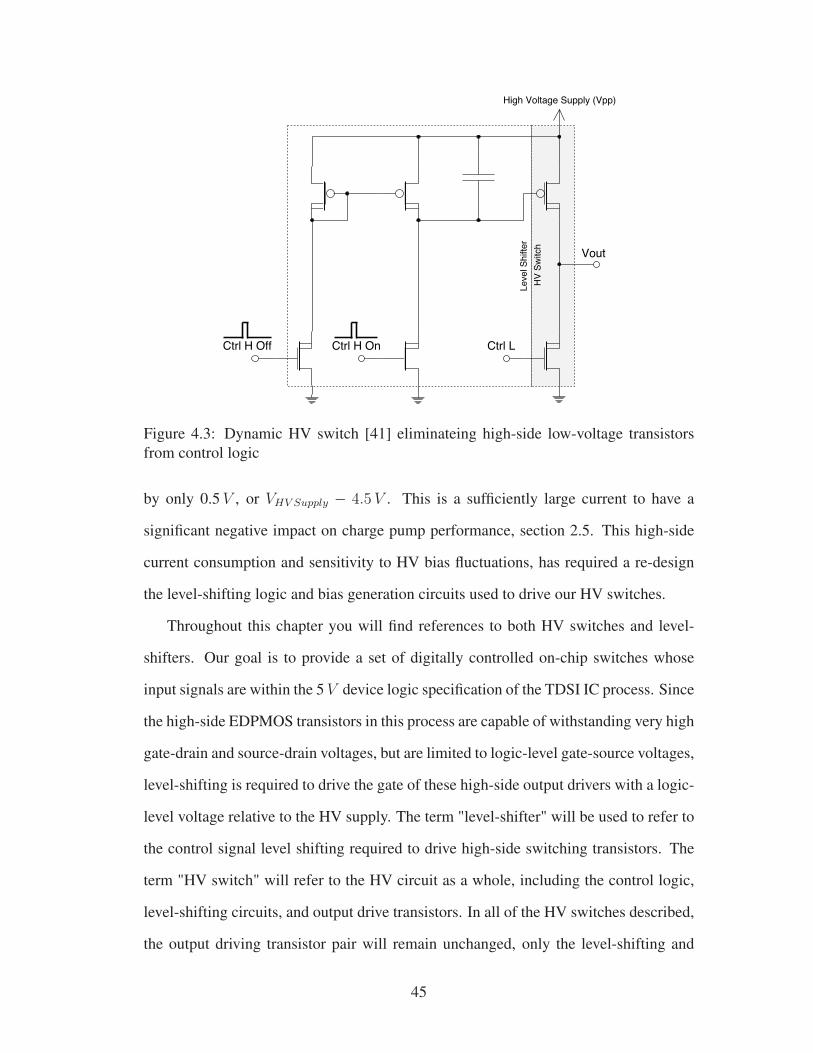
Figure 4.3: Dynamic HV switch [41] eliminateing high-side low-voltage transistorsfrom control logic
by only 0.5V , or VHV Supply − 4.5V . This is a sufficiently large current to have a
significant negative impact on charge pump performance, section 2.5. This high-side
current consumption and sensitivity to HV bias fluctuations, has required a re-design
the level-shifting logic and bias generation circuits used to drive our HV switches.
Throughout this chapter you will find references to both HV switches and level-
shifters. Our goal is to provide a set of digitally controlled on-chip switches whose
input signals are within the 5V device logic specification of the TDSI IC process. Since
the high-side EDPMOS transistors in this process are capable of withstanding very high
gate-drain and source-drain voltages, but are limited to logic-level gate-source voltages,
level-shifting is required to drive the gate of these high-side output drivers with a logic-
level voltage relative to the HV supply. The term "level-shifter" will be used to refer to
the control signal level shifting required to drive high-side switching transistors. The
term "HV switch" will refer to the HV circuit as a whole, including the control logic,
level-shifting circuits, and output drive transistors. In all of the HV switches described,
the output driving transistor pair will remain unchanged, only the level-shifting and
45

control logic vary from one HV switch design to another.
4.1 Capacitively Coupled Level-Shifting
Using capacitors to couple low-side and high-side circuits has successfully been used in
very high voltage discreet HV switching devices and single-IC “boot strapped” level-
shifters [43, 44]. In these HV switches, a pair of capacitors are used to pass signals
across the isolation boundary between low voltage and HV power domains. When
dealing with voltages in excess of 30V , there are no capacitive devices available to us
which utilize the, high capacitance per unit area, gate-oxide dielectric layer. This results
in significant increases in the required silicon area to implement these on-chip HV
capacitors. Provided it can be made large enough, a capacitor allows for the efficient
transmission of AC signals regardless of DC bias. At low currents, or when capacitive
loads are being driven, it is often acceptable to drive a load with a non-continuous duty
cycle at less than the maximum high-side switch Vgs. For processes with high-side
transistors with gate thresholds less than ½VLV supply, a square wave biased at the HV
supply potential can make an acceptable drive signal. In our case, we are working
with low voltage logic with a supply voltage of 5V , and high-side transistor threshold
voltages of 0.8V .
4.1.1 Dynamic RC Level-Shifter
Table 4.2: Dynamic RC switch control signallingState Control High Control LowHigh 0
High-Z 1 0Low 1 1
When considering low current loads with non-continuous duty-cycle requirements,
one of the simplest and smallest high-side control methods is a pulsed HV control signal
46

Figure 4.4: Dynamic RC HV switch proposed for low drive current applications
with capacitive coupling to low voltage driver logic and a resistive DC bias circuit. This
effectively forms a high-pass RC filter connecting a high-side switching transistor’s
gate to a low-side signal Fig 4.4. A high-valued resistor is connected to the HV supply
to provide a bias voltage during operation. The RC time constant is then tuned to
protect the gate during maximum expected HV supply on/off slew rates while passing
a signal frequency that can be easily generated on-chip. In our case, the designed
limits are 30V /μs HV supply maximum slew rate and the control signal pulses are
generated from a 10MHz clock signal. The control capacitor was chosen to be at least
3× greater than the high-side switch gate capacitance of 380 fF and was then refined
for efficient layout resulting in a Cctrl of 1.3 pF . Combining these parameters with a
maximum safe Vgs of 10V , Rbias can be found using (4.1), resulting in a resistance of
250 kΩ. Finally, calculating the RC time constant for this filter we find a time constant
of 325ns which is significantly greater than the half clock period of 50ns of the control
signal. Control signal power consumption can be calculated using the gate capacitance,
47

380 fF , control voltage, 5V , and switching frequency, 10MHz, resulting in 95μW
per driven high-side switch.
Vgs = RbiasCctrlΔVHV
t(4.1)
Figure 4.5: Drive strength of dynamic RC switches. HV supply =Vsd, switchingfrequency = 10MHz
Controlling the HV-PMOS with an AC-coupled signal saves a significant amount
of silicon area at the cost of weaker drive strength. By replacing the HV transistors
used in the control signal level-shifting circuit from previous generations with and RC
filter, we have been able to save 55% of the silicon area previously used by integrated
HV switches. Additionally, the only biasing voltage required is the HV supply
itself, eliminating the need for additional high-side components required to generate
a fixed voltage relative to the HV supply. The drive strength of these HV switches
is significantly reduced by the much lower on-voltage generated when switching a
high side switch and non-continuous duty cycle. This limitation makes this type of
switch useful for very small DC loads, such as driving small cross section mm scale
48

Figure 4.6: Comparison of drive strengths of RC switches across range of high sideduty cycles. HV switch HV supply =Vsd = 20V
CE [23], or low switching frequency capacitive loads. In process corner simulations
these HV switches have a worst case high-side drive strength of 20μA and have been
capable of driving just under 60μA when fabricated and tested, Fig. 4.5. It is possible to
boost the output drive strength by reducing the duty cycle, Fig. 4.6, resulting in a peak
drive strength increase in ICs tested of 65%, at a duty cycle of 30%. This method was
not pursued for implementation in fabricated hardware due to the added signal driver
complexity and availability of alternate designs.
4.1.2 Capacitively-Coupled-Buffer Level-Shifter
Table 4.3: Capacitively-coupled-buffer control signallingState Control High On Control High Off Control LowHigh 1 0
High-Z 1 0Low 1 1
A logical continuation of the previous design is to RC high-pass couple a set of
49
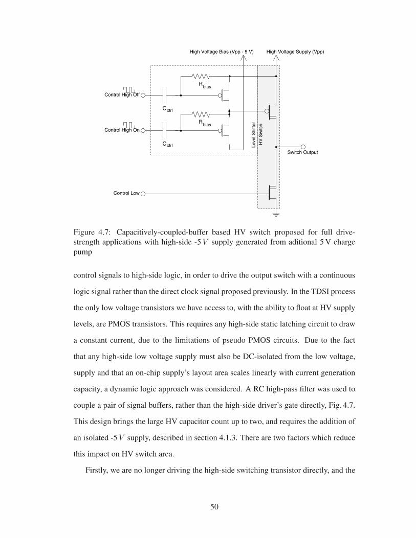
Figure 4.7: Capacitively-coupled-buffer based HV switch proposed for full drive-strength applications with high-side -5V supply generated from aditional 5 V chargepump
control signals to high-side logic, in order to drive the output switch with a continuous
logic signal rather than the direct clock signal proposed previously. In the TDSI process
the only low voltage transistors we have access to, with the ability to float at HV supply
levels, are PMOS transistors. This requires any high-side static latching circuit to draw
a constant current, due to the limitations of pseudo PMOS circuits. Due to the fact
that any high-side low voltage supply must also be DC-isolated from the low voltage,
supply and that an on-chip supply’s layout area scales linearly with current generation
capacity, a dynamic logic approach was considered. A RC high-pass filter was used to
couple a pair of signal buffers, rather than the high-side driver’s gate directly, Fig. 4.7.
This design brings the large HV capacitor count up to two, and requires the addition of
an isolated -5V supply, described in section 4.1.3. There are two factors which reduce
this impact on HV switch area.
Firstly, we are no longer driving the high-side switching transistor directly, and the
50

Figure 4.8: Comparison of control signals for dynamic RC drivers and high-side PMOSgates in buffered RC HV switches
high-side low voltage transistors have significantly smaller gates. Using lower gate-
source capacitances, 32 fF , allows for the use of a smaller signal capacitors, 146 fF .
Secondly, we have a much lower drive-strength requirement on the buffer transis-
tors, as they need only charge or discharge the high-side switching transistor’s gate,
and keep it in the desired state until a change is triggered by altering the control sig-
nals. This reduction in drive strength requirement means that we no longer need the
high-pass filter to pass a square wave. It is now acceptable to pass a pulse on each edge
of the signal, Fig. 4.8, reducing the required RC time constant. By selecting an Rbias
of 100 kΩ, reducing the RC time constant to 14ns, we also significantly increase the
maximum HV supply slew rate. Using (4.1), we find the maximum HV slew rate of
this design is 685V/μs. Due to the lower resistance of this circuit, causing full signal
capacitor discharge per control clock cycle, the CV 2F control power of this circuit is
based on the signal capacitor rather than the gate capacitance of the buffers. This is a
lower value at 37μW , due to the smaller capacitances involved, but unlike the direct
51

Figure 4.9: Switch layout area comparison. Previous generation switch to the left andRC-based switches from my research to the right
RC control, this power will be consumed regardless of HV switch state.
Figure 4.10: Comparison of drive strengths of fabricated switches. Vsupply = 70V
This design uses slightly more layout area than the direct RC HV switch at
0.105mm2, Fig. 4.9, but is still 46% smaller than the original static HV switch design,
and maintains nearly full output drive strength Fig. 4.10.
52

Figure 4.11: HV referenced -5V supply generation. Used to drive capacitively-coupled-buffer level shifting circuits
4.1.3 High-Side Bias Voltage Generation
The capacitively-coupled buffer level-shifter improves upon the direct RC design in
drive strength while maintaining high-side and low-side DC-isolation. Like the static
level-shifter design, the capacitively-coupled buffer level-shifter also requires a high-
side bias voltage to drive high-side switching transistors. In order to generate this
voltage while maintaining high-side to low-side DC-isolation a negative charge pump
circuit was implemented. This used floating diode-connected PMOS transistors and
a large value load resistor to keep the circuit operating at 2Vlv − 3Vth less than Vhv,
Fig. 4.11. By doing so we can generate and maintain a bias voltage, relying on low
voltage power without drawing static current from the HV supply. This bias generation
circuit also allows older static level-shifter designs to operate over a range of supply
voltages while maintaining a fixed bias relative to Vhv, and reduces the required silicon
area significantly from that used by earlier resistive designs, Fig. 4.12.
53

Figure 4.12: HV bias generator area comparison. Left: Negative change pump, Right:600MΩ Resistive network
4.2 Fabricated Circuits
Table 4.4: HV switch level-shifter power consumption at 70 V supply voltageSwitch Type High (nA) High-Z (nA) Low (nA) HiZ-High 667 Hz Switching (nA)
Dynamic-RC 209 1.2 60.2 109Buffered-RC 3.46 5350 5290 1110
Static 3.54 2.65 10.9 28400
HV switches of each type have been fabricated and tested. The performance of
each these HV switches was evaluated based on high-side drive capability, Fig. 4.10,
and HV supply power consumption, Table 4.4. Each circuit contains identical low-
side switching transistors. All of the fabricated ICs have met our maximum HV current
requirement of 60μA for CE experiments, however, the dynamic-RC HV switch design
is expected to be capable of sourcing only one third of the current measured under
worst-case process corners. Due to this current sourcing limitation the dynamic-RC
HV switch is only suitable for capacitive loads in our microfluidic designs.
While the buffered-RC HV switches have performed as expected in high-side drive
strength tests, the circuits fabricated have unacceptably high leakage currents when the
high-side switching transistor is held in its off state. This leakage current is attributed to
54

Figure 4.13: Buffed RC gate protection structure showing parasitic BJT
a gate protection structure which was added in an effort to eliminate the requirements of
HV supply slew limiting. In the fabricated buffered-RC switches a PMOS2 diode was
added to the gate connections of each buffer transistor, Fig. 4.13. This was designed to
protect the gate from both charge and discharge events by ether forward conduction of
the diode or 12V reverse biased breakdown of the drain PN junction. This mechanism
has been successfully used in the charge pump circuitry, however, relies on a floating
bulk connection to prevent current conduction through the parasitic BJT connecting
every PMOS2 transistors drain, source, and body to substrate. In the buffered-RC
circuits, this bodies of all transistors where tied to the HV supply rail which allows
charge, pumped through the protection structures drain contact, to activate the P+/HV-
NWell/P-substrate BJT and leak current to substrate resulting in the leakage currents
seen in columns 2 and 3 of Table 4.4.
Even with the additional current consumed by the protection structures in the
buffered-RC HV switches, both the buffered-RC and dynamic-RC switches show a
clear advantage when high switching activity is required. The dynamic-RC switches
consume 0.4% of the HV supply current required to drive the high-side control logic
of the static HV switch design and the buffered-RC switches consume 4% in currently
fabricated circuits. The 4% figure consumed by buffered-RC circuits is expected to
55

drop significantly with properly designed gate protection circuits.
4.3 Summary
Table 4.5: HV switch layout areaSwitch Type Area (mm2)
Dynamic-RC 0.0875Buffered-RC 0.105
Static 0.193
Two novel HV switching circuits have been designed, fabricated, and tested against
cross-coupled-static HV switches in the TDSI IC process. These designs have succeed
in meeting their design goals of reduced layout area, Table 4.5, and reduced power
consumption when switching the high side output transistor state, Table 4.4. The
dynamic-RC circuits have been shown to draw the least amount of HV power to run
switching logic, at 209nA maximum in the high state. The buffered-RC circuits have
shown to be capable of running with sub 10nA HV supply current consumption in
the output-high state, but draw considerably more current, 5.3μA, in all other modes
of operation. This large current draw is attributed a design error in the protection
structures connected to the gates of the buffer transistors. Given proper design and
biasing of the body contact of these protection circuits, this current is expected to drop
to that of the output-high state. Both RC HV switch designs consume significantly less
power on high-side signal transitions when compared to the static HV switch reference
and require only one half the silicon area to implement. I believe the dynamic-RC
design may be of particular use in capacitively loaded circuits where it is desirable
to be able to run the device without generating a bias voltage, referenced to the HV
supply. In situations where higher output currents are required and a high-side bias
voltage is available, a minor revision to the buffered-RC HV switches could drive high-
side switching transistors continuously, without the high switching currents required by
56

static HV circuits or high quiescent current of existing circuits.
57

Chapter 5
On-Chip Heater Control
On-chip heating is required for the amplification of genetic samples using PCR. The
heating surface problem has been studied by our group [11], and the heating electronics
which I have been involved in extends the work of Sunny Ho [8]. I have created
implementations of our research group’s non-iterative heater design algorithm, which
can be found in appendix A. This design algorithm allows for the creation of uniform
temperature heater designs of arbitrary shape and thermal flux. This has allowed for
rapid design and consideration of insulated heater chambers, requiring bowtie-shaped
support pillars for the microfluidic chamber floor, Fig. 5.1, enabling lower powered
devices and greater thermal insulation between heater electronics and microfluidic
cambers.
The main focus of my work in this area has been the extension of Sunny Ho’s
work adding increased drive current capabilities, and connection flexibility for multiple
heater designs. As heater designs evolve and microfluidic geometries dictate sane
track spacings to align with microfluidic structures such as support pillars, it becomes
increasingly difficult to target a single design voltage for all microfluidic layouts. In
order to satisfy minimum trace width and maximum current density constraints, the
design target current was relaxed. The drive capabilities of previous work, have been
58

limited to a continuous current of 300mA for an on-chip heater design and sensing
circuits designed for a single fixed range. My contributions have increased this to
1A DC, with considerations for peak switching currents of 4A, and the addition of
ranging circuits in the sensing logic allowing for accurate sensing of heater resistances
from 2.1Ω to 67Ω. In addition to the electronic advancements I have been involved
in the CMOS-microfluidic electronic interface design. This allows for multiple sizes
of heaters to be designed to be placed and connected to the surface of a CMOS chip
with a single layer heater design. All connections on a single edge of the heater or
opposing polarities are placed on opposite edges of this heater. These connections
must be capable of conducting the maximum heater current of 1A, without interfering
with HV electrode placement and optical detection.
5.1 Automated Heater Generation - Implementation
An implementation of the heater algorithm developed by our group [15] was created
in the C# programming language, to quickly visualize and iterate through design
parameters. The following will be a description of the algorithm from this, and my
implementation as used for IC design purposes.
5.1.1 Heat Flux Extraction
Our thermal design algorithm relies on one assumption, which must hold for the design
in question. The assumption is that the heating element is in close enough proximity
to the microfluidic chamber such that the temperature of the heater can be assumed
to be the same as the microfluidic chamber temperature, within reasonable limits of
error. This allows for thermal simulations treating the heating surface as an isothermal
plane. In order to design heating elements from a finite element simulation, the 3D
structure of a microfluidic heating chamber and IC below must be created with exterior
59

Figure 5.1: Q Field used to generate heater design in Fig. 5.2. This is a model of asuspended microfluidic chamber, with minimum sized supports from IC substrate tomicrofluidic chamber floor
boundaries selected, such that they do not affect the distribution of thermal flux during
heater operation. Once this has been created, the surface, which will be replaced by
a heating element, will be treated as an isothermal boundary condition. In order to
extract the data required for heater design, two additional boundaries must be added
immediately above and below the heating element. These boundaries will be used to
extract the heat flux at steady state which will be used to generate the heater layout
using our algorithm. Figure 5.1 shows the heat flux from one of our microfluidic PCR
chamber designs. This chamber is designed with an air gap between the microfluidic
chamber floor and LOC IC. Due to the manufacturing process used to etch the bottom
60

Figure 5.2: Heater designed from C# port of our non-iterative heater design algorithm.Plotted tracks are color mapped by current density. Design has been generated with alltracks electrically connected in parallel with a drive voltage of 1.3 V .
most microfluidic layer, the chamber supports reduce to a bowtie shape at minimum
size, resulting in the red peaks in flux distributed regularly across the chamber floor.
5.1.2 Automatic Heater Layout Generation
Once the heat flux has been extracted from a simulation of the desired microfluidic
structure it is then converted for use in layout generation. In this algorithm the first step
is to discretize the upper and lower extracted Q fields into a grid, where each element
is the sum of the upper and lower Q fields in that region. This Q field represents the
thermal power dissipation required across a heater designed for the studied microfluidic
topology.
The next step is to determine heater track placement and electrical specifications.
61

In most of our work we have focused on uniformly spaced parallel line heaters for
compatibility with existing LOC ICs and simplicity of implementation. This method
applies equally well to arbitrary heater track paths, which both cover the entire heating
surface, and do not overlap or cross at any point with in the active heating zone. Here
a heating track is defined as a path with a predefined width, or in our case, rectangle
in 2d space, which stretches from a point of higher voltage potential to lower voltage
potential, and lies within the heating surface. For each of these paths a total Q, or
thermal power output, its calculated for each point along is length, which is used to
calculate the relative resistance at that point in the segment, with respect to the rest of
the track. A predefined voltage, Vheater, is used to calculate the total track resistance,
Rtrack =V 2heater
Qtrack, and the resistance at each point is determined by discretized segments
Rseg = RtrackQseg
Qtrack. Once the resistance at each point along a track is determined, the
metallized trace can be generated using the sheet resistance (Rs) of the heating material
and calculated resistance distribution where Widthseg = Rs
RsegLengthseg. By splitting a
heater into uniform width rectangular tracks, it can be generated from a Q field with the
inputs: Widthtrack; the Rs of the heating material; and a function describing the heater
boundaries. For a circular heater this source code can be found in Fig. A.1.
5.1.3 Layout Export
Once the heater geometry has been generated, it is necessary to export these designs to
external tools for further processing and integration into microfluidic designs. This
has been broken into two steps: polygon generation; and export to a portable file
format. In the polygon generation step we extract trace width information for each
track, and produce a sequence of points which define the outline of each continuous
trace. Clockwise order was chosen, where each segment is defined as a single point
centred vertically, with respect to the segment’s occupied region. This results in an
average width of each segment which is equal to the design width, provided that all
62

segments share the same segment length along a single track. This smooths out the
transition between dissimilar widths, providing more accurate resistance values when
compared to connecting rectangles. Source code for this process can be found in
appendix A.2. The format chosen for export was DXF as this has good compatibility
with the tools used in our design flow, and has a text-based file structure which lends
itself to easy implementation. Source code was taken from David S. Tuft’s DXFExport
library written in C#, which was modified to support the polygon data structure used in
the previously discussed code. The relevant source can be found in appendix A.3.
5.2 PCR Chamber Temperature Sensing
Figure 5.3: Standard PCR thermal cycle used for amplification of genetic samples.Here Tm = 60 ◦C for the experiment shown.
In order to run on-chip genetic amplification using PCR, accurate temperature regu-
lation is required. A PCR thermo-cycle is comprised of 3 phases: denaturation; anneal-
ing; and extension, these phases occur at 94, Tm, and 72 ◦C respectively, Fig. 5.3. The
denaturation and extension phases require a thermal regulation accuracy of ±2.5 ◦C
and the annealing temperature, Tm. This is calculated for the specific amplification
target which requires regulation to within ±0.5 ◦C for standard amplification. A slight
modification can be made to run PCR with lower accuracy instruments. This modifi-
cation is to ramp down from a higher temperature through the annealing temperature,
63

Tm, at at most 1 ◦C/s. In our proposed system [11], thermal regulation of the PCR
chamber cannot be directly correlated to IC die temperature. This allows for both faster
thermo-cycles [45] and greater flexibility in microfluidic device topology. With this
design goal, temperature sensing must be done using embedded conductive layers in
our microfulidic devices. In our designs, this conductive layer is comprised of thin-
film aluminum with a measured TCR of 2.07×10⁻³ ◦C−1. This value of TCR is 48 % of
what would be expected from bulk aluminum, 4.308×10⁻³ ◦C−1, resulting in a smaller
signal sensor value. In my work, I deal with the electrical systems on-chip which drive
and sense the heater conductors in wafer-bonded microfluidic heaters. As the fluidic
devices discussed are under active development and could change in the future, I will
be using our measured TCR value of 2.07×10⁻³ ◦C−1 for temperature sensing accuracy
estimates. If our group is able to produce thin-film aluminum devices with a charac-
terized TCR which is closer to the nominal bulk value of 4.308 × 10⁻³ ◦C−1, this will
increase our sensing resolution by the ratio of old:new TCR.
Two device layouts have been considered for sensing the temperature of and heating
microfluidic layers. The first is to use a dedicated sensing element, which is constantly
powered by sensing electronics, but does not produce enough joule heating to contribute
significantly to the heating of the microfluidic PCR chamber itself. This method allows
for continuous sensing without disturbing the reading under examination. In order to
accommodate this method of temperature sensing additional contacts have been added
between the high-current heater-element contacts, and a current DAC was added to bias
the sensing element. The second proposed sensing method involves direct measurement
of the heating element resistance. Due to the fact that the heating element has been
designed to produce a uniform temperature profile across its entire surface, the total
resistance of the heater element can be safely assumed to be representative of the change
in resistance of each internal trace. This will not be dominated by hot or cold spots in
the individual traces which make up the heating element. Sensing the heater element
64
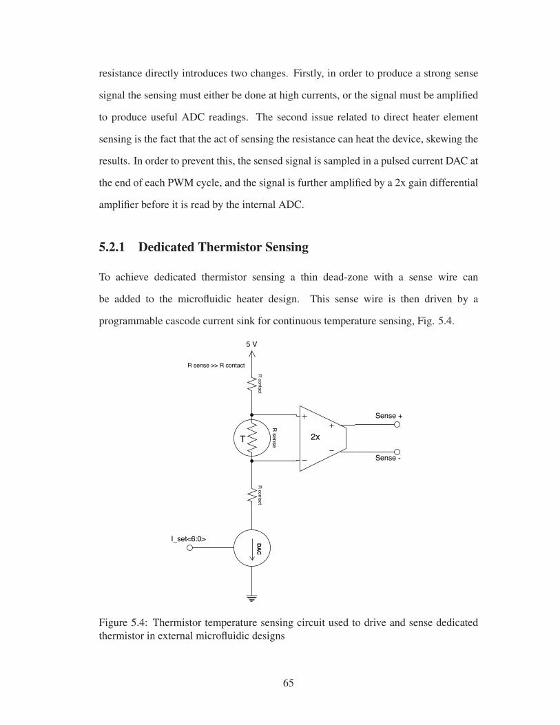
resistance directly introduces two changes. Firstly, in order to produce a strong sense
signal the sensing must either be done at high currents, or the signal must be amplified
to produce useful ADC readings. The second issue related to direct heater element
sensing is the fact that the act of sensing the resistance can heat the device, skewing the
results. In order to prevent this, the sensed signal is sampled in a pulsed current DAC at
the end of each PWM cycle, and the signal is further amplified by a 2x gain differential
amplifier before it is read by the internal ADC.
5.2.1 Dedicated Thermistor Sensing
To achieve dedicated thermistor sensing a thin dead-zone with a sense wire can
be added to the microfluidic heater design. This sense wire is then driven by a
programmable cascode current sink for continuous temperature sensing, Fig. 5.4.
Figure 5.4: Thermistor temperature sensing circuit used to drive and sense dedicatedthermistor in external microfluidic designs
65

Figure 5.5: Sweep of DAC used to drive external thermistor sensing
The programmable current sink has a range of 5.8μA to 714μA in tested ICs, Fig.
5.5. This results in a thermistor resistance range of 340 kΩ to 1.4 kΩ, while maintaining
an analog input signal within the range of 1V to 2V . With an expected 50 ◦C rise in
temperature from the nominal sensor temperature of 20 ◦C, and a measured TCR of
2.07 × 10⁻³ Ω/Ω◦C we expect the sensor resistance to increase by 10 % during normal
operation and as much as 20 % if aluminum processing is improved. In fabricated
sensors the resistance limits mentioned previously must be considered over the whole
range of expected operating temperatures, including room temperature for start-up
calibration.
DAC current varies by up to 0.24 A/AV
, which will result in a maximum 0.06 %
variation in output voltage over the operating region of one of our sensors. When
divided by the TCR to get absolute temperature error of the sensor, we find that this
results in an uncertainty of ± 0.29 ◦C, if no voltage dependency calibrations are taken
for DAC current compensation.
Without calibration, the differential amplifiers added to both LOC 13 and LOC
66
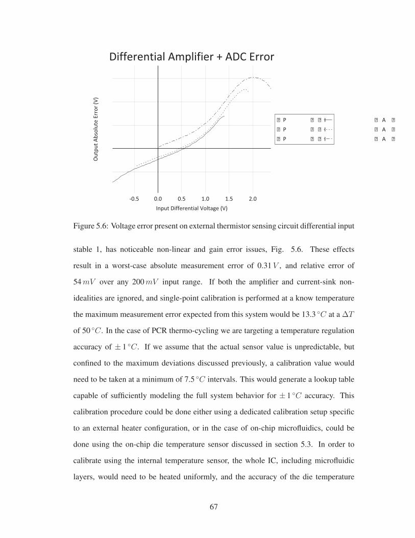
Figure 5.6: Voltage error present on external thermistor sensing circuit differential input
stable 1, has noticeable non-linear and gain error issues, Fig. 5.6. These effects
result in a worst-case absolute measurement error of 0.31V , and relative error of
54mV over any 200mV input range. If both the amplifier and current-sink non-
idealities are ignored, and single-point calibration is performed at a know temperature
the maximum measurement error expected from this system would be 13.3 ◦C at a ΔT
of 50 ◦C. In the case of PCR thermo-cycling we are targeting a temperature regulation
accuracy of ± 1 ◦C. If we assume that the actual sensor value is unpredictable, but
confined to the maximum deviations discussed previously, a calibration value would
need to be taken at a minimum of 7.5 ◦C intervals. This would generate a lookup table
capable of sufficiently modeling the full system behavior for ± 1 ◦C accuracy. This
calibration procedure could be done either using a dedicated calibration setup specific
to an external heater configuration, or in the case of on-chip microfluidics, could be
done using the on-chip die temperature sensor discussed in section 5.3. In order to
calibrate using the internal temperature sensor, the whole IC, including microfluidic
layers, would need to be heated uniformly, and the accuracy of the die temperature
67

sensor considered. When factoring in the 0.45 ◦C temperature uncertainty of the die
temperature sensor, the lookup table temperature interval would need to be reduced to
4.13 ◦C.
5.2.2 Direct Heater Element Sensing
Figure 5.7: PCR reaction chamber cross-section. The design shown here features aremovable lid which can function as a valve for sort term testing
The second proposed method of microfluidic PCR reaction chamber temperature
sensing is by direct measurement of the heating element resistance. In our proposed
microfluidic designs, the heating element is tightly coupled to the liquid in the reaction
chamber, Fig. 5.7. At these scales it can be safely assumed [45] that the heating element
surface temperature differs from the microfluidic chamber temperature by no more than
0.03 ◦C over our expect operating range, at an ambient temperature greater than or
equal to 20 ◦C.
In order to prevent contact resistances from affecting heater resistance measurement
results, it is necessary to perform 4-pt measurements on-chip. This 4-pt measurement
is accomplished by driving the heater switch with a modified PWM signal. Here a
bias voltage is applied to the switching transistor, mirroring the internal analog bias
current on to the heater drive circuitry for the duration of the sample period, Fig.
68

Figure 5.8: Direct element temperature sensing circuit used in our LOC ICs
5.8. In order to accommodate a greater range of heater element designs, allowing for
greater flexibility in microfluidic design, the heater switch is broken up into 32 identical
switching units. These can be enabled/disabled during the sense phase of operation.
This reconfigurability allows the heater switch to be programmed to sink 30 to 930mA
for resistance sensing, in 30mA steps. For a nominal sense voltage of 2V this allows
for a heating element resistance in the range 2.15 to 67Ω, with smaller resistance values
permissible, at the expense of signal amplitude.
Calibration Based on Simulation Fitting Parameters
Table 5.1: Die Temperature Effects on Sense Current (mA/A◦C )
���������
Vds
(V)PC
nom ff fs sf ss
3 -0.766 -0.777 -0.762 -0.783 -0.7673.5 -0.802 -0.772 -0.798 -0.778 -0.804
4 -0.835 -0.767 -0.831 -0.774 -0.8384.5 -0.867 -0.762 -0.862 -0.771 -0.870
69

Figure 5.9: Direct element temperature sensing die temperature dependence.DAC value = 16, Vds = 2.8V
Table 5.2: Drain-Source Voltage Effects on Sense Current (mA/AV
)���������
TDie
(◦C)
PCnom ff fs sf ss
20 62.8 69.4 62.9 69.1 62.745 59.8 65.9 59.9 65.6 59.670 57.5 63.2 57.7 62.8 57.490 56.3 61.6 56.6 61.2 56.1
The proposed sensing method suffers from both transistor temperature effects and
channel length modulation effects. Both of these can cause large errors in the sensor
value if not compensated for. In simulation, both changes caused by die temperature
shifts, Fig. 5.9, and changes in the drain-source voltage, Fig. 5.10, result in output
changes, which can be closely approximated as linear functions of TDie and Vds
respectively. What is more, the magnitude of these effects remains relatively constant
as percentage of nominal sense current, over both process corners and each other. We
can approximate these effects using the linear equation (5.1), and can find the constants
Tcomp and Vcomp by fitting the equation to simulation data, and averaging the results,
70

Figure 5.10: Direct element temperature sensing voltage dependence. DAC value = 16,TDie = 20 ◦C
tables 5.1 and 5.2, to get values of −7.91× 10⁻⁴ A/A◦C and 6.14× 10⁻² A/A
Vrespectively.
The current calibration equation is:
ISW � ISW0(1 + TcompΔTDie)(1 + VcompΔVSW ) (5.1)
where:
ΔTDie = TDie − TDie0 ,
ΔVSW = Vsup −RcompVsense − 3 , and
Rcomp =Rcnt+Rht0
Rht0
Here TDie0 and ISW0 are the die temperature and switch current at the point used
for calibration, Rht0 is the nominal heater resistance, and Rcnt is the combined contact
71

resistance, Fig. 5.8. For a known heater resistance and either known or negligible
contact resistance, single point calibration can be achieved using the equation (5.2) and
recording the current die temperature, TDie0 .
ISW0 =Vsense
Rht0(1 + VcompΔVSW0)(5.2)
Using equation (5.1), ohms law, and linear TCR we can then solve for element
temperature using only the heater sense voltage, Vsense, and die temperature from the
on-chip sensor discussed in section 5.3.
Tht =
Vsense
IswRht0− 1
TCR
+ Tht0 (5.3)
Table 5.3: Maximum Absolute Error in Simulation Data After Linear Correction (◦C)���������
TDie
(◦C)PC
nom ff fs sf ss
20 0.1 0.9 0.6 0.8 0.130 0.5 1.1 0.5 1.1 0.550 1.2 1.8 1.1 1.8 1.290 1.6 2.1 1.6 2.2 1.7
Using (5.3) on simulation data provides good accuracy across process corners
for sense voltages in the range 1.5 to 2V . Table 5.3 shows worst-case absolute
temperature errors from simulation data using equations (5.2) and (5.3) for calibration
and temperature calculation. For each entry in this table both the heater temperature,
Tht, and nominal resistance, Rel0 , where swept to find the maximum measurement error
for a heater at a temperature in the range 20 to 90 ◦C, with nominal sense voltage in the
range 1.5 to 2V . From this data it can be assumed that single point calibration on this
circuit should be capable of providing an absolute accuracy of ±2.2 ◦C for thermally
insulated ICs. For ICs with sufficient heat sinking to keep die temperatures below 30 ◦C
this accuracy increases to ±1.1 ◦C.
72

Physical Device Testing
Figure 5.11: Direct element temperature sensing error test. Rht = 2.37Ω, Calibrated atVsupply = 4.8V
Table 5.4: Absolute Error in Direct Element Sensing Test Device (◦C)����������
ΔTht
(◦C)
Rht (Ω)2.37 3.93 5.91 11.88 30.11
-10 -0.52 -0.26 -0.38 -0.10 0.4530 0.85 0.59 0.61 0.93 1.1160 1.03 1.27 1.12 1.51 1.5390 1.64 1.69 1.85 1.64 2.74
The direct element sensing circuit has been fabricated and has functional imple-
mentations in both LOC 13 and LOC stable 1. In order to verify proper circuit function
without access to the targeted heater devices, a set of fixed resistors were connected to
a LOC system set to various sense currents and a PWM value of 1, or 0.1% drive. For
each resistor connected, the heater supply voltage was swept to simulate the expected
change in Vds caused by a change in sensor resistance. Accuracy was then determined
by comparing the known resistance of each test circuit to the value calculated, using
73

the methods discussed in the previous section. All experiments were done at room tem-
perature and an assumed contact resistance of 0Ω with a single point calibration run at
Vsupply = 4.8V . The contact resistance and supply voltage used in the calibration have
a very small impact on calculated temperature when sensing at a nominal voltage of
2V with a supply voltage of 4.8V . The effects of supply voltage and contact resistance
on the calculated output resistance, provided they are kept constant for all calculations,
are 0.01◦C
%Rht
and 0.5◦CV
respectively, at the maximum ΔTht of 50 ◦C. Heater tem-
perature estimates are calculated based on the change in supply voltage relative to the
sense voltage at calibration, Tht � Vsupply0−Vsupply
Vsense0TCR. Table 5.4 lists the error found in
test circuits as a function of heater resistance and temperature difference from ambient.
The heater switch was configured to produce the maximum Vsense attainable without
signal clipping for each resistor network. DAC values used, listed from lowest valued
resistance to highest, where 30, 20, 11, 6, and 2. Figure 5.11 shows the plot of the
lowest valued resistor over the voltage sweep and corresponding error.
In physical devices it is unnecessary to measure or calculate either the heater
resistance or nominal DAC current. By using the linear TCR equation (5.4), our
original calibration equation (5.1), and neglecting the small effects cause by contact
resistance on shifts in drain-source voltage, we can express temperature change purely
as a function of sense voltage, Vsense, and die temperature, TDie, equation (5.5).
ΔTR =R−R0
TCRR0
(5.4)
ΔTR =Vsense
Vsense0(1 + TcompΔTDie)(1 + VcompΔVSW )TCR
− 1
TCR
(5.5)
Using this equation, calibration of on-chip microfluidic devices can be done by
simply sampling the die temperature, TDie0 , and sense voltage, Vsense0 , at device startup.
This requires only that the system as a whole be in a state of uniform temperature before
74

power is applied to the heating element. In order to achieve maximum accuracy, the
heater DAC should be set to the maximum value achievable, while preventing signal
clipping over the desired range of resistance. This system samples input signals using
a 2x gain differential amplifier, Fig. 5.8, which operates by amplifying both its positive
and negative input terminals, relative to the analog supply rail. This configuration limits
the voltage to the range Vdda/2 < ±Vsense < Vdda − 40mV , or 2.5 to 4.96V . Due to
the small distortion near the supply rails it is recommended to operate the heater supply
voltage at a slightly lower voltage than the analog supply voltage, or insure the high-
side contact resistance is at least 2 % that of the heater resistance.
5.3 Die Temperature Sensing
Figure 5.12: On-chip temperature sensor and amplification circuit, used for thermalcompensation of heater and HV sensing systems
In both the heater temperature sensing circuits and HV regulation circuits there
are die temperature effects which play a role in device operation. This requires
accurate measurement of die temperature for compensation and, in the case of heater
75

temperature sensing, startup calibration. The temperature sensor circuit I have chosen
for implementation in LOC 13 and LOC stable 1 was a forward-biased PN junction
driven with a fixed current, Fig. 5.12. Sensing is accomplished by measuring the
threshold voltage shift of this device as a function of die temperature. In order to
reduce optical effects on this device, a metal masking layer was added to the layout.
This was able to reduce the effects of global illumination of the chip to 0.02◦C
mW/m2 , or
±1.5 ◦C in current optical test configurations. At this stage in development, the optical
dependency is considered only for initial calibration at a fixed global illumination,
further characterization has been left for future work.
Figure 5.13: Die temperature sensor sweep in LOC stable 1
In systems using HV-sense transistor circuits, an accurate reading of IC temperature
is required. Since the HV-sense transistor sense values may vary by up to 4.4 V◦C , and
PCR applications will integrate heating elements onto the surface of our LOC ICs, an
on-chip temperature sensor is required. When sweeping the IC package temperature
from 25 to 100 ◦C we see maximum integral non-linearity of ±1◦C, Fig. 5.14. This
amount of temperature uncertainty results in an uncertainty in the HV-sense transistor
76

Figure 5.14: Temperature sensor deviation from linear calibration parameters
regulation circuits of ± 4.4V , due to thermal dependencies.
77

5.4 Summary
Precise thermal control is required to run PCR amplification, and thermal compensation
is required for accurate regulation of internal HV supply voltages. An automated
microfluidic heater design implementation has been presented, which generates heater
track layouts for aluminum thin film heaters from Q fields found in thermal simulation
of microfluidic heater geometry. This implementation identifies maximum current
density of final track segments, allowing for quick determination of design validity, and
exports the track geometry to a portable DXF vector file for integration in microfluidic
chip design flow.
Two methods of PCR chamber temperature measurement where proposed and
fabricated in LOC ICs. These methods are: dedicated thermistor sensing; and direct
element sensing. In the case of dedicated thermistor sensing, non-linearities in the
signal amplifier require the generation of a 20 point look-up table for calibration
purposes. This is required to maintain sufficient accuracy to thermo-cycle a PCR
reaction. In the case of direct element temperature sensing, recording the sense voltage
and die temperature at a known heater temperature is sufficiently accurate to run a
PCR thermo-cycle, if the annealing phase is run as a slow downward ramp through
the required annealing temperature, Tm. The single point calibration equation used
in direct element temperature sensing depends on both contact resistance and supply
voltage. However, at a nominal supply voltage of 4.8V deviations in supply voltage
used for calculation vs actual chip supply voltage produce output errors of 0.5 ◦C/V .
For the same reason contact resistance can be neglected for most systems, as a contact
resistance of 20 % of the nominal heater resistance will result in a measurement error
of only 0.2 ◦C at a ΔTht of 50 ◦C. Both of these circuits are sampled at 2.44 kHz, and
the heating element set point can be updated at up to 8 kHz. This is sufficiently fast to
drive our proposed integrated heaters which have time constants on the order of 50ms.
Finally, temperature compensation of on-chip circuits is accommodated using an
78

on-chip temperature sensor. This sensor is used to compensate for thermal effects in
both the heater sensing circuits and HV regulation circuits. A maximum temperature
error of ±1◦C was found for this device after linear calibration. This device has been
found to have a weak dependence on global illumination of the die, with a 1.5 ◦C rise
at maximum global illumination of current optical test configurations. Compensation
for this effect is accounted for in a single calibration at the fixed global illumination
of desired test setup. The LOC system requires tight control over illumination of
microfluidic structures, and does not require a modulation of this light source for
the duration of an experiment. Due to these factors optical dependence of the die
temperature sensor is not seen as a significant design issue at this time.
79

Chapter 6
Optics
In our designs, optical detection of florescent markers has been pursued, over electro-
chemical or capacitive methods [46]. In all of our LOC ICs we have internal photo-
diodes and data acquisition circuitry for sensing fluorophores at dedicated sites located
in the center of the microfluidic heater connections, for qPCR experiments, and at the
end of the intended CE separation channel, shown in Fig. 6.1. In previous work by Ben-
jamin Martin, an issue with unity-gain op-amp stability has reduced the useful working
range and sensitivity of our LOC optical systems. In my work I have corrected this is-
sue by replacing the op-amps in his circuits with lower-gain op-amps which have been
proven in previous generations of LOC ICs and have created a simplified integrator for
comparison. I have also been charged with microfluidic-optical site placement as part
of full system integration.
80
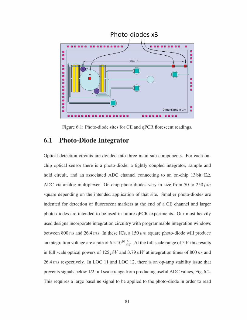
Figure 6.1: Photo-diode sites for CE and qPCR florescent readings.
6.1 Photo-Diode Integrator
Optical detection circuits are divided into three main sub components. For each on-
chip optical sensor there is a photo-diode, a tightly coupled integrator, sample and
hold circuit, and an associated ADC channel connecting to an on-chip 13 bit ΣΔ
ADC via analog multiplexer. On-chip photo-diodes vary in size from 50 to 250μm
square depending on the intended application of that site. Smaller photo-diodes are
indented for detection of fluorescent markers at the end of a CE channel and larger
photo-diodes are intended to be used in future qPCR experiments. Our most heavily
used designs incorporate integration circuitry with programmable integration windows
between 800ns and 26.4ms. In these ICs, a 150μm square photo-diode will produce
an integration voltage are a rate of 5×10¹⁰ VsW
. At the full scale range of 5V this results
in full scale optical powers of 125μW and 3.79nW at integration times of 800ns and
26.4ms respectively. In LOC 11 and LOC 12, there is an op-amp stability issue that
prevents signals below 1/2 full scale range from producing useful ADC values, Fig. 6.2.
This requires a large baseline signal to be applied to the photo-diode in order to read
81

Figure 6.2: Photo-diode instability at low light intensities. Experiment run with 26.6ms integration time. Optical power calculated using optical power meter in tandemwith LOC 11
optical power successfully. LOC 13 and LOC stable 1 contain a reduced gain op-amp in
the integration stage and a direct integration circuit to alleviate this problem. However,
in both of these systems, which share the same optical circuit design, the integration
reset line has been inverted in the digital logic. A work around has been developed to
allow optical reading from these ICs using external ADCs and careful control of the
LOC IC’s system clock.
My involvement in the optical subsystems has been system-level placement, to
allow for use with future microfluidic devices intended to be constructed on the CMOS
IC surface, and in minor circuit adjustments to compensate for previous design flaws.
These design changes manifest themselves in two circuits: one op-amp based design
intended to mimic Benjamin Martin’s work [6]; and a direct integration circuit using a
much simpler design and, which incorporates only proven on-chip circuits on all active
signal paths.
82
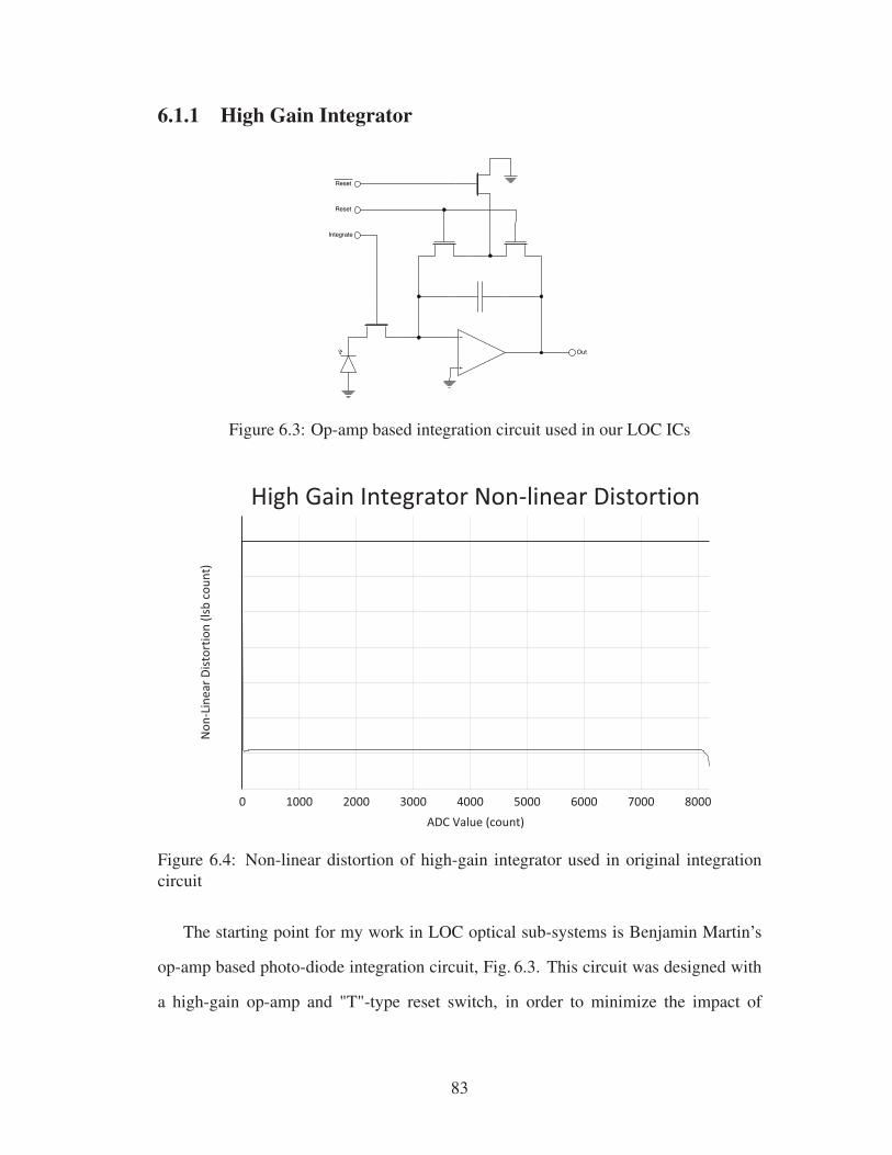
6.1.1 High Gain Integrator
Figure 6.3: Op-amp based integration circuit used in our LOC ICs
Figure 6.4: Non-linear distortion of high-gain integrator used in original integrationcircuit
The starting point for my work in LOC optical sub-systems is Benjamin Martin’s
op-amp based photo-diode integration circuit, Fig. 6.3. This circuit was designed with
a high-gain op-amp and "T"-type reset switch, in order to minimize the impact of
83

leakage currents and non-linear distortion, Fig. 6.4, on the target 13-bit ADC data-
acquisition circuitry. The op-amp based integration circuit holds the photo-diode in
zero bias photo-voltaic mode for the duration of the integration period. The "T"-type
reset logic maintains a 0 Vds bias across the reset transistor connected to input of the
op-amp circuit, greatly reducing the effects of sub-threshold leakage on photo-diode
readings.
Integrator Instability
Our original photo-diode integration circuitry has produced several artifacts in most
ICs tested. The most common issue displayed is a region of erratic behaviour at low
light intensities, as shown in Fig. 6.2. It is suspected that this behaviour is caused by
an op-amp stability issue, which causes the photo-diode to become forward biased and
discharge the integration capacitor under specific circuit conditions. In order to work
around this in our wet experiments, ICs were vetted before use, and operated with an
intentional minimum baseline optical signal during experiments.
6.1.2 Reduced Gain Integrator
Figure 6.5: High gain op-amp (left) was replaced with lower gain (right) op-amp toimprove integration circuit stability
In an effort to correct the stability issues discovered in previous designs, the
enhanced-gain op-amp was replaced with a more moderate 3-stage op-amp, Fig. 6.5.
84

Figure 6.6: Medium-gain op-amp non-linear distortion measured in ADC least-significant bits
This change increases the theoretical non-linear distortion, introduced by the integra-
tion amplifier circuit, to just under 2 least-significant-bits when the signal approaches
the rails and should not significantly affect expected test results, Fig. 6.6.
This reduced gain design was implemented in silicon on our most recently fabri-
cated LOC IC, LOC stable 1. Unfortunately, due to an inverted integration reset signal,
direct testing using the tightly coupled on-board ADC was not possible. A work-around
was implemented using a pair of external ADCs and precise system clock timing. De-
tails can be found in appendix B. While additional noise is injected into the signal due
to the additional logic, and signal wiring, there does appear to still be some small sta-
bility issue inherent in this design. The noise seen in test results and its proportionality
to the output voltage is greater that what would be expected due to external compo-
nents and timing synchronization issues alone, Fig. 6.8. Since many of the concerns
about leakage currents and photo-diode dark currents have been reduced from our early
conservative estimates, future LOC ICs will most likely rely on simplified integration
85

Figure 6.7: Gain enhancing op-amps used in high-gain amplifier. Left: High-side gain-enhancing op-amp. Right: Low-side gain-enhancing op-amp
circuits similar to what will be discussed in the next section.
6.1.3 Direct Integrator
A simplified integration circuit was implemented to increase the chances of proper
optical sensor functionality, and to provide some insight into expected leakage and dark
currents of our on-chip photo-diodes. The chosen simplified circuit is direct integration
by means of discharging a capacitor through the photo-diode directly. A fixed bias
NMOS transistor was placed between the photo-diode and capacitor to limit the reverse-
bias potential across the photo-diode during operation in an attempt to reduce dark
current, Fig. 6.9.
This has since been deemed unnecessary. The bias voltage required to permit
operation at our maximum target optical powers, without allowing the photo-diode to
enter its forward biased region of operation, is also high enough to saturate the dark
current of our photo-diode when operated at the lower end of our target optical power.
Testing has also shown no significant voltage offsets below minimum light intensity,
suggesting that the shunt resistance of our photo-diodes is large enough to be neglected
from future design considerations, Fig. 6.10. It should be noted, however, that the
linearity of designs based on the direct integrator approach will suffer significantly from
86
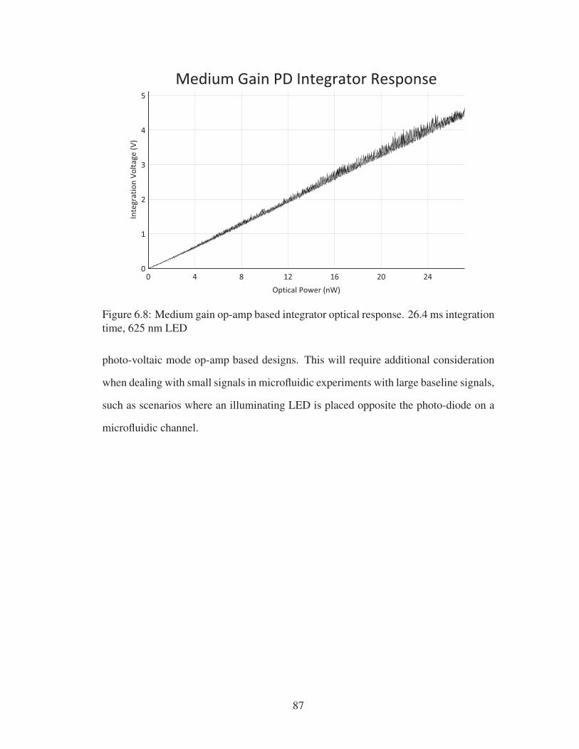
Figure 6.8: Medium gain op-amp based integrator optical response. 26.4 ms integrationtime, 625 nm LED
photo-voltaic mode op-amp based designs. This will require additional consideration
when dealing with small signals in microfluidic experiments with large baseline signals,
such as scenarios where an illuminating LED is placed opposite the photo-diode on a
microfluidic channel.
87

Figure 6.9: Direct integration circuit added as a backup to op-amp photodiod integrator
Figure 6.10: Direct integrator optical response. 26.4 ms integration time, 625 nm LED
88

6.2 Summary
The opto-electronic systems in our LOC ICs have suffered from an instability in
the integration circuitry which required the use of high base-line optical signals for
microfluidic experiments. Two simple fixes to this circuit have been presented and
implemented, and have been shown to correct the original instability present in earlier
chips. Unfortunately, in replacing the original circuits, a design error was made which
prevents use of the optical sensing circuits at the same time as any other system in
either LOC 13 or LOC stable 1. The reason for this is that, due to an inverted reset
line in the integrator circuit, the system clock must be paused for the duration of the
integration period and the analog signal must be read externally. It is left to future work,
for characterization of the corrected optical systems in-circuit with the on-chip ADC,
in an IC with functioning supporting circuits.
89

Chapter 7
Digital Logic
In order to support the analog, HV, and optical systems in our LOC ICs, digital logic
and communication is required. Over the course of my work I have improved upon
the existing digital circuitry and design methods used to facilitate efficient design and
operation of LOC ICs. This includes improvements to the serial peripheral interface
(SPI) communication controller, reducing the IO voltage on interface pins, and a digital
design flow method for running automate place and route around existing analog and
HV subsystems. This chapter should serve as an overview of these changes, the reasons
behind them, and impacts on our LOC systems as a whole.
7.1 SPI Interface
Control and monitoring of our LOC ICs has been handled by a SPI since the project’s
initial conception. This interface has evolved as IC complexity has increased and design
flexibility has become more desirable. Early op-code based SPI circuits have gradually
been replaced by register based designs [5] and internal memory bus [6] with 8 reserved
op-codes and 32 addressable registers. My work on this subsystem has been related
to physical device interfacing, expanding the available address space, and improving
data transfer efficiency. First, I have modified existing 5V input pads to level-shift
90

3.3V input signals to the internal 5V logic voltage used by core logic. The second
modification was to reduce the used op-codes to two: read; and read+write. This
change has also had the side effect of increaseing the address space to 64 bytes. This
would be increased to 128, however, an additional reserved op-code bit is kept only for
legacy’s sake. This may be removed in the future should 128 registers be required or
used for extra op-codes if specialized or single-byte SPI transactions are desired. The
final change is the addition of continuous read/write capability. This allows multiple
registers in a continuous memory region to be read from or written to, by transmitting
a single command and reducing the number of bits required to read multi-byte values
generated by the internal ADCs.
7.1.1 3.3 V IO
As our group has moved from 5V PIC microcontrollers to 3.3V ARM and propeller
based systems, a need for 3.3V logic interfaces has grown. In order to meet this need,
two new on-chip devices must be created: a 3.3V to 5V input level shifting pad; and
a 5V to 3.3V output level shifting pad. In the case of output level shifting, only
schematic level changes are required to allow for multiple power supply nets to be
connected to output driver pads. A 3.3V output pad was created by replacing the fixed
"vdd!" nets on a digital output pad and Vdd supply pad with a net expression which
can be overridden by our 3.3V IO supply. While the ouptut pads themselves may only
require net name changes to enable 3.3 V operation, additional design considerations
must be taken into account when placing these pads in an IC layout. The most obvious
change required, is the separation of the pads IO level Vdd rail from surrounding 5V
core rails, or ground rails in the case of HV pads. The second design requirement
is that of well isolation. In the TDSI process the entire IC is doped with a deep N-
well by default. All low voltage transistors must be placed in this deep N-well with
body connections to Vdd. Since we are defining a new 3.3V IO supply, which will be
91

connected to the deep N-well in our output pads, we must explicitly isolate this well
from the rest of the IC, to prevent our 5V core supply from being shorted to our 3.3V
IO supply through transistor body contacts. This is done by defining an HV-def region
along the inner edge of our IO pads and using HV cut IO cells to separate them from
adjacent cells. This creates an isolated deep N-well which contains our IO pad cells
which will be connected to our 3.3V IO supply.
Figure 7.1: 3.3V IO well isolation used to separate 3.3V IO well from 5V core supply
It is not strictly necessary to modify 5V input pads with a threshold voltage of
Vdd/2 for use with 3.3V input systems. However, adjusting the input threshold voltage
allows for a larger noise margin and reduced power consumption in corner cases where
the 3.3V signal is weakly driven, and the pad, as manufactured has its worst-case
threshold voltage of 2.75V . Early tests using the nominal 5V IO pads driven by
a 3.3V microcontroller resulted in unreliable performance, leading to the pursuit of
a new IO cell design. As this design was not a significant contributor to my thesis
work, and my working knowledge of IC level electrostatic discharge (ESD) protection
circuits is limited, the new IO pad was designed as a modification of the existing 5V
92

IO pad in the TDSI IO library. No changes were allowed which would either modify or
encroach upon the bond pad area, ESD protection structures, or power rails. With these
considerations in mind, the new IO cell was created by simply reducing the width of the
input PMOS transistor until the desired 1.65V nominal threshold voltage was achieved.
This has an expected manufactured threshold range of 1.45V to 1.66V from corner
simulations. Unlike the 3.3V output pads, the 3.3V input pads must be connected to
the 5V core supply internally to enable 3.3 to 5V level shifting. This means that 3.3 V
input pad N-wells must be isolated from 3.3 V output pads but do not need to be isolated
from core logic deep N-wells.
7.1.2 Controller Changes
Internal state and data access in our LOC ICs used a 16-bit SPI interface to a set of
internal 8-bit registers. In previous generations of LOC ICs, each SPI transaction has
been made up of three sections: a 3-bit command code; a 5-bit address; and a 8-
bit data section either sent by the microcontroller host or LOC IC, depending on the
command code received. Starting with Benjamin Martin’s ADC work [6] an interrupt
status register and multi-byte ADC data registers were added to the internal SPI data
bus. In order to more efficiently use the SPI bus with these new registers, two changes
were made to the SPI controller.
Figure 7.2: LOC single register SPI command
The first change made to the SPI controller was to change the two commands from
either read or write, to always read the existing state of a register but conditionally
write to a register. This modification allows for more efficient checking and clearing
93

of interrupts stored in the interrupt status register. This reduces the SPI transactions
required to check which interrupt source was flagged and clear it to a single 16-bit SPI
transaction. The improved single register command, with an added bit of address space,
can be seen in Fig. 7.2.
Figure 7.3: LOC multiple register SPI command
The second improvement to the SPI controller was to reduce the overhead required
to transfer multi-byte ADC data to a microcontroller. In order to reduce the overhead
required to get ADC data from our LOC ICs, an address auto-increment was added to
the controller, which advances the register address between each register accessed after
the first 8-bit command is sent in a single SPI transaction, Fig. 7.3. This allows ICs such
as LOC 13 and LOC Stable 1 to access ADC data in 24 SPI clock periods, rather than
the 32 plus chip-select deassertion and reassertion required by LOC 11. In LOC 12 part
of the ADC decimation filter was implemented in software. This resulted in a 24-bit
per ADC channel, rather than the standard 16-bit values. Starting from LOC 12, ADC
data registers form a continuous memory block allowing the reading of all ADC data
in a single SPI transaction in the case where multiple ADCs have been synchronized.
7.2 Constrained Digital Place and Route
Starting with LOC 12, microfluidic interface placement, increased HV switch counts,
and increased digital logic complexity have prevented the reservation of an unob-
structed rectangular region for the automated placement and routing of digital systems
within our LOC ICs. While a single rectangular region is difficult to find within these
94

Figure 7.4: The digital logic in LOC Stable 1 (left) has much higher silicon areautilization than LOC 11 (right) due to constrained place and route throughout the entireIC
ICs, there is still plenty of room for digital circuits and systems throughout the un-
used space. In order to place and route digital circuits by spreading them out across
all unused space within an IC, several additional factors must be considered. The first
factor is analog and digital power domain separation. With potentially noisy digital
logic spread across the IC, additional care must be taken to isolate sensitive analog cir-
cuits. Each analog region of the IC is placed in a separate deep N-well to isolate it from
digital power supplies and switching noise. Analog devices are protected by isolated
deep N-Wells and photo-diode P-N junctions, which share the common ground of the
IC substrate connection, are insulated from noise with a ring of ground contacts con-
nected to analog ground. A second consideration is HV signal lines which cross the
IC. These lines may cross digital routing layers, however, any unshielded low voltage
transistors which lay beneath a wire held at 300 V could potentially be turned on un-
intentionally. In order to work in this environment I have created a simple power rail
path, placement restriction, and routing restriction export utility, which exports a set
of user-defined restriction layers to an encounter initialization script. In doing this we
can specify the digital pin locations, power ring path, placement blockages, and routing
blockages in the cadence analog layout environment, before running our digital place
95

and route tools. This also gives the benefit of simplifying placement of the final digital
block. So long as no mistakes are made defining the blockage regions, the final syn-
thesized digital design can simply be placed at the origin and expected to line up with
other systems. One caveat to all of this is that any isolated digital regions will need
manual power rail placement, as the current iteration of scripts only supports a single
power rail path.
7.3 Summary
In order to keep up with increasing complexity of our LOC ICs, the digital support
systems and design methods have been improved. Digital inputs and outputs have
been modified to allow for direct interfacing with 3.3V micro-controllers. The SPI
communication controller has been expanded allowing for a larger register address
space, and more efficient access to continuous memory regions. Address space in the
most recent LOC ICs has been increased to 64 and the register access op-codes have
been optimized, allowing for an address space of up to 128 should they be required
in the future. As ADC values are stored in adjacent registers a continuous access
mode was added allowing for ADC reads in a single 24-bit SPI command rather than
the required two 16-bit commands in previous implementations. As the analog signal
sources in our LOC ICs have increased in number, we have added additional control
logic and decimation filters to the on-chip digital logic. In order to accommodate this
increased digital complexity, reserving a single rectangular area for digital place and
route became impractical. A method for exporting existing layouts to digital synthesis
tools for full chip place and route around analog and high-voltage components was
developed. This has significantly increased silicon area utilization in LOC 12, 13 and
LOC stable 1.
96

Chapter 8
Lab-on-Chip Integrated Circuits
I have been working with others in the BIOMEMS research group to create a set of
LOC IC test platforms which can be used with either wafer-level microfluidic layers
or external microfluidic chips. The LOC ICs that follow describe the LOC designs for
which I have played a leading role in development and testing. As the first LOC design
with both working on-chip HV generation systems and optical detection circuits, LOC
11 has been used almost exclusively for microfluidic testing and verification using a
highly integrated LOC IC device. LOC 12, 13, and stable 1 represent incremental
design improvements, and incorporate a higher density of HV circuits and digital logic,
in addition to the HV sensing circuit improvements and optical detection fixes described
in chapters 5 and 6. The sub-circuits in these chips make up a complete tool kit for LOC
IC design.
8.1 Lab-on-Chip 11
8.1.1 Overview
LOC 11 contains necessary circuits required for on-chip CE experiments and on-chip
PCR experiments. These circuits include a 150 μm square photo-diode and integration
97

Figure 8.1: LOC 11 die photo
circuit, located in the centre of the high current contacts for use in on-chip heaters. It
contains an unregulated 300 V charge pump and 7 HV switches. These can be used for
CE experiments and electrostatic valve test structures. The high current switch in LOC
11 is designed for a maximum current of 300mA at 5V , or a maximum heater power of
1.5W . LOC 11 contains a single ADC, which can be connected to either: HV systems;
heater systems; or photo-diode, through and internal analog multiplexer. ADC signals
are provided for reading the voltage on the: HV supply; current flow through the HV
switch return path; temperature sensing through a dedicated sense resistor; external 5
V analog signals; or internally integrated light intensity received by the photo-diode.
98

Figure 8.2: LOC 11 block diagram. External interfaces denoted by dotted lines
8.1.2 Microfluidic Interface
While LOC 11 was designed with greater flexibility in mind, a number of factors
have restricted the number of microfluidic designs available for on-chip fabrication.
LOC 11 was designed before the testing of the initial set of electrostatic valve test
structures had been completed. When LOC 11 was developed, it was expected that
the electrostatic valves would require only a grounded top plate and a switched bottom
plate from 0 - 300 V. As such, LOC 11 has three electrostatic valve plates, located
in-line with the designed location of a PCR chamber (heater contacts), but has no
method for controlling the top plate of these values. Due to charge trapping discovered
during early testing of these electrostatic membranes, it is necessary to reverse their
polarity to prevent significant shifts in valve actuation voltages. LOC 11 can be used for
electrostatic valve tests involving PCR-only experiments, however, as the CE channel
electrodes must be used to drive the top valve plates in microfluidic layers.
99

Figure 8.3: LOC 11 system-level block diagram
Figure 8.4: LOC 11 electrical connections
A second issue in LOC 11 is a missing wire in the design which connects the
photo-diodes located in the bottom right-hand corner to their corresponding integration
circuits. These photo-diodes were intended to give LOC 11 the ability to run both PCR
and CE experiments on the combined microfluidic-CMOS chip. As LOC 11 stands
currently, it must be configured for PCR or CE only on-chip microfluidic structures.
8.1.3 HV
LOC 11 contains both an on-chip 300 V charge pump, and HV switched and digital
logic required to run a boost converter for higher current applications. Regulation of
the HV supply on LOC 11 is accomplished through the use of an external Zener diode,
100

Figure 8.5: LOC 11 proposed on-chip CE microfluidic layout
Figure 8.6: LOC 11 proposed on-chip PCR/qPCR microfluidic layout
forming a shunt regulator for use in either charge pump or boost converter based modes
of operation. The static HV switches in LOC 11 are biased, using a tap on the 600 MΩ
resistive network used to sense the HV supply voltage. Due to the linear nature of this
circuit an isolated 5 V supply must be used to properly bias the HV switches, when
operating outside of the nominal 150 - 200 V HV supply range.
8.1.4 Optics
LOC 11 contains a single photo-diode and integrator circuit, capable of reading optical
signals with 16 programmable ranges from 3.79 nW - 125 μW. Optical range is set
by adjusting the integration time from 800 ns to 26.4 ms on a log2 scale. That is,
the integration time equals 2n × 800 ns where 0 ≤ n ≤ 15. Due to an op-amp
stability issue, integrated values less than 1/2 the full scale range of the ADC may
101

not convert properly, resulting in large baseline signals being required to operate the
optical detection systems on this IC, as discussed in section 6.1.1.
8.1.5 Heater Control
LOC 11 is designed with on-chip microfluidic PCR chamber heating and sensing in
mind. The heater is controlled by an 8-bit PWM signal capable of driving a 5V
heater with up to 1.5 W of power. Sensing can be accomplished by using the thermistor
circuits discussed in section 5.2. In LOC 11, the thermistor configuration requires an
external bias current. The microfluidic contacts and pad bonding of LOC 11 allow for
direct connection of external signals from a PCB through the IC packaging and on-chip
routing to microfluidic structures manufactures on a microfluidic-CMOS chip.
8.1.6 External Electronics
Figure 8.7: USB powered test system
One of the main design goals of this LOC platform was to minimize the supporting
hardware required to run LOC systems. To this end, all essential electronic systems
required for our genetic analysis experiments have been incorporated onto a single
CMOS chip. The system board shown in Fig. 8.7 represents a complete set of
102

electronics required to run genetic tests directly coupled to LOC 11’s surface. In order
to run CE experiments a microfluidic device must be placed in direct contact with the
surface of LOC 11 or be optically coupled through the use of an optical relay[22]. This
microfluidic chip must then be coupled electrically though either exposed bond pads on
the surface of the LOC IC or externally through bond wires to the HV and heater control
systems. A minimally populated functional board contains only voltage regulation
circuitry, USB-serial conversion, a microcontroller, and LOC 11 itself, however this
could be reduced to an SPI intreface found in the SD card specification for future high-
volume designs. Additional support circuitry includes crystal oscillators for precision
timing, trim pots for optimal circuit calibration and an external inductor and diode for
boost converter operation when greater than 3 mW of power is required from the HV
supply. All internal and support circuits for LOC 11 have been designed to consume
a combined power less than the 200 mW which is significantly less than the 2.5 W
afforded by the USB 2.0 specification and fits within the 330 mW afforded to low-
speed SD devices.
8.1.7 Experimental Verification
LOC 11 is the only IC fabricated as part of my research which has had microfluidic
structures coupled to its surface and verified through an electrophoresis experiment.
This verification was preformed by Gordon Hall, who used the internal charge pump
and optical detection circuits to run the experiment at 70V through a microfluidic
channel optically coupled to the IC’s surface using a GRIN lens [22], Fig. 8.8. The
electropherogram in Fig. 8.9 shows a successful separation of a 436 base pair PCR
product from primer remaining from amplification. More details on the experiment can
be found in [22, 47].
103

Figure 8.8: Side view of LOC 11 and microfluidic chip used to produce experimentalresults in Fig. 8.9. Here, LOC 11 is used to both read the optical signal and generatethe excitation voltage used to separate the genetic samples in the microfluidic channel.
Figure 8.9: Electropherogram produced using LOC 11’s charge pump based HVgeneration and integrated optics. From [23]
104

8.2 Lab-on-Chip 12
8.2.1 Overview
Figure 8.10: LOC 12 die photo
Figure 8.11: LOC 12 microfluidic design for sample prep + PCR + CE tests
LOC 12 was designed to allow for greater flexibility of microfluidic designs, when
compared to the previous generation, LOC 11. It adds support for several of the new
subsystems developed since the production of LOC 11. To this end LOC 12 has a larger
footprint, with carefully placed micrfluidic interfaces to electrical signals, electrostatic
105

Figure 8.12: LOC 12 electrical connection interface
valve plates, and photo-diodes. LOC 12 has a 3.6 x 7.0 mm area within it’s pad-frame
for microfluidic structures. Additionally, all of the HV switch channels, "LS 0-27",
on the bottom left-hand corner of Fig. 8.12, can be left unbonded and be covered by
microfluidic structures in situations where the connections between external fluids and
pneumatics cannot be made within the pad frame.
LOC 12 contains HV control, sensing, and regulation systems for running CE
experiments and driving electrostatic valves. High current switching circuits were
re-designed to allow for higher current heater designs and more flexibility, allowing
surface-bonded microfluidic heaters to contain either even or odd track group counts.
The analog design was changed to allow for simultaneous reading of optical signals,
HV potentials, and HV currents, with separate interrupt status bits accessible through
the SPI interface. Due to the higher data throughput requirements, and the common
operation of reading three sequential SPI registers to read ADC values, the SPI
controller was improved to allow for multiple sequential register reads, or writes, in
a single SPI command. Magnetic coils were added for on-chip magnetic bead capture
intended for sample preparation. Electrostatic valve slew rate limiting was implemented
106

to reduce the impacts of valve switching on the required holding force of the magnets.
LOC 12 contains the same optical detection photo-diodes and integration circuitry as
found in LOC 11.
8.2.2 Microfluidic Interface
Figure 8.13: LOC 12 microfluidic design for CE-only experiments
Figure 8.14: LOC 12 microfluidic design for qPCR/PCR + CE tests
This LOC 12 IC platform was designed with three microfluidic configurations in
mind for surface bonded microfluidic devices. These step up in complexity from: single
107

CE experimental verification, Fig. 8.13; to a microfluidic-CMOS running both PCR
amplification followed by a CE test, Fig. 8.14; though the final full-integration stage,
running everything from sample-preparation to final detection on the IC’s surface,
Fig. 8.11. In the figures shown, all valving is handled using electrostatic valves,
which are currently under development. For experiments using existing structures with
proven microfluidic devices these valves are replaced with pneumatic valves, additional
actuation connections, and microfluidic channels. All designs have space left in the
bottom-most microfluidic layer for routing of pneumatic microfluidic channels, and the
PCR + CE design has space left to add the two additional pneumatic connections for
valve actuation on the pad frame. In the case of the sample-prep + PCR + CE design,
additional silicon area must be reserved for pneumatic microfluidic connections outside
the pad-frame.
8.2.3 HV Channels
LOC 12 contains 30 HV channels which can be accessed from the surface of the IC
by microfluidic structures, 28 of which can be accessed externally through pin bond
pads. Of these 30 HV signals: 4 are connected to large electrode pads, formed by
all metal layers, for use in CE capillary channel excitation; 17 are connected to small
microfluidic contacts within the pad frame, and will be used to energize the top-plate of
future electrostatic valves; and the remaining 17 are connected to circular valve plates
at the top of the IC metal layer, and will be used to form the bottom plate of electrostatic
valves.
All LOC 12 HV channels are driven by dynamic RC HV switches discussed in
section 4.1.1. The CE electrode channels have a set of static HV switches connected in
parallel with the dynamic RC HV switches, for use in lower voltage, high current CE
experiments. The HV switches not in use are held in the Hi-Z state so as not to interfere
with microfluidic device operation.
108

An electrostatic valve slew rate limiting circuit was implemented in LOC 12, as
calculations indicated that valve switching could disturb magnetic beads trapped by the
sample-prep magnetic coils [12]. This limit was implemented by a global HV-switch-
enable pulse signal, which affects all but the CE electrode HV channels. This generates
a 100ns pulse every time a counter reaches zero, at which point the counter is reset
to a programmable value, and decrements by one every 100ns. When enabled, HV
channels 4-29, 0-3 being CE electrode channels, are only driven to the state configured
by their control registers during the enable pulse. At all other times they are held in
hi-Z.
As with LOC 11, LOC 12 uses a resistive network to bias the static HV switches
used to drive the CE electrodes. Due to the bias voltage sensitivity issue discussed in
section 4.0.2, it is recommended to override this bias voltage with a fixed isolated 5V
supply maintaining a voltage VHV Bias = VHV Supply − 5V .
8.2.4 HV Generation
The 300 V charge pump on LOC 12 has a defect which causes catastrophic failure
after ≈40V is reached. Due to this issue, LOC 12’s charge pump is not capable of
generating the HV supply voltage required to drive electrostatic valves and CE channel
excitation voltages internally. Fortunately LOC 12 was designed to be capable of
running external charge pumps using internal regulation circuitry, with its own internal
charge pump disconnected from the circuit. Due to this design, feature HV generation
can be accomplished by connecting LOC 12’s HV-sense transistor based regulation
signal to the enable pin of a 20MHz oscillator, driving the charge pump in test chip
22 from the same IC batch. While the cause of LOC 12’s charge pump failure has
yet to be conclusively determined, the failure at ≈40V is suspiciously close to the
specified breakdown voltage of the thin oxide in poly-poly capacitors. This suggests
that somewhere in the IC an active region was placed on one of the HV capacitors,
109

resulting in a non-300V tolerant component.
8.2.5 HV Regulation
LOC 12 contains the HV-sense transistor regulation design discussed in section 3.2.
This circuit has been tested using an external charge pump (T22). The charge pump
drive signal is controlled by a gated clock controlled by LOC 12’s regulation output
signal, which is driven by the internal DAC and comparator, sensing the HV-sense
transistor current.
8.2.6 HV Sensing
Like LOC 11, LOC 12 contains a resistive voltage divider for HV potential sensing,
and a transimpedance amplifier connected to the source of the low-side HV-NMOS
switch drivers for current monitoring. In addition to the resistive HV potential sensing,
the HV-sense transistor current can also be sensed through a separate transimpedance
amplifier allowing finer software controlled HV feedback and regulation using these
circuits. Unfortunately, the dynamic RC switches used in LOC 12 do not use the proper
HV-NMOS device for low-side current monitoring, resulting in current leakage through
the substrate. This signifcantly attenuates HV current readings.
8.2.7 Heater Control
LOC 12 contains a redesigned heater switching circuit, to allow for higher current
microfluidic devices. This switch is designed for up to 4A peak and 900mA continuous
operation. In order to accommodate this higher current a 20 cm width transistor was
designed with each heater connection, Vdd, Vss, and Vdrain, bonded through 3 parallel
bond pads rated for 300mA each. This circuit was intended to be used in direct heater
element sensing applications. The heater switch in LOC 12 is capable of driving a
110

heating element with a modified PWM signal which contains a 300ns fixed current
sink, followed by a fixed 100ns off period. This phase of opperation overrides the last
400ns of the regular 10-bit 9.77 kHz PWM signal. The fixed ’off’ period allows for
external circuit synchronization with the heater PWM signal, allowing for pseudo 4-pt
measurements relying on voltage measurements and fixed current drivers. However,
a design error in the combination analog signal mux and sample and hold circuit in
the on-chip heater logic, prevents the use of the internal ADC with the synchronized
sample an hold logic.
8.2.8 Analog to digital converter
1 ��� �� � ��2 ��� �� � ��3 ��� � � ��45 ��� ���� ����� ���� ���6 �7 ��� � ���� � ���8 ��� � ���� � ���9 ��� � ��� � ��
1011 �� � ����� �� �� �� � ��������12 ������ ����13 �� � ��� � �������� �� � � �� ���������� ! ���1415 �� � ���� " � ����� �� �� � ��#�����16 ������ ����17 �� � ��� � �������� �� � � �� ���������� ! ���1819 � � ���� " � ����� �� �� � ��$�����20 ������ ����21 � � �� � ������� �� � � � ���������� ! ��2223 %��%� ��� " � ���� �� � � �������24 &
Listing 8.1: Second half of decimation filter software implementation not implementedin hardware
LOC 12 contains three functional ADC circuits based on Benjamin Maritn’s design,
used in LOC11. However, in order to save layout area, the decimation filters required
were combined into one, time interleaved digital filter. Additionally the low-speed
subtraction circuits were pushed to software, Fig. 8.1, leaving only the 1.25MHz
accumulation circuits for implementation on-chip. These remaining circuits were then
time-interleaved, pushing the clock frequency up to 1/2 system clock frequency, or 5
MHz, using multiplexed registers and a 2-bit counter. The ADC data is only valid after
a minimum of three sequential values have been read, and software filtered from a given
ADC channel. After this, each successive call to decimate() with new ADC data will
111

return a valid ADC value. In Fig. 8.1, intermediate values are stored as global variables.
When reading multiple ADC channels these must be unique per channel.
8.3 Lab-on-Chip Stable 1
8.3.1 Overview
Figure 8.15: LOC Stable 1 die photo
Figure 8.16: LOC stable 1 proposed on-chip PCR + CE microfluidic layout
112

LOC stable 1 was the first LOC IC designed with no new experimental features
added. The systems in LOC stable 1 include: the charge pump from T22; 17 dynamic
HV switches from LOC 12; HV supply regulation circuits from LOC 12; and the
heater switch from LOC 12. While the goal was for no new circuits to be added,
several previous circuits contained bugs, requiring significant redesigns. The photo-
diode integration circuit from LOC 11 was modified in an attempt to fix the op-amp
stability issues, and an additional simplified integrator was added in case of continued
failure of the first design. The heater switching analog acquisition circuitry was re-
designed, using a differential input ADC from LOC 11, and synchronized sample and
hold circuitry. A temperature sensor was added, in the form of a metal masked PN
junction, to compensate for the temperature sensitivity of the HV supply regulation
circuitry. Implementation details of this circuit can be found in section 5.3.
8.3.2 Microfluidic Interface
Figure 8.17: LOC stable 1 electrical connections
LOC stable 1 was designed with PCR and CE experiments in mind, as sample
preparation was deemed to be to experimental for the first stable IC. These experiments
can be designed to both fit on the same microfluidic chip, or be placed separately by
removing the unneeded channels.
113

8.3.3 Optics
The optical systems on LOC stable 1 contain both modified integration circuits from
LOC 11 and a simplified direct integration circuit. Unfortunately, the integration reset
line inside the IC was inverted, which prevents optical signals from being read by the
LOC IC’s internal ADC. A work-around is described in appendix B. This requires
the use of external ADCs and a halt of the system clock during the integration period.
When using this IC for CE or qPCR experiments, the heater and HV systems cannot be
used for the duration of photo-diode integration. This will requires that tests be tolerant
of ms time scale interruptions in both HV signals and thermal regulation.
8.3.4 HV
LOC stable 1 contains 17 HV switches. 5 of these switches control electrode plates on
the IC’s surface and have higher current ratings, due to doubled up high-side drivers
on the dynamic RC HV switches. The remaining 12 switches are connected to valve
plates and microfluidic contacts for valve top-plates, and will be used to actuate future
electrostatic valve devices. When running CE experiments on this system, it will be
necessary to add capacitors to the separation electrodes and HV supply. The act of
running the photo-diode integrator work-around will shut down the charge pump and
put the dynamic RC HV switches into high impedance mode for the duration of an
integration period. Decoupling capacitors must be added in large enough values to
prevent excessive voltage dips on either the HV supply or channel potential, over the
duration of the integration period.
8.3.5 Heater Control
As with LOC 12, LOC stable 1 contains a high current PWM controlled heater switch,
and synchronized current sinking circuit. This system is designed to operate at a
114

maximum current of 600mA, and can handle peak currents of 4A, provided the bond-
wires and packaging have been designed to support this. LOC stable 1 can sense heater
temperature through either, the direct element method discussed in section 5.2.2, or
through the current sink DAC and thermistor proposed in section 5.2.1. As with other
systems, care must be taken when using the photo-diode integration method in appendix
B, as the heater’s PWM will pause during the integration phase. If the thermal mass
of the heater system is insufficient to tolerate a heater stuck on for this period it is
advisable to disable the heating system before running a photo-diode integration phase
when running qPCR experiments. Simply setting the heater PWM value to 0 may not
be sufficient for this, there is a risk of having the heater stuck at the sensing current
value. This may or may not be an issue, depending on the microfluidic device under
test.
8.4 Lab-on-Chip 13
8.4.1 Overview
Figure 8.18: LOC 13 die photo
LOC 13 was designed to be a sister-IC to LOC stable 1. It contains all of
the functionality of LOC stable 1, with added experimental devices and microfluidic
115

interfaces. The HV switches in LOC 13 have been replaced with the buffered dynamic
HV switches, as opposed to the previously tested RC drivers in LOC stable 1. These
switches offer full high-side drive strength, while maintaining much of the layout area
savings from static HV switch designs. In order to support these switches, a negative
5V charge pump, referenced to the HV supply, was added to allow for a fixed high-side
reference. The 300V charge pump in LOC 13 was divided into two separate sections,
which can be externally connected in series or parallel. This supports high-current
lower voltage operation when larger microfluidic channel cross sections are desired in
CE tests. The magnetic coils in LOC 12 were not included in LOC stable 1 as these
were deemed an experimental microfluidic device, with no existing test structures built
to date. In LOC 13 these coils were added, in addition to 8 more electrostatic valve
plates with corresponding top-plate connections and HV channels. This is to allow for
testing of reagent mixing and pumping in future on-chip microfluidic devices.
8.4.2 Microfluidic Interface
The microfluidic interface to LOC 13 is very similar to that of LOC stable 1. All of
the microfluidic interfaces on LOC stable 1 also exist in the same location, relative to
the heater pads in LOC 13. The only difference in the common microfluidic interfaces
is the increased drive strength of HV switches, when sourcing current from the HV
supply. In cases where this supply voltage is generated externally, each channel is
capable of sourcing up to 1mA of current, up from the 60μA of LOC stable 1. Where
the physical interface differs is in the addition of a row of 8 electrostatic valve plates,
and 2 magnetic bead trapping coils along the right-hand side of the IC (as viewed with
the charge pump in the bottom-left corner). These interfacing devices are intended to
be used to test microfluidic pumping structures, magnetic bead trapping, and to provide
additional inlet valves for on-chip reagent mixing. These interfaces have been arranged
in a line with equal centre-centre spacing of 424μm, and the magnetic coils dividing
116

the valve plates into two groups of 2 and 6. This makes full use of the edge of the IC,
allowing as much flexibility to future designs as possible. At the time of this writing
there have been no experimental microfluidic layouts planned for testing on LOC 13.
8.4.3 Optics
The optical systems on LOC 13 contain both modified integration circuits from LOC
11, and a simplified direct integration circuit. Unfortunately, the integration reset line
inside the IC was inverted, which prevents optical signals from being read by LOC
13’s internal ADC. A work-around is described in appendix B. This requires the use
of external ADCs and a halt of the system clock during the integration period. As with
LOC stable 1, when using this IC for CE or qPCR experiments, the heater and HV
systems cannot be used for the duration of photo-diode integration. This will require
that tests be tolerant of ms time scale interruptions in both HV signals and thermal
regulation.
8.4.4 HV - Switching
LOC 13 contains 33 HV switches, 5 of these switches control electrode plates on the
ICs surface. The remaining 28 switches are connected to valve plates and microfluidic
contacts for valve top-plates, and will be used to actuate future electrostatic valve
devices. When running CE experiments on this system, it will be necessary to add
capacitors to the separation electrodes and HV supply. The act of running the photo-
diode integrator work-around will shut down the charge pump, and will leave the
buffered RC HV switch’s high-side gates floating. Decoupling capacitors must be
added in large enough values to prevent excessive voltage dips on either the HV
supply or channel potential over the duration of the integration period. The buffered
RC HV switches in LOC 13 are biased, using an internal high-side -5 V charge
pump. This charge pump will also be disabled during photo-diode integration. An
117
external capacitor should be added between VHV Supply and VHV Bias, such that a 10 μA
current will not cause a significant drop in voltage over the course of the photo-diode
integration period.
8.4.5 HV - Generation
LOC 13 contains a reconfigurable 300 V charge pump. The charge pump is split into
two parts, which can either be connected in parallel or series, for either: 150 V, 20 μA;
or 300 V, 10 μA operation. The output pump driving circuitry has been decoupled from
the raw charge pump signals, allowing for experimentation using > 5 V pump signals
or inductive drivers, to boost the charge pump efficiency. This circuit is intended for
use with an external signal buffer, and will not function properly with the charge pump
output signals tied directly to the pump input clock signals.
8.4.6 Heater Control
As with LOC 12, LOC 13 contains a high current PWM controlled heater switch, and
synchronized current sinking circuit. This system is designed to operate at a maximum
current of 600mA, and can handle peak currents of 4A, provided the bond-wires and
packaging have been designed to support this. LOC 13 can sense heater temperature
through either the direct-element method discussed in section 5.2.2, or through a current
sink DAC and thermistor proposed in section 5.2.1. As with other systems, care must
be taken when using the photo-diode integration method in appendix B, as the heater’s
PWM will pause during the integration phase. If the thermal mass of the heater system
is insufficient to tolerate a heater stuck on for this period, it is advisable to disable the
heating system before running a photo-diode integration phase when running qPCR
experiments. Simply setting the heater PWM value to 0 may not be sufficient for this,
as there is a risk of having the heater stuck at the sensing current value which may or
may not be an issue, depending on the microfluidic device under test.
118
Chapter 9
Conclusions
9.1 HV Systems
Throughout my research, which has predominantly focused on HV circuit design and
systems-level integration, I have helped to advance the electrical instrumentation of
LOC devices intended for miniaturized PCR and CE experiments. To the best of
my knowledge this has produced the first fully integrated 300 V charge pump which
requires no components external to the IC to operate. This charge pump meets and
exceeds our target power output of 3 mW or 10μA and 300 V output, and is capable of
producing 60μA at the lower design voltage of 50 V. HV regulation and control systems
have been implemented and improved from previous generations of LOC devices.
Improvements on HV switches have reduced IC layout area of these devices to 50%
of their former implementations, while simultaneously eliminating all DC paths from
the HV supply to the low voltage supply in the control signal logic of high-side HV
switching circuits. This control signal improvement has removed power constraints
placed on the HV supply which formerly limited the number of active HV switching
circuits that could be powered by an integrated charge pump. The combination of
control signal changes and layout area improvements has allowed for a doubling of
119

the number of HV switches that can be placed in a single LOC IC. This allows for
LOC designs capable of controlling both valve plates of future electrostatic valves. By
doing so we compensate for charge trapping problems encountered in experimental
electrostatic membranes. A novel HV sensing device has been proposed, which is
capable of regulating the internal charge pump’s output voltage, while reducing the
layout area occupied by the sensing device from 478500μm2 to 5800μm2. While
this device is capable of regulating far faster, and without consuming current on the
HV supply, it introduces new temperature and process dependencies, which must be
calibrated and compensated for during use.
9.2 Meeting Evolving Design Targets
In addition to the HV circuit design work, there have been several systems within
our LOC devices which have required updating and/or correction, due to evolving
design requirements and uncovered circuit issues. The optical sensing systems were
re-designed to eliminate dead zones seen on previously fabricated ICs. While the
dead zone elimination was successful, an inverted digital signal has prevented the
use of these circuits with the internal ADC circuits. This has limited the sensitivity
of existing fabricated circuits by introducing noise into the reset state, and requiring
external capture of the analog signal. Die temperature sensing circuits have been
implemented and tested as a compensation device for novel circuits, with relatively
high thermal sensitivity. On-chip heater control logic is an area of research which
has had many design iterations over the course of my involvement in this project. In
order to accommodate a larger range of microfluidic heater designs for both wafer-
level and stand-alone microfluidic devices, the LOC heater control circuits and PWM
circuits were updated. The heater control switch maximum continuous current was
increased from 300 mA to 1 A by increasing the switching transistor width and gate
120
driver strength. The PWM digital logic was also changed to increase the original 8-
bit PWM controller to a 10-bit PWM controller. This was done to maintain the same
attainable output power resolution, over a wider range of heating device resistances.
In addition to the increased switch drive strength and PWM resolution, the heater
element resistance sensing method was changed. The original from a current mirror and
sampled transimpedance amplifier was changed to a programmable current sink and 4-
pt element sense circuit, reducing the contact resistance and external wiring effects on
element resistance readings.
9.3 Serial Interface
In addition to minor improvements and adjustments to the digital logic in our LOC
designs, the SPI controller has been redesigned for more efficient reading and writ-
ing to sequential registers. Since LOC 12, our LOC devices have contained multiple
ADCs and interrupts. In order to accommodate the additional data generated by these
devices, particularly in LOC 12, the SPI interface was changed to support continuous
reads/writes of sequential SPI registers. This change increased the maximum through-
put of 24-bit, 3x8-bit register reads from 13.12 k reads/s to 18.5 k reads/s at 1 MHz SPI
frequency. This frees up additional bandwidth for other systems, while running all 4
ADC circuits simultaneously.
9.4 Digital Synthesis
It has been my role in recent years of this project to run systems-level layout and digital
synthesis on LOC IC design iterations. As both microfluidic and digital logic designs
have increased in size and complexity, new tools were developed to aid in defining
the boundaries between manual placement of analog systems, microfluidic interfaces,
and automated place and route of digital logic. These tools have allowed our LOC
121

IC designs to move away from reserving a rectangular area for digital systems, where
no devices or routing wires may cross. In designs from LOC 12 onward, routing and
placement blockages, as well as pin placement, are exported from the manual analog
and microfluidic interface designs. The digital synthesis tools we use, are now able
place digital logic in all unused sections of the IC. This has allowed for much greater
flexibility in microfluidic interface placement and increased digital logic density.
9.5 Future Work
9.5.1 PCR Demonstration
We have designed high-current switches and measurement circuitry intended to drive
micro-PCR heaters, and the algorithms required to produce uniform hearer layouts
for arbitrary microfluidic structures [45, 11, 15].In the future, a single microfluidic-
CMOS chip, containing both a PCR chamber and heating electronics, as well as a CE
channel for experimental verification, may be produced to verify such designs as a fully
integrated solution.
9.5.2 Electrostatic Valves
In addition to PCR applications, one possible major improvement in microfluidic chip
design is the addition of electrostatic valves. Many of our more recent ICs have
been designed with lower plates and contacts within the pad frame, for use with such
microfluidic devices, bonded directly to the surface of our LOC ICs. Preliminary work
has been done to demonstrate the feasibility of such MEMS designs with reduced
layer count microfluidic stacks bonded to test ICs. This has shown proper deflection
at voltages compatible with our demonstrated ICs. Should these valves be perfected,
our group has pursued some preliminary work towards on-chip sample preparation,
122

involving valve mixing and activated magnetic bead capture on an LOC IC’s surface.
9.5.3 Magnetic Bead Capture
Since LOC 12 we have included magnetic coils with SPI control on our IC designs.
These coils are intended to be used for the capture of magnetic beads used in sample
preparation. While simulations and large scale experimentation have been done [12],
IC-scale designs and characterization have yet to be completed. The addition of on-
chip magnetic bead capture has the potential to increase the concentration of a target
sample before amplification using on-chip PCR, greatly increasing the sensitivity of
such devices.
9.5.4 On-Chip Microfluidic Structures
One of the driving goals of this project is to bring all electronics and instrumentation
onto a single device. The final goal is to have an IC platform with: microfluidic devices
patterned directly on its surface, miniaturizing the final stages of sample preparation;
amplification using PCR; and detection using CE down to a single microfluidic-
CMOS chip. While research into these microfluidic devices has been on-going and
miniaturized test structures have been produced and tested [11, 48], none of these
microfluidic devices have been patterned and tested on a functional LOC IC. Work
has been done by Gordon Hall [22] to simulate fluidic structures in direct contact
with LOC ICs, and allow for rapid iteration of fluidic prototypes, however, combined
CMOS/microfluidic devices will remain a long-term goal, due to the high cost and low
turn-around times of CMOS manufacturing processes.
123

Bibliography
[1] K. H. Lee, S. Choi, J. O. Lee, J. B. Yoon, and G. H. Cho, “CMOS capacitive
biosensor with enhanced sensitivity for label-free dna detection,” in 2012 IEEE
International Solid-State Circuits Conference, pp. 120–122, Feb 2012.
[2] A. Gonzalez-Guerrero, J. Maldonado, S. Herranz, and L. Lechuga, “Trends in
photonic lab-on-chip interferometric biosensors for point-of-care diagnostics.,”
Analytical Methods, vol. 8, no. 48, pp. 8380–8394, 2016.
[3] A. Hassibi, R. Singh, A. Manickam, R. Sinha, B. Kuimelis, S. Bolouki,
P. Naraghi-Arani, K. Johnson, M. McDermott, N. Wood, P. Savalia, and
N. Gamini, “4.2 a fully integrated cmos fluorescence biochip for multiplex poly-
merase chain-reaction (pcr) processes,” in 2017 IEEE International Solid-State
Circuits Conference (ISSCC), pp. 68–69, Feb 2017.
[4] G. V. Kaigala, M. Behnam, C. Bliss, M. Khorasani, S. Ho, J. N. Mcmullin,
D. G. Elliott, and C. J. Backhouse, “Inexpensive, universal serial bus-powered
and fully portable lab-on-a-chip-based capillary electrophoresis instrument,” IET
Nanobiotechnology, vol. 3, pp. 1–7, March 2009.
[5] A. M. Hakman, “CMOS single photon avalanche photodiodes and digital control
interface for lab-on-chip DNA analysis systems,” Master’s thesis, University of
Alberta, June 2015.
124

[6] B. R. Martin, “CMOS instrumentation for genetic analysis lab-on-a-chip,” Mas-
ter’s thesis, University of Alberta, Jan 2012.
[7] W. A. Al-Haddad, “High voltage CMOS devices and systems for lab-on-a-chip
applications,” Master’s thesis, University of Alberta, Nov 2010.
[8] S. Ho, “VLSI design and system integration for a USB genetic amplification
platform,” Master’s thesis, University of Alberta, May 2012.
[9] M. Behnam Dehkordi, Miniaturized Genetic Analysis Systems Based on Micro-
electronic and Microfluidic Technologies. PhD thesis, University of Alberta, 2010.
[10] M. Khorasani, “Mixed signal design of a high voltage (HV) CMOS integrated
circuit for microfluidic applications,” Master’s thesis, University of Alberta, 2008.
[11] J. Martinez-Quijada, S. Caverhill-Godkewitsch, M. Reynolds, L. Gutierrez-
Rivera, R. Johnstone, D. Elliott, D. Sameoto, and C. Backhouse, “Fabrication
and characterization of aluminum thin film heaters and temperature sensors on
a photopolymer for lab-on-chip systems,” Sensors and Actuators A: Physical,
vol. 193, no. 0, pp. 170 – 181, 2013.
[12] S. A. Caverhill-Godkewitsch, “Modeling of integrated microfluidics-CMOS lab-
on-chip technology,” Master’s thesis, University of Alberta, Nov 2015.
[13] J. Martinez-Quijada, Design and Microfabrication of Robust and Highly Inte-
grated Thermal Lab-On-A-Chip Polymeric Systems for Genetic Diagnosis. PhD
thesis, University of Alberta, 2014.
[14] M. Reynolds, “Development of KMPR-based microfluidic structures for use in
LOC systems,” Master’s thesis, University of Alberta, 2014.
[15] J. Martinez-Quijada, S. Caverhill-Godkewitsch, M. Reynolds, D. Sloan, C. J.
Backhouse, D. G. Elliott, and D. Sameoto, “Deterministic design of thin-film
125

heaters for precise spatial temperature control in lab-on-chip systems,” Journal
of Microelectromechanical Systems, vol. 25, pp. 508–516, June 2016.
[16] L. Blanes, W. K. T. Coltro, R. M. Saito, A. Van Gramberg, C. Lucio do
Lago, and P. Doble, “High-voltage power supplies to capillary and microchip
electrophoresis,” ELECTROPHORESIS, vol. 33, no. 6, pp. 893–898, 2012.
[17] G. E. Collins, P. Wu, Q. Lu, J. D. Ramsey, and R. H. Bromund, “Compact, high
voltage power supply for the lab-on-a-chip,” Lab Chip, vol. 4, pp. 408–411, 2004.
[18] D. Erickson, D. Sinton, and D. Li, “A miniaturized high-voltage integrated power
supply for portable microfluidic applications,” Lab Chip, vol. 4, pp. 87–90, 2004.
[19] M. Behnam, G. V. Kaigala, M. Khorasani, P. Marshall, C. J. Backhouse, and D. G.
Elliott, “An integrated CMOS high voltage supply for lab-on-a-chip systems,” Lab
Chip, vol. 8, pp. 1524–1529, 2008.
[20] L. Shen and K. Hofmann, “Fully integratable 4-phase charge pump architecture
for high voltage applications,” in Proceedings of the 19th International Confer-
ence Mixed Design of Integrated Circuits and Systems - MIXDES 2012, pp. 265–
268, May 2012.
[21] M. Khorasani, M. Behnam, L. van den Berg, C. J. Backhouse, and D. G.
Elliott, “High-voltage CMOS controller for microfluidics,” IEEE Transactions on
Biomedical Circuits and Systems, vol. 3, pp. 89–96, April 2009.
[22] G. H. Hall, D. L. Sloan, T. Ma, M. H. Couse, S. Martel, D. G. Elliott,
D. M. Glerum, and C. J. Backhouse, “An optical relay approach to very low
cost hybrid polymer-complementary metal-oxide semiconductor electrophoresis
instrumentation,” Journal of Chromatography A, vol. 1349, pp. 122 – 128, 2014.
126
[23] D. L. Sloan, B. Martin, G. Hall, A. Hakman, P. Marshall, S. Martel, C. Backhouse,
V. Gaudet, and D. G. Elliott, “HV-CMOS single-chip electronics platform for lab-
on-chip DNA analysis,” in 2016 IEEE International Symposium on Circuits and
Systems (ISCAS), pp. 2427–2430, May 2016.
[24] S. S. Mohan, M. del Mar Hershenson, S. P. Boyd, and T. H. Lee, “Simple accurate
expressions for planar spiral inductances,” IEEE Journal of Solid-State Circuits,
vol. 34, pp. 1419–1424, Oct 1999.
[25] D. L. Sloan, G. H. Hall, C. J. Backhouse, and D. G. Elliott, “300 v integrated
charge pump for lab on chip applications,” in 14th IEEE International Conference
on Nanotechnology, pp. 939–942, Aug 2014.
[26] J. F. Dickson, “On-chip high-voltage generation in MNOS integrated circuits
using an improved voltage multiplier technique,” IEEE Journal of Solid-State
Circuits, vol. 11, pp. 374–378, Jun 1976.
[27] R. Zhang, Z. Huang, and Y. Inoue, “A low breakdown-voltage charge pump based
on cockcroft-walton structure,” in 2009 IEEE 8th International Conference on
ASIC, pp. 328–331, Oct 2009.
[28] J. F. Richard and Y. Savaria, “High voltage charge pump using standard CMOS
technology,” in The 2nd Annual IEEE Northeast Workshop on Circuits and
Systems, 2004. NEWCAS 2004., pp. 317–320, June 2004.
[29] K.-H. Choi, J.-M. Park, J.-K. Kim, T.-S. Jung, and K.-D. Suh, “Floating-well
charge pump circuits for sub-2.0v single power supply flash memories,” in
Symposium 1997 on VLSI Circuits, pp. 61–62, June 1997.
[30] L. Zhou, W. Huang, T. Zhu, and M. Liu, “High voltage sensing based on fiber
fabry-perot interferometer driven by electric field forces,” Journal of Lightwave
Technology, vol. 32, pp. 3337–3343, Oct 2014.
127
[31] N. A. F. Jaeger and H. Kato, “The use of integrated optics mach-zehnder
interferometers in high-voltage sensing,” in Proceedings of Canadian Conference
on Electrical and Computer Engineering, pp. 946–949 vol.2, Sep 1993.
[32] D. A. Horsley, N. Wongkomet, R. Horowitz, and A. P. Pisano, “Precision
positioning using a microfabricated electrostatic actuator,” IEEE Transactions on
Magnetics, vol. 35, pp. 993–999, Mar 1999.
[33] M. Lemkin, “A 200-v high-voltage amplifier using a parasitic field-oxide transis-
tor for voltage feedback,” IEEE Journal of Solid-State Circuits, vol. 38, pp. 1730–
1734, Oct 2003.
[34] S. R. Udatha, A. Ruhela, G. Saravanavel, V. Yaswant, J. Singh, and S. Sam-
bandan, “Design optimization of thin-film transistors based on a metal-substrate-
semiconductor architecture for high dc voltage sensing,” IEEE Transactions on
Electron Devices, vol. 63, pp. 1696–1703, April 2016.
[35] M. Khorasani, L. van den Berg, P. Marshall, M. Zargham, V. Gaudet, D. Elliott,
and S. Martel, “Low-power static and dynamic high-voltage CMOS level-shifter
circuits,” in Circuits and Systems, 2008. ISCAS 2008. IEEE International Sympo-
sium on, pp. 1946–1949, May 2008.
[36] Z. Liu and H. Lee, “A 100V gate driver with sub-nanosecond-delay capacitive-
coupled level shifting and dynamic timing control for zvs-based synchronous
power converters,” in Proceedings of the IEEE 2013 Custom Integrated Circuits
Conference, pp. 1–4, Sept 2013.
[37] J. Buyle, V. D. Gezelle, B. Bakeroot, and J. Doutreloigne, “A new type of level-
shifter for N-type high side switches used in high-voltage switching ADSL line-
drivers,” in Electronics, Circuits and Systems, 2008. ICECS 2008. 15th IEEE
International Conference on, pp. 954–957, Aug 2008.
128

[38] P. Favrat, L. Paratte, H. Ballan, M. J. Declercq, and N. F. de Rooij, “A
1.5-V-supplied CMOS ASIC for the actuation of an electrostatic micromotor,”
IEEE/ASME Transactions on Mechatronics, vol. 2, pp. 153–160, Sep 1997.
[39] D. Pan, H. W. Li, and B. M. Wilamowski, “A low voltage to high voltage
level shifter circuit for mems application,” in University/Government/Industry
Microelectronics Symposium, 2003. Proceedings of the 15th Biennial, pp. 128–
131, June 2003.
[40] F. Richard, B. Lessard, R. Meingan, S. Martel, and Y. Savaria, “High voltage
interfaces for cmos/dmos technologies,” in IEEE Northeast Workshop on Circuits
and Systems 2003, June 2003.
[41] Z. Huang, Y. Savaria, and M. Sawan, “A dynamically controlled and refreshed
low-power level-up shifter,” in Circuits and Systems, 2004. MWSCAS ’04. The
2004 47th Midwest Symposium on, vol. 1, pp. I–97–100 vol.1, July 2004.
[42] Z. Liu, L. Cong, and H. Lee, “Design of on-chip gate drivers with power-
efficient high-speed level shifting and dynamic timing control for high-voltage
synchronous switching power converters,” Solid-State Circuits, IEEE Journal of,
vol. 50, pp. 1463–1477, June 2015.
[43] T. Andersen, M. Andersen, O. Thomsen, M. Foster, and D. Stone, “A capacitive
level shifter for high voltage (2.5kv),” in Power Modulator and High Voltage
Conference (IPMHVC), 2012 IEEE International, pp. 450–453, June 2012.
[44] J. Garcia, J. Montiel-Nelson, and S. Nooshabadi, “High performance bootstrapped
CMOS dual supply level shifter for 0.5v input and 1v output,” in Digital System
Design, Architectures, Methods and Tools, 2009. DSD ’09. 12th Euromicro
Conference on, pp. 311–314, Aug 2009.
129

[45] J. Martinez-Quijada, T. Ma, G. H. Hall, M. Reynolds, D. Sloan, S. Caverhill-
Godkewitsch, D. M. Glerum, D. Sameoto, D. G. Elliott, and C. J. Backhouse,
“Robust thermal control for CMOS-based lab-on-chip systems,” Journal of
Micromechanics and Microengineering, vol. 25, no. 7, p. 075005, 2015.
[46] E. Ghafar-Zadeh and M. Sawan, “A hybrid microfluidic/CMOS capacitive sensor
dedicated to lab-on-chip applications,” Biomedical Circuits and Systems, IEEE
Transactions on, vol. 1, pp. 270–277, Dec 2007.
[47] G. Hall, T. Ma, M. Couse, S. Hume, D. Sloan, D. Elliott, D. Glerum, and
C. Backhouse, “An automated hand-held cmos-based instrument for hand-held
mutation detection via electrophoresis,” in Nanotechnology (IEEE-NANO), 2014
IEEE 14th International Conference on, pp. 8–12, Aug 2014.
[48] M. Reynolds, A. Elias, D. G. Elliott, C. Backhouse, and D. Sameoto, “Variation
of thermal and mechanical properties of KMPR due to processing parameters,”
Journal of Micromechanics and Microengineering, vol. 22, no. 12, p. 125023,
2012.
130

Appendix A
Heater Design and Visualization Code
1 ����� �����2 ����� ����� ����������������34 ������ ���������5 �6 ����� ����� � ���� ��������� ��7 ����� ������ � ���� ����� ��������� ���89 ������ ������ ��������
10 �11 ������ ����� ����12 ������ ����� ! ����13 ������ ����� "�14 ������ ����� #��������15 ������ ����� ����$�16 ������ ����� %���$�17 &1819 ������ ����'�� (")���20 �21 ����� ��#����"*����� +, ����� �,22 ����� -���$ , ����� $��$�.�23 &2425 ������ ������ ����� /����������26 �27 00 ����� �������� $��� ����� '�� "'���� 1���� ������28 00'�� �� -���$2 �, 3�����2 4, �$�#�������2 �$�0�5��� ,29 00 ������2 � , ��� ������$2 �� " 3���� ������ '��30 00 ("'��� ����� � �� %���� *%.31 00 6����$ ����� �� � ����� �����������32 00 63����� , �������� , ��� ��-� ����� ��� ������� �����33 00 ��������� -$� �������34 ������ ������ ������ ���������������*35 (")��� 5)��� , ����� �����%���$ , ����� �����4����� ,36 ����� �$�#������� , ����� $���#����� ,37 ����� ��������$.38 �39 07 ����� ��������� '�� �������� $� ��$ ����� ��40 7 ������� �� � ��������� �' ����� '�� ���*�� !.41 7 �� �����*�+ !.�42 7043 ������ ������ � �- ������ *.�4445 ��� ����� ���� �46 *���.8��$� �����*$���#����� 7 9 0 �����%���$.�47 00'��� ����� ����� �� ��$� �� �' $���48 ����� ����� ����:�� � *����� ���� 6 ;. 7 �����%���$ 0 9�49 00 ����� �$����$ ��$ �����50 '�� *����� ����� ��� � 6����� ����:���51 ����� ��� � $���#������52 ����� ����:�� <� �����%���$.53 �54 00 ���� ���� ��������� ��������� ������ �����55 ����� ����� � �- �����*.�5657 00 ������� ������ +������ ����� ��%���$ 0 9 '�� $���58 �' *����� ��� �� 6$���#�����.59 ��������6061 00)��� ����� �� �������62 ����� �����!8�+ � 8��$��5��*$���#����� 7 $���#����� 663 ����� ��� 7 ����� ��� .�64 ����� �����!8�� � 6�����!8�+�6566 00)��� ����� ����� " ��� #�������67 ����� �����" � 5)������#����"*68 ����� ��� 6 �����%���$ 0 9, �����!8�� ,69 �����%���$ , �����!8�+ 6 �����!8��.�70 ����� �����# � �����4����� 7 �����4����� 0 �����"�7172 00 ����� �$����$ ����� �����
131

73 ��� ������ ��� ���� � ��� �����74 ��� ���� � ��� ���� � �������� � ��75 ��� ���� � ��������!76 "77 ����� �����#������� � ���$����78 �������� % ��� ���� � ��� ����!�79 �� ��� ����� ����� � �� �� ���80 ������� �� ��� !81 �� ���� ���� �������� &�82 ��� ���� � �������� � �!83 "84 �������� � ��� ���� � ��� �����85 '8687 ������ ���� (% )������ % ��� *���88 ����� ��( � +,���$-)����(�89 ��� .��/ � ��� 0��� � �% ��� ���� %90 ��� 0��� % �����#�������!�91 ����� ��) � ��� ) 1 ��( � ��� (�92 ����� ��0��� � ��)������ �93 ���) 1 �����#�������!�9495 ����� ���� � ����� ��� 96 ��� $2����* 3��#��� �!97 "98 /.�� � ��� .��/ %99 �.�� � ��� ���� �����#������� � �%
100 ( � ��( %101 )������ � ��) %102 ���� � �����#������� %103 0��� � ��0���104 '!�105 '106107 ����� ����� ��� � ��� ��������108 ��� �$2������ !�109 '110111 ���� ��� ��112 '113 '114 '
Listing A.1: Basic layout generation of circular heaters
1 ����� #4���2 ����� #4��$.��������$-�����34 ������� 3��5����5 "6 ����� ���� � ��� �3��#��� &�7 ����� ���� � � ��� ���� �3��#��� &&�89 ����� 6��4��� � ��� �6���5 &�
10 ����� 6��4���� � ��� ���� �6���5 &&�1112 ������ ���� 3��#���13 "14 ������ ����� /.���15 ������ ����� �.���16 ������ ����� (�17 ������ ����� )�������18 ������ ����� �����19 ������ ����� 0����20 '2122 ������ ���� 6���523 "24 ������ ����� /�25 ������ ����� ��2627 ������ 6���5������ �% ����� 4!28 "29 ���$/ � �� ���$� � 4�30 '31 '3233 ������ ���� ����� 7����3��8�����34 "35 �� -���� � � �� ���4���� ��� �� �� �� ����� �� ���� *�� ����36 ������ ���� 6��4���� .��9�3����6��4��������� � ���!37 "38 6��4���� ���-���4 � �* 6��4���� �!�39 ��� ��� ��� :��� � ;� ��� :��� � ���$.���� ��� :��� !40 "41 ���� ��������� � ���<��� :��� =�42 6��4��� ��� -���4 � �* 6��4��� �!�43 3��#��� ����#��� � ��������� <;=�44 ����� ���� ���4��� ���� �� � �� ���� ����� �� � ���� ��� ����45 ��� -���4$2����* 6���5�46 ����#���$/.�� ����#���$0��� � �%47 ����#���$�.�� � ����#���$���� � �!!�48 �� ��� ������ ���� ���� ��� �� ��� ���� �� � ����49 ��� ��� � � ;� � � ��������� $.���� � !50 "51 3��#��� ���� � ��������� <�=�52 ����� ����� ������ ���4��� � ���� 4 ���� �� ���� ��� ��53 ��� -���4$2����* 6���5�54 ����$/.�� ����$0��� � �%55 ����$�.��!!�56 '57 ����� �� ��� � ���4���58 3��#��� ���#��� � ��������� <��������� $.��� � >=�59 ����� ���� ���� ��� ���� �� ���� � ���4��� �� �� ����60 ��� -���4$2����* 6���5�61 ���#���$/.�� ���#���$0��� � �%62 ���#���$�.�� ���#���$���� � �!!�63 ��� -���4$2����* 6���5�
132

64 ��������������� � ��������������� � ��65 ��������������� � ��������������� � ����66 �� ���� ��� �� ���� ���� ��� ���� �� � ��� � �� ����� �� ��!67 �� "�� � # �� ��$ ������� � %� � &# '� ����68 (69 )���� ������ ������ # �� ��$ ���*�+�70 ����� !���� ����� !��,�� �� ������ , ���� � � ���� ���� ����71 � ���-����� ,.��"�/ 0���1"72 ����������� � ����������� � ��73 ����������� ���74 275 ����� ���� !��� �� ��� ��! ���� �� ��� �� �� ������76 � ���-����� ,.��"�/ 0���1"77 �� ������������� � �� ������������� � ��78 �� ������������� � �� ������������� � ����79 ����� � ��� !��,�� �� ����� !��,�� ���80 ����� -����� ,.��"� ���-����� ,��81 282 ��� ����� -����� ,�83 284 285 2
Listing A.2: Exporting heater geometry for further processing
1 ���� �,�����2 ���� �,��������������-�� ���3 ���� �,������3�4 ���� �,����$�4��5 ���� �,����$� �����$�����6 ���� �,����56�78 ����!��� )���� 1����9 (
10 ���� 0��,�� # ���� 70���1 &�11 ���� 0��,��� # ���� 7���� 70���1 &&�1213 !� ��� �� ��� 0���114 (15 !� ��� ��� �� ��16 !� ��� ��� �� ��17 21819 !� ��� ����� ���!��1�820 (21 ��$��� ��� �� /�� �������� � �� 1�9�� � $���� 1�8:��� �� � ,22 �� 6 ����� ������� ���/23 �� ################################################################24 ����9� �������� ��� � �� �.1 ����� ���� , ��������� ��� �����25 �� ! ����� 6��!�� 1�8 ����� � ��� ��, , ���� ���� ��� �� ����26 �� � ���� � ���!�� -;5 �� ����� ���� �� ��� ��� ��� ������ , �27 ����� �4!� � �� ������, �� � <�4�< ���� /���� �� � �� ���28 �� ��!!� ��� , ���� �.1 ����/� � �� �9� ���� ����� ����/� �2930 ��$��� 1�8 ��� ���� ��� �� ���� /�� � ����� , 1�9�� � $���� �31 ��,�� �� ������ �� �� �������=>����� $�� 9� �� ��� ���32 ���! � ��� 1�8 ����� � � �, !� ���� ! ��� ���� $��33 �� 9� �� ��� �� � ������ , � �� 9�� ��� ������� �� �,34 ��1�8 ���� /���� /�� ��9�� /��� ,�� ���� �� ! ��� ���� .��� �35 ���, ��������� ������ , �� � ����� �� ���� ���� � ��� �� � ��36 ��� ������ , � �� 9�� ��� 1�8 ���!�� �� �, �.1 ����/� � ����37 �� ��!!� �� 1�8 ����� -��� ���� �� ��9� �� 38 �� ################################################################3940 ! �9��� �� �� ?��,$�4��41 ! �9��� �� �� ?����?��,�42 ! �9��� �� ?����5��4�4344 !� ��� ����� 1������� # %'��4546 !� ��� �� �� ��,� �4748 !� ��� ���!��1�8 "�49 (50 ?����5��4 # '�51 ?��,$�4� # <<�52 ?����?��, # <<�53 ��,� # <@.<�54 25556 !� ��� 9��� .��"0��,��� ������ ,�57 (58 �� "�� � # '� � 7 ������ ,����� ����59 (60 ����.��"������ ,*�+��61 262 26364 !� ��� 9��� .��"0��,�� ������ ,�65 (66 �� A # ������ ,�����67 �� �� *+ ���� # �/ �� ��*A � B+�68 ���� *'+ # <06���5ACD ED< � ��,� � <D FFD %D'<�69 �� � # '�70 �� "� # '� � 7 A� ����71 (72 ����*� � %+ # <GCH$C�D ED< � ��,� � <D %'D < �73 ������ ,*�+�$��� �� "� � <D �'D < �74 ������ ,*�+�$��� �� "� � <D'<�75 276 ����*A � %+ # <GCH$C�D ED< � ��,� � <D %'D < �77 ������ , *'+�$��� �� "� � <D �'D < �78 ������ , *'+�$��� �� "� � <D'<�7980 ����*A � �+ # <�CICA1D ED< � ��,� � <D'D<�81 ?��,$�4� �# �� ��@��"<D<� ������82 283
133

84 ������ ��� ��� ��85 �86 ������������ � ���87 �8889 ������ ��� � ������ ��� ����90 �91 �� ��� �� !"#$%����� � �����92 �� ��� &' �� !"# � �����93 ((���� � ��� ���� �� ���94 �� !"#$%����� � �����)��� * ���������+)��� *95 ���������+��� * ���������+#���� *96 ��������)��� * ������������ *97 ��������#���� * �����#���� �98 ((����� ��� ���� �� ��� �� �,� �� ������ �� ����� �� ���99 �� !"# � �� !"#$%������-�����.,.��
100 -� ��/� ��� �� � ��0 -� ��/� ��� � �����101 � ���� � � 1� � 2� �� !"#�3����� 4 5� �**�102 �103 ���� ���3������ !"#&�'��104 �105 ������� ���106 �107108 � ����� �� ��� )��� 109 �110 ���111 �112 �� ��� &' )- � �113 � 1, -6�7%8, 9, )6:!6;, <�=114 �>::!?6;, 5, :511<, <�=115 �>78-�:-6, 51,1�1, 91,1�1, @1,1�1, <�=116 �>6"�A78, 51, 1, 91, 1, @1, 1, <�=117 �>6"�A:", 51,@BC, 91,@9B, @1,1�1, <�=118 �>37AA78, 51,1�1, 91,1�1, <�=119 �>37AA:", 51,511�1, 91,511�1, <�=120 �>%;�)%A%!6, D1, 5, <�=121 �>!7A-:36, E1,� * !�/-���� * �, <�=122 �>!7A-�F36, 9, -�:8!:;!, <�=123 �>#7336�;:!, E1,1�1, <�=124 �>G-3�-:36, D1, 5, 1�=125 �68!-6, 1�=126 �-6�7%8, 9, �:�36-, 1�=127 ��:�36, 9, ?G%;�, D1, 9, 1�=128 �?G%;�, 9,H :�7?6, D1, 1�=129 � 51,1�1, 91,1�1, 55,5�1, 95,5�1�=130 � 59,I1�1, 99,I1�1, 5@,1�1, 9@,1�1�=131 � 5E,5�1, 9E,5�1, 5I,1�1, 9I,1�1�=132 � 5B,1�1, 9B,1�1, @B,5�1, 5D,1�1�=133 � 9D,1�1, @D,1�1, E1,511�1, E5,5�II�=134 � E9,I1�1, E@,1�1, EE,1�1, I1,1�1�=135 � I5,1�1, D5, 1, D9, 511, D@�=136 � 5, DE, 5, DI, 1, DB�=137 � 1, DD, 1, DC, 1, 1�=138 �68!�:�, 1�=139 ��:�36, 9, 3�FG6, D1, 5, 1�=140 �3�FG6, 9, %8�78J%J-, D1, 1�=141 � @,-��� 3���, D9, BI, D@�=142 � 1, E1,1�1, 1, 68!�:�, 1�=143 ��:�36, 9, 3:F6;, D1, @, 1�=144 �3:F6;, 9,1, D1, 1, B9, D, B�=145 �%8�78J%J-, 1,3:F6;, 9�=146 3��� * �, D1, 1, B9, D, B�=147 �%8�78J%J-, 1,3:F6;, 9, !6#G%78�-, D1�=148 � 1, B9, D, B, %8�78J%J-, 1�=149 �68!�:�, 1�=150 ��:�36, 9,?76�, D1, 1, 1, 68!�:�, 1�=151 ��:�36, 9, !7A-�F36, D1, 5, 1�=152 �!7A-�F36, 9, -�:8!:;!, D1, 1, @,�=153 � E,, I,, B,, D,, E1,5�1, E5,1�59I�=154 � E9,1�1E, E@,1�9I, EE,1�59I, EI,1�1, EB�=155 �1�1, ED,1�1, EC,1�1,5E1,1�59I,5E5,1�1B�=156 �5E9,1�1,5E@,9I�E,5EE,5�1,5EI,1�1,5EB,5�1�=157 �5ED,1�1<, D5, 1, D9, 1, D@, 5�=158 � DE, 5, DI, 1, DB, 1, DD�=159 � 1, DC, 1,5D1, 1,5D5, 9�=160 �5D9, 1,5D@, 1,5DE, 1,5DI�=161 � 1,5DB, 1,5DD, 1,5DC, 1�=162 � 1, 68!�:�, 1�=163 �68!-6, 1,�164 ��165 ��� � �� ����K�����,�= )-��166 �167 �168 � ����� �� ��� ����+)��� 169 �170 ��� � ��� � �-6�7%8, 9, �3%L-, 1,�� �171 �172 � ����� �� ��� ����+#���� 173 �174 ��� � ��� � �68!-6, 1,�� �175 �176 � ����� �� ��� ���)��� 177 �178 ��� � ��� � �-6�7%8, 9, 68�7�76-, 1,�� �179 �180 � ����� �� ��� ���#���� 181 �182 ��� � ��� � �68!-6, 1,�� �183 �184 � ����� �� ��� #���� 185 �186 ��� � ��� � �6%#�� �187 �188 �189 �
Listing A.3: Code used to export heater geometry for use in CAD tools and simulation
134

environments.
135

Appendix B
Reading Photodiodes in ST1 and L13
LOC stable 1 and LOC 13 have an inverted reset line in their photo-diode integration
circuits. This design error prevents an IC from being able to read optical signals from
one of its internal ADCs. If one of these ICs is not used for other tasks, a pair of
external ADCs and careful control of the system clock can be used to capture internally
integrated optical data. In order to capture this data ST1 or L13 must be configured
send the PD integration output to its analog output pin and its clock source must be
set to use an external clock signal. Full control over ST1’s system clock is critical for
proper extraction of optical signals. In order to use this signal we must first understand
that the internal integration and ADC circuits when properly configured and enabled
run periodically with a fixed system clock cycle count between integration windows.
Secondly, even in the case of an inverted reset line there exists a state where reset is
held low and integrate is held high.
Our first task is to find this integration window. To do this will need two pieces
of information. The first is the integration window start period and the second is an
expected output value that differs from the reset state. For the first piece of information
a vhdl simulation with integration period set to minimum gives use an integration start
period of 40960 system clock cycles (integration period register set to 0). In order to
136

Figure B.1: LOC stable 1 photo-diode digital signalling error
Figure B.2: LOC stable 1 photo-diode analog signal routing
find and synchronize our external logic with this integration start value we need to be
able to read a signal from the on-chip photo-diode to distinguish this phase from other
phases in the integration circuitry. Thus a light source must illuminate photo-diode to
be tested for initial set-up. A second property of the integration circuitry helps us with
this search.
While the simplest method for finding the integration window would be to advance
the system clock by one cycle, wait for integrator saturation, and check to see if the
analog output has reached the opposite rail from reset. This method is incredibly
slow as it is convenient to allow ambient light to be used for the timing calibration
source. Ambient light saturation of the on-chip integrator in the VLSI lab in the
evening requires milliseconds which would require a few minutes to scan all possible
40960 states. One property of the integration logic that helps us in this regard is that
the integration with an inverted reset line holds the integrator in its integration state
137

for roughly 1/16th of the integration window period. Knowing this we can check 16
positions evenly spaced across the 40960 possible clock cycles and do a binary search
between the transition from reset state to saturated state to find the clock cycle which
starts the integration window. When allowing 0.5 seconds for PD saturation in very low
light conditions this aligns the integration window in ≈10 s.
While this gets us to the point of reading signals from a photo-diode there are two
more steps that must be taken to read actual values. First integration times must be
handled externally as the internal sample and hold circuitry is misaligned with the
inverted reset integration window. And secondly, since the IC is not reset properly
before integration the initial value read by an external ADC may be noisy. This requires
two samples to be taken to allow for correction of the correlated noise source.
Figure B.3: Signalling used by external ADC in LOC stable 1 photo-diode valueconversion
The solution chosen was to use a pair of MCP3202 serial ADC chips and time
the integration period with the sample and hold windows of these chips. In order
to get precise timing of the external ADCs and ST1 integration window a propeller
chip was used. Three cores were used to run ST1’s system clock and the two ADC’s
independently. ST1’s system clock is controlled in a 2 instruction loop which is called
before ADC execution to align ST1 to the clock cycle before integration begins. Both
ADC cores run identical code. The first ADC core is configured to run the zero
checking ADC and advance ST1’s system clock one clock cycle when the ADC sample
and hold clock edge is reached. The second ADC core is configured to control the
integration end ADC. The propeller chip contains a globally accessible system counter
running at full clock speed (80MHz) and each core has a wait instruction which will
138

Figure B.4: Propeller-chip core synchronization during LOC stable 1 photo-diode read
wait until a clock this counter reached a specific value before continuing. By using this
counter it is possible to precisely synchronize two cores with or offset the execution
timing in increments of 1 / 80 MHz or 12.5 ns, provided no system memory instructions
are called which must wait for hub synchronization. Using this method and timing the
ADC serial communications by instruction counting precise integration periods can be
achieved by staggering the wait values of the zero crossing and final integration ADC
cores. Zero crossing and ST1 integration synchronization is achieved by writing the
GPIO states of both the ST1 clock and the ADC serial clock in the same instruction on
the same core.123456789
1011121314151617181920
139

21 ���22 ���� ���� 23 ���� ��24 ���� ���2526 ��� ��������������2728 ���� �� �29 ��� �� �������3031 ���� �������� �� � ��� � � � ��� �� � ��� ��� � ���������32 ������!��������"#�����$���� � ���"%&��������3334 ��'� �������� �' � ��� � ' � ��� �' � ��� ��' � ���������35 ��'���!�������'"#�����$���� � ��'"%&��������3637 �������� �� � (( ��������3839 �)� �� *�)� 40 �� �� ����+�*� ��� � ��41 ������ +&�� �)� (, �4243 ��� ������������������44 ��� �� �������4546 ��� ����������47 ������ ���4849 ��� �������������������� - � � � �����50 ������� �.��51 � � �� �� / '�����52 ������������� � � �����53 ��'���������� � / ��������������� � �����5455 ! ���� �� ������ �56 ����� �� ��'�!� &����� . ����!� &�����57 �� �58 ����� �� ����!� &����� . ��'�!� &�����59 ������ �����60 ��'��� �����61 &!���� �'�6263 ������ �����6465 ��� �����&� - �����66 ! �& �� ��67 �������������� / ������ � !�� ��68 ������ ����!� &�����69 �� �! �& �� ��70 ��'����������� / ������ � !�� ��71 ������ ��'�!� &�����72 �� �73 ������ .�7475 ��� ��%����&��!)� �76 �)� �� &��!)� 77 ������ +&�� �)� (, �7879 ��� ��������&��!)�� - �����80 ������ +&�� �&��!)� �, ���������� 0 '�81 &��!)� .� ���������� 0 '82 ������ +&�� �&��!)� ( ��83 &��!)� /� ���������� 0 '8485 ����� �� &��!)� . ���� 8687 ! ������ ( ��88 ��%�������������� 0 ' / ������89 �� �90 ��%����������91 ���� �� &��!)�9293 ��� &!���� �&��!)� �94 ���� /� &��!)� 95 ������ +&�� ����� �, ���������� 0 '�96 ���� .� ���������� 0 '97 ������ +&�� ����� ( ��98 ���� /� ���������� 0 '99
100 ��� ���!���� - �� � �� ��� � ��� �'� ����� � 101 1��� �� � �! ����� ��!� ������ 102 ������� ���103 ������� ���104 ������ !�� � �� �2105 �� �� 0 ���������� 0 ' 3 �4106 �� ��� �� � / �� 0 ���������� 0 ' 3 �4107 �� �� 5����� �108 �' �� 5����� ����109 ! ����� ��� ��� �'�110 &!���� �.�� ����111 6��112 ����� �� ���������� 0 ' 3 �4113 ������ +&�� ����� , �114 ! � 5���.�������115 &!���� �������116 ����� �� ����� 3 '117118119 �� 5����� �120 ���������� �121 +������� / 7� ���������122 ! ���� �� ������ �123 ������ ���� ��� , '���124 �� �125 ������ ���� ��� ( '���126127128 ���129 � ���130 ���131
140

132 ��� ����� �133 � ���� ����� ������134 ��� �� � �����������135136 ���������137 ����� ����� ������ ��138 ���� ��� ���������139140 ����������� �� ���� ������ ���� � � !� �����141 "� ���� �����������142 ���� ����� ����������� 143144 � ���� ����� ������145 ��� ���������146147 ����������� ���� �148149 ������ ���� �150 ����� �� �151152 ���
Listing B.1: ST1 Clock generation and external ADC synchronization logic
1 ���23 #����������� � $%�����4 #������� � $�%����5 #���&����� � $��%���6 '(����� � $���%��7 )!����� � $����%�8 �&���������� � $�����%9
10 '������(���� � � ��11 *���� ������ � �����1213 )+������� � �����14 )+������% � � ��1516 ,��� ��&�,�� � �����17 ,��� ��&�-�� � � ��1819 �� 20 ���� ����21 ���� �����22 ���� ��� ������23 .&�� ���2425 ��. ��� �/������ ������� ������� ������. ����������026 �)��� 1� 2����27 ���� 1� 3%28 �*��� 1� 2�����29 ����� 1� 3%30 �'�� ������ 1� 2��� ������31 ������� 1� % 44 ������32 �������� 1� % 44 �������33 �������� 1� % 44 �������34 �������. 1� % 44 ������.35 �����5)���� 1� % 44 ����������3637 ��� 1� ������/2������� � �038 ����� �+��� ���� �� 3% ����� �� ��� �� ����������3940 ��. ������/��� ������� �������041 ��� ������ 1� ��� �������42 �� /�������043 ���� 6� �&����������44 ����45 ���� 7� 8�&����������46 ���� 6� #�������4748 ��. �����+� ���49 ����� �+��� /���� 7 #�������0 49 �50 ��� � �����5152 ��. ������� �/'(�*:;; )+������,��� ��&053 �� /'(�*:;;054 ���� 6� '(�����55 ����56 ���� 7� 8'(�����5758 �� /)+������,��� ��&059 ���� 6� )!�����60 ����61 ���� 7� 8)!�����6263 ��. ��������64 ���� 6� #�����������6566 ���67 ������� �68 � �6970 ����� ��� ��� � ����71 ��� ������ #���&�;���72 � ���� ������ �)���73 �������� � ����74 ��� ��������.����� �������.75 � ��������.����� �������76 � �� � ��������.�����77 � �� � ��������78 � �� � �����5)����7980 ���������81 ����� ������ �)���82 ��+��� �� ��� ����83 ��� ������ #����������� � ��84 ���� ��� ��������� ��85 ���� ������ #�����������
141

86 ������ ����� �����87 ��� ��� ����������88 ��� ���������89 �����������90 ������ � ������91 �� ����� ������� � �� ��92 ��� ��� ���������93 ����� �� ������� ��� �� ��94 �� ����� �� ��� � �� ��95 ����� � ������� �!96 �� ����� ��"��� � �� ��97 ����� �"������� �!98 �� ����� ��#�������� � �� ��99 ��� ��$ ������ �%
100 ���� ��$ ������ ����������101 ���� �� �#�� ��� &���� ��� ���������� ����� ��� ����'102 ������ ��� ��� ������103 ���� ()�104 � �� ����()�105 ������ �� ���106 �� ����� ��� �#��� �107 ��� ����� ������� �108 ������ ����� �����109 ��� ���������110111 ���()�112 � ���� ��� � ������113 � ����� ���*114 ��� ��� �������+�����115 �� ��� ������116117118119 ������ ,�����-�������� �120 � ���� ��� � ������121 ���122 ���123 ������ ���� ������� �� ���# . ���������� ���� � �124 �� ��� ������125126 � ���� ��� � ������127 ��$ ��� � ������� ��128 ����� ��� ������129 ��� ��� ������130131132133 ��� ���� ������134 � ���� ��� � ������135 ���136 ���137 �� ��� ������138139 � ���� ��� � ������140 ��$ ��� �"������� ��141 ����� ��� ������142 ��� ��� ������143144145146 � ���� ��� � ������147 ���148 ���149 �� ��� ������ ��� �� �-� � �� �������150151 � ���� ��� � ������152 ���153 �� ��� ������154 ��� ��� ������155156157158 � ���� ��� � ������159 ���160 ��$ ��� ��� 161 �� ��� ������162163 � ���� ��� � ������164 ���165 �� ��� ������166 ��$ ��� ��� �� ��� �-� $ ��� �� �� �� ����� ��� &+��� ����� ��� ��
� ����'167168169170 ����� +�171 � ���� ��� � ������172 ���173 ���174 �� ��� ������175176 � ���� ��� � ������177 ���178 ���179 ��� ��� ������180181 ��$ +����� �!.182183 �� ������184 � ���� ��� � ������185 �� ������ � �� ��186 ��� � � �!187 �� ��� ������188 ����� � � �!189190 � ���� ��� � ������191 ���192 ���193 ��� ��� ������194 ���� +����� ��� ������195 �� ����������
142

196197 ������� ��� ��� ���198 ��� ���� ���� ��199 ������ ���� �����200 ���������� �� �201 �� ���� ��� �� �202203204205 ������ ��� ���206207208209 ��� ��� ���� �210 ��� �� � ���� �211 ��� ���� ���� �212 ��� ���� ���� �213214 ��� !� ��� ���� �215216 ����� ���� �217 ����� ���� �218 ������ ���� ���� �219220 ��� ��� ���� "� ��� ������������221 ���� �� ���� #���� ����222223 �$ ������ ���� �224 �% ������ ���� �225226 ������ ��� �227228 ���� ��� �229230 ��� �� ��� �231232 ��� ��� �233 ��� ��� �234 ���� �� � ��� ��� �235 ��� ��� ��� �236237238 ���
Listing B.2: ST1 ADC interface with precise timing control. Synchronizes ST1’s clocksignal with external ADC sample and hold window
143

Appendix C
System PCBs
C.1 Lab-on-Chip 11 System Board
Figure C.1: LOC 11 system-board connectors
144

C.1.1 Power Configurations
USB Powered
USB powered mode is selected by switching the power select switch towards the USB
label on the board. In this mode the positive terminal on the DC barrel jack is isolated
from the rest of the system and all board functions are powered from the mini-USB jack
on-board. The supply voltage on the expansion connector is regulated to 7V from the
USB supply. It is possible to draw more current than allowed by the USB spec through
this rail so testing should be done when power requirements get close to 2.5W.
Figure C.2: LOC 11 system-board power select
DC Barrel Jack
To power the board from the DC barrel jack switch the supply select switch to the
"Ext" position and connect a dc supply to the Barrel jack on the edge of the board.
The polarity of the jack is ground on the outer ring and positive on the inner pin. The
ground of both the Barrel jack and USB connections are common so care must be taken
when connecting to both a lab power supply and computer. make sure the ground on
the power supply is earth ground. I have found that keeping the PC and Power supply
on the same power bar can significantly reduce noise in the circuit. In this configuration
supply voltage on the expansion header is connected directly to the DC input voltage
on the barrel jack.
145

Figure C.3: LOC 11 system-board DC barrel jack
Through Expansion Header
The DC Barrel Jack configuration can also be used to provide power from an expansion
board to the LOC 11 System board. Configure the board as in DC Barrel jack powered
configuration leaving the barrel jack unconnected. An expansion board must then
provide a 6.5 - 12 V supply voltage on the supply pin of the expansion header.
C.1.2 High Voltage Source Configurations
Charge Pump
To configure the board to use the charge pump as the HV source first place a jumper
on the HV Supply header connecting the "Vpp" pin to the "CP Vpp" pin. This supply
is regulated on-board to 300 V. To change the regulation voltage connect an external
zener diode to the pink "Level Shifter 6/Vpp" 3.5 mm connector through a 4 terminal
3.5mm cable. The zener diode should connect with Vpp and Vss on the nearest to tip
and tip contacts respectively on the cable.
Figure C.4: LOC 11 system-board HV configuration
146

Boost Converter
The boost converter is selected by placing a jumper on the HV source header connecting
the "Boost_Vpp" pin to the "Vpp" pin. See Charge pump for regulation.
External Supply
An external supply can be used by removing any jumpers on the HV source header and
connecting the external supply to the pink "Level Shifter 6/Vpp" 3.5mm jack. Similarly
to the DC power supply grounding care should be taken insure the ground on the HV
supply is the same as the USB ground as well as any other supplies connected directly
to the common ground.
C.1.3 3.5 mm HV Connection Usage
Each 4 contact 3.5mm jack on the left hand side of the board contain two level shifter
or HV power signals and two ground connections. the ground connections are on either
end of the jack and are intended to reduce the risk of ESD failures on the unprotected
LOC 11 level shifter outputs. In order to reduce the risk of ESD issues each contact
must brush the outer most ground terminal on the jack when inserting a 3.5mm plug.
Care should be taken to slide the plug along the edge closest to the board expansion
header when inserting into a HV jack to insure contact with the ground terminal is
made on every insertion.
C.1.4 Expansion Header
The expansion header can be used to connect to external SPI devices, send commands
to the arm processor on-board, power external devices, or power the LOC 11-ARM
System board. The Command RX and TX connections follow the exact same command
protocol as the USB-serial interface.
147

Figure C.5: LOC 11 system-board HV insertion method
C.1.5 Status Indicators
There are three status LEDs at the bottom centre of this board. The first two, labelled
USB and Board, indicate power status of the board. The USB indicator lights up as
soon as a powered USB host has been connected to the board. The board LED lights up
once the 3.3 V power supply has started on-board. When in USB powered configuration
the board LED will not turn on until a USB host has given permission to the FTDI chip
to enter it’s high power mode. On some unpowered USB hubs this may never happen
as the FTDI chip is configured to request the full 500 mA permitted. In external or
expansion power configurations this will light up when the external supply has been
turned on. The final LED labelled status indicated either the presence of a functional
LOC 11 (Tests for constant SPI register values) or some user defined function. This
LED will light up red when no LOC 11 or an unresponsive chip is detected. When an
unresponsive or no chip is detected the LED state cannot be modified however once a
chip is correctly identified either USB of Expansion commands may be sent to modify
the state of this LED.
148
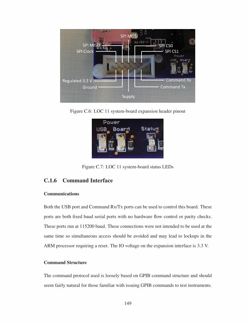
Figure C.6: LOC 11 system-board expansion header pinout
Figure C.7: LOC 11 system-board status LEDs
C.1.6 Command Interface
Communications
Both the USB port and Command Rx/Tx ports can be used to control this board. These
ports are both fixed baud serial ports with no hardware flow control or parity checks.
These ports run at 115200 baud. These connections were not intended to be used at the
same time so simultaneous access should be avoided and may lead to lockups in the
ARM processor requiring a reset. The IO voltage on the expansion interface is 3.3 V.
Command Structure
The command protocol used is loosely based on GPIB command structure and should
seem fairly natural for those familiar with issuing GPIB commands to test instruments.
149

All commands are terminated with a newline character ’
n’. carriage returns ’
r’ are ignored in the stream allowing for windows style newline character sequences
without errors. Commands may optionally end in a ’?’. The ’?’ tells the ARM to
generate a response string for the command with will be newline terminated. If a ’?’
does not follow a command it will not generate a response. The ’*’ character is a
special command character which may only occur as the first character in a command
string. ’*’ is treated as a command flush character which allows an application to bring
the command buffer into a known state without executing potential garbage data as a
command. eg. The command "abc*IDN?" will be interpreted as "*IDN?". The final
special character is ’’¯
or backspace. A backspace can be sent to shrink the current
command buffer by one character. Additional backspaces sent after the command
length reaches 0 will be ignored and will not produce an error. There is one command
which bends a few of these rules. The "*LST" command will return a result when sent
as either "*LST" or "*LST?" and returns multiple lines as its response. This command
is intended for human usability and should be considered to produce a variable length
output (line count as well as line length) is used in a computer controlled application.
Commands are separated from arguments with spaces and numeric arguments may have
metric suffixes attached eg. setting 14 uA bias would be "ib 14u". commands will also
return values with metric suffixes. The ’?’ is appended after the last argument without
a space eg. reading bias current DAC after setting it would be "ib 14u?" ? should return
"14u"
Commands
brackets () denote optional elements
*LST(?) List all available commands with brief descriptions and enumeration values.
150

*IDN? Return board identification. This should return "L11 System
Board,v1.1.0,Board n" for systems conforming to this document. Here ’n’ after
board returns a unique identifier for the board currently 1-3.
*RST Reset LOC 11 and ARM systems. This will reset and initialize LOC 11 and
external biases and clocks into a known safe state.
adc( enable)(?) Enables/Disables/Reports LOC 11 adc run state. Valid values for
enable are "en" and "dis".
adcbinc( numberOfBins)(?) Gets/Sets the number of samples to accumulate on the
ARM chip. numberOfBins must be an integer greater than 0.
adccds( enable)(?) Gets/Sets correlated double sampling in the ADC. Valid values
for enable are "en" and "dis"
adcread( flush)? Reads LOC 11 ADC value. This command waits for the current
sample to fully accumulate before returning the result. If the "flush" argument is passed
the current accumulation value is reset before beginning to read adc.
adcsrc( source)(?) Gets/Sets ADC source. Valid source values are "cepd1", "cepd2",
"pcrpd", "hvi", "tfb", "hvv", "ext_p", "ext_n", "dif_cepd", and "dif_ext".
boost( enable)(?) Enables/Disables/Reposts Boost converter run state. Valid values
for enable are "en" and "dis".
boostsrc( pwmSource)(?) Gets/Sets PWM source used to run boost converter. Valid
values for pwmSource are "int" and "ext". If boost converter is used in "ext" mode
additional wiring to test headers will be required (PWM signal into Boost_ext).
151

clksrc( clockSource)(?) Gets/Sets source of LOC 11 system clock. Valid values of
clockSource are "vco" and "ext". The signal for external system clock comes from an
on-board 20 MHz oscillator which must be enabled separately (see extclk command).
cp( enable)(?) Enables/Disables/Reports Charge Pump run state. Valid values for
enable are "en" and "dis".
extclk( enable)(?) Enables/Disables/Reports run state of crystal oscillator used to
generate external clock used by LOC 11. Valid values for enable are "en" and "dis".
ib( value)(?) Gets/Sets external bias current DAC used to control LOC 11 external
bias current. value is a metric number in amps between "0u" and "31.5u". Recom-
mended value is 14u
ibmon? Reads current on Ib mon pin of LOC 11 Reports value in amps with a metric
suffix.
ibsel( source)(?) Gets/Sets LOC 11 analog bias current source. Valid values for
source are "int" and "ext". *Preliminary* It is recommended to run LOC 11 in "int"
mode as the photo-diode integrating opamp appears to be near an unstable region of
operation. Using the internal bias even at lower than desired bias currents should
result in more reliable photo-diode readings due to reduced noise and temperature*
sensitivity. The analog circuits should remain functional at bias currents between 8uA
and 20 uA *Here temperature sensitivity of ARM-M3 electronics is assumed to be
worse than the temperature compensated electronics in LOC 11 this has yet to be
verified.
l11? Check for the presence of LOC 11 in zero-insertion-force (ZIF) socket Returns
either "yes" or "no"
152

l11rst(?) Pulses LOC 11 Reset pin and optionally returns LOC 11 presence.
l11spi address( value)(?) Reads/Writes to LOC 11 spi registers directly.
led( state)(?) Gets/Sets board status led state. Valid values for state are "on" and
"off". led state cannot be changed when no LOC 11 is present in ZIF socket.
ls channel( state)(?) Gets/Sets Level Shifter states. Valid values for channel are 0-6.
Valid values for state are "low", "high", "hi-z", "short". The short state is invalid unless
chip is in test mode. (see testmode command)
pdshut( time)(?) Gets/Sets integration time of photo-diode. Valid values for time
(s) are "800n", "1.6u", "3.2u", "6.4u", "12.8u", "25.6u", "51.2u", "102.4u", "204.8u",
"409.6u", "819.2u", "1.6384m", "3.2768m", "6.5536m", "13.1072m", and "26.2144m"
spi bytes( data)(?) Sends an spi command through the expansion header using
currently selected chip select line (see spichip command). bytes determines the number
of bytes to send/receive through the expansion header. data is a hexadecimal string
containing the data to send through the expansion header. if responses are enabled (’?’)
this function will return a hexadecimal string of length (2*bytes) representing the data
received.
spichip( csLine)(?) Gets/Sets the chip to select during expansion header spi com-
mands but does not assert the selected line. Valid values for csLine are ’0’ and ’1’
spifrq( frequency)(?) Gets/Sets the SPI clock frequency to be used on the expansion
header. valid values for frequency are "18M", "9M", "4.5M", "2.25M", "1.125M",
"562.5k", "281.25k", and "140.625k". Note: at higher frequencies SPI transactions
153

may not be continuous (the clock could pause while the ARM processor catches up
reading and writing data).
spimode( mode)(?) Gets/Sets Phase and Polarity of spi clock on expansion header.
Valid values for mode are "00", "01", "10", and "11". These correspond directly to arm
SPI modes, Fig. C.8.
Figure C.8: ARM SPI modes
testmode( state)(?) Gets/Sets LOC 11 test mode state. Test mode is used to enable
short circuit level shifter states for testing purposes and should not be enabled during
normal operation. Valid values for state are "en" and "dis".
vcoi( value)(?) Gets/Sets current DAC value used for external control of VCO
frequency. Value is a metric decimal value which should be in the range "0u" to "31.5u".
vcoisrc( source)(?) Gets/Sets bias current source used by LOC 11’s internal VCO.
Valid values for source are "int" and "ext". The "int" VCO source is derived from the
analog bias circuitry and "ext" is generated by a current DAC on-board.
vppmm( state)(?) Gets/Sets vpp– bias override state. This signal is used internally
when enabling/disabling the charge pump and is required for calibration of the Vpp–
154

bias circuit. The command should not be used to set the Vpp– bias state during normal
operation.
C.2 Lab-on-Chip 12 System Board
Figure C.9: LOC 12 system-board connectors
C.2.1 Power
Logic Power
The system board for LOC 12 was is powered from the LV power 5 pin molex connector
in Fig. C.9, compatible with earlier TTK designs. In this design we use the 7 V power
rail to derive all logic level supplies, 3.3 V digital and analog ARM supplies and the 5
V digital, 5 V analog and 3.3 V IO power supplies for LOC 12. The power supplies
used to run all LOC 12 systems can be enabled/disabled in software by the on-board
ARM micro-controller and is turned off when this control pin is left floating. This
design decision was made to allow for safe start up as LOC 12 defaults to powering up
with the charge pump running. In order to prevent this behavior the LOC 12 start-up
155

sequence must first disable the external 20 MHz clock, then power up LOC 12’s power
supplies and send the SPI command to disable the charge pump, and finally re-enable
LOC 12’s clock source.
Figure C.10: LOC 12 system-board screw terminals
Heater Power
The power supply used to run the on-chip heater electrodes or off chip heater has been
separated from the rest of the PCB power. LOC 12 is capable of driving a continuous
900 mA load with a peak current of 4 A at 5 V. This is supplied from the screw terminals
on the top of the board, Fig. C.10.
Magnetic Coil Power
The magnetic coils have a separate supply from the main board as well. This can be
accessed from the Screw terminals shown in Fig. C.10.
Expansion Header
The expansion header can either provide power or consume power from the 7 V supply,
Fig. C.11.
156

Figure C.11: LOC 12 system-board low voltage headers
USB
The LOC 12 system PCB was designed to be capable of running on USB 5V power by
removing the on-board 5V regulators and shorting two jumpers on the top side of the
board. This design feature does not work as intended as the USB header PCB traces
have a faulty connection on one of the inner PCB layers. This design error results in
USB 5V being shorted to ground. Due to this design error USB powered operation and
use of the ARM’s internal USB logic is not possible.
HV Power
LOC 12 contains a design flaw which prevents its internal charge pump from function-
ing properly. This results in an external HV power supply being required for HV device
operation. The internal static level shifters are biased using the internal resistive divider
network as a result it is advised to provide both an external HV power supply voltage
(Vpp) and and external HV bias voltage of Vpp − 5 V (Vpp − −). This external bias
voltage must not deviate from the HV supply voltage by more than 12 V at any time
during operation and will result in excessive current draw on the HV supply line when
the difference between Vpp and Vpp −− is less than 4.5V .
157

C.2.2 Status LEDs
ARM Status
Figure C.12: LOC 12 system-board ARM status LEDs
There are 3 ARM status indicators one green, one yellow, and one red. A flashing
green indicator shows that the ARM micro-controller has booted up successfully and
is listening for commands on it’s serial interface. The yellow indicator indicates the
presence or absence of a LOC 12 chip on the board. Solid yellow indicates no chip
present or no detection command has been issued and an unlit yellow indicator indicates
that L12 has been detected. A solid red light indicates that a hard fault has occurred or
that a task has returned from it’s main method. This should not happen during normal
operation unless a hardware debugger is present and incorrectly configured.
L12 Status
There are 5 LOC 12 status LEDs. These LEDs sow the current state of LOC 12’s power
supply, reset signal, and general purpose outputs as labeled on the top copper layer of
the PCB Fig. C.13.
158

Figure C.13: LOC 12 system-board LOC LEDs
C.2.3 External Heater Connections
LOC 12 is designed to be able to run up to 4.5 W heaters at 5 V while sensing the
heater element resistance. This chip contains both on-chip connections for microfluidic
devices and pad connections for external heating elements. On the LOC 12 PCB an
external heating element can be connected to the screw terminals shown in Fig. C.10.
The 4-point connection scheme reduces the impact of contact resistance to both the
PCB and chip pads and allows for properly designed heaters to exclude cold zones on
the heater it’s self.
C.2.4 External temperature sensors
LOC 12 contains an internal current DAC and ADC input channel tied to the same pin,
Fig. C.11. This circuit is intended for use with external thermistors when a standard
sensing device is preferred to the element sensing method.
159

Figure C.14: LOC 12 system-board high voltage headers
C.2.5 HV regulation
While LOC 12 may not have a functioning internal charge pump it is still capable
of regulating the HV potential generated by external devices. LOC 12’s internal HV
regulation comparator can be accessed from the header shown in Fig. C.14. This signal
will output a too low/ too high signal based on LOC 12’s internal DAC and HV sensing
circuits.
C.2.6 Command Interface
Figure C.15: LOC 12 system-board serial interface header
160

Communications
The LOC 12 PCB is controlled through the serial interface in Fig. C.15. This port has
a fixed baud rate of 1 Mbuad hardware flow control or parity checks. The IO voltage
on the serial interface is 3.3 V.
Command Structure
The LOC system PCB communication protocol differs significantly from that used
by L11 primarily due to the fact that is is capable of generating significantly more
ADC data when all internal systems are enabled. The communication interface is a
mixture of both ASCII commands for quick board life sign tests and raw binary data
for efficient communication with a PC. The serial interface between a PC and the LOC
12 board is asynchronous, meaning that either the host PC or the LOC board may
initiate communication and there is no guaranty that a response from a query command
will be the next response received by a PC. Every command sent from either the PC
or the LOC 12 board is prefixed with the character ’*’ and a one or two character
command followed by the arguments which may either be ASCII characters or binary
data. All commands issued from a PC have a fixed length. All but the "*v?" and "*i"
commands returned from the LOC PCB are also of fixed length. The exceptions to this
rule transmit a null (’\0’) terminated string after their prefix. All commands issued from
a PC will be responded to by a device command with the same prefix. In addition to
this the device with issue ADC commands whenever ADC activity has been detected by
the ARM micro-controller. This signal activity can be sent after a command has been
issued from a PC and before the ARM has responded to that command. The original
command will be responded to however may have to wait for up to 4 ADC commands
to be sent first.
161

Commands
Commands begin with an ASCII prefix, any commands containing raw binary param-
eters or responses will have each binary byte enclosed in ’<’ and ’>’ with optional [n]
indicating size in bytes. ASCII parameters or varying responses will be denoted by an
enclosed (parameter).
*v? Device responds with null terminated firmware version and date. At the time of
this writing the most current firmware will respond with "*vL12 Board R2 Firmware
V1.3, May 2017\0"
*i Device responds with current hardware information including the presence of a
LOC 12 in the ZIF socket. Responses should be either "*iL12 System PCB R02; ARM
Cortex M3 @ 72 MHz; LOC 12 Connected\0" or "L12 System PCB R02; ARM Cortex
M3 @ 72 MHz; LOC 12 Not found\0"
*p(enable) Enables (enable = ’1’), disables (enable = ’0’), or queries (enable = ’?’)
L12 power supplies and checks for presence of LOC 12.
Responds with "*p(state)" where state can be either ’0’ : L12 supplies off, ’1’ :
L12 supplies on and L12 present, or ’!’ : L12 was not found and supplies have been
powered down.
*r Resets and checks for presence of LOC 12 if L12 power is enabled.
Responds with "*r(present)". present = ’1’ : L12 is present and powered, present =
’0’ L12 is either not present or not powered.
*lr<address> Read LOC 12 register at passed address.
Responds with "*lr<address><value>".
162

*lw<address><data> Write passed value to LOC 12 register at address passed.
Responds with "*lw<address><value>" where the value returned is the previous
value held by the modified register.
*d<value>[2] Sets current source value.
Echoes in response.
*e(enable) Enables (enable = ’1’), disables (enable = ’0’), or queries (enable = ’?’)
20 MHz clock source used to drive LOC 12’s external system clock pin.
Responds with "*e(enabled)" where enabled = ’0’ if the source is currently disabled
and enabled = ’1’ if the source is currently enabled.
*o(pin)(state) Sets or queries general purpose output state in expansion header. pin
must be in range ’0’ - ’3’ and state can be either ’1’ for output high, ’0’ for output low,
or ’?’ for query.
Responds with "*o(pin)(state)" where state is either ’1’ : high or ’0’ : low.
*baw<value>[2] Sets L12 bias current value for external analog bias operation.
Responds with "*ba=<value>[2]".
*ba? Gets L12 bias current value for external analog bias operation.
Responds with "*ba=<value>[2]".
*bvw<value>[2] Sets L12 bias current value for external vco bias operation.
Responds with "*bv=<value>[2]".
*bv? Gets L12 bias current value for external vco bias operation.
Responds with "*bv=<value>[2]".
163

Async-Responses
Here the ADC responses are described, these may come at any time and do not require
a command to request them (sent on L12 ADC interrupts). Async commands will not
cause currently transmitting responses to be broken up.
*ap<value>[4]<time>[4] Photo-diode ADC value and time stamp in arm ticks
(10,000 ticks / s).
*at<value>[4]<time>[4] Thermal systems ADC value and time stamp in arm ticks
(10,000 ticks / s).
*ai<value>[4]<time>[4] HV systems voltage ADC value and time stamp in arm ticks
(10,000 ticks / s).
*av<value>[4]<time>[4] HV systems current ADC value and time stamp in arm
ticks (10,000 ticks / s).
164

Appendix D
Chip Pinouts
D.1 Lab-on-Chip 11 Pinouts
D.1.1 L11-DIP
Figure D.1: 64 DIP package used for L11 bonding
Table D.1: L11 DIP pinout
Pin Name Pin Name Pin Name
1 Heater_Vdd 23 NC 45 T_sense2
2 Heater_Vdd 24 Vpp 46 Vdd_core
3 Heater_Sw 25 Vpp– 47 Vss
4 Heater_Vss 26 CP_Vout 48 Vdd_IO
5 Heater_Vss 27 Vss_analog 49 SysClkOut
165
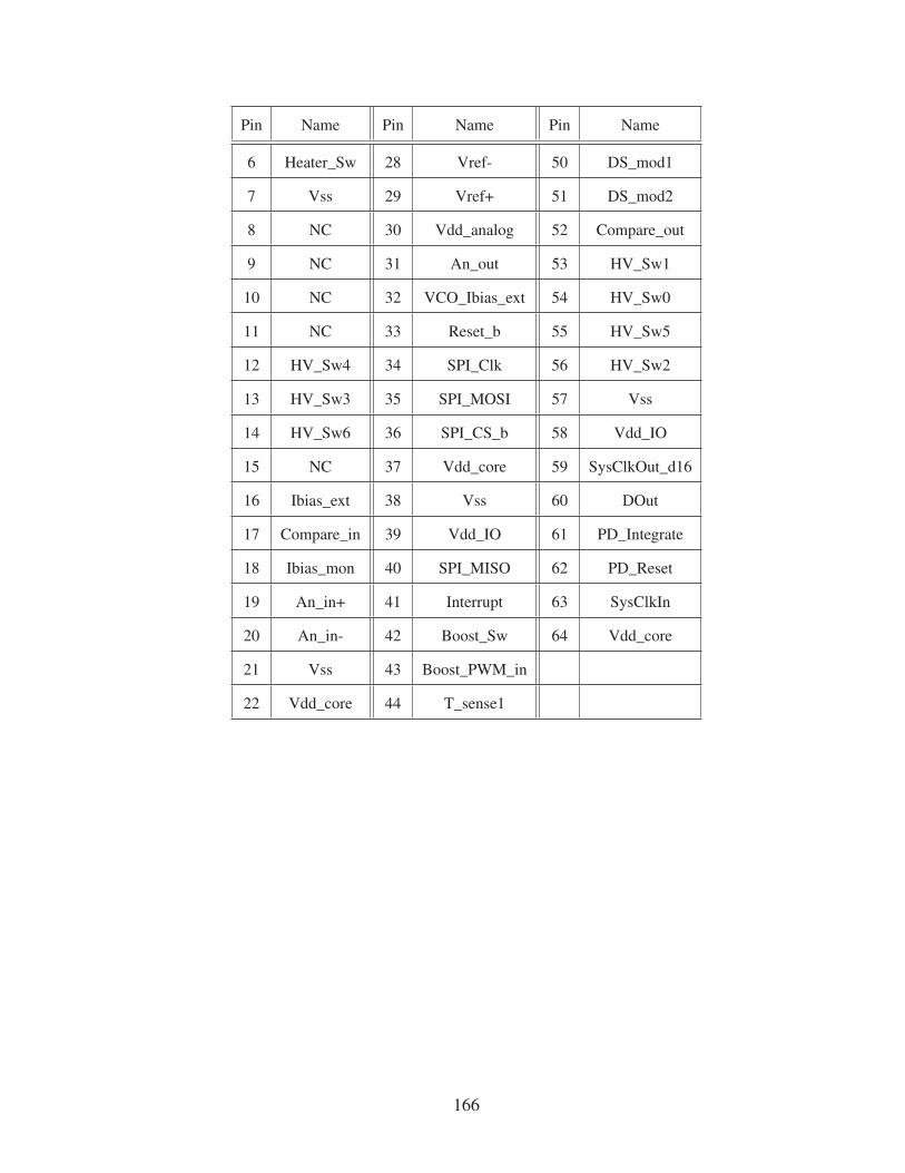
Pin Name Pin Name Pin Name
6 Heater_Sw 28 Vref- 50 DS_mod1
7 Vss 29 Vref+ 51 DS_mod2
8 NC 30 Vdd_analog 52 Compare_out
9 NC 31 An_out 53 HV_Sw1
10 NC 32 VCO_Ibias_ext 54 HV_Sw0
11 NC 33 Reset_b 55 HV_Sw5
12 HV_Sw4 34 SPI_Clk 56 HV_Sw2
13 HV_Sw3 35 SPI_MOSI 57 Vss
14 HV_Sw6 36 SPI_CS_b 58 Vdd_IO
15 NC 37 Vdd_core 59 SysClkOut_d16
16 Ibias_ext 38 Vss 60 DOut
17 Compare_in 39 Vdd_IO 61 PD_Integrate
18 Ibias_mon 40 SPI_MISO 62 PD_Reset
19 An_in+ 41 Interrupt 63 SysClkIn
20 An_in- 42 Boost_Sw 64 Vdd_core
21 Vss 43 Boost_PWM_in
22 Vdd_core 44 T_sense1
166

D.1.2 L11-PGA
Figure D.2: 68 PGA package used for L11 bonding
Table D.2: L11 PGA pinout
Pin Name Pin Name Pin Name
A2 Vpp C10 NC J2 Vdd_IO
A3 Vdd_core C11 NC J10 DOut
A4 An_in- D1 Vdd_analog J11 PD_Integrate
A5 Ibias_mon D2 Vref+ K1 Interrupt
A6 Ibias_ext D10 Heater_Sw K2 Boost_Sw
A7 HV_Sw3 D11 Vss K3 T_sense1
A8 NC E1 VCO_Ibias_ext K4 T_sense2
A9 NC E2 An_out K5 Vss
A10 NC E10 Heater_Vss K6 SysClkOut
B1 CP_Vout E11 Heater_Vss K7 DS_mod2
B2 Vpp– F1 SPI_Clk K8 HV_Sw1
B3 Vss F2 Reset_b K9 HV_Sw5
B4 An_in+ F10 Heater_Vdd K10 Vdd_IO
B5 Compare_in F11 Heater_Sw K11 SysClkOut_d16
167

Pin Name Pin Name Pin Name
B6 HV_Sw6 G1 SPI_CS_b L2 Boost_PWM_In
B7 HV_Sw4 G2 SPI_MOSI L3 NC
B8 NC G10 Vdd_core L4 Vdd_core
B9 NC G11 Heater_Vdd L5 Vdd_IO
B10 NC H1 Vss L6 DS_mod1
B11 NC H2 Vdd_core L7 Compare_out
C1 Vref- H10 PD_Reset L8 HV_Sw0
C2 Vss_analog H11 SysClkIn L9 HV_Sw2
C3 NC J1 SPI_MISO L10 Vss
**Note the L11 PGA chips where bonded 90◦ out of alignment. Pin 1 in the first
batch of chips corresponds to pin A11 instead of pin A1.
168
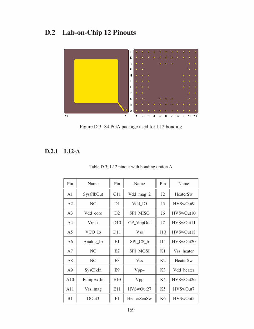
D.2 Lab-on-Chip 12 Pinouts
Figure D.3: 84 PGA package used for L12 bonding
D.2.1 L12-A
Table D.3: L12 pinout with bonding option A
Pin Name Pin Name Pin Name
A1 SysClkOut C11 Vdd_mag_2 J2 HeaterSw
A2 NC D1 Vdd_IO J5 HVSwOut9
A3 Vdd_core D2 SPI_MISO J6 HVSwOut10
A4 Vref+ D10 CP_VppOut J7 HVSwOut11
A5 VCO_Ib D11 Vss J10 HVSwOut18
A6 Analog_Ib E1 SPI_CS_b J11 HVSwOut20
A7 NC E2 SPI_MOSI K1 Vss_heater
A8 NC E3 Vss K2 HeaterSw
A9 SysClkIn E9 Vpp– K3 Vdd_heater
A10 PumpExtIn E10 Vpp K4 HVSwOut26
A11 Vss_mag E11 HVSwOut27 K5 HVSwOut7
B1 DOut3 F1 HeaterSenSw K6 HVSwOut5
169
Pin Name Pin Name Pin Name
B2 DOut0 F2 SPI_SCK K7 HVSwOut4
B3 HVCmpOut F3 Reset_b K8 HVSwOut25
B4 Vdd_analog F9 HVSwOut23 K9 HVSwOut15
B5 Vss_analog F10 HVSwOut2 K10 HVSwOut17
B6 Sw31SigHOut F11 HVSwOut24 K11 HVSwOut19
B7 Sw31SigLOut G1 HeaterSenExt L1 HeaterSw
B8 NC G2 HeaterSen- L2 Vdd_heater
B9 PumpEnIn G3 Vdd_core L3 Vdd_heater
B10 Vss G9 HVSwOut22 L4 HVSwOut8
B11 Vss_mag G10 HVSwOut1 L5 HVSwOut29
C1 InterruptOut G11 HVSwOut0 L6 HVSwOut28
C2 DOut2 H1 HeaterSenVdd L7 HVSwOut6
C5 Vref- H2 Vss_heater L8 HVSwOut12
C6 HVMon_I_In H10 HVSwOut21 L9 HVSwOut13
C7 HVMon_I_Out H11 HVSwOut3 L10 HVSwOut14
C10 Vdd_mag_1_3 J1 Vss_heater L11 HVSwOut16
D.2.2 L12-B
Table D.4: L12 pinout with bonding option B
Pin Name Pin Name Pin Name
A1 SysClkOut C11 Vdd_mag_2 J2 HeaterSw
A2 NC D1 Vdd_IO J5 NC
A3 Vdd_core D2 SPI_MISO J6 NC
A4 Vref+ D10 CP_VppOut J7 NC
A5 VCO_Ib D11 Vss J10 NC
A6 Analog_Ib E1 SPI_CS_b J11 NC
170

Pin Name Pin Name Pin Name
A7 NC E2 SPI_MOSI K1 Vss_heater
A8 NC E3 Vss K2 HeaterSw
A9 SysClkIn E9 Vpp– K3 Vdd_heater
A10 PumpExtIn E10 Vpp K4 NC
A11 Vss_mag E11 NC K5 NC
B1 DOut3 F1 HeaterSenSw K6 NC
B2 DOut0 F2 SPI_SCK K7 NC
B3 HVCmpOut F3 Reset_b K8 NC
B4 Vdd_analog F9 NC K9 NC
B5 Vss_analog F10 NC K10 NC
B6 NC F11 NC K11 NC
B7 NC G1 HeaterSenExt L1 HeaterSw
B8 NC G2 HeaterSen- L2 Vdd_heater
B9 PumpEnIn G3 Vdd_core L3 Vdd_heater
B10 Vss G9 NC L4 NC
B11 Vss_mag G10 NC L5 NC
C1 InterruptOut G11 NC L6 NC
C2 DOut2 H1 HeaterSenVdd L7 NC
C5 Vref- H2 Vss_heater L8 NC
C6 HVMon_I_In H10 NC L9 NC
C7 HVMon_I_Out H11 NC L10 NC
C10 Vdd_mag_1_3 J1 Vss_heater L11 NC
171

D.3 Lab-on-Chip 13 Pinout
Figure D.4: 68 PGA package used for L13 bonding
D.3.1 L13-A
Table D.5: L13-A pinout
Pin Name Pin Name Pin Name
A2 Ref- C11 SPI_Clk J10 Vpp
A3 Ref+ D1 An_in+ J11 CP_Vout
A4 SysClkOut D2 HV_reg_out K1 HV_Sw_CEW4
A5 Dout1 D10 Vss K2 NC
A6 SPI_MISO D11 SysClkIn K3 DS_mod_PCR
A7 Vss E1 R_sense_sink K4 DS_mod_Heater
A8 Heater_Sw E2 An_in- K5 DOut3
A9 Ibias_mon E10 CP_pumpSig_in K6 Vss
A10 Heater_sen+ E11 Vdd_core K7 NC
B1 Ibias_ext F1 An_out+ K8 NC
B2 Vss_analog F2 VCO_Ibias_ext K9 HV_Sw_VC0
B3 Vdd_analog F10 CP_pumpDirect_in K10 HV_Sw_CEW1
172

Pin Name Pin Name Pin Name
B4 DOut0 F11 CP_pumpDirect_b_in K11 HV_Sw_CEW0
B5 Interrupt G1 Vss_mag L2 NC
B6 Vdd_IO G2 An_out- L3 DS_mod_HV
B7 Vss_Heater G10 CP_pumpSig_out L4 DS_mod_CE
B8 Vdd_Heater G11 CP_pumpSig_b_out L5 DOut2
B9 Heater_sen- H1 Vss_mag L6 Vdd_IO
B10 SPI_MOSI H2 Vdd_mag L7 NC
B11 SPI_CS_b H10 CP_lowerMid_Vout L8 NC
C1 Vss H11 CP_upperMid_Vin L9 HV_Sw_VP0
C2 Vdd_core J1 HV_Sw_CEW3 L10 HV_Sw_CEW2
C10 Reset_b J2 Vdd_mag
D.3.2 L13-B
Table D.6: L13-B pinout
Pin Name Pin Name Pin Name
A2 Ref- C11 SPI_Clk J10 Vpp
A3 Ref+ D1 An_in+ J11 CP_Vout
A4 SysClkOut D2 HV_reg_out K1 NC
A5 Dout1 D10 Vss K2 NC
A6 SPI_MISO D11 SysClkIn K3 NC
A7 Vss E1 R_sense_sink K4 NC
A8 Heater_Sw E2 An_in- K5 NC
A9 Ibias_mon E10 CP_pumpSig_in K6 NC
A10 Heater_sen+ E11 Vdd_core K7 NC
B1 Ibias_ext F1 An_out+ K8 NC
B2 Vss_analog F2 VCO_Ibias_ext K9 NC
173

Pin Name Pin Name Pin Name
B3 Vdd_analog F10 CP_pumpDirect_in K10 HV_Sw_CEW1
B4 DOut0 F11 CP_pumpDirect_b_in K11 HV_Sw_CEW0
B5 Interrupt G1 Vss_mag L2 NC
B6 Vdd_IO G2 An_out- L3 NC
B7 Vss_Heater G10 CP_pumpSig_out L4 NC
B8 Vdd_Heater G11 CP_pumpSig_b_out L5 NC
B9 Heater_sen- H1 Vss_mag L6 NC
B10 SPI_MOSI H2 Vdd_mag L7 NC
B11 SPI_CS_b H10 CP_lowerMid_Vout L8 NC
C1 Vss H11 CP_upperMid_Vin L9 HV_Sw_VP0
C2 Vdd_core J1 NC L10 HV_Sw_CEW2
C10 Reset_b J2 Vdd_mag
174
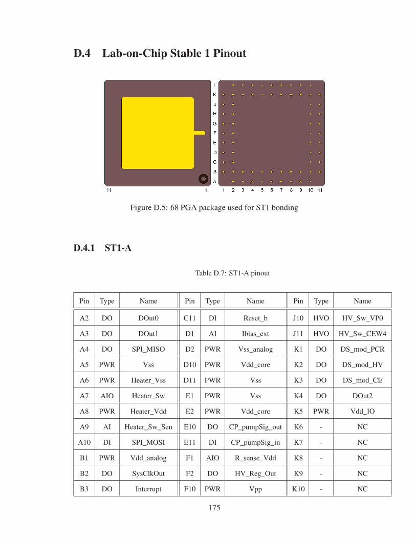
D.4 Lab-on-Chip Stable 1 Pinout
Figure D.5: 68 PGA package used for ST1 bonding
D.4.1 ST1-A
Table D.7: ST1-A pinout
Pin Type Name Pin Type Name Pin Type Name
A2 DO DOut0 C11 DI Reset_b J10 HVO HV_Sw_VP0
A3 DO DOut1 D1 AI Ibias_ext J11 HVO HV_Sw_CEW4
A4 DO SPI_MISO D2 PWR Vss_analog K1 DO DS_mod_PCR
A5 PWR Vss D10 PWR Vdd_core K2 DO DS_mod_HV
A6 PWR Heater_Vss D11 PWR Vss K3 DO DS_mod_CE
A7 AIO Heater_Sw E1 PWR Vss K4 DO DOut2
A8 PWR Heater_Vdd E2 PWR Vdd_core K5 PWR Vdd_IO
A9 AI Heater_Sw_Sen E10 DO CP_pumpSig_out K6 - NC
A10 DI SPI_MOSI E11 DI CP_pumpSig_in K7 - NC
B1 PWR Vdd_analog F1 AIO R_sense_Vdd K8 - NC
B2 DO SysClkOut F2 DO HV_Reg_Out K9 - NC
B3 DO Interrupt F10 PWR Vpp K10 - NC
175

Pin Type Name Pin Type Name Pin Type Name
B4 PWR Vdd_IO F11 HVO CP_Vout K11 HVO HV_Sw_VC0
B5 PWR Heater_Vss G1 AI An_in- L2 DO DS_mod_Heater
B6 AIO Heater_Sw G2 AI An_in+ L3 DO DOut3
B7 PWR Heater_Vdd G10 HVO HV_Sw_CEW1 L4 PWR Vss
B8 AO Ibias_mon G11 HVO HV_Sw_CEW0 L5 - NC
B9 AI Heater_Vdd_sen H1 AI VCO_Ibias_ext L6 - NC
B10 DI SPI_CS_b H2 AIO R_sense_sink L7 - NC
B11 DI SPI_Clk H10 HVO HV_Sw_CEW3 L8 - NC
C1 AI Vref- H11 HVO HV_Sw_CEW2 L9 - NC
C2 AI Vref+ J1 AO An_Out- L10 - NC
C10 DI SysClkIn J2 AO An_Out+
D.4.2 ST1-B
Table D.8: ST1-B pinout
Pin Name Pin Name Pin Name
A2 DOut0 C11 Reset_b J10 NC
A3 DOut1 D1 Ibias_ext J11 NC
A4 SPI_MISO D2 Vss_analog K1 NC
A5 Vss D10 Vdd_core K2 NC
A6 Heater_Vss D11 Vss K3 NC
A7 Heater_Sw E1 Vss K4 NC
A8 Heater_Vdd E2 Vdd_core K5 NC
A9 Heater_Sw_Sen E10 CP_pumpSig_out K6 NC
A10 SPI_MOSI E11 CP_pumpSig_in K7 NC
B1 Vdd_analog F1 R_sense_Vdd K8 NC
B2 SysClkOut F2 HV_Reg_Out K9 NC
176

Pin Name Pin Name Pin Name
B3 Interrupt F10 Vpp K10 NC
B4 Vdd_IO F11 CP_Vout K11 NC
B5 Heater_Vss G1 An_in- L2 NC
B6 Heater_Sw G2 An_in+ L3 NC
B7 Heater_Vdd G10 NC L4 NC
B8 Ibias_mon G11 NC L5 NC
B9 Heater_Vdd_sen H1 VCO_Ibias_ext L6 NC
B10 SPI_CS_b H2 R_sense_sink L7 NC
B11 SPI_Clk H10 NC L8 NC
C1 Vref- H11 NC L9 NC
C2 Vref+ J1 An_Out- L10 NC
C10 SysClkIn J2 An_Out+
177

D.5 Test Chip 22 Pinout
Figure D.6: 40 DIP package used for T22 bonding
Table D.9: T22 pinout
Pin Type Name Pin Type Name Pin Type Name
1 - NC 15 DI SCk 29 AIO Fuse_Common
2 - NC 16 DI Clk 30 AIO M3_Fuse
3 - NC 17 DI Reset 31 PWR Vss
4 - NC 18 DI CP_Clk_s0 32 PWR LS_Vss
5 - NC 19 DI CP_Clk_s1 33 HVO LS_Vout
6 PWR CP_Vin 20 DI Glitch_Reset 34 PWR LS_Vpp
7 DO Nor_Q 21 DI CP_Clk_ext 35 HVO CP_Vout
8 DO And_Q 22 DI I_ref_sel 36 - NC
9 DO Sh_out 23 AI I_ref_ext 37 - NC
10 PWR Vdd_IO 24 DI LS_ctrl_High 38 - NC
11 DO NCO_out 25 - NC 39 - NC
12 AO TrimRes 26 DI LS_ctrl_Low 40 - NC
13 PWR Vdd_core 27 AIO M1_Fuse
14 DI Sh_in 28 AIO M2_Fuse
178

Appendix E
Device Register Layouts
E.1 Lab-on-Chip 11
��� 0x02
��� 0xff
}constant registers
��� System Configuration
���
���Level Shifter States
���
���
ADC Configuration
�� PD Integrator
�� Interrupt Status
���
���
Heater Systems
��
���HV Generation
��� GP Output
��� – unused –
E.1.1 System Configuration Register01234567
unused CCE TME ABS CSS VCS unused 0x2
VCS - VCO Current Select
Select current source used to bias internal VCO. Internal current is derived from analog
bias current.
179

Internal IBias : ’0’
External Pin : ’1’
CSS - Clock Source Select
Select system clock source.
Internal VCO : ’0’
External Pin : ’1’
ABS - Analog Bias Select
Select bias current source used for analog circuitry.
Internal : ’0’
External : ’1’
TME - Test Mode Enabled
Enabled level shifter test mode allowing level shifters to be driven with high and low
signals simultaneously shorting Vpp to ground.
Enabled : ’1’
Disabled : ’0’
CCE - Comparator Clock Enable
Toggles HV comparator clock enabling or disabling comparator sampling.
Enabled : ’1’
Disabled : ’0’
E.1.2 Level Shifter States01234567
LS3 LS2 LS1 LS0 0x3
unused LS6 LS5 LS4 0x4
180

LSn - Level Shifter State
Sets the output state of the specified level shifter
High : "10"
Low : "01"
High-Z : "00"
Vpp-Gnd Short1 : "11"
E.1.3 ADC configuration01234567
unused PDS ASel2 ASel1 ADC2En ADC1En 0x5
ADC_LSB 0x6
ADC_MSB 0x7
ADC1En - ADC 1 Enable
Enables or disables single ended ADC.
Enable2 : ’1’
Disable : ’0’
ADC1En - ADC 2 Enable
Enables or disables differential ADC.
Enable2 : ’1’
Disable : ’0’
ASel1 - ADC 1 Input Select
Selects analog input source to use for single ended ADC conversion.
1For the short circuit state to be active Test Mode must also be enabled in the system configurationregister. Level shifter is set to high-z on "11" state otherwise.
2Only one ADC may be enabled at a time. If both are set to their enabled state in the ADCconfiguration register they will both be disabled.
181

CE PD13 : "000"
CE PD23 : "001"
PCR PD : "010"
Channel Current : "011"
Heater Temperature : "100"
HV Potential : "101"
External + : "110"
External - : "111"
ASel2 - ADC 2 Input Select
Selects analog input source to use for differential ADC conversion.
CE PD Pair3 : ’0’
External : ’1’
PDS - Photo-diode Select
Enable/disable synchronization between ADC and photo-diode integration logic.
Enable : ’1’
Disable : ’0’
ADC_MSB : ADC_LSB - ADC Output Value registers
These two registers are combined to form the most significant and least significant bytes
of the 16-bit decimation filter. These are populated immediately before and interrupt is
triggered and will remain valid for at least 400 μs after an interrupt event.
3Due to a missing routing wire in L11 only the PCR photo-diode is electrically connected to the ADCinput mux. Setting the mux to the CE photo-diode disconnects the ADC from any electrical signal.
182

E.1.4 PD Integrator01234567
unused CDS INT 0x8
INT - Integration Time
Sets integration time to 800ns× 2INT .
CDS - Correlated Double Sampling
Enabled/Disabled correlated double sampling. If enabled ADC will alternate between
reading PD value held in reset and integrated PD value in an effort to reduce electrical
noise.
Enable : ’1’
Disable : ’0’
E.1.5 Interrupt Status Register01234567
unused ADCRdy 0x9
ADCRdy - ADC Ready Interrupt
Reading register indicates interrupt status (’1’ = asserted, ’0’ = not asserted). Writing a
’1’ to this bit clears the interrupt.
E.1.6 Heater Control01234567
unused HEn 0xa
DUTY 0xb
183

HEn - Heater Switch Enable
Enable or disable heater switch PWM generator. When disabled heater switch is held
open.
Enable : ’1’
Disable : ’0’
DUTY
Set heater switch PWM duty to (DUTY + 1)/256 (0.39% - 100%).
E.1.7 HV Generation01234567
unused BPS CPEn HVFR BEn 0xc
unused HVSET 0xd
BEn - Boost Converter Enable
Enables or disables boos converter circuitry.
Enable : ’1’
Disable : ’0’
HVFR - High Voltage Free Run
Disables HV regulation circuitry forcing enabled charge pump or boost converter to run
continuously.
Override Regulation : ’1’
Allow Regulation4 : ’0’
CPEn - Charge Pump Enable
Enables or disables integrated charge pump.
184

Enable : ’1’
Disable : ’0’
BPS - Boost Converter PWM Source
Selects between internal fixed 93.75% duty PWM or external PWM signal
Internal : ’0’
External : ’1’
HVSET - High Voltage Regulation Set Point
Sets the HV regulation DAC to adjust the regulation output voltage4.
E.1.8 GP Output State01234567
unused GPO0 0xe
GPO0 - General Purpose Output 0
Gets or sets the driven state of L11’s GP Output pin.
4The HV regulation circuitry in L11 has an inverted control signal resulting in regulated operationrunning in either fully disabled or continuous operation (positive feedback).
185

E.2 Lab-on-Chip 12
���� 0xff
���� 0x0c
}constant registers
���� System Configuration
����
����
Magnet Configuration
����
����
Level Shifter States
����
����
HV Generation
���� GP Output
���
���
PD Configuration
����
����
Heater Systems
��� Interrupt Status
����
����
ADC Heater
����
����
ADC PD
����
���
ADC HV I
���
����
ADC HV V
����
����
unused
...
unused
E.2.1 System Configuration01234567
TME CSS VCS IBS IBTrim 0x02
186

IBTrim - Internal Bias Current Trim
Sets trim value for internal bias current generation resistor. 0 -> Minimum resistance
(max current); 15 -> Maximum resistance (minimum current).
IBS - Analog Bias Current Select
Selects analog bias current source.
Internal : ’0’
External : ’1’
VCS - VCO Current Select
Selects internal VCO current source.
Internal : ’0’
External : ’1’
CSS - Clock Source Select
Selects system clock source.
Internal VCO : ’1’
External Pin : ’0’
TME - Test Mode Enable
Enable short circuit operation of level shifters. Intended of automated testing.
Enable : ’1’
Disable : ’0’
187

E.2.2 Magnet Configuration01234567
unused M2En M1En M0En 0x03
DUTY 0x04
MnEn - Magnet n Enable
Enable/disable on-chip magnet coil n.
Enable : ’1’
Disable : ’0’
DUTY - Magnet Coil PWM Duty
Sets shared magnet coil PWM duty to (DUTY + 1)/256.
E.2.3 Level Shifter States01234567
STLS3 STLS2 STLS1 STLS0 0x05
RCLS3 RCLS2 RCLS1 RCLS0 0x06
RCLS7 RCLS6 RCLS5 RCLS4 0x07
RCLS11 RCLS10 RCLS9 RCLS8 0x08
RCLS15 RCLS14 RCLS13 RCLS12 0x09
RCLS19 RCLS18 RCLS17 RCLS16 0x0a
RCLS23 RCLS22 RCLS21 RCLS20 0x0b
RCLS27 RCLS26 RCLS25 RCLS24 0x0c
RCLS31 RCLS30 RCLS29 RCLS28 0x0d
SLEW_LSB 0x0e
unused SLEW_MSB 0x0f
188

STLSn - Static Level Shifter n State
Sets the output state of the static level shifter.
High : "10"
Low : "01"
High-Z : "00"
Short6 : "11"
RCLSn - RC Level Shifter n State
Sets the output state of the RC level shifter.
High5 : "10"
Low5 : "01"
High-Z : "00"
Short6 : "11"
SLEW - HV Switch Slew Rate Limiter
The SLEW_MSB and SLEW_LSB registers make up the most significant and least
significant bytes of a 11-bit pulse generator. When enabled (SLEW �= 0) RC
level shifters will be driven high or low by a for 100 ns pulse with a period of
(SLEW + 1)× 100ns.
5High and low HV switch drive states may be pulsed to reduce the slew rate when switchingelectrostatic valves. This pulsing is controlled by the HV SLEW registers at 0x0e - 0x0f.
6HV switch short circuit mode can only be used when the system chip is put in test mode. Otherwisethis state aliases to high-z.
189

E.2.4 HV Generation01234567
DACExt VMS MMS MDEn CPS MGS 0x10
MPol MDAC 0x11
unused ADCIEn ADCVEn MCEn CCEn unused 0x12
unused 0x13
unused MGTFlag 0x14
MGS - Metal Gate Transistor Select
Selects between different layers in metal-gate-transistor (MGT) sensors.
CP : ’01’
M1 : ’00’
Ext : ’10’
CPS - Charge Pump Clock Source
Selects pump clock source to use when driving charge pump.
Disabled : ’00’
External Pump : ’01’
Regulated : ’10’
20 MHz : ’11’
MDEn - Metal Gate Transistor DAC Enable
Enables/Disables DAC used for regulation using MGTss.
Enable : ’1’
Disable : ’0’
190
MMS - Metal Gate Transistor Monitor Select
Selects gate layer to use for voltage monitoring using MGTs.
CP : ’0’
M1 : ’1’
VMS - Voltage Monitor Select
Selects between resistive divider and MGT voltage monitoring.
MGT : ’1’
Resistive : ’0’
DACExt - Enable external DAC Routing
Route HV regulation DAC current to external pin for testing.
Internal : ’0’
External7 : ’1’
MDAC - Metal Gate Transistor DAC Value
Set regulation value of HV system. This controls the internal DAC current to be
compared with selected MGT Ids. Calibration is necessary to map values to regulated
output voltages.
MPol - Metal Gate Transistor Comparator Polarity
Used to set MGT output polarity.
Increase voltage on high value : ’0’
Decrease voltage on high value : ’1’
7Disables HV regulation.
191

CCEn - Comparator Clock Enable
Disable CP operation while running regulation circuitry.
Enable CP Clock : ’1’
Disable CP Clock : ’0’
MCEn - MGT Comparator Enable
Enable/Disable HV Regulation circuitry.
Enable : ’1’
Disable : ’0’
ADCVEn - Voltage ADC Enable
Enable : ’1’
Disable : ’0’
ADCIEn - Current ADC Enable
Enable : ’1’
Disable : ’0’
MGTFlag - Metal Gate Transistor State Flag
Flag is set when MGT comparator output goes high and is reset by writing a ’1’ to this
bit. This flag is useful in determining under-voltage conditions when regulating a high
current load.
E.2.5 GP Output01234567
OutputEnable OutputDrive 0x15
192

OutputDrive
State driven to output pins if enabled. 4 output pins are available corresponding to each
bit in this field.
OutputEnable
Selects between driven pin and high-z pin. If a pin is enabled (’1’) it will drive the
value set by OutputDrive. 4 output pins are available corresponding to each bit in this
field.
E.2.6 PD Configuration01234567
PDS CDS INT 0x16
unused 0x17
INT - Integration Time
Photo-diode integration time, Tint = 800ns× 2INT .
CDS - Correlated Double Sampling
Read zero signal followed by integrated signal to cancel out some electrical noise.
PDS - Photo-diode Select
Select photo-diode to use. This can be one of the three on-chip photo-diodes or a
differential reading from the two CE photo-diodes.
NONE(ADC Off) : "000"
CE0 : "100"
CE1 : "110"
193

CEDiff : "101"
PCR : "010"
E.2.7 Heater System01234567
TRIM DDAC 0x18
unused ADCEn SS 0x19
SDACEn SDAC 0x1a
DUTY_LSB 0x1b
unused DUTY_MSB 0x1c
DDAC - Drive DAC
Heater switch DAC.
TRIM - DDAC Trim Value
Heater reference voltage trim. 0 -> max, 7 -> min.
SS - Sense Select
Select between heater element based sensing or external PTC/NTC resistor based
sensing. Differential element sensing subtracts a fixed voltage from the element sense
value and applies a 5x gain to the output signal.
Differential Heater Element Sense : ’00’
Direct Heater Element Sense : ’01’
External Heater Sense- : ’10’
External Analog Signal : ’11’
194

ADCEn - ADC Enable
Enable/Disable heater temperature sensing ADC.
Enable : ’1’
Disable : ’0’
SDAC - External Resistive Sensor DAC Value
Sets current sink DAC to specified current for PTC/NTC resistive temperature sensor
readings.
SDACEn - External Resistive Sensor DAC Enable
Enable/Disable current sink DAC for external(non-heating element) sensors.
Enable : ’1’
Disable : ’0’
DUTY
DUTY_MSB and DUTY_LSB form a 10-bit PWM Duty value for heater switch
control. Calculated duty is DUTY/1024, in range (0% - 99.6%). The last 4 ticks
of each PWM cycle either switch to a current sink mode for heater sensing or hold the
switch in the off position.
Figure E.1: Heater PWM/Current mirror switch signalling
195

E.2.8 Interrupt Status01234567
unused PD T I V 0x1d
This interrupt status register holds interrupt event sources. These events may be
cleared by writing a ’1’ to the corresponding bit. All interrupt sources in L12 are ADC
interrupt sources. Each interrupted must be handled within 409 μs to prevent missed
data captures. Bit flags V, I, T, and PD correspond to the voltage, current, temperature,
and photo-diode ADC channels respectively.
E.2.9 ADC Heater, PD, HV I, and HV V01234567
DATA[7:0]
DATA[15:8]
DATA[23:16]
The ADC converters on LOC 12 implement only half of the filtering logic on-chip
the second half of the filter must be implemented in software, Fig. E.1. ADC data is
only valid after a minimum of 3 sequential values have been read and software filtered
from a given ADC channel, after this each successive call to decimate() with new ADC
data will return a valid ADC value.1 ��� �� � ��2 ��� �� � ��3 ��� � � ��45 ��� ���� ����� ���� ���6 �7 ��� � ���� � ���8 ��� � ���� � ���9 ��� � ��� � ��
1011 �� � ����� �� �� �� � ��������12 ������ ����13 �� � ��� � �������� �� � � �� ���������� ! ���1415 �� � ���� " � ����� �� �� � ��#�����16 ������ ����17 �� � ��� � �������� �� � � �� ���������� ! ���1819 � � ���� " � ����� �� �� � ��$�����20 ������ ����21 � � �� � ������� �� � � � ���������� ! ��2223 %��%� ��� " � ���� �� � � �������24 &
Listing E.1: Second half of decimation filter software implementation
196

E.3 Lab-on-Chip 13
���� 0xa5
���� 0x81
}constant registers
����
����
System Configuration
����
����HV Generation
���� CE Level Shifters
��� CE Configuration
���
����
Valve Level Shifters
���� MGT Status
���� GP Output
����
����
PD Configuration
����
���
Heater Systems
��� Interrupt Status
����
����ADC HV
����
����ADC Heater
����
����ADC PD
����
����
unused
...
unused
E.3.1 System Configuration01234567
ANOS IBTrim IBS VCS 0x02
unused MAGEn CSS 0x03
VCS - VCO Current Select
Selects internal VCO current source.
External : ’0’
197

Internal : ’1’
IBTrim - Internal Bias Current Trim
Sets trim value for internal bias current generation resistor.
IBS - Analog Bias Current Select
Selects analog bias current source.
Internal : ’0’
External : ’1’
ANOS - Analog Output Select
Selects analog system to route to buffered analog output pins.
Heater8 : "00"
PCR9 : "01"
HV9 : "10"
CE9 : "11"
MAGEn - Magnet Enable
Enables/disables magnetic on-chip coils.
Enable : ’1’
Disable : ’0’8Differential9Single-ended
198

E.3.2 HV Generation01234567
RDE RDAC 0x04
RMS ADCS TGS CPS CPE RGP RGE 0x05
RDE - Regulation DAC Enable
Enable/disable HV regulation DAC.
Enable : ’1’
Disable : ’0’
RDAC - Regulation DAC Value
Set regulation value of HV system. This controls the internal DAC current to be
compared with selected MGT Ids. Calibration is necessary to map values to regulated
output voltages.
RGE - Regulation Enable
Selects between free running HV systems or regulated.
Regulated : ’1’
Free Running : ’0’
RGP - Regulation Polarity
Select regulation polarity. Use default unless driving system with external signal.
Default: ’0’
Invert: ’1’
CPE - Charge Pump Enable
Enable/Disable Charge pump operation.
199

Enable: ’1’
Disable: ’0’
CPS - Charge Pump Clock Source
Selects pump clock source to use when driving charge pump.
Internal: ’0’
External: ’1’
TGS - Temperature Gain Select
Select Gain to apply to die temperature sensor.
6x : ’0’
3.5x : ’1’
ADCS - ADC Source Select
Select HV ADC source.
HV Potential : "00"
Channel Current : "01"
Die Temperature : "10"
External Input : "11"
RMS - Regulation MGT Select
Select gate layer to use in MGT sensor.
Cap Poly : ’0’
Metal 1 : ’1’
200

E.3.3 CE Level Shifters01234567
CELS3 CELS2 CELS1 CELS0 0x06
CELSn - CE Level Shifter n State
Sets the output state of the CE level shifter.
High : "10"
Low : "01"
High-Z : "00"
Short : "11"
E.3.4 CE Configuration01234567
unused ADCEn CECntrl 0x07
ADCEn - CE ADC Enable
Enable/disable HV ADC.
Enable : ’1’
Disable : ’0’
CECntrl - CE Level Shifter 5 State
Sets the output state of the CE level shifter.
High : "10"
Low : "01"
High-Z : "00"
Short : "11"
201

E.3.5 Valve Level Shifter States01234567
VLS3 VLS2 VLS1 VLS0 0x08
VLS7 VLS6 VLS5 VLS4 0x09
VLS11 VLS10 VLS9 VLS8 0x0a
VLS15 VLS14 VLS13 VLS12 0x0b
VLS19 VLS18 VLS17 VLS16 0x0c
VLS23 VLS22 VLS21 VLS20 0x0d
VLS27 VLS26 VLS25 VLS24 0x0e
LSn - Valve Level Shifter n State
Sets the output state of the static level shifter.
High : "10"
Low : "01"
High-Z : "00"
Short : "11"
E.3.6 MGT Status01234567
unused MCV 0x0f
MCV - MGT Comparator Value
Read-only register, returns the current value of the MGT comparator.
202

E.3.7 GP Output01234567
OutputEnable OutputDrive 0x10
OutputDrive
State driven to output pins if enabled. 4 output pins are available corresponding to each
bit in this field.
OutputEnable
Selects between driven pin and high-z pin. If a pin is enabled (’1’) it will drive the
value set by OutputDrive. 4 output pins are available corresponding to each bit in this
field.
E.3.8 PD Configuration01234567
PERIOD[23:16] 0x11
PERIOD[15:8] 0x12
PERIOD[7:0] 0x13
unused PDE IMS PDS 0x14
PERIOD - Integration Period
Photo-diode integration time, Tint = 100ns× PERIOD.
PDS - Photo-diode Select
Select photo-diode to use.
None : "00"
203

PCR PD : "01"
50μm CE PD : "10"
250μm CE PD : "11"
IMS - Integration Method Select
Select integration circuit to use.
Direct Integrator : ’0’
Buffered Integrator : ’1’
PDE - Photo-diode Enable
Enable/disable photo-diode integrator and ADC.
Enable : ’1’
Disable : ’0’
E.3.9 Heater System01234567
unused ANS SMD 0x15
SEN SDC 0x16
DUTY_LSB 0x17
PWME SWDC DUTY_MSB 0x18
SMD - Sample Mode
Selects sample mode to use for ADC. "None" and "Pass Through" disable the sample
and hold logic, keeping it in the hold and pass states respectively. Both "External"
and "Switch" sample a signal at the end of the PWM period, however, only "Switch"
enables the heater switch current sinking circuits for direct element sensing.
None : "00"
204

External : "01"
Pass Through : "10"
Switch : "11"
ANS - Analog Signal Select
Select differential source to use for microfluidic temperature sensing.
Direct Element : ’0’
Thermistor : ’1’
SDC - Sense DAC Value
Set thermistor sensing DAC value. IDAC � DAC × 6μA
SEN - Sense Enable
Enable/disable thermistor sense DAC.
Enable : ’1’
Disable : ’0’
DUTY
DUTY_MSB and DUTY_LSB form a 10-bit PWM Duty value for heater switch
control. Calculated duty is DUTY/1024, in range (0% - 99.9%). When element
sensing is enabled the duty is limited to 0 - 1014 allowing for switching to current
mode and sampling at the end of each cycle.
SWDC - Drive DAC
Set direct element sensing DAC value. IDAC � DAC × 30mA
205

PWME - Switch PWM Enable
Enable/disable heater switch PWM driver.
Enable : ’1’
Disable : ’0’
E.3.10 Interrupt Status01234567
unused INT HT HV PD 0x19
This interrupt status register holds interrupt event sources. These events may be
cleared by writing a ’1’ to the corresponding bit. The heater(HT), high voltage(HV),
and photo-diode(PD) ADC’s all send interrupts to the corresponding bits when data is
ready to read. This data will remain valid for 400 μs after an interrupt has occurred.
The INT bit signals PD integration completion and can be used to synchronize external
devices.
E.3.11 ADC HV, Heater, PD01234567
DATA[7:0]
DATA[15:8]
16-bit ADC value registers. read-only current ADC value.
206

E.4 Lab-on-Chip Stable 1
���� 0xa5
���� 0x81
}constant registers
����
����
System Configuration
����
����HV Generation
���� CE Level Shifters
��� CE Configuration
���
����
Valve Level Shifters
���� MGT Status
��� GP Output
����
����
PD Configuration
����
����
Heater Systems
���� Interrupt Status
����
���ADC HV
���
����ADC Heater
����
����ADC PD
���
����
unused
...
unused
E.4.1 System Configuration01234567
ANOS IBTrim IBS VCS 0x02
unused CSS 0x03
VCS - VCO Current Select
Selects internal VCO current source.
Internal : ’1’
External : ’0’
207

IBS - Analog Bias Current Select
Selects analog bias current source.
Internal : ’0’
External : ’1’
IBTrim - Internal Bias Current Trim
Sets trim value for internal bias current generation resistor. (lower value = higher
current)
ANOS - Analog Output Select
Heater Differential Signal : "00" PCR PD Single Ended Signal : "01" HV Single Ended
Signal : "10" CE Single Ended Signal : "11"
CSS - Clock Source Select
VCO : ’1’
External : ’0’
E.4.2 HV Generation01234567
RDE RDAC 0x04
RMS ADCS TGS CPS CPE RGP RGE 0x05
RDE - Regulation DAC Enable
Enable/disable HV regulation DAC.
Enable : ’1’
Disable : ’0’
208

RDAC - Regulation DAC Value
Set regulation value of HV system. This controls the internal DAC current to be
compared with selected MGT Ids. Calibration is necessary to map values to regulated
output voltages.
RGE - Regulation Enable
Selects between free running HV systems or regulated.
Regulated : ’1’
Free Running : ’0’
RGP - Regulation Polarity
Select regulation polarity. Use default unless driving system with external signal.
Default: ’0’
Invert: ’1’
CPE - Charge Pump Enable
Enable/Disable Charge pump operation.
Enable: ’1’
Disable: ’0’
CPS - Charge Pump Clock Source
Selects pump clock source to use when driving charge pump.
Internal: ’0’
External: ’1’
TGS - Temperature Gain Select
Gain of 6 : "0"
209

Gain of 3.5 : "1"
ADCS - ADC Source Select
Resistive Vpp_mon : "00"
HV I Mon : "01"
Temperature : "10"
External : "11"
RMS - Regulation MGT Select
Select gate layer to use in MGT sensor.
Cap Poly : ’0’
Metal 1 : ’1’
E.4.3 CE Level Shifters01234567
CELS3 CELS2 CELS1 CELS0 0x06
CELSn - CE Level Shifter n State
Sets the output state of the static level shifter.
High : "10"
Low : "01"
High-Z : "00"
Short : "11"
210

E.4.4 CE Configuration01234567
unused PSEL ADCEn CECntrl 0x07
PSEL - Charge Pump Clock Select(Future reserved)
Selects charge pump clock source. This is intended to select programmable frequency
clock source but was not implemented in this design.
10 MHz System : ’0’
NCO (Disabled) : ’1’
ADCEn - CE ADC Enable
Enable : ’1’
Disable : ’1’
CECntrl - CE Level Shifter 5 State
Sets the output state of the CE level shifter.
High : "10"
Low : "01"
High-Z : "00"
Short : "11"
E.4.5 Valve Level Shifter States01234567
VLS3 VLS2 VLS1 VLS0 0x08
VLS7 VLS6 VLS5 VLS4 0x09
VLS11 VLS10 VLS9 VLS8 0x0a
211

LSn - Valve Level Shifter n State
Sets the output state of the static level shifter.
High : "10"
Low : "01"
High-Z : "00"
Short : "11"
E.4.6 MGT Status01234567
unused MCV 0x0b
MCV - MGT Comparator Value
Read-only register, returns the current value of the MGT comparator.
E.4.7 GP Output01234567
OutputEnable OutputDrive 0x0c
OutputDrive
State driven to output pins if enabled. 4 output pins are available corresponding to each
bit in this field.
OutputEnable
Selects between driven pin and high-z pin. If a pin is enabled (’1’) it will drive the
value set by OutputDrive. 4 output pins are available corresponding to each bit in this
field.
212

E.4.8 PD Configuration01234567
PERIOD[23:16] 0x0d
PERIOD[15:8] 0x0e
PERIOD[7:0] 0x0f
unused PDE IMS PDS 0x10
PERIOD - Integration Period
Photo-diode integration time, Tint = 100ns× PERIOD.
PDS - Photo-diode Select
Select photo-diode to use.
None : "00"
PCR PD : "01"
50μm CE PD : "10"
250μm CE PD : "11"
IMS - Integration Method Select
Select integration circuit to use.
Direct Integrator : ’0’
Buffered Integrator : ’1’
PDE - Photo-diode Enable
Enable/disable photo-diode integrator and ADC.
Enable : ’1’
Disable : ’0’
213

E.4.9 Heater System01234567
unused ANS SM 0x11
SEN SDC 0x12
PWME SWDC DUTY_MSB 0x13
DUTY_LSB 0x14
SM - Sample Mode
None (Analog sys Disabled) : "00"
Sampled External(External sensing sampled at fixed point in PWM cycle) : "01"
Pass-through External : "10"
Switch Sensing (Sampled) : "11"
ANS - Analog Signal Select
Heater Switch : ’0’
External Sensor : ’1’
SDC - Sense DAC Value
Set thermistor sensing DAC value. IDAC � DAC × 6μA
SEN - Sense Enable
Enable/disable thermistor sense DAC.
Enable : ’1’
Disable : ’0’
214

DUTY
DUTY_MSB and DUTY_LSB form a 10-bit PWM Duty value for heater switch
control. Calculated duty is DUTY/1024, in range (0% - 99.9%). When element
sensing is enabled the duty is limited to 0 - 1014 allowing for switching to current
mode and sampling at the end of each cycle.
SWDC - Drive DAC
Set direct element sensing DAC value. IDAC � DAC × 30mA
PWME - Switch PWM Enable
Enable/disable heater switch PWM driver.
Enable : ’1’
Disable : ’0’
E.4.10 Interrupt Status01234567
unused INT HT HV PD 0x15
This interrupt status register holds interrupt event sources. These events may be
cleared by writing a ’1’ to the corresponding bit. The heater(HT), high voltage(HV),
and photo-diode(PD) ADC’s all send interrupts to the corresponding bits when data is
ready to read. This data will remain valid for 400 μs after an interrupt has occurred.
The INT bit signals PD integration completion and can be used to synchronize external
devices.
215

E.4.11 ADC HV, Heater, PD01234567
DATA[7:0]
DATA[15:8]
16-bit ADC value registers. read-only current ADC value.
E.5 Test Chip 2203413
NCOPeriod ResTrim
216