LinAmp: A Lin Topology Audio Amplifier
80
LinAmp: A Lin Topology Audio Amplifier Eddie Pettis and Charity Post ELEG 4062 – Electrical Engineering Design Lab Fall 2002
-
Upload
khangminh22 -
Category
Documents
-
view
1 -
download
0
Transcript of LinAmp: A Lin Topology Audio Amplifier

LinAmp: A Lin Topology Audio Amplifier
Eddie Pettis and Charity Post
ELEG 4062 – Electrical Engineering Design Lab
Fall 2002

2
Table of Contents
Introduction..........................................................................................................................................4
Analysis of Operation..........................................................................................................................4
Power Supply ...................................................................................................................................4
Input Stage........................................................................................................................................5
Voltage Amplifier Stage..................................................................................................................5
Output Stage ....................................................................................................................................6
Global Feedback..............................................................................................................................7
Circuit Test Procedures.......................................................................................................................8
Power Supply ...................................................................................................................................8
The Amplifier...................................................................................................................................9
Performance........................................................................................................................................19
Cost and Manufacturability Analysis ...............................................................................................21
Conclusion ..........................................................................................................................................24
References ...........................................................................................................................................24
Appendix A: Complete Schematic .................................................................................................25
Appendix B: Complete Parts Listing..............................................................................................27
Appendix C: Performance Specifications......................................................................................29
Power Supply .................................................................................................................................29
Amplifier .........................................................................................................................................29
Appendix D: Gantt Chart................................................................................................................30
Appendix E: Project Proposal ........................................................................................................31
Appendix F: Project Journal............................................................................................................34
Appendix G: PSpice Simulation Results........................................................................................45
Harmonic Analysis: 1 kHz at Nominal Listening Levels (8 W output)................................45

3
Harmonic Analysis: 10 kHz at Nominal Listening Levels (8 W Output) ............................56
Harmonic Analysis: 20 kHz at Nominal Listening Levels (8 W output) .............................67
Amplifier Bode Plot ......................................................................................................................78
Power Supply Output (No-Load) ...............................................................................................78
Power Supply Output ( Load) .....................................................................................................79
Appendix H: Datasheets ..................................................................................................................80

4
Introduction
The goal of this project is to construct a three-stage Lin topology stereo audio amplifier with peak electrical output power of approximately 100 watts RMS per channel. The Lin topology, developed by a researcher at RCA in 1956, has been experimentally determined to yield the highest performance specifications of any known topology. The design consists of three parts: an input stage, a voltage amplifier stage, and an output stage. The input stage is usually a differential amplifier due to its inherent ability to suppress common-mode signals, i.e., noise. The voltage amplifier stage is meant to perform the majority of the voltage gain for the circuit. Finally, the signal passes through a high-current output stage, which drives the speaker load. To produce an audio bandwidth (20-20,000 Hz) and accurate gain, negative feedback will also be employed.
Due to the large voltages required to produce 100 watts RMS into an 8-ohm resistive load, a hefty power supply must be used. This supply must be able to produce rail voltages of approximately 35 to 55 volts with low noise and little or no ripple. Due to the lack of availability, this power supply must become a part of the project design. Additionally, safety measures must be incorporated to prevent a potentially lethal shock from large capacitors during fabrication.
The high cost of this project will make the construction of protection circuitry imperative. The amplifier must be able to bypass output transistors in the event of power surges and device failures to allow fuses enough time to blow before destroying the output stages and causing a cascading wave of destruction through the circuit. Additionally, circuitry must be prepared to avoid damage to input devices and the speaker cones.
The system will be inserted into a 1950’s vintage Zenith radio cabinet. This cabinet was purchased two years ago in an antique shop and will be used to encase the project as well as provide aesthetics to the overall design. The knobs and radio dial will not necessarily be used to control the amplifier. Wiring should be hidden from view and be inaccessible without removing a safety panel to avoid accidental shock. In addition, heat sinks must be mounted to avoid thermal breakdown of output transistors. Unfortunately, cooling fans are not viable options, as the noise produced by the fans will become readily apparent at low volume levels. By completing this project, the students will gain valuable experience in analog system design, cost analysis, noise reduction, mechanical layout, and fabrication techniques.
Analysis of Operation
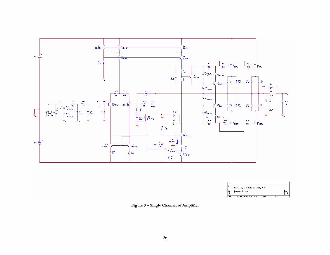
For a complete schematic to assist in explanation, please reference Appendix A.
Power Supply
The power supply for the prototype model is designed around a transformer that was extracted from a broken JVC 330 Watt amplifier. Thus, future designs may vary. However, the principle behind the construction remains the same. A bridge rectifier produces a rectified sinusoidal waveform which is filtered by a resistive-capacitive network and regulated by a zener shunt voltage regulator [1]. The value of the regulating resistor may

5
be determined by a simple mathematical calculation from Equation 1. Although the calculation may be somewhat trivial, the increased load causes a drop in the voltage from the transformer, so this value must be reduced to an optimal value.
max,min,
min,0min,
Lz
ZZZs
IIIrVV
R+
−−=
Equation 1 – Calculation of Regulating Resistor
Part selection for the power supply is slightly tricky. When the power switch is pressed, a large influx of current is distributed throughout the circuit. Therefore, all components must have higher current ratings than their nominal operating values. Additionally, many bridge rectifiers have lowered current ratings for driving capacitive loads, due to the current that must be produced to charge them.
Input Stage
The input stage consists of a differential pair amplifier biased by a Wilson current mirror. The differential pair acts as a transconductance amplifier, converting a small-signal input voltage into a small-signal output current. The Wilson current mirror acts as a high impedance current source, increasing both slew rate and common-mode rejection characteristics [1]. The implementation of an active load in the collectors of the differential pair refers the bias current through the inverting transistor to the positive transistor, allowing for a more balanced bias point. Low noise, high voltage transistors (2N5551 and 2N5401) are employed for this stage because feedback theory dictates that the mixing stage produces the greatest contribution to overall signal noise.
Voltage Amplifier Stage
The voltage amplifier stage is a transresistance amplifier, translating the small-signal output current from the input stage to a highly amplified voltage signal at its output node. The selected topology utilizes a Darlington pair, a cascoded transistor with current limiting, and local negative feedback. The Darlington pair consists of two transistors connected as shown in Figure 1. This structure doubles the beta value of the transistor, allowing low gain devices to be used for high gain applications. This is especially useful when considering the low noise transistors that are employed in this design.
Figure 1 – Darlington Pair Configuration

6
The implementation of a cascoded transistor adds two critical features to the voltage amplifier stage. First, it increases the output resistance considerably. Subsequently, the voltage gain increases, as it is highly dependent upon the output resistance. Secondly, the cascoded transistor allows for a current sensing action, as shown in Figure 2. A small resistor is placed in series with the emitter of the transistor and in parallel with the base and emitter of a sensing transistor. When the current flow through the resistor causes a voltage drop equal to the turn-on voltage of the sensing transistor, base current is removed from the cascode transistor through the sensing transistor. This acts as negative feedback to the increased bias current and prevents device overload.
Figure 2 – Current Limiting Scheme with Cascoded Transistor
A high voltage capacitor is placed between the input and output nodes to create a local negative feedback loop. This connection utilizes the Miller effect to create a dominant pole at the input node [1]. Due to the global negative feedback in the circuit, stability becomes an important issue. This pole may be set such that the magnitude of the gain drops below unity before the phase shifts -180 degrees.
Output Stage
The output stage is a class AB topology, realized with power MOSFETs for their ruggedness and high input impedance. The premise of the class AB output configuration is based upon setting a bias current and allowing the transistors to conduct for approximately 180 degrees of a cycle, while amplifying the output current to a high level. This allows the amplifier to handle much higher current loads without a corresponding drop in voltage.
A device called a Vbe multiplier, shown in Figure 3, biases the class AB topology such that the output transistors are able to conduct simultaneously [1]. The Vbe multiplier uses the on-voltage of the transistor to set a current through the resistor R1. This current can be assumed to be the same through R2. Thus, the voltage difference, Vbias, is equivalent to (R2+R1)IR.

7
Figure 3 – Vbe Multiplier
Global Feedback
Throughout the design of the previous three stages, the value of the small-signal gain is somewhat irrelevant, provided that it is very large. The amplifier utilizes a voltage sensing-voltage mixing feedback topology, also called series-shunt feedback, to increase input resistance and decrease output resistance. Additionally, this type of feedback allows the designer to specify the overall gain of the amplifier with two resistors, shown as R7 and R9 in Figure 4.
Figure 4 – Series-Shunt Feedback Topology
Basic feedback theory specifies that if the open-loop gain A(s) is very large and the loop gain A(s)β(s) is much greater than unity, the overall gain may be approximated as the reciprocal of the feedback gain, β(s). The overall gain is derived in Equation 2.
8
( ) ( )( ) ( )
( ) ( ) ( ) ( )( )
( )
( )
( )9
7
9
7
9
97
97
9
1)(
1)(
,11)(
RR
RR
RRR
sVsV
RRR
s
ssVsV
ssAandssAifssA
sAsVsV
i
i
i
≈+=+
=∴
+=
=
>>>>+
=
β
β
βββ
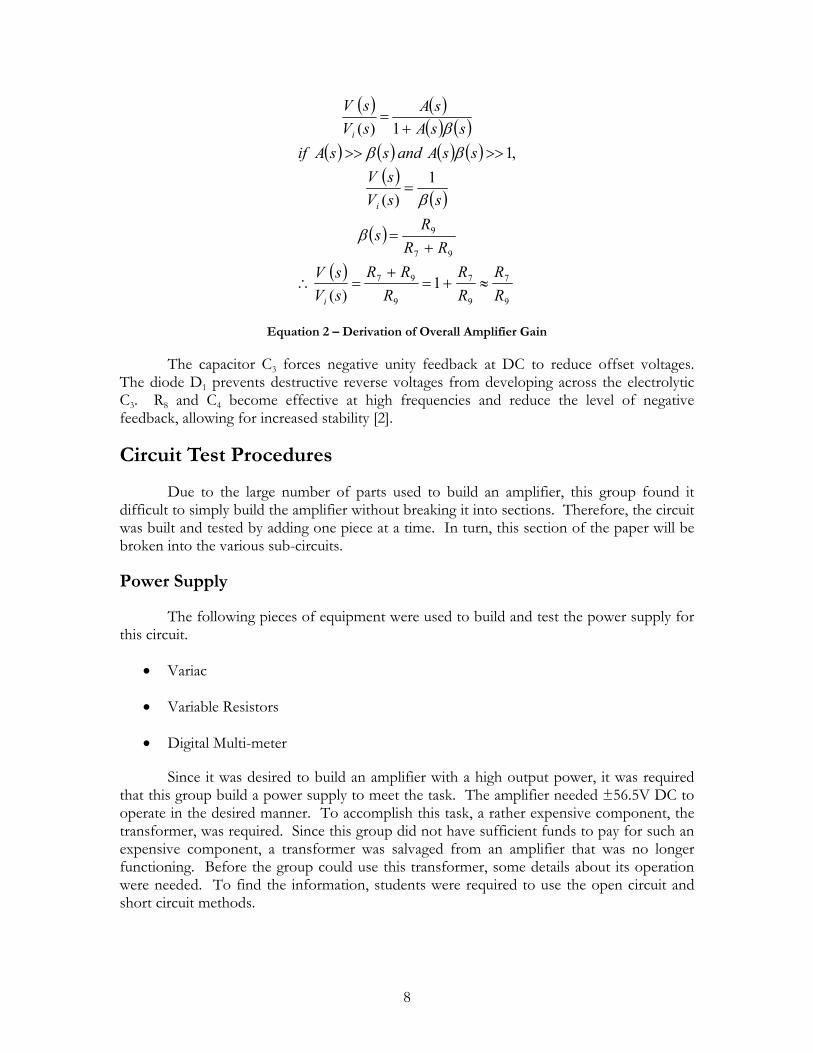
Equation 2 – Derivation of Overall Amplifier Gain
The capacitor C3 forces negative unity feedback at DC to reduce offset voltages. The diode D1 prevents destructive reverse voltages from developing across the electrolytic C3. R8 and C4 become effective at high frequencies and reduce the level of negative feedback, allowing for increased stability [2].
Circuit Test Procedures
Due to the large number of parts used to build an amplifier, this group found it difficult to simply build the amplifier without breaking it into sections. Therefore, the circuit was built and tested by adding one piece at a time. In turn, this section of the paper will be broken into the various sub-circuits.
Power Supply
The following pieces of equipment were used to build and test the power supply for this circuit.
• Variac
• Variable Resistors
• Digital Multi-meter
Since it was desired to build an amplifier with a high output power, it was required that this group build a power supply to meet the task. The amplifier needed ±56.5V DC to operate in the desired manner. To accomplish this task, a rather expensive component, the transformer, was required. Since this group did not have sufficient funds to pay for such an expensive component, a transformer was salvaged from an amplifier that was no longer functioning. Before the group could use this transformer, some details about its operation were needed. To find the information, students were required to use the open circuit and short circuit methods.
9
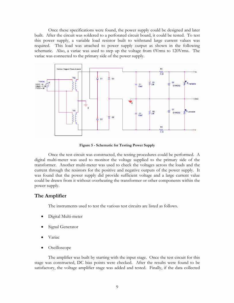
Once these specifications were found, the power supply could be designed and later built. After the circuit was soldered to a perforated circuit board, it could be tested. To test this power supply, a variable load resistor built to withstand large current values was required. This load was attached to power supply output as shown in the following schematic. Also, a variac was used to step up the voltage from 0Vrms to 120Vrms. The variac was connected to the primary side of the power supply.
Figure 5 - Schematic for Testing Power Supply
Once the test circuit was constructed, the testing procedures could be performed. A digital multi-meter was used to monitor the voltage supplied to the primary side of the transformer. Another multi-meter was used to check the voltages across the loads and the current through the resistors for the positive and negative outputs of the power supply. It was found that the power supply did provide sufficient voltage and a large current value could be drawn from it without overheating the transformer or other components within the power supply.
The Amplifier
The instruments used to test the various test circuits are listed as follows.
• Digital Multi-meter
• Signal Generator
• Variac
• Oscilloscope
The amplifier was built by starting with the input stage. Once the test circuit for this stage was constructed, DC bias points were checked. After the results were found to be satisfactory, the voltage amplifier stage was added and tested. Finally, if the data collected
10
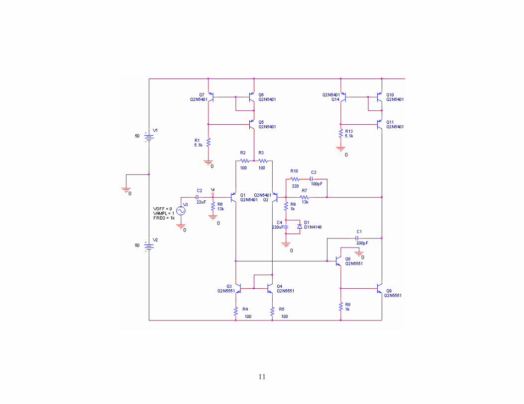
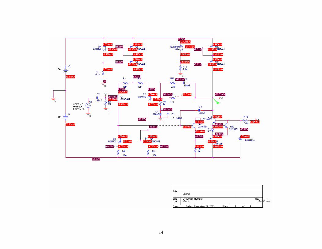
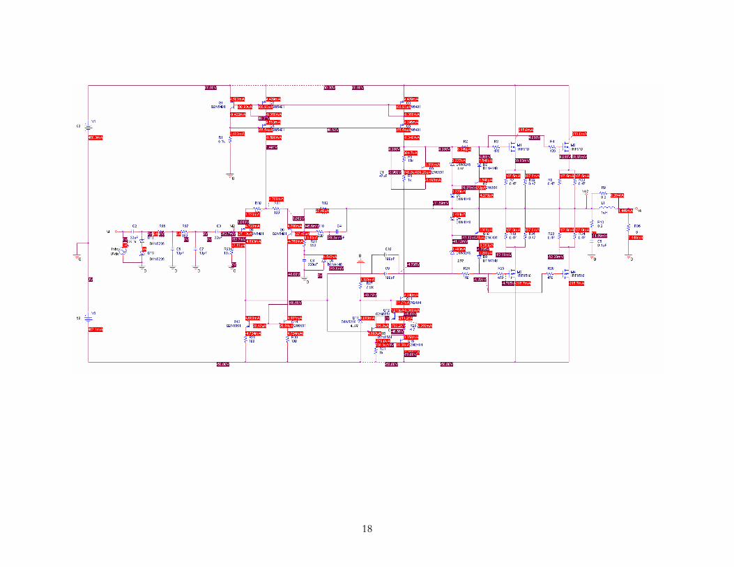
from this stage were in agreement with the simulations, the output stage was added and tested. For each stage, the DC bias points were tested with the power supply set to provide ±5V, ±10V, and ±20V. The input and voltage amplifier stages were also tested with the power supply set to provide ±30V, ±40V, and ±50V. The various voltage values were provided via a variac in place of the 120Vrms obtained from a standard outlet. After the bias points were checked at each stage, a sinusoidal signal with magnitude 2Vpp and frequency of 1kHz was applied to each of the test circuits using a signal generator. A frequency sweep was run on the pre-filter and output stage as well. All AC signals were monitored using an oscilloscope. The DC bias points were tested using a digital multi-meter. The following schematics are the circuits used for the sectioned building and testing purposes.
11

12

13
14

15

16

17
18

19
Performance
From the use of the open-circuit and short-circuit tests, the following values were measured from the transformer.
Short Circuit Test Open Circuit Test V1 120.99 V 6.81 V I1 245.60 mA 1.8705 A P1 12.075 W 12.4 W Power Factor 0.4064 0.9733
Table 1 - Results of Open Circuit, Short Circuit Test
These values were used to find the following specifications for the amplifier:
a 2.69 R1 0.8 Ω X1 j0.418 Ω RC 1.212 kΩ XM j527.64 kΩ R2 0.379 Ω X2 j0.0578 Ω V1,RATED 120 Vrms I1,RATED 0.691 A I2,RATED 5 A
Table 2 - Transformer Parameters
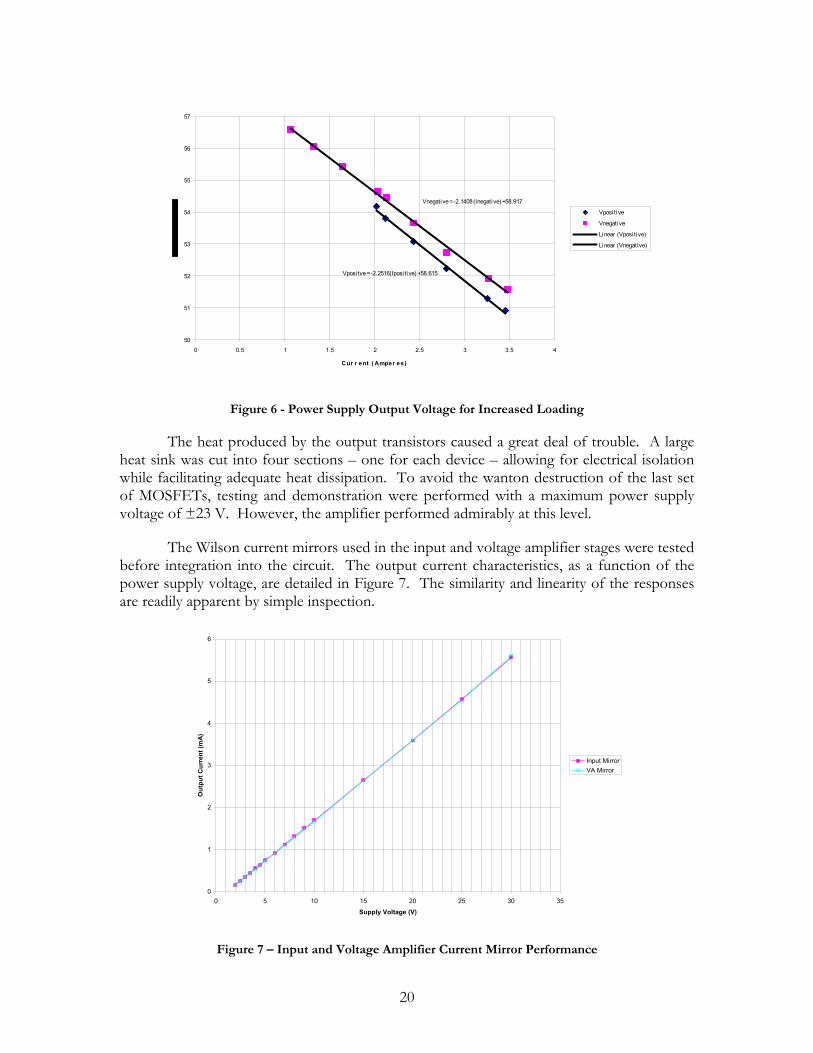
By applying a variable load to the power supply, the output of the power supply could be determined. The measurements for both the positive and negative outputs are listed below in Table 3. A plot with associated trend lines is displayed in Figure 6.
Positive Voltage (V) Positive Current (A) Negative Voltage (V) Negative Current (A)50.9 3.46 51.56 3.48 51.27 3.26 51.9 3.27 52.22 2.8 52.72 2.8 53.07 2.43 53.66 2.43 53.81 2.12 54.48 2.13 54.19 2.02 54.67 2.03
55.44 1.64 56.05 1.32 56.59 1.07
Table 3 - Power Supply Loading Results
20
Vposi tve = -2.2516(Iposi tive) + 58.615
Vnegative = -2.1408 (Inegative) + 58.917
50
51
52
53
54
55
56
57
0 0.5 1 1.5 2 2.5 3 3.5 4
Cur r ent ( Amper es)
Vposi tive
Vnegative
Linear (Vposi tive)
Linear (Vnegative)
Figure 6 - Power Supply Output Voltage for Increased Loading
The heat produced by the output transistors caused a great deal of trouble. A large heat sink was cut into four sections – one for each device – allowing for electrical isolation while facilitating adequate heat dissipation. To avoid the wanton destruction of the last set of MOSFETs, testing and demonstration were performed with a maximum power supply voltage of ±23 V. However, the amplifier performed admirably at this level.
The Wilson current mirrors used in the input and voltage amplifier stages were tested before integration into the circuit. The output current characteristics, as a function of the power supply voltage, are detailed in Figure 7. The similarity and linearity of the responses are readily apparent by simple inspection.
0
1
2
3
4
5
6
0 5 10 15 20 25 30 35
Supply Voltage (V)
Out
put C
urre
nt (m
A)
Input MirrorVA Mirror
Figure 7 – Input and Voltage Amplifier Current Mirror Performance

21
Inputting a 1 kHz sinusoidal signal of known amplitude to the amplifier and measuring the output voltage with an oscilloscope measured the small-signal gain characteristics. In all cases and levels of construction, the output node displayed a voltage gain of 13 (V/V). Note the correspondence with Equation 2, where R9 and R7 are 13 kΩ and 1 kΩ, respectively.
Distortion measurements were performed using a Hewlett-Packard spectrum analyzer. A 1 kHz tone from a function generator was examined for harmonics. The second and third harmonics exhibited a response -50 dB below the fundamental. These measurements may be even better because the function generator appears to generate a slightly noisy signal. The casual listening of many students could not detect any distortion a music playback. Subsequently, the amplifier may be considered satisfactory for nominal listening levels.
Cost and Manufacturability Analysis
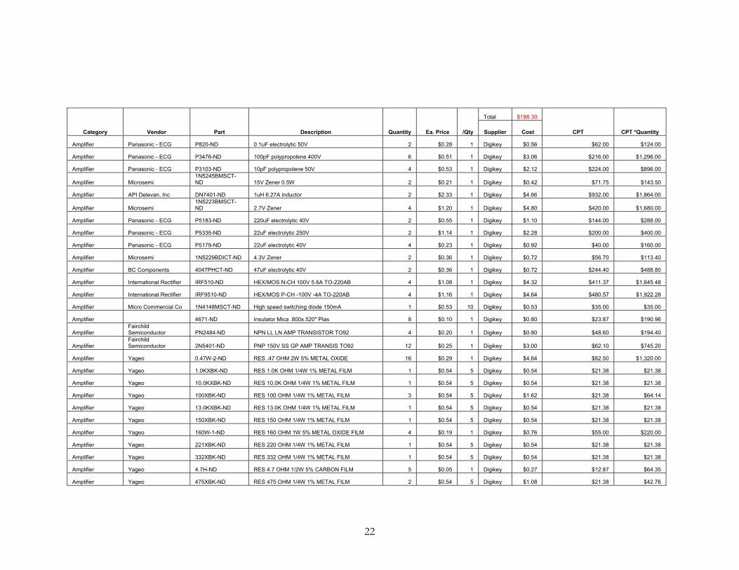
The following pages show the cost analysis run on the design chosen for this project. The cost for 1000 units of each part was found and multiplied by the quantity needed for one amplifier. Once these calculations were stored into a column of an Excel spreadsheet, the sum feature was used to find the total price for 1000 units of this product. To get the price per unit, one amplifier, the total was simply divided by 100. This yielded a cost of $137.73 per amplifier. The bulk of this cost is due to the price of the transformer $98.18. The price for this transformer could only be found quoted per item. Therefore, if it were possible to commission a company to build transformers for this project, the cost for one amplifier would likely be less than the approximation provided here. However, a notable difference between building one amplifier and building 1000 is still prevalent. Other than the obvious 999 amplifiers, the cost per amplifier was reduced by $60.57. Unfortunately, this amplifier, being more complex than other electronic items would undoubtedly require a large investment of time to build. For this reason, the cost for one of these amplifiers to a consumer would be over $200.
22
Total $198.30
Category Vendor Part Description Quantity Ea. Price /Qty Supplier Cost CPT CPT *Quantity
Amplifier Panasonic - ECG P820-ND 0.1uF electrolytic 50V 2 $0.28 1 Digikey $0.56 $62.00 $124.00
Amplifier Panasonic - ECG P3476-ND 100pF polypropolene 400V 6 $0.51 1 Digikey $3.06 $216.00 $1,296.00
Amplifier Panasonic - ECG P3103-ND 10pF polypropolene 50V 4 $0.53 1 Digikey $2.12 $224.00 $896.00
Amplifier Microsemi 1N5245BMSCT-ND 15V Zener 0.5W 2 $0.21 1 Digikey $0.42 $71.75 $143.50
Amplifier API Delevan, Inc DN7401-ND 1uH 6.27A inductor 2 $2.33 1 Digikey $4.66 $932.00 $1,864.00
Amplifier Microsemi 1N5223BMSCT-ND 2.7V Zener 4 $1.20 1 Digikey $4.80 $420.00 $1,680.00
Amplifier Panasonic - ECG P5183-ND 220uF electrolytic 40V 2 $0.55 1 Digikey $1.10 $144.00 $288.00
Amplifier Panasonic - ECG P5335-ND 22uF electrolytic 250V 2 $1.14 1 Digikey $2.28 $200.00 $400.00
Amplifier Panasonic - ECG P5179-ND 22uF electrolytic 40V 4 $0.23 1 Digikey $0.92 $40.00 $160.00
Amplifier Microsemi 1N5229BDICT-ND 4.3V Zener 2 $0.36 1 Digikey $0.72 $56.70 $113.40
Amplifier BC Components 4047PHCT-ND 47uF electrolytic 40V 2 $0.36 1 Digikey $0.72 $244.40 $488.80
Amplifier International Rectifier IRF510-ND HEX/MOS N-CH 100V 5.6A TO-220AB 4 $1.08 1 Digikey $4.32 $411.37 $1,645.48
Amplifier International Rectifier IRF9510-ND HEX/MOS P-CH -100V -4A TO-220AB 4 $1.16 1 Digikey $4.64 $480.57 $1,922.28
Amplifier Micro Commercial Co 1N4148MSCT-ND High speed switching diode 150mA 1 $0.53 10 Digikey $0.53 $35.00 $35.00
Amplifier 4671-ND Insulator Mica .800x.520" Plas 8 $0.10 1 Digikey $0.80 $23.87 $190.96
Amplifier Fairchild Semiconductor PN2484-ND NPN LL LN AMP TRANSISTOR TO92 4 $0.20 1 Digikey $0.80 $48.60 $194.40
Amplifier Fairchild Semiconductor 2N5401-ND PNP 150V SS GP AMP TRANSIS TO92 12 $0.25 1 Digikey $3.00 $62.10 $745.20
Amplifier Yageo 0.47W-2-ND RES .47 OHM 2W 5% METAL OXIDE 16 $0.29 1 Digikey $4.64 $82.50 $1,320.00
Amplifier Yageo 1.0KXBK-ND RES 1.0K OHM 1/4W 1% METAL FILM 1 $0.54 5 Digikey $0.54 $21.38 $21.38
Amplifier Yageo 10.0KXBK-ND RES 10.0K OHM 1/4W 1% METAL FILM 1 $0.54 5 Digikey $0.54 $21.38 $21.38
Amplifier Yageo 100XBK-ND RES 100 OHM 1/4W 1% METAL FILM 3 $0.54 5 Digikey $1.62 $21.38 $64.14
Amplifier Yageo 13.0KXBK-ND RES 13.0K OHM 1/4W 1% METAL FILM 1 $0.54 5 Digikey $0.54 $21.38 $21.38
Amplifier Yageo 150XBK-ND RES 150 OHM 1/4W 1% METAL FILM 1 $0.54 5 Digikey $0.54 $21.38 $21.38
Amplifier Yageo 160W-1-ND RES 160 OHM 1W 5% METAL OXIDE FILM 4 $0.19 1 Digikey $0.76 $55.00 $220.00
Amplifier Yageo 221XBK-ND RES 220 OHM 1/4W 1% METAL FILM 1 $0.54 5 Digikey $0.54 $21.38 $21.38
Amplifier Yageo 332XBK-ND RES 332 OHM 1/4W 1% METAL FILM 1 $0.54 5 Digikey $0.54 $21.38 $21.38
Amplifier Yageo 4.7H-ND RES 4.7 OHM 1/2W 5% CARBON FILM 5 $0.05 1 Digikey $0.27 $12.87 $64.35
Amplifier Yageo 475XBK-ND RES 475 OHM 1/4W 1% METAL FILM 2 $0.54 5 Digikey $1.08 $21.38 $42.76
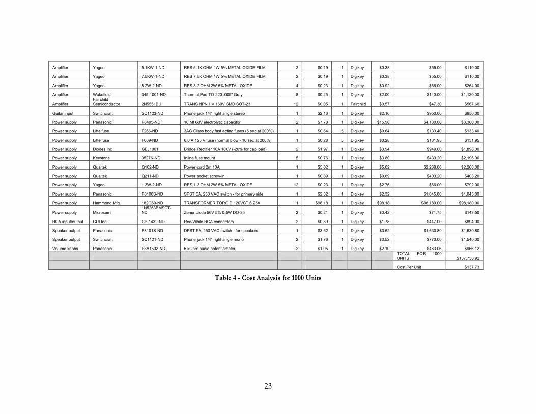
23
Amplifier Yageo 5.1KW-1-ND RES 5.1K OHM 1W 5% METAL OXIDE FILM 2 $0.19 1 Digikey $0.38 $55.00 $110.00
Amplifier Yageo 7.5KW-1-ND RES 7.5K OHM 1W 5% METAL OXIDE FILM 2 $0.19 1 Digikey $0.38 $55.00 $110.00
Amplifier Yageo 8.2W-2-ND RES 8.2 OHM 2W 5% METAL OXIDE 4 $0.23 1 Digikey $0.92 $66.00 $264.00
Amplifier Wakefield 345-1001-ND Thermal Pad TO-220 .009" Gray 8 $0.25 1 Digikey $2.00 $140.00 $1,120.00
Amplifier Fairchild Semiconductor 2N5551BU TRANS NPN HV 160V SMD SOT-23 12 $0.05 1 Fairchild $0.57 $47.30 $567.60
Guitar input Switchcraft SC1123-ND Phone jack 1/4" right angle stereo 1 $2.16 1 Digikey $2.16 $950.00 $950.00
Power supply Panasonic P6495-ND 10 Mf 63V electrolytic capacitor 2 $7.78 1 Digikey $15.56 $4,180.00 $8,360.00
Power supply Littelfuse F266-ND 3AG Glass body fast acting fuses (5 sec at 200%) 1 $0.64 5 Digikey $0.64 $133.40 $133.40
Power supply Littelfuse F609-ND 6.0 A 125 V fuse (normal blow - 10 sec at 200%) 1 $0.28 5 Digikey $0.28 $131.95 $131.95
Power supply Diodes Inc GBJ1001 Bridge Rectifier 10A 100V (-20% for cap load) 2 $1.97 1 Digikey $3.94 $949.00 $1,898.00
Power supply Keystone 3527K-ND Inline fuse mount 5 $0.76 1 Digikey $3.80 $439.20 $2,196.00
Power supply Qualtek Q102-ND Power cord 2m 10A 1 $5.02 1 Digikey $5.02 $2,268.00 $2,268.00
Power supply Qualtek Q211-ND Power socket screw-in 1 $0.89 1 Digikey $0.89 $403.20 $403.20
Power supply Yageo 1.3W-2-ND RES 1.3 OHM 2W 5% METAL OXIDE 12 $0.23 1 Digikey $2.76 $66.00 $792.00
Power supply Panasonic P8100S-ND SPST 5A, 250 VAC switch - for primary side 1 $2.32 1 Digikey $2.32 $1,045.80 $1,045.80
Power supply Hammond Mfg. 182Q60-ND TRANSFORMER TOROID 120VCT 6.25A 1 $98.18 1 Digikey $98.18 $98,180.00 $98,180.00
Power supply Microsemi 1N5263BMSCT-ND Zener diode 56V 5% 0.5W DO-35 2 $0.21 1 Digikey $0.42 $71.75 $143.50
RCA input/output CUI Inc CP-1432-ND Red/White RCA connectors 2 $0.89 1 Digikey $1.78 $447.00 $894.00
Speaker output Panasonic P8101S-ND DPST 5A, 250 VAC switch - for speakers 1 $3.62 1 Digikey $3.62 $1,630.80 $1,630.80
Speaker output Switchcraft SC1121-ND Phone jack 1/4" right angle mono 2 $1.76 1 Digikey $3.52 $770.00 $1,540.00
Volume knobs Panasonic P3A1502-ND 5 kOhm audio potentiometer 2 $1.05 1 Digikey $2.10 $483.06 $966.12
TOTAL FOR 1000 UNITS $137,730.92
Cost Per Unit $137.73
Table 4 - Cost Analysis for 1000 Units

24
Conclusion
Although the amplifier was not tested at its operational limits, the distortion level at a nominal volume was beneath the common level of human perception. The group is confident that soldering the amplifier onto a perfboard and more testing would reveal that he amplifier functions properly at higher power ratings. Another shortcoming of the project was the inability to mount the amplifier inside the Zenith radio cabinet because the input and voltage amplifier stages were constructed on one of the lab’s breadboards. However, this is simply a matter of drilling screws through the perfboards and the amplifier’s turntable stand. Future additions to this project could involve the implementation of a graphic equalizer at the input and a mixing board for handling the levels of multiple inputs. Also, a circuit could be designed to handle the current influx through the speakers when turning on the power.
Charity and Eddie would like to acknowledge the following individuals for their contributions to the project: Marcelo Schupach, for his assistance with power supply testing; Dr. Jerry Yeargan, for assistance with biasing the output stage; and Mark Heiliger, for selflessly donating parts for the project, including the power supply and heat sinks.
References
[1] Sedra, Adel S. and Kenneth C. Smith. Microelectronic Circuits. New York: Oxford University Press, 1998.
[2] Slone, G. Randy. High-Power Audio Amplifier Construction Manual. New York: McGraw Hill, 1999.

25
Appendix A: Complete Schematic
Figure 8 – Power Supply Schematic
26
Figure 9 – Single Channel of Amplifier

27
Appendix B: Complete Parts Listing
Vendor Digikey Part Description Qty Panasonic - ECG P820-ND 0.1uF electrolytic 50V 2 Panasonic - ECG P3476-ND 100pF polypropolene 400V 6 Panasonic - ECG P3103-ND 10pF polypropolene 50V 4 Microsemi 1N5245BMSCT-ND 15V Zener 0.5W 2 API Delevan, Inc DN7401-ND 1uH 6.27A inductor 2 Microsemi 1N5223BMSCT-ND 2.7V Zener 4 Panasonic - ECG P5183-ND 220uF electrolytic 40V 2 Panasonic - ECG P5335-ND 22uF electrolytic 250V 2 Panasonic - ECG P5179-ND 22uF electrolytic 40V 4 Microsemi 1N5229BDICT-ND 4.3V Zener 2 BC Components 4047PHCT-ND 47uF electrolytic 40V 2 International Rectifier IRF510-ND HEX/MOS N-CH 100V 5.6A TO-220AB 4 International Rectifier IRF9510-ND HEX/MOS P-CH -100V -4A TO-220AB 4 Micro Commercial Co 1N4148MSCT-ND High speed switching diode 150mA 1 4671-ND Insulator Mica .800x.520" Plas 8 Fairchild Semiconductor PN2484-ND NPN LL LN AMP TRANSISTOR TO92 4 Fairchild Semiconductor 2N5401-ND PNP 150V SS GP AMP TRANSIS TO92 12 Yageo 0.47W-2-ND RES .47 OHM 2W 5% METAL OXIDE 16 Yageo 1.0KXBK-ND RES 1.0K OHM 1/4W 1% METAL FILM 1 Yageo 10.0KXBK-ND RES 10.0K OHM 1/4W 1% METAL FILM 1 Yageo 100XBK-ND RES 100 OHM 1/4W 1% METAL FILM 3 Yageo 13.0KXBK-ND RES 13.0K OHM 1/4W 1% METAL FILM 1 Yageo 150XBK-ND RES 150 OHM 1/4W 1% METAL FILM 1 Yageo 160W-1-ND RES 160 OHM 1W 5% METAL OXIDE FILM 4 Yageo 220XBK-ND RES 220 OHM 1/4W 1% METAL FILM 1 Yageo 332XBK-ND RES 332 OHM 1/4W 1% METAL FILM 1 Yageo 4.7H-ND RES 4.7 OHM 1/2W 5% CARBON FILM 5 Yageo 475XBK-ND RES 475 OHM 1/4W 1% METAL FILM 2 Yageo 5.1KW-1-ND RES 5.1K OHM 1W 5% METAL OXIDE FILM 2 Yageo 7.5KW-1-ND RES 7.5K OHM 1W 5% METAL OXIDE FILM 2 Yageo 8.2W-2-ND RES 8.2 OHM 2W 5% METAL OXIDE 4 Wakefield 345-1001-ND Thermal Pad TO-220 .009" Gray 8 Fairchild Semiconductor 2N5551BU TRANS NPN HV 160V SMD 12 Switchcraft SC1123-ND Phone jack 1/4" right angle stereo 1 Panasonic P6495-ND 10 mf 63V electrolytic capacitor 2 Littelfuse F266-ND 3AG Glass body fast acting fuses (5 sec at 200%) 1 Littelfuse F609-ND 6.0 A 125 V fuse (normal blow - 10 sec at 200%) 1 Diodes Inc GBJ1001 Bridge Rectifier 10A 100V (-20% for cap load) 2 Keystone 3527K-ND Inline fuse mount 5 Qualtek Q102-ND Power cord 2m 10A 1 Qualtek Q211-ND Power socket screw-in 1 Yageo 1.3W-2-ND RES 1.3 OHM 2W 5% METAL OXIDE 12 Panasonic P8100S-ND SPST 5A, 250 VAC switch - for primary side 1 Hammond Mfg. 182Q60-ND TRANSFORMER TOROID 120VCT 6.25A 1 Microsemi 1N5263BMSCT-ND Zener diode 56V 5% 0.5W DO-35 2

28
CUI Inc CP-1432-ND Red/White RCA connectors 2 Panasonic P8101S-ND DPST 5A, 250 VAC switch - for speakers 1 Switchcraft SC1121-ND Phone jack 1/4" right angle mono 2 Panasonic P3A1502-ND 5 kOhm audio potentiometer 2
29
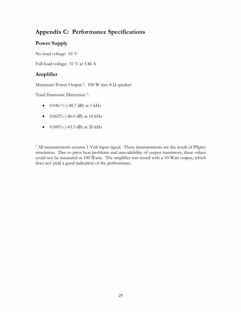
Appendix C: Performance Specifications
Power Supply
No-load voltage: 61 V
Full-load voltage: 51 V at 3.46 A
Amplifier
Maximum Power Output †: 100 W into 8 Ω speaker
Total Harmonic Distortion †:
• 0.046 % (-48.7 dB) at 1 kHz
• 0.062% (-46.0 dB) at 10 kHz
• 0.085% (-43.3 dB) at 20 kHz
† All measurements assume 1 Volt input signal. These measurements are the result of PSpice simulation. Due to prior heat problems and unavailability of output transistors, these values could not be measured at 100 Watts. The amplifier was tested with a 10-Watt output, which does not yield a good indication of the performance.

30
Appendix D: Gantt Chart

31
Appendix E: Project Proposal
ELEG 4062: Electrical Engineering Design Laboratory
Project Specifications and Requirements
Project Name: LinAmp 2002
Team Members: Eddie Pettis and Charity Post
Members’ e-mails: [email protected], [email protected]
Semester: Fall 2002
Section: 002 (Th 2:00 PM – 5:20 PM)
Task Description Responsible
Person
Met Not
Met
Design input stage Eddie
Design voltage amplifier stage Both
Design output stage Eddie
Design feedback loop Charity
Design power supply Both
Cost analysis Both
Mechanical design for cabinet Charity
Fabrication Both
Debugging Both
Documentation Both
AGREED TO:
Instructor: _______________________ Team: ________________________
Date: ___________________________ ________________________

32
Project Description
The goal of this project is to construct a three-stage Lin topology stereo audio
amplifier with peak electrical output power of approximately 100 watts RMS per channel.
The Lin topology, developed by a researcher at RCA in 1956, has been experimentally
determined to yield the highest performance specifications of any known topology. The
design consists of three parts: an input stage, a voltage amplifier stage, and an output stage.
The input stage is usually a differential amplifier due to its inherent ability to suppress
common-mode signals, i.e., noise. The voltage amplifier stage is meant to perform the
majority of the voltage gain for the circuit. Finally, the signal passes through a high-current
output stage, which drives the speaker load. To produce an audio bandwidth (20-20,000 Hz)
and accurate gain, negative feedback will also be employed.
Due to the large voltages required to produce 100 watts RMS into an 8-ohm resistive
load, a hefty power supply must be used. This supply must be able to produce rail voltages
of approximately 35 to 55 volts with low noise and little or no ripple. Due to the lack of
availability, this power supply must become a part of the project design. Additionally, safety
measures must be incorporated to prevent a potentially lethal shock from large capacitors
during fabrication.
The high cost of this project will make the construction of protection circuitry
imperative. The amplifier must be able to bypass output transistors in the event of power
surges and device failures to allow fuses enough time to blow before destroying the output
stages and causing a cascading wave of destruction through the circuit. Additionally,
circuitry must be prepared to avoid damage to input devices and the speaker cones.
The system will be inserted into a 1950’s vintage Zenith radio cabinet. This cabinet
was purchased two years ago in an antique shop and will be used to encase the project as
well as provide aesthetics to the overall design. The knobs and radio dial will not necessarily
be used to control the amplifier. Wiring should be hidden from view and be inaccessible
without removing a safety panel to avoid accidental shock. In addition, heat sinks must be
mounted to avoid thermal breakdown of output transistors. Unfortunately, cooling fans are

33
not viable options, as the noise produced by the fans will become readily apparent at low
volume levels.
This project is being funded privately by the students. The expense of speakers and
other costly components will likely be handled by soliciting donations from local businesses.
Other sources of materials, such as heat sinks and cases, include discarded audio amplifiers
and outdated computers. It is the students’ intention to keep the completed project
following the end of the course. By completing this project, the students will gain valuable
experience in analog system design, cost analysis, noise reduction, mechanical layout, and
fabrication techniques.
Rm
Voltageamplifier
(transimpedence)
B
Series-shuntfeedback
Gm
Low-noiseinput stage
(transconductance)
Line inputvoltage
1
s+woFrequency
compensation
DifferentialPair
Current outto speaker
Ai
Currentamplifier
Figure 10 – Simplified Block Diagram for Single Channel of Audio Amplifier
R
RC.s+1RC Peak Detector
OutputRail Voltage
a
Center-tapTransformer
|u|
BridgeRectifier
120V rmsfrom socket
Figure 11 – Simplified Block Diagram for Power Supply

34
Appendix F: Project Journal
9/2/02
We formatted the Gantt chart and wrote first draft of project specifications. Charity needs to help with block diagrams and task assignments. Eddie could also use her help with creating linked objects and milestones using MS Project.
9/4/02
We worked on the proposal for tomorrow. Charity developed block diagrams, which Eddie drew in Simulink for the documentation. We reviewed the entire proposal and Gantt schedule and accepted the document as complete.
Eddie began an attempt to design the power supply for the amplifier. Upon completing calculations, Eddie estimates a transformer power rating of 540 VA. Eddie attempted to look up a transformer with these specifications on the internet but found that the cost exceeded $60.00. This leads us to three conclusions: attempt to salvage the power supply from the JVC amplifier, change the power output of the design amplifier, or pay the $60.00 charge.
Should we attempt to salvage the power supply, we will need to schedule an appointment with Marcelo in the lab to perform open circuit-short circuit tests on the transformer to determine its rating and characteristics. Eddie will perform calculations to determine what type of transformer that will be required to produce an output of 75 volts RMS.
9/5/02
In lab, we opened up the JVC amplifier and removed the transformer, as well as the heat sink and other assorted parts. However, most of the parts were unidentifiable because they were obsolete and had no datasheets available on the internet. Most components appeared to be of Japanese or Korean origin. Unfortunately, the transformer also did not have any distinguishable markings.
We took the transformer to Marcelo to help determine the power rating of the transformer and any operating parameters. We have scheduled an appointment to come back to the energy conversion laboratory tomorrow at 1:00 PM to perform various experiments on the transformer.
Additional conversations with Marcelo have indicated that the ideal transformer for hour amplifier is toroidal because it will negate crossover distortion. Dr. Balda and Marcelo both recommended soliciting donations from the same source as Paul Sheppard. Additionally, Ty McNutt and Kevin Speer suggested a website called www.tubesandmore.com.
35
This search was largely unsuccessful. Subsequently, Eddie checked the Hammond transformers again. This time Eddie went straight to the web page and found a listing of all toroidal transformers. However, Eddie still did not find a suitable match. The standard secondary voltages of the transformers are 60 or 120 Volts, but we must choose between a lower voltage and proper current rating at 60 V or a lower current at 120 V.
9/6/02
We took the transformer to the Energy Conversion lab to perform various tests upon it. Marcelo was very helpful in determining the power output and model of the transformer by assisting us in performing measurements and open circuit and short circuit procedures. Apparently, the transformer is a center tap topology with a 2.69 turn ratio and a maximum power output that exceeds our requirements, although the exact value is unknown. We estimate that the transformer can easily handle a 5-A Rated current with minimal drop and secondary voltage.
9/8/02
After entering that the model into the computer, Eddie performed a transient analysis on the circuit. The peak voltages of the power supply using standard SPICE components are ±60.5 Volts (42.8 V RMS). Additionally, Eddie calculated the rise time of the voltages using a goal function to be 2.89 seconds when the power supply is connected to a 100 kΩ and 10 mF parallel loads. Experimentation shows that the rise time is due to the time constant created by the load. By decreasing the resistance of the amplifier, the rise time may be reduced, but the increase in current will load the transformer into a lowered voltage.
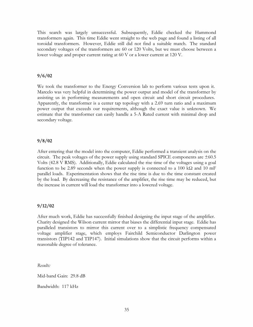
9/12/02
After much work, Eddie has successfully finished designing the input stage of the amplifier. Charity designed the Wilson current mirror that biases the differential input stage. Eddie has paralleled transistors to mirror this current over to a simplistic frequency compensated voltage amplifier stage, which employs Fairchild Semiconductor Darlington power transistors (TIP142 and TIP147). Initial simulations show that the circuit performs within a reasonable degree of tolerance.
Results:
Mid-band Gain: 29.8 dB
Bandwidth: 117 kHz
36
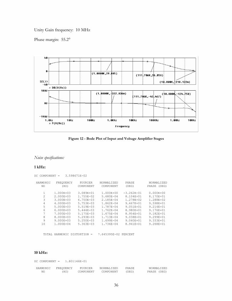
Unity Gain frequency: 10 MHz
Phase margin: 55.2°
Figure 12 - Bode Plot of Input and Voltage Amplifier Stages
Noise specifications:
1 kHz:
DC COMPONENT = 3.598671E-02 HARMONIC FREQUENCY FOURIER NORMALIZED PHASE NORMALIZED NO (HZ) COMPONENT COMPONENT (DEG) PHASE (DEG) 1 1.000E+03 3.089E+01 1.000E+00 -3.262E-01 0.000E+00 2 2.000E+03 1.755E-02 5.680E-04 8.104E+01 8.170E+01 3 3.000E+03 6.750E-03 2.185E-04 1.278E+02 1.288E+02 4 4.000E+03 5.753E-03 1.862E-04 9.467E+01 9.598E+01 5 5.000E+03 5.519E-03 1.787E-04 9.051E+01 9.214E+01 6 6.000E+03 5.444E-03 1.762E-04 8.980E+01 9.176E+01 7 7.000E+03 5.175E-03 1.675E-04 8.954E+01 9.182E+01 8 8.000E+03 5.293E-03 1.713E-04 9.038E+01 9.299E+01 9 9.000E+03 5.250E-03 1.699E-04 9.040E+01 9.333E+01 10 1.000E+04 5.363E-03 1.736E-04 8.941E+01 9.268E+01 TOTAL HARMONIC DISTORTION = 7.645395E-02 PERCENT
10 kHz:
DC COMPONENT = 1.801146E-01 HARMONIC FREQUENCY FOURIER NORMALIZED PHASE NORMALIZED NO (HZ) COMPONENT COMPONENT (DEG) PHASE (DEG)

37
1 1.000E+04 2.911E+01 1.000E+00 -5.017E+00 0.000E+00 2 2.000E+04 3.819E-01 1.312E-02 8.759E+01 9.762E+01 3 3.000E+04 1.923E-01 6.605E-03 7.612E+01 9.117E+01 4 4.000E+04 2.719E-01 9.341E-03 5.105E+01 7.112E+01 5 5.000E+04 2.527E-01 8.681E-03 5.965E+01 8.474E+01 6 6.000E+04 2.075E-01 7.129E-03 4.886E+01 7.897E+01 7 7.000E+04 7.181E-01 2.467E-02 -3.486E+00 3.164E+01 8 8.000E+04 1.843E-01 6.331E-03 3.674E+01 7.687E+01 9 9.000E+04 3.139E-01 1.079E-02 1.239E+02 1.691E+02 10 1.000E+05 1.427E-01 4.901E-03 2.579E+01 7.596E+01 TOTAL HARMONIC DISTORTION = 3.490346E+00 PERCENT
20 kHz:
DC COMPONENT = 2.556227E-01 HARMONIC FREQUENCY FOURIER NORMALIZED PHASE NORMALIZED NO (HZ) COMPONENT COMPONENT (DEG) PHASE (DEG) 1 2.000E+04 2.886E+01 1.000E+00 -1.035E+01 0.000E+00 2 4.000E+04 2.719E-01 9.422E-03 6.472E+01 8.542E+01 3 6.000E+04 1.400E-01 4.851E-03 1.261E+02 1.572E+02 4 8.000E+04 2.306E-01 7.992E-03 5.922E+01 1.006E+02 5 1.000E+05 2.686E-01 9.307E-03 6.208E+01 1.138E+02 6 1.200E+05 1.956E-01 6.780E-03 4.109E+01 1.032E+02 7 1.400E+05 6.547E-01 2.269E-02 -2.529E+01 4.716E+01 8 1.600E+05 1.546E-01 5.356E-03 3.001E+01 1.128E+02 9 1.800E+05 3.761E-01 1.303E-02 9.703E+01 1.902E+02 10 2.000E+05 1.128E-01 3.909E-03 2.278E+01 1.263E+02 TOTAL HARMONIC DISTORTION = 3.220701E+00 PERCENT
50 kHz:
DC COMPONENT = 6.514963E-02 HARMONIC FREQUENCY FOURIER NORMALIZED PHASE NORMALIZED NO (HZ) COMPONENT COMPONENT (DEG) PHASE (DEG) 1 5.000E+04 2.607E+01 1.000E+00 -2.502E+01 0.000E+00 2 1.000E+05 3.646E-01 1.399E-02 6.486E+00 5.652E+01 3 1.500E+05 9.215E-02 3.535E-03 -1.375E+02 -6.241E+01 4 2.000E+05 1.580E-01 6.060E-03 -9.125E+01 8.823E+00 5 2.500E+05 4.144E-02 1.590E-03 -4.108E+01 8.401E+01 6 3.000E+05 3.214E-02 1.233E-03 1.656E+02 3.157E+02 7 3.500E+05 5.263E-01 2.019E-02 -1.639E+02 1.120E+01 8 4.000E+05 5.544E-03 2.127E-04 -2.831E+01 1.718E+02 9 4.500E+05 3.254E-01 1.248E-02 -3.445E+01 1.907E+02 10 5.000E+05 1.767E-02 6.777E-04 -1.047E+01 2.397E+02 TOTAL HARMONIC DISTORTION = 2.850990E+00 PERCENT
38
9/18/02
Eddie feels that he has located the source of the distortion in the circuit. The balance between the differential input stages is off by approximately 30%. This is likely leading to high THD as frequency increases.
9/19/02
We sat in Brough today working on an explanation for the distortion levels of the amplifier. Mostly, we discussed the physical nature of the Darlington pair and worked on an explanation of how it worked. Additionally, we looked for ways to bias it in a state such that it did not sink 3.5-A of current.
The problem surrounding the obscene amounts of distortion within our design has been solved for a one-sided topology. Apparently, the problem has been an internal SPICE issue regarding the step size of the transient analysis. We began to run the simulation again, baffled by the appearance of the time domain signal at 10 kHz and the roughness of its edges. Then, Eddie reduced the maximum step size to 5 ns. Suddenly, THD dropped from around 60% to 0.0026%! One subtlety that we noticed is that the input sinusoid must also be changed when simulating the Fourier analysis or erroneous results occur.
Tests should be repeated with the push-pull topology.
9/27/02
We completed the design, including part selection, for a common source class AB output stage for the amplifier. This design includes a Vbe multiplier to create a bias voltage. Final modifications need to be made to enable various circuit protection schemes, increased gain in the feedback stage, and slightly reduced noise levels at frequencies above 10 kHz.
10/2/02
We explored the slew rate of the amplifier. The Slone text gives an equation for calculating slew limiting as:
max,max 2 oV
SRfπ
=
The slew rate was calculated by a SPICE goal function for rise time. With a capacitance of 100 pF, the slew rate (SR) was calculated to be 9.27 V/µs. Implementing this into the above equation, the maximum frequency that can be transmitted without slew rate distortion is 36.89 kHz with a 40 V peak output.

39
The text mentions these ideal slew rates on p. 236:
32 W RMS 11 V/µs 64 W RMS 16 V/µs 125 W RMS 23 V/µs 250 W RMS 32 V/µs 500 W RMS 45 V/µs 1000 W RMS 64 V/µs
These values were calculated by solving for SR in the above equation, given an 80 kHz bandwidth. For a 100 W RMS amplifier, the ideal slew rate is 20.1 V/µs.
The real question to ask is, “Should we care that the slew rate distorts 100 W signals at 80 kHz?” If you recomputed the ideal slew rate for a 20 kHz bandwidth, the SR must only be 5.03 V/µs. At this time, we would like to side with the wisdom of those who have been working with audio equipment for some time, but we are having a very difficult time increasing the slew rate.
Having completed all of the necessary requirements for the basic amplifier (neglecting only protection circuitry), the distortion measures are:
Cc = 100 pF Cc = 200 pF 1 kHz 0.01244390% 0.01297479% 10 kHz 0.02469728% 0.04323380% 20 kHz 0.03974483% 0.07018627% 50 kHz 0.05639360% 0.08083945%
As a result of this simulation and the assurance that the amplifier remains stable with approximately a 35 degree phase margin, we have decided to set Cc = 100 pF.
10/4/02
The harmonic distortion measurements to this point have been measured at maximum input voltages of 1 V. Subsequently, the distortion levels have been operational maximums. Measurements have been made at 0.2 V input levels with more favorable results.
10/7/02
Charity designed an input filter while Eddie played with the VA stage. Eddie attempted to add a cascode stage for better slew rate, but it kept having problems with input voltages near zero. Simulation without the cascode stage produced similar results. This was extremely odd, since no changes to the circuit had been made since the previous simulations, excluding the addition of the cascode stage and VA circuit protection. Careful examination showed

40
that the bias point calculation on the transient analysis was being omitted, causing extreme difficulties in getting an accurate output signal.
Slew rate is measured as 8.499 V/µs on the falling edge (8.592 V/µs on rising edge). This is slightly worse than before, but it has less distortion than a similar non-cascoded circuit. Therefore, we are keeping the cascode stage with a current sensing transistor.
Charity designed an input conditioning circuit that will pass audio frequencies. Eddie added the protection circuitry that limits the input voltage to roughly 4 Volts. This prevents the circuit from being destroyed in case a child decides to plug the output into the input.
Eddie also lowered the voltage on the Vbe multiplier to reduce the power consumption of the amplifier.
Complete simulations were run of the transient response during standard operation (output voltages of 8 Volts (8 Watts) and maximum power at 40 Volts (100 Watts). The harmonic values are listed in a table, and waveforms are captured for presentation.
10/9/02
We finished designing and simulating the power supply. Details are included within the design presentation. Completed all tasks involved with design presentation (5:00 AM). Completed parts listing for LinAmp project for ordering.
10/17/02
We spent about three hours sanding down the cabinet, trying to remove the old stain. We intend on replacing the veneer finish with a dark red mahogany stain. The most of the large surfaces are completed, but the edges and a small section on the front face need to be completed.
11/11/02 - 9:30-5:05 pm
We built the input filter on a breadboard and tested it using a sine wave generator and multimeter.

41
Frequency (Hz) Output Voltage (V) 20 0.985 50 0.985 80 0.985 100 0.985 200 1.000 500 0.977 800 0.977 1000 0.985 2000 0.969 5000 0.969 10000 0.922 20000 0.828 50000 0.524 80000 0.359
Table 5 – Filter Output Voltages for 1 V Input
The protection circuit operates as specified, cutting inputs at 3.406 V peak (2.583 V rms)
We later built all of amplifier excluding power supply and Zobel network on breadboard. This led to the discovery that we needed to order some additional parts: 2 1N5245BMCT-ND, 4 8.2 ohm 2W, and 10 1.3 ohm 2W.
11/16/02
Charity and I tested all of the components to see if they still had magic smoke after blowing the amplifier. All of the output transistors appeared to be destroyed. Subsequently, we had to order new parts.
11/19/02
We built and tested the current mirrors for proper functionality. The following measurements were taken.

42
Input Stage VA Stage Vcc Iref (mA) IL (mA) Iref (mA) IL (mA) 2 0.166 0.166 0.164 0.162
2.5 0.254 0.257 0.264 0.263 3 0.35 0.353 0.351 0.349
3.5 0.444 0.4448 0.451 0.45 4 0.552 0.556 0.538 0.536
4.5 0.634 0.64 0.634 0.632 5 0.738 0.741 0.733 0.73 6 0.918 0.919 0.92 0.918 7 1.115 1.119 1.111 1.108 8 1.306 1.31 1.301 1.295 9 1.506 1.51 1.496 1.489 10 1.7 1.701 1.691 1.681 15 2.652 2.644 2.658 2.637 20 3.613 3.589 3.627 3.594 25 4.588 4.566 4.586 4.54 30 5.569 5.569 5.567 5.619
Table 6 – Current Mirror Measurements
11/20/02 (2.5 hrs)
We tried to figure out why small-signal input is clipped at 0.7 V at the output. The obvious solution is that a diode is placed somewhere to limit the positive cycle. Checking all parts and connections shows that everything is wired properly. At the end of the day, there was no bias current flowing through our current mirrors. It is our belief that the breadboard is faulty.
11/21/02 (3 hrs)
To test our hypothesis about the breadboard, we searched around the lab to find a newer one. Then, we constructed the input and VA stages in pieces to monitor the wiring bugs for the circuit. The voltage and current measurements at 5, 10, 20, 30, 40, and 50 volts were measured to compare the operation of the amplifier to the simulations. The DC and AC measurements correspond to the simulations.
43
11/22/02 (2.5 hrs)
We implemented the cascode stage and the Vbe multiplier circuit. Testing yielded good DC values, but the AC signal had a lot of noise. This is likely due to noise within the function generator.
11/25/02 (3.5 hrs)
Eddie assembled the power supply, including the wiring beneath the board and the twisted pairs. To avoid damage to the power supply, the requirements may be relaxed to 50 Watts/channel. This would require a maximum current of less than 6 A, rather than 10 A (rms).
The goal is to test the power supply with Marcelo tomorrow.
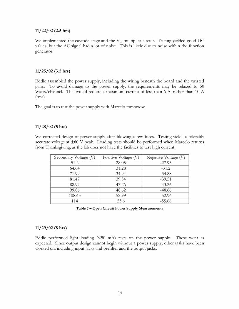
11/28/02 (5 hrs)
We corrected design of power supply after blowing a few fuses. Testing yields a tolerably accurate voltage at ±60 V peak. Loading tests should be performed when Marcelo returns from Thanksgiving, as the lab does not have the facilities to test high current.
Secondary Voltage (V) Positive Voltage (V) Negative Voltage (V) 51.2 28.05 -27.93 64.64 31.28 -31.2 71.99 34.94 -34.88 81.47 39.54 -39.51 88.97 43.26 -43.26 99.86 48.62 -48.66 108.63 52.99 -52.96
114 55.6 -55.66 Table 7 – Open Circuit Power Supply Measurements
11/29/02 (8 hrs)
Eddie performed light loading (<50 mA) tests on the power supply. These went as expected. Since output design cannot begin without a power supply, other tasks have been worked on, including input jacks and prefilter and the output jacks.
44
11/30/02 (7 hrs)
We performed high current loading tests on the amplifier. We tested input and VA stage with power supply and soldered all components of output stage to the perfboard and heat sink.
12/2/02 (5 hrs)
We finished designing the output stage and began testing. The DC values of the amplifier were favorable until the output transistors overheated. This problem was solved by breaking a large heat sink into many smaller, electrically isolated ones at the physics building machine shop.
12/3/02 (4.5 hrs)
The new heat sinks were attached to new output devices. A point was made to test all of the devices as they were installed. To avoid thermal failure (only one set of FETs left), the power supply is being operated in the minimum voltage to produce a tolerable output signal (23 V).
Testing shows that the amplifier works properly up to the current maximum volume (output of roughly 10.6 W rms). No distortion is audibly detectable. Harmonic analysis notes a 15 dBm peak at 1 kHz with a -35 dBm second and third harmonic to a 1 kHz test signal.
The important feature to note is the order of turning the amplifier on and off.
On: variac, main, speaker
Off: speaker, main, variac

45
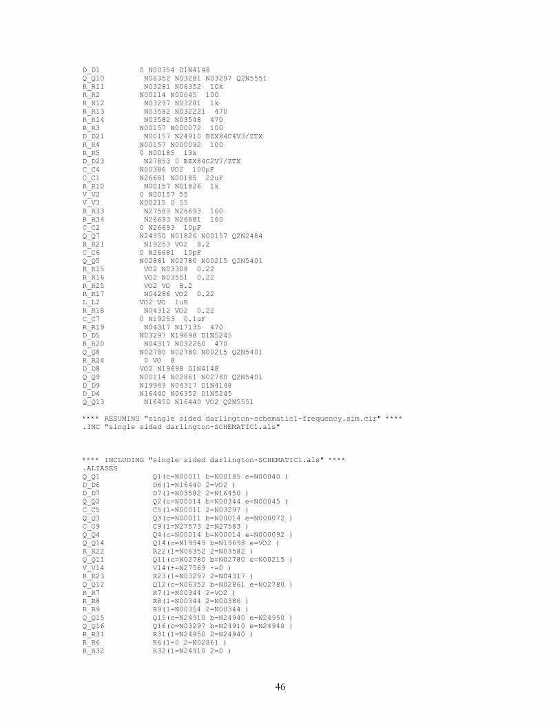
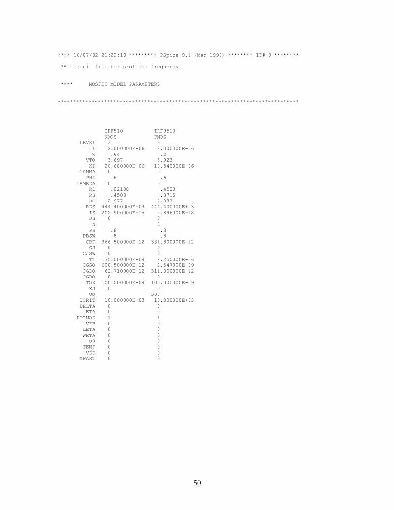
Appendix G: PSpice Simulation Results
Harmonic Analysis: 1 kHz at Nominal Listening Levels (8 W output)
**** 10/07/02 21:22:10 ********* PSpice 9.1 (Mar 1999) ******** ID# 0 ******** ** circuit file for profile: frequency **** CIRCUIT DESCRIPTION ****************************************************************************** ** WARNING: THIS AUTOMATICALLY GENERATED FILE MAY BE OVERWRITTEN BY SUBSEQUENT PROFILES *Libraries: * Local Libraries : * From [PSPICE NETLIST] section of pspice91.ini file: .lib "nom.lib" *Analysis directives: .TRAN/OP 0 5ms 0 10n .FOUR 1k 5 V([VO]) .OPTIONS STEPGMIN .PROBE .INC "single sided darlington-SCHEMATIC1.net" **** INCLUDING "single sided darlington-SCHEMATIC1.net" **** * source SINGLE SIDED DARLINGTON Q_Q1 N00011 N00185 N00040 Q2N5401 D_D6 N16440 VO2 D1N4148 D_D7 N03582 N16450 D1N4148 Q_Q2 N00014 N00344 N00045 Q2N5401 C_C5 N00011 N03297 200pF Q_Q3 N00011 N00014 N000072 Q2N5551 C_C9 N27573 N27583 22uF Q_Q4 N00014 N00014 N000092 Q2N5551 Q_Q14 N19949 N19698 VO2 Q2N5401 R_R22 N06352 N03582 150 Q_Q11 N02780 N02780 N00215 Q2N5401 V_V14 N27569 0 +SIN 0 1 1k 0 0 0 R_R23 N03297 N04317 150 Q_Q12 N06352 N02861 N02780 Q2N5401 R_R7 N00344 VO2 13k R_R8 N00344 N00386 220 R_R9 N00354 N00344 330 Q_Q15 N24910 N24940 N24950 Q2N5551 Q_Q16 N03297 N24910 N24940 Q2N2484 R_R31 N24950 N24940 4.7 R_R6 0 N02861 5.5k R_R32 N24910 0 7.5K Q_Q6 0 N00011 N01826 Q2N5551 R_R35 N27569 N27573 43.1k M_M1 N00215 N032221 N03308 N03308 IRF510 R_R36 0 N27573 56.9k M_M2 N00157 N17135 N04286 N04286 IRF9510 D_D22 N27853 N27583 BZX84C2V7/ZTX M_M4 N00157 N032260 N04312 N04312 IRF9510 C_C8 N03297 N06352 47uF R_R1 N00040 N00114 100 C_C3 0 N00354 220uF M_M3 N00215 N03548 N03551 N03551 IRF510
46
D_D1 0 N00354 D1N4148 Q_Q10 N06352 N03281 N03297 Q2N5551 R_R11 N03281 N06352 10k R_R2 N00114 N00045 100 R_R12 N03297 N03281 1k R_R13 N03582 N032221 470 R_R14 N03582 N03548 470 R_R3 N00157 N000072 100 D_D21 N00157 N24910 BZX84C4V3/ZTX R_R4 N00157 N000092 100 R_R5 0 N00185 13k D_D23 N27853 0 BZX84C2V7/ZTX C_C4 N00386 VO2 100pF C_C1 N26681 N00185 22uF R_R10 N00157 N01826 1k V_V2 0 N00157 55 V_V3 N00215 0 55 R_R33 N27583 N26693 160 R_R34 N26693 N26681 160 C_C2 0 N26693 10pF Q_Q7 N24950 N01826 N00157 Q2N2484 R_R21 N19253 VO2 8.2 C_C6 0 N26681 10pF Q_Q5 N02861 N02780 N00215 Q2N5401 R_R15 VO2 N03308 0.22 R_R16 VO2 N03551 0.22 R_R25 VO2 VO 8.2 R_R17 N04286 VO2 0.22 L_L2 VO2 VO 1uH R_R18 N04312 VO2 0.22 C_C7 0 N19253 0.1uF R_R19 N04317 N17135 470 D_D5 N03297 N19698 D1N5245 R_R20 N04317 N032260 470 Q_Q8 N02780 N02780 N00215 Q2N5401 R_R24 0 VO 8 D_D8 VO2 N19698 D1N4148 Q_Q9 N00114 N02861 N02780 Q2N5401 D_D9 N19949 N04317 D1N4148 D_D4 N16440 N06352 D1N5245 Q_Q13 N16450 N16440 VO2 Q2N5551 **** RESUMING "single sided darlington-schematic1-frequency.sim.cir" **** .INC "single sided darlington-SCHEMATIC1.als" **** INCLUDING "single sided darlington-SCHEMATIC1.als" **** .ALIASES Q_Q1 Q1(c=N00011 b=N00185 e=N00040 ) D_D6 D6(1=N16440 2=VO2 ) D_D7 D7(1=N03582 2=N16450 ) Q_Q2 Q2(c=N00014 b=N00344 e=N00045 ) C_C5 C5(1=N00011 2=N03297 ) Q_Q3 Q3(c=N00011 b=N00014 e=N000072 ) C_C9 C9(1=N27573 2=N27583 ) Q_Q4 Q4(c=N00014 b=N00014 e=N000092 ) Q_Q14 Q14(c=N19949 b=N19698 e=VO2 ) R_R22 R22(1=N06352 2=N03582 ) Q_Q11 Q11(c=N02780 b=N02780 e=N00215 ) V_V14 V14(+=N27569 -=0 ) R_R23 R23(1=N03297 2=N04317 ) Q_Q12 Q12(c=N06352 b=N02861 e=N02780 ) R_R7 R7(1=N00344 2=VO2 ) R_R8 R8(1=N00344 2=N00386 ) R_R9 R9(1=N00354 2=N00344 ) Q_Q15 Q15(c=N24910 b=N24940 e=N24950 ) Q_Q16 Q16(c=N03297 b=N24910 e=N24940 ) R_R31 R31(1=N24950 2=N24940 ) R_R6 R6(1=0 2=N02861 ) R_R32 R32(1=N24910 2=0 )
47
Q_Q6 Q6(c=0 b=N00011 e=N01826 ) R_R35 R35(1=N27569 2=N27573 ) M_M1 M1(d=N00215 g=N032221 s=N03308 s=N03308 ) R_R36 R36(1=0 2=N27573 ) M_M2 M2(d=N00157 g=N17135 s=N04286 s=N04286 ) D_D22 D22(1=N27853 2=N27583 ) M_M4 M4(d=N00157 g=N032260 s=N04312 s=N04312 ) C_C8 C8(1=N03297 2=N06352 ) R_R1 R1(1=N00040 2=N00114 ) C_C3 C3(1=0 2=N00354 ) M_M3 M3(d=N00215 g=N03548 s=N03551 s=N03551 ) D_D1 D1(1=0 2=N00354 ) Q_Q10 Q10(c=N06352 b=N03281 e=N03297 ) R_R11 R11(1=N03281 2=N06352 ) R_R2 R2(1=N00114 2=N00045 ) R_R12 R12(1=N03297 2=N03281 ) R_R13 R13(1=N03582 2=N032221 ) R_R14 R14(1=N03582 2=N03548 ) R_R3 R3(1=N00157 2=N000072 ) D_D21 D21(1=N00157 2=N24910 ) R_R4 R4(1=N00157 2=N000092 ) R_R5 R5(1=0 2=N00185 ) D_D23 D23(1=N27853 2=0 ) C_C4 C4(1=N00386 2=VO2 ) C_C1 C1(1=N26681 2=N00185 ) R_R10 R10(1=N00157 2=N01826 ) V_V2 V2(+=0 -=N00157 ) V_V3 V3(+=N00215 -=0 ) R_R33 R33(1=N27583 2=N26693 ) R_R34 R34(1=N26693 2=N26681 ) C_C2 C2(1=0 2=N26693 ) Q_Q7 Q7(c=N24950 b=N01826 e=N00157 ) R_R21 R21(1=N19253 2=VO2 ) C_C6 C6(1=0 2=N26681 ) Q_Q5 Q5(c=N02861 b=N02780 e=N00215 ) R_R15 R15(1=VO2 2=N03308 ) R_R16 R16(1=VO2 2=N03551 ) R_R25 R25(1=VO2 2=VO ) R_R17 R17(1=N04286 2=VO2 ) L_L2 L2(1=VO2 2=VO ) R_R18 R18(1=N04312 2=VO2 ) C_C7 C7(1=0 2=N19253 ) R_R19 R19(1=N04317 2=N17135 ) D_D5 D5(1=N03297 2=N19698 ) R_R20 R20(1=N04317 2=N032260 ) Q_Q8 Q8(c=N02780 b=N02780 e=N00215 ) R_R24 R24(1=0 2=VO ) D_D8 D8(1=VO2 2=N19698 ) Q_Q9 Q9(c=N00114 b=N02861 e=N02780 ) D_D9 D9(1=N19949 2=N04317 ) D_D4 D4(1=N16440 2=N06352 ) Q_Q13 Q13(c=N16450 b=N16440 e=VO2 ) _ _(Vo2=VO2) _ _(Vo=VO) _ _(VO=VO) _ _(VO2=VO2) .ENDALIASES **** RESUMING "single sided darlington-schematic1-frequency.sim.cir" **** .END

48
**** 10/07/02 21:22:10 ********* PSpice 9.1 (Mar 1999) ******** ID# 0 ******** ** circuit file for profile: frequency **** Diode MODEL PARAMETERS ****************************************************************************** D1N4148 D1N5245 BZX84C2V7/ZTX BZX84C4V3/ZTX IS 2.682000E-09 3.142000E-15 3.677000E-15 187.000000E-15 N 1.836 1.059 1.218 ISR 1.565000E-09 1.527000E-09 IKF .04417 1 1 BV 100 15 2.766 4.367 IBV 100.000000E-06 .024573 .06476 .06905 NBV 1.0932 IBVL 7.124900E-06 NBVL .65646 RS .5664 3.536 .12 .09 TT 11.540000E-09 57.710000E-09 331.800000E-09 CJO 4.000000E-12 80.500000E-12 312.100000E-12 221.200000E-12 VJ .5 .75 .3971 .7266 M .3333 .4186 .2052 .3317 TBV1 833.330000E-06

49
**** 10/07/02 21:22:10 ********* PSpice 9.1 (Mar 1999) ******** ID# 0 ******** ** circuit file for profile: frequency **** BJT MODEL PARAMETERS ****************************************************************************** Q2N5401 Q2N5551 Q2N2484 PNP NPN NPN IS 21.480000E-15 2.511000E-15 5.911000E-15 BF 132.1 242.6 697.1 NF 1 1 1 VAF 100 100 62.37 IKF .1848 .3458 .01393 ISE 21.480000E-15 2.511000E-15 5.911000E-15 NE 1.375 1.249 1.342 BR 3.661 3.197 1.297 NR 1 1 1 RB 10 10 10 RC 1.6 1 1.61 CJE 73.390000E-12 18.790000E-12 4.973000E-12 MJE .3777 .3416 .4146 CJC 17.630000E-12 4.883000E-12 4.017000E-12 MJC .5312 .3047 .3174 TF 641.900000E-12 560.000000E-12 820.400000E-12 XTF 8 7 VTF 5 4 ITF .05 .35 TR 1.476000E-09 1.202000E-09 4.687000E-09 XTB 1.5 1.5 1.5 CN 2.2 2.42 2.42 D .52 .87 .87
50
**** 10/07/02 21:22:10 ********* PSpice 9.1 (Mar 1999) ******** ID# 0 ******** ** circuit file for profile: frequency **** MOSFET MODEL PARAMETERS ****************************************************************************** IRF510 IRF9510 NMOS PMOS LEVEL 3 3 L 2.000000E-06 2.000000E-06 W .64 .2 VTO 3.697 -3.923 KP 20.680000E-06 10.540000E-06 GAMMA 0 0 PHI .6 .6 LAMBDA 0 0 RD .02108 .4523 RS .4508 .3715 RG 2.977 4.087 RDS 444.400000E+03 444.400000E+03 IS 202.900000E-15 2.896000E-18 JS 0 0 N 3 PB .8 .8 PBSW .8 .8 CBD 366.500000E-12 331.800000E-12 CJ 0 0 CJSW 0 0 TT 135.000000E-09 2.250000E-06 CGSO 600.500000E-12 2.547000E-09 CGDO 62.710000E-12 311.000000E-12 CGBO 0 0 TOX 100.000000E-09 100.000000E-09 XJ 0 0 UO 300 UCRIT 10.000000E+03 10.000000E+03 DELTA 0 0 ETA 0 0 DIOMOD 1 1 VFB 0 0 LETA 0 0 WETA 0 0 U0 0 0 TEMP 0 0 VDD 0 0 XPART 0 0

51
**** 10/07/02 21:22:10 ********* PSpice 9.1 (Mar 1999) ******** ID# 0 ******** ** circuit file for profile: frequency **** INITIAL TRANSIENT SOLUTION TEMPERATURE = 27.000 DEG C ****************************************************************************** NODE VOLTAGE NODE VOLTAGE NODE VOLTAGE NODE VOLTAGE ( VO) -.0118 ( VO2) -.0118 (N00011) -53.5880 (N00014) -53.7850 (N00040) 1.0147 (N00045) 1.0077 (N00114) 1.4975 (N00157) -55.0000 (N00185) .3492 (N00215) 55.0000 (N00344) .3419 (N00354) .3419 (N00386) .3419 (N01826) -54.2610 (N02780) 54.3040 (N02861) 53.6190 (N03281) -3.9732 (N03297) -4.7193 (N03308) .0374 (N03548) 4.0948 (N03551) .0374 (N03582) 4.0948 (N04286) -.0611 (N04312) -.0611 (N04317) -4.7193 (N06352) 4.0948 (N16440) .0167 (N16450) 4.0948 (N17135) -4.7193 (N19253) -.0118 (N19698) -.0413 (N19949) -4.7192 (N24910) -50.6930 (N24940) -51.4140 (N24950) -51.4590 (N26681) 0.0000 (N26693) 0.0000 (N27569) 0.0000 (N27573) 0.0000 (N27583) 0.0000 (N27853) 0.0000 (N000072) -54.5170 (N000092) -54.5170 (N032221) 4.0948 (N032260) -4.7193 VOLTAGE SOURCE CURRENTS NAME CURRENT V_V14 0.000E+00 V_V2 -4.750E-01 V_V3 -4.758E-01 TOTAL POWER DISSIPATION 5.23E+01 WATTS

52
**** 10/07/02 21:22:10 ********* PSpice 9.1 (Mar 1999) ******** ID# 0 ******** ** circuit file for profile: frequency **** OPERATING POINT INFORMATION TEMPERATURE = 27.000 DEG C ****************************************************************************** **** DIODES NAME D_D6 D_D7 D_D22 D_D1 MODEL D1N4148 D1N4148 BZX84C2V7/ZTX D1N4148 ID 3.33E-09 5.56E-12 0.00E+00 -4.54E-09 VD 2.85E-02 6.40E-05 0.00E+00 -3.42E-01 REQ 6.51E+06 1.15E+07 8.82E+11 1.21E+09 CAP 4.08E-12 4.00E-12 3.12E-10 3.36E-12 NAME D_D21 D_D23 D_D5 MODEL BZX84C4V3/ZTX BZX84C2V7/ZTX D1N5245 ID -6.74E-03 0.00E+00 -3.50E-09 VD -4.31E+00 0.00E+00 -4.68E+00 REQ 3.84E+00 8.82E+11 4.94E+09 CAP 8.66E-08 3.12E-10 3.52E-11 NAME D_D8 D_D9 D_D4 MODEL D1N4148 D1N4148 D1N5245 ID 3.50E-09 6.28E-12 -3.33E-09 VD 2.96E-02 7.24E-05 -4.08E+00 REQ 6.37E+06 1.15E+07 4.62E+09 CAP 4.08E-12 4.00E-12 3.69E-11 **** BIPOLAR JUNCTION TRANSISTORS NAME Q_Q1 Q_Q2 Q_Q3 Q_Q4 Q_Q14 MODEL Q2N5401 Q2N5401 Q2N5551 Q2N5551 Q2N5401 IB -2.69E-05 -2.72E-05 3.73E-05 3.73E-05 1.26E-12 IC -4.80E-03 -4.87E-03 4.80E-03 4.80E-03 -6.28E-12 VBE -6.65E-01 -6.66E-01 7.32E-01 7.32E-01 -2.96E-02 VBC 5.39E+01 5.41E+01 -1.97E-01 0.00E+00 4.68E+00 VCE -5.46E+01 -5.48E+01 9.29E-01 7.32E-01 -4.71E+00 BETADC 1.79E+02 1.79E+02 1.29E+02 1.29E+02 -5.00E+00 GM 1.83E-01 1.85E-01 1.83E-01 1.83E-01 2.68E-12 RPI 9.92E+02 9.79E+02 7.65E+02 7.64E+02 7.07E+11 RX 1.00E+01 1.00E+01 1.00E+01 1.00E+01 1.00E+01 RO 3.21E+04 3.16E+04 2.09E+04 2.09E+04 9.14E+11 CBE 2.40E-10 2.42E-10 1.52E-10 1.52E-10 7.45E-11 CBC 1.81E-12 1.80E-12 4.55E-12 4.89E-12 6.16E-12 CJS 0.00E+00 0.00E+00 0.00E+00 0.00E+00 0.00E+00 BETAAC 1.81E+02 1.81E+02 1.40E+02 1.40E+02 1.89E+00 CBX/CBX2 0.00E+00 0.00E+00 0.00E+00 0.00E+00 0.00E+00 FT/FT2 1.20E+08 1.21E+08 1.86E+08 1.85E+08 5.28E-03 NAME Q_Q11 Q_Q12 Q_Q15 Q_Q16 Q_Q6 MODEL Q2N5401 Q2N5401 Q2N5551 Q2N2484 Q2N5551 IB -8.28E-05 -5.49E-05 -2.19E-13 1.73E-05 4.86E-06 IC -9.57E-03 -9.56E-03 1.01E-12 9.56E-03 7.67E-04 VBE -6.96E-01 -6.85E-01 4.50E-02 7.22E-01 6.73E-01 VBC 0.00E+00 4.95E+01 -7.22E-01 -4.60E+01 -5.36E+01
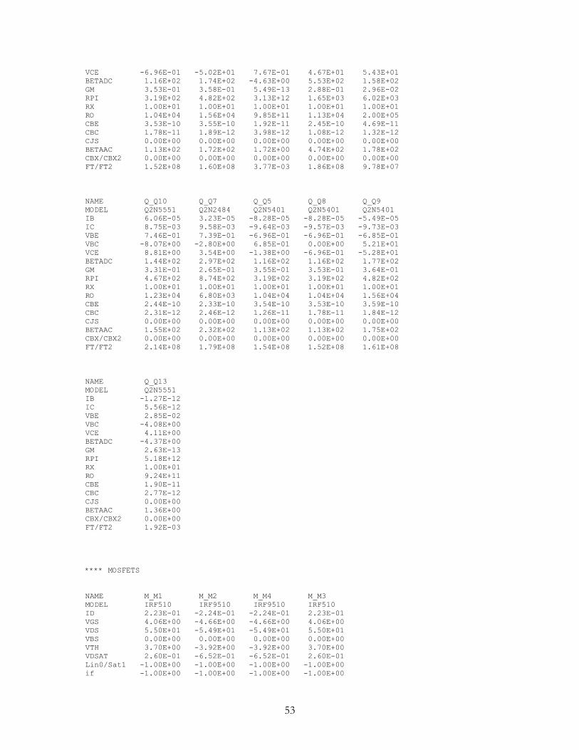
53
VCE -6.96E-01 -5.02E+01 7.67E-01 4.67E+01 5.43E+01 BETADC 1.16E+02 1.74E+02 -4.63E+00 5.53E+02 1.58E+02 GM 3.53E-01 3.58E-01 5.49E-13 2.88E-01 2.96E-02 RPI 3.19E+02 4.82E+02 3.13E+12 1.65E+03 6.02E+03 RX 1.00E+01 1.00E+01 1.00E+01 1.00E+01 1.00E+01 RO 1.04E+04 1.56E+04 9.85E+11 1.13E+04 2.00E+05 CBE 3.53E-10 3.55E-10 1.92E-11 2.45E-10 4.69E-11 CBC 1.78E-11 1.89E-12 3.98E-12 1.08E-12 1.32E-12 CJS 0.00E+00 0.00E+00 0.00E+00 0.00E+00 0.00E+00 BETAAC 1.13E+02 1.72E+02 1.72E+00 4.74E+02 1.78E+02 CBX/CBX2 0.00E+00 0.00E+00 0.00E+00 0.00E+00 0.00E+00 FT/FT2 1.52E+08 1.60E+08 3.77E-03 1.86E+08 9.78E+07 NAME Q_Q10 Q_Q7 Q_Q5 Q_Q8 Q_Q9 MODEL Q2N5551 Q2N2484 Q2N5401 Q2N5401 Q2N5401 IB 6.06E-05 3.23E-05 -8.28E-05 -8.28E-05 -5.49E-05 IC 8.75E-03 9.58E-03 -9.64E-03 -9.57E-03 -9.73E-03 VBE 7.46E-01 7.39E-01 -6.96E-01 -6.96E-01 -6.85E-01 VBC -8.07E+00 -2.80E+00 6.85E-01 0.00E+00 5.21E+01 VCE 8.81E+00 3.54E+00 -1.38E+00 -6.96E-01 -5.28E+01 BETADC 1.44E+02 2.97E+02 1.16E+02 1.16E+02 1.77E+02 GM 3.31E-01 2.65E-01 3.55E-01 3.53E-01 3.64E-01 RPI 4.67E+02 8.74E+02 3.19E+02 3.19E+02 4.82E+02 RX 1.00E+01 1.00E+01 1.00E+01 1.00E+01 1.00E+01 RO 1.23E+04 6.80E+03 1.04E+04 1.04E+04 1.56E+04 CBE 2.44E-10 2.33E-10 3.54E-10 3.53E-10 3.59E-10 CBC 2.31E-12 2.46E-12 1.26E-11 1.78E-11 1.84E-12 CJS 0.00E+00 0.00E+00 0.00E+00 0.00E+00 0.00E+00 BETAAC 1.55E+02 2.32E+02 1.13E+02 1.13E+02 1.75E+02 CBX/CBX2 0.00E+00 0.00E+00 0.00E+00 0.00E+00 0.00E+00 FT/FT2 2.14E+08 1.79E+08 1.54E+08 1.52E+08 1.61E+08 NAME Q_Q13 MODEL Q2N5551 IB -1.27E-12 IC 5.56E-12 VBE 2.85E-02 VBC -4.08E+00 VCE 4.11E+00 BETADC -4.37E+00 GM 2.63E-13 RPI 5.18E+12 RX 1.00E+01 RO 9.24E+11 CBE 1.90E-11 CBC 2.77E-12 CJS 0.00E+00 BETAAC 1.36E+00 CBX/CBX2 0.00E+00 FT/FT2 1.92E-03 **** MOSFETS NAME M_M1 M_M2 M_M4 M_M3 MODEL IRF510 IRF9510 IRF9510 IRF510 ID 2.23E-01 -2.24E-01 -2.24E-01 2.23E-01 VGS 4.06E+00 -4.66E+00 -4.66E+00 4.06E+00 VDS 5.50E+01 -5.49E+01 -5.49E+01 5.50E+01 VBS 0.00E+00 0.00E+00 0.00E+00 0.00E+00 VTH 3.70E+00 -3.92E+00 -3.92E+00 3.70E+00 VDSAT 2.60E-01 -6.52E-01 -6.52E-01 2.60E-01 Lin0/Sat1 -1.00E+00 -1.00E+00 -1.00E+00 -1.00E+00 if -1.00E+00 -1.00E+00 -1.00E+00 -1.00E+00
54
ir -1.00E+00 -1.00E+00 -1.00E+00 -1.00E+00 TAU -1.00E+00 -1.00E+00 -1.00E+00 -1.00E+00 GM 1.72E+00 6.87E-01 6.87E-01 1.72E+00 GDS 2.25E-06 2.25E-06 2.25E-06 2.25E-06 GMB 0.00E+00 0.00E+00 0.00E+00 0.00E+00 CBD 4.39E-11 3.98E-11 3.98E-11 4.39E-11 CBS 1.57E-19 2.25E-18 2.25E-18 1.57E-19 CGSOV 3.84E-10 5.09E-10 5.09E-10 3.84E-10 CGDOV 4.01E-11 6.22E-11 6.22E-11 4.01E-11 CGBOV 0.00E+00 0.00E+00 0.00E+00 0.00E+00 CGS 2.95E-10 9.21E-11 9.21E-11 2.95E-10 CGD 0.00E+00 0.00E+00 0.00E+00 0.00E+00 CGB 0.00E+00 0.00E+00 0.00E+00 0.00E+00

55
**** 10/07/02 21:22:10 ********* PSpice 9.1 (Mar 1999) ******** ID# 0 ******** ** circuit file for profile: frequency **** FOURIER ANALYSIS TEMPERATURE = 27.000 DEG C ****************************************************************************** FOURIER COMPONENTS OF TRANSIENT RESPONSE V(VO) DC COMPONENT = -2.903053E-02 HARMONIC FREQUENCY FOURIER NORMALIZED PHASE NORMALIZED NO (HZ) COMPONENT COMPONENT (DEG) PHASE (DEG) 1 1.000E+03 8.113E+00 1.000E+00 -1.342E+00 0.000E+00 2 2.000E+03 2.572E-03 3.170E-04 -1.268E+02 -1.241E+02 3 3.000E+03 1.825E-03 2.250E-04 8.831E+01 9.233E+01 4 4.000E+03 6.529E-04 8.048E-05 -1.595E+02 -1.541E+02 5 5.000E+03 1.848E-03 2.278E-04 -1.036E+02 -9.689E+01 TOTAL HARMONIC DISTORTION = 4.576727E-02 PERCENT JOB CONCLUDED TOTAL JOB TIME 1690.55
56
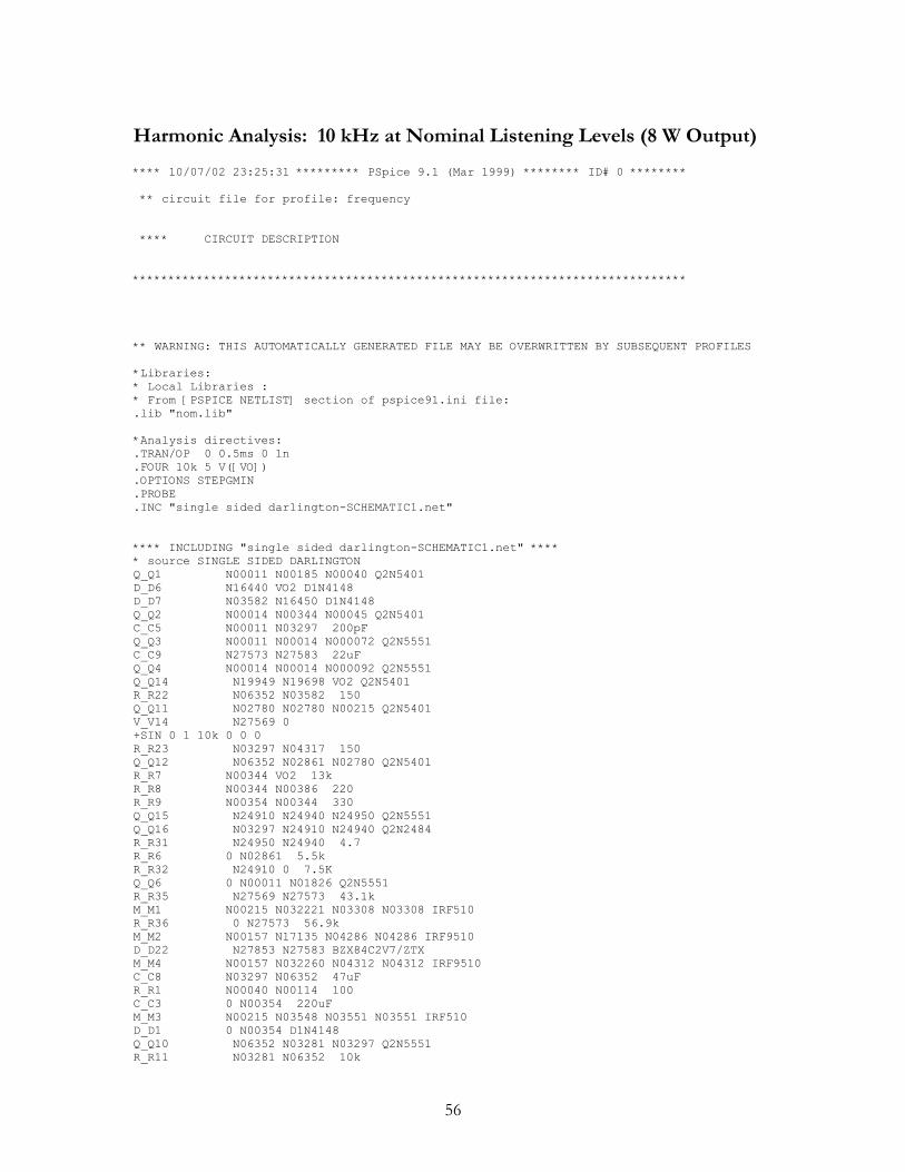
Harmonic Analysis: 10 kHz at Nominal Listening Levels (8 W Output)
**** 10/07/02 23:25:31 ********* PSpice 9.1 (Mar 1999) ******** ID# 0 ******** ** circuit file for profile: frequency **** CIRCUIT DESCRIPTION ****************************************************************************** ** WARNING: THIS AUTOMATICALLY GENERATED FILE MAY BE OVERWRITTEN BY SUBSEQUENT PROFILES *Libraries: * Local Libraries : * From [PSPICE NETLIST] section of pspice91.ini file: .lib "nom.lib" *Analysis directives: .TRAN/OP 0 0.5ms 0 1n .FOUR 10k 5 V([VO]) .OPTIONS STEPGMIN .PROBE .INC "single sided darlington-SCHEMATIC1.net" **** INCLUDING "single sided darlington-SCHEMATIC1.net" **** * source SINGLE SIDED DARLINGTON Q_Q1 N00011 N00185 N00040 Q2N5401 D_D6 N16440 VO2 D1N4148 D_D7 N03582 N16450 D1N4148 Q_Q2 N00014 N00344 N00045 Q2N5401 C_C5 N00011 N03297 200pF Q_Q3 N00011 N00014 N000072 Q2N5551 C_C9 N27573 N27583 22uF Q_Q4 N00014 N00014 N000092 Q2N5551 Q_Q14 N19949 N19698 VO2 Q2N5401 R_R22 N06352 N03582 150 Q_Q11 N02780 N02780 N00215 Q2N5401 V_V14 N27569 0 +SIN 0 1 10k 0 0 0 R_R23 N03297 N04317 150 Q_Q12 N06352 N02861 N02780 Q2N5401 R_R7 N00344 VO2 13k R_R8 N00344 N00386 220 R_R9 N00354 N00344 330 Q_Q15 N24910 N24940 N24950 Q2N5551 Q_Q16 N03297 N24910 N24940 Q2N2484 R_R31 N24950 N24940 4.7 R_R6 0 N02861 5.5k R_R32 N24910 0 7.5K Q_Q6 0 N00011 N01826 Q2N5551 R_R35 N27569 N27573 43.1k M_M1 N00215 N032221 N03308 N03308 IRF510 R_R36 0 N27573 56.9k M_M2 N00157 N17135 N04286 N04286 IRF9510 D_D22 N27853 N27583 BZX84C2V7/ZTX M_M4 N00157 N032260 N04312 N04312 IRF9510 C_C8 N03297 N06352 47uF R_R1 N00040 N00114 100 C_C3 0 N00354 220uF M_M3 N00215 N03548 N03551 N03551 IRF510 D_D1 0 N00354 D1N4148 Q_Q10 N06352 N03281 N03297 Q2N5551 R_R11 N03281 N06352 10k

57
R_R2 N00114 N00045 100 R_R12 N03297 N03281 1k R_R13 N03582 N032221 470 R_R14 N03582 N03548 470 R_R3 N00157 N000072 100 D_D21 N00157 N24910 BZX84C4V3/ZTX R_R4 N00157 N000092 100 R_R5 0 N00185 13k D_D23 N27853 0 BZX84C2V7/ZTX C_C4 N00386 VO2 100pF C_C1 N26681 N00185 22uF R_R10 N00157 N01826 1k V_V2 0 N00157 55 V_V3 N00215 0 55 R_R33 N27583 N26693 160 R_R34 N26693 N26681 160 C_C2 0 N26693 10pF Q_Q7 N24950 N01826 N00157 Q2N2484 R_R21 N19253 VO2 8.2 C_C6 0 N26681 10pF Q_Q5 N02861 N02780 N00215 Q2N5401 R_R15 VO2 N03308 0.22 R_R16 VO2 N03551 0.22 R_R25 VO2 VO 8.2 R_R17 N04286 VO2 0.22 L_L2 VO2 VO 1uH R_R18 N04312 VO2 0.22 C_C7 0 N19253 0.1uF R_R19 N04317 N17135 470 D_D5 N03297 N19698 D1N5245 R_R20 N04317 N032260 470 Q_Q8 N02780 N02780 N00215 Q2N5401 R_R24 0 VO 8 D_D8 VO2 N19698 D1N4148 Q_Q9 N00114 N02861 N02780 Q2N5401 D_D9 N19949 N04317 D1N4148 D_D4 N16440 N06352 D1N5245 Q_Q13 N16450 N16440 VO2 Q2N5551 **** RESUMING "single sided darlington-schematic1-frequency.sim.cir" **** .INC "single sided darlington-SCHEMATIC1.als" **** INCLUDING "single sided darlington-SCHEMATIC1.als" **** .ALIASES Q_Q1 Q1(c=N00011 b=N00185 e=N00040 ) D_D6 D6(1=N16440 2=VO2 ) D_D7 D7(1=N03582 2=N16450 ) Q_Q2 Q2(c=N00014 b=N00344 e=N00045 ) C_C5 C5(1=N00011 2=N03297 ) Q_Q3 Q3(c=N00011 b=N00014 e=N000072 ) C_C9 C9(1=N27573 2=N27583 ) Q_Q4 Q4(c=N00014 b=N00014 e=N000092 ) Q_Q14 Q14(c=N19949 b=N19698 e=VO2 ) R_R22 R22(1=N06352 2=N03582 ) Q_Q11 Q11(c=N02780 b=N02780 e=N00215 ) V_V14 V14(+=N27569 -=0 ) R_R23 R23(1=N03297 2=N04317 ) Q_Q12 Q12(c=N06352 b=N02861 e=N02780 ) R_R7 R7(1=N00344 2=VO2 ) R_R8 R8(1=N00344 2=N00386 ) R_R9 R9(1=N00354 2=N00344 ) Q_Q15 Q15(c=N24910 b=N24940 e=N24950 ) Q_Q16 Q16(c=N03297 b=N24910 e=N24940 ) R_R31 R31(1=N24950 2=N24940 ) R_R6 R6(1=0 2=N02861 ) R_R32 R32(1=N24910 2=0 ) Q_Q6 Q6(c=0 b=N00011 e=N01826 ) R_R35 R35(1=N27569 2=N27573 ) M_M1 M1(d=N00215 g=N032221 s=N03308 s=N03308 )

58
R_R36 R36(1=0 2=N27573 ) M_M2 M2(d=N00157 g=N17135 s=N04286 s=N04286 ) D_D22 D22(1=N27853 2=N27583 ) M_M4 M4(d=N00157 g=N032260 s=N04312 s=N04312 ) C_C8 C8(1=N03297 2=N06352 ) R_R1 R1(1=N00040 2=N00114 ) C_C3 C3(1=0 2=N00354 ) M_M3 M3(d=N00215 g=N03548 s=N03551 s=N03551 ) D_D1 D1(1=0 2=N00354 ) Q_Q10 Q10(c=N06352 b=N03281 e=N03297 ) R_R11 R11(1=N03281 2=N06352 ) R_R2 R2(1=N00114 2=N00045 ) R_R12 R12(1=N03297 2=N03281 ) R_R13 R13(1=N03582 2=N032221 ) R_R14 R14(1=N03582 2=N03548 ) R_R3 R3(1=N00157 2=N000072 ) D_D21 D21(1=N00157 2=N24910 ) R_R4 R4(1=N00157 2=N000092 ) R_R5 R5(1=0 2=N00185 ) D_D23 D23(1=N27853 2=0 ) C_C4 C4(1=N00386 2=VO2 ) C_C1 C1(1=N26681 2=N00185 ) R_R10 R10(1=N00157 2=N01826 ) V_V2 V2(+=0 -=N00157 ) V_V3 V3(+=N00215 -=0 ) R_R33 R33(1=N27583 2=N26693 ) R_R34 R34(1=N26693 2=N26681 ) C_C2 C2(1=0 2=N26693 ) Q_Q7 Q7(c=N24950 b=N01826 e=N00157 ) R_R21 R21(1=N19253 2=VO2 ) C_C6 C6(1=0 2=N26681 ) Q_Q5 Q5(c=N02861 b=N02780 e=N00215 ) R_R15 R15(1=VO2 2=N03308 ) R_R16 R16(1=VO2 2=N03551 ) R_R25 R25(1=VO2 2=VO ) R_R17 R17(1=N04286 2=VO2 ) L_L2 L2(1=VO2 2=VO ) R_R18 R18(1=N04312 2=VO2 ) C_C7 C7(1=0 2=N19253 ) R_R19 R19(1=N04317 2=N17135 ) D_D5 D5(1=N03297 2=N19698 ) R_R20 R20(1=N04317 2=N032260 ) Q_Q8 Q8(c=N02780 b=N02780 e=N00215 ) R_R24 R24(1=0 2=VO ) D_D8 D8(1=VO2 2=N19698 ) Q_Q9 Q9(c=N00114 b=N02861 e=N02780 ) D_D9 D9(1=N19949 2=N04317 ) D_D4 D4(1=N16440 2=N06352 ) Q_Q13 Q13(c=N16450 b=N16440 e=VO2 ) _ _(Vo2=VO2) _ _(Vo=VO) _ _(VO=VO) _ _(VO2=VO2) .ENDALIASES **** RESUMING "single sided darlington-schematic1-frequency.sim.cir" **** .END

59
**** 10/07/02 23:25:31 ********* PSpice 9.1 (Mar 1999) ******** ID# 0 ******** ** circuit file for profile: frequency **** Diode MODEL PARAMETERS ****************************************************************************** D1N4148 D1N5245 BZX84C2V7/ZTX BZX84C4V3/ZTX IS 2.682000E-09 3.142000E-15 3.677000E-15 187.000000E-15 N 1.836 1.059 1.218 ISR 1.565000E-09 1.527000E-09 IKF .04417 1 1 BV 100 15 2.766 4.367 IBV 100.000000E-06 .024573 .06476 .06905 NBV 1.0932 IBVL 7.124900E-06 NBVL .65646 RS .5664 3.536 .12 .09 TT 11.540000E-09 57.710000E-09 331.800000E-09 CJO 4.000000E-12 80.500000E-12 312.100000E-12 221.200000E-12 VJ .5 .75 .3971 .7266 M .3333 .4186 .2052 .3317 TBV1 833.330000E-06

60
**** 10/07/02 23:25:31 ********* PSpice 9.1 (Mar 1999) ******** ID# 0 ******** ** circuit file for profile: frequency **** BJT MODEL PARAMETERS ****************************************************************************** Q2N5401 Q2N5551 Q2N2484 PNP NPN NPN IS 21.480000E-15 2.511000E-15 5.911000E-15 BF 132.1 242.6 697.1 NF 1 1 1 VAF 100 100 62.37 IKF .1848 .3458 .01393 ISE 21.480000E-15 2.511000E-15 5.911000E-15 NE 1.375 1.249 1.342 BR 3.661 3.197 1.297 NR 1 1 1 RB 10 10 10 RC 1.6 1 1.61 CJE 73.390000E-12 18.790000E-12 4.973000E-12 MJE .3777 .3416 .4146 CJC 17.630000E-12 4.883000E-12 4.017000E-12 MJC .5312 .3047 .3174 TF 641.900000E-12 560.000000E-12 820.400000E-12 XTF 8 7 VTF 5 4 ITF .05 .35 TR 1.476000E-09 1.202000E-09 4.687000E-09 XTB 1.5 1.5 1.5 CN 2.2 2.42 2.42 D .52 .87 .87

61
**** 10/07/02 23:25:31 ********* PSpice 9.1 (Mar 1999) ******** ID# 0 ******** ** circuit file for profile: frequency **** MOSFET MODEL PARAMETERS ****************************************************************************** IRF510 IRF9510 NMOS PMOS LEVEL 3 3 L 2.000000E-06 2.000000E-06 W .64 .2 VTO 3.697 -3.923 KP 20.680000E-06 10.540000E-06 GAMMA 0 0 PHI .6 .6 LAMBDA 0 0 RD .02108 .4523 RS .4508 .3715 RG 2.977 4.087 RDS 444.400000E+03 444.400000E+03 IS 202.900000E-15 2.896000E-18 JS 0 0 N 3 PB .8 .8 PBSW .8 .8 CBD 366.500000E-12 331.800000E-12 CJ 0 0 CJSW 0 0 TT 135.000000E-09 2.250000E-06 CGSO 600.500000E-12 2.547000E-09 CGDO 62.710000E-12 311.000000E-12 CGBO 0 0 TOX 100.000000E-09 100.000000E-09 XJ 0 0 UO 300 UCRIT 10.000000E+03 10.000000E+03 DELTA 0 0 ETA 0 0 DIOMOD 1 1 VFB 0 0 LETA 0 0 WETA 0 0 U0 0 0 TEMP 0 0 VDD 0 0 XPART 0 0

62
**** 10/07/02 23:25:31 ********* PSpice 9.1 (Mar 1999) ******** ID# 0 ******** ** circuit file for profile: frequency **** INITIAL TRANSIENT SOLUTION TEMPERATURE = 27.000 DEG C ****************************************************************************** NODE VOLTAGE NODE VOLTAGE NODE VOLTAGE NODE VOLTAGE ( VO) -.0118 ( VO2) -.0118 (N00011) -53.5880 (N00014) -53.7850 (N00040) 1.0147 (N00045) 1.0077 (N00114) 1.4975 (N00157) -55.0000 (N00185) .3492 (N00215) 55.0000 (N00344) .3419 (N00354) .3419 (N00386) .3419 (N01826) -54.2610 (N02780) 54.3040 (N02861) 53.6190 (N03281) -3.9732 (N03297) -4.7193 (N03308) .0374 (N03548) 4.0948 (N03551) .0374 (N03582) 4.0948 (N04286) -.0611 (N04312) -.0611 (N04317) -4.7193 (N06352) 4.0948 (N16440) .0167 (N16450) 4.0948 (N17135) -4.7193 (N19253) -.0118 (N19698) -.0413 (N19949) -4.7192 (N24910) -50.6930 (N24940) -51.4140 (N24950) -51.4590 (N26681) 0.0000 (N26693) 0.0000 (N27569) 0.0000 (N27573) 0.0000 (N27583) 0.0000 (N27853) 0.0000 (N000072) -54.5170 (N000092) -54.5170 (N032221) 4.0948 (N032260) -4.7193 VOLTAGE SOURCE CURRENTS NAME CURRENT V_V14 0.000E+00 V_V2 -4.750E-01 V_V3 -4.758E-01 TOTAL POWER DISSIPATION 5.23E+01 WATTS

63
**** 10/07/02 23:25:31 ********* PSpice 9.1 (Mar 1999) ******** ID# 0 ******** ** circuit file for profile: frequency **** OPERATING POINT INFORMATION TEMPERATURE = 27.000 DEG C ****************************************************************************** **** DIODES NAME D_D6 D_D7 D_D22 D_D1 MODEL D1N4148 D1N4148 BZX84C2V7/ZTX D1N4148 ID 3.33E-09 5.56E-12 0.00E+00 -4.54E-09 VD 2.85E-02 6.40E-05 0.00E+00 -3.42E-01 REQ 6.51E+06 1.15E+07 8.82E+11 1.21E+09 CAP 4.08E-12 4.00E-12 3.12E-10 3.36E-12 NAME D_D21 D_D23 D_D5 MODEL BZX84C4V3/ZTX BZX84C2V7/ZTX D1N5245 ID -6.74E-03 0.00E+00 -3.50E-09 VD -4.31E+00 0.00E+00 -4.68E+00 REQ 3.84E+00 8.82E+11 4.94E+09 CAP 8.66E-08 3.12E-10 3.52E-11 NAME D_D8 D_D9 D_D4 MODEL D1N4148 D1N4148 D1N5245 ID 3.50E-09 6.28E-12 -3.33E-09 VD 2.96E-02 7.24E-05 -4.08E+00 REQ 6.37E+06 1.15E+07 4.62E+09 CAP 4.08E-12 4.00E-12 3.69E-11 **** BIPOLAR JUNCTION TRANSISTORS NAME Q_Q1 Q_Q2 Q_Q3 Q_Q4 Q_Q14 MODEL Q2N5401 Q2N5401 Q2N5551 Q2N5551 Q2N5401 IB -2.69E-05 -2.72E-05 3.73E-05 3.73E-05 1.26E-12 IC -4.80E-03 -4.87E-03 4.80E-03 4.80E-03 -6.28E-12 VBE -6.65E-01 -6.66E-01 7.32E-01 7.32E-01 -2.96E-02 VBC 5.39E+01 5.41E+01 -1.97E-01 0.00E+00 4.68E+00 VCE -5.46E+01 -5.48E+01 9.29E-01 7.32E-01 -4.71E+00 BETADC 1.79E+02 1.79E+02 1.29E+02 1.29E+02 -5.00E+00 GM 1.83E-01 1.85E-01 1.83E-01 1.83E-01 2.68E-12 RPI 9.92E+02 9.79E+02 7.65E+02 7.64E+02 7.07E+11 RX 1.00E+01 1.00E+01 1.00E+01 1.00E+01 1.00E+01 RO 3.21E+04 3.16E+04 2.09E+04 2.09E+04 9.14E+11 CBE 2.40E-10 2.42E-10 1.52E-10 1.52E-10 7.45E-11 CBC 1.81E-12 1.80E-12 4.55E-12 4.89E-12 6.16E-12 CJS 0.00E+00 0.00E+00 0.00E+00 0.00E+00 0.00E+00 BETAAC 1.81E+02 1.81E+02 1.40E+02 1.40E+02 1.89E+00 CBX/CBX2 0.00E+00 0.00E+00 0.00E+00 0.00E+00 0.00E+00 FT/FT2 1.20E+08 1.21E+08 1.86E+08 1.85E+08 5.28E-03 NAME Q_Q11 Q_Q12 Q_Q15 Q_Q16 Q_Q6 MODEL Q2N5401 Q2N5401 Q2N5551 Q2N2484 Q2N5551 IB -8.28E-05 -5.49E-05 -2.19E-13 1.73E-05 4.86E-06 IC -9.57E-03 -9.56E-03 1.01E-12 9.56E-03 7.67E-04 VBE -6.96E-01 -6.85E-01 4.50E-02 7.22E-01 6.73E-01 VBC 0.00E+00 4.95E+01 -7.22E-01 -4.60E+01 -5.36E+01

64
VCE -6.96E-01 -5.02E+01 7.67E-01 4.67E+01 5.43E+01 BETADC 1.16E+02 1.74E+02 -4.63E+00 5.53E+02 1.58E+02 GM 3.53E-01 3.58E-01 5.49E-13 2.88E-01 2.96E-02 RPI 3.19E+02 4.82E+02 3.13E+12 1.65E+03 6.02E+03 RX 1.00E+01 1.00E+01 1.00E+01 1.00E+01 1.00E+01 RO 1.04E+04 1.56E+04 9.85E+11 1.13E+04 2.00E+05 CBE 3.53E-10 3.55E-10 1.92E-11 2.45E-10 4.69E-11 CBC 1.78E-11 1.89E-12 3.98E-12 1.08E-12 1.32E-12 CJS 0.00E+00 0.00E+00 0.00E+00 0.00E+00 0.00E+00 BETAAC 1.13E+02 1.72E+02 1.72E+00 4.74E+02 1.78E+02 CBX/CBX2 0.00E+00 0.00E+00 0.00E+00 0.00E+00 0.00E+00 FT/FT2 1.52E+08 1.60E+08 3.77E-03 1.86E+08 9.78E+07 NAME Q_Q10 Q_Q7 Q_Q5 Q_Q8 Q_Q9 MODEL Q2N5551 Q2N2484 Q2N5401 Q2N5401 Q2N5401 IB 6.06E-05 3.23E-05 -8.28E-05 -8.28E-05 -5.49E-05 IC 8.75E-03 9.58E-03 -9.64E-03 -9.57E-03 -9.73E-03 VBE 7.46E-01 7.39E-01 -6.96E-01 -6.96E-01 -6.85E-01 VBC -8.07E+00 -2.80E+00 6.85E-01 0.00E+00 5.21E+01 VCE 8.81E+00 3.54E+00 -1.38E+00 -6.96E-01 -5.28E+01 BETADC 1.44E+02 2.97E+02 1.16E+02 1.16E+02 1.77E+02 GM 3.31E-01 2.65E-01 3.55E-01 3.53E-01 3.64E-01 RPI 4.67E+02 8.74E+02 3.19E+02 3.19E+02 4.82E+02 RX 1.00E+01 1.00E+01 1.00E+01 1.00E+01 1.00E+01 RO 1.23E+04 6.80E+03 1.04E+04 1.04E+04 1.56E+04 CBE 2.44E-10 2.33E-10 3.54E-10 3.53E-10 3.59E-10 CBC 2.31E-12 2.46E-12 1.26E-11 1.78E-11 1.84E-12 CJS 0.00E+00 0.00E+00 0.00E+00 0.00E+00 0.00E+00 BETAAC 1.55E+02 2.32E+02 1.13E+02 1.13E+02 1.75E+02 CBX/CBX2 0.00E+00 0.00E+00 0.00E+00 0.00E+00 0.00E+00 FT/FT2 2.14E+08 1.79E+08 1.54E+08 1.52E+08 1.61E+08 NAME Q_Q13 MODEL Q2N5551 IB -1.27E-12 IC 5.56E-12 VBE 2.85E-02 VBC -4.08E+00 VCE 4.11E+00 BETADC -4.37E+00 GM 2.63E-13 RPI 5.18E+12 RX 1.00E+01 RO 9.24E+11 CBE 1.90E-11 CBC 2.77E-12 CJS 0.00E+00 BETAAC 1.36E+00 CBX/CBX2 0.00E+00 FT/FT2 1.92E-03 **** MOSFETS NAME M_M1 M_M2 M_M4 M_M3 MODEL IRF510 IRF9510 IRF9510 IRF510 ID 2.23E-01 -2.24E-01 -2.24E-01 2.23E-01 VGS 4.06E+00 -4.66E+00 -4.66E+00 4.06E+00 VDS 5.50E+01 -5.49E+01 -5.49E+01 5.50E+01 VBS 0.00E+00 0.00E+00 0.00E+00 0.00E+00 VTH 3.70E+00 -3.92E+00 -3.92E+00 3.70E+00 VDSAT 2.60E-01 -6.52E-01 -6.52E-01 2.60E-01 Lin0/Sat1 -1.00E+00 -1.00E+00 -1.00E+00 -1.00E+00 if -1.00E+00 -1.00E+00 -1.00E+00 -1.00E+00

65
ir -1.00E+00 -1.00E+00 -1.00E+00 -1.00E+00 TAU -1.00E+00 -1.00E+00 -1.00E+00 -1.00E+00 GM 1.72E+00 6.87E-01 6.87E-01 1.72E+00 GDS 2.25E-06 2.25E-06 2.25E-06 2.25E-06 GMB 0.00E+00 0.00E+00 0.00E+00 0.00E+00 CBD 4.39E-11 3.98E-11 3.98E-11 4.39E-11 CBS 1.57E-19 2.25E-18 2.25E-18 1.57E-19 CGSOV 3.84E-10 5.09E-10 5.09E-10 3.84E-10 CGDOV 4.01E-11 6.22E-11 6.22E-11 4.01E-11 CGBOV 0.00E+00 0.00E+00 0.00E+00 0.00E+00 CGS 2.95E-10 9.21E-11 9.21E-11 2.95E-10 CGD 0.00E+00 0.00E+00 0.00E+00 0.00E+00 CGB 0.00E+00 0.00E+00 0.00E+00 0.00E+00

66
**** 10/07/02 23:25:31 ********* PSpice 9.1 (Mar 1999) ******** ID# 0 ******** ** circuit file for profile: frequency **** FOURIER ANALYSIS TEMPERATURE = 27.000 DEG C ****************************************************************************** FOURIER COMPONENTS OF TRANSIENT RESPONSE V(VO) DC COMPONENT = -1.125568E-02 HARMONIC FREQUENCY FOURIER NORMALIZED PHASE NORMALIZED NO (HZ) COMPONENT COMPONENT (DEG) PHASE (DEG) 1 1.000E+04 7.971E+00 1.000E+00 -1.482E+01 0.000E+00 2 2.000E+04 3.511E-03 4.404E-04 -7.522E+01 -4.559E+01 3 3.000E+04 3.034E-03 3.806E-04 4.206E+01 8.651E+01 4 4.000E+04 1.569E-03 1.969E-04 1.088E+02 1.681E+02 5 5.000E+04 8.358E-04 1.049E-04 -1.684E+02 -9.430E+01 TOTAL HARMONIC DISTORTION = 6.233572E-02 PERCENT JOB CONCLUDED TOTAL JOB TIME 1624.58

67
Harmonic Analysis: 20 kHz at Nominal Listening Levels (8 W output)
**** 10/08/02 00:49:50 ********* PSpice 9.1 (Mar 1999) ******** ID# 0 ******** ** circuit file for profile: frequency **** CIRCUIT DESCRIPTION ****************************************************************************** ** WARNING: THIS AUTOMATICALLY GENERATED FILE MAY BE OVERWRITTEN BY SUBSEQUENT PROFILES *Libraries: * Local Libraries : * From [PSPICE NETLIST] section of pspice91.ini file: .lib "nom.lib" *Analysis directives: .TRAN/OP 0 0.25ms 0 0.5n .FOUR 20k 5 V([VO]) .OPTIONS STEPGMIN .PROBE .INC "single sided darlington-SCHEMATIC1.net" **** INCLUDING "single sided darlington-SCHEMATIC1.net" **** * source SINGLE SIDED DARLINGTON Q_Q1 N00011 N00185 N00040 Q2N5401 D_D6 N16440 VO2 D1N4148 D_D7 N03582 N16450 D1N4148 Q_Q2 N00014 N00344 N00045 Q2N5401 C_C5 N00011 N03297 200pF Q_Q3 N00011 N00014 N000072 Q2N5551 C_C9 N27573 N27583 22uF Q_Q4 N00014 N00014 N000092 Q2N5551 Q_Q14 N19949 N19698 VO2 Q2N5401 R_R22 N06352 N03582 150 Q_Q11 N02780 N02780 N00215 Q2N5401 V_V14 N27569 0 +SIN 0 1 20k 0 0 0 R_R23 N03297 N04317 150 Q_Q12 N06352 N02861 N02780 Q2N5401 R_R7 N00344 VO2 13k R_R8 N00344 N00386 220 R_R9 N00354 N00344 330 Q_Q15 N24910 N24940 N24950 Q2N5551 Q_Q16 N03297 N24910 N24940 Q2N2484 R_R31 N24950 N24940 4.7 R_R6 0 N02861 5.5k R_R32 N24910 0 7.5K Q_Q6 0 N00011 N01826 Q2N5551 R_R35 N27569 N27573 43.1k M_M1 N00215 N032221 N03308 N03308 IRF510 R_R36 0 N27573 56.9k M_M2 N00157 N17135 N04286 N04286 IRF9510 D_D22 N27853 N27583 BZX84C2V7/ZTX M_M4 N00157 N032260 N04312 N04312 IRF9510 C_C8 N03297 N06352 47uF R_R1 N00040 N00114 100 C_C3 0 N00354 220uF M_M3 N00215 N03548 N03551 N03551 IRF510 D_D1 0 N00354 D1N4148 Q_Q10 N06352 N03281 N03297 Q2N5551 R_R11 N03281 N06352 10k
68
R_R2 N00114 N00045 100 R_R12 N03297 N03281 1k R_R13 N03582 N032221 470 R_R14 N03582 N03548 470 R_R3 N00157 N000072 100 D_D21 N00157 N24910 BZX84C4V3/ZTX R_R4 N00157 N000092 100 R_R5 0 N00185 13k D_D23 N27853 0 BZX84C2V7/ZTX C_C4 N00386 VO2 100pF C_C1 N26681 N00185 22uF R_R10 N00157 N01826 1k V_V2 0 N00157 55 V_V3 N00215 0 55 R_R33 N27583 N26693 160 R_R34 N26693 N26681 160 C_C2 0 N26693 10pF Q_Q7 N24950 N01826 N00157 Q2N2484 R_R21 N19253 VO2 8.2 C_C6 0 N26681 10pF Q_Q5 N02861 N02780 N00215 Q2N5401 R_R15 VO2 N03308 0.22 R_R16 VO2 N03551 0.22 R_R25 VO2 VO 8.2 R_R17 N04286 VO2 0.22 L_L2 VO2 VO 1uH R_R18 N04312 VO2 0.22 C_C7 0 N19253 0.1uF R_R19 N04317 N17135 470 D_D5 N03297 N19698 D1N5245 R_R20 N04317 N032260 470 Q_Q8 N02780 N02780 N00215 Q2N5401 R_R24 0 VO 8 D_D8 VO2 N19698 D1N4148 Q_Q9 N00114 N02861 N02780 Q2N5401 D_D9 N19949 N04317 D1N4148 D_D4 N16440 N06352 D1N5245 Q_Q13 N16450 N16440 VO2 Q2N5551 **** RESUMING "single sided darlington-schematic1-frequency.sim.cir" **** .INC "single sided darlington-SCHEMATIC1.als" **** INCLUDING "single sided darlington-SCHEMATIC1.als" **** .ALIASES Q_Q1 Q1(c=N00011 b=N00185 e=N00040 ) D_D6 D6(1=N16440 2=VO2 ) D_D7 D7(1=N03582 2=N16450 ) Q_Q2 Q2(c=N00014 b=N00344 e=N00045 ) C_C5 C5(1=N00011 2=N03297 ) Q_Q3 Q3(c=N00011 b=N00014 e=N000072 ) C_C9 C9(1=N27573 2=N27583 ) Q_Q4 Q4(c=N00014 b=N00014 e=N000092 ) Q_Q14 Q14(c=N19949 b=N19698 e=VO2 ) R_R22 R22(1=N06352 2=N03582 ) Q_Q11 Q11(c=N02780 b=N02780 e=N00215 ) V_V14 V14(+=N27569 -=0 ) R_R23 R23(1=N03297 2=N04317 ) Q_Q12 Q12(c=N06352 b=N02861 e=N02780 ) R_R7 R7(1=N00344 2=VO2 ) R_R8 R8(1=N00344 2=N00386 ) R_R9 R9(1=N00354 2=N00344 ) Q_Q15 Q15(c=N24910 b=N24940 e=N24950 ) Q_Q16 Q16(c=N03297 b=N24910 e=N24940 ) R_R31 R31(1=N24950 2=N24940 ) R_R6 R6(1=0 2=N02861 ) R_R32 R32(1=N24910 2=0 ) Q_Q6 Q6(c=0 b=N00011 e=N01826 ) R_R35 R35(1=N27569 2=N27573 ) M_M1 M1(d=N00215 g=N032221 s=N03308 s=N03308 )
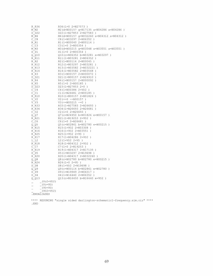
69
R_R36 R36(1=0 2=N27573 ) M_M2 M2(d=N00157 g=N17135 s=N04286 s=N04286 ) D_D22 D22(1=N27853 2=N27583 ) M_M4 M4(d=N00157 g=N032260 s=N04312 s=N04312 ) C_C8 C8(1=N03297 2=N06352 ) R_R1 R1(1=N00040 2=N00114 ) C_C3 C3(1=0 2=N00354 ) M_M3 M3(d=N00215 g=N03548 s=N03551 s=N03551 ) D_D1 D1(1=0 2=N00354 ) Q_Q10 Q10(c=N06352 b=N03281 e=N03297 ) R_R11 R11(1=N03281 2=N06352 ) R_R2 R2(1=N00114 2=N00045 ) R_R12 R12(1=N03297 2=N03281 ) R_R13 R13(1=N03582 2=N032221 ) R_R14 R14(1=N03582 2=N03548 ) R_R3 R3(1=N00157 2=N000072 ) D_D21 D21(1=N00157 2=N24910 ) R_R4 R4(1=N00157 2=N000092 ) R_R5 R5(1=0 2=N00185 ) D_D23 D23(1=N27853 2=0 ) C_C4 C4(1=N00386 2=VO2 ) C_C1 C1(1=N26681 2=N00185 ) R_R10 R10(1=N00157 2=N01826 ) V_V2 V2(+=0 -=N00157 ) V_V3 V3(+=N00215 -=0 ) R_R33 R33(1=N27583 2=N26693 ) R_R34 R34(1=N26693 2=N26681 ) C_C2 C2(1=0 2=N26693 ) Q_Q7 Q7(c=N24950 b=N01826 e=N00157 ) R_R21 R21(1=N19253 2=VO2 ) C_C6 C6(1=0 2=N26681 ) Q_Q5 Q5(c=N02861 b=N02780 e=N00215 ) R_R15 R15(1=VO2 2=N03308 ) R_R16 R16(1=VO2 2=N03551 ) R_R25 R25(1=VO2 2=VO ) R_R17 R17(1=N04286 2=VO2 ) L_L2 L2(1=VO2 2=VO ) R_R18 R18(1=N04312 2=VO2 ) C_C7 C7(1=0 2=N19253 ) R_R19 R19(1=N04317 2=N17135 ) D_D5 D5(1=N03297 2=N19698 ) R_R20 R20(1=N04317 2=N032260 ) Q_Q8 Q8(c=N02780 b=N02780 e=N00215 ) R_R24 R24(1=0 2=VO ) D_D8 D8(1=VO2 2=N19698 ) Q_Q9 Q9(c=N00114 b=N02861 e=N02780 ) D_D9 D9(1=N19949 2=N04317 ) D_D4 D4(1=N16440 2=N06352 ) Q_Q13 Q13(c=N16450 b=N16440 e=VO2 ) _ _(Vo2=VO2) _ _(Vo=VO) _ _(VO=VO) _ _(VO2=VO2) .ENDALIASES **** RESUMING "single sided darlington-schematic1-frequency.sim.cir" **** .END

70
**** 10/08/02 00:49:50 ********* PSpice 9.1 (Mar 1999) ******** ID# 0 ******** ** circuit file for profile: frequency **** Diode MODEL PARAMETERS ****************************************************************************** D1N4148 D1N5245 BZX84C2V7/ZTX BZX84C4V3/ZTX IS 2.682000E-09 3.142000E-15 3.677000E-15 187.000000E-15 N 1.836 1.059 1.218 ISR 1.565000E-09 1.527000E-09 IKF .04417 1 1 BV 100 15 2.766 4.367 IBV 100.000000E-06 .024573 .06476 .06905 NBV 1.0932 IBVL 7.124900E-06 NBVL .65646 RS .5664 3.536 .12 .09 TT 11.540000E-09 57.710000E-09 331.800000E-09 CJO 4.000000E-12 80.500000E-12 312.100000E-12 221.200000E-12 VJ .5 .75 .3971 .7266 M .3333 .4186 .2052 .3317 TBV1 833.330000E-06
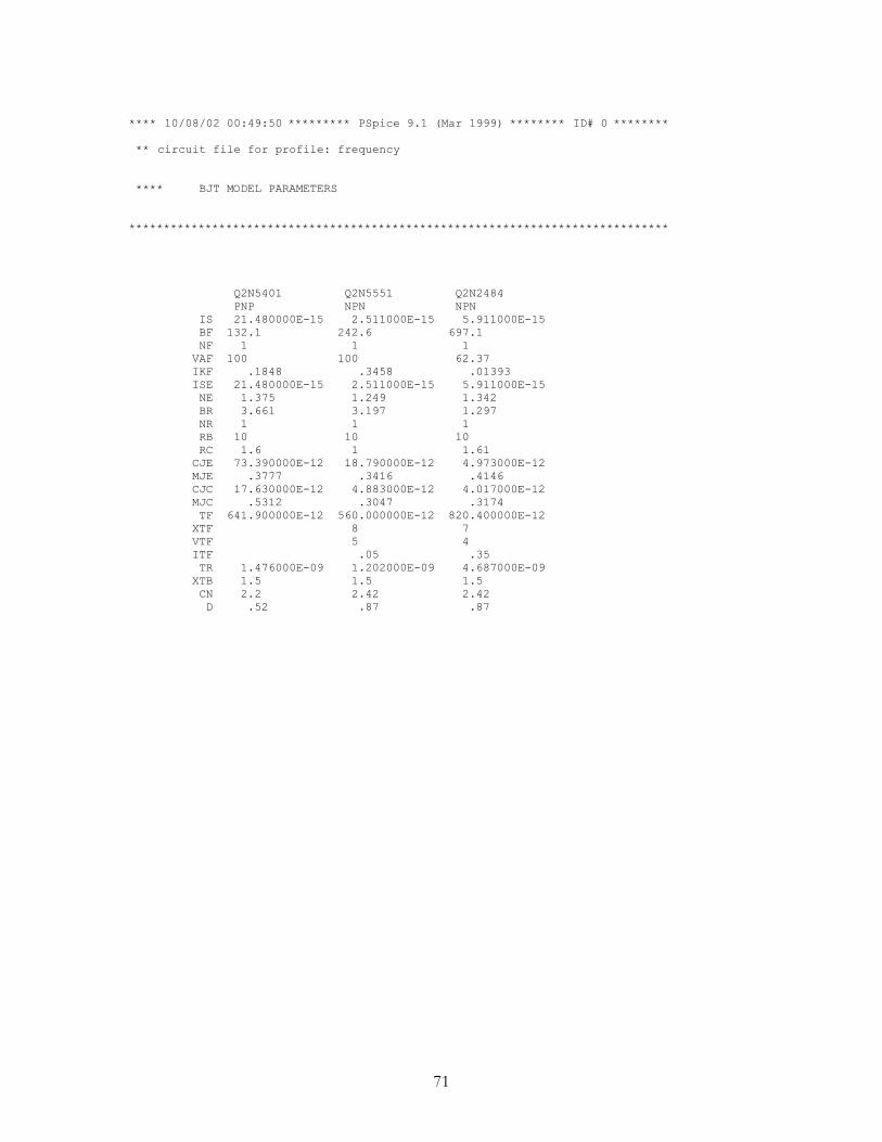
71
**** 10/08/02 00:49:50 ********* PSpice 9.1 (Mar 1999) ******** ID# 0 ******** ** circuit file for profile: frequency **** BJT MODEL PARAMETERS ****************************************************************************** Q2N5401 Q2N5551 Q2N2484 PNP NPN NPN IS 21.480000E-15 2.511000E-15 5.911000E-15 BF 132.1 242.6 697.1 NF 1 1 1 VAF 100 100 62.37 IKF .1848 .3458 .01393 ISE 21.480000E-15 2.511000E-15 5.911000E-15 NE 1.375 1.249 1.342 BR 3.661 3.197 1.297 NR 1 1 1 RB 10 10 10 RC 1.6 1 1.61 CJE 73.390000E-12 18.790000E-12 4.973000E-12 MJE .3777 .3416 .4146 CJC 17.630000E-12 4.883000E-12 4.017000E-12 MJC .5312 .3047 .3174 TF 641.900000E-12 560.000000E-12 820.400000E-12 XTF 8 7 VTF 5 4 ITF .05 .35 TR 1.476000E-09 1.202000E-09 4.687000E-09 XTB 1.5 1.5 1.5 CN 2.2 2.42 2.42 D .52 .87 .87

72
**** 10/08/02 00:49:50 ********* PSpice 9.1 (Mar 1999) ******** ID# 0 ******** ** circuit file for profile: frequency **** MOSFET MODEL PARAMETERS ****************************************************************************** IRF510 IRF9510 NMOS PMOS LEVEL 3 3 L 2.000000E-06 2.000000E-06 W .64 .2 VTO 3.697 -3.923 KP 20.680000E-06 10.540000E-06 GAMMA 0 0 PHI .6 .6 LAMBDA 0 0 RD .02108 .4523 RS .4508 .3715 RG 2.977 4.087 RDS 444.400000E+03 444.400000E+03 IS 202.900000E-15 2.896000E-18 JS 0 0 N 3 PB .8 .8 PBSW .8 .8 CBD 366.500000E-12 331.800000E-12 CJ 0 0 CJSW 0 0 TT 135.000000E-09 2.250000E-06 CGSO 600.500000E-12 2.547000E-09 CGDO 62.710000E-12 311.000000E-12 CGBO 0 0 TOX 100.000000E-09 100.000000E-09 XJ 0 0 UO 300 UCRIT 10.000000E+03 10.000000E+03 DELTA 0 0 ETA 0 0 DIOMOD 1 1 VFB 0 0 LETA 0 0 WETA 0 0 U0 0 0 TEMP 0 0 VDD 0 0 XPART 0 0
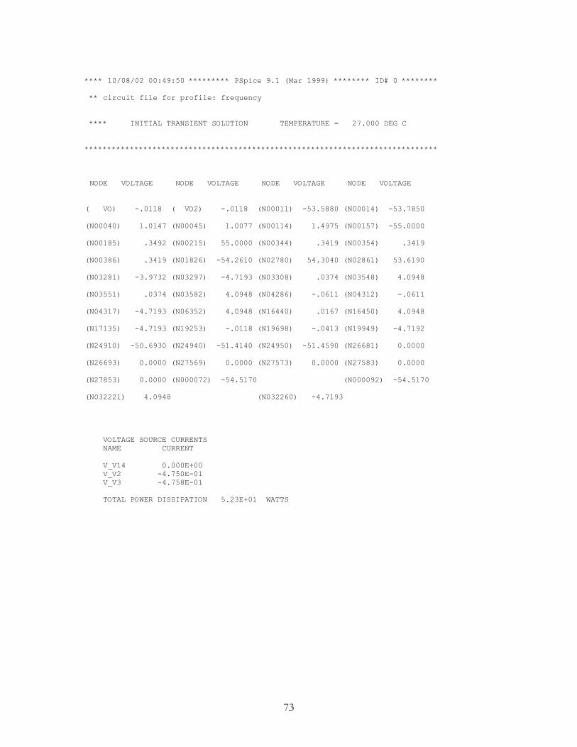
73
**** 10/08/02 00:49:50 ********* PSpice 9.1 (Mar 1999) ******** ID# 0 ******** ** circuit file for profile: frequency **** INITIAL TRANSIENT SOLUTION TEMPERATURE = 27.000 DEG C ****************************************************************************** NODE VOLTAGE NODE VOLTAGE NODE VOLTAGE NODE VOLTAGE ( VO) -.0118 ( VO2) -.0118 (N00011) -53.5880 (N00014) -53.7850 (N00040) 1.0147 (N00045) 1.0077 (N00114) 1.4975 (N00157) -55.0000 (N00185) .3492 (N00215) 55.0000 (N00344) .3419 (N00354) .3419 (N00386) .3419 (N01826) -54.2610 (N02780) 54.3040 (N02861) 53.6190 (N03281) -3.9732 (N03297) -4.7193 (N03308) .0374 (N03548) 4.0948 (N03551) .0374 (N03582) 4.0948 (N04286) -.0611 (N04312) -.0611 (N04317) -4.7193 (N06352) 4.0948 (N16440) .0167 (N16450) 4.0948 (N17135) -4.7193 (N19253) -.0118 (N19698) -.0413 (N19949) -4.7192 (N24910) -50.6930 (N24940) -51.4140 (N24950) -51.4590 (N26681) 0.0000 (N26693) 0.0000 (N27569) 0.0000 (N27573) 0.0000 (N27583) 0.0000 (N27853) 0.0000 (N000072) -54.5170 (N000092) -54.5170 (N032221) 4.0948 (N032260) -4.7193 VOLTAGE SOURCE CURRENTS NAME CURRENT V_V14 0.000E+00 V_V2 -4.750E-01 V_V3 -4.758E-01 TOTAL POWER DISSIPATION 5.23E+01 WATTS
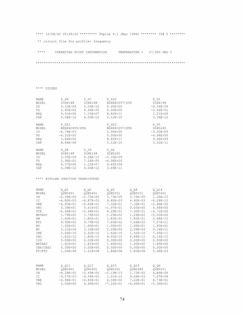
74
**** 10/08/02 00:49:50 ********* PSpice 9.1 (Mar 1999) ******** ID# 0 ******** ** circuit file for profile: frequency **** OPERATING POINT INFORMATION TEMPERATURE = 27.000 DEG C ****************************************************************************** **** DIODES NAME D_D6 D_D7 D_D22 D_D1 MODEL D1N4148 D1N4148 BZX84C2V7/ZTX D1N4148 ID 3.33E-09 5.56E-12 0.00E+00 -4.54E-09 VD 2.85E-02 6.40E-05 0.00E+00 -3.42E-01 REQ 6.51E+06 1.15E+07 8.82E+11 1.21E+09 CAP 4.08E-12 4.00E-12 3.12E-10 3.36E-12 NAME D_D21 D_D23 D_D5 MODEL BZX84C4V3/ZTX BZX84C2V7/ZTX D1N5245 ID -6.74E-03 0.00E+00 -3.50E-09 VD -4.31E+00 0.00E+00 -4.68E+00 REQ 3.84E+00 8.82E+11 4.94E+09 CAP 8.66E-08 3.12E-10 3.52E-11 NAME D_D8 D_D9 D_D4 MODEL D1N4148 D1N4148 D1N5245 ID 3.50E-09 6.28E-12 -3.33E-09 VD 2.96E-02 7.24E-05 -4.08E+00 REQ 6.37E+06 1.15E+07 4.62E+09 CAP 4.08E-12 4.00E-12 3.69E-11 **** BIPOLAR JUNCTION TRANSISTORS NAME Q_Q1 Q_Q2 Q_Q3 Q_Q4 Q_Q14 MODEL Q2N5401 Q2N5401 Q2N5551 Q2N5551 Q2N5401 IB -2.69E-05 -2.72E-05 3.73E-05 3.73E-05 1.26E-12 IC -4.80E-03 -4.87E-03 4.80E-03 4.80E-03 -6.28E-12 VBE -6.65E-01 -6.66E-01 7.32E-01 7.32E-01 -2.96E-02 VBC 5.39E+01 5.41E+01 -1.97E-01 0.00E+00 4.68E+00 VCE -5.46E+01 -5.48E+01 9.29E-01 7.32E-01 -4.71E+00 BETADC 1.79E+02 1.79E+02 1.29E+02 1.29E+02 -5.00E+00 GM 1.83E-01 1.85E-01 1.83E-01 1.83E-01 2.68E-12 RPI 9.92E+02 9.79E+02 7.65E+02 7.64E+02 7.07E+11 RX 1.00E+01 1.00E+01 1.00E+01 1.00E+01 1.00E+01 RO 3.21E+04 3.16E+04 2.09E+04 2.09E+04 9.14E+11 CBE 2.40E-10 2.42E-10 1.52E-10 1.52E-10 7.45E-11 CBC 1.81E-12 1.80E-12 4.55E-12 4.89E-12 6.16E-12 CJS 0.00E+00 0.00E+00 0.00E+00 0.00E+00 0.00E+00 BETAAC 1.81E+02 1.81E+02 1.40E+02 1.40E+02 1.89E+00 CBX/CBX2 0.00E+00 0.00E+00 0.00E+00 0.00E+00 0.00E+00 FT/FT2 1.20E+08 1.21E+08 1.86E+08 1.85E+08 5.28E-03 NAME Q_Q11 Q_Q12 Q_Q15 Q_Q16 Q_Q6 MODEL Q2N5401 Q2N5401 Q2N5551 Q2N2484 Q2N5551 IB -8.28E-05 -5.49E-05 -2.19E-13 1.73E-05 4.86E-06 IC -9.57E-03 -9.56E-03 1.01E-12 9.56E-03 7.67E-04 VBE -6.96E-01 -6.85E-01 4.50E-02 7.22E-01 6.73E-01 VBC 0.00E+00 4.95E+01 -7.22E-01 -4.60E+01 -5.36E+01

75
VCE -6.96E-01 -5.02E+01 7.67E-01 4.67E+01 5.43E+01 BETADC 1.16E+02 1.74E+02 -4.63E+00 5.53E+02 1.58E+02 GM 3.53E-01 3.58E-01 5.49E-13 2.88E-01 2.96E-02 RPI 3.19E+02 4.82E+02 3.13E+12 1.65E+03 6.02E+03 RX 1.00E+01 1.00E+01 1.00E+01 1.00E+01 1.00E+01 RO 1.04E+04 1.56E+04 9.85E+11 1.13E+04 2.00E+05 CBE 3.53E-10 3.55E-10 1.92E-11 2.45E-10 4.69E-11 CBC 1.78E-11 1.89E-12 3.98E-12 1.08E-12 1.32E-12 CJS 0.00E+00 0.00E+00 0.00E+00 0.00E+00 0.00E+00 BETAAC 1.13E+02 1.72E+02 1.72E+00 4.74E+02 1.78E+02 CBX/CBX2 0.00E+00 0.00E+00 0.00E+00 0.00E+00 0.00E+00 FT/FT2 1.52E+08 1.60E+08 3.77E-03 1.86E+08 9.78E+07 NAME Q_Q10 Q_Q7 Q_Q5 Q_Q8 Q_Q9 MODEL Q2N5551 Q2N2484 Q2N5401 Q2N5401 Q2N5401 IB 6.06E-05 3.23E-05 -8.28E-05 -8.28E-05 -5.49E-05 IC 8.75E-03 9.58E-03 -9.64E-03 -9.57E-03 -9.73E-03 VBE 7.46E-01 7.39E-01 -6.96E-01 -6.96E-01 -6.85E-01 VBC -8.07E+00 -2.80E+00 6.85E-01 0.00E+00 5.21E+01 VCE 8.81E+00 3.54E+00 -1.38E+00 -6.96E-01 -5.28E+01 BETADC 1.44E+02 2.97E+02 1.16E+02 1.16E+02 1.77E+02 GM 3.31E-01 2.65E-01 3.55E-01 3.53E-01 3.64E-01 RPI 4.67E+02 8.74E+02 3.19E+02 3.19E+02 4.82E+02 RX 1.00E+01 1.00E+01 1.00E+01 1.00E+01 1.00E+01 RO 1.23E+04 6.80E+03 1.04E+04 1.04E+04 1.56E+04 CBE 2.44E-10 2.33E-10 3.54E-10 3.53E-10 3.59E-10 CBC 2.31E-12 2.46E-12 1.26E-11 1.78E-11 1.84E-12 CJS 0.00E+00 0.00E+00 0.00E+00 0.00E+00 0.00E+00 BETAAC 1.55E+02 2.32E+02 1.13E+02 1.13E+02 1.75E+02 CBX/CBX2 0.00E+00 0.00E+00 0.00E+00 0.00E+00 0.00E+00 FT/FT2 2.14E+08 1.79E+08 1.54E+08 1.52E+08 1.61E+08 NAME Q_Q13 MODEL Q2N5551 IB -1.27E-12 IC 5.56E-12 VBE 2.85E-02 VBC -4.08E+00 VCE 4.11E+00 BETADC -4.37E+00 GM 2.63E-13 RPI 5.18E+12 RX 1.00E+01 RO 9.24E+11 CBE 1.90E-11 CBC 2.77E-12 CJS 0.00E+00 BETAAC 1.36E+00 CBX/CBX2 0.00E+00 FT/FT2 1.92E-03 **** MOSFETS NAME M_M1 M_M2 M_M4 M_M3 MODEL IRF510 IRF9510 IRF9510 IRF510 ID 2.23E-01 -2.24E-01 -2.24E-01 2.23E-01 VGS 4.06E+00 -4.66E+00 -4.66E+00 4.06E+00 VDS 5.50E+01 -5.49E+01 -5.49E+01 5.50E+01 VBS 0.00E+00 0.00E+00 0.00E+00 0.00E+00 VTH 3.70E+00 -3.92E+00 -3.92E+00 3.70E+00 VDSAT 2.60E-01 -6.52E-01 -6.52E-01 2.60E-01 Lin0/Sat1 -1.00E+00 -1.00E+00 -1.00E+00 -1.00E+00 if -1.00E+00 -1.00E+00 -1.00E+00 -1.00E+00

76
ir -1.00E+00 -1.00E+00 -1.00E+00 -1.00E+00 TAU -1.00E+00 -1.00E+00 -1.00E+00 -1.00E+00 GM 1.72E+00 6.87E-01 6.87E-01 1.72E+00 GDS 2.25E-06 2.25E-06 2.25E-06 2.25E-06 GMB 0.00E+00 0.00E+00 0.00E+00 0.00E+00 CBD 4.39E-11 3.98E-11 3.98E-11 4.39E-11 CBS 1.57E-19 2.25E-18 2.25E-18 1.57E-19 CGSOV 3.84E-10 5.09E-10 5.09E-10 3.84E-10 CGDOV 4.01E-11 6.22E-11 6.22E-11 4.01E-11 CGBOV 0.00E+00 0.00E+00 0.00E+00 0.00E+00 CGS 2.95E-10 9.21E-11 9.21E-11 2.95E-10 CGD 0.00E+00 0.00E+00 0.00E+00 0.00E+00 CGB 0.00E+00 0.00E+00 0.00E+00 0.00E+00

77
**** 10/08/02 00:49:50 ********* PSpice 9.1 (Mar 1999) ******** ID# 0 ******** ** circuit file for profile: frequency **** FOURIER ANALYSIS TEMPERATURE = 27.000 DEG C ****************************************************************************** FOURIER COMPONENTS OF TRANSIENT RESPONSE V(VO) DC COMPONENT = -1.041835E-02 HARMONIC FREQUENCY FOURIER NORMALIZED PHASE NORMALIZED NO (HZ) COMPONENT COMPONENT (DEG) PHASE (DEG) 1 2.000E+04 7.575E+00 1.000E+00 -2.907E+01 0.000E+00 2 4.000E+04 4.339E-03 5.728E-04 -8.841E+01 -3.028E+01 3 6.000E+04 4.286E-03 5.659E-04 -1.390E+01 7.330E+01 4 8.000E+04 1.885E-03 2.489E-04 4.698E+01 1.633E+02 5 1.000E+05 1.088E-03 1.436E-04 1.106E+02 2.560E+02 TOTAL HARMONIC DISTORTION = 8.549048E-02 PERCENT JOB CONCLUDED TOTAL JOB TIME 2558.76

78
Amplifier Bode Plot
Phase margin: 39.91° Frequency range: 2.60 Hz – 74.1 kHz Midband gain: 31.91 dB
Power Supply Output (No-Load)

79
Power Supply Output ( Load)
Minimum voltage: 56.6 V Ripple: 2.2 V

80
Appendix H: Datasheets