Laser Ablation of Polymer Waveguide and Integrated Mirrors for Optical Circuit Boards
30
Laser Ablation of Multimode Polymer Waveguide and Integrated Mirrors for Optical Circuit Boards © Shefiu S. Zakariyah [email protected] Shefiu S. Zakariyah
-
Upload
independent -
Category
Documents
-
view
4 -
download
0
Transcript of Laser Ablation of Polymer Waveguide and Integrated Mirrors for Optical Circuit Boards

Laser Ablation of Multimode Polymer
Waveguide and Integrated Mirrors for Optical
Circuit Boards
© Shefiu S. Zakariyah
Shefiu S. Zakariyah

Presentation Overview
Introduction
Optical communication overview
IeMRC OPCB flagship project
Laser ablation of optical waveguides
Results
o System characterisation
o Waveguides
Challenges
Summary
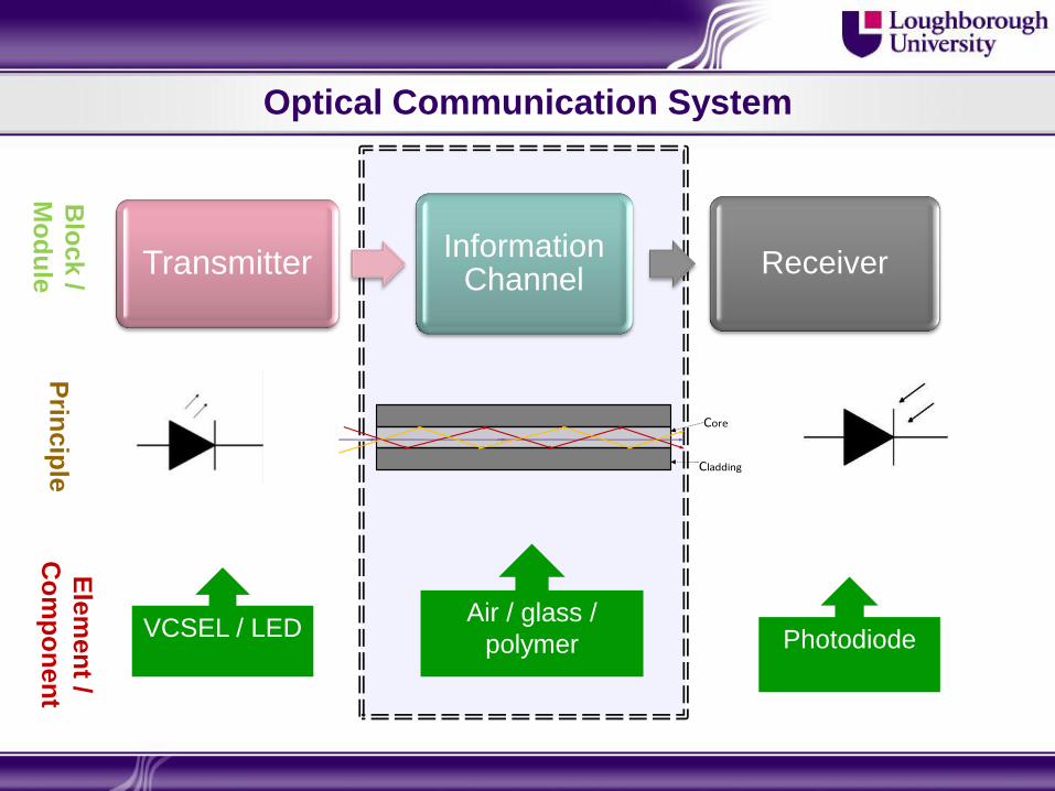
Optical Communication System
VCSEL / LED Air / glass /
polymer Photodiode
Core
Cladding
Blo
ck /
Mo
du
le
Prin
cip
le
Ele
men
t /
Co
mp
on
en
t
Transmitter Information
Channel Receiver

Optical Communication Methods
Optical Communication
Long-distance
Guided (e.g. optical fiber)
Unguided (e.g. free space)
Short-distance
Guided (e.g. OPCB)
Unguided (e.g. free space)
OPCB (Optical Printed Circuit Board) is the integration of optical waveguides with PCB to
solve the bottlenecks on the current electrical connections.

Why
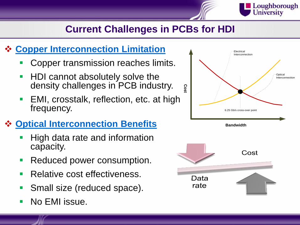
Current Challenges in PCBs for HDI
Copper Interconnection Limitation
Copper transmission reaches limits.
HDI cannot absolutely solve the density challenges in PCB industry.
EMI, crosstalk, reflection, etc. at high frequency.
Optical Interconnection Benefits
High data rate and information capacity.
Reduced power consumption.
Relative cost effectiveness.
Small size (reduced space).
No EMI issue.
Optical
Interconnection
Electrical
Interconnection
6.25 Gb/s cross-over point
Bandwidth
Co
st
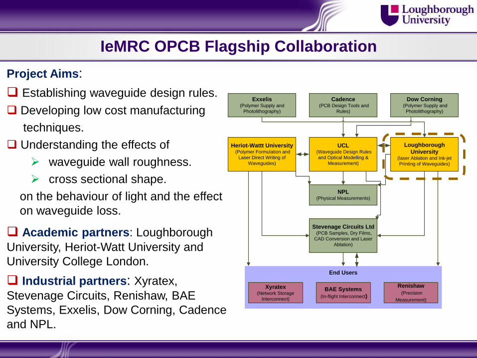
Exxelis (Polymer Supply and
Photolithography)
UCL (Waveguide Design Rules
and Optical Modelling &
Measurement)
Heriot-Wattt University (Polymer Formulation and
Laser Direct Writing of
Waveguides)
Dow Corning (Polymer Supply and
Photolithography)
Cadence (PCB Design Tools and
Rules)
NPL (Physical Measurements)
Stevenage Circuits Ltd (PCB Samples, Dry Films,
CAD Conversion and Laser
Ablation)
Loughborough
University (laser Ablation and Ink-jet
Printing of Waveguides)
BAE Systems
(In-flight Interconnect)
Renishaw
(Precision
Measurement)
Xyratex (Network Storage
Interconnect)
End Users
IeMRC OPCB Flagship Collaboration
Project Aims:
Establishing waveguide design rules.
Developing low cost manufacturing
techniques.
Understanding the effects of
waveguide wall roughness.
cross sectional shape.
on the behaviour of light and the effect
on waveguide loss.
Academic partners: Loughborough
University, Heriot-Watt University and
University College London.
Industrial partners: Xyratex,
Stevenage Circuits, Renishaw, BAE
Systems, Exxelis, Dow Corning, Cadence
and NPL.
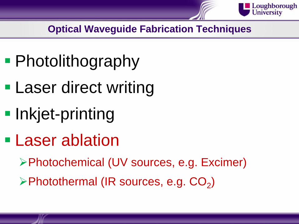
Optical Waveguide Fabrication Techniques
Photolithography
Laser direct writing
Inkjet-printing
Laser ablation
Photochemical (UV sources, e.g. Excimer)
Photothermal (IR sources, e.g. CO2)

Laser Material Processing
Laser Material Processing
Laser Generation Beam Delivery System Laser Processing (Material & Workpiece)
Laser Beam Monitoring
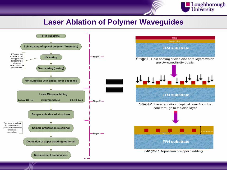
Laser Ablation of Polymer Waveguides
Stage1 : Spin coating of clad and core layers which
are UV-cured individually.
Stage2 : Laser ablation of optical layer from the
core through to the clad layer
Stage3 : Deposition of upper cladding
FR4 substrate
Lower clad
Core
PitchClad material
Core
FR4 substrate
FR4 substrate
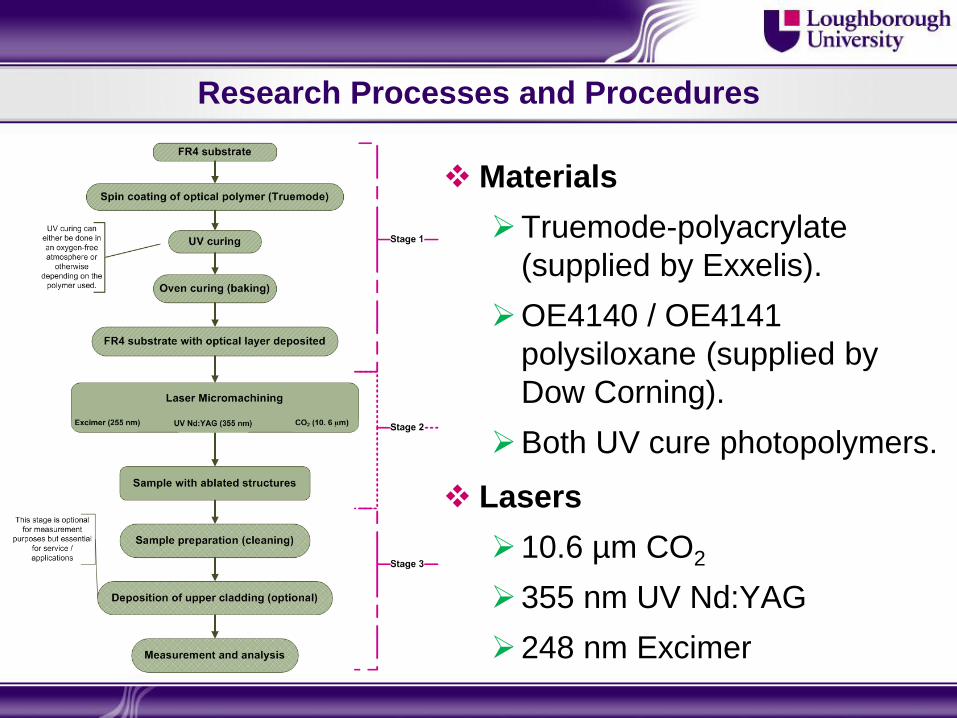
Research Processes and Procedures
Materials
Truemode-polyacrylate
(supplied by Exxelis).
OE4140 / OE4141
polysiloxane (supplied by
Dow Corning).
Both UV cure photopolymers.
Lasers
10.6 µm CO2
355 nm UV Nd:YAG
248 nm Excimer

Laser ablated channel (1)
Laser ablated channel (2)
Laser ablated channel (3)
Laser ablated channel (4)
20
0 µ
m
50 µm
Waveguide (1)
Waveguide (2)
Waveguide (3)
Laser Ablation of Polymer Waveguides

248 nm Excimer
Laser system characterisation
Fabrication of waveguides Mirror design & fabrication
for in-plane coupling
Laser System & Experimental Investigation

355 nm UV Nd:YAG
Feasibility study of optical polymer machining
Laser system characterisation
Fabrication of waveguides
248 nm Excimer
Laser system characterisation
Fabrication of waveguides Mirror design & fabrication
for in-plane coupling
Laser System & Experimental Investigation
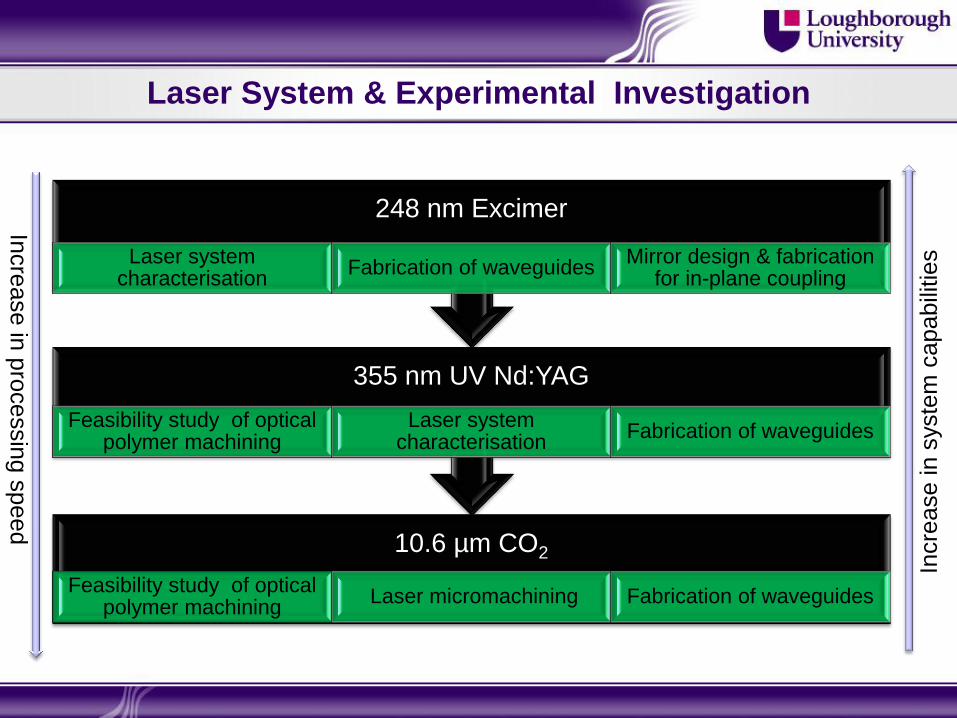
10.6 µm CO2
Feasibility study of optical polymer machining
Laser micromachining Fabrication of waveguides
355 nm UV Nd:YAG
Feasibility study of optical polymer machining
Laser system characterisation
Fabrication of waveguides
248 nm Excimer
Laser system characterisation
Fabrication of waveguides Mirror design & fabrication
for in-plane coupling
Laser System & Experimental Investigation
Incre
ase in
pro
cessin
g s
peed
Incre
ase in s
yste
m c
apabili
ties

Line ablated using the Gaussian beam
profile CO2 laser.
CO2 Laser Ablation of Optical Waveguides
CO2 Laser System 10 Watt (max.) power
Wavelength = 10.6 m
Continuous Wave (CW)
Gaussian beam profile
Investigation Photothermally-dominated ablation
process.
Feasibility study was conducted.
Effect of translation speed & power was investigated.
Material Polysiloxane OE4140 / OE4141
(Dow Corning).
Truemode (Exxelis).

Effect of scanning speed
at a fixed power of 3 W
on the quality of ablation
of Truemode™ polymer
using CW CO2 laser.
Effect of scanning speed at
a fixed 5 W power on the
quality of ablation of
polysiloxane OE4140 /
OE4141 using CO2 laser.
CO2 Laser Machining Trials

CO2 Laser Ablation of Optical Waveguides
(1) (2)
(3)
(4) (5)
FR4

Gaussian beam profile of UV Nd:YAG
laser (5200 model).
UV Nd:YAG Laser Ablation with Stevenage Circuits Ltd
UV Nd:YAG Laser Systems
Investigation
Laser system characterisation.
Waveguide fabrication.
Effects of stage speed, laser power & pulse
frequency were investigated.
Parameter / Model ESI model 5200 ESI Flex 5330
Wavelength (nm) 355 355
Beam profile Gaussian Gaussian & top-
hat
Frequency (kHz) 20 (max.) 70 (max.)
Spot size (µm) 25 (fixed) 53 – 123
(changeable)
Power (W) Up to 2.5
(approx.)
Up to 3.3
(approx.)
Pulse width (ns) 30 60

UV Nd:YAG Laser Ablation Beam Overlap
Issues were
encountered while
overlapping the narrow
beam to form trenches.
Methods to overcome
this was developed.
FR4
FR4
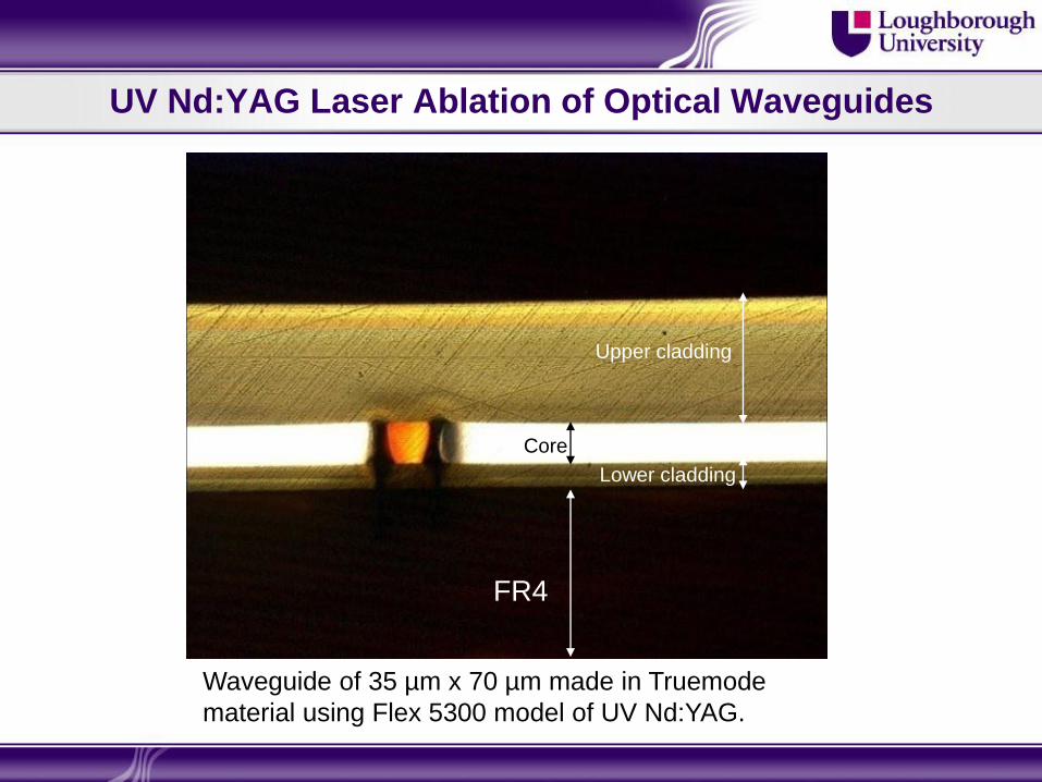
UV Nd:YAG Laser Ablation of Optical Waveguides
Waveguide of 35 µm x 70 µm made in Truemode
material using Flex 5300 model of UV Nd:YAG.
FR4
Upper cladding
Lower cladding
Core

‘Top-hat’ like beam profile (as a result of
mask projection) of Excimer laser trial
Excimer Laser Ablation of Optical Waveguides
Excimer Laser System 248nm Wavelength, Krypton Fluoride (KrF).
20 ns Pulse Length, 1- 40 Hz.
250mJ/pulse (max.) in energy mode or 27kV (max.) in Voltage mode.
Up to 100 mJ/pulse over 1 mm2 at the workpiece.
Investigation Laser system characterisation.
Waveguide fabrication.
Effects of stage translation speed, fluence & frequency were investigated.
Material Truemode (Exxelis).
Polysiloxane OE4140 / OE4141 (Dow Corning).
Square
Mask
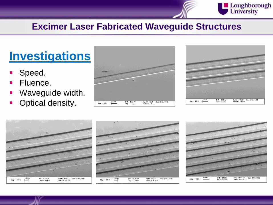
Excimer Laser Fabricated Waveguide Structures
Investigations
Speed.
Fluence.
Waveguide width.
Optical density.

Excimer Laser Fabricated Waveguide Structures
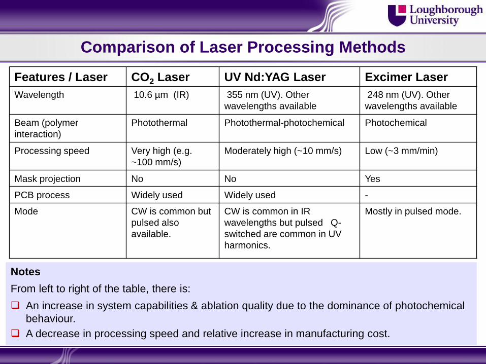
Comparison of Laser Processing Methods
Features / Laser CO2 Laser UV Nd:YAG Laser Excimer Laser
Wavelength 10.6 µm (IR) 355 nm (UV). Other
wavelengths available
248 nm (UV). Other
wavelengths available
Beam (polymer
interaction)
Photothermal Photothermal-photochemical Photochemical
Processing speed Very high (e.g.
~100 mm/s)
Moderately high (~10 mm/s) Low (~3 mm/min)
Mask projection No No Yes
PCB process Widely used Widely used -
Mode CW is common but
pulsed also
available.
CW is common in IR
wavelengths but pulsed Q-
switched are common in UV
harmonics.
Mostly in pulsed mode.
Notes
From left to right of the table, there is:
An increase in system capabilities & ablation quality due to the dominance of photochemical
behaviour.
A decrease in processing speed and relative increase in manufacturing cost.
26
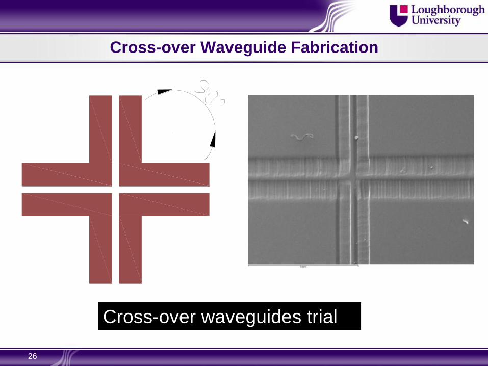
Cross-over Waveguide Fabrication
Cross-over waveguides trial

Embedded Mirror Fabrication
450
Optical polymer layer on FR4 substrate
Optical polymer layer on FR4 substrate
Optical polymer layer on FR4 substrate
450
45-degree in-plane coupling mirror
design with zero-degree effective turning
angle.
45-degree in-plane coupling mirror
design with 180-degree effective
turning angle.
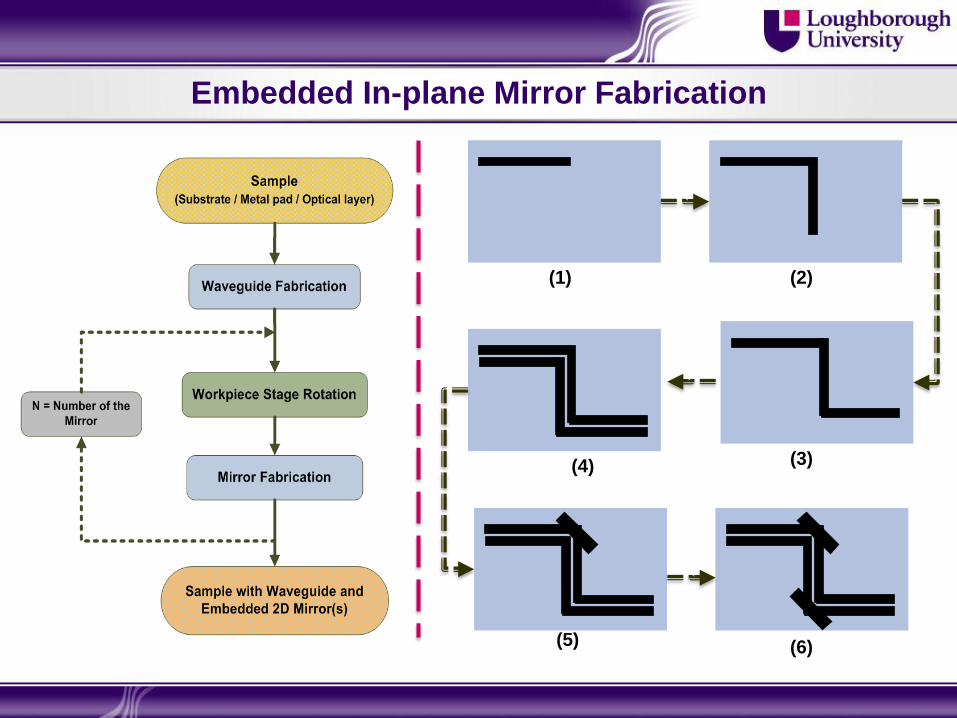
Embedded In-plane Mirror Fabrication
(1) (2)
(3) (4)
(5) (6)

Embedded In-plane Mirror Fabrication
45-degree in-plane coupling mirror design with zero-degree
effective turning angle.

Project financially supported by the UK Engineering and Physical Sciences Research
Council through the Innovative Electronics Manufacturing Research Centre (IeMRC).
Project partners:
University College London, Loughborough University & Heriot Watt University
Exxelis Ltd (UK), BAE Systems (UK), Cadence (UK), Dow Corning (USA), Stevenage Circuits Ltd (UK), National Physical Laboratory (UK) and Xyratex Technology Ltd (UK).
Particular thanks to Stevenage Circuits Ltd (for giving access to their UV Nd:YAG laser),
and Exxelis Ltd & Dow Corning (for providing optical polymers).