Lack of influence of the Cu-Sn mixing heat treatments on the super-conducting properties of two...
7
LACK OF INFLUENCE OF THE Cu-Sn MIXING HEAT TREATMENTS ON THE SUPER- CONDUCTING PROPERTIES OF TWO HIGH-Nb, INTERNAL-Sn Nb 3 Sn CONDUCTORS M.T. Naus, M.C. Jewell, PJ. Lee and D.C. Larbalestier Applied Superconductivity Center, University of Wisconsin - Madison Madison, WI 53706 USA ABSTRACT The heat treatment of internal-Sn, NbsSn superconductors has two primary purposes - (1) to mix the Cu and Sn, and (2) to form the A15 phase. We have studied the effect of the Cu-Sn mixing heat treatments on the superconducting properties of two high-Nb internal- Sn conductors. The samples underwent continuous ramps of 6, 30 or 60 °C/h from room temperature to the A15 reaction temperature, or used isothermal hold treatments to mix the Cu and Sn prior to A15 formation. The strands were then reacted for 180 hours at 650 °C to form the A15 phase. Inductive T c measurements showed no significant difference arising from vastly different mixing steps. However, the T c values were ~2 K below that of stoichiometric NbsSn (18.3 K) due to a high Nb:Sn ratio and Sn leakage from the filament bundle. H*, H c2 and J c (as inferred from magnetization measurements) were also unaffected by the Cu-Sn mixing heat treatments used. Unlike lower Nb content, lower J c internal-Sn conductors, we conclude that the superconducting properties of these internal- Sn composites are essentially independent of how the Cu and Sn are mixed, greatly simplifying heat treatment optimization. INTRODUCTION The heat treatment (HT) of internal-Sn, NbsSn composites requires the mixing of Sn from the filament bundle core with the interfilamentary Cu in order for each Nb filament to be adequately surrounded by Sn prior to NbaSn formation. Due to an extremely slow approach to equilibrium, the best mixing heat treatment is complex and varies strongly by composite geometry and/or manufacturer [1]. In principle, the goal of the mixing step is to achieve a homogeneous mixture of Cu and Sn within the Sn diffusion barrier, but in fact it is not possible to fully mix them in a reasonable time (< 200 hours) [2-6]. This inevitable incomplete mixing results in different Nb filaments being in contact with different Cu-Sn compositions at the time of A15 formation. From the Cu-Sn-Nb phase diagram [7], higher Sn A15 is in equilibrium with the higher Sn Cu-Sn phases. This implies that the initial A15 to form will have different, CP614, Advances in Cryogenic Engineering: Proceedings of the International Cryogenic Materials Conference - /CMC, Vol. 48, edited by B. Balachandran et al. © 2002 American Institute of Physics 0-7354-0060-l/02/$19.00 1016
-
Upload
independent -
Category
Documents
-
view
0 -
download
0
Transcript of Lack of influence of the Cu-Sn mixing heat treatments on the super-conducting properties of two...

LACK OF INFLUENCE OF THE Cu-Sn MIXINGHEAT TREATMENTS ON THE SUPER-CONDUCTING PROPERTIES OF TWO HIGH-Nb,INTERNAL-Sn Nb3Sn CONDUCTORS
M.T. Naus, M.C. Jewell, PJ. Lee and D.C. Larbalestier
Applied Superconductivity Center, University of Wisconsin - MadisonMadison, WI 53706 USA
ABSTRACT
The heat treatment of internal-Sn, NbsSn superconductors has two primary purposes - (1)to mix the Cu and Sn, and (2) to form the A15 phase. We have studied the effect of theCu-Sn mixing heat treatments on the superconducting properties of two high-Nb internal-Sn conductors. The samples underwent continuous ramps of 6, 30 or 60 °C/h from roomtemperature to the A15 reaction temperature, or used isothermal hold treatments to mix theCu and Sn prior to A15 formation. The strands were then reacted for 180 hours at 650 °Cto form the A15 phase. Inductive Tc measurements showed no significant difference arisingfrom vastly different mixing steps. However, the Tc values were ~2 K below that ofstoichiometric NbsSn (18.3 K) due to a high Nb:Sn ratio and Sn leakage from the filamentbundle. H*, Hc2 and Jc (as inferred from magnetization measurements) were alsounaffected by the Cu-Sn mixing heat treatments used. Unlike lower Nb content, lower Jcinternal-Sn conductors, we conclude that the superconducting properties of these internal-Sn composites are essentially independent of how the Cu and Sn are mixed, greatlysimplifying heat treatment optimization.
INTRODUCTION
The heat treatment (HT) of internal-Sn, NbsSn composites requires the mixing of Snfrom the filament bundle core with the interfilamentary Cu in order for each Nb filament tobe adequately surrounded by Sn prior to NbaSn formation. Due to an extremely slowapproach to equilibrium, the best mixing heat treatment is complex and varies strongly bycomposite geometry and/or manufacturer [1].
In principle, the goal of the mixing step is to achieve a homogeneous mixture of Cuand Sn within the Sn diffusion barrier, but in fact it is not possible to fully mix them in areasonable time (< 200 hours) [2-6]. This inevitable incomplete mixing results in differentNb filaments being in contact with different Cu-Sn compositions at the time of A15formation. From the Cu-Sn-Nb phase diagram [7], higher Sn A15 is in equilibrium withthe higher Sn Cu-Sn phases. This implies that the initial A15 to form will have different,
CP614, Advances in Cryogenic Engineering:Proceedings of the International Cryogenic Materials Conference - /CMC, Vol. 48,
edited by B. Balachandran et al.© 2002 American Institute of Physics 0-7354-0060-l/02/$19.00
1016

perhaps better, superconducting properties because a higher Sn content in the A15 phaseshould lead to higher Tc and Hc2. The question then arises whether the presence of differentCu-Sn compositions at the start of A15 reaction will have an effect on the A15 propertiesof fully reacted wires.
We have previously reported that there was no discernable effect on thesuperconducting properties in wires that underwent various sub-600 °C hold temperaturesfor the Cu-Sn mixing HT when followed by a reaction HT of 180 hours at 650°C(180h/650°C) [6]. However, the full range of possible mixing HT was not explored, as thelowest and highest Sn mixing temperatures were 362 and 533 °C, respectively. In responseto concerns about the generality of this earlier result, we have investigated the morestandard (and lengthy) manufacturer's HT and compare results to greatly abbreviated Cu-Sn mixing heat treatments.
In this paper, we test a full range of possible Cu-Sn mixing heat treatments. We haveinvestigated the effect on the transition temperature (Tc), the irreversibility field (//*), andthe upper critical field (Hc2) of continuous 6, 30 and 60 °C/h ramp rates from roomtemperature to a reaction temperature of 650 °C. We compare their properties to those ofsamples inserted directly into a furnace at 650 °C and to those that underwent a morestandard, long Cu-Sn mixing HT step. We also compare the critical current density (Jc) (asinferred from magnetization measurements) for a sub-set of these heat treatments.
EXPERIMENTAL PROCEDURE
The wires in this study (FIGURE 1), designated CRel912 and ORel02, weremanufactured by the MJR [8], internal-Sn process [9] by Teledyne Wah Chang (now WahChang) and Oxford Instruments - Superconducting Technology, respectively. Their Jc (4.2K, 12 T) values using a resistivity criterion of 10"13 Q-m are 2200 A/mm2 [10] and 2400A/mm2 [11] for CRel912 and ORel02, respectively. Both wires have 54 bundles, eachbundle consisting of an alloyed Sn core surrounded by alternating layers of Cu sheet andNb-lwt.%Ti mesh. Around each bundle is a Nb diffusion barrier. CRel912 has a Sn-2wt.%Mg core, while ORE102 has a Sn-lwt.%Cu core. The wire diameters are 0.7 and 0.8mm, respectively.
TABLE 1 shows the Cu:Nb:Sn atomic ratios derived from SEM cross-sectionalimage analysis on polished cross-sections like those in Figure 1. The reactedmicrostructures showed considerable conversion of the Nb diffusion barrier around eachbundle. Thus, TABLE 1 shows the Cu:Nb:Sn ratios both with and without the barrierincluded in the calculation. A potentially significant design difference between CRel912and ORel02 is that the atomic Nb:Sn ratios before reaction were 3.2 and 2.6, respectively,making CRel912 Sn-poor and ORel02 Sn-rich. When including the barrier, these ratiosincreased to 4.4:1 and 3.6:1 for ORel02 and CRel912, respectively, making bothconductors strongly sub-stoichiometric.
The ends of -80 mm long samples were electroplated with Cu to prevent Sn leakage.Samples were cleaned and sealed in quartz tubes under -30 mTorr of Ar, then placed in afurnace at room temperature, heated to 650 °C at 6 °C/h, 30 °C/h or 60 °C/h and reacted
TABLE 1. Cu:Nb:Sn Ratios Prior to Reaction
WireDesignation
CRel912ORel02
Including Entire BarrierCu2.11.6
Nb4.43.6
Sn11
CommentsSn deficientSn deficient
Cu2.11.6
Not Including BarrierNb3.22.6
Sn11
CommentsSn deficient
Sn rich
1017
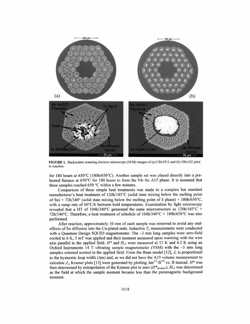
FIGURE 1. Backscatter scanning electron microscope (SEM) images of (a) CRel912 and (b) ORel02 priorto reaction.
for 180 hours at 650°C (180h/650°C). Another sample set was placed directly into a pre-heated furnace at 650°C for 180 hours to form the Nb-Sn A15 phase. It is assumed thatthese samples reached 650 °C within a few minutes.
Comparison of these simple heat treatments was made to a complex but standardmanufacturer's heat treatment of 120h/185°C (solid state mixing below the melting pointof Sn) + 72h/340° (solid state mixing below the melting point of 5 phase) + 180h/650°C,with a ramp rate of 60°C/h between hold temperatures. Examination by light microscopyrevealed that a HT of 104h/340°C generated the same microstructure as 120h/185°C +72h/340°C. Therefore, a heat treatment of schedule of 104h/340°C + 180h/650°C was alsoperformed.
After reaction, approximately 10 mm of each sample was removed to avoid any end-effects of Sn diffusion into the Cu-plated ends. Inductive Tc measurements were conductedwith a Quantum Design SQUID magnetometer. The -3 mm long samples were zero-fieldcooled to 6 K, 5 mT was applied and their moment measured upon warming with the wireaxis parallel to the applied field. H* and Hc2 were measured at 12 K and 4.2 K using anOxford Instruments 14 T vibrating sample magnetometer (VSM) with the ~5 mm longsamples oriented normal to the applied field. From the Bean model [12], Jc is proportionalto the hysteretic loop width (Am) and, as we did not have the A15 volume measurement tocalculate Jc, Kramer plots [13] were generated by plotting Am1/2-B1/4 vs. B instead. H* wasthen determined by extrapolation of the Kramer plot to zero (H * Kramer). HC2 was determinedas the field at which the sample moment became less than the paramagnetic backgroundmoment.
1018

0.0 -
15 16 17Temperature (K)
18 14 15 16 17Temperature (K)
FIGURE 2. rc of ORel02 (open symbols) and CRel912 (closed symbols) for various heat treatments. In (a),the samples were ramped from room temperature to 650°C at the ramp rates listed or inserted directly into apre-heated furnace, and then held for 180 hours at 650°C. No trend was seen in the Tc as a function of ramprate. A comparison of a standard manufacturer's HT ("Full HT") to one in which the sample was inserteddirectly at 650°C ("Direct") is shown in (b). The difference in Tc was ~ 0.4 K. Both composites have broadtransitions with mid-points near 16 K, well below the Tc of stoichiometric Nb3Sn.
Am was normalized by sample mass for ORel02 to get a relative comparison of Jcvalues after 3 different heat treatments. The heat treatments examined in this way were (1)direct insertion for 180h/650°C, (2) 104h/340°C + 180h/650°C, and (3) 120h/185°C +72h/340°C+180h/650°C.
RESULTS
The Tc curves are shown in FIGURE 2. As a whole they are broad and significantlylower than expected for high-Nb conductors. Their mid-point Tc transitions occur at -15.8K for CRel912 and at -16.3 K for ORel02, their 10% to 90% transitions are -1 K wide.There was no discernible difference in the Tc values for different ramp rates (Figure 2a),although ORel02 always had a slightly higher Tc than CRel912. Figure 2b shows the Tctraces after a standard manufacturer's HT of 120h/185°C + 72h/340°C + 180h/650°C("Full HT") and after putting the samples directly into a 650°C furnace for 180 hours("Direct"). The difference between the two heat treatments is less than 0.4 K. The Tc tracesof the 104h/340°C + 180h/650°C HT lay directly over the "Full HT" curves and, forclarity, they were not plotted.
TABLE 2 shows Hc2 (12 K) -13.3 T, H*Kramer (12 K) -10.0 T and H*Kramer (4.2 K)-24.2 T after all heat treatments for CRel912. In a few instances Hc2 could not beaccurately defined due to curvature in the magnetization curve and these are represented byan asterisk (*) in the table. The measurement errors for H*Kmmer (12 K) and Hc2 (12 K) areestimated to be 0.1 T and 0.2 T, respectively. The errors for H*Kmmer (4.2 K) are unknownbecause we must extrapolate from 14 T to -24 T, but we expect them to be small becausethere is good consistency between the 12 K and 4.2 K results.
TABLE 3 shows that #* and Hc2 for ORel02 are also not significantly different forthe different heat treatments. Hc2 (12 K), H*Kmmer (12 K) and H*Kmmer (4.2 K) were -13.3T, -10.0 T and -24.4 T, respectively. Also shown are three hysteretic loop widthsnormalized to sample mass (Am/mass), which includes the longest and shortest Cu-Snmixing heat treatments. The values at 4.2 K & 12 T and 12 K & 5 T differ by less than 1%.
1019

TABLE 2. H*Knmer and Hc2 of CRe 1912
Heat Treatment120h/185°C + 72h/340°C + 180h/650°C
104h/340°C + 180h/650°C6°C/h,RTtol80h/650°C
30°C/h,RTtol80h/650°C60°C/h,RTtol80h/650°C
Direct insertion, RT to 180h/650°C
H*4.2 K24.324.224.124.224.324.1
'Kramer (T)
12 K10.010.010.09.99.99.9
Hc2(T)12 K
*13.413.4
*13.3
*= Unable to determine.
It is interesting to note that H*Kramer (4.2 K) values for ORel02 are consistently slightlybelow those of CRel912, even though ORel02 has a slightly higher Tc. However, theH*Kmmer(l2 K) values are essentially the same for the two wires.
DISCUSSION
TABLE 2 and 3 clearly show that the Cu-Sn mixing HT has no influence on thesuperconducting properties in high-Nb wires. This is true whether the mixing HT lasts 200hours or just a couple of minutes (i.e. direct immersion). This is unlike lower Nbcomposites (e.g. ITER type), where the aggressiveness of the Cu-Sn mixing HT influencesCu-Sn phase boundary movement and thereby the amount of filament coupling [14].However, this is not an issue for high-Nb wires because the filaments are initially so closetogether that it is not possible to keep them from coupling during heat treatment. Aconsequence of the high-Nb design is that the Nb barrier can take part in the reaction,decreasing the average A15 Sn concentration and passing Sn into the stabilizing Cu, awayfrom the filaments.
The Tc of these high-Nb conductors is significantly lower than expected. The mid-point transitions are -16.4 and -16.0 K for ORel02 and CRe 1912, respectively, -2 Klower than that of stoichiometric NbsSn. A possible cause of the suppressed Tc values iscompressive strain induced by the higher thermal contraction of Cu relative to that ofNb3Sn. As a test, the Cu was etched off of a fully reacted CRe 1912 sample discussed in[6]. The inductive Tc of a single, free bundle was measured to be 0.5 K higher than that inthe unetched, strained state. Therefore, we conclude that the primary cause of thesuppressed Tc values of the wires in this study can not be due to strain and is most likely anA15 composition effect.
If the barrier reacts significantly, both wires will be Sn deficient (see TABLE 1), with
TABLE 3. H*Kramer, Hc2 and Am/mass of ORel02
H*Kramer(T) Hc2 (T) Am/mass (emu/mg)
120h/185Heat Treatment
°C + 72h/340°C +104h/340°C +6°C/h, RT to
30°C/h, RT to60°C/h, RT to
Direct insertion, RT to
180H/650180H/650180H/650180h/650180H/650180h/650
°C°c°c°c°c°c
4.2 K23.423.224.023.723.723.8
12 K10.010.010.210.010.110.1
12K13.313,
*13,13,13,
.4
.3
.4
.3
4.2 K, 12 T4,.SlxlO"3
4.80xlO'3
4,
---—
.78xlO"3
12K,5T2.2.
2.
llxlO'3
12xlO'3
----—
12xlO'3
* = Unable to determine.— = Not measured.
1020

FIGURE 3. Backscatter SEM image of ORel02 after direct insertion at 650°C for 180 hours showing theregion between 2 bundles where the A15 phase has grown completely through the barrier. As a result of Snleakage into the Cu stabilizer, A15 grains can be seen growing on the external side of the Nb barrier.
CRel912 more Sn deficient than ORel02. This is consistent with the fact that ORel02consistently has a higher Tc than CRel912. Clear evidence for significant barrier reactionis seen in the backscatter SEM image shown in FIGURE 3 of an ORel02 barrier regionafter direct insertion into a furnace for 180h/650°C. The image also shows a region wherethe barrier has reacted fully through. There also appear to be A15 grains on the externalside of the Nb barrier, indicating Sn leakage into the stabilizing Cu. As further proof ofcontamination of the pure stabilizing Cu, the residual resistivity ratio (RRR) (p30o K/p?? K)was only 3.1. Suppressed RRR values were also seen in the internal-Sn wires examined byBarzi et al. [15]. As a result, the Sn deficiency is now exacerbated by Sn loss into thestabilizing Cu. Moreover, some residual Sn will be left in the interfilamentary Cu afterreaction. Therefore, both wires may be even more Sn deficient than their pre-reactionCu:Nb:Sn ratios would indicate.
Although the above discussion provides a self-consistent explanation of why Tc isreduced for both conductors, and why Tc is higher in ORel02, the H*Kramer and Hc2 data isless clearly explained. H*Kramer (4.2 K) values for the higher Tc ORel02 (23.2 to 24.0 T)are consistently lower than those of CRel912 (24.1 to 24.3 T). Since H*Kramer may becontrolled by grain size (the Mg in CRel912 is an A15 grain refiner [16]), it may be thatthe small differences of TABLE 2 and 3 are explained by these rather than the overall Sncontent. Also, the Hc2 detected is the highest in the wire, but it is not necessarily that of themajority of the A15 material.
Even though there is no effect on the NbsSn superconducting properties, an additionalconsideration that often forces serious concern about the Cu-Sn mixing HT is that of Snburst, in which liquid Sn ruptures the wire. This can happen when the HT temperatureexceeds the melting point of Sn (232 °C) before the Sn and Cu have had a chance to forman adequate amount of higher melting point Cu—Sn phases. Although we have not seen Sn-burst in this study, the probability of it occurring increases with sample length due to theincreased probability of encountering weak diffusion barrier regions. The Sn-burstprobability might also be increased if cabling of the wire sufficiently reduces the integrityof the barrier.
1021

CONCLUSION
We have looked at the effect of vastly different Cu-Sn mixing heat treatments on thesuperconducting properties of fully reacted high Sn, internal-Sn NbsSn wire. We can findno significant influence on Tc, H*Kmmer, Hc2 or Jc due to the Cu-Sn mixing heat treatments.Since all of the filaments couple in these high-Nb wires, attention only needs to be paid tothe A15 reaction step. However, the integrity of the Nb barrier in these designs is atsignificant risk. Barrier breach and stabilization Cu poisoning is possible - even likely -leading to reduced Tc, H*Kmmer and Hc2 values in the A15 layer. Despite these concerns,high Jc values (defined as the critical current normalized to the bundle cross-section) havebeen achieved. Clearly, there presently exists a tradeoff between the area cross-section ofthe A15 layer and the A15 superconducting properties. If high-Nb, internal-Sn wires are toreach their full potential, the issues of the proper Nb:Sn ratio and Sn diffusion into thestabilizing Cu must be addressed.
ACKNOWLEDGEMENTS
This work was supported by the U.S. Department of Energy - Office of FusionEnergy Sciences (DE-FG02-86ER52131) and Division of High Energy Physics (DE-FG02-91ER40643), and benefited from NSF-MRSEC (DMR-9632427) supported facilities. Theauthors would like to thank Oxford Instruments - Superconducting Technology and WahChang for donating the wire in this study.
REFERENCES
1. Takayasu, M., Childs, R.A., Randall, R.N., Jayakumar, RJ. and Minervini, J.V., IEEE Trans. Appl.Supercond., 9 (2), 644 (1999).
2. Dietderich, D.R., Glazer, J., Lea, C, Hassenzahl, W.V. and Morris, J.W. Jr., IEEE Trans. Mag., 21 (2),297 (1985).
3. Taillard, R. and Verwaerde, C., Proc. Euromat95, Venice, 471 (1995).4. Glowacki, B.A., IEEE Trans. Appl. Supercond., 7 (2), 1520 (1997).5. Naus, M.T., Lee, P.J. and Larbalestier, D.C., IEEE Trans. Appl. Supercond., 10 (1), 983 (2000).6. Naus, M.T., Lee, P.J. and Larbalestier, D.C., IEEE Trans. Appl. Supercond., 11 (1), 3569 (2001).7. Villars, P., Prince, A. and Okamoto, H., Handbook of Ternary Alloy Phase Diagrams, (ASM
International, 1995), p. 9757.8. McDonald, W.K., Curtis, C.W., Scanlan, R.M., Larbalestier, D.C., Marken, K. and Smathers, D.B.,
IEEE Trans. Mag., 19 (3), 1124 (1983).9. Hashimoto, Y., Yoshizaki, K. and Tanka, M., Proc. of the 5th International Cryogenic Engineering
Conference, Kyoto, Japan, 332 (1974).10. Zhang, Y., McKinnell, J.C., Hentges, R.W. and Hong, S., IEEE Trans. Appl. Supercond., 9 (1), 1444
(1999).11. Personal communication, Michael B. Field, Oxford Instruments - Superconducting Technology.12. Bean, C.P., Rev. Mod. Phys, 36, 31 (1964).13. Kramer. E.J., J. Appl. Phys., 44 (3), 1360 (1973).14. Suenaga, M. and Sabatini, R.L., Proc. 9th US-Japan Workshop on High Field Materials, Wires and
Conductors, Japan, 111 (1995).15. Barzi, E., Limon, P.J., Yamada, R. and Zlobin, A.V., IEEE Trans. Appl. Supercond., 11 (1), 3573
(2001).16. Togano, K., Asano, T. and Tachikawa, K., J. Less Comm. Met., 68, 15 (1979).
1022


![MICROWAVE DIELECTRIC PROPERTIES OF CA[(LI1/3A2/3)1-XMX]O3-d [A=NB, TA AND M=TI, ZR, SN] COMPLEX PEROVSKITES: A REVIEW Sumesh](https://static.fdokumen.com/doc/165x107/6331727e2055169fc2032fb5/microwave-dielectric-properties-of-cali13a231-xmxo3-d-anb-ta-and-mti.jpg)