Lab Manual - St. ANNE'S College of Engineering & Technology
54
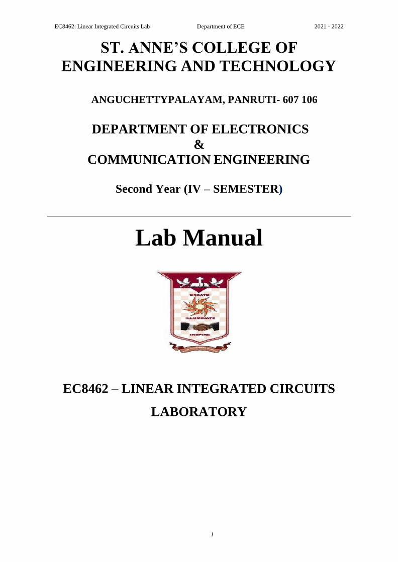
EC8462: Linear Integrated Circuits Lab Department of ECE 2021 - 2022 1 ST. ANNE’S COLLEGE OF ENGINEERING AND TECHNOLOGY ANGUCHETTYPALAYAM, PANRUTI- 607 106 DEPARTMENT OF ELECTRONICS & COMMUNICATION ENGINEERING Second Year (IV – SEMESTER) Lab Manual EC8462 – LINEAR INTEGRATED CIRCUITS LABORATORY
-
Upload
khangminh22 -
Category
Documents
-
view
0 -
download
0
Transcript of Lab Manual - St. ANNE'S College of Engineering & Technology
EC8462: Linear Integrated Circuits Lab Department of ECE 2021 - 2022
1
ST. ANNE’S COLLEGE OF
ENGINEERING AND TECHNOLOGY
ANGUCHETTYPALAYAM, PANRUTI- 607 106
DEPARTMENT OF ELECTRONICS
&
COMMUNICATION ENGINEERING
Second Year (IV – SEMESTER)
Lab Manual
EC8462 – LINEAR INTEGRATED CIRCUITS
LABORATORY
EC8462: Linear Integrated Circuits Lab Department of ECE 2021 - 2022
2
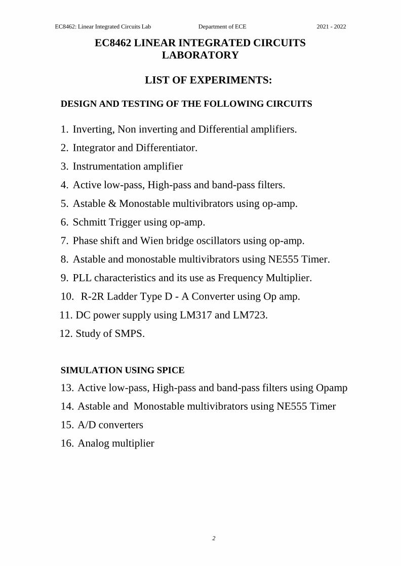
EC8462 LINEAR INTEGRATED CIRCUITS
LABORATORY
LIST OF EXPERIMENTS:
DESIGN AND TESTING OF THE FOLLOWING CIRCUITS
1. Inverting, Non inverting and Differential amplifiers.
2. Integrator and Differentiator.
3. Instrumentation amplifier
4. Active low-pass, High-pass and band-pass filters.
5. Astable & Monostable multivibrators using op-amp.
6. Schmitt Trigger using op-amp.
7. Phase shift and Wien bridge oscillators using op-amp.
8. Astable and monostable multivibrators using NE555 Timer.
9. PLL characteristics and its use as Frequency Multiplier.
10. R-2R Ladder Type D - A Converter using Op amp.
11. DC power supply using LM317 and LM723.
12. Study of SMPS.
SIMULATION USING SPICE
13. Active low-pass, High-pass and band-pass filters using Opamp
14. Astable and Monostable multivibrators using NE555 Timer
15. A/D converters
16. Analog multiplier
EC8462: Linear Integrated Circuits Lab Department of ECE 2021 - 2022
3
Wave- form
Time Period in ms
Voltage in Volts
Practical Gain
Input
(Vin)
Output
(Vo)
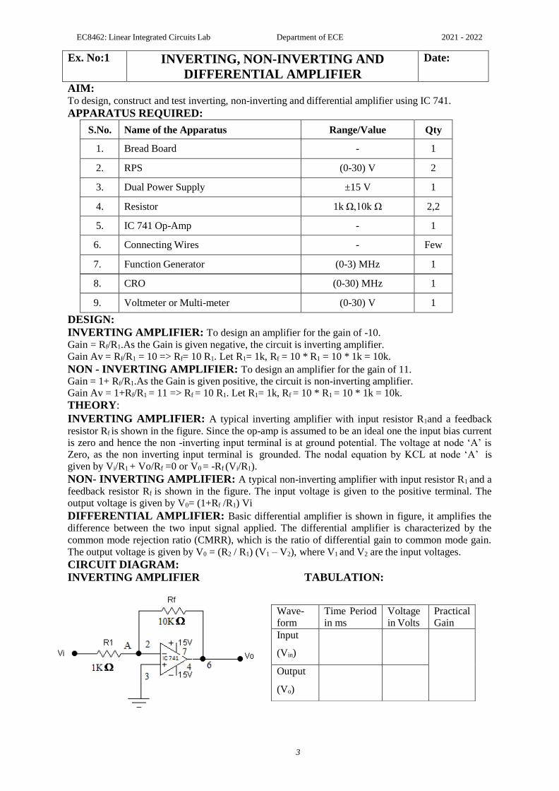
Ex. No:1 INVERTING, NON-INVERTING AND
DIFFERENTIAL AMPLIFIER
Date:
AIM: To design, construct and test inverting, non-inverting and differential amplifier using IC 741.
APPARATUS REQUIRED:
S.No. Name of the Apparatus Range/Value Qty
1. Bread Board - 1
2. RPS (0-30) V 2
3. Dual Power Supply ±15 V 1
4. Resistor 1k Ω,10k Ω 2,2
5. IC 741 Op-Amp - 1
6. Connecting Wires - Few
7. Function Generator (0-3) MHz 1
8. CRO (0-30) MHz 1
9. Voltmeter or Multi-meter (0-30) V 1
DESIGN:
INVERTING AMPLIFIER: To design an amplifier for the gain of -10.
Gain = Rf/R1.As the Gain is given negative, the circuit is inverting amplifier.
Gain Av = Rf/R1 = 10 => Rf= 10 R1. Let R1= 1k, Rf = 10 * R1 = 10 * 1k = 10k.
NON - INVERTING AMPLIFIER: To design an amplifier for the gain of 11. Gain = 1+ Rf/R1.As the Gain is given positive, the circuit is non-inverting amplifier. Gain Av = 1+Rf/R1 = 11 => Rf = 10 R1. Let R1= 1k, Rf = 10 * R1 = 10 * 1k = 10k.
THEORY:
INVERTING AMPLIFIER: A typical inverting amplifier with input resistor R1and a feedback
resistor Rf is shown in the figure. Since the op-amp is assumed to be an ideal one the input bias current is zero and hence the non -inverting input terminal is at ground potential. The voltage at node „A‟ is Zero, as the non inverting input terminal is grounded. The nodal equation by KCL at node „A‟ is
given by Vi/R1 + Vo/Rf =0 or V0 = -Rf (Vi/R1).
NON- INVERTING AMPLIFIER: A typical non-inverting amplifier with input resistor R1 and a
feedback resistor Rf is shown in the figure. The input voltage is given to the positive terminal. The
output voltage is given by V0= (1+Rf /R1) Vi
DIFFERENTIAL AMPLIFIER: Basic differential amplifier is shown in figure, it amplifies the
difference between the two input signal applied. The differential amplifier is characterized by the
common mode rejection ratio (CMRR), which is the ratio of differential gain to common mode gain.
The output voltage is given by V0 = (R2 / R1) (V1 – V2), where V1 and V2 are the input voltages.
CIRCUIT DIAGRAM:
INVERTING AMPLIFIER TABULATION:
EC8462: Linear Integrated Circuits Lab Department of ECE 2021 - 2022
4
Wave-
form
Time
in ms
Voltage
in Volts
Practical
Gain
Input
(Vin)
Output
(Vo)
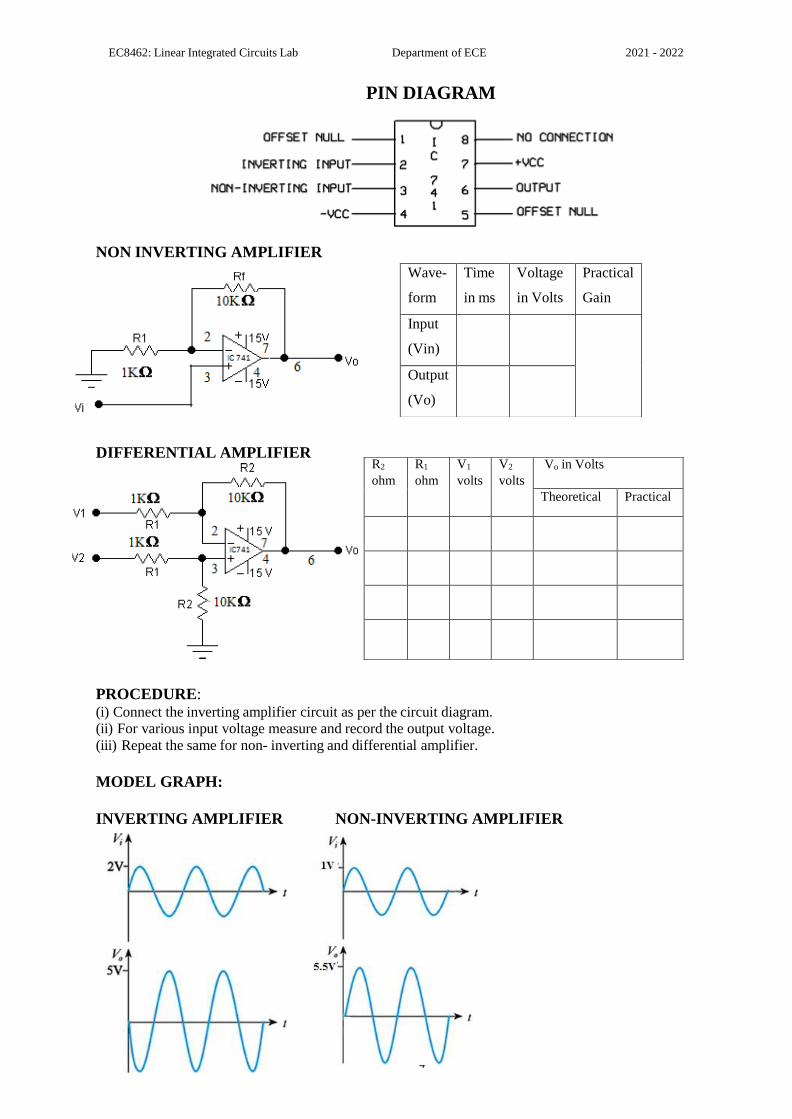
PIN DIAGRAM
NON INVERTING AMPLIFIER
DIFFERENTIAL AMPLIFIER
PROCEDURE: (i) Connect the inverting amplifier circuit as per the circuit diagram. (ii) For various input voltage measure and record the output voltage.
(iii) Repeat the same for non- inverting and differential amplifier.
MODEL GRAPH:
INVERTING AMPLIFIER NON-INVERTING AMPLIFIER
R2
ohm
R1
ohm
V1
volts
V2
volts
Vo in Volts
Theoretical Practical

EC8462: Linear Integrated Circuits Lab Department of ECE 2021 - 2022
5
SPECIFICATION FOR IC 741
+Vcc = +15V, - Vcc = -15V
Ambient Temparature : 250 C
Input offset voltage : 6 mV(Max)
Input offset current : 200nA(Max)
Input bias current : 500nA(Max)
Input resistance : 2M
Output resistance : 75
Total Power dissipation : 85mW.
RESULT: The design and testing of the inverting, non-inverting amplifier is done and the input and output waveforms
were drawn.
EC8462: Linear Integrated Circuits Lab Department of ECE 2021 - 2022
6
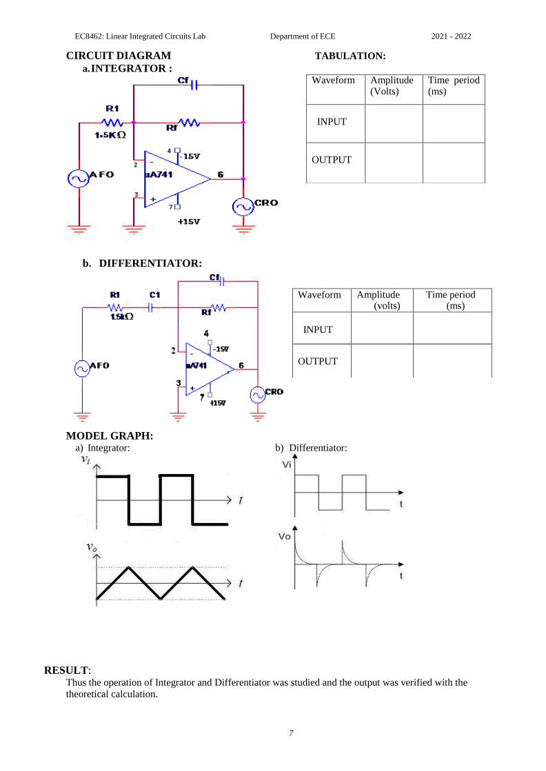
AIM: To design and test the following Op-Amp Circuits: a. Integrator b. Differentiator
APPARATUS REQUIRED:
S.No. Name of the Apparatus Range/Value Qty
1. Bread Board - 1
2. IC Power Supply ±15 V 1
3. Resistor 10 k Ω, 100 k Ω,1.5 k Ω,15k Ω 2, 1,1,1
4. IC 741 Op-Amp - 1
5. CRO 20 MHz. 1
6. Signal Generator 0-1 MHz. 1
7. Capacitor 0.1µF,0.01 µF 1(each)
8. Connecting Wires - Few
THEORY:
a. INTEGRATOR: The circuit performs the mathematical operation of integration, that is, the output waveform is the
integral of the input waveform. The output voltage Vo(t) = - (1/RfCf) Vi(t) dt , Where Vi is the input
voltage , Rf is the feedback resistance & Cf is the feedback capacitence.
b. DIFFERENTIATOR:
The circuit performs the mathematical operation of differentiation, that is, the output waveform is the
derivative of the input waveform. The output voltage Vo(t) = - RC (dvi / dt) Where Vi is the input
voltage , Rf is the feedback resistance & Cf is the feedback capacitence
DESIGN: a. Integrator: Design of Integrator with lower frequency limit of fmin = 160Hz.
f min 1
2Rf C f
Rf = 10R1
Let R1=1.5KΩ, then Rf = The range of Cf value from 0.001µF to 10µF is preferable. The capacitor has to very low leakage
C f 1
2Rf f min
b. Differentiator: Design of opamp differentiator that will differentiate an input signal with
fa =100Hz.The time period T of the input signal must be larger than or equal to RfC1.
Highest frequency of the input signal = fa 1
2Rf C1
Select C1 ( 1F). Let C1 0.1F
f a 100 1
2R f C1
R f 1
2 100 0.110 6
fb 10 f a 1KHz 1
2R C ; R1
1
2 1000 0.110
6
1 1
R1 C1 = Rf Cf; C f
PROCEDURE:
1.59 10
3 0.110
6
15.9 103
1. Connections are given as per the circuit diagram for integrator. 2. The square wave of 2Vp-p is given as input to the inverting terminal of the IC.
3. The output waveform is observed in the CRO.
4. Plot the input and output waveforms. 5. Repeat the same for differentiator
Ex. No:2 INTEGRATOR AND DIFFERENTIATOR Date:
EC8462: Linear Integrated Circuits Lab Department of ECE 2021 - 2022
7
Waveform Amplitude (volts)
Time period (ms)
INPUT
OUTPUT
CIRCUIT DIAGRAM TABULATION:
a. INTEGRATOR :
b. DIFFERENTIATOR:
MODEL GRAPH: a) Integrator:
b) Differentiator:
RESULT: Thus the operation of Integrator and Differentiator was studied and the output was verified with the
theoretical calculation.
Waveform Amplitude (Volts)
Time period (ms)
INPUT
OUTPUT
EC8462: Linear Integrated Circuits Lab Department of ECE 2021 - 2022
8
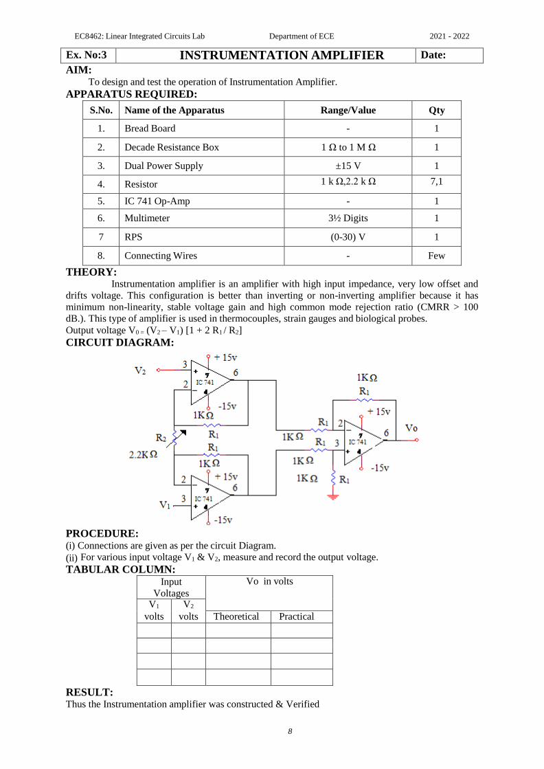
Ex. No:3 INSTRUMENTATION AMPLIFIER Date:
AIM: To design and test the operation of Instrumentation Amplifier.
APPARATUS REQUIRED:
S.No. Name of the Apparatus Range/Value Qty
1. Bread Board - 1
2. Decade Resistance Box 1 Ω to 1 M Ω 1
3. Dual Power Supply ±15 V 1
4. Resistor 1 k Ω,2.2 k Ω 7,1
5. IC 741 Op-Amp - 1
6. Multimeter 3½ Digits 1
7 RPS (0-30) V 1
8. Connecting Wires - Few
THEORY: Instrumentation amplifier is an amplifier with high input impedance, very low offset and
drifts voltage. This configuration is better than inverting or non-inverting amplifier because it has
minimum non-linearity, stable voltage gain and high common mode rejection ratio (CMRR > 100
dB.). This type of amplifier is used in thermocouples, strain gauges and biological probes.
Output voltage V0 = (V2 – V1) [1 + 2 R1 / R2]
CIRCUIT DIAGRAM:
PROCEDURE: (i) Connections are given as per the circuit Diagram.
(ii) For various input voltage V1 & V2, measure and record the output voltage.
TABULAR COLUMN: Input
Voltages
Vo in volts
V1 volts
V2 volts Theoretical Practical
RESULT: Thus the Instrumentation amplifier was constructed & Verified
EC8462: Linear Integrated Circuits Lab Department of ECE 2021 - 2022
9
h h
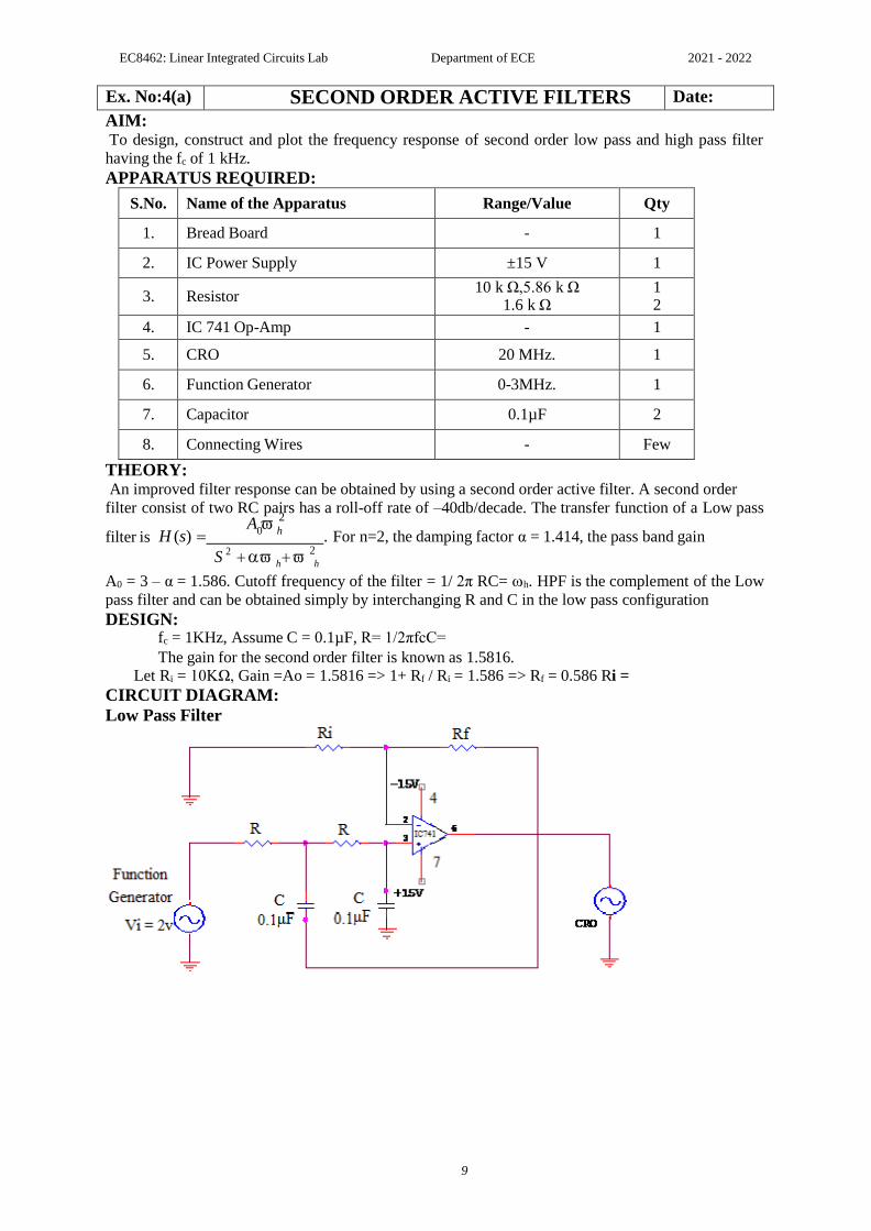
Ex. No:4(a) SECOND ORDER ACTIVE FILTERS Date:
AIM: To design, construct and plot the frequency response of second order low pass and high pass filter
having the fc of 1 kHz.
APPARATUS REQUIRED:
S.No. Name of the Apparatus Range/Value Qty
1. Bread Board - 1
2. IC Power Supply ±15 V 1
3. Resistor 10 k Ω,5.86 k Ω
1.6 k Ω 1 2
4. IC 741 Op-Amp - 1
5. CRO 20 MHz. 1
6. Function Generator 0-3MHz. 1
7. Capacitor 0.1µF 2
8. Connecting Wires - Few
THEORY: An improved filter response can be obtained by using a second order active filter. A second order
filter consist of two RC pairs has a roll-off rate of –40db/decade. The transfer function of a Low pass A 2
filter is H (s) 0 h . For n=2, the damping factor α = 1.414, the pass band gain
S 2 2
A0 = 3 – α = 1.586. Cutoff frequency of the filter = 1/ 2π RC= h. HPF is the complement of the Low
pass filter and can be obtained simply by interchanging R and C in the low pass configuration
DESIGN: fc = 1KHz, Assume C = 0.1µF, R= 1/2πfcC=
The gain for the second order filter is known as 1.5816. Let Ri = 10KΩ, Gain =Ao = 1.5816 => 1+ Rf / Ri = 1.586 => Rf = 0.586 Ri =
CIRCUIT DIAGRAM:
Low Pass Filter

EC8462: Linear Integrated Circuits Lab Department of ECE 2021 - 2022
10
PROCEDURE: 1. Connect the Low pass filter circuit as shown in the circuit diagram. 2. Give an input signal Vi of 2V(p-p) and measure the output voltage for different frequency from the
CRO.
3. Plot the frequency response 20 log Vo/Vi versus input frequency and find 3db frequency. 4. Determine the cut-off frequency from the plot.
5. Repeat the above for HPF.
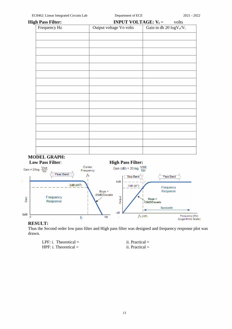
TABULATION: Low Pass Filter INPUT VOLTAGE: Vi = volts
Frequency Hz Output voltage Vo volts Gain in db 20 logVo/Vi
High Pass Filter:
EC8462: Linear Integrated Circuits Lab Department of ECE 2021 - 2022
11
High Pass Filter: INPUT VOLTAGE: Vi = volts Frequency Hz Output voltage Vo volts Gain in db 20 logVo/Vi
MODEL GRAPH:
Low Pass Filter: High Pass Filter:
RESULT: Thus the Second order low pass filter and High pass filter was designed and frequency response plot was
drawn.
LPF: i. Theoretical = ii. Practical =
HPF: i. Theoretical = ii. Practical =

EC8462: Linear Integrated Circuits Lab Department of ECE 2021 - 2022
12
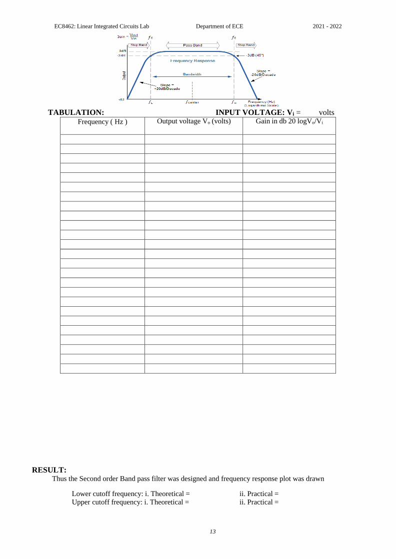
Ex. No:4 (b) BAND PASS FILTER Date:
AIM: To design, construct, test and to plot the frequency response of wide band pass filter.
APPARATUS REQUIRED:
S.No. Name of the Apparatus Range/Value Qty
1. Bread Board - 1
2. IC Power Supply ±15 V 1
3. Resistor 10 k Ω, 39.8 k Ω, 7.9 k Ω 4, 1
4. IC 741 Op-Amp - 1
5. CRO 20 MHz. 1
6. Signal Generator 0-3 MHz. 1
7. Capacitor 0.01µF 2
8. Connecting Wires - Few
THEORY: A wide band pass filter can be formed by cascading a HPF and LPF section. If the HPF and
LPF are of the first order, then the band pass filter (BPF) will have a roll off rate of -20 dB/decade. A
wide band pass filter formed by cascading I order HPF and I order LPF is shown in the circuit
diagram.
DESIGN: fh = 2KHz; fl = 400Hz; pass band gain A0= 4.
LPF and HPF sections may be designed to have a gain of 2.
As the opamp is used in non-inverting configuration Ao = 1+ (Rf/Ri) = 2=> Rf/Ri = 1=> Rf = Ri.
Let Ri =10 kΩ, Rf = . fh = 1/(2πR2C2) = 2KHz. Let C2= 0.01µF, R2 = 1/(2πX2X10
3X0.01X10
-6) =
fl = 1/(2πR1C1) = 400Hz. Let C1= 0.01µF, R1 = 1/(2πX400X0.01X10-6
) =
CIRCUIT DIAGRAM:
PROCEDURE: 1. Connect the Band pass filter circuit as shown in the circuit diagram.
2. Give an input signal Vi of 1V (p-p) and measure the output voltage for different frequency.
3. Plot the frequency response 20 log Vo/Vi versus input frequency and find 3db frequency.
4. Determine the cut-off frequency fh and fl .
MODEL GRAPH:
EC8462: Linear Integrated Circuits Lab Department of ECE 2021 - 2022
13
TABULATION: INPUT VOLTAGE: Vi = volts Frequency ( Hz ) Output voltage Vo (volts) Gain in db 20 logVo/Vi
RESULT: Thus the Second order Band pass filter was designed and frequency response plot was drawn
Lower cutoff frequency: i. Theoretical = ii. Practical = Upper cutoff frequency: i. Theoretical = ii. Practical =
EC8462: Linear Integrated Circuits Lab Department of ECE 2021 - 2022
14
Ex. No:5(a) ASTABLE MULTIVIBRATOR USING
OP-AMP IC 741.
Date:
AIM: To design a square wave generator for fo = 1kHz and study its performance.
APPARATUS REQUIRED:
S.No. Name of the Apparatus Range/Value Qty
1. Bread Board - 1
2. IC Power Supply ±15 V 1
3. Resistor 10KΩ, 11.6KΩ 2, 1
4. IC 741 Op-Amp - 1
5. CRO 20MHz. 1
7. Capacitor-DCB 0.05µF 1
8. Connecting Wires - Few
THEORY: Square wave outputs are generated when the opamp is forced to operate in the saturated
region. That is, the output of the opamp is forced to swing repetitively between positive saturation
V sat and negative saturation –Vsat, resulting in the square wave output. Astable multivibrator circuit is
shown in figure. The output of the opamp in this circuit will be in positive or negative saturation,
depending whether the differential voltage is positive or negative, respectively. The time period T of
the output wave form is T = 2 RC ln ((1+β)/(1-β)) where β=R2/(R1+R2). If R1 = 1.16 R2, T = 2RC and
frequency = 1/(2RC).
DESIGN: f0 = 1KHz R1 = 1.16R2, Let R2 = 10KΩ => R1 =
Let C= 0.05µF => R = 1/ (10 X10-8
X1000) =
CIRCUIT DIAGRAM:
PROCEDURE: 1. Connect the circuit as shown in the circuit diagram using component values as obtained in design. 2. Observe and sketch the capacitor voltage wave form and output wave form.
3. Determine the frequency and plot the graph.
TABULATION: Tlow (ms) Thigh (ms) Frequency (Hz) Output
Voltage (V)
Capacitor
Voltage (V)
Practical Theoretical Practical Theoretical Practical Theoretical
EC8462: Linear Integrated Circuits Lab Department of ECE 2021 - 2022
15
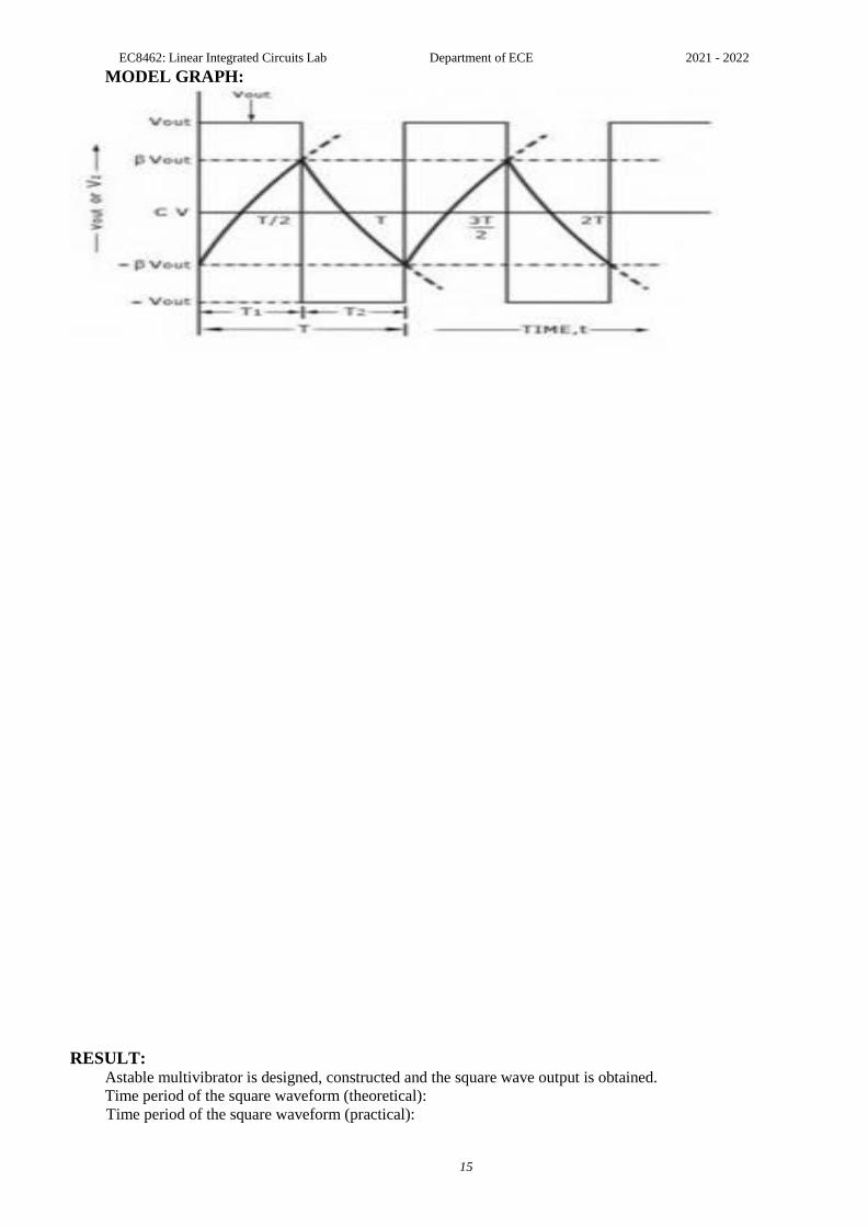
MODEL GRAPH:
RESULT: Astable multivibrator is designed, constructed and the square wave output is obtained.
Time period of the square waveform (theoretical):
Time period of the square waveform (practical):
EC8462: Linear Integrated Circuits Lab Department of ECE 2021 - 2022
16
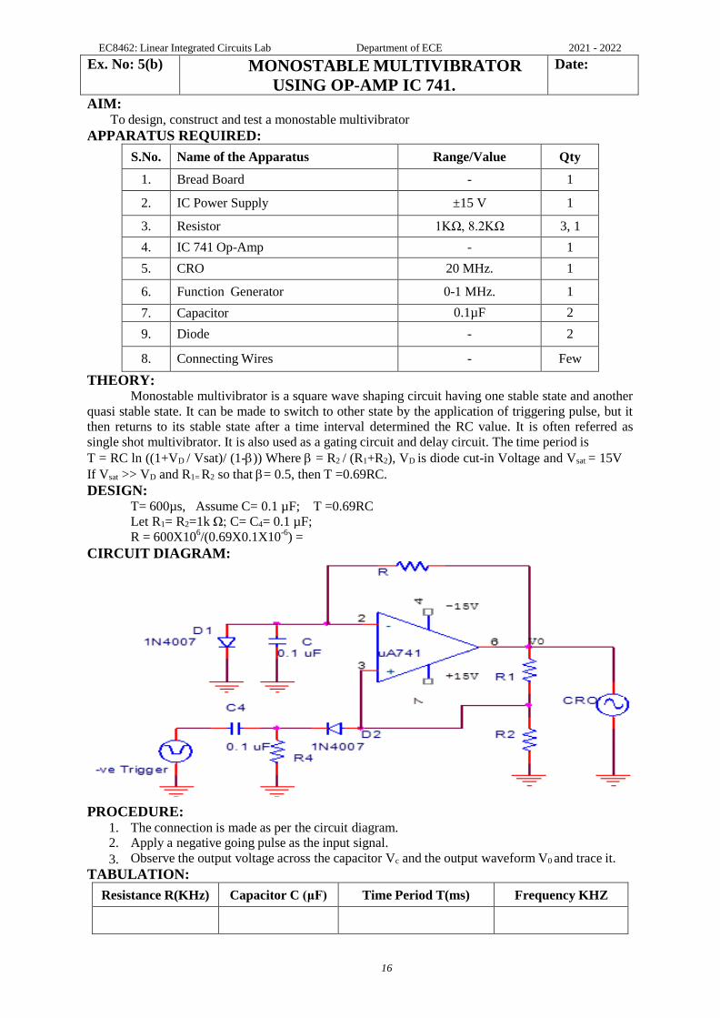
Ex. No: 5(b) MONOSTABLE MULTIVIBRATOR
USING OP-AMP IC 741.
Date:
AIM: To design, construct and test a monostable multivibrator
APPARATUS REQUIRED:
S.No. Name of the Apparatus Range/Value Qty
1. Bread Board - 1
2. IC Power Supply ±15 V 1
3. Resistor 1KΩ, 8.2KΩ 3, 1
4. IC 741 Op-Amp - 1
5. CRO 20 MHz. 1
6. Function Generator 0-1 MHz. 1
7. Capacitor 0.1µF 2
9. Diode - 2
8. Connecting Wires - Few
THEORY: Monostable multivibrator is a square wave shaping circuit having one stable state and another
quasi stable state. It can be made to switch to other state by the application of triggering pulse, but it
then returns to its stable state after a time interval determined the RC value. It is often referred as
single shot multivibrator. It is also used as a gating circuit and delay circuit. The time period is
T = RC ln ((1+VD / Vsat)/ (1-)) Where = R2 / (R1+R2), VD is diode cut-in Voltage and Vsat = 15V
If Vsat >> VD and R1= R2 so that = 0.5, then T =0.69RC.
DESIGN: T= 600µs, Assume C= 0.1 µF; T =0.69RC
Let R1= R2=1k Ω; C= C4= 0.1 µF; R = 600X10
6/(0.69X0.1X10
-6) =
CIRCUIT DIAGRAM:
PROCEDURE: 1. The connection is made as per the circuit diagram. 2. Apply a negative going pulse as the input signal.
3. Observe the output voltage across the capacitor Vc and the output waveform V0 and trace it.
TABULATION:
Resistance R(KHz) Capacitor C (μF) Time Period T(ms) Frequency KHZ
EC8462: Linear Integrated Circuits Lab Department of ECE 2021 - 2022
17
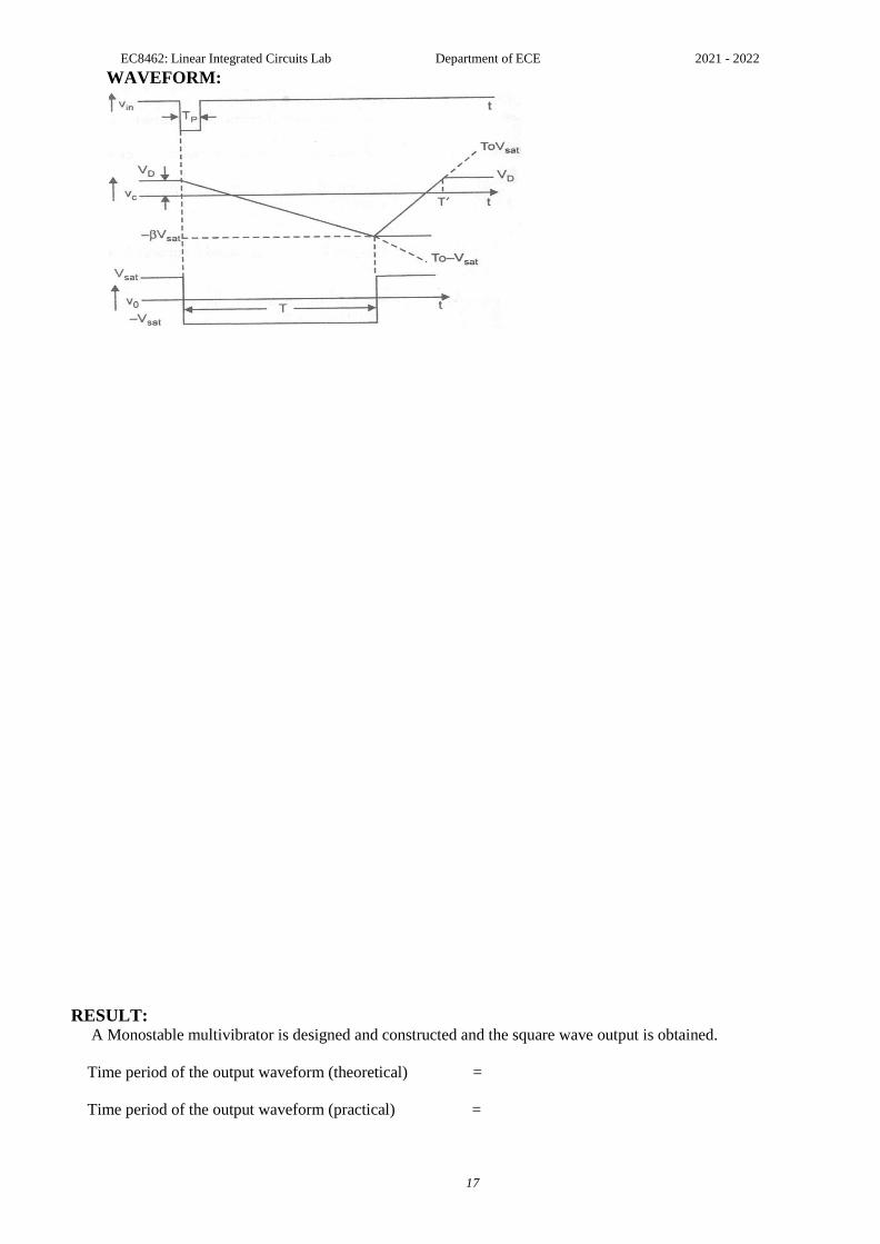
WAVEFORM:
RESULT: A Monostable multivibrator is designed and constructed and the square wave output is obtained.
Time period of the output waveform (theoretical) =
Time period of the output waveform (practical) =
EC8462: Linear Integrated Circuits Lab Department of ECE 2021 - 2022
18
Waveform Amplitude
(Volts)
Time period
(ms)
INPUT
OUTPUT
Ex. No:6 SCHMITT TRIGGER (REGENERATIVE
COMPARATOR)
Date:
AIM: To design a Schmitt trigger circuit for generating a square wave output.
APPARATUS REQUIRED:
S.No. Name of the Apparatus Range/Value Qty
1. Bread Board - 1
2. IC Power Supply ±15 V 1
3. Resistor 1 k Ω, 27 k Ω 2, 1
4. IC 741 Op-Amp - 1
5. CRO 20 MHz. 1
6. Function Generator 0-3 MHz. 1
7. Connecting Wires - Few
THEORY: Schmitt trigger circuit is an inverting comparator with positive feed back. The input voltage
is applied to the (-) terminal and feed back voltage to the (+) terminal. The input voltage Vi triggers
the output every time it exceeds certain voltage levels called upper threshold and lower threshold
voltage. This circuit converts an irregular shaped wave form to a square wave or pulse. The upper and
lower threshold is VUT = Vsat [R2/(R1+R2)], VLT = - Vsat [R2/(R1+R2)] respectively.
DESIGN: VUT = + 0.5V; VLT = - 0.5V
For 741, with supply voltages ±15V, the saturation voltage ±V sat = ±15V
0.5 = 15 [R2/ (R1+R2)]. R1=27 R2. Let R2 = 1 kΩ therefore R1 =
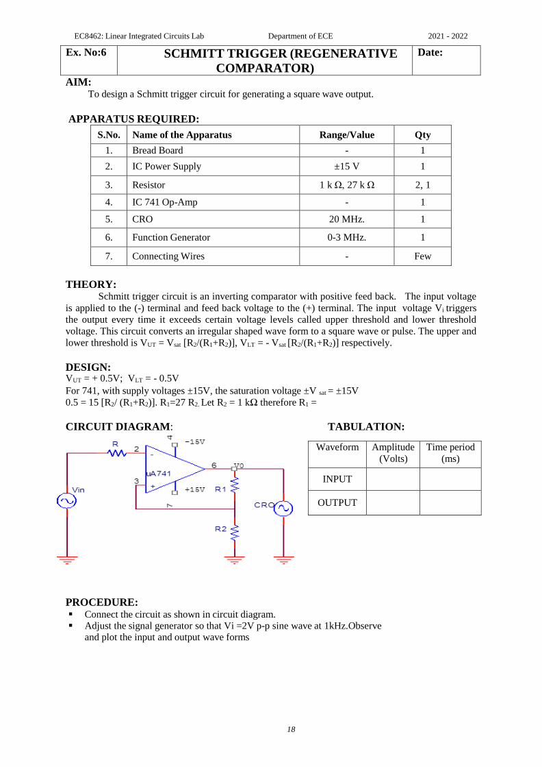
CIRCUIT DIAGRAM: TABULATION:
PROCEDURE: Connect the circuit as shown in circuit diagram. Adjust the signal generator so that Vi =2V p-p sine wave at 1kHz. Observe
and plot the input and output wave forms
EC8462: Linear Integrated Circuits Lab Department of ECE 2021 - 2022
19
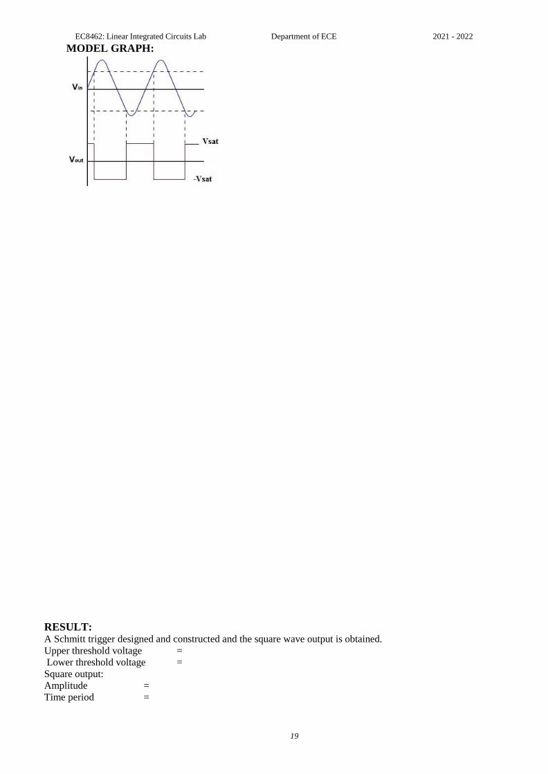
MODEL GRAPH:
RESULT: A Schmitt trigger designed and constructed and the square wave output is obtained.
Upper threshold voltage =
Lower threshold voltage =
Square output:
Amplitude =
Time period =
EC8462: Linear Integrated Circuits Lab Department of ECE 2021 - 2022
20
Ex. No:7(a) RC PHASE SHIFT OSCILLATOR Date:
AIM: To design, construct and test a RC phase shift oscillator for a frequency of 100Hz.
APPARATUS REQUIRED:
S.No. Name of the Apparatus Range/Value Qty
1. Bread Board - 1
2. IC Power Supply ±15 V 1
3. Resistor 1885 k Ω (1MΩ), 65 k Ω, 6.5 k Ω 1,1,3
4. IC 741 Op-Amp - 1
5. CRO 20 MHz. 1
6. Capacitor 0.1µF, 0.01µF 3, 1
7. Connecting Wires - Few
THEORY: Oscillator is a feed back circuit where a fraction of output voltage of an amplifier is fed back
to the input in the same phase. RC phase shift oscillators are sine wave oscillators which are used in
the audio frequency range. The amplification is done by the op-amp and as it is used in the inverting
mode is gives a phase shift of 180 .The feedback RC network produces an additional phase shift of
180.Each RC network gives 60 phase shift.
The frequency of oscillation is given by = 1/6(2RC)
DESIGN: fo = 100Hz; Assume C = 0.1 µF => R = 1/6(2foC) = 1/6(2X100X0.1X10
-6) =
To prevent overloading of the amplifier by RC network, R1 ≤ 10R
Let R1 = 10R = Rf = 29 R1 =
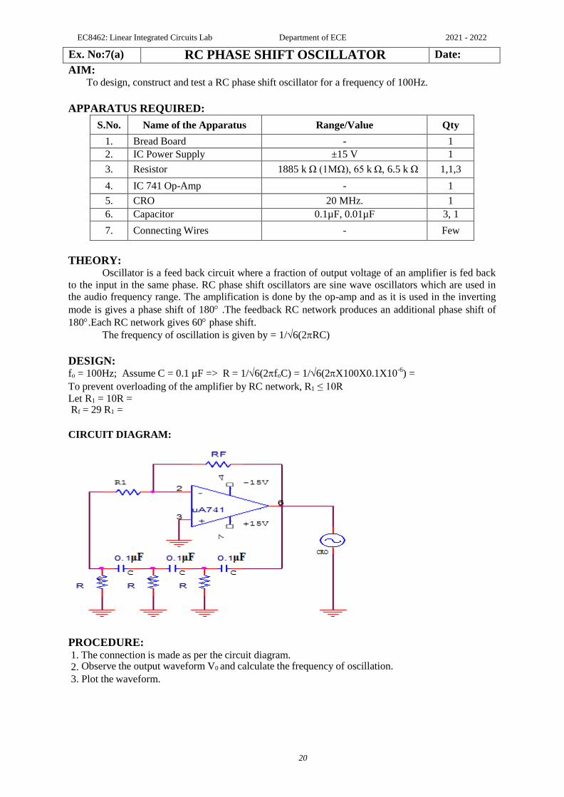
CIRCUIT DIAGRAM:
PROCEDURE: 1. The connection is made as per the circuit diagram.
2. Observe the output waveform V0 and calculate the frequency of oscillation.
3. Plot the waveform.
EC8462: Linear Integrated Circuits Lab Department of ECE 2021 - 2022
21
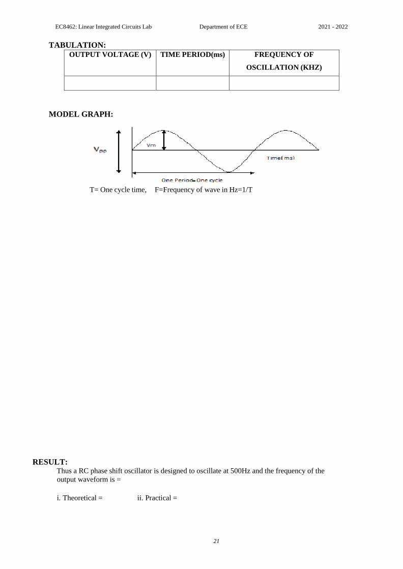
TABULATION:
OUTPUT VOLTAGE (V) TIME PERIOD(ms) FREQUENCY OF
OSCILLATION (KHZ)
MODEL GRAPH:
T= One cycle time, F=Frequency of wave in Hz=1/T
RESULT: Thus a RC phase shift oscillator is designed to oscillate at 500Hz and the frequency of the
output waveform is =
i. Theoretical = ii. Practical =
EC8462: Linear Integrated Circuits Lab Department of ECE 2021 - 2022
22
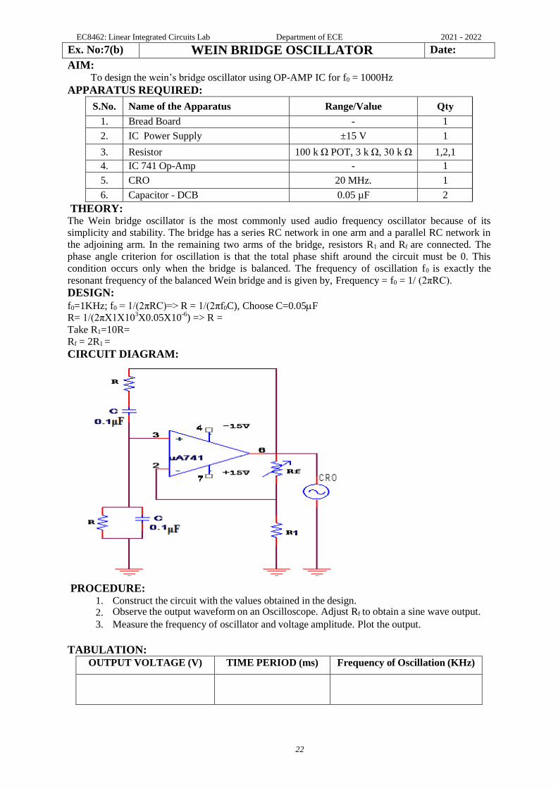
Ex. No:7(b) WEIN BRIDGE OSCILLATOR Date:
AIM: To design the wein‟s bridge oscillator using OP-AMP IC for f0 = 1000Hz
APPARATUS REQUIRED:
S.No. Name of the Apparatus Range/Value Qty
1. Bread Board - 1
2. IC Power Supply ±15 V 1
3. Resistor 100 k Ω POT, 3 k Ω, 30 k Ω 1,2,1
4. IC 741 Op-Amp - 1
5. CRO 20 MHz. 1
6. Capacitor - DCB 0.05 µF 2
THEORY: The Wein bridge oscillator is the most commonly used audio frequency oscillator because of its
simplicity and stability. The bridge has a series RC network in one arm and a parallel RC network in
the adjoining arm. In the remaining two arms of the bridge, resistors R1 and Rf are connected. The
phase angle criterion for oscillation is that the total phase shift around the circuit must be 0. This
condition occurs only when the bridge is balanced. The frequency of oscillation f0 is exactly the
resonant frequency of the balanced Wein bridge and is given by, Frequency = f0 = 1/ (2πRC). DESIGN:
f0=1KHz; f0 = 1/(2πRC)=> R = 1/(2πf0C), Choose C=0.05F
R= 1/(2πX1X103X0.05X10
-6) => R =
Take R1=10R=
Rf = 2R1 =
CIRCUIT DIAGRAM:
PROCEDURE: 1. Construct the circuit with the values obtained in the design.
2. Observe the output waveform on an Oscilloscope. Adjust Rf to obtain a sine wave output.
3. Measure the frequency of oscillator and voltage amplitude. Plot the output.
TABULATION:
OUTPUT VOLTAGE (V) TIME PERIOD (ms) Frequency of Oscillation (KHz)
EC8462: Linear Integrated Circuits Lab Department of ECE 2021 - 2022
23
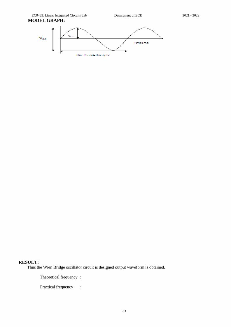
MODEL GRAPH:
RESULT: Thus the Wien Bridge oscillator circuit is designed output waveform is obtained.
Theoretical frequency :
Practical frequency :
EC8462: Linear Integrated Circuits Lab Department of ECE 2021 - 2022
24
Ex. No:8(a) DESIGN OF ASTABLE MULTIVIBRATOR
USING IC 555 TIMER
Date:
AIM: To design and test an astable multivibrator for generating symmetrical and unsymmetrical
square wave form for the given frequency and duty cycle.
APPARATUS REQUIRED:
S. No. Name of the Apparatus Range/Value Qty
1. Bread Board - 1
2. Resistor 3.6 k Ω, 7.2 k Ω 1, 2
3. IC 555 - 1
4. CRO 20 MHz. 1
5. Capacitor 0.1µF, 0.01µF 1, 1
6. RPS (0-30) V/ 5V 1
7. Diode 1
8. Connecting Wires - Few
THEORY: The 555 timer is connected as an astable multivibrator as shown in figure. In this mode of
operation the timing capacitor charges up towards Vcc (assuming Vo is high initially) through (Ra +
Rb) until the voltage across the capacitor reaches the threshold level (2/3) Vcc. At this point the internal upper comparator switches state causing the internal flip-flop output to go high. This turns on
the discharge transistor and the timing capacitor C then discharges through Rb and the discharging
transistor. The discharging continues until the capacitor voltage drops to (1/3) Vcc at which point the
internal lower comparator switches states causing the internal flip-flop output to go low, turning off the discharge transistor. At this point the capacitor starts to charge again, thus completing the cycle.
DESIGN: i. For Unsymmetrical waveform: f =1/T=1.44/(Ra+2Rb)C;
DutyCycle = D = tlow/ ( tlow + t high ) => D= R b/ (Ra +2Rb) ;
Where thigh = 0.693(Ra + R b)C; tlow = 0.69; Specifications: frequency = 1kHz; Duty cycle = 25%
Design: tlow = 0.25ms = 0.693R b C; Let C= 0.1µF => R b = 0.25/(0.693X0.1X10
-6) =
thigh = 0.693(Ra + R b)C = 0.75 ms => Ra = ii. For Symmetrical Wave form : thigh = 0.693 Ra C; tlow = 0.693 R bC f = 1/T = 1.44 /(Ra + Rb)C => D= Rb /(Ra + Rb); Specifications: frequency = 1 kHz; Duty cycle = 50% .
Design: tlow = 0.5 ms = 0.693 R bC; Let C= 0.1 µF; R b = thigh = 0.693 Ra C = 0.5 ms ; Ra =
EC8462: Linear Integrated Circuits Lab Department of ECE 2021 - 2022
25
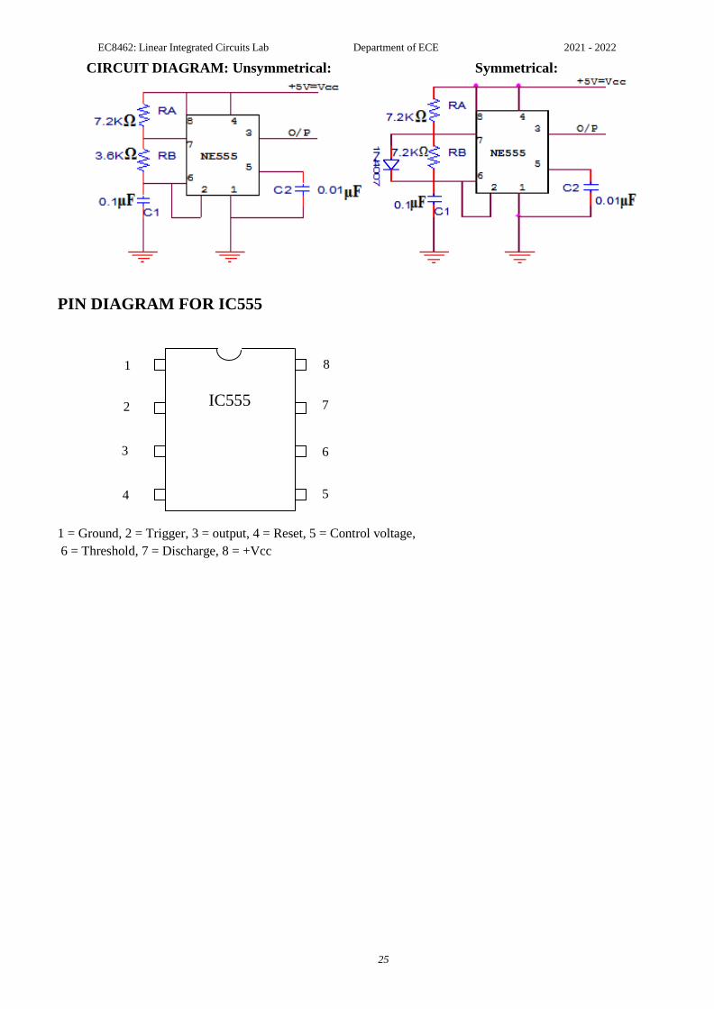
CIRCUIT DIAGRAM: Unsymmetrical: Symmetrical:
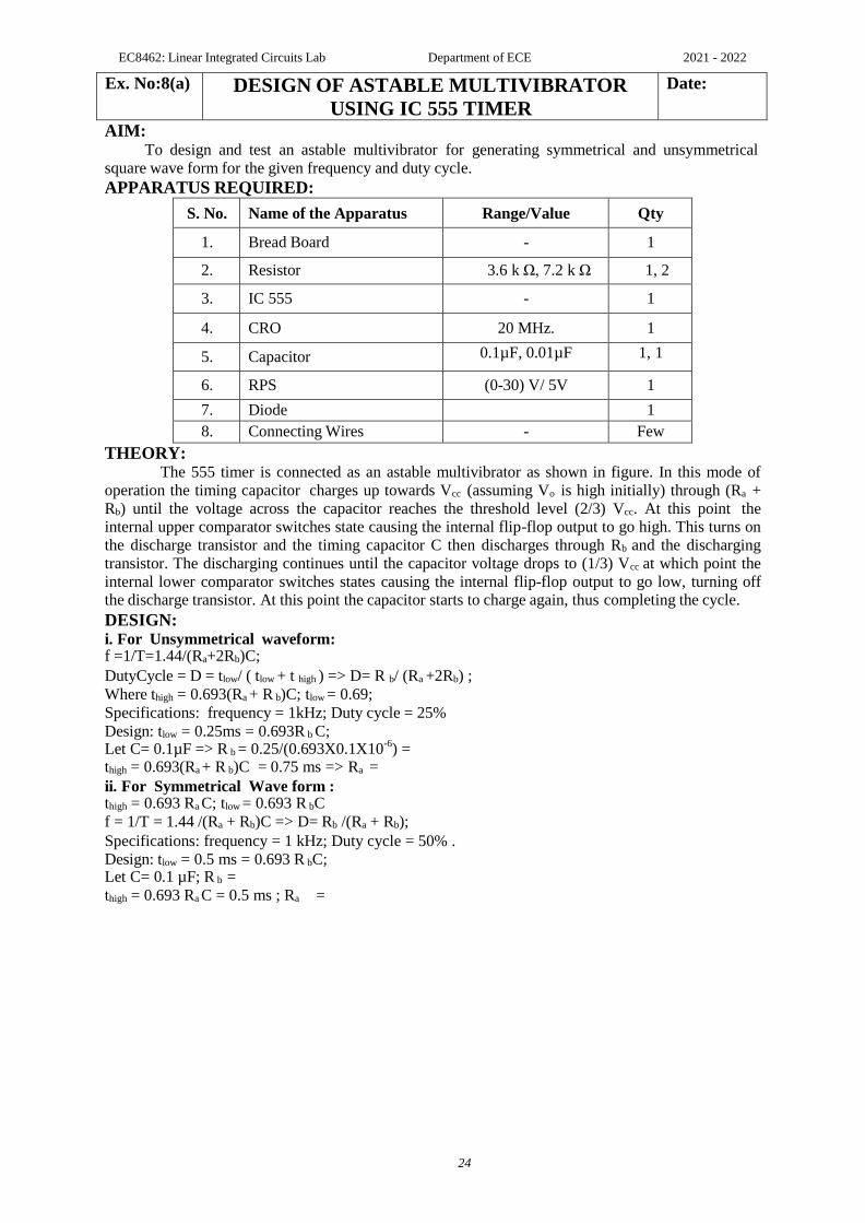
PIN DIAGRAM FOR IC555
IC555
1 = Ground, 2 = Trigger, 3 = output, 4 = Reset, 5 = Control voltage,
6 = Threshold, 7 = Discharge, 8 = +Vcc
1
2
3
4
8
7
6
5
EC8462: Linear Integrated Circuits Lab Department of ECE 2019 - 2020
26
PROCEDURE: 1. Connect the circuit as given using component values as obtained in designed part (i)
2. Observe and sketch the capacitor voltage waveform and output waveform.
3. Measure the frequency and duty cycle of the output waveform.
4. Connect the circuit using component values as obtained from designed part (ii). 5. Repeat step 2 and 3
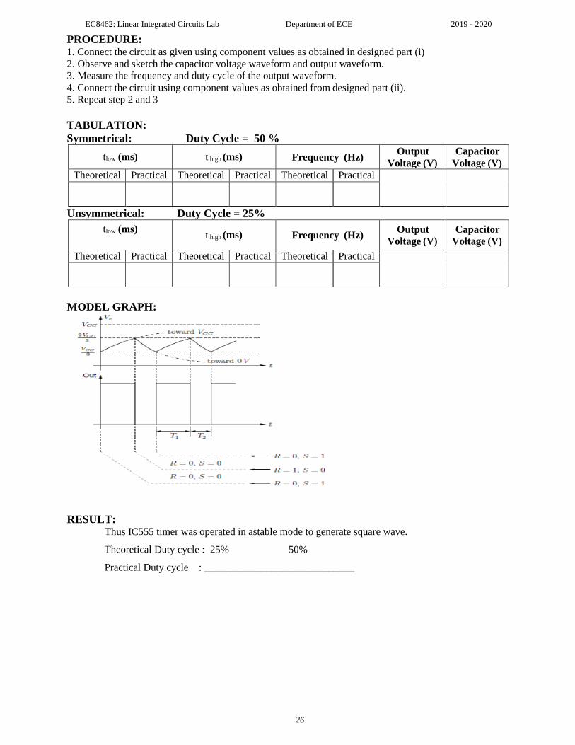
TABULATION:
Symmetrical: Duty Cycle = 50 %
tlow (ms) t high (ms) Frequency (Hz) Output
Voltage (V)
Capacitor
Voltage (V)
Theoretical Practical Theoretical Practical Theoretical Practical
Unsymmetrical: Duty Cycle = 25%
tlow (ms) t high (ms) Frequency (Hz)
Output
Voltage (V)
Capacitor
Voltage (V)
Theoretical Practical Theoretical Practical Theoretical Practical
MODEL GRAPH:
RESULT: Thus IC555 timer was operated in astable mode to generate square wave.
Theoretical Duty cycle : 25% 50%
Practical Duty cycle : _____________________________
EC8462: Linear Integrated Circuits Lab Department of ECE 2019 - 2020
27
Ex. No:8(b) MONOSTABLE MULTIVIBRATOR USING
IC 555 TIMER
Date:
AIM: To design, construct and test a monostable multivibrator using IC - 555 timer.
APPARATUS REQUIRED:
S. No. Name of the Apparatus Range/Value Qty
1. Bread Board - 1
2. Resistor 1.8 k Ω 1
3. IC 555 - 1
4. CRO 20 MHz. 1
5. Function Generator 0-3 MHz. 1
6. Capacitor 0.1µF, 0.01µF 1, 1
7. RPS (0-30) V/ 5V 1
8. Connecting Wires - Few
THEORY: Mono-stable multivibrator has only one stable state and one quasi-stable state. Transition is
obtained from the stable to quasi-stable by triggering. The transition time due to external triggering is very
short, whereas the time for the circuit to remain quasi-stable state is very large. The circuit returns to
stable state from its quasi-stable state by itself, without requiring any external triggering signal. Because,
after triggering, the circuit returns from quasi-stable state by itself after a certain time delay, therefore the
circuit is also called a one shot multivibrator or univibrator.
The mono-stable multivibrator is a regenerative device, which is used to generate rectangular
output, pulse of predetermined width. The device can make a fast transition in time T after the application
of input trigger and as such can be used as a delay circuit. The circuit is also referred to as gating circuit,
because it generates rectangular wave form, which can be used to gate other circuits. The Pulse width is T
= 1.1 RC, where R is the resistor and C is the capacitor.
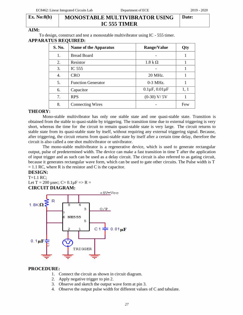
DESIGN: T=1.1 RC; Let T = 200 µsec; C= 0.1µF => R =
CIRCUIT DIAGRAM:
PROCEDURE: 1. Connect the circuit as shown in circuit diagram.
2. Apply negative trigger to pin 2.
3. Observe and sketch the output wave form at pin 3.
4. Observe the output pulse width for different values of C and tabulate.
EC8462: Linear Integrated Circuits Lab Department of ECE 2019 - 2020
28
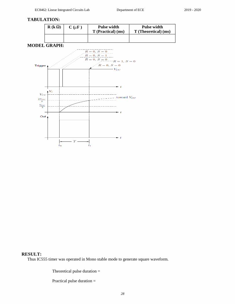
TABULATION:
R (k Ω) C (F ) Pulse width T (Practical) (ms)
Pulse width T (Theoretical) (ms)
MODEL GRAPH:
RESULT:
Thus IC555 timer was operated in Mono stable mode to generate square waveform.
Theoretical pulse duration =
Practical pulse duration =
EC8462: Linear Integrated Circuits Lab Department of ECE 2019 - 2020
29
Voltage Controlled
Oscillator
VCO LPF
Fin = fout / N
Amplifier Phase Comparator
Oscillator
Output
Phase Frequency
Detector Reference Signal
Source
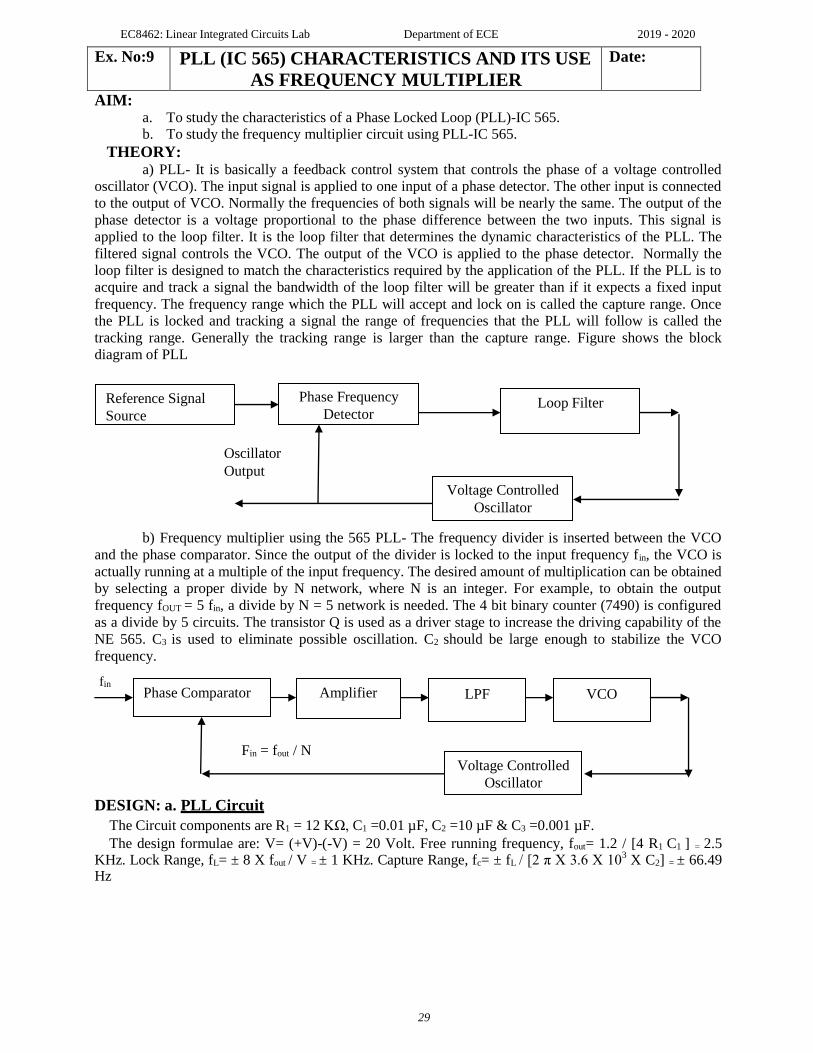
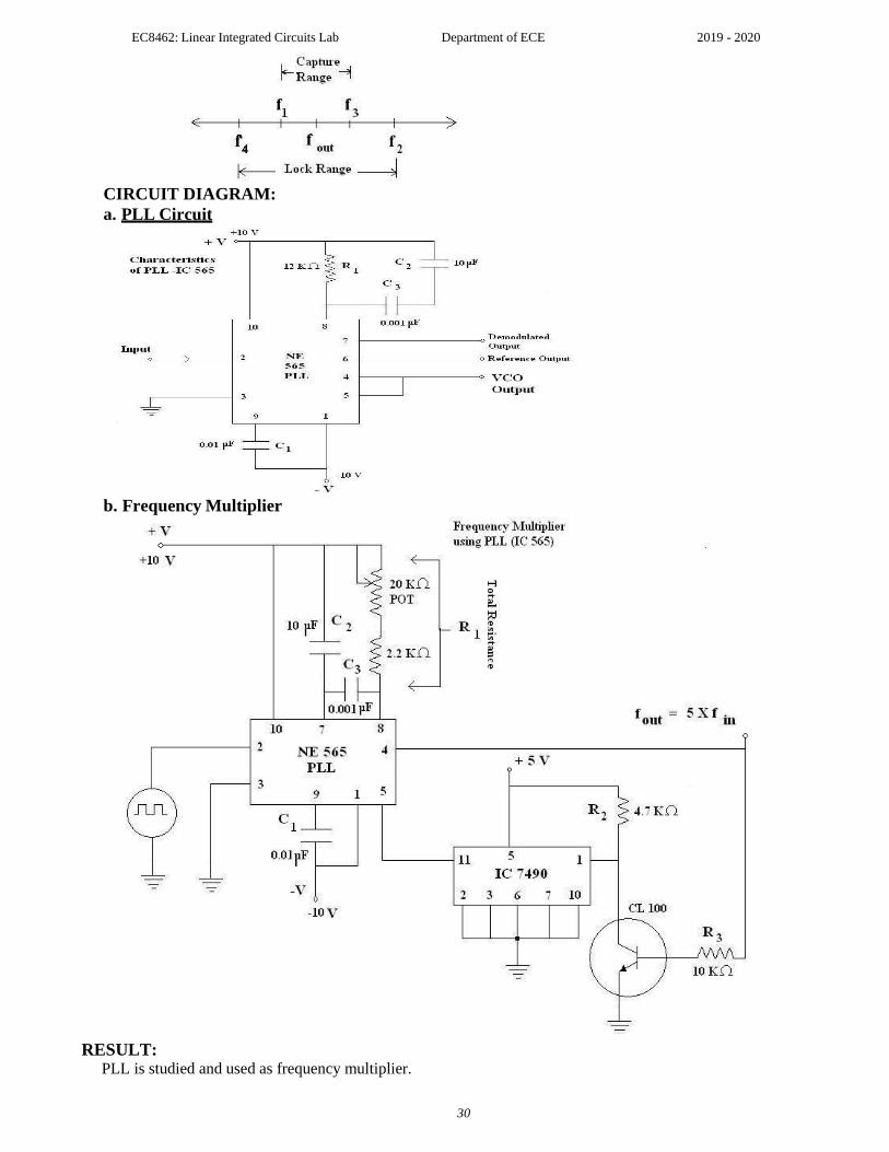
Ex. No:9 PLL (IC 565) CHARACTERISTICS AND ITS USE
AS FREQUENCY MULTIPLIER
Date:
AIM: a. To study the characteristics of a Phase Locked Loop (PLL)-IC 565. b. To study the frequency multiplier circuit using PLL-IC 565.
THEORY: a) PLL- It is basically a feedback control system that controls the phase of a voltage controlled
oscillator (VCO). The input signal is applied to one input of a phase detector. The other input is connected
to the output of VCO. Normally the frequencies of both signals will be nearly the same. The output of the
phase detector is a voltage proportional to the phase difference between the two inputs. This signal is
applied to the loop filter. It is the loop filter that determines the dynamic characteristics of the PLL. The
filtered signal controls the VCO. The output of the VCO is applied to the phase detector. Normally the
loop filter is designed to match the characteristics required by the application of the PLL. If the PLL is to
acquire and track a signal the bandwidth of the loop filter will be greater than if it expects a fixed input
frequency. The frequency range which the PLL will accept and lock on is called the capture range. Once
the PLL is locked and tracking a signal the range of frequencies that the PLL will follow is called the
tracking range. Generally the tracking range is larger than the capture range. Figure shows the block
diagram of PLL
b) Frequency multiplier using the 565 PLL- The frequency divider is inserted between the VCO
and the phase comparator. Since the output of the divider is locked to the input frequency fin, the VCO is
actually running at a multiple of the input frequency. The desired amount of multiplication can be obtained
by selecting a proper divide by N network, where N is an integer. For example, to obtain the output
frequency fOUT = 5 fin, a divide by N = 5 network is needed. The 4 bit binary counter (7490) is configured
as a divide by 5 circuits. The transistor Q is used as a driver stage to increase the driving capability of the
NE 565. C3 is used to eliminate possible oscillation. C2 should be large enough to stabilize the VCO
frequency.
fin
DESIGN: a. PLL Circuit
The Circuit components are R1 = 12 KΩ, C1 =0.01 µF, C2 =10 µF & C3 =0.001 µF.
The design formulae are: V= (+V)-(-V) = 20 Volt. Free running frequency, fout= 1.2 / [4 R1 C1 ] = 2.5 KHz. Lock Range, fL= ± 8 X fout / V = ± 1 KHz. Capture Range, fc= ± fL / [2 π X 3.6 X 10
3 X C2] = ± 66.49
Hz
Voltage Controlled
Oscillator
Loop Filter
EC8462: Linear Integrated Circuits Lab Department of ECE 2019 - 2020
30
CIRCUIT DIAGRAM:
a. PLL Circuit
b. Frequency Multiplier
RESULT: PLL is studied and used as frequency multiplier.
EC8462: Linear Integrated Circuits Lab Department of ECE 2019 - 2020
31
Ex. No:10 IC REGULATED DC POWER SUPPLY USING LM 723 and LM 317
Date:
AIM: To design the regulated DC power supply using LM 723 and LM 317.
APPARATUS REQUIRED:
S. No. Name of the Apparatus Range/Value Qty
1. Bread Board - 1
2. Resistor 5 KΩ, 240Ω 1
3. NE 565 , IC 7490 - 1 each
4. Voltmeter (0 – 30)V 1
6. Capacitor 10µF, 0.1µF, 0.100pF 1 each
7. RPS (0-30) V/ 5V 1
8. Connecting Wires - Few
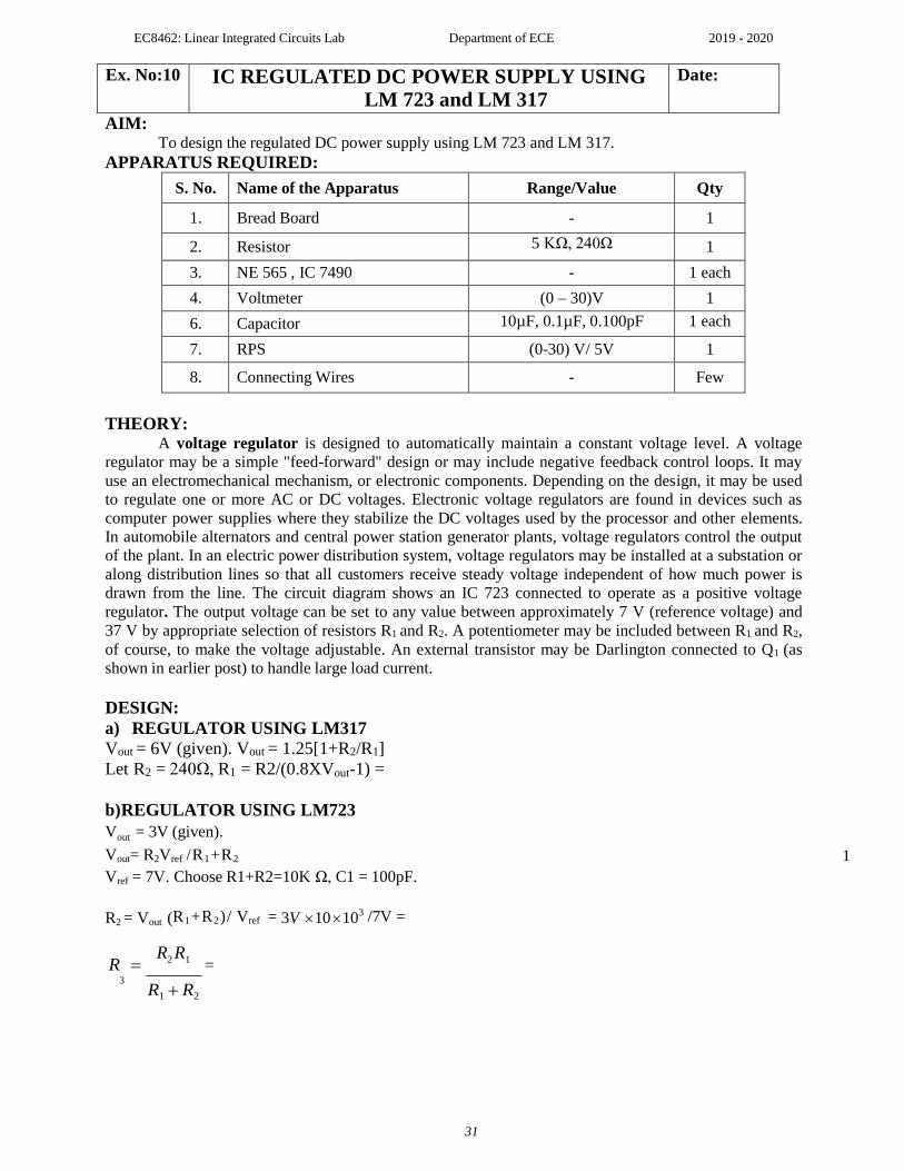
THEORY: A voltage regulator is designed to automatically maintain a constant voltage level. A voltage
regulator may be a simple "feed-forward" design or may include negative feedback control loops. It may
use an electromechanical mechanism, or electronic components. Depending on the design, it may be used
to regulate one or more AC or DC voltages. Electronic voltage regulators are found in devices such as
computer power supplies where they stabilize the DC voltages used by the processor and other elements.
In automobile alternators and central power station generator plants, voltage regulators control the output
of the plant. In an electric power distribution system, voltage regulators may be installed at a substation or
along distribution lines so that all customers receive steady voltage independent of how much power is
drawn from the line. The circuit diagram shows an IC 723 connected to operate as a positive voltage
regulator. The output voltage can be set to any value between approximately 7 V (reference voltage) and
37 V by appropriate selection of resistors R1 and R2. A potentiometer may be included between R1 and R2,
of course, to make the voltage adjustable. An external transistor may be Darlington connected to Q1 (as
shown in earlier post) to handle large load current.
DESIGN:
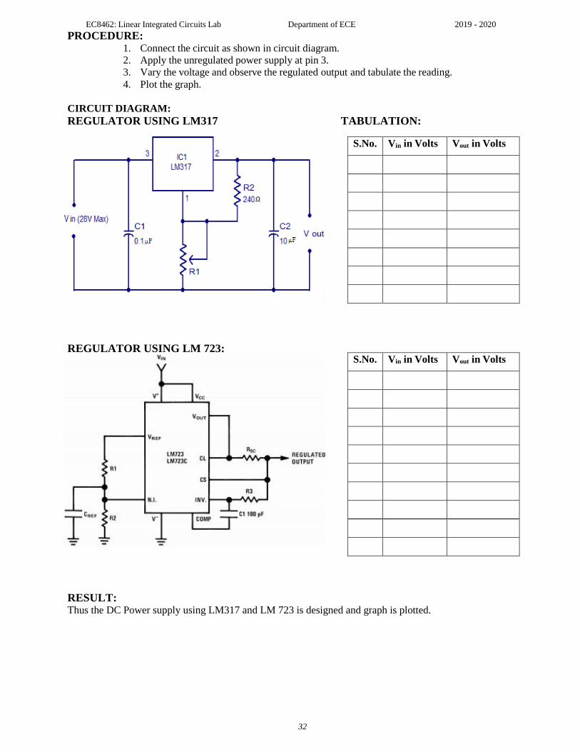
a) REGULATOR USING LM317
Vout = 6V (given). Vout = 1.25[1+R2/R1]
Let R2 = 240Ω, R1 = R2/(0.8XVout-1) =
b) REGULATOR USING LM723
Vout = 3V (given).
Vout= R2Vref /R1+R2
1
Vref = 7V. Choose R1+R2=10K Ω, C1 = 100pF.
R2 = Vout (R1+R2)/ Vref = 3V 10 103 /7V =
R R2 R1
=
R1 R2
3
EC8462: Linear Integrated Circuits Lab Department of ECE 2019 - 2020
32
S.No. Vin in Volts Vout in Volts
PROCEDURE: 1. Connect the circuit as shown in circuit diagram.
2. Apply the unregulated power supply at pin 3.
3. Vary the voltage and observe the regulated output and tabulate the reading.
4. Plot the graph.
CIRCUIT DIAGRAM:
REGULATOR USING LM317 TABULATION:
REGULATOR USING LM 723:
RESULT: Thus the DC Power supply using LM317 and LM 723 is designed and graph is plotted.
S.No. Vin in Volts Vout in Volts

EC8462: Linear Integrated Circuits Lab Department of ECE 2019 - 2020
33
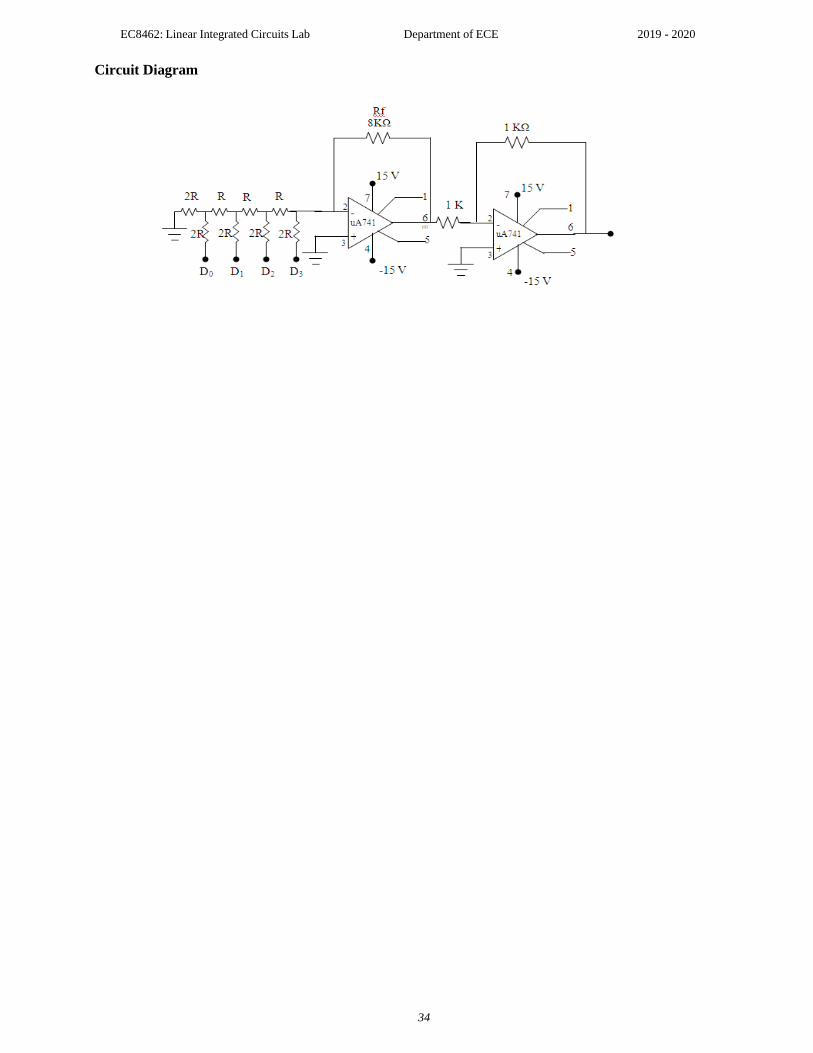
Ex. No:11 10-BIT R-2R DIGITAL TO ANALOG
CONVERTER
Date:
Aim : To design 4 bit R-2R ladder DAC using Op-Amp for an output voltage of 5 V when the
input is 10 (Binary 1010).
Apparatus :
Sl. Particulars
Specification
Quantity
No.
1.
IC
µA741
02
2.
Resistors
As per design
-
3. Multimeter - 01
4.
Base board + connecting wires
-
01 Set
Procedure :
1. Connections are made as shown in the circuit diagram.
2. Digital input data is given at D3, D2, D1, D0 and corresponding analog output voltage V0 is
measured.
3. Tabulate the readings & plot the graph between Vo on y-axis Vin on X-axis.
Note :
1. D0.D1.D2 & D3 are binary input.
2. Vo is the analog output.
3. Binary inputs Do.D1.D2 & D3 can take either the value „0‟ or „1‟.
4. Binary input Di (i = 0 to 3) can be made „0‟ by connecting the i/p to ground. It can be made „1‟ by
connecting to –5 V.
Logic 0 0V Logic 1 +5V
EC8462: Linear Integrated Circuits Lab Department of ECE 2019 - 2020
34
Circuit Diagram
EC8462: Linear Integrated Circuits Lab Department of ECE 2019 - 2020
35
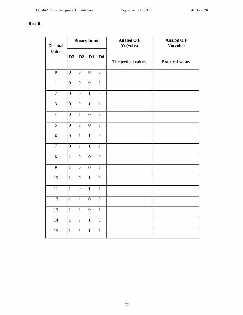
Result :
Binary Inputs Analog O/P Analog O/P
Decimal Vo(volts) Vo(volts)
Value D3
D2
D1
D0
Theoretical values
Practical values
0 0 0 0 0
1 0 0 0 1
2 0 0 1 0
3 0 0 1 1
4 0 1 0 0
5 0 1 0 1
6 0 1 1 0
7 0 1 1 1
8 1 0 0 0
9 1 0 0 1
10 1 0 1 0
11 1 0 1 1
12 1 1 0 0
13 1 1 0 1
14 1 1 1 0
15 1 1 1 1
EC8462: Linear Integrated Circuits Lab Department of ECE 2019 - 2020
36
RESULT: Thus the R-2R Digital to analog converter is designed and graph is plotted.

EC8462: Linear Integrated Circuits Lab Department of ECE 2021 - 2022
37
Mains
Input Input
Rectifier
and Filter
Input
Chopper Output
transformer
Output
rectifier and
transformer
DC Output
Chopper
controller
Ex. No:12 STUDY OF SMPS Date:
AIM: To study the switched mode power supply
THEORY: A switched-mode power supply (switching-mode power supply, SMPS, or simply switcher) is
an electronic power supply that incorporates a switching regulator in order to be highly efficient in the
conversion of electrical power. Like other types of power supplies, an SMPS transfer‟s power from a
source like the electrical power grid to a load (e.g., a personal computer) while converting voltage and
current characteristics. An SMPS is usually employed to efficiently provide a regulated output voltage,
typically at a level different from the input voltage. Unlike a linear power supply, the pass transistor of a
switching mode supply switches very quickly (typically between 50 kHz and 1 MHz) between full-on and
full-off states, which minimizes wasted energy. Voltage regulation is provided by varying the ratio of on
to off time. In contrast, a linear power supply must dissipate the excess voltage to regulate the output.
This higher efficiency is the chief advantage of a switched-mode power supply. Switching regulators are
used as replacements for the linear regulators when higher efficiency, smaller size or lighter weights are
required. They are, however, more complicated, their switching currents can cause electrical noise
problems if not carefully suppressed, and simple designs may have a poor power factor.
BLOCK DIAGRAM:
WORKING:
INPUT RECTIFIER STAGE If the SMPS has an AC input, then the first stage is to convert the input to DC. This is called
rectification. The rectifier circuit can be configured as a voltage doubler by the addition of a switch
operated either manually or automatically. This is a feature of larger supplies to permit operation from
nominally 120 V or 240 V supplies. The rectifier produces an unregulated DC voltage which is then sent
to a large filter capacitor. The current drawn from the mains supply by this rectifier circuit occurs in short
pulses around the AC voltage peaks. These pulses have significant high frequency energy which reduces
the power factor. Special control techniques can be employed by the following SMPS to force the average
input current to follow the sinusoidal shape of the AC input voltage thus the designer should try
correcting the power factor. An SMPS with a DC input does not require this stage.
An SMPS designed for AC input can often be run from a DC supply (for 230 V AC this would
be 330 V DC), as the DC passes through the rectifier stage unchanged. It's however advisable to consult
the manual before trying this, though most supplies are quite capable of such operation even though
nothing is mentioned in the documentation. However, this type of use may be harmful to the rectifier
stage as it will only use half of diodes in the rectifier for the full load. This may result in overheating of
these components, and cause them to fail prematurely. If an input range switch is used, the rectifier stage
EC8462: Linear Integrated Circuits Lab Department of ECE 2021 - 2022
38
is usually configured to operate as a voltage doubler when operating on the low voltage (~120 V AC) range and as a straight rectifier when operating on the high voltage (~240 V AC) range.
INVERTER STAGE (CHOPPER) The inverter stage converts DC, whether directly from the input or from the rectifier stage
described above, to AC by running it through a power oscillator, whose output transformer is very small
with few windings at a frequency of tens or hundreds of kilohertz (kHz). The frequency is usually chosen
to be above 20 kHz, to make it inaudible to humans. The output voltage is optically coupled to the input
and thus very tightly controlled. The switching is implemented as a multistage (to achieve high gain)
MOSFET amplifier. MOSFETs are a type of transistor with a low on-resistance and a high current-
handling capacity.
VOLTAGE CONVERTER AND OUTPUT RECTIFIER If the output is required to be isolated from the input, as is usually the case in mains power
supplies, the inverted AC is used to drive the primary winding of a high-frequency transformer. This
converts the voltage up or down to the required output level on its secondary winding. The output
transformer in the block diagram serves this purpose. If a DC output is required, the AC output from the
transformer is rectified. For output voltages above ten volts or so, ordinary silicon diodes are commonly
used. For lower voltages, Schottky diodes are commonly used as the rectifier elements; they have the
advantages of faster recovery times than silicon diodes (allowing low-loss operation at higher
frequencies) and a lower voltage drop when conducting. For even lower output voltages, MOSFETs may
be used as synchronous rectifiers; compared to Schottky diodes, these have even lower conducting state
voltage drops. The rectified output is then smoothed by a filter consisting of inductors and capacitors. For
higher switching frequencies, components with lower capacitance and inductance are needed.
REGULATION A feedback circuit monitors the output voltage and compares it with a reference voltage, which
shown in the block diagram serves this purpose. Depending on design/safety requirements, the controller
may contain an isolation mechanism (such as opto-couplers) to isolate it from the DC output. Switching
supplies in computers, TVs and VCRs have these opto-couplers to tightly control the output voltage.
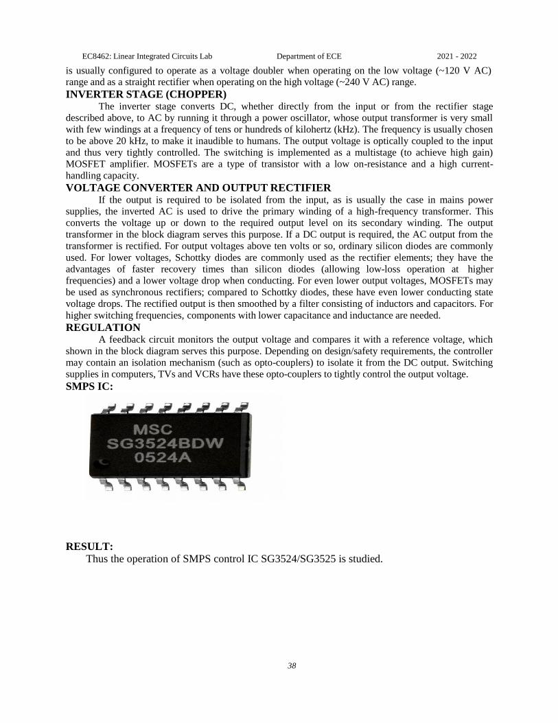
SMPS IC:
RESULT:
Thus the operation of SMPS control IC SG3524/SG3525 is studied.
EC8462: Linear Integrated Circuits Lab Department of ECE 2021 - 2022
39
SIMULATION EXPERIMENTS USING PSPICE
INTRODUCTION: PSpice is the acronym for personal SPICE, which is acronym for simulation program with
integrated circuit emphasis. It is a type of program for simulating analog and digital circuits.
The type of simulation performed by PSpice depends on the source specifications and control statements. The types of analysis usually executed in the PSpice program are as follows:
1. DC Analysis:- it is used for circuits with time – invariant sources (e.g., steady state dc
sources). It calculates all nodal voltages and branch currents over a range of values. The types of analysis
and their corresponding. (dot) commands are described below:
2. Transient Analysis:- It is used for circuits with time variant sources (e.g., ac
sources/switched dc sources). It calculates all nodes voltages and branch currents over a time interval and
their instantaneous values are the outputs. The corresponding. (dot) commands are as follows:
3. AC Analysis:- It is used for small signal analysis of circuits with sources of varying
frequencies. It also calculates all nodal voltages and branch currents (over a range of frequencies) and
their magnitudes and phase angles.
In PSpice, the circuit is first described to a computer by using a file called circuit file. It contains
the circuit details, viz., the information about source and commands for what to do and what to display as
output. The PSpice accepts circuit file as an input and after executing commands, creates and outputs file
to store results. However, the circuit to be analyzed is specified in terms of element names, element
values different sources (voltage or current) and different parameters.
PSpice calculates all nodal voltages and branch currents over a range of time interval by giving
the output of their instantaneous values. It can also perform other operations as will be evident later. For
circuits with variable frequency sources, AC analysis is used. Each circuit element is connected between
two nodes. All nodes must be connected to at least two elements and therefore appear twice at least.
OrCAD PSpice simulates analog-only circuits. After the preparation of a design for simulation,
OrCAD Capture generates a circuit file set. The circuit file set, containing the circuit netlist and analysis
commands, is read by PSpice for simulation.
PSpice formulates these into meaningful graphical plots, which can be marked for display directly from schematic page using markers.
OrCAD® offers a total solution for core design tasks, schematic- and VHDL-based design entry;
FPGA and CPLD design synthesis; digital, analog, and mixed-signal simulation; and printed circuit board
layout.
EC8462: Linear Integrated Circuits Lab Department of ECE 2021 - 2022
40
Ex.No: 13 (a) SECOND ORDER ACTIVE FILTERS Date:
AIM: To simulate a second order Low pass filter & high pass filter using Pspice and to obtain their
frequency response.
SOFTWARE REQUIRED: PC with Pspice software.
CIRCUIT DIAGRAM: Low Pass Filter
High Pass Filter:
PROCEDURE: 1. Open e-Sim.
2. Go to file option in the main menu and select new project.
3. Go to place part and select the components and place in the schematic window.
4. Add wires to all the components and specify the values of the components.
5. Go to Pspice in the main menu and check for errors in the netlist and set up the simulation profile by
adding required traces.
6. Observe the output waveform
EC8462: Linear Integrated Circuits Lab Department of ECE 2021 - 2022
41
RESULT: Thus the low pass and high pass – second order filter circuit is simulated and the required frequency response
graphs are plotted.
EC8462: Linear Integrated Circuits Lab Department of ECE 2021 - 2022
42
Ex.No:13 (b) ACTIVE BAND PASS FILTER Date:
AIM: To design and simulate a band pass filter using Pspice and to obtain the frequency response.
SOFTWARE REQUIRED: System with Pspice software.
CIRCUIT DIAGRAM:
PROCEDURE: 1. Open e-Sim.
2. Go to file option in the main menu and select new project. 3. Go to place part and select the components and place in the schematic window.
4. Add wires to all the components and specify the values of the components.
5. Go to Pspice in the main menu and check for errors in the netlist and set up the simulation profile by
adding required traces.
6. Observe the output waveform
RESULT: Thus the Active Band pass secondorder filter circuit is simulated and the required frequency response graphs
are plotted.
EC8462: Linear Integrated Circuits Lab Department of ECE 2021 - 2022
43
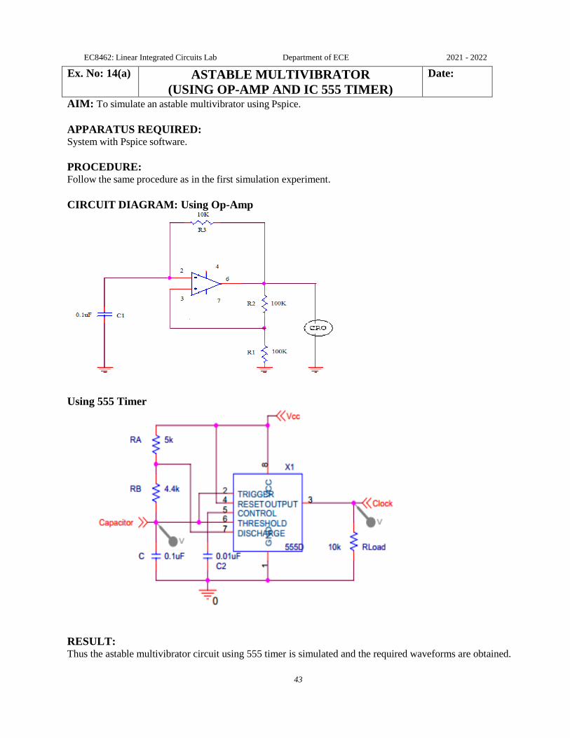
Ex. No: 14(a) ASTABLE MULTIVIBRATOR
(USING OP-AMP AND IC 555 TIMER)
Date:
AIM: To simulate an astable multivibrator using Pspice.
APPARATUS REQUIRED: System with Pspice software.
PROCEDURE: Follow the same procedure as in the first simulation experiment.
CIRCUIT DIAGRAM: Using Op-Amp
Using 555 Timer
RESULT: Thus the astable multivibrator circuit using 555 timer is simulated and the required waveforms are obtained.
EC8462: Linear Integrated Circuits Lab Department of ECE 2021 - 2022
44
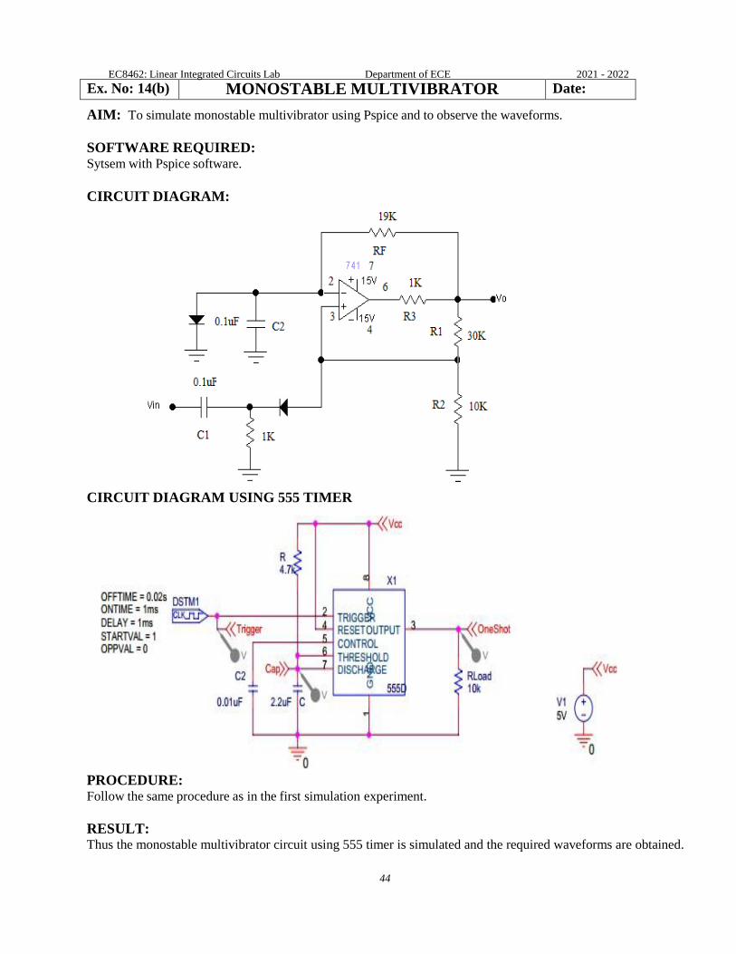
Ex. No: 14(b) MONOSTABLE MULTIVIBRATOR Date:
AIM: To simulate monostable multivibrator using Pspice and to observe the waveforms.
SOFTWARE REQUIRED: Sytsem with Pspice software.
CIRCUIT DIAGRAM:
CIRCUIT DIAGRAM USING 555 TIMER
PROCEDURE: Follow the same procedure as in the first simulation experiment.
RESULT: Thus the monostable multivibrator circuit using 555 timer is simulated and the required waveforms are obtained.
EC8462: Linear Integrated Circuits Lab Department of ECE 2021 - 2022
45
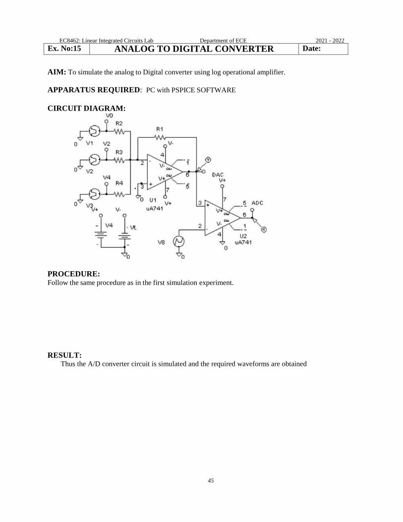
Ex. No:15 ANALOG TO DIGITAL CONVERTER Date:
AIM: To simulate the analog to Digital converter using log operational amplifier.
APPARATUS REQUIRED: PC with PSPICE SOFTWARE
CIRCUIT DIAGRAM:
PROCEDURE: Follow the same procedure as in the first simulation experiment.
RESULT: Thus the A/D converter circuit is simulated and the required waveforms are obtained
EC8462: Linear Integrated Circuits Lab Department of ECE 2021 - 2022
46
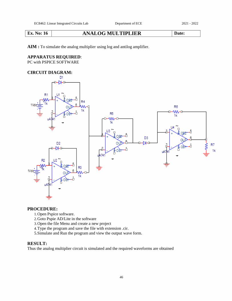
Ex. No: 16 ANALOG MULTIPLIER Date:
AIM : To simulate the analog multiplier using log and antilog amplifier.
APPARATUS REQUIRED: PC with PSPICE SOFTWARE
CIRCUIT DIAGRAM:
PROCEDURE:
1. Open Pspice software.
2. Goto Pspie AD/Lite in the software 3. Open the file Menu and create a new project
4. Type the program and save the file with extension .cir.
5.Simulate and Run the program and view the output wave form.
RESULT: Thus the analog multiplier circuit is simulated and the required waveforms are obtained
EC8462: Linear Integrated Circuits Lab Department of ECE 2021 - 2022
47
SAMPLE VIVA-VOCE QUESTIONS AND ANSWERS
1. Define operational amplifier
Ans: Op-amp is an operational amplifier capable of performing mathematical operations such as addition,
subtraction, multiplication, logarithm, anti-logarithm, integration, differentiation etc and amplification. It
is a multi stage differential amplifier which is in wide variety of applications.
2. What is the difference between ordinary amplifier and operational amplifier?
Ans: An ordinary amplifier can only amplify the given input signal. But, an operational amplifier can
perform many mathematical operations with enormous gain.
3. What are the different types of op-amp configurations available?
Ans: Op-amp configurations are broadly subdivided into two types. They are open-loop and Closed-loop
configurations. Open loop configurations are of three types. They are Inverting, Non-inverting and
differential configuration. Closed-loop configurations are of three types. They are Inverting, Non-
inverting, buffer amplifier and differential configuration. The differential configuration of closed-loop op-
amp is further subdivided into two types. They are configuration with one op-amp and configuration with
two op-amps.
4. Which is the basic building block of operational amplifier?
Ans: The basic building block of op-amp is differential amplifier. A differential amplifier amplifies the
difference between two input signals.
5. Mention some of the applications of op-amp.
Ans: Op-amps are mainly used in analog system design. They are used for wide variety of applications
such as mathematical operations, data acquisition systems, process control, programmable gain
amplifiers, automotive instrumentation and control, communication ICs, radio/audio/video ICs, analog
computers, A/D converters etc.
6. Can an op-amp be used for both AC and DC Applications?
Ans: Yes. Op-amps can be used for both AC and DC applications. This is one of the important features of
an op-amp. They have the ability to process both AC and DC input signals.
7. Why negative feedback is preferred in op-amp?
Ans: In most of the op-amp application, negative feedback is preferred to decrease the overall voltage
gain. Open-loop gain is huge and this is minimized by using two resistors. Input resistor and feedback
resistor is used to control the gain and thus suitable for many practical applications.
8. List out the ideal characteristics of op-amp.
Ans: The ideal characteristics of op-amp are i) Open-loop gain must be infinite. AoL = ∞ ii) The input impedance must be infinite. Ri = ∞
iii) The output impedance must be zero. Ro = 0
iv) Common Mode Rejection Ratio must be infinite. CMRR = ∞ v) Slew rate must be infinite. dvo/dt = ∞
vi) It must not provide output when there is no input. Vo = 0; when Vi = 0.
vii) Differential mode gain must be infinite. Ad = ∞ viii) Common mode gain must be zero. Ac = 0
9. Define slew rate. What causes it? Mention the effects and methods of minimizing Slew rate.
Ans: It is the rate at which the output voltage changes with respect to time. It tells how fast an output of
op-amp can change. Example: For a general purpose op-amp 741, the maximum slew rate is 0.5V/μs.
This means, the output voltage can change a maximum of 0.5V in 1 μs. Slew rate is a major limiting
factor for op-amps operating at high frequency.
Slew rate can also be given as the maximum current flowing through a compensating capacitor. S.R =
I/C. Op-amp with slew rate greater than 100V/μs are termed as “High Speed Op-amps”. For special
applications such as video systems, op-amps with slew rate of 1000V/μs are available.
CAUSES OF SLEW RATE:
EC8462: Linear Integrated Circuits Lab Department of ECE 2021 - 2022
48
The worst case, or slowest slew rate, occurs at unity gain. Therefore, slew rate is usually specified at unity
gain. Slew rate depends on many factors: the amplifier gain, Compensating capacitors, the current
flowing through the compensating capacitor and even whether the output voltage is going positive or
negative.
If Vi is a sine wave, with a peak amplitude of Vp, the maximum rate of change of Vi depends on both its
frequency f and peak amplitude. It is given by 2πfVp. If this change is larger than op-amps slew rate, the
output Vo will be distorted.
If a step input is given, it is observed that above certain step amplitude the output slope saturates at a
constant value called slew rate (SR). When the frequency of a train of square wave given to a voltage
follower is constantly increased, the shape of the output will be a triangular wave instead of square.
Methods of Minimizing Slew Rate The minimization methods can be summarized with the use of following expression.
SR = 2πIf / gm
By increasing the frequency f. By reducing the input stage transconductance gm.
By increasing the current I flowing through the capacitor.
Or by reducing the value of compensation capacitor Cc (which increases the frequency)
10. What is the maximum voltage that can be given at the inputs?
Ans: The inputs must be given in such a way that the output should be less than Vsat.
11. Why op-amps cannot be used in open-loop configuration?
Ans: Op-amp in open loop configuration has enormous gain. For example the op-amp 741 has a typical
gain of 200,000 (106 dB) & op-amp OP-77 has a typical gain of 12 million (141.6 dB). This huge gain is
not necessary for most of the application of op-amp. Since op-amp output will saturate at ±Vsat (positive
and negative saturation) which is approximately equal to ±V (Supply voltage)
12. Can a op-amp be operated using single power supply?
Ans: No. All the general purpose op-amp must be operated with two power supplies. Since, the
differential amplifier has two supply : +Vcc and – Vee, the op-amp which is a multi stage differential
amplifier stage must also have two supply voltages. However, op-amps with single supply voltage are
also used for very few applications.
13. Define offset voltage and state its significance.
Ans: When an op-amp has no inputs given, there is a possibility of getting output because of small
voltage at input terminals. This very small voltage difference between the two terminals of op-amp results
due to the slight mismatch between the characteristics of two transistors present in the starting stage of
op-amp. If a small voltage appears across the input terminals of op-amp, then because of the huge gain of
op-amp, the amplified output will result even when there is no input. So a voltage must be applied by the
user to cancel out the effects. The voltage that must be applied to nullify the output voltage is called as
offset voltage.
14. List the important features of op-amp 741.
Ans: Features of op-amp 741
1. No frequency compensation required. 2. Short circuit protection
3. Offset voltage null capability
4. Large common mode and differential voltage ranges
5. Low power consumption 6. No latch-up
15. How to construct a adder circuit using op-amp?
Ans: A two input summing amplifier may be constructed using the inverting mode. The adder can be
obtained by using either non-inverting mode or differential amplifier. Here the inverting mode is used. So
the inputs are applied through resistors to the inverting terminal and non-inverting terminal is grounded.
This is called “virtual ground”, i.e. the voltage at that terminal is zero. The gain of this summing amplifier
is 1, any scale factor can be used for the inputs by selecting proper external resistors.
EC8462: Linear Integrated Circuits Lab Department of ECE 2021 - 2022
49
16. List all Specifications of op-amp 741
Ans:
1. Voltage gain A = α typically 2,00,000
2. I/P resistance RL = α Ω, practically 2MΩ 3. O/P resistance R =0, practically 75Ω
4. Bandwidth = α Hz. It can be operated at any frequency
5. Common mode rejection ratio = α
(Ability of op amp to reject noise voltage)
6. Slew rate + α V/μsec
(Rate of change of O/P voltage)
7. When V1 = V2, VD=0
8. Input offset voltage (Rs ≤ 10KΩ) max 6 mv
9. Input offset current = max 200nA 10. Input bias current : 500nA 11. Input capacitance : typical value 1.4pF
12. Offset voltage adjustment range : ± 15mV
13. Input voltage range : ± 13V
14. Supply voltage rejection ratio : 150 μV/V 15. Output voltage swing: + 13V and – 13V for RL > 2KΩ
16. Output short-circuit current: 25mA 17. supply current: 28mA
18. Power consumption: 85mW
19. Transient response: rise time= 0.3 μs
17. What is the maximum voltage that can be given at the inputs?
Ans: The inputs must be given in such a way that the output should be less than Vsat.
18. How to construct a Subtractor?
Ans: A basic differential amplifier can be used as a subtractor. Input signals can be scaled to the desired
values by selecting appropriate values for the resistors. When this is done, the circuit is referred to as
scaling amplifier. However in this circuit all external resistors are equal in value. So the gain of amplifier
is equal to one. The output voltage Vo is equal to the voltage applied to the non-inverting terminal minus
the voltage applied to the inverting terminal; hence the circuit is called a subtractor.
19. Why op-amp integrator is called as precision Integrator?
Ans: The op-amp integrator has a high degree of accuracy. And it can
precisely implement the output voltage expression. Because of this, op-amp integrator
is often called as precision integrator.
20. Mention some of the applications of integrator.
Ans: Op-amp integrator finds wide application in function generators (Triangle and sawtooth wave generators), active filters (State variable & biquad
filters, Switched Capacitor filters), Analog to Digital Converters (Dual-slope
converters, Quantized feedback converters) and Analog controllers (PID Controllers).
21. What are the problems faced by basic ideal integrator and how can we
overcome ?
Ans: The input offset voltage Vio and the part of input current charging thefeedback capacitor Cf produces the
error voltage at the output of the ideal integrator. Therefore, in practical integrator, to reduce the error voltage at
the output, a resistor Rf is connected in parallel to Cf. This Rf, limits the low-frequency gain and hence
minimizes the variations in the output voltage. Both stability and the roll-off problems in basic ideal integrator can
be corrected by additional resistor Rf.
22. What is other name given to practical integrator?
Ans: The method of preventing saturation in integrator is to place a parallel resistance Rf with Cf. The resulting
circuit is called as lossy integrator (Practical Integrator) which can still provide integration function. But, only
over a limited frequency range. In most applications, integrators are placed in a control loop to avoid saturation
EC8462: Linear Integrated Circuits Lab Department of ECE 2021 - 2022
50
and there is no need for Rf in such applications.
23. What is meant by negative resistance?
Ans: Negative resistance indicates the release of power. Negative resistance
can be used to neutralize unwanted ordinary resistance, as in the design of current sources or to control the pole
location, as in the design of active filters and oscillators.
Integrator is otherwise called as fixed frequency, variable gain LPF. True or False?
Ans: True.
24. Give the meaning and use of Virtual ground.
Ans: If the difference input voltage is ideally zero, and non-inverting terminal
is grounded with a input signal applied to the non-inverting terminal via R1, then voltage at the inverting terminal
is approximately equal to voltage at the non-inverting terminal. This is known as virtual ground (A terminal that
is not connected to physical ground but, assumed to be.) It is much used in closed-loop analysis of inverting
amplifier.
25. How integrator is useful in constructing Servo Amplifer?
Ans: A Servo Amplifier is constructed when an integrator is followed by an inverting amplifier. Servo amplifiers
are used where the output is a delayed response to the input. Example: Radar (or) Position of a xy table in a
manufacturing process.
26. How to convert an op-amp integrator to op-amp differentiator?
Ans: To convert a op-amp integrator to differentiator, just replace the feedback capacitor Cf as feedback resistor
Rf. And replace the input resistor R1 as input capacitor C1 of an integrator.
27. How ideal differentiator suffers from instability? How can we overcome them?
Ans: The ideal or basic differentiator‟s circuit gain (Rf/R1) increases with increase in frequency at a rate of
+20dB/decade. This makes the circuit unstable. Also, the impedance Xc1 decreases with increase in frequency,
which makes the circuit very susceptible to high frequency noise. When amplified, this noise can
completely override the differentiated output signal. Both stability and high frequency noise can be corrected by
addition of two components R1 and Cf. This circuit is called as practical differentiator.
28. What is the condition to be followed for proper differentiation?
Ans: The input signal will be differentiated properly if the time period T of the input signal is larger than equal to
RfC1. That is T ≥ RfC1.
29. How high frequency noise affects the performance of an differentiator?
Ans: Due to poor Stability (i.e) Circuit tends to oscillate and gain of the circuit increases with an increase in
frequency. So high frequency noise is amplified and is dominant at the output.
30. Determine the output of differentiator for the following input waves.
Ans: The inputs and respective output waveform of differentiator are as follows, Sine Wave Negative Cosine
Wave, Sine Wave, Square Wave, Spike Wave, Sawtooth Wave, Square Wave
31. Give some important applications of differentiator.
Ans: Differentiator is most commonly used in wave shaping circuits to detect high frequency components in an
input signal and also as a rate-of-change detector in FM modulators.
32. What is Unity Gain Frequency?
Ans: Unity-gain frequency of op-amp differentiator is the frequency at which the gain is unity (0 dB).
33. What is UGB?
Ans: Unity Gain Bandwidth (UGB) is the bandwidth of op-amp when the voltage gain is 1. It is also called as
Closed-loop bandwidth, Gain-Bandwidth Product or Small signal bandwidth.
34. What are the important requirements of an instrumentation Amplifier?
Ans: The requirements of an instrumentation amplifier are low noise, low thermal and time drifts, high input
impedance, accurate closed-loop gain, high CMRR and high Slew Rate.
35. List the characteristics of a basic three op-amp instrumentation amplifier.
Ans: For 3 op-amp instrumentation amplifier, the characteristics are
The voltage gain, from differential input to single ended output is set by only one resistor.
The input resistance of both inputs are very high and does not change as the gain is varied.
Vo does not depend on the voltage common to both inputs (Common- mode rejection) but, only on their
difference.

EC8462: Linear Integrated Circuits Lab Department of ECE 2021 - 2022
51
36. Mention some of the applications of an instrumentation amplifier.
Ans: Instrumentation Amplifier is used in data acquisition unit, sensing, measurement & Control of physical
parameters such as temperature, used as signal conditioning circuit, Light-intensity meter, Measurement of flow
and thermal conductivity, Analog-weight scale, Active guard drive, digitally programmable gain and output
Offsetting.
37. What are the Different configurations of instrumentation amplifier? What are the merits and
demerits?
Ans: There were four configurations. They are
Triple op-amp IAs
Dual op-amp IAs
Monolithic IAs
Flying-Capacitor IAs Triple op-amp IA :
Offers high impedance because of buffer stage and too many components used. Dual op-amp IA:
Offers less Complexity in circuit (with fewer resistors & op-amps) with Significant boost in performance. But it
treats the input asymmetrically with Some delay.
Monolithic IA :
Better optimization of CMRR, gain linearity and noise reduction. Flying-Capacitor IA :
Excellent CMRR, as common mode signals are completely ignored.
How many stages does a three op-amp instrumentation amplifier contain? And what are they? Ans: A common
op-amp instrumentation amplifier uses 3 op-amps and seven resistors which is splitted into two stages. i) Buffer
stage (High impedance) Differential
input- differential output stage. ii) Difference amplifier stage.
38. What is the disadvantage of a instrumentation amplifier?
Ans: The requirement for instrumentation amplifier is too strict to follow for
general purpose applications. When the requirements are not too strict, then a general purpose op-amp can be
used in differential mode. Such amplifiers are called as differential instrumentation amplifier.
39. What is the use of op-amp buffer?
Ans: Op-amp buffer or voltage follower is a unity gain, high input impedance
and very low output impedance circuit used to provide isolation between two stages of an system.
40. What is meant by passive and active filters?
Ans: Passive filters: Uses Resistors, Capacitors and inductors as elements.
Active Filters: Uses Transistors or op-amps in addition to Resistors and Capacitors.
41. Why active filters are not suitable for high frequency applications?
Ans: Above MHZ range the op-amp open-loop gain rolls-off with increase in frequency.
42. List some of the applications of filters.
Ans: Filters are an integral part of electronic networks and are used in application from audio circuits to Digital
Signal Processing (DSP) Systems such as speech, audio, Video, Image processing etc.,
43. How Active filters are superior than passive filters?
Ans: Advantage of active filters over passive filters
Gain and frequency adjustment flexibility.
No loading problem.
Low Cost.
44. How Filters are classified and what are they?
Ans: Based on passband, stopband and cutoff frequency, filters are classified into Lowpass, Highpass, Bandpass,
Bandstop and Allpass filters.
45. What are poles and zeros?
Ans: Zeros are numerator and poles are denominator polynomials of the transfer function of a filter. Poles and
Zeros determine the characteristics of a filter.
46. Does a filter affect both amplitude and phase of the input signal?
Ans: Yes.
47. What is the use of bode plot?
Ans: The Bode Plots are plots of decibels and degrees versus decades (or Octaves). The purpose of bode plot is to
EC8462: Linear Integrated Circuits Lab Department of ECE 2021 - 2022
52
represent both logarithmic and semi-logarithmic scales.
48. In what basis the order of the filter is decided?
Ans: Based on the parameter „n‟, the order of the filter is decided. n=1; First order, n=2; Second order and so on.
The parameter „n‟ decides the accuracy of the filter primarily at the stopband (Rolloff). Higher the value of n,
better the filter will be and complex the design will be.
49. Define Bandwidth of a filter.
Ans: Bandwidth of a filter is defined as higher cutoff frequency minus lower cutoff frequency. Or in other words
it is the difference between Upper cutoff frequency and Lower cutoff frequency. Bandwidth is expressed in HZ.
B.W = fH – fL HZ
50. What do you understand from the frequency response of filter?
Ans: There were three cases that should be noted in any filter except allpass filter. The three cases for LPF filter
for example is given as
Case i: If the input frequency fin is less than the higher cutoff frequency fH, then magnitude of the gain is
maximum and it is given as passband gain of the filter AF. Case ii If the input frequency fin is equal to the cutoff
frequency, then the gain magnitude will be 70.7% of the maximum gain
Case iii: If the input frequency fin is greater than the higher cutoff frequency fH, then magnitude of the gain is
maximum and it is given as passband gain of the filter AF.
51. How filters are classified according to their band characteristics?
Ans: Filters are classified according to their passband and stopband characteristics. Butterworth Flat passband and
flat stopband (Flat-Flat filter) Chebyshev Ripple passbad and flat stop band Ripple passband and Ripple Stopband
52. How to convert a BPF to BSF?
Ans: Swap HPF-LPF series connection of BPF to LPF-HPF series connection to achieve Bandstop filter (BSF)
which is also called as BEF(Band Elimination Filter) or Notch Filter.
53. What is the function of a all pass filter?
Ans: This filter passes all frequencies well but it provides phase shift between input and Output voltage which is a
function of frequency.
54. List the applications of BPF.
Ans: It acts as frequency selector, stereo-equalizer octave filter, communication transmitter and receiver circuits,
radio, TV broadcast receivers, telephone, radar, space satellites and bio-medical equipment.
55. Write the way of constructing a I order Butterworth BPF.
Ans: I order Butterworth BPF can be constructed using I order Butterworth HPF followed by I order Butterworth
LPF.
56. Why inductors cannot be used with active filters?
Ans: Because, inductors are bulky due to windings and cannot be fabricated inside an IC.
57. What is the condition for stability of a network?
Ans: All the poles in unit circle must fall on the left half of the S-plane during mapping for Passive network
(Filter) The location of the poles determines the stability conditions for active network. All the roots must have
negative real parts for a active network (Filter). Also there are no changes in the signs of the first column of the
routh array.
58. Define multivibrator.
Ans: A multivibrator is an oscillatory circuit capable of generating waveforms without any Specific input signal.
The circuit only has supply voltage connections, from which the two amplifiers saturates one another to generate
vibrations.
59. State the relationship between Astable multivibrator and a comparator.
Ans: Astable multivibrator is almost a comparator except the trigger or threshold voltage will be generated on
its own.
60. What is the major difference between astable and monostable multivibrator?
Ans: In astable multivibrator there is no stable state and no triggering input. But, monostable multivibrator has
one stable state and works based on the triggering pulse
input.
61. Which Determines the switching time of a multivibrator?
Ans: The threshold value determines the switching time of a multivibrator. When ever a capacitor voltage
EC8462: Linear Integrated Circuits Lab Department of ECE 2021 - 2022
53
exceeds VT, the output state changes.
62. List some applications of multivibrator.
Ans: Multivibrators are mostly used for timing applications. Astable multivibrator is primarily used as square
wave generator in a function generator. Monostable
Multivibrator is used for timed control applications with the help of triggering input.
63. Say how to form a triangular wave generator using multivibrator?
Ans: To construct a triangular wave generator, a Astable multivibrator should be followed by an integrator.
Square wave is generated first and then converted to triangular with the help of integrator.
64. Define stable state.
Ans: The time over which a multivibrator output voltage stays constantly is called as stable state. A quasi-stable
in the other hand depends on the triggering input to regain the output state.
Give the relationship between tp and T of a monostable multivibrator. Ans: The Triggering pulse width „tp‟ must
be much smaller than the ON time „T‟ of Stable State.
65. What is a Schmitt trigger?
Ans: Schmitt trigger is the inverting comparator with positive feedback. The
other names given for Schmitt trigger circuit is regenerative comparator and squaring circuit. It is mainly used in
converting any irregular shaped waveform into square wave or pulse. So it is used in wave shaping circuit.
66. Write the truth table of a comparator.
Ans: Truth table of a Comparator When V+ > V- +Vsat
When V+ < V- - Vsat
When V+ = V- High Impedance State
67. What is Comparator chatter? And how can we eliminate it?
Ans: For slowly varying signals, comparators tend to produce multiple output transitions, or bounces, as input
crosses the threshold region. This is referred to as comparator chatter. This phenomenon is eliminated with the
help of Hysteresis. In hysteresis the circuit snaps and activates the other threshold.
68. What happens when both threshold points in a Schmitt trigger is equal to zero?
Ans: When VUT = VLT = 0, the Schmitt trigger behaves as a zero crossing detector. There were two types of
Schmitt trigger. They are positive and negative Schmitt trigger.
69. Can a Schmitt trigger can be operated with single supply & single threshold voltage?
Ans: Schmitt trigger can also be operated with single power supply or with a single triggering input (Either
Positive or Negative)
70. According to oscillations how oscillators are classified?
Ans: Based on how oscillations are created, oscillations are classified as under damping, over damping and
constant amplitude oscillations.
71. How oscillations are created in RC phase shift and wien Bridge oscillator?
Ans: When the bridge is balanced and the overall phase attained is 0°, the
Wien bridge oscillator produces oscillations. RC phase shift oscillator produces 360° of phase shift in two
parts. Firstly, each and every RC pair in the feedback network produces 60° phase shift and a totally there
were three pairs, thus producing 180°
Phase shift and secondly, the feedback input is given to the inverting terminal of opamp to produce another
180° phase shift and a total phase shift of 360°.
72. What are the merits and demerits of different types of oscillator?
Ans: The major problem in Wien bridge oscillator is balancing the bridge
becomes very difficult when the component values drifts unfortunately due to external or internal conditions.
Poor stability and low frequency application is the demerits of RC phase shift Oscillator. Both RC phase shift
and Wien bridge oscillator have a advantage that its operating frequency can be easily varied by just replacing
the values of either R or C to a new value. Crystal oscillator has excellent stability and poor deviation.
73. Why Timer IC is numbered as 555?
Ans: The timer IC is called as 555, because the internal architecture consists of three 5KΩ resistors.
74. What are the different operating modes of 555 Timer?
EC8462: Linear Integrated Circuits Lab Department of ECE 2021 - 2022
54
Ans: There were two operating modes of 555 Timer. It operates in Astable and Monostable mode.
75. What are the different types of packages available for 555 Timer IC?
Ans: The packages used for 555 Timer are 8-pin mini Dual-Inline-Package (DIP) and 8-pin Metal Can.
76. List some applications of 555 timers in both Astable mode and Monostable Mode.
Ans: In Astable mode of operation, some of the applications of 555 Timer were: Tone- burst oscillator,
Voltage controlled frequency shifter, square wave generator etc., In Monostable or one-shot mode, some of
the applications of 555 timer were: Water-level fill control, Touch switch, Frequency divider, missing pulse
detector and many more.
77. What is a PLL?
A PLL is a Phase Locked Loop Circuit used to track any changes in the input frequency.
78. What are the operating modes of an PLL?
A PLL functions in any in any one of the mode described here.
Free Running mode
Capture mode
Lock mode and
Tracking mode/range
79. What are the basic building blocks of a PLL IC?
The basic building blocks of PLL IC are 1) Phase comparator 2) Low Pass Filter and 3) Error Amplifier.
80. What is meant by free running mode of a PLL?
A PLL is said to be in this mode when there is no input frequency given to phase comparator for comparison.
When no input is given, PLL runs freely without any locking or tracking and so it is called as free running
mode of PLL.
81. Name some of the applications of PLL IC 565.
PLL ICs are mostly used in frequency application circuits such as Frequency synthesizer, frequency
multiplier, frequency divider, phase comparator, FM demodulator, PM demodulator, Phase magnitude
comparator, etc.,
82. Why PLL Circuit is mostly preferred in Frequency Applications?
It is preferred in most of the frequency applications because the frequency content of a signal is indirectly
proportional to Phase of the same signal. As we compare the phase of the two signals, we indirectly compare
the frequency of the same signal. This is due to the fact that direct phase is nothing but indirect frequency and
direct frequency is nothing but indirect phase.
83. What happens when the two input signals given to PLL is having same frequency or same phase?
When both the inputs are same, the PLL will start functioning in the Lock mode and if once lock has been
occurred, the PLL will start tracking the Phase or frequency changes in the input signal.
84. What is VCO?
VCO is the integral part of PLL. A VCO is the Voltage Controlled Oscillator. As the name implies it
generates oscillations according to the input voltage. This VCO is placed in the feedback path of a PLL. The
output of the VCO is changing according to the Error output voltage from the error amplifier placed finally in
the forward path.
85. Mention Some Important DAC characteristics.
Ans: Resolution, Full-scale output Voltage, Offset error, Gain error, Monotonocity and Relative accuracy.
86. What are the different types of D/A Converter techniques available?
Ans: The different types of DAC techniques are
Binary weighted DAC
R-2R Ladder network
Inverted R-2R ladder network
Current Driven DAC
87. Define resolution of a DAC.
Ans: The resolution is nothing but the number of distinct analog outputs that can be produced by DAC. It is
given as Resolution = 2n Where „n‟ is the number of digital inputs. Example: For 3 inputs DAC there are 8
distinct outputs.


![[Lab Report] PSpice](https://static.fdokumen.com/doc/165x107/631a338ebb40f9952b01e638/lab-report-pspice.jpg)