Jacob Fraden Physics, Designs, and Applications Fifth Edition
765
Jacob Fraden Handbook of Modern Sensors Physics, Designs, and Applications Fifth Edition
-
Upload
khangminh22 -
Category
Documents
-
view
3 -
download
0
Transcript of Jacob Fraden Physics, Designs, and Applications Fifth Edition

Jacob Fraden
Handbook of Modern SensorsPhysics, Designs, and Applications
Fifth Edition

Handbook of Modern Sensors


Jacob Fraden
Handbook of ModernSensorsPhysics, Designs, and Applications
Fifth Edition

Jacob FradenFraden Corp.San Diego, CA, USA
ISBN 978-3-319-19302-1 ISBN 978-3-319-19303-8 (eBook)DOI 10.1007/978-3-319-19303-8
Library of Congress Control Number: 2015947779
Springer Cham Heidelberg New York Dordrecht London# Springer International Publishing Switzerland 2004, 2010, 2016# American Institute of Physics 1993, 1997This work is subject to copyright. All rights are reserved by the Publisher, whether the whole or part ofthe material is concerned, specifically the rights of translation, reprinting, reuse of illustrations,recitation, broadcasting, reproduction on microfilms or in any other physical way, and transmissionor information storage and retrieval, electronic adaptation, computer software, or by similar ordissimilar methodology now known or hereafter developed.The use of general descriptive names, registered names, trademarks, service marks, etc. in thispublication does not imply, even in the absence of a specific statement, that such names are exemptfrom the relevant protective laws and regulations and therefore free for general use.The publisher, the authors and the editors are safe to assume that the advice and information in thisbook are believed to be true and accurate at the date of publication. Neither the publisher nor theauthors or the editors give a warranty, express or implied, with respect to the material containedherein or for any errors or omissions that may have been made.
Printed on acid-free paper
Springer International Publishing AG Switzerland is part of Springer Science+Business Media(www.springer.com)

Preface
Numerous computerized appliances wash clothes, prepare coffee, play music,
guard homes, and perform endless useful functions. However, no electronic device
operates without receiving external information. Even if such information comes
from another electronic device, somewhere in the chain, there is at least one
component that perceives external input signals. This component is a sensor.
Modern signal processors are the devices that manipulate binary codes generally
represented by electric impulses. As we live in an analog world that mostly is not
digital or electrical (apart from the atomic level), sensors are the interface devices
between various physical values and the electronic circuits that “understand” only
the language of moving electrical charges. In other words, sensors are eyes, ears,
and noses of the silicon chips. This book is about the man-made sensors that are
very much different from the sensing organs of living organisms.
Since the publication of the previous edition of this book, sensing technologies
have made remarkable leaps. Sensitivities of sensors have become higher, their
dimensions smaller, selectivity better, and prices lower. A new, major field of
application for sensors—mobile communication devices—has been rapidly
evolving. Even though such devices employ sensors that operate on the same
fundamental principles as other sensors, their use in mobile devices demands
specific requirements. Among these are miniature dimensions and complete inte-
gration with the signal processing and communication components. Hence, in this
new edition, we address in greater detail the mobile trend in sensing technologies.
A sensor converts input signals of a physical nature into electrical output. Thus,
we will examine in detail the principles of such conversions and other relevant laws
of physics. Arguably one of the greatest geniuses who ever lived, Leonardo da
Vinci, had his own peculiar way of praying (according to a book I read many years
ago, by Akim Volinsky, published in Russian in 1900). Loosely, it may be trans-
lated into modern English as something like, “Oh Lord, thank you for following Thyown laws.” It is comforting indeed that the laws of Nature do not change—it is our
appreciation of the laws that is continually refined. The sections of the book that
cover these laws have not changed much since the previous editions. Yet, the
sections that describe the practical designs have been revised substantially. Recent
ideas and developments have been added, while obsolete and less interesting
designs were dropped.
v

In the course of my engineering work, I often wished for a book which combined
practical information on the many subjects relating to the most important physical
principles, design, and use of various sensors. Of course, I could browse the Internet
or library bookshelves in search of texts on physics, chemistry, electronics, technical,
and scientific magazines, but the information is scattered over many publications and
websites, and almost every question I was pondering required substantial research.
Little by little, I gathered practical information on everything which is in any way
related to various sensors and their applications to scientific and engineering
measurements. I also spent endless hours at a lab bench, inventing and developing
numerous devices with various sensors. Soon, I realized that the information I had
collected would be quite useful to more than one plerson. This idea prompted me to
write this book, and this fifth updated edition is the proof that I was not mistaken.
The topics included in the book reflect the author’s own preferences and
interpretations. Some may find a description of a particular sensor either too
detailed or broad or perhaps too brief. In setting my criteria for selecting various
sensors for this new edition, I attempted to keep the scope of this book as broad as
possible, opting for many different designs described briefly (without being trivial,
I hope), rather than fewer treated in greater depth. This volume attempts (immod-
estly perhaps) to cover a very broad range of sensors and detectors. Many of them
are well known, but describing them is still useful for students and for those seeking
a convenient reference.
By no means this book is a replacement for specialized texts. It gives a bird’s-eye
view at a multitude of designs and possibilities, but does not dive in depth into
any particular topic. In most cases, I have tried to strike a balance between details
and simplicity of coverage; however simplicity and clarity were the most important
requirements I set for myself. My true goal was not to pile up a collection of informa-
tion but rather to entice the reader into a creative mindset. As Plutarch said nearly two
millennia ago, “The mind is not a vessel to be filled but a fire to be kindled. . .”Even though this book is for scientists and engineers, as a rule, the technical
descriptions and mathematic treatments generally do not require a background
beyond a high school curriculum. This is a reference text which could be used by
students, researchers interested in modern instrumentation (applied physicists and
engineers), sensor designers, application engineers, and technicians whose job is to
understand, select, or design sensors for practical systems.
The previous editions of this book have been used quite extensively as desktop
references and textbooks for the related college courses. Comments and suggestions
from sensor designers, application engineers, professors, and students have
prompted me to implement several changes and to correct errors. I am deeply
grateful to those who helped me to make further improvements in this new edition.
I owe a debt of gratitude and many thanks to Drs. Ephraim Suhir and David Pintsov
for assisting me in mathematical treatment of transfer functions and to Dr. Sanjay
V. Patel for his further contributions to the chapter on chemical sensors.
San Diego, CA, USA Jacob Fraden
April 12, 2015
vi Preface

Contents
1 Data Acquisition . . . . . . . . . . . . . . . . . . . . . . . . . . . . . . . . . . . . . . . 1
1.1 Sensors, Signals, and Systems . . . . . . . . . . . . . . . . . . . . . . . . 1
1.2 Sensor Classification . . . . . . . . . . . . . . . . . . . . . . . . . . . . . . . 7
1.3 Units of Measurements . . . . . . . . . . . . . . . . . . . . . . . . . . . . . 10
References . . . . . . . . . . . . . . . . . . . . . . . . . . . . . . . . . . . . . . . . . . . . 11
2 Transfer Functions . . . . . . . . . . . . . . . . . . . . . . . . . . . . . . . . . . . . . 13
2.1 Mathematical Models . . . . . . . . . . . . . . . . . . . . . . . . . . . . . . 13
2.1.1 Concept . . . . . . . . . . . . . . . . . . . . . . . . . . . . . . . . . 15
2.1.2 Functional Approximations . . . . . . . . . . . . . . . . . . . 15
2.1.3 Linear Regression . . . . . . . . . . . . . . . . . . . . . . . . . 19
2.1.4 Polynomial Approximations . . . . . . . . . . . . . . . . . . 19
2.1.5 Sensitivity . . . . . . . . . . . . . . . . . . . . . . . . . . . . . . . 21
2.1.6 Linear Piecewise Approximation . . . . . . . . . . . . . . . 21
2.1.7 Spline Interpolation . . . . . . . . . . . . . . . . . . . . . . . . 22
2.1.8 Multidimensional Transfer Functions . . . . . . . . . . . . 23
2.2 Calibration . . . . . . . . . . . . . . . . . . . . . . . . . . . . . . . . . . . . . . 24
2.3 Computation of Parameters . . . . . . . . . . . . . . . . . . . . . . . . . . 26
2.4 Computation of a Stimulus . . . . . . . . . . . . . . . . . . . . . . . . . . 28
2.4.1 Use of Analytical Equation . . . . . . . . . . . . . . . . . . . 29
2.4.2 Use of Linear Piecewise Approximation . . . . . . . . . 29
2.4.3 Iterative Computation of Stimulus
(Newton Method) . . . . . . . . . . . . . . . . . . . . . . . . . . 32
References . . . . . . . . . . . . . . . . . . . . . . . . . . . . . . . . . . . . . . . . . . . . 34
3 Sensor Characteristics . . . . . . . . . . . . . . . . . . . . . . . . . . . . . . . . . . 35
3.1 Sensors for Mobile Communication Devices . . . . . . . . . . . . . 35
3.1.1 Requirements to MCD Sensors . . . . . . . . . . . . . . . . 36
3.1.2 Integration . . . . . . . . . . . . . . . . . . . . . . . . . . . . . . . 37
3.2 Span (Full-Scale Input) . . . . . . . . . . . . . . . . . . . . . . . . . . . . . 38
3.3 Full-Scale Output . . . . . . . . . . . . . . . . . . . . . . . . . . . . . . . . . 39
3.4 Accuracy . . . . . . . . . . . . . . . . . . . . . . . . . . . . . . . . . . . . . . . 39
3.5 Calibration Error . . . . . . . . . . . . . . . . . . . . . . . . . . . . . . . . . . 42
3.6 Hysteresis . . . . . . . . . . . . . . . . . . . . . . . . . . . . . . . . . . . . . . . 43
3.7 Nonlinearity . . . . . . . . . . . . . . . . . . . . . . . . . . . . . . . . . . . . . 44
vii

3.8 Saturation . . . . . . . . . . . . . . . . . . . . . . . . . . . . . . . . . . . . . . . 45
3.9 Repeatability . . . . . . . . . . . . . . . . . . . . . . . . . . . . . . . . . . . . 46
3.10 Dead Band . . . . . . . . . . . . . . . . . . . . . . . . . . . . . . . . . . . . . . 47
3.11 Resolution . . . . . . . . . . . . . . . . . . . . . . . . . . . . . . . . . . . . . . 48
3.12 Special Properties . . . . . . . . . . . . . . . . . . . . . . . . . . . . . . . . . 48
3.13 Output Impedance . . . . . . . . . . . . . . . . . . . . . . . . . . . . . . . . . 48
3.14 Output Format . . . . . . . . . . . . . . . . . . . . . . . . . . . . . . . . . . . 48
3.15 Excitation . . . . . . . . . . . . . . . . . . . . . . . . . . . . . . . . . . . . . . . 49
3.16 Dynamic Characteristics . . . . . . . . . . . . . . . . . . . . . . . . . . . . 49
3.17 Dynamic Models of Sensor Elements . . . . . . . . . . . . . . . . . . . 54
3.17.1 Mechanical Elements . . . . . . . . . . . . . . . . . . . . . . . 54
3.17.2 Thermal Elements . . . . . . . . . . . . . . . . . . . . . . . . . 55
3.17.3 Electrical Elements . . . . . . . . . . . . . . . . . . . . . . . . . 57
3.17.4 Analogies . . . . . . . . . . . . . . . . . . . . . . . . . . . . . . . 58
3.18 Environmental Factors . . . . . . . . . . . . . . . . . . . . . . . . . . . . . 58
3.19 Reliability . . . . . . . . . . . . . . . . . . . . . . . . . . . . . . . . . . . . . . 61
3.19.1 MTTF . . . . . . . . . . . . . . . . . . . . . . . . . . . . . . . . . . 61
3.19.2 Extreme Testing . . . . . . . . . . . . . . . . . . . . . . . . . . . 62
3.19.3 Accelerated Life Testing . . . . . . . . . . . . . . . . . . . . . 63
3.20 Application Characteristics . . . . . . . . . . . . . . . . . . . . . . . . . . 65
3.21 Uncertainty . . . . . . . . . . . . . . . . . . . . . . . . . . . . . . . . . . . . . . 65
References . . . . . . . . . . . . . . . . . . . . . . . . . . . . . . . . . . . . . . . . . . . . 67
4 Physical Principles of Sensing . . . . . . . . . . . . . . . . . . . . . . . . . . . . . 69
4.1 Electric Charges, Fields, and Potentials . . . . . . . . . . . . . . . . . 70
4.2 Capacitance . . . . . . . . . . . . . . . . . . . . . . . . . . . . . . . . . . . . . 76
4.2.1 Capacitor . . . . . . . . . . . . . . . . . . . . . . . . . . . . . . . . 78
4.2.2 Dielectric Constant . . . . . . . . . . . . . . . . . . . . . . . . . 79
4.3 Magnetism . . . . . . . . . . . . . . . . . . . . . . . . . . . . . . . . . . . . . . 83
4.3.1 Faraday Law . . . . . . . . . . . . . . . . . . . . . . . . . . . . . 86
4.3.2 Permanent Magnets . . . . . . . . . . . . . . . . . . . . . . . . 88
4.3.3 Coil and Solenoid . . . . . . . . . . . . . . . . . . . . . . . . . . 89
4.4 Induction . . . . . . . . . . . . . . . . . . . . . . . . . . . . . . . . . . . . . . . 90
4.4.1 Lenz Law . . . . . . . . . . . . . . . . . . . . . . . . . . . . . . . 94
4.4.2 Eddy Currents . . . . . . . . . . . . . . . . . . . . . . . . . . . . 95
4.5 Resistance . . . . . . . . . . . . . . . . . . . . . . . . . . . . . . . . . . . . . . 96
4.5.1 Specific Resistivity . . . . . . . . . . . . . . . . . . . . . . . . . 98
4.5.2 Temperature Sensitivity of a Resistor . . . . . . . . . . . 99
4.5.3 Strain Sensitivity of a Resistor . . . . . . . . . . . . . . . . 102
4.5.4 Moisture Sensitivity of a Resistor . . . . . . . . . . . . . . 104
4.6 Piezoelectric Effect . . . . . . . . . . . . . . . . . . . . . . . . . . . . . . . . 104
4.6.1 Ceramic Piezoelectric Materials . . . . . . . . . . . . . . . 108
4.6.2 Polymer Piezoelectric Films . . . . . . . . . . . . . . . . . . 112
4.7 Pyroelectric Effect . . . . . . . . . . . . . . . . . . . . . . . . . . . . . . . . 113
4.8 Hall Effect . . . . . . . . . . . . . . . . . . . . . . . . . . . . . . . . . . . . . . 119
viii Contents

4.9 Thermoelectric Effects . . . . . . . . . . . . . . . . . . . . . . . . . . . . . 123
4.9.1 Seebeck Effect . . . . . . . . . . . . . . . . . . . . . . . . . . . . 123
4.9.2 Peltier Effect . . . . . . . . . . . . . . . . . . . . . . . . . . . . . 128
4.10 Sound Waves . . . . . . . . . . . . . . . . . . . . . . . . . . . . . . . . . . . . 129
4.11 Temperature and Thermal Properties of Materials . . . . . . . . . . 132
4.11.1 Temperature Scales . . . . . . . . . . . . . . . . . . . . . . . . 133
4.11.2 Thermal Expansion . . . . . . . . . . . . . . . . . . . . . . . . 135
4.11.3 Heat Capacity . . . . . . . . . . . . . . . . . . . . . . . . . . . . 137
4.12 Heat Transfer . . . . . . . . . . . . . . . . . . . . . . . . . . . . . . . . . . . . 138
4.12.1 Thermal Conduction . . . . . . . . . . . . . . . . . . . . . . . . 139
4.12.2 Thermal Convection . . . . . . . . . . . . . . . . . . . . . . . . 141
4.12.3 Thermal Radiation . . . . . . . . . . . . . . . . . . . . . . . . . 142
References . . . . . . . . . . . . . . . . . . . . . . . . . . . . . . . . . . . . . . . . . . . . 153
5 Optical Components of Sensors . . . . . . . . . . . . . . . . . . . . . . . . . . . . 155
5.1 Light . . . . . . . . . . . . . . . . . . . . . . . . . . . . . . . . . . . . . . . . . . 155
5.1.1 Energy of Light Quanta . . . . . . . . . . . . . . . . . . . . . 155
5.1.2 Light Polarization . . . . . . . . . . . . . . . . . . . . . . . . . . 157
5.2 Light Scattering . . . . . . . . . . . . . . . . . . . . . . . . . . . . . . . . . . 157
5.3 Geometrical Optics . . . . . . . . . . . . . . . . . . . . . . . . . . . . . . . . 159
5.4 Radiometry . . . . . . . . . . . . . . . . . . . . . . . . . . . . . . . . . . . . . . 160
5.5 Photometry . . . . . . . . . . . . . . . . . . . . . . . . . . . . . . . . . . . . . . 166
5.6 Windows . . . . . . . . . . . . . . . . . . . . . . . . . . . . . . . . . . . . . . . 169
5.7 Mirrors . . . . . . . . . . . . . . . . . . . . . . . . . . . . . . . . . . . . . . . . . 171
5.7.1 Coated Mirrors . . . . . . . . . . . . . . . . . . . . . . . . . . . . 172
5.7.2 Prismatic Mirrors . . . . . . . . . . . . . . . . . . . . . . . . . . 173
5.8 Lenses . . . . . . . . . . . . . . . . . . . . . . . . . . . . . . . . . . . . . . . . . 174
5.8.1 Curved Surface Lenses . . . . . . . . . . . . . . . . . . . . . . 174
5.8.2 Fresnel Lenses . . . . . . . . . . . . . . . . . . . . . . . . . . . . 176
5.8.3 Flat Nanolenses . . . . . . . . . . . . . . . . . . . . . . . . . . . 179
5.9 Fiber Optics and Waveguides . . . . . . . . . . . . . . . . . . . . . . . . 179
5.10 Optical Efficiency . . . . . . . . . . . . . . . . . . . . . . . . . . . . . . . . . 183
5.10.1 Lensing Effect . . . . . . . . . . . . . . . . . . . . . . . . . . . . 183
5.10.2 Concentrators . . . . . . . . . . . . . . . . . . . . . . . . . . . . . 185
5.10.3 Coatings for Thermal Absorption . . . . . . . . . . . . . . 186
5.10.4 Antireflective Coating (ARC) . . . . . . . . . . . . . . . . . 187
References . . . . . . . . . . . . . . . . . . . . . . . . . . . . . . . . . . . . . . . . . . . . 188
6 Interface Electronic Circuits . . . . . . . . . . . . . . . . . . . . . . . . . . . . . . 191
6.1 Signal Conditioners . . . . . . . . . . . . . . . . . . . . . . . . . . . . . . . . 193
6.1.1 Input Characteristics . . . . . . . . . . . . . . . . . . . . . . . . 194
6.1.2 Amplifiers . . . . . . . . . . . . . . . . . . . . . . . . . . . . . . . 198
6.1.3 Operational Amplifiers . . . . . . . . . . . . . . . . . . . . . . 199
6.1.4 Voltage Follower . . . . . . . . . . . . . . . . . . . . . . . . . . 201
Contents ix

6.1.5 Charge- and Current-to-Voltage Converters . . . . . . . 201
6.1.6 Light-to-Voltage Converters . . . . . . . . . . . . . . . . . . 203
6.1.7 Capacitance-to-Voltage Converters . . . . . . . . . . . . . 205
6.1.8 Closed-Loop Capacitance-to-Voltage Converters . . . 207
6.2 Sensor Connections . . . . . . . . . . . . . . . . . . . . . . . . . . . . . . . . 209
6.2.1 Ratiometric Circuits . . . . . . . . . . . . . . . . . . . . . . . . 209
6.2.2 Differential Circuits . . . . . . . . . . . . . . . . . . . . . . . . 212
6.2.3 Wheatstone Bridge . . . . . . . . . . . . . . . . . . . . . . . . . 212
6.2.4 Null-Balanced Bridge . . . . . . . . . . . . . . . . . . . . . . . 215
6.2.5 Bridge Amplifiers . . . . . . . . . . . . . . . . . . . . . . . . . . 216
6.3 Excitation Circuits . . . . . . . . . . . . . . . . . . . . . . . . . . . . . . . . 218
6.3.1 Current Generators . . . . . . . . . . . . . . . . . . . . . . . . . 220
6.3.2 Voltage Generators . . . . . . . . . . . . . . . . . . . . . . . . . 222
6.3.3 Voltage References . . . . . . . . . . . . . . . . . . . . . . . . 223
6.3.4 Oscillators . . . . . . . . . . . . . . . . . . . . . . . . . . . . . . . 224
6.4 Analog-to-Digital Converters . . . . . . . . . . . . . . . . . . . . . . . . . 225
6.4.1 Basic Concepts . . . . . . . . . . . . . . . . . . . . . . . . . . . . 226
6.4.2 V/F Converters . . . . . . . . . . . . . . . . . . . . . . . . . . . . 227
6.4.3 PWM Converters . . . . . . . . . . . . . . . . . . . . . . . . . . 231
6.4.4 R/F Converters . . . . . . . . . . . . . . . . . . . . . . . . . . . . 232
6.4.5 Successive-Approximation Converter . . . . . . . . . . . 234
6.4.6 Resolution Extension . . . . . . . . . . . . . . . . . . . . . . . 235
6.4.7 ADC Interface . . . . . . . . . . . . . . . . . . . . . . . . . . . . 237
6.5 Integrated Interfaces . . . . . . . . . . . . . . . . . . . . . . . . . . . . . . . 239
6.5.1 Voltage Processor . . . . . . . . . . . . . . . . . . . . . . . . . . 239
6.5.2 Inductance Processor . . . . . . . . . . . . . . . . . . . . . . . 240
6.6 Data Transmission . . . . . . . . . . . . . . . . . . . . . . . . . . . . . . . . 241
6.6.1 Two-Wire Transmission . . . . . . . . . . . . . . . . . . . . . 242
6.6.2 Four-Wire Transmission . . . . . . . . . . . . . . . . . . . . . 243
6.7 Noise in Sensors and Circuits . . . . . . . . . . . . . . . . . . . . . . . . 243
6.7.1 Inherent Noise . . . . . . . . . . . . . . . . . . . . . . . . . . . . 244
6.7.2 Transmitted Noise . . . . . . . . . . . . . . . . . . . . . . . . . 247
6.7.3 Electric Shielding . . . . . . . . . . . . . . . . . . . . . . . . . . 252
6.7.4 Bypass Capacitors . . . . . . . . . . . . . . . . . . . . . . . . . 255
6.7.5 Magnetic Shielding . . . . . . . . . . . . . . . . . . . . . . . . 256
6.7.6 Mechanical Noise . . . . . . . . . . . . . . . . . . . . . . . . . . 258
6.7.7 Ground Planes . . . . . . . . . . . . . . . . . . . . . . . . . . . . 258
6.7.8 Ground Loops and Ground Isolation . . . . . . . . . . . . 259
6.7.9 Seebeck Noise . . . . . . . . . . . . . . . . . . . . . . . . . . . . 261
6.8 Batteries for Low-Power Sensors . . . . . . . . . . . . . . . . . . . . . . 263
6.8.1 Primary Cells . . . . . . . . . . . . . . . . . . . . . . . . . . . . . 264
6.8.2 Secondary Cells . . . . . . . . . . . . . . . . . . . . . . . . . . . 265
6.8.3 Supercapacitors . . . . . . . . . . . . . . . . . . . . . . . . . . . 265
x Contents

6.9 Energy Harvesting . . . . . . . . . . . . . . . . . . . . . . . . . . . . . . . . 266
6.9.1 Light Energy Harvesting . . . . . . . . . . . . . . . . . . . . . 267
6.9.2 Far-Field Energy Harvesting . . . . . . . . . . . . . . . . . . 268
6.9.3 Near-Field Energy Harvesting . . . . . . . . . . . . . . . . . 269
References . . . . . . . . . . . . . . . . . . . . . . . . . . . . . . . . . . . . . . . . . . . . 269
7 Detectors of Humans . . . . . . . . . . . . . . . . . . . . . . . . . . . . . . . . . . . . 271
7.1 Ultrasonic Detectors . . . . . . . . . . . . . . . . . . . . . . . . . . . . . . . 273
7.2 Microwave Motion Detectors . . . . . . . . . . . . . . . . . . . . . . . . 276
7.3 Micropower Impulse Radars . . . . . . . . . . . . . . . . . . . . . . . . . 281
7.4 Ground Penetrating Radars . . . . . . . . . . . . . . . . . . . . . . . . . . 284
7.5 Linear Optical Sensors (PSD) . . . . . . . . . . . . . . . . . . . . . . . . 285
7.6 Capacitive Occupancy Detectors . . . . . . . . . . . . . . . . . . . . . . 289
7.7 Triboelectric Detectors . . . . . . . . . . . . . . . . . . . . . . . . . . . . . 292
7.8 Optoelectronic Motion Detectors . . . . . . . . . . . . . . . . . . . . . . 294
7.8.1 Sensor Structures . . . . . . . . . . . . . . . . . . . . . . . . . . 295
7.8.2 Multiple Detecting Elements . . . . . . . . . . . . . . . . . . 297
7.8.3 Complex Sensor Shape . . . . . . . . . . . . . . . . . . . . . . 297
7.8.4 Image Distortion . . . . . . . . . . . . . . . . . . . . . . . . . . 297
7.8.5 Facet Focusing Elements . . . . . . . . . . . . . . . . . . . . 298
7.8.6 Visible and Near-IR Light Motion Detectors . . . . . . 299
7.8.7 Mid- and Far-IR Detectors . . . . . . . . . . . . . . . . . . . 301
7.8.8 Passive Infrared (PIR) Motion Detectors . . . . . . . . . 302
7.8.9 PIR Detector Efficiency Analysis . . . . . . . . . . . . . . 305
7.9 Optical Presence Sensors . . . . . . . . . . . . . . . . . . . . . . . . . . . . 309
7.9.1 Photoelectric Beam . . . . . . . . . . . . . . . . . . . . . . . . 309
7.9.2 Light Reflection Detectors . . . . . . . . . . . . . . . . . . . 310
7.10 Pressure-Gradient Sensors . . . . . . . . . . . . . . . . . . . . . . . . . . . 311
7.11 2-D Pointing Devices . . . . . . . . . . . . . . . . . . . . . . . . . . . . . . 313
7.12 Gesture Sensing (3-D Pointing) . . . . . . . . . . . . . . . . . . . . . . . 314
7.12.1 Inertial and Gyroscopic Mice . . . . . . . . . . . . . . . . . 315
7.12.2 Optical Gesture Sensors . . . . . . . . . . . . . . . . . . . . . 315
7.12.3 Near-Field Gesture Sensors . . . . . . . . . . . . . . . . . . . 316
7.13 Tactile Sensors . . . . . . . . . . . . . . . . . . . . . . . . . . . . . . . . . . . 318
7.13.1 Switch Sensors . . . . . . . . . . . . . . . . . . . . . . . . . . . . 319
7.13.2 Piezoelectric Tactile Sensors . . . . . . . . . . . . . . . . . . 320
7.13.3 Piezoresistive Tactile Sensors . . . . . . . . . . . . . . . . . 323
7.13.4 Tactile MEMS Sensors . . . . . . . . . . . . . . . . . . . . . . 326
7.13.5 Capacitive Touch Sensors . . . . . . . . . . . . . . . . . . . . 326
7.13.6 Optical Touch Sensors . . . . . . . . . . . . . . . . . . . . . . 330
7.13.7 Optical Fingerprint Sensors . . . . . . . . . . . . . . . . . . . 331
References . . . . . . . . . . . . . . . . . . . . . . . . . . . . . . . . . . . . . . . . . . . . 332
Contents xi

8 Presence, Displacement, and Level . . . . . . . . . . . . . . . . . . . . . . . . . 335
8.1 Potentiometric Sensors . . . . . . . . . . . . . . . . . . . . . . . . . . . . . 336
8.2 Piezoresistive Sensors . . . . . . . . . . . . . . . . . . . . . . . . . . . . . . 340
8.3 Capacitive Sensors . . . . . . . . . . . . . . . . . . . . . . . . . . . . . . . . 342
8.4 Inductive and Magnetic Sensors . . . . . . . . . . . . . . . . . . . . . . . 345
8.4.1 LVDT and RVDT . . . . . . . . . . . . . . . . . . . . . . . . . 346
8.4.2 Transverse Inductive Sensor . . . . . . . . . . . . . . . . . . 348
8.4.3 Eddy Current Probes . . . . . . . . . . . . . . . . . . . . . . . 349
8.4.4 Pavement Loops . . . . . . . . . . . . . . . . . . . . . . . . . . . 351
8.4.5 Metal Detectors . . . . . . . . . . . . . . . . . . . . . . . . . . . 352
8.4.6 Hall-Effect Sensors . . . . . . . . . . . . . . . . . . . . . . . . 353
8.4.7 Magnetoresistive Sensors . . . . . . . . . . . . . . . . . . . . 358
8.4.8 Magnetostrictive Detector . . . . . . . . . . . . . . . . . . . . 361
8.5 Optical Sensors . . . . . . . . . . . . . . . . . . . . . . . . . . . . . . . . . . . 362
8.5.1 Optical Bridge . . . . . . . . . . . . . . . . . . . . . . . . . . . . 363
8.5.2 Proximity Detector with Polarized Light . . . . . . . . . 363
8.5.3 Prismatic and Reflective Sensors . . . . . . . . . . . . . . . 364
8.5.4 Fabry-Perot Sensors . . . . . . . . . . . . . . . . . . . . . . . . 366
8.5.5 Fiber Bragg Grating Sensors . . . . . . . . . . . . . . . . . . 368
8.5.6 Grating Photomodulators . . . . . . . . . . . . . . . . . . . . 370
8.6 Thickness and Level Sensors . . . . . . . . . . . . . . . . . . . . . . . . . 371
8.6.1 Ablation Sensors . . . . . . . . . . . . . . . . . . . . . . . . . . 372
8.6.2 Film Sensors . . . . . . . . . . . . . . . . . . . . . . . . . . . . . 373
8.6.3 Cryogenic Liquid Level Sensors . . . . . . . . . . . . . . . 375
References . . . . . . . . . . . . . . . . . . . . . . . . . . . . . . . . . . . . . . . . . . . . 376
9 Velocity and Acceleration . . . . . . . . . . . . . . . . . . . . . . . . . . . . . . . . 379
9.1 Stationary Velocity Sensors . . . . . . . . . . . . . . . . . . . . . . . . . . 382
9.1.1 Linear Velocity . . . . . . . . . . . . . . . . . . . . . . . . . . . 382
9.1.2 Rotary Velocity Sensors (Tachometers) . . . . . . . . . . 384
9.2 Inertial Rotary Sensors . . . . . . . . . . . . . . . . . . . . . . . . . . . . . 385
9.2.1 Rotor Gyroscope . . . . . . . . . . . . . . . . . . . . . . . . . . 386
9.2.2 Vibrating Gyroscopes . . . . . . . . . . . . . . . . . . . . . . . 387
9.2.3 Optical (Laser) Gyroscopes . . . . . . . . . . . . . . . . . . . 390
9.3 Inertial Linear Sensors (Accelerometers) . . . . . . . . . . . . . . . . 392
9.3.1 Transfer Function and Characteristics . . . . . . . . . . . 393
9.3.2 Inclinometers . . . . . . . . . . . . . . . . . . . . . . . . . . . . . 397
9.3.3 Seismic Sensors . . . . . . . . . . . . . . . . . . . . . . . . . . . 400
9.3.4 Capacitive Accelerometers . . . . . . . . . . . . . . . . . . . 401
9.3.5 Piezoresistive Accelerometers . . . . . . . . . . . . . . . . . 404
9.3.6 Piezoelectric Accelerometers . . . . . . . . . . . . . . . . . 405
9.3.7 Thermal Accelerometers . . . . . . . . . . . . . . . . . . . . . 406
9.3.8 Closed-Loop Accelerometers . . . . . . . . . . . . . . . . . 410
References . . . . . . . . . . . . . . . . . . . . . . . . . . . . . . . . . . . . . . . . . . . . 411
xii Contents

10 Force and Strain . . . . . . . . . . . . . . . . . . . . . . . . . . . . . . . . . . . . . . . 413
10.1 Basic Considerations . . . . . . . . . . . . . . . . . . . . . . . . . . . . . . . 413
10.2 Strain Gauges . . . . . . . . . . . . . . . . . . . . . . . . . . . . . . . . . . . . 416
10.3 Pressure-Sensitive Films . . . . . . . . . . . . . . . . . . . . . . . . . . . . 418
10.4 Piezoelectric Force Sensors . . . . . . . . . . . . . . . . . . . . . . . . . . 420
10.5 Piezoelectric Cables . . . . . . . . . . . . . . . . . . . . . . . . . . . . . . . 424
10.6 Optical Force Sensors . . . . . . . . . . . . . . . . . . . . . . . . . . . . . . 426
References . . . . . . . . . . . . . . . . . . . . . . . . . . . . . . . . . . . . . . . . . . . . 428
11 Pressure Sensors . . . . . . . . . . . . . . . . . . . . . . . . . . . . . . . . . . . . . . . 429
11.1 Concept of Pressure . . . . . . . . . . . . . . . . . . . . . . . . . . . . . . . 429
11.2 Units of Pressure . . . . . . . . . . . . . . . . . . . . . . . . . . . . . . . . . . 431
11.3 Mercury Pressure Sensor . . . . . . . . . . . . . . . . . . . . . . . . . . . . 432
11.4 Bellows, Membranes, and Thin Plates . . . . . . . . . . . . . . . . . . 433
11.5 Piezoresistive Sensors . . . . . . . . . . . . . . . . . . . . . . . . . . . . . . 435
11.6 Capacitive Sensors . . . . . . . . . . . . . . . . . . . . . . . . . . . . . . . . 440
11.7 VRP Sensors . . . . . . . . . . . . . . . . . . . . . . . . . . . . . . . . . . . . 442
11.8 Optoelectronic Pressure Sensors . . . . . . . . . . . . . . . . . . . . . . 443
11.9 Indirect Pressure Sensor . . . . . . . . . . . . . . . . . . . . . . . . . . . . 445
11.10 Vacuum Sensors . . . . . . . . . . . . . . . . . . . . . . . . . . . . . . . . . . 447
11.10.1 Pirani Gauge . . . . . . . . . . . . . . . . . . . . . . . . . . . . . 447
11.10.2 Ionization Gauges . . . . . . . . . . . . . . . . . . . . . . . . . 449
11.10.3 Gas Drag Gauge . . . . . . . . . . . . . . . . . . . . . . . . . . . 450
References . . . . . . . . . . . . . . . . . . . . . . . . . . . . . . . . . . . . . . . . . . . . 451
12 Flow Sensors . . . . . . . . . . . . . . . . . . . . . . . . . . . . . . . . . . . . . . . . . . 453
12.1 Basics of Flow Dynamics . . . . . . . . . . . . . . . . . . . . . . . . . . . 453
12.2 Pressure Gradient Technique . . . . . . . . . . . . . . . . . . . . . . . . . 456
12.3 Thermal Transport Sensors . . . . . . . . . . . . . . . . . . . . . . . . . . 458
12.3.1 Hot-Wire Anemometers . . . . . . . . . . . . . . . . . . . . . 459
12.3.2 Three-Part Thermoanemometer . . . . . . . . . . . . . . . . 463
12.3.3 Two-Part Thermoanemometer . . . . . . . . . . . . . . . . . 465
12.3.4 Microflow Thermal Transport Sensors . . . . . . . . . . . 468
12.4 Ultrasonic Sensors . . . . . . . . . . . . . . . . . . . . . . . . . . . . . . . . 470
12.5 Electromagnetic Sensors . . . . . . . . . . . . . . . . . . . . . . . . . . . . 472
12.6 Breeze Sensor . . . . . . . . . . . . . . . . . . . . . . . . . . . . . . . . . . . . 474
12.7 Coriolis Mass Flow Sensors . . . . . . . . . . . . . . . . . . . . . . . . . . 475
12.8 Drag Force Flowmeter . . . . . . . . . . . . . . . . . . . . . . . . . . . . . 477
12.9 Cantilever MEMS Sensors . . . . . . . . . . . . . . . . . . . . . . . . . . . 478
12.10 Dust and Smoke Detectors . . . . . . . . . . . . . . . . . . . . . . . . . . 479
12.10.1 Ionization Detector . . . . . . . . . . . . . . . . . . . . . . . . . 479
12.10.2 Optical Detector . . . . . . . . . . . . . . . . . . . . . . . . . . . 481
References . . . . . . . . . . . . . . . . . . . . . . . . . . . . . . . . . . . . . . . . . . . . 483
Contents xiii

13 Microphones . . . . . . . . . . . . . . . . . . . . . . . . . . . . . . . . . . . . . . . . . . 485
13.1 Microphone Characteristics . . . . . . . . . . . . . . . . . . . . . . . . . . 487
13.1.1 Output Impedance . . . . . . . . . . . . . . . . . . . . . . . . . 487
13.1.2 Balanced Output . . . . . . . . . . . . . . . . . . . . . . . . . . 487
13.1.3 Sensitivity . . . . . . . . . . . . . . . . . . . . . . . . . . . . . . . 487
13.1.4 Frequency Response . . . . . . . . . . . . . . . . . . . . . . . . 488
13.1.5 Intrinsic Noise . . . . . . . . . . . . . . . . . . . . . . . . . . . . 488
13.1.6 Directionality . . . . . . . . . . . . . . . . . . . . . . . . . . . . . 489
13.1.7 Proximity Effect . . . . . . . . . . . . . . . . . . . . . . . . . . . 492
13.2 Resistive Microphones . . . . . . . . . . . . . . . . . . . . . . . . . . . . . 493
13.3 Condenser Microphones . . . . . . . . . . . . . . . . . . . . . . . . . . . . 493
13.4 Electret Microphones . . . . . . . . . . . . . . . . . . . . . . . . . . . . . . 495
13.5 Optical Microphones . . . . . . . . . . . . . . . . . . . . . . . . . . . . . . . 497
13.6 Piezoelectric Microphones . . . . . . . . . . . . . . . . . . . . . . . . . . . 500
13.6.1 Low-Frequency Range . . . . . . . . . . . . . . . . . . . . . . 500
13.6.2 Ultrasonic Range . . . . . . . . . . . . . . . . . . . . . . . . . . 501
13.7 Dynamic Microphones . . . . . . . . . . . . . . . . . . . . . . . . . . . . . 504
References . . . . . . . . . . . . . . . . . . . . . . . . . . . . . . . . . . . . . . . . . . . . 505
14 Humidity and Moisture Sensors . . . . . . . . . . . . . . . . . . . . . . . . . . . 507
14.1 Concept of Humidity . . . . . . . . . . . . . . . . . . . . . . . . . . . . . . . 507
14.2 Sensor Concepts . . . . . . . . . . . . . . . . . . . . . . . . . . . . . . . . . . 511
14.3 Capacitive Humidity Sensors . . . . . . . . . . . . . . . . . . . . . . . . . 512
14.4 Resistive Humidity Sensors . . . . . . . . . . . . . . . . . . . . . . . . . . 515
14.5 Thermal Conductivity Sensor . . . . . . . . . . . . . . . . . . . . . . . . 516
14.6 Optical Hygrometers . . . . . . . . . . . . . . . . . . . . . . . . . . . . . . . 517
14.6.1 Chilled Mirror . . . . . . . . . . . . . . . . . . . . . . . . . . . . 517
14.6.2 Light RH Sensors . . . . . . . . . . . . . . . . . . . . . . . . . . 518
14.7 Oscillating Hygrometer . . . . . . . . . . . . . . . . . . . . . . . . . . . . . 519
14.8 Soil Moisture . . . . . . . . . . . . . . . . . . . . . . . . . . . . . . . . . . . . 520
References . . . . . . . . . . . . . . . . . . . . . . . . . . . . . . . . . . . . . . . . . . . . 523
15 Light Detectors . . . . . . . . . . . . . . . . . . . . . . . . . . . . . . . . . . . . . . . . 525
15.1 Introduction . . . . . . . . . . . . . . . . . . . . . . . . . . . . . . . . . . . . . 525
15.1.1 Principle of Quantum Detectors . . . . . . . . . . . . . . . 526
15.2 Photodiode . . . . . . . . . . . . . . . . . . . . . . . . . . . . . . . . . . . . . . 530
15.3 Phototransistor . . . . . . . . . . . . . . . . . . . . . . . . . . . . . . . . . . . 536
15.4 Photoresistor . . . . . . . . . . . . . . . . . . . . . . . . . . . . . . . . . . . . . 538
15.5 Cooled Detectors . . . . . . . . . . . . . . . . . . . . . . . . . . . . . . . . . 540
15.6 Imaging Sensors for Visible Range . . . . . . . . . . . . . . . . . . . . 543
15.6.1 CCD Sensor . . . . . . . . . . . . . . . . . . . . . . . . . . . . . . 544
15.6.2 CMOS Imaging Sensors . . . . . . . . . . . . . . . . . . . . . 545
15.7 UV Detectors . . . . . . . . . . . . . . . . . . . . . . . . . . . . . . . . . . . . 546
15.7.1 Materials and Designs . . . . . . . . . . . . . . . . . . . . . . 546
15.7.2 Avalanche UV Detectors . . . . . . . . . . . . . . . . . . . . 547
xiv Contents

15.8 Thermal Radiation Detectors . . . . . . . . . . . . . . . . . . . . . . . . . 549
15.8.1 General Considerations . . . . . . . . . . . . . . . . . . . . . . 549
15.8.2 Golay Cells . . . . . . . . . . . . . . . . . . . . . . . . . . . . . . 551
15.8.3 Thermopiles . . . . . . . . . . . . . . . . . . . . . . . . . . . . . . 552
15.8.4 Pyroelectric Sensors . . . . . . . . . . . . . . . . . . . . . . . . 558
15.8.5 Microbolometers . . . . . . . . . . . . . . . . . . . . . . . . . . 564
References . . . . . . . . . . . . . . . . . . . . . . . . . . . . . . . . . . . . . . . . . . . . 567
16 Detectors of Ionizing Radiation . . . . . . . . . . . . . . . . . . . . . . . . . . . . 569
16.1 Scintillating Detectors . . . . . . . . . . . . . . . . . . . . . . . . . . . . . . 570
16.2 Ionization Detectors . . . . . . . . . . . . . . . . . . . . . . . . . . . . . . . 574
16.2.1 Ionization Chambers . . . . . . . . . . . . . . . . . . . . . . . . 574
16.2.2 Proportional Chambers . . . . . . . . . . . . . . . . . . . . . . 575
16.2.3 Geiger–Muller (GM) Counters . . . . . . . . . . . . . . . . 576
16.2.4 Semiconductor Detectors . . . . . . . . . . . . . . . . . . . . 578
16.3 Cloud and Bubble Chambers . . . . . . . . . . . . . . . . . . . . . . . . . 582
References . . . . . . . . . . . . . . . . . . . . . . . . . . . . . . . . . . . . . . . . . . . . 583
17 Temperature Sensors . . . . . . . . . . . . . . . . . . . . . . . . . . . . . . . . . . . 585
17.1 Coupling with Object . . . . . . . . . . . . . . . . . . . . . . . . . . . . . . 585
17.1.1 Static Heat Exchange . . . . . . . . . . . . . . . . . . . . . . . 585
17.1.2 Dynamic Heat Exchange . . . . . . . . . . . . . . . . . . . . . 589
17.1.3 Sensor Structure . . . . . . . . . . . . . . . . . . . . . . . . . . . 592
17.1.4 Signal Processing of Sensor Response . . . . . . . . . . . 594
17.2 Temperature References . . . . . . . . . . . . . . . . . . . . . . . . . . . . 596
17.3 Resistance Temperature Detectors (RTD) . . . . . . . . . . . . . . . . 597
17.4 Ceramic Thermistors . . . . . . . . . . . . . . . . . . . . . . . . . . . . . . . 599
17.4.1 Simple Model . . . . . . . . . . . . . . . . . . . . . . . . . . . . 601
17.4.2 Fraden Model . . . . . . . . . . . . . . . . . . . . . . . . . . . . . 602
17.4.3 Steinhart and Hart Model . . . . . . . . . . . . . . . . . . . . 604
17.4.4 Self-Heating Effect in NTC Thermistors . . . . . . . . . 607
17.4.5 Ceramic PTC Thermistors . . . . . . . . . . . . . . . . . . . . 611
17.4.6 Fabrication . . . . . . . . . . . . . . . . . . . . . . . . . . . . . . . 615
17.5 Silicon and Germanium Thermistors . . . . . . . . . . . . . . . . . . . 617
17.6 Semiconductor pn-Junction Sensors . . . . . . . . . . . . . . . . . . . . 620
17.7 Silicon PTC Temperature Sensors . . . . . . . . . . . . . . . . . . . . . 624
17.8 Thermoelectric Sensors . . . . . . . . . . . . . . . . . . . . . . . . . . . . . 626
17.8.1 Thermoelectric Laws . . . . . . . . . . . . . . . . . . . . . . . 628
17.8.2 Thermocouple Circuits . . . . . . . . . . . . . . . . . . . . . . 630
17.8.3 Thermocouple Assemblies . . . . . . . . . . . . . . . . . . . 633
17.9 Optical Temperature Sensors . . . . . . . . . . . . . . . . . . . . . . . . . 635
17.9.1 Fluoroptic Sensors . . . . . . . . . . . . . . . . . . . . . . . . . 635
17.9.2 Interferometric Sensors . . . . . . . . . . . . . . . . . . . . . . 637
17.9.3 Super-High Resolution Sensing . . . . . . . . . . . . . . . . 637
17.9.4 Thermochromic Sensors . . . . . . . . . . . . . . . . . . . . . 638
17.9.5 Fiber-Optic Temperature Sensors (FBG) . . . . . . . . . 639
Contents xv

17.10 Acoustic Temperature Sensors . . . . . . . . . . . . . . . . . . . . . . . . 640
17.11 Piezoelectric Temperature Sensors . . . . . . . . . . . . . . . . . . . . . 641
References . . . . . . . . . . . . . . . . . . . . . . . . . . . . . . . . . . . . . . . . . . . . 642
18 Chemical and Biological Sensors . . . . . . . . . . . . . . . . . . . . . . . . . . . 645
18.1 Overview . . . . . . . . . . . . . . . . . . . . . . . . . . . . . . . . . . . . . . . 646
18.1.1 Chemical Sensors . . . . . . . . . . . . . . . . . . . . . . . . . . 646
18.1.2 Biochemical Sensors . . . . . . . . . . . . . . . . . . . . . . . 647
18.2 History . . . . . . . . . . . . . . . . . . . . . . . . . . . . . . . . . . . . . . . . . 647
18.3 Chemical Sensor Characteristics . . . . . . . . . . . . . . . . . . . . . . 648
18.3.1 Selectivity . . . . . . . . . . . . . . . . . . . . . . . . . . . . . . . 648
18.3.2 Sensitivity . . . . . . . . . . . . . . . . . . . . . . . . . . . . . . . 650
18.4 Electrical and Electrochemical Sensors . . . . . . . . . . . . . . . . . 651
18.4.1 Electrode Systems . . . . . . . . . . . . . . . . . . . . . . . . . 651
18.4.2 Potentiometric Sensors . . . . . . . . . . . . . . . . . . . . . . 655
18.4.3 Conductometric Sensors . . . . . . . . . . . . . . . . . . . . . 656
18.4.4 Metal Oxide Semiconductor (MOS)
Chemical Sensors . . . . . . . . . . . . . . . . . . . . . . . . . . 661
18.4.5 Elastomer Chemiresistors . . . . . . . . . . . . . . . . . . . . 663
18.4.6 Chemicapacitive Sensors . . . . . . . . . . . . . . . . . . . . 666
18.4.7 ChemFET . . . . . . . . . . . . . . . . . . . . . . . . . . . . . . . 668
18.5 Photoionization Detectors . . . . . . . . . . . . . . . . . . . . . . . . . . . 669
18.6 Physical Transducers . . . . . . . . . . . . . . . . . . . . . . . . . . . . . . . 671
18.6.1 Acoustic Wave Devices . . . . . . . . . . . . . . . . . . . . . 671
18.6.2 Microcantilevers . . . . . . . . . . . . . . . . . . . . . . . . . . 674
18.7 Spectrometers . . . . . . . . . . . . . . . . . . . . . . . . . . . . . . . . . . . . 676
18.7.1 Ion Mobility Spectrometry . . . . . . . . . . . . . . . . . . . 677
18.7.2 Quadrupole Mass Spectrometer . . . . . . . . . . . . . . . . 678
18.8 Thermal Sensors . . . . . . . . . . . . . . . . . . . . . . . . . . . . . . . . . . 679
18.8.1 Concept . . . . . . . . . . . . . . . . . . . . . . . . . . . . . . . . . 679
18.8.2 Pellister Catalytic Sensors . . . . . . . . . . . . . . . . . . . . 680
18.9 Optical Transducers . . . . . . . . . . . . . . . . . . . . . . . . . . . . . . . 681
18.9.1 Infrared Detection . . . . . . . . . . . . . . . . . . . . . . . . . 681
18.9.2 Fiber-Optic Transducers . . . . . . . . . . . . . . . . . . . . . 682
18.9.3 Ratiometric Selectivity (Pulse Oximeter) . . . . . . . . . 683
18.9.4 Color Change Sensors . . . . . . . . . . . . . . . . . . . . . . 686
18.10 Multi-sensor Arrays . . . . . . . . . . . . . . . . . . . . . . . . . . . . . . . 688
18.10.1 General Considerations . . . . . . . . . . . . . . . . . . . . . . 688
18.10.2 Electronic Noses and Tongues . . . . . . . . . . . . . . . . 688
18.11 Specific Difficulties . . . . . . . . . . . . . . . . . . . . . . . . . . . . . . . . 692
References . . . . . . . . . . . . . . . . . . . . . . . . . . . . . . . . . . . . . . . . . . . . 693
19 Materials and Technologies . . . . . . . . . . . . . . . . . . . . . . . . . . . . . . 699
19.1 Materials . . . . . . . . . . . . . . . . . . . . . . . . . . . . . . . . . . . . . . . 699
19.1.1 Silicon as Sensing Material . . . . . . . . . . . . . . . . . . . 699
19.1.2 Plastics . . . . . . . . . . . . . . . . . . . . . . . . . . . . . . . . . 703
xvi Contents

19.1.3 Metals . . . . . . . . . . . . . . . . . . . . . . . . . . . . . . . . . . 708
19.1.4 Ceramics . . . . . . . . . . . . . . . . . . . . . . . . . . . . . . . . 710
19.1.5 Structural Glasses . . . . . . . . . . . . . . . . . . . . . . . . . . 710
19.1.6 Optical Glasses . . . . . . . . . . . . . . . . . . . . . . . . . . . 711
19.2 Nano-materials . . . . . . . . . . . . . . . . . . . . . . . . . . . . . . . . . . . 714
19.3 Surface Processing . . . . . . . . . . . . . . . . . . . . . . . . . . . . . . . . 715
19.3.1 Spin Casting . . . . . . . . . . . . . . . . . . . . . . . . . . . . . 715
19.3.2 Vacuum Deposition . . . . . . . . . . . . . . . . . . . . . . . . 716
19.3.3 Sputtering . . . . . . . . . . . . . . . . . . . . . . . . . . . . . . . 717
19.3.4 Chemical Vapor Deposition (CVD) . . . . . . . . . . . . . 718
19.3.5 Electroplating . . . . . . . . . . . . . . . . . . . . . . . . . . . . . 719
19.4 MEMS Technologies . . . . . . . . . . . . . . . . . . . . . . . . . . . . . . 721
19.4.1 Photolithography . . . . . . . . . . . . . . . . . . . . . . . . . . 722
19.4.2 Silicon Micromachining . . . . . . . . . . . . . . . . . . . . . 723
19.4.3 Micromachining of Bridges and Cantilevers . . . . . . . 727
19.4.4 Lift-Off . . . . . . . . . . . . . . . . . . . . . . . . . . . . . . . . . 728
19.4.5 Wafer Bonding . . . . . . . . . . . . . . . . . . . . . . . . . . . . 729
19.4.6 LIGA . . . . . . . . . . . . . . . . . . . . . . . . . . . . . . . . . . . 730
References . . . . . . . . . . . . . . . . . . . . . . . . . . . . . . . . . . . . . . . . . . . . 731
Appendix . . . . . . . . . . . . . . . . . . . . . . . . . . . . . . . . . . . . . . . . . . . . . . . . 733
Index . . . . . . . . . . . . . . . . . . . . . . . . . . . . . . . . . . . . . . . . . . . . . . . . . . . 753
Contents xvii


About the Author
Jacob Fraden holds a Ph.D. in medical electronics and is President of Fraden Corp., a
technology company that develops sensors for consumer, medical, and industrial applications.
He has authored nearly 60 patents in the areas of sensing, medical instrumentation, security,
energy management, and others.
xix

Data Acquisition 1
“It’s as large as life, and twice as natural”
—Lewis Carroll, “Through the Looking Glass”
1.1 Sensors, Signals, and Systems
A sensor is often defined as a “device that receives and responds to a signal orstimulus”. This definition is broad. In fact, it is so broad that it covers almost
everything from a human eye to a trigger in a pistol. Consider the level-control
system shown in Fig. 1.1 [1]. The operator adjusts the level of fluid in the tank by
manipulating its valve. Variations in the inlet flow rate, temperature changes (these
would alter the fluid’s viscosity and consequently the flow rate through the valve),
and similar disturbances must be compensated for by the operator. Without
control the tank is likely to flood, or run dry. To act appropriately, the operator
must on a timely basis obtain information about the level of fluid in the tank. In this
example, the information is generated by the sensor, which consists of two main
parts: the sight tube on the tank and the operator’s eye, which produces an electric
response in the optic nerve. The sight tube by itself is not a sensor, and in this
particular control system, the eye is not a sensor either. Only the combination of
these two components makes a narrow-purpose sensor (detector) that is selectivelysensitive to the fluid level. If a sight tube is designed properly, it will very
quickly reflect variations in the level, and it is said that the sensor has a fast
speed response. If the internal diameter of the tube is too small for a given fluid
viscosity, the level in the tube may lag behind the level in the tank. Then, we have to
consider a phase characteristic of such a sensor. In some cases, the lag may be
quite acceptable, while in other situations, a better sight tube design would be
required. Hence, the sensor’s performance must be assessed only as part of a data
acquisition system.
# Springer International Publishing Switzerland 2016
J. Fraden, Handbook of Modern Sensors, DOI 10.1007/978-3-319-19303-8_11

This world is divided into natural andman-made objects. The natural sensors, like
those found in living organisms, usually respond with signals having electrochemi-
cal character; that is, their physical nature is based on ion transport, like in the nerve
fibers (such as an optic nerve in the fluid tank operator). In man-made devices,
information is also transmitted and processed in electrical form, however, through
the transport of electrons. Sensors intended for the artificial systems must speak the
same language as the systems “speak”. This language is electrical in its nature and
the sensor shall be capable of responding with the output signals where information
is carried by displacement of electrons, rather than ions.1 Thus, it should be possible
to connect a sensor to an electronic system through electrical wires, rather than
through an electrochemical solution or a nerve fiber. Hence, in this book, we use a
somewhat narrower definition of a sensor, which may be phrased as
A sensor is a device that receives a stimulus and responds with an electrical signal.
The term stimulus is used throughout this book and needs to be clearly understood.
The stimulus is the quantity, property, or condition that is received and converted
into electrical signal. Examples of stimuli are light intensity and wavelength, sound,
force, acceleration, distance, rate of motion, and chemical composition. When we
say “electrical,” we mean a signal which can be channeled, amplified, and modified
by electronic devices. Some texts (for instance, [2]) use a different term,
measurand, which has the same meaning as stimulus, however with the stress on
quantitative characteristic of sensing.
We may say that a sensor is a translator of a generally nonelectrical value into an
electrical value. The sensor’s output signal may be in form of voltage, current, or
charge. These may be further described in terms of amplitude, polarity, frequency,
Fig. 1.1 Level-Control
System. Sight tube and
operator’s eye form a
sensor—device that converts
information into electrical
signal
1 There is a very exciting field of the optical computing and communications where information is
processed by a transport of photons. That field is beyond the scope of this book.
2 1 Data Acquisition

phase, or digital code. The set of output characteristics is called the output signalformat. Therefore, a sensor has input properties (of any kind) and electrical output
properties.
Any sensor is an energy converter. No matter what you try to measure, you
always deal with energy transfer between the object of measurement to the sensor.
The process of sensing is a particular case of information transfer, and any trans-
mission of information requires transmission of energy. One should not be confused
by the obvious fact that transmission of energy can flow both ways—it may be with
a positive sign as well as with a negative sign; that is, energy can flow either from
the object to the sensor or backward—from the sensor to the object. A special case
is when the net energy flow is zero, and that also carries information about existence
of that particular situation. For example, a thermopile infrared radiation sensor will
produce a positive voltage when the object is warmer than the sensor (infrared flux
is flowing to the sensor). The voltage becomes negative when the object is cooler
than the sensor (infrared flux flows from the sensor to the object). When both
the sensor and the object are at exactly the same temperature, the flux is zero and
the output voltage is zero. This carries a message that the temperatures are equal to
one another.
The terms sensor and term detector are synonyms, used interchangeably and
have the same meaning. However, detector is more often used to stress qualitative
rather than quantitative nature of measurement. For example, a PIR (passive
infrared) detector is employed to indicate just the existence of human movement
but generally cannot measure direction, speed, or acceleration.
The term sensor should be distinguished from transducer. The latter is a
converter of any one type of energy or property into another type of energy or
property, whereas the former converts it into electrical signal. An example of a
transducer is a loudspeaker which converts an electrical signal into a variable
magnetic field and, subsequently, into acoustic waves.2 This is nothing to do with
perception or sensing. Transducers may be used as actuators in various systems. An
actuator may be described as opposite to a sensor—it converts electrical signal into
generally nonelectrical energy. For example, an electric motor is an actuator—it
converts electric energy into mechanical action. Another example is a pneumatic
actuator that is enabled by an electric signal and converts air pressure into force.
Transducers may be parts of a hybrid or complex sensor (Fig. 1.2). For example,
a chemical sensor may comprise two parts: the first part converts energy of an
exothermal chemical reaction into heat (transducer) and another part, a thermopile,
converts heat into an electrical output signal. The combination of the two makes a
hybrid chemical sensor, a device which produces electrical signal in response to a
chemical reagent. Note that in the above example a chemical sensor is a complex
sensor—it is comprised of a nonelectrical transducer and a simple (direct) sensor
converting heat to electricity. This suggests that many sensors incorporate at least
2 It is interesting to note that a loudspeaker, when connected to an input of an amplifier, may
function as a microphone. In that case, it becomes an acoustical sensor.
1.1 Sensors, Signals, and Systems 3

one direct-type sensor and possibly a number of transducers. The direct sensors are
those that employ certain physical effects to make a direct energy conversion into ageneration or modulation of an electrical signal. Examples of such physical effects
are the photoeffect and Seebeck effect. These will be described in Chap. 4.
In summary, there are two types of sensors, direct and hybrid. A direct sensor
converts a stimulus into an electrical signal or modifies an externally supplied
electrical signal, whereas a hybrid sensor (or simply—a sensor) in addition needs
one or more transducers before a direct sensor can be employed to generate an
electrical output.
A sensor does not function by itself; it is always part of a larger system that may
incorporate many other detectors, signal conditioners, processors, memory devices,
data recorders, and actuators. The sensor’s place in a device is either intrinsic or
extrinsic. It may be positioned at the input of a device to perceive the outside effects
and to inform the system about variations in the outside stimuli. Also, it may be an
internal part of a device that monitors the devices’ own state to cause the appropri-
ate performance. A sensor is always part of some kind of a data acquisition system.
In turn, such a system may be part of a larger control system that includes various
feedback mechanisms.
To illustrate the place of sensors in a larger system, Fig. 1.3 shows a block
diagram of a data acquisition and control device. An object can be anything: a car,
space ship, animal or human, liquid, or gas. Any material object may become a
subject of some kind of a measurement or control. Data are collected from an object
by a number of sensors. Some of them (2, 3, and 4) are positioned directly on or
inside the object. Sensor 1 perceives the object without a physical contact and,
therefore, is called a noncontact sensor. Examples of such a sensor is a radiation
detector and a TV camera. Even if we say “noncontact”, we remember that energy
transfer always occurs between a sensor and object.
Sensor 5 serves a different purpose. It monitors the internal conditions of the
data acquisition system itself. Some sensors (1 and 3) cannot be directly connected
to standard electronic circuits because of the inappropriate output signal
formats. They require the use of interface devices (signal conditioners) to produce
a specific output format.
Sensors 1, 2, 3, and 5 are passive. They generate electric signals without energy
consumption from the electronic circuits. Sensor 4 is active. It requires an operating
Fig. 1.2 Sensor may incorporate several transducers. Value s1, s2, etc. represent various types ofenergy. Direct sensor produces electrical output e
4 1 Data Acquisition

signal that is provided by an excitation circuit. This signal is modified by the sensor
or modulated by the object’s stimulus. An example of an active sensor is a
thermistor that is a temperature-sensitive resistor. It needs a current source, which
is an excitation circuit. Depending on the complexity of the system, the total
number of sensors may vary from as little as one (a home thermostat) to many
thousands (a space station).
Electrical signals from the sensors are fed into a multiplexer (MUX), which is
a switch or a gate. Its function is to connect the sensors, one at a time, to an analog-
to-digital converter (A/D or ADC) if a sensor produces an analog signal, or directly
to a computer if a sensor produces signals in a digital format. The computer controls
a multiplexer and ADC for the appropriate timing. Also, it may send control signals
to an actuator that acts on the object. Examples of the actuators are an electric
motor, a solenoid, a relay, and a pneumatic valve. The system contains some
peripheral devices (for instance, a data recorder, display, alarm, etc.) and a number
of components that are not shown in the block diagram. These may be filters,
sample-and-hold circuits, amplifiers, and so forth.
To illustrate how such a system works, let us consider a simple car door
monitoring arrangement. Every door in a car is supplied with a sensor that detects
the door position (open or closed). In most cars, the sensor is a simple electric
switch. Signals from all door switches go to the car’s internal processor (no need for
an ADC as all door signals are in a digital format: ones or zeros). The processor
identifies which door is open (signal is zero) and sends an indicating message to the
peripheral devices (a dashboard display and an audible alarm). A car driver (the
actuator) gets the message and acts on the object (closes the door) and the sensor
outputs the signal “one”.
Fig. 1.3 Positions of sensors in data acquisition system. Sensor 1 is noncontact, sensors, 2 and
3 are passive, sensor 4 is active, and sensor 5 is internal to data acquisition system
1.1 Sensors, Signals, and Systems 5

An example of amore complex device is an anesthetic vapor delivery system. It is
intended for controlling the level of anesthetic drugs delivered to a patient through
inhalation during surgical procedures. The system employs several active and
passive sensors. The vapor concentration of anesthetic agents (such as halothane,
isoflurane, or enflurane) is selectively monitored by an active piezoelectric sensor
being installed into a ventilation tube. Molecules of anesthetic vapors add mass to
the oscillating crystal in the sensor and change its natural frequency, which is a
measure of the vapor concentration. Several other sensors monitor the concentration
of CO2, to distinguish exhale from inhale, and temperature and pressure, to compen-
sate for additional variables. All these data are multiplexed, digitized, and fed into
the digital signal processor (DSP) which calculates the actual vapor concentration.
An anesthesiologist presets a desired delivery level and the processor adjusts the
actuators (valves) to maintain anesthetics at the correct concentration.
Another example of a complex combination of various sensors, actuators, and
indicating signals is shown in Fig. 1.4. It is an Advanced Safety Vehicle (ASV) that
was developed by Nissan. The system is aimed at increasing safety of a car. Among
many others, it includes a drowsiness warning system and drowsiness relieving
system. This may include the eyeball movement sensor and the driver head
inclination detector. The microwave, ultrasonic, and infrared range measuring
sensors are incorporated into the emergency braking advanced advisory system to
illuminate the break lamps even before the driver brakes hard in an emergency, thus
advising the driver of a following vehicle to take evasive action. The obstacle
warning system includes both the radar and infrared (IR) detectors. The adaptive
cruise-control system works if the driver approaches too closely to a preceding
vehicle; the speed is automatically reduced to maintain a suitable safety distance.
The pedestrian monitoring system detects and alerts the driver to the presence of
pedestrians at night as well as in vehicle blind spots. The lane-control system helps
in the event the system detects and determines that incipient lane deviation is not
the driver’s intention. It issues a warning and automatically steers the vehicle, if
necessary, to prevent it from leaving its lane.
Fig. 1.4 Multiple sensors, actuators, and warning signals are parts of the Advanced Safety
Vehicle (Courtesy of Nissan Motor Company)
6 1 Data Acquisition

In the following chapters we focus on sensing methods, physical principles of
sensor operations, practical designs, and interface electronic circuits. Other essen-
tial parts of the control and monitoring systems, such as actuators, displays, data
recorders, data transmitters, and others are beyond the scope of this book and
mentioned only briefly.
The sensor’s packaging design may be of a general purpose. A special packaging
and housing should be built to adapt it for a particular application. For instance, a
micromachined piezoresistive pressure sensor may be housed into a watertight
enclosure for the invasive measurement of the aortic blood pressure through a
catheter. The same sensor will be given an entirely different packaging when
intended for measuring blood pressure by a noninvasive oscillometric method
with an inflatable cuff. Some sensors are specifically designed to be very selective
in a particular range of input stimulus and be quite immune to signals outside the
desirable limits. For instance, a motion detector for a security system should
be sensitive to movement of humans and not responsive to movement of smaller
animals, like dogs and cats.
1.2 Sensor Classification
Sensor classification schemes range from very simple to the complex. Depending
on the classification purpose, different classification criteria may be selected. Here
are several practical ways to look at sensors.
1. All sensors may be of two kinds: passive and active. A passive sensor does not
need any additional energy source. It generates an electric signal in response to
an external stimulus. That is, the input stimulus energy is converted by the sensor
into the output signal. The examples are a thermocouple, a photodiode, and a
piezoelectric sensor. Many passive sensors are direct sensors as we defined themearlier.
The active sensors require external power for their operation, which is called
an excitation signal. That signal is modified (modulated) by the sensor to
produce the output signal. The active sensors sometimes are called parametricbecause their own properties change in response to an external stimulus and
these properties can be subsequently converted into electric signals. It can be
stated that a sensor’s parameter modulates the excitation signal and that modu-
lation carries information of the measured value. For example, a thermistor is a
temperature-sensitive resistor. It does not generate any electric signal, but by
passing electric current (excitation signal) through it its resistance can be
measured by detecting variations in current and/or voltage across the thermistor.
These variations (presented in ohms) directly relate to temperature through a
known transfer function. Another example of an active sensor is a resistive strain
gauge in which electrical resistance relates to strain in the material. To measure
the resistance of a sensor, electric current must be applied to it from an external
power source.
1.2 Sensor Classification 7

2. Depending on the selected reference, sensors can be classified into absolute andrelative. An absolute sensor detects a stimulus in reference to an absolute
physical scale that is independent on the measurement conditions, whereas a
relative sensor produces a signal that relates to some special case. An example of
an absolute sensor is a thermistor—a temperature-sensitive resistor. Its electrical
resistance directly relates to the absolute temperature scale of Kelvin. Another
very popular temperature sensor—a thermocouple—is a relative sensor. It
produces an electric voltage that is function of a temperature gradient across
the thermocouple wires. Thus, a thermocouple output signal cannot be related to
any particular temperature without referencing to a selected baseline. Another
example of the absolute and relative sensors is a pressure sensor. An absolute
pressure sensor produces signal in reference to vacuum—an absolute zero on a
pressure scale. A relative pressure sensor produces signal with respect to a
selected baseline that is not zero pressure—for example, to the atmospheric
pressure.
3. Another way to look at a sensor is to consider some of its properties that may be
of a specific interest [3]. Below are the lists of various sensor characteristics and
properties (Tables 1.1, 1.2, 1.3, 1.4, and 1.5).
Table 1.1 Sensor
specificationsSensitivity Stimulus range (span)
Stability (short and long term) Resolution
Accuracy Selectivity
Speed of response Environmental conditions
Overload characteristics Linearity
Hysteresis Dead band
Operating life Output format
Cost, size, weight Other
Table 1.2 Sensing
element materialInorganic Organic
Conductor Insulator
Semiconductor Liquid gas or plasma
Biological substance Other
Table 1.3 Conversion phenomena
Physical Thermoelectric
Photoelectric
Photomagnetic
Magnetoelectric
Electromagnetic
Thermoelastic
Electroelastic
Thermomagnetic
Thermo-optic
Photoelastic
Other
Chemical Chemical transformation
Physical transformation
Electrochemical process
Spectroscopy
Other
Biological Biochemical transformation
Physical transformation
Effect on test organism
Spectroscopy
Other
8 1 Data Acquisition

Table 1.4 Field of applications
Agriculture Automotive
Civil engineering, construction Domestic, appliances
Distribution, commerce, finance Environment, meteorology, security
Energy, power Information, telecommunication
Health, medicine Marine
Manufacturing Recreation, toys
Military Space
Scientific measurement Other
Transportation (excluding automotive)
Table 1.5 Stimuli
Stimulus Stimulus
AcousticWave amplitude, phase
Spectrum polarization
Wave velocity
Other
BiologicalBiomass (types, concentration states)
Other
ChemicalComponents (identities, concentration, states)
Other
ElectricCharge, current
Potential, voltage
Electric field (amplitude, phase, polarization,
spectrum)
Conductivity
Permittivity
Other
MagneticMagnetic field (amplitude, phase, polarization,
spectrum)
Magnetic flux
Permeability
Other
OpticalWave amplitude, phase, polarization, spectrum
Wave velocity
Refractive index
Emissivity, reflectivity, absorption
Other
Mechanical Position (linear, angular)
Acceleration
Force
Stress, pressure
Strain
Mass, density
Moment, torque
Speed of flow, rate of
mass transport
Shape, roughness,
orientation
Stiffness, compliance
Viscosity
Crystallinity, structural
integrity
Other
Radiation Type
Energy
Intensity
Other
Thermal Temperature
Flux
Specific heat
Thermal conductivity
Other
1.2 Sensor Classification 9

1.3 Units of Measurements
In this book, we use base units which have been established in The 14th General
Conference on Weights and Measures (1971). The base measurement system is
known as SI which stands for French “Le Systeme International d’Unites”(Table 1.6) [4]. All other physical quantities are derivatives of these base units.3
Some of them are listed in Table A.3.
Often it is not convenient to use base or derivative units directly—in practice
quantities may be either too large or too small. For convenience in the engineering
work, multiples and submultiples of the units are generally employed. They can be
obtained by multiplying a unit by a factor from the Appendix Table A.2. When
pronounced, in all cases the first syllable is accented. For example, 1 ampere
(A) may be multiplied by factor of 10�3 to obtain a smaller unit; 1 milliampere
(1 mA) which is one thousandth of an ampere or 1 kilohm (1 kΩ) is one thousandsof Ohms, where 1 Ω is multiplied by 103.
Sometimes, two other systems of units are used. They are the Gaussian System
and the British System, and in the U.S.A. its modification is called the
Table 1.6 SI basic units
Quantity Name Symbol Defined by. . . (year established)
Length meter m . . .the length of the path traveled by light in vacuumin 1/299,792,458 of a second. . . (1983)
Mass kilogram kg . . .after a platinum-iridium prototype (1889)
Time second s . . .the duration of 9,192,631,770 periods of the
radiation corresponding to the transition between
the two hyperfine levels of the ground state of the
cesium-133 atom (1967)
Electric current ampere A force equal to 2� 10�7 N/m of length exerted on
two parallel conductors in vacuum when they carry
the current (1946)
Thermodynamic
temperature
kelvin K The fraction 1/273.16 of the thermodynamic
temperature of the triple point of water (1967)
Amount of
substance
mole mol . . .the amount of substance which contains as many
elementary entities as there are atoms in 0.012 kg of
carbon 12 (1971)
Luminous
intensity
candela cd . . .intensity in the perpendicular direction of a
surface of 1/600,000 m2 of a blackbody at
temperature of freezing Pt under pressure of
101,325 N/m2 (1967)
Plane angle radian rad (supplemental unit)
Solid angle steradian sr (supplemental unit)
3 The SI is often called the modernized metric system.
10 1 Data Acquisition

US Customary System. The United States is the only developed country where SI
still is not in common use. However, with the increase of globalization, it appears
unavoidable that America will convert to SI in the future, though perhaps not in our
lifetime. Still, in this book, we will generally use SI; however, for the convenience
of the reader, the US customary system units will be used in places where US
manufacturers employ them for the sensor specifications.
For conversion to SI from other systems4 use Table A.4 of the Appendix. To
make a conversion, a non-SI value should be multiplied by a number given in the
table. For instance, to convert acceleration of 55 ft/s2 to SI, it must to be multiplied
by 0.3048:
55 ft=s2 � 0:3048 ¼ 16:764 m=s2
Similarly, to convert electric charge of 1.7 faraday, it must be multiplied by
9.65� 1019:
1:7 faraday� 9:65� 1019 ¼ 1:64� 1020 C
The reader should consider a correct terminology of the physical and technical
terms. For example, in the U.S.A. and several other countries, electric potential
difference is called “voltage”, while in other countries “electric tension” or simply
“tension” is in common use, such as spannung in German, напряжение in Russian,tensione in Italian, and 电压 in Chinese. In this book, we use terminology that is
traditional in the United States of America.
References
1. Thompson, S. (1989). Control systems: Engineering & design. Essex, England: Longman
Scientific & Technical.
2. Norton, H. N. (1989). Handbook of transducers. Englewood Cliffs, NJ: Prentice Hall.
3. White, R. W. (1991). A sensor classification scheme. In Microsensors (pp. 3–5). New York:
IEEE Press.
4. Thompson, A., & Taylor, B. N. (2008). Guide for the use of the international system of units(SI). NIST Special Publication 811, National Institute of Standards and Technology,
Gaithersburg, MD 20899, March 2008.
4 Nomenclature, abbreviations, and spelling in the conversion tables are in accordance with ASTM
SI10-02 IEEE/ASTM SI10 American National Standard for Use of the International System ofUnits (SI): The Modern Metric System. A copy is available from ASTM, 100 Barr Harbor Dr.,
West Conshocken, PA 19428-2959, USA. www.astm.org/Standards/SI10.htm
References 11

Transfer Functions 2
Everything is controlled by probabilities.I would like to know—who controls probabilities?
Stanisław Jerzy Lec
Since most of stimuli are not electrical, from its input to the output a sensor may
perform several signal conversion steps before it produces and outputs an electrical
signal. For example, pressure inflicted on a fiber optic pressure sensor, first, results
in strain in the fiber, which, in turn, causes deflection in its refractive index, which,
in turn, changes the optical transmission and modulates the photon density, and
finally, the photon flux is detected by a photodiode and converted into electric
current. Yet, in this chapter we will discuss the overall sensor characteristics,
regardless of a physical nature or steps that are required to make signal conversions
inside the sensor. Here, we will consider a sensor as a “black box” where we are
concerned only with the relationship between its output electrical signal and input
stimulus, regardless of what is going on inside. Also, we will discuss in detail the
key goal of sensing: determination of the unknown input stimulus from the sensor’s
electric output. To make that computation we shall find out how the input relates to
the output and vice versa?
2.1 Mathematical Models
An ideal or theoretical input–output (stimulus–response) relationship exists for
every sensor. If a sensor is ideally designed and fabricated with ideal materials by
ideal workers working in an ideal environment using ideal tools, the output of such a
sensor would always represent the true value of the stimulus. This ideal input–output
relationship may be expressed in the form of a table of values, graph, mathematical
formula, or as a solution of a mathematical equation. If the input–output function is
# Springer International Publishing Switzerland 2016
J. Fraden, Handbook of Modern Sensors, DOI 10.1007/978-3-319-19303-8_213

time invariant (does not change with time) it is commonly called a static transferfunction or simply transfer function. This term is used throughout this book.
A static transfer function represents a relation between the input stimulus s andthe electrical signal E produced by the sensor at its output. This relation can be
written as E¼ f(s). Normally, stimulus s is unknown while the output signal E is
measured and thus becomes known. The value of E that becomes known during
measurement is a number (voltage, current, digital count, etc.) that represents
stimulus s. A job of the designer is to make that representation as close as possible
to the true value of stimulus s.In reality, any sensor is attached to a measuring system. One of the functions of
the system is to “break the code E” and infer the unknown value of s from the
measured value of E. Thus, the measurement system shall employ an inverse
transfer function s¼ f�1(E)¼F(E), to obtain (compute) value of the stimulus s.It is usually desirable to determine a transfer function not just of a sensor alone, but
rather of a system comprising the sensor and its interface circuit.
Figure 2.1a illustrates the transfer function of a thermo-anemometer—the sensor
that measures mass flow of fluid. In general, it can be modeled by a square root
function f(s) of the input airflow rate. The output of the sensor can be in volts or in
digital count received from the analog-to-digital converter (ADC), as shown on the
y-axis of Fig. 2.1a for a 10-bit ADC converter. After the output count n¼ f(s) ismeasured, it has to be translated back to the flow rate by use of the inverse transfer
function. The monotonic square root function f(s) has parabola F(n) as its inverse.This parabola is shown in Fig. 2.1b, illustrating the relation between the output
counts (or volts) and the input flow rate. Graphically, the inverse function can be
obtained by a mirror reflection with respect to the bisector of the right angle formed
by x and y-axes.
Fig. 2.1 Transfer function (a) and inverse transfer function (b) of thermo-anemometer
14 2 Transfer Functions

2.1.1 Concept
Preferably, a physical or chemical law that forms a basis for the sensor’s operation
should be known. If such a law can be expressed in form of a mathematical formula,
often it can be used for calculating the sensor’s inverse transfer function by
inverting the formula and computing the unknown value of s from the measured
output E. Consider for example a linear resistive potentiometer that is used for
sensing displacement d (stimulus s is this example). The Ohm’s law can be applied
for computing the transfer function as illustrated in Fig. 8.1. In this case, the electric
output E is the measured voltage v while the inverse transfer function is given as
d ¼ F Eð Þ ¼ D
v0v ð2:1Þ
where v0 is the reference voltage and D is the maximum displacement (full scale);
both being the constants. By using this function we can compute displacement
d from the measured voltage v.In practice, readily solvable formulas for many transfer functions, especially for
complex sensors, does not exist and one has to resort to various approximations of
the direct and inverse transfer functions, which are subjects of the following
section.
2.1.2 Functional Approximations
Approximation is a selection of a suitable mathematical expression that can fit the
experimental data as close as possible. The act of approximation can be seen as a
curve fitting of the experimentally observed values into the approximating function.
The approximating function should be simple enough for ease of computation and
inversion and other mathematical treatments, for example, for computing a deriva-
tive to find the sensor’s sensitivity. The selection of such a function requires some
mathematical experience. There is no clean-cut method for selecting the most
appropriate function to fit experimental data—eyeballing and past experience
perhaps is the only practical way to find the best fit. Initially, one should check if
one of the basic functions can fit the data and if not, then resort to a more general
curve-fitting technique, such as a polynomial approximation, e.g., as described
below. Here are some most popular functions used for approximations of transfer
functions.
The simplest model of a transfer function is linear. It is described by the
following equation:
E ¼ Aþ Bs: ð2:2ÞAs shown in Fig. 2.2, it is represented by a straight line with the intercept A,
which is the output signal E at zero input signal s¼ 0. The slope of the line is B.
2.1 Mathematical Models 15

Sometimes it is called sensitivity since the larger this coefficient the greater the
stimulus influence. The slope B is a tangent of the angle α. The output Emay be the
amplitude of voltage or current, phase, frequency, pulse-width modulation (PWM),
or a digital code, depending on the sensor properties, signal conditioning, and
interface circuit.
Note that Eq. (2.2) assumes that the transfer function passes, at least theoreti-
cally, through zero value of the input stimulus s. In many practical cases it is just
difficult or impossible to test a sensor at a zero input. For example, a temperature
sensor used on a Kelvin scale cannot be tested at the absolute zero (�273.15 �C).Thus, in many linear or quasilinear sensors it may be desirable to reference the
sensor not to the zero input but rather to some more practical input reference value
s0. If the sensor response is E0 for some known input stimulus s0, Eq. (2.2) can be
rewritten in a more practical form:
E ¼ E0 þ B s� s0ð Þ ð2:3ÞThe reference point has coordinates s0 and E0. For a particular case where s0¼ 0,
Eq. (2.3) becomes Eq. (2.2) and E0¼A. The inverse linear transfer function for
computing the input stimulus from the output E is
s ¼ E� E0
Bþ s0 ð2:4Þ
Note that three constants shall be known for computing the stimulus s: sensitiv-ity B and coordinates s0 and E0 of the reference point.
Fig. 2.2 Linear transfer function. Black dots indicate experimental data
16 2 Transfer Functions

Very few sensors are truly linear. In the real world, at least a small nonlinearity is
almost always present, especially for a broad input range of the stimuli. Thus,
Eqs. (2.2) and (2.3) represent just a linear approximation of a nonlinear sensor’s
response, where a nonlinearity can be ignored for the practical purposes. In many
cases, when nonlinearity cannot be ignored, the transfer function still may be
approximated by a group of linear functions as we shall discuss below in greater
detail (Sect. 2.1.6).
A nonlinear transfer function can be approximated by a nonlinear mathematical
function. Here are few useful functions.
The logarithmic approximation function (Fig. 2.3) and the corresponding
inverse function (which is exponential) are respectively:
E ¼ Aþ B lns; ð2:5Þ
s ¼ eE�AB ; ð2:6Þ
where A and B are the fixed parameters.
The exponential function (Fig. 2.4) and its inverse (which is logarithmic) are
given by:
E ¼ Aeks; ð2:7Þ
s ¼ 1
kln
E
A; ð2:8Þ
where A and k are the fixed parameters.
Fig. 2.3 Approximation by
logarithmic function. Dotsindicate experimental data
2.1 Mathematical Models 17

The power function (Fig. 2.5) and its inverse can be expressed as
E ¼ Aþ Bsk; ð2:9Þ
s ¼ffiffiffiffiffiffiffiffiffiffiffiffiE� A
B
k
r; ð2:10Þ
where A and B are fixed parameters and k is the power factor.
Fig. 2.4 Approximation by
an exponential function. Dotsindicate experimental data
Fig. 2.5 Power functions
18 2 Transfer Functions

All the above three nonlinear approximations possess a small number of
parameters that shall be determined during calibration. A small number of
parameters makes them rather convenient, provided that they can fit response of a
particular sensor. It is always useful to have as small a number of parameters as
possible, not the least for the sake of lowering cost of the sensor calibration. The
fewer parameters, the smaller the number of the measurements to be made during
calibration.
2.1.3 Linear Regression
If measurements of the input stimuli during calibration cannot be made consistently
with high accuracy and large random errors are expected, the minimal number of
measurements will not yield a sufficient accuracy. To cope with random errors in
the calibration process, a method of least squares could be employed to find the
slope and intercept. Since this method is described in many textbooks and manuals,
only the final expressions for the unknown parameters of a linear regression are
given here for reminder. The reader is referred to any textbook on statistical error
analysis. The procedure is as follows:
1. Measure multiple (k) output values E at the input values s over a substantially
broad range, preferably over the entire sensor span.
2. Use the following formulas for a linear regression to determine intercept A and
slope B of the best-fitting straight line of Eq. (2.2):
A ¼ ΣEΣs2 � ΣsΣsEkΣs2 � Σsð Þ2 , B ¼ kΣsE� ΣsΣE
kΣs2 � Σsð Þ2 ; ð2:11Þ
where Σ is the summation over all kmeasurements. When the constants A and B are
found, Eq. (2.2) can be used as a linear approximation of the experimental transfer
function.
2.1.4 Polynomial Approximations
A sensor may have such a transfer function that none of the above basic functional
approximations would fit sufficiently well. A sensor designer with a reasonably
good mathematical background and physical intuition may utilize some other
suitable functional approximations, but if none is found, several old and reliable
techniques may come in handy. One is a polynomial approximation, that is, a
power series.
Any continuous function, regardless of its shape, can be approximated by a
power series. For example, the exponential function of Eq. (2.7) can be
2.1 Mathematical Models 19

approximately calculated from a third-order polynomial by dropping all the higher
terms of its series expansion1:
E ¼ Aeks � A 1þ ksþ k2
2!s2 þ k3
3!s3
� �ð2:12Þ
In many cases it is sufficient to see if the sensor’s response can be approximated
by the second or third degree polynomials to fits well enough into the experimental
data. These approximation functions can be expressed respectively as
E ¼ a2s2 þ a1sþ a0 ð2:13Þ
E ¼ b3s3 þ b2s
2 þ b1sþ b0 ð2:14ÞThe factors a and b are the constants that allow shaping the curves (2.13) and
(2.14) into a great variety of the practical transfer functions. It should be
appreciated that the quadratic (second order) polynomial of Eq. (2.13) is a special
case of the third degree polynomial when b3¼ 0 in Eq. (2.14). Similarly, the first-
order (linear) polynomial of Eq. (2.2) is a special case of the quadratic polynomial
of Eq. (2.13) with a2¼ 0.
Obviously, the same technique can be applied to the inverse transfer function as
well. Thus, the inverse transfer function can be approximated by a second or third
degree polynomial:
s ¼ A2E2 þ A1Eþ A0 ð2:15Þ
s ¼ B3E3 þ B2E
2 þ B1Eþ B0 ð2:16ÞThe coefficients A and B can be converted into coefficients a and b, but the
analytical conversion is rather cumbersome and rarely used. Instead, depending in
the need, usually either a direct or inversed transfer function is approximated from
the experimental data points, but not both.
In some cases, especially when more accuracy is required, the higher order
polynomials should be considered because the higher the order of a polynomial
the better the fit. Still, even a second-order polynomial often may yield a fit of
sufficient accuracy when applied to a relatively narrow range of the input stimuli
and the transfer function is monotonic (no ups and downs).
1 This third-order polynomial approximation yields good approximation only for ks� 1. In
general, the error of a power series approximation is subject of a rather nontrivial mathematical
analysis. Luckily, in most practical situations that analysis is rarely needed.
20 2 Transfer Functions

2.1.5 Sensitivity
Recall that the coefficient B in Eqs. (2.2) and (2.3) is called sensitivity. For a
nonlinear transfer function, sensitivity is not a fixed number, as would be the case
in a linear transfer function. A nonlinear transfer function exhibits different
sensitivities at different points in intervals of stimuli. In the case of nonlinear
transfer functions, sensitivity is defined as a first derivative of the transfer function
at the particular stimulus si:
bi sið Þ ¼ dE sið Þds
¼ ΔEi
Δsi; ð2:17Þ
where, Δsi is a small increment of the input stimulus and ΔEi is the corresponding
change in the sensor output E.
2.1.6 Linear Piecewise Approximation
A linear piecewise approximation is a powerful method to employ in a
computerized data acquisition system. The idea behind it is to break up a nonlinear
transfer function of any shape into sections and consider each such section being
linear as described by Eq. (2.2) or (2.3). Curved segments between the sample
points (knots) demarcating the sections are replaced with straight-line segments,
thus greatly simplifying behavior of the function between the knots. In other words,
the knots are graphically connected by straight lines. This can also be seen as a
polygonal approximation of the original nonlinear function. Figure 2.6 illustrates
Fig. 2.6 Linear piecewise approximation
2.1 Mathematical Models 21

the linear piecewise approximation of a nonlinear function with the knots at input
values s0, s1, s2, s3, s4, and the corresponding output values n0, n1, n2, n3, n4 (in thisexample, the digital counts from an ADC).
It makes sense to select knots only for the input range of interest (a span—see
definition in the next chapter); thus in Fig. 2.6 a section of the curve from 0 to s0 isomitted as being outside of the practically required span limits.
An error of a piecewise approximation can be characterized by a maximum
deviation δ of the approximation line from the real curve. Different definitions
exist for this maximum deviation (mean square, absolute max, average, etc.); but
whatever is the adopted metric, the larger δ calls for a greater number of samples,
that is a larger number of sections with the idea of making this maximum
deviation acceptably small. In other words, the larger the number of the knots the
smaller the error. The knots do not need to be equally spaced. They should be
closer to each other where nonlinearity is high and farther apart where nonlinearity
is small.
While using this method, the signal processor should store the knot coordinates
in a memory. For computing the input stimulus s a linear interpolation should be
performed (see Sect. 2.4.2).
2.1.7 Spline Interpolation
Approximations by higher order polynomials (third order and higher) have some
disadvantages; the selected points at one side of the curve make strong influence on
the remote parts of the curve. This deficiency is resolved by the spline method of
approximation. In a similar way to a linear piecewise interpolation, the spline
method is using different third-order polynomial interpolations between the
selected experimental points called knots [1]. It is a curve between two neighboring
knots and then all curves are “stitched” or “glued” together to obtain a smooth
combined curve fitting. Not necessarily it should be a third-order curve—it can be
as simple as the first-order (linear) interpolation. A linear spline interpolation (first
order) is the simplest form and is equivalent to a linear piecewise approximation as
described above.
The spline interpolation can utilize polynomials of different degrees, yet the
most popular being cubic (third order) polynomials. Curvature of a line at each
point is defined by the second derivative. This derivative should be computed at
each knot. If the second derivatives are zero, the cubic spline is called “relaxed” and
it is the choice for many practical approximations. Spline interpolation is the
efficient technique when it comes to an interpolation that preserves smoothness of
the transfer function. However, simplicity of the implementation and the computa-
tional costs of a spline interpolation should be taken into account particularly in a
tightly controlled microprocessor environment.
22 2 Transfer Functions

2.1.8 Multidimensional Transfer Functions
A sensor transfer function may depend on more than one input variable. That is, the
sensor’s output may be a function of several stimuli. One example is a humidity
sensor whose output depends on two input variables—relative humidity and tem-
perature. Another example is the transfer function of a thermal radiation (infrared)
sensor. This function2 has two arguments—two temperatures: Tb, the absolute
temperature of an object of measurement and Ts, the absolute temperature of the
sensing element. Thus, the sensor’s output voltage V is proportional to a difference
of the fourth-order parabolas:
V ¼ G T4b � T4
s
� �; ð2:18Þ
where G is a constant. Clearly, the relationship between the object’s temperature TBand the output voltage V is not only nonlinear but also in a nonlinear way
depends on the sensing element surface temperature Ts, which should be measured
by a separate contact temperature sensor. The graphical representation of a
two-dimensional transfer function of Eq. (2.18) is shown in Fig. 2.7.
Fig. 2.7 Two-dimensional
transfer function of thermal
radiation sensor.
Temperatures are in K
2 This function is known as the Stefan-Boltzmann law (Sect. 4.12.3).
2.1 Mathematical Models 23

2.2 Calibration
If tolerances of a sensor and interface circuit (signal conditioning) are broader than
the required overall accuracy, a calibration of the sensor or, preferably, a combina-
tion of a sensor and its interface circuit is required for minimizing errors. In other
words, a calibration is required whenever a higher accuracy is required from a less
accurate sensor. For example, if one needs to measure temperature with accuracy,
say 0.1 �C, while the available sensor is rated as having accuracy of 1 �C, it does notmean that the sensor cannot be used. Rather this particular sensor needs calibration.
That is, its unique transfer function should be determined. This process is called
calibration.A calibration requires application of several precisely known stimuli and reading
the corresponding sensor responses. These are called the calibration points whoseinput–output values are the point coordinates. In some lucky instances only one pair
is required, while typically 2–5 calibration points are needed to characterize a
transfer function with a higher accuracy. After the unique transfer function is
established, any point in between the calibration points can be determined.
To produce the calibration points, a standard reference source of the input
stimuli is required. The reference source should be well maintained and periodi-
cally checked against other established references, preferably traceable to a national
standard, for example a reference maintained by NIST3 in the U.S.A. It should be
clearly understood that the calibration accuracy is directly linked to accuracy of a
reference sensor that is part of the calibration equipment. A value of uncertainty of
the reference sensor should be included in the statement of the overall uncertainty,
as explained in Sect. 3.21.
Before calibration, either a mathematical model of the transfer function has to be
known or a good approximation of the sensor’s response over the entire span shall
be found. In a great majority of cases, such functions are smooth and monotonic.
Very rarely they contain singularities and if they do, such singularities are the useful
phenomena that are employed for sensing (an ionizing particle detector is an
example).
Calibration of a sensor can be done in several possible ways, some of which are
the following:
1. Modifying the transfer function or its approximation to fit the experimental data.
This involves computation of the coefficients (parameters) for the selected
transfer function equation. After the parameters are found, the transfer function
becomes unique for that particular sensor. The function can be used for comput-
ing the input stimuli from any sensor response within the range. Every calibrated
sensor will have its own set of the unique parameters. The sensor is not modified.
2. Adjustment of the data acquisition system to trim (modify) its output by making
the outputs signal to fit into a normalized or “ideal” transfer function.
3 NIST—National Institute of Standards and Technology: www.nist.gov
24 2 Transfer Functions

An example is a scaling and shifting the acquired data (modifying the system
gain and offset). The sensor is not modified.
3. Modification (trimming) the sensor’s properties to fit the predetermined transfer
function, thus the sensor itself is modified.
4. Creating the sensor-specific reference device with the matching properties at
particular calibrating points. This unique reference is used by the data acquisi-
tion system to compensate for the sensor’s inaccuracy. The sensor is not
modified.
As an example, Fig. 2.8 illustrates three methods of calibrating a thermistor
(temperature sensitive resistor). Figure 2.8a shows a thermistor that is immersed
into a stirred liquid bath with a precisely controlled and monitored temperature. The
liquid temperature is continuously measured by a precision reference thermometer.
To prevent shorting the thermistor terminals, the liquid should be electrically
nonconductive, such as mineral oil or Fluorinert™. The resistance of the thermistor
is measured by a precision Ohmmeter. A miniature grinder mechanically removes
some material from the thermistor body to modify its dimensions. Reduction in
dimensions leads to increase in the thermistor electrical resistance at the selected
bath temperature. When the thermistor’s resistance matches a predetermined value
of the “ideal” resistance, the grinding stops and the calibration is finished. Now the
thermistor response is close to the “ideal” transfer function, at least at that temper-
ature. Naturally, a single-point calibration assumes that the transfer function can be
fully characterized by that point.
Another way of calibrating a thermistor is shown in Fig. 2.8b where the
thermistor is not modified but just measured at a selected reference temperature.
The measurement provides a number that is used for selecting a conventional
(temperature stable) matching resistor as a unique reference. That resistor is for
use in the interface scaling circuit. The precise value of such a reference resistor is
achieved either by a laser trimming or selection from a stock. That individually
matched pair thermistor–resistor is used in the measurement circuit, for example, in
Fig. 2.8 Calibration of thermistor: grinding (a), trimming reference resistor (b), and determining
calibrating points for characterizing transfer function (c)
2.2 Calibration 25

a Wheatstone bridge. Since it is a matching pair, the response of the bridge will
scale to correspond to an “ideal” transfer function of a thermistor.
In the above examples, methods (a) and (b) are useful for calibration at one
temperature point only, assuming that other parameters of the transfer function do
not need calibration. If such is not the case, several calibrating points at different
temperatures and resistances should be generated as shown in Fig. 2.8c. Here, the
liquid bath is sequentially set at two, three, or four different temperatures and the
thermistor under calibration produces the corresponding responses, that are used by
the calibrating device to generate the appropriate parameters for the inverse transfer
function that will be stored in the application device (e.g., a thermometer).
2.3 Computation of Parameters
If a transfer function is linear, as in Eq. (2.2), then calibration should determine
constants A and B. If it is exponential as in Eq. (2.7), the constants A and k should bedetermined, and so on.
To calculate parameters (constants) of a linear transfer function one needs two
data points defined by two calibrating input–output pairs. Consider a simple linear
transfer function of Eq. (2.3). Since two points are required to define a straight line,
a two-point calibration shall be performed. For example, if one uses a forward-
biased semiconductor p–n junction (Fig. 2.9a) as a temperature sensor (see Sect.
17.6), its transfer function is linear (Fig. 2.9b) with temperature t being the input
stimulus and the ADC count n from the interface circuit is the output:
n ¼ n1 þ B t� t1ð Þ: ð2:19ÞNote that t1 and n1 are the coordinates of the first reference calibrating point.
To fully define the line, the sensor shall be subjected to two calibrating
temperatures (t1 and t2) for which two corresponding output counts (n1 and n2)will be registered. At the first calibrating temperature t1, the output count is n1.
Fig. 2.9 A p–n junction temperature sensor (a) and transfer functions for several sensors
(b). Each diode will produce different n1 at the same temperature t1
26 2 Transfer Functions

After subjecting the sensor to the second calibrating temperature t2, we receive thedigital counts for the second calibrating point. The count is
n2 ¼ n1 þ B t2 � t1ð Þ ð2:20Þfrom which the sensitivity (slope) is computed as
B ¼ n2 � n1t2 � t1
ð2:21Þ
and Eq. (2.19) becomes a linear transfer function with now three known parameters:
B, n1, and t1. The sensitivity (slope) B is in count/degree. In example of Fig. 2.9, the
slope B is negative since a p–n junction has a negative temperature coefficient
(NTC). Note that the parameters found from calibration are unique for the particular
sensor and must be stored in the measurement system to which that particular
sensor is connected. For another similar sensor, these parameters will be different
(perhaps except t1, if all sensors are calibrated at exactly the same temperature).
After calibration is done, any temperature within the operating range can be
computed from the ADC output count n by use of the inverse transfer function
t ¼ t1 þ n� n1B
ð2:22Þ
In some fortunate cases, parameter B may be already known with a sufficient
accuracy so that no computation of B is needed. In a p–n junction of Fig. 2.9a, the
slope B is usually very consistent for a given lot and type of the semiconductor
wafer and thus can be considered as a known parameter for all diodes in the
production lot. However, all diodes may have different offsets, so a single-point
calibration is still needed to find out n1 for each individual sensor at the calibrating
temperature t1.For nonlinear transfer functions, calibration at one data point may be sufficient
only in some rare cases when other parameters are already known, but often two
and more input–output calibrating pairs would be required. When a second or a
third degree polynomial transfer functions are employed, respectively three and
four calibrating pairs are required. For a third-order polynomial
E ¼ b3s3 þ b2s
2 þ b1sþ b0 ð2:23Þto find four parameters b0 to b3, four experimental calibrating input–output pairs
(calibrating points) are required: s1 and E1, s2 and E2, s3 and E3, and s4 and E4.
Plugging these experimental pairs into Eq. (2.23) we get a system of four
equations
E1 ¼ b3s31 þ b2s
21 þ b1s1 þ b0
E2 ¼ b3s32 þ b2s
22 þ b1s2 þ b0
E3 ¼ b3s33 þ b2s
23 þ b1s3 þ b0
E4 ¼ b3s34 þ b2s
24 þ b1s4 þ b0
ð2:24Þ
2.3 Computation of Parameters 27

To solve this system for the parameters, first we compute the determinants of the
system:
Δ ¼ s21 � s22s1 � s2
� s21 � s24s1 � s4
� �s31 � s32s1 � s2
� s31 � s33s1 � s3
� �� s21 � s22
s1 � s2� s21 � s23s1 � s3
� �s31 � s32s1 � s2
� s31 � s34s1 � s4
� �
Δa ¼ s21 � s22s1 � s2
� s21 � s24s1 � s4
� �E1 � E2
s1 � s2� E1 � E3
s1 � s3
� �� s21 � s22
s1 � s2� s21 � s23s1 � s3
� �E1 � E2
s1 � s2� E1 � E4
s1 � s4
� �
Δb ¼ s31 � s32s1 � s2
� s31 � s33s1 � s3
� �E1 � E2
s1 � s2� E1 � E4
s1 � s4
� �� s31 � s32
s1 � s2� s31 � s34s1 � s4
� �E1 � E2
s1 � s2� E1 � E3
s1 � s3
� �;
ð2:25Þfrom which the polynomial coefficients are calculated in the following fashion:
b3 ¼ Δa
Δ;
b2 ¼ Δb
Δ;
b1 ¼ 1
s1 � s4E1 � E4 � b3 s31 � s34
� �� b2 s21 � s24� �� �
;
b0 ¼ E1 � b3s31 � b2s
21 � b1s1
ð2:26Þ
If the determinantΔ is small, some considerable inaccuracy will result. Thus, the
calibrating points should be spaced within the operating range as far as possible
from one another.
When dealing with a large inertia or temperatures, calibration may be a slow
process. To reduce the manufacturing cost, it is important to save time and thus to
minimize the number of calibration points. Therefore, the most economical transfer
function or the approximation should be selected. Economical means having the
smallest number of the unknown parameters. For example, if an acceptable accu-
racy can be achieved by a second-order polynomial, a third order should not
be used.
2.4 Computation of a Stimulus
A general goal of sensing is to determine the value of the input stimulus s from the
measured output signal E. This can be done by two methods.
1. From an inverted transfer function s¼F(E), that may be either an analytical or
approximation function, or
2. From a direct transfer function E¼ f(s) by use of an iterative computation.
28 2 Transfer Functions

2.4.1 Use of Analytical Equation
This is a straight approach when an analytical equation for the transfer equation is
known. Simply measure the output signal E, plug it into the formula, and compute
the sought input stimulus s. For example, to compute a displacement from resis-
tance of a potentiometric sensor, use Eq. (2.4). For other functional models, use
respective Eqs. (2.4), (2.6), (2.8), and (2.10).
2.4.2 Use of Linear Piecewise Approximation
Refer to Sect. 2.1.6 for description of the approximation. For computing stimulus s,the very first step is to find out where it is located, in other words, between which
knots lays the output signal E? The next step is to use the method of linearinterpolation for computing the input stimulus s.
Here how it works.
First, determine where the output is located, that is, in between which knots? For
example, we found that the output is somewhere in between the knots p1 and p4 asillustrated in Fig. 2.10. The sensor’s output E¼ n is in counts from the ADC. A large
triangle is formed with the corners at the points p1, p3, and p4. The unknown stimulus
sx corresponds to the measured ADC output counts nx. This is indicated by the pointp5 on the approximation straight line, thus forming a smaller triangle between the
points p1, p2, and p5. Both triangles are similar, which allows us to derive a linear
equation for computing the unknown stimulus sx from the value of nx:
sx ¼ si þ nx � niniþ1 � ni
siþ1 � sið Þ ð2:27Þ
This equation is easy to program and compute by an inexpensive microprocessor,
which keeps in its memory a look-up table containing the knot coordinates
(Table 2.1).
Fig. 2.10 Computation of
stimulus from linear
piecewise approximation
2.4 Computation of a Stimulus 29

For illustration, let us compare uses of a full functional model of the transfer
function and a linear piecewise approximation. Obviously, the full functional model
gives the most accurate computation. Figure 2.11a shows a thermistor temperature
sensor with a pull-up resistor R1 connected to a 12-bit analog-to-digital (ADC)
converter (a full scale N0¼ 4095 counts corresponding to the reference voltage Vr).
The thermistor is used tomeasure temperature in the total input span from 0 to +60 �C.The output count of the thermistor measurements circuit can be modeled by a
nonlinear function of temperature:
nx ¼ N0
Rreβ T�1
x �T�1rð Þ
R1 þ Rreβ T�1
x �T�1rð Þ ; ð2:28Þ
where Tx is the measured temperature, Tr is the reference temperature, Rr is
resistance of the thermistor at reference temperature Tr, and β is the characteristic
temperature. All temperatures and β are in degrees kelvin.
After manipulating Eq. (2.28), we arrive at the inverse transfer function that
enables us to compute the input temperature in kelvin:
Tx ¼ 1
Tr
þ 1
βln
nxN0 � nx
R1
Rr
� � �1
ð2:29Þ
The above Eqs. (2.28) and (2.29) contain two unknown parameters: Rr and β.Thus, before we proceed further, the entire circuit, including the ADC, shall be
Table 2.1 Look-up table of knots for computing the input from the measured output
Knot 0 1 2 . . . i . . . k
Output n0 n1 n2 . . . ni . . . nkInput s0 s1 s2 . . . si . . . sk
Fig. 2.11 Thermistor circuit (a) and its linear piecewise approximation (b) with four knots
30 2 Transfer Functions

calibrated at temperature Tr and also at some other temperature Tc. In the circuit,
we use a pull-up resistor R1¼ 10.0 kΩ. For calibration, we select two calibrating
temperatures in the operating range as Tr¼ 293.15 K and Tc¼ 313.15 K, which
correspond to 20 �C and 40 �C, respectively.During calibration, the thermistor sequentially is immersed into a fluid bath at
these two temperatures and the ADC output counts are registered respectively as
nr¼ 1863 at Tr¼ 293.15 K
nc¼ 1078 at Tc¼ 313.15 K
By substituting these pairs into Eq. (2.28) and solving the system of two
equations, we arrive at parameter values Rr¼ 8.350 kΩ and β¼ 3895 K. This
completes the calibration.
Now, since all parameters in Eqs. (2.28) and (2.29) are fully characterized,
Eq. (2.29) can be used for computing temperature from any ADC count in the
operating range. We assume this is the most accurate way of computing true temper-
ature. Now, let us see what involves using the linear piecewise approximation.
Let us break up the transfer function of Eq. (2.28) just into three sections
(Fig. 2.11b) with two end knots at 0 and 60 �C (the span limits) and two equally
spaced central knots at 20 and 40 �C. We will use linear approximations between
the neighboring knot temperatures4 t0¼ 0 �C and t1¼ tr¼ 20 �C, t2¼ 40 �C, andt3¼ 60 �C.
From calibration, we find the ADC outputs at these knot temperatures:
n0¼ 2819 for t0¼ 0 �Cn1¼ nr¼ 1863 for t1¼ tr¼ 20 �Cn2¼ 1078 for t2¼ 40 �Cn3¼ 593 for t3¼ 60 �C
The count–temperature coordinate pairs are plugged into a look-up Table 2.2.
As an example, to compare temperatures computed form the functional model of
Eq. (2.29) and Table 2.2, consider that at some unknown temperature the ADC
outputs count nx¼ 1505. We need to find that temperature. From Table 2.2 we
determine that this measured count nx is situated somewhere between the knots
1 and 2. To find temperature ts, the measured counts and the knot values are plugged
into Eq. (2.27) to arrive at
4Note that the reference temperature in Celsius tr¼ t1¼ Tr� 273.15, where Tr is in kelvin.
Table 2.2 Look-up
table for computation
of temperature
Knot 0 1 2 3
Counts 2819 1863 1078 593
Temp (�C) 0 20 40 60
2.4 Computation of a Stimulus 31

tx ¼ t1 þ nx � n1n2 � ni
t2 � t1ð Þ ¼ 20þ 1505� 1863
1078� 186340� 20ð Þ ¼ 29:12 �C ð2:30Þ
Now, to compare two methods of calculation, use a real transfer function
Eq. (2.29) by plugging into it the same nx¼ 1505. After calculation, we get the
stimulus temperature tx¼ 28.22 �C. This number is lower than the one computed
from Eq. (2.30). Hence, the linear piecewise approximation with only two central
knots overestimates temperature by 0.90 �C which may be a too much of an error.
For a more demanding application, to reduce errors use more than two central knots.
2.4.3 Iterative Computation of Stimulus (Newton Method)
If the inverse transfer function is not known, the iterative method allows using a
direct transfer function to compute the input stimulus. A very powerful method of
iterations is the Newton or secant method5 [1–3]. It is based on first guessing the
initial reasonable value of stimulus s¼ s0 and then applying the Newton algorithm
to compute a series of new values of s converging to the sought stimulus value.
Thus, the algorithm involves several steps of computation, where each new step
brings us closer and closer to the sought stimulus value. When a difference between
two consecutively computed values of s becomes sufficiently small (less than an
acceptable error), the algorithm stops and the last computed value of s is considereda solution of the original equation and thus the value of the unknown stimulus is
found. Newton’s method converges remarkably quickly, especially if the initial
guess is reasonably close to the actual value of s.The output signal is represented through the sensor’s transfer function is f(s) as
E¼ f(s). It can be rewritten as E� f(s)¼ 0. The Newton method prescribes comput-
ing the following sequence of the stimuli values for the measured output value E:
siþ1 ¼ si � f sið Þ � E
f0sið Þ ð2:31Þ
This sequence after just several steps converges to the sought input s. Here, si+1is the computed stimulus value at the iteration i + 1, wherein si is the computed
value at a prior iteration i and f 0 (si) is the first derivative of the transfer function at
input si. The iteration number is i¼ 0, 1, 2, 3, . . .. Note that the same measured
value E is used in all iterations.
Start by guessing stimulus s0, then use Eq. (2.31) to calculate the next approxi-
mation to the true stimulus s. Then, do it again by using the result from the prior
approximation of s. In other words, computation of the subsequent si is performed
5 This method is also known as the Newton–Raphson method, named after Isaac Newton and
Joseph Raphson.
32 2 Transfer Functions

several times (iterations) until the incremental change in si becomes sufficiently
small, preferably in the range of the sensor resolution.
To illustrate use of the Newton method let us assume that our direct transfer
function is a third degree polynomial:
f sð Þ ¼ as3 þ bs2 þ csþ d; ð2:32Þ
having coefficients a¼ 1.5, b¼ 5, c¼ 25, d¼ 1. The next step is plugging
Eqs. (2.32) into (2.31) to arrive at the iteration of si+1:
siþ1 ¼ si � as3i þ bs2i þ csi þ d � E
3as2i þ 2bsi þ c¼ 2as3i þ bs2i � d þ E
3as2i þ 2bsi þ cð2:33Þ
This formula is used for all subsequent iterations. Let us assume, for example,
that we measured the sensor’s response E¼ 22.000 and our guess for the true
stimulus is s0¼ 2. Then Eq. (2.33) will result in the following iterative sequence
of the computed stimuli si+1:
s1 ¼ 2 � 1:5 � 23 þ 5 � 22 � 1þ 22
3 � 1:5 � 22 þ 2 � 5 � 2þ 25¼ 1:032
s2 ¼ 2 � 1:5 � 1:0323 þ 5 � 1:0322 � 1þ 22
3 � 1:5 � 1:0322 þ 2 � 5 � 1:032þ 25¼ 0:738
s3 ¼ 2 � 1:5 � 0:7383 þ 5 � 0:7382 � 1þ 22
3 � 1:5 � 0:7382 þ 2 � 5 � 0:738þ 25¼ 0:716
s4 ¼ 2 � 1:5 � 0:7163 þ 5 � 0:7162 � 1þ 22
3 � 1:5 � 0:7162 þ 2 � 5 � 0:716þ 25¼ 0:716
ð2:34Þ
We see that after just the third iteration, the sequence of si converges to 0.716.
Hence, at step 4, the Newton algorithm stops and the stimulus value is deemed to
be s¼ 0.716. To check accuracy of this solution, plug the s number into Eq. (2.32)
and obtain f(s)¼E¼ 22.014, which is within 0.06 % of the actually measured
response E¼ 22.000.
It should be noted that the Newtonmethod results in large errors when the sensor’s
sensitivity becomes low. In other words, the method will fail where the transfer
function flattens (1st derivative approaches zero). In such cases, the so-called
Modified Newton Method may be employed. In some cases when the first derivative
cannot be easily computed analytically, one uses instead a sensitivity value devised
from Δs and ΔE as in (2.17).
2.4 Computation of a Stimulus 33

References
1. Stoer, J., & Bulirsch, R. (1991). Introduction to numerical analysis (2nd ed., pp. 93–106).
New York, NY: Springer.
2. Kelley, C. T. (2003). Solving nonlinear equations with Newton’s method. Number 1 in Funda-mental algorithms for numerical calculations. Philadelphia, PA: SIAM.
3. Suli, E., & Mayers, D. (2003). An introduction to numerical analysis. Cambridge, UK:
Cambridge University Press.
34 2 Transfer Functions

Sensor Characteristics 3
O, what men dare do! What men may do!What men daily do, not knowing what they do.
—Shakespeare, Much Ado About Nothing
When selecting a sensor—the first thing to do is to outline requirements for the
particular application. When knowing what is needed, one is ready to evaluate what
is available. The evaluation starts by studying the sensor’s data sheet that specifies
all its essential characteristics. The task then is to match the requirements to
availability. It is tempting to get the best available sensor, yet selecting a too
good sensor means that you will be paying for an overkill—not a good engineering
practice. In this chapter we review the most typical sensor characteristics and
requirements that are usually specified in data sheets, or at least should be specified.
3.1 Sensors for Mobile Communication Devices
In the past decade, a major market for sensors has emerged—the Mobile Commu-nication Devices (MCD), such as smartphones, smartwatches, and tablets. Nowa-
days, MCD becomes a bionic extension of ourselves. No longer a telephone is just
for the far (tele) transmission of sound (phone)—it has been evolving into our
personal cyber-valet that can perform a multitude of services. For doing any useful
job, an MCD needs information from the outside of its own shell by using a number
of either external or built-in sensors and detectors. Some sensors are used for the
human-to-MCD interface: for receiving the operator’s commands (keypad, micro-
phone, accelerometer), while other sensors are required for perceiving the environ-
ment (light, pressure, chemistry, etc.). Today a generic MCD contains a rather
limited number of sensors, yet they support thousands of the apps for many
# Springer International Publishing Switzerland 2016
J. Fraden, Handbook of Modern Sensors, DOI 10.1007/978-3-319-19303-8_335

industrial, scientific, consumer, and medical purposes. These currently built-in
sensors are:
Imaging camera—takes still photo and video.
Microphone—detects sound mostly in the audible frequency range.
Accelerometer—detects motion of the MCD and direction of the gravity force.
Gyroscope—measures spatial orientation of the MCD.
Magnetometer (compass)—detects strength and direction of magnetic fields.
GPS—an RF receiver and processor for identifying global coordinates.
Proximity detector—detects closeness of the MCD to the user’s body.
Yet, the above sensors perceive a rather limited number of stimuli and cannot
supportmany emergingMCDapplications. These emerging application areas include:
Industrial for detecting noncontact temperature, thermal imaging, humidity, air
flow, ionizing radiation, smell, dielectric constant of objects, material composi-
tion, range (distance), air pressure, produce freshness, etc.
Medical for the inner (core) and skin body temperatures, thermal imaging, arterial
blood pressure, EKG, blood factors (glucose, cholesterol, hemoglobin oxygen
saturation), deep body imaging, smell (e-nose), behavior modification, etc.
Military for night vision, detecting poisonous gases, proximity, ionizing radiation,
explosives, chemical and biological agents, etc.
Consumer for the body core temperature, heart rate, radon gas, pregnancy detection,
breathalizer for alcohol and hydrogen sulfide, food composition, behavior modifi-
cation, proximity, UV level, electromagnetic pollution, surface temperature, etc.
3.1.1 Requirements to MCD Sensors
Since an MCD sensor is intended for embedding into a small hand-held device, it
should be designed in a specific way. Perhaps the most important feature that an
MCD sensor shall have is a full integration with the supporting components,
including among others, signal conditioning, data processing, and communication
circuits. The general idea is that an MCD sensor shall be more than just a sensor, it
has to be an integrated self-containing sensing module—aminiature instrument that
detects, conditions, digitizes, processes, outputs, and communicates information.
Other important requirements to MCD sensing modules include low power con-
sumption, small size/weight, high accuracy, stability, short response time, and
several others. Table 3.1 summarizes ten essential requirements to an MCD sensor
[1]. To emphasize their importance, we call them “10 Commandments” of the
Mobile Sensor Design. All and every requirement is critical and shall not be
ignored. Even if any one of the “commandments” is not met, such a sensor may
not be fully suitable for mobile applications.
There are four possible ways of coupling a sensing module to an MCD.
Figure 3.1 illustrates that a sensing module can be embedded directly into the
MCD housing (a), incorporated into a removable protective case (jacket) that
36 3 Sensor Characteristics

envelops an MCD (b), it can be configured as an external device for plugging into
one of the communication ports of an MCD (c), and finally the module can be
totally external to an MCD (d) and communicate with it wirelessly.
All these possible options are workable from the engineering standpoint, yet from a
convenience and practicality perspective, it appears that option b is the most attractive
for coupling with a generic MCD that is used by a consumer. Positioning sensors
inside a protective case allows hiding them ergonomically and inconspicuously and
making the sensors instantly available whenever needed without additional actions by
an operator. The sensing “smart case” communicates with anMCD either by wires or
preferably wirelessly, for example through NFC1 or Bluetooth.
3.1.2 Integration
Integration of various functions into a sensing module is based on the reality that a
sensing element rarely operates by itself—it needs numerous supporting
components, such as voltage or current references, signal conditioners, heaters,
Table 3.1 “10 Commandments” of mobile sensor design
1 Intelligent sensor: built-in signal conditioner and DSP
2 Built-in communication circuit (I2C, NFC, Bluetooth, etc.)
3 Integrated supporting components (optics, thermostat, blower, etc.)
4 High selectivity of the sensed signal (reject interferences)
5 Fast response
6 Miniature size to fit a mobile device
7 Low power consumption
8 High stability in changing environment
9 Lifetime stability: no periodic recalibration or replacement
10 Low cost at sufficiently high volumes
Fig. 3.1 Four possible ways of coupling sensing module to mobile communication device
1NFC stands for near-field communication.
3.1 Sensors for Mobile Communication Devices 37

multiplexers, gas blowers, lenses, digital signal processors (DSP), and many others.
To illustrate the point, refer to Fig. 3.2 that shows a sensing module with an
integrated noncontact infrared (IR) thermometer [2]. This module can be directly
incorporated into an MCD housing (option a) or be part of a “smart” case (option b).
The IR sensing module operates in concert with the MCD’s internal digital
imaging camera that functions as a viewfinder for the IR lens. Both the imaging
and IR lenses are aimed at the object’s preferred measurement location (the
measurement spot). Thermal IR radiation that is naturally emanated from the spot
surface is focused by a narrow-angle IR lens on the thermal radiation detector, such
as a thermopile or microbolometer. The detecting element converts the radiation
into minute electrical voltage that together with the reference temperature sensor’s
output are multiplexed and fed into the signal conditioner. The conditioner filters
out some interfering voltages and brings the measured signals to the levels suitable
for conversion to a digital format by a high-resolution analog-to-digital converter
(ADC). The digitalized signals are processed by a digital signal processor (DSP) to
compute temperature of the object and then send it through a serial digital commu-
nication link (I2C) to the MCD for display and interpretation. As it can be
appreciated, this sensing module is the entire noncontact IR thermometer that
requires no or very few external components for interfacing with an MCD. Any
sensor intended for an MCD should follow the similar approach—a complete
integration of all essential functions into a single small housing.
3.2 Span (Full-Scale Input)
A dynamic range of stimuli that may be converted by a sensor is called a span or aninput full scale (FS). It represents the highest possible input value, which can be
applied to the sensor without causing unacceptably large error. For sensors with
Fig. 3.2 Block-diagram of thermal radiation (IR) sensing module for MCD
38 3 Sensor Characteristics

very broad and nonlinear response characteristics, the dynamic ranges of the input
stimuli are often expressed in decibels, which is a logarithmic measure of ratios of
either power or force (voltage). It should be emphasized that decibels do not
measure absolute values, but a ratio of the values only. A decibel scale represents
signal magnitudes by much smaller numbers that in many cases is by far more
convenient. Being a nonlinear scale, it may represent low-level signals with high
resolution, while compressing the high-level numbers. In other words, the logarith-
mic scale for small objects works as a microscope and for the large objects as a
telescope. By definition, decibels are equal to ten times the log of the ratio of
powers (Table 3.2):
1dB ¼ 10logP2
P1
: ð3:1Þ
In a similar manner, decibels are equal to 20 times the log of the force, or current,
or voltage:
1dB ¼ 20logE2
E1
ð3:2Þ
3.3 Full-Scale Output
Full-scale output (FSO) for an analog output is the algebraic difference between the
electrical output signals measured with maximum input stimulus and the lowest
input stimulus applied. For a digital output it is the maximum digital count the A/D
convertor can resolve for the absolute maximum FS input. This must include all
deviations from the ideal transfer function. For instance, the FSO output in Fig. 3.3a
is represented by EFS.
3.4 Accuracy
A very important characteristic of a sensor is accuracy, which really means inaccu-
racy. Inaccuracy is measured as a highest deviation of a value represented by the
sensor from the ideal or true value of a stimulus at its input. The true value is
Table 3.2 Relationship between power, force (voltage, current), and decibels
Power
ratio
1.023 1.26 10.0 100 103 104 105 106 107 108 109 1010
Force
ratio
1.012 1.12 3.16 10.0 31.6 100 316 103 3162 104 3� 104 105
Decibels 0.1 1.0 10.0 20.0 30.0 40.0 50.0 60.0 70.0 80.0 90.0 100.0
3.4 Accuracy 39

attributed to the input stimulus and accepted as having a specified uncertainty (see
below) because one never can be absolutely sure what the true value is.
The deviation from an ideal (true) transfer function can be described as a
difference between the value that is computed back from the output, and the actual
input stimulus value. For example, a linear displacement sensor ideally should
generate 1 mV per 1 mm displacement. That is, its transfer function is a line with
a slope (sensitivity) B¼ 1 mV/mm. However, in the experiment, a reference
displacement of s¼ 10 mm produced an output of E¼ 10.5 mV. Since we assume
that the slope is 1 mV/mm, converting this number back into the displacement value
by using the inverted transfer function (1/B¼ 1 mm/mV), we calculate the dis-
placement as sx¼E/B¼ 10.5 mm. The result overestimates the displacement by
sx� s¼ 0.5 mm. This extra 0.5 mm is an erroneous deviation in the measurement,
or error. Therefore, in a 10 mm range the sensor’s absolute inaccuracy is 0.5 mm, or
in relative terms, the inaccuracy is 0.5 mm/10 mm times 100 %¼ 5 %. For a larger
displacement, the error may be larger. If we repeat this experiment over and over
again without any random error and every time we observe an error of 0.5 mm we
may say that the sensor has a systematic inaccuracy of 0.5 mm over a 10 mm span.
Naturally, a random component is always present, so the systematic error may be
represented as an average or mean value of multiple errors.
Fig. 3.3 Transfer function (a) and calibrated accuracy limits (b). Errors are specified in terms of
input values
40 3 Sensor Characteristics

Figure 3.3a shows an ideal or theoretical linear transfer function (thin line).
In the real world, any sensor performs with some kind of imperfection. A possible
real transfer function is represented by a thick line, which generally may be neither
linear nor monotonic. A real function rarely coincides with the ideal. Because of the
material variations, workmanship, design errors, manufacturing tolerances, and
other limitations, it is possible to have a large family of the real transfer functions,
even when the sensors are tested under presumably identical conditions. However,
all runs of the real transfer functions must fall within the limits of a specified
accuracy. These permissive limits differ from the ideal transfer function line by
�Δ. The real functions deviate from the ideal by �δ where δΔ.For example, let us consider a stimulus having value, x. Ideally, we would expect
this value to correspond to point z on the transfer function, resulting in the output
value Y. Instead, the real function will respond at point Z producing output value Y0.When we compute the value of a stimulus from the output Y0, we have no idea howthe real transfer function differs from the expected “ideal” so we use the ideal
inverted transfer function for calculation. The measured output value Y0
corresponds to point z0 on the ideal transfer function, which, in turn, relates to a
“would-be” input stimulus x0 whose value is smaller than x. Thus, in this example
an imperfection in the sensor’s performance leads to the measurement error �δ.The accuracy rating includes combined effects of part-to-part variations, hyster-
esis, dead band, calibration, and repeatability errors (see below). The specified
accuracy limits generally are used in the worst-case analysis to determine the worst
possible performance of the entire system.
To improve accuracy, a number of the error-contributing factors should be
reduced. This can be achieved by not fully trusting the manufacturer’s specified
tolerances, but rather calibrating each sensor individually under selected
conditions. Figure 3.3b shows that �Δ may more closely follow the real transfer
function, meaning a better sensor’s accuracy. This can be accomplished by a
multiple-point calibration of each individual sensor and a curve fitting as described
above. Thus, the specified accuracy limits are established not around the theoretical
(ideal) transfer function, but around the actual calibration curve, which is adjusted
during the calibration procedure. Then, the permissive limits become narrower as
they do not embrace part-to-part variations between the purchased sensors as they
are geared specifically to the particular device. Clearly, this method allows for a
more accurate sensing, albeit in some applications it may be prohibitive because of
a higher cost.
Often, inaccuracy (accuracy) is defined as a maximum, or typical, or averageerror.
Inaccuracy rating may be represented in several forms, some of which are:
1. Directly in terms of measured value of a stimulus (Δ).This form is used when error is independent on the input signal magnitude.
Often, it relates to additive noise or systematic bias, but also combines with all
other conceivable error sources, like calibration, manufacturer’s tolerances, etc.
For example, it can be stated as 0.15 �C for a temperature sensor or 10 fpm (foot-
3.4 Accuracy 41

per-minute) for a flow sensor. Usually, a specific range of the stimulus
accompanies this statement, then the accuracy specification may read:
10 fpm in the range from below 100 ft/min, and
20 fpm in the range over 100 ft/min
2. In percentage of the input span (full scale).
This form #2 is useful for a sensor with a linear transfer function and closely
relates to the above form #1. It is just another way of stating the same thing
because the input range must be specified for nearly any sensor. This form is not
useful for a sensor with a nonlinear transfer function, unless a small quasilinear
range is specified. For example, a thermo-anemometer (see Sect. 12.3) has a
response that can be modeled by a square root function—that is—it is more
sensitive at low-flow rates and less sensitive at high flows. Let us assume that the
sensor has a span of 3000 fpm and its accuracy is stated as 3 % of the full scale,
which is the other way to say 90 fpm. However, for measuring low-flow rates,
say from 30 to 100 fpm, this full-scale error of 90 fpm looks huge and in fact is
misleading due to a nonlinearity.
3. In percentage of the measured signal.
This is a multiplicative way of expressing error because the error magnitude is
shown as fraction of the signal magnitude. It is useful for a sensor with a
highly nonlinear transfer function. Considering the same example from the
form #2 above, the 3 % of the measured signal is more practical for low-flow
rates because it will be just few fpm, while for the high-flow rate range it will be
in tens of fpm and is also reasonable and realistic. Still, using this form is
not generally recommended because typically the error varies with a
stimulus. It makes more sense to break up the total nonlinear span into smaller
quasilinear sections. Then, form #2 should be used instead for each individual
section.
4. In terms of the output signal. This is useful for sensors with a digital output
format so the error can be expressed, for example, in units of LSB.
Which particular method to use? The answer often depends on the application.
In modern sensors, specification of accuracy often is replaced by a more
comprehensive value of uncertainty (Sect. 3.21) because uncertainty is comprised
of all distorting effects both systematic and random and is not limited to inaccuracy
of a sensor alone.
3.5 Calibration Error
Calibration error is the inaccuracy permitted when a sensor is calibrated in the
factory. This error is of a systematic nature, meaning that it is added to all possible
real transfer functions. It shifts accuracy for each stimulus point by a constant. This
error is not necessarily uniform over the range and may change depending on the
type of error. For example, let us consider a two-point calibration of a real linear
transfer function (thick line in Fig. 3.4). To determine the slope and the intercept of
42 3 Sensor Characteristics

the function, two stimuli, s1 and s2, are applied to the sensor. The sensor responds
with two corresponding output signals A1 and A2. Let us say the first response was
measured absolutely accurately, while the other response was measured with error
�Δ. This causes errors in the slope and intercept calculation. A new erroneous
intercept a1 will differ from the true intercept, a, by
δa ¼ a1 � a ¼ Δs2 � s1
; ð3:3Þ
and the slope will be calculated with error:
δb ¼ � Δs2 � s1
ð3:4Þ
Another source of errors in calibration is a reference sensor. No accurate calibration
is possible if one uses a not-so-accurate reference. Thus, it is essential to use and
maintain the high precision reference signal sources and/or sensors (meters) that are
traceable to the National standards.
3.6 Hysteresis
A hysteresis error is a deviation of the sensor’s output at a specified point of the
input signal when it is approached from the opposite directions (Fig. 3.5). For
example, a displacement sensor when the object moves from left to right at a certain
Fig. 3.4 Calibration error
3.6 Hysteresis 43

point produces voltage, which differs by 20 mV from that when the object moves
from right to left. If the sensitivity of the sensor is 10 mV/mm, the hysteresis error in
terms of displacement units is 2 mm. The typical causes for hysteresis are a
geometry of design, friction, and structural changes in the materials, especially in
plastics and epoxy.
3.7 Nonlinearity
Nonlinearity error is specified for sensors whose transfer functions may be
approximated by straight lines, Eq. (2.2 or 2.3). A nonlinearity is a maximum
deviation (L ) of a real transfer function from the approximation straight line. The
term “linearity” actually means “nonlinearity”. When more than one calibration run
is made, the worst linearity seen during any one calibration cycle should be stated.
Usually, it is specified either in percentage of a span or in terms of the measured
value, for instance, in kPa or �C. “Linearity”, when not accompanied by a statement
explaining what sort of straight line it is referring to, is meaningless. There are
several ways of specifying nonlinearity, depending on how the line is superimposed
on the transfer function. One way is to use the terminal points (Fig. 3.6a), that is, to
determine the output values at the smallest and highest stimuli and to draw a
straight line through these two points (line 1). Here, near the terminal points, the
nonlinearity error is the smallest and it is higher somewhere in between.
In some applications, higher accuracy may be desirable in particular narrower
section of the input range. For instance, a medical thermometer should have the best
accuracy in a fever borderline region which is between 36 and 38 �C. It may have a
Fig. 3.5 Transfer function
with hysteresis
44 3 Sensor Characteristics

somewhat lower accuracy beyond these limits. Thus, a sensor preferably is
calibrated in the region where the highest accuracy is desirable. Then, the approxi-
mation line may be drawn through the calibration point c, line 3 in Fig. 3.6a. As a
result, nonlinearity has the smallest value near the calibration point and increases
toward the ends of the span. In this method, the line is often determined as tangent
to the transfer function in point c. If the actual transfer function is known, the slope
of the line can be found from Eq. (2.17).
Independent linearity is referred to the so-called best straight line, Fig. 3.6b,
which is a line midway between two parallel straight lines closest together and
enveloping all output values on a real transfer function. It often is used when all
stimuli in the range are equally important.
Depending on the specification method, approximation lines may have different
intercepts and slopes. Therefore, the nonlinearity measures may differ quite sub-
stantially from one another. A user should be aware that manufacturers sometimes
publish the smallest possible number to specify nonlinearity without defining what
method was used.
3.8 Saturation
Every sensor has its operating limits. Even if it is considered linear, at some levels
of the input stimuli, its output signal no longer will be responsive. Further increase
in stimulus does not produce a desirable output. It is said that the sensor exhibits a
span-end nonlinearity or saturation, Fig. 3.7.
Fig. 3.6 Linear approximations of nonlinear transfer function (a) and independent linearity (b)
3.8 Saturation 45

3.9 Repeatability
Repeatability (reproducibility) error is caused by the inability of a sensor to
represent the same value under presumably identical conditions. The repeatability
is expressed as a maximum difference between the output readings as determined
by two run cycles (Fig. 3.8a), unless otherwise specified. It is usually represented as
percentage of FS:
δr ¼ ΔFS
100% ð3:5Þ
The possible sources of a repeatability error may be thermal noise, build up
charge, material plasticity, etc.
Fig. 3.7 Transfer function
with saturation
Fig. 3.8 Repeatability error (a). The same output signal E1 corresponds to two different input
signals. Dead-band zone in transfer function (b)
46 3 Sensor Characteristics

3.10 Dead Band
Dead band is the insensitivity of a sensor in a specific range of the input signals
(Fig. 3.8b). In that range, the output may remain near a certain value (often zero)
over an entire dead-band zone.
3.11 Resolution
Resolution describes the smallest increment of a stimulus that can be sensed. When
a stimulus continuously varies over the range, the output signals of some sensors
will not be perfectly smooth, even under the no-noise conditions. The output may
change in small steps. This is typical for potentiometric transducers, occupancy
infrared detectors with grid masks, and other sensors where the output signal
change is enabled only upon a certain degree of stimulus variation. Besides, any
signal that is converted into a digital format is broken into small steps where a
number is assigned to each step. The magnitude of the input variation, which results
in the output smallest step, is specified as a resolution under specified conditions
(if any). For instance, for the motion detector the resolution may be specified as
follows: “resolution—the minimum equidistant displacement of an object for 20 cmat a 5 m distance”. For a wire-wound potentiometric angular sensor, resolution may
be specified as “a minimum angle of 0.5�”. Sometimes, it may be specified as
percent of a full scale (FS). For instance, for the angular sensor having 270� FS, the0.5� resolution may be specified as 0.18 % of FS. It should be noted that the step
size may vary over the range, hence, the resolution may be specified as typical,
average, or worst.
The resolution of a sensor with a digital output format is given by the number of
bits. For instance, resolution may be specified as “8-bit resolution”. This statement
to make sense must be accomplished with either of FS value or the value of LSB
(least significant bit). When there are no measurable steps in the output signal, it is
said that the sensor has continuous or infinitesimal resolution (sometimes errone-
ously referred to as “infinite resolution”).
3.12 Special Properties
Special input properties may be needed to specify for some sensors. For instance,
light detectors are sensitive within a limited optical bandwidth. Therefore, it is
appropriate to specify for them a spectral response.
3.12 Special Properties 47

3.13 Output Impedance
Output impedance Zout is important to know for better interfacing a sensor with an
electronic circuit. Electrically, the output impedance is connected to the input
impedance Zin of the interface circuit either in parallel (voltage connection) or in
series (current connection). Figure 3.9 shows these two connections. The output and
input impedances generally should be represented in a complex form, as they may
include the reactive components (capacitors and inductors). To minimize signal
distortions, a current generating sensor (Fig. 3.9b) should have an output impedance
Zout as high as possible, while the interface circuit’s input impedance should be low.
Contrary, for the voltage connection (Fig. 3.9a), a sensor shall have a lower Zout,while the interface circuit should have Zin as high as practical.
3.14 Output Format
Output Format is a set of the output electrical characteristics that are produced by
the sensor alone or by its integrated excitation circuit and signal conditioner. The
characteristics may include voltage, current, charge, frequency, amplitude, phase,
polarity, shape of a signal, time delay, and digital code. Figure 3.10 shows examples
of the output electrical signals in form of current or voltage. A sensor manufacturer
Fig. 3.9 Sensor connection to interface circuit: sensor has voltage output (a), sensor has currentoutput (b)
Fig. 3.10 Examples of output signals: sine wave constant amplitude with frequency modulation
(FM), analog signal (d.c.) changing within the output range, and pulse-width modulation (PWM)
of rectangular pulses of a constant period but variable width
48 3 Sensor Characteristics

should provide sufficient information on the output format to allow for efficient
applications.
The most popular digital communication between an integrated sensor and
peripheral device is a serial link. As the name implies, a serial link sends and
receives bytes of information in a serial fashion—one bit at a time. These bytes are
transmitted using either a binary format or a text (ASCII) format. For communicat-
ing an integrated sensor with a digital output format, the most popular formats are
PWM (pulse-width modulation) and I2C and its variations.
The I2C (pronounced I-squared-C) protocol was developed by Philips
Semiconductors for sending data between the I2C devices over two wires. It sends
information from a sensor to a peripheral device serially using two lines: one line for
data (SDA) and one for clock (SCL). The protocol is based on a concept of themaster
and slave devices. A master device is a controller (often a microprocessor) that is in
charge of the bus at the present time and controls the clock. It also generates START
and STOP signals. Slaves simply listen to the bus and act on controls or data that they
sent. The master can send data to a slave or receive data from a slave—slaves do not
transfer data among themselves. The basic communication speed is selected
between 0 and 100 kHz. Some sensors are relatively slow (contact temperature
sensors, for example), thus a slow slave module may need to stop the bus while it
collects and processes data. It can do this while holding the clock line (SCL) low
forcing the master into the wait state. The master must then wait until SCL is
released before proceeding.
3.15 Excitation
Excitation is the signal needed to enable operation of an active sensor. Excitation is
specified as a range of voltage and/or current, or in some cases it may be light,
magnetic field and any other type of a signal. For some sensors, the frequency and
shape of the excitation signal, and its stability, must also be specified. Spurious
variations in the excitation may alter the sensor transfer function, produce noise,
and cause output errors. An example of an excitation signal is electric current
passing through a thermistor to measure its temperature-dependent resistance.
An example of the excitation signal specification is:
Maximum current through a thermistor in still air 50 μAin water 1 mA
3.16 Dynamic Characteristics
Under the static conditions (a very slow-changing input stimulus) a sensor is
described by a time-invariant transfer function, accuracy, span, calibration, etc.
However, when an input stimulus varies with an appreciable rate, a sensor response
3.16 Dynamic Characteristics 49

generally does not follow it with a perfect fidelity. The reason is that both the sensor
and its coupling with the stimulus source cannot always respond instantly. In other
words, a sensor may be described by a time-dependent characteristic that is called
dynamic. If a sensor does not respond instantly, it may represent the stimulus as
somewhat different from the real, that is, the sensor responds with a dynamic error.
A difference between a static and dynamic error is that the latter is always time-
dependent. If a sensor is part of a control system, which has its own dynamic
characteristics, the combination may cause at best a delay in representing a true
value of a stimulus or, at worst, cause spurious oscillations.
The warm-up time characteristic is a time delay between applying power to the
sensor or the excitation signal and the moment when the sensor can operate within
its specified accuracy. Many sensors have a negligibly short warm-up time. How-
ever, some sensors, especially those that operate in a thermally controlled environ-
ment (a thermostat, e.g.) and many chemical sensors employing heaters, may
require seconds and even minutes of a warm-up time before they are fully opera-
tional within the specified accuracy limits.
In the control theory, it is common to describe the input-output relationship
through a constant-coefficient linear differential equation. Then, the sensor’s
dynamic (time-dependent) characteristics can be studied by evaluating such an
equation. Depending on the sensor design, differential equations can be of several
orders.
A Zero-Order sensor is characterized by a transfer function that is time-
independent. Such a sensor does not incorporate any energy storage devices, like
a capacitor. A zero-order sensor responds instantaneously. In other words, such a
sensors does not need any dynamic characteristics to be specified. Naturally, nearly
any sensor still has a finite time to respond, but such time is negligibly short and
thus can be ignored.
A First-Order differential equation describes a sensor that incorporates one
energy storage component. The relationship between the input s(t) and output
E(t) is a first-order differential equation
b1dE tð Þdt
þ b0E tð Þ ¼ s tð Þ ð3:6Þ
An example of a first-order sensor is a temperature sensor where the energy
storage is a thermal capacity of the sensor within an encapsulation.
A dynamic characteristic of a first-order sensor may be specified by a manufac-
turer in various ways. A typical is a frequency response, which specifies how fast
the sensor can react to a change in the input stimulus. The frequency response is
expressed in Hz or rad/s to specify the relative reduction in the output signal at a
certain frequency of the stimulus (Fig. 3.11a). A commonly used reduction number
(frequency limit) is �3 dB. It shows at what frequency the output voltage
(or current) drops by about 30 %. The frequency response limit fu is often called
the upper cutoff frequency, as it is considered the highest frequency that a sensor
can process.
50 3 Sensor Characteristics

The frequency response directly relates to a speed response, which is defined in
the units of input stimulus per unit of time. How to specify, frequency or speed, in
any particular case, depends on the sensor type, application, and preference of a
designer.
Another way of specifying speed response is by the time that is required by the
output to reach an arbitrary, say 63 or 90 %, level of a steady state or maximum
response upon exposure to the input step stimulus. For the first-order response, it is
very convenient to use the so-called time constant. Time constant τ is a measure of
the sensor’s inertia. In electrical terms, it is a product of the electrical capacitance
and resistance: τ¼CR. In thermal terms, a thermal capacity and thermal conduc-
tivity or thermal resistance should be used instead. Practically, a time constant can
be easily measured.
A solution of Eq. (3.6) gives the first-order system time response:
E ¼ Em 1� e�t=τ� �
; ð3:7Þ
where Em is steady-state settled output, t is time, and e is the base of natural
logarithm.
Substituting t¼ τ, we arrive at:
E
Em
¼ 1� 1
e¼ 0:6321 ð3:8Þ
This means that after the elapsed time is equal to one time constant, the sensor’s
response reaches about 63 % of its steady-state level Em. Similarly, it can be shown
that after two time constants, the transition will be at a 86.5 % level and after three
time constants it will climb to 95 % of the value that would be reached after waiting
infinitely long.
Fig. 3.11 Frequency characteristic (a) and response of first-order sensor (b) with limited upper
and lower cutoff frequencies. τu and τL are the corresponding time constants
3.16 Dynamic Characteristics 51

A cutoff frequency shows what is the lowest or highest frequency of stimuli the
sensor can process? The upper cutoff frequency shows how fast the sensor reacts,
while the lower cutoff frequency shows how the sensor can process a slow-
changing stimulus. Figure 3.11b depicts the sensor’s response when both upper
and lower cutoff frequencies are limited. As a rule of thumb, a simple formula can
be used to establish a connection between the cutoff frequency fc (either upper andlower) and a time constant in a first-order sensor:
f c �0:159
τð3:9Þ
A phase shift at a specific frequency defines how the output signal lags behind
the stimulus, Fig. 3.11a. The shift is measured in angular degrees or rads and is
usually specified for sensors that process periodic signals. If a sensor is part of a
feedback control system, it is very important to know the phase characteristic. The
phase lag reduces the phase margin of the system and may result in the overall
instability.
A Second-Order differential equation describes a sensor that incorporates two
energy storage components. The relationship between the input s(t) and output E(t)is a differential equation
b2d2E tð Þdt2
þ b1dE tð Þdt
þ b0E tð Þ ¼ s tð Þ ð3:10Þ
An example of a second-order sensor is an accelerometer that incorporates an
inertial mass and a spring.
A second-order response is specific for a sensor whose response includes a
periodic signal. Such a periodic response may be very brief and we say that the
sensor is damped, or it may be of a prolonged time and even may oscillate
continuously. For many sensors such a continuous oscillation is a malfunction
and must be avoided.
Any second-order sensor may be characterized by a resonant (natural) fre-
quency, which is a number expressed in Hz or rad/s. The natural frequency shows
where the sensor’s output signal increases considerably while the stimulus does not.
When the sensor behaves as if the output conforms to the standard curve of a
second-order response, the manufacturer will state the natural frequency and the
damping ratio of the sensor. The resonant frequency may be related to mechanical,
thermal, or electrical properties of the detector. Generally, the operating frequency
range for a sensor should be selected well below (at least by 60 %) or above the
resonant frequency. However, in some sensors, a resonant frequency is the
operating point. For instance, in glass breakage detectors (used in the security
systems) a resonant makes the sensor selectively sensitive to a narrow bandwidth
of stimuli, which is specific for the acoustic spectrum, produced by shuttered glass.
Figure 3.12 illustrates responses of the sensors having different cutoff frequencies.
52 3 Sensor Characteristics

Damping is the progressive reduction or suppression of oscillations in a sensor
having higher than the first-order response. When sensor’s response is fast but
without an overshot, the response is said to be critically damped (Fig. 3.13).
Underdamped response is when the overshot occurs and the overdamped response
is slower than the critical. The damping ratio is a number expressing the quotient of
Fig. 3.12 Types of dynamic
responses unlimited upper
and lower frequencies (A);first-order limited upper
cutoff frequency (B); first-order limited lower cutoff
frequency (C); first-orderlimited both upper and lower
cutoff frequencies (D);narrow bandwidth response
(resonant) (E); widebandwidth with resonant (F)
Fig. 3.13 Responses of sensors with different damping characteristics
3.16 Dynamic Characteristics 53

the actual damping of a second-order linear sensor by its critical damping. Damping
in a sensor may be performed by a special component (damper) that has viscous
properties, for example—fluid (air, oil, water).
For an oscillating response, as shown in Fig. 3.13, a damping factor is a measure
of damping, expressed (without sign) as the quotient of the greater by the littlest of
pair of consecutive swings in opposite directions of the output signal, about an
ultimately steady-state value. Hence, the damping factor can be measured as:
Damping factor ¼ F
A¼ A
B¼ B
C¼ � � � ð3:11Þ
3.17 Dynamic Models of Sensor Elements
To determine a sensor’s dynamic response a variable stimulus should be applied to
its input while observing the output values. Generally, a test stimulus may have any
shape or form, which should be selected according to the practical need.
For instance, while determining a natural frequency of an accelerometer, sinusoidal
vibrations of different frequencies are the best. On the other hand, for a temperature
probe, a step-function of temperature would be preferable. In many other cases, a
step or square-pulse input stimulus is often employed. The reason is that the steps or
pulses have a theoretically infinite frequency spectrum. That is, the sensor simulta-
neously is tested at all frequencies.
A mathematical modeling of a sensor is a powerful tool in assessing its perfor-
mance. A modeling may address both responses: static and dynamic. The models
usually deal with the sensor’s transfer function. Here we briefly outline how some
sensors can be evaluated dynamically. The dynamic models may have several
independent variables, however, one of them must be time. The resulting model
is referred to as a lumped parameter model. In this section, the mathematical models
are formed by applying physical laws to some simple lumped parameter sensor
elements. In other words, for the analysis, a sensor is divided into simple elements
and each element is considered separately. However, once the equations describing
the elements have been formulated, individual elements can be recombined to yield
the mathematical model of the original sensor. The treatment is intended not to be
exhaustive, but rather to introduce the topic.
3.17.1 Mechanical Elements
Dynamic mechanical elements are made of masses, or inertias, which have attached
springs and dampers. Often the damping is viscous, and for the rectilinear motion
the retaining force is proportional to velocity. Similarly, for the rotational motion,
the retaining force is proportional to angular velocity. Also, the force, or torque,
54 3 Sensor Characteristics

exerted by a spring, or shaft, is usually proportional to displacement. The various
elements and their governing equations are summarized in Table 3.3.
One of the simplest methods of producing the equations of motion is to isolate
each mass or inertia and to consider it as a free body. It is then assumed that each of
the free bodies is displaced from the equilibrium position, and the forces or torques
acting on the body then drive it back to its equilibrium position. Newton’s second
law of motion can then be applied to each body to yield the required equation of
motion.
For a rectilinear system Newton’s second law indicates that for a consistent
system of units the sum of forces equals to the mass multiplied the acceleration.In the SI system of units, force is measured in newtons (N), mass in kilograms (kg),
and acceleration in meters per second squared (m/s2).
For a rotational system, Newton’s law becomes: the sum of the moments equalsthe moment of inertia multiplied by the angular acceleration. The moment, or
torque, has units of newton-meters (Nm), the inertia units of kilogram per meter
squared (kg/m2), and the angular acceleration units of radians per second squared
(rad/s2).
Detailed mathematical model of a linear accelerometer in given in Sect. 9.3.1.
3.17.2 Thermal Elements
Thermal elements include such components as heat sinks, heating and refrigeration
elements, insulators, heat reflectors, and absorbers. If heat is of a concern, a sensor
should be regarded as a component of a larger device. In other words, heat
conduction through the housing and the mounting elements, air convection, and
radiative heat exchange with other objects should not be discounted (see discussion
is Sect. 17.1).
Table 3.3 Mechanical, thermal, and electrical analogies
3.17 Dynamic Models of Sensor Elements 55

Heat may be transferred by three mechanisms: conduction, natural and forced
convection, and thermal radiation (Sect. 4.12). For simple lumped parameter
models, the first law of thermodynamics may be used to determine the temperature
changes in a body. The rate of change of a body’s internal energy is equal to the
flow of heat into the body less the flow of heat out of the body, very much like fluid
moves through pipes into and out of a tank. This balance may be expressed as
CdT
dt¼ ΔQ; ð3:12Þ
where C¼Mc is the thermal capacity of a body (J/K), T is the temperature (K), ΔQis the heat flow rate (W),M is the mass of the body (kg), and c is the specific heat ofthe material (J/kg K). The heat flow rate through a body is a function of the thermal
resistance of the body. This is normally assumed to be linear, and therefore
ΔQ ¼ T1 � T2
r; ð3:13Þ
where r is the thermal resistance (K/W) and T1� T2 is a temperature gradient across
the element, where heat conduction is considered.
For illustration, we analyze a heating element (Fig. 3.14) having temperature Th.The element is coated with insulation. The temperature of the surrounding air is Ta.The valueQ1 is the rate of heat supply to the element, and Q0 is the rate of heat loss.
From Eq. (3.12) we get:
CdTh
dt¼ Q1 � Q0; ð3:14Þ
but, from Eq. (3.13):
Q0 ¼Th � Ta
r; ð3:15Þ
and as a result, we obtain a differential equation:
Fig. 3.14 Thermal model of
a heating element
56 3 Sensor Characteristics

dTh
dtþ Th
rC¼ Q1
Cþ Ta
rC; ð3:16Þ
This is a first-order differential equation which is typical for thermal systems. A
thermal element, if not part of a control system with a feedback loop, is inherently
stable. A response of a simple thermal element may be characterized by a thermal
time constant which is a product of thermal capacity and thermal resistance:
τT¼Cr. The time constant is measured in units of time (s) and, for a passively
cooling element, is equal to time which takes to reach about 63 % of the initial
temperature gradient.
3.17.3 Electrical Elements
There are three basic electrical elements: the capacitor, the inductor, and the
resistor. Again, the governing equation describing the idealized elements are
given in Table 3.3. For idealized elements, the equations describing the sensor’s
behavior may be obtained from the Kirchhoff’s laws which directly follow from the
law of conservation of energy:
Kirchhoff’s first law: The total current flowing toward a junction is equal to the totalcurrent outflowing from that junction, i.e., the algebraic sum of the currents flowing
through a junction is zero.
Kirchhoff’s second law: In a closed circuit, the algebraic sum of the voltages across
each part of the circuit is equal to the applied e.m.f.
Let us assume that we have a sensor whose elements may be represented by a
circuit shown in Fig. 3.15. To find the circuit equation, we will use the first
Kirchhoff’s law, which sometimes is called Kirchhoff’s current law. For the
node, A
i1 � i2 � i3 ¼ 0; ð3:17Þand for each current
Fig. 3.15 Electrical circuit
diagram with resistive,
capacitive, and inductive
components
3.17 Dynamic Models of Sensor Elements 57

i1 ¼ e� V3
R1
¼ 1
L
ðV3 � V1ð Þdt
i2 ¼ V1 � V2
R3
¼ CdV2
dt
i3 ¼ V1
R2
:
ð3:18Þ
When these expressions are substituted into Eq. (3.17), the resulted equation
becomes
V3
R1
þ V1 � V2
R3
þ 2V1
R2
þ CdV2
dt� 1
L
ðV3 � V1ð Þdt ¼ e
R1
: ð3:19Þ
In the above equation, e/R1 is the forcing input, and the measurable outputs are V1,
V2, and V3. To produce the above equation, three variables i1, i2, and i3 have to be
specified and three equations of motion derived. By applying Eq. (3.17) of constrain
i1� i2� i3¼ 0 it has been possible to condense all three equations of motion into a
single expression. Note that each element in this expression has a unit of current
(ampere).
3.17.4 Analogies
Above, we considered mechanical, thermal, and electrical elements separately.
However, the dynamic behavior of these systems are analogous. It is possible, for
example, to take mechanical elements or thermal components, convert them into an
equivalent electric circuit, and analyze the circuit by using Kirchhoff’s laws.
Table 3.3 gives the various lumped parameters for the mechanical, thermal, and
electrical circuits, together with their governing equations. For the mechanical
components, Newton’s second law was used and for thermal we apply Newton’s
law of cooling.
In the first column there are the linear mechanical elements and their equations
in terms of force (F). In the second column there are the linear thermal elements and
their equations in terms of heat (Q). In the third and fourth columns are the
electrical analogies (capacitor, inductor, and resistor) in terms of voltage and
current (V and i). These analogies may be quite useful in a practical assessment
of a sensor and for the analysis of its mechanical or thermal interface with the object
and environment.
3.18 Environmental Factors
Every sensor is subject to various environmental influences during both a nonoper-
ational storage and operational functionality. All possible environmental factors
that may affect the sensor performance are generally specified by manufacturers.
58 3 Sensor Characteristics

Storage conditions are the nonoperating environmental limits to which a sensor
may be subjected during a specified period without permanently altering its perfor-
mance when operating under normal conditions. Usually, storage conditions
include the highest and lowest storage temperatures and maximum relative
humidities at these temperatures. Word “noncondensing” may be added to the
relative humidity number. Depending on the sensor’s nature, some specific limita-
tion for storage need to be considered. For instance, maximum pressure, presence of
some gases, or contaminating fumes.
Short- and long-term stabilities (drifts) are parts of the accuracy specification.
A short-term stability is manifested as changes in the sensor’s performance within
minutes, hours, or even days. Eventually, it is another way to express repeatability
(see above) as drift may be bidirectional. That is, the sensor’s output signal
may increase or decrease, which in other terms may be described as ultralow
frequency noise.
A long-term stability (aging) may be related to degrading of the sensor materials,
which is an irreversible change in the material’s electrical, mechanical, chemical, or
thermal properties. A long-term drift is usually unidirectional. It happens over a
relatively long time span, such as months and years. A long-term stability is very
important for sensors that are used for precision measurements. Aging greatly
depends on the environmental storage and operating conditions, how well the
sensor components are isolated from the environment, and what materials are
used for their fabrication. Aging phenomenon is typical for sensors having organic
components and, in general, is not an issue for a sensor made with only nonorganic
materials. For instance, a glass-coated metal-oxide thermistor exhibits much greater
long-term stability as compared with an epoxy-coated thermistor.
A powerful way of improving a long-term stability is to pre-age the sensor at
extreme conditions. The extreme conditions may be cycled from the lowest to the
highest. For instance, a sensor may be periodically swung from freezing to hot
temperatures. Such an accelerated aging not only enhances stability of the sensor’scharacteristics, but also improves reliability, as the pre-aging process reveals many
hidden defects. For instance, stability of thermistors may be greatly improved if
they are pre-aged at +150 �C for a month before they are calibrated and installed
into a product.
Environmental conditions to which a sensor is subjected during normal opera-tion do not include variables that the sensor measures. For instance, an air pressure
sensor usually is subjected not only to air pressure, but to other influences as well,
such as temperature of air, humidity, vibration, ionizing radiation, electromagnetic
fields, gravitational forces, etc. All these factors may and usually do affect the
sensor’s performance. Both static and dynamic variations of these conditions
should be considered. Some environmental conditions usually are of a multiplica-
tive nature, that is, they alter a transfer function of the sensor, for instance changing
a sensitivity. One example is a resistive strain gauge whose sensitivity increases
with temperature.
3.18 Environmental Factors 59

Environmental stability is a very important requirement. Both the sensor
designer and application engineer should consider all possible external factors
that may affect the sensor’s performance. Take for example a piezoelectric accel-
erometer that may generate spurious signals if affected by a sudden change in
ambient temperature, electrostatic discharge, triboelectric effect, vibration of a
connecting cable, electromagnetic interferences (EMI), etc. Even if a manufacturer
does not specify such effects, an application engineer should simulate them while
prototyping the product. If, indeed, the environmental factors degrade the sensor’s
performance, additional corrective measures may be required (see Sect. 6.7).
Examples are placing the sensor in a protective enclosure, electrical shielding,
using a thermal insulation or thermostat, and employing a differential design.
Temperature effects must be known and accounted for. The operating tempera-
ture range is a span of the ambient temperatures given by their upper and lower
extremes (“�20 to +150 �C”, e.g.) wherein the sensor maintains its specified
accuracy. Many sensor characteristics change with temperature and their transfer
functions may shift significantly. Special compensating elements are often
incorporated either directly into the sensor or signal conditioning circuits, to
compensate for temperature errors. The simplest way of specifying tolerances of
thermal effects is provided by the error-band concept, which is simply the error
band that is applicable over the operating temperature band. A temperature band
may be divided into sections while the error band is separately specified for each
section. For example, a sensor may be specified to have an accuracy of �1 % in the
range from 0 to 50 �C, �2 % from �20 to 0 �C, and from +50 to 100 �C, and �3 %
beyond these ranges within the operating limits which are from �20 to +150 �C.Temperatures will also affect the dynamic characteristics, particularly when they
employ viscous damping. A relatively fast temperature change may cause the
sensor to generate a spurious output signal. For instance, a dual pyroelectric sensor
in an infrared motion detector is nearly insensitive to slow varying ambient
temperature. However, when temperature changes fast, the sensor will generate
electric current, that may be recognized by its processing circuit as a valid response,
thus causing a false positive detection.
A self-heating error may be specified when an excitation signal is absorbed by a
sensor and changes its temperature by such a degree that it may affect accuracy.
For instance, a thermistor temperature sensor requires passage of electric current,
causing a heat dissipation within the sensor’s body. If a coupling with the environ-
ment is poor, the sensor’s temperature may increase significantly due to a
self-heating effect. This will result in errors since the sensor temperature will go
up. A coupling with environment depends on the media where the sensor
operates—a dry contact, liquid, air, etc. The worst thermal coupling may be through
still air. For thermistors, the manufacturers often specify the self-heating errors in
air, stirred liquid, or other media.
A resistive sensor’s temperature increase above its surroundings may be found
from formula:
60 3 Sensor Characteristics

Δt∘ ¼ V
R ξvcþ αð Þ ð3:20Þ
where ξ is the sensor’s mass density, c is specific heat, v is the volume of the sensor,
α is the coefficient of thermal coupling between the sensor and the outside (thermal
conductivity), R is electrical resistance of the sensor, and V is the effective constant
voltage across the resistance. If a self-heating results in errors, Eq. (3.20) may be
used as a design guidance. For instance, to increase α, a thermistor should be well
coupled to the object by increasing the contact area, applying thermally conductive
grease, or using thermally conductive adhesives. Also, the higher resistance sensors
and lower measurement voltages are preferable.
3.19 Reliability
Reliability is ability of a product (sensor, e.g.) to perform a required function under
stated conditions for a stated period of time. Reliability can be expressed in
statistical terms as the probability that the device will function without failure
over a specified time or a number of uses. Reliability specifies a failure—that
is—a temporary or permanent malfunction of a sensor. While reliability is an
important requirement, it is seldom specified however by the sensor manufacturers.
The reason for that is, perhaps, the absence of a commonly accepted measure(s) for
sensor reliability.
3.19.1 MTTF
For many repairable electronic devices, the procedure for predicting the in-service
reliability is the MTBF (mean-time-between-failures) whose calculation is
described in the MIL-HDBK-217 standard [3]. Since sensors are, as a rule,
nonrepairable devices and so after a failure they should be replaced, not repaired.
Thus sensors are more conveniently characterized by the MTTF—mean-timeto-failure, an average time of operation before the device fails. The MTTF
determines the dependability of the device and is computed as:
MTTF ¼ 1
n
Xi
t fi � t0ið Þ ð3:21Þ
where t0—time of the test start, tf—time of failure, n—total devices tested, and i isthe number of a device. This means that each tested device shall run to its failure
(recoverable or catastrophic) and the average work time till failure is computed.
3.19 Reliability 61

The MTTF tests should be performed under the extreme (off normal or typical)
operating conditions.
3.19.2 Extreme Testing
A device reliability can be inferred after tests at extreme conditions. One approach
(suggested by MIL-STD-883 [4]) is 1000 h, loaded at maximum temperature. This
test does not qualify, however, for such important impacts as rapid temperature
changes and many other factors, like humidity, ionizing radiation, shock and
vibrations, etc.
Extreme tests are especially helpful in the sensor design phase to uncover hidden
problems. During the extreme tests, a sensor may be subjected to some strong
environmental factors, which potentially can alter its performance or uncover
hidden defects. Among additional tests that may reveal such issues are:
• High temperature/high humidity, while being fully electrically powered. For
instance, a sensor may be subjected to its maximum allowable temperature at
85–90 % relative humidity (RH) and kept under these conditions during 500 h.
This test is very useful for detecting contaminations and evaluation of packaging
integrity. Failures are more likely to occur at 85 �C and 85 % RH. This test
sometimes is called an “85–85 test (temperature-humidity bias)”.
• Mechanical shocks and vibrations may be used to simulate adverse environmental
conditions, especially in evaluating wire bonds, adhesion of epoxy, etc. A sensor
may be dropped to generate high-level accelerations (up to 3000g’s of force). Thedrops should be made on different axes. Harmonic vibrations should be applied to
the sensor over the range, which includes its natural frequency.
• Extreme storage conditions may be simulated, for instance at +100 and �40 �Cwhile maintaining a sensor for at least 1000 h under these conditions.
This test simulates storage and shipping conditions and usually is performed
on nonoperating devices. The upper and lower temperature limits must be
consistent with the sensor’s physical nature. For example, TGS pyroelectric
sensors manufactured in the past by Philips were characterized by a Curie
temperature of +60 �C. Approaching and surpassing this temperature resulted
in a permanent destruction of the sensor sensitivity. Hence, temperature of such
sensors should never exceed +50 �C which shall be clearly specified and marked
on its packaging material.
• Thermal shock or temperature cycling (TC) is subjecting a sensor to alternate
extreme conditions. For example, it may be dwelled for 30 min at �40 �C, thenrapidly moved to +100 �C for 30 min, and then back to cold. The method must
specify total number of cycling, like 100 or 1000. This test helps to uncover die
bond, wire bond, epoxy connections, and packaging integrity.
• To simulate sea conditions, sensors may be subjected to a salt spray atmosphere
for a specified time, for example 24 h. This helps to uncover its resistance to
corrosion and structural defects.
62 3 Sensor Characteristics

3.19.3 Accelerated Life Testing
Another important method reliability of testing would be an accelerated life
(AL) qualification. It is a procedure that emulates the sensor’s operation, providing
the real-world stresses, but compressing years into weeks. Three goals are behind
such a test: to establish MTTF; identify first failure points that can then be remedied
by the design changes; and identify the overall system practical lifetime.
3.19.3.1 Environmental AccelerationOne possible way of compressing time is to use the same profile as the actual
operating cycle, including maximum loading and power-on, power-off cycles, but
expanded environmental highest and lowest ranges (temperature, humidity, and
pressure). The highest and lowest limits should be substantially broader than
normal operating conditions. Performance characteristics may be outside
specifications, but must return to those when the device is brought back to the
specified operating range. For example, if a sensor is specified to operate up to
50 �C at the highest relative humidity (RH) of 85 % at maximum supply voltage of
+15 V, it may be cycled up to 100 �C a 99 % RH and at +18 V power supply (still
lower than the maximum permissible voltages). To estimate number of the test
cycles (n), the following empirical formula developed by Sundstrand Corporation,
Rockford, IL and Interpoint Corp., Redmond, WA [1] may be useful:
n ¼ NΔTmax
ΔTtest
� �2:5
ð3:22Þ
where N is the estimated number of cycles per lifetime, ΔTmax is the maximum
specified temperature fluctuation, and ΔTtest maximum cycled temperature fluctua-
tion during the test. For instance, if the normal temperature is 25 �C, the maximum
specified temperature is 50 �C, cycling was up to 100 �C, and over the lifetime (say,
10 years) the sensor was estimated being subjected to 20,000 cycles, then the
number of test cycles is calculated as:
n ¼ 20, 000 � 50� 25
100� 25
� �2:5
¼ 1283: ð3:23Þ
As a result, the accelerated life test requires about 1300 cycles instead of 20,000.
It should be noted, however, that the 2.5 power factor was derived from a solder
fatigue multiple, since that element is heavily influenced by cycling. Some sensors
have no solder connections at all, while some might have components that are even
more sensitive to cycling substances than solder, for instance, electrically conduc-
tive epoxy. Then, the factor should be selected somewhat smaller. As a result of the
AL test, the reliability may be expressed as a probability of failure. For instance, if
2 out of 100 sensors (with an estimated lifetime of 10 years) failed the AL test, the
3.19 Reliability 63

reliability is specified as 98 % over 10 years. For a better understanding of
accelerated life tests and accelerated aging, refer to the excellent text [5]. Getting
maximum reliability information in short time and at minimum cost is the major
goal of a manufacturer. At the same time, it is impractical to wait for failures, when
the lifetime of typical today’s sensors is hundreds of thousands of hours.
Accelerated testing is therefore both a must and a powerful means in production.
3.19.3.2 HALT TestingTo uncover potential problems during the R&D process, Highly Accelerated LifeTesting (HALT) [6] is currently widely employed in different modifications. In this
testing the sensor is considered as a “black box” with no regard to its internal
structure or functionality. HALT is for determining the product’s reliability
weaknesses, assess its reliability limits, ruggedize the product by applying elevated
stresses (not necessarily mechanical and not necessarily limited to the anticipated
field stresses) that could cause field failures. HALT often involves transitional
stressing, rapid thermal changes, and other means that enable one to carry out
testing in a time and cost effective fashion. HALT is sometimes referred to as a
“discovery” test. It is not a qualification test (QT) that is a “pass/fail” test essential
in the product fabrication and reliability assurance. Over the years, HALT has
demonstrated its ability to improve robustness through a “test-fail-fix” process, in
which the applied stresses and stimuli are somewhat above the specified operating
limits. This “somewhat above” is based, however, on the intuition, rather than on
calculations. There is a general perception that HALT might be able to quickly
precipitate and identify failures of different origins.
3.19.3.3 FOAT TestingA highly focused and highly cost effective failure-oriented accelerated testing(FOAT) may be conducted in addition to and in some cases instead of HALT [7].
Unlike HALT, FOAT concerns with the actual physical or chemical effects inside
the sensor. The testing is based on a theoretical model of the transfer function and
other properties of the device that can be analytically or numerically modeled.
The FOAT’s objective is to use a particular predictive model (e.g., Arrhenius
model) to confirm (after HALT is conducted) the actual mechanism of failure,
and establish the numerical characteristics (activation energy, time constant, sensi-
tivity factors, etc.) and to improve the design. The FOAT models allow to predict
failures. Obviously, the major assumption is that the model is valid for the sensor at
the actual operation conditions. Therefore, HALT can be used for “rough tuning”
the device’s reliability, while FOAT should be employed whenever a “fine tuning”
is needed. FOAT and HALT could be carried out separately, or might be partially
combined in a particular accelerated test effort.
Some useful failure predictions could be based on the recently suggested
multiparametric Boltzmann-Arrhenius-Zhurkov (BAZ) model [8]. This model
assumes that reliability of the device is based on FOAT and aimed at prediction
of the probability of failure of the product.
64 3 Sensor Characteristics

3.20 Application Characteristics
Design, weight, and overall dimensions are geared to specific areas of applications.
As indicated above in Sect. 3.1, mobile devices have a specific set of requirements to
sensors. The overall dimensions and power consumption are just two of the critical
requirements. Dimensions for such sensors shall be very small—on the order of
several millimeters, while the supplied power typically should not exceed 10 mW.
Price may be a secondary issue when the sensor’s reliability and accuracy are of
a paramount importance. If a sensor is intended for a life support equipment,
weapon or spacecraft, a high price tag may be well justified to assure high accuracy
and reliability. On the other hand, for a very broad range of the high-volume
consumer applications, including nearly all uses in mobile communication devices,
the price of a sensor or sensing module may be a major decision factor of a design.
3.21 Uncertainty
Nothing is perfect in this World, at least in a sense that we perceive it. All materials
are not exactly as we think they are. Our knowledge even of the purest of the
materials is always approximate; machines are not perfect and never produce
perfectly identical parts according to drawings. All components experience drifts
related to the environment and their aging; external interferences may enter the
system, alter its performance, and modify the output signal. Workers are not
consistent and the human factor is nearly always present. Manufacturers fight an
everlasting battle for the uniformity and consistency of the processes, yet the reality
is that every part produced is never ideal and carries an uncertainty of its properties.
Any measurement system consists of many components, including sensors. Thus,
no matter how accurate the measurement is, it is only an approximation or estimate
of the true value of the specific quantity subject to measurement, that is the stimulus
or measurand. The result of measurement should be considered complete only when
accompanied by a quantitative statement of its uncertainty. We simply never can be
100 % sure of the measured value.
When taking individual measurements (samples) under real conditions we
expect that stimulus s is represented by the sensor as having a somewhat different
value s0, so that error of measurement is expressed as
δ ¼ s0 � s; ð3:24Þ
The difference between error, as defined by Eq. (3.24), and uncertainty, shouldalways be clearly understood. An error can be compensated to a certain degree by
correcting its systematic component. The result of such a correction can
unknowably be very close to the unknown true value of the stimulus and thus it
will have a very small error. Yet, in spite of a small error, the uncertainty of
measurement may be very large since we cannot really trust that the error is indeed
3.21 Uncertainty 65

that small. In other words, an error is what we unknowably get when we measure,
while uncertainty is what we think how large that error might be [9].
The International Committee for Weight and Measures (CIPM) considers that
uncertainty consists of many factors that can be grouped into two classes or types
[10, 11]:
A: those, which are evaluated by statistical methods;
B: those, which are evaluated by other means.
This division is not clear-cut and the borderline between A and B is somewhat
illusive. Generally, A components of uncertainty arise from random effects, while
the B components arise from systematic effects.
Type A uncertainty is generally specified by a standard deviation σi, equal to thepositive square root of the statistically estimated variance σi
2, and the associated
number of degrees of freedom νi. For such a component the standard uncertainty isui¼ σi. Standard uncertainty represents each component of uncertainty that
contributes to the total uncertainty of the measurement result.
Evaluation of a Type A standard uncertainty may be based on any valid statisti-
cal method for treating data. Examples are calculating standard deviation of the
mean of a series of independent observations, using the method of least squares. If
the measurement situation is especially complicated, one should consider obtaining
the guidance of a statistician.
Evaluation of a Type B of standard uncertainty is usually based on scientific
judgment using all the relevant information available, such may include
• Previous measurement data.
• Experience with or general knowledge of the behavior and property of relevant
sensors, materials, and instruments.
• Manufacturer’s specifications.
• Data obtained during calibration and other reports.
• Uncertainties assigned to reference data taken from handbooks and manuals.
For detailed guidance of assessing and specifying standard uncertainties one
should consult specialized texts, for instance [12].
When both A and B uncertainties are evaluated, they should be combined to
represent the combined standard uncertainty. This can be done by using a conven-
tional method for combining standard deviations. This method is often called the
law of propagation of uncertainty and in commonparlance is known as “root-sum-
of-squares” or “RSS” method of combining uncertainty components estimated as
standard deviations:
uc ¼ffiffiffiffiffiffiffiffiffiffiffiffiffiffiffiffiffiffiffiffiffiffiffiffiffiffiffiffiffiffiffiffiffiffiffiffiffiffiffiffiffiffiffiffiffiffiffiffiffiffiffiffiffiffiffiffiffiffiu21 þ u22 þ � � � þ u2i þ � � � þ u2n
q; ð3:25Þ
where n is a number of standard uncertainties in the uncertainty budget.
66 3 Sensor Characteristics

To illustrate the concept, Table 3.4 shows an example of the uncertainty budget
for an electronic thermometer with a thermistor sensor, which measures tempera-
ture of a water bath. While compiling such a table one shall be very careful not to
oversee any standard uncertainty not only in a sensor, but also in the interface
instrument, experimental setup, and the object of measurement. This shall be done
for various environmental conditions, which may include temperature, humidity,
atmospheric pressure, power supply variations, transmitted noise, aging, and many
other factors.
No matter how accurately any individual measurement is made, that is, how
close the measured temperature is to true temperature of an object, one never can be
sure that it is indeed accurate. The combined standard uncertainty of 0.062 �C does
not mean that error of measurement is no greater than 0.062 �C. That value is just astandard deviation and if an observer has enough patience she may find that
individual errors may be much larger. The word “uncertainty” by its very nature
implies that the uncertainty of the measurement is an estimate and generally does
not have well-defined limits.
References
1. Fraden, J. (2015). Medical sensors for mobile communication devices, Chapt. D-11. In H. Eren
& J. G. Webster (Eds.), The E-medicine, E-health, M-health, telemedicine and telehealthhandbook. Boca Raton, FL: CRC Press.
Table 3.4 Uncertainty budget for a thermistor thermometer
Source of uncertainty Standard uncertainty (�C) Type
Calibration of sensorReference temperature source
Coupling between reference and sensor
0.03
0.02
A
A
Measured errorsRepeated observations
Sensor inherent noise
Amplifier noise
DVM error
Sensor aging
Thermal loss through connecting wires
Dynamic error due to sensor’s inertia
Transmitted noise
Misfit of transfer function
0.02
0.01
0.005
0.005
0.025
0.015
0.005
0.02
0.02
A
A
A
A
B
A
B
A
B
Ambient drifts
Voltage reference
Bridge resistors
Dielectric absorption in A/D capacitor
Digital resolution
0.01
0.01
0.005
0.01
A
A
B
A
Combined standard uncertainty 0.062
References 67

2. Fraden, J., et al. (2012, September 25). Wireless communication device with integrated
electromagnetic sensors. U.S. Patent No. 8,275,413.3. U.S. Dept. of Defense. (1991, December 2). Military handbook. Reliability prediction of
electronic equipment (Mil-HDBK-217F).
4. Department of Defense. (1996, December 31). Test method standard. Microcircuits(MIL-STD-883E).
5. Suhir, E. (2007). How to make a device into a product. Accelerated life testing (ALT), its role
attributes, challenges, pitfalls and interaction with qualification tests, Chapt. 8. In E. Suhir,
Y. C. Lee, & C. P. Wong (Eds.),Micro- and opto-electronic materials and structures: physics,mechanics, design, reliability, packaging (Vol. 2, pp. 203–230). New York: Springer.
6. Suhir, E., et al. (2014, March). Highly accelerated life testing (HALT), failure orientedaccelerated Testing (FOAT), and their role in making a viable device into a reliable product.2014 I.E. Aerospace Conference, Big Sky, Montana.
7. Suhir, E. (2014, March 9–13). Failure-oriented-accelerated-testing (FOAT) and its role inmaking a viable IC package into a reliable product. SEMI-THERM 2014, San Jose, CA.
8. Suhir, E., et al. (2014, March). Application of multi-parametric BAZ Model in aerospaceoptoelectronics. IEEE Aerospace Conference, Big Sky, Montana.
9. Taylor, B. N., et al. (1994). Guidelines for evaluation and expressing the uncertainty of NISTMeasurement Results (NIST Technical Note 1297).
10. CIPM. (1981). BIPM Proc.-Verb. Com. Int. Poids et Mesures (in French) 49, 8–9, No. 26.11. International Organization for Standardization. (1993). ISO Guide to the expression of uncer-
tainty in measurements. Geneva, Switzerland: Author.12. Better reliability via system tests. (1991, August 19). Electronic Engineering Times, CMP
Publication, 40–41.
68 3 Sensor Characteristics

Physical Principles of Sensing 4
“The way we have to describe Natureis generally incomprehensible to us.”
—Richard P. Feynman,
“QED. The Strange Theory of Light and Matter”
“It should be possible to explainthe laws of physics to a barmaid.”
—Albert Einstein
Since a sensor is a converter of generally nonelectrical effects into electrical
signals, one and often several transformation steps are required before the electric
output signal can be generated. These steps involve changes of types of energy or
physical properties of materials, wherein the final step shall produce electrical
signal of a desirable format. As it was mentioned in Chap. 1, generally there are
two types of sensors: direct and complex. A direct sensor is the one that can directly
convert a nonelectrical stimulus into electric output signal. Many stimuli cannot be
directly converted into electricity, thus multiple conversion steps would be
required. If, for instance, one wants to detect displacement of an opaque object, a
fiber optic sensor can be employed. A pilot light beam (excitation signal) is
generated by the light emitting diode (LED). Then the light flux enters the optical
fiber and propagates through it, then exits toward the object and is reflected from its
surface. The reflected photon flux enters the receiving optical fiber and propagates
toward a photodiode, where it is detected to produce electric current representing a
distance from the fiber optic end to the object. We see that such a sensor involves
transformation of electrical current into photons, propagation of photons through
some refractive media (the fiber), reflection from the object, propagation again
through the fiber, and conversion back into electric current. Therefore, such a sensing
process includes two energy conversion steps and also manipulation of light.
# Springer International Publishing Switzerland 2016
J. Fraden, Handbook of Modern Sensors, DOI 10.1007/978-3-319-19303-8_469

There are several physical effects that result in a direct generation of electrical
signals in response to nonelectrical influences and thus can be used in direct
sensors. Examples are thermoelectric (Seebeck) effect, piezoelectricity, and
photoeffect. Other conversions of energy that do not produce electric output are
performed by devices known as transducers. The physical effects that can be used
to convert one type of energy or property into another nonelectrical energy or
property are outside of the scope of this book. However, since the optical
transducers are often used in many sensors, in the next chapter we will examine
them in greater detail.
In this chapter we describe various physical effects that can be used for a directconversion of stimuli into electric signals. Since all such effects are based on
fundamental principles of physics, first we briefly review these principles.
4.1 Electric Charges, Fields, and Potentials
There is a well-known phenomenon to those who live in dry climates—the
possibility of the generation of sparks by friction involved in walking across the
carpet. This is a result of the so-called triboelectric effect that is a process of an
electric charge separation1 due to object movements, friction of clothing fibers, air
turbulence, atmosphere electricity, etc. There are two kinds of charges.
Like charges repel and the unlike charges attract each other. Benjamin Franklin
(1706–1790), among his other remarkable achievements, was the first American
physicist. He named one charge negative and the other positive. These names have
remained to this day. He made an elegant experiment with a kite flying in a
thunderstorm to prove that the atmospheric electricity is of the same kind as
produced by friction. In doing the experiment, Franklin was extremely lucky, as
several Europeans who were trying to repeat his test were severely injured by the
lightning and one was killed.2
A triboelectric effect is a result of a mechanical charge redistribution. For
instance, rubbing a glass rod with silk strips off electrons from the surface of the
rod, thus leaving an abundance of positive charges, i.e., giving the rod a positive
charge. It should be noted that the electric charge is conserved—it is neither created
nor destroyed. Electric charges can be only moved from one place to another.
Giving negative charge means taking electrons from one object and placing them
onto another (charging it negatively). The object, which loses some amount of
electrons, is said gets a positive charge.
A triboelectric effect influences an extremely small number of electrons as
compared with the total electronic charge in an object. Actual amount of charges
in any object is very large. To illustrate this let us consider a total number of
1 Prefix tribo- means “friction”.2 A Russian physicist of German extraction Georg Wilhelm Richmann (1711–1753) was killed in
St. Petersburg during a thunderstorm experiment when a ball lightning having a size of a fist
jumped from the electrometer and struck him in a forehead.
70 4 Physical Principles of Sensing

electrons in an old US copper penny3 [1]. The coin weighs 3.1 g, therefore, it can be
shown that the total number of atoms in it is about 2.9� 1022. A copper atom has a
positive nuclear charge of 4.6� 10�18 C and, respectively, the same electronic
charge of the opposite polarity. A combined charge of all electrons in a penny is
q¼ (4.6� 10�18 C/atom) (2.9� 1022 atoms)¼ 1.3� 105 C, a very large charge
indeed. This electronic charge from a single copper penny may generate sufficient
current of 0.91 A to operate a 100 W light bulb for 40 h.
With respect to electric charges, there are three kinds of materials: conductors,isolators, and semiconductors. In conductors, electric charges (electrons) are free tomove through the material, whereas in isolators they are not. Although there is no
perfect isolator, the isolating ability of fused quartz is about 1025 times as great as
that of copper, so that for practical purposes many materials are considered perfect
isolators. The semiconductors are intermediate between conductors and isolators in
their ability to conduct electricity. Among the elements, silicon and germanium are
well-known examples. In semiconductors, the electrical conductivity may be
greatly increased by adding small amounts of other elements, traces of arsenic or
boron are often added to silicon for this purpose. For the sensing technologies,
semiconductors are very interesting materials because their ability to conduct
electricity can be manipulated by applying external inputs, like electric and mag-
netic fields and light.
Figure 4.1a shows an object which carries a positive electric charge q. If a small
positive electric test charge q0 is positioned in the vicinity of a charged object, it
will be subjected to a repelling electric force. If we place a negative charge on the
object, it will attract the test charge. In a vector form,4 the repelling (or attracting)
force is shown as f. A fact that the test charge is subjected to force without a
physical contact between charges means that the volume of space which is occupied
by the test charge may be characterized by a so-called electric field.
Fig. 4.1 Positive test charge
in vicinity of charged object
(a) and electric field of
spherical object (b)
3 Now, the U.S. pennies are just copper-plated (2.5 % of copper), but till 1982 they did contain
95 % of copper.4 The bold face indicates a vector notation.
4.1 Electric Charges, Fields, and Potentials 71

The electric field in each point is defined through the force as
E ¼ f
q0: ð4:1Þ
Here E is vector of the same direction as f because q0 is scalar. Formula (4.1)
expresses an electric field as a force divided by a property of a test charge. The test
charge must be very small not to disturb the electric field. Ideally, it should be
infinitely small, however, since the charge is quantized, we cannot contemplate a
free test charge whose magnitude is smaller than the electronic charge:
e¼ 1.602� 10�19 C.
The field is indicated in Fig. 4.1a by the field lines, which in every point of spaceare tangent to the vector of force. By definition, the field lines start on the positive
object and end on the negative. The density of field lines indicates the magnitude of
electric field E in any particular volume of space.
For a physicist, any field is a physical quantity that can be specified simulta-
neously for all points within a given region of interest. Examples are pressure field,
temperature field, electric field, and magnetic field. A field variable may be a scalar
(for instance, temperature field) or a vector (for instance, a gravitational field
around the earth). The field variable may or may not change with time. A vector
field may be characterized by a distribution of vectors, which form the so-called
flux (symbol Φ). Flux is a convenient description of many fields, such as electric,
magnetic, thermal, etc. The word flux is derived from the Latin word fluere(to flow). A familiar analogy of flux is a stationary, uniform field of fluid flow
(water) characterized by a constant flow vector v, the constant velocity of the fluid
at any given point. In case of electric field, nothing flows in a formal sense. If we
use E – vector representing electric field – the field lines form flux. If we imagine a
hypothetical closed surface (Gaussian surface) S, a connection between the charge
q and flux can be established as
ε0ΦE ¼ q; ð4:2Þwhere ε0 ¼ 8.8541878� 10�12 C2/Nm2 is the vacuum permittivity constant. By
integrating flux over the surface we arrive at:
ε0
þEds ¼ q; ð4:3Þ
where the integral is equal to ΦE. In the above equations, known as Gauss’ law,
charge q is the net charge surrounded by the Gaussian surface. If a surface enclosesequal and opposite charges, the net flux ΦE is zero. The charge outside the surface
makes no contribution to the value of q, nor does the exact location of the inside
charges affect this value. Gauss’ law can be used to make an important prediction,
namely: An exact charge on an insulated conductor is in equilibrium, entirely on itsouter surface. This hypothesis was shown to be true even before either Gauss’ law
or Coulomb law was advanced. The Coulomb law itself can be derived from the
72 4 Physical Principles of Sensing

Gauss’ law. It states that the force acting on a test charge is inversely proportional to
a squared distance from the charge
f ¼ 1
4πε0
qq0r2
: ð4:4Þ
Another result of Gauss’ law is that the electric field outside any spherically
symmetrical distribution of charge, Fig. 4.1b, is directed radially and has magnitude
(note that magnitude is not a vector)
E ¼ 1
4πε0
q
r2; ð4:5Þ
where r is the distance from the sphere’s center.
Similarly, the electric field inside a uniform sphere of charge q is directed
radially and has magnitude
E ¼ 1
4πε0
qr
R3; ð4:6Þ
where R is the sphere’s radius and r is the distance from the sphere’s center. It
should be noted that electric field in the center of the sphere (r¼ 0) is equal to zero.
If electric charge is distributed along an infinite (or, for the practical purposes,
long) line (Fig. 4.2a), the electric field is directed perpendicularly to the line and has
the magnitude
E ¼ λ
2πε0r; ð4:7Þ
Fig. 4.2 Electric field around infinite line (a) and near-infinite sheet (b). Pointed conductor
concentrates electric field (c)
4.1 Electric Charges, Fields, and Potentials 73

where r is the distance from the line and λ is the linear charge density (charge per
unit length).
The electric field resulted from an infinite sheet of charge, Fig. 4.2b, is
perpendicular to the plane of the sheet and has magnitude
E ¼ σ
2ε0; ð4:8Þ
where σ is the surface charge density (charge per unit area). However, for an
isolated conductive object, the electric field is two times stronger
E ¼ σ
ε0: ð4:9Þ
The apparent difference between electric fields is a result of different
geometries—the former is an infinite sheet and the latter is an object of an arbitrary
shape. A very important consequence of Gauss’ law is that electric charges are
distributed only on the outside surface. This is a result of repelling forces between
charges of the same sign—all charges try to move as far as possible from one
another. The only way to do this is to move to the foremost distant place in the
material, which is the outer surface. Of all places on the outer surface the most
preferable places are the areas with the highest curvatures. This is why pointed
conductors are the best concentrators of the electric field as in Fig. 4.2c.
A very useful scientific and engineering tool that is based on this effect is a Faraday
cage—a room entirely covered by either grounded conductive sheets or a metal net.
No matter how strong the external electric field, it will be essentially zero inside the
cage. This makes metal airplanes, cars, and ships the best protectors during
thunderstorms, because they act as virtual Faraday cages. It should be remembered,
however, that the Faraday cage, while being a perfect shield against electric fields,
is of little use to protect against magnetic fields, unless it is made of a thick
ferromagnetic material.
An electric dipole is a combination of two opposite charges, which are placed at a
distance 2a apart, Fig. 4.3a. Each charge will act on a test charge with force that
defines electric fields E1 and E2 produced by the individual charges. A combined
electric field of a dipole, E, is a vector sum of two fields. The magnitude of the field is
E ¼ 1
4πε0
2aq
r3; ð4:10Þ
where r is the distance from the center of the dipole. The essential properties of the
charge distribution are magnitude of the charge q and the separation 2a. In formula
(4.10) charge and distance are entered only as a product. This means that, if we
measure E at various distances from the electric dipole (assuming that distance is
much longer than a), we can never deduce q and 2a separately, but only the product2aq. For instance, if q is doubled and a is cut in half, the electric field will not
74 4 Physical Principles of Sensing

change. The product 2aq is called the electric dipole moment p. Thus, Eq. (4.10)can be rewritten as
E ¼ 1
4ε0
p
r3ð4:11Þ
The spatial position of a dipole may be specified by its moment in a vector form:
p. Not all materials have a dipole moment; gases such as methane, acetylene,
ethylene, carbon dioxide, and many others have no dipole moment. On the other
hand, carbon monoxide has a weak dipole moment (0.37� 10�30 C m) and water
has a strong dipole moment (6.17� 10�30 C m).
Dipoles are found in crystalline materials and form a foundation for such sensors
as piezo- and pyroelectric detectors. Usually, a dipole is part of a crystal, which
defines its initial orientation. When a dipole is placed in an electric field, it becomes
subjected to a rotation force: Fig. 4.3b. An electric field, if strong enough, will align
the dipole along its lines. Torque which acts on a dipole in a vector form is
τ ¼ pE: ð4:12ÞWork must be done by an external agent to change the orientation of an electric
dipole in an external electric field. This work is stored as potential energy U in the
system consisting of the dipole and the arrangement used to set up the external field.
In a vector form this potential energy is
U ¼ �pE: ð4:13ÞA process of dipole orientation is called poling. The aligning electric filed must
be strong enough to overcome a retaining force in the crystalline stricture of the
material. To ease this process, the material during the poling is heated to increase
mobility of its molecular structure. The poling of a ceramic or crystalline polymer is
used in fabrication of piezo- and pyroelectric materials.
Fig. 4.3 Electric dipole (a); electric dipole in electric field is subjected to rotating force (b)
4.1 Electric Charges, Fields, and Potentials 75

The electric field around the charged object can be described not only by the vector
E, but by a scalar quantity, the electric potential V as well. Both quantities are
intimately related and usually it is amatter of conveniencewhich one to use in practice.
A potential is rarely used as a description of an electric field in a specific point of space,
however, a potential difference (voltage) between two points is the most common
quantity in electrical engineering practice. To find the voltage between two arbitrary
points, wemay use the same technique as above—a small positive test charge q0. If theelectric charge is positioned in point A, it stays in equilibrium being under influence of
force q0E. Itmay remain there theoretically infinitely long. Now, if we try tomove it to
another point B, we have to work against the electric field.Work, -WAB, which is done
against the field (that is why it has a negative sign) to move the charge from A to B
defines voltage between these two points
VB � VA ¼ �WAB
q0: ð4:14Þ
Correspondingly, the electrical potential at point B is smaller than at point A. The
SI unit for voltage is 1 V¼ 1 J/C. For convenience, point A is chosen to be very far
away from all charges (theoretically at an infinite distance) and the electric potential
at that point is considered to be zero. This allows us to define electric potential at
any other point as
V ¼ �W
q0: ð4:15Þ
This equation tells us that the potential near the positive charge is positive, because
moving the positive test charge from infinity to the point in a field, must be made
against a repelling force. This will cancel the negative sign in Eq. (4.15). It should
be noted that the potential difference between two points is independent on a path at
which the test charge is moving. It is strictly a description of the electric field
difference between the two points. If we travel through the electric field along a
straight line and measure V as we go, the rate of change of V with distance l that weobserve is the components of E in that direction
El ¼ � dV
dl: ð4:16Þ
The minus sign tells us that E points in the direction of decreasing V. As it followsfrom Eq. (4.16), the appropriate unit for electric field is volts/meter (V/m).
4.2 Capacitance
Let us take two isolated conductive objects of arbitrary shape (plates) and connect
them to the opposite poles of a battery, Fig. 4.4a. The plates will receive equal
amounts of opposite charges. That is, a negatively charged plate will receive
76 4 Physical Principles of Sensing

additional electrons while there will be a deficiency of electrons in the positively
charged plate. Now, let us disconnect the battery. If the plates are totally isolated
and exist in a vacuum, they will remain charged theoretically infinitely long. A
combination of the plates, which can hold an electric charge, is called a capacitor. Ifa small positive electric test charge, q0, is positioned between the charged objects, itwill be subjected to an electric force from the positive plate to the negative. The
positive plate will repel the positive test charge and the negative will attract it, thus
resulting in a combined push-pull force. Depending on the position of the test
charge between the oppositely charged objects, the force will have a specific
magnitude and direction that is characterized by vector f.
The capacitor may be characterized by q, the magnitude of charge on either
conductor, shown in Fig. 4.4a, and by V, the positive potential difference betweenthe conductors. It should be noted that q is not a net charge on the capacitor, which
is zero. Further, V is not the potential of either plate, but the potential differencebetween them. The ratio of charge to voltage is constant for each capacitor:
q
V¼ C: ð4:17Þ
This fixed ratio, C is called the capacitance of the capacitor. Its value depends onthe shapes and relative position of the plates. The ratio, C, also depends on the
medium in which the plates are immersed. Note, that C is always positive since we
use the same sign for both q and V. The SI unit for capacitance is 1 F¼ 1 C/V which
is represented by the abbreviation F. A farad is a very large capacitance, hence, in
practice submultiples of the farad are generally used:
Fig. 4.4 Electric charge and voltage define capacitance between two objects (a); parallel-platecapacitor (b)
4.2 Capacitance 77

1 picofarad (pF) 10�12 F
1 nanofarad (nF) 10�9 F
1 microfarad (μF) 10�6 F
When connected into an electronic circuit, capacitance may be represented as a
complex resistance Z.
Zc ¼ V
i¼ � 1
jωC; ð4:18Þ
where j ¼ ffiffiffiffiffiffiffi�1p
and i is the sinusoidal current having a frequency of ω, meaning
that the complex resistance of a capacitor drops at higher frequencies. This is called
Ohm’s law for the capacitor. The minus sign and complex argument indicate that
the voltage across the capacitor lags by 90� behind the current.
Capacitance is a very useful physical phenomenon in the sensor designer’s
toolbox. Manipulating capacitance, according to Eq. (4.18), allows a direct conver-
sion of an input stimulus into electric voltage or current. A capacitive sensor can be
successfully employed for measuring distance, area, volume, pressure, force,
chemical composition, etc. The following background establishes fundamental
properties of a capacitor and gives few useful formulas.
4.2.1 Capacitor
Figure 4.4b shows a parallel-plate capacitor in which the conductors take the form of
two plane parallel plates of area A separated by a distance d. If d is much smaller that
the plate dimensions, the electric field between the plates will be uniform, which
means that the field lines (lines of force f) will be parallel and evenly spaced. The
laws of electromagnetism require that there be some “fringing” of the lines at the
edges of the plates, but for a small enough dwe can neglect it for our present purpose.To calculate the capacitance we must relate V (the potential difference between
the plates) to q, which is charge on the capacitor as in Eq. (4.17):
C ¼ q
V: ð4:19Þ
Alternatively, the capacitance of a flat capacitor in vacuum can be found from
C ¼ ε0A
d: ð4:20Þ
It could be jokingly said that to make a capacitive sensor one needs a bad capacitor;
traditionally all electronic components are fabricated as insensitive as possible to
any environmental influences. Yet, to make a sensor—one of the capacitor
parameters should be “spoiled”—so the capacitance will change under an external
influence. In a capacitive sensor, capacitance is modulated (modified) by an
78 4 Physical Principles of Sensing

external stimulus or by a signal from an intermediate transducer. Thus, to vary
capacitance, the stimulus needs to change one of the parameters that define the
capacitance. These parameters for a flat-plate capacitor are established by the key
formula (4.20). It shows a relationship between the plate area and distance between
the plates. Varying one of them will change the capacitance that according to
Eq. (4.19) affects voltage V that in turn can be measured quite accurately by an
appropriate circuit. It should be noted that Eq. (4.20) holds only for capacitors of the
parallel-plate type with nothing in-between the plates. A change in geometry will
require different formulas. A ratio, A/d, may be called a geometry factor for a
parallel-plate capacitor.
A cylindrical capacitor which is shown in Fig. 4.5a consists of two coaxial
cylinders of radii a and b, and length l. For the case when l b we can ignore
fringing effects and calculate capacitance from the following formula:
C ¼ 2πε0l
lnba: ð4:21Þ
In this formula l has a meaning of length of the overlapping conductors (Fig. 4.5b)
and 2πl(lnb/a)�1 may be called a geometry factor for a coaxial capacitor. A useful
displacement sensor can be built with such a capacitor if the inner conductor can be
made movable in and out of the outer conductor. According to Eq. (4.21), capaci-
tance of such a sensor is in a linear relationship with the displacement, l. It shouldbe noted however that the cylindrical capacitive displacement sensor is not a very
practical device, because it is technologically challenging to fabricate a coaxial
structure by using MEMS technologies (Chap. 19).
4.2.2 Dielectric Constant
Equation (4.20) holds for a parallel-plate capacitor with its plates in vacuum (or air,
for most practical purposes). In 1837, Michael Faraday first investigated the effect
of completely filling the space between the plates with a dielectric. He had found
Fig. 4.5 Cylindrical capacitor (a); capacitive displacement sensor (b)
4.2 Capacitance 79

that the effect of the filling is to increase the capacitance of the device by a factor of
κ, which is known as the dielectric constant of the material.
The increase in capacitance due to the dielectric presence is a result of molecular
polarization. In some dielectrics (for instance, in water), molecules have a perma-
nent dipole moment, while in other dielectrics, molecules become polarized only
when an external electric field is applied. Such polarization is called induced. Inboth cases, either permanent electric dipoles or those acquired by induction tend to
align molecules with an external electric field. This process is called dielectricpolarization. It is illustrated in Fig. 4.6a that shows the permanent dipoles before
and in Fig. 4.6b after an external electric field is applied to the capacitor. In the
former case, there is no electric field between the capacitor plates and all dipoles
are randomly oriented. After the capacitor is charged, the dipoles will align with the
electric field lines, however, thermal agitation will prevent a complete alignment.
Each dipole forms its own electric field which is predominantly oppositely directed
with the external electric field, Eo. Due to a combined effect of a large number of
dipoles (E0), the electric filed in the capacitor becomes weaker (E¼Eo+E0), where
the field, Eo, would be in the capacitor without the dielectric.
Reduced electric field leads to a smaller voltage across the capacitor: V¼V0/κ.Substituting it into Eq. (4.19) we arrive at the expression for a capacitor with
dielectric
C ¼ κq
V0
¼ κC0: ð4:22Þ
For the parallel-plate capacitor we thus have
C ¼ κε0A
d: ð4:23Þ
Fig. 4.6 Polarization of dielectric. Dipoles are randomly oriented without external electric field
(a); dipoles align with electric field (b)
80 4 Physical Principles of Sensing

In a more general form, the capacitance between two objects of any shape may
be expressed through a geometry factor, G
C ¼ εoκG; ð4:24Þwhere G depends on the shape of the objects and their separation. Thus, Eq. (4.24)
establishes that a capacitance can also be modulated by varying the geometry and
the dielectric constant, κ. Table A.5 gives dielectric constants, κ, for different
materials. Since the dielectric constant depends on material, temperature, and
humidity/moisture content—all these variables can be used in the capacitive
sensors as inputs to modulate capacitance.
Dielectric constants must be specified for a test frequency and temperature.
Some dielectrics have a very uniform dielectric constant over a broad frequency
range (for instance, polyethylene), while others display strong negative frequency
dependence, that is, a dielectric constant decreases with frequency. Temperature
dependence is also negative. Figure 4.7 illustrates κ for water as function of
temperature.
To illustrate how capacitance can be employed in sensing, consider a capacitive
water level sensor, Fig. 4.8a. The sensor is fabricated in form of a coaxial capacitor
where the surface of each conductor (electrode) is coated with a thin isolating layer
to prevent electric short circuit through water. The isolator is a dielectric, which we
disregard in the following analysis because it does not change in the process of
measurement. The coaxial sensor is immersed in a water tank so that water can fill
in-between the capacitive electrodes. When water level increases, water fills more
and more space between the sensor’s conductors, thus changing the average
dielectric constant between the conductors and according to Eq. (4.24)
Fig. 4.7 Dielectric constant
of water as a function of
temperature
4.2 Capacitance 81

subsequently changing the sensor’s capacitance). Total capacitance of the coaxial
sensor is
Ch ¼ C1 þ C2 ¼ ε0G1 þ ε0κG2; ð4:25Þwhere C1 is capacitance of the water-free portion of the sensor and C2 is capacitance
of the water-filled portion. The corresponding geometry factors are designated G1
and G2.
From formulas (4.21) and (4.25), total sensor capacitance can be found as:
Ch ¼ 2πε0lnba
H þ h κw � 1ð Þ½ �; ð4:26Þ
where h is the height of the water-filled portion of the sensor and κw is the water
dielectric constant at a calibrating temperature. If the water is at or below the level
h0, the capacitance remains constant because h¼ 0 and no water is present
in-between the sensor electrodes.
Cmin ¼ 2πε0lnba
H ð4:27Þ
Figure 4.8b shows the water level-capacitance dependence. It is a straight line
from level h0. Since the dielectric constant of water is temperature-dependent
(Fig. 4.7) this water level sensor shall be combined with a temperature sensor, for
Fig. 4.8 Capacitive water level sensor (a); capacitance as function of water level (b) (sensor’sdimensions are a¼ 10 mm, b¼ 12 mm, H¼ 200 mm, liquid—water)
82 4 Physical Principles of Sensing

instance, a thermistor or RTD that would monitor water temperature for compen-
sating the transfer function by the electronic signal conditioner.
The slope of the transfer function Eq. (4.26) depends on type of the liquid. For
instance, if instead of water the sensor measures a level of transformer oil, it is
expected to be about 22 times less sensitive (see Table A.5) because κ for oil is
much smaller than for water.
Another example of a capacitive sensor is a humidity sensor. In such a sensor, a
dielectric filling between the capacitor plates is fabricated of a material that is
hygroscopic, that is, it can absorb water molecules. The material dielectric constant
varies with the amount of absorbed moisture. According to Eq. (4.24), this changes
the capacitance that can be measured and converted to the value of relative
humidity. Figure 4.9 illustrates the dependence between a capacitance and a relative
humidity of such a sensor. The dependence is not perfectly linear but this usually
can be taken care of during the signal processing.
4.3 Magnetism
Magnetic properties were discovered in prehistoric times in certain specimens of an
iron ore mineral known as magnetite (Fe3O4). It was also discovered that pieces of
soft iron that rubbed against a magnetic material acquired the same property of
acting as a magnet, i.e., attracting other magnets and pieces of iron. The first
comprehensive study of magnetism was made by William Gilbert. His greatest
contribution was his conclusion that the earth acts as a huge magnet. The word
magnetism comes from the district of Magnesia in Asia Minor, which is one of the
places at which the magnetic stones were found.
Fig. 4.9 Transfer function of capacitive relative humidity sensor
4.3 Magnetism 83

There is a strong similarity between electricity and magnetism. One manifesta-
tion of this is that two electrically charged rods have like and unlike ends, very
much in the same way as two magnets have opposite ends. In magnets, these ends
are called S (south) and N (north) poles in analogy with the planet Earth. The like
poles repeal and the unlike attract. Contrary to electric charges, the magnetic poles
always come in pairs. This is proven by breaking magnets into any number of parts.
Each part, no matter how small, will have a north pole and a south pole. This
suggests that the cause of magnetism is associated with atoms or their arrangements
or, more probably, with both.
If we place a magnetic pole in a certain space, that space about the pole appears
to have been altered from what it was before. To demonstrate this, bring into that
space a piece of iron. Now, it will experience a force that it will not experience if the
magnet is removed. This altered space is called a magnetic field. The field is
considered to exert a force on any magnetic body brought into the field. If that
magnetic body is a small bar magnet or a magnetic needle, the magnetic field will
be found to have direction. By definition, the direction of this field at any point is
given by the direction of the force exerted on a small unit north pole. Directions of
the field lines are by definition from north to south pole. Figure 4.10a shows the
direction of the field by arrows. A tiny test magnet is attracted in the direction of the
force vector F. Naturally, about the same force but of the opposite direction is
exerted on the south pole of the test magnet.
The above description of the magnetic field was made for a permanent magnet.
However, the magnetic field does not change its nature if it is produced by a
different device—electric current passing through a conductor. It was Hans Chris-
tian Oersted (Ørsted), a Danish professor of physics, who in 1820 discovered that a
magnetic field could exist where there were no magnets at all. In a series of
experiments in which he was using an unusually large Voltaic pile (battery) so as
to produce a large current, he happened to note that a compass in the near vicinity
Fig. 4.10 Test magnet in magnetic field (a); compass needle rotates in accordance with direction
of electric current (b)
84 4 Physical Principles of Sensing

was behaving oddly. Further investigation showed that the compass needle always
oriented itself at right angles to the current carrying wire, and that it reversed its
direction if either current was reversed, or the compass was changed from a position
below the wire to the one above (Fig. 4.10b). Stationary electric charges make no
effect on a magnetic compass (in this experiment, a compass needle is used as a tiny
test magnet). It was clear that the moving electric charges were the cause of the
magnetic field. It can be shown that magnetic field lines around a wire are circular
and their direction depends on the direction of electric current, i.e., moving
electrons (Fig. 4.11). Above and below the wire, magnetic field lines are pointed
in the opposite direction. That is why the compass needle turns around when it is
placed below the wire.
A fundamental property of magnetism is that moving electric charges (electric
current) essentially produce a magnetic field. Knowing this, Albert Einstein came
up with explanation of the nature of a permanent magnet. A simplified model of a
magnetic field origination process is shown in Fig. 4.12a. An electron continuously
Fig. 4.11 Electric current
sets circular magnetic field
around conductor
Fig. 4.12 Moving electron sets magnetic field (a); superposition of field vectors results in
combined magnetic field of magnet (b)
4.3 Magnetism 85

spins in an eddy motion around the atom. The electron movement constitutes a
circular electric current around the atomic nucleus. That current is a cause for a
small magnetic field. In other words, a spinning electron forms a permanent magnet
of atomic dimensions. Now, let us imagine that many of such atomic magnets are
aligned in an organized fashion (Fig. 4.12b), so that their magnetic fields add
up. The process of magnetization then becomes quite obvious—nothing is added
or removed from the material—only orientation of atoms is made. The atomic
magnets may be kept in the aligned position in some materials that have an
appropriate chemical composition and a crystalline structure. Such materials are
called ferromagnetics.
4.3.1 Faraday Law
Michael Faraday pondered the question, “If an electric current is capable ofproducing magnetism, is it possible that magnetism can be used to produce elec-tricity?” It took him 9 or 10 years to discover how. If an electric charge is moved
across a magnetic field, a deflecting force is acting on that charge. It must be
emphasized that it is not important what actually moves—either the charge or the
source of the magnetic field. What matters is a relative displacement of those.
A discovery that a moving electric charge can be deflected as a result of its
interaction with the magnetic field is a fundamental in electromagnetic theory.
Deflected electric charges result in an electric field generation, which, in turn, leads
to a voltage difference in a conducting material, thus producing an electric current.
The intensity of a magnetic field at any particular point is defined by vector
B that is tangent to a magnetic field line at that point. For a better visual represen-
tation, the number of the field lines per unit cross-sectional area (perpendicular to
the lines) is proportional to the magnitude of B. Where the lines are close together,
B is large and where they are far apart, B is small.
The flux of magnetic field can be defined as
ΦB ¼þBds; ð4:28Þ
where the integral is taken over the surface for which FB is defined.
To define the magnetic field vector B we use a laboratory procedure where a
positive electric charge q0 is used as a test object. The charge is projected through
the magnetic field with velocity ν. A sideways deflecting force FB acts on the
charge (Fig. 4.13a). By “sideways” we mean that FB is at a right angle to ν. It isinteresting to note that vector ν changes its direction while moving through the
magnetic field. This results in a spiral rather than parabolic motion of the charge
(Fig. 4.13b). The spiral movement is a cause for a magnetoresistive effect, whichforms a foundation for the magnetoresistive sensors. A magnetoresistor shown in
Fig. 4.13c is placed in magnetic field B and supplied with constant electric current.
The swirling electronic path reflects in change of the resistance (Fig. 4.13c), thus for
86 4 Physical Principles of Sensing

a known current, voltage across the resistor represents strength of the magnetic
field. The reason why the resistance goes up is a longer path for electrons to travel
inside the material, thus experience a higher resistance to their travel.
Deflecting force FB is proportional to charge, velocity, and magnetic field
FB ¼ q0νB: ð4:29ÞVector FB is always at right angles to the plane formed by ν and B and thus is
always at right angles to v and to B; that is why it is called a sideways force. The
magnitude of magnetic deflecting force, according to the rules for vector products, is
FB ¼ q0vB sinϕ; ð4:30Þwhere ϕ is the angle between vectors ν and B. The magnetic force vanishes if ν is
parallel to B. The above Eq. (4.30) is used for definition of the magnetic field in
terms of deflected charge, its velocity, and deflecting force. Therefore, the units of
B is (N/C)/(m/s)�1. In the System SI its given name is tesla (abbreviated T). Since
coulomb/second is an ampere, we have 1 T¼ 1 N/(A �m). An older unit for B still is
sometimes in use. It is the gauss:
1T ¼ 104 G
Fig. 4.13 Positive charge projected through magnetic field is subjected to sideways force (a);spiral movement of electric charge in magnetic field (b); magnetoresistor (c), and dependence of
resistance on magnetic field and current (d)
4.3 Magnetism 87

4.3.2 Permanent Magnets
Permanent magnets are useful components for fabricating magnetic sensors for
detection of motion, displacement, position, proximity, etc. To select the magnet
for any particular application, the following characteristics should be considered:
– Residual inductance (B) in gauss or milli-tesla (mT)—how strong the magnet is?
– Coercive force (H ) in oersteds (Oe) or kA/m—how well will the magnet resist
external demagnetization forces? For a comparison, 1 Oe¼ 0.08 kA/m.
– Maximum energy product, MEP, (BHmax) is gauss-oersteds times 106 or kJ/m3.
A million of gauss-oersted is often indicated as MGOe (mega-gauss-oersted).
For a comparison, 1MGOe¼ 7.96 kJ/m3. A strong magnet that is also very
resistant to demagnetization forces has a high MEP. Magnets with higher MEP
are better, stronger, and more expensive.
– Temperature coefficient in %/�C shows how much B changes with temperature?
Magnets are produced from special alloys (see Table A.6). Examples are rareearth (e.g., samarium)-cobalt alloys. These are the best magnets, however, they are
too hard for machining, and must be ground if shaping is required. Their maximum
MEP is about 16� 106 or 16MGOe. Another popular alloy is Alnico, which
contains aluminum, nickel, cobalt, iron, and some additives. These magnets can
be cast, or sintered by pressing metal powders in a die and heating them. Sintered
Alnico is well suited to mass production. Ceramic magnets contain barium or
strontium ferrite (or another element from that group) in a matrix of a ceramic
material that is compacted and sintered. They are poor conductors of heat and
electricity, chemically inert, and have high value of H.Another alloy for the magnet fabrication is Cunife, which contains copper,
nickel, and iron. It can be stamped, swaged, drawn, or rolled into final shape. Its
MEP is about 1.4� 106. Iron-chromium magnets are soft enough to undergo
machining before the final aging treatment hardens them. Their maximum MEP
is 5.25� 106. Plastic and rubbermagnets consist of barium or strontium ferrite in a
plastic matrix material. They are very inexpensive and can be fabricated in many
shapes. Their maximum MEP is about 1.2� 106.
A neodymium magnet (also known as NdFeB, NIB, or Neo magnet), a type of
rare-earth magnet, is a permanent magnet made from an alloy of neodymium, iron,
and boron to form the Nd2Fe14B tetragonal crystalline structure. This material is
currently the strongest type of permanent magnet. In practice, the magnetic
properties of Neodymium magnets depend on the alloy composition, microstruc-
ture, and manufacturing technique employed. Neodymium magnets have very
much higher coercivity and energy product, but lower Curie temperature than
other types of magnets.
In the 1990s it was discovered that certain molecules containing paramagnetic
metal ions are capable of storing a magnetic moment at very low temperatures. In
fact, these magnets are large molecules with strong magnetic properties. Such
magnets are called single molecule magnets (SMM). Most SMM’s contain manga-
nese, but can also be found with vanadium, iron, nickel, and cobalt clusters.
88 4 Physical Principles of Sensing

Advantages of SMMs include strong residual inductance, solubility in organic
solvents, and subnanoscale dimensions. More recently it has been found that
some chain systems can also display a magnetization which persists for long
times at relatively higher temperatures. These systems have been called single-
chain magnets (SCM).
For selecting a permanent magnet for a practical application, one can use a
helpful magnet calculator on the Internet (www.kjmagnetics.com/calculator.asp).
4.3.3 Coil and Solenoid
A solenoid and coil are made in form of a long wire wound in helix and carrying
current i. Solenoids and coils are practical devices for producing magnetic fields.
Solenoids are often used as actuators for converting electric currents to mechanical
forces. But they also are the basis for many useful sensors, especially for detecting
movement and proximity. Word solenoid is derived from Greek: σωλήνας (pipe)
and εἶδoς (form). The difference between a coil and solenoid is that the former may
have any loopy shape, while the latter is a tightly packet coil in form of a cylinder.
In the following discussion we assume that a solenoid is very long as compared with
its diameter. The solenoid magnetic field is the vector sum of the fields’ setup by all
the turns that make up the solenoid.
If a coil has widely spaced turns, the magnetic fields tends to cancel between the
wires. At points inside the solenoid and reasonably far from the wires, magnetic
vector B is parallel to the solenoid axis. In the limiting case of adjacent very tightly
packed wires as shown in Fig. 4.14, the solenoid becomes essentially a cylindrical
Fig. 4.14 Solenoid or coil
4.3 Magnetism 89

current sheet. If we apply Ampere’s law to that current sheet, the magnitude of
magnetic field inside the solenoid becomes
B ¼ μ0ion; ð4:31Þwhere n is the number of turns per unit length and io is the current through the
solenoid wire. Although, this formula was derived for an infinitely long solenoid, it
holds quite well for actual solenoids for internal points near the center of the
solenoid. It should be noted that B does not depend on the diameter or the length
of the solenoid and that B is constant over the solenoid cross-section. Since the
solenoid’s diameter is not part of the equation, multiple layers of winding can be
used to produce a magnetic field of higher strength. Magnetic field outside of a
solenoid is weaker than that of the inside.
4.4 Induction
In 1831, Michael Faraday in England and Joseph Henry in the U.S.A. discovered
one of the most fundamental effects of electromagnetism: an ability of a varying
magnetic field to induce electric current in a wire. Magnetic field is nonspecific in
its origin, so it is not important how the field is produced—either by a permanent
magnet or by a solenoid—the effect is the same. Electric current is generated as
long as the magnetic field changes. A stationary magnetic field produces no current.
Faraday’s law of induction says that the induced voltage, or electromotive force(e.m.f.), is equal to the rate at which the magnetic flux through the circuit changes.
If the rate of change is in Wb/s, the e.m.f. (e) will be in volts:
e ¼ �dΦB
dt: ð4:32Þ
The minus sign is an indication of the direction of the induced e.m.f. If varying
magnetic flux is applied to a solenoid, e.m.f. appears in every turn and all these
e.m.f.’s must be added up. If a coil is wound in such a manner as each turn has
the same cross-sectional area, the flux through each turn will be the same, then the
induced voltage is
V ¼ �NdΦB
dt; ð4:33Þ
where N is the number of turns. This equation may be rewritten in form that is of
interest to a sensor designer or an application engineer
V ¼ �Nd BAð Þdt
: ð4:34Þ
90 4 Physical Principles of Sensing

The equation means that voltage in a pick-up circuit can be produced by either
changing amplitude of magnetic field (B) or changing area of the circuit (A). Thus,induced voltage depends on:
– Moving the source of magnetic field (magnet, coil, wire, etc.) with respect to a
receiving coil.
– Varying current in the coil or wire, which produces the magnetic field.
– Changing orientation of the magnetic source with respect to the pick-up circuit.
– Changing geometry of a pick-up circuit, for instance, by stretching it or squeez-
ing, or changing the number of turns in a coil.
If electric current passes through a coil, which is situated in close proximity with
another coil, according to Faraday’s law, e.m.f. in the second coil will appear.
However, the magnetic field penetrates not only the second coil, but the first coil as
well. Thus, the magnetic field sets e.m.f. in the same coil where it is originated. This
is called self-induction and the resulting voltage is called a self-induced e.m.f. TheFaraday’s law for a central portion of a solenoid is
ν ¼ � d nΦBð Þdt
: ð4:35Þ
The number in parenthesis is called the flux linkage and is an important character-
istic of the device. For a simple coil with no magnetic material in the vicinity, this
value is proportional to current through coil
nΦB ¼ Li; ð4:36Þwhere L is the proportionality constant, which is called the inductance of the coil.Then, Eq. (4.35) can be rewritten as
ν ¼ � d nΦBð Þdt
¼ �Ldi
dt: ð4:37Þ
From this equation we can define inductance as
L ¼ �νdidt
: ð4:38Þ
If no magnetic material is introduced in the vicinity of an inductor (a device
possessing inductance), the value defined by Eq. (4.38) depends only on the
geometry of the device. The SI unit for inductance is the volt·second/ampere,
which was named after American physicist Joseph Henry (1797–1878):
1H¼ 1 V � s/A. Abbreviation for henry is H.
Several conclusions can be drawn from Eq. (4.37):
– Induced voltage is proportional to the rate of change in current through the
inductor.
4.4 Induction 91

– Voltage is essentially zero for dc.
– Voltage increases linearly with the current rate of change.
– Voltage polarity is different for increased and decreased currents flowing in the
same direction.
– Induced voltage is always in the direction that opposes the change in current.
Like capacitance, inductance can be calculated from geometrical factors. For a
closely packed coil, just like the one shown in Fig. 4.14, the inductance is
L ¼ nΦB
i: ð4:39Þ
If n is the number of turns per unit length, the number of flux linkages in the coil
length, l, is
NΦB ¼ nlð Þ � BAð Þ; ð4:40Þwhere A is the cross-sectional area of the coil. For the solenoid without a magnetic
core, B¼ μ0ni, then the coil inductance is:
L ¼ NΦB
i¼ μ0n
2lA: ð4:41Þ
It should be noted that lA is the volume of a solenoid that often is called G—a
geometry factor.If a magnetic core is inserted into the inner space of the solenoid, inductance will
depend on two additional factors: the relative magnetic permeability, μr, of the corematerial, and g, the core geometry factor, g:
L ¼ μ0μrn2gG ð4:42Þ
Note that factor g depends on size and shape of the magnetic core, its depth of
insertion, and closeness to the ends of the solenoid. Another point that should be
considered is that relative permeability μr of a ferromagnetic material changes with
current i, thus, Eq. (4.42) needs a correction coefficient ηi that is function of the
current passing through the solenoid coil having a magnetic core (with no core
μr¼ ηi¼ 1):
L ¼ μ0μrn2ηigG ð4:43Þ
This equation suggest that inductance L can be modulated by every factor at its right
side (except μ0 that is a universal constant): the number of the coil turns can vary, all
dimensions of the coil can be changed, the core shape and depth of insertion can be
changed, and even the core material can be modified. This makes the inductive
sensors very useful in many applications, for example to measure displacement for
detecting force, pressure, position, and other variables.
92 4 Physical Principles of Sensing

When connected into an electronic circuit, inductance may be represented as a
“complex resistance”
V
i¼ jωL; ð4:44Þ
where j ¼ ffiffiffiffiffiffiffi�1p
and i is a sinusoidal current having frequency of ω¼ 2πf, meaning
that the complex resistance of an inductor increases at higher frequencies. This is
called Ohm’s law for an inductor. Complex notation indicates that current lags
behind voltage by 90� and thus a coil is called a reactive component.
If two coils are brought in the vicinity of one another and one coil conducts
electric current, the magnetic field produced by that coil interacts with electrons in
the second coil and induces in it e.m.f.:
v2 ¼ �M21
di1dt
ð4:45Þ
where M21 is the coefficient of mutual inductance between two coils. The calcula-
tion of a mutual inductance is not a simple exercise and in many practical cases can
be easier performed experimentally. Nevertheless, for some relatively simple
combinations mutual inductances have been calculated. For example, a coil having
N turns which is placed around a long solenoid, with n turns per unit length, the
mutual inductance is
M ¼ μ0πR2nN; ð4:46Þ
where R is the solenoid diameter.
If two coils are brought in the vicinity of one another, their mutual inductance
can be expressed as:
M12 ¼ N1N2P21; ð4:47Þwhere N1 and N2 are numbers of turns in the first and second coils respectively,
while P21 is permanence of space where the magnetic flux propagates. The meaning
of permanence is similar to an electric resistance but used for the magnetic flux. It is
proportional to the magnetic permeability of the coil-coupling material and its
geometry, thus forming the basis for designing many useful sensors.
Another useful way of expressing mutual inductance is through inductivities of
the coils and the coupling coefficient 0 k 1:
M ¼ kffiffiffiffiffiffiffiffiffiffiL1L2
p ð4:48ÞTo illustrate how a coil inductance and mutual inductance can be employed in
sensors, Fig. 4.15 shows four conceptual designs. If a coil is wound around a pliant
cylinder having a spring action, according to Eq. (4.43), the coil geometry G can be
varied by application to the core an external force, F, Fig. 4.15a. This causes a
4.4 Induction 93

change in the coil inductance, L. If the coil is part of an electronic LC oscillator, the
applied force, F, will modulate the output frequency.
A solenoid may have inside a movable ferromagnetic core, Fig. 4.15b, that while
moving, according the Eq. (4.43), will vary the factor g, because only a portion of
the core that is inside the solenoid modulates the solenoid inductance. Thus, the
deeper inside the core is inserted, the higher the inductance value. Figure 4.15c
shows the mutually movable coils. The left coil is fed by excitation signal from an
oscillator. The output coil will output a.c. voltage in proportion to the coil coupling,
because change in P21 in Eq. (4.47) modulates the mutual inductance. Another way
of modulating the coil coupling is illustrated in Fig. 4.15d, where two coils are
coupled via a movable (rotating) ferromagnetic semidisk—the coupling media. The
coupling is at its maximum when the overlapping areas of the semidisk with both
coils are the largest, while the coupling is the lowest when no ferromagnetic
material is positioned over any coil.
4.4.1 Lenz Law
In many sensor applications involving inductive coupling, one should always
consider that current induced in the secondary coil produces its own magnetic
field that works backward toward the primary coil. This phenomenon is known as
Fig. 4.15 Examples of sensors with coils. A changing geometry coil (a), solenoid with a moving
core (b), two moving coils (c), and variable mutual inductance coils (d)
94 4 Physical Principles of Sensing

Lenz Law5 that states: The induced current will appear in such a direction that itopposes the current that produced it. The minus sign in Eq. (4.35) suggests this
opposition. Thus, the induced current tends to reduce the originating current in the
primary coil. It can be said that Lenz Law is similar to Newton’s third law of motion
(i.e., to every action there is always an equal and opposite reaction). Lenz’s law
refers to induced currents, which means that it applies only in closed conduction
circuits. Note that the opposing magnetic flux in a coil reduces it inductance. Lenz
law has a very broad range of applications, including electromagnetic braking,
induction cooktops, metal detectors, and many others.
4.4.2 Eddy Currents
Eddy current is an electrical phenomenon discovered in 1851 by French physicist
Leon Foucault. Thus, this current sometimes is called Foucault current. It appearsin two cases: (1) when a conductor is exposed to a changing magnetic field due to
relative motion of the field source and conductor, and (2) due to changing intensity
of the magnetic field. These effects cause a circulating flow of electrons, or a
circular current, within the body of the conductor. The conductor may be magnetic
or not. The eddy currents circulate in the plains that are perpendicular to the
magnetic flux. If they are induced by a coil, they normally travel parallel to the
coil’s winding and the flow is limited to the area of the inducing magnetic field.
Eddy currents concentrate near the surface adjacent to an excitation coil and their
strength decreases with distance from the coil. Eddy current density decreases
exponentially with depth. This phenomenon is known as the skin effect.
These circulating eddies of current create induced magnetic fields that oppose
the change of the original magnetic field due to Lenz’s law, thus causing repulsive
or drag forces between the conductor and the magnet or the inducing coil.
The stronger the applied magnetic field, or the greater the electrical conductivity
of the conductor, or the faster the field that the conductor is exposed to changes,
then the greater the currents that are developed and the greater the opposing field.6
The skin effect arises when the eddy currents flowing in the test object at any depth
produce magnetic fields which oppose the primary field, thus reducing the net
magnetic flux and causing a decrease in current flow as the depth increases.
Alternatively, eddy currents near the surface can be viewed as shielding the coil’s
magnetic field, thereby weakening the magnetic field at greater depths and reducing
induced currents.
5 Lenz Law is named after the German scientist H.F.E. Lenz in 1834.6 Eddy currents are employed for inductive cooking. A coil positioned under a pot induces strong
circular currents in the pot base. For converting eddy currents into thermal energy, the base shall
have not too high and not too low electrical resistance. That is why neither glass or ceramic, nor
cupper or aluminum cookware can be used for inductive cooking.
4.4 Induction 95

4.5 Resistance
In any material, electrons move randomly like gas in a closed container. There is no
preferred direction and an average concentration of electrons in any part of material
is uniform (assuming that the material is homogeneous). Let us take a bar of an
arbitrary material. The length of the bar is l. When the ends of the bar are connected
to the battery having voltage V (Fig. 4.16), electric field E will be setup within the
material. It is easy to determine strength of the electric field
E ¼ V
lð4:49Þ
For instance, if the bar has a length of l¼ 1 m and the battery delivers 1.5 V, the
electric field has the strength of 1.5 V/m. The field acts on free electrons and sets
them in motion against the direction of the field. Thus, the electric current starts
flowing through the material. We can imagine a cross-section of the material
through which passes electric charge q. The rate of the electric charge flowing
(unit of charge per unit of time) is called electric current
i ¼ dq
dtð4:50Þ
The SI unit of current is ampere (A): 1 A¼ 1 C/1 s. In SI, ampere is defined as
electric current which is maintained in two infinitely long parallel wires separated
by 1 m in free space, which produce a force between the two wires (due to their
magnetic field) of 2� 10�7 N for each meter of length. An ampere is quite strong
electric current. In sensor technologies, generally much smaller currents are used,
therefore, submultiples of A are often employed:
1 milliampere (mA) 10�3 A
1 microampere (μA) 10�6 A
1 nanoampere (nA) 10�9 A
1 picoampere (pA) 10�12 A
1 femtoampere (fA) 10�15 A
Fig. 4.16 Voltage across a
material sets electric current
96 4 Physical Principles of Sensing

No matter what the cross-section of the material is, whether it is homogeneous or
not, the electric current through any cross-section is always the same for a
given electric field. It is similar to a water flow through a combination of serially
connected pipes of different diameters—the rate of flow is the same throughout of
the pipe combination. The water flows faster in the narrow sections and slower in
the wide section, but amount of water passing through any cross-section per unit of
time is constant. The reason for that is very simple—water in the pipes is
neither drained out, nor created. The same reason applies to electric current. One
of the fundamental laws of physics is the law of conservation of charge. Under
steady-state conditions, charge in a material is neither created nor destroyed.
Whatever comes in must go out. In this section, we do not consider any charge
storages (capacitors), and all materials we discuss are said have pure resistiveproperties.
The mechanism of electrical conduction in a simplified form may be described
as follows. A conducting material, say a copper wire, can be modeled as a semirigid
spring-like periodic lattice of positive copper ions. They are coupled together by
strong electromagnetic forces. Each copper atom has one conduction electron,
which is free to move about the lattice. When electric field E is established within
the conductor, force �eE acts on each electron (e is the electron charge). The
electron accelerates under the force and moves. However, the movement is very
short as the electron collides with the neighboring copper atoms, which constantly
vibrate with intensity that is determined by the material temperature. The electron
transfers its kinetic energy to the lattice and is often captured by the positive ion.
When captured, it frees another electron, which keeps moving in the electric field
until, in turn, it collides with the next portion of the lattice. The average time
between collisions is designated as τ. It depends on the material type, structure, and
impurities. For instance, at room temperature, a conduction electron in pure copper
moves between collisions for an average distance of 0.04 μmwith τ¼ 2.5� 10�14 s.
In effect, electrons that flow into the material near the negative side of the battery
are not the same that outflow to the positive terminal. However, the constant drift or
flow of electrons is maintained throughout the material. Collisions of electrons with
the material atoms further add to the atomic agitation and, subsequently, raise the
material temperature. This is why passing of electric current through a resistive
material results in the so-called Joule heat liberation.
It was arbitrarily decided to define the direction of current flow along with the
direction of the electric field, i.e., in the opposite direction of the electronic flow.
Hence, the electric current flows from the positive to negative terminal of the
battery while electrons actually move in the opposite direction. It is interesting to
note that unlike water flowing through a pipe, electrons do not need to initially “fill
up” the conductor before they start flowing out at a positive side. Electrons are
always present in a conductor, so it is already filled-up. Since electric filed in a
conductor propagates with the speed of light in the conductor’s material, electric
current appears at all parts of the conductor nearly instantaneously.
4.5 Resistance 97

4.5.1 Specific Resistivity
If we fabricate two geometrically identical rods from different materials, say from
copper and glass, and apply to them the same voltage, the electric fields in the rods
will be the same, but the resulting currents will be quite different. A material may be
characterized by its ability to pass electric current. It is called resistivity and
material is said to have electrical resistance that is defined by Ohm’s law, meaning
that a ratio of voltage to current is a constant
R ¼ V
i: ð4:51Þ
For the pure resistance (no inductance or capacitance) voltage and current are
in-phase with each other, meaning that they are changing simultaneously.
Any material has electric resistivity7 and therefore is called a resistor. The SI unitof resistance is 1 ohm (Ω)¼ 1 V/1 A. Other multiples and submultiples of Ω are:
1 milliohm (mΩ) 10�3 Ω
1 kilohm (kΩ) 103 Ω
1 Megohm (MΩ) 106 Ω
1 Gigohm (GΩ) 109 Ω
1 Terohm (TΩ) 1012 Ω
If we again compare electric current with water flow, pressure across the pipe
line (say, in pascal) is analogous of voltage (V) across the resistor, electric current
(C/s) is analogous of water flow (l/s), and electric resistance (Ω) corresponds to
water flow resistance in the pipe (no special unit). It is clear that resistance to water
flow is smaller when the pipe is short, wide, and has no obstructions. When the pipe
has, for instance, a filter installed in it, resistance to water flow will be higher.
Consider a human body where arterial blood flow may be restricted by cholesterol
deposits on the inner lining of arteries. These deposits increase the flow resistance
(called vascular resistance). The arterial blood pressure increases to compensate for
rise in the vascular resistance, so the heart pumps stronger. If arterial pressure
cannot keep-up with increase in the vascular resistance, the heart pumping force is
no longer sufficient for providing a necessary blood flow to vital organs, including
the heart itself. This may result in a heart attack or other complications.
The basic laws that govern the electric circuit designs are called Kirchhoff’s
Laws, after the German physicist Gustav Robert Kirchhoff (1824–1887). These
laws were originally conceived by considering a similarity to the plumbing
networks, which as we have seen, are analogous to the electric networks.
Resistance is a characteristic of a device. It depends on both: the material type
and geometry of the resistor. Material itself can be characterized by a specificresistivity, ρ, which is defined as
7 Excluding superconductors which are beyond the scope of this book.
98 4 Physical Principles of Sensing

ρ ¼ E
j; ð4:52Þ
where current density j¼ i/a (a is the area of the material cross-section). The SI unit
of resistivity is Ω �m. Resistivities of some materials are given in Appendix
(Table A.7). Quite often, a reciprocal quantity is used, which is called conductivity,σ¼ 1/ρ. The SI unit of conductivity is siemens having dimension [1/Ω]. Sometimes,
siemens is called mho—that is “ohm” spelled backwards.
Specific resistivity of a material can be expressed through the mean time
between collisions, τ, the electronic charge, e, the mass of electron,m, and a number
of conduction electrons per unit volume of the material, n:
ρ ¼ m
ne2τ: ð4:53Þ
To find the resistance of a conductor the following formula is frequently used:
R ¼ ρl
a; ð4:54Þ
where a is the cross-sectional area and l is the length of the conductor. The ratio l/ais called a geometry factor of a resistor.
Formula (4.54) establishes the fundamental relationship between resistance and
its parameters. Thus, if one wants to design a resistive sensor, she should find ways
of modulating either the specific resistivity or geometry factor, l/a. Below we
review several resistive sensors that use modulation of the variables in Eq. (4.54).
4.5.2 Temperature Sensitivity of a Resistor
In reality, the specific resistivity of a material is not constant. It changes somewhat
with temperature, t, and in a relatively narrow temperature range may be linearly
approximated through the thermal sensitivity (slope) α, which is the temperature
coefficient of resistivity (TCR).
ρ ¼ ρ0 1þ αt� t0t0
� �ð4:55Þ
where ρ0 is the specific resistivity at reference temperature t0 (commonly t0¼ 0 or
25 �C). In a broader range, resistivity is a nonlinear function of temperature.
For nonprecision applications over a broad temperature range, resistivity of
tungsten, as shown in Fig. 4.17, may be modeled by a best-fit straight line.
When a better accuracy is required, the linear Eq. (4.55) should not be employed.
Instead, a higher order polynomial may be employed. For instance, over a broader
temperature range, tungsten resistivity may be found from the second-order
approximation:
4.5 Resistance 99

ρ ¼ 4:45þ 0:0269tþ 1:914� 10�6t2; ð4:56Þwhere t is temperature in �C and ρ is in Ω m.
Metals have positive temperature coefficients8 (PTC) α, while many
semiconductors and oxides have negative temperature coefficients of resistance
(NTC). As a rule, the NTC resistors have high temperature nonlinearity.
When a conventional resistor is used in an electronic circuit, its resistance shall
be as temperature independent as possible. A “good” resistor may have α¼ 10�5 or
even lower. However, in sensing technologies, it is often desirable to have a “bad”
resistor whose temperature coefficient of resistivity α is high and predictable.
A strong α allows fabricating two types of temperature sensors: one is known as a
thermistor (a contraction of words thermal and resistor) and the other is a resistancetemperature detector (RTD).9 The most popular RTD is a platinum (Pt) sensor that
operates over a broad temperature range up to 600 �C. Resistance of a Pt RTD is
shown in Fig. 4.18. The best-fit straight line is given by equation:
R ¼ R0 1þ 36:79� 10�4t� �
; ð4:57Þwhere the calibrating resistance R0 is measured at 0 �C, t is in �C and R is in Ω. A
slight nonlinearity of the Pt resistance curve, if not corrected, may lead to an
appreciable error over a broad temperature range. A more precise approximation
Fig. 4.17 Specific resistivity
of tungsten as function of
temperature
8 Since resistance of a metal increases with temperature, a tungsten filament in a light bulb acts as a
self-regulator of temperature, so the filament does not burn out. When temperature increases, the
resistance goes up, and the current drops, causing the temperature to come down. If coefficients αfor metals were negative, the filaments would instantly burn out and we would not have incandes-
cent electric lights.9 See Sect. 17.1.
100 4 Physical Principles of Sensing

of the Pt resistance is a second-order polynomial which gives accuracy better than
0.01 �C:
R ¼ R0 1þ 39:08� 10�4t� 5:8� 10�7t2� �
Ω ð4:58ÞIt should be noted, however, that the coefficients in Eqs. (4.57 and 4.58) somewhat
depend on the material purity and manufacturing technologies. To compare
accuracies of the linear and second-order models of the platinum thermometer,
we use the following example. If a Pt RTD sensor at a reference temperature 0 �Chas resistivity Ro¼ 100Ω, for +150 �C the linear approximation gives
R ¼ 100 1þ 36:79� 10�4 � 150� � ¼ 155:18Ω;
while from the second-order approximation (Eq. 4.58)
R ¼ 100 1þ 39:08� 10�4 � 150� 5:8� 10�7 � 1502� � ¼ 157:32Ω:
The difference between the two is 2.13Ω. This is equivalent to an error at +150 �Cof approximately �5.8 �C, meaning that a linear approximation gives a lower
reading with the error of nearly �4 %.
Another type of the resistive temperature sensors includes thermistors that are
resistors with large, either negative (NTC), or positive (PTC) temperature
coefficients. For temperature measurements usually the NTC are employed, while
the PTCs thermistors due to their very high nonlinearity are used for applications
where a lesser accuracy is traded for a very high sensitivity in a selected region. The
thermistors are ceramic semiconductors commonly made of oxides of one or more
Fig. 4.18 Resistance-
temperature characteristics
for two thermistors and Pt
RTD (Ro¼ 1 k); note
different reference
temperatures for thermistors
(t0¼ 25 �C) and RTD
(t0¼ 0 �C)
4.5 Resistance 101

of the following metals: nickel, manganese, cobalt, titanium, iron. Oxides of other
metals are occasionally used.
Resistances of thermistors vary from a fraction of an ohm to many Megohms.
Thermistors can be produced in form of disks, droplets, tubes, flakes, or thin films
deposited on ceramic substrates. Also, a thick-film paste can be printed on ceramic
substrate to form a thick-film thermistor. Also resistance of a semiconductors
(Ge and Si) may be controlled to create either NTC or PTC to form semiconductive
RTDs and thermistors.
Thermistors possess nonlinear temperature-resistance characteristics (Fig. 4.18),
which are generally approximated by one of several different equations that are
covered in detail in Chap. 17. The most popular of the thermistor’s transfer function
approximations is the exponential form
Rt ¼ R0eβ 1
T� 1T0
� �ð4:59Þ
where T is the thermistor temperature, T0 is the calibrating temperature, R0 is its
resistance at the calibrating temperature T0, and β is the thermistor material’s
characteristic temperature. All temperatures and β are in kelvin. Commonly, βranges between 2600 and 4200 K (the value can reach even 6000 K for a
semiconductive thermistor made of Germanium) and for a relatively narrow tem-
perature range β can be considered temperature-independent, which makes
Eq. (4.59) a reasonably good approximation. When higher accuracy is required,
other approximations are employed. Figure 4.18 shows resistance/temperature
dependencies for two thermistors having β¼ 3000 and 4000 K and also for the
platinum RTD. The platinum temperature sensor is substantially less sensitive and
more linear with a positive slope, while NYC thermistors are nonlinear with a
higher sensitivity and variable negative slope.
Traditionally, in data sheets, thermistors are specified at a reference temperature
of t0¼ 25 �C (T0¼ 298.15 K), while RTDs are specified at t0¼ 0 �C(T0¼ 273.15 K).
4.5.3 Strain Sensitivity of a Resistor
Electrical resistance of a material changes when the material is mechanically
deformed. Strain is a measure of the deformation. A mechanical deformation
modulates either the specific resistivity or the geometry factor as shown by
Eq. (4.54). The resistor’s strain sensitivity is called the piezoresistivity from the
Greek word πίεση (pressure). As we have seen before, a “good” resistor better be
stable, while having a “bad” resistor gives us an opportunity to make a sensor. In
this case, we are talking about a strain sensor that may be used to measure strain.
Also it may serve as part in many other complex sensors, such as displacement,
force, pressure sensors, etc.
102 4 Physical Principles of Sensing

To deform a resistor and cause strain, it should be stressed. The stress, σ, relatesto force as
σ ¼ F
a¼ E
dl
l¼ Ee ð4:60Þ
where E is Young’s modulus of the material, F is the applied force, and a is the
cross-sectional area. In this equation, the ratio dl/l¼ e is strain which is a
normalized deformation of the material.
Figure 4.19 shows a cylindrical conductor (wire) that is stretched by the applied
force F. Volume v of the material stays constant (no material is added or removed),
while the length increases, and the cross-sectional area becomes smaller. As a
result, Eq. (4.54) can be rewritten as
R ¼ ρ
vl2: ð4:61Þ
Note that the ratio is a constant for a given material and design. After
differentiating, we can define a sensitivity of the wire resistor with respect to the
elongation:
dR
dl¼ 2
ρ
vl; ð4:62Þ
It follows from this equation that the strain sensitivity of a wire becomes higher for
the longer and thinner wires with a high specific resistivity. The normalized
incremental resistance of the strained wire is a linear function of strain, e, and it
can be expressed as:
dR
R¼ See; ð4:63Þ
where Se is known as the gauge factor or sensitivity of the strain gauge element. For
metallic wires it ranges from 2 to 6. It is much higher for the semiconductor gauge,
where it is between 40 and 200, because in semiconductors the geometry factor
plays a much smaller role than change in the specific resistivity due to deformation
of the crystalline structure of the material. When a semiconductor material is
stressed, its resistivity changes depending on the type of material and the doping
Fig. 4.19 Strain changes
geometry of conductor and its
resistance
4.5 Resistance 103

dose (see Sect. 10.2). However, the strain sensitivity in a semiconductor is
temperature-dependent that requires a proper compensation when used over a
broad temperature range.
4.5.4 Moisture Sensitivity of a Resistor
By selecting material for a resistor, one can control its specific resistivity and its
susceptibility to environmental factors. One of the factors that may greatly affect ρis the amount of moisture that can be absorbed by the resistor. A moisture-
dependent resistor can be fabricated of a hygroscopic material whose specific
resistivity is strongly influenced by concentration of the absorbed water molecules.
This is a basis for the resistive humidity sensors that are called hygristors.A typical resistive hygristor is comprised of a ceramic substrate that has two silk-
screen printed conductive interdigitized10 electrodes (Fig. 4.20a). The electrodes
are conductors where the space between them is covered by hygroscopic
semiconductive gel that forms a matrix to suspend conductive particles (see Sect.
14.4). This structure forms a resistor between two electrodes. The gel [2] is
typically fabricated of hydroxyethylcellulose, nonyl phenyl polyethylene glycol
ether (a tongue twister for a nonchemist!), and other organic materials with addition
of carbon powder. The gel is thoroughly milled to produce a smooth mixture.
Another type of a hygristor is fabricated of lithium chloride (LiCl) film and a
binder. The coated substrates are cured under controlled temperature and humidity.
Resistance of the coating changes with humidity in a nonlinear way as shown in
Fig. 4.20b, which should be taken into account during calibration and data
processing. The response time for many hygristors ranges from 10 to 30 s. It can
be shortened in moving air. The resistance range varies from 1 kΩ to 100 MΩ.Hygristors are the active sensors, that is, they require an excitation signal to
produce an electrical output. It is important to use only symmetrical AC excitation
current with no DC bias to prevent polarization of the coating, otherwise the sensor
will be destroyed.
4.6 Piezoelectric Effect
The piezoelectric effect is generation of electric charge by a crystalline material
upon subjecting it to stress, or more accurately—a redistribution of the electric
charge. The effect exists in natural crystals, such as quartz (chemical formula SiO2),
and poled (artificially polarized) man-made ceramics and some polymers, such
as PVDF. It is said that piezoelectric material possess ferroelectric properties.
The name was given by an analogy with ferromagnetic properties, though there is
no iron in most piezoelectrics. Unlike piezoresistivity that is manifested by change
10 The term is based on a similarity between the electrode shape and shapes of human fingers (digits).
104 4 Physical Principles of Sensing

of a resistance when pressed, piezoelectricity is manifested in appearance of
electric charge on the surface in response to pressure.
The Curie brothers discovered the piezoelectric effect in quartz in 1880, but very
little practical use was made until 1917 when another Frenchman, professor
P. Langevin used x-cut plates of quartz to generate and detect sound waves in
water. His work led to the development of sonar.
A simplified, yet quite explanatory model of the piezoelectric effect was
proposed in 1927 by A. Meissner [3]. A quartz crystal is modeled as a helix,
Fig. 4.21a, with one silicon, Si, and two oxygen, O2, atoms alternating around the
helix. A quartz crystal is cut along its axes x, y, and z, thus Fig. 4.21a is a view along
the z-axis. In a single crystal-cell, there are three atoms of silicon and six oxygen
atoms. Oxygen is being lumped in pairs. Each silicon atom carries four positive
charges and a pair of oxygen atoms carries four negative charges (two per atom).
Therefore a quartz cell is electrically neutral under the no-stress conditions.
When external force, Fx, is applied along the x-axis, the hexagonal lattice becomes
deformed. Figure 4.21b shows a compressing force, which shifts atoms in a crystal
Fig. 4.20 Hygristor design (a) and its transfer function (b)
Fig. 4.21 Piezoelectric effect in quartz crystal
4.6 Piezoelectric Effect 105

in such a manner as a positive charge is built up at the silicon atom side and the
negative at the oxygen pair side. Thus, the crystal develops an electric charge
disbalance along the y-axis. If the crystal is stretched along the x-axis(Fig. 4.21c), a charge of opposite polarity is built along the y-axis, which is the
result of a different deformation. This simple model illustrates that crystalline
material can develop electric charge on its surface in response to a mechanical
deformation. A similar explanation may be applied to the pyroelectric effect that is
covered in the next section of this chapter.
To pickup an electric charge, at least two conductive electrodes must be applied
to the crystal at the opposite sides of the cut (Fig. 4.22). As a result, a piezoelectric
sensor becomes a capacitor with a dielectric material in-between the metal plates,
where the dielectric is a piezoelectric crystalline material. The dielectric acts as a
generator of electric charge, resulting in voltage V across the capacitor. Although
charge in a crystalline dielectric is formed at the location of an acting force, metal
electrodes equalize charges along the surface making the capacitor not selectively
sensitive. However, if electrodes are formed with a complex pattern (e.g., multiple
electrodes), it is possible to determine the exact location of the applied force by
measuring the response from a selected electrode.
It can be said that strain in the material charges the capacitor. A piezoelectric
sensor is a direct converter of a mechanical stress into electricity. The piezoelectric
effect is a reversible physical phenomenon. This means that stress produces elec-
tricity, while voltage applied across the crystal produces mechanical strain—the
material deformation. So the piezoelectric material can convert strain to electricity
Fig. 4.22 Piezoelectric
sensor is formed by applying
electrodes to a poled
crystalline material
106 4 Physical Principles of Sensing

and convert electricity to strain. It is possible by placing several electrodes on the
crystal to use one pair of the electrodes to deliver voltage to the crystal and cause
strain, and the other pair of the electrodes to pick up charge resulting from
developed strain. This method is used quite extensively in various piezoelectric
transducers and devices. For example in the crystal oscillators.
The magnitude of the piezoelectric effect in a simplified form can be represented
by the vector of polarization [4]:
P ¼ Pxx þ Pyy þ Pzz; ð4:64Þwhere x, y, z refer to a conventional orthogonal system related to the crystal axes. In
terms of axial stress, σ, we can write11
Pxx ¼ d11σxx þ d12σyy þ d13σzz,
Pyy ¼ d21σxx þ d22σyy þ d23σzz,
Pzz ¼ d31σxx þ d32σyy þ d33σzz;
ð4:65Þ
where constants dmn are the piezoelectric coefficients along the orthogonal axes of
the crystal cut. Dimensions of these coefficients are C/N (coulomb/newton), i.e.,
charge unit per unit force. Depending on the material, all coefficients dmay be quite
different and for practical purposes the material should be used with the predomi-
nant direction where the coefficient is the largest.
Charge generated by the piezoelectric crystal is proportional to the applied force.
For instance, in the x-direction the charge is
Qx ¼ d11Fx: ð4:66ÞSince a crystal with the deposited electrodes forms a capacitor having capacitance,
C, voltage, V, which develops across the electrodes is:
V ¼ Qx
C¼ d11
CFx; ð4:67Þ
In turn, the capacitance can be represented by Eq. (4.23) through the electrode
surface area,12 a, crystal thickness, l, and κ—a dielectric constant:
C ¼ κε0a
l: ð4:68Þ
Then, the sensor output voltage is
11 The complete set of coefficients also includes shear stress and the corresponding d-coefficients.12 The electrode area, not the crystal area! Piezoinduced charge can be collected only over the area
covered by the electrode.
4.6 Piezoelectric Effect 107

V ¼ d11CFx ¼ d11l
κε0aFx: ð4:69Þ
The formula suggests that to get a higher output voltage, the piezoelectric material
shall have a smaller electrode area but a larger thickness. It also indicates that the
transfer function of force to voltage is linear. But it should be remembered that
voltage represented by Eq. (4.69) is the peak voltage of a decaying transient, since a
piezoelectric sensor is an a.c. sensor that responds only to changing forces but not toa constant force, as it will be explained below.
4.6.1 Ceramic Piezoelectric Materials
A popular ceramic material for piezoelectric sensors is lead zirconium titanate(PZT) having formula Pb(Zr,Ti)O3. The sensor manufacturing begins with high
purity metal oxides (lead oxide, zirconium oxide, titanium oxide, etc.) in form of
fine powders having various colors. The powders are milled to a specific fineness,
and mixed thoroughly in chemically correct proportions. In a process called “cal-
cining”, the mixtures are then exposed to an elevated temperature, allowing the
ingredients to react to form a powder, each grain of which has a chemical composi-
tion close to the desired final composition. At this stage, however, the grain does not
have yet the desired crystalline structure.
The next step is to mix the calcined powder with solid and/or liquid organic
binders (intended to burn out during firing) and mechanically form the mixture into
a “cake” which closely approximates a shape of the final sensing element. To form
the “cakes” of desired shapes, several methods can be used. Among them are
pressing (under force of a hydraulic powered piston), casting (pouring viscous
liquid into molds and allowing to dry), extrusion (pressing the mixture through a
die, or a pair of rolls to form thin sheets), tape casting (pulling viscous liquid onto a
smooth moving belt).
After the “cakes” have been formed, they are placed into a kiln and exposed to a
very carefully controlled temperature profile. After burning out of organic binders, the
material shrinks by about 15 %. The “cakes” are heated to a red glow and maintained
at that state for some time, which is called the “soak time”, during which the final
chemical reaction occurs. The crystalline structure is formed when the material is
cooled down. Depending on the material, the entire firing may take 24 h.
When the material is cold, the contact electrodes are applied to its surface. This
can be done by several methods. The most common of them are: a fired-on silver
(a silk-screening of silver-glass mixture and refiring), an electroless plating
(a chemical deposition in a special bath), and a sputtering (an exposure to metal
vapor in a partial vacuum).
Crystallities (crystal cells) in the material can be considered electric dipoles. In
some materials, like quartz, these cells are naturally oriented along the crystal axes,
108 4 Physical Principles of Sensing

thus giving the material sensitivity to stress. In other materials, the dipoles are
randomly oriented and the materials need to be “poled” to possess piezoelectric
properties. To give a crystalline material the piezoelectric properties, several poling
techniques can be used. The most popular poling process is a thermal poling, which
includes the following steps:
1. A crystalline material (ceramic or polymer film—see next section), which has
randomly oriented dipoles, Fig. 4.23a, is warmed up slightly below its Curie
temperature. In some cases (e.g., for a PVDF film) the material is stretched
(strained) to give the crystals a predominant orientation. High temperature
results in a stronger agitation of dipoles and permits to orient them more easily
in a desirable direction.
2. Material is placed in strong electric field, E, as illustrated in Fig. 4.23b, where
dipoles align along the field lines. The alignment is not total. Many dipoles
deviate from the field direction quite strongly, however, a statistically predomi-
nant orientation of the dipoles is maintained.
3. The material is cooled down while the electric field across its thickness is
maintained.
4. The electric field is removed and the poling process is complete. As long as the
poled material is maintained below the Curie temperature, its polarization
remains permanent. The dipoles stay “frozen” in the direction, which was
given to them by the electric field at high temperature, as shown in Fig. 4.23c.
Another method called a corona discharge poling. It is used to produce polymer
piezo/pyroelectric films (see Sect. 4.6.2). The film is subjected to a corona
discharge from an electrode at several million volts per cm of film thickness for
40–50 s [5, 6]. Corona polarization is uncomplicated to perform and can be easily
applied before electric breakdown occurs, making this process useful at room
temperature.
The final operation includes cutting, machining, and grinding. After the piezo
(pyro) element is prepared, it is installed into a sensor’s housing, where its electrodes
are bonded to the electrical terminals and/or other electronic components.
After poling, the crystal remains permanently polarized, with an electric charge
formed at the electrodes for a relatively short time. There is a sufficient amount of
Fig. 4.23 Thermal poling of piezo- and pyroelectric material
4.6 Piezoelectric Effect 109

free charge carriers, which move in the electric field setup inside the bulk material
and there are plenty charged ions in the surrounding air. The charge carriers move
toward the poled dipoles and neutralize their charges as in Fig. 4.23c. Hence, after a
while, the poled piezoelectric material becomes electrically discharged as long as it
remains under steady-state conditions. When stress is applied, or air blows near its
surface (Sect. 12.6) the balanced state is degraded and the piezoelectric material
develops electric charges on its opposite surfaces. If the stress is maintained, the
charges again will be neutralized by the internal leakage. Thus, a piezoelectric
sensor is responsive only to a changing stress rather than to a steady level of it. In
other words, a piezoelectric sensor is an a.c. device, rather than a d.c. device.
Piezoelectric directional sensitivities (d coefficients) are temperature-dependent.
For some materials (quartz), sensitivity drops with a slope of about �0.016 %/�C.For others (the PVDF films and ceramics) at temperatures below 40 �C it may go
down, while at higher temperatures it increases with a raise in temperature. Nowa-
days, the most popular materials for fabrication piezoelectric sensors are ceramics
[7–9]. The earliest of the ferroelectric ceramics was barium titanate, a polycrystal-
line substance having the chemical formula BaTiO3. The stability of permanent
polarization relies on the coercive force of the dipoles. In some materials, polariza-
tion may decrease with time. To improve stability of a poled material, impurities
have been introduced into the basic material with the idea that the polarization may
be “locked” into a position [4]. While the piezoelectric constant changes with
operating temperature, a dielectric constant, κ, exhibits a similar dependence.
Thus, according to Eq. (4.69), variations in these values tend to cancel each other
as they are entered into numerator and denominator. This results in a better stability
of the output voltage, V, over a broad temperature range.
The piezoelectric elements may be used as a single crystal, or in a multilayer
form where several plates of the material are laminated together. This must be done
with the electrodes placed in-between. Figure 4.24 shows a two-layer force sen-
sor.13 When an external force F is applied, the upper part of the sensor expands
while the bottom compresses. If the layers are laminated correctly, this produces a
double output signal. Double sensors can have either a parallel connection as shown
in Fig. 4.25a, or a serial connection as in Fig. 4.25c. The electrical equivalent circuit
Fig. 4.24 Laminated
two-layer piezoelectric sensor
13 Remember, a piezoelectric sensor is an AC device, so it will not respond to a constant or slowly
changing force.
110 4 Physical Principles of Sensing

of the piezoelectric sensor is a parallel connection of a stress-induced current source
(i), leakage resistance (r), and capacitance (C). Depending on the layer connection
equivalent circuits for the laminated sensors are as shown in Fig. 4.25b, d. The
leakage resistors r are very large—on the orders of 1012–1014Ω, meaning that the
sensor has an extremely high output impedance. This requires special interface
circuits, such as charge- to-voltage or current-to-voltage converters, or the voltage
amplifiers with very high input resistances and very low input capacitances.
Since silicon does not possess piezoelectric properties, such properties can be
added on by depositing crystalline layers of piezoelectric materials. The three most
popular materials are zinc oxide (ZnO), aluminum nitride (AlN), and PZT ceramic,
basically the same material used for fabrication of discrete piezoelectric sensors as
described above.
Zinc oxide in addition to the piezoelectric properties also is pyroelectric. It was
the first and most popular material for development of the ultrasonic acoustic
sensors, surface acoustic wave (SAW) devices, microbalances, etc. One of its
advantages is the ease of chemical etching in production of MEMS devices. The
zinc oxide thin films are usually deposited on silicon by employing the sputtering
technology.
Aluminum nitride, AlN, is an excellent piezoelectric material because of its high
acoustic velocity and its endurance in humidity and high temperature. Its piezo-
electric coefficient is somewhat lower than of ZnO but higher than of other thin-film
piezoelectric materials, excluding ceramics. The high acoustic velocity makes it an
attractive choice in the GHz frequency range. Usually, the AlN thin films are
fabricated by using the chemical vapor deposition (CVD) or reactive molecular
beam epitaxy (MBE) technologies. However, the drawback of using these deposi-
tion methods is the need for high heating temperature (up to 1300 �C) of the
substrate.
The PZT thin films possesses a larger piezoelectric coefficient than ZnO or AlN,
and also a high pyroelectric coefficient, which makes it a good candidate for
Fig. 4.25 Parallel (a) and serial (c) laminated piezoelectric sensors and their corresponding
equivalent circuits (b and d)
4.6 Piezoelectric Effect 111

fabrication of thermal radiation detectors. A great variety of deposition techniques
is available for the PZT, among which are the electron-beam evaporation [10], RF
sputtering [11], ion-beam deposition [12], epitaxial growth by RF sputtering [13],
magnetron sputtering [14], laser ablation [15], and sol-gel [16].
4.6.2 Polymer Piezoelectric Films
In 1969, H. Kawai discovered a strong piezoelectricity in PVDF (polyvinylidene
fluoride) and in 1975 the Japanese company Pioneer, Ltd. developed the first
commercial product with the PVDF as piezoelectric loudspeakers and earphones
[17]. PVDF is a semicrystalline polymer with an approximate degree of crystallin-
ity of 50 % [18]. Like other semicrystalline polymers, PVDF consists of a lamellar
structure mixed with amorphous regions. The chemical structure of it contains the
repeat unit of doubly fluorinated ethene CF2-CH2:
ð4:70Þ
PVDF molecular weight is about 105, which corresponds to about 2000 repeat
units. The film is quite transparent in the visible and near-IR region, and is
absorptive in the mid- and far-infrared portions of the electromagnetic spectrum.
The polymer melts near 170 �C. Its density is about 1780 kg/m3. It is a mechanically
durable and flexible material.
PVDF does not have a higher, or even as high piezoelectric coefficient as other
commonly used materials, like BaTiO3 or PZT. However, it has a unique quality not
to depolarize while being subjected to very high alternating electric fields. This
means that even though the value of d31 of PVDF is about 10 % of PZT, the
maximum strain observable in PVDF will be ten times larger than in PZT since the
maximum permissible field is a hundred times greater for PVDF. The film exhibits
good stability: when stored at 60 �C it loses its sensitivity by about 1–2 % over
6 months. Comparative characteristics for various piezoelectric materials are given
in Table A.8. Another advantage of piezofilm over piezoceramic is its low acoustic
impedance, which is closer to that of water, human tissue, and other organic
materials. For example, the acoustic impedance of piezofilm is only 2.6 times that
of water, whereas piezoceramics are typically 11 times greater. A close impedance
match permits more efficient transduction of acoustic signals in water and tissue.
Like some other ferroelectric materials, PVDF is also pyroelectric (Sect. 4.7
below), producing electrical charge in response to a change in temperature. PVDF
strongly absorbs infrared energy in the 7–20 μm wavelengths, covering the same
wavelength spectrum as heat from the human body. However, in spite that the film
can absorb thermal radiation, a pyroelectric sensor has the film sandwiched between
two thin metal electrodes that can be quite reflective, so no infrared radiation can
112 4 Physical Principles of Sensing

penetrate the electrodes and be absorbed by the film. To resolve this difficulty, the
electrode that is exposed to thermal radiation either is coated with a heat-absorbing
layer or is made of Nichrome—a metal alloy having high infrared absorptivity.
When the thermal radiation is absorbed, it is converted into heat that quickly
propagates though the PVDF film by means of thermal conduction.
The PVDF film makes a useful human motion sensor as well as pyroelectric
sensor for more sophisticated applications like vidicon cameras for night vision and
laser beam profiling sensors. Also, it has a broad range of applications in robotics,
medicine, prosthetics [19], and even in Space exploration for detecting
micrometeorites. The copolymers of PVDF permit use at higher temperatures
(135 �C) and offer desirable new sensor shapes, like cylinders and hemispheres.
Piezoelectric cable is also produced using the copolymer (Sect. 10.5).
4.7 Pyroelectric Effect
The pyroelectric materials are crystalline substances capable of generating an
electrical charge in response to heat flow. The pyroelectric effect very closely
relates to the piezoelectric effect. Before going further, we recommend that the
reader should familiarize herself with Sect. 4.6.
Like piezoelectrics, the pyroelectric materials are used in form of thin ceramic
slices or films with the charge pick-up electrodes deposited on the opposite sides,
Fig. 4.26a. A pyroelectric sensor is essentially a capacitor that can be electrically
charged by thermal flux. Even though there is no difference of the origin of
heat—either from contacting a warm/cold surface, or by absorbing thermal
radiation, the result is the same—electric charge is generated.
Fig. 4.26 Pyroelectric sensor has two electrodes at opposite sides of crystal (a). Thermal
radiation is applied along axis 3 from top and absorbed by heat-absorbing layer. Heat conductively
travels through pyroelectric material and is partially emanated downward from side a. Pyroelectricsensor in neutral state (b); heat expands upper layer, resulting in piezoelectric charge (c)
4.7 Pyroelectric Effect 113

The detector does not require any external electrical bias (excitation signal), thus
it is a direct converter of a heat flow into electricity. It needs only an appropriate
electronic interface circuit to measure the charge. Contrary to thermoelectrics
(thermocouples) that produce a steady voltage when two dissimilar metal junctions
are held at steady but different temperatures (Sect. 4.9), pyroelectrics generate
charge only in response to a change in temperature. Since a change in temperature
essentially causes propagation of heat, a pyroelectric device is a heat flow detector
rather than heat detector. When a pyroelectric crystal is exposed to a heat flow (for
instance, from an infrared radiation source or from touching a warm or cold object),
temperature of the exposed side is elevated and the side becomes a source or sink of
heat which propagates through the pyroelectric material towards or from its oppo-
site side. Hence, there is an outflow of heat from the crystal to the environment, as it
is shown in Fig. 4.26a.
A crystal is considered to be pyroelectric if it exhibits a spontaneous
temperature-dependent polarization. Of the 32 crystal classes, 21 are noncentro-
symmetric and 10 of these exhibit pyroelectric properties. Beside the pyroelectric
properties, all these materials exhibit piezoelectric properties as well—they gener-
ate electrical charge in response to mechanical stress. Thus, when a pyroelectric
sensor is designed, it is very important to minimize all potential mechanical
disturbances.
Pyroelectricity was observed for the first time in tourmaline crystals in the
eighteenth century (some claim that the Greeks noticed it 23 centuries ago).
Later, in the nineteenth century, Rochelle salt was used to make pyroelectric
sensors. A large variety of materials became available after 1915: KDP
(KH2PO4), ADP (NH4H2PO4), BaTiO3, and a composite of PbTiO3 and PbZrO3
known as PZT. Presently, more than 1000 materials with a reversible polarization
are known. They are called ferroelectric crystals.14 The most important among
them are triglycine sulfate (TGS) and lithium tantalate oxide (LiTaO3). In 1969
H. Kawai discovered strong piezoelectricity in the plastic materials, polyvinyl
fluoride (PVF) and polyvinylidene fluoride (PVDF) [20]. These materials also
possess substantial pyroelectric properties.
A pyroelectric material can be considered as a composition of a large number of
minute crystallities, where each behaves as a small electric dipole. All these dipoles
are randomly oriented, see Fig. 4.23a. Above a certain temperature, known as the
Curie point, the crystallities have no dipole moment. Manufacturing (poling) of
pyroelectric materials is similar to that of the piezoelectrics (see Sect. 4.6.1).
There are several mechanisms by which changes in temperature will result in
pyroelectricity. Temperature changes may cause shortening or elongation of indi-
vidual dipoles. It may also affect the randomness of the dipole orientations due to
thermal agitation. These phenomena are called primary pyroelectricity. There is
also secondary pyroelectricity that, in a simplified way, may be described as a result
14 This is a misnomer as the prefix ferro, meaning iron, is used despite the fact that most
ferroelectric materials do not have iron in their lattice. It is used by analogy with ferromagnetics.
114 4 Physical Principles of Sensing

of the piezoelectric effect, that is, development of strain in the material due to
thermal expansion. Figure 4.26b shows a pyroelectric sensor whose temperature T0is homogeneous over its volume. That is, the sensor generates zero voltage across
the electrodes. Now, let us assume that heat is applied to the top side of the sensor,
Fig. 3.26c, in form of thermal (infrared) radiation. The radiation is absorbed by the
heat-absorbing layer (e.g., goldblack or organic paint) and warms up the upper side
of the pyroelectric material. As a result of the heat absorption, the upper side
becomes warmer (the new warmer temperature is T1) which causes the top side
of the sensor to expand. The expansion leads to flexing (straining) of the crystalline
material, which, in turn, produces stress and a change in a dipole orientation. Being
a piezoelectric, the stressed material generates electric charges of the opposite
polarities on the electrodes and thus a voltage is observed across the electrodes.
Hence, we may regard a secondary pyroelectricity as a sequence of the events:
thermal radiation—heat absorption—thermally induced stress—electric charge.
Let us analyze properties of a pyroelectric material. The dipole moment, M, of
the bulk pyroelectric sensor is
M ¼ μAh; ð4:71Þwhere μ—the dipole moment per unit volume, A is the sensor’s area and h is the
thickness. The charge, Qa, which can be picked up by the electrodes, develops the
dipole moment across the material
Mo ¼ Qa � h: ð4:72ÞM must be equal to Mo, so that
Qa ¼ μ � A ð4:73ÞAs the temperature varies, the dipole moment also changes, resulting in an induced
charge. Thermal absorption may be related to a dipole change, so that μ must be
considered as function of both temperature, Ta, and an incremental thermal energy,
ΔW, absorbed by the material
ΔQa ¼ A � μ Ta,ΔWð Þ: ð4:74ÞFigure 4.27 depicts a pyroelectric detector (pyroelectric element) connected to
resistor Rb that represents either the internal leakage resistance or a combined input
resistance of the interface circuit, which is connected to the element. The equivalent
electrical circuit of the sensor is shown at right. It consists of three components: a
Fig. 4.27 Pyroelectric
sensor and its equivalent
circuit
4.7 Pyroelectric Effect 115

current source that generates the heat-induced current, i, (remember that current is a
movement of electric charges), sensor’s capacitance, C, and leakage resistance, Rb.
The output signal from the pyroelectric sensor can be taken in form of either
charge (current) or voltage, depending on the application. Being a capacitor, the
pyroelectric device is discharged when connected to a resistor, Rb. Electric current
through the resistor and voltage across the resistor represent the heat flow-induced
charge. It can be characterized by two pyroelectric coefficients [21]
PQ ¼ dPs
dTPyroelectric charge coefficient; ð4:75Þ
PV ¼ dE
dTPyroelectric voltage coefficient; ð4:76Þ
where Ps is the spontaneous polarization (which is the other way to say: “electriccharge”), E is the electric field strength, and T is temperature in K. Both coefficients
are related by way of the electric permittivity,15 κ and electric permittivity of free
space, εo
PQ
PV¼ dPs
dE¼ κεo: ð4:77Þ
The polarization is temperature dependent and, as a result, both pyroelectric
coefficients of Eqs. (4.75 and 4.76) are also functions of temperature.
If a pyroelectric material is exposed to a heat source, its temperature rises by ΔTand the corresponding charge and voltage changes can be described by the follow-
ing equations
ΔQ ¼ PQAΔT ð4:78ÞΔV ¼ PVhΔT ð4:79Þ
Remembering that the sensor’s capacitance can be defined as
Ce ¼ ΔQΔV
¼ κε0A
h; ð4:80Þ
then, from Eqs. (4.78–4.80) it follows that:
ΔV ¼ PQA
Ce
ΔT ¼ PQκε0h
ΔT ð4:81Þ
Thus, the peak output voltage is proportional to the sensor’s temperature rise and
15 Electric permittivity is the same thing as dielectric constant.
116 4 Physical Principles of Sensing

pyroelectric charge coefficient and inversely proportional to the sensing element
thickness.
When the pyroelectric element is subjected to a thermal gradient, its polarization
(electric charge developed across the crystal) varies with temperature of the crystal.
A typical polarization-temperature curve is shown in Fig. 4.28. The voltage pyro-
electric coefficient, Pv, is a slope of the polarization curve. It increases dramatically
near the Curie temperature at what the polarization disappears and the material
permanently loses its pyroelectric properties. The curves imply that the sensor’s
sensitivity increases with temperature at the expense of nonlinearity.
Piezo- and pyroelectric materials such as lithium-tantalite and the polarized
ceramics are typical materials to produce the pyroelectric sensors. During recent
years, a deposition of pyroelectric thin films has been intensively employed in the
MEMS technologies. Especially effective is use of lead-titanate-oxide (PbTiO3)
that is a ferroelectric ceramic having both a high pyroelectric coefficient and a high
Curie temperature of about 490 �C. This material can be easily deposited on the
silicon substrates by the so called sol-gel spin casting deposition method [22] as
described in Sect. 19.3.1.
Figure 4.29 shows the timing diagrams for a pyroelectric sensor when it is
exposed to a step function of thermal flux. It is seen that the electric charge reaches
its peak value almost instantaneously, and then decays with a thermal time constant,τT. The physical meaning is this: a thermally induced polarization occurs initially in
the most outer layer of the crystalline material (just few atomic layers), whose
Fig. 4.28 Polarization of a
pyroelectric crystal. The
sensor must be stored and
operated below Curie
temperature
4.7 Pyroelectric Effect 117

temperature nearly instantaneously raises to its maximum level. This creates the
highest thermal gradient across the material thickness, leading to the maximum
polarization. Then, heat propagates through the material, being absorbed by its
mass in proportion to thermal capacity, CT, while some of the heat is lost to the
surroundings through a thermal resistance, RT. This diminishes the initial gradient
that generates the electric charge. The thermal time constant is a product of the
sensors’ thermal capacity and thermal resistance:
τT ¼ CTRT ¼ cAhRT; ð4:82Þwhere c is the specific heat of the pyroelectric element. The thermal resistance RT is
function of all thermal losses to the surroundings through convection, conduction,
and thermal radiation. For the low frequency applications, it is desirable to use
sensors with τT as large as practical, while for the high speed applications (for
instance, to measure laser pulses), a thermal time constant should be dramatically
reduced. For that purpose, the pyroelectric material may be laminated with a heat
sink: a piece of aluminum or copper.
When a pyroelectric sensor is exposed to a heat source, we consider a thermal
capacity of the source being very large (an infinite heat source), and thermal
capacity of the sensor small. Therefore, the surface temperature Tb of a target canbe considered constant during the measurement, while temperature of the sensor Tsis a function of time. That time function is dependent on properties of the sensing
element: its density, specific heat, and thickness as per Eq. (4.82). If the input
thermal flux has shape of a step function of time and the sensor is freely mounted in
air, the output current can be approximated by an exponential function, so that
Fig. 4.29 Response of a
pyroelectric sensor to a
thermal step function.
Magnitudes of charge Q0 and
voltage V0 are exaggerated for
clarity
118 4 Physical Principles of Sensing

i ¼ i0e�t=τT ; ð4:83Þ
where i0 is peak current.
In Fig. 4.29, as long as a heat source is present, the chargeQ and voltage V do not
completely return to zero, no matter how much time has elapsed. Thermal energy
enters the pyroelectric material from side a (Fig. 4.26), resulting in the material
temperature increase. Subsequently, the sensor’s response decays with a thermal
time constant τT. However, since the other side b of the sensor faces a cooler
environment, part of the thermal energy leaves the sensor and is lost to its sur-
roundings. Because the sides a and b face objects of different temperatures (one is a
heat source and the other is the environment), a continuous heat flow exists through
the pyroelectric material and it maintains a continuous, albeit small, level of
polarization. Thus, electric current generated by the pyroelectric sensor has the
same shape as the thermal flow through the sensing material. An accurate measure-
ment can demonstrate that as long as heat continues to flow, the pyroelectric sensor
generates a constant voltage vo whose magnitude is proportional to the heat flow,
thus making the device a heat flow sensor. The output voltage greatly depends on
the sensing element capacitance and input resistance of the interface circuit that
define the voltage rise time. It is characterized by the electric time constant τe beinga product of the sensor capacitance and input resistance.
4.8 Hall Effect
This physical effect was discovered in 1879 in Johns Hopkins University by E. H.
Hall. Initially, the effect had a limited, however, a very valuable application as a
tool for studying electrical conduction in metals, semiconductors, and other con-
ductive materials. Nowadays, the Hall sensors are widely used for detecting mag-
netic fields, position, and displacement of objects [23, 24].
The effect is based on interaction between moving electric carriers and external
magnetic field, known as Faraday’s law: development of electromotive force as
electric charge moves in magnetic field. In metals, these electric carriers (charges)
are electrons. When an electron moves through a magnetic field, upon it acts the
sideways force:
F ¼ qνB; ð4:84Þwhere q¼ 1.6� 10�19 C is an electronic charge, v is the speed of an electron, and
B is the magnetic field. Vector notation (bold face) is indication that the force
direction and its magnitude depend on the spatial relationship between the magnetic
field and the direction of the electron movement. The unit of B is 1 T¼ 1 N/
(A �m)¼ 104 G.
Let us assume that electrons move inside a flat conductive strip that is placed in
magnetic field B (Fig. 4.30). The strip has two additional contacts at its left and
right sides that are connected to a voltmeter. Two other contacts are placed at the
4.8 Hall Effect 119

upper and lower ends of the strip. These are connected to a source of electric
current. Due to the magnetic field, the deflecting force shifts the moving electrons
toward the right side of the strip, which becomes more negative than the left side.
The stronger the electric current and the stronger the magnetic field, the larger the
number of the shifted electrons. That is, the magnetic field and electric current
produce the so-called transverse Hall potential difference VH. The sign and ampli-
tude of this potential depend on both magnitude and directions of magnetic field and
electric current. At a fixed temperature it is given by
VH ¼ hiB sin α; ð4:85Þwhere α is the angle between the magnetic field vector and the Hall plate (Fig. 4.31),
and h is the coefficient of overall sensitivity whose value depends on the plate
material, its geometry (active area), and temperature.
The overall sensitivity depends on the Hall coefficient, which can be defined as
the transverse electric potential gradient per unit magnetic field intensity per unit
current density. According to the free electron theory of metals, the Hall coefficient
is given by
Fig. 4.30 Concept of Hall
effect sensor. Magnetic field
deflects movement of electric
charges
120 4 Physical Principles of Sensing

H ¼ 1
Ncq; ð4:86Þ
where N is the number of free electrons per unit volume and c is the speed of light.
Depending on the material crystalline structure, charges may be either electrons
(negative) or holes (positive). As a result, the Hall effect may be either negative or
positive.
A linear Hall effect sensor is usually packaged in a four-terminal housing.
Terminals for applying the control current are called the control terminals and a
resistance between them is called the control resistance Ri. The terminals where the
output voltage is observed are called the differential output terminals and a resis-
tance between them is called the differential output resistance, Ro. The sensor’s
equivalent circuit (Fig. 4.32) may be represented by the cross-connected resistors
and two voltage sources connected in series with the output terminals. The cross �in Figs. 4.31b and 4.32 indicates the direction of the magnetic field from the viewer
to the symbol plane.
The sensor is specified by its resistances, Ri and Ro, across both pairs of
terminals, the offset voltage at no magnetic field applied, the sensitivity, and the
temperature coefficient of sensitivity. Many Hall effect sensors are fabricated from
silicon and fall into two general categories—the basic sensors and integrated
sensors. Other materials used for the element fabrication include InSb, InAs, Ge,
and GaAs. In the silicon element, an interface electronic circuit are frequently
incorporated into the same wafer. This integration is especially important since the
Hall effect voltage is quite small. An example of an integration is the three-axis
compass AK8975 for smartphones manufactured by AsahiKasei.
Fig. 4.31 Output signal of a Hall sensor depends on angle between magnetic field vector and
plate (a); four terminals of Hall sensor (b)
4.8 Hall Effect 121

In a discrete Hall Effect sensor, a built-in interface circuit may contain a
threshold device thus making an integrated sensor a two-state device. That is, it
generates “zero” when magnetic field strength is below the threshold, and produces
“one” when magnetic field is strong enough to cross the threshold.
Because of a natural piezoresistivity of silicon, all Hall effect sensors are
susceptible to mechanical stress effects. Caution should be exercised to minimize
application of stress to the leads or the housing. The sensor is also sensitive to
temperature variations because temperature influences resistance of the element.
If the element is fed by a voltage source, temperature will change the control
resistance, and subsequently the control current. Hence, it is preferable to connect
the control terminals to a current source rather than to a voltage source.
One way to fabricate the Hall sensor is to use a silicon p-substrate with
ion-implanted n-wells, Fig. 4.33a. Electrical contacts provide connections to the
power supply terminals and form the sensor outputs. A Hall element is a simple
square where a well with four electrodes attached to the diagonals, Fig. 4.33b.
A helpful way of looking at the Hall sensor is to picture it as a resistive bridge
Fig. 4.32 Equivalent circuit
of Hall sensor
Fig. 4.33 Silicon Hall effect sensor with n-well (a and b) and equivalent resistive bridge circuit (c)
122 4 Physical Principles of Sensing

depicted in Fig. 4.33c. This representation makes its practical applications more
conventional because the bridge circuits are the most popular circuits with
well-established methods of design (Sect. 6.2.3). For examples of practical designs
with the Hall Effect sensors see Sect. 8.4.6.
4.9 Thermoelectric Effects
4.9.1 Seebeck Effect
In 1821, Thomas Johann Seebeck (1770–1831), an Estonian born and Berlin and
G€ottingen educated physician, accidentally joined semicircular pieces of bismuth
and copper while studying thermal effects on galvanic arrangements [25]. A nearby
compass indicated a magnetic disturbance, Fig. 4.34a. Seebeck experimented
repeatedly with different metal combinations at various temperatures,
noting related magnetic field strengths. Curiously, he did not believe that an
electric current was flowing, and preferred to describe that effect as
“thermomagnetism” [26].
If we take a conductor and place one end of it into a cold place and the other end
into a warm place, energy will flow from the warm to cold part. The energy takes
the form of heat. Intensity of the heat flow is proportional to the thermal conductiv-
ity of the conductor. Besides, the thermal gradient also sets an electric field inside
the conductor (this directly relates to Thompson effect16). The thermally induced
electric field results in incremental voltage:
Fig. 4.34 Seebeck experiment (a), varying temperature along a conductor is a source of a
thermoelectric e.m.f. (b)
4.9 Thermoelectric Effects 123

dVa ¼ αadT
dxdx; ð4:87Þ
where dT is the temperature gradient across small length dx and αa is the absoluteSeebeck coefficient of the material [27]. If the material is homogeneous, αa is notfunction of length and Eq. (4.87) becomes:
dVa ¼ αadT: ð4:88ÞEquation (4.88) is the principle mathematical expression of a thermoelectric
effect. Figure 4.34b shows a conductor having nonuniform temperature T along its
length x. A temperature gradient between any arbitrary points defines an
electromotive force (e.m.f.) between these points. Other possible temperatures
between the selected points (temperatures T3, T4, and T5, for example) make no
effect whatsoever on the value of e.m.f. between points 1 and 2—only temperatures
of these two points matter.
To measure e.m.f., we would like to connect a voltmeter to the conductor as
shown in Fig. 4.34b and this is not as simple as may first look. To measure thermally
induced e.m.f. we would need to attach the voltmeter probes. However, the probes
are also made of conductors that may be different from the conductor we study. As a
result, the probe contacts will introduce their own e.m.f. and disturb out experiment.
Let us consider a simple measurement electric circuit where a current loop is
formed. We cut the left side of the conductor (Cu) and insert the current meter
into the cut in series with the wire, Fig. 4.35a. If the entire loop is made of a uniform
material, say cooper, then no current will be observed, even if the temperature along
the conductor is not uniform. Electric fields in the left and right arms of the loop
produce equal currents ia¼ ib which cancel one another, resulting in zero net
current. A thermally induced e.m.f. exists in every thermally nonhomogeneous
conductor, but it cannot be directly measured.
In order to observe thermoelectricity, it is in fact necessary to have a circuit
composed of two different materials,17 and we can then measure the net differencebetween their thermoelectric properties. Figure 4.35b shows a loop of two dissimi-
lar metals which produces net current Δi¼ ia� ib. The actual current depends on
many factors, including the shape and size of the conductors. If, on the other hand,
instead of current we measure the net voltage across the broken conductor, the
potential will depend only on the materials and the temperature difference. It does
not depend on any other factors. A thermally induced potential difference is called
16A Thompson effect was discovered by William Thompson around 1850. It consists of absorp-
tion or liberation of heat by passing current through a homogeneous conductor which has a
temperature gradient across its length. Unlike the Joule effect (liberated hear is proportional to
square of current), the heat is linearly proportional to current. Heat is absorbed when the current
and heat flow in opposite directions, and heat is produced when they flow in the same direction.17 Or perhaps the same material in two different states, for example, one under strain, the other
is not.
124 4 Physical Principles of Sensing

the Seebeck potential. Note that the only way to eliminate influence of the voltmeter
terminals is to connect it into a cut as shown in Fig. 4.35b, that is, both terminals of
the voltmeter must be connected to the same type of a conductor.
What happens when two conductors are joined together? Free electrons in metal
may behave as an ideal gas. Kinetic energy of electrons is function of the material
temperature. However, in different materials, energies and densities of free
electrons are not the same. When two dissimilar materials at the same temperature
are brought into a contact, free electrons diffuse through the junction [27]. The
electric potential of the material accepting electrons becomes more negative at the
interface, while the material emitting electrons becomes more positive. Different
electronic concentrations across the junction set up an electric field, which balances
the diffusion process and the equilibrium is established. If the loop is formed and
both junctions are at the same temperature, the electric fields at both junctions
cancel each other, which is not the case when the junctions are at different
temperatures.
A subsequent investigation has shown the Seebeck effect to be fundamentally
electrical in nature. It can be stated that the thermoelectric properties of a conductor
are in general just as much bulk properties as are the electrical and thermal
conductivities. Coefficient αa is a unique property of a material.
When a combination of two dissimilar materials (A and B) is used, the Seebeck
potential is determined from a differential Seebeck coefficient
αAB ¼ αA � αB; ð4:89Þand the net voltage of the junction is
dVAB ¼ αABdT: ð4:90ÞThe above equation can be used to determine a differential coefficient:
Fig. 4.35 Thermoelectric
loop Joints of identical metals
produce zero net current at
any temperature difference
(a); joints of dissimilar metals
produce net current Δi (b)
4.9 Thermoelectric Effects 125

αAB ¼ dVAB
dTð4:91Þ
Note that the Seebeck coefficient is not strictly a constant. It is somewhat tempera-
ture dependent and thus the Seebeck potential will be different at different
temperatures. Voltage as function of a temperature gradient for a thermocouple
with a high degree of accuracy can be approximated by a second-order equation
VAB ¼ ao þ a1T þ a2T2 ð4:92Þ
Then a differential Seebeck coefficient for ta thermocouple can be found by
differentiating Eq. (4.92) by temperature:
αAB ¼ dVAB
dT¼ α1 þ 2α2T ð4:93Þ
It is seen that the coefficient is a linear function of temperature. Sometimes this
coefficient αAB is called the sensitivity of a thermocouple junction. A junction that
is kept at a cooler temperature traditionally is called a cold junction and the warmer
is a hot junction.There is a very useful property of a joint: the Seebeck coefficient does not
depend on the nature of the junction, metals may be pressed together, welded,
fused, soldered, twisted, etc. What counts is temperature of the junction and the
actual metals. The Seebeck effect is a direct conversion of thermal energy into
electric energy.
Table A.11 gives values of the thermoelectric coefficients and volume
resistivities for some thermoelectric materials. It is seen that to achieve the best
sensitivity, the junction materials shall be selected with the opposite signs for α and
those coefficients should be as large as practical.
In 1826, A. C. Becquerel suggested to use the Seebeck’s discovery for
temperature measurements. Nevertheless, the first practical thermocouple was
constructed by Henry LeChatelier almost 60 years later [28]. He had found that
the junction of platinum and platinum-rhodium alloy wires produces “the most
useful voltage”. Thermoelectric properties of many combinations have been well
documented and for many years used for measuring temperature. Table A.10 gives
sensitivities of some practical thermocouples (at 25 �C) and Fig. 4.36 shows the
Seebeck voltages for the standard types of thermocouples over a broad
temperature range.
It should be emphasized once again that a thermoelectric sensitivity is not
constant over the temperature range and it is customary to reference thermocouples
at 0 �C. Besides the thermocouples, the Seebeck effect also is employed in
thermopiles that are, in essence, multiple serially connected thermocouples.
Nowadays, thermopiles are most extensively used for detecting thermal radiation
(Sect. 15.8.3). The original thermopile was made of wires and intended for increas-
ing the output voltage. It was invented by James Joule (1818–1889) [29].
126 4 Physical Principles of Sensing

Nowadays, the Seebeck effect is used in fabrication of the integral MEMS
sensors where pairs of materials are deposited on surfaces of the semiconductor
wafers. Quite sensitive thermoelectric sensors can be fabricated of silicon, since
silicon possess a strong Seebeck coefficient. The Seebeck effect results from the
temperature dependence of the Fermi energy EF, and the total Seebeck coefficient
for n-type silicon may be approximated as a function of its electrical resistivity:
αa ¼ mk
qlnρ
ρ0; ð4:94Þ
where ρ0� 5� 10�6Ω �m and m� 2.5 are constants, k is the Boltzmann constant,
and q is the electronic charge. The doping concentrations used in practice may
achieve very large Seebeck coefficients up to 0.6 mV/K. Examining Table A.11, it
can be seen that Seebeck coefficients for metals are much smaller than for
silicon and that influence of the aluminum terminals on chips is negligible
compared to the Seebeck coefficient for silicon. We conclude this discussion of
the thermoelectric effect by a remark that the effect allows fabrication a relativetemperature sensor but not an absolute sensor. In other words, a thermocouple or
thermopile sensor will measure only a temperature gradient. To measure an
absolute temperature, a cold or hot junction temperature must be either known
or independently measured by another sensor—the reference absolute sensor,
such as a thermistor.
Fig. 4.36 Output voltage
from standard thermocouples
as functions of cold-hot
temperature gradient
4.9 Thermoelectric Effects 127

4.9.2 Peltier Effect
In the early nineteenth century, a French watchmaker turned physicist, Jean Charles
Athanase Peltier (1785–1845) discovered that if electric current passes from one
substance to another (Fig. 4.37), then heat may be given or absorbed at the junction
[30]. Heat absorption or production is a function of the current direction
dQP ¼ �pidt; ð4:95Þwhere i is the current and t is time. The coefficient p has a dimension of voltage and
represents thermoelectric properties of the material. It should be noted that pro-
duced and absorbed heat does not depend on temperature at the other sides of the
material.
The Peltier effect concerns the reversible absorption of heat, which usually takes
place when an electric current crosses a junction between two dissimilar metals.
The effect takes place whether the current is introduced externally, or is induced by
the thermocouple junction itself (due to Seebeck effect).
The Peltier effect is used for two purposes: it can produce heat or “produce” cold
(remove heat), depending on the direction of electric current through the junction.
This makes it quite useful for the devices where precision thermal control is
required. Apparently, the Peltier effect is of the same nature as the Seebeck effect.
It should be well understood that the Peltier heat is different from that of the Joule.
The Peltier heat depends linearly on magnitude of the current flow as contrasted to
Joule heat.18 The magnitude and direction of Peltier heat does not depend in any
way on the actual nature of the contact. It is purely a function of two different bulk
materials that have been brought together to form the junction and each material
makes its own contribution depending on its thermoelectric properties. The Peltier
effect is a basis for operation of thermoelectric coolers, which are used for cooling
Fig. 4.37 Peltier effect
18 Joule heat is produced when electric current passes in any direction through a conductor having
finite resistance. Released thermal power of Joule heat is proportional to squared current: P¼ i2/R,where R is resistance of a conductor.
128 4 Physical Principles of Sensing

of the photon detectors operating in the far-infrared spectral range (Sect. 15.5) and
the chilled mirror hygrometers (Sect. 14.6.1).
To summarize the Seebeck and Peltier effects we should remember that thermo-
electric currents may exist whenever the junctions of a circuit formed of at least two
dissimilar metals are exposed to different temperatures. This temperature difference
is always accompanied by irreversible Fourier heat conduction, while the passage
of electric currents is always accompanied by irreversible Joule heating effect. At
the same time, the passage of electric current always is accompanied by reversible
Peltier heating or cooling effects at the junctions of the dissimilar metals, while the
combined temperature difference and passage of electric current always is
accompanied by reversible Thomson heating or cooling effects along the
conductors. The two reversible heating-cooling effects are manifestations of four
distinct e.m.f.’s, which make up the net Seebeck e.m.f.
Es ¼ pABT2� pABT1
þðT2
T1
σAdT �ðT2
T1
σBdT ¼ðT2
T1
αABdT; ð4:96Þ
where σ is a quantity called the Thomson coefficient, which Thomson referred to as
the specific heat of electricity because of an apparent analogy between σ and the usualspecific heat, c, of thermodynamics. The quantity of σ represents the rate at which
heat is absorbed, or liberated, per unit temperature difference per unit mass [31, 32].
4.10 Sound Waves
Alternate physical compression and expansion of medium (solids, liquids, and
gases) with certain frequencies are called sound waves. The medium contents
oscillate in the direction of wave propagation, hence these waves are called
longitudinal mechanical waves. The name sound is associated with the hearing
range of a human ear which is approximately from 20 to 20,000 Hz. Longitudinal
mechanical waves below 20 Hz are called infrasound and above 20,000 Hz
(20 kHz) ultrasound. If the classification was made by other animals, like dogs,
the range of sound waves surely would be wider since dogs can hear up to 45 kHz.
Detection of infrasound is of interest with respect to analysis of building
structures, earthquake prediction, and other geometrically large sources. When
infrasound is of a relatively strong magnitude it can be if not heard, at least felt
by humans, producing quite irritating psychological effects (panic, fear, etc.).19
19 There is an anecdote about the American physicist R. W. Wood (1868–1955). His friend, a
theatrical director from New York, asked Wood to invent a mysterious sound effect for a play
about time travel. Wood built a huge organ pipe (sort of a whistle) for the infrasonic frequency of
about 8 Hz. When during a dress rehearsal, Wood activated the pipe, the entire building and
everything in it started vibrating. The terrified audience ran out to the street, feeling uncontrollable
fear and panic. Needless to say, the pipe was never used during performances.
4.10 Sound Waves 129

Audible waves are produced by vibrating strings (string music instruments), vibrat-
ing air columns (wind music instruments), and vibrating plates (some percussion
instruments, vocal cords, loudspeakers). Whenever sound is produced, air is alter-
natively compressed and rarefied. These disturbances propagate outwardly. A
spectrum of waves may be quite different—from simple monochromatic sounds
from a metronome or an organ pipe, to a reach multiharmonic violin sound.
Acoustic noise may have a very broad spectrum. It may be of a uniform distribution
of density or it may be “colored” with predominant harmonics at some of its
portions.
When a medium is compressed, its volume changes from V to V�ΔV. The ratioof change in pressure, Δp, to relative change in volume is called the bulk modulus
of elasticity of medium:
B ¼ � Δ p
ΔV=V¼ ρ0v
2; ð4:97Þ
where ρ0 is the density outside the compression zone and v is the speed of sound in
the medium. Then speed of sound can be defined as
v ¼ffiffiffiffiffiB
ρ0
s; ð4:98Þ
Hence, the speed of sound depends on the elastic (B) and inertia (ρ0) properties ofthe medium. Since both variables are functions of temperature, the speed of sound
also depends on temperature. This feature forms a basis for the acoustic
thermometers (Sect. 17.10). For solids, longitudinal velocity can be defined through
its Young modulus E and Poisson ratio ν:
v ¼ffiffiffiffiffiffiffiffiffiffiffiffiffiffiffiffiffiffiffiffiffiffiffiffiffiffiffiffiffiffiffiffiffiffiffiffi
E 1� νð Þρ0 1þ νð Þ 1� 2νð Þ
sð4:99Þ
Table A.15 provides speeds of longitudinal waves in some media.
If we consider propagation of a sound wave in an organ tube, each small volume
element of air oscillates about its equilibrium position. For a pure harmonic tone,
the displacement of a particle from the equilibrium position may be represented by:
y ¼ ym cos2
λx� vtð Þ; ð4:100Þ
where x is the equilibrium position of a particle and y is a displacement from the
equilibrium position ym that is the amplitude, and λ is the wavelength. In practice, itis more convenient to deal with pressure variations in sound waves rather than with
displacements of the particles. It can be shown that the pressure exerted by the
sound wave is:
130 4 Physical Principles of Sensing

p ¼ kρ0v2ym sin kx� ωtð Þ; ð4:101Þ
where k ¼ 2πλ is a wave number, ω is angular frequency, and the front terms before
sin represent an amplitude, pm, of the sound pressure. Therefore, a sound wave may
be considered as a pressure wave. It should be noted that sin and cos in Eqs. (4.100
and 4.101) indicate that the displacement wave is 90� out of phase with the
pressure wave.
Pressure at any given point in media is not constant and changes continuously,
and the difference between the instantaneous and the average pressure is called an
acoustic pressure P. During the wave propagation, vibrating particles oscillate neara stationary position with the instantaneous velocity ξ. The ratio of the acoustic
pressure and the instantaneous velocity (do not confuse it with a wave velocity!) is
called an acoustic impedance:
Z ¼ P
ξ; ð4:102Þ
which is a complex quantity that is characterized by an amplitude and a phase. For
an idealized media (no loss) the Z is real and is related to the wave velocity as:
Z ¼ ρ0v: ð4:103ÞWe can define intensity I of a sound wave as the power transferred per unit area.
Also, it can be expressed through the acoustic impedance:
I ¼ Pξ ¼ P2
Z: ð4:104Þ
It is common, however, to specify sound not by intensity but rather by a related
parameter β, called the sound level and defined with respect to a reference intensityIo¼ 10�12 W/m2
β ¼ 10log10I
I0
� �ð4:105Þ
The magnitude of I0 was chosen because it is the lowest ability of a human ear. The
unit of β is a decibel (dB), named after Alexander Graham Bell. If I¼ I0, β¼ 0.
Pressure levels also may be expressed in decibels as:
Π ¼ 20log10p
p0
� �; ð4:106Þ
where p0¼ 2 � 10�5 N/m2.
Examples of some sound levels are given in Table 4.1. Since the response of a
human ear is not the same at all frequencies, sound levels are usually referenced to
I0 at 1 kHz where the ear is most sensitive.
4.10 Sound Waves 131

Since sound is a propagating pressure wave, theoretically it can be measured by
pressure sensors adapted for the media where the wave propagates. Sound pressure
in several respects differs from other types of pressure (mostly by frequency and
intensity ranges), thus a sound (acoustic) sensor should have a special set of
characteristics for the efficient conversion of the oscillating pressure into useful
electrical signals. Some of these characteristics are the sensitivity, frequency range,
and directionality. These are discussed in greater detail in Chap. 13.
4.11 Temperature and Thermal Properties of Materials
Our bodies have a sense of temperature, which by no means is an accurate method
to measure outside heat. Human senses are not only nonlinear, but also relative with
respect to our previous experience. Nevertheless, we can easily tell the difference
between warmer and cooler objects. Then, what is going on with these objects that
they produce different thermal perceptions?
Every single particle in this Universe exists in perpetual motion. Temperature of
a volume of a material, in the simplest way, can be described as a measure of an
average kinetic energy of vibrating particles. The stronger the particle movement
the higher temperature. Of course, molecules and atoms in a given volume of
material do not move with equal intensities. That is, microscopically, they all
are at different temperatures. The average kinetic energy of a very large number
of moving particles determines macroscopic temperature of an object.
Table 4.1 Sound levels
(b) referenced to I0 at1000 Hz
Sound source dB
Theoretical limit at 1 atm. pressure 194
Supersonic boom 160
Hydraulic press at 1 m 130
Threshold of pain 130
10 W Hi-Fi speaker at 3 m 110
Unmuffled motorcycle 110
Jet ski 100
Subway train at 5 m 100
Pneumatic drill at 3 m 90
Niagara Falls 85
Heavy traffic 80
Automobiles at 5 m 75
Vacuum cleaner 70
Conversation at 1 m 60
Accounting office 50
City street (no traffic) 30
Whisper at 1 m 20
Rustle of leaves 10
Threshold of hearing 0
132 4 Physical Principles of Sensing

These processes are studied by thermodynamics and statistical mechanics. Here,
however, we are concerned with the methods and devices that are capable of
measuring macroscopic average kinetic energy of vibrating particles, which is the
other way to say temperature of the object. Since temperature is related to move-
ment of molecules, it is closely associated with pressure, which is defined as the
force applied by moving molecules per unit area.
When atoms and molecules in a material move, they interact with each other,
that happen to be brought in contact with them. A jiggling atom agitates a neigh-
boring atom and transfers to it portion of its kinetic energy, so the neighbor starts
vibrating more intensely and kicks and pulls its next neighbors with the increased
forces. This agitation propagates through the material, elevating its temperature.
Since an atom contains moving electrons swirling around its nucleus like a cloud of
the electric current, thermal agitation causes that current to move and thus produc-
ing electromagneticwaves. Hence, every vibrating atom acts as a microscopic radio
transmitter that emanates electromagnetic radiation to the surrounding space in
relation to its own jiggling. These two types of activities form a basis for heat
transfer from warmer to cooler objects—conduction and radiation. The stronger the
atomic jiggling the hotter the temperature and the stronger the electromagnetic
radiation. Special devices (we call them thermometers), which either contact the
object or receive its electromagnetic radiation, produce physical responses, or
signals. These signals becomes a measure of the object’s temperature.
The word thermometer first appeared in literature in 1624 in a book by
J. Leurechon, entitled La Recreation Mathematique [27]. The author described a
glass water-filled thermometer whose scale was divided by 8�. The first pressure-
independent thermometer was built in 1654 by Ferdinand II, Grand Duke of
Tuscany20 in form of an alcohol-filled hermetically sealed tube.
Thermal energy is what we call heat. Heat is measured in calories.21 One calorie(cal) is equal to amount of heat which is required to warm up by 1 �C 1 g of water at
normal atmospheric pressure. In the U.S.A., a British unit of heat is generally used,
which is 1 Btu (British thermal unit): 1 Btu¼ 252.02 cal.
4.11.1 Temperature Scales
There are several scales to measure temperature. To make a linear scale
(for convenience, all thermometers have linear scales), at least two reference points
are required. Usually one of these points is called a zero point. A first zero for a
scale was established in 1664 by Robert Hooke at a point of freezing distilled water.
20More precisely, not “by him” but rather “for him”. The Duke was obsessed with new
technologies, and had several hygrometers, barometers, thermometers, and telescopes installed
in his Pitti palace in Florence.21 A calorie that measures energy in food is actually equal to 1000 physical calories that is called a
kilocalorie.
4.11 Temperature and Thermal Properties of Materials 133

In 1694 Carlo Renaldi of Padua suggested to take a melting point of ice (zero point)
and a boiling point of water (second point) to define a linear span of his thermome-
ter. He divided the span by 12 equal parts. Unfortunately, his suggestion had been
forgotten for almost 50 years. In 1701, Newton also suggested for the zero point to
use the temperature of melting ice and for the second point he chose the armpit
temperature of a “healthy Englishman”, he labeled that point “12”. At Newton’s
scale, water was boiling at point No. 34. Daniel Gabriel Fahrenheit, a Dutch
instrument maker, in 1706 selected zero for his thermometer at the coldest temper-
ature he could produce by mixing water, ice, and sal-ammoniac or household salt.
For the sake of convenience, he established the other point at 96�, which was “foundin the blood of a healthy man”.22 On his scale, the melting point of pure water was
at 32� and boiling at 212�. In 1742, Andreas Celsius, professor of astronomy at the
University of Uppsala (Sweden), proposed a scale with zero as the melting point
of ice and 100 at boiling point of water. He divided the span by 100 equal
parts—degrees.
Nowadays, in science and engineering, Celsius and Kelvin scales are generally
employed. The Kelvin scale is arbitrarily based on the so-called triple point ofwater. There is a fixed temperature at a unique pressure of 4.58 mmHg where water
vapor, liquid, and ice can coexist. This unique temperature is 273.16 K (degrees
kelvin) which approximately coincides with 0 �C. The Kelvin scale is linear with
zero intercept (0 K) at a lowest temperature where kinetic energy of all moving
particles is equal to zero. This point cannot be exactly attained in practice and is a
strictly theoretical limit. It is called the absolute zero. Kelvin and Celsius scales
have the same slopes,23 i.e., 1 �C¼ 1 K and 0 K¼�273.15 �C. So the Kelvin scaleis a shifted Celsius scale:
�C ¼ �K� 273:15� ð4:107ÞThe boiling point of water is at 100 �C¼ 373.15 �K. In the past, the Celsius scale
sometimes was called “centigrade scale”. Now, this term is no longer in use.
A slope of the Fahrenheit scale is steeper, because 1 �C¼ 1.8 �F. The Celsius andFahrenheit scales cross at �40 �C and F. The conversion between the two scales is
�F ¼ 32þ 1:8 �C ; ð4:108Þwhich means that at 0 �C, temperature on the Fahrenheit scale is +32 �F.
22After all, Fahrenheit was a toolmaker and for him 96, but not 100, was a convenient number
because to engrave the graduation marks, he could easily do so by dividing a distance between the
marks by two: 96, 48, 24, etc. With respect to nationality of the blood, he did not care if it was
blood of an Englishman or not. Now, it is known that blood temperature of a healthy person is not
really constant. It varies between approximately 97 and 99.5 �F (36 and 37.5 �C) but during his
times, Fahrenheit could not find a better thermostat than a human body.23 There is a difference of 0.01� between the Kelvin and Celsius scales, as Celsius’ zero point is
defined not at a triple point of water as for the Kelvin, but at temperature where ice and
air-saturated water are at equilibrium at atmospheric pressure.
134 4 Physical Principles of Sensing

4.11.2 Thermal Expansion
Essentially, all solids expand in volume with an increase in temperature. This is a
result of vibrating atoms and molecules. When the temperature goes up, an average
distance between the atoms increases, which leads to an expansion of a whole
body.24 The change in any linear dimension: length, width, or height is called a
linear expansion. A length, l2, at temperature, T2, depends on length, l1, at initialtemperature T1 and can be approximated by a linear equation:
l2 ¼ l1 1þ α T2 � T1ð Þ½ � ; ð4:109Þwhere α, called the coefficient of linear expansion, has different values for differentmaterials:
α ¼ Δll
1
ΔTð4:110Þ
where ΔT¼ T2� T1. Table A.16 gives values of α for different materials. Strictly
speaking, α depends on the actual temperature and thus is not strictly linear.
However, for most engineering purposes, small variations in α may be neglected.
For the so-called isotropic materials, α is the same for any direction. The fractional
change in area, A, of an object and its volume, V, with a high degree of accuracy canbe respectively represented by:
ΔA ¼ 2αAΔT ; ð4:111ÞΔV ¼ 3αVΔT: ð4:112Þ
Thermal expansion is a useful phenomenon that can be employed in many
sensors where thermal energy is either measured or used as an excitation signal.
Consider two laminated plates, X and Y, that are fused together at temperature T1(Fig. 4.38a). The plates have the same thickness, surface areas, and identical moduli
of elasticity. Their coefficients of thermal expansion, α1 and α2, however, aredifferent. The fused plates are anchored at the left-hand side to a reference wall.
Now, if we apply heat to the structure, that is, if we increase its temperature from T1to T2, plate X will expand more than plate Y (for α1> α2). The joint between the
plates will restrain plate X from a uniform expansion, while forcing plate Y to
expand more, than its coefficient of expansion would require. This results in
formation of the internal stress and the structure will warp downwardly. Contrary,
if we cool the structure, it will warp upwardly. The radius of warping can be
estimated from equation [33]:
24 This assumes that there is no phase change during warming up, like from solid to liquid.
4.11 Temperature and Thermal Properties of Materials 135

r � 2 j
3 αX � αYð Þ T2 � T1ð Þ ð4:113Þ
The warping results in deflection of the nonanchored portion of the laminated
plates. The deflection is strongest at the end of the structure. This deflection can
me measured as a representative of the temperature change with respect to the
reference temperature (we may call it calibration temperature). At the calibration
temperature the plate is flat, however, any convenient shape at a calibration
temperature may be selected. A bimetal plate is a transducer of temperature into
a displacement but not a sensor in formal sense as we define it, since it does not
produce electric output signals.
Most of such bimetal plate transducers are made of iron-nickel-chrome alloys.
They are useful in a temperature range from �75 �C and up to +600 �C.For relatively small temperature changes, radius of curvature is quite large (several
meters) and thus the tip deflection is rather small. A bimaterial plate tip deflection
can be computed from
Δ ¼ r 1� cos180L
πr
� �; ð4:114Þ
where r is found from Eq. (4.113) and L is the length the plate. For example, for a
bimetal plate made of brass (α¼ 20� 10�6) and chromium (α¼ 6� 10�6) having
L¼ 50 mm and j¼ 1 mm, for a 10 �C gradient the deflection is only Δ� 0.26 mm.
This deflection is not easy to observe with a naked eye, thus, in a practical
thermometer a bimetal plate is usually preshaped in form of a coil, Fig. 4.38b.
This allows for a dramatic increase in L and achieving a much larger Δ. In the same
example, for L¼ 200 mm, the deflection becomes 4.2 mm—a significant
Fig. 4.38 Warping of laminated plate where two materials have different coefficients of thermal
expansion (a); bimetal coil used as temperature transducer (b)
136 4 Physical Principles of Sensing

improvement. In modern sensors, the bimaterial structure is fabricated by
employing a micromachining technology (MEMS).
4.11.3 Heat Capacity
When an object is warmed up, its temperature increases. By warming we mean
transfer of a certain amount of heat (thermal energy) into the object. Heat is stored
in the object in form of a kinetic energy of vibration atoms. Since different materials
are composed of atoms having different atomic weights, which even may be locked
into crystalline structures, the kinetic energy of the atomic vibration also will be
different. The amount of heat that an object can store is analogous to the amount of
water that a water tank can store. Naturally, it cannot store more than its volume,
which is a measure of a tank’s capacity. Similarly, every object may be
characterized by a heat capacity which depends on both: the material properties
of the object and its mass, m:
C ¼ cm; ð4:115Þwhere c is a constant, which characterizes thermal properties of material. It is called
the specific heat and is defined as:
c ¼ Q
mΔTð4:116Þ
The specific heat describes the material while a thermal capacity describes the
object, which is made of that material. Strictly speaking, specific heat is not
constant over an entire temperature range of a phase of the material. It often
changes dramatically when a phase of the material changes, say from solid to
liquid. Microscopically, specific heat reflects structural changes in the material.
For instance, the specific heat of water is almost constant between 0 and 100 �C(liquid phase). Almost, but not exactly: it is higher near freezing, and decreases
slightly when the temperature goes to about 35 �C and then slowly rises again from
38 to 100 �C. Remarkably, the specific heat of water is the lowest near 37 �C—a
biologically optimal temperature of warm-blooded animals.25
Table A.17 gives the specific heat for various materials. Some other published
tables provide specific heat in cal/(g �C). The relationship between cal/(g �C) andj/(g �C) is as follows
25 Likely, this is because of a better compatibility between the animal protein molecules and
structures of the water crystals at that temperature that is manifested by the water specific heat.
4.11 Temperature and Thermal Properties of Materials 137

1j
g∘C¼ 0:2388
cal
g∘C: ð4:117Þ
It may be noted, that generally, the heavier the material the lower its specific heat.
A concept of thermal capacity is very important for development of temperature
sensors. It follows from Eq. (4.116) that for the same temperature increase, a
smaller thermal energy needs to be transferred from the object to a lighter sensor
with smaller specific heat. Hence, a temperature sensor having smaller heat
capacity will disturb the measured object to a lesser degree and respond faster.
4.12 Heat Transfer
There are two fundamental properties of heat, which should be well recognized:
1. Heat is totally not specific, that is, once it is produced, it is impossible to say
what origin it has.
2. Heat can not be contained, which means that it flows spontaneously from
warmer to the cooler part of the system and there is no method known to modern
science to stop the heat flow entirely.
Thermal energy may be transferred from one object to another by three ways:
conduction, convection, and radiation. While conduction and radiation relate to
solids, liquids, and gases, convection can transfer heat by an intermediate fluid
(liquid or gas). A measurement of any physical quantity always requires transfer of
energy. One of the objects being involved in thermal exchange may be a thermal
sensor. Its purpose would be to measure the amount of heat that represents certain
information about the object producing that heat. Such information may be the
temperature, chemical reaction, position of the object, heat flow, etc.
For illustrating the ways heat propagates, let us consider a sandwich-like multi-
layer object, where each layer is made of a different material. When heat moves
through the layers, a temperature profile within each material depends on its
thickness and thermal conductivity. Figure 4.39 shows three laminated layers
where the first layer is attached to a heat source—a device having an “infinite”
heat capacity and a high thermal conductivity. One of the best solid materials to act
as an infinite heat source is a thermostatically controlled bulk copper. In liquids, an
“infinite” heat capacity can be attributed to a stirred liquid, like water in a tempera-
ture controlled bath. Temperature within the source is higher and constant, except
of a thin boundary region at the joint of the laminated materials. Heat propagates
from one material to another by conduction, gradually dropping towards ambient
temperature. The temperature within each material drops with different rates
depending on the thermal properties of the material. The last layer loses heat to
air through the natural (gravitational) convection and to the surrounding objects
through the infrared (thermal) radiation. Thus, Fig. 4.39 illustrates all three possible
ways to transfer heat from one object to another: conduction, convection, and
138 4 Physical Principles of Sensing

radiation. Naturally, the same consideration is applicable if instead of a heat source
we will use a heat sink whose temperature is lower than that of surroundings.
4.12.1 Thermal Conduction
Heat conduction requires a physical contact between two bodies. Thermally
agitated particles in a warmer body jiggle and transfer kinetic energy to a cooler
body by agitating its particles. As a result, the warmer body loses heat while the
cooler body gains heat. Heat transfer by conduction is analogous to water flow or to
electric current. For instance, heat passage through a rod is governed by a law that is
similar to Ohm’s law. A heat flow rate (thermal “current”) is proportional to a
temperature gradient (thermal “voltage”) across the material (dT/dx) and a cross-
sectional area A:
H ¼ dQ
dt¼ �kA
ΔTdx
; ð4:118Þ
where k is called thermal conductivity. The minus sign indicates that heat flows in
the direction of temperature decrease (a negative derivative is required to cancel the
minus sign). A good thermal conductor has a high k (most of metals) while thermal
insulators (most of dielectrics) have a low k. Thermal conductivity is considered
constant, however it somewhat increases with temperature. To calculate heat
conduction through, say, an electric wire, temperatures at both ends (T1 and T2)must be used in equation:
Fig. 4.39 Temperature
profile in laminated materials
4.12 Heat Transfer 139

H ¼ kAT1 � T2
L; ð4:119Þ
where L is the length of the wire. Quite often, a thermal resistance r is used instead
of a thermal conductivity:
r ¼ L
k; ð4:120Þ
then, Eq. (4.119) can be rewritten as:
H ¼ AT1 � T2
r: ð4:121Þ
Values of thermal conductivities for some materials are shown in Table A.17.
Figure 4.39 shows an idealized temperature profile within the layers of
laminated materials having different thermal conductivities. This may be the case
when the materials are fused together. In the real world, heat transfer through an
interface of two adjacent materials may be different from that idealized case. If we
press together two materials and observe the heat propagation through the assem-
bly, a temperature profile may look like the one shown in Fig. 4.40a. If the sides of
the materials are well insulated, the heat flux (“thermal current”) must be the same
through both materials. The sudden temperature drop at the boundary region,
having surface area, a, is the result of a thermal contact resistance. Heat transferthrough the assembly can be described as:
H ¼ T1 � T3
RA þ Rc þ RB
; ð4:122Þ
Fig. 4.40 Temperature profile in joint (a) and a microscopic view of surface contact (b)
140 4 Physical Principles of Sensing

where RA and RB are thermal resistances of two materials and Rc is the contact
resistance:
Rc ¼ 1
hca: ð4:123Þ
The quantity hc is called the contact coefficient. This factor can be very important in
a number of sensor applications because many heat-transfer situations involve
mechanical joining of two materials. Microscopically, the joint may look like the
one shown in Fig. 4.40b. No real surface is perfectly smooth, and the actual surface
roughness is believed to play a central role in determining the contact resistance.
There are two principal contributions to the heat transfer at the joint:
1. The material-to-material conduction through the actual physical contact.
2. The conduction through trapped gases (air) in the void spaces created by the
rough surfaces.
Since thermal conductivity of gases is much smaller as compared with many
solids, the trapped gas creates the most resistance to heat transfer. Then, the contact
coefficient can be defined as
hc ¼ 1
Lg
aca
2kAkBkA þ kB
þ avak f
� �; ð4:124Þ
where Lg is the thickness of the void space, kf is the thermal conductivity of the fluid
(for instance, air) filling the void space, ac and av are areas of the contact and void,
respectively, and kA and kB are the respective thermal conductivities of the
materials. The main problem with this theory is that it is very difficult to determine
experimentally areas ac and av, and distance Lg. This analysis, however, allows us toconclude that the contact resistance should increase with a decrease in the ambient
gas pressure. On the other hand, contact resistance decreases with an increase in the
joint pressure. This is a result of a deformation of the high spots of the contact
surface which leads to enlarging ac and creating a greater contact area between the
materials. The joint surfaces should be as smooth as practical. To decrease the
thermal resistance, a dry contact between materials should be avoided. Before
joining, surfaces may be coated with fluid having low thermal resistance. For
instance, thermal grease is often used for the purpose.
4.12.2 Thermal Convection
Another way to transfer heat is convection. Convection requires an intermediate
agent (fluid: gas or liquid) which takes heat from a warmer body, carries it to a
cooler body, releases heat, and then may or may not return back to a warmer body to
pick up another portion of heat. Heat transfer from a solid body to a moving agent or
4.12 Heat Transfer 141

within the moving agent is also called convection. Convection may be natural
(gravitational) or forced (produced by a mechanism). With the natural convection
of air, buoyant forces produced by gravitation act upon air molecules. Warmed up
air rises carrying heat away from a warm surface. Cooler air descends toward the
warmer object. Forced convection of air is produced by a fan or blower. Forced
convection is used in liquid thermostats to maintain the temperature of a device at a
predetermined level. Efficiency of a convective heat transfer depends on the rate of
media movement, temperature gradient, surface area of an object, and thermal
properties of moving medium. An object whose temperature is different from the
surroundings will lose (or receive) heat, which can be determined from the
Newton’s Law of cooling which is governed by equation similar to that of a thermal
conduction:
H ¼ αA T1 � T2ð Þ; ð4:125Þwhere the convective coefficient α depends on the fluid’s specific heat, viscosity,
and a rate of movement. The coefficient is not only gravity-dependent, its value
changes somewhat with the temperature gradient. For a horizontal plate in air, the
value of α for the gravitational convection may be estimated from
α ¼ 2:49ffiffiffiffiffiffiffiffiffiffiffiffiffiffiffiffiT1 � T2
4p
W=m2K; ð4:126Þwhile for a vertical plate it is:
α ¼ 1:77ffiffiffiffiffiffiffiffiffiffiffiffiffiffiffiffiT1 � T2
4p
W=m2K: ð4:127ÞIt should be noted, however, that these values are applicable for one side of a
plate only, assuming that the plate is a surface of an infinite heat source (that is, its
temperature does not depend on heat loss) and the surroundings have constant
temperature. If volume of air is small, like in the air gap between two surfaces of
different temperatures, movement of gaseous molecules becomes very restricted
due to viscosity, hence the convective heat transfer becomes insignificant. In these
cases, thermal conductivity of air and radiative heat transfer should be considered
instead.
4.12.3 Thermal Radiation
It was mentioned above that in any object every atom and every molecule vibrate.
The average kinetic energy of vibrating particles is represented by temperature.
Each vibrating atom contains a nucleus and an electronic cloud, which is an orbiting
electric charge. According to laws of electrodynamics, a moving electric charge is
associated with a variable electric field that produces an alternating magnetic field.
In turn, when the magnetic field changes, it results in a coupled with it changing
electric field, and so on. Thus, a vibrating particle is a source of electromagnetic
142 4 Physical Principles of Sensing

field (EMF) which propagates outwardly with the speed of light and is governed by
the laws of optics, that is, the electromagnetic waves can be reflected, filtered,
focused, etc. The electromagnetic radiation associated with heat is called thermalradiation. Figure 4.41 shows the total electromagnetic radiation spectrum spreading
from γ rays to radio waves. Thermal radiation is predominantly situated in the mid-
and far-infrared (IR) spectral ranges.
The wavelength of the radiation directly relates to frequency, ν, by means of
speed of light c in a particular media
λ ¼ c
ν: ð4:128Þ
A relationship between λ and temperature is more complex and governed by
Planck’s Law, which was discovered26 in 1901. It establishes radiant flux density
Wλ as function of a wavelength λ and absolute temperature T. Radiant flux density
is power of electromagnetic radiation per unit of wavelength:
Fig. 4.41 Spectrum of electromagnetic radiation
26 In 1918, Max K. E. L. Planck (Germany, Berlin University) was awarded Nobel Prize inrecognition of his services he rendered to the advancement of Physics by his discovery of energyquanta.
4.12 Heat Transfer 143

Wλ ¼ ε λð ÞC1
πλ5 eC2=λT � 1ð Þ ; ð4:129Þ
where ε(λ) is the emissivity of a surface from which the EMF is emanated,
C1¼ 3.74� 10�12 W cm2 and C2¼ 1.44 cm K are constants, and e is the base of
natural logarithms. Note that this fundamental equation defines the radiant power at
a specific wavelength as function of the surface temperature T.Temperature is a result of averaged kinetic energies of an extremely large
number of vibrating particles. However, all particles do not vibrate with the same
frequency or magnitude. Different permissive frequencies (also wavelengths and
energies) are spaced very close to one another, which makes the material capable of
radiating of a virtually infinite number of frequencies, spreading from very long to
very short wavelengths. Since temperature is a statistical representation of average
kinetic energy, it determines the highest probability for the particles to vibrate with
a specific frequency and to have a specific wavelength. This most probable wave-
length is established by the Wien’s law,27 which can be found by equating to zero a
first derivative of Eq. (4.129). The result of the calculation is a wavelength near
which most of the radiant power is concentrated:
λm ¼ 2898
T; ð4:130Þ
where λm is in μm and T in K. Wien’s law states that the higher the temperature the
shorter the wavelength (Fig. 4.41). In view of Eq. (4.128), the Wien’s law also
states that the most probable frequency in the entire spectrum is proportional to the
absolute temperature:
νm ¼ 1011T Hz½ � : ð4:131ÞFor instance, at normal room temperature, most of the mid- and far-infrared energy
is radiated from an object near 30 THz (30� 1012 Hz). According to the Planck’s
equation, radiated frequencies and wavelengths depend only on temperature, while
the magnitude of radiation also depends on the emissivity ε(λ) of the surface, whichwe discuss below in detail as it is an important characteristic of a thermal radiation
sensor.
Figure 4.42 shows the radiant flux density for three different temperatures for an
infinitely wide bandwidth (λ1¼ 0 and λ2¼1). It is seen, that the radiant energy is
distributed over the spectral range highly nonuniformly, with a clearly pronounced
maximum defined by the Wien’s law. A hot object radiates a significant portion of
its energy in the visible range, while power radiated by cooler objects is
concentrated in the near-, mid-, and far-infrared (IR) portions of the spectrum.
27 In 1911, Wilhelm Wien (Germany, Wurtzburg University) was awarded Nobel Prize for hisdiscoveries regarding the laws governing the radiation of heat.
144 4 Physical Principles of Sensing

Theoretically, a thermal radiation bandwidth is infinitely wide. However, when
detecting that radiation, properties of the real world sensors must be accounted for.
Any sensor is capable of measuring only a limited spectral range (bandwidth) of
radiation. In order to determine the total radiated power within a particular band-
width, Eq. (4.129) is integrated within the range limits from λ1 to λ2:
Φbo ¼ 1
π
ðλ2λ1
ε λð ÞC1λ�5
eC2=λT � 1dλ; ð4:132Þ
Equation (4.132) is quite complex and cannot be solved analytically for any
particular bandwidth. A solution can be found either numerically or by an approxi-
mation. A useful approximation for a broad bandwidth (when λ1 and λ2 embrace
over 50 % of the total radiated power) is a fourth-order parabola, which is known as
the Stefan-Boltzmann law
Φbo ¼ Aε � σ � T4: ð4:133ÞHere σ¼ 5.67� 10�8 W/m2 K4 (Stefan-Boltzmann constant), A is the geometry
factor, and emissivity ε is assumed to be wavelength independent [34]. This
equation defines total thermal radiation flux emanated in all directions from a
Fig. 4.42 Spectral flux
density for three temperatures
for ideal radiator emanating
toward infinitely cold space
4.12 Heat Transfer 145

surface having temperature T and emissivity ε toward infinitely cold space
(at absolute zero). In reality, any surface faces other surfaces that have their own
temperatures and thus absorbs from them their thermal flux. This concept is
fundamental for development of thermal radiation sensors and thus is discussed
below in greater detail.
4.12.3.1 EmissivityWhile wavelengths of the radiated IR light are temperature dependent, the magni-
tude of radiation is also function of the surface property, which is called emissivity,ε. Emissivity is measured on a scale from 0 to 1. It is a ratio of the actual radiant flux
that is emanated from a surface to that would be emanated from an ideal emitter
(ε¼ 1) having the same temperature. There is a principal equation that connects
emissivity ε, transparency γ, and reflectivity ρ of an object:
εþ γ þ ρ ¼ 1 ð4:134ÞIn 1860, Kirchhoff had found that emissivity and absorptivity, α, are the same thing.
As a result, for an opaque object (γ¼ 0), reflectivity, ρ, and emissivity, ε, areconnected by a simple relationship: ρ¼ 1� ε.
The Stefan-Boltzmann law, Eq (4.133), specifies the radiant power (flux) that
would be emanated from a surface of temperature, T, toward an infinitely cold
space. When thermal radiation flux emanated from the object’s surface is detected
by a thermal sensor28 having its own temperature, the opposite flowing radiation
from the sensor toward the object must also be accounted for. A thermal sensor is
capable of responding only to a net thermal flux, i.e., flux Φbo from the object to the
sensor minus flux Φs from the sensor toward the object. The sensor’s surface that
faces the object has emissivity, εs (and, subsequently reflectivity ρs¼ 1� εs). Sincethe sensor is only partly absorptive, not the entire flux,Φbo, is absorbed and utilized.
Thus, one part of it, Φba, is absorbed by the sensor while another part, Φbr, is
reflected back toward object29 and lost (Fig. 4.43). The reflected flux is proportional
to the sensor’s coefficient of reflectivity
Φbr ¼ �ρsΦbo ¼ �Aε 1� εsð ÞσT4 ð4:135ÞA negative sign indicates an opposite direction with respect to flux Φbo. As a result,
the net flux originated by the object and utilized by the sensor depends on both the
object and sensor’s emissivities:
Φb ¼ Φbo þΦbr ¼ AεεsσT4: ð4:136Þ
28 Here we discuss the so-called thermal sensors as opposed to quantum sensors that are described
in Chap. 14.29 This simplified analysis assumes that there are no other objects in the sensor’s field of view.
146 4 Physical Principles of Sensing

Depending on its temperature Ts, the sensor’s surface radiates its own thermal flux
that in a similar way results in the net thermal flux emanated by the sensor’s surface:
Φs ¼ �AεεsσT4s : ð4:137Þ
Two fluxes that originate by the object and sensor are combined into the final net
flux existing between these two surfaces (object and sensor):
Φ ¼ Φb þΦs ¼ Aεεsσ T4 � T4s
� �: ð4:138Þ
This is a mathematical model of a net thermal flux that is converted by a thermal
sensor into the output signal. It establishes a connection between thermal power
absorbed by the sensor, and absolute temperatures of both the object and sensor.
The important implication of this model is that the thermal radiation sensor will
respond according to two temperatures: the object and the sensor itself.
The surface emissivity of a media is function of its dielectric constant and,
subsequently, refractive index n. The highest possible emissivity is 1. It is attributed
to the so-called blackbody—an ideal emitter of electromagnetic radiation. The
name implies its appearance at normal room temperatures because emissivity of
an ideal blackbody is wavelength independent—it is a unity all over the spectrum.
If the object is opaque (γ¼ 0) and nonreflective (ρ¼ 0) according to Eq. (4.134), it
becomes an ideal emitter and absorber of electromagnetic radiation (since ε¼ α).Thus, a blackbody is an ideal emitter and absorber of light. It reflects nothing—that
is why it looks black. In practice, a true blackbody does not exist. However it can be
approached quite closely in a specially designed instrument, as we discuss below. A
well-designed blackbody should have emissivity near ε¼ 0.999. A lower emissivity
approximately from 0.97 to 0.99 is attributed to the so-called graybody.It should be noted that emissivity of a real surface is generally wavelength
dependent (Fig. 4.44). For example, a white sheet of paper is very much reflective
in the visible spectral range and emits no visible light. However, in the mid- and
far-infrared spectral ranges its reflectivity is low and emissivity is high (about 0.92),
thus making paper a good emitter of thermal radiation. Some materials, like
Fig. 4.43 Thermal radiation
exchange between object and
thermal radiation sensor
4.12 Heat Transfer 147

polymers and gases, have highly nonuniform emissivities (absorptivities) at differ-
ent wavelengths, but within even a very narrow spectral range they still must obey
Eq. (4.134). For example, polyethylene, which is widely used for fabrication of the
far-infrared lenses, heavily absorbs (emits) in narrow bands around 3.5, 6.8, and
13.5 μm, while being quite transparent (nonemissive) in other bands.
For many practical purposes, emissivity of an opaque material in a relatively
narrow spectral range of thermal radiation may be considered constant. For preci-
sion noncontact IR measurements, when thermal radiation must be detected with
accuracy better than 1 %, surface emissivity either must be known, or special
methods to reduce effects of emissivity on accuracy should be employed. One
such method is the so-called dual-band IR detectors.30 The other method takes the
benefit of a thermally balanced infrared sensor.31
For a nonpolarized mid- and far-infrared light in normal direction, emissivity
may be expressed through refractive index by the equation
Fig. 4.44 Wavelength dependence of surface emissivities
30 Dual-band detectors use two narrow spectral ranges to detect the IR flux. Then, by using a
ratiometric technique of a signal processing, temperature of an object is calculated. During the
calculation, emissivity and other multiplicative constants are cancelled out.31 In a thermally balanced IR sensor, the sensor’s temperature is constantly controlled (warmed up
or cooled down) to bring the net thermal flux close to zero. Then, according to Eq. (4.138), the
emissivities are multiplied by zero and thus their values no longer make any difference.
148 4 Physical Principles of Sensing

ε ¼ 4n
nþ 1ð Þ2 : ð4:139Þ
All nonmetals are very good diffusive emitters of thermal radiation with a
remarkably constant emissivity defined by Eq. (4.139) within a solid angle of
about �70� from normal.32 Beyond that angle, emissivity begins to decrease
rapidly to zero with the angle approaching 90� from normal. Near 90� emissivity
is very low. A typical calculated graph of the directional emissivity of nonmetals
into air is shown in Fig. 4.45a. It should be emphasized that the above
considerations are applicable only to wavelengths in the mid- and far-infrared
spectral range and are not true for the visible light, since emissivity of thermal
radiation is a result of electromagnetic effects which occur at an appreciable depth
below the surface of a dielectric.
Metals behave quite differently. Their emissivities greatly depend on surface
finish. Generally, polished metals are poor emitters (good reflectors) within the
solid angle of �70� while their emissivity increases at larger angles (Fig. 4.45b).
This implies that even a very good metal-coated mirror reflects poorly at angles
approaching 90� from normal. Table A.18 gives typical emissivities of some
materials in a temperature range between 0 and 100 �C in a normal direction.
Unlike most solid bodies, gases in many cases are transparent to thermal radia-
tion. When they absorb and emit radiation, they usually do so only in certain narrow
spectral bands. Some gases, such as N2, O2, and others of nonpolar symmetrical
molecular structure, are essentially transparent at low temperatures, while CO2,
H2O, and various hydrocarbon gases radiate and absorb to an appreciable extent.
When infrared light enters a layer of gas, its absorption has an exponential decay
profile, governed by Beer’s law
Φx
Φo
¼ e�αλx; ð4:140Þ
where Φo is the incident thermal flux, Φx is the flux at thickness x, and αλ is thespectral coefficient of absorption (emissivity). The above ratio is called a
Fig. 4.45 Spatial emissivities for nonmetal (a) and polished metal (b)
32Normal means perpendicular to surface.
4.12 Heat Transfer 149

monochromatic transmissivity γλ at a specific wavelength λ. If gas is nonreflecting,then its emissivity at a specific wavelength λ is defined as
ελ ¼ 1� γλ ¼ 1� e�αλx: ð4:141ÞIt should be emphasized that since gasses absorb only in narrow bands, emissivity
and transmissivity must be specified separately for any particular wavelength. For
instance, water vapor is highly absorptive at wavelengths of 1.4, 1.8, and 2.7 μmand is very transparent at 1.6, 2.2, and 4 μm.
It is known that emissivity is essential when an infrared sensor is used for a
noncontact temperature measurement—see Eq. (4.138). For calibrating such a
noncontact thermometer or verifying its accuracy, a laboratory standard source of
radiative heat must be constructed. The source shall exhibit precisely known
emissivity and that emissivity preferably should approach unity as close as practi-
cal. In other words, this source is a blackbody. A nonunity emissivity would result
in reflection (Eq. 3.134) of thermal radiation from the surrounding objects that may
introduce a significant error in the measured infrared flux. There is no known
material that has emissivity of one. Thus, a practical way to artificially simulate
such a surface is employing the cavity effect, which is the basis for constructing a
blackbody.
4.12.3.2 Cavity EffectAn interesting effect develops when thermal radiation is measured from a cavity.
For this purpose, a cavity means a void of a generally irregular shape inside a body
whose inner wall temperature is uniform over its entire surface, Fig. 4.46a.
Emissivity of the cavity opening or aperture (not of the cavity inner surface!)
dramatically increases approaching unity at any wavelength, as compared with a
Fig. 4.46 Cavity effect enhances emissivity (a); construction of a practical blackbody with a
dual-cavity surface (b)
150 4 Physical Principles of Sensing

flat surface. The cavity effect is especially pronounced when the inner walls of a
void have relatively high emissivity (>0.95). Let us consider a nonmetal surface of
a cavity. All nonmetals are diffuse emitters. Also, they are diffuse reflectors as
shown in Fig. 4.45a. We assume that temperature and emissivity of the cavity walls
are homogeneous over the entire area. According to Stefan-Boltzmann Law,
Eq. (4.133), an ideal surface would emanate from some elementary area a, theideal infrared photon flux Φo¼ aσTb
4. However, the real surface has a lower
emissivity εb, and, as a result, the flux radiated from that area is smaller: Φr¼ εbΦo.
Since the cavity is thermally homogeneous, the flux which is emitted by any other
part of the cavity in the direction toward area a is also equal to Φr. A substantial
portion of that incident flux Φr is absorbed by the surface of area a, while a smaller
part is diffusely reflected:
Φρ ¼ ρΦr ¼ 1� εbð ÞεbΦo; ð4:142Þand the combined radiated and reflected flux from area a toward the cavity aperture is
Φ ¼ Φr þΦρ ¼ εbΦo þ 1� εbð ÞεbΦo ¼ 2� εbð ÞεbΦo: ð4:143ÞIf the aperture were a flat plate having emissivity, εb, it would radiate flux
Φr¼ εbΦo. However, since in reality it is an opening (hole) in a cavity, by defini-
tion, the effective emissivity of the aperture from Eq. (4.143) is expressed as
εe ¼ ΦΦo
¼ 2� εbð Þεb ð4:144Þ
Equation (4.144) suggests that due to just a single internal reflection (in reality there
are many more), a perceived (effective) emissivity of a cavity aperture is equal to
the inner wall surface emissivity magnified by a factor of (2� εb). For example,
assuming that the cavity wall is painted by an acrylic paint (typical emissivity 0.95),
the aperture effective emissivity becomes εe¼ (2� 0.95)0.95¼ 0.9975.
For a cavity effect to work, the effective emissivity must be attributed only to the
cavity opening from which radiation escapes. If during measuring of thermal
radiation, an IR sensor is inserted into the cavity too deeply facing its wall directly
and occluding the internally reflected rays, the cavity effect will disappear and the
emissivity becomes closer to that of the wall surface, which is always lower than
unity.
When measuring infrared emission from a cavernous surface, cavity effect
changes a perceived emissivity of a surface and, if not accounted for, may cause
error in evaluation of the radiated power and subsequently, the measured tempera-
ture. To illustrate this, Fig. 4.47 shows two photographs of a human face—one is
taken in visible light and the other in mid-infrared. Note that in the IR image, the
areas at the nostrils appear a little bit brighter (that is—warmer). Yet the skin
temperature in these spots is the same as nearby. Two wrinkles above the mustache
cause the cavity effect that increases the wrinkle emissivity from a typical human
4.12 Heat Transfer 151

skin emissivity of 0.96 to some higher value. This enhances intensity of the
emanated thermal crease, creating an illusion of a warmer skin inside the wrinkle.
Design and fabrication of a blackbody is not a trivial task. For a cavity effect to
work, a blackbody must satisfy the following conditions:
1. The cavity shall have the inner surface area much larger than the IR light exit—
the aperture.
2. Shape of the cavity must allow for multiple inner reflections before light may
escape from the aperture or any light entering the aperture from the outside
should be totally lost inside. Thus, the cavity shall be a light trap.
3. The cavity wall temperature must be highly uniform all over its entire surface.
Figure 4.46b shows an efficient way of fabricating a blackbody [35] whose
aperture emissivity approaches 0.999. The cavity body is fabricated of a solid
copper or aluminum having a shape of an inverted cone, allowing multiple inner
reflections. An imbedded temperature sensor and a thermoelectric heater/cooler
with a control circuit (not shown) form a thermostat that maintains temperature of
the cavity on a preset level with accuracy and stability better than�0.02 �C. The settemperature may be above or below the ambient temperature. The entire metal body
is covered with a thermally insulating layer. To minimize thermal loss from the
cavity to surroundings, an additional thermal shield envelops the entire assembly.
Temperature of the shield is close to the cavity temperature and thus a heat flow
through the insulation is drastically reduced. This helps in making temperature of
the cavity walls highly stable and uniform.
The inner portion of the cavity should be painted with organic paint. Visible
color of paint is not important as there is no correlation between the paint
Fig. 4.47 Photographs in visible light and IR thermal radiation that is naturally emanated from
the object. Note the brighter (appearing warmers) areas at wrinkles and skin folds near nose—a
result of cavity effect. Eyeglasses appear black (cold) because glass in opaque in mid- and
far-infrared spectral ranges and does not pass thermal radiation from eyes. (Photo: courtesy of
Infrared Training Center, www.infraredtraining.com)
152 4 Physical Principles of Sensing

reflectivity in a visible range (that determines color) and its emissivity in the
infrared spectral ranges. The most troublesome portion of the cavity is located
near the aperture, since it is very difficult to assure temperature of the aperture
surrounding wall be totally independent of the ambient temperature and equal to the
rest of the cavity walls. To minimize effects of the ambient temperature and
increase a virtual cavity size, the inners surface of the front wall around the aperture
is highly polished and gold-plated. Thus, the front side of the cavity has a very low
emissivity and thus its temperature is not that critical. Besides, the gold surface
reflects rays emitted by the right-side parts of the cavity walls that have high
emissivity and thus enhances the cavity effect. This is called a dual-cavity surface.
It should be stressed again that the blackbody near-unity emissivity is attributed
only to the virtual surface of an aperture, which reality is a hole.
References
1. Halliday, D., et al. (1986). Fundamentals of physics (2nd ed.). New York: John Wiley & Sons.
2. Crotzer, D., et al. (1993) Method for manufacturing hygristors. U.S. Patent No. 5,273,777.3. Meissner, A. (1927). Uber piezoelectrische Krystalle bei Hochfrequenz. Zeitschrift f€ur
Technische Physik, 8(74).4. Neubert, H. K. P. (1975). Instrument transducers. An introduction to their performance and
design (2nd ed.). Oxford: Clarendon.
5. Radice, P. F. (1982). Corona discharge poling process. U.S. Patent No. 4,365,283.6. Southgate, P. D. (1976). Room-temperature poling and morphology changes in pyroelectric
polyvinylidene fluoride. Applied Physics Letters, 28, 250.7. Jaffe, B., et al. (1971). Piezoelectric ceramics. London: Academic.
8. Mason, W. P. (1950). Piezoelectric crystals and their application to ultrasonics. New York:
Van Nostrand.
9. Megaw, H. D. (1957). Ferroelectricity in crystals. London: Methuen.
10. Oikawa, A., et al. (1976). Preparation of Pb(Zr, Ti)O3 thin films by an electron beam
evaporation technique. Applied Physics Letters, 29, 491.11. Okada, A. (1977). Some electrical and optical properties of ferroelectric lead-zirconite-lead-
titanate thin films. Journal of Applied Physics, 48, 2905.12. Castelano, R. N., et al. (1979). Ion-beam deposition of thin films of ferroelectric lead-zirconite-
titanate (PZT). Journal of Applied Physics, 50, 4406.13. Adachi, H., et al. (1986). Ferroelectric (Pb, La)(Zr, Ti)O3 epitaxial thin films on sapphire
grown by RF-planar magnetron sputtering. Journal of Applied Physics, 60, 736.14. Ogawa, T., et al. (1989). Preparation of ferroelectric thin films by RF sputtering. Journal of
Applied Physics, 28, 11–14.15. Roy, D., et al. (1991). Excimer laser ablated lead zirconite titanate thin films. Journal of
Applied Physics, 69, 1.16. Yi, G., et al. (1989). Preparation of PZT thin film by sol-gel processing: Electrical, optical, and
electro-optic properties. Journal of Applied Physics, 64, 2717.17. Tamura, M., et al. (1975). Electroacoustical transducers with piezoelectric high polymer.
Journal of the Audio Engineering Society, 23(31), 21–26.18. Elliason, S. (1984). Electronic properties of piezoelectric polymers. Report TRITA-FYS 6665
from Dept. of Applied Physics, The Royal Inst. of Techn., Stockholm, Sweden.
19. Dargahi, J. (2000). A piezoelectric tactile sensor with three sensing elements for robotic,
endoscopic and prosthetic applications. Sensors and Actuators A: Physical, 80(1), 1–90.
References 153

20. Kawai, H. (1969). The piezoelectricity of poly (vinylidene fluoride). Japanese Journal ofApplied Physics, 8, 975–976.
21. Meixner, H., et al. (1986). Infrared sensors based on the pyroelectric polymer polyvinylidene
fluoride (PVDF). Siemens Forsch-u Entwicl Ber Bd, 15(3), 105–114.22. Ye, C., et al. (1991). Pyroelectric PbTiO3 thin films for microsensor applications. In:
Transducers‘91 International Conference on Solid-State Sensors and Actuators. Digest ofTechnical Papers (pp. 904–907). #IEEE
23. Beer, A. C. (1963). Galvanomagnetic effect in semiconductors. In F. Seitz & D. Turnbull
(Eds.), Suppl. to solid state physics. New York: Academic.
24. Putlye, E. H. (1960). The Hall effect and related phenomena. In C. A. Hogarth (Ed.),
Semiconductor monographs. London: Butterwort.25. Williams, J. (1990). Thermocouple measurement, AN28. In: Linear applications handbook.
# Linear Technology Corp.
26. Seebeck, T. (1822–1823). Magnetische Polarisation der Metalle und Erze durch
Temperatur-Differenz. Abhaandulgen der Preussischen Akademic der Wissenschaften(pp. 265–373).
27. Benedict, R. P. (1984). Fundamentals of temperature, pressure, and flow measurements (3rded.). New York: John Wiley & Sons.
28. LeChatelier, H. (1962). Copt. Tend., 102, 188629. In: D. K. C. MacDonald (Eds.),
Thermoelectricity: An introduction to the principles. New York: John Wiley & Sons.
29. Carter, E. F. (1966). Dictionary of inventions and discoveries. In F. Muller (Ed.), Crane.New York: Russak.
30. Peltier, J. C. A. (1834). Investigation of the heat developed by electric currents in
homogeneous materials and at the junction of two different conductors. Annals of PhysicalChemistry, 56(2nd ser.), 371–386.
31. Thomson, W. (1854, May). On the thermal effects of electric currents in unequal heated
conductors. Proceedings of the Royal Soc. (Vol. VII).32. Manual on the use of thermocouples in temperature measurement. (1981). ASTM Publication
code number 04-470020-40. Philadelphia: ASTM.
33. Doebelin, E. O. (1990). Measurement systems: Application and design (4th ed.). New York:
McGraw-Hill.
34. Holman, J. P. (1972). Heat transfer (3rd ed.). New York: McGraw-Hill Book.
35. Fraden, J. (2002). Blackbody cavity for calibration of infrared thermometers. U.S. PatentNo. 6447160.
154 4 Physical Principles of Sensing

Optical Components of Sensors 5
“Where the telescope ends, the microscope begins.Which of the two has the grander view?”
—Victor Hugo
5.1 Light
5.1.1 Energy of Light Quanta
Light is a very efficient form of energy for sensing a great variety of stimuli. Among
many others, these include distance, motion, temperature, chemical composition,
pressure, etc. Light has an electromagnetic nature. It may be considered as propa-
gation of either quanta of energy or electromagnetic waves. This confusing duality
nowadays is well explained by quantum electrodynamics [1] and both the quantum
and wave properties are used for sensing.
Different portions of the wave frequency spectrum are given special names, for
example: ultraviolet (UV), visible, near-, mid- and far-infrared (IR), microwaves,
radio waves, etc. The name “light” was arbitrarily given to electromagnetic radia-
tion which occupies wavelengths from approximately 0.1 to 100 μm. Light below
the shortest wavelength that we can see—violet—is called ultraviolet (UV) andabove the longest that we can see—red—is called infrared (IR). The UV upper
wavelength limit is near 0.38 μm. The IR range is arbitrarily subdivided into three
regions: near-infrared (from about 0.75 to 1.5 μm), mid-infrared (1.5 to 5 μm), and
far-infrared (5 to 100 μm).
Different portions of the radiation spectrum are studied by separate branches of
physics and employed by different branches of engineering. The entire electromag-
netic spectrum is represented in Fig. 4.41. It spreads from γ rays (the shortest
wavelength is around 1 pm) to radio waves (the longest with the wavelength of
hundreds of meters). In this section, we will briefly review those properties of light
and the optical components which are mostly concerned with the visible and
# Springer International Publishing Switzerland 2016
J. Fraden, Handbook of Modern Sensors, DOI 10.1007/978-3-319-19303-8_5155

near-IR portions of the electromagnetic spectrum. Thermal radiation (mid- and
far-IR regions) is covered in Sect. 4.12.3.
The velocity of light c0 in vacuum is independent of wavelengths and can be
expressed through μ0¼ 4π� 10�7 H/m and ε0¼ 8.854� 10�12 F/m, which are the
magnetic and electric permittivities of free space:
c0 ¼ 1ffiffiffiffiffiffiffiffiffiμ0ε0
p ¼ 299, 792, 458:7� 1:1m=s: ð5:1Þ
However, when light propagates in some media, not in vacuum, its speed is lower.
The frequency of light waves in vacuum or any particular medium relates to its
wavelength λ by the Eq. (4.128) which we rewrite here as
ν ¼ c
λ; ð5:2Þ
where c is the speed of light in a medium.
The energy of a quanta of light or photon relates to its frequency as
E ¼ hν; ð5:3Þwhere h¼ 6.63� 10�34 J � s (4.13� 10�15 eV � s) is the Planck’s constant. The
photon energy E is measured in 1.602� 10�19 J¼ 1 eV (electron-volt). It is worth
recalling here the Wien’s Law—see Eq. (4.130), stating that the higher the object’s
temperature, the shorter wave of light it radiates. Considering Eqs. (5.2) and (5.3) it is
easy to arrive at a conclusion that photon energy is proportional to the object’s
absolute temperature. Thus, the hotter the object the more powerful photons it
emanates.
The UV and visible photons carry relatively large energy and are not difficult
to detect by the sensors based on the photoeffect. However, when temperature of
an object drops and the emanated wavelength increases, moving to the infrared
portion of the spectrum, the detection becomes more and more difficult. For
example, a near-infrared photon having a wavelength of 1 μm has the energy of
1.24 eV. Hence, an optical quantum detector operating in the range of 1 μm must
be capable of responding to that level of energy. If we keep moving even further
toward the mid- and far-infrared spectral ranges, we deal with smaller and smaller
energies. Human skin (at 34 �C) radiates the near- and far-infrared photons with
energies near 0.13 eV which is an order of magnitude lower than the red light,
making them much more difficult to detect. This is the reason, why low-energy
radiation is often detected by thermal detectors rather than quantum detectors.Unlike quantum (photon) detectors that respond to individual quanta of light,
thermal detectors are much less sensitive since they respond to temperature
increase of the sensing element upon absorption light quanta and that requires a
lot of photons.
156 5 Optical Components of Sensors

5.1.2 Light Polarization
The electromagnetic wave (now we ignore the quantum properties of light) has the
additional characteristic that is polarization—more specifically, plane polarization.This means that the alternating electric field vectors in space are parallel to each
other for all points in the wave. The magnetic field vectors are also parallel to each
other, but in dealing with the polarization issues related to sensor technologies, we
focus our attention on the electric field, to which most detectors of the electromag-
netic radiation are sensitive. Figure 5.1a shows the polarization feature. The wave
in the picture is traveling in the x-direction. It is said the wave to be polarized in they-direction because the electric field vectors are all parallel to this axis. The plane
defined by the direction of propagation (the x-axis) and the direction of polarization(the y-axis) is called the plane of vibration. In a polarized light, there are no other
directions for the field vectors.
Figure 5.1b shows a randomly polarized light which is the type of light that is
produced by the Sun and various incandescent light sources, however, the emerging
beam in most laser configurations is polarized. If unpolarized light passes through a
polarization filter (Polaroid), only specific planes can pass through and the output
electric filed will be as shown in Fig. 5.1c. The polarization filter transmits only
those wavetrain components whose electric vectors vibrate parallel to the filter
direction and absorbs those that vibrate at right angles to this direction. The
emerging light will be polarized according to the filter orientation. This polarizing
direction in the filter is established during the manufacturing process by embedding
certain long-chain molecules in a flexible plastic sheet and then stretching the sheet
so that the molecules are aligned in parallel to each other. The polarizing filters are
most widely used in the liquid crystal displays (LCD) and in some optical sensors
that are described in the corresponding sections of this book.
5.2 Light Scattering
In empty space and away from the astronomically massive objects, light travels
along straight lines. But if space is not entirely empty, this rule may be broken.
Scattering is an electromagnetic phenomenon where light is forced to deviate from
Fig. 5.1 Traveling electromagnetic wave has electric and magnetic field vectors (a); unpolarizedelectric field viewed along x-axis (magnetic vectors are not shown but they are always there) (b);vertically polarized electric field (c)
5.2 Light Scattering 157

a straight path by one or more localized nonuniformities in the medium
[2]. Examples of nonuniformities are smoke particles, dust, bacteria, water droplets,
and gaseous molecules. When a particle is larger than the wavelength of incident
light and happens to be in the light path, it serves as a reflector (Fig. 5.2b).
The reflection is governed by general laws of reflection as described below.
Smaller particles cause a different type of scattering. It is typical for particles
that are at least ten times smaller than the wavelength of light. In a simplified way,
the scattering mechanism by a small particle can be explained as absorption of the
light energy and re-emitting it in all directions (Fig. 5.2a). A scattering theory
studies electromagnetic radiation (light) scattered by a small spherical volume of
variant refractive indices, such as a bubble, droplet, or even a density fluctuation.
This effect was first modeled by Lord Rayleigh, from whom it gets its name. For a
very small particle, the exact shape of the scattering particle is usually not very
significant and can often be treated as a sphere of the equivalent volume.
The inherent scattering that light undergoes passing through a pure gas is due to
microscopic density fluctuations as the gas molecules move around, which are
normally small enough in scale for Rayleigh’s model to apply.
Scattering depends on size of the particle or irregularity, the wavelength of light,
and angle between the scattered and incident lights. This scattering mechanism is
the primary cause for blue color of the Earth’s sky on a clear day, as the shorter blue
wavelengths of sunlight passing overhead are more strongly scattered than the
longer red wavelengths at angles significantly deviating from the direction of
the light beam coming from the Sun. However, at a sunset, at angles closer to the
direction to the Sun, the sky appears orange and red because of a stronger scattering
of longer (red) wavelengths. At night, the sky appears black because the sun light
rays pass above the atmosphere and thus are not scattered toward the earth observer.
Therefore, a sensor that employs scattering by small particles can operate either on
a principle of measuring the light intensity or a shift in the scattered light spectrum.
Light scattering is a phenomenon that can be used for detecting small
impurities in gases and liquids and for sensing concentration of particles in a
fluid. Examples of the applications are a smoke detector and air cleanliness monitor
that senses presence and density of dust.
Fig. 5.2 Scattering of light from small (a) and large (b) particle
158 5 Optical Components of Sensors

5.3 Geometrical Optics
Light modifications, such as reflection, refraction, absorption, interference, polari-
zation, and speed are the powerful utensils in the sensor designer’s toolbox. Optical
components help to manipulate light in many ways. Below we discuss these
components from the standpoint of geometrical optics or ray optics. We will
describe light propagation in terms of “rays”. The “ray” in geometrical optics is
an abstraction that can be used to approximately model how light will propagate.
Light rays are defined to propagate in a rectilinear path as they travel in a homoge-
neous medium. We consider light as a moving front or a ray which is perpendicular
(normal) to that front. To do so, we will not discuss optical elements whose
dimensions are too small as compared with the wavelength. In cases of very
small objects, the methods of quantum electrodynamics (QED) need to be
employed [1]. When using geometrical optics, we omit properties of light that are
better described by quantum mechanics and quantum electrodynamics. Here, we
will generally ignore not only the quantum properties of light but the wave
properties as well. Just briefly we will address the emerging field of nano-optics.
For more detailed discussions of the geometrical optics we refer the reader to
special texts, for example [3–5].
Before light can be manipulated, first we need to have the light generated. There
are several ways to produce light. Some sources of light are natural and exist
without our will or effort, while some must be incorporated into a measurement
device. The natural sources of light include celestial objects, such as sun, moon,
stars, fire, etc. Also, natural sources of light in the mid- and far-infrared spectral
ranges include all material objects that radiate electromagnetic waves depending on
their temperatures, as it was described in Chap. 4. These include fire, exothermic
chemical reactions, living organisms, and other natural sources whose thermal
radiation can be selectively detected by the special optical devices. The
man-made sources of light include filaments in the electric bulbs, light emitting
diodes (LED), gas discharge lamps, lasers, laser diodes, heaters, etc.
After light is generated, it can be manipulated in many ways. Figure 5.3 shows
several examples of manipulation of light in sensors. Most of these methods involve
changing direction of light, while some use a selective blocking of certain
wavelengths. The latter is called filtering. The light direction can be changed by
use of reflection with the help of mirrors, prisms, optical waveguides, optical fibers,
and many reflective objects. Also, the light direction can be changed by refractionwith the help of lenses, prisms, windows, chemical solutions, crystals, organic
materials, and biological objects. While passing through these objects, properties
of light may be modified (modulated) by a measured stimulus. Then, the task of a
sensor designer is to arrange a conversion of such a modulation into electrical
signals that can be related to the stimulus. Which characteristics of light can be
modulated? The intensity, direction of propagation, polarization, spectral
contents—all these can be modified—and even the speed of light and phase of its
wave can be changed.
5.3 Geometrical Optics 159

When developing sensors, one may be concerned either with radiometry or
photometry. The former deals with the light power and its manipulation, while
the latter is about illumination (brightness) and its control.
5.4 Radiometry
Let us consider light traveling through a three-layer material. All layers are made of
different substances (materials) that we call media. Figure 5.4 shows what happens
to a ray of light which travels from the first medium into a flat plate of a second
Fig. 5.3 Examples of optical systems that use refraction (a) and reflection (a–c)
160 5 Optical Components of Sensors

medium, and then to a third medium. Examples of the media are air, glass, and
water. Part of the incident light is reflected from a planar boundary between the first
and second media according to the law of reflection which historically is attributed
to Heron of Alexandria (first century AD) who noticed that angle of incidence
equals angle of reflection
Θ1 ¼ Θ01 ð5:4Þ
This could be restated by saying that reflected light takes the shortest path or the
shortest time to travel between two points. The latter definition can be derived from
the Fermat’s principle. A mirror-like reflection is called a specular reflection.
Reflection not necessarily should be specular as defined by Eq. (5.4). When light
strikes a rough or granular boundary between two media, it bounces off in all
directions due to the microscopic irregularities of the interface. This is called diffusereflection. The exact form of reflection depends on structure of the surface and the
light wavelength.
While passing through a boundary between Medium 1 and Medium 2, a part of
the original light flux enters Medium 2 at a different angle. The new angle Θ2 is
governed by the refraction law which was discovered in 1621 by Willebrord Snell
(1580–1626) and is known as Snell’s law
n1SinΘ1 ¼ n2SinΘ2; ð5:5Þwhere n1 and n2 are the indices of refraction of two media.
Fig. 5.4 Light passing
through materials with
different refractive indices.
Fluxes Φα are absorbed by
respective media layers
5.4 Radiometry 161

In any medium light moves slower than in vacuum. An index of refraction is a
ratio of velocity of light in vacuum, c0, to that in a medium, c
n ¼ c0c; ð5:6Þ
Since c< c0, the refractive index of a medium is always more than unity. The
velocity of light in a medium directly relates to a dielectric constant εr of a medium,
which subsequently determines the refractive index
n ¼ ffiffiffiffiεr
p ð5:7ÞGenerally, n is function of a wavelength. A wavelength dependence of index of
refraction is manifested in a prism which was used by Sir Isaac Newton in his
experiments with the light spectrum. In the visible range, the index of refraction n isoften specified at a wavelength of 0.58756 μm, the yellow-orange helium line.
Indices of refraction for some materials are presented in Table A.19.
A refractive index dependence of wavelengths is called dispersion. The changein n with the wavelength is usually very gradual, and often negligible, unless the
wavelength approaches a region where the material is not transparent.
While propagating though the medium, portions of light flux Φα in each
medium, as shown in Fig. 5.4, is absorbed by the material and in most cases is
converted into heat. Coefficient of absorption α is also wavelength dependent and
thus the medium transparency changes over the light spectrum. Figure 5.5
illustrates transparency curves of some optical materials employed in various
optical sensors.
Fig. 5.5 Transparency characteristics for various optical materials
162 5 Optical Components of Sensors

It is important to remember that whenever electromagnetic radiation, including
light, comes to a boundary between media having different indices of refraction, a
reflection always takes place. However, whenever the indices of refraction are the
same—there is no reflection and the light propagates right through both media
without changing its direction. This suggests that reflection and refraction are
intimately connected.
A portion of light flux that is not absorbed by the first medium is reflected from a
boundary at angle Θ01, and depends on the light velocities in two adjacent media.
Amount of reflected flux Φρ relates to incident flux Φ0 through the coefficient ofreflection ρ which can be expressed by means of refractive indices
ρ ¼ Φρ
Φ0
¼ n1 � n2n1 þ n2
� �2
: ð5:8Þ
Equations (4.139) and (5.8) indicate that both the reflection and absorption (the
same as emissivity ε) depend solely on refractive indices of the material at a
particular wavelength.
If the light flux enters from air into an object having refractive index n, Eq. (5.8)is simplified as
ρ ¼ n� 1
nþ 1
� �2
; ð5:9Þ
Before light exits Medium 2 (Fig. 5.4) and enters the Medium 3, having
refractive index n3, other parts of it are absorbed and reflected internally from the
second boundary between the n2 and n3 media at angle Θ02. The remaining portion
of light exits at angle Θ3 which is also governed by the Snell’s law. If Media 1 and
3 are the same (for instance, air), then n1¼ n3 and Θ1 ¼ Θ3. This case is illustrated
in Fig. 5.6. It follows from Eq. (5.8) that coefficients of reflection are the same for
light striking a boundary from either direction—approaching from the higher or
lower index of refraction.
A combined coefficient of two reflections from both surfaces of a plate can be
found from a simplified formula
ρ2 � ρ1 2� ρ1ð Þ; ð5:10Þwhere ρ1 is the reflective coefficient from one surface. In reality, the light reflected
from the second boundary is reflected again from the first boundary back to the
second boundary, and so on. Thus, assuming that absorption in the material is
negligibly small, the total reflective loss within the plate can be calculated through
the refractive index of the material
ρ2 � 1� 2n
n2 þ 1ð5:11Þ
5.4 Radiometry 163

Reflection increases for higher differences in refractive indices. For instance, if
visible light travels without absorption from air through a heavy flint glass plate,
two reflectances result in a loss of about 11 % of the flux power, while for the air-
germanium-air interfaces (in the mid- and far-infrared spectral ranges) the reflective
loss is about 59 %. To reduce losses, optical materials are often given antireflective
coatings (ARC) which have refractive indices and thickness geared to specific
wavelengths and serve as optical buffers.
The radiant energy balance Eq. (4.134) should be modified to account for two
reflections in an optical material:
ρ2 þ αþ γ ¼ 1; ð5:12Þwhere α is a coefficient of absorption and γ is a coefficient of transmittance. In a
transparency region, α� 0, therefore, the overall transmittance can be approxi-
mately estimated as:
γ ¼ 1� ρ2 �2n
n2 þ 1: ð5:13Þ
In the above example, transmittance of a glass plate is 88.6 % (visible) while
transmittance of a germanium plate is 41 % (far IR). However, in the visible range,
germanium transmittance is zero, which means that 100 % of visible light is
reflected and absorbed. Figure 5.7 shows reflectance and transmittance of a thin
Fig. 5.6 Light passing
through optical plate
164 5 Optical Components of Sensors

plate as functions of the refractive indices. Here a plate means any optical device
(like a thin window or a lens) operating within its useful spectral range, that is,
where its absorptive loss is very small (α� 0).
Figure 5.8 shows a light energy distribution within an optical plate when incident
light fluxΦ0 strikes its surface.A part of incident fluxΦρ is reflected, another partΦα is
absorbed by the material, and the third part Φγ is transmitted through. The absorbed
portion of light is converted into heat, a portion of which ΔP is lost to a supporting
structure and surroundings through thermal conduction and convection. The rest of the
absorbed light, raises temperature of the material. The temperature increasemay be of
Fig. 5.7 Reflectance and
transmittance of a thin plate
as functions of a refractive
index
Fig. 5.8 Radiant energy
distribution at optical plate
5.4 Radiometry 165

concernwhen thematerial is used as awindow in a powerful laser.Another application
where temperature increase may cause problems is in far-infrared detectors. The
problem is associated with the flux Φε¼Φα�ΔP which is radiated by the material
due to its temperature change. This is called a secondary radiation. Naturally, theradiated spectrum relates to a temperature of the material, its chemical composition
and is situated in themid- and far-infrared regions of the optical spectrum. The spectral
distribution of the secondary radiation corresponds to the absorption distribution of the
material because absorptivity and emissivity is the same thing.
For materials with a relatively low absorption, the absorption coefficient can be
determined through a temperature rise in the material
α ¼ mc
Φγ
2n
n2 þ 1
dTg
dtþ dTL
dt
� �T0; ð5:14Þ
where m and c are the mass and the specific heat of the optical material, Tg and TLare the slopes of the rising and lowering parts of the temperature curve of the
material, respectively, at test temperature T0. Strictly speaking, light in the material
is lost not only due to absorption but to scattering as well. A combined loss within
material depends on its thickness and can be expressed through the so-called
attenuation coefficient, g, and thickness of the sample h. The transmission coeffi-
cient can be determined from Eq. (5.13) which is modified to account for the
attenuation:
γ � 1� ρ2ð Þe�gh: ð5:15ÞThe attenuation (or extinction) coefficient g is usually specified by
manufacturers of optical materials.
5.5 Photometry
When using the light sensitive devices (photodetectors), it is critical to take into
consideration both the sensor and light source. In some applications, light is
received from independent sources, while in others the light source is part of the
measurements system. In any event, the so-called photometric characteristics of the
optical system should be accounted for. Such characteristics include light, emit-
tance, luminance, brightness, etc.
To measure radiant intensity and brightness, special units have been devised.
Radiant flux (energy emitted per unit time) which is situated in a visible portion of
the spectrum is referred to as luminous flux. This distinction is due to the inability ofthe human eye to respond equally to like power levels of different visible
wavelengths. For instance, one red and one blue light of the same intensity will
produce very different sensations—the red will be perceived as much brighter.1
1 This is the reason why “stop” in a traffic light is red—much easier to notice at longer distances.
166 5 Optical Components of Sensors

Hence, comparing lights of different colors, the watt becomes a poor measure of
brightness and a special unit called a lumenwas introduced. It is based on a standardradiation source with molten platinum formed in a shape of a blackbody and visible
through a specified aperture within a solid angle of one steradian. A solid angle is
defined in a spherical geometry as
ω ¼ A
r2; ð5:16Þ
where r is the spherical radius and A is the spherical surface of interest. When A¼ r,then the unit is called a spherical radian or steradian (see Table 5.1).
Illuminance is given as
E ¼ dΦdA
; ð5:17Þ
that is, a differential amount of luminous flux (Φ) over a differential area (A). It ismost often expressed in lumens per square meter (square foot), or foot-meter (foot-
candle). The luminous intensity specifies flux over solid angle:
IL ¼ dΦdω
; ð5:18Þ
most often it is expressed in lumens per steradian or candela. If the luminous
intensity is constant with respect to the angle of emission, the above equation
becomes
IL ¼ Φω: ð5:19Þ
If the wavelength of the radiation varies, but the illumination is held constant,
the radiative power in watts is found to vary. A relationship between illumination
and radiative power must be specified at a particular frequency. For specifications, a
Table 5.1 Radiometric and photometric terminology
Description Radiometric Photometric
Total flux Radiant flux (Φ) in
watts
Luminous flux (Φ) in lumens
Emitted flux density at
a source surface
Radiant emittance
(W ) in watts/cm2Luminous emittance (L ) in lumens/cm2
(lamberts) or lumens/ft2 (foot-lamberts)
Source intensity (point
source)
Radiant intensity (Ir)in watts/steradian
Luminous intensity (IL) in lumens/steradian
(candela)
Source intensity (area
source)
Radiance (Br) in
watts/steradian/cm2Luminance (BL) in lumens/steradian/cm2
(lambert)
Flux density incident
on a receiver surface
Irradiance (H ) in
watts/cm2Illuminance (E) in lumens/cm2 (candle) or
lumens/ft2 (foot-candela)
5.5 Photometry 167

very exact wavelength has been selected, 0.555 μm, which is the peak of the
spectral response of a human eye. At this wavelength, 1 W of radiative power is
equivalent to 680 lm. For convenience of the reader, some useful terminology is
given in Table 5.1.
In selection of electro-optical sensors, the design considerations of light sources
are of prime concern. A light source will effectively appear as either a point source,or as an area source, depending upon the relationship between the size of the sourceand the distance between the source and the detector. Point sources are arbitrarily
defined as those whose diameter is less than 10 % of the distance between the
source and the detector. While it is usually desirable that a photodetector is aligned
such that its surface area is tangent to the sphere with the point source at its center, it
is possible that the plane of the detector can be inclined from the tangent plane.
Under this condition, the incident flux density (irradiance) is proportional to the
cosine of the inclination angle φ:
H ¼ Ircosφ
; ð5:20Þ
and the illuminance
E ¼ ILr2
cosφ: ð5:21Þ
The area sources are arbitrarily defined as those whose diameter is greater than
10 % of the separation distance. A special case that deserves some consideration
occurs when radius R of the light source is much larger than the distance r to the
sensor. Under this condition
H ¼ BrAs
r2 þ R2� BrAs
R2; ð5:22Þ
where As is the area of the light source and Br is the radiance. Since the area of the
source As¼ πR2, irradiance is:
H � Brπ ¼ W; ð5:23Þthat is, the emitted and incident flux densities are equal. If the area of the detector is
the same as area of the source, and R r, the total incident energy is approximately
the same as the total radiated energy, that is, a unity coupling exists between the
source and the detector. When the optical system is comprised of channeling,
collimating, or focusing components, its efficiency and, subsequently, coupling
coefficient, must be considered. Important relationships for point and area light
sources are given in Tables 5.2 and 5.3.
168 5 Optical Components of Sensors

5.6 Windows
The main purpose of windows is to protect interiors of optical sensors and detectors
from environment. A good window should transmit light rays in a specific
wavelength range with minimal distortions. Therefore, windows should possess
appropriate characteristics adapted for a particular application. For instance, if an
optical detector operates under water, perhaps its window should posses the
following properties: a mechanical strength to withstand water pressure, a low
water absorption, a transmission band corresponding to the wavelength of interest,
and an appropriate refractive index preferably should be close to that of water. A
useful window shape that can better withstand high pressures is spherical as shown
in Fig. 5.9. To minimize optical distortions, three limitations should be applied to a
spherical window: an aperture D (its largest dimension) should be smaller than the
window’s spherical radius R1, a thickness d of the window should be uniform, and
much smaller than radius R1. If these conditions are not met, the window becomes a
concentric spherical lens.
A surface reflectivity of a window should be considered for its overall perfor-
mance. To minimize a reflective loss, windows may be given antireflective coatings
(ARC) which are applied on either one or both sides of the window (Sect. 5.10.4).
These are the coatings that give blue and amber appearances to photographic lenses
and filters. Due to refraction in the window (see Fig. 5.6), a passing ray is shifted by
a distance L which for small angles Θ1 may be found from formula:
L ¼ dn� 1
n; ð5:24Þ
where n is the refractive index of the material.
Sensors operating in the mid- and far-infrared ranges require special windows
which are opaque in the visible and ultraviolet (UV) spectral regions and quite
transparent in the wavelength of interest. Several materials are available for fabri-
cation of such windows. Spectral transmittances of some materials are shown in
Table 5.3 Area source relationships
Description Radiometric Photometric
Point source intensity Br, W/(cm2 sr) BL, lumens/(cm2 sr)
Emitted flux density W¼ πBr, W/cm2 L¼ πBL, lumens/cm2
Table 5.2 Point source relationships
Description Radiometric Photometric
Point source intensity Ir, W/sr IL, lm/sr
Incident flux density Irradiance, H ¼ Irr2, W/m2 Illuminance, E ¼ IL
r2, lm/m2
Total flux output of a point source P¼ 4πIr, W F¼ 4πIL, lm
5.6 Windows 169

Fig. 5.5 When selecting material for a mid- and far-infrared window, the refractive
index shall be seriously considered because it determines coefficients of
reflectivity, absorptivity, and eventually transmittance. Figure 5.10 shows spectral
transmittances of two silicon windows having different thicknesses. Total radiation
(100 %) at the window is divided into three portions: reflected (average of about
50 % over the entire spectral range), absorptive (varies at different wavelengths),
and transmitted, which is whatever is left after reflection and absorption. Since all
windows are characterized by specific spectral transmissions, often they are called
filters.
Fig. 5.9 Spherical window
Fig. 5.10 Spectral
transmittance of a silicon
window. Note that majority of
loss is due to a reflection from
two surfaces
170 5 Optical Components of Sensors

5.7 Mirrors
A mirror is the oldest optical instrument ever used or designed. Whenever light
passes from one medium to another, there is some reflection. To enhance a
reflectivity, a single or multilayer reflecting coating is applied either on the front
(first surface) or the rear (second surface) of a plane-parallel plate or other substrate
of any desirable shape. The first surface mirrors are the most accurate. In the second
surface mirror, light first must enter a plate having generally a different index of
refraction than the outside medium. A second surface mirror in effect is a combi-
nation of a mirror and window.
Several effects in the second surface mirror shall be taken into consideration.
First, due to refractive index n of a plate, a reflective surface appears closer
(Fig. 5.11). A virtual thickness d of the carrier for smaller angles Θ1 may be
found from a simple formula:
d � L
n: ð5:25Þ
A front side of the second surface mirror may also reflect a substantial amount of
light creating the so-called ghost reflection. A glass surface typically reflects in air
about 4 % of visible light.
Fig. 5.11 Second surface
mirror
5.7 Mirrors 171

5.7.1 Coated Mirrors
Reflecting coatings applied to a surface for operation in the visible and near-
infrared range can be silver, aluminum, chromium, and rhodium. Gold is preferable
for the mid- and far-infrared spectral range devices. By selecting an appropriate
coating, the reflectance may be achieved of any desired value from nearly 0 to
almost 1 (Fig. 5.12).
The best mirrors for a broadband use have pure metallic layers, vacuum, or
electrolytically deposited on glass, fused silica, or metal substrates. Before the
reflective layer deposition, to achieve a leveling effect a mirror may be given an
undercoat of copper, zirconium-copper, or molybdenum.
A reflective surface may be sculptured practically in any shape to divert the
direction of the light travel. In optical systems, curved mirrors produce effects
equivalent to that of lenses. The advantages they offer include (1) higher transmis-
sion, especially in the longer wavelength spectral range where lenses become less
efficient due to higher absorption and reflectance loss, (2) absence of distortions
incurred by refracting surfaces due to dispersion (chromatic aberrations), (3) lower
size and weight as compared with many types of lenses. Spherical mirrors are used
whenever light must be collected and focused.2 However, spherical mirrors are
good only for the parallel or near parallel beams of light that strike a mirror close to
normal. These mirrors suffer from imaging defects called aberrations. Figure 5.13a
shows a spherical mirror with the center of curvature in point C. A focal point is
located at a distance of 1/2 of the radius from the mirror surface. A spherical mirror
is astigmatic, meaning that the off-axis rays are focused away from its focal point.
Fig. 5.12 Spectral reflectances of some mirror coatings
2Focus is from the Latin meaning fireplace—a gathering place in a house.
172 5 Optical Components of Sensors

Nevertheless, such mirrors prove very useful in detectors where no quality imaging
is required, for instance in infrared motion detectors which are covered in detail in
Sect. 7.8.8.
A parabolic mirror is quite useful for focusing light off-axis. When it is used in
this way, there is complete access to the focal region without shadowing, as shown
in Fig. 5.13b.
5.7.2 Prismatic Mirrors
Figure 5.14a illustrates passing light rays from a media having refractive index n2 toanother media of a lower refractive index n1. Ray “a” is normal to the boundary and
passes through without change in its direction (though portion of its energy is still
reflected back). Ray “b” approaches the boundary at angle Θ1 and according to
Eq. (5.5) exits at a larger angle Θ2. Similarly behaves the ray “c” having a larger
Fig. 5.13 Spherical (a) and parabolic (b) first surface mirrors
Fig. 5.14 Internal reflections (a) and prismatic mirror (b)
5.7 Mirrors 173

entrance angle Θ3. If the entry angle still increases, at a certain angle Θ0 the ray “d”
bends so much that after exiting it propagates along the boundary at the angle of
90�. This special entry angle is called the angle of total internal reflection (TIR). It
is a function of both refractive indices:
Θ0 ¼ arcsinn1n2
� �: ð5:26Þ
Ray “e” enters even at a larger angle Θ5 and thus instead of crossing the
boundary, it is reflected, like from a mirror, at the same angle Θ5. Note that the
TIR effect appears only when the rays try to exit from the media of a higher
refractive index into the media of a lower refractive index. TIR forms a reflector
that may serve as a second-surface mirror without the need for reflective coatings.
Usually it is employed in a prism as shown in Fig. 5.13b. The prismatic shape
allows the rays to enter the prism body at small angles (Θ1), while approaching from
inside the upper surface at the angles exceeding TIR. As a result, the rays are
reflected from the upper surface and exit the prism from the right-side slope. The
total internal reflectors are the most efficient in the visible and near-infrared spectral
ranges as the reflectivity coefficient is close to unity. The TIR principle is funda-
mental for operation of optical fibers and fiber-optic sensors.
5.8 Lenses
Like the mirrors, lenses3 are employed in sensors and detectors to divert the
direction of light rays and arrange them in a desirable fashion. But unlike the
mirrors that use reflection, lenses use refraction—the effect based on Snell Law
(Sect. 5.4) and Eq. (5.5). The main idea behind the lens is a bending of light ray
while crossing the lens surface and entering and exiting to another medium, such as
air. By sculpturing the lens surface, rays can be predictably diverted to a desired
location, for example—a focal point or focus.
5.8.1 Curved Surface Lenses
Figure 5.15 shows a plano-convex lens which has one surface spherical and the
other is flat. The lens has two focuses—one at each side: F and F0, which are
positioned at equal distances �f and f from the lens. When light rays from object
G enters the lens, their directions change according to Snell’s law. Light changes
direction only at a boundary between the lens and outside. Inside the lens light
propagates along straight lines.
3 The word lens is from the Latin name for lentils. A lentil seed is flat and round with its sides
bulging outward—just like a convex lens.
174 5 Optical Components of Sensors

A useful property of a lens (and a curved mirror as well) is that it forms an image
of object G. To better understand how that comes about, consider that the object is
illuminated (unless it glows) and each point P on its surface reflects light rays
toward every point on the lens surface that faces the object. In other words, each
point of the object projects endless number of rays toward the lens surface. To
determine where the image of point P will be formed, there is no need to trace all
possible rays that strike the lens. It is sufficient to evaluate just two rays—we know
from the plane geometry that coordinates of a point is fully defined by crossing of
two straight lines, so we need just two rays. These two rays that we evaluate are:
1—parallel to the optical axis, and 2—passing through the lens focus.
After exiting the lens, ray 1 (parallel to the axis) goes through focus F0. The otherray 2 first passes through focus F and upon exiting the lens, propagates in parallel
with the optical axis. Then, both rays cross at point P0 that is the image of point P.The entire multitude of the rays passing through the lens from point P converges
at the same image point P0 (if we ignore several optical aberrations, such as
spherical, e.g.).The formed image G0 is inverted and positioned at a distance b from the lens.
That distance may be found from a thin lens equation:
1
f¼ 1
aþ 1
b: ð5:27Þ
Lenses may have different shapes, for example:
– Biconvex (positive), when both sides are curved to bulge out.
– Plano-convex (positive) when one side is curved to bulge out and one is flat.
– Biconcave (negative) when both sides are curved to cave in.
– Plano-concave (negative) when one side caves in and the other is flat. Other
combinations are possible, such as meniscuses.
Fig. 5.15 Geometry of a plano-convex lens
5.8 Lenses 175

A thin biconvex lens whose radii of curvatures are much larger than thickness of
the lens has a focal distance f that may be found from the equation
1
f¼ n� 1ð Þ 1
r1þ 1
r2
� �; ð5:28Þ
where r1 and r2 are radii of the lens curvatures.For the thick lenses where thickness t is comparable with the radii of curvature a
focal distance may be found from formula
1
f¼ n� 1ð Þ 1
r1� 1
r2þ n� 1ð Þt
nr1r2
: ð5:29Þ
Several lenses may be combined into a more complex system. For two lenses
separated by a distance d, a combination focal length may be found from equation
f ¼ f 1 f 2f 1 þ f 2 � d
: ð5:30Þ
5.8.2 Fresnel Lenses
Fresnel lenses are optical elements with the step-profiled surfaces. They prove to be
very useful in sensors and detectors where a high quality of imaging is not required,
while minimizing the lens weight and cost are the key requirements. Major
applications include light condensers, magnifiers, and focusing element in the
infrared thermometers and occupancy detectors. Fresnel lenses may be fabricated
of glass, acrylic (visible and near-infrared range), silicon or polyethylene (mid- and
far-infrared ranges). The history of Fresnel lenses began in 1748, when Count
Buffon proposed grinding out a solid piece of glass lens in steps of the concentric
zones in order to reduce thickness of the lens to a minimum and to lower energy
loss. He realized that only the surface of a lens is needed to refract light, because
once the light is inside the lens, it travels in a straight line. His idea was modified in
1822 by Augustin Fresnel (1788–1827), who constructed a lens in which the centers
of curvature of the different rings receded from the axis according to their distances
from the center, so as to practically eliminate spherical aberration.
The concept of that lens is illustrated in Fig. 5.16, where a regular plano-convex
lens is depicted (a). The lens is sliced into several concentric rings. After slicing, all
rings still remain lenses that refract parallel incident rays into a common focus
defined by Eq. (5.27). A change in an angle occurs when a ray exits a curved
surface, not inside the lens, hence the section of a ring marked by the letter x doesnot contribute to the focusing properties, while having negative effects of
contributing to the lens weight and light absorption. If all such useless sections
are removed, the lens will look like it is shown in Fig. 5.16b and will fully retain its
ability to focus light rays. Now, all of the rings may be shifted with respect to one
176 5 Optical Components of Sensors

another to align their flat surfaces, Fig. 5.16c. The resulting near-flat but grooved
lens has nearly the same focusing properties as the original plano-convex lens.
A Fresnel lens basically consists of a series of concentric prismatic grooves,
designed to cooperatively direct incident light rays into a common focus. It has
several advantages over a conventional lens, such as low weight, thin size, ability to
be curved (for a plastic lens) to any desirable shape, and, most importantly, a lower
absorption loss of the light flux. This is the prime reason why this type of a lens is
almost exclusively has been used in lighthouses to form parallel beams of light,
Fig. 5.17a. A lower absorption loss is very important for fabrication of the mid- and
far-infrared lenses where absorption in the material may be significant. This is the
reason why low-cost polymer Fresnel lenses are used almost exclusively in the
passive-infrared (PIR) motion detectors. In such detectors, however, the entire lens
is used quire rarely. Typically, small portions of many lenses are “stitched” together
to form a single multifaceted lens, Fig. 5.17b, that has an ability to focus different
portions of the outside space into a single focal point. This is covered in Sect. 7.8.5.
Fig. 5.16 Concept of a Fresnel lens
Fig. 5.17 Fresnel lens for lighthouse (a) and section of plastic multifaceted Fresnel lens (b)
5.8 Lenses 177

When fabricating a Fresnel lens, it is difficult to produce and maintain a curved
surface of each small groove; hence, the profile of a groove is approximated by a flat
surface, Fig. 5.18a, and essentially becomes a refracting prism. This demands that
the steps be positioned close to each other. In fact, the closer the steps the more
accurate the lens. The limiting factor is the ability to tool and fabricate such closely
positioned curved grooves. There are several ways of designing grooves of the lens.
The most common is the so-called constant step where all groves have the same
pitch—the distance between the neighboring grooves.
A computation of the lens is essentially the computation of a groove angle,
depending on its number [6]. We assume that a monochromatic parallel beam is
incident normally from the left onto a flat surface of the lens. The refraction takes
place only at the grooved side. Applying Snell’s law of refraction of a ray passing
through the center of the groove, we arrive at:
SinΘm ¼ nSin Θm þ βmð Þ ; ð5:31Þwhere n is the refractive index of the material at the desired wavelength and the
angles are defined in Fig. 5.18b. Let ym be a distance from the optical axis to themthgroove, then for that particular groove:
Θm ¼ tan �1ym
nffiffiffiffiffiffiffiffiffiffiffiffiffiffiffiffiffiffiffiffiffiffiffiffiffiffiffiffiffiffiffiffiffiffiffiffiffiffiffiffiffiffiffiffiffiffiy2m þ f � tð Þ2 � f � tð Þ
q" #; ð5:32Þ
where f is the focal length and t is the mean lens thickness. This equation can be
rewritten in a dimensionless form, considering:
Fig. 5.18 Grooves of Fresnel lens (a); computation of groove angle (b)
178 5 Optical Components of Sensors

y0m ¼ ym
fand t
0 ¼ t
fð5:33Þ
and finally we arrive at the basic formula for computing a Fresnel lens:
Θm ¼ tan �1y0m
nffiffiffiffiffiffiffiffiffiffiffiffiffiffiffiffiffiffiffiffiffiffiffiffiffiffiffiffiffiffiffiffiffiffiffiffiffiffiffiffiffiffiffiffiffiffiffiffiffiy02m þ 1� t0ð Þ2 � 1� t0ð Þ
q2435: ð5:34Þ
The angles Θ0m of the refracting prisms are selected such that all the central rays
of a particular wavelength have a common focus. A refractive index n for a visible
spectrum may be found from Table A.19. For the mid- and far-infrared spectral
ranges, low-density polyethylene (LDPE) has a refractive index 1.510 while the
high-density polyethylene (HDPE) has n¼ 1.540. For the integrated IR sensors,
nowadays Fresnel lenses are fabricated of Si or Ge—these materials have much
larger refractive indices and thus focal points are positioned much closer to the lens’
grooved surfaces.
A plastic Fresnel lens may be slightly bent if it is required for a sensor design.
However, a bend changes positions of the focal points. If a lens is bent with its groves
inside the curvature, all angles Θ0m change depending on the radius of curvature. A
new focal distance can be found from inverting Eq. (5.32) and solving it for f.
5.8.3 Flat Nanolenses
Recent developments in MEMS fabrications on a nanoscale lead to a design of the
ultrathin flat lenses that are not only incredibly thin, but also do not suffer from
aberrations (spherical, chromatic, etc.) that are typical for lenses with spherical
surfaces [7]. The operating principle of the nanolens is based on a controlled phase
shift of light having different wavelengths that impinge on the lens surface. The
surface carries microscopic V-shaped gold structures that are smaller than the light
wavelength and thus scatter light with a predefined phase delay. By rotating and
modifying shapes of the V-reflectors, the lens regenerates beams of light that
converge in a common focus, similar to conventional lenses.
It should be noted that the nanostructure that requires use of gold complicates the
manufacturing technology as gold is known as contaminant for a microelectronic
circuitry (see Sect. 19.3.2) and thus the nanolenses should be processed on a
dedicated equipment.
5.9 Fiber Optics and Waveguides
Although light does not go around the corner, it can be channeled along complex
paths by the use of waveguides. To operate in the visible and near-infrared spectral
ranges, the guides may be fabricated of glass or polymer fibers. For the mid- and
5.9 Fiber Optics and Waveguides 179

far-infrared spectral ranges, the waveguides are made of special materials having
low absorption in these parts of the spectrum, or the guides are hollow tubes with
highly reflective inner surfaces. A tubular waveguide operates on the principle of a
first-surface reflection where light beams travel inside the tube in a zigzag pattern.
A fiber operates on the principle of TIR (see Sect. 5.7.2) and can be used to transmit
light energy in the otherwise inaccessible areas. Besides, since glass and most of
plastics are not transparent in the optical range of thermal radiation, they can
channel light without any transport of heat from the light source.
The surface and ends of a fiber are polished. An outside cladding may be added
along its length. When glass is hot, the fibers can be bent to curvature radii of 20–50
times their section diameter and after cooling, to 200–300 diameters. Plastic fibers
fabricated of polymethyl methacrylate may be bent at much smaller radii than glass
fibers.
A typical attenuation due to light absorptive and reflective losses for a 0.25-mm
polymer fiber is in the range of 0.5 dB/m of length. Light propagates through a fiber
by means of a total internal reflection (TIR), as shown in Fig. 5.19b. It follows from
Eq. (5.26) that light passing to air from a medium having a refractive index n is
subject to the limitation of an angle of total internal reflection (TIR). For a cladding
having refractive index n1, Eq. (5.26) is rewritten here as
Θ0 ¼ arcsinn1n
� �ð5:35Þ
Figure 5.19a shows a profile of the index of refraction for a single fiber with the
cladding that must have a lower index of refraction to assure a total internal
reflection at the boundary. For example, a silica-clad fiber may have compositions
set so that the core (fiber) material has an index of refraction of 1.5 and the clad has
an index of refraction of 1.485. To protect the clad fiber, it is typically enclosed in
some kind of protective rubber or plastic jacket.
Fig. 5.19 Optical fibers. Step-index multiple fiber (a); determination of maximum angle of
entry (b)
180 5 Optical Components of Sensors

When light enters the fiber, it is important to determine the maximum angle of
entry, which will result in total internal reflections, Fig. 5.19b. If we take that
minimum angle of an internal reflection Θ0¼Θ3, then the maximum angle Θ2 can
be found from Snell’s law:
Θ2 maxð Þ ¼ arcsin
ffiffiffiffiffiffiffiffiffiffiffiffiffiffiffin2 � n21
pn
!; ð5:36Þ
Applying Snell’s law again and remembering that for air n� 1, we arrive at:
sinΘin maxð Þ ¼ n1sinΘ2 maxð Þ ð5:37ÞCombining Eqs. (5.36) and (5.37), we obtain the largest angle with the normal to the
fiber end for which the total internal reflection will occur in the core:
Θin maxð Þ ¼ arcsin
ffiffiffiffiffiffiffiffiffiffiffiffiffiffiffin2 � n21
q� �: ð5:38Þ
Light rays entering the fiber at angles greater than Θin(max) will pass through to
the cladding and jacket and will be lost. For data transmission, this is an undesirable
event. However, in a specially designed fiber-optic sensor, the maximum entry
angle can be a useful phenomenon for modulating light intensity. Sometimes, the
value of Θin(max) is called the numerical aperture of the fiber. Due to variations in
the fiber properties, bends, and skewed paths, the light intensity does not drop to
zero abruptly but rather gradually diminishes to zero while approaching Θin(max). In
practice, the numerical aperture is defined as the angle at which light intensity drops
by some arbitrary number (e.g., �10 dB of the maximum value).
One of the useful properties of fiber-optic sensors is that they can be formed into
a variety of geometrical shapes depending on the desired application. The fibers are
very useful for design of miniature optical sensors which are responsive to such
stimuli as pressure, temperature, chemical concentration, and so forth. The basic
idea for use of the fiber optics in sensing is to modulate one or several
characteristics of light in a fiber.
A stimulus may act on a fiber either directly or it can be applied to a component
attached to the fiber’s outer surface or the polished end to produce an optically
detectable signal. To make a fiber chemical sensor, a special solid phase of a
reagent may be formed in the optical path coupled to the fiber. The reagent interacts
with the analyte to produce an optically detectable effect (e.g., to modulate the
index of refraction or coefficient of absorption). A cladding on a fiber may
be created from a chemical substance whose refractive index may be changed in
the presence of some fluids [8]. When the angle of total internal reflection changes,
the light intensity varies.
Optical fibers may be used in two modes. In the first mode, Fig. 5.20a, the same
fiber is used to transmit the excitation signal and to collect and conduct an optical
5.9 Fiber Optics and Waveguides 181

response back to the processing device. In the second mode, two or more fibers are
employed where the excitation (illumination) function and collection function are
carried out by separate fibers, Fig. 5.20b. The most commonly used type of fiber-
optic sensor is an intensity sensor, where light intensity is modulated by an external
stimulus [9]. Figure 5.21 shows a displacement sensor where a single-fiber wave-
guide emits light toward the reflective surface. Its operation is based on variations in
the optical coupling between the fiber end and the tested object. Light travels along
the optical fiber and exits in a conical profile toward the object. If the object is close
to the fiber end (distance d ), the optical coupling is the highest and most of light is
reflected into the fiber and propagates back to the light detector at the other end of
the fiber. If the object moves away, some of the rays are reflected outside of the fiber
end, and fewer photons are returned back. Due to a conical profile of the emitted
light, a quasilinear relationship between the distance d and the intensity of the
returned light can be achieved over a limited range.
The so-called microbend strain gauge can be designed with an optical fiber being
squeezed between two deformers, as shown in Fig. 5.22a. The external force that is
applied to the upper deformer bends the fiber, thus altering angles of the internal
reflective surface. As a result, a light beam, which normally would be reflected in
Fig. 5.20 Single (a) and dual (b) fiber-optic sensors
Fig. 5.21 Fiber-optic
displacement sensor utilizes
modulation of reflected light
intensity
182 5 Optical Components of Sensors

direction x, approaches the lower part of the fiber at an angle which is less than
Θ0 —the TIR angle, Eq. (5.35). Instead of being reflected, light is refracted, moves
in the direction y through the fiber wall and is lost. The closer the deformers come to
each other, the more bending of the fiber, the more light goes astray and less light is
transmitted along the fiber.
When operating in the spectral range where loss inside a fiber is too great (mid-
and far-infrared spectral ranges), hollow tubes are generally used for channeling
light beams, Fig. 5.22b. The tubes are highly polished inside and coated with
reflective metals. For instance, to channel thermal radiation, a tube is coated inside
by two layers: nickel as a leveling underlayer and the optical-quality gold having
thickness in the range 500–1000 A. Hollow waveguides may be bent to radii of
20 or more of their diameters.
While fiber optics use the effect of total internal reflection, tubular waveguides
use a first surface mirror reflection, which is always less than 100 %. As a result,
loss in a hollow waveguide is function of the number of reflections; that is, loss is
higher for a smaller diameter and longer length of a tube. At length/diameter
ratios more than 20, hollow waveguides become quite inefficient and fiber-optic
devices should be considered; for example, AMTIR (Table A.19).
5.10 Optical Efficiency
5.10.1 Lensing Effect
A light detector (Chap. 15) usually operates in conjunction with some kind of an
optical system that may be as simple as a window or spectral filter. Often, an optical
system includes lenses, mirrors, fiber optics, and other elements that alter direction
of light. In many applications, a sensor works together with a light source whose
properties shall match those of the sensor, both spectrum-wise and space-wise.
Several factors are critical in designing the optical components. Let us, for
instance, take a point light source whose light should be sensed by a photodetector
(Fig. 5.23a). In most cases, the detector’s output signal is proportional to the
received photonic power, which, in turn, proportional to the detector’s surface
Fig. 5.22 Fiber-optic microbend strain gauge (a) and waveguide for far-infrared radiation (b)
5.10 Optical Efficiency 183

area (input aperture). Yet, the sensing area of a detector is usually small. For
example, a thermopile pixel of the sensor shown in Fig. 15.25a has a sensing area
about 0.08 mm2 and thus it will receive a very small portion of the entire photon
flux that is emanated from the object. Fig. 5.24b shows how use of a focusing lens
having an aperture larger than the sensing element can dramatically increase the
received light flux. This is why high quality photo cameras have sizable lenses. The
lens receives incident light flux just like a funnel, bringing it to a small sensing area.
Efficiency of a single lens depends on its refractive index n (see Sect. 5.4). The
overall improvement in the sensitivity can be estimated by use of Eqs. (5.8) and
(5.11) to account for the reflective loss:
Fig. 5.23 Efficiency of optical system depends on (a) its surface area a and (b) input aperture A of
system
Fig. 5.24 Nonimaging concentrator. General schematic (a); concentrator having a parabolic
profile (b) and senor attached to concentrator (c)
184 5 Optical Components of Sensors

k � A
a1� 2
n� 1
nþ 1
� �2" #
; ð5:39Þ
where A and a are the respective effective areas (apertures) of the lens and sensing
area of a photodetector.
For glasses and most plastics operating in the visible and near-infrared spectral
ranges, Eq. (15.39) can be simplified to
k � 0:92A
a: ð5:40Þ
Thus, the amount of light received by the sensing element is proportional to the
lens area. It should be pointed out that arbitrary placement of a lens may be more
harmful than helpful. That is, a lens system must be carefully planed to be effective.
For instance, many photodetectors have built-in lenses which are effective for
parallel rays. If an additional lens is introduced in front of such a detector, it will
create nonparallel rays at the input, resulting in misalignment of the optical system
and poor performance. Thus, whenever additional optical devices need to be
employed, detector’s own optical properties must be considered.
5.10.2 Concentrators
There is an important issue of increasing density of the photon flux impinging on
the sensor’s surface. In many cases, when only the energy factors are of importance,
while focusing or imaging is not required, special optical devices can be used
quite effectively. These are the so-called nonimaging collectors, or concentrators
[10–12]. They have some properties of the waveguides and some properties of the
imaging optics (like lenses and curved mirrors). The most important characteristic
of a concentrator is a ratio of the input aperture area and area of the output aperture.
The ratio is called the concentration ratio C. Its value is always more than unity.
That is, the concentrator collects light from a larger area and directs it to a smaller
area, Fig. 5.24a, where the sensing element is positioned. A theoretical maximum
for C is:
Cmax ¼ 1
sin 2Θi
; ð5:41Þ
where Θi is the maximum input semiangle. Under these conditions, the light
rays emerge at all angles up to π/2 from the normal to the exit face. This means
that the exit aperture diameter is smaller by sinΘi times the input aperture. This
gives an advantage in the sensor design as its linear dimensions can be reduced by
that number while maintaining a near equal efficiency. The input rays entering
5.10 Optical Efficiency 185

at angle Θ will emerge within the output cone with the angles dependent of point
of entry.
The concentrators can be fabricated with reflective surfaces (mirrors) or
refractive bodies (Fresnel lenses, e.g.), or as combinations of both. A practical
shape of the reflective parabolic concentrator is shown in Fig. 5.24b. It is interesting
to note that the “cone” light receptors in a retina of a human eye have a shape
similar to that shown in Fig. 5.24b [11].
The tilted parabolic concentrators may have very high efficiency—they can
collect and concentrate well over 90 % of the incoming radiation. If a lesser
efficiency is acceptable, a conical rather than paraboloid concentrator can be
employed. Some of the incoming rays will be turned back after several reflections
inside the cone, however, its overall efficiency is still near 80 %. Clearly, the cones
are easier to fabricate than the paraboloids of revolution.
5.10.3 Coatings for Thermal Absorption
All thermal radiation sensors (Sect. 15.8) rely on absorption or emission of electro-
magnetic waves in the mid- and far-infrared spectral ranges. According to
Kirchhoff’s discovery, absorptivity α and emissivity ε is the same thing (see Sect.
4.12.3). Their value for the efficient sensor’s operation must be maximized, i.e., it
should be made as close to unity as possible. This can be achieved by either a
special surface processing of a sensing element to make it highly emissive, or by
covering it with a coating having high emissivity. Any such coating should have a
good thermal conductivity and a very small thermal capacity, which means it shall
be thin, but not too thin—a preferred thickness is at least 1 maximum wavelength it
should absorb.
Several methods are known to give a surface the emissive (absorptive)
properties. Among them a deposition of thin metal films (like Nichrome) having
reasonably good emissivity, a galvanic deposition of porous platinum black [13],
and evaporation of metal in atmosphere of low-pressure nitrogen [14]. The most
effective way to create a highly absorptive (emissive) material is to form it with a
porous surface [15]. Particles with sizes much smaller than the wavelength gener-
ally absorb and diffract light. High emissivity of a porous surface covers a broad
spectral range, however, it decreases with the increased wavelength. A film of
goldblack with a thickness corresponding to 500 μg/cm2 has an emissivity over 0.99
in the near-, mid-, and far-infrared spectral ranges.
To formporous platinumblack, the following electroplating recipe can be used [14]:
Platinum chloride H2PTCl6 aq 2 g
Lead Acetate Pb(OOCCH3)2 3H2O 16 mg
Water 58 g
186 5 Optical Components of Sensors

Out of this galvanic bath the films were grown at room temperature on silicon
wafers with a gold underlayer film. A current density 30 mA/cm2 was used.
To achieve absorption better than 0.95, a film of 1.5 g/cm2 is needed.
To form a goldblack by evaporation, the process is conducted in a thermal
evaporation reactor in a nitrogen atmosphere of 100 Pa pressure. The gas is injected
via a microvalve, and the gold source is evaporated from the electrically heated
tungsten wire from a distance of about 6 cm. Due to collisions of evaporated gold
with nitrogen, the gold atoms loose their kinetic energy and are slowed down to
thermal speed. When they reach the surface, their energy is too low to allow a
surface mobility and they stick to the surface on the first touch event. Gold atoms
form a surface structure in form of needles with linear dimensions of about 25 nm.
The structure resembles a surgical cotton wool. For the best results, goldblack
should have a thickness in the range from 250 to 500 μg/cm2.
Another popular method of enhancing emissivity is to oxidize a surface metal
film to form metal oxide, which generally is highly emissive. This can be done by a
metal deposition in a partial vacuum.
Another method of improving the surface emissivity is to coat a surface with
organic paint (visible color of the paint is not important). These paints have the
far-infrared emissivity from 0.92 to 0.97, however, the organic materials have low
thermal conductivity and cannot be effectively deposited with thicknesses less than
10 μm. This may significantly slow the sensor’s speed response. In the
micromachined sensors, the top surface may be given a passivation glass layer,
which not only provides an environmental protection, but also has emissivity of
about 0.95 in the far-infrared spectral range.
5.10.4 Antireflective Coating (ARC)
Windows and lenses for use in the mid- and far-infrared spectral ranges are
fabricated of materials having high refractive indices that cause a strong reflection
at the boundary with air. For example, a Ge plate, in the wavelength from 4 to
16 μm due to a reflective loss, has transmission of only about 40 %. To reduce
reflective loss, both sides of the window or lens may be coated (vacuum evapora-
tion) with the antireflective coating (ARC) to form a gradual transition from air to
the lens (window) refractive index. For example, an ARC layer having thickness
of a quarter wavelength (λ/4) of YbFe3 (Ytterbium Fluoride) is applied on the
front and back surface of a lens. YbFe3 has a relatively low-refractive index
(1.52), yet is transparent in a broad wavelength range from UV to over 12 μm.
Thus, its thin layer serves as a “buffer”—reducing reflection and passing more
light through the window boundary. For even a further improvement in
5.10 Optical Efficiency 187

transmission, a multilayer ARC may be applied. As a result, the transmission of
light, especially in the mid- and far-infrared ranges, is substantially increased, as
shown in Fig. 5.25.
References
1. Feynman, R. P. (2006). QED: The strange theory of light and matter. Princeton, NJ: PrincetonUniversity Press.
2. Stover, J. C. (1995). Optical scattering: Measurement and analysis. Bellingham, WA: SPIE
Optical Engineering Press.
3. Begunov, B. N., et al. (1988). Optical instrumentation. Theory and design. Moscow: Mir
Publishers.
4. Katz, M. (1994). Introduction to geometrical optics. New York: Penumbra Publishing.
5. Kingslake, R. (1978). Lens design fundamentals. New York: Academic Press.
6. Sirohi, R. S. (1979). Design and performance of plano-cylindrical fresnel lens. Applied Optics,45(4), 1509–1512.
7. Aieta, F., et al. (2012). Aberration-free ultrathin flat lenses and axicons at telecom wavelengths
based on plasmonic metasurfaces. Nano Letters. dx.doi.org/10.1021/nl302516v8. Giuliani, J. F. (1989). Optical waveguide chemical sensors. In Chemical sensors and
microinstrumentation. Chapt. 24. Washington, DC: American Chemical Society.
9. Johnson, L. M. (1991). Optical modulators for fiber optic sensors. In E. Udd (Ed.), Fiber opticsensors: Introduction for engineers and scientists. Hoboken, NJ: John Wiley & Sons.
10. Welford, W. T., et al. (1989). High collection nonimaging optics. San Diego: Academic.
11. Winston, R., et al. (1971). Retinal cone receptor as an ideal light collector. Journal of theOptical Society of America, 61, 1120–1121.
12. Leutz, R., et al. (2001). Nonimaging fresnel lenses: Design and performance of solarconcentrators. Berlin: Springer Verlag.
13. Persky, M. J. (1999). Review of black surfaces for space-borne infrared systems. Review ofScientific Instruments, 70(5), 2193–2217.
Fig. 5.25 Optical
transmissivity of single- and
double-ARC layers on Ge
(adapted from [16])
188 5 Optical Components of Sensors

14. Lang, W., et al. (1991). Absorption layers for thermal infrared detectors. In: Transducers‘91.International Conference on Solid-State Sensors and Actuators. Digest of technical papers(pp. 635–638). IEEE.
15. Harris, L., et al. (1948). The Preparation and Optical Properties of Gold Blacks. J. of the Opt.Soc. of Am., 38, 582–588.
16. Jiang, B. et al. (2013). Design and analysis of hermetic single chip packaging for large format
thermistor. Applied Mechanics and Materials. 3, 1-x manuscripts.
References 189

Interface Electronic Circuits 6
“Engineers like to solve problems.If there are no problems handily available,
they will create their own problems.”
—Scott Adams
A system designer is rarely able to connect a sensor directly to processing, monitoring,
or recording instruments, unless a sensor has a built-in electronic circuit with an
appropriate output format.When a sensor generates an electric signal, that signal often
is either too weak, or too noisy, or it contains undesirable components. Besides, the
sensor output may be not compatible with the input parameters of a data acquisition
system, that is, it may have a wrong output format. To mate a sensor and a processing
device, they either must share a “common value” or use in-between some kind of a
“mating” device. In other words, signals from a sensor usually have to be conditioned
and modified before they are fed into a processing device (a load). Such a load usually
requires voltage or current as its analog input signal, or a digital code. Nowadays, it is
preferable if the sensor’s output is preprocessed and presented at the output in a ready-
to-use form. An example is an accelerometer that outputs a digital signal with an
encoded number of measured g. Thus, a great majority of sensors that produce analog
signals require the interface circuits.
Trend in modern sensor designs focuses on integration of sensing components
with signal conditioning, converting, and communication circuits. Such a combina-
tion is called a sensing module. As an illustration, consider Fig. 6.1 that shows an
integrated sensing module having two sensing elements that selectively respond to
two input stimuli. For operation, a sensing element may require some supporting
parts. For example, an RH (relative humidity) sensor may need a protective grid or
# Springer International Publishing Switzerland 2016
J. Fraden, Handbook of Modern Sensors, DOI 10.1007/978-3-319-19303-8_6191

even blower for delivering sampled air to the sensing element. Another example is
an imaging sensor that requires a focusing lens. Another type of a supporting part is
required for an active sensor—a pilot signal generator (called excitation generator).
For example, a hygristor (moisture sensitive resistor) for its operation requires
a.c. current, thus the sensing element shall be appended with an a.c. current
generator.
Since a typical sensing element produces low-level analog signals, its output
signals need amplification, filtering, impedance matching, and perhaps a level
shifting, before it can be digitized. All these functions are performed by signal
conditioners. Since a module may comprise more than one channel, outputs of all
signal conditioners should be converted into a common digital format. One option
is to have one analog-to-digital converter (ADC) per channel, but in most cases it is
more convenient and economical to have a single high-quality ADC common for all
channels. Thus, the outputs of all signal conditioners shall be connected one at a
time to the common ADC. This function is performed by a switching analog gate or
multiplexer (MUX).
ADC generates a digital code that is fed into a processor for an on-board
computation of the input stimuli. For example, if the stimulus is temperature, the
processor should compute its value in a selected scale with acceptable resolution—
for example, in degree Celsius with a resolution of 0.02 �C. Due to various
imperfections, often accuracy cannot be achieved unless the entire system from
the input to the processor is individually calibrated. A calibration process requires
determination of certain unique parameters that are stored in the sensing module’s
memory. And finally, the processed information must be communicated in a
selected format to the outside peripheral device. This is the function of a communi-
cation circuit. An example is an I2C serial communication link that requires only
two wires for transmitting multichannel digital information.
In this chapter we will discuss some electronic interface components. These may
be parts of the sensing module, or used separately for supporting the nonintegrated
sensors. For details of digital signal processors, memory, and communication
devices, the reader is referred to specialized texts.
Fig. 6.1 Block diagram of sensing module
192 6 Interface Electronic Circuits

6.1 Signal Conditioners
A signal conditioning circuit has a specific purpose—to bring a signal from the
sensing element up to the format that is compatible with the load device—typically
an ADC. To do its job effectively, a signal conditioner must be a faithful slave of
two masters: the sensing element (sensor) and the load device. The signal-
conditioner input characteristics shall be compatible to the output characteristics
of the sensor while its output should generate voltage for ease of interfacing with an
ADC or other load. This book, however, is about sensors; therefore, below we
discuss only typical front stages of the signal conditioning circuits that are coupled
to various sensors.
The front end of a signal conditioner depends on type of the sensor’s output
electrical characteristics. Table 6.1 lists five basic types of the sensor output
properties: voltage, current, resistive, capacitive, and inductive. Selecting the
appropriate input stage of a signal conditioner is essential for the optimal data
collection.
A difference between a voltage-generating and current-generating sensors
should be clearly understood. The former has a relatively low-output impedance.
Its output voltage is little dependent on the load but the current is function of the
load. This sensor resembles a battery whose voltage is driven by a stimulus.
Table 6.1 Sensor types and corresponding inputs of signal conditioners
Sensor type Sensor impedance Signal conditioner front stage
Voltage out Very low resistive High input resistance amplifier
(“voltmeter”)
Current out Very high complex High input impedance amplifier or low
input resistance circuit (“amperemeter”)
Resistive Resistive Resistance-to-voltage converter
(“Ohm-meter”)
Capacitive Complex Capacitance-to-voltage converter
(“capacitance meter”)
Inductive Complex Inductance meter
6.1 Signal Conditioners 193

The latter sensor has a large output impedance, typically much larger than the load,
and thus produces current that is mainly independent of the load.
6.1.1 Input Characteristics
The input part of a signal conditioner may be specified through several standard
parameters. These are useful for calculating how accurately the circuit can process
the sensor’s output signals and what would be the circuit’s contribution to the total
error budget?
The input impedance shows by how much the circuit loads the sensor at different
frequencies. The impedance may be expressed in a complex form as:
Z ¼ V
I; ð6:1Þ
where V and I are the complex notations for the voltage and current across the input
impedance. For example, if input of a signal conditioner is modeled as a parallel
connection of the input resistance, R and input capacitance, C, (Fig. 6.2a), thecomplex input impedance may be represented as
Z ¼ R
1þ jωRC; ð6:2Þ
where ω is the circular frequency and j ¼ ffiffiffiffiffiffiffi�1p
is the imaginary unity.
Formula (6.2) suggests that the input impedance is function of the signal
frequency. With increase in the signal rate of change, the input impedance becomes
lower. On the other hand, at very low frequencies, a circuit, having a relatively
low-input capacitance C and resistance R, has an input impedance that is almost
equal to the input resistance: Z�R. Relatively low, here means that the reactive
part of the above equation becomes negligibly small, i.e., the following holds
Fig. 6.2 Complex input impedance of interface circuit (a), and equivalent circuit of voltage-
generating sensor (b)
194 6 Interface Electronic Circuits

RC1
ω: ð6:3Þ
The product RC is called a time constant τ that is measured in seconds.
Whenever the input impedance of a circuit is considered, the output impedance of
the sensor must be taken into account for a very obvious reason—when the sensor is
attached, the impedances are connected in parallel. For example, if the sensor is of a
capacitive nature (Table 6.1), to define a frequency response of the input stage,
sensor’s capacitance with its resistive components r1 and r2 must be connected in
parallel with the circuit’s input capacitance.
Figure 6.2b shows an equivalent circuit for a voltage-generating sensor. The
signal-conditioner’s front end comprises the sensor output, Zout, and the circuit
input, Zin, impedances (we use here scalar notations). Output signal from the sensor
is represented by a voltage source, E, which is connected in series with the output
impedance Zout. Note that an ideal voltage source E by definition has a zero internal
impedance. Its real impedance is modeled by Zout. If the impedance is low,
especially its resistive part over the entire frequency range, the sensor and signal-
conditioner’s reactive components (capacitive and/or inductive) can be safely
ignored.
However, if the sensor’s output impedance has a sizable value, it cannot be
ignored. Let us analyze a voltage-generating sensor (see Table 6.1). By accounting
for both impedances (the sensor’s output and signal-conditioner’s input), the signal-
conditioner input voltage, Vin is represented by
Vin ¼ EZin
Zin þ Zout
: ð6:4Þ
In any particular case, the output impedance of a sensor should be defined. This
helps to analyze a frequency response and phase lag of the sensor-conditioner
combination. For instance, a piezoelectric sensor that can be represented by a
very high-output resistance (on the order of 1011Ω) shunted by a capacitance
(in the order of 10 pF) is modeled as a current-generating sensor.
To illustrate importance of the input impedance characteristics, let us consider a
purely resistive sensor Zout¼Rout connected to the input impedance as shown in
Fig. 6.2a, b. A combined resistance at the circuit’s input becomes:
Rin ¼ RoutR
Rout þ Rð6:5Þ
The circuit’s input voltage as function of frequency, f, can be expressed by a formula:
Vin ¼ Effiffiffiffiffiffiffiffiffiffiffiffiffiffiffiffiffiffiffi1þ f
f c
� �2r ð6:6Þ
where fc¼ (2πRinC)�1 is the corner frequency (i.e., the frequency where the voltage
amplitude drops by 3 dB). If we assume a required accuracy in detection of the
6.1 Signal Conditioners 195

amplitude as 1 %, we can calculate the maximum stimulus frequency, which can be
processed by the circuit:
fmax � 0:14 f c; ð6:7Þor fc� 7fmax; that is, the impedance must be selected in such a way as to assure a
sufficiently high-corner frequency. For example, if the stimulus’ expected highest
frequency is 1 kHz, the corner frequency of the signal conditioner must be selected
at least at 7 kHz. In practice, fc is selected even higher, because of additional
frequency limitations in the subsequent circuits.
For a voltage-generating sensor Rout�R, then according to Eq. (6.5), Rin�Rout,
thus fc becomes very large. This lead to Vin�E, and as a result, the input stage of asignal conditioner does not distort the sensor’s signal. Therefore, for the voltage-
generating sensors, an input resistance of a signal conditioner should be as high as
practical. The input capacitance makes no difference because it is shunted by a
low-output resistance of the sensor.
Figure 6.3 is a more detailed equivalent circuit of the input properties of a signal
conditioner, for instance, an amplifier. The circuit is modeled by the input imped-
ance Zin and several generators producing interfering signals. They represent
voltages and currents that are spuriously generated by the circuit itself or picked
up from various external sources, even if the sensor generates no signal. These
undesirable voltages and currents may pose substantial problems if not handled
properly. Besides, many such noise generators are temperature dependent.
Voltage eo is nearly constant and called the input offset voltage. If the input
terminals of the signal conditioner are shorted together (zero input signal), that
voltage would simulate a presence of a virtual d.c. voltage input signal having value
eo. It should be noted that the offset voltage source is connected in series with the
input and its resulting error is independent of the output impedance of the sensor or
its signal, that is, the offset voltage has an additive nature.The input bias current io is also generated internally by the front stage or
introduced from some external interfering sources, such as circuit board leakage
currents. Its value is quite high for many input bipolar transistors, much smaller for
JFETs, and further much lower for the CMOS circuits. This current may present a
Fig. 6.3 Equivalent circuit
of electrical noise sources at
input stage
196 6 Interface Electronic Circuits

serious problem when a sensor has a high-output impedance (a current-generating
sensor). The bias current passes through the output resistance of the sensor,
resulting in a spurious voltage drop. This voltage drop may be of a significant
magnitude. For instance, if a piezoelectric sensor is connected to a circuit having a
combined (Eq. 6.5) input resistance of 1 GΩ (109Ω) and the input bias current is
100 pA (10�10 A), the voltage drop at the input becomes equal to 1 GΩ�100 pA¼ 0.1 V—a very high erroneous value, indeed. Error resulting from a bias
current is proportional to the combined resistance of the sensor and interface circuit.
This error is negligibly small for sensors having low-output resistances (voltage
generating) and thus can be ignored. For instance, an inductive detector is not
sensitive to bias currents.
A circuit board leakage currentmay be a source of errors while working with the
current-generating sensors. This spurious current may be resulted from a reduced
surface resistance in a printed circuit board (PCB). Possible causes for that are a
poor quality PCB material, surface contaminations by a solder flux residue
(a poorly washed PCB), moisture condensation, and degraded conformal coating.
Figure 6.4a shows that a power supply bus and board resistance, RL, may cause
leakage current, iL, through the front stage combined impedance. If the sensor is
capacitive, its output capacitance will be very quickly charged by the PCB leakage
current. This will not only cause error, but may even lead to a sensor’s destruction if
the sensor uses chemical compounds (e.g., a humidity sensor).
There are several techniques known to minimize the board leakage current
effect. One is a careful board layout to keep higher voltage conductors away from
the high-impedance components. A leakage through the board thickness in the
multilayer boards should not be overlooked. Another method is electrical guarding,
which is an old trick. The so-called driven shield is also highly effective. Here, the
input circuit is surrounded by a conductive trace that is connected to a
low-impedance point at the same potential as the input. The guard absorbs leakage
from other points on the board, drastically reducing spurious currents that may
reach the input terminal. To be completely effective, there should be guard rings on
Fig. 6.4 Circuit board leakage affects input stage (a); driven shield of input stage (b)
6.1 Signal Conditioners 197

both sides of the PCB. As an example, an amplifier is shown with a guard ring,
driven by a relatively low impedance of the amplifier’s inverting input.
It is highly advisable to position high-input impedance signal conditioners as
close as possible to the sensors. However, sometimes the connecting lines cannot be
avoided. The coaxial shielded cables with good isolation are recommended
[1]. Polyethylene or virgin (not reconstructed) Teflon is best for critical
applications. However, even short cable runs can reduce bandwidth unacceptably
with high sensor resistances. These problems can be largely avoided by
bootstrapping the cable’s shield. Figure 6.4b shows a voltage follower connected
to the inverting input of an amplifier. The follower drives the shield of the cable,
thus reducing the cable capacitance, the leakage, and spurious voltages resulting
from cable flexing. A small capacitance at the follower’s noninverting input
improves its stability.
Another problem that must be avoided is connecting to input of a signal
conditioner any components, besides a sensor, that potentially may cause problems.
An example of such a “troublemaker” is a ceramic capacitor. In a hope to filter out
high frequency transmitted noise at the input, a designer quite frequently uses filter
capacitors either at the input, or in the feedback circuit of an input stage. If for a cost
saving or the space saving reason a ceramic capacitor is selected—she may get what
she is not expecting. Many capacitors possess the so-called dielectric absorption
which is manifested as a memory effect. If such a capacitor is subjected to a charge
spike either from a sensor, or from a power supply, or just from any external noise
source, the charge will alter the capacitor’s dielectric properties in such a way that
the capacitor starts behaving like a small battery. That spurious “battery” may take
a long time to lose its charge—from few seconds to many hours. Voltage generated
by that “battery” is added to the sensor’s output signal and may cause significant
errors. If a capacitor must be employed at the input stage, a film capacitor should be
used instead of ceramic.
6.1.2 Amplifiers
Many sensing elements produce weak output signals. Magnitudes of these signals
may be on the order of microvolts (μV) for the voltage-generating sensors or
picoamperes (pA) for the current-generating sensors. On the other hand, standard
electronic data processors, such as analog-to-digital converters (ADC), frequency
modulators, data recorders, etc. require input signals of sizable magnitudes—in the
order of volts (V). Therefore, amplification of the sensor output signals has to be
made with a voltage gain up to 10,000 and a current gain up to one million.
Amplification is part of a signal conditioning. There are several standard
configurations of the amplifiers that might be useful for amplifying low-level
signals. These amplifiers may be built of discrete components, such as
semiconductors, resistors, capacitors, and inductors. Nowadays, amplifiers are
frequently composed of standard building blocks, such as operational amplifiers
(OP-AMPs) that are augmented with various discrete components.
198 6 Interface Electronic Circuits

The purpose of an amplifier is much broader than just increasing the signal
magnitude. An amplifier also is an impedance matching device, an enhancer of a
signal-to-noise ratio, a frequency filter, and an isolator between the sensor and rest
of the circuit.
6.1.3 Operational Amplifiers
One of the principle building blocks for amplifiers is the so-called operationalamplifier or OP-AMP, which is either an integrated (monolithic) or hybrid
(a combination of monolithic and discrete parts) circuit. An integrated OP-AMP
may contain hundreds of transistors, diodes, as well as resistors and capacitors. An
analog circuit designer, by arranging around the OP-AMP discrete components
(resistors, capacitors, inductors, etc.), may create endless number of useful
circuits—not only amplifiers, but also many other circuits as well. OP-AMPs are
also used as cells in custom-made integrated circuits—analog or mixed technology.
A custom circuit is called application-specific integrated circuit or ASIC, for short.Below, we will describe some typical circuits with OP-AMP, which are often used
as front ends of various signal-conditioning circuits.
As a building block, a good operational amplifier has the following properties
(a symbol representation of OP-AMP is shown in Fig. 6.5a):
– Two inputs: one is inverting (�) and the other is noninverting (+).
– High-input resistance (on the order of GΩ).
– Low-output resistance (a fraction of Ω), mostly independent of a load.
– Ability to drive capacitive loads without becoming unstable.
– low input offset voltage e0 (few mV or even few μV).– low input bias current i0 (few pA or even less).
– Very high open-loop gain AOL (at least 104 and preferably over 106). That is, the
OP-AMP must be able to magnify (amplify) a voltage difference Vin, between its
two inputs by a factor of AOL.
Fig. 6.5 General symbol of operational amplifier (a), and gain-frequency characteristic of
OP-AMP (b)
6.1 Signal Conditioners 199

– High common mode rejection ratio (CMRR). That is, the amplifier suppresses
the in-phase equal magnitude input signals (common-mode signals) VCM applied
to its both inputs.
– Low intrinsic noise.
– Broad operating frequency range.
– Low sensitivity to variations in the power supply voltage.
– High environmental stability of its own characteristics.
For detailed information and application guidance the reader should refer to data
sheets and catalogues published by the respective manufacturers and available
online. Such catalogues usually contain selection guides for every important feature
of an OP-AMP. For instance, OP-AMPs are grouped by such criteria as low offset
voltages, low-bias currents, low noise, bandwidth, etc.
Figure 6.5a depicts an operational amplifier without feedback components.
Therefore, it operates under the so-called open-loop conditions. An open-loop
gain, AOL, of an OP-AMP is always specified but is not a very stable parameter.
Its frequency dependence may be approximated by a graph of Fig. 6.5b. The AOL
changes with the load resistance, temperature, and power supply fluctuations.
Many amplifiers have an open-loop gain temperature coefficient in the order of
0.2–1 %/�C and the power supply gain sensitivity in the order of 1 %/%. An
OP-AMP as a linear circuit is very rarely used with an open loop (without the
feedback components) because the high open-loop gain may result in circuit
instability, a strong temperature drift, noise, etc. For instance, if the open-loop
gain is 105, the input voltage drift of 10 μV (ten microvolts) would cause the output
drifts by about 1 V.
Ability of an OP-AMP to amplify small magnitude high-frequency signals is
specified by the gain-bandwidth product (GBW) which is equal to the frequency f1where the amplifier’s open-loop gain becomes equal to unity. In other words, above
the f1 frequency, the amplifier cannot amplify.
An example of a feedback with a resistive divider R1 and R2 is shown in
Fig. 6.6a. The input voltage is applied to a noninverting (+) input of the
OP-AMP. This input has a very high-input impedance. The feedback resistors
convert the Op-AMP to a noninverting amplifier, where the resulting
closed-loop gain:
Fig. 6.6 Noninverting amplifier (a); voltage follower (b); charge-to-voltage converter (c)
200 6 Interface Electronic Circuits

A ¼ 1þ R2
R1
ð6:8Þ
Considering the AOL being very large, the closed-loop gain A depends only on
the feedback components and is nearly constant over a broad frequency range (see
Fig. 6.5b). However, f1 is still the frequency limiting factor, regardless of the
feedback. Linearity, gain stability, and output impedance—all are improved by
the amount of a feedback. The feedback may have various linear components,
including resistors, capacitors, inductors, as well as nonlinear components, such as
diodes. As a general rule for a moderate accuracy, the open-loop gain of an
OP-AMP should be at least 100 times greater than the closed-loop gain at the
highest frequency of interest. For even higher accuracy, the ratio of the open- and
closed-loop gains should be 1000 or more.
6.1.4 Voltage Follower
A voltage follower shown in Fig. 6.6b is an electronic circuit that provides
impedance conversion from a high to low level. It is a particular case of the
amplifier shown in Fig. 6.6a where R1 is removed (“infinite” value) and R2¼ 0.
Then, according to Eq. (6.8) the closed-loop gain is unity. A typical follower has
high-input impedance (very high-input resistance and low-input capacitance) and
very low-output resistance (the output capacitance makes no difference). A good
follower has a voltage gain being very close to unity (typically, 0.999 over a broad
frequency range). The buffering properties—high-input and low-output
impedances make it indispensable for interfacing between many sensors and signal
processing devices.
When designing a follower, these tips might be useful:
• For the current-generating sensors, the input bias current of the follower must be
at least 100 times smaller than the sensor’s current.
• The input offset voltage must be either trimmable or smaller than the
required LSB.
• A temperature coefficient of the bias current and the offset voltage should not
result in errors of more than 1 LSB over an entire temperature range.
6.1.5 Charge- and Current-to-Voltage Converters
Charge-to-voltage converters (CVC) are employed to convert signals from the
charge-generating sensors. Like a voltage follower, a CVC is a buffer between
the charge sensor and ADC that requires voltage from a low-impedance source.
A basic circuit of a CVC is shown in Fig. 6.6c. Capacitor, C, is connected into a
negative feedback network of an OP-AMP. Its leakage resistance R must be
substantially larger than impedance of the capacitor at the lowest operating
6.1 Signal Conditioners 201

frequency. A good film capacitor is usually recommended along with a good quality
printed circuit board where the components are coated with conformal coating.
A transfer function of the converter is:
Vout ¼ �ΔQC
: ð6:9Þ
If the sensor is of a capacitive nature (many charge-generating sensors are),
connecting it to an inverting input of OP-AMP may cause instability at high
frequencies. In other words, the amplifier may oscillate—a highly undesirable
behavior. To prevent oscillations, a small resistor r should be added in series with
the capacitive sensor.
Note, that when the OP-AMP operates, the feedback keeps voltage at its
inverting input (�) very close to the noninverting voltage that in this circuit is
zero (ground). That is why the noninverting input is called a virtual ground as
compared to the real ground of the noninverting input. In may practical circuits, a
provision should be made to periodically discharge the feedback capacitor, for
example by use of a parallel analog switch.
Many sensors can be modeled as current generators. An example is a photodi-
ode. A current-generating sensor is represented by a very large leakage resistance,
r, connected in parallel with a current generator (a double-circle symbol) that by
definition has an infinitely high internal resistance, Fig. 6.7a. To convert current to
voltage, it shall be pushed through a load resistor R. The sensor current, i0, has twoways to outflow: through the sensor’s internal leakage resistance, r, as current ir,and also through the load resistor as iout. Current ir is useless, thus to minimize
error, leakage resistance r of the sensor must be much larger than the load resistor R.According to Ohm’s law, output voltage V is proportional to magnitude of the
current and resistor R. Note that this voltage also appears across the sensor. This
could be undesirable, since it may cause some errors, including nonlinearity and
frequency limitations. To alleviate that problem, a special electronic circuit called
current-to-voltage converter is employed. One of its functions is to keep voltage
Fig. 6.7 Current-to-voltage converters
202 6 Interface Electronic Circuits

across the sensor on a constant level, often zero. Figure 6.7b shows a converter
where the sensor is connected to a virtual ground (inverting input of the OP-AMP)
and thus always is at a zero potential (the same as the grounded noninverting input).
This is because of a very large AOL that via the feedback keeps both inputs of the
OP-AMP very close to one another. Another advantage of the virtual ground input
is that the output voltage does not depend on the sensor’s capacitance, no matter
how large, and, as a result, has a much wider frequency response comparing with
the basic circuit of Fig. 6.7a. The output voltage of the circuit:
Vout ¼ �iR ð6:10ÞMinus sign indicates that the output voltage is negative (below ground) for the
positive (flowing in) currents.
6.1.6 Light-to-Voltage Converters
Light-to-voltage converters are required for converting output signals from
photosensors to voltage. For detecting extremely low-intensity light—typically
few photons—a photomultiplier is generally employed (Sect. 16.1); however, for
less demanding applications, three types of photosensors are available: a photodi-
ode, phototransistor, and photoresistor (Chap. 15). They all employ a photoeffect
that was discovered by A. Einstein and won him the Nobel Prize. These photo
sensors are called quantum detectors. The difference between a photodiode and a
phototransistor is in construction of a semiconductor chip. A photodiode has one
p-n junction, while a phototransistor has two junctions where the base of the
transistor may be floating or may have a separate terminal. The base current is a
photoinduced current that is multiplied by the transistor’s β (current gain) to
produce the collector current, that in turn can be converted to voltage as described
above. Thus, a phototransistor is equivalent to a photodiode with a built-in current
amplifier. The quantum detectors are the current-generating sensors having very
large internal resistances.
From the electrical point of view, a photodiode can be represented by an
equivalent circuit shown in Fig. 6.8a. It consists of a current generator (internal
Fig. 6.8 Equivalent circuit of photodiode (a). Reverse-biased photodiode with current-to-voltageconverter (b). Load diagram of circuit (c)
6.1 Signal Conditioners 203

input impedance is infinitely large), a parallel regular diode (like a rectifier diode),
resistance of the diode junction Rj, capacitance of the junction Cj, and a serial
resistance Rs. The current generator produces current proportional to the absorbed
photon flux. This current flows in the direction from the cathode to the anode of the
photodiode, that is in the opposite direction to that where the diode would normally
conduct. Note that for very strong illuminations, the portion iD of the photocurrent
ip will start flowing through a nonlinear rectifier diode which will degrade the
sensor’s linearity.
A photodiode can be used in a voltaic or current modes. In the voltaic mode, a
photodiode is connected to a very high resistor (107–109 Ω) and a good voltage
amplifier. The diode will work like a battery where voltage is nearly proportional to
the light intensity. This voltage is the result of a photocurrent ip passing through theinternal junction resistance Rj. In a current mode, the photodiode is either kept with
a constant voltage across its terminals or virtually shorted (a voltage across the
diode is held at zero) and current ip is drawn to the current-to-voltage converter as
described below. This mode is far more popular, especially for applications where a
high-speed response is required.
A circuit with an operational amplifier is shown in Fig. 6.8b. Note that the
reference voltage Vr creates a constant reverse bias across the photodiode.
Figure 6.8c shows the operating points for a load feedback resistor R. Advantagesof the circuits used with a reverse-biased photodiode are high-speed response and
wide linear range of output. Therefore, this circuit is generally used. Frequently
when illumination flux is rather small, the bias voltage is not applied, but rather the
noninverting input of the OP-AMP is grounded.
The interface circuits for a phototransistor are similar, except that they have to
provide a voltage across the collector-emitter terminals as shown in Fig. 6.9a. The
transfer function of this circuit is shown in Fig. 6.9b. A phototransistor circuit is
more sensitive to light but for the price of higher nonlinearity at stronger
irradiances.
Fig. 6.9 Light-to-Voltage converted with phototransistor (a); transfer function (b)
204 6 Interface Electronic Circuits

6.1.7 Capacitance-to-Voltage Converters
Capacitive sensors are very popular. Nowadays, micromachining technologies
allow fabrication of small monolithic capacitive sensors. Examples include a
pressure transducer with a thin silicon diaphragm as a movable plate of the
variable-gap capacitor. In a mechanical capacitive sensor, for example, an acceler-
ometer or pressure sensor, a moving plate of a capacitor (diaphragm or proof mass),
moves with respect to a stationary plate, thus modulating the capacitance that exists
between the plates. This sensor is called a capacitive displacement sensor and
presently is one of the widely produced sensors by employing MEMS technologies.
All capacitive sensors can be divided into asymmetrical and symmetrical
structures. In a mechanical asymmetrical structure, Fig. 6.10a, the capacitance
C change is measured only between the force-sensitive moving plate and a single
stationary conductive plate (electrode). In a symmetrical structure, Fig. 6.10b, the
capacitance measurement is performed between the moving plate and two
conductive electrodes placed on both sides of the plate, rendering the differential
capacitance (C1�C2) measurement possible.
The principle problem with these tiny capacitors is a relatively low capacitance
value per unit area of the plate (about 2 pF/mm2) which may result is large die sizes.
A typical capacitive pressure sensor offers a zero pressure capacitance on the order
of few picofarads, so that a 10-bit resolution requires the detection of capacitive
shifts on the order of 15 fF or less (1 femtofarad¼ 10�15 F). This difficulty may be
reduced by further narrowing a gap between the plates (down to a couple of
micrometers) or even maintaining the gap on a nearly constant level by providing
a force feedback, as described in Sect. 6.1.8. It is obvious that any external
measurement circuit will be totally impractical, as a parasitic capacitance of
connecting conductors at best can be on the order of 1 pF—too much with respect
to the sensor capacitance. Therefore, the only way to make such a sensor practical is
to build a signal conditioning and other interface circuits as an integral part of the
sensor itself.
One quite effective way of designing such a capacitance-to-voltage (C/V ) is touse a switched capacitor technique. The technique is based on a charge transfer
from one capacitor to another by the solid-state analog switches.
Fig. 6.10 Asymmetrical (a) and symmetrical (b) capacitive displacement sensor
6.1 Signal Conditioners 205

Figure 6.11a shows a simplified circuit diagram of a differential switched-
capacitor converter [2], where variable capacitance Cx and reference capacitance
Cr are parts of a symmetrical silicon pressure sensor. The same circuit can be used
for an asymmetrical sensor with Cr being a trimmed reference capacitor.
Monolithic MOS switches (1–4) are driven by the opposite phase clock pulses,
ϕ1 and ϕ2. When the clocks switch, a charge appears at the common capacitance
node—inverting input of OP-AMP. The charge is supplied by the constant voltage
source, VPM, and is proportional to (Cx�Cr) and, therefore to the applied pressure
in the sensor. This charge is fed to a charge-to-voltage converter which includes
an operational amplifier, integrating capacitor Cf, and MOS discharge (reset)
switch 5. The output signal is the variable-amplitude pulses shown in
Fig. 6.11b. These pulses can be demodulated to produce a linear signal or can
be directly converted into digital data. So long as the open-loop gain of the
integrating OP-AMP is high, the output voltage is insensitive to the input capaci-
tance C, offset voltage, and temperature drift. The minimum detectable signal
(noise floor) is determined by the component noise and temperature drifts of the
components.
When the MOS switch goes from the on-state to the off-state, the switching
signal at the gate injects some charge from the gate to the inverting input of the
OP-AMP. An injection charge results in the offset voltage at the amplifier output.
This error can be compensated for by a charge-cancelling device [3], which can
improve the signal-to-noise ratio by two orders of magnitude of the uncompensated
charge.
For the capacitive sensors having much larger capacitances (10–1000 pF),
simpler techniques can be employed. One is use of an RC or LC oscillator that
converts value of a variable C into a variable frequency or duty cycle of an
a.c. signal. Figure 6.12a illustrates an LC oscillator whose frequency depends on
both the variable capacitor and fixed inductor:
Fig. 6.11 Simplified schematic (a) and timing diagrams (b) of capacitance-to-voltage converterusing switched-capacitors technique
206 6 Interface Electronic Circuits

f ¼ 1
2πffiffiffiffiffiffiffiffiffiffiffiffiffiffiL C1þC2
C1C2
q ð6:11Þ
Another circuit has a relaxation network of a fixed resistor R and variable
sensor’s capacitance C, Fig. 6.11b. The network is connected to a microcontroller
having two I/O ports, where I/O1 generates the tristate square pulses with a period
T0, alternating between a high impedance and ground low. The other I/O2 is a
digital input with a triggering threshold of about 0.5VDD. Preferably, it should have
a Schmitt-trigger input. During the I/O1 low state, capacitor C is discharged, see
Fig. 6.11c. When the I/O1 goes high impedance, the sensor’s capacitor C charges
through resistor R to VDD voltage. At the moment of crossing the threshold, the I/O2
registers the crossover and the microcontroller computes duty cycle M that is
proportional to the sensor capacitance C:
M ¼ 0:693R
T0
C ð6:12Þ
6.1.8 Closed-Loop Capacitance-to-Voltage Converters
Closed feedback loop in a capacitance-to-voltage converter has the ability to extend
a dynamic range, increase linearity, flatten frequency response, and improve cross-
axis rejection in accelerometers. The idea behind the method is to generate a
compensating force that would prevent the moving plate of a capacitive sensor
from shifting from its balance position [4]. It is a practical implementation of the
null-balanced bridge concept as described in Sect. 6.2.4. Figure 6.13a illustrates the
closed-loop block diagram where the capacitive sensor is subjected to a difference
force: the deflecting force caused by a mechanical stimulus (pressure, acceleration,
sound, etc.) minus the feedback force from the voltage-to-force transducer (V-F).
The difference force is sensed by a capacitive displacement sensor, converted into
electric signal, amplified, and applied to the controller that modulates the V-F
transducer. The mechanical feedback maintains the difference force applied to
Fig. 6.12 LC oscillator (a); microcontroller converter of capacitance to PWM signal (b); timing
diagram of PWM converter (c)
6.1 Signal Conditioners 207

the moving plate of the sensor close to zero, thus the stimulus and compensating
forces are nearly equal in magnitude. As a result, instead of measuring the
deflecting force produced by the stimulus, the voltage that controls the V-F trans-
ducer is used as the output signal.
Design of a V-F transducer is not a trivial task. The most practical method for
use with MEMS is to employ an electrostatic force that appears between the plates
of a symmetrical capacitive sensor in response to a voltage gradient across the
plates. This force Fe can be expressed through U—the potential difference between
the capacitor plates (voltage), the distance between the plates d, ε0κ—dielectric
constant of the space between the plates, and the plate area A:
Fe ¼ ε0κ
2
ðA
U2
d2dA; ð6:13Þ
The electrostatic feedback force can be generated by a pulsed voltage. If the
pulse rate of the applied voltage is essentially above the transducer dynamic
response cutoff frequency (that is, the lowest natural frequency of the sensor), the
moving plate is subjected to an average electrostatic force. Note that the C-to-V
converter uses a.c. signal to measure capacitances C1 and C2 between the plates,
however, frequency of this a.c. signal must be much higher then the electrostatic
modulation rate. Thanks to the frequency difference, it is easy to separate them by
employing the appropriate filters.
Fig. 6.13 Block diagram of closed-loop capacitive signal conditioner (a) and use of voltage-to-
force transducer to generate electrostatic forces for balancing symmetrical capacitive sensor (b)
208 6 Interface Electronic Circuits

Figure 6.13b illustrates the V-F transducer where two switches alternate voltage
Vr and ground for applying to the upper and lower electrodes, where the moving
plate is at virtual ground (zero) potential. The stimulus force is applied to the
moving plate whose movement is suppressed by the electrostatic forces F1 and F2
produced by the applied voltage Vr with the phase and pulse-width modulation
(PWM) of the switching pulses. Phases of these pulses ϕ1 and ϕ2 are arranged to
oppose the stimulus force. A differential capacitive sensor based on controlled force
equilibrium excels by its linearity and low temperature dependence, since the
central plate can be kept stationary by virtue of the applied feedback.
6.2 Sensor Connections
A sensor may be directly connected to a signal conditioner, but often it is desirable
to reduce errors and noise caused by various interfering sources even before the
signal is conditioned. Some errors can be reduced or even entirely eliminated by use
of special sensor connections in front of the signal conditioner. Below are
descriptions of the most popular techniques.
6.2.1 Ratiometric Circuits
A powerful method of improving accuracy of a sensor is a ratiometric technique. Itshould be emphasized, however, that the method is useful only if a source of error
has a multiplicative nature but not additive. That is, the technique is useless for
reduction, for instance, thermal noise. On the other hand, it is quite potent to solve
problems as dependence of sensor’s sensitivity to such factors as power supply
instability, ambient temperature, humidity, pressure, effects of aging, etc. The
technique essentially requires the use of two sensors where one is the acting sensor
that responds to an external stimulus and the other is a compensating sensor, which
is either shielded from that stimulus or is insensitive to it. Both sensors must be
exposed to all other external effects, which may multiplicatively change their
performance. The second sensor, which is often called reference, must be subjected
to a reference stimulus, which is ultimately stable during the lifetime of the product.
In many practical systems, the reference sensor is not necessarily exactly similar to
the acting sensor, however its physical properties, which are subject to instabilities,
should be the same.
A ratiometric technique essentially requires the use of a division. It can be
performed by two standard methods: digital and analog. In a digital form, output
signals from both the acting and the reference sensors are multiplexed and
converted into binary codes in an analog-to-digital converter (ADC). Subsequently,
a computer or a microprocessor performs the operation of a division. In an analog
form, a divider may be part of a signal conditioner. A “divider”, Fig. 6.14a,
produces an output voltage or current proportional to a ratio of two input voltages
or currents or numbers:
6.2 Sensor Connections 209

VDIV ¼ kVN
VD
; ð6:14Þ
where the numerator is denoted as VN, the denominator VD, and k is equal to the
output voltage, when VN¼VD. The operating ranges of the variables (quadrants of
operation) are defined by the polarity and magnitude ranges of the numerator and
denominator inputs, and the output. For instance, if VN and VD are both either
positive or negative, the divider is of a 1-quadrant type. If the numerator is bipolar,
the divider is 2-quadrant. Generally, the denominator is restricted to a single
polarity, since the transition from one polarity to another would require the denom-
inator to pass through zero, which would call for an infinite output (unless the
numerator is also zero). In practice, VD is a signal from a reference sensor, which
usually has a relatively constant value.
Division has long been the most difficult of the four arithmetic functions to
implement. This difficulty stems primarily from the nature of division: the magni-
tude of a ratio becomes quite large, approaching infinity, for a denominator that is
approaching zero (and a nonzero numerator). Thus, an ideal divider must have a
potentially infinite gain and infinite dynamic range. For a real divider, both of these
factors are limited by the magnification of drift and noise at low values of VD. That
is, the gain of a divider for a numerator is inversely dependent on the value of the
denominator, Fig. 6.14b. Thus, the overall error is the net effect of several factors,
such as gain dependence of denominator, numerator, and denominator input errors,
like offsets, noise, and drift (which must be much smaller than the smallest values
of input signals). Besides, the output of the divider must be constant for constant
ratios of numerator and denominator, independent of their magnitudes. For exam-
ple, 10/10¼ 0.01/0.01¼ 1 and 1/10¼ 0.001/0.01¼ 0.1. In practice, some simple
division circuits are used quite extensively. An example is an amplifier of Fig. 6.15b
whose output signal is function of the resistor ratio (note that the reference voltage
Vr is negative):
Fig. 6.14 Symbol of divider (a) and gain of divider as function of denominator (b)
210 6 Interface Electronic Circuits

VDIV ¼ Vr
RN
RT
; ð6:15Þ
The most popular and efficient ratiometric circuits are based on the Wheatstone
bridge designs which are covered below.
To illustrate effects of a ratiometric technique, consider Fig. 6.14a that shows a
simple temperature detector where the acting sensor is a negative temperature
coefficient (NTC) thermistor RT. A reference resistor R0 has a value equal to
resistance of the thermistor at some reference temperature, for instance at 25 �C.Both are connected via an analog multiplexer to the amplifier with a feedback
resistor R. Let us assume that there is a some drift in the sensor value that can be
described by a function of time a(t) so that the sensor’s resistance becomes RT(t)¼a(t)RT. Property of the resistor R0 is such that it also changes with the same
function, so R0(t)¼ a(t)R0. The output signals of the amplifier produced by the
sensor and the reference resistor respectively are:
VD ¼ � ER
a tð ÞRT
¼ � ER
a tð ÞRT
; ð6:16Þ
VN ¼ � ER
a tð ÞR0
¼ � ER
a tð ÞR0
: ð6:17Þ
It is seen that both voltages are functions of a power supply voltage E and the
circuit gain, which is defined by resistor R. They also are functions of the drift a(t).The multiplexing switch causes two voltages VN and VD to appear sequentially at
the amplifier’s output. If these voltages are fed into a divider circuit, the resulting
signal is expressed as
NDIV ¼ kVN
VD
¼ kRT
R0
; ð6:18Þ
where k is the divider’s factor (gain). Therefore, the divider’s output signal does notdepend on neither power supply voltage nor the amplifier gain. It also not a subject
Fig. 6.15 Ratiometric temperature detector (a) and analog divider of resistive values (b)
6.2 Sensor Connections 211

of the multiplicative drift a(t). Thus, all these negative factors are rendered irrele-
vant. The divider’s output depends only on the sensor and its reference resistor. This
is true only if spurious variables, such as function a(t), the power supply, or
amplifier’s gain, do not change rapidly. That is, they should not change appreciably
during the multiplexing period. This requirement determines the rate of
multiplexing.
6.2.2 Differential Circuits
Beside multiplicative interferences, the additive interferences are very common and
pose serious problems for low-level output signals. Consider for example a pyro-
electric sensor, Fig. 15.26a, where a heat flow sensitive ceramic plate is supported
inside a metal can. Since a pyroelectric is also a piezoelectric, besides heat flow the
sensor is susceptible to mechanical stress interferences. Even a slight vibration will
generate a spurious piezoelectric signal that may be several orders of magnitude
higher than a pyroelectric current. The solution is to fabricate the sensor with dual
electrodes deposited on the same ceramic substrate as shown in Fig. 15.26b. This
essentially creates two identical sensors on the same ceramic plate. Both sensors
respond to all stimuli nearly identically. Since they are oppositely connected and
assuming that Vpyro and Vpiezo from one sensor are respectively equal to those of the
other sensor, the resulting output voltage is essentially zero:
Vout ¼ Vpyro1 þ Vpiezo1
� �� Vpyro2 þ Vpiezo2
� � ¼ 0 ð6:19ÞIf one of the sensors is blocked from receiving thermal radiation (Vpyro2¼ 0), then
Vout¼Vpyro1. In other words, thanks to subtraction (Vpiezo1¼Vpiezo2 are subtracted),
the combined sensor becomes insensitive to piezoelectric spurious signals.
A differential method where a sensor is fabricated in a symmetrical form and
connected to a symmetrical signal conditioning circuit (e.g., differential amplifier)
so that one signal is subtracted from another, is a very powerful way of noise and
drift reductions. Yet, this method is effective only if a dual sensor is fully symmet-
rical. An asymmetry will produce a proportional loss of noise cancellation. For
example, if asymmetry is 5 %, interference will be cancelled by no more than 95 %.
6.2.3 Wheatstone Bridge
The Wheatstone bridge circuits are popular and very effective implementations of
both the ratiometric technique (division) and differential techniques (subtraction)
before a sensor is coupled to a signal conditioner. A general circuit of the bridge is
shown in Fig. 6.16a. Impedances Zmay be either active or reactive, that is they may
be either simple resistances, like in the piezoresistive strain gauges, or capacitors, or
inductors, or combinations of the above. For a pure resistor, the impedance is R, foran ideal capacitor, the magnitude of its impedance is equal to 1/(2πfC) and for an
212 6 Interface Electronic Circuits

inductor, it is 2πfL, where f is frequency of the current passing through the
bridge arms, while at least one arm is the sensor. The bridge output voltage is
represented by:
Vout ¼ Z1
Z1 þ Z2� Z3
Z3 þ Z4
� �Vref ¼ Vref 1þ Z2
Z1
� ��1
� 1þ Z4
Z3
� ��1" #
; ð6:20Þ
The bridge is considered to be in a balanced state when the following condition
is met:
Z1
Z2¼ Z3
Z4
: ð6:21Þ
Under the balanced condition, the output voltage is zero. When at least one
impedance in the bridge changes, the bridge becomes imbalanced and the output
voltage goes either in a positive or negative direction, depending on direction of the
impedance change. To determine the bridge sensitivity with respect to each imped-
ance, partial derivatives may be obtained from Eq. (6.20):
∂Vout
∂Z1¼ Z2
Z1 þ Z2ð Þ2Vref
∂Vout
∂Z2¼ � Z1
Z1 þ Z2ð Þ2Vref
∂Vout
∂Z3¼ � Z4
Z3 þ Z4ð Þ2Vref
∂Vout
∂Z4¼ Z3
Z3 þ Z4ð Þ2Vref
ð6:22Þ
By summing these equations, we obtain the bridge sensitivity:
δVout
Vref
¼ Z2δZ1 � Z1δZ2
Z1 þ Z2ð Þ2 � Z4δZ3 � Z3δZ4
Z3 þ Z4ð Þ2 ; ð6:23Þ
It should noted that according to Eq. (6.20), the Wheatstone bridge possess both
properties: ratiometric and differential. The ratios Z2/Z1 and Z4/Z3 are ratiometric,
while the difference in the parenthesis represents a differential property, thus
making the Wheatstone bridge a very useful circuit.
A closer examination of Eq. (6.23) shows that only the adjacent pairs of the
impedances (i.e., Z1 and Z2, Z3 and Z4) have to be identical in order to achieve the
ratiometric compensation (such as the temperature stability, drift, etc.). For the
differential properties, impedances in the balanced bridge do not have to be equal,
as long as the balance ratio of Eq. (6.21) is satisfied.
6.2 Sensor Connections 213

In many practical circuits, only one impedance is used as a sensor, thus for Z1 as
a sensor, the bridge sensitivity becomes:
δVout
Vref
¼ δZ1
4Z1: ð6:24Þ
A simplified version of the bridge is shown in Fig. 6.16b, where only two serial
impedances are used as a voltage divider. The second divider is replaced by a fixed
reference voltage V0. As a result, the circuit that is called a half-bridge has no
differential properties, but still possess the ratiometric properties because its output
voltage is represented by:
Vout ¼ Vref 1þ Z2
Z1
� ��1
� V0: ð6:25Þ
The resistive bridges are commonly used with strain gauges, piezoresistive
pressure transducers, thermistor thermometers, hygristors, and many other sensors
when immunity against environmental factors is required. Similar arrangements are
used with the capacitive and magnetic sensors for measuring force, displacement,
moisture, etc.
The basic Wheatstone bridge circuit (Fig. 6.16a) generally operates when the
bridge is disbalanced. This is called the deflection method of measurement. It is
based on detecting voltage Vout across the bridge diagonal. Let us consider a bridge
with a sensor in place of impedance Z1. When the sensor’s impedance changes by
the value Δ, the new impedance becomes Zv¼ Z1(1 +Δ). The bridge output voltageis a nonlinear function of a disbalance Δ. However, for a small change
(Δ< 0.05Z1), which often is the case, the bridge output may be considered
quasilinear. The bridge maximum sensitivity is obtained when Z1¼ Z2. When
Z1 Z2 or Z2 Z1, the bridge output voltage decreases. Assuming that k¼ Z1/Z2,the bridge sensitivity may be expressed as:
α ¼ k
k þ 1ð Þ2 ð6:26Þ
A normalized graph calculated from this equation is shown in Fig. 6.17.
It indicates that the maximum sensitivity is achieved at k¼ 1, however, sensitivity
Fig. 6.16 General circuit of
Wheatstone bridge (a) andhalf-bridge (b)
214 6 Interface Electronic Circuits

drops relatively little for the range where 0.5< k< 2. If the bridge is fed by a
current source iref, rather by a voltage source Vref, its output voltage for small Δ and
a single variable component (sensor) is represented by:
Vout ¼ irefkΔ
2 k þ 1ð Þ ; ð6:27Þ
6.2.4 Null-Balanced Bridge
Another method of using a bridge circuit is called null-balanced. The method
overcomes the limitation of small changes (Δ) in the bridge arm to achieve a
good linearity over a broad span of the input stimuli. The null-balance essentially
requires that the bridge is always maintained near the balanced state. To satisfy the
requirement for a bridge balance of Eq. (6.21), there are two methods to balance the
bridge:
1. One of the impedances of the bridge, other than the sensor, is changing together
with the sensor to keep the bridge balanced. Figure 6.18a illustrates this concept.
The error amplifier magnifies the small bridge disbalances. The controller
modifies value of Z2 on command from the error amplifier. In effect, this is a
closed-loop control circuit of the PID type (proportional-integral-differential).
The output voltage is obtained from the control signal that balances the bridge
Fig. 6.17 Sensitivity of
disbalanced bridge as
function of impedance ratio
6.2 Sensor Connections 215

via Z2. Consider the example: both Z1 and Z2 may be photoresistors—the light
sensitive resistors where Z1 is used for sensing an external light intensity. The Z2photoresistor could be optically coupled with a light emitting diode (LED) that is
part of the controller. The controller modulates LED to modify Z2 for balancingthe bridge. When the bridge is balanced, the LED light is nearly equal to light
sensed by Z1. Therefore, electric current through the LED becomes a measure of
the resistance Z1, and, subsequently, of the light intensity detected by the sensor.Note that using impedance Z2 for the feedback, rather than Z3 or Z4, is preferableas the bridge not only will stay balanced, but also the voltage across the sensor
remains constant and the value of k will be close to unity, assuring the best
linearity and sensitivity of the circuit.
2. The bridge balancing feedback is provided directly to the same sensor as
measures the stimulus. Thus, the feedback shall be of the same nature and
magnitude but of the opposite sign as the stimulus, Fig. 6.18b. When both the
stimulus and “counter-stimulus” are equal to one another in magnitudes and
opposite in phase, the bridge is balanced and the output of the controller
becomes a measure of the stimulus. This approach was exemplified for mechan-
ical forces in Sect. 6.1.8. It can be used when an appropriate transducer is
available for converting voltage to the counter-stimulus. For example, a bidirec-
tional force can be generated by an electrostatic effect and thus this method is
useful for differential pressure sensors, accelerometers, and microphones, but
there is no known way of generating, for example, “negative light” if one would
like to use this option with photodetectors.
6.2.5 Bridge Amplifiers
The bridge amplifiers for resistive sensors are probably the most frequently used
front stages of signal conditioners. They may be of various configurations,
depending on the required bridge grounding and availability of either grounded or
floating reference voltages. Below we review some basic circuits with operational
Fig. 6.18 Balancing of Wheatstone bridge by feedback to nonsensing impedance (a) and to
sensor (b)
216 6 Interface Electronic Circuits

amplifiers. Figure 6.19a shows the so-called active bridge, where a variable resistor
(the sensor) is floating, i.e., isolated from ground, and is connected into a feedback
of the OP-AMP. If a resistive sensor’s transfer function can be approximated by a
linear function:
Rx � Ro 1þ αð Þ; ð6:28Þwhere α is a small normalized input stimulus, then the output voltage of this circuit is:
Vout ¼ V
21� αð Þ: ð6:29Þ
A circuit with a floating bridge and floating reference voltage source V is shown
in Fig. 6.19b. This circuit may provide gain that is determined by the feedback
resistor whose value is nR0, so the output voltage is:
Vout ¼ V1þ α
2þ α� 1
2
� �nþ 1ð Þ: ð6:30Þ
Note that when floating, the sensor and reference voltage source shall have no
connection whatsoever to ground neither directly nor through any other circuit.
Fig. 6.19 Connection of operational amplifiers to resistive bridge circuits (deflection method)
6.2 Sensor Connections 217

All connecting wires to the amplifier must be very short, so the amplifier should be
located close the sensor.
A bridge with the grounded sensor Rx but a floating reference voltage V is shown
in Fig. 6.19c. The output voltage is:
Vout ¼ V1þ α
2þ α� 1
2
� �n ð6:31Þ
Perhaps the most popular resistive bridge amplifier circuit is shown in
Fig. 6.19d. It is for the grounded resistive sensor Rx with the amplifier having
gain n. Its output voltage is:
Vout ¼ Vn1
2nþ 11þ n
2þ α
1þ α
� �� 1
: ð6:32Þ
Note that the circuit may contain a balancing potentiometer whose resistance
sectors should be included into the corresponding arms of the bridge. The potenti-
ometer is used to adjust the bridge component tolerances or offset the bridge
balance by some fixed bias. When the bridge is perfectly balanced, its output
voltage Vout is equal to zero. To better utilize the operational amplifier open-loop
gain, the value of n should not exceed 100.
Note that circuits Fig. 6.19b–d are nonlinear with respect to α, even if the sensoris linear, while circuit Fig. 6.19a is linear. The reason for this is that in circuit of
Fig. 6.19a, the sensor is supplied with a constant current being independent of the
sensor’s resistance, as it will be explained in the next section. In other circuits, the
sensor’s current varies when the sensor resistance changes, thus producing a
nonlinear output, albeit for small α, this nonlinearity is usually very small.
6.3 Excitation Circuits
External signals are required for operation of the so-called active sensors. Examples
are the absolute temperature sensors (thermistors and RTDs), pressure sensors
(piezoresistive and capacitive), and displacement sensors (electromagnetic, capaci-
tive and resistive). Different active sensors need different types of external signals
for their operation. Depending on the sensor, these may be constant voltage,
constant current, sinusoidal, or pulsing currents. It may even be light, magnetic
field, or ionizing radiation. The names for that external signal is the excitationsignal or pilot signal. In many cases, stability and precision of excitation signals
directly relate to the sensor’s accuracy and stability. Hence, it is imperative to
generate the signal with such accuracy that the overall performance of the sensing
system is not degraded. Below, we review several basic circuits, which feed sensors
with the appropriate electric excitation signals.
When selecting the excitation circuit, one should think not only about the sensor
but also what kind if signal processing is expected. Excitation signal is generally
218 6 Interface Electronic Circuits

multiplicative to the sensor’s transfer function and thus directly defines the shape
and behavior of the output. To illustrate this, consider two possible circuits shown
in Fig. 6.20a, b. These circuits are intended to pump electric current through a
thermistor (temperature-dependent resistor) having resistance r. Each resistance
r corresponds to a unique temperature. Thus, to measure temperature, one needs to
measure resistance. However, to measure resistance it is necessary to force electric
current i through that resistance. Then according to Ohm’s law, the voltage Vout
across the thermistor is function of current i, resistance r, and subsequently—
temperature:
Vout ¼ ir ð6:33ÞFigure 6.20a shows that current through r is also function of a pull-up fixed
resistor R connected to a constant voltage source VDD. Since r has a highly
nonlinear transfer function with a negative temperature coefficient (NTC), resis-
tance r and the current vary dramatically over a temperature range. Luckily, a
combination of a variable resistor r and variable current i cause a linearization of
the output voltage Vout in a narrow temperature range—see Fig. 6.20c, line
“constant voltage”. The linearization works only in a narrow temperature range,
yet for many nondemanding applications it may be what is needed. On the other
hand, circuit in Fig. 6.20b shows that instead of resistor R, a constant current
generator is used. It produces fixed current i0 that is independent of the thermistor
resistance and power supply voltage VDD and, as a result, according to Eq. (6.33),
Vout is directly proportional to r. Figure 6.20c shows the line “constant current” thatis highly nonlinear with temperature. Both circuits are useful, but which one to
employ—depends on how Vout is going to be processed.
Fig. 6.20 Generating of excitation currents by a constant voltage source VDD (a) and by constantcurrent source i0 (b); voltages across thermistor r at two different excitation currents as functions
of temperature (c)
6.3 Excitation Circuits 219

6.3.1 Current Generators
Current generators are often used as excitation circuits to feed sensors with
predetermined currents that, within limits, are independent of the sensor properties,
stimulus value, or environmental factors. In general terms, a current generator
(current pump or current source or current sink) is a device that produces electric
current independent of the load impedance. That is, within the capabilities of the
generator, the amplitude of its output current remains substantially independent of
any changes in the load and power supply voltage. It is said that an ideal current
generator has infinitely high output resistance, so any series load will not change the
output current. When generating a fixed current for a variable load, according to
Ohm’s Law, the corresponding voltage across the load changes in synch with
the load.
Usefulness of the current generators for the sensor interfaces is in their ability to
produce excitation currents of precisely controlled magnitude and shape. Hence, a
current generator should not only produce current which is load-independent, but it
also must be controllable from an external signal source (e.g., a wave-form genera-
tor), which in most cases has a voltage output.
There are two main characteristics of a current generator: the output resistance
and voltage compliance. The output resistance should be as high as practical.
A voltage compliance is the highest voltage which can be developed across the
load without affecting the output current. For a high-resistive load, according to
Ohm’s law, Eq. (6.33), a higher voltage is required for a given current. For instance,
if the required excitation current is i¼ 10 mA and the highest load impedance at any
given frequency is ZL¼ 10 kΩ, a voltage compliance of at least iZL¼ 100 V would
be needed. Below, we show some useful circuits with the increased voltage
compliance where the output currents can be controlled by external signals.
A unipolar current generator is called either a current source (generates the
out-flowing current), or a current sink (generates the in-flowing currents). Here,
unipolar means that it can produce currents of any shape flowing in one direction
only, usually toward the ground. Many of such generators utilize current-to-voltage
characteristics of transistors. A voltage controlled current source or sink may include
an operational amplifier, Fig. 6.21a. In such a circuit, a precision and stable resistor R1
defines the output current, iL, that flows through the load impedance ZL. The circuitcontains a feedback loop through the OP-AMP that keeps voltage across resistor R1
constant and thus assuring a constant current. To maximize the voltage compliance, a
voltage drop across the sensing resistor R1 should be as small as possible. For a better
performance, current through the base of the output transistor should be as small as
possible, hence, a field effect rather than bipolar transistor is used as an output current
delivering device. Note that in that circuit the load is not grounded.
For many sensors, bipolar current generators may be required. Such a generator
feeds a sensor with the excitation current that may flow in both directions (in- and
out-flowing). In cases where the sensor must be grounded, a useful current pump is
the circuit invented by Brad Howland at MIT [5]. One of its implementations is
shown in Fig. 6.21b. The pump operation is based on utilizing both the negative and
220 6 Interface Electronic Circuits

positive feedbacks around the operational amplifier. The load is connected to the
positive loop. In that circuit all resistors should be nearly equal with high
tolerances. Resistor Rx should be of a relatively low value for a sufficient output
current magnitude. The circuit is stable for most of the resistive loads, however, to
insure stability, a few picofarad capacitor may be added in a negative feedback
or/and from the positive input of the operational amplifier U1 to ground. When the
load is inductive, an infinitely large compliance voltage would be required to
deliver the set current when a fast transient control signal is applied. Therefore,
the real current pump will produce a limited rising slope of the output current. The
flowing current will generate an inductive spike across the output terminal, which
may be fatal to the operational amplifier. It is advisable, for large inductive loads, to
clamp the load with diodes to the power supply buses. The output current of the
Howland pump is defined by the equation
iL ¼ V1 � V2ð ÞRs
: ð6:34Þ
The advantage of this circuit is that resistors R may be selected with a relatively
high value and housed in the same thermally homogeneous packaging for better
thermal tracking.
When the sensor is floating (not connected to ground), a simpler current source
can be used. Figure 6.22 shows a noninverting (b) and inverting (a) circuits with
operational amplifiers where the load (sensor) is connected as a feedback. Current
through the load ZL is equal to V1/R1 and is load independent. The load current
follows variations in V1 within the operating limits of the amplifier. An obvious
limitation of the circuit is that the load is “floating”, i.e., it is not connected to the
ground bus or any other reference potential. For some applications, this is quite all
right, however, many sensors need to be grounded or otherwise referenced.
A circuit shown in Fig. 6.22b keeps one side of the load impedance near the
ground potential, because a noninverting input of the OP-AMP is a virtual ground.
Nevertheless, even in this circuit, the load is still fully isolated from the ground.
Fig. 6.21 Current sink with JFET transistor (a) and Howland current pump (b)
6.3 Excitation Circuits 221

6.3.2 Voltage Generators
As opposed to current generators, voltage generators (voltage sources or voltage
drivers) must produce output voltages which over broad ranges of the loads and
operating frequencies are independent of the load impedances and thus of the output
currents. Sometimes, the voltage generators are called hard voltage sources.Usually, when a sensor that has to be driven by hard voltage is purely resistive, a
driver can be a simple output stage which can deliver a sufficient current magni-
tude. However, when the load contains capacitances or inductances, that it, the load
is reactive, the output stage of a voltage generator becomes a more complex device.
In many instances, even when the load is purely resistive, there still can be some
capacitance associated with it. This may happen when the load is connected through
lengthy wires or coaxial cables. A coaxial cable behaves as a capacitor connected
from its central conductor to its shield if the length of the cable is less than 1/4 of the
wavelength in the cable at the frequency of interest f. For a coaxial cable, this
maximum length is given by
lmax 0:0165c
f; ð6:35Þ
where c is the velocity of light in a coaxial cable dielectric.
For instance, if f¼ 100 kHz, lmax 0:0165 3�108
105¼ 49:5, that is, a cable less than
49.5 m (162.4 ft) long will behave as a capacitor connected in parallel with the load,
Fig. 6.23a. For example, cable R6-58A/U has the capacitance of 95 pF/m. This capaci-
tance must be considered for two reasons: for the speed and stability of the circuits
having a feedback coefficient β. The instability results from the phase shift produced by
the output resistance of the voltage driver Ro and the loading capacitance CL:
φ ¼ arctang 2π f R0CLð Þ: ð6:36ÞFor example, if R0¼ 100Ω and CL¼ 1000 pF, at f¼ 1 MHz, the phase shift
φ� 32�. This shift significantly reduces the phase margin in a feedback network
that may cause a substantial degradation of the response and a reduced ability to
Fig. 6.22 Bidirectional current sources with floating loads (sensors)
222 6 Interface Electronic Circuits

drive the capacitive loads. The instability may be either overall, when an entire
system oscillates, or localized when the driver alone becomes unstable. The local
instabilities often can be cured by large by-pass capacitors (on the order of 10 μF)across the power supply or the so-called Q-spoilers consisting of a serial connectionof 3–10Ω resistor and a disc ceramic capacitor connected from the power supply
pins of the driver chip to ground.
To make a driver stage more tolerant to capacitive loads, it can be isolated by a
small serial resistor as it is shown in Fig. 6.24b. A small capacitive feedback (Cf) to
the inverting input of the amplifier, and a 10Ω resistor may allow to drive loads as
large as 0.5 μF. However, in any particular case it is recommended to find the best
values for the resistor and capacitor experimentally.
6.3.3 Voltage References
A voltage reference is an electronic device for generating precisely known constant
voltage that is affected very little by variations in power supply, temperature, load,
aging, and other factors. Many voltage references are available in a monolithic form
Fig. 6.23 Driving capacitive load. The load capacitor is coupled to driver’s input through
feedback (a); decoupling of capacitive load (b)
Fig. 6.24 Square-wave oscillator with OP-AMP (a) and crystal oscillator using a digital
inverter (b)
6.3 Excitation Circuits 223

for a large variety of the output voltages. Most of them operate with the so-called
internal band-gap circuits. A good voltage reference should be a good voltage
source, that is, it shall possess two critical features: have a very high stability of
the output voltage and low-output resistance.
6.3.4 Oscillators
Oscillators are generators of variable electrical signals. Some of them are for
generating a single signal wave (called “one-shot”), while others are free running.
In many applications, free-standing oscillators may be replaced with digital outputs
of a microprocessor or microcontroller, where the square-wave single or free-
running pulses may be generated at one of the I/O ports.
Any oscillator essentially is comprised of a circuit with a gain stage,
nonlinearity, and a certain amount of a positive feedback. By definition, an oscilla-
tor is an unstable circuit (as opposed to an amplifier that better be stable!) whose
timing characteristics are either steady or changeable according to a predetermined
functional dependence. The latter is called a modulation. Generally, there are threetypes of the electronic oscillators classified according to their time-keeping
components: the RC, LC, and crystal oscillators (mechanical).
An RC-oscillators is called a relaxation oscillator because its functionality is
based on a capacitor discharge (relaxation of a charge). The operating frequency is
defined by a capacitor (C) and resistor (R)An LC oscillator contains capacitive (C) and inductive (L ) components that
define the operating frequency.
In crystal oscillators, operating frequency is defined by a mechanical resonant in
the specific cuts of piezoelectric crystals, usually quartz or ceramic. There is a great
variety of the oscillation circuits, coverage of which is beyond the scope of this
book. Just as an introduction, below we briefly describe a couple of practical
circuits.
Many free-running oscillators (multivibrators) can be built with logic circuits,
for instance—with NOR, NAND gates, or binary inverters. These circuits possess
input nonlinearities, such as thresholds, that upon crossing, produce sharp transients
at the outputs. Also, many multivibrators can be designed with comparators or
operational amplifiers having a high open-loop gain. In all these oscillators, a
combination of a capacitor and a resistor, or a crystal is a time-keeping
combination.
In an RC-multivibrator, a voltage across a charging or discharging capacitor is
compared with either constant or changing thresholds. When the capacitor charges,
the moment of a threshold crossing is detected and causing generation of the
output pulse transient. The transient is fed back to the RC-network (positive
feedback) to cause the capacitor discharging that goes on until the next moment
of comparison and generation of another pulse transient. Then, the cycle repeats.
224 6 Interface Electronic Circuits

This basic principle essentially requires the following minimum components: a
capacitor, a charging circuit, and a threshold device (a comparator which is a
nonlinear circuit). Several monolithic relaxation oscillators are available from
many manufacturers, for instance a very popular timer, type 555, that can operate
in either monostable (one-shot), or actable (free-running) modes. A great variety of
oscillating circuits the reader can find in many books on operational amplifiers and
digital systems, for instance [6].
A very popular free-running square-wave oscillator, Fig. 6.24a, can be built with
one OP-AMP or a voltage comparator.1 The amplifier is surrounded by two
feedback loops—one is negative (to the inverting input) and the other is positive
(to the noninverting input). A positive feedback (via R3) controls the threshold
level, while the negative loop charges and discharges timing capacitor C1, through
resistor R4. Frequency of this oscillator can be determined from
f ¼ 1
R4C1
ln 1þ R1
R2
R3
� � �1
; ð6:37Þ
where R1
R2 is an equivalent resistance of parallel-connected R1 and R2.
A crystal oscillator is shown in Fig. 6.24b. It utilizes a digital voltage inverter
that can be described as an inverting amplifier having very high gain in a very
narrow linear range, that is near its threshold value (about 50 % of the power supply
voltage). To bias the input close to that linear range, a feedback resistor R1 is used as
a negative feedback. The inverter amplifies the input signal so much that the output
voltage is saturated either to ground or the positive power supply rail. It also flips its
phase by 180�. The crystal inverts the output by another 180�, thus providing a
positive feedback to the input, casing continuous oscillations.
6.4 Analog-to-Digital Converters
The conversion of an analog signal to a digital format involves quantization of the
input, so it necessarily introduces a small amount of error. The converter periodi-
cally samples the analog signal and, at specific moments, performs conversions.
The result is a sequence of digital values that have been converted from a
continuous-time and continuously variable analog signal to a discrete-time and
discrete-value digital signal.
1 A voltage comparator differs from an operational amplifier by its faster transient response and
special output circuit, which is easier interfaceable with digital circuits. A comparator may have a
built-in hysteresis input circuit and it’s called Schmitt trigger. Schmitt trigger is a digital compar-
ator having two thresholds: upper and lower. When the input voltage transient goes upward and
crosses the upper threshold, the trigger output switches high. When voltage moves downward and
crosses the lower threshold, the output switches low. It was invented in 1934 by Otto H. Schmitt.
6.4 Analog-to-Digital Converters 225

6.4.1 Basic Concepts
The analog-to-digital converters (abbreviated as A/D, or ADC, or A2D, or A-to-D)
range from discrete circuits, to monolithic ICs (integrated circuits), to
high-performance hybrid circuits, modules, and even boxes. Also, the converters
are available as standard cells for custom and semicustom application-specific
integrated circuits (ASIC). The ADCs transform continuous analog data—usually
voltage—into an equivalent discrete digital format, compatible with digital data
processing devices. Key characteristics of ADC include absolute and relative
accuracy, linearity, no-missing codes, resolution, conversion speed, stability, and
price. When price is of a major concern, a monolithic ADC as an embedded part of
a microcontroller is the most efficient.
The most popular ADC converters are based on a successive-approximation
technique because of an inherently good compromise between speed and accuracy.
However, other popular techniques are used in a large variety of applications,
especially when no high-conversion speed is required and only a small number of
channels is needed. These include dual-ramp, quad-slope, pulse-width modulators
(PWM), voltage-to-frequency (V/F) converters, and resistance-to-frequency (R/F)
converters. The art of ADC is well developed. Here, we briefly review some
popular architectures of ADCs, however, for detailed descriptions the reader should
refer to specialized texts, such as [7].
The best-known digital code is binary (base 2). Binary codes are most familiar in
representing integers, i.e., in a natural binary integer code having n bits, the
LSB (least significant bit) has a weight of 20 (i.e., 1), the next bit has a weight of
21 (i.e., 2), and so on up to MSB (most significant bit), which has a weight of 2n�1
(i.e., 2n/2). The value of a binary number is obtained by adding up the weights of all
nonzero bits. When the weighted bits are added up, they form a unique number
having any value from 0 to 2n� 1. Each additional trailing zero-bit, if present,
essentially doubles the size of the number.
When converting signals from analog sensors, because full scale is independent
of the number of bits of resolution, a more useful coding is fractional binary whichis always normalized to a full scale. Integer binary can be interpreted as fractional
binary if all integer values are divided by 2n. For example, the MSB has a weight of
1/2 (i.e., 2n�1/2n¼ 2�1), the next bit has a weight of 1/4 (i.e., 2�2), and so forth
down to the LSB, which has a weight of 1/2n (i.e., 2�n). When the weighted bits are
added up, they form a number with any of 2n values, from 0 to (1� 2�n) of full
scale. Additional bits simply provide more fine structure without affecting the full-
scale range. To illustrate these relationships, Table 6.2 lists 16 permutations of
5-bit’s worth of 1’s and 0’s, with their binary weights, and the equivalent numbers
expressed as both decimal and binary integers and fractions.
When all bits are “1” in natural binary, the fractional number value is 1� 2�n, or
normalized full-scale less 1 LSB (1� 1/16¼ 15/16 in the example). Strictly
speaking, the number that is represented, written with an “integer point”, is
0.1111 (¼1� 0.0001). However, it is almost a universal practice to write the
226 6 Interface Electronic Circuits

code simply as the integer 1111 (i.e., “15”) with the fractional nature of the
corresponding number understood: “1111”! 1111/(1111 + 1), or 15/16.
For convenience, Table 6.3 lists bit weights in binary for numbers having up to
20 bits. However, the practical range for the vast majority of sensors rarely exceeds
16 bits.
The weight assigned to the LSB is the resolution of numbers having n bits. The
dB column represents the logarithm (base 10) of the ratio of the LSB value to unity
(full scale), multiplied by 20. Each successive power of 2 represents a change of
6.02 dB [i.e., 20 log10(2)] or “6 dB/octave”.
6.4.2 V/F Converters
A voltage-to-frequency (V/F), as the name implies, converts voltage to a variable
frequency of pulses, in other words—input voltage modulates frequency. This is
called frequency modulation or FM. V/F can provide a high-resolution conver-
sion, that is also is useful for some additional sensor features, such as a voltage
isolation, communication, and storage of data. The converter accepts analog
output from a sensor, which can be either voltage or current (in latter case, of
course, it should be called a current-to-voltage converter). Here we will discuss a
conversion of voltage to frequency, or, in other words, to a number of squarepulses per unit of time. A frequency is a digital format because pulses can be gated
(selected for a given interval of time) and then counted, resulting in a binary
Table 6.2 Integer and fractional binary codes
Decimal fraction
Binary
fraction
MSB
�1/2
Bit2
�1/4
Bit3
�1/6
Bit4
�1/16
Binary
integer
Decimal
integer
0 0.0000 0 0 0 0 0000 0
1/16 (LSB) 0.0001 0 0 0 1 0001 1
2/16¼ 1/8 0.0010 0 0 1 0 0010 2
3/16¼ 1/8 + 1/16 0.0011 0 0 1 1 0011 3
4/16¼ 1/4 0.0100 0 1 0 0 0100 4
5/16¼ 1/4 + 1/16 0.0101 0 1 0 1 0101 5
6/16¼ 1/4 + 1/8 0.0110 0 1 1 0 0110 6
7/16¼ 1/4 + 1/8 + 1/16 0.0111 0 1 1 1 0111 7
8/16¼ 1/2 (MSB) 0.1000 1 0 0 0 1000 8
9/16¼ 1/2 + 1/16 0.1001 1 0 0 1 1001 9
10/16¼ 1/2 + 1/8 0.1010 1 0 1 0 1010 10
11/16¼ 1/2 + 1/8 + 1/16 0.1011 1 0 1 1 1011 11
12/16¼ 1/2 + 1/4 0.1100 1 1 0 0 1100 12
13/16¼ 1/2 + 1/4 + 1/16 0.1101 1 1 0 1 1101 13
14/16¼ 1/2 + 1/4 + 1/8 0.1110 1 1 1 0 1110 14
15/16¼ 1/2 + 1/4 + 1/8
+ 1/16
0.1111 1 1 1 1 1111 15
6.4 Analog-to-Digital Converters 227

number. All V/F converters are of the integrating type because the number of
pulses per second, or frequency, is proportional to the average value of the inputvoltage.
By using a V/F converter, a conversion to a digital format can be performed in
the most simple and economical manner. The time required to convert an analog
voltage into a digital number relates to a full-scale frequency of the V/F converter
and the required resolution. Generally, the V/F converters are relatively slow, as
compared with successive-approximation devices, however, they are quite appro-
priate for many sensor applications. When acting as an ADC, the V/F converter is
coupled to a counter which is clocked with the required sampling rate. For instance,
if a full-scale frequency of the converter is 32 kHz, and the counter is clocked eight
times per second, the highest number of pulses which can be accumulated every
counting cycle is 4000 which approximately corresponds to a resolution of 12 bit
(see Table 6.3). By using the V/F converter and counter, an integrator can be build
for the applications, where the stimulus needs to be integrated over a certain time.
The counter accumulates pulses over the gated interval rather than as an average
number of pulses per counting cycle.
Another useful feature of a V/F converter is that output pulses can be easily
transmitted through communication lines. The pulsed signal is much less sus-
ceptible to noisy environment than a high-resolution analog signal. In the ideal
Table 6.3 Binary bit weights and resolutions
BIT 2�n 1/2n fraction dB 1/2n decimal % ppm
FS 20 1 0 1.0 100 1,000,000
MSB 2�1 1/2 �6 0.5 50 500,000
2 2�2 1/4 �12 0.25 25 250,000
3 2�3 1/8 �18.1 0.125 12.5 125,000
4 2�4 1/16 �24.1 0.0625 6.2 62,500
5 2�5 1/32 �30.1 0.03125 3.1 31,250
6 2�6 1/64 �36.1 0.015625 1.6 15,625
7 2�7 1/128 �42.1 0.007812 0.8 7812
8 2�8 1/256 �48.2 0.003906 0.4 3906
9 2�9 1/512 �54.2 0.001953 0.2 1953
10 2�10 1/1024 �60.2 0.0009766 0.1 977
11 2�11 1/2048 �66.2 0.00048828 0.05 488
12 2�12 1/4096 �72.2 0.00024414 0.024 244
13 2�13 1/8192 �78.3 0.00012207 0.012 122
14 2�14 1/16,384 �84.3 0.000061035 0.006 61
15 2�15 1/32,768 �90.3 0.0000305176 0.003 31
16 2�16 1/65,536 �96.3 0.0000152588 0.0015 15
17 2�17 1/131,072 �102.3 0.00000762939 0.0008 7.6
18 2�18 1/262,144 �108.4 0.000003814697 0.0004 3.8
19 2�19 1/524,288 �114.4 0.000001907349 0.0002 1.9
20 2�20 1/1,048,576 �120.4 0.0000009536743 0.0001 0.95
228 6 Interface Electronic Circuits

case, the output frequency fout of the converter is proportional to the input
voltage Vin:
f outf FS
¼ Vin
VFS
; ð6:38Þ
where fFS and VFS are the full-scale frequency and input voltage, respectively. For a
given linear converter, ratio fFS/VFS¼G is constant and is called a conversion
factor:
f out ¼ GVin: ð6:39ÞThere are several known types of V/F converters. The most popular of them are
the multivibrator and the charge-balance circuit.
A multivibrator V/F converter employs a free-running square-wave
oscillator where charge-discharge currents of a timing capacitor are controlled by
the input signal. However, a more accurate type is the charge-balance type of
converter that employs an analog integrator and a voltage comparator as shown in
Fig. 6.25. This circuit has such advantages as high speed, high linearity, and good
noise rejection. The circuit is available in an integral form from several
manufacturers, for instance, AD652 from Analog Devices and LM331 from
Texas Instruments.
The converter operates as follows. Input voltage Vin is applied to an integrator
through the input resistor Rin. The integrating capacitor is connected as a negative
feedback loop to the operational amplifier whose output voltage is compared with a
small negative threshold of �0.6 V. The integrator generates a saw-tooth voltage
(Fig. 6.26) that at the moment of comparison with the threshold results in a transient
at the comparator’s output. That transient enables a one-shot generator to produce a
square pulse of a fixed duration tos. A precision current source generates constant
current iwhich is alternatively applied either to the summing node of the integrator,
or to its output. The switch S1 is controlled by the one-shot pulses. When the current
source is connected to the summing node, it delivers a precisely defined packet of
charge ΔQ¼ itos to the integrating capacitor. The same summing node also receives
Fig. 6.25 Charge-balance V/F converter
6.4 Analog-to-Digital Converters 229

an input charge through the resistor Rin, thus the net charge is accumulated on the
integrating capacitor Cin.
When the threshold is reached, the one-shot generator is triggered and the switch
S1 changes its state to high, thus initiating a reset period. During the reset period, the
current source delivers its current to the summing node of the integrator. The input
current charges the integrating capacitor upward. The total voltage between the
threshold value and the end of the deintegration is determined by the duration of a
one-shot pulse:
ΔV ¼ tosdV
dt¼ tos
i� IinCin
: ð6:40Þ
When the output signal of the one-shot circuit goes low, switch S1 diverts current
i to the output terminal of an integrator, which makes no effect on the state of the
integrating capacitor Cin. That is, the current source sinks a portion of the output
current from the operational amplifier. This time is called the integration period.
During the integration, the positive input voltage delivers current Iin¼Vin/Rin to the
capacitor Cin. This causes the integrator to ramp down from its positive voltage with
the rate proportional to Vin. The amount of time required to reach the comparator’s
threshold is:
T1 ¼ ΔVdV=dt
¼ tosi� IinCin
1
Iin=Cin
¼ tosi� IinIin
: ð6:41Þ
It is seen that the capacitor value does not affect duration of the integration period.
The output frequency is determined by:
f out ¼1
tos þ T1
¼ Iintosi
¼ Vin
Rin
1
tosi: ð6:42Þ
Therefore, the frequency of one-shot pulses is proportional to the input voltage. It
depends also on quality of the integrating resistor, stability of the current generator,
Fig. 6.26 Integrator output
in charge-balanced V/F
converter
230 6 Interface Electronic Circuits

and a one-shot circuit. With a careful design, this type of a V/F converter may reach
nonlinearity error below 100 ppm and can generate frequencies from 1Hz to 1MHz.
A major advantage of the integrating-type converters, such as a charge-balanced
V/ F converter, is the ability to reject large amounts of additive noise. By integrating
of the measurement, noise is reduced or even totally eliminated. Pulses from the
converter are accumulated for a gated period T in a counter. Then, the counter
behaves like a filter having a transfer function in the form
H fð Þ ¼ sin π f T
π f T; ð6:43Þ
where f is the frequency of pulses. For low frequencies, value of this transfer
function H( f ) is close to unity, meaning that the converter and the counter make
correct measurements. However, for a frequency 1/T the transfer function H(1/T ) iszero, meaning that these frequencies are completely rejected. For example, if gating
time T¼ 16.67 ms which corresponds to a frequency of 60 Hz (the power line
frequency which is a source of substantial noise in many sensors) the 60 Hz noise
will be rejected. Moreover, the multiple frequencies (120 Hz, 180 Hz, 240 Hz, and
so on) will also be rejected.
6.4.3 PWM Converters
The pulse-width modulation (PWM) in many respects is similar to FM. The main
difference is that in PWM, period T0 of the square pulses remains constant (there-
fore frequency of pulses is also constant), while the pulse duration tPWM is propor-
tional to the input voltage. In other words, a duty cycle D is proportional to voltage:
D ¼ tPWM
T0
¼ kVin; ð6:44Þ
where k is the conversion constant. Theoretically, duty cycle varies from 0 to
1, however, practically, it has a bit narrower range, typically from 0.05 to 0.95,
thus utilizing the period T0 with about 0.9 or 90 % efficiency.
To make conversion from PWM signal to a binary code, a PWM pulse can be
used as a gating function for a high-frequency pulse train and the subsequent
counting of the gated pulses. For example, if period T0 is 10 ms (the PWM
conversion is with frequency F0¼ 1/T0¼ 100 Hz) and the pulse train is of 1 MHz
(106 Hz), then with a PWM efficiency 0.9, each PWM pulse can gate maximum
106/102� 0.9¼ 9000 high-frequency pulses. This is approximately equivalent to a
13-bit resolution (see Table 6.3).
A PWMmodulator can be implemented with a saw-tooth generator as shown in
Fig. 6.27. The reset pulses (voltage V1) of a fixed period T0 are generated by the
microcontroller at its IO1. Each V1 pulse starts generation by the saw-tooth
generator of a positive ramp Vsaw. Input voltage Vin and Vsaw are fed to the
6.4 Analog-to-Digital Converters 231

respective noninverting and inverting inputs of the analog comparator, whose
output is a PWM pulse VPWM. The next reset pulse clears and restarts the
saw-tooth generator and a new cycle starts. The PWM pulses may be provided
to the IO2 of the microcontroller whose firmware may control a further conversion
of PWM to a binary code.
6.4.4 R/F Converters
For a resistive sensor, a conversion to a digital format can be performed without an
intermediate conversion of resistance to voltage. In a direct conversion, the sensor
is used as a component in a pulse modulator, usually as a frequency modulator of an
oscillator.
As a first example of this approach we discuss an R/F converter for a resistive
Whetstone bridge, where resistance of the sensor Rx¼R +ΔR. Figure 6.28
illustrates a simplified schematic [8] of a bridge being part of a free-running
relaxation-type oscillator. The oscillator comprises a timing capacitor C and timing
resistor RT that define the base frequency f0 when the bridge is perfectly balanced.
Fig. 6.27 Voltages (a) and block diagram of PWM converter with a microcontroller (b)
Fig. 6.28 Schematic of R/F converter for Wheatstone bridge
232 6 Interface Electronic Circuits

The circuit also contains a voltage followerU1, integratorU2, and comparatorU3. A
positive feedback from U3 to the resistive bridge results in a continuous generation
of square pulses whose frequency deviation Δf is a linear function of the bridge
disbalance ΔR:
Δ f ¼ ΔR2R
f 0 ð6:45Þ
Another R/F approach utilizes a microprocessor as illustrated in Fig. 6.29.
A resistive sensor Rx, for example—a thermistor or resistive humidity sensor, and
a reference resistor Rref are connected to a capacitor C. Under command of the
oscillator control circuit, the capacitor can be charged from the power supply
voltage VDD via one of these resistors and discharged to ground through the
solid-state switch SW3. Initially, the switch SW2 stays open, while the sensing
resistor Rx is connected to the capacitor via the charging SW1 that is alternatively
turned on and off out of phase with the discharging SW3. The capacitor C develops
a saw-tooth voltage that is fed to a Schmitt trigger producing pulses whose
frequency fx is function of the sensor resistor Rx and capacitor C. The processor
for some fixed time accumulates and counts these pulses to measure their frequency
related to the stimulus.
The next phase is generating the reference pulses by the same circuit, except that
the switch SW1 stays open and SW2 alternates with SW3 to use Rref for charging C.The new frequency is fref and again for the same fixed time the processor
accumulates and counts these reference pulses. After both frequencies are
measured, the output digital number representing the stimulus that modulates Rx
is computed as a ratio:
x ¼ f reff x
¼ Rx
Rref
ð6:46Þ
Thanks to the ratiometric technique, output (Eq. 6.46) depends only on
resistors Rref and Rx, while all other factors, such as capacitance C, power supply
Fig. 6.29 Ratiometric
resistance-to-frequency
converter
6.4 Analog-to-Digital Converters 233

voltage, thermal effects, circuit characteristics, and other interfering factors are
cancelled out. This method was utilized in the integrated circuit S1C6F666 from
Epson.
6.4.5 Successive-Approximation Converter
These converters are widely used in a monolithic form thanks to their high speed
(up to 1 MHz sampling rates) and high resolution (16 bit and higher). Conversion
time is fixed and independent of the input signal. Each conversion is unique, as the
internal logic and registers are cleared after each conversion, thus making these
ADC converters suitable for a multichannel multiplexing. The converter (Fig. 6.30)
consists of a precision voltage comparator, a module comprising shift registers and
a control logic, and a digital-to-analog converter (DAC) that serves as a feedback
from the digital outputs to the input analog comparator.
The conversion technique consists of comparing the unknown input, Vin, against
a precise voltage, Va, or current generated by the DAC. The conversion technique is
similar to a weighing process using a balance, with a set of n binary weights (for
instance, 1/2 kg, 1/4 kg, 1/8 kg, 1/16 kg, etc. up to total of 1 kg). Before the
conversion cycles, all the registers must be cleared and the comparator’s output is
HIGH. The DAC has MSB (1/2 scale) at its inputs and generates an appropriate
analog voltage, Va, equal to 1/2 of a full-scale input signal. If the input is still greater
than the DAC voltage (Fig. 6.31), the comparator remains HIGH, causing “1” at the
register’s output. Then, the next bit (2/8¼ 1/4 of FS) is tried. If the second bit does
not add enough weight to exceed the input, the comparator remains HIGH (“1” at
the output), and the third bit is tried. However, if the second bit tips the scale too far,
the comparator goes LOW resulting in “0” in the register, and the third bit is tried.
The process continues in order of descending bit weight until the last bit has been
tried. After the completion, the status line indicates the end of conversion and data
can be read from the register as a valid number corresponding to the input signal.
To make the conversion valid, the input signal Vin must not change until all the
bits are tried, otherwise, the digital reading may be erroneous. To avoid any
problems with the changing input, a successive-approximation converter usually
is supplied with a sample-and-hold (S&H) circuit. This circuit is a short-time
analog memory that samples the input signal and stores it as a dc voltage during
an entire conversion cycle.
Fig. 6.30 Block Diagram of
successive-approximation
DAC
234 6 Interface Electronic Circuits

6.4.6 Resolution Extension
In a typical data acquisition system, many low-cost monolithic microcontrollers
contain analog-to-digital converters, whose maximum resolutions are limited to
10 or 12 bits. When the resolution of a built-in converter is higher, or an external
converter of a high resolution is used, the cost may become prohibitively high. In
many applications, 12 bits may be not sufficient for a correct representation of a
minimum increment of a stimulus (the required input resolution Ro). There are
several ways of resolving this problem. One is to use an analog amplifier in front of
the ADC. For example, an amplifier of gain 4 will effectively increase the input
resolution Ro by two bits, say from 12 to 14. Of course, the price to pay is an
uncertainty in the amplifier’s characteristics. Another method of achieving higher
resolution is to use a dual-slope ADC converter whose resolution limited only by
the available counter rate and the speed response of a comparator.2 And another
method is to use a 12-bit ADC converter (for instance, of a successive-
approximation type) with a resolution extension circuit. Such a circuit can boost
the resolution by several bits, for instance from 12 to 15. A block diagram of the
resolution extension circuit is shown in Fig. 6.32a. In addition to a conventional
12-bit ADC converter, it includes a digital-to-analog converter (DAC), a
subtraction circuit, and an amplifier having gain A. In the ASIC or discrete circuits,
a DAC may be shared with the ADC part (see Fig. 6.30).
Fig. 6.31 3-Bit weighing
in successive-approximation
ADC
2A resolution should not be confused with accuracy.
6.4 Analog-to-Digital Converters 235

The input signal Vm has a full-scale value E, thus for instance, if we have a 12-bitADC, the initial resolution will be:
Ro ¼ E= 212 � 1� � ¼ E=4095; ð6:47Þ
which is expressed in volts per bit. For instance, for E¼ 5 V, the 12-bit resolution is
1.22 mV/bit. Initially, the multiplexer (MUX) connects the input signal to the ADC
which produces the output digital value, M, which is expressed in bits. Then, the
microprocessor outputs that value to the DAC that produces the output analog
voltage Vc, which is an approximation of the input signal. This voltage is subtracted
from the input signal and the difference is amplified by the amplifier to value
VD ¼ Vm � Vcð Þ � A ð6:48ÞThe voltage VD is an amplified error between the actual and digitally represented
input signals. For a full-scale input signal, the maximum error (Vm�Vc) is equal to
a resolution of an ADC converter, therefore, for an 12-bit conversion
VD¼ 1.22∙AmV. The multiplexer connects that voltage to the ADC converter
which converts VD to a digital value C:
C ¼ VD
R0
¼ Vm � Vcð Þ AR0
: ð6:49Þ
As a result, the microprocessor combines two digital values: M and C, whereC represents the high-resolution bits. If A¼ 255, then for the 5-V full-scale,
LSB� 4.8 μV which corresponds to a total resolution of 20 bit. In practice, it is
hard to achieve such a high resolution because of the errors originated in the DAC,
reference voltage, amplifier’s drift, noise, etc. Nevertheless, the method is quite
efficient when a modest resolution of 14 or 15 bit is deemed to be sufficient.
Another powerful method of a resolution extension is based on the so-called
oversampling [9]. The idea works only if the input analog signal is changing
between the sampling points. For example, if the ADC conversion steps are at
50 mV, 70 mV, 90 mV, etc., while the input signal is steady 62 mV, the digital
number will indicate 70 mV, thus producing a digitization error of 8 mV and no
oversampling would make any difference. However, if the input signal changes
with the maximum spectral frequency fm, according to the Nyquist-Shannon-
Kotelnikov theorem,3 the sampling frequency fs> 2fm. The oversampling requires
a much higher sampling frequency than defined by the Nyquist. Specifically, it is
based on the formula
3A fundamental theorem of the information theory. It states that the minimum sampling must be
twice as fast as the highest frequency of the signal.
236 6 Interface Electronic Circuits

f os > 22þn fm; ð6:50Þwhere n is a number of the extension bits. For example, if we have a 10-bit ADC
and would like to generate with it a number of 12-bits (n¼ 2), the sampling rate
must be at least 16 times higher than fm. The oversampling allows trading a
resolution of an ADC conversion for the maximum converted frequency. Thus,
this method is useful for converting relatively slow changing signals as compared
with the maximum sampling rate of an ADC.
As it was said above, the method requires the signal to change between
samplings. If the analog signal does not include natural variations or inherent
noise, an artificial noise can be added to the input signal or the ADC reference
voltage to jitter signal between the samples. A practical method of adding artificial
noise is shown in Fig. 6.32b. The microcontroller generates PWM (Pulse-Width
Modulated) random-width pulses that are smoothed by a capacitor and added to the
analog input signal. The magnitude of jittering must correspond to at least 0.5 LSB
of the original resolution but preferably should be about 2 LSB. After sampling, to
get an increased resolution, 22+n samples from the ADC are added and the result is
right-shifted n times. For the above example, 16 sequential 10-bit numbers are
added and then right-shifted two times, resulting in a 12-bit output number.
6.4.7 ADC Interface
When a sensor or sensing circuit, such as the Wheatstone bridge, is connected to an
ADC, it is important to assure that the coupling between the two does not introduce
an unexpected error. As we indicated above, a sensor can be powered either by a
voltage source (Sect. 6.3.2) or by a current source (Sect. 6.3.1). Further, a voltage
Fig. 6.32 Resolution enhancement circuit with DAC (a); adding artificial noise to input signal foroversampling (b)
6.4 Analog-to-Digital Converters 237

source can be connected by two options: constant voltage and ratiometric. On the
other hand, ADC also requires a voltage reference, that may be either internal or
external. Thus, to avoid a mismatch between the sensor and ADC, a coupling
between the sensor and ADC should consider how the sensor and ADC are
referenced? Figure 6.33 illustrates three possibilities for powering (referencing) a
resistive sensor—in this example a thermistor r with a pull-up resistor R.A power supply that feeds the sensor may be not very stabile, have some ripples,
noise, and even may drift substantially during operation. An example is a battery
producing voltage Vbat that drops during discharge. The sensor that requires an
excitation power may be fed by a constant voltage as shown in Fig. 6.33a.
A constant voltage is produced by a precision voltage reference Vref whose value
is independent of the battery voltage Vbat (see Sect. 6.3.3). Thus, the sensor’s
voltage divider outputs Vr that depends only on the sensor, pull-up resistor, and
reference voltage. This method is used when ADC has its own precision voltage
reference, thus conversion to a digital format is not affected by the battery.
Some sensor applications require a constant current i0 excitation (Fig. 6.33b). Inthat case, the divider output Vr depends on two factors: the constant current and
sensor resistance r. As in the previous case, to be independent of the battery, the
ADC must have its own voltage reference.
An efficient way of powering a sensor is to use a ratiometric technique, where
both the sensor and ADC are powered from the same voltage source (battery) that
does not have to be regulated (Fig. 6.33c). It is important that ADC uses Vbat as its
reference. Thus, the output ADC counts are proportional to the battery voltage.
Here is how it works.
Voltage from the sensor at the ADC input depends on the battery:
Vr ¼ r
r þ RVbat; ð6:51Þ
while ADC transfer function is also battery dependent. Its output digital count n is:
n ¼ Vr
Vbat
NFS; ð6:52Þ
Fig. 6.33 Powering the sensor circuit with constant voltage (a), constant current (b), and
ratiometric voltage (c)
238 6 Interface Electronic Circuits

where NFS is the maximum ADC count or MSB (most significant bit) corresponding
to the maximum (full-scale) input voltage. Substituting Eq. (6.51) into Eq. (6.52)
we arrive at the output count as function of the sensor resistance:
n ¼ r
r þ RNFS ð6:53Þ
We see that the digital output is independent of the power supply voltage and relates
only to the sensor’s and pull-up resistances.
6.5 Integrated Interfaces
In the past, an application engineer had to design her own interface circuit and often
that was a challenge. The modern trend in signal conditioning is to integrate in a
single chip the amplifiers, multiplexers, ADC, memory, and other circuits (see
Sect. 3.1.2). This frees the application engineers from designing the interface and
signal-conditioning circuits—few engineers might have an experience in designing
such systems. Thus, standardized interfaces are the reliable and efficient solutions.
Below are two examples of many highly useful commercially available
integrations.
6.5.1 Voltage Processor
Figure 6.34 illustrates an integrated signal conditioning circuit on a single chip
ZSC31050 from the German company ZMDI (www.zmdi.com). It is optimized for
several low-voltage and low-power multiple sensors, including a resistive bridge.
The differential voltage from the bridge sensor is preamplified by the programma-
ble gain amplifier and, along with several other sensor signals, fed to the multi-
plexer. The multiplexer transmits the signals, including one from the internal
temperature sensor, to the ADC in a specific sequence. Next, the ADC converts
Fig. 6.34 Integrated ZMDI Signal Conditioner
6.5 Integrated Interfaces 239

these signals into 15-bit digital values. The digital signal correction takes place in
the calibration microcontroller. The correction is based on sensor-special formulas
residing in the ROM and the sensor-specific calibrating coefficients (stored in the
EEPROM during calibration). Depending on the programmed output configuration,
the corrected sensor signal goes to the output through the communication module as
analog voltage, PWM signal, or in various communication formats, includes a serial
link I2C. The configuration data and the correction parameters can be programmed
into the EEPROM via the digital interfaces. The modular circuit concept used in the
design of the ZSC31050 allows fast customization of the IC for high-volume
applications.
6.5.2 Inductance Processor
Magnetic sensors operating on the inductive principle are highly popular for
detecting proximity, presence of magnetic and conductive objects, measuring
electrical impedance, etc. Many of these sensors are described throughout this
book. The chip LDC1000 from TI is an integrated inductance-to-digital converter
(LDC) that monitors a combined impedance of an external resonant tank consisting
of an inductive coil (L ) and capacitor (C). Loss of power in the tank is function of itsinductive coupling with the outside. By monitoring the loss through measuring the
LC-resonator’s parallel loss resistivity it is possible to monitor the external conduc-
tive objects with high degree of accuracy.
Consider Fig. 6.35 where inductance L of the sensing coil causes the circular
eddy currents in a conductive material positioned at some distance d from the coil.
An a.c. current flowing through a coil generates an a.c. magnetic field. If a
conductive material, such as a target made of metal, is brought into the vicinity
of the coil, the alternate magnetic field will induce circulating eddy currents inside
the target. These eddy currents are a function of the distance, size, and
Fig. 6.35 Generation of eddy currents in conductive material
240 6 Interface Electronic Circuits

composition of the target. The eddy currents then generate their own magnetic
field, that according to Lenz law, opposes the original field generated by the coil.
This mechanism is best compared to a transformer, where the coil is the primary
core and the eddy current is the secondary core. The inductive coupling between
both cores depends on distance and shape. Hence the resistance and inductance of
the secondary core shows up as a distant-dependent loss resistive R(d ) and
inductive L(d ) components on the primary side (coil). The conductive material
shifts the resonant frequency of the LC-resonator and increases the loss
resistance.
When the resonant shifts, a value of the power loss is the measure of the external
object properties (distance, composition, size, etc.). The integrated circuit
(Fig. 6.36) LDC1000 does not measure the series loss resistance directly; instead
it measures the equivalent parallel resonance impedance of the LC circuit that
operates in the range from 5 kHz to 5 MHz. The measured impedance is digitized
with a 16-bit resolution and processed by the integrated circuit.
6.6 Data Transmission
Signal from a sensor may be transmitted to a receiving end of the system either in a
digital format or analog. In most cases, a digital format essentially requires use of
an analog-to-digital converter at the sensor’s site. Transmission in a digital format
has several advantages, the most important of which is a noise immunity. Since
transmission of digital information is beyond the scope of this book we will not
discuss it further. In many cases, however, digital transmission cannot be done for
some reasons. Then, the sensor’s output signal is transmitted to the receiving site in
an analog form. Depending on connection, transmission methods can be divided
into a two, four, and six-wire methods.
Fig. 6.36 Block diagram of integrated inductance-to-digital converter (adapted from TI data
sheet of LDC1000)
6.6 Data Transmission 241

6.6.1 Two-Wire Transmission
The two-wire analog transmitters are used to couple sensors to control and
monitoring devices in the process industry [10]. For example, when a temperature
measurement is taken within a process, a two-wire transmitter relays that mea-
surement to the control room or interfaces the analog signal directly to a process
controller. Two wires can be used to transmit either voltage or current, however,
current was accepted as an industry standard. The current carried by a two-wire
loop varies in the range from 4 to 20 mA which represents the entire span of input
stimuli. The minimum stimulus corresponds to 4 mA while the maximum to
20 mA.
Two wires form a loop (Fig. 6.37) of serially connected two-wire transmitter,conductors, power supply, and the load resistor Rload. The transmitter may be a
voltage-to-current converter. That is, it converts the sensor signal into a variable
current in a 4–20 mA range. The load resistor Rload develops output voltage
representing the stimulus. When the sensor signal varies, the transmitter’s output
current varies accordingly and so the voltage across Rload. For example, if
Rload¼ 250Ω, the output voltage varies from 1 to 5 V.
The same current that carries information about the stimulus may also be used by
the transmitter side to harvest its operating power. The lowest sensor signal
produces a 4 mA current that often is sufficient for powering the transmitting side
of the loop. Thus, the same two-wire loop is used for both the information
transmission and delivering power to the sensor and transmitter.
The advantage of a two-wire current loop is that the loop current is independent
of Rload and the connecting wires resistance, obviously within the limits. Since the
current is produced by a current generator having very large output impedance (see
Sect. 6.3.1), it remains independent on many disturbing factors, including voltages
induced to the loop by external noise sources.
Fig. 6.37 Two-wire 4–20 mA analog data transmission
242 6 Interface Electronic Circuits

6.6.2 Four-Wire Transmission
Sometimes, it is desirable to connect a resistive sensor to a remotely located
interface circuit. When such a sensor has a relatively low resistance (for instance,
it is normal for piezoresistors or RTDs to have resistances on the order of 100Ω),
the connecting wire resistances pose a serious problem since they alter the excita-
tion voltage across the sensor and add up to the sensor’ resistance. The problem can
be solved by using the so-called four-wire method shown in Fig. 6.38. The method
allows measuring resistance of a remote sensor without accounting for the
connecting conductors. A sensor is connected to the interface circuit through four
wires. Two pairs of wires form two loops: a current loop (excitation) and voltage
loop. The excitation loop includes two wires that are connected to a current source-
generating excitation current i0. The voltage loop wires are attached to a voltmeter
or amplifier. A constant current source (current pump) has a very high-output
resistance (see Sect. 6.3.1), therefore current i0 in the current loop is independent
of the sensor Rx and any resistance r of the wire loop. Thus, effect of wires is
eliminated.
The input impedance of a voltmeter or amplifier is very high in comparison with
any resistances in the voltage loop, hence no current is diverted from the current
loop to the voltmeter, therefore wire resistances r that are in the voltage loop also
can be ignored. A voltage drop across the sensor resistor Rx is
Vx ¼ Rxio; ð6:54Þwhich is independent of any resistances r of the connecting wires. The four-wire
method is a very powerful means of measuring resistances of remote detectors and
is used in industry and science quite extensively.
6.7 Noise in Sensors and Circuits
Noise in sensors and circuits may present a substantial source of errors and should
be seriously considered. Like diseases, noise is never eliminated, just prevented,
cured, or endured, depending on its nature, seriousness, and the cost/difficulty of
treating. There are two basic types of noise for a given circuit: they are inherentnoise, which is noise arising within the circuit, and interference (transmitted) noise,which is noise picked up from outside the circuit.
Fig. 6.38 Remote
measurements of resistive
sensor by 4-wire transmission
6.7 Noise in Sensors and Circuits 243

Any sensor, no matter how well it was designed, never produces electric signal,
which is an ideal representation of the input stimulus. Often, it is a matter of
judgment to define the goodness of the signal. The criteria for this are based on
the specific requirements to accuracy and reliability. Distortions of the output signal
can be either systematic or stochastic. The former are related to the sensor’s transfer
function, its linearity, dynamic characteristics, etc. They all are the results of the
sensor’s design, manufacturing tolerances, material quality, and calibration. During
a reasonably short time, these factors either do not change or may drift relatively
slowly. They can be well defined, characterized, and specified (see Chap. 3). In
many applications, such a determination may be used as a factor in the error budget
and can be accounted for. Stochastic disturbances, on the other hand, often are
irregular, unpredictable to some degree and may change rapidly. Generally, they
are termed noise, regardless of their nature and statistical properties. It should be
noted that word noise, in association with audio equipment noise, is often mistaken
for an irregular, somewhat fast changing signal. We use this word in a much broader
sense for all disturbances, either in stimuli, environment, or in components of the
sensors and circuits from dc to the upper operating frequencies.
6.7.1 Inherent Noise
Signal which is amplified and converted from a sensor into a digital format should
be regarded not just by its magnitude and spectral characteristics, but also in terms
of a digital resolution. When a conversion system employs an increased digital
resolution, the value of the least-significant bit (LSB) decreases. For example, the
LSB of a 10-bit system with a 5 V full scale is about 5 mV, the LSB of 16 bits is
77 μV. This by itself poses a significant problem. It makes no sense to employ, say a
16-bit resolution system, if a combined noise is, for example, 300 μV. In a real
world, the situation is usually much worse. There are just few sensors that are
capable of producing a 5 V full-scale output signals. Most of them require amplifi-
cation. For instance, if a sensor produces a full-scale output of 5 mV, at a 16-bit
conversion it would correspond to a LSB of 77 nV—an extremely small signal
which makes amplification an enormous task by itself. Whenever a high resolution
of a conversion is required, all sources of noise must be seriously considered. In
electrical circuits, noise can arise within the monolithic amplifiers and other
components which are required for the feedback, biasing, filtering, etc.
Input offset voltages and bias currents may drift. In d.c. circuits, they are
indistinguishable from the low magnitude signals produced by a sensor. These
drifts are usually slow (within a bandwidth of tenths and hundredths of a Hz),
therefore they are often called ultralow frequency noise. They are equivalent to
random or predictable (e.g., temperature dependent) changing voltage and current
offsets and biases. To distinguish them from the higher frequency noise, the
equivalent circuit (Fig. 6.3) contains two additional generators. One is a voltageoffset generator e0 and the other is a current bias generator i0. The noise signals
(voltage and current) result from physical mechanisms within the resistors and
244 6 Interface Electronic Circuits

semiconductors that are used to fabricate the circuits. There are several sources of
noise whose combined effect is represented by the noise voltage and current
generators.
One cause for noise is a discrete nature of electric current because current flow is
made up of moving charges, and each charge carrier transports a definite value of
charge (charge of an electron is 1.6� 10�19 C). At the atomic level, current flow is
very erratic. The motion of the current carriers resembles popcorn popping. This
term was chosen as a good analogy for current flow and has nothing to do with the
“popcorn noise” which we will discuss below. Just as popcorn, the electron
movement may be described in statistical terms. Therefore, one never can be sure
about very minute details of current flow. The movement of carriers are temperature
related and noise power, in turn, is also temperature related. In a resistor, these
thermal motions cause Johnson noise [11]. The mean-square value of noise voltage
(which is representative of noise power) can be calculated from
en2 ¼ 4kTRΔ f V2=Hz� �
; ð6:55Þwhere k¼ 1.38� 10�23 J/K (Boltzmann constant), T is temperature in K, R is the
resistance in Ω, and Δf is the bandwidth over which the measurement is made,
in Hz.
For practical purposes, noise generated by a resistor at room temperature may be
estimated from a simplified formula en � 0:13ffiffiffiffiffiffiffiffiffiffiffiffiffiR � Δ f
pin nV. For example, if
noise bandwidth is 100 Hz and the resistance of concern is 10 MΩ (107Ω),
the average Johnson noise voltage at room temperature is estimated as en �0:13
ffiffiffiffiffiffiffi107
p ffiffiffiffiffiffiffiffi100
p � 4μV.Even a simple resistor is a source of noise, behaving as a perpetual generator of
random electric signal. Naturally, relatively small resistors generate extremely
small noise, however, in some sensors Johnson noise must be taken into account.
For instance, a typical pyroelectric detector uses a bias resistor on the order of
50 GΩ. If a sensor is used at room temperature within a bandwidth of 10 Hz, one may
expect the average noise voltage across the resistor to be on the order of 0.1 mV—a
pretty high value. To keep noise at bay, bandwidths of the interface circuits must
be maintained small, just wide enough to pass the minimum required signal. It should
be noted that noise voltage is proportional to square root of the bandwidth. It implies
that if we reduce the bandwidth 100 times, average noise voltage will be reduced
by a factor of 10. Johnson noise magnitude is constant over a broad range of
frequencies. Hence, it is often called white noise because of the similarity to white
light, which is composed of all the frequencies in the visible spectrum.
Another type of noise results from dc current flows in semiconductors. It is
called shot noise—the name which was suggested by Schottky not in association
with his own name but rather because this noise sounded like “a hail of shot striking
the target” (nevertheless, shot noise is often called Schottky noise). Shot noise is
also white noise. Its value becomes higher with increase in the bias current. This is
the reason why in FET and CMOS semiconductors the current noise is quite small.
6.7 Noise in Sensors and Circuits 245

For a bias current of 50 pA, it is equal to about 4 fA=ffiffiffiffiffiffiHz
p—an extremely small
current that is equivalent to movement of about 6000 electrons per second. A
convenient equation for shot noise is
isn ¼ 5:7� 10�4ffiffiffiffiffiffiffiffiIΔ f
p; ð6:56Þ
where I is a semiconductor junction current in pA and Δf is a bandwidth of interestin Hz.
Another a.c. noise mechanism exists at low frequencies (Fig. 6.39). Both the
noise voltage and noise current sources have a spectral density roughly proportional
to 1/f, which is called the pink noise, because of the higher noise contents at lowerfrequencies (lower frequencies are also at red side of the visible spectrum and red
mixing with white makes pink). This 1/f noise occurs in all conductive materials,
therefore it is also associated with resistors. At extremely low frequencies, it is
impossible to separate the 1/f noise from dc drift effects. The 1/f noise is sometimes
called a flicker noise. Mostly it is pronounced at frequencies below 100 Hz, where
many sensors operate. It may dominate Johnson and Schottky noise and becomes a
chief source of errors at these frequencies. The magnitude of pink noise depends on
current passing through the resistive or semiconductive material. Nowadays prog-
ress in semiconductor technology resulted in significant reduction of 1/f noise in
semiconductors, however, when designing a circuit, it is a good engineering
practice to use metal film or wirewound resistors in sensors and the front stages
of interface circuits wherever significant currents flow through the resistor and low
noise at low frequencies is a definite requirement.
Combined noise from all voltage and current sources is given by the sum of
squares of individual noise voltages:
eE ¼ffiffiffiffiffiffiffiffiffiffiffiffiffiffiffiffiffiffiffiffiffiffiffiffiffiffiffiffiffiffiffiffiffiffiffiffiffiffiffiffiffiffiffiffiffiffiffiffiffiffiffiffiffiffiffiffiffiffiffiffiffiffiffiffiffiffiffiffiffiffiffiffiffiffiffiffiffiffiffiffiffiffiffie2n1 þ e2n2 þ � � � þ R1in1ð Þ2 þ R1in2ð Þ2 þ � � �
q: ð6:57Þ
A combined random noise may be presented by its root mean square (r.m.s.)
value, that is
Fig. 6.39 Spectral
distribution of 1/f “pink”noise
246 6 Interface Electronic Circuits

Erms ¼
ffiffiffiffiffiffiffiffiffiffiffiffiffiffiffi1
T
ðT0
e2dt
vuuut ; ð6:58Þ
where T is total time of observation, e is noise voltage, and t is time.
Also, noise may be characterized in terms of the peak values which are the
differences between the largest positive and negative peak excursions observed
during an arbitrary interval. For some applications, in which peak-to-peak (p-p)
noise may limit the overall performance (in a threshold-type devices), p-p measure-
ment may be essential. Yet, due to a generally Gaussian distribution of noise signal,
p-p magnitude is very difficult to measure in practice. Because r.m.s. values are somuch easier to measure repeatedly, and they are the most usual form for presenting
noise data noncontroversially, the Table 6.4 should be useful for estimating the
probabilities of exceeding various peak values given by the r.m.s. values. Thecasually-observed p-p noise varies between 3� r.m.s. and 8� r.m.s., dependingon patience of the observer and amount of data available.
6.7.2 Transmitted Noise
A large portion of the environmental stability is attributed to immunity of the sensor
and interface circuit to noise which is originated in external sources. Figure 6.40
shows a diagram of the transmitted noise propagation. Noise comes from a source
which often cannot be identified. Examples of the transmitted noise sources are
voltage surges in power lines, lightnings, changes in ambient temperature, sun
activity, etc. These interferences propagate toward the sensors and interface
circuits, and to present a problem eventually must appear at the outputs. However,
before that, they somehow affect the sensing element inside the sensor, its output
terminals, or the electronic components in the circuit. Both the sensor and circuit act
as receivers of the interferences.
There can be several classifications of transmitted noise, depending on how it
affects the output signal, how it enters the sensor or circuit, etc.
Table 6.4 Peak-to-peak value vs. r.m.s. (for Gaussian
distribution)
Nominal p-p voltage
% of time that noise will exceed
nominal p-p value
2� r.m.s. 32.0
3� r.m.s. 13.0
4� r.m.s. 4.6
5� r.m.s. 1.2
6� r.m.s. 0.27
7� r.m.s. 0.046
8� r.m.s. 0.006
6.7 Noise in Sensors and Circuits 247

With respect to its relation to the output signals, noise can be either additive ormultiplicative.
6.7.2.1 Additive NoiseAdditive noise en is added to the useful signal Vs and mixed with it as a fully
independent voltage (or current)
Vout ¼ Vs þ en: ð6:59ÞAn example of such a disturbance is depicted in Fig. 6.41b. It can be seen, that the
noise magnitude does not change when the actual (useful) signal changes. As long
as the sensor and interface electronics can be considered linear, the additive noise
magnitude is totally independent of the signal magnitude and, if the signal is equal
to zero, the output noise still will be present.
To improve noise stability against transmitted additive noise, quite often sensors
are combined in pairs, that is, they are fabricated in a dual form whose output
signals are subtracted from one another (Fig. 6.42). This method is called a
differential technique (see Sect. 6.2.2). One sensor of the pair (it is called the
main sensor) is subjected to the stimulus of interest s1, while the other (reference)is shielded from the stimulus perception. Since additive noise is specific for the
linear or quasilinear sensors and circuits, the reference sensor does not have to be
subjected to any particular stimulus. Often, it may be equal to zero. It is anticipated
that both sensors are subjected to identical transmitted noise (nose generated inside
the sensor cannot be cancelled by a differential technique), which is a common-mode noise. This means that the noisy effects at both sensors are in-phase and have
the same magnitude. If both sensors are identically influenced by the common-
mode spurious stimuli, the subtraction removes the noise component. Such a sensor
is often called either a dual or a differential sensor. Quality of the noise rejection is
measured by a number which is called the common-mode rejection ratio (CMRR):
Fig. 6.40 Sources and coupling of transmitted noise
248 6 Interface Electronic Circuits

CMMR ¼ 0:5S1 þ S0S1 � S0
; ð6:60Þ
where S1 and S0 are output signals from the main and reference sensors, respec-
tively. CMRR may depend on magnitude of stimuli and usually becomes smaller at
greater input signals. The ratio shows how many times stronger the actual stimulus
will be represented at the output, with respect to a common mode noise having the
same magnitude. The value of the CMRR is a measure of the sensor’s symmetry. To
be an effective means of noise reduction, both sensors must be positioned as close
as possible to each other, they must be very identical and subjected to the same
Fig. 6.41 Types of noise:
noise-free signal (a);additive noise (b);multiplicative noise (c)
Fig. 6.42 Differential
technique. Shield prevents
stimulus s from reaching
reference sensor
6.7 Noise in Sensors and Circuits 249

environmental conditions. Also, it is very important that the reference sensor is
reliably shielded from the actual stimulus, otherwise the combined differential
response will be diminished.
6.7.2.2 Multiplicative NoiseMultiplicative noise affects the sensor’s transfer function or the circuit’s nonlinear
components in such a manner as Vs signal’s value becomes altered or modulated bythe noise:
Vout ¼ 1þ N tð Þ½ �Vs ; ð6:61Þ
where N(t) is a dimensionless function of noise. An example of such noise is shown
in Fig. 6.41c. Multiplicative noise at the output disappears or becomes small (it also
may become additive) when the signal magnitude nears zero. Multiplicative noise
grows together with the signal’s Vs magnitude. As its name implies, multiplicative
noise is a result of multiplication (which essentially is a nonlinear operation) of two
values where one is a useful signal and the other is a noise-dependent spurious
signal.
To reduce transmitted multiplicative noise, a ratiometric technique should be
used instead of a differential (see Sect. 6.2.1). Its principle is quite simple. Like for
a differential technique, the sensor is fabricated in a dual form where one part is
subjected to the stimulus of interest and both parts are subjected to the same
environmental conditions that may cause transmitted multiplicative noise. The
first, main sensor is responsive to a stimulus s1 and is affected by a transmitted
noise. The second sensor is called reference because a constant fixed reference
stimulus so is applied to its input. For example, let us consider a transmitted noise
being an ambient temperature that affects both the main and reference sensor
identically. The output voltage of a main sensor may be approximated by
V1 � F Tð Þ f s1ð Þ ; ð6:62Þwhere F(Τ) is a temperature-dependent function affecting the sensor’s transfer
function and T is temperature. Note that f(s1) is a noise-free sensor’s transfer
function. The reference sensor whose fixed reference input is s0 generates voltage
Vo � F Tð Þ f s0ð Þ: ð6:63ÞTaking ratio of the above equations we arrive at
V1
V0
¼ 1
f s0ð Þ f s1ð Þ: ð6:64Þ
Since f(s0) is constant, the ratio is not temperature dependent, and thus effect of
temperature as a transmitted noise is eliminated. It should be emphasized however,
that the ratiometric technique is useful only when the anticipated noise has a
250 6 Interface Electronic Circuits

multiplicative nature, while a differential technique works only for additive trans-
mitted noise. Neither technique is useful for inherent noise that is generated
internally in sensors and circuits. Also, the reference sensor output may not be
zero, nor too small, otherwise Eq. (6.4) will increase enormously. Value of the
reference stimulus should be selected near the center of the input stimulus span, as
long as the output f(s0) is far away from zero.
While inherent noise is mostly Gaussian, the transmitted noise is usually less
suitable for conventional statistical description. Transmitted noise may be mono-
tonic and systematic (like temperature effects), periodic, irregularly recurring, or
essentially random, and it ordinarily may be reduced substantially by a careful
sensor design and taking precautions to minimize electrostatic and electromag-
netic pickup from power sources at line frequencies and their harmonics, radio
broadcast stations, arcing of mechanical switches, and current and voltage spikes
resulting from switching in reactive (having inductance and capacitance) circuits.
Temperature effects can be reduced by placing a sensor in a thermostat. The
electrical precautions may include filtering, decoupling, shielding of leads and
components, use of guarding potentials, elimination of ground loops, physical
reorientation of leads, components and wires, use of damping diodes across relay
coils and electric motors, choice of low impedances where possible, and choice of
power supply and references having low noise. Transmitted noise from vibration
may be reduced by proper mechanical design. A list outlining some of the sources
of transmitted noise, their typical magnitudes, and some ways of dealing with
them is given in Table 6.5.
The most frequent channel for coupling electrical noise is a “parasitic” capaci-
tance. Such a coupling exists everywhere. Any object is capacitively coupled to
another object. For instance, a human standing on isolated earth develops a
Table 6.5 Typical sources of transmitted electric noise (adapted from [12])
External source Typical magnitude Typical cure
60/50 Hz power 100 pA Shielding; attention to ground loops;
isolated power supply
120/100 Hz supply ripple 3 μV Supply filtering
180/150 Hz magnetic pickup
from saturated 60/50 Hz
transformers
0.5 μV Reorientation of components
Radio broadcast stations 1 mV Shielding
Switch-arcing 1 mV Filtering of 5–100 MHz components;
attention to ground loops and shielding
Vibration 10 pA (10–100 Hz) Proper attention to mechanical coupling;
elimination of leads with large voltages
near input terminals and sensors
Cable vibration 100 pA Use a low noise (carbon coated
dielectric) cable
Circuit boards 0.01–10 pA/ffiffiffiffiffiffiHz
pbelow 10 Hz
Clean board thoroughly; use Teflon
insulation where needed and guard well
6.7 Noise in Sensors and Circuits 251

capacitance to ground on the order of 700 pF, electrical connectors have a pin-to-
pin capacitance of about 2 pF, and an optoisolator has an emitter-detector capaci-
tance of about 2 pF. Figure 6.43a shows that an electrical noise source is connected
to the sensor’s internal impedance Z through a coupling capacitance Cs. That
impedance may be a simple resistance or a combination of resistors, capacitors,
inductors, and nonlinear elements, like diodes and transistors. Voltage across the
impedance is a direct result of the noise signal, the value of coupling capacitance Cs
and impedance Z. For instance, a pyroelectric detector may have an internal
impedance which is equivalent to a parallel connection of a 30 pF capacitor and a
50 GΩ resistor. Let us assume that the impedance is coupled to a moving person
through just 1 pF, while the person on her body carries a surface electrostatic charge
of 1000 V. If we limit the main frequency of human movement to 1 Hz, the sensor
would pickup the electrostatic interference of about 30 V! This is over five orders of
magnitude higher than the sensor would normally produce in response to thermal
radiation received from the human body.
Since many sensors and virtually all electronic circuits have some nonlinearities,
the high-frequency interference signals may be rectified and appear at the output as
a d.c. or slow changing noise voltage.
6.7.3 Electric Shielding
Interferences attributed to electric fields can be significantly reduced by appropriate
shielding of the sensor and circuit, especially high impedance and nonlinear
components. Each shielding problem must be analyzed separately and carefully.
It is very important to identify the noise source and how it is coupled to the circuit.
Improper shielding and guarding may only make matters worse or create a new
problem.
A shielding serves two purposes [13]. First, it confines noise to a small region.
This will prevent noise from getting into nearby circuits. However, the problem
with such shields is that the noise captured by the shield can still cause problems if a
return path that the noise is not carefully planned and implemented by an under-
standing of the ground system and making the connections correctly.
Fig. 6.43 Capacitive coupling (a) and electric shield (b)
252 6 Interface Electronic Circuits

Second, if noise source is present in the circuit, shields can be placed around
critical parts to prevent noise from getting into sensitive portions of the detectors
and circuits. These shields may consist of metal boxes around circuit regions or
cables with shields around the center conductors.
As it was shown in Sect. 4.1, noise that resulted from electric fields can be well
controlled by metal enclosures because electric charge cannot exist on the interior
of a closed conductive surface. Coupling by a mutual, or stray, capacitance can be
modeled by a circuit shown in Fig. 6.43a. The parasitic capacitance Cs is the stray
capacitance (having impedance Zs at a particular frequency) between the noise
source and the circuit impedance Z, which acts as a receiver of the noise. Voltage Vn
is a result of the capacitive coupling. A noise current is defined as
in ¼ enZ þ Zs
; ð6:65Þ
and actually produces noise voltage
Vn ¼ en
1þ Zs
Z
� �: ð6:66Þ
For example, if Cs¼ 2.5 pF, Z¼ 10 kΩ (resistor) and en¼ 100 mV, at 1.3 MHz,
the output noise will be 67 mV.
One might think that 1.3 MHz noise is relatively easy to filter out from
low-frequency signals produced by a sensor. In reality, it cannot be done, because
many sensors and, especially the front stages of the amplifiers, contain nonlinear
components (semiconductor junctions) which act as rectifiers. As a result, after
passing a nonlinear component, the spectrum of high-frequency noise shifts into a
low-frequency region making the noise signal similar to voltages produced by a
sensor.
When a shield is added, the coupling changes as shown in Fig. 6.43b. With the
assumption that the shield has zero impedance, the noise current at the left side will
be in¼ en/Zc. On the other side of the shield, noise current will be essentially zero
since there is no driving source at the right side of the circuit. Subsequently, the
noise voltage over the receiving impedance will also be zero and the sensitive
circuit becomes effectively shielded from the noise source.
There are several practical rules that should be observed when applying electro-
static shields:
• An electrostatic shield, to be effective, should be connected to the reference
potential of any circuitry contained within the shield. If the reference is
connected to ground (chassis of the frame or to earth), the shield must be
connected to that ground. Grounding of shield is useless if current from the
reference is not returned to the ground.
• If a shielding cable is used, its internal shield must be connected to the signal
referenced node at the signal source side, Fig. 6.44a.
6.7 Noise in Sensors and Circuits 253

• If the shield is split into sections, as might occur if connectors are used, the shield
for each segment must be tied to those for the adjoining segments, and ultimately
connected only to the signal referenced node, Fig. 6.44b.
• The number of separate shields required in a data acquisition system is equal to
the number of independent signals that are being measured. Each signal should
have its own shield, with no connection to other shields in the system, unless
they share a common reference potential (signal “ground”). In that case, all
connections must be made by separate jumping wires connected to each shield at
a single point.• A shield must be grounded only at one point—preferably next to the sensor.
A shielded cable must never be grounded at both ends (Fig. 6.45). The potential
difference (Vn) between two “grounds” will cause shield current is to flow which
may induce a noise voltage into the center conductor via magnetic coupling.
• If a sensor is enclosed into a shield box and data are transmitted via a shielded
cable, Fig. 6.44c, the cable shield must be connected to the box. It’s a good
practice to use a separate conductor for the reference potential (“ground”) inside
the shield, and not to use the shield for any other purposes except shielding: donot allow shield current to exist.
Fig. 6.44 Connections of an
input cable to reference
potential
Fig. 6.45 Cable shield is
erroneously grounded at
both ends
254 6 Interface Electronic Circuits

• Never allow the shield to be at any potential with respect to the reference
potential (except in case of driven shields as shown in Fig. 6.4b). The shield
voltage couples to the center conductor (or conductors) via a cable capacitance.
• Connect shields to a ground via short wires to minimize inductance.
6.7.4 Bypass Capacitors
The bypass capacitors are used to maintain a low power supply impedance at the
point of a load. Parasitic resistance and inductance in supply lines mean that the
power supply impedance can be quite high. As the frequency goes up, the parasitic
inductive becomes troublesome and may result in circuit oscillation or ringing
effects. Even if the circuit operates at lower frequencies, the bypass capacitors
are still important as high-frequency noise may be transmitted to the circuit and
power supply conductors from external sources, for instance radio stations. At high
frequencies, no power supply or regulator has zero output impedance. What type of
capacitor to use is determined by the application, frequency range of the circuit,
cost, board space, and some other considerations. To select a bypass capacitor one
must remember that a practical capacitor at high frequencies may be far away from
the idealized capacitor which is described in textbooks.
A generalized equivalent circuit of a capacitor is shown in Fig. 6.46. It is
comprised of a nominal capacitance C, leakage resistance rl, lead inductances L,and resistances R. Further, it includes dielectric absorption terms r and ca, which aremanifested in capacitor’s “memory”. In many interface circuits, especially
amplifiers, analog integrators and current (charge)-to-voltage converters, dielectric
absorption is a major cause for errors. In such circuits, film capacitors should be
used whenever possible.
In bypass applications, rl and dielectric absorption are second order terms but
series R and L are of importance. They limit the capacitor’s ability to damp
transients and maintain a low power supply output impedance. Often, bypass
capacitors must be of large values (10 μF or more) so they can absorb longer
transients, thus electrolytic capacitors are often employed. Unfortunately, these
capacitors have large series R and L. Usually, tantalum capacitors offer better
results, however, a combination of aluminum electrolytic with nonpolarized
(ceramic or film) capacitors may offer even further improvement. Nowadays,
high-volume ceramic capacitors are available for low price.
Fig. 6.46 Equivalent circuit of a capacitor
6.7 Noise in Sensors and Circuits 255

A combination of wrong types of bypass capacitors may lead to ringing, oscilla-
tion, and crosstalk between data communication channels. The best way to specify a
correct combination of bypass capacitors is to first try them on a breadboard.
6.7.5 Magnetic Shielding
Proper shielding may dramatically reduce noise resulting from electrostatic and
electrical fields. Unfortunately, it is much more difficult to shield against magnetic
fields because they penetrate conducting materials. A typical shield placed around a
conductor and grounded at one end has little if any effect on the magnetically
induced voltage in that conductor. When magnetic field Bo penetrates the shield, its
amplitude drops exponentially as shown in Fig. 6.47b. The skin depth δ of the shieldis the depth required for the field attenuation to 37 % of that in the air. Table 6.6 lists
typical values of δ for several materials at different frequencies. At high
frequencies, any material from the list may be used for effective magnetic
shielding, however at a lower range, steel yields a much better performance. The
high-frequency magnetic shielding by an electrically conductive material arises
thanks to the induced eddy currents. These circular currents according to Lenz law
(Sect. 4.4.1) generate their own magnetic fields that oppose the originating field and
thus provide shielding. At lower frequencies however, eddy currents have much
lower efficiencies.
For improving low-frequency magnetic field shielding, a shield consisting of a
high-permeability magnetic material (e.g., mumetal) should be considered. How-
ever, the mumetal effectiveness drops at higher frequencies and strong magnetic
fields. An effective magnetic shielding can be accomplished with thick steel shields
at higher frequencies. Since magnetic shielding is very difficult, the most effective
approach at low frequencies is to minimize the strength of magnetic fields, mini-
mize the magnetic loop area at the receiving end, and select the optimal geometry of
conductors. Some useful practical guidelines are as follows:
Fig. 6.47 Reduction of transmitted magnetic noise. Powering load device through coaxial cable
(a); magnetic shielding improves with thickness of shield (b)
256 6 Interface Electronic Circuits

• Locate the receiving circuit as far as possible from the source of the magnetic
field.
• Avoid running wires parallel to the magnetic field; instead, cross the magnetic
field at right angles.
• Shield the magnetic field with an appropriate material for the frequency and
strength.
• Use a twisted pair of wires for conductors carrying the high-level current that is
the source of the magnetic field. If the currents in the two wires are equal and
opposite, the net field in any direction over each cycle of twist will be zero. For
this arrangement to work, none of the current can be shared with another
conductor, for example, a ground plane, which may result in ground loops.
• Use a shielded cable with the high-level source circuit’s return current carried by
the shield, Fig. 6.47a. If the shield current i2 is equal and opposite to that of the
center conductor i1, the center conductor field and the shield field will cancel,
producing a zero net field. This case seems a violation of a rule “no shieldcurrents” for the receiver’s circuit, however, the shielded cable here is not used
to electrostatically shield the center conductor. Instead, the geometry produces a
cancellation of the magnetic field which is generated by current supplied to a
“current-hungry” device (an electric motor in this example).
• Since magnetically induced noise depends on area of the receiver loop, the
induced voltage due to magnetic coupling can be reduced by making the
loop’s area smaller.
What is the receiver’s loop? Figure 6.48 shows a sensor which is connected to
the load circuit via two conductors having length L and separated by distance D.The rectangular circuit forms a loop area a¼ L�D. The voltage induced in series
with the loop is proportional to magnetic field B, the area and cosine of its angle to
Table 6.6 Skin depth d(mm) versus frequency
Frequency Copper Aluminum Steel
60 Hz 8.5 10.9 0.86
100 Hz 6.6 8.5 0.66
1 kHz 2.1 2.7 0.20
10 kHz 0.66 0.84 0.08
100 kHz 0.2 0.3 0.02
1 MHz 0.08 0.08 0.008
Fig. 6.48 Receiver’s loop formed by long conductors
6.7 Noise in Sensors and Circuits 257

the field. Thus, to minimize noise, the loop should be oriented at right angles to the
field, and its area should be minimized.
The area can be decreased by reducing the length of the conductors and/or
decreasing the distance between the conductors. This is easily accomplished with
a twisted pair, or at least with a tightly cabled pair of conductors. It is a good
practice to pair the conductors so that the circuit wire and its return path will always
be together. This requirement shall not be overlooked. For instance, if wires are
correctly positioned by a designer, a service technician may reposition them during
the repair work. A new wire location may create a disastrous noise level. Hence, a
general rule is—know the area and orientation of the wires and permanently secure
the wiring.
6.7.6 Mechanical Noise
Vibration and acceleration effects are also sources of transmitted noise in sensors
which otherwise should be immune to them. These effects may alter transfer
characteristics (multiplicative noise), or the sensor may generate spurious signals
(additive noise). If a sensor incorporates certain mechanical elements, vibration
along some axes with a given frequency and amplitude may cause resonant effects.
For some sensors, acceleration is a source of noise. For instance, pyroelectric
detectors possess piezoelectric properties. The main function of a pyroelectric
detector is to respond to thermal radiation. However, such environmental mechani-
cal factors as fast changing air pressure, strong wind, or structural vibrations cause
the sensor to respond with output signals which often are indistinguishable from
responses to normal stimuli. If this is the case, a differential noise cancellation may
be quite efficient (see Sect. 6.7.2).
6.7.7 Ground Planes
For many years ground planes have been known to electronic engineers and printed
circuit designers as a “mystical and ill-defined” cure for spurious circuit operation.
Ground planes are primarily useful for minimizing circuit inductance. They do this
by utilizing the basic magnetic theory. Current flowing in a wire produces an
associated magnetic field (Sect. 4.3). The field’s strength is proportional to the
current i and inversely related to the distance r from the conductor:
B ¼ μ0i
2πr: ð6:67Þ
Thus, we can imagine a current carrying wire surrounded by a magnetic field. Wire
inductance is defined as energy stored in the field setup by the wire’s current. To
compute the wire’s inductance requires integrating the field over the wire’s length
and the total area of the field. This implies integrating on the radius from the wire
258 6 Interface Electronic Circuits

surface to infinity. However, if two wires carrying the same current in opposite
directions are in close proximity, their magnetic fields are cancelled. In this case,
the virtual wire inductance is much smaller. An opposite flowing current is called
return current. This is the underlying reason for ground planes. A ground plane
provides a return path directly under the signal carrying conductor through which
return current can flow. Return current has a direct path to ground, regardless of the
number of branches associated with the conductor. Currents will always flow
through the return path of the lowest impedance. In a properly designed ground
plane this path is directly under the signal conductor. In practical circuits, a ground
plane is one side of the board and the signal conductors are on the other. In the
multilayer boards, a ground plane is usually sandwiched between two or more
conductor planes. Aside from minimizing parasitic inductance, ground planes have
additional benefits. Their flat surface minimizes resistive losses due to “skin effect”
(a.c. current travel along a conductor’s surface). Additionally, they aid the circuit’s
high-frequency stability by referring stray capacitance to the ground. Even though
ground planes are very beneficial for digital circuits, using them for current return
of analog sensor signals are dangerous—likely digital currents in a ground will
create strong interferences in the analog part of the circuit.
Some practical suggestions:
• Make ground planes of as much area as possible on the components side
(or inside for the multilayer boards). Maximize the area especially under traces
that operate with high frequency or digital signals.
• Mount components that conduct fast transient currents (terminal resistors, ICs,
transistors, decoupling capacitors, etc.) as close to the board as possible.
• Wherever a common ground reference potential is required, use separate
conductors for the reference potential and connect them all to the ground plane
at a common point to avoid voltage drops due to ground currents.
• Use separate nonoverlapping ground planes for digital and analog sections of the
circuit board and connect them at one point only at the power supply terminals.
• Keep the trace length short. Inductance varies directly with length and no ground
plane will achieve perfect cancellation.
6.7.8 Ground Loops and Ground Isolation
When a circuit is used for low-level input signals, a circuit itself may generate
enough noise and interferences to present a substantial problem for accuracy.
Sometimes, when a circuit is correctly designed on paper and a bench breadboard
shows quite a satisfactory performance, when a production prototype with the
printed circuit board is tested, the accuracy requirement is not met. A difference
between a breadboard and PC-board prototypes may be in the physical layout of
conductors. Usually, conductors between electronic components are quite
6.7 Noise in Sensors and Circuits 259

specific—they may connect a capacitor to a resistor, a gate of a JFET transistor to
the output of an operational amplifier, etc. However, there are at least two
conductors, which, in most cases are common for the majority of the electronic
circuit. These are the power supply bus and the ground bus. Both of them may carry
undesirable signals from one part of the circuit to another, specifically, they may
couple strong output signals to the sensors and input stages.
A power supply bus carries supply currents to all stages. A ground bus also
carries supply currents, but, in addition, it is often used to establish a reference
base for an electrical signal. For any measurement circuit electrical cleanliness of
a reference is essential. Interaction of the two functions (power supply and
reference) may lead to a problem which is known as ground loop. We illustrate
it in Fig. 6.49a where a sensor is connected to a noninverting input of an amplifier
which may have a substantial gain. The amplifier is connected to the power supply
and draws current i which is returned to the ground bus as i0. The sensor generatesvoltage Vs which is fed to the input of the amplifier. A ground wire is connected to
the circuit at point a—right next to the sensor’s terminal. A circuit has no visible
error sources, nevertheless, the output voltage contains substantial error. A noise
source is developed in a wrong connection of ground wires. Figure 6.49b shows
that the ground conductor is not ideal. It may have some finite resistance Rg and
inductance Lg. In this example, supply current, while returning to the battery from
the amplifier, passes through the ground bus between points b and a resulting in
voltage drop Vg. This drop, however small, may be comparable with signals
produced by the sensor. It should be noted that voltage Vg is serially connected
with the sensor and directly applied to the amplifier’s input. In other words, the
sensor is not referenced to a clean ground. Ground currents may also contain high-
frequency components, than the bus inductance will produce quite strong spurious
high-frequency signals which not only add noise to the sensor, but may cause
circuit instability as well.
Fig. 6.49 Wrong connection of ground terminal to circuit (a); path of supply current through
ground conductors (b)
260 6 Interface Electronic Circuits

As an example, consider a thermocouple temperature sensor which generates
voltage corresponding to 50 μV/�C of the object’s temperature. A low noise
amplifier has quiescent current, i¼ 1 mA, which passes through the ground loop
having resistance Rg¼ 0.2Ω. The ground-loop voltage Vg¼ iRg¼ 0.2 mV
corresponding to an error of �4 �C! The cure is usually quite simple—ground
loops must be broken. The most critical rule of the circuit board design: never usethe same conductor for the reference potential and power supply currents. A circuit
designer should always separate a reference ground from the current carrying
grounds, especially serving digital devices. Thus, it is advisable to have at least
three grounds: reference, analog, and digital.
The reference ground shall be used only for connecting the sensor components
that produce low-level input signals, all front stage amplifier input components that
need be referenced to a ground potential, and the reference input of an ADC. The
analog ground shall be used exclusively for returning stronger currents from the
analog interface circuits. And the digital ground shall be used only for binary
signals, like microprocessors, digital gates, etc. There may be a need for additional
“grounds”, for example those that carry relatively strong currents, especially
containing high-frequency signals (LEDs, relays, motors, heaters, etc.). Figure 6.50
shows that moving the ground connection from the sensor’s point a to the power
terminal point c prevents formation of spurious voltages across the ground conduc-
tor connected to the sensor and a feedback resistor R2.
A rule of thumb is to join all “grounds” on a circuit board only at one point,preferably at the power source. Grounding at two or more spots may form ground
loops which often is very difficult to diagnose.
6.7.9 Seebeck Noise
This noise is a result of the Seebeck effect (Sect. 4.9.1) which is manifested as
generation of an electromotive force (e.m.f.) when two dissimilar metals are joined
together. The Seebeck e.m.f. is small and for many sensors may be simply ignored.
However, when absolute accuracy on the order of 10–100 μV is required, that noise
Fig. 6.50 Correct grounding
of a sensor and interface
circuit
6.7 Noise in Sensors and Circuits 261

should be taken into account. A connection of two dissimilar metals produces a
temperature sensor. However, when temperature sensing is not a desired function, a
thermally induced e.m.f. is a spurious signal. In electronic circuits, connection of
dissimilar metals can be found everywhere: connectors, switches, relay contacts,
sockets, wires, etc. For instance, the copper PC board cladding connected to
kovar™4 input pins of an integrated circuit creates an offset voltage of 40 μV�ΔTwhere ΔT is the temperature gradient in �C between two dissimilar metal contacts
on the board. The common lead-tin solder, when used with the copper cladding,
creates a thermoelectric voltage between 1 and 3 μV/�C. There are special cadmium-
tin solders available to reduce these spurious signals down to 0.3 μV/�C. Figure 6.51ashows Seebeck e.m.f. for two types of solder. Connection of two identical wires
fabricated by different manufacturers may result in voltage having slope on the order
of 200 nV/�C.In many cases, Seebeck e.m.f. may be eliminated by a proper circuit layout and
thermal balancing. It is a good practice to limit the number of junctions between the
sensor and front stage of the interface circuit. Avoid connectors, sockets, switches,
and other potential sources of e.m.f. to the extent possible. In some cases this will
not be possible. In these instances, attempt to balance the number and type of
junctions in the circuit’s front stage so that differential cancellations occur. Doing
this may involve deliberately creating and introducing junctions to offset necessary
junctions. Junctions which intent to produce cancellations must be maintained at
the same temperature. Figure 6.51b shows a remote sensor connection to an
amplifier where the sensor junctions, input terminal junctions, and amplifier
components junctions are all maintained while at different but properly arranged
Fig. 6.51 Seebeck e.m.f. developed by solder-copper joints (a) (adapted from [14]); maintaining
joints at the same temperature reduces Seebeck noise (b)
4 Trademark of Westinghouse Electric Corp.
262 6 Interface Electronic Circuits

temperatures. Such thermally balanced junctions must be maintained at a close
physical proximity and preferably on common heat sinks. Air drafts and tempera-
ture gradients in the circuit boards and sensor enclosures must be avoided.
6.8 Batteries for Low-Power Sensors
Modern development of integrated sensors and need for long-term remote monitor-
ing and data acquisition demand use of reliable and high-energy density power
sources. History of battery development goes back to Volta and shows a remarkable
progress during last decades. Well-known old electrochemical power sources
improve dramatically. Examples are C-Zn, alkaline, Zn-air, NiCd, and lead-acid
batteries. Nowadays, Zn-air, Ni-metal-hydride, and especially lithium batteries
(such as Li-MnO2) are the most popular energy sources.
All batteries can be divided into two groups: primary—single use devices, and
secondary (rechargeable)—multiple use devices.
Often, batteries are characterized by energy per unit weight, however, for
miniature sensor applications energy per unit volume often becomes more critical
(see Table A.20)
In general, energy delivered by a battery depends upon the rate at which power is
withdrawn. Typically, as the current increases the amount of energy delivered
decreases. Battery energy and power are also affected by construction of battery,
the size, and the duty cycle of current delivery. Manufacturers usually specify
batteries as ampere-hours or watt-hours when discharged at a specific rate to a
specific voltage cutoff.
If the battery capacitance is C (in mA h) and the average current drain is I (mA),
the time of a battery discharge (lifetime for a primary cell when in use) is defined as
t ¼ C
In; ð6:68Þ
where n is a duty cycle. For instance, if the battery is rated as having capacity of
100 mA h, the load current consumption is 5 mA and the circuit works only 3 min
every hour (duty cycle is 3/60), the battery will last approximately for
t ¼ C
In¼ 100
5 360
¼ 400h
Yet, the manufacturer’s specification shall be used with a grain of salt and onlyas a guideline, because the specified discharge rate rarely coincides with the actual
power consumption. Also, a capacity is rated for a specific cutoff voltage because
when a battery discharges its output voltage drops. For example, a fresh battery
capacity is specified as 220 mA h for a cutoff voltage 2.6 V, while the load needs
minimum 2.8 V for its operation. Thus, the actual battery capacity will be less then
specified by the manufacturer.
6.8 Batteries for Low-Power Sensors 263

It is highly recommended to determine battery life experimentally, rather than
rely on calculation. When designing electronic circuit, its power consumption shall
be determined during various operating modes and over the operating temperature
range. Then, these values of power consumption should be used in simulation of the
battery load to determine the useful life with a circuit-specific cutoff voltage in
mind. The accelerated life tests of a battery shall be used with caution, since the
useful capacity of a battery greatly depends on the load, operational current profile,
and a real duty cycle.
Sometimes, a circuit draws high currents during short times (pulse mode) and the
battery ability to deliver such pulse current should be evaluated since the battery
internal resistance may be a limiting factor, so the battery would not be able to
deliver as much current as needed. A solution is to augment the battery with a large
parallel capacitor, for example 10–100 μF, that can be used as a charge storage tankfor quick delivering the current bursts. Another advantage of the parallel capacitor
is that it prolongs the battery life in pulsing applications [15].
6.8.1 Primary Cells
The construction of a battery cell determines its performance and cost. Most
primary cells (disposable batteries) employ single thick electrodes arranges in
parallel or concentric configuration and aqueous electrolytes. Most small secondary
cells (rechargeable batteries) are designed differently—they use “wound” or “jelly
roll” construction, in which long thin electrodes are wound into a cylinder and
placed into a metal container. This results in a higher power density, but with
decreased energy density and higher cost. Due to low conductivity of electrolytes,
many lithium primary cells also use “wound” construction [16].
6.8.1.1 Alkaline Manganese BatteriesDemand for these batteries grew significantly, especially after amajor improvement—
elimination of mercury from the zinc anode. The alkaline batteries are capable
of delivering high currents, have improved power/density ratio and at least 5 years
of shelf life (Table A.20)
6.8.1.2 Primary Lithium BatteriesMost of these batteries are being produced in Japan and China. Popularity of
lithium-manganese dioxide cells grows rapidly since they were first introduced by
Sony in 1991. They have higher operating voltage, wide range of sizes and
capacities, and excellent shelf life (Table A.21). Lithium iodine cells have very
high-energy density and allow up to 10 years of operation in a pacemaker (implant-
able heart rate controller). However, these batteries are designed with a low
conductivity solid-state electrolyte and allow operation with very low current
drain (in the order of microamperes), which is quite sufficient for many passive
sensors.
264 6 Interface Electronic Circuits

Amount of lithium in batteries is quite small, because just 1 g is sufficient for
producing capacity of 3.86 A h. Lithium cells are exempt from environmental
regulations, but still are considered hazardous because of their flammability and
thus restricted for transporting by aircrafts. Lithium-ion cells with cobalt cathodes
should never rise above 130 �C (265 �F) because at 150 �C (302 �F) the cell
becomes thermally unstable.
For portable equipment, thin batteries are highly desirable due to their small
thickness. There is a tradeoff between thickness and surface area—the area
becomes larger for thinner batteries. For example, lithium/manganese dioxide
battery CP223045 has thickness 2.2 mm with the surface area 13.5 cm2. It has an
impressive capacity of 450 mA h with only 2 % self-discharge per year.
6.8.2 Secondary Cells
Secondary cells (Tables A.22 and A.23) are rechargeable batteries.Sealed lead acid batteries offer small size at large capacities and allow about
200 cycles of life at discharge times as short as 1 h. The main advantages of these
cells are low initial cost, low self-discharge, and an ability to support heavy loads
and to withstand harsh environments. Besides, these batteries have long life. The
disadvantages include relatively large size and weight as well as potential environ-
mental hazard due to presence of lead and sulfuric acid.
Sealed Nickel-Cadmium (NiCd) and Nickel-Metal Hydrate (Ni-MH) are the most
widely used secondary cells, being produced at volumes over one billion cells per
year. Typical capacity for an “AA” cell is about 2000 mA h and even higher from
some manufacturers. The NiCd cells are quite tolerant of overcharge and
overdischarge. An interesting property of NiCd is that charging is the endothermic
process that is the battery absorbs heat, while other batteries warm up when
charging. Cadmium, however, presents potential environmental problem. Bi-MH
and modern NiCd do not exhibit “memory” effect, that is, a partial discharge does
not influence their ability to fully recharge. The Nickel-Metal Hydrate cells are
nearly direct replacement for NiCd, yet they yield better capacity, but have some-
what poorer self-discharge.
A Lithium Ion Polymer battery (LiPo or LIP) contain a nonliquid electrolyte,
which makes it a solid-state battery. This allows fabricating it in any size and shape,
however, these batteries are most expensive.
Rechargeable alkaline batteries have low cost and good power density. How-
ever, their life cycles are quite low.
6.8.3 Supercapacitors
Supercapacitors (SC) or ultracapacitors fill the gap between secondary batteries
and regular capacitors. They are characterized by very large capacitances
ranging from 1 to 200 F and a low internal resistance ranging from 0.07 to
6.8 Batteries for Low-Power Sensors 265

0.7Ω (www.maxwell.com). While supercapacitors have energy densities that are
approximately 10 % of the conventional batteries, their power density is generally
10–100 times greater. This results in much shorter charge/discharge times than for
batteries. While working in tandem with a regular primary or secondary battery
for applications that require both a constant low-power discharge for continual
function and a pulse power for peak loads they relieve batteries of peak power
functions resulting in an extension of battery life and reduction of the overall
battery size and cost. The SC main advantage is a long life—about 0.5 million
cycles, much exceeding that of a secondary cell that has a typical charge-
discharge cycles ranging from 500 to 10,000 (for lithium-ion cells). On a negative
side, a SC has a relatively large leakage current and its typical operating voltage is
not exceeding 2.8 V. This precludes the SC from replacing batteries for a
prolonged storage of electric charge. Thus, these capacitors are the most benefi-
cial when their charge can be constantly replenished either from a battery or
energy harvester.
6.9 Energy Harvesting
Providing electric power for a sensing module does not always have a simple
solution. When electric power line is available or a battery can be periodically
replaced—there is no issue. However, replacing a battery is not always easy or even
possible. In such special cases, energy should be obtained or harvested
from ambient sources [21]. This requires receiving one type of energy and
converting it to d.c. electric power. Examples of the potential sources for energy
harvesting are:
Thermal, where energy can be obtained from thermal gradients. For example, a
temperature difference between a human body and environment can be
converted into electricity by thermoelectric elements.
Mechanical, when energy is obtained by stressing a special transducer or moving a
coil or magnet. For example, a piezoelectric element may be built into a shoe
sole and stressed at every step to generate voltage spikes that can charge a
capacitor or battery. Another example is a floating sensing module with a built-in
electromagnetic transducer for converting mechanical energy of water waves to
electric power.
Light of different wavelengths can be converted to electricity by use of a
photoeffect or thermoelectric effect.
Acoustic, when sound (pressure waves) can be converted to electricity by use of
special microphones or hydrophones.
Electromagnetic (RF) sources (far-field), such as radio stations emitting electro-
magnetic fields that can be detected and converted to a d.c. power.
Magnetic (RF) sources (near field), such as power transformers and variable
magnetic filed transmitters in close proximities.
266 6 Interface Electronic Circuits

6.9.1 Light Energy Harvesting
Quanta of light carries a substantial energy depending on its wavelength, Eq. (5.3).
Portion of that energy can be captured and used for powering electronic circuits.
From low-energy light known as thermal radiation, electric power can be harvested
by using pyroelectric cells [17]. In these cells, light first is converted into heat and
subsequently heat is converted to electricity. For visible light, the most common
type of a conversion device is a photovoltaic (PV) or solar cell. These cells are
similar in many ways to a battery because they supply direct current. A PV cell has
a positive and a negative side, just like a battery.
Photovoltaic cells are made from single crystal silicon pn junctions, the same as
photodiodes with a very large light sensitive region. But unlike photodiodes, they
are used without the reverse bias. When illuminated, the light energy causes
electrons to flow through the pn junction and generates an open circuit voltage of
about 0.58 V (for an individual solar cell). To boost output voltage (and power),
individual solar cells can be connected together in series to form a solar panel. The
amount of available current from a PV cell depends upon the light intensity, size of
the cell, and its efficiency which is generally rather low: 15–20 %. To increase the
overall efficiency of the cell, commercially available solar cells use polycrystalline
silicon or amorphous silicon, which have no crystalline structure, and can generate
maximum currents between 20 and 40 mA/cm2.
For a given illumination, a cell has a flat ampere-voltage characteristic shown in
Fig. 6.52a. The optimal operating point is where the cell can deliver maximum
power, that is where the product of current and voltage is the highest. These points
are indicated by the dots. The higher illumination the stronger the PV current, i. Forillustration of the PV energy harvesting, consider a panel of seven solar cells
connected in series as shown in Fig. 6.52b. They deliver about 4 V that charge a
secondary battery whose purpose is to provide power in darkness, when the PV cells
output no current. To prevent a current reverse flow in darkness, a diodeD is used in
the current path. Whenever ambient light comes on, the battery is trickle-charged.
The battery output may be regulated to provide a fixed voltage to the sensing
Fig. 6.52 Volt-ampere characteristic of photovoltaic cell (a) and use of photovoltaic battery to
power sensing module (b)
6.9 Energy Harvesting 267

module and data transmitter, for example Bluetooth. Obvious disadvantages of light
harvesting include a need for the solar panels being exposed to bright ambient light
and a potential soiling of the panels by airborne dirt.
6.9.2 Far-Field Energy Harvesting
Ambient space around us is “packed” with electromagnetic fields (EMF) of
endless frequencies having substantial combined energy. Harvesting that entire
energy is not possible with modern technologies, yet tapping of small incident
EMF at selected frequencies is quite practical [18, 19]. The key point is—what
frequency? The answer depends on proximity of EMF sources, such as radio
stations, wireless routers, etc. Since the EMF strength drops dramatically when
moving away from the source, typical distances between the EMF source and
harvester preferably are no more than 3 m (10 ft). The harvesting range must be at
least 70 % of the wavelength of EMF or longer. Therefore, this type of the
electromagnetic reception is called a far-field harvesting. In some occasions,
when the transmitter emits significant EMF power (e.g., broadcasting or commu-
nication station), the harvesting range may be as long as 40 m. The RF to
d.c. power conversion system operates more efficiently in UHF frequencies in
the industrial, scientific, and medical bands (ISM band) of 902–928 MHz. In this
frequency range, RF power is transmitted more efficiently for longer distances
and experiences lower propagational losses than higher frequency bands (i.e.,
2.4 GHz).
Harvested EMF energy is used for charging battery as shown in Fig. 6.53a. The
circuit includes the antenna with an LC1 resonant tank that is tuned to a selected
frequency. The tuning may be fixes or automatically adjustable to maximize the
output power. The antenna preferably should be placed on the outside surface of
the converter. The RF voltage from the resonant tank is rather small for rectifica-
tion and charging the battery, thus first it passes through a voltage multiplier
called the Villard cascade, consisting of several diodes (D) and capacitors (C) thatrectify and multiply the d.c. output to the level that is sufficient for charging the
battery.
Fig. 6.53 Far-field energy harvesting circuit (a) and near-field magnetic coupling (b) with
charge pump
268 6 Interface Electronic Circuits

6.9.3 Near-Field Energy Harvesting
In the near-field harvester, only the magnetic component of the EMF vector is
employed, thus this method of energy harvesting resembles a transformer with two
magnetically coupled coils [20] as illustrated in Fig. 6.53b. Note that voltage after
the rectifier is rather small (about 0.5 V), thus a charge pump is employed to
increase that voltage to about 2 V. This type of a coupling dramatically limits the
range of energy transfer—typically it does not exceed 5 cm and must be less that
70 % of the wavelength. Due to its magnetic nature, a near-filed energy transfer
sometimes is called a coupling to H-field. These fields are abundant in close vicinity
of many appliances that use high electric currents. In some cases, H-filed in the RF
range is specially generated by a radio antenna for providing power to a wireless
circuit, for example for RFID tags. Thus, one coil that emanates EMF (for example
in the NFC frequency of 13.56 MHz) has to be inductively coupled with a receiving
coil and battery charger. The RF signal may be modulated to enable transfer of data
along with supplying energy.
References
1. Widlar, R. J. (1980). Working with high impedance Op Amps, AN24. Linear applicationhandbook. National Semiconductor.
2. Park, Y. E., et al. (1983). AnMOS switched-capacitor readout amplifier for capacitive pressure
sensors. IEEE Custom IC Conf. (pp. 380–384).3. Cho, S. T., et al. (1991). A self-testing ultrasensitive silicon microflow sensor. Sensor Expo
Proceedings (p. 208B-1).4. Ryhanen, T. (1996). Capacitive transducer feedback-controlled by means of electrostatic force
and method for controlling the profile of the transducing element in the transducer. U.S. Patent5531128.
5. Pease, R. A. (1983, January 20). Improve circuit performance with a 1-op-amp current pump.
EDN (pp. 85–90).
6. Bell, D. A. (1981). Solid state pulse circuits (2nd ed.). Reston, VA: Reston Publishing
Company.
7. Sheingold, D. H. (Ed.). (1986). Analog-digital conversion handbook (3rd ed.). Englewood
Cliffs, NJ: Prentice-Hall.
8. Johnson, C., et al. (1986). Highly accurate resistance deviation to frequency converter with
programmable sensitivity and resolution. IEEE Transactions on Instrumentation and Mea-surement, IM-35, 178–181.
9. AVR121: Enhancing ADC resolution by oversampling. (2005). Atmel Application Note8003A-AVR-09/05.
10. Coats, M. R. (1991). New technology two-wire transmitters. Sensors, 8(1).11. Johnson, J. B. (1928). Thermal agitation of electricity in conductors. Physical Review, 32,
97–109.
12. Rich, A. (1991). Shielding and guarding. In: Best of analog dialogue. #Analog Devices.
13. Ott, H. W. (1976). Noise reduction techniques in electronic systems. New York: John Wiley &
Sons.
14. Pascoe, G. (1977, February 6). The choice of solders for high-gain devices. New Electronics(U.K.).
15. Jensen, M. (2010). White Paper SWRA349. Texas Instruments.
References 269

16. Powers, R. A. (1995). Batteries for low power electronics. Proceedings of the IEEE, 83(4),687–693.
17. Batra, A., et al. (2011). Simulation of energy harvesting from roads via pyroelectricity. Journalof Photonics for Energy, 1(1), 014001.
18. Le, T. T., et al. (2009). RF energy harvesting circuit. U.S. Patent publ. No. 2009/0152954.19. Mickle, M. H., et al. (2006). Energy harvesting circuit. U.S. Patent No. 7084605.20. Butler, P. (2012). Harvesting power in near field communication (NFC) device. U.S. Patent
No. 8326224.21. Safak, M. (2014). Wireless sensor and communication nodes with energy harvesting. Journal
of Communication, Navigation, Sensing and Services, 1, 47–66.
270 6 Interface Electronic Circuits

Detectors of Humans 7
“Never confuse motion with action”
—Ernest Hemingway
Detection of humans embraces a very broad spectrum of applications, including
security, surveillance, energy management (electric lights control), personal safety,
man-machine interface, friendly home appliances, point-of-sale advertisements,
robotics, automotive, interactive toys, novelty products, etc. Detectors of human
bodies loosely can be subdivided into the following categories.
Occupancy sensors detect presence of people (and sometimes animals) in a
monitored area.
Motion detectors respond only to moving objects. Unlike occupancy sensors that
produce signals whenever a subject is stationary or not, motion detectors are
selectively sensitive to moving subjects.
Position detectors are the quantitative sensors that measure at least one coordi-
nate of the object location, for instance—a distance of a hand from the sensor.
Tactile sensors respond to small forces or a mere physical coupling between the
detector and part of the subject’s body, be it a human or a human equivalent (robot).
One of the most important applications is security. Sept. 11 has changed the way
people think about the airport, aviation, and security in general. The threat is
expanding interest in more reliable systems to detect and possibly identify people
within the protected perimeters.
Depending on the application, presence of humans may be detected through any
means that is associated with some kind of a human body’s property or body’s
actions [1]. For instance, a detector may be sensitive to the body image, optical
contrast, weight, heat, sounds, dielectric constant, smell, etc. The following types of
detectors are presently used for the occupancy and motion sensing of people:
# Springer International Publishing Switzerland 2016
J. Fraden, Handbook of Modern Sensors, DOI 10.1007/978-3-319-19303-8_7271

1. Air pressure sensors—detect minute variations in air pressure resulted from
opening doors and windows.
2. Capacitive—detectors of human body capacitance.
3. Acoustic—detectors of sound produced by people.
4. Photoelectric—interruption of light beams by moving objects.
5. Optoelectric—detection of variations in illumination or optical contrast in the
protected area.
6. Pressure mat switches—pressure-sensitive long strips used on floors beneath
the carpets to detect weight of an intruder.
7. Stress detectors—strain gauges imbedded into floor beams, staircases, and
other structural components.
8. Switch sensors—electrical contacts connected to doors and windows.
9. Magnetic switches—noncontact versions of switch sensors.
10. Vibration detectors—react to the vibration of walls or other building structures.
Also, may be attached to doors or windows to detect movements.
11. Glass breakage detectors—sensors reacting to specific vibrations produced by
shattered glass.
12. Infrared motion detectors—devices sensitive to heat waves naturally emanated
from warm or cold moving objects.
13. Microwave detectors—active sensors responsive to microwave electromag-
netic signals reflected from objects.
14. Ultrasonic detectors—devices similar to microwave detectors except that
instead of electromagnetic radiation, ultrasonic air waves are used.
15. Video presence detectors—a video equipment that compares a reference image
stored in memory with the current image from a protected area.
16. Image recognition—image analyzers that compare facial features with database.
17. Laser system detectors—similar to photoelectric detectors, except that they use
narrow light beams and combinations of reflectors.
18. Triboelectric detectors—sensors capable of detecting static electric charges
carried by moving objects.
One of the major aggravations in detecting occupancy or intrusion is a false-positive detection. The term “false positive” means that the system indicates an
intrusion when there is none. In some noncritical applications where false positive
detections occur once in a while, for instance, in an interactive toy or motion
controlled lights switch, this may be not a serious problem: the lights will be
erroneously turned on for a short time, which unlikely do any harm.1 In other
systems, especially used for security and military purposes, false positive
detections, while generally not as dangerous as false negative ones (missing an
intrusion), may become a serious problem.2 While selecting a sensor for critical
1 Perhaps just steering up some suspicion about living in a haunted house.2 A very nice movie “How to Steal a Million” (1966) was based on a plot where multiple false-
positive alarms were so irritating that the guards disabled the electronic protection system in the
museum—exactly what the perpetrator planned.
272 7 Detectors of Humans

applications, considerations should be given to its reliability, selectivity, and noise
immunity. It is often a good practice to form a multiple sensor arrangement with
differential interface circuits. It may dramatically improve a reliability of a system,
especially in presence of external transmitted noise. Another efficient way of
reducing erroneous detections is using sensors operating on different physical
principles, for instance, combining capacitive and infrared detectors is an efficient
method, as they are receptive to different kinds of transmitted noise.
7.1 Ultrasonic Detectors
Transmission and reception of ultrasonic waves (USW) energy is a basis for very
popular ultrasonic range meters, proximity detectors, and velocity meters. USW are
mechanical acoustic waves covering frequency range well beyond the capabilities
of human ears, i.e., over 20 kHz. However, these frequencies may be quite percep-
tive by smaller animals, like dogs, cats, rodents, and insects. Indeed, the ultrasonic
detectors are the biological ranging devices in bats and dolphins.
When USW are incident on an object, part of their energy is absorbed and part is
reflected. In many practical cases, USW energy is reflected in a diffuse manner.
That is, regardless of the direction where the waves come from, they are reflected
almost uniformly within a wide solid angle, which may approach 180�. If the objectmoves, frequency of the reflected wavelength will differ from the transmitted
waves. This is called the Doppler effect.3
A distance L0 to the object can be calculated through the speed v of the USW in
the media (see Table A.15), and the angle, Θ, Fig. 7.1a:
Fig. 7.1 Ultrasonic proximity measurement: basic arrangement (a); impedance characteristic of
piezoelectric transducer (b)
3 See Sect. 7.2 for description of the Doppler effect for microwaves. The effect is fully applicable
to propagation of any energy having wave nature, including ultrasonic.
7.1 Ultrasonic Detectors 273

L0 ¼ vt cosΘ2
; ð7:1Þ
where t is the time for the ultrasonic waves to travel to the object and back to the
receiver (thus the denominator 2). If a transmitter and a receiver are positioned
close to each other as compared with the distance to the object, then cos� 1. USW
have an obvious advantage over the microwaves: they propagate with the speed of
sound, which is much slower than the speed of light at what the microwaves
propagate. Thus, time t is much longer and its measurement can be accomplished
easier and cheaper.
For generating any mechanical waves, including ultrasonic, movement of a
surface is required. This movement creates compression and rarefication of medium
that can be gas (air), liquids, or solids. There are two main types of the ultrasonic
transducers for operation in air: piezoelectric and electrostatic [2]. Electrostatic
transducers have high sensitivity and bandwidth but require higher voltage for
polarization and operation. The most common type of the excitation device that
can generate surface movement in the ultrasonic range is a piezoelectric transduceroperating in the so-called motor mode. A piezoelectric device directly converts
electrical energy into mechanical energy. Piezoelectric transducers require lower-
voltage excitation signals (10–20 Vrms), so the excitation stages are simpler and
lower cost.
Figure 7.2a shows that the input voltage applied to the piezoelectric plate causes
it to flex and transmit ultrasonic waves. Because piezoelectricity is a reversible
phenomenon, the ceramic plate generates voltage when incoming ultrasonic waves
make it to flex. In other words, the element may work as both the sonic generator
(transmitter) and microphone (receiver). A typical operating frequency of the
transmitting piezoelectric element is near 32 kHz. For better efficiency, frequency
Fig. 7.2 Piezoelectric USW transducer. Input voltage flexes the element and transmits ultrasonic
waves, while incoming waves produce output voltage (a). Open aperture type of USW transducer
for operation in air (b) (Courtesy of Nippon Ceramic, Japan)
274 7 Detectors of Humans

of the driving oscillator should be adjusted to the resonant frequency fr of the
piezoelectric ceramic (Fig. 7.1b) where sensitivity and efficiency of the element is
the best. A typical design of an air-operating sensor is shown in Figs. 7.2b and 7.4a.
A directional sensitivity diagram (Fig. 7.4b) is important for a particular applica-
tion. The narrower the diagram, the more sensitive the transducer.
There are two possible operating modes for a USW transducer: a pulsed mode
and continuous mode. When the measurement circuit operates in a pulsed mode and
since piezoelectric crystal has a reversible nature, in most designs the same
transducer is used for both—transmission and reception of the US signals
[3]. The USW transducer transmits short bursts of sonic energy, detects reflected
signal, and measures time of arrival of the received burst for computing a range to
the object. Figure 7.3 illustrates shapes of the transmitted and received sonic bursts.
Since time delay can be measured quite accurately, pulsed USW detectors can
measure range with a high resolution. One popular application of this method is in
the parking assistance detectors for a car.
In a system with continues transmission of the USW, separate piezoelectric
elements are employed for the transmitter and receiver. Figure 7.5 illustrates a
Fig. 7.3 Transmitted and
received USW signals
in pulsed mode (adapted
from [2])
Fig. 7.4 USW transducer for air (a); directional diagram (b)
7.1 Ultrasonic Detectors 275

simplified circuit of a continuous USW detector. The transmitting transducer
emanates a continuous stream of USW toward the object. The transmitting square
pulses of 32 kHz are generated by the microcontroller and turn on and off the output
transistor. To increase the detection range, the transformer amplifies the pulse
amplitude, typically over 20 V. The reflected USW energy is received, amplified,
filtered, and rectified. The rectified signal representing magnitude of the received
energy is digitized by the microcontroller’s ADC and compared with a software
threshold. The stronger the amplitude the closer the object to the detector. Exceed-
ing the threshold is the indication of a critical proximity. Unlike the pulsed USW
device that measures a propagational time delay, the continuous device monitors
only a magnitude of the received sonic waves and thus accurate distance measure-
ment is not possible, yet for a great majority of applications such a qualitative
detection is sufficient. Example of the applications include robotics and door
openers.
7.2 Microwave Motion Detectors
The microwave detectors offer an attractive alternative to other devices when it is
required to cover large areas and operate over an extended temperature range under
the influence of strong ambient interferences, such as wind, acoustic noise, fog,
dust, moisture, and so forth. These detectors emit pulses of electromagnetic energy
toward the monitored area. The operating principle of a microwave detector is
based on radiation of electromagnetic radio-frequency (RF) waves toward a
protected area. The electromagnetic waves backscattered (reflected) from objects
whose sizes are comparable with or larger than the wavelength of the transmitted
signal. The reflected waves are received, amplified, and analyzed. A time delay
between the sent (pilot) signal and reflected received signal is used for measuring
Fig. 7.5 Simplified schematic of USW proximity detector operating in continuous mode
276 7 Detectors of Humans

distance to the object, while the frequency shift is used for calculating speed of the
object motion.
The microwave detectors belong to the class of devices known as radars. Radaris an acronym for RAdio Detection And Ranging.
The standard radar frequencies are
Band Frequency range (GHz), f Wavelength range (cm), λ
Ka 26.0–40.0 0.8–1.1
K 18.0–26.5 1.1–1.67
X 8.0–12.5 2.4–3.75
C 4.0–8.0 3.75–7.50
S 2.0–4.0 7.5–15
L 1.0–2.0 15–30
P 0.3–1.0 30–100
The namemicrowave is arbitrarily assigned to the wavelengths shorter than 4 cm(Ka, K, and X bands). They are long enough (λ¼ 3 cm at X-band) to pass freely
through most contaminants, such as fog and airborne dust, and short enough for
being reflected by larger objects. Other frequencies and types of energy (e.g.,
ultrasonic, and light,) are also used in a similar manner to the microwaves. For
example, traffic police use laser guns to identify speeders. In the laser detectors,
series of short (nanosecond) pulses of infrared laser light is emitted and the laser
gun measures the time it takes for the bursts of light to be reflected and detected, just
as in the microwave radars.
The microwave part of the detector (Fig. 7.6) consists of a Gunn oscillator,
antenna, and mixer diode. The Gunn oscillator is a diode mounted in a small
precision cavity that, upon application of power, oscillates at microwave
frequencies. The oscillator produces electromagnetic waves (frequency f0), part ofwhich is directed through an iris and mixing cavity into a waveguide and focusing
antenna that directs the radiation toward the object. The iris controls the amount of
microwave energy that reaches the mixing diode. Focusing characteristics of the
Fig. 7.6 Microwave motion detector with Gunn oscillator and mixing diode
7.2 Microwave Motion Detectors 277

antenna are determined by the application. As a general rule, the narrower the
directional diagram of the antenna, the more sensitive it is (the antenna has a higher
gain). Another general rule is that a narrow-beam antenna is much larger, whereas a
wide-angle antenna can be quite small. Typical radiated power of the transmitter is
10–20 mW. The Gunn oscillator is quite sensitive to stability of the applied dc
voltage from the controller and, therefore, must be powered by a good quality
voltage regulator. The oscillator may run continuously, or it can be pulsed,
depending on the design.
A smaller part of the microwave oscillations is coupled to the Schottky mixing
diode and serves as a reference signal. In many cases, the transmitter and receiver
are contained in one module called a transceiver. The target reflects some waves
back toward the antenna, which directs the received radiation toward the mixing
diode. This induces electric current in the diode, containing a multitude of harmonic
related to the object presence and movement. For the microwave and ultrasonic
occupancy and motion detectors, Doppler effect is the basis for operation. It should
be noted that a Doppler effect device is a true motion detector because it is
responsive only to moving targets. Here is how it works.
The antenna transmits a pilot signal having frequency f0 which is defined throughthe wavelength λ0 as
f 0 ¼c0λ0; ð7:2Þ
where c0 is the speed of light in air. When the target moves toward or away from the
transmitting antenna, frequency of the reflected radiation changes. Thus, if the
target is moving away with velocity v, the reflected frequency will decrease and it
will increase for the approaching targets. This is called the Doppler effect, after the
Austrian scientist Christian Johann Doppler (1803–1853).4 Although the effect first
was discovered for sound, it is applicable to electromagnetic radiation as well.
However, in contrast to sound waves that propagate with the velocities related
movement of both the source of sound and target, electromagnetic waves propagate
with the speed of light, which is an absolute constant, independent of the light
source speed. The frequency of reflected electromagnetic waves can be predicted by
the Einstein’s Special Theory of Relativity as
f r ¼ f 0
ffiffiffiffiffiffiffiffiffiffiffiffiffiffiffiffiffiffiffi1� v
c0
� �2r1þ v
c0
; ð7:3Þ
4 During Doppler times, the acoustical instruments for precision measurements did not exist. To
prove his theory, Doppler placed trumpeters on a railroad flatcar and musicians with a sense of
absolute pitch near the tracks. A locomotive engine pulled the flatcar back and forth at different
speeds for 2 days. The musicians on the ground “recorded” the trumpet notes as the train
approached and receded. The equations held up.
278 7 Detectors of Humans

where v is speed of the target movement toward or away from the detector. Note
that the target speed vmay be positive for the approaching target or negative for the
going away target.
For practical purposes when detecting relatively slow moving objects, the
quantity (v/c0)2 is very small as compared with unity; hence, it can be ignored.
Then, equation for the frequency of the reflected waves becomes:
f r ¼ f 01
1þ vc0
ð7:4Þ
As follows from Eq. (7.4), due to a Doppler effect, the reflected waves have a
different frequency fr. The mixing diode combines the radiated (reference) and
reflected frequencies and, being a nonlinear device, produces the induced signal
which contains multiple harmonics of both frequencies. The induced electric
current through the diode may be represented by a polynomial:
i ¼ i0 þXnk¼1
ak U1 cos 2π f0tþ U2 cos 2π frtð Þk; ð7:5Þ
where i0 is a d.c. component, ak are the harmonic coefficients which depend on
a diode operating point, U1 and U2 are amplitudes of the reference and
received signals, respectively, and t is time. The induced current through the
diode contains an infinite number of harmonics, among which there is a harmonic
of a differential frequency: Δf¼ a2U1U2cos2π( f0� fr)t, which is called a Doppler
frequency.
The Doppler frequency in the mixing diode can be found from Eq. (7.4):
Δ f ¼ f0 � fr ¼ f01
1þ c0v
¼ f0v
vþ c0; ð7:6Þ
and since c0 v, the following holds after substituting Eq. (7.2):
Δ f � v
λ0ð7:7Þ
Therefore, the signal frequency at the output of the mixer is proportional to the
velocity of a moving target. For instance, if a person walks toward the detectors
with a velocity of 0.6 m/s, a Doppler frequency for the X-band detector is Δf¼ 0.6/
0.03¼ 20 Hz.
Equation (7.7) holds true only for movements in the normal direction (to or away
from the detector). When the target moves at angles Θ with respect to the detector,
the Doppler frequency is
Δ f � v
λ0cosΘ ð7:8Þ
7.2 Microwave Motion Detectors 279

This implies that Doppler detectors theoretically become insensitive when a target
moves at angles approaching 90�.For the supermarket door openers and security alarms, instead of measuring
frequency, a threshold comparator is used to indicate presence of a moving target at
a predetermined range. It should be noted that even if Eq. (7.8) predicts that the
Doppler frequency is near zero for targets moving at angles Θ¼ 90�, entering of a
target into a protected area at any angle results in an abrupt change in the received
signal amplitude, and the output voltage from the mixer changes accordingly.
Usually, this is sufficient to trigger response of a threshold detector.
A signal from the mixer is in the range from microvolts to millivolts, so
amplification is needed for the signal processing. Because the Doppler frequency
is in the audio range, the amplifier is relatively simple. However, it generally must
be accompanied by the so-called notch filters, which reject a power line frequency
and the main harmonic from full-wave rectifiers and fluorescent light fixtures:
60 and 120 Hz (or 50 and 100 Hz).
For reliable operation, the received microwave power must be sufficiently high.
It depends on several factors, including the antenna aperture area A, target area a,and distance to the target r:
Pr ¼ ρP0A
2a
4πλ2r4; ð7:9Þ
where P0 is the transmitted power. For effective detection, the target’s cross-
sectional area a must be relatively large, because for λ2 a, the received signal is
drastically reduced. Further, the coefficient of reflectivity ρ of a target in the
operating wavelength is also very important for magnitude of the received signal.
Generally, conductive materials and objects with high dielectric constants are good
reflectors of electromagnetic radiation, whereas many dielectrics absorb energy and
reflect very little. Plastics and ceramics are quite transmissive and can be used as
windows in the microwave detectors.
The best target for a microwave detector is a smooth, flat conductive plate
positioned normally toward the detector. A flat conductive surface makes a very
good specular reflector; however, it may render the detector inoperable at angles
other than 0�. Thus, the angle Θ¼ 45� can completely divert a reflective signal from
the receiving antenna. This method of diversion, along with coating the target by
materials having high absorptivity of electromagnetic radiation, has been used quite
effectively in designs of the Stealth bombers, which are invisible on the radar screens.
To detect whether a target moves toward or away from the antenna, the Doppler
concept can be extended by adding another mixing diode to the transceiver module.
The second diode is located in the waveguide in such a manner that the Doppler
signals from both diodes differ in phase by one-quarter of the wavelength or by 90�
(Fig. 7.7a). These outputs are amplified separately and converted into square pulses
that can be analyzed by a logic circuit. The circuit is a digital phase discriminator
that determines the direction of motion (Fig. 7.7b). Door openers and traffic
controls are two major applications for this type of module. Both applications
280 7 Detectors of Humans

need the ability to acquire a great deal of information about the target for discrimi-
nation before enabling a response. In door openers, limiting the field of view and
transmitted power may substantially reduce the number of false-positive detections.
While for the door openers a direction discrimination is optional, for traffic control
it is a necessity to reject signals from the vehicles moving away.
If the module is used for intrusion detection, vibrations of the building structures
may cause false-positive detections. A direction discriminator will respond to
vibration with an alternate signal, while a response to an intruder is a steady logic
signal. Hence, the direction discriminator is an efficient way of improving reliabil-
ity of detection, the reader should familiarize herself with Sect. 4.4.
Generally, a transmission and reception are alternated in time. That is, the
receiver is disabled during a transmission, otherwise, a strong transmitted power
not only will saturate the receiving circuitry but also may damage its sensitive
components. In nature, bats use ultrasonic ranging to catch their small prey. The
bats become deaf for the short time when the ultrasonic burst of energy is transmit-
ted. This temporary blinding of the receiver is the main reason why radars and
pulsed acoustic rangers are not effective at short distances—it is just not enough
time to disable and enable the receiver.
Whenever a microwave detector is used in the United States, it must comply with
the strict requirements (e.g., MSM20100) imposed by the Federal Communication
Commission. Similar regulations are enforced in many other countries. Also, emis-
sion of the transmitter must be below 10mW/cm2 as averaged over any 0.1-h period,
as specified by OSHA 1910.97 for the frequency range from 100 MHz to 100 GHz.
7.3 Micropower Impulse Radars
In 1993, U.S. Lawrence Livermore National Laboratory developed the first
micropower impulse radar (MIR) which is a low-cost noncontact ranging sensor
[4–6]. The operating principle of the MIR fundamentally is the same as of a
Fig. 7.7 Block diagram (a) and timing diagrams (b) of microwave Doppler motion detector with
directional sensitivity
7.3 Micropower Impulse Radars 281

conventional pulse radar system as described above, however with several signifi-
cant differences. The MIR (Fig. 7.8) consists of a white noise generator whose
output signal triggers a pulse generator. The pulse generator produces pulses with
the average rate of 1 MHz and about 20 % variability. Each pulse has extremely
short duration (τ¼ 200 ps), while the repetition of these pulses is random, according
to a triggering by the noise generator. The pulses are spaced with respect to one
another in a Gaussian noise-like pattern. It can be said that the pulses have a pulse-
position modulation (PPM) by white noise with the maximum index of 20 %. These
pulses are called the pilot pulses. Since they are triggered by noise, it is impossible
to predict when the next pulse will appear. Because of the unpredictable modulation
pattern, ultra-wide bandwidth, and extremely low spectral density of the transmitted
signal, the MIR system is practically stealthy. Moreover, due to a random period of
the transmitted pulses, the spectrum is continuous and to any nonsynchronous
receiver it would appear as white noise.
Unlike a conventional pulse radar where a sine-wave carrier of high frequency is
modulated by the pilot pulses (similar to Fig. 7.3) and then the carrier frequency
bursts are radiated by the antenna, in the MIR the pilot pulses are transmitted
themselves, without any carrier signal. Since in MIR a pilot pulse is very short, it
has extremely wide frequency spectrum. Thus, this radar is often called the ultra-wide band (UWB) radar. To illustrate this point, refer to Fig. 7.8a that illustrates a
radio spectrum of transmitted frequencies from a conventional radar. A controller in
this radar modulates carrier frequency f0 (for example, 10 GHz in the X-band) by
the square pulses of fixed duration τ (for example, 10 μs), repeating with fixed
intervals T (for example, 10 ms). The transmitted spectrum is relatively narrow
(after a tuned antenna it is only 200 kHz wide) and discrete with the harmonic
intervals equal to 1/T, centering around the carrier frequency f0.For the MIR (UWB) radar with the pulses of 200 ps, the spectrum is continuous
and has no carrier frequency (Fig. 7.8b) and thus it spreads from d.c. to tens of GHz.
The UWB radio transmitter produces the infinite number of very low-power
harmonics that propagate from the antenna to surrounding space. Electromagnetic
waves reflect from the objects and return back to the antenna (Fig. 7.9). The same
random pulse generator that forms the transmitted pulses, also gates the ultrawide
Fig. 7.8 Radio spectrum of conventional radar transmitted signal with carrier frequency
f0¼ 10 GHz (a) and of UWB radar (b)
282 7 Detectors of Humans

band receiver with a predetermined delay from each transmitted pulse. This enables
a synchronous reception by the MIR only of those reflected pulses that arrive during
a specific time window, in other words – within a specific range of distances, d.At all other times, the receiver is turned off. Another reason for gating the receiver
is to reduce its power consumption.
Each received pulse is very weak and buried in noise, that is it has a very small
signal-to-noise ratio—well below unity. Thus, a large number of these pulses are
averaged before further processing. For example, for the mean period T¼ 1 MHz,
1000 received pulses are averaged to arrive at the 1 kHz combined pulses. Averaging
improves a signal-to-noise ratio by about 30 times. The averaged pulses are shaped
(a square-wave form is restored), and a time delay with respect to the respective
transmitted pulses is measured by the processor, just like in a conventional radar.
A time delay is proportional to distance d from the antenna to the object from which
the radio waves are reflected: td¼ 2d/c0, where c0 is the speed of light.
A spatial distribution of the transmitted energy is determined by type of the
antenna. For a dipole antenna it covers nearly 360�, but it may be shaped to a
desired pattern by employing a horn, reflector, or lens.
The average duty cycle of the transmitted pulses is very small (about 0.02 %) and
since they are spaced randomly, practically any number of identical MIR systems
may operate in the same space in spite of the overlapping spectra. There is a
negligible chance that pulses from different transmitters would coincide, and
even if they do, interferences will be nearly eliminated by the averaging circuit.
Other advantages of the MIR are a low cost and extremely small power con-
sumption of the radio receiver—about 12 μW. The total power consumption of the
entire MIR system is near 50 μW, thus two AA alkaline batteries may power it
continuously for several years. The MIR has a short operating range, usually no
longer than several meters.
Applications for the MIR include range meters, intrusion alarms, level detectors,
vehicle ranging devices, automation systems, detection of objects hidden behind
walls, penetrating imaging, robotics, medical instruments [7], weapons, novelty
products, and even toys where relatively short range of detection is required. As an
example, Fig. 7.10 illustrates detection of steel bars through a layer of concrete.
Fig. 7.9 Block-diagram of UWB micropower impulse radar
7.3 Micropower Impulse Radars 283

7.4 Ground Penetrating Radars
Civil engineering, archeology, forensic science, security (to detect illegal tunnels,
explosive devices, etc.)—these are just few examples of many applications of the
high frequency ground penetrating radars (GPR). The radar operation is rather
classical—it transmits radio waves and receives the reflected signal. The time
delay between the transmitted and received signal is the measure of a distance to
the reflecting surface. While the radars that operate in air and Space have ranges
that may reach thousands of kilometers, the GPR range at best is just several
hundred meters. A practical GPR operates at frequencies from 500 MHz to
1.5 GHz (www.sensoft.ca). Radio waves do not penetrate far through soils,
rocks, and most man-made materials such as concrete. The exponential attenua-
tion coefficient, α, is primarily determined by electrical conductivity of the
material. In simple uniform materials this is usually the dominant factor. In
most materials, energy is also lost to scattering from material variability and to
water contents. Water has two effects: first, it contains ions, which contribute to
bulk conductivity. Second, a water molecule absorbs electromagnetic energy at
high frequencies typically above 1 GHz. Figure 7.11a shows that attenuation
varies with excitation frequency and material. At low frequencies (<1 MHz),
the attenuation is primarily controlled by a d.c. conductivity. At high frequencies
(>1 GHz), water is a strong energy absorber, thus, the practical maximum
distance increases for dry materials, Fig. 7.11b. An example of data presented
on the radar monitor is shown in Fig. 7.12.
Lowering frequency improves depth of exploration because attenuation primar-
ily increases with frequency. As frequency decreases, however, two other funda-
mental aspects of the GPR measurement come into play. First, reducing frequency
results in loss of a resolution. Second, if frequency is too low, electromagnetic fields
no longer travel as waves but diffuse which is the realm of inductive EM or eddy
current measurements.
Fig. 7.10 MIR imaging of steel bars in concrete. Internal elements of a concrete slab before
pouring (a). Reconstructed 3-D MIR image of the steel bars embedded in finished 30-cm-thick
concrete slab (b)
284 7 Detectors of Humans

7.5 Linear Optical Sensors (PSD)
For precision position measurements over short and long ranges, optical systems
operating in the near infrared can be quite effective. An example is a position-sensitive detector (PSD) that originally was produced for precision position sensingand autofocusing in photographic and video cameras. The position measuring
module is of an active type: it incorporates a light-emitting diode (LED) and a
photosensitive PSD. The LED serves as an illuminator of the objects.
Fig. 7.11 Attenuation of radio waves in different materials (a). Maximum depth for various
materials (b)
Fig. 7.12 Images of depth slices in Roman Temple at Petra (Jordan), showing different levels of
temple at different depths (courtesy of Prof. L. Conyers, University of Denver)
7.5 Linear Optical Sensors (PSD) 285

Position of an object is determined by applying the principle of a triangular
measurement. Figure 7.13 shows that the near-infrared LED through a collimator
lens produces a narrow-angle beam (<2�) of a 0.7 ms wide pulse. On striking the
object, the beam is reflected back to the detector. The received low intensity light is
focused on a photosensitive surface of the PSD. The PSD is not a digital device, it
is a linear sensor that allows infinitesimal resolution of detection. It generates the
output currents IB and IA which are proportional to distance x of the light spot on itssurface, from the central position.
Intensity of a received beam greatly depends on the reflective properties of an
object. Diffusive reflectivity in the near-infrared spectral range is close to that in the
visible range, hence, intensity of the light incident on PSD has a great deal of
variations. Nevertheless, accuracy of the measurement depends very little on
intensity of the received light.
A PSD operates on the principle of photoeffect. It makes use of a surface
resistance of a silicon photodiode. Unlike MOS and CCD sensors incorporating
multielement photodiode arrays, the PSD has a nondiscrete sensitive area. It
provides one-dimensional, or two-dimensional [8] position signals from a light
spot traveling over its sensitive surface. A sensor is fabricated of a piece of high
resistance silicon with two layers ( p and n+ types), Fig. 7.13b. A one-dimensional
sensor has two electrodes (A and B) formed on the upper layer to provide electrical
contacts to the p-type resistance. There is a common electrode (C) at the center of
the bottom layer. Photoelectric effect occurs in the pn-junction. The distance
between two upper electrodes is D, and the corresponding resistance between
these two electrodes is RD. Let us assume that the beam incidence strikes the
surface at distance x from the A electrode. Then, the corresponding resistance
between that electrode and the point of incidence is, respectively, Rx. The photo-
electric current I0 produced by the beam is proportional to its intensity. That current
will flow to both outputs (A and B) of the sensors in the corresponding proportions
to the resistances and, therefore, to the distances between the point of incidence and
the electrodes
Fig. 7.13 The PSD sensor measures distance by applying triangular principle (a) and design of
one-dimensional PSD (b)
286 7 Detectors of Humans

IA ¼ I0RD � Rx
RDand IB ¼ I0
Rx
RD: ð7:10Þ
If the resistances-versus-distances are linear, they can be replaced with the respec-
tive distances on the surface
IA ¼ I0D� x
Dand IB ¼ I0
x
D: ð7:11Þ
To eliminate dependence of the photoelectric current (and of the light intensity), we
can use a ratiometric technique of the signal processing, that is we take a ratio of the
currents
P ¼ IAIB
¼ D
x� 1; ð7:12Þ
which we can rewrite for the value of x:
x ¼ D
Pþ 1: ð7:13Þ
To compute distance L0 refer to Fig. 7.13a where the lens with the focal distance
f focuses the beam incidence on the PSD surface at the shift x from the center.
Solving two triangles for L0 yields
L0 ¼ fLBx; ð7:14Þ
Substituting Eq. (7.13) to Eq. (7.14) we arrive at the distance in terms of the
currents ratio
L0 ¼ fLBD
Pþ 1ð Þ ¼ k Pþ 1ð Þ; ð7:15Þ
where k is called the module’s geometrical constant. Therefore, the distance from
the detector to the object linearly affects ratio of the PSD output currents.
A PSD with a triangulation principle is implemented in an industrial optical
displacement sensor, Fig. 7.14a, where PSD is used for measuring a small
displacements at the operating distances of several centimeters. Such optical
sensors are highly efficient for the production line measurements of height of a
device (the PC-board inspection, liquid and solids level control, laser torch height
control, etc.), for measuring eccentricity of a rotating object, thickness and preci-
sion displacement measurements, detection of presence or absence of an object
(e.g., medicine bottle caps), etc. [8].
The PSD elements are produced of two basic types: one- and two-dimensional.
The equivalent circuits of both are shown in Fig. 7.15. Since the equivalent circuit
has a distributed capacitance and resistance, the PSD time constant varies
depending on the position of the light spot. In response to an input step function,
7.5 Linear Optical Sensors (PSD) 287

a small area PSD has rise time in the range of 1–2 μs. Its spectral response is
approximately from 320 to 1100 nm, that is, the PSD covers the UV, visible, and
near-infrared spectral ranges. Small area one-dimensional PSDs have the sensitive
surfaces ranging from 1� 2 to 1� 12 mm, while the large area two-dimensional
sensors have square areas with the side ranging from 4 to 27 mm.
Fig. 7.14 Optical-position sensor (a) (From Keyence Corp. of America, Fair Lawn, N.J.) and
samples of different PSD (b)
Fig. 7.15 Equivalent circuits for one- (a) and two-dimensional (b) position-sensitive detectors
(Courtesy of Hamamatsu Photonics K.K., Japan)
288 7 Detectors of Humans

7.6 Capacitive Occupancy Detectors
Being a conductive medium with a high dielectric constant, a human body develops
a strong coupling capacitance to its surroundings.5 This capacitance greatly
depends on such factors as body size, clothing, type of the surrounding objects,
weather, and so forth. However wide the coupling range is, the capacitance may
vary from few picofarads to several nanofarads. When a person moves, the coupling
capacitance varies, thus making it possible to discriminate static objects from
moving objects.
Any object forms some degree of a capacitive coupling with respect to another
object. If a human (or for that purpose—anything) moves into vicinity of the
stationary objects whose coupling capacitance with each other has been previously
established, a new capacitive value arises between the surrounding objects as a
result of presence of an intruding body. Figure 7.16 shows that capacitance between
a test plate and earth6 is equal to C1. When a person moves into vicinity of the plate,
it forms two additional capacitors: one between the plate and its own body, Ca, and
the other between the body and the earth, Cb. The resulting capacitance C between
the plate and the earth becomes larger by the incremental capacitance ΔC
C ¼ C1 þ ΔC ¼ C1 þ CaCb
Ca þ Cb
: ð7:16Þ
Fig. 7.16 Intruder brings in an additional capacitance to a detection circuit
5 At 40 MHz, the dielectric constants of muscle, skin, and blood are quite large—about 97. For fat
and bones, it is near 15.6 Here, by “earth” we mean any large object, such as the earth, lake, metal fence, car, ship,
airplane, and so forth.
7.6 Capacitive Occupancy Detectors 289

With the appropriate apparatus, this phenomenon can be used for occupancy
detection. We just need to measure capacitance between a test plate (the probe)
and a reference plate (the earth).
Figure 7.17 illustrates the capacitive security system for an automobile [9]. The
sensing probe is imbedded into a car seat. It can be fabricated as a metal plate, metal
net, conductive fabric, etc. The probe forms one plate of a capacitor Cp. The other
plate of the capacitor is formed either by a body of an automobile, or by a separate
plate positioned under a floor mat. A reference capacitor Cx is composed of a simple
fixed or trimming capacitor which should be placed close to the seat probe. The
probe plate and the reference capacitor are, respectively, connected to two inputs of
a charge detector (resistors R1 and R2). The conductors preferably should be twisted
to reduce introduction of spurious signals as much as possible. For instance, strips
of a twinflex cabling were found quite adequate. A differential charge detector is
controlled by an oscillator which produces square pulses, Fig. 7.18. Under a no-
seat-occupied condition, the reference capacitor is adjusted to be approximately
equal to Cp. Resistors and the corresponding capacitors define time constants of the
networks. Both RC circuits have nearly equal time constants τ1. Voltages across theresistors are fed into the inputs of a differential amplifier, whose output voltage Vc is
near zero because it rejects the in-phase (common mode) signals. Small spikes at
the output are the result of some unavoidable imbalance. When a person is posi-
tioned on the seat, her body forms an additional capacitance in parallel with Cp, thus
increasing a time constant of the R1Cp network from τ1 to τ2. This causes the
increased spike amplitudes at the output of a differential amplifier. The comparator
compares Vc with a predetermined threshold voltage Vref. When the spikes exceed
the threshold, the comparator sends an indicating signal to the logic circuit that
generates signal V manifesting the car occupancy. It should be noted that a capaci-
tive detector is an active sensor, because it essentially required an oscillating pilot
signal for measuring the capacitance value.
When a capacitive occupancy (proximity) sensor is used near or on a metal
device, its sensitivity may be severely reduced due to a stray capacitive coupling
Fig. 7.17 Capacitive intrusion detector for automotive applications
290 7 Detectors of Humans

between the electrode and device’s metallic parts [10]. An effective way of
reducing that stray capacitance is to use driven shields. Figure 7.19a shows a
robot with a metal arm. The arm moves near people and other potentially conduc-
tive objects with which it potentially could collide if the robot’s control computer is
not provided with the advance warning on proximity to the obstacles. An obstacle
(object), while approaching the arm, forms a capacitive coupling with it, which is
equal to Cso. To form a capacitive sensor, the arm is covered with an electrically
isolated conductive sheath—the electrode. The nearby massive metal arm
(Fig. 7.19b) forms a much stronger capacitive coupling with the electrode which
drugs the electric field away from the obstacle. An elegant solution is to decouple
the electrode from the robot arm by a driven shield as shown in Fig. 7.19c.
The sensor’s assembly is a multilayer cover for the robotic arm, where the bottom
layer is an insulator, then there is a large electrically conductive shield, then another
Fig. 7.18 Timing diagrams for a capacitive intrusion detector
Fig. 7.19 Capacitive proximity sensor. A driven shield is positioned on metal arm of grounded
robot (a). Without shield, the electric field is distributed between electrode and robot (b), whiledriven shield directs electric field from electrode toward object (c)
7.6 Capacitive Occupancy Detectors 291

layer of insulation, and on the top is a narrower sheet of the electrode. To reduce a
capacitive coupling between the electrode and arm, the shield must be maintained
at the same potential as the electrode, that is, its voltage needs to be driven by the
electrode voltage (hence the name driven shield). As a result, no electric field is
formed between them. The electric field is squeezed out from beneath the electrode
and distributed toward the obstacle for a reliable detection.
Figure 7.20 shows a simplified circuit diagram of a square-wave oscillator whose
frequency depends on the net input capacitance, comprised of Csg (sensor-to-
ground), Cso (sensor-to-object), and Cog (object-to-ground). The electrode is
connected to the driven shield through a voltage follower. A frequency-modulated
signal is fed into the robot’s computer for controlling the arm movement. This
arrangement allows detection of proximity to conductive objects over the range up
to 30 cm.
7.7 Triboelectric Detectors
Any object can accumulate on its surface static electricity. These naturally occur-
ring charges arise from the triboelectric effect, that is a process of charge separationdue to object movements, friction of clothing fibers, air turbulence, atmosphere
electricity, etc. (see Sect. 4.1). Usually, air contains either positive or negative ions
that can be attracted to human body, thus modifying its charge. Under the idealized
static conditions, an object is not charged—its bulk charge is equal to zero. In
reality, any object that at least temporarily is isolated from ground can exhibit some
degree of its bulk charge imbalance. In other words, it becomes a carrier of electric
charges.
Any electronic circuit is made of conductors and dielectrics. If a circuit is not
electrically shielded, all its components exhibit a certain capacitive coupling to the
surrounding objects. To sense external electric fields, a pick-up electrode can be
Fig. 7.20 Simplified circuit diagram of frequency modulator controlled by input capacitance
formed by obstacle (object)
292 7 Detectors of Humans

added to the circuit’s input to increase its coupling to the environment, very much
like in the capacitive detectors that were covered in the previous Sect. 6.6.
The electrode can be fabricated in form of a conductive surface that is well isolated
from ground. The difference between the triboelectric and capacitive sensors is that
in the former no pilot signal is generated to measure capacitance, but rather an
electric charge that is accumulated on the object is detected, so the triboelectric
detector is passive, while capacitive is active.
Electric field is established between the surrounding objects and the electrode
whenever at least one of them carries electric charges. In other words, all distributed
capacitors formed between the electrode and environmental objects are charged by
the static or slow changing electric fields that resulted from a triboelectric effect.
Under a no-occupancy condition, electric field in the electrode vicinity is either
constant or changes relatively slow.
If a charge carrier (a human or animal) changes its position: moves away or a new
charge-carrying object enters into vicinity of the electrode, a static electric field is
disturbed. This results in a redistribution of charges between the coupling capacitors.
The charge magnitude depends on the atmospheric conditions and nature of the
objects. For instance, a person in dry man-made clothes7 walking along a carpet
carries much stronger charge than a wet intruder who has come in from the rain.
An electronic circuit can be adapted for sensing these variable charges at its input.
In other words, it can be made capable of converting the induced variable charges
into electric signals that may be amplified and further processed.
Figure 7.21 shows a monopolar triboelectric motion detector. It is comprised of a
conductive electrode connected to an analog impedance converter made with a
MOS transistor Q1, a bias resistor R1, input capacitance C0, gain stage, and
a window comparator [11]. While the rest of the electronic circuit may be shielded,
the sensing electrode is exposed to the environment and forms a coupling capacitor
Fig. 7.21 Monopolar triboelectric motion detector
7Many “man-made” objects are made by women, so do not look for any sexism here.
7.7 Triboelectric Detectors 293

Cp with the surrounding objects. In Fig. 7.21, static electricity is exemplified by
positive charges distributed along the person’s body. Being a charge carrier, the
person becomes a source of an electric field, having intensity E. The field induces acharge of the opposite sign in the electrode. Under the static conditions, when the
person does not move, the field intensity is constant and the input capacitance C0 is
discharged through a bias resistor R1. To make the circuit sensitive to relatively
slow motions, resistor R1 should be selected of a very high value: on the order of
1010Ω or higher. When the person moves, intensity E of the electric field changes.
This induces a corresponding variable electric charge in the input capacitor C0 and
results in appearance of a variable electric voltage across the bias resistor. That
voltage is fed to the gain stage whose output signal is applied to a window
comparator. The comparator compares the signal with two thresholds, as it is
illustrated in a timing diagram of Fig. 7.22b. A positive threshold is normally
higher than the baseline static signal, while the negative threshold is lower. During
human movement, a signal at the comparator’s input deflects either upward or
downward, crossing one of the thresholds. The output signals from the window
comparator are square pulses that can be utilized and further processed by the
conventional data processing devices. Since a triboelectric detector is passive and
relies on detection of electric fields that penetrate many nonconductive objects, it
may be hidden in or behind nonconductive objects such as wood, bricks, etc.
There are several possible sources of interferences that may cause spurious
detections. A triboelectric detector may be subjected to a transmitted noise.
Among the noise sources are 60 or 50 Hz power line signals, electromagnetic fields
generated by radio stations, power electric equipment, lightnings, etc. Most of these
interferences generate electric strong fields which are distributed around the detec-
tor quite uniformly and thus can be compensated for by employing a differential
input circuit with a large common-mode rejection ratio.
7.8 Optoelectronic Motion Detectors
By far the most popular intrusion sensors are the optoelectronic motion detectors.
They rely on electromagnetic radiation in the optical spectral range, specifically
having wavelengths from 0.4 to 20 μm. This covers visible, near-, and part of
far-infrared (IR) ranges. The detectors are primarily used for indication of move-
ment of people and animals. They operate over distances ranging up to several
hundred meters and, depending on the need, may have either a narrow or wide
angle of view.
The operating principle of the optical motion detectors is based on detection of
light reflected or emanated from surface of a moving object into the surrounding
space. The light may be originated either by an external light source and then
reflected by the object or it may be produced by the object itself in form of a natural
IR (thermal) emission. The former case is classified as an active detector and the
latter—a passive. Hence, an active detector requires an additional light source, for
instance, daylight, electric lamp, infrared LED projector, laser, etc. Passive infrared
294 7 Detectors of Humans

(PIR) detectors perceive mid- and far-infrared natural emission from objects having
temperatures that are different from the surroundings. Both types of detectors use a
variable optical contrast as means of the object recognition.
The optoelectronic detectors are used almost exclusively for detecting move-
ment qualitatively rather than quantitatively. In other words, optoelectronic
detectors are very useful for indicating whether an object moves or not, while
they cannot reliably distinguish one moving object from another and cannot be
utilized for accurate measurement of a distance to a moving object or its velocity.
Major application areas for the optoelectronic motion detectors are in security
systems (to detect intruders), in energy management (to turn lights on and off),
and in the so-called “smart” homes where they can control various appliances, such
as air conditioners, cooling fans, audio players, etc. They also may be used in
robots, toys, point-of-sale advertisements, and novelty products. The most impor-
tant advantage of an optoelectronic motion detector is simplicity, reliability, and
low cost.
7.8.1 Sensor Structures
A general structure of an optoelectronic motion detector is shown in Fig. 7.22a.
Regardless what kind of a sensing element is employed, the following components
are essential: a focusing device (a lens or curved mirror), a light detecting element,
and a threshold comparator. An optoelectronic motion detector resembles a photo-
graphic camera. Its focusing component creates on a focal plane an image of the
field of view. While there is no shutter like in a film camera, in place of an imaging
sensor or film, a light sensitive element is used. The element converts the optical
energy received from the image into electric signal. Since the image is not being
processed as it would be in a multipixel sensor in a video camera, the motion-
sensing element can be considered as a single-pixel optoelectronic detector.8
Let us assume that the motion detector is mounted in a room. A focusing lens
creates an image of the room on a focal plane where the light sensitive element is
positioned. If the room is unoccupied, the image is static and the output signal from
the element is steady-stable, depending on the optical power received from the
room. When an “intruder” enters the room and keeps moving, her image on the
focal plane also moves. At a certain moment, the intruder’s body is displaced from
an arbitrary reference position by the angle α and her image overlaps with the
sensing element. This is an important point to understand—a detection is produced
only at the moment when the object’s image either coincides with the element
surface or clears it. That is, no crossing—no detection. Assuming that the intruder’s
body creates an image whose photon flux is different from that bing detected from
8 In a differential sensor, as described below, two “pixels” are employed.
7.8 Optoelectronic Motion Detectors 295

the static surroundings, the light sensitive element responds with a deflecting
voltage V. In other words, to cause detection, a moving image shall have a certain
degree of an optical contrast with its surroundings.
Figure 7.22b shows that the output signal V is compared with two thresholds in a
window comparator. The purpose of the comparator is to convert the signal into two
logic levels: 0—no motion detected and 1—motion is detected. In most cases,
signal V from the sensing element first must be amplified and conditioned before it
becomes suitable for the threshold comparison. Operation of this circuit is identical
to the threshold circuits described earlier for other types of motion detectors.
It may be noted in Fig. 7.22 that the detector has quite a narrow field of view: if
the intruder moves, her image will overlap with the sensor only once. After that—
no detection. This is the result of a small area of the sensing element. Sometimes,
when only a narrow field of view is required it is quite all right, however, in the
majority of practical cases, a wider field of view is desirable, so the intruder image
should cross the sensing element multiple times—across the field of view. This can
be achieved by several methods described below.
Fig. 7.22 General arrangement of optoelectronic motion detector. Lens forms image of moving
object (intruder). When image crosses sensor’s optical axis it coincides with light-sensing element
(a). Sensor responds with electric signal that is amplified and compared with window thresholds in
comparator (b)
296 7 Detectors of Humans

7.8.2 Multiple Detecting Elements
An array of detecting elements (multiple pixels) may be placed in the focal plane of
a focusing mirror or lens. Each individual element covers a narrow field of view,
while in combination they protect larger area. All detectors in the array either shall
be multiplexed or otherwise interconnected to produce a combined detection signal.
7.8.3 Complex Sensor Shape
If the detecting element’s surface area is sufficiently large to cover the entire angle
of view, the area may be optically broken into smaller elements, thus creating an
equivalent of a multiple detector array. To break up the surface area into several
parts, one way is to shape the sensing (detecting) element in an odd pattern like that
shown in Fig. 7.23a. Each part of the element acts as a separate light detector.
All such detectors are electrically connected either in parallel or in series, being
arranged in a serpentine pattern. The parallel or serially connected detectors
generate a combined output signal, for instance, voltage v, when image of the
object moves along the element surface crossing alternatively sensitive and non-
sensitive areas. This results in an alternate signal v at the detector terminals. For a
better sensitivity, such sensitive and nonsensitive areas should be sufficiently large
to cover the entire angle of view.
7.8.4 Image Distortion
Instead of making the detector in a complex shape, the image of an entire field of
view may be broken into several parts. This can be done by placing a distortion
mask [12] in front of the detector having a sufficiently large area as is depicted in
Fig. 7.23b. The mask is opaque and allows formation of an image on the detector’s
surface only within its clearings. The mask operation is analogous to the complex
sensor’s shape as described above. A limitation of this method is the need of a
sensing element having large surface area.
Fig. 7.23 Complex shape of a sensing element (a); and image distortion mask (b)
7.8 Optoelectronic Motion Detectors 297

7.8.5 Facet Focusing Elements
A common way of broadening the field of view while employing a small area
detector is to use multiple focusing devices. A focusing mirror or a lens may be
divided into arrays of smaller mirrors or lenses (see Fig. 5.17b) called facets,resembling an eye of an insect. Each facet works as an individual lens (mirror)
creating its own image on a common focal plane, while receiving images from
different sections of the field of view. All facets form multiple images as shown in
Fig. 7.24a. When the object moves, the image made by each individual facet also
moves across the focal plane. Since numerous lenses produce numerous images, at
least one image will cross the sensing element causing it to generate an alternating
signal. By combining multiple facets it is possible to shape any desirable detecting
pattern in the field of view, in both horizontal and vertical planes. To develop the
lens and design the detector, first a field of view and ranges shall be defined. Then
the facet focal distances, their number, and the pitch of the facets (a distance
between the optical axes of two adjacent facets) may by calculated by applying
the rules of geometrical optics. The following practical formulas may be applied to
find the focal length of a single-facet lens:
f ¼ Ld
Δ; ð7:17Þ
and the facet pitch is
p ¼ 2nd; ð7:18Þ
where L is distance to the object, d is width of the sensing element, n is number of
the sensing elements (evenly spaced), and Δ is the object’s minimum displacement
which must result in detection.
For example, if the sensor has two sensing elements of d¼ 1 mm each, that are
positioned at 1 mm apart, and the object’s minimum displacement Δ¼ 25 cm at a
distance L¼ 10 m, the facet focal length is calculated from Eq. (7.17) as
Fig. 7.24 Facet lens creates multiple images near-sensing element (a); sensitive zones created bycomplex facet lens on a double-element sensor (b)
298 7 Detectors of Humans

f¼ 1000 cm� 0.1 cm/25 cm¼ 4 cm, and per Eq. (7.18) the lens facets should be
positioned with a pitch of p¼ 8 mm from one another.
Figure 7.24b shows a field coverage diagram for a motion detector with two
sensing elements (plus and minus). Each element for each facet forms its own
segment (zone) for generating an output when the image overlaps the element.
When the object moves, it crosses the zone boundaries, thus modulating the
sensor’s output. Even though each zone is narrow, a combination of many covers
up to a 180� field of detection. Currently, the facet lenses are primarily used in the
mid- and far-infrared spectral ranges. These lenses are molded of high-density
polyethylene, HDP (Fig. 7.25) and are quite inexpensive.
7.8.6 Visible and Near-IR Light Motion Detectors
Visible and near-infrared light motion detectors rely on sources of light that
illuminate objects. Illuminating light is reflected by the object’s surface toward
the focusing device of the motion detector. The light sources may be sun, incandes-
cent lamps, or invisible near-infrared (IR) light-emitting diodes (LEDs). The use of
visible light for detecting moving objects goes back to 1932 when during the
preradar era, inventors were looking for ways of detecting moving cars and flying
airplanes. In one invention [13], an airplane detector was built in form of a
photographic camera where the focusing glass lens was aimed at the sky. The
image of a moving plane was focused on a selenium photodetector which reacted to
a changing contrast in the sky image. Such a detector could operate only at daytime
to detect planes flying below clouds. Obviously, those detectors were not too
practical. Another version of a visible light motion detector was patented and
produced for less demanding applications: controlling lights in a room [12] and
making interactive toys [14].
Fig. 7.25 Various infrared faceted Fresnel lenses molded of HDP
7.8 Optoelectronic Motion Detectors 299

To turn lights off in a nonoccupied room, the visible light motion detector9 was
combined with a timer and a solid-state relay. The detector was activated only in the
illuminated room. Visible light photons carry a relatively high energy and may be
detected by quantum photovoltaic or photoconductive cells whose detectivity is
quite high (see Chap. 15). Thus, the optical system may be simplified. In “Motion
Switch” that operates in the visible spectrum of light, the focusing device was built
in the form of a pinhole lens (Figs. 7.26b and 7.27a). Such a lens is just a tiny hole in
an opaque foil. To avoid a light diffraction, a hole diameter must be substantially
larger than the longest detectable wavelength (red). The “Motion Switch” had
a three-facet pinhole lens with apertures of 0.2 mm in diameter (Fig. 7.26c).
A pinhole lens has a theoretically infinite depth of the focusing range, hence, a
Fig. 7.26 Simple optical motion detector for light switch and toys. Sensitive surface of
photoresistor forms complex-sensing element (a); Flat mirror and pinhole lens form image on
surface of photoresistor (b); pinhole lens (c)
Fig. 7.27 “Motion Switch”
[12] with a photoresistor and
pinhole lens for turning lights
off in unoccupied room (a);interactive toy (b) that reactsto child movement—dog
barks when child motion is
detected [14]
9 “Motion Switch” of Fig. 7.27a for some time was manufactured by Intermatic, Inc.
300 7 Detectors of Humans

photodetector can be positioned at any distance from the lens. For practical reasons,
that distance was calculated for the projected object displacements, view angle, and
the photoresistor sensing area. The photoresistor was selected with a serpentine
pattern of the sensing element (Fig. 7.26a) and connected to a resistive bridge and
high-pass filter with a cut-off frequency 0.25 Hz. When a room was illuminated, the
motion sensor acted as a miniature photographic camera: an image from the lens’
field of view was created on the surface of a photoresistor. Moving people in the
room caused the image to move across the serpentine pattern of the photoresistor
(Fig. 7.23a), resulting in modulation of the electric current passing through the
photoresistor. If no motion was detected within 10 min from the last event, the built-
in timer disabled the solid-state relay to turn lights off. Thanks to its low cost, this
type of a motion sensor was also used in interactive toys that react to movement of
children [14]. An example of such a toy is shown in Fig. 7.27b where a pinhole lens
was built into the “eye” of a mechanized barking dog. Normally, the dog was sitting
quietly but when motion in its vicinity was detected, the dog started moving and
barking. If you pet it on the back, the barking stopped and the dog wagged the tail
(a tactile sensor was installed on the back under the coat).
7.8.7 Mid- and Far-IR Detectors
The most popular version of an optical motion detector operates in the spectral
range of thermal radiation, the other name for which is mid- and far-infrared (IR).
Such detectors are responsive to radiative heat exchange between a sensing element
and moving object [15–17]. Here we will discuss detection of moving people,
however the technique is applicable to any warm or cold object having thermal
contrast with the environment.
The principle of thermal motion detection is based on the physical theory of
natural emission of electromagnetic radiation from a surface whose temperature is
above absolute zero. The fundamentals of this theory are described in Sect. 4.12.3.
We recommend that the reader first familiarize herself with that section before
going further.
For motion detection, it is essential that surface temperature of a moving object
be different from that of the surrounding objects, so a thermal contrast would exist,
just as a visible contrast in the optical sensors described above. All objects emanate
thermal radiation from their surfaces. Intensity of that radiation is governed by the
Stefan-Boltzmann law Eq. (4.133). If the object is warmer than the surroundings, its
thermal radiation is shifted toward shorter wavelengths and intensity becomes
stronger. Most objects whose movement is to be detected have nonmetal surfaces,
hence they radiate thermal energy quite uniformly within a hemisphere, Fig. 4.45a.
Moreover, dielectric objects generally have high emissivity of thermal radiation.
Human skin is a quite good emitter of thermal radiation. Its emissivity is well over
90 % (see Table A.18). Most of the natural and synthetic fabrics also have high
emissivities between 0.74 and 0.95.
7.8 Optoelectronic Motion Detectors 301

7.8.8 Passive Infrared (PIR) Motion Detectors
The passive infrared (PIR) motion detectors became very popular for use in the
security and energy management systems. The PIR-sensing element is responsive
to mid- and far-infrared radiation within a spectral range from approximately 4 to
20 μm where most of the thermal power emanated by humans is concentrated
(surface temperatures ranging from about 26 to 37 �C). There are three types of thesensing elements that are potentially useful for that detector: bolometers,
thermopiles, and pyroelectrics; however the pyroelectric elements are used almost
exclusively for motion detection thanks to their simplicity, low cost, high
responsivity, and a broad dynamic range. A pyroelectric effect is described in
Sect. 4.7 and some detectors are covered in Sect. 15.8.4. Here, we are going to
see how that effect may be employed in a practical PIR motion sensor design.
A pyroelectric ceramic plate (sensing element) generates electric charge in
response to a thermal energy flowing through its body. The plate has two deposited
electrodes: one—on its upper side, while the other—on the bottom side. In a very
simplified way, a pyroelectric response may be described as a secondary effect of a
thermal expansion (Fig. 7.28). Since all pyroelectrics are also piezoelectrics, IR
heat absorbed by the front electrode causes the upper side temperature Ts to increaseover the base temperature Ta. As a result, the upper side size expands, causing a
mechanical stress in the piezoelectric crystals. In turn, the stress leads to develop-
ment of a piezoelectric charge. This IR-induced charge is manifested as voltage
across the electrodes. Unfortunately, piezoelectric properties of the element have
also a negative effect. If the sensor is subjected to a minute mechanical stress due to
any external force, like sounds or structural vibrations, it generates a spurious
charge which often is indistinguishable from that caused by the infrared heat.
To separate thermally induced charges from the mechanically induced charges, a
pyroelectric sensor is usually fabricated in a symmetrical form, Fig. 7.29a. Two
identical sensing elements are positioned inside the sensor’s housing. The elements
are connected to the interface circuit in such a manner as to produce the out-of-
phase signals when subjected to the same in-phase inputs. The idea is based on the
fact that the piezoelectric or spurious thermal interferences are applied to both
sensing elements simultaneously (in phase) and thus will be canceled at the input of
Fig. 7.28 Simplified model
of pyroelectric effect as
secondary effect of
piezoelectricity. Initially, the
element has uniform
temperature (a); uponexposure to thermal radiation,
its front side warms up and
expands, causing stress-
induced voltage across
electrodes (b)
302 7 Detectors of Humans

the electronic circuit. On the other hand, since the IR flux that is focused by the lens
is absorbed by only one element at a time, cancellation is avoided. This arrange-
ment is called a differential PIR detector.
One way of fabricating a differential PIR detector is to deposit two pairs of the
electrodes on both sides of a single-pyroelectric plate. Each pair forms a capacitor
that may be charged either by heat or by a mechanical stress. The electrodes on the
upper side of the sensor are connected together, forming one continuous electrode,
while two bottom electrodes are separated, thus creating two opposite-serially
connected capacitors. Depending on the side where the electrodes are positioned,
the output signal will have either a positive or negative polarity for a thermally
induced response. In same applications, a more complex pattern of the sensing
electrodes may be required (for instance, to form predetermined detection zones),
so that more than one pair of the electrodes are needed. In such a case, for better
rejection of the in-phase signals (common-mode rejection), the sensor still should
have an even number of pairs where positions of the pairs alternate for a better
geometrical symmetry.
A symmetrical sensing element should be mounted in a way to assure that both
parts of the element generate the equal (but out-of-phase) signals if subjected to the
same external factor. At any moment, the optical component (e.g., a Fresnel lens,)
must focus thermal image of an object on a surface of one part of the sensor only,
otherwise signals will be cancelled. The element generates a charge only across the
electrode pair that is subjected to a heat flux. When a thermal image moves from
one electrode to another, the current i flowing from the sensing element to the bias
resistor R, Fig. 7.29b, changes from zero, to positive, then back to zero, then to
negative, and again back to zero, Fig. 7.29a—lower portion. A JFET transistor Q is
used as an impedance converter and a voltage follower (the gain is close to unity).
Fig. 7.29 Dual-pyroelectric sensor. Pyroelectric plate has front (upper) electrode and two bottomelectrodes (a). Moving thermal image travels from left side of sensor to right, generating alternate
voltage across bias resistor, R (b)
7.8 Optoelectronic Motion Detectors 303

The resistor R value must be very high. For example, a typical alternate current
generated by the element in response to a moving person is on the order of 1 pA
(10�12 A). For example, if a desirable output voltage for a maximum distance is
v¼ 10 mV, according to Ohm’s law, the resistor value should be R¼ v/i¼ 10 GΩ(1010Ω).
Table A.9 lists several crystalline materials that possess pyroelectric properties
and can be used for fabrication of PIR-sensing elements. Most often used are the
ceramic elements, thanks to their low cost and ease of fabrication. The pyroelectric
coefficients of ceramics to some degree may be controlled by varying the
ceramic porosity (creating voids inside the sensing plate body). An interesting
pyroelectric material is a polymer film PVDF which while being not as sensitive
as most of the ceramic crystals, has advantages of being flexible and inexpensive.
Besides, it can be produced in any size, and may be bent or folded in any desirable
fashion (see Sect. 4.6.2).
Besides the sensing element, the IR motion detector needs a focusing device.
Some detectors employ parabolic mirrors while the Fresnel plastic lenses (Sect.
5.8.2) become more and more popular because of low cost, ability to be molded in
any desirable shape (Fig. 7.25) and, in addition, they act as windows—protecting
interior of the sensor from elements.
To illustrate how a plastic Fresnel lens and a PVDF film can work together, let us
look at the motion detector depicted in Fig. 7.30a. It uses a high-density polyethyl-
ene multifaceted curved lens and curved PVDF film sensor [15]. The sensor design
combines two methods described above: a facet lens and a complex electrode
shape. The lens and the film are curved with the same radii of curvature equal to
one-half of the focal distance f, thus assuring that the film is always positioned in the
focal plane of the corresponding facet of the lens. The film has a pair of large
interdigitized electrodes that are connected to the positive and negative inputs of a
differential amplifier located in the electronic module. The amplifier rejects
common-mode interference and amplifies a thermally induced voltage. The front
side of the film facing the lens is coated with an organic coating to improve its
Fig. 7.30 PIR motion detector uses curved Fresnel lens and curved pyroelectric PVDF film.
Internal structure of sensor (a); external appearance of the sensor (b)
304 7 Detectors of Humans

absorptivity in the mid- and far-infrared spectral ranges. This design results in a fine
resolution (detecting small displacements at longer distances), and small size of the
sensor, Fig. 7.30b. Small sensors are especially useful for installation into products
where minimizing the overall dimensions is critical. For instance, one such appli-
cation is a light switch where the PIR detector is incorporated into a wall plate of the
switch.
7.8.9 PIR Detector Efficiency Analysis
Regardless of the type of the optical device employed, majority of modern PIR
detectors operate on the same physical effect—pyroelectricity. To analyze perfor-
mance of such a sensor, first we shall calculate the infrared power (flux) which is
converted into an electric charge by the sensing element. The optical device focuses
thermal radiation forming a miniature thermal image on a surface of the sensor. The
photon energy of an image is absorbed by the sensing element and converted into
heat. That heat while propagating through the pyroelectric element, in turn, is
converted into a minute electric charge. And finally, the charge causes a very
small electric current passing through the input of an interface circuit. The maxi-
mum operating distance for given conditions can be determined by a noise level in
the detector. For reliable detection, the worst-case noise power must be at least ten
times smaller than that of the signal detected by a moving person.
A pyroelectric sensor is a converter of thermal energy flow into electric charge.
Energy flow essentially demands a presence of a thermal gradient across the sensing
element. In the detector, the element of thickness h has the front side exposed to thelens, while the opposite side faces the detector’s interior housing, which normally is
at ambient temperature Ta. The front side of the sensor element is covered with a
heat absorbing coating to increase its emissivity εs to the highest possible level,
preferably close to unity. When thermal flux Φs is absorbed by the element’s front
side, the front side temperature goes up and heat starts propagating through the
sensor toward its rear side. Thanks to the pyroelectric effect, electric charge
develops on the element surfaces in response to the heat flow.
To estimate a IR power level at the sensor’s heat absorbing surface, let us make
some assumptions. For the simplicity sake, let us consider an idealized person
whose effective surface area is b (Fig. 7.31), temperature along this surface (Tb) isdistributed uniformly and expressed in degree K. The person is moving along an
equidistant path located at distance L from the PIR detector’s lens and, being a
diffuse emitter, radiates IR energy uniformly within a hemisphere having a surface
area of A¼ 2πL2. Also, we assume that the focusing device makes a sharp image
of the object. For this calculation we select a lens which has a surface area a.The sensor’s temperature in K is Ta—the same as that of ambient.
Total infrared power (flux) lost to surroundings from the object can be deter-
mined from the Stefan-Boltzmann law
7.8 Optoelectronic Motion Detectors 305

Φ ¼ bεaεbσ T4b � T4
a
� �; ð7:19Þ
where σ is the Stefan-Boltzmann constant, εb and εa are the object and the
surrounding emissivities, respectively [see Eq. (4.138)]. If the object is warmer
than the surroundings (which is usually the case), the net infrared power is
distributed toward an open space having ambient temperature Ta. Since the objectis a diffusive emitter, we may consider that the same flux density may be detected at
any point along the equidistant surface. In other words, intensity of the infrared
power is distributed uniformly along the spherical surface having radius L. Theabove assumptions are rather stretched, yet they should allow us to get an estimate
of the sensor’s response.
Assuming that the surroundings and the object’s surface are ideal emitters and
absorbers (εb¼ εa¼ 1) and the sensing element’s emissivity is εs, the net radiativeflux density at distance L can be derived as
ϕ ¼ b
2πL2εsσ T4
b � T4a
� � ð7:20Þ
The lens efficiency (transmission coefficient) is γ, which theoretically may as
large as 0.92 depending on properties of the lens material and the lens design.
For high-density polyethylene (HDPE) the transmission value of a Fresnel lens is
in the range from 0.5 to 0.75. After ignoring a minor nonlinearity related to the
fourth power of temperatures in Eq. (7.20), thermal power absorbed by the element
is expressed as
Φs � aγϕ � 2σεsπL2
abγT3a Tb � Tað Þ ð7:21Þ
Fig. 7.31 Formation of
thermal image on sensing
element of PIR motion
detector
306 7 Detectors of Humans

Note that infrared flux which is focused by the lens on the surface of the sensing
element is inversely proportional to the squared distance (L ) from the object and
directly proportional to the areas of the lens and the object. For a multifaceted lens,
the lens area a relates only to a single facet and not to the total lens area.
If the object is warmer than the sensor, the flux Φs is positive. If the object is
cooler, the flux becomes negative, meaning it changes its direction: the heat goes
from the sensor to the object. This may happen when a person walks into a warm
room from the cold outside. Surface of her clothing will be cooler than the sensor
and thus the flux becomes negative. In the following discussion we will consider
that the object is warmer than the sensor and the flux is positive.
Upon influx of the infrared radiation, temperature of the sensor element
increases with a rate that can be derived from the absorbed thermal power Φs and
thermal capacity C of the element
dT
dt� Φs
C; ð7:22Þ
where t is time. This equation is valid during a relatively short interval, immediately
after the sensor is exposed to the thermal flux, and can be used for evaluating the
peak signal.
The peak electric current generated by the sensor in response to a thermal influx
can be found from the fundamental formula:
i ¼ dQ
dt; ð7:23Þ
where Q is the electric charge developed by the pyroelectric sensor. This charge
depends on the sensor’s pyroelectric coefficient P, sensor’s area s, and temperature
change dT:
dQ ¼ PsdT ð7:24ÞThermal capacity C can be derived through a specific heat c of the material, area s,and thickness of the element h
C ¼ csh: ð7:25ÞBy substituting Eqs. (7.22), (7.24), and (7.25) into Eq. (7.23), we arrive at the peak
current which is generated by the sensor in response to the incident thermal flux:
i ¼ PsdT
dt¼ PsΦs
csh¼ P
hcΦs: ð7:26Þ
To establish relationship between the current and moving objects, the flux from
Eq. (7.21) has to be substituted into Eq. (7.26)
7.8 Optoelectronic Motion Detectors 307

i � 2Paσγ
πhcbT3
a
ΔTL2
; ð7:27Þ
where ΔT¼ (Tb� Ta).Several conclusions can be drawn from Eq. (7.27). The first part of the equation
(the first ratio) characterizes a detector while the rest relates to an object. The
pyroelectric current i is directly proportional to the temperature difference (thermal
contrast) between the object and its surroundings. It is also proportional to the
surface area b of the object which faces the detector. A contribution of the ambient
temperature Ta is not that strong as it might appear from its third power. The
ambient temperature must be entered in kelvin, hence, its variations become
relatively small with respect to the scale. The thinner the sensing element the
more sensitive the detector. The lens area also directly affects the signal magnitude.
On the other hand, pyroelectric current does not depend on the sensor’s area as long
as the lens focuses the entire image on the sensing element.
To evaluate Eq. (7.27) further, let us calculate voltage across the bias resistor.
That voltage can be used as the output signal of the motion detector. We select a
pyroelectric PVDF film sensor with typical properties: P¼ 25 μC/Km2,
c¼ 2.4� 106 J/m3 K, h¼ 25 μm, lens area a¼ 1 cm2, γ¼ 0.6, and the bias resistor
R¼ 109Ω (1 GΩ). We assume that the object’s surface temperature is 27 �C and
surface area b¼ 0.1 m2. The ambient temperature is ta¼ 20 �C. The output currentis calculated from Eq. (7.27) as function of distance L from the detector to the
object, then converted to voltage, and shown in Fig. 7.32.
The theoretical graph of Fig. 7.32 was calculated under the assumption that the
optical system makes a sharp image at all distances and that image is no larger than
the sensing element area. In practice, this is not always true, especially at shorter
ranges where the image is not only out of focus but also may overlap the out-of-
phase elements of a differential sensor. A reduction in the signal amplitude at
shorter distances becomes apparent, thus the experimental voltage does not go as
high as calculated from the theoretical equation.
Fig. 7.32 Calculated and
experimental amplitudes of
output signals in a PIR
detector
308 7 Detectors of Humans

7.9 Optical Presence Sensors
7.9.1 Photoelectric Beam
The old but efficient light-beam interrupters are still widely used in security
systems, thanks to their high reliability and long detection range (up to 500 m).
The idea behind these detectors is similar to a trip wire: an intruder occludes a beam
of light. Figure 7.33a illustrates this principle. A photoelectric-beam interrupter
comprises an optical coupler (emitter-detector) that is installed near the entrance to
a protected area. The emitter sends a narrow-beam infrared light (typical wave-
length 940 nm) toward a detector. Under normal conditions, the detector registers a
steady light intensity. To eliminate possible influence of ambient light, the emitter
modulates the light beam by an a.c. signal, such as short square pulses (turning the
beam on and off). At the detector side, only the a.c. component is registered, so any
potential offset from steady light sources is rejected. An intruder interrupts the
beam and the detector registers an abrupt reduction in the light intensity. If
reduction is below a preset threshold, the alarm is actuated. In cases when the
protected area has multiple points of entry (e.g., several doors and windows) one
optocoupler still can be used to cover several zones at once as shown in Fig. 7.33b.
Here, a beam from the emitter is directed toward the detector through multiple
reflections inside the protected area. Several reflectors (mirrors) are positioned near
the perimeter and adjusted to divert the beam sequentially from one mirror to
another and finally—to the detector. To avoid false positive detections, the
optocoupler and all mirrors must be securely fixed at their locations to prevent
vibrations and movements that may case spurious diversions of the light beam.
Obvious disadvantages of the photoelectric-beam interrupters are their susceptibil-
ity to airborne contaminants that may soil optical components, reduced reliability at
fog and relatively high-power consumption.
Fig. 7.33 Photoelectric-beam interrupters as intrusion detectors. Direct (a) and reflective cou-
pling (b)
7.9 Optical Presence Sensors 309

7.9.2 Light Reflection Detectors
A reflection of light is the optical phenomenon that is used quite extensively in
detecting not only motion but also a mere presence of an object in a monitored area.
The operating principle is very simple. Just like the optointerrupters, the sensor
contains two key components: a source of light (usually a near-infrared LED—the
emitter) and a photodetector. The LED emits a pilot light that illuminates objects
within the field of view of the photodetector. The detector measures intensity of
light reflected by the objects. Before monitoring, a background reflection from the
objects (reference) is established. As new object appears in the field of view, it
either absorbs more light or reflects more. In most cases it alters the established
reference level by the increment that can be detected by a threshold detector in the
electronic processor. This sensor will not measure distance to the object because
the registered light intensity depends on many unknown factors, such as size of
the object, its shape, material, surface finish, and distance to the sensor. This sensor
is merely a presence detector, yet in many practical applications it is just what’s
needed. Nowadays, the emitters and detectors are controlled by intelligent
integrated circuits that improve reliability of detection and reject spurious signals
[18]. An example is a presence detector for a bathroom faucet that is used to control
flow of water when hands are placed under the faucet [19, 20] to actuate water flow.
A similar detector is frequently employed in hand dryers, toilet tanks, light
switches, gesture controllers for home appliances (stereo player, air conditioner,
etc.), robotic vacuum cleaners, and many other products.
Figure 7.34a, b show two possible locations of the sensor in a water fixture. One
location is on the spout while in the other the sensor is built-in directly into the
faucet. It is important to make sure that the detection area is situated where the
hands are normally being placed. Figure 7.34c illustrated the faucet having a light
pipe and other parts that are normally needed for dispensing water. The light pipe is
similar to a fiber-optic that is used for transmitting and receiving reflected light—
see Fig. 5.20b.
Fig. 7.34 Installation of optical presence detector into spout (a) and faucet (b). Cross-sectionalview (c) of faucet with light pipe (adapted from [20])
310 7 Detectors of Humans

Figure 7.35 shows a block diagram of the water-flow control system. The light
pipe can be a bundle of the optical fibers or a solid translucent rod molded of
polycarbonate resin. The emitted light produced by the LED emitter is modulated
by the short pulses with relatively high frequency of 1 kHz. This helps in separating
the reflected pulsed light from a background (ambient) illumination. The ambient
light may contain three types of components: steady level, slow changing, and
ripple or flickering from fluorescent lights with the mains frequency of 50 or 60 Hz.
These spurious components are reduced by use of high-pass filters or synchronous
detectors for rectifying the detected signal.
7.10 Pressure-Gradient Sensors
An efficient sensor can be designed to detect intrusion into a closed room by
monitoring small variations in the atmospheric air pressure resulted from opening
doors, windows, or movement of people. In principle, variations in air pressure can
be monitored by a conventional air pressure sensor. However, it is not a practical
solution. A conventional air pressure sensor is characterized by a relatively large
span of the input pressures. Yet, pressure variations that are associated with
intrusion are very small—over three orders of magnitude smaller than the conven-
tional pressure sensor’s span. In fact, these variations approach the noise floor of a
sensor. Besides, such a sensor is just not sensitive enough for them. Appending it
with a high-gain amplifier is not a solution because noise will be amplified as well.
A practical solution would be designing a sensor with a narrow pressure span but
high sensitivity. It is also desirable to make the sensor responsive only to pressure
changes rather than to an absolute value of pressure. Preferably, such a sensor
should output a signal similar to a first derivative of the air pressure. Since the only
purpose of the sensor is detecting intrusion and not measuring the actual air
pressure, accuracy requirements can be significantly relaxed.
A high sensitivity can be achieved by making the sensing membrane very thin
with a relatively large area. An example of the intrusion air pressure sensor design
[21] is shown in Fig. 7.36. The main part of the sensor is an enclosed chamber. The
left wall of the chamber is covered with a thin stretched membrane made of a plastic
or metal foil having thickness on the order of 20 μm. The membrane area should be
relatively large, about 200 mm2 or larger. The right side of the chamber is a rigid
backplate with a small venting hole whose purpose is to equalize air pressures
Fig. 7.35 Block-diagram of the water-flow controller with optical presence detector
7.10 Pressure-Gradient Sensors 311

inside and outside of the chamber. A distance d from the membrane to backplate is
monitored by a built-in displacement sensor. All exterior surfaces of the sensor are
exposed to ambient air. When all doors and window in the monitored room are
closed and the room is unoccupied, the ambient air pressure is either static or
changes slowly. Thanks to a vent hole in the backplate, pressures Ph inside and
outside of the sensor’s chamber are equal and the membrane is flat. When a door or
window opens, the ambient air pressure changes slightly but rapidly by the incre-
ment Δ. Because the vent is very narrow and air has a finite viscosity, air pressure
Ph inside the chamber cannot change instantly, thus any changes inside the chamber
will lag behind the outside changes. The phase lag creates a temporary air pressure
differential across the membrane which deflects to or from the backplate in relation
to the differential pressure amplitude and sign. The distance d from the membrane
to the backplate is monitored by a displacement sensor and is used as an indication
of the intrusion. When the differential pressure is small, the membrane remains
substantially flat and the distance d is at its base level. Figure 7.37 illustrates the
timing diagrams of air pressures inside and outside of the sensing chamber and the
differential pressure across the membrane. The signal representative of displace-
ment d is compared with a threshold to detect an intrusion.
There are numerous ways of designing a displacement senor for monitoring the
membrane deflection, many of which are discussed in Chap. 8. As an example,
Fig. 7.36b illustrates a capacitive displacement sensor, where the sensing chamber
was built in the form of a flat capacitor with two plates. The first plate of a capacitor
is a metal foil (or metalized plastic membrane) and the other plate is a metal layer
on the backplate. The baseline gap d between the membrane and backplate should
be rather small—0.5 mm or less. For example, if the membrane and base have an
overlapping area of 400 mm2 and the gap is 0.5 mm, the baseline capacitance is 17 pF.
Fig. 7.36 Air pressure gradient sensor (a) and pressure gradient sensor with capacitive displace-
ment detector (b)
312 7 Detectors of Humans

The value of capacitance C will change when distance d varies according to the air
pressure differential (see Eq. 4.20). The capacitance variations are measured and
converted into a useful signal.
An alternative design includes a pressure gradient detector with a
thermoanemometer as a flow sensor [22] whose functionality is described in detail
in Sect. 11.9. This sensor responds to miniscule pressure differences by monitoring
very small air currents in a protected area. A conceptual design is shown in
Fig. 7.38. It contains a test tube with a small air-flow sensor positioned in the
center. If there is a pressure gradient across the left-right tube outlets (P1>P2), air
will flow inside the tube and be measured by a thermal anemometer. Since thermal
anemometer’s output is nonlinear, Fig. 12.9b, with a higher sensitivity at small
flows, the sensor is responsive to minute variations in room pressures caused by
opening/closing of doors and windows and even people walking.
7.11 2-D Pointing Devices
Personal computers presented a need for another displacement sensor that is called
a pointing device. Such a device for sensing movement of a human hand is a mouse
(or a tracking ball). It is intended for moving a pointer to a desired x–y coordinate ona computer monitor. The first mice used mechanical rollers coupled to optical
encoder disks (similar to that shown in Fig. 8.44) or electromagnetic pickups.
Fig. 7.37 Timing diagrams for pressure gradient detector
Fig. 7.38 Concept of
thermoanemometer as
detector of minute pressure
gradients
7.11 2-D Pointing Devices 313

Later, Steve Kirsch invented an optical mouse that required a special reflective pad
with a coordinate grid [23]. The newest mice and trackballs employ an optical
pickup with illumination by a red (or infrared) LED or laser diode. A typical optical
pointing device contains three essential components: an illuminator, CMOS
optoelectronic image sensor, and digital signal processing (DSP) chip (Fig. 7.39).
The optoelectronic image sensor takes successive pictures of the surface on which
the mouse operates, or of a surface pattern on the tracking ball. The DSP chip
compares the successive images. Changes between one frame and the next are
processed by the image processing part of the chip and translated into movement
along the two axes using an optical-flow estimation algorithm. For example, the
Avago Technologies ADNS-2610 optical mouse sensor processes 1512 frames per
second: each frame consisting of a rectangular array of 18� 18 pixels, and each
pixel can sense 64 different levels of gray. This advance enabled the mouse to
detect relative motion on a wide variety of surfaces, translating the movement of the
mouse into the movement of the cursor and eliminating the need for a special
mouse-pad.
7.12 Gesture Sensing (3-D Pointing)
To control human-machine interface devices, modern computingmoves from an x–yhuman detection to a three-dimensional sensing of the operator’s body. This allows
commanding a computer by gestures—motions of hands, head, and torso. Some
gesture sensors require the small sensing devices being attached directly to the
operator limbs, while others are totally contactless. The earliest noncontact gesture
sensor was part of the world first electronic music instrument that was invented [24]
in 1919 by the Russian engineer Лев Сергеевич Термен, known in the West as
Leon Theremin. Figure 7.40a illustrates a block diagram of his musical instrument
called “Theremin” or “Thereminvox”. The operating principle is based onmovement
of hands that modulate capacitances between the right hand and ground (CR) and the
left hand and ground (CL). The Theremin player moves her hands near two antennas.
Fig. 7.39 Concept of optical
pointing device (mouse)
314 7 Detectors of Humans

Proximity of the right hand to the vertical antenna changes the capacitance CR and
thus modulates high frequency fR of the LC-oscillator. A reference high-frequency
oscillator produces a fixed frequency f0 that along with fR is sent to the mixer. The
mixer, being a non-linear circuit, extracts a differential beat-frequency fΔ in the
audible range. The hand movement changes the pitch of generated sound over a
six-octave range. The beat-frequency method is known in electronics as a hetero-
dyne. The left hand controls the frequency fL that modulates the oscillations ampli-
tude, that is—controls the volume. Theremin’s sound resembles sometime the cello
or violin, sometime the flute, and often the human voice.
7.12.1 Inertial and Gyroscopic Mice
A sensing device attached to the operator’s wrist is often called the “air mouse”
since it does not require a contact with any surface or even proximity to a
stationary-sensing surface. It is the inertial mouse that uses a miniature accelerom-
eter and gyroscope for detecting movement for every axis supported. The sensing
module wirelessly communicates with the computer. The user requires only small
wrist rotations to move the monitor cursor or perform other controls.
7.12.2 Optical Gesture Sensors
A detector based on reflectance of light can be employed for detecting presence,
position, and movement of the operator hand (Fig. 7.41). The detection system
consists of several strategically placed point light emitters (PE) and at least one
photodetector (PD). The emitters are fed by the alternate current pulses generated
by the modulator, so only one PE illuminates at a time. This allows not only
cancelling the ambient background illumination, but also, by use of a synchronous
demodulator, to determine from which particular PE the reflected light beam is
Fig. 7.40 Block diagram of Thereminvox (a) and Leon Theremin in 1927 playing his instrument (b)
7.12 Gesture Sensing (3-D Pointing) 315

detected. The operating principle of the device is based on measuring change in the
detected light intensity [25]—the closer the operator’s hand to the detecting device
the stronger the PD response. Thus, by combining responses from several PE, it is
possible to determine both a distance to the base and position of the hand with
respect to all PE, that is, a 3-D coordinates of the hand. A signal processing from the
device is based on computation of both—the static coordinate and a phase lags in
the PD responses for monitoring a rate and direction of motion.
7.12.3 Near-Field Gesture Sensors
A detector of Fig. 7.19 for proximity detection uses the subject’s capacitive
coupling to a conductive object. In a somewhat similar manner, a 3-D gesture
sensor may be designed for detecting variations in electric fields near the sensing
electrodes. Figure 7.42 shows an electric field produced by the central electrode that
is attached to the output of an oscillator. The oscillator generates a sine-wave
voltage having frequency of about 100 kHz. This frequency corresponds to very
long electromagnetic waves (about 3 km), that are much longer then dimensions of
the sensor and subject. Thus, in vicinity of the central electrode, mostly the electric
field vectors exist, but not magnetic. The electric field lines propagate from the
central electrode outwardly to the surrounding objects having near the ground
electric potentials. Since human subjects have very large dielectric constants—in
the range of 90, we are strongly capacitively coupled to ground. As a result,
bringing part of the human body, such as hand or finger, into the near field will
attract the electric field lines, as shown at the left side of Fig. 7.42. If the hand is not
there, the electric field lines pass mostly through the detecting electrodes A and B
and appear as a.c. voltages at the inputs of the voltage followers made of opera-
tional amplifiers (see Fig. 6.6b). A human hand being positioned near the electrode
A diverts the electric field lines away from the electrode A, causing a drop in the
Fig. 7.41 Optical gesture sensor
316 7 Detectors of Humans

voltage amplitude. The closer to the electrode the stronger the voltage drop at the
corresponding voltage follower.
To minimize a stray coupling and increase sensitivity, the sensing electrodes A
and B are surrounded by the driven electric shields that are connected to the outputs
of the respective voltage followers. Functionality of a driven shield is similar to
arrangements of Figs. 7.19 and 6.4b.
For a spatial detection of a human hand, the electrodes are arranged in a
rectangular manner (Fig. 7.43) that allows detection of the coordinates [26]. Com-
mercial integrated circuits for the near-field gesture sensing are available from
several manufacturers, for example, from Microchip Technology, Inc.
Fig. 7.42 Near-field gesture sensor
Fig. 7.43 Top view of
electrode arrangement for
near-field gesture sensing
7.12 Gesture Sensing (3-D Pointing) 317
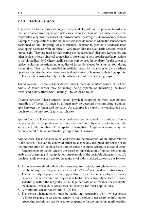
7.13 Tactile Sensors
In general, the tactile sensors belong to the special class of force or pressure transducers
that are characterized by small thicknesses, or to the class of proximity sensors that
respondtoaveryclosepresence(<1mm)orcontactbya“digit”—humanormechanical.
Examples of applications of the tactile sensors include robotics where the sensor can be
positioned on the “fingertip” of a mechanical actuator to provide a feedback upon
developing a contact with an object—very much like the live tactile sensors work in
human skin. They are used for fabricating the “touchscreen” displays, keyboards, and
otherdeviceswhereaphysical contact has tobe sensed.Averybroadareaof applications
is the biomedical field where tactile sensors can be used in dentistry for the crown or
bridge occlusion investigation, in studies of forces developed by a human foot during
locomotion. They can be installed in artificial knees for balancing of the prosthesis
operation, etc. Another interesting area is identification of humans by their fingerprints.
The tactile sensors loosely can be subdivided into several subgroups:
Touch Sensors. These sensors detect and/or measure contact forces at defined
points. A touch sensor may be analog, being capable of measuring the touch
force, and binary (threshold), namely—touch or no touch.
Contact Sensors. These sensors detect physical coupling between two objects,
regardless of forces. A touch by a finger may be detected by monitoring a contact
area between the finger and the panel. An example is a capacitive touchscreen on a
touch-sensitive monitor (e.g., smartphone).
Spatial Sensors. These sensors detect and measure the spatial distribution of forces
perpendicular to a predetermined sensory area or physical contacts, and the
subsequent interpretation of the spatial information. A spatial-sensing array can
be considered to be a coordinated group of touch sensors.
Slip Sensors. These sensors detect and measure the movement of an object relative
to the sensor. This can be achieved either by a specially designed slip sensor or by
the interpretation of the data from a touch sensor, contact sensor, or a spatial array.
Requirements to tactile sensors are based on investigation of human sensing and
analysis of grasping andmanipulation. An example of the desirable characteristics of a
touch or tactile sensor suitable for themajority of industrial applications are as follows:
1. A touch sensor should ideally be a single-point contact, through the sensory area
can be of any size. In practice, an area of 1–2 mm2 is considered satisfactory.
2. The sensitivity depends on the application, in particular any physical barrier
between the sensor and the object is a factor. For a force-type tactile sensor,
sensitivity within the range 0.4–10 N, together with an allowance for accidental
mechanical overload, is considered satisfactory for most applications.
3. A minimum sensor bandwidth of 100 Hz.
4. The sensor characteristics must be stable and repeatable with low hysteresis.
A linear response in an analog sensor is not absolutely necessary as information
processing techniques can be used to compensate for any moderate nonlinearities.
318 7 Detectors of Humans

If a tactile array is being considered, the majority of applications can
be undertaken by an array 10–20 sensors square, with a spatial resolution of
1–2 mm. In robotics and in design of prosthesis, a grasping force at a “finger” tip
should be measured. Thus, these tactile sensors can be integrated into the “skin” to
respond in real time, the magnitude, location, and direction of the forces at the
contact point.
7.13.1 Switch Sensors
A simple tactile sensor producing an “on-off” output can be formed with two
leaves of foil and a spacer (Fig. 7.44). The spacer has round (or any other
suitable shape) holes. One leaf is grounded and the other is connected to a pull-
up resistor. The grounded leaf may be a conductive cladding on a circuit board.
A multiplexer can be used if more than one sensing area is required. When an
external force is applied to the upper conductor over the hole in the spacer, the
top leaf flexes and upon reaching the lower conductor, makes an electric contact,
grounding the pull-up resistor. The output signal becomes zero indicating the
applied force. The upper and lower conducting leaves can be fabricated by a
silk-screen printing of conductive ink on the backing material, like Mylar® or
polypropylene. Multiple-sensing spots can be formed by printing rows and
columns by a conductive ink. Touching of a particular area on a sensor will
cause the corresponding row and column to join thus indicating force at a
particular location. These sensors are widely used in low cost consumer
products, such as TV remote controls and toys.
Fig. 7.44 Membrane switch as tactile sensor
7.13 Tactile Sensors 319

7.13.2 Piezoelectric Tactile Sensors
Efficient tactile sensors can be designed with piezoelectric films, such as
polyvinylidene fluoride (PVDF) used in the active or passive modes (see Sect.
4.6.2). An active ultrasonic coupling touch sensor with the piezoelectric films is
illustrated in Fig. 7.45 where three films are laminated together (there are also the
additional protective layers that are not shown in the figure). The upper and bottom
films are PVDF, while the center film is for the acoustic coupling between the two.
Softness of the center film determines sensitivity and operating range of the sensor.
A practical material for the center film is silicone rubber. The bottom piezoelectric
film acts as a vibration transmitter and is driven by an ac voltage from an oscillator.
This excitation signal results in mechanical contractions of the film that are coupled
to the compression film and, in turn, to the upper piezoelectric film, which acts as a
receiver. Since piezoelectricity is a reversible phenomenon, the upper film produces
alternating voltage upon being subjected to mechanical vibrations from the
compression film. These oscillations are amplified and fed into a synchronous
demodulator. The demodulator is sensitive to both the amplitude and the phase of
the received signal. When compressing force F is applied to the upper film, a
mechanical coupling between the three-layer assembly changes. This modulates
the amplitude and phase of the received signal. These changes are recognized by the
demodulator and appear at its output in form of a variable voltage.
Within certain limits, the output signal linearly depends on the force. If the
25 μm PVDF films are laminated with a 40 μm silicone rubber compression film,
the thickness of an entire assembly (including protective layers) does not exceed
200 μm. The PVDF film electrodes may be fabricated with a cell-like pattern on
either the transmitting or receiving side. This would allow to use an electronic
multiplexing of the cells to achieve spatial recognition of the applied stimuli.
The sensor also can be used for measuring small displacements. Its accuracy is
Fig. 7.45 Active piezoelectric tactile sensor
320 7 Detectors of Humans

better than �2 μm over a few millimeter range. Advantages of this sensor is in its
simplicity and a d.c. response, that is, in the ability to recognize static forces.
A piezoelectric tactile sensor for detecting touch and sliding motions can be
fabricated with the PVDF film strips imbedded into a rubber skin, Fig. 7.46a. This
sensor is passive, so the output signal is generated by the piezoelectric film without
the need for any excitation signal. As a result, it produces a response proportional to
the rate of stress, rather than to the stress magnitude. The design of this sensor is
tailored to the robotic applications where it is desirable to sense sliding motions
causing fast vibrations. The piezoelectric sensor is directly interfaced with a rubber
skin, thus the electric signal produced by the strips reflect movements of the elastic
rubber that are caused by the uneven friction forces.
The sensor is built on a rigid structure (a robot’s “finger”) which has a foamy
compliant underlayer (1 mm thick), around which a silicon rubber “skin” is
wrapped. It is also possible to use a fluid underlayer for a better smooth surface
tracking. Because the sensing strips are located at some depth beneath the skin
surface, and because the piezoelectric film responds differently in different
directions, a signal magnitude is not the same for movements in any direction.
The sensor responds with a bipolar signal, Fig. 7.46b, to surface discontinuity or
bumps as small as 50 μm high.
Electronics for musical instruments present a special problem in drums and
pianos. The very high dynamic range and frequency response requirements for
the drum triggers and piano keyboards are met by piezoelectric film impact
elements. Laminates of piezo film are incorporated in the foot pedal switches for
bass drums, and triggers for snares and tom-toms. The piezoelectric film impact
switches are force sensitive, faithfully duplicating the effort of the drummer or
pianist. In electronic pianos, the piezoelectric film switches respond with a dynamic
range and time constant that is remarkably similar to a piano keystrokes.
It should be noted that piezoelectric films mostly respond when stretched, while
compression generates much weaker signals. Thus, the designs should apply forces
along the film surface. This is illustrated in Fig. 7.47a where the longitudinal strain
in the film produces current i through the load resistor R0. The transverse force Fg
makes almost no signal. To resolve this difficulty, the film may be positioned or
Fig. 7.46 Tactile sensor with piezoelectric film for detecting sliding forces. Cross-sectional view
(a) and typical response (b) (adapted from [27])
7.13 Tactile Sensors 321

folded at an angle to the applied force as shown in Fig. 7.47b. The force vector Fg
can be replaced by a sum of two vectors: Fs and Fh, where vector Fs is parallel with
the film surface and thus causes a strain. This approach is illustrated in Fig. 7.48 that
shows the PVDF film sensor for detecting breathing rate of a sleeping child. The
minute movements of the child’s body resulted from respirations were monitored in
order to detect apnea—a cessation of breathing [28]. The sensor was placed under
the mattress in a crib. The body of a normally breathing baby slightly shifts
horizontally with each inhale and exhale due to a moving diaphragm in the chest.
The diaphragm movement causes displacement of the body’s center of gravity and
thus shifting horizontally the gravitational force Fg applied normally to the plane of
the mattress. This force movement is detected by the PVDF film sensor. The film
sheet has two electrodes deposited on its front and backsides. The sensor assembly
consists of three layers where the PVDF film is sandwiched between two preformed
pushers that are made, for instance, from silicone rubber.
The pushers have the corrugated or bump-shaped surfaces that squeeze the
PVDF film in-between the alternating bumps. The bumps fold the film and thus
apply a force to the film at an angle. Under a shifting force, the PVDF film is
Fig. 7.47 Piezoelectric film
responds to longitudinal
strain (a); applying force at anangle to film produces
response (b)
Fig. 7.48 Piezoelectric film respiration rate sensor
322 7 Detectors of Humans

variably stressed by the bumps and subsequently generates a variable electric
charge. The charge causes electric current flowing through the current-to-voltage
converter that produces the output voltage Vout. The amplitude of that variable
voltage within certain limits is proportional to the variations in gravitational force.
Operation of this sensor is similar to a piezoelectric cable placed under the mattress,
as illustrated in Fig. 10.11. Note that this design resembles the one shown in
Fig. 5.22 for the fiber-optic force sensor.
Small thickness, high sensitivity, and no energy consumption of the piezoelec-
tric film permits designing a great variety of medical sensors for monitoring minute
motions of human tissues. As an example, Fig. 7.49 shows recordings of the arterial
oscillations from two piezoelectric film sensors adhered to the patient’s skin over
the radial artery at two locations: wrist and middle arm.
7.13.3 Piezoresistive Tactile Sensors
Another type of a tactile sensor contains a piezoresistive element. It can be
fabricated by using materials having electrical resistance dependent on strain. The
sensor incorporates a force-sensitive resistor (FSR) whose resistance varies when
subjected to pressure [29]. The FSRs are conductive elastomers or pressure-
sensitive inks. A conductive elastomer is fabricated of silicone rubber, polyure-
thane, and other compounds that are impregnated with conductive particles or
fibers. For instance, conductive rubber can be fabricated by using carbon powder
as an impregnating material. Operating principles of the elastomeric tactile sensors
are based either on varying the contact area when the elastomer is squeezed
between two conductive parts, Fig. 7.50a, or on changing the elastomer thickness.
Fig. 7.49 Recording of arterial oscillations from two piezoelectric film sensors
7.13 Tactile Sensors 323

When the external force varies, a contact area at the interface between the pusher
and elastomer changes and the elastomer volume between the pusher and plate
becomes smaller, resulting in reduction of the electrical resistance.
At a certain pressure, the contact area reaches its maximum and the transfer
function, Fig. 7.50b, goes to saturation. The elastomer resistance Rs changes with
the force highly nonlinearly, however its reciprocal function, the conductivity a, isnearly linear with respect to the force:
a � kF; ð7:28Þwhere k is the force coefficient that depends on the elastomer conductive properties
and geometry. This linear feature may be utilized in the interface circuit shown in
Fig. 7.51a, where the force-sensitive resistor Rs is part of the resistive bridge
connected to an operational amplifier. The output voltage of the amplifier is a
nearly linear function of the applied force F:
Fig. 7.50 FSR tactile sensor. Through thickness application with elastomer (a); transfer functionfor resistance R0 and conductance a (b)
Fig. 7.51 Interface circuit for elastomer tactile sensor (a) and tactile sensor with polymer FSR (b)
324 7 Detectors of Humans

Vout ¼ VDD
2
R
Rs
� 1
� �� VDD
2Ra� 1ð Þ ¼ VDD
2RkF� 1ð Þ ð7:29Þ
It should be noted, however, that the elastomer conductivity may noticeably drift
when the polymer is subjected to prolonged pressure or temperature changes.
A thin FSR tactile sensor can be fabricated with a semiconductive polymer whose
resistance varies with pressure. A design of the sensor resembles a membrane
switch, Fig. 7.51b, [13]. Unlike a strain gauge, the FSR has a significantly wider
dynamic range: typically three decades of resistance change over a 0–3 kg force
range and a much lower accuracy (typically �10 %). However, in many
applications, where an accurate force measurement is not required, a low cost of
the sensor makes it an attractive alternative. A typical thickness of a FSR polymer
sensor is on the range of 0.25 mm (0.01000) but even thinner sheets are also available.A combination of a conductive rubber as FSR and the organic field effect
transistors (FET) as multiplexers allows fabrication of an electronic pressure-
sensitive skin suitable for robotic applications. The skin has of a multitude of the
miniature pressure sensors that is appended with a flexible switching matrix. The
organic FET is selected for the “skin” because organic circuits are inherently
flexible and potentially low in cost, even for a large skin area [30]. An important
step in production of a good artificial “electronic skin” is to fabricate large-area
tactile sensors with mechanical flexibility. The organic FET transistors are
integrated within a graphite-containing rubber to form a wide area as illustrated
in Fig. 7.52a. The skin is electrically functional even when it is wrapped around a
cylindrical bar with only a 2-mm radius. A pitch of the embedded FETs is 10 dpi
that is sufficient for generating a recognizable image as shown in Fig. 7.52b.
The basic idea behind the sensor is to modulate electric currents through the
FETs by the variable rubber resistances attached to the FET drains and multiplex
the FETs by applying control voltages to the gates. Figure 7.52c illustrates connec-
tion of the FET into a matrix.
The overall configuration is similar to a memory cell or a pixel of a charge-
coupled device (CCD): gate electrodes of each line are connected to a word line,
whereas drain electrodes are connected to a bit line. As pressure is applied on the skin
in the vicinity of a particular cell and varies from 0 to 30 kPa (�300 g force/cm), the
resistance of the rubbery sheet varies from 10 MΩ to 1 kΩ and the transconductance
of the FET, as well as the measured current iD, increases.
Fig. 7.52 Electronic skin with embedded organic FETs (a), 16� 16 FET matrix responds to a
“kiss” by a lip-shaped rubber stamp (b), and connection of FET (c). (Adapted from [30])
7.13 Tactile Sensors 325

7.13.4 Tactile MEMS Sensors
Subminiature tactile sensors are especially in high demand in robotics, where a
good spatial resolution, high sensitivity, and wide dynamic range are required. A
plastic deformation in silicon can be used for fabrication of a threshold tactile
sensor with a mechanical hysteresis [31]. In one design [32], the expansion of
trapped gas in a sealed cavity formed by wafer bonding is used to plastically deform
a thin silicon membrane bonded over the cavity, creating a spherically shaped cap.
The structure shown in Fig. 7.53 is fabricated by MEMS processing a silicon wafer.
At normal room temperature and above the critical force, the upper electrode will
buckle downward, making contact with the lower electrode. Experiments have
shown that the switch has hysteresis of about 2 psi of pressure with a closing action
near 13 psi. The closing resistance of the switch is on the order of 10 kΩ, which for
the micropower circuits is usually low enough.
7.13.5 Capacitive Touch Sensors
A capacitive touch sensor is based on fundamental equations for the parallel-plate
and coaxial capacitors (Sect. 4.2). A capacitive touch sensor relies on the applied
force that either changes the distance between the plates or varies surface area of the
capacitor electrodes (plates). In the sensor two conductive plates are separated by a
dielectric medium, which may also be used as an elastomer to give the sensor its
force-to-capacitance characteristics, Fig. 7.54a.
To maximize change in the capacitance when force is applied, it is preferable to
use a high-permittivity dielectric polymer such as polyvinylidene fluoride (PVDF).
To measure change in a capacitance, a number of techniques can be employed. If
the capacitor is not too small (on the order of 1 nF or larger), the most popular
technique is using a current source with a resistor and measure a time delay caused
by a variable capacitance. Another approach is using a capacitive sensor as part of
an oscillator with an LC or RC circuit, and measuring the frequency response.
Significant problem with capacitive sensors may arise if they are in close proximity
Fig. 7.53 Micromachined
silicon threshold switch with
trapped gas (from [16])
326 7 Detectors of Humans

with metal structures. The effect can be minimized by a good circuit layout and a
differential capacitor design.
Capacitive sensors are popular in touchscreen panels that typically are made of
glass or a clear polymer coated with a transparent conductor such as indium tin
oxide (ITO) that combines electrical conductivity and optical clarity. This type of a
sensor is basically a capacitor in which the plates are the overlapping areas between
the horizontal and vertical axes in a grid pattern. Each plate may be a dual-
interdigitized or single-plate electrode (Fig. 7.54b). Since a human body has a
high dielectric constant, touching the sensor electrode will affect distribution of the
electric field around the contact and create a measurable change in the capacitance.
These sensors work on proximity of the conductive medium (finger), thus they do
not have to be directly touched for triggering. It is a durable technology that has
been used in a wide range of applications including point-of-sale systems, industrial
controls, and public information kiosks. However, it only responds to a finger
contact and will not work with a gloved hand or pen stylus unless the stylus is
conductive.
Many popular touchscreens for computer monitors employ capacitive sensors.
The screen is formed of glass where each sensing element has two electrodes
deposited on the glass inner surface as shown in Fig. 7.55a. One of the electrodes
(G) is grounded and the other is connected to the capacitance meter (C-meter).
Some small baseline capacitance C0 exists between the two electrodes and that
capacitance is monitored by the C-meter.
When a finger comes in proximity of the electrodes (Fig. 7.55b), it develops with
each electrode a capacitive coupling C1. In response, the capacitance monitor will
register a new combined capacitance
Cm1 ¼ C0 þ 0:5C1; ð7:30Þwhich is much larger than C0. If the finger is pressed harder, due to the fingertip
elasticity the contact area with the touchscreen increases and that causes a larger
capacitive coupling C2>C1 as shown in Fig. 7.55c. This will further increase the
combined monitored capacitance and thus can be used as an indication of a harder
pressing.
Fig. 7.54 Capacitive parallel-plate touch sensor (a); interdigitized and single electrodes for
touchscreen (b)
7.13 Tactile Sensors 327

Now, let us assume that a droplet of water is deposited on the touchscreen above
the electrodes as shown in Fig. 7.55d. Being electrically conductive with a dielec-
tric constant between 76 and 80, water forms with the electrodes a strong coupling
C3 which is comparable with that of a finger and, as a result, the touchscreen will
indicate a false touch. Sensitivity to water droplets is a disadvantage of a dual-
electrode touchscreen where one electrode is grounded.
To resolve sensitivity to water droplets, an improvement of a capacitive
touchscreen that contains a single-electrode pattern was proposed [33]. No elec-
trode in that screen is grounded. Under the no-touch condition, only a small
capacitance Cg exists between the electrode and ground (earth) as indicated in
Fig. 7.56a and it is monitored by a C-meter. A human body naturally forms a strong
capacitive coupling CB to the surrounding objects. This capacitance is several
orders of magnitude larger than C0. Hence, a human body may be considered
Fig. 7.55 Dual-electrode touchscreen. No touch (a), light touch (b), strong touch (c) and water
droplet (d)
Fig. 7.56 Single electrode touchscreen. No touch (a), light touch (b), strong touch (c), waterdroplet (d), and touching through water droplet (e)
328 7 Detectors of Humans

having a low impedance to “ground”. When a finger comes into vicinity of the
electrode (Fig. 7.56b), a capacitance C1 is formed between the fingertip and
electrode. This capacitance is electrically connected in parallel with the baseline
capacitance C0, causing the C-meter to respond. Like in a two-electrode screen, a
stronger pressing will create a larger capacitance as shown in Fig. 7.56c. However,
when a water droplet is deposited on the screen (Fig. 7.56d), it will cause no false
detection as the water droplet is not couplet to ground. It is interesting to note that as
shown in Fig. 7.56e touching the water droplet will form a capacitive coupling to
ground and the touch will be correctly detected. Therefore, this electrode arrange-
ment is more robust under the adverse environmental conditions. Arranging the
electrode pattern in rows and columns and processing signals by the appropriate
circuit can make a reliable spatial touch recognition by an special electronic circuit
such as, for example, the Fujitsu controller FMA1127. A similar approach can be
used to form proximity detectors on surfaces of many shapes. For example, a
proximity sensor can be formed on a doorknob for the security purposes. It will
respond not only to touching but even to approaching the door knob surface by as
far as 5 cm.
A multielement capacitive “skin” can be developed for covering larger areas of
complex shapes, such as the robot’s arms shown in Fig. 7.57a. The skin is a
combination of modules that are the sensing arrays having 16� 16 matrix of
miniature-sensing elements [34]. Each element is comprised of a flexible molded
elastomer having a small pusher on the top and a cavity inside as shown in Fig. 7.58.
The cavity is sandwiched between two electrodes: the stationary and movable that
form the baseline capacitance C0. When an external force is applied to the pusher,
the cavity collapses bringing the electrodes closer to one another. This results in
change in capacitance that for a full compression more than doubles as shown in the
response curves of Fig. 7.57b.
Fig. 7.57 Modules of sensing arrays form robotic skin (a). Normalized change of capacitance for
different skin thicknesses (b)
7.13 Tactile Sensors 329

7.13.6 Optical Touch Sensors
A conventional optical-touch systems uses an array of infrared (IR) light-emitting
diodes (LEDs) on two adjacent bezel edges of a display, with the photodetectors
placed on two opposite bezel edges to analyze the system and determine a touch
event (Fig. 7.59). The LED and photodetectors pairs create a grid of light beams
across the display. An object (such as a finger or pen) that touches the screen
changes reflection due to a difference between refractive properties of air and a
finger. Since the acrylic or glass refractive index n2 is larger then the human skin
refractive index n2, at the point of touch, the angle of total internal reflection (TIR)
increases. This results in a light beam passing through the boundary to the skin and
not being transmitted toward the detector (see detailed explanation in the next
Sect. 7.13.7). This results in a measured decrease in the detected light intensity. The
photodetector output signals can be used to locate the touch-point coordinate.
Widespread adoption of infrared touchscreens has been hampered by two
factors: a relatively high cost of the technology compared to competing
capacitive technologies and somewhat reduced performance in bright ambient light.
Fig. 7.59 Concept of optical touchscreen
Fig. 7.58 Cross-sectional view of the sensing element (a). Sensing cavity collapses under
external force (b)
330 7 Detectors of Humans

The latter problem is the result of background light increasing the noise floor at
the photodetectors, sometimes to such a degree that the touchscreen’s LED light
cannot be detected at all, causing a temporary failure of the touchscreen. This is
most pronounced in direct sunlight conditions since the sun emanates very high
energy in the infrared region.
However, certain features of the infrared touch remain desirable and represent
attributes of the ideal touchscreen, including the option to eliminate the glass or
plastic overlay that most other touch technologies require in front of the display.
In many cases, this overlay is coated with an electrically conducting transparent
material such as ITO, which reduces the optical quality of the display.
This advantage of the optical touchscreens is important for applications that require
higher clarity.
7.13.7 Optical Fingerprint Sensors
Fingerprints are one of many forms of biometrics used for identifying and verifying
individuals. A fingertip recognition is employed by various security systems,
personal banking, medical records, and device protection. The analysis of
fingerprints for the matching with a database generally requires a comparison of
several features of the print pattern. These include the aggregate characteristics of
ridges and minutia points, which are unique features. To identify a touch by a
particular human finer tip, the pattern of the skin surface shall be reliably
recognized. Before performing the recognition, first a quality image shall be
obtained by a special fingertip sensor. Sensors for such detections include ultra-
sonic, capacitive, and optical. Below we discuss the optical sensor whose operating
principle is based on differences between refractive indices of glass, air, and human
skin. Figure 7.60 illustrates a conceptual design of the sensor. Its key element is a
glass prism with the base surface facing up. A light source (for example, LED) with
a collimator lens produces parallel beams of light that enter the prism and, in
Fig. 7.60 Optical fingerprint sensor uses a difference between refractive indices of glass (n2) andskin (n1)
7.13 Tactile Sensors 331

absence of a finger, are being reflected towards the imaging camera. Light is
reflected from the base surface because the rays enter at angles that exceed the
angle of total internal reflection or TIR (see Sect. 5.7.2). The TIR can be computed
from Eq. (5.26). A prism made of crown glass has a refractive index n2¼ 1.52, thus
the TIR for a boundary with air (refractive angle n¼ 1) is 41�. Since the light raysenter at larger angles of about 45�, they are fully diverted toward the imaging
camera that registers a uniform light surface.
When a fingertip touches the prism surface, the contacts occur only at the skin
ridges while the skin valleys have air trapped inside. As a result, two types of the
boundaries form on the prism surface: glass-skin and glass-air. Since a typical skin
refractive index in the visible and near-infrared spectral ranges is about n1¼ 1.38
[35], the glass-skin boundary forms the TIR angle:
Θ2�1 ¼ arcsinn1n2
� �¼ arcsin
1:38
1:52
� �� 65∘ ð7:31Þ
This wide TIR angle does not reflect the light rays x arriving at 45� and passes
them outside of the prism where they are lost and do not reach the camera. From
these spots, the camera registers black. On the other hand, the skin valleys have
trapped air, thus their TIR remains 41� and the light rays w are reflected toward the
camera, forming the white areas. A disadvantage of this method is that the sensor
may fail if the fingertip is wet or soiled with dirt that fills in the fingertip valleys.
References
1. Blumenkrantz, S. (1989). Personal and organizational security handbook. Washington, DC:
Government data publications.
2. Sarabia, E. G., et al. (2013). Accurate estimation of airborne ultrasonic time-of-flight for
overlapping echoes. Sensors, 13(11), 15465–15488.3. Kyrynyuk, V. et al. (2014), Automotive ultrasonic distance measurement for park-assist
systems. AN76530. cypress.com
4. McEwan, T. E. (1994, November 1). Ultra-wideband radar motion sensor. U.S. PatentNo. 5,361,070.
5. Azevedo, S. G., et al. (1995). Landmine detection and imaging using micropower impulse
radar (MIR). Proceedings of the Workshop on Anti-personnel Mine Detection and Removal,July 1, 1995, Lausanne, Switzerland (pp. 48–51).
6. Boles. S. et al. (1995). Signal processing for ultra-wide band impulse radar. U.S. PatentNo. 5381151.
7. Staderini, E. M. (2002). UWB radars in medicine. IEEE Aerospace and Electronic SystemsMagazine, 17(1), 13–18.
8. van Drecht, J., et al. (1991). Concepts for the design of smart sensors and smart signal
processors and their applications to PSD displacement transducers. In: Transducers‘91. Inter-national Conference on Solid-State Sensors and Actuators. Digest of technical papers(pp. 475–478). #IEEE.
9. Long, D. J. (1975, August 5). Occupancy detector apparatus for automotive safety system.U.S.Patent No. 3,898,472.
332 7 Detectors of Humans

10. Gao, X. (2013). Microchip capacitive proximity design guide. AN1492, DS01492A,
Microchip Technology Inc.
11. Fraden, J. (1991, May 28). Apparatus and method for detecting movement of an object. U.S.Patent No. 5,019,804.
12. Fraden, J. (1984, May 22). Motion discontinuance detection system and method. U.S. PatentNo. 4,450,351.
13. Fitz Gerald, A. S. (1932, February 4). Photo-electric system. U.S. Patent No. 2,016,036.14. Fraden, J. (1984, October 30). Toy including motion-detecting means for activating same.U.S.
Patent No. 4,479,329.15. Fraden, J. (1988, September 6). Motion detector. U.S. Patent No. 4,769,545.16. Fraden, J. (1990, January 23). Active infrared motion detector and method for detecting
movement. U.S. Patent No. 4,896,039.17. Fraden, J. (1992). Active far infrared detectors. In: Temperature. Its measurement and control
in science and industry (Vol. 6, Part 2, pp. 831–836). New York: #AIP.
18. APDS-9700. (2010). Signal conditioning IC for optical proximity sensors. Avago
Technologies. www.avagotech.com
19. Parsons, N. E., et al. (2003, September 16). Automatic flow controller employing energy-
conservation mode. U.S. Patent No. 6,619,614.20. Parsons, N. E., et al. (2008, July 8). Passive sensors for automatic faucets and bathroom
flushers. U.S. Patent No. 7,396,000.21. Fraden, J. (2007, August 31). Alarm system with air pressure detector. U.S. Patent Publication
No. US 2008/0055079.22. Fraden, J. (2009, February 17). Detector of low levels of gas pressure and flow. U.S. Patent
No. 7,490,512.23. Kirsch, S. T. (1985, October 8). Detector for electro-optical mouse. U.S. Patent No. 4546347.24. Theremin, L. (1928, February 28). Method of and apparatus for the generation of sounds. U.S.
Patent No. 1661058.25. Silicon Laboratories Inc. (2011). Infrared gesture sensing. AN580. www.silabs.com26. Microchip Technology. (2013). Gest IC design guide: Electrodes and system design.
MGC3130. Microchip Technology.
27. Measurement Specialties. (1999, April). Piezo film sensors technical manual. Norristown, PA:
Measurement Specialties. www.msiusa.com
28. Fraden, J. (1985). Cardio-respiration transducer. U.S. Patent No. 4509527.29. Del Prete, Z., et al. (2001). A novel pressure array sensor based on contact resistance variation:
Metrological properties. Review of Scientific Instruments, 72(3), 1548–1553.30. Someya, T., et al. (2004). A large-area, flexible pressure sensor matrix with organic field-effect
transistors for artificial skin applications. Proceedings of the National Academy of Sciences ofthe United States of America, 101(27), 9966–9970.
31. Mei, T., et al. (2000). An integrated MEMS three-dimensional tactile sensor with large force
range. Sensors and Actuators, 80, 155–162.32. Huff, M. A., et al. (1991). A threshold pressure switch utilizing plastic deformation of silicon.
In: Transducers‘91. International Conference on Solid-State Sensors and Actuators. Digest oftechnical papers (pp. 177–180). #IEEE.
33. Fujitsu Michroelectronics America. (2009). Touch screen controller technology and applica-tion trends. Fujitsu Technology Backgrounder.
34. Lee, H.-K., et al. (2006). A flexible polymer tactile sensor: Fabrication and modular
expandability for large area deployment. Journal of Microelectromechanical Systems, 15(6),1681–1686.
35. Ding, H., et al. (2006). Refractive indices of human skin tissues at eight wavelengths and
estimated dispersion relations between 300 and 1600 nm. Physics in Medicine and Biology, 51,1479–1489.
36. Parsons, N. E., et al. (1999, November 16). Object-sensor-based flow-control system
employing fiber-optic signal transmission. U.S. Patent No. 5,984,262.
References 333

Presence, Displacement, and Level 8
There are two ways of making progress.One is to do something better,
the other is to do something for the first time.
Detectors of presence indicate position of an object at a selected position or within apredefined system of coordinates. By definition, the presence detector is a static,
time invariant device.
Displacement is a shift of an object from one position to another for a specific
distance or angle. Displacement is measured when the object is referenced to its
own prior position rather than to an external reference or coordinates. Yet, regard-
less of the reference, measurements of displacement and position are closely related
and thus many sensors designed for a position can be used for measuring shifting
(displacement).
Proximity detectors indicate when a critical distance is reached. These detectors
may be responsive to either live or inanimate objects. Detection of live subjects was
described in Chap. 7. In effect, a proximity sensor is a threshold version of a
position detector. A position sensor measures distance to the object from a certain
reference point, while a proximity sensor generates output signals when a certain
distance to the object has reached. For instance, many moving mechanisms in
process control and robotics use a simple proximity sensor—the end switch. It is
a mechanical electrical switch having normally open or normally closed contacts.
When a moving object activates the switch by a physical contact, the switch sends a
signal to the control circuit. The signal is an indication that the object has reached
the end position. Obviously, such contact switches have several drawbacks, among
which are a mechanical load on a moving object and hysteresis. Displacement and
proximity often are measured by the same sensors.
Displacement sensors are the essential parts of many complex sensors where
detection and gauging of shifting of a sensing component is one of several steps in a
signal conversion. For example, Fig. 7.36 illustrates a special kind of an air pressure
# Springer International Publishing Switzerland 2016
J. Fraden, Handbook of Modern Sensors, DOI 10.1007/978-3-319-19303-8_8335

sensor where a variable air pressure is translated into displacement of a membrane.
Subsequently, the displacement is converted into the electrical output signal
representing the pressure variations. It is fair to say that displacement sensors are
the most widely employed sensors.
When describing displacement sensors in this chapter we consider them as the
zero-order devices (see Sect. 3.16) that instantly respond to stimuli. Thus, we do not
discuss responses that are functions of time, which by definition, relate to dynamic
sensors. Those sensors are covered elsewhere in this book. Here we will concern
only with the mechanisms of converting a displacement into electrical output.
When designing or selecting displacement sensors, first, the following questions
should be answered:
1. How big is the displacement and of what type (linear, circular)?
2. What resolution and accuracy are required?
3. What is the measured (moving) object made from (metal, plastic, fluid, ferro-
magnetic, etc.)?
4. How much space is available for mounting the detector?
5. What are the environmental conditions (humidity, temperature, sources of inter-
ference, vibration, corrosive materials, etc.)?
6. How much power is available for the sensor?
7. How much mechanical wear can be expected over the lifetime of the device?
8. What is the production quantity of the sensing assembly (limited number,
medium volume, mass production)?
9. What is the target cost of the detecting assembly?
A careful analysis will pay big dividends in the long term.
8.1 Potentiometric Sensors
A presence or displacement transducer may be built with a linear or rotary potenti-ometer, or a pot for short. The operating principle of this sensor is based on
Eq. (4.54) for a wire resistance. From the formula, it follows that a resistance
linearly relates to the wire length. Thus, by making an object to control the length of
the wire, as is done in a pot, a displacement measurement can be performed. Since a
resistance measurement requires passage of electric current through the pot wire,
the potentiometric transducer is an active type. That is, it requires an excitation
signal, for instance, d.c. current. A moving object is mechanically coupled to the
pot wiper, whose movement causes the resistance change (Fig. 8.1a). In many
practical circuits, a resistance measurement is replaced by a measurement of
voltage drop. Voltage across the wiper of a linear pot is proportional to the
displacement d
v ¼ v0d
D; ð8:1Þ
336 8 Presence, Displacement, and Level

where D is the full-scale displacement, and v0 is excitation voltage across the pot.
This assumes that there is no electrical loading effect from the interface circuit. If
there is an appreciable load, the linear relationship between the wiper position and
output voltage will not hold. The output signal is proportional to the excitation
voltage applied across the sensor. This voltage, if not maintained constant, may be a
source of error. This issue may be resolved by using a ratiometric analog-to-digital
converter (ADC) in a microcontroller (see Sect. 6.4.7), so the voltage influence will
be cancelled. A potentiometric sensor with respect to the pot resistance is a
ratiometric device, hence resistance of the pot is not part of the equation, as long
as the resistive element is uniform over its entire length. In other words, only a ratio
of the resistances is important, not the resistance value. This means that the pot
stability (for instance, over a temperature range) makes no effect on accuracy. For
low-power applications, high impedance pots are desirable, however, the loading
effect must be always considered, thus a voltage follower may be required. The
wiper of the pot is usually electrically isolated from the sensing shaft. To illustrate
an application of a potentiometric sensor, Fig. 8.1b shows a liquid level sensor with
a float being connected to the potentiometer wiper. Different applications require
different potentiometer designs, some of which are illustrated in Fig. 8.1c.
Figure 8.2a shows one problem associated with a wire-wound potentiometer.
The wiper may, while moving across the winding, make contact with either one or
two wires, thus resulting in uneven voltage steps, Fig. 8.2b, or a variable resolution.
Therefore, when a coil potentiometer with N turns is used, only the average
resolution n should be considered
n ¼ 100=N%: ð8:2ÞThe force which is required to move the wiper comes from the measured object
and the resulting energy is dissipated in form of heat. Wire-wound potentiometers
are fabricated with thin wires having a diameter in the order of 0.01 mm. A good
coil potentiometer can provide an average resolution of about 0.1 % of FS (full
scale), while the high-quality resistive film potentiometers may yield an infinitesi-
mal (continuous) resolution which is limited only by uniformity of the resistive
Fig. 8.1 Potentiometer as position sensor (a); fluid level sensor with float (b); linear
potentiometers (c)
8.1 Potentiometric Sensors 337

material and noise floor of the interface circuit. The continuous resolution pots are
fabricated with conductive plastic, carbon film, metal film, or a ceramic-metal mix,
known as cermet. The wipers of precision potentiometers are made from precious
metal alloys. Angular displacements sensed by the angular potentiometers may
range from approximately 10� to over 3000� for the multiturn pots (with gear
mechanisms).
A concept of another implementation of a potentiometric position sensor with a
continuous resolution is shown in Fig. 8.3. The sensor consists of two strips—the
upper strip is made of flexible plastic sheet having a metalized surface. This is a
contact or wiper strip. The bottom strip is rigid and coated with a resistive material
of a total resistance ranging from several kiloohms to Megaohms. The upper
conductive strip (wiper) and the bottom resistive strip are connected into an electric
circuit. When a pusher (e.g., a fingertip) is pressed against the upper strip at a
specific distance x from the end, the contact strip flexes, touching the bottom strip
and making en electric contact at the pressure point. That is, the contact strip works
as a wiper in a pot. The contact between two strips changes the output voltage from
E to ERx/R0 which is proportional to distance x from the left side of the sensor.
Fig. 8.2 Uncertainty caused by wire-wound potentiometer. Wiper may contact one or two wires
at a time (a); uneven voltage steps (b)
Fig. 8.3 Principle of a pressure-sensitive potentiometric position sensor
338 8 Presence, Displacement, and Level

Practical examples of various shapes of the pressure-sensitive potentiometers
are shown in Fig. 8.4a where a resistive layer is deposited on a polyester substrate.
The pusher (wiper) slides along the sensor causing a variable output voltage,
Fig. 8.4a, b. The overall resistance varies from 1 to 100 kΩ with a wiper force being
in the range from 1 to 3 N. Note that the wipers should be fabricated of a slippery
material, such as derlin or nylon. Alternatively, a roller can be used as a wiper.Another interesting potentiometric sensor uses the piezoresistive properties of
carbon-impregnated plastics. The operating principle of such a sensor is based on
change in resistance in response to a mechanical deformation. Carbon-impregnated
layer is deposited on a substrate that is fabricated of polyester, fiberglass, or
polyimide. When deformed, the carbon particles density varies and subsequently
varies the overall resistance. It is the same principle that is used in strain gauges and
is the basis of a Flex Sensor, Fig. 8.5a. Such sensors may be used for motion control,
medical devices, musical instruments, robotics, and other devices where bends or
mutual rotation of joined parts have to be monitored. It should be noted that the
bend sensors change resistance to any deformation of the substrate, including local
multiple bends and linear stresses. Also, they possess a very noticeable hysteresis
and may be the source of noise.
While being quite useful in many applications, potentiometers with contact
wipers have several drawbacks:
1. Noticeable mechanical load (friction)
2. Need for a physical coupling with the object
3. Low speed
Fig. 8.4 Various shapes of pressure-sensitive potentiometers (a), wiper with spring-loaded tip (b)and circular SoftPot with wiper (c) (Courtesy of spectrasymbol.com)
Fig. 8.5 Flex Sensor (a) and MagnetoPot (b) (Courtesy of spectrasymbol.com)
8.1 Potentiometric Sensors 339

4. Friction and excitation voltage cause heating of the potentiometer
5. Low environmental stability (wear, susceptibility to dust, etc.).
6. Large size
A potentiometric sensor where the physical contact between the wiper and a
resistive layer and thus friction are eliminated uses a wiper layer impregnated with
ferromagnetic particles. When an external magnetic filed is present at a specific
location above the potentiometer, the contact layer is pulled up to the conductive
layer making an electrical contact, just like the wiper in Fig. 8.3. This magnetic
potentiometer is sealed so it can be used as an immersed sensor for measuring, for
example, level of a liquid. It is important to select the appropriate magnet that is
sufficiently strong for the sensor operation (see Sect. 4.3.2). Even though such a
contactless potentiometer has no friction, a magnetic drag is still a force that
opposes the magnet motion. That force should be considered and accounted for in
the sensitive applications.
8.2 Piezoresistive Sensors
The piezoresistive effect (see Sect. 4.5.3) is the change of material electrical
resistance in response to stress or material deformation. A stress/strain-sensitive
resistor can be incorporated into a mechanical structure that is deformed and the
resistance change and amount of strain is calculated to relate them to a deformation.
Sensitivity of a piezoresistive element is quantified as gauge factor, which is
defined as the relative change in resistance per unit strain ε:
G ¼ Δr=rε
ð8:3Þ
By considering Eq. (4.54), a normalized change in the piezoresistance can be
expressed as:
Δrr
¼ Δρρ
þ Δ l=að Þl=a
¼ Δρρ
þ Δll� Δa
a
� �; ð8:4Þ
where ρ is the specific resistivity, l is the length and a is a cross-section area of the
sensing resistor. Thus, the sensor’s response depends on the material resistive
properties and geometry. To illustrate the how sensor converts displacement to
electrical output, Fig. 8.6a shows a plate that is supported by several silicon beams.
One of the beams has two strain-sensitive resistors, rx1 and rx2, embedded into its
upper and lower sides respectively. An external force pushes the plate downward by
distance d. The plate shifts to a new position, bending and straining the supporting
beams, which subsequently deform the embedded piezoresistors. Note that when
the plate goes down, the upper resistor rx1 is stretched, so its resistance increases,
while the lower resistor rx2 is compressed, causing the resistance decrease.
340 8 Presence, Displacement, and Level

Both resistors are connected to a Wheatstone bridge circuit that converts the
resistance changes to a voltage change, representing the plate displacement. This
type of displacement sensors is widely used with the Micro-Electro-Mechanical
Systems (MEMS) technologies for fabricating force and pressure sensors,
accelerometers, and many other sensors that require displacement transducers for
their operations.
A piezoresistor embedded in a thin MEMS beam must be localized as close to
the cantilever surface as possible for maximizing sensitivity. A choice must also
be made as to the dopant type and resistor orientation to achieve good sensitivity.
The sensitivity of a piezoresistor varies proportionately to the doping thickness.
The gauge factor of Eq. (8.3) can be calculated directly by straining the cantilevers
and measuring the resistance change. An example response of a Si piezoresistor to a
beam deflection is shown in Fig. 8.6b.
Progress in nanotechnologies allows development of sensitive displacement
sensors on a nanoscale with use of carbon nanotubes (CNT) [1, 2]. A CNT strain
gauge contains a large number of nanotubes attached in parallel between two
electrodes (Fig. 8.7). When due to strain, the electrodes move apart, the CNT
mesh stretches and its resistance increases accordingly. To allow bidirectional
measurements, at a zero-strain the CNT network is prestressed (biased), so the
electrodes can move closer or farther apart to modulate the resistance toward
decrease or increase.
Fig. 8.6 Displacement sensor with two piezoresistors embedded into supporting beam. Relative
dimensions and displacement are exaggerated for clarity (a); normalized resistance change as
function of the beam tip displacement for Si piezoresistor (b)
Fig. 8.7 Parallel carbon
nanotube mesh between
electrodes forms
subminiature strain gauge
sensor. (Adapted from [2])
8.2 Piezoresistive Sensors 341

8.3 Capacitive Sensors
The capacitive displacement sensors have very broad applications—they are
employed directly and also as building blocks in other sensors where displacements
are the result of force, pressure, temperature, acceleration, etc. The ability of
capacitive detectors to sense virtually all materials makes them an attractive choice
for many uses. Equation (4.20) defines that capacitance of a flat capacitor is
inversely proportional to distance between the plates and directly proportional to
the overlapping area of the plates. The operating principle of a capacitive gauge is
based on either changing the geometry (i.e., a distance between the capacitor plates
or the overlapping area), or variations in the dielectric materials positioned between
the plates. When the capacitance changes, it can be converted into a variable
electrical output signal by one of several well known circuits.
As it is with many sensors, a capacitive sensor can be either monopolar (usingjust one capacitor), differential (using two capacitors), or a capacitive bridge can beemployed (using four capacitors). When two or four capacitors are used, one or two
capacitors may be either fixed or variable, changing with the opposite phases.
As an introductory example, consider three equally spaced plates (Fig. 8.8a).
The plates form two capacitors C1 and C2. The upper and lower plates are fed with
the out-off-phase sinewave signals, that is, their signal phases are shifted by 180�.Both capacitors are nearly equal one another and thus the central plate has almost
no voltage with respect to ground—the charges on C1 and C2 cancel each other.
Now, let us assume that the central plate moves downward by distance x, Fig. 8.8b.This causes changes in the respective capacitance values:
C1 ¼ εA
x0 þ xand C2 ¼ εA
x0 � x; ð8:5Þ
and the central plate signal V increases in proportion to the displacement while the
phase of that signal is indication of the central plate direction—up or down. The
amplitude of the output signals is
Vout ¼ V0 � x
x0 þ xþ ΔC0
C0
� �: ð8:6Þ
Fig. 8.8 Operating principle of differential flat-plate capacitive sensor. Balanced (a) and
disbalanced (b) positions
342 8 Presence, Displacement, and Level

As long as x� x0, the output voltage may be considered a linear function of
displacement. The second summand represents an initial capacitance mismatch
and is the prime cause for the output offset. The offset is also caused by fringing
effects at the peripheral portions of the plates and by the so-called electrostatic force
that is a result of the charge attraction and repulsion which is applied to the plates of
the sensor, causing the plates to behave like springs. The instantaneous value of the
electrostatic force resulted from voltage difference on the plates ΔV is
F ¼ �1
2
CΔV2
x0 þ x: ð8:7Þ
In another design, two separate silicon plates are fabricated by using a MEMS
technology (Fig. 8.9). One plate serves for a displacement measurement, while the
other is for reference. Both plates have nearly the same surface areas, however the
measurement plate is supported by four flexible suspensions, while the reference
plate is held by the stiff suspensions. This particular design is especially useful for
accelerometers.
In many practical applications, especially when measuring a distance to an
electrically conductive object, the object’s surface itself may serve as a capacitor’s
plate. A design of a monopolar capacitive sensor is shown in Fig. 8.10, where one
Fig. 8.9 Dual-plate capacitive displacement sensor (adapted from [3]). Micromachined sensing
plate (a) and different suspensions for sensing and reference plates (b)
Fig. 8.10 Capacitive probe with guard ring. Internal view (a); outside view (b)
8.3 Capacitive Sensors 343

plate of a capacitor is connected to the central conductor of a coaxial cable, while
the other plate is formed by a target (object). Note that the probe plate is surrounded
by a grounded guard to minimize a fringing effect for improving linearity. A typical
capacitive probe operates at frequencies in the 3 MHz range and can detect very fast
moving targets, since a frequency response of a probe with a built-in electronic
interface is in the range of 40 kHz. A capacitive proximity sensor can be highly
efficient when used with electrically conductive objects. The sensor measures a
capacitance between the electrode and the object. Nevertheless, even for the
nonconductive objects, these sensors can be employed quite efficiently though
with lesser accuracy. Any object, conductive or nonconductive, that is brought in
the vicinity of the electrode, has its own dielectric properties that will alter the
capacitance between the electrode and the sensor housing and, in turn, will produce
a measurable response.
To improve sensitivity and reduce fringing effects, the monopolar capacitive
sensor may be supplied with a driven shield. The idea behind a driven shield is to
eliminate electric filed between the sensing electrode and undesirable parts of the
object, thus making the parasitic capacitance being virtually nonexistent (see
Fig. 7.19). A driven shield is positioned around the nonoperating sides of the
electrode and fed with voltage equal to that at the central electrode. Since the shield
and the electrode voltages are in-phase and have the same magnitude, no electric
field exists between the two and all components positioned behind the shield make
no effect on the operation. The driven shield technique for a capacitive proximity
sensor is illustrated in Fig. 8.11.
Nowadays, capacitive bridges become increasingly popular in designs of the
displacement sensors [4]. A linear bridge capacitive position sensor is shown in
Fig. 8.12a. The sensor comprises two planar electrode sets that are parallel and
adjacent to each other with a constant separation distance, d. For increasing
capacitance, spacing between the plate sets is made relatively small. The stationary
electrode set contains four rectangular elements while the moving electrode
set contains two rectangular elements. All six elements are of about the same size
Fig. 8.11 Driven shield around the electrode in capacitive proximity sensor
344 8 Presence, Displacement, and Level

(side dimension is b). The size of each plate can be as large as mechanically
practical, whenever a broad range of linearity is desired. The four electrodes of
the stationary set are cross-connected electrically, thus forming a bridge-type
capacitive network.
The bridge excitation source provides a sinusoidal voltage (5–50 kHz) and the
voltage difference between the pair of moving plates is sensed by a differential
amplifier whose output feeds the input of a synchronous detector. The capacitance
of two parallel plates at fixed separation distance is proportional to the overlapping
areas of either plate that directly faces the corresponding area of the other plate.
Figure 8.12b shows the equivalent circuit of the sensor that has a configuration of a
capacitive bridge. A value of capacitor C1 is
C1 ¼ ε0b
d
L
2þ x
� �ð8:8Þ
The other capacitances are derived from the identical equations. Note that the
opposite capacitors are nearly equal: C1¼C3 and C2¼C4. A mutual shift of the
plates with respect to a fully symmetrical position results in the bridge disbalance
and the phase-sensitive output of the differential amplifier. An advantage of the
capacitive bridge circuit is the same as of any bridge circuit—linearity and external
noise immunity. The same method can be applied to any symmetrical arrangement
of a sensor, for instant to detect a rotary motion.
8.4 Inductive and Magnetic Sensors
One of many advantages of using magnetic field for sensing position and distance is
that any nonmagnetic material can be penetrated by the filed with no loss of position
accuracy. Stainless steel, aluminum, brass, copper, plastics, masonry, and woods
can be penetrated, meaning that accurate position with respect to the probe at the
opposite side of a wall can be determined nearly instantly. Another advantage is
that the magnetic sensors can work in severe environments and corrosive situations
Fig. 8.12 Parallel-plate capacitive bridge sensor. Plate arrangement (a) and equivalent circuit
diagram (b). (Adapted from [5])
8.4 Inductive and Magnetic Sensors 345

because the probes and targets can be coated with inert materials that will not
adversely affect the magnetic fields. Before going further, it is recommended that
the readers should familiarize themselves with Sect. 4.4.
8.4.1 LVDT and RVDT
Position and displacement may be sensed by methods of electromagnetic induction.
A magnetic flux coupling between two coils is altered by movement of an object
and subsequently converted into voltage. Variable inductance sensors that use a
nonmagnetized ferromagnetic medium to alter the reluctance (magnetic resistance)
of the flux path are known as variable-reluctance transducers [6]. The basic
arrangement of a multi-induction transducer contains at least two coils—primary
and secondary. The primary one carries the ac excitation (Vref) that induces a steady
a.c. voltage in the secondary coil (Fig. 8.13). The induced amplitude depends on the
flux coupling between the coils. There are two techniques to change the coupling.
One is the movement of an object made of a ferromagnetic material within the flux
path. This changes the reluctance of the path, which, in turn, alters the coupling
between the coils. This is the basis for operation of LVDT (linear variable differ-
ential transformer), RVDT (rotary variable differential transformer), and the mutual
inductance proximity sensors. The other method is to physically move one coil with
respect to another.
Consider LVDT as a transformer with a mechanically actuated core. The
primary coil is driven by a sine wave (excitation signal) having a stabilized
amplitude. Sine wave eliminates error related harmonics in the transformer. An
a.c. signal is induced in the secondary coils. A core made of a ferromagnetic
material is inserted coaxially into the cylindrical opening without physically touch-
ing the coils. The two secondaries are connected in the opposed phase. When the
Fig. 8.13 Circuit diagram of
LVDT sensor
346 8 Presence, Displacement, and Level

core is positioned in the magnetic center of the transformer, the secondary output
signals cancel, and there is no output voltage. Moving the core away from the
central position unbalances the induced magnetic flux ratio between the
secondaries, developing an output. As the core moves, the reluctance of the flux
path changes. Hence, the degree of flux coupling depends on the axial position of
the core. At a steady state, the amplitude of the induced voltage is proportional, in
the linear operating region, to the core displacement. Consequently, voltage may be
used as measure of a displacement. The LVDT provides the direction as well as
magnitude of the displacement. The direction is determined by the phase angle
between the primary (reference) voltage and the secondary voltage. Excitation
voltage is generated by a stable oscillator. To exemplify how the sensor works,
Fig. 8.14 shows the LVDT connected to a synchronous detector that rectifies the
sine wave and presents it at the output as a d.c. signal. The synchronous detector is
comprised of an analog multiplexer (MUX) and a zero-crossing detector which
converts the sine wave into the square pulses compatible with the control input of
the multiplexer. A phase of the zero-crossing detector should be trimmed for the
zero output at the central position of the core. The output amplifier can be trimmed
to a desirable gain to make the signal compatible with the next stage, such as ADC.
The synchronized clock to the multiplexer means that the information presented to
the RC-filter at the input of the amplifier is the amplitude and phase sensitive. The
output voltage represents how far the core is from the center and on which side.
For LVDT to measure transient motions accurately, frequency of the oscillator
must be at least ten times higher than the highest significant frequency of the
movement. For a slow changing process, stable oscillator may be replaced by
coupling to a power line frequency of 60 or 50 Hz.
Fig. 8.14 Simplified circuit diagram of interface for LVDT sensor
8.4 Inductive and Magnetic Sensors 347

Advantages of the LVDT and RVDT are the following: (1) the sensor is a
noncontact device with no or very little friction resistance with small resistive
forces; (2) hysteresis (magnetic and mechanical) are negligible; (3) output imped-
ance is very low; (4) low susceptibility to noise and interferences; (5) construction
is solid and robust, (6) infinitesimal resolution is possible.
One useful application for the LVDT sensor is in the so-called gauge headswhich are used in tool inspection and gauging equipment. In that case, the inner
core of the LVDT is spring loaded to return the measuring head to a preset reference
position.
The RVDT operates on the same principle as LVDT, except that a rotary
ferromagnetic core is used. The prime use for the RVDT is measurement of the
angular displacements. A typical linear range of measurement is about �40� with anonlinearity error of about 1 %.
8.4.2 Transverse Inductive Sensor
Another electromagnetic position sensing device is called a transverse inductiveproximity sensor. It is useful for sensing relatively small displacements of ferro-
magnetic materials. As the name implies, the sensor measures the distance to an
object which alters the magnetic field in the coil. The coil inductance is measured
by an external electronic circuit (Fig. 8.15). A self-induction principle is the
foundation for the operation of this sensor. When it moves into the vicinity of a
ferromagnetic object, it magnetic field changes, thus altering inductance of the coil.
The advantage of the sensor is that it is a noncontact device whose interaction with
the object is only through magnetic field. An obvious limitation is that it is useful
only for the ferromagnetic objects at relatively short distances.
A modified version of the transverse transducer is shown in Fig. 8.16a. To
overcome the limitation for measuring only ferrous materials, a ferromagnetic
disk is attached to a displacing object while the coil has a stationary position.
Alternatively, the coil may be attached to the object and the core is stationary.
Fig. 8.15 Transverse
inductive proximity sensor
348 8 Presence, Displacement, and Level

This proximity sensor is useful for measuring small displacements only, as its
linearity is poor in comparison with LVDT. However, it is quite useful as a
proximity detector for indication of close proximity to an object which is made of
any solid material. Magnitude of the output signal as function of distance to the disk
is shown in Fig. 8.16b.
8.4.3 Eddy Current Probes
To sense proximity of nonmagnetic but conductive materials the effect of eddy
currents is employed in a dual-coil sensor (Fig. 8.17a).1 One coil is used as a
reference or receiving, while the other is for sensing the magnetic currents induced
in the conductive object. Eddy currents produce the magnetic field which opposes
that of the sensing coil, thus resulting in a disbalance with respect to the reference
coil. The closer the object to the coil the larger the change in the magnetic
impedance. The depth of the object where eddy currents are produced is defined by
δ ¼ 1ffiffiffiffiffiffiffiffiffiffiπfμσ
p ; ð8:9Þ
where f is the frequency and σ is the target conductivity. Naturally, for effective
operation, the object thickness should be larger than that depth. Hence, eddy
detectors should not be used for detecting film metallized or foil objects. Generally,
relationship between the coil impedance and distance to the object x is nonlinear
and temperature dependent. The operating frequency of the eddy current sensors
Fig. 8.16 Transverse sensor with auxiliary ferromagnetic disc (a) and output signal as function ofdistance (b)
1 See Sect. 4.4.2 for description of eddy currents.
8.4 Inductive and Magnetic Sensors 349

depends on physical dimensions. The small size probes (1–4 cm in diameter)
operate in the range from 50 kHz to 10 MHz.
Figure 8.17b, c shows two configurations of the eddy current probes: with the
shield and without one. The shielded sensor has a metal guard around the ferrite
core and the coil assembly. It focuses and directs the electromagnetic field to the
front of the sensor. This allows the sensor to be installed and even imbedded into a
metal structure with little influence on the detection range. The unshielded sensor
can sense at its sides as well as from the front. As a result, the detecting range of an
unshielded sensor is usually somewhat greater than that of the shielded sensor of the
same diameter; however, to operate properly, the unshielded sensors require non-
metallic surrounding objects.
In addition to position and motion detections, eddy sensors can be used to
determine material thickness, nonconductive coating thickness, conductivity and
plating measurements, and hidden cracks in the material. A crack detection and
surface flaws become the most popular applications for the sensors. Cracks inter-
rupt flow of eddy currents and result in abrupt change in the sensor’s output signal.
Depending on the applications, eddy probes may be of many coil configurations:
very small in diameter (2–3 mm), or quite large (25 mm). Some companies even
make custom designed probes to meet unique requirements of the customers (www.
olympus-ims.com). One important advantage of the eddy current sensors is that
they do not need magnetic material for the operation, thus they can be quite
effective at high temperatures (well exceeding the Curie temperature of a magnetic
material), and for measuring distance to or level of conductive liquids, including
molten metals. Another advantage of the detectors is that they are not mechanically
coupled to the object and thus the loading effect is very low.
Fig. 8.17 Electromagnetic proximity sensor with eddy currents (a). Sensor with shielded front
end (b); unshielded sensor (c)
350 8 Presence, Displacement, and Level

The eddy current proximity sensor shown in Fig. 8.17 is intended for detecting
relatively small distances to conductive objects. However, if the coil dimensions are
made substantially larger and its magnetic field is allowed to spread out further, the
same operating principle can be employed for detecting if not distance to, but at
least presence of a conductive object. Examples of other eddy currents detectors
include hand-held metal detectors, security gates for detecting presence of metal
objects on human subjects (e.g., for airports), and pavement loops for detecting
presence and passage of vehicles.
8.4.4 Pavement Loops
To monitor presence of a vehicle at a specific location—for controlling traffic
lights, opening gates, and generating warning signals, various sensors are currently
in use. They include digital cameras with the image processing software and the
in-ground magnetic sensors. The latter comprise large interconnected loops [7] that
are buried into a pavement and connected to an electronic control circuit shown in
Fig. 8.18a. Typically, several loops are serially connected for covering larger areas.
The control circuit contains an oscillator that generates sine-wave current ic (fre-quency is in the order of 10 kHz), that travels through the loops and produces
alternate magnetic fields below and above the ground surface. The fields that are
directed in-ground are of no interest for this device, while the above-ground fields
are used for detection.
The loops may have different shapes: circular, oval, or rectangular that are
shown in Fig. 8.18a. Note a mutual position of the wires 1 and 2 belonging to the
adjacent rectangular loops. The wires are specifically laid out for conducting
the excitation current ic in the same direction to prevent cancellation of a
magnetic field [8]. However, a cancellation would pose no problem if circular
loops are separated from one another by at appreciable distances of at least one
radius.
Fig. 8.18 Magnetic loops detect induced eddy currents (a); frequency signatures from various
vehicles (b)
8.4 Inductive and Magnetic Sensors 351

All loops in the network have a combined inductance LC that via a transformer is
brought in the LC resonant tank that controls the oscillator frequency fout:
fout ¼1
2πffiffiffiffiffiffiffiLC
p ; ð8:10Þ
where L is the combined tank inductance which defines the oscillator resonance.
In accordance with Eq. (4.42), the loop inductance is defined through its magnetic
flux Φ, number of wire turns n, and excitation current ic:
LC ¼ nΦic
ð8:11Þ
When no metal objects are present in vicinity of the loops, the combined loop
inductance LC remains constant and the oscillator produces a baseline frequency.
As soon as a vehicle enters the space above the loop, the magnetic flux induces eddy
currents ie in metal components of the vehicle. According to Lenz Law (see Sect.
4.4.1), these circular currents produce their own magnetic flux that opposes the
originating flux Φ. As a result, the net magnetic flux through the loop drops. From
Eq. (8.11) it follows that drop in a magnetic flux results in reduction in the loop
inductance LC. Subsequently, according to Eq. (8.10) the oscillator’s frequency
goes up and after demodulation it is used as indicator of the vehicle presence. This
frequency modulation represents several variables: the vehicle size and shape
(Fig. 8.18b), its speed of motion, position over the loops, weather conditions, etc.
8.4.5 Metal Detectors
Eddy currents are employed in various metal detectors. There are several design
options for the detectors, such as the number of loops (coils), their dimensions,
shapes, single- or multifrequency. Figure 8.19 illustrates a block diagram of a
double-loop single-frequency hand-held metal detector. It contains two closely
positioned coils working as a transformer. The generating coil is connected to the
output of a high frequency oscillator and used for producing a magnetic flux.
Fig. 8.19 Block diagram of double-loop metal detector
352 8 Presence, Displacement, and Level

The second coil is for receiving the flux and converting it back into an alternate
electric voltage that is amplified and demodulated. The design of the coils allows
magnetic flux to spread out at a significant range and form a sensing space
(Fig. 8.20). Any variations in flux measured by the receiving coil, if strong enough,
are the indications of conductive objects present in the sensing space. When a
conductive object (a mine, coin, metal jewelry, etc.) enters the sensing space, eddy
currents develop inside the object, close to its surface. The currents produce their
own magnetic fields that oppose and distort the magnetic field produced by the
generating coil. This distortion modulates voltage that is detected by the receiving
coil and after processing by the circuit, changes a pitch of sound in the speaker.
8.4.6 Hall-Effect Sensors
Probably the most widely used magnetic detectors are the Hall-effect sensors.2
Many smartphones and tablets employ these sensors for detecting the Earth mag-
netic field for controlling the electronic compasses.
The Hall sensors are produced in three configurations: analog (linear), bilevel
(digital), and integrated (multiaxial), as shown in Fig. 8.21. The analog sensors
usually incorporate amplifiers for easier interface with the peripheral circuits, they
operate over a broader voltage range, and are stable for a noisy environment. These
sensors are not quite linear (Fig. 8.22a) with respect to the magnetic field density
and, therefore, for precision measurements require a calibration. The end-of-span
nonlinearity may be up to �1.5 %. Besides, the linear sensor sensitivity is temper-
ature dependent [9].
A bilevel sensor, in addition to an amplifier, contains a Schmitt trigger with a
built-in hysteresis of the threshold levels. The output signal as function of a
magnetic field density is shown in Fig. 8.22b. The signal is bilevel and has a clearly
pronounced hysteresis with respect to the magnetic field. When the applied
Fig. 8.20 Magnetic field produced by generating coil (a); eddy currents in metal object distort
magnetic field (b)
2 See Sect. 4.8 for operating principle of the Hall sensor.
8.4 Inductive and Magnetic Sensors 353

magnetic flux density exceeds the upper threshold, the trigger provides a clean
positive transient from the OFF to ON position. When the flux drops and its signal
crosses the lower threshold, the transition is negative. The hysteresis eliminates
spurious oscillations by introducing a dead-band zone in which the action is
disabled after the threshold value has passed. The Hall sensors are usually
fabricated as monolithic silicon chips and encapsulated into small epoxy or ceramic
packages.
A much more complex sensor is a combination of several Hall-effect sensors as
shown in the block diagram of Fig. 8.21c. It is a system of three or more sensors that
detect magnetic field in all three spatial directions. Outputs from the orthogonal
Hall sensors are fed into the ADC, typically having a 15-bit resolution. A digital
Fig. 8.21 Circuit diagrams of linear (a), digital (b), and integrated (c) Hall-effect sensors
Fig. 8.22 Transfer functions of linear (a) and a threshold (b) Hall-effect sensors
354 8 Presence, Displacement, and Level

signal processor is programmable and the serial interface provides information on
both the intensity and spatial orientation of the magnetic field.
A Hall sensor responds only to the magnetic flux that is perpendicular to the
sensing-plate surface (see Fig. 4.30). Thus, the flux that is parallel to the die surface
(x- and y-directions) would not be sensed. To make the Hall sensors responsive to
the planar fluxes, either the magnetic filed lines should be rotated or the sensing pate
should be rotated. Rotation of the sensing plate in not practical, as that would
increase thickness of the sensor packaging and size of the die. Rotation of the
magnetic filed is accomplished by the so-called integrated magnetic concentrator or
IMC, for short [10]. The concept works as follows. Figure 8.23a illustrates a
conventional magnetic concentrator fabricated of a magnetic material, for example
of FeNi alloy. The concentrator has a gap where the Hall sensor is positioned.
The outside magnetic filed is attracted to the concentrator as it presents a path of
least resistance. Then, magnetic flux B inside the concentrator jumps across the gap.
In doing so, it fringes to the outside along the curved paths. The flux inside the gap
passes through the sensor in a normal (perpendicular) direction to the die plane.
This is a popular way of directing magnetic flux through a Hall sensor in many
practical applications. Yet, if the Hall sensor is rotated by 90� as shown in
Fig. 8.23b and positioned outside of the gap at its edges where the curved fringing
flux lines exist, some portion of the magnetic flux will be passing through the
rotated die at angles approaching normal and the Hall sensor will respond. In other
words, the IMS rotates the magnetic flux do direct it at the 90� angle to the sensingHall plate.
Note that in this arrangement, the die plane is parallel to the concentrator plane.
This allows an integration of a silicon die and a thin layer of the IMC in a small flat
chip. The ferromagnetic IMC film with a gap is deposited on the Hall plate.
Therefore, several Hall sensors may be positioned in a single flat die, yet they
will be responsive to three-dimensional magnetic fluxes. In practice, the IMC layer
may have various shapes: bars, discs, hexagons, etc., while its thickness is selected
in the order of 1 μm [11]. In the integrated sensor, the IMC layer is deposited on a
die surface by a sputtering technique (see Sect. 19.3.3).
For a position and displacement measurements of nonmagnetic materials, the
Hall-effect sensors should be provided with the magnetic field sources and interface
Fig. 8.23 Concepts of conventional magnetic concentrator (a) and integrated magnetic concen-
trator (b)
8.4 Inductive and Magnetic Sensors 355

electronic circuits. Magnetic field has two important characteristics for this appli-
cation—a flux density and polarity (or orientation). For a better responsivity,
magnetic field lines must be normal (perpendicular) to the flat face of the sensor
and be at a correct polarity. A magnetic flux concentrator is recommended to direct
flux to the correct section of the sensor.
Before designing a position or proximity detector with a Hall sensor, an overall
analysis should be performed in approximately the following manner.
The field strength of the magnet should be investigated.
The strength will be the greatest at the pole face, and will decrease with
increasing distance from the magnet.
The field may be measured by a gaussmeter or by a calibrated analog Hall
sensor. For a bilevel-type Hall sensor, the longest distance at which the sensor’s
output goes from ON (high) to OFF (low) is called a release point. It can be used todetermine a critical distance where the sensor is useful.
A magnetic field strength is not linear with distance and depends greatly upon
the magnet shape, the magnetic circuit, and the path traveled by the magnet. The
Hall conductive strip (plate) is situated at some depth within the sensor’s housing.
This determines the minimum operating distance. A magnet must operate reliably
with the total effective air gap in the working environment. It must fit the available
space, be mountable, affordable, and available.3
As a first example of the Hall sensor application, consider a liquid level detector
with a float (Fig. 8.24). A permanent magnet is imbedded inside a float having a
hole in the center. The float can freely slide up and down over the pole that is
positioned inside the tank containing liquid. The float position corresponds to the
liquid level. A bilevel Hall sensor is mounted at the top of the pole which should
be fabricated on a nonmagnetic material. When the liquid level rises and reaches the
detection level (release point), the Hall switch triggers and sends signal to
the monitoring device. When the liquid level drops below the release point plus
the threshold hysteresis, the output voltage changes indicating that the liquid level
dropped. The detection point depends on the key factors—the magnet strength and
shape, the Hall sensor’s sensitivity, the hysteresis, and presence of ferromagnetic
components in the vicinity of the Hall sensor.
The Hall sensors can be used with a flux interrupter attached to a moving object.
In this mode, the activating magnet and the Hall sensor are mounted on a single
rugged assembly of a flux concentrator, with a small air gap between them
(Fig. 8.25). Thus, the sensor is held in the ON position by the activating magnet.
If a ferromagnetic plate, or vane, is placed between the magnet and the Hall sensor,
the vane forms a magnetic shunt that diverts the magnetic flux away from the
sensor. This causes the sensor to flip to the OFF position. The Hall sensor and the
magnet could be molded into a common housing, thus eliminating the alignment
problem. The ferrous vanes which interrupt the magnetic flux could have linear or
rotating motion. An example of such a device is an automobile distributor.
3 For more information on permanent magnets see Sect. 4.3.2.
356 8 Presence, Displacement, and Level

Like many other sensors, four Hall sensors can be connected into a bridge circuit
to detect linear or circular motion. Figure 8.26a, b illustrates this concept where the
sensor is fabricated using MEMS technology on a single chip and packaged in a
SOIC-8 plastic housing. A circular magnet is positioned above the chip and its
angle of rotation and direction is sensed and converted into a digital code. The
properties of an ADC determine the maximum speed response, while the Hall
sensors allow the magnet to rotate with a rate of up to 30,000 rpm. Such an
Fig. 8.25 Bilevel Hall-effect sensor in interrupter switching mode. Magnetic flux turns sensor on
(a); magnetic flux is shunted by vane (b)
Fig. 8.24 Liquid level
detector with a Hall sensor
8.4 Inductive and Magnetic Sensors 357

integrated sensor permits a friction-free precision linear and angular sensing of
position, precision angular encoding, and even to make a programmable rotary
switch. Thanks to a bridge connection of the individual sensors, the circuit is highly
tolerant to the magnet misalignment and external interferences, including the
magnetic fields.
A rotary motion can be digitally encoded with high precision. To take advantage
of this feature, a linear distance sensor can be built with a converter of a linear into a
rotary motion as shown in Fig. 8.27. Such sensors are produced, for example, by
SpaceAge Control, Inc. (www.spaceagecontrol.com). A cable or thread is wound up
on a drum that is coaxially connected to a magnetic rotary encoder.
8.4.7 Magnetoresistive Sensors
These sensors are similar in application to the Hall-effect sensors, however, their
operating principle is quite different (see Sect. 4.3 and Fig. 4.13). Like the Hall
sensors, for functioning they require an external magnetic field. Hence, whenever
the magnetoresistive sensor is used as a proximity, position, or rotation detector it
must be combined with a source of a magnetic field. Usually, the field is originated
Fig. 8.26 Angular Hall-sensor bridge integrated circuit (a) and internal-sensor interface (b)(Courtesy of Austria Micro Systems: www.ams.com)
Fig. 8.27 Conversion of linear displacement (length of a thread or cable) into rotary motion (a)and cable position sensor (b) (Courtesy of SpaceAge Control, Inc.)
358 8 Presence, Displacement, and Level

in a permanent magnet that is attached to the sensor. Figure 8.28 shows a simple
arrangement for using a sensor-permanent-magnet combination to measure linear
displacement. It reveals some of the problems likely to be encountered if proper
account is not taken of the following effect. When the sensor is placed in the
magnetic field, it is exposed to the fields in both the x- and y-directions. As shown inFig. 8.28b, both vectors Hx and Hy vary with displacement x. If the magnet is
oriented with its axis parallel to the sensor strips (i.e., in the x-direction) as shown inFig. 8.28a, magnetic vectorHx then provides the auxiliary field, and the variation in
Hy can be used as a measure of x displacement. Therefore, the output signal
(Fig. 8.28c) has the same shape as the Hy vector.
Figure 8.29 shows how a magnetoresistive sensor can be useful for measuring
angular displacement. The sensor itself is located in the magnetic field produced by
two permanent magnets fixed to a rotable frame. The output of the sensor will then
be a measure of the rotation of the frame. Figure 8.30a depicts the use of a single
KM110B sensor for detecting rotation and direction of a toothed wheel. Note that
this sensor has a permanently attached magnet producing magnetic field in the x-direction. The method of directional detection is based on a separate signal
processing for the sensor’s two half-bridge outputs.
The sensor operates like a magnetic Wheatstone bridge measuring nonsymmet-
rical magnetic conditions such as when the teeth or pins move in front of the sensor.
The mounting of the sensor and the magnet is critical, so the angle between the
sensor’s symmetry axis and that of the toothed wheel must be kept near zero.
Fig. 8.28 Magnetoresistive
sensor in field of a permanent
magnet (a) as a function of itsdisplacement x parallel to the
magnetic axis (b); outputvoltage (c)
8.4 Inductive and Magnetic Sensors 359

Further, both axes (sensor’s and wheel’s) must coincide. The circuit of Fig. 8.30b
connects both bridge outputs to the corresponding amplifiers, and, subsequently, to
the low-pass filters and Schmitt triggers to form the rectangular output signals.
A phase difference between both outputs (Fig. 8.31a, b) is an indication of a rotation
direction.
Fig. 8.30 Optimum operating position of magnetoresistive module with permanent magnet is
positioned behind on sensor (a). Block diagram of module (b)
Fig. 8.29 Angular
measurement with the
KMZ10 sensor
Fig. 8.31 Output signal from the amplifiers for direction 1 (a) and 2 (b)
360 8 Presence, Displacement, and Level

8.4.8 Magnetostrictive Detector
A transducer which can measure displacement of an object with high resolution
across long distances can be built by using magnetostrictive and ultrasonic
technologies. The transducer is comprised of two major parts: a long waveguide
(up to 7 m long) and a permanent ring magnet (Fig. 8.32). The magnet can move
freely along the waveguide without touching it. A position of that magnet with
respect to the waveguide is the stimulus that is converted by the sensor into an
electrical output signal. A waveguide contains a conductor (conducting element),
which upon applying an electrical pulse, sets up a magnetic field over its entire
length. Another magnetic field produced by the permanent magnet exists only in its
vicinity. Thus two magnetic fields may be setup at the point where the permanent
magnet is located. A superposition of two fields results in the net magnetic field
which can be found from the vector summation. This net field, while being helically
formed around the waveguide, causes it to experience a minute torsional strain, or
twist at the location of the magnet. This twist is known as Wiedemann effect.4
Therefore, electric pulses injected into the waveguide’s coaxial conductor pro-
duce mechanical twist pulses which propagate along the waveguide with the speed
of sound specific for its material. When the pulse arrives to the excitation head of
4 Internally, ferromagnetic materials have a structure that is represented by domains, each of which
is a region of uniform magnetic polarization. When a magnetic field is applied, the boundaries
between the domains shift and the domains rotate, both these effects causing a change in the
material’s dimensions.
Fig. 8.32 Magnetostrictive detector uses ultrasonic waves to detect position of permanent magnet
8.4 Inductive and Magnetic Sensors 361

the sensor, the moment of its arrival is precisely measured. One way to detect that
pulse is to use a detector that can convert an ultrasonic twitch into electric output.
This can be accomplished by piezoelectric sensors, or as it is shown in Fig. 8.32, by
the magnetic reluctance sensor. The sensor consists of two tiny coils positioned
near two permanent magnets. The coils are physically coupled to the waveguide
and can jerk whenever the waveguide experiences the twitch. This sets up short
electric pulses across the coils. Time delay of these pulses from the corresponding
excitation pulses in the coaxial conductor is the exact measure of the ring magnet
position. An appropriate electronic circuit converts time delay into a digital code
representative of position of the permanent magnet on the waveguide. The advan-
tage of this sensor is in its high linearity (in the order of 0.05 % of the full scale),
good repeatability (in the order of 3 μm), and a long-term stability. The sensor can
withstand aggressive environments, such as high pressure, high temperature, and
strong radiation. Another advantage of this sensor is its low temperature sensitivity
which by a careful design can be achieved in the order of 20 ppm/�C.Applications of this sensor include hydraulic cylinders, injection molding
machines (to measure linear displacement for mold clamp position, injection of
molding material, and ejection of the molded part), mining (for detection of rocks
movements as small as 25 μm), rolling mills, presses, forges, elevators, and other
devices where fine resolution along large dimensions is a requirement. These
sensors are produced in a great variety of configurations and lengths (Fig. 8.33).
8.5 Optical Sensors
After the mechanical contact and potentiometric sensors, optical sensors are proba-
bly the most popular for measuring position and displacement. Their main
advantages are simplicity, the absence of a loading effect, and relatively long
operating distances. They are insensitive to stray magnetic fields and electrostatic
interferences, which makes them quite suitable for many sensitive applications.
An optical position sensor usually requires at least three essential components: a
light source, a photodetector, and light guidance devices, which may include lenses,
mirrors, optical fibers, etc. Examples of the single- and dual-mode fiber-optic
proximity sensors are shown in Figs. 5.20b and 5.21. The similar arrangements
are often implemented without the optical fibers, when light is guided toward a
target by focusing lenses, and is diverted back to the detectors by reflectors.
Fig. 8.33 Commercial
sensors based on Wiedemann
effect (TWK-Elektronik,
Germany)
362 8 Presence, Displacement, and Level

8.5.1 Optical Bridge
A concept of a bridge circuit, like a classical Wheatstone bridge, is employed in
many optical sensors. An example is a four-quadrant photodetector consisting of
four light detectors connected in a bridge-like circuit. The object that is detected
must have an optical contrast against the background. Consider a positioning
system of a space vehicle, Fig. 8.34a. An image of the sun or any other sufficiently
bright celestial object is focused by an optical system (e.g., a telescope) on a four-
quadrant photodetector. The opposite parts of the detector are connected to the
corresponding inputs of two difference amplifiers, Fig. 8.34b. Each amplifier
produces the output signal proportional to a displacement of the image from the
optical center of the sensor along the corresponding axis. When the image is
perfectly centered, both amplifiers produce zero outputs. This may happen only
when the optical axis of the telescope passes through the object.
8.5.2 Proximity Detector with Polarized Light
One method of building a better optoelectronic proximity sensor is to use polarized
light. Each light photon has specific magnetic and electric field directions perpen-
dicular to each other and to the direction of propagation. Direction of the electric
field is the direction of the light polarization (see Sect. 5.1.2). Most of the light
sources produce light with randomly polarized photons. To make light polarized, it
can be directed through a polarizing filter, that is, a special material which transmits
light polarized only in one direction and absorbs and reflects photons with wrong
polarizations. However, any direction of polarization can be represented as a
geometrical sum of two orthogonal polarizations: one is the same as the filter,
and the other is nonpassing. Thus, by rotating the polarization of light before the
polarizing filter we may gradually change the light intensity at the filter’s output
(Fig. 8.35).
When polarized light strikes an object, the reflected light may retain its polari-
zation (specular reflection) or the polarization angle may change. The latter is
typical for many nonmetallic objects. Thus, to make a sensor nonresponsive to
Fig. 8.34 Four-quadrant photodetector. Object is focused on sensor (a). Connection of sensing
elements to difference amplifiers (b). Packaging of the sensor (c) (from Advanced Photonix, Inc.)
8.5 Optical Sensors 363

reflective objects (like metal cans, foil wrappers, and the like), it may include two
perpendicularly positioned polarizing filters: one at the light source and the other at
the detector, Fig. 8.36a, b.
The first filter is positioned at the emitting lens (light source) to polarize the
outgoing light. The second filter is at the receiving lens (detector) to allow passage
of only those components of light, which have a 90� rotation with respect to the
outgoing polarization. Whenever light is reflected from a specular reflector (metal),
its polarization direction does not change and the receiving filter will not allow the
light to pass to a photodetector. However, when light is reflected in a nonspecular
manner, its components will contain a sufficient amount of polarization to go
through the receiving filter and activate the detector. Therefore, the use of
polarizers reduces false-positive detections of nonmetallic objects. This detector
not only identifies proximity of a nonmetal object, but it also makes a distinction
between metals and nonmetals.
8.5.3 Prismatic and Reflective Sensors
Fiber-optic sensors can be used quite effectively as proximity and level detectors.
One example of the displacement sensor is shown in Fig. 5.21, where intensity
Fig. 8.35 Passing polarized light through polarizing filter. Direction of polarization is the same as
of filter (a). Direction of polarization is rotated with respect to filter (b). Direction of polarization isperpendicular with respect to filter (c)
Fig. 8.36 Proximity detector with two polarizing filters positioned at a 90� angle with respect to
one another. Polarized light returns from the metallic object within the same plane of polarization
(a); nonmetallic object depolarizes light, thus allowing it to pass through the polarizing filter (b)
364 8 Presence, Displacement, and Level

of the reflected light is modulated by distance d to the reflective surface. This
principle has been implemented in numerous commercial products, including
APDS-9130 from Avago Technologies (www.avagotech.com), which is a fully
integrated sensor meeting all 10 commandments described in Sect. 3.1.1. One of
its prime applications is a smartphone proximity detector—to indicate when the
telephone is brought close to an ear. The detector incorporates lenses for the LED
emitter and photodetector, ADC, signal processor, and I2C communication link.
To detect level of liquid, an optical detector with a prism is shown in Fig. 8.37.
It utilizes the difference between refractive indices of air (or gaseous phase of a
material) and the measured liquid. The sensor contains a light-emitting diode
(LED) and photodetector (PD), operating in the near-infrared spectral range.
When the sensor is above the liquid level, the LED sends most of its light to the
receiving PD due to a total internal reflection in the prism (see Sect. 5.7.2). Some
light rays approaching the prism’s reflective surface at angles less than the angle of
total internal reflection are lost to the surrounding. When the prism reaches the
liquid level and is at least partially immersed, the angle of a total internal reflection
changes because the refractive index of a liquid is higher than that of air. Under
these conditions, a greater number of light rays is not reflected but pass to the liquid.
This reduces the light intensity that is detected by the PD. The light is converted
into an electrical signal that may activate, for example, a switch. Note that gravity
draws the liquid droplets to the tip of the prism, so they do not cover most of the
prism surface and thus make no effect on detection, Fig. 8.37c. The prismatic liquid
level detectors operating on this principle are produced by Gems Sensors &
Controls (www.gemssensors.com).
Another version of the sensor is shown in Fig. 8.38. The optical fiber is U-shaped
and upon being immersed into liquid, modulates the intensity of passing light. The
detector has two sensitive regions near the bends where the radii of curvatures are the
smallest. The entire assembly is packaged into a 5-mm diameter probe and has a
repeatability error of about 0.5 mm. That shape of the sensing element draws
liquid droplets away from the sensing regions when the probe is elevated above the
liquid level.
Fig. 8.37 Prismatic liquid level detector utilizing change in refractive index. Position away from
liquid (a); touching liquid (b); droplets do not create false detection (c)
8.5 Optical Sensors 365

8.5.4 Fabry-Perot Sensors
For measuring displacements on the nanoscale with high precision in harsh envi-
ronment, the so-called Fabry-Perot (FP) optical cavity can be employed [12]. The
cavity contains two semi-reflective mirrors facing each other and separated by
distance L, Fig. 8.39a. The cavity is injected with light from a controlled source
(a laser, for example). The photons inside the cavity bounce back and forth between
the two mirrors, interfering with each other in the process. In fact, the cavity is a
storage tank for light. At some frequencies of the photons, light can pass out of
the cavity. A Fabry-Perot interferometer is basically a frequency filter whose
transmission frequency is intimately related to the length L of the cavity,
Fig. 8.39b. As the cavity length changes, the frequencies at which it transmits
light change accordingly. If you make one of the mirrors movable, by monitoring
the optical transmission frequency, very small changes in the cavity length can be
Fig. 8.38 U-shaped fiber-optic liquid level sensor. When sensor is above liquid, passing light is
strongest (a); when sensitive regions touch liquid, light is diverted to liquid and intensity drops (b)
Fig. 8.39 Multiple-ray interference inside Fabry-Perot cavity (a). Transmitted frequencies of
light (b)
366 8 Presence, Displacement, and Level

resolved. The narrow bands of transmitted light are separated by frequencies that
are inversely proportional to the cavity length:
Δν ¼ c
2Lð8:12Þ
where c is the speed of light. For practical cavities with the mirror separation in the
order of 1 μm, typical values of Δν are between 500 MHz and 1 GHz. Thus, by
detecting the frequency shift of the transmitted light with respect to a reference light
source, changes in the cavity dimensions can be measured with accuracy compara-
ble with the wavelength of light. Whatever may cause changes in the cavity
dimensions (mirror displacement), may be the subject of measurements. These
include strain, force, pressure, and temperature [13, 14]. The FP sensor detects
changes in the optical path length induced by either a change in the refractive index
of the cavity (affects the speed of light) or change in a physical length of the cavity.
Micromachining techniques make Fabry-Perot sensors more attractive by reducing
size and cost of the sensing element. Another advantage of the miniature Fabry-
Perot sensor is that low coherence light sources, such as light-emitting diodes
(LEDs) or even light bulbs, can be used to generate the interferometric signal.
A pressure sensor with a FP cavity is shown in Fig. 8.40a. Pressure is applied to
the upper membrane. Under pressure, the diaphragm deflects inwardly thus reduc-
ing the cavity dimension L. The cavity is monolithically built by the MEMS
technology. The mirrors can be either the dielectric layers or metal layers deposited
or evaporated during the manufacturing process. The thickness of each layer must
be tightly controlled to achieve the target performance of a sensor. A commercial
ultraminiature pressure sensor produced by FISO Technologies (www.fiso.com) is
shown in Fig. 7.40b. The FOP-260 sensor released in 2014 has very small tempera-
ture coefficient of sensitivity (<0.03 %) with an outside diameter of only 0.25 mm
which makes it ideal for such critical applications as implanted medical devices and
other invasive instruments.
Fig. 8.40 Construction of Fabry-Perot pressure sensor (a) and view of FISO FOP-M pressure
sensor (b)
8.5 Optical Sensors 367

8.5.5 Fiber Bragg Grating Sensors
A typical fiber-optic cable generally may transmit a broad spectral range of light
from UV to near IR. The cable is characterized by several fundamental parameters,
all of which: length and refractive index of the core, can be modulated, at least in
theory, by external stimuli. A modulation of the length and refractive index is a
foundation of the so-called Fiber Bragg Grating (FBG) sensors [15]. A conventional
optical fiber is a thin strand of glass or plastic that transmits light by means of total
internal reflections (see Sect. 5.9). An optical cable is composed of three main
components: the core, cladding, and jacket (Fig. 5.19). The cladding has a lower
refractive index than the core and thus reflects stray light back into the core,
ensuring the transmission of light through the core with minimal loss. The outer
jacket protects the fiber from external conditions and physical damage.
Unlike a regular optical fiber having the core of a fixed refractive index, the FBG
index is not uniform throughout the fiber length. Thus, the FBG not only transmits
light but also reflects some back, in other words, it is a distributed reflector inside
the optical fiber. It reflects back only the specific wavelengths and transmits the rest,
working as a filter. The FBG fiber has periodic changes in the refractive index
(Fig. 8.41) called the gratings. They can be presented as sections of the fiber havingshapes of disks. The basic core refractive index is n1, while the grating discs have
index n2.The grating is fabricated by using an intense UV source such as a UV laser.
A germanium-doped silica fiber is photosensitive, which means that the refractive
index of the core changes when exposed to UV light. The amount of the change
depends on the intensity and duration of the exposure as well as the photosensitivity
of the fiber. Exposure to UV light permanently modifies the refractive index of the
core at specific locations, so the FBG discs inside the fiber are positioned at
distances L from one another.
When operating, the fiber is illuminated from a broad spectrum pilot light
source, such as an LED. The pilot light enters the fiber end and propagates toward
the FBG. The waves of the specific wavelength λ are reflected back, while the rest
of the wavelengths propagate along the fibers toward the other end and are not used
in the sensor. Small graphs in Fig. 8.41 illustrate spectral intensities M at both sides
Fig. 8.41 Concept of FBG sensor
368 8 Presence, Displacement, and Level

of the fiber. The wavelength that is reflected back and detected depends on the
grating period L and the fiber average refractive index n:
λ ¼ 2nL ð8:13ÞIt follows from this equation that if we measure the reflected wavelength λ, the
refractive index and grating period can be used as the sensor inputs. In other words,
they can be modulated by a stimulus, causing variations in λ. To modulate n and L,the FBG can be subjected to strain ε and temperature T, then the FBG normalized
wavelength variation is:
Δλλ
¼ 1� pεð Þεþ αL þ αnð ÞT ð8:14Þ
The first summand in the equation depends on the strain factor pε. When the fiber
is strained, the distance between the FBG discs changes, resulting in modulation of
λ. The second summand describes sensitivity of λ to temperature T. Change in
temperature causes thermal expansion or contraction of the fiber with the coeffi-
cient αL, and the subsequent variations of distances L between the disks. Tempera-
ture also causes change in the refractive index with coefficient αn. Thus, the FBGcan function as both a strain gauge (displacement sensor) and temperature sensor.
The wavelength shifts due to strain are typically more pronounced than tempera-
ture, and often cover a 5 nm output span. The temperature sensing span is up to
1 nm.
Advantages of the FBG sensors include ruggedness, immunity to electromag-
netic interferences (EMI), high stability, and ability for a chain connection. The last
feature allows using a single fiber for monitoring a multitude of locations. For that,
the fiber is manufactured with different periods L at separate portions. Each period
results in its own wavelength of the reflected light. This is called a wavelength
division multiplexing (WDM). As a result of the WDM, the detector will register
different reflected wavelengths corresponding to different positions of the fiber
(Fig. 8.42). The number of sensors that can be incorporated within a single fiber
depends on the wavelength range of operation of each sensor and the total available
wavelength range. Because typical FBG system provides a measurement range of
60–80 nm, each fiber array of sensors can usually incorporate anywhere from one to
more than 80 sensors—as long as the reflected wavelengths do not overlap in the
optical spectrum.
Fig. 8.42 Spectral response
of WDM fiber
8.5 Optical Sensors 369

8.5.6 Grating Photomodulators
A linear optical displacement transducer can be fabricated with two overlapping
gratings which serve as a light intensity modulator (Fig. 8.43a). The incoming pilot
beam strikes the first, stationary grating mask which allows only about 50 % of light
to pass toward the second, moving grating mask. The moving mask is mechanically
coupled to the measured object. When the opaque sectors of the moving mask are
precisely aligned with the transmitting sectors of the stationary mask, the light will
be completely occluded. Shifting the moving mask opens the light passages more
and more, and thus the transmitted light beam can be modulated from 0 to 50 % of
the pilot beam (Fig. 8.43b). The transmitted beam is focused on a sensitive surface
of a photodetector which converts light into electric current. This displacement
sensor is a linear transducer as the light intensity is proportional to displacement.
This type of a linear modulator was used in a sensitive hydrophone [16] to
measure displacements of a diaphragm. The grating pitch was 10 μm which means
that the full-scale displacement was 5 μm. The light source was a 2-mW He-Ne
laser whose light was coupled to the grating through an optical fiber. The tests of the
hydrophone demonstrated that the device was sensitive with a dynamic range of
125 dB of pressure as referenced to 1 μPa, with a frequency response up to 1 kHz.
A grating principle of a digital light modulation has been employed in very
popular rotating or linear encoders, where a moving mask, that is usually fabricated
in form of a disk, has transparent and opaque sections (Fig. 8.44). The photodetector
gives a binary output—on and off—thus, the encoding disk functions as an inter-
rupter of light beams within an optocoupler. When the opaque section of the disk
breaks the light beam, the detector is turned off (indicating digital ZERO), and
when the light passes through a transparent section, the detector is on (indicating
digital ONE). The optical encoders typically employ infrared emitters and detectors
operating in the spectral range from 820 to 940 nm. The disks are made from
laminated plastic and the opaque lines are produced by a photographic process.
Alternatively, the discs are fabricated of metal plates using a photoetching
Fig. 8.43 Optical displacement sensor with grating light modulator. Conceptual schematic
(a) and transfer function (b)
370 8 Presence, Displacement, and Level

technology.5 Plastic disks are light, have low inertia, low cost, and excellent
resistance to shock and vibration. However, they have a limited operating tempera-
ture range.
There are two types of encoding disks: the incremental, which produces a
transient whenever it is rotated for a pitch angle, and the absolute, whose angular
position is encoded in a combination of opaque and transparent areas along the
radius. The encoding can be based on any convenient digital code. The most
common are the gray code, binary, and BCD (binary coded decimals).
The incremental encoding systems are more commonly used than the absolute
systems, because of their lower cost and complexity, especially in applications,
where a displacement (incremental count) is desirable instead of a position. When
employing the incremental encoding disks, the basic sensing of movement can be
made with a single optical channel (an emitter-detector pair), while the speed and
incremental position, and direction sensing, must use two. The most commonly
used approach is a quadrature sensing, where the relative position of the output
signals from two optical channels are compared. The comparison provides the
direction information, while either of the individual channels gives the transition
signal which is used to derive either count or speed information (Fig. 8.44c, d).
8.6 Thickness and Level Sensors
In many industrial applications, measurement of material thickness is essential for
manufacturing, process and quality control, safety, airspace, etc. Manual methods
of using, say a caliper or micrometer, are rarely useful in the automatic high-speed
manufacturing processes or at difficult-to-reach places. The methods of thickness
gauging are ranging from optical to ultrasonic to X-ray. Here we briefly review
some interesting methods.
Fig. 8.44 Incremental (a) and absolute (b) optical encoding disks. When wheel rotates clockwise
(CW), signal in channel a leads b by 90� (c). When wheel rotates counter-clockwise (CCW), signal
in channel b leads a by 90� (d)
5 Photoetching or photochemical milling parts may be fabricated of a variety materials, including
Elgiloy, Nitinol, Titanium, and Kapton® (polyimide film). However, the encoding discs having
thickness of 0.00500 typically are etched from stainless steel or Beryllium-Copper alloy.
8.6 Thickness and Level Sensors 371

8.6.1 Ablation Sensors
Ablation is a removal of material from the surface by some erosive processes.
Specifically it relates to dissipation of heat by melting and removal of the sacrificial
protective layer such as in a spacecraft during the atmospheric re-entry. Aerospace
vehicles subjected to significant aerodynamic heating often rely on ablating thermal
protection systems (TPSs) to keep the internal structure and equipment below
critical operating temperatures. An ablating TPS undergoes chemical decomposi-
tion or phase change (or both) below the internal structure’s critical temperature.
Incident thermal energy is then channeled into melting, subliming, or decomposing
the ablator. Ablator recession rate is directly proportional to the thermal heat flux at
the surface. A measure of the ablator thickness is required to estimate surface heat
flux and estimate the level of thermal protection. Thus an ablation sensor is kind of
a position sensor that detects position of the ablation layer’s outer surface and
provides a measure of the remaining thickness. The ablation sensors can be
embedded into the ablation layer (intrusive sensors) or be noninvasive.
The intrusive sensors include the breakwire ablation gage, radiation transducer
(RAT) sensor, and light pipe. The breakwire ablation gage consists of several thin
wires implanted at various known levels in an ablator. As the material progressively
erodes, each successive wire is broken and results in an open circuit. Figure 8.45a
illustrates this concept. In some cases [17] a breakwire doubles as a thermocouple
(TC) and each is situated so that no breakwire TC is directly above another. This
arrangement allows an unobstructed conduction path through the ablator to each
breakwire TC, including those at lower levels. Although the breakwire method
provides temperature time histories until the last TC is exposed and destroyed, this
method only provides recession data at a few distinct points.
The light-pipe sensor consists of the quartz fibers implanted in an ablator and
terminated at known depths (Fig. 8.45b). When the TPS recedes to where a fiber
terminates, light transmits down to a photodiode. This method provides recession
Fig. 8.45 Breakwire concept with thermocouples consisting of metals x and y (a), and light-pipeconcept (b)
372 8 Presence, Displacement, and Level

data at distinct points only and does not provide temperature data, as the breakwire
method does.
Entirely noninvasive sensor for measuring the ablation layer can be build by
using a capacitive method. The sensor is made in form of two electrodes that may
have a variety of shapes [18]. The sensor is placed in series with an inductor and a
resistor forming a resistive, inductive, and capacitive (RLC) termination to a
waveguide (i.e., a coaxial cable). The arrangement shown in Fig. 8.46 is similar
to a transmitter-antenna configuration. The RLC termination has a resonant fre-
quency approximated by
f 0 ¼1
2πffiffiffiffiffiffiffiLC
p ð8:15Þ
When electromagnetic energy at the resonant frequency is sent down the wave-
guide, all the energy dissipates in the resistor. If, however, the resonant frequency
of the termination changes (say, because of a change in capacitance), a fraction of
the energy is reflected back toward the source. As the capacitance continues to
change, the energy reflected increases. Antennas that work like this are said to be
out of tune. In this situation, one could use a commercially available reflection
coefficient bridge (RCB) between the radio frequency (RF) source and the wave-
guide termination. The RCB generates a DC voltage proportional to the energy
reflected. Then the antenna can be adjusted until the bridge output voltage is a
minimum and the energy transmitted is a maximum.
8.6.2 Film Sensors
Sensors for measuring thickness of films range frommechanical gauges to ultrasonic
probes to optical to electromagnetic and capacitive types. The method of measure-
ment greatly depends on the film composition (conductive, isolating, ferromagnetic,
etc.), thickness range, motion, temperature stability, and other factors.
Coating thickness gauges (also referred to as paint meters) are used to measure
dry film thickness. Dry nonconductive film thickness can be measured by ultrasonic
gauges on any substrate or by electromagnetic sensors on either magnetic surfaces
Fig. 8.46 Block diagram of resonant ablation gauge (a) and sensor prototype (b)
8.6 Thickness and Level Sensors 373

or nonmagnetic metal surfaces such as stainless steel or aluminum. The latter
method is based on effects of eddy currents induced in the substrate. The operating
principle is shown in Fig. 8.17.
Here is an example of a simple capacitive sensor that can measure thickness of
nonconductive liquid film [19]. The liquid film thickness was measured via capaci-
tance between two small wire probes protruding into the liquid (Fig. 8.47).
The liquid acted as a dielectric between two plates of a capacitor with the plates
being two small wire probes. Since the liquid has a different dielectric constant than
air, a change in liquid level results in a change in the probe’s capacitance. The
capacitance changes were measured by incorporating the probe into a frequency
modulation circuit. This type of a liquid sensor is more efficient for measuring
liquids having high dielectric constants, such as water or methanol.
For measuring dry dielectric films a spherical electrode was found to be more
efficient [20]. The capacitance is measured between the metal sphere (a stainless
steel ball having a diameter between 3 and 4 mm) and a conductive base (Fig. 8.48).
To minimize a fringing effect, the ball was surrounded by a driven shield that helps
in directing the electric filed only toward the base electrode through the film.
A practical measurement range as follows from the calibration curve shown in
Fig. 8.48b is between 10 and 30 μm.
Another capacitive method employs a parallel-plate capacitor with the planar
electrode area A, as shown in Fig. 8.49. The electrode is a metal plate positioned at a
distance d from a conductive base. A nonconductive film having a dielectric
Fig. 8.47 Measurement of
thin film liquid by capacitive
method
Fig. 8.48 Dry dielectric film capacitive sensor (a) and shape of transfer function (b). (Adaptedfrom [20])
374 8 Presence, Displacement, and Level

constant κ moves in the gap between the plates. The capacitance measurement
circuit (C-meter) generates a high frequency signal to measure capacitance between
the plate and base. Presence in the gap of a dielectric material of thickness
b modifies capacitance according to formula (4.23) and thus, for a combination of
the film and empty space in a gap, the measured capacitance is:
C ¼ Aε0 d � b 1� 1
κ
� � �1
; ð8:16Þ
from where the film thickness can be derived as function of the measured capaci-
tance C:
b ¼ d � Aε0C
� �1� 1
κ
� ��1
ð8:17Þ
For small thickness variations, this equation may be considered linear. When
using capacitive methods, temperature effects should not be overlooked, since the
film dielectric constant κ is likely temperature dependent. Thus, an appropriate
temperature compensation circuit should be considered whenever an absolute
accuracy is required. However, when only the thickness variations from a reference
thickness b0 are needed (relative accuracy), a ratiometric formula should be
employed. It contains no dielectric constant:
δ ¼ b
b0¼ d � Aε0
C
� �d � Aε0
C0
� � ; ð8:18Þ
where C0 is the capacitance measured from a reference film having “ideal” thick-
ness b0. Naturally, both the reference and monitored films should be measured
under the same conditions (temperature, humidity, etc.). Use of this method is
limited to measuring thickness of only dielectric films.
8.6.3 Cryogenic Liquid Level Sensors
There are many ways of detecting levels of liquids. They include use of the resistive
(Fig. 8.1a), optical (Figs. 8.37 and 8.38), magnetic (Fig. 8.24), and capacitive
(Fig. 4.8) sensors. The choice of a particular sensor depends on many factors, but
Fig. 8.49 Planar electrode
capacitive sensor for
measuring thickness of
dielectric film
8.6 Thickness and Level Sensors 375

probably the defining parameter is type of a liquid. One of the most challenging
types are liquid gases, especially liquid helium which has low density and low
dielectric constant, not mentioning its storage in the enclosed Dewar bottles at a
cryogenic temperature. In such difficult cases, a transmission line sensor may be
quite efficient. Such sensor may be constructed as shown in Fig. 8.50.
The probe resembles a capacitive level sensor shown in Fig. 4.8; however, its
operation does not rely on the liquid dielectric constant as is the case of Fig. 4.8.
The probe looks like a long tube with an inner electrode surrounded by the outer
cylindrical electrode. The probe is immersed into liquid which may freely fill the
space between the electrodes. The electrodes are fed with a high frequency signal
(about 10MHz). A length of the probe can be of any practical length, but for a linear
response it is advisable to keep it less than 1/4λ [21]. The high frequency signal
propagates along the transmission line that is formed by the two electrodes.
The liquid fills the space between the electrodes up to a particular level x. Sincethe dielectric constant of liquid is different from its vapor, the properties of the
transmission line depend on position of the borderline between liquid and vapor, in
other words, on the liquid level. The high frequency signal is partially reflected
from the liquid-vapor borderline and propagates back toward the upper portion of
the sensor. To some degree, it resembles a radar that sends a pilot signal and
received the reflection. By measuring a phase shift between the transmitted and
reflected signals, a position of the borderline can be computed. The phase shift
measurement is resolved by a phase comparator that produces a d.c. voltage at its
output. A higher dielectric constant produces a better reflection and thus sensitivity
of the sensor improves accordingly (Fig. 8.50b).
References
1. Wilkinson, P., et al. (2008). Nanomechanical properties of piezoresistive cantilevers: Theory
and experiment. Journal of Applied Physics, 104, 103527.2. Cullinan, M., et al. (2010). Carbon nanotubes as piezoresistive microelectromechanical
sensors: Theory and experiment. Physical Review, B82, 115428.
Fig. 8.50 Transmission line probe (a) and transfer functions (b). (Adapted from [21])
376 8 Presence, Displacement, and Level

3. Young, D., et al. (1996, June). A micromachined variable capacitor for monolithic low-noise
VCOs. Solid-State Sensor and Actuator Workshop. Hilton Head, SC.
4. Barker, M. J., et al. (1997). A two-dimensional capacitive position transducer with rotation
output. Review of Scientific Instruments, 68(8), 3238–3240.5. Peters, R. D. (1994, November 3). Symmetric differential capacitance transducer employing
cross coupled conductive plates to form equipotential pairs. U.S. Patent No. 5461319.6. De Silva, C. W. (1989). Control sensors and actuators. Englewood Cliffs, NJ: Prentice Hall.
7. Bruce, R. (1984, February 7). Loop detector for traffic signal control.U.S. Patent No. 4430636.8. Lees, R. H. (2002, January 8). Inductive loop sensor for traffic detection. U.S. Patent
No. 6337640.9. Hall effect sensing and application. Honeywell, Inc. www.honeywell.com/sensing
10. Popovic, R. S., et al. (2002). Hall ASICs with integrated magnetic concentrators. Proceedingsof the Sensors Expo & Conference, Boston, USA.
11. Palumbo, V., et al. (2013). Hall current sensor IC with integrated Co-based alloy thin film
magnetic concentrator. EPJ Web of Conferences 40, 16002.12. Born, M., et al. (1984). Principles of optics (6th ed.). London: Pergamon.
13. Lee, C. E., et al. (1991). Fiber-optic Fabry-Perot temperature sensor using a low-coherence
light source. Journal of Lightwave Technology, 9, 129–134.14. Wolthuis, R. A., et al. (1991). Development of medical pressure and temperature sensors
employing optical spectrum modulation. IEEE Transactions on Biomedical Engineering,38, 974–980.
15. Hill, K. O., et al. (1978). Photosensitivity in optical fiber waveguides: Application to reflection
fiber fabrication. Applied Physics Letters, 32(10), 647.16. Spillman, W. B., Jr. (1981). Multimode fiber-optic hydrophone based on a schlieren technique.
Applied Optics, 20, 465.17. In-Depth Ablative Plug Transducers (1992). Series #S-2835, Hycal Engineering, 9650 Telstar
Avenue, P. O. Box 5488, El Monte, California.
18. Noffz, G. K., et al. (1996). Design and laboratory validation of a capacitive sensor formeasuring the recession of a thin-layered ablator. NASA Technical Memorandum 4777.
19. Brown, R. C., et al. (1978). The use of wire probes for the measurement of liquid film thickness
in annular gas-liquid flows. The Canadian Journal of Chemical Engineering, 56, 754–757.20. Graham, J., et al. (2000). Capacitance based scanner for thickness mapping of thin dielectric
films. Review of Scientific Instruments, 71(5), 2219–2223.21. Brusch, L., et al. (1999). Level meter for dielectric liquids. Review of Scientific Instruments,
70(2), 1514.
References 377

Velocity and Acceleration 9
“Eppur si muove!” (“And yet is does move” (Lat.)—the remark
by Galilei after his trial by the Inquisition in 1633.)
An object can be in either of two states—stationary or in motion. When we think of
motion, we should consider a frame of reference, since an object may be moving
with respect to one system of coordinates, yet be stationary with respect to the
another system of coordinates, if that systems moves together with the object.
A stationary object is described by its position within the selected coordinates—
just like a chess figure position on a specific square has a coordinate notation, for
example e2 (Fig. 9.1).
Linear MotionWhen position changes, we say that the object moves with a specific speed (rate of
motion) and acceleration, if any. Newton’s first law states that in absence of any
acting forces, an object will retain its position if it was stationary, or if it was
moving—will keep moving with a constant speed along a straight line. Einstein’s
Special Theory of Relativity took this law on a new level for cases when the rate of
motion is extremely high, approaching that of the speed of light, which, as it was
postulated and later shown experimentally, is a universal constant.
In this book we concern mostly with objects whose speed of motion is much
slower than the speed of light, thus we will generally use the Newton’s Laws.1 If the
object moves along a straight line x, at any moment we define its average velocity asa ratio of distance versus time:
1 In some cases, like for a Doppler effect, e.g., we must consider the Einstein equations of Special
Theory of Relativity, as in Eq. (7.3).
# Springer International Publishing Switzerland 2016
J. Fraden, Handbook of Modern Sensors, DOI 10.1007/978-3-319-19303-8_9379

v ¼ ΔxΔt
; ð9:1Þ
where Δx is the distance between two checkpoints and Δt is time of travel.
At any particular moment the instantaneous velocity is defined as
v ¼ dx
dtð9:2Þ
If motion is not steady (for example, a car driver presses either the brake or
accelerator pedals), the speed varies in time. Moving from one speed to another
causes either an acceleration or deceleration. According to the Newton’s second
Law, this essentially requires application of force—like the brakes or additional
torque from the engine. An instantaneous acceleration is a speed of the speed, or a
second derivative of coordinate x:
a ¼ dv
dt¼ d2x
dt2ð9:3Þ
Pondering about acceleration led Einstein to development of the General Theory
of Relativity. It is substantially based on the Equivalency Principle, which states
that a force arisen from an acceleration and force resulted from an attraction by a
massive body (gravity) are indistinguishable and thus acceleration and gravity are
just different ways of describing the same phenomenon. For our purpose, it means
that for measuring acceleration and gravity we should use the same sensors—
accelerometers.
Rotary MotionWhen an object moves along a curved trajectory, several properties of such
movement should be considered. Any curvature, at least over a short distance,
can be described by a radius r of the trajectory indicated by dotted lines in Fig. 9.2.
A rotation is described by an average angular velocity that is the rate of rotation byangle Θ over a time interval.
Fig. 9.1 Stationary objects have fixed coordinates. Linear steady motion is rate of coordinate
change, while force (gravity in the picture) acting on apple causes acceleration
380 9 Velocity and Acceleration

ω ¼ ΔΘΔt
ð9:4Þ
The instantaneous angular velocity then is defined as
ω ¼ dΘdt
ð9:5Þ
The angular velocity is a vector quantity where direction of the vector is alongthe axis of rotation.
At any moment, the moving object is characterized by a linear instantaneous
velocity (speed) v that is tangential to the radius of rotation and relates to the
angular velocity as
v ¼ ωr ð9:6ÞNote that for all rotating together objects, no matter how far away from the
center, the angular velocity is the same, while the linear velocity depends on
distance (radius) r from the center. This is because at different radii, r1 and r2, theobject moves for different distances S1 and S2, while rotating for the same angle Θ.
If the angular velocity changes, we speak of the angular acceleration:
α ¼ dω
dt¼ d2Θ
dt2ð9:7Þ
Now, consider the tangential velocity v1. When the object rotates with a constant
angular velocity, the tangential velocity continuously changes direction but its
magnitude remains the same. Yet, whenever the velocity changes, either in direc-
tion or magnitude, it gives rise to acceleration, which during a uniform rotary
motion is directed toward the center of rotation and has value
a ¼ v2
rð9:8Þ
The acceleration also changes its direction but not magnitude, as long as the angular
velocity is constant.
Fig. 9.2 Vectors of rotary
motion
9 Velocity and Acceleration 381
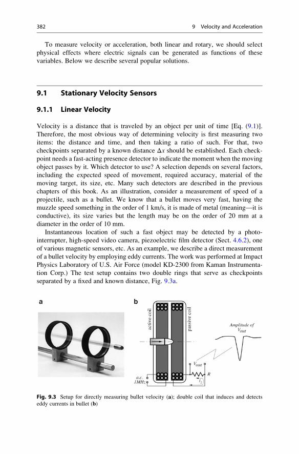
To measure velocity or acceleration, both linear and rotary, we should select
physical effects where electric signals can be generated as functions of these
variables. Below we describe several popular solutions.
9.1 Stationary Velocity Sensors
9.1.1 Linear Velocity
Velocity is a distance that is traveled by an object per unit of time [Eq. (9.1)].
Therefore, the most obvious way of determining velocity is first measuring two
items: the distance and time, and then taking a ratio of such. For that, two
checkpoints separated by a known distance Δx should be established. Each check-
point needs a fast-acting presence detector to indicate the moment when the moving
object passes by it. Which detector to use? A selection depends on several factors,
including the expected speed of movement, required accuracy, material of the
moving target, its size, etc. Many such detectors are described in the previous
chapters of this book. As an illustration, consider a measurement of speed of a
projectile, such as a bullet. We know that a bullet moves very fast, having the
muzzle speed something in the order of 1 km/s, it is made of metal (meaning—it is
conductive), its size varies but the length may be on the order of 20 mm at a
diameter in the order of 10 mm.
Instantaneous location of such a fast object may be detected by a photo-
interrupter, high-speed video camera, piezoelectric film detector (Sect. 4.6.2), one
of various magnetic sensors, etc. As an example, we describe a direct measurement
of a bullet velocity by employing eddy currents. The work was performed at Impact
Physics Laboratory of U.S. Air Force (model KD-2300 from Kaman Instrumenta-
tion Corp.) The test setup contains two double rings that serve as checkpoints
separated by a fixed and known distance, Fig. 9.3a.
Fig. 9.3 Setup for directly measuring bullet velocity (a); double coil that induces and detects
eddy currents in bullet (b)
382 9 Velocity and Acceleration

Each double ring comprises two coils where one coil is active for generating
alternate magnetic field. For that purpose, it is supplied by a.c. current having
frequency 1 MHz—sufficiently high for accurately detecting a fast moving bullet.
The second one is a passive coil being magnetically coupled with the active coil and
thus it produces an induced a.c. current i2. Two joined coils form a transformer.
When the bullet enters a void in the center of the first ring, magnetic field from the
active coil induces in the bullet eddy currents (see Sect. 8.4.3). These circulating
eddies of electrons create their own magnetic fields that, due to the Lenz’s law,
oppose changes in the originating magnetic field. As a result, a magnitude of the
output a.c. current in the passive coil starts dropping. When the bullet passes the
ring center the amplitude is the lowest. This is the precise indication of the bullet’s
position at the first checkpoint. After certain time, the bullet passes the second
double ring where it induces another current spike, which indicates presence of a
bullet at the second checkpoint. The time differenceΔt between the spikes is what ittakes for the bullet to travel between the rings separated by a known distance Δxand thus is the measure of its velocity according to Eq. (9.1).
Another example of a velocity sensor is the LVT—linear velocity transducer
(Fig. 9.4) that employs the Faraday law of electromagnetism. The coil is stationary,
while the core magnet is attached to the object of interest and moves inside the coil
with velocity v. Voltage across the coil is generated when the moving magnet
interacts with a wire:
V ¼ Blv; ð9:9Þwhere B is strength of the magnetic field and l is the wire length. Thus, the voltage isproportional to the speed of the magnet movement. In the LVT, both ends of the
Fig. 9.4 Operating principle of electromagnetic velocity sensor (Courtesy of Trans-Tek, Inc.,
Ellington, CT)
9.1 Stationary Velocity Sensors 383

magnet are inside the coil. With a single coil, this would give a zero output because
the voltage generated by one end of the magnet would cancel the voltage generated
by the other end. To overcome this limitation, the coil is divided into two sections.
The north pole of the magnet induces a current in one coil, while the south pole
induces a current in the other coil. The two coils are connected in a series-opposite
direction to obtain an output proportional to the magnet’s velocity. Maximum
detectable velocity depends primarily on the input stages of the interface electronic
circuit. Minimum detectable velocity depends on the noise floor, and especially of
transmitted noise from a nearby high a.c. current-carrying equipment. This design is
very similar to an LVDT position sensor (Sect. 8.4.1), except that LVDT is an
active sensor with a moving ferromagnetic core, while the LVT is a passive device
with a moving permanent magnet. In other words, the LVT is a passive voltage
generating sensor which does not need an excitation signal. An angular version of
the LVT (called RVT—rotary velocity transducer) may measure rotation rate
continuously for any number of turns. Stationary velocity sensors detect velocity
along a distance that is limited by the size of the sensor, so in most cases these
sensors measure vibration velocity.
9.1.2 Rotary Velocity Sensors (Tachometers)
For measuring angular velocity, rotating sprocket wheels with the position sensors
are often employed. This concept is illustrated in Fig. 8.26. Naturally, output
signals from this sensor have a discrete format—the higher the pitch of the
sprockets the finer the resolution.
For detecting the wheel rotation, many types of position sensors can be
employed, like the magnetic (Hall-sensors, magnetoresistors as in Fig. 8.25, and
the reed switches) and optical (photo-interrupters). One of the most popular is a
magnetic rotary sensor (Fig. 8.22a, b). The key feature of all these devices is that the
sensor is stationary and physically attached to the frame of reference (a car body,
for example), while the wheels rotate. In many applications, especially in mobile
devices, this arrangement is not possible and therefore an inertial sensor—a gyro-
scope—is the choice for measuring angular velocity.
Another type of a tachometer uses an eccentric wheel (cam) illustrated in
Fig. 9.5. When rotating, the cam bends the resilient beam whose right side is
anchored to a support structure. A strain transducer is applied to the beam surface.
The transducer may be of any suitable design, for example, a strain gauge
(Fig. 10.2) or piezoelectric element (Fig. 10.8). When the beam flexes up and
down, the transducer converts mechanical strains to a variable electrical signal
that, in turn, is converted by the signal conditioner to rectangular pulses—one per
the wheel turn.
384 9 Velocity and Acceleration

9.2 Inertial Rotary Sensors
Inertial rotary sensor is a self-contained device in which measurements are
provided by one or more gyroscopes. This sensor is used to track the position and
orientation of an object relative to the prior sensor orientation and velocity, rather
than to a stationary coordinate system. A complete inertial sensor typically contains
three orthogonal rate-gyroscopes, measuring angular velocities.Before advancement of a GPS (global positioning system), besides a magnetic
compass, a rotating wheel gyroscope probably was the most common mobile
navigation sensor for detecting deviation from a selected direction of motion. In
other words, a gyroscope was measuring an angular rotation of the direction of
motion. Word mobile means being attached to a moving object. In many cases
where a geomagnetic field was either absent (in Space), or is altered by presence of
some disturbances, a gyroscope was an indispensable sensor for monitoring angular
velocity of a vehicle, such as an aircraft or missile, Fig. 9.6b. Nowadays,
applications of gyroscopes are much broader than just for navigation. They are
used in the stabilization devices, weapons, robotics, tunnel mining, and—in very
large quantities—in mobile communications devices, such as smartphones.
The earliest known gyroscope containing a rotating massive sphere was made in
1817 by German Johann Bohnenberger. In 1832, American Walter R. Johnson
developed a gyroscope that was based on a rotating disk. In 1852 Leon Foucault
used a rotating disc in an experiment involving the rotation of the Earth. Foucault
coined the name gyroscope from the Greek gyros—circle or rotation—and
skopeein—to see.
Fig. 9.5 Cam tachometer
with flexing beam
9.2 Inertial Rotary Sensors 385

9.2.1 Rotor Gyroscope
A gyroscope, or a gyro for short, is a “keeper of direction”, like a pendulum in a
clock is a “keeper of time”. A keeper of direction means that it produces an output
signal whenever angular velocity deviates from zero, which happens when the
platform starts rotating. A gyro operation is based on the fundamental principle
of the conservation of angular momentum: in any system of particles, the totalangular momentum of the system relative to any point fixed in space remainsconstant, provided no external forces act on the system.
A mechanical gyro is comprised of a massive disk free to rotate about a spin axis
(Fig. 9.6a) which itself is confined within a framework that is free to rotate about
one or two axes. Hence, depending on the number of rotating axes, a gyro can be
either of a single-, or two-degree-of-freedom types. Two qualities of a gyro account
for it usefulness: (1) the spin axis of a free gyroscope will remain fixed with respect
to space, provided there are no external forces to act upon it, and (2) a gyro can be
made to deliver a torque (or output signal) which is proportional to the angular
velocity about an axis perpendicular to the spin axis.
When the wheel (rotor) freely rotates, it tends to preserve its axial position. If the
gyro platform rotates around the input axis, the gyro will develop a torque around a
perpendicular (output) axis, thus turning its spin axis around the output axis. This
phenomenon is called precession of a gyro. It can be explained by the Newton’s lawof motion for rotation: the time rate of change of angular momentum about anygiven axis is equal to the torque applied about the given axis. That is, when a torqueT is applied about the input axis, and the speed ω of the wheel is held constant, the
angular momentum of the rotor may be changed only by rotating the projection of
the spin axis with respect to the input axis. In other words, the rate of rotation of the
spin axis about the output axis is proportional to the applied torque:
T ¼ IωΩ; ð9:10Þwhere Ω is the angular velocity about the output axis and I is the inertia of a gyrowheel about the spin axis. To determine the direction of precession, the following
Fig. 9.6 Conceptual design of mechanical gyroscope (a) and early autopilot gyroscope (b)
386 9 Velocity and Acceleration

rule can be used: precession is always in such a direction as to align the direction ofrotation of the wheel with the direction of rotation of the applied torque.
Accuracy of a mechanical gyro greatly depends on the effects which may cause
additional unwanted torques and cause drifts. The sources of these are friction,
imbalanced rotor, magnetic effects, etc. One method which has been widely used to
minimize rotor friction is to eliminate the suspension entirely by floating the rotor
and the driving motor in a viscous, high-density liquid, such as one of the
fluorocarbons. This method requires close temperature control of the liquid and
also may suffer from aging effects. The other method of friction reduction is to use
the so-called gas bearings, where the shaft of the rotor is supported by high-pressure
helium, hydrogen, or air. And even a better solution is to support the rotor in
vacuum by an electric field (electrostatic gyros). In another version—a magnetic
gyro consists of a rotor supported by a magnetic field. In that case, the system is
cryogenically cooled to temperatures where the rotor becomes superconductive.
Then, an external magnetic field produces enough counter-field inside the rotor that
the rotor floats in a vacuum. These magnetic gyroscopes sometimes are called
cryogenic gyros.
While a spinning-rotor gyroscope for many years was the only practical choice,
its operating principle really does not lend itself to design of a small monolithic
sensor that is required by many mobile applications. Conventional spinning-rotor
gyroscopes contain parts such as gimbals, support bearings, motors, and rotors
which need accurate machining and assembly; these aspects of construction pro-
hibit conventional mechanical gyroscopes from ever becoming a low-cost portable
device. Wear on the motors and bearings during operation means that the gyroscope
will only meet the performance specifications for a set number of running hours.
Thus, other methods for sensing a direction and angular velocity have been devel-
oped. Often, a GPS would be the ideal choice. Yet, it just cannot be employed in
Space, under water, in tunnels, inside buildings, or whenever the size and cost are of
a paramount importance. Besides, spatial resolution of the GPS is just nearly not
sufficient for many hand-held devices.
9.2.2 Vibrating Gyroscopes
If, as illustrated in Fig. 9.2, the object initially rotates with radius r1, it is
characterized by a tangential velocity v1. When a rotating object moves farther
away from the center to the new radius r2, it will have a faster tangential velocity v2.Thus, when the object moves away from the center the tangential velocity
increases, meaning that the object accelerates. This phenomenon was discovered
in 1835 by Gaspard G. de Coriolis (1792–1843), a French mathematician—and the
effect is known as Coriolis acceleration. This acceleration ac in a vector notation isdescribed as:
ac ¼ �2ΩV; ð9:11Þ
9.2 Inertial Rotary Sensors 387

whereV is the velocity of the object moving within the rotating system, andΩ is the
angular vector which has magnitude equal to the rotation velocity ω and is directed
along the axis of rotation. If the object has mass m, the Coriolis acceleration
produces force that in a vector notation is
Fc ¼ �2ΩVm ð9:12ÞThis force is called a fictitious force as it arises not from an interaction between
different objects but rather from a rotation of a single object. The Coriolis acceler-
ation, which is directly proportional to the rate of turn, occurs in the third axis that is
perpendicular to the plane containing the other two axes. Figure 9.7 shows that the
Coriolis acceleration vector is perpendicular to the plane where the vectors of
angular velocity and object’s velocity are positioned.
Since the force magnitude is function of the angular velocity, this suggests that
the angular velocity sensor can be designed by incorporation a force sensor that
converts the Coriolis force into an electrical signal. The object having mass does
not need to move in one direction only, it can go back and forth within the reference
frame whose angular velocity we measure. In other words, the object may oscillate
in one direction, while the frame rotation will produce the Coriolis force in another
direction. We can measure that force for generating an output electrical signal.
Figure 9.8 is a conceptual illustration of how the oscillating gyro works. The
massive object M is forced by an external drive to oscillate along the y-axis withfrequency of several kHz [1]. So the mass goes up and down with high velocity that
has a sinusoidal form. When the frame rotates, a Coriolis force arises and pushes the
mass either to the left or to the right. The shift is measured by the proximity or
displacement sensors positioned along the x-axis. The shift also follows the sinu-
soidal function having a magnitude proportional to the angular velocity.
The vibrating gyros are fabricated in very large quantities. Use of the MEMS
micromachined technology takes advantage of the techniques developed in the
electronic industry and is highly suited to a high-volume manufacture. There are
Fig. 9.7 Vector of Coriolis
acceleration
388 9 Velocity and Acceleration

several practical ways of building a vibrating gyro, however, all of them can be
divided into three principle groups [2]:
1. Simple oscillators (mass on a string, beams)
2. Balanced oscillators (tuning forks)
3. Shell resonators (“wine glass”, cylinder, ring)
All three categories have been implemented in the actual designs.
As an example, a modern vibrating gyro is shown in Fig. 9.9. It uses a piezo-
electric ceramic (see Sect. 4.6.1) that is formed in shape of a small cylinder (0.8 mm
in diameter and 9 mm in length) with six electrodes deposited on it sides.
Fig. 9.8 Conceptual diagram of vibrating gyroscope. Massive object M is supported within frame
by four springs and forced to oscillate along y-direction (a). When frame rotates and object
oscillates upward (b), Coriolis force shifts it to left. When object oscillates downward (c), forceshifts it to the right
Fig. 9.9 Piezoelectric ceramic vibrating gyro has a cylindrical shape (a). Alternate voltage
applied to electrodes flexes cylinder along one axis (b); axial view of gyro cylinder, where Coriolis
force flexes it along perpendicular axis (c). [Adapted from www.nec-tokin.com]
9.2 Inertial Rotary Sensors 389

The design takes advantage of a reversible phenomenon of a piezoelectric effect:
application of electric charge strains the piezoelectric material, thus converting
electric signal into deformation. On the other hand, a strain produces an electric
charge, thus converting mechanical force into electrical signal. The driving pair of
the electrodes is supplied with a.c. voltage from an external oscillator. It flexes the
cylinder in a direction indicated by the black arrow in Fig. 9.9c. When the cylinder
rotates around its vertical axis with an angular velocity Ω, the arising Coriolis forceflexes it in the direction of the white arrow—the higher the angular velocity the
stronger the flexing. This rotation-related flexing induces piezoelectric charges in a
pick-up pair of the electrodes: +out and �out that generate the out-of-phase
sinusoidal voltages. These voltages are amplified and processed by a signal condi-
tioner for serving as the gyro output signals. Advantages of this design are a small
size and ease of production, meaning a lower cost. A sensitivity of this sensor to
angular velocity is fairly good—about 0.6 mV/deg/s. This miniature gyro is widely
used in the camera stabilization devices, game controllers, and supplementary
sensors for GPS (to continue navigating during times when the satellite RF signals
are lost), robots, and virtual reality systems.
9.2.3 Optical (Laser) Gyroscopes
A ring laser gyroscope (RLG) is another inertial navigation sensor. It is
characterized by very high reliability (no moving parts) and very high accuracy
with the angular uncertainty on the order 0.01�/h. A major advantage of the optical
gyros is their ability to operate under hostile environments that would be difficult, if
not impossible, for the mechanical gyros.
Operation of the RLG is based on employing the so-called Sagnac effect, which
is illustrated in Fig. 9.10 [3]. Two beams of light generated by a laser propagate in
Fig. 9.10 Sagnac effect
390 9 Velocity and Acceleration

opposite directions within an optical ring having refractive index n and radius R.One beam goes in clockwise (CW) direction, while the other in a counterclockwise
(CCW) direction. The amount of time which takes light to travel within the ring
takes Δt¼ 2πR/nc, where c is the speed of light. Now, let us assume that the ring
rotates with angular rate Ω in the clockwise direction. In that case, light will travel
different paths at two directions. The CW beam will travel lcw¼ 2πR +ΩRΔt, whilethe CCW beam will travel lccw¼ 2πR�ΩRΔt. Hence, the difference between the
paths is
Δl ¼ 4πΩR2
nc: ð9:13Þ
Therefore, to accurately measure Ω, a technique must be developed to determine
Δl. There are three basic methods known for the path detection: (1) optical
resonators, (2) open-loop interferometers, and (3) closed-loop interferometers.
For the RLG, the measurements of Δl are made by taking advantages of the
lasing characteristics of an optical cavity (that is, of its ability to produce coherent
light). For lasing to occur in a closed optical cavity, there must be an integer number
of wavelengths about the complete ring. The light beams, which does not satisfy
this condition, interfere with themselves as they make subsequent travel about the
optical path. In order to compensate for a change in the perimeter due to rotation,
the wavelength λ and frequency ν of the light must change
� dν
ν¼ dλ
λ¼ dl
l: ð9:14Þ
The above is a fundamental equation relating frequency, wavelength, and
perimeter change in the ring laser. If the ring laser rotates at a rate Ω, then
Eq. (9.14) indicates that light waves stretch in one direction and compress in the
other direction to meet the criteria for the lasing of an integral number of
wavelengths about the ring (somewhat similar to the Doppler effect). This, in
turn, results in a net frequency difference between the light beams. If the two
beams are bit together (mixed), the resulting signal has frequency
F ¼ 4AΩλnl
; ð9:15Þ
where A is the area enclosed by the ring.
In practice, optic gyros are designed with either a fiber ring resonator, or the fiber
coil where the ring has many turns of the optical fiber [4]. The optic ring resonator is
shown in Fig. 9.11a. It consists of a fiber loop formed by a fiber beam splitter that
has a very low cross-coupling ratio. When the incoming beam is at the resonant
frequency of the fiber ring, the light couples into the fiber cavity and the intensity in
the exiting light drops. The coil fiber gyro (Fig. 9.11b) contains a light source and
the detector coupled to the fiber. The light polarizer is positioned between the
detector and the second coupler to insure that both counter-propagating beams
9.2 Inertial Rotary Sensors 391

traverse the same path in the fiber optic coil [5]. The two beams mix and impinge
onto the detector, which monitors the cosinusoidal intensity changes caused by the
rotationally induced phase changes between the beams. This type of optical gyro
provides a relatively low cost, small size rotation sensitive sensor with a dynamic
range up to 10,000. Applications include yaw and pitch measurements, attitude
stabilization, and gyro compassing.
9.3 Inertial Linear Sensors (Accelerometers)
Linear accelerometers belong to the class of inertial sensors that do not require
referencing to a stationary coordinate system. They are attached to moving
platforms. The name “inertial” refers to an essential component that has a substan-
tial inertia to motion. In navigational devices, accelerometers work together with
gyroscopes, typically containing three orthogonal rate-gyroscopes and three orthog-
onal accelerometers, measuring angular velocity and linear acceleration, respec-
tively. By processing signals from these devices it is possible to track the position
and orientation of a moving object.
Accelerometers are used for measuring acceleration resulted from subjecting an
object to external forces, including gravity. While gravity is usually a constant force
directed toward the center of gravity of a massive object, other forces may vary in
magnitude and direction in the broad magnitude and frequency ranges. Thus, a
typical accelerometer should be responsive to various forms of accelerations—from
constant to slow moving to strong impacts and vibrations.
Fig. 9.11 Fiber optic ring resonator (a); fiber optic analog coil gyro (b) (adapted from [3])
392 9 Velocity and Acceleration

As it follows from the Newton’s second law, acceleration in a vector notation is
defined as
a ¼ F
m; ð9:16Þ
where F is the force vector and m is mass of the object (scalar value) that is
subjected to the force causing an acceleration. Thus, mass, acceleration, and force
are all interconnected. The direction of acceleration is the same as that of the force.
Equation (9.16) suggests that for measuring acceleration we need to provide a
known mass m and measure the force magnitude F that is exerted by that mass on
a force sensor. The force sensor is an essential part of an accelerometer. The force
sensor comprises two components: a spring that deforms under influence of the
force and a deformation sensor to determine the deformation magnitude. For a
compression spring, deformation is measured as change in the spring length by a
displacement sensor. For details on force sensors, refer to Chap. 10.
9.3.1 Transfer Function and Characteristics
A one-axis accelerometer can be specified as a single-degree-of-freedom device,
which has a massive object (sometimes called proof mass or seismic mass), aspring-like supporting system, a frame structure with damping properties
(Fig. 3.15a), and also a displacement sensor. To make a functional accelerometer,
its housing is attached to a moving platform (Fig. 9.12a).
The proof mass, m, is supported by a compressible spring that allows the mass to
shift up and down. In turn, the mass is attached to two additional components: a
damper and a displacement sensor. A damper slows down the mass motions while
the displacement sensor determines the mass position with respect to the neutral
(at no acceleration).
Fig. 9.12 Concept of linear mechanical accelerometer (a) and timing diagrams (b)
9.3 Inertial Linear Sensors (Accelerometers) 393

The platform with the attached accelerometer housing may be stationary or it
may travel along coordinate x. Consider the distance change as having the shape ofa parabolic function [Fig. 9.12b: x-curve]. The entire assembly accelerates upward
with the speed, v, changing linearly while the acceleration, a, that is a step-functionwe are attempting to measure. When the motion starts, due to its inertia, the proof
mass tends to remain in place and thus exerts force F on the spring, squeezing it for
a distance Δx¼ x2� x1. The spring is characterized by stiffness k. The spring
counteracts the force F so that the following equation holds:
F ¼ ma ¼ kΔx ¼ k x2 � x1ð Þ; ð9:17Þfrom which we can determine the proof mass displacement as
x2 � x1 ¼ m
ka: ð9:18Þ
where the ratio
S ¼ m
k¼ 1
ω02¼ 1
2π f 0ð Þ2 ð9:19Þ
is called the “static sensitivity” of an accelerometer. Note that sensitivity S is
inversely proportional to the squared f0—a natural (resonant) frequency in Hz of
the proof mass assembly (including all attached components). Notation ω0 is a
circular frequency in rad/s.
As follows from Eq. (9.19), to increase the natural frequency, the proof mass
must be reduced and the spring stiffness shall increase. Another conclusion from
this equation is that the higher the natural frequency the less sensitive the
accelerometer.
So far we discussed the static properties of an accelerometer. Now we need to
consider time dependent characteristics of the moving mass. When acceleration
onsets, the proof mass compresses the spring with force F. At some moment, the
spring will push the mass upward until the spring expands beyond its original size.
Then the motion reverses again, the spring compresses, and the process repeats. In
other words, the mass oscillates. To minimize undesirable oscillations of the proof
mass, it is connected to a damper (“shock absorber”) that slows down the mass
movement by absorbing its kinetic energy in relationship with the speed of the mass
motion. The damper exerts on the mass a damping force proportional to the speed of
the mass displacement:
Fb ¼ bd x2 � x1ð Þ
dt¼ b
dx2dt
� dx1dt
� �ð9:20Þ
where b is the dumping coefficient which is defined through a parameter called a
damping ratio ζ as:
b ¼ 2ζffiffiffiffiffiffikm
p; ð9:21Þ
394 9 Velocity and Acceleration

To account for all forces acting on the proof mass (inertial force, spring force,
and damping force) we shall write a second order linear differential equation:
md2x2dt2
þ bdx2dt
� dx1dt
� �þ k x2 � x1ð Þ ¼ 0; ð9:22Þ
Let’s call x2� x1¼ z which is a relative shift of the proof mass being translated
by the displacement sensor into output voltage Vout. Then, considering Eq. (9.16)
which is the Newton second Law, Eq. (9.22) can be rewritten as
md2z
dt2þ b
dz
dtþ kz ¼ �ma ¼ �F: ð9:23Þ
Its solution for a relative displacement z(t) is:
z tð Þ ¼ Be�ζffiffikm
ptSin 2π fdtþ φð Þ � Sa; ð9:24Þ
where the factor B and phase shift φ depend on position of the proof mass at the
moment of onset of acceleration.
The damped frequency fd is different from the natural frequency f0 and defined as:
fd ¼ f0
ffiffiffiffiffiffiffiffiffiffiffiffiffi1� ζ2
qonly for ζ < 1 ð9:25Þ
Several conclusions can be drawn from the solution (9.24). The output has a
decaying oscillatory nature characterized by the first summand. The decay rate is
exponential with a time constant:
τ ¼ 1
ζ
ffiffiffiffim
k
r: ð9:26Þ
Thus, the higher the damping ratio ζ, the quicker the spurious oscillations disap-
pear. If ζ� 1, then Eq. (9.24) has a noticeable oscillatory “underdumped” response
shown in Fig. 9.12b as output voltage Vout1. For ζ 1, the response is overdamped
with no oscillations, slow, and lagging behind the true acceleration a. A critical or
near critically damped response (ζ� 1) has a shape that is closer to the true
acceleration and is the optimal parameter. Another conclusion is that after the
oscillations disappear, the output characterized by the second summand is propor-
tional to acceleration a multiplied by the sensitivity factor defined by Eq. (9.19).
Depending on particular applications, the mass, spring, and damper should be
carefully selected.
A correctly designed, installed, and calibrated accelerometer should have one
clearly identifiable resonant (natural) frequency, and a flat frequency response
where the most accurate measurement can be made (Fig. 9.13). Within this flat
region, the output of the accelerometer will correctly reflect the change without
9.3 Inertial Linear Sensors (Accelerometers) 395

multiplying the signal by any variations in the frequency characteristic of the
accelerometer. Viscous damping is used in many accelerometers to improve the
useful frequency range by limiting effects of the resonant. As a damping medium,
silicone oil is used quite often. A damper is important in sensors where the
operating frequency is close to the natural frequency. However, when the natural
frequency is much higher than the operating bandwidth limit, a mechanical damper
may be replaced by a hardware of software low-pass filter in the signal conditioner.
When calibrated, several characteristics of an accelerometer should be
determined:
1. Sensitivity is the ratio of an electrical output to the mechanical input. It is usually
expressed in terms of volts per unit of acceleration under the specified
conditions. For instance, the sensitivity may be specified as 1 V/g (unit of
acceleration: g¼ 9.80665 m/s2 at sea level, 45� lat.) The sensitivity is typically
measured at a single reference frequency of a sine-wave shape.2 In the U.S.A. it
is 100 Hz, while in most European countries it is 160 Hz (outside of the power
line frequency and its harmonics).
2. Frequency response is the output signal over a range of frequencies where the
sensor should be operating. It is specified with respect to a reference frequency
which is where the sensitivity is specified.
3. Resonant (natural) frequency in an undamped sensor shows as a clearly defined
peak that can be 3–4 dB higher than the response at the reference frequency. In a
near critically damped device, the resonant may not be clearly visible, therefore,
the phase shift is measured. At the resonant frequency, it is 180� of that at the
reference frequency. For a 1 % accuracy the highest operating frequency should
be at least 2.5 times lower than the resonant frequency of the accelerometer.
When designing an accelerometer, the proof mass should be selected as small as
practical (without compromising sensitivity) while the support springs should be
Fig. 9.13 A frequency
response of an accelerometer
where fn is natural frequency;fref is reference frequency
2 These frequencies are chosen because they are removed from the power line frequencies and their
harmonics.
396 9 Velocity and Acceleration

stiff and sort—this helps to make the natural frequency much higher than the
operating range.
4. Zero stimulus output is specified for the position of the sensor where its sensitive(active) axis is either perpendicular to Earth’s gravity or during a free-fall
(weightlessness). That is, in accelerometers that include a d.c. component in
the output signals, the gravitational effect should be eliminated before the output
at a no-mechanical input is determined.
5. Linearity of the accelerometer is specified over the dynamic range of the input
signals.
When specifying an accelerometer for a particular application, one should
answer a number of questions, such as:
1. What is the anticipated magnitude of vibration or linear acceleration?
2. What is the operating temperature and how fast the ambient temperature may
change?
3. What is the anticipated frequency range?
4. What linearity and accuracy are required?
5. What is the maximum tolerable size?
6. What kind of power supply is available?
7. Are any corrosive chemicals or high moisture present?
8. What is an anticipated overshock?
9. Are intense acoustic, electromagnetic, or electrostatic fields present?
10. Is the machinery grounded?
9.3.2 Inclinometers
Inclination detectors are employed in ground and air-based vehicles, road construc-
tion, machine tools, inertial navigation systems, video monitors of mobile hand-
held devices (to control orientation of an image), robots, electronic games, and
other applications requiring a gravity reference.
Earth gravity is characterized by a constant force directed toward the Earth
center and causing acceleration of 1 g� 9.8 m/s2. This value changes somewhat at
different locations on the planet. One popular application of an accelerometer is
sensing a gravity direction rather then measuring its magnitude. These special
accelerometers are often called inclinometers or tilt detectors. According to the
Einstein’s theory of General Relativity, if we want to detect direction and magni-
tude of a gravitational force, an accelerometer is our sensor. Due to a relatively
small value of the earth gravity, a tilt accelerometer does not need a broad span of
the input signals, however, a practical device should be sensitive in all three axes
and also have some additional features, like being able to respond to tapping and
detect impacts resulted from dropping of the device. Thus, for a tilt accelerometer a
minimum input span of 2 g should be sufficient. However, there is always a trade-
off between the angular resolution and span.
9.3 Inertial Linear Sensors (Accelerometers) 397

An example of a commercial tilt accelerometer is BMA220 from Bosch. It is
very small (2� 2� 1 mm), senses accelerations along all three axes, has a free-fall
detection (zero gravity), and offers a high resolution [6]. An example of its
application is shown in Fig. 9.14 where a smartphone is rotated around one axis
resulting in the sinusoidal output of the accelerometer. A three-axial accelerometer
responds with similar signals along each axis allowing a correct spatial detection.
When an inclinometer is positioned on an accelerating vehicle, it produces an
erroneous signal because the response is a sum of two vectors—earth gravity and
acceleration force as shown in Fig. 9.15. The inclinometer cannot tell them apart. In
a stationary or steady moving vehicle, an inclinometer will measure angle αbetween its own internal axis and the gravity vector. If the vehicle carrying the
inclinometer accelerates, an acceleration force acting on the proof mass will appear
in the opposite direction from the direction of motion. The two vectors, gravity and
acceleration, will sum and the inclinometer will respond with an erroneous angle δ.
Fig. 9.14 Sensing of smartphone orientation
Fig. 9.15 Error of tilt
accelerometer in accelerating
vehicle
398 9 Velocity and Acceleration

If only a low-resolution direction of the gravitational force is of interest, a
simpler and cheaper tilt or inclination detector may be considered. A response of
such a detector is not function of the gravity vector magnitude but only of its
direction. The detector has its own internal axis with respect to which the gravity
direction is measured. A response is an electric signal representative of an angle
between the internal axis and the gravity vector. An old and still quite popular
detector is a mercury switch, Fig. 9.16a, b. The switch is made of a non-conductive
(often glass) tube having two electrical contacts and a drop of mercury. When the
sensor is positioned with respect to the gravity force in such a way as the mercury
slides away from the contacts, the switch is open. Tilting the switch causes the
mercury drop to move to the contacts and touch both of them, thus closing the
switch. One popular application of this design is in a household thermostat, where
the mercury switch is mounted on a bimetal coil (see Fig. 4.38) that serves as an air
temperature sensor. Winding or unwinding the coil in response to the room temper-
ature affects the switch inclination. Opening and closing the switch controls a
heating/cooling system. Since this tilt sensor is a threshold device, the obvious
limitation is an on-off operation: a “bang-bang” controller in the engineering
jargon.
To measure inclination with an infinitesimal resolution, a more complex sensor
is required. One elegant design is shown in Fig. 9.16c. It is called the electrolytic tiltsensor. A small slightly curved glass tube is filled with partly conductive electro-
lyte. Three electrodes are built into the tube: two at the ends and the third electrode
is at the center of the tube. An air bubble resides in the tube and may move along its
length as the tube tilts. Electrical resistances between the center electrode and each
of the end electrodes depend on position of the bubble. As the tube shifts away from
the balance position, the resistances increase or decrease proportionally. The
electrodes are connected into a bridge circuit which is excited by an a.c. current
to avoid damage to the electrolyte and electrodes. The electrolytic tilt sensors are
available3 in different designs (Fig. 9.16d) for a wide spectrum of angular ranges
from �0.5� to �80�. Correspondingly, the shapes of the glass tubes vary from
slightly curved to doughnut-like.
Fig. 9.16 Conductive gravitational sensors. Mercury switch in the open position (a) and closed
(b) positions; electrolytic tilt sensor (c) and electrolytic sensor housings (d)
3 The Fredericks Company. P.O. Box 67, Huntingdon Valley, PA 19006.
9.3 Inertial Linear Sensors (Accelerometers) 399

9.3.3 Seismic Sensors
Earth masses (e.g., tectonic plates), due to their huge masses, are characterized by
motions of very low frequencies in the infrasound range. Therefore, movements of
ground are better represented by velocity rather then acceleration. Since
seismometers or seismographs contain the same basic components as
accelerometers (proof mass, springs, force sensors, dampers), we briefly review
them here.
For measuring very slow earth movements, a seismic sensor shall be slow but
very sensitive, thus it employs a large proof mass and a soft spring—see Eq. (9.19)
for sensitivity. During measurements, position of the proof mass is considered fixed
(due to a large inertia) while the platform, attached to the ground, moves. This kind
of a sensor is used for detecting earthquakes and ground vibrations caused my
human activities.
Earth movement is characterized by two kinds of soil displacements. The first
are elastic longitudinal P-waves—horizontal shifts manifested by compression and
rarefication of soil when the soil density varies (similarly to sound waves). “P”
stands for primary because due to its higher speed the wave arrives first from a
remote earthquake. In the P-waves, the soil vibrates along the wave propagation
direction. Other motions are the S-waves (“S” stands for secondary)—transverse
displacements without change in soil density. They vibrate at a right angle to the
direction of propagation. P-waves can travel through solids and liquid, whereas
S-waves can travel only through solids.
Therefore, depending a on the wave type the sensing elements should be oriented
at different directions. This is illustrated in Fig. 9.17 that is a concept of a
pendulum-type seismometer. A large proof mass is supported by a soft spring and
can move both vertically and horizontally, that is in the x–y–z directions, dependingon motion of the platform that is solidly attached to ground. Two separate types of
Fig. 9.17 Concept of a
three-axial “pendulum”
seismograph
400 9 Velocity and Acceleration

transducers respond to different motions—an x–y sensor responds to the P-waves,
while a proximity sensor responds to the S-waves in a vertical direction. A great
variety of displacement sensors may be employed for the purpose. We indicated
above that seismometers measure ground velocity rather than acceleration, thus
electromagnetic velocity transducers are often employed, such as shown in Fig. 9.2.
Another type of a displacement transducer that is useful for seismometers is
capacitive. For example, x–y sensing can be successfully performed by a capacitive
sensor similar to that shown in Fig. 8.12, while proximity may be detected also by a
capacitive sensor that is conceptually shown in Fig. 8.8.
Like in an accelerometer, the seismograph has a very pronounced mechanical
resonance that, if not damped, will register long spurious oscillations. A damping
mechanism may be a viscous liquid (e.g., mineral oil), but the most efficient is an
electromagnetic damper [7]. Its operating principle is based on moving a ferromag-
netic core into a coil connected to a loss resistor (Fig. 9.18). The induced current
flowing through a load resistor creates its own magnetic field that, according to
Lenz law, counteracts the original magnetic field thus resisting motions of the core.
This slows down the seismic mass and damps oscillations with the oscillation
energy dissipating in the resistor in form of heat. Such a damper should be used
for all sensed axes.
9.3.4 Capacitive Accelerometers
The conceptual design of a mechanical linear accelerometer (Fig. 9.12) can be
implemented in a great variety of ways. Design options primarily are driven by
selection of the type of a displacement sensor or transducer for monitoring shifts of
the proof mass with respect to the housing.
Fig. 9.18 Electromagnetic
damper
9.3 Inertial Linear Sensors (Accelerometers) 401

A capacitive transducer is one of the proven and reliable elements that lends
itself to microminiaturization, high accuracy, and low cost. The transducer essen-
tially contains at least two conductors where the first one is anchored to the
accelerometer housing, while the other is connected to the proof mass that moves
inside the housing in response to acceleration. These conductors form a capacitor
whose value is function of their overlapping area A and a mutual distance d—see
Eq. (4.23). Depending on design, either the overlapping area or the distance may be
made variable. A maximum proof mass displacement which typically is measured
by the capacitive accelerometer rarely exceeds 20 μm. Hence, such a small dis-
placement requires a reliable compensation of drifts and various interferences. This
is usually accomplished by use of a differential technique, where an additional
capacitor is formed in the same MEMS structure. A value of the second capacitor
must be close to that of the first one, and it should be subjected an acceleration with
a 180� phase shift. Then, acceleration can be represented by a difference in values
between these two capacitors. See the concept in Fig. 8.8.
Figure 9.19a shows a cross-sectional diagram of a MEMS capacitive accelerom-
eter where an internal mass is sandwiched between the upper cap and the base
[8]. The mass is supported by four silicon springs (Fig. 9.19b). The upper plate and
the base are separated from it by respective distances d1 and d2. All three parts aremicromachined from a silicon wafer. Note that there is no damper. Figure 9.20 is a
simplified circuit diagram for a capacitance-to-voltage converter that in many
respects is similar to the circuit of Fig. 6.11.
A parallel plate capacitor Cmc between the mass and the cap electrodes has a
plate area S1. The plate spacing d1 can be reduced by an amount Δ when the mass
moves toward the upper plate. A second capacitor Cmb having a different plate area
S2 appears between the mass and the base. When mass moves toward the upper
plate and away from the base, the spacing d2 increases byΔ. The value ofΔ is equal
to the mechanical force Fm acting on the mass divided by the spring constant k ofthe silicon springs:
Δ ¼ Fm
k: ð9:27Þ
Fig. 9.19 Capacitive accelerometer with a differential capacitor side cross-sectional view (a); topview of a seismic mass supported by four silicon springs (b)
402 9 Velocity and Acceleration

Strictly speaking, the accelerometer equivalent circuit is valid only when
electrostatic forces do not affect the mass position, that is, when the capacitors
depend linearly on Fm [9]. When accelerometer capacitors are applied to a
switched-capacitor summing amplifier, the output voltage depends on value of
the capacitors, and subsequently on the force:
Vout ¼ 2ECmc � Cmb
C f
: ð9:28Þ
The above equation is true for small changes in the sensor’s capacitances.
The accelerometer output is also a function of temperature and a capacitive
mismatch. It is advisable that it be calibrated over the entire temperature range
and appropriate corrections are made during the signal processing. Another effec-
tive method of assuring high stability is to design self-calibrating systems which
make use of the electrostatic forces appearing in the accelerometer assembly when
voltage is applied to either a cap or a base electrode.
Figure 9.21 illustrates design of an advanced accelerometer where the proof
mass displacement is measured by capacitive “fingers” [10] that slide with respect
to one another and thus modulate the overlapping area. The overall capacitance is
proportional to the number of the narrow fingers. The proof mass is separated into
four sections where each is supported by the individual serpentine spring and
connected to its own set of the capacitive fingers. When the proof mass moves,
the bending fingers shift as shown in Fig. 9.22a. The overlapping area changes, thus
modulating the respective capacitances. The structure forms four sets of the sensing
capacitors that are connected into the bridge circuit as shown in Fig. 9.22b. Each set
of the capacitors has sensitivity of about 1.6 fF/g.
Fig. 9.20 Circuit diagram of capacitance-to-voltage conversion suitable for integration on silicon
9.3 Inertial Linear Sensors (Accelerometers) 403

9.3.5 Piezoresistive Accelerometers
As a sensing element a piezoresistive accelerometer incorporates strain gauges that
measure strain in the mass-supporting springs. The strain can be directly correlated
with the magnitude and rate of the mass displacement and, subsequently, with an
acceleration. These devices can sense accelerations within a broad frequency range:
from near d.c. up to 13 kHz. With a proper design, they can withstand overshock up
to 10,000 g. Naturally, a dynamic range (span) is somewhat narrower (1000 g with
error less than 1 %). The overshock is a critical specification for many applications.
Piezoresistive accelerometers with discrete, epoxy-bonded strain gauges tend to
have undesirable output temperature coefficients. Since they are manufactured
separately, the gauges require individual thermal testing and parameter matching.
This difficulty is virtually eliminated in modern sensors that use MEMS technology
of the silicon wafers. The concept of a piezoresistive Si strain gauge that monitors
deflection of a proof mass is given in Fig. 8.6.
Fig. 9.21 Structure of
capacitive accelerometer with
sensing “fingers”. (Adapted
from [10])
Fig. 9.22 Downward bending of fingers modulates capacitances C1 and C2 (a); capacitive bridge (b)
404 9 Velocity and Acceleration

9.3.6 Piezoelectric Accelerometers
The piezoelectric effect (do not confuse it with a piezoresistive effect!) has a natural
application in sensing vibration and acceleration. The effect allows a direct conver-
sion of mechanical energy into electrical (see Sect. 4.6). These sensors operate from
frequency as low as 2 Hz and up to about 5 kHz, they posses good off-axis noise
rejection, high linearity, and a wide operating temperature range (up to 120 �C).While quartz crystals are occasionally used as sensing elements, the most popular
are the ceramic piezoelectric materials, such as barium titanate, lead zirconite
titanate (PZT), and lead metaniobite. A piezoelectric crystal is sandwiched between
the supporting structure and proof mass which exerts on it a force proportional to
acceleration. In these sensors, a proof mass is directly coupled to the piezoelectric
crystal with no intermediate springs. The crystal itself acts as a spring, thus due to
its rather high stiffness, a natural frequency of the sensor is high—typically over
2 kHz [11].
There are several possible variations for mounting the crystal and proof mass on
the accelerometer housing, some of which are shown in Fig. 9.23. In the compres-
sion coupling, the crystal is sandwiched between a vibrating base and proof mass
(a). The flexural coupling causes the crystal to bend around a central support pin (b),
while the shear coupling causes the piezoelectric dipoles in the crystal to tilt under
influence of a shearing force (c). All these mechanical strains develop electric
charges across the piezoelectric crystal.
As in any piezoelectric sensor, the crystal is given two thin electrodes for picking
up electric charges (see Fig. 4.22). Since a piezoelectric sensor essentially is a
charge generator with extremely high output impedance, for assuring a broad
frequency response, the interface electronic circuit shall use a front stage in form
of a charge-to-voltage converter that conceptually is shown in Fig. 6.6c.
Two practical accelerometer designs are shown in Fig. 9.24. The first uses a
shearing mounting of the proof mass [11], while the second employs compression
of the crystal.
Fig. 9.23 Piezoelectric accelerometer options. Compression coupling (a), flexural coupling (b),and shear coupling (c)
9.3 Inertial Linear Sensors (Accelerometers) 405

In miniature piezoelectric accelerometers, a silicon support structure is usually
employed. Since silicon does not possess piezoelectric properties, a thin film of lead
titanate can be deposited on a micromachined silicon cantilever to fabricate an
integral miniature sensor.
9.3.7 Thermal Accelerometers
9.3.7.1 Heated Plate AccelerometerA heated plate accelerometer, as any accelerometer, contains a proof mass that is
suspended by a thin cantilever and positioned in close proximity with a heat sink, or
between two heat sinks, Fig. 9.25a [12]. The seismic mass and the cantilever
structure are fabricated by using a MEMS technology. The space between these
components is filled with a thermally conductive gas. The seismic mass is heated by
a surface-deposited or imbedded heater to a defined temperature T1. Since the basicidea behind any accelerometer is measurement of a displacement of a seismic
(proof) mass, a fundamental formula for a conductive heat transfer can be used
for computing motions of the heated seismic mass (see Eq. 4.121).
Under the no-acceleration conditions, a thermal equilibrium is established
between the mass and heat sinks: the amounts of heat q1 and q2 conducted to the
heat sinks through gas from the seismic mass is function of distances M1 and M2.
The temperature at any point x in the cantilever beam supporting the seismic
mass4 depends on its distance from the support x and the gaps at the heat sinks.
It can be found from
Fig. 9.24 Bruel and Kjær Delta Shear piezoelectric accelerometer (a) and compression-type
piezoelectric accelerometer with PZT ceramic crystal (b)
4 Here we assume steady-state conditions and neglect radiative and convective heat transfers.
406 9 Velocity and Acceleration

d2T
dx2� λ2T ¼ 0; ð9:29Þ
where constant λ ¼ffiffiffiffiffiffiffiffiffiffiffiffiffiffiffiffiffiffiKg M1þM2ð ÞKsiDM1M2
q, Kg and Ksi being thermal conductivities of gas and
silicon respectively, and D is the thickness of a cantilever beam. For boundary
conditions, where the heat sink temperature is 0, a solution of the above equation for
temperature of the beam is
T xð Þ ¼ Psinh λxð ÞWDKsiλcosh λLð Þ ; ð9:30Þ
whereW and L is the width and length of the beam respectively, and P is the thermal
power. To measure that temperature, a temperature sensor can be deposited on the
beam. It can be done by integrating silicone diodes into the beam,5 or by forming
serially connected thermocouples (a thermopile) on the beam surface. Eventually,
the measured beam temperature in form of an electrical signal is the measure of
acceleration. Sensitivity of a heated plate accelerometer (about 1 % of change in the
output signal per g) is somewhat smaller than that of a capacitive or piezoelectric
type, however, it is much less susceptible to such interferences as ambient temper-
ature or electromagnetic and electrostatic noise.
9.3.7.2 Heated Gas AccelerometerUnlike the heated plate accelerometer that uses a conductive heat transfer throughgas, the heated gas accelerometer (HGA) employs a convective heat transfer of
heated gas molecules within a sealed cavity.
Heat can be transferred by conduction, convection, and radiation (see Chap. 4).
Convection of fluids (liquids or gases) can be either natural, that is, caused by
gravity, or forced, arising from an external force, like that produced by e.g., a
blower. The HGA accelerometer is fabricated on a micromachined CMOS chip and
is a complete biaxial measurement system. The proof mass in this sensor is gas,
Fig. 9.25 Thermal accelerometer. Cross-section of heated part (a); accelerometer design shown
without roof (b) (adapted from [12])
5 See Sect. 17.6 for a description of a Si diode as a temperature sensor.
9.3 Inertial Linear Sensors (Accelerometers) 407

being thermally nonhomogeneous within the sealed cavity. The force that causes
the gas convection within the cavity is produced by acceleration. The embedded
temperature sensors measure the internal changes in the trapped gas and thermal
gradients within the gas make the accelerometer to function.
The sensor contains a micromachined plate adjacent to a sealed cavity filled with
gas (Fig. 9.26). The plate is positioned above the etched cavity (trench). A single
heat source, centered in the silicon chip, is suspended across the trench. Equally
spaced are four temperature sensors (two along the x-axis and two along the y-axis)that are the aluminum/polysilicon thermopile (TP) junctions. A thermopile is a set
of the serially connected thermocouples. These temperature sensors are located
equidistantly on all four sides of the heat source (dual axis). Note that a TP
measures only a temperature difference so that the left and right thermopile
junctions in fact are a single TP where the left side holds the “cold” junctions
while the right side is for the “hot” junctions (see Sect. 17.8 for the operating
principle of a thermocouple). A reason for using a thermopile instead of a thermo-
couple is for a sole purpose—to increase a magnitude of the electrical output signal.
Another pair of the TP junctions is for measuring a thermal gradient along the
y-axis.Under a zero acceleration, a temperature distribution across the gas cavity is
symmetrical about the heat source, so that the temperature is the same at all four TP
junctions, causing each pair to output a zero voltage. The heater is warmed to a
temperature that is well above ambient and typically is near 200 �C. Figure 9.26a
shows two TP junctions (TP) sensing a temperature gradient along a single axis.
Gas is heated so that it is hottest near the heater and rapidly cools down toward the
left and right temperature sensors (the junctions).
Fig. 9.26 Cross-sectional view of HGA sensor along x-axis (a). Heated gas is symmetrical
around the heater (b). Acceleration causes heated gas to shift to right, resulting in temperature
gradient
408 9 Velocity and Acceleration

When no force acts on gas, temperature has a symmetrical cone-like distribution
around the heater, where temperature T1 at the left junction is equal to temperature
T2 of the right junction. Since cooler gas is denser and more massive, acceleration
of the housing in any direction will move gas inside the cavity. A motion disturbs
the temperature profile due to a convection heat transfer, causing it to be asymmet-
rical. Figure 9.26b shows acceleration a in a direction of the arrow. Under the
acceleration force, cooler gaseous molecules lag behind while the warm molecules
shift toward the right TP junction and transfer to it a portion of their thermal energy.
The temperature, and hence voltage output of the opposite TP junctions will then be
different so that T1< T2. The differential temperature ΔT and voltage at the
thermopile outputs becomes nearly proportional to the acceleration. There are
two identical acceleration signal paths on the device, one to measure acceleration
in the x-axis and one to measure acceleration in the y-axis. A typical noise floor
from the TP sensors is below 1 mg/Hz, allowing the submilli-g signals6 to be
measured at very low frequencies.
This technology has a number of interesting properties:
1. There are no moving parts—the “proof mass” in this accelerometer consists of
molecules of gas.
2. The accelerometer exhibits no detectable natural frequency, which makes it
virtually immune to out-of-band vibration and shock.
3. An HGA is robust and reliable, providing shock tolerance of 50,000 g (nearly anorder of magnitude greater than many capacitive or piezoresistive devices).
4. The HGAs have good zero-g offset stability with time and temperature, and have
virtually undetectable thermal hysteresis (an effect that is commonly experi-
enced with many other accelerometer types, limiting their ability to measure
small accelerations or tilt angles).
5. The HGA can measure both the dynamic acceleration (e.g., vibration) and static
acceleration (e.g., gravity).
6. Another advantage of HGA accelerometers is a low cost and small size. For
example, the device MXC6226XC produced by Memsic, Inc. has dimensions
1.7� 1.2� 1.0 mm and incorporates a signal conditioner with the I2C serial
digital output with the interrupt pin [13, 14].
7. A noticeable limitation of the HGA is a relatively narrow frequency response.
A typical �3 dB roll-off occurs at above 30 Hz. However, a great majority of
consumer applications (smartphones, toys, video cameras, etc.) does not require
a faster response beyond this limit. Note that the maximum operating frequency
is limited not by a resonance, as in the mechanical accelerometers, but by the
inertia of gas molecules.
6 In terms of an angular rotation, 1 mg (milli-g) corresponds to approximately 0.06� of inclination.
9.3 Inertial Linear Sensors (Accelerometers) 409

9.3.8 Closed-Loop Accelerometers
All accelerometers that we discussed above belong to the class of open-loop
devices. For increasing a dynamic range, improving linearity and temperature
stability, and reducing other interfering factors, it is desirable to minimize deflec-
tion of the proof mass from its neutral position (no acceleration) [15]. This can be
achieved by providing a mechanical feedback to the proof mass. The similar idea
was discussed in Sect. 6.1.8 for a closed-loop capacitance-to-voltage converter.
The idea behind a feedback (closed-loop) accelerometer is in applying a com-
pensating force to a proof mass to keep it from shifting from the neutral position.
Figure 9.27 illustrates the concept.
Position of the proof mass is sensed and converted into a voltage that is amplified
for controlling the compensating circuit that produces the output signal that serves
as a feedback. The important component of the accelerometer is a voltage-to-force
transducer that applies a feedback force to the proof mass for opposing the
accelerating input force. Consequently, the proof mass is only being deflected by
the difference between these two forces that can be considered as the error signal.
That error controls the PID7 feedback loop. Some sort of a stabilizer may be
required in the compensator to ensure stability of the loop.
In a closed-loop accelerometer, the sensitivity S is not inversely proportional to
the square of the natural frequency f0 of the sensing element, see Eq. (9.19), but
depends on the loop gain and the form of a compensation. Another advantage is that
possible nonlinearities of the spring and damping are reduced considerably since
the proof mass stays close to its neutral position. Furthermore, the bandwidth of the
accelerometer can be increased past the natural frequency of the assembly. In many
closed-loop accelerometers, feedback forces are commonly generated by electro-
magnetic transducers. However, in the MEMS devices, the dimensions are so small
that electromagnetic transducer is not practical, thus the electrostatic forces can be
used instead to provide the feedback. This has the advantage of lower power
Fig. 9.27 Block diagram of closed-loop accelerometer
7 Term PID means “proportional-integral-differential” to indicate type of a feedback control.
410 9 Velocity and Acceleration

consumption and overcomes the problems of manufacturing micromachined
inductors. The drawback of the electrostatic feedback is that the forces are propor-
tional to the square of the potential difference between the plates [see Eq. (6.13)],
hence they are always positive. As a result, negative feedback is difficult to
generate. For this reason the electrostatically generated feedback relationship is
nonlinear.
References
1. Park, S., et al. (2009). Oscillation control algorithms for resonant sensors with applications to
vibratory gyroscopes. Sensors, 9, 5952–5967.2. Fox, C. H. J., et al. (1984). Vibratory gyroscopic sensors. Symposium Gyro Technology
(DGON).
3. Udd, E. (1991). Fiber optic sensors based on the Sagnac interferometer and passive ring
resonator. In E. Udd (Ed.), Fiber optic sensors (pp. 233–269). New York: John Wiley & Sons.
4. Ezekiel, S., & Arditty, H. J. (Eds.). (1982). Fiber-optic rotation sensors (Springer series inoptical sciences, Vol. 32). New York: Springer.
5. Fredericks, R. J., et al. (1984). Phase error bounds of fiber gyro with imperfect polarizer/
depolarizer. Electronics Letters, 29, 330.6. BMA220 Data sheet (2011). Bosch Sensortec GmbH.7. Havskov, J., et al. (2004). Instrumentation in earthquake seismology. New York: Springer.
8. Sensor signal conditioning: An IC designer’s perspective. (1991, November). Sensors, 23–30.9. Allen, H., et al. (1989). Accelerometer system with self-testable features. Sensors and
Actuators, 20, 153–161.10. Qu, P., et al. (2013). Design and characterization of a fully differential MEMS accelerometer
fabricated using MetalMUMPs technology. Sensors, 13, 5720–5736.11. Senldge, M., et al. (1987). Piezoelectric accelerometers and vibration preamplifiers.
Copenhagen, Denmark: Bruel & Kjær.
12. Haritsuka, R., et al. (1991). A novel accelerometer based on a silicon thermopile. In:
Transducers‘91. International conference on solid-state sensors and actuators. Digest oftechnical papers (pp. 420–423). #IEEE.
13. Fennelly, J., et al. (2012, March). Thermal MEMS accelerometers fit many applications.
Sensor Magazine. www.sensormagazin.de
14. Ultra Low Cost Accelerometer MXC6226XC Data Sheet. (2010). Memsic, Inc. www.memsic.
com
15. Dong, Y., et al. (2006). Force feedback linearization for higher-order electromechanical
sigma–delta modulators. Journal of Micromechanics and Microengineering, 16, S54–S60.
References 411

Force and Strain 10
Engineering is art of converting science into useful things
10.1 Basic Considerations
While the kinematics study positions of objects and their motions, the dynamics
answers the question—what causes motion? Classical mechanics deal with moving
objects whose velocities are substantially smaller than the speed of light. Moving
particles, such as photons, atoms, and electrons, or, on the other side of the scale—
planets and stars—are subjects of other branches of physics—quantum mechanics
and the theory of relativity. A typical problem of classical mechanics is the
question: “What is motion of an object that initially had a given mass, charge,dipole moment, position, etc. and was subjected to external objects having knownmass, charge, velocity, etc.?” That is, classical mechanics deals with interactions of
macro-objects. In a general form, this problem was solved by Sir Isaac Newton
(1642–1727) who was born in the year when Galileo died. He brilliantly developed
ideas of Galileo and other great mechanics. Newton stated his First Law as: “Everybody persists in its state of rest or of uniform motion in a straight line unless it iscompelled to change that state by forces impressed on it.” Sometimes, this is called
a law of inertia. Another way to state the first law is to say that: “If no net force actson a body, its acceleration is zero.”
When force is applied to a free body (not anchored to another body), it gives the
body an acceleration in direction of the force. Thus, we can define force as a vector
value. Newton had found that vector of acceleration a is proportional to the acting
force F and inversely proportional to the property of a body called the mass
m which is a scalar value:
a ¼ F
m: ð10:1Þ
# Springer International Publishing Switzerland 2016
J. Fraden, Handbook of Modern Sensors, DOI 10.1007/978-3-319-19303-8_10413

This equation is known as Newton’s Second Law—the name given by the great
Swiss mathematician and physicist Leonhard Euler in 1752, 65 years after the
publication of Newton’s Principia [1]. The First Law is contained in the second
law as a special case: when the net acting force F¼ 0, acceleration a¼ 0.
Newton’s second law allows us to establish the mechanical units. In SI terms,
mass (kg), length (m), and time (s) are the base units (see Table 1.6). Force and
acceleration are derivative units. The force unit is the force, which will accelerate
1 kg mass to acceleration 1 m/s2. This unit is called a newton.In the British and US Customary systems of units, however, force (lb), length
(ft), and time (s) were selected as the base units. The mass unit is defined as the
mass which is accelerated at 1 ft/s2 when it is subjected to force of 1 lb. The British
unit of mass is slug. Hence, the mechanical units are as shown in Table 10.1.
Newton’s Third Law establishes a principle of a mutual interaction between two
bodies:
“To every action there is always opposed an equal reaction; or, the mutualactions of two bodies upon each other are always equal, and directed to contraryparts.”
The SI unit of force is one of the fundamental quantities of physics.
The measurement of force is required in mechanical and civil engineering, for
weighing objects, designing prosthesis, etc. Whenever pressure is measured, it
requires the measurement of force. It could be said that force is measured when
dealing with solids, while pressure—when dealing with fluids (i.e., liquids or
gases). That is, force is considered when action is applied to a spot, and pressureis measured when force is distributed over a relatively large area.
Force sensors can be divided into two classes: quantitative and qualitative.
A quantitative sensor actually measures the force and represents its value in
terms of an electrical signal. Examples of these sensors are strain gauges and load
cells being used together with the appropriate interface circuits. The qualitative
sensors are the threshold devices that are not concerned with a good fidelity of
representation of the force value. Their function is merely to indicate whether a
sufficiently strong force is applied or not. That is, the output signal indicates when
the force magnitude exceeds a predetermined threshold level. An example of these
detectors is a computer keyboard where a key makes a contact only when it is
pressed sufficiently hard. The qualitative force sensors are frequently used for
detection of motion and position. A pressure-sensitive floor mat of a security system
and a piezoelectric cable in a pavement are examples of the qualitative force
sensors.
Table 10.1 Mechanical units (bold face indicates the base units)
System of units Force Mass Acceleration
SI newton (N) kilogram (kg) m/s2
British pound (lb) slug ft/s2
414 10 Force and Strain

The various methods of sensing force can be categorized as follows [2]:
1. By balancing the unknown force against the gravitational force of a
standard mass.
2. By measuring the acceleration of a known mass to which the force is applied.
3. By balancing the force against an electromagnetically developed force.
4. By converting the force to a fluid pressure and measuring that pressure.
5. By measuring the strain produced in an elastic member by the unknown force.
Method 1 is a classical balancing beam scale for weighing goods. It consisted of
a fulcrum or pivot and a lever with the unknown weight placed on one end of the
lever, and a counterweight applied to the other end. However, this scale is not a
sensor as it does not output electrical signal. In modern sensors, the most commonly
used method is 5, while 3 and 4 are used occasionally.
In many sensors, force is developed in response to some stimulus
(an accelerometer is an example). That force is not directly converted into an
electric signal, thus some additional steps are usually required. A typical force
sensor is a combination of a force-to-displacement transducer and displacement
sensor that converts displacement to electrical output. The former may be a simple
coil spring, whose compression displacement x can be defined through the spring
coefficient k and compressing force F as
x ¼ kF ð10:2ÞSpring scales were introduced in the 1760s as a more compact alternative to the
popular steelyard balance. In a sensor, the spring is augmented with a displacement-
to-electricity transducer. The sensor shown in Fig. 10.1a is comprised of a spring and
LVDT displacement sensor (Sect. 8.4.1). Within a linear range of the spring, the
LVDT sensor produces voltage that is proportional to the applied force. A similar
sensor can be constructed with other types of springs and pressure sensors, such as
the one shown in Fig. 10.1b where a pressure sensor is combined with a fluid-filled
bellows which is subjected to force. The bellows functions as a force-to-pressure
converter (transducer) by distributing a localized force at its input over the sensing
membrane of a pressure sensor, that, in turn, comprises another displacement
transducer for converting the membrane motion to an electrical output.
Fig. 10.1 Spring-based force sensor with LVDT (a); force sensor incorporating bellows and
pressure sensor (b)
10.1 Basic Considerations 415

In summary, a typical force sensor combines a resilient element (spring, polymer
lattice, silicon cantilever, etc.) and a gauge for measuring the degree of the element
compression or strain for the purpose of converting it to electrical output signal. The
force sensors are integral parts of the pressure, tactile, and acceleration sensors that
are covered in the relevant chapters of this book.
Depending on the applications, configurations, and force ranges, various force
sensors are known under different names, such as microforce sensor, compression
sensor, load cell, and so on. Yet, regardless what the name is—they all are
variations of the basic force sensor.
10.2 Strain Gauges
When force is applied to a compressible resilient component, the component is
deformed or strained. The degree of strain (deformation) can be used as measure of
displacement under influence of force. Thus, a strain gauge serves as a transducer
that measures a displacement of one section of a deformable component with
respect to its other part. A strain gauge shall be either embedded directly into a
resilient component (spring, beam, cantilever, conductive elastomer, etc.) or inti-
mately adhered to one or more of its outside surfaces, so the strain gauge will
deform together with the component when force acts upon it.
Strain is deformation of a physical body under action of the applied forces.
Several physical effects can be used for measuring strain. Among them are the
optical [3], piezoelectric [4], and capacitive [5], but by far the most popular are
piezoresistive.
A typical piezoresistive strain gauge is an elastic sensor whose resistance is
function of the applied strain (unit deformation). Since all materials resist to
deformation, some force must be applied to cause deformation. Hence, electrical
resistance can be related to the applied force. That relationship is generally called
the piezoresistive effect (see Sect. 4.5.3) and is expressed through the gauge factor
Se of the conductor, Eq. (4.63):
dR
R¼ See; ð10:3Þ
For many materials Se� 2 with the exception of platinum for which Se� 6
[6]. For small variations in resistance not exceeding 2 % (which is usually the
case), the resistance of a metallic wire can be approximated by a linear equation:
R ¼ Ro 1þ xð Þ ¼ Ro 1þ Seeð Þ; ð10:4Þwhere Ro is the resistance with no stress applied. For semiconductive materials, the
relationship depends on the doping concentration, Fig. 19.2a. Resistance decreases
with compression and increases with tension. Characteristics of some resistive
strain gauges are given in Table 10.2.
416 10 Force and Strain

A wire strain gauge is composed of a thin wire bonded with an elastic carrier
(backing). The backing, in turn, is applied (glued) to the object where strain is to be
measured. Obviously, that strain from the object must be reliably coupled to the
gauge wire, while the wire must be electrically isolated from the object. The
coefficient of thermal expansion of the backing should be matched to that of the
wire. Many metals can be used for making wire strain gauges. The most common
materials are alloys constantan, nichrome, advance, and karma. Typical nominal
resistances vary from 100 to several thousand ohms [7]. To possess good sensitiv-
ity, the sensor should have long longitudinal and short transverse segments,
Fig. 10.2a, so that transverse sensitivity is no more than a couple of percent of
the longitudinal. The gauges may be arranged in many ways to measure strains in
different axes. As an example, Fig. 10.2b illustrates a biaxial strain gauge. Typi-
cally, the resistive strain gauges are connected into Wheatstone bridge circuits
(Sect. 6.2.3).
For the semiconductive strain gauges see Sect. 8.2. It should be noted that
semiconductive strain gauges are quite sensitive to temperature variations. There-
fore, interface circuits or the gauges must contain temperature compensating
networks.
Some soft materials of relatively low conductivity can be used to fabricate thin-
film piezoresistive strain gauges for measuring the applied forces. One such mate-
rial is graphite. A simple test project to fabricate super-low cost strain gauges can
demonstrate the concept [9]. A quick-and-easy strain-sensitive resistor can be
drawn by a pencil on paper (Fig. 10.3). A pencil of any shade of blackness is
Table 10.2 Characteristics of some resistance strain gauges (after [8])
Material
Gauge factor
(Se)Resistance
(Ω)
TCR
(�C-1·10�6) Notes
57 % Cu–43 %
Ni
2.0 100 10.8 Se is constant over widerange of strain. For use under
260 �CPlatinum alloys 4.0–6.0 50 2160 For high temperature use
Silicon �100 to +150 200 90,000 High sensitivity, good for
large strain measurements
Fig. 10.2 Wire strain gauge bonded to elastic backing (a) and biaxial strain gauge (b)
10.2 Strain Gauges 417

composed of mixture of clay and amorphous graphite in form of very fine flakes.
A graphite resistor of any shape can be drawn on a sheet of paper that is cut into a
desirable form. Soft pencils (B2 type, for example) with higher concentration of
graphite should be used to draw the piezoresistive gauge line. Silver ink or
conductive epoxy electrically connect the ends of the gauge line to two copper
foil pads for soldering to wires and connecting to the bridge circuit. When paper is
flexed by the applied force, the graphite flakes slide with respect to one another,
changing the mutual contact areas and subsequently modulating the gauge resis-
tance. A practical resistance of the gauge is about 500Ω with the maximum change
in resistance, when flexed, as large as 15 %. The paper backing can be glued to an
external beam or cantilever for measuring its strain. Since a manual drawing of the
gauge is hardly accurate or consistent, before use such primitive strain gauge
together with the interface circuit shall be calibrated.
10.3 Pressure-Sensitive Films
Thin- and thick-film sensors, thanks to their very small thickness, flexibility,
variable sizes, and low cost are useful for measuring forces in very tight spaces.
Due to their unique properties, they often are used as tactile sensors. Their designs
and use are similar to the FSR sensors described in Sect. 7.13.3. A typical thick-film
sensor consists of five layers: the top and bottom protective films, printed pressure-
sensitive film and two electrodes terminals, as shown in Fig. 10.4.
The key component of the thick-film force sensor is a pressure-sensitive layer
produced by screen printing the piezoresistive ink with a predefined pattern. The
ink is printed as thick films having thickness from 10 to 40 μm. The printed ink is
dried at 150 �C and then sintered at temperatures ranging from 700 to 900 �C. Theink is a solution of small submicron particles of various metal oxides, such as PbO,
B2O2, RuO2 and others, in concentrations varying from 5 to 60 %. Sintering makes
grains of conductive and insulating oxides to bind together and give them cohesion
Fig. 10.3 Graphite strain
strain-sensitive resistor can be
drawn on paper by pencil
418 10 Force and Strain

and strength. The sintered ink has a large gauge factor, up to ten times more than of
metals and is more temperature stable than the semiconductive gauges [10].
The mechanism of converting force to resistance is illustrated in Fig. 10.4b.
There are three possible mechanisms to explain while increase in pressure causes
increase in the film conductivity. They are the conductivity, electron hopping, and
tunneling effect. There are two different types of oxides in the ink—conductive and
insulating. The applied pressure causes more conductive particles to touch and form
conductive paths. A temperature related tunneling effect appears when the grains
(particles) come very close to each other (on the order of 1 nm), while the electron
hopping appears when distances between the particles are about 10 nm.
The sensor is essentially a resistor whose conductivity varies linearly vs. applied
force. With no force is applied, the resistance is on the order of Megohms (conduc-
tivity is very low). As applied force rises, the sensor resistance drops, eventually
reaching about 10 kΩ or lower (conductivity goes up), depending on the ink and
geometry. The output, expressed in conductance vs. force, is quite linear (the
linearity error typically is less than�3 %) as shown in Fig. 7.50b. External circuitry
for converting the film conductivity into a linear analog voltage can be relatively
simple – one possible design is shown in Fig. 7.51a. These sensors can be fabricated
in custom form factors for a great variety of applications. Since sensitivity of the
printed ink sensors is quite high, they can register a light touch of only 5 g; however,
to enter a relatively linear region, the pressure-sensitive film should be compressed
along of at least 80 % of the sensing area with 40 g or more of a bias force.
To illustrate one of the many applications of the thick-film sensors, Fig. 10.5
shows a car safety belt where the film force sensor is positioned on the belt across
the belly of a driver. Respiratory and heart failure are conditions that can occur with
little warning while driving. To generate an alarm and perhaps even force the
vehicle to stop, should the driver experiences an adverse health event, the belt, at
least under the laboratory condition, continuously provides signals of a heart rate
and respiration [11]. Each heartbeat and each inhale-exhale cause small but mea-
surable tension variation of the safety belt. These tensions result in compressions of
the film force sensor whose resistance changes by several ohms—small but
Fig. 10.4 Composition of thin-film pressure sensor (a) and operating concept of pressure-
sensitive ink (b)
10.3 Pressure-Sensitive Films 419

measurable deviations. With use of a pattern recognition software, it is possible to
discriminate the cardiac and respiratory events, filter out motion artefacts,1 and
process the information for extracting vital signs that can be analyzed on-site for
producing warning signals.
10.4 Piezoelectric Force Sensors
While the tactile sensors that use piezoelectric effect as described in Sect. 7.13.2 are
not intended for accurate measurements of force, the same effect can be used quite
efficiently for precision measurements. It should be remembered however that a
piezoelectric effect is, so to speak, an a.c phenomenon. In other words, it can
convert a changing force into a variable electrical signal, while a steady state
force produces no electrical response. However, the applied force can change
some properties of the piezoelectric material that would affect an a.c. response
when the sensor is supplied with an excitation signal, that is—it is an active sensor.
One example of an active approach is shown in Fig. 7.45. Yet, for accurate
quantitative measurements this still would not be a right design. A better approach
is based on modulating a mechanical resonant frequency of the piezoelectric crystal
by the applied force. A basic idea behind such sensor’s operation is as follows.
Certain cuts of a quartz crystal, when used as resonators in the electronic oscillators,
shift the resonant frequency upon being mechanically loaded. The equation describ-
ing the natural mechanical frequency spectrum of a piezoelectric oscillator is
given by [14]
Fig. 10.5 Thick-film force sensor positioned on safety belt generates patterns corresponding to
driver’s heartbeats
1Word artefact in medicine means “spurious or artificial signal” that distorts a legitimate signal.
420 10 Force and Strain

f n ¼n
2l
ffiffiffic
ρ
r; ð10:5Þ
where n is the harmonic number, l is the resonance-determining dimension (e.g., the
thickness of a relatively large thin plate or the length of a thin long rod), c is the
effective elastic stiffness constant (e.g., the shear stiffness constant in the thickness
direction of a plate or Young’s modulus in the case of a thin rod), and ρ is density ofthe crystal material.
The frequency shift induced by external force is due to nonlinear effects in the
crystal. In the above equation, the stiffness constant c changes slightly with the
stress. The effect of the stress on the dimension (strain) or the density is negligible.
The minimal sensitivity to external force can occur when the squeezed dimension is
aligned in certain directions for a given cut. These directions are usually chosen
when crystal oscillators are designed, because their mechanical stability is impor-
tant. However, in the sensor applications, the goal is just the opposite—a sensitivity
to force along certain axes should be maximized For example, the diametric force
has been used for a high-performance pressure transducer [12] (Fig. 10.6).
Another design of a sensor that operates over a relatively narrow range from 0 to
1.5 kg is shown in Fig. 10.7. It has a good linearity and over 11-bit resolution. To
fabricate the sensor, a rectangular plate is cut of the crystal where only one edge is
parallel to the x-axis, and the face of the plate is cut at the angle of approximately
Θ¼ 35� with respect to the z-axis. This cut is commonly known as AT-cut plate,Fig. 10.7a.
Fig. 10.6 Piezoelectric disk
resonator as diametric force
sensor
Fig. 10.7 Quartz force sensor. AT-cut of quartz crystal (a); structure of sensor (b); outsideappearance of sensor (c). (Courtesy of Quartzcell, Santa Barbara, California)
10.4 Piezoelectric Force Sensors 421

The plate is given in the surface electrodes for utilizing a piezoelectric effect (see
Fig. 4.22), which are connected in a positive feedback of an oscillator, Fig. 10.7b. A
quartz crystal oscillates at a fundamental frequency fo (unloaded) which shifts at
loading by:
Δ f ¼ FK f 2on
l; ð10:6Þ
where F is the applied force, K is a constant, n is the number of the overtone mode,
and l is the size of the crystal [13]. To compensate for the frequency variations due
to temperature effects, a differential technique can be employed with a double
crystal. One-half is used for temperature compensation while the other for measur-
ing force. Each resonator is connected into its own oscillating circuit and the
resulting frequencies are subtracted, thus negating temperature effects. A commer-
cial force sensor (load cell) is shown in Fig. 10.7c.
A fundamental problem in all force sensors that use crystal resonators is based
on two contradictory demands. On one hand, the resonator shall have the highest
possible quality factor which means the sensor has to be decoupled from the
environment and possibly should operate in vacuum. On the other hand, application
of force or pressure requires relatively rigid structure and substantial loading effect
on the oscillation crystal, thus reducing its quality factor. This difficulty may be
partially solved by using a more complex sensor structure. For instance, in a
photolithographically produced double- and triple-beams structures [14, 15], the
so-called string concept is employed. The idea is to match dimensions of the
oscillating element to the acoustic quarter-wavelength (1/4 λ). The total wave
reflection occurs at the supporting points through which the external force is
coupled and the loading effect on quality factor is significantly reduced.
For measuring extremely small forces, a piezoelectric force sensor can be
developed on a nanoscale dimension. Molybdenum disulfate (MoS2) when formed
as a molecular monolayer exhibits strong piezoelectric properties, while in bulk
form, it is not piezoelectric. If a two-dimensional MoS2 flake having odd number of
monolayers is stretched and released, it produces piezoelectric voltage and current
outputs. No output is observed for flakes with an even number of layers. A single
monolayer flake strained by 0.53 % generates a peak output of 15 mV and current of
20 pA. The output increases with decreasing thickness and reverses sign when the
strain direction is rotated by 90� [16].Below are few examples of force sensors that use the PVDF and copolymer
films [17].
Reliability of many conventional contact switches is reduced due to
contaminates like moisture and dust which foul the contact points. Piezoelectric
film offers exceptional reliability because it is a fully sealed monolithic structure,
not susceptible to elements and other conventional switch failure modes. One of the
most challenging of all switch applications is found in pinball machines. A pinball
machine manufacturer uses a piezoelectric film switch as a replacement for the
momentary rollover-type switch. The switch is constructed from a laminated
422 10 Force and Strain

piezoelectric film on a spring steel beam, mounted as a cantilever to the end of a
circuit board, Fig. 10.8a. The “digital” piezoelectric film switch is connected to a
simple MOSFET circuit that consumes no power during the normally open state.
In response to a direct contact force, the film beam flexes, generates electric
charge, and momentarily triggers the MOSFET. This provides a momentary
“high” state of the switch. The sensor does not exhibit corrosion, pitting, or
bounce that are normally associated with contact switches. It can survive in
excess of ten million cycles without failure. Simplicity of the design makes it
effective in applications which include: counter switches for assembly lines and
shaft rotation, switches for automated processes, impact detection for machine
dispensed products, etc.
The cantilever beam that carries a PVDF film can be modified to adjust switch
sensitivity from high to low impact forces. Figure 10.8b shows construction of a
beam-type switch. The PVDF film element is laminated to a thicker substrate on
one side, and has a much thinner laminated substrate on the other. This moves the
neutral axis of the structure out of the piezoelectric film element, resulting in a fully
tensile strain in the film when deflected downward, and a fully compressive strain
when deflected in the opposite direction. Beam switches are used in shaft rotation
counters in natural gas meters and as gear tooth counters in electric utility metering.
The beam switch does not require an external power source, so the gas meter is safe
from spark hazard. Other examples of applications for the beam switch include a
baseball target that detects ball impact, a basketball game where a hoop mounted
piezoelectric film sensor counts good baskets, switches inside of an interactive soft
doll to detect a kiss to the “cheek” or a “tickle” (the sensor is sewn into the fabric of
the doll), coin sensors for vending and slot machines, and as digital potentiometer
for high reliability.
Textile plants require the continuous monitoring of often thousands of lines of
thread for breakage. An undetected break event can require a large volume of
material be discarded, as the labor costs to recover the material exceed the
manufacturing cost. Drop switches, where switch contact closure occurs when the
thread breaks, are very unreliable. Lint fouls the contact points, resulting in a
no-output signal. A piezoelectric film vibration sensor, mounted to a thin steel
Fig. 10.8 PVDF film switch for pinball machine (a), beam switch (b), thread-break sensor (c)(adapted from [17])
10.4 Piezoelectric Force Sensors 423

beam, monitors the acoustic signal caused by the abrasion of the thread running
across the beam, analogous to a violin string (Fig. 10.8c). The absence of the
vibrations instantly triggers the machinery to stop.
10.5 Piezoelectric Cables
A piezoelectric effect can be employed for detecting motions of objects exerting
gravitational force on a base (floor, ground, pavement, etc.). To sense forces
distributed over a relatively large area, the sensor has shape of a long coaxial
cable that is placed on a hard base and is compressed when external force acts
upon it. The cable length may range from few centimeters to many meters. It can be
positioned straight or in any desirable pattern. As any piezoelectric sensor, the cable
contains a crystalline material possessing the piezoelectric property and two
electrodes placed at the opposite sides of the material. One electrode is the outer
cable conductive cladding and the other electrode is the inner conductor, while the
crystalline material is positioned in between along the cable length. The cable
generates electric signal across the electrodes when subjected to variable
compressions.
One type of a piezoelectric cable consists of a solid insulated copper sheath
having 3 mm outer diameter, piezoelectric ceramic powder, and an inner copper
core, Fig. 10.9a. The powder is tightly compressed between the outer sheath and the
core. Usually, the cable is welded at one end and connected to a 50Ω extension
cable at the other end.
Another method of fabricating piezoelectric cables is to use a PVDF
piezopolymer film as a component in the cable insulation, Fig. 10.9b. The PVDF
can be made piezoelectric (see Sect. 4.6.2), thus giving the cable sensing properties.
When a mechanical force is applied to the cable, the piezoelectric film is stressed,
which results in development of electric charges of the opposite polarities on it
surfaces. The inner copper wire and the braided sheath serve as the charge pick-up
electrodes.
Fig. 10.9 Piezoelectric cable with crystalline powder (a); polymer film as voltage generating
component (b) (adapted from [18])
424 10 Force and Strain

For a cable to possess piezoelectric properties, its sensing component (the ceramic
powder or polymer film) must be poled during the manufacturing process [19].
During poling, the cable is warmed up to near the Curie temperature, and subjected
to high voltage to orient dipoles in the crystals, then cooled down while the high
voltage is maintained.
As it follows from Eq. (4.66), a piezoelectric material generates electric charge
when stressed. The charge is proportional to the compressing force Fx:
Qx ¼ dxFx ð10:7Þwhere dx is the piezoelectric coefficient along compression coordinate x.
When connected to a charge-to-voltage converter, Fig. 6.6c, the piezoinduced
charge first produces current:
i ¼ dQx
dt¼ dx
dFx
dt¼ dxvF; ð10:8Þ
that is converted to the output voltage:
Vout ¼ �iR ¼ RdxvF; ð10:9Þwhere vF is the rate (velocity) of the force change. Therefore, the piezoelectric cablemay be considered as the force velocity sensor.
Piezoelectric cables have been used in various experiments for monitoring
vibrations in the compressor blades in turboshaft aircraft engines, security sensors
for embedding into floors, detection of insects in silos, and automobile traffic
analysis.2 In the traffic applications, the cable is buried in a highway pavement,
positioned perpendicular to the traffic flow. In the road traffic applications, the cables
are sensitive primarily to the vertical forces. When properly installed, they last for at
least 5 years [18]. The long, thin piezoelectric insulating layer provides a relatively
low output impedance (600 pF/m), unusual for a piezoelectric device. The dynamic
range of the cable is substantial (>200 dB) allowing sensing even suchminute signals
as distant small amplitude vibrations caused by rain or hail, yet responding linearly to
the impacts of heavy trucks. The cables, when installed, have withstood pressures of
100MPa. The typical operating temperature range is�40 to +125 �C.When the cable
sensor is installed into the pavement (Fig. 10.10), its response should be calibrated,
because shape of the signal and its amplitude depend not only on the properties of the
cable, but also on type of the pavement and subgrade.
In medical research a piezoelectric cable was used for monitoring respiration
and patient body motion resulted from the heart contraction—ballistocardiogam
(BCD). Figure 10.11 illustrates a recording of the cable response to a 70 kg male
patient when the cable was positioned underneath the mattress.
2 www.irdinc.com
10.5 Piezoelectric Cables 425

10.6 Optical Force Sensors
A great variety of the optical sensors can be employed for measuring force. Just to
introduce the topic, we briefly present somemethods that are covered in greater detail
in other sections of this book for detecting andmeasuring other types of stimuli, yet the
same sensors with slight modifications can be used for detecting force.
Figure 10.12a illustrates a coupling type of the optical sensor. An optical fiber is
embedded into a holder that acts as a resilient component (spring). The fiber is
positioned inside a narrow channel and split into two sections, A and B, with a small
gap in between. Light passes from A to B section through the gap. When force is
applied to the holder, it flexes, causing a misalignment between the fiber ends.
A degree of the misalignment is proportional to the applied force, thus intensity of
light traveling through the fiber is modulated by external force. A photodetector
positioned at the other end of section B converts light into electrical output.
Another fiber-optic force sensor is shown in Fig. 10.12b. Here the fiber itself
serves as a resilient material that flexes under the influence of external force. Flexing
causes the fiber to curve, resulting in loss of intensity of the transmitted light. This
concept is the same as of a microbend strain gauge illustrated in Fig. 5.22a.
Fig. 10.10 Application of piezoelectric cables in highway monitoring installation into pavement
(a); shape of electrical response (b)
Fig. 10.11 Recording of
patient respiration and BCD
(ballistocardiogam) from a
1-m long piezoelectric cable
positioned between the
mattress and carpeted floor
(Adapted from [19])
426 10 Force and Strain

For measuring small forces, the optical fiber may be stretched or compressed as
shown in Fig. 10.12c. It employs the so-called Fiber Bragg Grating (FBG) where
the optical fiber has sections with different refractive indices: n1 and n2. The fiberworks as an optical filter. Its operation is described in Sect. 8.5.5. As an example of
many applications, the FBG sensor was employed for a noncontact measuring
forces between a small magnet attached to the fiber end and any ferromagnetic
material placed within a few millimeters of the magnet. Maintaining the sensor at a
constant standoff distance, material loss due to corrosion increased the distance
between the magnet and the corroded surface, which was decreasing the magnetic
pull force. This caused decrease of the fiber strain and, as a result, shifting the
reflected Bragg wavelength of the FBG [20].
Another type of the optical fiber sensor uses a micro-optical resonator coupled to
two fibers as shown in Fig. 10.12d. Its advantages include insensitivity to electro-
magnetic interferences (EMI) and no signal degradation even over vary long
(hundreds of meters) cable lengths [21]. It can be used at higher temperatures
than many conventional electrical sensors, and safe for use with combustible
materials and in HERO (Hazards of Electromagnetic Radiation to Ordnance)
applications. Operation of the sensor is based on Whispering Gallery Mode
(WGM) resonator that is comprised of a micro-optical element (e.g., a ball,) in
contact with the optical fibers.3 Optical resonances within the ball resonator occur
when the optical path to complete a round trip inside a resonator in an integer
multiple of the light wavelengths, and manifest as peaks in the spectrum. By
scanning the wavelength of light used to illuminate the microresonator, the WGM
Fig. 10.12 Fiber-optic coupling-type sensor (a); fiber-optic bend-type sensor (b); fiber Bragggrating force sensor (c) and whispering gallery optical force sensor (d)
3 See description of the WGM sensor in Sect. 17.9.3.
10.6 Optical Force Sensors 427

spectrum can be obtained by measuring intensity of the light that is decoupled out
of the resonator and returned to the interrogator. WGM resonances are highly
sensitive to changes of the microsphere (such as the size, shape, or refractive
index) caused by temperature changes or applied forces. Monitoring the shifting
(Δλ) of the resonant spectral peaks allows measurement of the applied force with
very high accuracy.
References
1. Newton, I. (1687). Philosophiæ Naturalis Principia Mathematica. London: Joseph Streater forthe Royal Society.
2. Doebelin, E. O. (1966).Measurement systems: Applications and design. New York: McGraw-
Hill.
3. Ioppolo, T., et al. (2009). High-resolution force sensor based on morphology dependent optical
resonances of polymeric spheres. Journal of Applied Physics, 105, 013535.4. Tilmans, H. A. C., et al. (1992). Micro resonant force gauges. Sensors and Actuators A, 30,
35–53.
5. Suster, M., et al. (2006). A high-performance MEMS capacitive strain sensing system. Journalof Microelectromechanical Systems, 15(5), 1069–1077.
6. Pallas-Areny, R., et al. (2001). Sensors and signal conditioning (2nd ed.). New York: John
Wiley & Sons.
7. Stefanescu, D. M. (2011). Handbook of force transducers. Principles and components.New York: Springer.
8. Holman, J. P. (1978). Experimental methods for engineers. New York: McGraw-Hill Book Co.
9. Ren, T.-L., et al. (2012). Flexible graphite-on-paper piezoresistive sensors. Sensors, 12,6685–6694.
10. Lefort, M.-H., et al. (2000). Thick film piezoresistive ink: Application to pressure sensors.
International Jounal of Microcircuits and Electronic Packaging, 23(2), 191–202.11. Hadmani, S. T. A., et al. (2014). The application of a piezo-resistive cardiorespiratory sensor
system in an automobile safety belt. Proced. Intern. Electronic Conf. on Sensors and
Applications. www.mdpi.com/journal/sensors
12. Karrer, E., et al. (1977). A low range quartz pressure transducer. ISA Transactions, 16, 90–98.13. Corbett, J. P. (1991). Quatz steady-state force and pressure sensor. In: Sensors Expo West
Proceedings, paper 304A-1. Peterborough, NH: Helmers Publishing, Inc.
14. Benes, E., et al. (1995). Sensors based on piezoelectric resonators. Sensors and Actuators A,48, 1–21.
15. Kirman, R. G., et al. (1986). Force sensors. U.S. Patent No. 4594898.16. Wu, W., et al. (2014). Piezoelectricity of single-atomic-layer MoS2 for energy conversion and
piezotronics. Nature. doi:10.1038/nature13792.17. Piezo Film Sensors Technical Manual. (1999, April). Norristown, PA: Measurement
Specialties, Inc. www.msiusa.com
18. Radice, F. P. (1991). Piezoelectric sensors and smart highways. Sensors Expo Proceed.19. Ebisawa, M., et al. (2007, April 3). Coaxial piezoelectric cable polarizer, polarizing method,
defect detector, and defect detecting method. US Patent No. 7199508.20. Pacheco, C. J., et al. (2013). A noncontact force sensor based on a Fiber Bragg Grating and its
application for corrosion measurement. Sensors, 13(9), 11476–11489.21. Ioppolo, T., et al. (2008). Micro-optical force sensor concept based on whispering gallery
mode resonators. Applied Optics, 47(16), 3009–3014.
428 10 Force and Strain

Pressure Sensors 11
“To learn something new,first, you must know something old.”
- My physics teacher
11.1 Concept of Pressure
The pressure concept was primarily based on the pioneering work of Evangelista
Torricelli who for a short time was a student of Galileo. During his experiments
with mercury-filled dishes, in 1643, he realized that the atmosphere exerts pressure
on earth [1]. A great French experimenter Blaise Pascal, in 1647, conducted an
experiment with the help of his brother-in-law, Perier, on the top of the mountain
Puy-de-Dome and at its base. He observed that pressure exerted on the column of
mercury depends on elevation. He named a mercury-in-vacuum instrument they
used in the experiment the barometer. In 1660, Robert Boyle stated his famous
relationship:
The product of the measures of pressure and volume is constant for a given mass of air at
fixed temperature.
In 1738 Daniel Bernoulli developed an impact theory of gas pressure to the point
where Boyle’s law could be deducted analytically. Bernoulli also anticipated the
Charles-Gay-Lussac law by stating that pressure is increased by heating gas at aconstant volume. For a detailed description of gas and fluid dynamics a reader
should be referred to one of the many books on the fundamentals of physics. Below,
we briefly summarize the basics that are essential for understanding designs and
uses of pressure sensors.
In general terms, matter can be classified into solids and fluids. The word fluid
describes something which can flow. That includes liquids and gases. The distinc-
tion between liquids and gases are not quite definite. By varying pressure it is
possible to change liquid into gas and vice versa.
# Springer International Publishing Switzerland 2016
J. Fraden, Handbook of Modern Sensors, DOI 10.1007/978-3-319-19303-8_11429

It is impossible to apply pressure to fluid in any direction except normal to its
surface. At any angle, except 90�, fluid will just slide over, or flow. Therefore, any
force applied to fluid is tangential and the pressure exerted on boundaries is normal
to the surface. For a fluid at rest, pressure can be defined as the force F exerted
perpendicularly on a unit area A of a boundary surface:
p ¼ dF
dA: ð11:1Þ
As it follows from the equation, pressure is force distributed over area. Thus,pressure sensors not only very closely relate to force sensors, but very frequently
force sensors are employed for pressure measurements and pressure sensors are
used to measure force.
Pressure is basically a mechanical concept that can be fully described in terms of
the primary dimensions of mass, length, and time. It is a familiar fact that pressure
is strongly influenced by the position within the boundaries, however at a given
position it is quite independent of direction.
We note the expected variations in pressure with elevation
dp ¼ �w dh; ð11:2Þwhere w is the specific weight of the medium on Earth, and h represents the verticalheight.
Pressure is unaffected by the shape of the confining boundaries. Thus, a great
variety of pressure sensors can be designed without a concern of shape and
dimensions. If pressure is applied to one of the sides of the surface confining liquid
or gas, pressure is transferred to the entire surface without diminishing in value.
Kinetic theory of gases states that pressure can be viewed as a measure of the
total kinetic energy of the molecules “attacking” the surface
p ¼ 2
3
KE
V¼ 1
3ρC2 ¼ NRT; ð11:3Þ
where KE is the kinetic energy, V is the volume, C2 is an average value of the square
of the molecular velocities, ρ is the density, N is the number of molecules per unit
volume, R is a specific gas constant, and T is the absolute temperature.
Equation (11.3) suggests that pressure and density of compressible fluids (gases)
are linearly related. Increase in pressure results in the proportional increase in
density. For example, at 0 �C and 1 atm pressure, air has a density of 1.3 kg/m3,
while at the same temperature and 50 atm of pressure its density is 65 kg/m3 which
is 50 times higher. Contrary, for liquids the density varies very little over ranges of
pressure and temperature. For instance, water at 0 �C and 1 atm has a density of
1000 kg/m3, while at 0 �C and 50 atm its density is 1002 kg/m3, and at 100 �C and
1 atm its density is 958 kg/m3.
Whether the gas pressure is above or below pressure of ambient air, we speak
about overpressure or vacuum. Pressure is called relative when it is measured with
430 11 Pressure Sensors

respect to ambient pressure. It is called absolute when it is measured with respect to
a vacuum at zero pressure. The pressure of a medium may be static when it is
referred to fluid at rest, or dynamic when it is referred to kinetic energy of a
moving fluid.
11.2 Units of Pressure
The SI unit of pressure is the pascal: 1 Pa¼ 1 N/m2. That is, one pascal is equal to
one newton force uniformly distributed over 1 square meter of surface. Sometimes,
in technical systems, the atmosphere is used which is denoted 1 atm. One atmo-
sphere is the pressure exerted on 1 square cm by a column of water having height of
1 m at a temperature of +4 �C and normal gravitational acceleration. 1 Pa may be
converted into other units by use of the following relationships (see also Table A.4)
1Pa ¼ 1:45� 10�4 lb=in:2 ¼ 9:869� 10�6atm ¼ 7:5� 10�4 cmHg:
One Pa is quite a low pressure. For a practical estimation, it is useful to remember that
0.1 mm H2O is roughly equal to 1 Pa. A much larger pressure unit 1 barr¼ 105 Pa.
In industry, another unit of pressure is often used. It is defined as pressure
exerted by 1 mm column of mercury at 0 �C at normal atmospheric pressure and
normal gravity. This unit is named after Torricelli and is called the torr:
1 torr ¼ 1 mmHg:
The ideal pressure of the Earth atmosphere is 760 Torr (mmHg) and is called the
physical atmosphere
1atm ¼ 760 torr ¼ 101, 325Pa:
In medicine, the arterial blood pressure (ABP) traditionally is measured in
mmHg. For a healthy person a typical ABP is about 120/70 mmHg, where the
first number is the systolic pressure (at heart ejecting blood), while the second
number is a diastolic pressure (at heart relaxation). These pressures can be
expressed as 0.158/0.092 atm, meaning that in the arteries, blood pressure
fluctuates, being always higher than the ambient atmospheric pressure by these
numbers.
The US Customary System of units defines pressure as a pound per square inch
(lbs/sq) or psi. Conversion into SI systems is the following
1psi ¼ 6:89� 103 Pa ¼ 0:0703 atm:
A pressure sensor is a complex sensor. That is, more than one step of the energy
conversion is required before pressure can be finally presented as an electrical
signal. The operating principle of many pressure sensors is based on the conversion
11.2 Units of Pressure 431

of a result of the pressure exertion on a sensitive element having a defined surface
area. In turn, the element is displaced or deformed. As a result, a pressure measure-
ment may be reduced to a measurement of a displacement or strain, which results
from application of force. We recommend that the reader first familiarize herself
with the displacement sensors covered in Chap. 8 and force sensors of Chap. 10.
11.3 Mercury Pressure Sensor
A simple yet efficient sensor is based on the communicating vessels principle
(Fig. 11.1). Its prime use is for the measurement of gas pressure. A U-shaped
wire is immersed into mercury which shorts the wire resistance in proportion
with the height of mercury in each column. The resistors are connected into a
Wheatstone bridge circuit that remains in balance as long as the differential
pressure in the tube is zero. Pressure is applied to one of the arms of the tube and
disbalances the bridge which results in the output signal. The higher the pressure in
the left tube the higher the resistance of the corresponding arm and the lower the
resistance of the opposite arm. The output voltage is proportional to a difference in
resistances ΔR of the wire arms that are not shunted by mercury:
Vout ¼ VΔRR
¼ VβΔ p: ð11:4Þ
Fig. 11.1 Mercury-filled
U-shaped sensor for
measuring gas pressure
432 11 Pressure Sensors

The sensor can be directly calibrated in units of torr. Being simple, this sensor
suffers from several drawbacks, such as necessity of precision leveling, suscepti-
bility to shocks and vibration, large size, and contamination of measured gas by
mercury vapors.1
11.4 Bellows, Membranes, and Thin Plates
As it was mentioned above, a typical pressure sensor contains a deformable element
whose deformation or movement is measured and converted by the displacement
sensor into an electrical signal representative of the pressure value. In pressure
sensors, this deformable or sensing element is a mechanical device that undergoes
structural changes under strain caused by pressure. Historically, such devices were
bourdon tubes (C-shaped, twisted, and helical), corrugated and catenary
diaphragms, capsules, bellows, barrel tubes, and other components whose shape
was changing under pressure.
A bellows, Fig. 11.2a, is intended for conversion of pressure into a linear
displacement which can be measured by an appropriate sensor. Thus, bellows
performs the first step in the complex conversion of pressure into electrical signal.
The bellows is characterized by a relatively large surface area and, therefore, by a
large displacement at low pressures. The stiffness of seamless metallic bellows is
proportional to the Young’s modulus of the material and inversely proportional to
the outside diameter and to the number of convolutions of the bellows. Stiffness
also increases with roughly the third power of the wall thickness.
Fig. 11.2 Steel bellows for pressure transducer (a) and metal corrugated diaphragm for conver-
sion of pressure into linear deflection (b)
1 Note that this sensor can be used as an inclination sensor when pressures at both sides of the tube
are equal.
11.4 Bellows, Membranes, and Thin Plates 433

A popular example of pressure conversion into a linear deflection is a diaphragm
in an aneroid barometer (Fig. 11.2b). A deflecting device always forms at least one
wall of a pressure chamber and is coupled to a strain sensor (for instance, a strain
gauge like the one shown in Fig. 10.2), which converts deflection into electrical
signals by means of piezoresistivity. Nowadays, a great majority of pressure sensors
are fabricated with silicon membranes by using the MEMS technologies.
A membrane is a thin diaphragm under radial tension S, which is measured in
N/m (Fig. 11.3b). The stiffness to bending forces can be neglected as the thickness
of the membrane is much smaller as compared with its radius (at least 200 times
smaller). When pressure is applied to one side of the membrane, it shapes spheri-
cally, like a soap bubble. At low pressure, p, differences across the membrane, the
center deflection zmax, and the stress σm2 are quasilinear functions of pressure
zmax ¼ r2 p
4S; ð11:5Þ
σmax � S
g; ð11:6Þ
where r is the membrane radius and g is the thickness. Stress is generally uniform
over the membrane area.
For the membrane, the lowest natural frequency can be calculated from [2]
f 0 ¼1:2
πr
ffiffiffiffiffiS
ρg
sð11:7Þ
where ρ is the membrane material density.
Fig. 11.3 Thin plate (a)and membrane (b) underpressure p
2 Stress is measured inN
m2.
434 11 Pressure Sensors

If thickness of the membrane is not negligibly small (r/g ratio is 100 or less),
the membrane is no longer a “membrane” and it is called a thin plate (Fig. 11.3a).If the plate is compressed between some kind of clamping rings, it exhibits a
noticeable hysteresis due to friction between the thin plate and the clamping
rings. A much better arrangement is a one-piece structure where the plate and the
supporting components are fabricated of a single bulk of material.
For a plate, the maximum deflection is also linearly related to pressure
zmax ¼ 3 1� ν2ð Þr4 p16Eg3
; ð11:8Þ
where E is Young’s modulus (N/m2) and v is Poisson’s ratio. The maximum stress
at the circumference is also a linear function of pressure:
σmax � 3r2 p
4g2: ð11:9Þ
The above equations suggest that a pressure sensor can be designed by exploiting
the membrane and thin-plate deflections. The next question is: what physical effect
to use for the conversion of deflection into an electrical signal? There are several
options that we discuss below.
11.5 Piezoresistive Sensors
To make a pressure sensor, two essential components are required: a deflection
detector and a resilient component having an area A over which the force F is
distributed. Both these components can be fabricated of silicon. A silicon-
diaphragm pressure sensor consists of a thin silicon diaphragm (membrane) having
area A, as an elastic material and the piezoresistive gauge resistors made by
diffusive impurities into the diaphragm. Thanks to single crystal silicon superior
elastic characteristics, virtually no creep3 and no hysteresis occur, even under
strong static pressure. The gauge factor of silicon is many times stronger than
that of thin metal conductors [3]. It is customary to fabricate the strain gauge
resistors for connecting as the Wheatstone bridge. The full-scale output of such a
circuit is on the order of several hundred millivolts, thus a signal conditioner is
required for bringing the output to an acceptable output format. Further, silicon
resistors exhibit strong temperature sensitivity, therefore, either the piezoresistors
should be temperature compensated or a signal conditioning circuit should include
temperature compensation.
3 Creep (sometimes called cold flow) is the tendency of a solid material to move slowly or deform
permanently under the influence of stress.
11.5 Piezoresistive Sensors 435

When stress is applied to a semiconductor resistor, having initial resistance R,the piezoresistive effect results in change in the resistance ΔR [4]
ΔRR
¼ π1σ1 þ πtσt ð11:10Þ
where πl and πt are the piezoresistive coefficients in a longitudinal and transverse
directions, respectively. Stresses in longitudinal and transverse directions are
designated σl and σt. The π-coefficients depend on the orientation of resistors on
the silicon crystal. Thus, for p-type diffused resistor arranged in the <110>direction or an n-type silicon square diaphragm with (100) surface orientation as
shown in Fig. 11.4, the coefficients are approximately denoted as [4]:
π1 ¼ �πt ¼ 1
2π44 ð11:11Þ
A change in resistivity is proportional to applied stress and, subsequently, to applied
pressure. The resistors are positioned on the diaphragm in such a manner as to have
the longitudinal and transverse coefficients of the opposite polarities, therefore
resistors change in the opposite directions:
Fig. 11.4 Position of
piezoresistors on a silicon
diaphragm
436 11 Pressure Sensors

ΔR1
R1
¼ �ΔR2
R2
¼ 1
2π44 σ1y � σ1x� �
: ð11:12Þ
When connecting R1 and R2 in a half-bridge circuit, and exciting the bridge with
voltage E, the output voltage is
Vout ¼ 1
4Eπ44 σ1y � σ1x
� �: ð11:13Þ
The pressure sensitivity ap and temperature sensitivity of the circuit bT can be
found by taking partial derivatives:
a p ¼ 1
E
∂Vout
∂ p¼ π44
4
∂ σ1y � σ1x� �
∂ p; ð11:14Þ
bT ¼ 1
a p
∂a p
∂T¼ 1
π44
∂π44∂T
: ð11:15Þ
Since ∂π44/∂T has a negative value, the temperature coefficient of sensitivity is
negative, that is, sensitivity decreases at higher temperatures.
There are several methods of fabricating the embedded piezoresistors that can be
used for the silicon pressure sensor processing. In one method [5], the starting
material is n-type silicon substrate with (100) surface orientation. Piezoresistors
with 3� 1018 cm-3 surface-impurity concentration are fabricated using a boron ion
implantation. One of them (R1) is parallel and the other is perpendicular to the
<110> diaphragm orientation. Other peripheral components, like resistors and pn-junctions used for temperature compensation, are also fabricated during the same
implantation process as that for the piezoresistors. They are positioned in a thick-
rim area surrounding the diaphragm and, as a result, are insensitive to pressure
applied to the diaphragm.
Another approach of stress sensing was used in Motorola MPX pressure sensor
chip shown in Fig. 11.5. The piezoresistive element, which constitutes a strain
gauge, is ion implanted on a thin silicon diaphragm. Excitation current passes
longitudinally through the resistor’s taps 1 and 3, while the pressure that stresses
the diaphragm is applied at a right angle to the current flow. The stress establishes a
transverse electric field in the resistor that is sensed as voltage at taps 2 and 4. The
single-element transverse voltage strain gauge can be viewed as the mechanical
analog of a Hall effect device (see Sect. 4.8). The use of a single element eliminates
the need to closely match the four stresses and temperature sensitive resistors that
form a Wheatstone bridge circuit. At the same time, it greatly simplifies the
additional circuitry necessary to accomplish a calibration and temperature compen-
sation. Nevertheless, the single-element strain gauge electrically is analogous to the
bridge circuit. Its balance (offset) does not depend on the matched resistors, as it
would be in a conventional bridge, but instead on how well the transverse voltage
taps are aligned.
11.5 Piezoresistive Sensors 437

A diaphragm (membrane) of a piezoresistive sensor in many sensors usually is
very thin—in the order of 1 μm, thus its mechanical properties is a limiting factor
for the maximum applied pressures. In applications where pressures are very high,
the silicon diaphragm is just too weak to be directly subjected to such pressures.
Thus, forces applied to the silicon diaphragm should be scaled down by the use of
an intermediate pressure plate having a significantly larger stiffness. For example,
in automotive industry for measuring pressure in combustion engines where tem-
perature reaches 2000 �C and pressures may exceed 200 bar, a special sensor
housing with a scaling pressure plate may be employed. Such a housing should
scale down pressure and protect the chip from a harsh environment. Figure 11.6
Fig. 11.5 Basic uncompensated piezoresistive element of Motorola MPX pressure sensor (# of
Motorola, Inc. Used with permission)
Fig. 11.6 Piezoresistive chip inside steel enclosure for measuring high pressures
438 11 Pressure Sensors

illustrates a housing where pressure sensitive chip with a micromachined Si
diaphragm is positioned above the steel plate. High pressures flex the steel plate
with a relatively small displacement in the center section that is coupled to the boss.
The Si boss is a mechanical extension of the Si diaphragm and flexes it upwards,
causing disbalance of the piezoresistive bridge. The scaling factor is controlled by
the springs formed around the steel plate.
Pressure sensors are usually available in three basic configurations that permit
measurement of absolute, differential, and gauge pressures. Absolute pressure,
such a barometric pressure, is measured with respect to a reference vacuum
chamber. The chamber may be either external, or it can be built directly into the
sensor, Fig. 11.7a. A differential pressure, such as the pressure drop in a pressure-
differential flowmeter, is measured by applying pressure to the opposite sides of the
diaphragm simultaneously. Gauge pressure is measured with respect to some kind
of reference pressure. An example is arterial blood pressure measurement, which is
done with respect to the atmospheric pressure. Thus, gauge pressure is a special
case of a differential pressure.
The diaphragm and strain gauge designs are the same for all three configurations,
while the packaging makes them different. For example, to make a differential or
gauge sensor, a silicon die is positioned inside the chamber (Fig. 11.7b) that has two
openings at both sides of the die. To protect them from harsh environment, the
interior of the housing may be filled with a silicone gel which isolates the die
surface and wire bonds, while allowing the pressure signal to be coupled to the
silicon diaphragm. Differential sensors may be incorporated into various porting
holders (Fig. 11.8), depending on applications. Certain applications, such as a hot
water hammer, corrosive fluids, and load cells, require physical isolation and
hydraulic coupling to the chip-carrier package. It can be done with additional
diaphragms, plates, and bellows. Silicon oil, such as Dow Corning DS200, can be
used to fill the air cavity so that system frequency response is not degraded.
All silicon-based sensors are characterized by temperature dependence. Tem-
perature coefficient of sensitivity bT as defined by Eq. (11.15) is usually negative
and for the accurate pressure sensing it must be compensated for. Without compen-
sation, the sensor’s output voltage may look like the one shown in Fig. 11.9a for
three different temperatures.
In many applications, a simple yet efficient temperature compensation can be
accomplished by adding to the resistive bridge either a series or parallel
Fig. 11.7 Absolute (a) and differential (b) pressure sensor packagings
11.5 Piezoresistive Sensors 439

temperature stable resistor [6]. By selecting an appropriate value of the resistor, the
sensor’s output can be tailored to the desirable operating range, Fig. 11.9b. When-
ever a better temperature correction over a broad range is required, more complex
compensation circuits with temperature detectors can be employed. A viable
alternative is a software compensation where temperature of the pressure transducer
is measured by an imbedded temperature sensor. Both data from the pressure and
temperature sensors relayed to the processing circuit where numerical compensa-
tion is digitally performed. But the best solution is still designing a temperature
compensated Si bridge inside the sensor.
11.6 Capacitive Sensors
A silicon diaphragm can be used with another pressure-to-electricity conversion
device—a capacitive sensor. In a capacitive pressure sensor, the diaphragm dis-
placement modulates capacitance with respect to the reference plate (backplate).
Fig. 11.9 Temperature characteristics of a piezoresistive pressure sensor. Transfer function at
three different temperatures (a); full-scale errors for three values of serial compensating resistor
connected to bridge circuit (b)
Fig. 11.8 Examples of pressure sensor housings
440 11 Pressure Sensors

The concept of the capacitive pressure sensor is similar to any capacitive displace-
ment sensors, for examples as illustrated in Fig. 8.8. Capacitive pressure sensors are
especially effective for measuring low pressures. The entire sensor can be fabricated
from a solid piece of silicon, thus maximizing its operational stability. The dia-
phragm can be designed to produce up to 25 % capacitance change over a full range.
While a piezoresistive diaphragm should be designed tomaximize stress at its edges,
the capacitive diaphragm utilizes a displacement of its central portion. These
diaphragms can be protected against overpressure by including mechanical stops
close to either side of the diaphragm (for a differential pressure sensor). Unfortu-
nately, in the piezoresistive diaphragms, the same protection is not quite effective
because of small operational displacements. As a result, while the piezoresistive
sensors typically have burst pressures of no more than ten times the full-scale rating,
the capacitive sensors with overpressure stops can handle a thousand times the rated
full-scale pressure. This is especially important for the low-pressure applications,
where relatively high-pressure pulses can occasionally occur.
When designing a capacitive pressure sensor, for good linearity it is important to
maintain flatness of the diaphragm. Traditionally, these sensors are linear only over
the displacements which are much less then their thickness. One way to improve the
linear range is to make a diaphragm with groves and corrugations by applying a
micromachining technology. Planar diaphragms are generally considered more
sensitive than the corrugated diaphragms with the same size and thickness. How-
ever, in the presence of the in-plane tensile stresses, the corrugations serve to
relieve some of the stresses, thus resulting in better sensitivity and linearity as
shown in Fig. 11.10a. As an example, a low-cost pressure sensor for a consumer
arterial blood pressure monitor is shown in Fig. 11.10b. The air hose from the arm
cuff it attached to the sensor’s inlet that is pneumatically coupled to the bellows
whose center is welded to a large moving top plate. A capacitance is measured
between the top and bottom plates. The sensor housing is fabricated of a molded
resin. The sensor exhibits a good linearity and low hysteresis in the pressure range
from 20 to 300 mmHg. However, its low temperature stability limits its use to room
temperatures.
Fig. 11.10 Central deflection of flat and corrugated diaphragms of the same sizes under in-plate
tensile stresses (a). Disassembled pressure sensor for blood pressure monitor. It has bellows
welded to moving top plate (b)
11.6 Capacitive Sensors 441

11.7 VRP Sensors
When measuring small pressures, deflection of a thin plate or diaphragm can be
very small. In fact, it can be so small that use of strain gauges attached to or
imbedded into the diaphragm becomes impractical due to the low-output signal.
One possible answer to the problem may be a capacitive sensor where a diaphragm
deflection is measured by its relative position to a reference base rather than by the
internal strain in the material. Such sensors were described above. Another solution
which is especially useful for very low pressures is a variable-reluctance pressure(VRP) sensor. It uses a magnetically conductive diaphragm to modulate the mag-
netic resistance of a differential transformer. Figure 11.11a illustrates the basic idea
behind magnetic flux modulation. The assembly of an E-shaped core and a coil
produces a magnetic flux whose field lines travel through the core, the air gap, and
the diaphragm. The permeability of the E-core magnetic material is at least 1000
times higher than that of the air gap [7], and, subsequently, its magnetic resistance is
much lower than the resistance of air. Since the magnetic resistance of the air gap is
much higher than the resistance of the core, it is the gap that determines inductance
of the core-coil assembly. When the diaphragm deflects, the air gap increases or
decreases depending on direction of the deflection, thus causing modulation of the
inductance.
To fabricate a pressure sensor, a magnetically permeable diaphragm is
sandwiched between two halves of the shell (Fig. 11.12). Each half incorporates a
E-core/coil assembly. The coils are encapsulated in a hard compound to maintain
maximum stability under even very high pressure. Thin pressure cavities are
formed at both sides of the diaphragm. The thickness of the diaphragm defines
a full-scale operating range, however, under most of the circumstances, total
deflection does not exceed 25–30 μm which makes this device very sensitive to
low pressures. Further, due to thin pressure cavities, the membrane is physically
prevented from excessive deflection under the over-pressure conditions.
Fig. 11.11 Variable-reluctance pressure sensor. Basic principle of operation (a); equivalentcircuit of inductive bridge (b)
442 11 Pressure Sensors

This makes VRP sensors inherently safe devices. When excited by an ac current, a
magnetic flux is produced in each core and air gaps at the diaphragm. Thus, the
sensors contain two inductances and can therefore be thought of as half of a
variable-reluctance bridge where each inductance forms one arm of the bridge
(Fig. 11.11b). As a differential pressure across the diaphragm is applied, the
diaphragm deflects, one side decreasing and the other increasing, and the air gap
reluctances in the electromagnetic circuit change proportionally to the differential
pressure applied. . When the bridge is excited by a carrier current, the output signal
across the bridge becomes amplitude-modulated by the applied pressure. The
amplitude is proportional to the bridge imbalance, while phase of the output signal
changes with direction of the imbalance. The a.c. signal can be demodulated to
produce a d.c. response. A full-scale pressure on the diaphragm, while being very
small, will produce a large output signal that is easily discriminated from noise.
11.8 Optoelectronic Pressure Sensors
When measuring low-level pressures or, contrary, when thick membranes are
required to enable a broad dynamic range, a diaphragm displacement may be too
small to assure a sufficient resolution and accuracy. Besides, most of piezoresistive
sensors, and some capacitive, are quite temperature sensitive requiring an addi-
tional thermal compensation. An optical readout has several advantages over other
technologies, namely, a simple encapsulation, small temperature effects, high
Fig. 11.12 Construction of VRP sensor for low-pressure measurements. Assembly of sensor (a);double E-core at both sides of cavity (b)
11.8 Optoelectronic Pressure Sensors 443

resolution, and accuracy. The optical pressure sensors can be designed with fiber
optics, which makes them especially useful for remote sensing where radio fre-
quency interferences present serious problem. Especially promising are the sensors
operating with the light interference phenomena [8]. Such sensors use a Fabry-Perot
(FP) principle of measuring small displacements as covered in more detail in
Section 8.5.4. A simplified circuit of another FP pressure sensor is shown in
Fig. 11.13.
The sensor consists of the following essential components: a passive optical
pressure chip with a diaphragm (membrane) etched in silicon, a light emitting diode
(LED), and a detector chip [9]. A pressure chip is similar to a capacitive pressure
sensor, except that a capacitor is replaced by an optical cavity forming a Fabry-
Perot interferometer [10] measuring a deflection of the diaphragm. A back-etched
single-crystal diaphragm on a silicon chip is covered with a thin metallic layer, and
a glass plate with a metallic layer on its backside. The glass is separated from the
silicon chip by the gap of a distance w. Two metallic layers form a variable-gap FP
interferometer with a pressure sensitive movable mirror (on the diaphragm) and a
plain-parallel stationary fixed half-transparent mirror (on the glass). A detector chip
contains three pn-junction photodiodes. Two of them are covered with integrated
optical FP filters of slightly different thicknesses. The filters are formed as first
surface silicon mirrors, coated with a layer of SiO2 and thin metal (Al) mirrors on
their surfaces. An operating principle of the sensor is based on measurement of a
wavelength modulation of the reflected and transmitted light depending on the
width w of the FP cavity. The reflection and transmission from the cavity is almost a
periodic function of the inverse wavelength, 1/λ, of the light with a period equal to
Fig. 11.13 Schematic of an optoelectronic pressure sensor operating on the interference
phenomenon (adapted from [9])
444 11 Pressure Sensors

1/2w. Since w is a linear function of the applied pressure, the reflected light is
wavelength modulated.
The detector chip works as a demodulator by generating electrical signals
representing the applied pressure. It performs an optical comparison of the sensing
cavity with a virtual cavity formed by the height difference between two FP filters.
If both cavities are the same, the detector generates the maximum photocurrent,
and, when the pressure changes, the photocurrent is cosine-modulated with a period
defined by a half the mean wavelength of the light source. The photodiode without
the FP filter serves as a reference diode, which monitors the total light intensity
arriving at the detector. Its output signal is used for a ratiometric processing of the
information. Since the output of the sensor is inherently nonlinear, a linearization
by a microprocessor is generally required.
11.9 Indirect Pressure Sensor
For measuring very small pressure variations on the order of few pascals, the
diaphragm-based pressure sensors are not really efficient because it is difficult to
make a very thin membrane (diaphragm) that would respond to miniscule
pressures.4 And when such a membrane is constructed, it is fragile and could be
easily damaged by an accidental overpressure. Thus, other methods of measuring
small pressures were devised. These methods often do not measure pressure
directly, that is by measuring force distributed over a specific area, but rather
rely on measurement of some other variable that is pressure dependent. Then,
pressure can be inferred or computed from value of the variable.
As an illustration, let us assume that we have a large enclosed tank filled with air
under low, relatively static pressure p1 that we would like to measure. This means
that pressure p1 is slightly above the atmosphere pressure p. To measure the
pressure gradient, we will use not a pressure sensor but the airflow sensor. To do
that, we attach a small bleed tube to the interior of the tank and open the other end of
the tube to the atmosphere. Thanks to a pressure gradient, air will be flowing out of
the tank to the atmosphere through the bleed tube. If p1 is lower than atmosphere p,the air will flow backwards—from atmosphere into the tank. Since the tank is large
and the tube is small, the airflow rate inside the bleed tube is considered constant v2.The pressure differential (the tank minus atmosphere) can be derived from the
Bernoulli equation (see Sect. 12.2) as
Δ p ¼ p1 � p2 ¼ bρv22; ð11:16Þwhere ρ is the air density, v is the mass flow rate, and b is the scaling coefficient thatamong other factors depends on size of the bleed tube. This equation is the modified
4Difficult, but not impossible. Thin diaphragms were developed for the vacuum sensors [18],
albeit they are expensive and very delicate.
11.9 Indirect Pressure Sensor 445

Eq. (12.9) where the flow resistance R is zero. Note that the air density is propor-
tional to the average pressure which makes the pressure differential nearly inde-
pendent on the absolute level of pressure. Equation (11.16) shows that the pressure
differential can be expressed in terms of flow rate. Thus, we can monitor the
differential pressure indirectly, without a conventional pressure sensor. This can
be done by measuring the velocity v (flow rate) of the outflowing or inflowing gas. It
is the basis of a low-differential pressure sensor that employs a flowmeter [11].
Since the flow rate is squared, the flow rate can be related to a pressure differential
but not to its sign: plus or minus will be lost in the second power of flow rate. This
method is primarily useful for monitoring pressure gradients in dynamic gas
systems, such as HVAC where gas is moved by a blower. In these cases, depending
on orientation of the bleed tube opening, the monitored pressure will be either the
static pressure or stagnation (total) pressure that includes the dynamic pressure of
the flowing gas, just like in the Pitot tube.5
Figure 11.14 shows a practical implementation of the differential pressure sensor
with a bleed tube and a flowmeter. An air duct of a HVAC system has air flowing
inside of it. The bleed tube is inserted into the air duct perpendicular to the vector of
the airflow, thus the open end is exposed only to static pressure p1. The other side ofthe tube is open to the atmosphere having pressure p2. According to Eq. (11.15), thepressure differential across the tube will cause airflow through the tube. The bleed
tube has a built-in mass flowmeter probe that measures the flow rate v. The pressuregradient can be calculated from Eq. (11.15). Note that value b needs a calibration.
The simplest and most efficient flowmeter for use in this device is a gas thermo-
anemometer that is described in Sect. 12.3.3.
Fig. 11.14 Flow meter as
differential pressure sensor
(adapted from [11])
5 Refer to description of Pitot tubes elsewhere.
446 11 Pressure Sensors

11.10 Vacuum Sensors
Measurement of extremely low pressures is important for processing of the micro-
electronic wafers, optical components, chemistry, and other industrial applications.
It also vital for scientific studies, for instance, in the Space exploration. In general,
vacuum means pressure below atmospheric, but usually the term is used with
respect to a near absence of gas pressure. True vacuum is never attained. Even
the intrastellar space in not entirely free of matter.
Vacuum can be measured as negative pressure comparing to the atmospheric
pressure by conventional pressure sensors, yet this is not quite efficient. Conven-
tional pressure sensors do not resolve extremely low concentrations of gas due to
poor signal-to-noise ratio. While a pressure sensor in most cases employs some kind
of membrane and a displacement (deflection) transducer, special vacuum sensors
operate on different principles. They rely on certain physical properties of gaseous
molecules that are related to the number of such molecules per volume of space.
These properties may be a thermal conductivity, viscosity, ionization, and others.
Here we briefly describe some popular sensor designs.
11.10.1 Pirani Gauge
Pirani vacuum gauge [12] is the sensor that infers the level of vacuum through
thermal conductivity of gas. It is one of the oldest vacuum sensors. The simplest
version of the gauge contains a heated plate. A measurement is done by detecting
the amount of heat loss from the plate. It assumes that the hear loss is function of the
gas pressure. Operation of the Pirani gauge is based on the pioneering works by Von
Smoluchowski [13]. He established that when an object is heated, thermal conduc-
tivity to the surrounding objects is governed by
G ¼ G0 þ Gg ¼ Gs þ Gr þ akPPT
Pþ PT
ð11:17Þ
where, Gs is thermal conductivity via the solid supporting elements, Gr is the
radiative heat transfer conductivity, G0¼Gs +Gr is the baseline thermal conductiv-
ity, a is the area of a heated plate, k is a coefficient related to gas properties, and PT
is a transitional pressure which is the maximum pressure that can be measured.
Figure 11.15a illustrates different factors that contribute to a thermal loss from a
heated plate. If the conductive (through solid components) and radiative heat loss is
accounted for, the gas conductivity Gg goes linearly down to absolute vacuum. The
trick is to minimize the interfering factors that contribute to G0. This can be
achieved by use of both the heated plate that is suspended with a minimal thermal
contact with the sensor housing and by a differential technique that to a large degree
cancels the influence of G0.
Several designs of the Pirani gauge are known in vacuum technologies. Some
employ two plates with different temperatures and the amount of power spent for
11.10 Vacuum Sensors 447

heating them is a measure of the gas pressure. The other use a single plate that
measures thermal conductivity of gas by heat loss to the surrounding walls.
Temperature measurement is usually done with either a thermocouple or
platinum RTD.
Figure 11.16 illustrates one version of the Pirani gauge that employs a thermal
balance (differential) technique. The sensing chamber is divided into two identical
Fig. 11.15 Thermal conductivities from heated plate (a). Transfer function of Pirani vacuum
gauge (b)
Fig. 11.16 Pirani vacuum gauge with NTC thermistors operating in self-heating mode
448 11 Pressure Sensors

sections where one is filled with gas at a reference pressure, say 1 atm¼ 760 Torr
and the other is connected to vacuum that is to be measured. Each chamber contains
a heated plate that is supported by the tiny links to minimize a conductive heat
transfer through solids. Both chambers are preferably of the same shape, size, and
construction so that the conductive and radiative heat loss would be nearly identi-
cal. The better the symmetry the better the cancellation of the spurious thermal
conductivity G0. The heaters on the plates are warmed up by electric current. In this
particular design, each heater is a self-heating thermistor having NTC—a negative
temperature coefficient (see Sect. 17.4.4). Resistances of the thermistors are equal
and relatively low to allow for a Joule self-heating. The reference thermistor Sr isconnected into a self-balancing bridge that also includes fixed resistors Rr, R1, R2
and an operational amplifier. The bridge automatically sets temperature of Sr on a
constant level Tr that is higher than and independent of the ambient temperature.
This set temperature is defined by the Sr thermistor and fixed bridge resistors R1
and R2. Note that the bridge is balanced by both the negative and positive feedbacks
to both arms of the bridge. Capacitor C keeps the circuit from oscillating. The same
voltage E that feeds the reference plate is applied to the thermistor SV on the sensing
plate via RV¼Rr. The output voltage ΔV is taken differentially from the sensing
thermistor and the bridge. The shape of the transfer function is shown in
Fig. 11.15b. A vacuum sensor often operates with gases that may contaminate the
sensing plates so the appropriate coatings and filters should be employed.
11.10.2 Ionization Gauges
This ionization sensor resembles a vacuum tube that was used as an amplifier in the
old-fashioned radio. The ion current between the plate and filament, Fig. 11.17a, is
a nearly linear function of the molecular density (pressure) [14]. The vacuum gauge
tube has a reversed connection of voltages: the positive high voltage is applied to a
grid while a negative lower voltage is connected to the plate. The output is the ion
current ip collected by the plate that is proportional to pressure and the electron
Fig. 11.17 Ionization vacuum gauge (a), Bayard-Alpert gauge (b), and gas drag gauge (c)
11.10 Vacuum Sensors 449

current ig of the grid. Presently, a further improvement of this gauge is the so-called
Bayard-Alpert vacuum sensor [15]. It is more sensitive and stable at much lower
pressures. Its operating principle is the same as a vacuum tube gauge, except that
the geometry is different—the plate is substituted by the wire surrounded by a grid
while the cathode filament is outside, Fig. 11.17b.
11.10.3 Gas Drag Gauge
The gas molecules mechanically interact with a moving body. This is the basic idea
behind the spinning rotor gauge [16] that is abbreviated SRG. Advantages of SRG
are as follows: it does not perturb the vacuum environment with a hot cathode
(filament) or high-voltage discharge and it is compatible with a wide variety of
gases, including corrosive gases. These characteristics have lead to the widespread
use of the SRG as a reference standard for calibration of other vacuum gages
between 10�4 and 10�1 Pa (10�6 and 10�3 Torr), and offer potential for monitoring
chemically active process gases.
The SRG monitor has three main components [17]:
1. The sensor or rotor—a magnetic steel ball located in a thimble that is a thin-
walled extension of the vacuum system.
2. The suspension head that is located outside the thimble. It contains permanent
and electromagnets for suspending the ball, the suspension coils to sense and
stabilize the position of the suspended ball, the inductive drive coils to spin the
ball to its operating frequency range, and pickup coils to sense the rotation of
the ball.
3. The electronic control unit (controller) which controls all operating functions,
amplifies the pickup signal from the rotating ball, and processes the data from
the signal to obtain the pressure.
In the current implementation of the device, a small steel ball having diameter of
4.5 mm is magnetically levitated, Fig. 11.17c, inside the thimble coupled to a
vacuum chamber and spinning with a rate of 400 Hz. The ball magnetic moment
induces a signal in a pick-up coil. The gas molecules exert drag on the ball and slow
its rate of rotation. From kinetic theory it can be shown that collisions with gas
molecules cause the ball’s rotation frequency to exponentially decrease, or the
rotation period r to exponentially increase with time t:
r ¼ τ0eKPt; ð11:18Þ
where P is the pressure, and К is the calibration constant. This constant is defined as:
K ¼ πραc
10σeff; ð11:19Þ
450 11 Pressure Sensors

where ρ is the density of the ball, α is its radius, с is the mean gas molecular speed
(which depends on the gas temperature and molecular weight), and σeff is the
effective tangential-momentum accommodation coefficient that accounts for the
surface roughness of the ball and molecular scattering characteristics. For “smooth”
balls σeff is typically between 0.95 and 1.07 (more accurate determination requires
calibration against a vacuum standard). Thus, pressure can be computed from the
inverted Eq. (11.18) by accounting for the slowing of the rotation rate. This requires
integration over a specified time interval.
References
1. Benedict, R. P. (1984). Fundamentals of temperature, pressure, and flow measurements (3rded.). New York, NY: John Wiley & Sons.
2. Clark, S. K., et al. (1979). Pressure sensitivity in anisotropically etched thin-diaphragm
pressure sensor. IEEE Transactions on Electron Devices, ED-26, 1887–1896.3. Kurtz, A. D., et al. (1967). Semiconductor transducers using transverse and shear
piezoresistance. Proceedings of the 22nd ISA Conference, No. P4-1 PHYMMID-67,
September 1967.
4. Tanigawa, H., et al. (1985). MOS integrated silicon pressure sensor. IEEE Transactions onElectron Devices, ED-32(7), 1191–1195.
5. Petersen, K., et al. (1998). Silicon fusion bonding for pressure sensors. Rec. of the IEEE Solid-state sensor and actuator workshop (pp. 144–147).
6. Peng, K. H., et al. (2004). The temperature compensation of the silicon piezo-resistive pressure
sensor using the half-bridge technique. In Tanner DM, Ramesham R (Eds.) Reliability, testing,and characterization of MEMS/MOEMS III, Proc. SPIE. Vol. 5343.
7. Wolthuis, R., et al. (1991). Development of medical pressure and temperature sensors
employing optical spectral modulation. IEEE Transactions on Bio-medical Engineering, 38(10), 974–981.
8. Halg, B. (1991). A silicon pressure sensor with an interferometric optical readout. In:
Transducers’91. International conference on solid-state sensors and actuators. Digest oftechnical papers (pp. 682–684). IEEE.
9. Vaughan, J. M. (1989). The Fabry-Perot interferometers. Bristol: Adam Hilger.
10. Saaski, E.W., et al. (1989). A fiber optic sensing system based on spectral modulation. Paper
#86-2803, #ISA.
11. Fraden, J. (2009). Detector of low levels of gas pressure and flow. U.S. Patent No. 7,490,512.February 17, 2009.
12. von Pirani, M. (1906). Selbszeigendes vakuum-mefsinstrument. Verhandlungen derDeutschen Physikalischen Gesellschaft, 1906, 686–694.
13. Von Smoluchovski, M. (1911). Zur theorie der warmteleitung in verdunnten gasen und der
dabei auftretenden druckkrafte. Annalen der Physik, 35, 983–1004.14. Leck, J. H. (1964). Pressure measurement in vacuum systems (2nd ed.). London: Chapman &
Hall.
15. Bayard, R. T., et al. (1950). Extension of the low pressure range of the ionization gauge.
Review of Scientific Instruments, 21, 571. American Institute of Physics.
16. Fremery, J. K. (1946). Vacuum, 32, 685.17. Looney, J. P., et al. (1994). PC-based spinning rotor gage controller. Review of Scientific
Instruments, 65(9), 3012.18. Zhang Y., et al. (2001). An ultra-sensitive high-vacuum absolute capacitive pressure sensor.
In: 14th IEEE international conference on micro electro mechanical systems. (Cat. No.01CH37090). Technical Digest, pp: 166–169.
References 451

Flow Sensors 12
A distinguished scientist was asked which two questions hewould ask God?
- Oh, I would ask to explain the theory which links quantum
mechanics and general relativity.
- And the second question? Would you ask God to explain
turbulence?
- No, I don’t wish to embarrass God. . .
12.1 Basics of Flow Dynamics
One of the fundamentals of physics is that mass is a conserved quantity. It cannot be
created or destroyed. In the absence of sources or sinks of mass, its quantity remains
constant regardless of boundaries. However, if there is influx or outflow of
mass through the boundaries, the sum of influx and efflux must be zero. Whatever
mass comes in and not stored, it must go out. When both are measured over the
same interval of time, mass entering the system (Min) is equal to mass leaving the
system (Mout) [1]. Therefore,
dMin
dt¼ dMout
dt: ð12:1Þ
In mechanical engineering, moving media whose flow is measured are liquids
(water, oil, solvents, gasoline, etc.), air, and gases (oxygen, nitrogen, CO, CO2,
methane CH4, water vapor, etc.). When we say “flow rate”, “flow velocity”, or
“velocity rate” we mean a speed of motion of a miniscule volumewithin the moving
fluid.
In a steady flow, the flow velocity at a given point is constant in time. We can
draw a streamline through every point in a moving medium (Fig. 12.1a). In a steady
flow, the line distribution is time independent. A velocity vector is tangent to a
# Springer International Publishing Switzerland 2016
J. Fraden, Handbook of Modern Sensors, DOI 10.1007/978-3-319-19303-8_12453

streamline in every point z. Any boundaries of flow which envelop a bundle of
streamlines is called a tube of flow. Since the boundary of such a tube consists
of streamlines, no fluid can cross the boundary of a tube of flow and the tube
behaves something like a pipe of some shape. The flowing medium can enter such a
pipe at one end, having cross-section A1 and exit at the other end through cross-
section A2. The velocity of a moving material inside a tube of flow will in general
have different magnitudes at different points along the tube.
The volume of moving medium passing a given plane (Fig. 12.1b) in a specified
time interval Δt is
Λ ¼ V
Δt¼ðΔxΔt
dA ¼ðvdA ð12:2Þ
where v is the velocity of moving medium which must be integrated over area A,while Δx is the displacement of volume V. Figure 12.2 shows that the velocity of
liquid or gas in a pipe may vary over the cross-section. It is often convenient to
define an average velocity
Fig. 12.1 Tube of flow (a) and flow of a medium through a plane (b)
Fig. 12.2 Profile of velocity
of flow in a pipe
454 12 Flow Sensors

va ¼
ðvdA
Að12:3Þ
When measuring the velocity by a sensor whose dimensions are substantially
smaller than the pipe size, one should be aware of a possibility of erroneous
detection of either too low or too high velocity, while the average velocity, va, issomewhere in-between. A product of the average velocity and a cross-sectional area
is called flux or flow rate. Its SI unit is m3/s. The US customary system unit is ft3/s.
The flux can be found by rearranging Eq. (12.3)
Ava ¼ðvdA ð12:4Þ
What a flow sensor usually measures is va. Thus, to determine a flow rate, a cross-
section area of tube of flow A must be known, otherwise the measurement is
meaningless.
The measurement of flow is rarely conducted for the determination of a dis-
placement of volume. Usually, what is needed is to determine the flow of massrather than volume. Of course, when dealing with virtually incompressible fluids
(water, oil, etc.), either volume or mass can be used. A relationship between mass
and volume for an incompressible material is through density ρ
M ¼ ρV: ð12:5ÞThe densities of some materials are given in Table A.12. The rate of mass flow is
defined as
dM
dt¼ ρAv ð12:6Þ
The SI unit for mass flow is kg/s while the US customary system unit is lb/s. For
a compressible medium (gas) either mass flow or volume flow at a given pressure
should be specified.
There is a great variety of sensors which can measure flow velocity by deter-
mining the rate of displacement either mass, or volume. Whatever sensor is used,
inherent difficulties of the measurement make the process a complicated procedure.
It is necessary to take into consideration many of the natural characteristics of the
medium, its surroundings, barrel and pipe shapes and materials, medium tempera-
ture and pressure, etc.
When selecting any particular sensor for the flow measurement it is advisable to
consult with the manufacturer’s specifications and very carefully considering the
application recommendations for a particular sensor. In this book we do not cover
such traditional flow measurement systems as a moving vane or turbine type
meters. It is of interest to us to describe sensors without moving components
which introduce either no or little restriction into the flow.
12.1 Basics of Flow Dynamics 455

12.2 Pressure Gradient Technique
A fundamental equation in fluid mechanics is Bernoulli equation1 which is strictly
applicable only to steady flow of nonviscous, incompressible medium
pþ ρ1
2v2a þ gy
� �¼ const; ð12:7Þ
where p is the pressure in a tube of flow, g¼ 9.80665 m/s2¼ 32.174 ft/s2 is the
Earth gravity constant, and y is the height of medium displacement. Note that in the
Space exploration, the gravity constant should be selected depending on the space
body (planet, satellite, comet, etc.). In weightlessness the constant is zero.
Bernoulli’s equation allows us to find fluid velocity indirectly—by measuring
pressures at different points along the flow.
The pressure gradient technique of flow measurement essentially requires an
introduction a flow resistance. Measuring the pressure gradient across a known
resistor allows calculating a flow rate. The concept is analogous to Ohm’s law:
voltage (pressure) across a fixed resistor is proportional to current (flow).
In practice, the restricting elements that cause flow resistances are orifices, porous
plugs, and Venturi tubes (tapered profile pipes). Figure 12.3 shows two types of
flow resistors. In the first case it is a narrow in the channel, while in the other case
there is a porous plug which somewhat restricts the medium flow. A differential
pressure sensor (the analog of a voltmeter) is positioned across the resistor. When
moving mass enters the higher resistance area, its velocity increases in proportion to
the resistance increase
v1a ¼ v2aR: ð12:8Þ
Fig. 12.3 Two types of flow resistors: narrow channel (a) and porous plug (b)
1 The Bernoulli’s principle is named after the Dutch-Swiss mathematician Daniel Bernoulli who
published his principle in his book Hydrodynamica in 1738.
456 12 Flow Sensors

Note that here resistance R is a dimensionless value. The Bernoulli equation defines
differential pressure as2
Δ p ¼ p1 � p2 ¼ρ
2v22a � v21a� � ¼ k
ρ
2v22a 1� R2� �
; ð12:9Þ
where k is the correction coefficient which is required because the actual pressure p2is slightly lower than the theoretically calculated. From Eq. (12.9) the average flow
velocity can be calculated as
v2a ¼ 1ffiffiffiffiffiffiffiffiffiffiffiffiffiffiffiffiffiffiffiffik 1� R2� �q
ffiffiffiffiffiffiffiffiffi2
ρΔ p
s: ð12:10Þ
To determine the mass flow rate per unit time, for incompressible medium, the
Eq. (12.10) is simplified to
q ¼ ξA2
ffiffiffiffiffiffiffiΔ p
p; ð12:11Þ
where ξ is a scaling coefficient which is determined through calibration.
The calibration must be done with a specified liquid or gas over an entire operating
temperature range since the value of ξ may be different at different temperatures.
It follows from the above that the pressure gradient technique essentially
requires the use of either one differential pressure sensor or two absolute sensors.
If a linear representation of the output signal is required, a square root-extraction
must be used. The root-extraction can be performed in a microprocessor by using
one of the conventional computation techniques. Advantage of the pressure gradi-
ent method is in the absence of moving components and use of standard pressure
sensors that are readily available. A disadvantage is in the restriction of flow by a
resistive device.
As a practical example, consider a microflow sensor that can be constructed by
utilizing a capacitive pressure sensor [2] shown in Fig. 12.4. The sensor was
fabricated using silicon micromachining and defused boron etch-stops to define
the structure. The gas enters the sensor’s housing at pressure P1 through the inlet,
and the same pressure is established all around the silicon plate, including the outer
side of the etched membrane. The gas flows into the microsensor’s cavity through a
narrow channel having a relatively high resistance to flow. As a result, pressure P2
inside the cavity is lower than P1, thus creating a pressure differential across the
membrane. Therefore, the flow rate can be calculated from Eq. (12.11). The
pressure differential causes the membrane deflection that is measured by a capaci-
tive pressure sensor. The capacitance Cx is formed of a thin, stress compensated, p++
boron-doped silicon membrane suspended above a metal plate. Pressure differential
2 It is assumed that both pressure measurements are made at the same height (y¼ 0) which is
usually the case.
12.2 Pressure Gradient Technique 457

changes capacitance Cx between the metal plate and the silicon structure with a
resolution of 1 mTorr/fF with a full pressure of about 4 Torr. An overall resolution
of the sensor is near 14–15 bits and accuracy of the pressure measurement about
9–10 bits. At approximately twice the full scale pressure differential, the membrane
touches the metal plate, hence a dielectric layer is required to prevent an electric
short, while the substrate glass plate protects the membrane from rupturing.
A capacitance measurement circuit (see for example Fig. 9.20) is integrated with
the silicon plate using a standard CMOS technology.
12.3 Thermal Transport Sensors
A good method of measuring a flow would be by somehow marking the flowing
medium and detecting movement of the mark. For example, a mark can be a
floating object that can move with the medium while being stationary with respect
to the medium (like a raft on a river). The time which it would take the object to
move with the flow from one position to another could be used for calculating the
flow rate. Such an object may be a float, radioactive element, or die, such as colored
fluid (color smoke or liquid paint). Also, the mark can be a different gas or liquid
whose concentration and rate of dilution can be detectable by appropriate sensors.
In medicine, a die-dilution method of flow measurement is used for studies in
hemodynamics. In most instances, however, placing any foreign material into the
flowing medium is either impractical or forbidden for some reasons. An alternative
would be to change certain physical properties of the moving medium and detect
the rate of displacement of the changed portion or rate of its dilution. Usually, the
physical property that can be easily modified without causing undesirable effects is
temperature.
The sensors that detect the rate of heat dissipation in flowing media are called
thermal transport flowmeters or thermoanemometers. Thermal transport flowmeters
are far more sensitive than other types and have a broad dynamic range. They can
be employed for measuring very minute gas or liquid displacements as well as fast
and strong currents. Major advantages of these sensors are the absence of moving
Fig. 12.4 Structure of a gas
microflow sensor utilizing
capacitive pressure sensor
(adapted from [2])
458 12 Flow Sensors

components and an ability to measure very low-flow rates. “Paddle wheel”, hinged
vane, and pressure differential sensors have low and inaccurate outputs at low-flow
rates. If a small diameter of a tubing is required, as in automotive, aeronautic,
medical, and biological applications, sensors with moving components become
mechanically impractical or difficult to use. In these applications, thermal transport
sensors are indispensable. Another advantage of these sensors is their usefulness
for detecting the material change in composition because they are sensitive to
heat transport in a media that is typically altered by a changing composition or
chemical reaction.
A thermoanemometer design determines its operating limits. At a certain veloc-
ity, the molecules of a moving medium while passing near a heater do not have
sufficient time to absorb enough thermal energy for developing a temperature
change in a temperature sensor. The upper operating limits for the thermal transport
sensors usually are determined experimentally. For instance, under normal atmo-
spheric pressure and room temperature (about 20 �C), the maximum air velocity
that can be detected by a thermal transport sensor is in the range of 60 m/s (200 ft/s).
The pressure and temperature of a moving medium, especially of gases, make a
strong contribution to the accuracy of a volume rate calculation. It is interesting to
note that for the mass flow meters, pressure makes very little effect on the measure-
ment as increase in pressure results in a proportional increase in mass.
A typical data processing system for a thermal transport sensing must receive at
least three variable input signals: a flowing medium temperature, a temperature
differential, and a heating power signal. These signals are multiplexed, converted
into digital form, and processed by a computer to calculate characteristics of flow.
Data are usually displayed in velocities (m/s or ft/s), volume rates (m3/s or ft3/s), or
mass rate (kg/s or lb/s).
12.3.1 Hot-Wire Anemometers
The oldest and best known thermal transport flow sensors are the hot-wire and later
developed hot-film anemometers [3]. They have been used quite extensively for
measurements of turbulence levels in wind tunnels, flow patterns around models,
and blade wakes in radial compressors. A hot-wire thermoanemometer is a single-
part sensor as opposed to two- and three-part sensors as described below. The key
element of this sensor is a heated wire having typical dimensions 0.00015–0.0002 in.
(0.0038–0.005 mm) in diameter and 0.040–0.080 in. (1.0–2.0 mm) in length.
Тhe wire resistance typically is between 2 and 3Ω. The operating principle is
based on warming up the wire by electric current to 200–300 �C—well above the
flowing media temperature and then measuring temperature of the wire. A high
temperature, that typically is well over temperatures of the flowingmedia, makes the
sensor little sensitive to the media temperature and thus no media temperature
compensation is required. Under the no-flow condition, temperature of the wire
will be constant, but when the media flows, the wire will be cooled. The stronger the
12.3 Thermal Transport Sensors 459

flow the stronger the cooling. Advantage of the hot-wire and hot-film probes is in
their fast speed responses—they can resolve frequencies up to 500 Hz.
There are two methods of controlling temperature and measuring a cooling
effect—a constant voltage and a constant temperature. In the former method,
reduction in the wire temperature is measured, while in the latter case, the temper-
ature is maintained constant at any reasonable flow rate by the increase in supplied
electric power. That power is the measure of the flow rate. In a hot-wire anemome-
ter, the wire has a positive temperature coefficient (PTC) and thus is used for a dual
purpose: to elevate temperature above the media temperature (to create a cooling
effect) and also to measure that temperature because the wire resistance goes down
when the wire cools. Figure 12.5 shows a simplified bridge circuit for the constant
temperature method. This is a null-balanced bridge that is based on the principle
described in Sect. 6.2.4.
The feedback from a servo amplifier keeps the bridge in a balanced state.
Resistors R1–R3 are constant, while Rw represents resistance of the hot wire and
is temperature dependent. Drop in the wire temperature tw causes temporary drop in
Rw and a subsequent reduction in the bridge voltage –e that is applied to the
negative input of a servo amplifier. This leads to increase in Vout which is applied
to the bridge as a feedback. When Vout goes up, current i through the wire increases,leading to increase in temperature. This restores the wire temperature when the
flowing media attempt to cool it, so tw remains constant over the entire flow rate
range. The feedback voltage Vout is the output signal of the circuit and the measure
of a mass flow rate. The faster the flow, the higher the voltage.
Under a steady flow rate, the electric power Qe supplied to the wire is balanced
by the out-flowing thermal power QT carried by the flowing media due to a
convective heat transfer. That is,
Qe ¼ QT: ð12:12ÞConsidering the heating current i, the wire temperature tw, temperature of the fluid
tf, the wire surface area Aw, and the heat transfer coefficient h, we can write the
power balance equation
Fig. 12.5 Null-balanced bridge for a constant temperature hot-wire anemometer
460 12 Flow Sensors

i2Rw ¼ hAw tw � t fð Þ ð12:13ÞIn 1914 L.V. King [4] developed a solution of a heat loss from an infinite
cylindrical body in an incompressible fluid with low Reynolds number. The heat
loss coefficient is:
h ¼ aþ bvcf ; ð12:14Þwhere a and b are constant and c� 0.5. This equation is known as King’s law.
Combining the above three equations allows us to eliminate the heat transfer
coefficient h:
aþ bvcf ¼i2Rw
Aw tw � t fð Þ ð12:15Þ
Considering that Vout¼ i(Rw +R1) and c¼ 0.5, we can solve this equation for the
output voltage as function of the fluid velocity ν:
Vout ¼ Rw þ R1ð ÞffiffiffiffiffiffiffiffiffiffiffiffiffiffiffiffiffiffiffiffiffiffiffiffiffiffiffiffiffiffiffiffiffiffiffiffiffiffiffiffiffiffiffiffiAw aþ b
ffiffiffiv
pð Þ tw � t fð ÞRw
s: ð12:16Þ
Thanks to high temperature gradient (tw� tf), the output signal depends little of themedia temperature tf. For efficient operation, the temperature gradient (tw� tf) andthe sensor surface area should be as large as practical.
Since the King’s law was derived for an infinite cylinder, its applicability to a
practical sensor should be taken with a grain of salt. The hot wire is relatively short
(no more than 2 mm) and must be somehow supported by the probe and held steady
while inside the flow. Also, electrical resistance of the wire should be relatively low
to allow for heating by electric current. At the same time, the wire should have as
large thermal coefficient as possible. A very careful design is required to meet these
requirements. Heat can be lost from the wire not only by means of convection (the
useful effect) but also via thermal radiation and thermal conduction (interfering
effects). While thermal radiation is usually negligibly small and can be ignored,
conductive heat loss via the support structure may be comparable or even greater
than the convective loss. Thus, the heated wire must have as large thermal resis-
tance to the support structure as physically possible. This poses series challenges to
the sensor designer.
A typical design of the hot-wire sensor is shown in Fig. 12.6a. The most common
wire materials are tungsten, platinum, and a platinum-iridium alloy. Tungsten wires
are strong and have a high temperature coefficient of electrical resistance
(0.004 �C�1). However, they cannot be used at high temperatures in many gases
because of poor oxidation resistance. Platinum has good oxidation resistance, has a
relatively large temperature coefficient (0.003 �C�1), but is very weak, particularly
at high temperatures. The platinum-iridium wire is a compromise between tungsten
and platinum with good oxidation resistance, and more strength than platinum, but
12.3 Thermal Transport Sensors 461

it has a low temperature coefficient of electrical resistance (0.00085 �C�1).
Presently, tungsten is the most popular hot-wire material. A thin platinum coating
is usually applied to improve bond with the plated ends and the support needles.
The needles should be thin but strong and have high thermal resistance (low thermal
conductivity) to the probe body. Stainless steel is the most often used material.
Hot-wires probes are expensive, extremely fragile, and can be damaged easily
mechanically or by an excessive electric pulse.
A hot-film sensor is essentially a conductive film deposited on an insulator, such
as a ceramic substrate. The sensor shown in Fig. 12.6b is a quartz cone with a
platinum film on the surface. Gold plating on the sides of the cone provides
electrical connection. When compared with hot wires, the hot-film sensor has the
following advantages:
– Better frequency response (when electronically controlled) than a hot wire of the
same diameter because the sensitive part of the film sensor has a larger
surface area.
– Lower heat conduction to the supports for a given length to diameter ratio due to
the low thermal conductivity of the substrate material. A shorter sensing length
can thus be used.
– More flexibility in sensor configuration. Wedge, conical, parabolic, and flat
surface shapes are available.
– Less susceptible to fouling and easier to clean. A thin quartz coating on the
surface resists accumulation of foreign material.
The metal film thickness on a typical film sensor is less than 1000 A, thus the
physical strength and the effective thermal conductivity is determined almost
entirely by the substrate material. Most films are made of platinum due to its
good oxidation resistance and the resulting long-term stability. A better ruggedness
and stability of film sensors have led to their use for many measurements that have
previously been very difficult with the more fragile and less stable hot wires.
The hot-film probes have been made on cones, cylinders, wedges, parabolas,
hemispheres, and flat surfaces. Cylindrical film sensors that are cantilever mounted
are also made. This is done by making the cylindrical film sensor from a
quartz tube and running one of the electrical leads through the inside of the tube.
Fig. 12.6 Hot-wire probe (a) and a conical hot-film probe (b)
462 12 Flow Sensors

The cone-shaped sensor of Fig. 12.6b is used primarily in water applications where
its shape is particularly valuable in preventing lint and other fibrous impurities from
getting entangled with sensor. The cone can be used in relatively contaminated
water, while cylindrical sensors are more applicable when the water has been
filtered.
12.3.2 Three-Part Thermoanemometer
The thermal anemometer shown in Fig. 12.7 is used primarily for liquids but also
may be useful for gases. It is a very rugged and contamination-resistant device. This
sensor is comprised of three small tubes immersed into a moving medium. Two
tubes contain temperature detectors Ro and Rs. The detectors are thermally coupled
to the medium and thermally isolated from the structural elements and the pipe
where the flow is measured. In between two detectors, a heating element is
positioned. Both detectors are connected to electrical wires through tiny conductors
to minimize thermal loss through conduction, Fig. 12.7b.
The sensor operates as follows. The first temperature detector Ro measures the
temperature of the flowing medium. Downstream from the first sensor, the heater
warms up the medium and the elevated temperature is measured by the second
temperature detector Rs. In a still medium, heat would be dissipated from the heater
through media to both detectors. In a medium with a zero flow, heat moves out from
the heater mainly by thermal conduction and gravitational convection. Since the
heater is positioned closer to the Rs detector, that detector will register higher
temperature. When the medium flows, heat dissipation increases due to forced
convection. The higher the rate of flow the higher the heat dissipation and the
lower temperature will be registered by the Rs detector. Heat loss is measured and
converted into the flow rate of medium.
A fundamental relationship of the thermoanemometry is based on King’s law as
described above for the hot-wire anemometer. An incremental heat change is
Fig. 12.7 Three-part thermoanemometer. Basic two-sensor design (a); cross-sectional view of a
temperature sensor (b)
12.3 Thermal Transport Sensors 463

ΔQ ¼ kl 1þffiffiffiffiffiffiffiffiffiffiffiffiffiffiffi2πρcdν
k
r !ts � t fð Þ; ð12:17Þ
where k and c are the thermal conductivity and specific heat of a medium at a given
pressure, ρ is the density of the medium, l and d are the length and diameter of the
second temperature sensor, ts is the surface temperature of the second sensor, tf isthe temperature of the first sensor (media temperature), and ν is the velocity of the
medium. Collis and Williams experimentally proved [5] that King’s theoretical law
needs some correction. For a cylindrical sensor with l/d 1, a modified King’s
equation yields the velocity of the medium:
v ¼ K
ρ
dQ
dt
1
ts � t f
� �1:87
; ð12:18Þ
where K is the calibration constant. It follows from the above that to measure a flow,
a temperature gradient between the second sensor and the moving medium, and
dissipated heat, must be measured. Then velocity of the fluid or gas becomes
although nonlinear, but a quite definitive function of a thermal loss (Fig. 12.8).
For accurate temperature measurements in a flowmeter, any type of temperature
detector can be used—resistive, semiconductor, optical, etc. (Chap. 17). Nowadays,
however, the majority of manufacturers use resistive sensors. In industry and
scientific measurements, RTDs is the prime choice as they assure higher linearity,
predictable response, and long-term stability over a broader temperature range. In
medicine, thermistors are often preferred thanks to their higher sensitivity. When-
ever a resistive temperature sensor is employed, especially for a remote sensing, a
four-wire measurement technique should be seriously considered. The technique is
a solution for a problem arising from a finite resistance of connecting wires which
may be a substantial source of error, especially with low-resistance temperature
sensors like RTDs. See Sect. 6.6.2 for description of the four-wire method.
Fig. 12.8 Transfer function
of a thermoanemometer
464 12 Flow Sensors

While designing thermal flow sensors, it is important to assure that the medium
moves through the detectors without turbulence in a laminar well mixed flow. Thus,
the sensor is often supplied with the mixing grids or turbulence breakers which
sometimes are called mass equalizers, Fig. 12.7a.
12.3.3 Two-Part Thermoanemometer
The hot-wire and hot-film anemometers that were described above are the fast-
response sensors. However, they are extremely delicate and expensive devices that
is sensitive to many airborne contaminants, like dust and smoke. In many
applications, a gas flow should be monitored continuously, for a long time without
the need for a fast response. Such sensors should be more resistant to gas impurities
and mechanically rugged. Since the speed of response can be sacrificed for the sake
of robustness, different design approaches are taken. Three functions should be
accomplished by a thermal transport sensor: measuring temperature of the flowing
media, heating the media, and monitoring the cooling effect caused by the flow.
Figure 12.9a shows a two-part thermoanemometer [6, 7] where one part is the
media temperature reference sensor S1, while the other part is a combination of the
heating H and temperature sensing S2 elements that are kept in an intimate thermal
coupling with each other. In other words, the second temperature sensor measures
temperature of the heater.
Both temperature sensors are the thick-film NTC thermistors (see Sect. 17.4.6)
printed on the ceramic substrates. These substrates form two sensing “strips” show in
Fig. 12.9a. The second substrate in addition comprises a heating resistor H¼ 150 Ωprinted over the thermistor layer S2 with an electrical isolating barrier in-between.
Both strips are coated with thin layers of protective glass or thermally conductive
epoxy. The thermistors are connected into a Wheatstone bridge (Fig. 12.10a) where
two fixed resistors R3 and R4 comprise the other two arms of the bridge [8].
To generate heat, the following condition must be met: R4<R3. The warm strip
is thermally decoupled from the reference strip and both strips are exposed to gas
flow. This sensor is not very fast. It can be characterized by a relatively long time
constant of about 0.5 s, yet for many applications this is sufficiently small.
Fig. 12.9 Two-part thermoanemometer probe (a) and transfer function (b) (Courtesy of
CleanAlert, LLC)
12.3 Thermal Transport Sensors 465

The thermistor S2 is warmed up above the media (air) temperature by a constant
increment Δt¼ 5–10 �C. During operation, air moves across both thermistors S1 andS2 and removes thermal energy from the warmer thermistor S2 in relation to the
airflow velocity. The convective cooling is compensated for by the electric power
provided to the heater H from a feedback circuit that is similar to Fig. 12.5.
However there is a difference—the heating voltage VH is a pulse-width modulated
(PWM) feedback to the heater whose r.m.s. value provides a Joule heat. The PWM
signal is formed with the help of a saw-tooth generator having a fixed period T0 ofabout 4 ms. The pulses from the comparator control the switch sw that connects the
heater to the reference voltage Vr. The wider the PWM pulses, the more heat is
generated. This PWM signal also serves as the output of the sensor where the duty
cycle N represent the airflow rate.
The sensor is quite rugged and both sensing strips are securely supported by the
interior of the probe. The price for the ruggedness is a not too high thermal resistance
r between the strip and probe body. As a result, a significant thermal power PL is lost
to the supporting structure via thermal conduction. To compensate for this undesir-
able effect, resistor R5 provides to H a compensating current i0 when the switch sw is
open. This is visible in Fig. 12.10b as a voltage pedestal E0 across H.Initially, at the moment when the reference voltage Vr is just being turned on, the
thermistors are at the same air temperature and thus have nearly equal resistances.
The bridge is disbalanced because R4<R3. The bridge differential voltage
(e+� e�) is amplified with gain a, compared with the saw-tooth signal to form a
PWM signal. The rectangular PWM pulses from the comparator control the gating
switch sw, resulting in the output voltage pulses VH which are applied to the heater
H. The pulses develop a Joule heat in the heater H and warm up the thermistor S2.Temperature of S2 goes up by Δt above the air temperature and resistance of S2drops until the moment when the bridge enters a balanced state:
S1S2
¼ R3
R4
ð12:19Þ
Fig. 12.10 Control circuit of a thermoanemometer with PWM modulator (a); heating PWM
signal (b)
466 12 Flow Sensors

The balance is kept by the feedback circuit as long as there is no change in the air
movement near the sensing thermistors, so the ratio of Eq. (12.19) is satisfied.
Change in the airflow rate (change in cooling) disbalances the bridge and subse-
quently modulates the duty cycle N of the PWM signal to restore the ratio of
Eq. (12.19). Thus, value of N reflects the airflow rate.
To obtain the sensor’s transfer function, remember that heater H and thermistor
S2 lose thermal energy to the probe body by means of thermal conduction at a rate
PL ¼ Δtr; ð12:20Þ
where r is a thermal resistance [�C/W] to the support structure. A typical value of
r is on the order of 50 �C/W and the design goal is to make that number as large as
possible. The compensating power to balance out the loss is provided to H via R5
when sw is open. Its value is
P0 ¼ E20
H1� Nð Þ2 ð12:21Þ
The flowing air results in a convective heat loss from S2 that is defined as
Pa ¼ kνΔt; ð12:22Þwhere ν is the air velocity and k is the scaling factor. To compensate for the
convective cooling, Joule heat power is delivered to H from the PWM feedback
circuit:
P f ¼ N2V2r
Hð12:23Þ
The law of conservation of energy demands that under a steady-state condition
PL þ Pa ¼ P0 þ P f ð12:24ÞSubstituting Eqs. (12.20)–(12.23) into Eq. (12.24) we arrive at:
Δtrþ kνΔt ¼ i20H 1� Nð Þ2 þ N2V2
r
H¼ E2
0
H1� Nð Þ2 þ N2V2
r
H; ð12:25Þ
from which we derive the output value of the PWM duty cycle N:
N ¼ffiffiffiffiffiffiffiffiffiffiffiffiffiffiffiffiffiffiffiffiffiffiffiffiffiffiffiffiffiffiffiffiffiffiffiffiffiffiffiffiffiΔtr þ kνΔt� �
H � i20H2
V2r � i20H
2
s�
ffiffiffiffiffiffiffiffiffiffiffiffiffiffiffiffiffiffiffiffiffiffiffiffiffiffiffiffiffiffiffiffiffiffiffiffiffiffiffiffiffiffi1r þ kν� �
Δt� i20H� �
Hq
Vr
: ð12:26Þ
Since the value in parenthesis is always positive, to prevent a dead-bad zone where
the sensor is not responsive, the following condition must be met:
12.3 Thermal Transport Sensors 467

Δtr i20H ¼ V2
rH
H þ R5ð Þ2 ð12:27Þ
The sensor’s response is shown in Fig. 12.9b. In a practical design, thermistors
S1 and S2 may have manufacturer’s tolerances that should be compensated for by
trimming one of the resistors R3, R4. If the conductive heat loss is fully compensated
by current i0, the compensating condition is met:
Δtr¼ i20H; ð12:28Þ
then from the inverted Eq. (12.26) the mass flow rate can be computed from a PWM
duty cycle N:
ν ¼ V2r
kΔtHN2 ð12:29Þ
12.3.4 Microflow Thermal Transport Sensors
In some applications, such as process control in precise semiconductor
manufacturing, chemical and pharmaceutical industries, and biomedical engineer-
ing, miniaturized gas flow sensors are in a strong demand. Most of them are ther
thermoanemometers. Miniature flow sensors are fabricated from a silicon crystal by
using micromachining technology (MEMS). Many of the microflow sensors use
thermopiles as temperature sensors [9, 10].
A cantilever design of a microflow sensor is shown in Fig. 12.11. Thickness of
the cantilever may be as low as 2 μm. It is fabricated in the form of a sandwich
consisting of layers of field oxide, CVD oxide, and nitrate [11]. The cantilever
sensor is heated by an imbedded resistor with a rate of 26 K/mW of the applied
electric power, and a typical transfer function of the flow sensor has a negative
slope of about 4 mV/(m/s).
Heat is removed from the sensor by three means: conductance Lb through the
cantilever beam, gas flow h(v), and thermal radiation, which is governed by the
Fig. 12.11 Micromachined
gas flow sensor
468 12 Flow Sensors

Stefan-Boltzmann law. Thus, the thermal power equation has three respective
components:
P ¼ Lb Ts � Tbð Þ þ h vð Þ Ts � Tbð Þ þ aσε T4s � T4
b
� �; ð12:30Þ
where σ is the Stefan-Boltzmann constant, a is the area along which the beam-to-
gas heat transfer occurs, ε is surface emissivity, and v is the gas velocity. From the
principles of energy and particle conservation we deduce a generalized heat trans-
port equation governing the temperature distribution T(x,y) in the gas flowing near
the sensor’s surface
∂2T
∂x2þ ∂2
T
∂y2¼ vnc p
kg
∂T∂x
for y > 0; ð12:31Þ
where n is the gas density, cp is the molecular gas capacity, and kg is the thermal
conductivity of gas. It can be shown that solution of this equation for the boundary
condition of a vanishing thermal gradient far off the surface is [11]:
ΔV ¼ B1ffiffiffiffiffiffiffiffiffiffiffiffiffi
μ2 þ 1p � 1
!; ð12:32Þ
where V is the input voltage, B is a constant, and μ¼ Lvncp/2πkg, and L is the
gas-sensor contact length. This solution coincides very well with the
experimental data.
Another design of a thermal transport microsensor is shown in Fig. 12.12a [12]
where the titanium films having thickness of 0.1 μm serve as both the temperature
sensors and heaters. The films are sandwiched between two layers of SiO2. Tita-
nium was used because of its high TCR (temperature coefficient of resistance) and
excellent adhesion to SiO2. Two microheaters are suspended with four silicon
girders at a distance of 20 μm from one another. The Ti film resistance is about
Fig. 12.12 Gas microflow sensor with self-heating titanium resistors sensor design (a); interfacecircuit (b). Ru and Rd are resistances of the up- and downstream heaters respectively (adapted from
[12])
12.3 Thermal Transport Sensors 469

2 kΩ. Figure 12.12b shows a simplified interface circuit diagram for the sensor,
which exhibits an almost linear relationship between the flow and output voltage
change ΔV.
12.4 Ultrasonic Sensors
Flow rate can be measured by employing ultrasonic waves. The main idea behind
the principle is the detection of frequency or phase shift caused by flowing medium.
One possible implementation is based on the Doppler effect (see Sects. 7.1 and 7.2
for the description of the Doppler effect), while the other relies on the detection of
the increase or decrease in effective ultrasound velocity in the medium. Effective
velocity of sound in a moving medium is equal to the velocity of sound relative to
the medium plus the velocity of the medium with respect to the source of the sound.
Thus, a sound wave propagating upstream will have a smaller effective velocity,
while the sound propagating downstream will have a higher effective velocity.
Since the difference between the two velocities is exactly twice the velocity of the
medium, measuring the upstream-downstream velocity difference allows us to
determine the velocity of the flow.
Figure 12.13a shows two ultrasonic generators positioned at opposite sides of a
tube of flow. Piezoelectric crystals are usually employed for that purpose. Each
crystal can be used for either the generation of the ultrasonic waves (motor mode),
or for receiving the ultrasonic waves (generator mode). In other words, the same
crystal, when needed, acts either as a “speaker” or “microphone”.
Two crystals are separated by distance D and positioned at angle Θ with respect
to flow. Also, it is possible to place the small crystals right inside the tube along the
flow. That case corresponds to Θ¼ 0. The transit time of sound between two
transducers A and B can be found through the average fluid velocity νc
Fig. 12.13 Ultrasonic flowmeter. Position of transmitter-receiver crystals in flow (a); waveforms
in circuit (b)
470 12 Flow Sensors

T ¼ D
c� νc cosΘ; ð12:33Þ
where c is the velocity of sound in the fluid. The plus/minus signs refer to the
downstream/upstream directions, respectively. The velocity νc is the flow velocity
averaged along the path of the ultrasound. Gessner [13] has shown that for laminar
flow νc¼ 4νa/3, and for turbulent flow, νc¼ 1.07νa, where νa is the flow averaged
over the cross-sectional area. By taking the difference between the downstream and
upstream velocities we arrive at [5]
ΔT ¼ 2Dνc cosΘc2 þ νc cos 2Θ
� 2Dνc cosΘc2
; ð12:34Þ
which is true for the most practical cases when c νccos Θ. To improve the signal-
to-noise ratio, the transit time is often measured for both up- and downstream
directions. That is, each piezoelectric crystal at one time works as a transmitter
and at the other time as a receiver. This can be accomplished by a selector
(Fig. 12.14) which is clocked by a relatively slow sampling rate (400 Hz in this
example). The sinusoidal ultrasonic waves (about 3 MHz) are transmitted as bursts
with the same slow clock rate (400 Hz). A received sinusoidal burst is delayed from
the transmitted one by time T which is modulated by the flow, Fig. 12.13b. This
time is detected by a transit time detector, then the time difference in both directions
is recovered by a synchronous detector.
An alternative way of measuring flow with the ultrasonic sensors is to detect a
phase difference in transmitted and received pulses in the up- and downstream
directions. The phase differential can be derived from Eq. (12.34)
Δφ ¼ 4 fDνc cosΘc2
; ð12:35Þ
where f is the ultrasonic frequency. It is clear that the sensitivity is better with the
increase in the frequency, however, at higher frequencies one should expect
stronger sound attenuation in the system, which may cause reduction in the signal-
to-noise ratio.
Fig. 12.14 Block diagram of ultrasonic flowmeter with alternating transmitter and receiver
12.4 Ultrasonic Sensors 471

For the Doppler flow measurements, continuous ultrasonic waves can be used.
Figure 12.15 shows a flowmeter with a transmitter-receiver assembly positioned
inside the flowing stream. Like in a Doppler radio receiver, transmitted and
received frequencies are mixed in a nonlinear circuit (a mixer). The output
low-frequency differential harmonic is selected by a bandpass filter. That differen-
tial is defined as
Δ f ¼ fs � fr � � 2 fsν
c; ð12:36Þ
where fs and fr are the frequencies in the transmitting and receiving crystals
respectively, and the plus/minus signs indicate different directions of flow. An
important conclusion from the above equation is that the differential frequency is
directly proportional to the flow velocity. Obviously, the piezoelectric crystals must
have much smaller sizes than the clearance of the tube of flow. Hence, the measured
velocity is not the average but rather a localized velocity of flow. In practical
systems, it is desirable to calibrate the ultrasonic sensors with actual fluids over
the useful temperature range, so that contribution of a fluid viscosity is
accounted for.
An ultrasonic piezoelectric sensors/transducers can be fabricated of small
ceramic discs encapsulated into a flowmeter body. The surface of the crystal can
be protected by a suitable material, for instance, silicone rubber. An obvious
advantage of an ultrasonic sensor is in its ability to measure flow without a direct
contact with the fluid.
12.5 Electromagnetic Sensors
The electromagnetic flow sensors are useful for measuring the movement of
conductive liquids. The operating principle is based on the discovery of Faraday
and Henry of the electromagnetic induction (see Sects. 4.3 and 4.4). When a
Fig. 12.15 Ultrasonic
Doppler flowmeter with
continuous transmission
472 12 Flow Sensors

conductive media—a wire, for instance, or for this particular purpose—flowing
conductive liquid crosses the magnetic flux lines, e.m.f. is generated in the moving
conductor (liquid). As follows from Eq. (4.35), the value of e.m.f. is proportional to
velocity of moving conductor. Figure 12.16 illustrates a tube of flow positioned into
the magnetic field B. There are two electrodes incorporated into a tube to pick up
the e.m.f. induced in the liquid. The magnitude of the e.m.f. is defined by
V ¼ e � e0 ¼ 2aBν; ð12:37Þ
where a is the radius of the tube of flow, and ν is the velocity of flow.
By solving the Maxwell’s equations, it can be shown that for a typical case when
the fluid velocity is nonuniform within the cross-sectional area but remains sym-
metrical about the tube axis (axisymmetrical), the e.m.f generated is the same as
that given above, except that ν is replaced by the average velocity, va, Eq. (12.3):
va ¼ 1
πa2
ð a0
2πvr dr ð12:38Þ
where r is the distance from the center of the tube. Equation (12.38) can be
expressed in terms of the volumetric flow rate
va ¼ 2ΛB
πa: ð12:39Þ
It follows from the above equation that the voltage registered across the pick-up
electrodes is independent of the flow profile or fluid conductivity. For a given tube
geometry and the magnetic flux, it depends only on the instantaneous volumetric
flow rate.
There are two general methods of inducing voltage in the pick-up electrodes.
The first is a dc method where the magnetic flux density is constant and induced
Fig. 12.16 Principle of electromagnetic flowmeter. Position of electrodes is perpendicular to the
magnetic field (a); relationships between flow and electrical and magnetic vectors (b)
12.5 Electromagnetic Sensors 473

voltage is a d.c. or slow changing signal. One problem associated with this method
is a polarization of the electrodes due to small but unidirectional current passing
through their surface. The other problem is a low-frequency noise which makes it
difficult to detect small flow rates.
Another and far better method of excitation is with an alternating magnetic field,
which causes appearance of an a.c. voltage across the electrodes (Fig. 12.17).
Naturally, the frequency of the magnetic field should meet a condition of the
Nyquist rate. That is, it must be at least two times higher than the highest frequency
of flow rate variations. In practice, the excitation frequency is selected in the range
between 100 and 1000 Hz.
12.6 Breeze Sensor
In some applications, it is desirable just to merely detect a change in the air (or any
other gas for that matter) movement, rather then to measure its flow rate quantita-
tively. This task can be accomplished by a breeze sensor, which produces an output
transient whenever velocity of the gas flow changes. One example of such a device
is a piezoelectric breeze sensor produced by Nippon Ceramic, Japan. A sensor
contains a pair of the piezoelectric (or pyroelectric) elements,3 where one is
exposed to ambient air and the other is protected by the encapsulating resin coating.
Two sensors are required for a differential compensation of variations in ambient
temperature. The elements are connected in a series-opposed circuit, that is,
whenever both of them generate the same electric charge in response to a spurious
influence, the resulting voltage across the bias resistor Rb (Fig. 12.18a) is essentially
zero. Both elements, the bias resistor, and the JFET voltage follower are
3 In this sensor, the crystalline element, which is poled during the manufacturing process is the
same as used in piezo- or pyroelectric sensors. However, the operating principle of the breeze
sensor relates to neither mechanical stress nor heat flow. Nevertheless, for the sake of simplicity,
we use the term piezoelectric.
Fig. 12.17 Electromagnetic
flowmeter with synchronous
(phase sensitive)
demodulator. Magnetic filed
is applied to tube by magnetic
concentrator (core). Pick-up
electrodes contact fluid
474 12 Flow Sensors

encapsulated into a TO-5 metal housing with vents for exposing the S1 element to
gas movement, Fig. 12.18b.
An operating principle of the sensor is illustrated in Fig. 12.19. When airflow is
either absent or is very steady, the charge across the piezoelectric element is
balanced. The internal electric dipoles, which were oriented during the poling
process (Sect. 4.6.1), are balanced by both the free carriers inside the material
and by the charged floating air molecules at the element’s surface. In the result,
voltage across the piezoelectric elements S1 and S2 is zero, which defines the
baseline output voltage Vout.
When the gas flow across the S1 surface changes (S2 surfaces are protected by
resin), the moving gas molecules strip off the floating charges from the element,
causing a charge disbalance. This results in appearance of voltage across the
element’s electrodes because the internally poled dipoles are no longer balanced
by the outside floating charges. The voltage is applied to the JFET follower, that
serves as an impedance converter, and appears as a transient in the output terminal.
12.7 Coriolis Mass Flow Sensors
Coriolis flowmeters measure flow of mass directly, as opposed to those that
measure velocity or volume [14]. Coriolis flowmeters are virtually unaffected by
the fluid pressure, temperature, viscosity, and density. As a result, Coriolis meters
can be used without recalibration and without compensating for parameters specific
Fig. 12.18 Piezoelectric
breeze sensor. Circuit
diagram (a); packaging in
TO-5 can (b)
Fig. 12.19 In-breeze sensor, gas movement strips off electric charges from surface of piezoelec-
tric element
12.7 Coriolis Mass Flow Sensors 475

to a particular type of fluid. While these meters were used mainly for liquids when
they were first introduced, now they have become adaptable for the gas applications
as well.
Coriolis flowmeters are named after Gaspard G. Coriolis (1792-1843), a French
civil engineer and physicist. A Coriolis sensor generally consists of one or two
vibrating tubes with an inlet and an outlet. A typical material for the tube is stainless
steel. It is critical for the meter accuracy to prevent any mechanical or chemical
attack of the tube or its lining by the flowing fluid. Many tubes are U-shaped but a
wide variety of other shapes have been also employed. The thinner tubes are used
for gas while thicker tubes are more appropriate for liquids. The Coriolis tube is set
to vibration by an auxiliary electromechanical drive system.
Fluid enters the meter in the inlet. A mass flow is determined based on the action
of the fluid on the vibrating tubes. As fluid moves from the inlet to outlet, it
develops different forces depending on its acceleration that is the result of the
tube vibration.
The Coriolis force induced by the flow is described by the following equation:
F ¼ 2mων ð12:40Þwhere m is the mass, ω is the rotating circular frequency and ν is the vector of theaverage fluid velocity. As a result of these forces, the tube takes on a twisting
motion as it passes though the vibrating cycle. The amount of twist is directly
proportional to the mass flow through the tube. Figure 12.20a shows the Coriolis
flow tube in a no-flow situation, and Fig. 12.20b shows Coriolis tube with the flow.
At a no-flow state, the tube vibrates identically at it inlet and outlet sides with the
sine-wave motions with the zero phase shift between them. During flow, the tube
twists in response to the flow, and the inlet and outlet sides vibrate differently with a
phase shift between them (Fig. 12.20c). The main disadvantage of the Coriolis
sensor is its relatively high initial cost. However, the versatility of the Coriolis
sensors in handling multiple fluids (water, crude oil, acids, etc.) makes them very
useful for the plants where flow of multiple fluid types must be measured. There
are also an increasing number of the gas applications for the Coriolis meters.
Figure 12.21 illustrates the Coriolis U-shaped sensor that is part of a pipeline for
loading crude oil to a tanker. Such sensors are capable of measuring mass flows up
to 3200 tons/h.
Fig. 12.20 Coriolis tube with no flow (a), twist of the tube with flow (b), vibrating phase shift
resulted from Coriolis forces (c)
476 12 Flow Sensors

12.8 Drag Force Flowmeter
When fluid motion is sporadic, multidirectional, and turbulent, a drag force flow
sensor may be quite efficient. Application of such flowmeters include environmen-
tal monitoring, meteorology, hydrology, and maritime studies to measure speeds of
air or water flow and turbulence close to surface [15]. In the flowmeter, a solid
object known as a drag element or target is exposed to the flow of fluid. The force
exerted by the fluid on the drag element is measured and converted to an electrical
signal indicative of a value for flow speed. An important advantage of the drag
sensor is that it can be made to generate a measurement of flow in two dimensions,
or even in three dimensions of flow speed. To implement this feature, the drag
element must be symmetrical in the appropriate number of dimensions. For over
half a century, these flowmeters have been used by industry, utilities, aerospace,
and research laboratories to measure the flow of liquids (including cryogenic),
gases, and steam (both saturated and superheated).
The operation of the sensor is based on strain measurement of deformation of an
elastic cantilever, to which a force is applied by a spherical symmetrical drag
element (Fig. 12.22). An ideal drag element however is a flat disk [16], because
this configuration gives a drag coefficient independent of the flow rate. Using a
spherical drag element, which departs from the ideal of a flat disk, the drag
coefficient may vary with flow rate, and therefore the gauge must be calibrated
and optimized for the conditions of intended use. The strain measurement can be
performed with strain gages that should be physically protected from interaction
with the moving fluids.
The drag force F, exerted by incompressible fluid on a solid object exposed to it
is given by the drag equation:
FD ¼ CDρAv2 ð12:41Þ
where ρ is fluid density, v is fluid velocity at the point of measurement, A is
projected area of the body normal to the flow, and CD is the overall drag coefficient.
CD is a dimensionless factor, whose magnitude depends primarily on the physical
Fig. 12.21 Coriolis mass
flow sensor for use in pipeline
(Emerson Electric Co.)
12.8 Drag Force Flowmeter 477

shape of the object and its orientation relative to the fluid stream. If mass of the
supporting beam is ignored, the developed strain is
ε ¼ 3CDρAv2 L� xð ÞEa2b
; ð12:42Þ
where L is the beam length, x is the point coordinate on the beam where the strain
gauges are located, E is the Young’s modulus of elasticity, and a and b are the
geometry target factors. It is seen that the strain in a beam is a square law function
of the fluid flow rate.
12.9 Cantilever MEMS Sensors
Similar to the drug force flow sensors, the cantilever sensors rely on measurement
of strain in a beam, where the strain is caused by a flowing media. A cantilever flow
sensor based on the MEMS material processing that allowed velocity measurement
up to 45 m�s�1, with a response time of about 0.5 s and a power consumption
of 0.02 mW, was realized for bio-medical applications by Wang et al. [17].
Figure 12.23a shows the MEMS sensor for measuring multidirectional flows.
The structure contains four prebended beams with platinum piezoresistors depos-
ited on each beam. The beam curvature is modulated by the flow in such a manner
as the left beam shown in Fig. 12.23b deflects downward, while the right beam
curves upwardly. This results in increase of the left, and decrease of the right
resistors in proportion to the force exerted by the flow. The resistors are connected
in a Wheatstone bridge circuit whose output voltage represents a flow rate.
Fig. 12.22 Concept of rag
force sensor
478 12 Flow Sensors

12.10 Dust and Smoke Detectors
Smoke and air (gas) impurity sensors are intended for detecting presence of the
small airborne particles and have wide range of applications. Even though these
detectors do not monitor airflow, their operation essentially requires movement of
gas through the detection chamber of the sensor. By far the most popular are the
smoke detectors that are positioned on or near a ceiling, Fig. 12.24a. The detector
has an inlet for air that can flow through passively or can be drown by a forced
convection with help from a fan or blower.
Airborne particles greatly vary in size depending on their origin. Table 12.1
exemplifies some contaminants that either may present health hazard or are the
manifestations of certain troubling events (a fire, e.g.). To detect presence of small
particles suspended in air, nowadays two types of sensors are widely employed:
ionization and optical detectors.
12.10.1 Ionization Detector
This detector is especially useful for detecting smoke composed of very small
submicron particles, like those generated by large hot fires. The key part of this
type of sensor is an ionization chamber containing less than a milligram of
radioactive element Americium-241 (Am241). This element is a natural source of
Alpha particles that resulted from the so-called alpha decay. The ionization cham-
ber resembles a capacitor with two opposite electrodes (Fig. 12.24b) having shapes
either of parallel plates or a coaxial cylinder, where one plate is electrically
connected to ground (or the negative side of the power source) and the other,
through resistor R, is connected to a positive voltage +Vr (few volts) [19]. The
voltage creates an electric field between the plates. Space between the plates is
filled with air drawn from air inlets at the sides of the plates.
If alpha particles are absent, no current can pass from the positive plate to
grounded plate, because air normally is not electrically conductive. Alpha particles
emanated by the radioactive element have kinetic energy about 5 MeV—enough to
Fig. 12.23 MEMS cantilever sensor (a). Airflow causes bending of the beams and modulation of
piezoresistors (b). Adapted from [18]
12.10 Dust and Smoke Detectors 479

Table 12.1 Sizes of some airborne contaminants
Particle
Particle size
(μm) Particle
Particle size
(μm)
Glass wool 1000 Coal dust 1–100
Spanish moss pollen 150–750 Smoke from
synthetic materials
1–50
Beach sand 100–10,000 Face powder 0.1–30
Mist 70–350 Asbestos 0.7–90
Pollens 10–1000 Calcium zinc dust 0.7–20
Textile fibers 10–1000 Paint pigments 0.1–5
Fiberglass Insulation 1–1000 Car emission 1–150
Grain dusts 5–1000 Clay 0.1–50
Human hair 40–300 Humidifier 0.9–3
Dust mites 100–300 Copier toner 0.5–15
Saw dust 30–600 Liquid droplets 0.5–5
Cement dust 3–100 Insecticide dusts 0.5–10
Mold spores 10–30 Anthrax 1–5
Textile dust 6–20 Yeast cells 1–50
Spider web 2–3 Carbon black dust 0.2–10
Spores 3–40 Atmospheric dust 0.001–40
Combustion-related carbon monoxide
from motor vehicles, wood burning, open
burning, industrial processes
up to 2.5 Smoldering or
flaming cooking
oil
0.03–0.9
Sea salt 0.035–0.5 Combustion 0.01–0.1
Bacteria 0.3–60 Smoke from
natural materials
0.01–0.1
Burning wood 0.2–3 Tobacco smoke 0.01–4
Coal flue gas 0.08–0.2 Viruses 0.005–0.3
Oil smoke 0.03–1 Pesticides and
herbicides
0.001
Fig. 12.24 Smoke detector (a) and concept of ionization smoke sensor (b)
480 12 Flow Sensors

ionize air molecules by breaking them into positively charged ions and negatively
charged electrons. The charged ions and electrons are being pulled by the electric
field in the opposite directions—electrons to the positive plate and ions to the
grounded plate. This results in small constant electric current i flowing from the
voltage source Vr, through resistor R, the ionized air-filled space between the plates,and to the “ground”. As a result, the input voltage at the amplifier “amp” drops,
indicating that no smoke is present in the ionization chamber.
When smoke is drawn into the ionization chamber between the plates, the smoke
particles absorb alpha radiation thus reducing the air ionization and subsequently
current i is reduced. This increases voltage at input of the amplifier, manifesting a
presence of smoke inside the ionization chamber. Since Americium-241 has a half-
life of 432.2 years, lifetime of the ionization source is long enough for all practical
purposes.
The reasons why alpha radiation is used instead of beta or gamma is twofold: a
higher ability of alpha radiation to ionize air and low-penetrating power of the
alpha particles,4 so the radiation will be absorbed by the smoke detector housing,
reducing a potential harm to humans.
12.10.2 Optical Detector
Another type of a smoke or dust detector is based on measuring scattering of light
(see Sect. 5.1.3). The optical detector includes a light emitter (incandescent bulb,
infrared LED, or a laser diode) and a photosensor, usually a photodiode or photo-
transistor (Fig. 12.25). The light emitter and detector are positioned inside a light-
tight enclosure in such a way as to prevent any photons reaching the detector from
the emitter either directly or by reflections from the enclosure inner walls. The
enclosure should also protect the photosensor from ambient light. To achieve these
difficult requirements, the light emitter and photosensor are positioned inside the
individual emitting and detecting channels that cross each other preferably at a 90�
angle. This is not an optimal angle since light scattering is not the strongest at 90�
(Fig. 12.26) but this is the best angle for minimizing a chance for stray light passing
from the photoemitter to photosensor. Many practical optical smoke detectors [20]
use smaller angles on the expense of a larger size and mechanical complexity—to
trap the unwanted light before it reaches a photosensor.
The interior walls of the channels have low-light reflectivity surfaces. In addi-
tion, the emitting channel has the far end that is conically shaped to prevent a
spurious light reflection toward the photosensor. This shape is called a light trap.
The emitter and photosensor may have built-in lenses to shape the narrow-angle
beams, thus assuring that very little light strikes the chamber walls. The space
4Alpha radiation consists of Helium-4 positively charged nucleus and due to high mass travels
with the speed of only about 15,000 km/s. Thus, it easily can be stopped by just a thin tissue paper
and, due to collisions with air molecules, travels in air at distances no farther than few centimeters.
12.10 Dust and Smoke Detectors 481

where two channels cross is called a “scattering chamber” or “smoke chamber”
which is open to ambient air or connected to the source of tested air. The smoke
chamber has the inlets and outlets for air passing through, but is shielded from
ambient light.
In presence of clean air inside the scattering chamber, light beam from the
emitter cannot reach the photosensor (in empty space, light cannot go around the
corner) and thus the photosensor produces a very low-output current, called the dark
current (see Sect. 15.2). When dust or smoke enters the scattering chamber, it
appears in the light beam path and some light is scattered by the particles in all
Fig. 12.25 Concept of optical smoke detector
Fig. 12.26 Scattering
directional diagram
482 12 Flow Sensors

directions (Fig. 12.26), including the direction toward the photosensor. Smaller
airborne particles cause the Rayleigh scattering while the larger particles cause
specular reflections in many directions (Fig. 5.2), including the direction along the
detecting channel toward the photosensor. The detecting channel may have a mirror
at the opposite end to bounce some scattered light toward the photosensor, thus
increasing the sensor’s sensitivity. Whatever is the physical nature of scattering,
thanks to air impurities, the photosensor now sees some light “in the tunnel”. Small
particles being much more numerous create a relatively constant shift in the
photocurrent, while the larger particles will glitter and result in a pulsing photocur-
rent. The effect of appearance of light in the detecting channel resembles appear-
ance of light rays when the Sun is partially covered by clouds—the sunlight rays
passing through openings in the cloud become visible due to light scattering by
water droplets and airborne dust particles.
A photodiode (light sensor) along with the interface circuit serves as light-to-
voltage converter (see Fig. 6.8) whose output is fed to a threshold detector connected
to an alarm. For responding to the light pulses resulted from larger particles, the
electronic interface circuit should have a sufficiently wide frequency bandwidth.
The optical smoke detectors are less prone to false alarms resulted from steam or
cooking fumes in kitchen or steam from a bathroom than the ionization smoke
alarms. They are especially efficient for detecting smoke from smoldering fires.
References
1. Benedict, R. P. (1984). Fundamentals of temperature, pressure, and flow measurements (3rded.). New York, NY: John Wiley & Sons.
2. Cho, S. T., et al. (1991). A high performance microflowmeter with built-in self test. In:
Transducers’91. International conference on solid-state sensors and actuators. Digest oftechnical papers (pp 400–403), IEEE.
3. Bruun, H. H. (1995). Hot-wire anemometry. Principles and signal analysis. Oxford: OxfordScience.
4. King, L. V. (1914). On the convention of heat from small cylinders in a stream of fluid.
Philosophical Transactions of the Royal Society A, A214, 373.5. Collis, D. C., et al. (1959). Two-dimensional convection from heated wires at low Reynolds’
numbers. Journal of Fluid Mechanics, 6, 357.6. Fraden, J., et al. (2007). Clogging detector for air filter. U.S. Patent No. 7178410, February
20, 2007.
7. Fraden, J. (2009). Detector of low levels of gas pressure and flow. U.S. patent No. 7490512,
February 17, 2009.
8. Fraden, J. (2012). Measuring small air pressure gradients by a flow sensor. IEEE Instrumenta-tion and Measurement Magazine, 15(5), 35–40.
9. Van Herwaarden, A. W., et al. (1986). Thermal sensors based on the Seebeck effect. Sensorsand Actuators, 10, 321–346.
10. Nan-Fu, C., et al. (2005). Low power consumption design of micro-machined thermal sensor
for portable spirometer. Tamkang Journal of Science and Engineering, 8(3), 225–230.11. Wachutka, G., et al. (1991). Analytical 2D-model of CMOS micromachined gas flow sensors.
In: Transducers’91. International conference on solid-state sensors and actuators. Digest oftechnical papers. #IEEE.
References 483

12. Esashi, M. (1991). Micro flow sensor and integrated magnetic oxygen sensor using it. In:
Transducers’91. International conference on solid-state sensors and actuators. Digest oftechnical papers. IEEE.
13. Gessner, U. (1969). The performance of the ultrasonic flowmeter in complex velocity profiles.
IEEE Transactions on Bio-medical Engineering, MBE-16, 139–142.14. Yoder, J. (2000). Coriolis effect mass flowmeters. In J. Webster (Ed.), Mechanical variables
measurement. Boca Raton, FL: CRC Press LLC.
15. Philip-Chandy, R., et al. (2000). Drag force flowmeters. In J. Webster (Ed.), Mechanicalvariables measurement. Boca, Raton, FL: CRC Press LLC.
16. Clarke, T. (1986). Design and operation of target flowmeters. Encyclopedia of fluid mechanics(Vol. 1). Houston, TX: Gulf Publishing Company.
17. Wang, Y. H., et al. (2007). A MEMS-based air flow sensor with a free-standing micro-
cantilever structure. Sensors, 7, 2389–2401.18. Ma, R. H., et al. (2009). A MEMS-based flow rate and flow direction sensing platform with
integrated temperature compensation scheme. Sensors, 9, 5460–5476.19. Dobrzanski, J., et al. (1977). Ionization smoke detector and alarm system. U.S. Patent
No. 4037206, July 19, 1977.
20. Steele, D. F., et al. (1975). Optical smoke detector. U.S. Patent No. 3863076, January 28, 1975.
484 12 Flow Sensors

Microphones 13
“Sound is the vocabulary of nature”
—Pierre Schaeffer, French composer
The fundamentals of acoustics are given in Sect. 4.10 and the reader is encouraged
to familiarize herself with materials of that section. Here we will discuss the
acoustic sensors for various frequency ranges. The audible range sensors are
generally called the microphones, however, the name is often used even for the
ultrasonic and infrasonic waves. In essence, a microphone is a pressure transducer
adapted for transduction of sound waves over a broad spectral range that generally
excludes very low frequencies below few Hz. The microphones differ by their
sensitivity, directional characteristics, frequency bandwidth, dynamic range, sizes,
etc. Also, their designs are quite different depending on the media from which
sound waves are sensed. For example, for perception airwaves or vibrations in
solids, the sensor is called a microphone, while for operation in liquids, it is called ahydrophone (even if liquid is not water) from the Greek name of the mythological
water serpent Hydra. The main difference between a pressure sensor and acoustic
sensor is that the latter does not need to measure constant or very slow changing
pressures. Its operating frequency range usually starts at several hertz (or as low as
tens of millihertz for some special applications), while the upper operating fre-
quency limit is quite high—up to several megahertz for the ultrasonic applications
and even gigahertz in a surface acoustic wave device. The operating frequency
range of a microphone or hydrophone depends on the particular application.
Figure 13.1 illustrates the spectral ranges of a human and bat ears—they differ
quite dramatically and practically do not overlap. Thus, a microphone for the
human use and for detecting sounds of bats shall have different frequency
characteristics.
# Springer International Publishing Switzerland 2016
J. Fraden, Handbook of Modern Sensors, DOI 10.1007/978-3-319-19303-8_13485

Since acoustic waves are mechanical pressure waves, any microphone or
hydrophone has the same basic structure as a pressure sensor; it is comprised of a
moving diaphragm and a displacement transducer that converts the diaphragm’s
deflections into electrical signal. All microphones and hydrophones differ by the
designs of these two essential components. Also, they may include some additional
parts such as mufflers, focusing reflectors, etc., however, in this chapter we will
describe only the sensing parts of some interesting acoustic sensors.
The wavelength depends on the speed of sound ν in a media and its frequency, f:
λ ¼ ν
fð13:1Þ
For sound waves in air, the speed of sound ν¼ 343.59 m/s (at room temperature
and atmospheric pressure). For most of other media, the speed of sound is
higher—see Table A.15. In general, the speed of sound in any media depends on
temperature and is given by the Newton-Laplace formula:
ν ¼ffiffiffiffiK
ρ
s; ð13:2Þ
where K is the temperature dependent stiffness coefficient that for gases is called
the modulus of bulk elasticity and ρ is the media density.
The sensor’s diaphragm is typically much smaller than the wavelength of sound,
however when operating at high frequencies of the ultrasonic spectral range, the
diaphragm dimensions may be comparable with the wavelength. For example, for
the ultrasonic frequency of 100 kHz in air, according to Eq. (13.1), the wavelength
is only 3.4 mm, while for an audible frequency of 300 Hz, the wavelength is about
1.1 m.
Fig. 13.1 Frequency
characteristics of human
and bat ears
486 13 Microphones

13.1 Microphone Characteristics
13.1.1 Output Impedance
One important characteristic of a microphone is its output impedance that is
connected to an amplifier through some conductive media, such as a cable. Gener-
ally, microphones can be divided into low (50–1000Ω), medium (5000–15,000Ω),
and high (20,000+Ω) output impedance devices. The impedance is important for
selecting the appropriate cable that would introduce low distortions. There is a limit
to how much cable should be used between a high-impedance microphone and the
amplifier input. For medium- and high-impedance microphones, any more than
about 20 ft will result in a loss of high-frequency components of a signal, and loss of
the output level. By using low-impedance microphones and low-impedance cables,
the cables can be almost of any practical length, with no serious losses of any kind.
Thus, for a serious sound recording, low-output impedance microphones are
preferable.
13.1.2 Balanced Output
Some high-quality microphones with long connecting lines offer balanced outputs
that produce the out-of-phase signals of equal amplitudes. The balanced lines are
much less susceptible to RFI (radio frequency interference) and the pick-up of other
electrical noise and hum. In a balanced line, the shield of the cable is connected to
ground, and the audio signal appears across the two inner conductors that are not
connected to ground. Because signal currents are flowing in the opposite directions
at any given moment in the pair of signal wires, transmitted noise, which is common
to both, is effectively cancelled out.
13.1.3 Sensitivity
Sensitivity characteristic shows the ability of a microphone to convert
low-level sounds into voltages of acceptable levels. Typically, the microphone
output is stated in dB (decibels) compared to a reference level. Most reference
levels are well above the output level of the microphone, so the resulting number
(in dB) will be negative. Thus, a microphone with a sensitivity rating of �55 dB
will provide more signal to the input terminals of an amplifier than one rated
at �60 dB.
Some manufacturers rate a microphone sensitivity in terms of its open circuit
output voltage per the input sound level. Stated in dB-relative-to-1-V, or in actual
millivolts (mV), the output voltage the microphone will deliver for a stated soundpressure level (SPL) input. A popular reference sound pressure is 1 Pa (Pascal),
which equals 94 dB SPL, thus sensitivity is expressed as:
13.1 Microphone Characteristics 487

Sm ¼ ΔV1Pa
ð13:3Þ
where ΔV is the output voltage deflection
In most modern audio equipment, the amplifier’s input impedances are substan-
tially greater than the output impedance of the microphone. Thus the amplifier may
be ignored and microphone output regarded as an open circuit. That makes the open
circuit voltage measurement a useful tool in comparing microphone sensitivities.
The output voltage level is important to know for design of the interface
amplifier. If at some high sound levels the microphone output voltage exceeds the
amplifier linear range, the signal will go to saturation, resulting in distortions. In
most practical cases, acoustic distortions result from the amplifier characteristics,
rather then of a microphone.
13.1.4 Frequency Response
The ability of a microphone to respond to a specific frequency range is described by
its frequency characteristic. The characteristic may indicate that some frequencies
are exaggerated and others are attenuated (reduced). For example, a frequency
response with the enhanced high frequencies means that the resulting audio output
will sound more trebly than the original sound. An ideal “flat” frequency response
means that the microphone is equally sensitive to all frequencies. In this case, no
frequencies would be exaggerated or reduced resulting in a more accurate repre-
sentation of the original sound. It could be said that a flat frequency response
produces the purest audio experience. Yet, a perfectly flat response is not possible
and even the best “flat response” microphones have some variations.
In many cases a flat frequency response is not always the most desirable option
and a tailored frequency response is more useful. For example, a response pattern
designed to emphasize the frequencies in a human voice would be well suited to
picking up speech in an environment with lots of low-frequency background noise.
To enhance recognition of speech, it may be desirable to enhance the higher
frequency portion of the sound spectrum. This is especially desirable for the hearing
aid microphones. Figure 13.2 illustrates a typical relative frequency response of a
microphone intended for reproducing human voices. Naturally, for the ultrasonic or
infrasonic microphones and hydrophones, the frequency responses are very
different.
13.1.5 Intrinsic Noise
The self-noise or equivalent input noise level is the sound level that creates the
same output voltage as the microphone does in the absence of sound.
This represents the lowest point of the microphone’s dynamic range. It is important
to know the self-noise for recording low-level sounds. The noise is often stated
488 13 Microphones

in dB(A), which is the equivalent loudness of the noise on a decibel scale
frequency-weighted for how the ear hears, for example: “24 dBA SPL” (SPL
means sound pressure level relative to 20 μPa). The lower the noise number the
better. A quiet microphone typically measures 20 dBA SPL, however the
super-quiet microphones exist with the noise level as low as 0 dBA SPL.
13.1.6 Directionality
A directional microphone has sensitivity that depends on the direction of the
incident sound wave. A directional microphone is typically used to suppress
unwanted sounds from directions other than that of the sound source of interest.
Miniature directional microphone systems are often used in hearing aids to improve
speech intelligibility in noisy environments. Directionality specifies spatial
directions where a microphone is more or less sensitive, or not sensitive at all.
Usually it is a graphical two- or three-dimensional representation of sensitivity
variations in a polar system of coordinates. While a 3-D sensitivity diagram is more
visually appealing (Fig. 13.3), in practice the 2-D polar diagrams are usually
employed as being more descriptive.
Tailoring a microphone directionality is highly desirable for many applications
when microphones should detect sounds from some predominant directions and
Fig. 13.2 Relative
frequency response of
microphone for human
hearing range. Reference
frequency is selected at 1 kHz
Fig. 13.3 3-D directional
sensitivity of a microphone
13.1 Microphone Characteristics 489

reject sounds from other directions. Figure 13.4a illustrates a concept of the
so-called pressure microphone where the diaphragm is stretched over an enclosed
chamber having a relatively constant internal atmospheric pressure. This means that
the diaphragm is deflected by the sound waves arriving only at its outer surface. The
degree of the diaphragm’s deflection represents sound wave pressure P1 with
respect to a relatively constant reference pressure Pref inside the chamber. The
diaphragm deflection is measured by transducers, some of which are described in
this chapter.
To keep the reference pressure Pref constant, slow changing atmospheric
pressures shall be compensated for, otherwise the diaphragm may bulge out or
cave out and will not respond to sounds. Thus, the chamber is not tightly sealed
from the outside. It may contain a tiny vent hole for equalizing pressures inside and
outside. Yet, the hole should not channel any significant level of the sound waves.
This pressure microphone is omnidirectional because the diaphragm is deflected
equally by the sound waves arriving from any direction. Since pressure is a scalar
quantity that does not carry any information about the direction of the sound, the
diaphragm responds only to the level of pressure. The omnidirectional polar
diagram is illustrated as a circle with radius r¼ 1 in Fig. 13.5a.
To make a microphone responsive to the direction of an incoming acoustic
sound wave, the difference in acoustic pressure at minimum of two different points
must be measured. The common method used in directional microphones is to
measure the sound pressure with the help of two sound ports across a single
diaphragm.
If the diaphragm is supported in such a manner that sound waves arrive at its
both sides, such a microphone is called a pressure-gradient microphone and the
diaphragm deflection is function of a differential pressure. If sound waves arrive in
such a manner as pressures P1 are the same at both sides of the diaphragm and are in
phase (Fig. 13.4b), the diaphragm will not move and the microphone is not sensitive
at all. In other words, it is deaf to sounds on this particular axis. In contrast, sounds
Fig. 13.4 Shaping directional sensitivity of microphone. Pressure microphone senses signals
arriving at the outer side of a diaphragm from all directions (a). Pressure-gradient diaphragmcancels equal-pressure sounds at its both sides (b), and nonuniform sensitivity formed by sound
delay channel (c)
490 13 Microphones

arriving perpendicular to the diaphragm will create a large pressure difference
between the sides, and diaphragm will be moved a maximum amount.
A directional microphone contains at least two sound entry ports. The sound
arriving at an angles between 0� and 90� reaches one port little sooner than the otherport, causing a pressure difference on the diaphragm, resulting in a polar pattern
that looks like a figure 8. It has the maximum sensitivity to sound on-axis normal to
the diaphragm and the minimum sensitivity perpendicular to this. Figure 13.5d
illustrates a figure-8 directionality diagram that indicates equal sensitivities at front
and back of the diaphragm but a complete muting at the sides.
Note that positive pressure on the front produces the same output as a negative
pressure on the back. In other words, a pressure-gradient microphone has polarity,
since a positive pressure on the front of the microphone moves the diaphragm in the
opposite direction to a positive pressure at the rear; the two lobes of the polar
pattern are of the opposite polarity. This is the reason why the left lobe of figure-8 is
marked with a minus sign, indicating the opposite phase to the right lobe. The phase
becomes significant when we combine the microphone polar patterns to form more
complex shapes, like a hypercardioid of Fig. 13.5c.
The above considerations suggest the ways of shaping directional diagrams by
manipulating pressures at the front and backside of the diaphragm. Since the
directional microphone subtracts the pressure on each side of the diaphragm, the
sensitivity of these microphones is highly dependent on the separation distance
between the sound ports. This separation distance needs to be significant as
compared to the wavelength of the sound to get accurate results. When the distance
between ports gets smaller in order to decrease the size of the microphone, the
pressure difference, P2�P1, between these two ports becomes too small to be
detected accurately. As a result, it is challenging to design a directional microphone
with small size and high sensitivity
Figure 13.5b shows a popular directionality shape called cardioid that is named
so because it resembles shape of a heart (from the Greek καρδία—heart). However,
originally the cardioid was not a primary microphone design, but was actually a
combination of both pressure-operated and pressure-gradient components.
Fig. 13.5 Directionality polar diagrams: omnidirectional (a), cardioid (b), hyper-cardioid (c), andfigure-8 (d). Equations on top describe curvatures in polar coordinates. Radius r is measure of
microphone’s sensitivity at angle θ relative to front of microphone (the positive horizontal axis)
13.1 Microphone Characteristics 491

During the early development of microphones back in the 1930s, a cardioid
response was achieved by mounting two separate microphone capsules—an omni-
directional and figure-8—within the same physical housing. Their outputs were
combined electrically and the resulting polar pattern was a cardioid. The in-phase
lobes were added, while the out-of-phase lobes were subtracted, resulting in a
cardioid shape.
Most modern cardioid microphones employ a mechanical time-delay technique
to maximize rejection of rearward sounds as illustrated in Fig. 13.4c. The micro-
phone bottom chamber contains a labyrinth which is open to the rear. If sound arrives
from the rear, its paths through the chamber to the bottom side of the diaphragm are
sufficiently convoluted to take sound a finite time to travel, and that time is set equal
to the time taken for sound to travel around the microphone from the bottom to the
top (dotted line on the left). Thus, rearward sounds will arrive at both sides of the
diaphragm near simultaneously and since P1�P2, cancel out, while frontal sounds
will be picked up with great sensitivity (because P1P2) and the cardioid response
results. By varying the rear chamber sizes and shapes, the sound ports number, and
positions, it is possible to shape a variety of the directional sensitivities.
Shaping a more complex spatial coverage can be accomplished by arranging
several omnidirectional or directional microphones and adding their output signals
with different phase shifts. This can be accomplished, for example, by at least three
discrete microphones which are individually directional with a cardioid pattern.
The directional discrete microphones are positioned with respect to each other so
that two microphones are always facing the sound source, while a third microphone
is directed away from the sound source. The outputs of the three microphones are
combined in a mixer by adding or subtracting their signals. The mixing can be
optimized to negate signals from the unwanted sound sources. A 180� phase shifteris also used for offsetting the sound signals incident from the lateral directions, so
that these signals are cancelled in the adder stage. This results in a directional
pattern only toward the front of the arrangement, i.e., in the direction toward the
desired sound source.
The polar patterns presented by manufacturers may be somewhat misleading.
The real directional sensitivity patterns deviate from the ideal and often vary
dramatically with frequency. Off-axis response can seriously alter the sound of a
microphone in real-world use. In a room, there are reflections of the direct sound
picked up off-axis and combined with the on-axis signal. The combination can alter
the sound quality through frequency-dependent reinforcements and cancellations.
One of the major differences between the high-quality microphones and others is
the smoothness of the off-axis frequency response.
13.1.7 Proximity Effect
One of the most degrading effects to a cardioid microphone’s frequency response is
what is called proximity effect. It is a result of an artificial disbalance between the
front and rear ports, where the rear port is forced to receive a much smaller sound
492 13 Microphones

pressure, especially in a low-frequency range where the wavelengths are much
longer. When a sound source gets closer to the front of the cardioid microphone the
bass frequencies can be boosted up to as much as 18 dB in some cases. The closer
the source the “boomier” the bass. Singers often use the proximity effect uncon-
sciously, bringing the microphone closer to their lips for a warmer, more
intimate tone.
13.2 Resistive Microphones
When the diaphragm vibrates, its motions are converted into variable electrical
output. The methods of conversion of the diaphragm movement to electrical output
are similar to the pressure sensors.
A piezoresistive effect has been popular for many years. In the past, resistive
pressure transducer (pressure to electricity) was used quite extensively in
microphones. The transducer consisted of a semiconductive powder (usually graph-
ite) whose bulk resistivity was sensitive to pressure. Nowadays we would say that
the powder possessed piezoresistive properties. However, these early devices had
quite a limited dynamic range, poor frequency response, and a high-noise floor.
A carbon microphone is a capsule containing carbon granules pressed between two
metal plates. A voltage is applied across the metal plates, causing a small current to
flow through the carbon. One of the plates, the diaphragm, vibrates under the
incident sound waves, applying a varying pressure to the carbon. The changing
pressure deforms the granules, causing the contact area between each pair of
adjacent granules to change, and this modulates the electrical resistance of the
mass of granules. The changes in resistance cause a corresponding change in the
current flowing through the microphone, producing the output electrical signal.
Carbon microphone was invented in the 1870s by the British inventor David
E. Hughes.1 These microphones were once commonly used in land-line telephones.
Presently, the same piezoresistive principle can be employed in the
micromachined sensors, where stress sensitive resistors are the integral parts of a
silicon diaphragm (see Sect. 11.5).
13.3 Condenser Microphones
If a parallel-plate capacitor is given an electric charge, q, voltage across its plates isgoverned by Eq. (4.19). On the other hand, according to Eq. (4.20) the capacitance
depends on distance d between the plates. Thus, by solving these two equations for
voltage we arrive at
1 Even though D. E. Hughes invented the first microphone, Thomas Edison managed to secure a
patent for himself.
13.3 Condenser Microphones 493

V ¼ qd
Aε0; ð13:4Þ
where ε0¼ 8.8542� 10�12 C2/Nm2 is the permitivity constant of free space
(Sect. 4.1). The above equation is the theoretical basis for operation of the con-densermicrophones, which is the other way to say “capacitive” microphones. Thus,
a capacitive microphone linearly converts a distance between the plates into electric
voltage which can be further amplified and processed. The device essentially
requires a source of an electric charge q whose magnitude directly determines the
microphone sensitivity. The charge can be provided from a power supply having a
voltage in the range from 10 to 200 V (Fig. 13.6).
Presently, many condenser microphones are fabricated with the silicon
diaphragms that serve two purposes: to convert acoustic pressure into displacement,
and to act as a moving plate of a capacitor. Some designs are described in [1–3]. To
achieve high sensitivity, a bias voltage should be as large as possible, resulting in a
large static deflection of the diaphragm, which may result in a reduced shock
resistivity and lower dynamic range. Besides, if the air gap between the diaphragm
and back plate is very small, the acoustic resistance of the air gap will reduce the
mechanical sensitivity of the microphone at higher frequencies. For instance, at an
air gap of 2 μm, the upper cutoff frequency of only 2 kHz has been measured [1].
One way of improving the characteristics of a condenser microphone is to use a
mechanical feedback from the output of the amplifier to the diaphragm [4].
Figure 13.7a shows a circuit diagram and Fig. 13.7b is a drawing of the interdigitized
electrodes of the microphone. The electrodes serve different purposes—one is for
conversion of a diaphragm displacement into voltage at the input of the amplifier A1,
while the other electrode is for converting feedback voltage Va into a mechanical
deflection by means of the electrostatic force. The mechanical feedback clearly
improves linearity and the frequency range of the microphone, however, it signifi-
cantly reduces the deflection which results in a lower sensitivity.
Another arrangement of a capacitive microphone is to use a radio frequency
(RF) signal generated by a low-noise oscillator. The RF frequency is modulated by
Fig. 13.6 Concept (a) and studio condenser microphone (b)
494 13 Microphones

the microphone capacitor. The oscillator may either be frequency modulated by the
capacitance changes produced by the sound waves moving the capsule diaphragm,
or the capsule may be part of a resonant circuit that modulates the amplitude of the
fixed-frequency oscillator signal. Demodulation yields a low-noise audio frequency
signal with a very low-source impedance. This technique permits use of a dia-
phragm with looser tension, which may be used to achieve wider frequency
response due to higher acoustic compliance.
Condenser microphones are employed in a wide range of devices from telephone
transmitters to inexpensive karaoke microphones to high-fidelity studio recording
microphones. They generally produce a high-quality audio signal and are now the
popular choice in laboratory and studio recording applications. For further reading
on condenser microphones an excellent book may be recommended [5].
13.4 Electret Microphones
Electret microphone is a close relative to a condenser (capacitive) microphone.
While a condenser microphone requires for operation a constant bias voltage, the
electret generates its own electric field without the need for an external voltage
source.
The first application of electret materials to microphones and earphones where
described in 1928 [6]. Electret microphones are small, cheap, durable, and offer
good performance at high frequencies. Most modern telephone handsets use
electrets. This type of a microphone is a prime choice for use in smartphones,
thus in 2015 over two Billion electret microphones were produced worldwide for
various applications.
An electret material is a close relative to piezoelectric and pyroelectric materials.
In effect, they are all electrets with the enhanced either piezoelectric or pyroelectric
properties. An electret is a permanently electrically polarized dielectric material
and can be considered an electrostatic equivalent of a permanent magnet. In
microphones, electret is used in form of rather thin films made from Teflon,
Mylar, and other polymers. The thickness ranges from 4 to 20 μm.While all electret
charges are subject to decay due to finite relaxation times, these changes
Fig. 13.7 Condenser microphone with mechanical feedback. Circuit diagram (a); interdigitizedelectrodes on diaphragm (b). (Adapted from [4])
13.4 Electret Microphones 495

are relatively slow—for high-quality electrets the relaxation times are many
years—long enough for lifetimes of most practical microphones.
An electret microphone is an electrostatic transducer consisting of a metallized
electret diaphragm and back plate separated from the diaphragm by an air gap
(Fig. 13.8).
The upper metallization and metal back plate are connected through a resistor R.Voltage V across the resistor can be amplified and used as an output signal. It can be
shown [8] that for a very large resistor R and sine-wave sound having circular
frequency ω, the microphone output voltage is:
V ¼ 4πσ1s
sþ s1Δ sinωt; ð13:5Þ
where σ1 is the electret surface charge, s is the electret thickness, s1 is the air gap,and Δ is the diaphragm displacement. Thus, the deflected diaphragm generates
voltage across the electrodes. That voltage is in phase with the diaphragm
deflection.
The electret microphone differs from the condenser one in the sense that it does
not require a d.c. bias voltage. For a comparable design dimensions and sensitivity,
a condenser microphone would require well over 100 V bias. The mechanical
tension of the membrane is generally kept at a relatively low value (about
10 Nm�1), so that the restoring force is determined by the air gap compressibility.
To give the polymer permanent electret properties, the membrane may be
fabricated either by a poling of the dielectric at high temperature while in a strong
electric field or by electron beams. The temperature coefficient of sensitivity of the
electret microphones is in the range of 0.03 dB/�C in the temperature range from
�10 to +50 �C [9].
Foil-electret (diaphragm) microphones have more desirable features than any
other capacitive microphone types. Among them is very wide frequency range from
10�3 Hz and up to hundreds of MHz. They also feature a flat frequency response
(within �1 dB), low harmonic distortion, low vibration sensitivity, good impulse
response, and insensitivity to magnetic fields. Sensitivities of electret microphones
are in the range of few mV/μbar.
Fig. 13.8 General structure
of electret microphone.
Thicknesses of layers are
exaggerated for clarity
(after [7])
496 13 Microphones

For operation in the infrasonic range, an electret microphone requires a minia-
ture pressure equalization hole on the back plate. When used in the ultrasonic range,
the electret is often given an additional bias (like a condenser microphone) on the
top of its own polarization.
Electret microphones are the high-impedance sensors and thus require high-
input impedance interface electronics. A JFET transistor has been the input of
choice for many years. However, recently the monolithic amplifiers gain popular-
ity. A more advanced electret microphones employs a built-in preamplifier, signal
conditioner, and Sigma-Delta ADC (Fig. 13.9a). Thus, the output signal is in a
digital format. The microphone back plate requires acoustic ports in the form of
small holes between the electret gap and the backspace chamber. A commercial
electret microphone is shown in Fig. 13.9b.
13.5 Optical Microphones
The limitations of piezoresistive and capacitive transducers for detection of very
small diaphragm displacements, especially in the MEMS microphones, demand a
need for alternative sensing techniques. Optical detection for displacement mea-
surement through interferometry has been an alternative detection method for
design of the microphones with improved performance for several demanding
applications [10]. Although a variety of optical techniques have been investigated,
most of them have not been successful in microscale implementations, due to
integration difficulties. The optical detection scheme that is more feasible to
integrate is the interferometric detection method shown in Fig. 13.10. In this
method that is based on the Michelson interferometer,2 the incoming beam of
Fig. 13.9 Omnidirectional electret microphone with embedded processor having digital output
(a) and module packaging (b)
2 Albert A. Michelson, the American physicist, in 1907 was awarded a Nobel Prize for measure-
ment the speed of light.
13.5 Optical Microphones 497

light is split into two beams which are then passed along different paths. One beam
serves as a reference, while the other beam bounces off the reflective vibrating
diaphragm. When these two beams are combined, the interference takes place
because of the path length difference due to the mechanical vibration of the
diaphragm. This interference can be any combination of the constructive and
destructive interferences depending on the displacement of the diaphragm. The
detection of this interference with a photodetector makes it possible to obtain highly
sensitive measurements of the diaphragm position.
Optical microphones are especially useful for the direct acoustic measurements
in hostile environments, such as in turbojets or rocket engines, that require sensors
which can withstand high heat and strong vibrations. The acoustic measurements
under such hard conditions are required for computational fluid dynamics (CFD)
code validation, structural acoustic tests, and jet noise abatement. These conditions
demand use of robust diaphragms (plates), meaning that their displacements are
very small. For such applications, a fiber-optic interferometric microphone can be
quite suitable. One such design [11] is comprised of a single-mode temperature
insensitive Michelson interferometer, and a reflective plate diaphragm. To provide
an effect of interference between the incoming and outgoing light beams, two fibers
are fused together and cleaved at the minimum tapered region (Fig. 13.11). The
fibers are incorporated into a stainless steel tube which is water-cooled. The internal
space in the tube is filled with epoxy, while the end of the tube is polished until the
optical fibers are observed. Next, aluminum is selectively deposited to one of the
fused fiber core ends to make its surface mirror reflective. This fiber serves as a
reference arm of the microphone. The other fiber core is left open and serves as the
sensing arm. Temperature insensitivity is obtained by the close proximity of the
reference and sensing arms of the assembly.
Light from a laser source (a laser diode operating near 1.3 μm wavelength) enters
one of the cores and propagates toward the fused end, where it is coupled to the other
fiber core. When reaching the end of the core, light in the reference core is reflected
from the aluminummirror toward the input and output sides of the sensor. The portion
Fig. 13.10 Concept of Michelson interferometric microphone (a) and interferences at different
phases of the light beams (b) (adapted from [10])
498 13 Microphones

of light which goes toward the input is lost and makes no effect on the
measurement, while the portion which goes to the output, strikes the detector’s
surface. That portion of light travels to the right in the sensing core, exits the fiber,
and strikes the copper diaphragm. Part of the light is reflected from the diaphragm
back toward the sensing fiber and propagates to the output end, along with the
reference light. Depending on the position of the diaphragm, the phase of the reflected
light will vary, thus becoming different from the phase of the reference light.
While traveling together to the output detector, the reference and sensing lights
interfere with one another, resulting in the light intensity modulation. Therefore, the
microphone converts the diaphragm displacement into a light intensity. Theoreti-
cally, the signal-to-noise ratio in such a sensor is obtainable in the order of 70–
80 dB, thus resulting in an average minimum detectable diaphragm displacement as
low as 1 A (10�10 m).
Figure 13.12 shows a typical plot of the optical intensity in the detector versus
the phase for the interference patterns. To assure a better linearity of the transfer
function, the operating point should be selected near the middle of the intensity,
where the slope is the highest and the linearity is the best. The slope and the
operating point may be changed by adjusting the wavelength of the laser diode. It
is important for the deflection to stay within a quarter of the operating wavelength
to maintain a proportional input.
The diaphragm is fabricated from a 0.05 mm foil with a 1.25 mm diameter.
Copper is selected for the diaphragm due to its good thermal conductivity and
Fig. 13.11 Fiber-optic interferometric microphone. Movement of the copper diaphragm is
converted into light intensity in the detector
Fig. 13.12 Intensity plot as
function of reflected light
phase
13.5 Optical Microphones 499

relatively low modulus of elasticity. The maximum acoustic frequency which can
be transferred with the optical microphone is limited to about 100 kHz which is well
above the desired working range needed for the structural acoustic testing.
13.6 Piezoelectric Microphones
The piezoelectric effect can be used for the design of simple microphones because a
piezoelectric crystal is a direct converter of a mechanical stress into an electric
charge. The most frequently used material for the sensor is a piezoelectric ceramic,
which can operate up to a very high-frequency limit. This is the reason, why
piezoelectric sensors are used for transduction of ultrasonic waves. Still, even for
the audible range, the piezoelectric microphones are employed quite extensively.
13.6.1 Low-Frequency Range
In a piezoelectric microphone, a diaphragm and displacement transducer are
combined in one. Since the diaphragm is either made of or coated by a piezoelectric
material, it flexing generates electric output. Typical applications are the voice
activated devices and blood-pressure measurement apparatuses where the arterial
Korotkoff sounds have to be detected. For such acoustically nondemanding
applications, a piezoelectric microphone design is quite simple (Fig. 13.13).
It consists of a piezoelectric ceramic disk with two electrodes deposited on the
opposite sides for picking up the sound induced electric charge. The electrodes are
connected to wires either by electrically conductive epoxy or by soldering. Since the
output electrical impedance of such a microphone is very large, a high-input
impedance amplifier is required. Such an amplifier, however, may have a degrading
effect on the frequency response: the pick-up electrode capacitance together with a
high output/input resistances form a first-order low-pass filter that cuts-off
higher frequencies. This problem can be easily resolved by employing instead a
charge-to-voltage converter as shown in Fig. 6.6c.
Fig. 13.13 Piezoelectric microphone
500 13 Microphones

Piezoelectric films, PVDF, and copolymers, as described in Sect. 4.6.2, were
used for many years as very efficient acoustic pick-ups in musical instruments
[12]. One of the first applications for a piezoelectric film was an acoustic pick-up
for a violin. Later, the film was introduced for a line of acoustic guitars as a
saddle-mounted bridge pick-up, mounted in the guitar bridge. A very high fidelity
of the pick-up led the way to a family of vibration sensing and accelerometer
applications. Because of the low Q-factor3 of the material, these transducers do not
have the self-resonance of the hard ceramic pick-ups. Shielding can be achieved by
a foldover design as shown in Fig. 13.14a. The sensing side is the slightly narrower
electrode on the inside of the fold. The foldover technique provides a more sensitive
pick-up than alternative shielding methods because the shield is formed by one of
the film electrodes. For application in water, the film can be rolled in tubes, and
many of such tubes can be connected in parallel (Fig. 13.14b).
13.6.2 Ultrasonic Range
Nowadays, use of the acoustic sensors is broader than detecting sound waves in air
or water. They become increasingly popular for detecting mechanical vibrations in
solid for operating such sensors as microbalances and surface acoustic wavedevices (SAW). Applications range over measuring displacement, concentration
of compounds, stress, force, temperature, etc. All such sensors are based on elastic
motions in solid parts of the sensor and their major use is serving as parts in other,
more complex sensors, for instance, in chemical detectors, accelerometers, pressure
sensors, etc. In chemical and biological sensors, the acoustic path, where mechani-
cal waves propagate, may be coated with chemically selective compound that
interacts only with the material of interest (Sect. 18.6.1).
An excitation device (usually of a piezoelectric nature) forces atoms of the solid
into vibratory motions about their equilibrium position. The neighboring atoms then
Fig. 13.14 Foldover piezoelectric acoustic pick-up (a) and arrangement of piezoelectric film
hydrophone (b)
3Q-factor (quality factor) describes how the resonant bandwidth Δf relates to the center frequencyfr: Q¼ fr/Δf. Q is an indicator of energy losses near the resonant frequency.
13.6 Piezoelectric Microphones 501

produce a restoring force, tending to bring the displaced atoms back to their original
positions. In the acoustic sensors, vibratory characteristics, such as phase velocity
and/or attenuation coefficient, are affected by the stimulus. In some sensors, the
external stimuli, such as mechanical strain in the sensor’s solid, increase the
propagating speed of sound. In other sensors, which are called gravimetric, sorptionof molecules or attachment of bacteria cause a reduction of acoustic wave velocity.
And in other detectors, called the acoustic viscosity sensors, viscous liquid contactsthe active region of an elastic wave sensor and the wave is attenuated.
Acoustic waves propagating in solids have been used quite extensively in
electronic devices such as electric filters, delay lines, microactuators, etc. The
major advantage of the acoustic waves as compared with electromagnetic waves
is their low velocity. Typical velocities in solids range from 1.5� 103 m/s to
12� 103 m/s, while the practical SAW utilize the range between 3.8� 103 m/s
and 4.2� 103 m/s [13]. That is, acoustic velocities are five orders of magnitude
smaller than those of electromagnetic waves. This allows for fabrication of minia-
ture sensors operating with frequencies up to 5 GHz.
When the solid-state acoustic sensor is fabricated it is essential to couple the
electronic circuit to its mechanical structure where the waves propagate. The most
convenient effect to employ is the piezoelectric effect works in both ways: the
mechanical stress induces electrical polarization charge so it acts as a microphone,
and the applied electric field stresses the piezoelectric crystal making to act as a
“speaker”. Thus, the sensor generally has two piezoelectric transducers at both ends:
one at the transmitting end for generation of acoustic waves and the other at the
receiving end as a microphone for converting acoustic waves into electrical signal.
A design is a different in the MEMS structures. Since silicon does not possess
piezoelectric effect, additional piezoelectric material must be deposited on the
silicon waver in a form of a thin film [13]. Typical piezoelectric materials used
for this purpose are zinc oxide (ZnO), aluminum nitride (AlN), and the so-called
solid solution system of lead-zirconite-titanium oxides Pb(Zr,Ti)O3 known as PZT
ceramic. When depositing thin films on a semiconductor material, several major
properties must be taken into account. They are:
1. Quality of the adhesion to the substrate.
2. Resistance to the external factors (such as fluids which interact with the sensing
surface during its operations).
3. Environmental stability (humidity, temperature, mechanical shock, and
vibration).
4. Value of electromechanical coupling with the substrate.
5. Ease of processing by the available technologies.
6. Cost.
The strength of the piezoelectric effect in elastic-wave devices depends on
configuration of the electrodes. Depending on the sensor design, for the bulk excita-
tion (when the waves must propagate through the cross-sectional thickness of the
sensor) the electrodes are positioned at the opposite sides and their area is quite large.
502 13 Microphones

Several configurations for the solid-state acoustic sensors are known. They differ
by the mode the waves propagate through thematerial. Figure 13.15 shows twomost
common versions: a sensor with flexural-plate mode (a) and with the acoustic-plate
mode (b). In the former case, a very thin membrane is flexed by the left pair of the
interdigitized electrodes and its vertical deflection induces response in the right pair
of the electrodes that act as a microphone. As a rule, the membrane thickness is
smaller than the wavelength of the oscillation. In the latter case, the waves are
formed on the surface of a relatively thick plate. In either case, the space between the
left and right pairs of the electrodes is used for interaction with the external stimuli,
such as pressure, viscous fluid, gaseous molecules, or microscopic particles.
Many internal and external factors may contribute to propagation of acoustic
wave and, subsequently, to change in frequency of oscillation, thus determination
of a change in stimulus may be ambiguous and contain errors. An obvious solution
to this problem is to use a differential technique, where two identical SAW devices
are employed: one device is for sensing the stimulus and the other is used as a
reference (Fig. 13.16). The reference device is shielded from stimulus, yet being
Fig. 13.15 Ultrasonic sensors with flexural-plate mode (a) and surface acoustic-plate mode (b)
Fig. 13.16 Differential
SAW sensor
13.6 Piezoelectric Microphones 503

subjected to common factors, such as temperature, aging, vibrations, etc.
The difference of the frequency changes of both oscillators is sensitive only to
variations in the stimulus, thus canceling effects of spurious factors.
13.7 Dynamic Microphones
Dynamic microphones work via electromagnetic induction. They are robust, rela-
tively inexpensive, and resistant to moisture. This, coupled with their potentially
high gain (before feedback is applied) makes them ideal for on-stage uses.
Moving-coil microphones use the same dynamic principle as in a loudspeaker,
only reversed, Fig. 13.17a. A small movable induction coil, positioned in the
magnetic field of a permanent magnet, is attached to the diaphragm. When sound
enters through the windscreen of the microphone (not shown in the figure), the
sound waves move the diaphragm. When the diaphragm vibrates, the coil moves in
the magnetic field, producing a varying voltage across the coil terminals. This is
the result of electromagnetic induction. As it follows from Eq. (4.35), a variable
magnetic field induces voltage in a coil. Thus, movement of the coil inside a
permanent magnet generates the induced voltage in direct relationship with the
rate of changing the magnetic field flux through the moving coil.
A single dynamic membrane will not respond linearly to all audio frequencies.
Some microphones for this reason utilize multiple membranes for the different parts
of the audio spectrum and then combine the resulting signals. Combining the
multiple signals correctly is difficult and designs that do this are rare and tend to
be expensive.
Ribbon microphones use a thin, usually corrugated metal ribbon suspended in a
magnetic field (Fig. 13.17b). The ribbon is electrically connected to the
microphone’s output, and its vibration within the magnetic field generates the
Fig. 13.17 Dynamic microphones: moving coil (a) and ribbon (b)
504 13 Microphones

electrical signal. Ribbon microphones are similar to moving coil microphones in
the sense that both produce sound by means of magnetic induction. Basic ribbon
microphones detect sound in a bidirectional figure-8 pattern because the ribbon,
which is open to sound both front and back, responds to the pressure gradient.
Though the symmetrical front and rear pick-up can be a nuisance in normal stereo
recording, the high-side rejection can be used to advantage is some applications,
especially where a background noise rejection is required.
References
1. Hohm, D., et al. (1989). A subminiature condenser microphone with silicon nitrite membrane
and silicon back plate. The Journal of the Acoustical Society of America, 85, 476–480.2. Bergqvist, J., et al. (1990). A new condenser microphone in silicon. Sensors and Actuators,
A21–A23, 123–125.3. Sprenkels, A. J., et al. (1989). Development of an electret microphone in silicon. Sensors and
Actuators, 17(3&4), 509–512.
4. van der Donk, A. G. H., et al. (1991). Preliminary results of a silicon condenser microphone
with internal feedback. In: Transducers’91. International Conference on Solid-State Sensorsand Actuators. Digest of technical papers (pp. 262–265). IEEE.
5. Wong, S. K., et al. (Eds.). (1995). AIP handbook of condenser microphones. New York: AIP
Press.
6. Nishikawa, S., et al. (1928). Proc. Imp. Acad. Tokyo (Vol. 4, p. 290).
7. Sessler, G. M. (Ed.). (1980). Electrets. Berlin: Springer.8. Sessler, G. M. (1963). Electrostatic microphones with electret foil. The Journal of the
Acoustical Society of America, 35(9), 1354–1357.9. Griese, H. J. (1977). Paper Q29. Proc. 9th Int. Conf. Acoust., Madrid.
10. Bicen, B. (2010). Micromachined diffraction based optical microphones and intensity probeswith electrostatic force feedback. Ph.D. Dissertation, Georgia Institute of Technology. Schoolof Mech. Eng.
11. Hellbaum, R. F., et al. (1991). An experimental fiber optic microphone for measurement of
acoustic pressure levels in hostile environments. In Sensors Expo Proceedings. Peterborough:Helmers.
12. Piezo Film Sensors Technical Manual. (1999). Norristown, PA: Measurement Specialties.
www.msiusa.com
13. Motamedi, M. E., et al. (1994). Acoustic sensors. In S. M. Sze (Ed.), Semiconductor sensors(pp. 97–151). New York: John Wiley & Sons.
References 505

Humidity and Moisture Sensors 14
“Water, taken in moderation, cannot hurt anybody”
—Mark Twain
14.1 Concept of Humidity
The water content in surrounding air is an important factor for the well-being of
humans and animals. The level of comfort is determined by a combination of two
factors: relative humidity and ambient temperature. You may be quite comfortable
at �30 �C (�22 �F) in Siberia, where the air is usually very dry in winter, and feel
quite miserable in Cleveland near lake Erie at 0 �C (+32 �F), where air may contain
substantial amount of moisture.1 Humidity is an important factor for operating
certain equipment, for instance, high impedance electronic circuits, electrostatic
sensitive components, high voltage devices, fine mechanisms, etc. A rule of thumb
is to assure a relative humidity near 50 % at normal room temperature (20–25 �C).This may vary from as low as 38 % for the Class-10 clean rooms to 60 % in hospital
operating rooms. Moisture is the ingredient common to most manufactured goods
and processed materials. It can be said that a significant portion of the U.S. GNP
(Gross National Product) is moisture [1].
Humidity can be measured by the instruments called hygrometers (from the
Greek name Hydra of a mythological water monster-serpent). The first hygrometer
was invented by Sir John Leslie (1766–1832) [2].
There are many ways to express moisture and humidity, often depending on
industry or the particular application. Moisture of gases sometimes is expressed in
pounds of water vapor per million cubic feet of gas. Moisture in liquids and solids is
generally given as a percentage of water per total mass (wet weight basis), but may
1Naturally, here we disregard other comfort factors, such as economical, cultural, and political,
otherwise I would not call Siberia a comfortable place. I spent some time there, so I know.
# Springer International Publishing Switzerland 2016
J. Fraden, Handbook of Modern Sensors, DOI 10.1007/978-3-319-19303-8_14507

be given on a dry weight basis. Moisture in liquids with low water miscibility is
usually expressed as parts per million by weight (PPMw).
The term moisture generally refers to the water content of any material, but for
practical reasons, it is applied only to liquids and solids, while the term humidity isreserved for the water vapor content in gases. Here are some useful definitions.
Moisture—the amount of water contained in a liquid or solid by absorption or
adsorption which can be removed without altering its chemical properties.
Mixing ratio (humidity ratio), r—the mass of water vapor per unit mass of dry gas.
Absolute humidity (mass concentration or density of water vapor)—the mass, m, ofwater vapor per unit volume v of wet gas: dw¼m/v. In other words, absolute
humidity is the density of water vapor component. It can be measured, for example,
by passing a measured quantity of air through a moisture-absorbing substance (such
as silica-gel) which is weighed before and after the absorption. Absolute humidity
is expressed in grams per cubic meter, or in grains per cubic foot. Since this
measure is also a function of atmospheric pressure, it is not generally useful in
engineering practice.
Relative humidity (RH) is the ratio of the actual vapor pressure of air at any
temperature, to the maximum of saturation vapor pressure at the same temperature.
Relative humidity in percents is defined as
H ¼ 100Pw
Ps
; ð14:1Þ
where Pw is the partial pressure of water vapor and Ps is the pressure of saturated
water vapor at a given temperature. The value of H expresses the vapor content as a
percentage of the concentration required to cause the vapor saturation, that is, the
formation of water droplets (dew) at that temperature. An alternative way to present
RH is as a ratio of the mole fraction of water vapor in a space to the mole fraction of
water vapor in the space at saturation.
The value of Pw together with partial pressure of dry air Pa is equal to pressure in
the enclosure, or to the atmospheric pressure Patm if the enclosure is open to the
atmosphere:
Pw þ Pa ¼ Patm: ð14:2ÞAt temperatures above the boiling point, water pressure could displace all other
gases in the enclosure. The atmosphere volume would then consist entirely of
superheated steam. In this case, Pw¼Patm. At temperatures above 100 �C, RH is
a misleading indicator of moisture content because at these temperatures Ps is
always more the Patm, and maximum RH never can reach 100 %. Thus, at normal
atmospheric pressure and temperature of 100 �C, the maximum RH is 100 %, while
at 200 �C it is only 6 %. Above 374 �C, saturation pressures are not thermodynami-
cally specified.
508 14 Humidity and Moisture Sensors

Dewpoint temperature—the temperature at which the partial pressure of the water
vapor present would be at its maximum, or saturated vapor condition, with respect
to equilibrium with a plain surface of ice. It also is defined as the temperature to
which the gas-water vapor mixture must be cooled isobarically (at constant
pressures) to induce frost or ice (assuming no prior condensation). The dewpointis the temperature at which relative humidity is 100 %. In other words, the dewpoint
is the temperature that the air must reach for the air to hold the maximum amount of
moisture it can. When the temperature cools to the dewpoint, the air becomes
saturated and fog, or dew, or frost can occur.
The following equations [3] calculate the dewpoint from relative humidity and
temperature, t. All temperatures are in Celsius.
The saturation vapor pressure ps over water surface is found from
ps ¼ 100:66077þ7:5 t237þt ð14:3Þ
and the dewpoint temperature is found from the approximation:
DP ¼ 237:3 0:66077� log10 pwð Þlog10 pw � 8:16077
t ð14:4Þ
where pw ¼ ps � RH100
Relative humidity displays an inverse relationship with the absolute tempera-
ture. This means that for the same absolute amount of moisture, the higher the
temperature, the lower the RH.
Dewpoint temperature is usually measured with a chilled mirror. However,
below 0 �C dewpoint, the measurement becomes uncertain as moisture eventually
freezes and a crystal lattice growth will slowly occur, much like a snowflake.
Nevertheless, moisture can exist for prolonged time below 0 �C in a liquid phase,
depending on such variables as molecular agitation, rate of convection, sample gas
temperature, contaminations, etc.
To calibrate humidity sensors, a reference source of humidity is required. There
are several methods of producing a known humidity level. For example, one can
generate a dry air (0 % humidity) and steaming moist air (100 % humidity) and then
mix them in a known proportion. Yet, the most popular method is using saturated
salt solutions in water. A dish with the saturated solution is placed in a closed box
that is tightly sealed from the atmosphere. The solution generates relative humidity
in the free space above the dish with good accuracy. The value of the relative
humidity depends on the type of salt used (Table 14.1). Relative humidity above the
saturated salt solution is very little dependent on temperature, but strongly depen-
dent on temperature spatial uniformity. For an accuracy of �2 %RH a temperature
uniformity inside the sealed box should be better than 0.5 �C.To make a relative or absolute humidity sensor, any physical effect that relates to
concentration of water molecules can be employed. One of the oldest sensors for
measuring humidity was a hair tension transducer. The hair may be human or
animal. Its tension is function of ambient humidity. If the hair is stretched between
14.1 Concept of Humidity 509

two anchor points, the tension can be converted to electrical signal by any
appropriate force sensor. Tension is stronger at dry air, while the hair relaxes at
humid air. On this principle, the folk art “weather houses” were operating: human
figure dolls changed positions under control of the hair tension and thus
“predicting” weather.
Traditionally, RH was measured by the device called aspirated psychrometer(from the Latin aspıratus—breathed upon and the ancient Greek ψυχρ�oς—cold,frozen) which is composed of two identical thermometers, where one has a dry
mercury bulb, while the second bulb is wrapped around by a wet gauze with a wick
immersed into a water to keep the gauze moist. Air is blown over both bulbs. When
water or ice covers the wet bulb of the second thermometer, latent heat is removed
from the surface of the bulb as the water evaporates, and the wet-bulb temperature
becomes lower than the air (dry-bulb) temperature. At a lower humidity, water
evaporates more actively, so that the wet-bulb temperature drops more. The
aspirated psychrometer determines humidity by measuring the difference between
the dry-bulb temperature and wet-bulb temperature: Δt¼ ta� tw, The RH is
computed from the following formula:
RH %ð Þ ¼ 100pw � AΔt
psð14:5Þ
where A is a constant equal to 63 for a wet bulb and to 56 if the bulb is covered with
ice, pw is the water vapor pressure, ps is the saturated water vapor pressure, and taand tw are the Celsius temperatures of the dry and wet bulb, respectively.
Table 14.1 Relative humidity of saturated salt solutions
Temperature
(�C)
Lithium
chloride
solution
LiCl, H2O
Magnesium
chloride
solution
MgCl, 6H2O
Magnesium
nitrate solution
Mg(NO3)2,
6H2O
Sodium
chloride
solution
NaCl, 6H2O
Potassium
chloride
solution
K2SO4
5 13 33.6� 0.3 58 75.7� 0.3 98.5� 0.9
10 13 33.5� 0.2 57 75.7� 0.2 98.2� 0.8
15 12 33.3� 0.2 56 75.6� 0.2 97.9� 0.6
20 12 33.1� 0.2 55 75.5� 0.1 97.6� 0.5
25 11.3� 0.3 32.8� 0.3 53 75.3� 0.1 97.3� 0.5
30 11.3� 0.2 32.4� 0.1 52 75.1� 0.1 97.0� 0.4
35 11.3� 0.2 32.1� 0.1 50 74.9� 0.1 96.7� 0.4
40 11.2� 0.2 31.6� 0.1 49 74.7� 0.1 96.4� 0.4
45 11.2� 0.2 31.1� 0.1 – 74.5� 0.2 96.1� 0.4
50 11.1� 0.2 30.5� 0.1 46 74.6� 0.9 95.8� 0.5
55 11.0� 0.2 29.9� 0.2 – 74.5� 0.9 –
From: Greenspan, L., Huang, P.H., Wahtstone, J.R., Aoro, RM. 808 10 and OIML
recommendations
510 14 Humidity and Moisture Sensors

The water vapor pressure is function of three factors: the atmospheric pressure P,the dry-wet bulb’s thermal gradient Δt, and saturated water vapor pressure ps at theair temperature:
pw ¼ ps �A
755PΔt ð14:6Þ
The aspirated psychrometer often is employed for calibrating the humidity
sensors.
14.2 Sensor Concepts
To detect humidity level, a sensor in a hygrometer must be selective to water
molecules and some of its internal properties should be modulated by the water
molecule concentration. In other words, the sensor shall contain a converter of the
H2O vapor pressure into electrical signal. The most popular converters are based on
capacitance and resistance that vary with humidity. We may say that these sensors
are “bad” capacitors or resistors whose values are not stable—they change when
these devices are subjected to moisture. Figure 14.1 illustrates general compositions
of the capacitive (a) and resistive (b) humidity sensors.
In a capacitive sensor, a thin layer (polymer or oxide dielectric) whose dielectric
properties depend on concentration of the absorbed moisture is sandwiched
between two metal electrodes. The upper electrode is made porous to allow water
molecules to reach the moisture sensitive dielectric layer and be absorbed. All
layers are deposited on a substrate that may be ceramic. Capacitance C is measured
between the electrodes by a conventional interface circuit.
Fig. 14.1 Layers in capacitive (a) and resistive (b) humidity sensors
14.2 Sensor Concepts 511

A resistive sensor contains a moisture-absorbing material whose electrical
resistance is function of the absorbed water molecules. This sensing hygroscopic
layer is positioned on the top of two interdigitized2 metal electrodes and the entire
assembly is built on a substrate. The resistance R, whose value depends on humid-
ity, is measured between the electrodes.
For signal processing, either capacitance or resistance or both shall be converted
into electrical signal by the appropriate circuit that depends on the conversion type:
Z-to-V (voltage), or Z-to-F (frequency), or Z-to-D (digital) converter. When
operating, the humidity-sensing element shall be measured only by an alternating
current to remove the direct current component and avoid electrolysis (polarization)
of the moisture sensitive material. The frequency of the a.c. is normally set within a
range of 200 Hz–10 kHz.
14.3 Capacitive Humidity Sensors
An air-filled capacitor may serve as a relative humidity sensor because moisture in
the atmosphere changes air electrical permitivity according to the following
equation:
κ ¼ 1þ 211
Tpw þ 48 ps
TH
� �10�6; ð14:7Þ
where T is the absolute temperature in kelvin, pw is the pressure of moist air in
mmHg, ps is the pressure in mmHg of saturated water-vapor at temperature T, andH is the relative humidity in %. Equation (14.7) shows that the dielectric constant of
moist air, and, therefore, the capacitance, is proportional to the relative humidity. In
spite of a good linearity, the air-filled capacitor as a humidity sensor has a low
sensitivity and thus not practical.
Instead of air, the space between the capacitor plates can be filled with an
appropriate isolator whose dielectric constant changes significantly upon being
subjected to humidity. A capacitive sensor may be formed of a hygroscopic
polymer film with metallized electrodes deposited on the opposite sides. In one
design [4] the dielectric was composed of a hygrophilic polymer thin film (8–12 μmthick) made of cellulose acetate butyrate and the dimetylephtalate as plasticizer.
The 8-mm-diameter gold porous disk electrodes (200 A thick) were deposited on
the polymer by the vacuum deposition. The film was suspended by a holder and the
electrodes were connected to the terminals. The capacitance of such a sensor is
approximately proportional to relative humidity H
2 Interdigitized term is an analogy of two joined hands whose fingers (digits) are positioned
alternatively.
512 14 Humidity and Moisture Sensors

Ch � Co 1þ αhHð Þ; ð14:8Þwhere Co is the capacitance at H¼ 0.
A discrete capacitive RH sensor is shown in Fig. 14.2a and its transfer function
(b) indicates that capacitance increase nearly linearly with the increase in humidity.
This is due to a high dielectric constant of water. Note that the water dielectric
constant also is function of temperature (see Fig. 4.7), thus the RH sensor requires a
compensation by an auxiliary temperature sensor. This was implemented in
commercially available integrated sensors, for example, in Si7015 produced by
Silicon Labs (see Fig. 14.3). Note a circular opening in the packaging for receiving
samples of air. Advantage of the integrated circuit is that in addition to the sensing
elements (humidity and temperature) it incorporates the signal conditioners, ADC,
calibration memory, compensation circuit, and a serial digital interface, such as I2C.
Fig. 14.2 Capacitive relative humidity sensor (a) and its transfer function (b) for capacitance andoutput voltage from interface circuit
Fig. 14.3 Integrated RH sensor packaging (a) and its functional diagram (b) (From Silicon Labs,
Inc.)
14.3 Capacitive Humidity Sensors 513

Measurement humidity by a capacitive sensor may be a rather slow process
because it take time for the dielectric layer to absorb water molecules. Use of
modern MEMS technology allows a dramatic speed enhancement by miniaturizing
sizes of the sensing capacitors and increasing the exposed area of a dielectric
material. One solution involves forming a multitude of cylindrical capacitive
columns with the exposed side walls as shown in Fig. 14.4b and 14.4c [5].
While a traditional capacitive sensor has a porous upper electrode, the column
capacitors form the exposed polyimide sides that absorb moisture much faster. The
column diameter is only few microns, allowing moisture to diffuse into them
circumferentially. In addition, the sensor is augmented with a heating element.
The heater is used to prevent condensation, after which a long recovery time is
required, and during which the sensor remains inoperative. Multiple cylinders are
connected in parallel as shown in Fig. 14.4c. This design speeds up the sensor
response by about ten times.
A capacitive technique can be used for measuring moisture in material samples
[6]. Figure 14.5 shows a conceptual diagram of the capacitive measurement
system where a dielectric constant of the sample changes frequency of the LC-oscillator. This method of moisture measurement is quite useful in the process
control of pharmaceutical products. Dielectric constants of most of the medical
tablets is quite low (between 2.0 and 5.0) as compared with that of water (75–80 at
room temperature). The sampled material is placed between two test plates which
form a capacitor connected into an LC-oscillating circuit. The frequency is
measured and related to moisture. The best way to reduce variations attributed
to environmental conditions, such as temperature and room humidity, is a use of a
differential technique. That is, the frequency shift Δf¼ fo� f1 is calculated, wherefo and f1 are frequencies produced by the empty container and that filled with the
sampled material, respectively. The method has some limitations, for instance, its
accuracy is poor when measuring moistures below 0.5 %, the sample must be
Fig. 14.4 Comparison of traditional (a) and cylindrical (b) moisture-sensing capacitors. Capaci-
tive columns are connected in parallel (c) (Adapted from [5])
Fig. 14.5 Capacitive
moisture-sensing
arrangement
514 14 Humidity and Moisture Sensors

clean of foreign particles having relatively high dielectric constants—examples
are metal and plastic objects, a packing density, and a fixed sample geometry must
be maintained.
14.4 Resistive Humidity Sensors
Resistances of many nonmetal conductors generally depend on their water content,
as it was discussed in Sect. 4.5.4. This phenomenon is the basis of a resistive
humidity sensor or hygristor. A basic design of a conductive hygrometric sensor is
shown in Fig. 14.6a. The sensor is fabricated on a ceramic (alumina) substrate. The
moisture-sensing material has a relatively low resistivity which changes signifi-
cantly under varying humidity conditions. The material is deposited on the top of
two interdigitized electrodes to provide a large contact area. When water molecules
are absorbed by the upper layer, resistivity between the electrodes changes which
can be measured by an electronic circuit. The first such sensor was developed by
F. W. Dunmore in 1935 of a hygroscopic film consisting of 2–5 % aqueous solution
of LiCl [7]. Another example of a conductive humidity sensor is the so-called Pope
element which contains a polystyrene film treated with sulfuric acid to obtain the
desired surface-resistivity characteristics.
Other promising materials for fabrication of a film for a conductivity sensor are
solid polyelectrolytes. A long term stability and repeatability of these compounds,
while generally not too great, can be significantly improved by using the
interpenetrating polymer networks and carriers, and supporting media. When
measured at 1 kHz, an experimental sample of such a film has demonstrated a
change in impedance from 100 MΩ to 100Ω while RH was changing from
Fig. 14.6 Substrate of hygristor carries interdigitized electrodes (a); commercial packaging of
hygristor (b), and resistance-vs-RH characteristic at three different temperatures (courtesy of
TDK)
14.4 Resistive Humidity Sensors 515

0 to 90 % (Fig. 14.6c). For practical measurements conductometric humidity sensor
can be mounted at the tip of a probe or mounted on a circuit board. Just as with the
capacitive sensors, the output signal is strongly influenced by the air temperature.
Thus, a signal conditioning circuit shall also receive a signal from an auxiliary
temperature sensor. The hygristor’s resistance is highly nonlinear, while its
conductivity, being reciprocal to resistivity, demonstrates a reasonable linearity
with respect to RH.
14.5 Thermal Conductivity Sensor
Using thermal conductivity of gas for measuring humidity can be accomplished by
a differential thermistor-based sensor, Fig. 14.7a [8]. Two tiny thermistors (Rt1 and
Rt2) are supported by thin wires to minimize thermal conductivity loss to the
housing. The left thermistor is exposed to the outside gas through small venting
holes, while the right thermistor is hermetically sealed in dry air. Both thermistors
are connected into a bridge circuit (R1 and R2), which is powered by the reference
voltage +E. The thermistors develop self-heating due to the passage of electric
current resulting in release of Joule hear, thus their resistivities shall be fairly low—
preferably from 10 to 50Ω, otherwise the current would be too low for developing
sufficient temperature rise up to 170 �C over the ambient temperature. Initially, the
bridge is balanced in dry air to establish a zero reference point. The output of this
sensor gradually increases as absolute humidity rises from zero. At about 150 g/m3
it reaches the saturation and then decreases with a polarity change at about 345 g/m3,
Fig. 14.7b. In this device, it is important to conduct measurement in a near-still air
with very little air flow through the venting holes. Otherwise, air convection will
cause additional cooling and thus cause errors in measurement.
Fig. 14.7 Absolute humidity sensor with self-heating thermistors. Design and electrical connec-
tion (a); output voltage (b)
516 14 Humidity and Moisture Sensors

14.6 Optical Hygrometers
14.6.1 Chilled Mirror
Most of the humidity sensors exhibit some repeatability problems, especially
hysteresis with a typical value from 0.5 to 1 %RH. In precision process control,
this may be a limiting factor, therefore indirect methods of humidity measurements
should be considered. The most efficient method is a calculation of the absolute or
relative humidity through dewpoint temperature by using Eq. (14.4). As was
indicated above, the dewpoint is the temperature at which liquid and vapor phases
of water (or any fluid for that matter) are in equilibrium. The temperature at which
the vapor and solid phases are in equilibrium is called the frostpoint. At the
dewpoint, only one value of saturation vapor pressure exist. Hence, absolute
humidity can be measured from this temperature as long as the pressure is
known. The optimum method of moisture measurement by which the minimum
hysteresis effects are realized requires the use of optical hygrometry. The cost of an
optical hygrometer is considerably greater, but if the benefit of tracking low-level
moisture enhances product yield and quality, the cost is easily justified.
The basic idea behind the optical hygrometer is the use of a mirror whose surface
temperature is precisely regulated by a thermoelectric heat pump. The mirror
temperature is controlled at a threshold of formation of dew. Sampled air is pumped
over the mirror surface and, if the mirror temperature crosses a dewpoint, releases
moisture in the form of water droplets. The reflective properties of the mirror
change at water condensation because water droplets scatter light rays. This can
be detected by an appropriate photodetector. Figure 14.8 shows a simplified block
diagram and a commercial instrument of a chilled mirror hygrometer. It is
comprised of a heat pump operating on a Peltier effect. The pump removes heat
from a thin mirrored surface which has an imbedded temperature sensor. That
sensor is part of a digital thermometer which displays temperature of the mirror.
Fig. 14.8 Chilled mirror dew point sensor with optical bridge (a) and commercial chilled mirror
hygrometer (b) (Courtesy of Michell Instruments Ltd., Cambridgeshire, UK)
14.6 Optical Hygrometers 517

The hygrometer’s circuit is of a differential type, where the top optocoupler, a light
emitting diode (LED), and a photodetector, are used for the compensation of drifts,
while the bottom optocoupler is for measuring the mirror reflectivity. The sensor’s
symmetry can be balanced by a wedged optical balance inserted into the light path
of the upper optocoupler. The lower optocoupler is positioned at 45� angle with
respect to the mirror. Above the dewpoint temperature, the mirror is dry and its
reflectivity is the highest. The controller lowers temperature of the mirror through
the heat pump. At the moment of the water condensation, the mirror reflectivity
drops abruptly, which causes reduction in the photodetector photocurrent. The
signals from the photodetector pass to the controller to regulate electric current
through the heat pump to maintain its surface temperature at the level of a dewpoint,
where no additional condensation or evaporation from the mirror surface occurs.
Actually, water molecules are continuously being trapped and are escaping from the
surface, but the average net level of the condensate density does not change once
equilibrium is established.
Since the sensed temperature of the mirrored surface precisely determines the
actual prevailing dewpoint, this is considered the moisture’s most fundamental and
accurate method of measurement. Hysteresis is virtually eliminated and sensitivity
is near 0.03 �C DP (dewpoint). From the dewpoint, all moisture parameters such as
%RH, vapor pressure, etc. are obtainable once the prevailing temperature and
pressure are known.
There are several problems associated with the method. One is a relatively high
cost, the other is a potential mirror contamination, and the third is a relatively high-
power consumption by the heat pump. Contamination problems can be virtually
eliminated with use of particle filters and a special technique which deliberately
cools the mirror well below the dewpoint to cause excessive condensation, with the
following fast rewarming. This flashes out the contaminants keeping the mirror
clean [9].
14.6.2 Light RH Sensors
Abilities of some materials to change their optical properties (polarization, refrac-
tive index, and light absorption) when subjected to water molecules are the basis for
sensing by the light modulating RH sensors. An example of a humidity-sensing
material is polyethylene glycol (PEG) that upon absorbing water molecules changes
it refractive index and becomes swollen [10] that allows the RH measurement in a
practical range from 10 to 95 %. PEG, which is a highly hydrophilic material,
shows no monotonic linear response to humidity but gives different characteristics
for various ranges of humidity levels both in index of refraction and in thickness. It
undergoes a physical phase change from a semi-crystalline structure to a gel at
around 80 % RH. At this phase-change point, a drastic decrease occurs in the index
of refraction as well as a drastic increase in the swelling of the PEG film. If the PEG
coating is hydrogenated in a vacuum chamber, hydrogen eliminates the effect on
the humidity induced phase change.
518 14 Humidity and Moisture Sensors

The PEG coating is used to make a light modulator as shown in Fig. 14.9.
The sensor contains a prism whose upper plane is coated with a thin film of PEG.
The effect of a total internal reflection (TIR) bouncing of the light generated by LED
from the upper flat surface coated with the film and direct it to the photo detector as a
beam w. The PEG film is being exposed to air that is drawn along the film surface.
To illustrate the concept, the drawing shows three optical effects working in
concert under influence of the water molecules in the sampled air stream. The first
effect is swelling of the PEG film that changes the amount of light reflected from the
upper plane of the prism, the second is change in the PEG refractive index n that
forces some light beams from being reflected toward the detector and diverted
outwardly as a beam x, and the last effect is rotation of the light polarization by the
PEG coating. A concept of the polarization rotation is shown in Fig. 8.36. Under the
water molecules influence, light reflected from the PEG film changes its angle of
polarization and thus after passing through a polarizing filer near the detector, its
intensity is modulated in relation with the RH.
Another optical HR sensor responds to a variable color of the sensing material.
A hygroscopic material can be impregnated with a dye that responds to the RH level.
A polymer material with a dye is exposed to air for measuring RH. Change in the
optical properties of a dye by humidity perhaps is due to association/dissociation
complex the dyemust be formingwith the polymer carrier filmor due to change in the
pH level [11]. In the sensor, the polymer with a dye is placed in the path of an opto-
coupler so that the light intensity can be converted into a variable electrical signal.
14.7 Oscillating Hygrometer
The idea behind the oscillating hygrometer is similar to that behind the optical
chilled mirror sensor. The difference is that the measurement of the dewpoint is
made not by the optical reflectivity of the surface, but rather by detecting a changing
mass of the chilled plate. The chilled plate is fabricated of a thin quartz crystal, that
is a part of an oscillating circuit. This implies the other name for the sensor: the
Fig. 14.9 Concept of light
intensity modulation in the
optical humidity sensor
14.7 Oscillating Hygrometer 519

piezoelectric hygrometer, because the quartz plate oscillation is based on the
piezoelectric effect. A quartz crystal is thermally coupled to the Peltier cooler
(see Sect. 4.9.2) which controls temperature of the crystal with a high degree of
accuracy (Fig. 14.10). When the temperature drops to that of a dewpoint, a film
of water vapor deposits on the exposed surface of the quartz crystal. Since the mass
of the crystal changes, the resonant frequency of the oscillator shifts from fo to f1.The new frequency f1 corresponds to a given thickness of the water layer. The
frequency shift controls current through the Peltier cooler, thus changing tempera-
ture of the quartz crystal to stabilize at the dewpoint temperature.
The major difficulty in designing the piezoelectric hygrometer is in providing an
adequate thermal coupling between the cooler and the crystal, while maintaining
small size of the crystal at a minimum mechanical loading [12]. This method may
be employed by using the SAW sensors, similar to that of Fig. 13.15.
14.8 Soil Moisture
In agriculture and geology, investigation of soils is a serious business. Many soil
moisture monitors operate on the principle of conductivity measurement. Pure
water is not a good conductor of electricity. Since in a solution, the electrical
current is transported by ions, the conductivity increases as the concentration of
the ions increases. Thus, conductivity increases as water dissolves ionic species.
Typical conductivity of waters3:
Deionized water 5.5� 10�6 S/m
Drinking water 0.005–0.05 S/m
Sea water 5 S/m
Fig. 14.10 Oscillating hygrometer
3 Conductivity is measured in units of siemens (S) that is a reciprocal function of specific
resistivity. See Sect. 4.5.1.
520 14 Humidity and Moisture Sensors

Soil is composed of a great variety of minerals and organic materials existing in
solid, gaseous, and aqueous states. Water in soils, depending on the soil composi-
tion, ranges in conductivity from 0.01 to 8 S/m and is the main contributor to soil
electrical conductivity.
To monitor the soil water content, several methods are currently employed. One
uses a simple two-electrode probe as shown in Fig. 14.11a where soil electrical
resistivity Rs is measured by monitoring the voltage and current flow between the
electrodes A and B that are inserted into the soil sample. Many hand-held moisture
meters use a d.c. measurement circuit where current is passes through the soil. The
circuit is a voltage divider consisting of a pull-up resistor R and soil resistance Rs.
Note that a capacitance Cs between the electrodes makes no difference as long as
direct current is used. As Fig. 14.11b illustrates, the output voltage clearly
represents the soil water content [13]. Yet, this is not the most efficient way of
measuring the soil resistivity as direct current causes the electrode polarization that
changes the electrode-soil boundary resistance, resulting in errors after a prolonged
use. In such sensors, to prevent accumulation of the electrolytic deposits, the
electrodes shall be cleaned after each use.
To avoid the electrode polarization, measurement should be made with
alternating current as illustrated in Fig. 14.12a. A typical probe has multiple
electrodes, where a current injecting electrode A is placed in the center of the
probe, Fig. 14.12b, while several (typically 3–5) return electrodes B are circumfer-
entially positioned and connected in parallel. Thus, the soil impedance consisting of
resistance Rs and capacitance Cs can be measured between the electrodes A and
B by passing current i of frequency about 1 kHz. To remove a possible d.c.
component from the current, the capacitor C1 is placed in series with resistor R1.
Voltage across the resistor is rectified and fed into the processor. Its magnitude
relates to the soil impedance at the selected frequency.
Sometimes, soil impedance measurement should be made at the appreciable
depth where using contact electrodes is impractical. In such cases, the
Fig. 14.11 Soil conductivity meter with d.c. current (a) and transfer functions (b)
14.8 Soil Moisture 521

electromagnetic conductivity measurement may be performed with use of eddy
currents. Figure 14.13a shows soil with the eddy currents that are induced by a coil
placed above the ground. The coil is driven by a high-frequency oscillator. The
operating principle is similar to a metal detector, such as the one illustrated in
Fig. 8.19. However, instead of metal, the coil would respond to circular induced
currents in the electrically conductive soil. The higher the water content the
stronger eddy currents. According to the Lenz law, these currents will oppose the
coil a.c. current and thus can be measured.
Another arrangement for using eddy currents is shown in Fig. 14.13b that uses
two coils—the transmitting and receiving. A transmitting coil is located at one end
of the instrument. It induces circular eddy-current loops in the soil. The magnitude
of these loops is directly proportional to the electrical conductivity of the soil where
loops appear. Each current loop generates a secondary induced electromagnetic
field that is proportional to the magnitude of the currents. A fraction of the
secondary induced electromagnetic field is intercepted by the receiver coil of
the instrument, and the sum of these induced signals is amplified and detected as
the output voltage, which relates to a depth-weighted bulk soil electrical
conductivity. The receiver coil measures amplitudes and phases of the secondary
Fig. 14.12 Multielectrode soil electrical impedance monitor (a) and commercial four-electrode
probe (b) (Courtesy of Delta-T Devices Ltd, Cambridge, UK.)
Fig. 14.13 Single (a) and dual (b) coil devices for noncontact measurement of electromagnetic
conductivity of soil
522 14 Humidity and Moisture Sensors

magnetic field that will differ from those of the primary field as function of the soil
properties (e.g., clay content, water content, and salinity), spacing of the coils and
their distance from the soil surface [14].
References
1. Quinn, F. C. (1985). The most common problem of moisture/humidity measurement and
control. In: Moisture and humidity. Proc. of the 1985 Int. Symp. on Moisture and Humidity(pp. 1-5). ISA: Washington, DC.
2. Carter, E. F. (1966). Dictionary of inventions and discoveries. In F. Muller (Ed.),
Crane. New York: Russak and Co.
3. Berry, F. A., Jr. (1945). Handbook of meteorology (p. 343). New York: McGraw-Hill Book
Company.
4. Sashida, T., et al. (1985, April 15–18). An interchangeable humidity sensor for an industrial
hygrometer. In: Moisture and humidity. Proc. of the Intern. Symp. on Moisture and Humidity,Washington, DC.
5. Kang, U., et al. (2000). A high-speed capacitive humidity sensor with on-chip thermal reset.
IEEE Transactions on Electron Devices, 47(4), 702–710.6. Carr-Brion, K. (1986). Moisture sensors in process control. New York: Elsevier Applied
Science Publishers.
7. Norton, H. N. (1989). Handbook of transducers. Englewood Cliffs, NJ: Prentice Hall.
8. Hilhorst, M. A. (2000). A pore water conductivity sensor. Soil Science Society of AmericaJournal, 64, 1922–1925.
9. Harding Jr., J. C. (1985, April 15–18). A chilled mirror dewpoint sensor/psychrometric
transmitter for energy monitoring and control systems. In: Moisture and humidity. Proc. ofthe Intern. Symp. on Moisture and Humidity, Washington, DC.
10. Actkcoz, S., et al. (2008). Use of polyethylene glycol coatings for optical fibre humidity
sensing. Optical Review, 15(2), 84–90.11. Somani, P. R., et al. (2001). Charge transfer complex-forming dyes incorporated in solid
polymer electrolyte for optical humidity sensing. Sensors and Actuators B, 80, 141–148.12. Porlier, C. (1991). Chilled piezoelectric hygrometer: Sensor interface design. In: Sensors Expo
proceedings, 107B-7. Dublin, NH: Helmers Publishing.
13. Moghaddam, M., et al. (2010). A wireless soil moisture smart sensor web using physics-based
optimal control: Concept and initial demonstrations. IEEE Journal of Selected Topics andApplied Earth Observations and Remote Sensing, 3(4), 522–535.
14. Hendrickx, J. M. H., et al. (2002). Indirect measurement of solute concentration: Nonintrusive
electromagnetic induction. In J. H. Dane & G. C. Topp (Eds.),Methods of soil analysis. Part 4(SSSA Book Ser. 5, pp. 1297–1306). Madison, WI: SSSA.
References 523

Light Detectors 15
“There is nothing more practical than a good theory”
- Gustav Robert Kirchhoff
15.1 Introduction
Light is electromagnetic radiation (EMR) which consists of synchronized
oscillations of electric and magnetic fields that propagate at the speed of light.
The oscillations of the two fields are perpendicular to each other and perpendicular
to the direction of energy and wave propagation, as shown in Fig. 5.1a. In the
quantum theory of electromagnetism, EMR consists of photons—the elementary
particles responsible for all electromagnetic interactions. A photon, while being a
localized bundle of energy – a particle, is characterized by its wavelength and
frequency. The entire wavelength (frequency) spectrum of the EMR is shown in
Fig. 4.41. It spreads from very short wavelengths of γ-rays to the very long waves ofthe AM radio and even longer. Physicists often say “light” when they refer to
ultraviolet (UV), visible, and infrared (IR) spectral ranges. The UV wavelengths
range is approximately from 10 to 380 nm, visible range is approximately from
380 nm (violet) to 750 nm (red), while infrared is from 750 nm to about 1 mm. EMR
in the spectral range from about 3 to 20 μm is called thermal radiation since it
covers natural radiation from objects being at temperatures that are not too hot to
glow in the visible spectral range.
Detectors of EMR in the spectral range from UV to far-IR are called light
detectors. A photodetector or light sensor absorbs quanta of light and produces,
directly or indirectly, an electrical response. From the standpoint of a sensor
designer, absorption of photons by a sensing element may result either in a quantum
or thermal response. Therefore, all photodetectors are divided into two major
groups that are called quantum and thermal.
# Springer International Publishing Switzerland 2016
J. Fraden, Handbook of Modern Sensors, DOI 10.1007/978-3-319-19303-8_15525

The quantum detectors operate from the ultraviolet to mid-infrared spectral
ranges, while thermal detectors are mostly useful in the mid- and far-infrared
spectral ranges where their efficiency at room temperatures exceeds that of the
quantum detectors. In this chapter, we cover both types. For description of highly
sensitive photon sensors called photomultipliers, refer to Sect. 16.1.
15.1.1 Principle of Quantum Detectors
Solid-state quantum detectors (photovoltaic and photoconductive devices) rely on
the interaction of individual photons with a crystalline lattice of semiconductor
materials. When we say photovoltaic we mean the sensor that generates the output
electric voltage in response to light. A photoconductive means a resistor whose
electrical resistance is affected by the incident light. Their operations are based on
the photoeffect that was discovered by A. Einstein, and brought him the Nobel
Prize. In 1905, he made a remarkable assumption about the nature of light, that at
least under certain circumstances the light energy was concentrated into localized
bundles, later named photons. The energy of a single photon is given by
E ¼ hν; ð15:1Þwhere ν is the frequency of light and h¼ 6.626075� 10�34 J s (or 4.13567�10�15 eV s) is Planck’s constant derived on the basis of the wave theory of light.
When a photon strikes a surface of a conductor, it may result in the generation of a
free electron. Part (ϕ) of the photon energy E is used to detach the electron from the
surface, while the other part gives to the electron its kinetic energy. Thus, the
photoelectric effect can be described as
hν ¼ ϕþ Km; ð15:2Þwhere ϕ is called the work function of the emitting surface and Km is the maximum
kinetic energy of the electron upon it exiting the surface. The similar processes
occur when a semiconductor pn-junction is subjected to radiant energy: the photon
transfers its energy to an electron and, if the energy is sufficiently high, the electron
may become mobile which results in an electric current. If energy is not sufficient
for liberating an electron, the photon energy is just converted to heat.
The periodic lattice of crystalline materials establishes the allowed energy bands
for electrons that exist within that solid. The energy of any electron within the pure
material must be confined to one of these energy bands that may be separated by
gaps or ranges of forbidden energies. That is, the electron can have only “permit-
ted” energies. Under certain conditions, electrons can jump over the forbidden
barrier into the neighboring permitted energy band.
If light of a proper wavelength, that is having a sufficiently high energy of
photons—see Eq. (15.1), strikes a semiconductor crystal, the concentration of
526 15 Light Detectors

charge carriers (electrons and holes) in the crystal increases, which manifests in the
increased conductivity of a crystal
σ ¼ e μenþ μh pð Þ; ð15:3Þwhere e is the electron charge, μe is the electron mobility, μh is the hole mobility,
and n and p are the respective concentrations of electrons and holes1 respectively.
Figure 15.1a shows energy bands of a semiconductor material, where Eg is the
magnitude in eV of the forbidden band gap. The lower band is called the valenceband, which corresponds to those electrons that are bound to specific lattice sites
within the crystal. In the case of silicon or germanium, they are parts of the covalent
bonding that constitute the interatomic forces within the crystal. The next higher-
lying band is called the conduction band and represents electrons that are free to
migrate through the crystal. Electrons in this band contribute to the electrical
conductivity of the material. The two bands are separated by the band gap, the
size of which determines the whether the material is classified as a semiconductor
or an isolator. The number of electrons within the crystal is just adequate to
completely fill all available sites within the valence band. In the absence of thermal
excitation, both isolators and semiconductors would therefore have a configuration
in which the valence band is completely full, and the conduction band completely
empty. Under these imaginable circumstances, neither would theoretically show
any electrical conductivity.
In a metal, the highest occupied energy band is not completely full. Therefore,
electrons can easily migrate throughout the material. Metals are characterized by
very high electrical conductivity. In isolators or semiconductors, on the other hand,
the electron must first cross the energy band gap in order to reach the conduction
band and the conductivity is therefore many orders of magnitude lower. For
isolators, the forbidden energy band gap is usually 5 eV or more, whereas for
semiconductors, the gap is considerably less (Table 15.1). Note that the longest the
Fig. 15.1 Photoeffect in a semiconductor for high (a) and low (b) energy photons
1An electron hole is the lack of an electron at a position where one could exist in an atom or atomic
lattice.
15.1 Introduction 527

wavelength (lower frequency of a photon) the less energy is required to originate a
photoeffect.
When the photon of frequency ν1 strikes the crystal, its energy is high enough toseparate the electron from its site in the valence band and push it through the
forbidden energy gap into a conduction band at a higher energy level. In that band,
the electron is free to serve as a current carrier. The deficiency of an electron in the
valence band creates a hole that also serves as a current carrier that can move within
the valence band. This is manifested in reduction of the specific resistivity of the
material. On the other hand, Fig. 15.1b shows that a photon of lower frequency
ν2 does not have sufficient energy to push the electron through the forbidden energygap. The photon energy is released as heat without creating current carriers.
The forbidden energy gap serves as a threshold below which the material is not
light sensitive. However, the threshold is not abrupt. Throughout the photon-
excitation process, the law of conservation of momentum applies. The momentum
and density of hole-electron sites are higher at the center of both the valence and
conduction bands, and fall to zero at the upper and lower ends of the bands.
Therefore, the probability of an excited valence-band electron finding a site of
like momentum in the conduction band is greater at the center of the bands, and the
lowest at the ends of the bands. Therefore, the response of a material to photon
energy increases from Eg gradually to its maximum and then falls back to zero at the
energy corresponding to the difference between the bottom of the valence band and
the top of the conduction band.
Table 15.1 Band gaps and longest detectable wavelengths for various semiconductors (from
various sources)
Material Band gap (eV) Longest detectable wavelength (μm)
SiC 2.0–7.0 0.18–0.62
C (diamond) 5.5 0.22
BN 5.0 0.25
NiO 4.0 0.31
ZnS 3.6 0.34
GaN 3.4 0.36
ZnO 3.3 0.37
CdS 2.41 0.52
CdSe 1.8 0.69
CdTe 1.5 0.83
GaAs 1.43 0.86
Si 1.12 1.10
Ge 0.67 1.85
PbS 0.37 3.35
InAs 0.35 3.54
Te 0.33 3.75
PbTe 0.3 4.13
PbSe 0.27 4.58
InSb 0.18 6.90
528 15 Light Detectors

A typical spectral response of a semiconductive material is shown in Fig. 15.2.
The light response of a bulk material can be altered by adding various impurities.
They can be used to reshape and shift a spectral response of the material. All
devices that directly convert photons of EMR into charge carriers are the quantumdetectors that are generally produced in forms of photodiodes, phototransistors, andphotoresistors.
When comparing the characteristics of different photodetectors, the following
specifications usually should be considered:
NEP (noise equivalent power) is the amount of light equivalent to the intrinsic
noise level of the detector. Stated differently, it is the light level required to obtain a
signal-to-noise ratio equal to unity. Since the noise level is proportional to the
square root of the bandwidth, the NEP is expressed in units of W/Hz�2.
NEP ¼ noise current A=ffiffiffiffiffiffiHz
p� �radiant sensitivity at λ p A=Wð Þ ð15:4Þ
D* (D-star) refers to the detectivity of a detector’s sensitive area of 1 cm2 and a
noise bandwidth of 1 Hz
D∗ ¼ffiffiffiffiffiffiffiffiffiffiffiffiffiffiffiffiffiffiffiffiffiarea cm2ð ÞpNEP
ð15:5Þ
Detectivity is another way to measure the sensor’s signal-to-noise ratio. Detectivity
is not uniform over the spectral range for the operating frequencies, therefore, the
spectral content must be also specified. The detectivity is expressed in units of
Hz�2/W. It can be said, that the higher the value of D*, the better the detector.IR cutoff wavelength (λc) represents the long wavelength limit of spectral
response and often is listed as the wavelength at which the detectivity drops by
10 % of the peak value.
Fig. 15.2 Spectral response
of near-infrared photodiode
15.1 Introduction 529

Maximum current is specified for photoconductive detectors (such as HgCdTe)
which operate at constant currents. The operating current never should exceed the
maximum limit.
Maximum reverse voltage is specified for Ge and Si photodiodes and photocon-
ductive cells. Exceeding this voltage can cause the breakdown and severe deterio-
ration of the sensor’s performance.
Radiant responsivity is the ratio of the output photocurrent (or output voltage)
divided by the incident radiant power at a given wavelength, expressed in A/W or
V/W.
Dark current ID for photodiodes is a leakage current at a reverse voltage when
the diode is in complete darkness. This current generally is temperature-dependent
and may vary from pA to μA. It approximately doubles for every 10 �C in
temperature increase.
Field of view (FOV) is the angular measure of the volume of space where the
sensor can respond to the source of radiation.
Junction capacitance (Cj) is similar to the capacitance of a parallel plate
capacitor. It should be considered whenever a high-speed response is required.
The value of Cj drops with reverse bias and is higher for the larger diode
areas.
15.2 Photodiode
Photodiodes are semiconductive optical sensors, which if broadly defined, may
even include solar batteries. However, here we consider only the information aspect
of these devices rather than the power conversion. In a simple way, the operation of
a photodiode can be described as follows.
If a pn-junction is forward biased (positive side of a battery is connected to the
p side) and is exposed to light of proper frequency, the current increase will be verysmall with respect to a dark current. In other words, the bias current caused by the
battery is much greater than the current generated by light and the diode is just a
diode, not really useful for sensing light.
If the junction is reverse biased (Fig. 15.3), when light strikes the semiconductor
the current will increase quite noticeably. The impinging photons create electron–
hole pairs on both sides of the junction. When electrons enter the conduction band
they starts flowing toward the positive side of the battery. Correspondingly, the
created holes flow to the negative terminal, meaning that photocurrent ip flows inthe network. Under dark conditions, dark current i0 is independent of the applied
voltage and mainly is the result of thermal generation of charge carriers. It is a
spurious current that should be as small as possible. Thus, a reverse-biased photo-
diode electrical equivalent circuit, Fig. 15.4a, contains two current sources and a
RC network.
530 15 Light Detectors

The process of optical detection involves the direct conversion of optical energy
(in form of photons) into an electrical signal (in form of electrons). If a probability
that a photon of energy hν will produce an electron in a detection is η, then the
average rate of production of electrons hri for an incident beam of optical power
P is given by [1]:
rh i ¼ ηP
hνð15:6Þ
The production of electrons due to the incident photons at constant rate hri israndomly distributed in time and obeys Poisson statistics, so that the probability of
the production of m electrons in some measurement time interval τ is given by
Fig. 15.3 Structure of photodiode as energy bands. Plus terminal of battery is connected to
cathode (n-side) of diode junction
Fig. 15.4 Equivalent circuit of photodiode (a) and its volt-ampere characteristic (b)
15.2 Photodiode 531

p m; τð Þ ¼ rh iτð Þm 1
m!e� rh iτ ð15:7Þ
The statistics involved with optical detection are very important in the determina-
tion of minimum detectable signal levels and hence the ultimate sensitivity of the
sensors. At this point, however, we just note that the electrical current is propor-tional to the optical power incident on the detector:
i ¼ rh ie ¼ ηeP
hν; ð15:8Þ
where e is the charge of an electron. A change in input power ΔP (due to intensity
modulation in a sensor, for instance) results in the output current Δi. Since power isproportional to squared current, the detector’s electrical power output varies
quadratically with input optical power, making it a “square-law” optical power
detector.
The voltage-to-current response of a typical photodiode is shown in Fig. 15.4b.
If we attach a high-input impedance voltmeter to the diode (corresponds to the case
when i¼ 0, that is along the y-axis), we will observe that with increasing optical
power, the voltage changes in a quite nonlinear fashion. In fact, variations are
logarithmic. However, for the short circuit conditions (V¼ 0, that is along the
x-axis), that is when the diode is connected to a current-to-voltage converter,
such as in Fig. 15.6a, current varies linearly with the optical power. The current-
to-voltage response of the photodiode is given by [2]:
i ¼ i0 eeV=kbT � 1� �
� is; ð15:9Þ
where i0 is a reverse “dark current” which is attributed to the thermal generation of
electron–hole pairs, is is the current due to the detected optical signal, kb is
Boltzmann constant, and T is the absolute temperature. Combining Eqs. (15.8)
and (15.9) yields:
i ¼ i0 eeV=kbT � 1� �
� ηeP
hν; ð15:10Þ
which is the overall characteristic of a photodiode. Efficiency of the direct conver-
sion of optical power into electric power is quite low. Typically, it is in the range of
5–10 %; however, it was reported that some experimental photocells were able to
reach efficiency as high as 90 %. In the sensor technologies, however, photocells
are generally not used.
There are two general operating modes for a photodiode: the photoconductive(PC) and the photovoltaic (PV). No bias voltage is applied for the PV mode. The
result is that there is no dark current, so there is only thermal noise present. This
allows much better sensitivities at low light levels. However, the speed response is
worst due to an increase inCj and responsivity to longer wavelengths is also reduced.
532 15 Light Detectors

Figure 15.5a shows a photodiode connected in a PV mode. In this connection,
the diode operates as a current generating device which is represented in the
equivalent circuit by a current source ip in Fig. 15.5b. The load resistor Rb
determines the voltage developed at the input of the amplifier and the slope of the
load characteristic is proportional to that resistor as shown in Fig. 15.5c.
When using a photodiode in a photovoltaic mode, its large capacitance Cj may
limit the speed response of the circuit. During operation with a direct resistive load,
as in Fig. 15.5a, a photodiode exhibits a bandwidth limited mainly by its internal
capacitance Cj. The equivalent circuit of Fig. 15.5b models such a bandwidth limit.
The photodiode acts primarily as a current source. A large resistance R and the
diode capacitance shunt the source. The capacitance ranges from 2 to 20,000 pF
depending for the most part on the diode area. In parallel with the shunt, there is the
amplifier’s input capacitance (not shown) that results in a combined input capaci-
tance C. The net input network determines the input circuit response rolloff of the
virtual low-pass filter.
To avoid effect of the input capacitance, it is desirable to develop input voltage
across the resistor and prevent it from charging the capacitance. This can be
achieved by employing a current-to-voltage amplifier (I/V) as shown in
Fig. 15.6a. The amplifier and its feedback resistor RL translate the diode current
into a buffered output voltage with the excellent linearity. Added to the figure is a
feedback capacitor CL that provides a phase compensation. An ideal amplifier holds
its two inputs at the same voltage (ground in the figure), thus the inverting input
Fig. 15.5 Connection of photodiode in a photovoltaic (PV) mode to noninverting amplifier (a);equivalent circuit (b); and loading characteristic (c)
15.2 Photodiode 533

which is not directly connected to ground is called a virtual ground. The photodiodeoperates at zero voltage across its terminals which improves the response linearity
and prevents charging the diode capacitance.
In practice, the amplifier’s high but finite open-loop gain A limits the circuit
performance by developing small, albeit nonzero voltage across the diode. Then,
the break frequency is defined as
fp ¼A
2πRLC� A f1 ð15:11Þ
where A is the open-loop gain of the amplifier. Therefore, the break frequency is
increased by a factor A as compared with f1. It should be noted that when frequencyincreases, gain A declines, and the virtual load attached to the photodiode appears to
be inductive. This results from the phase shift of gain A. Over most of the
amplifier’s useful frequency range, A has a phase lag of 90�. The 180� phase
inversion by the amplifier converts this to a 90� phase lead which is specific for
the inductive impedance. This inductive load resonates with the capacitance of the
input circuit at a frequency equal to fp (Fig. 15.6b) and may cause an oscillating
response (Fig. 15.7) or the circuit instability. To restore stability, a compensating
capacitor CL is placed across the feedback resistor. Value of the capacitor can be
found from:
CL ¼ 1
2πRL fp¼
ffiffiffiffiffiffiffiffiffiCCc
pð15:12Þ
where Cc¼ 1/(2πRL fc), and fc is the unity-gain crossover frequency of the opera-
tional amplifier. The capacitor boosts the signal at the inverting input by shunting
RL at higher frequencies.
When using photodiodes for detection of low-level light, noise floor should be
seriously considered. There are two main components of noise in a photodiode: shot
Fig. 15.6 Use of current-to-voltage converter (a) and frequency characteristics (b)
534 15 Light Detectors

noise and Johnson noise (see Sect. 6.7.1). Besides the sensor, noise from the
interface amplifier and auxiliary components also should be accounted for.
For the photoconductive operating mode (PC), a reverse bias voltage is applied
to the photodiode. The result is a wider depletion region, lower junction capacitance
Cj, lower series resistance, shorter rise time, and linear response in photocurrent
over a wider range of light intensities. However, as the reverse bias is increased,
shot noise increases as well due to increase in a dark current. The PC mode circuit
diagram is shown in Fig. 15.8a and the diode’s load characteristic in Fig. 15.8b. The
reverse bias moves the load line into the third quadrant where the response linearity
is better than that for the PV mode (the second quadrant). The load lines crosses the
voltage axis at the point corresponding to the bias voltage E, while the slope is
inversely proportional to the amplifier’s open-loop gain A. In this mode, the
photodiode functions as a photosensitive resistor. The PC mode offers bandwidths
to hundreds of MHz, providing an accompanying increase in the signal-to
noise ratio.
Fig. 15.7 Response of
photodiode with
uncompensated circuit
(Courtesy of Hamamatsu
Photonics K.K.)
Fig. 15.8 Photoconductive (PC) operating mode of photodiode. Circuit diagram (a); load char-
acteristic (b)
15.2 Photodiode 535

Presently, photodiodes together with interface electronic circuits are available in
integral forms and known as light-to-voltage converters. Such an integrated circuit
is comprised of a photodiode and current-to-voltage converter as shown in
Fig. 15.6. An example is the device TSL257T from TAOS (www.taosinc.com),
which operates primarily in the visible spectral range from 400 to 800 nm.
15.3 Phototransistor
A photodiode directly converts photons into charge carriers, specifically one
electron and one hole (hole-electron pair) per a photon. A phototransistors can do
the same, and in addition it provides current gain, resulting in a much higher
sensitivity. The collector–base junction is a reverse-biased diode that functions as
described above. If the transistor is connected into a circuit containing a battery, a
photoinduced current flows through the loop which includes the base-emitter
region. This current is amplified by the phototransistor in the same manner as a
conventional transistor amplifies the base current, resulting in a significant increase
in the collector current.
The energy bands for the phototransistor are shown in Fig. 15.9. The
photoninduced base current is returned to the collector through the emitter and
the external circuitry. In so doing, electrons are supplied to the base region by the
emitter where they are pulled into the collector by the electric field. The sensitivity
of a phototransistor is function of the collector–base diode quantum efficiency and
also of the d.c. current gain of the transistor. Therefore, the overall sensitivity is a
function of the collector current.
When subjected to varying ambient temperature, collector current changes
linearly with a positive slope of about 0.00667 per �C. The magnitude of this
temperature coefficient is primarily a result of the increase in current gain versus
Fig. 15.9 Energy bands in phototransistor
536 15 Light Detectors

temperature, since the collector–base photocurrent temperature coefficient is only
about 0.001 per �C. The family of collector current versus collector voltage
characteristics is very much similar to that of a conventional transistor. This implies
that the circuits with phototransistors can be designed by using regular methods of
transistor circuit techniques, except that its base should be used as an input of a
photoinduced current. Since the actual photogeneration of the carriers occurs in the
collector–base region, the larger the area of this region, the more carriers are
generated, thus, the phototransistor is so designed to offer a large area to impinging
light.
A phototransistor can be either a two-lead or a three-lead device. In the latter
case, the base lead is available and the transistor may be used as a standard bipolar
transistor with or without the additional capability of sensing light, thus giving a
designer greater flexibility in circuit development. However, a two-lead device is
the most popular as a dedicated photosensor.
When the base of the transistor is floating, it can be represented by an equivalent
circuit shown in Fig. 15.10. Two capacitors Cc and Ce represent base-collector and
base-emitter capacitances that are the speed limiting factors. Maximum frequency
response of the phototransistor may be estimated from
f1 �gm2Ce
; ð15:13Þ
where f1 is the current-gain-bandwidth product and gm is the transistor’s forward
transconductance.
Whenever a higher sensitivity of a photodetector is required, especially if
high-response speed is not of concern, an integrated Darlington detector is
recommended. It is comprised of a phototransistor whose emitter is coupled to
the base of a regular bipolar transistor. Since a Darlington connection gives a
current gain equal to the product of current gains of two transistors, the circuit
proves to be an efficient way to make a sensitive light detector.
Fig. 15.10 Equivalent
circuit of a phototransistor
15.3 Phototransistor 537

15.4 Photoresistor
A photoresistor, just as a photodiode, is a photoelectric device. It is a resistor whoseresistance is called a photoresistance Rp that depends on incident light. The most
common materials for its fabrication are cadmium sulfide (CdS) and cadmium
selenide (CdSe) that are semiconductors whose resistances change upon light
entering the surface. For its operation, a photoresistor requires a power source
(excitation signal) because unlike a photodiode or phototransistor, it does not
generate photocurrent—a photoeffect is manifested in change in the material’s
electrical resistance. Figure 15.11a shows a schematic diagram of a photoresistive
cell. An electrode is set at each end of the photoconductor. In darkness, the
resistance of the material is high. Hence, applied voltage V results in small dark
current which is attributed to temperature effects. When light is incident on the
surface, photocurrent current ip flows between its electrodes and through the
battery.
The reason for the current increase is the following. Directly beneath the
conduction band of the crystal is a donor level and there is an acceptor level
above the valence band. In darkness, the electrons and holes in each level are
almost crammed in place in the crystal, resulting in a high resistance of the
semiconductor. When light illuminates the photoconductive crystal, photons are
absorbed which result in the added-up energy in the valence-band electrons. This
moves them into the conduction band, creating free holes in the valence band,
increasing the conductivity of the material. Since near the valence band is a separate
acceptor level that can capture free electrons not as easily as free holes, the
recombination probability of the electrons and holes is reduced and the number
of free electrons in the conduction band is high. Since CdS has a band gap of
2.41 eV, the absorption edge wavelength is λ¼ c/ν� 515 nm, which is in the visible
spectral range. Hence, the CdS detects light shorter than 515 nm wavelengths
(violet, blue, and green). Other photoconductors have different absorption edge
Fig. 15.11 Structure of photoresistor (a) and plastic-coated photoresistor having serpentine
shape (b)
538 15 Light Detectors

wavelengths. For instance, while CdS is most sensitive at shorter wavelengths
range, Si and Ge are most efficient in the near infrared.
The conductance of a semiconductor is given by:
Δσ ¼ e f μnτn þ μpτp� �
: ð15:14Þ
where μn and μp are the free electron and hole movements (cm/V s), τn and τp arethe free electron and hole lives (sec), e is the charge of an electron, and f is thenumber of generated carriers per second per unit of volume. For a CdS sell
μnτn μpτp, hence, conductance by free holes can be ignored. Then the sensor
becomes an n-type semiconductor. Thus:
Δσ ¼ e fμnτn; ð15:15ÞWe can define sensitivity b of a photoresistor through a number of electrons
generated by one photon (until the carrier lifespan ends):
b ¼ τntt; ð15:16Þ
where tt¼ l2/Vμn is the transit time for the electron between the sensor’s electrodes,
l is distance between the electrodes, and V is applied voltage. Then, we arrive at:
b ¼ μnτnV
l2: ð15:17Þ
For example, if μn¼ 300 cm2/ V s, τn¼ 10�3 s, l¼ 0.2 mm, and V¼ 1.2 V, then
the sensitivity is 900, which means that a single photon releases for conduction
900 electrons, making a photoresistor to work as a photomultiplier. Indeed, a
photoresistor is a very sensitive device!
It can be shown that for better sensitivity and lower cell resistance, a distance
l between the electrodes should be reduced, while width of the sensor d should be
increased. This suggests that the sensor should be very short and very wide. For
practical purposes, this is accomplished by fabricating a sensor in a serpentine
shape as shown in Fig. 15.11b).
Depending on the manufacturing process, the photoresistive cells can be divided
into the sintered type, single-crystal type, and evaporated type. Of these, the
sintered type offers high sensitivity and easier fabrication of large sensitive areas,
which eventually translated into lower cost devices. The fabrication of CdS cells
consists of the following steps.
1. Highly pure CdS powder is mixed with appropriate impurities and a fusing
agent.
2. The mixture is dissolved in water.
3. The solution in form of paste is applied on the surface of a ceramic substrate and
allowed to dry.
15.4 Photoresistor 539

4. The ceramic subassemblies are sintered in a high-temperature oven to form a
multicrystal structure. At this stage a photoconductive layer is formed.
5. Electrode layers and leads (terminals) are attached.
6. The sensor is packaged into a plastic or metal housing with or without a window.
To tailor a spectral response of a photoresistor, the powder of step 1 can contain
some variations, for instance, the addition of selenide or even the replacement
of CdS for CdSe shifts the spectral response toward longer wavelengths (orange
and red).
To illustrate, how photoresistors can be used, Fig. 15.12 shows two circuits.
Circuit (a) shows an automatic light switch that turns lights on when illumination
drops and voltage at the diac increases allowing a firing of a triac, Th. Circuit (b)
shows a flashing beacon with a free running multivibrator, which is enabled
at darkness, when resistance of a photoresistor becomes high and stops
shunting the base of the right transistor. In these circuits, photoresistors work as a
resistors whose resistances are modulated by light intensity. Note that in both
circuits, the load lights should be shielded from the photoresistor, otherwise lights
will provide a positive feedback to the photoresistor and the circuit start spuriously
oscillate.
15.5 Cooled Detectors
For measurements of objects emanating photons on the range of 2 eV or higher,
quantum detectors being at room temperatures are generally used. For the smaller
energies (longer wavelengths) the narrower band gap semiconductors are required.
However, even if a quantum detector has a sufficiently narrow energy band gap, at
room temperatures its own intrinsic noise is much higher than a photoconductive
signal. In other words, the detector will sense its own thermal radiation and the
useful signal will be buried in noise. The noise level is temperature-dependent;
therefore, when detecting the long-wavelength photons, a signal-to-noise ratio may
become so small that an accurate measurement becomes impossible. This is the
reason, why for operation in the mid and far infrared spectral ranges a photodetector
not only should have a sufficiently narrow energy gap, but its temperature has to be
Fig. 15.12 Examples of photoresistor applications: light switch (a) and beacon light (b) (Cour-tesy of Hamamatsu Photonics K.K.)
540 15 Light Detectors

lowered to the level where intrinsic noise is reduced to an acceptable level.
Figure 15.13 shows typical spectral responses of many detectors with
recommended operating temperatures.
The operating principle of a cryogenically cooled detector is about the same as
that of a photoresistor described in Sect. 15.4, except that it detects far-longer
wavelengths at much lower temperatures. Thus, the sensor design becomes quite
different. Depending on the required sensitivity and operating wavelength, the
following crystals are typically used for this type of photoresistors: lead sulfide
(PbS), indium arsenide (InAs), germanium (G), lead selenide (PbSe), and mercury-
cadmium-telluride (HgCdTe).
Cooling shifts the spectral responses to longer wavelengths and increases sensi-
tivity. However, the response speeds of PbS and PbSe become slower with cooling.
Methods of cooling include Dewar cooling using dry ice, liquid nitrogen, liquid
helium (Fig. 15.14), or thermoelectric coolers operating on the Peltier effect (see
Sect. 4.9.2).
As an example, Table 15.2 lists typical specifications for an MCT photoconduc-
tive detector. MCT stands for the mercury-cadmium-telluride sensing element.
Applications of the cryogenically cooled quantum detectors include
measurements of optical power over a broad spectral range, thermal temperature
measurement and thermal imaging, detection of water content, and gas analysis.
Figure 15.15 depicts the gas absorption spectra for various molecules. Water
strongly absorbs at 1.1, 1.4, 1.9, and 2.7 μm. The gas analyzer makes use of
Fig. 15.13 Operating ranges for some infrared detectors
15.5 Cooled Detectors 541

absorption in the infrared region of the spectrum. This allows fabrication of the
spectrophotometers that measure the gas density. Also, similar sensors can be
employed for measuring the automobile exhaust gases (CO, HC, CO2), for emission
control (CO, SO, NO2), detecting fuel leakage (CH4, C3H2), etc. On the other hand,
when measuring the IR radiation over appreciable distance, air humidity should be
considered as water molecules will heavily absorb the IR light at specific
wavelengths. Note that the spectral gas analysis not necessarily should be
performed with the cooled quantum detectors. Modern thermal IR room
temperature detectors have similar efficiencies and are much more convenient for
use. These detectors (thermopiles and bolometers) are described below in
Sects. 15.8.3 and 15.8.5.
Fig. 15.14 Cryogenically cooled MCT quantum infrared detectors. Dimensional drawing
(in mm) of Dewar type (a); outside appearances of canned and Dewar detectors (b) (Courtesy of
Hamamatsu Photonics K.K.)
Table 15.2 Typical specifications for MCT far-infrared detectors
Sensitive
area
(mm)
Temperature
(�C)lp(μm)
lc(μm)
FOV
(�)
Dark
resist,
kΩ
Rise
time,
μs
Max
current,
mA
D* at
lp
1� 1 �30 3.6 3.7 60 1 10 3 109
1� 1 �196 15 16 60 20 1 40 3� 109
542 15 Light Detectors

15.6 Imaging Sensors for Visible Range
The CCD (Charge Coupled Device)2 and CMOS (Complementary Metal Oxide
Semiconductor) imaging sensors are two different technologies presently used for
digitally capturing images in the visible spectral range. Each has unique strengths
and weaknesses giving advantages in different applications.
Both types of the imagers convert light into electric charge and process it into
electronic signals. In a CCD sensor, every pixel’s charge is transferred through a
very limited number of output nodes (often just one) to be converted to voltage,
buffered, and sent off-chip as an analog signal. Then, the analog signal is digitized
by an external ADC. All of the pixel can be devoted to light capture, and the
output’s uniformity (a key factor in image quality) is high. In a CMOS sensor, each
pixel has its own charge-to-voltage conversion, and often the sensor also includes
amplifiers, noise-correction, and digitization circuits, so that the chip outputs digital
bits. These additional functions increase the design complexity and reduce the area
available for light capture. With each pixel doing its own conversion, uniformity is
lower. But the chip can be built to require less off-chip circuitry for basic operation.
CMOS imagers offer more integration (more functions on the chip), lower power
dissipation (at the chip level), and the possibility of smaller system size, but they
have often required tradeoffs between image quality and device cost. CMOS
cameras may require fewer components and less power, but they still generally
require companion chips to optimize image quality, increasing cost and reducing
the advantage they gain from lower power consumption. CCD devices are less
complex than CMOS, so they cost less to design. CCD fabrication processes also
Fig. 15.15 Absorption
spectra of gaseous molecules
2 In 2009 Willard S. Boyle and George E. Smith received a Nobel Prize for their invention of CCD
in 1969.
15.6 Imaging Sensors for Visible Range 543

tend to be more mature and optimized; in general, it will cost less (in both design
and fabrication) to yield a CCD than a CMOS imager for a specific high-
performance application. The choice continues to depend on the application and
the vendor more than the technology.
CCDs and CMOS imagers were both invented in the late 1960s and 1970. CCD
became dominant, primarily because they gave far-superior images with the fabri-
cation technology available. CMOS image sensors required more uniformity and
smaller features that the silicon wafer foundries could not produce at the time.
Nowadays, renewed interest in CMOS was based on expectations of lowered power
consumption, camera-on-a-chip integration, and lowered fabrication costs. CCDs
consume as much as 100 times more power than an equivalent CMOS sensor.
Both CCDs and CMOS imagers can offer excellent imaging performance when
designed properly. CCDs have traditionally provided the performance benchmarks
in the photographic, scientific, and industrial applications that demand the highest
image quality (as measured in quantum efficiency and noise) at the expense of
system size. Astronomers say that CCDs have a high quantum efficiency (QE),
meaning that a large percentage of incoming photons are actually detected. While
photographic plates might capture one photon out of every hundred, modern CCDs
would capture eighty photons out of every hundred. This allows for a substantial
decrease in exposure time. CCDs are also linear in nature, meaning that the signal
they produce is directly proportional to the amount of light collected. This makes it
easier to calculate the number of photons that hit the detector in the time of an
exposure.
15.6.1 CCD Sensor
A CCD chip is divided into pixels. Each pixel has a potential well that collects the
electrons produced by the photoelectric effect. At the end of an exposure (frame),
each pixel has collected an amount of electrons (i.e., charge) proportional to the
amount of light that fell onto it. The CCD is then read out by cycling the voltages
applied to the chip in a process called “clocking.” Due to the structure of a CCD,
clocking causes the charge in one pixel to be transferred to an adjacent pixel. To
understand how the whole chip can operate, consider the following analogy
suggested by Jerome Kristian and shown in Fig 15.16.
The incoming photons are represented by the raindrops, and the CCD chip is a
2D array of buckets. Each bucket represents a pixel, and the water it collects is the
combined charge accumulation due to photoelectrons. Once the rain has stopped
(the shutter is closed), conveyor belts move the columns of buckets down one row
(the gates are clocked). The water in the buckets at the edge of the array pours into
more buckets on a horizontal conveyor belt. This conveyor belt then pours these
buckets one at a time into a container on a scale, that is a graduated cylinder (the
readout electronics). The volume of water from each bucket is measured and
rounded to the nearest milliliter (corresponding to the digital output of a CCD,
544 15 Light Detectors

which reports the counts, or analog-to-digital units—ADUs, from each pixel). Then
the image is formed by reconstructing the distribution of rainfall on the array.
Most CCDs have a setting called binning which causes them to read out in a
slightly different manner. When binning is used, blocks of pixels are grouped
together into “superpixels.” Each superpixel acts as one large pixel, with several
results. Read times are faster, since fewer actual measurements of charge are
performed. Each superpixel is also more sensitive, since it can collect more photons
for a given exposure time, but this comes at the cost of resolution.
15.6.2 CMOS Imaging Sensors
Like CCDs, the CMOS imagers are made from silicon, but as the name implies, the
process they are made in is called CMOS. This process is today the most common
method of making processors and memories, meaning CMOS imagers take advan-
tage of the process and cost advancements created by other high-volume devices.
Because CMOS imagers are created in the same process as processors, memories,
and other major components, CMOS imagers can integrate with these same
components onto a single piece of silicon. Like CCDs, CMOS imagers include an
array of photosensitive diodes (PD), one diode within each pixel. Unlike CCDs,
however, each pixel in a CMOS imager has its own individual amplifier integrated
inside (Fig. 15.17). Since each pixel has its own amplifier, the pixel is referred to as
an “active pixel”. In addition, each pixel in a CMOS imager can be read directly on
an x–y coordinate system, rather than through the “bucket-brigade” process of a
CCD. This means that while a CCD pixel always transfers a charge, a CMOS pixel
always detects a photon directly, converts it to a voltage, and transfers the informa-
tion directly to the output. Since CMOS pixel has an additional circuitry located
next to it, the light sensitivity of a CMOS chip tends to be lower. Many of the
photons arriving at the chip hit the circuitry instead of the photodiode.
Fig. 15.16 Analogy of the
CCD operation
15.6 Imaging Sensors for Visible Range 545

15.7 UV Detectors
15.7.1 Materials and Designs
As noted above, the UV spectral range of EMR is approximately from 10 to 380 nm.
UV photons of very short wavelengths from 10 to 200 nm exist in Space and are
strongly absorbed by the earth atmosphere, especially by oxygen molecules.
The UV-C range from 100 to 280 nm is strongly absorbed by ozone in atmosphere
and is damaging to microorganisms and other living cells. The UV-B (280–315 nm)
is medium UV that is absorbed by ozone, while the UV-A is a weaker UV from
315 to 380 nm, also called a near-UV. This range is visible by insects and birds.
Human eye cannot perceive UV since our lenses block most radiation in the
wavelength range of 300–400 nm, while the shorter wavelengths are blocked by
the cornea.
As compared to visible light, the UV photons are characterized by higher energy
levels (Eq. 15.1) and thus can be sensed by quantum detectors. To tailor a spectrum
response of a quantum detector, the gap of forbidden energies serves as a filter of
the photons. Stronger photons (UV) jump the gap, while the weaker photons
(visible and IR) are being stopped from entering the conduction band (see Fig. 15.1).
This suggests the selection process of a semiconductive material for the UV sensing
element—for UV photons the energy gap shall be wider to prevent detection of
visible light.
Fig. 15.17 Organization of a CMOS imaging sensor
546 15 Light Detectors

Table 15.1 lists semiconductive materials such as NiO, ZnO, and ZnS that can be
used for detection in the A, B, and C-UV ranges. Silicon carbide (SiC) is useful over
a broad UV spectrum (Fig. 15.18). A design of a UV detector is similar to that of a
visible light photodiode, however, its window or lens shall be fabricated of a
material that is not opaque for the UV photons. Figure 5.5 shows that quartz is
fairly transparent in the UV range (below 0.5 μm of wavelength). However,
manufacturers often apply filter coatings to limit transparency to desirable limits.
Most of the UV-detectors are photodiodes with the enhanced responses in the
selected UV-ranges.
15.7.2 Avalanche UV Detectors
Detection of a gas flame is very important for security and fire prevention systems.
In many respects it is a more sensitive way of detecting fire than a smoke detector,
especially outdoors where smoke concentration may not reach a threshold level for
the alarm triggering.
To detect burning gas, it is possible to use a unique feature of the flame—a
noticeable portion of its optical spectrum is located in the ultraviolet (UV) spectral
range (Fig. 15.19). Sunlight, after passing through the atmosphere loses a large
portion of its UV spectrum located below 250 nm, while a gas flame contains UV
components down to 180 nm. This makes it possible to design a narrow-bandwidth
element for the UV spectral range which is selectively sensitive to flame and not
sensitive to the sunlight or electric lights.
An example of such a device is shown in Fig. 15.20a. The element is a UV
detector that makes use of a photoelectric effect in metals along with the gas
Fig. 15.18 Normalized (relative to maximum) spectral responses of various SiC UV photodiodes
(from Laser Components GMBH)
15.7 UV Detectors 547

multiplication effect (see Sect. 16.2). The detector is a rare-gas filled tube. The
UV-transparent quartz housing assures wide angles of view in both horizontal and
vertical planes (Fig. 15.20a, c). The device needs high voltage for operation and
under normal conditions is not electrically conductive. Upon being optically
exposed to a flame, the high-energy UV photons strike the cathode releasing free
electrons to the gas-filled tube interior. Gas atoms receive an energy burst from the
emitted electrons, which results in gas luminescence in the UV spectral range.
This, in turn, causes more electrons to be emitted, which results in a higher UV
luminescence. Thus, the element develops a fast avalanche-type electron multipli-
cation making the anode-cathode region electrically conductive. Upon being
exposed to a gas flame, the element works as a current switch producing a strong
positive voltage spike at its output (Fig. 15.20b). It follows from the above
description that the element generates UV radiation in response to the flame
detection. Albeit being of a low intensity, the UV does not present harm to people,
however it may lead to crosstalk between the similar neighboring sensors.
Fig. 15.19 Electromagnetic
spectra of various sources
(Courtesy of Hamamatsu
Photonics K.K.)
Fig. 15.20 UV flame detector. Glass-filled tube (a); recommended operating circuit (b), angle ofview in horizontal plane (c) (Courtesy of Hamamatsu Photonics K.K.)
548 15 Light Detectors

15.8 Thermal Radiation Detectors
15.8.1 General Considerations
Thermal infrared (IR) detectors are primarily used for detecting EMR in the mid-
and far-infrared (IR) spectral ranges. These are the prime sensors for noncontact
thermometers which have been known in industry under the name of pyrometersfrom the Greek word πυρ (fire). Today, noncontact methods of temperature mea-
surement embrace a very broad range, including subzero temperatures, which are
quite far away from that of flame. Therefore, radiation or infrared thermometry are
more appropriate terms for this technology.
Photodiodes, phototransistors, and photoresistors that we described above
belong to the class of quantum detectors, since their sensing mechanism is based
on a direct conversion of quanta of light into electrical signal in the UV, visible, and
near-infrared spectral ranges. However, in the mid- and far-infrared ranges (>3 μmof a wavelength), quantum detectors have to be cryogenically cooled, otherwise
their intrinsic noise will be unacceptably high. Thus, in those ranges, thermaldetectors are employed instead. Their main advantage is that they work at room
temperatures. The operating principle of thermal detectors is based on absorption or
liberation of radiant energy and conversion of the captured energy into heat. Heat
causes a temperature change of the sensing element. Then, change in temperature
becomes the measure of the absorbed or liberated infrared (thermal) radiation.
Below the mid-infrared range, thermal detectors are much less sensitive than
quantum detectors.
Figure 15.21 illustrates a concept of a thermal IR detector whose key component
is a sensing plate having high absorptivity (emissivity) in the thermal radiation
spectral range. Any object naturally emanates infrared radiation flux in relation to
Fig. 15.21 Concept of
thermal radiation detector
15.8 Thermal Radiation Detectors 549

its temperature T and surface emissivity ε (for description of emissivity refer to
Sect. 4.12.3.1). A small portion of the flux is radiated toward the sensing plate.
The plate has its own temperature Ts and emissivity εs and radiates its own IR flux.
Thus, the net IR flux that exists between the object and sensing plate, according to
Eq. (4.138) is
Φ ¼ Aεεsσ T4 � Ts4
� �; ð15:18Þ
where σ is the Stefan-Boltzmann constant and A is the geometry factor which
depends on the optical coupling between the object and sensing plate. The optical
coupling is shaped by the sensor components that channel the photon flux to the
plate. The optical component may be a filter or lens having the specific transmission
and a field of view (FOV). Also, the geometry factor depends on the sensing plate
IR absorption area, and some other factors.
When the plate absorbs (or liberates) flux Φ, the plate takes or releases heat
Q¼Φ. Then according to Eq. (4.116) the plate’s temperature changes by the value
ΔT ¼ Q
cm¼ Φ
cm; ð15:19Þ
where c and m are the specific heat and mass of the sensing plate. By combining
Eqs. (15.18) and (15.19) we arrive at the plate temperature change as function of the
object’s and plate’s temperatures:
ΔT ¼ Φ
cm¼ Aεsσ
cmε T4 � T4
s
� � ð15:20Þ
A ratio in Eq. (15.20) represents then sensor’s thermal sensitivity coefficient.
The larger the temperature change ΔT the higher the electrical output of the
transducer, thus for a better signal-to-noise ratio, the design should maximize the
sensitivity coefficient.
The sensing plate temperature changeΔT is the measure of thermal radiation and
thus shall be converted into the electrical output. The next step of a temperature-to-
electricity conversion can be performed by several known transducers that are
described in Chap. 17. The transducer defines the IR sensor type and functionality.
Further is this chapter we discuss the most popular thermal IR sensors.
In summary, a typical thermal radiation sensor consists of:
1. A sensing plate—the component that absorbs EMR in the selected wavelength
range and converts it to heat. The main requirements to the plate are a fast,
predictable, and strong thermal response to absorbed EMR, and a good long-
term stability.
2. Temperature-to-electricity transducer for the efficient conversion of the
absorbed or liberated heat into electrical signal.
550 15 Light Detectors

3. A housing, which shields its interior from environment. It should be hermetically
sealed and filled either with dry air or inert gas, such as argon or nitrogen. The
housing should have high thermal conductivity and thermal capacity for
maintaining itself at a uniform and slow changing temperature. It is important
to minimize all thermal couplings, including through radiation, between the
sensing plate and housing, thus the inner surface of the housing that is exposed
to the sensing plate should be coated with gold since gold has very low
emissivity in the thermal spectral range.
4. A supporting structure to hold the sensing plate inside the housing and expose it
only to thermal radiation arriving from the optical filter. The structure should
have low thermal conductivity for minimizing a spurious conductive heat
exchange between the housing and sensing plate.
5. A protective window or optical filter that is impermeable to environmental
factors and substantially transparent in the wavelength of detection. The window
may have a surface antireflective coating (ARC) to reduce reflective losses and
filter out the undesirable portions of the light spectrum. Alternatively, a focusing
lens or curved mirror may be used with or in place of the window. Preferably, the
window should be well thermally coupled to the housing to closely follow its
temperature.
In a noncontact detection of thermal radiation, due to a small value of factor A,the sensing plate is rather poorly thermally coupled to the heat source. An IR sensor
is usually positioned inside a radiation thermometer or thermal imaging camera that
typically is near the ambient temperature, while the object may be either hot or cold.
When the sensing plate is exposed to the object, after a short transitional time, the
plate’s temperature reaches a steady-state equilibrium with the object. However, an
equilibrium does not mean being thermally equal, just steady. The sensing plate
equilibrium temperature is always somewhere in-between the object’s temperature
and the initial temperature of the element, as illustrated in Fig. 17.5a. Typically, the
plate temperature change is no greater than 1 �C, even for very large thermal
gradients in Eq. (15.20). This is the reason why the thermal IR sensor shall be
designed so that the sensing plate is well thermally decoupled from the housing, and
thus a negligible heat from stray thermal sources that may exist in vicinity of the
sensor would be minimized.
15.8.2 Golay Cells
The Golay cells [3] are the broadband thermal detectors of infrared radiation. They
are extremely sensitive, but also extremely delicate. Just as any thermal radiation
detector, the cell contains a heat absorbing plate that is a thin membrane.
The operating principle of the Golay cell is based on detection of a thermal
expansion of gas trapped inside a sealed enclosure and conversion it into an
electrical output. This is why these sensors sometimes are called thermopneumaticdetectors. Figure 15.22 depicts an enclosed chamber having two membranes—the
15.8 Thermal Radiation Detectors 551

upper and lower. The upper membrane is for absorbing thermal radiation and thus it
is coated with an IR thermal radiation absorber (e.g., goldblack3) [4], while the
lower membrane has a mirror surface (e.g., coated with aluminum).
To monitor changes in the gas pressure, the mirror is illuminated by a light
source. The incident light beam is reflected from the mirror and impinges on a
position-sensitive detector (PSD), that is described in Sect. 7.5. The upper mem-
brane is exposed to thermal radiation that is captured by the thermal radiation
absorber. Temperature of the upper membrane increases and, in turn, warms up gas
that is trapped inside the sensor’s chamber. Gas expands and its pressure goes
up. Increase in the gas pressure deflects the lower membrane that bulges out for the
increase or caves in for the pressure decrease. A change in the mirror curvature
deflects the reflected light beam. The reflected light impinges on the PSD at its
various locations, depending on degree of the membrane bulging. The entire sensor
may be micromachined using modern MEMS technology. The degree of the lower
membrane deflection alternatively may be measured by different methods, for
example by using a FP interferometer (see Sect. 8.5.4).
15.8.3 Thermopiles
A thermopile belongs to the class of passive infrared (PIR) detectors, meaning that
it generates electric output in response to IR with no external power provided.
The key element of the sensor is a thin membrane that can absorb thermal radiation.
The membrane serves as an IR absorbing plate that was described above. The
sensing process consists of several energy conversion steps: thermal radiation
impinges on the surface of a membrane—the membrane temperature goes
Fig. 15.22 Golay cell
detector for thermal radiation
3Goldblack is a thin coating of gold molecules deposited by evaporation on a surface in a N2
atmosphere. It has high absorptivity of photons in a broad spectral range.
552 15 Light Detectors

up—the temperature change is measured by a contact temperature sensor coupled
to the membrane—the temperature sensor produces an electric output.
In a thermopile, a contact temperature sensor that is coupled to the membrane
consists of a multitude of thermocouples4 (see Sect. 17.8) embedded into the
membrane. A single thermocouple is a low-sensitivity device generating tens of
microvolts per one �C of a thermal gradient between its “hot” and “cold” junctions.
Words “hot” and “cold” are the remnants of a traditional thermocouple jargon and
used here conditionally since the junctions in reality are neither cold nor hot.
In any thermal radiation sensor, considering a rather poor thermal coupling with
an object, temperature change of the membrane, when exposed to an object, may be
very small, as low as 0.01 �C for small temperature gradients between the object
and sensor. Thus, to improve a signal-to-noise ratio, a higher conversion factor from
heat to voltage is required. This is achieved by increasing a number of
thermocouples positioned on a surface or embedded into the membrane. Multiple
thermocouples make a thermopile, like “piling up” thermocouples. A thermopile is
a chain of serially connected thermocouples, typically ranging from 50 to
100 junctions that are positioned at a radiation absorbing area of the membrane.
The chain will produce a 50–100 times stronger electrical signal. Originally, it was
invented by Joule to increase the output signal of a thermoelectric sensor. He
electrically connected several thermocouples in a series and thermally joined
together their “hot” junctions and separately—“cold” junctions. Nowadays, the
prime applications for thermopiles are for thermal detection of light in the mid-
and far-infrared spectral ranges and measuring heat in chemical sensors.
A conceptual drawing of a thermopile sensor is shown in Fig. 15.23a. The sensor
consists of a silicon frame having a comparatively large thermal mass, so its
temperature is relatively stable and not appreciably changing when the sensor
receives thermal radiation. The frame is glued to the housing (not shown) for a
better thermal stability. It supports a thin (<1 μm thick) membrane, just like a drum.
The frame is the place where the “cold” junctions are deposited, while the mem-
brane carries the “hot” junctions of the thermocouples.
The frame may be thermally coupled to a special reference temperature sensor or
attached to a thermostat having a precisely known reference temperature. While a
thermopile is a relative temperature sensor (measures only a temperature difference
between the junctions), the reference sensor is of an absolute type (measures the
frame temperature on the absolute scale: K or C or F). It may be a thermistor,
semiconductor, etc. The purpose of that auxiliary sensor will be shown below.
When the IR sensor is not exposed to any object and completely shielded from
any external thermal radiation, temperature gradient between the junctions is zero.
At exposure to an external heat source, a temperature gradient between the hot and
cold junctions arises and is converted into the output voltage by the thermopile
4A similar IR sensor called “microbolometer” instead of thermoelectric sensors uses another type
of temperature sensors—the RTDs—resistive temperature detectors. It is described in
Section 15.8.5.
15.8 Thermal Radiation Detectors 553

junctions having an aggregated thermoelectric factor αΔT for all junctions
together):
Vout ¼ αΔT ð15:21ÞThe factor α is not really a constant—it somewhat dependents on the frame
temperature Ts. For a better accuracy, its temperature coefficient g should be
accounted for by a linear approximation5:
α ¼ α0 1þ g Ts � Ts0ð Þ½ �; ð15:22Þ
Fig. 15.23 Thermopiles for detecting thermal radiation. Conceptual drawing where x and y aredifferent thermoelectric strips (a); micromachined thermopile sensor. Note the absorptive coating
on the hot junctions in the center of the membrane (b); sensor in a TO-5 packaging (c); andthermopile SMD packaging includes ASIC and EEPROM (d) (Courtesy of Heimann Sensor
GMBH)
5 Strictly speaking the membrane and frame temperatures are slightly different, but for the most
practical purposes a thermoelectric coefficient for the hot and cold junctions should be considered
the same for all operating temperatures.
554 15 Light Detectors

where α0 is the thermoelectric coefficient at a calibrating temperature Ts0. Still, in arelatively narrow ambient operating range within �5–7 �C from the calibrating
temperature Ts0, α may be considered constant and equal to α0 for most practical
cases.
By combining Eqs. (15.20) and (15.21) we arrive at the thermopile output
voltage as function of the object and the sensor (frame) temperatures:
Vout ¼ Aεsσα
cmε T4 � T4
s
� � ð15:23Þ
Evaluation of Eq. (15.23) shows that the sensor’s sensitivity can be improved
with increase in the optical coupling coefficient A, membrane’s emissivity εs, andlowering the membrane massm. It also improves with a correct selection of the type
of thermocouple junctions (α) and membrane material (c).Note that the sensor’s response in not a linear function of the thermal gradient—
it is a differential 4th- order parabola of the absolute temperatures. However, since
temperatures are in Kelvin, the nonlinearity is rather mild and for small temperature
differences (T� Ts) and not too stringent accuracy requirements, Eq. (15.23) may
be approximated by a linear function.
A thermopile is a d.c. device whose output voltage follows its “hot-cold”
junction temperature gradient according to Eq. (15.23). It can monitor a steady-
state level of thermal radiation. Electrically, it can be modeled as a temperature
controlled voltage source that is connected in series with a fixed resistor. The sensor
is hermetically sealed in a metal can (Fig. 15.23c) with a hard infrared-transparent
window that is transparent in a selected mid- and far-infrared spectral band.
Sometimes, the window is called a filter since it allows only certain bandwidth to
pass. Instead of a window, a focusing lens may be used to shape the sensor’s filed of
view (FOV). A choice of materials for windows and lenses includes silicon,
germanium, and zinc selenide. Alternatively to a metal can, a thermopile may be
sealed inside a surface mountable SMD ceramic packaging as shown in Fig. 15.23d.
When a thermopile is used in the IR noncontact thermometers, the inverted
Eq. (15.23) is used for computing the object’s temperature in Kelvin:
T ¼ffiffiffiffiffiffiffiffiffiffiffiffiffiffiffiffiffiffiffiffiffiffiffiffiffiffiffiffiffiffiffiffiffiffiT4s þ Vout
1
ε
cm
Aεsσα4
r¼
ffiffiffiffiffiffiffiffiffiffiffiffiffiffiffiffiffiffiffiffiffiT4s þ Vout
S
ε4
r; ð15:24Þ
where S is the sensitivity factor that is determined during calibration of the IR
thermometer. Note that the thermopile output voltage may be positive or negative,
depending if the object is warmer or cooler than the sensor. The auxiliary reference
sensor that is thermally coupled to the thermopile frame, measures Ts. Note that theobject emissivity makes a strong contribution to accuracy and thus it shall be
known. Since the emissivity is in a denominator, if it is too small, the uncertainty
of measurement would grow dramatically. Thus surface temperatures of the
low-emissivity objects (bare unoxidized metals) cannot be accurately measured
by the IR sensors.
15.8 Thermal Radiation Detectors 555

The best performance of a thermopile is characterized by high sensitivity, fast
response, and low noise which may be achieved by using the junction materials
having high thermoelectric coefficient α, low thermal conductivity, and
low-volume electric resistivity. The “hot” and “cold” junction pairs should have
the thermoelectric coefficients of the opposite signs. This dictates selection of their
materials. Unfortunately, most of metals having low electrical resistivity (gold,
copper, silver) have only very poor thermoelectric coefficients. The higher electri-
cal resistivity metals (especially bismuth and antimony) possess high thermoelec-
tric coefficients and in the past they were selected for designing thermopiles. By
doping these materials with Se and Te, the thermoelectric coefficient was improved
up to 230 μV K�1 [5]. Other thermocouple materials include the p-type silicon in
junction with the aluminum strips deposited on a silicon membrane [6].
Table A.11 lists thermoelectric coefficients for selected elements. It is seen that
coefficients for crystalline and polycrystalline silicon are very large and the volume
resistivity is relatively low. The advantage of using silicon is in the possibility of
employing a standard IC processes which results in a significant cost reduction.
The resistivity and thermoelectric coefficients can be adjusted by the doping
concentrations. However, the resistivity increases much faster then sensitivity, so
the doping concentration has to be carefully optimized for the high sensitivity-low
noise ratios.
Methods of construction of the metal junction thermopiles may differ to some
extent, but all incorporate vacuum deposition techniques and evaporation masks to
apply the thermoelectric materials and IR absorbing coatings. To improve absorp-
tivity (emissivity) of the infrared radiation, the “hot” junctions on the membrane are
often coated with an absorber of thermal radiation. For example, they may be
coated with Nichrome,6 goldblack, organic paint, or carbon nanotubes.
Figure 15.23b illustrates a silicon membrane with the deposited thermoelectric
strips. When fabricating, the central part of the silicon substrate is removed by
means of anisotropic etching from the back, leaving only about 1 μm thin layer
(membrane) of SiO2—Si3N4 on top, which has low thermal conductivity. Onto this
membrane, thin conductors of two different thermoelectric materials (e.g.,polysilicon and aluminum) are deposited. This allowed producing sensors with a
negligible temperature coefficient of sensitivity (g), which is an important factor for
operation over broad ambient temperatures ranges. Note a position of the reference
sensor that measures temperature of the frame that carries the “cold” junctions of
the strips.
The modern trend in IR sensing technology is in integrating a thermopile sensor
together with a signal conditioner that includes a low offset voltage amplifier, ADC,
and other processing circuitry. A Belgium company Melexis (www.melexis.com)
developed an entire noncontact IR thermometer MLX90615 in a miniature TO-46
can that contains a thermopile and data processing ASIC chip (Fig. 15.24). A small
output signal from the thermopile is fed into a precision amplifier having an offset
6 Alloy of 80 % nickel and 20 % chromium has emissivity (absorptivity) over 0.80.
556 15 Light Detectors

voltage as small as 0.5 μV. The digital signal processor (DSP) outputs the measured
temperature or individual outputs from the IR and reference sensors with a 15-bit
resolution. The packaging includes additional components, such as EEPROM
memory7 for storing the calibrating parameters. The device not only measures
intensity of the IR radiation, but also computes temperature of the outside object
whose IR signal is detected, and outputs the measured data over a serial link
(SM Bus or PWM).
The thermopile operating frequency limit is mainly determined by a thermal
capacity of the membrane, which is manifested through a thermal time constant. A
thermopile sensor exhibits quite a low noise which primarily equals to a thermal
noise of the sensor’s equivalent resistance, that is of 20–100 kΩ. Typical properties
of a thermopile sensor are given in Table 15.3.
It can be said that a thermopile as described above is a single-pixel thermal
radiation sensor. Yet, an IR sensor with multiple thermopile pixels can be designed
and used for a simultaneous detection of thermal radiation from multiple sources or
Fig. 15.24 Block-diagram of an integrated IR thermometer with a thermopile sensor
Table 15.3 Typical specifications of a thermopile (HMS-M11 from Heimann Sensor GMBH)
Parameter Value Unit Conditions
Sensitive element size 0.61� 0.61 mm
Output voltage 330 μV for ΔT¼ 75 K
Noise 38 nV/ffiffiffiffiffiffiHz
p25 �C, rms
Equivalent resistance 75 kΩ 25 �CThermal time constant <6 ms
Angle of view (shaped by the IR lens) 20 Degree 10 % power level
7 ASIC means Application Specific Integrated Circuit. EEPROM means Electrically ErasableProgrammable Read-Only Memory.
15.8 Thermal Radiation Detectors 557

for thermal imaging. An example of such a sensor is shown in Fig. 15.25 where the
thermopile pixels are arranged in a 32� 31 matrix. The number of junctions per
pixel is 80 and the thermoelectric junctions materials are is n-poly/p-poly Si. The
pixels have size of 150 μm and are positioned with a pitch of 220 μm. The sensing
module HTPA32�31 from Heimann Sensors has the imbedded preamplifiers,
multiplexer, and ADC. Advantage of the imaging module is that it does not require
a cryogenic cooling and operates over a broad ambient temperature range.
15.8.4 Pyroelectric Sensors
Just as a thermopile, a pyroelectric sensor belongs to the class of passive infrared
(PIR) detectors, meaning that it generates electric output in response to IR radiation
with no external power provided. Unlike a thermopile, this sensor can be called an
a.c. sensor, as it is responsive only to a variable part of thermal radiation signal and
very little responsive to a steady level of radiation. Refer to Sect. 4.7 for description
of the pyroelectric effect.
The key element in a pyroelectric sensor is a thin plate fabricated of a pyroelec-
tric ceramic that can develop surface electric charges when its temperature changes.
The conversion steps in a pyroelectric sensor are as follows: infrared signal
impinges on the pyroelectric plate—temperature of the plate goes up—electric
charge is generated on the plate surface as long as temperature changes—electric
charge is picked up and converted into electric voltage.
A pyroelectric sensing element consists of three essential components: the
pyroelectric ceramic plate called “element” and two electrodes deposited on the
opposite sides of the plate. In addition, several other components are required to
make a practical device, such as the element supporting structure, a hermetically
sealed housing, optical window or filter, electric terminals, etc. A typical construc-
tion of a pyroelectric sensor is shown in Fig. 15.26a. It is housed in a metal TO-5 or
TO-39 can that provides electric shielding and protects its interior from environ-
ment. The can has an opening that is covered by a silicon window (IR filter) being
Fig. 15.25 Thermopile thermal-imaging sensor. Sensing surface (a); imaging module (b);example of a thermal image (c) (Courtesy of Heimann Sensors GMBH)
558 15 Light Detectors

substantially transparent in the mid- and far-infrared spectral ranges. The inner
space of the can is filled with dry air or nitrogen.
The major problem in designing a pyroelectric detector is its sensitivity to
mechanical stress and vibrations. Since a pyroelectric sensor possesses also the
piezoelectric properties, the element is very much sensitive to minute mechanical
vibrations. In other words, in addition to sensing heat flow, it behaves as a
microphone or accelerometer. For a better mechanical noise rejection, the ceramic
element shall be mechanically decoupled from the housing, especially from the
electric terminals that are soldered to an external circuit board. Figure 15.26a shows
the element being held by two ceramic supports that are designed to prevent
stressing the element. In addition, to reduce the microphonic interferences, an
electrical differential technique is typically employed, where two identical sensing
elements are connected oppositely, serially, or in parallel. A differential connection
not only cancels the electric charges resulted from mechanical vibrations, it also
compensates for the rapid spurious thermal changes (thermal shocks).
In a differential design, two sensing elements are formed on a single-pyroelectric
plate by depositing two pairs of electrodes for picking up the electric charge as
shown in Fig. 15.25b. One upper X-electrode is either coated with the heat
absorbing dielectric layer or fabricated of Nichrome, while the second upper
X-electrode is either shielded from the IR radiation or gold-plated for a better
reflectivity, resulting in almost no absorption of IR signal. Nichrome has high
emissivity (absorptivity) and thus serves a dual purpose—for collecting electric
charge from the pyroelectric plate (serves as an electrode) and absorbing thermal
radiation. For applications in the PIR motion detectors (see Sect. 7.8.8), both
Fig. 15.26 Dual pyroelectric (PE) sensor. PE element is supported at IR window (a); conductiveelectrodes are deposited on opposite sides of pyroelectric plate (b); equivalent circuit of dualPE-element (c)
15.8 Thermal Radiation Detectors 559

electrodes are exposed to the window (IR filter) and made to absorb the IR
radiation. The bottom Y-electrode is common for both elements.
The metalized patterns on both sides of the plate form two serially connected
capacitors C1 and C2 between the X and Y electrodes. Figure 15.26c shows the
equivalent circuit of a dual pyroelectric (PE) element. Its ability to generate charges
is represented by two current sources—one per element. The current sources
generate currents i1 and i2 that are controlled by the heat flow and mechanical
stress. Since electric currents from both elements flow through the load resistor Rb
in the opposite directions, they will cancel each other, when equal—the case when
the currents are produced by spurious in-phase interferences. If one of the PE
elements does not receive IR signal but is subjected to the same interferences as
the other element, voltage across the load resistor will represent the IR signal
(no cancellation), while signals from interfering sources will be cancelled out.
The sensor where the electrodes for both elements are deposited side-by-side on
the same plate has the benefit of a good balance of the PE elements, resulting in a
better rejection of common-mode interferences. Note that the sensing part of the
ceramic plate exists only between the opposite electrodes. Portion of the pyroelec-
tric plate that is not sandwiched between the electrodes does not participate in
generation of a signal since electric charges from the electrode-free area are not
picked up by the electrodes.
Pyroelectric elements have very high internal leakage resistances r1 and r2. Theleakage resistance r1 is connected in parallel with capacitance C1, while r2 is in
parallel with C2. Values of r1 and r2 are very large—on the orders of 1012–1014Ω.
To convert flowing pyroelectric charges (current) to voltage, it shall flow through a
load resistor of a fixed value. In a practical sensor, the PE element is connected to an
interface circuit that contains a load resistor Rb along with an impedance converter
indicated as “circuit” in Fig. 15.26a. The converter may be either a voltage follower
(for instance, a JFET) or a current-to-voltage converter with an operational
amplifier.
The voltage follower (Fig. 15.27a) functions as an impedance converter—it
converts sensor’s high-output impedance (a combination of capacitance C in paral-
lel with the leakage and load resistances) into the lower output resistance of a
follower. In this example, the output resistance is composed of the transistor’s
transconductance in parallel with 47 kΩ in drain. A single-JFET follower is the
most cost effective and simple circuit, however it suffers from two drawbacks. The
first is dependence of its speed response on the so-called electrical time constant,that is a product of the sensor’s combined capacitance C and the load resistor Rb:
τc ¼ CRb; ð15:25Þwhere C equals to serially connected C1 and C2. For example, a typical dual sensor
may have C¼ 40 pF and Rb¼ 20 GΩ, which yield τc¼ 0.8 s, corresponding to a
first order low-pass filter with the upper cutoff frequency at 3 dB level equal to
about 0.2 Hz—a very low frequency indeed! This makes the voltage follower
suitable only for limited applications, where speed response in not important.
560 15 Light Detectors

An example is a PIR motion detector (see Sect. 7.8.8). The second drawback of the
circuit is a large offset voltage across the output resistor. This voltage depends on
type of a JFET and is temperature dependent. Thus, the output Vout is the sum of two
voltages: the offset voltage which can be as large as several volts, and a variable
pyroelectric voltage which may be on the order of millivolts.
A more efficient, however, more expensive front stage circuit for a pyroelectric
sensor is an I/V (current-to-voltage) converter, Fig. 15.27b. Its advantage is a faster
response and insensitivity to capacitance of the sensing element. The element is
connected to an inverting input of the operational amplifier which possesses
properties of the so-called virtual ground (the similar circuits are shown in
Figs. 15.6 and 15.8). That is, the voltage at the inverting input is constant and
almost equal to that of a noninverting input, which in this circuit is grounded. Thus,
the voltage across the sensor is forced by the feedback to stay near zero (ground) so
the combined capacitance C has no chance to be charged. The output voltage
follows the shape of the electric current (a flow of charges) generated by the sensor
(see Fig. 4.28). For an optimal performance, the circuit should employ an opera-
tional amplifier with a low-bias current (1 pA or less). There are three major
advantages in using this circuit: a fast response, insensitivity to capacitance of the
pyroelectric element, and a low-output offset voltage. However, being a broad-
bandwidth circuit, a current-to-voltage converter may suffer from higher noise, thus
resistor Rb should be shunted by a small capacitor to limit the bandwidth.
Both circuits, the JFET and I/V converter, transform pyroelectric current ip intothe output voltage Vout. According to the Ohm’s law
Vout ¼ i pRb: ð14:26ÞFor instance, if the pyroelectric current is 10 pA (10�11 A) and the load resistor is of
2� 1010Ω (20 GΩ), the output voltage swing is 200 mV. Note that in the absence of
a pyroelectric current, the circuit bias current (IB) when passing through the input
load resistor will produce the offset voltage Voff. Since the load resistor is of a very
high resistance, the JFET transistor or operational amplifier must have low-input
Fig. 15.27 Impedance converters for pyroelectric sensors. Voltage follower with JFET (a);current-to-voltage converter with operational amplifier (b)
15.8 Thermal Radiation Detectors 561

bias currents over the entire operating temperature range. CMOS OPAMs are
generally preferable as their bias currents are less than 1 pA.
It should be noted that the circuits described above (Fig. 15.27) produce output
signals of quite different shapes. The voltage follower’s output voltage is a repeti-
tion of voltage across the element and Rb, Fig. 15.28a. It is characterized by two
slopes: the leading slope having an electrical time constant τc¼CRb, and the
decaying slope having thermal time constant τT. Voltage across the PE element in
a current-to-voltage converter is essentially zero and, contrary to the follower, the
input impedance of the converter is low. In other words, while the voltage follower
acts as a voltmeter, the current-to-voltage converter acts as an ampermeter. The
leading edge of its output voltage is fast (determined by a capacitance across Rb)
while the decaying slope is characterized by the same τT. Thus, the converter’s
output voltage almost repeats shape of the sensor’s pyroelectric current,
Fig. 15.28b. Note that both circuits have some offset voltage Voff. However, in
the current-to-voltage converter the offset voltage can be substantially compensated
and an additional resistor equal to Rb is connected in series with a noninverting
input of the OPAM.
Fabrication of the Gigohm-range resistors that are essential for use with the
pyroelectric sensors is not a trivial task. High-quality load resistors should have
good environmental stability, low-temperature coefficient of resistance (TCR), and
low voltage coefficient of resistance (VCR). The VCR is defined as
ξ ¼ R1 � R0:1
R0:1� 100%; ð15:27Þ
where R1 and R0.1 are the resistances measured, respectively, at 1 and 0.1 V across
the resistor. Usually, VCR is negative, that is, the resistance value drops with
increase in voltage across the resistor (Fig. 15.29a). Since the pyroelectric sensor’s
output is proportional to the product of the pyroelectric current and the bias resistor,
VCR results in nonlinearity of the overall transfer function.
Fig. 15.28 Output signals of
a voltage follower (a) andcurrent-to-voltage converter
(b) in response to a step
function of thermal radiation
562 15 Light Detectors

A high-impedance resistor is fabricated by depositing a thin layer of a
semiconductive ink on a ceramic (alumina) substrate, firing it in a furnace, and
subsequent covering the surface with a protective coating. A high quality, relatively
thick (at least 50 μm thick) hydrophobic coating is very important for protection
against humidity, since even a small amount of water molecules may cause oxida-
tion of the semiconductive layer. This will lead to a substantial increase in the
resistance and a poor long-term stability. A typical design of a high-impedance
resistor is shown in Fig. 15.29b.
In applications where high accuracy is not required, such as thermal radiation
motion detection, the bias resistor can be replaced with one or two zero-biased
parallel-opposite connected silicon diodes.
In practical applications, a distinction exists between two cases in which
completely different demands have to be met with respect to the pyroelectric
material and its radiative coupling with the environment [7]:
(a) Fast sensors detect radiation of high intensity but very short duration
(nanoseconds) of laser pulses, with a high repetition on the order of 1 MHz.
The sensors are usually fabricated from single-crystal pyroelectrics, such as
lithium tantalate (LiTaO3) or triglicinesulfate (TGS). This assures a high
linearity of response. Usually, the pyroelectric material is bonded to a heat sink.
(b) Sensitive sensors detect thermal radiation of low intensity, however, with a
relatively low rate of change. Examples are the infrared thermometry and
motion detection [8–10]. Detection of low lever thermal radiation generally
requires a good optical coupling with a heat source. Optical devices, such as
focusing lenses and waveguides are generally employed. Contrary to a fast
sensor, in these sensors, a thermal coupling between the PE element and
environment (sensor’s housing) shall be minimized. If well designed, such a
Fig. 15.29 High-impedance resistor. VCRs for three different types of resistor (a); semi-
conductive ink is deposited in alumina substrate (b)
15.8 Thermal Radiation Detectors 563

sensor can have the sensitivity approaching that of a cryogenically cooled
quantum detector [6]. Commercial pyroelectric sensors are implemented on
the basis of single crystals, such as TGS and LiTaO3, or lead zirconate titanate
(PZT) ceramics. PVDF film is also occasionally used, thanks to its high-speed
response and good lateral resolution.
15.8.5 Microbolometers
Bolometers are miniature RTDs or thermistors (see Sects. 17.3 and 17.4) or other
temperature-sensitive resistors which are mainly used for measuring r.m.s. of
electromagnetic radiation over a broad spectral range from the mid-infrared to
microwaves. The applications include IR temperature detection and imaging,
measurements of local electromagnetic fields of high power, testing of microwave
devices, RF antenna beam profiling, testing of high-power microwave weapons,
monitoring of medical microwave heating, and others. The operating principle is
based on a fundamental relationship between the absorbed electromagnetic signal
and dissipated power [11]. The conversion steps in a bolometer are as follows: a
resistor is exposed to electromagnetic radiation—radiation is absorbed by the
resistor and converted into heat—the heat elevates resistor’s temperature
above the ambient—the temperature increase changes the bolometer’s ohmic
resistance—resistance is converted into electric output.
Below, we briefly outline the most common methods of the bolometer fabrica-
tion which evolved quite dramatically since Langley8 invented a bolometer in 1881.
A basic circuit for the voltage-biased bolometer application is shown in Fig. 15.30a.
It consists of a bolometer (a temperature-sensitive resistor) having resistance R, astable reference resistor Ro, and a bias voltage source E. The voltage V across Ro
is the output signal of the circuit. It has the highest value when both
Fig. 15.30 Equivalent circuit of electrically biased bolometer (a) and design of optical
bolometer (b)
8 Samuel Pierpont Langley (1834–1906) was an American astronomer and physicist.
564 15 Light Detectors

resistors are equal. Sensitivity of the bolometer to the incoming electromagnetic
(EM) radiation can be defined as [12]:
βV ¼ αεZTE
4
ffiffiffiffiffiffiffiffiffiffiffiffiffiffiffiffiffiffiffiffiffiffi1þ ωτTð Þ2
q ; ð15:28Þ
where α¼ (dR/dT )/R is the TCR (temperature coefficient of resistance) of the
bolometer, ε is the surface emissivity, ZT is the bolometer thermal resistance,
which depends on its design and the supporting structure, τΤ is the thermal time
constant, which depends on ZT and the bolometer’s thermal capacity, and ω is the
frequency of the absorbed EMR.
Since the bolometer’s temperature increase, ΔT is
ΔT ¼ T � T0 � PEZT ¼ E2
4RZT; ð15:29Þ
and the resistance of RTD bolometer can be represented by a linear approximation
R ¼ Ro 1 þ αoΔTð Þ; ð15:30ÞEquation (15.28) can be rewritten as:
βV ¼ 1
2εα
ffiffiffiffiffiffiffiffiffiffiffiffiffiffiffiffiffiffiffiffiffiffiffiffiffiffiffiffiffiffiffiffiffiffiffiffiffiffiffiffiffiffiffiffiffiffiffiffiffiRoZTΔT
1þ αoΔTð Þ 1þ ωτTð Þ2h i
vuut ð15:31Þ
As follows from this equation, to improve the bolometer’s responsivity, its electri-
cal resistance and thermal impedance should be increased.
The bolometers were traditionally fabricated as miniature thermistors,
suspended by tiny wires. Another popular method of bolometer fabrication is the
use of metal film depositions [12, 13], usually of nichrome. As it follows from
Eq. (15.29) one of the critical issues which always must be resolved when designing
a bolometer (or any other accurate temperature sensor, for that matter) is to assure
good thermal insulation of the sensing element from the supporting structure,
connecting wires, and interface electronics. Otherwise, heat loss from the element
may result in large errors and reduced sensitivity (see Fig. 17.1). One method to
achieve this is to completely eliminate any metal conductors and to measure
temperature of the bolometer by using a fiber optic technique, as it has been
implemented in the E-field probe fabricated by Luxtron, Mountain View, CA
[14]. In the design shown in Fig. 15.30b, a miniature heat absorbing ball is
suspended at the end of an optical probe, and its temperature is measured by a
fluoroptic® temperature sensor (see Sect. 17.9.1).
Modern bolometers for detecting IR radiation in the overall design are similar to
thermopiles. Due to a miniature size, such sensors are called microbolometers.
A microbolometer contains a frame with a stretched membrane across the frame
15.8 Thermal Radiation Detectors 565
opening. The membrane absorbs IR radiation and its temperature changes
according to Eq. (15.20). A thermoresistive thin film material is deposited on
surface of the micromachined silicon or glass membrane in a serpentine pattern
as shown in Fig. 15.32a. In fact, the membrane is etched through to make
suspending thermoresistors. The substrate sections where the resistor is deposited
is held by an elongated support to reduce thermal conductive loss. This approach
gains popularity with the increased demand for the focal-plane array sensors (FPA)
that are required for thermal imaging. Figure 15.31b shows a microphotograph of
an array with the microbolometers used for thermal imaging.
When an application does not need a high sensitivity and where cost of fabrica-
tion is a critical factor, a platinum film bolometer is an attractive choice. Platinum
has a small, but predictive temperature coefficient of resistivity. A platinum film
(having thickness of about 500 A) may be deposited and photolithographically
patterned over the thin glass membrane (Fig. 15.31a). The membrane is supported
in the cavity etched in silicon by tiny extended leads. So the membrane plate is
virtually floating over the V-grooved cavity in the Si substrate. This helps to
dramatically minimize its thermal coupling with the substrate (increase the thermal
resistance).
Fig. 15.31 Platinum film bolometer. Glass membrane over etched cavity (a); array of
bolometers (b)
Fig. 15.32 Pattern of resistive film deposited on a substrate (a) and germanium film bolometer
(b) floating over silicon cavity (courtesy of Prof. J. Shie)
566 15 Light Detectors

Besides platinum, many other materials may be used as temperature-sensitive
resistors, for example, polysilicon, germanium (Fig. 15.32b), TaNO and others.
The important issue when selecting a particular material is its compatibility with a
standards CMOS process so that a full monolithic device can be fabricated on
a single-silicon chip, including the interface electronic circuit. Thus, polysilicon is
an attractive choice.
References
1. Spillman, W. B., Jr. (1991). Optical detectors. In U. Eric (Ed.), Fiber optic sensors (pp. 69–97).New York, NY: John Wiley & Sons.
2. Verdeyen, J. T. (1981). Laser electronics. Englewood Clifs, NJ: Prentice-Hall.
3. Golay, M. J. E. (1947). Theoretical consideration in heat and infra-red detection, with
particular reference to the pneumatic detector. Review of Scientific Instruments, 18, 347.4. Qian, D.-P., et al. (2013). Hardening and optimizing of the black gold thin film as the
absorption layer for infrared detector. Optics and Photonics Journal, 3, 281–283.5. V€olklein, A., et al. (1991). High-sensitivity radiation thermopiles made of films. Sensors and
Actuators A, 29, 87–91.6. Schieferdecker, J., et al. (1995). Infrared thermopile sensors with high sensitivity and very low
temperature coefficient. Sensors and Actuators A, 46–47, 422–427.7. Meixner, H., et al. (1986). Infrared sensors based on the pyroelectric polymer polyvinylidene
fluoride (PVDF). Siemens Forsch-u Entwicl Ber Bd, 15(3), 105–114.8. Fraden, J. (1992). Active far infrared detectors. In J. F. Schooley (Ed.), Temperature. Its
measurement and control in science and industry (Vol. 6, pp. 831–836). College Park, MD:
American Institute of Physics.
9. Fraden, J. (1989). Radiation thermometer and method for measuring temperature. U.S. Patent
No. 4,854,730, August 8, 1989.
10. Fraden, J. (1990). Active infrared motion detector and method for detecting movement,
U.S. Patent No. 4,896,039, January 23, 1990.
11. Astheimer, R. W. (1984). Thermistor infrared detectors. SPIE, 443, 95–109.12. Shie, J.-S., et al. (1991) Fabrication of micro-bolometer on silicon substrate by anizotropic
etching technique (pp. 627–630). In Transducers’91. International conference on solid-statesensors and actuators. Digest of technical papers, #IEEE, 1991.
13. Vogl, T. P., et al. (1962). Generalized theory of metal-film bolometers. Journal of the OpticalSociety of America, 52, 957–964.
14. Lentz, R. R., et al. (1989). Method and apparatus for measuring strong microwave electric field
strengths. US Patent No. 4816634, 1989.
References 567

Detectors of Ionizing Radiation 16
“To understand something,means to derive it from quantum mechanics,
which nobody understands.”
-Joe Fineman
Fig. 4.41 shows a spectrum of the electromagnetic waves. On its left-hand side,
there is a region of the γ-radiation. Then, there are the X-rays that, depending on thewavelengths, are divided into hard, soft, and ultrasoft rays. However, a spontaneous
radiation from the matter not necessarily should be electromagnetic: there is the
so-called nuclear radiation, which is emission of particles from the atomic nuclei.
A spontaneous atomic decay can be of two types: the charged particles (α and βparticles, and protons), and uncharged particles, which are the neutrons. Some
particles are complex like the α-particles, which are the nuclei of helium atoms
consisting of two neutrons, while other particles are generally simpler, like the
β-particles which are either electrons or positrons. Ionizing radiations are given thatname because as they pass through various media that absorbs their energy,
additional ions, photons, or free radicals are created.
Certain naturally occurring elements are not stable but slowly decompose by
throwing away a portion of their nucleus. This is called radioactivity. It was
discovered in 1896 by Henry Becquerel while working on phosphorescent
materials. These materials glow in the dark after exposure to light, and he thought
that the glow produced in cathode ray tubes by X-rays might be connected with
phosphorescence. He wrapped a photographic plate in black paper and placed
various phosphorescent minerals on it. All results were negative until he used
uranium (Z¼ 92)1 salts. The result with these compounds was a deep blackening
of the plate. These radiations were called Becquerel Rays.
1 Z is the atomic number.
# Springer International Publishing Switzerland 2016
J. Fraden, Handbook of Modern Sensors, DOI 10.1007/978-3-319-19303-8_16569

Besides the naturally occurring radioactivity, there are many manmade nuclei
which are radioactive. These nuclei are produced in nuclear reactors, which may
yield highly unstable elements. The other source of radiation is the Space from
which the Earth is constantly bombarded by the particles.
Regardless of the sources or ages of radioactive substances, they decay in
accordance with the same mathematical law. The law is stated in terms of number
N of nuclei still undecayed, and dN, the number of nuclei which decay in a small
interval dt. It was proven experimentally, that
dN ¼ �λNdt; ð16:1Þwhere λ is a decay constant specific for a given substance. From Eq. (16.1) it can be
defined as a fraction of nuclei which decay in unit time
λ ¼ �1
N
dN
dt: ð16:2Þ
The SI unit of radioactivity is the Becquerel (Bq) which is equal to the activity ofradionuclide decaying at the rate of one spontaneous transition per second. Thus,
the becquerel is expressed in a unit of time: Bq¼ s�1. To convert to the old
historical unit which is the curie, the becquerel should be multiplied by
3.7� 1010 (Table A.4).
The radiation absorbed dose is measured in grays (Gy). A gray is the absorbed
dose when the energy per unit mass imparted to matter by ionizing radiation is 1 J/
kg. That is, Gy¼ J/kg.
When it is required to measure exposure to X and γ rays, the dose of ionizing
radiation is expressed in coulombs per kg, which is an exposure resulting in the
production of 1 C of electric charge per 1 kg of dry air. In SI, a unit of C/kg replaces
an older unit of roentgen.The function of any radiation sensor depends on themanner inwhich the radiation
interacts with the material of the detecting element. There are many excellent texts
available on the subject of detecting radioactivity, for instance refs. [1, 2].
There are four general types of radiation detectors: the scintillation detectors,
gaseous detectors, liquid detectors, and semiconductor detectors. Further, all
detectors can be divided into two groups according to their functionality: the
collision detectors and the energy detectors. The former merely detect the presence
of a radioactive particle, while the latter can measure the radiative energy. That is,
all detectors can be either quantitative or qualitative.
16.1 Scintillating Detectors
The operating principle of these detectors is based on the ability of certain materials
to convert nuclear radiation into light. Thus, an optical photon detector in a
combination with a scintillating material can form a radiation detector. It should
570 16 Detectors of Ionizing Radiation
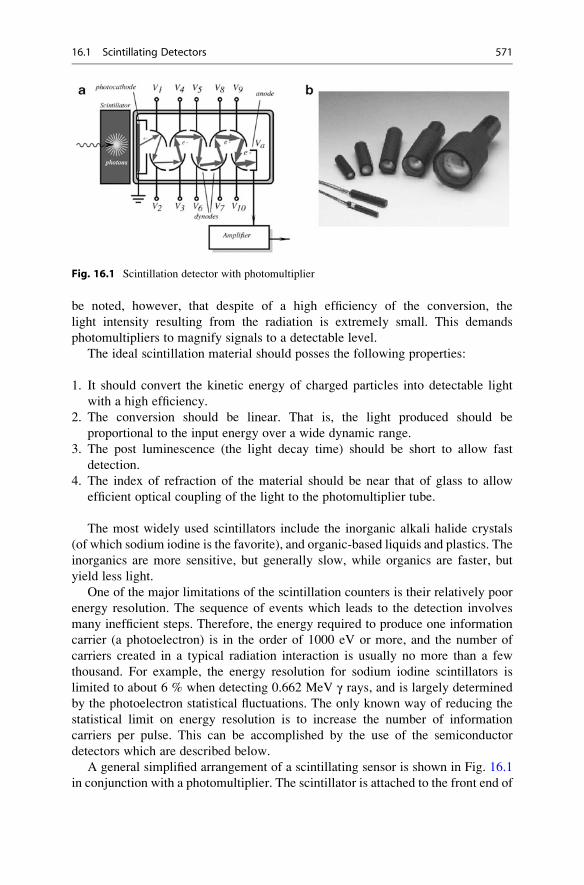
be noted, however, that despite of a high efficiency of the conversion, the
light intensity resulting from the radiation is extremely small. This demands
photomultipliers to magnify signals to a detectable level.
The ideal scintillation material should posses the following properties:
1. It should convert the kinetic energy of charged particles into detectable light
with a high efficiency.
2. The conversion should be linear. That is, the light produced should be
proportional to the input energy over a wide dynamic range.
3. The post luminescence (the light decay time) should be short to allow fast
detection.
4. The index of refraction of the material should be near that of glass to allow
efficient optical coupling of the light to the photomultiplier tube.
The most widely used scintillators include the inorganic alkali halide crystals
(of which sodium iodine is the favorite), and organic-based liquids and plastics. The
inorganics are more sensitive, but generally slow, while organics are faster, but
yield less light.
One of the major limitations of the scintillation counters is their relatively poor
energy resolution. The sequence of events which leads to the detection involves
many inefficient steps. Therefore, the energy required to produce one information
carrier (a photoelectron) is in the order of 1000 eV or more, and the number of
carriers created in a typical radiation interaction is usually no more than a few
thousand. For example, the energy resolution for sodium iodine scintillators is
limited to about 6 % when detecting 0.662 MeV γ rays, and is largely determined
by the photoelectron statistical fluctuations. The only known way of reducing the
statistical limit on energy resolution is to increase the number of information
carriers per pulse. This can be accomplished by the use of the semiconductor
detectors which are described below.
A general simplified arrangement of a scintillating sensor is shown in Fig. 16.1
in conjunction with a photomultiplier. The scintillator is attached to the front end of
Fig. 16.1 Scintillation detector with photomultiplier
16.1 Scintillating Detectors 571

the photomultiplier (PM). The front end contains a photocathode which is
maintained at a ground potential. There is a large number of special plates called
dynodes positioned inside the PM tube in an alternating pattern, reminding shape of
a “venetian blind.” Each dynode is attached to a positive voltage source in a manner
that the farther the dynode from the photocathode, the higher is its positive
potential. The last component in the tube is an anode, which has the highest positive
potential, sometimes on the order of several thousand volts. All components of the
PM are enveloped into a glass vacuum tube, which may contain some additional
elements, like focusing electrodes, shields, etc.
Although the PM is called a photomultiplier, in reality it is an electron multi-
plier, as there are no photons, only electrons inside the PM tube during its operation.
For illustration, let us assume that a γ-ray particle has a kinetic energy of 0.5 MeV
(Mega-electron-Volt). It strikes the scintillating crystal resulting in a number of
liberated photons. In a thallium-activated sodium iodine, the scintillating efficiency
is about 13 %, and therefore total of 0.5� 0.13¼ 0.065 MeV, or 65 keV of energy is
converted into visible light with an average energy of 4 eV. Therefore, about 15,000
scintillating photons are produced per gamma pulse. This number is too small to be
detected by an ordinary photodetector, and hence a multiplication effect is required
before the actual detection takes place. Of 15,000 photons probably about 10,000
reach the photocathode, whose quantum efficiency is about 20 %. The photocath-
ode serves to convert incident light photons into low-energy electrons. Therefore,
the photocathode produces about 2000 electrons per pulse. Now, that number is to
be multiplied in a PM. The PM tube is a linear device, that is, its gain is almost
independent of the number of multiplied electrons.
Since all dynodes are at positive potentials (V1–V10), an electron released from
the photocathode is attracted to the first dynode, liberating at impact with its surface
several very low energy electrons. Thus, a multiplication effect takes place at the
dynode. These electrons will be easily guided by the electrostatic field from the first
to the second dynode. They strike the second dynode and produce more electrons
which travel to the third dynode, and so on. The process results in an increasing
number of available electrons (avalanche effect). An overall multiplication ability
of a PM tube is in the order of 106. As a result, about 2� 109 electrons will be
available at a high voltage anode (Va) for production of electric current. This is a
pretty strong electric current which can be easily processed by an electronic circuit.
A gain of a PM tube is defined as
G ¼ αδN; ð16:3Þwhere N is the number of dynodes, α is the fraction of electrons collected by the PM
tube, δ is the efficiency of the dynode material, that is, the number of electrons
liberated at impact. Its value ranges from 5 to 55 for a high yield dynode. The gain is
sensitive to the applied high voltage, because δ is almost a linear function of the
inter-dynode voltage.
572 16 Detectors of Ionizing Radiation

A modern design of a photomultiplier is called the Channel Photomultiplieror CPM for short. It is the evolution of the classical photomultiplier tube PM.
The modern CPM technology preserves the advantages of the classical PM while
avoiding its disadvantages. Figure 16.2a shows a faceplate with a photocathode, the
bent channel amplification structure and the anode. Like in the PM of Fig. 16.1,
photons in the CPM are converted inside the photocathode into photoelectrons and
accelerated in a vacuum towards the anode by an electrical field. Instead of the
complicated dynode structure there is a bent thin semiconductive channel through
which the electrons have to pass. Each time when electrons hit the wall of the
channel, secondary electrons are emitted from the surface. At each collision, there
is a multiplication of the secondary electrons resulting in an avalanche effect.
Ultimately, an electron multiplication of 109 and more can be obtained. The
resulting current can be read out at the anode. The CPM detector is potted with
encapsulation material and is quite rugged as compared to the fragile PM. Magnetic
field disturbance is negligibly small. Figure 16.2b shows images of the CPM. An
important advantage of the CPM technology is its very low background noise. The
term background noise refers to the measured output signal in the absence of any
incident light. With classical PMs, the background noise originating from the
dynode structure is generally a non-negligible part of the total background. As a
result, the only effective source of background for the CPM is generated from
thermal emission of the photocathode. Since the CPM is manufactured in a mono-
lithic semiconductive channel structure, no charge-up effects might occur as known
of classical PMs with isolating glass bulbs. Hence, extremely stable background
conditions are observed. No sudden bursts occur. Also due to the absence of dynode
noise, a very clean separation between an event created from a photo electron and
electronic noise can be performed. This leads into a high stability of the signal
over time.
Fig. 16.2 Channel photomultiplier: cross-sectional view (a) and external view with potted
encapsulation at left and with no encapsulation at right (b). (Courtesy of PerkinElmer, Inc.)
16.1 Scintillating Detectors 573

16.2 Ionization Detectors
These detectors rely on the ability of some gaseous and solid materials to produce
ion pairs in response to the ionization radiation. Then, positive and negative ions
can be separated in an electrostatic field and measured.
Ionization happens because charged particles upon passing at a high velocity
through an atom can produce sufficient electromagnetic forces, resulting in the
separation of electrons, thus creating ions. Remarkably, the same particle can
produce multiple ion pairs before its energy is expended. Uncharged particles
(like neutrons) can produce ion pairs at collision with the nuclei.
16.2.1 Ionization Chambers
These radiation detectors are the oldest and most widely used. The ionizing particle
causes ionization and excitation of gas molecules along its passing track. As a
minimum, the particle must transfer an amount of energy equal to the ionization
energy of the gas molecule to permit the ionization process to occur. In most gasses
of interest for radiation detection, the ionization energy for the least tightly bound
electron shells is between 10 and 20 eV [2]. However, there are other mechanisms
by which the incident particle may lose energy within gas that do not create ions, for
instance, moving gas electrons to a higher energy level without removing
it. Therefore, the average energy lost by a particle per ion pair formed (called
W-value) is always greater than the ionizing energy. The W-value depends on gas
(Table 16.1), the type of radiation, and its energy.
In the presence of electric field, the drift of the positive and negative charges
represented by the ions end electrons constitutes an electric current. In a given
volume of gas, the rate of the formation of the ion pair is constant. For any small
volume of gas, the rate of formation will be exactly balanced by the rate at which
ion pairs are lost from the volume, either through recombination, or by diffusion or
migration from the volume. If recombination is negligible and all charges are
effectively collected, the steady state current is produced and it is an accurate
measure of the rate of the ion pair formation. Figure 16.3a illustrates a basic
structure of an ionizing chamber and the current/voltage characteristic.
A volume of gas is enclosed between the electrodes which produce an electric
field. An electric current meter is attached in series with the voltage source E and
Table 16.1 W-values for
different gases [adapted
from ref. [2])
W-value (in eV/ion pair)
Gas Fast electrons Alphas
A 27.0 25.9
He 32.5 31.7
N2 35.8 36.0
Air 35.0 35.2
CH4 30.2 29.0
574 16 Detectors of Ionizing Radiation

the electrodes. There is no electrical conduction and no current under the
no-ionization conditions. Incoming radiation produces, in the gas, positive and
negative ions which are pulled by the electric field toward the corresponding
electrodes forming an electric current. The current versus voltage characteristic of
the chamber is shown in Fig. 16.3b. At relatively low voltages, the ion recombina-
tion rate is strong and the output current is proportional to the applied voltage,
because higher voltage reduces the number of recombined ions. A sufficiently
strong voltage completely suppresses all recombinations by pulling all available
ions toward the electrodes, and the current becomes voltage independent. However,
it still depends on the intensity of irradiation. This is the region which is called
saturation and where the ionization chamber normally operates.
16.2.2 Proportional Chambers
The proportional chamber is a type of a gas-filled detector which almost always
operates in a pulse mode and relies on the phenomenon of a gas multiplication. This
is why these chambers are called the proportional counters. Due to gas multiplica-
tion, the output pulses are much stronger than in conventional ion chambers. These
counters are generally employed in the detection and spectroscopy of low energy
X-radiation and for the detection of neutrons. Contrary to the ionization chambers,
the proportional counters operate at higher electric fields, which can greatly accel-
erate electrons that are liberated during the collision. If these electrons gain
sufficient energy, they may ionize a neutral gas molecule, thus creating an addi-
tional ion pair. Hence, the process is of an avalanche type resulting in a substantial
increase in the electrode current. The name for this process is Townsend avalanche.In the proportional counter, the avalanche process ends when the electron collides
with the anode. Since in the proportional counter the electron must reach the gas
ionization level, there is a threshold voltage after which the avalanche process
occurs. In typical gases at atmospheric pressure, the threshold field level is on the
order of 106 V/m.
Fig. 16.3 Simplified schematic of ionization chamber (a) and current vs. voltage characteristic (b)
16.2 Ionization Detectors 575

Differences between various gas counters are illustrated in Fig. 16.4. At very low
voltages, the field is insufficient to prevent the recombination of ion pairs. In the
saturation level, all ions are drifted to the electrodes. A further increase in voltage
results in gas multiplication. Over some region of the electric field, the gas
multiplication will be linear, and the collected charge will be proportional to the
number of original ion pairs created during the ionization collision. An even further
increase in the applied voltage can introduce nonlinear effects, which are related to
the positive ions, due to their slow velocity.
16.2.3 Geiger–Muller (GM) Counters
The Geiger–Muller (GM) counter was invented2 in 1928 and is still in use thanks to
its simplicity, low cost, and ease of operation. The GM counter is different from
other ion chambers by its much higher applied voltage (see Fig. 16.4). In the region
of the GM operation, the output pulse amplitude does not depend on the energy of
ionizing radiation and is strictly a function of the applied voltage. A GM counter is
usually fabricated in form of a tube with an anode wire in the center, Fig. 16.5a. The
tube is filled with a noble gas, such as helium or argon. A secondary component is
usually added to the gas for the purpose of quenching, which is preventing of a
retriggering of the counter after the detection. The retriggering may cause multiple
pulses instead of the desired one. The quenching can be accomplished by several
methods, among which are a short-time reduction of the high voltage applied to the
tube, use of a high impedance resistor in series with the anode, and adding the
Fig. 16.4 Various operating
voltages for gas-filled
detectors (adapted
from ref. [2])
2 Johannes (Hans) Wilhelm Geiger (1882–1945) was a German physicist. He is best known as the
co-inventor of the GM counter and for the Geiger–Marsden experiment that discovered the atomic
nucleus. He was a ‘loyal Nazi’ who unhesitatingly betrayed many of his former colleagues.
Walther Muller (1905–1979) was a student of Geiger and a founder of a US company that
produced tubes for the GM counters.
576 16 Detectors of Ionizing Radiation

quench gas at concentrations of 5–10 %. Many organic molecules possess the
proper characteristics to serve as a quench gas. Of these, ethyl alcohol and ethyl
formate have proven to be the most popular.
In a typical avalanche created by a single original electron, the secondary ions
are created. In addition to them, many excited gas molecules are formed. Within a
few nanoseconds, these excited molecules return to their original state through the
emission of energy in form of ultraviolet (UV) photons. These photons play an
important role in the chain reaction occurring in the GM counter. When one of the
UV-photons interacts by a photoelectric absorption in some other region of the gas,
or at the cathode surface, a new electron is liberated which can subsequently
migrate toward the anode, and will trigger another avalanche. In a Geiger discharge,
the rapid propagation of the chain reaction leads to many avalanches which initiate
at random radial and axial positions throughout the tube. Secondary ions are
therefore formed throughout the cylindrical multiplying region which surrounds
the anode wire. Hence, the discharge grows to envelope the entire anode wire,
regardless of the position at which the primary initiating event occurred.
Once the Geiger discharge reaches a certain level, however, collective effects of
all individual avalanches come into play and ultimately terminate the chain reac-
tion. This point depends on the number of avalanches and not on the energy of the
initiating particle. Thus, the GM current pulse is always of the same amplitude,
which makes the GM counter just an indicator of irradiation, because all informa-
tion on the ionizing energy is lost.
In the GM counter, a single particle of a sufficient energy can create about
109–1010 ion pairs. Because a single ion pair formed within the gas of the GM
counter can trigger a full Geiger discharge, the counting efficiency for any charged
particle that enters the tube is essentially 100 %. However, the GM counters are
seldom used for counting neutrons because of a very low efficiency of counting.
The efficiency of GM counters for γ-rays is higher for those tubes constructed witha cathode wall of high-Z material. For instance, bismuth (Z¼ 83) cathodes have
been widely used for the γ-detection in conjunction with gases of high atomic
Fig. 16.5 Conceptual circuit of Geiger–Muller (GM) counter. Symbol ( filled circle) indicatesgas (a) and vintage GM counter (b)
16.2 Ionization Detectors 577

numbers, such as xenon and krypton, which yield a counting efficiency up to 100 %
for photon energies below about 10 keV.
A further improvement of GM counter is the so-called wire chamber that
contains many parallel wires, arranged as a grid. A high voltage is applied to the
wires with the metal casing being at a ground potential. As in the GM counter, a
particle leaves a trace of ions and electrons, which drift toward the case or the
nearest wire, respectively. By marking off the wires that had a pulse of current, one
can see the particle’s path.
16.2.4 Semiconductor Detectors
The best energy resolution in modern radiation detectors can be achieved in the
semiconductor materials, where a comparatively large number of carriers for a
given incident radiation event occurs. In these materials, the basic information
carriers are electron–hole pairs created along the path taken by the charged particlethrough the detector. The charged particle can be either primary radiation, or a
secondary particle. The electron–hole pairs in some respects are analogous to the
ion pairs produced in the gas-filled detectors. When an external electric field is
applied to the semiconductive material, the created carriers form a measurable
electric current. The detectors operating on this principle are called solid-state or
semiconductor diode detectors. The operating principle of these radiation detectors
is the same as that of the semiconductor light detectors. It is based on the transition
of electrons from one energy level to another when they gain or lose energy. For the
introduction to the energy band structure in solids the reader should refer to
Sect. 15.1.1.
When a charged particle passes through a semiconductor with the band structure
shown in Fig. 15.1, the overall significant effect is the production of many electron–
hole pairs along the track of the particle. The production process may be either
direct or indirect, in that the particle produces high-energy electrons (or Δ rays)
which subsequently lose their energy in production more electron–hole pairs.
Regardless of the actual mechanism involved, what is of interest to our subject is
the average energy expended by the primary charged particle produces one
electron–hole pair. This quantity is often called the “ionization energy.” The
major advantage of semiconductor detectors lies in the smallness of the ionization
energy. The value of it for silicon or germanium is about 3 eV, compared with
30 eV required to create an ion pair in typical gas-filled detectors. Thus, the number
of charge carriers is about ten times greater for the solid-state detectors for a given
energy of a measured radiation.
To fabricate a solid-state detector, at least two contacts must be formed across a
semiconductor material. For detection, the contacts are connected to the voltage
source which enables carrier movement. The use of a homogeneous Ge or Si,
however, would be totally impractical. The reason for that is in an excessively
high leakage current caused by the material’s relatively low resistivity (50 kΩ cm
for silicon). The external voltage, when applied to the terminals of such a detector
578 16 Detectors of Ionizing Radiation

may cause a current, which is 3–5 orders of magnitude greater than a minute
radiation-induced electric current. Thus, the detectors are fabricated with the
blocking junctions, which are reverse biased to dramatically reduce leakage cur-
rent. In effect, the detector is a semiconductor diode, which readily conducts (has
low resistivity) when its anode ( p side of a junction) is connected to a positive
terminal of a voltage source and the cathode (an n side of the junction) to the
negative. The diode conducts very little (it has very high resistivity) when the
connection is reversed, thus the name reverse biasing is implied. If the reverse bias
voltage is made very large, in excess of the manufacturer specified limit, the reverse
leakage current abruptly increases (the breakdown effect) which often may lead to a
catastrophic deterioration of detecting properties or to the device destruction.
Several configurations of silicon diodes are currently produced. Among them
diffused junction diodes, surface barrier diodes, ion implanted detectors, epitaxial
layer detectors, and others. The diffused junction and surface barrier detectors find
widespread applications for detection of α particles and other short-range radiation.
A good solid-state radiation detector should possess the following properties:
1. Excellent charge transport.
2. Linearity between the energy of the incident radiation and number of electron–
hole pairs.
3. Absence of free charges (low leakage current).
4. Production of a maximum number of electron–hole pairs per unit of radiation.
5. High detection efficiency.
6. Fast response speed.
7. Large collection area.
8. Low cost.
When using semiconductor detectors, several factors should be seriously con-
sidered. Among them are the dead band layer of the detector and the possible
radiation damage. If heavy charged particles or other weakly penetrating radiations
enter the detector, there may be a significant energy loss before the particle reaches
the active volume of the semiconductor. The energy can be lost in the metallic
electrode and in a relatively thick silicon body immediately beneath the electrode.
This thickness must be measured directly by the user if an accurate compensation is
desirable. The simplest and most frequently used technique is to vary the angle of
incidence of a monoenergetic charged particle radiation [2]. When the angle of
incidence is zero (that is, perpendicular to the detector’s surface) the energy loss in
the dead layer is given by
ΔEo ¼ dEo
dxt; ð16:4Þ
where t is the thickness of the dead layer. The energy loss for an angle of incidenceof Θ is
16.2 Ionization Detectors 579

ΔE θð Þ ¼ ΔEo
cosΘ: ð16:5Þ
Therefore, the difference between the measured pulse height for angles of incidence
of zero and Θ is given by
E0 ¼ Eo � ΔEo½ � � Eo � ΔE Θð Þ½ � ¼ ΔEo
1
cos� 1
� �: ð16:6Þ
If a series of measurements is made as the angle of incidence is varied, a plot of
E0 as a function of (1/cos Θ)� 1 should be a straight line whose slope is equal to
ΔEo. Using tabular data for dEo/dx for the incident radiation, the dead layer
thickness can be calculated from Eq. (16.4).
Any excessive use of the detectors may lead to some damage to the lattice of the
crystalline structure, due to disruptive effects of the radiation being measured as it
passes through the crystal. These effects tend to be relatively minor for lightly
ionizing radiation (β-particles or γ rays), but can become quite significant under
typical conditions of use for heavy particles. For example, prolonged exposure of
silicon surface barrier detectors to fusion fragments will lead to a measurable
increase in leakage current and a significant loss in energy resolution of the
detector. With extreme radiation damage, multiple peaks may appear in the pulse
height spectrum recorded for monoenergetic particles.
Mentioned above diffused junction diodes and surface barrier diodes are not
quite suitable for detecting of penetrating radiation. The major limitation is in the
shallow active volume of these sensors, which rarely can exceed 2–3 mm. This is
not nearly enough, for instance, for a γ-ray spectroscopy. A practical method to
make detectors for a more penetrating radiation is the so-called ion-drifting process.The approach consists of creating a thick region with a balanced number of donor
impurities, which add either p or n properties to the material. Under ideal
conditions, when the balance is perfect, the bulk material would resemble the
pure (intrinsic) semiconductor without either p or n properties. However, in reality
the perfect pn balance never can be achieved. In Si or Ge, the pure material with the
highest possible purity tends to be of p type. To accomplish the desired compensa-
tion, the donor atoms must be added. The most practical compensation donor is
lithium. The fabrication process involves a diffusing of lithium though the p crystalso that the lithium donors greatly outnumber the original acceptors, creating an
n type region near the exposed surface. Then, temperature is elevated and the
junction is reverse biased. This results in a slow drifting of lithium donors into
the p type for the near perfect compensation of the original impurity. The process
may take as long as several weeks. To preserve the achieved balance, the detector
must be maintained at low temperature: 77 K for the germanium detectors. Silicon
has very low ion mobility, thus the detector can be stored and operated at room
temperature. However, the lower atomic number for silicon (Z¼ 14) as compared
with germanium (Z¼ 32) means that the efficiency of silicon for detection of γ raysis very low and it is not widely used in the general γ-ray spectroscopy.
580 16 Detectors of Ionizing Radiation

A simplified schematic of a lithium-drifted detector is shown in Fig. 16.6a.
It consists of three regions where the “intrinsic” crystal is in the middle. In order
to create detectors of a larger active volume, the shape can be formed as a cylinder,
Fig. 16.6b, where the active volumes of Ge up to 150 cm3 can be realized. The
germanium lithium-drifted detectors are designated as Ge(Li).
Regardless of the widespread popularity of the silicon and germanium detectors,
they are not the ideal from certain standpoints. For instance, germanium must
always be operated at cryogenic temperatures to reduce thermally generated leak-
age current, while silicon is not efficient for the detection of γ rays. There are some
other semiconductors which are quite useful for detection of radiation at room
temperatures. Among them are cadmium telluride (CdTe), mercuric iodine (HgI2),
gallium arsenide (GaAs), bismuth trisulfide (Bi2S3), and gallium selenide (GaSe).
Useful for radiation detectors properties of some semiconductive materials are
given in Table 16.2.
Probably the most popular at the time of this writing is cadmium telluride which
combines a relatively high Z-value (48 and 52) with a large enough band gap energy
(1.47 eV) to permit room temperature operation. Crystals of high purity can be
grown from CdTe to fabricate the intrinsic detector. Alternatively, chlorine doping
is occasionally used to compensate for the excess of acceptors and to make the
Fig. 16.6 Lithium-drifted pin-junction detector. Structure of the detector (a); coaxial configura-tion of the detector (b)
Table 16.2 Detecting properties of some semiconductive materials (adapted from ref. [2])
Material (operating
temperature in K) Z Band gap, eV
Energy per
electron–hole pair, eV
Si (300) 14 1.12 3.61
Ge (77) 32 0.74 2.98
CdTe (300) 48–52 1.47 4.43
HgI2 (300) 80–53 2.13 6.5
GaAs (300) 31–33 1.43 4.2
16.2 Ionization Detectors 581

material of a near-intrinsic type. Commercially available CdTe detectors range in
size from 1 to 50 mm in diameter and can be routinely operated at temperatures up
to 50 �C without an excessive increase in noise. Thus, there are two types of CdTe
detectors available: the pure intrinsic type and the doped type. The former has high
volume resistivity up to 1010Ω cm; however, its energy resolution is not that great.
The doped type has significantly better energy resolution; however, its lower
resistivity (108Ω cm) leads to a higher leakage current. Besides, these detectors
are prone to polarization which may significantly degrade their performance.
In the solid-state detectors, it is also possible to achieve a multiplication effect as
in the gas-filled detectors. An analog of a proportional detector is called an
avalanche detector which is useful for the monitoring of low-energy radiation.
The gain of such a detector is usually in the range of several hundreds. It is achieved
by creating within a semiconductor high-level electric fields.
16.3 Cloud and Bubble Chambers
The cloud chamber, also known as the Wilson chamber,3 is used for detecting
particles of ionizing radiation. In its most basic form, a cloud chamber is a sealed
environment containing a supercooled, supersaturated water or alcohol (e.g.,
methylated spirits) vapor, which is at the point of condensation. When an alpha
particle or beta particle interacts with the mixture, it ionizes it. The resulting ions
act as condensation nuclei, around which a mist will form. In other words, the vapor
condenses into droplets when disturbed and ionized by the passage of a particle. A
trail is left along the particle path because many ions are being produced along the
path of the charged particle. These tracks have distinctive shapes (for example, an
alpha particle’s track is broad and straight, while an electron’s is thinner and shows
more evidence of deflection). The tracks are photographed and analyzed. When a
vertical magnetic field is applied, positively and negatively charged particles will
curve in opposite directions. There are different types of the cloud chambers. The
expansion cloud chambers use a vacuum pump to briefly produce the right
conditions for trails to form, while the diffusion type uses solid CO2 (dry ice) to
cool the bottom of the chamber and produce a temperature gradient in which trails
can be seen continuously.
A bubble chamber4 is similar to the cloud chamber except that a liquid is used
instead of vapor. Interestingly, a glass of champagne or beer is a kind of a bubble
chamber where tiny bubble formations are triggered by the ionizing radiation
coming from the environment and outer Space. For the physical experiments, a
3 The cloud chamber was invented by a Scottish physicist Charles Thomas Rees Wilson
(1869–1959).4 The bubble chamber was invented in 1952 by Donald A. Glaser, for which in 1960 he was
awarded the Nobel Prize in Physics.
582 16 Detectors of Ionizing Radiation

bubble chamber is filled with a more prosaic and much colder liquid, such as liquid
hydrogen. It is used for detecting electrically charged particles moving through it.
The bubble chamber is normally made by filling a large cylinder shown
Fig. 16.7a with liquid hydrogen heated to just below its boiling point. As particles
enter the chamber, a piston suddenly decreases its pressure, and the liquid enters
into a superheated, metastable phase. Charged particles create an ionization track,
around which the liquid vaporizes, forming microscopic bubbles. Bubble density
around a track is proportional to a particle’s energy loss.
Bubbles grow in size as the chamber expands, until they are large enough to be
seen or photographed. Several cameras are mounted around it, allowing a three-
dimensional image of an event to be captured. Bubble chambers with resolutions
down to a few micrometers have been operated. A constant magnetic field is formed
around the chamber by an electromagnet that causes charged particles to travel in
helical paths whose radii are determined by their charge-to-mass ratios, Fig.16.7b.
Although bubble chambers were very successful in the past, they are of only limited
use in current very-high-energy experiments for a variety of reasons, among which
are the problem with the superheated phase that must be ready at the precise
moment of collision, which complicates the detection of short-lived particles.
Also, the bubble chambers are neither large nor massive enough to analyze high-
energy collisions, where all products should be contained inside the detector.
References
1. Evans, R. D. (1955). The atomic nucleus. New York, NY: McGraw-Hill.
2. Knoll, G. F. (1999). Radiation detection and measurement (3rd ed.). New York, NY:
John Wiley and Sons.
3. The Elegant Universe. Teacher’s guide. Nova #pbs.org, 2012.
Fig. 16.7 Bubble chamber (a) and ionizing tracks (b) (adapted from ref. [3])
References 583

Temperature Sensors 17
When a scientist thinks of something, he asks, –‘Why?’When an engineer thinks of something, he asks, –‘Why not?’
From prehistoric times people are aware of heat and trying to assess its intensity by
measuring temperature. Perhaps the simplest, and certainly the most widely used,
physical phenomenon for temperature sensing is thermal expansion. This forms the
basis of the liquid-in-glass thermometers. For the electrical transduction, different
methods of sensing are employed. Among them are: the resistive, thermoelectric,
semiconductive, optical, acoustic, and piezoelectric detectors. For measuring
temperature, the sensor shall be thermally coupled to the object. The coupling
may be physical (contact) or remote (non-contact), but a thermal coupling always
must be established for the sensor to produce a measurable electrical response.
All temperature sensors can be divided into two classes: the absolute sensors andthe relative sensors. An absolute temperature sensor measures temperature that is
referenced to the absolute zero or any other fixed point on the absolute temperature
scale, for example, 0 �C (273.15 K), 25 �C or any other arbitrarily selected
reference temperature. Examples of the absolute sensors are thermistors and
RTDs. A relative sensor measures a temperature difference between two objects,
or thermal gradient. An example of a relative sensor is a thermocouple.
17.1 Coupling with Object
17.1.1 Static Heat Exchange
Taking a temperature essentially requires the transmission of a small portion of the
object’s thermal energy to the sensor whose function is to convert that energy into
an electrical signal. When a contact sensor (probe) is placed inside or on the
object’s surface, heat conduction takes place through the boundary between the
# Springer International Publishing Switzerland 2016
J. Fraden, Handbook of Modern Sensors, DOI 10.1007/978-3-319-19303-8_17585
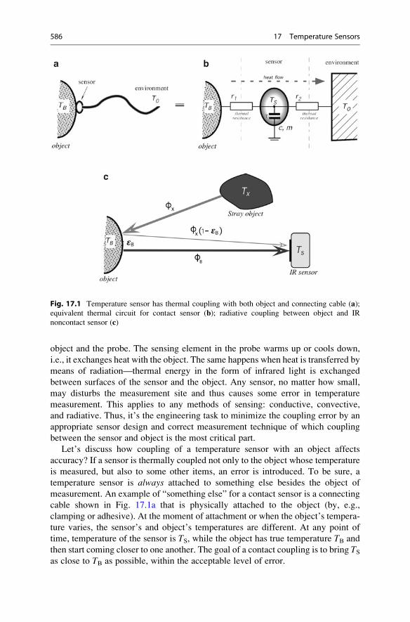
object and the probe. The sensing element in the probe warms up or cools down,
i.e., it exchanges heat with the object. The same happens when heat is transferred by
means of radiation—thermal energy in the form of infrared light is exchanged
between surfaces of the sensor and the object. Any sensor, no matter how small,
may disturbs the measurement site and thus causes some error in temperature
measurement. This applies to any methods of sensing: conductive, convective,
and radiative. Thus, it’s the engineering task to minimize the coupling error by an
appropriate sensor design and correct measurement technique of which coupling
between the sensor and object is the most critical part.
Let’s discuss how coupling of a temperature sensor with an object affects
accuracy? If a sensor is thermally coupled not only to the object whose temperature
is measured, but also to some other items, an error is introduced. To be sure, a
temperature sensor is always attached to something else besides the object of
measurement. An example of “something else” for a contact sensor is a connecting
cable shown in Fig. 17.1a that is physically attached to the object (by, e.g.,
clamping or adhesive). At the moment of attachment or when the object’s tempera-
ture varies, the sensor’s and object’s temperatures are different. At any point of
time, temperature of the sensor is TS, while the object has true temperature TB and
then start coming closer to one another. The goal of a contact coupling is to bring TSas close to TB as possible, within the acceptable level of error.
Fig. 17.1 Temperature sensor has thermal coupling with both object and connecting cable (a);equivalent thermal circuit for contact sensor (b); radiative coupling between object and IR
noncontact sensor (c)
586 17 Temperature Sensors

In a practical system, one end of the cable is connected to a contact sensor, and
thus is at temperature TS. The other end is at some another temperature, for
example, the ambient temperature T0 that may be quite different from TS. Thecable conducts both an electric signal and some heat from or to the sensor.
Figure 17.1b shows a thermal circuit that includes the object, sensor, environment,
and thermal resistances r1 and r2. Thermal resistances should be clearly understood.
A thermal resistance represents the ability of a matter to conduct thermal energy
and is inversely related to thermal conductivity, that is r¼ 1/α. If an object is
warmer than the environment, heat flows through the sensor in the direction
indicated by an arrow.
The circuit of Fig. 17.1b resembles an electric circuit and indeed its properties
can be evaluated by using the laws of electric circuits, such as Kirchhoff’s1 and
Ohms laws. Note that a thermal capacitance of the sensor is represented by a
capacitor. Assuming that we wait sufficiently long and all temperatures are settled
on some steady-stale levels, and also assuming that the object and environment
temperatures are stable and not affected by their interconnection by the sensor, for
such a steady state we may apply the law of conservation of energy. Consider that
the thermal energy that flows from the object to the sensor is equal to the energy that
outflows from the sensor to the environment. This allows us to write a static balance
(equilibrium) equation:
TB � TS
r1¼ TB � T0
r1 þ r2; ð17:1Þ
from which we derive the sensor’s temperature as
TS ¼ TB � TB � T0ð Þr1r2
¼ TB � ΔTr1r2; ð17:2Þ
where ΔT is a thermal gradient between the object and the surroundings. Let’s take
a closer look at Eq. (17.2). We can draw several conclusions from it. The first is that
the sensor temperature Ts is different from that of the object TB. The only exceptionis when the environment is at the same temperature as the object (a special case
when ΔT¼ TB� T0¼ 0). The second conclusion is that Ts will closely approach TB,regardless of the gradient ΔT, when the ratio r1/r2 approaches zero. This means that
for minimizing the measurement error we must improve a thermal coupling
between the object and sensor (r1! 0) and thermally de-couple the sensor from
surroundings as much as practical (r2!1). Often, it’s not easy to do.
The best way of bringing ΔT in Eq. (17.2) closer to zero is to embed the sensor
into the object as shown in Fig. 17.2a. A cavity is formed inside the object where the
sensor is placed, preferably with a thermal grease, epoxy or other method is used the
thermally bond the sensor with the cavity walls. The cable near the sensor is shaped
as a loop and also placed inside the cavity. This allows to equalize temperatures of
1Kirchhoff’s law was originally conceived not for the electrical circuits but for plumbing.
17.1 Coupling with Object 587

the sensor, cable, and cavity. Since the sensor and the proximal portion of the cable
are not exposed to external temperatures, the measurement becomes significantly
more accurate.
Forming a cavity inside an object is not always possible, thus a surface measure-
ment becomes the only practical choice. As we just discussed, this is not a desirable
arrangement for a contact measurement. Fortunately, there is a powerful technique
to form a “virtual cavity” at the object’s surface [1], forcing ΔT! 0. To create a
virtual cavity, the prime contact temperature sensor is provided with a surface
thermal shied shown in Fig. 17.2b. Conceptually, this is a thermal equivalent to a
driven capacitive shield (for example, see Figs. 6.4 and 7.20). The thermal driven
shield is fabricated of a metal having a good thermal conductivity (e.g., aluminum)
and contains two embedded components: a heater (and/or cooler) and another
temperature sensor called the shield temperature sensor. Both sensors provide
signals to the control servo-circuit that supplies power to the heater/cooler. The
servo-circuit works to minimize the thermal gradient ΔT between the prime and
shield sensors. Preferably, the driven thermal shield touches the object’s surface all
around the prime sensor, thus protects it from environment. The object surface and
the shield form a virtual thermostatic cavity around the measurement spot. When a
thermal gradient between both sensors approaches zero, the prime sensor becomes
nearly totally thermally shielded from the environment. It’s very important to
thermally decouple the prime sensor from the thermal shield, otherwise the circuit
may become unstable.
This method was implemented in a medical body core thermometer [1] where
the prime sensor was affixed to a pliant ear plug to touch the ear canal skin as shown
in Fig. 17.3. The driven shield was positioned outside of the ear to cover the helix
opening. Since interior of the ear canal was thermally shielded from the outside, this
prime sensor provided accurate continuous non-invasive monitoring of patient’s
temperature that is nearly the same as temperature of blood in the carotid artery.
A coupling problem may arise with a non-contact thermal (IR) radiation sensor
(see Sect. 4.12.3). Heat exchange between the IR sensor and object is illustrated in
Fig. 17.2 Embedded temperature sensor (a), surface temperature sensor with active driven
thermal shield (b)
588 17 Temperature Sensors

Fig. 17.1c. If the optical coupling between the object and sensor is not perfect, the
sensor may receive undesirable thermal flux from a stray object having temperature
Tx, even if that object is not within the filed of view of the IR sensor. The object of
measurement has temperature TB and surface emissivity εB, thus it emanates toward
the IR sensor the useful flux ΦB in proportion to that emissivity. However, since
εB< 1, the object is somewhat reflective, hence a portion of the stray flux Φx equal
to Φx(1� εB) will be reflected by the object toward the IR sensor. That spurious IR
flux will cause error in measurement because it is added to the useful flux.
Therefore, deficiency in the IR optical coupling between the object and noncontact
sensor is a potential source of errors.
17.1.2 Dynamic Heat Exchange
Above, we evaluated the static, that is—time invariant, conditions of heat exchange
between the sensor and object. Now let’s consider a dynamic case when
temperatures change with time. This occurs when either the object or the
surrounding temperatures change or the sensor was just recently attached to the
object and its temperature is not yet stabilized at the equilibrium. This equally
Fig. 17.3 Sensor for noninvasive continuous monitoring of temperature through patient’s ear
canal. Driven shield temperature is forced to be nearly equal to temperature measured by the prime
sensor that touches the ear canal skin
17.1 Coupling with Object 589

relates to both the contact and noncontact IR sensors, thus below we discuss only
the contact sensors.
Initially, let’s consider an ideal case that requires making two assumptions: (1) a
thermal resistance between the sensor and the environment is infinitely large
(r2!1), meaning that the sensor will be perfectly thermally coupled to the object
and to nothing else, and (2) the object’s temperature doesn’t change after the sensor
is attached. In other words, the object is considered being much larger than the
sensor and acts as an “infinite” heat source/sink. In other words, it has an infinitely
large thermal capacity and infinitely high thermal conductivity. When the sensor is
coupled to such an idealized object, the sensor’s temperature profile will like the
one shown in Fig. 17.4.
At a starting time t¼ 0 the temperature sensor having the initial temperature T1comes in contact with the object having temperature TB. After that, according to
Newton’s Law of Cooling the incremental amount of heat transferred from the
object to the sensor is proportional to a temperature gradient between the instant
sensor temperature Ts at a particular moment and a static temperature of the
object TB:
dQ ¼ α1 TB � TSð Þdt; ð17:3Þwhere α1¼ 1/r1 is the thermal conductivity of the sensor–object boundary. Note
that Ts is changing while TB is not. If the sensor has an average specific heat c andmass m, the heat absorbed by the sensor is
dQ ¼ mcdT: ð17:4ÞSince whatever heat is transferred the same heat is absorbed, Eqs. (17.3) and (17.4)
are equal and yield the 1st-order differential equation
α1 TB � Tsð Þdt ¼ mcdT: ð17:5Þ
Fig. 17.4 Temperature
change of ideal sensor after
being attached to object
590 17 Temperature Sensors

We denote the sensor’s thermal time constant τΤ as
τT ¼ mc
α1¼ mcr1: ð17:6Þ
Then the differential equation takes form
dT
TB � Ts
¼ dt
τTð17:7Þ
This equation has a solution
Ts ¼ TB � ΔTe�tτT ð17:8Þ
One time constant τT is equal to the time required for temperature T to reach about
63.2 % of the initial gradient ΔT¼ TB� T1. The smaller the time constant the faster
the sensor responds to a change in temperature. The time constant can be minimized
by reducing the size of the sensor (smaller m) and by improving its coupling with
the object (smaller r1).If we wait for a long time (t!1) after attaching the sensor, Eq. (17.8) states,
then the temperature of the sensor approaches temperature of the object: Ts¼ TBwhich is the ideal equilibrium condition, so the sensor output can be used for
computing the object’s temperature. Theoretically, it takes infinite time to reach a
perfect equilibrium between Ts and TB—hardly anyone can wait that long! Fortu-
nately, since only a finite accuracy is usually required, for most practical cases a
quasi-equilibrium state may be considered after 5–10 time constants. For instance,
after the waiting time t¼ 5τ the sensor’s temperature will differ from that of the
object by 0.7 % of the initial gradient, while after ten time constants it will be within
0.005 %.
Now, we will study a more realistic case. Let us remove the first of the above
assumptions and consider that a thermal coupling with the environment is not
extremely large, that is r2 6¼1. In other words, the sensor exchanges heat with
other objects as well. Then the thermal time constant should be determined from
τT ¼ mc
α1 þ α2¼ mc
r11þ r1
r2
ð17:9Þ
and the sensor’s response is shown in Fig. 17.5a. Note that now the sensor
responds faster (a smaller time constant) but its temperature will never reach that
of the object, no matter how long we wait. It may be higher or lower, but never
equal, unless everything has the same temperature (e.g., the object, sensor and
cable are inside a thermostat). Hence, due to a coupling to the environment, even at
the equilibrium state, there will be a remaining thermal gradient δT which is the
error.
17.1 Coupling with Object 591

Now let us remove the second assumption—we consider the object being not an
ideal heat source or sink. This means that the object is not dramatically larger than
the sensor or its thermal conductivity is relatively low. As a result of this “imper-
fection,” upon the attachment the sensor will disturb, at least temporarily, the
measurement site. Figure 17.5b shows that upon the sensor attachment, the object’s
temperature at the moment of contact deflects (cools down or warms up) and then
will gradually return to some steady-state level. This causes a deviation of the
sensor’s temperature profile from the ideal exponential function and a concept of a
thermal time constant (τΤ) no longer will be applicable. The measurement site
disturbance usually is difficult to evaluate or mitigate. In practice, this deviation
becomes significant if one wishes to employ a predictive algorithm as described
below, or a fast temperature tracking is required. The example is a medical axillary
(under-the-armpit) thermometer that requires up to 3 min to equilibrate in spite of a
relatively fast sensor. The problem is that the probe cools down the skin and it takes
minutes for a capillary blood flow to reestablish the original temperature of
the armpit.
17.1.3 Sensor Structure
A typical contact temperature sensor consists of the following components,
Fig. 17.6a:
1. A sensing element—a device whose electrical properties vary in response to
changes in temperature. Considering Eq. (17.9), a good sensing element should
have low specific heat, small mass, strong and predictable sensitivity to temper-
ature, and good long-term stability.
2. Terminals are the conductive pads or wires for interfacing between the sensing
element and external electronic circuit. The terminals should have the lowest
possible thermal conductivity and low electrical resistance (platinum is often the
best compromise, yet expensive). Also, the terminals may be used for supporting
Fig. 17.5 Temperature changes of sensor that is coupled to environment (a) and when the object
has limited thermal conductivity (b)
592 17 Temperature Sensors

the sensing element so they should have a reasonable mechanical strength and
stability.
3. A protective envelope is either a housing or coating which physically separates
the sensing element from the environment, yet couples thermally. The envelope
should have a low thermal resistance (high thermal conductivity), low thermal
capacity, high electrical isolation properties, and be mechanically strong. It must
be environmentally stable and impermeable to moisture and other compounds
that may spuriously affect the sensing element.
A noncontact temperature sensor, Fig. 17.6b, is an optical thermal (IR) radiation
sensor whose designs are covered in detail in Sect. 15.8. Like a contact sensor, it
also contains a sensing element that is responsive to its own temperature. Temper-
ature changes upon absorbing or liberating heat via radiation. The difference
between the contact and noncontact is in the way of a heat transfer between the
object and sensing element: in a contact sensor—it is through a thermal conduction
by way of a physical contact, while in a noncontact sensor—it is through a thermal
radiation (optically).
Either contact or noncontact sensors are thermally coupled to the objects through
the respective thermal resistances r1. However, that resistance for a contact sensoris much smaller than for an IR sensor. As a result, according to Eq. (17.2) the
equilibrium temperatures for both sensors are quite different as shown in Fig. 17.7.
While in a contact sensor the equilibrium temperature in closer to that of the object,
the IR radiation sensor’s temperature is much closer to temperature T0 of the
instrument, resulting in a potentially very large thermal gradient δTradiation betweenthe sensor and object. For a contact sensor, the thermal gradient δTcontact is much
smaller. In summary, for a contact sensor, r1� r2, while for a noncontact IR sensor
r1 r2.
Fig. 17.6 General structures of temperature sensors. Contact sensor (a) touches object for
conductive heat transfer. IR sensor (b) exchanges heat with object through thermal radiation
17.1 Coupling with Object 593

17.1.4 Signal Processing of Sensor Response
When a temperature sensing element thermally couples to the object, its own
temperature changes and the sensor generates an electric output signal. At some
moment, the temperature change may come to a stop, meaning that the net heat flow
through the sensor either ends or becomes steady. As long as the sensor’s tempera-
ture keeps changing, the sensor either absorbs or liberates thermal energy. Thus, the
sensor’s response may be of two kinds: steady or changing. According to these
conditions, to determine the object’s temperature two basic methods of the signal
processing can be employed: equilibrium and predictive. In the equilibrium
method, a temperature measurement is complete when a thermal gradient between
the object and sensing element inside the probe becomes steady. At that moment the
sensor output represents the object temperature.
Reaching a thermal equilibrium between the object and sensor may be a slow
process. For instance, a contact medical electronic thermometer measures tempera-
ture from a water bath in just 3 s (a good thermal coupling), yet it will take at least
3 min when temperature is measured axillary. In the equilibrium method, the end of
measurement is determined when within a specified time interval the signal changes
less than an acceptable error limit. For example, if within an interval of 1 s the
temperature change is less than 0.05 �C, for a medical accuracy it may be consid-
ered steady enough.
17.1.4.1 Predictive AlgorithmTo shorten the measurement time, occasionally a predictive method is employed. It
is based on inferring or anticipating the equilibrium temperature through computa-
tion of a variable rate of the sensor’s temperature change. Thus, the end result is
predicted well before a thermal equilibrium is established. A predictive method is
often employed in clinical medical thermometers. It should be noted however, that
the predictive method is inherently less accurate than the equilibrium method, due
Fig. 17.7 Difference in
thermal responses between
contact and noncontact
(IR radiation) temperature
sensors
594 17 Temperature Sensors

to effects of noise, finite digital resolution, and assumptions about the sensor’s
response function.
As an illustration of a basic concept of the predictive technique, let us assume
that upon contacting the object, temperature of the sensor follows an exponential
function of Eq. (17.8). This is the only assumption we make. We have no prior
knowledge of the starting temperature T1, nor of the thermal time constant τΤ.The goal of the algorithm is to compute the “would-be” equilibrium temperature TBfrom several sequential measurements taken well before the actual equilibrium is
achieved. According to the algorithm, we take just three sequential measurements
with the equal time intervals t0 as shown in Fig. 17.8. The instantaneous sensor
temperatures at these three points are Tx, Ty, and Tz.From Eq. (17.8), considering that each ΔT is referred to the previously taken
temperature point, values of Ty and Tz may be represented as:
Ty ¼ TB � TB � Txð Þe�t0τT ð17:10Þ
Tz ¼ TB � TB � Ty
� �e� t0
τT ð17:11ÞRemembering that τΤ and t0 are constants, by manipulating Eqs. (17.10) and (17.11)
we arrive at the predicted equilibrium temperature as function of three measured
temperatures:
TB ¼ T2y � TxTz
2Ty � Tx � Tz
ð17:12Þ
This algorithm works and makes sense only during the temperature transient
when values of the measured points (Tx, Ty and Tz) are not too close to one
another. When the points are near the equilibrium level, the denominator in
Fig. 17.8 Predicting equilibrium temperature from three data points taken at equal intervals
17.1 Coupling with Object 595

Eq. (17.12) approaches zero and the prediction error grows dramatically. The
error greatly depends on noise, time delay t0, and digital resolution of the ADC.
The time delay preferably should be t0> 0.25τΤ. Before applying the predictive
algorithm, the sensor’s signal shall be treated in a low-pass filer to limit its
bandwidth to about 0.2/τΤ Hz and then converted in an ADC with at least 12-bit
resolution.
This simple algorithm works well for many practical applications as long as the
noise level is minimal, the object has a relatively high thermal conductivity and the
sensor–object contact does not change until the last point Tz is taken.When the sensor’s response is not exponential, the equal-interval
measurements (more than three points may be required) can be used for a curve
fitting (see Sect. 2.1.2) to find a more realistic approximation of the temperature
transient. Then, use the found approximation for predicting the equilibrium
temperature.
17.2 Temperature References
When a temperature sensor is designed and fabricated, it is essential to assure its
accuracy—a closeness of the response to the established standards of temperature.
Thus, for calibration of any temperature sensor, a precision reference is required.
Typically, a reference sensor is a very stable probe that, in turn, must be calibrated
to even higher reference standard. The calibration scale depends on the selected
standard. According to the International Temperature Scale (ITS-90),2 precision
temperature instruments should be calibrated at reproducible equilibrium states of
some materials. This scale designated kelvin temperatures by symbol T90 and the
Celsius scale by t90. In science and industry, the calibrating materials are certain
chemical compounds (Table 17.1) whose temperature behavior at selected equilib-
rium states is governed by the fundamental laws of nature.
During calibration, the reference sensor is placed at a controlled pressure inside
the material being at a specific physical state and the sensor response is measured.
Then, it is moved to the next material and calibrated again. After being calibrated at
several temperature points, the reference sensor may serve as a primary standard for
calibrating other temperature sensors.
2 The International Temperature Scale of 1990 was adopted by the International Committee ofWeights and Measures at its meeting in 1989. This scale supersedes the International Practical
Temperature Scale of 1968 (amended edition of 1975) and the 1976 Provisional Temperature
Scale.
596 17 Temperature Sensors

17.3 Resistance Temperature Detectors (RTD)
Sir Humphry Davy had noted as early as 1821 that electrical resistances of various
metals depend on temperature [2]. Sir William Siemens, in 1871, first outlined the
use of a platinum resistance thermometer. In 1887 Hugh Callendar published a
paper [3] where he described how to practically use platinum temperature sensors.
The advantages of thermoresistive sensors are in simplicity of the interface circuits,
sensitivity, and long-term stability. All such sensors can be divided into three
groups: RTDs, semiconductors and thermistors. They belong to class of the abso-
lute temperature sensors, that is, they can measure temperatures which are
referenced to an absolute temperature scale.
The RTD term is usually pertinent to metal sensors, fabricated either in form of a
wire or a thin film. Nowadays, this class also covers some semiconductor materials
Table 17.1 Temperature
reference pointsTemperature reference point description �CTriple pointa of hydrogen �259.34
Boiling point of normal hydrogen �252.753
Triple point of oxygen �218.789
Boiling point of nitrogen �195.806
Triple point of argon �189.352
Boiling point of oxygen �182.962
Sublimation point of carbon dioxide �78.476
Freezing point of mercury �38.836
Triple point of water 0.01
Freezing point of water (water-ice mixture) 0.00
Boiling point of water 100.00
Triple point of benzoic acid 122.37
Freezing point of indium 156.634
Freezing point of tin 231.968
Freezing point of bismuth 271.442
Freezing point of cadmium 321.108
Freezing point of lead 327.502
Freezing point of zinc 419.58
Freezing point of antimony 630.755
Freezing point of aluminum 660.46
Freezing point of silver 961.93
Freezing point of gold 1064.43
Freezing point of copper 1084.88
Freezing point of nickel 1455
Freezing point of palladium 1554
Freezing point of platinum 1769aTriple point is the equilibrium between the solid, liquid
and vapor phases
17.3 Resistance Temperature Detectors (RTD) 597

with a pronounced sensitivity to temperature (e.g., germanium). Temperature
dependence of resistivities of all metals and most alloys gives an opportunity to
use them for temperature sensing (Table A.7). While virtually all metals can be
employed for sensing, platinum is used almost exclusively because of its predict-
able response, long-terms stability and durability. Tungsten RTDs are usually
applicable for temperatures over 600 �C. All RTDs have positive temperature
coefficients. Several types of them are available from various manufacturers:
1. Thin film RTDs are often fabricated of thin platinum or its alloys and deposited
on a suitable substrate, such as a micromachined silicon membrane. The RTD is
often made in a serpentine shape to ensure a sufficiently large length/width ratio.
2. Wire-wound RTDs, where the platinum winding is partially supported by a high
temperature glass adhesive inside a ceramic tube. This construction provides a
detector with the most stability for industrial and scientific applications.
Equation (4.58) gives a best fit 2nd-order approximation for platinum. In indus-
try, it is customary to use separate approximations for the cold and hot
temperatures. Callendar-van Dusen approximations represent approximations of
the platinum transfer functions:
For the range from �200 to 0 �C
Rt ¼ Ro 1 þ Atþ Bt2 þ Ct3 t� 100�ð Þ� �: ð17:13Þ
For the range from 0 to 630 �C it becomes identical to Eq. (4.58)
Rt ¼ Ro 1 þ Atþ Bt2� �
: ð17:14ÞThe constants A, B, and C are determined by the properties of platinum used in the
construction of the sensor. Alternatively, the Callendar-van Dusen approximation
can be written as
Rt ¼ R0 1þ α 1� δt
100
� � t
100� 1
� �� β
t
100
� �3 t
100� 1
� � � �ð17:15Þ
where t is the temperature in �C and the coefficients are related to A, B, and C as
A ¼ α 1þ δ
100
� �
B ¼ �αδ� 10�4
C ¼ �αβ � 10�8:
ð17:16Þ
The value of δ is obtained by calibration at a high temperature, for example, at the
freezing point of zinc (419.58 �C) and β is obtained while calibrating at a negative
temperature.
598 17 Temperature Sensors

To conform to the ITS-90, the Callendar-van Dusen approximation must be
corrected. The correction is rather complex and the user should refer for details to
the ITS-90. In different countries, some national specifications are applicable to
RTDs. For instance, in Europe these are BS 1904: 1984; DIN 43760-1980; IEC
751:1983. In Japan it is JISC1604-1981. In the U.S.A. different companies have
developed their own standards for the α-values. For example, SAMA Standard
RC21-4-1966 specifies α¼ 0.003923 �C�1, while in Europe DIN standard specifies
α¼ 0.003850 �C�1, and the British Aircraft industry standard is
α¼ 0.003900 �C�1.
Usually, RTDs are calibrated at standard points which can be reproduced in a
laboratory with high accuracy (Table 17.1). Calibrating at these points allows for
precise determination of approximation constants α and δ.Typical tolerance for the wire-wound RTDs is �10 mΩ which corresponds to
about �0.025 �C. Giving high requirements to accuracy, packaging isolation of the
device should be seriously considered. This is especially true at higher temperatures
where the resistance of isolators may drop significantly. For instance, a 10 MΩshunt resistor at 550 �C results in the resistive error of about 3 mΩ which
corresponds to temperature error of �0.0075 �C.
17.4 Ceramic Thermistors
The term thermistor is a contraction of words thermal and resistor. The name is
usually applied to metal-oxide sensors fabricated in forms of droplets, bars,
cylinders, rectangular flakes, and thick films. Thermistors can be also fabricated
of silicon and germanium (Sect. 17.5). A thermistor belongs to class of the absolute
temperature sensors, that is, it can measure temperature that is referenced to an
absolute temperature scale. All thermistors are divided into two groups: NTC
(negative temperature coefficient) and PTC (positive temperature coefficient).
A conventional metal-oxide (ceramic) thermistor has a negative temperature
coefficient, that is, its resistance decreases with increase in temperature. The NTC
thermistor’s resistance, as of any resistor, is determined by its physical dimensions
and the material-specific resistivity. The relationship between the resistance and
temperature is highly nonlinear (Fig. 4.18).
A ceramic thermistor (thermo-resistor) is fabricated of a crystalline material that
essentially is a semiconductor. There is a similarity between a photo-resistor and a
thermo-resistor in the way their resistances are modulated. A photoresistor, as
described in Sect. 15.4, is characterized by the energy band gap (forbidden
energies), while a thermo-resistor is characterized by the activation energy. Both
the band gap and activation energy serve as the barriers for electrons, preventing
them from moving, energy-wise, from the valence band to conduction band. For
being able to jump through the band gap, the electron’s energy shall be boosted up
either by absorbing a photon or by gaining extra kinetic (thermal) energy. In more
detail this process is described in Sect. 17.5.
17.4 Ceramic Thermistors 599

Whenever a high accuracy is required, or the operating temperature range is
wide, thermistor characteristics should not be taken directly from a manufacturer’s
data sheet. Typical tolerances of the nominal resistance (at 25 �C) for the mass
produced thermistors may be rather wide: �5 % is quite common, however for a
higher price, a 1 % or even better thermistors are readily available. Unless it was
produced with tight tolerances, to reach a high accuracy, each low-tolerance
thermistor needs to be individually calibrated over the entire operating
temperature range.
Manufacturers can trim a ceramic thermistor by grinding its body to a required
dimension that directly controls the nominal value of its resistance at a set temper-
ature (typically 25 �C). This, however, increases cost. An alternative approach for
an end-user is to individually calibrate thermistors. Calibration means that a
thermistor has to be subjected to a precisely known temperature (a stirred water
bath is often employed3) and its resistance is measured. This is repeated at several
temperatures if a multi-point calibration is needed (Sect. 2.2). Naturally, a
calibration is as good as the accuracy of a reference thermometer used during the
calibration. To measure resistance of a thermistor, it is attached to a measurement
circuit that passes through it an electric current. Depending on the required accu-
racy and production cost restrictions, a thermistor calibration can be based on use of
one of several known approximations (models) of its temperature response.
When a thermistor is used as a temperature sensor, we assume that all its
characteristics are based on the so-called zero-power resistance, meaning that
electric current passing through a thermistor does not result in any noticeable
temperature increase (Joule self-heating) which may affect accuracy of measure-
ment. A static temperature increase of a thermistor due to a self-heating is governed
by the following equation:
ΔTH ¼ rN2V2
Rt
ð17:17Þ
where r is a thermal resistance from the thermistor to surroundings, V is the applied
d.c. voltage during the resistance measurement, Rt is the resistance of a thermistor at
a measured temperature, and N is a duty cycle of measurement (for example,
N¼ 0.1 means that constant voltage is applied to a thermistor only during 10 %
of the time.) For a continuous d.c. measurement, N¼ 1.
As follows from Eq. (17.17), a zero-power can be approached by selecting high
resistance thermistors, increasing coupling to the object of measurement
(reducing r), and measuring its resistance at low voltages that are applied during
short time intervals. Below in this chapter we will show effects of a self-heating on
the thermistor response, but for now we assume that a self-heating results in a
negligibly small error.
3 Actually, water is not used with the unprotected thermistors. Mineral oil or Fluorinert® electronic
fluid are more practical liquids.
600 17 Temperature Sensors

To use a thermistor in the actual device, its transfer function (temperature
dependence of a resistance) must be accurately established. Since that function is
highly nonlinear (Fig. 4.18) and specific for each particular sensor, an analytical
equation connecting the resistance and temperature is highly desirable. Several
mathematical models of a thermistor transfer function have been proposed. It
should be remembered, however, that any model is only an approximation and
generally, the simpler the model the lesser accuracy should be expected. On the
other hand, at a more complex model, calibration and practical use of a thermistor
become more difficult. All present models are based on the experimentally
established fact that logarithm of a thermistor’s resistance Rt relates to its absolute
temperature T by a polynomial equation:
lnRt ¼ A0 þ A1
Tþ A2
T2þ A3
T3; ð17:18Þ
From this basic equation, three static transfer functions (models) have been
proposed.
17.4.1 Simple Model
The Simple Model is the simplest approximation of the thermistor transfer function.
Over a relatively narrow temperature range and accepting that some accuracy may
be lost, we can eliminate two last terms in Eq. (17.18) and write it in form [4]:
lnRt ffi Aþ β
T; ð17:19Þ
where A is a dimensionless constant and β is another constant called the materialcharacteristic temperature (in kelvin). If the thermistor’s resistance R0 at the
calibrating temperature T0 is known, then the resistance-temperature relationship
(transfer function) is expressed as:
Rt ¼ R0eβ 1
T� 1T0
� �ð17:20Þ
Equation (17.20)is the most popular and widely used thermistor model. As
shown in Sect. 17.5, it also can be derived from the Svante Arrhenius equation
that describes the rate of chemical reactions as function of temperature. An obvious
advantage of this model is a need to calibrate a thermistor at only one point (R0 at
T0). This, however, assumes that value of β is already known, otherwise a two-pointcalibration is required to find the value of β:
β ¼ lnR1
R0
1T1� 1
T0
� � ; ð17:21Þ
17.4 Ceramic Thermistors 601

where T0 and R0, T1 and R1 are two pairs of the corresponding temperatures and
resistances at two calibrating points on the curve of Eq. (17.20). The value of β in
this model is considered temperature independent, but may vary from part to part
due to the manufacturing tolerances which typically are within �1 %.
When the thermistor is used, its resistance Rt is measured. From that resistance,
temperature in K can be computed from an inverse transfer function that is:
T ¼ 1
T0
þ lnRt
S0
β
!�1
ð17:22Þ
Error from the approximation of Eq. (17.20) is small near the calibrating
temperature T0, but increases noticeably while moving away from that point.
Beta (β) specifies the thermistor curvature, but it does not directly describe its
sensitivity, which is the negative temperature coefficient, α that can be found by
differentiating and normalizing Eq. (17.20)
αr ¼ 1
Rt
dRt
dT¼ � β
T2ð17:23Þ
It follows from Eq. (17.23) that the sensitivity depends on both: beta and
temperature. Being a highly non-linear sensor, a thermistor is much more sensitive
at lower temperatures while its sensitivity drops fast with a temperature increase. In
the ceramic NTC thermistors, the sensitivity α varies over the temperature range
from �2 % (at the warmer side of the scale) to �8 %/�C (at the cooler side of the
scale), which implies that an NTC thermistor, albeit a nonlinear sensor, is a very
sensitive device, roughly an order of magnitude more sensitive than any RTD. This
is especially important for the applications where a high output signal over a
relatively narrow temperature range is desirable. Examples are the medical elec-
tronic thermometers and home thermostats.
17.4.2 Fraden Model
In 1998, the author of this book proposed a further improvement of the Simple
Model [5]. It is based on the experimental fact that in many thermistors, the
characteristic temperature β is not a constant but rather a function of temperature
(Fig. 17.9). Depending on the manufacturing process and type of a thermistor, the
function may have either positive slope, as shown in the picture, or negative.
Ideally, β should not change with temperature, but that is just a special case
which can be seen only from the best manufacturers who tightly control composi-
tion of the ceramic material. In such cases, the Simple Model provides a quite
accurate basis for temperature computation. But for a relatively inexpensive sensor,
the Fraden model should be considered.
602 17 Temperature Sensors

It follows from Eqs. (17.18) and (17.19) that the thermistor material
characteristic temperature β can be approximated as:
β ¼ A1 þ BT þ A2
Tþ A3
T2ð17:24Þ
where A and B are constants. The evaluation of this equation shows that the third
and fourth summands are very small as compared with the first two and for most
practical cases can be removed. After elimination of two last terms, a model for βcan be represented as a linear function of temperature:
β ¼ A1 þ BT ð17:25ÞConsidering β a linear function of temperature, the Simple Model can be
enhanced to improve its fidelity. Since β is no longer considered a constant, its
linear approximation can be defined through at least one fixed point at some
selected temperature Tb and a slope γ. Then, Eq. (17.25) can be written in form
β ¼ βb 1þ γ T � Tbð Þ½ �; ð17:26Þwhere βb is attributed to temperature Tb. A dimensionless coefficient γ has a
meaning of a normalized change (a slope) in β:
Fig. 17.9 Value of βchanges with temperature
17.4 Ceramic Thermistors 603

γ ¼ βxβy
� 1
!1
Tc � Ta
; ð17:27Þ
where βx and βy are two material characteristic temperatures at two Ta and Tccharacterizing temperatures4 that is equally spaced (up and down) from Tb. Thevalue of γ depends on the thermistor material and the manufacturing process, so it
may be considered more or less constant for a production lot of a particular type of a
thermistor. Thus, it is usually sufficient to find γ for a lot or type of a thermistor
rather than for each individual sensor.
By substituting Eq. (17.26) into Eq. (17.19) we arrive at the model of a
thermistor:
lnRt ffi Aþ βb 1� γ Tb � Tð Þ½ �T
ð17:28Þ
Solving Eq. (17.28) for resistance Rt yields the transfer function that represents the
thermistor’s resistance as function of its temperature:
Rt ¼ R0eβb 1þγ T�T0ð Þ½ � 1
T� 1T0
� �; ð17:29Þ
where R0 is the resistance at calibrating temperature T0 and βb is the characteristictemperature defined at two calibrating temperatures T0 and T1. This is similar to a
simple model of Eq. (17.20) with an introduction of an additional constant γ. Eventhough this model requires three points to define γ for a production lot, each
individual thermistor still needs a two-point calibration. This makes the Fraden
Model quite attractive for the low-cost high-volume applications that at the same
time require higher accuracy. Note that the calibrating temperatures T0 and T1preferably should be selected closer to the ends of the operating range, while
temperature TB should be selected near a middle of the operating range. See
Table 17.2 for the practical equations. Errors in temperature computations are
shown in Fig. 17.10.
17.4.3 Steinhart and Hart Model
Steinhart and Hart in 1968 proposed a model for the oceanographic range from �3
to 30 �C [6] which in fact is useful for a much broader range. The model is based on
Eq. (17.18) from which temperature can be calculated as:
4 Note that β and T are in Kelvin. When temperature is indicated as t, the scale is in Celsius.
604 17 Temperature Sensors

Table
17.2
Practical
use
ofthreeNTCthermistormodels Sim
ple
model
Fraden
model
Steinhart-Hartmodel
Maxim
um
Errorfrom
0to
70
� C�0
.7� C
�0.03
� C�0
.003
� CNumber
ofcharacterizingtemperatures
23
0
Number.ofcalibratingtemperatures
22
3
Resistance–temperature
dependence
Rt¼
R0eβ
1 T�
1 T0
��
Rt¼
R0eβ 0
1þγ
T�T
0ð
Þ½
�1 T�
1 T0
��
Rt¼
eA0þA
1 TþA
2
T2þA
3
T3
��
Characterizingaproductionlotortypeofthethermistors
Characterizing
points
Nocharacterizationrequired
fora
two-pointcalibration
RaatTa,R
batTb,andRcatTcforatemperaturerangefromTatoTcwhere
Tbisin
themiddle
oftherange
No
characterization
required
Characterizing
factors
γ¼
β x βy�1
�� 1Tc�T
a,whereβ x
¼ln
Rc
Rb
1 Tc�
1 Tb
�� ,
βy¼
lnRa
Rb
1 Ta�
1 Tb
��
Calibratingan
individual
thermistor
CalibratingPoints
R0atT0andR1atT1
R0at
T0andR1at
T1
R1at
T1,R2at
T2,andR3at
T3
Analyticcomputationoftemperature
T(inkelvin)from
resistance
R
Insertresistance
Rt,thecharacterizingfactors
andthecalibratingfactors
into
theequation
T¼
1 T0þ
lnRt
R0
β
�� �1
where
β m¼
lnR1
R0
1 T1�
1 T0
��
T¼
1 T0þ
lnRt
R0
β b1�γ
T1�T
rð
Þ½
�
�� �1
where
Tr¼
1 T0þ
lnRt
R0
β b
�� �1
andβ b
¼ln
R1
R0
1 T1�
1 T0
��
T¼
AþBlnRtþC
lnRt
ðÞ3
hi �1
where
C¼
G�
ZH F
��
lnR3 1�lnR3 2
�� �
�Z FlnR3 1�lnR3 3
��
"# �1
B¼
Z�1
G�C
lnR3 1�lnR3 2
��
��
A¼
T�1 1
�ClnR3 1�BlnR1,
Z¼
lnR1�lnR2,F¼
lnR1�lnR3,
H¼
T�1 1
�T�1 3,G¼
T�1 1
�T�1 2
Thermistortypeorproductionlotshould
becharacterizedfirstto
findcharacterizing
factor(Fraden
Model
only).Individual
thermistoris
calibratedto
determinecalibratingfactors.T
ocomputetemperatureT,m
easurethermistorresistance
Rtandcalculatetemperaturewithuse
ofcharacterizingandcalibrating
factors.Alltemperaturesarein
K
17.4 Ceramic Thermistors 605

T ¼ α0 þ α1lnRt þ α2 lnRtð Þ2 þ α3 lnRtð Þ3h i�1
ð17:30Þ
Steinhart and Hart showed that the square term can be dropped without any
noticeable loss in accuracy so the final equation becomes:
T ¼ b0 þ b1lnRt þ b3 lnRtð Þ3h i�1
ð17:31Þ
A correct use of the above equation assures accuracy in a millidegree range from
0 to 70 �C [7]. To find coefficients b for the above equation, a system of three
equations should be solved after a thermistor is calibrated at three temperatures
(Table 17.2). Thanks to a very close approximation, the Steinhart and Hart model
became an industry standard for calibrating precision thermistors. Some
manufacturers prefer to use the complete Eq. (17.30) while the others find the
simplified version of Eq. (17.31) more practical. Extensive investigation of the
Steinhart-Hart accuracy has demonstrated that even over a broader temperature
range the approximation error does not exceed the measurement uncertainty of a
couple of millidegrees [8]. Nevertheless, a practical implementation of the
Fig. 17.10 Errors of Simple and Fraden models for a thermistor calibrated at two temperature
points (T0 and T1) to determine β. Errors of Steinhart-Hart model are too small to be shown on
this scale
606 17 Temperature Sensors

approximation for the mass produced instruments is significantly limited by the
need to calibrate each sensor at three or four temperature points.
A practical selection of the appropriate approximation depends on the required
accuracy and cost constrains. Cost is affected by the number of temperature points
at which the sensor is calibrated. Calibration of thermal sensors is time consuming
and thus may be expensive. A complexity of mathematical computations is not a
big deal, thanks to the computational power of modern processors. When the
accuracy demand is not high, or cost is of a prime concern, or the application
temperature range is narrow (typically�5–10 �C from the calibrating temperature),
the Simple Model is sufficient. The Fraden Model is preferred when a low cost and
higher accuracy is a must. The Steinhart-Hart model should be used when the
highest possible accuracy is required while the cost is not a major limiting factor.
To use a Simple Model, you need to know the values of β and the thermistor
resistance R0 at a calibrating temperature T0,. To use Fraden Model, you need also
know the value of γ which is not unique for each thermistor but is unique for a lot or
a type. For the Steinhart-Hart Model you need to know three resistances at three
calibrating temperatures. Table 17.2 provides equations for calibrating and com-
puting temperatures from the thermistor resistances. Each model requires a series of
computations if the equations to be resolved directly. However, in most practical
cases these equations can be substituted by the look-up tables. To minimize size of a
look-up table, a piece-wise linear approximation can be employed (see Sect. 2.1.6).
17.4.4 Self-Heating Effect in NTC Thermistors
As it was mentioned above, when using an NTC thermistor, a self-heating effect
should not be overlooked. A thermistor is an active type of a sensor, meaning it does
require an excitation signal for its operation. The signal is usually either a d.c. or
a.c. passing through the thermistor. The electric current causes a Joule heating and a
subsequent increase in temperature. In some applications, this may be the source of
errors since heat is coming not from the object but from inside of the sensor.
However, in other applications, a self-heating is successfully employed for sensing
fluid flow, thermal radiation and other stimuli.
Let us analyze the thermal effects in a thermistor, when electric power is applied.
Figure 17.11a shows a voltage source E connected to a thermistor RT thorough a
current limiting resistor R.When electric power P is applied to the circuit, the moment on in Fig. 17.11b,
the rate at which energy is supplied to the thermistor must be equal the rate at which
energy HL is lost, plus the rate at which energy Hs is absorbed by the thermistor
body. The absorbed energy is stored in the thermistor’s thermal capacity C. Thepower balance equation is
dH
dt¼ dHL
dtþ dHs
dt: ð17:32Þ
17.4 Ceramic Thermistors 607

According to the law of conservation of energy, the rate at which thermal energy
is supplied to the thermistor is equal to electric power delivered by voltage source E
dH
dt¼ P ¼ V2
T
RT
¼ VTi; ð17:33Þ
where VT is the voltage drop across the thermistor. The rate at which thermal energy
is lost from the thermistor to its surroundings is proportional to a temperature
gradient ΔT between the thermistor and surrounding temperature Ta
PL ¼ dHL
dt¼ δΔT ¼ δ Ts � Tað Þ; ð17:34Þ
where δ is the so-called dissipation factor which is equivalent to the thermal
conductivity from the thermistor to its surroundings. It is defined as a ratio of
dissipated power and a temperature gradient (at a given surrounding temperature).
The factor depends upon the sensor design, length and thickness of leadwires,
thermistor material, supporting components, thermal radiation from the thermistor
surface, and relative motion of medium in which the thermistor is located.
The rate of heat absorption is proportional to thermal capacity of the sensor
assembly
dHs
dt¼ C
dTs
dt: ð17:35Þ
This rate causes the thermistor’s temperature Ts to rise above its surroundings.
Substituting Eqs. (17.34) and (17.35) into (17.33) we arrive at
dH
dt¼ P ¼ Ei ¼ δ Ts � Tað Þ þ C
dTs
dt: ð17:36Þ
Fig. 17.11 Current passing through thermistor causes self-heating (a); temperature of thermistor
rises with thermal time constant τΤ. PL is thermal power lost to surroundings (b)
608 17 Temperature Sensors

The above is a differential equation describing the thermal behavior of a thermistor
when heat is generated by electric current. Let us solve it for a constant electric
power supplied to the sensor: P¼ const. Then, solution of Eq. (17.36) is
ΔT ¼ Ts � Tað Þ ¼ P
δ1� e�
δCt
� �; ð17:37Þ
where e is the base of natural logarithms. The above solution indicates that upon
applying electric power, the temperature of the sensor will exponentially rise above
ambient. This specifies a transient condition which is characterized by a thermal
time constant τT¼Cδ�1. Here, the value of δ�1¼ rT has a meaning of a thermal
resistance between the sensor and its surroundings. The exponential transient is
shown in Fig. 17.11b.
Upon waiting sufficiently long to reach a steady-state level Ts, the rate of changein Eq. (17.36) becomes equal to zero (dTs/dt¼ 0), then the rate of heat loss is equal
to supplied power
δ Ts � Tað Þ ¼ δΔT ¼ VTi: ð17:38ÞIf by selecting a low-supply voltage and high resistances the current i is made very
low, temperature rise, ΔT, can be made negligibly small and the self-heating is
virtually eliminated. Then, from Eq. (17.36) the temperature rate of change
becomes
dTs
dt¼ �δ
CTs � Tað Þ: ð17:39Þ
A solution of this differential equation is the same as of Eq. (17.8), which means
that the sensor responds to heating either from the inside or outside with the same
time constant τT. Since the time constant depends on the thermistor coupling to the
surroundings, it is usually specified for certain conditions, for instance, τT¼ 1 s at
25 �C, in still air, or 0.1 s at 25 �C, in stirred water. It should be kept in mind, that
the above analysis represents a simplified model of heat flows. In reality, a
thermistor response has a somewhat nonexponential shape due to a propagation
of heat either from inside out or from outside through the entire thermistor body,
including its protective coating.
All thermistor applications require the use of one of three basic characteristics:
1. The resistance vs. temperature characteristics of NTC thermistors are shown in
Fig. 4.18. In most applications that are based on these characteristics, the self-
heating effect is undesirable. Thus, the nominal resistance RT0 of the thermistor
should be selected high and its coupling to the object should be maximized
(increase in δ). The characteristic is primarily used for sensing and measuring
temperature. Typical applications are contact electronic thermometers,
thermostats and thermal breakers.
17.4 Ceramic Thermistors 609

2. The temperature versus time (or resistance versus time), are shown in Figs. 17.4
and 17.5.
3. The voltage versus current characteristic is important for applications where the
self-heating effect is employed, or otherwise cannot be neglected. Power supply-
loss balance is governed by Eq. (17.38). If variations in δ are small (which is
often the case) and the resistance versus temperature characteristic is known,
then Eq. (17.39) can be solved for the static voltage versus current characteristic.
That characteristic is usually plotted on log-log coordinates, where lines of
constant resistance have a slope of +1 and lines of constant power have slope
of �1 (Fig. 17.12).
At very low currents (left side of Fig. 17.12), the power dissipated by the
thermistor is negligibly small, and the characteristic is tangential to a line of
constant resistance of the thermistor at a specified temperature. Thus, the thermistor
behaves as a simple resistor, albeit temperature sensitive. That is, voltage drop VT is
proportional to current i.As the current increases, the self-heating increases as well. This results in a
decrease in the resistance of the thermistor. Since the resistance of the thermistor is
no longer constant, the characteristics start to depart from the straight line. The slope
of the characteristic (dVT/di) (the resistance at that temperature) drops with increase
in current. The current increase leads to a further resistance drop that, in turn,
increases the current. Eventually, currentwill reach itsmaximumvalue ip at a voltagemaximumvalueVp. It should be noted that, at this point, a resistance of the thermistor
is zero. Further increase in current ip will result in continuing decrease in the slope,which means that the resistance has a negative value (right side of Fig. 17.12).
Fig. 17.12 Voltage-current characteristic of NTC thermistor in still air at 25 �C (curvature of
characteristic is due to self-heating effect)
610 17 Temperature Sensors

An even further increase in current will produce another reduction of resistance,
where leadwire resistance becomes a contributing factor. A thermistor should never
be operated under such conditions. A thermistor manufacturer usually specifies the
maximum power rating for thermistors.
According to Eq. (17.38), self-heating thermistors can be used to measure
variations in δ, ΔT, or VT. The applications where δ vary, include vacuum
manometers (Pirani gauges), anemometers, flow meters, fluid level sensors, etc.
Applications where ΔT is the stimulus include microwave power meters. The
applications where VT varies include some electronic circuits: automatic gain
control, voltage regulation, volume limiting, etc.
17.4.5 Ceramic PTC Thermistors
All metals possess positive temperature coefficients (PTC). Their temperature
coefficients of resistivity (TCR) are quite low (Table A.7) thus many of them are
not very useful for temperature sensing that requires high sensitivity. The RTDs, as
described above, have small positive temperature coefficients. In contrast, the
ceramic PTC materials in certain and relatively narrow temperature ranges are
characterized by very large temperature dependences.
A PTC thermistors are fabricated of polycrystalline ceramic substances, where
the base compounds, usually barium titanate or solid solutions of barium and
strontium titanate (highly resistive materials), are made semiconductive by the
addition of dopants [9]. Above the Curie temperature of a composite material, the
ferroelectric properties change rapidly resulting in a rise in resistance, often several
orders of magnitude. A typical transfer function curve for a ceramic PTC thermistor
is shown in Fig. 17.13 in comparison with the NTC and platinum RTD responses.
The shape of the curve does not lend itself to an easy mathematical approximation,
therefore, manufacturers usually specify the PTC thermistors by a set of numbers:
1. Zero power resistance, R25, at 25�C, where self-heating is negligibly small.
2. Minimum resistance Rm is the value on the curve where thermistor changes its
TCR from positive to negative value (point m).3. Transition temperature Tτ is the temperature where resistance begins to change
rapidly. It coincides approximately with the Curie point of the material. A
typical range for the transition temperatures is from �30 to +160 �C.4. TCR is defined in a standard form
α ¼ 1
R
ΔRΔT
: ð17:40Þ
The coefficient changes very significantly with temperature and often is
specified at point x, that is, at its highest value, which may be as large as 2/�C,meaning the change in resistance is 200 % per �C;
17.4 Ceramic Thermistors 611

5. Maximum voltage Emax is the highest value that the thermistor can withstand at
any temperature.
6. Thermal characteristics are specified by a thermal capacity, a dissipation con-
stant δ (specified under given conditions of coupling to the environment) and a
thermal time constant (defines speed response under specified conditions).
It is important to understand that for the PTC thermistors two factors play a key
role: environmental temperature and a self-heating effect. Either one of these two
factors shifts the thermistor’s operating point.
The temperature sensitivity of a PTC thermistor is reflected in a volt-ampere
characteristic of Fig. 17.14. A regular resistor with the near zero TCR, according to
Ohm’s law has a linear characteristic. An NTC thermistor has a positive curvature
of the volt-ampere dependence. An implication of the negative TCR is that if such a
thermistor is connected to a hard voltage source,5 a self-heating due to Joule heat
dissipation will result in resistance reduction. In turn, that will lead to further
increase in current and more heating. If a heat outflow from the NTC thermistor
is restricted, a self-heating may eventually cause overheating and a catastrophic
destruction of the device.
Fig. 17.13 Transfer
functions of PTC thermistor
as compared with NTC
thermistors and RTD
5A hard voltage source means any voltage source having a near zero output resistance and capable
of delivering unlimited current without change in voltage.
612 17 Temperature Sensors

However, thanks to positive TCRs, metals do not overheat when connected to
hard voltage sources and behave as self-limiting devices. For instance, a filament in
an incandescent lamp does not burn out because the increase in its temperature
results in increase in resistance which limits current. This self-limiting (self-
regulating) effect is substantially enhanced in PTC thermistors. A shape of the
volt-ampere characteristic indicates that in a relatively narrow temperature range
the PTC thermistor possesses a negative resistance, that is:
Rx ¼ � dVx
di: ð17:41Þ
This results in the creation of an internal negative feedback that makes this device a
self-regulating thermostat. In the region of a negative resistance, any increase in
voltage across the thermistor results in heat production which, in turn, increases the
resistance and reduces heat production. As a result, the self-heating effect in a PTC
thermistor produces enough heat to balance the heat loss on such a level that it
maintains the device’s temperature on a constant level T0 (Fig. 17.13). That
temperature corresponds to point xwhere tangent to the curve has the highest value.It should be noted that PTC thermistors are much more efficient when T0 is
relatively high (over 100 �C) and their efficiency (the slope of the R–T curve near
point x) drops significantly at lower temperatures. By their very nature, PTC
Fig. 17.14 Volt-ampere
characteristic of a PTC
thermistor
17.4 Ceramic Thermistors 613

thermistors are useful in the temperature range that is substantially higher than the
operating ambient temperature.
There are numerous applications where the self-regulating effect of a PTC
thermistor may be quite useful. We briefly mention four of them.
1. Circuit protection. A PTC thermistor may operate as a nondestructible
(resettable) fuse in electric circuits, sensing excessive currents. Figure 17.15a
shows a PTC thermistor connected in series with a power supply voltage
E feeding the load with current i. A resistance of the PTC thermistor at room
temperature is quite low (typically from 10 to 140Ω). Current i develops voltageVL across the load and voltage Vx across the thermistor. It is assumed that
VLVx. Power dissipated by the thermistor P¼Vxi, is lost to the surroundings
and the thermistor’s temperature is raised above ambient by a relatively small
value. Whenever either ambient temperature becomes too hot, or load current
increases dramatically (for instance, due to internal failure in the load), the heat
dissipated by the thermistor elevates its temperature to a Tτ region where its
resistance starts increasing. This limits further current increase. Under the
shorted-load conditions, Vx¼E, current i drops to its minimal level. This will
be maintained until normal resistance of the load is restored and, it is said, that
the fuse resets itself. It is important to assure that E< 0.9Emax, otherwise a
catastrophic destruction of the thermistor may occur.
2. A miniature self-heating thermostat, Fig. 17.15b, for the microelectronic, bio-
medical, chemical, and other suitable applications can be designed with a single
PTC thermistor. Its transition temperature must be appropriately selected. A
thermostat consists of a dish, which is thermally insulated from the environment
and thermally coupled to the thermistor. Thermal grease is recommended to
eliminate a dry contact. The terminals of the thermistor are connected to a
voltage source whose value may be estimated from the following formula:
E 2ffiffiffiffiffiffiffiffiffiffiffiffiffiffiffiffiffiffiffiffiffiffiffiffiffiffiffiffiδ Tτ � Tað ÞR25
p; ð17:42Þ
where δ is the heat dissipation constant which depends on thermal coupling to
the environment and Ta is the ambient temperature. The thermostat’s set point is
Fig. 17.15 Applications of PTC thermistors. Current limiting circuit (a); mini-thermostat (b)
614 17 Temperature Sensors

determined by the physical properties of the PTC ceramic material (Curie
temperature) and due to internal thermal feedback, the device reliably operates
within a relatively large range of the power supply voltages and ambient
temperatures. Naturally, ambient temperature must be always less than Tτ.3. Time delay circuits can be created with the PTC thermistors thanks to a
relatively long transition time between the application of electric power in its
heating to a low resistance point.
4. Flowmeter and liquid level detectors that operate on principle of heat dissipation
(thermo-anemometers as described in Sect. 12.3) can be made very simply with
the PTC thermistors.
17.4.6 Fabrication
Generally, NTC ceramic thermistors can be classified into three major groups
depending upon the method by which they are fabricated. The first group consists
of bead-type thermistors. The beads may be bare, or coated with glass (Fig. 17.16),
epoxy, or encapsulated into a metal jacket. Many of these beads have platinum alloy
lead-wires, which are sintered into the ceramic body. The platinum is selected
primarily because it combines a good electrical conductivity with a not-so-good
thermal conductivity. When fabricated, a small portion of mixed metal oxide with a
suitable binder is placed onto parallel lead-wires, which are under slight tension.
After the mixture has been allowed to dry, or has been partly sintered, the strand of
beads is removed from the supporting fixture and placed for the final sintering into a
tubular furnace. The metal oxide shrinks onto the leadwires during this firing
process and forms an intimate electrical bond. Then, the beads are individually
cut from the strand, and given an appropriate coating.
Another type of a thermistor is a chip thermistor with surface contacts for the
leadwires or direct soldering onto a circuit board. Usually, the chips are fabricated
by a tape casting process, with subsequent screen-printing, spraying, painting or
vacuum metallization of the surface electrodes. The chips are either bladed or cut
into desired geometry. If desirable, the chips can be ground to meet the required
Fig. 17.16 Glass coated axial and radial bead thermistors (a); surface mounted thermistor (b) andtop-bottom uncoated chip thermistor (c)
17.4 Ceramic Thermistors 615

tolerances. The chips are given two electrodes either axially or top-bottom.
Presently, many thermistor chips are fabricated in standard forms (0201, 0402,
0603, and 0805 in the U.S. or 0603, 1005, 1608 and 2012—metric) for the
surface-mounted assemblies on circuit boards.
The third type of thermistors is fabricated by the depositing of semiconductive
materials on a suitable substrate, such as glass, alumina, silicon, etc. These
thermistors are preferable for integrated sensors and for a special class of thermal
infrared detectors. A typical method of fabrication is silk-screening (see below).
Among the metallized surface contact thermistors, flakes and uncoated chips are
the least stable. A moderate stability may be obtained by epoxy coating. The bead
type with leadwires sintered into the ceramic body permit operation at higher
temperatures, up to 550 �C. The metallized surface contact thermistors usually
are rated up to 150 �C. Whenever a fast response time is required, bead thermistors
are preferable: however, they are more expensive than the chip type. Besides, the
bead thermistors are more difficult to trim to a desired nominal value. Trimming is
usually performed by mechanical grinding of a thermistor at a selected temperature
(usually 25 �C) to change its geometry and thus to bring its resistance to a specified
value.
A thermistor can be produced in a process similar to making conventional thick-
film resistors. The process involves screen-printing of conductive ink on a ceramic
substrate. The ink for printing contains a powder with the thermistor characteristics,
glass powder and organic binder. The thermistor powder is composed of oxides of
Mn, Co, Ni, oxides of some noble metals such as Ru and other materials [10]. After
printing, the thermistors fired in a furnace (sintered), then contact electrodes are
printed at the edges of the thermistor pattern and fired again. Then, the substrates
are cut into individual thermistors. Currently, high-quality thermistor inks (pastes)
are commercially available from DuPont. Examples are pastes NTC40 and NTC50.
The sensitivity α for different pastes range from 0.2 to 3.7 % [11].
While using the NTC thermistors, one must not overlook possible sources of
error. One of them is aging, which for the inexpensive sensors may be as large as
+1 %/year. Figure 17.17 shows typical percentage changes in resistance values for
Fig. 17.17 Long term
stability of thermistors
616 17 Temperature Sensors

the epoxy encapsulated chip thermistors as compared with the sintered glass
encapsulated thermistors. A good environmental protection and pre-aging is a
powerful method of sensor characteristic stabilizing. During pre-aging, the therm-
istor is maintained at +300 �C for at least 700 h. For a better protection, it may be
further encapsulated into a stainless steel jacket and potted with epoxy. After
pre-aging and encapsulation in glass and then into a stainless steel tube, a thermistor
may have a drift as low as few millidegree per year.
17.5 Silicon and Germanium Thermistors
High-quality NTC thermistors can be successfully fabricated from monocrystalline
or polycrystalline germanium or silicon [12, 13]. These thermistors have several
advantages, among which their high sensitivity, tight manufacturing tolerances,
small sizes, low cost, and ability to operate at cryogenic and high temperatures—
from as low as 1 mK to as high as 500 �C. The discrete Si and Ge thermistors were
developed by AdSem, Inc. (www.adsem.com) for a broad range of applications.
For operation at higher temperatures, thanks to use of the well developed
standard semiconductor processes, the Si and Ge thermistors can be produced
with tight tolerances and therefore do not require individual calibration in the
temperature ranges from 0 to 500 �C (Si) and from �20 to 300 �C (Ge). Table 17.3
illustrates some characteristics of the discrete thermistors when operating at
non-cryogenic temperatures. Since they are produced from a standard Si or Ge
wafer, they can be combined in the same chip with other MEMS sensors, like
pressure, humidity, acceleration, and many others.
Temperature dependence of resistance in semiconductors is function of the
so-called activation energy. The term originally was proposed in 1889 by the
Swedish scientist Svante Arrhenius to specify the minimum energy required to
start a chemical reaction. The Arrhenius equation defines the rate of a chemical
reaction as:
Table 17.3 Typical characteristics of semiconductor higher temperature NTC thermistors (cour-
tesy of AdSem, Inc.)
Parameter Silicon Germanium
Minimum dimensions (mm) 0.1� 0.1� 0.1 0.1� 0.1� 0.1
Operating temperatures (�C) �10 to +500 �200 to +300
Beta at 25 �C (K) 6600 4700
Resistance range (Ohm)
(for sizes 1� 1� 0.25 mm)
1 Ω to 5 MΩ 1 Ω to 500 kΩ
Tolerances 0 to +500 �C: �0.1 �C25 to +200 �C: �0.05 �C
�40 to +25 �C: �0.2 �C25 to +300 �C: �0.05 �C
17.5 Silicon and Germanium Thermistors 617

k ¼ Ae� Ea
kBT ð17:43Þwhere kB is the Boltzmann constant, T is the absolute temperature, Ea is the
activation energy of a reagent, and A is a constant. For the non-cryogenic
temperatures, the same idea can be used for describing a minimum thermal energy
that would be required to move an electron through the energy band gap of a
semiconductor into the conduction band and, as a result, to change resistance of a
semiconductor. Each semiconductor is characterized by its own activation energy
Ea. The probability to excite a free carrier in a semiconductor due to a thermal
agitation can be similarly expressed as:
P ¼ P0e� Ea
kBT ð17:44ÞThis probability of a thermal excitation is translated into a thermally induced
conductivity of a semiconductor. The higher probability of the electron excitation
the smaller resistance. The sensing process is similar to a photoeffect that was
described in Sect. 15.1.1 (see Fig. 15.1). Unlike a photo-resistor, an electron in a
thermistor gets extra kinetic energy for jumping through the energy gap from a
thermal agitation, rather than from absorption of a photon. Figure 17.18 illustrates a
concept of a thermal effect in a semiconductor.
Any thermistor is a crystalline material, fabricated either of a special ceramic as
described in Sect. 17.4 or from a Si or Ge wafer. The activation energy of a
crystalline material in a simplified form can be considered as an equivalent to the
gap of forbidden energies in the photoeffect. In a semiconductive crystalline
material, most of the electrons have lower energies in the valence energy band,
with a smaller number being in the conduction band. The valence band electrons are
mostly bound in the crystal, while the conduction electrons are free to move through
Fig. 17.18 At lower
temperature T1 few electrons
can jump the forbidden
energy gap and resistance of
material is high. At warmer
temperature T2, probability of
jumping gap is higher and
resistance is lower
618 17 Temperature Sensors

the material, creating an electric current. Thus, resistivity of the material depends
on number of electrons in the conduction band. When external electric field E is
applied, electrons flow, making a current.
If temperature of the material is low (T1), the probability, Eq. (17.44), of an
electron to have a sufficient energy for jumping the gap of forbidden energies is
low.6 Thermal agitations of the particles are statistically described by the Plank’s
Law, Eq. (4.129), where the most probable temperature is defined by the Wien’s
Law, Eq. (4.130). Slow vibrating (“colder”) electrons either cannot dislodge from
the crystal and enter the energy gap or, even if they can, they are turned back to the
valence band. Few “hot” electrons jump the energy gap and participate in the
electronic flow. The negatively charged electrons that are lost from the valence
band, create holes—virtual positive charges that can contribute to electric current.
A low number of the charge carriers (negative and positive) define a low conduc-
tivity (higher material resistance).
At a higher temperature T2, more electrons are “hotter” and thus the probability
of them to cross the energy gap is higher. As a result, a larger number of the
electrons participate in the flow, resulting in a higher current and correspondingly—
in lower resistance of the material.
Remembering that the electrical resistance of a material is reciprocal of its
conductance, the thermally related probability of crossing the energy gap defines
the material resistance, and after simple mathematical manipulations of Eq. (17.44),
the normalized resistance of a Ge or Si thermistor can be expressed as:
r ¼ R Tð ÞR0
¼ eEakB
1T� 1
T0
� �¼ e
β 1T� 1
T0
� �; ð17:45Þ
where β is a characteristic temperature of the semiconductor and R0 is the nominal
resistance at a selected temperature T0. The nominal resistance depends on the
semiconductor type, its processing impurities and the sensor geometry. Note that
Eq. (17.45) is the same as Eq. (17.20), meaning that the ceramic as well as Si and
Ge thermistors are governed by the same law, where the activation energy defines
the characteristic temperature and thus the sensitivity αr—see Eq. (17.23).
Figure 17.19a shows transfer functions of the Si and Ge thermistors for the
non-cryogenic temperatures. A significant advantage of these thermistors is that
they can be used also at the cryogenic range. During manufacturing, a dislocation
doping [14] and doping by “hot” neutrons techniques [15] in combination with a
regular impurity doping allows controlling the characteristics of Si and Ge to tailor
them to specific temperature ranges. The cryogenic NTC thermistors with high
interchangeability can be produced for the ranges 77–300, 20–300 and 1–300 K.
There is a possibility of fabricating Si and Ge thermistors for the ultra-low range
below 1 K (down to as low as 900 μK).
6 This mechanism is different for the cryogenic temperatures.
17.5 Silicon and Germanium Thermistors 619

To cover a super-wide operating temperature range (from a few mK up to 750 K)
two Si thermistors can be joined in a single packaging: one thermistor for the
cryogenic range, while the other—for higher temperatures. Besides, the Ge and Si
thermistors are hardened for the operation at strong magnetic fields (up to 5 T) at
liquid He temperatures, and have the increased radiation hardness for gamma-
radiation and fast neutrons. As an example, Fig. 17.19b shows a temperature
response of the Ge cryogenic thermistor having the chip size of
0.25� 0.25� 0.7 mm. Note that at this range the thermistor response is not
governed by Eq. (17.45), since an electrical conduction of a semiconductor at
such low temperatures primarily depends on impurities.
17.6 Semiconductor pn-Junction Sensors
A semiconductor pn-junction in a diode or bipolar transistor exhibits quite a strongthermal dependence [16]. If the forward biased junction is connected to a constant
current generator, the voltage across the diode becomes a measure of the junction
temperature, Fig. 17.21a. A very attractive feature of such a sensor is its high degree
of linearity (Fig. 17.20) and possibility of integration with other components when
the MEMS processing is used. Linearity allows a simple method of calibration
using just two points to define a slope (sensitivity) and intercept.
The current-to-voltage equation of a pn-junction diode can be expressed as:
I ¼ I0eqV2kT; ð17:46Þ
where I0 is the saturation current, which itself is a strong function of temperature. It
can be shown that temperature-dependent voltage across the junction can be
expressed as:
Fig. 17.19 Static transfer functions of Si and Ge NTC thermistors at warmer temperatures (a) andof Ge at cryogenic temperatures (b)
620 17 Temperature Sensors

V ¼ Eg
q� 2kT
qlnK � lnIð Þ; ð17:47Þ
where Eg is the energy band gap for silicon at 0 K (absolute zero), q is the charge ofan electron and K is a temperature independent constant. It follows from the above
equation that when the junction is operated under constant current conditions, the
voltage linearly relates to temperature, and the slope (sensitivity) is given by:
b ¼ dV
dT¼ � 2k
qlnK � lnIð Þ: ð17:48Þ
Typically, for a silicon junction operating at 10 μA, the slope is approximately
�2.3 mV/�C and it drops to about �2.0 mV/�C for a 1 mA current. Any diode or
junction transistor can be used as a temperature sensor. A practical circuit for a
transistor as a temperature sensor is shown in Fig. 17.21b. A voltage source E and a
stable resistor R is used in place of a current source. Current though the transistor is
determined as:
Fig. 17.21 Forward biased
pn-junction temperature
sensors. Diode (a); diode-connected transistor (b)
Fig. 17.20 Voltage-temperature dependence of forward biased semiconductor junction under
constant current conditions
17.6 Semiconductor pn-Junction Sensors 621

I ¼ E� V
R: ð17:49Þ
It is recommended to use current on the order of I¼ 100 μA, therefore for
E¼ 5 V and V� 0.6 V, the resistor R¼ (E�V )/I¼ 44 kΩ. When temperature of
the diode increases, voltage V slightly drops which results in a minute increase in
current I. According to Eq. (17.48), this causes some reduction in sensitivity which,
in turn, is manifested as nonlinearity. However, the nonlinearity may be either small
enough for a particular application, or it can be taken care of during the signal
processing. This makes a transistor (diode) temperature sensor a very attractive
device for many applications, due to its simplicity and very low cost. Figure 17.22
shows an error curve for the temperature sensors made with the PN100 transistor
operating at 100 μA. It is seen that the error is quite small and for many practical
purposes no linearity correction is required.
A diode sensor can be formed in a silicon substrate in many monolithic MEMS
sensors that may require temperature compensation. For instance, it can be diffused
into a micromachined membrane of a silicon pressure sensor to compensate for
temperature dependence of the piezoresistive elements.
Inexpensive, yet precise, semiconductor temperature sensors are fabricated by
using the fundamental properties of transistors that allow to produce voltages that
are proportional to absolute temperatures (in K). That voltage can be used directly
or it can be converted into current [17]. The relationship between the base-emitter
voltage (Vbe) and collector current of a bipolar transistor is the key property for
producing a linear semiconductor temperature sensor. Figure 17.23a shows a
simplified integrated circuit where transistors Q3 and Q4 form the so-called current
mirror that forces two equal currents IC1¼ I and IC2¼ I into transistors Q1 and Q2.
The collector currents in these transistors are determined by a resistor R. In a
monolithic circuit, transistor Q2 is actually made of several identical transistors
connected in parallel, for example, 8. Therefore, the current density in Q1 is 8 times
higher than that of each of transistors Q2. The difference between base-emitter
voltages of Q1 and Q2 is
Fig. 17.22 Error curve for
silicon transistor (PN100) that
is used as temperature sensor
calibrated at 35 �C
622 17 Temperature Sensors

ΔVbe ¼ Vbe1 � Vbe2 ¼ kT
qln
rI
Iceo
� �� kT
qln
I
Iceo
� �¼ kT
qlnr; ð17:50Þ
where r is a current ratio (equal to 8 in our example), k is the Boltzmann constant,
q is the charge of an electron and T is temperature in K. Currents Iceo are the same
for both transistors. As a result, the current across resistor R produces voltage
VT¼ 179 μV�T which is independent on the collector currents. Therefore, the
total current through the sensor is
IT ¼ 2VT
R¼ 2
k
qRlnr
� �T; ð17:51Þ
which for the currents ratio r¼ 8 and resistor R¼ 358Ω produces a transfer
function where current linearly depends on temperature with sensitivity
IT/T¼ 1 μA/K.Figure 17.23b shows current-to-voltage curves for different temperatures. Note
that the value in parenthesis of Eq. (17.51) is constant for a particular sensor design
and may be precisely trimmed during the manufacturing process for a desired slope
IT/T. The current IT may be easily converted into voltage. If, for example, a 10 kΩresistor is connected in series with the sensor, the voltage across that resistor will be
a linear function of the absolute temperature with a slope of 10 mV/K.
The simplified circuit of Fig. 17.23a works according to the above equations
only with the perfect transistors (β¼1). The practical monolithic sensors contain
many additional components to overcome limitations of the real transistors. Several
companies produce temperature sensors based on this principle. The examples are
Fig. 17.23 Simplified circuit for semiconductor temperature sensor (a) and current-to-voltage
curves (b)
17.6 Semiconductor pn-Junction Sensors 623

LM35 from TI (voltage output circuit) and AD590 from Analog Devices (current
output circuit).
Figure 17.24 shows a transfer function of a LM35Z temperature sensor which
has a linear output internally trimmed for the Celsius scale with a sensitivity of
10 mV/�C. The function is quite linear where the nonlinearity error is confined
within �0.1� and can be approximated by
Vout ¼ Vo þ at; ð17:52Þwhere t is the temperature in degrees C. Ideally, V0 should be equal to zero, however
part-to-part variations of its value may be as large as �10 mV which correspond to
an error of 1 �C. The slope a may vary between 9.9 and 10.1 mV/�C, hence, for ahigh-accuracy application this sensor still may require a calibration to determine V0
and a.
17.7 Silicon PTC Temperature Sensors
Conductive properties of bulk silicon have been successfully implemented for
fabrication of temperature sensors with the positive temperature coefficient
(PTC). Nowadays, silicon resistive sensors are often incorporated into the
micromachined structures for temperature compensation or direct temperature
measurement. The discrete silicon sensors are also available, for example, the
so-called KTY temperature detectors that originally were manufactured by Philips.
Nowadays, such sensors are also produced by other manufacturers, such as Sie-
mens. The Si PTC sensors have reasonably good linearity, and a high long-term
stability (typically �0.05 K per year). The positive temperature coefficient makes
them inherently safe for operation in the heating systems—a moderate overheating
Fig. 17.24 Typical transfer
function of LM35DZ
semiconductor temperature
sensor
624 17 Temperature Sensors

(below 200 �C) results in RTD’s resistance increase and a self-protection. A silicon
RTD belongs to the class of the absolute temperature sensors, that is, it can measure
temperature that is referenced to the absolute temperature scales (K, C or F).
Pure silicon, either polysilicon or single crystal silicon, intrinsically has a
negative temperature coefficient of resistance, Fig. 19.1b. However, when it’s
doped with an n-type impurity, in a certain temperature range, its temperature
coefficient becomes positive (Fig. 17.25). This is the result of reducing a charge
carrier mobility at lower temperatures. At higher temperatures, the number n of freecharge carriers increases due to the number ni of spontaneously generated charge
carriers, and the intrinsic semiconductor properties of silicon predominate. Thus, at
temperatures below 200 �C resistivity ρ has a positive temperature coefficient while
over 200 �C it becomes negative. The basic KTY sensor consists of an n-type
silicon cell having approximate dimensions of 500� 500� 240 μm, metallized on
one side and having contact areas on the other side.
A KTY sensor may be somewhat sensitive to a current direction, especially, at
larger currents and higher temperatures. To alleviate this problem, a serially-
opposite design is employed where two of the sensors are connected with the
opposite polarities to form a dual sensor. These sensors are especially useful for
the automotive applications.
A typical sensitivity of a PTC silicon sensor is on the order of 0.7 %/�C, that is,its resistance changes by 0.7 % per every �C. As for any other sensor with a mild
nonlinearity, the KTY sensor transfer function may be approximated by a 2nd-order
polynomial
Fig. 17.25 Resistivity and
number of free charge carriers
for n-doped silicon
17.7 Silicon PTC Temperature Sensors 625

RT ¼ R0 1 þ A T � T0ð Þ þ B T � T0ð Þ2h i
; ð17:53Þ
where R0 and T0 are the resistance (Ω) and temperature (K) at a reference point. For
instance, for the KTY-81 sensors operating in the range from �55 to +150 �C, thecoefficients are: A¼ 0.007874 K�1 and B¼ 1.874� 10�5 K�2. A typical transfer
function of the sensor is shown in Fig. 17.26.
17.8 Thermoelectric Sensors
A thermoelectric contact sensor is called a thermocouple because at least two
dissimilar conductors (a couple) are joined to form a junction. However, at least
two of these junctions are needed to make a practical sensor. A thermocouple is a
passive sensor, meaning it generates voltage in response to temperature and does
not require any external excitation power. In other words, a thermocouple is a direct
converter of thermal energy into electrical energy and because it’s a voltage-
generating sensor, sometimes thermocouple is called a “thermal battery.”
The thermoelectric sensors belong to the class of relative sensors, because the
voltage produced depends on a temperature difference between two thermocouple
Fig. 17.26 Transfer
function of KTY silicon
temperature sensor
626 17 Temperature Sensors

junctions, in large part regardless of the absolute temperature of each junction. To
measure temperature with a thermocouple, one junction will serve as a referenceand its absolute temperature must be measured by a separate absolute sensor, such a
thermistor or RTD, or be thermally coupled to a material that is in a state of a known
reference temperature (Table 17.1). Section 4.9 provides a physical background for
a better understanding of the thermoelectric effect and Table A.10 lists some
popular thermocouples that are designated by the letters originally assigned by
the Instrument Society of America (ISA) and adopted by an American Standard
ANSI MC 96.1. Detailed description of various thermocouples and their
applications can be found in many excellent texts, for instance in [2, 18, 19].
The metals that are used to make thermocouples are:
Copper (Cu), Constantan (55 % Cu+ 45%Ni), Iron (Fe), Chromel (90 % Ni
+ 10 % Cr), Alumel® (95 % Ni + 2 % Mn, 2 % Al), Nicrosil® (84.6 % Ni + 14.2 %
Cr + 1.4 Si), Nisil® (95.5 % Ni + 4.4 % Si + 1 % Mg), Platinum (Pt), and
Rhodium (Rh).
Below, we summarize the most important recommendations for the use of these
standard thermocouples.
Type T: Copper (+) versus Constantan (–) is resistant to corrosion in moist atmo-
sphere and suitable for subzero temperature measurements. Its use in air oxidizing
environment is restricted to 370 �C (700 �F) due to the oxidation of the copper
thermoelement. It may be used to higher temperatures in some other atmospheres.
Type J: Iron (+) versus Constantan (�) is suitable in vacuum and in oxidizing,
reducing, or inert atmospheres, over the temperature range of 0–760 �C (32–
1400 �F). The rate of oxidation in the iron thermoelement is rapid above 540 �C(1000 �F), and the use of heavy-gage wires is recommended when long life is
required at the higher temperatures. This thermocouple is not recommended for use
below the ice point because rusting and embrittlement of the iron thermoelement
make its use less desirable than Type T.
Type E: Chromel® (+) versus Constantan (–) is recommended for use over the
temperature range of �200 to 900 �C (�330 to 1600 �F) in oxidizing or inert
atmospheres. In reducing atmospheres, alternately oxidizing or reducing
atmospheres, marginally oxidizing atmospheres, and in vacuum, it is subject to
the same limitations as type K. These thermocouples are suitable to subzero
measurements since they are not subject to corrosion in atmospheres with high
moisture content. Type E develops the highest e.m.f. per degree of all the com-
monly used types and is often used primarily because of this feature (see Fig. 4.36).
Type K: Chromel® (+) versus Alumel® (�) is recommended for use in an oxidizing
or completely inert atmosphere over a temperature range of�200 to 1260 �C (�330
to 2300 �F). Due to the resistance to oxidation, type K is often used at temperatures
above 540 �C. However, it should not be used in reducing atmospheres, in sulfurous
atmospheres, and in a vacuum.
17.8 Thermoelectric Sensors 627

Types R and S: Pt/Rh (+) versus Pt (�) is recommended for continuous use
in oxidizing or inert atmospheres over a temperature range of 0–1480 �C(32–2700 �F).
Type B: 30 % Pt/Rh (+) versus 6%Pt/Rh (�) is recommended for continuous use in
oxidizing or inert atmospheres over the range of 870–1700 �C (1000–3100 �F). It isalso suitable for short term use in a vacuum, but should not be used in reducing
atmospheres, nor those containing metallic or nonmetallic vapors. It should never
be directly inserted into a metallic primary protecting tube or well.
17.8.1 Thermoelectric Laws
For practical purposes, an application engineer shall be concerned with three basic
laws which establish the fundamental rules for proper connection of thermocouples.
Note that an interface electronic circuit must always be connected to two identicalconductors, otherwise two parasitic thermocouples will be formed at the circuit and
cause errors. These identical conductors may be formed from one of the thermo-
couple loop arms. That arm is broken for connecting the thermocouple to the
voltage measuring circuit. The broken arm is indicated as material A in Fig. 17.27.
Law No 1 A thermoelectric current can’t be established in a homogeneous circuit
by heat alone.
Fig. 17.27 Illustrations for the thermoelectric laws
628 17 Temperature Sensors

This law provides that a nonhomogeneous material is required for the generation
of the Seebeck potential. If a conductor is homogeneous, regardless of the
temperature distribution along its length, the resulting voltage is zero. The junction
of two dissimilar conductors provides a condition for voltage generation.
Law No. 2 The algebraic sum of the thermoelectric forces in a circuit composed of
any number and combination of dissimilar materials is zero if all junctions are at a
uniform temperature.
The law provides that an additional material C can be inserted into any arm of
the thermoelectric loop without affecting the resulting voltage V1 as long as both
additional joints are at the same temperature, T3 in Fig. 17.27a. There is no
limitation on the number of inserted conductors, as long as both contacts for each
insertion are at the same temperature. This implies that an interface circuit must be
attached in such a manner as to assure a uniform temperature for both contacts.
Another important consequence of the law is that thermoelectric joints may be
formed by any technique, even if an additional intermediate material is involved
(e.g., solder). The joints may be formed by welding, soldering, twisting, fusion, and
so on without affecting accuracy of the Seebeck voltage. The law also provides a
rule of additive materials, Fig. 17.27b: if thermoelectric voltages (V1 and V2) of two
conductors (B and C) with respect to a reference conductor (A) are known, the
voltage of a combination of these two conductors is the algebraic sum of their
voltages against the reference conductor.
Law No. 3 If two junctions at temperatures T1 and T2 produce Seebeck voltage V2,
and temperatures T2 and T3 produce voltage V1, then temperatures T1 and T3 willproduce V3¼V1 +V2, Fig. 17.27c. This sometimes is called the law of intermediate
temperatures. The law allows to calibrate a thermocouple at one temperature
interval and then to use it at another interval. It also provides that extension wires
of the same combination may be inserted into the loop without affecting accuracy.
The above laws provide for numerous practical circuits where thermocouples
can be used in a great variety of combinations. They can be arranged for measuring
the average temperature of an object, to measure the differential temperature
between two objects, and to use other than thermocouple sensors for the reference
junctions, etc.
It should be noted that thermoelectric voltage is quite small and the sensors,
especially with long connecting wires are susceptible to various transmitted
interferences. To increase the output signal, several thermocouples may be
connected in series, while all reference junctions and all measuring junctions are
maintained at the respective temperatures. Such an arrangement is called a thermo-pile (like piling up several thermocouples). Traditionally, the reference junctions
are called cold and the measuring junctions are called hot.Figure 17.28a shows an equivalent circuit for a thermocouple or thermopile.
Each junction consists of a voltage source and a serial resistor. The voltage sources
17.8 Thermoelectric Sensors 629

represent the hot (eh) and cold (ec) junctions, while the resistances are combined in
a resistor Rp. Seebeck potentials form the net voltage Vp¼ eh� ec that has a
magnitude being function of the temperature differential between the object and
reference junction (TO� Tr). The terminals of the circuit are assumed being
fabricated of the same material, iron in this example of a J-thermocouple.
17.8.2 Thermocouple Circuits
In the past, thermocouples were often used with a reference cold junction immersed
into a melting ice bath to maintain its temperature at 0 �C (thus, the name “cold”
junction). This presents serious limitation for many practical uses. The second and
third thermoelectric laws described above allow for simplified solutions. A “cold”
junction can be maintained at any temperature, including ambient, as long as that
temperature is precisely known. Therefore, a “cold” junction is thermally coupled
to an additional reference temperature sensor. Usually, such a reference sensor is
either a thermoresistive sensor (thermistor or RTD) or a semiconductor.
17.8.2.1 Split Wire CircuitFigure 17.28b shows connection of a thermocouple to an electronic circuit where
one of the thermoelectric wires (iron) is cut (dotted line) and two copper wires are
inserted into the split. The copper wires (the traces on a circuit board, for example)
are connected to an amplifier. A “cold” (reference) junction is positioned on a
“thermal equalizer” that is thermally joined to an absolute temperature reference
sensor. The equalizer may be a copper or aluminum block. To avoid a dry contact,
thermally conductive grease or epoxy should be applied for a better thermal
tracking. A reference temperature detector in this example is a semiconductor
sensor LM35DZ manufactured by Texas Instruments. The circuit has two
outputs—one for the signal from the amplifier representing the Seebeck thermo-
couple voltage and the other for the reference signal Vr. The figure illustrates that
connections to the input terminals of a circuit board and then to the amplifier’s
Fig. 17.28 Use of thermocouple. Equivalent circuit of thermocouple (a); front end of thermome-
ter with semiconductor reference sensor and split thermoelectric wire (b)
630 17 Temperature Sensors

noninverting input and to the ground bus are made by the same type of wires (Cu).Both board terminals should be at the same temperature Tc, however, they not
necessarily have to be at the “cold” junction temperature. This is especially
important for the remote measurements, where circuit board temperature may be
different from the reference “cold” junction temperature Tr.For computing the absolute temperature of a hot junction (Th) from a thermo-
couple sensor, two signals are essentially required. The first is a thermocouple
voltage from the amplifier having gain G, and the other is the reference sensor
output voltage Vr. The amplifier output voltage is:
V ¼ G eh � ecð Þ ¼ Gα TO � Trð Þ; ð17:54Þwhere αΤ [V/K] is the differential thermoelectric coefficient and Tr is the referencetemperature as measured by the reference sensor. Thus, the object’s temperature is
computed as:
TO ¼ V
Gαþ Tr ð17:55Þ
Signals from both the pre-amplifier and reference sensor may be digitized and used
by a signal microprocessor for computing a sum with the appropriate scaling
factors. Note that the thermoelectric coefficient αΤ is not necessarily a constant. It
somewhat depends on temperature and thus shall be corrected for precision
measurements.
17.8.2.2 Split Junction CircuitAs follows for the second thermoelectric law, a wire may be inserted into a junction
to form two more junctions without affecting accuracy, as long as the newly formed
junctions are at the same temperature. The basic thermocouple circuit is illustrated
in Fig. 17.29 (left side) where hot and cold junctions of two different metals A and
B are respectively positioned on the object having temperature TO and on the
isothermal block (thermal equalizer) having reference temperature Tr. Yet, thisarrangement is impractical as it is not connected to a meter. At the right side of
Fig. 17.29, the cold (reference) junction is split and two copper wires are inserted to
form two cold junctions. This will make no effect on the thermoelectric signals as
Fig. 17.29 Cold junction is split to insert copper conductors for attaching to a voltmeter. The left
and right circuits are thermoelectrically equivalent
17.8 Thermoelectric Sensors 631

long as two cold junctions are at the same temperature. Two copper wires form a
connection to the external voltmeter to monitor a differential thermocouple voltage.
This split junction circuit is the most popular due to its simplicity and ease of
practical use.
Figure 17.30 illustrates how two cold junctions are thermally coupled to a
reference sensor that measures temperature Tr and both feed their signals to the
analog-to-digital converter (ADC) for the further digital adding by a processor
according to Eq. (17.55).
Adding the thermocouple and reference voltages not necessarily should be done
by a computer. Figure 17.31 illustrates a concept of the analog adding of voltages
from a thermocouple and reference temperature sensor to obtain a combined analog
output signal. The thermocouple and reference voltages are connected in series.
When adding up the voltages, the temperature sensitivities (volts per degree) of the
thermocouple and reference sensor shall be closely matched. This was accom-
plished in the integrated thermocouple reference circuit LT1025 that has several
scaling outputs for different types of thermocouples (type K is shown). Thus, the
Fig. 17.30 Voltages from split-junction thermocouple and reference sensor are processed
by ADC
Fig. 17.31 Combining analog signals from thermocouple and reference integrated circuit
632 17 Temperature Sensors

combined output voltage represents the hot junction absolute temperature. It is fed
to a common scaling amplifier whose gain is selected to provide a standardized
output scale of 10 mV/�C. Note that the integrated reference circuit shall be
positioned on the same isothermal block (equalizer) that holds the cold junctions.
17.8.3 Thermocouple Assemblies
A complete thermocouple sensing assembly generally consists of one or more of the
following: a sensing element assembly (the junction), a protective tube (ceramic or
metal jackets), a thermowell (for some critical applications these are drilled solid
bar stocks which are made to precise tolerances and are highly polished to inhibit
corrosion), terminations (contacts which may be in the form of a screw type, open
type, plug and jack-disconnect, military standard type connectors, etc.). Some
typical thermocouple assemblies are shown in Fig. 17.32a–d. The wires may be
left bare, or given electrical isolators. For high-temperature applications, the
isolators may be of a fish-spine or ball ceramic type, which provide sufficient
flexibility. If thermocouple wires are not electrically isolated, a measurement
error may occur. Insulation is affected adversely by moisture, abrasion, flexing,
temperature extremes, chemical attack, and nuclear radiation. A good knowledge of
particular limitations of insulating materials is essential for accurate and reliable
measurements. Some insulations have a natural moisture resistance. Teflon, poly-
vinyl chloride (PVC), and some forms of polyimides are examples of this group.
With the fiber-type insulations, moisture protection results from impregnating with
substances such as wax, resins, or silicone compounds. It should be noted that only
one-time exposure to over-extreme temperatures cause evaporation of the
impregnating materials and loss of protection. The moisture penetration is not
confined to the sensing end of the assembly. For example, if a thermocouple passes
Fig. 17.32 Some thermocouple assemblies (a–d). (e) Polarized jack for connecting thermopile
wires to circuit (from Dataq Instruments) and (f) is thermocouple sealed in stainless steel tube
(from RdF Corp.)
17.8 Thermoelectric Sensors 633

through hot or cold zones, condensation may produce errors in the measurement,
unless adequate moisture protection is provided.
The basic types of flexible insulations for elevated temperature usage are
fiberglass, fibrous silica, and asbestos (which should be used with proper precaution
due to health hazard). In addition, thermocouples must be protected from
atmospheres that are not compatible with the alloys. Protecting tubes serve the
double purpose of guarding the thermocouple against mechanical damage and
interposing a shield between the wires and the environment. The protecting tubes
can be made of carbon steels (up to 540 �C in oxidizing atmospheres), stainless steel
(up to 870 �C), ferric stainless steel (AISI 400 series), high-nickel alloys,
Nichrome,7 Inconel,8 etc. (up to 1150 �C in oxidizing atmospheres). While the
thermoelectric wires shall be well isolated and insulated from each other and from
environment, the hot junction still must be in an intimate thermal coupling with the
object of measurement.
Practically all base-metal thermocouple wires are annealed or given a
“stabilizing heat treatment” by the manufacturer. Such treatment generally is
considered sufficient, and seldom it is found advisable to further anneal the wire
before testing or using. Although a new platinum and platinum-rhodium thermo-
couple wire as sold by some manufacturers already is annealed, it has become a
regular practice in many laboratories to anneal all types R, S, and B thermocouples,
whether new or previously used, before attempting an accurate calibration. This is
accomplished usually by heating the thermocouple electrically in air. To anneal, the
entire thermocouple is supported between two binding posts, which should be close
together, so that the tension in the wires and stretching while hot are kept at a
minimum. The temperature of the wire is conveniently determined with an optical
pyrometer. Most of the mechanical strains are relieved during the first few minutes
of heating at 1400–1500 �C.Thin film thermocouples are formed by bonding junctions of foil metals. They
are available in a free filament style with a removable carrier and in a matrix style
with a sensor embedded in a thin laminated material. The foil having a thickness in
the order of 5 μm (0.000200) gives an extremely lowmass and thermal capacity. Thin
flat junctions may provide intimate thermal coupling with the measured surface.
Foil thermocouples are very fast (a typical thermal time constant is 10 ms), and can
be used with any standard interface electronic apparatuses. While measuring
temperature with sensors having small mass, thermal conduction through the
connecting wires always must be accounted for (see Fig. 17.1). Thanks to a very
large length to thickness ratio of the film thermocouples (on the order of 1000) heat
loss via wires usually is negligibly small.
To attach a film thermocouple to an object, several methods are generally used.
Among them are various cements and flame or plasma sprayed ceramic coatings.
For ease of handling, the sensors often are supplied on a temporary carrier of
7 Trademark of the Driver-Harris Company.8 Trademark of the International Nickel Company.
634 17 Temperature Sensors

polyimide film (Kapton, e.g.) which is tough, flexible, dimensionally stable, excep-
tionally heat resistant, and inert. While selecting cements, care must be taken to
avoid corrosive compounds. For instance, cements containing phosphoric acid are
not recommended for use with thermocouples having copper in one arm. Special
isothermal connectors should be employed for electrical connections to the circuits,
Fig. 17.32e.
17.9 Optical Temperature Sensors
Temperature can be measured by the contact and noncontact methods. The non-
contact instruments are generally associated with the infrared (IR) optical sensors
that were covered in Sects. 4.12.3 and 15.8, however, there are other noncontact
methods as described below. The need for noncontact temperature sensors exists
when the surface measurement must be done fast. Also, they are needed for
determining temperatures at hostile environments where very strong electrical,
magnetic or electromagnetic fields, or very high voltages make measurements
either too susceptible to interferences, or too dangerous for the operator. And also
there are situations when it is just difficult to reach an object during a routine
measurement. In medicine, noncontact IR measurements of body temperatures are
preferable because they do not disturb the measurement sites (ear canal or skin
surface), hygienic, and fast (typically from 1 to 2 s).
17.9.1 Fluoroptic Sensors
The fluoroptic sensors rely on the ability of a special phosphor compound to give
away a fluorescent signal in response to light excitation. The compound can be
directly painted over the measured surface and illuminated by an ultraviolet
(UV) pulse, while observing the afterglow. The shape of the response afterglow
pulse is function of temperature. The decay of the response afterglow is highly
reproducible over a wide temperature range [20, 21]. As a sensing material,
magnesium fluoromagnetite activated with tetravalent manganese is used. This is
phosphor, long known in the lighting industry as a color corrector for mercury
vapor street lamps, prepared as a powder by a solid-state reaction at approximately
1200 �C. It is thermally stable, relatively inert, benign from a biological standpoint,
and insensitive to damage by most chemicals or by prolonged exposure to ultravio-
let UV radiation. It can be excited to fluoresce by either UV or blue radiation. Its
fluorescent emission is in the deep red region, and the fluorescent decay is essen-
tially exponential.
To minimize crosstalk between the excitation and emission signals, they are
passed through the bandpass filters, which reliably separate the related spectra,
Fig. 17.33a. The pulsed excitation source, a Xenon flash lamp, can be shared among
a number of optical channels in a multisensor system. The temperature measure-
ment is made by measuring the rate of decay of the fluorescence, as shown in
17.9 Optical Temperature Sensors 635

Fig. 17.33b. In other words, a temperature is represented by the time constant τwhich drops fivefold over the temperature range from �200 to +400 �C. Sincemeasurement of time is usually one of the simplest and most precise operations that
can be performed by an electronic circuit, temperature can be measured with a good
resolution and accuracy: about �2 �C over the above range without calibration.
Since the time constant is independent of the excitation intensity, a variety of
designs is possible. For instance, the phosphor compound can be directly coated
onto the surface of interest and the optic system can take measurement without a
physical contact, Fig. 17.34a. This makes possible a continuous temperature moni-
toring without disturbing the measured site. In another design, a phosphor is coated
on the tip of a pliable probe that can form a good contact area when touches the
object, Fig. 17.34b, c.
Fig. 17.34 Placement of a phosphor compound in fluoroptic method. On surface of object (a); ontip of the probe (b and c) (adapted from [20])
Fig. 17.33 Fluoroptic method of temperature measurement. Spectral responses of the excitation
and emission signals (a); exponential decay of the emission signal for two temperatures (T1 and T2)(b); where e is the base of natural logarithms, and τ is decay time constant (adapted from [20])
636 17 Temperature Sensors

17.9.2 Interferometric Sensors
Another method of the optical temperature measurement is based on modulation of
light intensity by interfering two light beams. One beam is a reference, while the
other’s travel through the temperature sensed medium is somewhat delayed,
depending on temperature. This results in a phase shift and a subsequent
extinction of the interference signal. For temperature measurement, a thin layer
of silicon [22, 23] can be used because its refractive index changes with temperature
(thermo-optic effect), thus modulating a light travel distance.
Figure 17.35 shows a concept of a thin film optical sensor. The sensor was
fabricated by sputtering three layers onto the ends of the step-index multimode
fibers with 100 μm core diameters and 140 μm cladding diameters [24]. The first
layer is silicon coated with silicon dioxide. The FeCrAl layer on the end of the
probe prevents oxidation of the underlying silicon. The fibers can be used up to
350 �C, however more expensive fibers with gold buffered coatings can be used up
to 650 �C. The sensor is used with the LED light source operating in the range of
860 nm and a micro-optic spectrometer.
17.9.3 Super-High Resolution Sensing
Temperature measurements with super-high resolution are important for precision
calorimetry, radio-astronomy and other fields of precision measurements. Yet,
achieving extremely high resolution is limited by several interfering factors, such
Fig. 17.35 Schematic of thin
film optical temperature
sensor
17.9 Optical Temperature Sensors 637

as thermal and electric noise, thermal expansion of materials, etc. In a laboratory
setting, a super-high resolution as low as 30 nK/ffiffiffiffiffiffiHz
pwas achieved [25] by using an
isotropic crystalline whispering-gallery mode (WGM) resonator. This resolution is
so fine that it allows observing thermal jiggling of individual atoms. A concept of a
WGM stems from the acoustic phenomenon observed in certain architectural
structures having circular shapes. In such galleries, whispers could be heard across
the circle but not at any intermediate position. Lord Rayleigh in 1914 developed a
theory explaining that waves inside a circular cavity involve the resonance based on
wave interference. The WGM waves are guided by a circular wall depending on its
curvature, and the effect disappears for straight corridors. The same phenomenon
was observed for the optical waves and can be used for various sensing, including a
temperature sensing with the ultra-high resolution. The temperature sensor involves
a round-shaped light resonator, like a disk or small sphere (radius about 5 mm)
made of anisotropic material (e.g., MgF2, CaF2). The circular device serves as a
WGM resonator having an exceptionally high Q (resonance quality factor) on the
order of 108. The frequency of a WGM mode is affected by temperature depen-
dence of the refractive index (thermo-optic effect) of the resonator and the thermal
expansion of the resonator. The first dependence leads to temperature sensitivity
solely within the optical mode, whereas in the latter, the mode frequency depends
on temperature distribution throughout the entire resonator volume. The sensing
device (Fig. 17.36) uses light of two frequencies (near IR and green). The near IR
light is produced by a laser. Then, the laser beam is split into two, wherein one
travels through the fiber optic guide to the WGM resonator, while the other first
goes to the frequency doubler that outputs the green beam. When entering the
WGM resonator, the waves of both frequencies interfere with each other and the
resulting intensity is detected by an output photo-detector. The exit intensity greatly
depends on the resonator temperature. The dependence results from change in the
refractive index, while the thermal expansion effects are mostly cancelled due to a
differential technique.
17.9.4 Thermochromic Sensors
For biomedical applications, where electromagnetic interferences may present a
problem, a temperature sensor can be fabricated with use of a thermochromic
solution [26], such as cobalt chloride (CoCl2·6H2O).
Fig. 17.36 Concept of
whispering gallery mode
(WGM) temperature sensor
638 17 Temperature Sensors

The operation of this sensor is based on temperature dependence of a spectral
absorption in the visible range of 400-800 nm by the thermochromic solution,
Fig. 17.37a. This implies that the sensor should comprise a light source, photode-
tector and cobalt chloride solution that is thermally coupled with the object. Two
possible designs are shown in Fig. 17.37b, c, where transmitting and receiving
optical fibers are coupled through a cobalt chloride solution.
17.9.5 Fiber-Optic Temperature Sensors (FBG)
As it was described in Sect. 8.5.5 the Fiber Bragg Grating (FBG) sensor is sensitive
to temperature. Advantages of these temperature sensors among others are immu-
nity to EMI, absence of electrical conductors, stability, and ability to chain-connect
multiple sensors in a single fiber. The operating principle of the FBG sensor is based
on a thermal expansion of a fiber and a subsequent modulation of distance between
the gratings having different refractive indices. The sensor has a temperature
sensitivity described by Eq. (8.14) which we rewrite here as:
Δλλ
¼ αL þ αnð ÞT; ð17:56Þ
Practical values for the constants are αL¼ 0.55� 10�6 K�1 and
αn¼ 6.67� 10�6 K�1 [27]. In one experiment [28], the reflected light from FBG
was detected and measured by the optical spectrum analyzer. The wavelength shift
exhibited quite a linear transfer function as shown in Fig. 17.38. The obvious
practical limitation is a temperature range that shall not exceed physical and
chemical stability of the fiber optic assembly. This sensor has a rather broad
range of uses, including the aerospace applications, where some of the quantities
that need to be measured are strain mapping, deformation, vibration detection,
micrometeorite detection, distributed temperature measurements. They are also
suitable for civil engineering, biomedical engineering, and embedding into smart
structures for continuous monitoring of strain and temperature.
Fig. 17.37 Thermochromic solution sensor. Absorption spectra of cobalt chloride solution (a);reflective fiber coupling (b); transmissive coupling (c) (from [26])
17.9 Optical Temperature Sensors 639

17.10 Acoustic Temperature Sensors
Under extreme conditions, temperature measurement may become a difficult task.
These conditions include a cryogenic temperature range, high radiation levels
inside nuclear reactors, etc. Another unusual condition is the temperature measure-
ment inside a sealed enclosure with a known medium, in which no contact sensors
can be inserted and the enclosure in not transmissive for infrared radiation. Under
such restraining conditions, acoustic temperature sensors may come in quite handy.
An operating principle of such a sensor is based on a relationship between temper-
ature of the medium and speed of sound. For instance, in dry air at a normal
atmospheric pressure the relationship is approximated by:
υ � 331:5
ffiffiffiffiffiffiffiffiffiffiffiffiffiffiffiffiffiffiffiffiffiffiT
273:15m=s
s; ð17:57Þ
where ν is the speed of sound and T is the absolute temperature.
An acoustic temperature sensor (Fig. 17.39) is composed of three components:
an ultrasonic transmitter, an ultrasonic receiver, and a gas filled hermetically sealed
tube. The transmitter and receiver are ceramic piezoelectric plates that are acousti-
cally decoupled from the tube to assure sound propagation primarily through the
enclosed gas, which in most practical cases is dry air. Alternatively, the transmitting
and receiving crystals may be incorporated into a sealed enclosure with a known
content whose temperature has to be measured. That is, an intermediate tube in not
necessarily required in cases where the internal medium, its volume and mass are
held constant. When a tube is used, care should be taken to prevent its mechanical
deformation and loss of hermeticity under the extreme temperature conditions. A
suitable material for the tube is invar.
The clock of a low frequency (near 100 Hz) generates pulses that trigger the
transmitter and disable the receiver, just like in a radar. The piezoelectric crystal
Fig. 17.38 Transfer function
of FBG temperature sensor
640 17 Temperature Sensors

flexes and that causes a transmission of an ultrasonic wave along the tube. The
receiving crystal is enabled before the wave arrives to its surface and converts it
into an electrical transient, which is amplified and sent to the control circuit. The
control circuit calculates the speed of sound by determining propagation time along
the tube. Then, the corresponding temperature is determined from the calibration
numbers stored in a look-up table. In another design, the thermometer may contain
only one ultrasonic crystal which alternatively acts either as a transmitter, or as a
receiver. In that case, the tube has a sealed empty end. The ultrasonic waves are
reflected from the end surface and propagate back to the crystal, which before the
moment of the wave arrival is turned into a reception mode. The electronic circuit
[29] converts the received pulses into a signal that corresponds to the tube
temperature.
A miniature temperature sensor can be fabricated with the surface acoustic
waves (SAW) and plate waves (PW) techniques (see Sect. 13.6.2). The idea behind
such a sensor is in temperature modulation of some mechanical parameters of a
time-keeping element in the electronic oscillator [30, 31]. This leads to a change in
the oscillating frequency. In effect, such an integral acoustic sensor becomes a
direct converter of temperature into frequency. A typical sensitivity is in the range
of several kilohertz per degree Kelvin.
17.11 Piezoelectric Temperature Sensors
Piezoelectric effect, in general, is a temperature dependent phenomenon. Thus, a
temperature sensor based on variability of the oscillating frequency of a quartz
crystal can be designed. Since quartz is an anisotropic medium, the resonant
frequency of a plate is highly dependent on the crystallographic orientation of the
plate—the so-called angle of cut. Thus, by selecting a cut, a negligibly
small temperature sensitivity may be achieved (AT- and BT-cuts), or just the
opposite—a cut with pronounced temperature dependence may be selected.
Fig. 17.39 Acoustic thermometer with ultrasonic detection system
17.11 Piezoelectric Temperature Sensors 641

Temperature dependence of the resonant frequency may be approximated by a
3rd-order polynomial:
Δ f
f o¼ a0 þ a1ΔT þ a2ΔT2 þ a3ΔT3 ð17:58Þ
where ΔT and Δf are the temperature and frequency shifts respectively, f0 is the
calibrating frequency and a are the coefficients. The first utilization of temperature
dependence was made in 1962 by utilizing a non-rotated Y-cut crystal [32]. A very
successful development of a linear temperature coefficient-cut (LC) was made by
Hewlett-Packard [33]. The 2nd- and 3rd-order coefficients had been eliminated by
selecting a doubly-rotated Y-cut. As a result, the sensor became highly linear with
sensitivity (a1) 35 ppm/�C and the operating temperature range from�80 to 230 �Cwith calibration uncertainty of 0.02 �C. With the advent of microprocessors,
linearity became a less important factor and more sensitive, yet somewhat nonlinear
quartz temperature sensors had been developed by using a slightly singly rotated
Y-cut (Q¼�4�) with sensitivity of 90 ppm/�C [34] and by utilizing a tuning-fork
resonator in flexural and torsional modes [35, 36]. It should be noted however, that
thermal coupling of the object of measurement with the oscillating plate is always
difficult and, thus, all piezoelectric temperature sensors have relatively slow
response as compared with thermistors and thermoelectrics.
References
1. Fraden, J. et al. (2007). Ear temperature monitor and method of temperature measurement.U.S. Patent No. 7306565, 11 December 2007.
2. Benedict, R. P. (1984). Fundamentals of temperature, pressure, and flow measurements (3rded.). New York, NY: John Wiley & Sons.
3. Callendar, H. L. (1887). On the practical measurement of temperature. PhilosophicalTransactions. Royal Society of London, 178, 160.
4. Sapoff, M. (1999). Thermistor thermometers. In J. G. Webster (Ed.), The measurement,instrumentation and sensors handbook (pp. 3225–3241). Boca Raton, FL: CRC Press.
5. Fraden, J. (2000). A two-point calibration of negative temperature coefficient thermistors.
Review of Scientific Instruments, 71(4), 1901–1905.6. Steinhart, J. S., & Hart, S. R. (1968). Calibration curves for thermistors. Deep Sea Research,
15, 497.7. Mangum, B. W. (1983). Triple point of succinonitrile and its use in the calibration of
thermistor thermometers. Review of Scientific Instruments, 54(12), 1687.8. Sapoff, M., et al. (1982). The exactness of Δt of resistance—temperature data. In J. E.
Schooley (Ed.), Temperature Its measurement and control in science and industry (Vol.
5, p. 875). College Park, MD: American Institute of Physics.
9. Keystone Carbon Company. (1984). Keystone NTC and PTC thermistors. Catalogue
# Keystone Carbon Company, St. Marys, PA.
10. Tosaki H et al. (1986) Thick film thermistor composition. U.S. Patent No. 4587040, 6 May
1986.
11. Zhiong J, et al. Thick film thermistors printed on low temperature co-fired ceramic tapes.University of Pensilvania. Retrieved from http://repository.upenn.edu/meam_papers/117/.
12. Villemant, C. M., et al. (1971). Thermistor. U.S. Patent No. 3,568,125, March 2, 1971.
642 17 Temperature Sensors

13. Silver, E. H, et al. (2007). Method for making an epitaxial germanium temperature sensor.
U.S. Patent No. 7232487, June 19, 2007.
14. Kozhukh, M. (1993). Low-temperature conduction in germanium with disorder caused by
extended defects. Nuclear Instruments & Methods, A329, 453–466.15. Kozhukh, M. (1993). Neutron doping of silicon in power reactors. Journal of Physics:
Condensed Matter, 5, 2351–2376.16. Sachse, H. B. (1975). Semiconducting temperature sensors and their applications. New York,
NY: Wiley.
17. Timko, M. P. (1976). A two terminal IC temperature transducer. IEEE Journal of Solid-StateCircuits, 11, 784–788.
18. Caldwell, F. R. (1962) Thermocouple materials. NBS monograph 40. National Bureau ofStandards, 1 March 1962.
19. ASTM. (1993). Manual on the use of thermocouples in temperature measurement. ASTMmanual series: MNL: 12-93 (4th ed.). Philadelphia, PA: ASTM.
20. Wickersheim, K. A., et al. (1987). Fluoroptic thermometry. Medical Electronics, February,84–91.
21. Fernicola, V. C., et al. (2000). Investigations on exponential lifetime measurements for
fluorescence thermometry. Review of Scientific Instruments, 71(7), 2938–2943.22. Schultheis, L., et al. (1988). Fiber-optic temperature sensing with ultrathin silicon etalons.
Optics Letters, 13(9), 782–784.23. Wolthuis, R., et al. (1991). Development of medical pressure and temperature sensors
employing optical spectral modulation. IEEE Transactions on Biomedical Engineering, 38(10), 974–981.
24. Beheim, G., et al. (1990). A sputtered thin film fiber optic temperature sensor. Sensors,January, 37–43.
25. Weng, W., et al. (2014). Nano-Kelvin thermometry and temperature control: Beyond the
thermal noise limit. PRL, 112, 160801.26. Hao, T., et al. (1990). An optical fiber temperature sensor using a thermochromic solution.
Sensors and Actuators A, 24, 213–216.27. Kersey, A. D., et al. (1997). Fiber grating sensors. Journal of Lightwave Technology, 15,
1442–1463.
28. Cazo, R. M., et al. Fiber Bragg Grating temperature sensor. Photonics Div., IEAv, Sao Jose dos
Campos-SP-Brazil, e-mail:[email protected].
29. Williams, J. (1990). Some techniques for direct digitization of transducer outputs, AN7, LinearTechnology application handbook. Milpitas, CA: Linear Technology.
30. Venema, A., et al. (1990). Acoustic-wave physical-electronic systems for sensors. Fortschritteder Acustik der 16. Deutsche Arbeitsgemeinschaft f€ur Akustik (pp. 1155–1158).
31. Vellekoop, M. J., et al. (1990). All-silicon plate wave oscillator system for sensor applications.New York, NY: Proceedings of the IEEE Ultrasonic Symposium.
32. Smith, W. L., et al. (1963). Quartz crystal thermometer for measuring temperature deviation in
the 10�3 to 10�6 �C range. Review of Scientific Instruments, 4, 268–270.33. Hammond, D. L., et al. (1962). Linear quartz thermometer. Instrumentation and Control
Systems, 38, 115.34. Ziegler, H. (1984). A low-cost digital sensor system. Sensors and Actuators, 5, 169–178.35. Ueda T, et al. (1986). Temperature sensor utilizing quatz tuning fork resonator (pp. 224–229).
In Proceedings of the 40th annuals of frequency control symposium, Philadelphia, PA, 1986.36. EerNisse E. P., et al. (1986). A resonator temperature transducer with no activity dips.
(pp. 216–223). In Proceedings of the 40th annuals of frequency control symposium,Philadelphia, PA, 1986.
References 643

Chemical and Biological Sensors 18
Of all smells, bread;Of all tastes, salt.
George Herbert, English poet
Sensors for measuring and detecting chemical and biological substances are
pervasively employed yet are, for the most part, unobtrusive. They are used to
help run our cars more efficiently, track down criminals, and monitor our
environment and health. Examples of uses include monitoring of oxygen in auto-
mobile exhaust systems, glucose levels in samples from diabetics and carbon
dioxide in the environment. In the laboratory, chemical detectors are the heart of
key pieces of analytical equipment employed in the development of new chemicals
and drugs and to monitor industrial processes. Progress has been impressive and the
literature is full of interesting developments. Recent developments include a broad
spectrum of technologies, such as improved screening systems for security
applications [1] and miniaturization of systems once only used in laboratories
[2]. Chemical sensors respond to stimuli produced by various chemicals or
chemical reactions. These sensors are intended for identification and quantificationof chemical species (including both liquid and gaseous phases). Chemical sensors
can be stand-alone devices, or part of larger, more complex systems that include
instrumentation for chemical reactions, separations, or other processes.
In industry, chemical sensors are used for process and quality control during
plastics manufacturing and in the production of foundry metals where the amount of
diffused gasses affects metal characteristics such as brittleness. They are used for
environmental monitoring of workers to control their exposure to dangers and limit
This chapter is written in collaboration with Dr. Sanjay V. Patel (Seacoast Science, Inc.,[email protected]) and Prof. Todd E. Mlsna (Mississippi State University,[email protected]).
# Springer International Publishing Switzerland 2016
J. Fraden, Handbook of Modern Sensors, DOI 10.1007/978-3-319-19303-8_18645

health risks. Chemical sensors find many new applications as electronic noses.An electronic nose generally uses many different types of sensor [3] in order to
mimic the olfaction capabilities of mammals [4]. In medicine, chemical sensors are
used to determine patient health by monitoring oxygen and trace gas content in the
lungs and in blood samples. These sensors are often used for breathalyzers to test
for blood alcohol levels, and as indicators of the digestion problems of patients.
In the military, chemical sensors are used to detect fuel dumps and to warn soldiers
of the presence of airborne chemical warfare agents. Chemical sensors are used to
detect trace contaminants in liquids, and, for example, they are used to search for
and monitor ground water contamination near military, civilian, and industrial
sites, where significant amounts of chemicals are stored, used, or dumped
[5]. Combinations of liquid and gas sensors are used in experimental military
applications to monitor compounds produced from refineries and nuclear plants to
verify compliance with weapons treaties.
18.1 Overview
18.1.1 Chemical Sensors
Traditionally, chemical sensing of unknown substances is done in an analytical
laboratory with complex benchtop equipment including, for example, mass
spectrometry, chromatography, nuclear magnetic resonance, X-ray and infrared
technology. These methods are very accurate and it is possible to identify most
classes of unknown chemicals with a high degree of confidence. However, the
instruments are often expensive and require trained personnel to operate. Consider-
able efforts have been devoted to developing miniaturized, low cost sensing
systems to address specific markets. Impressive advances have been made and
many sensor systems are available at low cost but these miniaturized systems
traditionally have problems with sensitivity, selectivity, baseline stability, and
reproducibility. In this chapter we provide a brief overview of chemical sensors
and sensing systems both for the analytical laboratory and miniaturized systems for
mobile applications.
There is no universally accepted method to categorize the complete list of
chemical detectors. For the purpose of this chapter we have grouped them into
two main categories, one being transduction methods and the other being methods
of implementation. We have further divided the methods of transduction into three
classes including (1) sensors that measure electrical or electrochemical properties,
(2) those that measure a change in a physical property, (3) and those that rely on
absorption or release of optical or other wavelengths of electromagnetic radiation.
An impressive range of sensor technologies have been developed to respond to
different chemical, physical, and optical properties to aid in the detection of
chemical analytes. Some of these technologies, for example microcantilevers, can
be used to measure chemical and/or physical properties, and thus are not
easily classified.
646 18 Chemical and Biological Sensors

18.1.2 Biochemical Sensors
Biosensors are a special class of chemical sensors. Evolution of species by means of
natural selection led to extremely sensitive organs, which can respond to presence
of just few molecules. Man-made sensors, while generally not as sensitive, employ
biologically active materials in combination with several physical sensing
elements, for example, amperometric or thermal. The bio-recognition element is
actually a bioreactor on the top of the conventional sensor, so the response of the
biosensor will be determined by the diffusion of the analyte, reaction products,
co-reactants, or interfering species, and the kinetics of the recognition process.
Examples of biological elements that may be detected qualitatively and quantita-
tively by the biosensors are: organisms, tissues, cells, organelles, membranes,
enzymes, receptors, antibodies, and nucleic acids [6].
In fabrication of a biosensor, one of the key issues is immobilization of
biochemical transducers on the physical or electrical transducer. The immobilizing
layer or surface must confine the biologically active material on a sensing element
and keep it from leaking out over the lifetime of the biosensor, allow contact to the
analyte solution, allow any product to diffuse out of the immobilization layer, and
not denature the biologically active material. Most of the biologically active
materials used in biosensors are proteins or contain proteins in their chemical
structures. To immobilize the proteins on the surface of the sensor, two basic
techniques are employed: binding or physical retention. Adsorption and covalent
binding are the two types of binding techniques. The retention involves separating
the biologically active material from analyte solution with a layer on the surface of
the sensor, which is permeable to the analyte and any products of the recognition
reaction, but not to the biologically active material. Examples of biosensors are
given in various sections in this chapter.
18.2 History
The history of man benefiting from sensing chemicals is rich and colorful. The first
examples involved clever use of the animal kingdom including theminer’s canary [7]
employed to monitor air quality (Fig. 18.1). Early miners often worked in dangerous
conditions without the benefit of modern ventilation systems. For hundreds of years
miners would work side by side with caged canaries to warn of dangerous environ-
mental conditions. Canaries are more sensitive than man to low levels of methane,
carbonmonoxide and diminished oxygen levels that can occur with a tunnel collapse
or the release of pockets of trapped gases. As long as the canary lived theminer knew
his air supply was safe. A dead canary alerted the miners of a potentially dangerous
situation. In modern mines most canaries have been replaced with various types of
personal, portable and fixed gas monitoring equipment [8].
Since prehistoric times canines were used for finding and tracking game. Today
trained dogs are used for finding explosives and drugs in airports and other public
places. A disproportionately large portion of the dog’s brain is dedicated to smell
18.2 History 647

when compared to the human brain. As a result, dogs have demonstrated the ability
to discriminate some odors at concentrations eight orders of magnitude lower than
man. Ever since dogs have been domesticated 30,000 years ago [9] man has relied
on the dog nose. From these modest beginnings chemical sensors have expanded
beyond the animal kingdom, grown to become big business and are now perva-
sively employed. Reducing size and power and improving portability are the
dominant industrial trends, with the goal of deploying chemical sensors in cell-
phones and on unmanned vehicles. Recent advances in microfluidics have made
miniaturized medical devices prevalent in the diagnostic analysis industry.
18.3 Chemical Sensor Characteristics
Most chemical sensors can be described using criteria and characteristics general to
all sensors such as stability, repeatability, linearity, hysteresis, saturation, response
time, and span (see Chap. 3) However, two special characteristics are unique and
meaningful as applied to chemical detection. These are selectivity and sensitivity.
Because chemical sensors are used both for identification and quantification, they
need to be both selective and sensitive to a desired target species in a mixture of
chemical species.
18.3.1 Selectivity
Selectivity describes the degree to which a sensor responds to only the desired
target species, with little or no interference from non-target species. Therefore, one
of the most important functions in the evaluation of a chemical sensor’s perfor-
mance is the qualification of its selectivity.
Fig. 18.1 Canary
in miner’s cage
648 18 Chemical and Biological Sensors

Most sensors are not highly selective to one species, but respond to many
different chemicals with varied sensitivity. Still, there are some types of sensors
that can be very selective, by relying on selective materials or mechanisms. The
signal processing mimicking that of live organisms often can dramatically enhance
selectivity. Chemical sensors that rely on a physical or chemical interaction of
analyte (the species that is subject of detection) can be generally divided into three
groups [107]: lock-and-key, catalytic, and electrochemical.
18.3.1.1 Lock-and-KeyA chemical sensor having ideal selectivity should not respond to any analyte except
just one specific chemical. Then, the question is—how to identify the correct
chemical? In the lock-and-key approach, a specific molecule that is part of the
sensing element binds only to the analyte of interest. Sometimes this approach is
called the affinity sensing. Examples in biology are the antibodies, phages and
nucleic acids. Biosensors including these types of interactions may require
specialized fluidic systems to keep the biomaterials viable and allow for the optical
or electrical transduction.
One affinity approach is to use the molecular imprintable polymers (MIP) that
apply the lock-and-key principle: they recognize the molecular shape and size in a
predictable way. The MIP is produced by creating an imprint of a template
molecule, then removing the template and leaving a void in the polymer that
becomes a negative image of the template (Fig. 18.2). The MIP imprint is a stable
structure, both thermally and chemically, with a lifetime up to 8 years. MIP
materials can be constructed and used with a variety of different transducers [73].
18.3.1.2 Catalytic SelectivityA sensing element can be given a catalyst, such as an enzyme or metal, to help
discriminate a specific analyte by activating or enhancing a chemical reaction.
Detectors based on heated metal-oxides may contain catalysts and use the
so-called “spillover” effect [60]. In this type of gas sensor, the catalyst helps to
dissociate certain gas molecules, causing the dissociated atoms (or fragments) to
spill over onto the surface of the sensing element. There they react with the
Fig. 18.2 Creating lock-and-key MIP sensor (after [107])
18.3 Chemical Sensor Characteristics 649

available oxygen on the metal-oxide surface, creating a measurable change. The
rate of catalytic activity is highly dependent on temperature and many other factors.
One of the most efficient ways of achieving selectivity is by using sensors with
the enzymatic reactions. Enzymes are a special kind of catalyst—proteins having
molecular weight 6–4000 kDa, found in living organisms. They have two remark-
able properties: (1) they are extremely selective to a given substance and (2) they
are extraordinarily effective in increasing the rate of reactions. Therefore, they
favorably contribute to both: the selectivity and the magnitude of the output signal.
The maximum velocity of the reaction is proportional to the concentration of
the enzyme.
The enzyme-containing sensing element can be a heated probe, an electrochem-
ical sensor, or an optical sensor. Enzymes operate only in an aqueous environment,
so they are incorporated into immobilization matrices that are gels, specifically
hydrogels. One common mode of operation is as follows: an enzyme is
immobilized inside a layer into which the target chemical from the sample diffuses.
When the enzyme reacts with the target chemical, it produces a chemical product or
other effect, which can be detected.
18.3.1.3 Electrochemical SelectivityElectrochemical sensors typically contain two or three electrodes having one as a
“working” electrode, where the chemical interaction of interest takes place, while
the others are the counter or auxiliary electrode and reference electrode. In some
cases a reference electrode is used to force the system to help with measurement or
controlling the electrochemical reactions. The sensor operation is similar to a
battery, where a certain chemical reaction (oxidation or reduction) is induced to
occur, with the application of a specific electrical potential or chemical species. The
reaction usually produces a current or potential that can be detected. Examples are
presented below.
18.3.2 Sensitivity
Sensitivity describes the minimal concentrations and concentration changes (then
referred to as resolution) that can be successfully and repeatedly sensed by a device.Figures 18.3 and 18.4 display typical sets of data used to establish a sensors
sensitivity and selectivity. For the chemical sensors, sensitivity is the synonym of
resolution. Note that for the sensors described in the previous chapters of this book,
the term sensitivity is often used as a synonym of “slope” when the transfer function
of a sensor is linear, at least in a narrow range of the input stimuli. Calibration
curves prepared using known standard chemicals at known concentrations in a
similar way can be used to determine the slope of the plot of chemical concentration
vs sensor response and thus establish the sensor sensitivity.
650 18 Chemical and Biological Sensors

18.4 Electrical and Electrochemical Sensors
Sensors that directly measure the electrical properties of a target analyte or the
affect of the analyte on the electrical properties of another material are often the
least expensive commercially available detectors. With these sensors, detection can
be a reversible interaction or a destructive irreversible process resulting in analyte
decomposition. These devices and supporting electronics are often simple in design
and the resulting products can often be used in harsh applications. Sensors in this
class include metal oxide semiconductors, electrochemical sensors, potentiometric
sensors, conductometric sensors amperometric sensors, elastomeric chemiresistors,
chemicapacitors, and ChemFET.
18.4.1 Electrode Systems
The electrochemical sensors are commercially available and very versatile.
Depending on the operating mode, they can be divided into sensors that measure
voltage (potentiometric), those that measure electric current (amperometric), andthose which rely on the measurement of conductivity or resistivity (conductomet-ric). In all these methods, special electrodes are used, where either a chemical
reaction takes place, or the charge transport is modulated by the reaction. A
fundamental rule of an electrochemical sensor is that it always requires a closed
circuit, that is, an electric current (either DC or AC) must be able to flow in order to
3500
3000
2500
2000
1500
1000
500
0
Minutes
EtO
H (
ppm
)
0 10 20 30 40 50 60 70 80 90 100
Fig. 18.3 Metal-oxide semiconductor-based sensor response to increasing and decreasing
concentrations of ethanol
18.4 Electrical and Electrochemical Sensors 651

make a measurement. Since electric current flow essentially requires a closed loop,
the sensor needs at least two electrodes, one of which often is called a workingelectrode (WE), while the other is called a return electrode or counter electrode orauxiliary electrode (Fig. 18.5). Both electrodes are immersed into the analyte or
electrolyte. It should be noted however, that even though in a potentiometric sensor
Fig. 18.4 Response of a capacitive VOC sensor array containing seven differently absorbing
polymer coated chemicapacitors to pulses of acetone, methyl ethyl ketone, toluene, ethanol, and
water at 25 �C
652 18 Chemical and Biological Sensors

no flow of current is required for the voltage measurement, the loop still must be
closed for measuring voltage. The sensor formed by these electrodes and
electrolytes is called an electrochemical cell.Analyte is a material that is analyzed. It may be dissolved in liquid to form
electrolyte which is a medium that carries charges using ions instead of electrons.
This directly limits the reactions that can take place and is the first stage of lending
selectivity to the electrochemical sensor.
The electrodes in these sensing systems are often made of catalytic metals such
as platinum or palladium, or they can be carbon-coated metals. Electrodes are
designed to have high surface area to react with as much of the analyte as possible,
producing the largest measurable signal. Electrodes can be treated (modified) to
improve their reaction rates and extend their working life spans. The working
electrode is where the targeted chemical reactions take place. The electrical signal
is measured with respect to the reference electrode. Often, the return electrode
serves as a reference electrode. Ideally, that electrode should not cause any chemi-
cal change to the analyte and the analyte should not modify the reference electrode.
The reference electrode shall maintain a constant potential with respect to the
analyte, regardless of its concentration or type.
Often, a reference electrode is surrounded by the “bridge solution,” so an
electrical contact with the analyte is made through this buffer solution. A
concentrated solution of potassium chloride is often selected for the bridge liquid.
To prevent leaking the solution into the analyte, the reference electrode is made as
an assembly of the metal electrode surrounded by a porous barrier (made of ceramic
for example) that restricts the fluid flow. In the barrier, ions from both solutions
diffuse to each other, but due to their different mobilities, they will diffuse at
different rates. As a result, an electric charge will appear across the barrier in
proportion to a difference in the ionic mobilities. Due to a bridge solution, the
reference electrode potential is a sum of two potentials: one (er) is from the
electrode–bridge solution interface, while the other (ej) is from the bridge solution–
analyte interface:
eref ¼ er þ ej ð18:1Þ
Fig. 18.5 Electrochemical
cell with working and return
electrodes
18.4 Electrical and Electrochemical Sensors 653

To account for this effect, before use, the sensor is calibrated with a standard
analyte solution, so the reference potential becomes known.
There are two types of electrochemical interfaces from the viewpoint of the
charge transfer: ideally polarized (purely capacitive) and nonpolarized. Some
metals (e.g., Hg, Au, Pt) in contact with solutions containing only inert electrolyte
(e.g., H2SO4) approach the behavior of the ideally polarized interface. Neverthe-
less, even in those cases a finite charge-transfer resistance exists at such an interface
and excess charge leaks across with the time constant given by the product of the
double-layer capacitance and the charge-transfer resistance (τ¼RctCdl).
Many analytes are aqueous solutions, thus it makes sense to use a reference
electrode where hydrogen ions participate in the reaction. A standard hydrogen
electrode (SHE) consists of a platinum foil surrounded by a platinum sponge called
“platinum black” having very large surface area (Fig. 18.6). The platinum assembly
is positioned inside a glass tube with a built-in small chamber where a drop of
mercury is placed to make electrical contact between the platinum and copper wires
for the external electrical connection. The Pt Black is dipped in the analyte solution
for the electrochemical reaction. The glass tube has an inlet for pumping in H2 gas,
while the base is perforated for escaping the excess of hydrogen.
When pure, dry hydrogen gas is passed through the inlet, it flows by the Pt Black
sponge. Between the hydrogen gas that is absorbed on the Pt surface and H+ of the
solution, an equilibrium is established and an electrical double layer of the opposite
charges is formed. The electric potential developed on the wire is called hydrogenelectrode potential. It is defined as the potential that is developed between the
hydrogen gas adsorbed on the Pt metal and H+ of the solution, when the hydrogen
Fig. 18.6 Hydrogen
reference electrode
654 18 Chemical and Biological Sensors

gas at a pressure of one atmosphere (~1 bar) is in equilibrium with H+ of unit
concentration. The magnitude of SHE potential is considered to be zero. Since
SHEs are difficult to prepare and maintain, they are rarely used in practice as
reference electrodes. Their main purpose is for establishing the base potential for
standardizing other reference electrodes. Thus, the potentials of the reference
electrodes are measured on a hydrogen scale.Other reference electrodes include the calomel electrode that consists of mercury
with a layer of mercurous chloride (Hg2Cl2) and silver–silver chloride (Ag/AgCl)
electrode. In many practical applications, the latter is preferable as it does not
contain poisonous mercury and is much more temperature stable. This type of an
electrode is widely used in electrophysiology to pick-up the EKG, EEG and other
biological electrical potentials. In chemical sensors, silver electrodes suffer from a
high solubility of AgCl in a concentrated potassium chloride solution, thus the
electrode erodes, reducing its lifetime. Its construction is shown in Fig. 18.7.
The standard potential of this electrode for a saturated solution is 0.1989 V.
18.4.2 Potentiometric Sensors
These sensors use the effect of the concentration on the equilibrium of the redox
reactions occurring at the electrode–electrolyte interface in an electrochemical cell.
An electrical potential may develop at this interface due to the redox reaction which
takes place at the WE surface, where Ox denotes the oxidant, Ze- is the number of
electrons involved in the redox reaction, and Red is the reduced product [10]:
Oxþ Ze� ¼ Red: ð18:2Þ
Fig. 18.7 Silver–silver
chloride reference electrode
18.4 Electrical and Electrochemical Sensors 655

This reaction occurs at one of the electrodes (cathodic reaction in this case) and
is called a half-cell reaction. Under thermodynamical quasi-equilibrium conditions,
the Nernst equation is applicable and can be expressed as
E ¼ E0 þ RT
nFln
C*0
C*R
; ð18:3Þ
where C0* and CR
* are the concentrations of Ox and Red, respectively, n is the
number of electrons transferred, F is the Faraday constant, R is the gas constant,
T is the absolute temperature, and E0 is the electrode potential at a standard state.
In a potentiometric sensor, two half-cell reactions will take place simultaneously at
each electrode. However, only one of the reactions should involve the sensing
species of interest, while the other half-cell reaction is preferably reversible,
noninterferring, and known.
The measurement of the cell potential of a potentiometric sensor should be made
under zero-current or quasi-equilibrium conditions, thus a very high input
impedance amplifier with a low bias current (which is called an electrometer1) isgenerally required. An ion-selective membrane is the key component of all
potentiometric ion sensors. It establishes the reference with which the sensor
responds to the ion of interest in the presence of various other ionic components
in the sample. An ion-selective membrane forms a nonpolarized interface with the
solution. A well-behaved membrane, i.e., one which is stable, reproducible,
immune to adsorption and stirring effects, and also selective, has both high absolute
and relative exchange-current density.
18.4.3 Conductometric Sensors
An electrochemical conductivity sensor measures the change in conductivity of the
electrolyte in an electrochemical cell. An electrochemical sensor may involve a
capacitive impedance resulting from the polarization of the electrodes and faradic
or charge transfer process.
In a homogeneous electrolytic solution, the conductance of the electrolyte G(Ω�1), is inversely proportional to L, which is the segment of the solution along the
electrical field and directly proportional to A, which is the cross-sectional area
perpendicular to the electric field [11]
G ¼ ρA
L; ð18:4Þ
where ρ(Ω�1 cm�1) is the specific conductivity of the electrolyte and is related
quantitatively to the concentration and the magnitude of the charges of the ionic
1An electrometer is an instrument for measuring very small electric charges, currents or electrical
potential differences. It is characterized by very low leakage currents, down to 1 fA.
656 18 Chemical and Biological Sensors

species. According to Kohlrausch [12], the equivalent conductance of the solution
at any concentration, C in mol/l or any convenient units, is given by
Λ ¼ Λ0βffiffiffiffiC
p; ð18:5Þ
where β is a characteristic of the electrolyte and Λ0 is the equivalent conductance of
the electrolyte at an infinite dilution.
Measurement techniques of electrolytic conductance by an electrochemical
conductivity sensor has remained basically the same over many years. Often, a
Wheatstone bridge (similar to Fig. 18.11) is used with the electrochemical cell (the
sensor) forming one of the resistance arms of the bridge. However, unlike the
measurement of the conductivity of a solid, the conductivity measurement of an
electrolyte is often complicated by the polarization of the electrodes at the operating
voltage. A faradic or charge transfer process occurs at the electrode surfaces.
Therefore, a conductivity sensor should be operated at a voltage where no faradic
process could occur. Another important consideration is the formation of a double
layer adjacent to each of the electrodes when a potential is imposed on the cell. This
is described by the so-called Warburg impedance. Hence, even in the absence of the
faradic process, it is essential to take into consideration the effect of the double
layers during measurement of the conductance. The effect of the faradic process can
be minimized by maintaining the high cell constant L/A of the sensor so that the cell
resistance lies in the region between 1 and 50 kΩ. This implies using a small
electrode surface area and large inter-electrode distance. This, however, reduces
sensitivity of the Wheatstone bridge. Often the answer is in use of a multiple
electrode configuration. Both effects of the double layers and the faradic process
can be minimized by using a high frequency low amplitude alternating current.
Another technique is to balance both the capacitance and the resistance of the cell
by connecting a variable capacitor in parallel to the resistance of the bridge area
adjacent to the cell.
An example of conductometric sensor is a blood glucose monitor. Conductivity
of a blood sample cannot be directly tested to measure concentration of the glucose
molecules, but using an electrochemical reaction, glucose can be used to generate a
current. There are multiple chemical methods to achieve this. In one method, a drop
of blood is applied to a test strip, where it is chemically preprocessed by a special
reagent—enzyme (a protein catalyst) called glucose dehydrogenase. However,
glucose and enzymes do not readily exchange electrons directly with the conduc-
tivity sensor electrode, so another chemical is required—a mediator to facilitate
(or mediate) the electron transfer. The following steps take place in the glucose test
strip, Fig. 18.8a:
(a) Glucose in a blood sample first reacts with the enzyme glucose dehydroge-
nase. Glucose is oxidized by use of the atmospheric oxygen to gluconic acid
and the enzyme is temporarily reduced by two electrons being transferred
from the glucose molecule to the enzyme.
18.4 Electrical and Electrochemical Sensors 657

(b) The reduced enzyme next reacts with the mediator (Mox), transferring a
single electron to each of two mediator ions. The enzyme is returned to its
original state, and the two Mox ions are reduced to Mred.
(c) At the sensor’s electrode surface, Mred is oxidized back to Mox (completing
the circuit) and, after some incubation time that is required to complete the
reactions and stabilize the process, the current passing through the modified
sample is used to determine the concentration of glucose in the blood.
The enzyme glucose dehydrogenase is highly specific and accelerates the
oxidation of glucose to gluconic acid. It is also less susceptible than glucose oxidase
to common interferences. Its high specificity enables it to selectively react only with
glucose in the presence of the thousands of compounds that could potentially
interfere within the complex blood sample. This specificity is critical because
glucose levels vary widely over time in a single healthy patient along with many
other factors such as hematocrit, oxygen levels, metabolic by-products, and
medications. The mediator in a test strip is potassium ferricyanide. The redox
couple ferricyanide–ferrocyanide is capable of rapidly exchanging electrons with
the working electrode. As a result, electrons are transferred between glucose and the
electrode via enzyme and mediator and facilitate change in the reduction of
electrical conductivity as function of glucose concentration.
Figure 18.8b illustrates a simplified block diagram of the blood glucose monitor
that uses a conductometric method. The test strip has three electrodes that come in
contact with the blood sample. The working electrode exchanges electrons with the
mediator in the reagent. The reference electrode closes the current loop and
provides a bias voltage that facilitates the chemical reaction and allows measure-
ment of the sample conductivity, while the trigger electrode is for detecting the
moment when the blood sample is applied to the strip. The Start circuit detects drop
Fig. 18.8 Concept of conductometric blood glucose sensor. Chemical reactions on a test strip (a);simplified block-diagram (b)
658 18 Chemical and Biological Sensors

in voltage that is caused by the blood conductivity. Electric current through the
working electrode is a linear function of the number of released electrons. Thus, it is
nearly proportional to concentration of glucose molecules in the blood sample.
Another example of a conductometric sensor is the alcohol detector. There are
several methods of detecting blood alcohol wherein a direct blood test is the most
accurate, albeit less convenient and slow. Screening for blood alcohol is used to
determine whether an individual’s blood alcohol content (BAC) is below or above a
certain threshold value. Inmost practical cases, instead of sampling blood, screening
is done by a breathalyzer to establish the breath alcohol content (BrAC). Conversionfactors have been established to convert BrAC values into BAC values. The most
commonly accepted conversion factor is 2100 [109]. To detect alcohol in breath,
sample gas (breath) is injected into the sensingmodule of the breathalizer. Of several
possible ways of detecting breath alcohol, three possibilities are practical:
1. Fuel cell sensor devices are based on electrochemical reactions, in which alcohol
in the gas phase is oxidized on a catalytic electrode surface to generate a
quantitative electrical response.
2. Infrared absorption devices for breath sampling operate on the principle of
infrared light being absorbed by alcohol molecules. The amount of light
absorbed by the gas sample flowing though the sample cell can be taken as a
measure of the alcohol content.
3. Semiconductor sensing element utilizes small, heated (300 �C) beads of a
transition metal oxide, across which a voltage is applied to produce a small
standing current. The current magnitude depends on the conductivity of the
surface of the bead. Since the conductivity is affected by the amount of alcohol
molecules adsorbed, it can be utilized as a measure for the alcohol concentration
in the gas sample.
18.4.3.1 Amperometric SensorsAn example of an amperometric chemical sensor is a Clark oxygen sensor which
was proposed in 1956 [13]. The operating principle of the electrode is based on the
use of electrolyte solution contained within the electrode assembly to transport
oxygen from an oxygen-permeable membrane to the metal cathode. The cathode
current arises from a two-step oxygen-reduction process that may be represented as:
O2 þ 2H2Oþ 2e� ! H2O2 þ 2OH�
H2O2 þ 2e� ! 2OH�: ð18:6Þ
Figure 18.9a shows the membrane which is stretched across the electrode tip,
allowing oxygen to diffuse through a thin electrolyte layer to the cathode. Both
anode and cathode are contained within the sensor assembly, and no electrical
contact is made with the outside sample. A first-order diffusion model of the Clark
electrode is illustrated in Fig. 18.9b [14]. The membrane-electrolyte-electrode
system is considered to act as a one-dimensional diffusion system with the partial
pressure at the membrane surface equal to the equilibrium partial pressure po and
18.4 Electrical and Electrochemical Sensors 659

that at the cathode equal to zero. It can be shown that the equilibrium steady-state
electrode current is given by:
I � 4FamDm pO
xm; ð18:7Þ
where A is the electrode area, αm is the solubility of oxygen in the membrane, F is
the Faraday’s constant, Dm is the diffusion constant, and xm is the thickness of the
membrane. It should be noted that the current is independent on the electrolyte
thickness and diffusion properties. A Teflon® membrane can be used as an oxygen
permeable film. We may define the sensor’s sensitivity as a ratio of the current to
the oxygen partial pressure
S ¼ I
po: ð18:8Þ
For example, if the membrane is 25 μm thick, and the cathode area is
2� 10�6 cm2, then the sensitivity is approximately 10�12 A/mmHg.
An enzymatic type amperometric sensor can be built with a sensor capable of
measuring the relative oxygen deficiency caused by the enzymatic reaction by using
two Clark oxygen electrodes. The operating principle of the sensor is shown in
Fig. 18.10. The sensor consists of two identical oxygen electrodes, where one (A) is
coated with an active enzyme layer, while the other (B) with an inactive enzyme
layer. An example of the application is a glucose sensor, where inactivation can be
carried out either chemically, or by radiation, or thermally. The sensor is
encapsulated into a plastic carrier with glass coaxial tubes supporting two Pt
cathodes and one Ag anode. In the absence of the enzyme reaction, the flux of
oxygen to these electrodes, and therefore the diffusion limiting currents, are
approximately equal to one another. When glucose is present in the solution and
the enzymatic reaction takes place, the amount of oxygen reaching the surface of
the active electrode is reduced by the amount consumed by the enzymatic reaction,
which results in a current imbalance.
Fig. 18.9 Clark electrode (a) and first-order one-dimensional model (b) of oxygen tension
distribution throughout system (adapted from ref. [14])
660 18 Chemical and Biological Sensors

18.4.4 Metal Oxide Semiconductor (MOS) Chemical Sensors
The most common type of metal oxide based sensor (MOS) translates changes in
concentration of a reactive species into changes in resistance. Development of these
sensors began over 60 years ago when researchers discovered that the resistivity of
a semiconductor changes with its chemical environment [15]. Germanium was used
as an early model and clearly displayed measurable changes in resistance but
suffered from problems with reproducibility for a range of reasons. Today metal-
oxide sensors are commercially available, inexpensive, robust and serve in a
number of different applications.
A metal-oxide-based sensor is generally comprised of a semiconducting sensi-
tive layer, an electrical connection to measure the resistance of that layer, and a
heater to control the temperature of the device [10]. After a reactive molecule
chemisorbs on the metal-oxide surface a charge transfer takes place. When a metal
oxide crystal such as SnO2 is heated at a certain high temperature in air, oxygen is
adsorbed on the crystal surface and a surface potential is formed that inhibits
electron flow. When the surface is exposed to oxidizable gases, such as hydrogen,
methane, and carbon monoxide, the surface potential lowers and conductivity
measurably increases [16]. As the concentration of the target chemical increases
so does the magnitude of the change in resistance.
The relationship between the film’s electrical resistance and a given oxidizable
gas’s concentration is described by the following empirical equation:
Rs ¼ A C½ ��α; ð18:9Þwhere Rs is the sensor electrical resistance, A is a constant specific for a given film
composition, C is the gas concentration, and α is the characteristic slope of Rs curve
for that material and expected gas [17].
Metal oxide devices change resistivity in the presence of oxidizable gases and as
such they require additional electronic circuitry to operate. A typical arrangement is
to design the sensor as one leg in a Wheatstone bridge circuit (see Sect. 6.2.3) so
Fig. 18.10 Simplified
schematic of an amperometric
Clark oxygen sensor adapted
for detecting glucose
18.4 Electrical and Electrochemical Sensors 661

that the changing resistance can be detected as an unbalancing of the potential drops
observed across the bridge circuit, Fig. 18.11a. An NTC thermistor2 with a
linearizing parallel resistor is required to adjust the bridge balance point according
to the sensor’s temperature.
Since the sensor behaves as a variable resistor whose value is controlled by the
gas species and gas concentration the voltage drop across it is proportional to its
resistance and a plot of voltage drop vs. gas concentration is typically recorded. The
response signal from the sensors is linear when plotted on logarithmic charts,
Fig. 18.11b. The slopes and offsets of the curves produced by different oxidizable
gases allow them to be distinguished from each other and quantified within certain
concentration ranges where the curves do not overlap [18]. Optionally, the rate-of-
change of the conductivity may be used to differentiate gases and concentrations
[19]. The bulk conductivity can drift for these devices, but the rate-of-change of that
conductivity when driven by a pulsed input is more stable and reproducible.
These solid-state sensors have the advantage of being small, having relatively
low power consumption, low in cost, and can be easily batch-fabricated. The
control and measurement circuitry can be fabricated on the silicon microchip as
well, providing opportunities to design sensor packages containing monolithically
integrated arrays of sensing elements along with the on-chip data acquisition and
control systems. Several references to thin and thick film sensors on silicon devices
have appeared based on a number of different materials for sensing a variety of
gases [20, 21]. Tin oxide is the most prevalent pure film material studied [22–26]. In
addition, Pt-doped [27, 28] and Pd-doped tin oxide films [29, 30] have been used to
sense carbon monoxide, hydrogen, and hydrocarbons. Titania, in various forms and
environments, has been used for sensing oxygen [31]. Rhodium-doped TiO2 [32]
has been used to sense hydrogen. Zinc oxide [33] has been used to sense hydrogen,
carbon monoxide, and hydrocarbons. The electrical properties of these materials
change with the adsorption, absorption, desorption, rearrangement, and reaction of
Fig. 18.11 SnO2 wheatstone bridge circuit (a) used for metal oxide sensors and responses to
different gases (b)
2 Resistive temperature sensor having negative temperature coefficient (NTC)—see Chap. 17.
662 18 Chemical and Biological Sensors

gases on the surface or in the bulk. Many of these materials have catalytic
properties, and the adsorption and/or surface reactions of gases contribute to
changes in electrical conductivity.
18.4.5 Elastomer Chemiresistors
Elastomer chemiresistors or polymer conductive composites (also polymerconductors or simply “PCs”) are polymer films that adsorb chemical species and
swell, increasing resistance as a physical response to the presence of a chemical
species. These can be used as chemical detectors but do not truly employ a chemical
reaction. The polymers are designed and/or treated to attract subsets of chemicals
providing a degree of speciation or selectivity [34]. The PC sensors can respond to
the presence of simple hydrocarbons such as isopropyl alcohol in only a couple of
seconds, while less volatile chemicals, such as oils, may take 10–15 s. The PC
element is not expected to be tolerant of corrosives, but barring such exposure
should have a lifespan of months in normal operation. The typical PC sensing
strategy uses several differently treated PC elements to produce an array, and then
sample the array to produce a signature. Unlike metal oxide based sensors, the PCs
do not require the high, controlled operating temperatures and therefore consume
significantly less power. However, since the response is temperature dependent, a
constant temperature of the PC should be maintained. This may be achieved by
warming up the sensing element above ambient temperature (e.g., 40 �C), whileduring measurement maintaining that temperature on a stable level. In other words,
the PC sensor should be augmented with a thermostat. In the manufacturing
process, the PC film is impregnated with microscopic conductive particles [108],
carbon black powder,3 e.g., as shown in Fig. 18.12a. Initially, a reference current is
established by the monitoring circuit in the absence of the odor of interest. When
the specific odor is present in the air and absorbed by the coating, the bulk volume
Fig. 18.12 Swell-type chemo-resistor. Reference state (a) and detecting state (b)
3 The mechanism of resistivity change is similar to that of a thick film force sensor shown in
Fig. 10.4.
18.4 Electrical and Electrochemical Sensors 663

of the PC coating swells somewhat, causing increase in the average distance
between the conductive particles, that in turn leads to increase in electrical
resistance between the terminals. Subsequently, resistance is converted to electrical
signal for processing, Fig. 18.12b.
Because swelling of the polymer begins immediately after exposure to the vapor,
the resistance signals can be read in real-time or near-real-time. Currently, with
sensing films having thickness on the order of 1 μm, the swelling (and therefore
resistance) response times to equilibrium film swelling values range from 0.1 to
100 s, depending on the vapor and the polymer through which the vapor must
diffuse. More rapid responses to equilibrium could be simply obtained through
reduction in the film thickness. Since the diffusion time is proportional to the square
of the film thickness, decreasing the film thickness to the range of 0.1 μm should
provide a practically quick response. At small swellings, the film returns fully to its
initial unswollen state after the vapor source is removed, and the film resistance on
each array element returns back to its original value. The sensitivity of the
conducting polymer composite based electronic nose compares highly favorably
to other vapor detection systems.
To detect the presence of a liquid or vapor, a sensor usually must be specific to
that particular agent at a certain concentration. That is, it should be selective to the
liquid’s physical and/or chemical properties. An example of such a sensor is a
resistive detector of hydrocarbon fuel leaks. A detector is made of silicone
(a nonpolar polymer) and carbon black composite. The polymer matrix serves as
the sensing element and the conductive filler is used to achieve a relatively low
volume resistivity, on the order of 10Ω cm in the initial stand-by state. The
composition is selectively sensitive to the presence of a solvent with a large
solvent–polymer interaction coefficient [35] and both the sensitivity and resistance
can be modified by varying the conductive particle to polymer ratio. The sensor is
fabricated in the form of a thin-film with a very large surface/thickness ratio.
Whenever the solvent or vapor is exposed to the thin-film sensor, the polymer
matrix swells resulting in the separation between conductive particles. This causes a
conversion of the composite film from being more conductive to less conductive
with a resistivity on the order 109Ω cm, or even higher. The response time for a
thin-film sensor can be less than 1 s. The sensor returns to its normally conductive
state when it is no longer in contact with the hydrocarbon fuel, making the device
reusable.
An example of a swelling chemo-resistor for in an e-nose is a hydrogen sulfide
(H2S) detector. Hydrogen sulfide is a toxic gas, which may be present in many
environments and has a distinct smell of a rotten egg or decaying waste. In
particular, it is responsible for a mouth malodor (halitosis). A level of H2S gas at
or above 100 parts per million (ppm) is immediately dangerous to life and health.
The H2S sensors require high sensitivity to fairly low levels of the gas and must also
be able to discriminate H2S from other gases that may be present and not give
spurious readings affected by such other gases.
Just as in many breathalizers, to operate, the H2S sensor’s surface has to be
heated well above ambient temperature to about 300 �C. This puts a significant
664 18 Chemical and Biological Sensors

strain on the sensing module power supply and also prolongs a response time of
the sensor. To reduce both, a modern MEMS technology may be employed.
Figure 18.13 illustrates a concept of the MEMS H2S sensor, where a silicon
structure is formed with a substrate supporting a thin membrane having thickness
on the order of 1 μm. Such a membrane has low thermal capacity and thus can be
warmed up to high temperature in a short time by a relatively low power.
Two inter-digitized (alternating) electrodes are formed on the membrane’s upper
surface. A selective coating is deposited by a sputtering and oxidizing technique on
the top of the electrodes. The coating has a finite resistance that varies in relation
with concentration of the H2S molecules in the gas sample. To form a sensing film,
firstly a layer of a molybdenum sulfide, MoS2, having thickness no greater than
1000 A is sputtered over the silicon membrane and the electrodes and subsequently
a layer of tungsten oxide, WOx, of the same thickness are sputtered on. The
resulting double-coating is then heated in air for several hours at a temperature of
around 500 �C. This has both a sintering and oxidizing effect and generates a
complex combination of metal oxides [110]. This coating combination does not
consist merely of separate oxides of tungsten and molybdenum, but instead an
ordered structure is formed which is an inseparable combination of the oxides and is
in effect a type of crystal structure having both types of oxide contained within the
same crystal lattice. The bottom of the silicon membrane is given a heater layer that
during operation brings up the membrane temperature close to 300 �C.When in use,
after the heater temperature is settled on a constant level, a sample of the outside gas
is drawn over the membrane either by blowing into the gas duct, or sucking up by a
miniature blower that augments the sensing module. The gas reacts with the coating
whose electrical resistance changes accordingly to a concentration of the H2S
molecules. The resistance can be easily measured by one of the conventional
methods and related to the gas concentration. This sensor responds in few seconds
and, what is also very important, has a fast clearing time, that is a quick readiness
for the next measurement.
Recently nanomaterials have been used in place of carbon black to make fast-
responding polymer composites for different applications [36]. These materials
Fig. 18.13 Concept of the H2S MEMS variable resistance sensor
18.4 Electrical and Electrochemical Sensors 665

include carbon nanotubes [37], graphene [38], and metal nanoparticles
[39]. In some cases, the polymers themselves have been spun into conductive fibers
[40], or carbon nanotubes have been modified [41] to have some selective chemical
functionality.
18.4.6 Chemicapacitive Sensors
A “chemicapacitive” sensor (or “chemicapacitor”) is a capacitor that has a selec-
tively absorbing material, such as a polymer or other insulator, as a dielectric. When
a chemical absorbs into the dielectric, its dielectric constant is altered, and corre-
spondingly the capacitance of the sensor changes [42]. The most common type of
commercially available chemicapacitor consists of water sensitive polymers and is
used for humidity sensing (see Sect. 14.3). However, chemicapacitors are not
limited to polymer dielectrics. Other materials have been used to broaden the
range of detectable chemicals, sol–gel chemicapacitors, for example, can detect
carbon dioxide [43]—although such materials often have to be heated to achieve
optimal performance. More recently, polymers have been used to make low power
sensors for volatile organic compounds (VOCs) [44].
Chemicapacitors can be constructed using conventional thin film techniques,
where conductive electrodes are arranged in either a parallel or interdigital layout,
similar to Fig. 18.13. Typically, interdigitized electrodes consist of a single layer of
metal deposited on a substrate to form two meshed combs. The polymer or other
materials are deposited on top of the combs. Parallel-plate sensors [45] typically
consist of a layer of metal deposited on a substrate, followed by a layer of insulator
and finally a second, porous layer of metal on top of the insulator.
One example of a chemicapacitor is a MEMS-sensor based on micromachined
capacitors [46] has been developed and commercialized. An example geometry is
the square-shaped parallel-plate capacitor seen in Fig. 18.14. It has approximately
285 μm on a side, with a 0.75 μm vertical gap between the plates (Fig. 18.15). The
top plate is perforated forming a waffle pattern, with silicon beams of 2.5 μm and
holes of 5 μm. The 16 larger squares are the support posts, which together with the
Fig 18.14 MEMS chip (2� 5 mm) containing a variety of parallel-plate capacitor designs (a).Close-up top-view of a parallel-plate capacitor (b)
666 18 Chemical and Biological Sensors

outer edge of the square (also perforated) keep the top plate from flexing. The
structures are made from conductive polycrystalline silicon, deposited on an
insulating silicon nitride layer using commercially available semiconductor
manufacturing methods [47].
These types of sensors can be made with varying geometries, and varying
numbers of sensors and each sensor can receive a different analyte-sensitive
coating. Each capacitor is filled with a polymer using an ink-jet [37]. The interac-
tion between target analyte and polymer modifies the dielectric properties of the
polymer resulting in a change in capacitance. Any capacitance measuring circuit
can be used to measure these types of devices. These MEMS detector arrays operate
well in ambient air at ambient pressures and temperatures, thus requiring no special
compressed carrier gas and allowing for systems with decreased size and increased
portability. They are now used commercially as the detectors for a gas chromato-
graph suitable for training students in academic laboratories.4
To measure the capacitance, a circuit applies a square wave voltage to the
bottom plate. A charge/discharge readout circuit [48, 49] shown in Fig. 18.16
measures the capacitance of each sensor array using an oscillating charge/discharge
drive voltage, and producing the corresponding output voltage, Vout:
Fig. 18.15 Cross-section
diagram of the parallel-plate
capacitor showing the
0.75 μm gap
Fig. 18.16 Capacitance measurement circuit (a) and timing diagrams (b)
4 Vernier Mini Gas Chromatograph (www.vernier.com/probes/gc-mini.html).
18.4 Electrical and Electrochemical Sensors 667

CSensor ¼ Vout � Vmidð ÞΔVosc
XCre f
� �; ð18:10Þ
where Vmid is a virtual ground voltage or reference, ΔVosc the amplitude of the
oscillator drive voltage, CSensor the capacitance of the capacitive sensor, and Cref is
the reference capacitance, which should be near or in the range of the capacitance of
the sensor and is determined by the position of the gain switch. In the circuit, the
reference capacitors are charged as the sensing capacitor discharges.
18.4.7 ChemFET
A conventional field effect transistor (FET) can be modeled as a voltage controlled
resistor. The FET has source, drain, and gate terminals. When presenting FET as a
variable resistor, the resistance is attributed to a narrow silicon channel between the
source and drain, while the gate serves as a control terminal. The names of the
terminals refer to their functions. Some FETs have a fourth terminal called the body,
base, bulk, or substrate. This fourth terminal serves to bias the transistor into
operation, but often it is not used in designs of electric circuits and typically is
internally connected to the source terminal. Its presence is important when setting up
the physical layout of an integrated circuit. The gate is insulated from the channel by
a thin insulator—a layer of silicon dioxide (SiO2). Electrons in the FET “resistor”
flow from the source terminal towards the drain terminal while the current magni-
tude is influenced by a control voltage applied between the source and gate.
The idea behind converting a FET into a chemical sensor is to augment the gate
terminal with chemically sensitive components that would modify the source-gate
voltage for controlling the source-drain resistance, and subsequently the source-
drain current. The chemically selective gate material alters the gate potential at
which the device begins to conduct and thus indicates the presence of specific
chemical species. This modified FET was given the name ChemFET. Different
materials applied to the gate react with different chemical species (gases or liquids)
and provide differentiation of species. ChemFETs can be used for detecting H2 in
air, O2 in blood, some military nerve gases, NH3, CO2, and explosive gases
[50]. Hydrogen gas-sensing ChemFETs use a palladium–nickel (Pd/Ni) film at
their gate materials [51]. ChemFETs that are used for liquid sensing may employ
a silver–sliver chloride hydrogel (Ag/AgCl) bridge between the silicon dioxide
(SiO2) gate isolator and a selective membrane that separates the gate from the
analyte. The selective membrane is commonly polyvinyl chloride (PVC), polyure-
thane, silicone rubber, or polystyrene.
To detect a specific analyte, a ChemFET may use a small chamber that is
positioned on the top of the gas- or ion-selective coating (or membrane) or series
of coatings between its transistor gate and the analyte. A chemical sensitive element
gives the device a control input that modifies the source-drain conduction in
relationship with selected chemical species (analyte). Membrane-containing
ChemFETs are commonly used to detect ions or biological molecules in liquids,
668 18 Chemical and Biological Sensors

Fig. 18.17a. When the membrane is placed into a contact with the test solution, for
example, containing ions of the analyte, an additional potential ΔV is generated at
the membrane–electrolyte interface. This potential together with the bias voltage
from the external source modifies the gate potential and thus modulates the current
flow between the drain and source.
For an ion-selective ChemFET (ISFET) [52] the gate is replaced by or coated with
a chemical selective electrolyte or other semiconductor material. If the ion-sensitive
membrane is ion-penetrable, then the device is called a MEMFET (membrane-
modified FET) and if the membrane is ion-impenetrable it is called a SURFET,
since a surface potential is established by the ions. The gate coatings for the
ChemFET can be enzyme membranes (ENFET) or ion-selective membranes.
Ion-selective membranes produce a chemical sensor, while enzyme membranes can
produce a biochemical-sensor. The enzyme membrane is made from polyaniline and
is itself created using a voltammetric electrochemical process to produce this organic
semiconductor [53]. The devices are inherently small and low in power consumption.
Just as in a conventional FET, the ChemFET is constructed using thin film
techniques and commonly employs a p-type silicon body with two n-type silicon
diffusion regions (source and drain). Operation of the ChemFET involves applying
positive voltages to the gate and drain with respect to the source. The most popular
circuit includes a feedback loop from the output to the reference gate electrode as
shown in Fig. 18.17a. The feedback sets a constant current i through resistor R,depending on concentration of the analyte. When the concentration changes, the
volt-ampere characteristic of the ChemFET shifts, Fig. 18.17b, and is measured as
variation in the source-drain current.
18.5 Photoionization Detectors
A photoionization detector (PID) typically uses high energy ultraviolet (UV) light
to break molecules into positively charged ions. The molecules absorb the light
energy resulting in temporary loss of electrons and the formation of positively
Fig. 18.17 Liquid ChemFET construction and electrical connection for a feedback to the
reference electrode (a) and volt-ampere characteristics (b)
18.5 Photoionization Detectors 669

charged ions. The molecules produce an electric current which is measured by an
electrometer. Equation (18.11) shows a molecular species, R, being ionized by
incident UV radiation, to an ion, R+ and electron.
Rþ hν ! Rþ þ e� ð18:11ÞThe UV lamp is the heart of the detector and improvements in the UV lamp
designs have led to significant reduction in cost and longer life expectancies. The
wavelength of the UV light depends on the type of gas in the lamp employed. A
popular choice is krypton which emits light with energies5 of 10.0 and 10.6 eV.
Xenon and argon lamps are also used occasionally.
When gas molecules pass by the UV lamp, they become ionized (Fig. 18.18).
The free electrons are collected at a pair of closely placed electrode plates. These
electrodes generate a signal in response to small changes in the electric field. The
magnitude of the current flow is directly proportional to the gas concentration.
Each chemical has an ionization potential (IP), and gases with IP values below
the rated eV output of the lamp will be ionized and thereby detected. For example,
organic aromatic compounds and amines can be ionized by the 9.5 eV lamps, many
aliphatic organic compounds require a 10.6 eV lamp and compounds such as
acetylene, formaldehyde and methanol are more difficult to ionize and require an
11.7 eV lamp. Each lamp can ionize gases with ionization potentials below its eV
rating but will not ionize gases with higher ionization potentials. Typically, portable
PID systems are equipped with the 10.6 eV lamp because of its ability to ionize
most volatile organic compounds. Isobutylene is often used to calibrate these
devices. Each chemical will have a calibration factor, for a given lamp energy,
which is related to the degree of ionization. The output of the PID sensor is typically
linear below 200 ppm and will become saturated above 2000 ppm.
Fig. 18.18 Concept of PID
detector
5 The electron volt (eV) is a unit of energy. By definition, it is equal to the amount of kinetic energy
gained by a single unbound electron when it accelerates through an electrostatic potential
difference of 1 V. One eV is equal to 1.60217653� 10�19 J.
670 18 Chemical and Biological Sensors

18.6 Physical Transducers
Several types of chemical sensors rely on measurement of a physical property of an
analyte or the affect of the analyte’s interaction with another material for detection.
Usually, no chemical reaction occurs at the sensing element. These sensor
technologies can be reversible or destructive. Common, reversible technologies
include those that require absorption of the analyte into a substrate sitting on a
sensitive microbalance that can respond to changes in mass. These sensors include
surface acoustic wave (SAW) devices, quartz crystal microbalances (QCMs) and
microcantilevers. Destructive sensors may directly measure the molecular mass of
an analyte, as in ion mobility spectrometry, or the quantity of heat released during
complete oxidation, as in thermal or calorimetric sensors.
18.6.1 Acoustic Wave Devices
Acoustic wave devices can be used to make chemical sensors that detect very small
mass change from adsorbed chemical molecules altering mechanical properties of a
system, and are referred to as mass, gravimetric, or microbalance sensors. Thesedevices are generally constructed from piezoelectric crystals or materials which can
be oscillated at high frequencies (from kHz to GHz). In various types of these
devices, acoustic waves are generated by an oscillator circuit, which allows the
crystal to resonate. The resonant frequency of the sensor changes when the crystal is
perturbed, typically the frequency decreases when the mass of the device increases
during sorption [54]. The shift in the resonant frequency of a piezoelectric crystal is
proportional to the additional mass that is deposited on the crystal surface.
Depending upon how the circuit is constructed, a piezoelectric quartz oscillator
resonates with a frequency that is called either a series ( fr) or a parallel ( far)resonant, see Fig. 7.1b. The frequency is function of the crystal mass and shape.
For example, in one type of sensing structure, which in a simplified manner may be
described as an oscillating plate whose natural frequency depends on its mass, the
mass change and frequency are related by:
Δ f
f o¼ SmΔm ð18:12Þ
where fo is the unloaded natural oscillating frequency, Δf is the frequency shift:
Δf¼ floaded� fo, Δm is the added mass per unit area, and Sm is called the sensitivity
factor. The numerical value of Sm depends upon the design, material, and operating
frequency (wavelength) of the acoustic sensor [47]. Since frequency and time are
the easiest variables to measure by the electronic circuits the entire sensor’s
accuracy is determined virtually by the ability to assure that coefficient Sm is
known and does not change during the measurement. Figure 18.19 shows an
example of this type of a sensor.
18.6 Physical Transducers 671

An electronic circuit measures the frequency shift, which can be related to a
chemical concentration in the sampled gas. The absolute accuracy of the method
depends on such factors as the mechanical clamping of the crystal, temperature, and
therefore, calibration is usually required.
Generally speaking, there are four types of acoustic sensors widely used in
chemical sensing research and products. These include quartz crystal
microbalances (QCM), surface acoustic wave (SAW), acoustic plate mode
(APM), and flexural-plate-wave (FPW) devices made from thin membranes.
There are also several variations on these types of devices, which have been
developed or adapted for specific uses. These variations include use of different
modes of oscillation, resonance, and materials. Unlike a QCM, which operates at its
resonant frequency, SAW, APM, and FPW devices are typically called “delay-line”
devices. The delay refers to the time it takes for an applied electrical signal at one
end (transmitter) of the device to propagate through the material (the acoustic
wave) and to be measured at the opposing end (receiver).
Unlike the chemiresistors or chemicapacitors described in the earlier sections,
the gravimetric transducers do not need to directly measure the properties of a
sensitive layer; rather they indirectly measure the interaction of the layer with the
environment. Generally speaking, all of the oscillating sensors are extremely
sensitive. For instance, a typical sensitivity is on the range of 5 MHz cm2/kg,
which means that 1 Hz in frequency shift corresponds to about 17 ng/cm2 added
mass. The dynamic range is quite broad: up to 20 μg/cm2. To improve selectivity,
devices may be coated with a chemical layer specific for the material of interest.
One type of a gravimetric detector is a surface acoustic wave sensor. SAW
devices use propagating mechanical waves along a solid surface, which is in contact
with a medium of lower density, such as air [55]. These waves are sometimes called
Rayleigh waves after the man who predicted them in 1885. As with the other delay-
line devices, the surface acoustic wave sensor is a transmission line with three
essential components: the piezoelectric transmitter, the transmission line, typically
with a chemically selective layer, and the piezoelectric receiver.6 An electrical
oscillator causes the electrodes of the transmitter to flex the substrate, thus
Fig. 18.19 Concept of microbalance vapor sensor (a) and its transfer function (b) for
amylacetate gas
6 See Sect. 13.6.2.
672 18 Chemical and Biological Sensors

producing a mechanical, or acoustic, wave. The wave propagates along the
transmission surface toward the receiver. The substrate may be fabricated of for
example LiNbO3, a material with a high piezoelectric coefficient [56]. However,
the transmission line does not have to be piezoelectric, which opens several
possibilities for designing the sensor of different materials, like silicon. The trans-
mission surface interacts with the sample according to the selectivity of the coating,
thus modulating the propagating waves. The waves are received at the other end and
subsequently converted back to an electric form. Often, to reduce interferences and
drifts, there is another reference sensor whose signal is subtracted from the test
sensor’s output.
Another type of a gravimetric sensor is shown in Fig. 18.20. The sensor is
designed in form of a flexural thin silicon plate with two pairs of the interdigitized
electrodes deposited by use of the sputtering technology. A thin piezoelectric ZnO
thin film is deposited beneath the electrodes, so that the plate can be mechanically
excited by the external electronic circuit. The piezoelectric film is needed to give
silicon substrate piezoelectric properties. The top surface of the sensing plate can be
coated with a thin layer of any number of different chemically selective materials.
In this example, the entire sensor is positioned inside a tube where the sampled gas
is blown through. The left and right pairs of the electrodes are connected to the
oscillating circuit whose frequency fo is determined by the natural mechanical
frequency of the sensor’s plate.
The circuit contains an amplifier whose output drives the excitation electrode.
Thanks to a piezoelectric effect, this causes flexing the membrane and propagation
of the deflection wave from right to left. The wave velocity is determined by the
state of the membrane and its coating. Change in mechanical properties of the
coating depends on its interaction with the sampled gas. Thus, the left electrodes
Fig. 18.20 Flexural plate SAW gas sensor (deflection of membrane is exaggerated for clarity)
18.6 Physical Transducers 673

will detect piezoelectric response either sooner or later, depending how fast the
wave goes through the membrane. The received signal is applied to the amplifier’s
input as a positive feedback voltage and causes the circuit to oscillate. The change
in output frequency is a measure of the sampled gas concentration. The reference
frequency is usually determined before sampling the gas.
A theoretical sensitivity of the flexural plate sensor is given by Sm¼½ρd, whereρ is the average density of the plate and d is its thickness [57]. At an operating
frequency of 2.6 MHz the sensor has sensitivity on the order of �900 cm2/g. Thus,
for example, if the sensor having the sensing area of 0.2 cm2 captures 10 ng (10�8 g)
of material, the oscillating frequency is shifted by Δf¼�900� 2.6� 106� 10�8/
0.2¼�117 Hz. Acoustic sensors are quite versatile and can be adapted for measur-
ing variety of chemical compounds. The key to their efficiency is selection of the
coating. Table 18.1 gives examples of various coatings for acoustic sensors.
18.6.2 Microcantilevers
Microcantilevers are devices shaped as miniature diving boards that are typically
micromachined from silicon or other materials. Originally used in various types of
surface probe microscopies (SPM) [58] they have since been adapted to detect
chemicals [59, 60] and biological materials [61, 62]. As with chemiresistors and
acoustic devices, a chemically sensitive sorbent coating can be added to the
cantilever to enhance its sensitivity and selectivity to certain chemicals. Cantilevers
have been shown to detect a wide range of chemical analytes from fixed gases such
as hydrogen [42], to common volatile organic compounds [63], to explosives [64].
The length of these cantilevers is often in the range of 100–200 μm, with a
thickness range from 0.3 to 1 μm. Since 1994, these devices have been developed
for detecting a variety of chemicals by monitoring either the bending or frequency
Table 18.1 SAW chemical sensor coatings and materials (after [58])
Compound Chemical coating SAW substrate
Organic vapor Polymer film Quartz
SO2 TEA Lithium niobate
H2 Pd Lithium niobate, silicon
NH3 Pt Quartz
H2S WO3 Lithium niobate
Water vapor Hygroscopic Lithium niobate
NO2 PC Lithium niobate, Quartz
NO2, NH3, NH3, SO2, CH4 PC Lithium niobate
Vapor explosives, drugs Polymer Quartz
SO2, methane Ca Lithium niobate
TEA triethanolamine, PC phthalocyanineaNo chemical coating used. Detection is based on changes in thermal conductivity produced by the
gas
674 18 Chemical and Biological Sensors

shift of an oscillating microcantilever [65–67]. The key to the sensitivity of these
very thin devices is the high surface-to-volume ratio. This amplifies the effect of
surface stresses due to interactions with chemicals.
When oscillated at its harmonic frequency, a cantilever can be used to detect
sorbed mass, much like the acoustic devices described earlier. The resonance
frequencies decrease due to the adsorbed mass and the more mass absorbed the
greater the shift in frequency. Alternatively, the bending of a cantilever can be used
to measure the change in surface stresses on the cantilever beam when a target
chemical is preferentially absorbed to one of the surfaces of the cantilever by
placing a selectively absorbent chemical coating on that surface (Fig. 18.21).
Because surface stress is being monitored, diffusion into the coating is not neces-
sary, and therefore, monolayer coatings are ideally suited for these devices.
The bending of the microcantilever is not caused by the weight of the absorbed
chemical but by the absorption induced surface stresses due to changes in surface
free energy. The cantilever will bend if the surface free-energy density change is
comparable with the cantilevers spring constant. When chemicals come in contact
with a coated cantilever, electrostatic repulsions, swelling, or other affects result in
changes in surface stress, which ultimately result in measurable cantilever bending.
Fig. 18.21 Standard optical microcantilevers used for surface probe microscopy that have been
modified with an absorbent coating. The cantilever beam on the right has five drops of a sorbent
polymer coating and the beam on the left has a continuous sorbent polymer coating covering the
entire length
18.6 Physical Transducers 675

Cantilevers can be measured in many ways. Originally the sensing systems were
based on optical (laser) detection (Fig. 18.22) being developed for SPM. Newer
research has implemented thermal [65], capacitive [41], and piezoresistive [68]
measurement techniques, thereby removing the need for lasers and associated
optics, resulting in a simpler measurement circuit.
18.7 Spectrometers
Spectrometry (spectroscopy) is a class of powerful methods used to analyze chem-
ical compositions based on energy or mass. There are several types of spectrometry,
including:
Mass Spectrometry (MS): Sample molecules are ionized, and the mass to charge
ratio of these ions is measured very accurately by electrostatic acceleration and
magnetic field perturbation, providing a precise molecular weight.
Ion mobility spectrometry (IMS): a technique that detects and differentiates
chemicals based on differential migration of ions under the influence of an electric
field [69].
Fig. 18.22 Concept of the measurement setup for optical cantilevers (adapted from ref. [53])
676 18 Chemical and Biological Sensors

UV and visible spectroscopy: Absorption of this (wavelengths of 200–800 nm)
relatively high-energy light causes electronic excitation.
Infrared spectroscopy: Absorption of this lower energy radiation causes vibrationaland rotational excitation of groups of atoms within the molecule.
Nuclear magnetic resonance spectroscopy: Absorption in the low-energy
radiofrequency part of the spectrum causes excitation of nuclear spin states.
NMR spectrometers are tuned to certain nuclei.
18.7.1 Ion Mobility Spectrometry
Ion mobility spectrometry has become the go-to technique for detection of contra-
band and explosives, due to its high sensitivity and selectivity. IMS both separates
and detects chemicals, using differential migration of ions in an electric field. In
IMS, gas phase species are required to be ionized, for example by high energy
electrons from a radioactive 63Ni source. Ions travel in a gas stream through an
electric deflection field that spatially separates the ions with respect to their ion
mobility at atmospheric pressure. Ion species with different characteristics (mass,
charge, and size) have different drift velocities, as in Eq. (18.13) where K is an ions
mobility and vd is its drift velocity (see Fig. 18.23). Ideally, individual ion beams
develop that are spatially separated.
vd ¼ KE ð18:13ÞBy increasing the deflection voltage of the electric field all ion beams are
successively directed onto the collector electrode, where the ion current I is
measured. Differentiating the recorded I(V ) curve results in the ion mobility
spectrum. Under constant conditions the ion mobility K is a characteristic measure
for a certain ion species. Typically an IMS will have a high resolution of R> 20:
R ¼ td=Wt, 1=2 ð18:14Þ
Fig. 18.23 Principle of ion mobility spectrometry
18.7 Spectrometers 677

where td is the drift time andWt,1/2 the temporal peak width measured at half of the
maximum peak height.
Ion mobility spectrometers have become common in security and screening
applications, such as in airports where they are used for drug [70], and explosives
detection [71]. Such systems have been made into hand-held sniffers and bench-top
instruments. Research and development of this detection technology remains very
active with several groups around the world dedicated to advancing this analytical
approach. Variations include different methods of ionization, the addition of
chemicals to enhance ionization, and alternating electric fields to improve ion
separation [72].
Recent advances in micro fabrication have allowed for miniaturization of the ion
mobility drift tube and detectors to chip-sized devices, known as differential
mobility spectrometry (DMS) or field asymmetric IMS (FAIMS) [6]. In this
technique, as ions flow through the gas channel, an asymmetric AC voltage is
applied (perpendicular to flow) with a DC bias. The result is that ions are filtered by
field strength. Commercial FAIMS systems are available primarily for defense and
screening applications.
18.7.2 Quadrupole Mass Spectrometer
Quadrupole mass filtering was invented in 1960 [74] and now is the most common
mass analyzer. It is also known under other names such as a transmission quadru-
pole mass spectrometer (QMS) or quadrupole mass filter. Mass spectrometry is
used to determine a specific molecular characteristic called mass-to-charge (m/z)ratio. The spectrometer is fast, has a very wide dynamic range, and is quite efficient,
albeit it is also quite expensive.
In a quadrupole mass spectrometer (QMS), the separation and determination of
the molecule and fragment masses is controlled with high-frequency electric fields
produced by the radiofrequency (RF) generator. The RF voltages are applied to four
rod-shaped electrically conductive electrodes (quadrupole) placed in high vacuum,
as shown in Fig. 18.24a. The filtering and determination of the ionized molecules is
then implemented with a programmed modulation of the RF voltage amplitude with
simultaneous superimposition of a DC voltage which can also be modulated.
The tested molecules are ionized by high-energy electrons, plasma, or with
chemical reagents, and enter the space between four rods (poles). The alternating
electric field produced by the rods accelerates ions out of the source region and into
the quadrupole channel between the rods. As the ions travel through the channel,
they are filtered according to their m/z ratio so that only a single m/z value ions canstrike the detector inside the ion collector that is positioned at the opposite side from
the source. The m/z ratio is determined by the RF and DC voltages applied to the
electrodes. These voltages produce an oscillating electric field that functions as a
bandpass filter to transmit only the selected m/z value. Thus, the molecules of the
specific m/z are in resonance with the RF frequency and oscillate in the x–y plane,while propagating toward the collector. On the other hand, the out of resonance
678 18 Chemical and Biological Sensors

molecules go astray, hit the rods, and never reach the detector—in other words, they
are rejected. The RF and DC fields are scanned (either by DC potential or
frequency) to collect a complete mass spectrum. Recently attempts were made to
develop QMS in a miniature form by using MEMS technologies, Fig. 18.24b.
18.8 Thermal Sensors
18.8.1 Concept
When the internal energy of a system changes, it is accompanied by an absorption
or evolution of heat (as defined by the first law of thermodynamics). Therefore, a
chemical reaction, which is associated with heat, can be detected by an appropriate
thermal sensor, such as described in Chap. 17. These sensors operate on the basic
principles that form the foundation of a microcalorimetry. The operating principle
of a thermal sensor is rather simple: a temperature probe is coated with a chemically
selective layer. Upon a chemical exposure, the probe measures transfer of heat
during the reaction between the sample and the coating.
A simplified drawing of such a sensor is shown in Fig. 18.25. It contains a thermal
shield to reduce heat loss to the environment and a thermistor coated by a catalytic
layer. A biosensor based microcalorimeter may be made where the sensitive layer
has an enzyme immobilized into a matrix. An example of such a sensor is the
enzyme thermistor covered by an immobilized glucose oxidase (GOD). The
enzymes are immobilized on the tip of the thermistor, which is then enclosed in a
glass jacket in order to reduce heat loss to the surrounding solution. Another similar
sensor with similarly immobilized bovine serum albumin is used as a reference.
Both thermistors are connected as the arms of a Wheatstone bridge [73].
Fig. 18.24 Concept of quadrupole mass spectrometer (a) and miniature QMS assembly made
with MEMS technology (b) (from Imperial College London)
18.8 Thermal Sensors 679

The temperature increase, dT, as a result of a chemical reaction is proportional to the
incremental change in the enthalpy dH
dT ¼ 1
Cp
dH; ð18:15Þ
where Cp is the heat capacity of the sensing assembly.
The chemical reaction in the coating is
β‐D‐glucose þ H2O þ O2 ���� !GODH2O þ D‐gluconic acid, ΔH1 ð18:16Þ
and
H2O2 �������� !cstalase 1
2O2 þ H2O, ΔH2; ð18:17Þ
where ΔH1 and ΔH2 are partial enthalpies, the sum of which (for the above
reaction) is approximately �80 kJ/mol. The sensor responds linearly with the
dynamic range depending on the concentration of hydrogen peroxide (H2O2).
18.8.2 Pellister Catalytic Sensors
Pellisters and other catalytic sensors operate on the principle similar to thermal
enzymatic sensors. Heat is liberated as a result of a catalytic reaction taking place at
the surface of the sensor and the related temperature change inside the device is
measured. Thus, the chemistry is similar to that of high temperature metal-oxide
sensors, only the method of transduction is different. Catalytic gas sensors [10] have
been designed specifically to detect low concentrations of flammable gases in ambient
air inside mines. In a pellister, the platinum coil is imbedded in a pellet of ThO2/Al2O3
coated with a porous catalytic metal: palladium or platinum (Fig. 18.26).
Fig. 18.25 Schematic
diagram of chemical thermal
sensor
680 18 Chemical and Biological Sensors

Thecoil acts as both the heater and the resistive temperaturedetector (RTD).Naturally,
any other type of heating element and temperature sensor can be successfully
employed. When the combustible gas reacts at the catalytic surface, the heat evolved
from the reaction increases the temperature of the pellet and of the platinum coil, thus
increasing its resistance. There are two possible operating modes of the sensor. One is
isothermal, where an electronic circuit controls the current through the coil tomaintain
a constant temperature. In the non-isothermalmode the sensor is connected as a part of
a Wheatstone bridge whose output voltage is a measure of the gas concentration.
18.9 Optical Transducers
Optical transducers measure the interactions of various forms of light or electro-
magnetic radiation and a target chemical or a selective layer, by detecting the
modulation of some properties of the radiation. Examples of such modulations
are variations in intensity, polarization, and velocity of light in a medium. The
presence of different chemicals in the analyte affects which wavelengths of light are
modulated. Optical modulation is studied by spectroscopy, which provides infor-
mation on various microscopic structures from atoms to polymer dynamics. In a
general arrangement, the monochromatic radiation passes through a sample (which
may be gas, liquid, or solid), and its properties are examined at the output.
Alternatively, the sample may respond with a secondary radiation (e.g., induced
luminescence), which is also measured.
18.9.1 Infrared Detection
Most chemicals can absorb infrared (IR) light at wavelengths representative of the
types of bonds present. For these chemicals, the Lambert–Beer law can be used
because the absorbance of the gas is proportional to the concentration. Most small
portable systems employing this technology use non-dispersive IR (NDIR).
Fig. 18.26 Pellister or
catalytic type thermal
detector
18.9 Optical Transducers 681

In NDIR a polychromatic light source, typically a lamp or LED, is used to pass
electromagnetic energy through a gas sample, Fig. 18.27a. Gases may be sampled
using a fan or pump, or simply allowed to diffuse through a filter into an optically
transparent cell, as is typically done in CO2 sensors of this type. An optical filter is
used in front of the light detector to limit the incoming light to only a particular
wavelengths associated with a target analyte, Fig. 18.27b. The attenuated absorp-
tion of that wavelength by the chemical indicates its presence and concentration.
Spectroscopic systems for measuring optical absorption are useful for the UV and
IR wavelengths and can be used to detect many chemicals, by producing a more
complex absorbance signature in the form of a spectrum. Bench-top IR instruments
typically use dispersive IR techniques. In these instruments a grate or prism is used
to provide a broad wavelength range to select a specific wavelength of light to pass
through the sample. In all strategies, the wavelength of the light source is routinely
matched to the reactive energy of the optrode indicator to achieve a best possible
electronic signal.
18.9.2 Fiber-Optic Transducers
Fiber-optical chemical sensors (Fig. 18.28) use a chemical reagent or sorbent phase
to alter the amount or wavelength of light reflected by, absorbed by, or transmitted
through a fiber wave-guide. A fiber optic sensor typically contains three parts, a
Fig. 18.27 Non-dispersive IR (adapted from [74]) (a) and examples of absorption spectra (b)
Fig. 18.28 Fiber optic gas sensor
682 18 Chemical and Biological Sensors

source of incident (pilot) light, an optrode, and a transducer (detector) to convert the
changing photonic signal to an electrical signal. It is the optrode that contains the
reagent phase membrane or indicator whose optical properties are affected by the
analyte [75].
The location of the reagent, and the specific optical characteristic that is affected
by it, vary from one type of the optical sensor to another. Simple polymer-coated
fibers cover the polished lens end of a glass fiber with a reagent that absorbs
incident light. Coating the cladding of a fiber instead of its polished end affects
the reflection and refraction of the light. This is referred to as evanescent wavesensing. While the glass optical fiber is rugged and in many cases chemically
resistant, the coating or indicator is not and becomes the weak component in the
system [76].
Differential designs (to isolate all but reaction of interest) are often employed to
split the original incoming light source and pass one through the reagent area while
the other is unaltered. The two optical paths are either multiplexed to a single
detector (transducer) or fed to different transducers to produce a difference signal
used for sensing. One variation of the fiber optic sensors is the use of coated beads,
which are attached or embedded into the end or a surface of an optical fiber
[77]. These beads can be modified or coated to have chemical or biological
sensitivity.
18.9.3 Ratiometric Selectivity (Pulse Oximeter)
A ratiometric technique (Sect. 6.2.1) is an efficient method for enhancing an optical
selectivity when analyzing a specific property of a material. It requires taking a ratio
of the light transmission intensity at two different wavelengths. The basic idea
behind the technology is that certain chemicals transmit specific wavelengths of
light more than similar chemicals. The ratiometric technique cancels signals from
the interfering chemicals and nonspecific portions of the light spectra, thus allowing
a higher degree of selectivity. To illustrate the concept, consider a pulse oximeter—amedical instrument for the in vivo noninvasive monitoring oxygenation of arterial
blood hemoglobin. Word “noninvasive” means that no blood sample is drawn but
rather the measurement is performed optically without penetrating the patient’s
skin. The word “pulse” here means that only a variable pulsatile portion of the
detected light is analyzed to eliminate the additive light components.
The blood oxygenation chemistry in a very simplified form is this. Oxygen is
carried to all living cells in the body by the red blood cells where it is combined
with molecules of hemoglobin (Hgb)—a protein having the oxygen-binding capac-
ity. Hgb picks up oxygen in lungs, carries it to all organs and releases. It is vital that
hemoglobin within the arterial blood carries the maximum possible amount of
oxygen. Oxygen saturation, which is often referred to as SaO2 or SpO2, is defined
as the ratio of oxyhemoglobin (HgbO2) to the total concentration of Hgb within the
blood (HgbO2 +Hgb). Usually, it is expressed as percent of the maximum possible
oxygenation. In a healthy person under normal conditions arterial SpO2 is between
18.9 Optical Transducers 683

96 and 98 %. If the level drops below 90 %, it is considered low, resulting in
hypoxemia that can be sleep apnea, asthma crisis, pulmonary infection, etc. SpO2
levels below 80 % may compromise organ functions, such as the brain and heart,
and should be promptly addressed. Venous blood is about 75 % saturated because
oxygen was already released to the body organs.
The operating principle of a pulse oximeter is based on the red and infrared light
absorption characteristics of oxygenated and deoxygenated hemoglobin. Body
tissues allow transmission of more red and near infrared, while absorbing heavily
blue, green, yellow, and mid-infrared lights. Oxygenated hemoglobin absorbs more
infrared light while allowing more red light to pass through. Deoxygenated
(or reduced) hemoglobin is the opposite—it absorbs more red light and allows
more infrared light to pass through. Red light is in the 600-750 nm wavelength
range, while infrared light is in the 850–1000 nm range. Figure 18.30d illustrates
spectral absorption of two types of Hgb.
Fig. 18.29 Pulse oximeter finger clip (a) and conceptual block-diagram (b)
Fig. 18.30 Output voltages from demodulator and band-pass filter for either red or IR light (a);structure of finger including bone, various tissues and artery, before heartbeat (b); structure of
finger with engorged artery following heartbeat (c), and absorption spectrum of oxygenated and
deoxygenated hemoglobin (d)
684 18 Chemical and Biological Sensors

To take advantage of different light absorption by hemoglobin, a thin area of
patient tissue (often—a tip of a finger or earlobe) is illuminated by two light sources
(LEDs): one operates at the peak wavelength near 660 nm (red) and the second at
920 nm (near-infrared). Intensity of light that reaches the other side of the finger is
detected by a photodetector and analyzed. The light sources are positioned inside
the finger clip, Fig. 18.29a, at its upper portion, while the photodetector is at the
opposite side of the finger. A conceptual block-diagram of a pulse oximeter is
shown in Fig. 18.29b. The LEDs are turned on and off alternatively with a high rate
(e.g., 1 kHz) by the switch SW, so only one at a time illuminates the finger. Their
stability is assured by a constant current sink. The photodetector is common for
both LEDs, hence its spectral response covers the visible and near IR regions of the
optical spectrum. The detector’s current passes to the current-to-voltage (i/V)converter that produces the output pulses of variable amplitudes—alternatively
for each LED. The pulses are demodulated to produce two analog voltages. Only
one (red or IR) is shown in Fig. 18.30a as an example.
Figure 18.30b illustrates the structure of a finger that includes various tissues,
such as muscles, nail, capillaries, fat, skin, and bone. There is also the artery full of
blood—a pliant tube being in a relaxed state just before a heartbeat. Figure 18.30c
shows that following a heartbeat, the artery engorges with blood and its volume
expands.7 This expansion leads to a larger absorption of light within the finger and
the detected level of light drops as shown in Fig. 18.30a. The i/V converter
generates the voltage pulses for each wavelength. These amplitude-modulated
pulses are demodulated in a synchronous demodulator having two outputs: one
for the red and the other for IR signal. The demodulated red and infrared voltages
respectively are:
Vr � grkΔ0
Γr
þ Δ p f tð Þγr
¼ Vr þ er
Vrb � girkΔ0
Γir
þ Δ p f tð Þγir
¼ Vir þ eir;
ð18:18Þ
where gr and gir are the red and IR respective LED brightness, k is the combined
detector and i/V conversion scaling factor, Δ0 is the finger equivalent thickness,
Δp is the arterial equivalent maximum volume engorgement, f(t) is a normalized
variable heartbeat function of time, γr and γir are the blood absorptions for each
wavelength, and Γr, Γir are the maximum combined absorptions for the finger
tissues at two wavelengths respectively. Note that the detected light intensity is
inversely proportional to the absorption coefficients.
Each signal has two components: a constant (DC) V that reflects the total light
absorption in a finger just before a heartbeat and a variable component, e,representing the light absorption being modulated by heartbeats. The magnitude
7 This is a simplified model. In fact, the arterioles and capillaries also change their volumes with
each heartbeat. However, the venous blood flow has almost no pulsatile component.
18.9 Optical Transducers 685

of e is only about 1 % of V. The constant component depends on many factors
(finger size, tissue composition, vasoconstriction, etc.), thus it carries a lot of
unknown interfering variables, so it should be eliminated before further signal
processing. It is removed by the band-pass filter (0.5–5 Hz) that allows only the
variable components to pass for digitizing in the ADC:
er ¼ grk
γrΔp f tð Þ
eir ¼ girk
γirΔp f tð Þ
ð18:19Þ
To eliminate the constant or slow changing multiplicative factors in these
equations, the processor computes the ratio R:
R ¼ eirer
¼ girgr
γrγir
� γrγir
ð18:20Þ
This final ratio assumes that the LED intensities g are adjusted to equal levels.
Figure 18.30d shows that absorptions γ for a partially oxygenated hemoglobin, as
indicated by the dotted line, varies for different ratios of HgbO2 and Hgb. The ratio
of Eq. (18.20) is used as the measure of blood oxygenation. The relationship
between R and SpO2 is established in clinical studies (Fig. 18.31) and used for
calibrating the monitor.
18.9.4 Color Change Sensors
Sensing devices that change color upon exposure to certain chemical or biochemi-
cal species are a subset of optical sensors. Color change can be accomplished by
many chemical pathways, such as acid–base reactions [78], hydration or solvation
Fig. 18.31 Experimentally
determined relation between
ratio R and hemoglobin
oxygen saturation
686 18 Chemical and Biological Sensors

[79], metal complex formation [80], shifts in surface plasmon resonance [81], or
enzyme reactions [82] and have been used to detect gases [83, 84], liquids [85] and
dissolved metals [86]. Acid–base indicating litmus paper is the most well-known
optical indicating platform, where a pH sensitive chromophore is embedded into
filter paper. Different chromophore containing molecules allow for detecting dif-
ferent pH transitions or ranges. Color change is also commonly used for indicating
the presence of moisture, as in commercially available materials such as Drierite™[87], a desiccant, calcium sulfate, which contains cobalt(II)chloride that turns from
blue to pink as water is absorbed forming the hexahydrate.
Color change mechanisms have been implemented in a variety of sensing
applications. The military has used chemical agent detecting paper (M8/M9
paper) to detect the presence of nerve and blister agents. These sheets can be
wiped on a surface, or simply placed on personnel or equipment. A color change
indicates possible exposure to certain chemical agents. For example, V-type nerve
agents turn the M8 paper dark green, G-type nerve agents turn it yellow and blister
agents (H) turn it red. M9 paper will turn pink, red, reddish-brown, or reddish-
purple when exposed to liquid agent and can detect but not identify the specific
agent.
Typically a human reader is required to detect the color change, but recent
advances in optical detection technologies have allowed for miniaturization, quan-
titative analysis, and construction of arrays of detectors with varied selectivity
[88]. Such devices compare the relative intensity of photodetector signals to
reflected red, green and blue light and generate a quantitative measure of chemical
exposure, often by using a ratiometric technique like in the pulse oximeter.
Similarly, Drager tubes are commonly used for exposure monitoring
applications [89]. These devices typically rely on one or more chemical reaction
to change color of an indicating substance. Their color-change mechanism is easy
to see, but may be difficult to quantify. They can also have many cross-sensitivities,
to other chemicals [90]. Graduated tubes filled with these materials can be used to
quantify the amount of chemical absorbed over a given period of time [91].
Enzyme Linked Immunosorbent Assay (ELISA) is a common type of colorimet-
ric method, which uses antigen–antibody reactions [92] to react with target analytes
in a multistep process, requiring either hands-on use or automation in a lab. Many
types of biological and nonbiological chemicals can be detected using ELISA
commercially available kits, including glucose, viruses [93], pesticides [94],
or drugs. Color-changing immunoassay tests can be very specific and sensitive
[95, 96], as is the case with commercially available pregnancy tests that detect
human chorionic gonadotropin (hCG).
Color of a reflected or transmitted light can be accurately detected and measured
by the RGB+ IR color sensors that have 4 narrow-band color sensing channels: red
for 615 nm of wavelength, green for 530 nm, blue for 460 nm, and near IR for
855 nm. The example of such a detector is S11059-02DT color sensor from
Hamamatsu. It not only detects color at four different wavelength components
but also presents the results of measurement as 16-bit numbers in a serial I2Cinterface.
18.9 Optical Transducers 687

18.10 Multi-sensor Arrays
18.10.1 General Considerations
Processing multiple measurements from an individual chemical sensor, and from a
number of different or independent sensors, can provide information needed to
statistically reduce error and improve both selectivity and sensitivity of a chemical
sensor [97] or chemical detection instrument. Since measurement error is a sum of
systematic error and random error, the measurement error of an individual sensor
can be statistically reduced via multiple samples by using statistics to reduce or
eliminate the random error [98]. Multiple redundant sampling can provide enough
data to reduce the measurement standard deviation by a factor of n0.5 where n is thenumber of redundant samples. The redundant samples may come from the same
sensor, or multiple sensors of the same type, to further insure the best possible
response [99]. This, however, is useful against random errors but is not efficient
against systematic errors.
Responses frommultiple independent sensors of different types can be combined
(often referred to as sensor fusion) to provide overlapping reinforced responses that
better span the sensors’ response spaces leaving fewer gaps where analyte identifi-
cation would be weak or unavailable.
18.10.2 Electronic Noses and Tongues
Two of the basic senses of humans, smell and taste, play a very important role in
daily life for recognizing environmental conditions. Electronic smell and taste
sensors (e-noses and e-tongues) have been intensely researched and developed
due to their potentially broad commercial applications. They are very useful in
the food industry, environmental protection, medicine, military, and other areas.
The detection ability of these systems mainly depends on the ability of the sensitive
materials to absorb or react with specific odors and ions. Although some
achievements have been made, the e-noses and e-tongues still have significant
limitations in sensitivity and specificity, compared with the biology binding of
specific odorants and tastants to the olfactory and taste receptor cells.
The sensing parts of the e-noses and e-tongues are devices consisting of
many similar, yet different sensing elements. An example of this multisensory
approach is based on interactions between chemical species and semiconducting
sensing materials placed on top of MEMS micro heater platforms developed at
NIST [100–102]. The NIST electronic nose was comprised of eight types of sensors
in the form of metal-oxide films deposited on the surfaces of 16 microheaters, with
two copies of each material (Fig. 18.32). A polycrystalline silicon resistor was used
for heating. A thermal time constant of the heater is a few milliseconds. In this
example, different chemically sensitive films were deposited on the top of the
different heaters: tin (SnO2), tin oxide coated with titanium oxide (SnO2/TiO2),
titanium oxide (TiO2), and titanium oxide coated with ruthenium oxide
688 18 Chemical and Biological Sensors

(TiO2/RuOx). These oxides are known to undergo chemical interactions with gas
species ranging from surface-mediated oxidation of analyte gases to charge transfer
upon analyte chemisorption. Since catalytic surface reaction rates vary with tem-
perature, precise control of the individual heating elements allows for the ability to
treat each of them as a collection of “virtual” sensors at 350 temperature increments
between 150 and 500 �C, increasing the number of sensors to about 5600. The
combination of the sensing films and the ability to vary the temperature gave the
device the analytical equivalent of a snoot full of sensory neurons.
A natural olfactory system is specialized to detect small airborne molecules at
concentrations as low as a few parts per trillion and to discriminate among myriads
of distinct compounds. In mammals, odorant molecules in the air enter the nostrils
and bind with sensory neurons in the nose that convert the chemical interactions
Fig. 18.32 Top view of single chemical-sensor element (a); expanded schematic of critical
components of microsensor device (b); 16-element microsensor array (c); scanning electron
microscope images of variety of chemically sensitive films deposited on microhotplate-sensor
platforms (d). Images are shown at different scales to highlight each film’s nanostructure and
morphology: (a) Polycrystalline metal oxide films deposited via chemical vapor deposition.
Shown here is tin oxide (SnO2); titanium oxide (TiO2), TiO2 layered on SnO2, and ruthenium
(Ru) deposited on TiO2 have also been used. (b) Mesoporous TiO2 film applied by drop coating.
(c) Drop-coated shells of Sb:SnO2. (d ) Electrophoretically deposited nanostructured conductive
polymer (here, colloidal polyaniline). Courtesy of Dr. Steven Semancik, NIST (stephen.
18.10 Multi-sensor Arrays 689

into electrical signals that the brain interprets as a smell. The extraordinary
performances of the olfactory and gustatory sensing are due to numerous receptors
that are the sensory neurons and their subsequent neuronal processing. Each
individual neuron can bind to multiple distinct molecules and ions with distinct
affinities and specificities, though some receptors are relatively restricted to a set of
few chemically related compounds. In humans, there are about 400 types of
olfactory sensory receptors built into the many millions of cells in our
nasal passages, allowing for detection of potentially billions of different
scents [103]. Animals, such as dogs have hundreds more types of sensory neurons
than humans. The process of olfactory perception begins when volatile compounds
approach (via the respiratory air-stream) the nasal neuroepithelium where millions
of distinct olfactory sensory cells reside.
Figure 18.33 shows a simplified diagram of the olfactory neuron. The perception
occurs at tiny hair-like protrusions (cilia) from the receptor cells. The cilia are
covered by mucus that captures the odorant molecules. The molecular properties of
odorants that provide sensory properties are: low water solubility, high vapor
pressure, low polarity, ability to dissolve in fat (lipophilicity), and surface activity.
Electrical response of the receptor cell is transmitted via axon to the next level of
signal processing. Nearly all chemical sensors suffer from a relatively short life due
to drift and contamination of the sensing element. Nature solved this problem by
frequent regeneration of all olfactory neurons that are replaced about every 40 days
in humans—a very rare case of neural regeneration.
Receptors in the nasal cavities of mammals do not detect individual chemicals
selectively, but use thousands of partially selective receptors that absorb inhaled
chemicals. Each partially selective receptor may respond to a specific odorant
strongly, weakly, or not at all, resulting in a distinct pattern that is sent to the
brain for interpretation. The brain determines if this “smell” pattern has been
detected before (learning and memory) and associates the chemical with a specific
odor. Thus, different analytes give the brain different patterns, and these patterns
determine the perception of the odor. It should be stressed that recognition of
odorant species is not a job for any specific “olfactory sensor.” The odor or taste
sensation and recognition are accomplished by a very complex system (brain)
where the sensor is an integral part. A nose and tongue receptors are not just sensors
but rather extensions of the brain.
Fig. 18.33 Structure
of olfactory neuron
690 18 Chemical and Biological Sensors

Odor and taste recognition is a sequential process where the molecule
identification is gradual by narrowing down a selection by means of a layered
pattern recognition technique—from a coarse to fine signature of the odorant
molecule. Generally, the recognition is faster and the sensitivity is better for
more complex compounds. For example, there is a remarkable regularity in the
sensitivity values for hydrocarbon alcohols such as methanol, ethanol, propanol,
butanol, and pentanol. As the length of the chain increases, the sensitivity increases
[104]. For a chain of eight carbon atoms (octanol) the human sensitivity is about
10 ppb (parts per billion), while for one carbon atom (methanol) it is
1 ppt (parts per thousand).
The sensation of taste is also initiated by the interaction of tastants with receptors
and ion channels in the apical microvilli of taste receptor cells when some sapid
molecules dissolve in saliva [3]. Subsequently, through a cellular signaling pathway
gustatory signals are transduced gradually into the brain which integrates and
analyzes these signals. Utilizing olfactory and gustatory cells as sensitive materials
to develop a bioelectronic nose or tongue device is one of the emerging trends in the
research and development of e-noses and e-tongues.
Much like people detect and remember many different smells and tastes and
then use that knowledge to generalize about the perceptions they have not
encountered before, the e-nose and e-tongue also need to be trained to recognize
the chemical signatures of different smells before it can deal with unknowns. The
current trend is a bionic approach based on combination of the multiple sensors
and a signal processing by neural networks or their computer-based
equivalents. The main idea is to use many sensors of different types and process
data in a way that resembles data processing by living brains [105]. Electronic
noses and tongues are less of a sensor or instrument and more of a measurement
strategy.
Since the e-nose and e-tongue sensing cells in an array are relatively slow to
respond, produce intrinsic noise and have relatively low selectivity, the bionic
methods of signal processing become more popular. They employ the adaptive
and learning (trainable) neural-network software in the DSP and can yield quite
impressive results by responding to dynamics of the changing outputs of the sensing
array [111]. This neural processing has three advantages: faster speed response,
improved signal-to-noise ratio, and better selectivity. Figure 18.6 illustrates an
array of multiple CP sensors that are exposed to an odorant [112]. The dynamical
approach utilizes time transients of the sensor responses without waiting for their
settling on constant levels. Each sensor in the array is predominantly sensitive to a
specific odorant and coupled to one or more inputs of the neural network that
responds to the rates of the signal changes and their magnitudes (Fig. 18.34).
Noisy and slow sensor responses are refined by the neural system formed as a
multiple coupling of the excitatory (white circles) and inhibitory (black circles)
dynamical units. Such processing improves accuracy of detection and speeds up the
analyte recognition.
18.10 Multi-sensor Arrays 691

18.11 Specific Difficulties
The difficulty of developing chemical sensors (and systems) vs. other sensors (such
as temperature, pressure, and humidity) is that interactions with chemicals during
the sensing process can result in permanent changes in the sensor. This typically
results in drift in the sensor baseline which can adversely affect sensor calibration.
For example, electrochemical cells, which employ liquid electrolytes (material that
conducts electrical current via charged ions, not electrons), consume a small
amount of electrolyte with each measurement requiring that the electrolyte be
replenished eventually. Chemical FET sensors operating in aqueous solutions
may build up carbonic acid at the gate–membrane interface, which etches its
components, and absorbent polymer coatings can become oxidized in harsh
environments.
Also, unlike pressure or temperature sensors which have comparatively few
conditions under which they need to be modeled to operate, chemical sensors are
often exposed to nearly unlimited numbers of chemical combinations. This
introduces interference responses, for example many chemical sensors have some
degree of sensitivity to water. Therefore, when developing a sensor system to
operate in the environment, the operator must account for changes in humidity
when calibrating the system.
Ceramic bead-type and other catalytic hydrocarbon sensors begin to sinter
(~400 �C), and bulk platinum electrodes and heating elements begin to evaporate
at elevated (1000 �C) temperatures, limiting their life spans and their usefulness for
long-term continuous monitoring [106]. This evaporation rate is even higher in the
presence of combustible gases. The loss of the platinum metal results in a change in
the resistance of the wire that introduces offset error into the sensor reading, and
leads to early burn-out of the heating platinum coil.
Chemical poisoning can affect many sensors such as the catalytic bead devices
where, chlorinated, sulfur and lead containing compounds can irreversibly bind to
the sensing element, inhibiting the oxidation of the hydrocarbon species, and
Fig. 18.34 Dynamical processing of the e-nose signals by a neural network (from ref. [112])
692 18 Chemical and Biological Sensors

producing an inaccurate false-low reading. Filters are commonly used with any
chemical sensor if it is to be subjected to an environment containing a characteristic
poison. Judicious selection of the filter material is required to eliminate only the
poisoning agent without an associated reduction in the target analyte (the chemical
species being exposed to the sensor).
Surface Acoustical Wave devices that use species-selective adsorptive films can
be poisoned mechanically by species that adsorb, but which do not desorb returningthe mass of the device back to its original (calibrated) state. Similarly, gas-selective
coatings on fiber-optic devices also may be poisoned by non-removable species,
permanently reducing the optical reflectance and indicating a false positive.
Another problem unique to chemical sensors is the significant chemical reaction
changes that occur at different concentration levels. For example, certain reactive
hydrocarbon devices (metal oxide devices, voltammetric devices, etc.) require
mixtures near stoichiometric (balanced chemical reactions) so that required mini-
mal levels of both target analyte hydrocarbons and needed oxygen are available to
feed the measurement reaction. If the hydrocarbon levels are too high (or better
stated as the accompanying oxygen levels are too low) then only a fraction of the
hydrocarbons will react producing a false negative reading.
References
1. Jacoby, M. (2009). Keepers of the gate. Chemical and Engineering News, 87(22), 10–13.2. Zheng, O., et al. (2009). Handheld miniature ion trap mass spectrometers. Analytical Chem-
istry, 81(7), 2421–2425.3. Nagle, H. T., et al. (1998). The how and why of electronic noses. IEEE Spectrum, 35, 22–34.4. Amoore, J. E., et al. (1964). The stereochemical theory of odor. Scientific American, 210,
42–99.
5. Ho, C. K., et al. (2002). In-situ chemiresistor sensor package for real-time detection of
volatile organic compounds in soil and groundwater. Sensors, 2, 23–34.6. Dewa, A. S., et al. (1994). Biosensors. In S. M. Sze (Ed.), Semiconductor sensors
(pp. 415–472). New York, NY: John Wiley & Sons.
7. Kim, T. (2009, February 16). Canary in the old growth. High Country News.8. For a wealth of information on Mine Safety Gas Monitoring Equipment is the United States
Department of Labor.Mine Safety & Health Administration (MSHA) website. Retrieved fromhttp://www.msha.gov.
9. Clutton-Brock, J. (1995). Origins of the dog: domestication and early history. In J. Serpell
(Ed.), The domestic dog, its evolution, behaviour and interactions with people (pp. 7–20).
Cambridge: Cambridge University Press.
10. Gentry, S. J. (1988). Catalytic devices. In T. E. Edmonds (Ed.), Chemical sensors. New York,
NY: Chapman and Hall.
11. Cobbold, R. S. C. (1974). Transducers for biomedical measurements. New York, NY: John
Wiley & Sons.
12. www.askiitians.com/iit-jee-chemistry/physical-chemistry/Kohlrausch-law.aspx
13. Tan, T. C., & Liu, C. C. (1991). Principles and fabrication materials of electrochemical
sensors. In Kodansha Ltd (Ed.), Chemical sensor technology (Vol. 3). Tokyo: Kodansha Ltd.14. Clark, L. C. (1956). Monitor and control of blood and tissue oxygen tension. Transactions –
American Society for Artificial Internal Organs, 2(p), 41–46.
References 693

15. Madou, M. J., et al. (1989). Chemical sensing with solid state devices. Waltham, MA:
Academic.
16. Wolfrum, E. J., et al. (2006). Metal oxide sensor arrays for the detection, differentiation, and
quantification of volatile organic compounds at sub-parts-per-million concentration levels.
Sensors and Actuators B, 115, 322–329.17. Persaud, K., et al. (1982). Analysis of discrimination mechanisms in the mammalian olfac-
tory system using a model nose. Nature, 299, 352–355.18. Sberveglieri, G. (1992).Gas sensors: principles, operations, and developments (p. 8, 148, 282,
346–408). Boston, MA: Kluwer.
19. Blum, L. J. (1997). Bio- and chemi-luminescent sensors (pp. 6–32). River Edge, NJ: World
Scientific Publishing Co. Pte. Ltd.
20. Sberveglieri, G. (1995). Recent developments in semiconducting thin-film gas sensors.
Sensors and Actuators B, 23, 103–109.21. Demarne, V., et al. (1992). Thin film semiconducting metal oxide gas sensors.
In G. Sberveglieri (Ed.), Gas sensors (pp. 89–116). Dordrecht: Kluwer.22. Malyshe, V., et al. (1992). Gas sensitivity of SnO2 and ZnO thin-film resistive sensors to
hydrocarbons, carbon monoxide, and hydrogen. Sensors and Actuators B, 10, 11–14.23. Hoefer, U., et al. (1994). CO and CO2 thin-film SnO2 gas sensors on Si substrates. Sensors
and Actuators B, 22, 115–119.24. Demarne, V., et al. (1988). An integrated low-power thin-film CO gas sensors on silicon.
Sensors and Actuators B, 13, 301–313.25. Barsan, N., et al. (1995). The temperature dependence of the response of SnO2-based gas
sensing layers to O2, CH4, and CO. Sensors and Actuators B, 26–27, 45–48.26. Van Geloven, P., et al. (1989). Tin(IV) oxide gas sensors: thick-film versus metallo-organic
based sensors. Sensors and Actuators B, 17, 361–368.27. Schierbaum, K. D., et al. (1993). Specific palladium and platinum doping for SnO2-based thin
film sensor arrays. Sensors and Actuators B, 13–14, 143–147.28. Sulz, G., et al. (1993). Ni, In, and Sb implanted Pt and V catalyzed thin-film SnO2 gas
sensors. Sensors and Actuators B, 16, 390–395.29. Tournier, G., et al. (1995). Selective detection of CO and CH4 with gas sensors using SnO2
doped with palladium. Sensors and Actuators B, 26–27, 24–28.30. Huck, R., et al. (1993). Spillover effects in the detection of H2 and CH4 by sputtered SnO2
films with Pd and PdO deposits. Sensors and Actuators B, 17, 355–359.31. Saji, K., et al. (1983). Characteristics of TiO2 oxygen sensor in nonequilibrium gas mixtures.
In T. Seiyama, K. Fueki, J. Shiokawa, & S. Suzuki (Eds.), Chemical sensors, proceedings ofthe international meeting on chemical sensors, Fukuoka Japan (pp. 171–176). Tokyo:
Elsevier.
32. Mumuera, G., et al. (1989). Mechanism of hydrogen gas-sensing at low temperatures using
Rh/TiO2 systems. Sensors and Actuators B, 18, 337–348.33. Egashira, M., et al. (1989). Gas-sensing characteristics of Li + -doped and undoped ZnO
whiskers. Sensors and Actuators B, 18, 349–360.34. Grate, J. W., et al. (1990). Role of selective sorption in chemiresistor sensors for organo-
phosphorus detection. Analytical Chemistry, 62(18), 1927–1934.35. Eastman, M. P., et al. (1999). Application of the solubility parameter concept to the design of
chemiresistor arrays. Journal of the Electrochemical Society, 146, 3907–3913. doi:10.1149/1.1392571.
36. Liu, Q., et al. (2014). Nanomaterials for analysis and monitoring of emerging chemical
pollutants. Trends in Analytical Chemistry, 58, 10–22.37. Sharma, S., et al. (2014). MWCNT-conducting polymer composite based ammonia gas
sensors: A new approach for complete recovery process. Sensors and Actuators B: Chemical,194, 213–219.
38. Benz, M., et al. (2012). Freestanding chemiresistive polymer composite ribbons as high-flux
sensors. Journal of Applied Polymer Science, 125(5), 3986–3995.
694 18 Chemical and Biological Sensors

39. Garg, N., et al. (2010). Robust gold nanoparticles stabilized by trithiol for application in
chemiresistive sensors. Nanotechnology, 21, 405501.40. Kwon, O., & Seok, O. (2012). Seok multidimensional conducting polymer nanotubes for
ultrasensitive chemical nerve agent sensing. Nano Letters, 12(6), 2797–2802.41. Penza, M., et al. (2010). Metalloporphyrins-modified carbon nanotubes networked films-
based chemical sensors for enhanced gas sensitivity. Sensors and Actuators B: Chemical, 144(2;17), 387–394.
42. Hierlemann, A., et al. (2000). Application-specific sensor systems based on cmos chemical
microsensors. Sensors and Actuators B: Chemical, 70, 2–11.43. Endres, H.-E., et al. (1999). A capacitive CO2 sensor system with suppression of the humidity
interference. Sensors and Actuators B: Chemical, 57, 83–87.44. Patel, S. V., et al. (2003). Chemicapacitive microsensors for volatile organic compound
detection. Sensors and Actuators B, 96(3), 541–553.45. Fotis, E. (2002). A new ammonia detector based on thin film polymer technology. Sensors, 19
(5), 73–75.
46. Mlsna, T. E., et al. (2006). Chemicapacitive microsensors for chemical warfare agent and
toxic industrial chemical detection. Sensors and Actuators B: Chemical, 116(1-2), 192–201.47. The Multi-User MEMS Process (MUMPs) from MEMSCAP, Inc. (Durham, NC) is used to
manufacture the these chemicapacitive sensor chips.
48. Britton, C. L., et al. (2000). Multiple-input microcantilever sensors. Ultramicroscopy, 82,17–21.
49. Baselt, D. R., et al. (2003). Design and performance of a microcantilever-based hydrogen
sensor. Sensors and Actuators B: Chemical, 88(2), 120–131.50. Polk, B. J. (2002). ChemFET arrays for chemical sensing microsystems. IEEE, 2002,
732–735.
51. Wilson, D. M., et al. (2001). Chemical sensors for portable, handheld field instruments. IEEESensor Journal, 1(4), 256–274.
52. Janata, J. (1989). Principles of chemical sensors, Chapter 4. New York, NY: Plenum.
53. Kharitonov, A. B., et al. (2000). Enzyme monolayer-functionalized field-effect transistors for
biosensor applications. Sensors and Actuators, B, 70(1–3), 222–231.54. Ballantine, D. S., et al. (1997). Acoustic wave sensors: Theory, design and physicochemical
applications. Boston, MA: Academic.
55. Ristic, V. M. (1983). Principles of acoustic devices. New York: Wiley and Sons.
56. Nieuwenhuizen, M. S., et al. (1986). Transduction mechanism in SAW gas sensors.
Electronics Letters, 22, 184–185.57. Wenzel, S. W., et al. (1989). Analytic comparison of the sensitivities of bulk-surface-, and
flextural plate-mode ultrasonic gravimetric sensors. Applied Physics Letters, 54, 1976–1978.58. Binnig, G., et al. (1986). Atomic force microscope. Physical Review Letters, 56, 930–933.59. Battiston, F. M., et al. (2001). A chemical sensor based on a microfabricated cantilever array
with simultaneous resonance-frequency and bending readout. Sensors and Actuators B:Chemical, 77, 122–131.
60. Sharma, S., et al. (2012). Review article: a new approach to gas sensing with nanotechnology.
Philosophical Transactions of the Royal Society A, Mathematical, Physical and EngineeringSciences, 370(1967), 2448-24-73.
61. Hansen, K. M., et al. (2001). Cantilever-based optical deflection assay for discrimination of
DNA single-nucleotide mismatches. Analytical Chemistry, 73, 1567–1571.62. Baselt, D. R., et al. (2001). A biosensor based on magnetoresistance technology. Biosensors
& Bioelectronics, 13, 731–739.63. Betts, T. A., et al. (2000). Selectivity of chemical sensors based on micro-cantilevers coated
with thin polymer films. Analytica Chimica Acta, 422, 89–99.64. Senesac, L. R., et al. (2009). Micro-differential thermal analysis detection of adsorbed
explosive molecules using microfabricated bridges. Review of Scientific Instruments, 80,035102.
References 695

65. Thundat, T., et al. (1995). Detection of mercury-vapor using resonating microcantilevers.
Applied Physics Letters, 66(13), 1695–1697.66. Thundat, T., et al. (1995). Vapor detection using resonating microcantilevers. Analytical
Chemistry, 67(3), 519–521.67. Pinnaduwage, L. A., et al. (2004). Detection of trinitrotoluene via deflagration on a
microcantilever. Journal of Applied Physics, 95, 5871–5875.68. Datskos, P. G., et al. (1996). Remote infrared radiation detection using piezoresistive
microcantilevers. Applied Physics Letters, 69(20), 2986–2988.69. Creaser, C., et al. (2004). Ion mobility spectrometry: a review. Part 1. Structural analysis by
mobility measurement. The Analyst, 129, 984–994.70. Wu, C., et al. (2000). Secondary electrospray ionization ion mobility spectrometry/mass
spectrometry of illicit drugs. Analytical Chemistry, 72(2), 396–403.71. Tam, M., et al. (2004). Secondary electrospray ionization-ion mobility spectrometry for
explosive vapor detection. Analytical Chemistry, 76(10), 2741–2747.72. Rhykerd, C. L., et al. (1999). Guide for the selection of commercial explosives detection
systems for law enforcement applications. NIJ Guide 100-99, NCJ 178913. Retrieved
September, 1999, from www.ojp.usdoj.gov/nij/pubs-sum/178913.htm.
73. Kriz, D., et al. (1997). Molecular imprinting: New possibilities for sensor technology.
Analytical Chemistry, 69(11), 345A–349A. doi:10.1021/ac971657e.74. Dybko, A., et al. (2000). Fiber optic chemical sensors. Retrieved from www.ch.pw.edu.pl/
~dybko/csrg/fiber/operating.html.
75. Seiler, K., et al. (1992). Principles and mechanisms of ion-selective optodes. Sensors andActuators B, 6, 295–298.
76. Walt, D. R. (2000).Molecular biology: Bead based fiber-optic arrays. Science, 287(5452), 451.77. Chen, H. X., et al. (2010). Colorimetric optical pH sensor production using a dual-color
system. Sensors and Actuators B: Chemical, 146(1), 278–282.78. Kreno, L. E., et al. (2011). Metal–organic framework materials as chemical sensors. Chemi-
cal Reviews, 112(2), 1105–1125.79. Xu, Z., et al. (2010). Sensors for the optical detection of cyanide ion. Chemical Society
Reviews, 39(1), 127–137.80. Vilela, D., et al. (2012). Sensing colorimetric approaches based on gold and silver
nanoparticles aggregation: Chemical creativity behind the assay. A review. AnalyticaChimica Acta, 751, 24–43.
81. Miranda, O. R., et al. (2011). Colorimetric bacteria sensing using a supramolecular enzyme–
nanoparticle biosensor. Journal of the American Chemical Society, 133(25), 9650–9653.82. Mader, H. S., et al. (2010). Optical ammonia sensor based on upconverting luminescent
nanoparticles. Analytical Chemistry, 82(12), 5002–5004.83. Feng, L., et al. (2010). A simple and highly sensitive colorimetric detection method for
gaseous formaldehyde. Journal of the American Chemical Society, 132(12), 4046–4047.84. Burgess, I. B., et al. (2011). Wetting in color: Colorimetric differentiation of organic liquids
with high selectivity. ACS Nano, 6(2), 1427–1437.85. Quang, D. T., et al. (2010). Fluoro-and chromogenic chemodosimeters for heavy metal ion
detection in solution and biospecimens. Chemical Reviews, 110(10), 6280–6301.86. http://www.drierite.com/
87. Janzen, M. C., et al. (2006). Colorimetric sensor arrays for volatile organic compounds.
Analytical Chemistry, 78, 3591–3600.88. Doran, J. W., et al. (1996). Field and laboratory tests of soil respiration. Methods for
Assessing Soil Quality, 1996, 231–245.89. Drager Safety AG & Co. KGaA. (2008). Dr€ager-Tubes & CMS-handbook (15th ed., p. 114).
Lubeck: Drager Safety AG & Co. KGaA.
90. Costello, B. P., et al. (2008). A sensor system for monitoring the simple gases hydrogen,
carbon monoxide, hydrogen sulfide, ammonia and ethanol in exhaled breath. Journal ofBreath Research, 2(3), 037011.
696 18 Chemical and Biological Sensors

91. R&D Systems, Inc. ELISA development guide. Retrieved January 12, 2015, from http://www.
rndsystems.com/pdf/edbapril02.pdf.
92. Jiao, Y., et al. (2012). Preparation and evaluation of recombinant severe fever with thrombo-
cytopenia syndrome virus nucleocapsid protein for detection of total antibodies in human and
animal sera by double-antigen sandwich enzyme-linked immunosorbent assay. Journal ofClinical Microbiology, 50(2), 372–377.
93. Pesticides and companies providing ELISA systems are listed at: http://www.aoac.org/
testkits/TKDATA7.HTM.
94. Rissin, D. M., et al. (2010). Single-molecule enzyme-linked immunosorbent assay detects
serum proteins at subfemtomolar concentrations. Nature Biotechnology, 28(6), 595–599.95. Immunoassay methods of acetochlor: Detection Review of existing immunoassay kits for
screening of acetochlor and other acetanilides in water. Acetochlor Registration Partnership.
Retrieved March, 1995, from http://www.epa.gov/oppefed1/aceto/elisa.htm.
96. Gottuk, D. T., et al. (1999). Identification of fire signatures for shipboard multi-criteria firedetection systems (pp. 48–87). Washington, DC: NRL/MR/6180-99-8386, Naval Research
Laboratory.
97. Einax, J. W., et al. (1997). Chemometrics in environmental analysis (pp. 2–75). VCH:
Weinheim.
98. Prasad, L., et al. (1994). Fault-tolerant sensor integration using multiresolution decomposi-
tion. Physical Review E, 49(4), 3452–3461.99. Raman, B., et al. (2009). Designing and optimizing microsensor arrays for recognizing
chemical hazards in complex environments. Sensors and Actuators B, 137, 617–629.100. Raman, B., et al. (2008). Bioinspired methodology for artificial olfaction. Analytical Chem-
istry, 80, 8364.101. Meier, D. C., et al. (2009). Detecting chemical hazards with temperature-programmed
microsensors: Overcoming complex analytical problems with multidimensional databases.
Annual Review of Analytical Chemistry, 2, 463–484.102. Bushdid, C., et al. (2014). Humans can discriminate more than 1 trillion olfactory stimuli.
Science, 343, 1370–1372.103. Cometto-Mu~niz, J. E., et al. (1990). Thresholds for odor and nasal pungency. Physiology and
Behaviour, 48, 719–725.104. Wang, P., et al. (2007). Olfactory and taste cell sensor and its applications in biomedicine.
Sensors and Actuators A, 139, 131–138.105. Edmonds, T. E. (Ed.). (1988). Chemical sensors. New York, NY: Blackie and Son Ltd.
106. Wilson, D. (2014). Interference and selectivity in portable chemical sensors (Chapter 54).
In J. G. Webster & H. Eren (Eds.), Measurement, instrumentation and sensors handbook.Boca Raton, FL: CRC Press.
107. Burl, M. C., et al. (2001). Assessing the ability to predict human percepts of odor quality from
the detector responses of a conducting polymer composite-based electronic nose. Sensors andActuators B, 72, 149–159.
108. Jones, A. W. (1976). Precision, accuracy and relevance of breath alcohol measurements.
Modern Problems of Pharmacopsychiatry, 11, 65–78.109. Jones, E., et al. (1989). Hydrogen sulfide sensor. U.S. Patent No. 4822465.110. Rabinovich, M., et al. (2008). Transient dynamics for neural processing. Science, 321, 48–50.111. Muezzinoglu, M. K., et al. (2009). Chemosensor-driven artificial antennal lobe transient
dynamics enable fast recognition and working memory. Neural Computation, 21, 1018–1103.112. RAE Systems Inc., Theory and operation of NDIR Sensors, Technical Note TN-169. rev
1 wh.04-02.
References 697

Materials and Technologies 19
“Any sufficiently advanced technology is indistinguishablefrom magic.”
-Arthur C. Clarke
Methods of sensor fabrication are numerous and specific for each particular design.
They comprise processing of semiconductors, optical components, metals,
ceramics, and plastics. Here, we briefly overview some materials and the most
popular processing techniques.
19.1 Materials
19.1.1 Silicon as Sensing Material
Silicon is present in the sun and stars and is a principle component of a class of
meteorites known as aerolites. Silicon is the second most abundant material on
Earth, being exceeded only by oxygen—it makes up to 25.7 % of the earth’s crust,
by weight. Silicon is not found free in nature, but occurs chiefly as the oxide, and as
silicates. Some oxides are sand, quartz, rock crystal, amethyst, clay, mica, etc.
Silicon is prepared by heating silica and carbon in an electric furnace, using carbon
electrodes. There are also several other methods for preparing the element. Crys-
talline silicon has a metallic luster and grayish color.1 The Czochralski process is
commonly used to produce single crystals of silicon used for the solid-state
semiconductors and micro-machined sensors. Silicon is a relatively inert element,
1 Silicon should not be confused with silicone which is made by hydrolyzing silicon organic
chloride, such as dimethyl silicon chloride. Silicones are used as insulators, lubricants, and for
production of silicone rubber.
# Springer International Publishing Switzerland 2016
J. Fraden, Handbook of Modern Sensors, DOI 10.1007/978-3-319-19303-8_19699

but it is attacked by halogens and dilute alkali. Most acids, except hydrofluoric, do
not affect it. Elemental silicon transmits infrared radiation and is commonly used as
windows and lenses in the mid- and far-infrared sensors.
Silicon atomic weight is 28.0855� 0.0003, and its atomic number is 14. Its
melting point is 1410 �C and boiling point is 2355 �C. Specific gravity at 25 �C is
2.33 and valence is 4.
Properties of silicon are well studied and its applications to sensor designs have
been extensively researched around the world. The material is inexpensive and can
now be produced and processed controllably to unparalleled standards of purity and
perfection. Silicon exhibits a number of physical effects which are quite useful for
the sensor applications (Table 19.1).
Unfortunately, silicon does not possess the piezoelectric effect (or perhaps—
fortunately because in many sensors piezoelectricity would generate interferences).
Most effects of silicon such as the Hall effect, the Seebeck effect, and the piezo-
resistance are quite large; however, a major problem with silicon is that its
responses to many stimuli show a substantial temperature sensitivity. For instance:
strain, light, and magnetic field responses are temperature dependent. When silicon
does not display the proper effect, it is possible to deposit layers of materials with
the desired sensitivity on top of the silicon substrate. For instance, sputtering of the
ZnO thin films is used to form piezoelectric transducers which are useful for
fabrication of SAW (surface acoustic waves) devices and accelerometers. In the
later case, the strain at the support end of an etched micromechanical cantilever is
detected by a ZnO overlay.
Silicon itself exhibits very useful mechanical properties which nowadays are
widely used to fabricate such devices as pressure transducers, temperature sensors,
force and tactile detectors by employing the MEMS technologies. Thin film and
photolithographic fabrication procedures make it possible to realize a great variety
of extremely small, high precision mechanical structures using the same processes
that have been developed for electronic circuits. High-volume batch-fabrication
techniques can be utilized in the manufacture of complex, miniaturized mechanical
components which may not be possible with other methods. Table A.14 presents a
comparative list of mechanical characteristics of silicon and other popular crystal-
line materials.
Although single-crystal silicon (SCS) is a brittle material, yielding catastro-
phically (not unlike most oxide-based glasses) rather than deforming plastically
Table 19.1 Effects in the silicon-based sensors [1]
Stimuli Effects
Radiant Photovoltaic effect, photoelectric effect, photoconductivity,
photomagneto-electric effect
Mechanical Piezoresistivity, lateral photoelectric effect, lateral photovoltaic effect
Thermal Seebeck effect, temperature dependence of conductivity
and junction, Nernst effect
Magnetic Hall effect, magneto-resistance, Suhi effect
Chemical Ion-sensitivity
700 19 Materials and Technologies

(like most metals), it certainly is not as fragile as is often believed. The Young’s
modulus of silicon (1.9� 1012 dyn/cm or 27� 106 psi) has a value of that
approaching stainless steel and is well above that of quartz and most of glasses.
The misconception that silicon is extremely fragile is based on the fact that it is
often obtained in thin slices (Table 19.2) which are only 250–775 μm thick. Even
stainless steel at these dimensions is very easy to deform inelastically.
As mentioned above, many of the structural and mechanical disadvantages of
SCS can be alleviated by deposition of thin films. Sputtered quartz, for example, is
utilized routinely by industry to passivate integrated circuit chips against airborne
impurities and mild atmospheric corrosion effects. Another example is a deposition
of silicon nitrate (Table A.14) which has a hardness second only to diamond.
Anisotropic etching is the key technology for micromachining of miniature three
dimensional structures in silicon. Two etching systems are of practical interest. One
based on ethylenediamine and water with some additives. The other consists of
purely inorganic alkaline solutions like KOH, NaOH, or LiOH.
Forming the so-called polysilicon (PS) materials allows developing sensors with
unique characteristics. Polysilicon layers (on the order of 0.5 μm) may be formed by
vacuum deposition onto oxided silicon wafer with an oxide thickness of about
0.1 μm [2]. Polysilicon structures are doped with boron by a technique known in the
semiconductor industry as LPCVD (low-pressure chemical vapor deposition).
Figure 19.1a shows resistivity of boron doped LPCVD polysilicon in a compari-
son with SCS. Resistivity of PS layers is always higher than that of a single crystal
material, even when the boron concentration is very high. At low doping
concentrations the resistivity climbs rapidly, so that only the impurity concentration
range is of interest to a sensor fabrication. The resistance change of PS with
temperature is not linear. Through selected doping, Fig. 19.1b, the temperature
coefficient of resistance may be selected over a wide range, both positive and
negative (see Sects. 17.8 and 17.9). Generally, at non-cryogenic temperatures the
temperature coefficient of resistance (TCR) increases with decreased doping
concentration.
Figure 19.2a shows that the temperature sensitivity of PS is substantially higher
than that of SCS and can be controlled by doping. It is interesting to note that at a
specific doping concentration, the resistance becomes insensitive to temperature
variations (point Z ).
Table 19.2 Standard
silicon wafersDiameter (inch) Diameter (mm) Thickness (micron)
1 25.4 250
2 51 275
3 76 375
4 100 525
5 130 625
6 (5.9) 150 675
8 (7.9) 200 725
12 (11.8) 300 775
19.1 Materials 701

Fig. 19.1 Specific resistivity of boron doped silicon (a); temperature coefficient of resistivity of
silicon for different doping concentrations (b)
Fig. 19.2 Temperature coefficient as function of doping (a) and piezoresistive sensitivity of
silicon (b)
702 19 Materials and Technologies

For the development of sensors for pressure, force, or acceleration, it is critical to
know the strain sensitivity of PS resistors expressed through the gauge factor.
Figure 19.2b shows curves of the relative resistance change of boron dopes PS
resistors, referenced to the resistance value Ro under no-stress conditions, as a
function of longitudinal strain ε1. The parameter varies with the implantation
dose. It can be seen that the resistance decreases with compression and increases
under tension. It should be noted that the gauge factor, the slope of the line in
Fig. 19.2b, is temperature dependent. PS resistors are capable of realizing at least as
high a level of long-term stability as any can be expected from resistors in SCS,
since surface effects play only a secondary role in device characteristics.
19.1.2 Plastics
Plastics are synthetic materials made from chemical raw materials called
monomers. A monomer (one chemical unit) such as ethylene is reacted with other
monomer molecules to form long chains of repeating ethylene units, forming the
polymer polyethylene. In a similar manner, polystyrene is formed from styrene
monomers. The polymers consist of carbon atoms in combination with other
elements. Polymer chemists use only eight elements to create thousands of different
plastics. These elements are: carbon (C), hydrogen (H), nitrogen (N), oxygen
(O) fluorine (F), silicon (Si), sulfur (S), and chlorine (Cl). Combining these
elements in various ways produce extremely large and complex molecules.
Each atom has a limited capacity (energy bonds) for joining with other atoms,
and every atom within a molecule must have all its energy bonds satisfied if the
compound is to be stable. For example, hydrogen can bond only to one other atom,
while carbon or silicon must attach to four other atoms to satisfy its energy bonds.
Thus, H–H and H–F are stable molecules, while C–H and Si–Cl are not. Figure 19.3
shows all eight atoms and the corresponding energy bonds.
Adding more carbon atoms in a chain and more hydrogen atoms to each carbon
atom creates heavier molecules. For example, ethane gas (C2H6) is heavier than
methane gas because it contains additional carbon and two hydrogen atoms. Its
molecular weight is 30. Then, the molecular weight can be increased in the
increments of 14 (one carbon + two hydrogen), until the compound pentane
(C5H12) is reached. It is too heavy to be gas and indeed it is liquid at room
temperature. Further additions of CH2 groups makes progressively heavier liquid
until C18H38 is reached. It is solid—paraffin wax. If we continue and grow larger
molecules, the wax becomes harder and harder. At about C100H202 the material with
a molecular weight 1402 is tough enough and is called a low-molecular weight
polyethylene, the simplest of all thermoplastics. Continuing the addition of more
CH2 groups further increases the toughness of the material until medium molecular
weight (between 1000 and 5000 carbons) and high-molecular weight polyethylene.
Polyethylene, being the simplest polymer (Fig. 19.4), has many useful properties in
the sensor technologies. For example, the polyethylene is reasonably transparent in
19.1 Materials 703

Fig. 19.3 Atomic building
blocks for polymers
Fig. 19.4 Monomers and their respective polymer units
704 19 Materials and Technologies

the mid- and far-infrared spectral ranges and thus is used for fabrication of infrared
Fresnel lenses.
By applying heat, pressure and catalysts, monomers are grown into long chains.
The process is called polymerization. Chain length (molecular weight) is important
because it determines many properties of a plastic. The major effects of the
increased length are increased toughness, creep resistance, stress-crack resistance,
melt temperature, melt viscosity, and difficulty of processing. After polymerization
is completed, the finished polymer chains resemble long intertwined bundles of
spaghetti with no physical connections between chains. Such a polymer is called
thermoplastic (heat-moldable) polymer (Fig. 19.5).
If chains are packed closer to one another, a denser polyethylene is formed
which in effect results in formation of crystals. Crystallized areas are stiffer and
stronger. Such polymers are more difficult to process since they have higher and
sharp melt temperatures. That is, instead of softening, they quickly transform into
low-viscosity liquids. On the other hand, amorphous thermoplastics soften gradu-
ally, but they do not flow as easily as crystalline plastics. The examples of
amorphous polymers are ABS, polystyrene, polycarbonate, polysulfone, and
polyetherimide. Crystalline plastics include polyethylene, polypropylene, nylon,
PVDF, acetal, and others.
Below is a non-exhaustive list of thermoplastics.
ABS (acrylonitrile-butadiene-styrene) is very tough, yet hard and rigid. Fair chemi-
cal resistance and low water absorption. Good dimensional stability. Some grades
may be electroplated.
Acrylic has high optical clarity and excellent resistance to outdoor weathering. Thisis hard, glossy material with good electrical properties. It is available in a variety of
colors.
Fluoroplastics comprise a large family of materials (PTFE, FEP, PFA, CTFE,
ECTFE, ETFE, and PFDF) with excellent electrical properties and chemical
Fig. 19.5 Molecular chains
of thermoplastic polymer
19.1 Materials 705

resistance, low friction and outstanding stability at high temperatures. However,
their strength is moderate and cost is high. One example is polytetrafluoroethylene
(PTFE) which is known as DuPont brand Teflon.
Nylon (polyimide) has outstanding toughness and wear resistance with low
coefficient of friction. Good electrical and chemical properties. However, it is
hygroscopic and dimensional stability is worst than in most other plastics.
Polycarbonate has highest impact resistance. It is transparent with excellent
outdoor stability and resistance to creep under load. It may have some problems
with chemicals.
Polyester has excellent dimensional stability but is not suitable for outdoor use or
for service in hot water.
Polyethylene is lightweight, inexpensive with excellent chemical stability and good
electrical properties. Moderate transparency in broad spectral range from visible to
far infrared. Has poor dimensional and thermal stability.
Polypropylene has outstanding resistance to flex and stress cracking with excellent
chemical and electrical properties with good thermal stability. It is lightweight and
cheap. Optical transparency is good down to far-infrared spectral range. However,
absorption and scattering of photons if mid-infrared range is higher than in
polyethylene.
Polyurethane is tough and extremely abrasion and impact-resistant. Can be made
into films and foams. Has good chemical and electrical properties; however, UV
exposure degrades its quality.
Polybutadiene is a synthetic rubber has a high resistance to wear. It has been used tocoat or encapsulate electronic assemblies, offering extremely high electrical resis-
tivity. It exhibits a recovery of 80 % after stress is applied.
Polyvinyl chloride (PVC), is the third most widely used thermoplastic polymer after
polyethylene and polypropylene. PVC is cheap, durable, and easy to assemble. It
can be made softer and more flexible by the addition of plasticizers, the most
common being phthalates. In electronics, it is used in to make flexible tubing and
electrical cable insulation.
Other type of plastics is called thermoset in which polymerization (curing) is
done in two stages: one—by the material manufacturer and the other—by the
molder. An example is phenolic which during the molding process is liquefied
under pressure, producing a cross-linking reaction between molecular chains. After
is has been molded, a thermoset plastic has virtually all its molecules
interconnected with strong physical bonds, which are not heat reversible. In effect,
curing a thermoset is like cooking an egg. Once it is cooked, it will remain hard. In
general, thermoset plastics resist higher temperatures and provide greater dimen-
sional stability. This is the reason why such thermoset plastics as polyester
(reinforced) used to make boat hulls and circuit-breaker components, epoxy is
used to make printed circuit boards, and melamine is used to make dinnerware.
706 19 Materials and Technologies

On the other hand, thermoplastics offer higher impact strength, easier processing,
and better adaptability to complex designs than do thermosets.
The thermoplastics that are most useful in sensor-related applications are the
following.
Alkyd has excellent electrical properties and very low moisture absorption.
Allyl (diallyl phtalate) has outstanding dimensional stability and high heat and
chemical resistance.
Epoxy has exceptional mechanical strength, electrical properties and adhesion to
most of materials.
Phenolic is a low-cost material. Color is limited to black and brown.
Polyester (thermoplastic version) has a great variety of colors, may be transparent
or opaque. Shrinkage is high.
If two different monomers (A and B) are combined in a polymerization reaction,
such a polymer is called copolymer. Final properties of copolymer depend on ratio
of components A and B.Polymer mechanical properties can be modified by providing additives, such as
fibers to increase strength and stiffness, plastisizers for flexibility, lubricants for
easier molding, or UV stabilizers for better performance in sun light.
Another good way to control properties of plastics, is to make polymer alloys or
blends. Primarily this is done to retain properties of each component.
Conductive plastics. Being wonderful electrical isolators, plastic materials often
require lamination with metal foil, painting with conductive paint, or metallization
to give them electrical conductive properties, required for shielding. Another way
of providing electrical conductivity is mixing plastics with conductive additives
(for instance, graphite or metal fibers) or building composite plastic parts
incorporating metal mesh.
Piezoelectric plastics are made from PVF2, PVDF and copolymers which are
crystalline materials. Initially, they do not possess piezoelectric properties and must
be poled either in high voltage or by corona discharge (Sect. 4.6.2). Metal
electrodes are deposited on both sides of the film either by silk-screening or vacuum
metallization. These films, in some applications are used instead of ceramics,
thanks to their flexibility and stability against mechanical stress. Another advantage
of the piezoelectric plastics is they ability to be formed into any desirable shape.
A polymer that is very useful for the sensing technologies is Kapton which is a
polyimide (PI) film developed by DuPont. It is a thermoset material with density of
1.42 g/cm3 and low thermal conductivity of 0.12 W/(m K). PI remains stable in a
wide range of temperatures, from near the absolute zero of �273 �C to +400 �C.Among other things, PI is used in flexible printed circuits that can be employed to
connect sensors to rigid printed circuit boards (PCB). A flexible PI printed circuit
board can be made as thin as 50 μm and even thinner. These boards are flexible and
can withstand close to a million bends. PI is also commonly used as a material for
windows of all kinds at X-ray sources (synchrotron beam-lines and X-ray tubes)
19.1 Materials 707

and X-ray detectors. Its high mechanical and thermal stability as well as high
transmittance to X-rays make it the preferred material. It also does not suffer
from radiation damage. However, PI has relatively poor resistance to mechanical
abrasion.
19.1.3 Metals
From the sensor designer standpoint, there are two classes of metals: nonferrous and
ferrous. Ferrous metals, like steel, are often used in combination with magnetic
sensors to measure motion, distance, magnetic field strength, etc. Also, they are
quite useful as magnetic shields. Nonferrous metals, on the other hand, are perme-
able to magnetic fields and used whenever these fields are of no concern.
Nonferrous metals offer a wide variety of mechanical and electrical properties.
When selecting a metal, one must consider not only its physical properties but also
ease of mechanical processing. For example, copper has excellent thermal and
electrical properties, yet it is difficult to machine, so in many instances aluminum
should be considered as a compromise alternative, especially where soldering is not
required.
Aluminum has a high strength-to-weight ratio and possesses its own anticorrosion
mechanism. When exposed to air, aluminum does not oxide progressively, like iron
would do. The protection is provided by a microscopic oxide coating which forms
on the surface and seals the bare metal from environment.
There are hundreds of aluminum alloys. They can be processed by many ways,
like drawing, casting, stamping. Some alloys can be soldered and welded. Besides
excellent electrical properties, aluminum is a superb reflector of light over nearly
entire spectrum from UV to radio waves. Aluminum coatings are widely used for
mirrors and waveguides. In the mid- and far-infrared ranges, the only superior to
aluminum reflector is gold.
On a negative side, aluminum is difficult to solder. In “normal” soldering of
copper, removal of the copper oxide is relatively easy with mild organic and
inorganic fluxes. However, because the rapid formation of an aluminum oxide
layer and the difficulty in removing that oxide layer, the solder cannot wet the
aluminum surface. This is the reason for using a special flux such as an organic
amine-based flux (up to 285 �C), inorganic fluxes (chloride or fluoride up to
400 �C), and complex fluoroaluminate salts (above 550 �C).
Beryllium has several remarkable properties. Its low density (two thirds that of
aluminum) is combined with high modulus per weight (five times that of steel), high
specific heat, excellent dimensional stability and transparency to X-rays. However,
it is expensive metal. Like aluminum, beryllium forms a protective coating on its
surface, thus resisting to corrosion. It may be processed by many conventional
methods, including powder cold pressing. The metal is used as X-ray windows,
optical platforms, mirror substrates, satellite structures.
708 19 Materials and Technologies

Magnesium is a very light metal with high strength-to-weight ratio. Due to its low
modulus of elasticity, it can absorb energy elastically which gives its good damping
characteristics. The material is very easy to process by most of metal working
techniques.
Nickel allows designing very tough structures which are also resistant to corrosion.
When compared with steel, the nickel alloys have ultrahigh strength and high
modulus of elasticity. Its alloys include binary systems with copper, silicon, and
molybdenum. Nickel and its alloys preserve their mechanical properties down to
cryogenic temperatures and at high temperatures up to 1200 �C. Nickel is used in
high-performance superalloys such as Inconell, Monel (Ni–Cu), Nichrome (Ni–Cr),
and Ni–Cr–Fe alloys.
Copper combines very good thermal and electrical conductivity properties (second
only to pure silver) with corrosion resistance and relative ease of processing.
However, its strength-to-weight ratio is relatively poor. Copper is also difficult to
machine since it is too soft. Copper and its alloys—the brasses and bronzes come in
variety of forms, including films. Brasses are alloys which contain zinc and other
designated elements. Bronzes comprise main groups: copper–tin–phosphorus
(phosphor bronze), copper–tin–lead–phosphorus (lead phosphor bronzes), and
copper–silicon (silicon bronzes) alloys. Under the outdoor condition, copper
develops a blue-green patina. This can be prevented by applying acrylic coating.
Copper alloy with beryllium has excellent mechanical properties and used to
make springs.
Lead is the most impervious of all common metals to X-rays and γ-radiation. Itresists attack by many corrosive chemicals, most types of soil, marine, and indus-
trial environment. It has low melting temperature, ease of casting and forming,
good sound and vibration absorption. It possesses natural lubricity and wear
resistance. Lead is rarely used in pure form. Its most common alloys are “hard
lead” (1–13 % of antimony), calcium and tin alloys which have better strength and
hardness.
Platinum is a silver-white precious metal that is extremely malleable, ductile and
corrosion resistant. Its positive temperature coefficient of resistance is very stable
and reproducible which allows its use in temperature sensing.
Gold is extremely soft and chemically inert metal. It can only be attacked by aquaregia and by sodium and potassium in presence of oxygen. One gram of pure gold
can be worked into a leaf covering 5000 cm2 and only less than 0.1 μm thick.
Mainly, it is used for plating and alloyed with other metals like copper, nickel, and
silver. In sensor applications, gold is used for fabricating electrical contacts and
plating mirrors and waveguides that operate in the mid- and far-infrared
spectral ranges.
Silver is least costly of all precious metals. It is very malleable and corrosion
resistant. It has the highest electrical and thermal conductivity of all metals.
19.1 Materials 709

Palladium, iridium, and rhodium resemble and behave like platinum. They are used
as electrical coatings to produce hybrid and printed circuit boards and various
ceramic substrates with electrical conductors. Another application is in fabrication
of high quality reflectors operating in broad spectral range, especially at elevated
temperatures or highly corrosive environments. Iridium has the best corrosion
resistance of all metals and thus used in the most critical applications.
Molybdenum maintains its strength and rigidity up to 1600 �C. The metal and its
alloys are readily machinable by conventional tools. In nonoxidizing environments,
it resists attacks by most of acids. Its prime application is for high-temperature
devices, such as heating elements and reflectors of intense infrared radiation for
high-temperature furnaces. Molybdenum has low coefficient of thermal expansion
and resists erosion by molten metals.
Tungsten in many respects is similar to molybdenum, but can operate even at higher
temperatures. A thermocouple sensor fabricated of tungsten is alloyed with 25 % of
rhenium and used with another wire—with 5 % of rhenium.
Zinc is seldom used alone, except for coating, and mainly used as an additive in
many alloys.
19.1.4 Ceramics
In sensor technologies, ceramics are very useful crystallinematerials thanks to their
structural strength, thermal stability, light weight, resistance to many chemicals,
ability to bond with other materials, and excellent electrical properties. Although
most metals form at least one chemical compound with oxygen, only a handful of
oxides are useful as the principal constituent of ceramics. Examples are alumina andberyllia. The natural alloying element in the alumina is silica; however, alumina can
be alloyed also with chromium, magnesium, calcium, and other elements.
Several metal carbides and nitrades qualify as ceramics. Most commonly used
are boron carbide and nitrate and aluminum nitrade (Table A.24). Whenever fast
heat transfer is of importance, aluminum nitrade shall be considered, while silicon
carbide has high dielectric constant, which makes it attractive for designing capaci-
tive sensors. Due to their hardness, most ceramics require special processing. A
precise and cost-effective method of cutting various shapes of ceramic substrates is
scribing, machining, and drilling by use of computer-controlled CO2 laser.
Ceramics for the sensor substrates are available from many manufacturers in
thickness ranging from 0.1 to 10 mm.
19.1.5 Structural Glasses
Glass is amorphous solid material made by fusing silica with a basic oxide.
Although its atoms never arrange themselves into crystalline structure, atomic
spacing in glass is quite tight. Glass is characterized by optical transparency,
710 19 Materials and Technologies

availability in many colors, hardness, and resistance to most chemicals except
hydrofluoric acid (Table A.25). Most glasses are based on the silicate system and
made from three major components: silica (SiO), lime (CaCO3), and sodium
carbonite (NaCO3). Nonsilicate glasses include phosphate glass (which resists
hydrofluoric acid), heat absorbing glasses (made with FeO), and systems based
on oxides of aluminum, vanadium, germanium, and other metals. An example of
such specialty glass is arsenic trisulfate (As2S3) known as AMTIR which is
substantially transparent in mid- and far-infrared spectral range and is used for
fabricating infrared optical devices (see below).
Borosilicate glass is the oldest type of glass that is substantially resistant to thermal
shock. In the trademark Pyrex®, some of the SiO2 molecules are replaced by boric
oxide. This glass has a low coefficient of thermal expansion and thus is used for
fabricating optical mirrors (like in telescopes).
Lead-alkali glass (lead glass) contains lead monoxide (PbO) which increases its
index of refraction. Also, it is a better electrical insulator. In the sensor
technologies, it is used for fabricating optical windows, prisms and as a shield
against nuclear radiation. Other glasses include alumosilicate glass (in which Al2O3
replaces some silica), 96 % silica, and fused silica.
Another class of glass is light-sensitive glasses that are available in three
grades. Photochromatic glass darkens when exposed to ultraviolet radiation and
clears when UV is removed or glass is heated. Some photochromatic compositions
remain darkened for a week or longer. Others fade within few minutes when UV is
removed. The photosensitive glass reacts to UV in a different manner: if it is
heated after exposure, it turns from clear to opal. This allows to create some
patterns within the glass structure. In a similar manner, the germanium-doped
silica glass can change its refractive index when exposed to strong UV light (see
Sect. 8.5.5). Moreover, the exposed opalized glass is much more soluble in
hydrofluoric acid which allows for efficient etching technique.
19.1.6 Optical Glasses
19.1.6.1 Visible and Near Infrared RangesMost optical glasses are mixtures of silica obtained from beds of fine sand or from
pulverized sandstone; an alkali to lower the melting point, usually a form of soda or,
for finer glass, potash; lime as a stabilizer; and cullet (waste glass) to assist in
melting the mixture. The properties of glass are varied by adding other substances,
commonly in the form of oxides, e.g., lead, for brilliance and weight; boron, for
thermal and electrical resistance; barium, to increase the refractive index; cerium,
to absorb infrared rays; metallic oxides, to impart color; and manganese, for
decolorizing.
Optical glasses are classified by their main chemical components and are
identified by refractive index. Since refractive index is function of a wavelength,
19.1 Materials 711

it is measured at specific spectral lines of spectrum produced by various elements.
Examples of the spectral lines and the corresponding refractive indices of some
glasses and clear plastics are given in Table 19.3.
Quality and durability of glasses depend on the environment to which they are
subjected. In various processes of fabricating optical components such as lenses and
prisms, surface deterioration is often encountered and recognized as dimming,
staining, and latent scratching. These surface defects are caused by chemical
reactions of the glass constituents with water in the surrounding environment or
with detergents in the cleaning fluids. A high refractive index leads to weaker
surfaces.
Polished glass exposed to high humidity and rapid temperature variations
may “sweat.” Water vapor may condense to form droplets on the glass surface.
Some of the glass components that dissolve in the droplets may in turn attack
the glass surface and react with gaseous elements in the air (e.g., CO2). The
reaction products form as white spots or a cloudy film as the glass surface
dries. It is called “dimming.” Water contact causes chemical reactions (ion
exchange between cations in the glass and hydronium ions H3O+ in water)
which result in a silica-rich surface layer that causes an interference color on
that layer. It is called “staining.” Fine scratches created on the glass surfaces
during polishing will sometimes grow to a large visible size when the surfaces
are exposed to corrosive ions out of inorganic builders in a detergent used for
cleaning.
Table 19.3 Wavelengths of Spectral Lines and Refractive Indices for some Glasses and Plastics
(glasses are from Pilkington Special Glass Ltd)
Wavelength
(nm)
Spectral
line Element
Refractive index
Glass
BSC517642
Glass
LAF744447
Plastic
acrylic
Plastic
polycarbonate
1013.98 t Hg 1.507 1.726
852.11 S Cs 1.510 1.730
768.19 A0 K
706.52 r He
656.27 C H 1.514 1.739 1.489 1.578
643.85 C0 Cd
632.8 632.8 He-Ne Laser
589.29 D Na 1.492 1.584
587.56 d He 1.516 1.744
546.07 e Hg 1.518 1.748
486.13 F H 1.498 1.598
479.99 F’ Cd 1.522 1.756
435.83 g Hg 1.526 1.765
404.66 h Hg 1.530 1.773
365.01 i Hg 1.536 1.787
712 19 Materials and Technologies

19.1.6.2 Mid- and Far-Infrared RangesFor operation in the range of thermal radiation (mid- and far-infrared), the silicon
based amorphous glasses have very high coefficient of absorption and thus cannot
be used. The alternatives are the crystalline materials (e.g., germanium and
silicon), some polymers (polyethylene and polypropylene) and special chalcogen-
ide glasses containing selenium. These glasses can be drawn into fibers to form
fiber optic sensors and thermal radiation transmission lines. To produce lenses and
prisms they can be molded, just like the silicon based glasses or plastics. This can
dramatically simplify production and lower cost as compared with the crystalline
materials that as a rule require grinding and polishing. Examples of the most
popular chalcogenide glasses are given in Table 19.4. Note the relatively low, as
compared with Si and Ge, refractive indices, meaning that the AMTIR glasses
have lower IR reflectance.
An alternative to the AMTIR glasses is the use of crystalline materials having
substantial transmission in the mid- and far-infrared ranges. The most popular IR
materials and their properties are given in Table 19.5. Note that a high refractive
index results in a high coefficient of reflection. This may cause an undesirable loss
in the signal intensity. To reduce reflection, anti-reflection (AR) coating is
recommended.
Table 19.4 Properties of chalcogenide glasses (courtesy of Amorphous Materials, Inc. Garland,Texas, USA)
AMTIR-1 AMTIR-2 AMTIR-3 AMTIR-4 AMTIR-5 AMTIR-6 C1
Composition Ge-As-Se As-Se Ge-Sb-Se As-Se As-Se As-S As-Se-Te
Transmission
range, μm0.7–12 1.0–14 1.0–12 1.0–12 1.0–12 0.6–8 1.2–14
Refr. index
at 10 μm2.4981 2.7613 2.6027 2.6431 2.7398 2.3807 2.8051
Upper use
temp, �C300 150 250 90 130 150 120
Table 19.5 Crystalline Infrared Materials
Material Useful spectral range (μm) Appx. refractive index
Magnesium fluoride 0.5–9.0 1.36
Zinc sulfide 0.4–14.5 2.25
Calcium fluoride <0.4–11.5 1.42
Zinc selenide 0.5–22.0 2.44
Magnesium oxide <0.4–9.5 1.69
Calcium telluride 0.9–31.0 2.70
Silicon 1.2–8.0 3.45
Germanium 1.3–22.0 4.00
19.1 Materials 713

19.2 Nano-materials
The idea to fabricate functional devices on atomic scales first was expressed in 1959
by the great physicist Richard Feynman. He described a possibility for scientists to
manipulate and control individual atoms and molecules. Later, Professor Norio
Taniguchi suggested the term nano-technology. For nearly 40 years nanotechnol-
ogy was a somewhat emotional term, more of a wishful thinking than a real thing.
While it referred to dimensions of a device on a nanometer (10�9 m) scale, most of
the sub-miniature elements had sizes about a thousand times larger—in a microm-
eter (10�6 m) range. Nowadays, this technology progresses very rapidly. Presently,
we can produce nano-materials and devices in sizes from 1 to 100 nm, approaching
those of atoms. An atom has a diameter of about 0.1 nm, yet an atomic nucleus is
much smaller—about 0.00001 nm.
Nano-scale materials are proving attractive for a new generation of sensors due
to their unique electrical and mechanical properties [3]. For example, they are used
to create fast-responding sensors with good sensitivity and selectivity for the
detection of chemical species and biological agents [4].
One of the nano-materials being of a great interest for sensing is the CNT—
carbon nanotubes [5]. In a nanotube, molecules of carbon are arranged in a tubular
shape with a remarkable length-to-diameter ratio of 28 million which is signifi-
cantly larger than any other known material [6]. The tubes are rolled of a large
graphite sheet called graphene (Fig. 19.6). The diameter of a nanotube is just few
nanometers while the length is several millimeters. The tubes are characterized by
extremely large surface area for a given volume. The tensile strength is over
100 times larger than that of stainless steel. CNTs are the strongest and stiffest
materials yet discovered in terms of tensile strength and elastic modulus. They have
a very large Young’s modulus in their axial direction (see Table 19.6). The Young
modulus value of a single-walled nano-tube (SWNT) is estimated as high as
1–1.8 Tpa [7].
All CNT exhibit strong anisotropic thermal conductivity. They are very good
thermal conductors along the tube, exhibiting a property known as “ballistic
conduction,” but good thermal insulators laterally to the tube axis. Thermal con-
ductivity of CNT is on the order of 6000 W/(m K) at room temperature, comparing
to the best metal heat conductor—silver, that has thermal conductivity 419 W/
Fig. 19.6 Graphite nanotube
of “armchair” type
714 19 Materials and Technologies

(m K). The temperature stability of CNT is estimated to be about 750 �C in air. It is
expected that low-defect CNTs will have very low coefficients of thermal expan-
sion. This makes the nanotube materials attractive for fabricating temperature and
infrared sensors. At least in theory, the tubes can carry electric currents thousand
times stronger than copper. Their final usage, however, may be limited by their
potential toxicity.
19.3 Surface Processing
Surface processing is required to give a sensing element certain properties which it
otherwise does not possess. For example, to enhance absorption of thermal radia-
tion by a mid- and far-infrared sensor, the surface of a sensing element may be
coated with a material having high IR photon absorptivity, for instance nichrome. A
piezoelectric film may be applied to a silicon waver to give it piezoelectric
properties. The thick films are often used for fabrication of pressure sensors or
microphones where flexible membranes are the key components. Several methods
may be used to deposit thin and relatively thin (often referred to as “thick”) layers of
films on a substrate or semiconductor wafer. Among them are the spin-casting,
vacuum deposition, sputtering, electroplating, and screen printing [8].
19.3.1 Spin Casting
The spin casting (coating) process involves use of a thin-film material dissolved in a
volatile liquid solvent (Fig. 19.7). The solution is pored on the substrate (a) and the
sample is rotated in a high speed – typically over 10 rotations per second. The
centrifugal forces spread the material (b) and the excess is flung off the sides.
Airflow dries the majority of the solvent off (c) and after the solvent evaporates,
a thin layer of film remains on the sample (d). This technique is often used for
deposition of organic materials, especially for fabricating humidity and chemical
sensors. The thickness depends on solubility of the deposited material and typically
is in the range from 0.1 to 50 μm.
The advantages of spin coating are the simplicity and relative ease with which a
process can be set up coupled with the thin and fairly uniform coating that can be
Table 19.6 Mechanical properties of single-walled nanotube (SWNT) and multi-walled nano-
tube (MWNT) in comparison with other materials
Material Young modulus (GPa) Tensile strength (GPa) Density (g/cm3)
Single wall nanotube 1054 150 n/a
Multi wall nanotube 1200 150 2.6
Steel 208 0.4 7.8
Epoxy 3.5 0.005 1.25
Wood 16 0.008 0.6
19.3 Surface Processing 715

achieved. Due to the ability to have high spin speeds the high airflow leads to fast
drying times which in turn results in high consistency at both macroscopic and nano
length scales. Yet, since the process relies on the flow of the solution, it may not
yield a uniform film or can form island (film-free areas) when the sample has a
nonflat surface. Besides, the material may have tendency to shrinkage. Finally, the
material usage is typically very low, at around 10 % or less, with the rest being flung
off the side and wasted. Whilst this is not usually an issue for research
environments, it is clearly wasteful for manufacturing. Nevertheless, in many
cases the process is useful and often the only acceptable method of deposition.
19.3.2 Vacuum Deposition
A metal can be converted into gaseous form and then deposited on the surface of the
sample. The evaporation system consists of a vacuum chamber (Fig. 19.8) where
diffuse pump evacuates air down to 10�6–10�7 Torr of pressure. A deposited material
is placed into a ceramic crucible which is heated by tungsten filament above the metal
melting point. An alternative method of heating is use of an electron beam.
On a command from the control device, the shutter opens and allows the metal
atoms emanated from the molten metal to deposit on the sample. Parts of the sample
which shall remain free of the deposited material are protected by the mask. The
deposited film thickness is determined by the evaporation time and the vapor
pressure of the metal. Hence, materials with low melting point are easy to deposit,
for instance aluminum. In general, vacuum deposited films have large residual
stress and thus this technique is used mainly for depositing only thin layers.
Since the molten material is virtually a point source of atoms, it may cause both
nonuniform distribution of the deposited film and the so-called shadowing effect
where the edges of the masked pattern appear blurry. Two methods may help to
Fig. 19.7 Concept of spin
casting
716 19 Materials and Technologies

alleviate this problem. One is use of multiple sources where more than one crucible
(often three or four) is used. Another method is rotation of the target.
When using the vacuum deposition, one shall pay attention to introduction of
spurious materials into the chamber. For instance, even minuscule amount of oil
leaking from the diffuse pump will result in burning of organic materials and
co-deposition on the sample of such undesirable compounds as carbohydrates.
19.3.3 Sputtering
As in the vacuum deposition method, sputtering is performed in a vacuum chamber
(Fig. 19.9); however, after evacuation of air, an inert gas, such as argon or helium, is
introduced into the chamber at about 2� 10�6–5� 10�6 Torr. An external high
voltage DC or AC power supply is attached to the cathode (target) which is
fabricated of the material which has to be deposited on the sample. The sample is
attached to the anode at some distance from the cathode. High voltage ignite plasma
of the inert gas and the gas ions bombard the target. The kinetic energy of the
bombarding ions is sufficiently high to free some atoms from the target surface.
Hence, the escaped sputtered atoms deposit on the surface of the sample.
The sputtered techniques yields better uniformity, especially if magnetic field is
introduced into the chamber allowing for better directing atoms toward the anode.
Since this method does not require high temperature of the target, virtually any
material, including organic, can be sputtered. Moreover, materials from more than
one target can be deposited at the same time (co-sputtering) permitting controlled
Fig. 19.8 Deposition of thin metal film in vacuum chamber
19.3 Surface Processing 717

ratio of materials. For example, this can be useful for sputtering nichrome (Ni and
Cr) electrodes on the surface of pyroelectric sensors.
19.3.4 Chemical Vapor Deposition (CVD)
A chemical vapor phase deposition (CVD) process is an important technique for
production of optical, optoelectronic and electronic devices. For the sensor
technologies, it is useful for forming optical windows and fabrication of semicon-
ductor sensors where thin and thick crystalline layers have to be deposited on the
surface.
The CVD process takes place in a deposition (reaction) chamber, one of the
versions of which in a simplified form is shown in Fig. 19.10.
Fig. 19.9 Sputtering process
in a vacuum chamber
Fig. 19.10 Simplified structure of a CVD reactor chamber
718 19 Materials and Technologies

The substrates or wafers are positioned on a stationary or rotating table (the
substrate holder) whose temperature is elevated up to the required level by the
heating elements. The top cover of the chamber has an inlet for the carrier H2 gas,
which can be added by various precursors and dopants. These additives, while
being carried over the heated surface of the substrate, form a film layer. The gas
mixture flows from the distribution cone over the top surface of the wafers and exits
through the exhaust gas outlets. This is accompanied by the production of chemical
by-products that are exhausted out of the chamber along with unreacted
precursor gases.
The average gas pressure in the chamber may by near 1 atm, or somewhat lower.
For example, a layer 6000 A of Ga0.47In0.53As can be grown on the InP substrate
at 1 atm and 630 �C with a rate of 1.4 A/s [4].
In the sensor technologies, especially in MEMS structures, CVD has a number of
advantages as a method for depositing thin films. One of the primary advantages is
that CVD films are generally quite conformal, i.e., that the film thickness on the
sidewalls of features is comparable to the thickness on the top. This means that
films can be applied to elaborately shaped MEMS structures, including the insides
and undersides of features, and that high-aspect ratio holes and other features can be
completely filled.
CVD also has a number of disadvantages. One of the primary disadvantages lies
in the properties of the precursors. Ideally, the precursors need to be volatile at near-
room temperatures. This is nontrivial for a number of elements in the periodic table,
although the use of metal-organic precursors has eased this situation. CVD
precursors can also be toxic (Ni(CO)4), explosive (B2H6), or corrosive (SiCl4).
The by-products of CVD reactions can also be hazardous (CO, H2, or HF). Some of
these precursors, especially the metal-organic precursors, can also be quite costly.
The other major disadvantage is the fact that the films are usually deposited at
elevated temperatures. This puts some restrictions on the kind of substrates that can
be coated. More importantly, it leads to stresses in films deposited on materials with
different thermal expansion coefficients, which can cause mechanical instabilities
in the films deposited of the miniature structures.
19.3.5 Electroplating
Electroplating is a deposition of a metal coating on an electrically conductive object
by using electric current. The result is a thin, smooth, even coat of metal on the
object. Modern electrochemistry was invented by the Italian chemist Luigi
V. Brugnatelli in 1805. Brugnatelli used Alessandro Volta’s invention of 5 years
earlier—the voltaic pile, to facilitate the first electroplating.
The process used in electroplating is called electrodeposition and is analogous toa galvanic cell acting in reverse. The part to be coated is placed into a bath or tank
containing a solution of one or more metal salts. The part that requires plating is
connected to an electrical circuit, forming the cathode (negative) of the circuit
while an electrode (typically of the same metal to be plated) forms the anode—a
19.3 Surface Processing 719

positive electrode. When an electrical current is passed through the circuit, metal
ions in the solution take up excess electrons at the part.
The anode and cathode in the electroplating cell are connected to a DC power
supply (Fig. 19.11). The metal of the anode is oxidized to form cations with a
positive charge. These cations associate with the anions in the solution. The cations
are reduced at the cathode to deposit in the metallic state.
A popular practical process that is different from the bath plating called brushelectroplating. The selected areas or entire part are plated using a brush saturated
with the plating solution. The brush, typically a stainless-steel body wrapped with a
cloth material that both holds the plating solution and prevents direct contact with
the item being plated, is connected to the positive side of a low voltage DC power
supply. The part to be plated connected to the negative terminal. The brush acts as
the anode, but typically does not contribute any plating material, although some-
times the brush is made from or contains the plating material in order to extend the
life of the plating solution.
The plating most commonly is done by a single metallic element, not an alloy.
However, some alloys can be electrodeposited, notably brass and tin/lead alloy
Often, direct deposition of a metal on a part (substrate) is not the most efficient
way of plating, mainly for the reliability reasons. Let us for example consider
electroplating with a metal that has inherently poor adhesion to the substrate.
In such a case, a “strike” (the under-plating) can be first deposited. A typical strike
is a very thin (less than 0.1 μm thick) plating of an aid metal having high quality and
good adherence to the plated material. The strike is “friendly” or compatible with
both—the metal and the substrate. The strike serves as a foundation for the
subsequent plating processes. One example of this situation is a notably poor
adhesion of electrolytic nickel on zinc alloys. The solution is to use the copper
strike first, since copper has good adherence to most materials.
In the sensing technologies, one of the most frequently used metals for plating is
gold. It serves to provide corrosion-resistant electrically conductive layers on
copper conductors, printed circuit boards and also as an excellent reflector for use
Fig. 19.11 Gold plating in a bath (PGC means potassium gold cyanide salt used for gold plating)
720 19 Materials and Technologies

in the mid- and far-infrared spectral ranges. However, plating gold directly on
copper, if not done correctly, may pose serious problems because the copper atoms
tend to diffuse through the gold layer, causing tarnishing of its surface and forma-
tion of an oxide and/or sulfide layer. In an IR reflector, this will result in degradation
of performance due to a dramatic reduction in reflectivity. A layer of a suitable
barrier metal, usually nickel, is deposited on the copper substrate before the gold
plating. The layer of under-plating nickel provides mechanical backing for the gold
layer, improving its wear resistance. It also reduces the impact of micro-pores that
may be present in the gold layer.
19.4 MEMS Technologies
Present trend in the sensor technologies is undoubtedly shifted toward the micro-
miniaturization or microsystem technologies, known as MST. A subset of these is
known as micro-electro-mechanical systems or MEMS for short [9]. A MEMS
device has electrical and mechanical components, which means there must be at
least one moving or deformable part and that electricity must be part of its opera-
tion. Another subset is called MEOMS which stands for micro-electro-optical
systems. As the name implies, at least one optical component is part of the device.
Most of the sensors that are fabricated with use of MEMS or MEOMS are three-
dimensional devices with dimensions in the order of micrometers. In fact, MEMS
and nano-technology are different labels of micro-engineering, since both are
concerned with fabrication of micro-miniature structures. One main criterion of
MEMS is that there are at least some elements having some sort of mechanical
functionality whether or not these elements can move.
The two constructional technologies of microengineering are microelectronicsand micromachining. Microelectronics, producing electronic circuitry on silicon
chips, is a very well developed technology. Micromachining is the name for the
techniques used to produce the structures and moving parts of microengineered
devices. One of the main goals of microengineering is to be able to integrate
microelectronic circuitry into micromachined structures, to produce completely
integrated systems (microsystems). Such systems typically have the same
advantages of low cost, reliability and small size as silicon chips produced in the
microelectronics industry.
Presently, there are three micromachining techniques that are in use or are
extensively used by the industry. Silicon micromachining is given most promi-
nence, since this is one of the better developed micromachining techniques. Silicon
is the primary substrate material used in the production microelectronic circuitry
and so is the most suitable candidate for the eventual production of microsystems.
The Excimer Laser is an ultraviolet laser which can be used to micromachine a
number of materials without heating them, unlike many other lasers which remove
material by burning or vaporizing it. The Excimer laser lends itself particularly to
the machining of organic materials (polymers etc.).
19.4 MEMS Technologies 721

LIGA. The acronym comes from the German name for the process (Lithographie,Galvanoformung, Abformung). LIGA uses lithography, electroplating, and molding
processes to produce microstructures.
19.4.1 Photolithography
Photolithography is the basic technique used to define the shape of micromachined
structures in the three techniques outlined below. The technique is essentially the
same as that used in the microelectronics industry
Figure 19.12a shows a thin film of some material (e.g., silicon dioxide) on a
substrate of some other material (e.g., a silicon wafer). The goal of the process is to
selectively remove some silicon dioxide (oxide) so that it only remains in particular
areas on the silicon wafer, Fig. 19.12f. The process beings with producing a mask.
This will typically be a chromium pattern on a glass plate. The wafer is then coated
with a polymer which is sensitive to ultraviolet light, Fig. 19.12b, called a photore-
sist. Ultraviolet light is then shone through the mask onto the photoresist,
Fig. 19.12c. The photoresist is then developed which transfers the pattern on the
mask to the photoresist layer, Fig. 19.12d.
Fig. 19.12 Positive and
negative photolithography
722 19 Materials and Technologies

There are two types of photoresist, termed positive (lefts side of Fig. 19.12) and
negative (right side of Fig. 19.12). Where the ultraviolet light strikes the positive
resist it weakens the polymer, so that when the image is developed the resist is
washed away where the light struck it—transferring a positive image of the mask to
the resist layer. It is similar to glass-plate photography. The opposite occurs with
the negative resist. Where the ultraviolet light strikes negative resist it strengthens
the polymer, so when developed the resist that was not exposed to ultraviolet light is
washed away—a negative image of the mask is transferred to the resist.
A chemical (or some other method) is then used to remove the oxide where it is
exposed through the openings in the resist, Fig. 19.12e. Finally the resist is removed
leaving the patterned oxide, Fig. 19.12f.
19.4.2 Silicon Micromachining
There is a number of basic techniques that can be used to pattern thin films that have
been deposited on a silicon wafer, and to shape the wafer itself, to form a set of
basic microstructures (bulk silicon micromachining). The techniques for depositing
and patterning thin films can be used to produce quite complex microstructures on
the surface of silicon wafer (surface silicon micromachining). Electrochemical
etching is the basic silicon micromachining technique. Silicon bonding techniques
can also be utilized to extend the structures produced by silicon micromachining
techniques into multilayer structures.
19.4.2.1 Basic TechniquesThere are three basic techniques associated with silicon micromachining. These are
the deposition of thin films of materials, the removal of material (patterning) by wet
chemical etchants, and the removal of material by dry etching techniques. Another
technique that is utilized is the introduction of impurities into the silicon to change
its properties (i.e., doping).
19.4.2.2 Thin FilmsThere are a number of different techniques that facilitate the deposition or forma-
tion of very thin films (on the order of micrometers, or even much less) of different
materials on a silicon wafer (or other suitable substrate). These films can then be
patterned using photolithographic techniques and suitable etching techniques.
Common materials include silicon dioxide (oxide), silicon nitride, polycrystalline
silicon (polysilicon or poly), and aluminum. A number of other materials can be
deposited as thin films, including noble metals such as gold. However, noble metals
will contaminate microelectronic circuitry causing it to fail, so any silicon wafers
with noble metals on them have to be processed using equipment specially set aside
for the purpose. Noble metal films are often patterned by a method known as “lift
off,” rather than wet or dry etching.
Often, photoresist is not tough enough to withstand the etching required. In such
cases a thin film of a tougher material (e.g., oxide or nitride) is deposited and
19.4 MEMS Technologies 723

patterned using photolithography. The oxide/nitride then acts as an etch mask
during the etching of the underlying material. When the underlying material has
been fully etched the masking layer is stripped away.
19.4.2.3 Wet EtchingWet etching is a blanket name that covers the removal of material by immersing the
wafer in a liquid bath of the chemical etchant. Wet etchants fall into two broad
categories; isotropic etchants and anisotropic etchants. Isotropic etchants attack the
material being etched at the same rate in all directions. Anisotropic etchants attack
the silicon wafer at different rates in different directions, and so there is more
control of the shapes produced. Some etchants attack silicon at different rates
depending on the concentration of the impurities in the silicon (concentration
dependent etching).
Isotropic etchants are available for oxide, nitride, aluminum, polysilicon, gold,
and silicon. Since isotropic etchants attack the material at the same rate in all
directions, they remove material horizontally under the etch mask (undercutting) at
the same rate as they etch through the material. This is illustrated for a thin film of
oxide on a silicon wafer in Fig. 19.13 using an etchant that etches the oxide faster
than the underlying silicon (e.g., hydroflouric acid).
Anisotropic etchants are available to etch different crystal planes in silicon at
different rates. The most popular anisotropic etchant is potassium hydroxide
(KOH), since it is the safest to use.
Etching is done on a silicon wafer. Silicon wafers are slices that have been cut
from a large ingot of silicon that was grown from a single seed crystal. The silicon
atoms are all arranged in a crystalline structure, so the wafer is monocrystalline
silicon (as opposed to polycrystalline silicon mentioned above). When purchasing
silicon wafers, it is possible to specify that they have been sliced with the surface
parallel to a particular crystal plane.
The simplest structures that can be formed using KOH to etch a silicon wafer
with the most common crystal orientation (100) are shown in Fig. 19.14. These are
the V-shaped groves, or pits with right angled corners and sloping side walls. Using
Fig. 19.13 Isotropic etching
under the mask
724 19 Materials and Technologies

wafers with different crystal orientations can produce grooves or pits with vertical
walls.
Both oxide and nitride etch slowly in KOH. Oxide can be used as an etch mask
for short periods in the KOH etch bath (i.e., for shallow grooves and pits). For long
periods, nitride is a better etch mask as it etches more slowly in the KOH.
KOH can also be used to produce mesa structures, Fig. 19.15a. When etching
mesa structures the corners can become beveled, Fig. 19.15b, rather than right angle
corners. This has to be compensated for in some way. Typically the etch mask is
designed to include additional structures on the corners. These compensation
structures are designed so that they are etched away entirely when the mesa is
formed to leave 90� corners. One problem with using compensation structures to
form the right-angled mesa corners is that they put a limit on the minimum spacing
between the mesas.
Fabrication of a diaphragm is one of the most popular sensor processes. It is used
to produce accelerometers, pressures sensor, infrared temperature sensors
(thermopiles and micro-bolometers) and many others. Silicon diaphragms from
about 50 μm thick upwards can be made by etching through an entire wafer with
KOH, Fig. 19.16a. The thickness is controlled by timing the etch, and so is subject
to errors.
Fig. 19.14 Simple structures
etched by KOH
Fig. 19.15 Mesa structures
19.4 MEMS Technologies 725

19.4.2.4 Concentration-dependent EtchingThinner diaphragms, of up to about 20 μm thick, can be produced using boron to
stop the KOH etch, Fig. 19.16b. This is called the concentration-dependent etching.
The thickness of the diaphragm is dependent on the depth to which the boron is
diffused into the silicon, which can be controlled more accurately than the simple
timed KOH etch. High levels of boron in silicon will reduce the rate at which it is
etched in KOH by several orders of magnitude, effectively stopping the etching of
the boron rich silicon. The boron impurities are usually introduced into the silicon
by a process known as diffusion.Besides the diaphragms, many other structures can be built by the concentration
dependent etching. A thick oxide mask is formed over the silicon wafer and
patterned to expose the surface of the silicon wafer where the boron is to be
introduced, Fig. 19.17a. The wafer is then placed in a furnace in contact with a
boron diffusion source. Over a period of time boron atoms migrate into the silicon
wafer. Once the boron diffusion is completed, the oxide mask is stripped off,
Fig. 19.16 Micromachining
of a diaphragm or membrane
Fig. 19.17 Etching around
the boron doped silicon
726 19 Materials and Technologies

Fig. 19.17b. A second mask may then be deposited and patterned, Fig. 19.17c,
before the wafer is immersed in the KOH etch bath. The KOH etches the silicon that
is not protected by the mask, and etches around the boron-doped silicon,
Fig. 19.17d. Boron can be driven into the silicon as far as 20 μm over periods of
15–20 h; however, it is desirable to keep the time in the furnace as short as possible.
19.4.2.5 Dry EtchingThe most common form of dry etching for micromachining applications is reactiveion etching (RIE). Ions are accelerated towards the material to be etched, and the
etching reaction is enhanced in the direction of travel of the ion, thus RIE is an
anisotropic etching technique. Deep trenches and pits (up to ten or a few tens of
microns) of arbitrary shape and with vertical walls can be etched in a variety of
materials including silicon, oxide and nitride. Unlike anisotropic wet etching, RIE
is not limited by the crystal planes in the silicon. A combination of dry etching and
isotropic wet etching can be used to form very sharp points. First, a column with
vertical sides is etched away using an RIE, Fig. 19.18a. A wet etch is then used,
which undercuts the etch mask leaving a very fine point, Fig. 19.18b, the etch mask
is then removed. Very fine points like this can be fabricated on the end of cantilever
beams as probes for use, for example, in tactile sensors.
19.4.3 Micromachining of Bridges and Cantilevers
Cantilevers and narrow bridges are frequently employed on the MEMS sensors
thanks to a very large spectrum of applications (e.g., Fig. 15.32b). One of the
applications for these beams and bridges is the resonant sensors. The structure can
be set vibrating at its fundamental frequency. Anything causing a change in the
mass, length, etc. of the structure will register as a change frequency. Care has to be
taken to ensure that only the quantity to be measured causes a significant change in
frequency.
Figure 19.19 illustrates some popular uses of the micro-cantilevers. In many
sensors, the cantilever ability to flex under various stimuli can be detected by
embedded piezo-resistive sensors. Examples include strains developed under
Fig. 19.18 Dry etching of pointed structure
19.4 MEMS Technologies 727

various chemical reactions (e), nonuniform absorption (b) of heat and electrostatic
forces (j).
Concentration dependent etching can be used to produce narrow bridges or
cantilever beams. Figure 19.20a shows a bridge, defined by a boron diffusion,
spanning a pit that was etched from the front of the wafer in KOH. A cantilever
beam (a bridge with one end free) produced by the same method is shown in
Fig. 19.20b. The bridge and beam project across the diagonal of the pit to ensure
that they will be etched free by the KOH. More complex structures are possible
using this technique, but care must be taken to ensure that they will be etched free
by the KOH.
19.4.4 Lift-Off
Lift-off is a stenciling technique often used to pattern noble metal films. There are a
number of different techniques, but here we will outline just one that is an assisted
lift-off method. A thin film of the assisting material (e.g., oxide) is deposited. A
layer of resist is put over this and patterned, as for photolithography, to expose the
oxide in the pattern desired for the metal, Fig. 19.21a. The oxide is then wet etched
Fig. 19.19 Uses of a micromachined cantilever sensors (adapted from ref. [10])
728 19 Materials and Technologies

so as to undercut the resist, Fig. 18.17b. The metal is then deposited on the wafer,
typically by a process known as evaporation, Fig. 19.21c. The metal pattern is
effectively stenciled through the gaps in the resist, which is then removed lifting off
the unwanted metal with it, Fig. 19.21d. The assisting layer is then stripped off too,
leaving the metal pattern alone, Fig. 19.21e.
19.4.5 Wafer Bonding
There are a number of different methods available for bonding micromachined
silicon wafers together, or to other substrates, to form more complex devices. A
method of bonding silicon to glass that appears to be gaining in popularity is anodic
bonding (electrostatic bonding). The silicon wafer and glass substrate are brought
together and heated to a high temperature. A large electric field is applied across the
join, which causes an extremely strong bond to form between the two materials.
Figure 19.22 shows a glass plate bonded over a channel etched into a silicon wafer
(RIE).
It is also possible to bond silicon wafers directly together using gentle pressure,
under water (direct silicon bonding). Other bonding methods include using an
adhesive layer, such as a glass, or photoresist. Whilst anodic bonding and direct
silicon bonding form very strong joins, they suffer from some disadvantages,
including the requirement that the surfaces to be joined are very flat and clean.
Fig. 19.20 Etching of bridge and cantilever
Fig. 19.21 Lift-off technique
19.4 MEMS Technologies 729

Wafer bonding techniques can potentially be combined with some of the basic
micromachined structures to form the membranes, cantilevers, valves, pumps, etc.
of a microfluid handling system that may be parts of chemical sensors.
19.4.6 LIGA
LIGA is capable of creating very finely defined microstructures of up to 1000 μmhigh. In the process as originally developed, a special kind of photolithography
using X-rays (X-ray lithography) is used to produce patterns in very thick layers of
photoresist. The X-rays from a synchrotron source are shone through a special mask
onto a thick photoresist layer (sensitive to X-rays) which covers a conductive
substrate, Fig. 19.23a. This resist is then developed (Fig. 19.23b). The pattern
formed is then electroplated with metal, Fig. 19.23c. The metal structures produced
can be the final product; however, the metal structure can be used as a micro-mold
that can be filled with various materials, such as a plastic to produce the finished
structures in that material. As the synchrotron source makes LIGA expensive,
alternatives are being developed. These include high voltage electron beam lithog-
raphy which can be used to produce structures of the order of 100 μm high, and
excimer lasers capable of producing structures of up to several hundred
microns high.
Fig. 19.22 Bonding of glass
to silicon
Fig. 19.23 LIGA technique to produce metal structure
730 19 Materials and Technologies

Naturally, electroplating is not limited to use with the LIGA process, but may be
combined with other processes and more conventional photolithography to produce
microstructures.
References
1. Middelhoek, S., et al. (1985). Smart sensors: when and where? Sensors and actuators, 8(1),39–48. Elsevier Sequoya.
2. Obermier, E., et al. (1986). Characteristics of polysilicon layers and their application in
sensors. In: IEEE solid-state sensors workshop.3. Honeychurch, K. C. (Ed.). (2014). Nanosensors for chemical and biological applications.
Sawston: Woodhead Publishing.
4. Frijlink, P. M., et al. (1991). Layer uniformity in a multiwafer MOVPRE reactor for III-V
compounds. Journal of of Crystal Growth, 107, 167–174.5. Ratner, M., et al. (2003). Nanotechnology. A gentle introduction to the next big idea.
New York City, NY: Pearson Education, Inc.
6. Popov, V. N. (2004). Carbon nanotubes: properties and application. Materials Science andEngineering, R43, 61–102.
7. Varshney, K. (2014). Carbon nanotubes: a review on synthesis, properties and applications.
International Journal of Engineering Research and General Science, 2(4), 660–667.8. Rancourt, J. D. (1996). Optical thin films – User’s handbook. New York, NY: McGraw-Hill.
9. Gad-El-Hak, M. (Ed.). (2006).MEMS – Introduction and fundamentals (2nd ed.). Boca Raton,FL: CRC Press.
10. Lang, H. P., et al. (1999). An artificial nose based on a micromechanical cantilever array.
Analytica Chimica Acta (Elsevier), 393, 59–65.
References 731

Appendix
# Springer International Publishing Switzerland 2016
J. Fraden, Handbook of Modern Sensors, DOI 10.1007/978-3-319-19303-8733

Table A.1 Chemical symbols for the elements
Ac Actinium Co Cobalt In Indium Os Osmium Sm Samarium
Ag Silver Cr Chromium Ir Iridium P Phosphorous Sn Tin
Al Aluminum Cs Cesium K Potassium Pa Protactinium Sr Strontium
Am Americium Cu Copper Kr Krypton Pb Lead Ta Tantalum
Ar Argon Dy Dysprosium La Lanthanum Pd Palladium Tb Terbium
As Arsenic Er Erbium Li Lithium Pm Promethium Tc Technetium
At Astatine Es Einsteinium Lr Lawrencium Po Polonium Te Tellurium
Au Gold Eu Europium Lu Lutetium Pr Praseodymium Th Thorium
B Boron F Fluorine Md Mendelevium Pt Platinum Ti Titanium
Ba Barium Fe Iron Mg Magnesium Pu Plutonium Tl Thallium
Be Beryllium Fm Fermium Mn Manganese Ra Radium Tm Thulium
Bi Bismuth Fr Francium Mo Molybdenum Rb Rubidium U Uranium
Bk Berkelium Ga Gallium N Nitrogen Re Rhenium V Vanadium
Br Bromine Gd Gadolinium Na Sodium Rh Rhodium W Tungsten
C Carbon Ge Germanium Nb Niobium Rn Radon Xe Xenon
Ca Calcium H Hydrogen Nd Neodymium Ru Ruthenium Y Yttrium
Cd Cadmium He Helium Ne Neon S Sulfur Yb Ytterbium
Ce Cerium Hf Hafnium Ni Nickel Sb Antimony Zn Zinc
Cf Californium Hg Mercury No Nobelium Sc Scandium Zr Zirconium
Cl Chlorine Ho Holmium Np Neptunium Se Selenium
Cm Curium I Iodine O Oxygen Si Silicon
Table A.2 SI multiples Factor Prefix Symbol Factor Prefix Symbol
1018 exa E 10�1 deci d
1015 peta P 10�2 centi c
1012 tera T 10�3 milli m
109 giga G 10�6 micro μ106 mega M 10�9 nano n
103 kilo k 10�12 pico p
102 hecto h 10�15 femto f
101 deca da 10�18 atto a
734 Appendix

Table A.3 Derivative SI units
Quantity Name of unit
Expression in
terms of basic units
Area square meter m2
Volume cubic meter m3
Frequency hertz (Hz) s�1
Density
(concentration)
kilogram per cubic meter kg/m3
Velocity meter per second m/s
Angular velocity radian per second rad/s
Acceleration meter per second squared m/s2
Angular acceleration radian per second squared rad/s2
Volumetric flow rate cubic meter per second m3/s
Force newton (N) kg m/s2
Pressure newton per square meter (N/m2) or pascal (Pa) kg/m s2
Work energy heat
torque
joule (J), newton-meter (N m) or watt-second
(W s)
kg m2/s2
Power heat flux watt (W) Joule per second (J/s) kg m2/s3
Heat flux density watt per square meter (W/m2) kg/s3
Specific heat joule per kilogram degree (J/kg deg) m2/s2 deg
Thermal conductivity watt per meter degree (W/m deg) or
(J m/s m2 deg)
kg m/s3 deg
Mass flow rate
(mass flux)
kilogram per second kg/s
Mass flux density kilogram per square meter-second kg/m2 s
Electric charge coulomb (C) A s
Electromotive force volt (V) or (W/A) kg m2/A s3
Electric resistance ohm (Ω) or (V/A) kg m2/A2 s3
Electric conductivity ampere per volt-meter (A/V m) A2 s3/kg m3
Electric capacitance farad (F) or (A s/V) A3 s4/kg m2
Magnetic flux weber (Wb) or (V s) kg m2/A s2
Inductance henry (H) or (V s/A) kg m2/A2 s2
Magnetic permeability henry per meter (H/m) kg m/A2 s2
Magnetic flux density tesla (T) or weber per square meter (Wb/m2) kg/A s2
Magnetic field strength ampere per meter A/m
Magnetomotive force ampere A
Luminous flux lumen (lm) cd sr
Luminance candela per square meter cd/m2
Illumination lux (lx) or lumen per square meter (lm/m2) cd sr/m2
Appendix 735

Table A.4 SI conversion multiples (to make a conversion to SI, a non-SI value should be
multiplied by a number given in the table)
Acceleration: (m/s2)
ft/s2 0.3048 gal 0.01
free fall (g) 9.80665 in/s2 0.0254
Angle: radian (rad)
degree 0.01745329 second 4.848137� 10�6
minute 2.908882� 10�4 grade 1.570796� 10�2
Area: (m2)
acre 4046.873 hectare 1� 104
are 100.00 mi2 (US statute) 2.589998� 106
ft2 9.290304� 10�2 yd2 0.8361274
Bending Moment or torque: (N m)
dyne cm 1� 10�7 lbf in 0.1129848
kgf m 9.806650 lbf ft 1.355818
ozf in 7.061552� 10�3
Electricity and magnetisma
ampere hour 3600 coulomb (C) EMU of inductance 8.987� 1011 henry (H)
EMU of capacitance 109 farad (F) EMU of resistance 8.987� 1011 (Ω)
EMU of current 10 ampere (A) faraday 9.65� 1019coulomb (C)
EMU of elec. potential 10�8 volt (V) gamma 10�9 tesla (T)
EMU of inductance 10�9 henry (H) gauss 10�4 tesla (T)
EMU of resistance 10�9 ohm (Ω) gilbert 0.7957 ampere (A)
ESU of capacitance 1.112� 10�12
farad (F)
maxwell 10�8 weber (Wb)
ESU of current 3.336� 10�10
ampere (A)
mho 1.0 siemens (S)
EMU of elec. potential 299.79 volt (V) ohm centimeter 0.01 ohm meter (Ω m)
Energy (work): joule (J)
British thermal unit
(Btu)
1055 kilocalorie 4187
calorie 4.18 kW h 3.6� 106
calorie (kilogram) 4184 ton (nuclear equiv.
TNT)
4.184� 109
electronvolt 1.60219� 10�19 therm 1.055� 108
erg 10�7 W h 3600
ft lbf 1.355818 W s 1.0
ft-poundal 0.04214
Force: newton (N)
dyne 10�5 ounce-force 0.278
kilogram-force 9.806 pound-force (lbf) 4.448
kilopond (kp) 9.806 poundal 0.1382
kip (1000 lbf) 4448 ton-force (2000 lbf) 8896
(continued)
736 Appendix

Table A.4 (continued)
Heat
Btu ft/(h ft2 �F) (thermal
conductivity)
1.7307 W/(m K) cal/cm2 4.18� 104 J/m2
Btu/lb 2324 J/kg cal/(cm2 min) 697.3 W/m2
Btu/(lb �F)¼ cal/(g �C)(heat capacity)
4186 J/(kg K) cal/s 4.184 W
Btu/ft3 3.725� 104 J/m3 �F h ft2/Btu
(thermal resistance)
0.176 K m2/W
cal/(cm s �C) 418.4 W/(m K) ft2/h (thermal
diffusivity)
2.58� 10�5 m2/s
Length: meter (m)
angstrom 10�10 microinch 2.54� 10�8
astronomical unit 1.495979� 1011 micrometer
(micron)
10�6
chain 20.11 mil 2.54� 10�5
fermi (femtometer) 10�15 mile (nautical) 1852.000
foot 0.3048 mile (international) 1609.344
inch 0.0254 pica (printer’s) 4.217� 10�3
light year 9.46055� 1015 yard 0.9144
Light
cd/in.2 1550 cd/m2 lambert 3.183� 103 cd/m2
footcandle 10.76 lx (lux) lm/ft2 10.76 lm/m2
footlambert 3.426 cd/m2
Mass: kilogram (kg)
carat (metric) 2� 10�4 ounce (troy or
apothecary)
3.110348� 10�2
grain 6.479891� 10�5 pennyweight 1.555� 10�3
gram 0.001 pound
(lb avoirdupois)
0.4535924
hundredweight (long) 50.802 pound (troy or
apothecary)
0.3732
hundredweight (short) 45.359 slug 14.5939
kgf� s2/m 9.806650 ton (long, 2240 lb) 907.184
ounce (avoirdupois) 2.834952� 10�2 ton (metric) 1000
Mass: per unit time (includes Flow)
perm (0 �C) 5.721� 10�11
kg/(Pa s m2)
lb/(hp h) SPC—
specific fuel
consumption
1.689659� 10�7 kg/J
lb/h 1.2599� 10�4 kg/s ton (short)/h 0.25199 kg/s
lb/s 0.4535924 kg/s
Mass per unit volume (includes Density and Capacity): (kg/m3)
oz (avoirdupois)/gal
(UK liquid)
6.236 oz (avoirdupois)/
gal (US liquid)
7.489
oz (avoirdupois)/in.3 1729.99 slug/ft3 515.3788
lb/gal (US liquid) 11.9826 kg/m3 ton (long)/yd3 1328.939
(continued)
Appendix 737

Table A.4 (continued)
Power: watt (W)
Btu (International)/s 1055.056 horsepower
(electric)
746
cal/s 4.184 horsepower
(metric)
735.499
erg/s 10�7 horsepower (UK) 745.7
horsepower
(550 ft lbf/s)
745.6999 ton of refrigeration
(12,000 Btu/h)
3517
Pressure or stress: pascal (Pa)
atmosphere, standard 1.01325� 105 dyne/cm2 0.1
atmosphere, technical 9.80665� 104 foot of water
(39.2 �F)2988.98
bar 105 poundal/ft2 1.488164
centimeter of mercury
(0 �C)1333.22 psi (lbf/in.2) 6894.757
centimeter of water
(4 �C)98.0638 torr (mmHg, 0 �C) 133.322
Radiation units
curie 3.7� 1010
becquerel (Bq)
rem 0.01 sievert (Sv)
rad 0.01 gray (Gy) roentgen 2.58� 10�4 C/kg
Temperature� Celsius TK¼ t�C
+ 273.15 K
� Fahrenheit T�C¼ (t�F� 32)/1.8 �C
� Fahrenheit TK¼ (t�F+ 459.67)/1.8 K
� Rankine TK¼T�R/1.8
Velocity (includes Speed): (m/s)
ft/s 0.3048 mi/h (International) 0.44704
in./s 2.54� 10�2 rpm (r/min) 0.1047 rad/s
knot (International) 0.51444
Viscosity: (Pa s)
centipose (dynamic
viscosity)
10�3 lbf� s/in2 6894.757
centistokes (kinematic
viscosity)
10�6 rhe 10� 1/(Pa s)
poise 0.1 slug/(ft s) 47.88026
poundal s/ft2 1.488164 stokes 10�4 m2/s
lb/(ft s) 1.488164
Volume (includes capacity): (m3)
acre-foot 1233.489 gill (US) 1.182941� 10�4
barrel (oil, 42 gal) 0.1589873 in.3 1.638706� 10�5
bushel (U.S.) 3.5239� 10�2 litre 10�3
cup 2.36588� 10�4 ounce (US fluid) 2.957353� 10�5
ounce (U.S. fluid) 2.95735� 10�5 pint (US dry) 5.506105� 10�4
(continued)
738 Appendix

Table A.4 (continued)
ft3 2.83168� 10�2 pint (US liquid) 4.731765� 10�4
gallon (Canadian,
U.K. liquid)
4.54609� 10�3 tablespoon 1.478� 10�5
gallon (U.S. liquid) 3.7854� 10�3 ton (register) 2.831658
gallon (U.S. dry) 4.40488� 10�3 yd3 0.76455aESU means electrostatic cgs unit; EMU means electromagnetic cgs unit
Table A.5 Dielectric constants of some materials at room temperature (25 �C)
Material κFrequency
(Hz) Material κFrequency
(Hz)
Air 1.00054 0 Paraffin 2.0–2.5 106
Alumina ceramic 8–10 104 Plexiglas 3.12 103
Acrylics 2.5–2.9 104 Polyether
sulfone
3.5 104
ABS/Polysulfone 3.1 104 Polyesters 3.22–4.3 103
Asphalt 2.68 106 Polyethylene 2.26 103–108
Beeswax 2.9 106 Polypropylenes 2–3.2 104
Benzene 2.28 0 Polyvinyl
chloride
4.55 103
Carbon tetrachloride 2.23 0 Porcelain 6.5 0
Cellulose nitrate 8.4 103 Pyrex glass
(7070)
4.0 106
Ceramic (titanium
dioxide)
14–110 106 Pyrex glass
(7760)
4.5 0
Cordierite 4–6.23 104 Rubber
(neoprene)
6.6 103
Compound for thick
film capacitors
300–5000 0 Rubber
(silicone)
3.2 103
Diamond 5.5 108 Rutile ⊥ optic
axis
86 108
Epoxy resins 2.8–5.2 104 Rutile || optic
axis
170 108
Ferrous oxide 14.2 108 Silicone resins 3.4–4.3 104
Flesh (skin, blood,
muscles)
97 40� 106 Tallium
chloride
46.9 108
Flesh (fat, bones) 15 40� 106 Teflon 2.04 103–108
Lead nitrate 37.7 6� 107 Transformer
oil
4.5 0
Methanol 32.63 0 Vacuum 1 —
Nylon 3.5–5.4 103 Water 78.5 0
Paper 3.5 0
Appendix 739

Table A.6 Properties of magnetic materials (adapted from Sprague, CN-207 Hall effect IC
applications, 1986)
Material
MEP
(G Oe)� 106
Residual
induction
(G)� 103
Coercive
force
(Oe)� 103
Temperature
coefficient %/�C Cost
R.
E.-Cobalt
16 8.1 7.9 �0.05 highest
Alnico
1,2,3,4
1.3–1.7 5.5–7.5 0.42–0.72 �0.02 to
�0.03
medium
Alnico
5,6, 7
4.0–7.5 10.5–13.5 0.64–0.78 �0.02 to
�0.03
medium/high
Alnico 8 5.0–6.0 7–9.2 1.5–1.9 �0.01 to 0.01 medium/high
Alnico 9 10 10.5 1.6 �0.02 high
Ceramic
1
1.0 2.2 1.8 �0.2 low
Ceramic
2,3,4,6
1.8–2.6 2.9–3.3 2.3–2.8 �0.2 low/medium
Ceramic
5,7,8
2.8–3.5 3.5–3.8 2.5–3.3 �0.2 medium
Cunife 1.4 5.5 0.53 � medium
Fe-Cr 5.25 13.5 0.6 � medium/high
Plastic 0.2–1.2 1.4 0.45–1.4 �0.2 lowest
Rubber 0.35–1.1 1.3–2.3 1–1.8 �0.2 lowest
Table A.7 Resistivities (r) 10�8Ω m (at room temperature) and temperature coefficients of
resistivity (TCR) 10�3/�K of some materials at room temperature
Material ρ TCR (α) Material ρ TCR (α)
Aluminaa >1020 Palladium 10.54 3.7
Aluminum (99.99 %) 2.65 3.9 Platinum 10.42 3.7
Beryllium 4.0 0.025 Platinum + 10 %
Rhodium
18.2
Bismuth 106 Polycrystalline
glassa6.3� 1014
Brass (70Cu, 30Zn) 7.2 2.0 Rare earth metals 28–300
Carbon 3500 –0.5 Silicon (very
sensitive to
purity)
(3.4–15)� 106
Chromium plating 14–66 Silicon bronze
(96Cu, 3Si, 1Zn)
21.0
Constantan (60Cu,
40Ni)
52.5 0.01 Silicon nitride 1019
Copper 1.678 3.9 Silver 1.6 6.1
Evanohm (75Ni,
20Cr, 2.5Al, 2.5Cu)
134 Sodium 4.75
Germanium
(polycrystalline)
46.106 Stainless steel
(cast)
70–122
(continued)
740 Appendix

Table A.7 (continued)
Material ρ TCR (α) Material ρ TCR (α)
Gold 2.24 3.4 Tantalum 12.45 3.8
Iridium 5.3 Tantalum carbide 20
Iron (99.99 %) 9.71 6.5 Tin 11.0 4.7
Lead 22 3.36 Titanium 42
Manganese 185 Titanium and its
alloys
48–199
Manganin 44 0.01 Titanium carbides 105
Manganin (84Cu,
12Mn, 4Ni)
48 Tungsten 5.6 4.5
Mercury 96 0.89 Zinc 5.9 4.2
Mullitea 1021 Zircona >1020
Nichrome 100 0.4 Zirconium and its
alloys
40–74
Nickel 6.8 6.9aVolume resistivity
Table A.8 Properties of piezoelectric materials at 20 �C
PVDF BaTiO3 PZT Quartz TGS
Density (�103 kg/m3) 1.78 5.7 7.5 2.65 1.69
Dielectric constant, εr 12 1700 1200 4.5 45
Elastic modulus (1010 N/m) 0.3 11 8.3 7.7 3
Piezoelectric constant (pC/N) d31¼ 20
d32¼ 2
d33¼�30
78 110 2.3 25
Pyroelectric constant (10�4 C/m2K) 4 20 27 – 30
Electromechanical coupling constant (%) 11 21 30 10 –
Acoustic impedance (106 kg/m2s) 2.3 25 25 14.3 –
Table A.9 Physical properties of pyroelectric materials (from Meixner, H., Mader, G. and
Kleinschmidt, P. Infrared sensors based on the pyroelectric polymer polyvinylidene fluoride
(PVDF). Siemens Forsch.-u. Entwicl. Ber. Bd., vol. 15, No. 3, pp: 105–114, 1986)
Material
Curie
Temperature,�C
Thermal
Conductivity,
W/(mK)
Relative
Permitivity,
εr
Pyroelectric
Charge
Coef.,
C/(m2K)
Pyroelectric
Voltage
Coef.,
V/(mK)
Coupling,
kp2 (%)
Single crystals
TGS 49 0.4 30 3.5� 10�4 1.3� 106 7.5
LiTa03 618 4.2 45 2.0� 10–4 0.5� 106 1.0
Ceramics
BaTiO3 120 3.0 1000 4.0� 10–4 0.05� 106 0.2
PZT 340 1.2 1600 4.2� 10–4 0.03� 106 0.14
Polymers
PVDF 205 0.13 12 0.4� 10–4 0.40� 106 0.2
Polycrystalline layers
PbTiO3 470 2 (monocrystal) 200 2.3� 10–4 0.13� 106 0.39
Note: The above figures may vary depending on manufacturing technologies

Table A.10 Characteristics of thermocouple types
Junction materials
Sensitivity
μV/�C(at 25 �C)
Temperature
range (�C) Applications Designation
Copper/constantan 40.9 �270 to +600 Oxidation, reducing,
inert, vacuum.
Preferred below
0 �C. Moisture
resistant
T
Iron/constantan 51.7 �270 to +1000 Reducing and inert
atmosphere. Avoid
oxidation and
moisture
J
Chromel/alumel 40.6 �270 to 1300 Oxidation and inert
atmospheres
K
Chromel/constantan 60.9 �200 to 1000 E
Pt (10 %)/Rh-Pt 6.0 0–1550 Oxidation and inert
atmospheres, avoid
reducing atmosphere
and metallic vapors
S
Pt (13 %)/Rh-Pt 6.0 0–1600 Oxidation and inert
atmospheres, avoid
reducing atmosphere
and metallic vapors
R
Silver–Paladium 10.0 200–600
Constantan–Tungsten 42.1 0–800
Silicon–Aluminum 446 �40 to 150 Used in thermopiles
and micromachined
sensors
Table A.11 Thermoelectric coefficients and volume resistivities of selected elements (Adapted
from J. Schieferdecker et al. Infrared thermopile sensors with high sensitivity and very low
temperature coefficient. Sensors and Actuators A 46–47, pp: 422–427, 1995)
Element α (μV K�1) ρ (μΩ m)
p-Si 100–1000 10–500
p-Poly-Si 100–500 10–1000
Antimony (Sb) 32 18.5
Iron (Fe) 13.4 0.086
Gold (Au) 0.1 0.023
Copper (Cu) 0 0.0172
Silver (Ag) �0.2 0.016
Aluminum (Al) �3.2 0.028
Platinum (Pt) �5.9 0.0981
Cobalt (Co) �20.1 0.0557
Nickel (Ni) �20.4 0.0614
Bismuth (Bi) �72.8 1.1
n-Si �100 to �1000 10–500
n-Poly-Si �100 to �500 10–1000
742 Appendix

Table A.12 Thermocouples for very low and very high temperatures
Materials Useful range, �C Approx sensitivity, μV/�CIron-constantan down to �272 �32
Copper-constantan down to �273 �22.9
Cromel-alumel down to –272 �23.8
Tantalum-tungsten up to 3000 6.1
Tungsten—tungsten(50)/molybdenum up to 2900 2.8
Tungsten -tungsten(20)/rhenium up to 2900 12.7
Table A.13 Densities (kg/m3) of some materials, at 1 atm pressure and 0 �C
Best laboratory vacuum 10�17 Silica 1938–2657
Hydrogen 0.0899 Graphite recrystallized 1938
Helium 0.1785 Borosilicate glass (TEMPAX®)a 2200
Methane 0.7168 Asbestos fibers 2400–3300
Carbon monoxide 1.250 Silicon 2333
Air 1.2928 Polycrystalline glass 2518–2600
Oxygen 1.4290 Aluminum 2700
Carbon dioxide 1.9768 Mullite 2989–3293
Plastic foams 10–600 Silicon nitride 3183
Benzene 680–740 Alumina ceramic 3322–3875
Alcohol 789.5 Zinc alloys 5200–7170
Turpentine 860 Vanadium 6117
Mineral oil 900–930 Chromium 7169
Natural rubber 913 Tin and its alloys 7252–8000
Polyethylene, low density 913 Stainless steel 8138
Ice 920 Bronzes 8885
Polyethylene, high density 950 Copper 8941
Carbon and graphite fibers 996–2000 Cobalt and its alloys 9217
Water 1000 Nickel and its alloys 9245
Nylon 6 1100 Bismuth 9799
Hydrochloric acid (20 %) 1100 Silver 10,491
Acrylics 1163–1190 Lead and its alloys 11,349
Epoxies 1135–2187 Palladium 12,013
Coal tar 1200 Mercury 13,596
Phenolic 1246–2989 Molybdenum 13,729
Glycerin 1260 Tantalum and its alloys 16,968
PVC 1350 Gold 19,320
Saran fibers 1700 Tungsten and its alloys 19,653
Sulfuric acid (20 %) 1700 Platinum 21,452
Polyester 1800 Iridium 22,504
Beryllium and its alloys 1855–2076 Osmium 22,697aTEMPAX® is a registered trademark of Schott Glasswerke, Mainz, Germany
Appendix 743

Table A.14 Mechanical properties of some solid materials
Material Modulus of elasticity (GPa) Poisson’s ratio (ν) Density (kg/m3)
Aluminum 71 0.334 2700
Beryllium copper 124 0.285 8220
Brass 106 0.324 8530
Copper 119 0.326 8900
Glass 46.2 0.245 2590
Lead 36.5 0.425 11,380
Molybdenum 331 0.307 10,200
Phosphor bronze 11 0.349 8180
Steel (carbon) 207 0.292 7800
Steel (stainless) 190 0.305 7750
Table A.15 Mechanical properties of some crystalline materials (from Petersen, K. E. Silicon as
a mechanical material. Proc. IEEE, vol. 70, No. 5, pp: 420–457, May 1, 1982)
Material
Yield
strength,
1010 dyne/cm2
Knoop
hardness,
kg/mm2
Young’s
modulus,
1012 dyne/cm2
Density,
g/cm3
Thermal
conductivity,
W/cm�C
Thermal
expansion,
10�6/�C
Diamonda 53 7000 10.35 3.5 20.0 1.0
SiCa 21 2480 7.0 3.2 3.5 3.3
TiCa 20 2470 4.97 4.9 3.3 6.4
Al2O3a 15.4 2100 5.3 4.0 0.5 5.4
Si3N4a 14 3486 3.85 3.1 0.19 0.8
Irona 12.6 400 1.96 7.8 0.803 12.0
SiO2 (fibers) 8.4 820 0.73 2.5 0.014 0.55
Sia 7.0 850 1.9 2.3 1.57 2.33
Steel (max.
strength)
4.2 1500 2.1 7.9 0.97 12.0
W 4.0 485 4.1 19.3 1.78 4.5
Stainless steel 2.1 660 2.0 7.9 0.329 17.3
Mo 2.1 275 3.43 10.3 1.38 5.0
Al 0.17 130 0.70 2.7 2.36 25.0
aSingle crystal
744 Appendix

Table A.16 Speed of
sound waves (gases at
1 atm pressure, solids in
long thin rods)
Medium speed (m/s)
Rubber 40–150
Air (dry at 20 �C) 344
Steam (134 �C) 494
Hydrogen (20 �C) 1330
Water (fresh) 1433
Water (sea) 1519
Lead 1190
Concrete 3200–3600
Brass 3475
Copper 3810
Aluminum 3100–6320
Gold 3240
Class 3962
Hardwood 3962
Brick 4176
Pyrex® glass 5640
Steel 6100
Diamond 12,000
Beryllium 12,890
Table A.17 Coefficient (a) of linear thermal expansion of some materials (per �C� 10�6)
Material α Material α
Alnico I (permanent magnet) 12.6 Nylon 90
Alumina (polycrystalline) 8.0 Phosphor-bronze 9.3
Aluminum 25.0 Platinum 9.0
Brass 20.0 Plexiglas (lucite) 72
Cadmium 30.0 Polycarbonate (ABS) 70
Chromium 6.0 Polyethylene (high density) 216
Comol (permanent magnet) 9.3 Silicon 2.6
Copper 16.6 Silver 19.0
Fused quartz 0.27 Solder 50–50 23.6
Glass (Pyrex®) 3.2 Steel (SAE 1020) 12.0
Glass (regular) 9.0 Steel (stainless: type 304) 17.2
Gold 14.2 Teflon 99
Indium 18.0 Tin 13.0
Invar 0.7 Titanium 6.5
Iron 12.0 Tungsten 4.5
Lead 29.0 Zinc 35.0
Nickel 11.8
Appendix 745

Table A.18 Specific heat and thermal conductivity of some materials (at 25 �C)
Material
Specific heat,
J/kg �CThermal conductivity,
W/m �CDensity,
kg/m3
Air (1 atm) 995.8 0.024 1.2
Alumina 795 6 4000
Aluminum 481 88–160 2700
Bakelite 1598 0.23 1300
Brass 381 26–234 8500
Chromium 460 91
Constantan 397 22 8800
Copper 385 401 8900
Diamond 99–232
Fiberglass 795 0.002–0.4 60
Germanium 60
Glass (Pyrex) 780 0.1 2200
Glass (regular) 1.9–3.4
Gold 130 296 19,300
Graphite 112–160
Iron 452 79 7800
Lead 130 35 11,400
Manganin 410 21 8500
Mercury 138 8.4 13,500
Nickel and its alloys 443 6–50 8900
Nylon 1700 0.24 1100
Platinum 134 73 21,400
Polyester 1172 0.57–0.73 1300
Polyurethane foam 0.024 40
Silicon 668 83.7 2333
Silicone oil 1674 0.1 900
Silver 238 419 10,500
Stainless steel 460 14–36 8020
Styrofoam 1300 0.003–0.03 50
Teflon TFE 998 0.4 2100
Tin 226 64 7300
Tungsten 139 96.6 19,000
Water 4184 0.6 1000
Zinc 389 115–125 7100
746 Appendix

Table A.19 Typical emissivities of different materials (from 0 to 100 �C)
Material Emissivity Material Emissivity
Blackbody (ideal) 1.00 Green leaves 0.88
Cavity radiator 0.99–1.00 Ice 0.96
Aluminum (anodized) 0.70 Iron or steel (rusted) 0.70
Aluminum (oxidized) 0.11 Nickel (oxidized) 0.40
Aluminum (polished) 0.05 Nickel (unoxidized) 0.04
Aluminum (rough surface) 0.06–0.07 Nichrome (80Ni-20Cr) (oxidized) 0.97
Asbestos 0.96 Nichrome (80Ni-20Cr) (polished) 0.87
Brass (dull tarnished) 0.61 Oil 0.80
Brass (polished) 0.05 Silicon 0.64
Brick 0.90 Silicone Rubber 0.94
Bronze (polished) 0.10 Silver (polished) 0.02
Carbon filled latex paint 0.96 Skin (human) 0.93–0.96
Carbon lamp black 0.96 Snow 0.85
Chromium (polished) 0.10 Soil 0.90
Copper (oxidized) 0.6–0.7 Stainless steel (buffed) 0.20
Copper (polished) 0.02 Steel (flat rough surface) 0.95–0.98
Cotton cloth 0.80 Steel (ground) 0.56
Epoxy resin 0.95 Tin plate 0.10
Glass 0.95 Water 0.96
Gold 0.02 White paper 0.92
Gold-black 0.98–0.99 Wood 0.93
Graphite 0.7–0.8 Zinc (polished) 0.04
Table A.20 Refractive indices (n) of some materials
Material nwavelength
(μm) Note
Vacuum 1
Air 1.00029
Acrylic 1.5 0.41
AMTIR-1
(Ge33As12Se55)
2.6
2.5
1
10
Amorphous glassa
AMTIR-3
(Ge28Sb12Se60)
2.6 10 Amorphous glassa
As2S3 2.4 8.0 Amorphous glassa
CdTe 2.67 10.6
Crown glass 1.52
Diamond 2.42 0.54 Excellent thermal conductivity
Fused silica (SiO2) 1.46 3.5
Borosilicate glass 1.47 0.7 TEMPAX®b
Transparent: 0.3–2.7μmGaAs 3.13 10.6 Laser windows
(continued)
Appendix 747

Table A.20 (continued)
Material nwavelength
(μm) Note
Germanium 4.00 12.0
Heaviest flint glass 1.89
Heavy flint glass 1.65
Irtran 2 (ZnS) 2.25 4.3 Windows in IR sensors
KBr 1.46 25.1 Hygroscopic
KCl 1.36 23.0 Hygroscopic
KRS-5 2.21 40.0 Toxic
KRS-6 2.1 24 Toxic
NaCl 1.89 0.185 Hygroscopic, corrosive
Polyethylene 1.54 8.0 Low cost IR windows/lenses
Polystyrene 1.55
Pyrex 7740 1.47 0.589 Good thermal and optical
properties
Quartz 1.458 0.589
Sapphire (Al2O3) 1.59 5.58 Chemically resistant
Silicon 3.42 5.0 Windows in IR sensors
Silver bromide (AgBr) 2.0 10.6 Corrosive
Silver chloride (AgCl) 1.9 20.5 Corrosive
Skin (human) 1.38
Water [20 �C] 1.33
Ytterbium fluoride
(YbF3)
1.52 0.22–12 Used for ARC on windows/lenses
ZnSe 2.4 10.6 IR windows, brittleaAvailable from Amorphous Materials, Inc. Garland, TX, USA: amorphousmaterials.combTEMPAX® is a registered trademark of Schott Glasswerke, Mainz, Germany
Table A.21 Characteristics of C–Zn and Alkaline cells (from Powers R.A. Batteries for low
power electronics. In: Proceedings of the IEEE, Vol. 83, No. 4, pp: 687–693, April 1995)
Battery Wh/L Wh/kg Drain rate Shelf life
Carbon–Zinc 150 85 Low–medium 2 years
Alkaline 250 105 Medium–high 5 years
Table A.22 Lithium-manganese dioxide primary cells (from Powers R.A. Batteries for low
power electronics. In: Proceedings of the IEEE, Vol. 83, No. 4, pp: 687–693, April 1995)
Construction Voltage
Capacity
(mA h)
Rated d.c.
current (mA)
Pulse
current (mA)
Energy sensity
(W h/L)
Coin 3 30–1000 0.5–7 5–20 500
Cyl. wound 3 160–1300 20–1200 80–5000 500
Cyl. bobbin 3 650–500 4–10 60–200 620
Cyl. “D” cell 3 10,000 2500 575
Prismatic 3 1150 18 490
Flat 3 /6 150–1400 20–125 290
748 Appendix

Table A.23 Typical characteristics of “AA”-size secondary cells
System Volts Capacity (mA h) Rate (C)a W h/L W h/kg Cycles Loss/Mo (%)
NiCad 1.2 1000 10 150 60 1000 15
Ni-MH 1.2 1200 2 175 65 500 20
Pb Acid 2 400 1 80 40 200 2
Li Ion
(CoO2)
3.6 500 1 225 90 1200 8
Li/MnO2 3 800 0.5 280 130 200 1aNote: Discharge rate unit, C, (in mA) is equal numerically to the nominal capacity (in mA h).
Appendix 749

Table
A.24
Miniature
secondarycellsandbatteries
Manufacturer
Part
Type
Size
Capacity
(mAh)
Voltage
Price
$
(approx.)
Avex
Corp.Bensalem,PA,800-345-1295
RAM
AA
1.4
1.5
1
GN
National
ElectricInc.Pomona,CA
909-598-1919
GN-360
NiCd
15.5�19mm
60
3.6
1.10
GPBatteries
USA,San
Diego,CA
619-674-5620
Green-
Charge
NiM
H2/3AA,AA,2/3AF,
4/5AF
600–2500
1.2
2–7
Gould,Eastlake,OH
216-953-5084
3C120M
LiM
nO2
3�4�0.12cm
120
32.71
House
ofBatteries
Inc.,HuntingtonBeach,CA,800-432-
3385
Green
Cell
NiM
HAA,4/5A,7/5A
1200–2500
1–2
3.50–12
MaxellCorp.,Fairlaw
n,NJ201-794-5938
MHR-
AAA
NiM
HAAA
410
1.2
4
MoliEnergyLtd.,Maple
Ridge,BC,Canada,604-465-7911
MOLICEL
Li-ion
18(dia)�65mm
1200
3.0–4.1
25
Plainview
Batteries,Inc.,Plainview,NY
516-249-2873
PH600
NiM
H48�17�7.7
mm
600
1.2
4
Power
Conversion,Inc.,Elm
woodPark,NJ201-796-4800
MO4/11
LiM
nO2
1/2AA
1000
3.3
5–8
Power
Sonic
Corp.,RedwoodCity,CA,415-364-5001
PS-850AA
NiCd
AA
850
1.2
1.75
Rayovac
Corp.,Madison,WI608-275-4690
Renew
alRAM
AA,AAA
1200,600
1.5
from
0.50
RenataUS,Richardson,TX214-234-8091
CR1025
Li
10mm
25
3.0
0.50
SanyoEnergy(U
SA),San
Diego,CA,691-661-7992
Twicell
NiM
H10.4�44.5�67mm
450
1.2
3.85
SaftAmerica,Inc.,San
Diego,CA,619-661-7992
VHAA
NiM
HAA
1100
1.2
2.95
Tadiran
Electronics,PortWashington,NY,516-621-4980
Li
1/AA-D
Dpacks
370mAhto
30Ah
3–36
1+
ToshibaAmerica,Deerfield,IL,800-879-4963
LSQ8
Li-ion
8.6�3.4�48mm
900
3.7
12–15
Ultralife
Batteries,Inc.,New
ark,NJ,315-332-7100
U3VL
Li
25.8�44.8�16.8
3600
3.0
4.60
Varta
Batteries,Inc.,Elm
sford,NY
914-592-2500
NiM
HAAA-F
300–8000
1.2
0.80+
Li-ionlithium-ion,LiM
nO2lithium
manganesedioxide,NiCdnickel-cadmium,NiM
Hnickel-m
etal
hydride,RAM
rechargeable
alkalinemanganese
750 Appendix

Table A.25 Electronic ceramics (between 25 and 100 �C)
96 %
Alumina
(Al2O3)
Beryllia
(BeO)
Boron
nitride
(BN)
Aluminum
nitride
(AlN)
Silicon
carbide
(SiC)
Silicon
(Si)
Hardness, Knopp
(kg/mm2)
2000 1000 280 1200 2800 –
Flexural Strength
(105 N/m2)
3.0 1.7–2.4 0.8 4.9 4.4 –
Thermal
conductivity
(W/(m K)
21 250 60 170–200 70 150
Thermal
expansion
(10�6/K)
7.1 8.8 0.0 4.1 3.8 3.8
Dielectric strength
(kV/mm)
8.3 19.7 37.4 14.0 15.4 –
Dielectric loss
(10�4 tan delta
at 1 MHz)
3–5 4–7 4 5–10 500 –
Dielectric
constant, κ(at 10 MHz)
10 7.0 4.0 8.8 40 –
Appendix 751

Table
A.26
Properties
ofglasses
Soda-lime
Borosilicate
Leadglass
Aluminosilicate
Fusedsilica
96%
silica
Modulusofelasticity
(106psi)
10.2
9.0
8.5–9.0
12.5–12.7
10.5
9.8
Softeningtemperature
(�F)
1285
1510
932–1160
1666–1679
2876
2786
Coefficientofthermal
expansion(10�6in./in.�C)
8.5–9.4
3.2–3.4
9–12.6
4.1–4.7
0.56
0.76
Thermal
conductivity(BTU—
in./hft2� F)
7.0
7.8
5.2
9.0
9.3
10.0
Density
(lb/in.3)
0.089
0.081
0.103–0.126
0.091–0.095
0.079
0.079
Electricalresistivity(Log10Ω
cm)
12.4
14
17
17
17
17
Refractiveindex
1.525
1.473
1.540–1.560
1.530–1.547
1.459
1.458
752 Appendix

Index
AA/D converters, 5
successive approximation, 234
voltage-to-frequency, 228
Absolute zero, 134
Absorption, 9, 164
Absorptivity, 146, 186
Accelerated life test, 64
Acceleration, 733
Accelerometer
characteristics, 396
piezoelectric, 405
piezoresistive, 404
thermal, 406
Accuracy, 8, 39
Active sensor, 5
Aging, 59
Alternating magnetic field, 142
Ampere, 10
Amplifiers, 198–199
bridge, 216
charge, 201
current, 203
differential, 304
noninverting, 201
Angular acceleration, 733
Angular velocity, 733
Antenna, 564
Area, 733
Atmosphere, 431, 736
Attenuation, 166
Avalanche detector, 582
BBand gap. See Energy gap
Barometer, 429, 434
Barrel tubes, 433
Beamsplitter, 391
Bellows, 415, 433
Below mid infrared, thermal detectors, 549
Bernoulli, 429, 456
Bias current, 196, 199
Bimetal coil, 399
Bolometer, 564
Boltzmann constant, 245, 532
Bootstrapping, 198
Bourdon tubes, 433
Boyle, 429
Bridge, 213, 214
amplifiers, 216
disbalanced, 214
null-balanced, 215
Btu, 133
CCadmium sulfide (CdS), 538
Cadmium telluride (CdTe), 581
Calibration, 42
Calorie, 133, 734
Candela, 10
Capacitance, 77, 733
Capacitive gauge, 342
Capacitive sensor, 342–345
Capacitor, 77, 402, 534
bypass, 255
Car, 5, 290
Cavity, 151
The Celsius, 134
Charge, 9, 290, 302, 475, 657
Coatings, 169, 186
Coil, 93, 346, 442
Collectors, 185
Common-mode rejection, 248
Comparator, 290, 296
Complementary metal oxide semiconductor
(CMOS), 196, 245
# Springer International Publishing Switzerland 2016
J. Fraden, Handbook of Modern Sensors, DOI 10.1007/978-3-319-19303-8753

Concentrators, 185–186
Conductive rubber, 323
Conductivity, 9, 99, 527
Conductor, 99
Constantan, 417
Convection, 141, 463
Conversion multiples, 734
Core, 347
Coulomb, 733
Coulomb law, 73
Cryogenic light detectors, 540
Curie, 105, 114, 736
Curie temperature, 62, 350, 425, 611, 615
Current generators, 220
mirrors, 222
Current limiting, 614
Current pumps. See Current generators
DDamping factor, 54
Data acquisition, 4, 5
Dead band, 8
Decibel, 39
Density, 430, 733, 746
Diaphragm, 437, 441
Dielectric constant, 79, 81, 301
Digital representation, 226
Diode, 80, 445, 533, 578
Dipole moment, 115
Displacement, 320, 402, 455
Displacement measurements, 287
Displacement sensor, 364, 370
Dissipation factor, 608
Divider, 209
Doping, 701
Doppler effect, 273
Dynode, 572
EEddy currents, 349
Einstein, 526
Electric charge, 70–76
Electric current, 10, 96, 97
Electric dipole, 74
Electric field, 9, 72, 96, 143, 293
Electric force, 71
Electric lights control, 271
Electric potential, 76
Electrical conductivity, 71
Electricity, 70
Electrode, 292, 422, 473, 659
Electrolyte, 399, 659
Electromagnetic radiation, 525
Electromotive force (e.m.f), 90, 262Electron-volt, 156
Emissivity, 9, 146, 147, 186, 301, 306
spatial diagrams, 149
Encoding disks, 371
Energy bands, 526, 536, 578
Energy gap, 528
Energy management, 271
Excitation, 7, 49, 50, 218–225, 346
FFahrenheit, 134
False positive detection, 272
Farad, 77, 733
Faraday, 79, 90, 472
Faraday cage, 74
The Faraday’s constant, 660
Faraday’s law, 90
Ferromagnetics, 346
Fiber optics, 179–183, 366, 392
Fiber-optic sensors, 364–365
Fiber-optics, 444
Field lines, 72
Field of view, 296
Film, 186
Flow dynamics, 453–455
Flowmeter, 615
Fluoroptics, 565
Flux, 9, 72, 144, 166, 733
Flux density, 306
Focus, 175
Force, 403, 430, 733
Force-sensitive resistor (FSR), 325
Franklin, 70
Frequency, 733
corner, 196
natural, 52, 54
resonant, 52, 397
Frequency response, 195
Full-scale output (FSO), 39
GGain-bandwidth product, 200
Galileo, 413
Gallon, 737
Gas multiplication, 547
Gauge, 103, 435
Gauge factor, 103
Gauging, 348
754 Index

Gauss’ law, 72
Geiger-Mueller counters, 576–578
Germanium, 580
Gold, 172, 739, 745, 747
Gold-black, 186, 747
Grating sensors, 370–371
Gravitational sensors, 399
Ground loops, 259–261
Ground planes, 258
Guarding, 197
HHall coefficient, 121
Hall effect, 119–123, 700
Hall sensor, 119
Heat flow, 116
Heat flux, 733
Heat transfer, 133
Heater, 406, 463
Henry, 90, 91, 472, 733
Hermistor, 564
Hydrophone, 370
Hygrometer, 507
Hysteresis, 8, 43–44, 353
IImage, 297, 305
Impedance
output, 48, 195
Impedance conversion, 201
Inaccuracy, 39
Inductance, 733
Induction, 90–95
Inductor, 91
Infrared, 144, 541
Infrasound, 129
Interference, 243
Ionization detectors, 574–582
Isolator, 71
JJFET, 196, 303, 475, 560
Johann Seebeck (1770-1831), 123
Joule, 76, 137, 733
KKelvin, 10, 134
Keyboards, 318
Kilogram, 10, 414
King’s law, 463
Kirchhoff law, 58
LLangevin, P., 105
Leakage current, 197
The Leakage resistance, 116
Length, 10
Lens, 174, 286, 296, 299
facet, 298
Fresnel, 304
pinhole, 300
Level detector, 365, 615
Light, 155
Light detectors, 155
Light-emitting diodes (LEDs), 285, 444
Linear expansion, 135
Linearity, 8, 45
independent, 45
Linear variable differential transformer
(LVDT), 346, 415
Lithium, 580
Load resistance, 200
Lumen, 167, 734
Luminance, 734
Luminescence, 548
MMagnet, 361
Magnetic field, 90, 119, 349, 358, 474
Magnetic flux, 9, 346, 353, 442, 473
Magnetic resistance, 346, 442
Magnetoresistance, 358
Magnetostrictive detector, 361–362
Mask, 297
Mass, 10, 55, 56, 405, 453
Mean-time-between-failures (MTBF), 61
Measurand, 2
Mechanical load, 339
Membrane, 326, 434
ion-slective, 656
Mercury cadmium-telluride (HgCdTe), 541
Mercury switch, 399
Metal oxide, 187
Metal oxide semiconductor (MOS), 206
Meter, 10
Microcalorimetry, 679
Micromachining, 700
Microphone
electret, 495
Microwaves, 274, 564
Index 755

Mirrors, 170, 444
Mole, 10
Motion detectors, 271
Movements, 292, 295
Multiplexer, 5, 347
Mutual inductance, 93
NNavigation systems, 397
Newton, 55, 59, 162, 413, 414, 733
Nichrome, 186, 417, 634, 747
Noise
additive, 248
current, 244
inherent, 244
Johnson, 245
mechanical, 258
multiplicative, 250
peak-to-peak, 247
pink, 246
popcorn, 245
Schottky, 245
Seebeck, 261
sources, 243
thermal, 245
transmitted, 247, 257
white, 245
Noise equivalent power (NEP), 529
Nonlinearity, 44–45
OOffset voltage, 196, 199
Ohm, 733
Ohm’s law, 93, 98
Operational amplifier, 199, 534, 561
Optical distortions, 169
Optical materials, 164
Optical sensors, 362–371
Optics, 143
Oscillators, 224
LC, 224, 225
RC, 224, 225
Output format, 8
Output resistance, 201
PPascal, 429
Passive-infrared (PIR), 302
Peltier, 123–129
Permitivity, 9
Permitivity constant, 72
Phase shift, 52
Photoconductivity, 700
Photodiode, 530
Photoeffect, 286, 526
Photometry, 166–168
Photomultiplier, 571
Photon, 525, 572
Photon detector, 570
Photoresistor, 301, 538
Phototransistor, 536
Photovoltaic effect, 700
Piezoelectric effect, 104–113, 195,
197, 274, 422, 474, 585,
673, 700, 736
Piezoelectric films, 320
Piezoresistive effect, 416
Piezoresistivity, 700
Planck, 526
Planck’s constant, 156
Plate, 435
Platinum, 100, 416, 634, 738, 745
Polarization, 80, 116
Polarized light, 363
Poling, 75
Polymer, 325, 425
Polymer piezo/pyroelectric film, 109
Polynomial, 100
Polysilicon, 701
Polyvinylidene fluoride (PVDF), 304, 320,
322, 424
Position sensitive detector (PSD), 285
Potential, 9
Potentiometer, 336
Pound, 414
Precession, 386
Pressure, 733
absolute, 439
differential, 439
Pressure sensor
mercury, 432
piezoresistive, 435
Pressure transducers, 318
Price, 65
Primary pyroelectricity, 115
Prism, 365
Proportional chamber, 575
Proximity detector, 363–364
Proximity sensor, 350
Pyroelectric effect, 113–119, 474, 558
Pyroelectric coefficient, 307
Pyroelectric detector, 75
Pyroelectric sensor, 305
Pyroelectricity, 114
Pyroelectrics, 302
756 Index

QQuantum detectors, 526
Quartz, 71, 105, 745, 748
Quenching, 576
RRadian, 10
Radiation, 133
Radiation detectors, 569
Radioactivity, 569
Range meters, 273
Ratiometric technique, 209
Reflection, 9, 146, 161
Reflective coefficient, 164, 174
Reflector, 364
Refraction, 161
Refractive index, 9, 162, 169
Reliability, 61
Repeatability, 46
Resistance, 96–104, 703
Resistance temperature detector (RTD),
100, 564
Resistivity, 98, 701
Resistor, 98
Resolution, 8, 47
Robots, 291, 295
Rotary variable differential transformer
(RVDT), 346
Rotation, 386
SSagnac effect, 390
Scintillating detectors, 570–573
Second, 10
Secondary pyroelectricity, 115
Security, 271, 295
Security system, 7
Seebeck, 629, 700
Selectivity, 8
Self-induction, 91
Sensor, 424, 599, 610, 611
acoustic, 640
amperometric, 659
angular, 359
array, 297
breeze, 474
capacitive, 440
catalytic, 680
classification, 7
conductometric, 656
definition, 2
differential, 248
displacement, 365
eddy currents, 350
electrochemical, 651
electromagnetic, 472
enzyme, 650
far infrared, 301
flow, 453
fuel detection, 664
gas, 680
gas flame, 547
grating, 370
Hall effect, 353
ionizing radiation, 569
magnetic, 347
magnetoresistive, 359
magnetostrictive, 361
navigation, 386
noncontact, 4
occupancy, 271
optical, 362
optoelectronic, 295, 443, 550
oscillating, 671
output format, 4
piezoelectric, 320, 362, 405, 474
cable, 424
piezoresistive, 404
platinum, 597, 598
pn-junction, 620
position, 285
potentiometric, 655
pressure gradient, 456
proximity, 348, 350, 364
reliability, 63
RTD, 597
self-heating, 610
tactile, 318
temperature, 551, 564, 593
the pressure concept was primarily based on
the pioneering work of Evangelista.i.
Torricelli, 429
thermal, 406, 458
thermistor, 599
characteristics, 610
NTC, 599
PTC, 611
thermoelectric, 626
transverse, 348
triboelectric, 292
ultrasonic, 273, 470
VRP, 442
Shielding
electric, 252
magnetic, 256
SI multiples, 733
Index 757

Signal conditioner, 4
Signal conditioning, 60, 198
Signal format, 3, 4
Silicon, 122, 286, 326, 354, 406, 435,
444, 580, 621, 624–626,
699, 747, 748
Silicon nitrate, 701
Silicone rubber, 747
Skin (human), 156, 747
Slug, 414
Snell’s law, 161
Solenoid, 5, 92
Solid angle, 10
Sound, 129
Specific heat, 9, 137, 733
Speed of light, 143
Speed of response, 8
Spring, 415
Stability, 8
Stefan-Boltzmann law, 145, 301, 305
Steradian, 10, 167
Stimulus, 1
definition, 2
Storage conditions, 59
Strain gauge, 414
Stress, 104, 416, 436
Surface acoustic wave (SAW), 672
Switched capacitor, 205
Synchronous detector, 347
Systems of units, 10
TTemperature coefficient of resistivity
(TCR), 99
Temperature, 9, 97, 99, 114, 301, 417, 457,
550, 585
reference points, 597
Temperature detector, 211
Tesla, 733
Thermal conductivity, 9, 139, 590, 733
Thermal expansion, 585
Thermal radiation, 118
Thermal resistance, 57
Thermal shock, 62
Thermal time constant, 118
Thermal transport (flow sensors), 458
Thermistors, 7, 100, 214, 302, 599, 679
Thermoanemometer, 463
Thermocouple, 627, 741
assemblies, 633
film, 634
laws, 628
Thermoelectrics, 114
Thermometer, 585
Thermopiles, 302, 552, 629
Thermostat, 399, 553
Time, 10
Time constant, 51, 57, 560, 591
Toothed wheel, 359
Torque, 734
Toys, 271, 295
Transformer, 346, 442
Transmission
four-wire, 243
two-wire, 242
Transmittance, 164
Transparency, 162
Triangular measurement, 286
Triboelectric effect, 60, 70
Tungsten, 100, 739
UUltrasound, 129
Ultraviolet (UV), 155, 547
Units of measurements, 10–11
US Customary systems, 414
VVelocity, 464, 733
Velocity detectors, 273
Velocity of light, 162
Viscosity, 9, 736
Volt, 733
Voltage follower, 201, 560
Voltage gain, 198
Voltage reference, 223
Volume, 733
WWater, 81, 134, 169, 737, 746–748
Waveguide, 361
Weber, 733
Wheatstone bridge, 212, 359,
417, 432, 437
Window, 169
Wiper, 337
W-value, 574
YYoung’s modulus, 701
758 Index