Jack PhD Thesis - eScholarship
367
UNIVERSITY OF CALIFORNIA Los Angeles Generalized Approach for Selecting Plasma Chemistries in Metal Etch A dissertation submitted in partial satisfaction of the requirements for the degree Doctor of Philosophy in Chemical Engineering by Kun-Chieh Chen 2016
-
Upload
khangminh22 -
Category
Documents
-
view
1 -
download
0
Transcript of Jack PhD Thesis - eScholarship
UNIVERSITY OF CALIFORNIA
Los Angeles
Generalized Approach for Selecting Plasma Chemistries in Metal Etch
A dissertation submitted in partial satisfaction of the
requirements for the degree Doctor of Philosophy
in Chemical Engineering
by
Kun-Chieh Chen
2016


ii
ABSTRACT OF THE DISSERTATION
Generalized Approach for Selecting Plasma Chemistries in Metal Etch
by
Kun-Chieh Chen
Doctor of Philosophy in Chemical Engineering
University of California, Los Angeles, 2016
Professor Jane Pei-Chen Chang, Chair
A generalized methodology, combining thermodynamic assessment and kinetic
verification of surface reactions, is established in this work and shown great promise in
developing effective etching chemistries for patterning complex magnetic metals in magnetic
tunnel junction (MTJ) based magnetic random access memory (MRAM). To screen various
chemistries, reactions between the dominant vapor phase/condensed species at various partial
pressures of reactants are first considered. The volatility of the etch product is determined to aid
the selection of viable etch chemistry. Selected metals (Fe, Co, Pt) and their alloys within the
MRAM were studied by this generalized approach. To validate the thermodynamic calculation,
films were patterned using a modified reactive ion etch process of halogen discharge with
subsequent hydrogen plasma exposure. This sequential chemical processing is shown to be
much more viable than a pure halogen chemistry in that, not only the etch rate of Fe, Co, and Pt
were enhanced by 40%, 25%, and 20% respectively, the deteriorated coercive field strength after
halogen exposure was nearly completely restored after hydrogen exposure. Surface
compositional analysis by X-ray photoelectron spectroscopy confirmed chemical removal of
non-volatile metal chlorides by hydrogen plasma.

iii
To further improve the etch rate and selectivity, organic chemistry capable of generating
highly volatile etching products was investigated. Through the thermodynamic calculations,
acetyleacetone (acac) and hexafluoroacetyleacetone (hfac) were selected for Co and Fe etch. A
series of etching experiments verified the theoretical calculation through etch rate measurement
and identification of etch products. Ion beam assisted chemical etch (IBACE) using Ar was then
investigated to develop a vacuum-compatible and highly effective process in patterning magnetic
metal stacks. The etching of Co by alternating Ar ion and acac vapor showed an enhancement of
the etch rate by approximately 180% compared to that of Ar ion alone. The etch rate of Co by
alternating Ar ion and acac vapor was much greater than the sum of the two, suggesting a
synergistic effect of chemical etching. The final validation of this generalized approach was to
assess the chemical etching efficacy in order to avoid the sputtering effect. A sequential etch
process including surface modification by oxygen plasma followed by organic vapor etch in
formic acid was developed to pattern Fe, Cu, Co, Pd, and Pt, and the etch rates were 4.2, 3.7, 2.8,
1.2, 0.5 nm/cycle, respectively. A high etch selectivity of metal oxide to metal by formic acid
vapor was achieved, suggesting one of the most important requirement in atomic layer etch, self-
limiting reaction, was fulfilled. By controlling the thickness of oxides with oxygen plasma
oxidation, the etch rates of metals could be controlled at the atomic scale. The patterned samples
of Co and MTJ stack were investigated in the optimized condition, and an isotropic etching
profile, high selectivity of mask to metals, and retaining of magnetic characteristic were
observed, suggesting a process with solely chemical etch was realized. An anisotropic etching
profile of Co was demonstrated by biasing the samples in O2 plasma to achieve directional
oxidation, and a much higher etch rate of 7.5 nm/cyc was achieved.
iv
The dissertation of Kun-Chieh Chen is approved.
Vasilios Manousiouthakis
Yvonne Y. Chen
Richard E. Wirz
Jane Pei-Chen Chang, Committee Chair
University of California, Los Angeles
2016

v
TABLE OF CONTENTS
CHAPTER 1: INTRODUCTION ............................................................................................. 1
1.1 Motivation ............................................................................................................................ 2
1.2 Complex Materials and Architecture for MTJ ................................................................... 10
1.3 Plasma Etching of Metal Stack .......................................................................................... 15
1.4 Organo-metallic Chemistry for Etching Magnetic Metal .................................................. 25
1.5 Thermodynamic Assessment for Etching Magnetic Metal ................................................ 33
1.6 Scope and Organization ..................................................................................................... 38
CHAPTER 2: EXPERIMENTAL SETUP ............................................................................. 42
2.1 UHV Transfer Tube and Load Lock .................................................................................. 42
2.2 ICP Plasma Etcher ............................................................................................................. 44
2.3 Wet Etching System of Organic Chemistry ....................................................................... 47
2.4 Ion Beam Assisted Chemical Etch System ........................................................................ 49
2.5 Material Systems for MRAM Applications ....................................................................... 58
2.6 Plasma Diagnostics ............................................................................................................ 59
2.7 Surface Characterization .................................................................................................... 71
2.8 Solution Etching Characterization ..................................................................................... 94
2.9 Theoretical Methods ........................................................................................................ 100
CHAPTER 3: GENERALIZED APPROACH FOR REACTIVE ION ETCH OF
MAGNETIC METALS .......................................................................................................... 102
3.1 Thermodynamic Calculation of Etching Efficacy ........................................................... 104
3.2 Experimental Verification of Thermodynamic Calculation ............................................ 115
3.3 CoFe Alloy Thin Film Patterned by Cl2/H2 Plasma......................................................... 123
3.4 Summary .......................................................................................................................... 133
CHAPTER 4: ION BEAM ASSISTED ORGANIC CHEMICAL ETCH OF MAGNETIC
MATERIALS ....................................................................................................................... 134
4.1 Thermodynamic Calculation of Etching Efficacy ........................................................... 135
4.2 Organic Solution Etch of Co, Fe, Pt and Pd .................................................................... 140
4.3 Ion Beam Assisted Chemical Etch of Co ......................................................................... 146
4.4 Summary .......................................................................................................................... 154
CHAPTER 5: ORGANIC CHEMICL ETCH OF METALS WITH SURFACE
MODIFICATION ................................................................................................................... 156
5.1 Surface Modification of Metals ....................................................................................... 157
5.2 Metal Oxidation ............................................................................................................... 167
5.3 Organic Chemical Solution Etch ..................................................................................... 173
5.4 Organic Chemical Vapor Etch ......................................................................................... 188
5.5 Summary .......................................................................................................................... 199
CHAPTER 6: SUMMARY................................................................................................... 202
APPENDICES ....................................................................................................................... 207
BIBLIOGRAPHY ....................................................................................................................... 330
vi
LIST OF FIGURES
Figure 1-1 (a) Trends in number of transistors over a period of time for several DRAM and
microprocessor technologies, (b) Trend in the linewidth over time. (Jones 2004) ......................... 3
Figure 1-2 The evolution of transistor gate length (minimum feature size) and the density of
transistors in microprocessors over time. Between 1970 and 2011, the gate length of MOSFETs
shrank from 10μm to 28nm (yellow circles; y axis, right), and the number of transistors per
square millimetre increased from 200 to over 1million (diamonds, triangles and squares show
data for the four main microprocessor manufacturers; y axis, left). AMD, Advanced Micro
Devices; IBM, International Business Machines. (Ferain, Colinge et al. 2011) ............................ 4
Figure 1-3 Types of multigate MOSFET. a, A silicon-on-insulator (SOI) fin field-effect transistor
(FinFET). b, SOI triple-gate (or tri-gate) MOSFET. c, SOI Π-gate MOSFET. d, SOI Ω-gate
MOSFET. The names Π gate and Ω gate reflect the shape of the gates. e, SOI gate-all-around
MOSFET. f, A bulk tri-gate MOSFET. Gate control is exerted on the channel from three sides of
the device (the top, the left and the right). In this case, there is no buried oxide underneath the
device. (Ferain, Colinge et al. 2011) ............................................................................................... 5
Figure 1-4 Processor-DRAM Memory Gap (latency). (Patterson, Anderson et al. 1997) ............. 6
Figure 1-5 Trend in TMR ratio for Al2O3 and MgO barriers. (Ikeda, Hayakawa et al. 2007) ..... 10
Figure 1-6 Evolution of magnetically engineered multilayers. (Parkin, Jiang et al. 2003) .......... 12
Figure 1-7 (a) Cross-section HRTEM images of CoFeB/MgO/CoFeB MTJs. (b) Enlarged cross-
section HRTEM image of MTJs shown in (a). (Djayaprawira, Tsunekawa et al. 2005) .............. 14
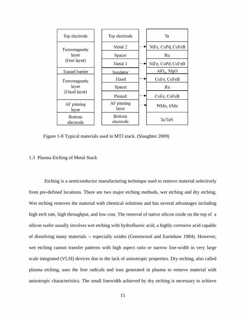
Figure 1-8 Typical materials used in MTJ stack. (Slaughter 2009) .............................................. 15
Figure 1-9 Ar+ ion etch rate of different materials as function of the beam incidence angle.
(Smith, Melngail.J et al. 1973)...................................................................................................... 17
Figure 1-10 Masking strategies for ion-beam etching. (Lee 1979) .............................................. 18
Figure 1-11 Method to control facet and trench formation during ion-beam etching. Ions incident
on mask (a) cause facet formation, which leads to trenching because of the concentrated ion flux
at the base. (Lee 1979) .................................................................................................................. 18
Figure 1-12 Schematic of the junction fabrication processes, from left to right: Reactive ion
etching of hard mask and magnetic stack structure, photoresist strip and ion beam trimming at
glancing incidence and resulting structure. (Gajek, Nowak et al. 2012) ...................................... 19
vii
Figure 1-13 Arrhenius plot of etch rate versus temperature: experiments on F for 10 sccm 10 Pa
Ar plasma 400 W rf power (triangle), 20 sccm 10 Pa HCl plasma 400 W rf power (+) and 20
sccm 10 Pa HCl resistive heating only (square). Model calculation for sputter etching (dash dot
line), chemical etching (solid line), and reactive ion etching (dash line). (Vandelft 1995) .......... 21
Figure 1-14 Mass spectra of 13CO/D2 (top), 12CO/D2 (middle), and 12CO/H2 (bottom) plasmas.
The anticipated isotopic shifts for chemical identifications have observed. (Orland and
Blumenthal 2005).......................................................................................................................... 23
Figure 1-15 Proposed surface chemical mechanism of potential products, including formic acid,
formaldehyde, large alkanes and metal carbide produced through Fischer-Tropsch reaction with
CO, H2, CO2H2-x, and C2O2H4-x as reactants. (Orland and Blumenthal 2005) ............................. 24
Figure 1-16 Mass spectra of CO in NH3 plasmas over the range from m/z=40 to 80. (Orland and
Blumenthal 2005).......................................................................................................................... 25
Figure 1-17 XPS spectrum of hfac-treated (a) Fe film and (b) Fe2O3 film. {George, 1996 #868}
....................................................................................................................................................... 28
Figure 1-18 (a) The different desorption species on a Ni(110) surface and on an oxygen covered
Ni(110) surface. Acac ligand was dosed at 100K and the surface was heated with 10K/ sec. (b)
The desorption species are detected by mass spectrometer. ......................................................... 29
Figure 1-19 (a) The structures of acac and its anion, (b) keto in left and enol tautomer in right
(Caminati and Grabow 2006, Czech and Wojciechowicz 2006). ................................................. 31
Figure 1-20 The structure of Co(acac)3 (Jensen and O'Brien 2001). ............................................ 32
Figure 1-21 Volatility diagrams for (a) Cu/Cl2 system at 50oC and (b) Cu/Cl2-H/H2 system at
varying pressures of H/H2 and varying temperatures. (Kulkarni and DeHoff 2002). .................. 36
Figure 1-22 Flow diagram of this work. RIE has been introduced in Chapter 3, organic chemical
etch with different surface modifications has been described in Chapter 4 and 5. ....................... 39
Figure 2-1 A schematic illustration of a UHV Transfer Tube Setup. ........................................... 43
Figure 2-2 Schematic of ICP etcher showing divisions in chamber. ............................................ 45
Figure 2-3 Schematic of wet etching standard operating procedure. ............................................ 48
Figure 2-4 The schematic diagram of the ion beam assisted chemical etch system. .................... 50

viii
Figure 2-5 Schematic diagram of the 3 cm ion source installation (Image courtesy of Kauffmann
ion source manual). ....................................................................................................................... 52
Figure 2-6 Schematic diagram of the design of sample holder and shutter in 3D and side view of
organic doser and the shutter to block Ar+ beam. ........................................................................ 53
Figure 2-7 A coupled vapor etch chamber with ICP chamber for conducting metal etch with
sequential surface oxidation and organic vapor exposure. ........................................................... 55
Figure. 2-8 Schematic diagram of the design of Horiba liquid vaporizer system (Image courtesy
of Horiba, 2013). ........................................................................................................................... 55
Figure. 2-9. Generic phase diagram with two approaches to vaporize the liquid instantaneously.
....................................................................................................................................................... 56
Figure 2-10 A method of mixing gas and liquid utilized in vaporizer system (Image courtesy of
Horiba, 2013). ............................................................................................................................... 57
Figure 2-11 SEM images of the Co film patterned by a TiN hard mask and a SiN protecting layer
with a TiN barrier layer at the bottom as the etch stop layer. ....................................................... 59
Figure 2-12 Schematic of Langmuir Probe Setup and sample I-V curve for O2 plasma taken in
the ICP reactor at 500 W, 0 W bias power with 2.5 mT. .............................................................. 60
Figure 2-13 Schematic of OES setup, and sample spectrum of Cl2 plasma with 5% Ar addition.
....................................................................................................................................................... 65
Figure 2-14 OES intensity ratio of Cl (738.62 nm), BCl (272 nm) and Cl (792.54 nm) to Ar
(750.42 nm) as a function of the power at 5 mTorr (left) and chamber pressure (right) at 300 W in
a pure BCl3 plasma (Sha and Chang 2004). .................................................................................. 68
Figure 2-15 Schematic of UTI 100C Mass Spectrometer and mass spectrum for an etch of Co
film in Cl2 plasma, the Cl, Cl2, CoCl2 and CoCl3 peaks have been discovered. ........................... 69
Figure 2-16 Naturally occurring isotope composition patterns of the Cl2. ................................... 70
Figure 2-17 Schematic of XPS system and sample spectra for the Fe 2p and Co 2p peaks after
etching a CoFe alloy film in a Cl2 plasma. ................................................................................... 74
Figure 2-18 Illustration of the variation in escape length from a planar surface at take-off angles
of 90° and 30°. At a take-off angle of 30° an excited electron can only exit from a depth half that
of one from a surface oriented at 90°. ........................................................................................... 74

ix
Figure 2-19 XPS spectra taken for Pt (20 nm) treated by 500 W O2 ICP plasma for 5 min. The Pt
4f spectra taken at three electron take-off angles. From the top to bottom are 30o (dash line), 60o
(solid line), 90o (gray line), respectively. ...................................................................................... 75
Figure 2-20 Basic model assumed for the formation of platinum oxide on a metallic Pt surface
through O2 plasma treatment. ....................................................................................................... 76
Figure 2-21 XPS spectra taken for pre-treated and O2 plasma treated Pt with (a) Pt 4f, (b) O 1s,
and (c) Survey. .............................................................................................................................. 77
Figure 2-22 Inelastic-Mean-Free-Path in (nm) as a function of electron energy (eV) of electron in
platinum oxide (Jablonski and Powell 2002). ............................................................................... 79
Figure 2-23 Components of a scanning electron microscope and cross-sectional image taken of a
patterned cobalt sample. ................................................................................................................ 81
Figure 2-24 Schematic of Dektak profiler system and sample spectra for the Co etched by Ar+
beam with and without acac alternative etch. ............................................................................... 83
Figure 2-25 Schematic view of a ellipsometric measurement in reflection configuration. The
polarized beam is incident on the sample from the left side. After reflection the polarization state
of the beam has changed and pursuits its propagation to the right side (Zheng, Zhang et al. 2012).
....................................................................................................................................................... 85
Figure 2-26 Refractive index (n) and extinction coefficient (k) as a function of wavelength for (a)
Co and (b) Pt. ................................................................................................................................ 87
Figure 2-27 A fitting of refractive index (n) and extinction coefficient (k) measured by
ellipsometer to the model of (a) Co and (b) Pt. ............................................................................. 87
Figure 2-28 A fitting of refractive index (n) and extinction coefficient (k) measured by
ellipsometer to the model developed for CoPt alloy thin films. ................................................... 88
Figure 2-29 A Josephson junction is composed of two bulk superconductors separated by a thin
insulating layer through which Cooper pairs can tunnel, and the Josephson junction is served as a
nonlinear inductor (You and Nori 2011). ..................................................................................... 89
Figure 2-30 (a) Magnetic hysteresis loop of pristine Co 10 nm film (solid line) and Co treated by
surface oxidation by 500 W O2 plasma for 5 min (hollow square). The SQUID measurement was
conducted at 300 K from -2000 to 2000 Oe. (b) Enlarged hysteresis loop from -100 to 100 Oe. 91

x
Figure 2-31 Magnetic hysteresis loop of pristine Pt 15 nm film (solid line) and Pt treated by
surface oxidation by 500 W O2 plasma for 5 min (hollow square). The SQUID measurement was
conducted at 300 K from -2000 to 2000 Oe. ................................................................................ 92
Figure 2-32 (a) Magnetic hysteresis loop of pristine CoPt 27 nm film (solid line) and CoPt
treated by surface oxidation by 500 W O2 plasma for 5 min (hollow square). The SQUID
measurement was conducted at 300 K from -2000 to 2000 Oe. (b) Enlarged hysteresis loop from
-400 to 400 Oe. ............................................................................................................................. 93
Figure 2-33 Three steps of electrospray ionization (Ho, Lam et al. 2003). .................................. 94
Figure 2-34 Schematic diagram of a tandem triple quadrupole system. First (Q1) and third (Q3)
are mass spectrometers and the second (Q2) is a collision cell (Ho, Lam et al. 2003). ............... 95
Figure 2-35 Sample spectra for the Co(acac)2 and Fe(acac)3 in the post-etch solution of Co and
Fe etched by 10 M acac solution at 80oC for 30 min. ................................................................... 96
Figure 2-36 The ICP torch with RF load coil generate the argon plasma in the end of torch which
ionize the species in the aerosol (Wolf 2005). .............................................................................. 98
Figure 2-37 The interface region of an ICP-MS, including a plasma torch, sampler, skimmer
cones and a shadow stop with lens for detector (Wolf 2005). ...................................................... 98
Figure 2-38 Approximate detection capabilities of the ELAN 6000/6100 quadrupole ICP-MS
(Wolf 2005). .................................................................................................................................. 99
Figure 2-39 The plot of composition as a function of temperature for the system of 1 kmol
SiOCH2 and 6 kmol CF4 at P = 10-5atm based on the Gibbs free energy minimization. ............ 101
Figure 3-1 Volatility diagram for (a) Co in Cl2, (b) Fe in Cl2, and (c) Ni in Cl2 system at 300,
350, 400, 450, and 500K. The reactions in the figure are presented in Table 3-1. The square and
dashed line at 10-8 atm infers the reactant volatility, corresponding to a weight loss that is
detectable in a thermogravimetric analyzer (Lou, Mitchell et al. 1985). .................................... 107
Figure 3-2 Calculated vapor pressure from the sublimation reaction of metal halide condensed
phase at 300, 400, 500, 600, 700, 800, and 900 K. (a) Co in Cl2, (b) Fe in Cl2, and (c) Ni in Cl2
system. Hollow stars represent the partial pressure of MH(g) (M = Co, Fe, and Ni) at an
equilibrium when metal chloride is exposed to hydrogen radicals. ............................................ 109
Figure 3-3 A partial pressure of CoO(g) generated from atomic oxygen (left) addition on
CoCl2(c) and that of CoH(g) generated from atomic hydrogen (right) addition on CoCl2(c) at
300K. The hollow square symbol was achieved from the mass balance from reaction (19) and
(32). ............................................................................................................................................. 111

xi
Figure 3-4 A partial pressure of NiH(g) at equilibrium generated from an atomic H addition on
NiCl2(c) (left) and that of NiCl(g) generated from an atomic Cl addition on NiH0.5(c). The
hollow square symbol was achieved from the mass balance from reaction (34) and (40). ........ 114
Figure 3-5 Summary of a partial pressure enhancement induced by chlorine, bromine, oxygen,
and hydrogen addition to MClx(c), MBrx(c), and MO(c). (M=Co, Fe, and Ni). ........................ 115
Figure 3-6 Surface composition measurements of Co, Ni, and Fe thin films using XPS
representing before-etch, Cl2 plasma 30 sec, Cl2 plasma 30 sec followed by H2 plasma 30 sec,
and Cl2 plasma 30 sec followed by H2 plasma 90 sec. ............................................................... 117
Figure 3-7 Etch rate measurement using profilometer. Cl2 and H2 plasma were exposed
alternating manner. The etch rate by hydrogen plasma was zero (filled square symbol in the
figure). Co etch rates in Cl2 and Cl2/H2 cycle were 4.61 and 3.94 nm/cycle, respectively. Fe etch
rates in Cl2 and Cl2/H2 cycle were 8.50 and 8.01 nm/cycle, respectively. Fe etch rates in Cl2 and
Cl2/H2 cycle were 5.74 and 4.77 nm/cycle, respectively. ........................................................... 118
Figure 3-8 OES spectra of Cl2 plasma etching Co, H2 plasma etching Cl2-plasma pretreated Co,
and H2/Cl2 plasma etching Co. (a) OES with the wave length from 200 to 1000 nm. (b)
Magnified spectra of (a) from 435 to 455 nm. The peaks assigned as CoH(g) and Co(g) do not
appear in H2 plasma on SiO2. ...................................................................................................... 121
Figure 3-9 (a) Calculated partial pressures of etch products generated from atomic Br, O, and H
addition on CoCl2 and FeCl3. Detailed calculation can be found in the supporting information.
(b) Etched thickness is shown as a function of chlorine and hydrogen plasma cycles after 20 sec
exposure with Cl2 plasma and 20 sec exposure individually with Cl2/H2 plasma. A Cl2 cycle is 20
sec Cl2 plasma and Cl2/H2 cycle is composed of 20 sec Cl2 followed by 20 sec H2. The dashed
lines represent linear fittings of etched thicknesses for Cl2 and Cl2/H2 cycles. .......................... 124
Figure 3-10 XPS spectra of (a) Co 2p, (b) Fe 2p, and (c) Cl 2p. From the top, the spectra
represents pre-etch, Cl2(30sec), Cl2(30sec)/H2(30sec), and Cl2(30sec)/H2(90sec) plasma exposure
on 500 nm Co0.8Fe0.2 films. For each element analyzed, each chemical state is represented by a
spin-orbit split doublet, 2p3/2 and 2p1/2, which is constrained to have a 2:1 peak area ratio, equal
full-width-at-half-maximum, and their energy separations are 15.0 eV, 12.9 eV, and 1.53 eV, for
Co, Fe and Cl, respectively. For simplicity, only the 2p3/2 peaks are labeled in the figure. In Fe
2p spectra, the Co Auger LMM peak at ~714.3 eV is overlapped with Fe-O and Fe-Cl peak at
~710.7 eV and ~711 eV. ............................................................................................................. 125
Figure 3-11 Cross-sectional ((a), (c), (e), and (g)), and bird eye ((b), (d), (f), and (g)) view SEM
images of 300 nm TiN- masked 45 nm CoFe films. (a, b) CoFe pattern prior to plasma etching;
(c, d) after 4 min Ar plasma etching with RF1 power of 100 W, RF2 power of 500 W and 20
mTorr pressure, (e, f) 2 min Cl2 plasma etching with RF1 power of 50 W, RF2 power of 500 W
and 20 mTorr pressure, (g, h) 4 min subsequent H2 plasma etching with RF1 power of 50 W,

xii
RF2 power of 500 W and 20 mTorr pressure. Figure 3-11(i) and (j) present EDX spectra
measured at the positions denoted by circles in Figure 3-11 (f) and (h), respectively. .............. 128
Figure 3-12 Magnetic hysteresis loop measured in CoFe films. Normalized magnetization (to
saturation magnetization of pre-etch CoFe) vs. magnetic field under various etching conditions.
..................................................................................................................................................... 131
Figure 3-13 Coercive field and saturation magnetization as a function of H2 plasma exposure
time extracted from the magnetic hysteresis loop. The left and right y-axis indicate the coercive
field and saturation magnetization from the pre-etched CoFe film, respectively. ...................... 131
Figure 3-14 FMR spectra measured in CoFe films. (a) FMR spectra measured in pre-etched and
post-etched CoFe films. Vertical dashed lines are the guide lines to represent the peak-to-peak
line width deciding a damping coefficient. (b) FMR linewidth and resonance magnetic field
obtained from FMR spectra with the values from the pre-etched film. (c) Resonance field and
calculated anisotropy field as a function of H2 plasma exposure time including the value from
pre-etched CoFe film as denoted by the horizontal line. ............................................................ 132
Figure 4-1 Volatility diagram for Co in acac and hfac at 300K. The reactions in the figure are
presented in Table 4-2. The dashed line at 10-8 atm refers to the reactant volatility, corresponding
to a weight loss that is detectable in a thermogravimetric analyzer. .......................................... 139
Figure 4-2 Volatility diagram for Fe in ACAC and HFAC at 300K. The reactions in the figure
are presented in Table II. The dashed line at 10-8 atm refers to the reactant volatility,
corresponding to a weight loss that is detectable in a thermogravimetric analyzer. ................... 140
Figure 4-3 The etch rate of Co, Fe, Pd and Pt in (a) acetylacetone (acac) solution, (b)
hexafluoroacetylacetone (hfac) and (c) 2,2,6,6-tetramethyl-3,5-heptanedione (tmhd) at 80oC was
quantified by SEM. The triangle represents the etch of Co, the circle represents the etch of Fe,
and the hollow square represents the etch of Pt and solid square represents the etch of Pd. ...... 142
Figure 4-4 The mass spectrum of post-etch solution of (a) Co & Fe etched in acac solution, (b)
Co & Fe etched in hfac solution. The isotope patterns of organometallic complex are shown on
the right table. ............................................................................................................................. 144
Figure 4-5 XPS spectra of (a) Co 2p3/2, (b) O 1s, and (c) Ti 2p. From the top, the spectra
represents as deposited, acac solution etch 5 min, acac solution etch 10 min. For Co and Ti, each
chemical state is represented by a spin-orbit split doublet, 2p3/2 and 2p1/2, which is constrained to
have a 2:1 peak area ratio, equal full-width-at-half-maximum, and their energy separations are
15.0 eV, and 6.1 eV, for Co and Ti, respectively. For simplicity, only the 2p3/2 peak of Co is
shown in the figure...................................................................................................................... 145
Figure 4-6 XPS spectra of (a) Fe 2p3/2, (b) O 1s, and (c) Ti 2p. From the top, the spectra
represents as deposited, hfac solution etch 5 min, hfac solution etch 10 min. For Fe and Ti, each
xiii
chemical state is represented by a spin-orbit split doublet, 2p3/2 and 2p1/2, which is constrained to
have a 2:1 peak area ratio, equal full-width-at-half-maximum, and their energy separations are
12.9 eV, and 6.1 eV, for Fe and Ti, respectively. For simplicity, only the 2p3/2 peak of Co is
shown in the figure...................................................................................................................... 146
Figure 4-7 The etch rate of Co etched in several concentrations of acac diluted by acetonitrile at
80oC for 60 min. .......................................................................................................................... 147
Figure 4-8 XPS spectra of C 1s. The top spectrum represents Co as deposited, and bottom
spectrum represents Co etched by acac vapor for 8 hrs. ............................................................. 148
Figure 4-9 Etching yield of Co as a function of Ar ion energy. The Ar ion was vertical to the Co
film. The hollow square represents the data from the literature (Laegreid and Wehner 1961,
Stuart and Wehner 1962, Sletten and Knudsen 1972, Behrisch and Eckstein 2007), and the solid
circle represents the data of ion beam in used. ........................................................................... 149
Figure 4-10 Uniformity of Co etch at 1 keV Ar ion beam. The etch rate was plotted as a function
of distance from the center of Ar ion beam. The standard deviation is 0.32 nm at 1 keV, and 0.24
nm at 0.5 keV. The etched thickness was measured by SEM. .................................................... 150
Figure 4-11 The process and mechanism proposed to facilitate the alternating etch, including the
surface cleaning, acac vapor exposure, chemically bonding ligand and metal, Ar ion beam
exposure, and the desorption of organometallic compounds. ..................................................... 151
Figure 4-12 The detail of the process of alternating Ar and organic vapor exposure. ............... 151
Figure 4-13 The design of the sample stage and shutter for the alternating etch system. Left
figure presents the three dimensional setup of the sample, shutter, and organic vapor doser. The
right figure shows a side view of setup that only 1 mm gap between shutter and sample would
reduce the pressure of acac on the covered region dramatically. ............................................... 152
Figure 4-14 The SEM images of (a) Co etched by 1keV Ar ion beam for 75 min, and (b) Co
etched by sequential dosing of 5 sec 1keV Ar ion beam and 5 sec acac vapor for 450 cycles,
equivalent to 75 min.................................................................................................................... 153
Figure 4-15 The etch rate of Co etched by acac vapor, Ar ion beam, and alternating exposure of
Ar ion beam and acac vapor were 0.004, 0.73, and 1.29, respectively. The thickness was
measured by SEM. ...................................................................................................................... 154
Figure 5-1 XPS spectra of (a) Pt 4f, (b) Cl 2p (c) S 2p, and (d) O 1s peaks for (1) pre-etch, 1 min
surface treatment at (2) SO2 in 500 W plasma source with 0W bias, (3) SO2 in 500 W plasma
source with 50W bias, (4) Cl2 in 500 W plasma source with 0W bias, (5) Cl2 in 500 W plasma
source with 50W bias. ................................................................................................................. 159

xiv
Figure 5-2 XPS spectra of (a) Pt 4f, (b) Cl 2p (c) S 2p, and (d) C 1s peaks for (1) pre-etch, 1 min
surface treatment at (2) CF4 in 500 W plasma source with 0W bias, (3) CF4 in 500 W plasma
source with 50W bias, (4) SF6 in 500 W plasma source with 0W bias, (5) SF6 in 500 W plasma
source with 50W bias. ................................................................................................................. 161
Figure 5-3 XPS spectra of (a) Pt 4f, (b) O 1s, and (c) Pt 4p3/2 peaks for (1) pre-etch, 5 min O2 ion
beam treatment at (2) 50 eV, (3) 100 eV, (4) 200 eV, and (5) 500 eV. ...................................... 163
Figure 5-4 Schematic phase diagram for producing reactively sputtered platinum-oxygen films.
Sputtering power is plotted against oxygen content for fixed sputtering pressure and substrate
temperature (Mcbride, Graham et al. 1991). ............................................................................... 164
Figure 5-5 XPS spectra of (a) Pt 4f, (b) O 1s, and (c) Pt 4p3/2 peaks for (1) pre-etch, 5 min 500 W
source power of O2 plasma treatment with (2) 0 V, (3) -100 V, (4) -150 eV, and (5) -200 V bias.
..................................................................................................................................................... 165
Figure 5-6 Degree of surface modification for pre-etch, SO2, Cl2, CF4, SF6, O2 ion source, and O2
plasma treated Pt. (a) The percentage of modified Pt to metallic Pt. (b) The composition of
various chemical states in Pt 4f spectrum, including Pt0+, Pt2+,and Pt4+. .................................... 166
Figure 5-7 I-V curve measured by Langmuir probe at 500 W source power, 0 W bias power with
2.5 mtorr O2 under ICP plasma. .................................................................................................. 167
Figure 5-8 Oxide thickness of Fe, Cu, Co, Pd, and Pt as a function of the O2 plasma oxidation
time. ............................................................................................................................................ 168
Figure 5-9 Curve fitting for oxidation of Fe, Cu, Co, Pd and Pt by O2 plasma with (a) linear, (b)
parabolic, (c) cubic, (d) inverse logarithmic, and (e) exponential. ............................................. 171
Figure 5-10 XPS spectra of (a) Pt 4f, (b) Survey for (1) pre-etch Pt, oxidized Pt treated by
following organic solution for 20 min, (2) acac, (3) hfac, (4) edta, (5) nta, (6) pdca, (7) oxalic
acid, and (8) formic acid. ............................................................................................................ 175
Figure 5-11 XPS spectra of (a) Ta 4f, (b) Survey for (1) pre-etch Ta, oxidized Ta treated by
following organic solution for 20 min, (2) acac, (3) hfac, (4) edta, (5) nta, (6) pdca, (7) oxalic
acid, and (8) formic acid.Ta etched by organics solution etch 20 min. ...................................... 176
Figure 5-12 Cross-sectional SEM images of (a) Ta pre-etch, (b) Ta with surface modification of
500 W O2 plasma without bias for 5 min, and (c) modified Ta etched by formic acid solution for
4 hr at 80 oC for 20 min. ............................................................................................................. 177

xv
Figure 5-13 XPS spectra of (a) Pt 4f, (b) Co 2p, (c) O 1s for (1) pre-etch CoPt alloy, oxidized
CoPt alloy treated by following organic solution for 20 min, (2) acac, (3) hfac, (4) edta, (5) nta,
(6) pdca, (7) oxalic acid, and (8) formic acid. ............................................................................ 178
Figure 5-14 ICP-MS data of (a) Pt and (b) Co concentrations in the post-etch solution of formic
acid, pdca, edta, nta, acac, and hfac. A control experiment with organic chemical solution only is
shown in dotted line (square), etching of CoPt without surface oxidation is presented with long
dotted line (circle), and the etch of CoPt with surface oxidation is labeled as solid line (triangle).
..................................................................................................................................................... 179
Figure 5-15 The ratio of Pt0+ to Pt4+ in atomic percentage decoupled from XPS results of CoPt
etched by organics solution of pdca, formic acid, edta, nta, acac, and hfac for 20 min. (labeled by
solid line with triangle) The ratio of Pt0+ to Pt4+ of metallic CoPt and oxidized CoPt are labeled
as solid circle, and solid square, respectively. ............................................................................ 180
Figure 5-16 Estimated thickness of of Co and Pt etched by organic solution of formic acid, pdca,
edta, nta, acac, and hfac for 20 min. The etched thickness is estimated by the results of ICP-MS
by known dimension of sample, density of Co and Pt, and volume of organic solutions. A control
experiment with organic chemical solution only is shown in dotted line (square), etching of CoPt
without surface oxidation is presented with long dotted line (circle), and the etch of CoPt with
surface oxidation is labeled as solid line (triangle). .................................................................... 181
Figure 5-17 XPS spectra of (a) Pt 4f, (b) Co 2p, (c) O 1s, (d) C 1s, and (e) Survey for (1) pre-etch
CoPt alloy, (2) oxidized CoPt alloy, oxidized CoPt treated by formic acid solution for (3) 3, (4)
5, (5) 10, (6) 20 min. ................................................................................................................... 183
Figure 5-18 The ratio of Pt0+ to Pt4+ in atomic percentage decoupled from XPS results of CoPt
etched by formic acid solution for 1 sec, 10 sec, 3min, 5 min, 10 min, 20 min, 40 min, and 60
min. The ratio of Pt0+ to Pt4+ of metallic CoPt is labeled as solid square. .................................. 184
Figure 5-19 The thickness change of CoPt etched by surface modification of 500 W O2 plasma
for 5 min and formic acid solution for 30 sec alternatively. The dotted line with hollow circle
represents CoPt etch without surface modification, and the solid line with hollow square stands
for CoPt etch with surface modification prior to organic solution etch. ..................................... 185
Figure 5-20 XPS spectra of (a) Pt 4f, (b) Co 2p3/2, and (c) O 1s, for (1) pre-etch CoPt alloy, (2)
oxidized CoPt, and different cycles of surface oxidation and formic acid solution etch from (3) to
(7). ............................................................................................................................................... 186
Figure 5-21 XPS spectra of (a) Pt 4f, and (b) Survey, for (1) pre-etch Pt, (2) oxidized Pt, (3) 1st
cycle, and (4) 2nd cycle of sequential etch of surface oxidation and formic acid vapor exposure.
..................................................................................................................................................... 189

xvi
Figure 5-22 Etched thickness of Co and Pt etched by surface modification and exposure of
formic acid vapor as a function of etching cycle. Hollow square represents etching of Co on left
y-axis, and hollow circle represents etching of Pt on right y-axis. ............................................. 190
Figure 5-23 Etched thickness of CoPt alloy by surface modification and exposure of formic acid
vapor as a function of etching cycle. .......................................................................................... 191
Figure 5-24 The growth of oxide thickness for Fe, Cu, Co, Pd, and Pt as a function of the
oxidation time of 500 W O2 plasma. The symbol of circle, diamond, square, inverted triangle,
and triangle are represent FeO, Cu2O, CoO, PdOx, and PtOx, respectively. ............................... 192
Figure 5-25 Etched thickness of Fe, Cu, Co, Pd, and Pt as a function of sequential etch cycle.
The symbol of circle, diamond, square, inverted triangle, and triangle are represent FeO, Cu2O,
CoO, PdOx, and PtOx, respectively. ............................................................................................ 193
Figure 5-26 Etched thickness per cycle as a function of oxide thickness per cycle for Fe, Cu, Co,
Pd, and Pt. The symbol of circle, diamond, square, inverted triangle, and triangle are represent
FeO, Cu2O, CoO, PdOx, and PtOx, respectively. ........................................................................ 194
Figure 5-27 SEM images of patterned Co (a) pre-etch, (b) 6 cycles sequential etch, and (c) 8
cycles sequential etch. ................................................................................................................. 195
Figure 5-28 A series of cross-sectional SEM images of patterned Co etched by 8 cycles
sequential etch with titled angle of (a) 10 o, (b) 8 o, (c) 6 o, (d) 4 o, (e) 2 o, and (f) 0 o. ................ 196
Figure 5-29 Magnetic hysteresis loop measured in patterned Co films. Normalized magnetization
(to saturation magnetization of pre-etch patterned Co) vs magnetic field. The spectrum labeled
by solid triangle represents pre-etch patterned Co, and the 4 cycles sequential etch of Co is
labeled by hollow circle. ............................................................................................................. 197
Figure 5-30 The EDS spectra of pre- and post- etched patterned Co with various cycles of
sequential etch of surface oxidation and exposure of formic acid vapor. ................................... 198
Figure 5-31 SEM images of patterned Co (a) pre-etch, (b) 500 W O2 plasma with -200 V bias for
10 min, and (c) 4 cycles sequential etch with -200 V bias in 500W O2 plasma. ........................ 199

xvii
LIST OF TABLES
Table 1-1. Solid-state memory comparison. (ITRS(2011)) ............................................................ 7
Table 1-2 Boiling point of metal fluoride, chloride and bromide. All values taken from
“Handbook of Inorganic Compounds.” (Phillips and Perry 1995) ............................................... 20
Table 1-3 Traditional organometallic precursors of beta diketonates for CVD process. (Orland
and Blumenthal 2005) ................................................................................................................... 26
Table 1-4 Melting point, boiling point and vapor pressure of metal complex species vs.
chlorinated species. (Phillips and Perry 1995) .............................................................................. 27
Table 1-5. Reactions utilized for plotting volatility diagrams in the Cu-Cl system.(Kulkarni and
DeHoff 2002). ............................................................................................................................... 35
Table 2-1 Detailed listing of the material blanket films investigated in this work. ...................... 58
Table 2-2 XPS Atomic Sensitivity Factors (ASFs) for elements of interests. .............................. 73
Table 2-3 The detail information required for estimating the inelastic mean free path of electron
(λ) in metal oxide including Pt, Pd, Co, Fe, and Cu. .................................................................... 79
Table 3-1 Reactions utilized for plotting volatility diagrams in the M-Cl systems (M = Co, Fe,
Ni) at 300K. ............................................................................................................................... 106
Table 3-2 Reactions utilized for plotting volatility diagrams in CoCl2 etching with O, Co etching
with O, and CoO etching with Cl systems at 300K. ................................................................... 110
Table 3-3 Reactions considered in hydrogen plasma reacting with CoCl2. ................................ 112
Table 3-4 Reactions considered in hydrogen plasma reacting with NiCl2 and chlorine plasma
reacting with NiH0.5. ................................................................................................................... 113
Table 3-5 Plasma condition of Cl2 and H2 plasma. ..................................................................... 116
Table 4-1 Acetylacetonates organometallic compound (Pierson 1999). .................................... 136
Table 4-2 Reactions utilized for plotting volatility diagrams in the M-acac & M-hfac systems (M
= Co, Fe; acac = Acetylacetonate, hfac = Hexafluoroacetylacetonate) at 300K. ....................... 137

xviii
Table 5-1 Goodness of fitting for oxidation of Fe, Cu, Co, Pd and Pt by O2 plasma with 500 W,
2.5mtorr O2, Te~2.5eV and ion density:1015#/cm3. .................................................................... 172
Table 5-2 Potential organics in etching metals. .......................................................................... 174
Table 5-3 Surface composition of Co and Pt in atomic percentage of CoPt etched by surface
oxidation and formic acid solution etch sequentially from pre-etch, and cycle one to cycle four.
..................................................................................................................................................... 187

xix
ACKNOWLEDGEMENTS
Zillions of great, invaluable ideas and actions have supported me during the journey.
Unfortunately, I am not able to include everyone’s name due to space constraints, and for that I
apologize.
My advisor, Professor Jane Chang, brought me into academia, exhibited a professional standard
of research, and planted the seeds of hope in my mind that I could contribute to the plasma
society. She also led me to industry and demonstrated that our research definitely promoted the
progress of science and technology. A conversation we had on the day I received an award from
the Semiconductor Research Corporation at Tucson will always remind me to keep moving
forward. I would also like to thank my committee members. Professor Vasilios Manousiouthakis
walked me through the prospectus individually with insightful comments. Professor Yvonne
Chen always gave me constructive feedback. Professor King-Ning Tu helped me to improve my
conversation skills. Professor Richard Wirz pointed out critical facts at my defense. Industrial
sponsors have also contributed to my study. Dr. Meihua Shen at Lam Research not only
supported me during the entire journey of my PhD but also offered me a job. Dr. Satyarth Suri at
Intel supported my study through SRC, and we have appreciated his critical feedback.
Special thanks are due to my lab mentor, Dr. Nathan Marchack, for his advice on how to make
things work out. My knowledge of science increased greatly thanks to his dedication and
patience in mentoring me. If I have any accomplishments in the field of science, it must be a
consequence of his guidance and mentorship. Based on my experience of working with my
successors, I believe the royal lineage of the etch crew will be successful. Nicholas Altieri is
eager to help teammates, and he has shown his strong willingness in taking the SRC project
further. The patience of Luke Minardi drives him to the world of simulation (IMPACT), which

xx
matches his hobby of watching Fish Center. I am genuinely inspired by Ernest Chen, who always
brings up brilliant ideas in designing a new chamber (Lam), and he also shows enthusiasm to
continue some of the work. Long live the etch crew!
The Chang Lab group has always been a great source of imagination, patience, and fulfillment.
Dr. Taeseung “Father” Kim, a master of problem solver, was my best teammate, and together we
have conquered numerous etching projects. He was the one who inspired me to execute my
vision and make those dreams come true. My knowledge of science was acquired from those
intelligent senior students. James Dorman passed down all the tricks of wet chemistry in the 1st
quarter of my PhD as my temporary mentor. Sandy Perng not only taught me the skills of
vacuum science but also sheltered me while interviewing at Intel. Vladan Jancovic was the
philosopher of the lab who taught me to never give up. Captain Jea Cho, the soul of the gang,
made me both optimistic and sober through his unique and insightful opinions. Without Calvin
and Diana’s skills at XPS, I could not have gotten as far as I did. Cyrus accompanied me
throughout my PhD, and I will never forget the nights we spent working in the dry lab. Colin is
the best teacher for broadening my horizons, and I already miss the parties after the group
meetings. Jeff is a hardworking friend, and I want to thank him for all the discussions and
instructions on new ideas. Kevin has a strong desire for knowledge, and he will guide and
improve the PZT project. Ryan will be the master of the LASO battery project. It was also nice
having friends outside the world of the Chang Lab, and I would like to thank the NTU gang
(Candy and Paul) and Friday Night club for making life at UCLA more fascinating. Lastly, I am
thankful to my mother, father, brother, sister, and grandparents, I would never have been able to
get where I am today if it was not for my family. Finally, I would love to thank the person closest
to my heart, my wife, Iris, for your continual love, endless support, and faith in my abilities.

xxi
VITA
2007-2010 Presidential Award 4 times through 4 years
National Taiwan University
Taipei, Taiwan
2010 B. S., Chemical Engineering
National Taiwan University
Taipei, Taiwan
2010 College Student Research Award
National Science Council
Taiwan
2010-2011 Political Warfare Officer
Ministry of National Defense
Taiwan
2011-2014 Graduate Student Researcher
Department of Chemical Engineering
University of California, Los Angeles
2015 Teaching Assistant
Department of Chemical Engineering
University of California, Los Angeles
2015 Simon Karecki Award
Semiconductor Research Corporation
2015 AVS Coburn and Winters Award Finalist
62th AVS International Symposium
PUBLICATIONS
1. T. Kim*, Y. Kim*, J. K. Chen* and J. Chang, “A viable alternating chemical approach for
patterning technology of nanoscale MRAM devices,” J. Vac. Sci. Technol. A, Vol. 33, (2015)
021308 *Shared first author
2. T. Kim*, J. K. Chen* and J. Chang, “Thermodynamic assessment and experimental verification
of reactive ion etching of magnetic metal elements,” J. Vac. Sci. Technol. A, Vol. 32, No.4,
(2014) 041305 *Shared first author
3. J. K. Chen, C. Y. Hsu, C. W. Hu and K. C. Ho, “A novel complementary electrochromic device
based on Prussian blue and Poly(ProDOT-Et2) with high-contrast and high-coloration

xxii
efficiency”, Sol. Energy Mater. Sol. Cells, 2010.
4. C. W. Hu, K.M. Lee, J. K. Chen, C. Y. Hsu, T. H. Kuo, and K. C. Ho, “High contrast all-solid-
state electrochromic device based on 2,2,6,6-tetramethyl-1-piperidinyloxy (TEMPO), heptyl
viologen, and succinonitrile,” Sol. Energy Mater. Sol. Cells, Vol. 99, (2012) 135.
PRESENTATIONS
1. J. K. Chen, N. Altieri, L. and J. Chang, “Generalized Approach for Selecting Plasma Chemistries
in Metal Etch,” AVS 62th International Symposium & Exhibition, San Jose, CA, October, (2015)
(Oral Presentation - Nominated for Coburn and Winters Award)
2. J. K. Chen, N. Altieri, L. Minardi, and J. Chang, “Benefit of Modeling-Based Process
Development,” IMPACT program, San Jose, CA, March 6, (2015)
3. J. K. Chen, N. Altieri, M. Paine, and J. Chang, “Non-PFC plasma chemistries for patterning low-
k dielectric materials,” AVS 61th International Symposium & Exhibition, Baltimore, MD,
November 10, (2014)
4. J. K. Chen, T. Kim, and J. Chang, “Thermodynamic approach to select viable etch chemistry for
magnetic metals,” Plasma Processing Science, Gordon Research Conference, Bryant University,
U.S., July 26, (2014)
5. J. K. Chen, N. Marchack, and J. Chang, “Selection of non-PFC chemistries for Through-silicon
via etch,” 2013 AICHE Annual Meeting, San Francisco, CA, November, (2013)
6. J. K. Chen, N. Marchack, and J. Chang, “Selection of non-PFC chemistries for Through-silicon
via etch,” AVS 60th International Symposium & Exhibition, Long Beach, CA, October 28, (2013)
7. T. Kim, J. K. Chen (contribute equally) and J. Chang, “Thermodynamic Approach to Select
Viable Etch Chemistry for Magnetic Metals,” AVS 60th International Symposium & Exhibition,
Long Beach, CA, October 27, (2013)
8. J. K. Chen, T. Kim and J. Chang, “Selection Generalized approaches for selecting plasma
chemistries in metal etch,” IMPACT program, Albany, NY, March 25, (2013)
9. N. Marchack, J. K. Chen, and J. Chang, “Predictions of the Etch Behavior of Complex Oxide
Films for High-k Applications,” AVS 59th International Symposium & Exhibition, Temple, FL,
November 1, (2012)
10. N. Marchack, J. K. Chen, and J. Chang, “Predictions of the Etch Behavior of Complex Oxide
Films for High-k Applications,” 2012 AICHE Annual Meeting, Pittsburgh, PA, November
(2012)
11. J. K. Chen, N. Marchack, and J. Chang, “Selection of non-PFC chemistries for Through-silicon
via etch,” Plasma Processing Science, Gordon Research Conference, Bryant University, U.S.,
July 21, (2012)
12. J. K. Chen, C. Y. Hsu, C. W. Hu and K. C. Ho, “A novel complementary electrochromic device
based on Prussian blue and Poly(ProDOT-Et2) with high-contrast and high-coloration
efficiency,” 9th International Meeting on Electrochromism (IME-9), Bordeaux, France,
September 5-9, (2010)

1
CHAPTER 1: INTRODUCTION
Nowadays, mobile electronics such as smart phones, tablet PC’s and laptops have
benefited from downscaling that allows for higher performance processors and higher capacity
memory to store and process enormous amounts of data at lower cost. However, as we continue
to push the envelope for micro- and nano-electronics, major challenges arise for plasma
patterning. Since novel materials form the backbone of certain emerging technologies such as
spintronic devices, a solution to patterning materials that are intrinsically hard to etch is required.
Meanwhile, the structural complexity of high aspect ratio and multilayer features, present
challenges in achieving the desired final products. Furthermore, the continual downscaling of
integrated circuit (IC) devices requires precision at the atomic scale, and minor deviations from
those pattern dimensions can result in unbearable degradation in device performance. Ultimately,
to address these challenges, developing a new generalized approach for the patterning process is
necessary. Physics- and chemistry-based modeling affords a tremendous understanding of the
elementary reaction mechanisms in plasma patterning; however, the parameters necessary for
kinetic modeling are sometimes difficult to obtain experimentally for novel multifunctional
compounds. Developing a comprehensive framework for selecting viable chemistries in plasma
patterning of magnetic metals has the potential to reduce the time and cost associated with the
design of experiments. A brief introduction to the basic concepts as they apply to magnetic
metals has been given, followed by the discussion of today’s state-of-the-art techniques of
patterning the metal stack. Finally, a thermodynamic analysis of the etching process was
demonstrated with a copper etch case study, which has been applied to screening the potential
plasma chemistries for patterning magnetic metals in this work.
2
1.1 Motivation
The conventional metal-oxide-semiconductor field-effect transistor (MOSFET) has been
shrinking exponentially in dimensions over the past century. As a result, the number of
transistors in a microelectronic chip has been increasing exponentially. The MOSFET is the
foundation of microprocessors, memory chips, and telecommunications microcircuits. For
example, there are more than 2 billion MOSFETs in a modern microprocessor, and more than
256 billion transistors in a 32 gigabyte (GB) memory. In 1965, Gordon Moore, the co-founder of
Intel and Fairchild Semiconductor, published a famous paper, where he predicted that the density
of transistor on a chip would double every 18 months. (Moore 1965, Moore 1998) Reducing the
dimension of transistors allows an increase of density on a chip, resulting in an increase of the
functionality of the circuit. Besides the benefits of performance, shrinking feature size on an
integrated circuit (IC) also reduces the cost, typically 30% per linewidth generation, (Jones 2004)
which shown in Figure 1-1.
Dennard and co-workers have demonstrated that scaling down the device by a factor of
two, increases the switching speed twice, reduces the power dissipation by four times and
improves the power-delay product by eight times, which based on the assumption of maintaining
a constant electric field in the transistor. (Dennard, Gaenssle.Fh et al. 1974) However, due to the
limit of the threshold voltage, the benefits from the scaling predicted by Dennard were
interrupted by the short-channel effects, which arise when the distance separating the source
from the drain becomes very small. From the Figure 1-2, the gate length in the current generation
of microprocessor is around 30 nm, and the feature size can be reduced to 5 nm in several

3
technology nodes, which is only 10 times larger than the lattice parameter of a silicon crystal,
resulting in much more severe of short-channel effects on MOSFET.
Figure 1-1 (a) Trends in number of transistors over a period of time for several
DRAM and microprocessor technologies, (b) Trend in the linewidth over time.
(Jones 2004)
(a)
(b)

4
Figure 1-2 The evolution of transistor gate length (minimum feature size) and the
density of transistors in microprocessors over time. Between 1970 and 2011, the
gate length of MOSFETs shrank from 10μm to 28nm (yellow circles; y axis,
right), and the number of transistors per square millimetre increased from 200 to
over 1million (diamonds, triangles and squares show data for the four main
microprocessor manufacturers; y axis, left). AMD, Advanced Micro Devices;
IBM, International Business Machines. (Ferain, Colinge et al. 2011)
The configuration of MOSFET in the beginning was planar, where the gate electrode is
situated on top of an insulator that covers the channel region of the device between the source
and the drain, and it has evolved to multigate MOSFET, in which the shape is modified and
shown in Figure 1-3. Multigate MOSFET takes advantage of a third dimension to approach the
issue of short-channel effects by having several sides of the channel region covered the electrode.
Figure 1-3 presents the various multigate devices, (a) FinFET, (Huang, Lee et al. 1999) (b) tri-
gate MOSFET, (Doyle, Datta et al. 2003) (c) Π-gate MOSFET, (Jong-Tae, Colinge et al. 2001)
(d) Ω-gate MOSFET, (Fu-Liang, Hao-Yu et al. 2002) (e) gate-all around MOSFET, (Colinge,
Gao et al. 1990) and (f) bulk tri-gate MOSFET. (Cho, Choe et al. 2004, Okano, Izumida et al.
2005). Most of the devices were made using silicon-on-insulator (SOI) substrates (a-e), but bulk
tri-gate with bulk silicon under MOSFET has been shown to have good short-channel effect
immunity down to the sub-20-nm gate-length regimes. (Cho, Choe et al. 2004) Therefore, in

5
order to shrink the feature dimension of the transistor and avoid the short-channel effect, a
complex architecture has been proposed, resulting in a complicated patterning process where
silicon fins need to be patterned on a bulk silicon before the ion implantation to form the source
and drain.
Figure 1-3 Types of multigate MOSFET. a, A silicon-on-insulator (SOI) fin field-
effect transistor (FinFET). b, SOI triple-gate (or tri-gate) MOSFET. c, SOI Π-gate
MOSFET. d, SOI Ω-gate MOSFET. The names Π gate and Ω gate reflect the
shape of the gates. e, SOI gate-all-around MOSFET. f, A bulk tri-gate MOSFET.
Gate control is exerted on the channel from three sides of the device (the top, the
left and the right). In this case, there is no buried oxide underneath the device.
(Ferain, Colinge et al. 2011)
Although the development of the MOSFET has advanced both microprocessor and
memory device to the higher level in the past 4 decades, a shift of focus from processor to
memory has slowly occurred due to a continuous growing gap between CPU and memory speeds
in the computer performance as shown in Figure 1-4. (Patterson, Anderson et al. 1997) The

6
enhancement rate in microprocessor speed so far exceeds that of DRAM memory since speed is
the main focus for processor while capacity is the goal for memory. As a result, the improvement
rate of 60% per year presented in microprocessor performance is much greater than that of 10%
per year of memory. A practical example is shown in Figure 1-4, considering a hypothetical
computer with a processor that operates at 800 MHz (Pentium III) attached to a memory through
a 100 MHz bus, meaning that the processor manipulated 800 million items per second needs to
wait for the memory working at 100 million items per second.
1980 1990 2000 2010 2020
1
10
100
1k
10k
100k
DRAM
Year
Spee
d p
erfo
rman
ce
CPU
Figure 1-4 Processor-DRAM Memory Gap (latency). (Patterson, Anderson et al.
1997)
In order to shrink the gap between processor and memory, a number of solid-state
memory devices such as flash, ferroelectric random access memory (FeRAM), magnetoresistive
random access memory (MRAM), static random access memory (SRAM), and phase-change
memory (PCM) were created. Each memory device employs one or more types of electronic

7
component such as diodes, resistors, and capacitors. Non-volatile flash memory was able to
follow Moore’s law for the past two decades, but physical limitations of read-write time, high
operational energy consumption, and cell size have forced semiconductor manufacturers to
develop other potential memory devices such as MRAM, FeRAM, and PCM. A comparison of
these devices is shown in Table 1-1 (ITRS(2011)).
Table 1-1. Solid-state memory comparison. (ITRS(2011))
DRAM
(Embedded) SRAM
NAND
Flash FeRAM MRAM PCM
Volatility Volatile Memory Non-Volatile Memory
Feature size, F, (nm) 65 45 22 180 65 45
Cell Area (F2) 12 140 4 22 20 4
Density (Gb/chip) 8 - 64 0.125 0.03 -
R/W Time(ns) 2/2 0.2/0.2 10/100 40/65 25/25 12/100
Program Energy/bit
(nJ) 5 0.5 0.2 30 25 6000
Retention time 64ms - >10y >10y >10y >10y
Magnetoresistive random access memory (MRAM) utilizes ferromagnetic storage
devices to provide non-volatile memory with the high performance characteristics of short read
and write times and low energy consumption. Many ideas have been explored by both academia
and industry for developing the properties of MRAM materials. The main idea of MRAM is to
store data by adjusting the magnetic configuration of materials to specific stable states and
retrieve data by measuring the resistance of the device with a small current. The shift from
dynamic random access memory (DRAM), in which data is stored by charging a capacitor, to
MRAM results in three main benefits: (i) non-volatile magnetic polarization, allowing data
retention; (ii) data stability despite small reading currents; (iii) lack of electron movement in the

8
write mode, eliminating expend ability. (Sbiaa, Meng et al. 2011) The magnetoresistance ratio
(MR) is used to determine the magnetic quality of an MRAM cell and is defined as:
low
lowhigh
R
RRMR
(1.1)
Rhigh and Rlow represent the resistance of the device in a high and low magnetic state,
respectively. In the early years of MRAM research, the anisotropic magnetoresistance (AMR)
properties of ferromagnetic alloys such as NiFe alloy showed an MR of only a few percent.
AMR utilized the change of angle between the magnetization and the current to provide the
change of resistance. The small resistance resulted in a small read signal that limited the
development of memory devices. In the 1980s, giant magnetoresistance (GMR) was discovered
by Albert Fert and Peter Grünberg, who received the 2007 Nobel Prize in physics. When the
magnetic polarities of the layers of a device are oriented in the same direction, the spin-
dependent scattering of minority electrons results in a small resistance. The phenomenon of
GMR occurs with anti-parallel magnetization, where both majority and minority electrons are
scattered and the resistance is significantly increased. These two states represent “1” and “0”
respectively. The MR values achieved using GMR, 14%, were observed in multilayered metallic
films of Fe/Cr superlattices at 4.2 K. (Baibich, Broto et al. 1988) Numerous studies in both
industry and academia have significantly improved the magnetoresistive effect through
development of tunneling magnetoresistance (TMR),
21
21
1
2
PP
PP
R
RRTMR
P
PAP
(1.2)
Where RAP is the electrical resistance in the anti-parallel state, RP is the resistance in the parallel
state, and P is the spin polarization of the ferromagnetic material. The spin polarization is
calculated from the spin dependent density of states (DOS) at the Fermi energy. High MR values
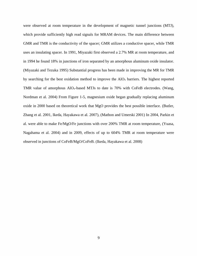
9
were observed at room temperature in the development of magnetic tunnel junctions (MTJ),
which provide sufficiently high read signals for MRAM devices. The main difference between
GMR and TMR is the conductivity of the spacer; GMR utilizes a conductive spacer, while TMR
uses an insulating spacer. In 1991, Miyazaki first observed a 2.7% MR at room temperature, and
in 1994 he found 18% in junctions of iron separated by an amorphous aluminum oxide insulator.
(Miyazaki and Tezuka 1995) Substantial progress has been made in improving the MR for TMR
by searching for the best oxidation method to improve the AlOx barriers. The highest reported
TMR value of amorphous AlOx-based MTJs to date is 70% with CoFeB electrodes. (Wang,
Nordman et al. 2004) From Figure 1-5, magnesium oxide began gradually replacing aluminum
oxide in 2000 based on theoretical work that MgO provides the best possible interface. (Butler,
Zhang et al. 2001, Ikeda, Hayakawa et al. 2007), (Mathon and Umerski 2001) In 2004, Parkin et
al. were able to make Fe/MgO/Fe junctions with over 200% TMR at room temperature, (Yuasa,
Nagahama et al. 2004) and in 2009, effects of up to 604% TMR at room temperature were
observed in junctions of CoFeB/MgO/CoFeB. (Ikeda, Hayakawa et al. 2008)

10
1996 2000 2004 20080
100
200
300
400
500
600
AlO-barrier MTJs
Year
R
/R (
%)
MgO-barrier MTJs
Figure 1-5 Trend in TMR ratio for Al2O3 and MgO barriers. (Ikeda,
Hayakawa et al. 2007)
1.2 Complex Materials and Architecture for MTJ
The MTJ stack requires improvement to make it beneficial for memory applications. The
evolution of tunneling magnetoresistance (TMR) structure is described in Figure 1-6 (Parkin,
Jiang et al. 2003). In (a) and (b), the free layer in a magnetoresistive device is oriented based on
the purpose of the device. For example, the free layer is designed to be orthogonal to the moment
of the pinned layer in field sensor devices such as read heads. Conversely, in MRAM devices,
the magnetic direction in free layer must be parallel or anti-parallel to that of pinned layer.
Figure 1-6 (c) shows the fundamental structure of GMR and TMR stacks, which include a pinned
layer, a free layer, a conduction spacer layer between the ferromagnetic layers, and an exchange-
biased pinned layer. Exchange-bias is an induced magnetic anisotropy, which occurs in
ferromagnetic materials when coupled to an antiferromagnetic layer. The antiferromagnetic layer

11
leads to an internal exchange field at the interface with the adjacent ferromagnetic layer whose
direction is fixed by cooling from above the Neel Temperature of the antiferromagnetic layer in a
magnetic field. Due to the exchange coupling, the ferromagnetic layer exhibits a unidirectional
magnetic anisotropy so that its magnetic moment direction is fixed in one direction. Therefore,
the external magnetic field required to rotate the moment of the ferromagnetic layer increases
inversely with the thickness of the ferromagnetic layer. In the Figure 1-6 (d), the pinned layer is
coupled through a Ru spacer layer, and the lower layer is pinned via exchange bias. The flux
closure stabilizes the magnetic properties of the pinned layer and reduces the coupling to the free
layer. In stack (e), the exchange bias layer has been removed to discourage rotation of the pinned
layer. Stack (f) shows both pinned and free layers consisting of antiferromagnetic (AF)-coupled
pairs, and (g) depicts a double tunnel junction element in which the current tunnels from the first
pinned layer to the free layer to the second pinned element. These schematics show the
complexity of the evolution of magnetically engineered MTJ stack. (Parkin, Jiang et al. 2003)

12
Figure 1-6 Evolution of magnetically engineered multilayers. (Parkin, Jiang et al.
2003)
13
1.2.1 Materials in magnetic tunnel junctions (MTJ)
Materials in magnetic tunnel junctions are transition metals such as Co and Fe and noble
metals such as Pd, Pt and Au. These materials show perpendicular magnetic anisotropy (PMA)
with a specific range of thicknesses and layers. For example, Broeder et al reported that Pd/Co
multilayers have a higher saturation magnetization than pure Co, which is attributed to an
induced ferromagnetism on Pd interfacial atoms. (Denbroeder, Donkersloot et al. 1987) Carcai et
al showed that Co/Pd films with Co thickness less than 8 Å are easy to magnetize along a
direction normal to the film surface. (Carcia, Meinhaldt et al. 1985) Magnetic properties like
saturation magnetization and anisotropy energy can be easily controlled by tailoring the
thickness and number of periods in metal stacks. Transition metals, Pd/Pt, Co/Pd, Co/Pt, and
Co/Ni are commonly used multilayers in MRAM stack due to their relatively high PMA
properties. Although spin valve has been studied intensively, the interest of using multilayers
with PMA in MTJ devices is being vigorously studied as well. Since MTJ consists of two
ferromagnets separated by a thin insulator, the AlOx tunnel barrier has been investigated since it
is easier to deposit than a crystalline MgO barrier. However, with coherent tunneling of the MgO
(001) phase, MgO can theoretically provide much higher TMR values than AlOx. One challenge
researchers face is the precise control of the growth of the magnetic electrode deposited under
the MgO layer. Therefore, a solution to find the best ferromagnetic materials for MgO (001)
growth is crucial (Zhang, Wang et al. 2004). In 2005, Yuasa et al. observed TMR ratios up to
230% at room temperature by replacing the polycrystalline CoFe ferromagnetic electrodes
surrounding the MgO layer with amorphous CoFeB, as seen in Figure 1-7. (Djayaprawira,
Tsunekawa et al. 2005) In 2010, Yakushiji et al. showed that with very thin Co and Pd films –

14
about 0.2 nm – a TMR of 62% with ultralow resistance-area product (3.9 Ω µm2) in MgO based
junctions was achieved, enabling a development of gigabit-scale nonvolatile memory (Yakushiji,
Saruya et al. 2010). The superlattice of multilayers can be annealed at high temperature to
promote the formation of the MgO (001) phase. To summarize the materials in MRAM, Figure
1-8 shows the typical materials such as Co, Fe, Pd and MgO used in MTJ stack. (Slaughter 2009)
The approach of patterning these materials with high fidelity and selectivity is the focal point in
this work.
Figure 1-7 (a) Cross-section HRTEM images of CoFeB/MgO/CoFeB MTJs. (b)
Enlarged cross-section HRTEM image of MTJs shown in (a). (Djayaprawira,
Tsunekawa et al. 2005)
15
Figure 1-8 Typical materials used in MTJ stack. (Slaughter 2009)
1.3 Plasma Etching of Metal Stack
Etching is a semiconductor manufacturing technique used to remove material selectively
from pre-defined locations. There are two major etching methods, wet etching and dry etching.
Wet etching removes the material with chemical solutions and has several advantages including
high etch rate, high throughput, and low cost. The removal of native silicon oxide on the top of a
silicon wafer usually involves wet etching with hydrofluoric acid, a highly corrosive acid capable
of dissolving many materials -- especially oxides (Greenwood and Earnshaw 1984). However,
wet etching cannot transfer patterns with high aspect ratio or narrow line-width in very large
scale integrated (VLSI) devices due to the lack of anisotropic properties. Dry etching, also called
plasma etching, uses the free radicals and ions generated in plasma to remove material with
anisotropic characteristics. The small linewidth achieved by dry etching is necessary to achieve

16
the wafer density improvements dictated by Moore’s Law. Due to its preciseness, dry etching has
become more important in semiconductor processes over the last few decades.
Various chemistries have been chosen in plasma etching to etch different materials such
as oxides, nitrides, metals and polymers. (Kastenmeier, Matsuo et al. 1996) This section focuses
on the application of plasma etching of the aforementioned MRAM materials. Ar+ ion milling
has been using widely in pattern transfer techniques for magnetic materials. However, side wall
redeposition and low etch rates are two major challenges with this technique. (Hsiao 1999) Jung
et al. reported a significantly higher etch rate of 5 nm/s for magnetic multilayer structures by
high ion density Cl2/Ar plasmas. (Jung, Lambers et al. 1997) Nevertheless, the chlorinated etch
products of magnetic materials lack the volatility of conventional materials and tend to severely
corrode the magnetic material. Therefore, non-corrosive CO/NH3 plasma has been developed to
decrease corrosion and maintain high etch rate. (Orland and Blumenthal 2005) Each of these
processes are described in more detail below.
1.3.1 Ar+ Ion Milling for Etching Magnetic Metals
Ar+ ion beams are typically capable of etching materials in an MTJ multilayer stack with
Ta capping. This capping acts as a hard mask material due to the low sputter yield compared to
other magnetic materials. Features with size around 100 nm can be transferred by Ar+ ion
milling. The energy and momentum of Ar+ is used to knock off an atom on the surface of
material by exceeding the binding energy of the etched material. (Kaufman, Cuomo et al. 1982)
However, R. E. Lee reported particular limitations imposed by ion-beam etching such as mask
erosion and faceting, side wall re-deposition, and trenching. (Lee 1979) First, the etching rate of

17
Ar+ ion beam is strongly dependent on the angle between incoming Ar+ ion beam and the
surface. The etch rates of different materials with various incidence angles of the Ar+ ion beam
are depicted in Figure 1-9. The angle of maximum etch rate is important due to formation of
stable facets transference of etched material. (Smith, Melngail.J et al. 1973)
10 20 30 40 50 60 70 80 900
50
100
150
200
250
300
350
400
0
Ion beam
direction
Ti
AZ 1350
SiO2
Al
Au
Mil
l R
ate
(A/m
in)
Beam Angle (º)
GaAs
Figure 1-9 Ar+ ion etch rate of different materials as function of the beam
incidence angle. (Smith, Melngail.J et al. 1973)
Second, back-sputtering caused by the ion beam tends to redeposit the material around
the edges of steep surface features, resulting in the interconnection of isolated regions or the
prevention of complete coverage by a subsequent deposition. Figure 1-10 shows the three
undesirable phenomena in ion beam etching caused by backsputtered material accumulating on
the vertical sidewalls of the mask. (Gloersen 1976)

18
Figure 1-10 Masking strategies for ion-beam etching. (Lee 1979)
Finally, R. E. Lee developed a method to control facet and trench formation during ion
beam etching by tilting the material under etching. In Figure 1-11, the sample with 20 degree tilt
shows a much more uniform etch rate distribution than that of non-tilted sample. (Lee 1979)
Figure 1-11 Method to control facet and trench formation during ion-beam
etching. Ions incident on mask (a) cause facet formation, which leads to trenching
because of the concentrated ion flux at the base. (Lee 1979)
0o tilt
10o tilt
20o tilt

19
In Figure 1-12, M. Gajek et al have demonstrated the removal of side wall deposition by
Ar+ ion beam post etch with 80 degree tilt from sample normal. (Gajek, Nowak et al. 2012)
Figure 1-12 Schematic of the junction fabrication processes, from left to right:
Reactive ion etching of hard mask and magnetic stack structure, photoresist strip
and ion beam trimming at glancing incidence and resulting structure. (Gajek,
Nowak et al. 2012)
1.3.2 Halogen-based Plasma for Etching Magnetic Metals
The first inclination towards etching stable materials is the use of highly reactive
chemistry, e.g. fluorine-based chemistries. However, due to environmental considerations, there
is a need to seek alternatives that are not as damaging, e.g. chlorine-based chemistries.
Nevertheless, it is still important to analyze the properties of potential etch products. From the
CRC handbook, Table 1-2 indicates all metal-halogenated species have high boiling points,
resulting in low volatility and difficulties in etching with halogen chemistries. (Phillips and Perry
1995)

20
Table 1-2 Boiling point of metal fluoride, chloride and bromide. All values taken
from “Handbook of Inorganic Compounds.” (Phillips and Perry 1995)
Element Fluoride : TB (°C) Chloride : TB (°C) Bromide : TB (°C)
Co CoF2 : 1400 CoCl2 : 1049 CoBr2 : unknown
Fe FeF2 : unknown
FeF3 : unknown
FeCl2 : 1023
FeCl3: 316
FeBr2 : decompose
Mn MnF2 : 1820 MnCl2 :1190 MnBr2 : unknown
Pd PdF2 : unknown PdCl2 : decompose PdBr2 : unknown
Ni NiF2 : 1750 NiCl2 : decompose NiBr2 : unknown
Ti TiF4 : 284 (subl.) TiCl4 : 136.4 TiBr4 : 230
Ru RuF5 : 227 RuCl3 : >500 (subl.) RuBr4 : unknown
Ta TaF5 : 229.5 TaCl5 : 242 TaBr5 : 348.8
W WF6 : 17 WCl5 : 275.6 WBr5 : 333
Ir IrF6 : 53 IrCl4 : non-volatile IrBr3 : non-volatile
Cl2-based plasmas have much higher etch rates in MTJ stack etching than Ar+ ion beam
etching. K. B. Jung et al. have etched NiFe and NiFeCo at >300nm/min at <80° K in a Cl2/Ar
plasma in electron cyclotron resonance (ECR) condition with post etch of in situ H2 plasma.
Although the etch products NiClx, FeClx, and CoClx are nonvolatile, the high ion current under
ECR conditions increases the efficiency of ion-assisted desorption while preventing the
formation of a side wall chlorinated selvedge layer. (Jung, Lambers et al. 1997)
However, the maximum etch rate is limited by the unbalanced formation of etch products
and an inefficient ion-assisted desorption. (Jung, Cho et al. 1999) Although high etch rate of
MTJ materials can be achieved, the disadvantage of Cl-based plasma is the corrosion of
chlorinated etch residues on the surface or in the side wall features. Y. B. Hahn et al. observed
that post etch cleaning with H2 or SF6 plasmas or H2O rinsing is necessary to prevent the
corrosion of the metal layers from chlorinated etch residues for high density Cl2/Ar plasma etch
of NiFe, NiFeCo, TaN and CrSi. (Cho, Lee et al. 2000) In Figure 1-13, despite van Delft’s
prediction that high temperatures of plasma etching are needed to increase the efficiency of

21
desorption of etch products by Arrhenius plot, high temperature also deteriorates the magnetic
properties of most soft-magnetic materials and decrease the selectivity of materials over mask
(Vandelft 1995).
0.0005 0.0010 0.0015 0.0020 0.0025 0.00301E-3
0.01
0.1
1
10
100
1000
Reactive ion etch
Sputtering etch
Chemical etch
FeCl3FeCl
2
1/T (K-1)
r (n
m/s
)
Fe
Figure 1-13 Arrhenius plot of etch rate versus temperature: experiments on F for
10 sccm 10 Pa Ar plasma 400 W rf power (triangle), 20 sccm 10 Pa HCl plasma
400 W rf power (+) and 20 sccm 10 Pa HCl resistive heating only (square). Model
calculation for sputter etching (dash dot line), chemical etching (solid line), and
reactive ion etching (dash line). (Vandelft 1995)
To increase the chemical etch rate instead of only physical sputtering, M. S. P. Andriesse
et al. reported that a few percent of BCl3 or SiCl4 in an ICP Cl2 plasma combines the
spontaneous and ion enhanced chemical etching. Etch rates of Fe up to 300nm/min at 190oC
have been observed. (Andriesse, van der Drift et al. 2001) For the etching of Co and related alloy
such as CoNbZr, Andriesse et al. not only observed the 35% etch rate enhancement from the
addition of BCl3 but also 40% enhancement from the exposure of deep ultraviolet radiation. A

22
fast anisotropic dry etching process of CoNbZr has been developed with 300 nm/min at 220 oC.
(Andriesse, Zijlstra et al. 2000)
1.3.3 Noncorrosive Plasma for Etching Magnetic Metals
In the search for noncorrosive gas, CO seemed to be a promising alternative due to
increased volatility of metal carbonyl compounds over analogous chlorinated products. However,
results indicated deposition of carbonaceous materials as organic molecules broke down in
plasma conditions, resulting in etch stop. Nakatani and Pearton suggested addition of NH3 to the
CO plasma in RIE to avoid the deposition of carbide. (Nakatani 1996), (Jung, Hong et al. 1999),
(Jung, Hong et al. 1999) Etch rate in NH3 plasma was approximately 20 nm/min; however, etch
rates as high as 50 nm/min was observed with 15% CO addition. Orland et al. attempted to
investigate CO/NH3 plasma by mass spectral signals, however they also proved that it is difficult
to assign unequivocally. (Orland and Blumenthal 2005) Therefore, CO/H2 plasma was
investigated as a tool to understand more about CO/NH3 plasmas. Using the mass spectra in
Figure 1-14, CO/H2, CO/D2, and 13CO/D2 was analyzed to determine the major compounds
generated in each plasma. Combining all the results, the chemical composition of this family
peaks can be confirmed as CO2H2-x. Three possible chemical structures can be assigned to this
composition: formic acid, a van der Waals cluster of carbon monoxide and water, and a van der
Waals cluster of carbon dioxide and hydrogen. However, van der Waals bonds are too weak to
exist in these conditions. It can be concluded that formic acid has been generated in the CO/H2
plasma. Under the same analysis, the peak around m/z=55-60 can be assigned to C2O2H4-x,
which could be acetic acid, methylformate, hydroxyacetetadehyde, ethenediol, or dioethane. By

23
comparing every peak, the only possible chemical structure is ethenediol. It was proven that
volatile ethenediol complexes were formed. (Orland and Blumenthal 2005)
Figure 1-14 Mass spectra of 13CO/D2 (top), 12CO/D2 (middle), and 12CO/H2
(bottom) plasmas. The anticipated isotopic shifts for chemical identifications have
observed. (Orland and Blumenthal 2005)
Although it is difficult to image the suitable gas reactions needed to create CO2H2-x and
C2O2H4-x species from CO and H2, the proposed surface chemical mechanism is introduced in
Figure 1-15. The method, known as the Fischer-Tropsch process, is one of the synthesis
mechanisms of hydrocarbons and other aliphatic compounds by hydrogen and carbon monoxide
on the surface of a catalytic metal (e.g., iron, cobalt, or nickel). In industrial Fischer-Tropsch
processes the products are methane, sysnthetic gasoline and waxes, and alcohols with water or
carbon dioxide produced as a by-product. With the variety of surface sites created by ion
bombardment during plasma exposure, the opportunity for a number of reaction pathways are
dependent primarily upon the neighbors of the reacting species. Formic acid (HCO2H),

24
formaldehyde (HCOH), large alkanes and metal carbide are generated in the gas phase reacts
with the sites to synthesize the metal formate and metal ethenediol complexes.
Figure 1-15 Proposed surface chemical mechanism of potential products,
including formic acid, formaldehyde, large alkanes and metal carbide produced
through Fischer-Tropsch reaction with CO, H2, CO2H2-x, and C2O2H4-x as
reactants. (Orland and Blumenthal 2005)
With the reference of CO/H2 plasmas completed, the next stage was to prove the
formation of a metal complex in CO/NH3 plasma etch processes. From the mass spectroscopic
results shown in Figure 1-16, the chemical processes have been found to be consistent with
Fischer-Tropsch chemistry, resulting in the formation of formamide in plasma conditions.
Meanwhile, the metal formamide complex has been suggested as being responsible for the etch
rate enhancement in CO/NH3 plasmas. (Orland and Blumenthal 2005)

25
Figure 1-16 Mass spectra of CO in NH3 plasmas over the range from m/z=40 to
80. (Orland and Blumenthal 2005)
Although the NH3 addition enhanced the etch rate of magnetic metal in CO plasma
chemically, the major etch mechanism in high density CO/NH3 plasma continues to be physical
sputtering. Therefore, the selectivity between the CoFe of the free layer over the MgO of the
tunnel junction is not significant due to the strong physical component. Therefore, the discovery
of a new chemistry for MTJ etching is still necessary.
1.4 Organo-metallic Chemistry for Etching Magnetic Metal
Table 1-3 illustrates the bulky volatile ligands acetylacetone (acac) (Mane, Shalini et al.
2002), 2,2,6,6-tetramethyl-3,5-heptanedionate (tmhd) (Barreca, Massignan et al. 2001),
trifluoroacetylchloride (tfac), hexafluoroacetylacetone (hfac), acetic acid (Maruyama and Nakai

26
1991), as well as the nitrogen containing ligands N,N-dimethylethylenediamine (dmen) (Senocq,
Urrutigoity et al. 1999), N,N-diethylethylenediamine (deen) (Senocq, Urrutigoity et al. 1999) and
acetylacetonime (acim) (Gorbenko, Kaul et al. 1997) commonly used in organo-metallic
precursors for atomic layer deposition (ALD). Table 1-4 lists the melting points, boiling points,
and vapor pressures of organometallics with these ligands compared to conventional chlorinated
compounds. The boiling points of these organometallics are much lower than those of
chlorinated compounds. The vapor pressure of organo-metallic complexes are very high at 150°
C, which is still in the acceptable operating temperature range to protect the magnetic properties
of metals.
Table 1-3 Traditional organometallic precursors of beta diketonates for CVD
process. (Orland and Blumenthal 2005)
Organics Acetylacetonate
2,2,6,6-tetra-
methyl-3,5-
heptanedionate
Trifluoroacetyl-
acetonate
Hexauoroacetyl-
acetonate
Abbr. ACAC TMHD TFAC HFAC
Structure
of organics
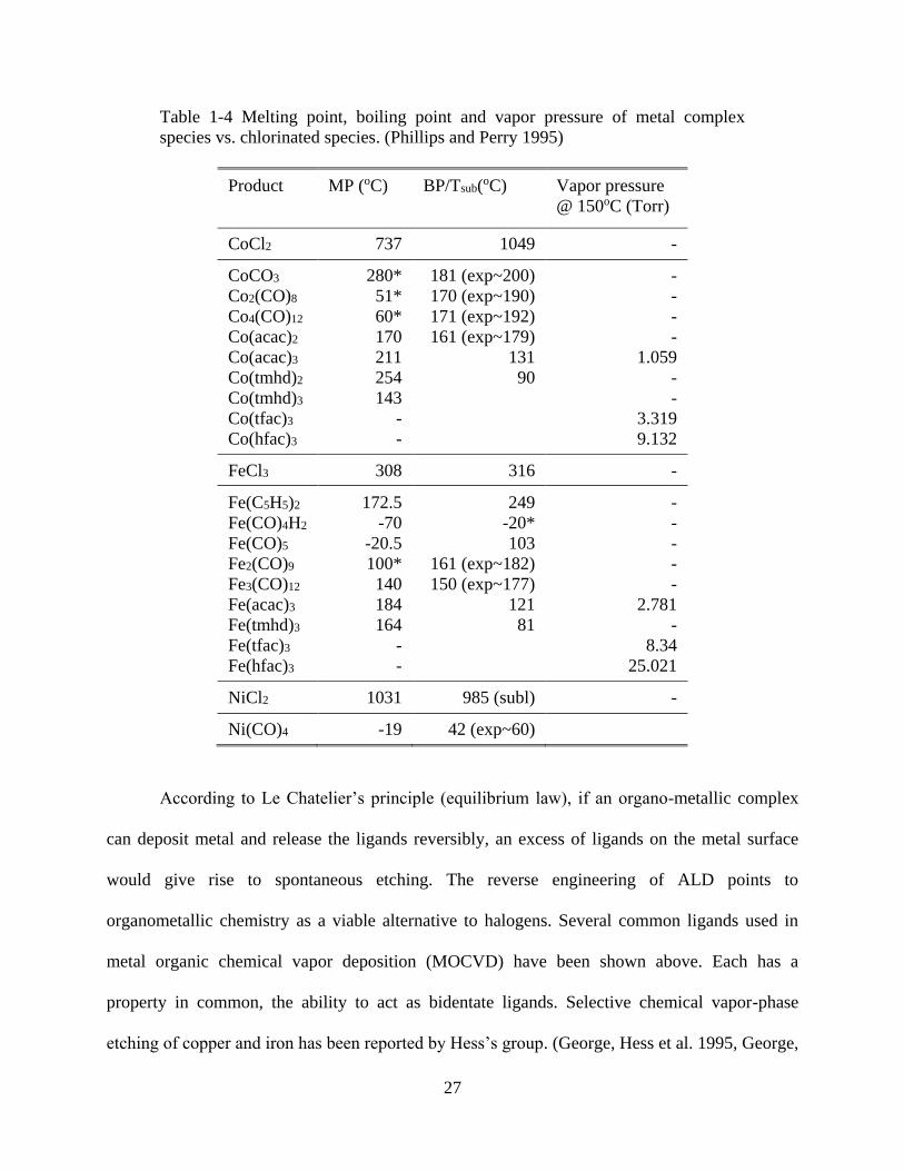
27
Table 1-4 Melting point, boiling point and vapor pressure of metal complex
species vs. chlorinated species. (Phillips and Perry 1995)
Product MP (oC) BP/Tsub(oC) Vapor pressure
@ 150oC (Torr)
CoCl2 737 1049 -
CoCO3
Co2(CO)8
Co4(CO)12
Co(acac)2
Co(acac)3
Co(tmhd)2
Co(tmhd)3
Co(tfac)3
Co(hfac)3
280*
51*
60*
170
211
254
143
-
-
181 (exp~200)
170 (exp~190)
171 (exp~192)
161 (exp~179)
131
90
-
-
-
-
1.059
-
-
3.319
9.132
FeCl3 308 316 -
Fe(C5H5)2
Fe(CO)4H2
Fe(CO)5
Fe2(CO)9
Fe3(CO)12
Fe(acac)3
Fe(tmhd)3
Fe(tfac)3
Fe(hfac)3
172.5
-70
-20.5
100*
140
184
164
-
-
249
-20*
103
161 (exp~182)
150 (exp~177)
121
81
-
-
-
-
-
2.781
-
8.34
25.021
NiCl2 1031 985 (subl) -
Ni(CO)4 -19 42 (exp~60)
According to Le Chatelier’s principle (equilibrium law), if an organo-metallic complex
can deposit metal and release the ligands reversibly, an excess of ligands on the metal surface
would give rise to spontaneous etching. The reverse engineering of ALD points to
organometallic chemistry as a viable alternative to halogens. Several common ligands used in
metal organic chemical vapor deposition (MOCVD) have been shown above. Each has a
property in common, the ability to act as bidentate ligands. Selective chemical vapor-phase
etching of copper and iron has been reported by Hess’s group. (George, Hess et al. 1995, George,

28
Hess et al. 1996) For Cu etched by 1,1,1,5,5,5- hexafluoro-2,4-pentadione (H+hfac), the
following chemical reaction has been proposed:
( ) ( ) 2( ) 2 ( )2 ( )g s g gH hfac CuO Cu hfac H O (1.2)
For the reaction of Cu2+ with h+hfac results in copper disproportionation:
( ) 2 ( ) ( ) 2( ) 2 ( )2 ( )g s s g gH hfac Cu O CuO Cu hfac H O (1.3)
However, no reaction takes place with H+hfac on Cu0 surface, resulting in an accumulation of
Cu0 and a termination of the copper removal process. Fe behaves similarly to Cu above, (George,
Hess et al. 1996) with the following reaction:
( ) 2 3( ) 3( ) 2 ( )6 2 ( ) 3g s g gH hfac Fe O Fe hfac H O (1.4)
In Figure 1-17, the H2O peak appearing in hfac treated Fe2O3 film is strong evidence for
the reaction proposed above. Angle resolved X-ray photoelectron spectroscopy suggests H2O is
localized on the surface.
Figure 1-17 XPS spectrum of hfac-treated (a) Fe film and (b) Fe2O3 film.
(George, Hess et al. 1996)
(a) (b)

29
Although the H+hfac can decompose on an iron surface, it appears to have a limited effect
on the etching process. Similar experiments have shown that the reactivity of acac on a Ni
surface and an oxygen covered Ni surface is different. (Nigg and Masel 1998) Figure 1-18 (a)
shows that acac on a pure nickel surface did not lead to any Ni-containing desorption species.
However, Ni(acac)2 was desorbed from oxygen covered Ni surfaces, confirming that Ni surfaces
are etched by acac. Similar results were also shown with tfac and hfac ligands as shown in Figure
1-18(b).
Figure 1-18 (a) The different desorption species on a Ni(110) surface and on an
oxygen covered Ni(110) surface. Acac ligand was dosed at 100K and the surface
was heated with 10K/ sec. (b) The desorption species are detected by mass
spectrometer. (Nigg and Masel 1998)
1.4.1 Organo-metallic Complex Synthesis
Since the goal in this section is to generate volatile organometallic complex with metal
film and organic ligand, an in-depth understanding of organo-metallic synthesis is necessary. The
definition of organo-metallic chemistry is the possession of a metal carbon bond in the chemical

30
structure. As a result, it combines aspects of inorganic chemistry and organic chemistry. In the
past, such numerous interests in this field are owing to the application of organo-metallic
compounds as catalysts in industrial chemistry. However, there has been a dramatic growth in
the field of ALD and CVD over the past ten years, driven by the needs of the semiconductor
industry such as high-k dielectric in transistor, DRAM capacitors, metal film of interconnection
and so on. The precursor chemistry plays an important role in ALD process. The precursor must
be volatile and thermally stable without restricting to gases but also liquids and solids. Metal
halides, metal alkyls, and metal alkoxides have been widely applied in ALD, but the beta-
diketonates are the most studied compounds of these metals due to its high volatility (Tiitta and
Niinistou 1997, Leskela and Ritala 2002). Since the concept of organo-metallic chemical etch is
based on the reverse process of ALD, the synthesis of beta-diketonate is the concentration in this
section.
The fundamental structure of beta-diketonate is 2,4-pentanedione, usually denoted as
acac (acetylacetone). Acac is the most common representative of a large group of ligands that
form especially stable and useful chelate complexes with a large variety of metals. The structures
of acac and its anion are shown in Figure 1-19 (a). Acac exists as an equilibrium mixture of keto
and enol tautomers in Figure 1-19 (b). (Caminati and Grabow 2006, Czech and Wojciechowicz
2006) Enol tautomer provides much stable structure due to the formation of intramolecular
hydrogen bond and an extended π system, namely, conjugated system. The negative charge is
highly delocalized by resonance since the enolate form of acac anion. Due to the conjugated
system of acac, planar structure has been observed. Although there are two potential geometries,
cis and trans of the anion, the cis conformation is encountered normally while the anion acts as a
ligand. Under cis conformation, the conjugated system of the enolate provides the favorable

31
position of oxygen for coordination, resulting in the most stable structure as the six-membered
chelating ring has little strain energy and electrophilic substitution of the methine hydrogen.
Figure 1-20 shows the sample structure of Co(acac)3. (Jensen and O'Brien 2001) Furthermore,
not only Co(acac)3, but also Na(acac), Be(acac)2, Zn(acac)2, Ni(acac)2, Al(acac)3, Fe(acac)3,
La(acac)3, Zr(acac)4, Cr(acac)3, Cu(acac)2, Mn(acac)2, VO(acac)2, Pd(acac)3, Ru(acac)3 and
Ir(acac)3 have been synthesized. (Lamprey 1960, Beck 1965, Habeeb, Tuck et al. 1978, Bennett,
Heath et al. 1998, Isakova, Baidina et al. 2000, Hamid, Zeller et al. 2005)
Figure 1-19 (a) The structures of acac and its anion, (b) keto in left and enol
tautomer in right. (Caminati and Grabow 2006, Czech and Wojciechowicz 2006)
(a)
(b)

32
Figure 1-20 The structure of Co(acac)3. (Jensen and O'Brien 2001)
It is usually straightforward to synthesize acac organo-metallic complex, because of the
stability of the reaction products. Unlike most of ketone, diketones have much lower pKa, which
allows it to be extensively deprotonated by mild bases such as carbonate or ammonia. For
example, pKa of acac is 9, which is much lower than that of acetone, 20. Because the 6 fluorine
atoms serve as electron-withdrawing groups, Hfac (1,1,1,5,5,5-Hexafluoro-2,4-pentanedione)
provides an even lower pKa, 4.3. The synthesis of Co(acac)3 and Co(hfac)3 are introduced as
samples here: the preparation of Co(acac)3 begins with cobalt carbonate and a large excess of
acac which serves as the reaction solvent as well as for generation of the enolate. Meanwhile,
oxidation of Co2+ to Co3+ with hydrogen peroxide is necessary to generate Co(acac)3 instead of
Co(acac)2 (Shalhoub 1980). By using the excess hfac as a reactant and solvent, the synthesis of
Co(hfac)3 has a similar procedure to that of Co(acac)2. Since the metal is surrounded by
hydrophobic methyl group, the complex tends to have higher solubility in the organic solvent.
Furthermore, the intermolecular forces within the molecules are relatively low, resulting in
relative high volatility. Even higher volatility has been discovered in hfac due to the low
polarizability of fluorine makes the van der Waals force within the molecules exceptionally

33
weak. Based on this phenomenon, the complex can be purified by sublimation or distillation.
(Shalhoub 1980, Jensen and O'Brien 2001)
1.5 Thermodynamic Assessment for Etching Magnetic Metal
According to previous sections, patterning a magnetic metal individually or in stack via
plasma etching is a challenging process. One issue in realizing the etching process is that it is not
clear which metal gaseous species is responsible for the primary etching mechanism. Although
the measurement of partial pressure of metal gaseous species by mass spectrometer along with
other techniques could determine the major etch products in gas phase and condensed phase, it is
a tedious and costly diagnostic. To save resources and eliminate the need for trial and error
methods, a systematic approach in determining the possibility of etch chemistries is needed.
Theoretical approaches based on thermodynamics, which provide the foundation for analyzing
the respective probabilities of competing mechanisms, may be preferable to experiments. In
making the selection, several crucial thermodynamics parameters such as melting point, boiling
point, heat of formation, heat of reaction, Gibbs free energy, and vapor pressure must be
considered. These data for magnetic metals, such as iron, cobalt and nickel, are available in the
NIST JANAF tables, (Chase 1998) HSC Chemistry, (Smith 1996) and CRC handbook. (Phillips
and Perry 1995) There are certain methods based on thermodynamic calculations, one is the
Ellingham diagram, which is a plot of Gibbs free energy change as a function of reaction
temperature, (Ellingham 1944) and the Pourbaix diagram, which plots the potential with respect
to standard hydrogen electrodes as a function of pH. Since the species in plasma etching
conditions are mostly in gaseous and condensed phases, the volatility diagram is the most

34
suitable tool for depicting thermodynamic analysis. The volatility diagram is a plot of the partial
pressure of a particular gaseous product as a function of the pressure of the reactant gas. It was
first used in ceramic reaction analysis (Gulbranse and Jansson 1972) and metals. (Gulbransen
1970) The etching capability of plasma chemistries can be determined by the vapor pressure of
gaseous etching product, suggesting that the weight loss due to the loss of the volatile etching species
should be appreciable to be considered as etchable. In more detail, the weight loss in a
thermogravimetric analyzer (TGA) can be registered provided the vapor pressure of the evaporating
species is higher than 10-8 atm. (Lou, Mitchell et al. 1985) Therefore, the volatility diagram can be
applied to any material with available Gibbs free energy data. In 2002, Kulkarni and DeHoff applied
the volatility diagrams to analyze the dry etching of copper by chlorine plasma at various
temperatures. (Kulkarni and DeHoff 2002) Reactions of copper with molecular and atomic chlorine
were investigated, and molecular and atomic hydrogen reactions were also considered. To construct
the volatility diagram, the dominant species in gas and condensed phase needs to be determined in
order to assess the possible reaction. A list of relevant reactions in the Cu-Cl system with equilibrium
constants is given in Table 1-5.
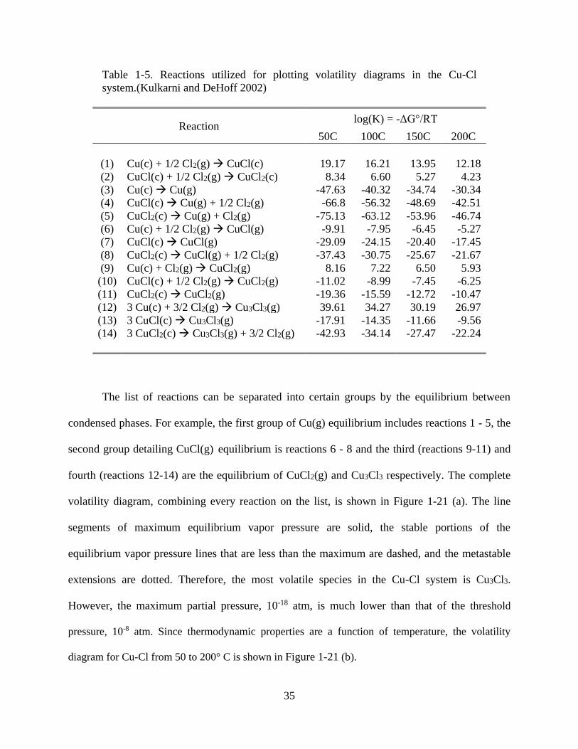
35
Table 1-5. Reactions utilized for plotting volatility diagrams in the Cu-Cl
system.(Kulkarni and DeHoff 2002)
Reaction log(K) = -ΔG°/RT
50C 100C 150C 200C
(1) Cu(c) + 1/2 Cl2(g) CuCl(c) 19.17 16.21 13.95 12.18
(2) CuCl(c) + 1/2 Cl2(g) CuCl2(c) 8.34 6.60 5.27 4.23
(3) Cu(c) Cu(g) -47.63 -40.32 -34.74 -30.34
(4) CuCl(c) Cu(g) + 1/2 Cl2(g) -66.8 -56.32 -48.69 -42.51
(5) CuCl2(c) Cu(g) + Cl2(g) -75.13 -63.12 -53.96 -46.74
(6) Cu(c) + 1/2 Cl2(g) CuCl(g) -9.91 -7.95 -6.45 -5.27
(7) CuCl(c) CuCl(g) -29.09 -24.15 -20.40 -17.45
(8) CuCl2(c) CuCl(g) + 1/2 Cl2(g) -37.43 -30.75 -25.67 -21.67
(9) Cu(c) + Cl2(g) CuCl2(g) 8.16 7.22 6.50 5.93
(10) CuCl(c) + 1/2 Cl2(g) CuCl2(g) -11.02 -8.99 -7.45 -6.25
(11) CuCl2(c) CuCl2(g) -19.36 -15.59 -12.72 -10.47
(12) 3 Cu(c) + 3/2 Cl2(g) Cu3Cl3(g) 39.61 34.27 30.19 26.97
(13) 3 CuCl(c) Cu3Cl3(g) -17.91 -14.35 -11.66 -9.56
(14) 3 CuCl2(c) Cu3Cl3(g) + 3/2 Cl2(g) -42.93 -34.14 -27.47 -22.24
The list of reactions can be separated into certain groups by the equilibrium between
condensed phases. For example, the first group of Cu(g) equilibrium includes reactions 1 - 5, the
second group detailing CuCl(g) equilibrium is reactions 6 - 8 and the third (reactions 9-11) and
fourth (reactions 12-14) are the equilibrium of CuCl2(g) and Cu3Cl3 respectively. The complete
volatility diagram, combining every reaction on the list, is shown in Figure 1-21 (a). The line
segments of maximum equilibrium vapor pressure are solid, the stable portions of the
equilibrium vapor pressure lines that are less than the maximum are dashed, and the metastable
extensions are dotted. Therefore, the most volatile species in the Cu-Cl system is Cu3Cl3.
However, the maximum partial pressure, 10-18 atm, is much lower than that of the threshold
pressure, 10-8 atm. Since thermodynamic properties are a function of temperature, the volatility
diagram for Cu-Cl from 50 to 200° C is shown in Figure 1-21 (b).

36
-80 -60 -40 -20 0-80
-60
-40
-20
0
20
K I
O
CuCl2(g)
Cu(g)
CuCl(g)
Cu3Cl
3(g)
H
D
Cu3Cl
3(g)
CuCl2(c)CuCl(c)
L
og
PC
uxC
l y
Log PCl
2
T=50ºC
Cu(c)
N
M
Figure 1-21 Volatility diagrams for (a) Cu/Cl2 system at 50oC and (b) Cu/Cl2-
H/H2 system at varying pressures of H/H2 and varying temperatures. (Kulkarni
and DeHoff 2002)
The isomolar line (dash) in Figure 1-21 (b) represents the mass balance criterion that the
reactions that lie above this line are technically metastable and are in violation of the principle of
mass conservation. The vapor pressure of Cu3Cl3 is sufficiently high (10-8 atm) at temperatures
greater than 200° C. In order to increase the pressure of etch products under operating
temperature, the introduction of molecular and atomic hydrogen has been investigated. The
reactions of hydrogen considered are:
2( ) 2( ) 3 3( ) ( )
33 3
2c g g gCuCl H Cu Cl HCl (1.5)
2( ) ( ) 3 3( ) ( )3 3 3c g g gCuCl H Cu Cl HCl (1.6)
The reaction for the same partial pressure of hydrogen falls on a straight line known as
the isobaric line, shown in Figure 1-21 (b) as a dashed line. The line with positive slope
represents molecular hydrogen and the negative slope represents atomic hydrogen. As a result,
the pressure of Cu3Cl3 for a given pressure of atomic hydrogen is extremely high at low
(a) (b)

37
temperatures. By utilizing the results from thermodynamics analysis, a two-step reaction scheme
for a dry etching process of copper has been proposed. Meanwhile, this process has been verified
experimentally. (Tamirisa, Levitin et al. 2007) This two-step etch process includes a chlorine
plasma followed by a hydrogen plasma. From the XPS results, a CuClx layer was generated by
the chlorine plasma, while H2 plasma assisted the removal of the CuClx layer by forming Cu3Cl3,
which confirmed the etch mechanism from the thermodynamic prediction.
In this work, a thermodynamic approach was used to assess the feasibility of various etch
chemistries, beginning with the consideration of reactions between the dominant vapor
phase/condensed species and the surface at various temperatures and reactant partial pressures.
The volatility of etching product was determined to aid the selection of viable etch chemistry
leading to improved etch rate. As mentioned in previous sections, a few magnetic metals were
considered (Co, Fe, and Ni) along with various halogen and organometallic based chemistries.
The thermodynamically favorable reactions were investigated and the vapor pressures of its
products were calculated. In addition, the vapor pressure enhancement induced by adding
secondary gas such as hydrogen were investigated. Since experimental validation is an important
part to verify the thermodynamic prediction, the etch rate of different magnetic metals applied in
plasmas were compared by cross-sectional image by scanning electron microscopy (SEM).
Furthermore, optical emission spectroscopy (OES) and quadrupole mass spectrometry (QMS)
applied to plasma chamber to measure the relative amount of predicted etching products. Finally,
the SEM was utilized to observe the morphology of surface and the etching profile of patterned
sample, determining the physical sputtering, chemical etching or synergetic chemical sputtering
in pattering magnetic metals.

38
1.6 Scope and Organization
To continue to push the envelope for micro- and nano-electronics, there are certain major
challenges that arise for plasma etching. Firstly, as novel materials form the backbone of such
emerging technologies such as magnetoresistive RAM (MRAM), the need of patterning
materials that are intrinsically hard to etch such as Co, Fe, Pt and Pd is inevitable. Secondly, the
structural complexity of high aspect ratios and multilayered features presents challenges in
achieving the desired final product. Finally, the downscaling of devices suggests that a minor
deviation from pattern dimensions could result in unbearable degradation in device performance.
Ultimately to address these challenges, developing a new generalized approach to select the
viable chemistries for patterning magnetic metal is inevitable. Figure 1-22 presents the flow
diagram of this work that the first step of the generalized approach was screening of the potential
plasma chemistries for patterning MRAM stack, including several transition and noble metals by
conducting thermodynamic calculations. The plasma chemistries predicted by thermodynamic
calculation have been verified by reactive ion beam etch and organic chemical etch in Chapter 3,
4 and 5.

39
Figure 1-22 Flow diagram of this work. RIE has been introduced in Chapter 3,
organic chemical etch with different surface modifications has been described in
Chapter 4 and 5.
Chapter 2 describes the apparatus used to conduct the experimental work in this study,
focusing primarily on the inductively coupled plasma (ICP) reactor and the in situ diagnostic
probes equipped for the purpose of characterizing the plasma, etch products and macroscopic
etch rate of the complex metal films. An ultra-high vacuum transfer system and surface
characterization techniques are discussed. On the other hand, a low vacuum setup of organic
solution, vapor, ion beam assisted organic vapor etch chambers, and the solution characterization
are introduced. Since the magnetic device is the final product of the study, the measurement of
magnetic properties for metal film is also included. In addition, theoretical methods of
thermodynamic such as Gibbs free energy minimization and volatility diagram analysis are
described in detail using specific model systems.
Chapter 3 discusses the generalized approach for reactive ion etch of magnetic metals,
including the detailed analysis of volatility diagram for etching Co, Fe, Ni, and CoFe alloy by

40
halogen plasmas such as chlorine, fluorine, and bromine. The introduction of secondary
chemistries such as oxygen and hydrogen radicals after halogen gases treatment are also studied,
and the theoretical works are verified by the experiments, including etch rate measurement,
etching product characterization, surface chemical analysis, etching profile observation, and
magnetic properties study.
Chapter 4 presents the ion beam assisted organic chemical etch of magnetic materials
such as Co and Fe. Although an enhancement of etching performance of reactive ion etch has
shown in Chapter 3, a highly volatile etching products are required to increase the selectivity of
mask to metal in patterning MRAM stack. A reversed engineering of ALD is proposed for
patterning metal. First, thermodynamic calculation is performed to select a viable organic
chemistry for each metal, followed by verification of experiments with solution and vapor etch.
Second, due to the low density of organic molecules in vapor phase, an ion beam is selected to
activate the metal surface and assist the desorption of organometallic complex. Finally, etch rate
measurement, etching product characterization, and surface chemical analysis are conducted for
understanding the etching efficacy.
Chapter 5 further explores the organic chemical etch of metals with surface modification.
Various processes of surface modification including O2, Cl2, SO2, CF4, SF6 plasma and O2 ion
source for metal are studied through XPS to understand the conversion of metallic to oxidized
state on surface. Multiple organic ligands are also examined in etching metal in both solution and
vapor phase, and XPS, ICP-MS, and ellipsometer are applied to analyze the etching efficacy of
organic ligands. Finally, the patterned samples of Co and MRAM stack are chosen to
demonstrate the etching performance. Etch rate, surface morphology, etching profile evolution

41
and magnetic property of patterned sample are studied for realizing the atomic scale control of
etching.
Finally, the accomplishment of this work is summarized in Chapter 6 that a
comprehensive framework for selecting viable chemistries in patterning magnetic metals has
been developed, and the surface modification prior to organic chemical etch was realized to be
necessary in chemically etching metals. A high selectivity of metal oxide to metal by formic acid
vapor is achieved, suggesting that one of the most important requirement in atomic layer etch,
self-limiting reaction, is fulfilled. By controlling the thickness of oxides in oxidation, the etch
rate of metals could be controlled in atomic scale level. High density MRAM fabrication can be
achieved based on the results of this work.

42
CHAPTER 2: EXPERIMENTAL SETUP
This chapter is a description of the systems that have been used for the experimental
work of the study, including wet and plasma etching. The synthesis of the several materials and
patterned samples investigated in this work are introduced. Additionally, the various analytical
tools that are used to characterize the plasma environment have also been described.
Furthermore, the measurement of etching performance such as etch rate and etching profile are
presented. Finally, analyses of surface chemical compositions, surface morphology, magnetic
properties, and reaction products have been presented.
2.1 UHV Transfer Tube and Load Lock
An ultra high vacuum transfer tube system provides the capability for processing and
analyzing in a variety of chambers without having to expose samples to ambient conditions.
Each chamber is separated from the main tube by a gate valve. Figure 2-1 shows the relevant
chambers to this experimental work attached to the tube: an inductively coupled plasma reactor
and X-ray photoelectron spectroscopy system.
The main tube is connected to three pumps, an Edwards E2M-18 mechanical pump, a
Leybold 360 turbomolecular pump, and a CTI CT-8 croygenic pump each utilized to achieve a
separate pressure regime. Pressure is monitored by a cold cathode gauge or an ion guage.
Samples are introduced to the tube via a load lock pumped by an additional Leybold 360
turbomolecular pump (base pressure ~10-6 Torr), which is in turn backed by the same E2M-18

43
mechanical pump connected to the tube. A linear transfer arm on the other side of load lock
allows the sample to be transferred to a cart which is utilized to ferry samples along the tube to
various chambers. The cart runs along a metal track secured to the floor of the transfer tube and
is towed by a motorized pulley system. Linear transfer arms connected to the tube allow samples
to be loaded from the cart into various chambers.
Sample Transfer Cart
Load
Lock
XPS
ICP
Etcher
Load
Lock
Gate Valve
Transfer Arm
with X-Y
Manipulator
Sample Transfer Cart
Load
Lock
XPS
ICP
Etcher
Load
Lock
Gate Valve
Transfer Arm
with X-Y
Manipulator
Figure 2-1 A schematic illustration of a UHV Transfer Tube Setup.

44
2.2 ICP Plasma Etcher
The main experimental system used in this study was a custom-built inductively coupled
plasma etcher. The system can be operated in both capacitively coupled (E) and inductively
coupled (H) modes based on the magnitude of the RF power supplied as observed and described
by numerous authors. (Amorim, Maciel et al. 1991, Hopwood 1992, Kortshagen, Gibson et al.
1996) At low RF powers the E mode (driven by an electrostatic field) dominates. As the RF
power is increased there is a transition to the H mode (driven by electromagnetic induction)
which is marked by a dramatic increase in plasma density. However, it is possible for the H
mode to be sustained at lower power values owing to its more efficient sustaining mechanism.
(Miyoshi, Petrovic et al. 2002) This reactor’s main chamber is constructed from stainless steel
and is divided into two sections as depicted in Figure 2-2.
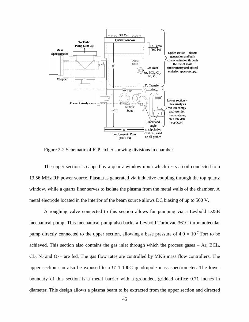
45
Quartz Window
e-
To Cryogenic Pump
(4000 l/s)
To Turbo
(360 l/s)
Gas Inlet
Plane of Analysis
To Transfer
Tube 0.71”
RF Coil
Quartz
Linerse-
Mass
Spectrometer
To Turbo
Pump (360 l/s)
Chopper
8”
9.25”
9”
Upper section – plasma
generation and bulk
characterization through
the use of mass
spectrometry and optical
emission spectroscopy.
Lower section –
Flux Analysis
via ion energy
analyzer, ion
flux analyzer,
etch rate data
via QCM.
Ar, BCl3, Cl2,
N2, O2
Sample
Stage
Linear and
angle
manipulation
controls, used
on all probes
Quartz Window
e-
To Cryogenic Pump
(4000 l/s)
To Turbo
(360 l/s)
Gas Inlet
Plane of Analysis
To Transfer
Tube 0.71”
RF Coil
Quartz
Linerse-
Mass
Spectrometer
To Turbo
Pump (360 l/s)
Chopper
e-
Mass
Spectrometer
To Turbo
Pump (360 l/s)
Chopper
8”
9.25”
9”
Upper section – plasma
generation and bulk
characterization through
the use of mass
spectrometry and optical
emission spectroscopy.
Lower section –
Flux Analysis
via ion energy
analyzer, ion
flux analyzer,
etch rate data
via QCM.
Ar, BCl3, Cl2,
N2, O2
Sample
Stage
Linear and
angle
manipulation
controls, used
on all probes
Figure 2-2 Schematic of ICP etcher showing divisions in chamber.
The upper section is capped by a quartz window upon which rests a coil connected to a
13.56 MHz RF power source. Plasma is generated via inductive coupling through the top quartz
window, while a quartz liner serves to isolate the plasma from the metal walls of the chamber. A
metal electrode located in the interior of the beam source allows DC biasing of up to 500 V.
A roughing valve connected to this section allows for pumping via a Leybold D25B
mechanical pump. This mechanical pump also backs a Leybold Turbovac 361C turbomolecular
pump directly connected to the upper section, allowing a base pressure of 4.0 × 10⁻⁷ Torr to be
achieved. This section also contains the gas inlet through which the process gases – Ar, BCl3,
Cl2, N2 and O2 – are fed. The gas flow rates are controlled by MKS mass flow controllers. The
upper section can also be exposed to a UTI 100C quadrupole mass spectrometer. The lower
boundary of this section is a metal barrier with a grounded, gridded orifice 0.71 inches in
diameter. This design allows a plasma beam to be extracted from the upper section and directed

46
into the lower area. For a 13.56 MHz RF ICP system using Cl2 as the feed gas (with 1% each of
He, Ne, Ar, Kr, and Xe) with an incident power of 400 W and operating pressure of 2 mTorr,
typical ion density (ni) and electron density (ne) values are 6 × 1010 cm-3 (Malyshev and Donnelly
2001) with an average electron temperature (Te) of 3 eV. (Malyshev and Donnelly 2000) In a
similar system utilizing CF4 as the feed gas, with an incident power of 300 W and operating
pressure of 10 mTorr, ni and ne were 2.75 and 1.6 × 1011 cm-3, with Te ~ 6.2 eV. The mean free
path of particles in the chamber is given by the equation:
22 odp
KT
(2.1)
Where p is the pressure, and d0 is the collision diameter of the gas molecule. For diatomic Cl2
with collision diameter of 4.11 Å (Ono and Tuda 1997), the mean free path at the given
operating pressure of 2 mTorr and a neutral gas temperature of 590 K (Donnelly and Malyshev
2000) is estimated as 4.07 cm. CF4 with collision diameter of 4.1Å (Cui, He et al. 2000) at 10
mTorr and an estimated neutral gas temperature of 750 K (Cruden, Rao et al. 2002) the mean
free path is calculated to be 1.04 cm. However, it should be noted that at the pressure of the
extracted beam chamber (~1 × 10⁻⁴ Torr) the mean free paths are accordingly higher: 81 cm for
the Cl2 plasma and 104 cm for the CF4 plasma.
The lower area of this system is connected to a CTI CT-8 cryogenic pump with a
pumping speed of 4000 L/s which maintains a base pressure of 10-8 Torr and a processing
pressure of ~1.0 × 10⁻⁴ Torr. The cryo pump is necessary in this reactor as the small conductance
of the extraction grid hole prevents the turbo pump in the upper chamber from efficiently
evacuating the entire reactor. An ion gauge connected to this area provides the current pressure
inside the chamber, and viewports allow for visual confirmation of the plasma generation. A
0.004 inch diameter tungsten filament minimizes spreading of the aforementioned plasma beam

47
by emitting low energy electrons, while also preventing charge accumulation on insulated
samples. This section houses a rotatable, grounded sample stage which can hold wafer chips
roughly 1.5 cm2 in area. The lack of biasing means that ions are accelerated toward the substrate
solely by the bias potential applied to the extraction grid. The sample holder is physically
mounted on a pin protruding from the stage without electrostatic chucking. The rotational
capability of the stage allows for variation in the beam impingement angle relative to the
substrate surface. The stage and a variety of analytical tools, including an ion flux analyzer, ion
energy analyzer and an optical emission spectrometer, lie in the analytical plane of the lower
section. The ion flux analyzer and ion energy analyzer can be rotated and manipulated in the x, y
and z directions, and can be positioned away from the center of the chamber if necessary. These
diagnostic tools are discussed in greater detail in Section 2.7.
2.3 Wet Etching System of Organic Chemistry
Wet etching is a material removal process involving multiple chemical reactions between
liquid solution and solid state materials to consume the reactants and generate favorable etch
products. The specific patterns are usually defined via masking in the standard semiconductor
process; however, the wet etching in this work focused on etching efficacy of organic chemistry
toward hard-to-etch metals. Therefore, the etch rate of metals, surface composition and post-etch
solution have been analyzed to quantify the etching efficacy.
In Figure 2-3, the wet etching procedure applied in this work is described. Since the
organic chemistries used in this work are quite volatile, the interface between etched and un-
etched area is ambiguous. In order to increase the accuracy of measurement of etch rate, a

48
mixture of Loctite 1C and EPKC epoxy paste were applied to define the un-etched area to
improve the clarity of the boundary separating the etched and un-etched areas. After 24-hour
solidification of epoxy, the components were placed in a vial and heated to 80oC. The water bath
has been chosen to increase the uniformity of heat in the vial. After the predetermined etching
time, the metal sample was immersed in dichloridemethane (DCM) to remove the epoxy on the
un-etched area. The post-etch solutions were analyzed via inductively coupled plasma mass
spectrometry (ICP-MS) to determine the etch products. With the change of surface composition
analyzed by XPS and etch rate measured by Dektak profiler, the etch efficacy of metals with
specific organic chemistry can be determined.
Figure 2-3 Schematic of wet etching standard operating procedure.

49
2.4 Ion Beam Assisted Chemical Etch System
In order to carry out the chemical etch with assistance of ion beam, a customer-designed
ion beam assisted chemical etch system equipped with a 3-cm Commonwealth Scientific
Kaufman ion source has been built (Figure 2-4). The main system is connected to two pumps, an
Edwards E2M-18 mechanical pump and a Leybold 361 turbomolecular pump, each for a separate
pressure regime. Meanwhile, a Pfeiffer Vacuum TCP-040 turbo pump serves as a differential
pump of the ion source. Pressure is monitored by a MKS 627B Baratron gauge and a nude ion
gauge.
A brief introduction of the principle of the broad beam ion source is provided here, but
detailed information including the designs of the multi-aperture ion optics can be found in
literature (Kaufman 1978, Kaufman, Harper et al. 1979, Harper, Cuomo et al. 1982, Kaufman,
Cuomo et al. 1982). A schematic of the ion source is shown in Figure 2-4. By applying a
potential difference between anode and cathode, a DC discharge can be generated in the
discharge chamber.

50
Figure 2-4 The schematic diagram of the ion beam assisted chemical etch system.
The cathode filament, made of 0.25 mm tungsten wire, in the discharge chamber is used
to sustain the discharge through thermionic emission of electrons. The neutral argon (Ar) feed
gas is supplied to the discharge chamber through a built-in 1/8” outer-diameter tube. Although
the primarily ionizations are Ar+ generation of single electron impacts, in order to maximize
dissociation, a discharge voltage of 40V was used to maintain the low probability of Ar2+
formation. To confine the energetic electrons generated from cathode in discharge chamber and
prevent the neutralization before colliding with Ar gas molecules, a permanent magnet was
designed to situate beneath the anode to generate a magnetic field directed parallel to the axis.
The floated potential of anode determines the energy of extracted ions with respect to a grounded

51
sample. Two grids outside the discharge chamber serve as the ion optics to facilitate ion
extraction. The first screen gird was designed to confine the plasma, which possesses a similar
potential to that of cathode. The second grid serves as accelerator which is biased negatively to
extract the Ar+ through the discharge chamber to sample surface. In order to extend the lifetime
of the grids, low sputtering yields of graphite have been chosen as the material. An external
neutralizer made of a 0.25 mm-diameter tungsten wire is needed to not only reduce the Ar+ beam
spreading due to the repulsion of positive Ar+ ions, but also prevent surface charging of insulated
substrate. Since the typical operating pressure of ion source is in several millitorr, the
recombination rate of electrons and Ar+ is negligible due to the large mean free path. Meanwhile,
the negative-biased accelerator also avoids the backstreaming of electrons. Based on the Child’s
law (Kaufman 1978), the current density j of the extracted ion beam can be expressed as
following,
2
2/32/1
0 2
9
4
l
V
m
qj
(2.2)
Where, 0 is the vacuum permittivity, q/m is the charge-to-mass ratio of extracted ions, V is the
voltage difference between the screen and the accelerator grid, and l is the spacing between the
two grids. Usually around 5 sccm of Ar feed gas is used to sustain the high ion flux without too
high background pressure (10-4 torr), the maximum current density of 1keV Ar+ can be achieved
approximately 50 μA/cm2.
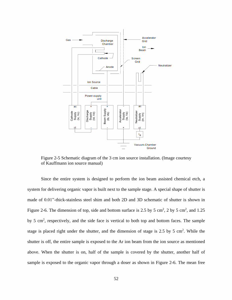
52
Figure 2-5 Schematic diagram of the 3 cm ion source installation. (Image courtesy
of Kauffmann ion source manual)
Since the entire system is designed to perform the ion beam assisted chemical etch, a
system for delivering organic vapor is built next to the sample stage. A special shape of shutter is
made of 0.01”-thick-stainless steel shim and both 2D and 3D schematic of shutter is shown in
Figure 2-6. The dimension of top, side and bottom surface is 2.5 by 5 cm2, 2 by 5 cm2, and 1.25
by 5 cm2, respectively, and the side face is vertical to both top and bottom faces. The sample
stage is placed right under the shutter, and the dimension of stage is 2.5 by 5 cm2. While the
shutter is off, the entire sample is exposed to the Ar ion beam from the ion source as mentioned
above. When the shutter is on, half of the sample is covered by the shutter, another half of
sample is exposed to the organic vapor through a doser as shown in Figure 2-6. The mean free

53
path of acac molecule, 5 cm, has been calculated based on following parameters: P=1 mtorr,
T=300 K and ζ (diameter of acac) = 1.19x10⁻⁹ m. It is much larger than 1-mm-gap between
sample and shutter, resulting in high concentration of acac on the exposed area, but extremely
low concentration of acac on the surface covered by the shutter.
Figure 2-6 Schematic diagram of the design of sample holder and shutter in 3D
and side view of organic doser and the shutter to block Ar+ beam.
2.4.1 Vapor Etch Chamber Coupled With ICP Chamber
Once the etching efficacy of organic chemical is examined by solution etch, a study of
vapor etch is required for incorporating the etching approach into vacuum-compatible
semiconductor process. The result from the organic solution etch suggests that the surface
modification by O2 plasma treatment is necessary to achieve higher reactivity between metal and
organic ligand. Therefore, a vapor etch chamber is attached onto ICP chamber with a gate valve
for isolation is shown in Figure 2-7. A 1.33” six-way-cross nipple is selected as a vapor etch
chamber due to the temperature control issue and the usage of organic solution. The main system
is connected to a pump, an Edwards E2M-18 mechanical pump, and the pressure is monitored by
Ar+
acac vapor
Sample
mask
Ar+
2.5cm
2cm
1mm 1cm
3D view Side view
acac Shutter
cm5
Shutter

54
a MKS 627B Baratron gauge, ranging from 1 to 1000 Torr. In order to maintain an 80oC
environment to avoid condensation of organic, several heating wires are placed uniformly on the
chamber wall externally. If the vapor etch chamber is too large, the temperature of environment
would be easily perturbed, resulting in local condensation of organic chemical. Meanwhile, a
small etch chamber reduces the usage of organic chemical due to the high density of organic
molecule could be obtained easily. Since a sequential process of surface oxidation and organic
vapor exposure is desired, a gate valve is needed to isolate the plasma from vapor etch chamber.
A precision magnetic transporter is designed to move the sample between the ICP chamber and
the vapor etch chamber. By rotating the transporter, an alignment of sample to the organic doser
is available in the vapor etch chamber. A doser is connected to a vaporizer system, allowing the
delivery of organic vapor.
In order to deliver the organic chemical efficiently onto sample, the commercially
available M1-1141-PN liquid vaporizer provided by HoribaTM allows the fine control of the
organic chemical vapor. Three steps are carried out by vaporization systems to inject the
chemical vapor. First, a flow rate varied from 0.02 to 0.1 g/min of liquid is measured, and
controlled by LF-F20M-A liquid mass flow rate controller (MFC). Second, a carrier gas of N2 is
measured and controlled by SEC-E40 gas MFC, and facilitate the vaporization for liquid. Third,
the vaporized gas is released into the reactor.

55
Figure 2-7 A coupled vapor etch chamber with ICP chamber for conducting metal
etch with sequential surface oxidation and organic vapor exposure.
Figure. 2-8 Schematic diagram of the design of Horiba liquid vaporizer system.
(Image courtesy of Horiba, 2013)

56
A fundamental of vaporization is described in a phase diagram, Figure. 2-9. There are
two ways to get from a liquid to a gaseous state. The first method involves increasing the
temperature while holding the pressure steady, as indicated by the arrow with the dash line. This
method is commonly used in everyday settings of boiling water. In the second approach which is
applied in the vaporizer system, one can also heat the liquid in advance and then abruptly reduce
the pressure, as depicted by the arrow with the solid line. The pressure in the vaporization section
of the injector can be reduced instantaneously, and this makes it possible to vaporize a liquid
source instantaneously.
2
1Gas
LiquidSolid
Temperature (oC)
Pre
ssure
(at
m)
Triple point
Figure. 2-9. Generic phase diagram with two approaches to vaporize the liquid
instantaneously.
A method of mixing gas and liquid is illustrated in Figure 2-10. Since the pressure on the
carrier gas is higher at the front of the nozzle inside the injector, it can be heated efficiently. The
liquid source and the heated carrier gas are mixed together in the front of nozzle, and the

57
pressure is reduced as they pass through the nozzle, which vaporizes the mixture. A large flow
rate can be generated steadily without applying high energy to keep the temperature.
Figure 2-10 A method of mixing gas and liquid utilized in vaporizer system.
(Image courtesy of Horiba, 2013)

58
2.5 Material Systems for MRAM Applications
Although the target of this work is to develop a generalized approach for fabricating
MRAM memory stack, fundamental studies on each metal utilized in MTJ stack are required.
Blanket film is required for fundamental studies such as surface chemical state, etching product
identification and quantification which required a large amount of material. Thus, for the purpose
of this work it is important to obtain blanket films of the materials of interest as shown on Table
2-1. The synthesis method, film thickness, and source of the films are listed on Table 2-1 as well.
Table 2-1 Detailed listing of the material blanket films investigated in this work.
Material Synthesis Method Film Thickness
(Å) Source
Co E-beam evaporation (PVD) 100, 200, 500, 1k CNSI (UCLA)
Fe E-beam Evaporation (PVD) 100, 500, 1k CNSI (UCLA)
Ni E-beam Evaporation (PVD) 500 CNSI (UCLA)
Pd E-beam Evaporation (PVD) 100 Nanolab (UCLA)
Pt Sputtering Deposition (PVD) 270 Lam Research Crop.
Co0.3Fe0.7 Sputtering Deposition (PVD) 500 CNSI (UCLA)
Co0.9Fe0.1 Sputtering Deposition (PVD) 10k Lam Research Crop.
Co1Fe2 Co4 Sol-Gel 1500 Tolbert’s lab (UCLA)
Co1Fe2B1 Sputtering Deposition (PVD) 500 Nanolab (UCLA)
Co1Fe2B1 Sputtering Deposition (PVD) 300 Intel
Co0.5Pt0.5 Sputtering Deposition (PVD) 240 Lam Research Crop.
Co0.5Pd0.5 Sputtering Deposition (PVD) 270 Lam Research Crop.
Ultimately, the etching behavior of materials in the MTJ stack is of great importance for
the goal of understanding the feature profile evolution, as achieving the desired profile for all of
the components involved is largely dependent on the relative selectivity of the chemistries
chosen. For example, the etching of a blanket film may not able to distinguish the pure physical
sputtering, pure chemical etch, or combination of two, not to mention the undercut or sidewall

59
re-deposition. Due to the intellectual property and proprietary technology, the publication of
etched profiles in cutting edge devices is rare, and when such profiles are available, the complete
details of the process parameters used are often withheld. Thus, in this work, limited number of
patterned Co film shown in Figure 2-11 is used to study the organic chemical etch with surface
modification.
Figure 2-11 SEM images of the Co film patterned by a TiN hard mask and a SiN
protecting layer with a TiN barrier layer at the bottom as the etch stop layer.
2.6 Plasma Diagnostics
2.6.1 Langmuir Probe
Langmuir probe is one electric probe for plasma diagnostics, and it was developed by
Irving Langmuir in early 1924. A detailed introduction of the device can be found in the original
paper published by Mott-Smith and Langmuir (Mott-Smth and Langmuir 1926). Basically, the

60
electric probe measures the electron density (ne), space potential (Vs), and the electron
temperature (TeV) in local plasmas by using stationary or slow-scanning-rate of electric fields to
emit or to collect charged particles. A metallic electrode in spherical, cylindrical, or planar
geometries have been used as a probe, which first immersed into the plasma and polarized to the
potential Vp by external power supply. The probe current of Ip can be measured due to the
voltage drop in between Vp and plasma potential, Vsp, and a characteristic curve of voltage-
current (I-V) is recorded for extracting the plasma parameters. In this study, an ESPIon
Langmuir Probe from Hiden Inc. was utilized, with a 3 mm long cylindrical tungsten tip of
radius 0.075 mm. The probe voltage range was -200 to +100 V, while the current range was -100
mA to 1000 mA. A typical voltage step of -0.1 V was used, the resolution of voltage and current
data obtained by the system was 10-4 V and 10-8 A, respectively. A diagram of this setup and a
typical I-V curve from an O2 plasma are shown in Figure 2-12. (Chen 2015)
Computer
Probe
Z-Motion Drive
Linear Motion Driver
Probe Interface Unit
Cooling Gas
InletGate Valve
Computer
Probe
Z-Motion Drive
Linear Motion Driver
Probe Interface Unit
Cooling Gas
InletGate Valve
-60 -40 -20 0 20 40
-0.5
0.0
0.5
1.0
1.5
2.0
2.5
3.0
3.5
VP=V
sp
Te= 2.4eV (Maxwellian assumption)
Te= 2.9eV (Non-Maxwellian)
ne=8.87*10
15 #/m
3
ni=3.35*10
16 #/m
3
I p (
mA
)
Vp (Volt)
Vfloating
=-4.6V
Ion Saturation
Region
Transition
Region
Electron
Saturation
Region
Figure 2-12 Schematic of Langmuir Probe Setup and sample I-V curve for O2
plasma taken in the ICP reactor at 500 W, 0 W bias power with 2.5 mT.

61
To qualitatively interpret the I-V curve, an idealized, non-equilibrium, collisionless,
Maxwellian and unmagnetized plasma is considered. Some assumptions have proposed, for
example, the collisional mean free paths of all particles are greater than all characteristic lengths
such as radius of Langmuir probe and Debye length, as well as the electron temperature is higher
than those of ions and neutrals. The plasma potential of Vsp in Figure 2-12 corresponds to the
electric potential at the point of local plasma, resulting in a probe current of Ip, which is
composed of an ion (Ii) and electron currents (Ie) (Ip = Ii + Ie). While the bias is far negative,
Vp<<Vsp, the electrons are repelled, resulting in domination of ion current of Ip, which is called
ion saturation current, Iis. On the other hand, when it is at positive bias, Vp>>Vsp, the ions are
repelled, leaving electrons attracted by the probe. In this case, the electrons are responsible for
the electric shielding of the probe, and it is called electron saturation current, Ies. If the potential
of Vp is equal to Vsp, leaving no current passes through the probe, the floating potential is
obtained where the contribution of the ion and electron currents are equals. (Axford, Goodings et
al. 1998, Goodings, Guo et al. 2001, Merlino 2007)
To consider the ion current (Ii) with a Maxwellian ion distribution at the temperature Ti,
the ion current Ii can be expressed as a function of applied voltage (Vp), (Auciello and Flamm
1989)
]/)(exp[)( ipspispi kTVVe IVI , when Vp≥Vsp, (2.3)
ispi IVI )( , when Vp<Vsp, (2.4)
where e is the electron’s charge, and k is the Boltzmann constant. When Ti is comparable to the
electron temperature TeV as proposed above, the ion saturation current can be expressed as
(Cherrington 1982)
probethiiis AenI ,4
1 (2.5)

62
where ni is the ion density, iithi mkT /8, is the ion thermal motion speed,
However, when TeV>>Ti, the ion saturation current is not a function of Ti but TeV,
0.6 /is Bohm i eV i probeI I en T m A (2.6)
If an electrode in the plasma has a potential different from the local plasma potential, the
electrons and ions distribute themselves spatially around the electrode in order to shield the
effect of this potential on the bulk plasma. An electron shielding cloud would surround the
positively biased electrode, and the negatively biased electrode acquires positive space charge
cloud to cover the electrode, and the characteristic shielding distance for negatively biased
electrode can be expressed by Debye length, 0
2
eVD
e
T
e n
. A positive space charge sheath can
form only when the ion density exceeds that of electron at the sheath edge, which the velocity of
ion must surpass Bohm velocity, /B eV iu T m . To achieve the speed of Bohm velocity, the
corresponding energy is acquired to overcome a potential drop of )/(5.0 ekTe . The factor of 0.6
= e-1/2 comes from the approximation of the plasma potential at the end of the presheath. (Chen
2015)
On the other hand, electron current (Ii) with a Maxwellian ion distribution at the
temperature Te, the electron current Ie can be expressed as a function of applied voltage (Vp),
(Chen 2015)
]/)(exp[)( epspespe kTVVe IVI , when Vp≤Vsp, (2.7)
espe IVI )( , when Vp>Vsp, (2.8)

63
Similar to ion saturation current, the electron saturation current is given by probethiiis AenI ,4
1 ,
where ne is the electron density, eethe mkT /8, is the electron thermal speed, and me is the
electron mass. Since the electron density is similar to that of ion by assumption of
quasineutrality, and the mi is much higher than me, resulting in greater electron saturation current
compared to ion saturation current. Figure 2-12 presents the Langmuir Probe measurement taken
at the O2 operating condition (500 W, 2.5 mT), TeV and ni were calculated as 2.4 eV and 3.35 ×
1010 #/cm-3 respectively, translating to an ion flux of 8.9 × 1015 cm-2 s-1 by equation below. (Chen
2015)
1/2
eVion i
TJ n
M
(2.9)
The next parameter that may be determined is the electron temperature, TeV (eV). A
Maxwellian distribution of electrons is commonly assumed, but since this is not necessarily true.
A useful concept to implement is the electron energy distribution function (EEDF) – ge(ε) from
which both ne and an effective electron temperature Teff can be calculated. The EEDF is defined
as:
dvvfvdg ee )(4)( 2 (2.10)
where v is the electron velocity and fe is the electron distribution function. In terms of energy (ε =
½ mv2/e) this equation takes the form:
)(2
2)( 2/1
2/3
vfm
eg ee
(2.11)
which can then be expressed in terms of Ie and probe potential V as:
2
22/1
2
22)(
dV
Id
m
eV
Ae
mVg e
e
(2.12)

64
where m is the electron mass, e is the electron charge and A is the area of the probe tip. For a
Maxwellian distribution of electrons, the electron energy distribution function, expressed as the
electron energy probability function (EEPF) gp(ε) = ε-1/2ge(ε) then can be expressed as:
/3/22( ) eT
p e eVg n T e
(2.13)
when ln[gp(Vp – Vs)] is plotted versus Vp – Vs, Te can be determined from the slope of the linear
region. However in the case of a non-Maxwellian distribution, the slope is not linear and thus the
effective electron temperature is more suitable, defined as:
dgn
T e
e
eff
0
)(3
2
3
2, where dgn ee
0
)( (2.14)
Thus, by integrating the curves of both ge(Vp – Vs) and (Vp – Vs)ge(Vp – Vs) vs. (Vp – Vs), ne and
Teff can be calculated. For the I-V characteristic from the Figure 2-12 calculated ne and Teff using
this method were 3.5 x 10¹⁶ m-3 and 4.17 eV respectively. Once the plasma density and electron
temperature are known, the Debye length of the plasma (the characteristic distance scale over
which significant charge densities can spontaneously exist) can be calculated by the following
equation:
1/2
0 eVDe
e
T
n e
(2.15)
where ε0 is the permittivity of free space, and e is the fundamental charge of an electron. Based
on the values of TeV and ne above, the calculated Debye length for the ICP system was 0.08 mm.

65
2.6.2 Optical Emission Spectroscopy
The Ocean Optics S2000 system used in this study is comprised of five fiber optic cables
(designated as Master and Slaves 1-4) with a total wavelength range of 200-1000 nm. These are
connected to an analyzer which interfaces with a computer workstation for data collected. The
fiber optic cables are attached to a viewport in the ECR reactor through a machined cover held in
place by screws. The described system and a sample OES spectrum are shown in Figure 2-13.
S2000
Analyzer Module
ADC-1000
USB
Module
Computer
Fiber Optic
Cables
Viewport
S2000
Analyzer Module
ADC-1000
USB
Module
Computer
Fiber Optic
Cables
Viewport
300 600 900
B I,
249.7 nm
Ar I,
794.8 nm
Cl I,
726.7 nm
Cl II,
522.1 nm
Inte
nsi
ty
Wavelength (nm)
50:50 Cl2/BCl
3 Plasma,
400 W, 4 mTorr
Figure 2-13 Schematic of OES setup, and sample spectrum of Cl2 plasma with 5%
Ar addition.
The interaction between plasma species such as electrons, ions and neutrals results in the
creation of particles with excited electronic states. These excited species can subsequently
undergo electric dipole radiation to emit photons, returning to a relaxed state. The energy of
these photons is characteristic of a particular transition in the plasma species, corresponding to
the difference between initial and final quantum energy states of the relaxed electron. The use of
this measured energy to ascertain the identity of species present in the plasma is known as optical
emission spectroscopy (OES). Among the primary advantages of OES is its non-intrusive nature.

66
OES has been utilized to monitor the endpoints of plasma etching experiments (Litvak 1996),
quantify the relative percentages of plasma species present, calculate the reaction kinetics of said
species through actinometry (Booth, Joubert et al. 1991, Booth and Sadeghi 1991), and obtain
bulk plasma information such as Te, ne and EEDF using Trace Rare Gases OES (Donnelly and
Schabel 2002).
As OES spectra are gathered periodically over the time span of an experiment, the
endpoint of etching can be estimated by the appearance of certain lines (e.g. atomic Si) in the
spectra. Additionally, species can be quantified using the principle of actinometry, which is
described as follows. For an electron impact excitation from the ground state to an excited state,
the equation relating the measured emission intensity to the concentration of the free radical
species is as follows:
AAnI (2.16)
where αλA is defined by the following equation:
0
2 )()(),(4)( * vvfvnpdvQvk eAeADA
(2.17)
In the above equations Iλ is the optical emission intensity, nA is the concentration of free
radical A, σλA is the cross section for the emission of a photon having wavelength λ due to
electron impact excitation of A to A*, kd is the detector response constant, QA* is the quantum
yield for photon emission from the excited state, and fe is the electron distribution function.
However, since the aforementioned variables are not normally obtainable, it is impossible to
solve for nA and thus the measured intensities can only provide qualitative information. To
circumvent this problem, a trace amount (generally < 5% of the inlet flow) of a known

67
concentration of inert gas (the actinometer) is fed into the plasma. An emission line (T) with an
excited state that possesses excitation threshold energy close to that of the chosen radical A is
then selected so that the cross sections for the radical and the actinometer are similar near the
excitation energy. The intensity of the emission line from the actinometer can then be described
in a manner analogous to the first set of equations:
TT nI '' (2.18)
where
0
'
2
' )()(),(4)'( * vvfvnpdvQvk eTeTDT
(2.19)
On an energy scale, only the energetic tail end of the electron distribution is above the
threshold energy for the photon emission cross sections, which allows the cross sections near the
threshold energy to be approximated as linear functions of electron velocity:
)( thrAA vvC (2.20)
and
)('' thrTT vvC (2.21)
where CλA and Cλ’T are proportionality constants. The ratio of intensities of the two emission
lines can then be taken to yield the radical density:
'
I
InCn TAT
(2.22)
where
TTD
AADAT
CQk
CQkC
'*
*
)'(
)(
(2.23)
If the chosen emission wavelengths are similar to each other, i.e. λ’ ~ λ and QA* ~ QT*,
then CAT ~ CλA/Cλ’T can be determined and an absolute value of the radical density nA can be

68
calculated. (Coburn and Chen 1980) In general for the experimental section of this work the
actinometer used is five percent of argon in the inlet gas feed. The normalized intensities of the
BCl (272 nm), Cl (738.62 nm) and Cl (792.54 nm) lines to Ar (750.42 nm) in a pure BCl3
discharge is shown in Figure 2-14 from Sha et al. (Sha and Chang 2004)
Figure 2-14 OES intensity ratio of Cl (738.62 nm), BCl (272 nm) and Cl (792.54
nm) to Ar (750.42 nm) as a function of the power at 5 mTorr (left) and chamber
pressure (right) at 300 W in a pure BCl3 plasma. (Sha and Chang 2004)
2.6.3 Quadrupole Mass Spectrometry
A UTI 100C line of sight quadrupole mass spectrometer is set up on this reactor in order
to analyze the ion and neutral compositions of the plasma discharges in the ICP chamber. (Figure
2-15) The mass spectrometer assembly is housed within a stainless steel manifold which is
evacuated by a Leybold 361C turbomolecular pump. An orifice 0.065 inches in diameter and
0.0625 inches deep allows the passage of ions from the plasma in the upper section of the ICP
reactor to the QMS. For ionization of neutral species, a potential of -50.0 V at a current of
approximately 2.0 mA is applied to the filament electrons. A quadrupole - a precise square array

69
of four parallel metal rods between which a combined RF/DC field is maintained serves as a
mass filter and also increases the sensitivity and speed of analysis. (Yinon and Klein 1971)
e-
Mass
Spectrometer
To Turbo
Pump (360 l/s)
Chopper
e-
Mass
Spectrometer
To Turbo
Pump (360 l/s)
Chopper
20 40 60 80 120 140 160 180 200
CoCl2
Inte
nsi
ty (
Cp
s)
Mass to charge ratio (m/z)
37C
l
35C
l 35C
l+35C
l
35C
l+37C
l
37C
l+37C
l
CoCl3
Figure 2-15 Schematic of UTI 100C Mass Spectrometer and mass spectrum for an
etch of Co film in Cl2 plasma, the Cl, Cl2, CoCl2 and CoCl3 peaks have been
discovered.
Since its inception, mass spectrometry has become an important tool in physics,
chemistry and biology (Mayne 1952). In the context of this study, it is a versatile analytical
technique that allows for detailed compositional analysis of the bulk plasma. Unlike OES, mass
spectrometry allows for the identification of complicated molecules over a wide range of masses,
rather than simple atomic and diatomic species. The basic principle of mass spectrometry lies in
the fact that when a beam of charged species is passed through a variable magnetic field, species
with a fixed mass to charge ratio can be focused into a collector and spectra dependent only on
mass can be obtained. (Aston 1920) By comparing these spectra to calculated isotope patterns of
the various molecules that may be present in the plasma, the composition of the discharge can be
verified. Figure 2-16 depicts the isotope composition patterns of the Cl2 that was encountered in
this study.

70
10 15 20 25 30 35 40 65 70 75 80
0
1
2
3
4
5
28N
2
18H
2O
37C
l
35C
l 35C
l+3
5C
l
35C
l+3
7C
l
Inte
nsi
ty (
Cp
s)
Mass (amu)
37C
l+3
7C
l
Figure 2-16 Naturally occurring isotope composition patterns of the Cl2.
For QMS systems, there is an inverse relationship between the mass to charge ratio of
species and the sensitivity of the spectrometer. It is important to determine this sensitivity change
as a function of mass to charge ratio in order for quantitative analysis to be considered accurate.
For this particular QMS, the relationship is as follows.
k
cmI
1
(2.24)
where I is the signal intensity and mc is the mass to charge ratio. The constant k varies between
1.0 and 1.2. (Chae, Vitale et al. 2003)

71
2.7 Surface Characterization
2.7.1 X-Ray Photoelectron Spectroscopy
Originally known as Electron Spectroscopy for Chemical Analysis (ESCA), x-ray
photoelectron spectroscopy (XPS) is based on the fact that when a material sample is bombarded
with ionizing radiation or high energy particles, electrons possessing energies specific to each
element are emitted from either inner or outer valence shells. By measuring the kinetic energy of
these electrons, the ionization potential or binding energy can be derived using the following
equation:
bk EhE (2.25)
where Ek is the kinetic energy of the electron, hν is the energy of the incident radiation, Eb is the
binding energy of the electron, and Φ is the work function of the spectrometer (Hagström,
Nordling et al. 1964). When the radiation source used is an X-ray source (Mg Kα, 1254 eV or Al
Kα, 1487 eV), this technique is known as XPS. Use of a crystal monochromator can further
enhance the resolution of the electron spectra and increase the accuracy in interpretation of
results by reducing some of the uncertainty associated with inherent linewidths and degree of
chemical shifts (Siegbahn, Barnett et al. 1972).
The XPS system used to take the measurements in this study was a Kratos XPS Axis
Ultra DLD unit. The Al Kα anode (1486.6 eV emission) was used with a monochromator at a
30° takeoff angle. Survey scans were performed at 160 eV pass energy, 1 eV step size and 100
ms dwell time, while detailed scans were performed at 20 eV, 0.1 eV step size and 400 ms dwell
time.

72
XPS can also be used to obtain information about the local structure of solid surfaces.
The immediate environment, charge and oxidation state of a particular atom can all have effects
on the binding energies of its electrons. By comparing the shift in energy of an atom relative to a
standard value, specific details about the aforementioned parameters can be deduced.
The integrated intensity of a specific peak is proportional to the number of photoelectrons
per second from that peak, given by the following equation:
ATynfI (2.26)
where n is the number density of atoms of that element in the sample, f is the x-ray flux, is the
photoelectric cross-section for the atomic orbital of interest, is the angular efficiency factor for
the instrumental arrangement, y is the efficiency of the photoelectric process for formation of
photoelectrons with the normal photoelectron energy, is the mean free path of the
photoelectrons in the sample, A is the area of the sample from which photoelectrons are detected,
and T is the detection efficiency. If rearranged in terms of the density:
ASF
I
Tyf
In
(2.27)
where the denominator is defined as the atomic sensitivity factor ASF and used only in
calculations involving a ratio of sensitivity factors. This is because quantities in ASF can vary
based on references used, yet the ratio remains unaffected. The atomic fraction of an element in
the film can be determined from the fraction of corrected integrated intensity of one peak from
the element of interest over the summed corrected integrated intensities of each peak from all of
the elements in the film as shown in the following equation:

73
i
ii
xx
i
i
xx
ASFI
ASFI
n
nC
/
/
(2.28)
The atomic sensitivity factors are XPS equipment dependent and the elements encountered in
this study are tabulated along with the spin orbital splitting (S.O.S.) values and peak binding
energy (B.E.) in Table 2-2.
Table 2-2 XPS Atomic Sensitivity Factors (ASFs) for elements of interests.
Element Line B.E. (eV) S.O.S ASF
B 1s 186.5 - 0.159
C 1s 284.6 - 0.278
N 1s 396.8 - 0.477
O 1s 529.2 - 0.780
F 1s 684.8 - 1.000
Mg 2p 49.6 0.30 0.168
Si 2p 99.7 0.50 0.328
Cl 2p 198.6 1.50 0.891
Fe 2p 706.7 13.20 2.957
Co 2p 778.3 15.10 3.59
Ni 2p 852.7 17.50 4.044
Cu 2p 932.7 19.60 5.321
Pd 3d 334.8 5.25 5.356
Pt 4f 17.1 3.35 5.575
Ta 4f 230 12.00 5.158
The XPS system used to take the measurements in this study was a Kratos XPS Axis
Ultra DLD unit. The Al Kα anode (1486.6 eV emission) was used with a monochromator at a
30° takeoff angle. Survey scans were performed at 160 eV pass energy, 1 eV step size and 100
ms dwell time, while detailed scans were performed at 20 eV, 0.1 eV step size and 400 ms dwell
time. A schematic and sample spectrum of the XPS is shown in Figure 2-17.

74
UV
Lamp
Ion Pump
Electron Energy
Analyzer
UV
Lamp
Ion Pump
Electron Energy
Analyzer
750 740 730 720 710 810 800 790 780 770
Inte
nsi
ty (
Cp
s)
Fe 2p
Binding Energy (eV)
Co 2p
Figure 2-17 Schematic of XPS system and sample spectra for the Fe 2p and Co 2p
peaks after etching a CoFe alloy film in a Cl2 plasma.
Other variation on the XPS process involves adjusting the take-off angle at which
electrons are detected. Doing so allows the effective depth from which an electron emitted (and
thus the maximum depth that can be probed) is controlled. This is due to the restricted mean free
path of the electrons within a surface film. The effect is illustrated in the following Figure 2-18:
x/2x
θ
θ = 30°
x/2x
θ
θ = 30°
Figure 2-18 Illustration of the variation in escape length from a planar surface at
take-off angles of 90° and 30°. At a take-off angle of 30° an excited electron can
only exit from a depth half that of one from a surface oriented at 90°.
This technique is referred to as angle-resolved XPS (ARXPS) and can be used to conduct
depth profiling of a surface film, allowing a greater degree of insight into the composition of a
film (Layadi, Donnelly et al. 1997). The percentages of elements present are often normalized to

75
the intensity of the substrate peak for each variation in take-off angle. Figure 2-19 shows the Pt
4f spectra taken at three different electron take-off angles of 30o, 60o, and 90o (measured from
the substrate normal) for the Pt (20 nm) treated by 500 W ICP O2 plasma for 5 min. First of all,
the area under the spectra remained the same through all the angles, suggesting a normalized
intensity has achieved. Second, the intensity of Pt0+ peak increased while that of Pt4+ decreased
from 30o to 90o, implying a thin layer of platinum oxide on the metallic platinum film. By
quantitatively comparison, the amount of Pt4+ in 30o, 60o, and 90o are 23%, 20%, and 5%,
respectively.
80 78 76 74 72 70
90o
60o
30o
Pt4+
Pt2+
Pt0+
Pt 4f
Binding Energy (eV)
Inte
nsi
ty (
Cps)
Figure 2-19 XPS spectra taken for Pt (20 nm) treated by 500 W O2 ICP plasma for
5 min. The Pt 4f spectra taken at three electron take-off angles. From the top to
bottom are 30o (dash line), 60o (solid line), 90o (gray line), respectively.
XPS can not only characterize the surface chemical state, but it can also be utilized to
estimate the thickness of thin films less than 10 nm thick by quantification. A good example of

76
XPS quantification would be estimating the thickness of the oxide on the top of metal by O2
plasma treatment shown in Figure 2-20.
Figure 2-20 Basic model assumed for the formation of platinum oxide on a
metallic Pt surface through O2 plasma treatment.
The basic model of metallic platinum to platinum oxide conversion for Pt film via O2
plasma treatment is shown. Based on the mass balance criteria, the formation of platinum oxide
via O2 plasma needs to consume corresponding amount of metallic Pt on the surface. The volume
density of the platinum oxide (Pt(IV)O2), 11 g/cm3, is much lower than that of metallic Pt, 21
g/cm3, suggesting the expansion of volume for converting platinum to platinum oxide. The basic
model would be helpful on interpreting XPS data for thickness quantification.
XPS quantification of the plasma-produced platinum oxide on 20 nm metallic platinum
film utilizes Pt 4f, O 1s spectra and survey. The survey scan is needed to confirm no other
element is found except platinum, oxygen, and adventitious carbon. Although the adventitious
carbon would attenuate signal of electron of platinum, the exposure time of platinum film in the
air was controlled, suggesting a negligible amount of carbon left on the platinum surface.
Meanwhile, a thick Pt film (20 nm) was chosen in quantifying oxide thickness to avoid the signal
from the underlying Si substrate. An example of XPS spectra for both pre-treated and O2 plasma
Pt Pt
PtOx
Pre-treated Pt O2 plasma
treated Pt

77
treated Pt is shown in Figure 2-21. First, the survey in Figure 2-21 (c) shows platinum, oxygen,
and carbon without contamination. A qualitative comparison of two samples in Pt 4f shows a
significantly change with an additional peak, and the intensity of O 1s increased dramatically
after O2 plasma treatment. Quantitatively deconvolution of the range of spectra actually reveals
that at least two new peaks, Pt 4+7/2 and Pt 4+
5/2, emerge in Pt 4f. All the peaks were fitted by the
same asymmetric Gaussian-Lorentzian sum function, and the separation of the doublet peaks for
Pt 4f chemical state is held constant. For the Pt 4f region in Figure 2-21 (a), a minimum of three
doublet peaks are required in order to reasonably fit the data. On the other hand, the pre-treated
Pt (metallic) only presents Pt0+ doublet peak with weak Pt2+ doublet peaks. For the O 1s region, a
background oxygen signal was detected due to the adventitious oxygen in physisorbed molecules
in pre-treated sample, but an obvious O-Pt peak appeared after O2 plasma treatment.
80 78 76 74 72 70 535 530 525
Pt2+
XP
S I
nte
nsi
ty (
arb
. unit
s)
Binding Energy (eV)
(a) Pt 4f
Pt_Pre-etch
Pt_O2
500W 0V
O-C
(b) O 1s
Binding Energy (eV)
O-PtPt4+
5/2
Pt0+
800 600 400 200 0
O 1s
O KLL Pt 4sPt 4p
3/2
Pt 4p5/2 Pt 4fC 1sPt 4d(c) Survey
Binding Energy (eV)
Figure 2-21 XPS spectra taken for pre-treated and O2 plasma treated Pt with (a) Pt
4f, (b) O 1s, and (c) Survey.
A basic model presented in Figure 2-20 was employed for the purposes of quantifying
oxide thickness. According to the model, the intensity of metallic doublet Pt 4f peaks should be

78
attenuated by expcos
d
, where d is the thickness of oxide on the top of metallic Pt, λ is the
inelastic mean free path (IMFP) of an electron in platinum oxide at the kinetic energy associated
with the peak, and θ is the electron take-off angle. The ratio of oxide thickness to inelastic mean
free path can be calculated by the ratio of Pt0+ intensity of Pt with O2 plasma treatment to that
without O2 plasma treatment:
0
2
0
2
(Pt with O plasma treatment)ln
(Pt without O plasma treatment)
Ptd
Pt
(2.29)
The advantage of the model is that the ratio of platinum oxide thickness to inelastic mean free
path can be extracted independently from the platinum oxide properties, but the platinum oxide
thickness would still requires inelastic mean free path of an electron in platinum oxide.
A database of electron effective-attenuation-length released from the US National
Institute of Standards and Technology (NIST) (Jablonski and Powell 2002) with the empirical
approximation formula developed by Tanuma et al. (Tanuma, Powell et al. 1994) provide the
estimation of inelastic mean free path of electron as a function of electron kinetic energy in
Figure 2-22. The detailed information for estimating inelastic mean free path (λ) of metal oxide,
including, Pt, Pd, Co, Fe, and Cu are shown in Table 2-3, where Eg is band gap in eV, Nv is the
number of electron in the valence band, and bulk density of film is utilized in g/cm3. Since the
kinetic energy of electron at PtOx peak is around 1415.5 eV, the corresponding IMFP is
estimated to be 1.96 nm. Therefore, the thickness of platinum oxide could be calculated by the
equation above, which the platinum oxide generated by O2 plasma 500 W without bias is around
0.83 nm.

79
Table 2-3 The detail information required for estimating the inelastic mean free
path of electron (λ) in metal oxide including Pt, Pd, Co, Fe, and Cu. (Jablonski
and Powell 2002).
Metal Pt Pd Co Fe Cu
Compound PtO PtO2 PdO PdO2 CoO Co3O4 FeO Fe2O3 Fe3O4 Cu2O CuO
Eg (eV) 1.40 1.25 4.50 2.00 2.40 1.96 2.40 2.20 0.10 2.17 1.55
Nv (#) 16 22 16 22 15 51 14 34 48 28 17
Density(g/cm3) 14.10 10.20 8.30 4.23 6.44 6.11 5.7 5.2 5.0 6.0 6.3
λ (nm) 1.74 1.96 1.82 2.40 1.43 1.47 1.59 1.67 1.67 1.23 1.22
100100 400 700 10001000
5
10
15
20
25
IMF
P (
A)
Electron Energy (eV)
2500
Figure 2-22 Inelastic-Mean-Free-Path in (nm) as a function of electron energy
(eV) of electron in platinum oxide (Jablonski and Powell 2002).
2.7.2 Scanning Electron Microscopy
The scanning electron microscope (SEM) allows observation of a surface at significantly
higher resolutions than that of an optical microscope, with a depth of field that is orders of
magnitude larger. Figure 2-23 displays a schematic of the essential components of an SEM, as

80
well as an image of a patterned Pt sample. A 120-nm-thick of Pt was deposited on Si substrate,
and a 50-nm-thick Ti hard mask was patterned by lift-off process. The spacing of Ti was 10nm
with a 30 nm pitch on Pt film. Most of the SEM images taken in this work were using Nova 600
at 10 kV and 0.54 nA with a processed resolution of 1 nm. The current of filament is 0.27 mA at
1×10⁻⁵ torr, which was controlled by a mechanical pump and turbo pump. The magnification of
image was ranging from 500 to 250,000×.
A simple explanation of the operational concept follows. Electrons are accelerated toward
the anode with energies ranging from volts to tens of kilovolts and subsequently pass through
one or more lenses which serve to reduce the image of the electron source to a nanometer scale
as it impinges on the plane of the surface. A scanning generator is used to deflect the path of the
electron beam, allowing the beam to be moved over the sample surface in a pattern. The
interaction between the electron beam and the surface generates secondary electrons which are
collected and passed through an amplifier before being transmitted to a display cathode ray tube
(CRT). Other types of emission such as light, x-rays, IR and UV radiation may also be produced,
and collected.
From the obtained images, information about the physical dimensions of the pre- and
post-etched samples can be derived, which can be used to calculate effect of the plasma
parameters and chemistry on the etch rate and sidewall angles of the features.

81
Anode
Electron Gun
First Magnetic
Lens
Second
Magnetic Lens
Deflecting
Field
Display
Cathode-
Ray Tube
Scanning
Generator
Amplifier
SpecimenElectron
Collector
Anode
Electron Gun
First Magnetic
Lens
Second
Magnetic Lens
Deflecting
Field
Display
Cathode-
Ray Tube
Scanning
Generator
Amplifier
SpecimenElectron
Collector
Figure 2-23 Components of a scanning electron microscope and cross-sectional
image taken of a patterned cobalt sample.
2.7.3 Dektak Surface Profiler
Stylus profiling is a technology of surface metrology that is used to determine the
thickness change of two different surface treatment. Stylus profilers are versatile functional tools
that not only measure the film thickness but also surface roughness, thin film stress, and
waviness. The movement of a small-diameter stylus can record the surface morphology in both
vertical and horizontal directions. Via direct contact with the surface, the stylus measurement
provides highly precise and repeatable results. Therefore, it becomes the standard for monitoring
thin film deposition or etching processes. A stylus is composed of metal with a diamond tip,
mounted on an arm as shown in the Figure 2-24, and coupled with a linear variable differential
transformer (LVDT). The LVDT is the heart of the profiler and is driven by a special
electromechanical transducer which composed of one primary coil, two secondary coils and a
movable coil in between. The signal detected by the primary coil can vary the displacement of
Ti Ti Ti Ti
Pt Pt Pt Pt
30nm
82
the two secondary coils. The output of multiplexed signal is then filtered to provide a varying
DC signal. In the end, the varying DC signal is digitized and stored to represent the surface
profile of the sample. A schematic and sample spectra of the profiler are shown in Figure 2-24.
To prepare the sample for measuring the thickness change by profiler, the part of sample
is first covered by the Kapton® Tape and followed by etching process. And the Kapton® Tape is
removed for measuring the step under the profiler once the etching process is done. In the Figure
2-24, a Co film is etched by Ar ion beam (top) and Ar ion beam assisted acac vapor etch
(bottom). The removal thickness of Co etched by Ar ion beam and Ar ion beam assisted acac
vapor are 37.1, and 57.5 nm. All of the spectra taken in this work were using Dektak 150 surface
profiler, which allowed sample size in maximum of six inch diameter and one centimeter thick.
The tool can measure steps less than 10 nm as well as measure surface roughness, and the step-
height repeatability is 0.6 nm. The standard stylus of 25 µm wide and stylus force of 3.0 mg is
selected, and a scan resolution of 0.513 µm/sec is applied onto the samples in this work.
(Thomas, Hartnett et al. 1988)

83
100 200 300 400 500 600 700 800 900
-500
0
500
1000 Co
Distance (m)
T
(A
)
Ar+ W/ acac
T=57.5nm
Ar+ W/O acac
T=37.1nm
Figure 2-24 Schematic of Dektak profiler system and sample spectra for the Co
etched by Ar+ beam with and without acac alternative etch.

84
2.7.4 Spectroscopic Ellipsometry
Spectroscopic ellipsometry is a power tool to detect the optical properties of materials
through the change of polarization state after interaction with the sample. It provides a sensitive,
nondestructive and comprehensive approach to achieve a highly accurate measurement of film
thickness and optical properties.
As Figure 2-25 presents, a beam of linearly polarized light with known wavelength
incidents onto the sample surface, and the polarization state of the incident light is interfered to
elliptical polarization. The polarization state depends on multiple parameters such as the incident
angle of light and the refractive index of the sample. The ratio ρ of the Fresnel amplitude
reflection coefficients for p- and s-wave polarized light is defined by
s
p
r
r (2.30)
Where, rp and rs stand for amplitude reflection coefficients for p- and s-wave, respectively.
(Tompkins and McGahan 1999, Fujiwara 2007) All the terms of ρ, rp and rs are complex, which
can be expressed by amplitude (Ψ) in real part and phase (Δ) in imagine part as follows,
)exp(tan i (2.31)
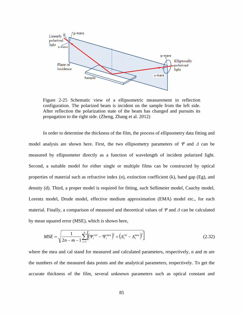
85
Figure 2-25 Schematic view of a ellipsometric measurement in reflection
configuration. The polarized beam is incident on the sample from the left side.
After reflection the polarization state of the beam has changed and pursuits its
propagation to the right side. (Zheng, Zhang et al. 2012)
In order to determine the thickness of the film, the process of ellipsometry data fitting and
model analysis are shown here. First, the two ellipsometry parameters of Ψ and Δ can be
measured by ellipsometer directly as a function of wavelength of incident polarized light.
Second, a suitable model for either single or multiple films can be constructed by optical
properties of material such as refractive index (n), extinction coefficient (k), band gap (Eg), and
density (d). Third, a proper model is required for fitting, such Sellimeier model, Cauchy model,
Lorentz model, Drude model, effective medium approximation (EMA) model etc., for each
material. Finally, a comparison of measured and theoretical values of Ψ and Δ can be calculated
by mean squared error (MSE), which is shown here,
n
i
mea
i
cal
i
mea
i
cal
imn
MSE1
22
12
1 (2.32)
where the mea and cal stand for measured and calculated parameters, respectively, n and m are
the numbers of the measured data points and the analytical parameters, respectively. To get the
accurate thickness of the film, several unknown parameters such as optical constant and

86
thickness are varied to produce a best fitting of the measured Ψ and Δ. Once a global minimum
of MSE is reached in the equation above, an accurate thickness in the model would be achieved.
(Tompkins and McGahan 1999, Fujiwara 2007)
A JA Woollam M88 Spectroscopic Ellipsometer has been utilized to measure the film
thickness in the work, and the spectral wavelength ranging from 280 to 760 nm is covered by this
model. Two examples for single film of Co and Pt are shown in Figure 2-26 that refractive index
(n), extinction coefficient (k) are expressed as a function of wavelength. Since cobalt is one of
the group of transition metals, at long wavelengths in the infrared region, may be expected to
behave according to the classical Drude formulas for free-electron materials, namely,
2 2 2 2
1
2 2 2
2
1 / 2 ( )
2 / 2 ( )
c c
c c
n k Av
nk A
(2.33)
where, A is a constant, proportional to the DC electrical conductance, is the frequency and
c is the electron collision frequency. These formulas predict that in the infrared the optical
constants n and k should have large values with both increasing with wavelength. A further
review by Ordal et al. showed a Drude-model fit to the various experimental results. (Ordal, Bell
et al. 1985) Similar to cobalt, platinum displays Drude behavior in dielectric function above 1
eV, but deviations from a free-electron metal behavior are seen at lower energies due to
interband transitions from the d-electron to s-electron bands near the Fermi level. (Zollner 2000)
(Palik 1985, Palik 1991, Palik and Ghosh 1998) With known optical parameters such as n and k,
an appropriate fitting of the measured Ψ and Δ can be achieved with global minimum MSE in
Figure 2-27, which MSE for Co and Pt are 5.69 and 7.02, respectively. Although MSE for Co
and Pt are not extremely low, the MSE lower than 10 would be acceptable empirically. The

87
thickness of Co and Pt measured by ellipsometer are 40.7 and 32.8 nm, which are verified by the
measurement of SEM, 39.0 and 35.0 nm, respectively.
300 400 500 600 700 800
1
2
3
4
5(a)
k
Wavelength (A)
n, k n
300 400 500 600 700 800
1
2
3
4
5
n, k
Wavelength (A)
(b)
k
n
Figure 2-26 Refractive index (n) and extinction coefficient (k) as a function of
wavelength for (a) Co and (b) Pt.
300 400 500 600 700 8000
10
20
30
40
50
60
70
80
90
100
110
120(a) Model fit of
Model fit of
Exp. of
Exp. of
(deg
ree)
Wavelength (A)300 400 500 600 700 800
0
10
20
30
40
50
60
70
80
90
100
110
120
Model fit of
Model fit of
Exp. of
Exp. of
(b)
(deg
ree)
Wavelength (A)
Figure 2-27 A fitting of refractive index (n) and extinction coefficient (k)
measured by ellipsometer to the model of (a) Co and (b) Pt.

88
However, the data of refractive index (n) and extinction coefficient (k) would not
available for alloy such as CoPt. A unique model for alloy to fit experimental data is built by a
Bruggeman Effective Medium Approximation (EMA), which has been developed to predict the
effect of inclusions of a given material within a host medium. (Aspnes 1982) The following
equation has shown the approach for EMA to estimate the thickness,
(2.34)
where, fCo, fPt are the volume fractions of Co and Pt, ɛCo, and ɛPt are the dielectric function of Co
and Pt, and ɛ is the effective dielectric function. The fitting of the CoPt alloy is shown in Figure
2-28 that MSE is 2.67 which is relatively low compared to Co and Pt single films. The thickness
measured by ellipsometer is 25.0 nm, which is within 7% difference from SEM measurement,
27.0 nmÅ, suggesting an EMA model is adequate in calculating thickness of CoPt alloy.
300 400 500 600 700 8000
10
20
30
40
50
60
70
80
90
100
110
120
Model fit of
Model fit of
Exp. of
Exp. of
(d
egre
e)
Wavelength (A)
Figure 2-28 A fitting of refractive index (n) and extinction coefficient (k)
measured by ellipsometer to the model developed for CoPt alloy thin films.

89
2.7.5 Superconducting quantum interference device (SQUID)
Superconducting quantum interference device (SQUID) magnetometer provides the
highest sensitivity for magnetic field measurement, and a resolution of 10-12 G can be obtained.
The fundamental theories behind SQUID contained quantization of the magnetic flux in a
superconducting ring and the Josephson effect, which allows the tunneling of Copper pairs
through a normal conducting barrier. Flux quantization suggests that magnetic flux enclosed by a
superconducting loop can be quantized by,
215
0 1007.22
mTeslae
h (2.35)
Where, h is Plank’s constant and e is the electron charge (Kleiner, Koelle et al. 2004). On the
other hand, a Josephson effect involves the coherent tunneling of Cooper pairs through a thin
insulator sandwiched between two superconductors as shown in Figure 2-29, and only when a
current passes the critical value, a voltage across the junction can be detected.
Figure 2-29 A Josephson junction is composed of two bulk superconductors
separated by a thin insulating layer through which Cooper pairs can tunnel, and
the Josephson junction is served as a nonlinear inductor (You and Nori 2011).
Based on the operation mode of alternating current (AC) or direct current (DC), a
superconducting ring in SQUID is interrupted by one or two Josephson junctions. A DC SQUID
90
consists of two Josephson junctions connected in parallel on a superconducting loop and is
operated in the voltage state with a current bias, and eventually a magnetic flux can be measured
by the oscillation of voltage (Jaklevic, Silver et al. 1964) For AC SQUID, only a single
Josephson junction inserted into a superconducting loop, which is inductively coupled to the
inductor of an LC-resonant circuit excited by a current at a frequency from megahertz to
gigahertz. The flux change can be detected by the amplitude of the oscillating voltage across the
resonant circuit. (Silver and Zimmerma.Je 1967), (Kleiner, Koelle et al. 2004)
A magnetic property measurement system (MPMS) XL from Quantum Design with a
resolution higher than 10-8 emu at an external magnetic field of 5.5 Tesla, and the standard setup
allows the measurements at the temperature between 1.9 and 400 K with 0.5% accuracy. MPMS
SQUID XL allows the measurements with the applied field pointing out-of-plane or in-plane
with respect to the sample surface. A straw holder made of plastic is selected as a sample holder
due to the total vertical dimension of the pickup coils is smaller than the length of the straw,
which shows no contribution to the magnetic flux. However, the silicon substrate of the metal
film produces a diamagnetic background signal and contributed to the magnetic flux
measurement. A careful background subtraction by linear fit of the raw data at the high end of
magnetic field is required. Some examples of magnetic hysteresis loop measured by SQUID for
ferromagnetic, paramagnetic, and the combination of ferro- and para-magnetic materials are
described below. (Cullity 1972)
A sample hysteresis loop of ferromagnetic Co with and without surface oxidation is
shown in Figure 2-30 (a). In order to observe the coercivity field which the ability of a
ferromagnetic material to withstand an external magnetic field, a spectrum is shown in Figure
2-30 (b). The coercivity increased from 33 to 54 Oe, and the saturated magnetization decreased
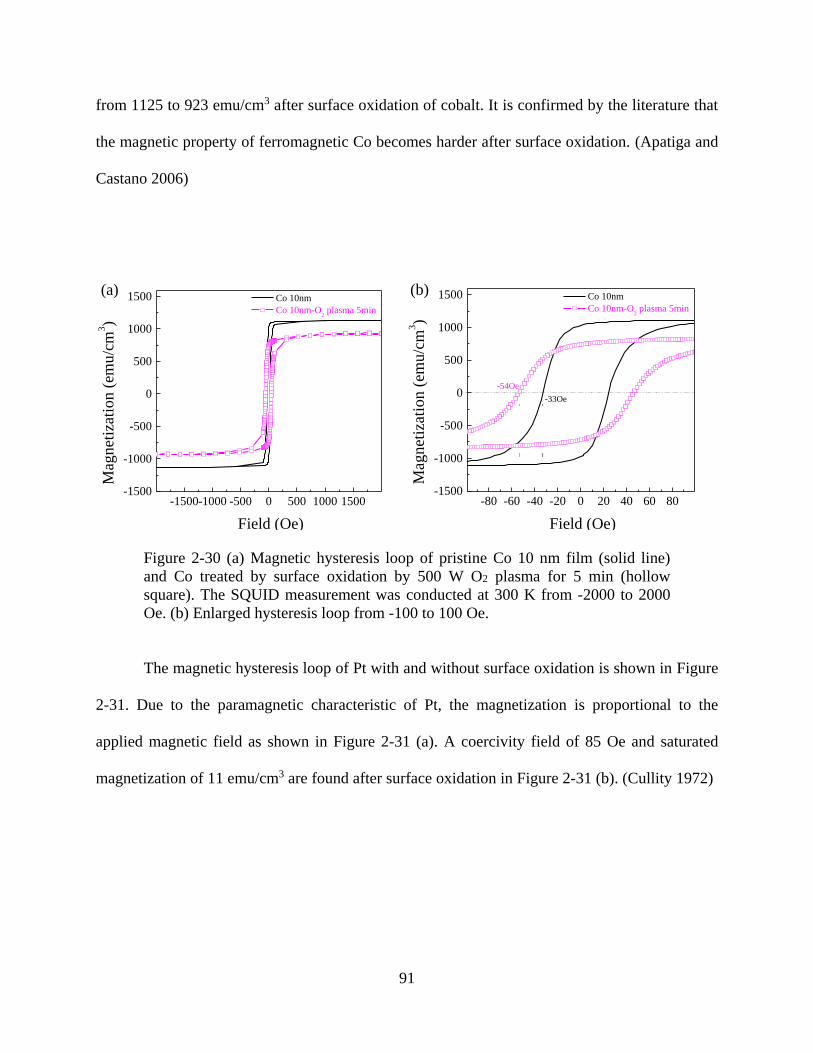
91
from 1125 to 923 emu/cm3 after surface oxidation of cobalt. It is confirmed by the literature that
the magnetic property of ferromagnetic Co becomes harder after surface oxidation. (Apatiga and
Castano 2006)
-1500-1000 -500 0 500 1000 1500-1500
-1000
-500
0
500
1000
1500 Co 10nm
Co 10nm-O2 plasma 5min
Field (Oe)
Mag
net
izat
ion
(em
u/c
m3)
(a)
-80 -60 -40 -20 0 20 40 60 80-1500
-1000
-500
0
500
1000
1500 Co 10nm
Co 10nm-O2 plasma 5min
-33Oe
Field (Oe)
Mag
net
izat
ion
(em
u/c
m3)
-54Oe
(b)
Figure 2-30 (a) Magnetic hysteresis loop of pristine Co 10 nm film (solid line)
and Co treated by surface oxidation by 500 W O2 plasma for 5 min (hollow
square). The SQUID measurement was conducted at 300 K from -2000 to 2000
Oe. (b) Enlarged hysteresis loop from -100 to 100 Oe.
The magnetic hysteresis loop of Pt with and without surface oxidation is shown in Figure
2-31. Due to the paramagnetic characteristic of Pt, the magnetization is proportional to the
applied magnetic field as shown in Figure 2-31 (a). A coercivity field of 85 Oe and saturated
magnetization of 11 emu/cm3 are found after surface oxidation in Figure 2-31 (b). (Cullity 1972)
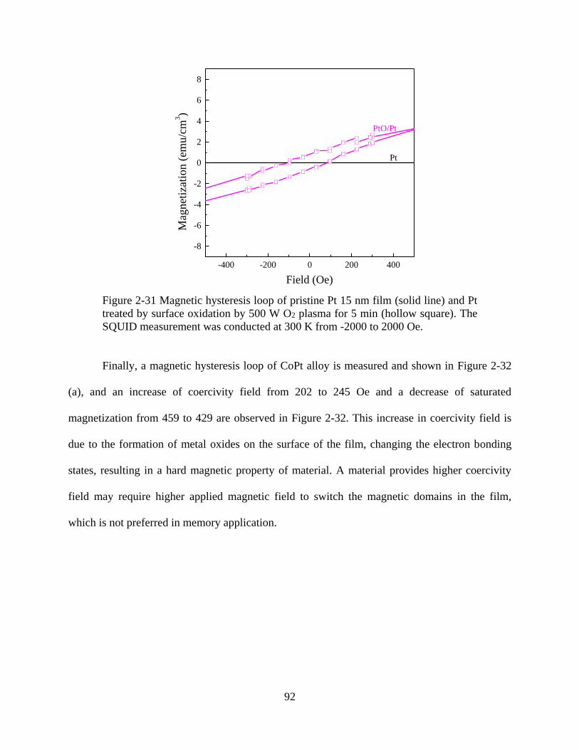
92
-400 -200 0 200 400
-8
-6
-4
-2
0
2
4
6
8
Field (Oe)
Mag
net
izat
ion (
emu
/cm
3)
PtO/Pt
Pt
Figure 2-31 Magnetic hysteresis loop of pristine Pt 15 nm film (solid line) and Pt
treated by surface oxidation by 500 W O2 plasma for 5 min (hollow square). The
SQUID measurement was conducted at 300 K from -2000 to 2000 Oe.
Finally, a magnetic hysteresis loop of CoPt alloy is measured and shown in Figure 2-32
(a), and an increase of coercivity field from 202 to 245 Oe and a decrease of saturated
magnetization from 459 to 429 are observed in Figure 2-32. This increase in coercivity field is
due to the formation of metal oxides on the surface of the film, changing the electron bonding
states, resulting in a hard magnetic property of material. A material provides higher coercivity
field may require higher applied magnetic field to switch the magnetic domains in the film,
which is not preferred in memory application.

93
-2000 -1000 0 1000 2000-600
-400
-200
0
200
400
600(a)
CoPtOx/CoPt
CoPt
Field (Oe)
Mag
net
izat
ion
(em
u/c
m3)
-400 -300 -200 -100 0 100 200 300 400
-400
-200
0
200
400
(b)
CoPtOx/CoPt
CoPt
Field (Oe)
Mag
net
izat
ion
(em
u/c
m3)
-202Oe
-245Oe
Figure 2-32 (a) Magnetic hysteresis loop of pristine CoPt 27 nm film (solid line)
and CoPt treated by surface oxidation by 500 W O2 plasma for 5 min (hollow
square). The SQUID measurement was conducted at 300 K from -2000 to 2000
Oe. (b) Enlarged hysteresis loop from -400 to 400 Oe.

94
2.8 Solution Etching Characterization
2.8.1 Electrospray Ionization - Mass Spectrometry (ESI-MS)
A mass spectrometry using electrospray ionization (ESI) technique has been applied in
the study of the formation of organometallic complex in organic chemistry etching. ESI is a
technique used to assist the transfer of ions from liquid to gas phase, allowing the ions to be
analyzed by ESI-MS. Neutral compounds with ionic conversion such as protonation or
cationaisation can also be subjected to ESI-MS. Three main steps have been proposed to transfer
ionic species from liquid to gas phase: (1) dispersal of charged droplets, followed by (2)
evaporation of solvent and finally (3) ion ejection from the highly charged droplets (Figure 2-33).
Figure 2-33 Three steps of electrospray ionization (Ho, Lam et al. 2003).
In the beginning, the sample solution is passed through the quartz capillary tube to which
a high voltage is applied relative to the surrounding chamber. At the same time, the charged
droplet has been generated by a biased capillary tube with identical polarity. The nebulising gas
(e.g. N2) increased the flow rate of charged droplet and reduced the size by evaporation of the

95
solvent. At the exit of the electrospray tip, the electric field strength in the charged droplet
overcomes the kinetic energy barrier resulting in the ejection of ions from the surface of droplet.
Finally, the emitted ions are accelerated into quadrupole mass analyzer. Depending on the mass
to charge ratio (m/z), the movement of ionic species can be affected by electrical and magnetic
field, and the different ion can be distinguished. Moreover, Figure 2-33 shows the tandem triple
quadrupole system designed in the ESI-MS equipment which can potentially investigate the
structure of molecule by analyzing the fragment of compound (Ho, Lam et al. 2003).
Figure 2-34 Schematic diagram of a tandem triple quadrupole system. First (Q1)
and third (Q3) are mass spectrometers and the second (Q2) is a collision cell (Ho,
Lam et al. 2003).
The post-etch solutions have been analyzed by the Waters Micromass LCT Premier Mass
Spectrometer. The ionization of liquid species was performed by 10 µA with sample cone
voltage of 100 V. Propranolol of 260.16 amu was selected as a reference mass, which allows the
acquisition range of 100 – 1000 m/z (mass to charge ratio). The scanning rate is about one
spectrum per second, and the full width half maximum (FWHM) is 5500, presenting an ultrahigh
signal to noise ratio.
An isotope of given element is an atom with the same number of protons but a different
number of neutrons, resulting in a different mass. For example, carbon shows six protons but

96
various neutrons of 6, 7, and 8, represented by 12C, 13C, and 14C, respectively. The amount of
12C, 13C, and 14C are 98.89%, 1.11%, and trace, resulting in an isotope pattern for particular
species. A sample spectrum from the ESI-MS is shown in Figure 2-35. The spectra were taken
from two post-etch solutions that Co and Fe films etched in 10 M acac solution at 80oC for 30
min separately. The intensity of Co(acac)2 is pronounce compared to that of Fe(acac)3,
suggesting a higher reactivity of cobalt to acac compared to Fe.
252 254 256 258 2600
25
50
75
100
No
rmat
lize
d i
nte
nsi
ty (
%)
Isotope
m/z
Co(acac)2
(257 amu)
354 355 356 357
m/z
Fe(acac)3
(353 amu)
Isotope
Figure 2-35 Sample spectra for the Co(acac)2 and Fe(acac)3 in the post-etch
solution of Co and Fe etched by 10 M acac solution at 80oC for 30 min.
2.8.2 Inductively Coupled Plasma - Mass Spectrometry (ICP-MS)
Inductively Coupled Plasma - Mass spectrometry (ICP-MS) is an analytical technique
utilized for detecting the element in the solution. An ICP-MS contains a high-temperature ICP
source, ionizing the neutral molecule in the sample, in order to let the element to be detected by
mass spectrometer. Usually, argon gas is selected to flow inside the concentric channels of the

97
ICP torch which is connected to a radio-frequency (RF) generator as shown in Figure 2-36, and
an oscillating electric and magnetic fields can be established at the end of the torch once power is
supplied to the load coil. After ignition of plasma, argon molecule is converted to argon ion,
becoming a stable argon discharge, which can ionize the sample that introduced as an aerosol.
Once the elements in the sample are ionized, they are brought into the mass spectrometer via the
interface cones. Sampler, and skimmer cone are the first, and second interface cone, respectively,
as they can reduce the pressure of the sample stream from 1 to 10-5 torr by a small hole of 1 mm
in the center. A shadow stop blocks the photon generated from ICP which may interfere the lens
of determining the elements. In order to avoid the clogging of the small hole on the interface
cones, a low concentration sample from dilution is required. Finally, the ions from the ICP
source are then focused by the electrostatic lenses into the entrance aperture or slit of the mass
spectrometer, which contains a quadrupole mass filter that allows only single mass-to-charge
ratio (m/e) pass through the rods to the detector at a given instant in time. (Niu and Houk 1996)

98
Figure 2-36 The ICP torch with RF load coil generate the argon plasma in the end
of torch which ionize the species in the aerosol (Wolf 2005).
Figure 2-37 The interface region of an ICP-MS, including a plasma torch,
sampler, skimmer cones and a shadow stop with lens for detector (Wolf 2005).
The ELAN DRCII was utilized for all the samples in this work. A 20 L/min flow rate of
Ar is used as a carrier gas with a 175 μL/min of sample uptake rate, and the maximum RF power

99
is 1500 W for ionization of sample spices. An Instrumental detection limit (IDL) of and the
isotopes pattern of all the elements are shown in Figure 2-38. And the detection limit depends
upon many factors, including: lab and instrument background levels, sample matrix, sample
collection and preparation methods, and operator skill level. However, the IDL can be used as a
general guide as to the relative capabilities of the ICP-MS technique as compared to other
analytical techniques. (Wolf 2005)
Figure 2-38 Approximate detection capabilities of the ELAN 6000/6100
quadrupole ICP-MS (Wolf 2005).
The concentration of sample preparation for ICP-MS is critical. If the sample
concentration is too high, the excess of species would block the small hole on the interface cones
and it could potentially contaminate the quartz in the ICP-MS as well. However, if the
concentration is lower than the instrumental detection limit (IDL), for example, 0.03 μg/L for
Co, 0.39 μg/L for Pd, and 0.14 μg/L for Pt, the detector would not be able to distinguish the

100
signal and the background noise. Therefore, a standard sample preparation is designed. First, the
metal film for etching is prepared approximately in a rectangle of 7 by 10 cm, and the volume of
the etchant is controlled in 10 mL. Second, the post-solution is stored in the metal-free VWR 50
mL vial with 1:10 (v:v) dilution. One of the most important studies with ICP-MS is to confirm
the etching efficacy of the meal by organics with and without surface modification. For instance,
the concentration of post-etch solution with surface modification prior to etch is found 2.61 and
2.76 μg/L, for Co and Pt respectively, which is much higher than that without surface
modification, 0.08 μg/L Co and 0.39 μg/L Pt, suggesting an enhancement of etching efficacy
with surface modification prior to organic etch.
2.9 Theoretical Methods
2.9.1 MATLABTM code
MATLABTM is a multi-paradigm numerical computing environment and fourth-
generation programming language, and it allows matrix manipulations, plotting of functions and
data, implementation of algorithms, creation of user interfaces, and interfacing with programs
written in other languages such as C, C++, Java, Fortran and Python. In this work, Gibbs free
energy minimization adopted MATLABTM as a tool to predict the etching product in various
plasma environments. The Gibbs energy minimization method first applies a linear constraint of
atomic conservation matrix. This constraint designates the limitations set on the atoms in each of
the system constituents. The equilibrium chemical potentials of the constituents are obtained as a
linear combination of the component-specific contributions, which are solved with the Lagrange
method of undetermined multipliers. Basically, if a list of etching products and byproducts are

101
available, by considering all of them and their respective Gibbs free energies of formation, a
global minimum of Gibbs free energy would be obtained with a selected combination of
compounds within the system at equilibrium. Figure 2-39 presents a plot of composition as a
function of temperature for the system of 1 kmol SiOCH2 and 6 kmol CF4 at P = 10-5atm based
on the Gibbs free energy minimization through MATLABTM code. The detail of MATLABTM
code utilized in this work is included in the Appendix L.
0 500 1000 1500 2000
0
1
2
3
4
5
6
CH4(g) SiF
2(g)
CO(g)
CHF3(g)
SiOCH2(s)
CF4(g)
Co
mp
osi
tio
n (
km
ol)
Temperature (K)
Figure 2-39 The plot of composition as a function of temperature for the system
of 1 kmol SiOCH2 and 6 kmol CF4 at P = 10-5atm based on the Gibbs free energy
minimization.

102
CHAPTER 3: GENERALIZED APPROACH FOR REACTIVE ION ETCH OF
MAGNETIC METALS
A thermodynamic analysis of etch chemistries for Co, Fe, and Ni using a combination of
hydrogen, oxygen and halogen gases suggested that a single etchant does not work at 300K;
however, a sequential exposure to multiple etchants results in sufficiently high partial pressure
of the reaction products for the process to be considered viable. This sequential dose utilized the
two reactions, a surface halogenation followed by the secondary etchant exposure. (MX2 (c) +
3Y MY(g) + 2XY(g), where M = Co, Fe, Ni; X = F, Cl, Br; Y= O, H) The volatilization
reaction induced by sequential plasma exposure changed the equilibrium point, increasing the
partial pressure of the etch product. Amongst all combinations, Cl2 or Br2 plasmas followed by
H2 plasma were the most effective. Followed by the thermodynamic calculation, the
experimental kinetic verification was performed. From both the gas phase diagnostics and
surface composition analysis, H2 plasma alone could not etch metallic Co, Fe, and Ni films, but
alternating doses of Cl2 and H2 plasmas resulted in more effective removal of chlorinated metals
and increased the overall etch rate. Since the generalized approach has been proven to work for
single metal films, the alloy of CoFe, which is actually utilized in the MRAM device has been
studied. Starting with systematic thermodynamic calculations assessing various chemistries and
reaction pathways leading to the highest possible vapor pressure of the etch products reactions,
the potential chemical combinations were verified by etch rate investigation and surface
chemistry analysis in plasma treated CoFe films. An approximately ~20% enhancement in etch
rate was observed with the alternating use of Cl2 and H2 plasmas, in comparison with the use of
only Cl2 plasma. This chemical combination was effective in removing metal chloride layers thus

103
maintaining the desired magnetic properties of the CoFe films. Scanning electron microscopy
(SEM) equipped with energy-dispersive X-ray spectroscopy (EDX) showed visually and
spectroscopically that the metal chloride layers generated by Cl2 plasma were eliminated with H2
plasma to yield a clean etch profile. This work suggests that the selected chemistries can be used
to etch magnetic metal alloys with a smooth etch profile and this general strategy can be applied
to design chemically based etch processes to enable the fabrication of highly integrated
nanoscale MRAM devices.

104
3.1 Thermodynamic Calculation of Etching Efficacy
Motivated by the above, this work focuses on a systematic thermodynamic approach to
examine potentially viable etch chemistries for magnetic metals. While conventional phase
diagrams, such as Richardson-Ellingham diagrams and Pourbaix diagrams, (DeHoff 1993) are
useful exhibits summarizing thermodynamic properties, we adopted the use of a volatility
diagram to summarize the thermodynamic calculations of the partial pressure of reactants as a
function of the partial pressure of the main etchants. The volatility diagram was first shown in
the work of Wagner et al. who analyzed the silicon oxidation process (Wagner 1958) and later
used in assessing the feasibility of etching of copper by chlorine and hydrogen
chemistries.(Kulkarni and DeHoff 2002) The viable chemistry and operating conditions
predicted by thermodynamics for copper etching were subsequently verified experimentally.
(Tamirisa, Levitin et al. 2007, Wu, Levitin et al. 2010) According to the thermodynamic
calculation for Cu-Cl2 system, an atomic hydrogen addition on CuCl2(c) can generate Cu3Cl3(g)
by utilizing a reaction (3CuCl2(c) + 3H Cu3Cl3(g) + 3HCl(g)).(Kulkarni and DeHoff 2002)
Although this thermodynamic calculation is based on equilibrium conditions, which is not a
realistic representation of what happens in a plasma system that is by definition non-equilibrium,
(Coburn and Winters 1979, Coburn and Winters 1979),(McNevin and Becker 1985) nonetheless
this work inspired a series of experimental work that proved that Cu can indeed be etched by a
two step plasma etching processing employing chlorine and hydrogen(Wu, Levitin et al. 2010)
and under specific conditions by hydrogen plasma alone.(Wu, Levitin et al. 2010, Wu, Levitin et
al. 2011) This set of literature based on independent theoretical prediction and experimental
105
verification established the feasibility of using the thermodynamic calculations as a guide to help
search of viable etch plasma chemistries.
3.1.1 Volatility Diagrams for Co, Fe and Ni Etched in Cl2 System
In this work, several simple reactions leading to the generation of gaseous and condensed
phase metal chlorides were chosen. The generation of metal clusters such as dimerized Co2Cl4(g)
and Fe2Cl4(g) were considered because the species are relatively stable in the gas phase.
However, Ni2Cl4(g) was not considered because its formation was constrained by that of
monomeric counterparts. Table 3-1 lists the probable reactions that were considered in the
thermodynamic calculations involving chlorine etching of Co, Ni, and Fe films. Reactions (1)-
(10) represent the sublimation of pure cobalt, chlorination reaction of cobalt, and formation of
CoCl(g), CoCl2(g), CoCl3(g) and Co2Cl4(g). Because the Gibbs free energies of reactions (2),
(3), (8), and (9) were negative, the partial pressures of CoCl2(g), CoCl3(g) and Co2Cl4(g) in
general increase as that of Cl2(g) increases and are determined by the vapor pressure of CoCl2(c)
(reaction (4),(5),(7), and (10)). The reaction sets, (11)-(15), considered for nickel were very
similar to those for cobalt, but more reactions were considered for iron because of the attainable
valency (+2 and +3) of its condensed phase.

106
Table 3-1 Reactions utilized for plotting volatility diagrams in the M-Cl systems
(M = Co, Fe, Ni) at 300K.
Reaction ΔG (kJ/mol)
(1) Co(c) Co(g) 379.8
(2) Co(c) + Cl2(g) CoCl2(c) -269.3
(3) Co(c) + Cl2(g) CoCl2(g) -107.2
(4) CoCl2(c) CoCl2(g)
162.1
(5) CoCl2(c) Co(g) +Cl2(g) 593.8
(6) Co(c) + 1/2Cl2(g) CoCl(g) 141.3
(7)
CoCl2(c) CoCl(g) + 1/2Cl2 382.9
(8) CoCl2(c) + 1/2Cl2(g) CoCl3(g) -148.4
(9) 2Co(c) + 2Cl2(g) Co2Cl4(g) -323.1
(10) 2CoCl2(c) Co2Cl4(g) 160.3
(11) Ni(c) Ni(g) 384.3
(12) Ni(c) + Cl2(g) NiCl2(c) -258.8
(13) Ni(c) + Cl2(g) NiCl2(g) -86.4
(14) NiCl2(c) NiCl2(g) 172.3
(15) NiCl2(c) + 1/2Cl2(g) NiCl3(g) -222.3
(16) Fe(c) Fe(g) 369.4
(17)) Fe(c) + Cl2(g) FeCl2(c) -301.6
(18) FeCl2(c) + 1/2Cl2(g) FeCl3(c) -32.0
(19) Fe(c) + Cl2(g) FeCl2(g) -155.7
(20) FeCl2(c) FeCl2(g) 145.9
(21) FeCl2(c) Fe(g) + Cl2(g) 671.6
(22) FeCl3(c) Fe(g) + 3/2Cl2(g) 703.0
(23) Fe(c) + 1/2Cl2(g) FeCl(g) 215.4
(24) FeCl2(c) FeCl(g) + 1/2Cl2(g) 517.5
(25) FeCl3(c) FeCl(g) + Cl2(g) 548.9
(26) FeCl3(c) FeCl2(g) + 1/2Cl2(g) 177.8
(27) Fe(c) + 3/2Cl2(g) FeCl3(g) -247.8
(28) FeCl2(c) + 1/2Cl2(g) FeCl3(g) 54.285
(29) FeCl3(c) + FeCl3(g) 85.7
(30) 2Fe(c) + 3Cl2(g) Fe2Cl6(g) -598.3
(31) 2FeCl2(c) + Cl2(g) Fe2Cl6(g)
Fe??????FeCl3(g)
5.8
(32) 2FeCl3(c) Fe2Cl6(g) 68.7 1) Reaction (28) is equal to 2FeCl2(c) + Cl2(g) 2FeCl3(g).

107
The vapor pressures of metal chlorides at temperatures between 300 K and 500 K were
determined and shown in Figure 3-1 as a function of the chlorine partial pressure. To assess the
volatility of a reaction product, the square symbol and gray line at 10-8 atm represented a
reference point at which the weight loss of a material is measurable by a thermogravimetric
analyzer and considered etchable.(Lou, Mitchell et al. 1985)
-100 -50 0-80
-60
-40
-20
0
20
-100 -50 0-100 -50 0
log P
(Co(g
)) o
r lo
g P
(CoC
l 2(g
)) o
r lo
g P
(MC
l 3(g
))
log P(Cl2(g))
Ni in Cl2
Fe in Cl2
Co in Cl2
log P(Cl2(g))
300 K
350 K
400 K450 K500 K
300 K
350 K
400 K450 K500 K
(15)
(32)(8)
(c)(b)(a)
(14)
(11)
(13)
(12)
(31)
(28)(20)
(20)
(16)
(18)(17)
(4)
(3)
(1)
(2)
500 K450 K
400 K
350 K
300 K
log P(Cl2(g))
Co(c)
CoCl2
(c)
Fe(c)
FeCl2(c)
FeCl3(c)
Ni(c)
NiCl2
(c)
Figure 3-1 Volatility diagram for (a) Co in Cl2, (b) Fe in Cl2, and (c) Ni in Cl2
system at 300, 350, 400, 450, and 500K. The reactions in the figure are presented
in Table 3-1. The square and dashed line at 10-8 atm infers the reactant volatility,
corresponding to a weight loss that is detectable in a thermogravimetric analyzer
(Lou, Mitchell et al. 1985).
In the volatility diagram of Co in Cl2, the horizontal lines of reaction (1) represent the
sublimation from Co(c) to Co(g). The corresponding vapor pressure at 300 K was lower than
10-60 atm. The vertical lines correspond to the equilibrium state between Co(c) and CoCl2(c),
showing that CoCl2(c) is preferred as the partial pressure of Cl2 increases. CoCl2(c) vapor
pressure increases as Cl2 pressure increases in reaction (3) and is limited at the equilibrium of

108
CoCl2(c) sublimation, reaction (4). This is because the reaction to generate CoCl2(c) is
significantly more favorable than Co(c), even at low temperatures. As a result, the attainable
vapor pressure is dictated by the sublimation of CoCl2(c) which shows the highest vapor pressure
in this diagram. In addition, it is well known that the dihalide state is the only known condensed
halides of cobalt.(Greenwood and Earnshaw 1998) The reaction (8) does not have an
intermediate state to make a reaction because CoCl2(c) is saturated with chlorine, so an
equilibrium line of the reaction is displayed as a dashed line.
Very similar trends were observed for chlorine reacting with Ni; however, the volatility
diagram for Fe was different from Co and Ni since Fe can form FeCl3(c) in a +3 valance state. In
the reaction between Fe and Cl, FeCl3(c) is thermodynamically preferred over FeCl2(c) since the
enthalpy of the former reaction is lower.(Kiihamaki and Franssila 1999) In addition, it was
reported that the chlorine-based plasma etching of an Fe/Si alloy film generated FeCl3 rather than
FeCl2.(Kinoshita, Yamada et al. 1991) A temperature-dependent volatility diagram is presented
from 300 to 500 K (Figure 3-1). The required temperatures to make CoCl2, FeCl3, and NiCl2
volatile were calculated to be 613 K, 392 K, and 633 K, respectively.
The vapor pressures of various metal halides were plotted against temperature in Figure
3-2. Metal chloride and bromide (Metal = Co, Fe, or Ni) have higher vapor pressures than metal
fluoride, consistent with their melting and boiling points.(Lide 1995) The metal halide
compounds were not volatile below 473 K except FeCl3 and FeBr3. The incorporation of an
additional chemistry is necessary to etch these metals.

109
400 600 800
-50
-40
-30
-20
-10
0
400 600 800400 600 800
(c)(b)(a)
CoF2
CoCl2
CoBr2
CoCl2+H
Ni in F2,Cl
2,Br
2Fe in F
2, Cl
2, Br
2
log
P (
MaX
b(g
))
Temperature / K
Co in F2, Cl
2, Br
2
FeF3
FeCl3
FeBr3
FeCl3+H
Temperature / K
NiF2
NiCl2
NiBr2
NiCl2+H
Temperature / K
Figure 3-2 Calculated vapor pressure from the sublimation reaction of metal
halide condensed phase at 300, 400, 500, 600, 700, 800, and 900 K. (a) Co in Cl2,
(b) Fe in Cl2, and (c) Ni in Cl2 system. Hollow stars represent the partial pressure
of MH(g) (M = Co, Fe, and Ni) at an equilibrium when metal chloride is exposed
to hydrogen radicals.
3.1.2 Secondary Chemistries Addition in Cl2 System
The addition of the secondary plasma was investigated on a CoCl2(c) layer. The first
chemistry examined was molecular and atomic oxygen addition as summarized in Table 3-3. The
addition of an oxygen plasma enabled access to the meta-stable extension of the CoO(g)-
CoCl2(c) equilibrium line. In Figure 3-3(a), a dashed line (35) represents an equilibrium line to
generate CoO(g) from the reaction between a meta-stable CoCl2(c) layer and an oxygen atom.
Three equilibrium lines were shown, depending on the partial pressure of oxygen. The
equilibrium pressure increased as the oxygen partial pressure varied from 10-30 to 10-10 atm. The
maximum attainable partial pressure of CoO(g) was decided by the mass balance of a

110
thermodynamically favorable reaction (36), which was represented as hollow squares in Figure
3-3. At the oxygen radical pressure of 10-10 atm, the partial pressure of CoO(g) was 10-11 atm
which is higher than the CoCl2(c) vapor pressure but lower than the required pressure to be
considered etchable (10-8 atm). O2 addition by reaction (33) and (34) does not enhance the partial
pressure of CoO(g) compared to CoCl2(g) pressure at the equilibrium.
Table 3-2 Reactions utilized for plotting volatility diagrams in CoCl2 etching with
O, Co etching with O, and CoO etching with Cl systems at 300K.
Reaction ΔG (kJ/mol)
(33) CoCl2(c) + 1/2O2(g) CoO(g) + Cl2(g) 526.7
(34) CoCl2(c) + 3/2O2(g) CoO(g) + 2OCl(g) 723.3
(35) CoCl2(c) + O(g) CoO(g) + Cl2(g) 295.1
(36) CoCl2(c) + 3O(g) CoO(g) + 2OCl(g) 28.5
(37) Co(c) + 1/2O2(g) CoO(c) -214.1
(38) 3CoO(c) + 1/2O2(g) Co3O4(c) -152.0
(39) Co(c) + 1/2O2(g) CoO(g) 257.3
(40) CoO(c) CoO(g) 471.4
(41) 1/3Co3O4(s) CoO(g)+1/6O2(g) 522.1
(42) CoO(c) + 1/2Cl2(g) CoCl(g) + 1/2O2(g) 375.2
(43) CoO(c) + Cl2(g) CoCl(g) + ClO(g) 473.5
(44) CoO(c) + Cl(g) CoCl(g) + 1/2O2(g) 270.0
(45) CoO(c) + 2Cl(g) CoCl(g) + ClO(g) 263.1 1)Reaction (33) is equal to 2CoCl2(c) + O2(g) 2CoO(g) + 2Cl2(g).

111
-100 -80 -60 -40 -20 0-80
-60
-40
-20
0
20
-100 -80 -60 -40 -20 0-80
-60
-40
-20
0
20(b)(a)
log
P(C
o(g
)) o
r lo
gP
(Co
Cl 2
(g))
or
log
(Co
O(g
))
log P(Cl2(g))
CoCl2 with O
P(O)
10-10
10-20
10-30
-60
-40
-20
0
20
Lo
g P
(O(g
))
(1)
(2)
(3)
(4)
(35)
(36)
log
P(C
o(g
)) o
r lo
gP
(Co
Cl 2
(g))
or
log
(Co
H(g
))
log P(Cl2(g))
CoCl2 with H
(1)(49)
P(H)
10-10
10-20
10-30
(4)
(48)(3)
(2)-80
-60
-40
-20
0
log
P(H
(g))
Figure 3-3 A partial pressure of CoO(g) generated from atomic oxygen (left)
addition on CoCl2(c) and that of CoH(g) generated from atomic hydrogen (right)
addition on CoCl2(c) at 300K. The hollow square symbol was achieved from the
mass balance from reaction (19) and (32).
Another chemistry examined was hydrogen with reactions involving molecular and
atomic hydrogen for etching Co as summarized in Table 3-4. A reaction with hydrogen was
considered because it results in a more negative Gibbs free energy of the reaction compared to
the CoO(g) generation reaction. In Figure 3-3(b), a dashed line (48) represents an equilibrium
line derived from the reaction between a meta-stable CoCl2(c) layer and hydrogen. The
maximum partial pressure of CoH(g) was represented as a hollow square at which point the
thermodynamically favorable state and mass balance are simultaneously satisfied. The partial
pressure of CoH(g) was estimated to be higher than 10-8 atm, indicating that the addition of an
atomic hydrogen on CoCl2(c) is a promising etch chemistry. While the vapor pressure of a
compound is an intrinsic property and thus constant at a given temperature, the cobalt chloride
surface acts as an intermediate state to the subsequent reaction path and generates CoH(g) at an

112
enhanced rate. The result indicates that the kinetics changed during this sequential reaction
process.
Table 3-3 Reactions considered in hydrogen plasma reacting with CoCl2.
Reaction ΔG (kJ/mol) (46) CoCl2(c) + 1/2H2(g) CoH(g) + Cl2(g) 678.5
(47) CoCl2(c) + 3/2H2(g) CoH(g) + 2HCl(g) 487.9
(48) CoCl2(c) + H(g) CoH(g) + Cl2(g) 475.3
(49) CoCl2(c) + 3H(g) CoH(g) + 2HCl(g) -121.7 1) Reaction (46) is equal to 2CoCl2(c) + H2(g) 2CoH(g) + 2Cl2(g).
Having established that a hydrogen exposure to a chlorinated cobalt surface is a
potentially effective route to chemically etch cobalt, the combination of hydrogen and chlorine
plasmas was tested on nickel, where one chemistry was used first followed by the exposure to
the other chemistry. This analysis was done only for nickel because the thermodynamic data
existed for condensed nickel hydride but not for cobalt hydride or iron hydride. The left panel of
Figure 3-4 represents an equilibrium line (50) derived from the hydrogen addition reaction on the
meta-stable NiCl2(c). The maximum pressure achieved from the mass balance of reaction (51)
was marked as a hollow square, showing the enhanced partial pressure of an etch product. An
atomic chlorine addition on a nickel hydride film was shown in the right panel of Figure 3-4. The
maximum partial pressure of NiCl(g) achieved from the mass balance of reaction (56) was ~10-2
atm which is significantly higher than the reference point (10-8 atm). This result indicates that
both an H(g) addition on NiCl2(c) and a Cl(g) addition on NiHx can increase the partial pressure
of etch products to make the etch chemistry viable. The driving force to enhance the equilibrium
pressure is the highly reactive H atom’s propensity to form MH(g). In addition, a stable
byproduct such as HCl(g) (ΔGf = -95.3) contributes to the Gibbs free energy of a reaction being

113
negative, so an equilibrium point forms at the point to generate CoH(g) with a higher partial
pressure. (NiCl2(c) + 3H NiH(g) + 2HCl(g), ΔGr = -190.9 kJ/mol) This reaction can be
compared with that to generate CoH(g) directly from Co(c), which has a positive Gibbs free
energy. Because of the negative Gibbs free energy of a reaction, the equilibrium point moved to
the forward reaction to generate CoH(g) and to increase the vapor pressure of an etch product.
Table 3-4 Reactions considered in hydrogen plasma reacting with NiCl2 and
chlorine plasma reacting with NiH0.5.
Reaction ΔG (kJ/mol) (50) NiCl2(c) + H(g) NiH(g) + Cl2(g) 406.1
(51) NiCl2(c) + 3H(g) NiH(g) + 2HCl(g) -190.9
(52) Ni(c) + 1/4H2(g) NiH0.5(c) 5.9
(53) Ni(c) Ni(g) 384.3
(54) Ni(c) + 1/2H2(g) NiH(g) 350.5
(55) NiH0.5(s) +1/2H(g) NiH(g) 239.4
(56) NiH0.5(c) + Cl(g) NiCl(g)+1/4H2(g) 37.7
(57) NiH0.5(c)+3/2Cl(g) NiCl(g)+1/2HCl(g) -62.6

114
-100-80 -60 -40 -20 0 20-100
-80
-60
-40
-20
0
20
-100-80 -60 -40 -20 0 20-100
-80
-60
-40
-20
0
20(b)(a)
(57)
(56)
(55)(54)
(52)
(53)
(51)
(50)
10-30
10-20
10-10
P(H)
NiHx with ClNiCl
x with H
NiCl2(c)Ni(c)
log P
(NiH
(g))
or
log P
(NiC
l 2(g
))
log P(Cl2(g))
P(Cl)
10-10
10-20
10-30
NiH0.5
(c)
Ni(c)
log
P(N
iH(g
)) o
r lo
g P
(NiC
l(g))
log P(H2(g))
-100
-80
-60
-40
-20
0
Lo
gP
(H(g
))
-100
-80
-60
-40
-20
0
Lo
gP
(Cl(
g))
Figure 3-4 A partial pressure of NiH(g) at equilibrium generated from an atomic
H addition on NiCl2(c) (left) and that of NiCl(g) generated from an atomic Cl
addition on NiH0.5(c). The hollow square symbol was achieved from the mass
balance from reaction (34) and (40).
3.1.3 Summary of Thermodynamic Calculation
This general framework for thermodynamic calculations was applied to various
combinations of H2, O2, Cl2, Br2, and F2 plasmas. (Figure 3-5) There are common trends
observed for Co, Fe, and Ni metals. First, an etch product generated by a single gas plasma, such
as MClx(s), MBrx(s) and MO(s), is not volatile at 300 K (M=Co, Fe, or Ni). Atomic oxygen
addition to a metal halide enhanced the partial pressure of an etch product, but is still considered
non-volatile. The addition of atomic hydrogen to metal halides appeared to be the most viable in
terms of increasing the partial pressure of an etch product. According to the calculation, the
combinations of Cl2/H2 and Br2/H2 plasmas were proposed as feasible chemistries to etch Co, Ni,
and Fe.

115
-90
-60
-30
0
-90
-60
-30
0
-90
-60
-30
0
(h)(g)
(f)(e)
CoH(g)CoO(g)CoBr(g)
(a)
(d)
CoCl(g)CoO(g)CoH(g)
CoCl(g)CoBr(g)
CoH(g)
T = 300 K
log
(P(M
Cl x
)) o
r lo
g(P
(MB
r x))
or
log
(P(M
O))
or
log
(P(M
H(g
))
FeBr(g)FeO(g)
FeH(g)
(i)
(c)(b)
FeCl(g)FeO(g) FeH(g)
FeCl(g)FeBr(g)
FeH(g)
NiBr(g)NiO(g)NiH(g)
Ni
Fe
Co
MOx + Cl, Br, HMBr
x + Cl, O, H
NiCl(g)NiO(g)NiH(g)
MClx + Br, O, H
NiCl(g)NiBr(g)
NiH(g)
Figure 3-5 Summary of a partial pressure enhancement induced by chlorine,
bromine, oxygen, and hydrogen addition to MClx(c), MBrx(c), and MO(c).
(M=Co, Fe, and Ni).
3.2 Experimental Verification of Thermodynamic Calculation
3.2.1 Surface Chemical Characterization and Etch Rate of Co, Fe, and Ni in Cl2/H2 Plasma
In the experiments to prove the thermodynamic calculations, Cl2 and H2 plasma were
exposed sequentially to measure surface composition and etch rate. Figure 3-6 represents XPS
data for pre-etch, Cl2 plasma (30 sec), Cl2 plasma (30 sec) followed by H2 plasma (30 sec) and
Cl2 plasma (30 sec) followed by H2 plasma (90 sec) on Co film at 300K. A Co 2p spectrum taken
after a Cl2 plasma dose does not change significantly because the electron binding energies of
cobalt chloride and cobalt oxide are similar. However, the Cl 2p peak increased significantly,

116
indicating the formation of a CoCl2 layer. When this layer was exposed to H2 plasma, the Cl 2p
peak decreased significantly, indicating that the metal chloride layer had been etched. Surface
composition measurements for Fe and Ni also showed similar results.
Table 3-5 Plasma condition of Cl2 and H2 plasma.
Cl2 plasma H2 plasma
Plasma power (W) 400.0 800.0
Sample bias (W) 100.0 100.0
Electron temperature (eV) 1.6 1.9
Self-bias (V) 8.0 9.5
Frequency (MHz) 2.0 2.0
Flow rate (sccm) 20.0 50.0
Pressure (mtorr) 10.0 30.0
Pulse time (sec) 20.0 20.0

117
810 800 790 780 210 200 190
880 870 860 850 210 200 190
740 730 720 710 210 200 190
(c)
(b)
(a)
H2 90 sec
H2 30 sec
H2 90 sec
H2 30 sec
2p1/2
2p3/2
Co-Co
CoO
CoClCl2 30 sec
Before etch
Fe 2p
Ni 2p
Cl 2p
Cl 2p
Cl 2p
Co 2p
Before etch
Cl2 30 sec
Cl2 30 sec /
Cl2 30 sec /
Before etch
Cl2 30 sec
Before etch
Cl2 30 sec
Cl2 30 sec /
Cl2 30 sec /
Cl2 30 sec /
H2 30 sec
Cl2 30 sec /
H2 90 sec
Cl2 30 sec /
H2 30 sec
Cl2 30 sec /
H2 90 sec
H2 30 sec
Cl2 30 sec /
H2 30 sec
XP
S S
ign
al (
arb
. u
nit
s) X
PS
Sig
nal
(ar
b. u
nit
s)
Ni-Cl
Ni-O
Ni-Ni
XP
S S
ign
al (
arb
. u
nit
s)
Before etch
Cl2 30 sec
Before etch
Cl2 30 sec
Cl2 30 sec /
2p1/2
2p3/2
Fe-Fe
Fe-Cl
Fe-O
Binding Energy (eV)
Binding Energy (eV)
2p3/2
2p1/2
Figure 3-6 Surface composition measurements of Co, Ni, and Fe thin films using
XPS representing before-etch, Cl2 plasma 30 sec, Cl2 plasma 30 sec followed by
H2 plasma 30 sec, and Cl2 plasma 30 sec followed by H2 plasma 90 sec.

118
3.2.2 Surface Chemical Characterization and Etch Rate of Co, Fe, and Ni in Cl2/H2 Plasma
The etch rate measurement was also consistent with the thermodynamic calculation. The
etch rates of Co, Fe, and Ni by Cl2 plasma were 3.9, 8.0, and 4.8 nm/cycle, corresponding to
11.8, 24.0, and 14.3 nm/min, respectively. (1 cycle = 20 sec) (Figure 3-7).
0 10 200
50
100
150
200
250
0 10 200 10 20
(c)(b)(a)
Cl2/H
2
Cl2
Cl2
Cl2/H
2
H2
H2
H2
Cl2
Cl2/H
2
Etc
hed
Thic
knes
s (n
m)
Cycles
Co
Cycles
Fe
Cycles
Ni
Figure 3-7 Etch rate measurement using profilometer. Cl2 and H2 plasma were
exposed alternating manner. The etch rate by hydrogen plasma was zero (filled
square symbol in the figure). Co etch rates in Cl2 and Cl2/H2 cycle were 4.61 and
3.94 nm/cycle, respectively. Fe etch rates in Cl2 and Cl2/H2 cycle were 8.50 and
8.01 nm/cycle, respectively. Fe etch rates in Cl2 and Cl2/H2 cycle were 5.74 and
4.77 nm/cycle, respectively.
Though chlorine chemistry seems to yield limited chemical etching, the physical
sputtering component is still significant. In terms of physical sputtering, a sputtering yield with
an ion energy below 1 keV can be expressed as follows:(Steinbrüchel 1985)

119
1/2
1/2
t
p
4/33/22/3
t
t EM
M
)(Z
Z
U
4.6 Y
pi MZ ( 3.1 )
In (3.1) U is the surface binding energy in eV, Zt and Zp are target and ion atomic
numbers, Mt and Mp are the respective masses and E is the ion energy in keV. The binding
energies of Co, Ni, and Fe are known to be 4.4, 4.4 and 4.3 eV, respectively.(Gshneider 1964)
The sputtering yield of a Cl ion on a Co film was therefore ~ 0.28. The vapor pressure of CoCl2
was lower than the reference point in the volatility diagram, however the film was etched with
the rate of 11.8 nm/min. This can be explained by the physical sputtering or the ion assisted
etching. Although the surface binding energies and atomic masses of Co, Fe, and Ni are similar
to within 2%, the etch rate of Fe by Cl2 plasma was two times higher than that of Co, a trend that
is similar to the vapor pressure evaluation.
The next step is to consider the reaction kinetics to assess the rate constant (k) = Aexp(-
Ea/RT) where A, Ea, R, and T represent the pre-exponential factor, activation energy of reaction,
ideal gas constant (= 8.314 J/molK), and temperature, respectively. Assuming that the
concentration of atomic hydrogen is at least 5-10 orders of magnitude of smaller than that of
H2(Kulkarni and DeHoff 2002) under the experimental condition (30mtorr), the pre-exponential
factor is related with the flux of H(g), which is calculated to be 1.531014 atoms/cm2sec when
the partial pressure of H(g) was 110-10 atm. Assuming that all the impinged H(g) react to make
CoH(g), the maximum etch rate for a Co film was calculated to be 1.02 nm/min. This
quantitative analysis indicates that an equilibrium pressure estimated from the thermodynamic
calculation is high enough to etch a CoCl2(c) film if the pressure is kept constant by CoH(g)
supplemented from the reaction of hydrogen with the film. However, the etch rate in the

120
experiment was limited by the impingement rate of H(g) because the flux on the surface was not
sufficient to convert all CoCl2(g) to CoH(g).
The etch rates of Co, Fe, and Ni by Cl2/H2 plasma were 4.6, 8.5, and 5.7 nm/cycle, which
was enhanced by 17, 6, and 20% compared to Cl2 plasma, respectively. Cl2 plasma on cobalt film
showed a rough etch profile. Soaking the chlorinated samples in ethanol and water did not result
in any additional removal of surface species. However, exposure to H2 plasma after Cl2 plasma
on the cobalt film resulted in a clean etch profile (SEM not shown). The etch rate measurement
from SEM analysis of the etch profile before and after the etching corroborated the XPS analysis.
If the reduction of the Cl 2p peak in XPS came from the abstraction reaction to generate HCl(g)
(CoCl2(c) + H(g) Co(c) + HCl(g)), the etch rate by Cl2 and Cl2/H2 plasma would be similar
since Co atoms could not be etched by H2 plasma.
3.2.3 Etching Products Analysis by Optical Emission Spectrum for Cobalt in Cl2/H2 Plasma
OES spectra of Cl2 plasma etching Co, H2 plasma etching CoClx, and Cl2/H2 plasma
etching Co have been recorded to study the etch chemistry. In Figure 3-8(a), atomic Cl peaks
appear from 700 nm to 900 nm in Cl2 plasma.(Donnelly 1996, Lee, Chang et al. 2000) When H2
plasma was used after Cl2 plasma, the spectrum showed H, H, H and H* emission
corresponding to n=3, n=4, and n=5 excited states of H, and excited state of H2, respectively. In
the magnified spectrum (b), four peaks at 441.6, 442.6, 444.3 and 449.8 nm appeared in H2
plasma etching CoClx and Cl2/H2 plasma etching Co, but not in H2 plasma etching SiO2. This
confirms that they did not originate from H2 excitation, but from CoH. The representative
excitation states of CoH were reported as A34 and A33 which are located 2.76 and 2.80 eV
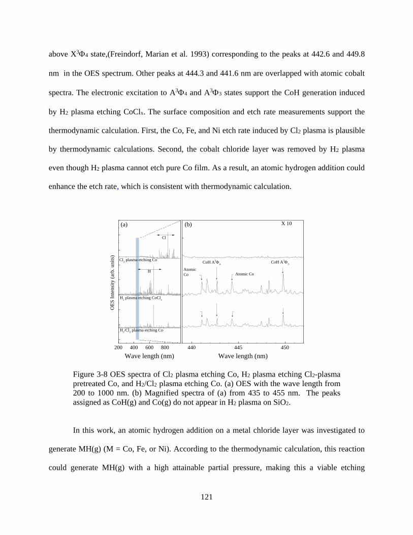
121
above X34 state,(Freindorf, Marian et al. 1993) corresponding to the peaks at 442.6 and 449.8
nm in the OES spectrum. Other peaks at 444.3 and 441.6 nm are overlapped with atomic cobalt
spectra. The electronic excitation to A34 and A33 states support the CoH generation induced
by H2 plasma etching CoClx. The surface composition and etch rate measurements support the
thermodynamic calculation. First, the Co, Fe, and Ni etch rate induced by Cl2 plasma is plausible
by thermodynamic calculations. Second, the cobalt chloride layer was removed by H2 plasma
even though H2 plasma cannot etch pure Co film. As a result, an atomic hydrogen addition could
enhance the etch rate, which is consistent with thermodynamic calculation.
200 400 600 800 440 445 450
Atomic
Co
(b) (a)
Atomic Co
CoH A3
3
Cl
H
CoH A3
4
H2/Cl
2 plasma etching Co
H2 plasma etching CoCl
x
OE
S I
nte
nsi
ty (
arb
. u
nit
s)
Wave length (nm)
Cl2 plasma etching Co
X 10
Wave length (nm)
Figure 3-8 OES spectra of Cl2 plasma etching Co, H2 plasma etching Cl2-plasma
pretreated Co, and H2/Cl2 plasma etching Co. (a) OES with the wave length from
200 to 1000 nm. (b) Magnified spectra of (a) from 435 to 455 nm. The peaks
assigned as CoH(g) and Co(g) do not appear in H2 plasma on SiO2.
In this work, an atomic hydrogen addition on a metal chloride layer was investigated to
generate MH(g) (M = Co, Fe, or Ni). According to the thermodynamic calculation, this reaction
could generate MH(g) with a high attainable partial pressure, making this a viable etching

122
process. Similarly, atomic chlorine addition on metal hydride layer (NiH0.5) resulted in a higher
attainable partial pressure of NiCl(g), making this two step etching process a viable approach to
etch magnetic metal elements.
3.2.4 Summary of Experimental Verification on Thermodynamic Calculation
The attainable partial pressure of an etch product was evaluated by thermodynamic
calculations. The metal hydride was not volatile, but oxygen radical addition on MClx (M = Co,
Fe, or Ni) could enhance the vapor pressure of the etch product. Hydrogen radical addition on
chlorinated surfaces appears to be the most effective combination to etch metals, showing that
the partial pressure of MH(g) can be higher than the reference value (~10-8 atm). According to
the surface composition measurements, hydrogen plasma could etch a MClx layer but not pure
metals. As a result, the etch rates of Co, Fe, and Ni by Cl2/H2 plasmas were enhanced by 17, 6,
and 20%, respectively, compared to those measured in a Cl2 plasma. The thermodynamic
expectation was consistent with the experimental result: 1) Co and Ni etch rate by a Cl2 plasma
was similar, while Fe etch rate was higher than those metals and 2) atomic hydrogen addition
could etch a metal chloride layer with an increased etch rate. A reactive hydrogen atom and the
stable byproduct such as HCl acted as driving forces for the enhanced attainable partial pressure.
123
3.3 CoFe Alloy Thin Film Patterned by Cl2/H2 Plasma
3.3.1 Etch Rate and Surface Chemical Characterization of CoFe Alloy Etched by Cl2/H2 Plasma
The etch rate analysis of CoFe films with Cl2 and Cl2/H2 plasma support the fact that H2
plasma induces a higher partial pressure of the etch product than that generated by Cl2 plasma. In
Figure 3-9 (b), etch rates with Cl2 plasma itself and with the subsequent H2 plasma have been
found to be 3.2 and 4.2 nm/min, extracted from linear fits, shown with black and gray dashed
lines, respectively. The enhanced etch rate of Cl2/H2 plasma demonstrates that H2 plasma etches
the surface modified by Cl2 plasma although H2 plasma itself cannot etch CoFe magnetic film as
shown in the supporting information. The surface reactions resulting from halogen-based plasma
have been demonstrated in Figure 3-10. The XPS spectrum of Cl2-plasma exposed CoFe film
presents a significant increase of spectral weight for Cl 2p peak, indicating the formation of
metal chloride layers such as CoFeClx, on the CoFe film surface (Figure 3-10 (c)), while the
spectral weight of the Co 2p and Fe 2p peaks were barely affected by Cl2 plasma since the CoO
and CoCl2 electron binding energies are comparable (Figure 3-10 (a)) and Fe 2p peak of FeO
overlaps with Co Auger electron peak (Figure 3-10b). Afterwards, the chemical effect of H2
plasma in the metal chloride layers was studied. The spectral weight of Co 2p3/2 peak, measured
at approximately 781.1 eV, is diminished, and a peak around 777.9 eV corresponding to metallic
cobalt appears when the metal chloride product is exposed to H2 plasma for 30 sec as shown in
Figure 3-10a. As the exposure time of H2 plasma is increased up to 90 sec, the peak related to
metallic cobalt has an increased spectral weight indicating clearly that the metal chloride layers
react with H2 plasma. The H2 plasma causes the emergence of Fe metallic peak at approximately
706.4 eV as shown in Figure 3-10. As the metallic Co and Fe peaks develop in the spectra, the

124
spectral weight of the Cl 2p peak decreases significantly as the time of H2 plasma exposure is
increased, e.g. H2 plasma doses for 30 and 90 sec reduce Cl 2p area to 6.1 % and 3.2 % as
shown in Figure 3-10 (c). An enhanced etch rate of Cl2/H2 plasma compared to Cl2 plasma
indicates that the surface composition variation of Figure 3-10 was not the result of de-
chlorination reaction, but from the removal of metal chloride layer. Combining the etch thickness
and the surface composition measurements, the resulting thermodynamic calculation implies that
the surface modification prior to H2 plasma exposure changes the reaction path, and H2 plasma
enhances the equilibrium partial pressure of those etch products including metal atoms.
-60
-40
-20
0
0 5 10 15 20 250
20
40
60
80
100
-60
-40
-20
0
logP
(atm
)
(b)(a)
CoH(g)
CoO(g)
CoCl2+X
FeCl3+X
CoBr(g)
FeBr(g)
FeO(g)
FeH(g)
HOX=Br
Cl2/H
2
Cl2
Etc
hed
Th
ick
nes
s (n
m)
Cycles
logP
(atm
)
Figure 3-9 (a) Calculated partial pressures of etch products generated from atomic
Br, O, and H addition on CoCl2 and FeCl3. Detailed calculation can be found in
the supporting information. (b) Etched thickness is shown as a function of
chlorine and hydrogen plasma cycles after 20 sec exposure with Cl2 plasma and
20 sec exposure individually with Cl2/H2 plasma. A Cl2 cycle is 20 sec Cl2 plasma
and Cl2/H2 cycle is composed of 20 sec Cl2 followed by 20 sec H2. The dashed
lines represent linear fittings of etched thicknesses for Cl2 and Cl2/H2 cycles.

125
810 800 790 780 740 730 720 710 210 205 200 195 190
x10x4
Co-Cl
Co-Co
Co-O
XP
S I
nte
nsi
ty (
arb. unit
s)
Binding Energy (eV)
(a) Co 2p
Cl2 30s/H
2 90s
Cl2 30s/H
2 30s
Cl2 30s
Pre-etch
Co Auger
Fe-Fe
(b) Fe 2p
Binding Energy (eV)
Pre-etch
Cl2 30s
Cl2 30s/H
2 30s
Cl2 30s/H
2 90s
Cl 2p3/2
Cl 2p1/2
(c) Cl 2p
Binding Energy (eV)
Pre-etch
Cl2 30s
Cl2 30s/H
2 30s
Cl2 30s/H
2 90s
Figure 3-10 XPS spectra of (a) Co 2p, (b) Fe 2p, and (c) Cl 2p. From the top, the
spectra represents pre-etch, Cl2(30sec), Cl2(30sec)/H2(30sec), and
Cl2(30sec)/H2(90sec) plasma exposure on 500 nm Co0.8Fe0.2 films. For each
element analyzed, each chemical state is represented by a spin-orbit split doublet,
2p3/2 and 2p1/2, which is constrained to have a 2:1 peak area ratio, equal full-
width-at-half-maximum, and their energy separations are 15.0 eV, 12.9 eV, and
1.53 eV, for Co, Fe and Cl, respectively. For simplicity, only the 2p3/2 peaks are
labeled in the figure. In Fe 2p spectra, the Co Auger LMM peak at ~714.3 eV is
overlapped with Fe-O and Fe-Cl peak at ~710.7 eV and ~711 eV.
3.3.2 Etching Feature Profile Analysis of CoFe Etched in Cl2/H2 Plasma
To demonstrate the potential of the halogen-based plasma-etching method for fabricating
a high-density integrated circuit, SEM was used to assess the effects on patterns with various
plasma etching processes. Figure 3-11 indicates SEM images obtained from pre-, post-Cl2, post-
Cl2/H2, and post-Ar plasma assisted etching on patterned wafers, which has the layer structure of
TiN(300nm)/CoFe(45nm)/Ti(10nm) on Si wafer. In the case of Cl2 with subsequent H2 plasma,
pure gases rather than a mixture were introduced to comprehend the effect of etch chemistry.
Figure 3-11 (a) and (b) show SEM images of the CoFe patterned wafer prior to etching, where a

126
steep slope and a smoothed surface are visible. Figure 3-11 (c) and d display etch profile after a 4
min Ar plasma exposure, where a 45 nm CoFe film is completely removed above a 10nm Ti
adhesion layer under the following conditions: RF1 (plate power) of 100 W, RF2 (coil power) of
500 W, and 20 mTorr pressure. The image indicates that the Ar plasma induces a sidewall re-
deposition and/or TiN hard mask corrosion and further coarsens the film surface as shown in
Figure 3-11 (c) and (d). It is known that Ar plasma causes a rough surface due to defect sites
induced by the ion bombardment. (Kinoshita, Utsumi et al. 2010, Gajek, Nowak et al. 2012).
Figure 3-11 (e) and (f) indicate that a 2 min Cl2 plasma exposure removes the CoFe film entirely
under the conditions of RF1 of 50 W, RF2 of 500 W, and 20 mTorr pressure with supporting
evidence as shown in the cyan colored EDX spectrum in Figure 3-11 (i). The metal chloride
layers formed by Cl2 plasma have accumulated on the border between CoFe and TiN films as
shown in Figure 3-11 (f). The time-dependent Cl2 plasma influence on patterned wafers has been
presented to demonstrate experimentally the accumulated metal chlorides on the border in the
supporting information. SEM-EDX spectroscopy was performed to systematically confirm the
existence of metal chloride after Cl2 plasma treatment. Figure 3-11 (i) shows the EDX spectra
measured in three different positions marked with colored circles in the SEM image of Figure
3-11 (f). The cyan colored circular region where the CoFe film was exposed to Cl2 plasma shows
the absence of Co-L, Fe-L, and Cl-K peaks because the film was etched by Cl2 plasma. The
Cl-K is observed only in the red colored spectrum, which was measured at the border as shown
in Figure 3-11 (f). This spectrum is an indication that most of the metal chloride has accumulated
on the edge of the TiN hard mask, and the CoFe film after the metal chloride layers were
partially removed. The black colored spectrum measured on the TiN hard mask shows Ti-L,
Co-L, and Fe-L peaks with the absence of Cl-K indicating the metal chloride is induced

127
from the CoFe film. The Co-L and Fe-L peaks were detected because the penetration depth of
the emitted X-ray is larger than 1 m. In Figure 3-11 (g) and (h), a 4 min exposure to H2 plasma
chemistry totally removes the metal chlorides with the conditions of RF1 of 100 W, RF2 of 800
W, and 20 mTorr pressure. In addition, the reactive ion etch by Cl2/H2 plasma renders the etched
surface smooth compared to the Ar sputtering-assisted surface as presented in Figure 3-11 (h).
The red colored EDX spectrum in Figure 3-11 (j) demonstrates the extinction of the Cl-Kpeak
induced by the Cl2 plasma.

128
200 nm
200 nm
200 nm
200 nm
Si
TiN
CoFe
Si
TiNCoFe
Si
TiN
CoFe
Si
TiNCoFe
Si
TiN
CoFe
Si
TiNCoFe
Si
TiN
CoFe
Si
TiNCoFe
200 nm
200 nm
200 nm
200 nm
(a) (b)
(c) (d)
(e) (f)
(g) (h)
0 1 2 0 1 2 3
CoFe film
TiN mask
(j)(i)
Ti L
Si K
Cl K
Si K
O K
C K
Co L
Fe L
Ti L
Inte
nsi
ty (
arb
. u
nit
s)
Energy (keV)
Co L
Fe L
O K
C K
regionborder
Energy (keV)
regionborder
Figure 3-11 Cross-sectional ((a), (c), (e), and (g)), and bird eye ((b), (d), (f), and
(g)) view SEM images of 300 nm TiN- masked 45 nm CoFe films. (a, b) CoFe
pattern prior to plasma etching; (c, d) after 4 min Ar plasma etching with RF1
power of 100 W, RF2 power of 500 W and 20 mTorr pressure, (e, f) 2 min Cl2
plasma etching with RF1 power of 50 W, RF2 power of 500 W and 20 mTorr
pressure, (g, h) 4 min subsequent H2 plasma etching with RF1 power of 50 W,
RF2 power of 500 W and 20 mTorr pressure. Figure 3-11(i) and (j) present EDX
spectra measured at the positions denoted by circles in Figure 3-11 (f) and (h),
respectively.

129
3.3.3 Etching Profile Analysis of CoFe Etched in Cl2/H2 Plasma
In addition, the surface modification by Cl2 and Cl2/H2 plasma is closely related with the
restoration of magnetic properties in the magnetic metallic film. Figure 3-12 presents magnetic
hysteresis loops for magnetization as a function of applied magnetic field of the pre-etched CoFe
film, as a reference, and Cl2 and Cl2/H2 plasma-treated CoFe films. The inset of Figure 3-12
shows coercive field and saturation magnetization extracted from the magnetic hysteresis loops
as a function of hydrogen plasma duration. The hysteresis loop measured in the pre-etched CoFe
film indicates the film exhibits soft magnetic properties characterized by low coercive
field.(Osaka, Yokoshima et al. 2003) In Figure 3-12, formation of metal chloride layers renders
the soft magnetic material harder, where the coercive field increases from ~20.9 Oe to ~63.6 Oe,
and the saturation magnetization decreases from ~1300 emu/cm3 to ~520 emu/cm3. We have
systematically studied the effect of H2 plasma exposure time on the chlorinated CoFe film to
reduce the amount of metal chloride as suggested in Figure 3-12. As the H2 plasma treatment
time is increased, the hard magnetism in the Cl2 plasma exposed CoFe film is gradually reverted
to soft magnetism as indicated by the coercive field and saturation magnetization. The existence
of an optimal H2 plasma exposure time can be explained by the hydrogenation of the magnetic
metallic film, in which the magnetic moments and the coercive fields in the hydrides decrease
and increase with increasing hydrogen concentration, respectively.(Antonov 2002, Lin, Tsai et
al. 2013) The Cl2 plasma treated ferromagnetic free layer in a MTJ device increases on/off
energy triggered by a large amount of dissipated energy in repeatedly reversing the
magnetization as implied from the broad hysteresis loop. For a more detailed explanation of the
effect of metal chloride layers on the functionality of MTJ device, FMR spectra of the Cl2/H2-

130
plasma treated samples were measured under the same plasma conditions used in Figure 3-14
while keeping the microwave source of X-band (9.78 GHz) constant. Figure 3-14c indicates in-
plane anisotropy fields obtained from the resonance magnetic fields in Figure 3-14b and the
saturation magnetizations. The FMR linewidth and resonance field show similar trend as the
coercive fields in inset of Figure 3-12. However, FMR spectroscopy can be a more accurate
probe to measure the anisotropy field.(Lee, Wang et al. 2009) The in-plane anisotropy field is
calculated from the Kittel equation(Kittel 1948, Pettiford, Zeltser et al. 2006)
sFMRkFMR M4)( HHf where gyromagnetic constant is MHz/Oe 2.8 , HFMR is the
resonance magnetic field from FMR measurements and Ms is the saturation magnetization
obtained from SQUID experiments. For a fixed microwave frequency, Hk is inversely
proportional to the saturation magnetization. On the other hand, the switching current density Jc
in an MTJ is approximated by 2/perk,dkc HHHJ (Sun 2000), where is the magnetic
damping constant; Hk,per is the free layer perpendicular anisotropy, which is induced from the
interaction between the free and buffer layers(Ikeda, Miura et al. 2010); and Hd is the out-of-
plane demagnetizing field. Since Hk,per has not been applied in this work, Jc is inversely
proportional to Hk and implies Jc must be reduced by increasing H2 plasma treatment time up to
the optimal time. In addition, the FMR linewidth is broader when the Cl2 plasma exposure time
on the pre-etched CoFe film increases. The broader FMR linewidth indicates higher switching
current density because the FMR linewidth is proportional to the magnetic damping constant.
(Liu, Zhang et al. 2011)

131
-200 0 200
-1.0
-0.5
0.0
0.5
1.0
Nor
mal
ized
mag
net
izat
ion
Magnetic Field (Oe)
Pre-etch
Cl2 30s
Cl2 30s / H
2 30s
Cl2 30s / H
2 60s
Figure 3-12 Magnetic hysteresis loop measured in CoFe films. Normalized
magnetization (to saturation magnetization of pre-etch CoFe) vs. magnetic field
under various etching conditions.
0 20 40 60
20
40
60
Coe
rciv
e F
ield
(O
e)
H2 Plasma Time (sec)
400
800
1200
Mag
neti
zati
on
(em
u/cm
3)
Figure 3-13 Coercive field and saturation magnetization as a function of H2
plasma exposure time extracted from the magnetic hysteresis loop. The left and
right y-axis indicate the coercive field and saturation magnetization from the pre-
etched CoFe film, respectively.

132
500 1000 1500
0 20 40 60
600
800
1000
1200
1400
1600
0 20 40 60
160
180
200
220
240
260
(a)
(c)(b)
Cl2 30 sec/H
2 60 sec
Cl2 30 sec/H
2 30 sec
Cl2 30 sec
Der
ivat
ive
Abso
rpti
on (
arb.
unit
)
Magnetic Field (Oe)
Pre-etch
HK (
Oe)
H2 Plasma Exposure (sec)
f = 9.78 GHz
640
680
720
Res
on
ance
Fie
ld (
Oe)
FM
R l
inew
idth
(O
e)
H2 Plasma Exposure (sec)
Figure 3-14 FMR spectra measured in CoFe films. (a) FMR spectra measured in
pre-etched and post-etched CoFe films. Vertical dashed lines are the guide lines to
represent the peak-to-peak line width deciding a damping coefficient. (b) FMR
linewidth and resonance magnetic field obtained from FMR spectra with the
values from the pre-etched film. (c) Resonance field and calculated anisotropy
field as a function of H2 plasma exposure time including the value from pre-
etched CoFe film as denoted by the horizontal line.

133
3.4 Summary
The alternating exposure of Cl2 and H2 plasma is a viable etch chemistry for CoFe alloy
film despite the fact that Cl2 plasma alone is not an effective etch chemistry due to the generation
of a metal chloride layer. According to the thermodynamic calculation, the atomic hydrogen
addition to CoCl2 and FeCl2 film changes the equilibrium and leads to the formation of an etch
product with a higher partial pressure. The measurements of an etch rate and a surface
composition revealed that the alternating Cl2/H2 plasma exposure enhanced the etch rate by 20%
compared to Cl2 plasma showing the metal chloride removal from the surface. In addition, H2
plasma could remove a metal chloride layer to yield a smooth etch profile. The development of a
chemical etching process is required to fabricate high density integrated circuits. These results
indicate that the alternating plasma approach is the first step toward fabricating high density
MTJ-based RAM devices. Concerning the degradation of magnetic properties associated with
halogen chemistry etch, the formation of metal chloride resulted in a significant change/increase
in the coercive field which is not desirable. It was determined that the utilization of hydrogen led
to a complete removal of the metal chloride, thus restoring the soft magnetic characteristics of
CoFe. This confirms that the combination of Cl2 and H2 plasmas can not only etch CoFe at a
reasonable rate but also preserve the magnetic property of CoFe. Since the thickness of the CoFe
layer (3-5nm) is usually thicker than that of the tunnel oxide (~1nm), a double patterning process
combining both chemical and physical etch processes may be necessary to successfully pattern
both the magnetic layers as well as the tunnel oxide.

134
CHAPTER 4: ION BEAM ASSISTED ORGANIC CHEMICAL ETCH OF MAGNETIC
MATERIALS
An ion beam assisted organic chemical etch has been shown to chemically etch cobalt
and iron which are major components in magetoresistive random access memory (MRAM).
Acetylacetone (acac), hexafluoroacetylacetone (hfac) and 2,2,6,6-tetramethyl-3,5-heptanedionate
(tmhd) have been first examined on etching cobalt and iron in solution. The etch rate of cobalt
and iron in acac, hfac and tmhd solution were quantified by scanning electron microscopy
(SEM). High selectivity of Co over Fe was observed in acac solution etch, which Co is 3.3
nm/min, and Fe is 0.9 nm/min. On the other hand, high selectivity of Fe over Co was also
discovered in hfac, which Fe is 12.1 nm/min and Co is 0.3 nm/min. The electrospray ionization
mass spectrometer (ESI-MS) has confirmed the formation of organometallic complex from
metals and organics. Cobalt acetylacetonate (Co(acac)2) and iron hexafluoroacetylacetonate
(Fe(hfac)3) were discovered in the post-etch solution of acac and hfac, respectively. To make
organic chemical etch compatible with CMOS processing techniques and allow it to be
integrated with other semiconductor processes, the thermodynamic analysis was applied to
evaluate the dry etching efficacy. Although the organometallic product was calculated
thermodynamically volatile, the merely no etch rate of cobalt in acac vapor suggested it was not
kinetically favorable. Therefore, the argon ion beam was introduced to modify the surface prior
vapor etch. An approximately ~180% enhancement of Co etch rate was observed with the
alternating of argon ion beam and acac vapor, in comparison with only argon ion beam. This
work suggests that a double patterning process combining ion beam assisted organic chemical
etch may be necessary to successfully pattern the magnetic metals in MRAM device.

135
4.1 Thermodynamic Calculation of Etching Efficacy
This section documents the application of a previously developed, thermodynamic based
methodology to explore the volatility of organometallic compounds. The thermodynamic
calculation has proven to successfully predict the enhancement of Co and Fe etch rate by adding
secondary H2 plasma in traditional halogen-based plasma in chapter 3. However, the
thermodynamic data for most of organometallic complex are not available, only selected
organometallic complex such as metal acetylacetonates and metal hexafluoroacetylacetonates are
found in the literature. (Fahlman and Barron 2000) Therefore, only cobalt and iron etched by
acac and hfac are presented in the thermodynamic calculation.
Metal acetylacetonates, also known as pentanedionates, are synthesized by reacting
metals and acetylacetone solution. Most of the common conventional precursors for the chemical
vapor deposition (CVD) or atomic layer deposition (ALD) are metal acetylaceonates. Most of the
metal acetylaceonates are stable in air and readily soluble in organic solvents such as acetonitrile
or ethanol. Commercially available acetylacetonates organometallic compounds are shown in
Table 4-1. (Pierson 1999) Halogen version metal acetylacetonate were increasingly synthesized
recently due to its higher volatility compared to metal acetylacetonate. The fluorinated
acetylacetonates such as Cu(hfac)2, which has been proven to deposit high-purity copper films
via thermally-induced CVD process. (Hampdensmith and Kodas 1995) Motivated by chapter 1,
if an organo-metallic complex could facilitate the metal deposition with releasing the ligands, an
excess of ligands on the metal surface may give rise to spontaneous etching based on Le
Chatelier’s principle (equilibrium law). This set of literature based on understanding the

136
thermodynamic property of organometallic compounds would be helpful on investigating metal
etching efficacy by organic chemistry.
Table 4-1 Acetylacetonates organometallic compound (Pierson 1999).
Metal Formula Form Melting point (oC)
Barium Ba(C5H7O2)2 Crystal >320
Calcium Ca(C5H7O2)2 White crystal 175 Cerium Ce(C5H7O2)3 Yellow crystal 131 Chromium Cr(C5H7O2)3 Violet crystal 214 Cobalt Co(C5H7O2)3 Green powder 240 Copper Cu(C5H7O2)2 Blue crystal 230 Dysprosium Dy(C5H7O2)3 Powder Erbium Er(C5H7O2)3 Powder Indium In(C5H7O2)3 Cream powder 186 Iron Fe(C5H7O2)3 Orange powder 179 Lanthanum La(C5H7O2)3 Powder Lead Pb(C5H7O2)2 Crystal Lithium LiC5H7O2 Crystal 250 Lutetium Lu(C5H7O2)3 Powder Magnesium Mg(C5H7O2)2 Powder Decompose at room temp. Manganese Mn(C5H7O2)2 Buff crystal 180 Nickel Ni(C5H7O2)2 Powder Palladium Pd(C5H7O2)2 Orange needle 210 Platinum Pt(C5H7O2)2 Yellow needle Silver AgC5H7O2 Crystal Strontium Sr(C5H7O2)2 Crystal 220 Terbium Tb(C5H7O2)3 Powder Vanadium V(C5H7O2)3 Powder Ytterbium Yb(C5H7O2)3 Powder Yttrium Y(C5H7O2)3 Powder Zinc Zn(C5H7O2)2 Needle 138 Zirconium Zr(C5H7O2)4 White crystal 172
4.1.1 Volatility Diagram of Co and Fe in Acac and Hfac System
The potential reactions that were considered in the thermodynamic calculation for the
system of Co and Fe etched by acac and hfac are listed in the Table 4-2. Reaction (1), (2) and (6)

137
are the sublimation of pure cobalt, reaction (3)-(5) are the sublimation of Co(acac)x, reaction (7)
is the sublimation of Co(hfac)3. Reaction (8)-(12) are considered for iron which are very similar
to those for cobalt, but less reactions were considered due to the lack of Fe(acac)2, which
According to literature, is readily transformed into Fe(acac)3, based on the literature resulting in
significant amounts of Fe(acac)3 contaminated in Fe(acac)2 commercial precursor. (Xue, Daran
et al. 2011)
Table 4-2 Reactions utilized for plotting volatility diagrams in the M-acac & M-
hfac systems (M = Co, Fe; acac = Acetylacetonate, hfac =
Hexafluoroacetylacetonate) at 300K.
Reaction ΔG (kJ/mol)
(kJ/mol)
(1) Co(c) Co(g) 379.8
(2) Co(c)+ 2(acac)(g) → Co(acac)2(g) 1053.0
(3) Co(acac)2(c)+(acac)(g) → Co(acac)3(g) 551.8
(4) Co(acac)2(c) → Co(acac)2(g)
50.6
(5) Co(acac)3(c) → Co(acac)3(g) 44.7
(6) Co(c)+ 3(hfac)(g) → Co(hfac)3(g) 885.3
(7)
Co(hfac)3(c) → Co(hfac)3(g) 13.0
(8) Fe(c) Fe(g) 369.4
(9) Fe(c)+ 3(acac)(g) → Fe(acac)3(g) 1537.9
(10) Fe(acac)3(c) → Fe(acac)3(g) 34.3
(11) Fe(c)+ 3(hfac)(g) → Fe(hfac)3(g) 881.6
(12) Fe(hfac)3(c) → Fe(hfac)3(g) 9.3
The vapor pressures of organometallic compounds are plotted as function of partial
pressure of acac and hfac in Figure 4-1. The horizontal dashed line at 10-8 atm referred to a
reference point at which the weight loss of a material is detectable by a thermogravimetric
analyzer and considered etchable. (Lou, Mitchell et al. 1985) The line (1) represents the reaction
(1) and the sublimation of Co(c) to Co(g). The vapor pressure of Co(g) at 300K was lower than
138
10-66 atm. Line (2) represents the formation of Co(acac)2(g) from Co(c), showing that the
pressure of Co(acac)2 increases dramatically as acac pressure increases in the reaction (2). The
results suggest that the formation of Co(acac)2(c) is much more favorable than Co(c). The
vaporization of Co(acac)2(c) to Co(acac)2(g) is plotted by line (4). The pressure of Co(acac)2(g)
is much higher than that of Co(g), and it is very closed to the etchable reference line. While
increasing the pressure of acac over1088 atm, the formation of Co(acac)3(g) finally presented by
line (5). From the Figure 4-1, the volatility of Co(acac)3(g) is slightly higher than that of
Co(acac)2(g) and the etchable standard pressure, but the requirement of acac partial pressure is
unreasonable high, which is not in the operational condition, 10-100 mtorr, ca. 10-4 atm. In the
case of hfac chemistry for Co etch, the generation of Co(hfac)3(g) takes place at 1067 atm, which
is represented by line (11). Although the pressure of Co(hfac)3(g) is much higher than that of
Co(g), Co(acac)2(g), and even Co(acac)3(g), the requirement of acac partial pressure is too high
to facilitate the reaction. In the conclusion, the thermodynamic calculation predicted that the acac
would be relatively efficient in terms of etching efficacy compared to hfac.

139
-150-100 -50 0 50 100-100
-80
-60
-40
-20
0
20
40
60
-150-100 -50 0 50 100
Co(hfac)3
(c)
Co(hfac)3
(g)
log P
(Co(g
)), lo
g P
(Co(a
cac)
x(g
)) o
r lo
g P
(Co(h
fac)
3(g
))
log P(acac(g))
Co(acac)2(c)Co(c)
(2)
(3)
Co(acac)3(c)
(5)
Co(acac)3(g)
Co(acac)2(g) (4)
Co(g)
(1)
(1) Co(g)
(7)
(6)
Co(c)
log P(hfac(g))
Figure 4-1 Volatility diagram for Co in acac and hfac at 300K. The reactions in
the figure are presented in Table 4-2. The dashed line at 10-8 atm refers to the
reactant volatility, corresponding to a weight loss that is detectable in a
thermogravimetric analyzer.
The volatility diagram for iron is similar to that of cobalt (Figure 4-2), except the
formation of Fe(acac)2 is missing due to the nature of instability. (Xue, Daran et al. 2011) The
sublimation of Fe(c) is presented by line (8), and the partial pressure of Fe (g) is as low as Co(g)
in Figure 4-1. The generation of Fe(acac)3(g) and Fe(hfac)3(g) are presented by line (9) and (11),
and they take place at 1075, and 1050 atm of acac partial pressure, respectively. Line (10) and (12)
represent the sublimation of Fe(acac)3(c) and Fe(hfac)3(c), and it is very similar to the case of Co
that Fe(hfac)3(g) has higher partial pressure than Fe(acac)3(g). However, the formation of
Fe(hfac)3(g) requests lower partcial pressure of hfac than that of Fe(acac)3(g), suggesting
Fe(hfac)3(g) would be more volatile than Fe(acac)3(g). In the summary, hfac is relatively a
promising chemistry compared to acac in etching Fe.
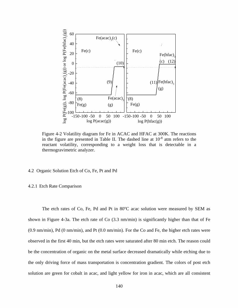
140
-150-100 -50 0 50 100-100
-80
-60
-40
-20
0
20
40
60
-150-100 -50 0 50 100
Fe(c)Fe(hfac)
3
(c)
Fe(hfac)3
(g)
log
P(F
e(g
)),
log
P(F
e(ac
ac) x
(g))
or
log
P(F
e(h
fac)
3(g
))
log P(acac(g))
Fe(c)
(9)
Fe(acac)3(c)
(10)
Fe(acac)3
(g)Fe(g)
(8) (8)
Fe(g)
(12)
(11)
log P(hfac(g))
Figure 4-2 Volatility diagram for Fe in ACAC and HFAC at 300K. The reactions
in the figure are presented in Table II. The dashed line at 10-8 atm refers to the
reactant volatility, corresponding to a weight loss that is detectable in a
thermogravimetric analyzer.
4.2 Organic Solution Etch of Co, Fe, Pt and Pd
4.2.1 Etch Rate Comparison
The etch rates of Co, Fe, Pd and Pt in 80oC acac solution were measured by SEM as
shown in Figure 4-3a. The etch rate of Co (3.3 nm/min) is significantly higher than that of Fe
(0.9 nm/min), Pd (0 nm/min), and Pt (0.0 nm/min). For the Co and Fe, the higher etch rates were
observed in the first 40 min, but the etch rates were saturated after 80 min etch. The reason could
be the concentration of organic on the metal surface decreased dramatically while etching due to
the only driving force of mass transportation is concentration gradient. The colors of post etch
solution are green for cobalt in acac, and light yellow for iron in acac, which are all consistent

141
with the literature, suggesting the formation of organometallic complex during the etch. (Pierson
1999) In the case of hfac solution etch, a high etch rate of Fe, 12.1 nm/min, is shown in the
Figure 4-3b. Co is etched by hfac solution at merely 0.3 nm/min, and no etching is observed on
Pd and Pt film. Figure 4-3c represents the etching of metal in tmhd, and no significant etching is
observed. The experimental results follow the prediction of the thermodynamic calculation
above. The reactivity between Co and acac is higher than that of Co and hfac; on the other hand,
Fe shows a higher reactivity with hfac than that of acac.

142
0 20 40 60 80 100 120 140 160 180 200
0
1k
2k
3k
4k
5k
6k
7k
8k(a)
ER (Pt & Pd) = 0.0nm/min
ER (Fe) = 0.9nm/min
ER (Co) = 3.3 nm/min
Etching time (min)
T
(A
)
0 20 40 60 80 100 120 140 160 180 200
0
1k
2k
3k
4k
5k
6k
7k
8k(b)
T
(A
)
ER (Pt & Pd) = 0.0 nm/min
ER (Fe) = 12.1nm/min
ER (Co) = 0.3 nm/min
Etching time (min)
0 20 40 60 80 100 120 140
0.0
50.0
100.0
150.0
200.0
250.0
300.0(c)
ER (Pd/Pt) = 0.0nm/min
ER (Fe) = 0.1nm/min
ER (Co) = 0.1 nm/min
Etching time (min)
T
(A
)
Figure 4-3 The etch rate of Co, Fe, Pd and Pt in (a) acetylacetone (acac) solution,
(b) hexafluoroacetylacetone (hfac) and (c) 2,2,6,6-tetramethyl-3,5-heptanedione
(tmhd) at 80oC was quantified by SEM. The triangle represents the etch of Co, the
circle represents the etch of Fe, and the hollow square represents the etch of Pt
and solid square represents the etch of Pd.
4.2.2 Etch Products Analysis
In order to confirm the formation of predicted etching products, the post-etch solutions
were characterized by electrospray ionization mass spectrometry (ESI-MS). Figure 4-4(a) shows
the mass spectra of Co and Fe etched in acac solution for 40 min. According to the mass to

143
charge ratio (m/z) and isotope patterns in the mass spectra, the isotopes of Co(acac)2 (257amu) is
found but not Fe(acac)3 (353amu). Based on the theoretical calculation, the family of Co(acac)2
isotopes would be 257 amu (100%), 258 amu (11.2%), 259 amu (1.3%), and 260 amu (0.1%).
The experimental results follow the first two peaks with similar ratio of intensity but the rest of
two are out of the detection range. In the case of Fe, almost no signal is found at Fe(acac)3
(353amu), suggesting the low reactivity between Fe and acac. Figure 4-4(b) shows the mass
spectra of Co and Fe etched in hfac solution for 40 min. The signal of Co(hfac)3 (683 amu) in the
post-etch solution would be too low to detect. The mass spectrum of Fe etched in hfac shows a
strong set of signals, following that of calculated, 680 amu (100%), 681 amu (18.9%), 682 amu
(3.1%), 683 amu (0.3%). Only the last peak is out of detection range, rest of them are matched
the calculation results.
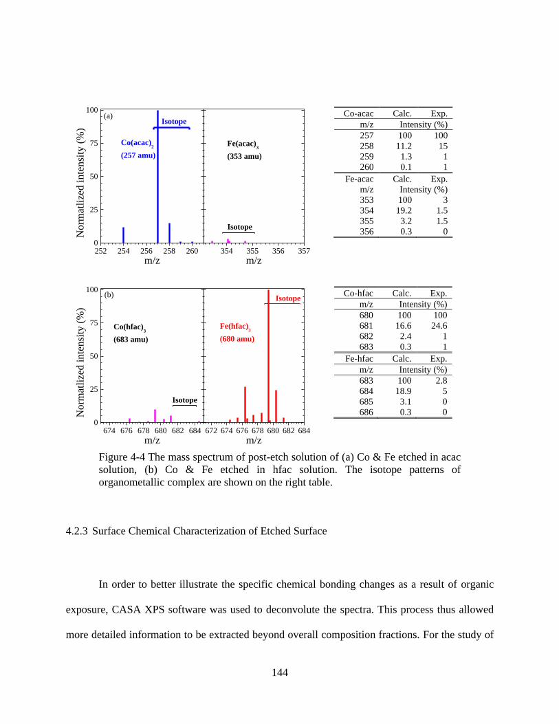
144
252 254 256 258 2600
25
50
75
100(a)
No
rmat
lize
d i
nte
nsi
ty (
%)
Isotope
m/z
Co(acac)2
(257 amu)
354 355 356 357
m/z
Fe(acac)3
(353 amu)
Isotope
Co-acac Calc. Exp.
m/z Intensity (%)
257 100 100
258 11.2 15
259 1.3 1
260 0.1 1
Fe-acac Calc. Exp.
m/z Intensity (%)
353 100 3
354 19.2 1.5
355 3.2 1.5
356 0.3 0
674 676 678 680 682 6840
25
50
75
100
No
rmat
lize
d i
nte
nsi
ty (
%)
Isotope
m/z
Co(hfac)3
(683 amu)
672 674 676 678 680 682 684
(b)
m/z
Fe(hfac)3
(680 amu)
Isotope
Co-hfac Calc. Exp.
m/z Intensity (%)
680 100 100
681 16.6 24.6
682 2.4 1
683 0.3 1
Fe-hfac Calc. Exp.
m/z Intensity (%)
683 100 2.8
684 18.9 5
685 3.1 0
686 0.3 0
Figure 4-4 The mass spectrum of post-etch solution of (a) Co & Fe etched in acac
solution, (b) Co & Fe etched in hfac solution. The isotope patterns of
organometallic complex are shown on the right table.
4.2.3 Surface Chemical Characterization of Etched Surface
In order to better illustrate the specific chemical bonding changes as a result of organic
exposure, CASA XPS software was used to deconvolute the spectra. This process thus allowed
more detailed information to be extracted beyond overall composition fractions. For the study of

145
surface reactions, the thin films of Co and Fe were deposited as 20 nm, for observing the change
in a short time. Figure 4-5 presents the surface chemical state of Co etched in acac solution at
80oC for 5 and 10 min. From the Figure 4-5a, the ratio of Co0+ to Co2+ increases significantly
after 5 min acac solution etch. Similarly, the intensity of O-Co decreases after 5 min acac
solution etch in O 1s spectrum, suggesting the preferential removal of cobalt oxide with acac. Ti
2p peaks show up after 10 min acac solution etch, indicating the end-point is achieved. From the
Figure 4-6, similar phenomenon is observed on the Fe film etched in hfac. The ratio of Fe0+ to
Fe2+ is slightly increased at Fe 2p3/2 spectra, and the O-Fe peak dramatically decreases while
reaching end-point. In conclusion, the organic chemicals tend to react with metal oxide, resulting
in reducing of Co2+ and Fe2+ after 5 min etch in acac and hfac, respectively.
790 785 780 775 534 531 528 470 465 460 455 450
Binding Energy (eV)
Acac 5min
XP
S I
nte
nsi
ty (
arb
. u
nit
s)
(a) Co 2p3/2
As deposited
Acac 10min
O-CoCo sat.
O-CCo
2+(b) O 1s
Co0+
Ti2p3/2
Ti2p1/2
(c) Ti 2p
Figure 4-5 XPS spectra of (a) Co 2p3/2, (b) O 1s, and (c) Ti 2p. From the top, the
spectra represents as deposited, acac solution etch 5 min, acac solution etch 10
min. For Co and Ti, each chemical state is represented by a spin-orbit split
doublet, 2p3/2 and 2p1/2, which is constrained to have a 2:1 peak area ratio, equal
full-width-at-half-maximum, and their energy separations are 15.0 eV, and 6.1
eV, for Co and Ti, respectively. For simplicity, only the 2p3/2 peak of Co is shown
in the figure.

146
715 710 705 534 531 528 470 465 460 455 450
XP
S I
nte
nsi
ty (
arb
. u
nit
s)
(a) Fe 2p3/2
O-FeFe
3+ O-HFe2+
(b) O 1s
Binding Energy (eV)
Fe0+
Ti2p3/2
Ti2p1/2
(c) Ti 2p
As deposited
Hfac 5min
Hfac 10min
Figure 4-6 XPS spectra of (a) Fe 2p3/2, (b) O 1s, and (c) Ti 2p. From the top, the
spectra represents as deposited, hfac solution etch 5 min, hfac solution etch 10
min. For Fe and Ti, each chemical state is represented by a spin-orbit split
doublet, 2p3/2 and 2p1/2, which is constrained to have a 2:1 peak area ratio, equal
full-width-at-half-maximum, and their energy separations are 12.9 eV, and 6.1
eV, for Fe and Ti, respectively. For simplicity, only the 2p3/2 peak of Co is shown
in the figure.
4.3 Ion Beam Assisted Chemical Etch of Co
4.3.1 Acac Vapor Etch of Co
As motivated above, the etching process needs to be compatible with CMOS processing
techniques and allowed to integrate with other semiconductor processes. Organic vapor etch is
inevitable to the MRAM patterning. Before investigating the vapor etch, the acac solution is
diluted by acetonitrile to perform the concentration dependent solution etch. In the Figure 4-7,
the etch rate of Co decreases dramatically to zero when the concentration of acac decreases by
the 4 order of magnitude. The etch rate of Co etched by acac vapor is labeled as a solid circle in

147
Figure 4-7. The density of acac molecule at 150oC and 0.5 mtorr is about 1.9x10⁻⁸ M (mol/L) and
the etch rate is only 0.004 nm/min.
1E-8 1E-7 1E-6 1E-5 1E-4 1E-3 0.01 0.1 1 10-0.5
0.0
0.5
1.0
1.5
2.0
2.5
3.0
3.5
Acac vapor etch
Acac solution etch
Etc
h r
ate
(nm
/min
)
Conc. of acac in ACN solution (M)
Figure 4-7 The etch rate of Co etched in several concentrations of acac diluted by
acetonitrile at 80oC for 60 min.
Figure 4-8 represents the XPS spectra of Co pre-etch and Co etched by acac vapor at
150oC for 8 hr. Due to the many peaks that had to be assigned in the case of carbon, Figure 4-8
shows the specific deconvolution of the C 1s region to better illustrate the bonding changes. The
same peak location values that were assigned in Chapter 2 were used to align the bonding states
in these spectra. As the C-Co, C-O, and C=O are appeared on the spectrum of Co etched in acac
vapor, suggesting the formation of organometallic compounds on the metal surface. Based on the
results above, the formation of the organometallic compounds is not the rate determining step but
the desorption of the organometallic compounds. Although the desorption process strongly

148
depends on the temperature of the surface, the operating temperature is not allowed to go over
300oC, which the magnetic susceptibility of the metal would decrease significantly and the
magnetic property of MRAM device would be damaged. Therefore, Ar ion beam without heating
up the metal surface was chosen to facilitate the desorption process of organometallic
compounds.
290 288 286 284 282
Inte
nsi
ty (
Cp
s)
C-O
C-C
o
C-C
Binding Energy (eV)
C 1s
C=
O
Before Etch
Acac vapor
Figure 4-8 XPS spectra of C 1s. The top spectrum represents Co as deposited, and
bottom spectrum represents Co etched by acac vapor for 8 hrs.
4.3.2 Ion Beam Etch of Co
Kaufman ion source with 3 cm beam size and defocused beam shape was selected to
assist the chemical vapor etch of Co by acac. (Kaufman, Harper et al. 1979, Kaufman, Harper et
al. 1979, Harper, Cuomo et al. 1982, Kaufman, Cuomo et al. 1982) The average number of
atoms removed from a target per incident particle (atom or ion) is etching yield. It depends on

149
the target material, on the species of bombarding particles and their energy and the angle of
incidence. Figure 4-9 shows the comparison of etching yield of Co as a function of Ar ion energy
at a vertical incident angle from literature and the experimental results. (Laegreid and Wehner
1961, Stuart and Wehner 1962, Sletten and Knudsen 1972, Behrisch and Eckstein 2007) The
range of ion energy on 3 cm Kaufman ion source is from 50 to 1000 eV. Thus, the etching yield
is experimentally performed at 50, 100, 200, 300, 500, 1000 eV of Ar ion energy on Co 20 nm
film. The experimental results follow the etching yield on literature, suggesting the controlling of
ion beam energy is reliable. (Laegreid and Wehner 1961, Stuart and Wehner 1962, Sletten and
Knudsen 1972, Behrisch and Eckstein 2007)
101
102
103
104
105
10-4
10-3
10-2
10-1
100
101
Yie
ld (
#C
o/#
Ar)
Ion Energy (eV)
Figure 4-9 Etching yield of Co as a function of Ar ion energy. The Ar ion was
vertical to the Co film. The hollow square represents the data from the literature
(Laegreid and Wehner 1961, Stuart and Wehner 1962, Sletten and Knudsen 1972,
Behrisch and Eckstein 2007), and the solid circle represents the data of ion beam
in used.

150
Meanwhile, since the sample size of Co is about 15 mm in lateral dimension, the etch rate
of Co is measured from -8 to 8 mm off of the beam center in lateral direction at 1 and 0.5 keV in
Figure 4-10. The standard deviation are 0.32 and 0.24 nm at 1 and 0.5 keV, respectively,
suggesting the Ar ion beam is uniform enough to neglect the deviation across the sample.
-8 -6 -4 -2 0 2 4 6 80.0
0.2
0.4
0.6
0.8
1.0
1.2
1.4
0.5keV
Etc
hed
rat
e (n
m/m
in)
Distance from the center (mm)
Co(500nm)/ 90o Ar
+ - 1 keV, I
sample=0.04 mA
- 0.5 keV, I
sample=0.02 mA
1keV
Figure 4-10 Uniformity of Co etch at 1 keV Ar ion beam. The etch rate was
plotted as a function of distance from the center of Ar ion beam. The standard
deviation is 0.32 nm at 1 keV, and 0.24 nm at 0.5 keV. The etched thickness was
measured by SEM.
4.3.3 Ar Ion Beam Assisted Acac Vapor Etch of Co
An ion beam is used to assist the desorption of the organometallic compounds and
subsequent etching process is performed by introducing acac vapor. Figure 4-11 represents the
one cycle of alternating etch by following sequences: the surface cleaning performed by Ar ion

151
beam, 1) Ar ion beam is blocked by the shutter, and Co surface is exposed to the acac vapor, 2)
acac ligands chemically bond to Co to form organometallic compounds, 3) Acac vapor is
isolated from the valve, and Ar ion beam is exposed to the Co surface, 4) the desorption of
organometallic compounds takes place on the Co surface. The process is simplified in Figure
4-12. It starts with a 5 sec Ar 1keV ion beam exposure, and followed by a 5 sec acac vapor
exposure.
Figure 4-11 The process and mechanism proposed to facilitate the alternating
etch, including the surface cleaning, acac vapor exposure, chemically bonding
ligand and metal, Ar ion beam exposure, and the desorption of organometallic
compounds.
Figure 4-12 The detail of the process of alternating Ar and organic vapor
exposure.

152
The design of the sample stage and shutter for the alternating etch system is shown in
Figure 4-13. Top figure represents the three dimensional setup of the sample, shutter, and
organic vapor doser. The figure at the bottom presents a side view of setup. When the shutter is
closed, only right half of the sample is exposed to the acac vapor. But when the shutter is open,
the entire sample is exposed to the Ar ion beam. Due to the pressure of acac is as low as 30 mtorr
(4.0 Pascal), the mean free path can be calculated by following equation,
22
Bk Tl
d p (4.1)
where, kB is the Boltzmann constant in J/K, T is the temperature in K, p is pressure in Pascals,
and d is the dimeter of the gas particles in meters. Since the mean free path of acac in the etching
condition is about 8 mm, the 1 mm gap between film and shutter would not be visible to the acac
molecular. Therefore, only the area directly exposed to doser is etched by acac vapor but not the
area covered by shutter.
Figure 4-13 The design of the sample stage and shutter for the alternating etch
system. Left figure presents the three dimensional setup of the sample, shutter,
and organic vapor doser. The right figure shows a side view of setup that only 1
mm gap between shutter and sample would reduce the pressure of acac on the
covered region dramatically.
Ar+
acac vapor
Sample
mask
Ar+
2.5cm
2cm
1mm 1cm
3D view Side view
acac Shutter
cm5
Shutter

153
During the acac dosing on right part of the sample, Ar ions were blocked by the shutter
from sample. As shown in Figure 4-14, the SEM images are first aligned by a reference layer of
100 nm SiO2, and the thickness of Co etched by alternating dosing is thinner than that of Co
etched by Ar ion beam alone, suggesting an enhanced etch rate is achieved by additional organic
chemical dosing. Figure 4-15 (a) presents the etch rate of Co etched by acac vapor, Ar ion beam,
and sequential of Ar ion beam/acac vapor exposure were 0.004, 0.73, and 1.29 nm/min,
respectively. The etch rate of Co is enhanced 176% by alternating Ar ion/acac vapor exposure
compared to Ar ion only. Figure 4-15 (b) emphasizes the etch rate of the Ar ion beam and acac
vapor combined beam is much greater than the sum of the two. The plot is learned from the Dr.
Coburn and Dr. Winters when they first introduced the synergistic effect of chemical etching
along with sputtering. (Coburn and Winters 1979)
Figure 4-14 The SEM images of (a) Co etched by 1keV Ar ion beam for 75 min,
and (b) Co etched by sequential dosing of 5 sec 1keV Ar ion beam and 5 sec acac
vapor for 450 cycles, equivalent to 75 min.
SiO2 550nm
SiO2 100nm
Si substrate
(a) (b)
Co 430nm Co 390nm

154
0 10 20 30 40 50 60 70 80 90 100
0
10
20
30
40
50
60
70
80
90
100(a)
Co_acac
Etch rate ~0.004nm/min
Co_Ar
Etch rate
~0.73nm/min
Etching time (min)
T
(n
m)
Co_Ar/acac
Etch rate
~1.29nm/min
0.0
0.2
0.4
0.6
0.8
1.0
1.2
1.4(b)
Co/Ar+
Etch rate
~0.73nm/min
Co/Ar+ & acac
Etch rate
~1.29nm/min
Co/acac
Etch rate
~0.004nm/min
Figure 4-15 The etch rate of Co etched by acac vapor, Ar ion beam, and
alternating exposure of Ar ion beam and acac vapor were 0.004, 0.73, and 1.29,
respectively. The thickness was measured by SEM.
4.4 Summary
The etching of Co and Fe in acac and hfac are evaluated by the thermodynamic
calculation and verified by experiments. The volatility diagram has predicted the selectivity of
acac over hfac in etching Co, due to the higher partial pressure of Co(acac)2(g) than that of
Co(hfac)3(g) at operating conditions. In the case of Fe, the high selectivity of hfac over acac is
discovered, which the formation of Fe(hfac)3(g) requests lower partial pressure of hfac than that
of acac to generate Fe(acac)3(g). The etch rates of Co and Fe by acac and hfac solution follow
the prediction in thermodynamic calculation. The high selectivity of Co over Fe is observed in
acac solution, and the even higher selectivity of Fe over Co is observed in hfac solution.
However, when it comes to the concentration dependent etch, the etch rate of Co decreases to 0
nm/min when the concentration decreases by 4 orders of magnitude. The concentration of acac
molecule in vapor phase is much lower than that in solution, which is about 8 order of magnitude

155
lower. Therefore, the etch rate of Co etched by acac vapor is extremely low, suggesting the
modification in the etching process. Ar ion beam was introduced in order to facilitate the
desorption process of organometallic compounds without degradation of the magnetic property
of metals. The etching of Co by alternating Ar ion beam exposure and acac vapor exposure has
the effect of significantly increasing the etch rate by approximately 180% compared to that of Ar
ion beam only. The etch rate of Co by alternating Ar ion beam and acac vapor is much greater
than the sum of the two, suggesting the synergistic effect of chemical etching along with
sputtering is discovered in the ion beam assisted chemical etch process.

156
CHAPTER 5: ORGANIC CHEMICAL ETCH OF METALS WITH SURFACE
MODIFICATION
The approach to capturing the metal etching in organics discussed in Chapters 4 utilized a
combination of thermodynamic calculation and experimental methods to verify its efficacy.
Although an Ar ion beam has gained significantly improvement on patterning Co with organic
vapor etch, the enhancement of the reactivity between metals and ligands is required to realize a
sole chemical etch of metal. By modifying metal surface with plasma, the electron on the metal
surface would be localized, resulting in a higher reactivity between organic ligands to metal. In
this chapter, Pt is chosen as an example in terms of selecting the approach of surface
modification and examining the etching efficacy of organic solution, because Pt is the most
difficult-to-etch metal in the MRAM stack. Upon developing the optimized process for surface
modification and the most efficient organic ligands in etching metals, the vapor etch is studied
systematically with a vaporizer for delivering organic ligands and ICP O2 plasma for surface
modification. Furthermore, the sequential vapor etch was not only applied on Pt but extended to
the other transition and noble metals such as Co, Fe, Cu, and Pd, demonstrating the capability of
the generalized approach of metal etch. The etch of patterned samples with hard mask TiN on Co
film and Ta on MTJ stack were performed by sequential vapor etch, and the selectivity of mask
to metal, etching profile evolution, and magnetic property were realized to further understanding
the atomic layer control of metal etch. Finally, the desired anisotropic etching profile was
investigated in order to achieve a high density patterning of MRAM memory.

157
5.1 Surface Modification of Metals
The surface modification was originated from the chamber cleaning, which was a huge
challenge in 1995. Very large scale integrated (VLSI) manufacturers applied a lot of efforts on
removing the contamination from depositing the metal film through chemical vapor deposition.
(Farkas, Chi et al. 1993, Kruck and Schober 1997, Lee, Ford et al. 1998, Nigg and Masel 1998,
Nigg, Ford et al. 1999, Nigg and Masel 1999, Steger and Masel 1999) One of the most
challenging contaminant was Ni, which drew a lot of attentions on chemical vapor cleaning.
Some of the literature reported that pre-oxidized Ni shows higher reactivity to acac
(acetylacetone) and hfac (hexafluoropentanedione) than metallic Ni. (Nigg and Masel 1998)
In early 1997, patterning of Cu was studied intensively due to its promising properties in
repalcing Al alloy for circuit intenconnecting application. [need a literature]. However, it was
very difficult in patterning Cu because there was no promising method in generating highly
volatile products in dry etching process. (Kang, Kim et al. 1999) An approach involved the
oxidation of Cu followed by hexafluoroacetylacetone (Hfac) vapor etch was investigated.
(George, Hess et al. 1995, Jain, Kodas et al. 1995, Perry, Jain et al. 1995) While the metallic Cu
exposed to hfac vapor, the fragments of decomposed hfac was found on the Cu surface. In
contracts, the formation of organometallic compound, Cu(hfac)2, was detected when Cu was
oxidized prior hfac vapor etch. Therefore, the surface modification of metals are discussed in the
following section.

158
5.1.1 Chemistry Selection for Metal Surface Modification
Several chemistries are selected to modify the metal surface, such as SO2, Cl2, CF4, SF6,
O2 plasma, and O2 ion source. [Describe why we chose these chemistries] The metals of interest
are hard-to-etch metals, such as Cu, and fundamental components in MRAM (Magnetoresistive
random access memory) device such as Co, Fe, Pd, and Pt. In order to elucidate the generalize
approach in patterning metal by surface modification, one of the most challenging metal, Pt, is
selected as an example to show the surface chemical characterization. Pt is a noble metal, which
is also the least reactive metal by nature. It has prominent resistance to corrosion even at high
temperature, which makes it chemically stable on earth. (Weast 1988) Pt would be a great
example in representing surface modification of metal.
Due to the availability of gas chemistry, several different plasma etcher were applied to
study the surface modification of Pt. SO2 and Cl2 plasma treatments were supported by sponsor,
Lam Research, with [etcher model] at source power of 500 W and bias power of 0 and 50 W.
[waiting for Pressure and etcher model] The etcher of CF4 and SF6 plasma is Ulvac 550, and it is
located at Integrated Systems Nanofabrication Cleanroom (ISNC) of California NanoSystems
Institute (CNSI). The etch experiments were conducted at 500 W of source power, 5 mT, and 0
and 50 W bias power. O2 plasma was conducted at custom-built inductively coupled plasma
etcher in house. The operational condition was at 500 W of source power, 5 mT, and 0, -100, -
150, and -200 V of bias voltage. Wafer pieces of the Pt films (~20 nm thick on Si substrates)
approximately 2 cm2 in area were loaded into the plasma chamber with several plasma
conditions listed above. Samples were then analyzed via ex-situ XPS at a takeoff angle of 30° to
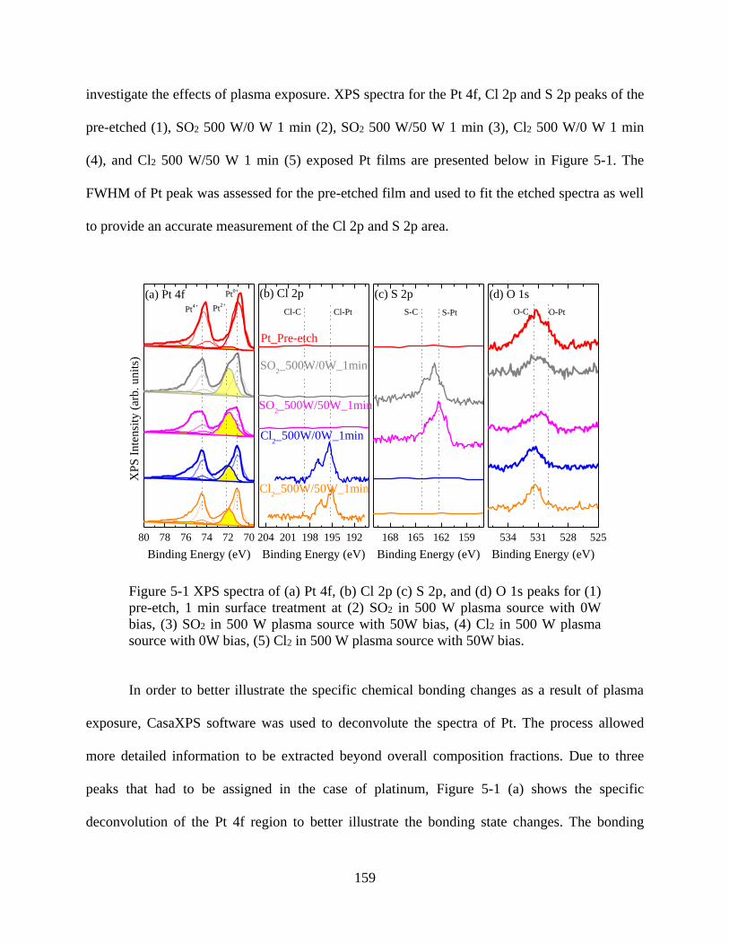
159
investigate the effects of plasma exposure. XPS spectra for the Pt 4f, Cl 2p and S 2p peaks of the
pre-etched (1), SO2 500 W/0 W 1 min (2), SO2 500 W/50 W 1 min (3), Cl2 500 W/0 W 1 min
(4), and Cl2 500 W/50 W 1 min (5) exposed Pt films are presented below in Figure 5-1. The
FWHM of Pt peak was assessed for the pre-etched film and used to fit the etched spectra as well
to provide an accurate measurement of the Cl 2p and S 2p area.
80 78 76 74 72 70 204 201 198 195 192 168 165 162 159
SO2_500W/50W_1min
SO2_500W/0W_1min
Binding Energy (eV)
(a) Pt 4f
Pt_Pre-etch
XP
S I
nte
nsi
ty (
arb
. u
nit
s)
Cl2_500W/50W_1min
Cl2_500W/0W_1min
Pt2+
Cl-C Cl-PtPt4+
(b) Cl 2p
Binding Energy (eV)
Pt0+
S-PtS-C
(c) S 2p
Binding Energy (eV)
534 531 528 525
O-Pt
Binding Energy (eV)
(d) O 1s
O-C
Figure 5-1 XPS spectra of (a) Pt 4f, (b) Cl 2p (c) S 2p, and (d) O 1s peaks for (1)
pre-etch, 1 min surface treatment at (2) SO2 in 500 W plasma source with 0W
bias, (3) SO2 in 500 W plasma source with 50W bias, (4) Cl2 in 500 W plasma
source with 0W bias, (5) Cl2 in 500 W plasma source with 50W bias.
In order to better illustrate the specific chemical bonding changes as a result of plasma
exposure, CasaXPS software was used to deconvolute the spectra of Pt. The process allowed
more detailed information to be extracted beyond overall composition fractions. Due to three
peaks that had to be assigned in the case of platinum, Figure 5-1 (a) shows the specific
deconvolution of the Pt 4f region to better illustrate the bonding state changes. The bonding

160
energy of the peaks were assigned in Chapter 2, which can align the bonding states in these
spectra.
Figure 5-1 (a) shows a deconvoluted Pt with Pt0+ (71.1 eV) and Pt2+ (71.9 eV). Since both
sulphur and oxygen could potentially generate chemical bond of Pt(II)-S and Pt(II)-O, it would
be complex in deconvoluting Pt 4f. Fortunately, the detail of O 1s in Figure 5-1 (d) suggests that
the amount of oxygen on the platinum surface did not change significantly after SO2 plasma
treatment, implying the O 1s peak was basically C-O bond which formed in the atmosphere due
to the ex situ XPS measurement. Furthermore, the peak of metal oxide located at 530.0 eV in
Figure 5-1 (d) was relatively small compared to that of metal sulfide in S 2p spectra of Figure
5-1 (c). Therefore, the major bonding in Pt2+ peak is Pt(II)-S, suggesting Pt-S bond is relative
easy to form compared to Pt-O. This observation is somewhat consistent with evidence in the
literature that bond energy of Pt-O is 392 kJ/mol, which is 167% higher than that of Pt-S, ca. 234
kJ/mol. (Luo 2003) After 1min SO2 plasma without bias exposure, the fraction of the Pt-S peak
(Pt2+) increased significantly compared to pre-etched spectra. Nevertheless, the fraction of Pt-S
peak increased even higher at SO2 plasma with 50 W bias, suggesting a higher degree of
modification was achieved. On the other hand, it is relatively simpler in deconvoluting Pt 4f of
the Pt treated by Cl2 plasma, because there is no other element in competing with Cl for Pt2+
peak. Thus, the Pt2+ peak in Figure 5-1 (a) can be assigned to Pt-Cl bond. The fraction of Pt-Cl
bond in Cl2 plasma with and without bias increased slightly compared to pre-etched film, but
they were not as significant as Pt-S peak in SO2 plasma. Although the area under S 2p spectra is
quite similar to that of Cl 2p, the atomic sensitivity factor (ASF) of S 2p is smaller than that of Cl
2p on XPS machine, suggesting the preference of bonding sulfur than chlorine to platinum.

161
After studying the surface modification by SO2 and Cl2 plasma, fluorine-contained
compound plasma was investigated by XPS as well. Figure 5-2. shows the XPS spectra for the Pt
4f, F 1s and S 2p peaks of the pre-etched (1), CF4 500 W/0 W 1 min (2), CF4 500 W/50 W 1 min
(3), SF6 500 W/0 W 1 min (4), and SF6 500 W/50 W 1 min (5) exposed Pt films.
80 78 76 74 72 70 693 690 687 684 168 165 162 159
Pt_CF4_500W/0W_1min
XP
S I
nte
nsi
ty (
arb. unit
s)
Binding Energy (eV)
(a) Pt 4f
Pt_Pre-etchPt
2+Pt
0+
Pt_SF6 500W/50W
1min
F-Pt
Pt_SF6
500W/0W
1min
(b) F 1s
Binding Energy (eV)
2p2/22p
1/2
Pt_CF4
_500W/50W_1mins
F-C(c) S 2p
Binding Energy (eV)
286 284 282
XP
S I
nte
nsi
ty (
arb. unit
s)
Binding Energy (eV)
(d) C 1s
C-O
Figure 5-2 XPS spectra of (a) Pt 4f, (b) Cl 2p (c) S 2p, and (d) C 1s peaks for (1)
pre-etch, 1 min surface treatment at (2) CF4 in 500 W plasma source with 0W
bias, (3) CF4 in 500 W plasma source with 50W bias, (4) SF6 in 500 W plasma
source with 0W bias, (5) SF6 in 500 W plasma source with 50W bias.
The deconvoluted Pt 4f with Pt0+ (71.1 eV) and Pt2+ (71.9 eV) is presented in Figure 5-2
(a). Similar to Pt treated by SO2 plasma, a competing between F-Pt(II)-F and C-Pt(II)-C was
found in Pt treated by CF4 plasma. However, the detail of C 1s in Figure 5-2 (d) shows a very
low amount of carbon on the film before and after CF4 plasma treatment, suggesting the majority
of Pt2+ is Pt-F bond. The increase of Pt-F peak (Pt2+) were observed after CF4 plasma treatment
for 1 min compared to pre-etched Pt. But the amount of Pt-F did not increase with increasing

162
bias power, implying the difficulty in generating PtF2 compound. The observation is confirmed
by the literature that platinum fluoride is stable at solid PtF6, instead of PtF2. (Drews, Supel et al.
2006)
Therefore, it would be more complex in deconvoluting Pt 4f of Pt treated by SF6 plasma,
since sulphur and fluorine would possibly bond to platinum. However, Figure 5-2 (b) shows the
amount of F-Pt (686.4 eV) is even lower than that in CF4 plasma treatment. Meanwhile, Figure
5-2 (c) presents the S 2p peak that the atomic percentage of S-Pt is similar to that of Pt-S in
Figure 5-2 (a), which has verified that the majority of Pt2+ is Pt-S bond. In contrast to CF4 plasma
treatment, the amount of Pt-S increased while increasing bias power, suggesting a higher degree
of surface modification was achieved. The observation is perfectly matched the literature that Pt
is easily poisoned by sulfur atom in catalyst application. (Argyle and Bartholomew 2015)
The surface modification by O2 ion source is shown in Figure 5-3. The XPS spectra for
the Pt 4f, O 1s and Pt 4p3/2 peaks of the pre-etched (1), 50 eV (2), 100 eV (3), 200 eV (4), and
500 eV (5) O2 ion source exposed Pt films for 5 min.

163
80 78 76 74 72 70 534 531 528 525 540 520 500
XP
S I
nte
nsi
ty (
arb
. u
nit
s)
Binding Energy (eV)
(a) Pt 4fPt
2+7/2
O-C O-PtPt
4+5/2
(b) O 1s
Binding Energy (eV)
Pt0+
7/2
Pt_Pre-etch
Pt_O2_50eV
Pt_O2_100eV
Pt_O2_200eV
Pt_O2_500eV
Pt 4p 3/2O 1s
(c) Pt 4p3/2
Binding Energy (eV)
Figure 5-3 XPS spectra of (a) Pt 4f, (b) O 1s, and (c) Pt 4p3/2 peaks for (1) pre-
etch, 5 min O2 ion beam treatment at (2) 50 eV, (3) 100 eV, (4) 200 eV, and (5)
500 eV.
Unlike the studies of fluorine-, chlorine-, and sulfur-contained plasma, the Pt 4f of Pt
treated by oxygen ion source is deconvoluted to Pt0+, Pt2+, and Pt4+ due to the formation of
Pt(IV)O2, which is much significant compared to others. Since there is only oxygen in the
plasma, the only possibility of Pt2+ and Pt4+ peaks would be bonding of Pt-O and Pt-O2,
respectively. By considering the Pt4+5/2 peaks in Figure 5-3 (a), the 50 and 100 eV present a high
amount of Pt-O2 bond compared to 200 and 500 eV. In the O 1s spectra of Figure 5-3 (b), the O-
Pt (530 eV) is distinct after 50 and 100 eV O2 ion source treated. Figure 5-3 (c) of Pt 4p3/2 shows
the peak of O 1s and Pt 4P3/2 together, which would allow to observe the ratio of O 1s to Pt 4p3/2.
The peak of O 1s is stronger than Pt 4p3/2 in 50 and 100 eV, suggesting a higher degree of
oxidation is achieved compared to pre-etched, 200, and 500 eV oxygen ion exposed Pt. This
observation suggests that Pt is able to be oxidized by O2 ion source, but it is also easily sputtered
at high energy by O2 ion source when ion energy is higher than 200 eV. In the Figure 5-4, the
similar result was found in the literature that PtO2 only formed at low sputtering power with O2

164
gas. The PtO2 tends to reduce to PtO and Pt while increasing sputtering energy from 40 to 100
W. (Mcbride, Graham et al. 1991) Although some of the literature suggests that PtO2 tends to
decompose above 400 oC in ambient air, the maximum temperature of Pt surface was at 100 oC
based on thermocouple thermometer while conducting ion source experiments at all ion energies.
(Mosquera, Horwat et al. 2012) Therefore, the low energy of O2 ion source is desired to generate
higher degree of platinum oxide.
0 25 50 75 1000
50
100
PtO2
aPtO2
PtO
Pt
PtO
Spu
tter
ing
po
wer
(W
)
% Oxygen
Pt
Figure 5-4 Schematic phase diagram for producing reactively sputtered platinum-
oxygen films. Sputtering power is plotted against oxygen content for fixed
sputtering pressure and substrate temperature (Mcbride, Graham et al. 1991).
Thus far, the XPS analysis suggests oxygen would be the most effective chemistry in
modifying platinum surface. Therefore, the surface modification by O2 plasma is shown in
Figure 5-5. The XPS spectra for the Pt 4f, O 1s and Pt 4p3/2 peaks of the pre-etched (1), 0 V (2), -
100 V (3), -150 V (4), and -200 V (5) bias voltage with 500 W source power of O2 plasma

165
exposed Pt films. Similar to deconvolution of Pt treated by O2 ion source, Pt 4f in Figure 5-5 (a)
is deconvoluted to Pt0+, Pt2+, and Pt4+ due to the formation of Pt(IV)O2. The amount of Pt-O2
bond is even higher than that generated in O2 ion source, and it is quite constant across 0 to -200
V bias voltage compared to pre-etched Pt. O 1s spectra in Figure 5-5 (b) is deconvoluted to O-C
and O-Pt bond, and the amount of O-Pt bond increased significantly with O2 plasma with 0 V
bias for 5min compared to pre-etched Pt. Also, the amount of O-Pt did not change while
increasing bias voltage from 0 to -200 V. Figure 5-5 (c) presents the spectra of O 1s and Pt 4p3/2,
the ratio of O 1s to Pt 4p3/2 increased significantly as well after O2 plasma treatment, which is
consistent with Pt 4f and O 1s spectra.
80 78 76 74 72 70 535 530 525 540 520 500
Pt_O2
500W
-150V
Pt_O2
500W
-200V
Pt_O2
500W
-100V
XP
S I
nte
nsi
ty (
arb
. u
nit
s)
Binding Energy (eV)
(a) Pt 4f
Pt
Pt_O2
500W 0V
O2 -200V
O2 -150V
O2 -100V
PtO 1sO-C
(b) O 1s
Binding Energy (eV)
O-PtPt4+ Pt
0+
O2 0V
Pt 4p3/2
(c) Pt 4p3/2
Binding Energy (eV)
Figure 5-5 XPS spectra of (a) Pt 4f, (b) O 1s, and (c) Pt 4p3/2 peaks for (1) pre-
etch, 5 min 500 W source power of O2 plasma treatment with (2) 0 V, (3) -100 V,
(4) -150 eV, and (5) -200 V bias.
In order to compare the surface modification of Pt in various chemical treatment, Figure
5-6 has summarized the percentage of Pt 0+, Pt 2+, and Pt 4+ from Pt 4f of XPS spectra. Figure 5-6
(a) presents the ratio of modified Pt to metallic Pt, i.e. (Pt2+ + Pt 4+)/Pt0+. The highest ratio of

166
modified Pt happened at O2 plasma treated Pt, and the ratio increases with increasing bias
voltage, indicating higher energy of oxygen ion could potentially diffuse deeper to form thicker
oxide with higher oxidation state, Pt(IV). However, the higher the bias voltage, the more
sputtering effect found on Pt surface. The thickness of Pt decreased significantly while
increasing bias, for example, the Pt was etched 9 nm in 5 min at -200 V bias. The observation of
physical sputtering at high bias voltage of O2 plasma would damage the MRAM device as
discussed in the Chapter 1, which short circuit may occur due to the sidewall re-deposition by
generation of non-volatile etching products. Therefore, the O2 plasma without bias voltage is
selected due to the low sputtering effect and high degree of Pt surface modification.
0
10
20
30
40
50
60
70
0
1
2
3
4 (a)
(b)
O 2
500W -2
00V
O 2
500W -1
50V
O 2
500W -1
00V
O 2
500W 0
V
O+ 500eV
O+ 200eV
O+ 100eV
Pre-e
tch
(Pt2+
+Pt4+
)
Pt0+P
tx+/P
t0+
Pt4+
Pt2+P
t0+,
Pt2
+,
Pt4
+ (
%)
Pt0+
CF 4 50W
0W
CF 4 50W
50W
SF 6 5
0W0W
SF 6 5
0W50W
SO 2 50W
0W
SO 2 50W
50W
Cl 2 5
0W0W
Cl 2 5
0W50W
O+ 50eV
Figure 5-6 Degree of surface modification for pre-etch, SO2, Cl2, CF4, SF6, O2 ion
source, and O2 plasma treated Pt. (a) The percentage of modified Pt to metallic Pt.
(b) The composition of various chemical states in Pt 4f spectrum, including Pt0+,
Pt2+,and Pt4+.

167
5.2 Metal Oxidation
Since O2 plasma has proven to be the most effective chemistry in modifying Pt surface
and the thickness of thin oxide layer can be estimated by quantifying XPS results, other
transition and noble metals such as Co, Fe, Cu, and Pd are examined under the same O2 plasma
condition. Figure 5-7 presents the Langmuir Probe measurement taken at the O2 operating
condition (500 W, 2.5 mT), Te and ni were calculated as 2.4 eV and 3.35 × 10¹⁰ #/cm-3
respectively, translating to an ion flux of 8.9 × 1015 cm-2 s-1.by equation below.
2/1
M
TnJ e
iion
While this is a higher value than expected, it should be noted that noise in the Langmuir
Probe measurements could affect the estimate of the ion flux.
-60 -40 -20 0 20 40-0.5
0.0
0.5
1.0
1.5
2.0
2.5
3.0
3.5
I (m
A)
V (Volt)
Vfloating
=-4.6V
Figure 5-7 I-V curve measured by Langmuir probe at 500 W source power, 0 W
bias power with 2.5 mtorr O2 under ICP plasma.

168
Figure 5-8 presents the oxidation of metals as a function of O2 plasma oxidation time.
Apparently, the metal oxides increased immediately in the first few minutes, and the growth rate
saturated at fifth min for all the metals. Various empirical kinetics for oxidation has been
proposed at low temperature, parabolic, linear, and logarithmic. (Evans 1960) Most of them are
suited for the presentation of experimental results but usually they cannot provide the
interpretation of the mechanism. One of the traditional method to understand the mechanism is
by curve fitting, although sometimes kinetics can be attributed to different reaction mechanisms,
which is true if experiments are performed in the transition range between two mechanisms.
0 1 2 3 4 5
0
1
2
3
4
5
CuO
PtOx
PdOx
Fe2O
3
Time(min)
Ox
ide
thic
knes
s(n
m)
CoO
Figure 5-8 Oxide thickness of Fe, Cu, Co, Pd, and Pt as a function of the O2
plasma oxidation time.
The basis of the parabolic law is the linear transport equation
,
, , , ,
e i
e i e i e i e i
nj D En
x
(5.1)

169
where je,i is the flux of the electron and ion in the oxide, De,i present the diffusivity of electron
and ion in the metal oxide, , /e in x is the concentration gradient of electron and ion in a thin
oxide layer, E is electrical field, ,e i is the charge mobility of the electron and ions. The first part
of the equation represents the diffusion of oxygen ion, metal ion and electron due to the
concentration gradient, and the second part is driven by the electrical field formed by the charge
separation. The parabolic rate law, l t , is achieved after integration of the equation above.
Diffusion control is the most common mechanism proposed in some theories, but the migration
of cations is enhanced by an intrinsic electric field across the oxide layer produced by tunneling
electrons was also proposed by Cabrera et al. (Cabrera and Mott 1948, Evans 1960, Hauffe 1965)
Inverse logarithmic law was derived by Cabrera and Mott for the special case that incorporation
of metal cations into interstitial sites of the oxide is rate determining. (Cabrera and Mott 1948)
The oxide growth rate is proportional to the probability of surmounting the potential barrier
between the sites of the atoms in the metal and interstitial sites in the oxide. The potential barrier
is assumed to be potential dependent and integration of the rate law yields the Cabrera-Mott
inverse logarithmic time law 0 / . logl l const t . (Cabrera and Mott 1948) Meanwhile, the
logarithmic rate law was proposed by Mott for very thin oxide layers where electron tunneling
prevails the electronic current depends on the tunneling probability. The oxide growth rate
decreases exponentially with increasing layer thickness and a logarithmic time law logl t is
obtained by integration. (Mott 1940) For cubic rate law of oxidation, Cabrera and Mott used
essentially the same assumptions as for n-type oxide, derived a theory for the growth of a thin p-
type oxide such as copper oxide. It depends on the concentration of cation vacancies, which are
assumed to be proportional to the number of adsorbed oxygen ions on the surface of the oxide.
Wagner also suggested that the rate determining step for cubic rate law is the dissociation of
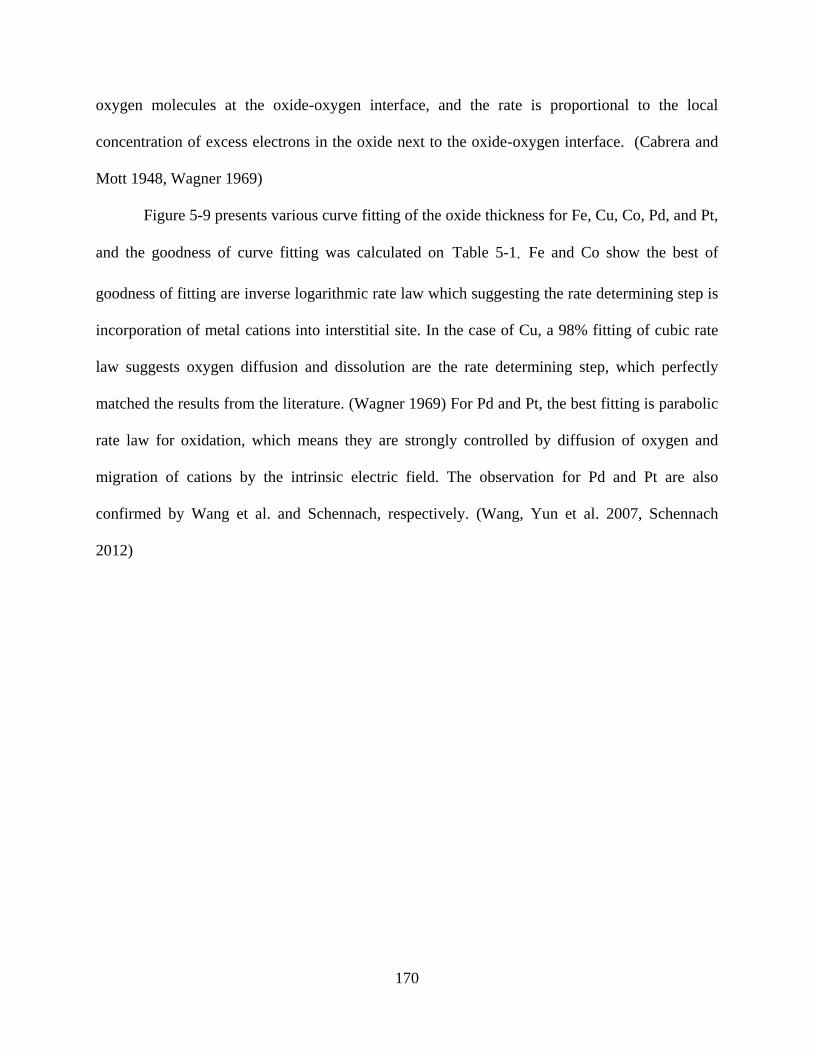
170
oxygen molecules at the oxide-oxygen interface, and the rate is proportional to the local
concentration of excess electrons in the oxide next to the oxide-oxygen interface. (Cabrera and
Mott 1948, Wagner 1969)
Figure 5-9 presents various curve fitting of the oxide thickness for Fe, Cu, Co, Pd, and Pt,
and the goodness of curve fitting was calculated on Table 5-1. Fe and Co show the best of
goodness of fitting are inverse logarithmic rate law which suggesting the rate determining step is
incorporation of metal cations into interstitial site. In the case of Cu, a 98% fitting of cubic rate
law suggests oxygen diffusion and dissolution are the rate determining step, which perfectly
matched the results from the literature. (Wagner 1969) For Pd and Pt, the best fitting is parabolic
rate law for oxidation, which means they are strongly controlled by diffusion of oxygen and
migration of cations by the intrinsic electric field. The observation for Pd and Pt are also
confirmed by Wang et al. and Schennach, respectively. (Wang, Yun et al. 2007, Schennach
2012)
171
0 50 100 150 200 250 300
0
5
10
15
20
25
30
35
40
45
50
55
x=0.01t+3.70
x=0.08t+3.89
x=0.12t+8.08
x=0.12t+11.69
Cu2O
PtOx
PdOx
Fe2O
3
Time(sec)
Ox
ide
thic
kn
ess(
A)
CoO
x=0.12t+16.84
(a)
0 50 100 150 200 250 300
0
5
10
15
20
25
30
35
40
45
50
55(b)
x=0.55t2
x=1.46t2
x=2.39t2
x=2.96t2
x=3.35t2
Cu2O
PtOx
PdOx
Fe2O
3
Time(sec)
Ox
ide
thic
knes
s(A
) CoO
0 50 100 150 200 250 300
0
5
10
15
20
25
30
35
40
45
50
55(c)
(a)
x=7.88t3
x=6.87t3
x=5.48t3
x=1.32t3
x=3.31t3
Cu2O
PtOx
PdOx
Fe2O
3
Time(sec)
Ox
ide
thic
kn
ess(
A)
CoO
0 1 2 3 4 5 6
0.0
0.1
0.2
0.3
(d)
1/x=0.06-0.01*ln(t)
1/x=0.12-0.02*ln(t)
1/x=0.16-0.02*ln(t)
1/x=0.28-0.02*ln(t)
1/x=0.25-0.03*ln(t)
Cu2O
PtOx
PdOx
Fe2O
3
Time(sec)
(Ox
ide
thic
knes
s)-1
(A-1
)
CoO
-5 0 5 10 15 20 25 30 35 40 45 50 55
0
5
10
15
(e)
dx/dt=1.1E-30exp(144.2/x)
dx/dt=2.2E-6exp(48.2/x)
dx/dt=0.02exp(10.8/x)
dx/dt=0.01exp(34.3/x)
Cu2O
PtOx
PdOx
Fe2O
3
Oxide thickness(A)
dx
/dt
(1st
der
. o
f ox
ide
ov
er t
ime)
CoO
dx/dt=8.63exp(221.3/x)
Figure 5-9 Curve fitting for oxidation of Fe, Cu, Co, Pd and Pt by O2 plasma with
(a) linear, (b) parabolic, (c) cubic, (d) inverse logarithmic, and (e) exponential.

172
Table 5-1 Goodness of fitting for oxidation of Fe, Cu, Co, Pd and Pt by O2 plasma
with 500 W, 2.5mtorr O2, Te~2.5eV and ion density:1015#/cm3.
Fitting approach r-square Fe Cu Co Pd Pt
Linear x=At 70% 71% 84% 87% 37%
Parabolic x2=2Bt 72% 90% 95% 97% 95%
Cubic x3=3Ct 94% 98% 95% 91% 57%
Inverse log 1/x=D-E*ln(t) 98% 89% 97% 90% 94%
Logarithmic dx/dt=F*exp(G/x) 78% 66% 77% 75% 79%

173
5.3 Organic Chemical Solution Etch
Since O2 plasma is able to modify metal surface, the potential organic ligands for etching
metals listed on Table 5-2 with boiling point and schematic structure have been investigated for
patterning. Beta-diketone species such as acetylacetone (acac) and hexafluoroacetylacetone
(hfac) have been utilized as common ligands for synthesizing metal precursors in atomic layer
deposition (ALD) application. Metal acetylacetonates (M(acac)x) are coordination complexes
derived from the acetylacetonate anion and metal ions. A six-membered chelate ring stabilizes
the organometallic compound when two oxygen atoms on the acac bind to the metal. (Braunstein
2004) Hfac presents the same structure as acac except the functional group on two ends are
substituted by CF3, exhibits the enhanced volatility and Lewis acidity relative to acac. (Henne,
Newman et al. 1947) (Aygen and Vaneldik 1989) Ethylenediaminetetraacetic acid (Edta) is a
hexadentate ligand which could bond to metal ions such as Ca2+ and Fe3+ efficiently. Similar to
edta, Nitrilotriacetic acid (nta) presents three ligands, which could form coordination compounds
with Ca2+, Cu2+, and Fe3+. Pyridine-2,6-dicarboxylic acid (pdca) owns two carboxylic acid ligand
which could be utilized in binding metal ions. Oxalic acid (oa) and formic acid have been using
in removing iron oxide with formation of stable water-soluble salt. All the concentration of
organic ligands was prepared at the maximum in order to rule out the concentration effect, but
some of the organics were at low concentration such as edta, nta, and pdca due to the low
saturated concentration.

174
Table 5-2 Potential organics in etching metals.
Organics Acetyl-
acetone
Hexafluoro-
acetylacetone
Ethylene diamine
tetraacetic
acid
Nitrilo
triacetic
acid
Pyridine-2,6-
dicarboxylic
acid
Oxalic
acid
Formic
acid
Abbr. ACAC HFAC EDTA NTA PDCA OA FA
Boiling
point (oC) 140 70 614 340 245 149 100
Concentr-
ation (M) 9.7 7 0.5 0.5 0.5 1.2 13
Structure
of
organics
Since platinum is the most challenging element in patterning due to its high stability, it
was selected to examine the etching efficacy of the organic ligands. Usually the etch rate was
determined by thickness change through scanning electron microcopy (SEM), transmission
electron microcopy (TEM), or profilometer, but the thickness change on platinum was relatively
small which could not measure by microcopy. Therefore, the surface characterization of
chemical state on platinum via X-ray photoelectron spectroscopy (XPS) is chosen to screen the
organic ligands in etching metal oxide.
After surface modification with 500 W oxygen plasma without bias for 5 min at 80 oC,
Figure 5-10 presents Pt 4f and survey spectra of modified Pt film treated by various organic
ligands. First of all, no contamination or carbon deposition was found in survey spectrum,
suggesting the platinum surface remained intact. Later, the chemical state on Pt 4f spectra has
revealed the etching efficacy of organic ligands. The strong Pt4+ peak was found on modified Pt
after acac, hfac, edta, and nta treatment, suggesting no reaction took place with platinum oxide.
Based on the decreasing of Pt4+ peak after pfca, oa, and formic acid treatment, the etching

175
efficacy with platinum oxide was proven. More chemical evidence has been provided in the case
of CoPt etch in later paragraph.
80 75 70 800 600 400 200 0
Pt_Blank
(a) Pt 4f
ACAC
EDTA
PDCA
NTA
OA
HFAC
FA
XP
S I
nte
nsi
ty (
arb.
unit
s)
Pt_Blank
ACAC
HFAC
EDTA
NTA
PDCA
OA
FA
Pt4pPt
4+ Pt0+ Pt4d Pt4fC1sO1sF1s
Binding Energy (eV)
O KLL
(b) Survey
Binding Energy (eV)
Figure 5-10 XPS spectra of (a) Pt 4f, (b) Survey for (1) pre-etch Pt, oxidized Pt
treated by following organic solution for 20 min, (2) acac, (3) hfac, (4) edta, (5)
nta, (6) pdca, (7) oxalic acid, and (8) formic acid.
As described in Chapter 1, the etching selectivity of metals to hard mask needs to be high
enough to improve the fidelity in the vertical and horizontal direction. Tantalum as one of the
most important hard mask material has been examined with all the ligands as well. Ta was first
treated with same process of surface modification, 500 W oxygen plasma without bias for 5
minutes, and then etched by various organic solutions for 20 min at 80 oC. Figure 5-11 shows the
Ta 4f and survey spectra of Ta before and after etched by acac, hfac, edta, nta, pdca, oa, and
formic acid. According to the survey spectra, none of sample showed neither contamination nor
carbon decomposition, suggesting clean Ta surfaces were sustained. The detailed scans of Ta 4f
are presented in Figure 5-11 (a), the atomic ratio of oxidized Ta (Ta5+) to metallic Ta (Ta0+)

176
remained the same after all the organic solutions etch, suggesting no reaction occurred between
tantalum oxide and organic solutions. Since the thickness change also needs to be confirmed to
verify the etch of Ta, Figure 5-12 presents the cross-sectional SEM images of Ta that no
significant thickness change was observed after 4 hr etch by formic acid solution. Combing the
results of XPS and SEM, Ta is verified as a potential candidate in patterning Pt as a hard mask
due to the inert characteristic with selected organic ligands.
30 25 20 800 600 400 200 0
(a) Ta 4f
XP
S I
nte
nsi
ty (
arb
. u
nit
s)
FA
OA
PDCA
NTA
EDTA
HFAC
ACAC
Pre-treatmentTa
5+ Ta0+
Ta4p Ta4d S2s
FA
Ta4fS2p
C1sO1sF1s
Binding Energy (eV)
EDTA
PDCA
NTA
Oxalic Acid
ACAC
HFAC
O KLL
(b) Survey
Binding Energy (eV)
Pre-treatment
Figure 5-11 XPS spectra of (a) Ta 4f, (b) Survey for (1) pre-etch Ta, oxidized Ta
treated by following organic solution for 20 min, (2) acac, (3) hfac, (4) edta, (5)
nta, (6) pdca, (7) oxalic acid, and (8) formic acid.Ta etched by organics solution
etch 20 min.
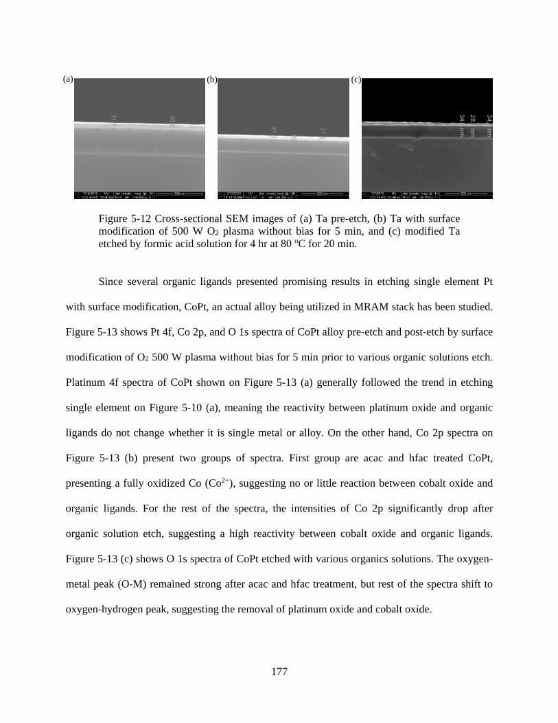
177
Figure 5-12 Cross-sectional SEM images of (a) Ta pre-etch, (b) Ta with surface
modification of 500 W O2 plasma without bias for 5 min, and (c) modified Ta
etched by formic acid solution for 4 hr at 80 oC for 20 min.
Since several organic ligands presented promising results in etching single element Pt
with surface modification, CoPt, an actual alloy being utilized in MRAM stack has been studied.
Figure 5-13 shows Pt 4f, Co 2p, and O 1s spectra of CoPt alloy pre-etch and post-etch by surface
modification of O2 500 W plasma without bias for 5 min prior to various organic solutions etch.
Platinum 4f spectra of CoPt shown on Figure 5-13 (a) generally followed the trend in etching
single element on Figure 5-10 (a), meaning the reactivity between platinum oxide and organic
ligands do not change whether it is single metal or alloy. On the other hand, Co 2p spectra on
Figure 5-13 (b) present two groups of spectra. First group are acac and hfac treated CoPt,
presenting a fully oxidized Co (Co2+), suggesting no or little reaction between cobalt oxide and
organic ligands. For the rest of the spectra, the intensities of Co 2p significantly drop after
organic solution etch, suggesting a high reactivity between cobalt oxide and organic ligands.
Figure 5-13 (c) shows O 1s spectra of CoPt etched with various organics solutions. The oxygen-
metal peak (O-M) remained strong after acac and hfac treatment, but rest of the spectra shift to
oxygen-hydrogen peak, suggesting the removal of platinum oxide and cobalt oxide.
(a) (b) (c)

178
85 80 75 70 65 800 790 780 536 534 532 530 528 526
Blank
ACAC
HFAC
EDTA
NTA
PDCA
XP
S I
nte
nsi
ty (
arb. unit
s)
Binding Energy (eV)
(a) Pt 4f
OA
FA
Co2+
sat. O-HCo
2+
(b) Co 2p
Binding Energy (eV)
Co0+
Pt4+ Pt
0+
Blank
ACAC
HFAC
EDTA
NTA
PDCAOAFA
O-PtO-Co
(c) O 1s
Binding Energy (eV)
FAOAPDCA
NTA
EDTA
HFAC
ACAC
Blank
Figure 5-13 XPS spectra of (a) Pt 4f, (b) Co 2p, (c) O 1s for (1) pre-etch CoPt
alloy, oxidized CoPt alloy treated by following organic solution for 20 min, (2)
acac, (3) hfac, (4) edta, (5) nta, (6) pdca, (7) oxalic acid, and (8) formic acid.
To confirm the removal of Co and Pt after surface modification prior to organic solution
etch, the post-etch solutions were analyzed by Inductively Coupled Plasma Mass Spectrometry
(ICP-MS) in Figure 5-14. Firstly, the pure organic solutions were examined in short dotted line
in Figure 5-14 as a background check, and neither Pt nor Co were detected by ICP-MS,
suggesting a contamination-free sample preparation was designed. A control experiment for
etching CoPt without surface modification prior organic solution etch is presented in dotted line.
A negligible amount of Pt was found in edta and acac solution, it could be attributed to a small
amount of native oxide remained on Pt surface. On the other hand, a significant high
concentration of Co was detected in formic acid and edta, suggesting a relatively high etch rate
with metallic cobalt. However, the amount of Co detected by ICP-MS increased dramatically
after oxidation followed by organic solution etch, implying a relatively high reactivity between
cobalt oxide and organic ligands. Among the organic chemicals, edta shows the highest
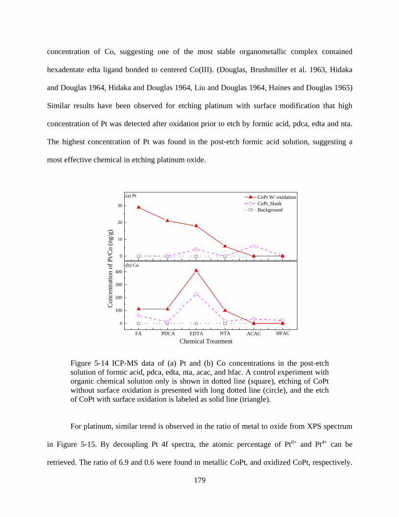
179
concentration of Co, suggesting one of the most stable organometallic complex contained
hexadentate edta ligand bonded to centered Co(III). (Douglas, Brushmiller et al. 1963, Hidaka
and Douglas 1964, Hidaka and Douglas 1964, Liu and Douglas 1964, Haines and Douglas 1965)
Similar results have been observed for etching platinum with surface modification that high
concentration of Pt was detected after oxidation prior to etch by formic acid, pdca, edta and nta.
The highest concentration of Pt was found in the post-etch formic acid solution, suggesting a
most effective chemical in etching platinum oxide.
0
10
20
30
0
100
200
300
400
(a) Pt CoPt W/ oxidation
CoPt_blank
Background
Chemical Treatment
(b) Co
HFACACACNTAEDTAPDCAFA
Conce
ntr
atio
n o
f P
t/C
o (
ng/g
)
Figure 5-14 ICP-MS data of (a) Pt and (b) Co concentrations in the post-etch
solution of formic acid, pdca, edta, nta, acac, and hfac. A control experiment with
organic chemical solution only is shown in dotted line (square), etching of CoPt
without surface oxidation is presented with long dotted line (circle), and the etch
of CoPt with surface oxidation is labeled as solid line (triangle).
For platinum, similar trend is observed in the ratio of metal to oxide from XPS spectrum
in Figure 5-15. By decoupling Pt 4f spectra, the atomic percentage of Pt0+ and Pt4+ can be
retrieved. The ratio of 6.9 and 0.6 were found in metallic CoPt, and oxidized CoPt, respectively.

180
A ratio of Pt0+ to Pt4+ follows the order of pdca, formic acid, edta, nta, acac, and hfac, suggesting
pdca is the most effective organic chemical in removing platinum oxide. The general trend
follows the results from ICP-MS in Figure 5-14, except the discrepancy of the most effective
chemical. Because the ex situ XPS was carried out for analyzing the chemical state of surface,
CoPt treated by formic acid was exposed to the air relatively longer compared to pdca, resulting
in lower ratio of Pt0+/Pt4+ to pdca. Therefore, two conclusions can be drawn on the basis of the
evidence that formic acid is the most effective organic chemical in etching platinum oxide, and
the organic chemical ligands only react with Pt(IV) oxide, instead of Pt(II) oxide or metallic Pt.
0
1
2
3
4
5
6
7Metallic CoPt
Oxidized CoPt
PDCA
FA
HFACACAC
NTA
EDTA
Pt0
+/P
t4+
(ato
mic
%/a
tom
ic %
)
Chemical Treatment
Figure 5-15 The ratio of Pt0+ to Pt4+ in atomic percentage decoupled from XPS
results of CoPt etched by organics solution of pdca, formic acid, edta, nta, acac,
and hfac for 20 min. (labeled by solid line with triangle) The ratio of Pt0+ to Pt4+
of metallic CoPt and oxidized CoPt are labeled as solid circle, and solid square,
respectively.

181
Meanwhile, the etched thickness could be estimated by the amount of metal in the
solution with known sample dimension, volume of organic solution, and the density of metal
film. For example, all the samples were approximately 7 by 10 mm rectangles, the volume of
organic solutions were about 2 mL, and the density of Co and Pt are approximately 8.9, and 21.5
g/cm3, respectively. (Lide 1995) The etched thickness was estimated in Figure 5-16 that greatest
removal was only 0.8 Å for Pt etched by formic acid, but a removal of 28.0 Å was found for Co
etched by edta. In order to keep the same composition of Co and Pt after patterning, formic acid
is selected as a potential candidate due to the highest etch rate of platinum oxide but relatively
low etch rate of cobalt oxide compared to other organic chemicals.
0.0
0.5
1.0
0
10
20
30
(a) Pt CoPt W/ oxidation
CoPt_blank
Background
Th
ick
nes
s o
f P
t an
d C
o (
A)
Chemical Treatment
(b) Co
HFACACACNTAEDTAPDCAFA
Figure 5-16 Estimated thickness of of Co and Pt etched by organic solution of
formic acid, pdca, edta, nta, acac, and hfac for 20 min. The etched thickness is
estimated by the results of ICP-MS by known dimension of sample, density of Co
and Pt, and volume of organic solutions. A control experiment with organic
chemical solution only is shown in dotted line (square), etching of CoPt without
surface oxidation is presented with long dotted line (circle), and the etch of CoPt
with surface oxidation is labeled as solid line (triangle).

182
Since formic acid is selected as an organic chemical etchant for CoPt, the time-dependent
etch needs to be studied as well. Figure 5-17 presents the Pt 4f, Co 2p, O 1s, C 1s, and survey
spectra of CoPt pre-etch, post-oxidation, oxidation prior to formic acid etch for 3, 5, 10, 20 min.
Based on the result of survey in Figure 5-17 (e), no other elements were found, suggesting a
contamination-free sample preparation is designed. Figure 5-17 (d) present C 1s spectra, and no
carbon decomposition is observed from 3 to 20 min formic acid etch. O 1s spectra is presented in
Figure 5-17 (c), an oxygen-metal peak in post-oxidation spectrum was totally removed in 3 min
etch and left an oxygen-hydrogen peak alone. The result followed the trend in Pt 4f and Co 2p in
Figure 5-17 (a) and (b) that Pt4+ and Co2+ peaks were entirely eliminated, suggesting the etch of
metal oxide by formic acid was rapidly. Thus, the shorter etching time was examined in Figure
5-18. The removal of platinum (IV) oxide by formic acid solution was as rapid as in one second,
which also confirmed the etching efficacy of organic chemical.
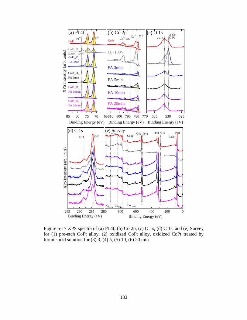
183
85 80 75 70 65810 800 790 780 770 535 530 525
FA 20min
FA 10min
FA 5min
FA 3min
CoPt_O2
FA 20min
CoPt_O2
FA 10min
CoPt_O2
FA 5min
CoPt_O2
FA 3min
XP
S I
nte
nsi
ty (
arb
. u
nit
s)
Binding Energy (eV)
(a) Pt 4f
CoPt
CoPt_O2
500W -100V
CoPtCo
2+ sat. O-H
Co2+
(b) Co 2p
Binding Energy (eV)
Co0+
Pt4+ Pt
0+
O2 -100V
O-PtO-Co
(c) O 1s
Binding Energy (eV)
295 290 285 280 800 600 400 200 0
C-C
XP
S I
nte
nsi
ty (
arb. unit
s)
Pt4pCo3s
CoLMMc
Co2s
OKLL
CoLMMa
Co2pO1s Pt4d C1s Pt4f
C-O
(d) C 1s (e) Survey
Binding Energy (eV)Binding Energy (eV)
Figure 5-17 XPS spectra of (a) Pt 4f, (b) Co 2p, (c) O 1s, (d) C 1s, and (e) Survey
for (1) pre-etch CoPt alloy, (2) oxidized CoPt alloy, oxidized CoPt treated by
formic acid solution for (3) 3, (4) 5, (5) 10, (6) 20 min.

184
0.0 10 20 30 40 50 600
1
2
3
4
5
6
7
8
9
10
5min
3min10sec
1sec
CoPtO
CoPt
Formic acid sol. etching time (min)
Pt0
+/P
t4+
Figure 5-18 The ratio of Pt0+ to Pt4+ in atomic percentage decoupled from XPS
results of CoPt etched by formic acid solution for 1 sec, 10 sec, 3min, 5 min, 10
min, 20 min, 40 min, and 60 min. The ratio of Pt0+ to Pt4+ of metallic CoPt is
labeled as solid square.
A multiple etching cycles for CoPt alloy was conducted, and the thickness change as a
function of etching cycle is shown in Figure 5-19. The thickness was measured by ellipsometer,
and the calibration of ellipsometry model was confirmed by SEM with 10 and 20 nm CoPt films.
A dotted line with circle presents a control experiment without surface modification of 500W O2
plasma for 5 min. The thickness of CoPt decreased in the first two cycles due to the removal of
native metal oxide which was approximately 1 nm. Because of the high selectivity of metal oxide
to metal by formic acid solution, no thickness change was found after first two cycles. The solid
line in Figure 5-19 represented an alternating etch with surface modification of 500 W O2 plasma
for 5 min followed by 30 sec organic solution etch. In the first half cycle, the decrease of CoPt
thickness could be attributed to the removal of adventitious hydrocarbon layer by forming

185
volatile carbon dioxide and methane with O2 plasma. Due to the etching of metal oxide by
formic acid solution, the second half of the first cycle also showed the decrease of CoPt
thickness. The volume expansion started at first half of second cycle, it is because the density of
metal oxide formed by the O2 plasma oxidation is relatively smaller than metal oxide. For
example, the density of Co and CoO are 8.9 and 6.44 g/cm3, respectively; the density of Pt and
PtO2 are 21.45 and 10.2 g/cm3, respectively. (Lide 1995) As the density of CoO is only 2/3 of
Co, the volume of oxide would be one and half times more than that of metal. After second
cycle, the etched thickness gradually increased by cycles, and the average etch rate is 1.1
nm/cycle.
0 1 2 3 4 5
0
10
20
30
40
50
60
CoPt etched by FAvap
ER~0 nm/cycle
Etch cycle
Th
ick
nes
s ch
ang
e (A
)
CoPt etched by O2/FAvap
ER=1.1 nm/cycle
Figure 5-19 The thickness change of CoPt etched by surface modification of 500
W O2 plasma for 5 min and formic acid solution for 30 sec alternatively. The
dotted line with hollow circle represents CoPt etch without surface modification,
and the solid line with hollow square stands for CoPt etch with surface
modification prior to organic solution etch.

186
Not only physical measurement of thickness but also the chemical state of surface
characterization through XPS was conducted for analyzing alternating etch by O2 plasma and
formic acid solution etch. Figure 5-20 shows Pt 4f, Co 2p3/2 and O 1s spectra from pre-etch, first,
second, third, and fourth cycle of etching. For Pt 4f spectra, Pt4+ peak is shown periodically,
which exactly the same as predicted, suggesting the removal of platinum oxide. Cobalt spectra
are similar to that of platinum, the Co2+ peak presents periodically as well. The O 1s spectra is
the most obvious that oxygen-metal peak appears at the first half of cycles, and disappear at the
second half of cycles, suggesting the removal of metal oxide is completed.
85 80 75 70 65 788 784 780 776 772 535 530 525
etch
etch
etch
etch
oxi.
oxi.
oxi.
XP
S I
nte
nsi
ty (
arb
. u
nit
s)
Binding Energy (eV)
(a) Pt 4f x4
Cycle 4
O-HCo
2+
(b) Co 2p3/2
Binding Energy (eV)
Co0+
Pt4+
Pt0+
Cycle 2
Cycle 3
Cycle 1
CoPt
oxi.
oxi.
etch
oxi.
etch
oxi.
etch
oxi.
etch
O-Co
O-Pt
(c) O 1s
Binding Energy (eV)
Figure 5-20 XPS spectra of (a) Pt 4f, (b) Co 2p3/2, and (c) O 1s, for (1) pre-etch
CoPt alloy, (2) oxidized CoPt, and different cycles of surface oxidation and
formic acid solution etch from (3) to (7).
However, as the cycles continued, the atomic percentage of Co to Pt on the CoPt alloy
surface changed significantly. Table 5-3 shows the atomic percentage of Co and Pt at different
cycle. In the beginning, the ratio of Co to Pt was about 3:7; however, the ratio became 1:9 at the

187
end of fourth cycle. It is attributed to the preferential removal of Co than Pt on CoPt surface. The
new organic chemical is necessary to develop for balancing the atomic ratio of alloy in the
future.
Table 5-3 Surface composition of Co and Pt in atomic percentage of CoPt etched
by surface oxidation and formic acid solution etch sequentially from pre-etch, and
cycle one to cycle four.
Cycle (#) Pre-etch 1 2 3 4
Atomic % Blank Oxi. Etch Oxi. Etch Oxi. Etch Oxi. Etch
Co (%) 31 41 13 18 14 23 14 21 11
Pt (%) 69 59 87 82 86 77 86 79 89
188
5.4 Organic Chemical Vapor Etch
A vacuum-compatible etching process is needed in order to integrate it with other
semiconductor processes, the study of the vapor etch is required. Since the formic acid solution
etch of metal oxide was proven effective in the previous section, the etching efficacy of formic
acid vapor was investigated by the setup of vapor etch chamber described in chapter two. Similar
to solution etch, XPS was utilized to determine the removal of metal oxide by organic ligands.
Figure 5-21 shows the XPS spectra of Pt thin film etched by formic acid vapor with surface
modification of 500W O2 plasma for 5 min. The survey in Figure 5-21 (b) shows clean platinum
surfaces without contamination after one or two cycles of formic acid vapor etch with surface
oxidation, excluding the decomposition of organic ligands on the surface. The detail scan of Pt 4f
in Figure 5-21 (a) shows an increase of Pt4+ peak after O2 plasma oxidation, and a significantly
decrease of Pt4+ peak after formic acid vapor exposure, suggesting a similar etching efficacy of
Pt in solution of formic acid etch.

189
85 80 75 70 65 800 600 400 200 0
Pt4p
Pt_O2
FA vapor
1st cycle
Pt_O2
FA vapor
2nd cycle
XP
S I
nte
nsi
ty (
arb
. u
nit
s)
Binding Energy (eV)
(a) Pt 4fPt4p
OKLL
Pt4sO1s Pt4d C1s Pt4f
(b) Survey
Binding Energy (eV)
Pt_O2
500W -100V
Pt_
Pre-treatment
Figure 5-21 XPS spectra of (a) Pt 4f, and (b) Survey, for (1) pre-etch Pt, (2)
oxidized Pt, (3) 1st cycle, and (4) 2nd cycle of sequential etch of surface oxidation
and formic acid vapor exposure.
In order to confirm the etch efficacy, the thickness measurement of Co and Pt was
performed by the ellipsometer in Figure 5-22. Etching of Co by formic acid vapor with surface
modification is significant that a 25 nm Co film was totally removed in 3 cycles. The reason of
etched thickness not being equal in each cycle was that the pressure of formic acid vapor in each
cycle was not controlled well. Although a Baratron capacitance monometer is attached onto the
vapor etch chamber to measure the pressure of formic acid vapor in the system, the pressure right
on the sample surface is still not fully controlled, resulting in a fluctuated etching thickness of
metal in each cycle. Due to a low reactivity of Pt by nature, a thickness change of 4 nm in 4
cycles for Pt is relatively lower than that of Co. But the etched thickness of Pt was equally
distributed in each cycle, suggesting a saturation of removing platinum oxide by formic acid
vapor was achieved in each cycle. Therefore, a same conclusion of preferential removal of Co to
Pt found in solution etch is observed in vapor etch as well.

190
0 1 2 3 4 5
0
50
100
150
200
250
Co_O2/FAvap
Pt_O2/FAvap
Etch cycle (#)
T(A
)
0
10
20
30
40
50
60
70
T(A
)
Figure 5-22 Etched thickness of Co and Pt etched by surface modification and
exposure of formic acid vapor as a function of etching cycle. Hollow square
represents etching of Co on left y-axis, and hollow circle represents etching of Pt
on right y-axis.
Since the etching efficacy of Co and Pt by sequential surface oxidation and formic acid
vapor exposure are confirmed separately, the etching of CoPt alloy is studied. A removal of 6-
nm CoPt film was observed in 4 cycles in Figure 5-23, and a relatively large thickness change
was found in the first cycle, ca. 4 nm. The reason could be the preferential removal of Co to Pt in
the first cycle. Since the component of Co on the surface decreased significantly in the first cycle,
the following cycles were mainly removal of Pt, resulting in a lower removal rate compared to
first cycle.

191
0 1 2 3 4
0
10
20
30
40
50
60
70
T(A
)
Etch cycle (#)
CoPt_ICPO2/FAvap
Figure 5-23 Etched thickness of CoPt alloy by surface modification and exposure
of formic acid vapor as a function of etching cycle.
To further explore the etching efficacy of transition and noble metals with organic
ligands, Fe, Cu, Co, Pd, and Pt have studied systematically. Figure 5-24 presents a growth of
metal oxide as a function of O2 plasma time. The thickness of metal oxide was estimated by XPS
spectra as mentioned in Chapter 2. Apparently, the thickness of metal oxides increased
immediately in the first few minutes, and the growth rate saturated at fifth min for most of the
metals. Since there was no bias applied on the metals in the O2 plasma treatment, the O2 source
were mainly oxygen radicals and neutrals. Thus, the principal mechanism of oxidation is the
diffusion of oxygen radicals onto the metal surface. Iron oxide presents the highest growth rate
followed by copper oxide, cobalt oxide, palladium oxide and platinum oxide, which follows the
same trend in the literature that the self-diffusion coefficients of iron, copper, and cobalt ions in
oxides are 1.18 × 10⁻¹, 4.36 × 10⁻², 2.15 × 10⁻³ cm2/sec, respectively. (Hauffe 1965) Although,

192
the self-diffusion coefficients of noble metals, palladium and platinum, are not available, the
lower reactivity to oxygen radical compared to transition metals are as expected.
0 1 2 3 4 5
0
1
2
3
4
5
PtOx
Cu2O
PdOx
FeO
Time(min)
Ox
ide
thic
kn
ess(
nm
)
CoO
Figure 5-24 The growth of oxide thickness for Fe, Cu, Co, Pd, and Pt as a
function of the oxidation time of 500 W O2 plasma. The symbol of circle,
diamond, square, inverted triangle, and triangle are represent FeO, Cu2O, CoO,
PdOx, and PtOx, respectively.
The etching of metals with formic acid vapor are conducted right after the surface
oxidation in Figure 5-25, and the thickness change were measured by ellipsometer. The etch rate
of iron, copper, cobalt, palladium, and platinum are 4.2, 3.7, 2.8, 1.2, and 0.5 nm/cycle,
respectively, the order of the etch rate follows the trend in the growth of metal oxide presented in
Figure 5-24. Therefore, the etch rate per cycle has compared to the growth rate of oxide in Figure
5-26, and a linear relationship between two components are shown. A high selectivity of metal
oxide to metal etched by formic acid vapor is achieved, suggesting one of the most important
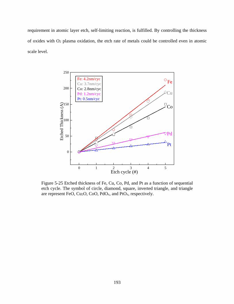
193
requirement in atomic layer etch, self-limiting reaction, is fulfilled. By controlling the thickness
of oxides with O2 plasma oxidation, the etch rate of metals could be controlled even in atomic
scale level.
0 1 2 3 4 5
0
50
100
150
200
250
Pt
Cu
Pd
Co
FeFe: 4.2nm/cyc
Cu: 3.7nm/cyc
Co: 2.8nm/cyc
Pd: 1.2nm/cyc
Pt: 0.5nm/cyc
Etch cycle (#)
Etc
hed
Thic
kn
ess
(A)
Figure 5-25 Etched thickness of Fe, Cu, Co, Pd, and Pt as a function of sequential
etch cycle. The symbol of circle, diamond, square, inverted triangle, and triangle
are represent FeO, Cu2O, CoO, PdOx, and PtOx, respectively.

194
0 1 2 3 4 5
0
1
2
3
4
5
PtOx
Cu2O
PdOx
Fe2O
3
Oxide thickness/cycle (nm)
Etc
hed
thic
knes
s/cy
cle
(nm
) CoO
Figure 5-26 Etched thickness per cycle as a function of oxide thickness per cycle
for Fe, Cu, Co, Pd, and Pt. The symbol of circle, diamond, square, inverted
triangle, and triangle are represent FeO, Cu2O, CoO, PdOx, and PtOx,
respectively.
Although a chemical etch of blanket metal film is demonstrated, the patterning of metals
with hard mask needs to be investigated as well in order to confirm the selectivity of hard mask
to metals, which is one of the most severe issue in MRAM fabrication. In the Figure 5-27 (a), a
Co 30 nm film was patterned by TiN hard mask 40 nm and SiN for 10 nm, and a 10-nm-barrier
layer served as an etching stop layer under Co film. After 6 cycles sequential etch of 500W O2
plasma 5 min and formic acid vapor 50 sec exposure, the etching profile is shown in Figure 5-27
(b). A significant undercut of cobalt is observed due to the isotropic characteristic of pure
chemical etch. However, the hard mask is remained intact, which the thickness and sidewall
profile are sustained due to the low reactivity of TiN to formic acid ligand. After 8 cycles of

195
sequential etch, a sever undercut of cobalt resulting in suspension of TiN hard masks shown in
Figure 5-27 (c). A series of cross-sectional SEM images with different tilted angle is shown in
Figure 5-28, several suspensions of TiN hard masks across a large area on sample is
observed, suggesting a uniform isotropic etch of Co by formic acid vapor.
(a) (b) (c)
Figure 5-27 SEM images of patterned Co (a) pre-etch, (b) 6 cycles sequential
etch, and (c) 8 cycles sequential etch.

196
(a) 10o (b) 8o (c) 6o
(d) 4o (e) 2o (f) 0o
Figure 5-28 A series of cross-sectional SEM images of patterned Co etched by 8
cycles sequential etch with titled angle of (a) 10 o, (b) 8 o, (c) 6 o, (d) 4 o, (e) 2 o,
and (f) 0 o.
In addition, the formic acid vapor etch with surface modification by O2 plasma is closely
related with the magnetic properties in the magnetic metallic film. The magnetic property of
patterned sample was investigated by Superconducting Quantum Interference Device (SQUID)
in Figure 5-29, which presents magnetic hysteresis loop for magnetization as a function of
applied magnetic field of the pre-etched patterned Co, as a reference, and the patterned Co
treated by O2 plasma followed by formic acid vapor etch. The coercive field of 20 Oe and
saturation magnetization of pre- and post-etch Co are approximately identical, which implying
the magnetic property of Co is remained intact after the sequential etch. The change of remnant
magnetization could be due to the adsorption of the formic acid molecules on the Co surface, but
it was not enough to be detected by XPS as shown in Figure 5-21.

197
-400 -200 0 200 400
-1.0
-0.5
0.0
0.5
1.0
O2/Organic
vapor 4cyc
Pre-etch
Magnetic Field (Oe)
Norm
aliz
ed M
agnet
izat
ion
Figure 5-29 Magnetic hysteresis loop measured in patterned Co films. Normalized
magnetization (to saturation magnetization of pre-etch patterned Co) vs magnetic
field. The spectrum labeled by solid triangle represents pre-etch patterned Co, and
the 4 cycles sequential etch of Co is labeled by hollow circle.
Besides the observation by SEM imaging, a surface chemical characterization through
Energy-Dispersive X-Ray Spectroscopy (EDS) was also utilized to confirm the removal of Co
by sequential etch of O2 plasma oxidation followed by exposure of formic acid vapor in Figure
5-30. The spectra from bottom to top are pre-etch, 1, 2, 3, 5, 6, 7, 8 cycles of sequential etch.
Two strong peaks of Si Kα (1.70 eV) and Al Kα (1.46 eV) are prenseted through all the spectra
due to the silicon substrate and aluminum sample holder. The present of C Kα (0.28 eV) and O
Kα (0.52 eV) peaks are from the exposure of atmosphere due to the ex-situ EDS measurement.
Ti Kα (0.39 eV) peak, Co L3-M1 (0.66 eV), and Co L (0.77 eV) are from the Ti hard mask and
Co film. Because of the low reactivity of Ti and formic acid ligand, the peak of Ti Kα is

198
remained the same throughout the etching. However, a gradual decreasing of the Co peak is
found due to the slowly removal of Co by sequential etch. A 30-nm-Co film was totally removed
in 8 cycles, suggesting an etch rate of 3.75 nm/cycle is achieved with O2 plasma oxidation and
formic acid vapor treatments.
0.0 0.5 1.0 1.5 2.0
Co L3-M1
8cyc
7 cyc
6 cyc
5 cyc
3 cyc
2 cyc
1 cyc
Pre-etch
O K Al K
Ti K
Co LC K Si K
Inte
nsi
ty (
CP
S)
Energy (keV)
Figure 5-30 The EDS spectra of pre- and post- etched patterned Co with various
cycles of sequential etch of surface oxidation and exposure of formic acid vapor.
Nonetheless, the anisotropic etching profile is still desired in pattering metals for MRAM
fabrication. In order to obtain a directional oxygen ion to achieve higher degree of oxidation in
vertical than lateral direction, a bias voltage of 200 V is chosen to apply onto Co sample. A
control experiment of 500 W O2 plasma with 200 V bias for 10 min is conducted, and a tapered
etching profile is found in Figure 5-31 (b). Due to the physical sputtering of low-mass oxygen
ion, TiN hard mask was sputtered faster than that of Co, resulting in re-deposition of Ti. The

199
sequential etch of patterned Co is shown in Figure 5-31 (c), which an anisotropic etching profile
is observed and an acceptable recession of 5-nm TiN hard mask is found.
(a) (b) (c)
Figure 5-31 SEM images of patterned Co (a) pre-etch, (b) 500 W O2 plasma with
-200 V bias for 10 min, and (c) 4 cycles sequential etch with -200 V bias in 500W
O2 plasma.
5.5 Summary
A comprehensive framework for selecting viable chemistries in patterning magnetic
metals has been developed, and the surface modification prior to organic chemical etch was
realized to be necessary in chemically etching metals. The surface modification for metals were
studied by XPS, and a process of O2 plasma for converting metal to oxide was found to be the
best among other plasma chemistries such as SO2, Cl2, CF4, SF6, and O2 ion beam, and atomic
percentage of Pt4+ was increased 5 times compared to pristine Pt. With the same technique of
surface chemical analysis, the thickness of metal oxide was estimated by quantification of XPS
with known inelastic mean free path (IMFP) of characteristic electron. By knowing the oxide
thickness, the etch rate of each metals could be calculated and verified by ellipsometer and SEM.
The mechanism of metal oxidation under mild O2 plasma without bias was discussed by the

200
fitting of data and model, and Fe and Co follow inverse logarithmic rate law which suggested the
rate determine step was incorporation of metal cations into interstitial site. In the case of Cu, a
cubic rate law suggests oxygen diffusion and dissolution was the rate determining step. For noble
metals Pd and Pt, the parabolic rate law points out a rate determining step of oxygen diffusion
and migration of cations. Once the optimized process for surface modification was achieved, a
study of organic solution etch of metal was performed with acac, hfac, edta, nta, podca, oxialic
acid, and formic acid. Based on the results of XPS and ICP-MS, the relative high reactivity
between platinum oxide to formic acid was observed among the organic chemicals. As a result, a
sequential etch of Co, Pt and CoPt alloy with O2 plasma followed by formic acid solution etch
was studied. Due to the preferential removal of Co to Pt, a ratio of Co to Pt on the surface of
CoPt alloy was decreased from 3:7 to 1:9, which the magnetic property would be changed. Thus,
a new organic chemical is required to keep the same composition of surface in the future. Vapor
etch of metals were performed after solution etch, and the etch rate of Fe, Cu, Co, Pd, and Pt
were 4.2, 3.7, 2.8, 1.2, 0.5 nm/cycle, respectively. A high selectivity of metal oxide to metal by
formic acid vapor was achieved, suggesting one of the most important requirement in atomic
layer etch, self-limiting reaction, was fulfilled. By controlling the thickness of oxides with O2
plasma oxidation, the etch rate of metals could be controlled in atomic scale level. The patterned
samples of Co and MTJ stack were investigated with the optimized etching process, and an
isotropic etching profile, high selectivity of mask to metals, and retaining of magnetic
characteristic were observed, suggesting a process with solely chemical etch without physical
sputtering was developed. In order to get a desired etching profile with anisotropic characteristic,
directional oxygen ion for oxidation was successfully examined with applying bias onto the

201
patterned sample. Finally, an approach of successfully patterning metal was developed, and high
density of MRAM fabrication could be achieved based on the preliminary results.

202
CHAPTER 6: SUMMARY
As advanced memory devices begin to dictate the adoption of complex magnetic and
multiferroic materials, overcoming the challenge of achieving high-fidelity patterning for these
multifunctional films becomes imperative. Physics and chemistry-based modeling affords greater
understanding of elementary reaction mechanisms in plasma patterning; however, the parameters
necessary for kinetic modeling are sometimes difficult to obtain experimentally for novel
multifunctional compounds. A comprehensive framework for selecting viable chemistries in
plasma patterning of magnetic metals has been developed. In this work, a generalized
methodology, combining thermodynamic assessment of various etching chemistries and kinetic
verification of etching efficacy, is proposed. To screen various chemistries, reactions between
the dominant vapor phase/condensed species at various partial pressures of reactants are first
considered. The volatility of etch products is determined to aid the selection of viable etch
chemistry. MTJ based MRAM was used as a case study to address the challenge of patterning
multilayer constituent materials. Ar ion beam milling was a traditional method in patterning
MRAM devices; however, sidewall re-deposition results in electrical shorts as the features
become smaller with higher aspect ratios. Reactive ion beam etch has been investigated intensely
to pattern magnetic metals, but degradation of magnetic properties was found due to residue of
etching products with low volatility. In this work, three approaches have been developed and
verified experimentally in the following order. First, the volatility of etching products was
improved by introducing secondary chemistries to reactive ion etch. Second, the physical and
chemical etch were combined into ion beam assisted organic chemical etch. Third, a solely
chemical process was developed by introducing surface modification prior to organic vapor etch.
203
For the first approach, the attainable partial pressure of the major etch product was
evaluated by thermodynamic calculations. The metal hydride was not volatile, but oxygen radical
addition on MClx (M = Co, Fe, or Ni) could enhance the vapor pressure of the etch product.
Hydrogen radical addition on chlorinated surfaces appears to be the most effective combination
to etch metals, showing that the partial pressure of MH(g) can be higher than the reference value
(~10-8 atm). According to the surface composition measurements, hydrogen plasma could etch a
MClx layer but not pure metals. As a result, the etch rates of Co, Fe, and Ni by alternating Cl2/H2
plasmas were enhanced by 17, 6, and 20%, respectively, compared to those measured in a
continuous Cl2 plasma. The thermodynamic expectation was consistent with the experimental
result. First, Co and Ni etch rate by a Cl2 plasma was similar, while Fe etch rate was higher than
those metals. Second, atomic hydrogen addition could etch a metal chloride layer at an enhanced
rate. A reactive hydrogen atom and the stable byproduct such as HCl acted as driving forces for
increasing the attainable partial pressure. These results indicate that the alternating plasma
approach is the first step toward fabricating high density MTJ-based RAM devices. Concerning
the degradation of magnetic properties associated with halogen chemistry etch, the formation of
metal chloride resulted in a significant change/increase in the coercive field which is not
desirable. It was determined that the utilization of hydrogen led to a complete removal of the
metal chloride, thus restoring the soft magnetic characteristics of CoFe. This confirms that the
combination of Cl2 and H2 plasmas can not only etch CoFe at a reasonable rate but also preserve
the magnetic property of CoFe. Since the thickness of the CoFe layer (3-5nm) is usually thicker
than that of the tunnel oxide (~1nm), a double patterning process combining both chemical and
physical etch processes may be necessary to successfully pattern both the magnetic layers as well
as the tunnel oxide.
204
Although the reactive ion etch has been verified to achieve reasonable etch rates with
preservation of magnetic properties of metals, the low selectivity of the hard mask to metals due
to the sputtering effect is still not acceptable. From the second approach, the organic chemical
etch of generating highly volatile etching products is desired. Two traditional β-diketonate
precursors for CVD have been selected to perform the reverse engineering of ALD.
Thermodynamic calculations were first utilized to screen the organic chemistries in etching Co
and Fe. A preferential etch of Co by acac through formation of Co(acac)2 and the generation of
by Fe(hfac)3 etched with hfac were predicted to be the most thermodynamically favorable
products. Similarly, experiments were conducted to verify the theoretical prediction. The etch
rates of Co and Fe by acac and hfac solutions have been quantified by profilometer, etching
products have been analyzed and verified by ESI-MS, and the selectivity predicted by
thermodynamics was verified. The volatility diagram has predicted the selectivity of acac over
hfac in etching Co, due to the higher partial pressure of Co(acac)2(g) than that of Co(hfac)3(g) at
operational condition. In the case of Fe, the high selectivity of hfac over acac was discovered,
wherein the formation of Fe(hfac)3(g) requires lower partial pressure of hfac than that of acac to
generate Fe(acac)3(g). However, a significant drop of etch rate was found while decreasing the
concentration of organic in solution, suggesting a lower reactivity of metal with organic vapor. A
surface modification with Ar ion beam was introduced in order to facilitate the activation of
surface and desorption of organometallic compounds without degrading the magnetic property of
metals. The etching of Co by alternating Ar ion beam exposure and acac vapor exposure has a
strong effect in improving the etch rate by approximately 180% compared to that of Ar ion beam
alone. The etch rate of Co by alternating Ar ion beam and acac vapor is much greater than the

205
sum of the two, suggesting a synergistic effect of chemical etch along with sputtering has
discovered in the ion beam assisted chemical etch.
Nevertheless, Ar ion beam is a limiting factor in patterning high density MRAM device
due to the high aspect ratio of features, requiring development of an etching process using only
chemical reaction. Thus, a surface modification prior to organic chemical etch was realized to be
necessary in chemically etching metals. The surface modification for metals were studied by
XPS, and a process of O2 plasma for converting metal to oxide was found to be the most
effective. The mechanism of metal oxidation under mild O2 plasma without bias was discussed
by the fitting of data and model for Co, Fe, Cu, Pd and Pt. Once the optimized process for
surface modification is achieved, a study of organic solution etch of metal is performed with
several solutions. Based on the results of XPS and ICP-MS, the relative high reactivity between
metal oxide and formic acid was observed among the organic etchants. As a result, a sequential
etch of metal with O2 plasma followed by formic acid solution etch was studied. Vapor etch of
metals was performed after solution etch, and the etch rate of Fe, Cu, Co, Pd, and Pt were 4.2,
3.7, 2.8, 1.2, 0.5 nm/cycle, respectively. A high selectivity of metal oxide to metal by formic acid
vapor is achieved, suggesting one of the most important requirements in atomic layer etch, self-
limiting reaction, is satisfied. By controlling the thickness of oxides with O2 plasma oxidation,
the etch rate of metals could be controlled at the atomic level. Patterned Co and MTJ stack
samples were investigated with the optimized etching process, and an isotropic etching profile,
high selectivity of mask to metals, and retention of magnetic characteristics were observed,
suggesting a process of solely chemical etch without physical sputtering was developed. In order
to get a desired etching profile with anisotropic characteristic, directional oxygen ion for
oxidation was successfully examined with applying bias onto the patterned sample. Finally, an

206
approach of successfully patterning metal is developed, and high density of MRAM fabrication
would be achieved based on the preliminary results.
This work has developed a generalized approach for plasma patterning with a case study
of magnetic metal etch, and this methodology could be applied to additional fields. For example,
as critical dimensions of gate-length approach 7 nm in 2016, the industrial need for an etching
method capable of atomic resolution has led to the pursuit of atomic layer etch. Although the
atomic layer etch (ALE) of silicon has been realized recently, controlling of threshold energy in
the ALE window is extremely challenging and it requires stringent control of system cleanliness.
The ALE process developed in this work does not require the controlling of ion energy, because
it depends on the generation of highly volatile products with bulky organic ligand. Finally,
anisotropic and selective etching with atomic scale control could be achieved by the generalized
approach proposed in this work. Atomic layer etch has been realized by reversing atomic layer
deposition (ALD), which required a self-limiting reaction to achieve atomic scale control.
However, the isotropic characteristic of ALD is not desired in atomic layer etch, which
necessitates anisotropic etching profile. Based on the outcome of generalized approach above, it
could potentially facilitate anisotropic etch for selected metals with directional oxygen ion while
surface modification. All of this work is a great challenge and opportunity to keep up with
Moore’s law, and an opportunity for academia to fully understand the truth inside the black box.

207
APPENDICES
TABLE OF CONTENTS
A. Inductively Coupled Plasma Reactor ............................................................................... 209
A.1. Emergency Shutdown Procedures .............................................................................. 209
A.2. Schematics .................................................................................................................. 214
A.3. Operating Procedures .................................................................................................. 223
B. Quadrupole Mass Spectrometer Operational Guidelines ................................................... 229
B.1. Emergency Shutdown Procedures ............................................................................... 229
B.2. Schematics ................................................................................................................... 230
B.3. Operation Procedures .................................................................................................. 231
C. Langmuir Probe Operation Procedure ................................................................................ 233
C.1. Emergency Shutdown Procedures ............................................................................... 233
C.2. Schematics ................................................................................................................... 234
C.3. Operating Procedures .................................................................................................. 235
D. Optical Emission Spectrometer Operation Procedures ...................................................... 238
D.1 Emergency Shutdown Procedures ............................................................................... 238
D.2. Schematic .................................................................................................................... 238
D.3. Safety and Operating Procedures ................................................................................ 239
D.4. Wavelength Calibration Settings: ............................................................................... 240
E. X-ray Photoelectron Spectroscopy Operational Guidelines .............................................. 241
E.1 Emergency Shutdown Procedures ................................................................................ 241
E.2. Safety and Operating Procedures ................................................................................ 242
F. Spectroscopic Ellipsometer Operational Guidelines .......................................................... 247
F.1 Emergency Shutdown Procedures ................................................................................ 247
F.2. Safety and Operating Procedures................................................................................. 248
F.3. Software Operation ...................................................................................................... 248
F.4. Hardware Calibration Procedure ................................................................................. 249
F.5. Installation of Compensator ......................................................................................... 250
F.6. Replacement of Protection Device .............................................................................. 251
G. Transfer Tube ..................................................................................................................... 252
G.1 Emergency Shutdown Procedures ............................................................................... 252
G.2. Safety and Operating Procedures ................................................................................ 254
H. Vapor Etch Chamber .......................................................................................................... 257
H.1. Emergency Shutdown Procedures .............................................................................. 257
H.2. Operating Procedures .................................................................................................. 257
H.3. Schematics .................................................................................................................. 259
H.4. Vaporizer Info ............................................................................................................. 262
I. Ion Source Chamber ............................................................................................................ 264
I.1 Troubleshooting ............................................................................................................. 264
I.2. Operation Procedures for Ion Source Chamber ............................................................ 266
I.3. Operating Procedure for Analysis (#6) in Professor Chang’s Lab ............................... 271
I.4. Install and Test EQP QMS System............................................................................... 273

208
I.5. Schematics .................................................................................................................... 284
J. Superconducting quantum interference device (SQUID) ................................................... 287
J.1. Introduction .................................................................................................................. 287
J.2. SQUID Operating Procedure ........................................................................................ 288
K. Copper Volatility Diagram Construction ........................................................................... 291
K.1. Introduction ................................................................................................................. 291
K.2. Example Calculations ................................................................................................. 291
K.3. Volatility Diagrams ..................................................................................................... 294
K.4. Matlab Code ................................................................................................................ 296
L. Gibbs Free Energy Minimization ....................................................................................... 300
L.1. Introduction ................................................................................................................. 300
L.2. Examples ..................................................................................................................... 302
L.3. Matlab Code ................................................................................................................ 304
M. Gaussian ............................................................................................................................ 316
M.1. Gaussian Introduction................................................................................................. 316
M.2. Sample Calculations with SiH4 .................................................................................. 316
M.3. References .................................................................................................................. 318
N. HSC Database .................................................................................................................... 319
N.1. HSC Operating Procedure ........................................................................................... 319
O. Etching of carbon-doped silicon dioxide ........................................................................... 322

209
APPENDICES
A. Inductively Coupled Plasma Reactor
A.1. Emergency Shutdown Procedures
I. In case of Cl2 is smelled
1. Close tank valve.
2. Close others valve if possible. The diaphragm valve D4, located directly behind chamber,
and the regulator R1 on Cl2 cylinder located in gas cabinet to the right of the MFC
cabinet.
Figure A-6-1 D4 valve directly behind chamber.
Figure A-6-2 R1 regulator located in chlorine gas cabinet.
3. Evacuate.
D4
R1
N2 purge
gas valve

210
4. Contact EH&S as needed.
Figure A-6-3 Gas line system for ICP system including corrosive gases Cl2 and
BCl3, inert gases Ar, N2, and O2.
The ICP system including corrosive and inert gas line, molecular turbo pump, cryopump and
mechanical pump. V1 and V2 are the valves for Ar, V3 and V4 are the valves for O2. Since the
control flow rate of Ar MFC is small which only has 10 sccm, the one for O2 can go to 50 sccm,
the bridge from Ar to O2 gas line enable high flow rate for Ar gas. V5 and V6 are the valves for
high purity of N2 and D5 is a valve for industrial N2 which go to the back of TMP to dilute the
corrosive gas into mechanical pump. In the corrosive gas aspect, Cl2 is accompanied with purge
N2 gas, and share with the double wall corrosive gas line with BCl3. D1 and D2 are the valves for
Cl2 and purge N2 gas, and D6 and D7 are the valves for BCl3. D3 is the inert valve and D4 is the
corrosive valve control the flow rate into chamber. A1 and A3 are the valves pumping down the
chamber by mechanical pump, and A2 and A4 are the valves for MTP back side to the
mechanical pump.

211
II. In case a noise is heard from turbo molecular pump on Main Chamber
1. Close manual gate valve between turbo pump and chamber.
Figure A-6-4 Gate Valve for Main Chamber Turbo Pump.
2. Turn off the turbo molecular pump by pushing the “stop” button on the controller.
Figure A-6-5. Turbo Pump Controller for Chamber.
3. Isolate mechanical pump by closing manual valve between turbo and MP.
III. In case a noise is heard from mechanical pump on Chamber
1. Close manual gate valve between turbo pump and chamber. (See Figure 3)
2. Turn off the turbo molecular pump by pushing the “stop” button on the controller. (See
Figure 4) And close the roughing from turbo pump to mechanical pump.
3. Switch off the mechanical pump by turning off the breaker.
IV. In case a ratcheting is heard from Cryopump on Chamber
1. Close the pneumatic gate valve between ICP and Cryopump by pressing the corresponding
switch on the control box (trace the cable if unsure). (See Figure 5)
Gate
Valve
Stop button
(read label to
confirm)

212
Figure A-6-6 Gate Valve between Cryopump and ICP.
2. Ensure that the roughing valve between the cryopump and the chamber mechanical pump is
closed.
3. Turn off the cryopump by flipping the white circuit breaker on the compressor (See Figure
6 - in the event of pump failure this may turn off automatically – check to see if the unit is
operating).
Figure A-6-7 Compressor and Circuit Breaker Switch.
V. In case noises are heard from any of the electronics
Gate
Valve
Control
Box
Circuit
Breaker

213
1. If units have power switches, turn them off and unplug all units (see pictures below).
Figure A-6-8 The components of ICP system.
VI. In case the vapor etch system needs to be shut down 1. Turn off vaporizer heater.
2. Close valve to 1.
3. Unplug vaporizer heater, LFC controller, and MFC controller.
Bias
Controller
Induction
Coil
QMS
Controller &
Oscilloscope
Matching Network
Ion Gauge
RF Power
QCM Controller
Filament Control

214
A.2. Schematics
ICP reactor
Main chamber – Side view
University of California, Los Angeles, Department of Chemical and Biomolecular Engineering
Part Material Stainless steel
Filename Scale Yes Units inch Quantity 1
Designer Yunpeng Yin(MIT) Date 6/11/2003
Revised by Date
Contractor Applied Vacuum
Technologies
Date 6/11/2003
Comments Tolerance +/- .0001

215
ICP reactor
Main chamber – Isometric view
University of California, Los Angeles, Department of Chemical and Biomolecular Engineering
Part Material Stainless steel
Filename Scale Yes Filename Scale Yes
Designer Yunpeng Yin(MIT) Date 6/11/2003
Revised by Date
Contractor Applied Vacuum
Technologies
Date 6/11/2003
Comments Tolerance +/- .0001

216
ICP reactor
Main chamber – Front view
University of California, Los Angeles, Department of Chemical and Biomolecular Engineering
Part Material Stainless steel
Filename Scale Yes Filename Scale Yes
Designer Yunpeng
Yin(MIT)
Date 6/11/2003
Revised by Date
Contractor Applied Vacuum
Technologies
Date 6/11/2003
Comments Tolerance +/- .0001

217
ICP reactor
Main chamber – Top view
University of California, Los Angeles, Department of Chemical and Biomolecular Engineering
Part Material Stainless steel
Filename Scale Yes Filename Scale Yes
Designer Yunpeng
Yin(MIT)
Date 6/11/2003
Revised by Date
Contractor Applied Vacuum
Technologies
Date 6/11/2003
Comments Tolerance +/- .0001
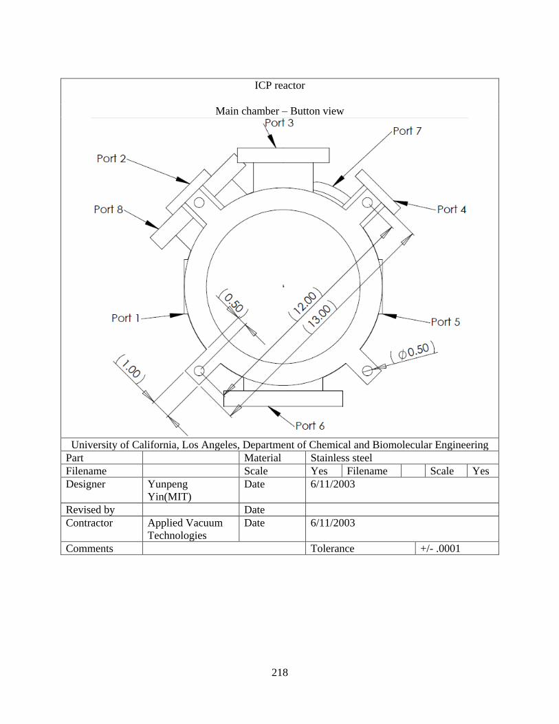
218
ICP reactor
Main chamber – Button view
University of California, Los Angeles, Department of Chemical and Biomolecular Engineering
Part Material Stainless steel
Filename Scale Yes Filename Scale Yes
Designer Yunpeng
Yin(MIT)
Date 6/11/2003
Revised by Date
Contractor Applied Vacuum
Technologies
Date 6/11/2003
Comments Tolerance +/- .0001

219
ICP reactor
Main chamber – QMS chamber
University of California, Los Angeles, Department of Chemical and Biomolecular Engineering
Part Material Stainless steel
Filename Scale Yes Filename Scale Yes
Designer Yunpeng
Yin(MIT)
Date 6/11/2003
Revised by Date
Contractor Applied Vacuum
Technologies
Date 6/11/2003
Comments Tolerance +/- .0001

220
ICP reactor
Sample stage
University of California, Los Angeles, Department of Chemical and Biomolecular Engineering
Part Material Stainless steel
Filename Scale Yes Filename Scale Yes
Designer Yunpeng Yin(MIT) Date 6/11/2003
Revised by Date
Contractor Applied Vacuum
Technologies
Date 6/11/2003
Comments Tolerance +/- .0001

221
ICP reactor
Quartz in the ICP chamber
University of California, Los Angeles, Department of Chemical and Biomolecular Engineering
Part Material Stainless steel
Filename Scale Yes Filename Scale Yes
Designer Yunpeng Yin
(MIT)
Date 6/11/2003
Revised by Date
Contractor Applied Vacuum
Technologies
Date 6/11/2003
Comments Tolerance +/- .0001
1
(10.0)
(0.71)
(0.5)
(0.5)
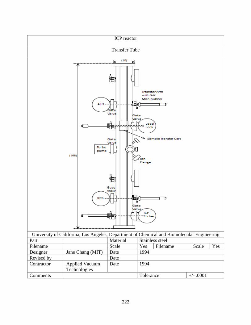
222
ICP reactor
Transfer Tube
University of California, Los Angeles, Department of Chemical and Biomolecular Engineering
Part Material Stainless steel
Filename Scale Yes Filename Scale Yes
Designer Jane Chang (MIT) Date 1994
Revised by Date
Contractor Applied Vacuum
Technologies
Date 1994
Comments Tolerance +/- .0001

223
Figure A-6-9 Gas line system for ICP system including corrosive gases Cl2 and
BCl3, inert gases Ar and N2, and O2.
The ICP system including corrosive and inert gas line, molecular turbo pump, cryopump
and mechanical pump. V1 and V2 are the valves for Ar, V3 and V4 are the valves for O2. Since
the control flow rate of Ar MFC is small which only has 10 sccm, the one for O2 can go to 50
sccm, the bridge from Ar to O2 gas line enable high flow rate for Ar gas. V5 and V6 are the
valves for high purity of N2 and D5 is a valve for industrial N2 which go to the back of TMP to
dilute the corrosive gas into mechanical pump. In the corrosive gas aspect, Cl2 is accompanied
with purge N2 gas, and share with the double wall corrosive gas line with BCl3. D1 and D2 are
the valves for Cl2 and purge N2 gas, and D6 and D7 are the valves for BCl3. D3 is the inert valve
and D4 is the corrosive valve control the flow rate into chamber. A1 and A3 are the valves
pumping down the chamber by mechanical pump, and A2 and A4 are the valves for MTP back
side to the mechanical pump.
A.3. Operating Procedures
1. Pump down the main chamber (Note: The chamber’s default state should be pumped down,
check the pressure reading on the ion gauge to verify. The following steps should only be taken
if you aware that the chamber has been vented and not pumped back down).
a. The following interlocks for the pump down procedure must be met to begin pumping:
I. cooling water for main chamber turbo molecular pump(TMP) must be on
II. cooling water flow to compressor should be between 2.3 and 3.5 gpm.
b. Check that all the flanges are tightened and all the valves are in the closed position.
c. Check all the cables are correctly connected.

224
d. Check the oil level in the mechanical pump(MP), which should be 2/3 full in view
window.
e. Check MP and its exhaust for liquid leaks. (oil, condensation, exhaust fluid)
f. Turn on MP by turning on the breaker. The thermocouple(TC) gauge reading should start
going down within 20 seconds. If not, turn off the pump and check connections to
chamber, turbopump and cryopump for vacuum leaks.
g. Wait until MP reaches the base pressure ~60 mTorr. This process may take several
minutes if system was shut down for some time.
h. If the gas lines have been exposed to ambient conditions, diaphragm valve D3 and D4
should be open so that the gas lines could be pumped down as well. Rough pump the
chamber using MP until a base pressure of ~75-85 mTorr is achieved.
i. After the TC gauge reaches the base pressure, close roughing valve between chamber and
MP and gradually open roughing valve between TMP and MP.
2. Before TMP is turned on, check:
a. The cooling water is running
b. The roughing valve between the chamber and TMP should be always CLOSED while the
TMP is on.
c. If TMP is running, the base pressure should be achieved right away. (This would occur
only if MP was turned off for less than approximately 10 minutes and TMP was isolated
prior to shut off of MP)
d. If pumping down after TMP has been off for a few hours it may be safer to purge TMP
with N2 using the N2 MFC for 30 seconds. Then gradually open the roughing valve and
wait until base pressure is reached in MP.
e. Open the gate valve between TMP and chamber. At this stage, the TC gauge readout
should NOT vary at all.
f. Turn on TMP by pushing the start button on the Leybold controller, unless already on.
The green acceleration indicator should be on.
g. Within 5 minutes, the turbo molecular pump should reach full speed and the yellow
indicator should be on normal.
1.If any strange noise is heard from TMP, turn it off right away by pushing the off button
on the controller.
2.If corrosive gas is anticipated to be used, 36 sccm industrial level nitrogen
(corresponding to ~50 mTorr rise in TC pressure) should be provided through the purging
port on the bottom of the pump by opening valve D5 and switching on the MFC “N2 ind.”
on the control panel once the pump has reached full rotation, which is indicated by the
normal light being lit on the TMP controller. (Refer to Leybold 361C Turbo Molecular
Pump manual.)
h. Wait until the chamber reaches the base pressure 6.0 x10⁻⁷. This process may take up to
couple of days depending on how long the chamber has been under atmosphere.
If the chamber has been exposed to ambient or pumping system has been off for more
than a day, baking the chamber is necessary to achieve base pressure and remove any
build up on the sidewalls of the chamber. Two heating tapes are used to bake the
chamber. Do NOT turn on the power over 20% of the full range on the variable
transformer to prevent over heating. At this point the chamber pump down procedure is
complete. If no processing is to be performed system should be left in this idle state.

225
After base pressure in the chamber is achieved, plasma processing can begin using the
following procedure. If a sample is to be processed the following procedure must be
followed to load the sample in to the chamber. However, it is better to warm up the plasma
before processing a sample, in which case skip to steps 3-6, and then return to step 2 and
repeat the following steps.
3. Transfer the sample from transfer tube to the chamber:
a. See instructions for loading a sample from the loadlock in the Transfer Tube SOP.
b. Move the cart into position for transfer to the ICP.
c. Before opening the gate valve between the ICP and the TT check that their pressures are
roughly equivalent. If the ICP pressure is over 10-7 torr which is 2 order higher than TT
pressure, 10-9 torr, then the gate valve between the TT and its cryopump/turbo pump
should be closed. Ensure that no gas is flowing into the ICP.
d. Open the gate valve (G4) using the controller box (trace the cable to ensure). Check the
ion gauge controllers on both the ICP and TT to ensure that the pressure has not changed
significantly.
e. Secure the sample by sliding the holding fork attached to the end of the transfer arm
around the upper groove of the sample holder.
f. Using the manipulator, lift the sample off the cart. Verify that the arm has cleared the cart
(a setting of about 4-5 on the Y-axis manipulator is sufficient).
g. Slowly slide the transfer arm forward to move the sample into the ICP chamber.
h. Visually confirm the location of the sample in relation to the sample stage pin by
checking through the viewport on the lower section of the ICP chamber.
i. Lower the sample holder onto the protruding pin. Visually confirm.
j. Slowly begin sliding the transfer arm out. The holder should stay on the stage.
k. When re-entering the transfer tube ensure the height of the transfer arm is readjusted so
as not to hit the cart or holding pin in front of the ICP chamber.
l. Fully withdraw the transfer arm into the tube so that it has cleared the gate valve.
m. Close the gate valve (G4) between the ICP and TT.
With the sample loaded, if necessary, plasma processing can begin. Processing gases must
be introduced into the reactor prior to striking plasma by performing the following
procedure. Proceed to step 3, 4, or 5 depending on plasma chemistry.
4. Feed in process gas for plasma for inert gas only:
a. Check that the chamber is at the base pressure of 1.0 x 10⁻⁷ torr.
b. Check regulators for all the desired gases (N2, Ar, O2 ) by opening the gas tank.
c. Check the cylinders are filled with enough gas to obtain required flow rate.
d. Open the pneumatic valves for gases to be used before the Mass Flow Controller (MFC),
which are V1, V3, and V5.
e. Gradually open the corresponding valve after the MFC, which are V2, V4, and V6, to
prevent a large pressure difference to the MFCs.
f. Adjust the set point on the MFC control unit to desired flow rate for each gas.
g. Open Diaphragm valve D3 and then gradually open D4. The chamber pressure should go
slightly higher; wait until it goes back to the base pressure. This will pump down the
gases which have been sitting in the line.
h. Turn off the ion gauge, which cannot go above 1x10⁻³ torr.
i. Turn on the MFCs for the gases to be used. Wait until a steady flow is achieved. Do fine
adjustments if needed.

226
j. Record pressure achieved in chamber after steady flow is reached
5. Feed in corrosive process gas (Cl2 and/or BCl3) only:
The following interlock for corrosive gas use must be met to begin: n2 purge to main
chamber and QMS turbo pumps must be on.
a. Check that the chamber is at the base pressure of 1.0 x 10⁻⁷ torr.
b. Check there is enough Cl2 gas in the cylinder and the tank and regulator should be
CLOSED. (This regulator should always be closed while Cl2 gas is not in use.)
c. Check that 36 SCCM nitrogen is supplied to the purging ports of TMP1 and 2 by MFC.
d. Gradually open Diaphragm valve D4. The chamber pressure should go slightly higher;
wait until it goes back to the base pressure.
e. Adjust the set point on MFC control unit, which is channel 1, to desired flow rate for Cl2
gas.
f. Turn off the ion gauge.
g. Open the valve on Cl2 cylinder and the isolation valve after the regulator. Adjust the
regulator to get 12 Torr outlet pressure. Then close gas cabinet door.
h. Gradually open the Diaphragm valve D1 and then D2 for Cl2 and/or D6 and D7 for BCl3.
Close the gas cabinet door.
i. Turn on the MFC. Wait until the steady flow is achieved.
j. Record pressure in chamber once steady flow is achieved.
6. For corrosive gas and inert gas mixture (Cl2, BCl3, Ar, O2, N2):
The following interlock for corrosive gas use must be met to begin: n2 purge to main
chamber and qms turbo pumps must be on.
a. Check that the chamber is at the base pressure of 1.0 x 10⁻⁷ torr.
b. Check there is enough Cl2 and or BCl3 gas in the cylinder.
c. The regulators should be CLOSED. (This regulator should always be closed while Cl2
gas is not in use.)
d. Check 36 SCCM nitrogen is supplied to the purging ports of Turbopumps 1 and 2.
e. Gradually open Diaphragm valve D3 and D4. The chamber pressure should go slightly
higher; wait until it goes back to the base pressure.
f. Adjust the set points on MFC control unit to desired flow rates for gases.
g. Turn off the ion gauge.
h. Open the regulator on Cl2 cylinder and/or BCl3 at their respective gas tanks.
i. Open the pneumatic valves, for the inert gas, before the MFC (V1, V3, and V5) first, and
then open the corresponding valve after the MFC (V2, V4, and V6).
j. Turn on the MFCs for the inert gases.
k. Gradually open the Diaphragm valve D1 and then D2 for Cl2 and/or D6 and D7 BCl3.
l. Close the gas cabinet doors.
m. Turn on the Cl2 and/or the BCl3 MFC. Wait until the steady flow is achieved.
n. Record chamber pressure once flows have stabilized.
7. Turning on the plasma
The following interlock for plasma generation must be met to begin:
1. Induction coil fan on.
a. Ensure the fan on the induction coil is plugged in and operating.
b. Turn on the main power of the RF generator (Seren R1000) by flipping the main power
switch.

227
c. Turn on the main power of the matching network tuning controller (RFPP 761 Unit) and
ensure its operation mode is set to "Auto".
d. If bias is desired, turn on the main power and bipolar voltage control of the DC bias
controller (Kepco BOP 500M).
e. If etching in the lower chamber is desired, turn on the filament power supply (Harrison
Labs 6263A). Let all the electronics units warm up for 30 - 45 minutes.
f. Flow the process gases (pressures should be adjusted in steps 2-4).
g. Set the RF generator to the desired source power and press the "RF on" button. A red
light should indicate RF power is being supplied.
h. If plasma does not strike, check that the reflected power as indicated on the generator
display is not higher than 70 W, or that no warnings are displayed. If the reflected power
is low, consider increasing the gas flow using the appropriate MFC. If the power is high
or if warnings are displayed, turn off the RF supply by pressing the "RF on" button again
and check the connections between the generator, matching network and source coil.
i. If bias is desired, set the DC bias to the appropriate voltage.
j. If etching in the lower chamber is desired, set the filament power supply to ~2 Amps.
Usually this should be done a minute or two before the experiment to ensure the filament
is receiving current (indicated by a reddish glow).
k. After the process is finished, turn off the RF power by pushing the "RF on" button on the
front panel of the Seren R1000. Processes should not exceed 15 minutes so as to not over
heat system.
l. Turn off the corrosive process gases first on the MFC.
m. Leave the inert gases running for about 5 minutes.
n. Turn off the MFCs, close the corresponding pneumatic valves and the Diaphragm valve
D4 and D3 for Cl2 and/or D6 and D7. BCl3.
o. Turn off TMP1 purging nitrogen.
8. Troubleshooting
This section details major problems occurring on ICP chamber and the steps taken to fix them.
3/2012:
Problem: Unable to strike the plasma such as O2(g) and N2(g).
Solution:
1. Check the connection of cable on the top of chamber.
2. Shine the light into chamber while turning on the RF generator.
3. Flow the Ar gas with O2 or N2 to strike the plasma, once the plasma been ignited then
Ar could be slowly decreased to 0.
7/2012:
Problem: The wire connected from voltage supplier to bias ring was burn out.
Solution:
1. Order stainless steel wire from McMaster Carr.
2. Clean up the stainless steel wire by IPA and alcohol, cut into a suitable length and then
replace old one.
3. Check by the multimeter for connection between voltage supplier and bias ring.
8/2012:
Problem: The turbo pump started making a high pitch noise.
Solution:

228
1. Check the turbo pump controller is in normal condition.
2. Isolated the turbo pump. First, close gate valve to chamber, and then switch off the turbo
pump by controller. Wait 20 mins to pump out the turbo pump by mechanical pump, and
close the roughing valve to mechanical pump.
8/2012:
Problem: The bias beam couldn’t be observed during the plasma etching process.
Solution:
1. Check the mesh at the center of upper chamber is clean and grounded.
2. If mesh is covered by green species or other contamination, the mesh need to be cleaned.
a. Flip up the plate in the upper chamber, undo the filament connection carefully.
b. Take out the plate and undo the screws at the center mesh. Be careful that there are
three small of stainless steel piece between the plate and mesh which can make the
mesh grounded.
c. Sonicate the mesh with IPA for 10 mins two times.
d. Reinstall the mesh and plate into the chamber, and connect the filament wire.
e. Use multimeter to check the mesh is grounded.
9. Cryopump Regeneration
a. Isolate cryopump by closing gate valve and closing backing valve.
b. Turn off compressor. Leave cryopump for 2-3 hours, expect to see condensation.
c. After condensation evaporates, apply heating jacket and plug it in.
d. Let the cryopump heat for 8 hours.
e. Close backing of transfer tube (TT) and load lock (LL) turbo pumps, set timer to 5 min.
f. Look at TT mechanical pump thermocouple (TC) gauge, slowly open cryopump backing. You
should see a pressure spike.
g. Let cryopump pump out until timer runs out, then close cryopump backing. Let TC gauge
bottom out, then reopen TT and LL backing.
h. Repeat steps e-g until TC gauge no longer spikes when cryopump backing is opened. Close
cryo backing.
i. Unplug heating jacket, let it cool then remove it.

229
B. Quadrupole Mass Spectrometer Operational Guidelines
B.1. Emergency Shutdown Procedures
1. Turn off the UTI100C Electronics Controller by following the sequence labeled below in the
order indicated.
Figure B-1 QCM panel.
2. Turn off the oscilloscope by pressing the power button:
Figure B-2 Oscilloscope panel.
Power Button
1
2
Rotate the Emission
Control fully
counter-clockwise
until it clicks off. Depress the Off Switch

230
B.2. Schematics
Figure B-3 QMS schematics.

231
B.3. Operation Procedures
1. Check the base pressure of the system, which should be about 2.8*10-8 Torr. Write the base pressure
in the logbook.
2. Check the connections between the Spectrometer and the Interface Box, the Interface Box and the
Spectrometer Control Unit (SCU), the SCU and the Oscilloscope, and the Oscilloscope and the
Computer (Illustrated below). Turn on the computer.
Figure B-4 The connection of interface box and spectrometer
3. Ensure that the power cable into the SCU is plugged in. Check that the follow switches are depressed
(labeled below): “Var” and “Man” in the Scan section, “Norm” in the Program Section, “Off” in the
Function Section and “10-5” in the Damper Section. Also make sure the emission control is off
(rotated fully counter-clockwise).
Figure B-5 QCM panel.
Spectrometer
Interface Box
Interface Box
Oscilloscope
SCU
Computer
Var Man
Norm
Off
Emission
Control 10-5

232
4. Depress the “On/Stby” switch on the SCU directly to the right of the “Off” switch. Let the
electronics warm up for 30 minutes. Power on the oscilloscope by pressing its power button.
Windows should indicate that new USB device has been plugged in and you need to select the
software option to view the device.
5. Select TekDesktopAcquisition (the TDS 1012B should be selected as device by default).
6. After the electronics have warmed up set the scan center and width using the Scan Control section of
the SCU. To set the center “Man” has to be depressed. To set the width, “Width Set” has to be
depressed and “Man” should be released. Both of these values are set by using the corresponding
rotary controls above the switches (can be seen in the preceding image).
7. Flow gas and strike plasma as required by your experiment.
8. Monitor the QMS pressure. The maximum operating pressure for QMS is 5*10-6 Torr.
9. Start the QMS scan by releasing the “Man” switch, and depressing “Emiss (mA) and “Mult”
switches at the same time. Adjust the emission current using the rotary control (max = 0.5 mA). If no
signal is seen adjust the Damper (max = 10-9).
10. Monitor the scan on the oscilloscope and adjust the visual as necessary using the controls for the y-
and x-axis. A visual can be captured using the Tektronic software “Data Capture” button.
11. After finishing all the experiments, close the software and transfer all the data files to the server.
12. Turn off the power to the SCU by using the steps outlined below:
Figure B-6 QCM panel.
13. Turn off the oscilloscope by pressing its power switch.
14. Finish the logbook.
Depress the “Manual”
switch.in the Scan
Control section
Release both the
Emission and Multiplier
Switches simultaneously
1
2
3
Depress the 10-5
switch on the
damper control
Rotate the Emission
Control fully counter-
clockwise until it clicks
off.
4
5 Depress the Off Switch

233
C. Langmuir Probe Operation Procedure
C.1. Emergency Shutdown Procedures
I. In case of an emergency overpressure situation in the plasma etcher
1. Stop any current scans using the Hiden ESPsoft software: STOP SCAN
2. If necessary, pull the probe tip out of the etcher main chamber and back it’s housing unit
by homing the z-stage: Probe → Home ZStage.
3. Exit the Hiden ESPsoft program: File → Exit.
4. Turn off the Langmuir probe electronics by pressing the “OFF” switches on the front
panels of both electronics units.
II. In case probe has been driven into the closed gate valve
1. Immediately stop the motor of the z-stage by pressing “Cancel” on the “Probe
Positioning” window of the ESPsoft software.
2. Home the z-stage.
3. At this point, the Langmuir probe housing will need to be disassembled off the etcher
system in order to assess damage to the probe.

234
C.2. Schematics
The Hiden Analytical Langmuir Probe system consists of the following components:
Figure C-1 Schematic of Langmuir Probe System and ICP chamber connection.
RF Coil
Probe
Plasma
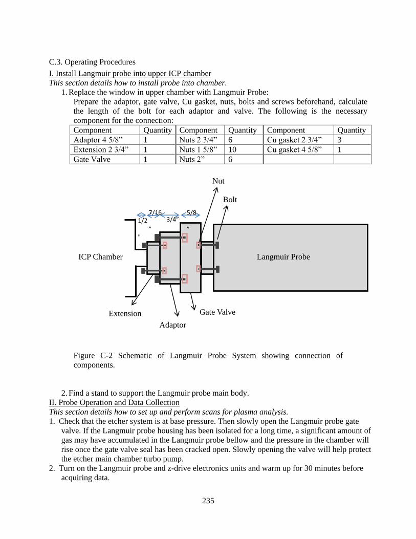
235
C.3. Operating Procedures
I. Install Langmuir probe into upper ICP chamber
This section details how to install probe into chamber.
1. Replace the window in upper chamber with Langmuir Probe:
Prepare the adaptor, gate valve, Cu gasket, nuts, bolts and screws beforehand, calculate
the length of the bolt for each adaptor and valve. The following is the necessary
component for the connection:
Component Quantity Component Quantity Component Quantity
Adaptor 4 5/8” 1 Nuts 2 3/4” 6 Cu gasket 2 3/4” 3
Extension 2 3/4” 1 Nuts 1 5/8” 10 Cu gasket 4 5/8” 1
Gate Valve 1 Nuts 2” 6
Figure C-2 Schematic of Langmuir Probe System showing connection of
components.
2. Find a stand to support the Langmuir probe main body.
II. Probe Operation and Data Collection
This section details how to set up and perform scans for plasma analysis.
1. Check that the etcher system is at base pressure. Then slowly open the Langmuir probe gate
valve. If the Langmuir probe housing has been isolated for a long time, a significant amount of
gas may have accumulated in the Langmuir probe bellow and the pressure in the chamber will
rise once the gate valve seal has been cracked open. Slowly opening the valve will help protect
the etcher main chamber turbo pump.
2. Turn on the Langmuir probe and z-drive electronics units and warm up for 30 minutes before
acquiring data.
5/8
”
3/4” 7/16
” 1/2
"
Langmuir Probe
Extension Gate Valve
Bolt
Nut
ICP Chamber
Adaptor

236
3. Open the ESP soft program on the diagnostics computer.
4. With the gate valve is open, advance the probe into the main chamber by selecting Probe → Z-
Stage, then entering the desired insertion distance (in cm) in the Park position prompt, then
selecting “Move Now” and “Ok”. (parking the probe tip at the center of the main chamber
requires a position of 26-27 cm)
5. Set the desired parameters for acquisition by selecting Probe → Edit, and then inputting all
desired parameters.
6. Once a plasma is struck, data can be acquired by selecting Probe → Run, then entering the
amount of acquisitions, naming the file, and selecting “Start”.
III. Probe Tip Replacement
This section details how to uninstall the Langmuir probe from the vacuum chamber and replace
the probe tip
1. Home the z-drive and close the manual gate valve connecting the Langmuir probe house from the
main chamber.
2. Remove screws holding the outer housing to the z-drive chassis, then take off the outer housing.
3. Disconnect the cables connecting the back end of the 2 ¾” CF flange (the end that the probe is
attached to on the inside), then, while holding the flange (and probe) in place, remove the bolts
connecting the CF flange to the bellow valve.
4. While carefully and firmly holding the bellow valve in place with one hand, and holding the CF
flange/probe in the other, advance the z-drive forward in small (~2 cm) increments until the
probe can be safely removed from the bellow. It is very important to secure the bellow valve
while doing this as when it is compressed it want to spring out sideways! Allowing this to
happen could damage the fragile bellow weldings and cause a leak.
5. Replace the probe tip using gloves and clean tongs.
6. To replace the probe, follow this procedure in reverse order, making sure to hold the probe steady
while retracting the z-stage. Colliding the probe tip with the bellow while retracting could
damage the new tip!
7. Once the probe CF flange is reattached to the bellow and the housing cover is replaced, the
bellow volume will have to be opened to the etcher while it is isolated from all turbopumps in
order to protect them (remember the bellow volume will be at atmospheric pressure!).
8. Rough pump the chamber and then pump down with the turbopump, as instructed in the etcher
system operation procedures.
IV. Troubleshooting
This section details major problems occurring on the Langmuir probe and the steps taken to fix
them.
Spring 2007:
It was found that some plasma conditions (e.g. BCl3-containing chemistries) lead to rapid
degradation of the collected current. This is due to deposition on the probe tip while it is idle. In
order to avoid deposition on the tip and prolong the lifetime of each probe tip, the following
procedures are suggested:
a. Always keep the Langmuir probe retracted into the housing with the gate valve closed for any
experiments that do not require data acquisition using the Langmuir probe.
b. Keep experiments as short as possible whenever the Langmuir probe is in use(this applies to all
plasma conditions!)
c. If a potentially depositing plasma chemistry will be in use, always set the “Idle Park Potential” of
probe (in the Probe → Edit menu) to a high negative voltage (~-80 V) right before striking

237
plasma, and return the idle park potential to 0 V once the plasma has been turned off. This will
induce ion bombardment of the probe with the plasma on which will prevent a deposition layer
from developing.
d. In addition, in the Probe → Edit menu, turn on the automatic cleaning during for data acquisition
in depositing plasmas by selecting the checkbox next to “Automatic Cleaning On” as well as “20
ms clean/5 ms data acq.”, and set the “Cleaning Potential” to a high negative voltage (~ -80 V).

238
D. Optical Emission Spectrometer Operation Procedures
D.1 Emergency Shutdown Procedures
1. Stop the program, and no further shutdown procedure is required.
2. The modules needed to be moved are optical fibers and the S2000 module where the
fibers are attached.
3. The ADC1000-USB module is used for the computer on the ECR etcher (or other
computers with the software properly installed if needed).
Figure D-1 OES operating software.
D.2. Schematic
The Ocean Optics S2000 System consists of 5 fiber optic cables (Labeled Master, Slave 1-4)
connected to an analyzer which interfaces with a computer workstation so that data can be
collected. The fiber optic cables are attached to a viewport in the ECR reactor through a
machined cover held in place by screws
From within the software,
selecting File Exit will
shutdown the program.

239
Figure D-2 Schematic of Optical Emission Spectrometer showing connection of
components.
D.3. Safety and Operating Procedures
1. Have Optical fiber and cable connections ready
i. One end of the fiber points to the light source (plasma)
ii. The other side of the fiber plugged into the S2000 module.
iii. S2000 module connects to ADC1000-USB (S/N ADUD6666) converter
iv. USB cable goes from ADC1000-USB to the computer USB port
2. Start the OOIBase 32 program
3. Load the configuration file:
a. Go to Spectrometer Open Configuration
b. Load c:\Program Files\Ocean Optics\OOIBase32\Default.spec
4. Enable channels:
a. Go to Spectrometer Configure
b. Select Wavelength Calibration Spectrometer Channel
c. For Master, Slave 1, Slave 2, Slave 3, and Slave 4: check Channel Enabled Box.
d. Click OK

240
5. Set proper integration time and time of average required.
D.4. Wavelength Calibration Settings:
These calibrations are set in the *.spec, the file that currently loads properly is located in Jerry’s
directory in the main Ocean Optics\OES folder.
Settings for Each Channels
Channel Coefficient
Master First Coefficient 0.09149
Second Codfficient -6.95276e-6
Third Coefficient 8.21743e-11
Intercept 195.774872
Slave 1 First Coefficient 0.08122
Second Codfficient -6.12735e-6
Third Coefficient -4.10603e-10
Intercept 327.208588
Slave 2 First Coefficient 0.10891
Second Codfficient -9.05373e-6
Third Coefficient -3.54458e-10
Intercept 437.932098
Slave 3 First Coefficient 0.16705
Second Codfficient -1.29450e-5
Third Coefficient -5.23387e-10
Intercept 585.628601
Slave 4 First Coefficient -015435
Second Codfficient -1.47189e-5
Third Coefficient -1.54958e-10
Intercept 786.201172

241
E. X-ray Photoelectron Spectroscopy Operational Guidelines
E.1 Emergency Shutdown Procedures
1. Make sure the transfer loading arm from the tube is all the way out of the XPS chamber
and then close the gate valve to the transfer tube.
2. Turn off X-ray source by pressing HV button (should be lit, light will turn off when
pressed) and then STANDBY button (should be unlit, will light when pressed and OPER
button to the right should become unlit). If there is time, wait for water to flow to cool the
anode for ~ 1 minute and press COOLING ON button. Then, turn off the main power and
chiller power.
3. Turn off energy analyzer by turning off ESCA kV and power switches on boxes from
bottom to top (lens, detector, control and display)
4. Turn off software by pressing the Stop Expt/Kill Data switch until experiment stops.
Figure E-1 XPS apparatus and control panel.
Gate valve to
transfer tube 1
2
HV button
Cooling
Button
Standby
Button
Operate
Button

242
Figure E-2.
E.2. Safety and Operating Procedures
1. Before transferring the sample, make sure the x-ray gun is backed out to a setting of
about 1.5 mm on the motion manipulator (~1 cm from the Teflon spacer). Move the
sample stage towards the gate valve to a setting of 1-2 on the corresponding
manipulator). Lower the stage to a setting of ~4 on the corresponding manipulator.
Ensure the stage is vertical. Be careful as the stage rotates easily.
Figure E-3 Sample stage manipulator.
2. Check the pressure on the XPS using the ion gauge controller (base is ~1 x 10⁻⁹ Torr, but
anything below 3 x 10⁻⁹ Torr is acceptable. If the pressure is above the 10-9 Torr range
check the ion pump controller for current reading – should read ~105 – 106 A). Check the
pressure on the TT using its ion gauge controller, pressure should be ~4 x 10⁻⁹ Torr (if it
3
4
ESCA
kV (1)
Lens (2)
Detector (3)
Control (4)
Display (5)
Stop Experiment/Kill
Data
Motion Manipulator
Teflon Spacer
Lateral Manipulator
Rotation Manipulator
Axial Manipulator
Height manipulator

243
is higher check that the gate valve between the cryo and the TT is open, if it is not, then
open it using the controller box (trace the cable to be sure)). Once both pressures are in
the requisite range open the gate valve between the TT and XPS using the corresponding
controller box (trace the cable if unsure).
3.
Figure E-4 XPS pressure gauge.
4. Slide the transfer arm into the tube slowly, checking the viewport occasionally to make
sure that you do not collide with the stage or x-ray source. The manipulator settings on
the arm should be X-setting = 5.5 (black) and Y-setting = 5 (black). Make sure the stage
is aligned with the sample using the lateral manipulator (pictured in Step 1 on previous
page). At this point you may have to raise the sample or lower the stage to provide the
necessary vertical clearance. Lower the sample onto the stage. You may have to lower the
loading arm to a Y-setting of 3-4 in order to remove the fork from the sample – slowly
pull out the fork and after each small movement, increase the Y-setting slightly to avoid
excessive straining. Retract the fork completely, being cautious to clear the transfer cart,
and close the gate valve between the tube and the XPS.
5. Move the sample stage closer to the source and move source in until it is about 0.25 cm
away from the Teflon spacer. Select the angle theta, which is the angle between the
sample surface and the detector axis, using the rotational control - 240° corresponds to a
90° take off angle and 270° to a 60° take-off angle.
6. Move x-ray source closer if desired and adjust the stage position using the various
manipulators until you are satisfied that the beam will illuminate the sample. Check the
pressure in the XPS chamber – it should be at or below 3 x 10⁻⁹ Torr. Turn on the
analyzer by turning on the switches labeled in the left picture below – from top to bottom:
Display, Control, Detector, Lens, then ESCA kV. Turn on the x-ray source by pressing
the power switch on the Control Unit. Press “Cooling On” (this should result in the
button beginning to blink with a green light) and then turn on the NESLAB HX-75
Chiller (This should result in the green light becoming steady). Select an anode by
pressing the corresponding button (selection will result in the button being illuminated by
a green light). At this point none of the Interlock Buttons should be lit red. If they are
seek assistance from a senior lab member or cautiously check all connections from
electronics to the unit.
Ion Gauge Ion Pump Controller

244
Figure E-5 XPS control panel.
Figure E-6 XPS chiller control panel and grounding test by multimeter.
Check the chiller setpoint by pushing in the chiller mode switch. This should read 17
degrees. If it has changed adjust the setpoint dial while keeping the mode switch
depressed. Check the flow rate by plugging in the BNC/Banana Plug connection to the
multimeter. When set to measure DC Voltage the multimeter should give a reading of
over 3.4 V. All the electronics to warm up for 10 minutes before running an experiment.
7. Launch the software program SPECTRA by double clicking the icon labeled SPECTRA
in the center of the desktop. To save time before the experiment begins you can define
your regions (survey, detailed, etc) by clicking the Edit Region Info Button. Also confirm
that the software is configured for the anode you selected in Step 5, by clicking the Tools
Button, then clicking “Setup Card” in the menu that pops up. In the dialogue box that
Display (1)
Control (2)
Detector (3)
Lens (4)
ESCA kV (5) Power
Button
Multimeter
Anode Buttons (left is
Al, right is Mg)
Interlock Buttons Cooling On
Button
Chiller Mode
Switch
Setpoint Dial
Chiller
Power Button
BNC/Banana
Plug Connection
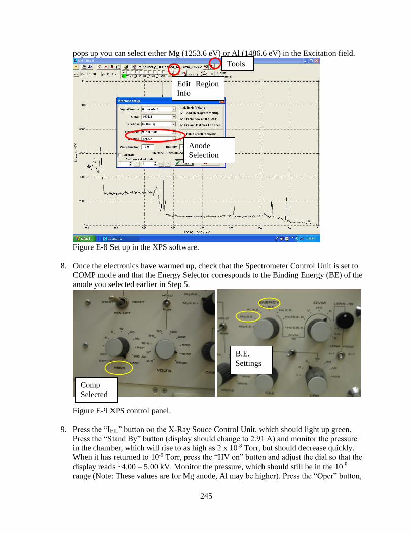
245
pops up you can select either Mg (1253.6 eV) or Al (1486.6 eV) in the Excitation field.
Figure E-8 Set up in the XPS software.
8. Once the electronics have warmed up, check that the Spectrometer Control Unit is set to
COMP mode and that the Energy Selector corresponds to the Binding Energy (BE) of the
anode you selected earlier in Step 5.
Figure E-9 XPS control panel.
9. Press the “IFIL” button on the X-Ray Souce Control Unit, which should light up green.
Press the “Stand By” button (display should change to 2.91 A) and monitor the pressure
in the chamber, which will rise to as high as 2 x 10⁻⁸ Torr, but should decrease quickly.
When it has returned to 10-9 Torr, press the “HV on” button and adjust the dial so that the
display reads ~4.00 – 5.00 kV. Monitor the pressure, which should still be in the 10-9
range (Note: These values are for Mg anode, Al may be higher). Press the “Oper” button,
Edit Region
Info
Tools
Anode
Selection
Comp
Selected
B.E.
Settings

246
the value of IFIL should rise to ~ 3.6 A and the light should blink briefly before becoming
steady again. Press the “IE” button (should light up green) and use the left and right dials
to gradually increase the IE and HV values to the desired reading (14 mA for IE and 10
kV for HV are standard, 18 mA for IE and 12 kV are maximum for Mg anode, 14 kV can
be used for Al anode). In the SPECTRA window press the circular button marked “Go”
to the right of the Edit Regions Button.
Figure E-10 XPS control panel.
10. Once the scans are finished, ramp down the HV and IE values by turning down the dials
slowly until they are at about 4 kV and 5 mA respectively, then Press “Oper” (the light
should go off and the “Standby” button should light up. Press “HV” (the light should go
off), then press “Standby” (the light should go off. If you are going to do more scans but
the pressure has increased significantly over the course of your run, the system can be left
in this state while it pumps down. If the pressure has not increased significantly, you can
adjust the region info and then run more scans at your discretion without having to turn
off the HV/IE switches.
If you will not run anymore scans, leave the “Cooling On” button on to let the anode cool down
for ~5-10 minutes. Press “Cooling On”, then press the power switch. Turn off the chiller. Turn
off the analyzer electronics by turning off ESCA kV first, then the boxes from bottom to top (in
reverse order from Step 5). Remove your sample from the chamber if desired.
HV
Button
Voltage
Dial
Stand
By
Current
Dial
Oper
IE
IFIL

247
F. Spectroscopic Ellipsometer Operational Guidelines
F.1 Emergency Shutdown Procedures
1. Turn off the power of LPS-400 light source.
2. Shut off the circuit breaker of the power controller.
Figure F-1 Ellipsometer apparatus.
Light source power
and ignition buttons
LPS-400 lamp
housing/power
supply
Circuit breaker of the
power controller
Power button of
the ellipsometer
power supply

248
F.2. Safety and Operating Procedures
Turn-on procedure
1. Turn on the circuit breaker of the power controller.
2. Turn on the power of the ellipsometer power supply (Electronics Control Module EC-270).
3. Turn on the light source (LPS-400). Press “power” button, and wait a few seconds, then press
“ignition” button.
4. Flip on the sign that reads “Lamp ON!”
Turn-off procedure
<For short time off>
1. Turn off the light source (LPS-400).
2. Flip on the sign that reads “Lamp OFF but Power ON!”
<For system off at the end of the day>
1. Turn off the light source (LPS-400).
2. Turn off the circuit breaker of the power controller.
3. Flip on the sign that reads “Power OFF!”
Do not leave the light source on for extended time periods.
F.3. Software Operation
1. Load the software (WVASE32).
2. Press “Window” on the menu bar, and select “Hardware”.
The “Hardware” window pops up, showing a message “Status:Hardware NOT
Initialized”
3. Press “Initialize”.
You will hear motor-running sound from the ellipsometer.
4. Place your sample on the stage. Make sure the beam is hitting the area you want to probe.
5. Press “Align”. The window for alignment will pop up. Your goal is to align the red cross to
the center of the reference frame.
6. Adjust two tuning knobs underneath the sample stage until the red cross appears on the
center of the reference frame.
7. Once alignment is done, press “Esc” key on the keyboard to exit the window.
8. Press “Ellipsometric data”. A new window of “In-situ real-time scan” will appear.
9. Press “Acquire Single Scan”. Data will be collected. It takes only a second.
10. To see the graphical results, press “Window” to select “Graph”.
It will show Ψ and Δ.
You can see other parameters (such as ε1, ε2, n, k, etc.) by pressing “Type” and selecting
the parameter you want to see.
To estimate layer thickness (Sequence: choose a model → fit the data)
1. Choose a model
1) Press “Window” and select “Model”.
2) Press “Addlayer” and select a proper material file (*.mat) for substrate.
You can set substrate thickness to 1 mm. Contact Woolam if the material you are
interested in is not in the data base.
3) Press “Addlayer” and select a proper material file (*.mat) for each layer.

249
1. For files containing n and k data (tabulated-layer file), the initial layer thickness
should be reasonably close to the actual thickness. Check the “Fit” box, and press
“OK”.
2. For functional files, you can fit other coefficients as well as layer thickness by
checking the “Fit” boxes.
Recommended material-data file (*.mat): Files are located in C:\wvase32\mat\
Examples:
Si: SI_JELL.mat (n,k data)
SiO2: Sio2.mat (n,k data)
HfO2: \mat\dielectr\Hfo2.mat (n,k data) or Hfo2_c.mat (Cauchy fit)
ZrO2: \ mat\dielectr\ Zro2_c.mat (Cauchy fit)
Y2O3: \mat\dielectr\y2o3.mat (n,k data)
SiC: \mat\semicond\sic.mat (n,k data)
AlN: aln_final_nk.mat (n,k data) or aln_cauchy_final.mat (Cauchy fit)
2. Fit
1) Press “Window” and select “Fit”.
2) Press “Normal fit” several time until the result value conversed.
3. Save the data
1) Press “Experimental Data” window and go to “file” to save the data.
2) Press “Generated Data” window and go to “file” to save the data.
F.4. Hardware Calibration Procedure
1. Place a sample on the stage and align it.
2. Load the software (WVASE32).
3. window hardware calibrate
4. You will see a dialog box “Calibration Mode” with five selections, which are;
a. Normal
b. Coarse
c. Detector electronics (off sample)
d. Detector system (straight-through configuration)
e. Detector system (with calibration sample)
“Normal” or “coarse” calibration can be performed every time the system is turned on and
the data acquisition is to be carried out. However, it is not necessary to perform it unless you
suspect the system is not working correctly.
“Detector system (straight-through configuration)” calibration must be performed only once,
when the instrument is first set up, and does not need to be performed every time the
instrument is turned on. To perform it, please see the manufacturer’s manual.
5. For routine calibration, choose “normal” or ‘coarse” calibration, and press “OK”
6. To see the graph: window graph

250
F.5. Installation of Compensator
Follow the manual for the JA Woollam Manual Retarder to remove the input module and install
compensator in between the base and the input.
Figure F-2 Sample stage, light source and compensator of ellipsometer .
A Si wafer with a medium thickness SiO2 film ~260 Å should be used for calibration.
9/7/04
After the Retarder is set to “IN”, be careful not to turn X and Y screws too far or they will come
out and the compensator must be reassembled.
The screws should be adjusted so Psi lines up exactly and the Delta model should be shifted
lower than the experimental value by 40-90deg.
Problems: On Step 10 in the manual for the JA Woollam Manual Retarder, when doing the
Detector System Calibration (Calibration Sample), it finished acquiring the data. Then at
Channel #87 an Error Message appeared “Error bars on calibration parameters exceed suggested
limits. Verify instrument is operating properly and then repeat the straight through calibration
procedure.”
Solution: Increased error tolerances in the “mmx-cal.cnf” file in the WVASE32 folder. Repeated
Step 10. The calibration finished. Entered delta offsets in the “hardware.cnf” file according to the
manual.In “Ellipsometric Data”, the High Accuracy Mode option needs to be checked.Took data
on several SiC and Si samples. Much cleaner data. Better fit. Delta is much smoother, near
90deg. Unsure if it is still very accurate for SiC…
9/29/04
Problem: Tried to measure SiC samples. Delta for the model was extremely noisy for all samples
and would not fit the data.
Solution: Tried to repeat Steps 10,11. No Change.
Repeating entire calibration procedure.
Compensator

251
Performed normal calibration (out)
Acquired dynamic data (in) and aligned psi and offset delta.
Guessed delta offset parameters in Model Options
Performed Detector System Calibration (with Calibration Sample)
DelOff1 = 78.014
DelOff2 = -1.9517e-2
F.6. Replacement of Protection Device
On March 11, 2005 the WVASE 32 program would not load. When clicking on the WVASE 32
icon on the desktop, the message “Protection Device Not Found!” was given. After contacting
J.A. Woollam (phone # (402) 477-7501) and speaking to Ping He, it was determined that the
protection device plugged into one of the parallel ports in the back of the computer was no
longer working. J.A. Woollam sent us a replacement protection device, and the WVASE 32
program is now working.

252
G. Transfer Tube
G.1 Emergency Shutdown Procedures
1. Ensure that all transfer arms are in the fully withdrawn position (i.e. they are not
extended into any reactor chambers).
2. Close all electrically operated gate valves on the system using the control boxes located
on the transfer tube table. (In the event of a power outage, this should automatically
happen). Visually inspect that this has taken place whenever possible by looking through
the appropriate windows on the transfer tube. In the event that a manual gate valve is
present, close it by hand.
Figure G-1 Windows, gate valve and gate valve controller of transfer tube.
3. Press the stop button on all the turbo pump controllers (in the event of the power outage
the controllers should all turn off).
Figure G-2 Controller of TMP.
4. If power is still available, allow the turbo pumps 10-15 minutes to wind down and then
close all the roughing valves between the turbo pumps and their backing mechanical
pumps. In the event of power loss close these valves immediately.
Gate valves
can be seen
through these
viewports
Example of a
manual gate valve
This switch closes
the gate valve (trace
power cable to gate
valve to confirm).
Stop button (read label to
confirm)

253
Figure G-3 Roughing valve of TMP and cryopump.
5. Use your discretion to turn off the mechanical pump on the tube, situated under the table.
Figure G-4. Mechanical pump of TMP.
6. The pressure of the transfer tube is displayed on a readout/controller located on the tube
table next to the loadlock (this controller monitors the loadlock and transfer tube
pressure), facing the north side of the room. Monitor the pressure regularly.
Roughing valves between turbo (and
cryo) pump and mechanical pump
(trace flexible hoses to confirm)
Power switch for the pump
is located on the pump
itself, near the front.

254
Figure G-5. Ion gauge of transfer tube system.
7. Double check that the gate valve above the cryopump is shut and the rough valve between
the cryopump and the mechanical pump is closed (this should have been done in the previous
steps). Turn off the CTI 9600 Compressor connected to the cryopump by flipping the white
circuit breaker to the “off” position.
Figure G-6 Compressor of cryopumps.
G.2. Safety and Operating Procedures
Please refer to the following labeled picture when performing Steps 1 and 2.
Circuit
Breaker
Load Lock
Tube
Pressure
Readout
Compressor
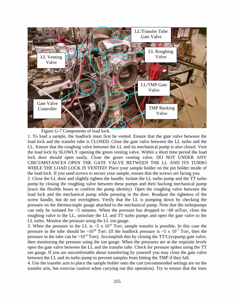
255
Figure G-7 Components of load lock.
1. To load a sample, the loadlock must first be vented. Ensure that the gate valve between the
load lock and the transfer tube is CLOSED. Close the gate valve between the LL turbo and the
LL. Ensure that the roughing valve between the LL and its mechanical pump is also closed. Vent
the load lock by SLOWLY opening the green venting valve. Within a short time period the load
lock door should open easily. Close the green venting valve. DO NOT UNDER ANY
CIRCUMSTANCES OPEN THE GATE VALVE BETWEEN THE LL AND ITS TURBO
WHILE THE LOAD LOCK IS VENTED! Place your sample holder on the pin holder inside of
the load lock. If you used screws to secure your sample, ensure that the screws are facing you.
2. Close the LL door and slightly tighten the handle. Isolate the LL turbo pump and the TT turbo
pump by closing the roughing valve between these pumps and their backing mechanical pump
(trace the flexible hoses to confirm the pump identity). Open the roughing valve between the
load lock and the mechanical pump while pressing in the door. Readjust the tightness of the
screw handle, but do not overtighten. Verify that the LL is pumping down by checking the
pressure on the thermocouple gauge attached to the mechanical pump. Note that the turbopumps
can only be isolated for ~5 minutes. When the pressure has dropped to ~60 mTorr, close the
roughing valve to the LL, unisolate the LL and TT turbo pumps and open the gate valve to the
LL turbo. Monitor the pressure using the LL ion gauge.
3. When the pressure in the LL is ~5 x 10⁻⁶ Torr, sample transfer is possible. In this case the
pressure in the tube should be ~10-8 Torr. (If the loadlock pressure is ~5 x 10⁻⁷ Torr, then the
pressure in the tube can be ~10-9 Torr). Accomplish this by closing the TT/Cryopump gate valve,
then monitoring the pressure using the ion gauge. When the pressures are at the requisite levels
open the gate valve between the LL and the transfer tube. Check for pressure spikes using the TT
ion gauge. If you are uncomfortable about transferring by yourself you may close the gate valve
between the LL and its turbo pump to prevent samples from hitting the TMP if they fall.
4. Use the transfer arm to place the sample holder onto the cart (recommended settings are on the
transfer arm, but exercise caution when carrying out this operation). Try to ensure that the tines
LL/Transfer Tube
Gate Valve
LL Roughing
Valve
LL/TMP Gate
Valve
Gate Valve
Controller
LL Venting
Valve
TMP Backing
Valve

256
of the loading fork extend past the edge of the sample holder nearest to you. Also remember that
the arm cannot be lifted to its maximum value if it is near the limit of its lateral extension. Make
adjustment in small increments, consistently checking to ensure that nothing is strained. Retract
the transfer arm completely and close the LL/TT gate valve.
Figure G-8 Transfer arm on the transfer tube.
5. Use the motor control situated at the eastern end of the tube to move the cart to the desired
chamber. If the cart is having problems moving, closing the gate valve between the tube and its
turbo pump often rectifies this situation, as well as the gate valve between the tube and its
cryopump. However, remember to reopen the valves after moving the cart into place. Once in
place, close the gate valve between the transfer tube and its cryo pump, then open the gate valve
to the transfer tube. Use the transfer arm to lift the sample holder off the cart and place it into the
chamber. Retract the arm completely and then close the chamber/TT gate valve before reopening
the TT/Cryopump gate valve.
Figure G-9 Gate valve of cryopump to transfer tube.
6. To transfer samples from chambers to the transfer tube, first make sure the experiment has
been fully halted (i.e. there is no gas flow, plasma, etc.) and that the chamber has been pumped
down to its base pressure for ~15-30 minutes. Close the TT/Cryo gate valve first, then open the
chamber/TT gate valve. Use the transfer arm to remove the sample from the chamber and place it
into the transfer cart. Retract the transfer arm completely, close the chamber/TT gate valve and
then reopen the TT/Cryo gate valve.
Transfer Arm
TT/Cryo Gate
Valve

257
H. Vapor Etch Chamber
Figure H-1 Vapor Etch Chamber Components
Figure H-2 Valve Layout for Vapor Delivery.
H.1. Emergency Shutdown Procedures
1. To Shut off the chamber in the event of an emergency:
a. Turn off vaporizer heater.
b. Close VV1.
c. Unplug vaporizer heater, LFC controller, and MFC controller.
H.2. Operating Procedures
1. To load sample into vapor etch chamber:
a. Check that gate valve to ICP chamber is in the closed position.
b. Check that valve to mechanical pump is in the closed position.
c. Loosen viewport door lock.
¼ Turn Valve
(VV4)
¼ Turn Valve
(VV1)
¼ Turn Valve
(VV2)
Gate Valve to
ICP Chamber Baratron
Gauge
Viewport
Door
Transfer
Arm
Valve to
Mechanical
Pump
Valve to
Vent Line
¼ Turn Valve
(VV3)

258
d. Open vent line valve until viewport door opens. Pressure gauge should read approx. 750
torr.
e. Attach sample to transfer arm with carbon tape.
f. Close viewport door.
b. To pump down vapor etch chamber:
a. Check that vent line valve is in the closed position.
b. Check that viewport door is closed and secured.
c. Open valve to mechanical pump slowly. Pressure should drop at approx. 10 mtorr/sec.
until gauge reads approx. 30 torr.
c. To operate vapor delivery system
a. Check that VV2 is closed, allow LFC to fill.
b. Check that VV3 and VV4 are open. Thermocouple gauge should show a slight increase in
pressure. Set MFC and check that it is holding at setpoint correctly.
c. Once MFC is flowing, open VV2 slowly. Set LFC and check that it is holding at setpoint
correctly.
d. Check that flow is correct and vaporizer heater is set correctly. When ready, open VV1
slowly to expose sample to vapor.
d. To stop vapor delivery system
a. Close VV1.
b. Close MFC and LFC and turn off vaporizer heater.
e. To load sample from vapor chamber to ICP chamber
a. Open pneumatic gate valve and close mechanical pump valve immediately after. Pressure
should read approx. 0.5 mtorr.
b. Insert arm into ICP chamber with sample facing vapor chamber viewport door.
c. Once the sample has reached the desired position within the ICP chamber, rotate the
transfer arm such that the sample is facing down.
d. If the transfer arm is having clearance issues, the height of the transfer arm can be adjusted
to compensate.

259
H.3. Schematics
Vapor Etch Chamber + ICP Chamber
Front View
University of California, Los Angeles, Department of Chemical and Biomolecular Engineering
Part Material Stainless steel
Filename Scale Yes Units inch Quantity 1
Designer Jack Chen (UCLA) Date 1/1/2015
Revised by Date
Contractor Date
Comments Tolerance +/- .0001
(a)

260
Vapor Etch Chamber + ICP Chamber
Side View
University of California, Los Angeles, Department of Chemical and Biomolecular Engineering
Part Material Stainless steel
Filename Scale Yes Units inch Quantity 1
Designer Jack Chen (UCLA) Date 1/1/2015
Revised by Date
Contractor Date
Comments Tolerance +/- .0001
(b)

261
Vapor Etch Chamber + ICP Chamber
Side View
University of California, Los Angeles, Department of Chemical and Biomolecular Engineering
Part Material Stainless steel
Filename Scale Yes Units inch Quantity 1
Designer Jack Chen (UCLA) Date 1/1/2015
Revised by Date
Contractor Date
Comments Tolerance +/- .0001
(c)
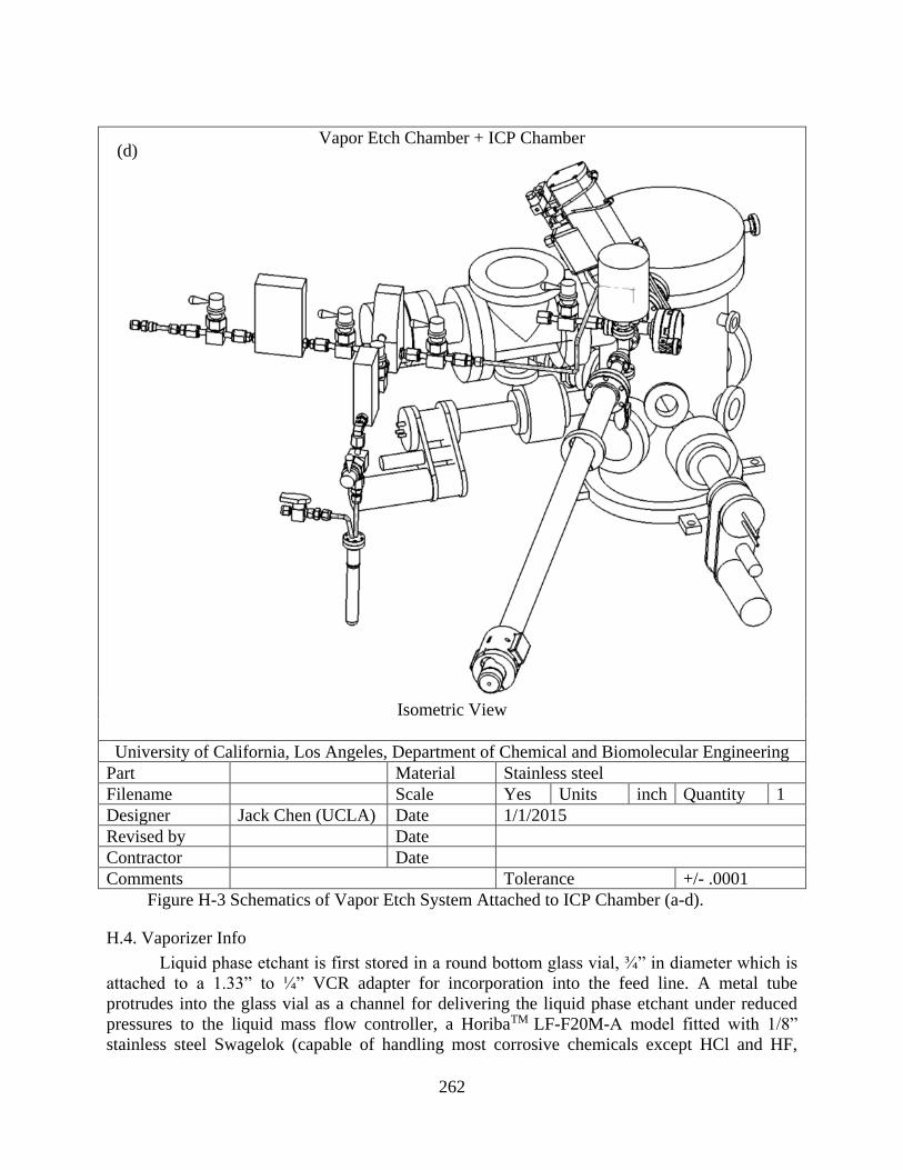
262
Vapor Etch Chamber + ICP Chamber
Isometric View
University of California, Los Angeles, Department of Chemical and Biomolecular Engineering
Part Material Stainless steel
Filename Scale Yes Units inch Quantity 1
Designer Jack Chen (UCLA) Date 1/1/2015
Revised by Date
Contractor Date
Comments Tolerance +/- .0001
Figure H-3 Schematics of Vapor Etch System Attached to ICP Chamber (a-d).
H.4. Vaporizer Info
Liquid phase etchant is first stored in a round bottom glass vial, ¾” in diameter which is
attached to a 1.33” to ¼” VCR adapter for incorporation into the feed line. A metal tube
protrudes into the glass vial as a channel for delivering the liquid phase etchant under reduced
pressures to the liquid mass flow controller, a HoribaTM LF-F20M-A model fitted with 1/8”
stainless steel Swagelok (capable of handling most corrosive chemicals except HCl and HF,
(d)

263
generally) and 1/8” Swagelok to ¼” VCR fittings for vacuum compatibility. This allows for
metered feeding up to mass flow rates of 0.1 g/min of the liquid phase etchant at temperatures
varying from 5-50ºC into the vaporizing unit.
Figure H-4 Liquid injection method utilizing heating element to vaporize liquid
flow and introduce to vacuum chamber (Image courtesy of STEC Inc)
To aid in the delivery of the vaporized gas output, an inert gas input is recommended as a
secondary input to the vaporizer unit. For these studies, ultra-high purity N2 will be used at
flowrates controlled via a HoribaTM SEC-E40 gas MFC with maximum flowrates of 100 sccm.
This MFC contains two 1/4” VCR connections, eliminating any need for adapters between the
N2 MFC and vaporizer. With both of these MFC units connected to the M1-1141-PN, resulting
vapor can be delivered at flowrates of up to 3cm3/min (rated with ispropanol) at temperatures of
up to 140ºC. This delivery temperature is sufficient for complete vaporization of the organic
chemicals of interest to the study.

264
I. Ion Source Chamber
PLEASE SEE ATTACHED DIAGRAM AT THE END OF THE EMERGENCY SHUT
DOWN FOR LOCATION OF VALVES, GAS AND PUMPS, IF PICTURE IS NOT
PROVIDED!
I.1 Troubleshooting
1. In case a noise is heard from turbo molecular pumps on Main Chamber
a. Close manual gate valves between turbo pumps and chamber and the pneumatic gate
valve between top turbo pump and ion gun.
Manual
Gate Valve
Manual
Gate Valve

265
Figure I-1 Gate valves for turbo pumps.
b. Turn off the turbo molecular pumps by pushing the “stop” button on the two Leybold
controllers and the “stand by” button on the Pfeiffer controller.
Figure I-2 (a) Leybold controller for bottom turbo pump and mass spectrometer
turbo pump. (b) Pfeiffer controller for top turbo pump.
c. Isolate the turbo pumps by closing the three roughing valves between the TMPs and MP.
Stop
Button
Stand By
Button
(b) (a)
Roughing
Valve
Manual
Gate Valve

266
Figure I-3 Roughing valves between turbo pumps and mechanical pump.
2. In case a noise is heard from mechanical pump on chamber
a. Close the three manual gate valves between the TMPs and the chamber and the pneumatic
gate valve between the ion gun and the TMP.
b. Turn off the turbo molecular pumps by pushing the “stop” button on the Leybold controller
and the “stand by” button on the Pfeiffer controller.
c. Switch off the mechanical pump by turning off the breaker switch on the power strip.
3. In case noises are heard from any of the electronics
a. If units have power switches turn them off, and unplug all units.
I.2. Operation Procedures for Ion Source Chamber
1. Pumping down the entire system (Note: The chamber’s default state should be pumped down;
check the pressure reading on the ion gauge to verify. The following steps should only be
taken if you aware that the chamber has been vented and not pumped back down).
a. THE FOLLOWING INTERLOCKS FOR THE PUMP DOWN PROCEDURE MUST BE
MET TO BEGIN PUMPING: COOLING WATER FOR MAIN CHAMBER TURBO
Roughing
Valve
Roughing
Valve

267
PUMP AND ION GUN TURBO PUMP MUST BE ON, COOLING WATER FLOW TO
COMPRESSOR SHOULD BE BETWEEN 2.3 AND 3.5 GPM).
b. Check that all the flanges are tightened and all the valves are in the closed position.
c. Check all the cables are correctly connected.
d. Check the oil level in the mechanical pump, which should be 2/3 full in view window.
e. Check MP and its exhaust for liquid leaks. (oil, condensation, exhaust fluid).
f. Check that the Baratron and thermocouple gauges are on and that the ion gauges are off.
g. Turn on MP by turning on the switch on the power strip. The thermocouple gauge reading
should start going down within 20 seconds. If not, turn off the pump and check
connections to chamber and turbopumps for vacuum leaks.
h. Slowly open the three roughing valves between the turbo pumps and mechanical pump.
Wait until Baratron gauge reaches ~10 mTorr.
i. Slowly open the two roughing valves between the chamber and the MP and between the
mass spectrometer and the MP.
Figure I-4 Roughing valves between the chamber and mechanical pump.
j. Wait until Baratron gauge reaches the base pressure ~10 mTorr. This process may take
several minutes if system was shut down for some time.
k. Slowly open manual gate valve between ion gun and main chamber.
l. Slowly open Ar gas line valve to purge the gas line.
m. After the Baratron gauge reads less than 10 mTorr, close the two roughing valves
between the chamber and the MP and between the mass spectrometer and the MP.
a. Before TMPs are turned on, check:
i. The cooling water is running.
ii. TC gauge reads less than 10 mTorr.
iii. Either the roughing valve between the chamber and MP or the roughing
valves between the TMPs and MP and gate valves between TMPs and
main chamber should be always CLOSED while the TMPs are on.
n. Turn on TMPs by pushing the start button on the Leybold controllers and the pumping
unit button on the Pfeiffer controller, unless already on. The green acceleration indicator
on the Leybold controllers should be on, and the rotation gauge on the Pfeiffer controller
should shift from red to green.
a. Within 5 minutes, the turbo molecular pumps should reach full speed. The
yellow indicator on the Leybold controllers should be on normal, and the
rotation gauge on the Pfeiffer controller should be in the solid green area.
Roughing
Valve Roughing
Valve
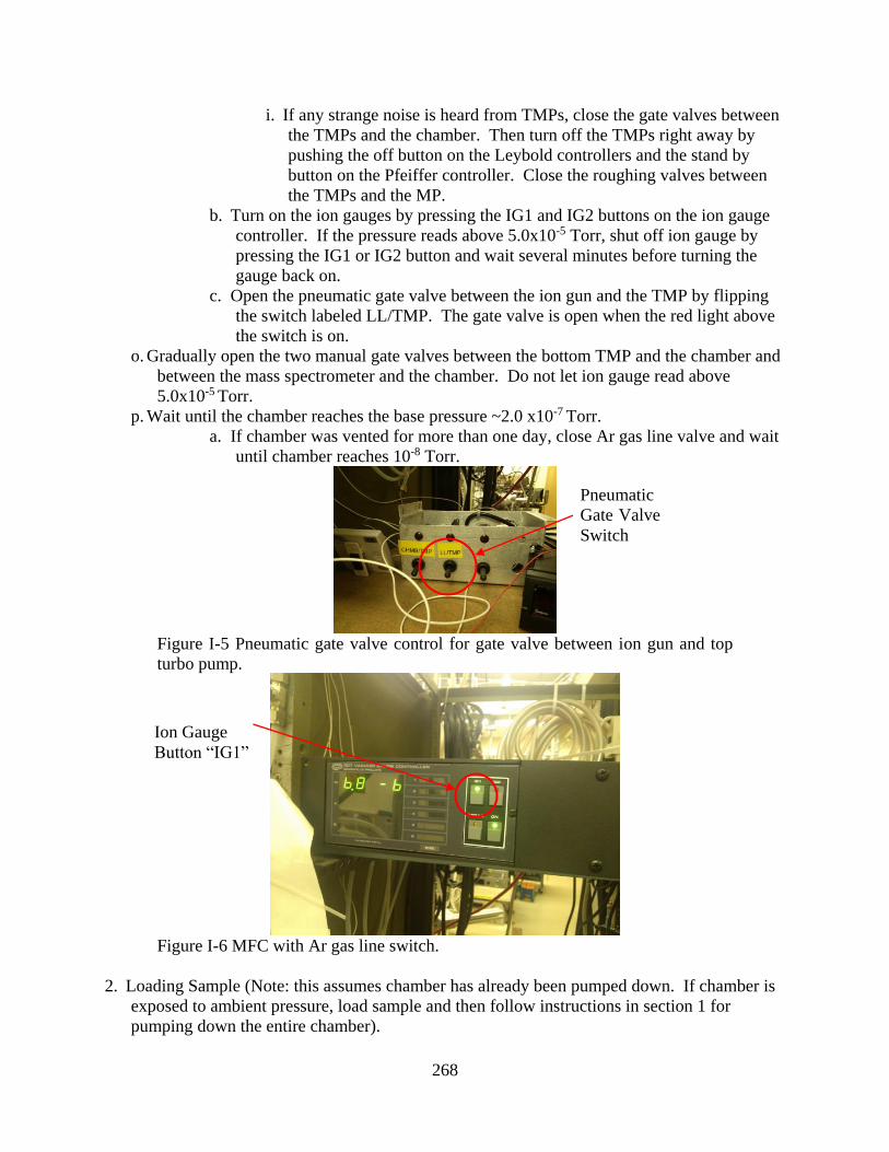
268
i. If any strange noise is heard from TMPs, close the gate valves between
the TMPs and the chamber. Then turn off the TMPs right away by
pushing the off button on the Leybold controllers and the stand by
button on the Pfeiffer controller. Close the roughing valves between
the TMPs and the MP.
b. Turn on the ion gauges by pressing the IG1 and IG2 buttons on the ion gauge
controller. If the pressure reads above 5.0x10⁻⁵ Torr, shut off ion gauge by
pressing the IG1 or IG2 button and wait several minutes before turning the
gauge back on.
c. Open the pneumatic gate valve between the ion gun and the TMP by flipping
the switch labeled LL/TMP. The gate valve is open when the red light above
the switch is on.
o. Gradually open the two manual gate valves between the bottom TMP and the chamber and
between the mass spectrometer and the chamber. Do not let ion gauge read above
5.0x10⁻⁵ Torr.
p. Wait until the chamber reaches the base pressure ~2.0 x10⁻⁷ Torr.
a. If chamber was vented for more than one day, close Ar gas line valve and wait
until chamber reaches 10-8 Torr.
Figure I-5 Pneumatic gate valve control for gate valve between ion gun and top
turbo pump.
Figure I-6 MFC with Ar gas line switch.
2. Loading Sample (Note: this assumes chamber has already been pumped down. If chamber is
exposed to ambient pressure, load sample and then follow instructions in section 1 for
pumping down the entire chamber).
Pneumatic
Gate Valve
Switch
Ion Gauge
Button “IG1”

269
a. Close the three manual gate valves between chamber and TMPs and the pneumatic gate
valve between the ion gun and the TMP by flipping the switch labeled LL/TMP.
b. Loosen black knob on loading door. The knob will be damaged if it is not loosened before
pressurizing the chamber.
c. Slowly open air inlet valve to chamber. Watch ion gauge reading to make sure the manual
gate valves are completely closed.
d. Wait until the loading door pops open. The chamber is now at ambient pressure.
e. Close air inlet valve to chamber.
f. Open loading door and load the sample.
g. Close loading door and hand tighten black knob.
h. Close the three roughing valves between the TMPs and the MP.
i. Gradually open the two roughing valves between chamber and MP and between mass
spectrometer and MP. Wait until Baratron gauge reads below 10 mTorr.
j. Gradually open manual gate valve between ion gun and main chamber.
k. Close the two roughing valves between chamber and MP and between mass spectrometer
and MP.
l. Open the three roughing valves between the TMPs and the MP.
m. Open gate valve between ion gun and TMP by flipping switch labeled LL/TMP.
n. Gradually open the two manual gate valves between chamber and TMP and between mass
spectrometer and TMP. Do not let ion gauge read above 5.0x10⁻⁵ Torr.
o. Wait until chamber reaches base pressure 10-7 Torr.
3. Turning on the ion source controller (Note: the sample must already be loaded and the
chamber must be already pumped down).
a. Ensure the Ar gas line valve is open.
b. Turn off the ion gauges by pressing the IG1 and IG2 buttons on the ion gauge controller if
they are on.
c. Turn on the Ar gas switch on the MFC. The Baratron gauge should read ~0.30 mTorr.
d. Turn on power switch on ion source controller.
e. Turn on left source beam switch. Do not turn on the right source beam switch yet.
f. Hold down discharge switch to the voltage setting and adjust the discharge dial until the
monitor reads 40.0 V.
g. Hold up discharge switch to the current setting and adjust the cathode dial until the monitor
reads 0.25 mA.
h. Turn on right source beam switch.
i. Hold neutralizer switch to the emission setting and adjust the neutralizer dial until the
monitor reads a value close to the value displayed on the beam display. This value
should be about 5 mA.

270
Figure I-7 MFC with Ar gas line switch.
4. Turning off the ion source controller.
a. Turn the neutralizer, cathode, and discharge dials counter-clockwise until they stop.
b. Turn off the right source beam switch, then the left source beam switch.
c. Turn off the power switch.
d. Turn off Ar gas switch on MFC.
e. Turn on ion gauges by pressing the IG1 and IG2 buttons on the ion gauge controller.
Figure I-8 Ion source controller.
Cathode
Dial Source Beam
Switches
Power Switch
Ar Gas Line
Switch
Neutralizer
Dial
Discharge
Dial

271
I.3. Operating Procedure for Analysis (#6) in Professor Chang’s Lab
EQP QMS
Emergency Shutdown
1. Turn off the filament and stop data acquisition from the software: In the MASsoft
Software Window, click the red button icon on the primary row of buttons, or select
“Shutdown” from the System Menu.
2. Switch off the power switches on the electronics (Green power button on the MSIU, large
middle button on cold cathode gauge controller – see picture below).
Operating Procedures
1. Check the QMS logbook for the previous scan and check the base pressure of the system, which
should be about 9*10-8 Torr. Write the base pressure in the logbook.
2. Plug the power cable into the RF generator (the electronic box next to the computer monitor) and
turn on the power switch of the MSIU unit on the bottom level of the cart. The switch should be
lighted green and a beep sound should be heard. Allow 30 min warm up before doing any
analysis. If the beep sound is continuous (longer than 1 s), turn the unit off and check for errors.
3. Open the operating software MASsoft.
Shutdown Button
System Shutdown
Cold Cathode
Gauge Power
Switch (Note:
Picture on the right
is a rear view of the
controller)
MSIU Power
Switch

272
4. Degas the filament (as necessary) by choosing the “system”, “maintenance”, and “degas”. The
desired the degas filaments and time can be chosen.
5. Set up the operation file. The new operation file can be generated by choose “file”, and “new”.
However, because the EQP parameters need to be consistent, it is suggested that one “open” an
existing file and “save as” to another filename. For neutral scan, double check the electron
energy and emission current, and make sure electron energy is not very low.
6. Start the experiment, for example, turn on and tune the plasma. It is very important to turn on the
plasma before turn on the filament for neutral scan. Otherwise, the filament will be broken.
7. Monitor the QMS pressure. The maximum operating pressure for QMS is 5*10-6 Torr.
8. Start the QMS scan by clicking the green circle in the top section of the window. A promotion
will ask you if you want to overwrite the current file or save to another filename. If the “open
and save as” procedure was followed in step 5, you may choose “overwrite”.
9. Monitor the scan and make sure the signal intensity is not too high (close to 1*107).
10. The scan can be terminated automatically or manually. To terminate the scan automatically, the
proper scan cycle can be set in the operation file. To terminate the scan manually, click the
yellow circle next to the starting green circle. The scan will stop after the current cycle is
finished. The scan can also be terminated immediately by clicking the red circle next to the
yellow circle. However, the data will not be saved in this way.
11. After finishing all the experiments, close MASsoft and transfer all the data files to the server.
12. Turn off the power to the electronics following the reversed procedure in step 2.
13. Check the base pressure of QMS and bake it as necessary.
14. Finish the logbook.

273
I.4. Install and Test EQP QMS System
August-September 2001
Make sure the EXP pressure is ALWAYS < 5x10⁻⁶ Torr
Make sure the count rates are < 5x10⁶ cts/s
Make sure the electron energy is tuned so that the filament current is not too high
Need to connect CCG to the trig connector on MSIU (trig pressure < 5x10⁻⁶ Torr)
Problems
(1) H2O dominates the RGA spectra after striking a plasma (mass peak splits due to saturation)
(2) Ar+(40) dominates the +ion SIMS spectra (energy peak splits due to saturation --> de-tune
the system)
Use isotope whenever possible to AutoTune (Ar36)
Extl.actor energy should not be changed
Use Lens 1 and Lens 2 energies to de-tune the signal as they won't affect the IED
(Multiplier voltage is also effective)
Focus 2 energy can also be adjusted
(3) Mass peaks of O2 and O splits in 900 W plasma (tune Lens 2, set Vert, Horiz, and DC Quad
to 0)
(4) S/N: Use ms rather than % in Dwell Time to better control the S/N ratio, Use
“Accumulation” and “Mean”
(5) Computer crash “Error Detected in MemFreePtr[117F:0032]”, “Error at or near addresses
117F:0000”
a. Obtain base pressure < 6x10⁻⁵ Torr
b. (Aug. 31). Check Base Pressure, EQP:2.5-6x10⁻⁷ Torr; PECVD: 3.8x10⁻⁶ Torr
c. Cold cathode gauge failed
d. Turbo pump failed
e. Switched the PECVD turbo pump with the EQP turbo pump
f. Connect all cables (some were labeled incorrectly, now corrected.)
g. The computer need to be > 200 MHz
h. Connect the computer with the EQP using RS232 cable
Installation
1. Install software: MASSoft (one CD and one System disk) –
MASSoft\wr11029\ 5 Tune files
(Master, NegTune, nRGATune, PosiTune, and RGATune)
2. Read ReadMe and Initialization file
3. Program
a. INI file editor --If re-setup computer with the 10-base T connection, change
NoOfAddresses in Initialization file from "0" to" 1 "
b. 3b. Terminal (Hyper Terminal) --Need to turn on MSIU first to establish the
connection
type "help [return]" (to get all information about Interface Unit)
Important parameters: AutoTuneWindow, AutoTuneThreshold, and
AutoTuneMinimum
type "pget AutoTuneWindow [return]" to get the value for AutoTuneWindow

274
type "pget AutoTuneThreshold [return]" to get the value for AutoTuneThreshold
type" pget AutoTuneMinimum [return]" to et the value for AutoTuneMinimum
Hiden tested setting Default
AutoTuneWindow 2 7
AutoTuneThreshold 50 500
AutoTuneMinimum 50 0
AutoTuneMaximum ? 500
type "pset AutoTuneMinimum [return]" to set the value for AutoTuneMinimum
4. The system does not have Suppressor, and the source focus is connected to DAC (pp. 210-
211)
5. Scan:
BAR
PROFILE
MID
LEAK DETECT
MAP
SURFACE
6. Red-LED in RF Generator indicating tuning is needed
7. Tune the RF Generator
1) Open the cover of RFG
2) Using multimeter to measure the voltage(DC) between TP25 (or TP24) and
TP36(GND), V=O0
3) Go to Hyper Terminal
type "Iget mass 5.50"
type "Iset mass 0.4 "
Adjust the turning screw head on the front panel of the RFG
type "Iset mass 0.4", measure V =0.05v
type "Iset mass I ", V= 0.05v
type "Iset mass 2", V= 0.05v
type "Iset mass 3", v= 0.05v
type "Iset mass 4", V= 0.05v
type "Iset mass 3", v= 0.05v
type "lset mass 3.5", v= 0.05v
V doesn't change!
4) Suspect the electronics inside the RFG or the EQP Head have faults
5) Remove the Amplifier from the EQP Head
6) Open the cover of the EQP Head
7) Check the Quadropole, measure the resistance between the top 4 connectors inside
the head
make sure none of the poles shorts to the ground
8) Quadrupole is OK
9) Open the RFG again, take out the circuit boards together with the coil
10) The wires connecting with the Coil are both BROKEN!
11) Weld the broken wires
12) Connect the RFG and the EQP Head again

275
13) Tune the RFG again
14) Go to Hyber Terminal
15) "lget mass" 3.0
Iset mass Voltage TP25 TP36
0.4 (min mass) ? (10 mV)
1 0.004v
5 ?
10 ?
50 ?
100 ?
200 ?
500 0.344v
1000 (max mass) 0.714v (~700mV)
16) Now the RFG tuning is done
8. Run MASsoft application
1) Scan: mass 0.4 50
2) There are peaks appearing. But the peaks do not correspond the correct masses
3) Tune the RFG again.
Open the cover of RFG
Adjust the RV 1 potentiometer on the circuit board (3 next to a red wire) ????
By adjusting the screws, the peaks can shift.
Scan mass: 0.4 --> 10, check the peaks
Scan mass: 13 --> 23, refer the peak around m=18.0, adjust the screw, make the
peak shift to m=18
Scan mass: 144 --> 154, check the peaks
Scan mass: 164 --> 174, check the peaks
m = l47 and m= 167 are filament material peaks, but they will disappear
eventually ???
4) Tune the RGA mode ? Need to check with Byeong and Alex
5) Test RGA mode with air only; OK
6) Test RGA mode with Ar flowing in, pressure = 3.0mT; OK
7) Test RGA mode with Ar + O2, pressure = 5 .0mT , OK
8) Test to get the appearance potential, OK
9) Tune the +ion SIMS mode ? ? ? Need to check with Byeong and Alex
10) Test +ion SIMS mode with Ar + O2 plasma, pressure = 7.8mT, OK
11) Test the function of NEUTRAL analysis in plasma
In RGA mode
Set Extractor = +50V
Set Len 1 = -10 ~ -20V
Other parameters keep the same
* The m = 18 peak is too high, ~1.4x10⁷ c/s
Turn off the plasma in PECVD, the peak is still high
* Suspect the filament is covered by some material
-Degas the filament. (How???)
* Suspect there is too much H2O inside the EQP chamber

276
Keep scanning and monitoring the m =18 peak, for ~1 hr, the intensity 1.4x10⁷
1.8 x 10⁶
*** The procedure of testing, refer to the MASsoft manual
9. AutoTune
3 scans or so
System --> Maintanence --> AutoTune
Select Mass, Select Mode to be Tuned
Ex: +ion Mass (save to PSIMSTUN.exp on 09/03/2001)
a. Energy: 0 to 30, it is important to do the energy scan for different conditions to
maximize the signal intensity as the IEDF changes significantly with conditions
(chemistry, power, bias, etc.)
b. Lens 1: -370 to 0 (once the scan starts, can reduce the range, for example to -140
in one case)
c. Lens 2: -200 to -50 (can not be set to ZERO!)
(once the scan starts, can reduce the range, for example to -140 in one case)
d. Focus 2: -360 to 0 (once the scan starts, can reduce the range, for example to -300
in one case)
Use Lens I, Focus2, Lens 2 to de-tune the signal, as they won't affect the IED
10. Manual Tune --> Chang save option to "Manual Selection" to avoid software crashing during
manual tuning
(This should not be done if the system is tuned.
This was done when we didn't realize the peak splitting was due to signal saturation)
Fine Tune (Plates, Lens 2, Vert, Horiz, Axis, Energy, DC Quad)
+- 2V for DC Quad (correspond to 100% to -100%)
+- 4V for Vertical and Horizontal (correspond to 100% to -100%)
Change a few % on DC Quad, Vert, and Horiz
Chang Horiz from 0% to -16% affected the IED significantly
Generate a co-variance plot (Horiz -16 to 0 and energy 0 to 25) cycle=l, l00 ms,
FineTunl.exp
11. Electron attachment for 0 (high pressure at 400 mtorr , e- ~ 10 e V) ?
12. Integrate the mass over the energy
Control Schemes
Shutdown Events
Global: RGA/SIMS
SEM (detector) Scan 1: mass/f(x)
Stop (Continuous, cycles, shutdown after scan)

277
Global Environment (Before Dec, 2005)
RGA Min Max Current Setpoint Note
Multiplier 0 3000 1800 V increase up to 2200 V
1st dynode -1200 1200 -1200 V
Resolution -100 100 0 % for > 100 amu
Delta-M -100 100 0 amu for < 100 amu
Discriminator -100 100 -10 %
Mass 0.4 1000 18 amu sit on a mass for energy analysis
Rate_selection 0 1 0 c/s
Reference -1000 1000 0 V see pp. 211, ref. Voltage adjustment
Emission 0.2 2000 100 microA de-sensitize the instrument
Electron Energy 0 150 70 V set to very small for electron
attachment
Cage (ion
collector)
-10 10 3 V set to –25 V at the end of the scan
Source focus -370 370 -340 V
Focus 2 -360 360 -356 V
Extractor -370 370 0 V
Lens 1 -370 370 0 V
Plates -20 20 7.27 V 45o energy filter (see pp. 213)
Lens 2 -360 360 -104 V
Vertical -100 100 12 %
Horizontal -100 100 5 %
Axis -90 90 -40 V
Energy -100 100 3.85 V
D. C. Quad -100 100 2 %
Transit energy -10 10 3 V
Mode-change
delay
0 2.1E+09 1000 ms switch between modes, eg. SIMS
and RGA
+ ion SIMS Min Max Current Setpoint Note
Multiplier 0 3000 1800 V
1st dynode -1200 1200 -1200 V
Resolution -100 100 0 % for > 100 amu
Delta-M -100 100 0 amu for < 100 amu
Discriminator -100 100 -10 %
Mass 0.4 1000 18 amu sit on a mass for energy analysis
Rate_selection 0 1 0 c/s
Reference -1000 1000 0 V see pp. 211, ref. Voltage adjustment
Emission 0.2 2000 100 microA de-sensitize the instrument
Electron Energy 0 150 70 V set to very small for electron
attachment
Cage (ion
collector)
-10 10 0 V set to –25 V at the end of the scan

278
Source focus -370 370 0 V
Focus 2 -360 360 -264 V
Extractor -370 370 -2 V
Lens 1 -370 370 -76 V
Plates -20 20 7.27 V 45o energy filter (see pp. 213)
Lens 2 -360 360 -95 V
Vertical -100 100 0 %
Horizontal -100 100 0 %
Axis -90 90 -40 V
Energy -100 100 14 V
D. C. Quad -100 100 0 %
Transit energy -10 10 3 V
Mode-change
delay
0 2.1E+09 1000 ms switch between modes, eg. SIMS
and RGA
-ion SIMS Min Max Current Setpoint Note
Multiplier 0 3000 1800 V
1st dynode -1200 1200 800 V
Resolution -100 100 0 % for > 100 amu
Delta-M -100 100 0 amu for < 100 amu
Discriminator -100 100 -10 %
Mass 0.4 1000 18 amu sit on a mass for energy analysis
Rate_selection 0 1 0 c/s
Reference -1000 1000 0 V see pp. 211, ref. Voltage adjustment
Emission 0.2 2000 100 microA de-sensitize the instrument
Electron Energy 0 150 70 V set to very small for electron
attachment
Cage (ion
collector)
-10 10 0 V set to –25 V at the end of the scan
Source focus -370 370 0 V
Focus 2 -360 360 340 V
Extractor -370 370 50 V
Lens 1 -370 370 201 V
Plates -20 20 -7.27 V 45o energy filter (see pp. 213)
Lens 2 -360 360 119 V
Vertical -100 100 0 %
Horizontal -100 100 0 %
Axis -90 90 40 V
Energy -100 100 -16.6 V
D. C. Quad -100 100 0 %
Transit energy -10 10 -3 V
Mode-change
delay
0 2.1E+09 1000 ms switch between modes, eg. SIMS
and RGA

279
-ion RGA Min Max Current Setpoint Note
Multiplier 0 3000 1800 V
1st dynode -1200 1200 800 V
Resolution -100 100 0 % for > 100 amu
Delta-M -100 100 0 amu for < 100 amu
Discriminator -100 100 -10 %
Mass 0.4 1000 18 amu sit on a mass for energy analysis
Rate_selection 0 1 0 c/s
Reference -1000 1000 0 V see pp. 211, ref. Voltage adjustment
Emission 0.2 2000 20 microA de-sensitize the instrument
Electron Energy 0 150 1.9 V set to very small for electron
attachment
Cage (ion
collector)
-10 10 -3 V set to –25 V at the end of the scan
Source focus -370 370 367 V
Focus 2 -360 360 353 V
Extractor -370 370 0 V
Lens 1 -370 370 0 V
Plates -20 20 -7.27 V 45o energy filter (see pp. 213)
Lens 2 -360 360 108 V
Vertical -100 100 0 %
Horizontal -100 100 0 %
Axis -90 90 40 V
Energy -100 100 -3.7 V
D. C. Quad -100 100 0 %
Transit energy -10 10 -3 V
Mode-change
delay
0 2.1E+09 1000 ms switch between modes, eg. SIMS
and RGA
Global Environment (Oct 10, 2006)
RGA, tuned for mass 70 in a Cl2/BCl3 plasma(Oct 10, 2006)
RGA Min Max Current
Setpoint
Note
Multiplier 0 3000 3000 V ( increase up to 2200 V)
1st dynode -1200 1200 -1200 V
Resolution -100 100 0 % for > 100 amu
Delta-M -100 100 0 amu for < 100 amu
Discriminator -100 100 -10 %
Mass 0.4 1000 70 amu sit on a mass for energy analysis
Rate_selection 0 1 0 c/s
Reference -1000 1000 0 V see pp. 211, ref. Voltage adjustment
Emission 0.2 2000 100 microA de-sensitize the instrument
Electron Energy 0 150 70 V set to very small for electron
attachment

280
Cage (ion
collector)
-10 10 3 V set to –25 V at the end of the scan
Source focus -370 370 -295 V Parameter tuned
Focus 2 -360 360 -138 V Parameter tuned
Extractor -370 370 50 V Not Tuned
Lens 1 -370 370 -15 V Not Tuned
Plates -20 20 7.27 V 45o energy filter (see pp. 213)
Lens 2 -360 360 -89 V Parameter tuned
Vertical -100 100 8 % Parameter tuned
Horizontal -100 100 2 % Parameter tuned
Axis -90 90 -40 V
Energy -100 100 -3.05 V Parameter tuned
D. C. Quad -100 100 20 % Parameter tuned
Transit energy -10 10 3 V
Mode-change
delay
0 2.1E+09 1000 ms switch between modes, eg. SIMS
and RGA
Ion SIMS: Tuned for Mass 40 aum (Oct 10, 2006)
+ ion SIMS Min Max Current Setpoint Note
Multiplier 0 3000 3000 V
1st dynode -1200 1200 -1200 V
Resolution -100 100 0 % for > 100 amu
Delta-M -100 100 0 amu for < 100 amu
Discriminator -100 100 -10 %
Mass 0.4 1000 18 amu sit on a mass for energy analysis
Rate_selection 0 1 0 c/s
Reference -1000 1000 0 V see pp. 211, ref. Voltage adjustment
Emission 0.2 2000 100 microA de-sensitize the instrument
Electron Energy 0 150 70 V set to very small for electron
attachment
Cage (ion
collector)
-10 10 0 V set to –25 V at the end of the scan
Source focus -370 370 -352 V Parameter tuned
Focus 2 -360 360 -307 V Parameter tuned
Extractor -370 370 -20 V Parameter tuned
Lens 1 -370 370 -237 V Parameter tuned
Plates -20 20 7.27 V 45o energy filter (see pp. 213)
Lens 2 -360 360 -141 V
Vertical -100 100 77 % Parameter tuned
Horizontal -100 100 3 % Parameter tuned
Axis -90 90 -40 V
Energy -100 100 V Parameter tuned
D. C. Quad -100 100 -88 % Parameter tuned
Transit energy -10 10 3 V

281
Mode-change
delay
0 2.1E+09 1000 ms switch between modes, eg. SIMS
and RGA
Ion SIMS: Tuned for Mass 320 aum (Oct 10, 2006)
+ ion SIMS Min Max Current Setpoint Note
Multiplier 0 3000 3000 V
1st dynode -1200 1200 -1200 V
Resolution -100 100 0 % for > 100 amu
Delta-M -100 100 0 amu for < 100 amu
Discriminator -100 100 -10 %
Mass 0.4 1000 320 amu sit on a mass for energy analysis
Rate_selection 0 1 0 c/s
Reference -1000 1000 0 V see pp. 211, ref. Voltage adjustment
Emission 0.2 2000 100 microA de-sensitize the instrument
Electron Energy 0 150 70 V set to very small for electron
attachment
Cage (ion
collector)
-10 10 0 V set to –25 V at the end of the scan
Source focus -370 370 -225 V Parameter tuned
Focus 2 -360 360 -302 V Parameter tuned
Extractor -370 370 -16 V Parameter tuned
Lens 1 -370 370 -240 V Parameter tuned
Plates -20 20 7.27 V 45o energy filter (see pp. 213)
Lens 2 -360 360 -141 V
Vertical -100 100 37 % Parameter tuned
Horizontal -100 100 7 % Parameter tuned
Axis -90 90 -40 V
Energy -100 100 V Parameter tuned
D. C. Quad -100 100 -69 % Parameter tuned
Transit energy -10 10 3 V
Mode-change
delay
0 2.1E+09 1000 ms switch between modes, eg. SIMS
and RGA

282
Scan Editor
Scan Mode Global (RGA)
RGA
+ion SIMS
-ion SIMS
- ion RGA
Scan legend mass
f(x)
electron-energy
Source focus
focus 2
Extractor
Lens1
Lens2
Axis
Energy
(Can also create new terms, such as scanning multiplier)
Start Stop
Stop
Increment
Step
Advance Option RestartAutoRange
NoDeferAutoRange
SaveScanDevice --> Reset after each scan
BeamOnBefore --> Turn on the beam before each scan
BeamOffAfter --> Turn off the beam after each scan
YieldToEvents
Accumulate --> Useful for low intensity ions (e.g. neg.
ion)
Mean --> Useful for low intensity ions (e.g. neg. ion)
ScanRest None
Align
AutoTune
Max
Sum
Top
XvalAtMaxY
Input Selection
SEM Start c/s
raw-counts Highest c/s
auxiliary I Lowest c/s
auxiliary 2 Dwell Time % or ms --> Time spent at each point
f (x) Settle Time % or ms --> Time between two sets of scans

283
Discussions with Peter Hatton
CC gauge
RFG
Filament material
IED
H2O dominates the spectra
Heat the EQP Head
Tech Support: Allen Reese, Claire Greenwood
Improve the S/N: Use ms rather than %

284
I.5. Schematics
Ion Source Chamber
Isometric View
University of California, Los Angeles, Department of Chemical and Biomolecular Engineering
Part Material Stainless steel
Filename Scale Yes Units inch Quantity 1
Designer Jack Chen (UCLA) Date 1/1/2015
Revised by Date
Contractor Date
Comments Tolerance +/- .0001
(a)

285
Ion Source Chamber
Side View
University of California, Los Angeles, Department of Chemical and Biomolecular Engineering
Part Material Stainless steel
Filename Scale Yes Units inch Quantity 1
Designer Jack Chen (UCLA) Date 1/1/2015
Revised by Date
Contractor Date
Comments Tolerance +/- .0001
(b)

286
Ion Source Chamber
Front View
University of California, Los Angeles, Department of Chemical and Biomolecular Engineering
Part Material Stainless steel
Filename Scale Yes Units inch Quantity 1
Designer Jack Chen (UCLA) Date 1/1/2015
Revised by Date
Contractor Date
Comments Tolerance +/- .0001
Figure I-10 Ion Source Chamber Schematics (a-c).
(c)

287
J. Superconducting quantum interference device (SQUID)
J.1. Introduction
Superconducting quantum interference device (SQUID) is a magnetometer that measures
magnetization (M) as a function of the applied field (H). A hysteresis loop can be plotted to
extract information regarding the magnetic properties of the film. For example, coercivity, Hc, is
the horizontal intercept of the hysteresis curve. It is the applied field necessary to change the
direction of magnetization within the domains of the material. It indicates the stability of
magnetization in the material. The saturation magnetization, Ms, is the maximum magnetization
of a material dM/dH=0. It indicates the magnetic strength a material. The enabling phenomenon
behind SQUID is the Josephson junction.
Figure J-1 Diagram of Josephson junction utilizing a superconducting loop with
two parallel non-superconducting sections.
The Josephson junction is a superconducting loop separated by two parallel pieces of
non-superconducting material (Figure 1). Electrons tunnel through the non-superconducting
material in the form of Cooper pairs, electrons that are bound together in a very low energy state
that allows for long range interaction over hundreds of nanometers (Allender, Bray et al. 1973).
This interaction is very weak, on the order of 0.001 eV, and requires reduced temperatures since
small amounts of thermal energy can break it.
An applied current, I, is split equally across the two parallel branches. If a magnetic field
is applied, a screening current, Is, is circulates the loop resulting in a magnetic flux equal but
opposite of the external magnetic flux (Bardeen, Cooper et al. 1957). This induced current
travels in the same direction as current in one branch, and opposite in the other, causing two
different currents across the parallel non-superconducters Equations 1 and 2.
(1)
and
(2)
Once a threshold current is reached, a measurable voltage appears across the junction. If
the magnetic flux exceeds φ0/2, or half of the magnetic flux quantum, the system will

288
energetically favor an increase in this value to an integer of φ0, which results in the current
flipping direction. This phenomenon causes the current to oscillate as a function of the applied
magnetic flux. Equation 3 represents the magnetic flux quantum, where h is Planck’s constant
and e is the elementary charge.
tesla-m2 (3)
The SQUID device has two Josephson junctions, at either end of the device. By
maintaining a constant current within the SQUID, the measurable voltage will fluctuate at each
of the two Josephson junctions, allowing for the oscillation to be correlated to the amount of
magnetic flux through the sample. Equation 4 is the resulting voltage change, which is dependent
on the resistance, R, and the loop’s inductance, L, as well as the change in the magnetic flux
quantum, Δφ.
(4)
To measure the magnetic properties via SQUID, the sample is first moved up and down
between two electromagnets to change the applied field. A pair of sensory coils around the
sample measures the voltage. For these measurements, a Quantum Design Magnetic Property
Measurement System (MPMS) XL was used. This tool only measures the total magnetization, so
data must be normalized by the volume of magnetic material, excluding the substrate. Due to the
diamagnetic influence of air within the sample holder as well as the response generated from the
silicon substrate, it is necessary to first perform a linear fit of the raw data at either very high or
very low fields. The diamagnetic response can be subtracted from raw data to obtain the
magnetic measurement of the sample.
J.2. SQUID Operating Procedure
Sample preparation
1. Put on clean pair of gloves. Obtain drinking straw, remove wrapper.
2. Using diamond scribe, cleave sample of interest into a 5mm x 5mm square
3. Record dimension of sample using digital calipers
4. Calculate and make a note of the volume of magnetic film in cm3 by taking product of
calculated sample area and film thickness
5. Obtain a pill capsule, pull apart the two halves, and insert the sample into the inner half of
the capsule. It may be necessary to gently squeeze the capsule to accommodate larger
samples.
6. Once the sample has been placed inside, releasing the capsule should hold the sample
upright by tension of the capsule wall. Rejoin the two halves and insert the capsule into
the straw
7. Using a metal rod, gently push the capsule into an eye-balled center of the straw.
8. Using a fine-tipped permanent marker, label the very top of the straw with the date and
sample information
Sample loading
1. Check the MPMS MultiVu Application window at the bottom to determine the current
state of the SQUID machine.
2. If the temperature is below 298 K, left-click System (see photo, outlined in red)

289
3. The “Temperature Parameters” window will appear.
4. Under “Control” change “Set Point” value to 298. Change “Rate” to 10 K/min. Left-click
“Set” button.
Figure J-2 Example SQUID MPMS MultiVu Application window. Outlined in
red is the System temperature. Left-clicking here will bring up the Temperature
Parameter window.
5. The temperature must reach a minimum 100K before the sample can be loaded. Otherwise
a “Remove Servo Sample” window will display saying that “The sample space is too cold
to be safely opened.”
Figure J-3 Remove Servo Sample window will appear when the system
temperature is below 100K while trying to remove a sample.
6. The SQUID machine will make a clicking noise and while observing the loading port, the
top of the sample insertion rod should become visible—generally the top consists of a
small blue cylindrical piece at the top. This can be seen through the clear plastic housing.
7. Remove the top piece sealing the loading port and turn it over.
8. Screw the threaded white plastic portion into the top of the sample loading rod and
carefully remove the rod from the SQUID chamber. If a sample was previously in the
chamber, it will appear mounted to the end of the loading rod. Carefully remove it from
the bottom of the rod and place it on the SQUID machine housing next to the computer.
9. Before mounting on the rod, carefully pierce the straw, making three of holes radially
around the sample. Do this two more times, each time making the set about 1.5 cm from
the last.

290
Figure J-4 (a) SQUID loading chamber with sealing top piece, (b) centering rod,
piercing tool, and straw with inserted pill capsule and sample, and (c) loading rod
with blue cylindrical top piece.
10. Avoid piercing the capsule as it can crack and break, releasing the sample and causing it
to fall out of the straw.
11. Taking the sample to be scanned, gently push the top of the straw onto the peg at the
bottom of the loading rod.
12. Insert the second plug on the bottom of the sample straw.
13. Re-insert the loading rod into the SQUID loading chamber until it is just barely visible,
the exact same position was when it was unloaded.
14. Replace the sealing topper, ensuring that the o-ring makes good contact with the port.
15. Press the black button labeled “Purge”. The SQUID will cycle through purging the
chamber with helium until a green light is illuminated indicating that the port has been
purge and is ready to load.
16. Left-click “Center” “RSO…” “Initialize Transport" to load the sample. The sample
loading rod can be observed descending into the chamber.
17. Next the sample must be centered. Left-click “Center” to perform the centering scan. A
window will appear showing both a fitted regression (blue) and the measured data (red).
The key is to have the blue fit overlapping with red data in a Gaussian shaped peak at the
ideal centered distance (x-axis).
18. Adjust the position manually to 3.5 and scan, this will seek out the more sensitive bottom
coil and establish a lower limit to the position
19. Ensure that the box is checked, adjust the position manually again to 3.5 and scan
20. At this point, the program should have lined up the maximum or minimum from the scan.
21. Using the value automatically populated in the field, click Adjust position (without
inputting 3.5)
22. The result should be that the fit and data should overlap and the sample will be
sufficiently centered in between the coils.
(a) (b) (c)

291
K. Copper Volatility Diagram Construction
K.1. Introduction
A volatility diagram is a suitable method for studying the dry etching of solid materials, and it
can be constructed from knowledge of the reaction thermodynamics of a particular system. For
the etching of copper by chlorine, the relevant reactions can be found in Table K-1.
The relationship between the pressure of each gas phase Cu-Cl compound and the pressure of Cl2
can be determined from expressions for the equilibrium constant of each reaction. Examples of
this for each reaction listed in Table K-1 can be found below.
Table K-1 Table of relevant reaction for Cu-Cl systems, reproduced from
(Kulkarni, et al., 2002).
K.2. Example Calculations
For Cu(g) only:
(1)
(2)

292
(3)
(4)
(5)
For CuCl2(g) only:
Eq. 1 and 2.
(6)
(7)
(8)
For CuCl2(g) only:Eq. 1 and 2.
(9)
(10)
(11)
For Cu3Cl3(g) only:Eq. 1 and 2.

293
(12)
(13)
(14)
Each of these equations can be plotted together to produce a volatility diagram for the system of
Cu and the species in question. Volatility diagrams for each gas can be found below in Fig. K-1-
K-4. A volatility diagram for all species can be found in Fig. K-5. MATLAB code for calculating
and producing these plots can be found following Fig. K-5.

294
K.3. Volatility Diagrams
Figure K-1. Volatility diagram for Cu(g) only.
-80 -60 -40 -20 0-80
-60
-40
-20
0
20
(8)(6)
(7)
FB
CuCl(g)
CuCl2(c)CuCl(c)
Lo
g P
Cu
Cl
Log PCl2
T=50oC
Cu(c)
Figure K-2. Volatility Diagram for CuCl(g) only.
-80 -60 -40 -20 0-80
-60
-40
-20
0
20
(11)
(9)
(10)
G
C
CuCl2(g)
CuCl2(c)CuCl(c)
Lo
g P
Cu
Cl2
Log PCl2
T=50oC
Cu(c)
Figure K-3 Volatility diagram for CuCl2(g) only.

295
-80 -60 -40 -20 0-80
-60
-40
-20
0
20
(14)
(12)
(13)
HD
Cu3Cl
3(g)
CuCl2(c)CuCl(c)
Lo
g P
Cu
3C
l3
Log PCl2
T=50oC
Cu(c)
Figure K-4 Volatility diagram for Cu3Cl3(g) only.
-80 -60 -40 -20 0-80
-60
-40
-20
0
20
K I
O
CuCl2(g)
Cu(g)
CuCl(g)
Cu3Cl3(g)
H
D
Cu3Cl3(g)
CuCl2(c)CuCl(c)
Lo
g P
Cu
xC
ly
Log PCl2
T=50oC
Cu(c)
N
M
Figure K-5 Volatility diagram for entire CuxCly system.

296
K.4. Matlab Code
Matlab code for constructing these diagrams at T = 50ºC can be found below: %% Set up log(P_Cl2), log(K), and log(P_gas_species) (rxn) logPCl2 = linspace(10,-80,1000); logK = [19.17 8.34 -47.63 -66.80 -75.13 -9.91 -29.09 -37.43 8.16 -11.02 -
19.36 39.61 -17.91 -42.93]; rxn = {-2*logK(1); -2*logK(2); logK(3); logK(4)-0.5*logPCl2; logK(5)-logPCl2; logK(6)+0.5*logPCl2; logK(7); logK(8)-0.5*logPCl2; logK(9)+logPCl2; logK(10)+0.5*logPCl2; logK(11); logK(12)+1.5*logPCl2; logK(13); logK(14)-1.5*logPCl2};
%% For Cu(g) only xmin = -80; xmax = 10; ymin = -80; ymax = 30;
rxn1 = ones(1,2).*cell2mat(rxn(1)); rxn2 = ones(1,2).*cell2mat(rxn(2)); rxn3 = ones(1,length(logPCl2)).*cell2mat(rxn(3)); rxn4 = cell2mat(rxn(4)); rxn5 = cell2mat(rxn(5));
[L1] = InterX([rxn1; [ymin ymax]],[logPCl2; rxn3]); [L2] = InterX([rxn2; [ymin ymax]],[logPCl2; rxn4]);
l1x = [L1(1) L1(1)]; l1y = [L1(2) ymax]; l2x = [L2(1) L2(1)]; l2y = [L2(2) ymax]; l3x = [xmin L1(1)]; l3y = [L1(2) L1(2)]; l4x = [L1(1) L2(1)]; l4y = [L1(2) L2(2)]; l5x = [L2(1) xmax]; l5y = [L2(2) ymin];
plot(l1x,l1y,l2x,l2y,l3x,l3y,l4x,l4y,l5x,l5y);
axis([xmin xmax ymin ymax]); xlabel('Log P_{Cl_2}99 (atm)'); ylabel('Log P_(Amorim, Maciel et al.) (atm)'); legend('Reaction 1','Reaction 2','Reaction 3','Reaction 4','Reaction
5','Location','NorthWest');
%% For CuCl(g) only xmin = -80; xmax = 10; ymin = -80; ymax = 30;
rxn1 = ones(1,2).*cell2mat(rxn(1)); rxn2 = ones(1,2).*cell2mat(rxn(2)); rxn6 = cell2mat(rxn(6));

297
rxn7 = ones(1,length(logPCl2)).*cell2mat(rxn(7)); rxn8 = cell2mat(rxn(8));
[L1] = InterX([rxn1; [ymin ymax]],[logPCl2; rxn6]); [L2] = InterX([rxn2; [ymin ymax]],[logPCl2; rxn7]);
l1x = [L1(1) L1(1)]; l1y = [L1(2) ymax]; l2x = [L2(1) L2(1)]; l2y = [L2(2) ymax]; l3x = [xmin L1(1)]; l3y = [rxn6(length(rxn6)) L1(2)]; l4x = [L1(1) L2(1)]; l4y = [L1(2) L2(2)]; l5x = [L2(1) xmax]; l5y = [L2(2) rxn8(1)];
plot(l1x,l1y,l2x,l2y,l3x,l3y,l4x,l4y,l5x,l5y);
axis([xmin xmax ymin ymax]); xlabel('Log P_{Cl_2} (atm)'); ylabel('Log P_{CuCl} (atm)'); legend('Reaction 1','Reaction 2','Reaction 6','Reaction 7','Reaction
8','Location','NorthWest');
%% For CuCl2(g) only xmin = -80; xmax = 10; ymin = -80; ymax = 30;
rxn1 = ones(1,2).*cell2mat(rxn(1)); rxn2 = ones(1,2).*cell2mat(rxn(2)); rxn9 = cell2mat(rxn(9)); rxn10 = cell2mat(rxn(10)); rxn11 = ones(1,length(logPCl2)).*cell2mat(rxn(11));
[L1] = InterX([rxn1; [ymin ymax]],[logPCl2; rxn9]); [L2] = InterX([rxn2; [ymin ymax]],[logPCl2; rxn10]);
l1x = [L1(1) L1(1)]; l1y = [L1(2) ymax]; l2x = [L2(1) L2(1)]; l2y = [L2(2) ymax]; l3x = [xmin L1(1)]; l3y = [rxn9(length(rxn9)) L1(2)]; l4x = [L1(1) L2(1)]; l4y = [L1(2) L2(2)]; l5x = [L2(1) xmax]; l5y = [L2(2) rxn11(1)];
plot(l1x,l1y,l2x,l2y,l3x,l3y,l4x,l4y,l5x,l5y);
axis([xmin xmax ymin ymax]); xlabel('Log P_{Cl_2} (atm)');

298
ylabel('Log P_{CuCl_2} (atm)'); legend('Reaction 1','Reaction 2','Reaction 9','Reaction 10','Reaction
11','Location','NorthWest');
%% For Cu3Cl3(g) only xmin = -80; xmax = 10; ymin = -80; ymax = 30;
rxn1 = ones(1,2).*cell2mat(rxn(1)); rxn2 = ones(1,2).*cell2mat(rxn(2)); rxn12 = cell2mat(rxn(12)); rxn13 = ones(1,length(logPCl2)).*cell2mat(rxn(13)); rxn14 = cell2mat(rxn(14));
[L1] = InterX([rxn1; [ymin ymax]],[logPCl2; rxn12]); [L2] = InterX([rxn2; [ymin ymax]],[logPCl2; rxn13]);
l1x = [L1(1) L1(1)]; l1y = [L1(2) ymax]; l2x = [L2(1) L2(1)]; l2y = [L2(2) ymax]; l3x = [xmin L1(1)]; l3y = [rxn9(length(rxn12)) L1(2)]; l4x = [L1(1) L2(1)]; l4y = [L1(2) L2(2)]; l5x = [L2(1) xmax]; l5y = [L2(2) rxn14(1)];
plot(l1x,l1y,l2x,l2y,l3x,l3y,l4x,l4y,l5x,l5y);
axis([xmin xmax ymin ymax]); xlabel('Log P_{Cl_2} (atm)'); ylabel('Log P_{Cu_3Cl_3} (atm)'); legend('Reaction 1','Reaction 2','Reaction 12','Reaction 13','Reaction
14','Location','NorthWest');
%% Total volatility diagram for Cu(g), CuCl(g), CuCl2(g), and Cu3Cl3(g) xmin = -80; xmax = 10; ymin = -80; ymax = 30;
[L1] = InterX([logPCl2; rxn3],[logPCl2; rxn6]); l1x = [xmin L1(1)]; l1y = [L1(2) L1(2)]; [L2] = InterX([logPCl2; rxn12],[logPCl2; rxn6]); l2x = [L1(1) L2(1)]; l2y = [L1(2) L2(2)]; [L3] = InterX([logPCl2; rxn12],[logPCl2; rxn13]); l3x = [L2(1) L3(1)]; l3y = [L2(2) L3(2)]; [L4] = InterX([logPCl2; rxn13],[logPCl2; rxn14]); l4x = [L3(1) L4(1)];

299
l4y = [L3(2) L4(2)]; [L5] = InterX([logPCl2; rxn14],[logPCl2; rxn11]); l5x = [L4(1) L5(1)]; l5y = [L4(2) L5(2)]; l6x = [L5(1) xmax]; l6y = [L5(2) L5(2)]; l7x = [L3(1) L3(1)]; l7y = [L3(2) ymax]; l8x = [L4(1) L4(1)]; l8y = [L4(2) ymax];
plot(l1x,l1y,l2x,l2y,l3x,l3y,l4x,l4y,l5x,l5y,l6x,l6y,l7x,l7y,l8x,l8y); axis([xmin xmax ymin ymax]); xlabel('Log P_{Cl_2} (atm)'); ylabel('Log P_{Cu or CuCl or CuCl_2 or Cu_3Cl_3} (atm)'); legend('Reaction 3','Reaction 6','Reaction 12','Reaction 13','Reaction
14','Reaction 11','Reaction 1','Reaction 2','Location','NorthWest');
The function InterX is used to calculate the intersection and self-intersections between two
curves within a particular range. It is authored by NS and is available online at the Matlab File
Exchange (File ID #22441).

300
L. Gibbs Free Energy Minimization
L.1. Introduction
Total Gibbs free energy for a system is defined as:
Where npj defined as mols of species j in phase p, and μpj is defined as the chemical potential of
species j in phase p. Chemical potential is defined by:
Where Go is the heat of formation, R is the universal gas constant, T is temperature, f hat is the
species fugacity, and f0 is the reference fugacity.
For gasses:
Where ϕ is the fugacity coefficient, yjP is the partial pressure of j.
For Solids:
Where fsat is the fugacity at Psat
Where ϕsat is the fugacity coefficient at Psat.
Where Bjj is the virial coefficient corresponding to volume occupied by molecules.
301
The Bjj term goes to zero if it is assumed that gas molecules have negligible volume.
For a system at equilibrium:
A generic atom balance is given as:
Where Na is the total number of atom a, nj are mols of species j, and νaj is the atoms of a in
species j. Mols can be constrained to only positive values
The most energetically favorable distribution of products at equilibrium is the product
distribution that has minimum total Gibbs energy while satisfying mass balance and equilibrium
constraints.

302
L.2. Examples
Example: 1 kmol SiOCH2 and 6 kmol CF4 at P = 10-5atm
The Gibbs free energy minimization scheme utilizes three separate MATLAB files
“createSpeciesHSC.m”, “gibbsminsolve_Cr_phasecorrected.m”, and “gibbsInterface_solve.m”.
“createSpeciesHSC.m” is a list of possible species that can form in the system at equilibrium.
The list is sorted into gas and solid phase components using the specs.gas and specs.solid tags.
Each gas phase component has 3 variables:
specs.gas(n).name : gives the name in the form of the molecular formula
specs.gas(n).bal : elemental composition of each compound [Si O C F H N I]
specs.gas(n).Gf : Gibbs free energies of formation at temperatures defined in the temperature
array contained in “gibbsInterface_solve.m”.
The data for these Gibbs free energies of formation can be taken in the form of ΔGf̊ reported in
the NIST-JANAF databases or in the HSC software. Solid phase components, generally in the
form of the thin film material of interest, contains an added variable:
specs.solid(n).molvol : this is the molar volume (i.e. inverse of the molar density) of the
material of interest. These values can be calculated based off of the reported density of the
material.
“gibbsminsolve_Cr_phasecorrected.m” is the portion of the MATLAB code which does the
actual calculations for minimizing the objective function in the form of the total Gibbs free
energy of the system. This file contains the gas constant (R), standard state pressure (Po), array
of temperatures wherein the calculation is done at each element (T= […], and the operating
pressure (P). The conditions used for the simulations done in this work are provided below. R = 0.008314; Po = 0.986923267; T = [1 100 200 298.15 300 400 500…2000]; P = 1e-5;
Due to the numerical nature of the algorithm used in calculating the minimum, initial guesses
must be provided in the form of an array (x0). Generally these values are held at unity for each
species: x0 = [1 1 1 1 1 1 1 1 1 1 1 1 1 1 1 1 1 1 1 1 1];

303
Additionally, a lower boundary must be established such as that seen in the solving criteria,
depicting that one cannot have less than zero moles of any component, thus the lower bound is
set to zero in the following array (LB = zeros…) LB = zeros(1,lenGas+lenSol).
Finally, the “gibbsInterface_solve.m” file contains the vital information of the names of the
gases and solids, for example: gases = {'CO2(g)' 'SiF4(g)' 'COF2(g)' 'SiF3(g)' 'CO(g)' 'CF4(g)' 'SiF2(g)'
'N2(g)' 'CH4(g)' 'CHF3(g)' 'CH2F2(g)' 'CH3F(g)' 'CH2O(g)' 'CIF3(g)' 'H2(g)'
'HF(g)' 'HCN(g)' 'H2O(g)' 'NH3(g)' 'SiF(g)'};
solids = {'SiOCH2(s)'};
as well as the input feed of each mol of each atom. For this example a feed of 1 kmol of
SiOCH2(s) and 6 kmol of CF4(g) was simulated. Converting this into a column vector of Si, O,
C, F, H, N, and I atoms in kmol results in: input = [1 % mol Si fed 1 % mol O fed 7 % mol C fed 24 % mol F fed 2 % mol H fed 0 % mol N fed 0]; % mol I fed
This is then handed as input into the aforementioned “gibbsminsolve_Cr_phasecorrected.m” file,
which in turn matches each component name with the specific Gibbs free energy data contained
in “createSpeciesHSC.m” and minimizes the total Gibbs free energy function.
The output can then be graphed to visualize the product distribution of components predicted to
be present at equilibrium as a function of temperature—since the calculation was done at each
temperature predefined in the T = […] array previously shown.

304
0 500 1000 1500 2000
0
1
2
3
4
5
6
CH4(g) SiF
2(g)
CO(g)
CHF3(g)
SiOCH2(s)
CF4(g)
Co
mp
osi
tio
n (
km
ol)
Temperature (K) Figure L-1 The plot of composition as a function of temperature for the system of
1 kmol SiOCH2 and 6 kmol CF4 at P = 10-5atm based on the Gibbs free energy
minimization.
L.3. Matlab Code
The full code for the “createSpeciesHSC.m” of this example is shown below: function specs = createSpeciesHSC() %Gases specs.gas(1).name = 'CO2(g)'; specs.gas(1).bal = [0 2 1 0 0 0 0]'; %element composition of each compound
[Si O C F H N I] specs.gas(1).Gf = [-393.151 -393.683 -394.085 -394.389 -394.394 -394.675 -394.939 -395.182 -395.398 -395.586 -395.748 -395.886 -396.001 -396.098 -396.177 -396.24 -396.288 -396.323 -396.344 -396.353 -396.349 -396.333]';

305
specs.gas(2).name = 'SiF4(g)'; specs.gas(2).bal = [1 0 0 4 0 0 0]'; specs.gas(2).Gf = [-1609.428 -1599.596 -1586.418 -1572.711 -1572.449 -1558.165 -1543.75 -1529.287 -1514.816 -1500.354 -1485.91 -1471.484 -1457.077 -1442.686 -1428.308 -1413.941 -1399.58 -1385.222 -1370.418 -1353.088 -1335.767 -1318.454]'; specs.gas(3).name = 'COF2(g)'; specs.gas(3).bal = [1 1 0 2 0 0 0]'; specs.gas(3).Gf = [-635.798 -632.823 -628.302 -623.329 -623.232 -617.909 -612.454 -606.918 -601.329 -595.701 -590.046 -584.369 -578.676 -572.968 -567.247 -561.516 -555.774 -550.021 -544.258 -538.485 -532.7 -526.905]'; specs.gas(4).name = 'SiF3(g)'; specs.gas(4).bal = [1 0 0 3 0 0 0]'; specs.gas(4).Gf = [-1082.273 -1080.471 -1077.058 -1073.218 -1073.143 -1068.976 -1064.673

306
-1060.29 -1055.855 -1051.384 -1046.883 -1042.354 -1037.8 -1033.221 -1028.615 -1023.983 -1019.323 -1014.634 -1009.467 -1001.745 -994.005 -986.247]'; specs.gas(5).name = 'CO(g)'; specs.gas(5).bal = [0 1 1 0 0 0 0]'; specs.gas(5).Gf = [-113.805 -120.239 -128.526 -137.163 -137.328 -146.338 -155.414 -164.486 -173.518 -182.497 -191.416 -200.275 -209.075 -217.819 -226.509 -235.149 -243.74 -252.284 -260.784 -269.242 -277.658 -286.034]'; specs.gas(6).name = 'CF4(g)'; specs.gas(6).bal = [0 0 1 4 0 0 0]'; specs.gas(6).Gf = [-927.229 -916.822 -902.995 -888.507 -888.229 -873.107 -857.841 -842.523 -827.197 -811.884 -796.596 -781.337 -766.108 -750.909 -735.739 -720.597

307
-705.479 -690.383 -675.308 -660.251 -645.21 -630.184]'; specs.gas(7).name = 'SiF2(g)'; specs.gas(7).bal = [1 0 0 2 0 0 0]'; specs.gas(7).Gf = [-587.013 -590.839 -594.726 -598.278 -598.343 -601.733 -604.955 -608.046 -611.029 -613.918 -616.723 -619.449 -622.103 -624.685 -627.201 -629.651 -632.036 -634.359 -636.173 -635.401 -634.583 -633.72]'; specs.gas(8).name = 'N2(g)'; specs.gas(8).bal = [0 0 0 0 0 2 0]'; specs.gas(8).Gf = [0 0 0 0 0 0 0 0 0 0 0 0 0 0 0 0 0 0 0 0 0 0]'; specs.gas(9).name = 'CH4(g)'; specs.gas(9).bal = [0 0 1 0 4 0 0]'; specs.gas(9).Gf = [-66.911

308
-64.353 -58.161 -50.768 -50.618 -42.054 -32.741 -22.887 -12.643 -2.115 8.616 19.492 30.472 41.524 52.626 63.761 74.918 86.088 97.265 108.445 119.624 130.802]'; specs.gas(10).name = 'CHF3(g)'; specs.gas(10).bal = [0 0 1 3 1 0 0]'; specs.gas(10).Gf = [-690.096 -683.593 -673.566 -662.586 -662.372 -650.535 -638.317 -625.867 -613.274 -600.593 -587.861 -575.1 -562.325 -549.546 -536.77 -524 -511.239 -498.488 -485.747 -473.016 -460.296 -447.585]'; specs.gas(11).name = 'CH2F2(g)'; specs.gas(11).bal = [0 0 1 2 2 0 0]'; specs.gas(11).Gf = [-443.005 -439.137 -431.68 -423.076 -422.905 -413.261 -403.037 -392.424 -381.549 -370.494

309
-359.319 -348.062 -336.752 -325.407 -314.042 -302.665 -291.282 -279.9 -268.519 -257.142 -245.77 -234.404]'; specs.gas(12).name = 'CH3F(g)'; specs.gas(12).bal = [0 0 1 1 3 0 0]'; specs.gas(12).Gf = [-226.275 -223.802 -217.703 -210.359 -210.21 -201.716 -192.515 -182.822 -172.783 -162.5 -152.045 -141.47 -130.81 -120.093 -109.338 -98.557 -87.761 -76.956 -66.147 -55.338 -44.53 -33.725]'; specs.gas(13).name = 'CH2O(g)'; specs.gas(13).bal = [0 1 1 0 2 0 0]'; %element composition of each
compound [Si O C F H N I] specs.gas(13).Gf = [-112.057 -112.63 -111.598 -109.921 -109.884 -107.615 -104.923 -101.917 -98.675 -95.259 -91.712 -88.068 -84.351 -80.578 -76.763 -72.914 -69.039 -65.141

310
-61.225 -57.292 -53.345 -49.385]'; specs.gas(14).name = 'CIF3(g)'; specs.gas(14).bal = [0 0 1 3 0 0 1]'; specs.gas(14).Gf = [-583.227 -581.659 -576.793 -571.109 -570.997 -564.51 -553.952 -540.717 -527.541 -514.427 -501.372 -488.371 -475.421 -462.516 -449.651 -436.822 -424.023 -411.25 -398.499 -385.766 -373.046 -360.336]'; specs.gas(15).name = 'H2(g)'; specs.gas(15).bal = [0 0 0 0 2 0 0]'; specs.gas(15).Gf = [0 0 0 0 0 0 0 0 0 0 0 0 0 0 0 0 0 0 0 0 0 0]'; specs.gas(16).name = 'HF(g)'; specs.gas(16).bal = [0 0 0 1 1 0 0]'; specs.gas(16).Gf = [-272.499 -273.266 -273.947
311
-274.646 -274.659 -275.344 -275.981 -276.566 -277.102 -277.59 -278.036 -278.443 -278.816 -279.157 -279.471 -279.76 -280.027 -280.273 -280.502 -280.714 -280.911 -281.093]'; specs.gas(17).name = 'HCN(g)'; specs.gas(17).bal = [0 0 1 0 1 1 0]'; specs.gas(17).Gf = [135.529 131.784 128.187 124.725 124.66 121.192 117.769 114.393 111.063 107.775 104.525 101.308 98.12 94.955 91.812 88.687 85.579 82.484 79.403 76.333 73.274 70.226]'; specs.gas(18).name = 'H2O(g)'; specs.gas(18).bal = [0 1 0 0 2 0 0]'; specs.gas(18).Gf = [-238.921 -236.584 -232.766 -228.582 -228.5 -223.901 -219.051 -214.007 -208.812 -203.496 -198.083 -192.59

312
-187.033 -181.425 -175.774 -170.089 -164.376 -158.639 -152.883 -147.111 -141.325 -135.528]'; specs.gas(19).name = 'NH3(g)'; specs.gas(19).bal = [0 0 0 0 3 1 0]'; specs.gas(19).Gf = [-38.907 -34.034 -25.679 -16.367 -16.183 -5.941 4.8 15.879 27.19 38.662 50.247 61.91 73.625 85.373 97.141 108.918 120.696 132.469 144.234 155.986 167.725 179.447]'; specs.gas(20).name = 'SiF(g)'; specs.gas(20).bal = [1 0 0 1 0 0 0]'; specs.gas(20).Gf = [-21.912 -30.708 -41.165 -51.559 -51.755 -62.254 -72.636 -82.905 -93.071 -103.142 -113.123 -123.02 -132.837 -142.578 -152.246 -161.844 -171.372 -180.834 -189.783 -196.144 -202.456

313
-208.722]'; specs.solid(1).name = 'SiOCH2(s)'; specs.solid(1).bal = [1 1 1 0 2 0 0]'; specs.solid(1).molvol = 0.0000226888218; specs.solid(1).Gf = [-556.4131 -538.8001 -521.1871 -503.89994 -503.5741 -485.9611 -468.3481 -450.7351 -433.1221 -415.5091 -397.8961 -380.2831 -362.6701 -345.0571 -327.4441 -309.8311 -292.2181 -274.6051 -256.9921 -239.3791 -221.7661 -204.1531]';
end %creates structure "specs" that contains name, Gibbs energy of formation
(from HSC data)

314
The full code for the “gibbsInterface_solve.m” of this example is shown below: clear; gases = {'CO2(g)' 'SiF4(g)' 'COF2(g)' 'SiF3(g)' 'CO(g)' 'CF4(g)' 'SiF2(g)'
'N2(g)' 'CH4(g)' 'CHF3(g)' 'CH2F2(g)' 'CH3F(g)' 'CH2O(g)' 'CIF3(g)' 'H2(g)'
'HF(g)' 'HCN(g)' 'H2O(g)' 'NH3(g)' 'SiF(g)'}; solids = {'SiOCH2(s)'};
n = 0; % initial feed of 1 kmol SiOCH2(s), 6 kmol CF4(g) input = [1 % mol Si fed 1 % mol O fed 7 % mol C fed 24 % mol F fed 2 % mol H fed 0 % mol N fed 0]; % mol I fed moles = gibbsminsolve_Cr_phasecorrected(gases,solids,input,'HSC'); eqBal(1,n+1) = {[num2str(input(3)/2) ' mol O2']}; eqBal(2,n+1) = {moles};
figure; markers = '+o*.xsd'; colors = 'rgbkmcy';
hold; c = 1; m = 1;
for z = 2:length(gases)+length(solids)+1 plot(moles(:,1),moles(:,z),strcat(colors(c),markers(m)),'MarkerSize',
8); c = c + 1; if c == 8 m = m + 1; c = 1;
end end legend([gases solids]) xlabel('Temperature (K)');ylabel('Number of Moles');
The full code for the “gibbsminsolve_Cr_phasecorrected.m” of this example is shown below: function [moles] = gibbsminsolve_Cr_phasecorrected(gases,solids,beq,database) global specs; if strcmp(database,'NIST') == 1 specs = createSpeciesNIST(); elseif strcmp(database,'HSC') == 1 specs = createSpeciesHSC(); else error('Input name of thermodynamic database.'); end R = 0.008314; % gas constant [kJ/mol*K] Po = 0.986923267; % standard state pressure [atm] T = [1 100 200 298.15 300 400 500 600 700 800 900 1000 1100 1200 1300 1400
1500 1600 1700 1800 1900 2000]; %temperature range in Kelvin

315
P = 1e-5; %Total operating pressure in atm lenGas = length(gases); lenSol = length(solids); Ggas = zeros(length(gases),1); Gsol = zeros(length(solids),1); x0 = [1 1 1 1 1 1 1 1 1 1 1 1 1 1 1 1 1 1 1 1 1]; LB = zeros(1,lenGas+lenSol); for t = 1:length(T); for n = 1:lenGas %make array of G_f/RT values for gases for m = 1:length(specs.gas) if strcmp(gases{n},specs.gas(m).name) == 1 Aeq(:,n) = specs.gas(m).bal; Ggas(n) = specs.gas(m).Gf(t)/R/T(t); break; elseif m == length(specs.gas) str = gases{n}; error(['Input compound ' str ' is not in list.']); end end end
for n = 1:lenSol %make array of Gf/RT values for solids for m = 1:lenSol if strcmp(solids{n},specs.solid(m).name) == 1 Aeq(:,n+lenGas) = specs.solid(m).bal; Gsol(n) = specs.solid(m).Gf(t)/R/T(t) +
specs.solid(m).molvol*101.325*(P-Po)/R/T(t); break; elseif m == length(specs.solid) str = solids{n}; error(['Input compound ' str ' is not in list.']); end end end
options = optimset('Algorithm','sqp'); [x,f] = fmincon(@gibbsArray,x0,[],[],Aeq,beq,LB,[],[],options);
moles(t,1) = T(t); moles(t,2:length(x)+1) = x; gibbs(t,1) = T(t); gibbs(t,2) = f*R*T(t); end
function F = gibbsArray(nj) ntot = sum(nj(1:lenGas));
F = sum(nj(1:lenGas)'.*(Ggas + log(nj(1:lenGas)'/ntot*P/Po))) +
sum(nj(lenGas+1:lenGas+lenSol)'.*Gsol); end
end

316
M. Gaussian
M.1. Gaussian Introduction
GAUSSVIEW program was used to compute thermochemical values of various compounds.
Calculations were based on a white paper published by Orchterski [1]. Gaussian calculates
optimal geometry and frequency of gaseous compounds using density functional theory.
Theoretical thermochemical data can then be calculated from the output of the geometry
optimization simulation and a frequency optimization calculation. Total electronic energy, εo is
the relevant output from geometry optimization. Frequency optimization gives values for zero
point correction (εzpe), thermal energy (Etot), thermal enthalpy correction (HCorr), and thermal free
energy correction (Gcorr).
The heat of formation for a molecule at 0 K is given by:
Where xj is the atoms of j in molecule M, ΔfH0(j, 0K) is the heat of formation of atom j at 0K,
and sum(D0) is the atomization energy.
The heat of formation for a molecule at 298K is given by:
Gibbs free energy is given by:
So that
Where:
M.2. Sample Calculations with SiH4
Examples of calculating heat of formation of formaldehyde and bond dissociation energy of SiH4
are discussed here. A comparisons of theoretical calculation and experimental values published
by Casserly [2] is shown in Table M-1.
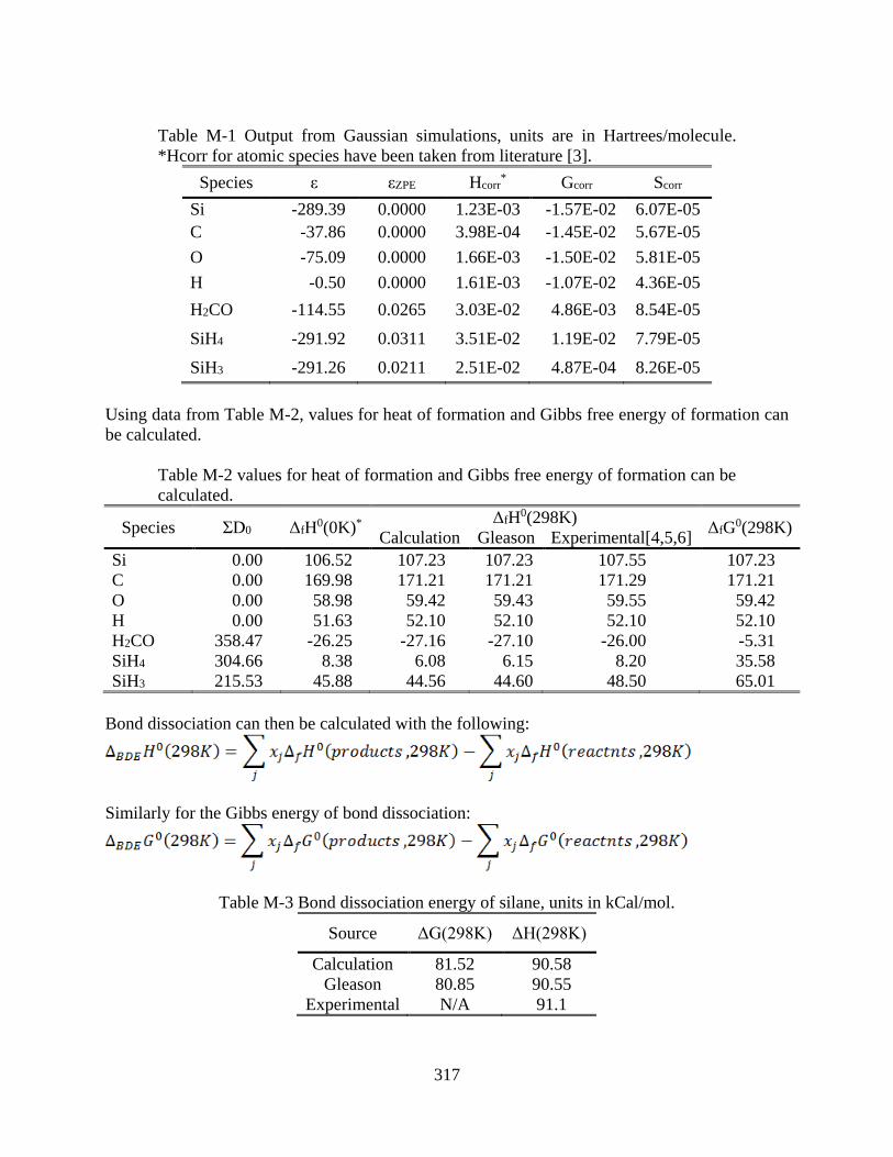
317
Table M-1 Output from Gaussian simulations, units are in Hartrees/molecule.
*Hcorr for atomic species have been taken from literature [3].
Species ε εZPE Hcorr* Gcorr Scorr
Si -289.39 0.0000 1.23E-03 -1.57E-02 6.07E-05
C -37.86 0.0000 3.98E-04 -1.45E-02 5.67E-05
O -75.09 0.0000 1.66E-03 -1.50E-02 5.81E-05
H -0.50 0.0000 1.61E-03 -1.07E-02 4.36E-05
H2CO -114.55 0.0265 3.03E-02 4.86E-03 8.54E-05
SiH4 -291.92 0.0311 3.51E-02 1.19E-02 7.79E-05
SiH3 -291.26 0.0211 2.51E-02 4.87E-04 8.26E-05
Using data from Table M-2, values for heat of formation and Gibbs free energy of formation can
be calculated.
Table M-2 values for heat of formation and Gibbs free energy of formation can be
calculated.
Species ƩD0 ΔfH0(0K)* ΔfH0(298K)
ΔfG0(298K) Calculation Gleason Experimental[4,5,6]
Si 0.00 106.52 107.23 107.23 107.55 107.23
C 0.00 169.98 171.21 171.21 171.29 171.21
O 0.00 58.98 59.42 59.43 59.55 59.42
H 0.00 51.63 52.10 52.10 52.10 52.10
H2CO 358.47 -26.25 -27.16 -27.10 -26.00 -5.31
SiH4 304.66 8.38 6.08 6.15 8.20 35.58
SiH3 215.53 45.88 44.56 44.60 48.50 65.01
Bond dissociation can then be calculated with the following:
Similarly for the Gibbs energy of bond dissociation:
Table M-3 Bond dissociation energy of silane, units in kCal/mol.
Source ΔG(298K) ΔH(298K)
Calculation 81.52 90.58
Gleason 80.85 90.55
Experimental N/A 91.1

318
M.3. References
[1] Ochterski, J. W. Thermochemistry in Gaussian. www. gaussian.com (accessed December 9,
2015)
[2] Casserly, T. B. and Gleason, K. K., Plasma Process. Polym. 2005, 2, 669-678
[3] Curtiss, L. A., et al., J. Chem. Phys. 106, 1063 (1997)
[4]Q. Z. Zhang, S. K. Wang, J. H. Zhou, Y. H. Gu, J. Phys. Chem.A 2002, 106, 115.
[5] G. Rauhut, P. Pulay, J. Phys. Chem. 1995, 99, 3093.
[6] M. W. Wong, Chem. Phys. Lett. 1996, 256, 391.

319
N. HSC Database
N.1. HSC Operating Procedure
1. Run HSC. The menu shown below in Fig. N-1 should appear.
Figure N-1 Main Menu of HSC Chemistry 7.
2. Click on “DATABASE for H, S and Cp Data”. The menu shown in Fig. N-2 below should
appear.

320
Figure N-2 HSC Database Main Menu.
3. Click on “Database Editor with Diagrams”. The screen shown in Fig. N-3below should
appear.
Figure N-3 Database Editor.
4. Values can be set to be reported in joules and calories using the radio buttons in the top
right hand corner. The database can be searched by entering a formula in the “Find
Formula” field highlighted in teal and clicking on “Find Formula”. The desired species
can be selected from the list on the left hand side.
5. Once a desired species has been found, thermodynamic data can be displayed using the
“Table” button in the upper right hand corner. Clicking “Table” should bring up two

321
screens, shown below in Fig. N-4 and Fig. N-5. SiO2 is being used as an example
compound.
Figure N-4 Reaction Equations.
Figure N-5 Thermodynamic Results.
6. Results format can be cycled between Normal and Delta using the radio buttons beneath
“Format of Results”. The table of values given in Fig. N-4 can be updated by pressing the
“Calculate” button in the lower right of Fig. N-4. The temperature range can be altered by
changing the temperature values in Fig. N-4.

322
O. Etching of carbon-doped silicon dioxide
Gases primarily used in etching interlayer dielectric materials include SF6 and
perfluorocarbons (PFC) such as CF4. These etchants generally have high global warming
potentials (GWP), making their increased usage undesirable (Table O-1). In this work, a
systematic study based on the assessment of various non-PFC yet halogen-based gases utilizes
Gibbs free energy minimization to identify the thermodynamically favored etch products for
etching carbon doped silica films. This technique operates under the precept that a system at
equilibrium will tend to have a minimum total Gibbs free energy.
Gibbs minimization assists in the identification and quantification of species predicted to
form at equilibrium (Figure O-1 a,b,c). Once identified, these products can be used in
conjunction with idealized surface-gas reactions (Table O-2) and volatility diagrams (Figure O-
2) to screen various chemistries. The viability of a large number of etchants was assessed using
thermodynamic analysis to calculate the partial pressure of the main etch product—SiF4—as a
function of the etchant pressure. Both CF4 and CHF3 with H2 were selected to explore the effects
of differing amounts of additive hydrogen. Based on our thermodynamic analysis, H2 is an
effective addition to fluorocarbon etchants, resulting in increased partial pressure of the etch
product (Figure O-2).
For this study, special focus is placed on the use of partially hydrogenated fluorocarbons,
e.g. CHF3, as well as additive H2, to allow for independent control of the F/H ratio and
observation of its influence on etch rate with the aim of supplanting a portion of fluorocarbon gas
usage with hydrogen while potentially enhancing or maintain the etch rate of each material.
Introduction of hydrogen is believed to target and liberate the carbon present within the silica
structure through formation of volatile organic species such as CH4. For a simple system such as
etching SiO2 with CF4, Gibbs minimization predicts production of SiF4 and CO2 (Figure O-1a).
Upon introduction of a small fraction of hydrogen by changing the etchant to CHF3, the product
distribution becomes significantly more complex (Figure O-1b). This distribution only evolves
further upon introduction of molecular hydrogen (Figure O-1c), suggesting that, among the
typical products of SiF4 and CO2, HF, CO, and CH4 have may be generated.
In an effort to identify viable plasma parameters, preliminary experiments were
performed using CF4 with 1400W source power to study the effect of substrate bias—and thus
ion energy—on the etch rate of each of the three materials. At lower bias values, most notably
those below 10W, a net deposition was observed on the medium carbon doped silica film, while
very little etch was seen on the low carbon doped film (Figure O-3). X-ray photoelectron
spectroscopy (XPS) analysis was performed to elucidate the surface composition of the medium
carbon doped film at this plasma condition. Detailed scans for Si 2p (Figure O-4a) show the
expected Si-O, Si-C, Si-Si bonding states for the blank film (red); however, no Si signal was
detected in the apparent deposited film. The C 1s spectra (Figure O-4b) of the blank film (red)
shows C-C and C-Si bonding states, likely from surface hydrocarbon contamination and
substrate composition. Post-etch (blue), the carbon spectrum broadens significantly, showing
signals indicative of C-F3, C-F2, C-F, and C-CFx bonding states, evidence of fluorocarbon
polymer deposition. Together with the survey scan (Figure O-4c), the loss of detectable Si,
emergence of F 1s peak, and broadening of the C 1s suggest that at lower bias powers a

323
fluorocarbon layer is deposited from reactive species within the plasma, a phenomenon seen
previously in etch studies performed on silica films using fluoroalkane etchants.
Etch rate studies were performed in conjunction with optical emission spectroscopy
(OES) on the three (low, medium, high carbon content) blanket thick films supplied by Intel
using CF4 and CHF3 with 25%, and 50% additive H2. The absolute intensity of the atomic
fluorine emission peaks at 685.6 and 703.7nm (Figure O-5) were recorded at each of the plasma
conditions. A noticeable increase in emission intensity at both wavelengths of atomic fluorine is
observed for the CF4 chemistry with 25% H2 before decreasing steadily to a minimum intensity
at 50% H2 (Figure O-6a). Identical behavior can be seen in the etch rate across all three blank
thick films (Figure O-6b), suggesting a correlation between the presence of fluorine radical and
etch rate within the system.
Although not identical, the observed negative effect of hydrogen addition on the emission
intensity of atomic fluorine for CHF3 discharge also can be seen in the decreasing etch rate of all
three films (Table O-6c). This overarching decrease could indicate that an optimal feed
composition of hydrogen exists and must be examined through the use of smaller increments of
additive H2. OES studies of CHF3 repeated under identical plasma conditions but with smaller
increments of %H2 are summarized in Figure O-7. A noticeable maximum in the intensity is seen
at 10% H2, warranting further investigation to determine if an optimized amount of hydrogen
could further correlate to an increase in etch rate. Through the utilization of an 85 nm Ti hard
mask, CF4, CF4 with 25% H2, CHF3, and CHF3 with 25% H2 were all successful in patterning the
three levels of carbon doped silica while maintaining good profile features (Table O-3).
Despite developing a guideline for analyzing the reactions occurring between the gas and
silica surfaces and screening various plasma chemistries, a key component is missing in terms of
understanding the formation and deposition of polymeric species. A large part of future work
will be devoted to developing a model for and experimentally probing the reactions occurring
only within the gas phase itself. Use of the Gibbs minimization technique has so far been focused
on equilibrium between the surface and gas phases. However, it is believed that thermodynamic
analysis can be extended to model the gas phase, providing insight into which polymerizing
species may be present. This information would a more complete understanding of the
competing etch and deposition mechanisms.

324
Table O-1 Global warming potentials of various chemistries in semiconductor
processes. The two etchants investigated in this work, CF4 and CHF3 and their
respective environmental and emissions data are bolded.
Chemistrie
s
Atmospheric
conc. in 2015
(ppt)
Atmospheric
conc. in 2005
(ppt)
Con. since
1994 &
1998
(ppt)
Annual
emission
in late
1990s
(Gg)
Radiative
efficiency
(W/m2/ppb)
Lifetim
e
(year)
Global
Warming
Potential
CO2 403×106 379×106 358×106* - - variable 1
CH4 7×10⁵ 7×10⁵ 2×10⁵* - - 12.2 21
N2O 326×105 275×103 311×103* - - 120 310
CHClF2 - - 105×103* - - 12.1 1400
CF4 76 74 - ~15 0.1 50,000 6500
CCl2F2 - - 503×103* - - 102 7100
C2F6 - 2.9 3.4 ~2 0.26 10,000 9200
CHF3 21 18 22 ~7 0.19 270 11700
SF6 - 5.6 7.1 ~6 0.52 3,200 23900
NH3 - - - 0.054 - 2 hrs 0
NF3 <0.1 - - ~2.3 0.21 740 16800
C2F4 - - - - - 1.9 days <1
C6F6 - - - - -
<1
CF3I - - - - - 2 days 1

325
0 500 1000 1500 20000.0
0.5
1.0
1.5
2.0(a) SiO2 + CF
4
Co
mp
osi
tio
n (
km
ol)
Temperature (K)
SiF4(g)
CO2(g)
0 500 1000 1500 20000.0
0.5
1.0
1.5
2.0(b) SiO2 + CF
4
SiO2 + CHF
3
HF(g)
Co
mp
osi
tio
n (
km
ol)
Temperature (K)
SiF2(g)CH
4(g) SiO
2(s)
CO2(g)
CO(g)H
2(g)
H2O(g)
SiF4(g)
0 500 1000 1500 20000.0
0.5
1.0
1.5
2.0(c) SiO2 + CF
4
SiO2 + CHF
3
SiO2 + CHF
3 + H2
SiF2(g)C
om
posi
tion (
km
ol)
Temperature (K)
SiF4(g)
CO(g)
H2O(g)
CH4(g) SiO
2(s)
CO2(g)
H2(g)
HF(g)
Figure O-1 Temperature-dependent product distribution of (a) SiO2 + CF4 (b)
SiO2 + CHF3, and (c) SiO2 + CHF3 + H2 as calculated through use of
minimization of Gibbs free energy. Feed composition consists of 1 kmol of SiO2,
CF4, CHF3, and H2 at 7.6 mTorr (10-5 atm).

326
Table O-2 Proposed surface-gas reactions for etching of silica species in CF4 with H2.
Reaction G (eV)
1 SiO2(c) + 2CF4(g) → SiF4(g) + 2COF2(g) -1.92
2 2SiO1.5CH3(c) + 2CF4(g) → 2SiF4(g) + COH2(g) + CH4(g) + 2CO(g) -5.24
3 2SiOCH2(c) + 2CF4(g) → 2SiF4(g) + C2H4(g) + 2CO(g) -5.87
4 SiO(CH2)2(c) + CF4(g) → SiF4(g) + CO(g) + C2H4(g) -2.67
5 SiOCH2(c) + CF4(g) + H2(g) → SiF4(g) + CO(g) + CH4(g) -3.82
6 SiO(CH2)2(c) + CF4(g) + 2H2(g) → SiF4(g) + CO(g) + 2CH4(g) -4.43
7 2SiO1.5C2H(c) + 2CF4(g) + 5H2(g) → 2SiF4(g) + 3CO(g) + 3CH4(g) -8.33
-40 -35 -30 -25 -20 -15 -10 -5 0 5 10-100
-50
0
50
100
150
200 CF
4
CF4 w/ H
2
Operating pressure
Log P
SiF
4
(atm
)
Log PCF
4
(atm)
1
2 4
5
3
76
Figure O-2 Volatility diagram based upon reactions proposed in Table 2. Utilizing
the Gibbs free energy of reaction allows for formulation of a functional
relationship between the partial pressure of the etch product (SiF4) and the etchant
(CF4).

327
0 20 40 60 80
-200
-100
0
100
200
300
400
500
Deposition
(Polymerization)
Etching
Low C%-SiO2
Bias Power (W)
Etc
h R
ate(
nm
/min
)
High C%-SiO2
Med C%-SiO2
Figure O-3 A study of the effects of substrate bias power on the etch rates for all
three (low, medium, and high) levels of carbon doped silica blank thick films.
Deposition (negative etch rate values) occurs on the medium C%-SiO2 at reduced
bias powers suggesting that ion enhanced etch plays a significant role in a net etch
of this material. XPS analysis was performed on the 1400W/10W condition and is
shown below in blue.
105 102 99 297 294 291 288 285 282 279
Binding Energy (eV)
(a) Si 2p
MCSiO2_Blank
Si-O Si-C
MCSiO2_CF
4
C-F3
C-F2
C-F C-CFx
C-C C-Si(b) C 1s
Si-Si
1000 800 600 400 200 0
OKLL
Si2pSi2sO1sF1s C1s(c) Survey
Binding Energy (eV) Figure O-4 XPS surface analysis of medium carbon doped silica blank thick film
(red) and etched by pure CF4 at 1400W with 10W bias (blue) showing (a) detailed
Si 2p, (b) C 1s, and (c) Survey scans.

328
200 250 300 350 400 450 500 550 600 650 700 750 800 850 900
0
500
1000
1500
2000
2500
3000
3500
4000
Inte
nsi
ty (
cou
nts
)
(nm)
CN
C
H
F
H
F
Figure O-5 Optical emission spectrum of CHF3 plasma with 600W source power,
40W bias power, and operating pressure of 6 mTorr. Primary and secondary
atomic fluorine emission peaks (highlighted in red) measured at 685.6 and 703.7
nm.
0 10 20 30 40 50600
800
1000
1200
1400
CHF3
CF4
F(703.7nm)
F(703.7nm)
F(685.6nm)
Inte
nsi
ty (
counts
)
% H2 [H
2/(etchant+H
2)]
F(685.6nm)(a)
0 10 20 30 40 500
50
100
150
200
250
300(b)CF
4
H2/(CF
4+H
2) (%)
Etc
h R
ate(
nm
/min
)
Med C%-SiO2
Low C%-SiO2
High C%-SiO2
0 10 20 30 40 500
50
100
150
200
250
300(c)CHF
3
H2/(etchant+H
2) (%)
Etc
h R
ate(
nm
/min
)
High C%-SiO2
Low C%-SiO2
Med C%-SiO2
Figure O-6 (a) Atomic fluorine emission intensities at 685.6 and 703.7nm wavelengths as
a function of %H2 in feed gas for CF4 (red) and CHF3 (blue) at 600W source power and
40W bias power. (b) Etch rate as a function of %H2 in CF4. (c) Etch rate as a function of
%H2 in CHF3.

329
0 10 20 30 40 50
0
200
400
600
Inte
nsi
ty (
a.u
.)
% H2 [H
2/(CHF
3+H
2)]
F(685.6nm)
F(703.7nm)
Figure O-7 Atomic fluorine intensities at 685.6 and 703.7nm wavelengths as a
function of %H2 in CHF3 discharge at 600W source power and 40W bias power.
Table O-3 SEM images of etched carbon doped silica films in CF4 and CHF3 with
25% H2 under 600W source power and 40W bias power.
High C% doped SiO2 Low C% doped SiO2 Med. C% doped SiO2
CF4
CHF3
CF4
/
25% H2
CHF3
/
25% H2
330
BIBLIOGRAPHY
Allender, D., J. Bray and J. Bardeen (1973). "Model for an Exciton Mechanism of
Superconductivity." Physical Review B 7(3): 1020-1029.
Amorim, J., H. S. Maciel and J. P. Sudano (1991). "High-Density Plasma Mode Of An
Inductively Coupled Radio-Frequency Discharge." Journal Of Vacuum Science & Technology B
9(2): 362-365.
Andriesse, M. S., T. Zijlstra and E. van der Drift (2000). "High speed anisotropic dry etching of
CoNbZr for next generation magnetic recording." Journal of Vacuum Science & Technology B
18(6): 3462-3466.
Andriesse, M. S. P., E. van der Drift and W. G. Sloof (2001). "High speed, dry etching of Fe for
integration of magnetic devices in microelectronics." Journal of Vacuum Science & Technology
B 19(6): 2901-2905.
Antonov, V. E. (2002). "Phase transformations, crystal and magnetic structures of high-pressure
hydrides of d-metals." Journal of Alloys and Compounds 330–332(0): 110-116.
Apatiga, L. M. and V. M. Castano (2006). "Magnetic behavior of cobalt oxide films prepared by
pulsed liquid injection chemical vapor deposition from a metal-organic precursor." Thin Solid
Films 496(2): 576-579.
Argyle, M. D. and C. H. Bartholomew (2015). "Heterogeneous Catalyst Deactivation and
Regeneration: A Review." Catalysts 5(1): 145-269.
Aspnes, D. E. (1982). "Optical-Properties of Thin-Films." Thin Solid Films 89(3): 249-262.
Aston, F. W. (1920). "Isotopes and atomic weights." Nature 105: 617-619.
Auciello, O. and D. L. Flamm (1989). Plasma Diagnostics: Discharge parameters and chemistry,
Academic Press.
Axford, S. D. T., J. M. Goodings and A. N. Hayhurst (1998). "Mass-spectrometric sampling of
ions from flames at atmospheric pressure: The effects of applied electric fields and the variation
of electric potential in a flame." Combustion and Flame 114(3-4): 294-302.
Aygen, S. and R. Vaneldik (1989). "A Spectroscopic and Mechanistic Study of the Enolization
and Diol Formation of Hexafluoroacetylacetone in the Presence of Water and Alcohol."
Chemische Berichte 122(2): 315-320.
Baibich, M. N., J. M. Broto, A. Fert, F. N. Vandau, F. Petroff, P. Eitenne, G. Creuzet, A.
Friederich and J. Chazelas (1988). "Giant Magnetoresistance of (001)Fe/(001) Cr Magnetic
Superlattices." Physical Review Letters 61(21): 2472-2475.

331
Bardeen, J., L. N. Cooper and J. R. Schrieffer (1957). "Theory of Superconductivity." Physical
Review 108(5): 1175-1204.
Barreca, D., C. Massignan, S. Daolio, M. Fabrizio, C. Piccirillo, L. Armelao and E. Tondello
(2001). "Composition and microstructure of cobalt oxide thin films obtained from a novel
cobalt(II) precursor by chemical vapor deposition." Chemistry of Materials 13(2): 588-593.
Beck, W. (1965). "Infrared Spectra of Inorganic and Coordination Compounds." Kolloid-
Zeitschrift and Zeitschrift Fur Polymere 202(2): 171-&.
Behrisch, R. and W. Eckstein (2007). Sputtering by particle bombardment : experiments and
computer calculations from threshold to MeV energies. Berlin ; New York, Springer.
Bennett, M. A., G. A. Heath, D. C. R. Hockless, I. Kovacik and A. C. Willis (1998). "Alkene
complexes of divalent and trivalent ruthenium stabilized by chelation. Dependence of
coordinated alkene orientation on metal oxidation state." Journal of the American Chemical
Society 120(5): 932-941.
Booth, J. P., O. Joubert, J. Pelletier and N. Sadeghi (1991). "Oxygen atom actinometry
reinvestigated: Comparison with absolute measurements by resonance absorption at 130 nm."
Journal of Applied Physics 69(2): 618-626.
Booth, J. P. and N. Sadeghi (1991). "Oxygen and fluorine atom kinetics in electron cyclotron
resonance plasmas by time-resolved actinometry." Journal of Applied Physics 70(2): 611-620.
Braunstein, P. (2004). "Functional ligands and complexes for new structures, homogeneous
catalysts and nanomaterials." Journal of Organometallic Chemistry 689(24): 3953-3967.
Butler, W. H., X. G. Zhang, T. C. Schulthess and J. M. MacLaren (2001). "Spin-dependent
tunneling conductance of Fe vertical bar MgO vertical bar Fe sandwiches." Physical Review B
63(5).
Cabrera, N. and N. F. Mott (1948). "Theory of the Oxidation of Metals." Reports on Progress in
Physics 12: 163-184.
Caminati, W. and J. U. Grabow (2006). "The C-2v structure of enolic acetylacetone." Journal of
the American Chemical Society 128(3): 854-857.
Carcia, P. F., A. D. Meinhaldt and A. Suna (1985). "Perpendicular Magnetic-Anisotropy in
Pd/Co Thin-Film Layered Structures." Applied Physics Letters 47(2): 178-180.
Chae, H., S. A. Vitale and H. H. Sawin (2003). "Silicon dioxide etching yield measurements with
inductively coupled fluorocarbon plasmas." Journal of Vacuum Science & Technology A:
Vacuum, Surfaces, and Films 21(2): 381-387.
Chase, M. W. (1998). NIST-JANAF Thermochemical Tables. Woodbury, New York, American
Chemical Society
American Institute of Physics.

332
Chen, F. F. (2015). Introduction to Plasma Physics and Controlled Fusion, Springer International
Publishing.
Cherrington, B. E. (1982). "The use of electrostatic probes for plasma diagnostics—A review."
Plasma Chemistry and Plasma Processing 2(2): 113-140.
Cho, H., K. P. Lee, K. B. Jung, S. J. Pearton, J. Marburger, F. Sharifi, Y. B. Hahn and J. R.
Childress (2000). "Corrosion-free dry etch patterning of magnetic random access memory stacks:
Effects of ultraviolet illumination." Journal of Applied Physics 87(9): 6397-6399.
Cho, H. J., J. D. Choe, L. Ming, K. Jin Young, C. Sung Hoon, C. W. Oh, Y. Eun-Jung, K. Dong-
Won, P. Donggun and K. Kim (2004). Fin width scaling criteria of body-tied FinFET in sub-50
nm regime. Device Research Conference, 2004. 62nd DRC.
Coburn, J. W. and M. Chen (1980). "Optical emission spectroscopy of reactive plasmas: A
method for correlating emission intensities to reactive particle density." Journal of Applied
Physics 51(6): 3134-3136.
Coburn, J. W. and H. F. Winters (1979). "Ion-Assisted and Electron-Assisted Gas-Surface
Chemistry - Important Effect in Plasma-Etching." Journal of Applied Physics 50(5): 3189-3196.
Coburn, J. W. and H. F. Winters (1979). "Ion‐ and electron‐assisted gas‐surface chemistry—An
important effect in plasma etching." J. Appl. Phys. 50: 3189-3196.
Coburn, J. W. and H. F. Winters (1979). "Plasma etching—A discussion of mechanisms." J. Vac.
Sci. Technol. 16: 391-403.
Colinge, J. P., M. H. Gao, A. Romano-Rodriguez, H. Maes and C. Claeys (1990). Silicon-on-
insulator 'gate-all-around device'. Electron Devices Meeting, 1990. IEDM '90.
Cruden, B. A., M. V. V. S. Rao, S. P. Sharma and M. Meyyappan (2002). "Neutral gas
temperature estimate in CF4/O2/Ar inductively coupled plasmas." Applied Physics Letters 81(6):
990-992.
Cui, J. P., Y. Z. He, S. Wang, J. Wang and B. C. Fan (2000). "Temperature measurement of
reflected shock wave by using chemical indicator." Acta Mechanica Sinica 16(1): 63-69.
Cullity, B. D. (1972). Introduction to magnetic materials. Reading, Mass.,, Addison-Wesley Pub.
Co.
Czech, Z. and M. Wojciechowicz (2006). "The crosslinking reaction of acrylic PSA using
chelate metal acetylacetonates." European Polymer Journal 42(9): 2153-2160.
DeHoff, R. T. (1993). Thermodynamics in Materials Science. New York, McGraw-Hill.
Denbroeder, F. J. A., H. C. Donkersloot, H. J. G. Draaisma and W. J. M. Dejonge (1987).
"Magnetic-Properties and Structure of Pd/Co and Pd/Fe Multilayers." Journal of Applied Physics
61(8): 4317-4319.

333
Dennard, R. H., Gaenssle.Fh, H. N. Yu, V. L. Rideout, E. Bassous and A. R. Leblanc (1974).
"Design of Ion-Implanted Mosfets with Very Small Physical Dimensions." Ieee Journal of Solid-
State Circuits Sc 9(5): 256-268.
Djayaprawira, D. D., K. Tsunekawa, M. Nagai, H. Maehara, S. Yamagata, N. Watanabe, S.
Yuasa, Y. Suzuki and K. Ando (2005). "230% room-temperature magnetoresistance in
CoFeB/MgO/CoFeB magnetic tunnel junctions." Applied Physics Letters 86(9).
Donnelly, V. M. (1996). "A simple optical emission method for measuring percent dissociations
of feed gases in plasmas: Application to Cl2 in a high‐density helical resonator plasma." J. Vac.
Sci. Technol. A 14: 1076-1087.
Donnelly, V. M. and M. V. Malyshev (2000). "Diagnostics of inductively coupled chlorine
plasmas: Measurements of the neutral gas temperature." Applied Physics Letters 77(16): 2467.
Donnelly, V. M. and M. J. Schabel (2002). "Spatially resolved electron temperatures, species
concentrations, and electron energy distributions in inductively coupled chlorine plasmas,
measured by trace-rare gases optical emission spectroscopy." Journal of Applied Physics 91(10):
6288.
Douglas, B. E., J. G. Brushmiller and R. A. Haines (1963). "Circular Dichroism of Coordination
Compounds .1. Splitting Patterns for Potassium Ethylenediaminetetraacetatocobaltate(Iii) and
Model Compounds." Inorganic Chemistry 2(6): 1194-&.
Doyle, B. S., S. Datta, M. Doczy, S. Hareland, B. Jin, J. Kavalieros, T. Linton, A. Murthy, R.
Rios and R. Chau (2003). "High performance fully-depleted tri-gate CMOS transistors." Electron
Device Letters, IEEE 24(4): 263-265.
Drews, T., J. Supel, A. Hagenbach and K. Seppelt (2006). "Solid state molecular structures of
transition metal hexafluorides." Inorganic Chemistry 45(9): 3782-3788.
Ellingham, H. (1944). "Transactions and Communications." Journal of the Society of Chemical
Industry 63(5): 125-160.
Evans, U. R. (1960). The corrosion and oxidation of metals; scientific principles and practical
applications. London, E. Arnold.
Fahlman, B. D. and A. R. Barron (2000). "Substituent effects on the volatility of metal beta-
diketonates." Advanced Materials for Optics and Electronics 10(3-5): 223-232.
Farkas, J., K. M. Chi, M. J. Hampden-Smith, T. T. Kodas and L. H. Dubois (1993). "Etching of
copper and copper oxide at high rates via generation of volatile copper species." Materials
Science and Engineering: B 17(1): 93-96.
Ferain, I., C. A. Colinge and J. P. Colinge (2011). "Multigate transistors as the future of classical
metal-oxide-semiconductor field-effect transistors." Nature 479(7373): 310-316.
334
Freindorf, M., C. M. Marian and B. A. Hess (1993). "Theoretical study of the electronic
spectrum of the CoH molecule." J. Chem. Phys. 99: 1215-1223.
Fu-Liang, Y., C. Hao-Yu, C. Fang-Cheng, H. Cheng-Chuan, C. Chang-Yun, C. Hsien-Kuang, L.
Chi-Chuang, C. Chi-Chun, H. Huan-Tsung, C. Chih-Jian, T. Hun-Jan, Y. Yee-Chia, L. Mong-
Song and H. Chenming (2002). 25 nm CMOS Omega FETs. Electron Devices Meeting, 2002.
IEDM '02.
Fujiwara, H. (2007). Spectroscopic ellipsometry: principles and applications. Chichester,
England; Hoboken, NJ, John Wiley & Sons.
Gajek, M., J. J. Nowak, J. Z. Sun, P. L. Trouilloud, E. J. O'Sullivan, D. W. Abraham, M. C.
Gaidis, G. Hu, S. Brown, Y. Zhu, R. P. Robertazzi, W. J. Gallagher and D. C. Worledge (2012).
"Spin torque switching of 20 nm magnetic tunnel junctions with perpendicular anisotropy."
Appl. Phys. Lett. 100(13): 132408.
Gajek, M., J. J. Nowak, J. Z. Sun, P. L. Trouilloud, E. J. O'Sullivan, D. W. Abraham, M. C.
Gaidis, G. Hu, S. Brown, Y. Zhu, R. P. Robertazzi, W. J. Gallagher and D. C. Worledge (2012).
"Spin torque switching of 20 nm magnetic tunnel junctions with perpendicular anisotropy."
Applied Physics Letters 100(13).
George, M. A., D. W. Hess, S. E. Beck, J. C. Ivankovits, D. A. Bohling and A. P. Lane (1995).
"Reaction of 1,1,1,5,5,5-Hexafluoro-2,4-Pentanedione (H(+)Hfac) with Cuo, Cu2o, and Cu
Films." Journal of the Electrochemical Society 142(3): 961-965.
George, M. A., D. W. Hess, S. E. Beck, J. C. Ivankovits, D. A. Bohling and A. P. Lane (1995).
"Reaction of 1,1,1,5,5,5-Hexafluoro-2,4-Pentanedione (H(+)Hfac) with Cuo, Cu2o, and Cu
Films (Vol 142, Pg 961, 1995)." Journal of the Electrochemical Society 142(5): 1732-1732.
George, M. A., D. W. Hess, S. E. Beck, K. Young, D. A. Bohling, G. Voloshin and A. P. Lane
(1996). "Reaction of 1,1,1,5,5,5-hexafluoro-2,4-pentanedione (H(+)hfac) with iron and iron
oxide thin films." Journal of the Electrochemical Society 143(10): 3257-3266.
Gloersen, P. G. (1976). "Masking for Ion-Beam Etching." Solid State Technology 19(4): 68-73.
Goodings, J. M., J. Z. Guo, A. N. Hayhurst and S. G. Taylor (2001). "Current-voltage
characteristics in a flame plasma: analysis for positive and negative ions, with applications."
International Journal of Mass Spectrometry 206(1-2): 137-151.
Gorbenko, O. Y., A. R. Kaul, A. A. Molodyk, V. N. Fuflyigin, M. A. Novozhilov, A. A. Bosak,
U. Krause and G. Wahl (1997). "MOCVD of perovskites with metallic conductivity." Journal of
Alloys and Compounds 251(1-2): 337-341.
Greenwood, N. N. and A. Earnshaw (1984). Chemistry of the elements. Oxford, Oxfordshire;
New York, Pergamon Press.
Greenwood, N. N. and A. Earnshaw (1998). Chemistry of the elements, 2nd ed. Oxford; Boston,
Butterworth-Heinemann.

335
Gshneider, K. A. (1964). In Solid State Physics. New York, Academic Press.
Gulbranse, E. A. and S. A. Jansson (1972). "High-Temperature Oxidation, Reduction, and
Volatilization Reactions of Silicon and Silicon-Carbide." Oxidation of Metals 4(3): 181-&.
Gulbransen, E. A. (1970). "Thermochemistry and Oxidation of Refractory Metals at High
Temperature." Corrosion 26(1): 19-&.
Habeeb, J. J., D. G. Tuck and F. H. Walters (1978). "Direct Electrochemical Synthesis of Some
Metal Chelate Complexes." Journal of Coordination Chemistry 8(1): 27-33.
Hagström, S., C. Nordling and K. Siegbahn (1964). "Electron spectroscopy for chemical
analyses." Physics Letters 9(3): 235.
Haines, R. A. and B. E. Douglas (1965). "Circular Dichroism of Coordination Compounds .V.
Pentadentate Ethylenediaminetetraacetic Acid Complexes of Cobalt(3)." Inorganic Chemistry
4(4): 452-&.
Hamid, M., M. Zeller, A. D. Hunter, M. Mazhar and A. A. Tahir (2005). "Redetermination of
bis(2,4-pentanedionato)-palladium(II)." Acta Crystallographica Section E-Structure Reports
Online 61: M2181-M2183.
Hampdensmith, M. J. and T. T. Kodas (1995). "Chemical-Vapor-Deposition of Copper from
(Hfac)Cul Compounds." Polyhedron 14(6): 699-732.
Harper, J. M. E., J. J. Cuomo and H. R. Kaufman (1982). "Technology and Applications of
Broad-Beam Ion Sources Used in Sputtering .2. Applications." Journal of Vacuum Science &
Technology 21(3): 737-756.
Hauffe, K. (1965). Oxidation of metals. New York,, Plenum Press.
Henne, A. L., M. S. Newman, L. L. Quill and R. A. Staniforth (1947). "The Alkaline
Condensation of Fluorinated Esters with Esters and Ketones." Journal of the American Chemical
Society 69(7): 1819-1820.
Hidaka, J. and B. E. Douglas (1964). "Circular Dichroism of Coordination Compounds .2. Some
Metal Complexes of 2,2]-Dipyridyl + 1,10-Phenanthroline." Inorganic Chemistry 3(8): 1180-&.
Hidaka, J. and B. E. Douglas (1964). "Circular Dichroism of Coordination Compounds .4. Some
Metal Complexes with Dithiooxalic Acid." Inorganic Chemistry 3(12): 1724-&.
Ho, C. S., C. W. Lam, M. H. Chan, R. C. Cheung, L. K. Law, L. C. Lit, K. F. Ng, M. W. Suen
and H. L. Tai (2003). "Electrospray ionisation mass spectrometry: principles and clinical
applications." Clin Biochem Rev 24(1): 3-12.
Hopwood, J. (1992). "Review of inductively coupled plasmas for plasma processing." Plasma
Sources Science and Technology 1(2): 109.

336
Hsiao, R. (1999). "Fabrication of magnetic recording heads and dry etching of head materials."
IBM Journal of Research and Development 43(1-2): 89-102.
Huang, X., W. Lee, C. Kuo, D. Hisamoto, L. Chang, J. Kedzierski, E. Anderson, H. Takeuchi, Y.
Choi, K. Asano, V. Subramanian, T. J. King, J. Bokor and C. Hu (1999). "Sub 50-nm FinFET:
PMOS " IEEE Electron Device Letters 99: 67.
Ikeda, S., J. Hayakawa, Y. Ashizawa, Y. M. Lee, K. Miura, H. Hasegawa, M. Tsunoda, F.
Matsukura and H. Ohno (2008). "Tunnel magnetoresistance of 604% at 300 K by suppression of
Ta diffusion in CoFeB/MgO/CoFeB pseudo-spin-valves annealed at high temperature." Applied
Physics Letters 93(8).
Ikeda, S., J. Hayakawa, Y. M. Lee, F. Matsukura, Y. Ohno, T. Hanyu and H. Ohno (2007).
"Magnetic tunnel junctions for spintronic memories and beyond." IEEE Transactions on Electron
Devices 54(5): 991-1002.
Ikeda, S., K. Miura, H. Yamamoto, K. Mizunuma, H. D. Gan, M. Endo, S. Kanai, J. Hayakawa,
F. Matsukura and H. Ohno (2010). "A perpendicular-anisotropy CoFeB-MgO magnetic tunnel
junction." Nature Materials 9(9).
Isakova, V. G., I. A. Baidina, N. B. Morozova and I. K. Igumenov (2000). "gamma-Halogenated
iridium(III) acetylacetonates." Polyhedron 19(9): 1097-1103.
ITRS(2011) "Emerging Research Devices (ERD)." International Technology Roadmap for
Semiconductors.
Jablonski, A. and C. J. Powell (2002). "The electron attenuation length revisited." Surface
Science Reports 47(2-3): 35-91.
Jain, A., T. T. Kodas and M. J. HampdenSmith (1995). "Thermal dry-etching of copper using
hydrogen peroxide and hexafluoroacetylacetone." Thin Solid Films 269(1-2): 51-56.
Jaklevic, R. C., A. H. Silver, J. Lambe and J. E. Mercereau (1964). "Quantum Interference
Effects in Josephson Tunneling." Physical Review Letters 12(7): 159-&.
Jensen, A. W. and B. A. O'Brien (2001). "Simple preparation and NMR analysis of mer and fac
isomers of tris(1,1,1-trifluoro-2,4-pentanedionato)cobalt(III) - An experiment for the inorganic
chemistry laboratory." Journal of Chemical Education 78(7): 954-955.
Jones, S. W. (2004). "Exponential trends in the integrated circuits industry." ICKnowledge.
Jong-Tae, P., J. Colinge and C. H. Diaz (2001). "Pi-Gate SOI MOSFET." Electron Device
Letters, IEEE 22(8): 405-406.
Jung, K. B., H. Cho, Y. B. Hahn, D. C. Hays, E. S. Lambers, Y. D. Park, T. Feng, J. R. Childress
and S. J. Pearton (1999). "Comparison of Cl-2/He, Cl-2/Ar, and Cl-2/Xe plasma chemistries for
dry etching of NiFe and NiFeCo." Journal of the Electrochemical Society 146(4): 1465-1468.

337
Jung, K. B., J. Hong, H. Cho, S. Onishi, D. Johnson, Y. D. Park, J. R. Childress and S. J. Pearton
(1999). "Parametric study of NiFe and NiFeCo high density plasma etching using CO/NH3."
Journal of the Electrochemical Society 146(6): 2163-2168.
Jung, K. B., J. Hong, H. Cho, S. Onishi, D. Johnson, Y. D. Park, J. R. Childress and S. J. Pearton
(1999). "Patterning of NiFe and NiFeCo in CO/NH3 high density plasmas." Journal of Vacuum
Science & Technology a-Vacuum Surfaces and Films 17(2): 535-539.
Jung, K. B., E. S. Lambers, J. R. Childress, S. J. Pearton, M. Jenson and A. T. Hurst (1997).
"High rate dry etching of Ni0.8Fe0.2 and NiFeCo." Applied Physics Letters 71(9): 1255-1257.
Kang, S. W., H. U. Kim and S. W. Rhee (1999). "Dry etching of copper film with
hexafluoroacetylacetone via oxidation process." Journal of Vacuum Science & Technology B
17(1): 154-157.
Kastenmeier, B. E. E., P. J. Matsuo, J. J. Beulens and G. S. Oehrlein (1996). "Chemical dry
etching of silicon nitride and silicon dioxide using CF4/O-2/N-2 gas mixtures." Journal Of
Vacuum Science & Technology A-Vacuum Surfaces And Films 14(5): 2802-2813.
Kaufman, H. R. (1978). "Technology of Ion-Beam Sources Used in Sputtering." Journal of
Vacuum Science & Technology 15(2): 272-276.
Kaufman, H. R., J. J. Cuomo and J. M. E. Harper (1982). "Technology and Applications of
Broad-Beam Ion Sources Used in Sputtering .1. Ion-Source Technology." Journal of Vacuum
Science & Technology 21(3): 725-736.
Kaufman, H. R., J. M. E. Harper and J. J. Cuomo (1979). "Focused Ion-Beam Designs for
Sputter Deposition." Journal of Vacuum Science & Technology 16(2): 179-180.
Kaufman, H. R., J. M. E. Harper and J. J. Cuomo (1979). "Focused Ion-Beam Designs for
Sputter Deposition." Journal of Vacuum Science & Technology 16(3): 899-905.
Kiihamaki, J. and S. Franssila (1999). "Pattern shape effects and artefacts in deep silicon
etching." Journal Of Vacuum Science & Technology A-Vacuum Surfaces And Films 17(4):
2280-2285.
Kinoshita, K., H. Utsumi, K. Suemitsu, H. Hada and T. Sugibayashi (2010). "Etching Magnetic
Tunnel Junction with Metal Etchers." Jpn. J. Appl. Phys. 49.
Kinoshita, K., K. Yamada and H. Matsutera (1991). "Reactive ion etching of Fe-Si-Al alloy for
thin film head." IEEE T. Magn. 27: 4888-4890.
Kittel, C. (1948). "On the Theory of Ferromagnetic Resonance Absorption." Physical Review
73(2): 155-161.
Kleiner, R., D. Koelle, F. Ludwig and J. Clarke (2004). "Superconducting quantum interference
devices: State of the art and application's." Proceedings of the Ieee 92(10): 1534-1548.
338
Kortshagen, U., N. D. Gibson and J. E. Lawler (1996). "On the E - H mode transition in RF
inductive discharges." Journal of Physics D: Applied Physics 29(5): 1224.
Kruck, T. and M. Schober (1997). "Low-temperature dry etching of copper using a new chemical
approach." Microelectronic Engineering 37-8(1-4): 121-126.
Kulkarni, N. S. and R. T. DeHoff (2002). "Application of Volatility Diagrams for Low
Temperature, Dry Etching, and Planarization of Copper." J. Electrochem. Soc. 149: G620-G632.
Kulkarni, N. S. and R. T. DeHoff (2002). "Application of volatility diagrams for low
temperature, dry etching, and planarization of copper." Journal of the Electrochemical Society
149(11): G620-G632.
Laegreid, N. and G. K. Wehner (1961). "Sputtering Yields of Metals for Ar+ and Ne+ Ions with
Energies from 50 to 600 Ev." Journal of Applied Physics 32(3): 365-&.
Lamprey, H. (1960). "Properties and Applications of Metal Acetylacetonates." Annals of the
New York Academy of Sciences 88(2): 519-525.
Layadi, N., V. M. Donnelly and J. T. C. Lee (1997). "Cl-2 plasma etching of Si(100): Nature of
the chlorinated surface layer studied by angle-resolved x-ray photoelectron spectroscopy."
Journal of Applied Physics 81(10): 6738-6748.
Lee, H., Y.-H. A. Wang, C. K. A. Mewes, W. H. Butler, T. Mewes, S. Maat, B. York, M. J.
Carey and J. R. Childress (2009). "Magnetization relaxation and structure of CoFeGe alloys."
Applied Physics Letters 95(8): -.
Lee, J. M., K. M. Chang, I. H. Lee and S. J. Park (2000). "Cl2 ‐ Based Dry Etching of GaN and
InGaN Using Inductively Coupled Plasma The Effects of Gas Additives." J. Electrochem. Soc.
147: 1859-1863.
Lee, R. E. (1979). "Microfabrication by Ion-Beam Etching." Journal of Vacuum Science &
Technology 16(2): 164-170.
Lee, W. T., L. Ford, P. Blowers, H. L. Nigg and R. I. Masel (1998). "Why do heats of adsorption
of simple gases on platinum surfaces vary so little with surface structure?" Surface Science
416(1-2): 141-151.
Leskela, M. and M. Ritala (2002). "Atomic layer deposition (ALD): from precursors to thin film
structures." Thin Solid Films 409(1): 138-146.
Lide, D. R. (1995). CRC Handbook of Chemistry and Physics. New York, CRC Press.
Lin, W.-C., C.-J. Tsai, B.-Y. Wang, C.-H. Kao and W.-F. Pong (2013). "Hydrogenation induced
reversible modulation of perpendicular magnetic coercivity in Pd/Co/Pd films." Applied Physics
Letters 102(25): -.

339
Litvak, H. E. (1996). End point control via optical emission spectroscopy. The 3rd International
Workshop on Advanced Plasma Tools for Etching, Chemical Vapor Deposition, and Plasma
Vapor Deposition: Sources, Process Control, and Diagnostics, San Jose, California (USA), AVS.
Liu, C. T. and B. E. Douglas (1964). "Circular Dichroism of Coordination Compounds .3.
Cobalt(3) Complexes of Optically Active Amino Acids." Inorganic Chemistry 3(10): 1356-&.
Liu, X., W. Zhang, M. J. Carter and G. Xiao (2011). "Ferromagnetic resonance and damping
properties of CoFeB thin films as free layers in MgO-based magnetic tunnel junctions." Journal
of Applied Physics 110(3): -.
Lou, V. L. K., T. E. Mitchell and A. H. Heuer (1985). "Graphical Displays of the
Thermodynamics of High-Temperature Gas-Solid Reactions and Their Application to Oxidation
of Metals and Evaporation of Oxides." Journal of the American Ceramic Society 68(2): 49-58.
Lou, V. L. K., T. E. Mitchell and A. H. Heuer (1985). "REVIEW—Graphical Displays of the
Thermodynamics of High-Temperature Gas-Solid Reactions and Their Application to Oxidation
of Metals and Evaporation of Oxides." J. Am. Ceram. Soc. 68: 49-58.
Luo, Y.-R. (2003). Handbook of bond dissociation energies in organic compounds. Boca Raton,
Fla., CRC Press.
Malyshev, M. V. and V. M. Donnelly (2000). "Diagnostics of chlorine inductively coupled
plasmas. Measurement of electron temperatures and electron energy distribution functions."
Journal of Applied Physics 87(4): 1642.
Malyshev, M. V. and V. M. Donnelly (2001). "Diagnostics of inductively coupled chlorine
plasmas: Measurement of electron and total positive ion densities." Journal of Applied Physics
90(3): 1130.
Mane, A. U., K. Shalini, A. Wohlfart, A. Devi and S. A. Shivashankar (2002). "Strongly oriented
thin films of Co3O4 deposited on single-crystal MgO(100) by low-pressure, low-temperature
MOCVD." Journal of Crystal Growth 240(1-2): 157-163.
Maruyama, T. and T. Nakai (1991). "Cobalt Oxide Thin-Films Prepared by Chemical Vapor-
Deposition from Cobalt(Ii) Acetate." Solar Energy Materials 23(1): 25-29.
Mathon, J. and A. Umerski (2001). "Theory of tunneling magnetoresistance of an epitaxial
Fe/MgO/Fe(001) junction." Physical Review B 63(22).
Mayne, K. I. (1952). "MASS SPECTROMETRY." Reports on Progress in Physics 15: 24-48.
Mcbride, J. R., G. W. Graham, C. R. Peters and W. H. Weber (1991). "Growth and
Characterization of Reactively Sputtered Thin-Film Platinum Oxides." Journal of Applied
Physics 69(3): 1596-1604.
McNevin, S. C. and G. E. Becker (1985). "Investigation of kinetic mechanism for the ion‐
assisted etching of Si in Cl2." J. Vac. Sci. Technol. B 3: 485-491.

340
Merlino, R. L. (2007). "Understanding Langmuir probe current-voltage characteristics."
American Journal of Physics 75(12): 1078-1085.
Miyazaki, T. and N. Tezuka (1995). "Giant Magnetic Tunneling Effect in Fe/Al2o3/Fe
Junction." Journal of Magnetism and Magnetic Materials 139(3): L231-L234.
Miyoshi, Y., Z. L. Petrovic and T. Makabe (2002). "Transition between capacitive and inductive
mode in inductively coupled plasma observed by emission computerized tomography." Ieee
Transactions On Plasma Science 30(1): 130-131.
Moore, G. E. (1965). "Cramming more components onto integrated circuits." Electronics 8: 114-
117.
Moore, G. E. (1998). "Cramming more components onto integrated circuits (Reprinted from
Electronics, pg 114-117, April 19, 1965)." Proceedings of the IEEE 86(1): 82-85.
Mosquera, A., D. Horwat, L. Vazquez, A. Gutierrez, A. Erko, A. Anders, J. Andersson and J. L.
Endrino (2012). "Thermal decomposition and fractal properties of sputter-deposited platinum
oxide thin films." Journal of Materials Research 27(5): 829-836.
Mott-Smth, H. M. and I. Langmuir (1926). "The theory of collectors in gaseous discharges."
Physical Review 28(4): 0727-0763.
Mott, N. F. (1940). "The theory of the formation of protective oxide films on metals, II."
Transactions of the Faraday Society 35(3): 0472-0482.
Nakatani, I. (1996). "Ultramicro fabrications on Fe-Ni alloys using electron-beam writing and
reactive-ion etching." IEEE Transactions on Magnetics 32(5): 4448-4451.
Nigg, H. L., L. P. Ford and R. I. Masel (1999). "The surface chemistry of 1,1,1-trifluoro-2,4-
pentanedione on clean and oxygen pre-covered Cu(210) - A comparison with 1,1,1,5,5,5-
hexafluoro-2,4-pentanedione and 2,4-pentanedione surface chemistry on the same surfaces."
Surface Science 419(2-3): 97-103.
Nigg, H. L. and R. I. Masel (1998). "The surface chemistry of hexafluoroacetylacetone on clean
and oxygen pre-covered Cu(210): a temperature-programmed desorption study." Surface Science
409(3): 428-434.
Nigg, H. L. and R. I. Masel (1998). "Surface reaction mechanisms of trifluoracetylacetone on
clean and pre-oxidized Ni(110): An example where etching chemistry does not follow volatility
trends." Journal of Vacuum Science & Technology a-Vacuum Surfaces and Films 16(6): 3259-
3265.
Nigg, H. L. and R. I. Masel (1999). "Surface reaction pathways of 1,1,1,5,5,5-hexafluoro-2,4-
pentanedione on clean and pre-oxidized Ni(110) surfaces." Journal of Vacuum Science &
Technology A 17(6): 3477-3480.

341
Niu, H. and R. S. Houk (1996). "Fundamental aspects of ion extraction in inductively coupled
plasma mass spectrometry." Spectrochimica Acta Part B-Atomic Spectroscopy 51(8): 779-815.
Okano, K., T. Izumida, H. Kawasaki, A. Kaneko, A. Yagishita, T. Kanemura, M. Kondo, S. Ito,
N. Aoki, K. Miyano, T. Ono, K. Yahashi, K. Iwade, T. Kubota, T. Matsushita, I. Mizushima, S.
Inaba, K. Ishimaru, K. Suguro, K. Eguchi, Y. Tsunashima and H. Ishiuchi (2005). Process
integration technology and device characteristics of CMOS FinFET on bulk silicon substrate
with sub-10 nm fin width and 20 nm gate length. Electron Devices Meeting, 2005. IEDM
Technical Digest. IEEE International.
Ono, K. and M. Tuda (1997). Profile evolution during cold plasma beam etching of silicon.
Ordal, M. A., R. J. Bell, R. W. Alexander, L. L. Long and M. R. Querry (1985). "Optical
properties of fourteen metals in the infrared and far infrared: Al, Co, Cu, Au, Fe, Pb, Mo, Ni, Pd,
Pt, Ag, Ti, V, and W." Applied Optics 24(24): 4493-4499.
Orland, A. S. and R. Blumenthal (2005). "Magnetic metal etching with organic based plasmas. I.
CO/H-2 plasmas." Journal of Vacuum Science & Technology B 23(4): 1589-1596.
Orland, A. S. and R. Blumenthal (2005). "Metal etching with organic based plasmas. II. CO/NH3
plasmas." Journal of Vacuum Science & Technology B 23(4): 1597-1602.
Osaka, T., T. Yokoshima, D. Shiga, K. Imai and K. Takashima (2003). "A High Moment CoFe
Soft Magnetic Thin Film Prepared by Electrodeposition." Electrochemical and Solid-State
Letters 6(4): C53-C55.
Palik, E. D. (1985). Handbook of optical constants of solids. Orlando, Academic Press.
Palik, E. D. (1991). Handbook of optical constants of solids II. Boston, Academic Press.
Palik, E. D. and G. Ghosh (1998). Handbook of optical constants of solids. San Diego, Academic
Press.
Parkin, S., X. Jiang, C. Kaiser, A. Panchula, K. Roche and M. Samant (2003). "Magnetically
engineered spintronic sensors and memory." Proceedings of the IEEE 91(5): 661-680.
Patterson, D., T. Anderson, N. Cardwell, R. Fromm, K. Keeton, C. Kozyrakis, R. Thomas and K.
Yelick (1997). "A case for intelligent RAM." Micro, IEEE 17(2): 34-44.
Perry, W. L., A. Jain, T. T. Kodas and M. J. Hampdensmith (1995). "Selective Chemical-Vapor-
Deposition on Excimer-Laser-Patterned Polytetrafluoroethylene from Hexafluoroacetylacetonate
Copper(I) Vinyltrimethylsilane." Thin Solid Films 262(1-2): 7-11.
Pettiford, C., A. Zeltser, S. D. Yoon, V. G. Harris, C. Vittoria and N. X. Sun (2006). "Effective
Anisotropy Fields and Ferromagnetic Resonance Behaviors of CoFe/PtMn/CoFe Trilayers."
Magnetics, IEEE Transactions on 42(10): 2993-2995.

342
Phillips, S. L. and D. L. Perry (1995). Handbook of inorganic compounds, Boca Raton : CRC
Press.
Pierson, H. O. (1999). Handbook of chemical vapor deposition. Norwich, NY, Noyes
Publications.
Sbiaa, R., H. Meng and S. N. Piramanayagam (2011). "Materials with perpendicular magnetic
anisotropy for magnetic random access memory." Physica Status Solidi-Rapid Research Letters
5(12): 413-419.
Schennach, F. (2012). Oxidation of Two Different Pt-Aluminised Bond Coats. Doctor of
Philosophy, University of Birmingham.
Senocq, F., M. Urrutigoity, Y. Caubel, J. P. Gorrichon and A. Gleizes (1999). "Preliminary
studies of Ni(dmen)(2)(CF3CO2)(2), Ni(deen)(2)(CF3CO2)(2) and
Ni(en)(CF3C(O)CHC(O)CF3)(2) as precursors for metalorganic chemical vapour deposition:
structures, thermal behaviours and vapour pressures." Inorganica Chimica Acta 288(2): 233-238.
Sha, L. and J. P. Chang (2004). "Plasma etching of high dielectric constant materials on silicon
in halogen chemistries." Journal Of Vacuum Science & Technology A 22(1): 88-95.
Shalhoub, G. M. (1980). "Co(Acac)3 - Synthesis, Reactions, and Spectra - an Experiment for
General-Chemistry." Journal of Chemical Education 57(7): 525-528.
Siegbahn, K., E. F. Barnett, Fellnerf.H and D. Hammond (1972). "Electron Spectroscopy With
Monochromatized X-Rays." Science 176(4032): 245-&.
Silver, A. H. and Zimmerma.Je (1967). "Quantum States and Transitions in Weakly Connected
Superconducting Rings." Physical Review 157(2): 317-&.
Slaughter, J. M. (2009). "Materials for Magnetoresistive Random Access Memory." Annual
Review of Materials Research 39: 277-296.
Sletten, G. and P. Knudsen (1972). "Preparation of Isotope Targets by Heavy-Ion Sputtering."
Nuclear Instruments & Methods 102(3): 459-&.
Smith, H. I., Melngail.J, Williams.Rc and W. T. Brogan (1973). "Ion-Beam Etching of Surface
Gratings." Journal of Vacuum Science & Technology 10(6): 1127-1127.
Smith, W. R. (1996). "HSC chemistry for Windows, 2.0." Journal of Chemical Information and
Computer Sciences 36(1): 151-152.
Steger, R. and R. Masel (1999). "Chemical vapor etching of copper using oxygen and
1,1,1,5,5,5-hexafluoro-2,4-pentanedione." Thin Solid Films 342(1-2): 221-229.
Steinbrüchel, C. (1985). "A simple formula for low-energy sputtering yields." Appl. Phys. A-
Mater 36: 37-42.

343
Stuart, R. V. and G. K. Wehner (1962). "Sputtering Yields at Very Low Bombarding Ion
Energies." Journal of Applied Physics 33(7): 2345-&.
Sun, J. Z. (2000). "Spin-current interaction with a monodomain magnetic body: A model study."
Physical Review B 62(1): 570-578.
Tamirisa, P. A., G. Levitin, N. S. Kulkarni and D. W. Hess (2007). "Plasma etching of copper
films at low temperature." Microelectronic Engineering 84(1): 105-108.
Tamirisa, P. A., G. Levitin, N. S. Kulkarni and D. W. Hess (2007). "Plasma etching of copper
films at low temperature." Microelectron. Eng. 84: 105-108.
Tanuma, S., C. J. Powell and D. R. Penn (1994). "Calculations of Electron Inelastic Mean Free
Paths .5. Data for 14 Organic-Compounds over the 50-2000 Ev Range." Surface and Interface
Analysis 21(3): 165-176.
Thomas, M. E., M. P. Hartnett and J. E. Mckay (1988). "The Use of Surface Profilometers for
the Measurement of Wafer Curvature." Journal of Vacuum Science & Technology a-Vacuum
Surfaces and Films 6(4): 2570-2571.
Tiitta, M. and L. Niinistou (1997). "Volatile Metal β-Diketonates: ALE and CVD precursors for
electroluminescent device thin films." Chemical Vapor Deposition 3(4): 167-182.
Tompkins, H. G. and W. A. McGahan (1999). Spectroscopic ellipsometry and reflectometry: a
user's guide. New York, Wiley.
Vandelft, F. C. M. J. M. (1995). "Structuring Magnetic Thin-Films by Means of Plasma-
Etching." Journal of Magnetism and Magnetic Materials 140: 2203-2204.
Wagner, C. (1958). "Passivity during the Oxidation of Silicon at Elevated Temperatures." J.
Appl. Phys. 29: 1295-1297.
Wagner, C. (1969). "Distribution of Cations in Metal Oxide and Metal Sulphide Solid Solutions
Formed during Oxidation of Alloys." Corrosion Science 9(2): 91-&.
Wang, D. X., C. Nordman, J. M. Daughton, Z. H. Qian and J. Fink (2004). "70% TMR at room
temperature for SDT sandwich junctions with CoFeB as free and reference layers." IEEE
Transactions on Magnetics 40(4): 2269-2271.
Wang, J., Y. Yun and E. I. Altman (2007). "The plasma oxidation of Pd(100)." Surface Science
601(16): 3497-3505.
Weast, R. C. (1988). CRC handbook of chemistry and physics. Boca Raton, FL, CRC Press.
Wolf, R. E. (2005). What is ICP-MS? … and more importantly, what can it do? . I. PerkinElmer.
PerkinElmer, Inc., USGS/CR/CICT.

344
Wu, F., G. Levitin and D. W. Hess (2010). "Low-Temperature Etching of Cu by Hydrogen-
Based Plasmas." ACS Applied Materials & Interfaces 2: 2175-2179.
Wu, F., G. Levitin and D. W. Hess (2010). "Patterning of Cu Films by a Two-Step Plasma
Etching Process at Low Temperature." J. Electrochem. Soc. 157: H474-H478.
Wu, F., G. Levitin and D. W. Hess (2011). "Mechanistic considerations of low temperature
hydrogen-based plasma etching of Cu." J. Vac. Sci. Technol. B 29: 011013.
Xue, Z. G., J. C. Daran, Y. Champouret and R. Poli (2011). "Ligand Adducts of
Bis(acetylacetonato)iron(II): A H-1 NMR Study." Inorganic Chemistry 50(22): 11543-11551.
Yakushiji, K., T. Saruya, H. Kubota, A. Fukushima, T. Nagahama, S. Yuasa and K. Ando
(2010). "Ultrathin Co/Pt and Co/Pd superlattice films for MgO-based perpendicular magnetic
tunnel junctions." Applied Physics Letters 97(23).
Yinon, J. and F. S. Klein (1971). "The quadrupole and its applications in vacuum technology and
mass spectrometry." Vacuum 21(9): 379-383.
You, J. Q. and F. Nori (2011). "Atomic physics and quantum optics using superconducting
circuits." Nature 474(7353): 589-597.
Yuasa, S., T. Nagahama, A. Fukushima, Y. Suzuki and K. Ando (2004). "Giant room-
temperature magnetoresistance in single-crystal Fe/MgO/Fe magnetic tunnel junctions." Nature
Materials 3(12): 868-871.
Zhang, B., R. J. Wang, D. Q. Zhao, M. X. Pan and W. H. Wang (2004). "Properties of Ce-based
bulk metallic glass-forming alloys." Physical Review B 70(22).
Zheng, Y., R. Zhang and L. Chen (2012). Ellipsometry and Its Applications in Stoichiometry.
Ellipsometry and Its Applications in Stoichiometry, Stoichiometry and Materials Science - When
Numbers Matter. D. A. Innocenti, InTech: 49.
Zollner, S. (2000). "Ellipsometry of Platinum Films on Silicon." Physica Status Solidi (A)
177(2): r7-r8.